Clevo M730SR Service Manual. Www.s Manuals.com. Manual
User Manual: Notebook Clevo M730SR - Service manuals and Schematics, Disassembly / Assembly. Free.
Open the PDF directly: View PDF ![]() .
.
Page Count: 95
- Manual
- Preface
- Chapter 1: Introduction
- Overview
- System Specifications
- External Locator - Top View with LCD Panel Open
- External Locator - Front & Rear Views
- External Locator - Left & Right Side Views
- External Locator - Bottom View
- Mainboard Overview - Top (Key Parts)
- Mainboard Overview - Bottom (Key Parts)
- Mainboard Overview - Top (Connectors)
- Mainboard Overview - Bottom (Connectors)
- Chapter 2: Disassembly
- Overview
- Maintenance Tools
- Connections
- Maintenance Precautions
- Removing the Battery
- Removing the Hard Disk Drive
- Removing the System Memory (RAM)
- Removing the Processor
- Removing the Wireless LAN Module
- Removing the Bluetooth Module
- Removing the Optical (CD/DVD) Device
- Removing the Keyboard
- Removing the Modem Module
- Appendix A: Part Lists
- Appendix B: Schematic Diagrams
- SYSTEM BLOCK DIAGRAM
- Meron (Socket-P) 1/2
- Meron (Socket-P) 2/2
- SiSM672 HOST PCIE 1/5
- SiSM672 DRAM 2/5
- SiSM672 MuTIOL VGA 3/5
- SiSM672 PWR 4/5
- SISM672 GND 5/5
- DDRII SO-DIMM 1
- DDRII SO- DIMM 2
- SiS307ELV
- PANEL, INVERTER, CRT
- 968 PCI IDE MuTIOL SPI 1/4
- 968 PCIE LAN GPI0 2/4
- 968 USB SATA 3/4
- 968 PWR GND 4/4
- CLK GEN & CLK BUFFER
- SATA, 3G POWER, PCI DEBUG
- MULTI I/O, ODD, CCD, BT
- NEW CARD, MINI PCIE, USB
- LED, FAN, PC BEEP, TP, FP
- ENE MR510, 7 IN 1
- PHY REALTEK 8201CL
- AUDIO CODEC ALC883
- AUDIO AMP
- KBC-ITE IT8512E
- SYSTEM POWER
- VCORE
- VDD3, VDD5
- 1.05VS, 1.2V, 1.5V
- 1.8V, 0.9VS
- AC IN, CHARGER
- CLICK BOARD
- MULTI I/O BOARD 1/2
- MULTI I/O BOARD 2/2
- FINGERPRINT BOARD
- AUDIO BOARD
- ODD BRIDGE BOARD


Preface
I
Preface
Notebook Computer
M73XSR
Service Manual

Preface
II
Preface
Notice
The company reserves the right to revise this publication or to change its contents without notice. Information contained
herein is for reference only and does not constitute a commitment on the part of the manufacturer or any subsequent ven-
dor. They assume no responsibility or liability for any errors or inaccuracies that may appear in this publication nor are
they in anyway responsible for any loss or damage resulting from the use (or misuse) of this publication.
This publication and any accompanying software may not, in whole or in part, be reproduced, translated, transmitted or
reduced to any machine readable form without prior consent from the vendor, manufacturer or creators of this publica-
tion, except for copies kept by the user for backup purposes.
Brand and product names mentioned in this publication may or may not be copyrights and/or registered trademarks of
their respective companies. They are mentioned for identification purposes only and are not intended as an endorsement
of that product or its manufacturer.
Version 1.0
June 2008
Trademarks
Intel and Intel Core are trademarks/registered trademarks of Intel Corporation.
Windows® is a registered trademark of Microsoft Corporation.
Other brand and product names are trademarks and./or registered trademarks of their respective companies.

Preface
III
Preface
About this Manual
This manual is intended for service personnel who have completed sufficient training to undertake the maintenance and
inspection of personal computers.
It is organized to allow you to look up basic information for servicing and/or upgrading components of the M73XSR
series notebook PC.
The following information is included:
Chapter 1, Introduction, provides general information about the location of system elements and their specifications.
Chapter 2, Disassembly, provides step-by-step instructions for disassembling parts and subsystems and how to upgrade
elements of the system.
Appendix A, Part Lists
Appendix B, Schematic Diagrams

Preface
IV
Preface
FCC Statement
(Federal Communications Commission)
You are cautioned that changes or modifications not expressly approved by the party responsible for compliance could
void the user's authority to operate the equipment.
This equipment has been tested and found to comply with the limits for a Class B digital device, pursuant to Part 15 of
the FCC Rules. These limits are designed to provide reasonable protection against harmful interference in a residential
installation. This equipment generates, uses and can radiate radio frequency energy and, if not installed and used in ac-
cordance with the instructions, may cause harmful interference to radio communications. However, there is no guarantee
that interference will not occur in a particular installation. If this equipment does cause harmful interference to radio or
television reception, which can be determined by turning the equipment off and on, the user is encouraged to try to correct
the interference by one or more of the following measures:
• Re orient or relocate the receiving antenna.
• Increase the separation between the equipment and receiver.
• Connect the equipment into an outlet on a circuit different from that to which the receiver is connected.
• Consult the service representative or an experienced radio/TV technician for help.
Operation is subject to the following two conditions:
1. This device may not cause interference.
And
2. This device must accept any interference, including interference that may cause undesired operation of the device.
FCC RF Radiation Exposure Statement:
1. This Transmitter must not be co-located or operating in conjunction with any other antenna or transmitter.
2. This equipment complies with FCC RF radiation exposure limits set forth for an uncontrolled environment. This equipment
should be installed and operated with a minimum distance of 20 centimeters between the radiator and you body.
Warning
Use only shielded ca-
bles to connect I/O de-
vices to this
equipment. You are
cautioned that chang-
es or modifications not
expressly approved by
the manufacturer for
compliance with the
above standards could
void your authority to
operate the equip-
ment.
If your purchase option
includes both Wire-
less LAN and 3.5G
modules, then the ap-
propriate antennas will
be installed. Note that
In order to comply with
FCC RF exposure
compliance require-
ments, the antenna
must not be co-located
or operate in conjunc-
tion with any other an-
tenna or transmitter.

Preface
V
Preface
IMPORTANT SAFETY INSTRUCTIONS
Follow basic safety precautions, including those listed below, to reduce the risk of fire, electric shock and injury to per-
sons when using any electrical equipment:
1. Do not use this product near water, for example near a bath tub, wash bowl, kitchen sink or laundry tub, in a wet
basement or near a swimming pool.
2. Avoid using a telephone (other than a cordless type) during an electrical storm. There may be a remote risk of elec-
trical shock from lightning.
3. Do not use the telephone to report a gas leak in the vicinity of the leak.
4. Use only the power cord and batteries indicated in this manual. Do not dispose of batteries in a fire. They may
explode. Check with local codes for possible special disposal instructions.
5. This product is intended to be supplied by a Listed Power Unit (DC Output 19V, 3.42A or 18.5V, 3.5A (65W) AC/DC Adapter).
CAUTION
Always disconnect all telephone lines from the wall outlet before servicing or disassembling this equipment.
TO REDUCE THE RISK OF FIRE, USE ONLY NO. 26 AWG OR LARGER,
TELECOMMUNICATION LINE CORD
This Computer’s Optical Device is a Laser Class 1 Product
Preface
VI
Preface
Instructions for Care and Operation
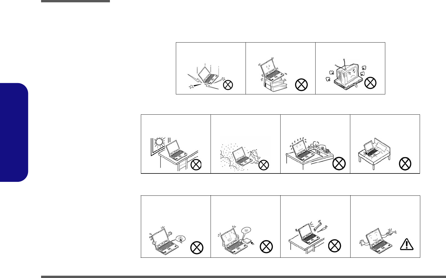
The notebook computer is quite rugged, but it can be damaged. To prevent this, follow these suggestions:
1. Don’t drop it, or expose it to shock. If the computer falls, the case and the components could be damaged.
2. Keep it dry, and don’t overheat it. Keep the computer and power supply away from any kind of heating element. This
is an electrical appliance. If water or any other liquid gets into it, the computer could be badly damaged.
3. Follow the proper working procedures for the computer. Shut the computer down properly and don’t forget to save
your work. Remember to periodically save your data as data may be lost if the battery is depleted.
Do not expose the computer
to any shock or vibration.
Do not place it on an unstable
surface.
Do not place anything heavy
on the computer.
Do not expose it to excessive
heat or direct sunlight.
Do not leave it in a place
where foreign matter or mois-
ture may affect the system.
Don’t use or store the com-
puter in a humid environment.
Do not place the computer on
any surface which will block
the vents.
Do not turn off the power
until you properly shut down
all programs.
Do not turn off any peripheral
devices when the computer is
on.
Do not disassemble the com-
puter by yourself.
Perform routine maintenance
on your computer.
Preface
VII
Preface
4. Avoid interference. Keep the computer away from high capacity transformers, electric motors, and other strong mag-
netic fields. These can hinder proper performance and damage your data.
5. Take care when using peripheral devices.
Power Safety
The computer has specific power requirements:
• Only use a power adapter approved for use with this computer.
• Your AC adapter may be designed for international travel but it still requires a steady, uninterrupted power supply. If you are
unsure of your local power specifications, consult your service representative or local power company.
• The power adapter may have either a 2-prong or a 3-prong grounded plug. The third prong is an important safety feature; do
not defeat its purpose. If you do not have access to a compatible outlet, have a qualified electrician install one.
• When you want to unplug the power cord, be sure to disconnect it by the plug head, not by its wire.
• Make sure the socket and any extension cord(s) you use can support the total current load of all the connected devices.
• Before cleaning the computer, make sure it is disconnected from any external power supplies.
Use only approved brands of
peripherals.
Unplug the power cord before
attaching peripheral devices.
Do not plug in the power
cord if you are wet.
Do not use the power cord if
it is broken.
Do not place heavy objects
on the power cord.
Power Safety
Warning
Before you undertake
any upgrade proce-
dures, make sure that
you have turned off the
power, and discon-
nected all peripherals
and cables (including
telephone lines). It is
advisable to also re-
move your battery in
order to prevent acci-
dentally turning the
machine on.

Preface
VIII
Preface
Battery Precautions
• Only use batteries designed for this computer. The wrong battery type may explode, leak or damage the computer.
• Do not continue to use a battery that has been dropped, or that appears damaged (e.g. bent or twisted) in any way. Even if the
computer continues to work with a damaged battery in place, it may cause circuit damage, which may possibly result in fire.
• Recharge the batteries using the notebook’s system. Incorrect recharging may make the battery explode.
• Do not try to repair a battery pack. Refer any battery pack repair or replacement to your service representative or qualified service
personnel.
• Keep children away from, and promptly dispose of a damaged battery. Always dispose of batteries carefully. Batteries may explode
or leak if exposed to fire, or improperly handled or discarded.
• Keep the battery away from metal appliances.
• Affix tape to the battery contacts before disposing of the battery.
• Do not touch the battery contacts with your hands or metal objects.
Related Documents
You may also need to consult the following manual for additional information:
User’s Manual on CD
This describes the notebook PC’s features and the procedures for operating the computer and its ROM-based setup pro-
gram. It also describes the installation and operation of the utility programs provided with the notebook PC.
Battery Disposal
The product that you have purchased contains a rechargeable battery. The battery is recyclable. At the end of
its useful life, under various state and local laws, it may be illegal to dispose of this battery into the municipal
waste stream. Check with your local solid waste officials for details in your area for recycling options or proper
disposal.
Caution
Danger of explosion if battery is incorrectly replaced. Replace only with the same or equivalent type recommend-
ed by the manufacturer. Discard used battery according to the manufacturer’s instructions.

Preface
IX
Preface
Contents
Introduction ..............................................1-1
Overview .........................................................................................1-1
System Specifications .....................................................................1-2
External Locator - Top View with LCD Panel Open ......................1-6
External Locator - Front & Rear Views ..........................................1-7
External Locator - Left & Right Side Views ...................................1-8
External Locator - Bottom View .....................................................1-9
Mainboard Overview - Top (Key Parts) .......................................1-10
Mainboard Overview - Bottom (Key Parts) ..................................1-11
Mainboard Overview - Top (Connectors) .....................................1-12
Mainboard Overview - Bottom (Connectors) ...............................1-13
Disassembly ...............................................2-1
Overview .........................................................................................2-1
Maintenance Tools ..........................................................................2-2
Connections .....................................................................................2-2
Maintenance Precautions .................................................................2-3
Removing the Battery ......................................................................2-5
Removing the Hard Disk Drive .......................................................2-6
Removing the System Memory (RAM) ..........................................2-8
Removing the Processor ................................................................2-10
Removing the Wireless LAN Module ...........................................2-12
Removing the Bluetooth Module ..................................................2-13
Removing the Optical (CD/DVD) Device ....................................2-14
Removing the Keyboard ................................................................2-15
Removing the Modem Module .....................................................2-16
Part Lists ..................................................A-1
Part List Illustration Location ........................................................A-2
Top with Fingerprint ......................................................................A-3
Top without Fingerprint .................................................................A-4
Bottom ........................................................................................... A-5
LCD ............................................................................................... A-6
HDD ............................................................................................... A-7
Combo ............................................................................................ A-8
DVD-DUAL-RW ........................................................................... A-9
Schematic Diagrams................................. B-1
SYSTEM BLOCK DIAGRAM ......................................................B-2
Meron (Socket-P) 1/2 .....................................................................B-3
Meron (Socket-P) 2/2 .....................................................................B-4
SiSM672 HOST PCIE 1/5 ..............................................................B-5
SiSM672 DRAM 2/5 ......................................................................B-6
SiSM672 MuTIOL VGA 3/5 ..........................................................B-7
SiSM672 PWR 4/5 .........................................................................B-8
SISM672 GND 5/5 .........................................................................B-9
DDRII SO-DIMM 1 .....................................................................B-10
DDRII SO- DIMM 2 ....................................................................B-11
SiS307ELV ...................................................................................B-12
PANEL, INVERTER, CRT ..........................................................B-13
968 PCI IDE MuTIOL SPI 1/4 .....................................................B-14
968 PCIE LAN GPI0 2/4 ..............................................................B-15
968 USB SATA 3/4 ......................................................................B-16
968 PWR GND 4/4 ......................................................................B-17
CLK GEN & CLK BUFFER ........................................................B-18
SATA, 3G POWER, PCI DEBUG ...............................................B-19
MULTI I/O, ODD, CCD, BT .......................................................B-20
NEW CARD, MINI PCIE, USB ...................................................B-21
LED, FAN, PC BEEP, TP, FP ......................................................B-22
ENE MR510, 7 IN 1 .....................................................................B-23
PHY REALTEK 8201CL .............................................................B-24
AUDIO CODEC ALC883 ............................................................B-25

Preface
X
Preface
AUDIO AMP ............................................................................... B-26
KBC-ITE IT8512E ....................................................................... B-27
SYSTEM POWER ...................................................................... B-28
VCORE ........................................................................................ B-29
VDD3, VDD5 ............................................................................... B-30
1.05VS, 1.2V, 1.5V ...................................................................... B-31
1.8V, 0.9VS .................................................................................. B-32
AC IN, CHARGER ...................................................................... B-33
CLICK BOARD ........................................................................... B-34
MULTI I/O BOARD 1/2 .............................................................. B-35
MULTI I/O BOARD 2/2 ............................................................. B-36
FINGERPRINT BOARD ............................................................. B-37
AUDIO BOARD .......................................................................... B-38
ODD BRIDGE BOARD .............................................................. B-39

Introduction
Overview 1 - 1
1.Introduction
Chapter 1: Introduction
Overview
This manual covers the information you need to service or upgrade the M73XSR series notebook computer. Information
about operating the computer (e.g. getting started, and the Setup utility) is in the User’s Manual. Information about driv-
ers (e.g. VGA & audio) is also found in User’s Manual. That manual is shipped with the computer.
Operating systems (e.g. Windows XP, Windows Vista, etc.) have their own manuals as do application software (e.g. word
processing and database programs). If you have questions about those programs, you should consult those manuals.
The M73XSR series notebook is designed to be upgradeable. See “Disassembly” on page 2 - 1 for a detailed description
of the upgrade procedures for each specific component. Please note the warning and safety information indicated by the
“” symbol.
The balance of this chapter reviews the computer’s technical specifications and features.

Introduction
1 - 2 System Specifications
1.Introduction
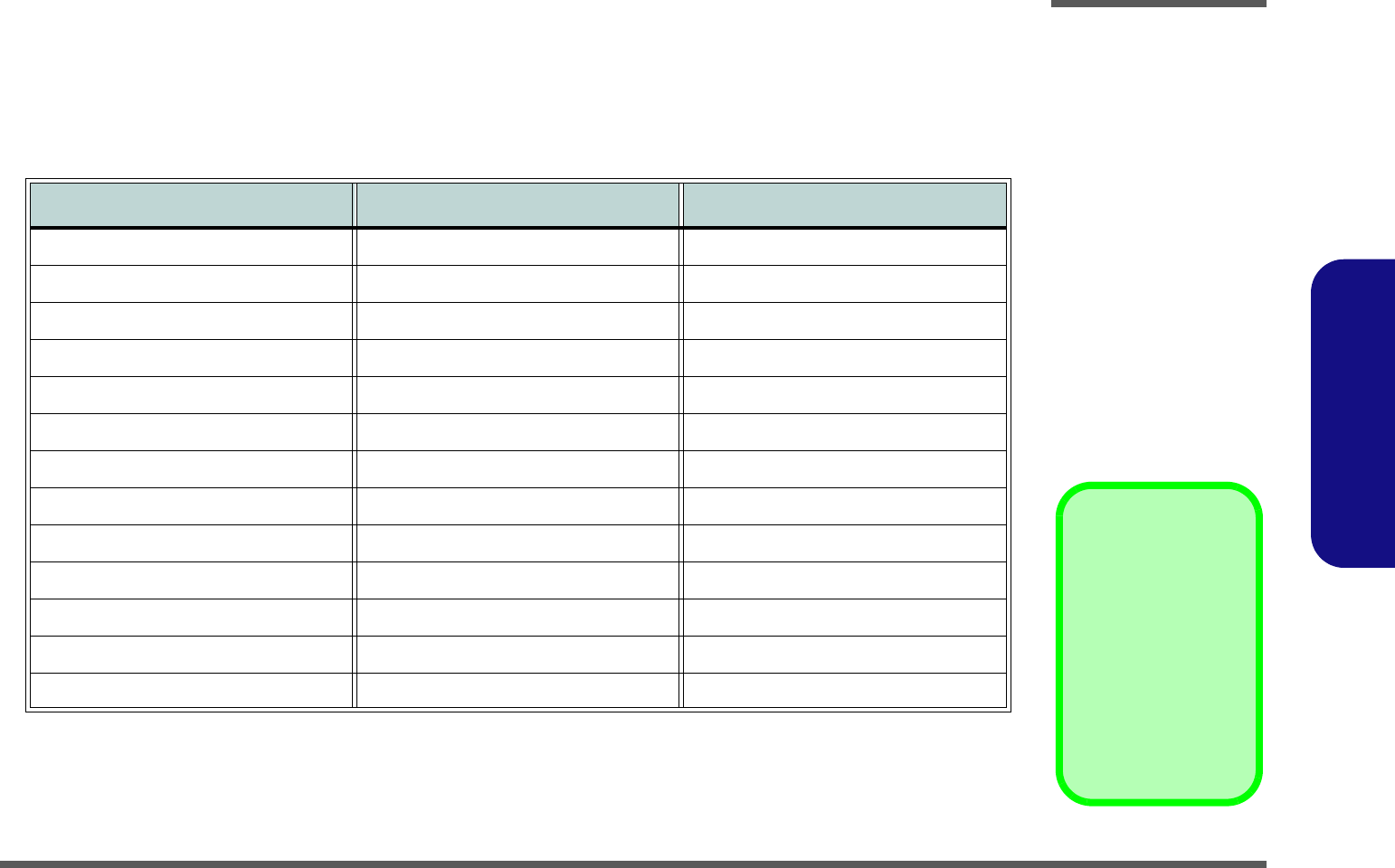
System Specifications
Feature Specification
Processor Intel® Core™2 Duo Processor
(478-pin) Micro-FC-PGA Package, Socket P
T8100/ T8300
45nm (45 Nanometer) Process Technology
3MB On-die L2 Cache & 800MHz FSB
2.12/ 2.4 GHz
Intel® Core™2 Duo Processor
(478-pin) Micro-FC-PGA Package, Socket P
T7100/ T7250
65nm (65 Nanometer) Process Technology
4MB On-die L2 Cache & 800MHz FSB
1.8/ 2.0 GHz
Intel® Core™2 Duo Processor
(478-pin) Micro-FC-PGA Package, Socket P
T7300/ T7500/ T7700/ T7800
65nm (65 Nanometer) Process Technology
4MB On-die L2 Cache & 800MHz FSB
2.0/ 2.2/ 2.4/ 2.6 GHz
Intel® Celeron® M Processor
(478-pin) Micro-FCPGA Package, Socket P
530/ 540/ 550/ 560
65nm (65 Nanometer) Process Technology
1MB On-die L2 Cache & 533MHz FSB
1.73/ 1.86/ 2.0/ 2.13 GHz
Core Logic SiS M672 + SiS968 Chipset
LCD 13.3" WXGA (1280 * 800) Glare / Non Glare TFT LCD)
Memory Two 200 Pin SO-DIMM Sockets Supporting DDRII (DDR2) 667 MHz
64-bit Wide DDRII (DDR2) Data Channel
Memory Expandable up to 2GB (1024/ 2048 MB DDRII Modules)
Latest Specification Information
The specifications listed in this Appendix are correct at the time of going to press. Certain items (particularly processor types/speeds and
CD/DVD device types) may be changed, delayed or updated due to the manufacturer's release schedule. Check with your service center
for details.
Introduction
System Specifications 1 - 3
1.Introduction
Video Adapter SiS M672 Integrated Video
High Performance 2D/3D Graphics Accelerator
Shared Memory Architecture up to 256MB
Supports Microsoft DirectX 9.0
Supports Vertex Shader 2.0 and Pixel Shader 2.0
Security Security (Kensington® Type) Lock Slot
Fingerprint ID Reader Module (Factory Option)
BIOS Password
BIOS One 8Mb SPI Flash ROM Phoenix™ BIOS
Storage One Changeable 12.7mm(h) Optical Device (CD/DVD) Type Drive (see “Optional” on page 5) Easy Changeable 2.5"
9.5 mm (h) SATA (Serial) HDD
Audio High Definition Audio (HDA)
Compliant with Microsoft UAA (Universal Audio
Architecture)
Direct Sound 3D™ Compatible
EAX™ 1.0 & 2.0 Compatible
A3D™ Compatible
S/PDIF Digital Output
2 * Built-In Speakers
Built-In Microphone
Keyboard &
Pointing Device
Winkey Keyboard Built-In TouchPad with Scrolling Function
Interface Three USB 2.0 Ports
One Headphone-Out Jack
One Microphone-In Jack
One S/PDIF Out Jack
One Internal Microphone
One RJ-11 Modem Jack
One RJ-45 LAN Jack
One DC-In Jack
One External Monitor Port
Card Reader Embedded 7-in-1 Card Reader (MS/ MS Pro/ SD/ Mini SD/ MMC/ RS MMC/ MS Duo) Note: MS Duo/ Mini SD/ RS
MMC Cards require a PC adapter
Card SlotS One ExpressCard/34(54) Slot
One Mini-Card Slot Supporting USB and PCIe Interfaces
Second Mini-Card Slot Supporting USB Interface (Factory Option)
Feature Specification
Introduction
1 - 4 System Specifications
1.Introduction
Communication
*Note: The Blue-
tooth and 3.5G Op-
tional Modules
cannot coexist. If
one of these facto-
ry options is includ-
ed in your
purchase option,
then the other is
unavailable.
10M/100Mb Base-T Ethernet LAN
56K MDC Modem V.90 & V.92 Compliant
802.11 b/g Mini-Card USB Wireless LAN Module (Option)
1.3M or 2.0M Pixel USB PC Camera Module (Factory Option)
Bluetooth OR 3.5G Module Options:
*Bluetooth 2.0 + EDR (Enhanced Data Rate) Module (Factory Option)
OR
*UMTS/HSPDA-based 3.5G Module with Mini-Card Interface (Factory Option)
Quad-band GSM/GPRS (850 MHz, 900 MHz, 1800 MHz, 1900 MHz)
UMTS WCDMA FDD (2100 MHz)
Operating
Systems
Supported
Windows XP SP2 Windows Vista 64bit SP1
Home Premium/ Business/ Enterprise/ Ultimate
Power
Management
Supports ACPI 3.0
Supports Resume from Modem Ring
Supports Wake on LAN
Supports Wake on USB
Power Full Range AC/DC Adapter AC input 100 - 240V, 50 - 60Hz, DC Output 19V, 3.42A or 18.5V, 3.5A (65 Watts)
Battery 4 Cell Smart Lithium-Ion Battery Pack, 14.8V/2.4AH
8 Cell Smart Lithium-Ion Battery Pack, 14.8V/4.4AH (Option)
Environmental
Spec
Temperature
Operating: 5°C - 35°C
Non-Operating: -20°C - 60°C
Relative Humidity
Operating: 20% - 80%
Non-Operating: 10% - 90%
Dimensions
& Weight
310mm (w) * 233mm (d) * 30-36mm (h)
2.0 kg With 4 Cell Battery and ODD
Feature Specification
UMTS Modes
Note that UMTS
modes CAN NOT
be used in North
America.
Introduction
System Specifications 1 - 5
1.Introduction
Optional
*Note: The Blue-
tooth and 3.5G Op-
tional Modules
cannot coexist. If
one of these facto-
ry options is includ-
ed in your
purchase option,
then the other is
unavailable.
Optical Drive Module Options:
SATA DVD/CD-RW Combo Drive Module
SATA Super Multi Drive Module
USB Floppy Disk Drive
802.11 b/g Mini-Card USB Wireless LAN Module
8 Cell Smart Lithium-Ion Battery Pack
1.3M or 2.0M Pixel USB PC Camera Module (Factory
Option)
Fingerprint ID Reader Module (Factory Option)
*Bluetooth 2.0 + EDR (Enhanced Data Rate) Module
(Factory Option)
OR
*UMTS/HSPDA-based 3.5G Module with MiniCard
Interface (Factory Option)
Quad-band GSM/GPRS (850 MHz, 900 MHz, 1800
MHz, 1900 MHz)
UMTS WCDMA FDD (2100 MHz)
Feature Specification
UMTS Modes
Note that UMTS modes CAN NOT be used in
North America.
Introduction
1 - 6 External Locator - Top View with LCD Panel Open
1.Introduction
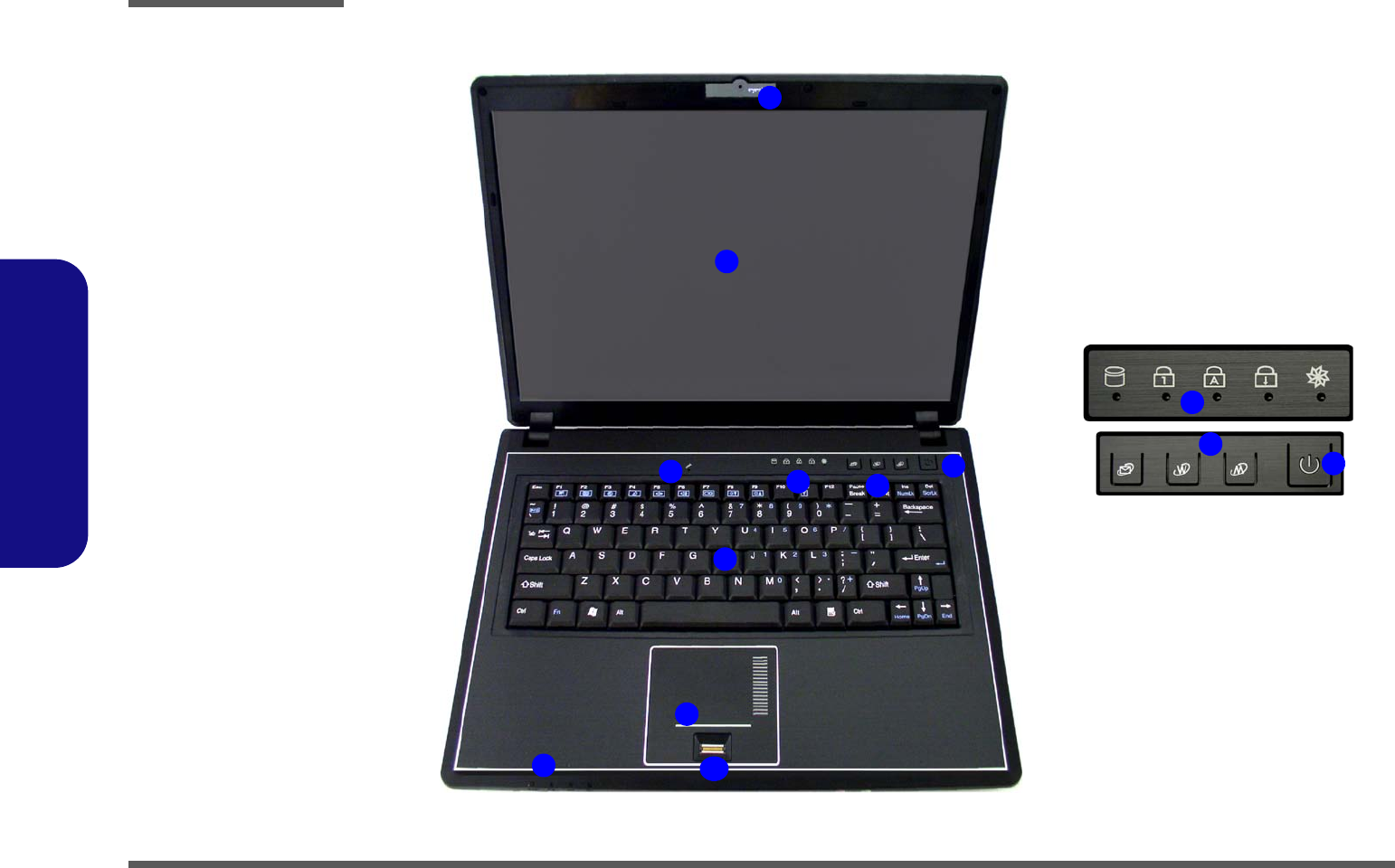
External Locator - Top View with LCD Panel Open
Figure 1
Top View
1. Built-In PC
Camera
(Optional)
2. LCD
3. Built-In
Microphone
4. Power Button
5. Hot-Key Buttons
6. LED Status
Indicators
7. Keyboard
8. Touchpad &
Buttons
9. LED Power &
Communication
Indicators
10. Fingerprint
Module (Optional)
6
5
4
2
5
1
7
8
4
6
9
3
10
Introduction
External Locator - Front & Rear Views 1 - 7
1.Introduction
External Locator - Front & Rear Views
Figure 2
Front View
1. LED Power &
Communication
Indicators
2. 7-in-1 Card Reader
3. S/PDIF-Out Jack
4. Microphone-In Jack
5. Headphone-Out
Jack
Figure 3
Rear View
1. Battery
Front
143 5
2
1
Rear
Introduction
1 - 8 External Locator - Left & Right Side Views
1.Introduction
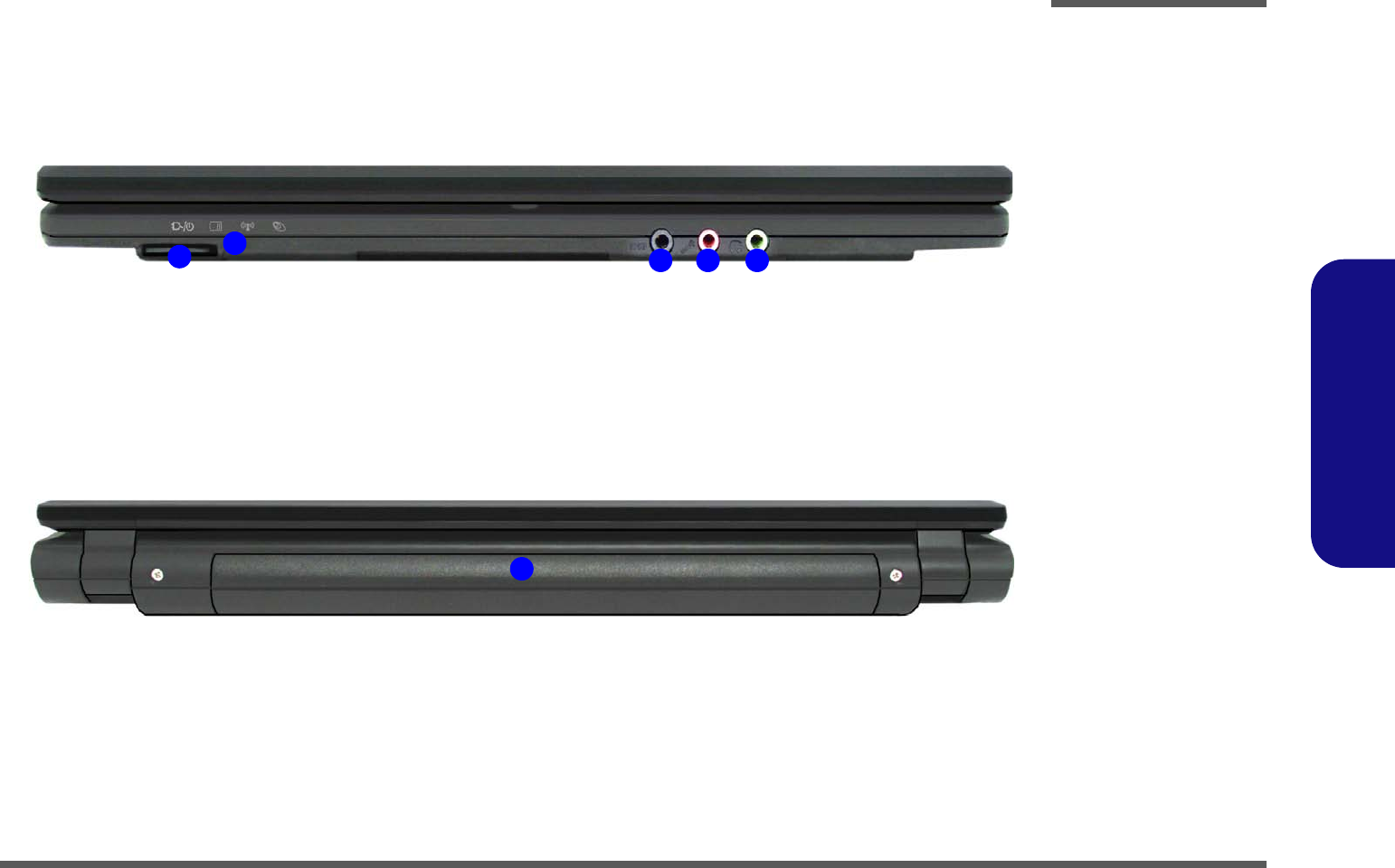
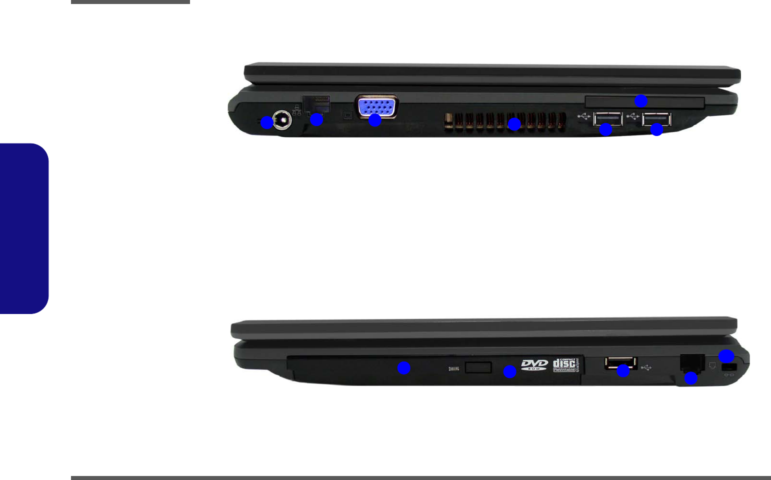
External Locator - Left & Right Side Views
4
123
6
Left
5 5
Figure 4
Left Side View
1. DC-In Jack
2. RJ-45 LAN Jack
3. External Monitor
Port
4. Vent
5. 2 * USB 2.0 Ports
6. ExpressCard/
54(34) Slot
Figure 5
Right Side View
1. Optical Device
Drive Bay
2. Emergency Eject
Hole
3. 1 * USB 2.0 Port
4. RJ-11 Phone Jack
5. Security Lock Slot
234
5
Right
1
Introduction
External Locator - Bottom View 1 - 9
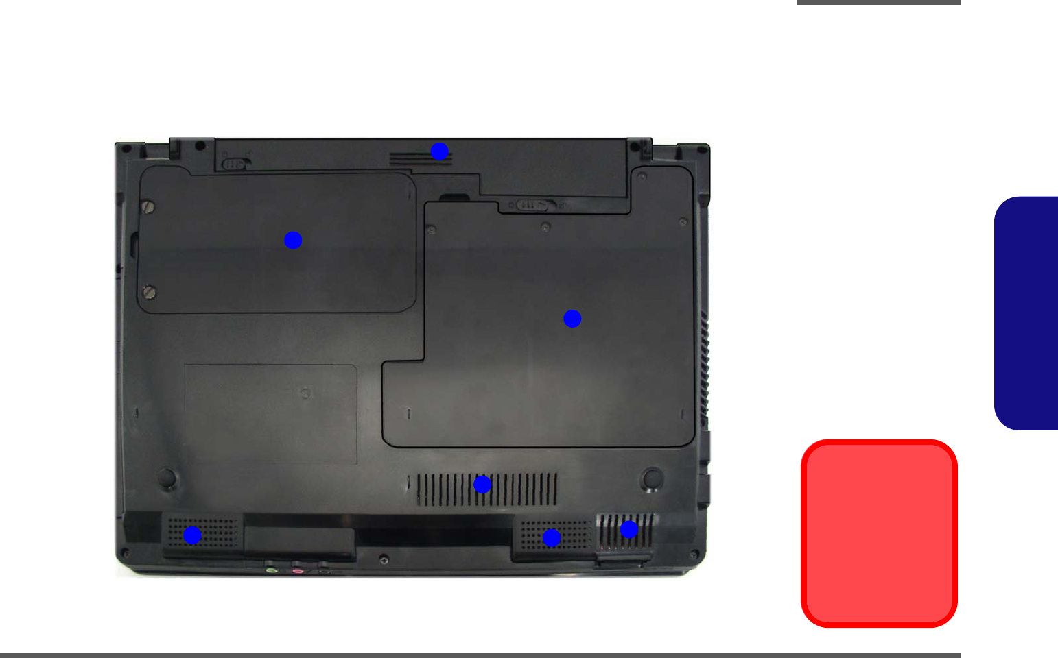
1.Introduction
External Locator - Bottom View
Figure 6
Bottom View
1. Battery
2. Hard Disk Bay
Cover
(3.5G Module)
3. RAM & CPU Bay
Cover
4. Vent/Fan Intake/
Outlet
5. Speakers
Overheating
To prevent your com-
puter from overheating
make sure nothing
blocks the vent/fan in-
takes while the com-
puter is in use.
2
3
1
4
5
4
5
Introduction
1 - 10 Mainboard Overview - Top (Key Parts)
1.Introduction
Mainboard Overview - Top (Key Parts)
Figure 7
Mainboard Top
Key Parts
1. Clock Buffer
ICS9P935
2. ITE 8512E
3. ExpressCard
Assembly
2
1
3
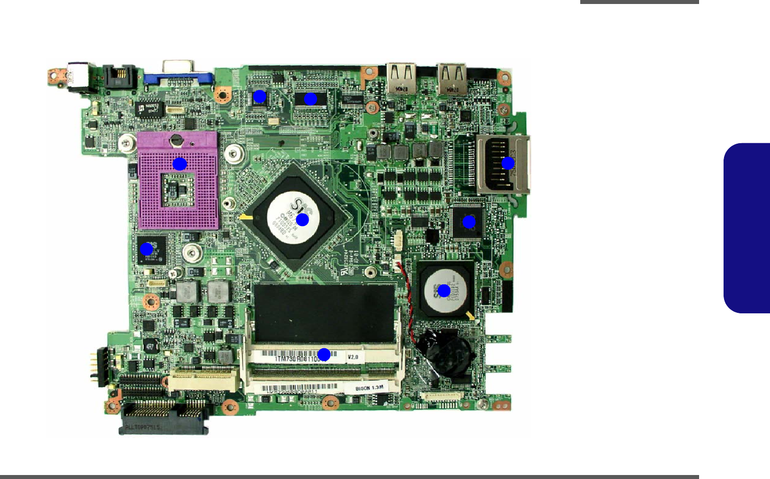
Introduction
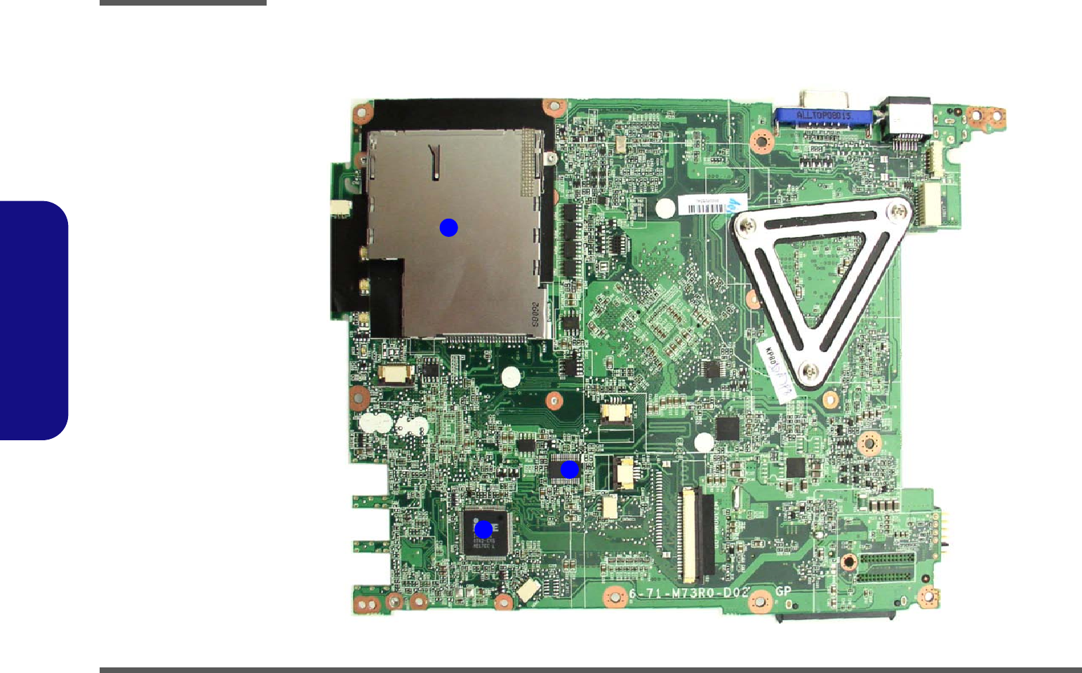
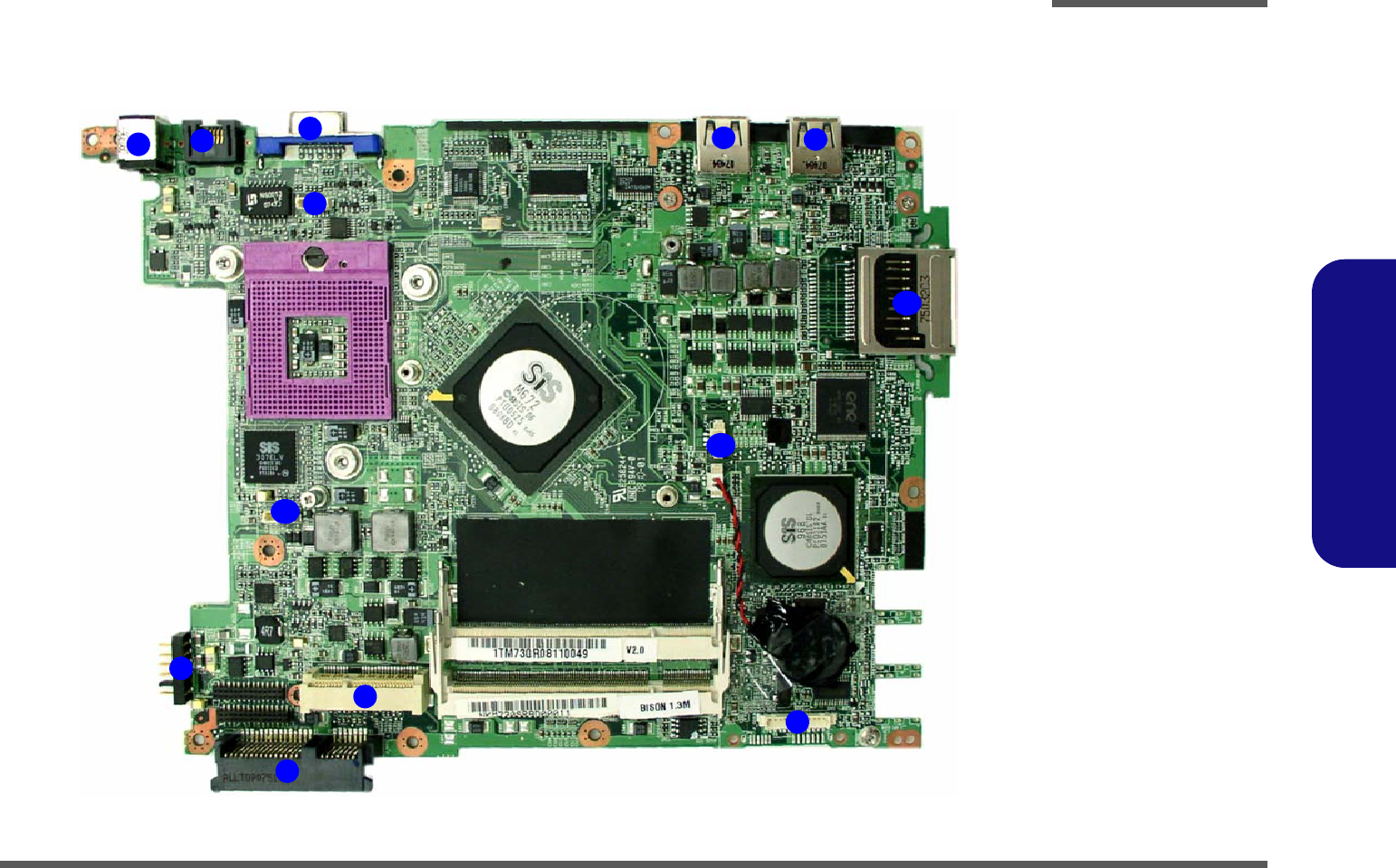
Mainboard Overview - Bottom (Key Parts) 1 - 11
1.Introduction
Mainboard Overview - Bottom (Key Parts)
Figure 8
Mainboard Bottom
Key Parts
1. CPU Socket (no
CPU installed)
2. LAN PHY
RTL8201CL
3. CLOCK
GENERATOR
ICS9LPR600
4. Northbridge-
SiSM672
5. 7-in-1 Card
Reader Controller
6. Card Reader
Controller ENE
MR510
7. Southbridge-
SiS968
8. Memory Slots
DDRII So-DIMM
9. SiS307ELV
23
1
4
5
6
8
7
9
Introduction
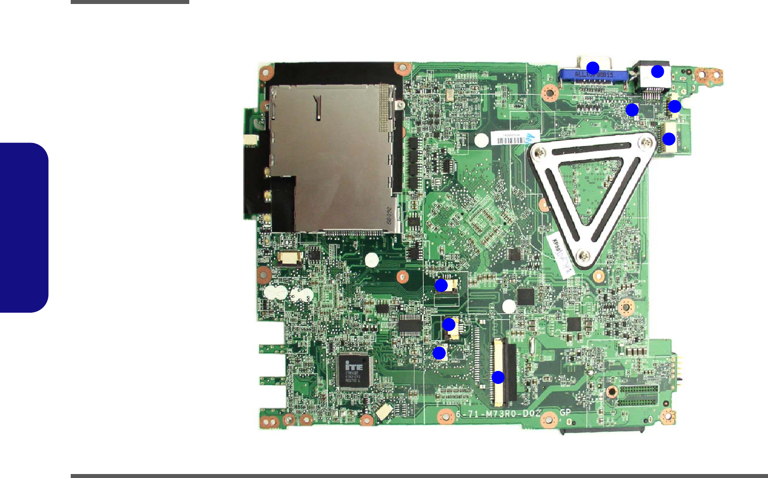
1 - 12 Mainboard Overview - Top (Connectors)
1.Introduction
Mainboard Overview - Top (Connectors)
Figure 9
Mainboard Top
Connectors
1. External Monitor
Port
2. RJ-45 LAN Jack
3. CCD Cable
Connector
4. LCD Cable
Connector
5. Speaker Cable
Connector
6. Touch Pad Cable
Connector
7. Fingerprint Cable
Connector
8. Internal
Microphone Cable
Connector
9. Keyboard Cable
Connector
8
9
3
12
4
5
6
7
Introduction
Mainboard Overview - Bottom (Connectors) 1 - 13
1.Introduction
Mainboard Overview - Bottom (Connectors)
Figure 10
Mainboard Bottom
Connectors
1. DC-In Jack
2. RJ-45 LAN Jack
3. External Monitor
Port
4. Inverter Cable
Connector
5. USB Port
6. Optical Device
Drive Connector
7. Mini PCIe Socket
8. SATA HDD
Connector
9. Battery
Connector
10. Bluetooth/3.5G
Cable Connector
11. Fan Cable
Connector
12. Card Reader
2
6
3
15
4
7
5
8
9
10
12
11

Introduction
1-14
1.Introduction

Disassembly
Overview 2 - 1
2.Disassembly
Chapter 2: Disassembly
Overview
This chapter provides step-by-step instructions for disassembling the M73XSR series notebook’s parts and subsystems.
When it comes to reassembly, reverse the procedures (unless otherwise indicated).
We suggest you completely review any procedure before you take the computer apart.
Procedures such as upgrading/replacing the RAM, CD device and hard disk are included in the User’s Manual but are
repeated here for your convenience.
To make the disassembly process easier each section may have a box in the page margin. Information contained under
the figure # will give a synopsis of the sequence of procedures involved in the disassembly procedure. A box with a
lists the relevant parts you will have after the disassembly process is complete. Note: The parts listed will be for the dis-
assembly procedure listed ONLY, and not any previous disassembly step(s) required. Refer to the part list for the previ-
ous disassembly procedure. The amount of screws you should be left with will be listed here also.
A box with a will also provide any possible helpful information. A box with a contains warnings.
An example of these types of boxes are shown in the sidebar.
Information
Warning

Disassembly
2-2Overview
2.Disassembly
NOTE: All disassembly procedures assume that the system is turned OFF, and disconnected from any power supply (the
battery is removed too).
Maintenance Tools
The following tools are recommended when working on the notebook PC:
• M3 Philips-head screwdriver
• M2.5 Philips-head screwdriver (magnetized)
• M2 Philips-head screwdriver
• Small flat-head screwdriver
• Pair of needle-nose pliers
• Anti-static wrist-strap
Connections
Connections within the computer are one of four types:
Locking collar sockets for ribbon connectors To release these connectors, use a small flat-head screwdriver to
gently pry the locking collar away from its base. When replac-
ing the connection, make sure the connector is oriented in the
same way. The pin1 side is usually not indicated.
Pressure sockets for multi-wire connectors To release this connector type, grasp it at its head and gently
rock it from side to side as you pull it out. Do not pull on the
wires themselves. When replacing the connection, do not try to
force it. The socket only fits one way.
Pressure sockets for ribbon connectors To release these connectors, use a small pair of needle-nose pli-
ers to gently lift the connector away from its socket. When re-
placing the connection, make sure the connector is oriented in
the same way. The pin1 side is usually not indicated.
Board-to-board or multi-pin sockets To separate the boards, gently rock them from side to side as
you pull them apart. If the connection is very tight, use a small
flat-head screwdriver - use just enough force to start.

Disassembly
Overview 2 - 3
2.Disassembly
Maintenance Precautions
The following precautions are a reminder. To avoid personal injury or damage to the computer while performing a re-
moval and/or replacement job, take the following precautions:
1. Don't drop it. Perform your repairs and/or upgrades on a stable surface. If the computer falls, the case and other
components could be damaged.
2. Don't overheat it. Note the proximity of any heating elements. Keep the computer out of direct sunlight.
3. Avoid interference. Note the proximity of any high capacity transformers, electric motors, and other strong mag-
netic fields. These can hinder proper performance and damage components and/or data. You should also monitor
the position of magnetized tools (i.e. screwdrivers).
4. Keep it dry. This is an electrical appliance. If water or any other liquid gets into it, the computer could be badly
damaged.
5. Be careful with power. Avoid accidental shocks, discharges or explosions.
•Before removing or servicing any part from the computer, turn the computer off and detach any power supplies.
•When you want to unplug the power cord or any cable/wire, be sure to disconnect it by the plug head. Do not pull on the wire.
6. Peripherals – Turn off and detach any peripherals.
7. Beware of static discharge. ICs, such as the CPU and main support chips, are vulnerable to static electricity.
Before handling any part in the computer, discharge any static electricity inside the computer. When handling a
printed circuit board, do not use gloves or other materials which allow static electricity buildup. We suggest that
you use an anti-static wrist strap instead.
8. Beware of corrosion. As you perform your job, avoid touching any connector leads. Even the cleanest hands pro-
duce oils which can attract corrosive elements.
9. Keep your work environment clean. Tobacco smoke, dust or other air-born particulate matter is often attracted
to charged surfaces, reducing performance.
10. Keep track of the components. When removing or replacing any part, be careful not to leave small parts, such as
screws, loose inside the computer.
Cleaning
Do not apply cleaner directly to the computer, use a soft clean cloth.
Do not use volatile (petroleum distillates) or abrasive cleaners on any part of the computer.
Power Safety
Warning
Before you undertake
any upgrade proce-
dures, make sure that
you have turned off the
power, and discon-
nected all peripherals
and cables (including
telephone lines). It is
advisable to also re-
move your battery in
order to prevent acci-
dentally turning the
machine on.

Disassembly
2-4Overview
2.Disassembly
Disassembly Steps
The following table lists the disassembly steps, and on which page to find the related information. PLEASE PERFORM
THE DISASSEMBLY STEPS IN THE ORDER INDICATED.
To remove the Battery:
1. Remove the battery page 2 - 5
To remove the HDD:
1. Remove the battery page 2 - 5
2. Remove the HDD page 2 - 6
To remove the System Memory:
1. Remove the battery page 2 - 5
2. Remove the system memory page 2 - 8
To remove the Processor:
1. Remove the battery page 2 - 5
2. Remove the processor page 2 - 10
To remove the Wireless LAN Module:
1. Remove the battery page 2 - 5
2. Remove the Wireless LAN page 2 - 12
To remove the Bluetooth:
1. Remove the battery page 2 - 5
2. Remove the bluetooth page 2 - 13
To remove the Optical Device:
1. Remove the battery page 2 - 5
2. Remove the Optical device page 2 - 14
To remove the Keyboard:
1. Remove the battery page 2 - 5
2. Remove the keyboard page 2 - 15
To remove the Modem :
1. Remove the battery page 2 - 5
2. Remove the HDD page 2 - 6
3. Remove the CPU heat sink page 2 - 10
4. Remove the Wireless LAN page 2 - 12
5. Remove the bluetooth page 2 - 13
6. Remove the Optical device page 2 - 14
7. Remove the keyboard page 2 - 15
8. Remove the modem page 2 - 16
Disassembly
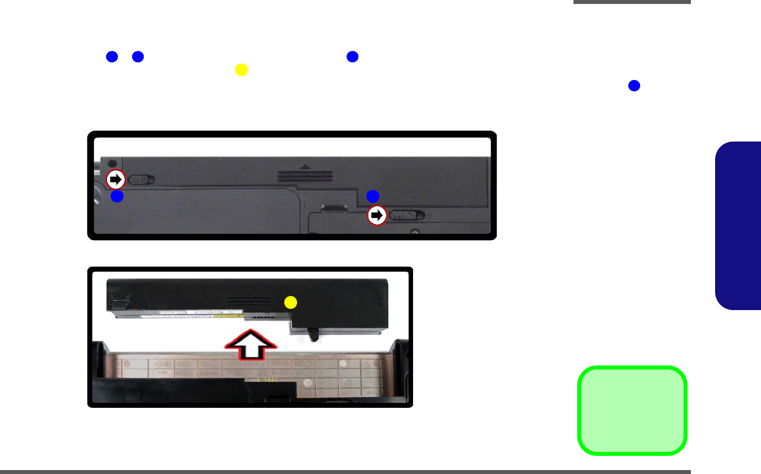
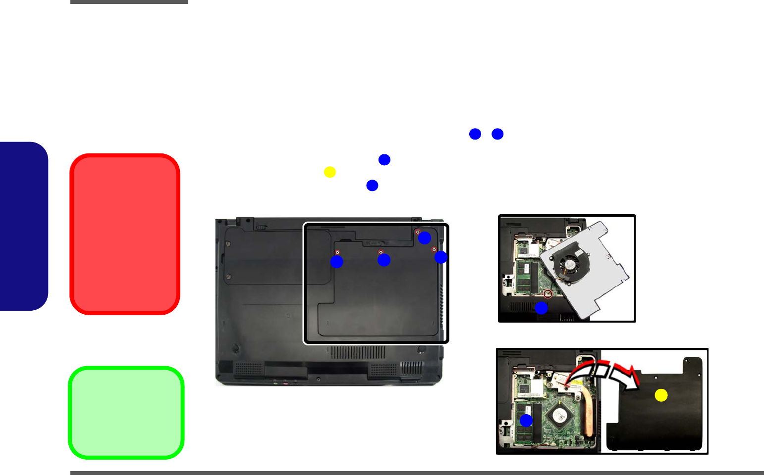
Removing the Battery 2 - 5
2.Disassembly
Removing the Battery
1. Turn the computer off, and turn it over.
2. Slide the latches ( & ) the direction of the arrow, and hold latch in place.
3. Slide the battery in the direction of the arrow .
3. Battery
1
2
2
6
3
1
a.
b.
2
3
Figure 1
Battery Removal
a. Slide the 2 latches and
hold latch in place.
b. Slide the battery in the di-
rection of the arrow.
2
Disassembly
2 - 6 Removing the Hard Disk Drive
2.Disassembly
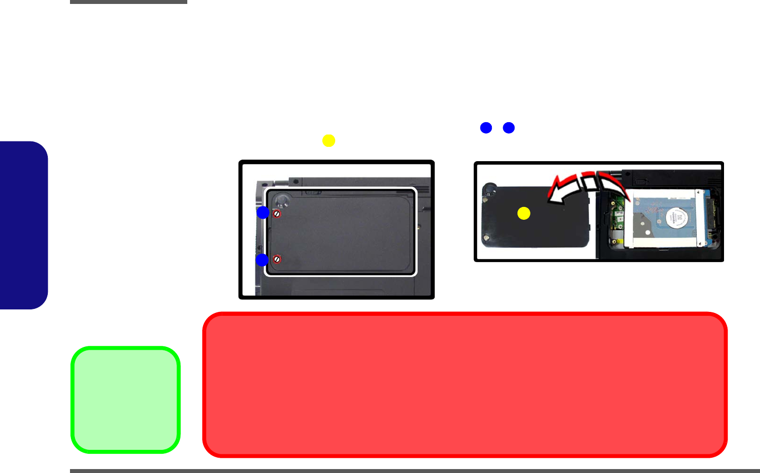
Removing the Hard Disk Drive
The hard disk drive can be taken out to accommodate other 2.5" serial (SATA) hard disk drives with a height of 9.5mm
(h). Follow your operating system’s installation instructions, and install all necessary drivers and utilities (as outlined in
Chapter 4 of the User’s Manual) when setting up a new hard disk.
Hard Disk Upgrade Processl
1. Turn off the computer, and remove the battery (page 2 - 5).
2. Locate the hard disk bay cover and remove the screws ( - ).
3. Remove the bay cover .
Figure 2
HDD Assembly
Removal
a. Locate the HDD bay cov-
er and remove the
screws.
b. Remove the bay cover.
3. HDD Bay Cover
•2 Screws
1
2
6
3
a.
1
2
HDD System Warning
New HDD’s are blank. Before you begin make sure:
You have backed up any data you want to keep from your old HDD.
You have all the CD-ROMs and FDDs required to install your operating system and programs.
If you have access to the internet, download the latest application and hardware driver updates for the operating system you plan
to install. Copy these to a removable medium.
3
b.
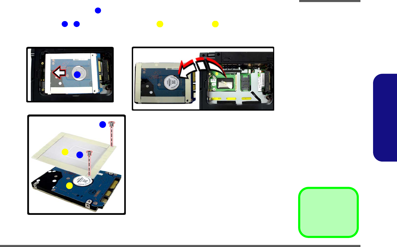
Disassembly
Removing the Hard Disk Drive 2 - 7
2.Disassembly
4. Carefully grip the mylar cover tab and slide the hard disk in the direction of arrow.
5. Lift the hard disk up (Figure d) in the direction of arrow.
6. Remove the screws - and separate the mylar cover from the hard disk .
7. Reverse the process to install any new hard disk.
4
Figure 3
HDD Assembly
Removal Sequence
c. Slide the HDD in the di-
rection of the arrow.
d. Lift the HDD out of the
bay.
e. Remove the screws and
separate the mylar cover
from the HDD.
5
6
6
7
6
8
7. Mylar Cover
8. HDD
•2 Screws
c. d.
4
e.
6
5
8
7
Disassembly
2 - 8 Removing the System Memory (RAM)
2.Disassembly
Removing the System Memory (RAM)
The computer has two memory sockets for 200 pin Small Outline Dual In-line Memory Modules (SO-DIMM) supporting
DDRII 667MHz. The main memory can be expanded up to 2GB. The SO-DIMM modules supported are 1024MB and
2048MB DDRII Modules. The total memory size is automatically detected by the POST routine once you turn on your
computer.
Memory Upgrade Process
1. Turn off the computer, remove the battery (page 2 - 5).
2. Locate the CPU/RAM bay cover, and remove screws - .
3. Carefully (a fan and cable are attached to the under side of the cover) lift up the bay cover.
4. Carefully disconnect the fan cable .
5. Remove the bay cover .
6. The RAM will be visible at point on the mainboard.
Figure 4
RAM Module
Removal
a. Remove the screws.
b. Disconnect the fan
cable.
c. Remove the cover.
Contact Warning
Be careful not to touch
the metal pins on the
module’s connecting
edge. Even the clean-
est hands have oils
which can attract parti-
cles, and degrade the
module’s perfor-
mance.
1
4
5
6
6. CPU/RAM Bay Cover
•4 Screws
7
a.
3
4
1
6
b.
2
5
c.
7
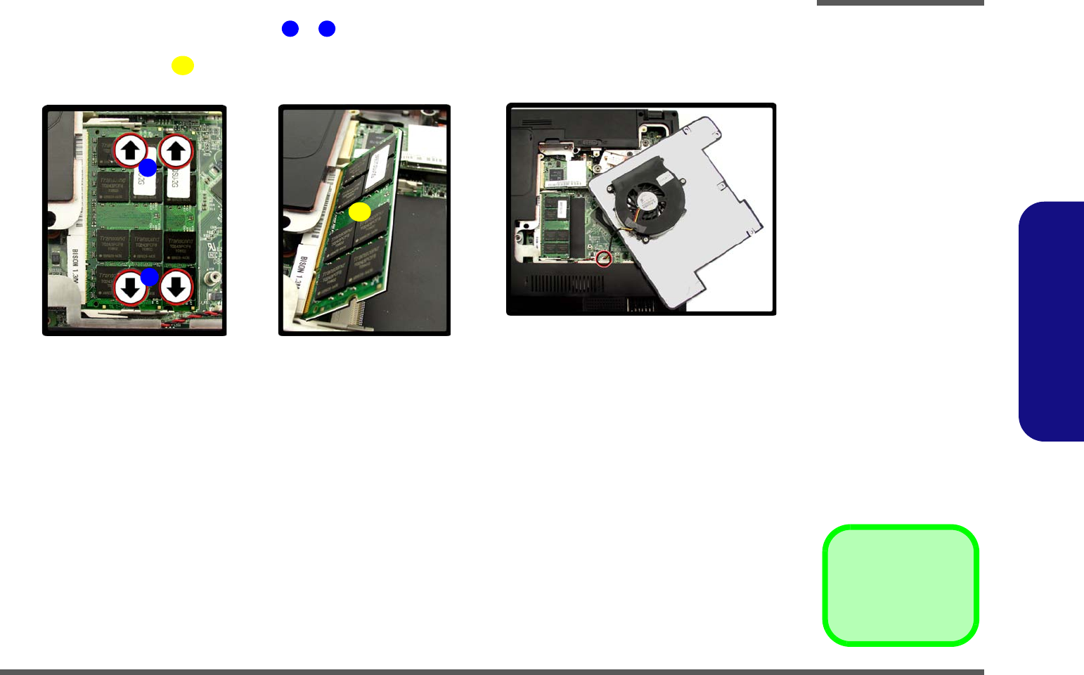
Disassembly
Removing the System Memory (RAM) 2 - 9
2.Disassembly
7. Gently push the two release latches ( & ) on the sides of the memory socket in the direction indicated by the
arrows (Figure d).
8. The RAM module(s) will pop-up (Figure e), and you can then remove it.
9. Push the latches to release the second module if necessary.
10. Insert a new module holding it at about a 30° angle and fit the connectors firmly into the memory slot.
11. The module will only fit one way as defined by its pin alignment. Make sure the module is seated as far into the slot
as it will go. DO NOT FORCE IT; it should fit without much pressure.
12. Press the module down towards the mainboard until the slot levers click into place to secure the module.
13. Replace the bay cover and the screws (make sure you reconnect the fan cable before screwing down the bay cover
- Figure f).
14. Restart the computer to allow the BIOS to register the new memory configuration as it starts up.
8
9
10
Figure 5
Memory Removal
Sequence
d. Push the release
latch(es).
e. Remove the module(s).
d. e.
10
f.
8
9
10 RAM Module(s)
Disassembly
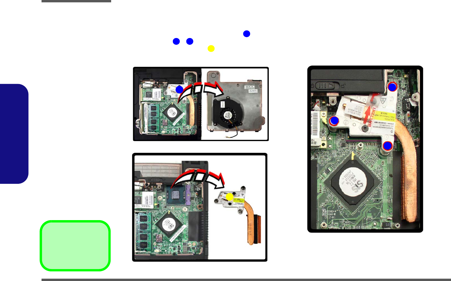
2 - 10 Removing the Processor
2.Disassembly
Removing the Processor
1. Turn off the computer, and remove the battery (page 2 - 5) and the CPU/RAM bay cover (page 2 - 8).
2. The CPU heat sink will be visible at point on the mainboard.
3. Remove screws - from the heat sink in the order indicated.
4. Carefully lift up the heat sink (Figure c) off the computer.
1
2
4
5
Figure 6
Processor Removal
a. Remove the cover and
Iocate the heat sink.
b. Remove the 3 screws in
the order indicated.
c. Remove the heat sink.
5. Heat Sink
•3 Screws
b.
5
1
4
a.
c.
3
2
Disassembly
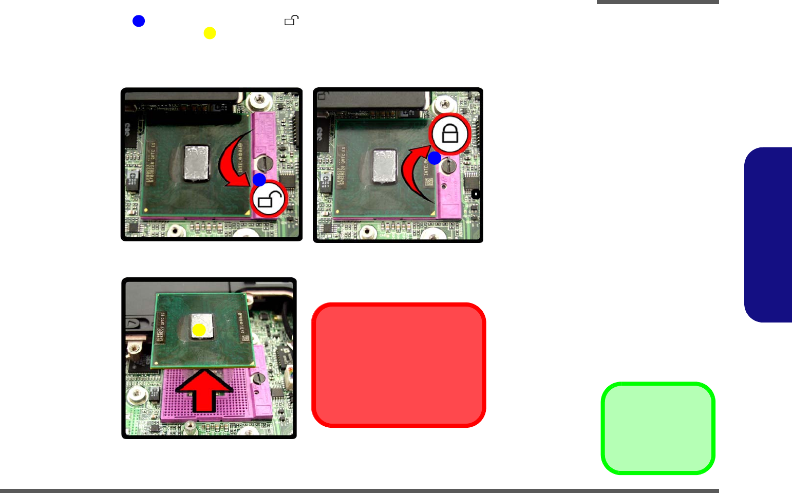
Removing the Processor 2 - 11
2.Disassembly
5. Turn the release latch towards the unlock symbol , to release the CPU (Figure d).
6. Carefully (it may be hot) lift the CPU up out of the socket (Figure e).
7. Reverse the process to install a new CPU.
8. When re-inserting the CPU, pay careful attention to the pin alignment, it will fit only one way (DO NOT FORCE IT!).
6
7
Figure 7
Processor Removal
Sequence
d. Turn the release latch to
unlock the CPU.
e. Lift the CPU out of the
socket.
d.
7
e.
Caution
The heat sink, and CPU area in
general, contains parts which are
subject to high temperatures. Allow
the area time to cool before remov-
ing these parts.
Unlock Lock
6
6
7. CPU
Disassembly
2 - 12 Removing the Wireless LAN Module
2.Disassembly
Removing the Wireless LAN Module
1. Turn off the computer, remove the battery (page 2 - 5) and the CPU/RAM bay cover (page 2 - 8).
2. The Wireless LAN module will be visible at point on the mainboard.
3. Carefully disconnect cable , then remove the screw from the module socket.
4. The Wireless LAN module will pop-up.
5. Lift the Wireless LAN module (Figure d) up and off the computer.
Figure 8
Wireless LAN
Module Removal
a. Remove the cover and
Iocate the heat sink.
b. Disconnect the cable
and remove the screw.
c. The WLAN module will
pop up.
d. Remove the WLAN
module.
Note: Make sure you
reconnect the antenna
cable to the “Main”
socket (Figure b).
1
2
3
4
1
2
c.
a.
4
3
b.
d.
4. WLAN Module
•1 Screw
Disassembly
Removing the Bluetooth Module 2 - 13
2.Disassembly
Removing the Bluetooth Module
1. Turn off the computer, remove the battery (page 2 - 5), and the CPU/RAM bay cover (page 2 - 8).
2. The Bluetooth module will be visible at point on the mainboard.
3. Remove screw and carefully disconnect the cable and separate the module from the connector .
4. Lift the Bluetooth module up and off the computer.
1
2
3
4
5
Figure 9
Bluetooth Removal
a. Remove the cover and
locate the Bluetooth
module.
b. Remove the screw and
disconnect the cable and
seperate the connector.
c. Lift the Bluetooth module
out.
a.
c.
b.
34
1
2
c.
5
5. Bluetooth Module
•1 Screw
Disassembly
2 - 14 Removing the Optical (CD/DVD) Device
2.Disassembly
Removing the Optical (CD/DVD) Device
1. Turn off the computer, remove the battery (page 2 - 5), and the CPU/RAM bay cover (page 2 - 8).
2. Remove the screw at point , and use a screwdriver to carefully push out the optical device at point .
3. Insert the new device and carefully slide it into the computer (the device only fits one way. DO NOT FORCE IT; The
screw holes should line up.
4. Restart the computer to allow it to automatically detect the new device.
Figure 10
Optical Device
Removal
a. Remove the cover and
locate the screw.
b. Remove the screw and
push the optical device
out off the computer at
point 2 and remove the
optical device.
1
2
3. Optical Device
•1 Screw
2
1
a.
3
b.
Disassembly
Removing the Keyboard 2 - 15
2.Disassembly
Removing the Keyboard
1. Turn off the computer, and remove the battery (page 2 - 5).
2. Press the three keyboard latches at the top of the keyboard to elevate the keyboard from its normal position (you
may need to use a small screwdriver to do this).
3. Carefully lift the keyboard up, being careful not to bend the keyboard ribbon cable (Figure b).
4. Disconnect the keyboard ribbon cable from the locking collar socket .
5. Carefully lift up the keyboard (Figure c) off the computer.
4
5
Figure 11
Keyboard Removal
a. Press the three latches
to release the keyboard.
b. Lift the keyboard up and
disconnect the cable
from the locking collar.
c. Remove the keyboard.
Re-Inserting the Key-
board
When re-inserting the
keyboard firstly align
the three keyboard
tabs at the bottom of
the keyboard with the
slots in the case.
6. Keyboard Module.
6
a. b.
5
4
6
Keyboard Tabs
c.
13
2
6
Disassembly
2 - 16 Removing the Modem Module
2.Disassembly
Removing the Modem Module
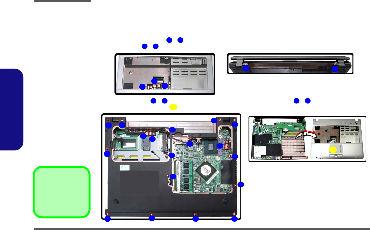
1. Turn off the computer, remove the battery (page 2 - 5) and the CPU/RAM bay cover (page 2 - 8) and the CPU heat
sink (page 2 - 10) and the Wireless LAN (page 2 - 12) and the optical device (page 2 - 14) and the keyboard (page
2 - 15).
2. Disconnect the connectors - from under the keyboard and turn it over.
3. Remove screws - from the rear of the computer.
4. Remove the screws - from the bottom case and disconnect the connectors - on the mainboard.
5. Carefully lift up the top case off the computer.
Figure 12
Modem Removal
a. Disconnect the connec-
tors from under the key-
board.
b. Remove the screws.
c. Remove the screws and
disconnect the connec-
tors from the main-
board.
d. Remove the top case.
24. Top Case
• 18 Screws
1
3
4
5
a. b.
13
2
5
4
6
21
22
23
24
c.
9
76
8
10 11
13
12
14
15
16
23
17
20
18
19
21 22
d.
24
Disassembly
Removing the Modem Module 2 - 17
2.Disassembly
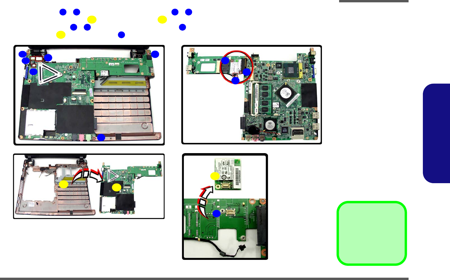
6. Remove screws - and disconnect the connectors - from the mainboard.
7. Separate the bottom case from the mainboard and turn it over.
8. Remove the screws - and disconnect the connector from the modem.
9. Lift the modem up off the socket .
25
27
28
30
Figure 13
Modem Removal
Sequence
e. Remove the screws and
and disconnect the con-
nectors.
f. Separate the bottom
case from the main-
board.
g. Remove the screws and
and disconnect the con-
nector.
h. Lift the modem up off
the socket.
31. Bottom Case
32. Main Board
37. Modem
•5 Screws
31
32
33
34
35
37
36
e.
h.
g.
32
31
28
29
25 30 26
27
33
34
35
37
36
f.

Disassembly
2-18
2.Disassembly

Part Lists
A-1
A.Part Lists
Appendix A:Part Lists
This appendix breaks down the M73XSR series notebook’s construction into a series of illustrations. The component part
numbers are indicated in the tables opposite the drawings.
Note: This section indicates the manufacturer’s part numbers. Your organization may use a different system, so be sure
to cross-check any relevant documentation.
Note: Some assemblies may have parts in common (especially screws). However, the part lists DO NOT indicate the
total number of duplicated parts used.
Note: Be sure to check any update notices. The parts shown in these illustrations are appropriate for the system at the
time of publication. Over the product life, some parts may be improved or re-configured, resulting in new part numbers.
Part Lists
A - 2 Part List Illustration Location
A.Part Lists
Part List Illustration Location
The following table indicates where to find the appropriate part list illustration.
Table A - 1
Part List Illustration
Location Part Pages#
Top with Fingerprint page A - 3
Top without Fingerprint page A - 4
Bottom page A - 5
LCD page A - 6
HDD page A - 7
Combo page A - 8
DVD-DUAL-RW page A - 9

Part Lists
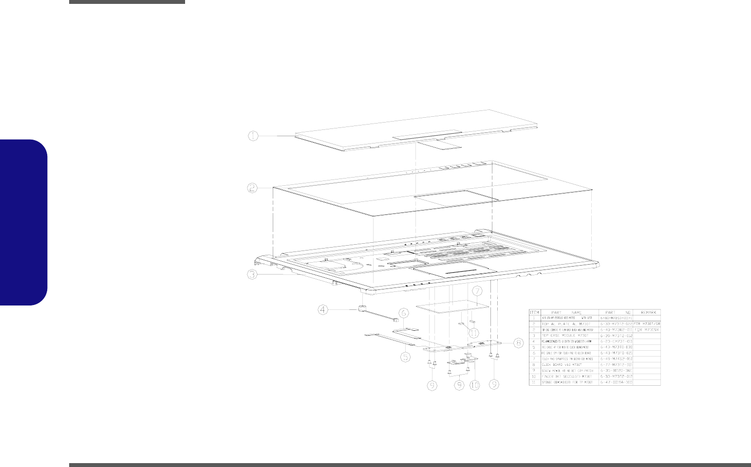
Top with Fingerprint A - 3
A.Part Lists
Top with Fingerprint
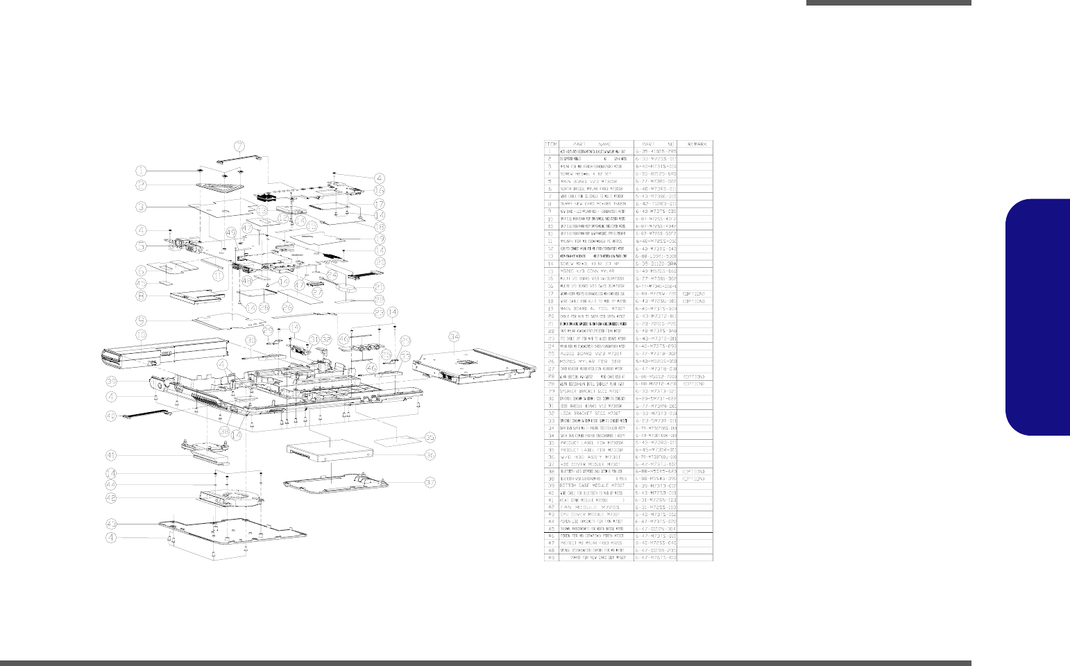
Figure A - 1
Top with
Fingerprint
無鉛
無鉛
無鉛
無鉛
無鉛
無鉛
無鉛
無鉛
無鉛
黑色 無鉛
無鉛
無鉛
無鉛
無鉛
無鉛
Part Lists
A - 4 Top without Fingerprint
A.Part Lists
Top without Fingerprint
無鉛
無鉛
無鉛
無鉛
無鉛
無鉛
無鉛
無鉛
無鉛
無鉛
無鉛
黑色 無鉛
Figure A - 2
Top without
Fingerprint
Part Lists
Bottom A - 5
A.Part Lists
Bottom
Figure A - 3
Bottom
無鉛
無鉛
無鉛
無鉛
無鉛
凱碩 無鉛
無鉛
無鉛
無鉛
無鉛
無鉛
無鉛
無鉛
無鉛
無鉛
兩個孔徑尺寸由 改為 無鉛
無鉛
無鉛
無鉛
無鉛
無鉛
無鉛
無鉛
無鉛
無鉛
無鉛
無鉛
藍天3 互億 無鉛
無鉛
無鉛
無鉛
無鉛
無鉛
海華 無鉛
無鉛
無鉛
無鉛
無鉛
無鉛
無鉛
無鉛
無鉛
無鉛
無鉛
無鉛
無鉛
拉帶加長 無鉛
無鉛
無鉛
無鉛
無鉛
無鉛
無鉛
無鉛
無鉛
導電布 無鉛
Part Lists
A - 6 LCD
A.Part Lists
LCD
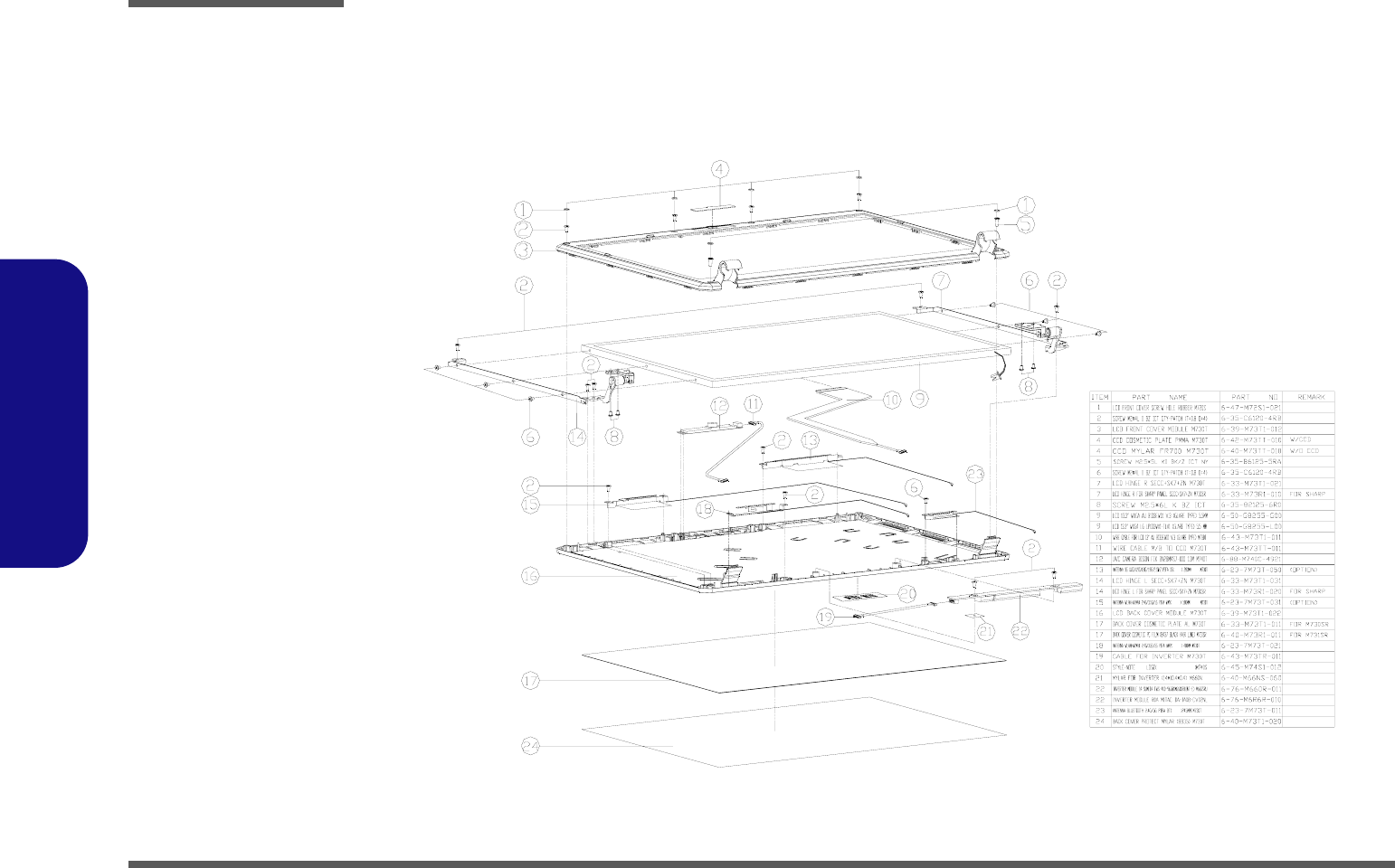
Figure A - 4
LCD
無鉛
無鉛
無鉛
無鉛
無鉛
無鉛
無鉛
無鉛
無鉛
無鉛
無鉛
無鉛
黑色 惠貿無鉛
黑色 惠貿 無鉛
黑色 惠貿 無鉛
無鉛
中性 電鑄薄膜鍍亮鉻 無鉛
無鉛
黑色 惠貿 無鉛
無鉛
無鉛
無鉛
無鉛
無鉛
無鉛
無鉛
無鉛
無鉛
無鉛
無鉛
Part Lists
HDD A - 7
A.Part Lists
HDD
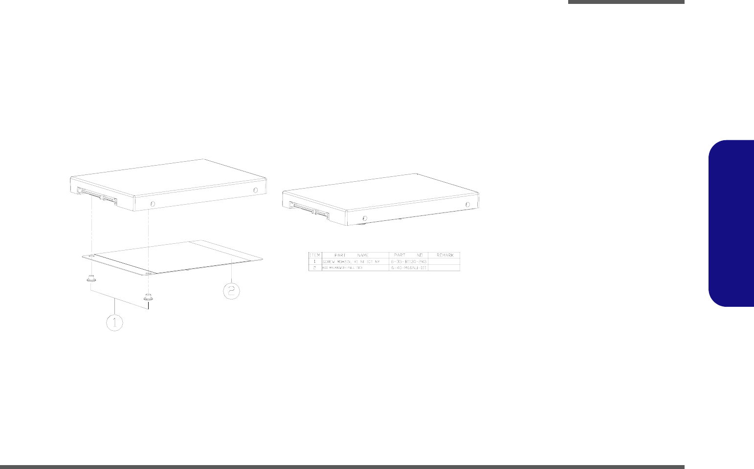
Figure A - 5
HDD
無鉛
無折切痕(設變)(無鉛)
Part Lists
A - 8 Combo
A.Part Lists
Combo
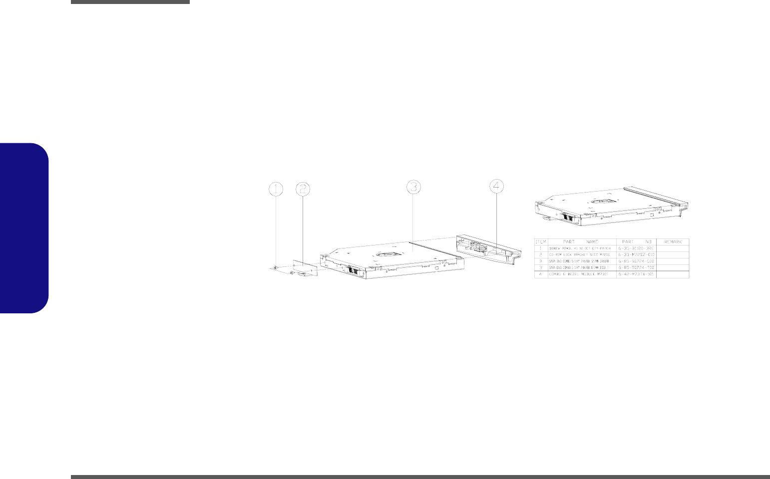
Figure A - 6
Combo
無鉛
無鉛
無鉛
無鉛
無鉛

Part Lists
DVD-DUAL-RW A - 9
A.Part Lists
DVD-DUAL-RW
Figure A - 7
DVD-DUAL-RW
無鉛
無鉛
無鉛
無鉛
無鉛

Part Lists
A - 10
A.Part Lists
Schematic Diagrams
B-1
B.Schematic Diagrams
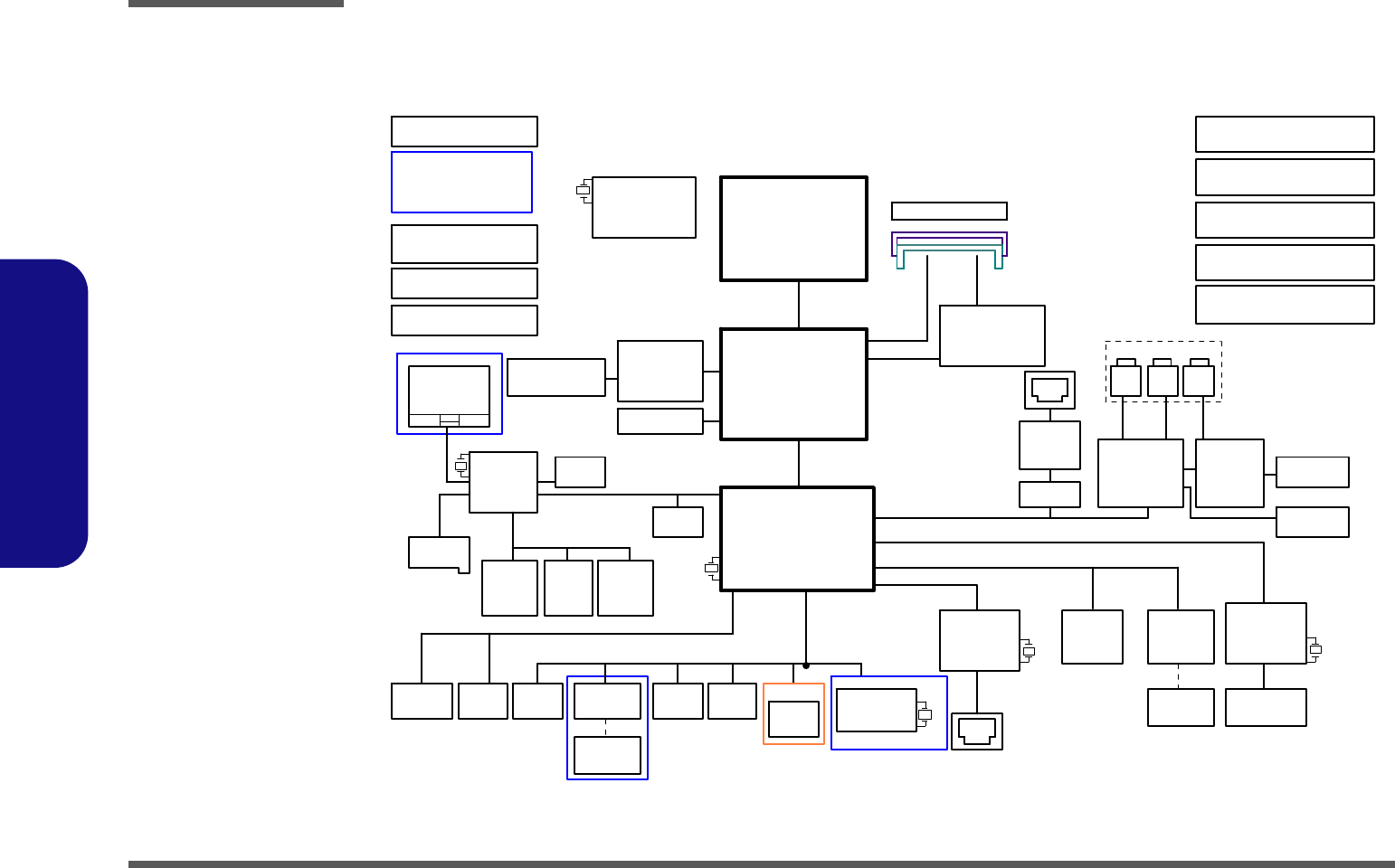
Appendix B:Schematic Diagrams
This appendix has circuit diagrams of the M73XSR notebook’s PCB’s. The following table indicates where to find the
appropriate schematic diagram.
Diagram - Page Diagram - Page Diagram - Page
SYSTEM BLOCK DIAGRAM - Page B - 2 968 PCIE LAN GPI0 2/4 - Page B - 15 SYSTEM POWER - Page B - 28
Meron (Socket-P) 1/2 - Page B - 3 968 USB SATA 3/4 - Page B - 16 VCORE - Page B - 29
Meron (Socket-P) 2/2 - Page B - 4 968 PWR GND 4/4 - Page B - 17 VDD3, VDD5 - Page B - 30
SiSM672 HOST PCIE 1/5 - Page B - 5 CLK GEN & CLK BUFFER - Page B - 18 1.05VS, 1.2V, 1.5V - Page B - 31
SiSM672 DRAM 2/5 - Page B - 6 SATA, 3G POWER, PCI DEBUG - Page B - 19 1.8V, 0.9VS - Page B - 32
SiSM672 MuTIOL VGA 3/5 - Page B - 7 MULTI I/O, ODD, CCD, BT - Page B - 20 AC IN, CHARGER - Page B - 33
SiSM672 PWR 4/5 - Page B - 8 NEW CARD, MINI PCIE, USB - Page B - 21 CLICK BOARD - Page B - 34
SISM672 GND 5/5 - Page B - 9 LED, FAN, PC BEEP, TP, FP - Page B - 22 MULTI I/O BOARD 1/2 - Page B - 35
DDRII SO-DIMM 1 - Page B - 10 ENE MR510, 7 IN 1 - Page B - 23 MULTI I/O BOARD 2/2 - Page B - 36
DDRII SO- DIMM 2 - Page B - 11 PHY REALTEK 8201CL - Page B - 24 FINGERPRINT BOARD - Page B - 37
SiS307ELV - Page B - 12 AUDIO CODEC ALC883 - Page B - 25 AUDIO BOARD - Page B - 38
PANEL, INVERTER, CRT - Page B - 13 AUDIO AMP - Page B - 26 ODD BRIDGE BOARD - Page B - 39
968 PCI IDE MuTIOL SPI 1/4 - Page B - 14 KBC-ITE IT8512E - Page B - 27
Table B - 1
Schematic
Diagrams
Version Note
The schematic dia-
grams in this chapter
are based upon ver-
sion 6-7P-M73R6-003.
If your mainboard (or
other boards) are a lat-
er version, please
check with the Service
Center for updated di-
agrams (if required).
Schematic Diagrams
B - 2 SYSTEM BLOCK DIAGRAM
B.Schematic Diagrams
SYSTEM BLOCK DIAGRAM
Sheet 1 of 38
SYSTEM BLOCK
DIAGRAM
LID, HOT KEY, USB, 3G
17. 1* 8. 1* 1.2 m m
SO-DIMM0
SO CKE T
479 pin s socket P
128-pin LQFP
EC
SMART
FAN
Az ali a Co dec
SPDIF
OU T
(U SB0 )
F7 538 3M
S PK _R, R J- 11, L ED
12 M Hz
M 72 0T /M7 30 T Cl ic k
Board
SOC KE T
128pins LQFP
AZALIA
MDC
MODULE
33 MHz
RJ-11
RJ-45
Re al te k
AL C8 83
(U SB 5)
CLEVO M730SR System Block Diagram
Mini PCIE
OD D
28pins TSSOP
CCD
(USB3)
TO UC H PAD
14* 1 4* 1.4 m m
+V COR E
SO CK ET
1.8V,0.9VS
MR510
(Optional)
852balls TEBGA
14.318 MHz
USB & Phone
Jack B'd
M730T ODD Board
1 7.1 *8.1 *1 .2 mm
10 /10 0M P HY N ew Ca rd
En E
SiSM672
32.768KHz
B lue to ot h
810602-1703
27 *2 7* 2. 5m m
GOL AN
R TL8 20 1C L
169balls BGA
(U SB 7)
FS B
(USB3)
56pins TSSOP
ANPAC
APA2056A
24 MHz
SM AR T
BA TT ERY
PROCESSO R
MINI PCIE
GMAC
SPI
MDC CON
33 MHz
Memory Termination
SATA HDD
480 Mbps
CR T
13 *1 3* 1. 7m m
M 73 0T Au di o Bo ar d
100 MHz
533/667 MHz
TH ERM AL
SE NSO R
USB4
SOUTH BRIDGE
1.05VS,1.5V,1.2V
LV DS (T V)
LP C
667/800 MHz
3G CA RD
USB2.0
35*35*2.4mm
25 MHz
AUDIO AMP
Mu TI OL 1 G
Intel Merom
SO-DIMM1
SH E E T 1 8
PCI BUS
24.576
MHz
48 pin s LQ FP
SA TA I/ II 3 .0 Gb /s
SHEET 10
(Optional)
14 *1 4* 1. 6m m
CLICK BOARD
LP C
MULTI I/O BOARD
PCIE
9* 9* 1. 7m m
MIC
IN
28 p i ns SS O P
SiS968
Colck Generator
DDRII
FingerPrint
35*35*2.7mm
INT . K/ B
ICS 9P 93 5
Si S3 07E LV
US B2
Sy na pt ic
570balls mBGA
AZALIA LINK
9.8*6.4*1.2mm
VDD3,VDD5,3.3V,5V
SHEET 9
CA RD RE AD ER
EC SMBUS
HP
OU T
Clo ck B uff er
48pins LQFP
FINGER PRINTER BOARD
32.768 KHz
INT SPK
9*9*1.6m m
SY STE M PO WE R, 2.5 V
ICS9LPR600
7I N1
US B6
LCD CONNECTOR,
IVERTER
AC-IN,CHARGER
NORTH BRIDGE
IT E 851 2E
INT MIC
(U SB1 )
DDRII
Schematic Diagrams
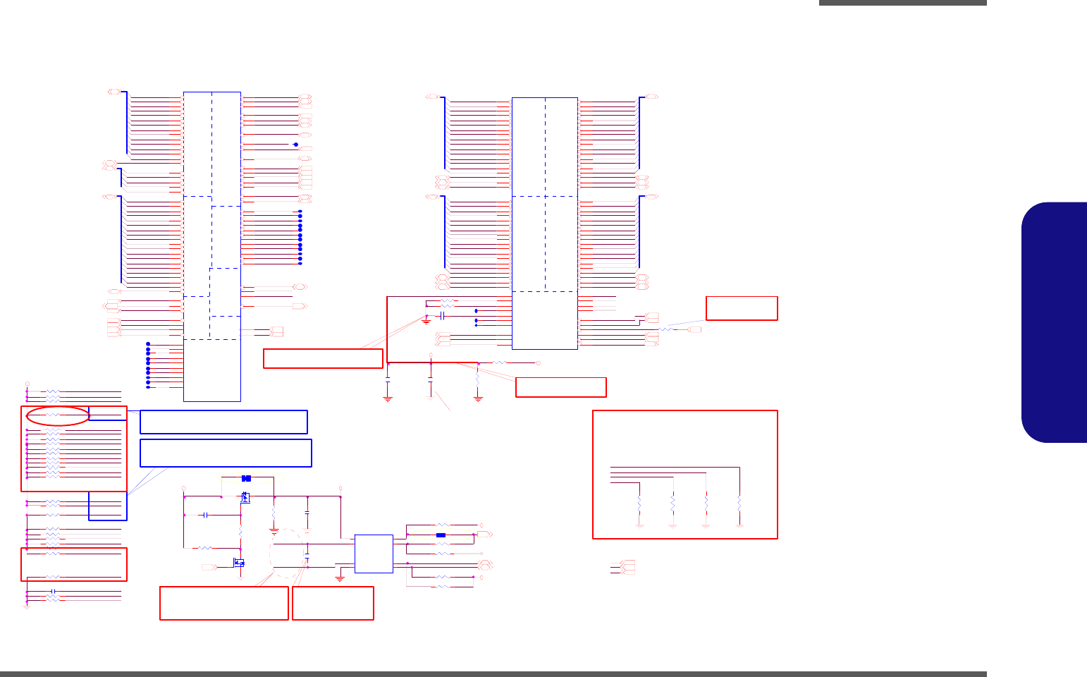
Meron (Socket-P) 1/2 B - 3
B.Schematic Diagrams
Meron (Socket-P) 1/2
Sheet 2 of 38
Meron (Socket-P)
1/2
S MD_ C PU_ T HERM 2 6
H_A#21
R243 *1K_04
DATA GRP 0 DATA GRP 1
DATA GRP 2DATA GRP 3
MIS C
JS K T1 B
Me ro m B a l l -ou t R ev 1 a
R2 6
U2 6
AA1
Y1
E22
F24
J24
J23
H22
F26
K22
H23
N22
K25
P26
R23
E26
L23
M24
L22
M23
P25
P23
P22
T24
R24
L25
G22
T25
N25
Y22
AB24
V24
V26
V23
T2 2
U2 5
U2 3
F23
Y25
W22
Y23
W24
W25
AA23
AA24
AB25
AE24
AD24
G25
AA21
AB22
AB21
AC26
AD20
AE22
AF2 3
AC25
AE21
AD21
E25
AC22
AD23
AF2 2
AC23
E23
K24
G24
AF1
H25
N24
U2 2
AC20
E5
B5
D2 4
J26
L26
Y26
AE25
H26
M26
AA26
AF2 4
AD 26
AE6
D6
D7
C24
B22
B23
C21
D25
AF26
A26
C23 COMP[0]
COMP[1]
COMP[2]
COMP[3]
D[0]#
D[1]#
D[10]#
D[11]#
D[12]#
D[13]#
D[14]#
D[15]#
D[16]#
D[17]#
D[18]#
D[19]#
D[2]#
D[20]#
D[21]#
D[22]#
D[23]#
D[24]#
D[25]#
D[26]#
D[27]#
D[28]#
D[29]#
D[3]#
D[30]#
D[31]#
D[3 2 ]#
D[3 3 ]#
D[3 4 ]#
D[3 5 ]#
D[3 6 ]#
D[3 7 ]#
D[3 8 ]#
D[3 9 ]#
D[4]#
D[4 0 ]#
D[4 1 ]#
D[4 2 ]#
D[4 3 ]#
D[4 4 ]#
D[4 5 ]#
D[4 6 ]#
D[4 7 ]#
D[4 8 ]#
D[4 9 ]#
D[5]#
D[5 0 ]#
D[5 1 ]#
D[5 2 ]#
D[5 3 ]#
D[5 4 ]#
D[5 5 ]#
D[5 6 ]#
D[5 7 ]#
D[5 8 ]#
D[5 9 ]#
D[6]#
D[6 0 ]#
D[6 1 ]#
D[6 2 ]#
D[6 3 ]#
D[7]#
D[8]#
D[9]#
TEST5
D INV[0 ]#
D INV[1 ]#
DIN V [2 ]#
DIN V [3 ]#
DPR S T P#
D PSLP#
DPW R #
DSTBN[0]#
DSTBN[1]#
DSTBN[2]#
DSTBN[3]#
DSTBP[0]#
DSTBP[1]#
DSTBP[2]#
DSTBP[3]#
GTLREF
PSI#
PW R GO OD
SLP#
TEST3
BS EL[0 ]
BS EL[1 ]
BS EL[2 ]
TEST2
TEST4
TEST6
TEST1
R 2 49 56 _ 0 4
Route H_THERMDA and
H_THERMDC on same layer.
10 mil trace on 10 mil spacing.
H_D#19
H_D#61
U26
AD M1032AR M
1
2
3
4
5
6
7
8
VDD
D+
D-
THER M
GN D
ALERT
SDATA
SCLK
H_INTR14
H_D#28
H_ T RDY # 4
H_ A# 6
6-14-5603B-11B
0.5" max, Zo= 55 Ohms
R 5 04 56 _ 0 4
H_ D PW R# 4
H_DBR#
R 2 48 56 _ 0 4
H_ A# 12
H_D#57
H_D#43
H_D PSL P#
H_A20M#
H_DBSY # 4
CP U_ BS EL 0
H_A#23
H_ RS# 0 4
C PU_BSEL 2
R 266 150_1% _04
H_ D# [6 3 :0] 4
H_ D# [6 3 :0] 4
H_ BR0 # 4
Z0202
C460
* . 01 U _1 6 V _ 04
Layout Note:
H_D#30
H_A20M#14
H_D#8
H_D#20
H_ PW R GD
H_CPURST#
R 2 50 56 _ 0 4
H_ DPS LP# 6
TH ERM _AL ER T# 26
H_INTR
H_THERMDC
H_ INT R
R1 8
27. 4_1%_04
V DD3 15,21,26,27,29,31,32
CO MP0
CO MP3
H_A#31
H_A#32
R 12 39.2_1%_04
R2 4 1 *0 _0 4
H_D#9
H_ CPU RST #
Z0213
ADM1032 1000p
F75383M 2200p
CO MP3
H_BPM 0#
H_A#18
H_D#32
H_INIT#
R 2 60 56 _ 0 4
H_ NM I14
H_D#7
H_D#4
H_D#62
CO MP1
R 2 59 56 _ 0 4
H_ BP RI# 4
H_D#25
CPU _BS EL217
H_D#41
H_ DST BN #04
H_REQ#[4:0]4
H_D#34
H_BPM 3#
H_ A# 9
C 447 * .1U _16V_04
H_ D# [6 3 :0]4
H_D#46
H_ A# 16
R 2 57 1K _ 0 4
1.05VS
H _ PREQ #
CO MP2
C454
.1U_16V_04
R2 7
*100K_04
H_ADSTB# 04
H_D#47
CPU to SB interface
H_ RS# 2 4
H_ ADS # 4
H_IGNNE#
H_D#2
H_BPM 2#
H_ DBR #
C PU_BSEL 1
C1 9
1U_6.3V_X5R_06
R 8 1K _ 1 % _0 4
V_T HE RM
H_FERR#
H_ A# 5
R 24 *51_04
4/16
H_D#17
H_D#12
Z0205
H_PWRGD
R 2 53 56 _ 0 4
H _DPSLP#
Z0208
R229
54.9_1% _04
R 2 55 56 _ 0 4
H_ A# 10
H_A#35
ADDR
GROUP 0 ADDR GROUP
1
CONTROLX DP / I TP SI G N ALS
H C LK
THERMAL
RE SE RV ED
IC H
JSKT1A
Merom Ball-out Rev 1a
N3
P5
P2
L2
P4
P1
R1
Y2
U5
R3
W6
U4
Y5
U1
R4
T5
T3
W2
W5
Y4
J4
U2
V4
M4
N5
T2
V3
B2
C3
D2
D2 2
L5
L4
K5
M3
N2
J1
A6
H1
M1
V1
D3
A22
A21
E2
AD 4
AD 3
AD 1
AC 4
G5
F1
C20
E1
H5
F21
A5
G6
E4
D20
C4
B3
C6
B4
H4
AC 2
AC 1
D21
K3
H2
K2
J3
L1
C1
F3
F4
G3
A3
D5
AC 5
AA 6
AB 3
C7
A24
B25
AB 5
G2
AB 6
W3
AA4
AB2
AA3
F6
A[10]#
A[11]#
A[12]#
A[13]#
A[14]#
A[15]#
A[16]#
A[17]#
A[18]#
A[19]#
A[20]#
A[21]#
A[22]#
A[23]#
A[24]#
A[25]#
A[26]#
A[27]#
A[28]#
A[29]#
A[3]#
A[30]#
A[31]#
R SVD[0 1 ]
R SVD[0 2 ]
R SVD[0 3 ]
R SVD[0 4 ]
R SVD[0 5 ]
R SVD[0 6 ]
R SVD[0 7 ]
R SVD[0 8 ]
A[4]#
A[5]#
A[6]#
A[7]#
A[8]#
A[9]#
A20 M#
ADS #
AD STB [0]#
AD STB [1]#
R SVD[0 9 ]
BC LK[0]
BC LK[1]
BNR #
BPM [0] #
BPM [1] #
BPM [2] #
BPM [3] #
BPRI #
BR 0#
DBR #
D BSY #
DEFER#
DR DY #
FER R#
HIT#
HITM #
IERR #
IG NNE #
IN IT#
LINT0
LINT1
LOCK #
PR DY #
PREQ#
PROC HO T#
REQ[0]#
REQ[1]#
REQ[2]#
REQ[3]#
REQ[4]#
R ESET#
RS[0]#
RS[1]#
RS[2]#
SM I#
STPCLK#
TCK
TDI
TD O
THER MTRIP #
TH E R M D A
THE RMD C
TMS
TR DY #
TR S T #
A[32]#
A[33]#
A[34]#
A[35]#
R SVD[1 0 ]
H_ DI NV# 2 4
H_ L OCK # 4
H_D#10
H_D#49
H_D#59
Z0207
H_A#20
R 2 56 1K _ 0 4
H_D#45
H_DPWR#_R
H_A#26
C6 5
1000P_50V_04
H_ DS TB N # 3 4
H_TMS
H_D#3
H_ IER R#
H_ T MS
Z0224
H_ A# 15
H_D#21
If PR OC HOT # is ro ut ed be tw ee n C PU , IMV P an d M CH ,
pul l- up re si st or ha s to be 6 8 o hm ? 5% . If no t
use , pu ll- up r esi st or ha s to be 5 6 ohm ? 5 %
Close to Thermal IC
S MC_ C PU_ T HERM 2 6
H_D#50
H_ CL K_ CP U 1 7
R 2 62 56 _ 0 4
Q2 5
*N DS352AP_N L
G
DS
R 11 27.4_1%_04
IF US ED De sk to p C PU , H_C PU RS T#, H_ PW RGD ,H _B RD, ne ed
add pull high resistor
H_D#39
H_ ST PCL K#
C24
.01 U_1 6V_X7 R_04
CPU_GRFE=0.7V
4/16
H_ CPU SL P # 14
H_D#55
H_A#25
R238 *1K_04
H _DSTBP# 04
H_NMI
H_D#48
H_ A# 3
H_A#22
VDD3
PSI# 28
R 267 4.7K_04
H _TH RMTR IP# 14
H_DPWR#_R
H_D#38
H_ T HER MD C
Q26
* 2N7002W
G
DS
CP U_ BS EL 2
C PU_BSEL 0
Z0225
Z0212
3.3V
H_ CL K_ CP U# 1 7
H_D#33
Z0201
C686 *0.1u_X7R_04
H_D#27
H_D#40
H_ T DO
H_IERR#
R 252 *330_04
H_ DST BN #14
H_ PW R GD 4
H_D#58
H_TDI
H_REQ#4
R 2 54 56 _ 0 4
V_ THER M
Z0206
Z0209
R 242 *56_04
H_ DI NV# 3 4
H_A#30
R 264 75_1%_04
H_D#16
H_ DR DY # 4
H_D#6
H_D#24
H_A#29
H _STPC LK#14
H_REQ#2
H_ CPU RST # 4
R 2 65 1K _ 0 4
H_D#0
H_ C PUSL P #
CPU _ GTLR EF
H_D#35
H_ A2 0M #
H_ HIT # 4
H_D#37
Z0204
H_D#36
H_ A# 11
H_ SMI#
Thermal IC
H_D#60
H_ BR0 #
Z0226
H_A#19
H_ DS TB N # 2 4
H_SMI#14
R274
*330K_04
COMP0, COMP2: 0.5" Max, Zo=27.4 Ohms(20mil)
COMP1, COMP3: 0.5" Max, Zo=55 Ohms(5mil)
Best estimate is 18 mils wide trace for outer
layers and 14 mils wide trace if on internal
layers.
H_ INIT # 1 4
H_TCK
H_BR0#
H_ IGN NE# Z0211
H_D#31
H_ T RST #
H_PWRGD
R 2 61 56 _ 0 4
Layout Note:
H_REQ#0
R 2 51 56 _ 0 4
R 10 56_04
H _DSTBP# 14
H_ P R OCH OT# 1 4
H_STPCLK#
H_ A# 7
Layout Note:
CPU _BS EL017
H_ IGN NE#14
H_ D# 1 4
H_ T DI
H_A#27
R 23 *51_04
R2 30
27 . 4 _ 1% _ 04
R 13 680_04
1. 05 V S
H_D#42H_ A# 14
R272
* 100K_04
R1 7
54.9_1% _04
3.3V 12,14,15,16,18,19,20,23,27,29,30,31
H_A#[35:3]4
H_D#54
H_D#26
H_ D PW R# _ R
H_A#28
H_A#34
H_D#18
H_THERMDA
H_ D# [6 3 :0]4
CO MP1
H_ PRD Y#
H_ RS# 1 4
Z0203
H_REQ#3
R245 10K_04
CPU _BS EL117
R 2 58 56 _ 0 4
R 14 150_1% _04
H_D#52
H_THRMTRIP#
H_A#24
Layout note:
H_ BNR # 4
H_ NM I
H_FERR#14
H_D#53
1.05VS 3,4,6,7,16,30
H_ DS TB P# 3 4
H_ HIT M# 4
TH E R M _ R S T #26
H_SMI#
H_D#29
H_D#56
CP U_ BS EL 1
R482 *32mil_short
H_D#63
H_ A# 4
Z0210
( Si S R ec om man da ti on 20 0p )
H_TRST#
H_ P R OCH OT#
H_ F ER R#
R 483 *10K_04
C686 Close to TEST4 (Pin AF26)
H _ PRO CHO T #
H_D#44
H_D#13
H_ T CK
H_CPUSLP#
H_D#11
H_ DS TB P# 2 4
H_D#1
H_THR MTRIP#
R 263 4.7K_04
I f us ed M6 72
than del R241
VDD3
H_D#22
CO MP0
H_REQ#1
H_D#23
R4
2 K _1 % _ 04
R246 *0_04
H_ A# 8
H_ A# 13
Layout Note:
Z0223
H_A#33
R247 *10m il_short
H _AD STB#14
H_ DPR ST P# 6,2 8
H_ DEF E R# 4
CO MP2
H_D#51
H_D#5
H_ INIT #
H_ PRE Q#
H_BPM 1#
H_A#17
56_04
I f us ed M6 72 th an
d el R 242 a nd ad d R5 04
H_ DIN V #14
H_ DIN V #04
H _A#[35:3]4
H_D#15
H_ T HER MD A
Schematic Diagrams
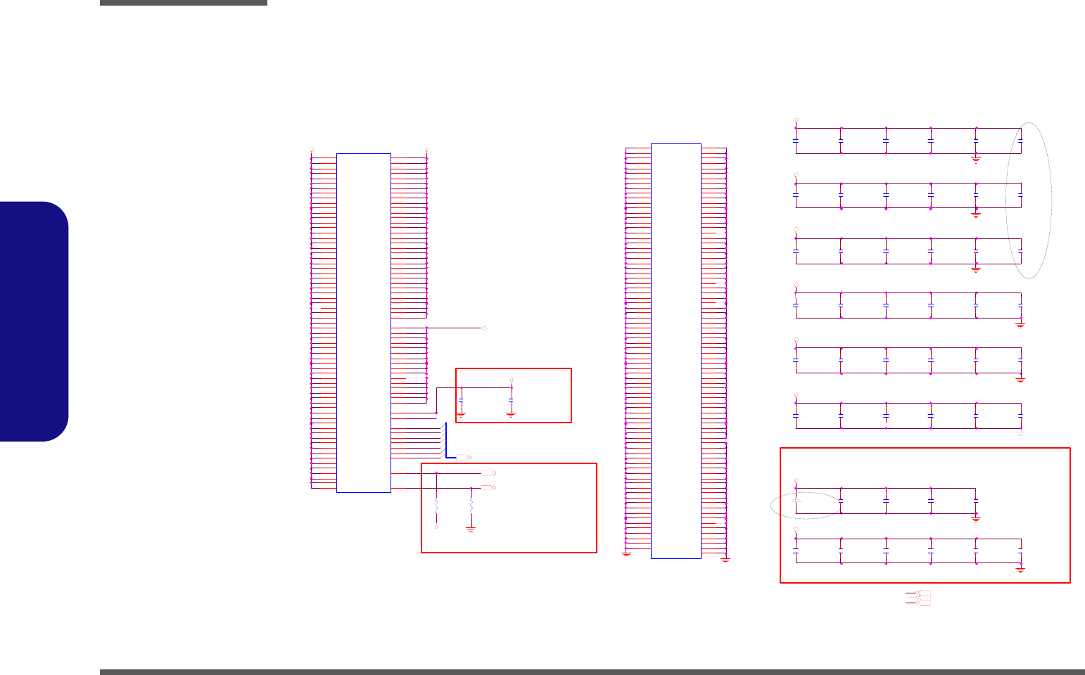
B - 4 Meron (Socket-P) 2/2
B.Schematic Diagrams
Meron (Socket-P) 2/2
C4 1 3
.1 U_ 1 0 V_ X7 R _0 4
C4 5 3
10U _6.3V_X5R_08
C6 1
1U _6. 3V _X5R_06
C5 2
.1U _10V _X7R_04
C4 5 2
1U _6. 3V _X5R_06
C433
10U _6.3V_X5R_08
C446
10U_6.3V_X5R _08
C391
10U_6.3V_X5R _08
5/10
PLACE NEAR CPU
1.05VS
VSSSEN SE
C450
1U _6 .3V_ X5R_0 6
H_VID6
V CC SENSE
2A
VC OR E
C448
1U_6.3V_X5R _06
C392
10U_6.3V_X5R _08
C449
10U _6.3V_X5R_08
C412
.1U_10V _X7R _04
1.05VS
C415
.1U_10V_X7R _04
Check cap for santa rosa platform
C4 2 9
.1U _10V _X7R_04
C3 7 3
10U _6.3V_X5R_08
C430
.1U _10V_X7R _04
H_VID4
VC OR E
C5 7
.1 U_ 1 0 V_ X7 R _0 4
C444
.01U_16V_X7R _04
+
C425
15 0 U _4 V _ B 2
H_VID2
C3 7 5
10U _6.3V _X5R_08
PLACE NEAR CPU
Route VCCSENSE and
VSSSENSE traces at 27.4
ohms with 50 mils spacing.
Place PU and PD within 1
inch of CPU.
Power Plane
1.5VS
J SKT1 D
M erom Ba ll-ou t R ev 1 a
.
P6
AE11
A8
A11
A14
A16
A19
A23
AF2
B6
B8
B11
B13
B16
B19
B21
B24
C5
C8
C11
C14
C16
C19
C2
C22
C25
D1
D4
D8
D11
D13
D16
D19
D23
D26
E3
E6
E8
E11
E14
E16
E19
E21
E24
F5
F8
F11
F13
F16
F19
F2
F22
F25
G4
G1
G23
G26
H3
H6
H21
H24
J2
J5
J22
J25
K1
K4
K23
K26
L3
L6
L21
L24
M2
M5
M22
M25
N1
N4
N23
N26
P3 A25
AF21
AF19
AF16
AF13
AF11
AF8
AF6
A2
AE26
AE23
AE19
P21
P24
R2
R5
R22
R25
T1
T4
T23
T26
U3
U6
U21
U24
V2
V5
V22
V25
W1
W4
W23
W26
Y3
Y21
Y24
AA2
AA5
AA8
AA11
AA14
AA16
AA19
AA22
AA25
AB1
AB4
AB8
AB11
AB13
AB16
AB19
AB23
AB26
AC3
AC6
AC8
AC11
AC14
AC16
AC19
AC21
AC24
AD2
AD5
AD8
AD11
AD13
AD16
AD19
AD22
AD25
AE1
AE4
Y6
A4
AE14
AE16
AE8
AF25
VSS [082 ]
VSS [148 ]
VSS[00 2 ]
VSS[00 3 ]
VSS[00 4 ]
VSS[00 5 ]
VSS[00 6 ]
VSS[00 7 ]
VSS[00 8 ]
VSS[00 9 ]
VSS[01 0 ]
VSS[01 1 ]
VSS[01 2 ]
VSS[01 3 ]
VSS[01 4 ]
VSS[01 5 ]
VSS[01 6 ]
VSS[01 7 ]
VSS[01 8 ]
VSS[01 9 ]
VSS[02 0 ]
VSS[02 1 ]
VSS[02 2 ]
VSS[02 3 ]
VSS[02 4 ]
VSS[02 5 ]
VSS[02 6 ]
VSS[02 7 ]
VSS[02 8 ]
VSS[02 9 ]
VSS[03 0 ]
VSS[03 1 ]
VSS[03 2 ]
VSS[03 3 ]
VSS[03 4 ]
VSS[03 5 ]
VSS[03 6 ]
VSS[03 7 ]
VSS[03 8 ]
VSS[03 9 ]
VSS[04 0 ]
VSS[04 1 ]
VSS[04 2 ]
VSS[04 3 ]
VSS[04 4 ]
VSS[04 5 ]
VSS[04 6 ]
VSS[04 7 ]
VSS[04 8 ]
VSS[04 9 ]
VSS[05 0 ]
VSS[05 1 ]
VSS[05 2 ]
VSS[05 3 ]
VSS[05 4 ]
VSS[05 5 ]
VSS[05 6 ]
VSS[05 7 ]
VSS[05 8 ]
VSS[05 9 ]
VSS[06 0 ]
VSS[06 1 ]
VSS[06 2 ]
VSS[06 3 ]
VSS[06 4 ]
VSS[06 5 ]
VSS[06 6 ]
VSS[06 7 ]
VSS[06 8 ]
VSS[06 9 ]
VSS[07 0 ]
VSS[07 1 ]
VSS[07 2 ]
VSS[07 3 ]
VSS[07 4 ]
VSS[07 5 ]
VSS[07 6 ]
VSS[07 7 ]
VSS[07 8 ]
VSS[07 9 ]
VSS[08 0 ]
VSS[08 1 ] VSS [16 2]
VSS [161 ]
VSS [160 ]
VSS [159 ]
VSS [158 ]
VSS [157 ]
VSS [156 ]
VSS [155 ]
VSS [154 ]
VSS [153 ]
VSS [152 ]
VSS [151 ]
VSS [083 ]
VSS [084 ]
VSS [085 ]
VSS [086 ]
VSS [087 ]
VSS [088 ]
VSS [089 ]
VSS [090 ]
VSS [091 ]
VSS [092 ]
VSS [093 ]
VSS [094 ]
VSS [095 ]
VSS [096 ]
VSS [097 ]
VSS [098 ]
VSS [099 ]
VSS [100 ]
VSS [101 ]
VSS [102 ]
VSS [103 ]
VSS [104 ]
VSS [105 ]
VSS [107 ]
VSS [108 ]
VSS [109 ]
VSS [110 ]
VSS [111 ]
VSS [112 ]
VSS [113 ]
VSS [114 ]
VSS [115 ]
VSS [116 ]
VSS [117 ]
VSS [118 ]
VSS [119 ]
VSS [120 ]
VSS [121 ]
VSS [122 ]
VSS [123 ]
VSS [124 ]
VSS [125 ]
VSS [126 ]
VSS [127 ]
VSS [128 ]
VSS [129 ]
VSS [130 ]
VSS [131 ]
VSS [132 ]
VSS [133 ]
VSS [134 ]
VSS [135 ]
VSS [136 ]
VSS [137 ]
VSS [138 ]
VSS [139 ]
VSS [140 ]
VSS [141 ]
VSS [142 ]
VSS [143 ]
VSS [144 ]
VSS [145 ]
VSS [146 ]
VSS [106 ]
VSS[00 1 ]
VSS [149 ]
VSS [150 ]
VSS [147 ]
VSS [163 ]
VC OR E
R 216
100_1% _04
C4 3 7
10U _6.3V_X5R_08
C4 3 8
10U _6.3V _X5R_08
C58
.1U _10 V_ X7 R_0 4
H _ V I D [ 6 : 0] 28
C4 5 1
10U _6.3V _X5R_08
130mA
VC OR E
C423
.1U_10V _X7R _04
VC OR E
VCC SEN SE 28
C434
10U_6.3V_X5R _08
J SKT1 C
Merom Ball-out R ev 1a
.
A7
A9
A10
A12
A13
A15
A17
A18
A20
B7
B9
B10
B12
B14
B15
B17
B18
B20
C9
C10
C12
C13
C15
C17
C18
D9
D10
D12
D14
D15
D17
D18
E7
E9
E10
E12
E13
E15
E17
E18
E20
F7
F9
F10
F12
F14
F15
F17
F18
F20
AA7
AA9
AA10
AA12
AA13
AA15
AA17
AA18
AA20
AB9
AC 10
AB10
AB12
AB14
AB15
AB17
AB18
AB20
AB7
AC 7
AC 9
AC 12
AC 13
AC 15
AC 17
AC 18
AD 7
AD 9
AD 10
AD 12
AD 14
AD 15
AD 17
AD 18
AE9
AE10
AE12
AE13
AE15
AE17
AE18
AE20
AF9
AF1 0
AF1 2
AF1 4
AF1 5
AF1 7
AF1 8
AF2 0
B26
J6
K6
M6
J21
K21
M2 1
N2 1
N6
R2 1
R6
T21
T6
V21
W21
AF7
AD 6
AF5
AE5
AF4
AE3
AF3
AE2
AE7
C2 6
G2 1
V6
VCC [0 0 1]
VCC [0 0 2]
VCC [0 0 3]
VCC [0 0 4]
VCC [0 0 5]
VCC [0 0 6]
VCC [0 0 7]
VCC [0 0 8]
VCC [0 0 9]
VCC [0 1 0]
VCC [0 1 1]
VCC [0 1 2]
VCC [0 1 3]
VCC [0 1 4]
VCC [0 1 5]
VCC [0 1 6]
VCC [0 1 7]
VCC [0 1 8]
VCC [0 1 9]
VCC [0 2 0]
VCC [0 2 1]
VCC [0 2 2]
VCC [0 2 3]
VCC [0 2 4]
VCC [0 2 5]
VCC [0 2 6]
VCC [0 2 7]
VCC [0 2 8]
VCC [0 2 9]
VCC [0 3 0]
VCC [0 3 1]
VCC [0 3 2]
VCC [0 3 3]
VCC [0 3 4]
VCC [0 3 5]
VCC [0 3 6]
VCC [0 3 7]
VCC [0 3 8]
VCC [0 3 9]
VCC [0 4 0]
VCC [0 4 1]
VCC [0 4 2]
VCC [0 4 3]
VCC [0 4 4]
VCC [0 4 5]
VCC [0 4 6]
VCC [0 4 7]
VCC [0 4 8]
VCC [0 4 9]
VCC [0 5 0]
VCC [0 5 1]
VCC [0 5 2]
VCC [0 5 3]
VCC [0 5 4]
VCC [0 5 5]
VCC [0 5 6]
VCC [0 5 7]
VCC [0 5 8]
VCC [0 5 9]
VCC [0 6 0]
VCC [0 6 1]
VCC [0 6 2]
VCC [0 6 3]
VCC [0 6 4]
VCC [0 6 5]
VCC [0 6 6]
VCC [0 6 7]
VC C[068]
VC C[069]
VC C[070]
VC C[071]
VC C[072]
VC C[073]
VC C[074]
VC C[075]
VC C[076]
VC C[077]
VC C[078]
VC C[079]
VC C[080]
VC C[081]
VC C[082]
VC C[083]
VC C[084]
VC C[085]
VC C[086]
VC C[087]
VC C[088]
VC C[089]
VC C[090]
VC C[091]
VC C[092]
VC C[093]
VC C[094]
VC C[095]
VC C[096]
VC C[097]
VC C[098]
VC C[099]
VC C[100]
VCC A[01 ]
VCC P[03 ]
VCC P[04 ]
VCC P[05 ]
VCC P[06 ]
VCC P[07 ]
VCC P[08 ]
VCC P[09 ]
VCC P[10 ]
VCC P[11 ]
VCC P[12 ]
VCC P[13 ]
VCC P[14 ]
VCC P[15 ]
VCC P[16 ]
V CC SENS E
VID [0 ]
VID [1 ]
VID [2 ]
VID [3 ]
VID [4 ]
VID [5 ]
VID [6 ]
VSS SENS E
VCC A[02 ]
VCC P[01 ]
VCC P[02 ]
C395
1U _ 6 . 3V _X 5 R _0 6
VCORE
Layout note:
VSSSEN SE 2 8
C62
1U_6.3V_X5R _06
C416
.1U _10V_X7R _04
C436
10U_6.3V_X5R _08
C4 7
.1 U_ 1 0 V_ X7 R _0 4
VC OR E
VCO RE 2 8
C688
10U_6.3V_X5R _08
1.05VS 2,4,6, 7,16,30
C420
.1U_10V_X7R _04
C3 9 9
.1U _10V _X7R_04
1.05VS
C687
10U_6.3V_X5R _08
6-07-10611-7C0
Near pin B26
R215
100_1% _04
1.5V S 6,20,27
C422
.1U _10 V_ X7 R_0 4
VCO RE
C6 0
1U_6.3V_X5R _06
H_VID3
H_VID1
C419
.1U_10V_X7R _04
Layout note:
5/17
EE
VC OR E
C689
10U_6.3V_X5R _08
C376
1U_6.3V_X5R _06
H_VID0
C374
1U _ 6 . 3V _X 5 R _0 6
C377
10U_6.3V_X5R _08
C4 2 4
1U_6.3V_X5R _06
C435
10U_6.3V_X5R _08
C396
1U _6 .3V_ X5R_0 6
H_VID5
C393
10U _6.3V_X5R_08
C398
.1U _10 V_ X7 R_0 4
C426
1U_6.3V_X5R _06
Sheet 3 of 38
Meron (Socket-P)
2/2
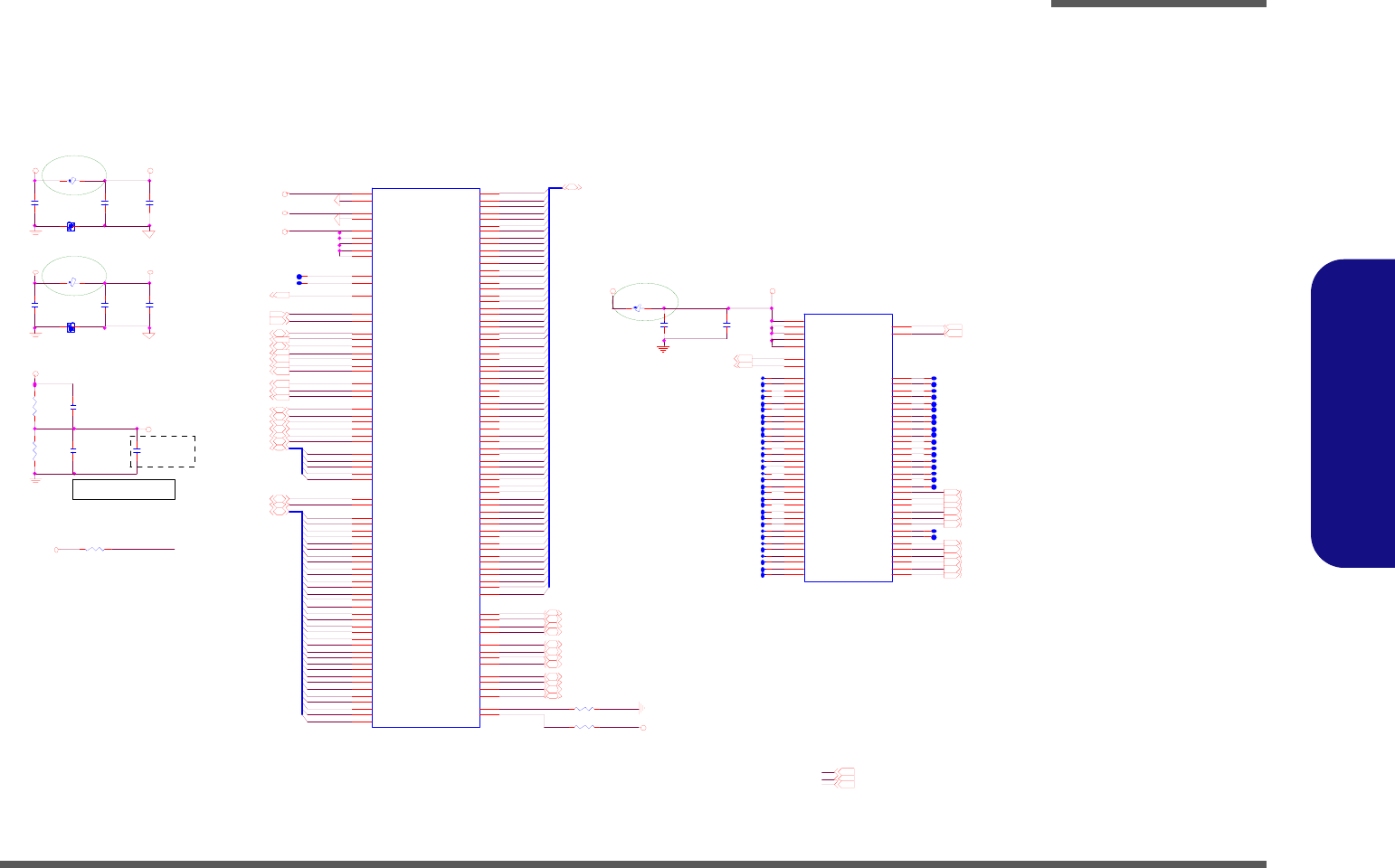
Schematic Diagrams
SiSM672 HOST PCIE 1/5 B - 5
B.Schematic Diagrams
SiSM672 HOST PCIE 1/5
Sheet 4 of 38
SiSM672 HOST
PCIE 1/5
H_ D STB P #3 2
H_ D #4 9
Z0436
C9 2
10U _10V_08
H_ D #2 3
H_ D #4 5
H DVBP1 1 1
H_ A# 6
Z0442
H_ D #1 0
Z0457
NC 8 NC _ 04
H _AD STB# 02
H_ D #3 2
H_A#11
C142
.01U _16V_X7R_04
H_ D INV# 1 2
H_REQ#0
C100
.1U_16V _04
C104
.01U_16V_X7R _04
H_ D #1 8
C474
.1U _16V_04
H_ D STB N# 0 2
H_ D #2 7
H_ D #1 3
H_A#15
Z0418
C4XAVD D
H DVAN 0 11
H DVBP0 1 1
H_AD S#2
L40
H CB1005KF -121T20
H_ D #3 5
H_A#24
H_A#34
H_ D STB N# 3 2
Z0413
H_ D #5 3
H_A#27
EM I 1/ 3
H_ D #1
H_ D #5 9
Z0432
H_ RS #02
H_ RS #22
Z0453
R49 8.25_1% _04
C1XAVD D
H_ D #4 0
Z0444
R50 110_1%_06
NB_ GT L RE F
H_ DE F ER#2
H_A#19
Z0439
H_HITM#2
H_ D #5 8
Z0437
R5 7
75_1% _04
H_DPWR#2
H_ D #4 8
L8
HC B1005KF- 121T20
H_ D #2 2
H_ A# 5
Z0408
H_ D INV# 0 2
H_ D #9
Z0456
NB_ P C RE Q #
H DVAN 1 11
H_ D #4
H_A#10
H DVBN 0 11
Z0425
H_ D #1 7
H_ CPU RS T#2
H_ D #0
H_ D #2 6
H_ D #5 7
PCIE _W AKE#15 , 2 0
H_ D #6 3
H_ REQ # [4 :0]2
H _ CL K_ NB17
Z0417
H DVBN 1 11
H_ D #4 4
H_A#33
H_REQ#4
H_A#23
Z0412
H_ RS #12H_ D #3 1
1.8VS
H_ D INV# 3 2
H_ D #5 2
Z0433
Z0452
H _AD STB# 12
H _ CL K_ NB#17
H_PWRGD2
H_ D #3 9
H DVBP2 1 1
H_A#14
C1 1 3
10U _10V_08
H DVAP0 1 1
1.05VS 2,3,6,7,16,30
H_REQ#2
Z 0401
H_A#18
Z0421
Z0438
C 4XAVD D
H_ D STB N# 2 2
H DVAN 2 11
H_ D #4 7
H_A#31
H_D BSY#2
Z0407
Z0428
NB_PC IE_1.2VS
PC I_ INT # A6,13,22
H_ D #8
H_ D #3
C478
.01U_16V_X7R _04
NB_GTLREF=0.7V
H_ BR 0#2
H_ A# 9
Z0426
C483
.01U_16V_X7R _04
R 315 *56_04
H_HIT#2
H_ D #1 6
Z0449
1.8V S 5,6,7,11,12, 13,14,15,16,17, 27
H_ D #2 5
C1XAVSS
H DVAP2 1 1
H_ D #5 6
H _A#[35:3]2
H DVAP1 1 1
H_ D #6 2
Z0429
C4XAVSS
Z0416
H_ D #2 1
H_ D #4 3
H_A#32
Z0411
H _BPRI#2
H_A#22
Z0448
H _D#[63:0] 2
1.2V S 7,27
H_ D #3 0
Z0451
1.05VS
H_ D STB P #2 2
Z0434
1.8VS
NB_PCREQ#
Place under M671MX
solder side
NB_GTLREF
PC IE_CLK_NB# 17
H_REQ#3
H_ D #3 8
H_ D #1 2
H_A#13
Z0420
H_A#17
H_A#30
Z0422
Z0406
H_ D #7
H_ D #2
H_ D #5 1
Z0443
Z0427
PCIE
U30D
SiSM6 7 2
E4
E5
F1
G1
H3
H2
H1
J1
V1
V6
W4
W1
W2
Y1
Y6
AA4
AA 1
AB 1 AB6
AC4
AB 2
AC 1
AD 1
AD6
AE4
AE 1
AE 2
AF 1
AG 1
T2
U1
K1
K2
L1
M1
N1
N2
P1
R1
T1
J6
G6
G4
J4
L6
M4
P6
P4
H6
G5
K6
J5
M6
M5
R6
P5
W6
W5
AA6
AA5
AC6
AC5
AE6
AE5
P7
R7
T7
U7
V7
D7
G16
T5
T4
PERP0
PERN 0
PERP1
PERN 1
PERP2
PERN 2
PERP3
PERN 3
PERN 9
PETP8
P ETP 9(H DVB P2 )
PERP10
PERN 10
PERP11
PETP1 0(H DVB P1 )
PETP1 1(H DVB P0 )
PERN 11
PERP12 PETP1 2
PETP1 3(H DVA P2 )
PERN 12
PERP13
PERN 13
PETP1 4(H DVA P1 )
PETP1 5(H DVA P0 )
PERP14
PERN 14
PERP15
PERN 15
PERN 8
PERP9
PERP4
PERN 4
PERP5
PERN 5
PERP6
PERN 6
PERP7
PERN 7
PERP8
PETP2
PETP0
PETP1
PETP3
PETP4
PETP5
PETP6
PETP7
PE TN 0
PE TN 1
PE TN 2
PE TN 3
PE TN 4
PE TN 5
PE TN 6
PE TN 7
PE TN 8
PETN9 (H DVBN 2)
PETN10 (H DVBN 1 )
PETN11 (H DVBN 0 )
PETN12
PETN13 (H DVAN 2 )
PETN14 (H DVAN 1 )
PETN15 (H DVAN 0 )
PCIEAV DD
PCIEAV DD
PCIEAV DD
PCIEAV DD
PCIEAV DD
PME#
INTX#
REF C L K+
REFCLK-
PC IE_CLK_NB 17
H_ D #1 5
H_ A# 8
H_ D STB N# 1 2
H_A#26
H_ D #3 4
NB_ C OM P
H_ D #5 5
C 1XA VSS
Z0415
H_ D #2 0
H_ D #4 2
Z0410
Z0447
Z0455
H_ D #2 9
Z0441
Z0450
H_ D #2 4
H_ A# 4
C150
.01U _16V_X7R_04
H_ D #3 7
H_ BN R#2
H_ D #6 1
Z0430
H_A#12
H_A#29
C 4XA VSS
H_LOC K#2
H_A#16
Z0423
C480
.1U _16V_04
C 1XAVD D
H_ D INV# 2 2
H_ D #6
1.2V S
H_ D STB P #1 2
H_A#21
H_ D #5 0
H_ D #4 6
Z0435
H_ A# 7
EM I 1/ 3
1.05VS
H_A#25
H_A#35
H_ D #1 1
H_ D #3 3
H_ T RD Y #2
H_ D STB P #0 2
H_ D #1 9
Z0446
C155
.1U _10V_X7R _04
H_ D #2 8
Z0419
Z0445
EM I 1/ 3
H_ D #1 4
Z0440
H_DRDY#2
NB_ C OM P #
R5 8
150_1% _04
1.05VS
H_ D #3 6
NC 11 NC _ 04
H DVBN 2 11
H_ D #5 4
Z0414
H_REQ#1
H_ D #6 0
H_A#28
Z0431
Z0409
H_ D #5
H_ D #4 1
Z0424
Z0454
H_ A# 3
H_A#20
Host
U30C
SiSM6 7 2
R34
E2 1
P3 2
B1 6
C17
A1 7
B1 8
F18
G18
P3 1
N30
P3 3
L32
P3 0
P2 8
F21
K3 4
M31
K3 3
M33
M32
L34
N32
N34
M34
T34
R30
R29
R32
P3 4
U34
AA3 4
N2 9
M3 0
M2 8
L3 0
L2 9
K28
K31
K30
H3 1
G3 4
H3 2
G3 2
K32
F34
F33
F32
H2 8
J3 0
H3 0
G2 9
J2 9
G3 0
F30
D3 3
D3 4
B32
B33
C3 4
D3 1
A32
A31
C3 1
B30
C3 0
A30
D2 8
G2 8
C2 9
C2 8
E28
E27
C2 7
G2 6
E26
D2 6
B26
A26
C2 6
G2 2
C2 4
A25
B24
C2 5
A24
E23
E25
G2 4
D2 2
C2 2
E22
C2 3
A23
A22
B22
T32
T28
T31
T33
T30
U32
U30
V3 4
U29
V3 3
V3 2
V2 8
V3 1
W34
Y33
W32
V3 0
W30
Y34
Y28
W29
Y32
Y30
Y31
AA3 2
AA3 0
AA2 9
AB3 3
AB3 4
AB3 2
AC 3 4
AB3 0
AB3 1
J3 2
E32
F27
F23
H3 3
E31
B28
D2 4
H3 4
D3 2
A28
E24
A21
C2 1
W24
U24
R24
N24
L21
PCR EQ#
NC 2 (D PW R # )
EDR DY #
C1XAVDD
C1XAVSS
C4XAVDD
C4XAVSS
CPU CL K
CPU CL K#
HTRD Y#
BPRI#
BREQ 0#
HL OC K #
DEF E R #
CPU PW R GD
CPU RST #
RS0 #
RS1 #
RS2 #
DR DY #
BNR #
DBSY #
HIT#
HITM#
ADS#
HR EQ0 #
HR EQ1 #
HR EQ2 #
HR EQ3 #
HR EQ4 #
HASTB0#
HASTB1#
HD 0 #
HD 1 #
HD 2 #
HD 3 #
HD 4 #
HD 5 #
HD 6 #
HD 7 #
HD 8 #
HD 9 #
H D10#
H D11#
H D12#
H D13#
H D14#
H D15#
H D16#
H D17#
H D18#
H D19#
H D20#
H D21#
H D22#
H D23#
H D24#
H D25#
H D26#
H D27#
H D28#
H D29#
H D30#
H D31#
H D32#
H D33#
H D34#
H D35#
H D36#
H D37#
H D38#
H D39#
H D40#
H D41#
H D42#
H D43#
H D44#
H D45#
H D46#
H D47#
H D48#
H D49#
H D50#
H D51#
H D52#
H D53#
H D54#
H D55#
H D56#
H D57#
H D58#
H D59#
H D60#
H D61#
H D62#
H D63#
HA3 #
HA4 #
HA5 #
HA6 #
HA7 #
HA8 #
HA9 #
HA10#
HA11#
HA12#
HA13#
HA14#
HA15#
HA16#
HA17#
HA18#
HA19#
HA20#
HA21#
HA22#
HA23#
HA24#
HA25#
HA26#
HA27#
HA28#
HA29#
HA30#
HA31#
HA32#
HA33#
HA34#
HA35#
DBI0#
DBI1#
DBI2#
DBI3#
H DSTBN 0#
H DSTBN 1#
H DSTBN 2#
H DSTBN 3#
HD STBP0#
HD STBP1#
HD STBP2#
HD STBP3#
HPCOMP
HN CO MP
HVR EF
HVR EF
HVR EF
HVR EF
HVR EF
L42
H CB1005KF -121T20
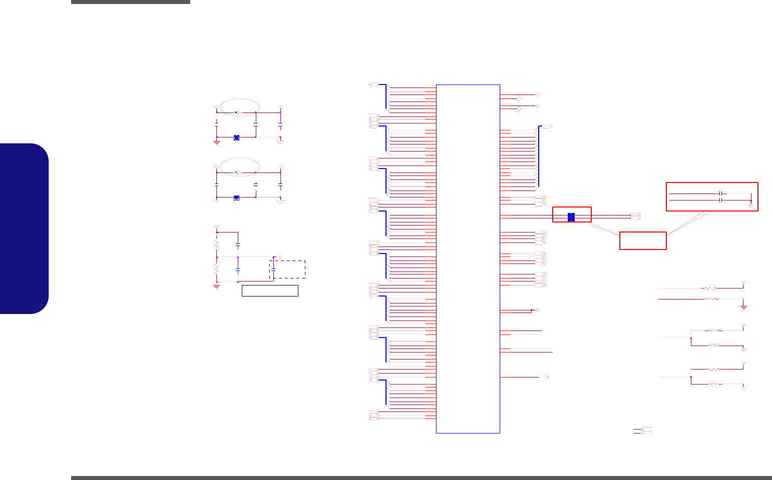
Schematic Diagrams
B - 6 SiSM672 DRAM 2/5
B.Schematic Diagrams
SiSM672 DRAM 2/5
Sheet 5 of 38
SiSM672 DRAM 2/5
M_A_D Q18
M_A_D Q0
4/16
M_A_D Q19
M _ C K E 0 9, 10
C173
.1U _ 10 V_ X 7 R_ 0 4
C171
.1 U _ 10 V_ X 7 R_ 0 4
M_A_D Q1
R 85 36_1%_06
M_CO MP_P
C176
.1U _ 10 V_ X 7 R_ 0 4
R70
1K_1%_04
C484
.01U _16V_X7R_04
M_A_D Q53
M_A_D Q56
M_A_D Q29
M_A_D Q38
M_ CO MP _P
M_ A _ D Q [ 6 3 : 0]9,10
M_ A _ D Q [ 6 3 : 0]9,10
M_ D Q S 0 #9,10
M_ D Q S 4 #9,10
M_DQS79,10
M_ OC D V R E F _ N
M_A_D Q21
M_A_D Q26
M_A_D Q5
M_FWDSDC LKOA_D #
EMI 1/3
D 1XAVD D
M_ A _ A 6
M_DM19,10
M_ A_ A [1 7 :0 ] 9 ,10
M_WE# 9,10
1.8V 7,9,10, 14,15,16, 27,30,31
D 1XAVSS
1.8V
M_A_D Q52
EMI 1/3
M _ C A S # 9, 10
M _ C S 0 # 9, 10
M_ A _ A 4
M_A_D Q11
M_A_D Q23
M_A_D Q33
D 4XAVSS
M_DM79,10
M_CO MP_N
M_CS3# 10
M_A_D Q3
M_A_D Q55
D 4XAVD D
M_ D Q S 3 #9,10
M_ A _ D Q [ 6 3 : 0]9,10
M_A_D Q31
M_A_D Q27
M_A_D Q60
NB_S 3AUXSW# 18
M_A_D Q61
M_ A _ A 1 5
D1XA VSS
M_DQS59,10
M_ A _ A 1 2
M _ R A S # 9, 10
M_ D Q S 7 #9,10
M_A_D Q14
M_ DD R V REF
M_DQS09,10
M_ A _ A 1
M_OCDVRE F_N
M_A_D Q7
M_A_D Q4
M_A_D Q59
M_F WDS DCLKOA_D#
M_A_D Q47
M_ A _ A 1 1
M_ A _ A 0
M_DD RVREF
M_A_D Q57
M_A_D Q40
M_DQS39,10
M_A_D Q36
M _ O D T 0 9, 10
M_A_D Q50
M _FWD SDC LKOA_D _R
M_ A _ A 1 0
M_A_D Q62
L44
HC B1005KF-121T20
1.8V
M_A_D Q58
R88 36_1% _06
M_ D Q S 5 #9,10
M_A_D Q12
M_A_D Q17
M_ A _ D Q [ 6 3 : 0]9,10
M_A_D Q46
M_A_D Q49
M _ C K E 1 9, 10
M_A_D Q51
M_A_D Q41
M_FWDS DCLK OA_D# 17
C519
.01U _16V_X7R_04
M_A_D Q16
M_CKE 3 10
M_ A _ D Q [ 6 3 : 0]9,10
M_A_D Q25
M_DM59,10
M_ A _ A 2
M_CKE 2 10
M_ D Q S 1 #9,10
M_A_D Q30
M_A_D Q63
M_A_D Q2
M_A_D Q37
C522
. 1U _16V_04
M_ A _ A 5
M_ A _ A 3
M_OCDVREF_N=0.969V
M_DM29,10
M_ A _ A 8
R89 40.2_1%_04
Place close to
M671MX
1.8V
M_F WDS DCLKOA_D
1 .8 VS 4 ,6 ,7 ,1 1,1 2 ,1 3 ,1 4,1 5,1 6 ,1 7,2 7
M_ A _ A 1 3
R 6 8 * 10m il_ sho rt
M_OCDVRE F_P
M_OCDVREF_P=0.874V
M_ A _ A 1 6
M_DM09,10
1.8V S
M_A_D Q34
M_A_D Q45
M_A_D Q44
NC12 NC_04
R64
1K_1%_04
M_A_D Q32
M _FWD SDC LKOA_D #_R
C481
. 1U _16V_04
D1XAVDD
M_A_D Q13
M_ CO MP _N
C133
10U_10V_08
1.8V
M_A_D Q8
M_DM39,10
M_A_D Q28
M_DDRVREF=0.9V
M_ A _ D Q [ 6 3 : 0]9,10
M_A_D Q35
R87 40.2_1%_04
M_DQS69,10
DRAM
U3 0 B
SiSM6 7 2
AM 15
AM 17
AM 18
AD 28
AD 30
AD 31
AE 29
AE 30
AE 32
AF 31
AF 32
AF 33
AF 34
AG 34
AH24
AH 32
AH 33
AH 34
AJ 25
AK 21
AK2 5
AK2 6
AK 33
AL 25
AL34
AM2 5
AM2 6
AM 30
AM 31
AN24
AN26
AN28
AN 32
AP2 1
AP2 5
AP2 6
AP2 9
AJ 30
AH 16
AL19
AP2 4
AM2 8
AM2 7
AP2 7
AP2 8
AK2 4
AK 19
AL17
AL15
AJ 29
AH28
AF 28
AJ 34
AH 31
AG 30
AF 30
AG 32
AJ 32
AJ 31
AK 34
AH 30
AL32
AM 33
AK 32
AG 29
AM 34
AL31
AM 32
AP 32
AP 31
AM 29
AK 30
AK 29
AJ 27
AK 28
AK 20
AM 20
AM 19
AJ 19
AN 20
AJ 21
AP 19
AH 20
AK 18
AJ 17
AK 17
AP 16
AH 18
AP 18
AN 18
AP 17
AN 16
AK 16
AN 14
AJ 15
AP 15
AM 16
AK 15
AP 14
AL13
AM 13
AM 12
AJ 13
AM 14
AK 14
AN 12
AH 14
AK 13
AP 12
AP 13
B1 5
A1 5
AP1 0
AP1 1
AM2 3
AP2 2
AJ 23
AK1 2
AH12
AP2 3
AH22
AM2 2
AM2 1
AK2 2
AP2 0
AN22
AL 21
AN30
AP3 0
AH26
AK2 7
B6
AD18
AD23
DQS6A#
DQS5A#
DQM5A
DQM0A
MD1A
MD0A
MD3A
MD7A
MD4A
MD6A
DQS0A
DQS0A#
MD5A
MD2A
MA 0 A
DQS1A
DQS1A#
DQM1A
DDRCOMP
DQM4A
MA 7 A
DD RC OM N
DQS2A
MA 3 A
DQS2A#
MA 2 A
MA 5 A
DQS3A
DQS3A#
MA 11 A
MA 6 A
MA 15 A
DQM3A
MA 16 A
MA 1 A
MA 4 A
MA 17 A
DQM2A
DQM6A
DQS4A#
MA 12 A
MA 13 A
MA 14 A
MA 8 A
MA 9 A
MA 10 A
DQS4A
DQS5A
DQS6A
OCDVREFN
OC D VR E F P
MD8A
MD9A
M D10A
M D11A
M D12A
M D13A
M D14A
M D15A
M D16A
M D17A
M D18A
M D19A
M D20A
M D21A
M D22A
M D23A
M D24A
M D25A
M D26A
M D27A
M D28A
M D29A
M D30A
M D31A
M D32A
M D33A
M D34A
M D35A
M D36A
M D37A
M D38A
M D39A
M D40A
M D41A
M D42A
M D43A
M D44A
M D45A
M D46A
M D47A
M D48A
M D49A
M D50A
M D51A
M D52A
M D53A
M D54A
M D55A
M D56A
M D57A
M D58A
M D59A
M D60A
M D61A
M D62A
M D63A
DQM7A
DQS7A
DQS7A#
D1XAVSS
D1XAVD D
D4XAVSS
D4XAVD D
RASA #
CASA #
WEA #
FWD SDC L KOA
FW D SDC L KOA #
CS 0A #
CS 1A #
CS 2A #
CS 3A #
OD T0 A
OD T1 A
OD T2 A
OD T3 A
CKEA 0
CKEA 1
CKEA 2
CKEA 3
S3AUXSW #
DDRVREF0
DDRVREF1
????
M_A_D Q48
M_A_D Q9
M_ A _ D Q [ 6 3 : 0]9,10
M_ A _ D Q [ 6 3 : 0]9,10
M _ F W D S D C LK O A _ D 17
M_A_D Q39
D4XAVDD
M_ D Q S 6 #9,10
M_A_D Q54
M_A_D Q15
M_DM69,10
M_DM49,10
M _ C S 1 # 9, 10
M_ D Q S 2 #9,10
R 71 36_1%_06
M_OD T3 10
M_CS2# 10
M_ A _ A 7
M_ A _ A 1 4
M_A_D Q24
M_DQS29,10
R81 36_1% _06
M_DQS49,10
M_A_D Q42
M_A_D Q43
M_A_D Q6
M_DQS19,10
M_OD T2 10
M_A_D Q10
M_ A _ A 1 7
M_FWDSDC LKOA_D
C97
10U_10V_08
M_A_D Q22
M_ A _ A 9
M_ OC D V R E F _ P
NC10 NC_04
D4XA VSS
M _ O D T 1 9, 10
M_A_D Q20
C186 *10P_50V_04
L43
HC B1005KF-121T20
C185 *10P_50V_04
1.8V S
R 6 9 * 10m il_ sho rt
Place under M671MX
solder side
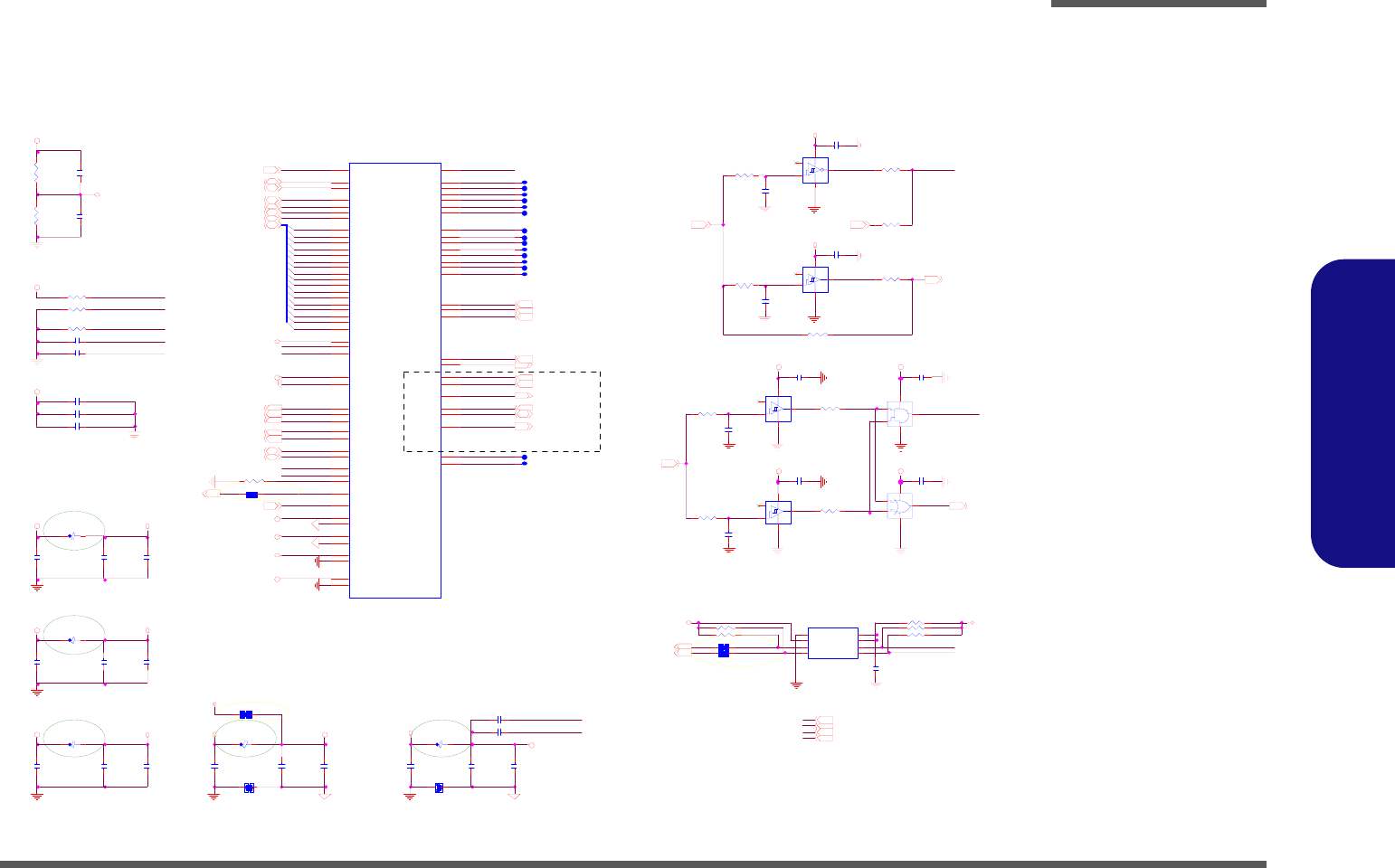
Schematic Diagrams
SiSM672 MuTIOL VGA 3/5 B - 7
B.Schematic Diagrams
SiSM672 MuTIOL VGA 3/5
Sheet 6 of 38
SiSM672 MuTIOL
VGA 3/5
1. 8VS 4,5,7,11,12,13,14,15,16,17,27
C5 2 8
.1U_10V_X7R_04
Z4 XAVD D 1.5VS
SB_DPR SLPVR14
VRSET
PM _D PRSLPVR 2 8
Z_C OM P_N
6-0 1- 74 108 -Q 61
AUX_PW R OK
Z0621
DAC_ B L UE12
C475
.01U_16V_X7R_04
Z_V REF
ZU REQ13
DPR STP#_INV
VCO MP
EM I 1/3
3.3VS
U4
74LV C1G17GW
1
2
53
4
CPU _STP#14
DEL A Y _P W R GD
SB_DPR STP#14
D ACAVSS 2
1.05VS
R3 2 2
150_1%_04
1. 5V S 3 , 2 0 , 27
Z 0601
EM I 1/3
Z 0605
L4 1
H CB1005KF-121T20
1.05V <=> 3.3V
Z 0612
1. 8V S
Z_CLK017
ZAD2
DELAY_PWRGD
R39 130_1%_04
DAC _G REEN12
Z 0613
C160
.01U_16V_X7R_04
R90
33_04
DAC AVDD 1
L3 8
H CB1005KF-121T20
H_DPSL P#2
R1 02
33_04
Level Shitt
AGPSTO P# 14
ZAD1
Z4XAVD D
ZAD12
Z 0626
C78 .1U_16V_04
R 77 150_1%_04
C210
.01U _16V_X7R _04
R 44 4.7K_04
ZAD3
DA C_ HSY NC12
Z0623
C1 9 9
.1U _16V_04
ZSTB_D#113
Z_COM P_P
C542
.1 U_ 16 V_ 0 4
H_DPRSTP#2,28
DAC_DDCACLK12
R9 4
*3 3 _0 4
E CLKAVDD
D ACAVD D1
ZD REQ13
ZAD9
For SiS VB 307
use only
DAC _VS YNC12
ZAD11
N C9 NC_04
Z_ VR EF
ZSTB_D#013
C468
.01U_16V_X7R_04
C2 05
100P_50V_04
PCI_ INT#A4,13,22
C 71 .1U_16V_04
U3
PC A9306DC UR
1
2
3
4
8
7
6
5
GN D
VREF 1
SCL1
SDA1
EN
VREF2
SC L2
SDA2
R 73 56_04
1. 8V S
R3 2 4
49.9_1% _04
ZAD10
R 72 56_04
Z_C OM P_P
ZAD[16:0]13
ZAD14
Z0622
ZSTB_D013
ZAD7
C655
* .1U_16V_04
N B_TES TM OD E1 C211
* 100P_50V_04
1. 8V S
Z0620
R47 *10m il_short
3. 3V S
U9
74LVC 1G17G W
1
2
53
4
R7 5 *1 0 m il _ s ho rt
4/ 1 6
3.3VS
3.3VS
1. 8V S
Z0624
C2 02
*100P_50V _04
Z0618
C 651 *.1U _16V_04
ZAD16
C656
*.01U_16V_04
H _D PSL P#_L S
Z0629
4/16
VBCLK 11
1. 05VS 2,3,4,7,16,30
R1 01
33_04
AUX_PW RO K
C196
.1U _16V_04
C477
.1U_16V_04
ECLKAVD D
Z 0614
C9 9
10U _10V_08
NC 16 N C_ 04
1.8VS
VBVSY NC 1 1
ZAD15
Z 0608
Z0617
D ACAVSS 1
DAC_DDCADAT12
Z 0606
Z 0611
VBHSY NC 11
ZAD13
ZAD8
Z0628
L6 0
* HC B1005KF-121T20
VBHC LK 1 1
VC OM P
VACLK 11
U8
74LVC 1G14G W
1
2
53
4
C217
* 100P_50V_04
L1 1
H CB1005KF-121T20
Z0619
DCL KAVD D
C469
.1U_16V_04
1. 8V S
D ACAVSS 1
C 69 .1U_16V_04
4/16
DAC AVDD 2
C654
* 10U _10V_08
ZSTB_D113
U6
74 L V C 1 G 08 G W
1
2
5
4
3
3. 3 V S
DAC _ RED12
CLK_14M _671MX17
Z_COM P_N
ZAD0
ZAD5
R100 *0_04
C2 16
.1U_16V_04
R103
33_04
C471
.1U_16V_04
3. 3 V S
3.3VS
AUX_PW RO K 1 4, 23
N B_ENTEST
R84 1K_1%_04
R93 1K_1%_04
Z 0602
Z 0607
L3 9
H CB1005KF-121T20
3. 3VS 10,11,12,13,14,15,16,17,18,19,20,21,22,24,25,26,27,28
ZAD4
DELAY _PWR GD 27,28
C 652 *.1U _16V_04
C147
10U_10V_08
R 74 150_1%_04
EMI 1/3
R438 *32m il_s hort
C79 .1U_16V_04
C 653 *.1U _16V_04
C1 1 7
10U _10V_08
ZAD6
N B_TES TM OD E2
DAC AVDD 2
VBCAD 11
Z 0625
U7
74LV C1G17GW
1
2
53
4
C5 41
.1U_16V_04
R83
33_04
R9 1
499_1% _04
DPRSTP#_INV
E MI 1/ 3
NB_EN TEST
U5
74AH C1G32GW
4
53
1
2
AGPBU SY# 1 4
DC LKA VDD
C5 3 8
.1U_10V_X7R_04
C1 2 1
10U _10V_08
Z0627R7 6 *1 0 m il _ s ho rt
C473
.01U_16V_X7R_04
CP UST P # 17
Z 0610
Z 0604
C163
.1U_16V_04
R8 2
33_04
1.8VS
R96 200K_04 3.3VS
Z 0603
DAC AVSS2
NB_RS T# 11,27
H_D PSLP #_ L S
N B_TES TM OD E0
C198
.1 U_ 16 V_ 0 4
R9 2
33_04
ASL
U30A
SiSM672
AM8
AM9
AM1 0
AN8
AN10
AP4
AP5
AP8
AP9
AH10
AL7
AL9
AM7
AK10
AM6
AK11
AJ 1 1
AP7
AJ 9
AP6
AN6
AK9
AM4
AK6
AK8
AN4
AK7
AL5
AM5
D1 3
C1 2
C1 3
G1 2
F12
D1 1
E12
D1 5
C1 4
C1 5
F11
F13
A12
B12
A13
B13
B10
A11
A9
F15
D1 6
E16
F16
D1 7
E17
F17
AC32
AD34
AB28
AD32
AD33
AE34
AC30
AC29
A5
C6
A7
A6
D9
C8
E9
E7
D8
F7
AH2
AG3
B8
G1 4
ZAD16
ZCM P_N
Z4XAV DD
ZUR EQ
Z4XAV SS
ZSTB1
ZSTB1#
ZDR EQ
ZCM P_P
ZCLK
ZSTB0#
ZVREF
ZSTB0
ZAD0
ZAD1
ZAD2
ZAD3
ZAD4
ZAD5
ZAD6
ZAD7
ZAD8
ZAD9
ZAD10
ZAD11
ZAD12
ZAD13
ZAD14
ZAD15
RO UT
GO UT
BOU T
VSYN C
HSY NC
VGPIO 0
VGPIO 1
VCO MP
VRSET
VVBW N
VOSC I
INTA#
DAC AVDD 1
DAC AVSS1
DAC AVDD 2
DAC AVSS2
DC LKA V DD
DC LKA V SS
ECLKAVD D
EN TE ST
TE S TM O D E 0
TE S TM O D E 1
TE S TM O D E 2
TRA P0
TRA P1
TRA P2
TRA P3
TRA P4
TRA P5
TRA P6
TRA P7
TRA P8
TRA P9
TR AP10
AUXOK
PW R OK
PCIR ST#
AG PBUSY #
VAC LK
VBC LK
VBC AD
VBHC LK
VBVSY NC
VBHSYNC
NC 0
NC 1
ECLKAVSS
AGPSTO P#
Z 0609
VV BW N
VVBW N
EM I 1/3
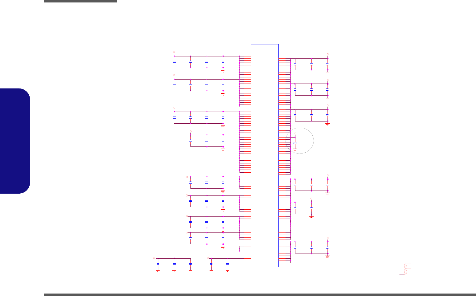
Schematic Diagrams
B - 8 SiSM672 PWR 4/5
B.Schematic Diagrams
SiSM672 PWR 4/5
Sheet 7 of 38
SiSM672 PWR 4/5
C13 8
.1U_16V_04
C12 0
1U_ 10V_06
1.8V S 4, 5, 6, 11 ,12,13 ,14,15 ,16,17 ,27
5/10
C126
.1U_16V_04
1.2V S
1.2 V
C479
1U_1 0V_06
1.2VS
C123
. 1U_16V _04
C140
1U_10 V_06
C178
.1U_16V_04
1. 8V
C119
. 1U_16V _04
PWR
U30E
Si S M 6 7 2
AB 12
AB 13
AC12
AC13
AC14
AC15
AH6
AH7
AJ4
AJ5
AJ6
AJ7
AN2
AK 4
AK 5
AL1
AL2
AL3
AL4
AM1
AM2
AM3
AN3
AN5
AN7
AN9
E8
E10
F9
F10
F8
AB18
AB20
P20
P22
R21
T22
U21
V22
M11
N11
P11
R11
T11
U11
V11
W11
Y11
AA 11
AB 11
D6
G8
N19
N21
W23
Y23
AA 23
AB 23
AC23
AC18
AC20
AC16
AD16
AD17
AD19
AD20
AD21
AD22
AJ 22
AJ 24
AL 23
AN21
AN23
AN25
AN27
AN29
AA13
AA22
AB14
AB15
AB16
AB22
AF6
AF7
AK3
AG4
AG5
AG6
AG7
R13
AH3
AH4
AH5
AJ1
AJ2
AJ3
AK1
AK2
AC22
AC21
AC19
AC17
A19
A20
B19
B20
C19
C20
D19
D20
E19
E20
F19
F20
G19
G20
L18
L19
L20
M20
M21
M22
M23
N23
P23
R23
T23
U23
V23
M12
N12
P12
R12
T12
U12
V12
W12
Y12
AA12
AP 3
M13
M14
M15
M16
M17
M18
M19
N16
N17
N18
N20
R22
N22
N13
P13
Y13
Y22
T13
U13
U22
V13
W13
W22
C5
B5
AL 26
VCC1. 8
VCC1. 8
VCC1. 8
VCC1. 8
VCC1. 8
VCC1. 8
VCC1. 8
VCC1. 8
VCC1. 8
VCC1. 8
VCC1. 8
VCC1. 8
VCC1. 8
VCC1. 8
VCC1. 8
VCC1. 8
VCC1. 8
VCC1. 8
VCC1. 8
VCC1. 8
VCC1. 8
VCC1. 8
VCC1. 8
VCC1. 8
VCC1. 8
VCC1. 8
VDDVB1. 8
VDD1. 8
VDDVB1. 8
VDD1. 8
VDDVB1. 8
IVDD
IVDD
PVDDH
PVDDH
PVDDH
PVDDH
PVDDH
PVDDH
VDDPEX
VDDPEX
VDDPEX
VDDPEX
VDDPEX
VDDPEX
VDDPEX
VDDPEX
VDDPEX
VDDPEX
VDDPEX
AU X_ I VD D
AU X1 . 8
PVDDH
PVDDH
VCCM
VCCM
VCCM
VCCM
VCCM
VCCM
VCCM
VCCM
VCCM
VCCM
VCCM
VCCM
VCCM
VCCM
VCCM
VCCM
VCCM
VCCM
VCCM
VCCM
VCCM
VCCM
IVDD
IVDD
IVDD
IVDD
IVDD
IVDD
IVDD
IVDD
IVDD
IVDD
IVDD
IVDD
IVDD
IVDD
IVDD
IVDD
IVDD
IVDD
IVDD
IVDD
IVDD
IVDD
IVDD
IVDD
IVDD
IVDD
VTT
VTT
VTT
VTT
VTT
VTT
VTT
VTT
VTT
VTT
VTT
VTT
VTT
VTT
VTT
VTT
VTT
VTT
VTT
VTT
VTT
VTT
VTT
VTT
VTT
VTT
VTT
V TTP
V TTP
V TTP
V TTP
V TTP
V TTP
V TTP
V TTP
V TTP
V TTP
VCC1. 8
IVDD
IVDD
IVDD
IVDD
IVDD
IVDD
IVDD
IVDD
IVDD
IVDD
IVDD
IVDD
IVDD
IVDD
IVDD
IVDD
IVDD
IVDD
IVDD
IVDD
IVDD
IVDD
IVDD
AU X_ I VD D
AU X_ I VD D
VCCM
C510
1U_1 0V_06
C106
.1U _16V _04
C131
1U_10 V_06
C197
10U_1 0V_08
1.8V 5, 9,10,1 4,15,1 6,27,3 0,31
C485
1U_10V _06
C115
1U_1 0V_06
C110
1U_1 0V_06
C465
1U_10V_06
C112
1U_1 0V_06
C49 0
10 U_10V_0 8
C513
1U_1 0V_06
C503
.1U_16V_04
1.2V S 4, 27
C109
10U_10V _08
C507
. 1U_16V _04
C139
.1U_16V_04
1. 8V
C539
1U_10V _06
1.8VS
C129
.1U _16V _04
C107
.1 U_16V_ 04
C116
1U_10V _06
C206
10U_10V _08
+
C492
150 U_4V_B2
C13 6
.1U_16V_04
C462
1U_10V_06
C124
1U_10V _06
C108
10U_10V_08
1.2V 27, 30
C118
10U_1 0V_08
C530
1U_1 0V_06
1.8VS
1.8VS
1.8V S
C125
1U_1 0V_06
1.2VS
1. 05VS
C190
1U_10 V_06
C495
1U_10 V_06
1.2V S
C135
.1U _16V _04
C11 1
10 U_10V_0 8
C501
.1 U _16V_ 04
1.8V S
C181
.1 U _16V_ 04
C455
.1 U _16V_ 04
C114
10U_ 10V_08
C498
1U_10 V_06
C162
.01U _16 V_X7R_0 4
1. 8V
1.05V S
1.2V S
C536
1U_10V_06
C145
.1U_16V_04
1.05 VS 2, 3,4,6, 16,30
C146
1U_10V _06
1.2VS
C192
. 1U_16V _04
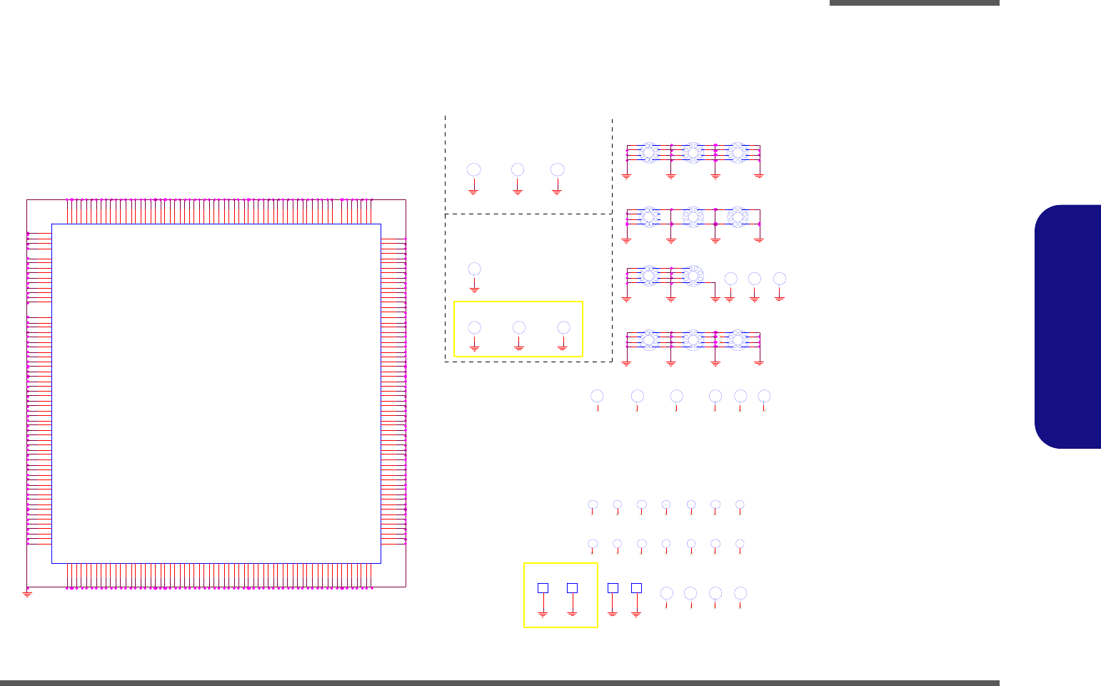
Schematic Diagrams
SISM672 GND 5/5 B - 9
B.Schematic Diagrams
SISM672 GND 5/5
Sheet 8 of 38
SISM672 GND 5/5
M2
M-MARK1
1
H1 0
MTH315D111- 3_4
2
3
4
5 6
7
8
9
MH2
H4_0
M7
M-M A R K 1
H12, H13, H14
6-34-M52GS-020
1
H1 1
MT H3 1 5 D1 1 1
2
3
4
5 6
7
8
9
M8
M-MA RK1
M5
M-M A R K 1
1
H6
MTH5_5D2_8
2
3
4
5 6
H3
O44X59D44X59
S1
SM D80X80
11
H16
C 355B264D186
M1 4
M-M A R K 1
H17
C237D87
H19
C 217D87
MH 3
H4_0
H25
O 44X59D44X59
H2 4
C40D40
1
H1 2
MTH315D111A
2
3
4
5 6
9
M1 0
M-M A R K 1
S6
SMD 80 X8 0
11
GND
U30F
SiSM6 7 2
A3
B2
B3
B4
AA16
AA17
AA18
AA19
AA20
AA21
AA 31
AA33
AB 3
AB4
AB5
AG2
AG 31
AG3 3
AH29
B21
B23
B25
B27
B29
B31
C1
C2
C3
C4
AB7
AB29
AC 2
AC3
AC 31
AC33
AD 2
AD3
AD 4
AD5
AD 7
AD29
AE3
AE31
AE 33
AF2
AF 3
AF4
AF5
AF2 9
AJ 8
AJ 10
AJ 1 2
AJ 14
AJ 1 6
AJ 18
AJ 2 0
AJ 26
AJ 2 8
AJ 33
AK 31
AL6
AL8
AL10
AL12
AL14
AL1 6
AL18
AL2 0
AL28
AL30
AL33
AN 11
AN13
AN 15
AN17
AH 1
T29
U2
U3
U4
U5
U6
U1 4
U1 5
U1 6
U1 7
U1 8
U1 9
U2 0
U3 1
U3 3
V2
V3
V4
V5
V1 4
V1 5
V1 6
V1 7
V1 8
V1 9
V2 0
V2 9
AN33
AN31
AN19
W3
W14
W15
W16
W17
W18
W19
W20
W21
W31
W33
Y2
Y3
Y4
Y5
Y7
Y1 4
Y1 5
Y1 6
Y1 7
Y1 8
Y1 9
Y2 0
Y2 1
Y2 9
AA2
AA3
AA1 4
AA1 5
H5
H29
J2
J3
J7
J31
J33
K3
K4
K5
K29
L2
L3
L4
L5
L7
L31
L3 3
M2
M3
M29
N3
N4
N5
N6
N7
N14
N1 5
N31
N3 3
P2
P3
P14
P15
P16
P17
P18
P29
R2
R3
R4
R5
R1 4
R15
R1 6
R17
R1 8
R19
R2 0
R3 1
R33
T3
T6
T14
T15
T16
T17
T18
T19
T20
G31
G3 3
H4
C9
C1 0
C1 1
C1 6
C1 8
C3 2
C3 3
D1
D2
D3
D4
D5
D1 0
D1 2
D2 1
D2 3
D2 5
D2 7
D2 9
E1
E2
E3
E6
E11
E13
E14
E18
E29
E30
E33
F2
F3
F4
F5
F6
F14
F22
F24
F26
F28
G2
G3
G7
G1 0 AB1 7
AB1 9
AB2 1
P1 9
P21
T21
V21
VSS
VSS
VSS
VSS
VSS
VSS
VS S
VSS
VS S
VSS
VSS
VSS
VSS
VSS
VSS
VSS
VSS
VSS
VSS
VSS
VSS
VSS
VSS
VSS
VSS
VSS
VSS
VSS
VSS
VSS
VSS
VSS
VSS
VSS
VSS
VSS
VSS
VSS
VSS
VS S
VSS
VS S
VSS
VSS
VSS
VSS
VSS
VSS
VSS
VSS
VSS
VS S
VSS
VS S
VSS
VS S
VSS
VSS
VSS
VSS
VSS
VSS
VSS
VSS
VSS
VSS
VSS
VSS
VSS
VS S
VSS
VS S
VSS
VSS
VSS
VSS
VS S
VS S
VS S
VS S
VS S
VS S
VS S
VS S
VS S
VS S
VS S
VS S
VS S
VS S
VS S
VS S
VS S
VS S
VS S
VS S
VS S
VS S
VS S
VS S
VS S
VS S
VS S
VS S
VS S
VS S
VS S
VS S
VS S
VS S
VS S
VS S
VS S
VS S
VS S
VS S
VS S
VS S
VS S
VS S
VS S
VS S
VS S
VS S
VS S
VS S
VS S
VS S
VS S
VS S
VS S
VS S
VS S
VS S
VS S
VSS
VS S
VSS
VSS
VSS
VSS
VSS
VSS
VSS
VSS
VSS
VSS
VSS
VSS
VSS
VSS
VSS
VSS
VS S
VSS
VS S
VSS
VSS
VSS
VSS
VSS
VSS
VSS
VSS
VSS
VSS
VSS
VSS
VSS
VSS
VS S
VSS
VS S
VSS
VS S
VSS
VSS
VSS
VSS
VSS
VSS
VSS
VSS
VSS
VSS
VSS
VSS
VSS
VSS
VS S
VSS
VS S
VSS
VSS
VSS
VSS
VSS
VS S
VSS
VSS
VSS
VSS
VSS
VSS
VSS
VSS
VSS
VSS
VSS
VSS
VSS
VSS
VSS
VSS
VSS
VSS
VSS
VSS
VSS
VSS
VSS
VSS
VSS
VSS
VSS
VSS
VSS
VSS
VSS
VSS
VSS
VSS
VSS
VSS
VSS
VSS
VSS
VSS
VSS
VSS
VSS
VSS VS S
VS S
VS S
VS S
VSS
VSS
VSS
1
H2
MT H3 1 5 D1 1 1
2
3
4
5 6
7
8
9
M1 2
M-M A R K 1
H16, H17, H18, H19
M13
M-MARK1
M9
M-MARK1
MH4
H4_0
M6
M-MARK1
1
H7
MTH315D111
2
3
4
5 6
7
8
9
1
H8
MTH315D111B
2
3 5
4
1
H4
MTH315D111
2
3
4
5 6
7
8
9
H2 2
O40X102D40X102
H23
C40D40
H2 7
C237D146
S3
SM D80X80
11
1
H9
M TH 315D 111B
2
3 5
4
M1
M-MA RK1
MH1
H4_0
1
H5
MTH 315D 111
2
3
4
5 6
7
8
9
H26
C237D91
H1 8
C355B264D186
2/ 29
H15
C217D111
H2 1
O40X102D40X102
H1 3
C237D 91
H2 0
C237D87
S2
S MD80X80
1
1
M3
M-MAR K1
H1 4
C355B 264D186
1
H1
MT H3 1 5 D1 1 1
2
3
4
5 6
7
8
9
M11
M-MAR K1
M4
M-M A R K 1
6-34-M52NS-020
2/29
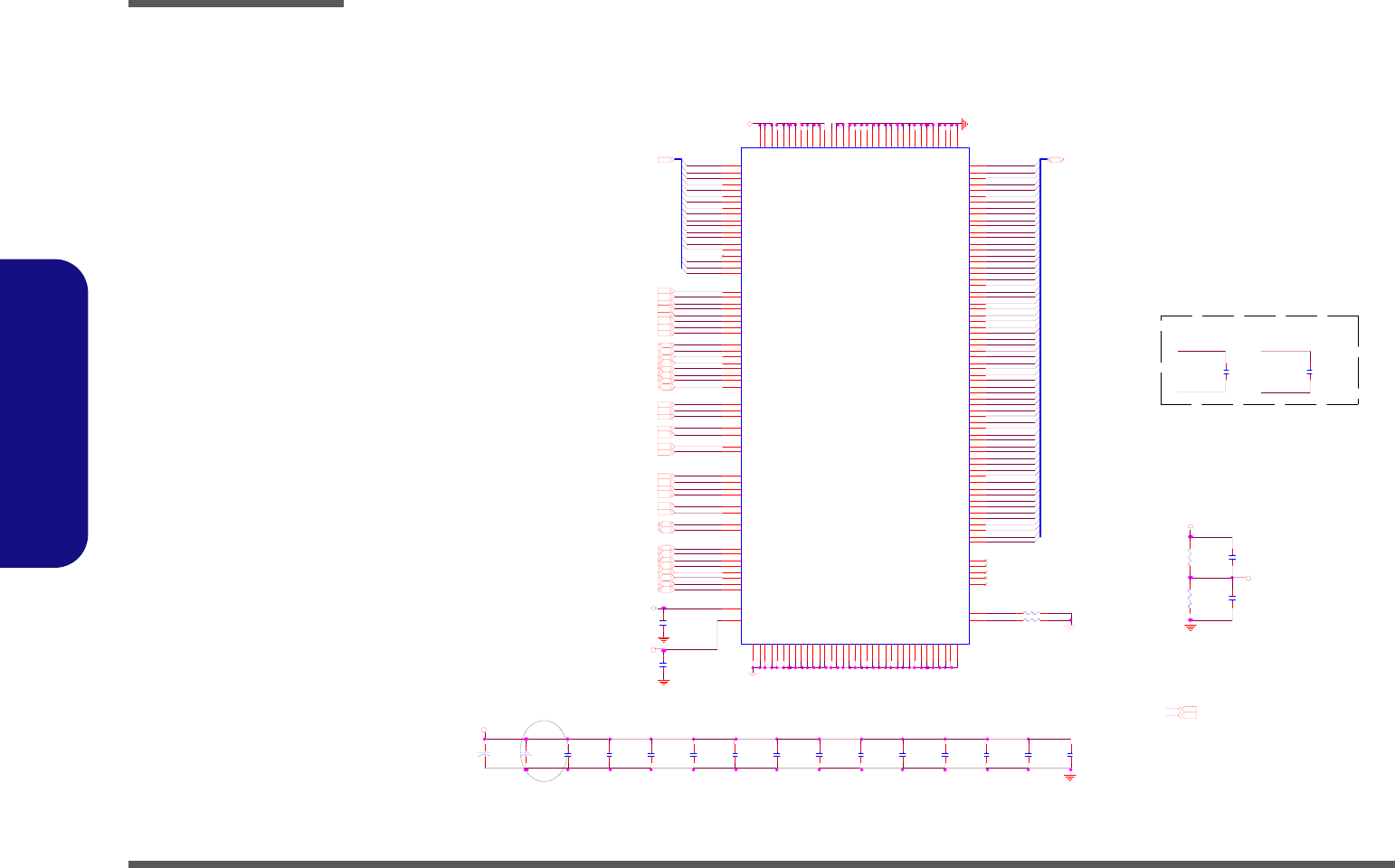
Schematic Diagrams
B - 10 DDRII SO-DIMM 1
B.Schematic Diagrams
DDRII SO-DIMM 1
Sheet 9 of 38
DDRII SO-DIMM 1
M_DQS7#5,10
M_CKE05,10
M_CS1#5,10
M_ A _ A 2
M_ DM 15,10
M_CLK_DDR017
M_ A _ A 8
M_ A _ A 1 7
C556
.1 U _1 0 V_ X 7R _ 04
M_ A _ D Q 5 2
M_ CS 0#
M_ A _ D Q 5 6
M_ A _ D Q 4 7
M_ D Q S 65,10
M_ A _ D Q 2 5
M_ A _ D Q 5 7
M_ CL K_ D DR0 #17
M_ A _ D Q 3 4
???????!
1. 8 V
M_ RAS#5,10
M_ CL K_ D DR0 #
M_ A _ D Q 1 1
M_ A _ D Q 1 4
C82
10U_10V_08
M_ DM 35,10
M_ A _ D Q 2 2
M_ A _ D Q 6 1
M_ A _ D Q 3 6
M_ A _ D Q 5 1
S_DAT10,14,17,20
M_ A _ D Q 1 5
M _A_A[17 :0]5,10
Z0901
M_ D Q S 25,10
M_ A _ D Q 2 4
C529
.1U _16V_04
M_ A _ D Q 1 6
M_ A _ A 1 4
M_ A _ D Q 4 9
M_ A _ A 1 1
M_ CL K_ D DR0
C81
10U_10V_08
M_ D Q S 35,10
M_ A _ D Q 3 1
M_ A _ A 1 6
M_ A _ D Q 4 1
M_ A _ D Q 2 9
C2 3 0
*3 .3 P_ 50 V_0 4
C5 2 0
.1U_16V_04
5/10
M_CLK_DDR0#
M_ CS 1#
M_ A _ D Q 2 1
C461
10U _10V_08
C5 6 2
1U _ 6. 3V_X5 R_0 6
M_DQS4#5,10
M_ A _ D Q 5 0
C5 2 4
.1U _ 16 V_ 0 4
M_ A _ A 3
M _ CL K _ DD R1
M_ A _ D Q 4 4
C571
.1 U _1 0 V_ X 7R _ 04
M_DQS3#5,10
M_ A _ D Q 5
M_ D Q S 55,10
M_ A _ A 0
M_ A _ D Q 2 7
M_ CL K_ D DR1 #
M_DQS6#5,10
M_ A _ D Q 2 6
M_ODT15,10
M_ A _ D Q 5 3
M_ A _ D Q 4 5
M_ A _ D Q 0
M_ A _ A 5
M_ C A S #
M_ODT05,10
M_ A _ D Q 1 3
M_DQS1#5,10
M_ A _ A 4
M_ A _ D Q 4 2
M_ A _ A 1 0
M_ A _ D Q 5 4
M_ DM 45,10
M_ W E #
3.3V S_S PD
M_DQS5#5,10
M_ DM 75,10
M_CLK_DDR0
M_ D Q S 15,10
M_ A _ D Q 5 9
+
C4 8 7
150U_4V_B2
M_ A _ D Q 1 7
M_ A _ D Q 1
MVREF1
M_ A _ D Q 1 9
M_ A _ D Q 3 7
M_ A _ A 7
M_ A _ D Q 6
M_ A _ D Q 9
M_ A _ D Q 3 3
M_CKE15,10
M_CLK_DDR117
M_ A _ A 1 5
M_ A _ D Q 2 3
M_ A _ D Q 3 5
M_ A _ A 9
C526
.1 U _1 6 V_ 04
M _ CL K _ DD R1 #
M_ A _ D Q 5 5
M_ A _ A 1 3
1.8V 5,7,10, 14,15,16,27,30,31
M_ A _ D Q 7
M_ A _ A 6
M_ A _ D Q 3 2
M_ A _ D Q 3
M_ A _ D Q 3 0
J_DI M2
AS 0A421-NAR N-4F
102
101
100
99
98
97
94
92
93
91
105
90
89
107
106
5
7
17
19
4
6
14
16
23
25
35
37
20
22
36
38
43
45
55
57
44
46
56
58
61
63
73
75
62
64
74
76
123
125
135
137
124
126
134
136
141
143
151
153
140
142
152
154
157
159
173
175
158
160
174
176
179
181
189
191
180
182
192
194
112
11 1
117
96
95
11 8
81
82
87
10 3
88
104
149
47
133
183
77
12
48
184
78
71
72
12 1
122
19 6
193
8
162
15 0
138
40
28
18
24
41
53
42
54
59
65
60
66
12 7
139
128
145
165
171
172
187
178
190
9
21
33
155
34
132
14 4
156
16 8
2
3
15
27
83
120
50
69
163
86
39
198
200
161
1
177
199
116
11
29
49
68
129
146
167
186
10
26
52
67
130
147
170
185
84
13
31
51
70
131
148
169
188
85
108
109
113
110
115
79
80
30
164
114
32
166
119
195
197
A0
A1
A2
A3
A4
A5
A6
A7
A8
A9
A10/A P
A11
A12
BA0
BA1
DQ0
DQ1
DQ2
DQ3
DQ4
DQ5
DQ6
DQ7
DQ8
DQ9
DQ 10
DQ 11
DQ 12
DQ 13
DQ 14
DQ 15
DQ 16
DQ 17
DQ 18
DQ 19
DQ 20
DQ 21
DQ 22
DQ 23
DQ 24
DQ 25
DQ 26
DQ 27
DQ 28
DQ 29
DQ 30
DQ 31
DQ 32
DQ 33
DQ 34
DQ 35
DQ 36
DQ 37
DQ 38
DQ 39
DQ 40
DQ 41
DQ 42
DQ 43
DQ 44
DQ 45
DQ 46
DQ 47
DQ 48
DQ 49
DQ 50
DQ 51
DQ 52
DQ 53
DQ 54
DQ 55
DQ 56
DQ 57
DQ 58
DQ 59
DQ 60
DQ 61
DQ 62
DQ 63
VD D
VDD
VD D
VDD
VD D
VDD
VD D
VDD
VD D
VDD
VD D
VDD
VS S
VSS
VSS
VSS
VSS
VSS
VSS
VSS
VSS
VSS
VSS
VSS
VSS
VSS
VSS
VSS
VSS
VSS
VS S
VSS
VS S
VSS
VSS
VSS
VSS
VSS
VSS
VSS
VS S
VSS
VS S
VSS
VS S
VSS
VSS
VSS
VSS
VSS
VSS
VSS
VSS
VSS
VSS
VSS
VSS
VSS
VSS
VSS
VSS
VSS
VS S
VSS
VS S
VSS
NC1
NC2
NC3
NC4
NCTEST
A14
VS S
SA0
SA1
VSS
VREF
VSS
VDD SPD
A13
DQ S# 0
DQ S# 1
DQ S# 2
DQ S# 3
DQ S# 4
DQ S# 5
DQ S# 6
DQ S# 7
DM 0
DM 1
DM 2
DM 3
DM 4
DM 5
DM 6
DM 7
A15
DQ S0
DQ S1
DQ S2
DQ S3
DQ S4
DQ S5
DQ S6
DQ S7
A16/B A2
RAS#
WE#
CAS#
S0#
S1#
CKE0
CKE1
CK0
CK1
OD T0
CK0 #
CK1 #
OD T1
SDA
SCL
M_ CL K_ D DR1 #17
M_ A _ A 1
M_ A _ D Q 6 2
C5 3 4
.1U_16V _04
SO-DIMM 1
M_ A _ D Q 2 0
M_ A _ D Q 5 8
C8 4
10U_10V_08
M_ A _ D Q 4 3
M_ D Q S 45,10
C5 1 6
.1U _ 16 V_ 0 4
M_ DM 05,10
M_ OD T 1
M_ A _ D Q 4 8
M_ C K E 0
C494
* 3.3P_5 0 V_04
R36 10K_04
M_ A _ D Q 3 9
M_ A _ D Q 8
M_ CAS#5,10
M_ DM 25,10
R35 10K_04
M_ A _ D Q 4
M_DQS0#5,10
M_ A _ D Q 1 0
M_ A _ D Q 4 6
1.8V
M_ A _ D Q 2 8
C7 3
.1U_16V_04
M_ A _ D Q 6 3
M_ A _ D Q 4 0
Z0902
M_ A _ D Q 1 2
M_ C K E 1
1.8V
M_CS0#5,10
M_ CL K_ D DR1
M_ R A S #
C5 1 2
.1U _ 16V _ 0 4
S_CLK10,14,17,20
3.3VS_SPD 10
M_A_DQ [63:0] 5,10
M_ A _ D Q 6 0
M_DQS2#5,10
M_ A _ D Q 3 8
M_ DM 55,10
M_ OD T 0
+
C4 6 6
*150U_4V_B2
R3 4 8
1K _1 % _ 04
MVREF1
M_ A _ D Q 1 8M_ A _ A 1 2
C514
.1 U _1 6 V_ 04
M_ W E #5,10
M_ D Q S 75,10
M_ DM 65,10
M_ A _ D Q 2
R3 4 0
1K _1 % _ 04
C2 2 0
10U_10V_08
M_ D Q S 05,10
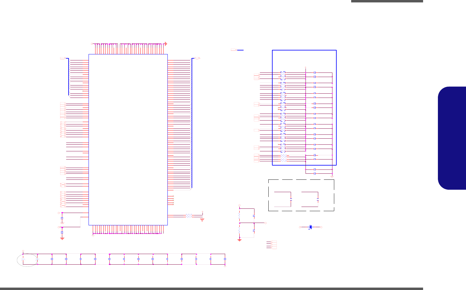
Schematic Diagrams
DDRII SO- DIMM 2 B - 11
B.Schematic Diagrams
DDRII SO- DIMM 2
M_ DM 25,9
M_A_D Q40
M_A_D Q15
M_A_D Q18
Layout Note:
M_ DM 15,9
M_A_D Q57
C 193 .1U _16V_04
M_ DM 45,9
M_A_D Q47
M_A_D Q51
M_ DQ S 7 #5,9
M_A _A[17:0]5, 9
3.3VS_SPD
M_ D Q S 75,9
M_CS2#5
M_A_D Q37
M_ A_ A4
M_A_D Q28
M_A_D Q43
M_ DQ S 6 #5,9
M_ A_ A16
MVREF2
M_ A_ A10
M_A_D Q24
M_A_D Q38
M_A_D Q11
RN18
8P4RX56_04
1
2
3
45
6
7
8
M_ A_ A10
M_CLK_DDR3#17
M_ CL K _ DD R3
M_ DQ S 0 #5,9
M_CS3#5
M_ D Q S 55,9
M_A_D Q13
M_ A_ A6 M_ A_ A16
RN16
8P4RX56_04
1
2
3
45
6
7
8
Z1002
M_ CL K _ DD R2
C 540 .1U _16V_04
M_A_D Q55
C 183 .1U _16V_04
M_A_D Q7
M_CS0#5,9
M_A_D Q0
M_ DM 65,9
M_ R A S #
M_ A_ A11
0. 9 V S 3 1
M_A_D Q33
M_ CS 2 #
M_A_D Q14
M_ D Q S 35,9
M_A_D Q59
M_A_D Q44
1. 8 V
M_ CL K _ DD R3 #
M_ DQ S 4 #5,9
M_ A_ A8
M_ A_ A17
+
C5 44
150U_4V_B2
M_ D Q S 45,9
M_ A_ A11
R1 0 7
1K_1% _04
M_A_DQ [63:0] 5,9
M_A_D Q56
M_A_D Q41
M_A_D Q58
M_ A_ A12
C2 2 1
10 U _1 0 V _ 08
3 .3VS_ SPD
M_A_D Q6
M_A_D Q27
M_A_D Q36
M_ A_ A1
C 159 .1U _16V_04
1.8V
M_ DM 35,9
M_ A_ A6
M_A_D Q53
M_A_D Q60
M_ C A S #
M_ A_ A2
C7 2
.1U _16V_04
M_CKE35
0.9VS
C1 0 5
*3 .3 P _ 50 V _ 0 4
R37 10K_04
M_ DQ S 2 #5,9
M_CKE15,9
M_A_D Q5
M_A_D Q39
M_A_D Q50 C 502 1U _10V_06
???????!
R38 10K_04
RN13
8P4RX56_04
1
2
3
45
6
7
8
M_A_D Q48
C 504 .1U _16V_04
3.3VS
M_RAS#5,9
M_ A_ A0
C537
.1U_16V_04
M_ DM 55,9 M_A_D Q26
C464
.1U _16V_04
M_ DM 05,9
M_ A_ A1
M_ A_ A0
M_ CL K_ DD R3
M_ CL K_ DD R3 #
M_A_D Q45
M_A_D Q12
R59 56_04
R1 0 8
1K_1% _04
M_A_D Q32
C5 4 6
.1U_16V_04
C83
10U_10V _08
RN3
8P4RX56_04
1
2
3
45
6
7
8
M_A_D Q49
M_ A_ A9
C5 4 5
.1U _ 16 V_ 0 4
R325 56_04
S_C L K9,14,17,20
M_A_D Q31
RN6
8P4RX56_04
1
2
3
45
6
7
8
M_ DQ S 5 #5,9
S_D AT9,14,17,20
M_ D Q S 25,9
M_ D Q S 15,9
M_ W E #
M_ C K E 3
C2 2 9
*3 .3 P_ 50 V_ 0 4
C 156 .1U _16V_04
C463
.1U_16V_04
M _A_ A[17 :0]5,9
M_CKE25
M_A_D Q4
C 515 .1U _16V_04
C 201 .1U _16V_04
M_A_D Q21
M_ C K E 2
M_ A_ A2
1.8V 5,7,9,14,15,16,27,30,31
M_ CL K _ DD R2 #
M_A_D Q19
C236
.1U_ 1 0 V_X7 R_ 0 4
SO-DIMM 2
C 508 .1U _16V_04
C 195 .1U _16V_04
M_ DM 75,9
RN1
8P4RX56_04
1
2
3
45
6
7
8
M_ D Q S 65,9
M_OD T05,9
M_ A_ A14
M_ A_ A9
M_A_D Q8
M_ A_ A5
C 511 .1U _16V_04
M_WE#5,9
M_ A_ A7
M_ A_ A3
R80 56_04
C2 1 9
10U _10V_08
M _ CL K _ DD R2
M_A_D Q17
M_A_D Q22
M_ A_ A13
C237
.1U_ 1 0 V_X7 R_ 0 4
5/10
Z1001
M_A_D Q35
M_A_D Q1
M_ A_ A14
C 189 .1U _16V_04
MVREF2
M_ DQ S 1 #5,9
M_CAS#5,9
M_A_D Q20
J_DIM1
AS0 A4 2 1-N 2 RN-4 F
10 2
10 1
10 0
99
98
97
94
92
93
91
10 5
90
89
10 7
10 6
5
7
17
19
4
6
14
16
23
25
35
37
20
22
36
38
43
45
55
57
44
46
56
58
61
63
73
75
62
64
74
76
123
125
135
137
124
126
134
136
141
143
151
153
140
142
152
154
157
159
173
175
158
160
174
176
179
181
189
191
180
182
192
194
112
111
117
96
95
11 8
81
82
87
10 3
88
10 4
149
47
13 3
183
77
12
48
184
78
71
72
121
122
196
193
8
162
15 0
138
40
28
18
24
41
53
42
54
59
65
60
66
12 7
139
12 8
145
16 5
171
17 2
187
178
190
9
21
33
155
34
132
144
156
16 8
2
3
15
27
83
120
50
69
163
86
39
198
200
16 1
1
177
19 9
11 6
11
29
49
68
12 9
14 6
16 7
18 6
10
26
52
67
13 0
14 7
17 0
18 5
84
13
31
51
70
13 1
14 8
16 9
18 8
85
10 8
10 9
11 3
11 0
11 5
79
80
30
16 4
11 4
32
16 6
11 9
19 5
19 7
A0
A1
A2
A3
A4
A5
A6
A7
A8
A9
A1 0 /AP
A1 1
A1 2
BA0
BA1
DQ0
DQ1
DQ2
DQ3
DQ4
DQ5
DQ6
DQ7
DQ8
DQ9
DQ10
DQ11
DQ12
DQ13
DQ14
DQ15
DQ16
DQ17
DQ18
DQ19
DQ20
DQ21
DQ22
DQ23
DQ24
DQ25
DQ26
DQ27
DQ28
DQ29
DQ30
DQ31
DQ32
DQ33
DQ34
DQ35
DQ36
DQ37
DQ38
DQ39
DQ40
DQ41
DQ42
DQ43
DQ44
DQ45
DQ46
DQ47
DQ48
DQ49
DQ50
DQ51
DQ52
DQ53
DQ54
DQ55
DQ56
DQ57
DQ58
DQ59
DQ60
DQ61
DQ62
DQ63
VDD
VDD
VD D
VDD
VD D
VDD
VD D
VDD
VD D
VDD
VD D
VDD
VSS
VSS
VSS
VSS
VSS
VSS
VSS
VSS
VSS
VSS
VSS
VSS
VSS
VSS
VS S
VSS
VS S
VSS
VSS
VSS
VSS
VSS
VSS
VSS
VS S
VSS
VS S
VSS
VSS
VSS
VSS
VSS
VSS
VSS
VSS
VSS
VSS
VSS
VSS
VSS
VSS
VSS
VSS
VSS
VSS
VSS
VS S
VSS
VS S
VSS
VSS
VSS
VSS
VSS
NC1
NC2
NC3
NC4
NCTEST
A1 4
VSS
SA0
SA1
VSS
VR EF
VSS
VD DSPD
A1 3
DQS#0
DQS#1
DQS#2
DQS#3
DQS#4
DQS#5
DQS#6
DQS#7
DM0
DM1
DM2
DM3
DM4
DM5
DM6
DM7
A1 5
DQS0
DQS1
DQS2
DQS3
DQS4
DQS5
DQS6
DQS7
A1 6 /BA2
RAS#
WE#
CAS#
S0 #
S1 #
CKE0
CKE1
CK0
CK1
ODT0
CK0#
CK1#
ODT1
SD A
SC L
D4 SC S55 1 V-3 0
AC
M_ DQ S 3 #5,9
M_A_D Q62
M_A_D Q3
C5 0 5
.1U_16V _04
3.3VS
M_OD T25
M_ A_ A15
M_ OD T3
C 154 .1U _16V_04
C 517 .1U _16V_04
M _ CL K _ DDR 217
M_A_D Q10
M_CKE05,9
M_ OD T2
RN4
8P4RX56_04
1
2
3
45
6
7
8
C 172 .1U _16V_04
M_ A_ A4
M_A_D Q9
M_ A_ A15
M_A_D Q63
C 521 .1U _16V_04
C 166 .1U _16V_04
M_ D Q S 05,9
M_A_D Q42
RN5
8P4RX56_04
1
2
3
45
6
7
8
+
C496
*1 5 0 U _ 4V _B 2
3.3VS 6,11,12,13,14,15,16,17,18,19,20,21,22,24,25,26,27,28
M_CLK_DDR2#17
M _ CL K _ DDR 317
M_ A_ A17
3.3VS_ SPD 9
M_CS1#5,9
C 179 .1U _16V_04
M _ CL K _ DD R2 #
M_A_D Q46
M_ CS 3 #
M_ A_ A3
M_A_D Q61
C80
10U_10V_08
M_A_D Q25
M_A_D Q52
M_A_D Q29
C 203 10U_10V_08
M_A_D Q2
M_ A_ A5
M_A_D Q54
M_A_D Q23
M_A_D Q30
M_OD T15,9
M_A_D Q34
M_ A_ A8
Two pieces of 56 ohms must use one
0.1U bypass capacitor.
M_ A_ A13
R61 56_04
M_OD T35
M_A_D Q16
M_ A_ A7
C509
.1U_16V _04
C523
.1 U _1 6 V _ 04
1.8V
M_ A_ A12
C223
10 U _1 0 V _ 08
C238
1U _ 6. 3 V _ X 5R _ 06
Sheet 10 of 38
DDRII SO-DIMM 2
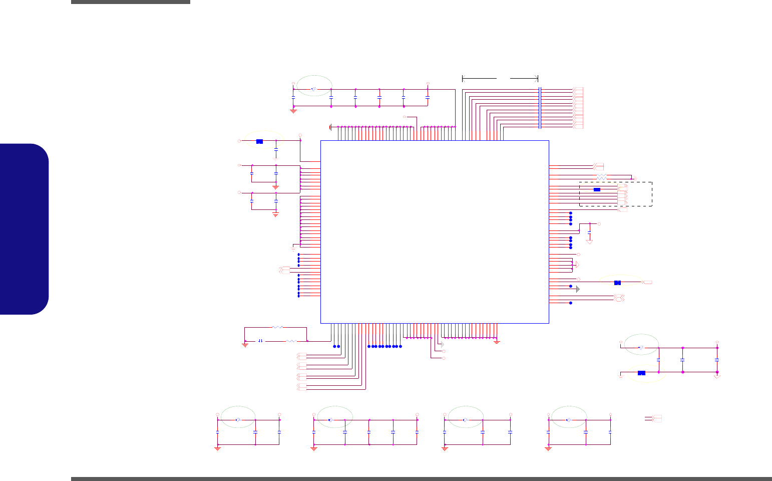
Schematic Diagrams
B - 12 SiS307ELV
B.Schematic Diagrams
SiS307ELV
Sheet 11 of 38
SiS307ELV
Z1126
Z 1121
C3 9
10U _10V_08
EMI 1/3
HDV BN0 _ R
Z1129
C13
* . 1U _1 6 V _ 0 4
C23
.1U _16V_04
EMI 1/3
HDVBP1 4
C2 6
.1 U_ 1 6V_ 0 4
HDV BP0_ R
Z1105
C4 10 .1 U_ 1 0 V_X7 R_ 0 4
1. 8 V S
VBHC LK 6
LVDS-L0N12
R 16 499_1%_04
C9
10U_10V_08
LVDS-LC LKP12
4/16
HDVBN1 4
C4 0
.1U _ 16 V_ 0 4
C41
.01U_16V_X7R_04
HDVAP0 4
LVDS-L0P
VBCA D 6
Z1118
C37
. 1U _16V_04
R 15 124_1%_04
C4 09 .1 U_ 1 0 V_X7 R_ 0 4
1.8VS
C2 0
10U _10V_08
Side-Band
Signals
C4 5
.01U _16V_X7R _04
VB_ PCIEAVD D
Z1108
VB_ DAC VDD
Z1112
VBVSY NC 6
C46
.1 U _1 6 V _ 04
L1
HDV AN1 _ R
Z1128
HDV AP2_ R
EM I 1/ 3
VBHS YNC 6
Z1104
LVDS-L1P
3. 3 V S
LVDS-LC LKP
C44
.1U _16V_04
LVDS-L0P12
Z1122
VB_LVDS PLL VD D
C4 11 .1 U_ 1 0 V_X7 R_ 0 4
C3 4
.1 U_ 1 6V_ 0 4
LVDS-L1N12
Z 1119
EM I 1/ 3
C4 03 .1 U_ 1 0 V_X7 R_ 0 4
VB_HDV RSET0
C21
.1 U _1 6 V _ 04
EM I 1/ 3
LVDS-L2P
C4 06 .1 U_ 1 0 V_X7 R_ 0 4
VB_ DAC VSS
Z1107
Z1114
R220 *32mil_short
HDV BN2 _ R
Z1131
307ELV
U2 2
SiS307EL V
C13
A12
A13
C1 1
C12
A10
A11
C9
C10
A8
A9
C7
C8
A6
A7
C5
C6
A4
A5
C3
C4
E5
E6
E7
E8
E9
B3
A2
A3
B4
B5
B6
B7
B8
B9
B10
B11
B12
B13
D10
D1 1
F12
E13
E12
H1 0
G1 0
G2
H2
H1
G1
G1 3
G1 2
F11
F3
G3
B2
B1
D2
D1
E2
E1
F2
F1
H3
J3
C2
K2
J2
J1
K1
C1
E3
F4
N6
N7
N4
N5
N2
N3
K13
J12
K11
J11
L13
L12
F13
E11
E10
F10
G1 1
L7
L8
L4
L5
L11
L9
L2
L10
N12
M4
J5
K3
M2
M11
M8
J7
L6
M5
M9
J6
N9
L3
N1
M1
M12
N8
K4
N10
N1 3
M3
J8
M7
M13
J9
L1
M6
N1 1
M10
H4
J4
F5
F6
F7
F8
F9
G5
G6
G7
G8
G9
H5
H6
H7
H8
H9
G4
D12
D1 3
H1 1
H1 2
H1 3
K5
K6
K7
K8
K9
K10
K12
D3
E4
D4
D5
D6
D7
D8
D9
J1 0
EXTSWING
L X3 P //NC 5
LX3N //NC 6
L X2 P //NC 11
LX2 N //NC 12
L X1 P //NC 3
LX1 N //NC 4
L X0 P //NC 9
LX0 N //NC 10
LXC1P//N C1
LXC 1 N//N C2
LXC2P//D XC1P
LX C 2 N / / D X C 1 N
L X4 P //DX0 P
LX4 N //DX0 N
L X5 P //DX1 P
LX5 N //DX1 N
L X6 P //DX2 P
LX6 N //DX2 N
L X7 P //NC 7
LX7 N //NC 8
LVDSP HYVD D//TM D SPHYVD D
LVD SPH YVDD //TM DSPH YVDD
LVDSP HYVD D//TM D SPHYVD D
LVD SPH YVDD //TM DSPH YVDD
LVDSP HYVD D//TM D SPHYVD D
LVD SPLLVDD //TM DSPLLVDD
LVDSP LLVSS//T MD SPLLVSS
LVD SPH YVSS//TM DSP HYVSS
LVDSP HYVSS// TMD SPH YVSS
LVD SPH YVSS//TM DS PHYVSS
LVDSP HYVSS// TMD SPH YVSS
LVD SPH YVSS//TM DS PHYVSS
LVDSP HYVSS/ /TMD SPH YVSS
LVD SPH YVSS//TM DS PHYVSS
LVDSP HYVSS/ /TMD SPH YVSS
LVD SPH YVSS//TM DS PHYVSS
LVDS PHYVSS/ /TMD SPH YVSS
LVD SPH YVSS//TM DS PHYVSS
LVD SPH YVDD //TM DSPH YVDD
LVDSP HYVD D//TM D SPHYVD D
LD IDD CC LK// DVID DCC L K
L D IDDC DAT A//D VIDD CD AT A
BL _ A DJ //D VIHPD
IVD D
VD D33
GPIOA
GPIOB
GPIOC
GPIOD
L CD VDD _ EN//G PIOG
BL _ EN//G PIOH
GPIOI
GPIOJ
GPIOK
DACRSET
DACCOMP
TVD ACR
TVD ACG
TVDAC B
TVCSY NC
GPIOL
GPIOM
GPION
GPIOO
DAC V DD
CO REP L L VDD
VBRC LK
VBO SCO
C OR EPLLV SS
DACVSS
DACVSS
DACVSS
HDVAN2
HD VAP2
HDVAN1
HD VAP1
HDVAN0
HD VAP0
VAC L K
VBC L K
VBHSY NC
VBVSY NC
VBH CAD
VBHC LK
EXTRSTN
G PIOF/ DVIN TN
PFTESTO
PFT EST 1
PFT EST 2
HDVREFCLKN
HD VREF C L KP
HD VRSET0
HD VRSET1
VSS
HDV PLL VS S
HDV P HY VD D
VSS
HDV BN2
VSS
HDV P HY VD D
HDV P HY VD D
VSS
VSS
VSS
HDV P HY VD D
H DVPLLVDD
VSS
VSS
HDVPHYVDD
H DVBP0
HDVPHYVDD
VSS
HDV P HY VD D
VSS
HD VB N0
HDVPHYVDD
HDV BN1
H DVBP2
VSS
HDVPHYVDD
VSS
VSS
HDV P HY VD D
HDVPHYVDD
VSS
H DVBP1
VSS
IVD D
IVD D
VSS
VSS
VSS
VSS
VSS
VSS
VSS
VSS
VSS
VSS
VSS
VSS
VSS
VSS
VSS
IVD D
LVD SPH YVDD //TM DSPH YVDD
LVDSP HYVD D//TM D SPHYVD D
IVD D
IVD D
IVD D
VSS
VSS
VSS
VSS
VSS
VSS
VSS
DACVSS
DACVSS
LVDS PHYVSS/ /TMD SPH YVSS
LVD SPH YVSS//TM DS PHYVSS
LVDS PHYVSS/ /TMD SPH YVSS
LVD SPH YVSS//TM DS PHYVSS
LVDS PHYVSS/ /TMD SPH YVSS
LVD SPH YVSS//TM DS PHYVSS
VSS
Z1132
C3 71
.1U _ 16 V_ 0 4
R9 *1 0 m il_ s ho rt
LVDS-L1P12
HDV AN0 _ R
Z1103
LVDS-L0N
C4 08 .1 U_ 1 0 V_X7 R_ 0 4
C372
1U_6.3V_X5R_06
VB_LAVD D
VB_PLL1VD D
4/16
VB_DA CVD D
HDVAN1 4
HDV AP1_ R
VB_ DAC VSS
1 .8V S 4,5 ,6 ,7 ,1 2,1 3 ,1 4, 15 ,1 6 ,17 ,2 7
HDV BP1_ R
L3 4
H CB1005KF-121T20
Z1111
1.8VS
HDVAP2 4
Z1106
VB_LAVDD
VBCLK 6
Z 1115
Z1134
C1 1
.1U_16V _04
C3 1
10U _10V_08
L1
H C B 1 0 0 5K F - 12 1 T 20
3.3VS 6,10,12,13,14,15,16,17,18,19,20,21, 22,24,25,26,27,28
VBRC LK
Z1102
R5 *32 m il_sho rt
HDVBP2 4
C22
.1U _16V_04
C4 00 .1 U_ 1 0 V_X7 R_ 0 4
VB_PCIEVDD
PC IE_CLK_HD V 17
L32
H CB1005K F-121T20
3.3VS
C7
10U _10V_08
VACLK 6
C4 04 .1 U_ 1 0 V_X7 R_ 0 4
HDV Signals
VB_PLL1VDD
1. 8 V S
VB_VDD 3V
P_DDC_CLK 12
R2 1 0
24K_1%_06
C4 07 .1 U_ 1 0 V_X7 R_ 0 4
LVDS-LC LKN12
C4 01 .1 U_ 1 0 V_X7 R_ 0 4
C4 3
.1U_16V _04
ENAVD D12
Z1124
Z 1123
Z1125
Z1116
C35
.1 U _1 6 V _ 04
3.3V SVB_PCIEA VDD
HDVBN2 4
3. 3 V S
C LK_14M_307ELV 17
LVDS-L2N
EM I 1/ 3
HDVAN0 4
Z1110
HDV AN2 _ R
C4 05 .1 U_ 1 0 V_X7 R_ 0 4
Z1127
L3
H C B 1 0 0 5K F - 12 1 T 20
HDV AP0_ R
EXTS W ING
Z1120
HDV BN1 _ R
Z1130
L2
HCB 1005KF-121T20
HDVAN2 4
LVDS-L1N
C2 5
*10U_10V_08
C27
.1 U _1 6 V _ 04
C10
.1 U_ 1 6 V_ 04
L1<=400mils
4/16
VB _D ACVS S
30 7 _ B LO N12
VBCLK_ R
LVDS-LC LKN
LVDS-L2N12
HDV BP2_ R
L4
H C B 1 0 0 5K F - 12 1 T 20
P_DDC_DATA 12
R227 * 10m il_s hort
Z1101
C6
.01U _16V_X7R _04
C38
.1U _16V_04
VB _LVD SPL LVD D
C4 02 .1 U_ 1 0 V_X7 R_ 0 4
Close to 307 side
3.3VS
HDVBP0 4
R211
6 . 04 K _ 1 % _0 6
HDVAP1 4
PC IE_CLK_HD V# 17
C1 2
.1 U_ 1 6V _0 4
LVDS-L2P12
Z1113
Z 1117
Z1133
HDVBN0 4
C1 5
.01U _16V_X7R _04
C3 6
.1U_16V _04
4/16
VB_DAC VDD
VB_HDV RSET1
General I/O Power
NB_ R ST# 6,2 7
Z1109
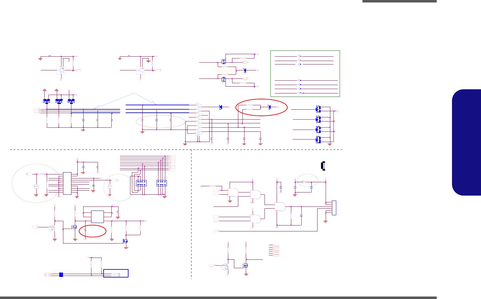
Schematic Diagrams
PANEL, INVERTER, CRT B - 13
B.Schematic Diagrams
PANEL, INVERTER, CRT
Sheet 12 of 38
PANEL, INVERTER,
CRT
LVDS-L1N 11
J_ C R T1
C10509-91505-L
8
7
6
5
4
3
2
1
9
10
11
12
13
14
15
GN D2
GND 1
7/ 13
Modify C4 from 0.1uF change to
0. 01u F f or L VDS po w er t im e .
LVDS-LCLKN
4/16
DAC_ HS Y NC 6
R204 *1K_04
DAC_ B L UE
LVDS- L1N
LVDS-L0N
C RT_DDC ADAT_R
R234 100K_04
Zo=75 Ohm
D3
BAV99
A
C
AC
R207
1M _ 04
1 .8 VS 4,5 ,6 ,7,1 1 ,1 3,1 4 ,15 ,1 6 ,17 ,2 7
CR T_ VSYN C
Q1 6
DT C1 14 E U A
CE
B
U23B
74LVC 08PW
4
5
6
147
R212 *10mil_short
L36
HCB1608KF-121T25
LVDS-L1N
U24
S N 74 A H C 1 G 1 25 D C K R
1
2
5
4
3
R2
200_1% _06
CR T_ DD CAC LK
LVDS- L2P
INVERTER CONNECTOR
1
DAC _BL UE6
DAC_ GR EEN_ R
C56
4 7 P_ 50 V_ 04
L VDS -L CL K P 1 1
R3
200_1%_06
Z1205
DAC_ RE D
D17
* SCS751V-40
AC
5/ 17
EM I
P_D DC _D ATA11
D AC_ RED6
LVDS- L0P
LVDS- LC LKP
R2 32
39 0 _0 6
SY S15 V
SB_ PW ROK14,27
L CD_ B RIG HT NES S26
For Panel ID
VIN
LVDS-L0P 11
DAC_ RE D _ R
LVDS- L0N
EDI D_ DAT
CRT_DDCACLK_R
LC D I D 114
307_BLON_3V
Z1207
D39 *BAV9 9
A
C
AC
Z1209
Q1 8
2N7002W
G
DS
EM I 1/3
3. 3 V S
PLVDD
CR T_ DD CAD AT
LVDS-L1P
5VS
R240 2.2K_04
CRT_HSYNC_R
R244
10K_04
C397
.1U_50V_06
Q21
2N 7002W
G
D S
3.3V
LID_SW#19,26
U2 5
SN74AHC 1G 125DCKR
1
2
5
4
3
2A
Fo llo w
????
BKL _ EN26
EDI D_CLK
D AC_ RED_ R
C RT_ VSYNC _R
C5
.1 U_ 16 V_ 0 4
Q1 7
2N 70 0 2W
G
DS
J_INV1
C4 2 1
22 P_ 5 0V_ 0 4
R233
390_06
LVDS- LC LKN
CR T_ DD CAD AT_R
R235
10 K _ 0 4
CP2
*8 P 4 C X 1 0P
1
2
3
45
6
7
8
EMI 1/3
CP1
*8 P 4 C X 1 0P
1
2
3
45
6
7
8
L VDS -L CL KN 11
R239 2.2K_04
C681
.1U_16V_04
J_IN V1
87212-06G 0
1
2
3
4
5
6
L71 FCM 1005KF-121T03
C49
220P_50V_04
SB_ BL ON14
LVDS-L0P
Z1201
R237 2.2K_04
R5 15
0_04
P_DDC_CLK11
CRT_DD CACLK
D2
BAV99
A
C
AC
R2 08
1M _0 4
R236 2.2K_04
EDID_D AT
R2 1
75_1%_04
IN V_BLON
C RT_ HSYN C_R
R231
1M_04
3.3VS
CR T_ HSY NC
DAC_ GR EEN
Q23
2N7002W
G
DS
C440 .1U_16V_04 3.3VS
C417
.1U _16V_04
CRT
LVDS-L2N 11
C418
100P _50V_04
5VS 18,21,24,25,27
CRT_ DD CADAT
VIN 28,29,30,31,32
Z1203
DAC_BLUE
C2
.1 U_ 1 6V_ 0 4
C 442 .1U_16V _04
12/ 25
LVDS-L2P
L73 FCM 1005KF-121T03
3.3V
CRT_VSYNC_R
C4 2 7
22P_50V_04
CR T_ D DCAD AT_ R
C RT_ VSYNC _R
J2
1m m
1 2
D AC_ DD CACL K 6
LVDS-LCLKP
C5 9
47P_50V_04
R22
75_1% _04
DAC_RED
LVDS- L1P
L77 FCM 1005KF-121T03
C431
2 2 P_5 0 V_ 04
VIN _IN V
SY S15 V 27,29
Q1
SI34 5 6BD V-T1 -E3
3
2
1
4
5
6
G
D
D
S
D
D
1.8VS
DAC_GREEN_R
R1
100K_04
6 -20 -4 1A1 0-1 06
3.3V
3.3V
U2 3 D
74LVC 08PW
12
13
11
147
C1
*10U_10V_08
3.3VS
D AC_ DD CADAT 6
L76 FCM 1005KF-121T03
L74 FCM 1005KF-121T03
C414
.1U_50V_06
3 .3 VS 6,1 0 ,11 ,1 3 ,14 ,1 5,1 6 ,1 7,1 8 ,19 , 2 0,2 1 ,2 2,2 4 ,25 ,2 6 ,27 ,2 8
D40 *BAV9 9
A
C
AC
L75 FCM 1005KF-121T03
D38 *BAV9 9
A
C
AC
C53
47P_50V_04
3.3VS
LVDS-L0N 11
C5 5
1 00 0 P_ 50 V_ 04
D41 *BAV9 9
A
C
AC
D AC_ VSYNC 6
LVDS-L2P 11
Q24
DTC 114EUA
CE
B
5V S
Z1208
U2 3 A
74LVC 08PW
1
2
3
147
2A
3.3V 2,14,15,16,18,19,20,23,27,29,30,31
LVDS-L2N
CRT_HSYNC_R
J_LCD 1
88107-20001
12
34
56
78
910
11 1 2
13 1 4
15 1 6
17 1 8
19 2 0
6
CRT_ VSYN C
CR T_ DD CAC LK_ R
Z12 10
R 514 * 0_04
L72 FCM 1005KF-121T03
Z1204
C RT_ DDC ACL K _R
4/16
D AC_ GR EEN
R203
2.2K_04
SY S15 V
5VS
LVDS- L2N
D18 SCS751V-40
AC
PANEL
Z12 06
3.3VS
LVDS-L1P 11
DAC_ B L UE_ R
C4
.01U_16V_X7R_04
D1
BAV99
A
C
AC
D4 2
SCS751V-40
AC
C51
220P_50V_04
LCD ID0 14
DAC_BLUE_R
R213 *10mil_short
12 /2 5
R2 0 5
2.2K_04
C4 8
10 0 0P_5 0V_ 0 4
40 m il
3.3VS
307_BLON11
R5 06 1K_ 0 4
R2 0
75_1%_04
307_BLON_3V
J1
1m m
1 2
3.3V
3.3V
ED ID_CLK
Q22
2N 7002W
G
D S
ENAVD D11
R5 05 1K_ 0 4
CR T_ HS YNC
PLV DD
DAC _GREEN6
U2 3 C
74LVC 08PW
9
10
8
147
R202 *1K_04
Schematic Diagrams
B - 14 968 PCI IDE MuTIOL SPI 1/4
B.Schematic Diagrams
968 PCI IDE MuTIOL SPI 1/4
Sheet 13 of 38
968 PCI IDE
MuTIOL SPI 1/4
PCI_ C/ BE# 222
AVS S_S Z4 X
PC I_ INT# B
IDE_ PD D2
ZAD 3
IDE_ PD D8
PCI_PAR22
ID E_AVSS
IDE_ PD D5
Z1305
Z13 01
R346 56_04
PCI_ IN T#B
PC I_A D6
SZC MP_ N
R190 8.2K_04
PCI_ D EV SEL #22
ZAD 2
PC I_A D2 9
R358 *4.7K_04
PC I_IR DY #22
ZA D4
PCI
MuTIOL
IDESPI
U3 6 A
SiS9 68
H5
J4
J3
K1
K2
J5
K4
K3
L2
K5
L4
L3
M1
M2
L5
M4
P3
R1
R2
P5
R4
R3
T1
T2
T4
T3
U1
U2
T5
U4
U3
V1
H2
H1
G3
G4
G2
J2
J1
H3
H4
G5
L1
M3
N5
R5
F5
F4
F3
G1
N1
N2
M5
N3
P2
P4
N4
P1
V2
D5
AC 26
V2 2
V2 3
V2 5
V2 6
AA2 3
AA2 4
AB2 4
AB2 5
AA2 2
AB2 3
AB2 6
AA26
Y22
Y25
Y23
W21
Y26
W22
W24
W25
U2 1
U24
U2 2
T22
U2 5
T23
T25
T26
AE1 9
AD 18
AC 17
AF1 8
AB1 6
AE1 7
AD 16
AF1 6
AE1 6
AF1 7
AC 16
AD 17
AE1 8
AB1 7
AF1 9
AC 18
AC 21
AB2 1
AD 21
AD 20
AB2 0
AF2 0
AD 19
AC 19
V3
V4
AE2 0
AB1 8
AB1 9
AC 20
AE2 1
AF2 1
AD 22
AF2 2
AE2 2
AF2 3
AD 31
AD30
AD 29
AD28
AD 2 7
AD26
AD 2 5
AD 24
AD23
AD 22
AD21
AD 2 0
AD19
AD 1 8
AD 17
AD16
AD 15
AD14
AD 1 3
AD12
AD 1 1
AD 10
AD9
AD 8
AD7
AD 6
AD5
AD 4
AD3
AD2
AD 1
AD0
PREQ 4#
PREQ 3#
PREQ 2#
PREQ 1#
PREQ 0#
PGN T4#
PGN T3#
PGN T2#
PGN T1#
PGN T0#
C/BE 3#
C/BE 2#
C/BE 1#
C/BE 0#
INT A#
INT B#
INT C #
INT D #
FRAM E#
IRD Y#
TR D Y #
STOP#
SERR #
PAR
DEVS EL#
PL OC K#
PCIC L K
PCIR ST#
ZCLK
ZSTB0
ZSTB0#
ZSTB1
ZSTB1#
ZUR EQ
ZDR EQ
ZCM P_N
ZCM P_P
AVDD _ Z4 X
AVSS_ Z4 X
ZVRE F
ZA D16
ZAD 0
ZAD 1
ZA D2
ZAD 3
ZAD4
ZAD 5
ZAD6
ZAD 7
ZAD 8
ZA D9
ZAD 10
ZAD11
ZAD 12
ZAD1 3
ZAD 14
ZAD 15
ID A0
ID A1
ID A2
ID A3
ID A4
ID A5
ID A6
ID A7
ID A8
ID A9
IDA1 0
IDA1 1
IDA1 2
IDA1 3
IDA1 4
IDA1 5
IDE CSA 1 #
IDE CSA 0 #
ID SAA2
ID SAA1
ID SAA0
IIOR A#
IIO W A#
IDAC K A#
AVD D_ID E
AVSS_ ID E
IC HR DY A
ID REQ A
IIRQ A
CBL ID A
SPI_CS 0N
SPI_CS 1N
SPI_DO
SP I_C L K
SPI _D I
SPI_ HA RD W ARE _TR AP
ZS TB _D #16
PCI_ PLO CK#
C336
.01U_16V_X7R _04
12/25
PC I_F RA ME#
PC I_ AD2 0
PCI_ IN T#D
Z1307
C3 3 0
.1 U_ 1 6 V_ 04
3.3VS 6,10,11,12,14, 15,16,17,18,19,20,21,22,24,25,26, 27,28
PC I_REQ #4
PCI_ R EQ# 1
1.8V S
PC I_ AD3 0
PCI_ STO P#
PCI_ AD 19
C2 3 9
10U_10V _08
PC I_ INT# D
SZC MP_ P
R3 4 3
49.9_1% _04
PC I_REQ #2
PC I_AD 8
IDE_ PD D0
R 134 10K_04
SPI_TRA P
PC I_A D1 5
PC I_F RAM E#22
ZAD6
PCI_AD0
PCI_AD14
PCI_ AD 26
C3 0 9
.1 U_ 1 6 V _ 04
L17
HC B1005KF-121T20
PCI_ C/ BE# 322
C5 6 4
.1U_10V_X7R _04
Z_CLK117
ZA D11
C257
.01U_16V_X7R _04
ID E_A VDD
IDE_ PD D4
0:LPC Internal Pull down
1:SPI External Pull up
3.3V S
ZSTB_D06
PC I_AD[31:0] 22
ZAD1
PCI_ IN T# B22
PCI_ IR DY #
C2 6 3
.1 U_ 1 6 V_ 04
PCI_ AD 24
SZVR EF
IDE _AV DD
PCI_ IN T# A4,6,22
ZSTB_D16
PCI_AD7
IDE_ PD D6
ZAD15
ZAD 12
RN 28
8P4R X4.7K_04
1
2
3
4 5
6
7
8
PCI_AD21
ZAD8
PCI_AD28
PC I_IRD Y#
IDE_ PD D1 0
1.8V S
Z1308
ZAD 0
PCI_ R EQ# 3
PC I_ AD2 3
PCI_ IN T#C
ZAD 16
6- 16 -4 72 38 -4 5A
PCI_ C/ BE# 022
PC I_ INT# C
PC I_ AD1 8
Z13 04
SZVR EF
ZS TB _D #06
PCI_ AD 10
PC I_REQ #022
IDE_ PD D7
PCI_ C/ BE# 122
PCI_ TR DY #
PC I_ RE Q# 0
PC I_ GN T# 0
FO R MR 51 0
PC I_ AD1 6
PC I_ AD1 1
IDE_ PD D9
Z1309
1.8V S
ZDR EQ6
ZAD 14
EMI 1/3
PC I_ST OP#
PCI_ SE RR #
AVSS_ SZ 4 X
Z1311
PC I_SER R#
PCI_ AD 12
PCI_ AD 17
PC I_AD4
ZAD 9
ZAD 5
PC I_REQ #0
Z13 03
EMI 1/3
PC I_REQ #3
L25
HC B1005KF-121T20
3.3VS
NC 7 N C_ 0 4
PC I_ AD2 7
IDE_ PD D1 1
IDE_ PD D1 2
PCI_ R EQ# 0
R345 56_04
PC I_S TO P#22
R3 4 4
150_1%_04
AVD D_SZ4 X
IDE_ PD D3
PCI_ AD 3
PCI_ R EQ# 4
PCI_ AD 31
PC I_TR DY #22
PCI_ IN T#A
ZAD 10
1.8V S
1 .8 VS 4 ,5 ,6 ,7, 11 ,1 2 ,1 4,1 5 ,1 6 ,1 7,2 7
PC I_T RD Y#
IDE_ PD D1 5
RN 25
8P4R X8.2K_04
1
2
3
4 5
6
7
8
PCLK_SB17
Z1310
PC I_ AD1 3
PCI _AD 1
PC I_ INT# A
PCI_ D E VSEL #
PC I_ AD2 5
IDE_ PD D1
ZAD13
ZUR EQ6
PC I_REQ #1
PCI_ R EQ# 2
PCI_ F R AM E#
PCI_ AD 5
NC 3 N C_ 0 4
PC I_SERR #22
SB _ P CI RST #27
ZAD 7
IDE_ PD D1 3
Z13 02
IDE_ PD D1 4
ZA D[16:0]6
RN 26
8P4R X8.2K_04
1
2
3
4 5
6
7
8
ID E_A VSS
PC I_PL OC K#
PC I_AD2
PC I_A D2 2
AVD D_SZ4 X
PC I_ DEV SEL #
RN 27
8P4R X4.7K_04
1
2
3
4 5
6
7
8PC I_G NT# 022
PC I_AD9
Schematic Diagrams
968 PCIE LAN GPI0 2/4 B - 15
B.Schematic Diagrams
968 PCIE LAN GPI0 2/4
Sheet 14 of 38
968 PCIE LAN GPI0
2/4
SB_ DPR SL PVR
C318
.1 U _1 6 V _ 04
RXCLK_PHY 23
12 /2 5
H _STPCLK#2
PM_CLKRUN# 26
ODD_DETECT# 18
SB_ THER M#
R513 *0_04
Lan e 0
3.3V
AUX_PW R OK 6 ,2 3
GA20#26
SB_DPR STP#6
PC IE_TXP0_NEW _C ARD 20
Z14 12
SB_ SUS C#18
Z14 05
AGP STO P#
Z14 07
AU X_PW RO K
GA 2 0 #
Z140 2
R 428 10K_04
R115 124_1% _04
RN 24 8P4R X10K_04
1
2
3
4 5
6
7
8
H_ IG NN E#2
ODD_DETECT#
R 1 86 1 K _0 4
MDC _PH Y 23
R 185 10K_04
AV DD _ GMA CCM P
GA20#
X6
32.768KH z
14
3 2
X5
25MH z
1 2
C248
.1U_16V_04
AVD D_PEXTRX
H_THRMTRIP#2
EEC S
SB_ PW R OK
SB_ SUS B#18
A GPBU SY#
RGMVREF
LPC_AD 226
SM I#
TXER_PHY
CL KR UN #
EEPROM
4/16
EESK
R114 499_1% _04
H_ A2 0 M#2
LPC _LD RQ #
C722
3 3 P_ 50 V_ 0 4
C3 2 4
.1U _16V_04
R401 * 10m il_sh ort
4/16
LPC_AD 126
PC IE_CLK_SB 17
H_P ROCHOT#2
S_DAT
SB_ KBCR ST#26
SB _KBC RS T#
C 649 15P _50V_04
PC IE_RXN1_WLAN 20
R 378 56_04
R 411 10K_04
R161 4.7K_04
AVS S_G MAC CM P
Z14 11
PS ON#
C5 9 3
.1U _ 10 V_ X7 R_ 04
R XE R_PHY 23
EESK
AG PBU SY#
PC I-Express X1
PW R _BTN #
C 631 27P_50V_04
RXDV_PHY 23
C RS_ PH Y 2 3
R 372 56_04
6- 22 -3 2R 76- 0B 1, H= 2.4
PC IE_RXN0_NEW _C ARD 20
PC IE_TXN 1_ W L AN 20
close chip
SC I#26
PC IE_RXP1_WLA N 20
PC IE_PRSN T0 2 0
P-R SET1
C332 .1U _16V_04
LPC _S IRQ
3.3V
Z14 06
PC IE_TXP1_WLAN 20
EMI 1/3
PC IE_RXP0_NEW_CA RD 20
CPU_STP#
R 4 06 4 . 7K _ 0 4
TXD3_PHY 23
Z1404
R171
*330K_04
AVD D_PEXTRX
RG MC MP_ N
LPC_FLASH
LCD ID1
RN 23 8P4R X10K_04
1
2
3
4 5
6
7
8
R490 *10K_04
LP C _ S I R Q22,26
R365
150_1%_04
H_ IN TR2
PSO N#
SEN TES T
Z141 3
C 606 27P_50V_04
3.3V
COL_PHY 23
R426
10M_04
EED I
R 418 10K_04
EEC S
R 160 10K_04
TXD2_PHY 23
AG PSTOP#
R371
150_1%_04
V_LA N
LPC_AD 326
R 166 10K_04
PC IE_P RSN T0
PW R_BTN#
PW R _ BTN#26
EED O
LPC _LD RQ #
EM I 1/ 3
1.8VS
GTXCLK_PH Y_R
KBC _AU XPW RO K 2 6
LCD ID1 12
CPU_S
APIC
LPC
RTC
HD Audio
ACPI/Others
GPIO
GMACPCI-Express
MAIN POWERAUX POWER
U36B
SiS968
AC23
AE2 6
AD23
AC22
AE2 5
AE2 4
AF2 4
AF2 5
AD24
Y5
AA4
AB2
AB3
AB1
AB4
AA5
F1
E4
D1
D2
W5
Y4
E5
C4
Y3
Y2
B3
Y1
AA2
F2
AA1
E6
A6
E7
C3
A5
D3
B5
C7
B7
D7
B4
D4
F6
C2
C6
C12
D12
A13
B13
C13
A11
C10
E12
A10
C9
B9
A9
E10
E11
E14
E13
U5
V5
W4
W3
W2
W1
D6
A4
C11
A14
C14
B14
A8
B8
M26
M25
N24
N23
K26
K25
L24
L23
P25
P26
R25
R26
P22
P21
E2
E1
J23
J24
H25
H26
G23
G24
F25
F26
D8
F8
E8
A7
B11
A12
F14
C8
D9
R21
R23
AB5
AC24
AD25
AE2 3
IN IT#
A20 M#
SM I#
IN TR
NMI
IG NN E#
FER R#
STPC LK#
C PUSLP#/CP USTOP#
LAD 0
LAD 1
LAD 2
LAD 3
LFR AME#
LDR Q#
SIR Q
BATO K
PW R OK
RTCVDD
RTCVSS
GPIO 2 0
GPIO 1 9
HDA_SDIN0
HDA_SDIN1
HDA_SDOUT
HDA_SY NC
HDA_RESET#
HDA_BIT_CLK
OSCI
EN TEST
SPK
PW R BTN#
PM E#
PSO N#
AU XOK
AC PILED
G P IO1 3 /DP R S L PVR
G PIO1 4 /AGPS TO P# /S3AUXSW #
SLP_S3 #
G P IO1 6 /DP R S TP #
G P IO1 7 /GA2 0 #
G P IO1 8 /K BDR ST #
G P IO1 2 /CP U S TP #
G PIO11/STP_PCI#/AGP STO P#
SLP_S5 #
G PIO9/H DA_SDIN 2
TXEN
TX D 0
TX D 1
TX D 2
TX D 3
RXCL K
RXDV
RXER
RXD 0
RXD 1
RXD 2
RXD 3
CO L
CRS
MD C
MD IO
GPIO0
GPIO2/THERM#
GPIO3/EXTSMI#
GP I O4 /C L K R UN #
GP IO 5 / P RE Q 5 #
GPIO6/PGNT5#
GPIO7/GPWAK#
GPIO8/R ING
TXER
RG MC MP _ N
RGMVREF
RGMCMP_P
OS C 2 5M HI
OSC25MHO
PRX0+
PR X0 -
PTX0 +
PTX0 -
PRX1+
PR X1 -
PTX1 +
PTX1 -
P C LK 10 0 N
PCLK100P
AVDD _PE XTR X
AVSS_PEXTRX
RSET0
RSET1
O S C3 2 KHO
O S C3 2 KHI
NC 4
NC 5
NC 6
NC 7
NC 8
NC 9
NC 1 0
NC 1 1
GPIO 2 1
GPIO 2 2
GPIO 2 3
GPIO 2 4
TXCL K
GT X C L K
EXTCL K
AVSS _G MAC CM P1 8
AVDD_GMACCMP18
PC IEPRSN T1
PC IEPRSN T0
GPIO 1/LDRQ 1#/P CIE_HO TPLU G
PR OC HO T#
THE RMTR IP#
BM BUSY #
LP C _ F R A M E #26
LPC_FLASH
C327
* 10U _10V_08
Z14 10
PM _CLKRU N#
D9
*SCS751V -40
A C
AVSS_ G MAC CM P
1.8V 5,7,9,10,15,16,27,30,31
TXD1_PHY 23
L20
H C B 1 0 0 5K F - 12 1 T 20
EM I 1/ 3
RTC_PWROK15
LCD ID0 12
SB_BLO N 12
Z140 3
PME #
S_D AT 9 ,10,17,20
RTC_CLKI
AUX_PW R OK
R1 7 2 0 _ 04
SEN TEST
R 164 10K_04
V_LAN
SM I# 26
TXCL K_ PHY 2 3
AZ_ SD IN119
SC I#
R397
*1 M_ 0 4
SW I#
C342
1U _6.3V_04
AG PBUS Y#6
SB_ KBC RST#
VCC _RTC 1 5
CPU _STP#6
RTC_CLKO
C 645 15P _50V_04
12/25
AGP STO P#6
AZ_ R ST#19,24,25
1.8V
AZ_ SDO UT19 , 2 4
EXTCLK_PHY
U19
AT93C465666
1
2
3
4
8
7
6
5
CS
SK
DI
DO
VCC
DC
ORG
GND
H_FERR#2
SP KRO UT21
1 . 8V S 4, 5 , 6 , 7 , 1 1, 1 2 , 1 3, 15 , 1 6 , 17 , 2 7
PC IE_CLK_SB# 17
EED O
P-R SET0
Z14 09
LCD ID0
V_ LA N 16
RXD3_PHY 23
SW I#26
RG MC MP_ P
AU X_ PW R OK
R170
*2.2K_04
H_ SM I#2
L C DID1
PC IE_PRSN T0
Put closed to 968
PCI-Express
SB_ PWR OK12,27
TXEN_PH Y 23
EED I
3.3V
S_D AT
SB _THE RM #
SM I#
RGMVREF
CPU _STP#
NC 6 NC _0 4
C3 1 9
.01U _16V_X7R _04
AVS S_P EXTR X
H_ CP USL P #2
PCIE_TXN0_NEW_CARD 20
SB _D PRSLPVR
3.3V 2,12,15,16,18,19,20,23,27,29,30,31
SB _PW ROK
R 3 57 4 . 7K _ 0 4
?????PHY>>1.5V
R 417 10K_04
3.3VS 6,10,11,12,13,15,16,17,18,19,20,21, 22,24,25,26,27,28
RXD2_PHY 23
AU X_P W RO K6,23
SCI # OD D_D E TE CT #
S_C LK 9 ,10,17 ,20
LPC _FLASH
3.3V
H_NMI2
M D I O _P H Y 23
SW I#
12/25
Ne w C ard
7/13
Modify C606,C631 from 20PF
change to 27P F for OSC
issuse.
AVDD_GMACCMP
RTC_CLKI
L14
HC B1005KF-121T20
TXD0_PHY 23
L C DID0
R184 *10m il_short
R 427 10K_04
AVSS_ PEXT RX
Z14 08
C246
.01U_16V_X7R_04
PM E#
R 187 *10 m il_short
Z14 01
NC1 NC_04
R 1 88 1 K _0 4
Mini C ard( Wireless LAN)
PM E#22,26
R 534 0_04
R 113 *10K_04
3.3VS
1.8VS
LPC_AD 026
SB_ DPR SL PVR6
S_C LK
AZ_ SYN C19,24
S_CLK
RTC_CLKO
SB_ MU TE#25
C333 .1U _16V_04
4/ 1 6
RXD1_PHY 23
AZ_ BITCLK19,24
RXD0_PHY 23
AZ_ SD IN024
Lan e 1
VCC _RTC
CLK_14M _96817
PSON #18
H_INIT#2
4/21
Schematic Diagrams
B - 16 968 USB SATA 3/4
B.Schematic Diagrams
968 USB SATA 3/4
USB_O C#1
C340
1U _6.3V_04
? ????
AV DD_SATAPL L 3 3
L18
H CB1005KF -121T20
EM I 1/ 3
L49
H CB1005KF -121T20
VCC _RTC 1 4
USB6:
1.8V 5,7,9,10,14,16,27,30,31
SA TAT XP1 18
SA TAT XN0 1 8
C279
.1 U _1 6 V_ 04
FINGER PRINTER
U SBPVD D18
ISW 1
USB_PN620
USB
SATA
U3 6 C
SiS968
D2 6
D2 5
E24
E23
A20
B20
C1 9
D1 9
A18
B18
A23
F21
A24
B24
C2 3
C2 2
F20
B26
B25
D2 2
C1 7
D1 7
A16
B16
A25
C2 4
AF1 4
AF1 5
AC 9
AD 9
AC 8
AD 8
AF7
AC 6
AD 6
AF5
AE5
AE8
E22
F16
E16
J19
H1 8
E18
H1 7
H1 6
F15
H1 5
J15
E21
E20
D2 1
C2 1
F17
F19
F22
AA3
B23
C1 5
D1 5
AE15
AD15
A22
B22
AC 1
AD 1
AF1 2
AE12
AC 13
AD 13
AF8
D1 0
E9
UV0 +
UV0 -
UV1 +
UV1 -
UV2 +
UV2 -
UV3 +
UV3 -
UV4 +
UV4 -
OC 0#
OC 1#
OC 2#
OC 3#
OC 4#
IP B_O UT1
USBR EF
AVD D_U SBPL L18
AVSS_U SBPL L1 8
IP B_O UT0
UV5 +
UV5 -
UV6 +
UV6 -
OC 6#
OC 5#
AVDD _SATARX
AVSS_SATARX
AVDD _SATAPLL 3 3
AVDD _SATAPLL 3 3
AVSS_SATAPL L 33
AVSS_SATAPL L 33
REXT
STX1 +
STX1-
SR X1 +
SRX1-
XI N
TR AP0
UVD D1 8
UVD D1 8
UVD D1 8
UVD D1 8
UVD D1 8
UVD D1 8
UVD D1 8
UVD D1 8
UVD D1 8
UVD D1 8
AVDD _USBC MP18
AVSS_USBC MP18
AVDD _USBC MP33
AVSS_USBC MP33
UVD D3 3
UVD D3 3
UVD D3 3
HD ACT
OC 7#
UV7 +
UV7 -
CLK100P
CLK100N
OSC12MHI
OS C1 2M HO
ISW IT C HOP EN1
ISW IT C HOP EN0
SR X0 +
SRX0-
STX0 +
STX0-
XO UT
ATR AP
PCIEW AKE
SA TAR XP0 18
USB_PN020
3. 3 V
U SB_OC #020
USB _O C# 3
MuTIOL Clock Select (ZCLK)
133MHz : Interanl Pull down
66MHz : External Pull up
Z15 07
D 15 SC S751V-40
A C
PORT1
SATARXN1
VC C_R TC
UVD D1 8
L53
H CB1005KF -121T20
R191 1K_04
USB5:
R159 10K_04
RN22
8P4R X10K_04
1
2
3
45
6
7
8
C255
.01U _16V_X7R_04
CCD
USB PVSS18
SA TA_LED# 19
1.8V
USB _O C# 5
USB_O C#5
USB4:
3.3V
CLK_ SAT A#17
C603
.1 U _1 6 V_ 04
R 425 1K_04
BLUETOOTH
PC IE_ W AKE# 4 ,2 0
SATARXN0
SOSC 25M HO
A VDD _SATAR X
SA TAT XP0 18
USB_PN319
UVDD33
S ATAR EXT
USB3:
AVSS_SATAPL L 33
U SBCM PAVSS18
MINI CARD
U SBCM PAVSS33
Z1511
VDD 3 2,2 1 ,2 6 ,27 ,2 9 ,31 ,3 2
USB_PP020
S ATAR EXT
USB2:
AVSS _SA TAR X
USBR EF
C 634 22 P_ 5 0V_ 0 4
NEW CARD
ISW 0
NC 2 NC _ 04
U SB_OC #2 620
NC 15 NC _0 4
USBPVD D18
UVD D1 8
C313
.1 U _1 6 V_ 04
USB1:
L15
H CB1005KF -121T20
C254
.1U _16V_04
R 409 12K _1%_04
SA TAR XN1 1 8
SATATXN 0
C281
.01U _16V_X7R _04
U SBC MPAVSS 18
1.8VS 4,5,6,7,11,12,13, 14,16,17,27
C LK_ SATA17
12 /2 5
AVS S_SA TAP LL 33
UVD D3 3
USB_PN220
U SB_OC #419
R405 0_04
D 14 SC S751V-40
A C
PORT0
R 167 10K_1%_04
NC 5 NC _0 4
SA TAR XP1 18
SATARXP0
USB_PP719
Z1501
J_RTC 1
85205-02R
1
2
USB_PN121
4/16
U SBCM PAVD D18
SATATXN 1
USB0:
C LK_12M_U SB 17
USB_PP620
3.3VS
USB_PP520
PCIE_ W AKE #
C249
.1 U _1 6 V_ 04
PC IE_ W AKE#
D 16 1SS 355 SOD -323
AC
D16 fro m
SCS75 1V -40
change to 1SS355
S OD- 32 3 fo r co st
do w n .
USB_PN419
USB _O C# 7
L16
H CB1005KF -121T20
SA TAR XN0 1 8
C314
.01U _16V_X7R _04
Zo=90 Ohm
R135 127_1% _04
VDD 3
C261
.1 U _1 6 V _ 0 4
EM I 1/ 3
U SBPVSS18
SOSC 25M HI
R196 *10mil_short
USB_PP220
USB_O C#3
C367
10U_10V_08
NO 1
NO _ 04
3.3V 2,12,14,16,18,19,20,23,27,29,30,31
Z C LK _S E L
1.8VS
UVD D3 3
USB_O C#7
C568
.1 U _1 6 V_ 04
C6 9 0
22U_6.3V_08
EM I 1/ 3
3.3V
USB_PP121
AVDD _SATARX
RTC_PWROK 14
Z1510
L19
H CB1005KF -121T20
R 424 1K_04
SA TAT XN1 1 8
USB _O C# 0
C3 44
1U _6 . 3 V _ 0 4
EM I 1/ 3
USB_PN520
3.3VS 6,10,11,12,13,14,16,17,18,19,20,21, 22,24,25,26,27,28
1.8V
USB_PN719
Z 1512
C252
.01U _16V_X7R _04
1.8V
R360 10K_04
Z15 08
EM I 1/ 3
SATATXP0
C260
.01U_16V_X7R_04
PORT2
USB_PP419
SATATXP1
R 379 1K_04
C560
.01U _16V_X7R _04
NC 4 N C_ 0 4
USB_PP319
USB _O C# 1
AVDD _SA TAP LL 3 3 Z15 06
NC 13 NC _0 4
7/ 18
C6 90 fr o m 1 0u F _1 0V _ 08 c ha n g e
to 22u F _ 6.3 V _0 8 fo r RT C tim e
iss ue .
EM I 1/ 3
R1 2 1 * 10 K_ 0 4
3. 3 V
USB_O C#0
USB7:
U SBCM PAVDD 18
SATARXP1
ZCLK_SEL
AVSS _SATAR X
C602
.01U _16V_X7R _04
Sheet 15 of 38
968 USB SATA 3/4
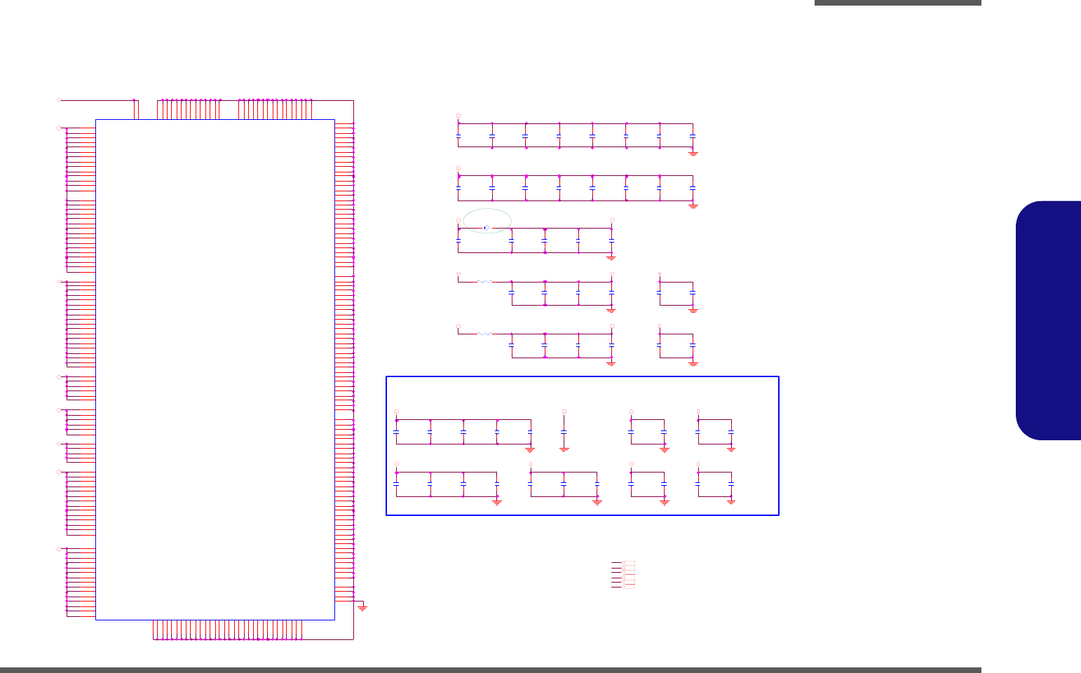
Schematic Diagrams
968 PWR GND 4/4 B - 17
B.Schematic Diagrams
968 PWR GND 4/4
Sheet 16 of 38
968 PWR GND 4/4
C624
10U _10V_08
3.3V
C3 0 5
.1U_16V_04
R138 0_08
C251
1U_10V_06
C304
.1U_16V_04
1.8VS
3.3V 2, 12,14,15,18,19,20,23,27,29,30,31
V_ AVD D_SATA
V _AVD D_ SAT A
C284
.1U_16V _04
C271
.1U_16V_04
C618
1 0 U _ 1 0V _0 8
C278
.01U_16V_X7R_04
C267
10U_10V_08
EMI 1/3
C293
.1U_16V_04
C5 5 5
.1U _16V_04
C2 9 7
.1 U_ 1 6 V_0 4
C285
.1U _16V_04
Power/Ground
U3 6 D
SiS96 8
U26
W26
P1 8
R18
N18
V1 7
V1 6
N9
P9
W18
V1 5
J18
J17
H19
H9
J9
AA2 5
R24
L10
L1 1
L12
M10
M1 1
M12
N1 0
N11
N12
N13
N14
K10
K11
K12
P1 0
P1 1
P1 2
P1 3
D14
E1 5
A1 5
B1 5
C16
D16
A1 7
B1 7
E1 7
C18
D18
A1 9
B1 9
E1 9
C20
D20
A2 1
B2 1
D23
D24
C25
C26
AF 3
AF 4
AF 2
AE 11
AE 9
AE 7
AE 3
AE 4
AE 1
AD 12
AD 3
AD 2
AC 12
K1 3
K1 4
K1 5
L13
L1 4
M1 3
P1 4
R10
R11
T10
U10
L15
L1 6
M14
M1 5
R13
P1 6
V2 4
Y24
M9
K9
V1 0
V1 1
V1 2
V1 4
T8
N8
L9
W17
W16
W15
W14
W13
W12
K8
L8
M8
P8
R8
U8
V8
AA21
AB22
J16
B1 2
H8
L17
T24
R17
T18
U18
V1 8
V1 9
W19
R9
T9
U9
J14
J12
J10
J8
H10
H11
H12
J11
D11
H13
J13
R14
T14
U14
U15
AC 2
AC 3
AC 4
AC 5
M1 7
N17
P17
M16
N1 6
N1 5
F7
E2 5
E2 6
F23
F24
G2 5
G26
H2 3
H24
J25
J26
K2 3
K2 4
L25
L26
G2 2
J22
K2 2
L22
M23
M24
N2 5
N2 6
N2 2
P23
P2 4
K1 6
K1 7
V1 3
K1 8
L18
L19
M18
M19
N19
H21
J21
K2 1
L21
M21
N21
M22
H22
AE 2
AC 25
AD 26
B1 0
D13
AF 9
AF 11
R12
T11
T12
T13
U11
U12
U13
AB 6
AB 7
AB8
AB9
AC 1 0
AC 1 1
AD 1 0
AD 1 1
AE1 0
AF1 0
V9
W8
W9
W10
W11
U2 3
W23
R2 2
T21
V21
Y21
T15
P15
T17
R1 5
R16
T16
U16
U1 7
AB 13
AB 14
AB 15
AE 13
AC 14
AC 15
AD 14
AF 13
AE 14
AB 12
AC 7
AD 7
AD 4
AD 5
AE 6
AF 6
AB1 0
AB1 1
VDDZ
VDDZ
VDDZ
IVDD
VDDZ
IVDD
PVDD
IVDD
IVDD
VDDZ
PVDD
IVDD _AU X
IVDD _AU X
OVDD _ AUX
OVDD _ AUX
IVDD _AU X
VDDZ
VDDZ
VSS
VSS
VSS
VSS
VSS
VSS
VSS
VSS
VSS
VSS
VSS
VSS
VS S
VSS
VSS
VSS
VSS
VSS
U SBVSS
U SBVSS
U SBVSS
U SBVSS
U SBVSS
U SBVSS
U SBVSS
U SBVSS
U SBVSS
U SBVSS
U SBVSS
U SBVSS
U SBVSS
U SBVSS
U SBVSS
U SBVSS
U SBVSS
U SBVSS
U SBVSS
U SBVSS
U SBVSS
U SBVSS
AVSS_ SATA
AVSS_ SATA
AVSS_ SATA
AVSS_ SATA
AVSS_ SATA
AVSS_ SATA
AVSS_ SATA
AVSS_ SATA
AVSS_ SATA
AVSS_ SATA
AVSS_ SATA
AVSS_ SATA
AVSS_ SATA
U SBVSS
U SBVSS
U SBVSS
U SBVSS
VSS
VSS
VSS
VSS
VSS
VSS
VSS
VSS
VSS
VSS
VSS
VSS
AVS SPEX
VDDZ
VDDZ
IVDD
IVDD
IVDD
IVDD
IVDD
PVDD
PVDD
PVDD
PVDD
OVDD
OVDD
OVDD
OVDD
OVDD
OVDD
OVDD
OVDD
OVDD
OVDD
OVDD
OVDD
OVDD
VTT
VTT
IVDD _AU X
VSS
OVDD _ AUX
U SBVSS
VDDZ
IVDD
IVDD
VDDZ
VDDZ
VDDZ
VDDZ
IVDD
IVDD
IVDD
IVDD
OVDD _ AUX
IVDD _AU X
IVDD _AU X
GMIIV D D_ AU X
GMIIV D D_ AU X
GMIIV D D_ AU X
OVDD _ AUX
VSS
GMIIV D D_ AU X
GMIIV D D_ AU X
VSS
VSS
VSS
VSS
AVSS_ SATA
AVSS_ SATA
AVSS_ SATA
AVSS_ SATA
AVSSPEX
AVSS PEX
AVSSPEX
AVSS PEX
AVSSPEX
AVSS PEX
OVDD _ AUX
AVSSPEX
AVS SPEX
AVSSPEX
AVS SPEX
AVSSPEX
AV SSPEX
AVSSPEX
AV SSPEX
AVSSPEX
A VSSPEX
AVSSPEX
A VSSPEX
AVSSPE X
A VSSPEX
AVSSPE X
AVSSPEX
AVSSPE X
AVSSPEX
AVSSP EX
AVSSPEX
AVSSP EX
AVSSPEX
AVSSP EX
AVSSPEX
AVSS PEX
U SBVSS
U SBVSS
IVDD
AVDD PEX
AVDD PEX
AVDD PEX
AVDD PEX
AVDD PEX
AVDD PEX
AVDD PEX
AVDD PEX
AVDD PEX
AVDD PEX
AVDD PEX
AVDD PEX
AVDD PEX
AVDD PEX
AVSS_ SATA
VSS
VSS
VSS
VSS
AVSS_ SATA
AVSS_ SATA
VSS
VSS
VSS
VSS
VSS
VSS
VSS
AVSS_ SATA
AVSS_ SATA
AVDD _SATA
AVDD _SATA
AVDD _SATA
AVDD _SATA
AVDD _SATA
AVDD _SATA
AVDD _SATA
AVDD _SATA
AVDD _SATA
AVDD _SATA
AVDD _SATA
AVDD _SATA
AVDD _SATA
VSSZ
VSSZ
VSSZ
VSSZ
VSSZ
VSSZ
VSSZ
VSSZ
VSSZ
VSSZ
VSSZ
VSSZ
VSSZ
VSSZ
AVSS_ SATA
AVSS_ SATA
AVSS_ SATA
AVSS_ SATA
AVSS_ SATA
AVSS_ SATA
AVSS_ SATA
AVSS_ SATA
AVSS_ SATA
AVSS_ SATA
AVSS_ SATA
AVSS_ SATA
AVSS_ SATA
AVSS_ SATA
AVSS_ SATA
AVSS_ SATA
AVDD _SATA
AVDD _SATA
C2 8 2
.1U _16V_04
3.3VS
V_AVDD _SBP CIE
C554
1U_10V _06
1.8V
C307
.1U_16V _04
C2 7 5
.1 U_ 1 6 V_0 4
C294
. 01U_16V_X7R_04
C283
.1 U _1 6 V _ 04
3.3V
C296
.01U_16V_X7R_04
V_LAN 14
V_ AVD D_ SBPC IE
C286
.1 U_ 16 V_ 0 4
1.8V S
L21
H CB1005KF -121T20
3.3VS 6, 10,11,12,13,14,15,17,18,19,20,21,22,24,25,26,27,28
C259
.1U_16V _04
2.5 V ch an ge to 3 .3V
C2 8 0
.1U _ 16 V_ 0 4
C2 5 6
.1U _16V_04
V_LAN
1.05VS 2, 3,4,6,7,30
C3 2 3
.1U_16V_04
C308
.1U_16V_04
1.05VS
C2 7 2
.1U _16V_04
C2 62
.1U _16V_04
3.3V S
C3 16
.1U _16V_04
C290
.1 U _1 6 V _ 04
C298
.1U_16V_04
C321
1U_10V _06
1.8V
C303
1U_10V_06
1.8V
C3 0 6
.1 U_ 1 6V_ 0 4
1. 8 V S
R131 0_08
C302
1U_10V_06
V_ AVD D_ SATA
1.05VS
1. 0 5 V S
C559
.1 U_ 16 V_ 0 4
C552
1U _10V_06
C243
10U _10V_08
C310
.1U_16V_04
V_LAN
C2 7 4
.1U _ 16 V_ 0 4
C557
1 0 U _ 1 0V _0 8
C240
.1 U _1 6 V _ 04
C242
1U_10V_06
1.8V 5, 7,9,10,14,15,27,30,31
V_ AVDD _SB PCIE
1.8VS 4, 5,6,7,11,12,13,14,15, 17,27
C315
1U _10V_06
P ut u nd er S iS 96 8 sol de r si de
C312
1U _10V_06
V_L AN
C317
.1U_16V_04
3.3V
C3 1 1
.1 U_ 1 6V_ 0 4
3. 3 V S
C266
1U _10V_06
1.8V S
C295
.1 U_ 1 6 V_0 4
C320
1U _10V_06
C273
.1U _16V_04
1.8V S
C277
.1 U_ 1 6 V_0 4
C627
10U_10V_08
C276
. 01U_16V_X7R_04
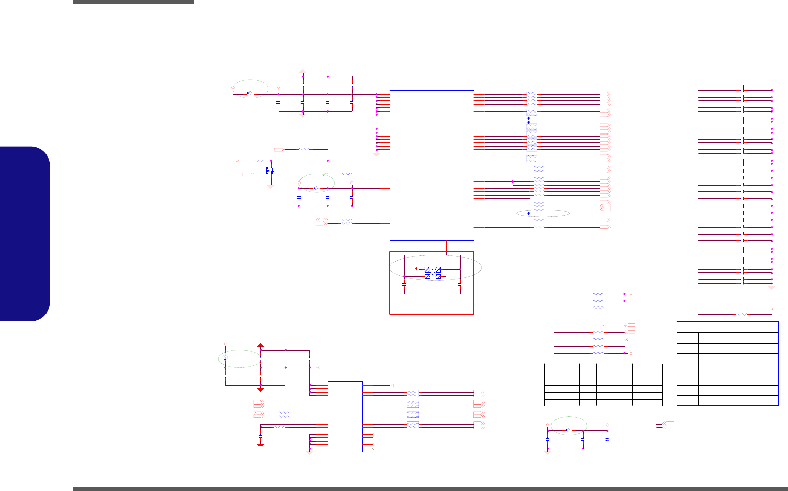
Schematic Diagrams
B - 18 CLK GEN & CLK BUFFER
B.Schematic Diagrams
CLK GEN & CLK BUFFER
Sheet 17 of 38
CLK GEN & CLK
BUFFER
PCIE_CLK_SB# 14
PCIE_CLK_NB#
C207 *10P_50V_04
C1 5 7
.1U_16V_04
Mobile mode
CL K_ 4 8M _C ARD
R106 22_04
BSE L2
CPU _BSEL 1 2
PC IE_C LK_SB_R
R 302 22_04 C151 *10P_50V_04
PECLKREQ1#
EM I 1/ 3
H_ CL K_ CPU #
CLK_12M _U SB
S_C LK9,10,14,20
PC IE_C L K_N EW# _R
R67 33_04
1.8VS
PC IET_ L 1
CL K_ 48 M_ C ARD 2 2
Z_CLK1
M_ C LK _ DD R0 # _R
M_ C LK _ DD R1 # _R
C165 *10P_50V_04
CPU_STOP#
1 2 00 MH z
3.3VS 6,10,11,12,13,14,15,16,18,19,20,21,22,24,25,26,27,28
CL K_ S ATA 15
M_ CL K_ DD R1
BS EL 0
M_ C LK _ DD R 2 #
C LK_ SATA_R
C231 *10P_50V_04
R6 5 0 _0 4
CLK_STOP#
CLK_14M_968 14
C525 *10P_50V_04
C143 *10P_50V_04
CL KGEN _VD D
H_CLK_CPU_R
H_ CL K_ NB
C1 3 0
.1U_16V_04
3.3VS
PCIE_CLK_HD V# 11
CLKGEN_MODE
C149 *10P_50V_04
R3 26 2 .2 K_0 4
RESET#
(HI)PULLl-UP
C161 *10P_50V_04
EM I 1/3
M_CLK_DDR 3 10
CLKEN
R309 * 10K_04
Status
1
H_ CL K_ CP U 2
Z1707
CL K BU F _AV DD
M_CLK_DDR 0# 9
C215 *10P_50V_04
PCIE_CLK_NB
C LKG EN_ FSL 2
C234 *10P_50V_04
R299 0_04
R 311 33_04
R6 6 * 2.7 K_ 0 4
PCI_STOP#Pin 12
CPU _BSEL 0 2
PC IE_C LK_H DV#_R
PC IE_C L K_N B_R
PC IE_C L K_M INI# _ R
R 301 33_04
1
3.3VS
CL K_ 12 M_ U SB 15
RN 11
4P2R X33_04
1 4
2 3
L4 5
H CB1005KF-121T20
Mode
C2 2 7
10P_50V _04
0
H_ CL K_ CP U # 2
Z1706
FB_IN A
M_ C LK _ DD R3 # _R
PC LK_DE BUG_R
M_ C LK _ DD R 0 #
CL K_ S AT A
L12
HCB1005KF-121T20
R3 17 2 .2 K_0 4
1
PCIE_CLK_HD V 11
CL K_ S ATA #
Z_CLK1 13
M_ CL K_ DD R0 #
H_CLK_NB#_R
C228 *10P_50V_04
Pin 28
PCICLK6
PCLK_ CAR D 2 2
PCLK_ SB
M_ C LK _ DD R2 _ R
C2 2 4
.1U_16V_04
RN 12
4P2R X33_04
1 4
2 3
C531 *10P_50V_04
C1 7 4
.01U _16V_X7R _04
3. 3 V S
M_FWDSDCLKOA_D#5
PCIE_CLK_MIN I 20
RN8
4P2RX0_04
1 4
2 3
Ho st Cl oc k
CLKGEN_FSL2
R307 10K_04
C132 *10P_50V_04
1
C L K _ 14 M _ 6 7 1M X
CL K_ 14 M_ 9 6 8
PC IE_C LK_SB#_R
C2 1 2
.1U_16V_04
C2 1 8
.1U_16V_04
M_ C LK _ DD R 1 #
Clock Generator Pin 15
M_ CL K_ DD R1 #
CLKGEN_FSL1
KBC_P C LK
L9
H CB1005KF-121T20
C128 *10P_50V_04
H_ CL K_ NB # 4
CLK_14M _671MX
C122 *10P_50V_04
1
PCLK_ CAR DCLKGEN_FS4
R305 10K_04
1
4 /12
M_CLK_DDR 1# 9
PCIE_CLK_SB
C5 00
10U_10V_08
RN 17
4P2R X33_04
1 4
2 3
R 327 10K_04
PCIE_CLK_MIN I
M_ C LK _ DD R 3 #
X3
HSX53 1 S_14 .3 1 8M Hz
12
34
C2 3 3
10U _10V_08
Fr eq uen cy
PCLK_ SB 1 3
H_ CL K_ NB 4
1
CL K_ S ATA
PCICLK3
FS3
3.3VS
M_ CL K_ DD R3
PC IE_C L K_H DV_R
PCLK_ LPC RO M
R6 3 0 _0 4
VTTOWRGD/PD#
C LKEN #28
H_ CL K_ CPU
CLK_14M _968
C137 *10P_50V_04
0 0
MINI_CARD_CLKREQ# 20
PCIE_CLK_NEW# 20
U1 1
ICS9P93 5
1
2
3
4
5
6
7
8
9
10
11
12
13
14
28
27
26
25
24
23
22
21
20
19
18
17 16
15
DD RC0
DDRT0
VD D1.8
DDRT1
DD RC1
GND
VDD A1.8
GND
CLK_INT
CLK_INC
VD D1.8
DDRT2
DD RC2
GND
GND
DD RC5
DDRT5
VD D1.8
GND
DD RC4
DDRT4
VD D1.8
SD ATA
SC LK
FB_IN
FB_OUT DDRT3
DD RC3
3.3VS
M_CLK_DDR 0 9
PCLK_ SB
RN7
4P2RX0_04
1 4
2 3
C5 32
33P_50V_04
PCICLK5
0
FS4
PCIE_CLK_NB# 4
C L K _ 14 M _ 3 0 7E L V
M_ C LK _ DD R0 _ R
CLK_12M_USB_R
R60 10K_04
M_ C LK _ DD R1 _ R
C127 *10P_50V_04
C208 *10P_50V_04
R 323 33_04
CL K_ S ATA # 1 5
M_CLK_DDR 3# 10
M_ CL K_ DD R2
1
0
CLKBUF_AVDD
CPUSTP#6
PCLK_ L PCRO M
C LK_ SATA#_R
H_CLK_CPU#_R
R 303 22_04
PCIE_CLK_NEW 20
C191 *10P_50V_04
C2 2 5
.1 U_ 16 V_ 0 4
0
KBC_PCLK 26
R104 *0_04
R 306 0_04
PCIE_CLK_NB 4
STP_ PCI#
C168 *10P_50V_04
C175 *10P_50V_04
S_D AT9,10,14,20
C LKG EN_ FSL 1
RN 14
4P2R X33_04
1 4
2 3
M_ C LK _ DD R3 _ R
RN 19
4P2R X33_04
1 4
2 3
L13
HCB1005KF-121T20
C187 *10P_50V_04
C158 *10P_50V_04
100 MHz
FB_O UTA
PCIE_CLK_HD V
Z1703
R308 *0_04
M_ CL K_ DD R0
Z1702
CL KGEN _M OD E
R 321 33_04
C169 *10P_50V_04
BS EL1
PCIE _ CL K_ MIN I# 20
PCIE_CLK_SB#
CL K_ 48 M_ C ARD
C1 6 4
1U_10V_06
C1 8 8
.1U_16V_04
C527 *10P_50V_04
M_CLK_DDR 2# 10
PEC LK REQ0#
CL K_ 12 M_ U SB
Z_CLK0_R
H_ CL K_ NB#
M_CLK_DDR 2 10
PEC LK REQ1#
H_CLK_NB_R
R3 10 2 .7 K_0 4
C182 *10P_50V_04
0
0
PC IE_C L K_N EW_ R
Z_CLK1 Z_CLK0
C LKG EN_ FS3
C1 5 2
.1U_16V_04
RN9
4P2RX0_04
1 4
2 3
0
M_ C LK _ D D R 1
PC IE_C L K_N B#_ R
RN 20
4P2R X33_04
1 4
2 3
C1 8 0
.1U_16V_04
Pin 1
CLK_ 14M_3 0 7EL V 1 1
R 319 33_04
C153 *10P_50V_04
C2 14
10U_10V_08
CPU _BSEL 2 2
KBC_PCLK
3/20
Z1704
R62 *33_04
1
PC IE_C L K_M INI_ R
CLKGEN_FS3
CLKBUF_VDD
C2 2 2
.01U_16V_X7R _04
U31
ICS9LPR600C GLF
1
2
3
4
5
6
7
8
9
10
11
12
13
14
15
16
17
18
19
20
21
22
23
24
25
26
27
28
56
55
54
53
52
51
50
49
48
47
46
45
44
43
42
41
40
39
38
37
36
35
34
33
32
31
30
29
(CLK_STOP#)/VTTPWR GD /PD#
VDD REF
** FSL0/R EF0_2x
*FSL1/R EF1_2x
X1
X2
GN DR E F
GN DP C I
** F S L2 / P C I CL K 0 _2 x F
**F S 3 / P C I C L K 1 _2 x F
** F S 4/ P C I C L K 2
*(PC I_STO P#)/PC ICLK3
GN DP C I
VDD PCI
**MO DE/PC ICLK4
(PE CL K RE Q 0 #)/P C ICL K 5
(PE CL K RE Q 1 #)/P C ICL K 6
PC ICL K7
VDD PCI
GN DZ
ZCLK0
ZCLK1
VDD Z
VDD 48
12MHz
** SEL24_48#/24_48MHz
GN D4 8
*(C PU_ STOP#)/RESET#
VDD CPU
CPU T_L0F
C PUC _L0F
GN DC P U
CPU T _L 1
CPUC_L1
VDD A
SATAC L KT_ L
SATACLKC_L
GN DA
SCLK
SDATA
PC IET _L 0
PCIEC _L 0
GN DP C IEX
PC IET _L 1
PCIEC _L 1
VDD PCIEX
PC IET _L 2
PCIEC _L 2
PC IET _L 3
PCIEC _L 3
PC IET_L4F
PCIEC _L4F
GN DP C IEX
PC IET_L5F
PCIEC _L5F
VDD PCIEX
166 MHz
EM I 1 /3
1. 8 V S
PCLK_ LPC RO M
M_ C LK _ D D R 0
M_CLK_DDR 1 9
M_ C LK _ D D R 3
C144 *10P_50V_04
Place CRYSTAL Within 500
mils of ICS9LPR600
NEW_CAR D_CLKR EQ# 20
M_ CL K_ DD R3 #
CLK_14M _307ELV
Q7
2N7002W
G
DS
R3 13 2 .2 K_0 4
CLKGEN _VD DA
PCIE_CLK_HD V#
SEL24_ 4 8 #
CL K_ S AT A#
C533
33P_50V_04
C535 *10P_50V_04
PECLKREQ0#
SU SB#1 8 , 2 0, 2 2 , 27 , 3 0 , 31
M_ CL K_ DD R2 #
PEC LKR EQ0 #
C1 3 4
10U _10V_08
C177 *10P_50V_04
3. 3 V S
M_ F W D S D C LKO A _D5
1 .8 VS 4 ,5,6 ,7 ,1 1,1 2 ,13 ,1 4 ,15 ,1 6 ,27
PCLK_ CAR D
Z_CLK1_R
CLKGEN_FSL0
R 300 33_04
PC IEC_ L 1
M_ C LK _ D D R 2
STP_ PCI#
R3 2 8 *0 _ 04
S_CLK9,10,14,20
Z1701
C518 *10P_50V_04
Z 1705
RN 15
4P2R X33_04
1 4
2 3
S_DA T9,10,14,20
PCIE_CLK_NEW#
M_ C LK _ DD R2 # _R
Z_CLK0
RN10
4P2RX0_04
1 4
2 3
0
E MI 1/ 3
R 314 33_04
PCIE_CLK_NEW
(LO)Non-STUFF
C LKG EN_ FSL 0
C235 *10P_50V_04
C2 1 3
.1U_16V_04
CLK_14M_671M X 6
PEC LKR EQ1 #
C1 8 4
1U_10V_06
Pin 16
C141 *10P_50V_04
133 MHz
RN 21
4P2R X33_04
1 4
2 3
Pin 17
PCIE_CLK_MIN I#
C209 *10P_50V_04
R105 *0_04
C2 3 2
.1 U_ 16 V_ 0 4
C167 *10P_50V_04
Desktop mode
Z_CLK0 6
PCIE_CLK_SB 14
C LKG EN_ FS4
Schematic Diagrams
SATA, 3G POWER, PCI DEBUG B - 19
B.Schematic Diagrams
SATA, 3G POWER, PCI DEBUG
Sheet 18 of 38
SATA, 3G POWER,
PCI DEBUG
C 428 .01U_16V_X7R _04
R503
100K _04
0
C6 50
*.1U_16V_04
C 439 .01U_16V_X7R _04
R432
*4 . 7 K _ 04
3G POWER CONNECTOR
SATAR XN 1 _R
R433
*4 . 7 K _ 04
S0/S1
SATATXN0 15
SB_ SUSB# 1 4
SATATXN 1 15
R435
*1 0 K _0 4
SATA HDD
0
3.3VS 6,10,11,12,13,14,15,16,17,19,20,21,22,24,25,26,27,28
SATARXP0 _R
C680
* .1U _16V_04
+
C386
100U _6.3V_B2
C 726 .01U_16V_X7R _04 S AT ARXN1 1 5
Q3 2
*2N7002W
G
DS
C6 94
10 U _ 1 0V _ 0 8
1
R429
* 0_04
3.3V
J_ODD _72
* 91924-0130P-02
S1
S2
S3
S4
S5
S6
S7
P1
P2
P3
P4
P5
P6
SIGNAL
C3 0
.1U_16V_04
5/10
SATAR XP1 _ R
SATATXP1 _R
S ATATXP0 1 5
KBC _SU SC# 2 6
5VS 12,21,24,25,27
3.3V
SATAR XN1_R
J_OD D_73
85205-12
1
2
3
4
5
6
7
8
9
10
11
12
C 727 .01U_16V_X7R _04
FOR M720SR
C3 81
10U_10V_08
PSON#
1
C32
1U_10V_06
C29
.1U _16V_04
PSO N#14
J_ HD D1
SAT-22R C1AA
S1
S2
S3
S4
S5
S6
S7
P1
P2
P3
P4
P5
P6
P7
P8
P9
P10
P11
P12
P13
P14
P15
SA TA RXN0 _ R
3.3V S
SB_ SUSC # 14
Z18 01
LPC BIOS CONN
R 489 0_04
PIN GN D1~2=G ND
SI S? ? ? ?
?????
Co nne cto r
C674
*.1U _16V_04
C692
0.1U_16V_04
C 432 .01U_16V_X7R _04
FO R M7 3 0S R
SATARXP1 1 5
ODD_DETECT#
Z1806
C 441 .01U_16V_X7R _04SATATXP0_R
Z 1808
C 725 .01U_16V_X7R _04
Z18 03
SATATXP1 15
3.3V
U41
* 74AHC 1G08G W
1
2
5
4
3
POWER MANAGMENT
KBC _SU SB# 26
Q3 1
*2N7002W
G
DS
C695
* 10 0 U _ 6. 3V _ B 2
TO SB GPIO
SATATXN 0_R
SATATXN1 _ R
SATAR XP1_R
3.3V
5VS
SATATXP1_R
3.3V 2,12,14,15,16,19,20,23,27,29,30,31
Layout Note
1
Z18 04
SATA SINGAL FROM SB TO JODDB1
E N D O F J O DD 1
SATATXN1 _ R
C 724 .01U_16V_X7R _04
SATARXN0 15
R 434 0_04
C2 8
.1U _16V_04
C389
10U _10V_08
5V S
Z18 02
S4/S5
R436
* 10K_04
R 431 0_04
1 2/2 5
SU SB# 17,20,22,27,30,31
S3
3.3V
Z1807
ODD _D ETE CT #
For NB control and Level shift
SATA ODD
ODD _ DET ECT # 1 4
Z1805
R481
*1 0 0K _ 0 4
C6 91
0.1U_16V_04
1.6A
Q3 3
*2N7002W
G
DS
SATARXP0 15
C4 2
.01U _16V_X7R_04
NB_ S3 A UXSW #5
5VS
Q3 4
*D TC114EUA
CE
B
If ne ed PS ON#
th an us ed 100 K
an d 0 .1 U
1
S3AUXSW#
Z18 10
C693
1U_10V_06
Schematic Diagrams
B - 20 MULTI I/O, ODD, CCD, BT
B.Schematic Diagrams
MULTI I/O, ODD, CCD, BT
3G_EN 21,26
6
1
C369
10U _10V_08
C3 7 8
1 0U _ 10 V _ 08
SPKO UTR-25
U2 1
RT9701-CPL
1
2
3
4
5
VOUT
GN D
VIN
VIN
VOUT
W EB_ EMAIL # 26
LED_CAP#26
R218 *1 0m il_s hort
CCD _EN26
R214 330K_04
AZ _ SDIN114
C382
.1U_16V _04
J_BT1
87212-06G0(M)
1
2
3
4
5
6
U SB_ PN715
EM I 1/3
US B_O C# 415
5
WEB_WWW# 26
EMI 1/3
C3
0.1U_16V_04
R535 0_04
3.3VS
CC D_ DET #26
USB _P N 3_ R
3. 3VS =4A
USB _ PP315
SATA_L ED#15
5V 20,21,24,28,29,30,31
R6 10K_04
C 370 .1U_16V_04
3.3V
7/13
From 3.3VS change to 3.3V.
4/16
3. 3V
C3 8 0
10U _10V_08
MULTI I/O CONN
USB _P P3 _ R
Fo llo w
????
W EB_ AP# 31
Fo ll ow
????
5V
U SB_ PP715
LED_TH ROTTLE# 26
3.3VS
48 mil
M_BTN#31
R209
100K_04
50 mil
J_CCD 1
85204-05001
1
2
3
4
5
C33
0.1U_16V_04
CCD
C3 7 9
10U _10V_08
SP KOUTR+25
LED _N UM#26
USB _PN 415
cl ose J _MF B1
Z1907
V D D 3 2, 1 5 , 21 , 2 6 , 27 , 2 9, 3 1 , 3 2
J_BT1
3VS_ BT
5V
LED_SCRO LL# 26
EM I 1 /3
5VS 12,18,21,24,25,27
Z1909
R2 06
10 0 K _0 4
5V_C CD
AZ_ BIT CLK14 , 2 4
3.3V
C14
.1U_16V_04
Q2
2N 7002W
G
DS
50 mil
1
12 /25
C368
.1U_16V_04
3. 3V
AZ_ SD OUT14 , 2 4
J_MFB1
5F1-233A1-A2000-214
12
34
56
78
910
11 1 2
13 1 4
15 1 6
17 1 8
19 2 0
21 2 2
23 2 4
25 2 6
27 2 8
Bluetooth
BT_E N#
BT_ DET#26
3 .3 VS 6,1 0 ,11 ,1 2 ,13 ,1 4,1 5 ,1 6,1 7 ,18 ,2 0,2 1 ,2 2, 24 ,25 ,2 6 ,27 ,2 8
USB _PP415
Z1908
50 mil
BT_ EN21,26
L31
HCB1005KF-121T20
C723
*33P_50V_04
3. 3 V S
USB _ PN315
R219 10K_04
3.3V 2,12,14,15,16,18,20,23,27,29,30,31
R217 *1 0m il_s hort
AZ _SY NC14 , 2 4
Q20
2N7002W
G
DS
J_CCD1
ODD
L33
HCB1005KF-121T20
6- 20- 41A 10 -10 6
Q1 9
ND S352AP_NL
G
DS
J_MFB2
5F1-233A1-A2000-214
12
34
56
78
910
11 12
13 14
15 16
17 18
19 20
21 22
23 24
25 26
27 28
C18
.1U _16V_04
USBV CC2
LID_SW# 12,26
R7 560K_04
12/25
From H8 default HI
C8
10U_10V_08
AZ_ RST#14 , 2 4, 2 5
3G_DET#26
USBV CC2
Sheet 19 of 38
MULTI I/O, ODD,
CCD, BT
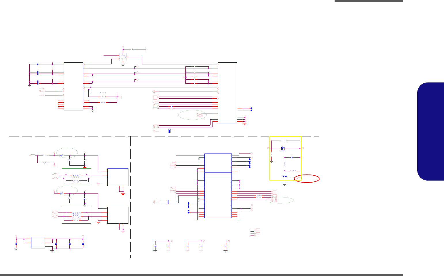
Schematic Diagrams
NEW CARD, MINI PCIE, USB B - 21
B.Schematic Diagrams
NEW CARD, MINI PCIE, USB
Sheet 20 of 38
NEW CARD, MINI
PCIE, USB
C620
.1 U_ 16 V_ 04
U SB_VC C26 _2
MINI_ CAR D_ CL K REQ #17
40 mil
R 537 * short_04
L56
*WC M2012F2S-161T03
1
4
2
3
C 584 .1U_16V_04
J _ USB2
C 10777-104A3-L
1
G ND1
2
3
4
GN D2
V+
G ND1
DAT A_ L
DAT A_ H
GN D
GN D2
USBVCC 26
PCIE_ TXN 1_ W LAN_ R
Q36
* 2N 7002W
G
DS
R369
10K_04
USB_PP615
R 347 * 10K_04
R370
560K_04
U34
RT9701-CPL
1
2
3
4
5
VOU T
GND
VIN
VIN
VOU T C591
10U_10V_08
USBVC C2 6
3 .3 VS_W L AN
C566 .1U _16V_04
3.3 VS_W L AN
USB_O C#2615
R 366 * 100K_04
PCIE_ W AKE#
1.5VS
C5 4
10U _10V_08
N C_CPPE#
20 mil
Fo llo w
?? ? ?
UIM _D A T A
U3 5
74A HC1G08GW_SOT
1
2
5
4
3
C 445 .1U_10V_X7R _04
WLAN_EN 21,26
EMI 1 /3
5V 19,21,24,28,29,30,31
W LAN _D ET#26
USB_PN615
Z2002
NEW_CARD_CLKREQ#17
S_C L K9, 10 , 1 4, 1 7
C6 3
.1 U_ 16 V _ 0 4
EM I 1 /3
1. 5 V S
UIM _C LK
20 mil
Z2012
R 361 * 100K_04
N C_PERST#
Z2003
S_D AT9, 10 , 1 4, 1 7
3.3VS 6,10,11,12,13,14,15,16,17,18,19,21,22,24,25,26,27,28
LP C _ R S T #26,27
KEY
J_MINI1
88908-5204
3
5
7
9
11
13
1
15
23
25
21
27
31
33
29
17
19
20
37
39
41
43
45
47
49
51
44
42
18
16
14
2
12
10
8
6
4
22
24
26
28
30
32
34
36
38
40
46
48
50
52
35
BT_D ATA
BT _C HCL K
CLKREQ #
GN D0
REF C LK-
REF C LK+
W AKE#
GN D1
PETn0
PETp0
GN D2
GN D3
PERn0
PERp0
GN D4
NC 3
NC 4
W _ D ISABLE#
NC 6
NC 7
NC 8
NC 9
NC 10
NC 11
NC 12
NC 13
LED _WLAN#
N C(LED_WWAN#)
G ND6
U IM_VPP
U IM_RESET
3.3V_0
UIM_CLK
UIM_DATA
UIM_PWR
1.5V_0
G ND5
PER SET#
3.3VAUX
G ND7
1.5V_1
NC (SMB_CLK)
NC (SMB_ DATA)
G ND8
NC( US B_ D-)
NC (USB _ D+ )
G ND9
N C(L ED_ W PAN# )
1.5V_2
GND 10
3.3V_1
GN D1 1
EMI 1/3
C 599 .1U_16V_04
20 mi l
PCIE_ RXP0_N EW _C ARD14
R499 * short_08
20 m il
C685
*.1U_16V_04
L52
H CB1608KF-121T25
40 mi l
3.3VS
C5 85
.1U _16V_04
C247 .1U _16V_04
C66
10U_10V_08
R 538 * short_04
2/ 26
3.3V 2,12,14,15,16,18,19,23,27,29,30,31
PC IE_PR SNT014
C569 .1U _16V_04
PCI_ RST# 2 2,2 7
UIM _R S T
20 m il
3.3 VS_W L AN
PCIE_ TXN 0_NEW _ CAR D14
NC_ CPPE#
3.3VS
C 581 .1U_16V_04
C553
.1 U_ 16 V_ 04
S_CLK 9,10,14,17
PCIE_ W AKE#4,15
R 536 * short_04
EMI 1 /3
PCIE_CLK_MINI#17
NC _R ST#
U3 3
P2231THLFC1
2
3
4
6
5 8
7
9
1
11
14
15
16
17
18
19
20
21
22
23
10
12
13
24 25
SYSR ST#
S HDN #
STBY#
3.3VIN
3.3VIN 3.3VOU T
3.3VOU T
PERST#
NC
GND
CPU SB#
C PPE#
1.5VOU T
1.5VOU T
1.5VIN
1.5VIN
AUXOU T
AUXIN
R CLKEN
OC #
NC
NC
NC
NC G ND
Z2001
J _ USB1
C 10777-104A3-L
1
G ND1
2
3
4
GN D2
V+
G ND1
DAT A_ L
DAT A_ H
GN D
GN D2
C50
.1U_16V_04
PCIE_CLK_MINI17
USB_PN215
3.3VS
NC_3.3V
R502
*330K_04
C 578 .1U_16V_04
MINI CARD
PC IE_TXN1 _W L AN14
C580 .1U _16V_04
WLAN_EN
Z 2007
D30 from SCS751V-40
change to 1SS355
SOD-323 for cost
dow n.
C443
.1U_1 0V_ X7R _ 04
40 mi l
C583 .1U _16V_04
60 mil
LPC_R ST#
+
C6 09
10 0 U_6 .3V_ B2
USB_PP5 1 5
PCIE_ RXN0 _NEW _ CAR D14
R26 * 0_04
NC_1.5VS
E NE P22 31 pi n3, 4, 14, 15, 22
h as int er nal ly pu lle d h ig h
( 17 0K oh mS )
3. 3 V
PCIE_RXP1_WLAN14
P CIE_W AKE#
C588
.1U_16V_04
60 mil
?????? ?
LP C _R S T#
R25 * 0_04
PCIE_TXP1_WLA N_R
3. 3 V
USBVC C2 6
PCIE_CLK_N EW17
Z 2010
R 539 * short_04
PCIE_ R XN 1_W L AN14
C 575 .1U_16V_04
Z 2008
C608 .1U_10V_X7R _04
D30 1SS355 SO D-323
A C
J_N EW1
130801-1
17
1
10
26
20
23
4
19
18
22
21
25
24
14
15
12
9
13
11
8
7
16
5
6
3
2
CPPE#
GN D
+1 . 5 V
GN D
GN D
GN D
CPUS B#
REF C LK+
REF C LK-
PERp0
PERn0
PETp0
PETn0
+3 . 3 V
+3 . 3 V
+3 .3VAUX
+1 . 5 V
PERST#
W AKE#
SMB_ DATA
SMB_ CL K
CLKREQ #
RESER VED
RESER VED
USB_D+
USB_D-
100 MIL
UIM _VPP
C600 .1U_10V_X7R _04
L48
*WC M2012F2S-161T03
1
4
2
3
3.3V
Z2004
NC_CPUSB#
Q3 5
*AO3409
G
D S
3 .3VS_ W L AN
NC_3.3VS
USB_PN015
U SB_VC C26 _1
1.5VS
C5 89
10U_10V_08
1.5VS 3,6,27
Z2013
USB PORT
PCIE_TXP1_WLAN14
P CIE_TXN0_NEW_CAR D_R
C6 4
.1U_16V_04
USB_PN5 15
USB_PP215
USB_O C#015
L51
H CB1608KF-121T25
Z2005
C5 72 .1U _16 V _ 04
6 -01 -7 410 8-Q 61
NEW CARD
Z 2009
R501
*100K_04
5V
EM I 1 /3
USB_PP015
SU SB#17 , 1 8, 2 2 , 2 7, 3 0 , 31
WLAN_PWR 26
R500
*100K_04
S_DAT 9,10,14,17
3.3V
E MI 1/ 3
UIM _PW R
+
C5 51
10 0 U_6 .3V_ B2
P CIE_CLK_N EW#17
G ND1 ~4=GN D
PCIE_ TXP0 _ NEW _ CAR D14 P CIE_ TXP0 _N EW _ CARD _R
1. 5 V S
Z 2006
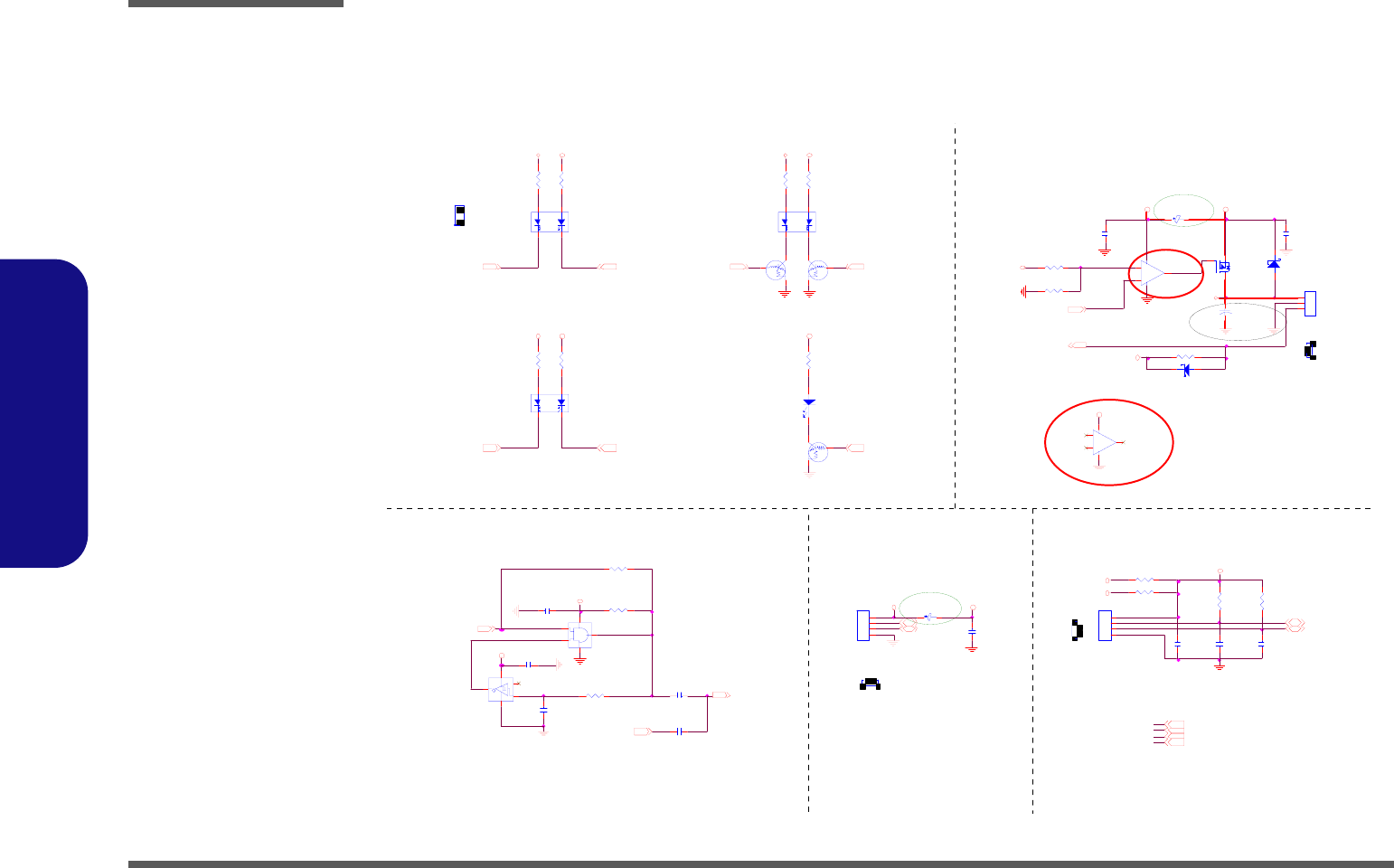
Schematic Diagrams
B - 22 LED, FAN, PC BEEP, TP, FP
B.Schematic Diagrams
LED, FAN, PC BEEP, TP, FP
Sheet 21 of 38
LED, FAN, PC
BEEP, TP, FP
CPU _FAN SEN26
3.3VS
R156 0_04
SG
Y
D1 1
KPB-302 5 YSG C
1
3
2
4
J_ F A N 1
85205-03001
1
2
3
R3 32
4.99K_1%_06
U1 7
*7 4L V C1 G 14 GW
1
2
53
4
EM I 1/3
J_FAN1
U1 8
*7 4 A H C 1G 08 G W
1
2
5
4
3
C5 4 8
.1 U_ 16 V _ 0 4
J_FP1
85201-04051
1
2
3
4
C621
* 22 0 0P _5 0 V _0 4
Z210 5
KBC_BEEP26
R86
10K_04
Z211 6 C2 04
1U _10V_06
AC IN/POWER ON LED
7/1 3
Remove Q9,Q10,Q11,Q14
fo r LE D lo w ac ti ve .
F AN_ DC _ VOL
3.3VS 6,10,11,12,13,14,15,16,17,18,19,20,22,24,25,26,27,28
J_TP1
85201-04051
1
2
3
4
7/11
5V S
Z2110
C5 4 9
10 U _1 0 V _0 8
5V
5VS 12,18,24,25,27
L1 0
HCB1005KF-121T20
USB_PP1 1 5
R200
470_04
C200
4 7 P _ 50 V _ 04
LED
3G LED
KBC _BEE P_R
R197
220_04
R79
10K_04
R1 92
22 0 _0 4
LED_BAT_FULL# 26
C607
*.1U_16V_04
C299
1U_10V_06
R95 0_06
7/11
Z2106
Q12
DT C1 1 4 EUA
CE
B
J_FP1
5VS_FAN
5VS_TP
R3 33
10K_1%_04
R 97 *0_06
L46
HC B1 60 8 K F-12 1 T25
VDD3
D1 3
KP-20 12 SGC
AC
Z211 7
Q1 5
DT C1 1 4E U A
CE
B
3.3VS
VD D3 2,1 5 ,26 ,2 7 ,29 ,3 1,3 2
LED_AC IN#26
1
R1 93
22 0 _0 4
CPU_ F AN26
SPKR OUT14
Z2109
R1 99
47 0 _0 4
PC BEEP
5VS
C194
47P_50V_04
4
D21 SCS551V-30
AC
FAN CONTROL
Z2102
WLAN/BT LED
6-01-74108-Q61
VD D3
BEEP 24
C6 05
* . 1U _1 6 V _0 4
Z2113
4
5V 19,20,24,28,29,30,31
3. 3 V S _ F P
SG
Y
D1 2
KPB-3025YSG C
1
3
2
4
BT_ EN19,26
BAT CHARGE/FULL LED
5/10
D11,D12,D15
VDD3
3G _EN 19,26
R2 01
47 0 _0 4
TP_DATA 26
C300
1U_10V_06
LE D _B A T _ C H G #26
1
C148
.1 U_ 1 6V _ 0 4
Q13
DT C1 1 4 EUA
CE
B
2
Z2114
D2 0
SCS55 1V -30
A C
J_TP1
FP CONN
5VS
5V S
EM I 1/3
Q27
ND S35 2 AP _N L
G
D S
USB_PN 1 15
+
-
U1 0B
GM358S8R
5
6
7
F AN_ DC _ VOL _R
LED_PWR # 26
4
1
5VS
40 MIL
R198
220_04
5VS
3
TP_CLK 26
+
-
U1 0A
GM3 5 8S 8 R
3
2
1
84
3.3VS
3. 3 V S
FAN_DC_VOL Z2115
Z210 1
R 144 *10K_04
3
VD D3
WLAN_EN 20,26
Z2111
R334 4.7K_04
+
C5 5 0
100U_6.3V_B2
Z2112
R1 55 *1 M_ 0 4
SG
Y
D1 0
KPB-302 5 YSG C
1
3
2
4
CLICK CONN
1
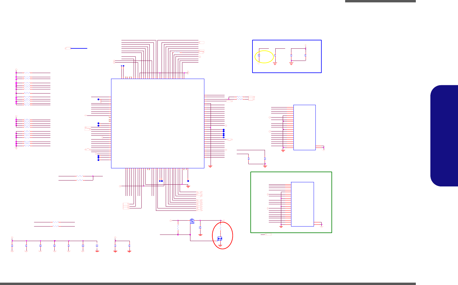
Schematic Diagrams
ENE MR510, 7 IN 1 B - 23
B.Schematic Diagrams
ENE MR510, 7 IN 1
Sheet 22 of 38
ENE MR510, 7 IN 1
MS _ I N S #
Z2208
C604
* 10U_10V_08
PCI_AD 12
SD _C MD
C361
.1 U _1 6 V _ 04
PC I_A D26
MS_C LK
MF U N C 1
R 384 22_04
SD_D 3
Z22 10
Z2218
PCI_AD 15
SD _D 0
MFUNC5
MS_BS
R389 47K_04
Near Cardreader CONN
For M720SR
PC I_ PAR 1 3
SD_C D#
PC M_ IDSEL
R392 47K_04
R173 47K_04
PC I_ STO P# 13
MS_D 1
C6 2 8
*.1 U _ 1 6 V _0 4
C616
* 10P_50V _04
SD_D 0
R416 47K_04
V CC_ C ARD
PCI_AD22
PCI_AD 14
MS_D 2
PCI_AD 4
CARD_PWREN#
MS _ D 2
SD_CLK
R176 47K_04
C615
.1U_16V_04
PC I_AD 19
C LOS E TO CH IP
PCI_ INT# B 1 3
PCI_AD 9
C3 6 2
.1U _ 16 V_ 0 4
R423 47K_04
PCI_AD 3
VCC_CARD
PC I_ C/BE# 2 1 3
SD _D 0
Z2205
R486 100_04
R396 *100_04
R387 47K_04
R422 47K_04
xDSM CE#
PCI_AD 6
CLOSE TO CHIP
MS_D 3
L PC_ S IRQ
Q3 0
AO 3409
G
DS
J_CAR D-R EV_73
M DR 019-C0-0010(R ev erse)
P2
P21
P3
P4
P5
P6
P7
P8
P9
P10
P11
P12
P13
P14
P15
P16
P17
P18
P19
P20
P1
P23
P22
DAT2_SD
VSS_ M S
CD/DAT3_SD
CMD_SD
VSS_ SD
VD D_SD
C LK_SD
VSS_ SD
DAT0_SD
DAT1_SD
WP_SD
VSS_ M S
VC C_MS
SC LK_ M S
DAT3_MS
IN S_M S
DAT2_MS
SD IO/D AT0 _ MS
DAT1_MS
BS_MS
CD_SD
GND
GND
1 2/2 5
R183 47K_04
3.3VS
SD _ CL K
SD _D 3
SD_CM D
ENE INT
SD _C MD
MS _ B S
MS _ D 3
MS _ B S
PCI_AD 0
SDCLK
Z2201
Z221 1
U38
MR510
1
2
3
4
5
6
7
8
9
10
11
12
13
14
15
16
17
18
19
20
21
22
23
24
25
26
27
28
29
30
31
32
33
34
35
36
37
38
39
40
41
42
43
44
45
46
47
48
49
50
51
52
53
54
55
56
57
58
59
60
61
62
63
64
65
66
67
68
69
70
71
72
73
74
75
76
77
78
79
80
81
82
83
84
85
86
87
88
89
90
91
92
93
94
95
96
97
98
99
100
101
10 2
103
10 4
105
10 6
107
10 8
109
11 0
111
112
113
114
115
116
117
118
11 9
120
12 1
122
12 3
124
12 5
126
12 7
128
XSDPW R33O Z
NC
GND_SD
SD DAT2SMC LE
SD DAT3SMD AT4
SD CMD SMA LE
SD CL KSMW EOZ
SD DAT0SMD AT7
SD DAT1SMD AT0
VC C_SD
NC
NC
NC
NC
NC
PC IREQ OZ
PC IGN TIZ
PC IAD3 1
PC IAD3 0
PC IAD2 9
VSS
PC IAD2 8
PC IAD2 7
PC IAD2 6
PC IAD2 5
PC IAD2 4
PC ICBE3Z
PC IIDSELI
VC C
NC
NC
NC
PC IAD23
PCIAD 22
PC IAD21
PCIAD 20
PC IRSTIZ
PCIC LKI
PC IAD19
PCIAD 18
SD CLKI
VCC
VSS
NC
NC
PCIAD17
PCIA D16
PC ICBE 2Z
PCIFR AM EZ
NC
NC
VC C
PCIIR DYZ
PC ITRD YZ
PCID EVSEL Z
PC ISTOPZ
PCIPER RZ
PC ISERR OZ
PCIPAR
PC ICBE1Z
VSS
NC
NC
NC
PCIAD 15
PCIAD 14
PCIAD 13
PCIAD 12
VC C
PCIAD 11
PCIAD 10
PCIAD 9
PCIAD 8
PC ICBE 0Z
NC
NC
NC
NC
NC
VSS
VC C
PCIAD 7
PCIAD 6
PCIAD 5
PCIAD 4
PCIAD 3
PCIAD 2
PCIAD 1
SMC DIZ
MSINSIZ
PCIAD 0
VSS
R IOU TZ _P M EOZ
MFUNC0
MS_SMPWR OZ
MS B S O S MD A T 1
VSS
XMD AT7 BSM CEO Z
XM DAT4 B
XMF UNC 1B
VC C
XMF UNC 2B
XM FU NC3B
XGR STIZ
XM FU NC4B
XM FUN C5 B
XM FU NC6B
XSUSP ENDI Z
GND_SD
XM FUN C7 B
XM D AT6 BSM BSYIZ
XM DAT5 BSM W PO Z
VCC_SD
XM SDAT1BSM D AT6B
X MSD AT 0 BSM DAT2 B
XM SDAT 2BSM D AT5 B
XMSD AT3 BSM DAT3 B
XM SCLKO SM REOZ
VSS
VC C
XSDWPIS MW P DIZ
XSDCDIZ
NC
NC
XPM PW R_ VC C
XPM PW R _O
XPM PW R_ EN IZ
NC
R415 47K_04
7/ 13
M od i fy R38 5 fr om 10 0K ch a n ge
to 470 ohm and ADD Q37 for remove
SD card time > 1ms issue.
SD _D 2
MS_D 3
C6 4 2
.1 U_ 16 V_ 0 4
PC I_A D29
V CC_ C ARD
MS _ I NS #
MS _ D 1
R388 47K_04
MS_D 2
VC C_CAR D
PC I_A D31
Q37
2N 7002W
G
DS
R413 47K_04
VC C_CAR D
LPC_SIRQ 14,26
PC I_ C/BE# 1 1 3
3.3VS
MS_D 0
Z2206
MS_D 0
SD _D 3
PC I_A D28
XMDA T4 B
C6 1 0
.1U _ 16 V_ 0 4
VCC_CARD
R393 47K_04
R484 *0_04
PC LK_ C ARD17
VCC_CARD
MS _ I N S #
SD CLK
C3 43
.1U _1 6 V_ 0 4
3. 3 V S
CL K_ 48 M_ C ARD17
MF U N C 6
Ca rd R ea der P ow er
PCI_ AD[ 31 :0 ]13
PM E# 1 4,26
MS_IN S#
SD _D 2
Z2209
MSCLK
PCI_AD 16
SD _C D#
SD _D 1
R410 47K_04
PC I_A D30
R 407 22_04
SD_C MD
PC I_A D23
PCI_AD 2
R403 47K_04
R414 47K_04
3.3VS
PC I_AD 2 3
C613
1 0 P_5 0 V_ 04
SM_ C D#
PC I_PERR #
R408 47K_04
SM_ C D#
C6 1 2
.1 U_ 1 6V_ 0 4
PC M_ IDSEL
SD_D0
R390 47K_04
XMDA T4 B
SD _C L K
PCI_ INT # A 4 ,6, 13
PC I_ DEVSEL# 1 3
SD_D 1
MS _ D 3
3 . 3 V S 6 , 1 0, 1 1 , 1 2, 1 3 , 1 4, 1 5 , 1 6, 1 7 , 1 8, 1 9 , 2 0, 2 1 , 2 4, 2 5 , 2 6, 27 , 2 8
PC I_ AD17
PCI_AD20
SD _D 1
CARD _ PW RE N #
C3 6 3
.1U _ 16 V_ 0 4
3.3V S SD _C D#
MF U N C 7
SD_CD #
SD_D1
R394 47K_04
30 mil
MFUNC4
MF U N C 2
PC I_G NT#013
PC I_AD 2 0
C6 3 5
.1U_16V _04
xDWP#
PCI_AD 13
R182 47K_04
PC I_FRAM E# 13
PCI_AD 5
MS _ D 1
2/ 26
PC I_RST#20,27
MS_INS#
Z2216
Z2220
R4 3 7 * 0 _0 4
MF U N C 5
30 mil
SD_W P
MS_CLK
C3 6 0
.1U_16V_04
SUSB# 17,18,20,27, 30,31
PCI_AD 7
VCC_ C ARD
Z22 23
Z222 4
C6 1 4
*.1 U _1 6 V _ 04
R386 47K_04
PCI_ C /BE#313
xDWP #
3.3V S
MSCLK
x D_BSY#
SD_D 2
R174 47K_04
MS_D 1
MS _ C LK
SD_W P
SD _W P
Z2228
CARD_PWREN#
C633
.1U_16V_04
PCI_AD 8
PC I_A D24
SD_D3
MS_C LK
xDSMCE#
PC I_A D21
SD _C D#
VCC_CARD
Z2217
Z2219
R404 47K_04
Z2207
PCI_R ST# 20,27
Z222 7
R485 0_04
PC I_SERR # 13
MS _ D 2
x D_ BSY #
PCI_AD 10
MFUNC1
J_C ARD -REV_72
*M DR 019-C0-0010(Rev erse)
P2
P2 1
P3
P4
P5
P6
P7
P8
P9
P1 0
P1 1
P1 2
P1 3
P1 4
P1 5
P1 6
P1 7
P1 8
P1 9
P2 0
P1
P23
P22
DAT 2 _SD
VSS_ MS
CD/D AT 3_ SD
CMD _ SD
VSS_ SD
VDD _SD
CLK_ SD
VSS_ SD
DAT 0 _SD
DAT 1 _SD
WP_SD
VSS_ MS
VCC _M S
SCLK_ MS
DAT 3 _M S
INS_ MS
DAT 2 _M S
SDIO /DAT 0 _M S
DAT 1 _M S
BS_M S
CD_ SD
GN D
GN D
3.3VS
MFUNC6
SD_C LK
PCI_AD 11
PC I_ IRD Y# 13
PCI_AD 1
R412 47K_04
3. 3 V S
R380
100K_04
3. 3V S
MF U N C 4
MS _ B S
SD_D2
VC C_ CA R D
PC I_ C/BE# 0 1 3
PC I_A D25
SD _W P
PCI_ AD [31 :0 ]
R391 47K_04
MS _ D 0
PC I_TR DY # 1 3
PCI_REQ#013
PC I_A D27
MFUNC2
MFUNC7
PCI_AD18
MS _ D 0
PCI_PER R#
R385
470_04
For M730SR
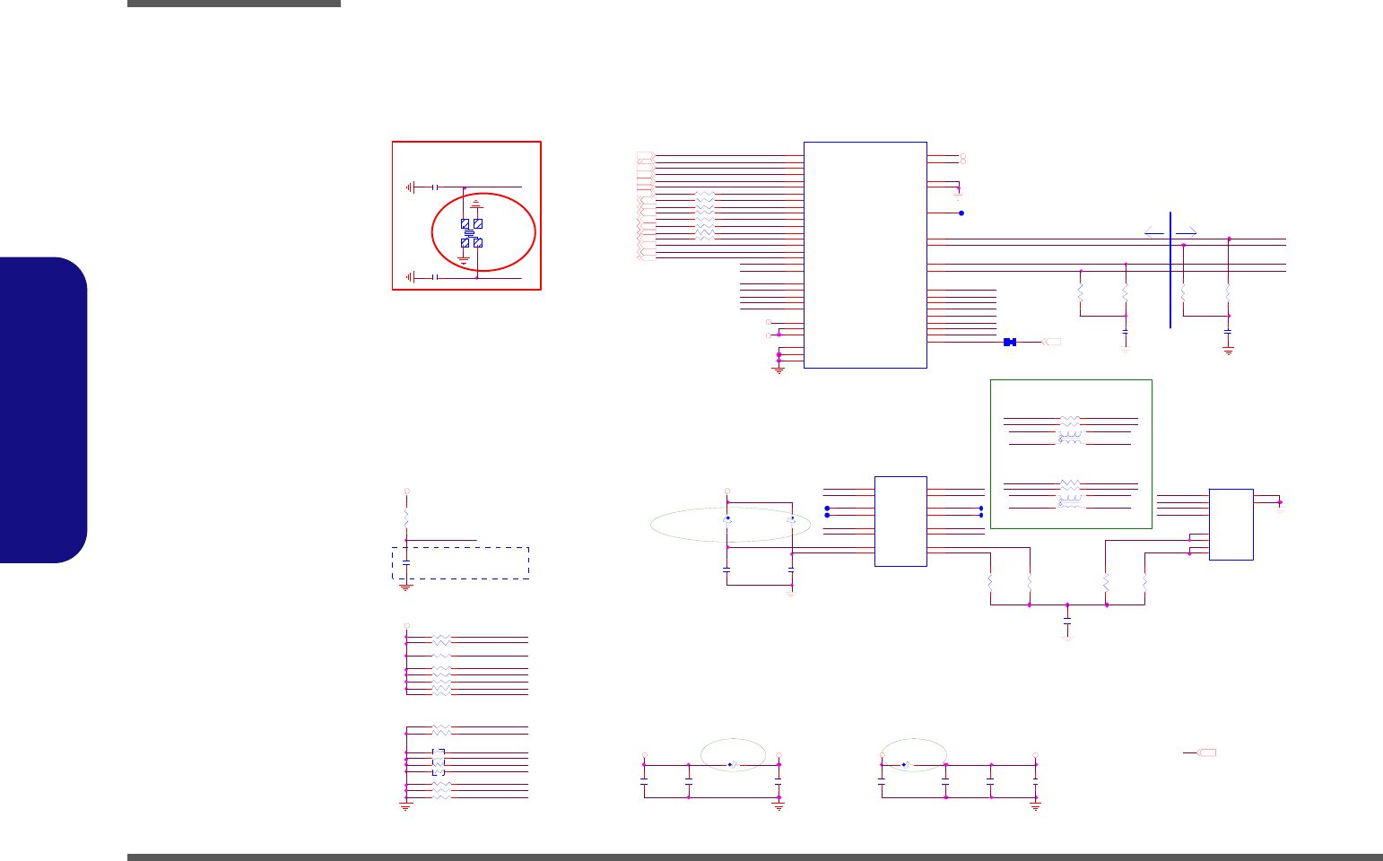
Schematic Diagrams
B - 24 PHY REALTEK 8201CL
B.Schematic Diagrams
PHY REALTEK 8201CL
Sheet 23 of 38
PHY REALTEK
8201CL
LE D 2
R476 5.1K_04
R 452 0_04
MLMX0-
LAN _R T SET
R 447 0_04
R466
75_1%_04
C669
.1U_16V_04
3.3V
TXD 2_PHY14
LE D 1
MDIO_PHY
R472 5.1K_04
MDI0+
MLMX1+_R
RXD 2_P HY _ R
MDC _PHY14
MLM X0+_R
R 448 22_04
DD_NP
PW F BOU T
COL_PHY
LED _TX
C663
18P_50V_04
COL_PHY14
TXD 1_PHY14
AN E
PHY_XTAL1
V_L AN _ 3. 3
V_LAN _3.3
LAN _R ST#
MLMX0+
LE D 3
RD_CT
PW FBIN
R457
49.9_1%_04
CRS_PHY
L62
H CB 1005KF -121T20
R478 2K_1%_04
C667
.1U_16V_04
LAN _RS T#
MLMX0-
R464
75_1% _04
C662
18P_50V_04
ML M X1 -_ R
RXDV_PHY14
MLMX1-
LAN _RTSE T
RXD 1 _ PHY14
TD_C T
MLMX1-_R
PHY _XTAL 1
R477 5.1K_04
MLMX0+_R
R 453 0_04
TXD 3_PHY14
Z2308
TXC LK _ PHY14
MDI1+
R 450 0_04
R470 5.1K_04
R542 * s hort_04
EMI 1/3
R456
49.9_1% _04
R541 * s hort_04
DC_NP
LE D _ T X
SPE ED
R475 5.1K_04
L79
* WC M2012F2S-161T03
1
4
2
3
U43
R TL8201C L-V D-LF
25
26
6
5
4
3
2
7
22
21
20
19
18
16
1
23
46
47
9
10
12
13
15
8
14
11
17
32
36
48
29
35
45
24
27
34
33
31
30
28
43
40
42
39
38
37
41
44
MDC
MDIO
TXD0
TXD1
TXD2
TXD3
TXEN
TXC
RXDV
RXD0
RXD1
RXD2
RXD3
RXC
COL
CRS
X1
X2
LED0/PHYAD0
LED1/PHYAD1
LED2/PHYAD2
LED3/PHYAD3
LED4/PHYAD4
PW FBIN
DVDD33
DGND0
DGND1
PW FBO UT
AVD D33
DVDD33
AG ND
AG ND
DGND2
R XE R/F XEN
NC1
TP TX+
TPTX-
TPRX+
TP RX-
R TSET
ISO L A TE
RP TR
RE SETB
SPEED
DU PLEX
AN E
LD PS
MII/ SNI B /R TT 3
C672
.1U _16V_04
ML M X 0 + _R
EMI 1/3
RXD 0_P HY _ R
RXCLK_PHY_R
LED 3
DUPLEX
C684
.1U_16V_04
M540JE? ? ?
MLMX0-
MLMX1-
R4 6 7
75_1% _04
R 451 0_04
TXEN _ PH Y14
R458
49.9_1%_04
PHY _XTAL 2
LED 2
V_LAN _3.3
MLM X1-_R
C666
1000P_2KV _12
Z2305
MI I/SIN B
Z2303
RXER _PH Y14
Z2307
AU X_PW R OK 6 ,14
M II/SIN B
R471 5.1K_04
7/13
Modify C662,C 663 from 22P F
change to 18PF for OSC
i ssu s e .
MLMX1+
MLM X1+_R
C673
10U_6.3V_X5R _08
X2
FSX5 M_ 2 5 M HZ
12
34
RXD 3_P HY _ R
RXER _PH Y
C668
10U _6.3V_X5R_08
R459 * 10m il_s hort
Close to RTL8201CL
MDI1-
Z2301
R479 5.1K_04
C671
.1U_16V_04
MDI0-
MDI0+
LED 1
PHY_XTAL2
RXD 0 _ PHY14
PW F BO UT
R543 * s hort_04
MDI1+
MLMX1+
L61
N S0013LF
1
2
16
15
314
412
5
6
7
13
98
11
10
RD+
RD-
RX+
RX-
RD_CT RX_CT
NC NC
NC
TD_C T
TD+
NC
TX-TD-
TX_CT
TX +
3. 3V 2,12,14,15,16,18,19, 20,27,29,30,31
CO L _P HY
R473 5.1K_04
R480 5.1K_04
R XER_PH Y
L80
HC B1005KF-121T20
RN 29 8P4R X10K_04
1
2
3
45
6
7
8
CLOSE TO LAN CHIP
MDI1-
C6 7 0
10U _6.3V_X5R _08
CRS_PHY14
TXD 0_PHY14
RXD 1_P HY _ R
V_L AN _ 3. 3
CLOSE TO
PWFBIN
ML M X 1 + _R
MLMX1+
L81
H CB 1005KF- 121T20
4/16
MLMX0+
LDP S
RPTR
R469 5.1K_04
RXCLK _PHY14
TX_C T
R468 1.5K_04
EMI 1/3
TXEN _PH Y_R
R 455
49.9_1% _04
RXD 3 _ PHY14
R474 5.1K_04
R 454 22_04
RX_ C T
Z2302
LD PS
Z2306
ML M X0 -_ R
ISO L A TE
L78
* WC M2012F2S-161T03
1
4
2
3
MDI0- MLMX1-
L63
HC B1005KF-121T20
PW FBO UT
CR S_PH Y
LE D 4
MLM X0-_R
R 449 0_04
PHY Address : 01
CLOSE TO TRANSFORMAL
AN E
TXC LK_ PH Y_ R
MD I O _ P H Y14 MD IO_ P H Y
C664
.01U _16V_X7R _04
LED 4
R460
5. 1K _ 04
C661
.1U _16V_04
PW F BIN
V _LA N_3.3
DU PLEX
PJ S- A8 J D3G
J_RJ-45
8
7
6
5
4
3
2
1GN D 1
GN D 2
DD-
DD+
DB-
DC-
DC+
DB+
DA-
D A+ shield
shield
EMI 1/3
R 465
75_1%_04
RXD 2 _ PHY14
RXDV_PHY_R
RP TR
MLMX0-_R
C 665
.01U _16V _X7R _04
C660
.1U _16V_04
ISO L A TE
R540 * s hort_04
Z2304
SP EED
MLMX0+

Schematic Diagrams
AUDIO CODEC ALC883 B - 25
B.Schematic Diagrams
AUDIO CODEC ALC883
Sheet 24 of 38
AUDIO CODEC
ALC883
C354
* 680P_50V_04
Ve ry c los e to Au di o C od ec
AU DG
MIC IN
3.3VS
HP _SEN SE
L6 6
*FC M1005KF-102T02
12 /2 5
R168
2.2K_04
12 /2 5
HP _SEN SE
M IC_ SENSE
Z2411
Z2407
R 5 16 0 _ 04
R 395 33_04
2
H P -OU T-L 2 5
C322 .1U_16V_04
L28 *FC M1005KF-121T03
AU DG
Z2425
M IC1-R_73
Z2416
MIC1-L
Z 2422
MIC2-VREFO
C3 5 5
*680P_50V_04
L54
HC B1005K F-121T20
1
R520 0_04
R 145 0_04
PINK
AU DG
Z2428
AZ_SDIN 0_R
R158
2 . 2K _0 4
R 518 0_04
AU DG
C678 .1U_16V_04
C 6 41 4. 7U _6 . 3 V _ 06
AUDG
Z2404
AZ_ RST# _R
AUD G
C676 .1U_16V_04
5V
5V 19,20,21,28,29,30,31
3.3VS 6,10,11,12,13,14,15,16,17,18,19,20,21,22,25,26,27,28
Z2433
R 399 1K_04
J_INTMIC 1
88266-02001
PCB Footprint = 88266- 2L
2
1
HEAD PHO NE-L25
3.3VS_AUD
C630 .1U_16V_04
J_INTMIC1
H EADPH ON E-L_7 3
Z2406
MIC 1- R
C6 43
10U_10V_08
Fo ll ow
????
AU DIOG PIO0 #25
AZ_ BITC L K_R
12/25
12 /2 5
Z2408
HP-OUT-R
SPD IFO
C356
* 680P_50V_04
C648
.1U_16V_04
Z2403
Z2432
INT_ MIC
Z2418
SPD IFO
L27 *FC M1005KF-121T03 Z2429
HP_SENSE
Z 2413
C617 *22P_50V_04
J D_SEN SE
R5 08
100K_04
R169
2 . 2K _0 4
M IC2 -VRE F O
AUD G
R
L
J_SPD IF_ 72
* C12103-10609-L
2
6
5
3
1
4
U2 0
*G 9 24
1
23
4 5
SH DN#
GN DBYP
OU T V IN
SPK_HP #25
Z2408
R 165 20K_1% _04
EM I 1/ 3
Z 2412
R
L
J_ H P _7 2
* C12103-60609-L
2
6
5
3
1
4
L29 *FC M1005KF-121T03
AU DG
Z2441
C677 .1U_16V_04
C352 .1U_16V_04
EMI 1/3
5VS_ AUD
H EADPH ON E-R_ 7 3
L5 5
FC M1005KF-121T03
5VS 12,18,21,25,27
R509
100K_04
AZ_ SYN C14,19
MI C 1- V R E F O - L
D 37 *SCS 551V-30
AC
C364
* . 1U _1 6 V _ 04
2
H EADPH ON E-R_ 7 3
V ery c lo se to Au di o Cod ec
Z2426
MIC1-L
R 41 9 10 K _ 04
C347 0_04
R 154 39.2K_1%_04
Z2431
Z2402
C350
* 680P_50V_04
C3 6 6
1U_10V_06
6
AUD G
H P -OU T-R 2 5
Z2427
MIC1-VREFO-R
C675 .1U_16V_04
5
12/25
C601
.1U_16V_04
C622 100P_50V _04
12 /2 5
5VS
Z 2423
R498 * 100_06
HP-OUT-L
HEA DPHONE
7/11
C347 0.1uF_16V_04 ? ? 0_04
?? ?? ?? ?? ?? ?? ?? ?? ?? ?? .
FR ON T-R 25
Z2401
C611 1U_10V_06
C644
10U_10V_08
1
Layout Note:
Z2424
AZ_ SYNC _ R
C6 23
.1U _16V_04
H EADPH ON E-L_7 3
C351
* .01U _16V_X7R_04
R 153 20K_1%_04
Z 2420
R 152 33_04
AZ _ SDO UT14,19
MIC1-R
R 398 10K_04
12/25
C619
10U_10V_08
E MI 1/ 3
Z2410
EMI 1/3
Z2419
SPD IF OUT
MIC1-R_73
R519 0_04
R
L
J_ M I C _ 72
* C12103-D0609-L
2
6
5
3
1
4
MIC1-R
MIC1-L_73
C 629 1U _10V_06
C3 5 3
*680P_50V_04
AUD G
AZ_ BITCL K14,19
M IC_ SENSE
Z 2415
SPD IFO_ 7 3
C329
.1 U_ 1 6V _0 4
Co dec p in 1 ~ pin 1 1 and p in 47 a nd pi n 4 8
ar e D ig ita l si gna ls .
Th e o th ers a re An al og si gn als .
Z 2421
C170
680P_50V _04
Z2442
BLACK
IN T_M IC
Z2409
C 6 38 4. 7U _6 . 3 V _ 06
C 335 1U _10V_06
C 632 1U _10V_06
C 647 10U _10V_08
FR ON T-L 25
L59 HCB 1005K F-121T20
EMI 1 /3
MIC1-VREFO-L
MIC _SENSE
HEA DPHO NE-R
C337
680P _50V_04
3
AZ_ SD IN014
C 339 1U _10V_06
C301
.1U _16V_04
GREEN
HEA DPHO NE-L
SPK_H P#
AUD G
Z2410
R 150 22_04
AU DG
BEEP21
Z2417
Z2440
R1 7 9
*220_04
La yo ut N ot e:
MIC1-VREFO -R
AZ_ SDOU T_R
C338
680P_50V _04
5VS_ AU D
Z2411
Z2430
DI GI TA L
ANALOG
U37
ALC883
1
2
3
4
5
6
7
8
9
10
11
12
13
14
15
16
17
18
19
20
21
22
23
24
26
27
28
29
30
31
32
33
34
35
36
37
39
40
41
42
43
44
45
46
47
48
38
25
DVD D1
GPI O0
GPI O1
D VSS1
SDA TA-O UT
BIT-CLK
DVSS2
SDA TA-IN
DVDD2
SYN C
RES ET#
PCB EEP
Sense A(JD1)
LINE2-L
LINE2-R
MIC 2 -L
MIC 2 -R
CD -L
CD -GN D
CD -R
MIC 1 -L
MIC 1 -R
LI N E 1 - L
LINE1-R
AVSS 1
VREF
MI C 1 -V R E F O - L
LIN E1 -VREFO -L
MI C 2-V R E F O
LINE 2-VR EFO
M IC1 -VRE F O-R
DCVOL
Sense B(JD2)
FRO NT-OU T-L
FR ON T-O UT-R
LINE1-VREF O-R
SUR R-OU T-L
JD R E F
SUR R-O UT-R
AVSS2
CEN -OU T
LFE-OU T
SID ESUR R-OU T-L
SI DESUR R-O UT-R
SPD IFI/EAPD
SPD IFO
AVDD 2
AVD D1
R 151 33_04
J_ A U D _ 73
87151-12071G
1
2
3
4
5
6
7
8
9
10
11
12
L30 *FC M1005KF-121T03
R517 0_04
Z2409
4
La yo ut No te :
AUD G
AZ _R ST#14,19,25
12 /25
EM I 1/3
C334 .1U_16V_04
FOR M730SR
SPD IFO_ 7 3
MIC1-L_73
H EADPH ON E-R25
MIC 1- L
R497 * 100_06
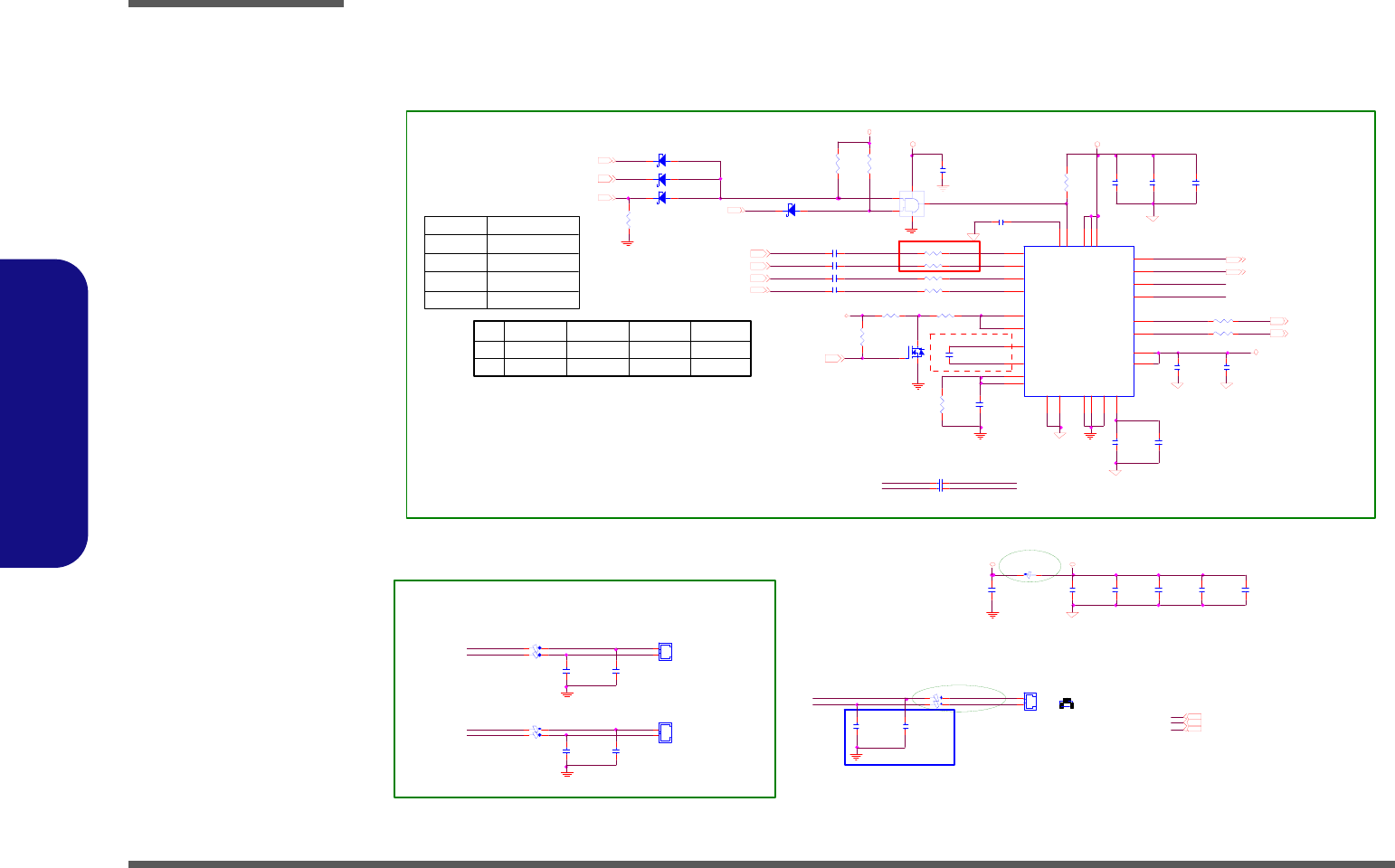
Schematic Diagrams
B - 26 AUDIO AMP
B.Schematic Diagrams
AUDIO AMP
Sheet 25 of 38
AUDIO AMP
R_HP_O
R 524 4.7K_04
FR ON T-R24
SPKO UTL-_R1
C7 1 6
1U _10V_06
C7 0 3
180P_50V_04
SPKO UTL +
Default( L = Mute )
J_SPK_ 7 2
*88266-02001_R
PC B Footprint = 88266-02R
2
1
C706
1U_10V_06
2
3.01K_1%_04
R_HP_O
C7 1 7
0.1U _16V_04
AU DG
Z25 09
R5 28
10 0 K _ 04
EM I 1/3
AUD G
SPKO UTL +
J_SPK L_73
88266-02001_R
PCB F ootprint = 88266-02R
2
1
SPKO UTL+_R 1
L_HP_O
L5 8
H CB1005KF-121T20
A Z_R ST #
L67
FCM 1005KF-121T03
AUD G
R530 100_04
C625
10U_10V_08
J_SPK1
AUDG
AU DG
3.3VS 6,10,11,12,13,14,15,16,17,18,19,20,21,22,24,26,27,28
Z25 10
C331
.1U_16V_04
3.01K_1%_04
M7 20 SR
5V 19,20,21,24,28,29,30,31
C 712 4.7U _6.3V_X5R _06
L68
FCM 1005KF-121T03
FO R EM I
L -> H
SPKOUTR+
M730T
L65 * FCM 1005KF-121T03
R5 31
10 0 K _ 04
C 713 4.7U _6.3V_X5R _06
D 35 1SS355 SOD -323
AC
C707
0.1U_16V_04
10K
HEAD PHO NE-L 24
SPKO UTR-
Z25 09
SB_MU TE#14
1
R144
R532 100_04
M730SR
R526 39K_04
30mils
L -> H
SPK_ HP#24
AUD IOGP IO0 #24
C3 5 9
.1U _16V_04
SPKO UTL -
R5 3 3
*5 1 0K _ 0 4
R5 2 2
10K_04
C6 2 6
10U _10V_08
10K
5VS 12,18,21,24,27
C702
180P_50V_04
SPKOUTR-
SPKO UTR+
EM I 1/ 3
AZ_ RST#14,19,24
C718
1U_10V_06
C 7 20 6 8P_5 0 V_04
R523
100K_04
AUDIOGPIO0#
K BC_ MU TE #
5VS
D 34 1SS355 SOD -323
AC
HP-OUT-R24
FRO NT-L24
4.7K
L70
FCM 1005KF-121T03
12/25
C 711 4.7U _6.3V_X5R _06
5 VS_ AMP
C7 19
0.1U _16V_04
R5 2 9
10K_04
3.3VS
C639
.1 U_ 1 6 V_ 04
SPKOU TL+
C7 0 5
0.1U _16V_04
4.7K
5 VS_ AM P
C 7 21 6 8P_5 0 V_04
U44
74AHC 1G08G W
1
2
5
4
3
R521
10K_04
R 525 4.7K_04
6.2K_1%_04
SPKOU TL-
L_HP_O
Q3 8
2N 70 0 2 W
G
DS
L64 * FCM 1005KF-121T03
12/25
C714
1U_10V_06
R157
1M _04
SPKOUTR+ 19
D 36 1SS355 SO D-323
AC
5VS_AMP
C708
0.1U_16V_04
C7 0 1
180P_50V_04
SPKO UTR+_ R1
HP-O UT -L24
C704
180P_50V_04
D 33 1SS355 SOD -323
AC
C 709 0.1U_16V_04
SPKO UTR-_R 1
SPKO UTL -
5VS
Ne ar CP + an d CP-
C 710 4.7U _6.3V_X5R _06
C3 28
.1U _ 16 V_ 0 4
H -> H
5.6K_1%_04R141
C17
*180P_50V_04
L69
FCM 1005KF-121T03
M7 20 T
5V S
AUDG
Z25 10
J_SPK R_73
88266-02001_R
PCB F ootprint = 88266-02R
2
1
AUD G
R527 39K_04
C1 6
*180P_50V_04
A PA2056
U4 5
APA2056A
6
4
19
11
26
13
17
18
15
9
27
25
8
21
22
3
12
14
16
24
5
28
1
20
10
2
7
23
29
L _ IN_ HP
R_IN_HP
HPV DD
CPV DD
SD#
CPG ND
R_HP_OUT
L_HP_OU T
C PVSS
L_OU T-
AM P_ EN#
BY PASS
L_ O U T +
R_ OU T-
R_ O UT +
R_IN_AMP
CP+
CP-
H PVSS
HP_EN
L_IN_AM P
BEEP
VDD
PVDD
PVD D
GN D
PGND
PG ND
GND
C7 1 5
0.1U_16V_04
For M730SR
S B_M UT E#
HEAD PHO NE-R 2 4
KBC _M UTE#26
L -> H
SPKOUTR- 19
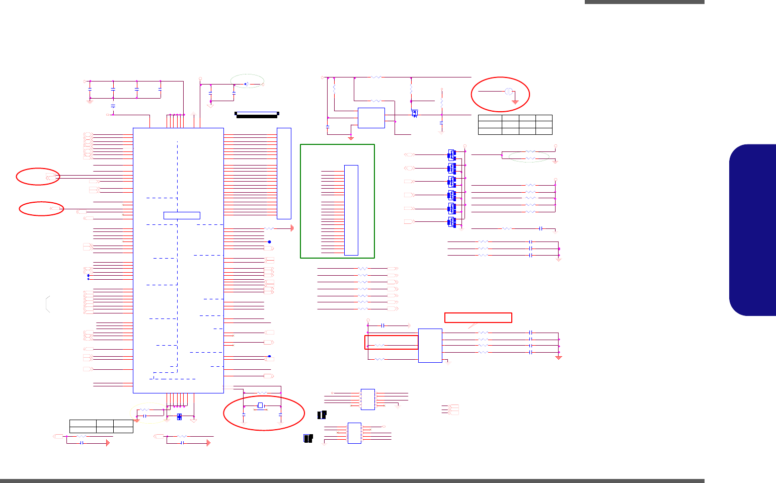
Schematic Diagrams
KBC-ITE IT8512E B - 27
B.Schematic Diagrams
KBC-ITE IT8512E
Sheet 26 of 38
KBC-ITE IT8512E
VDD 3
BAT1_VO LT
KBC_SPI_ SO_R
KB-SO0
J_KB1
WLAN_EN20,21
KB-SO3
3G _E N
3G_DET#19
C270
12P_50V_04
8 0 PORT_ DET#
KBC_SMI#
C5 86
.1U _16V_04
KB-SI7
3I N 1
CCD_DET#
RB
CHG_CURSEN_R
Z26 09
KB-SO1 5
L CD_ BRI G HT NES S12
Z26 06
TOTAL_C UR_ R
KBC_SPI_ SI_ R
R495 0_04
LE D _A C I N #21
W EB_ AP1#31
C 5 7 4 . 1U _ 16 V _ 04
THER M_ AL ERT#2
PW R_SW #31
LI D _S W #12,19
PM_ CL KRU N# 14
KBC _G A20#
KB-SO4
KB-SO3
8Mbit
SM C_BAT
KB-SI5
VDD 3
KB-SI1
R 546 0_04
RA
BAT_D ET
KBC _ SPI_SC LK
PW R_SW #
PM_CLKRU N#
7/13
Modify C268,C270 from 15PF
change to 12PF for OSC
issuse.
LED_SCR OLL#19
LE D _ TH R O T T LE #19
Z261 0
J_KB_73
85202-24051
24
23
22
14
12
11
21
8
20
19
6
5
18
4
17
10
9
7
3
2
1
16
15
13
1
VDD3
BAT1 _ VOL T32
KBC_PCL K17
KB-SO1 2
SM D_ VGA_ TH ERM
C5 7 7
.1 U_ 16 V _ 0 4
C5 6 7
.1 U_ 1 6V_ 0 4
C5 61
.1U _16V_04
R111
10K_04
LOW ACTIVE
KB-SO9
R7 8
10 0 K _0 4
KB-SO4
SMC _ CP U_ THE RM2
KBC _M UTE#
R133 * 10M_04
M OD EL_ ID
SMC _BAT
KB-SO1 1
KBC_FLASH
C597 *33P _50V_04
C268
12P_50V_04
R 363 10K_04
KB-SO10
D6
BAV9 9
A
C
AC
C265 *10P_50V_04
1/9
SW I# 14
CC D_ DET #19
KBC_SUSB# 1 8
R492 0_04
KBC _T XD
LP C _F R A M E #14
KBC_SCI#
KB-SI2
KBC _PC LK
Q8
2N7002W
G
DS
VDD3
KBC_PWRBTN#
???
TP_DATA21
KB-SO9
KBC_SP I_SCL K
KB C_ RST #
R 337 1K_04
3.3VS 6,10,11,12,13,14,15,16,17,18,19,20,21,22,24,25,27,28
N C 14 N C _0 4
R1 1 7
100K_04
WEB_WWW#19
KB-SI0
10
10
0.1uF
KB-SI7
KBC_AVDD
KBC_SUSC # 1 8
R 330 47_04
4/1 6
VD D3
TO TAL_CUR
BR IGHTNESS
LED_THROTTLE#
For ITE8512IX
KBC_AGN D
KBC _PC LK
K BC_ SPI_SI_ R
KB-SO8
C5 6 5 *1 U_ 1 0V_ 0 6
R119 0_04
Follow
????
EMI 1/3
BAT_ DET32
TOTAL_ CUR _R
KB-SO13
9
SM I# 14
LPC_RST#20,27
KBC _R ST#
DD_ O N 2 9
WLAN _PW R
KBC _SW I# R491 0_04
SM D_BAT
AC_IN#
R 331 47_04
KBC_SP I_SO
R 336 15_1% _04
EC pin swap foll ow
????
For ITE8512JX
SM D_BAT32
CPU_FAN_R
BAT_ VOLT_ R
WD_DISABLE
VD D3 2,15,21,27,29,31,32
C HG_ CU RSEN32
KB-SI3
C2 41
.1U _16V_04
LI D _S W #
WDT_EN
KBC_SW I#
C570
.1U_16V_04
C245 *.1U_16V_04
2
KBC _W R ESET #
L ED_ P W R#21
KB-SI1
D25
BAV9 9
A
C
AC
LPC_SIRQ14,22
KB-SI4
WEB_WWW #
J_ H 8 D B G 1
*SP U F Z -10 S 3 -V B -0 -B
12
34
56
78
910
VDD3
VD D3
Z2612
KBC_RXD
KBC _ RXD
BAT_ VOL T _RKB-SO12
12/25
VDD 3
SM D_BAT
KBC _ SPI_C E#
KB-SO1 3
8 0 POR T_ DET#
KB-SI3
J_SPI1
* S P U F Z -1 0 S 3-V B -0-B _ N
12
34
56
78
910
1
WEB0--->AP KEY
WEB1--->EMAILKEY
WEB2--->WWW KEY
R496 0_04
J _ KB_ 72
*85202-24051
24
23
22
14
12
11
21
8
20
19
6
5
18
4
17
10
9
7
3
2
1
16
15
13
KB-SI0
R120 120K_04
K BC_ SPI_SC L K_R
C5 8 2 *1 U_ 1 0V_ 0 6
Option circuit for Pin12
LP C _A D 114
L50
H CB1005KF-121T20
KB-SO7
SM C_ VGA_ TH ERM BKL_ EN
WLAN_EN
X4 32.768KH z
14
3 2
BKL_ EN 1 2
CHG_CURSEN_R
KB-SO11
C5 76
.1U _1 6 V_ 04
3.3V 2,12,14,15,16,18,19,20,23,27,29,30,31
BT_EN 19,21
K/B MATRIX
FLASH
LPC
SMBUS
PS/2
PWM
UART
DAC
CLOCK
IT8512E
CIR
ADC
WAKE UP
PWM/COUNTER
LPC/WAKE UP
EXT GPIO
GP INTERRUPT
WAKE UP
GPIO
U13
IT8512E
14
13
10
9
8
7
6
17
5
15
23
126
4
58
59
60
61
62
63
64
65
36
37
38
39
40
41
42
43
44
45
46
51
52
53
54
55
11
26
50
92
114
127
12 1
3
74
85
86
87
120
124
22
35
125
18
21
112
109
108
123
88
89
90
47
48
24
25
28
29
30
31
32
34
66
67
68
69
70
71
72
73
1
12
27
49
122
113
75
2
128
79
78
77
76
83
84
82
33
20
91
81
80
16
119
56
57
93
94
95
96
97
98
99
107
110
111
115
116
117
118
100
101
102
103
104
105
106
19
WR ST#
LPCC LK
LAD0
LAD1
LAD2
LAD3
LFRAM E#
( PD )L PCPD#/W U I6/G PE6
SER IRQ
EC SMI# /GPD 4( PU )
EC SCI# /GPD 3( PU )
GA20/GPB5
KBR ST# /GPB 6( PU )
KSI0/ST B#
KS I1/AFD #
KSI2/INIT#
KS I3 /SLIN #
KSI4
KSI5
KSI6
KSI7
KSO 0/PD 0
KSO 1/PD 1
KSO 2/PD 2
KSO 3/PD 3
KSO 4/PD 4
KSO 5/PD 5
KSO 6/PD 6
KSO 7/PD 7
KSO 8/AC K#
KSO 9 /BUSY
KSO10/PE
KSO 11 /ERR #
KSO1 2 /SLC T
KSO1 3
KSO1 4
KSO1 5
VCC
VSTBY
VS TBY
VSTBY
VSTBY
VSTBY
VSTBY
VBAT
AVCC
PS2CLK0/GPF0( PU )
PS2DAT0/GPF1( PU )
PS2CLK1/GPF2( PU )
( PD )TM RI0/W UI2 /GPC 4
( PD )TM RI1/W UI3 /GPC 6
LPCR ST#/W U I4/G PD2( PU )
( PD )W U I5/G P E 5
PW R SW /GPE4( PU )
RI1#/WUI0/GPD0( PU )
RI2#/WUI1/GPD1( PU )
( PD ) RING #/PW R F AIL #/L PCR ST #/G PB7
TXD/GPB1( PU )
RXD/GPB0( PU )
( PD )C TX/G PB2
PS2DAT1/GPF3( PU )
PS2CLK2/GPF4( PU )
PS2DAT2/GPF5( PU )
( PD )TAC H0/GPD 6
( PD )TAC H1/GPD 7
PW M 0/G PA0( PU )
PW M 1/G PA1( PU )
PW M 2/G PA2( PU )
PW M 3/G PA3( PU )
PW M 4/G PA4( PU )
PW M 5/G PA5( PU )
PW M 6/G PA6( PU )
PW M 7/G PA7( PU )
AD C0/GPI0
AD C1/GPI1
AD C2/GPI2
AD C3/GPI3
AD C4/GPI4
AD C5/GPI5
AD C6/GPI6
AD C7/GPI7
VSS
VS S
VSS
VSS
VSS
VSS
AVSS
CK3 2KE
CK3 2K
DAC3/GPJ3
DAC2/GPJ2
DAC1/GPJ1
DAC0/GPJ0
( PD )EGC S#/G PE2
( PD )EGC LK/G PE 3
( PD )E G A D /G PE 1
G INT/GPD5 ( PU )
L80LLAT/G PE7( PU )
VSS
DAC5/GPJ5
DAC4/GPJ4
PW U REQ# /G PC7 ( PU )
( PD )C RX/GPC 0
( P D )K S O 16 /GP C 3
( P D )K S O 17 /GP C 5
( PD )GPH 0/ID 0
( PD )GPH 1/ID 1
( PD )GPH 2/ID 2
( PD )GPH 3/ID 3
( PD )GPH 4/ID 4
( PD )GPH 5/ID 5
( PD )GPH 6/ID 6
( PD )GPG 1/ID 7
SM CLK0/G PB3
SM DAT0/G PB4
SM CLK1/G PC1
SM DAT1/G PC2
SM CLK2/G PF6( PU )
SM DAT2/G PF7( PU )
FLFR AME#/GPG 2
FL AD 0/SC E#
F LAD 1/SI
FL AD2 /SO
FLAD3/GPG 6
FL CLK/SCK
( P D )F L R S T # /W UI7 /GP G 0/ T M
( PD )L 8 0H L AT/G PE0
3I N 1
R493 0_04
C592 *33P _50V_04
3.3VS
D22
* BAV99
A
C
AC
KBC _ SPI_SO
C728 *.1u_16V_04
1
CCD _ E N 1 9
W EB_EM AIL#19
80CLK
0 ohm
LED _BAT_FULL#21
KBC _T XD
BRIG HTNESS
R 125 10K_04
R 118 10K_04
FOR M730SR
W LAN _ DET# 2 0
CHG _ EN 3 2
Z2612
FLFR AM#
BT_ DE T#
R512 0_04
C596 *33P _50V_04
J_ SP I1 PIN ? ? LV2 2 0 JS PID BG
L ED_ CA P#19
M7 20S
CH G_ CU RSEN
KB-SO1 4
CCD _ E N
24
KB-SO6
D29
* BAV99
A
C
AC
R 110 10K_04
KB-SO2
W EB_ EMAIL #
R 329 4.7K_04
9
KBC_SP I_SI
R141 100K_04 R128 *10_04
VDD3
T OTA L _ CUR32
CHG_CURSEN
Z26 04
KBC_GA2 0#
R 374 4.7K_04
9/6 De le t
J_H8 BDG1 for BO M
co st
an d M P st ag e .
BAT_ DET
3G_DET#
KB-SI5
KBC_SPI_*_R = 0.1"~0.5"
LP C _A D 214
TH E R M _ R S T #2
PME# 1 4,22
WLAN_PWR20
KB-SO8
KBC _SM I#
C547
.1 U_ 16 V_ 04
C5 6 3
10U _10V_08
R 112 100_04
X
Follow
????
KBC_MUT E#25
TH ERM_ AL ERT#
KBC _R SMRST#
U1 2
AA T3510IGV-2.93-C-C-T1
3
5
2
1
4
MR#
VCC
GND
RESET#
WDI
SMD _ CP U_ THE RM2
THER M_RST#
R494 0_04
KBC_AGN D
W EB_AP1 #
WDT_EN
KB-SI6
LED_BAT_C HG#21
Z2608
BT_ EN
KB-SO5
KB-SO1
WD T_EN
3IN1
U3 2 fro m
SST25VF080B SO8
change to EN25F80
SO8.
LED_NUM#19
KBC_F L ASH
KB C_ SPI_ CE #
R 375 4.7K_04
KBC_SPI_ SCL K_ R
10K
TP_CLK21
KBC_AUXPW RO K 14
KB-SO2
KBC_SPI_CE#_R
D5
BAV9 9
A
C
AC
J_H8DBG1
CPU_ F AN SEN 2 1 KBC _ SPI_SI
LP C _A D 014
CPU_ F AN _ R
CIR_ IN
MODEL_ID
R124 10K_04
GA20# 14
KBC_BEEP21
WLAN _DET#
R 335 15_1% _04
J_SPI1 software not use and for
PVT BOM cost.
W D_ D ISABLE
KB-SO15
J_SPI1
KB-SO1
RB
Un_stuff
KBC _SC I#
KB C_ RS M RS T #
KB-SO6
R 349 * 100_04
SM C_BAT32
CPU_FAN21
3G _E N 1 9, 2 1
BAT1_VOLT
MODEL_ID
80 C L K
KBC _W R ESET#
KB-SO7
U3 2
EN25F80 SO 8
1
2
3
4
5
6
7
8
CE#
SO
WP#
VSS
SI
SCK
HOL D#
VDD
PW R _BT N # 1 4
TOTAL_C UR
D28
BAV9 9
A
C
AC
7/ 13
IT E 85 12E p i n4 a nd p i n1 6 sw a p
for LED dri ver circuit.
LP C _A D 314
KB-SO1 0
Z26 07
C244 1U _10V_06
VCOR E _ ON 2 8
2
KB-SO14
R381 10K_04
SMD _BAT
KBC_PW RBTN#
SC I# 14
AC_IN #32
SM C_BAT
BAT_ DET
C598 *33P _50V_04
R 354 * 100_04
C5 5 8
1U_10V_06
PJ 9
20mil
1 2
Un_stuff
VDD3
K BC_ SPI_SO _ R
KB-SI2
3G_DET#
KB-SI4
SB_KBCR ST# 14
BT_ DE T# 19
KB-SI6
KB-SO0
KBC_SPI_CE#_R
C CD_DE T#
RA
KB-SO5
R 359 10K_04
Schematic Diagrams
B - 28 SYSTEM POWER
B.Schematic Diagrams
SYSTEM POWER
PQ 29
2N7002W
G
DS
4A
SYS15V
1.2VS
SUSB
Z270 1
SUSB
1.2V
1.5V S 3,6,2 0
LPC_RST# 20,26
SUSB#17,18,20,22,30,31
SUSB
1.8V S 4,5,6 ,7,1 1 ,12 ,1 3 ,14 ,1 5,1 6 ,17
4A
NB_ RS T# 6 ,11
Z270 3
PQ2 0
2N7002W
G
DS
3. 3 V
1.8VS
PC 12 4
.1U_16V_04
PR117
1M _0 4
PR72
10 0 K _0 4
R32 33_04
SB_ PW RO K 12 ,14
1.5A
SYS15V 12,29
PR57
1M_04
PC118
10 U _ 1 0V _ 0 8
3.3VS 6,10,11,12,13,14,15,16,17,18,19,20,21,22,24,25,26,28
5V 19,20,21,24,28, 29,30,31
PR12 5
100K_04
PQ4 2
AO4 46 8
4
6 2
5
7 3
1
8
1. 2 V S 4, 7
VD D3
PQ4 3
2N 70 0 2 W
G
DS
PR12 7
100K_04
3.3VS
PQ 51
AO 44 6 8
4
6 2
5
7 3
1
8
1. 8 V 5, 7 , 9 , 10 , 1 4, 1 5 , 1 6, 3 0 , 31
1.5A
PC123
10 U _ 1 0V _ 0 8
SY S15 V
PR132
10 0 K _0 4
PC132
.1U _1 6 V_ 04
3A
PR69
10 0 K _0 4
Z27 05
Z270 2
Z27 04
4A
PC11 7
.01U _50V_X7R_04
VCORE Power Good delay
3ms and Notice SB
U2 A
74 L V C 0 8P W
1
2
3
147
PQ2 8
2N 70 0 2W
G
DS
VDD 5
1. 2 V 7, 3 0
3. 3 V
3A
PQ2 4
AO4 46 8
4
6 2
5
7 3
1
8
R439
100K_04
PQ2 2
2N 70 0 2 W
G
DS
SYS15 V
R34 33_04
PC128
.01U_50V_X7R _04
1.8V_PWRG D31
Z27 08
DELAY_ PW RG D6,28
Z270 6
1.8V
PCI_ RST# 20 ,2 2
1.2VS,1.5VS,1.8VS,3.3VS,5VS
VDD5
U2B
74 LVC 08PW
4
5
6
147
4A
VDD3 2,15,21,26,29,31,32
PC129
.1U _1 6 V_ 04
U2 D
74 L V C 0 8P W
12
13
11
147
1. 5 V 30
5VS 12,18,21,24,25
C 7 0 . 1U _1 6 V _0 4
SU SB
SUSB
PR 73
1M_04
PC57
10 U _ 1 0V _ 0 8
Close to SIS968
PR11 6
100K_04
5V S
R1 9
10 K _ 04
SB_PCIRST#13
PC69
.01U_50V_X7R _04
PQ 30
AO 44 6 8
4
6 2
5
7 3
1
8
1.5VS
1 .05 VS_ PW RGD30
PC113
.1U_16V_04
PC52
.01U _50V_X7R_04
POWER GOOD & RESET
PR 131
1M_04
PR70
10 0 K _0 4
3.3V
PQ2 6
AO4 46 8
4
6 2
5
7 3
1
8
3A
VDD5 29
Z270 7
R33 33_04
3. 3 V
PR59
1M _0 4
PC121
.1U_16V_04
SYS15V SY S15 V
PC 13 1
10U_10V_08
3.3V 2,12,14,15,16,18,19,20,23,29,30,31
1.5V
U2 C
74 L V C 0 8P W
9
10
8
147
PC50
2200P_50V_04
PC 68
10U_10V_08
3A
PQ 48
2N7002W
G
DS
All Power Good and
Notice SB
1.5V_PWRG D30
SUSB
Sheet 27 of 38
SYSTEM POWER
Schematic Diagrams
VCORE B - 29
B.Schematic Diagrams
VCORE
Sheet 28 of 38
VCORE
Z2812
P R 42 10 _ 0 4
BG1
PC41 *100P_50V_04
H_VID63
H_VID23
Z 2802
SG ND 3
H_V ID2
+
PC92
15U _25V_D2
PC 34 * 100P_50V _04
4/16
H_VID53
DPR SL _S TP
PQ 15
*2N7002W
G
DS
7/ 24
EM I
1/9
PR35
17 . 4 K _ 1 % _0 4
PC18 9
10 0 0 P_ 50 V_ 0 6
PR 163 *10m il_short
PC 23
10U_25V_12
BG1
DR N2
SGN D3
FB-
DRP+
Z2811
P R 1 1 5 2 2 0K _1 % _ 04
CS2 P
PC106
10U _25V_12
PR31
28K_1% _04
VC _SS
VC OR E_VREF
PC39 .0 22 U _5 0 V_ X7 R_0 4
VCORE FOR MEROM AND SAN TA ROSA CPU
5V
BG1
PR30
17 . 4 K _ 1 % _0 4
VIN
BG2
PR16 6
10 _ 0 6
PRT2
100K_NTC _06
12
Z2807
PC 44 *1 0 0 P_ 50 V_ 0 4
Z2810
PD8
FM5822
A C
+
PC90
470U_2.5V_D3
VC OR E_HYS
PQ3 6
IRF7413ZPBF
4
62
73
8
5
1
PL 4
.5 U H
BST2
DRN1
H_V ID1
DR N1
PQ 18
2N7002W
G
DS
V-RC 1
PC24
.1U_50V_06
VIN
Z28 05
EN_VCORE
Z28 03
PC 114
*.1U_16V_04
VC OR E_O N26
ISH
SG ND 3
PC37 1U _10V_06
+
PC 80
470U_2.5V_D 3
close to IMVP6
PR10 1 * 0_ 0 4
PQ 16
2N7002W
G
DS
PC188
1000P _50V_06
4/16
PM_ D PRSLPVR6
H_V ID0
PC 38 1000P_50V _04
VIN
DC R_ D R1
CS1 N
PR 112 *0_04
CS2N
PR29 4 7 K_ 04
P C47 100P _50V_04
20A
CL KE N #
5V
DC R_ D R2
CL KE N # PR 16 5
10_06
PR36
28K_1% _04
PC43
1U _25V_08
PC45
1U_25V_08
SGN D3
VCORE
VCC SENS E3
DPRSL_STP
4/16
5V 19,20,21,24,29,30,31
VPN1
BST1
PR48
100_1%_04
3. 3V S
H_VID33
DRP_L1
PC111
1U _10V_06
P C36 100P_50V_04
PR51
1K _0 4
P C116 100P _50V_04
4/ 1 6
TG1
P C46 1000P_50V_04
PRT1
100K_N TC_06
12
DPR SL
FB+
+
PC 102
15U_25V_D 2
DRP-
PR 11 1
100K_04
PQ1 7
2N 7 00 2 W
G
DS
PL3
.5 UH
PR10 0 7.5K_1 % _0 4
PC 40
.1 U_ 5 0 V _0 6
PQ 12
*IR F 7 83 2 Z T R PB F
4
62
73
8
5
1
+
PC 100
*470U_2.5V_D3
4/16
5V
7/11
PQ14
* IRF7832ZTR PBF
4
62
73
8
5
1
E-RC
PR32
47K_04
P R 41 10 _ 0 4
PC 10 7
10U_25V_12
VPN2
PC 28 .033 U _1 6 V_ 0 4
PR113 100_1% _04
TG2
PD12
FM0540- N
AC
H_V ID5
7/24
EMI
PR 52
130K_1% _04
PC 27 .033 U _1 6 V_ 0 4
PC33 *100P_50V_04
TRERMAL PAD
PU1
SC 45 2
1
2
3
4
5
6
7
8
9
10
11
15
16
17
18
19
20
21
22
23
24
25
26
27
28
29
30
31
32
33
34
35
36
37
38
39
40
41
42
43
44
14
13
12
45
CLKEN#
VR EF
HYS
CLSET
VID 6
VID 5
VID 4
VID 3
VID 2
VID 1
VID 0
BST2
TG 2
DR N2
BG 2
V5_2
PSI#
FB+
FB-
DR P-
DR P+
SS
DAC
AG ND
VCC A
ER RO UT
CS2 +
CS2-
CS1-
CS1 +
ISH
DP RST P#
EN
V5_ 1
BG 1
DR N1
TG 1
BST1
VIN 1
VPN1
DPRSL
VIN 2
VPN2
PW R GD
GND
PC10 4
*.022U_16V _X7R_04
5/10
VC_SS
VC OR E_CLSET
CS2 N
PC10 8
.015U_50V _06
7/11
PR 109 *0_04
PR54 * 3 2m il_s h o rt
40A
PR46
*1 0 K _ 04
CS1N
PR 105 *10mil_short
+
PC 97
470U_2.5V_D 3
SG ND 3
DRN1
DR P-
4/16
VCO RE 3
4/16
4/16
??? Santa Rosa CPU ??????
7/24 Power PR115
from 300K_1%_04
change to
220K_1%_04.
4/16
CV_TES T29,30,31,32
H_VID03
Z2808
EN _ VCO RE
VC CA
+
PC95
470U_2.5V_D3
Z 2801
PQ37
IR F7 8 32 Z TRP B F
4
62
73
8
5
1
PC42
1000P_50V_04
SGND3
PR 47 10 K_ 04
PC 22
10U_25V_12
PQ4 1
IRF7413ZPBF
4
62
73
8
5
1
DAC
PR106
7 . 5K _1 % _ 04
DRP_L2
PC11 5
1000P_50V_04
H_ DP RST P#2,6
V SSSENS E3
Z2804
PR33
47K_04
3. 3 V S
H_V ID4
P C35 .015U _50V_06
PSI#2
PR 28 * 32m il_short
PR10 3
10_06
PR10 4
*6 8 0 _0 4
PR10 7 *0_ 04
V-R C2
SG ND 3
PR 11 4
130K_1% _04
4/16
SG ND 3
VIN 1 2,29 ,3 0 ,31 ,32
3.3V S 6,10,11,12,13,14,15,16,17,18,19,20,21,22,24,25,26,27
PC11 2
.1U_25V _X7R_06
PU5
* 74A HCT1G02G W
4
53
1
2
PR 50
680_04
PQ40
IRF7 8 3 2Z TR PB F
4
62
73
8
5
1
CS1 N
PR 108 *0_04
20A
DEL A Y _P W RG D6,27
DR P+
DPRSL
PR 110 *0_04
PR 10 2
1K _1 % _ 04
PD9
FM5822
A C
Z2806
P R40 * 10m il_s hort
P R53 33K_1% _04
H_V ID6
PR162 * 10m il_s hort
PC 30
680P_50V_04
BG1
PR 39 * 32m il_short
1/9
SGN D3
5V
H_V ID3
VC ORE _VR EF
PR21 *32m il_s hort
PC 32 1500 P_ 50 V_ 04
3.3V S
CS2 N
H_VID13
+
PC 101
470U _2.5V_D 3
H_VID43
BG1
PC110
1U _10V_06
SG ND 3
PD 11
FM 0540-N
AC
PR 38
9.1K_1% _06
Z2809
PR44 * 10m il_short
CLKE N#17
DRN2
PR34 4 7 K_ 04
VIN
PR 49 *10mil_short
Schematic Diagrams
B - 30 VDD3, VDD5
B.Schematic Diagrams
VDD3, VDD5
PC179
.1U_16V_04
4A
7/11
PC162 .01U_50V_X7R_04
+
PC 1 39
150U_6.3V_D2
4A
PC186
.1U_16V_04
5V
PD 1 6
FM5822
AC
PR 153 15K _04
5V
PC164 * 30P_50V_04
PQ5 5
AO4468
4
62
5
73
1
8
PQ58
DTA114EUA
C E
B
Ra
PR 1 5 7
100K_04
? VDD3 VDD5 High Side ? ? ? ? 2pcs 1 0u_25V
VD D3
PR151 * 10mil_short
PR58
1M_04
Z2917
PC 1 5 7
1000P_50V_04
SY S15 V
PC 1 7 0
2200P_50V_06
PC 183
.1U_16V_04
PL8
4.7UH 5.5A 6.8* 7.3*3.5
4/16
Z2912
Z2915
VD D 5
PC 1 55
.01U _50V _X7R _04
PJ 6
5mm
1 2
PC163 * 30P_50V_04
PD 1 9 F M0540-N
A C
SG N D4
DD_ON#
Z2907
VI N 2 Z 2929
SY S5 V
PR 1 5 5
100K_04
PC 1 8 2
.1U _16V_04
PC181
.1U_16V_04
SY S3V
PC143
.1U_16V_04
Z2903
Z2927
PC 1 8 5
.1U_16V _04
PC51
.01U_50V_X7R_04
PC 1 68
.01U_50V_X7R_04
VD D 5 2 7
Z2920
PC160 * 180P_50V_04
PC 178
.1U_16V_04
5V
PR 1 48 *10mil _short
VI N131
PR 1 39 1 0_04
+
PC 1 41
150U_4V_B2
RUN_SS2
PD 1 5
FM5822
A C
PC166 220P_50V_04
SY S5V
5V
Z2926
PR 1 46
63.4K_1%_04
PR 1 41 1 0_04
PL9
4.7U H 5.5A 6.8* 7.3*3.5
Z2905
3A
SY S1 5 V 12 , 2 7
PC159
* 1000P_50V_04
5A
DD_ON26
Z2925
Z2921
DD_ON#
DD_ON#30,31
Z2918
5V
PD 1 7
FM0540-N
AC
Z2916
PC 145
.1U_50V_06
SY S5V 3 2
DD_ONH
PR149 * 0_04
PR136 * 32mil _short
PC 1 4 2
10U_25V _12
PR 144 20K _1%_04
PR 1 4 3
200K_04
3.3V
7/11
PC153
.1U_25V_X7R_06
PC 1 8 0
.1U_16V _04
Z2913
VIN2
SGND4
PC165 .01U_50V_X7R_04
Rb
PC 1 8 7
.1U _16V_04
VI N 12,28, 30, 31,32
PQ5 6
AO4468
4
62
5
73
1
8
VI N 1
CV_TE ST 28,30,31, 32
Z2901
Z2928
PQ23
AO4468
4
6 2
5
7 3
1
8
DD_ONH 31
Z2922
PR133
10m_12
Z2902
PQ5 4
AO4468
4
6 2
5
7 3
1
8
PC184
.1U_16V_04
PC149
1U_10V_06
Z2909
5/10
SYS15V
PNC1 NC_04
Z2919
PQ5 9
2N7002W
G
DS
PD 1 8
FM0540-N
AC
SY S5 V
PJ8 1mm
12
Power Plane
Power Plane
5V
PR137
1M_04
THERMAL PAD
PU7
LTC3728LXCUH
28
30
31
1
2
3
4
5
6
15
17
14
19
20
21
22
23
24
27
187
8
9
11
12 13
25
26
32
29
10
16
RUN/SS1
SENSE1+
SENSE1-
VOSENSE1
PLLF LTR
PLLI N
FCB
ITH1
SGND
SW 2
BOO ST2
TG2
PGND
INTVCC
EXTVC C
BG1
VI N
BOO ST1
PGOOD
BG23.3V OUT
ITH2
VOSENSE2
SENSE2-
SENSE2+ RUN/SS2
SW 1
TG1
NC
NC
NC
NC
PR 145 20K _1%_04
SGND4
PC140
.1U_16V_04
0V: 220K Hz
5V: 640K Hz
PC 1 6 1
2200P_50V_06
PC158
.1U_16V_04
PC 1 69
.01U_50V_X7R_04
PC 1 51
.1U_50V_06
VD D5
PC152
4.7U_10V_08
PR134
8m_25
SYS5V
5V
5V
Z2924
5V
PQ21
2N7002W
G
DS
PD 2 1 F M0540-N
A C
VDD 3 2,15,21,26, 27,31,32
Z2908
PR 1 50
100K_04
PR152 *0_04
4A
PQ19
2N7002W
G
DS
INTVCC2
Z2914 Z2923
PQ5 7
AO4468
4
6 2
5
7 3
1
8
PC154 .022U_16V_04
INTVCC2
PR142 10_04
5V
PR 1 5 8
100K_04
PC 1 4 4
10U_25V_12
PD 2 0 F M0540-N
AC
4/16
DD_ON#
PR56
1M_04
PR138 1M_04
PC167 220P_50V_04PR 154 15K _04
PC150
.1U_ 2 5 V_ X7 R _06
Z2906
PR135 10_06
Ra
3A
PR147 105K _1%_06
PQ25
AO4468
4
6 2
5
7 3
1
8
Z2910
PC 1 5 6
1000P_50V_04
Rb
PC148
10U_25V_12
PC49
2200P_50V_04
5V
Z2904
5V
5V 19,20, 21,24,28,30, 31
PD 2 2 F M0540-N
AC
PQ6 0
2N7002W
G
DS
5/10
VI N
PJ 7
5mm
1 2
PC147
10U_25V_12
RUN_SS1
VI N2
VD D 3
3.3V 2, 12,14,15,16, 18,19,20,23, 27,30,31
Z2911
SY S15 V
PR140 10_04
SYS10V
Z2930
PR 1 56
1M_04
EMI
Sheet 29 of 38
VDD3, VDD5
Schematic Diagrams
1.05VS, 1.2V, 1.5V B - 31
B.Schematic Diagrams
1.05VS, 1.2V, 1.5V
Sheet 30 of 38
1.05VS, 1.2V, 1.5V
PC56
.1U _25V_X7R _06
3.3V
Z 3020
PR 164 *10mil_short
2/ 29
P C48 1U _10V_06
PC 60
10U _10V_08
4/16
Rb
1.5V
5V 19,20,21,24,28,29,31
1. 05 V S
PC 135
.1U _50V_06
1.8V 5,7,9,10,14,15, 16,27,31
PC55
.1U_25V _X7R_06
PR 61
*10m il_s hort
PD 3
FM 0540 -N
AC
Z3005
Z3009
Z3011
PJ3
5m m
1 2
2A
Z3021
PC 17 5
.1U_16V_04
Z3003
Z30 06
PC14 6
.1U_50V_06
PR12 4
10K_1% _04
SGND2
PD 13
FM 5822
A C
7/ 24 P ow er
PR 12 1 fr om
75 0K _0 4 ch an ge
to 1.2M_04
V1.5
Z30 14
Z30 17
PR66
14K_1%_04
4/16
SC413
PU 6
SC 41 3
1
2
3
4
5
6
7
8
9
10
11
12
13
14
15
16
17
18
19
20
21
22
23
24
25
26
27
28
PG ND 1
DL 1
VD DP1
IL IM1
LX1
DH 1
BST1
EN /PSV2
TO N2
VO UT2
VC CA2
FBK2
PG OO D2
AGN D2
PG ND 2
DL 2
VD DP2
IL IM2
LX 2
DH2
BST2
EN /PSV1
TO N1
VO UT1
VC CA1
FBK1
PG OOD 1
AGN D1
Z3008
PR 65 1 0 K_0 4
2A
3. 3 V
PD 14
FM 5822
A C
PC 13 7
10U_25V_12
PC 59
22P _50V_04
PC 53 1U _10V_06
PR12 0
10K_1%_04
SGN D1
5V
6A
Z3007
Z30 22
PR11 9
11K_1%_06
1.5V 27
PC54
.1U _ 16 V_ 0 4
PC62
1U _10V_06
P R121 1.2M_04
PQ4 9
IR F7413ZPBF 4
62
5
73
1
8
PC 1 25
.1U _16V_04
+
PC134
220U_4V_D2
Power Plane
SGN D1
PR 126 10_06
P C120 1000P_50V_04
VIN
1.05VS 2,3,4,6,7, 16
PC63
82 P_ 5 0 V_0 4
PQ47
2N7002W
G
DS
1.8V
PC 12 2 1U _1 0 V_ 06
PC11 9
100P_50V _04
Z30 19
P C65 1U _10V_06
3A
PR 122 *32m il_s hort
SGN D2
1.2V
PR64
19.6K_1%_06
PD 4
FM 0540-N
AC
Z30 10
7/11
5V
Rb
SGN D1
SGN D1
1.5V_PWR GD27
PR12 3 * 3 2m il_ s h ort
7/1 1
3.3V 2,12,14,15,16,18,19,20,23,27,29,31
DD_ON#29,31
Ra
1.05VS_P W RG D27
PR 128 10 0 K_ 04
Z3001
+
PC12 7
22 0 U _ 4 V _ D 2
5/10
SGN D2
Power Plane
Z30 16
5V
DD_ON#29,31
PR 67 *32m il_short
5V
PC 138
10U_25V_12
PL6
2. 5 U H + / - 2 0%
1.8V 5,7,9,10,14,15, 16,27,31
Z30 13
PR 129 10 0 K_ 04
PC 64
10U_10V_08
Z30 15
Z3002
Ra
VIN 12,28,29,31,32
Z30 18
PQ4 4
2N7002W
G
DS
PQ 27
2N 7002W
G
DS
Z30 23
PR 68
1 7 . 4K _1 % _ 04
PR60
17.4K_04
SGN D2
PC13 0
*10U_25V_12
PQ5 0
IRF 7832ZTR PBF
4
62
5
73
1
8
SG ND 2
PR 13 0
100K_04
PC 1 26
.1U _16V_04
CV _TEST2 8,2 9 ,3 1,3 2
PC67
.1 U_ 1 6V _0 4
P C58 1000P_50V_04
1 .5A
1.2V 7,27
PC13 6
*10U _25V_12
PC133
10U _25V_12
PC61
10U_10V_08
PJ 4
3mm
1 2
PR11 8 1 0K_ 0 4
V1.2
PQ45
2N 7002W
G
DS
4/16
PJ 5
2mm
1 2
PQ5 3
AO4468
4
62
5
73
1
8
PL 7
2. 5U H + / - 2 0 %
1.5A
4/16
5V
PR 55 1 0 _0 6
PR 62 4 7 K_0 4
PQ5 2
AO4468
4
62
5
73
1
8
PR71
10K_1%_04
S USB#17,18,20,22,27,31
Z3012
PU2
APL 5 91 3
1
6
3
5
4
2
7
8
9
GND
VCN TL
VO UT
VIN
VO UT
VFB
POK
EN
VIN
V1.05
SGN D1
PQ46
2N 7002W
G
DS
Z3004
PC66
.1 U _1 6 V _ 04
PR63 1M_04
Schematic Diagrams
B - 32 1.8V, 0.9VS
B.Schematic Diagrams
1.8V, 0.9VS
VIN
PU 4
SC 4 86
11
2
3
4
5
6
7
8
9
10
1
12
13
14
15
16
17
18
19
20
21
22
23
24
VTTEN
TON
VD DQ S
VSS A
VC CA
FB
PG D
REF
COMP
VTTS
EN /PSV
VD DP2
VD DP2
VTT
VTT
PG ND 1
PG ND 2
PG ND 1
DL
VDDP1
IL IM
LX
DH
BST
1.5A
R544
*100K_04
PR89
10K_04
VI N1 2 9
SUSB #17,18,20,22,27,30
Z31 21
V1.8
Z3122
Z3108
PC91
100P_50V_04
4/16
5V
1. 8 V
+
PC96
150U_4V_B2
PR 27 47K_04
PR 91
100K_04
PR 16 100K_04
1.8V 5,7,9,10,14,15,16,27,30
PC 29
10U_25V _12
VI N 12,28,29,30,32
PQ10
2N 7002W
G
DS
PQ5
DTA114EUA
CE
B
PC109
.01U _50V_X7R_04
PR 94
2.2K_1%_04
PQ 33
2N 7002W
G
DS
7/24 power P C103 from
220U_4V_D2
change to 470U_2.5V_D3.
A DD P C19 0 4. 7U_ 10 V _ 08 .
VI N
Z3118
VIN
PC 174
4.7U_10V _08
PL5
2.5UH +/-20%
PJ1
3m m
12
PD 10
FM 5822
A C
PQ 34
2N 7002W
G
DS
PD 6 SCS 140P
A C
VA
3. 3 V
0.9V S
VIN
Z3114
VSSA
Z3103
PR 20 100K_04
PQ3 9
IR F7413ZPBF
4
62
5
73
1
8
VD D3 2,15,21,26,27,29, 32
PQ 6
2N 7002W
G
DS
PR 15 10K_04
W EB_ AP1 #26
PC 105
.1U _16V_04
PC 21
1000P_50V _04
PR17 20K _1% _04
PR 96
10K_1% _04
PC 88
1U_10V_06
PC94
1 U _ 1 0V _0 6
PR98
4.7K _04
PR 23
* 32m il_s hort
+
PC 10 3
470U _2. 5V_D 3
3.3V 2,12,14,15,16,18, 19,20,23,27,29,30
Z3123
PR 24
10_06
Z31 09
PJ2
8m m
1 2
PD 2
FM 0540-N
AC
PD 7 SCS 140P
A C
Z3105
Z3113
PQ3 8
IR F7832ZTRPB F
4
62
5
73
1
8
PR37
* 32m il_s hort
7/11
VTTEN
PR 22
100K_04
W EB_ AP# 1 9
5V
V1.8
V1.8
5V 19,20,21,24,28,29,30
PR26
1M_04
PC18
1U _10V_06
PQ 13
2N 7002W
G
DS
CV_TES T28,29,30,32
Z31 19
PR 18
100K_04
5/10
Z3111
PC 25
.1U_16V_04
DD _ ON #29 , 3 0
Z3107
VD D3
PR25
20K_1% _04
PW R_SW #26
Z3104
Z3112
Z3115
PC 20
.068U_10V _04
VIN
PQ3 5
2N 7002W
G
DS
4/16
PQ1 1
N DS352AP_NL
G
DS
PC 98
.1U _25V_X7R _06
5V
VIN
PC99
1U_10V _06
Q4 0
*2N7002W
G
DS
PQ 7
2N7002W
G
DS
PR97 10_06
PC 31
.1U_50V_06
PC89
*10U_10V _08
PC 26
10U_25V _12
0.9VS 10
Z3102
PR 19 * 3 2m il_s ho rt
PC 86
.1U_16V_04
D D_O NH 29
Z3110
Z3120
1.8VEN
Rb
PC 1 6
.1U _50V_06
Z31 17
VSSA
5V
PC 93
1U_10V_06
M_ B T N #19
Q41
* 2N7002W
G
DS
4/16
Q3 9
*2N7002W
G
DS
PR93
10_06
PC 19
* .1U_10V _04
PC 17
.1U_50V _06
Z3101
PC87
1U _10V_06
PR 92 47K_04
Ra
4/16
PC190
4.7U _10V_08
Z3106
R5 4 5
*1 0 0 K _ 04
1.8V_P WRG D 27
PR99
* 32m il_s hort
6A
PR 95
10_06
VIN1
Z3116
Sheet 31 of 38
1.8V, 0.9VS
Schematic Diagrams
AC IN, CHARGER B - 33
B.Schematic Diagrams
AC IN, CHARGER
Sheet 32 of 38
AC IN, CHARGER
PQ3
2N7002W
G
DS
4/ 1 6
Z3217
PC85
.1 U_ 1 6V _0 4
PR 75
100K _04
Z 3202
Z3207
PR160 *0_04
Z3220
VD D3
Ch arg e Cu rr en t 2. 0A
PR 10
4.7_04
PR 79
33K _1% _04
PR82
10K_1%_04
BAT
Z3204
Z 3223
PR6
10K_04
PC71
.1U_50V_06
Z3230
Z320 3
PQ3 1
AM4835P
4
62
5
73
1
8
12V~16. 8 V
PR4 1M_04
SGN D5
Z3219
PR 11
27K_1% _04
PC 2
30P_50V_04
PC 15
10U_25V_12
PR80 *10m il_short
SYS5V
Z 3213
PC 10
.1U_50V_06
VIN
PQ2
DT A1 14 EU A
CE
B
PD 5 S BM1040
A1
A2
C
PR 87 100K _04
TRERMAL PAD
PU3
MB39A 119
1
2
3
4
5
6
7
8
9
10
11
12
13
14
15
16
17
18
19
20
21
22
23
24
25
26
27
28
29
VC C
-IN C1
+IN C1
AC IN
AC OK
CVM
+IN E1
-IN E 1
OU T C2
+IN C2
-IN C 2
+IN E2
-IN E 2
FB123
-INE 3
OUTD
CS
RT
VREF
GN D
CTL
XACO K
PG ND
OUT -2
VB
VS
OU T -1
CB
SGN D
CV _TEST28,29,30,31
+
PC79*15U_25V_D2
0. 73 5V /1 A
PC 710U_25V _12
CH G_ EN26
PR 12 * 10m il_short
5/10
VDD 3 2,15,21,26,27,29,31
BAT_ DE T26
PQ32A
SP8K10SFD5TB
7
8
1
2
PC 6
.1U _50V_06
PR78 39. 2K_1% _04
BAT
PC84 .1U_25V_X7R_06
PR83
10K_1% _04
PC 4
.1U_50V_06
PC17 6
.1U_50V_06
BAT1 _VO LT 26
PL2
4.7UH 5. 5A 6.8* 7.3* 3.5
VIN
SG ND 5
PR 76
20K_1% _04
SMC_BAT26
PC172
47P_50V_04
P L10 FCM 1005KF-121T03
Z3211
PR 74
10K_08
PF1
5A
PC 171
22P _50V_04
PR 85
30K_1% _04
Z 3212
PC81 .22U_10V_04
SGND5
Z32 27
+IN E2
Z32 25
PC 5
.1U_50V_06
VA
SMD_BAT26
PC11
.1U_50V_06
AC _IN# 26
Z3214
PR 90 *32m il_short
P L11 FCM 1005KF-121T03
Z3222
SY S5V
PM BAT
BTD -05TI1G
1
2
3
4
5
PR 77
30m _20
PQ 9
2N 7002W
G
DS
Z3221
P C173
. 022U_16V_04
PR161 *0_04
P L12 FCM 1005KF-121T03
Z3231
PC3
30P _50V_04
PR88
6.04K_1%_04
PD1 F M0540-N
AC
Z 3209
PC77
.1U_50V_06
SYS 5V 2 9
PR 86
1 0 0K _0 4
Z3216
Z32 26
PC74
10U _25V_12
PC 12
.1U_50V_06
CTL
PC 70
.1U_50V_06
Z3206
PR 15 9
*205K_1% _04
PC82
6800P_50V_04
Z3215
PR 14 30m _20
PR81
100K_0. 5%_04
PR84
100K_1% _04
VA
SGN D5
PR 8
47K_1% _04
PC72
. 1U _50V_06
PC 7610U_25V_12
0. 75 V/ 1A
PC83
6800P_50V_04
PR 13
22.1K _1% _04
Ch arg e Vo lt ag e 16 .8 V
Z3228
PQ4
2N7002W
G
DS
PQ8
2N7002W
G
DS
To tal P ow er 6 0W
Z3208
BAT
Z3218
PR7
300K_0.5%_04
Z3229
PC14 1U _25V_08
PC 7 5
.1U _50V_06
PL1
H CB 4532KF-800T60
J _ DC -J ACK1
2DC -G 213-B200
GN D2
GN D1
2
1
GN D4
GN D3
SG ND 5
PR5
200K_04
Z3210
Z3224
PC 9
.1U _50V_06
Z3205
PC 1
30P_50V_04
PQ 1
2N7002W
G
DS
Bttery V ol tage:
V_BAT
4/16
SYS5V
PC 78
2200P_50V_04
PQ32B
SP8K10SF D5TB
4
3
5
6
PC810U _25V_12
PR 9
113K_1%_04
VIN 12, 28,29,30,31
CTL
PC 13
10U_25V_12
EMI 1/3
CHG_CURSEN26
VA
TO TAL_C UR26
PC 73
10U_25V_12
BAT
PF2
5A
7/11
Z3201
4/16
Schematic Diagrams
B - 34 CLICK BOARD
B.Schematic Diagrams
CLICK BOARD
Sheet 33 of 38
CLICK BOARD
CT P_C LK
CJ_TP2
CSW 2
TJG -53 3-S -T/R
3
1
4
2
5
6
CJ_TP2
85201-0405 1_R
1
2
3
4
RIGHT
KEY
CGND
CTPB TN_R_73
CSW1
TJG-533-S-T/R
3
1
4
2
5
6
CTP B TN_L_72
LIFT
KEY
CTP BUTTO N_L
For M730SR
CT PB TN_R _72
C R3 *0_04
1
CC2
.1U_16V _04
CGND
1
CH1
MTH237D 91
2
3
4
5 6
7
8
9
3
CGND
CTPBUTTON_L
CSW1~2
Z3303
CGND
4
CR 2 0_0 4
CT P_D ATA
CGND
CT PB TN_R _73
CGND CGND
CGN D
1
12/25
CTP BTN_R_7 2
6 -20- 94A 20-1 12
CGND
CG ND
2
CJ_TP1
87152-12071
1
2
3
4
5
6
7
8
9
10
11
12
Z3304
CC1
.1U_1 6V_04
CG ND
4
CT PB TN_L_72
12/25
C5V
CT PBUTTO N_R
CT PB TN_L_73
C TPB UTTO N _R
CG ND
1
CH3
MTH2 37D91
2
3
4
5 6
7
8
9
1
CH2
MTH237 D91
2
3
4
5 6
7
8
9
12/25
C5V
1
CH 4
MTH 23 7D 9 1
2
3
4
5 6
7
8
9
CJ_TP1
1
CTPB TN_L_73
CTPBUTTON_R
CT PBUTTO N_L
C R1 *0_04
For M720SR
CTP_DATA
CR 4 0_0 4
12
CTP_CL K
Schematic Diagrams
MULTI I/O BOARD 1/2 B - 35
B.Schematic Diagrams
MULTI I/O BOARD 1/2
MD2
KP -201 2SGC
AC
MJ_ S PK _ 72
* 8 826 6- 0 20 01
PCB Footprint = 88266-2L
2
1
PO WER BU TTO N
1
ML 4
H C B1 60 8K F - 12 1T2 5
MM_ BT N #
MW EB 2 #
3
MGN D
MGN D
MW EB 1 #
MU1
M H - 248
1
2
3
VCC
GN D
OUT
MS3
SM D 8 0X 80
11
M_3 . 3V S
MGN D
MAZ _ SDO U T
M_U S B V C C 2
MGN D
MA Z _S Y N C35 M3 G _E N
M J _M F B 1_ 73
5P 1- 2 51 A4 - 13 V0 0- 2 14
12
34
56
78
910
11 12
13 14
15 16
17 18
19 20
21 22
23 24
25 26
27 28
Z3409
MD D- S P KR +
MD6
KP - 2 0 1 2 S G C
AC
2
M_3.3VS NEED 4A
MW EB 0 #
MSCROLL_LED
1
TH ROT TLE
LE D
MA Z _B I TCL K
MR5
22 0_ 04
MHD _L ED #
MLI D _ S W#
3
7/13
Remove
MQ1,M Q2,MQ3, MQ4
fo r L ED low active .
MAIL KEY
M_3.3VS NEED 4A
MJ_MFB2_72
*5P 1 -251A4-13V00-214
12
34
56
78
910
11 12
13 14
15 16
17 18
19 20
21 22
23 24
25 26
27 28
12/25
MH D_ LE D #
M3G_ D ET #
MG ND
MN UM_L E D
MJ_ MF B 2_7 3
5 P1 - 25 1A 4- 1 3V 00 - 21 4
12
34
56
78
910
11 12
13 14
15 16
17 18
19 20
21 22
23 24
25 26
27 28
M_ 3. 3 VS
Z34 12
MC8
.1U _16 V _0 4
USB PORT
MD D- S P KR +
MC7
.1U_ 16 V_0 4
FOR M730SR
M_3 . 3V S
MGN D
MSW 4
TJG -533-S-T/R
3
14
2
5
6
1
MAZ_RST#35
EMI 1/3
M_3 .3VS
MC AP _ LE D
+
MC1 3
10 0U _ 6. 3 V_ B 2
60 mil
PJ MO DE M
MA Z_ S D O U T35 MAZ _ SY N C
MR 1
220_04
MC12
.1 U_1 6V _ 04
MD1
KPC-32 16 QBC-C
AC
MGN D
M _ 3. 3V S
MGND
MA Z _S Y N C
CAPS LOCK
LED
M_USBVCC
M_3 . 3V S
MM_ BT N#
MR3
220_04
MTH R OTT LE _L E D
MW E B 1# MSW 3
TJG -533-S-T/R
3
1
4
2
5
6
MGN D
M_3 . 3V S
Z34 03
MW E B 2#
MU SB _ PN 4
MU SB _ PN 4 _R
M_ 3. 3 V
Z34 11
ML I D_S W #
MC A P_ LE D
SC ROL L
LO CK
LE D
2/29
MJ_ U S B1
C107B3-10403-Y
1
GND 1
2
3
4
GND 2
GND 3
GND4
V+
shield
DAT A_ L
DAT A_ H
GND
shield
shield
shield
M_3.3V
FOR M720SR
MGN D
MWE B 1#
MD 5
K P- 2 01 2S G C
AC
POWER
SWITCH
LED
MGN D
MA Z_ B I TC L K35
M3 G_E N 3 5
MS W1
TJ G - 5 3 3 - S - T/ R
3
1
4
2
5
6
MGN D
MAZ _ BIT C LK
M J _M F B 1_ 72
*5 P1-251A4 -1 3V 0 0- 21 4
12
34
56
78
910
11 12
13 14
15 16
17 18
19 20
21 22
23 24
25 26
27 28
MA Z _S D IN 1
ML6 *FCM1005KF-121T03
MC 2
.1 U _1 6V _ 04
MD 3
KP-2012SGC
AC
MU S B_ P P4
MS W2
TJ G - 5 3 3 - S - T/ R
3
1
4
2
5
6
MGND
Z340 1
MU S B _P N 4
2
M _ 3. 3V
ML ID_ S W#
MWE B 2#
MN U M_L E D
HDD /CD -RO M
LED
LID SWITCH IC
EMI 1/3
MGN D
M _3 . 3V 35
M R 12 1 0K _ 04
MD D- S P KR -
HOT KEY & POWER SW
MC A P _L ED
M_ U SB V C C
MGN D
MU SB _ PP 4
MGN D
MW E B 0#
MR4
22 0_ 04
MUSB_PP4
NUM LO CK
LED
Z34 05
SI LEN T K EY
MC10
* 180P_50V_04
FOR EMI
M_3 . 3V
MGN D
M3 G_D E T#
MS 2
SMD8 0X8 0
11
MS 1
SMD80 X8 0
11
MH D_L E D #
SPEAKER CONNECTOR
MGN D
MAZ _ SDI N1
MN UM_ LE D
MC1
. 1U _ 16 V_ 04
MGN D
MW EB 0 #
M3 G_D E T #35
2
MA Z _S D OU T
M3G _ E N
INT ERN ET KEY
MM_B TN #
MR6
22 0_ 04
P SW 1~8
MD D- SP K R -
EMI 1/3
MGN D
MU S B_ P N 4
MD D- SP K R +
MR 2
220_04
MGN D
MAZ_BITCLK 35
MD D- S P KR -
MSCROLL_LED
MD 4
K P- 2 01 2S G C
AC
MGN D
MR17 *short_04
12/25
M_ 3. 3 VS
4/13
MA Z _S D IN 135
MT H R OTT LE _L E D
MR16 *short_04
P SU 1, PS U2
4
Z34 07
MAZ _ R ST #
MC 6
.1 U _1 6V _ 04
MGN D
ML7 *FCM1005KF-121T03
MA Z _R S T#
M_ U SB V C C
Z 340 2
M SC R O LL_ LE D
MC1 1
* 1 80 P_ 50 V _04
MU SB _ PP 4 _R
LED
M_3 . 3V S
M _ 3. 3V S
M_3 . 3V S 35
MTHR O T TL E_ LE D
ML3
* W C M 2 012 F 2S - 16 1T 03
1
4
2
3
Sheet 34 of 38
MULTI I/O BOARD
1/2
Schematic Diagrams
B - 36 MULTI I/O BOARD 2/2
B.Schematic Diagrams
MULTI I/O BOARD 2/2
Layout?
1. SIM??????? ?(10mil)
2. ?????? ??GND
3. SIM hold ?????GND??
4.SIM CONN ? ? MINI CARD CO NN
MGN D
IH1 1
C2 37 D1 4 6
IH7
C2 37 D1 4 6
Z350 2
M3 G_ D ET #34
EMI 1 /3
IH8
C2 3 7D 14 6
MOD E M
MA Z _ B I T C L K _ R
MC5
.1 U_ 1 6V_ 0 4
MR 10 33 _ 04
2
MA Z _ B I TC L K 34
M L2 BK 1608H S121
MGN D MGN D
11
MGN D
MGN D
IH7(A2)
MGND
MUIM _CLK
1
IH1
MTH 315D111
2
3
4
5 6
7
8
9
IH 6
C 256D146
MC 17
.1 U_ 1 6V_ 0 4
MAZ_SDO UT_R
MJ_MODEM1
85205-02001
PC B Footprint = 85204-02L
2
1
IH4, IH5
EM I 1 /3
M L1 BK 1608H S121
MA Z _ S D O U T34
Z350 1
20 mil
MGN D
MA Z _ S D IN 1 _R
MGND
IH6(A1)
MR1 5 * 4. 7 K _ 0 4
MGN D
IH1 0
C2 3 7D 1 46
? ? 6-34-D90T0-010
MGND
MG ND
MA Z _ S D I N134 MR 9 22 _ 04
MGN D
+
MC 15
220U_4V_D 2
MUSB_ PN 3_R
MU I M _ V P P
3
MUIM_VPP
MC1 8
*22P_50V_04
Z3506
M_3.3V 34
MA Z _ R S T # _ R
MU IM_CLK
MU I M _ P W R
1
MR 8 33 _ 04
MG ND
M _3.3VS
MG ND
Z3505
MG ND
M_ 3. 3 V S
MC4
.1U _16V_04
2
MUSB_ PP3 _ R
10 m i l
? ? 6-34-M56AS-011
MG ND
MU I M _ R S T
1
IH 4
MT H3 1 5D 11 1
2
3
4
5 6
7
8
9
Z35 04
PIN GN D 1 ~2 = MGN D
M_3.3VS
MGN D
+
MC 14
220U_4V_D2
2/ 26
MU I M_ P W R
1
IH3
M TH 237D111
2
3
4
5 6
7
8
9
3G
MG N D
ML5
H CB1005KF-121T20
MC2 1
*22P_50V_04
MA Z _ S Y N C _ R
IH9
C2 76 D 18 6
1
IH 2
MT H3 1 5D 11 1
2
3
4
5 6
7
8
9
1 2/2 5
( TOP VI EW )
LO CK
OPE N
MJ _ S I M1
SIMLOC K 1770661-1
C7
C6
C5C1
C2
C3 UIM_DATA
UIM_VPP
UIM_GNDUIM_ PW R
UIM_ R ST
UIM_ C LK
? ? 6-34-M72SS-020
MJ _M D C 1
88018-120G
1
3
5
7
9
11 12
10
8
6
4
2
GND
Az alia_S D O
GND
Az alia_S Y NC
Az alia_S D I
Azalia_R ST# Azalia_BCLK
GN D
GN D
3.3V M ain/aux
RESER VED
RESER VED
M_3.3V
1
MUSB_ PN 3_R
MU I M _ D A T A
M_ 3. 3 V S 3 4
MR11 0_04
MDC MODULE
1
? ? 2.5mm ? ?
Z35 03
KEY
MJ_3G1
88910-5204
3
5
7
9
11
13
1
15
23
25
21
27
31
33
29
17
19
20
37
39
41
43
45
47
49
51
44
42
18
16
14
2
12
10
8
6
4
22
24
26
28
30
32
34
36
38
40
46
48
50
52
35
BT_D ATA
BT_C HCLK
CL KREQ #
GN D0
REF C LK-
REF C LK+
W AKE#
GN D1
PETn0
PETp0
GN D2
GN D3
PERn0
PERp0
GN D4
NC 3
NC 4
W _ DIS ABLE#
NC 6
NC 7
NC 8
NC 9
NC 10
NC 11
NC 12
NC 13
LED_W LAN#
N C(LED_WWAN#)
G ND6
UIM_VPP
UIM_RESET
3.3V_0
UIM_CLK
UIM_DATA
UIM _ PW R
1.5V_0
G ND5
PER SET#
3.3VAUX
G ND7
1.5V_1
NC (SMB_ CL K)
NC (SMB_ DATA)
G ND8
NC(U SB _ D-)
NC (US B_ D+ )
G ND9
N C(L ED_ W PAN#)
1.5V_2
GND10
3.3V_1
GN D1 1
MUIM_DATA
MJ _ RJ -11
PJ S-02 FB3 G
1
2TIP
RING
MG ND
MC20
* 22P_50V_04
M R 14 0 _ 04
M3 G_ E N 3 4
MC19
* 22P_50V_04
? ? 6-34M72SS-010
MA Z _ S Y N C34
MU I M_ R S T
MJ _ 3G 2
88266-03001
1
2
3
MGN D
M AZ_RST#34
MUSB_ PP3 _ R
MGND
Z3507
12
IH 5
C 256D146
MGND
RJ-11
MR 7 33 _ 04
?????????
RJ-11
MJ_MDC1
MG N D
MG ND
MC3
10U_10V_08
MJ_MODEM1
MG ND
M R 13 0 _ 04
MGN D
MGN D
MC 16
*22P_50V_04
MJ_3G1
IH8, IH9
Sheet 35 of 38
MULTI I/O BOARD
2/2
Schematic Diagrams
FINGERPRINT BOARD B - 37
B.Schematic Diagrams
FINGERPRINT BOARD
Z 3705
FM CS
FMC S
FR 13 47K_04
FR 12 47K_04
FG ND
FE SD_GN D
FR4
33_06
FGN D
FM ISO /MO DE3
F P D_ REG
FGP IO0/IN T
FL1
FCM 160 8K-121T06
FGN D
FU SB_PN1
FR17 *47K_04
FR 11 47K_04
FG _FE T
FU SB_PP1
FPD_REG
TC S4 B
FG ND
FG ND
Z3706
FC5
1U _10V_06
FG ND
FMC LK
FGN D
FR 6
*330K_04
FGN D
FGN D
FU SB_ PN1_ R
FC1
. 022U_16V_04
FGN D
FTC _VDD
1U _1 0V _0 6
FDATA1
FESD _RIN G
FNR ESET
Un st uf f
Un st uf f
FM CLK
FUSB _PN 1
FJ_F P1
85201-04051
1
2
3
4
FR 2 10K_04
FGPIO 1
FM OS I
FTC_VDD
FG ND
FR10
100_06
FG ND
FC20
47 P _ 5 0V _0 4
FDVD D1
FC 2 2. 2U _6.3V_06
FC11
.1U_16V _04
FR 16
*0_06
FQ 1
ND S352AP _N L
G
D S
FC 17
1 8 P_ 50 V_ 0 6
330K_04
FXOU T
FR3
100K_04
FC 13 .1U _16V_04
FES D_GN D
FESD _RIN G
FMI SO/M OD E3
FG ND
F3.3V
FGN D
FJ_FP1
FG ND
FU SB_PP1
FR15 15_06
FESD _RIN G
TC S4 C
FD VD D1
FG RID 0 /SENSE
FUS B_PP1_R
FG ND
FGN D
FG ND
FC 14 1U _10V_06
FGND
47 P_ 50 V_ 06
FMO SI
FDATA0
F3.3V
FC 12 33P_50V_04
4
Unstuff
FQ2
2SB1198K R/T146
B
EC
FC8
*47P_50V_06
33P_50V_04
FGN D
FR 14 47K_04
FG ND
FTC _V DD
FU SB_ PP1 _ R
FTC _V DD
FR20 27.4_1%_04
TCS4C
FESD_G ND
FR 18
100K _04
F3.3V
FGN D
FTC _V DD
F3.3V
TCS4B
FG ND
FR19 1.5K _04
Z 3703
FD 1
* SCS551V-30
A C
FMISO /MO DE 3
FU 1
SN74LVC1G123DCT
8
7
6
54
3
2
1VCC
Rx/Cx
Cx
QGN D
CL R #
B
A#
FG ND
FA VDD
FGRID0/SE NSE
FU3
M95128WM N6TP
1
2
3
4
5
6
7
8
CS#
Q
WP#
VSS
S
SCK
HOLD#
VD D
FX1
HSX531S _12MH z
12
34
1
FC4
.1U _16V_04
TCS4B
FG ND
FR 1
330K_04
FDATA1
10mil
TCS4C
FC18
18P_50V_06
F3.3V
FC7
.1U_16V_04
Z37 01
FC 10
1U_10V_06
FG_FET
FDATA2
22P_50V_04
FXIN
FU2
R CLAMP 0502B
1
2
3
FGN D
Z 3702
FG PIO 0/IN T
FC21
1U _10V_06
FR 5
0_04
FU 4
TCS4B
A1
B1
C1
D1
E1
F1
G1
H1
J1
A2
B2
C2
D2
E2
F2
G2
H2
J2
A3
B3
C3
D3
E3
F3
G3
H3
J3
EXT_ RIN G2
CR IDO
RING
MUXOUT
AVDD
MC S
P AD_ V D D1 B
MI S O
DVDD
GP IO1
AG ND
DAT A0
DAT A1
GP IO0
MCLK
USB_DN
USB _D P
MO S I
PD_REG
NR ESET
DG ND
DAT A2
EXT_ RIN G1
PVDD
XTA LIN
PG ND
XTAL O UT
TCS4C
TCS4B
F3.3V
FDATA2
FUS B_PN1_R
FR 9
330K_06
FC 6
* 1U_10V_06
FC 9
. 1U _25V_X7R_06
FG ND
FGP IO1
FC22
.1U_16V _04
FR 8 47K_04
FR21 27.4_1%_04
FTC _VDD
FC19
47 P _ 5 0V _0 4
FR 7 330K _04
Z 3704
FDATA0
FC 3
1U_10V_06
FAVD D
FC 15 1U _10V_06
FC 16 .1U _16V_04
Sheet 36 of 38
FINGERPRINT
BOARD
Schematic Diagrams
B - 38 AUDIO BOARD
B.Schematic Diagrams
AUDIO BOARD
AC 3
680P_50V_X7R_04
AAG N D
AMIC1-L
AC 2
680P_50V_X7R_04
3
AMI C 1-R
AHP_SENSE
AA GND
R
L
AJ MI C 1
C12103-D0609-L
2
6
5
3
1
4
AJ _ AU D 2
87151-12071G
1
2
3
4
5
6
7
8
9
10
11
12
AUDIO BRIDGE BOARD
AMI C _SENSE
AR2
220_04
12/17
ASPDIFO
AC 1
0.01U _16V_X7R_04
AH 3
C45D45N
AH P- R
ASPDIFO
6
AL 1 FC M1005KF -121T03
AA GND
AAG N D
AH P- L
4
AHP-L
AC 5
1000P_50V_X7R_04
AL 4 F C M1 005K F-102T02
AA GND
R
L
AJ SP DIF1
C12103-10609-L
2
6
5
3
1
4
5
AMIC1-R
AHP-R
AA GND
MIC IN
AL 5 F C M1 005K F-121T03
AL 2 FC M1005KF -121T03
GREE N
1
AH P_ PL U G
SP DIF O UT
AH 1
C315D110
HE AD PHON E
R
L
AJ H P1
C12103-60609-L
2
6
5
3
1
4
AC 4
680P_50V_X7R_04
AMI C 1-L
AC 6
680P_50V_X7R_04
AMIC_SENSE
AH P_ SE NSE
BLA CK
PIN K
AA GND
AL 3 F C M1 005K F-121T03
AH 2
C315D110
2
AHP_PLUG
AH 4
C45D45N
Sheet 37 of 38
AUDIO BOARD
Schematic Diagrams
ODD BRIDGE BOARD B - 39
B.Schematic Diagrams
ODD BRIDGE BOARD
BSATA_R XN 1
BJ_ SATA1
91 92 4- 01 30 P
S1
S2
S3
S4
S5
S6
S7
P1
P2
P3
P4
P5
P6
BSATA_TXP1
ODD BRIDGE BOARD
B5VS
BGN D
BOD D_DETECT#
BODD _D ETEC T#
BH 3
C45D45N
BH 4
C236D110
BGND
B5VS
BSATA_TXN1
BH1
C2 36 D1 10
BGND
BSATA_RXP1
BSATA_TXP1
BSATA_RXN1
BSATA_R XP1
BH 2
C45D45N
BGND
BJ ODD 2
88266-12
1
2
3
4
5
6
7
8
9
10
11
12
BGN D
BSATA_TXN 1
1.6A
Sheet 38 of 38
ODD BRIDGE
BOARD

Schematic Diagrams
B - 40
B.Schematic Diagrams