Clevo M730TG Service Manual. Www.s Manuals.com. Manual
User Manual: Notebook Clevo M730TG - Service manuals and Schematics, Disassembly / Assembly. Free.
Open the PDF directly: View PDF ![]() .
.
Page Count: 91
- Manual
- Preface
- Chapter 1: Introduction
- Overview
- System Specifications
- External Locator - Top View with LCD Panel Open
- External Locator - Front & Right side Views
- External Locator - Left Side & Rear View
- External Locator - Bottom View
- Mainboard Overview - Top (Key Parts)
- Mainboard Overview - Bottom (Key Parts)
- Mainboard Overview - Top (Connectors)
- Mainboard Overview - Bottom (Connectors)
- Chapter 2: Disassembly
- Overview
- Maintenance Tools
- Connections
- Maintenance Precautions
- Disassembly Steps
- Removing the Battery
- Removing the Hard Disk Drive
- Removing the Optical (CD/DVD) Device
- Removing the System Memory (RAM)
- Removing the Inverter Board
- Removing the Processor
- Removing the Wireless LAN Module
- Removing the Bluetooth Module
- Removing the Keyboard
- Removing the Modem
- Appendix A: Part Lists
- Appendix B: Schematic Diagrams
- System Block Diagram
- Intel Penryn (Socket-P) 1/2
- Intel Penryn (Socket-P) 2/2
- Cantiga 1/6 - Host
- Cantiga 2/6 - VGA, CRT
- Cantiga 3/6 - DDR
- Cantiga 4/6 - Power
- Cantiga 5/6 - Power
- Cantiga 6/6 - GND
- DDRII CHANNEL A
- DDRII CHANNEL B
- Panel, Inverter, CRT
- ICH9-M 1/5 - SATA
- ICH9-M 2/5 - PCIE, PCI, USB
- ICH9-M 3/5 - GPIO, PWR Management
- ICH9-M 4/5 - Power
- ICH9-M 5/5 - GND
- Clock Generator
- Multi I/O, ODD, CCD, BT, TPM
- New Card, Mini PCIE
- LED, FAN, TP, FP, USB
- JMB385 Card Reader
- PCI-E LAN RTL8111C
- Audio Codec ALC662
- Audio AMP2056
- KBC-ITE IT8512E
- System Power, LED BKLT
- Power VDD3, VDD5
- Power 1.5VS, 1.05VS, 3.3V, 5V
- Power 1.8V, 0.9VSM
- Power VCORE
- Power AC-IN, Charger
- Multi I/O Board 1/2
- Multi I/O Board 2/2
- Finger Printer Board
- Click Board
- M730T ODD Bridge Board
- M730T Audio Board
- Power Sequence Diagram
- Power Sequence v3.0


Preface
I
Preface
Notebook Computer
M730TG
Service Manual

Preface
II
Preface
Notice
The company reserves the right to revise this publication or to change its contents without notice. Information contained
herein is for reference only and does not constitute a commitment on the part of the manufacturer or any subsequent ven-
dor. They assume no responsibility or liability for any errors or inaccuracies that may appear in this publication nor are
they in anyway responsible for any loss or damage resulting from the use (or misuse) of this publication.
This publication and any accompanying software may not, in whole or in part, be reproduced, translated, transmitted or
reduced to any machine readable form without prior consent from the vendor, manufacturer or creators of this publica-
tion, except for copies kept by the user for backup purposes.
Brand and product names mentioned in this publication may or may not be copyrights and/or registered trademarks of
their respective companies. They are mentioned for identification purposes only and are not intended as an endorsement
of that product or its manufacturer.
Version 1.0
February 2010
Trademarks
Intel, Celeron and Intel Core are trademarks of Advanced Micro Devices, Inc.
Windows® is a registered trademark of Microsoft Corporation.
Other brand and product names are trademarks and./or registered trademarks of their respective companies.

Preface
III
Preface
About this Manual
This manual is intended for service personnel who have completed sufficient training to undertake the maintenance and
inspection of personal computers.
It is organized to allow you to look up basic information for servicing and/or upgrading components of the M730TG se-
ries notebook PC.
The following information is included:
Chapter 1, Introduction, provides general information about the location of system elements and their specifications.
Chapter 2, Disassembly, provides step-by-step instructions for disassembling parts and subsystems and how to upgrade
elements of the system.
Appendix A, Part Lists
Appendix B, Schematic Diagrams
Appendix C, Updating the FLASH ROM BIOS

Preface
IV
Preface
IMPORTANT SAFETY INSTRUCTIONS
Follow basic safety precautions, including those listed below, to reduce the risk of fire, electric shock and injury to per-
sons when using any electrical equipment:
1. Do not use this product near water, for example near a bath tub, wash bowl, kitchen sink or laundry tub, in a wet
basement or near a swimming pool.
2. Avoid using a telephone (other than a cordless type) during an electrical storm. There may be a remote risk of elec-
trical shock from lightning.
3. Do not use the telephone to report a gas leak in the vicinity of the leak.
4. Use only the power cord and batteries indicated in this manual. Do not dispose of batteries in a fire. They may
explode. Check with local codes for possible special disposal instructions.
5. This product is intended to be supplied by a Listed Power Unit (DC Output 19V, 3.42A OR 18.5V, 3.5A (65W) mini-
mum AC/DC Adapter).
CAUTION
Always disconnect all telephone lines from the wall outlet before servicing or disassembling this equipment.
TO REDUCE THE RISK OF FIRE, USE ONLY NO. 26 AWG OR LARGER,
TELECOMMUNICATION LINE CORD
This Computer’s Optical Device is a Laser Class 1 Product
Preface
V
Preface
Instructions for Care and Operation
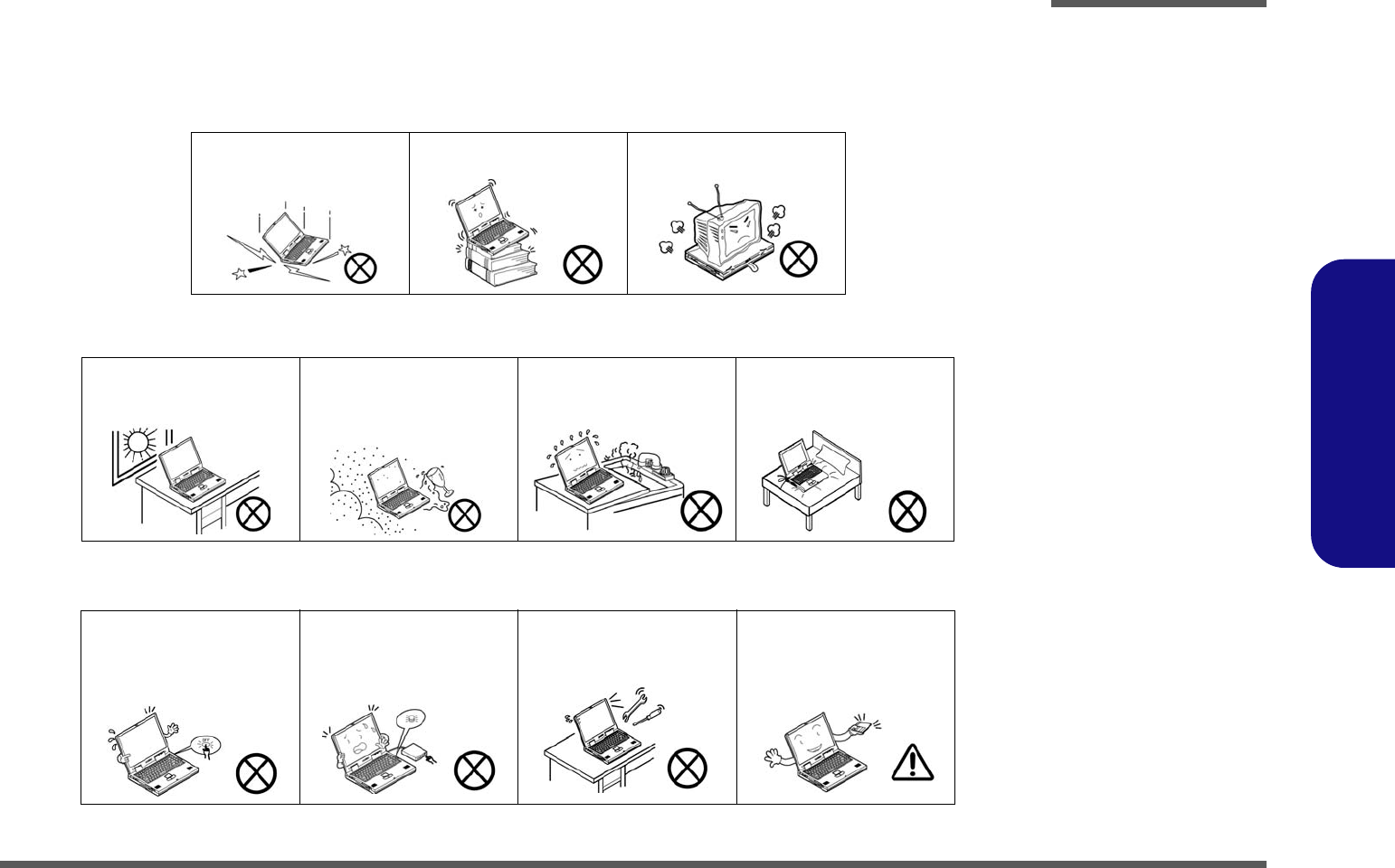
The notebook computer is quite rugged, but it can be damaged. To prevent this, follow these suggestions:
1. Don’t drop it, or expose it to shock. If the computer falls, the case and the components could be damaged.
2. Keep it dry, and don’t overheat it. Keep the computer and power supply away from any kind of heating element. This
is an electrical appliance. If water or any other liquid gets into it, the computer could be badly damaged.
3. Follow the proper working procedures for the computer. Shut the computer down properly and don’t forget to save
your work. Remember to periodically save your data as data may be lost if the battery is depleted.
Do not expose the computer
to any shock or vibration. Do not place it on an unstable
surface. Do not place anything heavy
on the computer.
Do not expose it to excessive
heat or direct sunlight. Do not leave it in a place
where foreign matter or mois-
ture may affect the system.
Don’t use or store the com-
puter in a humid environment. Do not place the computer on
any surface which will block
the vents.
Do not turn off the power
until you properly shut down
all programs.
Do not turn off any peripheral
devices when the computer is
on.
Do not disassemble the com-
puter by yourself. Perform routine maintenance
on your computer.
Preface
VI
Preface
4. Avoid interference. Keep the computer away from high capacity transformers, electric motors, and other strong mag-
netic fields. These can hinder proper performance and damage your data.
5. Take care when using peripheral devices.
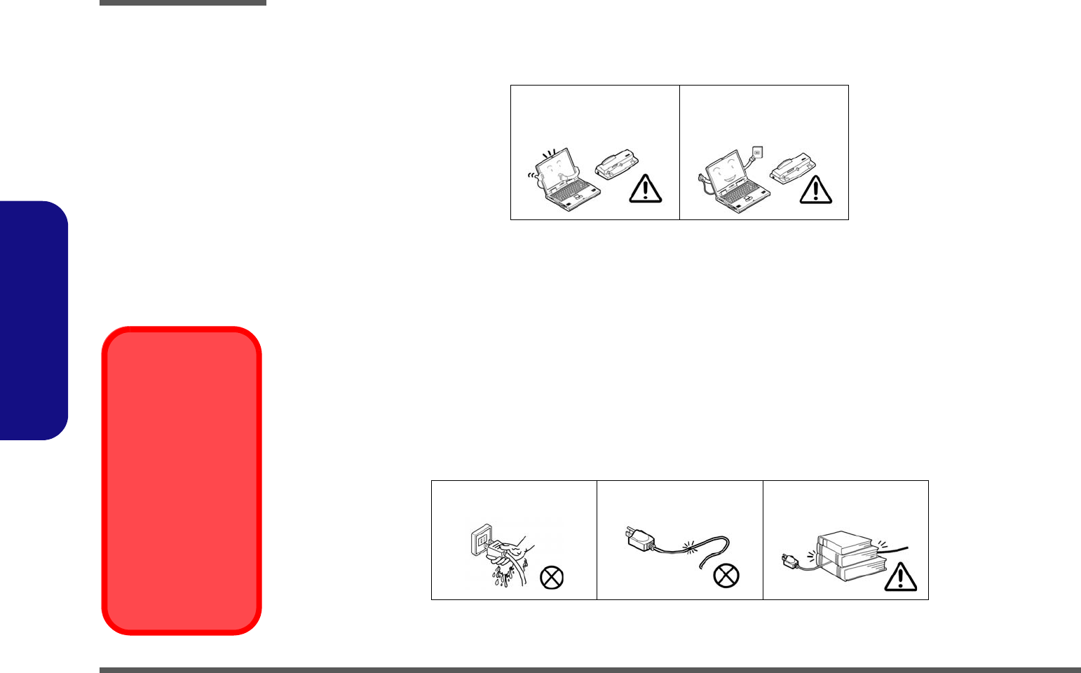
Power Safety
The computer has specific power requirements:
• Only use a power adapter approved for use with this computer.
• Your AC adapter may be designed for international travel but it still requires a steady, uninterrupted power supply. If you are
unsure of your local power specifications, consult your service representative or local power company.
• The power adapter may have either a 2-prong or a 3-prong grounded plug. The third prong is an important safety feature; do
not defeat its purpose. If you do not have access to a compatible outlet, have a qualified electrician install one.
• When you want to unplug the power cord, be sure to disconnect it by the plug head, not by its wire.
• Make sure the socket and any extension cord(s) you use can support the total current load of all the connected devices.
• Before cleaning the computer, make sure it is disconnected from any external power supplies.
Use only approved brands of
peripherals. Unplug the power cord before
attaching peripheral devices.
Do not plug in the power
cord if you are wet. Do not use the power cord if
it is broken. Do not place heavy objects
on the power cord.
Power Safety
Warning
Before you undertake
any upgrade proce-
dures, make sure that
you have turned off the
power, and discon-
nected all peripherals
and cables (including
telephone lines). It is
advisable to also re-
move your battery in
order to prevent acci-
dentally turning the
machine on.

Preface
VII
Preface
Battery Precautions
• Only use batteries designed for this computer. The wrong battery type may explode, leak or damage the computer.
• Do not continue to use a battery that has been dropped, or that appears damaged (e.g. bent or twisted) in any way. Even if the
computer continues to work with a damaged battery in place, it may cause circuit damage, which may possibly result in fire.
• Recharge the batteries using the notebook’s system. Incorrect recharging may make the battery explode.
• Do not try to repair a battery pack. Refer any battery pack repair or replacement to your service representative or qualified service
personnel.
• Keep children away from, and promptly dispose of a damaged battery. Always dispose of batteries carefully. Batteries may explode
or leak if exposed to fire, or improperly handled or discarded.
• Keep the battery away from metal appliances.
• Affix tape to the battery contacts before disposing of the battery.
• Do not touch the battery contacts with your hands or metal objects.
Battery Guidelines
The following can also apply to any backup batteries you may have.
• If you do not use the battery for an extended period, then remove the battery from the computer for storage.
• Before removing the battery for storage charge it to 60% - 70%.
• Check stored batteries at least every 3 months and charge them to 60% - 70%.
Battery Disposal
The product that you have purchased contains a rechargeable battery. The battery is recyclable. At the end of its useful life, under var-
ious state and local laws, it may be illegal to dispose of this battery into the municipal waste stream. Check with your local solid waste
officials for details in your area for recycling options or proper disposal.
Caution
Danger of explosion if battery is incorrectly replaced. Replace only with the same or equivalent type recommended by the manufacturer.
Discard used battery according to the manufacturer’s instructions.
Battery Level
Click the battery icon in the taskbar to see the current battery level and charge status. A battery that drops below a level of 10%
will not allow the computer to boot up. Make sure that any battery that drops below 10% is recharged within one week.

Preface
VIII
Preface
Related Documents
You may also need to consult the following manual for additional information:
User’s Manual on CD
This describes the notebook PC’s features and the procedures for operating the computer and its ROM-based setup pro-
gram. It also describes the installation and operation of the utility programs provided with the notebook PC.

Preface
IX
Preface
Contents
Introduction ..............................................1-1
Overview .........................................................................................1-1
System Specifications .....................................................................1-2
External Locator - Top View with LCD Panel Open ......................1-4
External Locator - Front & Right side Views .................................1-5
External Locator - Left Side & Rear View .....................................1-6
External Locator - Bottom View .....................................................1-7
Mainboard Overview - Top (Key Parts) .........................................1-8
Mainboard Overview - Bottom (Key Parts) ....................................1-9
Mainboard Overview - Top (Connectors) .....................................1-10
Mainboard Overview - Bottom (Connectors) ...............................1-11
Disassembly ...............................................2-1
Overview .........................................................................................2-1
Maintenance Tools ..........................................................................2-2
Connections .....................................................................................2-2
Maintenance Precautions .................................................................2-3
Disassembly Steps ...........................................................................2-4
Removing the Battery ......................................................................2-5
Removing the Hard Disk Drive .......................................................2-6
Removing the Optical (CD/DVD) Device ......................................2-8
Removing the System Memory (RAM) ..........................................2-9
Removing the Inverter Board ........................................................2-11
Removing the Processor ................................................................2-12
Removing the Wireless LAN Module ...........................................2-14
Removing the Bluetooth Module ..................................................2-15
Removing the Keyboard ................................................................2-16
Removing the Modem ...................................................................2-17
Part Lists ..................................................A-1
Part List Illustration Location ........................................................A-2
Top without Fingerprint ................................................................. A-3
Bottom ........................................................................................... A-4
LCD ............................................................................................... A-5
DVD-Dual Drive ............................................................................ A-6
Schematic Diagrams.................................B-1
System Block Diagram ...................................................................B-2
Intel Penryn (Socket-P) 1/2 ............................................................B-3
Intel Penryn (Socket-P) 2/2 ............................................................B-4
Cantiga 1/6 - Host ...........................................................................B-5
Cantiga 2/6 - VGA, CRT ................................................................B-6
Cantiga 3/6 - DDR ..........................................................................B-7
Cantiga 4/6 - Power ........................................................................B-8
Cantiga 5/6 - Power ........................................................................B-9
Cantiga 6/6 - GND ........................................................................B-10
DDRII CHANNEL A ...................................................................B-11
DDRII CHANNEL B ...................................................................B-12
Panel, Inverter, CRT .....................................................................B-13
ICH9-M 1/5 - SATA .....................................................................B-14
ICH9-M 2/5 - PCIE, PCI, USB ....................................................B-15
ICH9-M 3/5 - GPIO, PWR Management ....................................B-16
ICH9-M 4/5 - Power .....................................................................B-17
ICH9-M 5/5 - GND ......................................................................B-18
Clock Generator ............................................................................B-19
Multi I/O, ODD, CCD, BT, TPM .................................................B-20
New Card, Mini PCIE ...................................................................B-21
LED, FAN, TP, FP, USB ..............................................................B-22
JMB385 Card Reader ...................................................................B-23
PCI-E LAN RTL8111C ................................................................B-24
Audio Codec ALC662 ..................................................................B-25
Audio AMP2056 ...........................................................................B-26

Preface
X
Preface
KBC-ITE IT8512E ....................................................................... B-27
System Power, LED BKLT .......................................................... B-28
Power VDD3, VDD5 ................................................................... B-29
Power 1.5VS, 1.05VS, 3.3V, 5V .................................................. B-30
Power 1.8V, 0.9VSM ...................................................................B-31
Power VCORE .............................................................................B-32
Power AC-IN, Charger ................................................................. B-33
Multi I/O Board 1/2 ...................................................................... B-34
Multi I/O Board 2/2 ...................................................................... B-35
Finger Printer Board ..................................................................... B-36
Click Board ..................................................................................B-37
M730T ODD Bridge Board .......................................................... B-38
M730T Audio Board ....................................................................B-39
Power Sequence Diagram ............................................................ B-40
Power Sequence v3.0 ................................................................... B-41

Introduction
Overview 1 - 1
1.Introduction
Chapter 1: Introduction
Overview
This manual covers the information you need to service or upgrade the M730TG series notebook computer. Information
about operating the computer (e.g. getting started, and the Setup utility) is in the User’s Manual. Information about driv-
ers (e.g. video & audio) is also found in User’s Manual. That manual is shipped with the computer.
Operating systems (e.g. Windows XP, Windows Vista, Windows 7, etc.) have their own manuals as do application soft-
ware (e.g. word processing and database programs). If you have questions about those programs, you should consult
those manuals.
The M730TG series notebook is designed to be upgradeable. See Disassembly on page 2 - 1 for a detailed description
of the upgrade procedures for each specific component. Please note the warning and safety information indicated by the
“” symbol.
The balance of this chapter reviews the computer’s technical specifications and features.
Introduction
1 - 2 System Specifications
1.Introduction
System Specifications
Processor
Intel® Mobile Celeron Dual Core Processor:
T3100 (1.9GHz)
45nm (45 Nanometer) Process Technology, 1MB
L2 Cache & 800MHz FSB
(478-pin) Micro-FC-PGA Package - Socket-P
T3000 (1.8GHz)
45nm (45 Nanometer) Process Technology, 1MB
L2 Cache & 800MHz FSB
(478-pin) Micro-FC-PGA Package - Socket-P
T1700 (1.9GHz)
65nm (65 Nanometer) Process Technology, 1MB
L2 Cache & 667MHz FSB
(478-pin) Micro-FC-PGA Package - Socket-P
T1600 (1.83GHz)
65nm (65 Nanometer) Process Technology, 1MB
L2 Cache & 667MHz FSB
(478-pin) Micro-FC-PGA Package - Socket-P
Intel® Mobile Celeron Processor:
900 (2.2GHz)
45nm (45 Nanometer) Process Technology, 1MB
L2 Cache & 800MHz FSB
(478-pin) Micro-FC-PGA Package - Socket-P
Core Logic
Intel® GL40 + ICH9M Chipset
Display
13.3” WXGA (1280 * 800) TFT LCD
Memory
Dual Channel DDRII (DDR2)
Two 200 Pin SO-DIMM Sockets Supporting
DDRII (DDR2) 800MHz
Memory Expandable up to 4GB (Supporting
1GB/2GB Modules)
Video
Intel® GL40 Integrated Video
High Preference 3D/2D Graphic Accelerator
Shared Memory Architecture of up to 512M
Supports Microsoft DirectX 10
BIOS
One 16M SPI Flash ROM
Phoenix™ BIOS
Storage
One Changeable 12.7mm(h) Super Multi
Optical Device Drive - SATA interface
One Changeable 2.5" 9.5 mm (h) HDD OR
with SATA (Serial) Interface
Audio
High Definition Audio
Compliant with Microsoft UAA (Universal
Audio Architecture)
Direct Sound 3D™ Compatible
Built-In Microphone
2 * Built-In Speakers
Keyboard & Pointing Device
Full Size WinKey Keyboard
Built-in TouchPad
Interface
Three USB 2.0 Ports
One External Monitor Port
One Headphone-Out Jack
One Microphone-In Jack
One S/PDIF-Out Jack
One RJ-11 LAN Jack for Fax/Modem
One RJ-45 LAN Jack for LAN
One DC-In Jack
Card Reader
Embedded 7-in-1 Card Reader (MS/ MS Pro/
SD/ Mini SD/ MMC/ RS MMC/ MS Duo)
Note: MS Duo/ Mini SD/ RS MMC Cards
require a PC adapter
Slots
One ExpressCard/34/54 Slot
Two Mini-Card Slots with USB & PCIe
interface:
Slot 1 for Mini-Card WLAN Module with PCIe
Interface
Slot 2 for 3.75G Module with USB Interface
(
Factory Option
)
Introduction
System Specifications 1 - 3
1.Introduction
Communication
56K Fax/Modem V90/92 Compliant
10/100/100Mb Base-TX Ethernet LAN
Intel® WiFi Link 5300 Series (3*3 - 802.11a/g/
n) Wireless LAN Mini-Card Module with PCIe
interface (Option)
3rd Party 802.11b/g Wireless LAN Mini-Card
Module with USB interface (Option)
Bluetooth 2.1 + EDR (Enhanced Data Rate)
Module (Factory Option)
1.3M Pixel PC Camera Module with USB
interface (Factory Option)
3.75G Module:
UMTS/HSPDA-based 3.75G Module with
Mini-Card Interface (Factory Option)
Quad-band GSM/GPRS (850 MHz, 900 MHz,
1800 MHz, 1900 MHz)
UMTS WCDMA FDD (2100 MHz)
Note that UMTS modes CAN NOT be used
in North America
Power Management
Supports Wake on LAN
Supports Wake on Modem Ring
Power
Full Range AC/DC Adapter
AC input 100 - 240V, 50 - 60Hz,
DC Output 19V, 3.42A or 18.5V, 3.5A (65
Watts)
4 Cell Smart Lithium-Ion Battery Pack,
2400mAH
8 Cell Smart Lithium-Ion Battery Pack,
4400mAH (Option)
Security
Security (Kensington® Type) Lock Slot
BIOS Password
Operating System
Windows® Vista (with Service Pack 2)
Windows® XP (with Service Pack 3)
Environmental Spec
Temperature
Operating: 5°C - 35°C
Non-Operating: -20°C - 60°C
Relative Humidity
Operating: 20% - 80%
Non-Operating: 10% - 90%
Dimensions & Weight
310mm (w) * 233mm (d) * 30 - 36mm (h)
2.0 kg (with 4 Cell Battery and ODD)
Optional
Intel® WiFi Link 5300 Series (3*3 - 802.11a/g/
n) Wireless LAN Mini-Card Module with PCIe
interface
3rd Party 802.11b/g Wireless LAN Mini-Card
Module with USB interface
Bluetooth 2.1 + EDR (Enhanced Data Rate)
Module (Factory Option)
1.3M Pixel PC Camera Module with USB
interface (Factory Option)
UMTS/HSPDA-based 3.75G Module with
Mini-Card Interface (Factory Option)
8 Cell Smart Lithium-Ion Battery Pack,
4400mAH (Option)
Introduction
1 - 4 External Locator - Top View with LCD Panel Open
1.Introduction
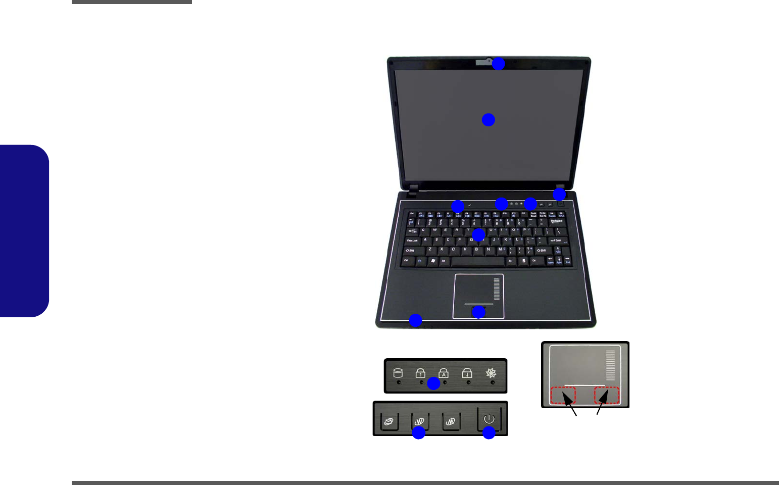
External Locator - Top View with LCD Panel Open
Figure 1
Top View
1. Optional Built-In
PC Camera
2. LCD
3. Built-In
Microphone
4. Power Button
5. Hot Key Buttons
6. LED Status
Indicators
7. Keyboard
8. Touchpad &
Buttons
9. LED Power &
Communication
Indicators
10
2
5
1
7
8
4
6
9
6
5 4 Touchpad Buttons
(valid operation area)
3
Introduction
External Locator - Front & Right side Views 1 - 5
1.Introduction
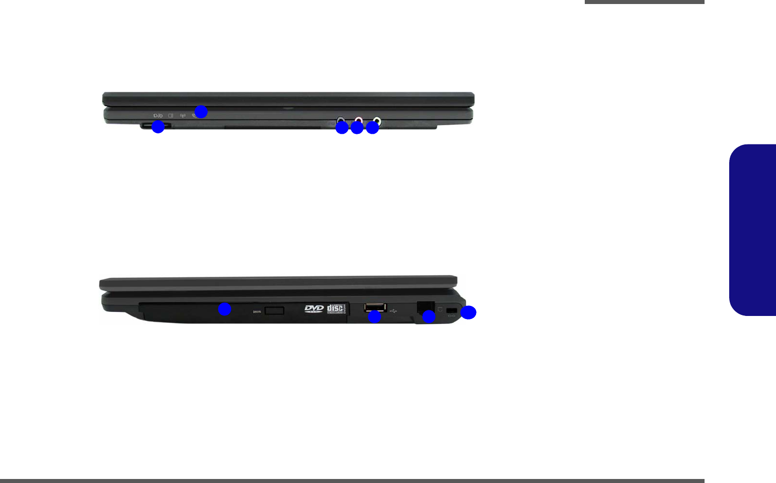
External Locator - Front & Right side Views
Figure 2
Front Views
1. LED Power &
Communication
Indicators
2. 7-in-1 Card
Reader
3. S/PDIF-Out Jack
4. Microphone-In
Jack
5. Headphone-Out
Jack
Figure 3
Right Side Views
1. Optical Device
Drive Bay
2. USB 2.0 Port
3. RJ-11 Phone
Jack
4. Security Lock
Slot
1
43 5
2
1234
Introduction
1 - 6 External Locator - Left Side & Rear View
1.Introduction
External Locator - Left Side & Rear View
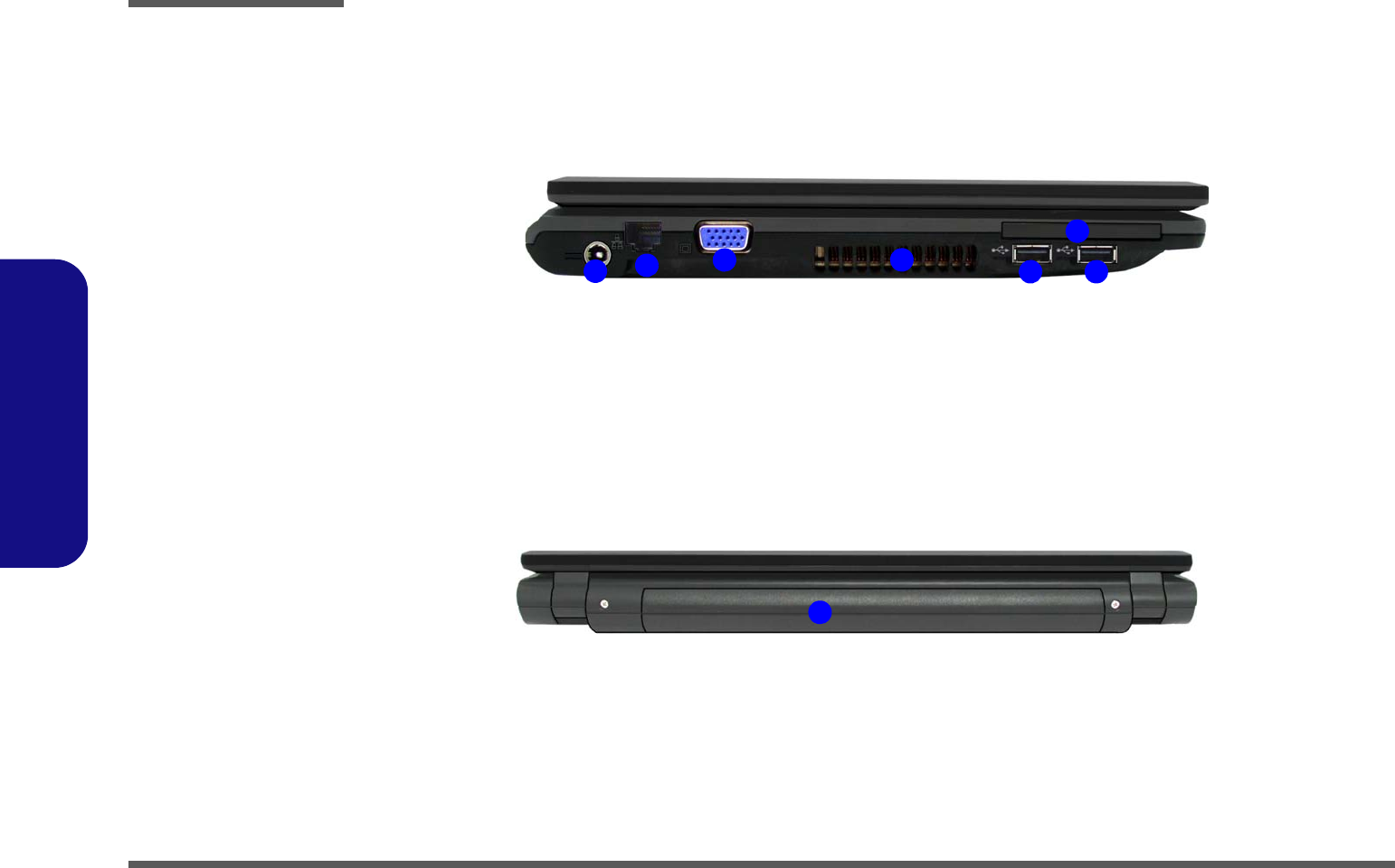
Figure 4
Left Side View
1. DC-In Jack
2. RJ-45 LAN Jack
3. External Monitor
Port
4. Vent/Fan Intake/
Outlet
5. 2 * USB 2.0 Ports
6. ExpressCard Slot
4
12355
6
Figure 5
Rear View
1. Battery
1
Introduction
External Locator - Bottom View 1 - 7
1.Introduction
External Locator - Bottom View
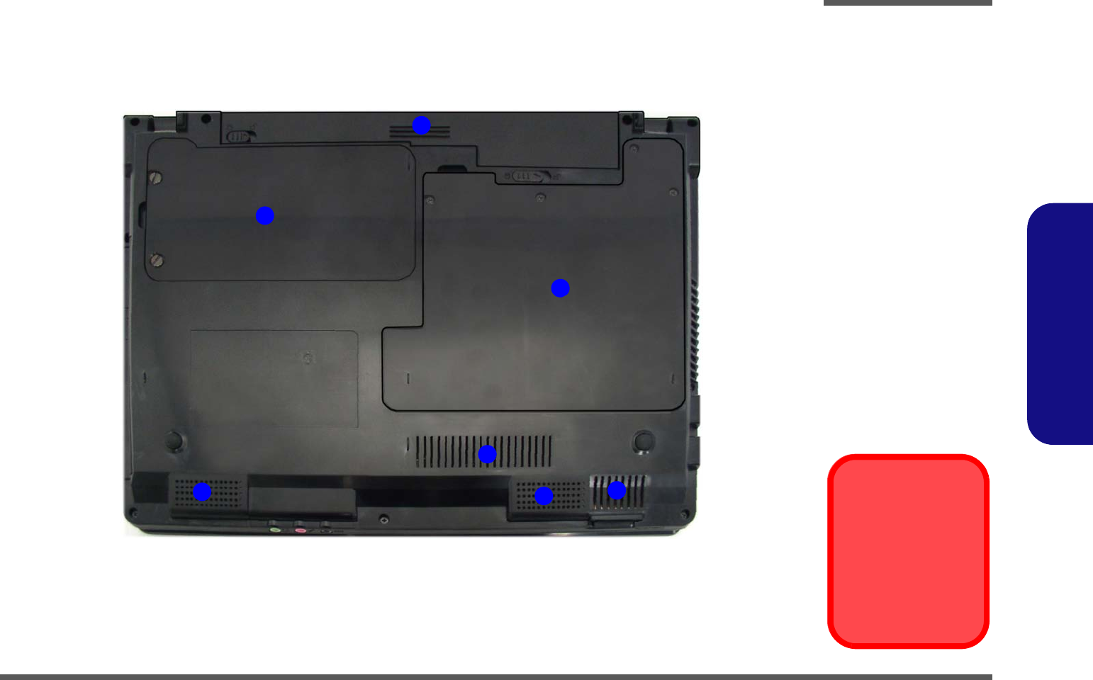
Figure 6
Bottom View
1. Battery (4 Cell
Battery Pictured)
2. Hard Disk Bay
Cover
(3.5G Module
Location)
3. RAM & CPU Bay
Cover
4. Vent/Fan Intake/
Outlet
5. Speakers
Overheating
To prevent your com-
puter from overheating
make sure nothing
blocks the vent/fan in-
takes while the com-
puter is in use.
2
3
1
4
54
5
Introduction
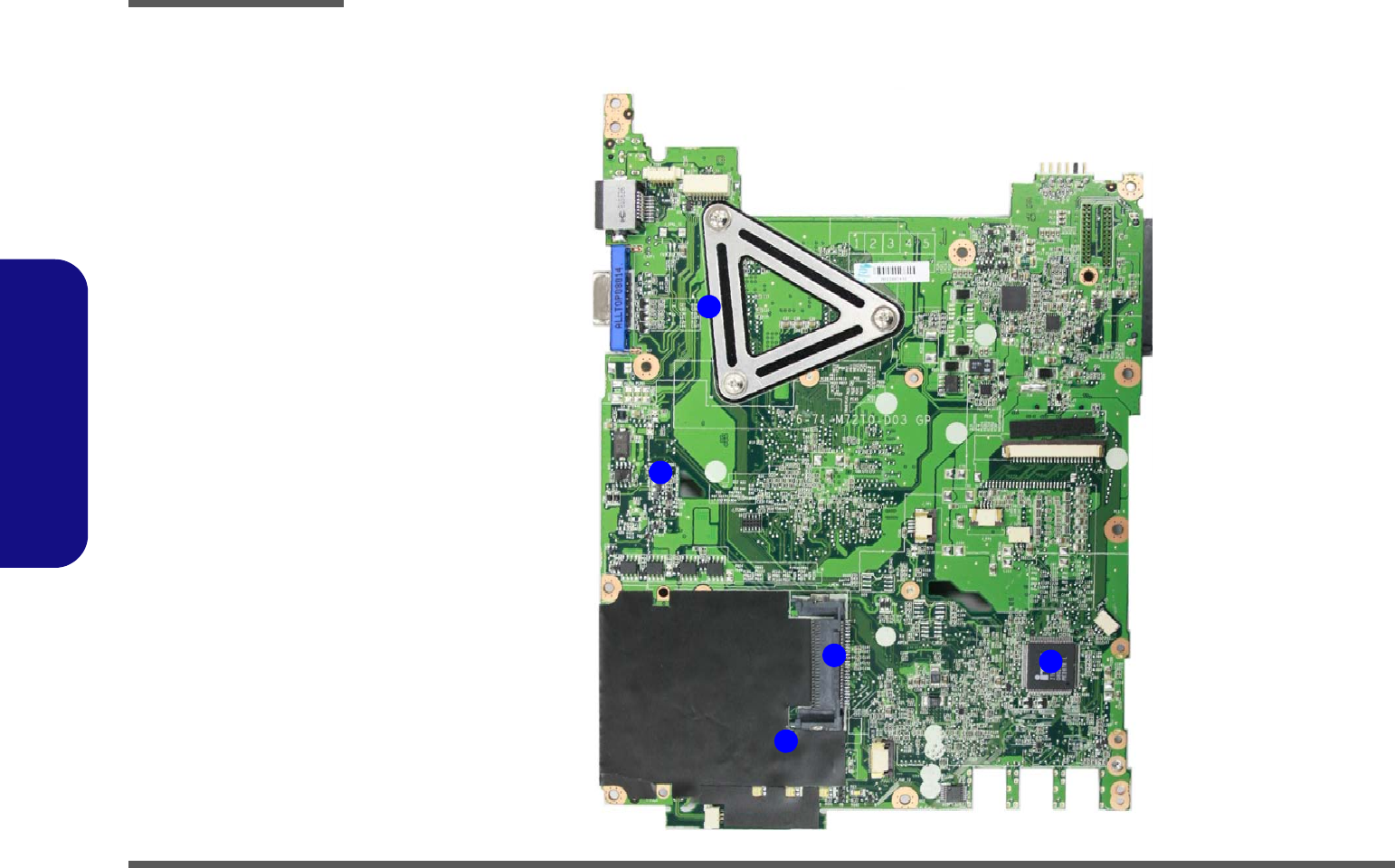
1 - 8 Mainboard Overview - Top (Key Parts)
1.Introduction
Mainboard Overview - Top (Key Parts)
Figure 7
Mainboard Top
Key Parts
1. Transformer
2. RTL6111C
3. ExpressCard
Connector
4. JMB385
5. KBC ITE IT8502E
1
2
3
4
5
Introduction
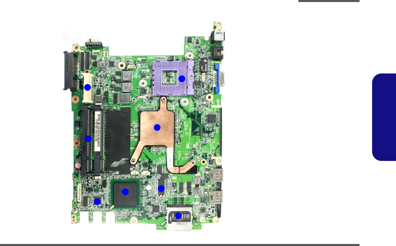
Mainboard Overview - Bottom (Key Parts) 1 - 9
1.Introduction
Mainboard Overview - Bottom (Key Parts)
1
2
3
4
5
6
7
8
Figure 8
Mainboard Bottom
Key Parts
1. CPU Socket (no
CPU installed)
2. Northbridge
3. Memory Slots
DDR2 SO-DIMM
4. ICS
5. Card Reader
Socket
6. Southbridge
7. Audio Codec
8. Mini-Card
Connector (WLAN
Module)
Introduction
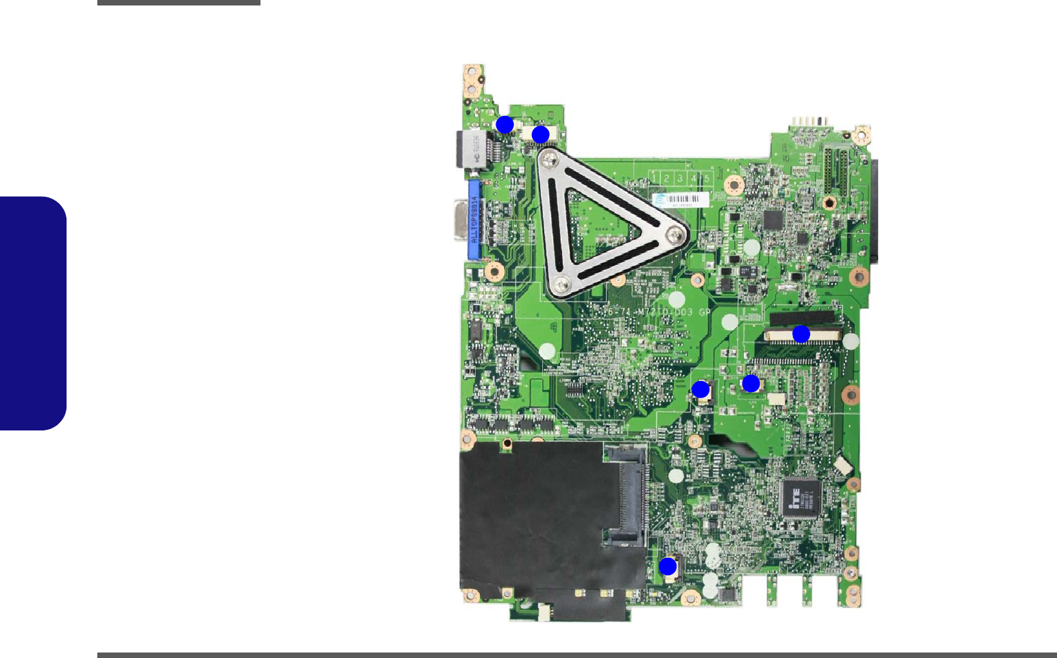
1 - 10 Mainboard Overview - Top (Connectors)
1.Introduction
Mainboard Overview - Top (Connectors)
Figure 9
Mainboard Top
Connectors
1. Hot-key
Connector
2. LCD Cable
Connector
3. Keyboard Cable
Connector
4. Audio Board
Connector
5. Microphone
Cable Connector
6. TouchPad Cable
Connector
65
1
4
2
3
Introduction
Mainboard Overview - Bottom (Connectors) 1 - 11
1.Introduction
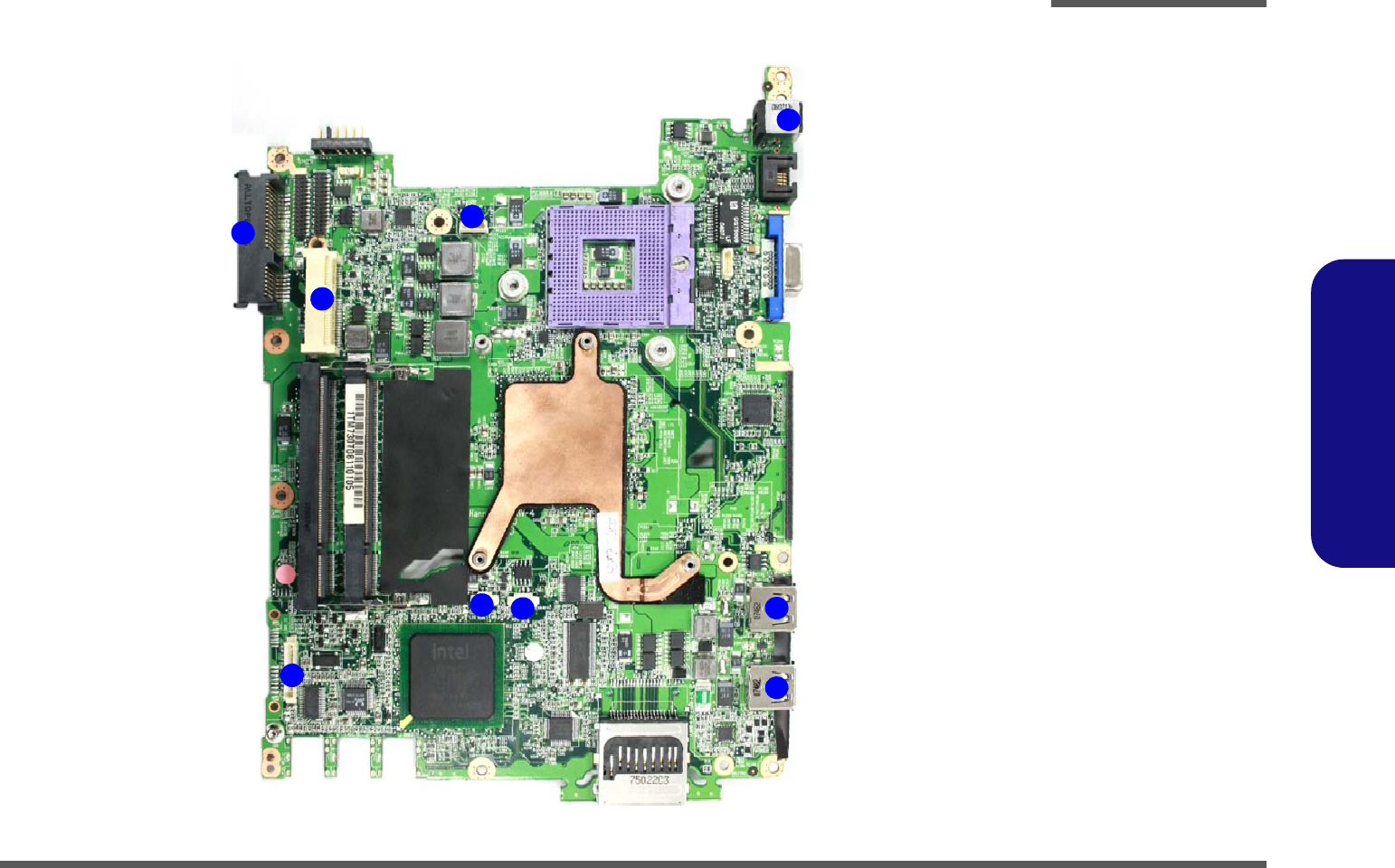
Mainboard Overview - Bottom (Connectors)
Figure 10
Mainboard Bottom
Connectors
1. BT Cable
Connector
2. Multi Board
Connector
3. CD-ROM
Connector
4. HDD Connector
5. CMOS Bat.
Connector
6. CPU Fan Cable
Connector
7. DC-In Jack
8. USB Port
1
2
3
4
568
8
7

Introduction
1-12
1.Introduction

Disassembly
Overview 2 - 1
2.Disassembly
Chapter 2: Disassembly
Overview
This chapter provides step-by-step instructions for disassembling the M730TG series notebook’s parts and subsystems.
When it comes to reassembly, reverse the procedures (unless otherwise indicated).
We suggest you completely review any procedure before you take the computer apart.
Procedures such as upgrading/replacing the RAM, optical device and hard disk are included in the User’s Manual but are
repeated here for your convenience.
To make the disassembly process easier each section may have a box in the page margin. Information contained under
the figure # will give a synopsis of the sequence of procedures involved in the disassembly procedure. A box with a
lists the relevant parts you will have after the disassembly process is complete. Note: The parts listed will be for the dis-
assembly procedure listed ONLY, and not any previous disassembly step(s) required. Refer to the part list for the previ-
ous disassembly procedure. The amount of screws you should be left with will be listed here also.
A box with a will also provide any possible helpful information. A box with a contains warnings.
An example of these types of boxes are shown in the sidebar.
Information
Warning

Disassembly
2 - 2 Overview
2.Disassembly
NOTE: All disassembly procedures assume that the system is turned OFF, and disconnected from any power supply (the
battery is removed too).
Maintenance Tools
The following tools are recommended when working on the notebook PC:
• M3 Philips-head screwdriver
• M2.5 Philips-head screwdriver (magnetized)
• M2 Philips-head screwdriver
• Small flat-head screwdriver
• Pair of needle-nose pliers
• Anti-static wrist-strap
Connections
Connections within the computer are one of four types:
Locking collar sockets for ribbon connectors To release these connectors, use a small flat-head screwdriver to
gently pry the locking collar away from its base. When replac-
ing the connection, make sure the connector is oriented in the
same way. The pin1 side is usually not indicated.
Pressure sockets for multi-wire connectors To release this connector type, grasp it at its head and gently
rock it from side to side as you pull it out. Do not pull on the
wires themselves. When replacing the connection, do not try to
force it. The socket only fits one way.
Pressure sockets for ribbon connectors To release these connectors, use a small pair of needle-nose pli-
ers to gently lift the connector away from its socket. When re-
placing the connection, make sure the connector is oriented in
the same way. The pin1 side is usually not indicated.
Board-to-board or multi-pin sockets To separate the boards, gently rock them from side to side as
you pull them apart. If the connection is very tight, use a small
flat-head screwdriver - use just enough force to start.

Disassembly
Overview 2 - 3
2.Disassembly
Maintenance Precautions
The following precautions are a reminder. To avoid personal injury or damage to the computer while performing a re-
moval and/or replacement job, take the following precautions:
1. Don't drop it. Perform your repairs and/or upgrades on a stable surface. If the computer falls, the case and other
components could be damaged.
2. Don't overheat it. Note the proximity of any heating elements. Keep the computer out of direct sunlight.
3. Avoid interference. Note the proximity of any high capacity transformers, electric motors, and other strong mag-
netic fields. These can hinder proper performance and damage components and/or data. You should also monitor
the position of magnetized tools (i.e. screwdrivers).
4. Keep it dry. This is an electrical appliance. If water or any other liquid gets into it, the computer could be badly
damaged.
5. Be careful with power. Avoid accidental shocks, discharges or explosions.
•Before removing or servicing any part from the computer, turn the computer off and detach any power supplies.
•When you want to unplug the power cord or any cable/wire, be sure to disconnect it by the plug head. Do not pull on the wire.
6. Peripherals – Turn off and detach any peripherals.
7. Beware of static discharge. ICs, such as the CPU and main support chips, are vulnerable to static electricity.
Before handling any part in the computer, discharge any static electricity inside the computer. When handling a
printed circuit board, do not use gloves or other materials which allow static electricity buildup. We suggest that
you use an anti-static wrist strap instead.
8. Beware of corrosion. As you perform your job, avoid touching any connector leads. Even the cleanest hands pro-
duce oils which can attract corrosive elements.
9. Keep your work environment clean. Tobacco smoke, dust or other air-born particulate matter is often attracted
to charged surfaces, reducing performance.
10. Keep track of the components. When removing or replacing any part, be careful not to leave small parts, such as
screws, loose inside the computer.
Cleaning
Do not apply cleaner directly to the computer, use a soft clean cloth.
Do not use volatile (petroleum distillates) or abrasive cleaners on any part of the computer.
Power Safety
Warning
Before you undertake
any upgrade proce-
dures, make sure that
you have turned off the
power, and discon-
nected all peripherals
and cables (including
telephone lines). It is
advisable to also re-
move your battery in
order to prevent acci-
dentally turning the
machine on.

Disassembly
2 - 4 Disassembly Steps
2.Disassembly
Disassembly Steps
The following table lists the disassembly steps, and on which page to find the related information. PLEASE PERFORM
THE DISASSEMBLY STEPS IN THE ORDER INDICATED.
To remove the Battery:
1. Remove the battery page 2 - 5
To remove the HDD:
1. Remove the battery page 2 - 5
2. Remove the HDD page 2 - 6
To remove the Optical Device:
1. Remove the battery page 2 - 5
2. Remove the Optical device page 2 - 8
To remove the System Memory:
1. Remove the battery page 2 - 5
2. Remove the system memory page 2 - 9
To remove the Inverter Board:
1. Remove the battery page 2 - 5
2. Remove the inverter board page 2 - 11
To remove and install a Processor:
1. Remove the battery page 2 - 5
2. Remove the processor page 2 - 12
To remove the Wireless LAN Module:
1. Remove the battery page 2 - 5
2. Remove the wireless LAN page 2 - 14
To remove the Bluetooth Module:
1. Remove the battery page 2 - 5
2. Remove the Bluetooth page 2 - 15
To remove the Keyboard:
1. Remove the battery page 2 - 5
2. Remove the keyboard page 2 - 16
To remove the Modem:
1. Remove the battery page 2 - 5
2. Remove the HDD page 2 - 6
3. Remove the system memory page 2 - 9
4. Remove the Optical device page 2 - 8
5. Remove the processor page 2 - 12
6. Remove the keyboard page 2 - 16
7. Remove the modem page 2 - 17
Disassembly
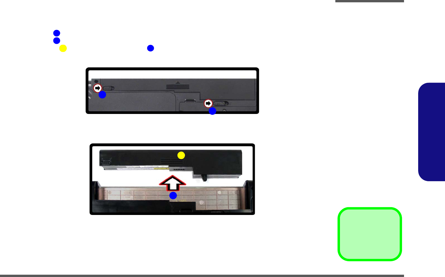
Removing the Battery 2 - 5
2.Disassembly
Removing the Battery
1. Turn the computer off, and turn it over.
2. Slide the latch in the direction of the arrow.
3. Slide the latch in the direction of the arrow, and hold it in place.
4. Slide the battery in the direction of the arrow .
3. Battery
1
2
6
3
4
a.
3
b.
2
4
1
Figure 1
Battery Removal
a. Slide the latch and hold
in place.
b. Slide the battery in the di-
rection of the arrow.
Disassembly
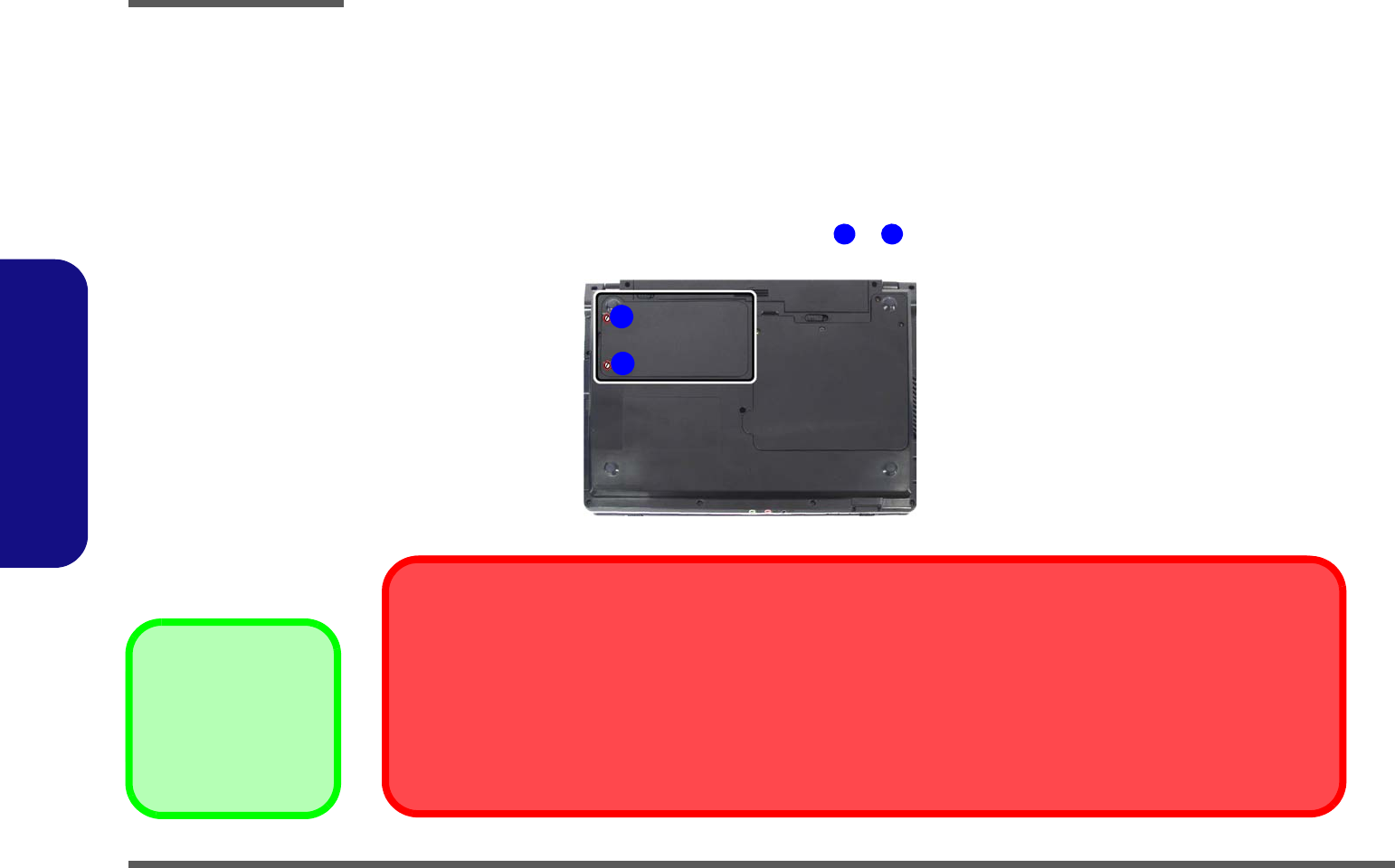
2 - 6 Removing the Hard Disk Drive
2.Disassembly
Removing the Hard Disk Drive
The hard disk drive can be taken out to accommodate other 2.5" serial (SATA) hard disk drives with a height of 9.5mm
(h). Follow your operating system’s installation instructions, and install all necessary drivers and utilities (as outlined in
Chapter 4 of the User’s Manual) when setting up a new hard disk.
Hard Disk Upgrade Process
1. Turn off the computer, and remove the battery (page 2 - 5).
2. Locate the hard disk bay cover and loosen screws & .
Figure 2
HDD Assembly
Removal
a. Locate the HDD bay
cover and loosen the
screw(s).
•2 Screws
1
2
a.
HDD System Warning
New HDD’s are blank. Before you begin make sure:
You have backed up any data you want to keep from your old HDD.
You have all the CD-ROMs and FDDs required to install your operating system and programs.
If you have access to the internet, download the latest application and hardware driver updates for the operating system you plan
to install. Copy these to a removable medium.
2
1Note:
Only one model is pictured
here, however the compo-
nent locations are the same
for both models.
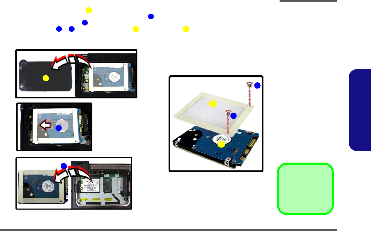
Disassembly
Removing the Hard Disk Drive 2 - 7
2.Disassembly
3. Remove the hard disk bay cover .
4. Grip the tab and slide the hard disk in the direction of arrow .
5. Lift the hard disk out of the bay .
6. Remove the screws & and the adhesive cover from the hard disk .
7. Reverse the process to install a new hard disk (do not forget to replace all the screws and covers).
6
3
4
5
6
7
6
8
6
9
4
b.
c.
e.
5
6
d.
3
8
9
7
3. HDD Bay Cover
8. Adhesive Cover
9. HDD
•2 Screws
Figure 3
HDD Assembly
Removal (cont’d.)
b. Remove the HDD bay
cover.
c. Grip the tab and slide the
HDD in the direction of
the arrow.
d. Lift the HDD assembly
out of the bay.
e. Remove the screw and
adhesive cover.
Disassembly
2 - 8 Removing the Optical (CD/DVD) Device
2.Disassembly
Removing the Optical (CD/DVD) Device
1. Turn off the computer, and remove the battery (page 2 - 5).
2. Locate the component bay cover and remove screws - .
3. Carefully (a fan and cable are attached to the under side of the cover) lift up the bay cover.
4. Carefully disconnect the fan cable and remove the bay cover .
5. Remove the screw at point , and use a screwdriver to carefully push out the optical device at point .
6. Insert the new device and carefully slide it into the computer (the device only fits one way. DO NOT FORCE IT; The
screw holes should line up).
7. Restart the computer to allow it to automatically detect the new device.
1
2
5
6
1
7
9
8
1. Component Bay Cover
9. Optical Device
•5 Screws
3
4
2
6
7
c.
d.
9
1
a.
b.
5
18
Figure 4
Optical Device
Removal
a. Remove the screws.
b. Disconnect the fan cable
and remove the cover.
c. Remove the screw.
d. Push the optical device
out off the computer at
point 8.
Disassembly
Removing the System Memory (RAM) 2 - 9
2.Disassembly
Removing the System Memory (RAM)
The computer has two memory sockets for 200 pin Small Outline Dual In-line Memory Modules (SO-DIMM) supporting
DDR2 800MHz. The main memory can be expanded up to 4GB. The SO-DIMM modules supported are 1024MB, and
2048MB and DDRII Modules. The total memory size is automatically detected by the POST routine once you turn on
your computer.
Memory Upgrade Process
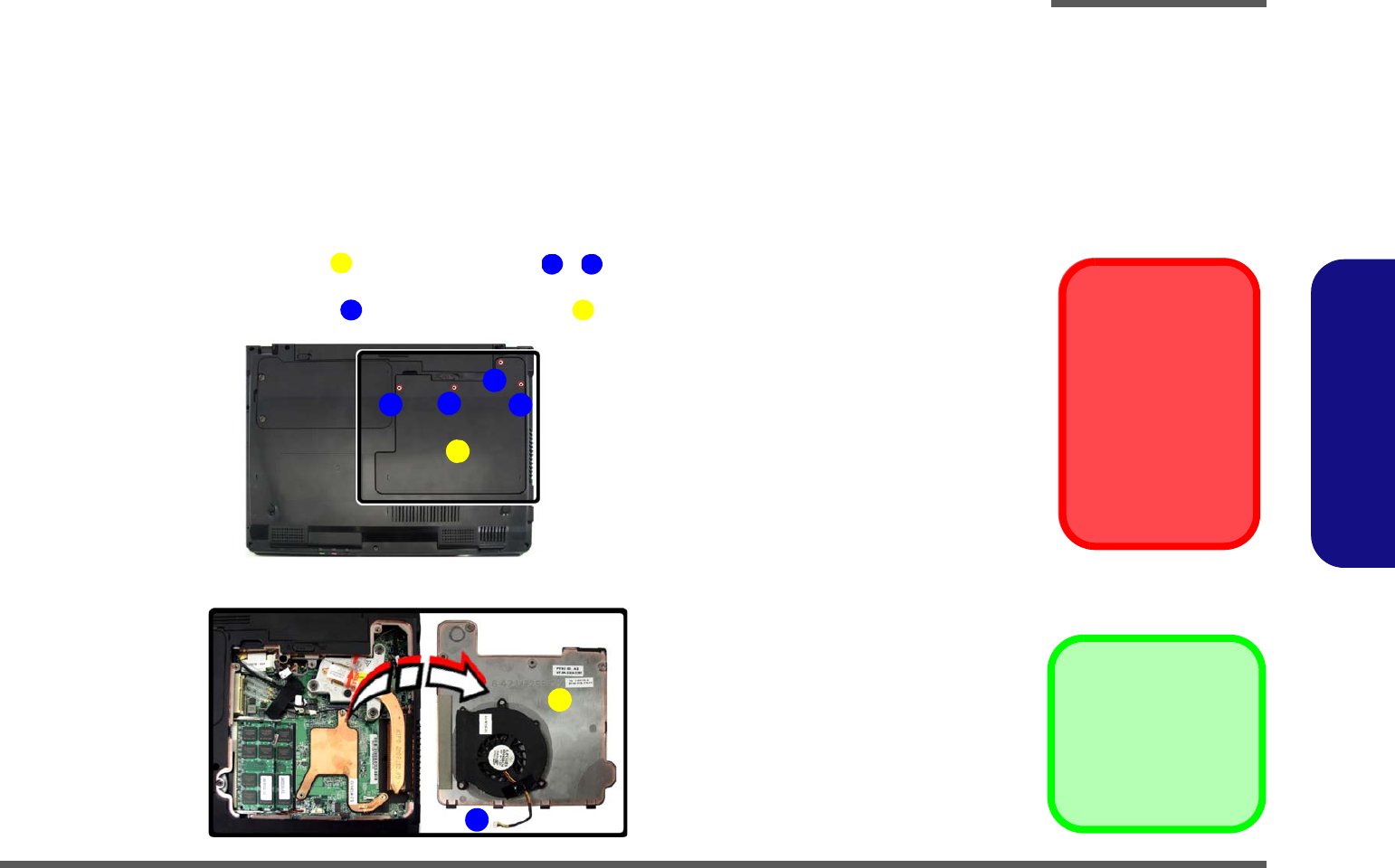
1. Turn off the computer, remove the battery (page 2 - 5).
2. Locate the component bay cover , and remove screws - .
3. Carefully (a fan and cable are attached to the under side of the cover) lift up the bay cover.
4. Carefully disconnect the fan cable , and remove the cover .
Figure 5
RAM Module
Removal
a. Remove the screws.
b. Remove the cover.
Contact Warning
Be careful not to touch
the metal pins on the
module’s connecting
edge. Even the clean-
est hands have oils
which can attract parti-
cles, and degrade the
module’s perfor-
mance.
1
2
5
6
1
1. Component Bay
Cover
•4 Screws
a.
b.
6
1
Note:
Only one model is pictured
here, however the compo-
nent locations are the same
for both models.
34
2
1
5
Disassembly
2 - 10 Removing the System Memory (RAM)
2.Disassembly
5. Gently pull the two release latches ( & ) on the sides of the memory socket in the direction indicated by the
arrows (Figure 6c).
6. The RAM module(s) will pop-up (Figure 6d), and you can then remove it.
7. Pull the latches to release the second module if necessary.
8. Insert a new module holding it at about a 30° angle and fit the connectors firmly into the memory slot.
9. The module’s pin alignment will allow it to only fit one way. Make sure the module is seated as far into the slot as it
will go. DO NOT FORCE the module; it should fit without much pressure.
10. Press the module in and down towards the mainboard until the slot levers click into place to secure the module.
11. Replace the bay cover and screws (make sure you reconnect the fan cable before screwing down the bay
cover).
12. Restart the computer to allow the BIOS to register the new memory configuration as it starts up.
7
8
d.
9
7
8
c.
Figure 6
RAM Module
Removal (cont’d.)
c. Pull the release
latch(es).
d. Remove the module(s).
e. Replace the bay cover.
Single Memory
Module Installation
If your computer has a
single memory module,
then insert the module
into the Channel 0
(JDIMM_1) socket. In
this case, this is the up-
per memory socket (the
socket furthest to the
mainboard) as shown in
Figure 6d.
9. RAM Module(s)
9
e.
Note:
Only one model is pictured
here, however the compo-
nent locations are the same
for both models.
Disassembly
Removing the Inverter Board 2 - 11
2.Disassembly
Removing the Inverter Board
1. Turn off the computer, and remove the battery (page 2 - 5).
2. Remove any rubber covers, screws - (Figure 7a), then run your finger around the middle of the frame to
carefully unsnap the LCD front panel module from the back.
3. Discharge the remaining system power (see Inverter Power Warning below).
4. Remove screws - (Figure 7b) from the inverter, and carefully lift the inverter board up slightly.
5. Disconnect cables & (Figure 7c) from the inverter, then remove the inverter (Figure 7d) from the top
case assembly.
Figure 7
Inverter Board
Removal
a. Remove the 6 screws
and unsnap the LCD
front panel module from
the back.
b. Remove the screw and
discharge the remaining
power from the inverter
board and lift the board
up slightly.
c. Disconnect the cables
from the inverter.
d. Remove the inverter.
1
6
7
8
9
10
11
12
7. LCD Front Panel
12. Inverter Board
• Screws
a. b.
Inverter Power Warning
In order to prevent a short circuit when removing
the inverter it is necessary to discharge any re-
maining system power. To do so, press the com-
puter’s power button for a few seconds before
disconnecting the inverter cable.
1
2 5
34
6
c.
d.
8
7
9
12
10 11
Disassembly
2 - 12 Removing the Processor
2.Disassembly
Removing the Processor
1. Turn off the computer, and remove the battery (page 2 - 5) and the CPU/RAM bay cover (page 2 - 9).
2. The CPU heat sink will be visible at point on the mainboard.
3. Loosen screws - from the heat sink in the order indicated.
4. Carefully lift up the heat sink (Figure c) off the computer.
1
2
4
5
Figure 8
Processor Removal
a. Remove the cover and
Iocate the heat sink.
b. Remove the 3 screws in
the order indicated.
c. Remove the heat sink.
5. Heat Sink
b.
5
1
4
a.
c.
3
2
Note:
Only one model is pictured
here, however the compo-
nent locations are the same
for both models.
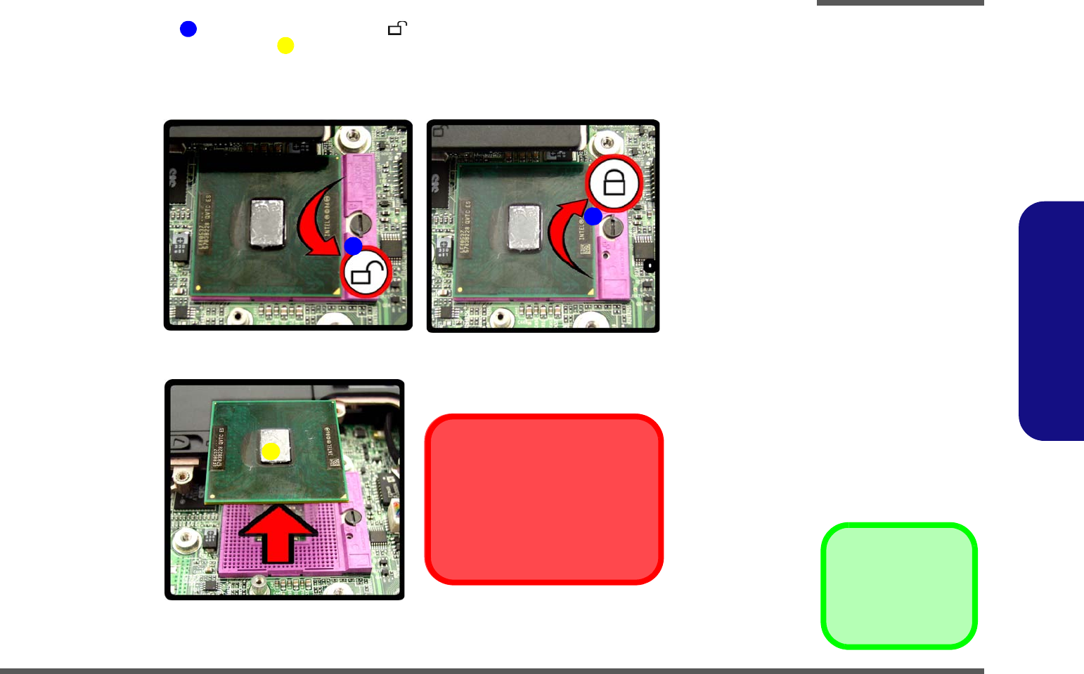
Disassembly
Removing the Processor 2 - 13
2.Disassembly
5. Turn the release latch towards the unlock symbol , to release the CPU (Figure d).
6. Carefully (it may be hot) lift the CPU up out of the socket (Figure e).
7. Reverse the process to install a new CPU.
8. When re-inserting the CPU, pay careful attention to the pin alignment, it will fit only one way (DO NOT FORCE IT!).
6
7
Figure 9
Processor Removal
Sequence
d. Turn the release latch to
unlock the CPU.
e. Lift the CPU out of the
socket.
d.
7
e.
Caution
The heat sink, and CPU area in
general, contains parts which are
subject to high temperatures. Allow
the area time to cool before remov-
ing these parts.
Unlock Lock
6
6
7. CPU
Disassembly
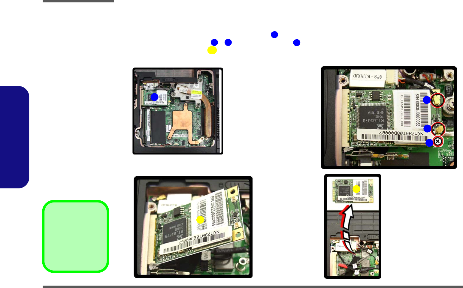
2 - 14 Removing the Wireless LAN Module
2.Disassembly
Removing the Wireless LAN Module
1. Turn off the computer, remove the battery (page 2 - 5) and the component bay cover (page 2 - 9).
2. The Wireless LAN module will be visible at point on the mainboard.
3. Carefully disconnect cables - , then remove screw from the module socket.
4. The Wireless LAN module will pop-up.
5. Lift the Wireless LAN module (Figure 10d) up and off the computer.
Figure 10
Wireless LAN
Module Removal
a. Remove the cover.
b. Disconnect the cables
and remove the screw.
c. The WLAN module will
pop up.
d. Lift the WLAN module
out.
Note: Make sure you
reconnect the antenna
cable to “1” + “2”
socket (Figure b).
1
2
3
4
5
5
b.
c.
a.
d.
2
3
1Note:
Only one model is pic-
tured here, however
the component loca-
tions are the same for
both models. 4
5
5. WLAN Module.
•1 Screw
Disassembly
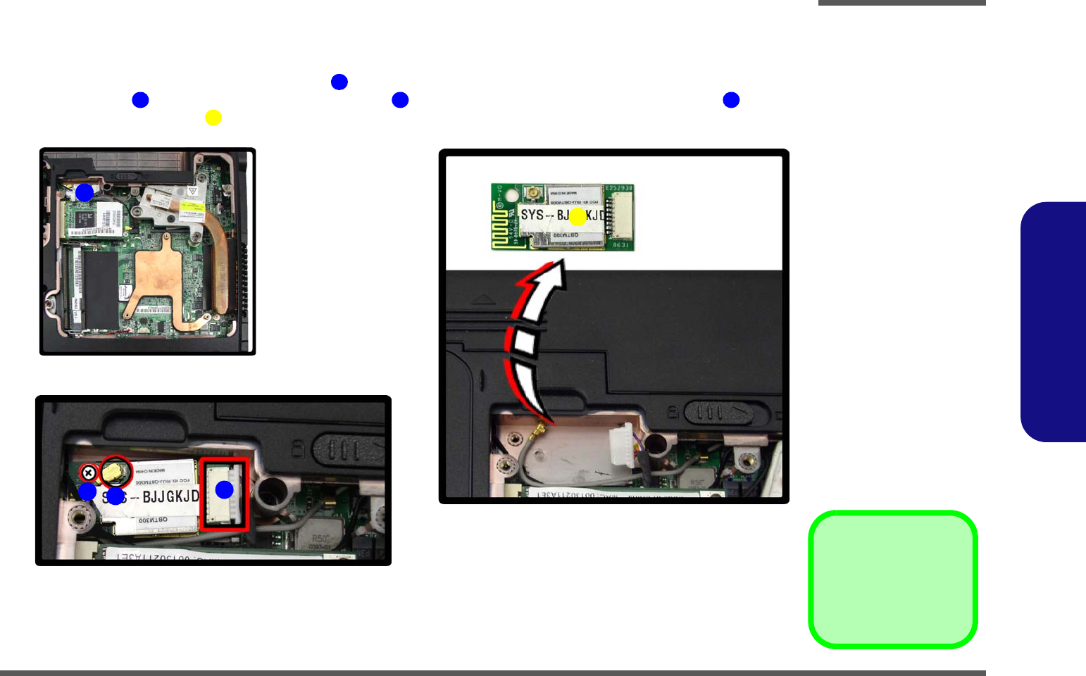
Removing the Bluetooth Module 2 - 15
2.Disassembly
Removing the Bluetooth Module
1. Turn off the computer, remove the battery (page 2 - 5).
2. The Bluetooth module will be visible at point on the mainboard.
3. Remove screw and carefully disconnect the cable and separate the module from the connector .
4. Lift the Bluetooth module up and off the computer.
1
2
3
4
5
Figure 11
Bluetooth Removal
a. Remove the cover and
locate the Bluetooth
module.
b. Remove the screw and
disconnect the cable and
seperate the connector.
c. Lift the Bluetooth module
out.
a.
b.
34
1
2
c.
5
Note:
Only one model is pic-
tured here, however
the component loca-
tions are the same for
both models.
5. Bluetooth Module
•1 Screw
Disassembly
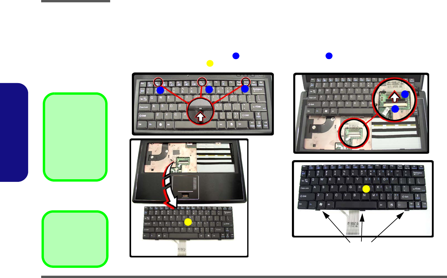
2 - 16 Removing the Keyboard
2.Disassembly
Removing the Keyboard
1. Turn off the computer, and remove the battery (page 2 - 5).
2. Press the three keyboard latches at the top of the keyboard to elevate the keyboard from its normal position (you
may need to use a small screwdriver to do this).
3. Carefully lift the keyboard up, being careful not to bend the keyboard ribbon cable (Figure 12b).
4. Disconnect the keyboard ribbon cable from the locking collar socket .
5. Carefully lift up the keyboard (Figure 12c) off the computer.
4
5
Figure 12
Keyboard Removal
a. Press the three latches
to release the keyboard.
b. Lift the keyboard up and
disconnect the cable
from the locking collar.
c. Remove the keyboard.
Re-Inserting the Key-
board
When re-inserting the
keyboard firstly align
the three keyboard
tabs at the bottom of
the keyboard with the
slots in the case.
6. Keyboard Module.
6
a. b.
5
4
6
Keyboard Tabs
c.
13
2
6
Disassembly
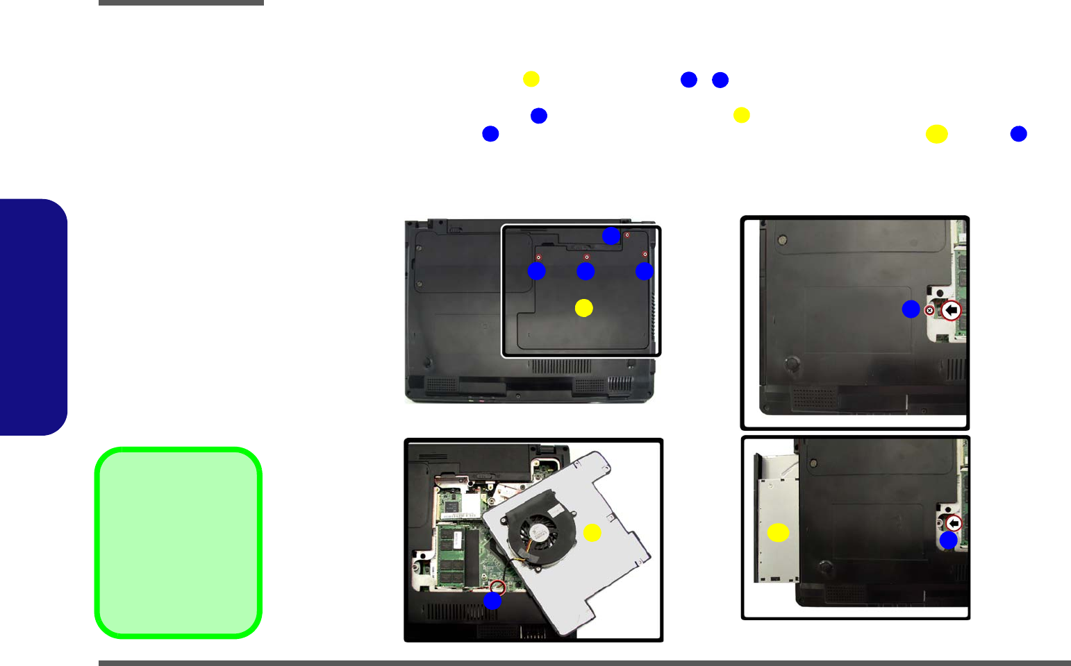
Removing the Modem 2 - 17
2.Disassembly
Removing the Modem
1. Turn off the computer, remove the battery (page 2 - 5), HDD (page 2 - 6), component bay cover (page 2 - 9), opti-
cal device (page 2 - 8), CPU (page 2 - 12), bluetooth (page 2 - 15) and keyboard (page 2 - 16).
2. Disconnect the connectors - from under the keyboard and turn it over.
3. Remove screws - from the rear of the computer.
4. Remove the screws - from the bottom case and disconnect the connectors - on the mainboard.
5. Carefully lift up the top case off the computer.
1
3
4
5
a. b.
13
2
5
4
Figure 13
Modem Removal
a. Disconnect the connec-
tors from under the key-
board.
b. Remove the screws.
c. Remove the screws and
disconnect the connec-
tors from the main-
board.
d. Remove the top case.
24. Top Case
•18 Screws
6
21
22
23
24
c.
9
76
8
10 11
13
12
14
15
16
23
17
20
18
19
21
22
d.
24

Disassembly
2 - 18 Removing the Modem
2.Disassembly
6. Remove screws - and disconnect the connectors - from the mainboard.
7. Separate the bottom case from the mainboard and turn it over.
8. Remove the screws - and disconnect the connector from the modem.
9. Lift the modem up off the socket .
25
27
28
30
Figure 14
Modem Removal
Sequence
e. Remove the screws and
and disconnect the con-
nectors.
f. Separate the bottom
case from the main-
board.
g. Remove the screws and
and disconnect the con-
nector.
h. Lift the modem up off
the socket.
31. Bottom Case
32. Mainboard
37. Modem
•5 Screws
31
32
33
34
35
37
36
e.
h.
g.
32
31
28
29
25 30 26
27
33
34
35
37
36
f.

Part Lists
A-1
A.Part Lists
Appendix A: Part Lists
This appendix breaks down the M730TG series notebook’s construction into a series of illustrations. The component part
numbers are indicated in the tables opposite the drawings.
Note: This section indicates the manufacturer’s part numbers. Your organization may use a different system, so be sure
to cross-check any relevant documentation.
Note: Some assemblies may have parts in common (especially screws). However, the part lists DO NOT indicate the
total number of duplicated parts used.
Note: Be sure to check any update notices. The parts shown in these illustrations are appropriate for the system at the
time of publication. Over the product life, some parts may be improved or re-configured, resulting in new part numbers.
Part Lists
A - 2 Part List Illustration Location
A.Part Lists
Part List Illustration Location
The following table indicates where to find the appropriate part list illustration.
Table A- 1
Part List Illustration
Location
Parts M730T
Top without Fingerprint page A - 3
Bottom page A - 4
LCD page A - 5
DVD-Dual Drive page A - 6
Part Lists
Top without Fingerprint A - 3
A.Part Lists
Top without Fingerprint
Figure A - 1
Top without
Fingerprint
Part Lists
A - 4 Bottom
A.Part Lists
Bottom
Figure A - 2
Bottom
Part Lists
LCD A - 5
A.Part Lists
LCD
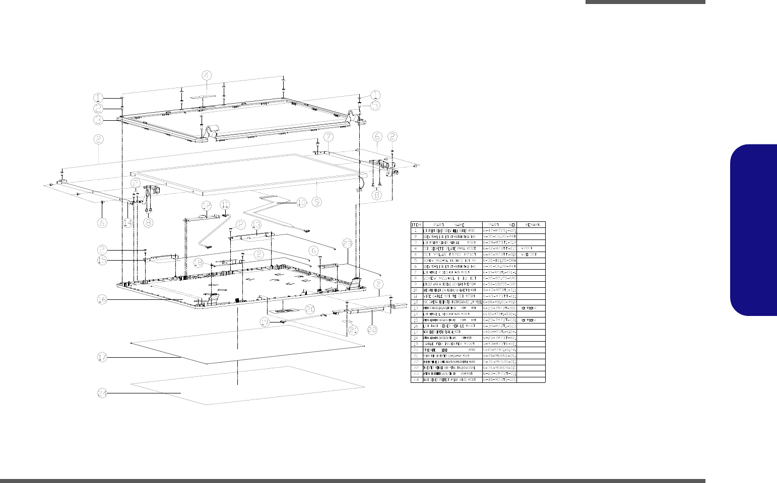
Figure A - 3
LCD
Part Lists
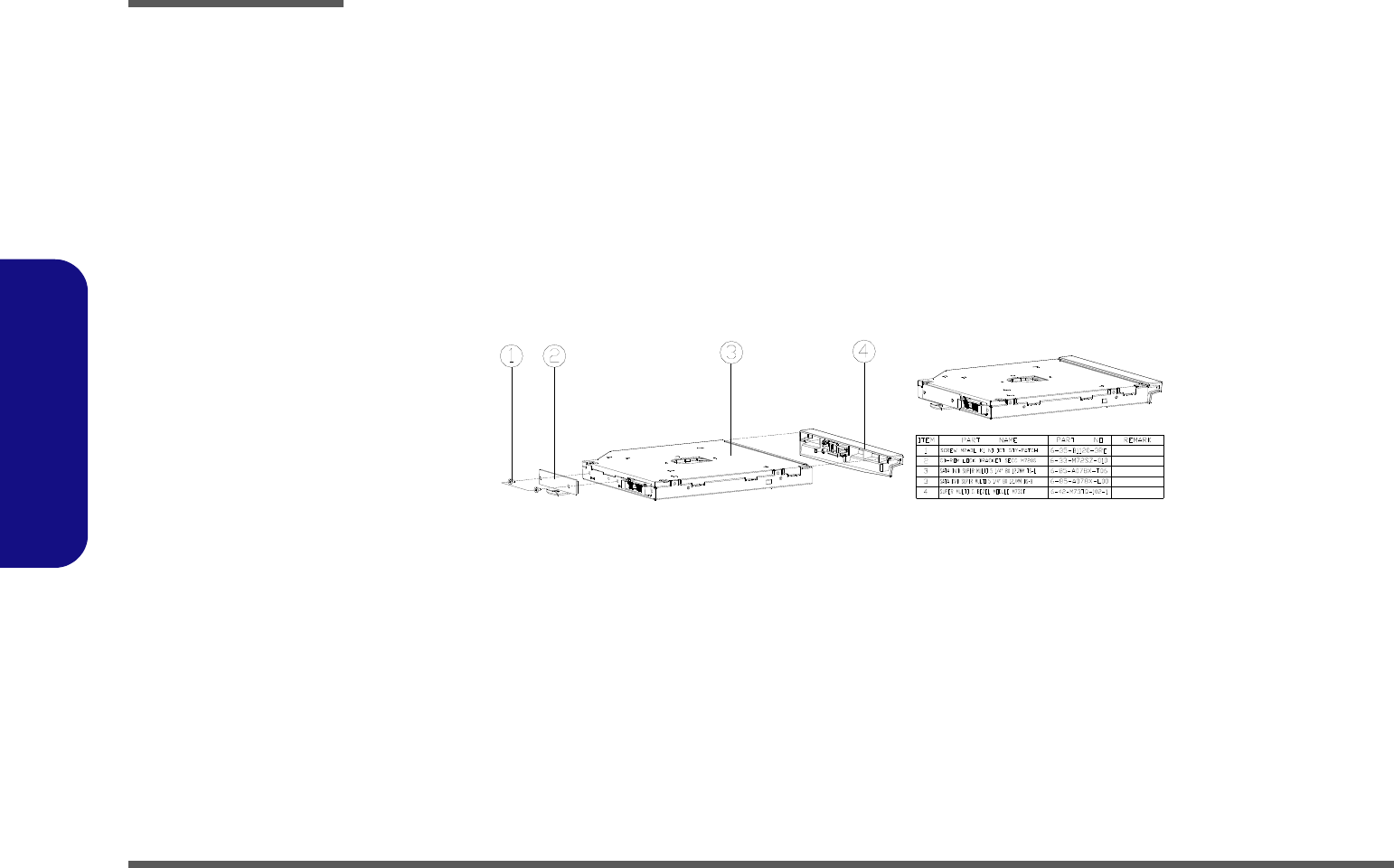
A - 6 DVD-Dual Drive
A.Part Lists
DVD-Dual Drive
Figure A - 4
DVD-Dual Drive
Schematic Diagrams
B-1
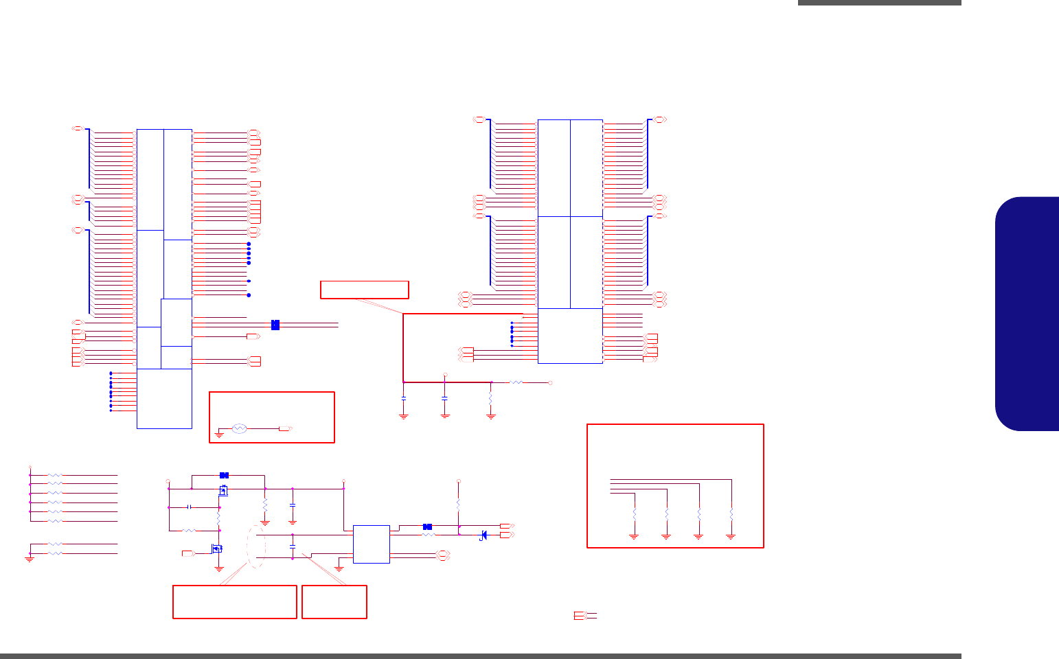
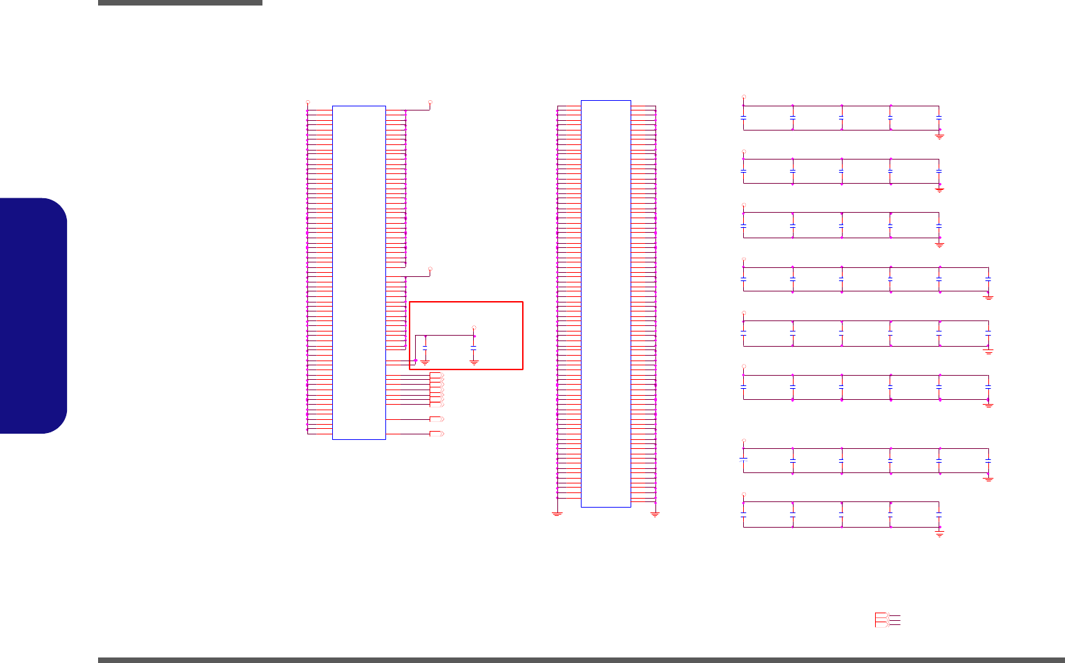
B.Schematic Diagrams
Appendix B: Schematic Diagrams
This appendix has circuit diagrams of the M730TG notebook’s PCB’s. The following table indicates where to find the
appropriate schematic diagram.
Diagram - Page Diagram - Page Diagram - Page
System Block Diagram - Page B - 2 ICH9-M 3/5 - GPIO, PWR Management - Page B - 16 Power 1.5VS, 1.05VS, 3.3V, 5V - Page B - 30
Intel Penryn (Socket-P) 1/2 - Page B - 3 ICH9-M 4/5 - Power - Page B - 17 Power 1.8V, 0.9VSM - Page B - 31
Intel Penryn (Socket-P) 2/2 - Page B - 4 ICH9-M 5/5 - GND - Page B - 18 Power VCORE - Page B - 32
Cantiga 1/6 - Host - Page B - 5 Clock Generator - Page B - 19 Power AC-IN, Charger - Page B - 33
Cantiga 2/6 - VGA, CRT - Page B - 6 Multi I/O, ODD, CCD, BT, TPM - Page B - 20 Multi I/O Board 1/2 - Page B - 34
Cantiga 3/6 - DDR - Page B - 7 New Card, Mini PCIE - Page B - 21 Multi I/O Board 2/2 - Page B - 35
Cantiga 4/6 - Power - Page B - 8 LED, FAN, TP, FP, USB - Page B - 22 Finger Printer Board - Page B - 36
Cantiga 5/6 - Power - Page B - 9 JMB385 Card Reader - Page B - 23 Click Board - Page B - 37
Cantiga 6/6 - GND - Page B - 10 PCI-E LAN RTL8111C - Page B - 24 M730T ODD Bridge Board - Page B - 38
DDRII CHANNEL A - Page B - 11 Audio Codec ALC662 - Page B - 25 M730T Audio Board - Page B - 39
DDRII CHANNEL B - Page B - 12 Audio AMP2056 - Page B - 26 Power Sequence Diagram - Page B - 40
Panel, Inverter, CRT - Page B - 13 KBC-ITE IT8512E - Page B - 27 Power Sequence v3.0 - Page B - 41
ICH9-M 1/5 - SATA - Page B - 14 System Power, LED BKLT - Page B - 28
ICH9-M 2/5 - PCIE, PCI, USB - Page B - 15 Power VDD3, VDD5 - Page B - 29
Table B - 1
Schematic
Diagrams
Version Note
The schematic dia-
grams in this chapter
are based upon ver-
sion 6-7P-M72T6-005.
If your mainboard (or
other boards) are a lat-
er version, please
check with the Service
Center for updated di-
agrams (if required).
Schematic Diagrams
B - 2 System Block Diagram
B.Schematic Diagrams
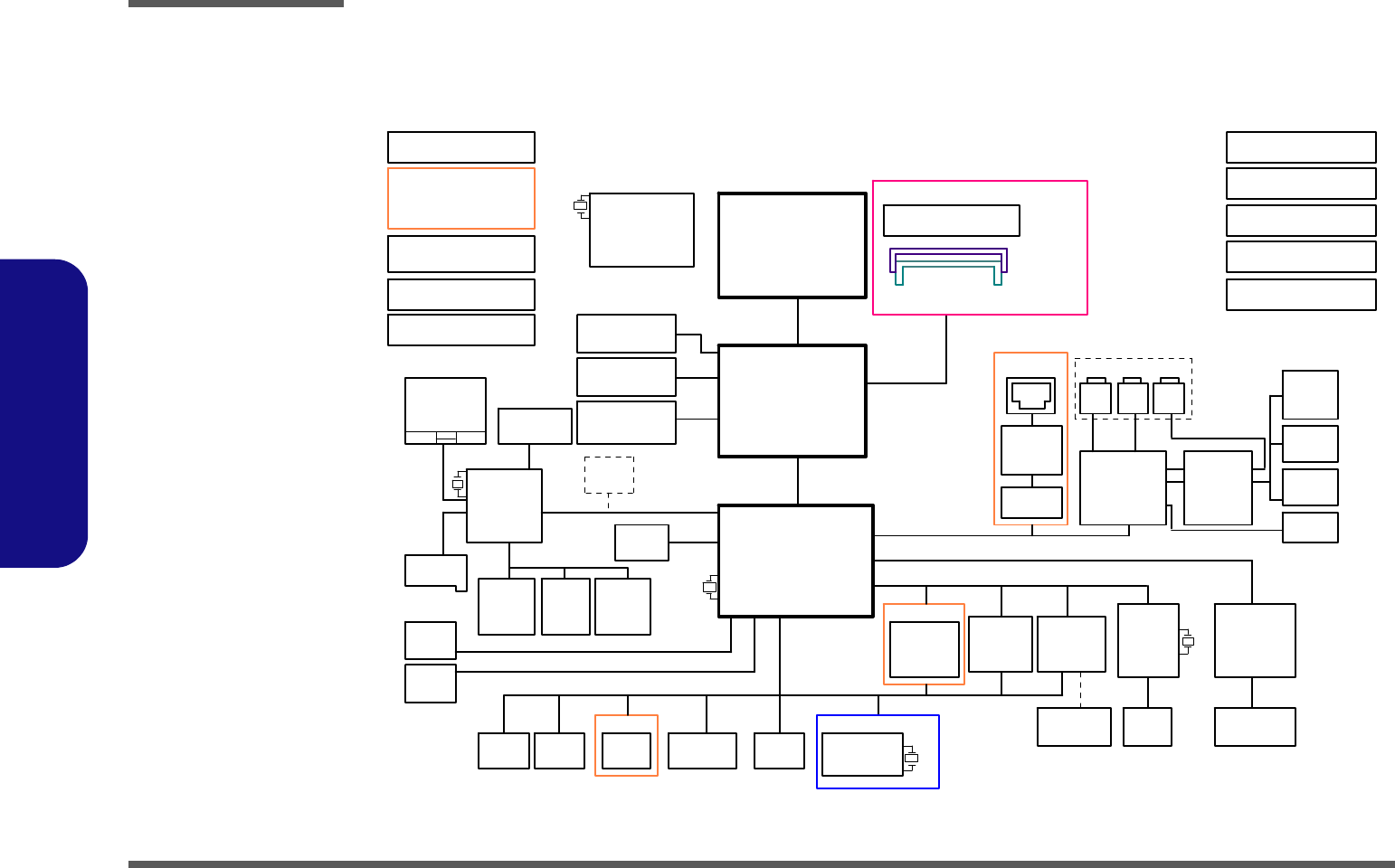
System Block Diagram
Sheet 1 of 40
System Block
Diagram
24 MHz
100 MHz
33 MHz
SPK_R, RJ-11, LED
PCI
128pins LQFP
IT 85 12E /E X
0. 1" ~1 3
M 73 0T OD D Bo ar d
Azalia Codec
LP C
Multi I/O
Board
128pins LQFP
14 *1 4*1. 6mm
0.5"~11"
( USB 5)
M720T
1. 05 VM, 1. 5V S
533/667/800 MHz
MD C
Co nn ec tor
(U SB 11)
9*9*1. 6mm
1"~16"
51 2K b
INT SPK L
667/800/1066 MHz
TP M1 .2
AL C66 2
Azalia
SA TA I /II 3 .0 Gb /s
12 MHz
<1 2"
<8"
M730T
Colck Generator
480 Mbps
LID, HOT KEY, USB, 3G
IN T MI C
EC S PI RO M
1" ~16 "
CRT Connector
M 72 0T /M7 30 T Cl ic k
Board
North Bridge
USB2.0
A PA2 05 6A
Sm ar t
Ba tt ery
Smart
FAN
478pins uFCPGA
13 29 FC BGA
Multi I/O
Board
3G Ca rd /
Ra bos on
<1 2"
USB0
SP D IF
OU T
A C- IN ,Ch ar ge r
<1 2"
PCIe
SO-DIMM1
LAN
32.768 KHz
To uc h Pad
Co nn ec tor
Cantiga GMCH
Re alt ek
M ul ti I/ O Bo ar d
16 Mb
VC OR E
SA TA I /II 3 .0 Gb /s
14 *1 4* 1. 4mm
DM I
AM P.
Th erm al
Se nso r
INT SPK R
ITE
Min i ca rd
Intel Penryn
Socket
9. 8* 6.4 * 1.2 mm
14.318 MHz
VD D3 ,VD D5
SO-DIMM0
25
MHz
(U SB 7)
FS B
M73 0T
LED B AC KLI GH T
DRI VE R
Ca rd Re ad er
EC
SA TA
HD D
DDR2
810602-1703
Socket
HP
OU T
Sy st em Powe r
Ne w Car d
32.768KHz
X4
RJ-11
INT K/B
REALTEK
M 73 0T Au di o Bo ar d
South Bridge
(USB9)
7 IN1
33 MHz
S PI RO M
RJ-45
ANP AC
CLEVO M720T System Block Diagram
IC S9 LPR 36 3EG LF
Memory Termination
EC S MBUS
64 p i ns T SS O P
31*31*2.5mm
(USB2)
Bl ue too th
SO CKE T
SA TA
OD D
CCD
Soket P
RTL8111C
28 p i ns T SS O P
DDR2
17. 1*8. 1*1. 2mm
25*21*2.05mm
676 mBGA
US B3
MIC
IN
ICH9-M
INT SPK R
<=8"
64pins QFN
Sy na pt ic
Min i PC Ie
US B1
ID T
System Me mory
<15"
FINGER PRINTER BOARD
JMB385
Az al ia
MD C
Mo du le
M720T
Proces sor
0 .5" ~5 .5 "
9*9*1.0mm
1. 8V ,0. 9V
Multi I/O
Board
FingerPrint
LC D Con ne ct or,
In ve rte r
JMicron
48pins LQFP
(USB4)
WiF i/ Wi Max
Ech o Pe ak
aS C75 25
INT SPK L
Schematic Diagrams
Intel Penryn (Socket-P) 1/2 B - 3
B.Schematic Diagrams
Intel Penryn (Socket-P) 1/2
Sheet 2 of 40
Intel Penryn
(Socket-P) 1/2
H_BNR # [4]
R5 1 K_ 1 %_ 0 4
H_A#4
H_D#63
V_TH RM
TR 1
* T S M 1A 1 0 3 H 3 4D 3R
CL K_ CPU_ BC LK# [18 ]
H_DSTBN#0[4 ]
H_NMI[13] C PU_BSEL1[4,18]
H_ D# 2 7
H_ DEF ER # [4 ]
H_A#26
R4
2K_1% _04
H_DSTBN#2 [4]
THER M_RST#[26 ]
H_ D# 2 5
H_A#9
H_A#18
H _A#[35:3][4 ]
H_ DBSY # [4 ]
H_HITM# [4]
H_A#7
H_A#34
H_PREQ#
H_ D# 2 8
C3 3 7
*0.01U _16V_X7R _04
1.05VS
C336
1U _6.3V_04
H_ TH E RM DA
H_ D# 2 1
H_ D# 6
H_ D# 1
H_D#41
H_D#44
H_ RS# 2 [4 ]
H_D#59
H_ D# 1 9
H_A#10
COMP2
H_ D# 2 3
R8
54.9_1%_04
R2 0 0
*100K_04
H_ D# 2 6
PM _THR M# [15]
COMP2
H_D#33
SM C_ CPU _T HE RM [26 ]
H_ D# 3 1
H_ D# 2 9
C7
*1U_6.3V_X5R_06
? ADT7421 Colay
PS I# [31 ]
H_D#57
R2 1 1
*330K_04
H_ RS# 1 [4 ]
H_A#25
H_REQ#2
R 7 54 . 9 _ 1% _ 04
H_ DIN V # 1[4]
R 197 56_04
H_ADS# [4]
H_DINV#3 [4]
H_A#12
H_ D# 3 0
H_REQ#4
H_D#53
H_A#14
R 173 54.9_1%_04
R2 09
*1 00 K _ 0 4
ADDR
GROUP_0 ADDR
GROUP_1
CONTROL
XD P /I TP S I GNALS
H C LK
THERM AL
RESERVED
ICH
U9 A
MOLEX_47430-6215
N3
P5
P2
L2
P4
P1
R1
Y2
U5
R3
W6
U4
Y5
U1
R4
T5
T3
W2
W5
Y4
J4
U2
V4
M4
N5
T2
V3
B2
D2
D22
L5
L4
K5
M3
N2
J1
A6
H1
M1
V1
D3
A22
A21
E2
AD 4
AD 3
AD 1
AC 4
G5
F1
C2 0
E1
H5
F21
A5
G6
E4
D2 0
C4
B3
C6
B4
H4
AC 2
AC 1
D2 1
K3
H2
K2
J3
L1
C1
F3
F4
G3
A3
D5
AC 5
AA6
AB3
C7
A24
B25
AB5
G2
AB6
W3
AA4
AB2
AA3
F6
A[10]#
A[11]#
A[12]#
A[13]#
A[14]#
A[15]#
A[16]#
A[17]#
A[18]#
A[19]#
A[20]#
A[21]#
A[22]#
A[23]#
A[24]#
A[25]#
A[26]#
A[27]#
A[28]#
A[29]#
A[3]#
A[30]#
A[31]#
RSVD[01]
RSVD[02]
RSVD[03]
RSVD[04]
RSVD[05]
RSVD[06]
RSVD[07]
A[4]#
A[5]#
A[6]#
A[7]#
A[8]#
A[9]#
A20M#
ADS#
AD STB [0]#
AD STB [1]#
RSVD[08]
BCLK[0]
BCLK[1]
BN R#
BPM[0]#
BPM[1]#
BPM[2]#
BPM[3]#
BPRI#
BR 0#
DBR#
D BSY#
DEFER#
DRD Y#
FER R#
HI T#
HITM#
IER R#
IG NNE #
INI T#
LINT0
LINT1
LO C K #
PRD Y#
PR EQ#
PROCHOT#
REQ[0]#
REQ[1]#
REQ[2]#
REQ[3]#
REQ[4]#
RESE T#
RS[0 ]#
RS[1 ]#
RS[2 ]#
SM I#
STPCLK#
TC K
TDI
TD O
THER MTRIP#
TH E R M D A
THER MD C
TM S
TRD Y#
TRS T#
A[32]#
A[33]#
A[34]#
A[35]#
RSVD[09]
H_A#31
H_ RS# 0 [4 ]
H_D#34
R195 *10mil_short
V_TH RM
SM D_ CPU _T HE RM [26 ]
PM_ T HRM T RIP# [5 ,1 3, 28 ]
COMP0, COMP2: 0.5" Max, Zo=27.4 Ohms
COMP1, COMP3: 0.5" Max, Zo=55 Ohms
Best estimate is 18 mils wide trace for outer
layers and 14 mils wide trace if on internal
layers.
Put it at central of
CPU socket
H_ HIT# [4 ]
H _DPRSTP# [5,13,31]
CPU ONLY SUPPORT TO 35W
CL K_ CPU_ BC LK [1 8]
H_DSTBN#1[4 ]
H_D#50
H_A#5
H_D#47
H_D#42
R1 9 3 * 0_ 0 4
3.3V
3. 3 V[12..17,19,20,23,29,30]
H_REQ#3
COMP3
H_ INIT# [1 3 ]
H_ D# [6 3:0 ][4 ]
H_D#38
H_A#13
H_ D# 2 2
R 171 649_1%_06
Q 18 *AO 3409
G
DS
Layout Note:
H_PREQ#
H_ D# 1 0
U1 3
aS C 75 2 5
1
2
3
4
5
6
7
8
VD D
D+
D-
THER M
GND
ALER T
SDA TA
SC LK
H_A#16
H_A#28
H_ D# 4
H_ D# 1 1
H_D#55
H_ TRDY # [4 ]
H_ DST BP# 1[4]
H_D#52
H_PROCHOT#
H_D#51
R6
27.4_1%_04
1.05VS[3..5,7,8,13,16,29]
CPU_ BSEL 0
C335
1000P_50V_X7R_04
H_ D# 1 7
H_ THE RM DC
H_BPRI# [4]
H_TDI
H_D#61
10mils
H_TMS
CPU_ BSEL 1
H_CPURST#
Route H_THERMDA and
H_THERMDC on same layer.
10 mil trace on 10 mil spacing.
1. 0 5 V S
H_A#6
H_A#17
H_A#32
H_TCK
COMP0
H_A#29
H_IERR#
THER M_AL ERT# [26]
H_AD STB#1[4 ]
R210 *10m il_short
H_D#45
R182
54.9_1%_04
12mils
H_INTR[13]
Layout Note:
H_ D# 3
H_A#11
H_ D# 1 2
COMP1
H_CPU RST# [4]
COMP0
H_D#46
H_ D# 1 6
H_TDI
H_ D# 2 0
H_PR OCH OT #
H_D#48
H_ D# 2 4
0.5" max, Zo= 55 Ohms
H_A#23
H_D#54
Near to Thermal
IC
H_D#62
H_DPSLP# [13]
R183
27.4_1%_04
COMP3
H_D#58
H_D#32
H_T HER MDC _ R
H_DINV#2 [4]
H_DSTBP#3 [4]
R196 *10mil_short
H_ ST PCL K#[13]
COMP1
CPU_ BSEL 2
H_REQ#1
H_A#21
H_A#30
H_TRST#
R194
10K_04
H_D#60
H_D#56
D15
ASD751V
AC
CPU TEMP [26]
H_ D# 8
H_IGNNE#[13 ]
H_A#15
H_ D# 1 8
H_DSTBP#2 [4]
H_A#8
H_TRST#
H_ D# 2
H_ REQ #[4 :0 ][4]
H_IERR#
H_ D# 5
H_D#39
R 19 *51_1% _04
H_DR DY# [4]
H_A#24
H_D#49
H _A#[35:3][4 ]
H_REQ#0
H_ D# 1 5
R 198 54.9_1%_04
Q1 9
*2N7002W
G
DS
Layout note:
H_ TH E RM DC
H_A#19
H_ D# 7
H_A#22
Layout Note:
H _A20M#[13 ]
DATA GRP 0 DATA GRP 1
DATA GRP 2DATA GRP 3
MIS C
U9B
MOLEX_47430-6215
R2 6
U2 6
AA1
Y1
E22
F24
J24
J23
H22
F26
K22
H23
N22
K25
P26
R23
E26
L23
M24
L22
M23
P25
P23
P22
T24
R24
L25
G22
T25
N25
Y22
AB2 4
V24
V26
V23
T22
U2 5
U2 3
F23
Y25
W22
Y23
W24
W25
AA2 3
AA2 4
AB2 5
AE2 4
AD24
G25
AA2 1
AB2 2
AB2 1
AC26
AD20
AE2 2
AF2 3
AC25
AE2 1
AD21
E25
AC22
AD23
AF2 2
AC23
E23
K24
G24
AF 1
H25
N24
U2 2
AC20
E5
B5
D2 4
J26
L26
Y26
AE2 5
H26
M26
AA2 6
AF2 4
AD 26
AE6
D6
D7
C24
B22
B23
C21
D25
AF2 6
A26
C23
C3
CO MP[0 ]
CO MP[1 ]
CO MP[2 ]
CO MP[3 ]
D[0]#
D[1]#
D[10]#
D[11]#
D[12]#
D[13]#
D[14]#
D[15]#
D[16]#
D[17]#
D[18]#
D[19]#
D[2]#
D[20]#
D[21]#
D[22]#
D[23]#
D[24]#
D[25]#
D[26]#
D[27]#
D[28]#
D[29]#
D[3]#
D[30]#
D[31]#
D[32]#
D[33]#
D[34]#
D[35]#
D[36]#
D[37]#
D[38]#
D[39]#
D[4]#
D[40]#
D[41]#
D[42]#
D[43]#
D[44]#
D[45]#
D[46]#
D[47]#
D[48]#
D[49]#
D[5]#
D[50]#
D[51]#
D[52]#
D[53]#
D[54]#
D[55]#
D[56]#
D[57]#
D[58]#
D[59]#
D[6]#
D[60]#
D[61]#
D[62]#
D[63]#
D[7]#
D[8]#
D[9]#
TEST5
D INV[0 ]#
D INV[1 ]#
DINV[2 ]#
DINV[3 ]#
DPRST P#
DPSL P #
DPWR#
DSTBN[0]#
DSTBN[1]#
DSTBN[2]#
DSTBN[3]#
DSTBP[0]#
DSTBP[1]#
DSTBP[2]#
DSTBP[3]#
GTLREF
PSI#
PW RG OO D
SLP#
TEST3
BSE L[0]
BSE L[1]
BSE L[2]
TEST2
TEST4
TEST6
TEST1
TEST7
H_ D# [6 3:0 ][4 ]
H_ THE RM DA
R192 *10mil_short
H_D#[63:0] [4]
H _PWRGD [13]
H_AD STB#0[4 ] H_ L OCK# [4]
Layout Note:
H_A#33
H_A#27
H_TMS
C PU_BSEL2[4,18]
H_A#35
H_D#36
H_ BREQ # [4 ]
H_DSTBN#3 [4]
H_A#3
R 181 54.9_1%_04
H _CPUSLP# [4]
H_D#40
CPU_GTLREF
H_F ERR #[1 3]
H_DINV#0[4 ]
H_ D# 9
H_D#43
R 174 54.9_1%_04
H_DSTBP#0[4]
H_ D# 1 4
H_SMI#[13]
H_D#[63:0] [4]
H_ D# 0
C PU_BSEL0[4,18] H_DPWR# [4]
H_D#35
H_D#37
H_ D# 1 3
CPU_GRFE=0.7V
H_A#20
H_TCK
H_T HER MDA_R
H_CPURST#
C8
0. 0 1 U _ 1 6V _ X 7R _ 04
Schematic Diagrams
B - 4 Intel Penryn (Socket-P) 2/2
B.Schematic Diagrams
Intel Penryn (Socket-P) 2/2
C311
0.1U_10V_X7R_04
C301
1U _6.3V_04
C 309
0.1U _10V _X7R _04
C283
10U_6.3V_X5R_08
H _V ID4 [31]
C3 3 0
22U _6.3V _X5R _08
C2 9 6
1U _6.3V_04
1.5VS[8,13,14,16,19,20, 29]
VCO R E
C332
1U_6.3V_04
1.05V S
C31
0.1U_10V_X7R_04
C38
22U_6.3V_X5R_08
C2 9 9
0. 01 U _ 16 V _X 7 R _0 4
1.05VS
H _V ID3 [31]
C PU_VS SSEN SE [31]
C 308
* 0.1U_1 0 V_X7R_04
C322
22U_6.3V_X5R_08
C291
0.01U _16V_X7R _04
C327
10U_6.3V_X5R_08
VC OR E[31 ]
C 321
10U _6.3V _X5R _08
C3 2 3
10U _6.3V _X5R _08
C 279
0.1U _10V_X7R_04
C 305
1U _6.3V _04
C334
1U _6.3V_04
C 316
0.1U _10V_X7R_04
U9 C
MO LEX_47430-6215
.
A7
A9
A10
A12
A13
A15
A17
A18
A20
B7
B9
B10
B12
B14
B15
B17
B18
B20
C9
C1 0
C1 2
C1 3
C1 5
C1 7
C1 8
D9
D1 0
D1 2
D1 4
D1 5
D1 7
D1 8
E7
E9
E10
E12
E13
E15
E17
E18
E20
F7
F9
F10
F12
F14
F15
F17
F18
F20
AA7
AA9
AA10
AA12
AA13
AA15
AA17
AA18
AA20
AB9
AC10
AB10
AB12
AB14
AB15
AB17
AB18
AB20
AB7
AC7
AC9
AC12
AC13
AC15
AC17
AC18
AD7
AD9
AD10
AD12
AD14
AD15
AD17
AD18
AE9
AE10
AE12
AE13
AE15
AE17
AE18
AE20
AF9
AF1 0
AF1 2
AF1 4
AF1 5
AF1 7
AF1 8
AF2 0
B26
J6
K6
M6
J2 1
K21
M2 1
N2 1
N6
R2 1
R6
T2 1
T6
V21
W21
AF7
AD6
AF5
AE5
AF4
AE3
AF3
AE2
AE7
C2 6
G2 1
V6
V CC [001]
V CC [002]
V CC [003]
V CC [004]
V CC [005]
V CC [006]
V CC [007]
V CC [008]
V CC [009]
V CC [010]
V CC [011]
V CC [012]
V CC [013]
V CC [014]
V CC [015]
V CC [016]
V CC [017]
V CC [018]
V CC [019]
V CC [020]
V CC [021]
V CC [022]
V CC [023]
V CC [024]
V CC [025]
V CC [026]
V CC [027]
V CC [028]
V CC [029]
V CC [030]
V CC [031]
V CC [032]
V CC [033]
V CC [034]
V CC [035]
V CC [036]
V CC [037]
V CC [038]
V CC [039]
V CC [040]
V CC [041]
V CC [042]
V CC [043]
V CC [044]
V CC [045]
V CC [046]
V CC [047]
V CC [048]
V CC [049]
V CC [050]
V CC [051]
V CC [052]
V CC [053]
V CC [054]
V CC [055]
V CC [056]
V CC [057]
V CC [058]
V CC [059]
V CC [060]
V CC [061]
V CC [062]
V CC [063]
V CC [064]
V CC [065]
V CC [066]
V CC [067]
VC C[ 068]
VC C[ 069]
VC C[ 070]
VC C[ 071]
VC C[ 072]
VC C[ 073]
VC C[ 074]
VC C[ 075]
VC C[ 076]
VC C[ 077]
VC C[ 078]
VC C[ 079]
VC C[ 080]
VC C[ 081]
VC C[ 082]
VC C[ 083]
VC C[ 084]
VC C[ 085]
VC C[ 086]
VC C[ 087]
VC C[ 088]
VC C[ 089]
VC C[ 090]
VC C[ 091]
VC C[ 092]
VC C[ 093]
VC C[ 094]
VC C[ 095]
VC C[ 096]
VC C[ 097]
VC C[ 098]
VC C[ 099]
VC C[ 100]
VC CA[01]
VC CP[03]
VC CP[04]
VC CP[05]
VC CP[06]
VC CP[07]
VC CP[08]
VC CP[09]
VC CP[10]
VC CP[11]
VC CP[12]
VC CP[13]
VC CP[14]
VC CP[15]
VC CP[16]
V CC SEN SE
VI D[0]
VI D[1]
VI D[2]
VI D[3]
VI D[4]
VI D[5]
VI D[6]
VS SSEN SE
VC CA[02]
VC CP[01]
VC CP[02]
C 320
22U _6.3V _X5R _08
C39
1U _6.3V _04
C 315
* 0.1U_10V_X7R _04
VCO R E
VC OR E
H _V ID1 [31]
H _V ID2 [31]
C 319
10U _6.3V_X5R_08
1. 05 V S[2 ,4 ,5 ,7, 8, 13 ,1 6 ,2 9 ]
C 281
22U _6.3V_X5R_08
C35
* 0. 1U _10V _X7R _04
C324
1U_6.3V_04
C3 1 3
150U_4V_B2
C 295
1U _6.3V _04
C304
0.1U_10V_X7R_04
H _V ID0 [31]
VCO R E
VCO R E
C 302
1U _6.3V _04
1.05VS
C2 8 0
22U _6.3V _X5R _08
Layout Note:
C36
22U_6.3V_X5R_08
C282
10U_6.3V_X5R_08
C333
22U_6.3V_X5R_08
0.5A
C362
0.1U_10V_X7R_04
C278
1U_6.3V_04
H _V ID6 [31]
47A
C1 7
0.1U_10V_X7R _04
C331
0.1U_10V_X7R_04
H _V ID5 [31]
C328
0.01U_16V_X7R_04
VCO R E
C 298
0.1U _10V _X7R _04
C3 2 9
1U _6.3V_04
2.5A
U9D
M O LE X_47430- 6215
.
P6
AE11
A8
A11
A14
A16
A19
A23
AF2
B6
B8
B11
B13
B16
B19
B21
B24
C5
C8
C1 1
C1 4
C1 6
C1 9
C2
C2 2
C2 5
D1
D4
D8
D1 1
D1 3
D1 6
D1 9
D2 3
D2 6
E3
E6
E8
E11
E14
E16
E19
E21
E24
F5
F8
F11
F13
F16
F19
F2
F22
F25
G4
G1
G2 3
G2 6
H3
H6
H2 1
H2 4
J2
J5
J22
J25
K1
K4
K23
K26
L3
L6
L21
L24
M2
M5
M2 2
M2 5
N1
N4
N2 3
N2 6
P3 A25
AF21
AF19
AF16
AF13
AF11
AF8
AF6
A2
AE26
AE23
AE19
P21
P24
R2
R5
R22
R25
T1
T4
T23
T26
U3
U6
U21
U24
V2
V5
V22
V25
W1
W4
W23
W26
Y3
Y21
Y24
AA2
AA5
AA8
AA11
AA14
AA16
AA19
AA22
AA25
AB1
AB4
AB8
AB11
AB13
AB16
AB19
AB23
AB26
AC 3
AC 6
AC 8
AC 11
AC 14
AC 16
AC 19
AC 21
AC 24
AD 2
AD 5
AD 8
AD 11
AD 13
AD 16
AD 19
AD 22
AD 25
AE1
AE4
Y6
A4
AE14
AE16
AE8
AF25
VSS [082]
VSS [148]
VS S[00 2]
VS S[00 3]
VS S[00 4]
VS S[00 5]
VS S[00 6]
VS S[00 7]
VS S[00 8]
VS S[00 9]
VS S[01 0]
VS S[01 1]
VS S[01 2]
VS S[01 3]
VS S[01 4]
VS S[01 5]
VS S[01 6]
VS S[01 7]
VS S[01 8]
VS S[01 9]
VS S[02 0]
VS S[02 1]
VS S[02 2]
VS S[02 3]
VS S[02 4]
VS S[02 5]
VS S[02 6]
VS S[02 7]
VS S[02 8]
VS S[02 9]
VS S[03 0]
VS S[03 1]
VS S[03 2]
VS S[03 3]
VS S[03 4]
VS S[03 5]
VS S[03 6]
VS S[03 7]
VS S[03 8]
VS S[03 9]
VS S[04 0]
VS S[04 1]
VS S[04 2]
VS S[04 3]
VS S[04 4]
VS S[04 5]
VS S[04 6]
VS S[04 7]
VS S[04 8]
VS S[04 9]
VS S[05 0]
VS S[05 1]
VS S[05 2]
VS S[05 3]
VS S[05 4]
VS S[05 5]
VS S[05 6]
VS S[05 7]
VS S[05 8]
VS S[05 9]
VS S[06 0]
VS S[06 1]
VS S[06 2]
VS S[06 3]
VS S[06 4]
VS S[06 5]
VS S[06 6]
VS S[06 7]
VS S[06 8]
VS S[06 9]
VS S[07 0]
VS S[07 1]
VS S[07 2]
VS S[07 3]
VS S[07 4]
VS S[07 5]
VS S[07 6]
VS S[07 7]
VS S[07 8]
VS S[07 9]
VS S[08 0]
VS S[08 1] VSS [162]
VSS [161]
VSS [160]
VSS [159]
VSS [158]
VSS [157]
VSS [156]
VSS [155]
VSS [154]
VSS [153]
VSS [152]
VSS [151]
VSS [083]
VSS [084]
VSS [085]
VSS [086]
VSS [087]
VSS [088]
VSS [089]
VSS [090]
VSS [091]
VSS [092]
VSS [093]
VSS [094]
VSS [095]
VSS [096]
VSS [097]
VSS [098]
VSS [099]
VSS [100]
VSS [101]
VSS [102]
VSS [103]
VSS [104]
VSS [105]
VSS [107]
VSS [108]
VSS [109]
VSS [110]
VSS [111]
VSS [112]
VSS [113]
VSS [114]
VSS [115]
VSS [116]
VSS [117]
VSS [118]
VSS [119]
VSS [120]
VSS [121]
VSS [122]
VSS [123]
VSS [124]
VSS [125]
VSS [126]
VSS [127]
VSS [128]
VSS [129]
VSS [130]
VSS [131]
VSS [132]
VSS [133]
VSS [134]
VSS [135]
VSS [136]
VSS [137]
VSS [138]
VSS [139]
VSS [140]
VSS [141]
VSS [142]
VSS [143]
VSS [144]
VSS [145]
VSS [146]
VSS [106]
VS S[00 1]
VSS [149]
VSS [150]
VSS [147]
VSS [163]
C 318
22U _6.3V_X5R_08
1. 5 V S
VC OR E
C PU_VC C SEN SE [31]
C37
22U _6.3V _X5R _08
C3 1 2
*0.1U_10V_X7R_04
Place near pin B26, C26
C303
1U_6.3V_04
VCO R E
Sheet 3 of 40
Intel Penryn
(Socket-P) 2/2
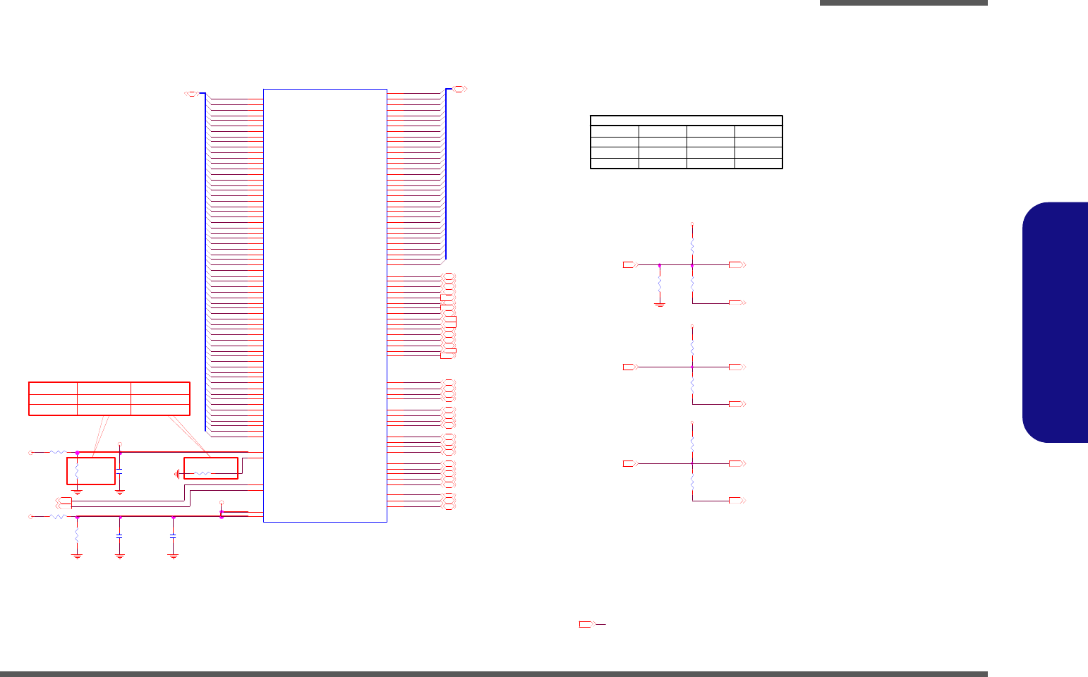
Schematic Diagrams
Cantiga 1/6 - Host B - 5
B.Schematic Diagrams
Cantiga 1/6 - Host
MCH_BSEL2 [ 5]
H_D#52
R29
H _ AD STB# 0 [ 2 ]
H_D#3
H_D#42
C353
0.1U_10V_X7R_04
1.05VS
H_DINV#2 [ 2]
H_D#20
24.9_1%_04
H_BREQ# [2]
1.05VS
MCH_BSEL0 [ 5]
H_A#32
H_D#14
H_D#50
H_D#54
H_A#3
H_A#8
H_D#37
R218
2K_1%_04
H_DINV#3 [ 2]
H_D#51
H_A#24
H_D#27
H_A#19
266
16.9_1%_04
CPU_BSEL0[2,18]
H_D#19
R204
1K_04
R202
1K_04
R212 221_1%_04
H_DSTBP#1 [2]
H_A#23
H_A#34
H_D#33
H_A#6
R208
* 56_04
H_D#39
H_A#29
H_D#25
H_D#18
H_DSTBN#3 [2]
H_D#43
H_D#36
H_DEFER# [2]
R206
1K_04
H_DPWR# [ 2]
H_REQ#4 [2]
L
1.05VS
H
H_HIT#[2]
1.05VS
H_DRDY# [2]
H_DSTBP#2 [2]
H_REQ#1 [2]
H_A#27
H_CPURST#[2]
H_D#13
CPU_BSEL1
L
H
C L K_BSE L 2 [ 2 , 18 ]
H_D#17
H_D#47
H_D#30
H_D#56
H_D#45
H_DSTBP#3 [2]
H_DINV#1 [ 2]
1.05VS[2,3,5,7,8,13,16,29]
H_D#46
H_D#61
H_A#20
H_D#32
H_A#21
CPU_BSEL0
CLK_MCH_BCLK# [ 18]
H_D#63
H_A#13
H_A#33
H
H_A#9
H_A#18
L
H_DINV#0 [ 2]
H_REQ#2 [2]
H_D#59
H _ AD STB# 1 [ 2 ]
H_CPUSLP#[2]
H_D#55
R 213
H_REQ#3 [2]
H_HITM# [2]
H_DSTBN#2 [2]
H_D#38
CPU_BSEL2
H_VREF
H_ADS# [2]
H_D#12
L
H_DSTBN#1 [2]
H_A#16
H_D#6
H_D#53
H_A#14
C363
0.1U_1 0 V_X7 R _ 04
H_TRDY# [2]
H_D#22
H_D#8
H_A#15
H_D#29
166
CPU
H_D#16
H_D#49
H_D#60
H_D#23
H_D#31
C L K_BSE L 1 [ 2 , 18 ]
H_RS#2 [2]
H_D#41
H_A#10
C L K_BSE L 0 [ 2 , 18 ]
H_REQ#0 [2]
H_D#35
R29 24.9_1%_ 04
200
100_1%_04
H_D#1
H_BPRI# [2]
R203
1K_04
1.05VS
H_A#28
H_A#11
H_D#58
H_A#22
H_LOCK# [2]
H_D#0
H_A#30
C366
0.1U_10V_X7R_04
H_A#26
R219 1K_1%_04
12mils
H_BNR#[2]
H_D#62
H_D#7
H_A#35
HOST
U15A
CANTIGA-EB88CTGM
P16
R16
N17
M13
E17
P17
F17
G20
B19
J16
E20
H16
J20
L17
A17
B17
L16
C21
J17
H20
A14
B18
K17
C15
F16
H13
C18
M16
J13
H12
B16
G17
A9
F11
G12
AH 6
C12
AH 7
F2
F13
B13
G8
M9
L6
N10
AA8
AA2
AE11
D4
H3
B10
M11
J1
J2
N12
J6
P2
L2
R2
N9
F8
M5
J3
N2
R1
N5
N6
P13
N8
L7
E6
M3
Y3
AD 1 4
Y6
Y10
Y12
Y14
Y7
W2
G2
Y9
AA13
AA9
AA11
AD 1 1
AD 1 0
AD 1 3
AE12
AE9
H6
AD 8
AA3
AD 3
AD 7
AE14
AF3
AC 1
AE3
AC 3
H2
AE8
AG2
AD 6
F6
E9
J8
L3
Y13
Y1
J11
F9
L10
M7
AA 5
AE 6
L9
M8
AA 6
AE 5
A11
B11
C9
H9
E12
H11
B15
K13
B14
B20
F21
K21
L20
C5
E11
E3
B6
F12
C8
H_A#_10
H_A#_11
H_A#_12
H_A#_13
H_A#_14
H_A#_15
H_A#_16
H_A#_17
H_A#_18
H_A#_19
H_A#_20
H_A#_21
H_A#_22
H_A#_23
H_A#_24
H_A#_25
H_A#_26
H_A#_27
H_A#_28
H_A#_29
H_A#_3
H_A#_30
H_A#_31
H_A#_4
H_A#_5
H_A#_6
H_A#_7
H_A#_8
H_A#_9
H_ADS#
H_ADSTB#_0
H_ADSTB#_1
H_BNR#
H_BP RI#
H_BREQ#
HPLL_CLK#
H_CPURST#
HPLL_CLK
H_D#_0
H_REQ#_2
H_REQ#_3
H_D#_1
H_D#_10
H_D#_20
H_D#_30
H_D#_40
H_D#_50
H_D#_60
H_D#_8
H_D#_9
H_DBSY#
H_D#_11
H_D#_12
H_D#_13
H_D#_14
H_D#_15
H_D#_16
H_D#_17
H_D#_18
H_D#_19
H_D#_2
H_D#_21
H_D#_22
H_D#_23
H_D#_24
H_D#_25
H_D#_26
H_D#_27
H_D#_28
H_D#_29
H_D#_3
H_D#_31
H_D#_32
H_D#_33
H_D#_34
H_D#_35
H_D#_36
H_D#_37
H_D#_38
H_D#_39
H_D#_4
H_D#_41
H_D#_42
H_D#_43
H_D#_44
H_D#_45
H_D#_46
H_D#_47
H_D#_48
H_D#_49
H_D#_5
H_D#_51
H_D#_52
H_D#_53
H_D#_54
H_D#_55
H_D#_56
H_D#_57
H_D#_58
H_D#_59
H_D#_6
H_D#_61
H_D#_62
H_D#_63
H_D#_7
H_DEFER#
H_DINV#_0
H_DINV#_1
H_DINV#_2
H_DINV#_3
H_DPW R #
H_DR
DY#
H_D ST BN #_ 0
H_ D STBN # _1
H_ D STBN # _2
H_ D STBN # _3
H_DSTBP#_0
H_DSTBP#_1
H_DSTBP#_2
H_DSTBP#_3
H_AVREF
H_DVREF
H_TRDY#
H_HIT#
H_HITM#
H_LOCK#
H_REQ#_0
H_REQ#_1
H_REQ#_4
H_A#_32
H_A#_33
H_A#_34
H_A#_35
H_SWING
H_CPUSLP#
H_RCOMP
H_RS#_0
H_RS#_1
H_RS#_2
H_A#31
H_D#40
Dual Core
CPU_BSEL2[2,18]
H_DSTBP#0 [2]
H_D#57
H_SWING
H_D#21
H_D#24
12mils
H_D#10
H_D#28
L
CLK_MCH_BCLK [18]
H_D#9
H_A#4
H_D#34
H_A#12
L
CPU_BSEL[2:0] (FSB) D AEFULT SETTING
Quad Core
H_A#17
H_DBSY# [2]
H_DSTBN#0 [2]
H_D#26
H_D#[63:0][2]
H_A#5
H_D#44
MCH_BSEL1 [ 5]
H_RS#0 [2]
H_A#25
R213
100_1%_04
75_1%_04
CPU_BSEL1[2,18]
H_D#4
H_A#[35: 3][2]
H_A#7
H_D#11
H_D#2
R205
1K_04
H_RS#1 [2]
H_D#15
H_D#48
H_D#5
R207
1K_04
Sheet 4 of 40
Cantiga 1/6 - Host
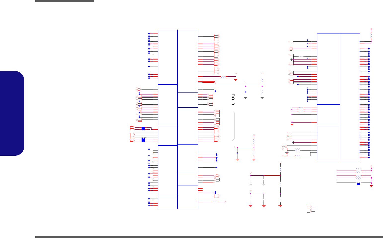
Schematic Diagrams
B - 6 Cantiga 2/6 - VGA, CRT
B.Schematic Diagrams
Cantiga 2/6 - VGA, CRT
DAC_RED[12]
MC H_ CF G 9[9]
GF X _V ID 1
C3 9 5
0.01 U _16 V_X7 R_0 4
Zdiff= 100O? 5%
M_CLK_DDR#3 [11]
D MI_ RXN1 [14 ]
M _C KE0 [10 ]
M _C KE3 [11 ]
D MI_ T XN 1 [1 4]
D MI_ RXN2 [14 ]
M _C KE1 [10 ]
C L_PWR OK [12,15,17,26]
LVD S_L3P
LV D S - L 2N[1 2 ,27 ]
M CH_C LKR EQ# [18 ]
M_CLK_DDR0 [10]
SM_ PW RO K
R221 499_1%_04
SM _VR EF
DMI_TXP3 [14]
DAC_RED
R68
10K_1% _04
1.8V
M_CLK_DDR#0 [10]
R 4 9 15 0 _1 % _ 04
3. 3V S
SM_ R EXT
R65 10 K_04
1.05VS
PM_ DPR SLP VR[1 5 ,31 ]
LV D S - L 1N[1 2 ,27 ]
M C H_ IC H_ S YN C# [1 5 ]
GF X _V ID 2
M CH_ C F G1 1
R 3 2 *1 0m il_s h or t D MI_ RXP 2 [1 4 ]
MCH_CFG13[9 ]
R222 80.6_1%_04
M CH_ C F G1 4
D MI_ RXP 1 [1 4 ]
MCH_CFG16[9 ]
M _O DT2 [11]
R64
49 . 9 _1 % _ 04
CL _ VRE F
M_C S#0 [10]
LVDS-LC LKP[12,27]
DMI_TXP0 [14]
R58 10 K_04
GF X _V ID 4
GF X _V ID 0
DAC_ D DCAC L K[12 ]
M CH_ C F G1 8
CLK_PCIE_3GPLL# [18]
D MI_ T XN 2 [1 4]
D MI_ RXN3 [14 ]
PM_ EXTTS_ EC #
M CH_ C F G1 5
1.05VM_PEG
DMI_TXP2 [14]
MC H_ CF G 7[9]
DAC _ GREE N
R 6 0 *1 0m il_s h or t
R 43 75_04
DAC _ HSYN C[1 2 ]
SM_ RC OM P_V OL
PM
MI SC
NC
DDR CLK/ CONTROL/COMPENSATIONCL KDM I
CFGRSVD
GRAP HI CS V IDME
HDA
U15B
C ANTIGA-EB88 CTGM
AP24
AT21
AV24
AR 24
AR 21
AU 24
BC 28
AY 28
AY 36
BB36
BA17
AY 16
AV16
AR 13
BC 36
BD 17
AY 17
BF15
AY 13
BG 22
BH 21
P29
R2 8
P25
T2 5
R2 5
T2 8
P20
P24
C2 5
N2 4
M2 4
E21
C2 3
C2 4
N2 1
P21
T2 1
R2 0
M2 0
L2 1
H2 1
R2 9
N3 3
P32
AT4 0
AT1 1
B38
A38
E41
F41
AE41
AE37
AE47
AH 39
AE40
AE38
AE48
AH 40
AE35
AE43
AE46
AH 42
AD 35
AE44
AF46
AH 43
AL3 4
AN35
AK34
AM3 5
BG23
BF2 3
BH18
BF1 8
B7
AU 20
AV20
AY21
AH9
AH10
AH12
AH13
M3 6
N3 6
R3 3
T3 3
B33
B32
G33
F33
C34
BF28
BH 28
T2 0
R3 2
K12
AH 37
AH 36
AN 36
AJ35
AH 34
A47
BG48
BF4 8
BD48
BC48
BH47
BG47
BE47
BH46
BF4 6
BG45
BH44
BH43
BH6
BH5
BG4
G36
E36
K36
T2 4
H36
B12
E43
F43
BH3
E33
B31
N28
BF3
BH2
BG2
BE2
BG1
BF1
BD1
BC1
F1
AV42
AR 36
BF17
M1
B28
B30
B29
C2 9
A28
M28
B2
SA_C K_0
SA_C K_1
SB_C K_0
S A _C K # _0
S A _C K # _1
S B _C K # _0
SA_C KE_0
SA_C KE_1
SB_C KE_0
SB_C KE_1
S A _C S # _0
S A _C S # _1
S B _C S # _0
S B _C S # _1
SM_DR AMR ST#
SA_O DT_0
SA_O DT_1
SB_O DT_0
SB_O DT_1
SM _R CO MP
S M_ RCO MP#
CFG _ 18
CFG _ 19
CFG _ 2
CFG _ 0
CFG _ 1
CFG _ 20
CFG _ 3
CFG _ 4
CFG _ 5
CFG _ 6
CFG _ 7
CFG _ 8
CFG _ 9
CFG _ 10
CFG _ 11
CFG _ 12
CFG _ 13
CFG _ 14
CFG _ 15
CFG _ 16
CFG _ 17
PM_ SY NC#
PM_ EXT _TS# _0
PM_ EXT _TS# _1
PWRO K
RSTIN #
DPLL_REF_CLK
DPLL_REF_CLK#
DPLL _R EF_SSCLK
D PLL _REF_ SSC LK#
DMI_ R XN _0
DMI_ R XN _1
DMI_ R XN _2
DMI_ R XN _3
DM I_R XP_0
DM I_R XP_1
DM I_R XP_2
DM I_R XP_3
DMI_TXN_0
DMI_TXN_1
DMI_TXN_2
DMI_TXN_3
DMI_ TX P_0
DMI_ TX P_1
DMI_ TX P_2
DMI_ TX P_3
RSVD 10
RSVD 12
RSVD 11
RSVD 13
RSVD 22
RSVD 23
RSVD 24
RSVD 25
PM_D PRSTP#
SB_C K_1
S B _C K # _1
RSVD 20
RSVD 5
RSVD 6
RSVD 7
RSVD 8
RSVD 1
RSVD 2
RSVD 3
RSVD 4
GFX_VID _0
GFX_VID _1
GFX_VID _2
GFX_VID _3
GFX_VR_EN
SM_ RC OMP_VO H
SM _R CO MP_VOL
THER MTRIP#
DPR SLPVR
RSVD 9
CL_CLK
CL_DATA
CL_PWROK
CL_RST#
CL_V REF
NC _26
NC _1
NC _2
NC _3
NC _4
NC _5
NC _6
NC _7
NC _8
NC _9
NC _10
NC _11
NC _12
NC _13
NC _14
NC _15
SDVO _CTRLCLK
SDVO _CTRLDATA
CLKREQ#
RSVD 14
ICH_SYNC#
TSATN#
PEG_C LK#
PEG_CLK
NC _16
GFX_VID _4
RSVD 15
DDPC _CTRLCLK
NC _17
NC _18
NC _19
NC _20
NC _21
NC _22
NC _23
NC _24
NC _25
SM _V REF
SM_ PW R OK
SM_R EXT
RSVD 17
HD A_ BCLK
HD A_ RST#
HD A_ SDI
HD A_ SDO
HD A_ SYNC
DDPC _ CT RL DAT A
RSVD 16
MCH_CFG10[9 ]
M CH_BSEL 0[4 ]
96MHz
LV D S - L 2P[1 2 ,27 ]
C LK_D REF [1 8]
MC H_ CF G 6[9]
D MI_ T XN 0 [1 4]
R232
1K_1%_04
R23 6
2.37K_1% _04
C131
0.1U_10V_X7R _04
LVDS-LCLKN[1 2 ,27 ]
SM_RC OMP#
R63
1K_1% _04
M _O DT0 [10]
100MHz
LV D S - L 1P[1 2 ,27 ] LV D S - L 0P[1 2 ,27 ]
M_CLK_DDR2 [11]
C392
2.2U_6.3V _06
DAC_BLUE[1 2]
H_DPRSTP#[2 ,1 3,3 1 ]
M CH_ C F G1 7
R 44 75_04
3.3VS[8 ..1 6,1 8 ..2 7,3 1 ]
SM_RC OMP
R69
10K_1% _04
ENAVD D[12]
MCH_CFG12[9 ]
100MHz
GM_BLON[1 2 ]
LV D S - L 0N[1 2 ,27 ]
MC H _ CL K RE Q#
M CH_ C F G3
LVD S_L3N
M_CLK_DDR3 [11]
1. 8 V
R 4 7 15 0 _1 % _ 04
SM_ RC OMP_VO H
SM _RCO MP_VOL
PM_ EXTTS_EC #
PM_ EXTTS_ D DR#
M CH_ CL K R E Q#
R59 10 K_04
M CH_BSEL 2[4 ]
C L K _PC IE_ 3G PL L [1 8]
R61 *10m il_short
D MI_ T XN 3 [1 4]
MCH_CFG19[9 ]
CL_DATA0 [15]
MC H_ CF G 5[9]
R230
3.01K_1%_04
C LK_D REFSS# [18]
PLT_ RS T#[14,19]
M CH_ C F G8
DMI_TXP1 [14]
M_CLK_DDR#2 [11]
GFX_V REN
R 30 100_04
M_C S#2 [11]
M_C S#1 [10]
M _C KE2 [11 ]
PM_ THR MTRIP#[2, 13,28]
1 . 05 V M _P E G[8 ]
GF X _V ID 3
M _O DT1 [10]
M_CLK_DDR#1 [10]
M CH_ C F G4
1.05VS[2 ..4 ,7,8 ,1 3 ,16 ,2 9]
D MI_ RXN0 [14 ]
DAC_GREEN
P_ DD C_ CL K[12,27]
C399
2.2U_6.3V _06
C118
0.1U _10V_X7R _04
D MI_ RXP 3 [1 4 ]
M_CLK_DDR1 [10]
PM_ EXTTS_D DR#
P_ DD C_ DAT A[12 ,2 7 ]
PM_SYN C#[1 5]
R52 1K_1% _04
R 3 61 5 6 _0 4
C LK_D REF# [ 18]
DAC_BLUE
DAC_BLUE
C3 9 8
0.01 U _16 V_X7 R_0 4
12mils
R 4 8 15 0 _1 % _ 04
C LK_D REFSS [1 8]
R 5 3 3 0 . 1_ 1 % _0 4
R226 80.6_1%_04
DAC_DDCADATA[12 ]
1. 8 V
1.8V[7 ,8, 10 ,1 1,3 0 ]
R62
5 1 1_ 1 % _0 4
C L_CLK0 [15]
D MI_ RXP 0 [1 4 ]
R 5 5 *1 0m il_s h or t
12mils
DAC _ GREE N[1 2 ]
R 2 16 *1 0m i l _s h or t
CL_VREF
SM _RCO MP_VOH
PM_EXTTS_ DD R#[10,11]
R 42 75_04
DAC _ RED
SM_ PW R OK
1. 0 5 V S
R 5 4 3 0 . 1_ 1 % _0 4
LVDS
PCI-EXPRESS GRAPHICS
TV VGA
U15C
CANTIG A-EB8 8C TG M
T3 7
T3 6
H4 4
J4 6
L4 4
L4 0
N4 1
P48
N4 4
T4 3
U4 3
Y43
Y48
Y36
AA43
AD37
AC47
AD39
H4 3
J4 4
L4 3
L4 1
N4 0
P47
N4 3
T4 2
U4 2
Y42
W47
Y37
AA42
AD36
AC48
AD40
J4 1
Y40
M4 0
M4 2
R4 8
N3 8
T4 0
U3 7
U4 0
M4 6
AA46
AA37
AA40
AD43
AC46
M4 7
J4 2
L4 6
M4 8
M3 9
M4 3
R4 7
N3 7
T3 9
U3 6
U3 9
Y39
Y46
AA36
AA39
AD42
AD46
M32
M33
K33
J33
M29
C44
B43
E37
E38
C41
C40
H47
E46
G40
D45
F40
B37
A37
A41
H38
G37
G38
F37
G32
F25
H25
K25
H24
E28
H32
J32
G28
J29
E29
J28
G29
L29
H48
B42
L32
C31
E32
A40
B40
J37
K37
PEG_CO MPI
PE G_ COM PO
PEG_RX#_0
PEG_RX#_1
PEG_RX#_2
PEG_RX#_3
PEG_RX#_4
PEG_RX#_5
PEG_RX#_6
PEG_RX#_7
PEG_RX#_8
PEG_RX#_9
PEG _R X# _1 0
PEG _R X# _1 1
PEG _R X# _1 2
PEG _R X# _1 3
PEG _R X# _1 4
PEG _R X# _1 5
PEG_RX_0
PEG_RX_1
PEG_RX_2
PEG_RX_3
PEG_RX_4
PEG_RX_5
PEG_RX_6
PEG_RX_7
PEG_RX_8
PEG_RX_9
PEG_RX_10
PEG_RX_11
PEG_RX_12
PEG_RX_13
PEG_RX_14
PEG_RX_15
PEG_TX# _0
PEG_TX# _ 10
PEG_TX# _3
PEG_TX# _4
PEG_TX# _5
PEG_TX# _6
PEG_TX# _7
PEG_TX# _8
PEG_TX# _9
PEG_TX# _1
PEG_TX# _ 11
PEG_TX# _ 12
PEG_TX# _ 13
PEG_TX# _ 14
PEG_TX# _ 15
PEG_TX# _2
PEG _TX_0
PEG _TX_1
PEG _TX_2
PEG _TX_3
PEG _TX_4
PEG _TX_5
PEG _TX_6
PEG _TX_7
PEG _TX_8
PEG _TX_9
PEG_TX_ 10
PEG_TX_ 11
PEG_TX_ 12
PEG_TX_ 13
PEG_TX_ 14
PEG_TX_ 15
L_CTRL_CLK
L_CTRL_DATA
L _ DD C_ CL K
L _ DD C_ DAT A
L_VDD _EN
LVD S_IBG
LVD S_VBG
LVDS_VREFH
LVDS_VREFL
LVDSA_CLK#
LVDSA_CLK
LVDSA_DATA#_0
LVDSA_DATA#_1
LVDSA_DATA#_2
LVDSA_DATA_1
LVDSA_DATA_2
LVDSB_CLK#
LVDSB_CLK
LVDSB_DATA#_0
LVDSB_DATA#_1
LVDSB_DATA#_2
LVDSB_DATA_1
LVDSB_DATA_2
L_BKL T_EN
TVA_ DAC
TVB_ DAC
TVC _D AC
TV_RTN
CRT_BLUE
CRT_DDC_CLK
CRT_DDC_DATA
CRT_GREE N
C RT_HSYN C
CRT_TVO_IREF
CRT_RED
CRT_IRTN
C RT_VSYN C
LVDSA_DATA_0
LVDSB_DATA_0
L_BKL T_CTR L
TV_DC ONS EL_0
TV_DC ONS EL_1
LVDSA_DATA#_3
LVDSA_DATA_3
LVDSB_DATA#_3
LVDSB_DATA_3
MCH_CFG20[9 ]
M_C S#3 [11]
R229
1K_1%_04
DELAY_PWRGD[17,31 ]
M CH_BSEL 1[4 ]
M _O DT3 [11]
DAC _VSY NC[12 ]
CL_RST#0 [15]
SM_REXT
Sheet 5 of 40
Cantiga 2/6 -
VGA, CRT
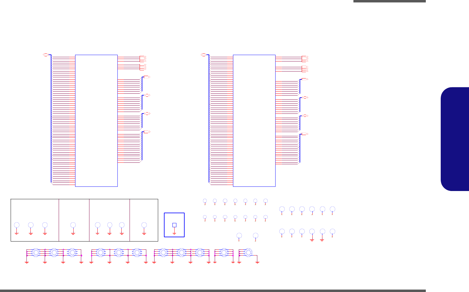
Schematic Diagrams
Cantiga 3/6 - DDR B - 7
B.Schematic Diagrams
Cantiga 3/6 - DDR
M_ B _ DQ [63 : 0 ][11]
M_ A _ D Q 6 0
M_ B _ D Q 4
M_ A _ A 10
H29
M_B_ A3
M_ A _ D M7
M_ A _ D Q 2 1
M_ A _ D Q 5 0
M_ B _ D M1
M_ B _ D Q 14
M1 0
M-M A R K 1
M_BBS1
DDR SYSTEM MEMORY A
U1 5 D
CA NT IGA-EB8 8 CT GM
AJ38
AJ41
AU40
AT38
AN41
AN39
AU44
AU42
AV39
AY44
BA40
BD43
AN38
AV41
AY43
BB41
BC40
AY37
BD38
AV37
AT36
AY38
BB38
AM38
AV36
AW36
BD13
AU11
BC11
BA12
AU13
AV13
BD12
BC12
AJ36
BB9
BA9
AU10
AV9
BA11
BD9
AY8
BA6
AV5
AV7
AJ40
AT9
AN8
AU5
AU6
AT5
AN10
AM11
AM5
AJ 9
AJ 8
AM44
AN12
AM13
AJ11
AJ12
AM42
AN43
AN44
BD21
BG18
AT25
BD20
AM37
AT41
AY41
AU39
BB12
AY6
AT7
AJ 44
AT44
BA43
BC37
AW 1 2
BC8
AU8
AM7
AJ 5
AJ 43
AT43
BA44
BD37
AY12
BD8
AU9
AM8
BA21
BC24
BC21
BG26
BH26
BH17
BG24
BH24
BG25
BA24
BD24
BG27
BF2 5
AW 2 4
BB20
AY20
AY25
SA_DQ_0
SA_DQ_1
SA_DQ_10
SA_DQ_11
SA_DQ_12
SA_DQ_13
SA_DQ_14
SA_DQ_15
SA_DQ_16
SA_DQ_17
SA_DQ_18
SA_DQ_19
SA_DQ_2
SA_DQ_20
SA_DQ_21
SA_DQ_22
SA_DQ_23
SA_DQ_24
SA_DQ_25
SA_DQ_26
SA_DQ_27
SA_DQ_28
SA_DQ_29
SA_DQ_3
SA_DQ_30
SA_DQ_31
SA_DQ_32
SA_DQ_33
SA_DQ_34
SA_DQ_35
SA_DQ_36
SA_DQ_37
SA_DQ_38
SA_DQ_39
SA_DQ_4
SA_DQ_40
SA_DQ_41
SA_DQ_42
SA_DQ_43
SA_DQ_44
SA_DQ_45
SA_DQ_46
SA_DQ_47
SA_DQ_48
SA_DQ_49
SA_DQ_5
SA_DQ_50
SA_DQ_51
SA_DQ_52
SA_DQ_53
SA_DQ_54
SA_DQ_55
SA_DQ_56
SA_DQ_57
SA_DQ_58
SA_DQ_59
SA_DQ_6
SA_DQ_60
SA_DQ_61
SA_DQ_62
SA_DQ_63
SA_DQ_7
SA_DQ_8
SA_DQ_9
SA_BS_ 0
SA_BS_ 1
SA_BS_ 2
SA_C AS#
SA_D M_ 0
SA_D M_ 1
SA_D M_ 2
SA_D M_ 3
SA_D M_ 4
SA_D M_ 5
SA_D M_ 6
SA_D QS_ 0
SA_D QS_ 1
SA_D QS_ 2
SA_D QS_ 3
SA_D QS_ 4
SA_D QS_ 5
SA_D QS_ 6
SA_D QS_ 7
SA_D M_ 7
SA_DQ S#_ 0
SA_DQ S#_ 1
SA_DQ S#_ 2
SA_DQ S#_ 3
SA_DQ S#_ 4
SA_DQ S#_ 5
SA_DQ S#_ 6
SA_DQ S#_ 7
SA_MA_ 0
SA_MA_ 1
SA_M A_10
SA_M A_11
SA_M A_12
SA_M A_13
SA_MA_ 2
SA_MA_ 3
SA_MA_ 4
SA_MA_ 5
SA_MA_ 6
SA_MA_ 7
SA_MA_ 8
SA_MA_ 9
SA_R AS#
SA_ W E#
SA_M A_14
M_ A _ D Q 1 3
M_ B _ D Q 27
M_ B _ D Q 53
M_B _WE# [11]
M _A _A[14:0] [10]
M_BBS0
M_ B _ D Q 45
M_ B _ D QS #4
M_ A _ D Q 5 6
M_B_ A9
M12
M-MAR K1
For M720T
M_A_RAS# [10]
M_A_ CAS#
M_ A _ D Q 2 7
M_ A _ D Q 4 7
M_ A _ D Q 5 4
M_ B _ D Q 34
M_ A _ A 3
M_ A _ A 4 M_B_ A4
H2 8
C237D 91
M_ A _ D Q 3 2
M_ A _ D Q 4 2
M_ B _ D Q 18
M_ B _ D Q 46
M_ B _ D Q 5
M_ A _ D Q 1 7
M_ A _ D Q 4 9
M_ B _ D Q 1
M_ B _ D Q 60
M_B_ A0
M1
M-M A R K 1
M _A _D QS[7:0 ] [10]
M_A_ RAS#
M_ B _ D Q 41
M7
M-MAR K1
M_B_ A13
M _B _C AS# [11]
M_ A _ D M3
H1 6
C217D 87
MH 3
H4 _ 0
H26
C237D87
M_ A _ D Q 1 8
M6
M-M A R K 1
M_ A _ A 0
M _ABS2 [10]
M_ A _ D Q 3 9
M_B_ A7
1
H22
MT H3 1 5D 11 1 A
2
3
4
5 6
9
M_ A _ D Q 5 3
M_ A _ D Q 5 9
M_ A _ A 12
M1 4
M-MAR K 1
M_ B _ D QS 5
M_ B _ D QS 7
M_ A _ D Q 6
M_ B _ D Q 39
H2 0
O40X102D40X102
M_ B _ D QS 6
M_ B _ D Q 58
M_ A _ D QS 6
M_ A _ D QS 3
M_ A _ A 1
H2 3
C2 37 D 91
1
H13
MT H3 1 5D 11 1 B
2
3 5
4
M_ A _ D M4
M_ B _ D Q 19
M_ A _ A 11
M_B_ A6
H16,H26,H18
M _A _D QS# [7 :0] [1 0]
M_ B _ D Q 30
M_ B _ D QS #3
M _B _A[14:0] [11]
M_ A _ D Q 1 6
M_ B _ D Q 3
M_ B _ D Q 7
M_ B _ D Q 11
M_ A _ D Q 1 2
M_ B _ D Q 59
M_ A _ D Q 9
M_ B _ D Q 12
M_ B _ D Q 36
H24
C 355B264D186
M _A _D M[7 :0 ] [1 0 ]
M_ABS2
M_ B _ D M6
1
H17
MTH 315D111-3_4
2
3
4
5 6
7
8
9
M_ B _ D Q 51
M_ A _ D QS #0
M_B_ A1
M_B_ A2
??
6-36-12181-20E
M _B BS2 [11]
M_ B _ D Q 29
M9
M-MAR K 1
M_ A _ D Q 5 5
M_ B _ W E #
M_ B _ D Q 26
M_ B _ D QS #0
H29
C237D146
M_ A _ D Q 2 0
M_ A _ D Q 4 6
M_ B _ D Q 42
H7
C4 4 D4 4
M2
M-MA R K 1
M_ A _ D Q 1 1
M_ A _ D Q 4 5
M_ A _ D Q 2 3
M8
M-M A R K 1
M_ A _ D Q 6 2
M_ A _ D QS #4
M_B_ A12
H14
M_ A _ D Q 5
M_ A _ D Q 3 5
M_ B _ D QS 3
M_ B _ D QS #2
M_ A _ DQ [63 : 0 ][1 0]
M_ B _ D M5
M_ B _ D Q 50
M_ B _ D Q 24
H27
C355B264D186
M_ A _ D Q 3 0
M_ B _ D M0
M_ B _ D QS #6
M_B_ A10
1
H21
MTH315D111
2
3
4
5 6
7
8
9
M_ A _ D M2
M_ B _ D Q 48
M3
M-M A R K 1
M_ A _ D Q 4 3 M_ A _ A 5
M_ B _ D QS #5
H6
C 44D44
1
H1
MTH 315D111
2
3
4
5 6
7
8
9
H5
C44D44
M_ A _ D QS 4
M_ B _ D QS 2
M_ A _ A 13
??
6-34-M52NS-020
M_ A _ D Q 2
M_ A _ D Q 2 9
M_ B _ D Q 21
M_ A _ A 8
M_ A _ D M5
M_ A _ D Q 1 5
M_ B _ D Q 9
M_ B _ D Q 15 M_ B _ D M4
M_ B _ D Q 43
M_ B _ D Q 56
M5
M-MA R K 1
M_B _D M[7:0] [11]
M_ A _ D M6
M_ B _ D Q 54
M_ A _ D Q 3 6
M_ A _ D Q 4 0
M_ A _ D QS #7
H3
C 44D44
M_ B _ D QS #7
S1
SMD80X80
11
M_ B _ D Q 0
MH1
H4_0
? ? 6-34-M52GS-020
M_ B _ D Q 33
M11
M-MAR K1
M_ A _ D Q 1 0
H18
C217D87
M_ A _ D Q 1 4
M_ A _ D Q 3 8
M_ B _ D Q 44
M_ABS0
M_ A _ D Q 2 4
M_ A _ D QS #5
M_B_ CAS#
H24,H25,H27
M_ A _ D Q 5 8
M_B_ A11
M_ A _ D M0
M_ B _ D Q 62
1
H9
MTH315D111
2
3
4
5 6
7
8
9
1
H1 0
MTH 315D111
2
3
4
5 6
7
8
9
M_ A _ D Q 4 8
M_ B _ D Q 25
M_ B _ D QS #1
M4
M-MAR K1
MH2
H4 _0
M_B_ RAS#
M _ABS0 [10]
M_ B _ D Q 16
M_ A _ A 14
M_ A _ A 9
M_ABS1
M_ A _ D Q 4
M_ A _ D Q 2 2
M_ B _ D Q 49
1
H15
MTH315D 111B
2
3 5
4
H14
C217D 111
M_ A _ D Q 1
M_ B _ D Q 31
M _ABS1 [10]
M_ B _ D QS 0
M_ B _ D Q 47
M_ B _ D Q 40
M _B BS1 [11]
M_ B _ D Q 35
M_ A _ D QS 1
M_ A _ D Q 2 6
M_ B _ D Q 52
M_ A _ D QS #6
M_ A _ D QS 0
M_B_ A14
M_ B _ D Q 28
M_ B _ D Q 2
M_ A _ D QS #3
M_ A _ D Q 7
M_ A _ D Q 3 7
M_ B _ D Q 57
M_ B _ D Q 6
1
H1 2
MTH 315D111B
2
3 5
4
M _B BS0 [11]
M_ A _ D Q 1 9
M_ A _ D QS #1
M_ A _ D QS 7
H19
O 4 0X 1 0 2D 40 X 1 02
1
H1 1
MTH 5_5D2_8
2
3
4
5 6
M_ B _ D QS 1
M_ B _ D M2
M_ A _ D Q 5 7
M_ A _ D Q 6 3
M_ A _ D Q 5 1
M_ B _ D Q 10
M_ A _ A 7
02/26
M_B_ A5
1
H2
MTH315D111
2
3
4
5 6
7
8
9
M_ B _ D QS 4
M_ B _ D Q 32
M_ A _ A 2
M1 3
M-M A R K 1
H25
C 355B264D 186
M_ A _ W E #
M_ B _ D M3
M_ B _ D Q 17
M_ A _ D Q 0
M_ B _ D Q 37
M_ A _ D Q 6 1
M_ B _ D M7
M_ B _ D Q 61
H8
C 44D44
M_A_WE # [10]
M_ A _ D QS 5
M_ A _ D Q 8
M_ A _ D Q 2 5
M_ A _ D Q 4 1
M_ B _ D Q 23
M_B_ A8
M_ B _ D Q 13
M_ B _ D Q 22
M_ B _ D Q 8
M_ A _ D M1
M_ A _ D Q 3 3
M_ A _ A 6
M_ A _ D Q 3 1
M_ B _ D Q 55
M_ A _ D Q 3 4
M_ B _ D Q 63
M_ B _ D Q 38
DDR SYSTEM MEMORY B
U1 5 E
CA NTIGA-EB88CTGM
AK47
AH46
BA48
AY48
AT4 7
AR47
BA47
BC47
BC46
BC44
BG43
BF4 3
AP47
BE45
BC41
BF4 0
BF4 1
BG38
BF3 8
BH35
BG35
BH40
BG39
AP46
BG34
BH34
BH14
BG12
BH11
BG 8
BH12
BF1 1
BF8
BG 7
AJ 4 6
BC 5
BC 6
AY 3
AY 1
BF6
BF5
BA1
BD 3
AV2
AU 3
AJ 4 8
AR 3
AN 2
AY 2
AV1
AP3
AR 1
AL1
AL2
AJ 1
AH 1
AM48
AM 2
AM 3
AH 3
AJ 3
AP48
AU47
AU46
BC16
BB17
BB33
BG16
AM47
AY47
BD40
BF3 5
BG11
BA3
AP1
AK2
AL47
AV48
BG41
BG37
BH9
BB2
AU1
AN6
AL46
AV47
BH41
BH37
BG9
BC2
AT2
AN5
AV17
BA25
BB16
AW 3 3
AY33
BH15
BC25
AU25
AW 2 5
BB28
AU28
AW 2 8
AT33
BD33
AU33
AU17
BF1 4
SB_DQ_ 0
SB_DQ_ 1
SB_DQ_ 10
SB_DQ_ 11
SB_DQ_ 12
SB_DQ_ 13
SB_DQ_ 14
SB_DQ_ 15
SB_DQ_ 16
SB_DQ_ 17
SB_DQ_ 18
SB_DQ_ 19
SB_DQ_ 2
SB_DQ_ 20
SB_DQ_ 21
SB_DQ_ 22
SB_DQ_ 23
SB_DQ_ 24
SB_DQ_ 25
SB_DQ_ 26
SB_DQ_ 27
SB_DQ_ 28
SB_DQ_ 29
SB_DQ_ 3
SB_DQ_ 30
SB_DQ_ 31
SB_DQ_ 32
SB_DQ_ 33
SB_DQ_ 34
SB_DQ_ 35
SB_DQ_ 36
SB_DQ_ 37
SB_DQ_ 38
SB_DQ_ 39
SB_DQ_ 4
SB_DQ_ 40
SB_DQ_ 41
SB_DQ_ 42
SB_DQ_ 43
SB_DQ_ 44
SB_DQ_ 45
SB_DQ_ 46
SB_DQ_ 47
SB_DQ_ 48
SB_DQ_ 49
SB_DQ_ 5
SB_DQ_ 50
SB_DQ_ 51
SB_DQ_ 52
SB_DQ_ 53
SB_DQ_ 54
SB_DQ_ 55
SB_DQ_ 56
SB_DQ_ 57
SB_DQ_ 58
SB_DQ_ 59
SB_DQ_ 6
SB_DQ_ 60
SB_DQ_ 61
SB_DQ_ 62
SB_DQ_ 63
SB_DQ_ 7
SB_DQ_ 8
SB_DQ_ 9
SB_BS_ 0
SB_BS_ 1
SB_BS_ 2
SB_C AS#
SB_D M_0
SB_D M_1
SB_D M_2
SB_D M_3
SB_D M_4
SB_D M_5
SB_D M_6
SB_D M_7
SB_D QS_ 0
SB_D QS_ 1
SB_D QS_ 2
SB_D QS_ 3
SB_D QS_ 4
SB_D QS_ 5
SB_D QS_ 6
SB_D QS_ 7
SB_DQS #_0
SB_DQS #_1
SB_DQS #_2
SB_DQS #_3
SB_DQS #_4
SB_DQS #_5
SB_DQS #_6
SB_DQS #_7
SB_MA_ 0
SB_MA_ 1
SB_MA _10
SB_MA _11
SB_MA _12
SB_MA _13
SB_MA_ 2
SB_MA_ 3
SB_MA_ 4
SB_MA_ 5
SB_MA_ 6
SB_MA_ 7
SB_MA_ 8
SB_MA_ 9
SB_MA _14
SB_R AS#
SB_W E#
??
6-34-D90C0-021
M_ A _ D Q 3
M_ A _ D Q 4 4
M_ B _ D Q 20
H4
C 4 4D 44
M_A_CAS# [10]
M_ A _ D Q 2 8
M_ A _ D QS #2
M _B _D QS# [7 :0] [1 1]
M_ A _ D QS 2
M_ A _ D Q 5 2
M_B _D QS[7:0] [11]
M_BBS2
M _B _R AS# [11]
MH 4
H4_0
Sheet 6 of 40
Cantiga 3/6 -DDR
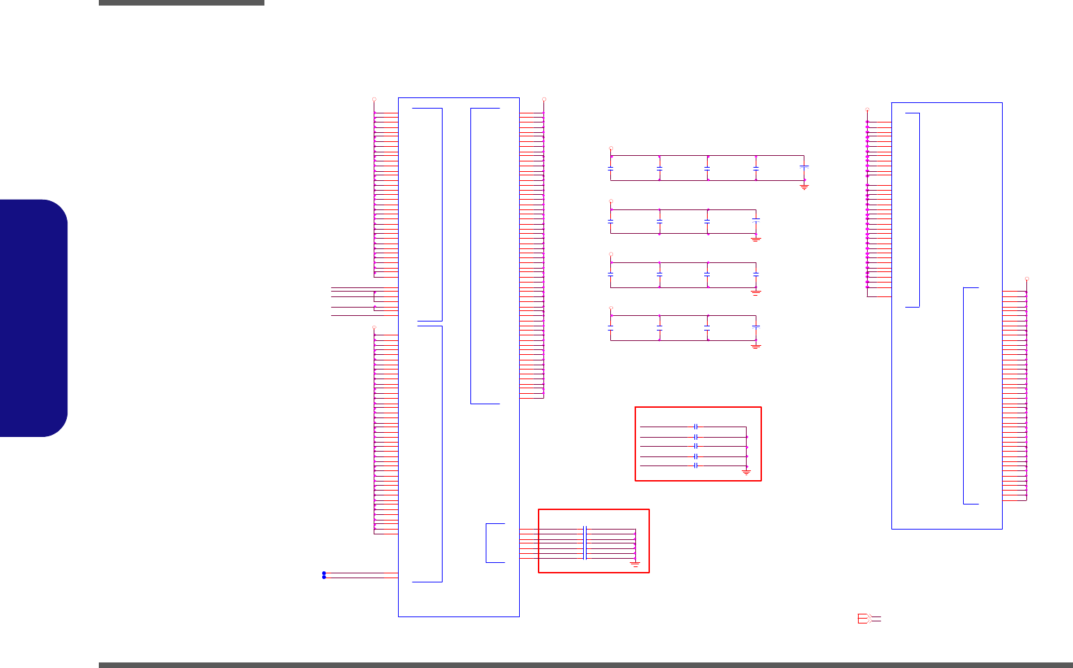
Schematic Diagrams
B - 8 Cantiga 4/6 - Power
B.Schematic Diagrams
Cantiga 4/6 - Power
C127 0.47U_10V_04
8.7A
1.05VS
C62
0.1U_1 0 V_X7 R _ 0 4
1.05VS
VCC_SM_38
C56 0.1U_10V_X7R_04
1.05VS
SM_ LF1
3A
1.05VS[2..5,8,13,16,29]
C63 *0.1U_10V_X7R_04
C52 0.22U_10V_04
1.05VS
C406
10U_6.3V_X5R_08
VCC_SM_38
All trace width are 10mils
All trace width are 10mils
3A
1.05VS
VCC_SM_40
VCC_SM_37
SM_ LF4
CLOSE TO GMCH
C405
10U_6.3V_X5R_08
POWER
VCC NCTF
VCC CORE
U15F
CANTIGA-EB88CTGM
AM3 2
AC 3 0
AJ 2 9
AK25
AA32
Y32
W32
U32
AM3 0
AL30
AK30
AG30
AF3 0
AE30
AL32
W30
V30
AK32
AH 2 9
AG29
AE29
AL28
AK28
AL26
AK26
AJ 3 2
AK24
AH 3 2
AG32
AE32
AC 3 2
AC 2 9
AA29
Y29
W29
V29
U30
AL29
AK29
AH 3 0
AB30
AA30
Y30
AG34
AC 34
AB 34
AA 34
Y34
V34
U34
AM33
AK 33
AJ33
AG33
AF 33
AE 33
AC 33
AA 33
Y33
W33
V33
U33
AH 28
AF 28
AC 28
AA 28
AJ26
AG26
AE 26
AC 26
AH 25
AG25
AF 25
AG24
AJ23
AH 23
AF 23
T32
AK23
VC C_NCTF_1
VC C _NCTF_20
VC C _NCTF_29
VC C _NCTF_42
VC C_NCTF_9
VC C _NCTF_10
VC C _NCTF_11
VC C _NCTF_12
VC C _NCTF_13
VC C _NCTF_14
VC C _NCTF_15
VC C _NCTF_17
VC C _NCTF_18
VC C _NCTF_19
VC C_NCTF_2
VC C _NCTF_24
VC C _NCTF_25
VC C_NCTF_3
VC C _NCTF_30
VC C _NCTF_31
VC C _NCTF_32
VC C _NCTF_38
VC C _NCTF_39
VC C _NCTF_40
VC C _NCTF_41
VC C_NCTF_4
VC C _NCTF_43
VC C_NCTF_5
VC C_NCTF_6
VC C_NCTF_7
VC C_NCTF_8
VC C _NCTF_33
VC C _NCTF_34
VC C _NCTF_35
VC C _NCTF_36
VC C _NCTF_37
VC C _NCTF_26
VC C _NCTF_27
VC C _NCTF_28
VC C _NCTF_16
VC C _NCTF_21
VC C _NCTF_22
VC C _NCTF_23
VC C_1
VC C_2
VC C_3
VC C_4
VC C_5
VC C_6
VC C_7
VC C_8
VC C_9
VC C_10
VC C_11
VC C_12
VC C_13
VC C_14
VC C_15
VC C_16
VC C_17
VC C_18
VC C_19
VC C_20
VC C_21
VC C_22
VC C_23
VC C_24
VC C_25
VC C_26
VC C_27
VC C_28
VC C_29
VC C_30
VC C_31
VC C_32
VC C_33
VC C_34
VC C_35
VC C _NCTF_44
C78
1U_6.3V_04
C94
0.1U_10V_X7R_04
C69
1U_6.3V_X5R_06
C59
10U_6.3V_X5R_08
C77
10U_6.3V_X5R_08
C420
*220U_4V_D
VCC_SM_36
C58 0.1U_10V_X7R_04
SM_ LF2
C407
0.01U_16V_X7R_04
V SS_ AXG_ SEN SE
C117
0.1U_10V_X7R_04
1.8V
C85
0.1U_1 0 V_X7 R _ 0 4
1.05VS
C65 *0.1U_10V_X7R_04
C76
0.47U_10V_04
VCC_SM_37
C114 1U_6.3V_X5R_06
VCC_SM_42
SM_ LF3
1.05VS
C409
150U_4V_B2
C113 *0.1U_10V_X7R_04
SM_ LF7
C64 *0.1U_10V_X7R_04
VCC _ AXG_SENSE
VCC_SM_42
C73 *0.1U_10V_X7R_04
C68
*330U_2. 5V_D3
1.8V
POWER
VCC SMVCC GFX
VCC GFX NCTF
VCC SM LF
U15G
CANTIGA-EB88CTGM
AY 32
BF31
AW 2 9
BD 3 2
BC 3 2
BB32
BA32
AW 3 2
AV32
AU 3 2
AT3 2
AR 3 2
AP32
AN 3 2
BH 3 1
BG31
AN 3 3
BG30
BH 2 9
BG29
BF29
BD 2 9
BC 2 9
BB29
BA29
AY 29
BH 3 2
AV29
AU 2 9
AT2 9
AR 2 9
V23
AM21
AL21
AK21
W21
V21
U21
AM20
AK20
W20
V28
U20
AM19
AL19
AK19
AJ 1 9
AH 19
AG19
AF1 9
AE19
AB19
W26
AA19
Y19
W19
V19
U19
AM17
AK17
AH 17
AG17
AF1 7
V26
AE17
AC 17
AB17
Y17
W17
V17
AM16
AL16
AK16
AJ 1 6
W25
AH 16
AG16
AF1 6
AE16
AC 16
AB16
AA16
V25
W24
V24
W23
AP29
BG32
BF32
W28AP33
Y26
AE25
AB25
AA25
AE24
AC 2 4
AA24
Y24
AE23
AC 2 3
AB23
AA23
AJ 2 1
AG21
AE21
AC 2 1
AA21
Y21
AH 2 0
AF20
AE20
AC 2 0
AB20
AA20
T17
AM1 5
AL15
AJ 1 5
AH 1 5
AF15
AB15
AV44
BA37
AM40
AV21
AY 5
AM10
BB13
T16
AG15
AA15
Y15
V15
U15
AN 1 4
AM1 4
U14
T14
AJ 1 4
AH 1 4
Y16
W16
V16
U16
BA36
BB24
BD 1 6
BB21
AW 1 6
AW 1 3
AT1 3
AE15
VC C _SM_10
VC C _SM_20
VC C _SM_30
VC C _SM_6
VC C _SM_7
VC C _SM_8
VC C _SM_9
VC C _SM_11
VC C _SM_12
VC C _SM_13
VC C _SM_14
VC C _SM_15
VC C _SM_16
VC C _SM_17
VC C _SM_18
VC C _SM_19
VC C _SM_2
VC C _SM_21
VC C _SM_22
VC C _SM_23
VC C _SM_24
VC C _SM_25
VC C _SM_26
VC C _SM_27
VC C _SM_28
VC C _SM_29
VC C _SM_3
VC C _SM_31
VC C _SM_32
VC C _SM_33
VC C _SM_34
VC C _AXG_NCTF_10
VC C _AXG_NC
TF_11
VC C _AXG_NCTF_12
VC C _AXG_NCTF_13
VC C _AXG_NCTF_14
VC C _AXG_NCTF_15
VC C _AXG_NCTF_16
VC C _AXG_NCTF_17
VC C _AXG_NCTF_18
VC C _AXG_NCTF_19
VC C_AXG_NCTF_2
VC C _AXG_NCTF_20
VC C _AXG_NCTF_21
VC C _AXG_NCTF_22
VC C _AXG_NCTF_23
VC C _AXG_NCTF_24
VC C _AXG_NCTF_25
VC C _AXG_NCTF_26
VC C _AXG_NCTF_27
VC C _AXG_NCTF_28
VC C _AXG_NCTF_29
VC C_AXG_NCTF_3
VC C _AXG_NCTF_30
VC C _AXG_NCTF_31
VC C _AXG_NCTF_32
VC C _AXG_NCTF_33
VC C _AXG_NCTF_34
VC C _AX
G_NCTF_35
VC C _AXG_NCTF_36
VC C _AXG_NCTF_37
VC C _AXG_NCTF_38
VC C _AXG_NCTF_39
VC C_AXG_NCTF_4
VC C _AXG_NCTF_40
VC C _AXG_NCTF_41
VC C _AXG_NCTF_42
VC C _AXG_NCTF_43
VC C _AXG_NCTF_44
VC C _AXG_NCTF_45
VC C _AXG_NCTF_46
VC C _AXG_NCTF_47
VC C _AXG_NCTF_48
VC C _AXG_NCTF_49
VC C_AXG_NCTF_5
VC C _AXG_NCTF_50
VC C _AXG_NCTF_51
VC C _AXG_NCTF_52
VC C _AXG_NCTF_53
VC C _AXG_NCTF_54
VC C _AXG_NCTF_55
VC C _AXG_NCTF_56
VC C_AXG_NCTF_6
VC C_AXG_NCTF_7
VC C_AXG_NCTF_8
VC C_AXG_NCTF_9
VC C _SM_35
VC C _SM_4
VC C _SM_5
VC C_AXG_NCTF_1VC C _SM_1
VC C _AXG_1
VC C _AXG_2
VC C _AXG_3
VC C _AXG_4
VC C _AXG_5
VC C _AXG_6
VC C _AXG_7
VC C _AXG_8
VC C _AXG_9
VC C _AXG_10
VC C _AXG_11
VC C _AXG_12
VC C _AXG_13
VC C _AXG_14
VC C _AXG_15
VC C _AXG_16
VC C _AXG_17
VC C _AXG_18
VC C _AXG_19
VC C _AXG_20
VC C _AXG_21
VC C _AXG_22
VC C _AXG_23
VC C _AXG_24
VC C _AXG_25
VC C _AXG_27
VC C _AXG_28
VC C _AXG_30
VC C _AXG_31
VC C _AXG_33
VC C _AXG_34
VC C_SM_LF1
VC C_SM_LF2
VC C_SM_LF3
VC C_SM_LF4
VC C_SM_LF5
VC C_SM_LF6
VC C_SM_LF7
VC C _AXG_26
VC C _AXG_32
VC C _AXG_35
VC C _AXG_36
VC C _AXG_37
VC C _AXG_38
VC C _AXG_39
VC C _AXG_40
VC C _AXG_41
VC C _AXG_42
VC C _AXG_SE NSE
VS S_AXG_SENSE
VC C _AXG_NCTF_57
VC C _AXG_NCTF_58
VC C _AXG_NCTF_59
VC C _AXG_NCTF_60
VC C _SM_36/NC
VC C _SM_37/NC
VC C _SM_38/NC
VC C _SM_39/NC
VC C _SM_40/NC
VC C _SM_41/NC
VC C _SM_42/NC
VC C _AXG_29
C60
0.1U_10V_X7R_04
C112
10U_6.3V_X5R_08
C140 1U_6.3V_X5R_06
VCC_SM_40
C72 0.22U_10V_04
SM_ LF6
1.8V[5,8,10,11,30]
SM_ LF5
VCC_SM_36
Sheet 7 of 40
Cantiga 4/6 - Power
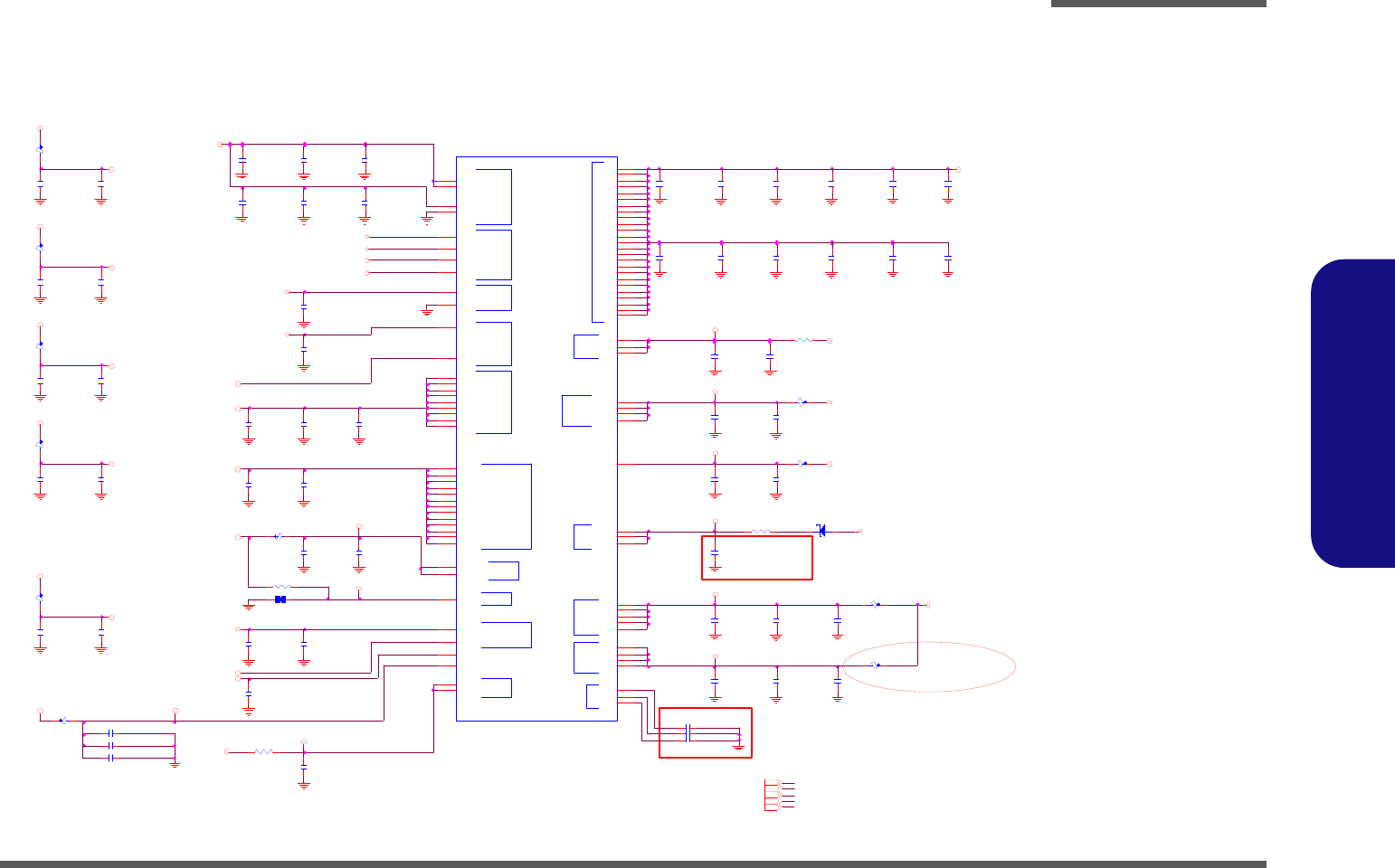
Schematic Diagrams
Cantiga 5/6 - Power B - 9
B.Schematic Diagrams
Cantiga 5/6 - Power
1.05VS[2..5,7,13,16,29]
1.8V[5,7 ,1 0,11 ,3 0 ]
C380
0. 01 U _ 1 6 V _X 7 R _ 0 4
C340
10U_6.3V _X5R_08
C82
0.01U _16V_X7R _04
C5 7
0.1U _10V_X7R _04
C6 35
0.1U_10V_X7R_04
C617
4.7U_6.3V_X5R_06
1.05V M_MPLL
1.05VS
1.5VS
L72
0_0402
L26
HC B1005KF-121T20
12mils
C341
* 10U _6.3V_X5R_08
C4 32
10U_6.3V_X5R_08
D03BCN? ? 0 OHM
1.05VS
C3 9 6
0. 01U_16V_X7R_04
10mils
10mils
1.5VS_Q DAC
3. 3 V S
1.05VS
10mils
C346
0.1U_10V_X7R _04
VC C_ HD A
C48 0. 47U_10V_04
C384
10U _6.3V_X5R _08
C6 6
1U _6.3V_X5R _06
C5 5
0.1U _10V_X7R _04
10mils
30mils
C1 38
1000P_50V_X7R_04
10mils
1.05VS
1.05VS
1.05VM _D PLLB
C415
10U _6.3V_X5R_08
C3 5 2
*0.1U_1 0V_X7R_04
12mils
50mils
C3 8 1
0. 1U _10V_X7R_04
10mils
R2 2 0
0_04
C347
0.1U_10V_X7R _04
C350
1U_6.3V_04
1.05V M_HPLL
L2 4
H C B 10 0 5K F - 12 1 T 20
C 3 61 0. 47 U _ 1 0 V _0 4
C390
0.01U _16V_X7R _04
C3 9 4
0. 1U _10V_X7R_04
C417
0.1U_10V_X7R _04
C 3 48 0. 47 U _ 1 0 V _0 4
10mils
12mils
C339
10U _6.3V_X5R_08
1.8V_LVD S
C3 8 9
0. 1U _10V_X7R_04
C3 4 3
2.2U _6.3V_06
C423
0.1U _10V_X7R _04
1.05VM_ PEG PLL
R 235 10_06
Within 10mils
1.05VS
L7
H C B 10 0 5K F - 12 1 T 20
12mils
1.05VS
C54
0.1U_10V _X7R_04
0. 5 A
10mils
1.5VS
1.05VM_D MI
C6 0 7
1U _6.3V_04
C1 0 9
1U _6.3V_04
10mils
C426 0.1U _10V_X7R _04
L2 3
H C B 10 0 5K F - 12 1 T 20
C3 83
0.1U_10V_X7R_04
C428
0.1U _10V_X7R _04
3.3V S_ATVD AC
C8 1
0. 1U _10V_X7R_04
1. 8 A
C422
0.1U_10V _X7R_04
1.8V_TXLVD S
L28
HC B1608KF-121T25
C338
10U _6.3V_X5R_08
02/12
D17
RB551V-30AC
20mils
C608
1U _6.3V_04
C345
0. 1U _10V_X7R_04
C4 2 4
0. 1U _10V_X7R_04
1.8V
C616
4.7U_6.3V_X5R_06
3.3VS
02/12
C425 0.1U _10V_X7R _04
10mils
R363 *10m il_short
C3 76
1U _6 . 3 V _ X5 R _0 6
1.05VS
1.05VM _AXF
C8 3
0.1U _10V_X7R_04
L9
HC B1005KF-121T20
C397
0. 1U _10V_X7R_04
C133
10U _6.3V_X5R _08
Remove R360
1A
10mils
C4 27
0.1U_10V_X7R_04
C3 51
*0.1U_10V_X7R_04
1.05VM _HPLL
1. 0 5 V S
02/12
10mils
10mils
3.3V S[5 ,9 ..16 ,1 8 ..27 ,3 1 ]
1.05V M_DPLLA
1. 5V S
1.05 VM_ PEG PLL
1.5VS_ QDAC
C393
0.01U _16V_X7R _04
1.05VM _MPLL
C3 44
* 1 U _ 6. 3V _ X 5R _ 06
1.05VM_DPLLA
1.8V
02/12
C1 4 3
1000P_50V_X7R _04
L3 0
H C B 10 0 5K F - 12 1 T 20
C342
1U_6.3V_X5R_06
10mils
1.05VS
C431 10U _6.3V_X5R _08
C3 72
*1 0U _6 .3 V _ X5 R _0 8
1.05VM_PEG[5 ]
1.05V M_DPLLB
C606
1U _6.3V_04
1.05VS
L29 H CB1005KF-121T20
C429
0.1U_10V_X7R _04
Close to U15
10mils
3.3VS_ATVDAC
L2 7
H C B 10 0 5K F - 12 1 T 20
C430
10U _6.3V_X5R_08
1.8V_SMC K
1.8V_TXLVDS
1.5V S[3,13,14,16,19,20,29]
C349
0.1U_10V _X7R_04
C433
10U_6.3V _X5R_08
L71
HC B1005KF-121T20
R362 * 0_04
R 393 0_04
POWER
CRTPLLA PEGA SM
DT V/ CRT
LVDS
VT TL F VTT
A LVDSHDA
AX FDM I PE G
A CK
TV
SM CK
HV
U15H
C ANTIGA -EB88 C TG M
V3
U3
V2
U2
AD 48
AA48
B27
A26
F47
L48
AD1
J48
AE1
B24
A24
AA47
U6
T6
U5
T5
T8
U7
T7
AF1
U13
T13
T12
U11
T11
U10
T10
U9
T9
U8
U12
AP28
AN 28
A25
M25
A8
L1
AB 2
AH 48
AF 48
BF 21
BH 20
BG 20
BF 20
M38
L28
B22
B21
A21
AR 20
AP20
AN 20
AR 17
AP17
AT16
AR 16
AP16
K47
J47
C35
B35
V48
L37
U48
V47
U47
U46
AN 17
AP25
AN 25
AN 24
AM 28
AM 26
AM 25
AL25
AM 24
AL24
AM 23
T2
V1
U1
A35
AH 47
AG 47
B25
AL23
A32
VTT_19
VTT_20
VTT_21
VTT_22
VC CA_PEG_BG
VC CA_PEG_PLL
VC CA_CR T_D AC_1
VC CA_CR T_D AC_2
VC CA_DPLLA
VC CA_DPLLB
VC CA_HPLL
VC CA_ L VDS
VC CA_MPLL
VC CA_ TV_D AC_ 1
VC CA_ TV_D AC_ 2
VC CD_PEG _P LL
VTT_15
VTT_16
VTT_17
VTT_18
VTT_12
VTT_13
VTT_14
VC CD_ H PLL
VTT_1
VTT_2
VTT_4
VTT_5
VTT_6
VTT_7
VTT_8
VTT_9
VTT_10
VTT_11
VTT_3
VC CA_ S M_ CK _1
VC CA_ S M_ CK _2
VC CA_DAC _B G
VC CD_ T VDAC
VTTLF 1
VTTLF 2
VTTLF 3
VC C_ DM I_ 1
VC C_ DM I_ 2
VCC_ SM _C K_ 1
VCC_ SM _C K_ 2
VCC_ SM _C K_ 3
VCC_ SM _C K_ 4
VC CD_LVDS_1
VC CD_Q DAC
VC C_AXF_1
VC C_AXF_2
VC C_AXF_3
VC CA_SM_ 1
VC CA_SM_ 2
VC CA_SM_ 3
VC CA_SM_ 4
VC CA_SM_ 5
VC CA_SM_ 7
VC CA_SM_ 8
VC CA_SM_ 9
VC C_ T X_ L V DS
VSSA_L VDS
VCC _H V_1
VCC _H V_2
VCC _PEG _ 1
VC CD_LVDS_2
VCC _PEG _ 2
VCC _PEG _ 3
VCC _PEG _ 4
VCC _PEG _ 5
VC CA_SM_ 6
VC CA_ S M_ CK _3
VC CA_ S M_ CK _4
VC CA_ S M_ CK _5
VC CA_ S M_ CK _N CTF _ 1
VC CA_ S M_ CK _N CTF _ 2
VC CA_ S M_ CK _N CTF _ 3
VC CA_ S M_ CK _N CTF _ 4
VC CA_ S M_ CK _N CTF _ 5
VC CA_ S M_ CK _N CTF _ 6
VC CA_ S M_ CK _N CTF _ 7
VTT_23
VTT_24
VTT_25
VCC _H V_3
VC C_ DM I_ 3
VC C_ DM I_ 4
VSSA_D AC_BG
VC CA_ S M_ CK _N CTF _ 8
VC C_ HD A
1.05VM_ PEG
1.8V
1.05VS
Sheet 8 of 40
Cantiga 5/6 - Power
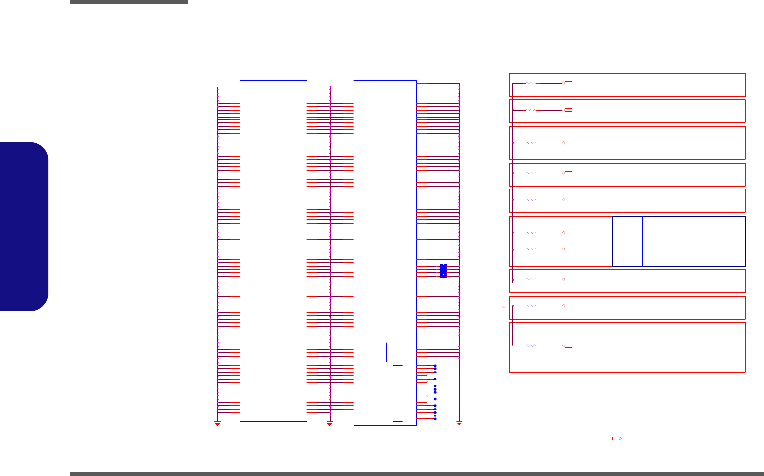
Schematic Diagrams
B - 10 Cantiga 6/6 - GND
B.Schematic Diagrams
Cantiga 6/6 - GND
XOR Mode Enable
Disable
LO W
R40 * 2.2K_1%_04
Lanes Reversed
R3 8 * 1 0m il_ s hort
DMI Lane Reversal
LO W
MCH_CFG13
Reserved
LOW
MC H_ CF G 1 3 [5]
R37 * 2.2K_1%_04
LOW :
HIGH:
EnableHIGH:
MC H_ CF G 1 9 [5]
Nomal Operation
R3 9 2 .2 K_ 1% _ 0 4
HI G H
Enable
Normal operation
PCIE Loopback Enable
MC H_ CF G 1 0 [5]
HIGH
R34 * 2.2K_1%_04
LOW :
DMI=4
iTPM Host Interface
R228 * 2.2K_1%_04
ATM Firmware use TLS cipher
suite with no
confidentiality
Disable
Default
LOW :
HIGH:
3.3VS
HIGH:
R31 * 2.2K_1%_04
MCH_CFG12
ATM Firmware use TLS cipher
suite with confidentiality
MC H_ CF G 7 [5 ]
Reverse Lane
Default
Digital Display Port
All-Z Mode Enable
R33 * 2.2K_1%_04
HIGH
MC H_ CF G 1 6 [5]
R4 6 * 1 0m il_ s hort
VSS
U15I
C ANTIG A-EB88C TG M
AU 48
A23
AR 48
AL48
BB47
AW47
AN 47
AJ 47
AF47
AD 47
AB47
Y47
T47
N47
L47
G47
BD 46
BA46
AV46
AR 46
AM 46
V46
R46
P46
H46
F46
BF44
AH 44
AD 44
AA44
Y44
U44
T44
M44
F44
BC 43
AV43
AU 43
AM 43
J43
C43
BG 42
AY 42
AT42
AN 42
AJ 42
AE42
N42
L42
BD 41
AU 41
AM 41
AH 41
AD 41
AA41
Y41
U41
T41
M41
G41
B41
BG 40
BB40
AV40
AN 40
H40
E40
AT39
AM 39
AJ 39
AE39
N39
L39
B39
BH 38
BC 38
BA38
AU 38
AH 38
AD 38
AA38
Y38
U38
T38
J38
F38
C38
BD 36
AM3 6
AE36
P36
L36
J36
F36
B36
AH35
AA35
Y35
U3 5
T35
BF3 4
AM3 4
AJ 34
AF3 4
AE34
W34
B34
A34
BG33
BC33
BA33
AV33
AR33
AL33
AH33
AB33
P33
L33
H3 3
N3 2
K32
F32
C3 2
A31
AN29
T29
N2 9
K29
H2 9
F29
A29
BG28
BD28
BA28
AV28
AT28
AR28
AJ 28
AG28
AE28
AB28
Y28
P28
K28
H2 8
F28
C2 8
BF2 6
AH26
AF2 6
AB26
AA26
C2 6
B26
BH25
BD25
BB25
AV25
AR25
AJ 25
AC25
Y25
N2 5
L25
J25
G2 5
E25
BF2 4
BF37
BB37
AW37
AT37
AN 37
AJ 37
H37
C37
BG 36
AU 36
AT24
AH24
AB24
L24
AY 46
G2 4
E24
AG23
B23
AY24
AJ 24
AF2 4
R2 4
K24
J24
F24
BH23
Y23
AK15
AD12
AJ 6
VSS_1
VSS_198
VSS_2
VSS_3
VSS_4
VSS_5
VSS_6
VSS_7
VSS_8
VSS_9
VSS_1 0
VSS_1 1
VSS_1 2
VSS_1 3
VSS_1 4
VSS_1 5
VSS_1 6
VSS_1 7
VSS_1 9
VSS_2 0
VSS_2 1
VSS_2 2
VSS_2 3
VSS_2 4
VSS_2 5
VSS_2 6
VSS_2 7
VSS_2 8
VSS_2 9
VSS_3 0
VSS_3 1
VSS_3 2
VSS_3 3
VSS_3 4
VSS_3 5
VSS_3 6
VSS_3 7
VSS_3 8
VSS_3 9
VSS_4 0
VSS_4 1
VSS_4 2
VSS_4 3
VSS_4 4
VSS_4 5
VSS_4 6
VSS_4 7
VSS_4 8
VSS_4 9
VSS_5 0
VSS_5 1
VSS_5 2
VSS_5 3
VSS_5 4
VSS_5 5
VSS_5 6
VSS_5 7
VSS_5 8
VSS_5 9
VSS_6 0
VSS_6 1
VSS_6 2
VSS_6 3
VSS_6 4
VSS_6 5
VSS_6 6
VSS_6 7
VSS_6 8
VSS_6 9
VSS_7 0
VSS_7 1
VSS_7 2
VSS_7 3
VSS_7 4
VSS_7 5
VSS_7 6
VSS_7 7
VSS_7 8
VSS_7 9
VSS_8 0
VSS_8 1
VSS_8 2
VSS_8 3
VSS_8 4
VSS_8 5
VSS_8 6
VSS_8 7
VSS_9 7
VSS_100
VSS_101
VSS_102
VSS_103
VSS_104
VSS_105
VSS_106
VSS_107
VSS_108
VSS_109
VSS_110
VSS_111
VSS_112
VSS_113
VSS_114
VSS_115
VSS_116
VSS_117
VSS_118
VSS_119
VSS_120
VSS_121
VSS_122
VSS_123
VSS_124
VSS_125
VSS_126
VSS_127
VSS_128
VSS_129
VSS_130
VSS_131
VSS_132
VSS_133
VSS_134
VSS_135
VSS_136
VSS_137
VSS_138
VSS_139
VSS_140
VSS_141
VSS_142
VSS_143
VSS_144
VSS_145
VSS_146
VSS_147
VSS_148
VSS_149
VSS_150
VSS_151
VSS_152
VSS_153
VSS_154
VSS_155
VSS_156
VSS_157
VSS_158
VSS_159
VSS_160
VSS_161
VSS_162
VSS_163
VSS_164
VSS_165
VSS_166
VSS_167
VSS_168
VSS_169
VSS_170
VSS_171
VSS_172
VSS_173
VSS_174
VSS_175
VSS_176
VSS_177
VSS_178
VSS_179
VSS_8 8
VSS_8 9
VSS_9 0
VSS_9 1
VSS_9 2
VSS_9 3
VSS_9 4
VSS_9 5
VSS_9 6
VSS_9 9
VSS_182
VSS_184
VSS_186
VSS_188
VSS_1 8
VSS_191
VSS_193
VSS_195
VSS_197
VSS_181
VSS_183
VSS_185
VSS_187
VSS_189
VSS_190
VSS_192
VSS_194
VSS_196
VSS_9 8
VSS_180
VSS_199
Default
Intel Management Engine Crypto Strap
PCIE Graphics Lane
MC H_ CF G 6 [5 ]
MC H_ CF G 9 [5 ]
Default
HIGH:
MC H_ CF G 5 [5 ]
Default
Default
R5 6 * 1 0m il_ s hort
MC H_ CF G 1 2 [5]
Normal
LOW :
LOW :
R4 1 * 1 0m il_ s hort
Digital Display Port
(SDVO/DP/iHDMI) and PCIE
are operational simultaneously
via PEG port
Default
Disable
R36 * 2.2K_1%_04
R51 * 4.02K_1% _04
DMI X2 Select
LOW :
HIGH:
Enable
Default
FSB Dynamic ODT
HI G H
Only Digital Display Port
(SDVO/DP/iHDMI) or PCIE
is operational
Default
VSS
VS S NCT F
VSS SCB
NC
U15J
CANTIGA-EB88CTGM
BG 21
AW21
AU 21
AP21
AN 21
AH 21
AF21
AB21
R21
M21
J21
G21
BC 20
BA20
AW20
AT20
AJ2 0
AG 20
Y20
N20
K20
F20
C20
A20
BG 19
A18
BG 17
BC 17
AW17
AT17
R17
M17
H17
C17
BA16
AU 16
AN 16
N16
K16
G16
E16
BG 15
W15
A15
BG 14
AA14
C14
BG 13
BC 13
BA13
AN 13
AJ1 3
AE13
N13
L13
G13
E13
BF12
AV12
AT12
AM 12
AA12
J12
A12
BD 11
BB11
AY 11
AN 11
AH 11
Y11
N11
G11
C11
BG 10
AV10
AT10
AJ1 0
AE10
AA10
BH 8
B9
G9
AD 9
AM 9
AN 9
BC 9
M10
BF 9
AH8
Y8
L8
E8
B8
AY7
AU7
AN7
AJ7
AE7
AA7
N7
J7
BG6
BD6
AV6
AT6
AC 15
AM6
M6
C6
BA5
AH5
AD5
Y5
L5
J5
H5
F5
BE4
BC3
AV3
AL3
AF32
AB32
V32
AJ30
AM29
AF29
AB29
U26
U23
AL20
V20
AC19
AL17
AJ17
AA17
U17
BH48
BH1
A48
C1
A3
E1
D2
C3
B4
A5
A6
A43
A44
B45
C46
D47
B47
A46
F48
E48
C48
B48
R3
P3
BA2
AR2
AU2
AP2
F3
AW2
AE2
AF2
AH2
AJ2
AD2
AC2
Y2
M2
K2
AM1
AA1
P1
H1
BB 8
AV 8
AT8
U24
U28
U25
U29
L12 VS S_19 9
VS S_20 1
VS S_20 2
VS S_20 3
VS S_20 4
VS S_20 5
VS S_20 6
VS S_20 7
VS S_20 8
VS S_20 9
VS S_21 0
VS S_21 1
VS S_21 2
VS S_21 3
VS S_21 4
VS S_21 5
VS S_21 6
VS S_21 7
VS S_21 8
VS S_21 9
VS S_22 0
VS S_22 1
VS S_22 2
VS S_22 3
VS S_22 4
VS S_22 5
VS S_22 6
VS S_22 7
VS S_22 8
VS S_22 9
VS S_23 0
VS S_23 1
VS S_23 2
VS S_23 3
VS S_23 5
VS S_23 7
VS S_23 8
VS S_23 9
VS S_24 0
VS S_24 1
VS S_24 2
VS S_24 3
VS S_24 5
VS S_24 6
VS S_24 7
VS S_24 8
VS S_24 9
VS S_25 0
VS S_25 1
VS S_25 2
VS S_25 5
VS S_25 6
VS S_25 7
VS S_25 8
VS S_25 9
VS S_26 0
VS S_26 1
VS S_26 2
VS S_26 3
VS S_26 4
VS S_26 5
VS S_26 6
VS S_26 7
VS S_26 8
VS S_26 9
VS S_27 0
VS S_27 1
VS S_27 2
VS S_27 3
VS S_27 5
VS S_27 6
VS S_27 7
VS S_27 8
VS S_27 9
VS S_28 0
VS S_28 1
VS S_28 2
VS S_28 3
VS S_28 4
VS S_29 3
VS S_29 2
VS S_29 1
VS S_29 0
VS S_28 9
VS S_28 8
VS S_28 7
VS S_28 5
VS S_28 6
VS S_297
VS S_298
VS S_299
VS S_300
VS S_301
VS S_302
VS S_303
VS S_304
VS S_305
VS S_306
VS S_307
VS S_308
VS S_309
VS S_310
VS S_311
VS S_312
VS S_313
VS S_24 4
VS S_314
VS S_315
VS S_316
VS S_317
VS S_318
VS S_319
VS S_320
VS S_321
VS S_322
VS S_323
VS S_324
VS S_325
VS S_327
VS S_328
VS S_329
VSS_NCTF_1
VSS_NCTF_2
VSS_NCTF_3
VSS_NCTF_4
VSS_NCTF_5
VSS_NCTF_6
VSS_NCTF_7
VSS_NCTF_8
VSS_NCTF_9
VSS_NC TF_10
VSS_NC TF_11
VSS_NC TF_12
VSS_NC TF_13
VSS_NC TF_14
VSS_NC TF_15
VSS_NC TF_16
VSS_S CB_1
VSS_S CB_2
VSS_S CB_3
VSS_S CB_4
VSS_S CB_5
N C_26
N C_27
N C_28
N C_29
N C_30
N C_31
N C_32
N C_33
N C_34
N C_35
N C_36
N C_37
N C_38
N C_39
N C_40
N C_41
N C_42
VS S_330
VS S_331
VS S_333
VS S_336
VS S_335
VS S_337
VS S_332
VS S_334
VS S_341
VS S_340
VS S_339
VS S_338
VS S_342
VS S_343
VS S_344
VS S_345
VS S_346
VS S_347
VS S_348
VS S_349
VS S_350
VS S_29 4
VS S_29 5
VS S_29 6
VS S_351
VS S_352
VS S_353
VS S_354
VS S_20 0
MC H_ CF G 2 0 [5]
HIGH:
LOW
3.3V S[5,8 ,1 0 .. 16 ,1 8. .27 ,3 1]
LOW :
HIGH:
DMI=2
Configuration
R50 * 4.02K_1% _04
LOW :
Sheet 9 of 40
Cantiga 6/6 - GND
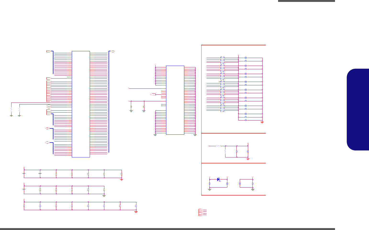
Schematic Diagrams
DDRII CHANNEL A B - 11
B.Schematic Diagrams
DDRII CHANNEL A
Sheet 10 of 40
DDRII CHANNEL A
VDD SPD
C1 1 1
1U_6.3V_04
JDIMM_1 Terminator
M_A_A6
M _A_A11
M_CS#1
M_ A _D Q2 9
M_ A _D Q6 1
M_ A _D Q5 6
C47
0.1U_16V_04
M _A_D QS#3
C163
*1 50 U _4 V _ B2
RN 1
8P4R X56_04
1
2
3
4 5
6
7
8
C8 9 0 .1 U_ 10 V _ X7 R _0 4
M_ A _D Q2 8
M _A_D QS0
RN 20
8P4R X56_04
1
2
3
4 5
6
7
8
R2 7
10 K _ 04
M _A_A4
M_A_D M3
M _A_A0
M _ABS2
M_ A _D Q4 1
R28
10K_04
D8
RB5 5 1 V-30
A C
C103 0.1U_10V_X7R _04
M_A_A2
M_ A _D Q2
M _A_A1
C152 1U_6.3V_04
SA 0_ DIM 0
C147 0.1U_10V_X7R _04
SO-DIMM 1
M_A_DQS[7:0][6]
R8 1
1K_1% _04
C106 0.1U_10V_X7R _04
M_ CS # 1
M_ A _ DQS# [7 :0 ][6]
M_A_A1
M_ A _D Q9
C129 0.1U_10V_X7R _04
M_ A _D Q4 2
M _A_A7
M _A_D QS#6
M_A_A4
M_ A _D Q4 6
M_ A _D Q4 3
M_ C K E 1[5 ]
M _A_ DM [7 :0][6 ]
M_ABS0
1.8V
ICH_ SMBC L K0[1 1,1 5 ,18 ]
M_A_A8
M_ A _D Q2 5
M_ A _D Q3 8
M_CLK_DDR0[5 ]
M _A_D QS4
M _A_D QS5
C1 3 0
10U _6.3V_X5R_08
C121 0.1U_10V_X7R _04
M_ A _D Q2 4
C8 6
10U _6.3V_X5R_08
M_ABS1[6 ]
M_ O D T 1
C125 0.1U_10V_X7R _04
M_ODT0
M_ A _D Q1 7
M_ A _D Q2 0
M_ A _D Q5
M _A_D QS2
M_ A _D Q6 2 C176
1U _6 . 3 V _ 04
VD DSPD[1 1 ]
M_ A _D Q4 8
M_ A _D Q3 4
M_A_CAS#[6 ]
M_ A _D Q4 5
0.9VSM
M_ A _D Q1 6
M_ A _D Q5 3
C174
0.1U_10V_X7R _04
M_ABS2[6 ]
M_A_D M0
RN 17
8P4R X56_04
1
2
3
4 5
6
7
8
C135
1U_6.3V_04
M_ A _D Q1 9
C1 6 7
2.2U _6.3V_06
RN 5
8P4R X56_04
1
2
3
4 5
6
7
8
M_ C K E 0[5 ]
M_A_A9
M_ A _D Q2 2
M_ CL K_ DD R# 1[5]
M _A_A12
M_ A _D Q1 0
M_ C S #1[5 ]
C90
0.1U _10V_X7R_04
RN 3
8P4R X56_04
1
2
3
4 5
6
7
8
C149
*0.22U_16V_X7R_06
M_ C K E 0
M_ A _D Q3 7
M_ C S #0[5 ]
M_A_A7
MVREF_DIM0
M_A_WE#[6 ]
M_ A _D Q5 9
M _A_A2
M_ C K E 1
M_A_A11
SA 1_ DIM 0
C87 10U_6.3V_X5R _08
M_CKE1
M_ A _D Q3 1
M_A_D M4
C3 9 1
0.1U _10V_X7R_04
M_ A_ A [1 4:0 ][6 ]
M_A_D M2
20mils
M _A_A10
M _ABS0
M_ A _D Q3 3
M_ A _D Q5 7
C1 3 9
*0.22U_16V_X7R _06
C382
22 0 U _ 4 V _D
M_ O D T 0
M_A_D M6
M_ A _D Q5 1
M_ A _D Q1 4
M_ A _D Q8
M _A_DQ [63:0] [6]
3.3VS
M_ A _ R A S #
C9 8 0 .1 U_ 10 V _ X7 R _0 4
20mils
CLOSE TO JDIMM_1
M _A_A6
1.8V
M _A_A9
0.9VSM
PM_ EXTTS_DD R#[5 ,1 1]
M_A_A13
M_ A _D Q3 6
RN 7
8P4R X56_04
1
2
3
4 5
6
7
8
C142 0.1U_10V_X7R _04
Layout note:
M _A_D QS1
C173
0.1U_10V_X7R_04
M _A_A5
M_A_D M7
M_ A _D Q6 3
C154
10U_10V_08
M_ A _D Q5 0
M_ A _D Q5 5
C101 0.1U_10V_X7R _04
M _A_D QS#4
3.3VS[5 ,8 ,9,1 1 ..1 6,1 8 ..27 ,3 1 ]
C1 3 6
0. 1U _1 0 V _X 7 R _ 0 4
C1 4 5
1U_6.3V_04
C144
0.1U_10V_X7R _04
M_CS#0
M_ A _D Q3 9
M_ A _D Q3 5
J D IMM_ 1 B
AS 0A421-N 2R N-4F
112
111
117
96
95
118
81
82
87
103
88
104
199
83
120
50
69
163
1
201
202
47
133
183
77
12
48
184
78
71
72
121
122
196
193
8
18
24
41
53
42
54
59
65
60
66
127
139
128
145
165
171
172
177
187
178
190
9
21
33
155
34
132
144
156
168
2
3
15
27
39
149
161
28
40
138
150
162
VD D1
VD D2
VD D3
VD D4
VD D5
VD D6
VD D7
VD D8
VD D9
VD D10
VD D11
VD D12
VD DSPD
NC1
NC2
NC3
NC4
N CTEST
VR EF
GND0
GND1
VSS1
VSS2
VSS3
VSS4
VSS5
VSS6
VSS7
VSS8
VSS9
VSS10
VSS11
VSS12
VSS13
VSS14
VSS15
VSS16
VSS17
VSS18
VSS19
VSS20
VSS21
VSS22
VSS23
VSS24
VSS25
VSS26
VSS27
VSS28
VSS29
VSS30
VSS31
VSS32
VSS33
VSS34
VSS35
VSS36
VSS37
VSS38
VSS39
VSS40
VSS41
VSS42
VSS43
VSS44
VSS45
VSS46
VSS47
VSS48
VSS49
VSS50
VSS51
VSS52
VSS53
VSS54
VSS55
VSS56
VSS57
M_ A _D Q1
M_ A _D Q3 0
M_ A _D Q5 4
M_ABS2
M_A_A3
M _A_D QS#7
C161
*1 50 U _4 V _ B2
M_ A _D Q3
M_ CL K_ DD R# 0[5]
M_ A _D Q1 8
1.8V
1.8V
CLOSE TO JDIMM_1
M_ O D T 1[5 ]
0.9VSM[11,30]
M_A_A0
C1 1 9
4.7U _6.3V_X5R_06
C1 4 8
10 U _1 0 V _0 8
M_ A _D Q0
C115 0.1U_10V_X7R _04
C124
0.1U _10V_X7R_04
M_ABS0[6 ]
M_ A _D Q2 3
M_ A _ C A S #
M_ A _D Q2 6
M_ A _D Q4 0
M_ A _D Q1 2
M_A_D M1
M _A_D QS#0
M_ A _D Q4
M_A_A5
1.8V[5,7,8,11,30]
M_ A _D Q4 7
M _A_A14
M _A_C AS#
M_ A _D Q5 8
M_ A _D Q1 1
M_ O D T 0[5 ]
M _A_D QS#2
M_ A _D Q5 2
C110
0.1U _10V_X7R _04
C9 1
0.1U _10V_X7R_04
1.8V
MVREF_DIM0
ICH_SMBD AT0[1 1,1 5 ,18 ]
R8 0 1 K_ 1% _ 04
M_A_A14
M_A_A12
M _A_A3
M _A_D QS3
M _A_D QS6
M_ A _D Q4 4
M _ABS1
M_ A _D Q1 5
M _A_D QS#5
C132 0.1U_10V_X7R _04
VD DSPD
M_A_A10
M_ A _D Q1 3
C137 0.1U_10V_X7R _04
M_ A _D Q2 7
M_ODT1
RN 16
8P4R X56_04
1
2
3
4 5
6
7
8
M_A_RAS#[6 ]
C9 3 0 .1 U_ 10 V _ X7 R _0 4
Pl ac e o ne c ap clo se to ev er y 2 pu ll -u p r esi stors
terminated to +VTT_MEM
M_CLK_DDR1[5 ]
M_ CS # 0
M _A_A13
M_ A _D Q7
M_A_WE#
M_ A _ W E #
M_A_D M5
M_ A _D Q6
M_ A _D Q2 1
C1 5 3
10 U _6 . 3 V _X 5 R _ 0 8
M_ABS1
C1 0 0
4.7U _6.3V_X5R_06
C46
*2.2U_6.3V_06
M _A_A8
M_ A _D Q4 9
M_ A _D Q3 2
C9 7 0 .1 U_ 10 V _ X7 R _0 4
M_CKE0
C1 2 3
0.1U _10V_X7R_04
M _A_D QS#1
M _A_R AS#
J D IMM_ 1 A
AS0A421-N2RN-4F
102
101
100
99
98
97
94
92
93
91
105
90
89
116
86
84
85
5
7
17
19
4
6
14
16
23
25
35
37
20
22
36
38
43
45
55
57
44
46
56
58
61
63
73
75
62
64
74
76
123
125
135
137
124
126
134
136
141
143
151
153
140
142
152
154
157
159
173
175
158
160
174
176
179
181
189
191
180
182
192
194
107
106
108
109
113
110
115
79
80
30
32
164
166
195
197
200
198
10
26
52
67
130
147
170
185
13
31
51
70
131
148
169
188
11
29
49
68
129
146
167
186
114
119
A0
A1
A2
A3
A4
A5
A6
A7
A8
A9
A10 /AP
A11
A12
A13
A14
A15
A16 _BA2
DQ 0
DQ 1
DQ 2
DQ 3
DQ 4
DQ 5
DQ 6
DQ 7
DQ 8
DQ 9
DQ 10
DQ 11
DQ 12
DQ 13
DQ 14
DQ 15
DQ 16
DQ 17
DQ 18
DQ 19
DQ 20
DQ 21
DQ 22
DQ 23
DQ 24
DQ 25
DQ 26
DQ 27
DQ 28
DQ 29
DQ 30
DQ 31
DQ 32
DQ 33
DQ 34
DQ 35
DQ 36
DQ 37
DQ 38
DQ 39
DQ 40
DQ 41
DQ 42
DQ 43
DQ 44
DQ 45
DQ 46
DQ 47
DQ 48
DQ 49
DQ 50
DQ 51
DQ 52
DQ 53
DQ 54
DQ 55
DQ 56
DQ 57
DQ 58
DQ 59
DQ 60
DQ 61
DQ 62
DQ 63
BA0
BA1
RAS#
WE#
CAS#
S0#
S1#
CKE0
CKE1
CK0
CK0#
CK1
CK1#
SD A
SC L
SA1
SA0
DM0
DM1
DM2
DM3
DM4
DM5
DM6
DM7
DQS0
DQS1
DQS2
DQS3
DQS4
DQ
S5
DQS6
DQS7
DQS0#
DQS1#
DQS2#
DQS3#
DQS4#
DQS5#
DQS6#
DQS7#
ODT0
ODT1
M_ A _D Q6 0
M _A_D QS7
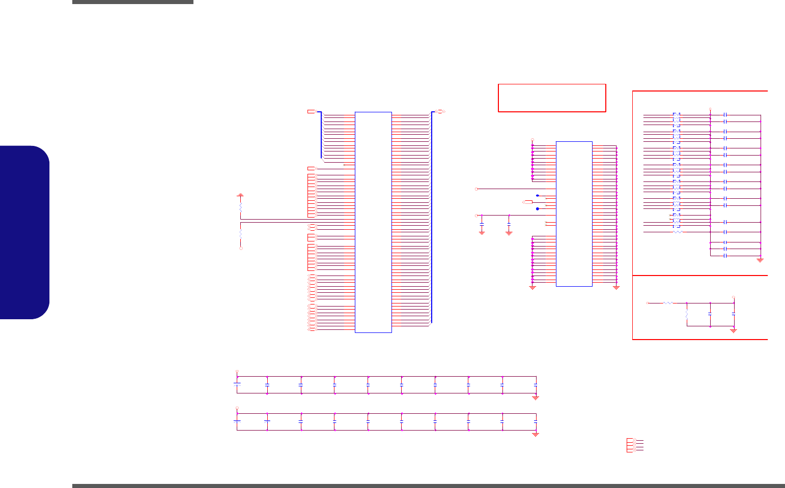
Schematic Diagrams
B - 12 DDRII CHANNEL B
B.Schematic Diagrams
DDRII CHANNEL B
Sheet 11 of 40
DDRII CHANNEL B
VDD SPD
M_BBS0[6 ]
M_B_DQ10
C1 6 0
*0.22U _16V_X7R _06
C134
0.1U _10V_X7R_04
0.9VSM[10 ,3 0 ]
M_ B _D M2
C108
0.1U _10V_X7R_04
R26
10K_04 M_ B_ RAS#[6 ]
M_B_DQ9
M_B_DQ22
M_ B_ DQ S#4[6]
C1 1 6
4 . 7U _6 . 3 V _ X5 R _ 0 6
M_B_DQ33
M_ B_ A5
R78
1K_1% _04
La yo ut no te :
M_ O DT 2
C1 2 6
4.7U _6.3V_X5R_06
C170
2.2U_6.3V_06
M_ BBS2
C412 0.1U_10V_X7R _04
M_ B_ D Q S 3[6 ]
1.8V[5,7 ,8 ,10 ,3 0 ]
M_B_DQ44
M_B_A3
M_B_DQ48
C128
0.1U _10V_X7R_04
M_B_DQ34
M_ C K E 3
RN 4
8P4R X56_04
1
2
3
4 5
6
7
8
M_ B_C AS#
M_B_DQ49
JDIMM_2 is placed farther
from the GMCH than JDIMM_1
M_B_DQ27
M_B_DQ50
M_B_WE#[6 ]
M_ B _ D M 3[6 ]
M_ CKE2
M_B_DQ0
M_ B_ DQ S#6[6]
RN 18
8P4R X56_04
1
2
3
4 5
6
7
8
M_B_DQ46
M_B_DQ31
M_B_DQ1
C141
0.1U _10V_X7R_04
M_ B _ D M 4[6 ]
M_ B_ A4
M_ O D T 3 RN 15
8P4R X56_04
1
2
3
4 5
6
7
8
M_B_DQ53
C104
0.1U _10V_X7R_04
M_ C S #2[5 ]
M_B_A4
M_ B _D M1
C171
1U_6.3V_04
M_ O D T 2[5 ]
C418 0.1U_10V_X7R _04
M_BBS2[6 ]
M_ B_ D Q S 5[6 ]
M_B_A6
M_B_DQ20
C9 5
0.1U _10V_X7R_04
M_ B_ D Q S 2[6 ]
1.8V
M_B_DQ8
M_ B _D M3
M_ B _ C A S #
M_ B_ A1
JD I M M _2 A
A S 0A 42 1 - N 2 A N - 4 F
102
101
100
99
98
97
94
92
93
91
105
90
89
116
86
84
85
5
7
17
19
4
6
14
16
23
25
35
37
20
22
36
38
43
45
55
57
44
46
56
58
61
63
73
75
62
64
74
76
12 3
12 5
13 5
13 7
12 4
12 6
13 4
13 6
14 1
14 3
15 1
15 3
14 0
14 2
15 2
15 4
15 7
15 9
17 3
17 5
15 8
16 0
17 4
17 6
17 9
18 1
18 9
19 1
18 0
18 2
19 2
19 4
107
106
108
109
113
110
115
79
80
30
32
164
166
195
197
200
198
10
26
52
67
130
147
170
185
13
31
51
70
131
148
169
188
11
29
49
68
129
146
167
186
114
119
A0
A1
A2
A3
A4
A5
A6
A7
A8
A9
A10/AP
A11
A12
A13
A14
A15
A16_BA2
DQ 0
DQ 1
DQ 2
DQ 3
DQ 4
DQ 5
DQ 6
DQ 7
DQ 8
DQ 9
DQ10
DQ11
DQ12
DQ13
DQ14
DQ15
DQ16
DQ17
DQ18
DQ19
DQ20
DQ21
DQ22
DQ23
DQ24
DQ25
DQ26
DQ27
DQ28
DQ29
DQ30
DQ31
DQ32
DQ33
DQ34
DQ35
DQ36
DQ37
DQ38
DQ39
DQ40
DQ41
DQ42
DQ43
DQ44
DQ45
DQ46
DQ47
DQ48
DQ49
DQ50
DQ51
DQ52
DQ53
DQ54
DQ55
DQ56
DQ57
DQ58
DQ59
DQ60
DQ61
DQ62
DQ63
BA0
BA1
R AS#
WE#
C AS#
S0#
S1#
C KE0
C KE1
CK0
CK0#
CK1
CK1#
SD A
SC L
SA1
SA0
DM0
DM1
DM2
DM
3
DM4
DM5
DM6
DM7
DQS0
DQS1
DQS2
DQS3
DQS4
DQS5
DQS6
DQS7
DQS0#
DQS1#
DQS2#
DQS3#
DQS4#
DQS5#
DQS6#
DQS7#
ODT0
ODT1
1.8V
M_CLK_DDR2[5 ]
M_B_DQ15
C4 21
1U _6 . 3 V _ 04
M_ O D T 3[5 ]
M_ B_ A12
M_ CL K_ DD R# 2[5]
M_B_DQ59
M_ BBS0
0.9VSM
C99
1U _6 . 3 V _ 04
RN 8
8P4R X56_04
1
2
3
4 5
6
7
8
M_ B _ D M 6[6 ]
M_B_A1
C1 5 0
*0.22U _16V_X7R_06
20mils
M VREF _ DIM 1
M_B_DQ62
M_B_DQ6
M_ BBS0
M_B_A7
M_B_DQ11
M_B_DQ38
M_B_DQ55
M_B_DQ52
JDIM M_2B
AS0A4 21 -N2AN- 4F
11 2
11 1
11 7
96
95
11 8
81
82
87
10 3
88
10 4
19 9
83
12 0
50
69
16 3
1
20 1
20 2
47
13 3
18 3
77
12
48
18 4
78
71
72
12 1
12 2
19 6
19 3
8
18
24
41
53
42
54
59
65
60
66
127
139
128
145
165
171
172
177
187
178
190
9
21
33
155
34
132
144
156
168
2
3
15
27
39
149
161
28
40
138
150
162
VDD 1
VDD 2
VDD 3
VDD 4
VDD 5
VDD 6
VDD 7
VDD 8
VDD 9
VDD 10
VDD 11
VDD 12
VDD SPD
NC1
NC2
NC3
NC4
NCTEST
VREF
GND 0
GND 1
VSS1
VSS2
VSS3
VSS4
VSS5
VSS6
VSS7
VSS8
VSS9
VSS10
VSS11
VSS12
VSS13
VSS14
VSS15
VSS16
VSS17
VSS18
VSS19
VSS20
VSS21
VSS22
VSS23
VSS24
VSS25
VSS26
VSS27
VSS28
VSS29
VSS30
VSS31
VSS32
VSS33
VSS34
VSS35
VSS36
VSS37
VSS38
VSS39
VSS40
VSS41
VSS42
VSS43
VSS44
VSS45
VSS46
VSS47
VSS48
VSS49
VSS50
VSS51
VSS52
VSS53
VSS54
VSS55
VSS56
VSS57
M_B_DQ45
M_B_DQ51
M_ B _ A[ 1 4: 0 ][6 ]
M_ B_ D Q S 1[6 ]
RN 19
8P4R X56_04
1
2
3
4 5
6
7
8
C102
1U _6 . 3 V _ 04
3.3VS
M_BBS1[6 ]
M_ B_ A3
C75
*150U _4V_B2
SA0_D IM1
M_B_DQ23 M_ B_A0
M_ B _ D M 7[6 ]
M_ B _W E #
M_B_DQ60
R237 56_04
M_ B _D M5
C369 *10U_6.3V_X5R_08
C413 0.1U_10V_X7R _04
C411 0.1U_10V_X7R _04
La y ou t no t e:
1. 8 V
M_ B _ D M 1[6 ]
M_ B_ D Q S 0[6 ]
M_B_A2
M_B_DQ42
M_B_DQ7
M_ B_ DQ S#7[6]
M_B_DQ21
M_ B_ A8
C120
0.1U _10V_X7R_04
M_ CL K_ DD R# 3[5] M_CLK_DDR3[5 ]
M_B_DQ16
M_B_DQ[63:0] [ 6]
M_B_DQ43
M_ B_ A2
M_ B_ DQ S#0[6]
Pla ce o n e ca p cl o se to e ve ry 2 p u ll- up re sist ors
te r m in at e d to + V T T_ MEM
M_B_DQ3
C107 0.1U_10V_X7R _04
M_ B_ DQ S#3[6]
M_ BBS1
M_B_DQ12
M_B_A12
M_ C S # 3
R25
10K_04
M_B_DQ35
M_B_A5
CLOSE TO JDIMM_2
M_ C K E 2[5 ]
M_B_DQ14
M_ C S # 2
M_ B_ A6
C1 62
10U_6.3V_X5R_08
M_ C K E 3[5 ]
M_ B _ D M 0[6 ]
M_ B_ A9
M VREF _ DIM 1
M_ B_ DQ S#2[6]
3.3VS[ 5,8 .. 1 0,1 2 ..1 6,1 8 ..27 ,3 1 ]
M_ C S #3[5 ]
M_B_DQ54
M_ B _ R A S #
ICH_SMBD AT0[1 0,1 5 ,18 ]
M_B_DQ37
M_ B _D M4
M_B_DQ58
R7 9 1 K _ 1% _ 04
RN 2
8P4R X56_04
1
2
3
4 5
6
7
8
M_ B _D M0
M_B_A11
M_B_DQ18
M_B_DQ39
M_ BBS2
C419 0.1U_10V_X7R _04
C1 5 6
*1 50 U _ 4 V _ B 2
VD DSPD[10]
M_B_A10
M_ B_ A11
C1 22
10U_6.3V _X5R_08
J D IM M _ 2 T e rm i n at o r
M_B_DQ4
C403 0.1U_10V_X7R _04
M_ CKE3
1.8V
M_B_DQ24
M_B_DQ63
ICH_ SMBC L K0[1 0,1 5 ,18 ]
C414 0.1U_10V_X7R _04
C410 1U_6.3V_04
16 -5 603 4-4 5A
M_ B_ D Q S 6[6 ]
M_ BBS1
M_ B_ A10
M_B_A13
C402 0.1U_10V_X7R _04
C105 0.1U_10V_X7R _04
M_ B_ D Q S 4[6 ]
M_B_DQ28
M_B_DQ56
M_B_DQ40
M_B_DQ29
M_ C S # 3
PM _EXTTS_D DR #[5 ,10 ]
M_B_DQ41
M_B_DQ5
M_B_DQ47
M_B_DQ19
M_ B _D M7
M_ C S # 2
M_ C K E 2
C404 0.1U_10V_X7R _04
M_ O DT 3
M_ B_ DQ S#1[6]
M_ B_ DQ S#5[6]
M_B_DQ32
SO-DIMM 2
M_B_DQ61
M_ B_ A7
C408 0.1U_10V_X7R _04
M_B_A8
C151 0.1U_10V_X7R _04
M_ B _ D M 2[6 ]
M_ O D T 2
M_B_DQ17
M_B_DQ36
M_ B _D M6
M_B_A0
C416 0.1U_10V_X7R _04
M_B_DQ26
M_ B _ W E #
M_ B_ A14
M_ B_R AS#
M_B_A14
M_ B _ D M 5[6 ]
M_ B_ D Q S 7[6 ]
C1 7 7
0.1U _10V_X7R_04
C179
0.1U _10V_X7R_04
C92
*220U _4V_D
M_ B_ CAS#[6 ]
M_B_DQ57
SA1_D IM1
RN 6
8P4R X56_04
1
2
3
4 5
6
7
8
M_B_DQ13
M_ B_ A13
C96
0.1U_10V_X7R_04
C400 0.1U_10V_X7R _04
M_B_A9
M_B_DQ30
M_B_DQ2
M_B_DQ25
20mils
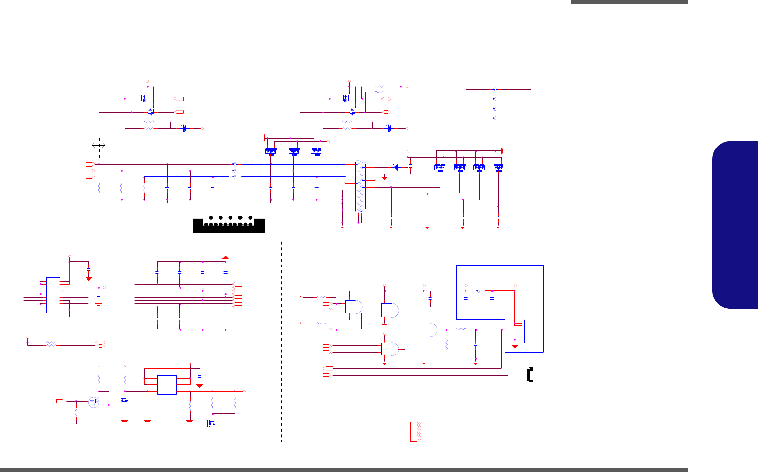
Schematic Diagrams
Panel, Inverter, CRT B - 13
B.Schematic Diagrams
Panel, Inverter, CRT
3. 3V
Z1109
D AC_ GR E EN_ R
SY S15V[2 7 ..29 ]
C RT_ DD C ACL K _R
Q2 7
2N 70 0 2W
G
D S
11
C2 97
*0 .1U _ 16 V _ 04
R1 7
150_1%_04
1
CRT _ DD CACL K _ R
C622
*10P_50V_04
CRT
LVD S-LC LK P [5 ,27 ]
8
LVD S-L2N
LVDS-LCLKP
5
D1 3
*ASD7 5 1V
AC
LVDS-L1N
CR T_ DD CAC LK
D7
BAV9 9
A
C
AC
VIN
C RT_ DDC ADA T _R
3.3V[2 ,13 ..1 7,1 9 ,2 0,2 3 ,29 ,3 0]
CR T_ H S YNC
CR T_ DD CAD AT
D14 ASD751V
AC
R380
*200_06
C3 0 6
*0 .1 U_ 1 6V _ 0 4
3.3V
R399 1K_04
R5 7 1 00 K _0 4
LVD S -LC LK N [5 ,2 7]
LVD S-L2 P [5,2 7 ]
C2 7 3
*0 .1 U _ 16 V _ 0 4
14
GM _ B LO N[5 ]
5V S[1 3 ,16 ,1 9, 21 ,2 4,2 5 ,27 ]
DAC_ D DCAD ATA [5 ]
3.3VS[5 ,8 ..1 1,1 3 ..16 ,1 8 ..27 ,3 1]
C629
*10P_50V_04
D AC_ HSY NC [5 ]
P_ DDC _ CL K [5 ,27 ]
R3 7 8
1M_04
R15
150_1%_04
P_ DD C_ CL K
D6
BAV99
A
C
AC
C293
0.1U_50V_06
C6 2 3
*10P_50V_04
C30
47 P _ 50 V _ 0 4
3.3VS
LVDS-L2P
Q2 6
2N 70 0 2W
G
D S
D1
*B A V 9 9
A
C
AC
6
For CCFL Panel only
LVD S-L2 N [5 ,27 ]
U10C
74LVC08PW
9
10 8
147
LVD S-L0 P [5,2 7 ]
CRT _ DD CADA T_ R
R382
*100K_04
L21
H CB1608KF-121T25
40 mil
CRT _ HSY N C_ R
C618
*0 .1 U_ 1 6V _ 0 4
C628
* 1 0P _ 5 0V _ 0 4
VIN[2 7..3 2 ]
J_INV1
3.3VS
C3 1 4
22P_50V _04
5V S
PANEL
PLVDD
LVD S-L0 N [5 ,27 ]
C28
10 00P_ 5 0V_ X7R _04
C6 1 9
0.022U_25V_X7R _06
R14
150_1% _04
R1 8 4
*1 M_ 0 4
R164 2.2K_04
15
D AC_VSYN C [5]
LID _SW#[1 9 ,26 ]
CRT_VSYN C
Q1 7
2N7002W
G
D S
1
DAC_ R ED[5]
CL_PWROK[5 ,15 ,1 7 ,26 ]
P_ DD C_ DAT A U10A
74 L V C 0 8 P W
1
2
3
147
BR IGHTN ESS[2 6,2 7 ]
L62 F CM1005KF-121T03
D5
BAV99
A
C
AC
J_LC D1
88107-20001
12
34
56
78
910
11 12
13 14
15 16
17 18
19 20
C25
220P_50V_04
D2
*B A V 9 9
A
C
AC
CR T_ D DCAD AT
LVDS-L0N
Q23
DT C1 1 4E U A
CE
B
2
C1
0. 1 U _1 6 V _0 4
Zo=55 Ohm
2A
LVD S-L0P
LVDS-LCLKN
CRT_VSYN C_R
L63 FCM1005KF-121T03
3. 3V
PLVD D
LVD S-L1 P [5,2 7 ]
R3 79
20 0 _0 6
Q2 5
2N7002W
G
DS
R163 2.2K_04
EN AVDD[5 ]
R187 *100K_04
LVD S-L0N
9
L60 F CM1005KF-121T03
C19
220P_50V_04
R191 2.2K_04
LVD S-L1N
C RT_ VSYNC _R
R398 1K_04
D AC_ BL UE _ R
2A
3
U1 0 B
74LVC08PW
4
56
147
INVERTER CONNECTOR
3. 3 V S
12
5V S
LVDS -LC LKP
CR T_ D DCAC LK
C307
0.1U_16V _04
6-2 0-4 1A 10- 106
J_CRT1 Solder side
PLVDD[2 7]
C RT_ HS YN C_ R
L61 F CM1005KF-121T03
D AC_ BL UE[5 ]
SY S15V
Q2 2
SI3456B DV-T1-E3
3
2
1
4
5
6
G
D
D
S
D
D
Q2 4
2N7002W
G
DS
U1 0 D
74LVC08PW
12
13
11
147
Zo = 5 5 O hm
5V S
LVD S-L1P
D3
*BAV99
A
C
AC
C6 2 7
*10P_50V_04
D AC_ RED _R
R3 8 1
*1 0 0K _ 0 4
DAC_ GR EEN[5]
C3 10
22 P _ 5 0V _ 0 4
Q1 6
2N7002W
G
D S
LVDS-L1P
P_ DD C_ DAT A
R3 7 7
1M_04
LVDS-L2N
R190 2.2K_04
R3 92 4 7K_ 0 4
3. 3 V
10
4
3.3VS
D3 1 ASD 75 1 V
AC
C27
47P_50V_04
7
2A
5VS
IN V_ BLO N[27 ]
SB_BLO N[1 5]
P_ DD C_ CL K
L64 FCM1005KF-121T03
3.3VS LVDS-L0P
C300
*0.1U _50V_06
J_INV1
87 2 1 2- 0 6 G 0
1
2
3
4
5
6
R188 2.2K_04
13
VIN_INV
CRT_ HSYN C
LVD S-L1 N [5 ,27 ]
L65 FCM1005KF-121T03
C3 4
47 P _ 5 0V _ 0 4
SYS1 5V
C626
*10P_50V_04
6
LVD S-L2P
Zo=50 Ohm
DAC_ D DCAC LK [5 ]
R189 2.2K_04
D4
*BAV99
A
C
AC
BKL_EN[26]
J_ C R T1
C10509-91505-L
8
7
6
5
4
3
2
1
9
10
11
12
13
14
15
GN D2
GND 1
P_ DDC _ DAT A [5 ,2 7]
CR T_ VSY NC
C625
*10P_50V_04
L66 FCM1005KF-121T03
C624
* 1 0P _ 5 0V _ 0 4
LVDS -LC LKN
C317
22P_50V_04
C18
10 00P_ 5 0V_ X7R _04
Sheet 12 of 40
Panel, Inverter,
CRT
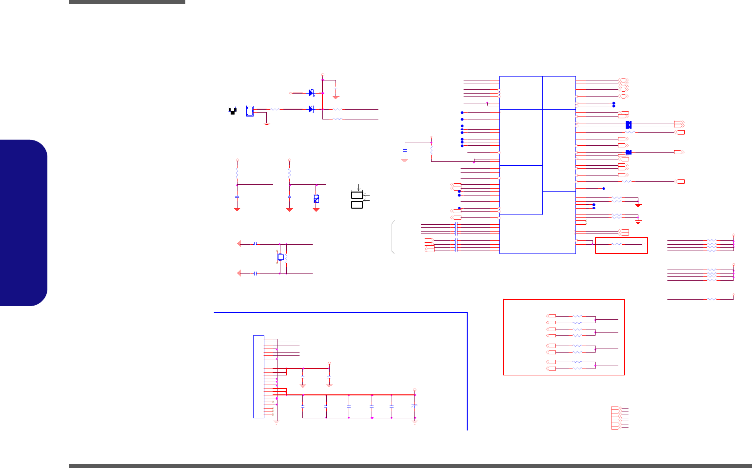
Schematic Diagrams
B - 14 ICH9-M 1/5 - SATA
B.Schematic Diagrams
ICH9-M 1/5 - SATA
AZ_BITC L K
R257 54.9_1%_04
Zo= 55O? 5%
R 1 20 1 0 K _ 04
R94 1M_04
R2 6 2 56 _ 0 4
35mil
R 245 1K_04
C453
0.1U_16V _04
MD C _ A Z _ S Y N C[1 9]
X4
32.768KHz
14
3 2
1.05VS
H_INIT# [2]
C lea r CM OS
1. 0 5 V S[2 ..5,7 ,8 ,1 6 ,29 ]
3. 3 V[2,12,14..17, 19,20, 23,29,30]
IC H_ DPS L P#
GPIO56
H_ D PRST P#
R123 33_04
R318 *10K_04
PIN G ND 1~2=G ND
SATA_ RXN0
R96 332K_1%_06
KBC _R ST#
GL AN _ C LK
C496 15P_50V_04
AZ_SDOUT
RTCR ST #
SRTCR ST#
C1 7 2
1U_6.3V_04
PM _ TH RM TR IP# [2 ,5 , 28 ]
C6
0.1U_16V_04
R135 *1K_04
IC H_ DPR STP #
SATA_ TXP0
SATA HDD
Z diff= 10 0O? 0%
RTC VCC
C12
0.1U_16V_04
1.0A
SB_MU TE#[2 5 ]
HDA_SDIN3
INTRU DER #
R95
20K_1% _04
LPC _FR AME# [19,26]
3. 3 V S[5,8 ..1 2,1 4 ..1 6,1 8 ..2 7 ,31 ]
SATA_ TXP0
R324 *10K_04
C1 69
1U _6 . 3 V _ 04
C 2 31 0 . 01 U _ 1 6 V _X 7 R _ 0 4
LP C _ A D 0 [ 1 9 , 2 6]
AZ_SDOUT
SATA_ RXN1[1 9]
GPIO 56
H_STPCLK# [2]
LP C _ A D 3 [ 1 9 , 2 6]
J _ HD D1
C16623-122A4
S1
S2
S3
S4
S5
S6
S7
P1
P2
P3
P4
P5
P6
P7
P8
P9
P10
P11
P12
P13
P14
P15
3.3V
LPC _AD 1 [19,26]
R2 5 8
24.9_1% _04
C 5 13 0 . 01 U _ 1 6 V _X 7 R _ 0 4
AZ_ SDIN 1[1 9]
H_A20M# [2]
R319 *10K_04
H _ SMI# [2 ]
R326 24.9_1%_04
C11
0 . 1U _1 6 V _ 0 4
3.3VS
AZ_SYNC
D9
ASD751V
A C
M DC _AZ _R ST#[1 9 ]
R 1 24 1 0 K _ 04
CLK_SATA [18]
3. 3 V S
C13
1U _10V_06
R 256 * 56_04C483 15P_50V_04
5VS[1 2,1 6 ,1 9,2 1 ,2 4, 25 ,2 7]
AZ_SDOUT
25mil
VDD 3[21,26..30,32]
GA20 [26]
ICH _I NTVRM EN
C294
*100U _6.3V_B2
MDC_AZ_SDOUT[19 ]
Within 500mil
MDC_AZ_BITCLK[19 ]
C 2 32 0 . 01 U _ 1 6 V _X 7 R _ 0 4
C 5 21 0 . 01 U _ 1 6 V _X 7 R _ 0 4
5mil
C 5 10 0 . 01 U _ 1 6 V _X 7 R _ 0 4
AUD _AZ_BITCL K[24 ]
PM_THRMTRIP#
RTC_ X2
AZ_RST#
C 5 31 0 . 01 U _ 1 6 V _X 7 R _ 0 4
R139 33_04
H_FERR#
R291
10M_04
C 2 33 0 . 01 U _ 1 6 V _X 7 R _ 0 4
SATA_ RXP1[1 9]
H_F ERR# [2]
KBC _RST#
VERY CLOSE TO ICH9M
SB_THR MTRIP#
LA N _ TX D 1
R 2 55 5 6 _0 4
JCBAT1
85205-02001
2
1
2
SB_M UTE#
20mils
H_DPSLP# [2]
LA N _ TX D 0
SATA_ TXN 0
AZ_ SDIN 0[2 4]
IC H_ FE RR #
R133 33_04
R125 33_04
RTC_ X1
R 2 50 5 6 _0 4
SATA_TXN1[19 ]
RTC VCC[1 6 ]
C14
0 . 1U _1 6 V _ 0 4
H_INTR [2]
INTRU DER #
1
LPC _AD 2 [19,26]
GA 20
R138 33_04
H_DPRSTP# [2,5,31]
C213
1U _6.3V_04
CLK_SATA# [18]
SRTCR ST#
R 3 48 1 0 K _ 04
H _ IGNN E# [2 ]
LPC _D RQ 0#
RTCLAN / GLANIHD ASAT A LPCCPU
U2 3 A
IC H9M- NH82801IBM
C23
C24
B22
C22
E25
C13
F14
G13
D14
D13
D12
E13
AF6
AH4
AE7
AF4
AG4
AH3
AG5
AG8
AJ16
AH 16
AF 17
AG 17
AH 13
AJ13
AG 14
AF 14
AH18
AJ1 8
AJ7
AH7
K5
K4
L6
K2
J3
J1
K3
N7
AJ2 7
AJ2 5
AE23
AJ2 6
AD22
AF25
AE22
AG25
L3
AF24
AF23
AH27
AG26
A25
B10
B27
B28
AE5
AG12
AH11
AF12
AJ1 1
AG27
AG7
AE8
A22
AH9
AJ9
AE10
AF10
F20
RTCX1
RTCX2
IN TVR MEN
IN TR UD ER#
G LAN _CLK
LAN_R STSY NC
LAN_RXD0
LAN_RXD1
LAN_RXD2
L AN_ T XD0
L AN_ T XD1
L AN_ T XD2
HDA_BIT_CLK
HDA_SYNC
HDA_RST#
HDA_SDIN0
HDA_SDIN1
HDA_SDIN2
HDA_SDOUT
SATALED#
SATA0RXN
SATA0RXP
SATA0TXN
SATA0TXP
SATA1RXN
SATA1RXP
SATA1TXN
SATA1TXP
SATA_CLKN
SA TA_C LKP
SATARB IAS#
SATARBIAS
FWH 0/LAD 0
FWH 1/LAD 1
FWH 2/LAD 2
FWH 3/LAD 3
LDR Q0#
LD RQ1#/GP IO23
F WH4/LFRAM E#
A20G ATE
A20M #
DPR STP#
DPSLP#
FERR #
CP UPW R GD
IG NN E#
INIT#
INTR
RCIN#
SM I#
NMI
STPC L K#
TH RMTR IP#
RTCRST#
GPIO56
G LAN _ COM PO
G LAN _ COM PI
HDA_SDIN3
SATA4TXN
SATA4 RXN
SATA4TXP
SATA4RXP
TP12
H DA_ DO CK_ E N# /G PI O3 3
H DA_DO CK_RST#/GPIO 34
LAN100_SLP
SATA5 RXN
SATA5RXP
SATA5TXN
SATA5TXP
SR TC RST#
Layout Note:
LA N_ RX D1
SATA_ RXN0
H_DPRSTP#
KB C_RST# [26]
SATA_ TXN 0
LA N _ TX D 2
HDA_SDIN2
H_ F ER R#
D10
ASD751V
A C
R130 33_04
1.5VS
C 2 34 0 . 01 U _ 1 6 V _X 7 R _ 0 4
H_PWRGD [2]
SB_M UTE#
SATA_ RXP0
H_ D PSLP#
RTCVC C
AU D_AZ_ SYNC[2 4]
5VS
AU D_AZ_ RST#[2 4,2 5 ]
C22
10U_10V_08
AZ_SYN C
R 1 29 1 0 K _ 04
JCBAT
SATA_LED #[19 ]
RTC_X2
PM_THRMTRIP#
LA N _ R S T S Y N C R263 *10mil_short
VDD 3
AZ_RST#
R261 *10mil_short
RTCR ST#
RTC_X1
R325 *10K_04
JO P E N 1
*O P E N _ 3 5m i l
R9 3 * 10 m il_ s ho rt
R126 33_04
1.5A
LDR Q1#
R 254 * 56_04
GA20
C2 1
10U_10V_08
AUD_AZ_SDOUT[24 ]
H DA_ DO CK_ EN #
SATA_ RXP0
IC H _ INTV R MEN
R131 33_04
LA N_ RX D0
RTCVCC
H_DPSLP#
AZ_BITCLK
LA N_ RX D2
SATA_TXP1[19 ]
H_NMI [2]
R7 6
20K _1%_04
1. 5 V S[3 ,8, 14 ,1 6, 19 ,2 0 ,29 ]
Sheet 13 of 40
ICH9-M 1/5 - SATA
Schematic Diagrams
ICH9-M 2/5 - PCIE, PCI, USB B - 15
B.Schematic Diagrams
ICH9-M 2/5 - PCIE, PCI, USB
Within 500 mils
LPC(default)
1.5VS
PCI_IN T#F
RN 3 5
8P4R X8.2K_ 0 4
1
2
3
4 5
6
7
8
Remove C164
PCI_GNT#0
PCI_C /BE#0
PCI_AD2
PCI_AD23
PCI_AD26
CLGPIO5
PCIE_R XP1 _ W LA N[2 0]
PCI_PERR #
C 1 75 * 3 3P _ 5 0 V _0 4
R407 *33_04
USB_PN4_ NEW [20]
USB_PP4 _N EW [20]
PCIE_TXP3_C
DMI_ R XP3 [ 5]
USB_PN0 [21]
PCI_AD14
US B_O C# 9
USB _ OC #7
SPI_CS1#_R
R3 76
0_04
PME# [26]
PCI_AD1
No stuff
CL GPIO 5 [15 ]
U3
MX25L1605A16M
1
2
3
4
5
6
7
8
CE#
SO
WP#
VSS
SI
SCK
HOL D#
VDD
R375 * 0_04
Stuff
R115 *8.2K_04
PCI_INT#D
PCI_DEVSEL#
PCI_AD28
PCI_FRAM E#
SPI_SI
Enable
DMI_ T XP0 [5 ]
RN 3 4
8P4R X8.2K_ 0 4
1
2
3
4 5
6
7
8
iTPM Enable
PCIE_RXP3_3G[19 ]
PCIE_TXP2_C
SPI_SCLK
PCI_G NT#1
SPI_SI_R
C454 0.1U_10V_X7R _04
PC I_G NT# 3
3.3VS
USB _ OC #1 1
3.3VS[5,8..13,15,16,18..27,31]
PCI_G NT#0
PCI_LO CK#
PCI_STO P#
DMI_ T XP1 [5 ]
PCI_AD10
2
R128 * 100K_04
Strap
PCIE_T XN 1_ W L AN[20 ]
SPI1_SC LK_R
PCI_AD22
PCI_G NT2#
PCI_R EQ#0
No stuff
No stuff
DMI_ T XN3 [5 ]
PCI_G NT#3
PCI_R EQ#2
DMI_ R XN 3 [5 ]
PCI_ INT # C
RN 1 2
8P4R X8.2K_ 0 4
1
2
3
4 5
6
7
8
Z diff= 90O? 5 %
1.5VS[3,8 ,1 3 ,16 ,1 9 ,20 ,2 9]
PCI_PAR
PCIE_TXN3_C
USB _ OC #2
3.3V[2,1 2 ,1 3,1 5 ..1 7,1 9 ,20 ,2 3 ,29 ,3 0]
R77 33_04
C461 0.22U _16V_X7R_06
USB_PN7_ CC D [19 ]
10
PCIE _TXN4_LAN[2 3 ]
DMI_ R XN 0 [5 ]
PCI_R ST#
PLT_ RST#
SPI_C S0#_R
R89 33_04
USB_PP7 _C CD [19]
PCI_AD6
R75
3.3K_1%_04
USB_PN3 [19]
USB_PN5_ 3G [19 ]
PCI_AD29
R148 1K_04
J_SBSPI1
PCIE_RXN2_NEW_CARD[20]
SBSPI_HO LD#
PCI_L OC K#
PCI_ IRD Y#
C457 0.1U_10V_X7R _04
C459 0.1U_10V_X7R _04
R408
*3 .3 K _ 1% _ 04
SPI_SI
USB _ OC #0 1[21 ]
USB_PP2 _M INI [20]
PCI_PER R#
US B_O C# 11
SPI_CS0#_R
R145 * 10_04
C460 0.22U _16V_X7R_06
Z diff= 100O? 5%
No stuff
PCI_ INT # E
SBSPI_ W P#_ R
CLK_ PCIE_ICH # [18 ]
USB_PP3 [1 9 ]
SBSPI_ W P#_ R
PCI_AD15
SPI_SI
PCI_ INT # D
C458 0.1U_10V_X7R _04
RN 1 3
8P4R X8.2K_ 0 4
1
2
3
4 5
6
7
8
RN 1 4
8P4R X10K_04
1
2
3
4 5
6
7
8
3.3VM _SBSP I1
PC IE_TXP3_3G[19]
iTPM Enable
PCIE_TXN5_C
PCIE_TXN 5_ CAR D[22 ]
R351 10K_04
C455 0.1U_10V_X7R _04
C456 0.1U_10V_X7R _04
PC I
I nt err up t I/F
U23B
I C H 9M - N H 82 8 0 1I B M
D11
C8
D9
E12
E9
C9
E10
B7
C7
C5
G1 1
F8
F11
E7
A3
D2
F10
D5
D10
B3
F7
C3
F3
F4
C1
G7
H7
D1
G5
H6
G1
H3
F1
G4
B6
A7
F13
F12
E6
F6
D8
B4
D6
A5
D3
E3
R1
C6
E4
C2
J4
A4
F5
D7
C1 4
D4
R2
J5
E1
J6
C4 G2
F2
K6
H4
AD0
AD1
AD2
AD3
AD4
AD5
AD6
AD7
AD8
AD9
AD10
AD11
AD12
AD13
AD14
AD15
AD16
AD17
AD18
AD19
AD20
AD21
AD22
AD23
AD24
AD25
AD26
AD27
AD28
AD29
AD30
AD31
REQ0#
GNT 0 #
REQ 1 #/G PIO5 0
GNT1#/GPIO51
REQ 2 #/G PIO5 2
GNT2#/GPIO53
REQ 3 #/G PIO5 4
GNT3#/GPIO55
C/BE0#
C/BE1#
C/BE2#
C/BE3#
IRDY #
PAR
PC IRST#
DEVSEL#
PERR #
PLOC K#
SERR #
STO P#
TRDY #
FRAM E#
PLTRST#
PCIC LK
PM E#
PIRQ A#
PIRQ B#
PIRQ C#
PIRQ D# PIRQ H# /GPIO 5
PIRQ G#/GPIO 4
PIR QF# /GPIO 3
PIR QE#/GPIO 2 PCI_IN T# E
Disable
01
PCI_STOP#
PCI_INT#C
DMI_ T XP2 [5 ]
PCI_TR DY #
SPI1_SI_R
Default
Within 500 mils
PCIE_R XN 1_W L AN[2 0]
PCI_AD16
PCIE_TXP5_C
3.3VS
CLK_ PCIE_ICH [18]
PCI_AD11
SPI_S I
PC IE_RXP4_LAN[23]
USB_O C# 3[19]
Stuff
A16 swap override Strap
PCI_AD19
PCI_AD31
C 1 66 * 3 3P _ 5 0 V _0 4
USB_PN1 [21]
PC IE_RXN4_LAN[23]
USB_PN9_ BT [19]
SPI_SO_ R
PCI_AD12
SBSPI_HO LD#
R8 6 * 1K _0 4
1
3.3V M_SBSPI1
DMI_ R XP1 [ 5]
PC IE_TXN3_3G[19]
R411
*3 .3 K _ 1% _ 04
PCI_AD21
PCIE_TXN2_C
PCI_REQ #0
USB _ OC #4
C462 0.1U_10V_X7R _04
PCI_AD17
PCI_REQ #1
R346 22.6_1%_04
R409 *33_04
C463 0.1U_10V_X7R _04
PCI_AD25
PCI_AD18 C264 *10P_50V_04
3.3V
PCI_AD7
C1 65
0.1U_16V_04
U29
*M X25L1605A16M
1
2
3
4
5
6
7
8
CE#
SO
WP#
VSS
SI
SCK
HOL D#
VDD
DMI_ T XN0 [5 ]
USB_PP1 1_FP [21]
USB_PP0 [2 1 ]
R260 24.9_1% _04
SBSPI_W P# [15]
PCI_AD4
PCIE_TXN4_C
USB_PN11 _F P [21]
PCI_SER R#
PCI_C /BE#3
HIGH
PCIE_RXP5_C ARD[22 ]
PCI_TRD Y#
PCI_INT#A
PCIE_TXN1_C
PCI_G NT#3
SPI_CS0#
R1 1 3
*100K_04
US B_O C# 6
PCI
3. 3 V S
PCIE_TXN2_NEW_CARD[20 ]
SPI_SCLK_R
J_SBSPI1
*SP N Z-0 8S3 -B -C- 0-P
12
34
56
78
SPI
PCLK_ICH 33 [ 18]
US B_O C# 7
R73 33_04
PC IE_TXP5 _C ARD[22]
PCI_ INT # A
SBSPI_ W P#_ R
PCIE_TXP1_C
SPI_S O
SPI_C S1#_R
PCI_IN T#G
PCI_IN T#H
US B_O C# 4
PCI_R EQ#1
SPI1_SO _R
SPI_CS1#
Stuff
DMI_ T XP3 [5 ]
PCIE_TXP1_WLA N[20 ]
PCI_D EVSEL#
PCI_REQ #2
USB _ OC #6
R406 *33_04
PCI_C /BE#2
PCI_SERR #
PCI_ INT # F
SPI_C S0 #
C6 43
* 0 . 1U _ 16 V _ 04
R132 * 1K _04
Enable
PCIE_R XP2_NEW _ CAR D[20]
R136 10K_04
RN 3 3
8P4R X10K_04
1
2
3
4 5
6
7
8
USB_PP5 _3G [19]
PCI_IR DY#
PCI_AD8
PCI_AD30
SPI_C S1 #
PCI_ INT # B
SPI_CS1#
PCIE_ TXP2 _NEW _ CAR D[20 ]
US B_O C# 8
SPI_SCLK
No stuff
PCI_AD24
RN 1 1
8P4R X8.2K_ 0 4
1
2
3
4 5
6
7
8
PCI_AD9
PC I_GNT# 0
SPI_SO
No stuff
8
DMI_ R XN 1 [5 ]
USB_PN2_ MIN I [20]
P L T_ R S T#
USB _ OC #9
J SPI1
*O PEN_35m il
C 1 68 * 3 3P _ 5 0 V _0 4
LOW
7
USB_PP1 [2 1 ]
PCI_FR AME#
PCI_AD20
US B_O C# 2
R405
* 3.3K_1%_04
Default
D03 BCN
3.3VM _SBSP I1
P C I E _T X P 4_ L A N[2 3 ]
PCI_AD0
SPI_SO_R
US B_O C# 10
Disable
DMI_ R XN 2 [5 ]
USB_O C# 4[20]
SPI_CS#_CON
PCIE_TXP4_C
PCI_GNT2#
R410 *33_04
U6
74AH C1G08GW
1
2
5
4
3
DMI_ T XN1 [5 ]
DMI_ R XP2 [ 5]
Stuff
PCI_INT#B
USB _ OC #1 0
USB_PP9 _BT [19 ]
PCLK_ICH 33
SPI_S CLK
SPI_SO
PCI_ INT # G
USB _ OC #8
De fau lt
BUF_PLT_R ST# [19,20, 22,23,26]
PCIE_R XN 5_CAR D[2 2]
PCI_AD3
PCI_ INT # H
R82 33_04
P CI- Ex pre ss
Direct Media Interface
USB
SPI
U23D
IC H9M-NH 82801IB M
N2 9
N2 8
P27
P26
L2 9
L2 8
M2 7
M2 6
J2 9
J2 8
K27
K26
G2 9
G2 8
H2 7
H2 6
E29
E28
F27
F26
C2 9
C2 8
D2 7
D2 6
V27
V26
U2 9
U2 8
Y27
Y26
W29
W28
AB27
AB26
AA29
AA28
AD27
AD26
AC29
AC28
T2 6
T2 5
AF2 9
AF2 8
N4
N5
N6
P6
M1
N2
M4
M3
AC5
AC4
AD3
AD2
AC1
AC2
AA5
AA4
AB2
AB3
AA1
AA2
W5
W4
Y3
Y2
AG1
AG2
D2 3
D2 4
F23
D2 5
E23
N3
N1 W2
W1
V2
V3
U5
U1
U4
U2
P5
P3
PERN 1
PERP1
PETN1
PETP1
PERN 2
PERP2
PETN2
PETP2
PERN 3
PERP3
PETN3
PETP3
PERN 4
PERP4
PETN4
PETP4
PERN 5
PERP5
PETN5
PETP5
PERN 6/G LAN_RXN
PERP6/G LAN _R XP
PE TN6 /GL AN_ T XN
PETP6/G LAN_TXP
DMI0 R XN
DM I0R XP
DMI0TXN
DMI0 T XP
DMI1 R XN
DM I1R XP
DMI1TXN
DMI1 T XP
DMI2 R XN
DM I2R XP
DMI2TXN
DMI2 T XP
DMI3 R XN
DM I3R XP
DMI3TXN
DMI3 T XP
DMI_ CL KN
DM I_C L K P
DM I_ZC OM P
D MI_ IRC OM P
OC 0# /GP IO5 9
OC 1# /GP IO4 0
OC 2# /GP IO4 1
OC 3# /GP IO4 2
OC 4# /GP IO4 3
OC 5# /GP IO2 9
OC 6# /GP IO3 0
OC 7# /GP IO3 1
USBP 0N
U SBP0P
USBP 1N
U SBP1P
USBP 2N
U SBP2P
USBP 3N
U SBP3P
USBP 4N
U SBP4P
USBP 5N
U SBP5P
USBP 6N
U SBP6P
USBP 7N
U SBP7P
USBR BIAS#
USBR BIAS
SPI_CLK
SPI_CS0#
SPI_CS1#/GPIO58/CLGPI O6
SPI_MOS I
SPI_MISO
OC 8# /GP IO4 4
OC 9# /GP IO4 5 U SBP8 P
USBP 8N
USBP 9N
U SBP9P
U SBP10N
U SBP11N
USBP10 P
USBP11 P
OC 10 # /GPIO 46
OC 11 # /GPIO 47
SPI_S I_R
02/20
DMI_ R XP0 [ 5]
PCI_AD27
PCI_REQ #3
11
PCI_AD5
R74
3.3K_1%_04
Zo= 55O? 5%
Enable
3.3V
DMI_ T XN2 [5 ]
PCIE_RXN3_3G[19 ]
PCI_AD13
PCI_R EQ#3
US B_O C# 5
PCI_C /BE#1
SPI_SI
SPI_S CLK_R
USB _ OC #5
C235
* 0 . 1U _ 16 V _ 04
Disable
3. 3 V
PL T_ RS T# [5 ,1 9 ]
PCLK_ ICH 33
Boot BIOS Strap
US B_O C# 3
J SPI2
*O PEN_35m il
Sheet 14 of 40
ICH9-M 2/5 - PCIE,
PCI, USB
Schematic Diagrams
B - 16 ICH9-M 3/5 - GPIO, PWR Management
B.Schematic Diagrams
ICH9-M 3/5 - GPIO, PWR Management
SB_BLON
IC H_SM BDAT0
R 121 *10mil_short
PM_STPPCI #
PM _SY NC #[5 ]
PM_STPCPU #
SE RIRQ
SW I#
PM_THR M#
IC H_SM BCLK0
SA TA_C LKR EQ#
SUS_ PWR_ AC K
CL_ DATA1 [20 ]
R2 9 8
45 3 _ 1% _ 0 6
IC H_SMBD AT1[2 0 ]
Zo= 55 O? 5%
PM _ STP CPU#
C218
*0.1U_16V_04
CL_RST#0 [5]
IC H_SM BCLK1
SATA4GP
CL_CLK0 [5]
SA TA1G P
CLKEN#[31]
SU S_ PW R_ ACK [26]
SWI#
RN9
8P4RX10K_04
1
2
3
45
6
7
8
R 1 06 1 0 0K _ 0 4
R99 10K_04
PM _THR M#[2 ]
LAN _PW R[2 3 ]
PM _TH RM #
R97 100K_04
SLP_ S3# [17]
R277 *10K_04
CL_ DATA0 [5]
3. 3 V S
CL K_ ICH 14 [18 ]
MCH _ICH_SY NC#
R1 0 4
10K_04
CL K_ ICH 48 [18 ]
3.3V[2,12..14,16,17,19,20,23,29,30]
RSMRST#
C504
0.1U_10V_X7R_04
SB_BLO N[1 2]
U5
* G690L293T73
1
2
3
GND
RST#
VCC
3.3VS
PW R _BT N# [26 ]
PM_CLKRUN#
SCI#
IC H_ SPK R[2 4 ]
R112 10K_04
IC H_SM BDAT1
ICH_SMBDAT1
R 111 2.2K_04
R92 10K_04
AC_PRESEN T
PM_C LKR UN #[1 9]
PC IE_W AKE#
MC H_ I CH _S Y NC #
R350 * 10m il_s hort
R303 10K_04
CL _ PW RO K [5 ,1 2 ,17 ,2 6 ]
OD D_ D ET E C T#
SLP_ M#
CL_CLK1 [20]
SLP_ S4# [17]
R91 100_04
R 2 97 1 0 0K _ 0 4
CL_VREF0
3.3VS
SMI#
LAN_PWR
R304 10K_04
C 2 04 1 0 0P _ 5 0 V _0 4
RSM RS T # [1 7 ,2 6]
GPIO 1 7
PM_D PRSLPVR [5,31]
AC _PRESEN T_R
R 1 02 1 0 0K _ 0 4
PM _CLKRU N#
SC I#
ODD_DETECT#
R3 0 2
3. 24 K _ 1 %_ 0 4
GPIO 1 8
R 101 1M_04
SATA0GP
R 313 2.2K_04
SATA
SMBSYS GPIO
GPIO
GPIO
Clocks
Power MGTController Link
MISC
U23C
ICH 9M -NH 8 28 0 1IB M
AH23
AF1 9
AE21
AD20
G1 6
A13
E17
C17
B18
R4
G1 9
M6
AG19
AH21
AG21
A21
C12
A17
AE18
K1
AJ 2 2
L1
A14
E19
AE19
AG22
L4
AF2 1
E20
M5
AJ 2 3
D21
H1
AF3
P1
C1 6
E16
G1 7
G2 0
M2
B13
R3
D2 0
D2 2
F19
C1 0
A9
D19
A20
R5
R6
B16
AF8
F24
B19
F22
C1 9
C2 5
A19
F21
C1 8
C2 0
C1 1
A16
M7
B21
D1 8AH24
C21
A8
AJ 2 1
AH20
AJ 2 4
AJ 2 0
SATA0GP/G PIO21
SATA1GP/G PIO19
SATA4GP/G PIO36
SATA5GP/G PIO37
SMBC LK
SMBD ATA
LIN KALERT#/GPIO 60/C LG PIO4
SML INK0
SML INK1
SUS_STAT#/L PC PD#
SYS_ RESE T#
PMSY NC#/G PIO0
GPIO 1
GPIO 6
GPIO 7
GPIO 8
GPIO 12
SMBALERT# /GPI O1 1
GPIO 17
GPIO 18
SCLOC K/GPIO 22
SATA CLKREQ #/G PIO35
STP_PC I#
STP_ C PU#
SLOAD/GPIO38
SDATAOU T0/G PIO3 9
CL KRU N#
SDATAOU T1/G PIO4 8
WAKE#
SERIR Q
TH R M #
VRM PW RG D
CLK14
CLK48
SUSC LK
SLP_ S3 #
SLP_ S4 #
SLP_ S5 #
PWROK
DPR SLPVR/G PIO16
BATLO W #
PW R BTN #
LA N _ R S T #
RSM RS T #
RI#
S 4 _ S TA TE # / G P I O 2 6
GPIO 27
GPIO 28
TP 1 1
CK_ PW R GD
CLPWROK
SLP_M #
GPIO 20
CL_CLK0
CL_CLK1
CL_ DATA0
CL_ DATA1
CL_VREF0
CL_VREF1
CL_RST0#
GPIO 1 0/SU S _ PW R_ A CK
W O L _EN /GPIO 9
GPI O14/A C_PRESEN T
M EM_LED/G PIO24
SPKR
TP 3
CL_RST1#GPIO 49
GPIO 13
GP IO 57 /CL G P IO5
TP 1 0
TP 8
MC H _ S Y N C #
TP 9
SB_PWRO K [17]
GPIO 1 3
GPIO17
3. 3 V
PM_ STPCPU #[18]
SATA_CLKREQ #_R
SB _BLO N
R180 *100K_04
RN36
8P4RX10K_04
1
2
3
45
6
7
8
ICH _S MB CL K0
3.3VS
VR M_ PW R GD
PW R_ BT N#
ICH _S MB CL K1
ICH_SMBDAT0
PCIE_W AKE#[19,20,23]
S 4 _ S TA TE #
AC _PR ESEN T_R
C2 1 5
0.033U_16V_X7R_04
R110 10K_04
RN37
8P4RX10K_04
1
2
3
4 5
6
7
8
3.3V
IC H_SMBC LK1[2 0 ]
SA TA5G P
C L_VRET0/1 =0.405V
Zo= 55 O? 5%
M CH_ IC H_ SYN C#[5 ]
VRM _ PW RG D
SERIR Q
GPIO13
SA TA0G P
CL _ VREF 1
NEW CARD, MINI CARD
SW I#[2 6 ]
CLG PIO5[1 4 ]
SB _BATL OW #
VR M_PW R GD
R107 *10K_04
CLK_ICH14
SB_L ANR ST#
PM_SY SRST#
GPIO 2 0
SM I#
RSMRST#
R345 *10K_04
CLK_ICH48
( IMP 80 9)
GPIO 6 0
SB_BAT LOW #
R311 *10K_04
CL_RST#1 [20]
SERIR Q[19,26]
PCIE_ W AKE #
R8 8
3. 24 K _ 1 %_ 0 4
SATA_CLKREQ #[18] SA TA_ C LKR EQ#
PM _PW ROK
SLP_ S5 #
R 3 01 1 0 0K _ 0 4
CLK_ PW RG D [18]
PM _DPR SLPV R
GPIO24
Q4
2N 7002W
G
DS
R114
*100K_04
R309 *100K_04
VCORE PWRGD
GPIO9
SATA1GP
PM _D PRSL PVR
GPIO60
R 278 8.2K_04
R 108 *10mil_short
LPCPD #[19]
AC _PRESEN T [26]
PM _SYSR ST#
SU S_P W R_ACK_ R
SA TA4G P
12mils
PM _STP PCI#
SU S_ PW R_ AC K_R
R3 4 4
*1 0m il_s h or t
CL _ VREF 0
OD D_DET EC T#[1 9]
CL_VREF1
PWR_BTN#
GPIO9
IC H_SMBC LK0[10,11,18]
PM_ STPPC I#[1 8]
SCI#[26 ]
IC H_SMBD AT0[10,11,18]
SBS PI_W P#[1 4 ]
SATA5GP
C197
0.1U_10V_X7R_04
R 349 8.2K_04
12mils
SMI#[26 ]
R8 7
45 3 _ 1% _ 0 6
POWER OK
SU SCLK
SB _LAN RST#
GPIO24
LAN _PW R
R 146 8.2K_04
DDR2, CLK GEN
3. 3V S[5 ,8 ..14 ,1 6 ,18 ..2 7 ,3 1]
R308 10K_04
Sheet 15 of 40
ICH9-M 3/5 - GPIO,
PWR Mangement
Schematic Diagrams
ICH9-M 4/5 - Power B - 17
B.Schematic Diagrams
ICH9-M 4/5 - Power
1.5VS
C46 4
0. 1U_10V_X7R_04
10m il s
C540 0.1 U_10V_ X7R_04
10m il s
1.5VS
C206
100U_6. 3V_B 2
C546
0.1 U_10V_ X7R_04
3.3VS
3.3V
V5 R E F
20mils
C56 4 0.1U_10V_X7R_0 4
C202
0.1U_10V_X7R_0 4
RTCVCC
5VS[12,1 3,19,2 1,24, 25,27]
1.05VS
R259
*10m il _short
C547
1U_16V_X5R_06
C241
0.1 U_10V_X7R_04
1. 7A
10m il s
C214 0. 1U_10V_X7R_04
10mils
5VS
3.3VS
3.3V
L1 2
HC B1005 KF -121T2 0
VCCGLANP LL
1.5VS
C223
0.1U_10V_X7R_0 4
1.5VS
C586 D 03 BCN? ?
3.3VS
1.05VS
C598
1U_6.3V_04
L3 3
HC B1005 KF -121T2 0
C225
*4. 7U_6.3V_X5R_0 6
40m il s
C239 0. 1U_10V_X7R_04
3.3VS[ 5,8. .15,18 ..27, 31]
C18 3
0. 1U_10V _X7R_04
C211
10U_10V_08
C60 1
1U_ 6.3V_04
V5 R E F
10mils
C547 D 03 BCN? ?
C242
0.1U_10V_X7R_0 4
C19 0
0. 1U_10V _X7R_04
C208
* 0.1U_10V_X7R_0 4
C21 7
0. 1U_10V_X7R_04
TP_VCCSUS15_ICH1
C248
0.0 22U_16V_X7R_04
TP_VCCCL_ 105
10m il s
10mils
30m il s
VCC1_5 _B
C599 0.1 U_10V_X7R_04
5V
1.5VS
C554 0. 1U_10V_X7R_04
10 mi ls
CLOSE TO ICH9M
C201
0.1U_10V_X7R_0 4
TP_VCCSUS105_ICH2
VCCDMI
C448
* 10U_10V _08
C585
0.1 U_10V_ X7R_04
D29
ASD751V
AC
10mils
VCCDMIPLL
RTCVCC[ 13]
1.5VS
10mils
C24 9
0. 1U_10V_X7R_04
V5 R E F_ SU S
1.05VS[ 2..5, 7,8,1 3,29]
1A
1.5VS
3. 3VS
C195
0.1 U_10V_ X7R_04
C212 4. 7U_6.3V _X5R_ 06
3. 3VS
R270
*10m il _short
C247
0.1 U_10V_X7R_04
3. 3V
10m il s
TP_VCCSUS105_ICH1
10mils
R347
10_04
D30
ASD751V
AC
10mils
TP_VCCSUS15_ICH2
1.5VS
C20 7
* 1U_6. 3V_0 4
VCCGLAN3_3
C23 0
1U_ 6.3V_04
C189
0.1U_10V_X7R_0 4
C21 0
10 U_10V_ 08
C465 0. 1U_10V_X7R_04
VCCGLAN3_ 3
C250
0.1U_10V_X7R_0 4
1.05VS
C20 0
0. 1U_10V_X7R_04
C469
0.1U_10V_X7R_0 4
CORE
VCCA 3GP ATXARX USB CORE
PCI
GLAN POWER
VCCP _CORE
VCCPSU SVCCPUS B
U23 F
I CH9M-NH82801I BM
A6
AE1
AA24
AA25
AB24
AB25
AC 2 4
AC 2 5
AD 2 4
AD 2 5
AE25
AE26
AE27
AE28
AE29
F25
G25
H24
H25
J24
J25
K24
K25
L23
L24
L25
M24
M25
N23
N24
N25
P24
P25
R24
R25
R26
R27
T24
T27
T28
T29
U24
AG29
R29
AC 1 6
AD 1 5
AD 1 6
AE15
AF15
AJ19
AJ6
AC 1 1
AD 1 1
AJ 5
A10
A11
A15
B15
C15
D15
E15
F15
L11
L12
L14
L16
L17
L18
M11
M18
P11
P18
T11
T18
U11
U18
A12
B12
AJ4
AJ3
AB23
AC23
F9
G3
G6
J2
J7
K7
A23
A18
D16
D17
E22
T1
T2
T3
T4
T5
T6
U6
U7
V6
V7
W6
W7
AG10
AC8
F17
G9
AC 1 2
AC 1 3
AC 1 4
AA7
AF1
B9
AB6
V12
V17
V14
V11
V18
V16
E27
D29
E26
D28
A26
A27
AD19
Y6
AD8
F18
Y23
W23
G22
B24
A24
G23
W24
V25
U25
W25
U23
V24
K23
Y24
Y25
AG15
AH 1 5
AJ15
AE11
AF11
Y7
AF20
AG24
AC20
AC10
AC 2 1
G10
AC 1 9
AC 1 8
AC 9
AJ10
AH 1 0
AG11
AB7
AC 6
AC 7
T7
V5REF
V5REF_SUS
VCC1_5_B[1]
VCC1_5_B[2]
VCC1_5_B[3]
VCC1_5_B[4]
VCC1_5_B[5]
VCC1_5_B[6]
VCC1_5_B[7]
VCC1_5_B[8]
VCC1_5_B[9]
VCC1_5_B[10 ]
VCC1_5_B[11 ]
VCC1_5_B[12 ]
VCC1_5_B[13 ]
VCC1_5_B[14 ]
VCC1_5_B[15 ]
VCC1_5_B[16 ]
VCC1_5_B[17 ]
VCC1_5_B[18 ]
VCC1_5_B[19 ]
VCC1_5_B[20 ]
VCC1_5_B[21 ]
VCC1_5_B[22 ]
VCC1_5_B[23 ]
VCC1_5_B[24 ]
VCC1_5_B[25 ]
VCC1_5_B[26 ]
VCC1_5_B[27 ]
VCC1_5_B[28 ]
VCC1_5_B[29 ]
VCC1_5_B[30 ]
VCC1_5_B[31 ]
VCC1_5_B[32 ]
VCC1_5_B[33 ]
VCC1_5_B[34 ]
VCC1_5_B[35 ]
VCC1_5_B[36 ]
VCC1_5_B[37 ]
VCC1_5_B[38 ]
VCC1_5_B[39 ]
VCC1_5_B[40 ]
VCC3_3[ 1]
VCCDMIPLL
VCC1_5_A[1]
VCC1_5_A[2]
VCC1_5_A[3]
VCC1_5_A[4]
VCC1_5_A[5]
VCCSATAPLL
VCC3_3[ 2]
VCC1_5_A[9]
VCC1_5_A[10 ]
VCCUSBPLL
VCCLAN1_05[1]
VCCLAN1_05[2]
VCC1_05[ 1]
VCC1_05[ 2]
VCC1_05[ 3]
VCC1_05[ 4]
VCC1_05[ 5]
VCC1_05[ 6]
VCC1_05[ 7]
VCC1_05[ 8]
VCC1_05[ 9]
VCC1_05[1 0]
VCC1_05[1 1]
VCC1_05[1 2]
VCC1_05[1 3]
VCC1_05[1 4]
VCC1_05[1 5]
VCC1_05[1 6]
VCC1_05[1 7]
VCC1_05[1 8]
VCC1_05[1 9]
VCC1_05[2 0]
VCCLAN3_3[1]
VCCLAN3_3[2]
VCCHDA
VCCSUSHDA
V_ C P U _ I O [ 1 ]
V_ C P U _ I O [ 2 ]
VCC3_3[ 9]
VCC3_3[1 0]
VCC3_3[1 1]
VCC3_3[1 2]
VCC3_3[1 3]
VCC3_3[1 4]
VCCRTC
VCCSUS3_3[ 1]
VCCSUS3_3[ 2]
VCCSUS3_3[ 3]
VCCSUS3_3[ 4]
VCCSUS3_3[ 6]
VCCSUS3_3[ 7]
VCCSUS3_3[ 8]
VCCSUS3_3[ 9]
VCCSUS3_3[1 0]
VCCSUS3_3[1 1]
VCCSUS3_3[1 2]
VCCSUS3_3[1 3]
VCCSUS 3_3[1 4]
VCCSUS3_3[1 5]
VCCSUS3_3[1 6]
VCCSUS3_3[1 7]
VCC1_5_A[13 ]
VCCSUS1_05[ 1]
VCCSUS1_05[ 2]
VCC1_5_A[22 ]
VCC1_5_A[23 ]
VCC1_5_A[24 ]
VCC1_5_A[25 ]
VCC1_5_A[26 ]
VCCSUS3_3[ 5]
VCC3_3[ 8]
VCC1_5_A[27 ]
VCC1_05[2 2]
VCC1_05[2 5]
VCC1_05[2 3]
VCC1_05[2 1]
VCC1_05[2 6]
VCC1_05[2 4]
VCCGLAN1_5[4]
VCCGLAN1_5[2]
VCCGLAN1_5[3]
VCCGLAN1_5[1]
VCCGLAN3_3
VCCGLANPLL
VCC3_3[ 3]
VCCSUS3_3[1 8]
VCCSUS1_5[ 1]
VCCSUS1_5[ 2]
VCC_DMI[ 2]
VCC_DMI[ 1]
VCCCL1 _05
VCCCL3_3[ 2]
VCCCL3_3[ 1]
VCCCL 1_5
VCC1_5_B[45 ]
VCC1_5_B[43 ]
VCC1_5_B[41 ]
VCC1_5_B[46 ]
VCC1_5_B[44 ]
VCC1_5_B[42 ]
VCC1_5_B[47 ]
VCC1_5_B[48 ]
VCC1_5_B[49 ]
VCC1_5_A[6]
VCC1_5_A[7]
VCC1_5_A[8]
VCC1_5_A[11 ]
VCC1_5_A[12 ]
VCCSUS3_3[1 9]
VCC3_3[ 4]
VCC3_3[ 5]
VCC3_3[ 6]
VCC3_3[ 7]
VCC1_5_A[20 ]
VCC1_5_A[21 ]
VCC1_5_A[19 ]
VCC1_5_A[18 ]
VCC1_5_A[17 ]
VCC1_5_A[16 ]
VCC1_5_A[15 ]
VCC1_5_A[14 ]
VCC1_5_A[28 ]
VCC1_5_A[29 ]
VCC1_5_A[30 ]
VCCSUS3_3[2 0]
C246
0.1U_10V_X7R_0 4
VCCGLANPLL
L11
HCB1005K F- 121T20
C224
100U_6.3 V_B 2
C22 6
1U_ 6.3V_04
C59 7
10 U_10V_ 08
R328
10_04
3.3 V[2,12 ..15, 17,19, 20,23, 29,30]
10mils
TP_VCCLAN105_ ICH1
C603
0.1 U_10V_X7R_04
C55 9 0.1U_10V_X7R_0 4
L52
HCB1608KF- 121T25
C184
0.1 U_10V_ X7R_04
C229
0.1 U_10V_X7R_04
C60 2
0.1U_1 0V_X7 R_04
10 mi ls
3.3V S
C473
0.1U_10V_X7R_0 4
1.5VS
C24 0
1U_ 6.3V_04
TP_VCCCL_ 15
C545
0.01U_16 V_X7R_ 04
C584
0.022U_1 6V_X 7R_04
V5R E F_S U S
C586
1U_16V_X5R_06
VC CS ATA PL L
1.5VS[ 3,8, 13,14, 19,20, 29]
C209
10U_1 0V_08
1.7 A
VCC1_5_ B
5V[ 19,21 ,28.. 31]
C244
0.1 U_10V_X7R_04
C600
0.1 U_10V_X7R_04
TP_VCCLAN105_ ICH2
C243
0.1U_10V_X7R_0 4
10m il s
Sheet 16 of 40
ICH9-M 4/5 - Power
Schematic Diagrams
B - 18 ICH9-M 5/5 - GND
B.Schematic Diagrams
ICH9-M 5/5 - GND
3. 3V
R 156
* 1 0K _04
C27 2
* 0.1 U_1 6V _04
SL P_ S 4#[15]
RSMRST#[15 ,26 ]
3.3V[2, 12. .16 ,19 ,20, 23, 29, 30]
SLP_S3#[ 15]
U8B
7 4LVC08 PW
4
5
6
147
1.8 V_ PW RGD[30 ]
1.5VS_PWRG D[29]
R10 9 * 10m i l_s h ort
U8C
7 4LVC08 PW
9
10 8
147
SYS_PWROK
U8D
7 4LVC08 PW
12
13 11
147
3. 3V
1.0 5V M_PWRGD[29 ]
U2 3E
I CH9M -NH8 2801 IBM
AA26
AA27
AA3
AA6
AB1
AA23
AB28
AB29
AB4
AB5
AC17
AC26
AC27
AC3
AD1
AD10
AD12
AD13
AD14
AD17
AD18
AD21
AD28
AD29
AD4
AD5
AD6
AD7
AD9
AE12
AE13
AE14
AE16
AE17
AE2
AE20
AE24
AE3
AE4
AE6
AE9
AF13
AF16
AF18
AF22
AH26
AF26
AF27
AF5
AF7
AF9
AG13
AG16
AG18
AG20
AG23
AG3
AG6
AG9
AH12
AH14
AH17
AH19
AH2
AH22
AH25
AH28
AH5
AH8
AJ12
AJ14
AJ17
AJ 8
B1 1
B1 4
B1 7
B2
B2 0
B2 3
B5
B8
C2 6
C2 7
E1 1
E1 4
E1 8
E2
E2 1
E2 4
E5
E8
F1 6
F2 8
F2 9
G1 2
G1 4
G1 8
G2 4
G2 6
G2 7
G8
H2
H2 3
H2 8
H2 9
H5
J23
J26
J27
AC 22
K2 8
K2 9
L13
L15
L2
L26
L27
L5
L7
M12
M13
M14
M15
M16
M17
M23
M28
M29
N11
N12
N13
N14
N15
N16
N17
N18
N26
N27
P1 2
P1 3
P1 4
P1 5
P1 6
P1 7
P2
P2 3
P2 8
P2 9
P4
P7
R11
R12
R13
R14
R15
R16
R17
R18
R28
T12
T13
T14
T15
T16
T17
T23
U12
U13
U14
U15
U16
U17
AD 23
U26
U27
U3
A1
A2
A2 8
A2 9
AH 1
AH 29
AJ 1
AJ 2
AJ 28
AJ 29
B1
B2 9
V1
V1 3
V1 5
V2 3
V2 8
G2 1
V2 9
V4
V5
W26
W27
W3
Y1
Y28
Y29
Y4
Y5
AG 28
AH 6
AF 2
B2 6
B2 5
VS S [ 1 ]
VS S [ 2 ]
VS S [ 3 ]
VS S [ 4 ]
VS S [ 5 ]
VS S [ 6 ]
VS S [ 7 ]
VS S [ 8 ]
VS S [ 9 ]
VS S [ 1 0 ]
VS S [ 1 1 ]
VS S [ 1 2 ]
VS S [ 1 3 ]
VS S [ 1 4 ]
VS S [ 1 5 ]
VS S [ 1 6 ]
VS S [ 1 7 ]
VS S [ 1 8 ]
VS S [ 1 9 ]
VS S [ 2 0 ]
VS S [ 2 1 ]
VS S [ 2 2 ]
VS S [ 2 3 ]
VS S [ 2 4 ]
VS S [ 2 5 ]
VS S [ 2 6 ]
VS S [ 2 7 ]
VS S [ 2 8 ]
VS S [ 2 9 ]
VS S [ 3 0 ]
VS S [ 3 1 ]
VS S [ 3 2 ]
VS S [ 3 3 ]
VS S [ 3 4 ]
VS S [ 3 5 ]
VS S [ 3 6 ]
VS S [ 3 7 ]
VS S [ 3 8 ]
VS S [ 3 9 ]
VS S [ 4 0 ]
VS S [ 4 1 ]
VS S [ 4 2 ]
VS S [ 4 3 ]
VS S [ 4 4 ]
VS S [ 4 5 ]
VS S [ 4 6 ]
VS S [ 4 7 ]
VS S [ 4 8 ]
VS S [ 4 9 ]
VS S [ 5 0 ]
VS S [ 5 1 ]
VS S [ 5 2 ]
VS S [ 5 3 ]
VS S [ 5 4 ]
VS S [ 5 5 ]
VS S [ 5 6 ]
VS S [ 5 7 ]
VS S [ 5 8 ]
VS S [ 5 9 ]
VS S [ 6 0 ]
VS S [ 6 1 ]
VS S [ 6 2 ]
VS S [ 6 3 ]
VS S [ 6 4 ]
VS S [ 6 5 ]
VS S [ 6 6 ]
VS S [ 6 7 ]
VS S [ 6 8 ]
VS S [ 6 9 ]
VS S [ 7 0 ]
VS S [ 7 1 ]
VS S [ 7 2 ]
VS S [ 7 3 ]
VS S [ 7 4 ]
VS S [ 7 5 ]
VS S [ 7 6 ]
VS S [ 7 7 ]
VS S [ 7 8 ]
VS S [ 7 9 ]
VS S [ 8 0 ]
VS S [ 8 1 ]
VS S [ 8 2 ]
VS S [ 8 3 ]
VS S [ 8 4 ]
VS S [ 8 5 ]
VS S [ 8 6 ]
VS S [ 8 7 ]
VS S [ 8 8 ]
VS S [ 8 9 ]
VS S [ 9 0 ]
VS S [ 9 1 ]
VS S [ 9 2 ]
VS S [ 9 3 ]
VS S [ 9 4 ]
VS S [ 9 5 ]
VS S [ 9 6 ]
VS S [ 9 7 ]
VS S [ 9 9 ]
VSS[10 0]
VSS[10 1]
VSS[10 2]
VSS[10 3]
VSS[10 4]
VSS[10 5]
VSS[10 6]
VSS[ 107 ]
VSS[ 108 ]
VSS[ 109 ]
VSS[ 110 ]
VSS[ 111 ]
VSS[ 112 ]
VSS[ 113 ]
VSS[ 114 ]
VSS[ 115 ]
VSS[ 116 ]
VSS[ 117 ]
VSS[ 118 ]
VSS[ 119 ]
VSS[ 120 ]
VSS[ 121 ]
VSS[ 122 ]
VSS[ 123 ]
VSS[ 124 ]
VSS[ 125 ]
VSS[ 126 ]
VSS[ 127 ]
VSS[ 128 ]
VSS[ 129 ]
VSS[ 130 ]
VSS[ 131 ]
VSS[ 132 ]
VSS[ 133 ]
VSS[ 134 ]
VSS[ 135 ]
VSS[ 136 ]
VSS[ 137 ]
VSS[ 138 ]
VSS[ 139 ]
VSS[ 140 ]
VSS[ 141 ]
VSS[ 142 ]
VSS[ 143 ]
VSS[ 144 ]
VSS[ 145 ]
VSS[ 146 ]
VSS[ 147 ]
VSS[ 148 ]
VSS[ 149 ]
VSS[ 150 ]
VSS[ 151 ]
VSS[ 152 ]
VSS[ 153 ]
VSS[ 154 ]
VSS[ 155 ]
VSS[ 156 ]
VSS[ 157 ]
VSS[ 158 ]
VSS[ 159 ]
VSS[ 160 ]
VSS[ 161 ]
VSS[ 162 ]
VSS[ 163 ]
VSS[ 164 ]
VSS[ 165 ]
VSS[ 166 ]
VSS[ 167 ]
VSS[ 169 ]
VSS[ 170 ]
VSS[ 171 ]
VSS[ 172 ]
VSS[ 173 ]
VSS[ 174 ]
VSS[ 175 ]
VSS[ 176 ]
VSS[ 177 ]
VSS[ 178 ]
VSS_NCTF[1]
VSS_NCTF[2]
VSS_NCTF[3]
VSS_NCTF[4]
VSS_NCTF[5]
VSS_NCTF[6]
VSS_NCTF[7]
VSS_NCTF[8]
VSS_NCTF[9]
VSS_N CTF[10 ]
VSS_N CTF[11 ]
VSS_N CTF[12 ]
VSS[ 179 ]
VSS[ 180 ]
VSS[ 181 ]
VSS[ 182 ]
VSS[ 183 ]
VS S [ 9 8 ]
VSS[ 184 ]
VSS[ 185 ]
VSS[ 186 ]
VSS[ 187 ]
VSS[ 188 ]
VSS[ 189 ]
VSS[ 190 ]
VSS[ 191 ]
VSS[ 192 ]
VSS[ 193 ]
VSS[ 194 ]
VSS[ 195 ]
VSS[ 196 ]
VSS[ 197 ]
VSS[ 168 ]
VSS[ 198 ]
1. 8V_PWRGD
SY S_ PW R O K
3. 3V
U8A
7 4LVC08 PW
1
23
147
R 154
* 1 0K _04
CL_ PW ROK [ 5,1 2,1 5,2 6]
1. 8V_PWRGD
C26 7
* 0.1 U_1 6V _04
DELAY_PWRGD[5 ,31 ]
SUS B# [ 20, 23, 26, 27,2 9]
SB_ PW ROK [ 15]
3. 3V
SU SC # [ 26 ]
Sheet 17 of 40
ICH9-M 5/5 - GND
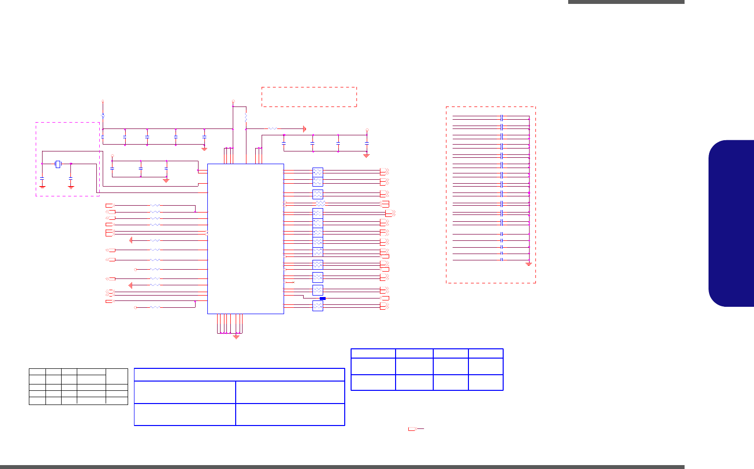
Schematic Diagrams
Clock Generator B - 19
B.Schematic Diagrams
Clock Generator
CLK_ PCIE_ M INI_3G
Z1740
C 488 *10P_50V_04
C5 3 4
10U_10V_08
Z1726
R279 33_04
BSEL0
SELLCD_27#=0
Z1712
R2 6 8 10 K _ 0 4
C502
0.1U_10V _X7R_04
1
M CH_CL KREQ #
(PEREQ2#)
CLK_BSEL1 [2,4]
REF _ 14 .31 8 M C LK_PC IE_N EW _ CAR D#
R284 2.2K_04
DO T 9 6
3.3VM _CLK
C 499 *10P_50V_04
3.3VM_CLK
X3
14.318M Hz
1 2
CLK_DREF
C LK_ CP U_ B CL K
CLK_PCIE_3GPLL#
C 507 *10P_50V_04
PC I E X9
CLK_ PCIE_3 GPLL
R293 *10m il_short
CL K_ ICH 48
Red words must be controlled by BIOS
CL K_ P W RG D[1 5]
Z1733
C LK_ P C IE_M IN I#
C 466 *10P_50V_04
R272 33_04
27FIX/SS
CLK_DREF#
RN24
4P2RX33_04
1 4
2 3
C468
0.1U_10V_X7R_04
Z1735
Z1704
RN21
4P2RX33_04
14
23
1
SELLCD_27#
PC LK_ IC H33[14]
MCH _CLKREQ # [5]
667 M Hz16 6 MHz
CLK_DREF # [5]
L39
HC B1608KF-121T25
WL AN_C LKREQ #
(PEREQ3#)
PM _STPPC I#[15]
CL K_ ICH 14
CLK_ SATA
FSLA
Z1736
R 2 95 3 0 0_ 1 % _0 4
PC I E X9
CLK_ PCIE_ M INI_3G #
R271 33_04
U2 2
ICS9L PR363EG LF
5
11
56
62
49
51
35
48
52
2
6
8
55 16
61
12
42
34
58
57
45
36
33
60
3
4
28
50
54
9
64
13 21
37
53
32
30
31
27
26
24
25
23
22
19
20
18
17
14
15
10
47
7
1
29
46
39
38
41
40
44
43
59
63
PC ICL K3/*SELPCIEX0_ LC D#
VD D48
VDD REF
CPU_STOP#
CPUT _ L 1F
CPU C_L 0
PCIe C_L 5
CPU C_L1F
CPU T_ L 0
GND
GN D
PC ICL K_ F4/IT P_ EN
SD ATA FSL B/TEST_M ODE
REF1/F SLC/TEST_SEL
FSLA/U SB_48MH z
VD DPC IEX
* PW RS AVE#
X1
X2
VD DA
PC IeT_L5
*PER EQ4#
R EF0_14.318M
PC ICL K1
PC ICL K2
VDD PCIEX
VDD CPU
SC LK
* SELLC D_27#/PCIC LK_F5
**PCICLK0/R EQ_SEL
GND VD DPC IEX
GND
GND
*PER EQ3#
PC IeT_L4
PCIe C_L 4
SATACLKC_L
SATACLKT_ L
PC IeT_L3
PCIe C_L 3
PCIe C_L 2
PC IeT_L2
PC IeT_L1
PCIe C_L 1
27 SS/L CD_SSC GC /PCIeC_L 0
27F IX/LCD _SSCG T/PC Ie T_L 0
PCIe T_ L9 /DO TT_ 96 MHz L
PCIe C_ L 9/D OTC_ 9 6 MHz L
VTT_PW R_GD /PD#
VR EF
VD DPC I
VDD PCI
GN D
GN DA
PC IeT_L6
PCIe C_L 6
PCIeT_L7/PER EQ1 #
PC IeC _L 7 /PER EQ2#
PCIeT_L8/CPU ITP T_ L 2
PC Ie C_ L8 /C PUIT PC_ L 2
GN D
PC I/PCIEX_STOP#
CLK_PCIE_MIN I [20 ]
C 492 *10P_50V_04
RN28
4P2RX33_04
14 23
RN31
4P2RX33_04
1 4
2 3
C471
27P_50V_04
CK505
106 6 MHz
PCI E CLK 4 (J M3 85 )
LCD(96MHz)
C532
0.1U_10V_X7R _04
C 498 *10P_50V_04
CLK_PCIE_ICH
C LK_DR EFSS
C 474 *10P_50V_04
BS EL2
CL K_ MC H_ B CL K
PCLK_TPM
Z1723
PCLK_ICH 33
C 509 *10P_50V_04
CL K_ ICH 48
C 449 *10P_50V_04
CLK_SATA
PCLK_TPM
Z1728
La y o ut n o te :
LAN_CLKREQ #
(PEREQ4#)
FS LC
IC H_SMBD AT0[10,11,15]
C LK_ P C IE_M IN I_ 3 G
XTAL_ IN
PCIECLK 2 (MINI )
3.3VS
CL K_ PCIE_ MIN I_3 G # [1 9]
CL K_ CP U _B CL K
CLK_ CPU_BC LK# [2]
CL K_ DR EF SS #
RN26
4P2RX33_04
14 23
C 484 *10P_50V_04
C 494 *10P_50V_04
PCIEX0
PCLK_ICH 33
C 501 *10P_50V_04
C LK_BSEL 2[2 ,4]
C491
0.1U_10V_X7R_04
PCIECLK 8 ( ICH)
BS EL1
DO T 9 6
3.3VM_CLK
PCLK_TP M[1 9]
SATACLK
CLK_DREF SS [5]
CLK_PCIE_GLAN [23]
CLK_ PCIE_ M INI
C LK_ P C IE_M IN I_ 3 G#
RN30
4P2RX33_04
1 4
2 3
C 536 *10P_50V_04
C 542 *10P_50V_04
Z1713
C 490 *10P_50V_04
SELPCIEX0_LCD#/
CLK_ PCIE_G LAN #
R267 33_04
CLK_ICH48[1 5]
30mils
CL K_ PCIE_ MIN I_3 G [1 9 ]
Z1725
0
Pin14/15
PCIECLK 3 ( MI NI_ 3G )
C 528 *10P_50V_04
C 497 *10P_50V_04
0
CLK_ SATA#
R296
1K_1%_04
SELLCD_27#=1
LAN _CLKREQ # [23]
CL K_ DR EF SS
CLK_SATA#
Z1731
CLOCK GENERATOR
Z1730
R2 6 9 10 K _ 0 4
SELLCD_27#=1
R 307 475_1%_04
PCIECLK 1 ( 3GP LL)
CLK_ CPU_BC LK [2]
CL K_ MC H_ B CL K#
CLK_PCIE_GLAN# [23]
CLK_PCIE_ICH [14]
Z1741
SELPCIEX0_LCD#/
CLK_PCIE_J M380# [22 ]
C 481 *10P_50V_04
Insatlled: Differential clock
level is higher
PCI ECLK 6 (NEW CARD)
CLK_ PCIE_N EW _C ARD
PCLK_KBC
C 541 *10P_50V_04
C 512 *10P_50V_04
C LK_DR EFSS#
Z1732
Z1729
C 537 *10P_50V_04
R253 *10K_04
C 475 *10P_50V_04
CLK_ PCIE_N EW _C ARD #
Fr eq uen cy
PCIEX0
CLK_ PCIE_ M INI#
Layout note:
CLK_PCIE_3GPLL [5]
CLK_ PCIE_J M38 0
Z1742
3.3VS
PCLK_KBC
CLK_MCH_BCLK
RN32
4P2RX33_04
1 4
2 3
0
Z1724
PCLK_KBC[2 6]
C 450 *10P_50V_04
Z1710
C LK_ P C IE_M IN I
PCI3 = 1 (high)
Z1711
CLK_PCIE_3GPLL
PLACE CRYSTAL WITHIN
500 MILS OF
ICS9LPR363EGLF
20 0 MHz
CL K_ CP U _B CL K #
C511
1U_6.3V_04
SATA_CLKREQ#
(PEREQ1#)
800 M Hz
Z1718
CLK_PCIE_GLAN
C 533 *10P_50V_04
FSLA
PM_ ST PCPU #[15 ]
CLK_PCIE_ICH # [14]
CLK_DREF SS# [5 ]
CLK_MCH_BCLK#
SELPCIEX0_ LC D#
PCI3 = 0 (low)
CLK_ PCIE_IC H
Z1719
CLK_PCIE_J M380 [22]
CLK_ PCIE_3 GPLL #
CLK_ PCIE_G LAN
Z1715
Z1738
Z1703
C LK_ CP U_ B CL K#
Host Clock
Z1722
PCIECLK 5 ( GLAN)
3.3VS
CL K_ MCH _ BCL K # [ 4 ]
C4 72
27 P_50V_04
0
WLA N_CLKREQ # [19,20]
Z1714
C478
* 10U _10V_0 8
RN22
4P2RX33_04
1 4
2 3
De f a ul t
Place termination close
to ICS9LPR363DGLF
CL K_ DR EF #
C 519 *10P_50V_04
Z1727
C4 6 7
1U _ 6. 3 V _ 0 4
C 487 *10P_50V_04
1
CL K_ MCH _ BCL K [ 4 ]
CLK_PCIE_ICH#
CLK_PCIE_NEW_CARD# [20]
C4 82
0.1U _10V_X7R_04
0
CL K_ ICH 14
FSLC
C 543 *10P_50V_04
R282 *100K_04
Pin5
REQ _ SE L
C 505 *10P_50V_04
Layout note:
3.3V S[5 ,8..16 ,1 9. .27,3 1]
CLK_ PCIE_J M38 0#
C LK_PC IE_N EW _ CAR D
CLK_ICH14[1 5]
26 6 MHz
SATA _C LKR EQ# [15]
IC H_SMBC LK0[10,11,15]
XTAL_ OU T
C4 8 0
0.1U_10V_X7R _04
RN29
4P2RX33_04
14
23
20mils
Pin17/18
C LK_BSEL 0[2 ,4]
CLK_DREF [5]
C 544 *10P_50V_04
FS LB
CLK_SATA# [13 ]
CLK_PCIE_JM380
Pin9
CLK_SATA [13]
CLK_PCIE_NEW_CARD [20]
RN23
4P2RX33_04
14
23
C535
10U_10V _08
C500
1U _6.3V_04
R 306 475_1%_04
CLK_ PCIE_IC H#
CLK_PCIE_JM380#
ITP_E N
0
CLK_PCIE_3GPLL# [5]
40mils
CL K_ PCIE_ MIN I# [2 0]
FSLB
R2 6 5 10 K _ 0 4
R266 *33_04
RN25
4P2RX33_04
14
23
SELLCD_27#=0
CL K_ DR EF
CLK_PCIE_GLAN#
RN27
4P2RX33_04
14 23
Sheet 18 of 40
Clock Generator
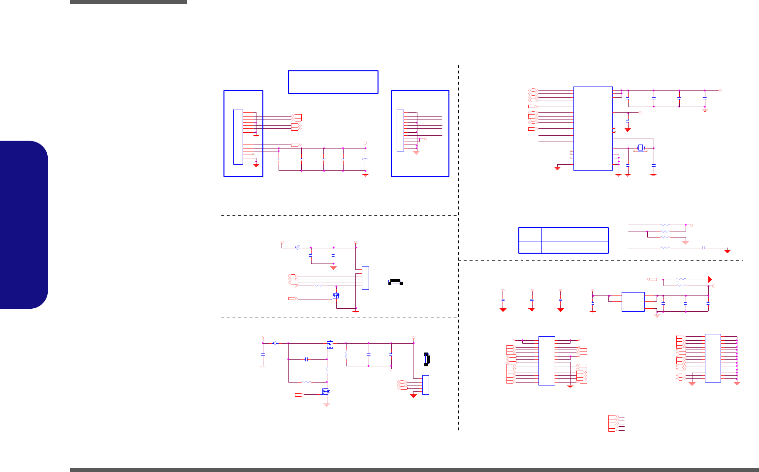
Schematic Diagrams
B - 20 Multi I/O, ODD, CCD, BT, TPM
B.Schematic Diagrams
Multi I/O, ODD, CCD, BT, TPM
AZ _SD IN1[13 ]
C5
0.1U_16V_04
C275
10U _10V_08
3.3VS
M DC_AZ_ SYN C[1 3 ]
TP M
U7
*SLB9635TT
17
26
23
20
10
13
24
19
22
21
16
27
15
4
11
18
25
6
2
14
8
9
7
1
3
12
28
5
LA D 3
LA D 0
LA D 1
LA D 2
VDD1
XTALI
VDD3
VDD2
LF R A M E #
LC LK
LR ESET#
SERIR Q
CL KRU N#
GND _1
GND _2
GND _3
GND _4
GPIO
GPIO2
XT A L O
TESTI
TESTBI/BAD D
PP
NC_ 1
NC_ 2
NC_ 3
LP C P D #
VSB
L2 0
HCB1005KF-121T20
LPC _FR AME#[1 3 ,26 ]
ODD_DETECT#
L PCP D#[1 5]
5V S[12,13,16, 21,24,25,27]
SATA_ RXP1
J_O DD_73
*85205-12
1
2
3
4
5
6
7
8
9
10
11
12
C5 8 7
*0.1U_16V_04
50m il
R168
100K_04
BT_ EN[21,26]
LP C _A D 0[1 3 ,26 ]
TPM_BADD
USB_PN5_3G[14 ]
C270
* 15P_50V_04
Layout Note
BT_D ET#[2 6]
3.3V[2 ,1 2..1 7 ,2 0,2 3 ,29 ,3 0]
SATA_ TXN1 [13]
Z1908
MULTI I/O CONN
1
SATA_TXN1
C268 *10P_50V_04
6
5V[16,21,28..31]
PCLK_TPM
SATA_ TXP1
C3 2
1U _10V_06
Z1909
TPM_PP
X2
* 3 2. 7 6 8K H z
14
3 2
PCIE_RXN3_3G[1 4]
48 mil
CCD _ DET #[2 6]
PCIE_TXN3_3G[14 ]
R152 *10K_04
USB _O C# 3[1 4 ]
SATA_ RXN1 [13]
BT_ EN#
M DC_ A Z_ B ITCL K[13 ]
( De fau lt )
SATA_RXN1
TPM_BADD
SATA_ RXN1
LPCPD# inactive to LRST# inactive 32~96us
3.3VS
CCD
5V_C CD
3.3V
PCIE_TXP3 _ 3G[14 ]
J_MFB2
5F1-233A1-A2000-214
12
34
56
78
910
11 12
13 14
15 16
17 18
19 20
21 22
23 24
25 26
27 28
C16
0.1U_16V_04
L OW : 2E / 2F h
LP C _A D 1[1 3 ,26 ]
5
TPM 1.2
SATA_RXP1
Asserted before entering S3
U SBVCC 2
FOR M720T FOR M730T
3G_EN [21,26]
WEB_WWW# [26]
TP M _B A D D
C216
*100U _6.3V_B 2
LOW : NORMAL
C5 8 1
*0.1U_16V_04
R151 *10K_04
J_CCD1
85204-05001
1
2
3
4
5
LPC reset timing:
3 .3 VS= 1. 5A
Q1 4
2N7002W
G
DS
J_BT1
87212-06G0
1
2
3
4
5
6
PCIE_ W AKE#[1 5,2 0 ,23 ]
O DD_DETEC T# [15]
C2 8 8
0 . 1U _1 6 V _0 4
WLAN_CLKR EQ# [18,20]
3G _D ET#[26 ]
TP M _P P
R 11 100K_1%_04
R147 *10K_04
HI : ACCESS
LED _ CAP#[2 6]
USB_PN9_BT[14]
L18 H CB1005KF-121T20
Bluetooth
5V S
LID_SW# [12,26]
3. 3V S
M_ B T N #[3 0]
1.5VS[3 ,8,1 3 ,14 ,1 6 ,20 ,2 9]
C4
10U_10V_08
H I : 4E / 4F h
PCLK_ TPM[1 8]
J_ M F B 1
5F1-233A1-A2000-214
12
34
56
78
910
11 12
13 14
15 16
17 18
19 20
21 22
23 24
25 26
27 28
SERIR Q[15,26]
C2 65
*1 U_ 10 V _ 06
R 13 200K_1%_04
LP C _A D 2[1 3 ,26 ]
SATA_TXP1
C15
0.1U_16V_04
3.3VS
C LK_ P C IE _M INI_ 3G #[18 ]
LED_THR OTTLE# [26]
( De fau lt )
5V
Q1 3
AO3409
G
DS
P CIE_RXP3_ 3 G[14 ]
C290
10U _10V_08
J_BT1
WLAN_CLKRE Q#[18,20]
1.6A
USB_PP7 _C CD[14 ]
CCD_EN[26 ]
3.3V
Z1907
C198
10U _10V_08
USB _ PN3[1 4]
SATA_ LED #[1 3 ]
MD C _A Z _R S T#[1 3]
USB_PP3[1 4]
USB_PP9 _BT[14]
SATA ODD
SATA_ RXP1 [13]
U SB_PP5 _3 G[1 4 ]
J_CCD1
U1
RT9701-CPL
1
2
3
4
5
VOUT
GN D
VIN
VIN
VOUT C2 0
*10U_10V_08
SATA_ TXP1 [13]
SATA SINGAL FROM SB TO JODDB1
END OF JODD1
C276
0. 1 U _1 6 V _0 4
3.3VS
L ED_ NU M#[2 6 ]
1.5VS
J_O DD_72
C18535-11305-L
S1
S2
S3
S4
S5
S6
S7
P1
P2
P3
P4
P5
P6
60 mil
TO SB GPIO
BUF_PLT_ RS T#[ 1 4 , 20 , 2 2 , 23 , 2 6]
SPKO UTR+[2 5 ]
PM_CLKRU N#[1 5]
3VS_BT
3.3V
5V
SPKOU TR -[2 5]
TPM_PP
OD D_ DE TE CT#
R169 330K_04
C2 7 1
*15P_50V_04
C266
* 0.1U_16V _04
60 mil
R153 *33_04
R177 100K_04
1
C LK _ PC IE_M INI_ 3 G[18 ]
W EB_ EMA IL# [26 ]
C2 77
0.1U_16V_04
C269
* 0.1U _16V_04
LED_SCR OLL# [26]
C199
0.1U _16V_04
R165
100K_04
LP C _A D 3[1 3 ,26 ]
PLT_RST#[5 ,14 ]
3.3VS[5 ,8..1 6 ,18 ,2 0 ..27 ,3 1]
5VS
1.5VS
C2 19
1U _10V_06
C289
0.1U_16V_04
USB_PN7_CCD[14 ]
APKEY # [30]
C274
0.1U_16V_04
USBVC C2
SATA_ TXN1
C205
0.1U_16V_04
M DC_ A Z_ S DO UT[1 3 ]
Q15
2N7002W
G
DS
From H8 default HI
3. 3 V
Sheet 19 of 40
Multi I/O, ODD,
CCD, BT, TPM
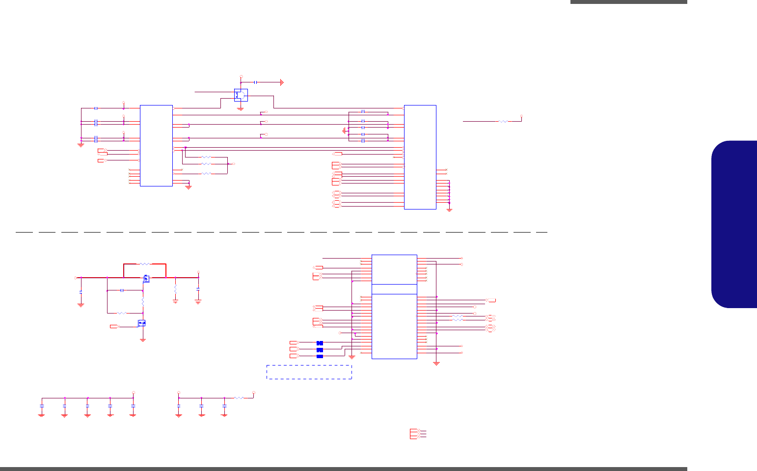
Schematic Diagrams
New Card, Mini PCIE B - 21
B.Schematic Diagrams
New Card, Mini PCIE
Sheet 20 of 40
New Card,
Mini PCIE
CL _ RST #1[1 5]
NC _P ERST#
WLAN _C LKREQ#
1.5VS
1.5VS
IC H_ SMBC LK1 [1 5 ]
R16
*100K_04
SUSB#[1 7 ,23 ,2 6,2 7 ,2 9]
USB_PN4_NEW[14 ]
WLAN_EN [21,26]
BU F_PLT_R ST#
WLAN1.5VS
R 21 *0_04
3.3VS
R 383 0_04
20mil
PCIE_RXN2_NEW_CAR D[14 ]
C440 0.1U _16V_04
C29
*10U_10V_08
3.3VS
3. 3 V
R2 3 *1 0m i l_s h ort
3.3V
NC_3.3VS
20 m il
PCIE_R XP1 _ W LAN[14]
Q3 *AO3409
G
DS
NC_3.3V
USB_PN2_MINI [14]
U SB_PP4_NEW[1 4 ]
GN D1 ~ 4 = G ND
WLAN3.3V
C40
0.1U_16V_04
C4 1
0. 1 U _ 1 6V _ 0 4
PCIE_TXN 2_N EW_C ARD[14]
R 20 *0_04
R249 *100K_04
WLAN3.3V
C 193 0.1U_16V_04
WLAN1.5VS
C442 0.1U _16V_04
C 196 0.1U_16V_04
PC IE_W AKE# WLAN3.3V
R18
0_04
Q2
*2N7002W
G
DS
BUF_PLT_RST#
R2 4 *1 0m i l_s h ort
U SB_PP2_MIN I [14]
BUF_ PLT_ RST#
C 191 0.1U_16V_04
R9 *1 0 K_ 04
C45
0. 1 U _1 6 V _0 4
C2 4
10U_10V_08
C43
0.1U_16V_04
C4 4
10U _10V_08
6- 01- 74 108 -Q6 1
R2 42 *10 K_04
BU F_PLT_R ST#[14,19,22,23,26]
IC H_ SMBD AT1 [15]
CL K_ P CIE_ MIN I#[1 8 ]
NC _C PPE#
WLAN_CLKREQ #
R247 *100K_04
CL K_PCIE_ NEW _CAR D#[18]
40 mil
WLAN1.5VS
PC IE_R XN1_W LAN[14 ]
USB_ OC# 4[14]
C446
*0.1U_16V_04
PCIE_ W AKE#[ 1 5 , 19 , 2 3]
3.3V[2 ,1 2..1 7 ,1 9,2 3 ,29 ,3 0]
U1 8
74 A H C 1 G 0 8G W
1
2
5
4
3
CL K _ PCIE _ MIN I[1 8 ]
WLAN_DET#[2 6]
ENE P2231 pin3,4,14,15,22
has internally pulled high
( 170K ohmS )
WLAN 3.3V
C23
0.1U_16V_04
3.3VS
NC_RST #
C441 0.1U _16V_04 C 181 0.1U_16V_04
40 mil
20 mil
WLAN_CLKREQ #[1 8,1 9 ]
PCIE_ W AKE#
J_ N E W 1
130801-1
17
1
10
26
20
23
4
19
18
22
21
25
24
14
15
12
9
13
11
8
7
16
5
6
3
227
28
29
30
CPPE#
GND
+1.5V
GND
GND
GND
CPUSB#
REFCLK+
REFCLK-
PER p0
PER n0
PETp0
PETn0
+3.3V
+3.3V
+3.3VAU X
+1.5V
PER ST#
WAKE#
SM B_D ATA
SM B_C LK
CLKREQ#
RESERVED
RESERVED
USB_D+
USB_D- GND
GND
GND
GND
PCIE_ TXP2 _NEW _CAR D[14]
CLK_PCIE_NEW _ CAR D[1 8]
C33
*0.1U _16V_04
U1 9
P22 3 1TH LFC 1
2
3
4
6
5 8
7
9
1
11
14
15
16
17
18
19
20
21
22
23
10
12
13
24 25
SY SRST#
SHD N#
STBY#
3.3VIN
3.3VIN 3.3VO UT
3.3VO UT
PERS T#
NC
GN D
CPUSB#
CPPE#
1.5VO UT
1.5VO UT
1.5VIN
1.5VIN
AU XO UT
AU XIN
RC LKE N
OC#
NC
NC
NC
NC GND
KEY
J_ M I N I 1
88908-5204
3
5
7
9
11
13
1
15
23
25
21
27
31
33
29
17
19 20
37
39
41
43
45
47
49
51
44
42
18
16
14
2
12
10
8
6
4
22
24
26
28
30
32
34
36
38
40
46
48
50
52
35
BT_DATA
BT_CHC LK
CLKREQ#
GND0
REFCLK-
REFCLK+
W AKE#
GND1
PETn0
PETp0
GND2
GND3
PER n0
PER p0
GND4
NC3
N C4 W _D ISABLE#
NC6
3.3V_3
3.3V_4
NC9
NC10
NC11
NC12
NC13
LE D _ W LA N #
NC(LED_WWAN #)
GND 6
UIM _VPP
UIM _R ESET
3.3V_0
UIM _C LK
UIM _D ATA
UIM_PWR
1.5V_0
GND 5
PERSET#
3.3V_2
GND 7
1.5V_1
N C ( S M B _C LK )
N C(SM B_D ATA)
GND 8
NC (US B_ D-)
NC(USB_D+)
GND 9
N C ( L E D _W P A N #)
1.5V_2
GN D1 0
3.3V_1
GND11
PCIE_ TXP1 _W LAN[1 4]
C445 0.1U _16V_04
I CH_ SMBD AT1[15 ]
1.5VS[3 ,8, 13 ,14 ,1 6 ,19 ,2 9]
20 mil
20 mil
R10
*100K_04
C26
*0.1U_16V_04
NC_1.5VS
3.3V
R1 2
*330K_04
CL_DATA1[1 5]
3.3VS[5 ,8 ..1 6,1 8 ,19 ,2 1 ..27 ,3 1]
C443 0.1U _16V_04
MINI CARD
20 mil
WLAN3.3V
C 187 0.1U_16V_04
R2 2 *1 0m i l_s h ort
C42
0. 1 U _1 6 V _0 4
PCIE_RXP2_NEW_CARD[14 ]
NC _C PUSB#
WLAN3.3V
PCIE_TXN1 _W L AN[14]
CL _ CL K1[1 5]
WLAN 1.5VS
NEW CARD
For Kedron WLAN Device
WLAN _PWR[26 ]
ICH_SMBCLK1[15 ]
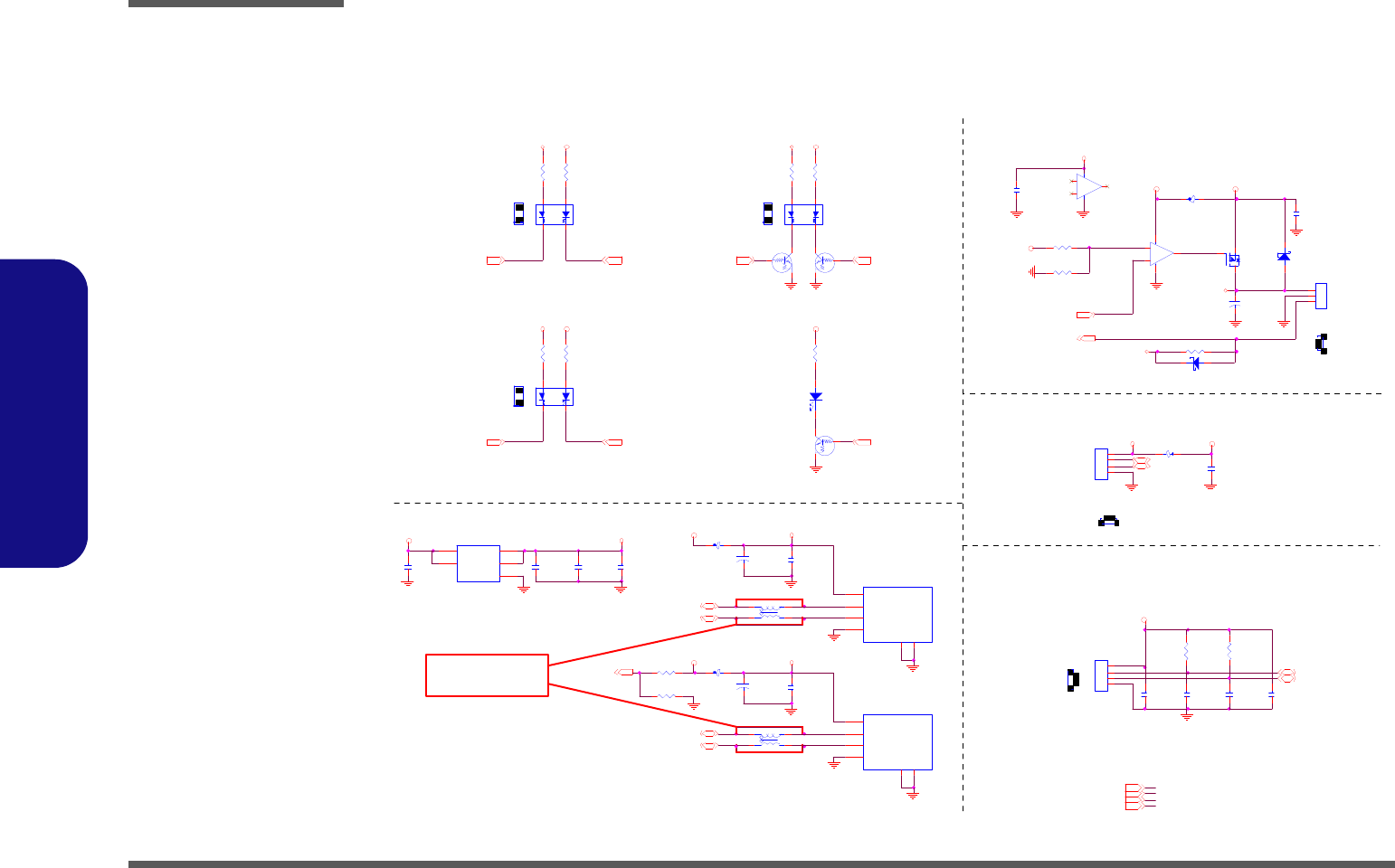
Schematic Diagrams
B - 22 LED, FAN, TP, FP, USB
B.Schematic Diagrams
LED, FAN, TP, FP, USB
C447
0.1U _16V_04
W LAN _EN [20,26]
3G LED
LED _BAT_CH G#[26 ]
R71
10K_04
Q20
AO3409
G
D S
VD D3
U SBVCC01
J_TP1
30mils
60 m i l
L ED_ B AT _ FUL L# [26 ]
1
3.3VS
USBVC C01
Z2101
1
3.3VS[5,8..16,18..20,22..27,31]
1
5VS
C4 3 9
100U_6.3V_B2
C529
0.1U _16V_04
LED_PWR # [26]
J_USB2
C10777-104A3-L
1
5
2
3
4
6
V+
GND1
DA TA_ L
DA TA_ H
GN D
G ND2
Z2109
WLAN/BT LED
R158
220_04
R2 9 9
100K_1%_04
USB_PP1[1 4]
VDD3
USB_PP0 _R
Z2115
2
5V[16,19,28..31]
USB_PN11_FP [14 ]
C1 58
47 P_ 50V_0 4
3
BAT LED
5VS_FAN
Z2112
Z2105
USB_VCC01 _0
C4 37
*0.1U _16V_04
60 mil
R2 44
10K_1% _04
L36 HCB 1608KF-121T25
L35 HCB 1608KF-121T25
Layout note:
TP_D ATA [26]
3.3VS
C495
*10U_10V_08
J_ F A N 1
85205-03001
1
2
3
USB_PN0[1 4]
J_FP1
85201-04051
1
2
3
4
R3 0 0
200K_1%_04
R1 61
220_04
U2 1
RT9701-CPL
1
2
3
4
5
VOUT
GN D
VIN
VIN
VOUT C503
0.1U_16V_04
4
USB PORT
USB_PN1[1 4]
F AN_ DC _ VOL _R
Place under the common
bead body and same as
USB trace requirment
USB_PP11_FP [14]
C146
1U_10V_06
60mil
U SB_O C#01[14]
L3 1
H CB1005KF-121T20
C159
47 P_ 50V_04
R1 62
220_04
VD D3
C493
1U_10V_06
5V S
C438
10U _10V_08
F AN_ DC _ VOL
60 mil
USB_PP1 _R
3.3VS
3
Z2111
30mils
3.3VS
3.3VS_FP
R1 57
220_04
1
4
3. 3 V S
5V S[ 1 2 , 13 , 1 6, 19 , 2 4, 2 5 , 27 ]
R159
220_04
C444
100U_6.3V _B2
4
USB_PP0[1 4]
C157
* 10U_10V_08
SG
Y
D1 8
RY -SP155HY YG4
1
3
2
4
J_FAN1
FAN CONTROL
USB_PN1_R
POWER ON LED
USBVC C01
5V
C88
0.1U_16V_04
2
VDD3
L8
HCB1 0 05 K F-1 2 1T 2 0
C508
100U_6.3V _B2
C4 86
0.1U_16V_04
FAN_DC_VOL
USB_VCC01 _1
VDD 3[13 ,2 6 ..30 , 3 2]
+
-
U1 6 B
LM358L
5
67
LED
Z2113
BT_ EN[1 9,2 6 ]
L3 4
*WCM 2012F 2S-161T03
1
4
2
3
3
J_FP1
R7 0
10 K _ 04
CPU_FANSEN[26]
Z2102
Q7
DT C1 1 4 EUA
CE
B
4
J_TP1
85201-04051
1
2
3
4
1
1
Z2114
Q8
DT C1 1 4E U A
CE
B
R246 4.7K_04
LED_AC IN#[26]
Q9
DT C1 1 4 EUA
CE
B
SG
Y
D2 2
RY -SP155HY YG4
1
3
2
4
USB_PN0_R
SG
Y
D1 9
RY -SP1 55HY YG4
1
3
2
4
R1 55
220_04
CLICK CONN
J_USB1
C10777-104A3-L
1
5
2
3
4
6
V+
GND1
DA TA_ L
DA TA_ H
GN D
G ND2
D2 0
RB5 5 1V - 30
A C
+
-
U1 6A
LM 35 8 L
3
21
84
TP_C LK [26]
D 21 R B551V-30
AC
R2 43
4.99K_1%_04
4
Z2110
L4 1
*WCM 2012F 2S-161T03
1
4
2
3
FP CONN
5VS
Z2106
3
2
CPU_ F AN[26 ]
R160
220_04
3G _EN [19,26]
D2 3
RY -SP172YG 34
AC
Sheet 21 of 40
LED, FAN, TP, FP,
USB
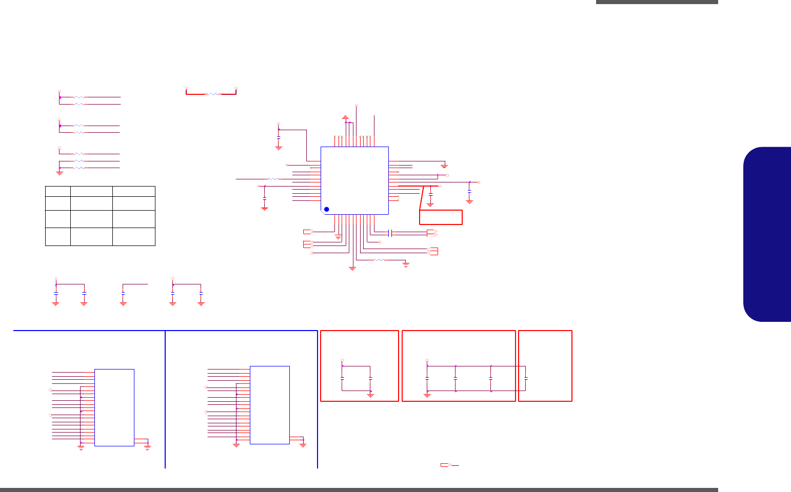
Schematic Diagrams
JMB385 Card Reader B - 23
B.Schematic Diagrams
JMB385 Card Reader
SD/M S_D3
LOW
MDIO12
M720T Card Reader
Connector
PCIE _R XP5_C ARD [14]
SDCMD/MSBS
C 549 0.1U _10V_X7R _04
MDIO14
MS_INS#
HI GH
C591
0.1U_16V_04
VCC_CARD
SD/M S_ D3
Layout note:
3. 3V S
PC IE_TXN 5_C ARD [14]
SD/M S_D2
MDIO7
VCC_CARD
3.3VS_CAR D
SD/M S_ D3
R403 0_06
Ve ry c los ed b et wee n
pin 10
MDIO13
SD _CD#
B U F _ P L T_ R S T#[14,19,20,23,26]
MS _ I N S #
SD/M S_ D2
SD/M SCLK
SD W P #
DV1 .8 V
SD/M SCLK
V er y clo se d to pi n 5( Tr ac e w id th /l eng th :
20mil/ <120mil)
DV1.8V
CLK_PCIE _JM380[18 ]
MS _ I N S #
3. 3 V S _ C A R D VC C_ CAR D
SD/M S_D0
SDW P #
PC IE_TXP5_CAR D [14]
R 384 22_04
C604
0.1U _16V_04
Layout note:
SD/M S_ D1
CLK_PCIE_JM380#[1 8 ]
JMB385 CARD READER
C5 2 2
10P_50V_04
R335 10K_04
SD/M S_ D1
D V1.8V
MDIO1 4
CR1_LEDN
High
Active
02/12
SD W P#
SD CM D/M SBS
C5 5 7
0.1U _16V_04
C5 5 2
1000P_50V_X7R _04
SD/M S_D1
SDCMD/MSBS
MDIO13
MDIO1 2
CR1_LEDN
Low
Active
Layout note:
MS_INS#SD /MS_ D 2
MDIO14
C5 5 1
0.1U _16V_04
3.3VS_C ARD
C592
0.1U_16V_04
MDIO7
R331 10K_04
SD/M S_D3
SD /MS_ D 3
PCIE _R XN5_C ARD [14]
R339 200K_04
Layout Note:
SD/M SCLK
SD_C D#
C6 0 5
0.1U _16V_04
C573
0.1U _16V_04
VCC _CAR D
R353 200K_04
SD/M S_ D0
SD /MSC L K
R310 4.7K_04
C524
0.1U _16V_04
Add-in Card
MDIO12
C583
0.1U _16V_04
C517
0.1U _16V_04
JMB385
U27
JMB 385-LGEZ0B
1
2
3
4
5
6
7
8
9
10
11
12
14
15
16
17
18
19
20
21
22
23
24
13
37
38
39
40
41
42
43
44
45
46
47
48
36
35
34
33
32
31
30
29
28
27
26
25
XRS TN
XT EST
APC LKN
AP CLKP
APVD D
AP GND
APR EXT
AP RXP
APR XN
AP V18
APTXN
AP TXP
SEECLK
CR1 _ CD 1 N
CR1 _ CD 0 N
C R1_PCTLN
DV 18
REG _ CTRL
DV 33
CR _L ED N
MDIO14
MDIO13
GN D
SEEDAT
DV 18
PC IES_EN
PC IES
MD IO7
MD IO6
MD IO5
MD IO4
DV 33
MD IO3
MD IO2
MD IO1
MD IO0
NC
NC
NC
GND
GN D
GND
TAV33
MDIO8
MDIO9
MDIO10
MDIO11
MDIO12
3.3VS_CAR D
SD /MS_ D 0
C5 6 1
0.1U _16V_04
R332 4.7K_04
3.3VS_CAR D
3.3VS_CAR D
On Borad
Must > 30mil
3.3VS_CAR D
SD/M S_D2
SD/M S_D0
J_CAR D-R _72
M DR 019-C0-0010(R ev erse)
P2
P21
P3
P4
P5
P6
P7
P8
P9
P10
P11
P12
P13
P14
P15
P16
P17
P18
P19
P20
P1
P23
P22
DA T2_SD
VSS_M S
CD /DA T3 _ SD
CM D_SD
VSS_SD
VD D_SD
CL K_ SD
VSS_SD
DA T0_SD
DA T1_SD
WP_SD
VSS_M S
VC C_MS
SC LK_M S
DA T3_MS
IN S_M S
DA T2_MS
SD IO/D AT0 _ MS
DA T1_MS
BS_MS
CD _ SD
GN D
GN D
3.3VS[5,8. .16,18..21,23..27,31]
3.3VS_CAR D
40mil
SD/M SCLK
C 550 0.1U _10V_X7R _04
VC C_ CAR D
D V1.8V
SD /MSC L K
VC C_CAR D
R343 10K_04
SD _ CD#
CR1_PCTLN
Low
Active
40mil
VCC _CAR D
MDIO7
SDCMD/MSBS
SDW P #
C5 5 3
10U _10V_08
Near Cardreader CONN
J_CAR D-R _73
*MD R019-C 0-0010(Reverse)
P2
P21
P3
P4
P5
P6
P7
P8
P9
P10
P11
P12
P13
P14
P15
P16
P17
P18
P19
P20
P1
P23
P22
DA T2 _ SD
VSS_M S
CD /DA T3_SD
CM D_ S D
VSS_SD
VD D_SD
CL K_ SD
VSS_SD
DA T0 _ SD
DA T1 _ SD
WP_SD
VSS_M S
VC C_MS
SC LK_M S
DA T3 _ MS
IN S_M S
DA T2 _ MS
SD IO/D AT0_MS
DA T1 _ MS
BS_MS
CD _ SD
GN D
GN D
SD_C D#
3.3VS_CAR D
SD /MSC L K_R
Ve ry cl os ed b et wee n
pi n 19 an d pi n 20
DV1 .8 V
R 327 8.2K_1%_04
CR1_PCTLN
High
Active
SD/M S_D1
M730T Card Reader
Connector
SD/M S_ D2
C590
10U_10V _08
SDCMD/MSBS
SD /MS_ D 1
SD/M S_ D0
Sheet 22 of 40
JMB385 Card Reader
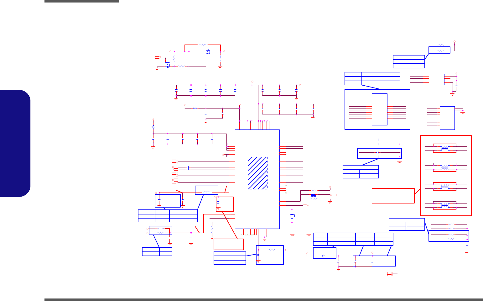
Schematic Diagrams
B - 24 PCI-E LAN RTL8111C
B.Schematic Diagrams
PCI-E LAN RTL8111C
Sheet 23 of 40
PCI-E LAN
RTL8111C
LMX1+
MX 1 +
C365
22P_50V_04
MDI O 0 -
RT L81 11 C
MA0/EED O
MX4+
20mils
C50
* 10U _10V_ 08
Unstuff
C4 9
PC IE_RXP4_LAN[14]
MX 2 -
R 404 *0_04
V_D AC
R413
* 100K_04
1. 2V _ L A N
C5 1
0.1U _16V_04
R225 *15K_04
C286 0.01U_16V_X7R _04
C388
0.1U _16V_04
MCT2
P CIE_RXP4_LAN _C
MDIO2-
LMX4+
R2 2 4 * 1 0m i l_ s h ort
La yo ut n ot e:
LAN_EVD D12
MX3+
Stuff
RT L8 11 1C
V_D AC
15mils
PCIE_WAKE# [15,19,20]
Un stu ff
LAN_EVDD 12
V_DAC
C3 7 9
0.1U _16V_04
C3 67
X1
25MHz
12
MCT 4
MDIO1-
L69
*WC M2012F2S-161T03
1
4
2
3
R215
2.49K_1% _04
1.2V_LAN
1.2V_LA N
BUF_PLT_R ST#[14,19,20,22, 26]
MA1/EED I
MDI O 1 -
MX2-
R4 1 2
*3 3 0K _0 4
C360
0.1U _16V_04
G ST 50 09L F / LG -24 13 S- 1
C374 0.1U_10V_X7R_04
3.3V[2,12..17,19,20, 29,30]
M A1/EEDI
L5
H CB1005KF- 121T20
C377 0.1U_10V_X7R_04
R217
MX 2 +
C367
0.1U_16V_04
L4
SWF2520CF-4R 7M -M
LMX2+
C84
0.1U_16V_04
L5
Layout note:
LMX4-
C6 4 1
*0.1U_16V_04
C3 5 8
0.1U _16V_04
C49
22U_6.3V_X5R_08
LA N _ V D D 3
MA2/E ESK
C3 8 6
0.1U _16V_04
C292
1000P _2KV_12
6 0mi ls a nd le ng th < 20 0m il
RT L81 02 E
LAN_AVD D3
MDI O 3 -
MCT 1
R TL8 11 1C
R4 1 4
* 100K_04
P CIE_RXN4_LAN_C
MX 1 -
R223 *1K _04
0_ 04 02
RT L81 11 C
RTL8102E
V_DAC
L53
0_04
C354
0.1U _16V_04
EN _LAN 12
MX1+
MX2+
L3
0_04
V_D AC
EN_LAN12
R402, C641
60mil
RTL8111C
MX4-
Stuff
MDI O 2 -
R TL8 10 2E
3.3V S[5,8..16,18..22,24..27,31]
LMX3+
MDIO3+
MDI O 3 +
C285 0.01U_16V_X7R _04
MCT1
C3 5 5
0. 1U _1 6 V _ 04
L70
*WC M2012F2S-161T03
1
4
2
3
Stu ff
LMX4+
C2 86 ,C 28 7
MA2/EES K
C61
MA1/E EDI
C373
0.1U _16V_04
V_D AC
RTL8111C
RTL8111C
60 mi ls a nd le ng th < 20 0mi l
RT L8 10 2E
RTL8102E
R 176 75_04
V_DAC
C5 3
*10U_10V_08
RTL 81 11 C
20mils
C3 7 8
0. 1U _1 6 V _ 04
Place under the common
bead body and same as
LAN trace requirment
R178,R179
LAN _PW R[15]
MCT3
LMX4-
C287 0.01U_16V_X7R _04
3.3VS
LAN_C LKR EQ#[18]
MDIO1+
MX3-
R 178 75_04
U2
H T93LC46-A18PB
1
2
3
4
7
6
5
8
CS
SK
DI
DO
NC
ORG
GND
VCC
L4
MCT 2
LMX3-
RT L8 111 C/
RT L8 102 E
PCI-E LAN
GND
U1 4
R TL8111C -VB-GR
18
19
20
21
22
23
24
25
26
27
28
29
30
31
32
1
2
3
4
5
6
7
8
9
10
11
12
13
14
15
16
48
47
46
45
44
43
42
41
40
39
38
37
36
35
34
33
64
63
62
61
60
59
58
53
52
51
50
49
17
54
55
56
57
NC
LANW AKE#
PER ST#
DVDD12
EVD D12
HSI P
HSI N
EG ND
REF CLK_P
REF CLK_N
EVD D12
HSO P
HSO N
EGND DV DD1 2 /NC
SRO UT12/VCTRL12A
AVD D33
MD IP0
MDIN0
FB12/AVDD 12
MD IP1
MDIN1
AVD D12
MD I P 2 / NC
MDIN 2 /NC
AVD D12/ NC
MD I P 3 / NC
MDIN 3 /NC
AVD D12/ NC
N C/DV DD1 2
VDD 33
EESK
EEDI/AU X
VDD 33
EEDO
EECS
DV DD1 2
NC
NC
NC
NC
DVDD 1 2/N C
VD D33
ISOL AT E#
NC
NC
CL KR EQ#
RSE T
VDD SR/V CTRL12D
ENS R/NC
CKT AL 2
CKT AL 1
AVDD33/NC
AVD D12/ DVDD 12
VD D33
D VDD1 2 /NC
GPO
GPI
DVD D1 2
NC
LE D 3
LE D 2
LE D 1
LE D 0
Unstuff
SW F2 520 CF -4 R7 M-M
PCIE_RXN 4_LAN[14 ]
LMX1-
R402 *0_04
R 175 75_04
3. 3V
MX 3 -
St uf f
EEC S
R4 04
60mil
R 179 75_04
C67
22U _6.3V_X5R _08
RTL 81 02 E
LMX2+
MA0/E EDO
PC IE_TXP4_LAN[1 4 ]
R 401 0_04
PC IE_TXN 4_LAN[14]
MX 4 -
L68
*WC M2012F2S-161T03
1
4
2
3
C3 5 9
0.1U _16V_04
LMX1-
C385
0.1U_16V_04
RT L81 02 E
R400 0_04
02/22
MX 3 +C370
0.1U_16V_04
LA N _ V D D 3
Un st uf f
1.2V_LAN
C645
0.1U_16V_04
Stuff
Unstuff
MCT4
ISOL AT E#
1. 2V_LAN
C358 must close
to U14 pin5
CLK_ PCIE_G LAN[18 ]
EEC S
MCT 3
MDIO2+
CLK_PCIE_GLAN#[18]
LMX2-
L19
G ST5009LF
1
2
3
4
5
6
7
8
9
10
11
12 13
14
15
16
17
18
19
20
21
22
23
24
TCT1
TD1+
TD1-
TCT2
TD2+
TD2-
TCT3
TD3+
TD3-
TCT4
TD4+
TD4- MX4-
MX4+
MCT 4
MX 3 -
MX3+
MCT 3
MX 2 -
MX2+
MCT 2
MX 1 -
MX1+
MCT 1
LF-H6442S-1
MDI O 0 +
C6 4 0
0. 1U _1 6 V _ 04
40mils and length < 200mil
LAN_ VD D3
1.2V_LAN
1.2V_LAN
C375
0.1U_16V_04
20mils
C371
0.1U_16V_04
C6 1
*4.7U_6.3V _X5R_06
St uf f
LAN_VDD3
C10091-108A4
J_ R J- 4 5
8
7
6
5
4
3
2
1GND1
GND2
DD-
DD+
DB-
DC-
DC+
DB+
DA-
DA+ shield
s hie ld
Unstuff
SUS B# [17,20,26,27,29]
MDI O 2 +
R4 5 3.6 K _ 0 6
C356
0.1U_16V_04
RTL8102E
LAN _VD D3
MX 4 +
LMX3+
C357
0.1U_16V_04
C644
*0.1U _16V_04
St uff
Un st uff
R4 01
MDIO0-
Q28 *AO 3409
G
DS
C368
22P_ 50V_0 4
C3 64
0.1U _16V_04
0_ 08 05
MX1-
MDI O 1 +
LMX2-
Q2 9
*2N 7002W
G
DS
HCB1005KF-121T20
LA N _ V D D 3
MDIO0+
C284 0.01U_16V_X7R _04
V_DAC
C3 8 7
0. 1U _1 6 V _ 04
L67
*WC M2012F2S-161T03
1
4
2
3
15mils
LMX3-
MDIO3-
LMX1+
R217 0_04
L1 9
Schematic Diagrams
Audio Codec ALC662 B - 25
B.Schematic Diagrams
Audio Codec ALC662
C los e t o cod ec pi n 3 8
5V S _ A U D
C2 5 9
0. 1 U _1 6 V _0 4
C5 06
0.1U_16V_04
GREEN
AU DG
C5 6 8
680P_50V_X7R _04
R334
2.2K_04
5V S[12,13,16,19,21,25,27]
MIC_SENSE
MIC1-VREFO-R
Z2404
C5 7 4
0.01U_16V_X7R _04
AZ_ SDIN 0[1 3 ] R312 33_04
Z2412
L46 FC M1005KF-121T03
AUD G
Z2424
R385 *0_04
CO DEC _EAPD #[2 5 ]
C588
680P_50V_X7R _04
MIC 1- L _ 73
BLACK
HP-R[25]
HP-L_73
MIC 1-L
AUDG
INT _ MIC
Z2408
HP-R_73
R337
220_04
Layout Note:
J _IN TMIC1
88266-02001
PCB Footprint = 88266-2L
2
1
A UD_AZ_ RST#[13,25]
MIC 1-R _7 3
BEEP
IC H_SPKR[15]
HP_PLUG[25]
FR ON T-R [25]
Z2409
SPDIF OUT
KBC _BEEP[26]
FR ON T-L [25]
MIC_ SENS E
L47 FC M1005KF-121T03
C556 4.7U _6.3V_X5R_06
INT _ MIC
C565
4.7U_6.3V_X5R _06
FO R M7 30T
HP-L
C514
10U _10V_08
R388 *0_04
MIC1 -R_ 7 3
C155
680P_50V_X7R _04
C576
1U _10V_06
R142 20K_1% _04
AU DG
C562 0. 1U _16V_04
HP_OUT-L [25]
SPDIFO
MIC1-VREFO-R
MIC1 -L
L38 HC B1005KF-121T20
Close to codec
R116 4.7K_04
1
C2 36
0. 1 U _ 1 6V _0 4
R
L
J_MIC _72
C12103-D0609-L
2
6
5
3
1
4
HEADPHONE
For M730T
AUD G
5VS
HP-L[25 ]
AUD _AZ_SDO UT[1 3]
Z2411
R386 *0_04
L54 FC M1005KF-102T02
AUDG
4
Layout Note:
3.3VS_AUD
MIC _SEN SE
C575
10U_10V_08
MIC1-VREFO-L
AUD _AZ_SYN C[1 3]
HP_SENSE
MIC1 -R
FOR M720T
Z2421
5
C567
0.1U_16V_04
MIC1-VREFO-L
Z2408
B EEP
Z2427
AZ_SDIN0_R
C237
0.1U_16V_04
MI C 2 - V R E F O
AUD G
MIC1 -L
Z2410
HP-R _7 3
JD _S E N S E 1
L45
H CB1005KF-121T20
AUDG
Z2426
AU DG
R7 2
4.7K_04
C 530 22P_50V_04
HP-R
JD _S E N S E 2
AUD G
2
Z2409
Layout Note:
6
2
SPDIFO
Lay ou t N ot e:
R320 39.2K_1%_04
SPDIFO_73
Z2410
Z2411
R 3 29 1 K _0 4
AUD _AZ_BITCLK[1 3] Z2425
L48 FC M1005KF-121T03
C558 0. 1U _16V_04
3
C5 6 6
10U_10V_08
3.3V S[5,8..16,18..23,25..27,31]
R387 *0_04
R
L
J_SPDIF_72
C12103-10609-L
2
6
5
3
1
4
3.3VS
HP_ S ENS E
C578
680P_50V_X7R _04
C570
10U _10V_08
1
Z2428
C577
680P_50V_X7R_04
MIC2-VREFO
J_INTMIC1
C 238 100P_50V_04
C523 1U_10V_06
R389 *0_04
L50 FC M1005KF-121T03
PINK
C228 1U_10V_06
AUD G
R3 3 3
2.2K_04
AU DG
Z2430
C560 4.7U _6.3V_X5R_06
Ve ry clo se to Au dio C ode c
Clo se to co dec p in 25
HP_OUT-R [25]
C569
680P_50V_X7R_04
HP-L _7 3
Z2403
C548 0. 1U _16V_04
MIC 1-R
L16
H CB1608KF-121T25
C555 0. 1U _16V_04
DIG ITA L
ANALOG
U25
ALC66 2-G R
1
2
3
4
5
6
7
8
9
10
11
12
13
14
15
16
17
18
19
20
21
22
23
24
26
27
28
29
30
31
32
33
34
35
36
37
39
40
41
42
43
44
45
46
47
48
38
25
DVDD1
GPIO 0
GPIO 1
DVSS1
SDATA-OU T
BIT-CLK
D VSS2
SDATA-IN
DVDD 2
SYN C
RESET #
PCBEEP
Sens e A(JD 1)
LINE2-L
LINE2-R
MIC 2-L
MIC 2-R
CD -L
CD -GND
CD -R
MIC 1-L
MIC 1-R
LINE1-L
LINE1-R
AVSS1
VR EF
MI C 1 - V R E F O -L
N.C .
M IC2 -VREFO
LINE2-VREFO
MIC1-VREFO-R
N.C .
Sens e B(JD 2)
FRON T-O UT-L
FRO NT-OUT-R
N.C .
SU RR-O UT-L
JDR EF
SURR -OUT-R
AVSS2
CEN
LFE
N.C .
N.C .
EAPD
SPDIFO
AVDD2
AVD D1
SPDIFO _73
Cod ec pi n 1 ~ 11 an d p in 47 ~ 48
are D igi tal s ign als .
The o the rs ar e a nal og si gna ls.
HP_PLUG
R1 17 4 7K_ 0 4
5VS_AU D
C563
4.7U_6.3V_X5R _06
HP_ PLU G
C580
1000P_50V_X7R_04
MIC IN
MIC 1 -R
J_ A U D _7 3
*87151-12071G
1
2
3
4
5
6
7
8
9
10
11
12
C227 1U_10V_06
R 3 23 2 0K _ 1 % _0 4
Layout Note:
C579
680P_50V_X7R_04
R 3 30 1 K _0 4
R
L
J_HP_72
C12103-60609-L
2
6
5
3
1
4
R385,R386,R387,R388,
R389
MIC1 -L _7 3
HP_SENSE
Z2429
EAPD_MO DE
Sheet 24 of 40
Audio Codec
ALC662
Schematic Diagrams
B - 26 Audio AMP2056
B.Schematic Diagrams
Audio AMP2056
Sheet 25 of 40
Audio AMP2056
SPKO UTL+_R1
R 134 39K_04
AU DG
Z2506
C2 6 0
0.1U_16V_04
Low mute!
SPKO UTL -
C1 0
180P_50V_04
SPKO UTL-
MU TEAM P#
C538
0.1U _10V_X7R_04
C5 2 0
0. 1U _16V _04
C 251 4.7U _6.3V_X5R_06
HP_ O UT -R[2 4 ]
R 140 39K_04
HP_OUT-L[24]
MU TEAM P#
Near CP+ and CP-
C6 3 6
0. 01 U _ 16 V _ X 7 R _ 0 4
For M720T
3.3VS
SPKOUTR- [19]
C245
*0.1U_16V_04
R_HP_O
5VS
SPKO U TL-_R
C620 68P _50V_04
AU DG
L1
FCM 1005KF- 121T03
L57
* F C M 1 0 05 K F - 1 21 T 0 3
C6 3 7
1U _ 1 0V _0 6
HP -R [2 4 ]
AU D_AZ _R ST#[13,24]
SPKOUTR-
SPKO UTL-_R1
SPKO UTL+ SPKOUTR+
R144
M730T
5V S
5VS[12,13,16,19,21,24,27]
J_S PKL_72
88266-02001_R
PC B Footprint = 88266-02R
2
1
AU DG
C615
*180P_50V_04
SPKOUTR+ [19]
R_ H P_ O
L59
* F C M 1 0 05 K F - 1 21 T 0 3
3.3VS_AM P
5VS_AM P
AUD G
C613
*180P_50V_04
C261
0.1U_16V_04
5.6K_04
SPKO UTL +
S YSM UTEA MP#
5VS
C 257 4.7U _6.3V_X5R_06
J_SP KR_73
*88266- 02001_R
PC B Footprint = 88266-02R
2
1
Z2509
C 642
*0.1U_16V_04
3.01K_1%_04
C539 0.1U_16V_04
R1 2 7
10K _04
SPK OU TL+
C515
*10U _10V_08
C 255 4.7U _6.3V_X5R_06
R141
Z2512
AP A205 6A
U2 6
APA20 5 6A
6
4
19
11
26
13
17
18
15
9
27
25
8
21
22
3
12
14
16
24
5
28
1
20
10
2
7
23
29
L_IN _HP
R_IN _ HP
HVD D
CVD D
SD #
CG ND
R_ O UT _ HP
L_O UT_HP
CVS S
L_OU T-
AMP_EN#
BIAS
L_OU T+
R_OUT-
R_OUT+
R_IN _ AMP
CP+
CP-
HVS S
HP_ EN
L_IN _AM P
BE EP
VD D
PVD D
PVDD
GND
PG ND
PGND
GN D
C 262 4.7U _6.3V_X5R_06
AU DG
L_HP _O
SPKO UTR +
Z2510
Z2509
U24
74AH C1G 08G W
1
2
5
4
3
AUDG
HP -L [ 2 4 ]
SB_ MU TE#[1 3 ]
3. 3 V S[ 5,8..16,18..24,26,27,31]
R321 100K_04
FR O NT-L[2 4 ]
Z2519
C5 7 1
2.2U_16V_X5R _06
C621 68P _50V_04
2
C5 7 2
2.2U_16V_X5R _06
D32 ASD75 1 V
AC
FR O NT-R[2 4 ]
Z2510
Z2505R144 3.01K_1%_04
L58
* F C M 1 0 05 K F - 1 21 T 0 3
5V S
R314 0_04
M720T
D0 3
BC N
AU DG
SPKO UTR -
R141 3.01K_1%_04
1
L2
FCM 1005KF- 121T03
C612
*180P_50V_04
U2 8
*74AH C1G08G W
1
2
5
4
3
30mils
R137
100K _04
5V S_AMP
5V S _ A M P
KBC _MU TE#[26]
6.2K_1%_04
Z 2520
C2 5 6
0.1U _16V_04
C 518
* 0.1U_16V_04
Z2513
C614
*180P_50V_04
R391 270_04
J_SPK*_*
AU DG
L_HP_O
SPK OU TL-
R322 10K_04
J_ S P K L _7 3
*88266- 02001_R
PC B Footprint = 88266-02R
2
1
C2 5 8
0.1U _16V_04
R315 *0_04
D03
BCN
L55
H CB100 5KF-121T20
C2 6 3
*0 .1 U_ 1 6 V _ 0 4
H P_PLUG[2 4]
SPKO UTR -_R1
L56
* F C M 1 0 05 K F - 1 21 T 0 3
R390 270_04
C516
*10U _10V_08
C253
0.1U_16V_04
For M730T
Q5
DTC114EUA
CE
B
C9
180P_50V_04
L37
H CB1005KF-121T20
CO DE C_ EA PD #[24]
AU DG
C252
1U _10V_06
SPKO UTR +_R 1
3.01K_1%_04
D0 3 BC N
? ? AP A2 05 7A
SPKO U TL+_R
C254
1U_10V_06
Schematic Diagrams
KBC-ITE IT8512E B - 27
B.Schematic Diagrams
KBC-ITE IT8512E
KB-SI0
KB-SI5
C182 0.1U _16V_04
C479 1U_10V_06
SM C_BAT[32]
80CLK
KBC_SPI_*_R = 0.1"~0.5"
THERM _ALER T#[2]
D03A
BOM? ?
WD T_EN
KBC_SPI_CE#
R 276 10K_04
C180
* 0.1U _16V_04
J_ECDBG1
KBC _SPI_C E#_ R
BAT_DET
KB-SO0
VDD3
SERIR Q[ 15,19]
CC D_ DET #[1 9]
L10
HCB1005KF-121T20
PW R_BT N# [1 5]
J_ K B _ 7 2
85202-24051
24
23
22
14
12
11
21
8
20
19
6
5
18
4
17
10
9
7
3
2
1
16
15
13
CPU _F A NSEN [2 1]
LPC_FR AME#[13,19]
KB-SO14
CPUTEMP
D24
BAV99
A
C
AC
A P_KEY #[30 ]
KB-SI5
KBC _AGND
80CLK
KBC_SPI_SCLK
KBC _W R ESET#
C UR_SEN SE_R
R273 4.7K_04
R281 10K_04
KB C_AGND
3G_DET#[1 9 ]
LED_BAT_ FULL#[2 1 ]
KB-SO1
C1 78
0.1U_16V_04
1
CPU TEM P[2]
FOR M730T
C194 *10P_50V_04
3.3V
WD _D ISABLE
BAT_VOLT_R
3.3VS
PME#[14 ]
WLAN_EN[20,21]
R 275 10K_04
LED_TH RO TTLE# [19]
CC D_ EN [19 ]
R251 15_1%_04
J _ KB_7 3
*85202-24051
24
23
22
14
12
11
21
8
20
19
6
5
18
4
17
10
9
7
3
2
1
16
15
13
KB-SO7
RSM RST# [15,17]
KB C_W RESET#
C220
0.1U_16V_04
MO D E L I D S E LE C T OR
MP???
PW R_SW #[30]
SM C_BAT
CPU_FAN_R
R280 100_04
C186
0.1U_16V_04
R289 100_04
R415
CH G_E N [32 ]
X5 32.768KHz
14
3 2
SCI# [1 5 ]
KBC _SPI_SO _R
SMD_BAT
KB-SO6
R 199 4.7K_04
KB-SI6
3G_DET#
VD D3
KB-SI2
R 2 9 4 10 K _ 04
SMD _C PU_THERM
C222
15P_50V_04
35mil
80DET#
T OT AL _ CUR[32 ]
WLAN_DET# [20]
KB-SO15
80DET#
R240 15_1%_04
KB C_ AV DD
J1
*OP E N _ 35 m il
R290
100K_04
THER M_RST#[2 ]
KB-SO11
KB-SI0
R 264 10K_04
LOW ACTIVE
VD D3
SM C_CPU _ TH ERM[2 ]
SM D_BAT
KB-SO8
0V
Z2612
Z2608
KB-SO8
PC LK_KBC
LID_SW#[1 2,1 9 ]
R370 *1K_1%_04
FOR M720T
VDD3
R286 100_04
C485 1U_10V_06
WLAN _PWR[2 0 ]
3IN1
C489
1U _10V_06
25mil
KB-SO14
KB-SO3
KB-SI2
KB-SO5
KB C_SPI_SC L K
KB-SO10
R2 85
I T8 512 E/ EX -- -0 _0 4 O HM
PCLK_KBC[1 8]
BT_EN[19,21]
VDD3[1 3,2 1 ,27 ..3 0 ,32 ]
R9 0 * 10 _ 04
U20
AT3510IGV-2.93-C -C-T1
3
5
2
1
4
MR#
VC C
GND
RE SET#
WDI Q2 1
2N7002W
G
DS
KB-SI7
KB-SO4
PC LK_KBC
KB-SO10
R105 * 10M _04
R415
0_04
KB C_SPI_SI
NC1 *NC_04
LED_BAT_C HG#[2 1]
LE D _ A C I N #[2 1]
D12
BAV99 A
C
AC
KBC_FLA SH
D11
BAV99
A
C
AC
KBC_AGN D
GA2 0[1 3]
KBC_SPI_SI
TOTAL_CUR_R
R241 15_1%_04
SM C_ CP U _T HER M
KB-SO0
R 239 3.3K_1%_04
2
LPC _AD 2[1 3 ,19 ]
VDD 3
Z2609
3G_DET#
KB-SO15
R 201 4.7K_04
VDD 3
LED_SC ROLL#[19]
LCD_BRIGHTNESS
D25
BAV99 A
C
AC
D26
BAV99 A
C
AC
TP_CLK[2 1 ]
TO TAL_CUR _R
VCO RE_ON [31 ]
CC D_ DET #
SMC_BAT
C PU_ F AN_ R
C 434 0.1U_16V_04
24
LPC _AD 3[1 3 ,19 ]
KB-SI7
KB-SO12
WDT_EN
KB-SO7
KB-SI3
SMI# [1 5 ]
3. 3 V S[5 ,8 ..1 6,1 8 ..25 ,2 7 ,31 ]
KB-SO5
I T8 502 E- J-- - -0. 1U _16 V_0 4
C UR _SEN SE_R
C435 *33P_50V_04
KB-SO9
C452 *33P_50V_04
D27
BAV99 A
C
AC
KBC _SPI_SC LK_ R
KB-SO12
C192 *0.1U_16V_04
KBC_SPI_SO
LED _C AP#[19 ]
KBC _SPI_SI_ R
TOTAL_C UR
C436 *33P_50V_04
5mil
J_KB1
KBC_RS T# [13]
W D _D ISABL E
SMC _C PU_THERM
KB-SI1
KBC _MUTE#[2 5 ]
KB-SI3
KB-SI4
C476
0.1U_16V_04
S U S B # [ 17 , 2 0, 2 3 , 2 7, 2 9 ]
KB-SO3
C2 0 3
0. 1 U _1 6 V _0 4
SUSC # [17]
R252 15_1%_04
SW I# [1 5 ]
R 285 *10K_04
R 2 8 8 10 K _ 04
M7 20T /M7 30 T
3G_EN [19,21]
CPU TEM P
CHG_CUR
R292
10K_04
M ODE L_ ID
CL_PWRO K [5,12,15,17]
AC_IN#[3 2]
WEB_WWW#[1 9 ]
3IN1
X
TOTAL_C UR
J_ECD BG1
SP UFZ-10S 3-VB-0-B
12
34 56
78 910
R 248 3.3K_1%_04
KB-SI1
C188
0. 1 U _1 6 V _0 4
C221
15P_50V _04
C CD_ DET #
1
10
VO LTA GE
BAT_ DET[3 2 ]
BUF_PL T_RST#[ 1 4, 1 9 , 2 0, 2 2 , 23 ]
BAT_ VOL T
VDD3
KB-SO11
R 276
AC_ P RE SE NT [1 5 ]
R274 4.7K_04
CL KRU N#
BA T_ VOLT_R
X
BAT_VO LT[3 2]
KB C_SPI_SO
BKL_EN[12 ]
W EB_ EMAIL #[1 9 ]
LPC _AD 0[1 3 ,19 ]
C451 *33P_50V_04
10K
D D _O N [ 28 ]
MO D E L _I D
KB-SO6
SM D_CPU _ TH ERM[2 ]
LED_PWR#[2 1 ]
WD T_EN
KB-SO9
K/B MATRIX
FL A SH
LPC
SMBUS
PS/2
PWM
UART
DAC
CLOCK
IT 85 12 E
CI R
ADC
WAKE UP
PWM/COUNTER
LPC/WAKE UP
EXT GPIO
GP INTERRUPT
WAKE UP
GP I O
U4
IT8512E/EX
14
13
10
9
8
7
6
17
5
15
23
126
4
58
59
60
61
62
63
64
65
36
37
38
39
40
41
42
43
44
45
46
51
52
53
54
55
11
26
50
92
11 4
12 7
121
3
74
85
86
87
120
124
22
35
125
18
21
112
109
108
123
88
89
90
47
48
24
25
28
29
30
31
32
34
66
67
68
69
70
71
72
73
1
12
27
49
122
11 3
75
2
128
79
78
77
76
83
84
82
33
20
91
81
80
16
119
56
57
93
94
95
96
97
98
99
107
110
111
115
116
117
118
100
101
102
103
104
105
106
19
WRST#
LPC CLK
LAD 0
LAD 1
LAD 2
LAD 3
LFR AME#
( PD ) LPC PD#/W UI6/GPE 6
SE RIRQ
EC SMI#/GP D4( PU )
EC SCI#/GP D3( PU )
GA20/GPB5
KB RST#/G PB6 ( PU )
KS I0 /STB #
KS I1 /AF D #
KSI2/IN IT#
KS I3/S L IN #
KS I4
KS I5
KS I6
KS I7
KSO0/PD 0
KSO1/PD 1
KSO2/PD 2
KSO3/PD 3
KSO4/PD 4
KSO5/PD 5
KSO6/PD 6
KSO7/PD 7
KSO8/ACK #
KSO 9/BU SY
KSO 10/PE
KSO11/ERR #
KSO12/SLCT
KSO 13
KSO 14
KSO 15
VC C
VSTBY
VSTBY
VSTB Y
VSTBY
VSTBY
VSTBY
VBAT
AVCC
P S 2C LK 0 / G P F 0( P U )
PS 2D AT0/G PF1( PU )
P S 2C LK 1 / G P F 2( P U )
( PD )TMR I0/W UI2 /GPC 4
( PD )TMR I1/W UI3 /GPC 6
L PC RST#/W UI4 /GPD 2( PU )
( PD )W U I5 /GP E 5
PW RSW/GP E4( PU )
R I1 #/W U I0/ GPD0 ( PU )
R I2 #/W U I1/ GPD1 ( PU )
( PD )RIN G# /PW RF AIL# /LPCR ST# /GPB 7
TXD/G PB1( PU )
R XD/GPB0( PU )
( PD )C TX/GP B 2
PS 2D AT1/G PF3( PU )
P S 2C LK 2 / G P F 4( P U )
PS 2D AT2/G PF5( PU )
( PD )TAC H0/GPD 6
( PD )TAC H1/GPD 7
PW M0 /GPA0( PU )
PW M1 /GPA1( PU )
PW M2 /GPA2( PU )
PW M3 /GPA3( PU )
PW M4 /GPA4( PU )
PW M5 /GPA5( PU )
PW M6 /GPA6( PU )
PW M7 /GPA7( PU )
AD C0/GPI0
AD C1/GPI1
AD C2/GPI2
AD C3/GPI3
AD C4/GPI4
AD C5/GPI5
AD C6/GPI6
AD C7/GPI7
VSS
VSS
VSS
VSS
VSS
VSS
AVSS
CK32KE
CK32K
DAC3/GPJ3
DAC2/GPJ2
DAC1/GPJ1
DAC0/GPJ0
( PD )E G CS # /GPE 2
( PD )E G CL K /GPE 3
( PD )E G AD/GP E 1
G INT/GPD 5 ( PU )
L8 0 LL AT/GPE7( PU )
VSS
DAC5/GPJ5
DAC4/GPJ4
PW UREQ #/ GPC7( PU )
( PD )C RX /GPC 0
( PD )KSO1 6 /GPC 3
( PD )KSO1 7 /GPC 5
( PD )ID0 /GP H 0
( PD )ID1 /GP H 1
( PD )ID2 /GP H 2
( PD )ID3 /GP H 3
( PD )ID4 /GP H 4
( PD )ID5 /GP H 5
( PD )ID6 /GP H 6
( PD )ID7 /GP G 1
SM CLK0 /GPB3
SM DAT0/GPB4
SM CLK1 /GPC 1
SM DAT1/GPC 2
SM CLK2/GPF6 ( PU )
SM DAT2 /GPF7( PU )
FLFRA ME#/GPG 2
FLAD0/SCE #
FL AD1/SI
FL AD2 /SO
FLAD3/GPG 6
FL CL K/SCK
( PD )FLR ST #/W U I7 /TM /GPG 0
( PD )L 80 H LAT /GPE 0
R67
100K_04
10 K
VD D3
LPC _AD 1[1 3 ,19 ]
KB-SI6
M73 5T
BRIGH TNESS[12,27]
KB-SO4
CH G_C UR[3 2]
BT_D ET# [19]
LCD_BRIGHTNESS
KB-SO2
SUS_PW R _AC K [15]
CHG_CUR
KB-SO13
KB-SO1
U17
EN 25P05-50G CP
1
2
3
4
5
6
7
8
CE#
SO
WP#
VSS
SI
SC K
HOLD#
VD D
R84 *10mil_short
BAT_ DET
VD D3
KB-SO13
R 8 5 1 20 K _ 1% _ 0 4
3IN1
KB C_SPI_C E#
M ODEL_ID
BAT_ VOL T
9
KB C_BEEP[24]
SM D_BAT[32]
C185
*0.1U_16V_04
TP_DATA[2 1 ]
SM D_ CP U _T HER M
KB-SI4
C4 7 0
10 U _1 0 V _0 8
CPU _ FAN[2 1 ]
LED _N UM#[19]
KB-SO2
C477 1U_10V_06
Sheet 26 of 40
KBC-ITE IT8512E
Schematic Diagrams
B - 28 System Power, LED BKLT
B.Schematic Diagrams
System Power, LED BKLT
1
LED 5-
VD D5
PQ59
*2N7002W
G
DS
SG ND
LVDS-L1N[5,12]
LVDS-L0P[5,12]
J _ LE D 1 _7 3
* 20374-030E-31
1
2
3
4
5
6
7
8
9
10
11
12
13
14
15
16
17
18
19
20
21
22
23
24
25
26
27
28
29
30
Only LED1 on
5VS
LED1 throgh LED5 on
PC206
*0.1U_16V_04
Fsw=2MHz
0
L VDS -L CL KP[5 ,1 2]
PR91
100K_04
LED5-
PQ29
AO4468
4
6 2
5
7 3
1
8
LED1 throgh LED2 on
SEL1
SUSB
PU 9
*A 8 5 00
19
20
6
2
3
4
5
7
8
9
10
11
12
13
14
15
16
17
18
1
26
22
23
24
25
21
27
EN
PW M
APW M
SKIP
CO MP
FSET
ISET
LED1
LED3
LED5
LED 7
LG N D
LED8
LED6
LED4
LED2
SEL1
SEL2
SEL3
PGN D
AGN D
OVP
SW
SW
VIN
PGN D
EP
L ED_ P W R+
PC 201
* 10U_25V_12
PR189 *0_04
1
1
PQ32
2N7002W
G
DS
SGN D
0
VDD 5[28 ,2 9]
PR 147
* 100K_04
PC103
*100P_50V_04
PC 10 0
100P_50V_04
0
PC204
*1U_50V_12
SGND
R.OVP = (V.OVP-30)/54.9uA
LVDS-L0N[5,12]
20K-2MHz
VDD5
3.3VS[5,8..16,18..26,31]
PQ 25
2N7002W
G
DS
0
1
V DD5
LED 2-
PC104
*10U_10V_08
PC207
*0.1U _16V_04
2A
SY S15V[ 1 2, 2 8 , 29 ]
SGN D
0
PR95
100K_04
0
PLVDD
LED1 throgh LED6 on
PQ 64
*2N7002W
G
DS
PQ 27
AO 4468
4
6 2
5
7 3
1
8
SGN D
PR187 *10K_04
1
0
LED1 throgh LED7 on
SUSB
Fsw = 26.03/R.FSET ID =
1.23/I.SET * 210
(mA/LED)
VD D3
SU SB
5VS,3.3VS
1
LED3-
PD23 *FM26 0
A C
PR 154
1M_04
0
3.3VS
PR 20 0
*1 0 _ 06
1
SUSB#[17,20,23,26,29]
P L10 *4.7uH
VIN
PR188
*1.05K_1%_04
SEL2=L
PR 19 1
* 13K_1% _04
LED1 throgh LED3 on
PQ60
*2N7002W
G
DS
PLVDD[1 2]
PR190 *10K
LED=20 m A
PC98
0.1U_16V_04
VDD5
VDD 3[13,21,26,28..30,32]
0
L ED_ P W R+
LED 6-
PR19 2
*12K_04
PQ24
2N7002W
G
DS
3A
SG ND
1
IN V_B LO N[12 ] LED1-
PR97
1M_04
0
OV P=3 5V
M735T LED PANEL BACKLIGHT DRIVER
1
SG ND
BRIG HT NESS[12,26]
6A
SYS15V
3.3VS
LED 1-
LED 3-
LVDS-L2N[5,12]
SEL3=H
LED1 throgh LED4 on
P _ D D C _C LK[5 ,1 2]
3A
PC105
*10U _10V_08
LEDx Output
0
VDD 5
PC20 3
*1U_50V_12
L VDS -L CL KN[5 ,1 2]
LED2-
PC 20 2
* 10U_25V_12
SY S15 V
VIN[12,28..32]
SEL2
1
PC10 1
0.1U _16V_04
SEL1=H
LVDS-L2P[5,12]
LED 4-
LED4-
0
LED6-
PR186
* 1 00 K _ 04
100 - 400H z
5VS[12,13,16,19,21,24,25]
SEL3
PR 193 *0 _ 06
PC 205
* 1U _10V_06
PR98
100K_04
LED1 throgh LED8 on
30mil
PR185
*90.9K_1%_04
1
6A
0
P_D DC_DATA[5 ,12 ]
LVDS-L1P[5,12]
Sheet 27 of 40
System Power,
LED BKLT
Schematic Diagrams
Power VDD3, VDD5 B - 29
B.Schematic Diagrams
Power VDD3, VDD5
PL8
4.7UH _6.8*7.3*3.5
PR 17 9
* 10K_04
PR158
8m _ 25
PR 85
100K_04
S YS5V[32 ]
PC192
* 1 00 P _ 50 V _ 0 4
PR 165
* 10_06
PL9
2.5U H_6.8*7.3*3.5
6 -06 -0 054 0- 021
VDD 5
LG A TE 2
SGN D4
PR 16 2 * 10 m il_ s ho rt
PR168
105K_1% _06 PC186 * 100P_50V_04
PC163
0.1U_10V_X7R_04
5V[1 6,1 9 ,2 1,2 9 .. 31 ]
7A
PC200
0.022U_16V_X7R _04
P R182 10_04
SGN D4
VIN[12,27,29..32]
PC 191
* 0.1U _16V_04
PR175
*0 _0 4
5A
LDO5V
LDO5V
SG ND 4
PC 199 1000P _50V_X7R_04
PC176
*1000P_50V_X7R _04
PR166
*0_04
P R181 10_04
PC 187
* 22P_50V_04
P R 17 6 0 _0 6
5mil
PR178
*1 00 K_ 0 4
SY S5V
PD 16
FM5822
A C
PD21
FM0540-N
AC
PJ 1 2
*O PEN_5mm
PR184
* 10m il_s hort
PC 181 220P_50V_04
SGN D4
SG ND4
PJ 1 3
*O PEN_5mm
+
PC 17 7
150U _6.3V_V
12
5V
PQ 57
* 2N 7002W
G
DS
VDD 3
PQ 55
AO 4468
4
62
5
73
1
8
PR 170
20K_1%_04
PJ 1 4
*O PEN_3 5m il
PR159 10K_04
PQ53
AO 44 6 8
4
62
5
73
1
8
PC178
2200P_50V_X7R _04
PR 171
*1M_04
PR183
*10K_04
D D _O N H [ 3 0]
PC 17 4
0.1U_10V_X7R _04
SGN D4
PC189
0.01U_50V_X7R_04
PR157
*10_06
02/22
VIN 2
PC19 7
0.1U _10V_X7R _04
P M _T H R M T R I P # [ 2, 5 , 1 3]
PD15
FM5822
A C
SGND 4
PC194
4.7U _6.3V_X5R _06
SY S5V
LD O 5 V
SY S3V
LGATE1
LGATE1
PQ 18
2N7002W
G
DS
5mil
EN_3V
5A
PC184
1000P_50V_X7R _04
PQ56
*2N7002W
G
DS
+
PC211
*15U_25V_D 2
PD 19 FM0540-N
AC
SY S15V[12,27,29]
VIN
SYS5V
25mil
DD_ON#[29,30]
EN_5V
P R161 10_04
PC19 3
0.1U _10V_X7R _04
+
PC171
150U _6.3V_V
12
35mil
PR177
*10K_04
PC 148
0.1U_16V_04
PC18 8
0.1U_25V_X7R _06
PQ 21
D TA114EUA
C E
B
VDD3,VDD5
2 5m ohm _NE C
SGN D4
PR141
200K_1% _04
SY S10V
LD O5V
PC19 8
1000P_50V_X7R _04
PC190
0.01U_50V_X7R_04
SY S15V
PR180
*0_04
+
PC210
15U _25V_D 2
25 mo hm_ NE C
25mil
SGND 4
PC180
*1000P_50V_X7R _04
PR169 10_04
VIN1
PQ52
AO4468
4
62
5
73
1
8
EN _3V
PC 195 220P_50V_04
PR167
20K_1%_06
PNC1 *NC_04
PR163
3.32K_1%_06
PD 18 FM0540-N
A C
PC 182
0.01U _50V_X7R _04
PR 172
63.4K_1%_06
SG ND 4
VDD 3[13,21,26,27,29,30,32]
TK/SS2
PD22
F M0540-N
AC
PD 17 FM0540-N
AC
EN_5V
PC179
2200P_50V_X7R _04
P R160 10_04
PIN 29 = SGND4
PU 8
LTC3850
5
10
9
25
15
13
14
1720
18
23
22
1
12
26
21
19
2
6
3
11
16
4
24
8
7
27
28
ITH2
ILIM
RUN2
FREQ /PLLFLTR
BOO ST2
SW2
TG2
BG2BG1
IN TVCC
SW 1
TG1
TK/SS1
PGO OD
RU N1
BO OST1
VIN
ITH1
TK/SS2
VFB1
EXTVCC
PGND
VFB2
MO DE/PLLIN
SENSE2+
SE NSE2-
SENSE1+
SENSE1-
PJ 9
* OPEN _35m il
PC185
0.1U _10V_X7R _04
PR156
10 m _1 2
DD_ O N[26 ]
SG ND 4
PR173 47K_04
LD O 5 V
PD 20 FM0540-N
A C
PQ 58
* 2N 7002W
G
DS
PC196 100P_50V_04
SYS5V
PR16 4 47K_ 04
7A
SGND4
PC16 2
0. 1U _10V_X7R_04
PR174 * 0_04
SGN D4
5V
VDD 5[27,29]
PQ 54
AO 4468
4
62
5
73
1
8
35mil
PC 183 1000P _50V_X7R_04
Sheet 28 of 40
Power VDD3, VDD5
Schematic Diagrams
B - 30 Power 1.5VS, 1.05VS, 3.3V, 5V
B.Schematic Diagrams
Power 1.5VS, 1.05VS, 3.3V, 5V
PC217
1U _1 0 V _ 06
SY S15V[12,27,28]
5V
SUSB #[17,20,23,26,27]
VD D5
PR151 10K_04
DD_ON#
PR78 100K_04
PQ3 0
2N 70 0 2W
G
DS
1. 5 V S _ P W R G D[1 7]
1. 05 V S[2..5 ,7,8 ,13 ,16]
PR90
100K_04
5V
+
PC 214
220U _4V_D
PC151
82P_50V_04
PR 205
24.9K_1% _06
PQ47
2N7002W
G
DS
1.5VS[3,8,13,14,16,19,20]
PU10
SC412A
1
2
3
4
5
6
7
8
9
10
11
12
13
14
15
16
17
LX
BST
VC C
DL
GND
RTN
N.C
N.C
FB
VOU T
PGD
EN
ILIM
N.C
N.C
DH
PAD
SU SBL[30 ]
1.05VS
PC213
0. 1 U _ 5 0V _ 0 6
V1.8
PQ 23
2N7002W
G
DS
PQ 46
2N7002W
G
DS
SY S15V
PR 96
1M_04
PR149
100K_04
2. 5A
3.3V V1 .5
25mil
PC153
10U_10V_08
DD _O N#
PR 204
10.7K_1% _04
PC 90
0.033U_16V_X7R_04
SYS15 V
1. 05 V M _ P W R G D[17]
3.3V[2 ,1 2..1 7 ,1 9,2 0,23 ,3 0]
PL1 1
2.5UH +/-20%_BC IHP1040
1 2
VDD 3
VIN[12,27,28,30..32]
VDD 3[13,21,26..28,30,32]
PC 102
470P_50V_X7R _04
PD 25
F M5822
A C
PC 158
10U_10V_08
2. 5A
PC152
10 00P _5 0V_X7R_04
VIN
DD _ ON# [2 8 ,30 ]
VDD 5[27,28]
+
PC215
*2 20 U_ 4 V _D
35mil
PR148 100K_04
EN _1.05VS
PC 219
20P_50V_04
3.3V
1.5VS
PR 93
100K_04
PQ6 5
IRF7413ZPBF
4
62
73 8
5
1
PR152
19.6K_1%_06
3A
PU 7
APL5 9 13
1
6
3
5
4
2
7
8
9
GN D
VCNTL
VO UT
VIN
VO UT
VFB
POK
EN
VIN
PQ28
AO4468
4
6 2
5
7 3
1
83.3V
PR150
17 . 4 K _1 % _ 04
15A
PR202 10K_04
SUSBL
3A
5V
1.5V
SUSBL
PC99
*100P_50V_04
PC 218
0.01U _16V_X7R_04
PR201 5.1K _1%_04
PC159
0. 1 U _ 1 6V _0 4
PQ66
IRF7832ZTRPBF
4
62
73 8
5
1
PQ3 1
2N 70 0 2 W
G
DS
V1.05
5V
PD24
FM0540-N
AC
+
PC212
15 U _ 2 5 V _D
PJ10
*OPEN _3mm
1 2
PQ26
AO4468
4
6 2
5
7 3
1
8
5V
3A
V1.8[3 0 ]
PC 160
10U_10V_08
PJ 27
*OPEN _35mil
5mil
PJ 28
10m m
1 2
1.05VS
3A
PR 203
0_04
PR94
1M _0 4
PC154
1U_10V_06
PC15 6
0.1U _16V_04
5V[16,19,21,28,30,31]
PC21 6
0.1U _16V_04
3.3V,5V
Sheet 29 of 40
Power 1.5VS,
1.05VS, 3.3V, 5V
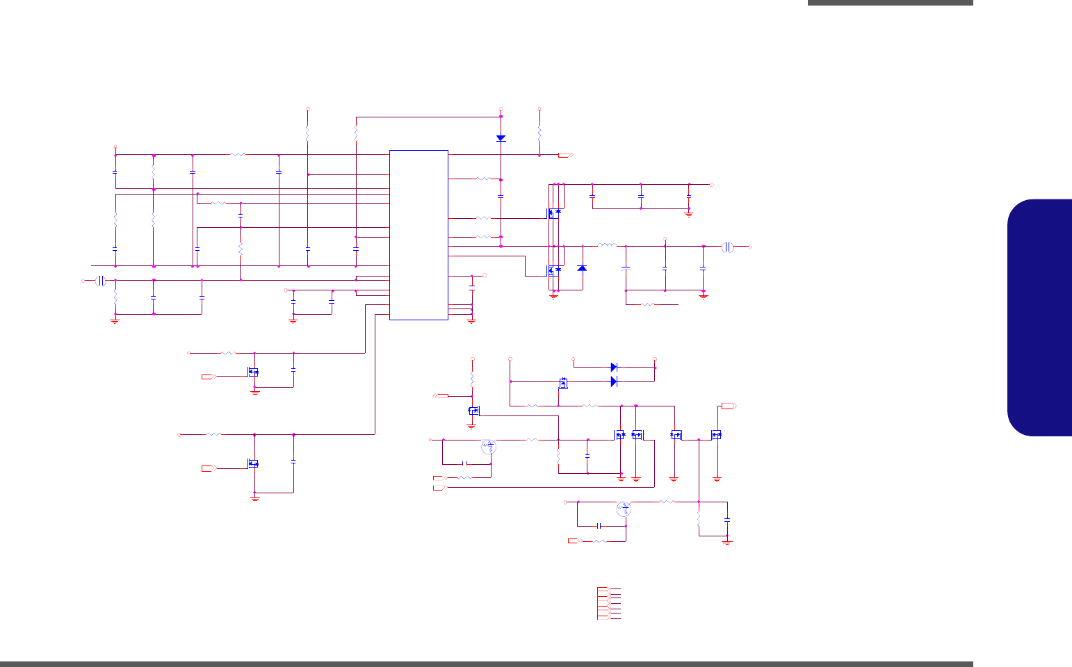
Schematic Diagrams
Power 1.8V, 0.9VSM B - 31
B.Schematic Diagrams
Power 1.8V, 0.9VSM
Sheet 30 of 40
Power 1.8V,
0.9VSM
1.8V_PWR GD [ 17]
PR132
10K_1%_04
VIN
VIN[12,27..29,31,32]
VSSA
PQ 9
2N 7 0 02 W
G
DS
PR133 10_06
PR62
2.2K _1%_04
PU3
SC 486
11
2
3
4
5
6
7
8
9
10
1
12
13
14
15
16
17
18
19
20
21
22
23
24
VTTEN
TON
VD DQ S
VSSA
VC CA
FB
PG D
RE F
CO MP
VTTS
EN /PSV
VD DP2
VD DP2
VTT
VTT
PGN D1
PGN D2
PGN D1
DL
VD DP1
IL IM
LX
DH
BST
PC67
10U _10V_08
VS SA
APKE Y#[1 9]
VDD 3[13,21,26..29,32]
PD 8 F M0 5 40-N
A C
PL5
2.5U H_6.8*7.3*3.5
1 2
PR 54
10_06
PC 14 0
0.1U_50V_06
PJ2
* OPEN _ 3m m
12
PC 48
*0 .0 6 8 U _ 1 0V _0 4
PR 194 100 K_0 4
PR56
0_06
PQ 43
IR F7 41 3 Z PB F
4
62
5
73
1
8
PC44
1U _ 1 0V _ 0 6
PQ15
ND S3 52A P_N L
G
DS
PWR_SW#[26]
5V
V1.8[29]
PR 142 20K_1%_04
PD 12
FM 0540-N
AC
VIN
P R51 10_06
PR 196 10K_04
500mA
PC136
1U _10V_06
PD7
FM5822
A C
PQ 14
2N7002W
G
DS
PQ 40
2N 7 0 02 W
G
DS
VIN
PR 143 100 K_04
0.9VSM[10 ,1 1]
M_ B T N #[1 9 ]
PC55
4.7U _6. 3V_X5R_06 PC52
1U_10V _06
PJ4
*OPE N_8mm
1 2
PC 50
100P_50V_04
1.8V,0.9VSM
PR41 47K_04
PQ 13
2N 7002W
G
DS
PC20 8
0. 1 U _5 0 V _ 0 6
1.5A
5V VTTEN
PC 42
1000P_50V_X7R _04
V1.8
5V
+
PC14 6
22 0 U _ 4 V _ D
V1.8
PC 77
0.1U_16V_04
PR 40
20K_1% _04
7A
PC 53
1U_10V_06
PR14 6
10 0 K _ 0 4
PC 150
0.1U_50V_06
VD D3
S USBL[2 9 ]
PR 140 100 K_04
VA
PR 144 10K_ 0 4
VIN1
1.8VEN
Ra
PC 49
10U_10V_08
DD _ ON #[ 2 8, 29 ]
PR 42
0_06
PQ62
2N 7002W
G
DS
PC 56
*4.7U _25V_X5R_08
5V
PQ 61
2N7002W
G
DS
PC35
1U _10V_06
PC74
0.01U _50V_X7R _04
PC 209
0.1U _50V_06
P R30 220K_1%_04
PR 39
1M_04
V1.8
1. 8 V
VIN
PD 9 F M0 5 40-N
A C
PC 149
0. 1 U _5 0 V _ 0 6
PR57
0_06
PC 13 9
1U _10V_06
PQ 42
AO 4456
4
62
5
73
1
8
PQ 63
DTA114EUA
CE
B
PR145
10K_04
PR47
10 _ 0 6
3.3V[2,12..17,19,20,23, 29]
PC 51
*0.1U _16V_04
Rb
PR26
0_06
PR 195
100K_04
0.9VSM
AP_ KEY # [26 ]
PQ 17
2N7002W
G
DS
PC142
*4 .7 U _ 2 5 V _X 5 R _0 8
1.8V[5 ,7 ,8 ,1 0, 11 ]
PQ 16
DTA114EUA
CE
B
DD_ONH[2 8 ]
PC 38
0.1U_16V_04
VIN
PC 46
0.1U_16V_04
PC36
0.1U _25V_X7R_06
5V[16,19,21,28,29,31]
PR25
4.7K_04
3.3V
PR 50
100K_04
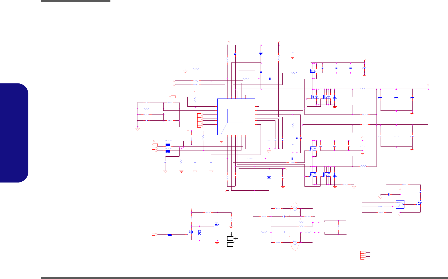
Schematic Diagrams
B - 32 Power VCORE
B.Schematic Diagrams
Power VCORE
VIN
PR20 7.5K_1%_04
CS2 N
PR 14
7.5K_1% _04
SG ND3
PC47
0.033U_16V_X7R_04
SGN D3
VC _S S
DRP+
40A
PC20
0 . 1U _5 0 V _ 06
PL4
0.5UH _10*10*4.1
PC133
*1 00P_ 5 0V_04
PR19
680_04
H_ VID4[3]
VI N
BG 2
H_ VID0[3]
TRERMAL PAD
PU2
SC45 2
1
2
3
4
5
6
7
8
9
10
11
15
16
17
18
19
20
21
22
23
24
25
26
27
28
29
30
31
32
33
34
35
36
37
38
39
40
41
42
43
44
14
13
12
45
C LKEN #
VR EF
HYS
C LSET
VID 6
VID 5
VID 4
VID 3
VID 2
VID 1
VID 0
BST2
TG2
DRN2
BG2
V5_2
PSI#
FB+
FB -
DRP-
DR P+
SS
DAC
AGN D
VC CA
ERR OU T
CS2+
CS 2-
CS 1-
CS1+
IS H
NC
EN
V5_1
BG1
DRN1
TG1
BST1
VIN1
VPN 1
DPR SL
VIN2
VPN 2
PW RG D
GN D
PC39
0.033U_16V_X7R_04
CPU_VC CSEN SE[3 ]
VCOR E_VREF
PC 31
1500P_50V_04
VCOR E
EN _VCOR E
PRT1
100K_NTC_06
12
PR43 47K_04
DRP-
DCR _ DR1
CS 1N
DRN 1
PQ41
IRF7832ZTRPBF
4
62 73
8
5
1
PR 131 10_04
PR15 0_06
PR37
47 K _ 0 4
5mil
CS1N
C LKEN#
PR 35
28K_1% _04
P C 13 4 0 . 0 22 U _1 6 V _ X 7R _0 4
PQ38
2N7002W
G
DS
SGN D3
PD13
FM0540-N
AC
PC23
1U_25V_08
DRP+
PC33 1000P_50V_X7R _04
5V
PC37 1000P _50V_X7R _0 4
PQ 37
2N7002W
G
DS
PR 21
1K _1 % _0 4
5V
SG ND3
H_ DPR STP#[2 , 5 ,13 ]
PR122 499_1%_04
PQ36
IRF7413ZPBF
4
62 73
8
5
1
DPRS L_ST P
+
PC13 1
33 0 U _ 2 . 5V _D 3
DR N1
+
PC 12 4
330U _2.5V_D3
PC 29
0.015U _50V_06
VCC A
PC128
1000P_50V_X7R _04
5V[16,19,21,28..30]
PQ44
IRF7413ZPBF
4
62 73
8
5
1
PR23 220K_1% _04
CS2P
ISH
PC 13 7
*100P_50V_04
PC21
0.1U _50V_06
PD3
FM5822
A C
PR 18
130K_1%_04
SGND3
TG1
+
PC 12 3
*3 3 0 U_ 2.5 V _ D3
VIN
3.3VS[5,8..16,18..27]
DRP_L1
PC 25 0.1U_25V_X7R_06
PR129 0_06
20A
20A
VCOR E
25mil
E-RC
PC 26
*0.022U _16V_X7R _04
DRP-
SGN D3
PQ 7
* IRF7832ZTRPBF
4
62
73 8
5
1
PR 12 5
100K_04
PR 33 10_04
DPRS L
H_ VID5[3]
BST2
PR127 *10m il_short
SGND 3
PR 11 *0 _ 04
Z2802
PR 22
130K_1%_04
cl o s e t o IM V P 6
PC32 1U_10V_06
PR 27
17.4K_1%_04
PD11
FM0540-N
AC
VC ORE_H YS
CS2N
PR44 47K_04
PR38 0_06
PC43
1000P_50V_X7R _04
PR 124
*10K_04
DRP_L2
+
PC 11 6
330U _2.5V_D3
PR24
10_06
PC45
1U _2 5 V _ 08
V-RC 2
PR49
100_1%_04
CS1 N
PC13 5
*100P _50V_04
PR 32 0_06
+
PC 13 0
* 330U_2.5V _D 3
EN_ V CO RE
PS I#[2 ]
BST1
PR 12 *0 _ 04
PC59
0.1U _50V_06
5V
PC 19
0.1U_50V_06
H_ VID1[3]
VCO RE[3 ]
P R 3 1 * 1 0m i l _s h or t
BG 1
CLKEN#[1 5]
PR 16 * 0_04
PC34 100P_50V _04
PR36
47 K _ 0 4
DAC
H_ VID6[3]
PU1
*7 4A H CT 1 G0 2 GW
4
53
1
2
R 170 100_1%_04
SGN D3
V-R C1
3.3V S
C PU_VSSSEN SE[3 ]
DCR _ DR2
PQ 39
IR F783 2ZTRPBF
4
62 73
8
5
1
PM_DPR SLPVR[5 ,15 ]
PC30 100P_50V _04
+
PC12 9
33 0 U _ 2 . 5V _D 3
VIN[12,27..30,32]
BG 1
VPN2
DRN 2
FB-
R1 7 2
100_1%_04
PQ 6
*2N7002W
G
DS
H_ VID3[3]
DEL A Y _PW R GD[5 ,1 7]
BG 1
PR 46
17.4K_1%_04
PR48 0_06
PC27
0.015U_50V_06
PC 22
0.1U_50V_06
PR10 0_04
5V
VIN
DPRSL_STP
VC _SS
PR 1 28 * 10m il_ s ho rt
H_ VID2[3]
Z2801
VCORE
BG 1
PR 13 *0_04
PC18
* 0.1U _16V_04
PR17 33K_1% _04
PC58
0.1U_50V_06
V COR E _ ON[26 ]
PR28
9.1K_1%_06
PR12 3
100_1%_04
PC 24
1U_10V_06
PD4
FM5822
A C
PL3
0.5UH _10*10*4.1
VC ORE_C LSET
+
PC 132
15U_25V _D 2
FB+
PC41
1U_10V_06
PC28 100P_50V _04
PR 29
1K_04
BG 1
PRT2
100K _N TC _06
12
CS 2N
D RN1
TG2
PJ 6
*O PE N_ 3 5m il
PR13 0
*680_04
PQ8
*IR F7832ZTRPBF
4
62 73
8
5
1
35mil
VC ORE_VR EF
PC40
680P_50V_X7R_04
SGND 3
DPRSL
DR N2
VPN 1
PR 45
28K_1% _04
+
PC138
15U _25V_D2
3.3V S
PR 126 10K_04
Sheet 31 of 40
Power VCORE
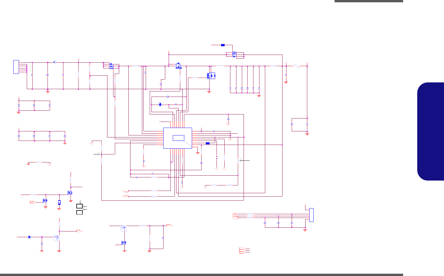
Schematic Diagrams
Power AC-IN, Charger B - 33
B.Schematic Diagrams
Power AC-IN, Charger
PQ 1
DTD114EK
CE
B
SG ND 5
PC11 7 0.1 U_ 5 0V_ 0 6
PC 17
4.7U_25V_X5R _08
VD D3
VA
BAT_ VOL T [2 6]
PC 122
0.1U_16V_04
PC 11 8 0.1U_16V_ 04
Z3231
PR 104
30m_20
SGND5
PL1
HCB4532KF-800T60
PC 9
*0.1U_16V_04
PQ 2
D TA114EUA
CE
B
35mil
SGND 5
PR 115
10K_1%_04
PC 108
0.1U _50V_06
02/22
SYS5V[28]
PMBAT1
BTD-05 TI1G
1
2
3
4
5
PQ 35B
SP8K10SF D5TB
4
3
5
6
Ch arg e Cur re nt 2.0 A
SMD_BAT[26 ]
V_BAT
SY S5V
PR102
1K_1%_04
PC14
4.7U_25V_X5R_08
CH G_CU R[2 6]
Z3228
BA T
VIN[1 2 ,2 7..3 1 ]
PC113
4.7U_25V_X5R_08
PQ 4
2N 70 0 2 W
G
DS
PC 1
30P_50V_04
PR 114 0 _0 6
PC 121 *22P_50V_04
PC4
0.1U _50V_06
Z3230
PQ 34
AM 4835P
4
62 5
73
1
8
SG ND 5 SG ND 5
SG ND5
TOTAL_CUR[26]
PC 3
30 P_5 0 V_04
PQ5
2N 70 0 2W
G
DS
PR 119
1K_1%_04
V_BAT
Z3226
PR 99
10K_08
PC7
0.1U_50V_06
PC8
0.1U _50V_06
PR 116
100K_1%_04
AC IN & CHARGER
VA
PC 6
0.1U_50V_06
SYS 5V
TRERMAL PAD
PU6
MB39A132
1
2
3
4
5
6
7
9
10
11
12
13
14
15
17
18
19
20
21
22
23
25
26
27
28
29
30
31
8
16
24
32
33
VC C
-IN C1
+INC 1
AC IN
AC OK
-IN E 3
AD J 1
-INE 1
OUTC1
OUT C 2
+INC 2
-INC2
ADJ 2
COMP 2
BATT
AD J3
CS
RT
VREF
GN D
CTL1
CEL L S
PG ND
OU T -2
VB
LX
OUT -1
CB
COMP1
CO MP3
VIN
CTL 2
SGN D
PR106
49.9K_1%_04
PR8
30K_1% _04
PC 107
0.1U_50V_06
PR 4
10K_04
CHARGE
CURRENT
ADJ
PR7
0_04
0 .7 5V/ 1A
PR 108
*10m il_short
PL2
10 UH _6 .8 *7 .3 *3 .5
1 2
Z3229
PQ3
2N7002W
G
DS
VA
PC 10
0.1U_50V_06
PC109
4.7U_25V_X5R_08
VA
PC12
0.1U_50V_06
PC 119 1000P_50V_X7R _04
J_DC -J ACK1
2D C - G 2 1 3 - B 20 0
GND2
GND1
2
1
GND4
GND3
PC111
4 . 7U _2 5 V _ X 5R _0 8
PC11
0.1U _50V_06
PR 111 0_ 04
PQ 35A
SP8K 10 SFD5TB
7
8
1
2
PC125
0.1U_25V_X7R _06
PR2 100_04
PC115
0.1U _50V_06
5mil
PR 112 0_ 04
PC 5
0.1U_50V_06
25mil
SGND 5
PC112
4.7U_25V_X5R_08
PR 117
200K_1%_04
PC15
0.1U _16V_04
PC12 6
2200P_50V_X7R_04
12V~16.8V
PC 11 4
4. 7 U _2 5 V _X 5 R _0 8
PD 2
FM0540 -N AC
VIN
CTL1
PR9
30 m _ 20
VDD 3[13 ,2 1, 26 ..3 0]
PR110
10K_1%_04
TOTAL
POWER
AD J
PC106
0.1U_50V_06
B tt er y Volta ge :
CT L 1
PR 5
0_04
PJ1
*O P E N _ 3 5 mi l
PC16
1U_25V _08
PR 103
22K_1%_04
PF2
5A
PC 120
10 00 P_ 50V_ X7R _ 04
PQ3 3
AM4835 P
4
6 2
5
7 3
1
8
VA
CH G_ E N[2 6 ]
BAT
0 .7 5V/ 1A
PR100
130K_1%_04
PR 120
10.2K_1%_04
PR10 5
*10mil_short
P R 10 9 2 2 K _1 % _ 04
PC 11 0
4.7U_25V_X5R _08
PC 13
0 . 1U _5 0 V _ 06
PR1 100_04
SY S5V
PR118
100K_04
PD1
UD Z1 6B
AC
Ch arg e Vol ta ge 16. 8V
SGND5
SMC_BAT[26 ]
PR101
10K_1%_04
BAT
PR3 100_04
Z3227
PR 12 1 1 00K_04
VIN
To tal P owe r 60W
PR107 39.2K_1%_04
PC 2
30P_50V_04
A C_IN# [26]
PR11 3
10K_1%_04
PC 127
100P_50V_04
PR6
6.04K_1%_04
SGN D5
BAT_ DET[2 6 ]
Z3225
Sheet 32 of 40
Power AC-IN,
Charger
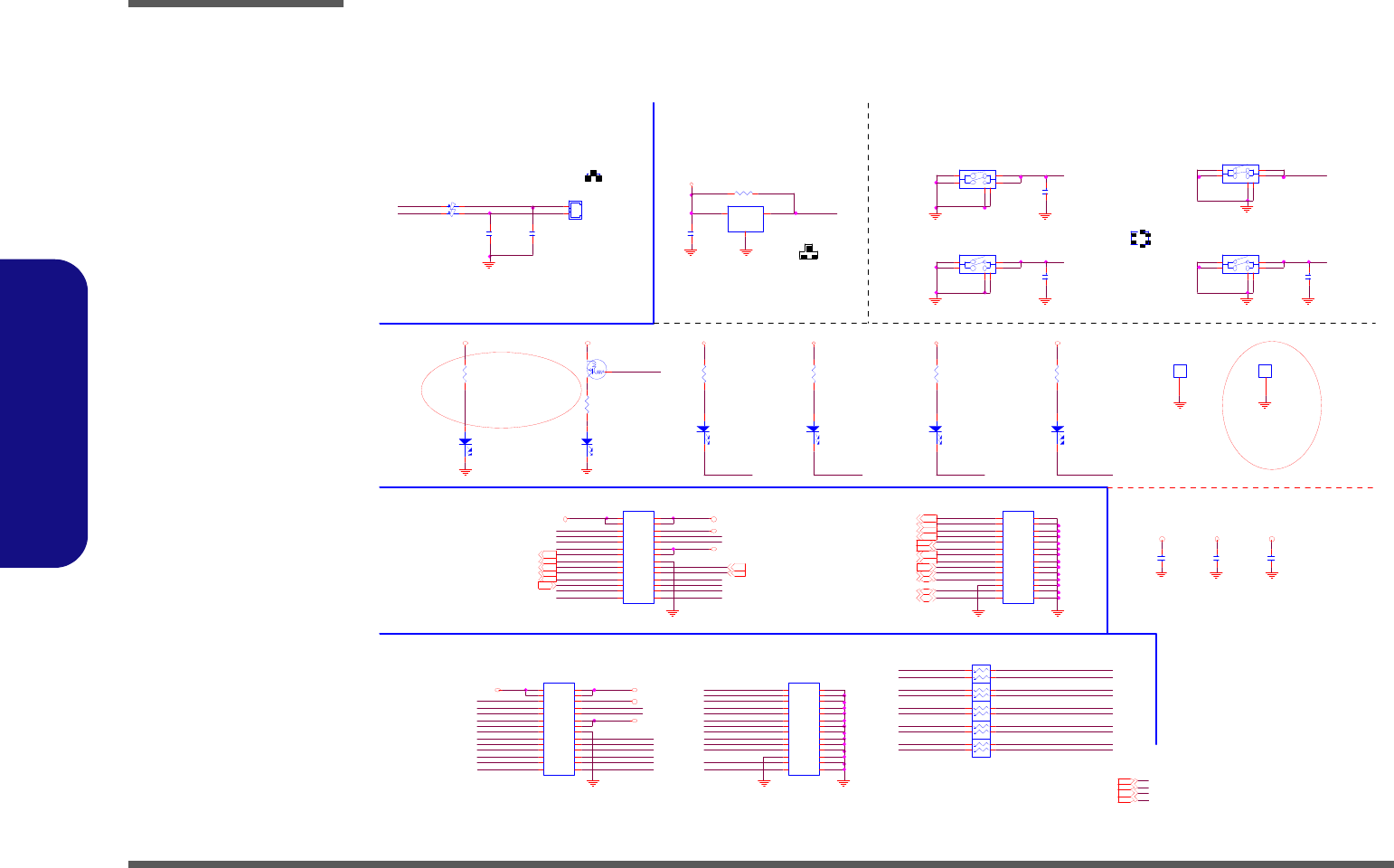
Schematic Diagrams
B - 34 Multi I/O Board 1/2
B.Schematic Diagrams
Multi I/O Board 1/2
MAZ_SYN C[34 ]
MUSB_PP5 _ 3G _1 3
MC17
180P_50V_04
SW2
MGND
MW L AN_CL KR EQ#[3 4]
M AZ_BITC LK[34]
MG ND
MSPKR -
MD2
R Y-SP17 2Y G34
AC
1
M3 . 3 V S
M USB_PN5 _3G
MG ND
THROTTLE
LED
M3.3V
MW EB_ EMA IL#
MR N1
*4 P2 R X 0_ 0 4
1 4
2 3
SW4
M1 .5 V S
MCLK_PC IE_MINI_3G#
MA Z _ B I TC LK
MD1
R Y-SP172Y G34
AC
1
MM_ B T N #
M J_MF B1_73
*5 P1-2 5 1A 4 -1 3 V00 -2 14
12
34
56
78
910
11 12
13 14
15 16
17 18
19 20
21 22
23 24
25 26
27 28
MC 19
0 . 1U _1 6 V _ 04
MPCIE_TXP3_3G
MW L AN_C LKR EQ#
MC 16
180P_50V_04
ML 6
FCM 1005KF- 121 T03
MP C I E _R X N 3 _3 G
ML ID_ S W #
MP C I E _R X P 3_ 3 G
MC LK_ P C I E _M I N I_ 3G # _1 3
MG ND
MPC IE_W AKE#
MC A P _ L E D #
M3 .3 V
MU S B _P N3 _1 3
M3 G_ E N
MJ_SPKR_72
88266-02001
PCB Footprint = 88266-2L
2
1
MAZ_SDIN1
MUSB_PP3 _ 13
MW EB_ EM AIL#
M J_S PK R_7 2
MA Z _ S D I N 1[34 ]
MC1
0.1U_16V_04
MG ND
MGN D
M AZ_RST#
MPCIE_RXN3_3G_13
MG ND
MG ND
M3 .3 V S
MU SB_PN 3
MLID _SW #
SW6
2
M1 .5 V S
MA Z _ RS T#[34]
MM_BTN#
SW8
M USB_PP3[34 ]
MA P K E Y #
MC 22
0 . 1U _1 6 V _ 04
MU S B _P N5 _3 G_ 1 3
M SPKR+
M3.3VS
M P CIE_ RX P3 _3 G
MAZ_BITCLK
M1 .5 VS
M3 .3 V
MW E B _E M A I L#
MPCIE_RXN3_3G[3 4]
M1 .5 V S[34]
M3G_DET#
MPC IE_W AKE#
MPC IE_TXP3 _3G
MC LK _ P C I E _M I N I_ 3G #
M B U F _P LT _ R S T #
MWLAN_CLKREQ#
MSW1~4
MPCIE_RXP3_3G_13
MS W 4
TJG -533-S-V-T/R
3
1
4
2
5
6
MPCIE_RXN3_3G_13
MS W 2
TJG -533-S-V-T/R
3
14
2
5
6
3.3 VS= 2A
MU S B _P N 3[3 4]
MCLK_PC IE_MINI_3G
MWLAN_CLKREQ# [34]
MG ND
MA Z _ S D OU T
M3 .3 V[3 4]
M USB_PP5_ 3G
MS P K R -
MD4
R Y-SP172YG 3 4
AC
2
MP C IE _ T XN 3 _3 G[34 ]
M SATA_LED#
MR 6
220_04
MJ_MFB2_72
5P1- 251A4-13V00-214
12
34
56
78
910
11 12
13 14
15 16
17 18
19 20
21 22
23 24
25 26
27 28
MPCIE_RXP3_3G[34 ]
MSCROLL_LED#
MR N3
*4 P2 R X 0_ 0 4
1 4
2 3
SPEAKER
MU SBVCC 2
MAZ_SDOU T[34]
MU SB_PN 5_3G
MAZ_SDOU T
M3 G_ E N
MQ 1
DTA114EUA
C E
B
M3.3VS
M PCIE_W AKE#[3 4 ]
MPCIE _ R XP 3 _ 3G _1 3
4
MG ND
M P CIE_ RX N3 _ 3G
M CAP_LED#
MNU M_LED #
MC9
*0.1U_16V_04
MD3
RY-SP172YG34
AC
MR2
22 0 _0 4
MR1 100K_04
MC LK _ P C I E _ MI N I _ 3G[3 4]
FO R E MI
MR 5
220_04
M3 .3 VS
MPCIE _ TX P3_ 3 G_ 13
MU SB_PP 3
MM_ B T N #
M3.3VS
MSPKR+_R
M SATA_L ED#
FOR M730T
2
M730T/M735T D03
BCN? ? 470
MG ND
MA Z _ S D I N1
MW L A N_ CL KR EQ#
M USBVCC 2
For M720T
MC LK _ P C I E _M I N I_ 3G
MAZ_SYNC
MS A T A _L E D #
3
MWEB_WWW#
MAPKEY #
MUSB_PN 3_13
MCLK_PCIE_MIN I_3G _13
MR N5
*4 P2 R X 0_ 0 4
1 4
2 3
M3.3VS
3. 3V S=2 A
MC LK _ P C I E _M I N I _ 3G _ 13
MWEB _WWW#
M USB_PP3
MR 3
22 0 _ 04
MG ND
M3 . 3V S
MU SBVCC 2[3 4 ]
MNU M_ LE D #
MGND
MTH ROTTLE _LED#
MGND
MPCIE_TXN3_3G_13
MT H R OT T LE _ L E D #
MS1
SM D80 X8 0
11
LED
POWER SWITCH
LE D
MG ND
MS 2
SMD 80X80
11
3
3/31 MS1? ? 180?
BY? ? ? ?
M3 .3VS MCLK_PCIE_MIN I_3G #[34]
M3 .3 V S[34]
MAPKEY #
MS P K R +
M SCRO LL _ L ED#
MR7
220_04
MGND
MPC IE_TXN3_3G
MPC IE_TXP3_3G_1 3
MA Z _ R S T #
HDD/ODD
LE D NUM LOCK
LE D
MU SB_P P5_3G_13
MS W 1
TJG -533-S-V-T/R
3
14
2
5
6
MPCIE_TXP3_3G[3 4] MC 11
*0 .1 U _ 1 6V _ 0 4
LID SWITCH
ML ID_ S W #
MG ND
MUSB_PN 5_3G_13
MCLK_PCIE_MIN I_3G #_13
MD 6
RY -SP17 2 YG 34
AC
MS W 3
TJG -533-S-V-T/R
3
1
4
2
5
6
MP C I E _T X N 3 _ 3G _1 3
M USB_PP5 _3G[3 4 ] M USB_PN5_3G[3 4 ]
MSPKR +
M AZ_ SYNC
MU SB_PP 5_3G
MC 18
0 . 1U _1 6 V _ 04
FOR M720T
SCROLL LOCK
LED
MU 1
M USB_PN3
MJ_MFB1_72
5P1-251A4-13V00-214
12
34
56
78
910
11 12
13 14
15 16
17 18
19 20
21 22
23 24
25 26
27 28
MJ _ MF B2 _ 73
* 5P1-251A4 -13V00-21 4
12
34
56
78
910
11 1 2
13 1 4
15 1 6
17 1 8
19 2 0
21 2 2
23 2 4
25 2 6
27 2 8
MU SBVCC 2
MR N2
*4 P2 R X 0_ 0 4
1 4
2 3
M3 G_ D ET #
MN UM_ L E D#
MR 4
220_04
1
MB U F _P L T _ R S T #[3 4]
MPCIE_TXN3_3G
M3 G_ DE T#[34]
MW LAN_C LKR EQ#
MG ND
M SPKR-
MGND
MW EB_ W W W #
MG ND
MD 5
RY -SP150DN B84-5/1X
AC
HOT KEY & POWER SWITCH
MG ND
MGND
MSPKR-_R
MU SB_P P3_13
MT HR OT TL E _ L ED#
MU1
MH-2 4 8
1
2
3
VCC
GN D
OUT
ML 7
FCM 1005KF- 121 T03
MR N4
*4 P2 R X 0_ 0 4
1 4
2 3
MGND
M3 G_ E N [ 3 4]
MS C R O LL _ LE D #
MB U F _P L T _ R S T #
MC A P _ LE D #
MC8
0. 1 U _ 1 6V _ 0 4
CAPS LOCK
LE D
Sheet 33 of 40
Multi I/O Board 1/2
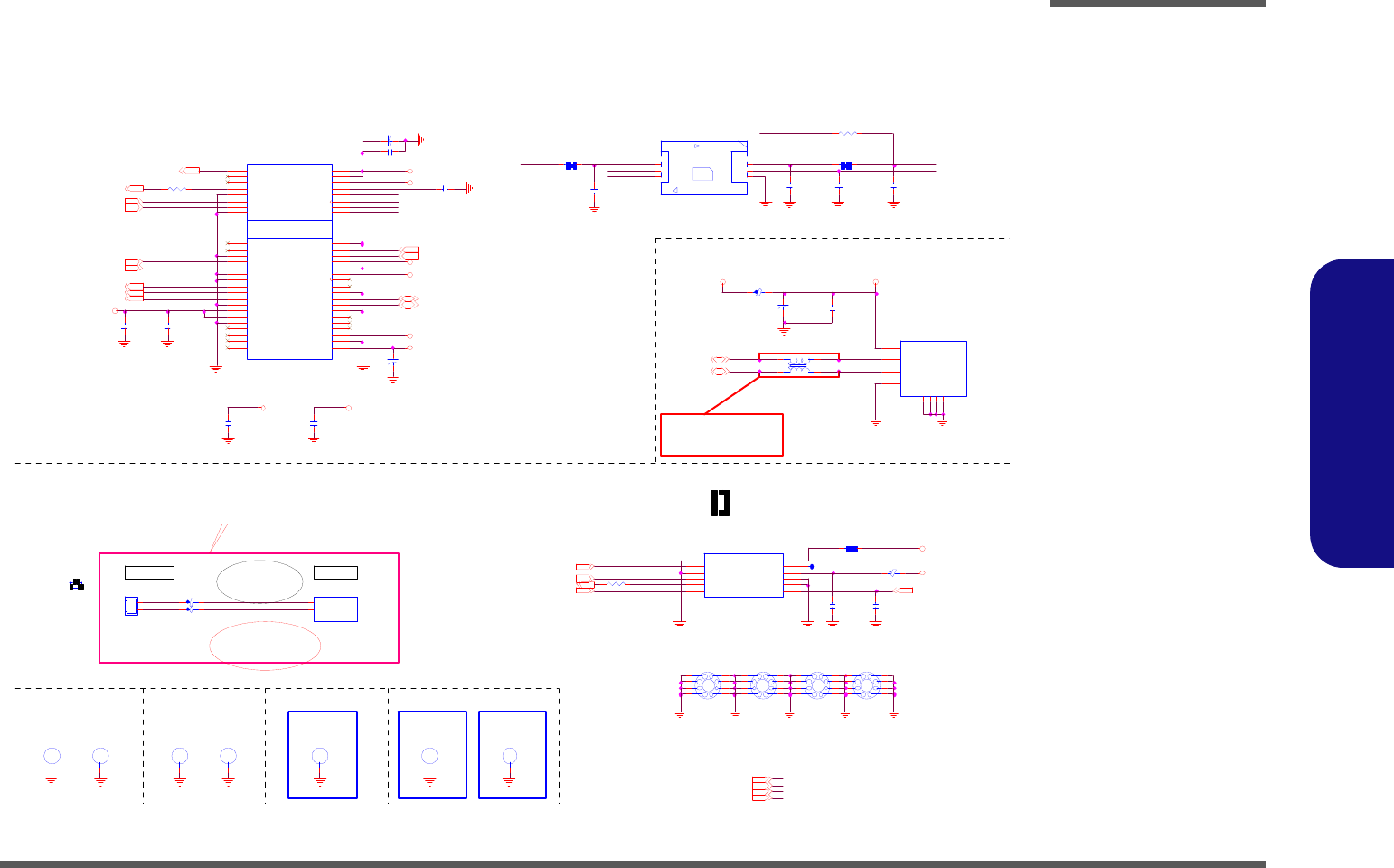
Schematic Diagrams
Multi I/O Board 2/2 B - 35
B.Schematic Diagrams
Multi I/O Board 2/2
IH 8
C237D146
MR1 2 *4 .7 K _ 04
MR 11
22_04
MC 13
0 . 1U _1 6 V _0 4
M3 G_ D E T #[3 3]
MGN D
MG ND
Z3504
MJ _ RJ -1 1
PJ S-02 FB3 G
1
2TI P
RING
FOR M720T
1
IH2
MT H3 1 5D 1 11
2
3
4
5 6
7
8
9
M3 .3 V[3 3]
?????????
MG ND
ML 1
H CB1005KF-121T20
MGND
MC 27
* 2 2 P _5 0 V _0 4
IH1 1
C2 3 7D 14 6
MC21
150U_6.3V _V
FOR M730T
M3 .3 V
M USB_PP5 _3G [33]
M3 .3 V S
11
1
60 m il
M3 . 3 V S[3 3]
M CLK_PC IE_MINI_3G#[33]
MU I M_ P W R
IH9
C2 76 D1 8 6
20 mi l
MG ND
M USB_PP3 _R
MG ND
MU IM _P W R
MU I M_ D A T A
1
IH 3
MT H2 37 D 11 1
2
3
4
5 6
7
8
9
MGND
M1 .5 V S
MC1 4
100 U_ 6.3V_B2
MA Z _ S D IN 1[33 ]
KEY
MJ _3 G1
88910-5204
3
5
7
9
11
13
1
15
23
25
21
27
31
33
29
17
19 20
37
39
41
43
45
47
49
51
44
42
18
16
14
2
12
10
8
6
4
22
24
26
28
30
32
34
36
38
40
46
48
50
52
35
BT_ DATA
BT_CH CLK
CLKREQ#
GND0
REFCLK-
REFCLK+
W AKE #
GND1
PETn 0
PETp 0
GND2
GND3
PER n0
PER p0
GND4
NC3
NC4 W_DISABLE#
NC6
NC7
NC8
NC9
NC10
NC11
NC12
NC13
LED_WLAN #
NC(LED_WWAN#)
GND 6
UIM _VPP
UIM _R ESET
3.3V_0
UIM _C LK
UIM _D ATA
UIM_ P W R
1.5V_0
GND 5
PERSET#
3.3VAU X
GND 7
1.5V_1
N C ( S M B _C LK )
N C(SM B_D ATA)
GND 8
N C(USB_D-)
NC(USB_D+)
GND 9
NC(L ED _W P AN #)
1.5V_2
GN D1 0
3.3V_1
GND11
MGN D MGND
MA Z _ R S T#[33]
USB PORT
RJ-11
M1 . 5 V S[3 3]
MCLK_PCIE_MINI_3G[33]
Z3502
MU IM _D A TA
MUSB VCC
MG ND MGN D
2
Place under the common
bead body and same as
USB trace requirment
MAZ_SDOU T[33]
MGND
M AZ_BITC LK [33]
MC 23
10U _10V_08
? ? 6-34M72SS-010
MGND
MU SBVCC 2[33 ]
MU I M_ P W R
MR13
*1 0m i l _s h or t
M R8 *0_04
MGN D
ML 2 BK160 8H S12 1
? ? 6-34-D90T0-010-1
? ? 2.5mm ? ?
La you t not e:
MU IM_DATA_ R
MC2
0.1U_16V_04
1
MG ND
MAZ_SYN C[33 ]
IH5
C2 56 D 14 6
? ? 6-34-M56AS-011
IH1 0
C2 37 D 14 6
MUSB_PN5_3G [33]
MJ _ MOD EM1
85205-02001
2
1
3G/Raboson
PIN GN D1 ~2=MG ND
MU IM_VPP
MJ _ USB1
C 107B3-10403-Y
1
GN D1
2
3
4
GND2
GND 3
GND4
V+
shield
DATA_L
DATA_H
GND
shield
sh i e ld
shield
MA Z _ S D IN 1_ R
MC20
150U_6.3V_V
MDC MODULE
? ? 6-34-M72SS-020
MG ND
M3 .3 V S
MBUF_PLT_RST# [33]
12
MW L AN_ C LKR EQ#[3 3 ]
MU I M_ R S T
MG ND
ML 3 BK160 8H S12 1
MGND
MG ND
M1 .5 V S
1
IH1
MTH315D111
2
3
4
5 6
7
8
9
MG ND
MG ND
M C 3 0 . 1 U _ 16 V _ 04
M1 . 5V S
M1 .5 V S
M PCIE_TXP3_ 3G[33 ]
MUIM _VPP
MUSB_PP3[33 ]
MGND
M3G_EN [33]
MG ND
10mil
MODEM
MC7
22P_ 50V_ 0 4
MC5
0.1U_16V_04
MPCIE _TX N3 _3 G[3 3]
MGND
MU SB_PN 3[33 ]
1
IH 6
M TH315D1 11
2
3
4
5 6
7
8
9
MC 4
0 . 1U _1 6 V _0 4
MGND
MC28
* 22P_50V_04
MC 2 5
*22P_50V_04
ML 4
*WCM 2012F2S-161T03
1
4
2
3
MJ_MODEM1
M3 .3 V
M U I M _C LK
Z3503
MU IM _R S T
RJ-11
M3 .3 V S
M3 .3 V S
3/ 31 DE L
*M C1 5 F OR EM I
IH4
C2 56 D1 4 6
MGND
M USB_PN3_R
IH 7
C237D146
ML5
H CB1608KF-121T25
MG ND
Z3501
MG ND
MR 15 *10mil_short
MJ_MDC1
88018-120G
1
3
5
7
9
11 12
10
8
6
4
2
GN D
Azalia_SDO
GN D
Azalia_SYN C
Azalia_SDI
Azalia_RST# Azalia_BC LK
GND
GND
3. 3 V Ma i n/ au x
R ESERVED
R ESERVED
La you t?
1. SIM????????(10mil)
2. ????????GND
3. SIM hold ?????GND??
4. SIM CO NN ? ? MI NI CAR D CON N
FOR M720T
M3 .3 V S
3/31 DEL
*MC12 FOR
EMI
MPCIE _R XP3_3G[3 3]
MJ_MDC1
MGN D
MU IM_CLK_R MR14 *10m il_s hort
MUSBVC C2
MG ND
MGN D
M PCIE_W AKE#[33]
(TO P VIE W)
LOC K
OP EN
MJ_SIM1
SIM LOCK 1770661-1
C7
C6
C5C1
C2
C3 UIM_ DA TA
UIM_ VPP
UIM_ GN DUI M_ PW R
UI M_ RS T
UI M_ CL K
MG ND
MC 24
0.1U_16V_04
MPC IE _ RXN3 _3 G[33]
M U I M _C LK
MC 6
0 . 1U _1 6 V _0 4
MC26
*22P_50V_04
2
Sheet 34 of 40
Multi I/O Board 2/2
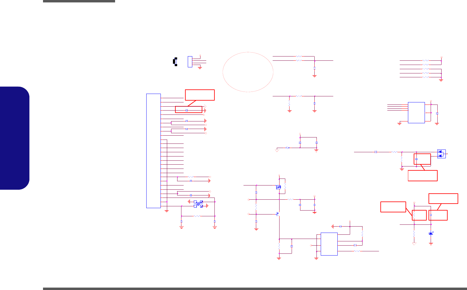
Schematic Diagrams
B - 36 Finger Printer Board
B.Schematic Diagrams
Finger Printer Board
F3.3V
FR 2 10K_04
FGR ID0/SEN SE
330K_04
FG ND
FU SB_PP1_R
FG ND
FR5
0_04
FC 3
1U_10V_06
FG PIO0/IN T
FR16
*0 _ 06
FGND
FG ND
FESD _R ING
TC S4 C
FTC_VD D
Z3706
FC 13 1U_6.3V_04
FG ND
FD VDD 1
FG ND
FDATA1
FGND
FG ND
FU1
SN7 4 L VC1 G1 2 3 DCT
8
7
6
54
3
2
1VC C
Rx /Cx
Cx
QGND
CL R#
B
A#
Z3701
FR 20 27 .4 _1% _ 04
FG ND
FJ_FP1
FU3
M95128W M N6TP
1
2
3
4
5
6
7
8
CS#
Q
WP#
VSS
S
SCK
HOLD#
VD D
FC 14 1U_10V_06
FJ_FP1
85201-04051
1
2
3
4
FG_FET
FR4
33_06
FU SB_PP1
FG ND
FC 16 0.1U_16V_04
Unstuff
3/31 ? ? FUSB_PN1 BOT? ? -?Case ? ?
FQ1
ND S352AP_ NL
G
D S
FG _FET
FR6
*3 3 0K _0 4
FR 14 47K_04
4
FXIN
FR13 47K_04
FGPIO 1
FESD _G ND
FC20
47P_ 50V_04
FG ND
FM ISO/M OD E3
TC S4 B
FG PIO0/IN T
FR9 47K_04
FGN D
FG ND FAVDD
FC 4
0.1U _16V_04
FC 9
0.1U _25V_X7R _06
FU4
TCS4B
A1
B1
C1
D1
E1
F1
G1
H1
J1
A2
B2
C2
D2
E2
F2
G2
H2
J2
A3
B3
C3
D3
E3
F3
G3
H3
J3
EXT_R ING 2
CR IDO
RING
MUXOUT
AVDD
MCS
PAD _VDD 1B
MISO
DVDD
GPIO 1
AG ND
DATA0
DATA1
GPIO 0
MC LK
U SB_DN
USB_DP
MOSI
PD _REG
NRE SET
DG ND
DATA2
EXT_R ING 1
PVDD
XT A L I N
PG ND
XT A L O U T
FR 15 15_06
FGN D
FC19
47P_ 50V_04
FC 15 1U_10V_06
FG RID 0/SENSE
FDATA2
F3.3V
FQ2
2SB1198KR/T146
B
EC
FC17
18P_50V_06
FR10
100_06
FR11 47K_04
FGN D
Z3704
FR17 *1M_04
FC 22
0.1U_16V_04
FGN D
FTC_VD D
FC1
0.022U_16V_X7R_04
FR 1
330K_04
22P_50V_04
10mil
FG ND
FU SB_PN1
FMISO /MO DE3
FPD _REG
FC5
1U_10V_06
FR12 47K_04
FMISO /MO DE3
TC S4 B
FU SB_PN1
FD ATA1
FC 7
* 47P_50V_06
47 P_ 50 V_0 6
FR 19 1.5K_04
FTC_VD D
FL1
HC B1608KF-121T25
FD ATA2
FX1
HSX531S_ 12MH z
12
34
FG ND
FES D_RIN G
FC 12 33P_50V_04
1
FTC_VD D
FR 3
100K_04
Un st uf f
FGN D
FR 21 27 .4 _1% _ 04
FTC _VDD
FU SB_ PP1_R
FR18
100K_04
FG ND
33P_50V_04
F3.3V
FMC LK FC 8
0.1U_16V_04
TCS4C
FMO SI
FC11
0.1U _16V_04
FDATA0
TC S4 C
FD ATA0
FGN D
TCS4B
Z3705
FM CLK
FC6
*1U_6.3V_04
FGN D
FAVDD
FESD _G ND
F USB_PP1
FTC_VD D
FM OSI
Finger Printer
F3.3V
FC 2 2.2U _6.3V_06
1U _6 .3 V_0 4
F3.3V
FN RESE T
Z3702
FC 10
1U_10V_06
FGN D
FR8
330K_06
FMC S
TCS4C
FXO UT
Z3703
FGN D
FG ND
FU SB_PN1_R
FPD _REG
FES D_RIN G
FM CS
Un st uf f
FR7 330K_04
FC 21
1U_10V_06
FU2
RC la m p 05 0 2 B
1
23
FD VDD 1
FESD _G ND
FD 1
*R B 5 51 V -3 0
A C
TCS4B
FG PIO1
FC18
18P_50V_06
FU SB_PN1_R
F3.3V
Sheet 35 of 40
Finger Printer
Board
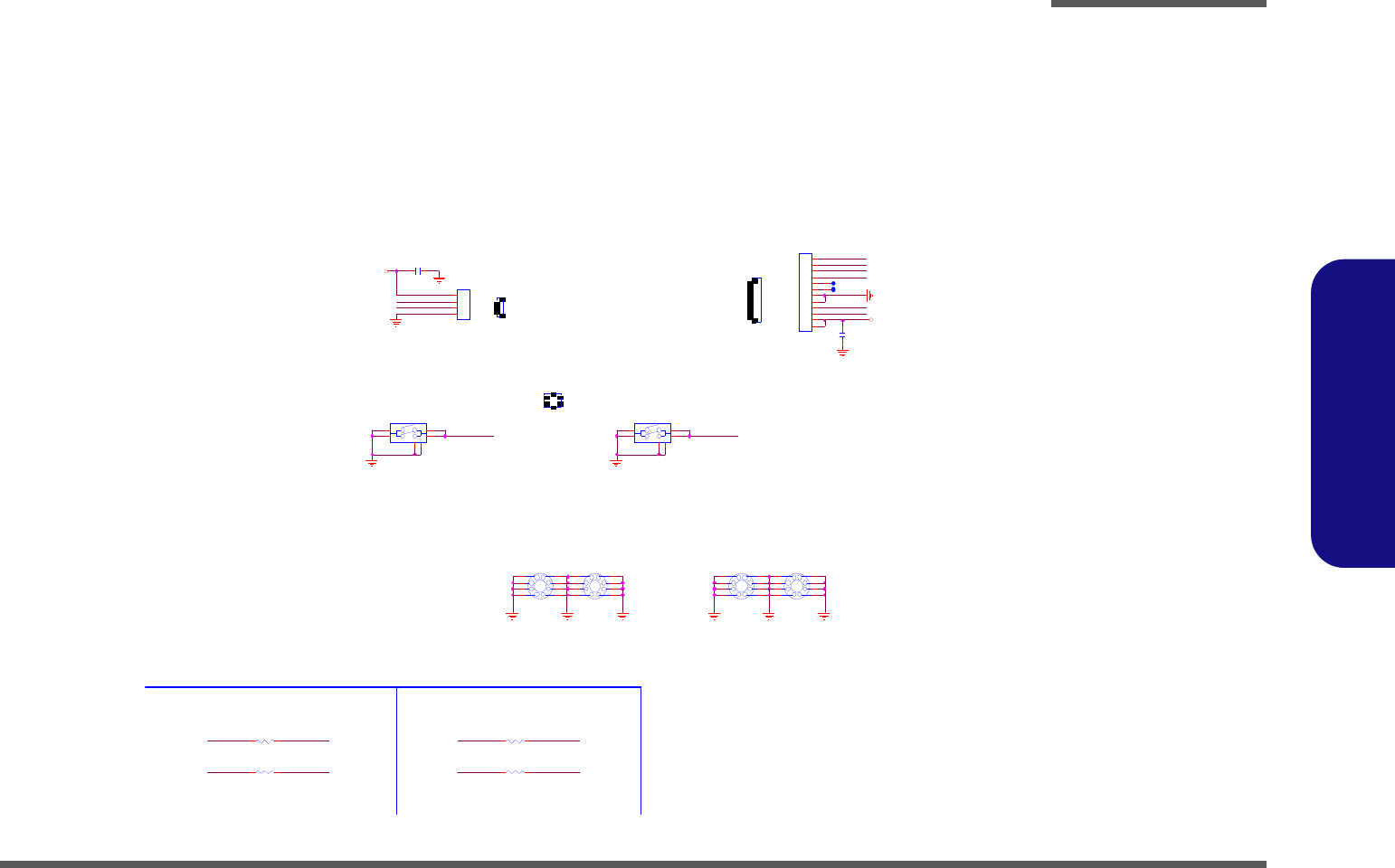
Schematic Diagrams
Click Board B - 37
B.Schematic Diagrams
Click Board
Sheet 36 of 40
Click Board
CTPBU TTON_ L
CGND
CSW 1~2
CTPBTN_R_73
CGND
CTPBTN_ L_73
CTPBTN_R_73
C5V
CC1
0.1U_16V_04
CJ_TP1
8 7151 -12 071G
1
2
3
4
5
6
7
8
9
10
11
12
1
1
CH2
MTH2 37D9 1
2
3
4
5 6
7
8
9
CGND
C TPBTN _L_7 3
2
4
CG ND
CTPBTN_R_72
CGND
CGND
CTP_D AT A
For M720T
CJ_T P1
CTPBTN_ L_72
C TP BU TTON _ R CTPB TN_R _72
For M730T
12
CSW1
TJG-533-S-V-T/R
3
1
4
2
5
6
CR 2 * 0_04
1
CGND
CR 1 0 _04
CSW2
T JG-5 33-S - V- T/R
3
1
4
2
5
6
1
CH1
MTH 2 37D9 1
2
3
4
5 6
7
8
9
1
CG ND
1
CH4
MTH23 7D91
2
3
4
5 6
7
8
9
CGND
6-2 0-94A2 0-112
CTP_CL K
CJ _TP2
C TP BU TTO N _ R
CR 4 * 0_04
C TP BU TTON _ L
CJ_ TP 2
8520 1-04 051_ R
1
2
3
4
CGND
CR 3 0 _04
RIGHT
KE Y
C5V
CGND
CLICK BOARD
LIFT
KEY
4
CTPBUTTON_R
CTP_DATA
CTPBTN_L _72
CGND
CTP_C LK
1
CH3
MT H23 7 D91
2
3
4
5 6
7
8
9
3
CC2
0.1U _16V _0 4
CTPBUTTON_L
Schematic Diagrams
B - 38 M730T ODD Bridge Board
B.Schematic Diagrams
M730T ODD Bridge Board
BGND
BH4
C236D110
BJ O DD 2
* 8 82 66 - 12
1
2
3
4
5
6
7
8
9
10
11
12
BSATA_RXP1
BSATA_R XP1
BGN D
BSATA_T XN 1
BSATA_TXP1
BH2
C45D45N
BGN D
BSATA_TXN1
B5VS
BGND
M730T ODD BRIDGE BOARD
BSATA_TXP1
1.6A
BH1
C2 36 D1 10
BSATA_R XN 1
BO DD _D ETEC T#
BH 3
C45D45N
BGND
BSATA_RXN1
B5VS
BJ_SATA1
*C18535-11305-L
S1
S2
S3
S4
S5
S6
S7
P1
P2
P3
P4
P5
P6
BOD D_ DETECT#
Sheet 37 of 40
M730T ODD Bridge
Board
Schematic Diagrams
M730T Audio Board B - 39
B.Schematic Diagrams
M730T Audio Board
Sheet 38 of 40
M730T Audio Board
GREE N
AMIC1-L
AH 1
C315D110
SP DIF OUT
AHP_PLUG
AMI C 1-R
HE AD PHON E
AC 4
*680P_50V_X7R_04
AA GND
AMI C _SENSE
AA GND
AC 5
*1000P_50V_X7R_04
M730T AUDIO BRIDGE BOARD
AH P_ SE NSE
AMIC_SENSE
AC 6
*680P_50V_X7R_04
AA GND
5
AHP_SENSE
AH 2
C315D110
R
L
AJ SP DIF1
*C12103-10609-L
2
6
5
3
1
4
AL3 *F CM1005KF-121T03
AL2 *F CM1005KF-121T03
AH P- L
AAG N D
AL1 *F CM1005KF-121T03
AHP-L
ASPDIFO
AC 2
*680P_50V_X7R_04
AR2
* 220_04
AH P_ PLU G
R
L
AJ MI C 1
*C12103-D0609-L
2
6
5
3
1
4
AC 1
*0.01U_16V_X7R_04
AC 3
*680P_50V_X7R_04
AAG N D
ASPDIFO
AHP-R
6
AH P- R
AMI C 1-L
3
MIC IN
4
AL4 * FCM1005KF- 102T02
AH 3
C45D45N
PIN K
R
L
AJ H P1
*C12103-60609-L
2
6
5
3
1
4
AMIC1-R
BLA CK
AA GND
AJ_AUD2
*87151-12071G
1
2
3
4
5
6
7
8
9
10
11
12
AL5 *F CM1005KF-121T03
1
AA GND
AH 4
C45D45N
2
3/31 ???NET?????,????
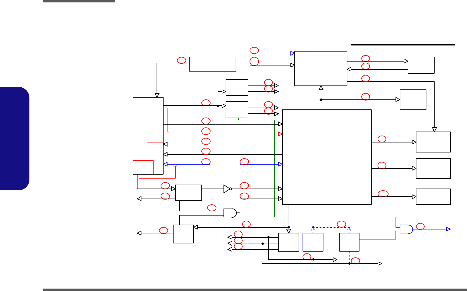
Schematic Diagrams
B - 40 Power Sequence Diagram
B.Schematic Diagrams
Power Sequence Diagram
14
13
CL_PWROK
6
3.3VM
DD _O N
SL P_ M#
DR AM V R
10
7
M ULT I I/ O BO AR D
CL _P WR OK
9
5VS
6
FO R ME
IC S9 LP R3 63E GL F
Other
1
SC472B
Other
VR
PCI
9
Platform
1. 5V S_ PW RGD
4a
Processor
SC 41 1
5b
2
150 ms
6
5b
15
12
8
DE LAY
PLT_RST#
1. 5V S
FOR M E
6
3
SC486
12-1
3.3 VS
DD _ON
3
MOS FE T
1.0 5V S
CL KE N#
H_P WR GD
Penryn
4b
6
PW R_ SW #
Clock Generator
1.05VM
Cantiga
DE LA Y_ PW RGD
DELAY
Devices
5b
CLK _P WR GD
3
CL _P WR OK
PM _R SM RS T#
CL _P WRO K
GFX VR
NORTH BRIDGE
13
6
PCI _R ST #
VGFX_CORE
PW R_ BT N#
GFX_VREN
LT C3 85 0
ITE8512E
5V
5a
DE LA Y_ PW RG D
APL5913
SU SC #
11
MOSFET
EC
VRM_PWRGD
1.8V
17
1. 8V _P WR GD
SB_PWROK
VC OR E_ ON
1. 05 VM _P WR GD
16
0.9VSM
3.3V
9
SC 45 2
SOUTH BRIDGE
Devices
VC OR E
M720T V0.0 BOOT BLOCK DIAGRAM
VDD3/VDD5
75 ms
9
H_CPURST#
ICH9-M
??????
SU SB #
VCORE VR
SUSB#
16
6
CL_PWROK
Sheet 39 of 40
Power Sequence
Diagram
Schematic Diagrams
Power Sequence v3.0 B - 41
B.Schematic Diagrams
Power Sequence v3.0
CLK_PWRGD
206.4ms
3.3V
5b SUSB#
6
ms
2.64ms (950mV)
4b
17
6
12
1.5VS
H_CPURST#
10.44ms
2
3
PWR_SW#
560ms
120.8ms
3.32ms
9.36ms
1.17V
9
3
365.6us
6
2.981ms
PLT_RST#
DELAY_PWRGD
3.932ms
10
690.8us
568.0us
8
VCORE_ON
11
1
16
SUSC#
DD_ON
VRM_PWRGD
9.4ms
0.9VSM
3
13
15
5a
174.4ms
370us
6
5VS
107.6ms
1.8V
V5REF_SUS
14
61.10us
920us
(440mV)
CL_PWROK
515.4us
1.5912ms
RSMRST#
5V
SB_PWROK
6
12ms
6.215ms
76.4ms
12-1
(1.05V)
482.8us
6
4a
9.36ms
V5REF
VCORE
3.3VS
164.7ms
PWR_BTN#
85.6ms
105.6ms
1.05VS
3
M720T V3.0 POWER ON SEQUENCE
H_PWRGD
371.5us
7
Sheet 40 of 40
Power Sequence
v3.0

Schematic Diagrams
B - 42
B.Schematic Diagrams