Clevo W245CUQ, W246CUQ, W247CUQ, W24ACU, W24BCU Service Manual. Www.s Manuals.com. Manual
User Manual: Notebook Clevo W24ACU - Service manuals and Schematics, Disassembly / Assembly. Free.
Open the PDF directly: View PDF ![]() .
.
Page Count: 89
- Manual
- Notice
- Chapter 1: Introduction
- Overview
- Models Differences
- Specifications
- External Locator - Top View with LCD Panel Open
- External Locator - Front & Right side Views
- External Locator - Left Side & Rear View
- External Locator - Bottom View
- Mainboard Overview - Top (Key Parts)
- Mainboard Overview - Bottom (Key Parts)
- Mainboard Overview - Top (Connectors)
- Mainboard Overview - Bottom (Connectors)
- Chapter 2: Disassembly
- Overview
- Maintenance Tools
- Connections
- Maintenance Precautions
- Disassembly Steps
- Removing the Battery
- Removing the Hard Disk Drive
- Removing the Optical (CD/DVD) Device
- Removing the System Memory (RAM)
- Removing the Wireless LAN Module
- Removing the 3.75G Module
- Removing the Keyboard
- Appendix A: Part Lists
- Part List Illustration Location
- Top (W245CUQ, W246CUQ)
- Top (W247CUQ)
- Top (W24ACU, W24BCU)
- Bottom 3.5W (W245CUQ, W246CUQ)
- Bottom 3.5W - No SIM (W245CUQ, W246CUQ)
- Bottom 3.5W (W24ACU, W24BCU)
- Bottom 6.5W (W245CUQ, W246CUQ)
- Bottom 6.5W - No SIM (W245CUQ, W246CUQ)
- Bottom 6.5W (W24ACU, W24BCU)
- LCD (W245CUQ)
- LCD (W246CUQ)
- LCD (W247CUQ)
- LCD (W24ACU, W24BCU)
- SATA-DVD (W245CUQ, W246CUQ)
- SATA-DVD (W24ACU, W24BCU)
- Appendix B: Schematic Diagrams
- System Block Diagram
- CEDARVIEW CPU PART-D
- CEDARVIEW CPU PART-A-C-F
- CEDARVIEW CPU PART-B
- CEDARVIEW CPU PART-E
- DDR3 SO-DIMM 1
- DDR3 SO-DIMM 2
- IDT CLOCK
- Tigerpoint PART-A-B
- Tigerpoint PART-C
- Tigerpoint PART-D
- Tigerpoint PART-E-F
- LVDS, INVERTER
- CRT, HDMI
- TPM, SATA HDD, ODD, FAN
- AUDIO CODEC VT1802P
- CARD READER JMB261C
- KBC-ITE IT8518E, SPI
- 3G, WLAN, BT
- USB PORT & USB CHARGER
- CONN, CCD, LED
- PWR VDD3, VDD5V, SYS15V
- PWR SW, 3V, 5V, 3VS, 5VS, 1.5VS
- PWR 1.05VS
- PWR 1.5V, 0.75V
- PWR VCORE
- PWR AC_IN, CHARGE
- CLICK BOARD
- AUDIO BOARD/USB
- POWER SWITCH & LID BOARD
- EXTERNAL ODD BOARD
- Appendix C: Updating the FLASH ROM BIOS

W245CUQ/W246CUQ/W247CUQ/W24ACU/W24BCU

Preface
I
Preface
Notebook Computer
W245CUQ/W246CUQ/W247CUQ/W24ACU/W24BCU
Service Manual

Preface
II
Preface
Notice
The company reserves the right to revise this publication or to change its contents without notice. Information contained
herein is for reference only and does not constitute a commitment on the part of the manufacturer or any subsequent ven-
dor. They assume no responsibility or liability for any errors or inaccuracies that may appear in this publication nor are
they in anyway responsible for any loss or damage resulting from the use (or misuse) of this publication.
This publication and any accompanying software may not, in whole or in part, be reproduced, translated, transmitted or
reduced to any machine readable form without prior consent from the vendor, manufacturer or creators of this publica-
tion, except for copies kept by the user for backup purposes.
Brand and product names mentioned in this publication may or may not be copyrights and/or registered trademarks of
their respective companies. They are mentioned for identification purposes only and are not intended as an endorsement
of that product or its manufacturer.
Version 1.0
May 2012
Trademarks
Intel and Atom are registered trademark of Intel Corporation.
Windows® is a registered trademark of Microsoft Corporation.
Other brand and product names are trademarks and/or registered trademarks of their respective companies.

Preface
III
Preface
About this Manual
This manual is intended for service personnel who have completed sufficient training to undertake the maintenance and
inspection of personal computers.
It is organized to allow you to look up basic information for servicing and/or upgrading components of the W245CUQ/
W246CUQ/W247CUQ/W24ACU/W24BCU series notebook PC.
The following information is included:
Chapter 1, Introduction, provides general information about the location of system elements and their specifications.
Chapter 2, Disassembly, provides step-by-step instructions for disassembling parts and subsystems and how to upgrade
elements of the system.
Appendix A, Part Lists
Appendix B, Schematic Diagrams
Appendix C, Updating the FLASH ROM BIOS

Preface
IV
Preface
IMPORTANT SAFETY INSTRUCTIONS
Follow basic safety precautions, including those listed below, to reduce the risk of fire, electric shock and injury to per-
sons when using any electrical equipment:
1. Do not use this product near water, for example near a bath tub, wash bowl, kitchen sink or laundry tub, in a wet
basement or near a swimming pool.
2. Avoid using a telephone (other than a cordless type) during an electrical storm. There may be a remote risk of elec-
trical shock from lightning.
3. Do not use the telephone to report a gas leak in the vicinity of the leak.
4. Use only the power cord and batteries indicated in this manual. Do not dispose of batteries in a fire. They may
explode. Check with local codes for possible special disposal instructions.
5. This product is intended to be supplied by a Listed Power Unit (Full Range 30W AC/DC Adapter – AC Input 100 -
240V, 50 - 60Hz, DC Output 19V, 1.58A).
CAUTION
This Computer’s Optical Device is a Laser Class 1 Product
FCC Statement
This device complies with Part 15 of the FCC Rules. Operation is subject to the following two conditions:
This device may not cause harmful interference.
This device must accept any interference received, including interference that may cause undesired operation.
Preface
V
Preface
Instructions for Care and Operation
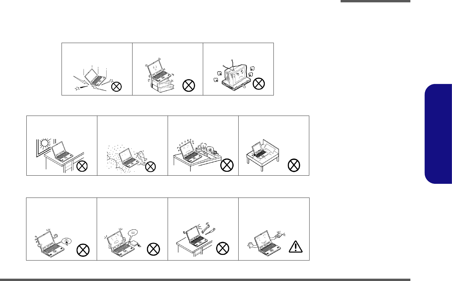
The notebook computer is quite rugged, but it can be damaged. To prevent this, follow these suggestions:
1. Don’t drop it, or expose it to shock. If the computer falls, the case and the components could be damaged.
2. Keep it dry, and don’t overheat it. Keep the computer and power supply away from any kind of heating element. This
is an electrical appliance. If water or any other liquid gets into it, the computer could be badly damaged.
3. Follow the proper working procedures for the computer. Shut the computer down properly and don’t forget to save
your work. Remember to periodically save your data as data may be lost if the battery is depleted.
Do not expose the computer
to any shock or vibration. Do not place it on an unstable
surface. Do not place anything heavy
on the computer.
Do not expose it to excessive
heat or direct sunlight. Do not leave it in a place
where foreign matter or mois-
ture may affect the system.
Don’t use or store the com-
puter in a humid environment. Do not place the computer on
any surface which will block
the vents.
Do not turn off the power
until you properly shut down
all programs.
Do not turn off any peripheral
devices when the computer is
on.
Do not disassemble the com-
puter by yourself. Perform routine maintenance
on your computer.
Preface
VI
Preface
4. Avoid interference. Keep the computer away from high capacity transformers, electric motors, and other strong mag-
netic fields. These can hinder proper performance and damage your data.
5. Take care when using peripheral devices.
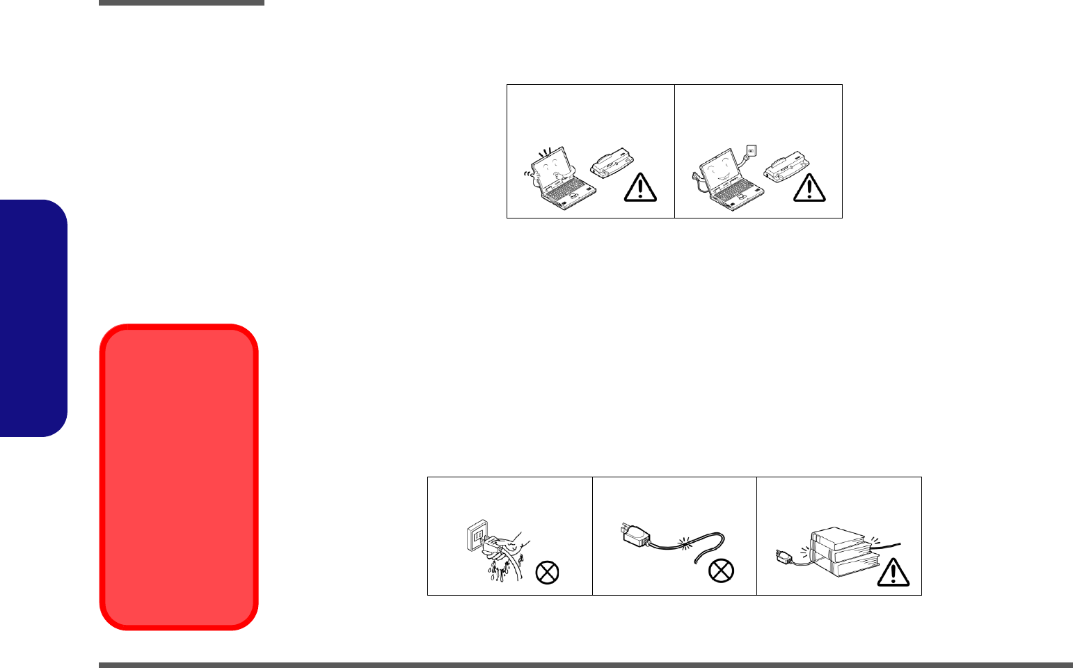
Power Safety
The computer has specific power requirements:
• Only use a power adapter approved for use with this computer.
• Your AC adapter may be designed for international travel but it still requires a steady, uninterrupted power supply. If you are
unsure of your local power specifications, consult your service representative or local power company.
• The power adapter may have either a 2-prong or a 3-prong grounded plug. The third prong is an important safety feature; do
not defeat its purpose. If you do not have access to a compatible outlet, have a qualified electrician install one.
• When you want to unplug the power cord, be sure to disconnect it by the plug head, not by its wire.
• Make sure the socket and any extension cord(s) you use can support the total current load of all the connected devices.
• Before cleaning the computer, make sure it is disconnected from any external power supplies.
Use only approved brands of
peripherals. Unplug the power cord before
attaching peripheral devices.
Do not plug in the power
cord if you are wet. Do not use the power cord if
it is broken. Do not place heavy objects
on the power cord.
Power Safety
Warning
Before you undertake
any upgrade proce-
dures, make sure that
you have turned off the
power, and discon-
nected all peripherals
and cables (including
telephone lines). It is
advisable to also re-
move your battery in
order to prevent acci-
dentally turning the
machine on.

Preface
VII
Preface
Battery Precautions
• Only use batteries designed for this computer. The wrong battery type may explode, leak or damage the computer.
• Do not continue to use a battery that has been dropped, or that appears damaged (e.g. bent or twisted) in any way. Even if the
computer continues to work with a damaged battery in place, it may cause circuit damage, which may possibly result in fire.
• Recharge the batteries using the notebook’s system. Incorrect recharging may make the battery explode.
• Do not try to repair a battery pack. Refer any battery pack repair or replacement to your service representative or qualified service
personnel.
• Keep children away from, and promptly dispose of a damaged battery. Always dispose of batteries carefully. Batteries may explode
or leak if exposed to fire, or improperly handled or discarded.
• Keep the battery away from metal appliances.
• Affix tape to the battery contacts before disposing of the battery.
• Do not touch the battery contacts with your hands or metal objects.
Battery Guidelines
The following can also apply to any backup batteries you may have.
• If you do not use the battery for an extended period, then remove the battery from the computer for storage.
• Before removing the battery for storage charge it to 60% - 70%.
• Check stored batteries at least every 3 months and charge them to 60% - 70%.
Battery Disposal
The product that you have purchased contains a rechargeable battery. The battery is recyclable. At the end of its useful life, under var-
ious state and local laws, it may be illegal to dispose of this battery into the municipal waste stream. Check with your local solid waste
officials for details in your area for recycling options or proper disposal.
Caution
Danger of explosion if battery is incorrectly replaced. Replace only with the same or equivalent type recommended by the manufacturer.
Discard used battery according to the manufacturer’s instructions.
Battery Level
Click the battery icon in the taskbar to see the current battery level and charge status. A battery that drops below a level of 10%
will not allow the computer to boot up. Make sure that any battery that drops below 10% is recharged within one week.
Preface
VIII
Preface
Related Documents
You may also need to consult the following manual for additional information:
User’s Manual on CD
This describes the notebook PC’s features and the procedures for operating the computer and its ROM-based setup pro-
gram. It also describes the installation and operation of the utility programs provided with the notebook PC.
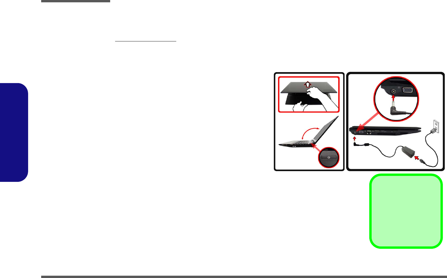
System Startup
1. Remove all packing materials.
2. Place the computer on a stable surface.
3. Insert the battery and make sure it is locked in position.
4. Securely attach any peripherals you want to use with the computer
(e.g. keyboard and mouse) to their ports.
5. Attach the AC/DC adapter to the DC-In jack on the left of the
computer, then plug the AC power cord into an outlet, and connect
the AC power cord to the AC/DC adapter.
6. Use one hand to raise the
lid/LCD to a comfortable viewing angle
(do
not exceed 130 degrees)
;
use the other hand to support the base of
the computer (Note: Never lift the computer by the lid/LCD).
7. Press the power button to turn the computer “on”.
Shut Down
Note that you should always
shut your computer down
by choosing Shut Down
from the Start Menu.
This will help prevent hard
disk or system problems.
Figure 1
Opening the Lid/LCD/Com-
puter with AC/DC Adapter
Plugged-In

Preface
IX
Preface
Contents
Introduction ..............................................1-1
Overview .........................................................................................1-1
Models Differences .........................................................................1-1
Specifications ..................................................................................1-2
External Locator - Top View with LCD Panel Open ......................1-4
External Locator - Front & Right side Views .................................1-5
External Locator - Left Side & Rear View .....................................1-6
External Locator - Bottom View .....................................................1-7
Mainboard Overview - Top (Key Parts) .........................................1-8
Mainboard Overview - Bottom (Key Parts) ....................................1-9
Mainboard Overview - Top (Connectors) .....................................1-10
Mainboard Overview - Bottom (Connectors) ...............................1-11
Disassembly ...............................................2-1
Overview .........................................................................................2-1
Maintenance Tools ..........................................................................2-2
Connections .....................................................................................2-2
Maintenance Precautions .................................................................2-3
Disassembly Steps ...........................................................................2-4
Removing the Battery ......................................................................2-5
Removing the Hard Disk Drive .......................................................2-6
Removing the Optical (CD/DVD) Device ......................................2-8
Removing the System Memory (RAM) ..........................................2-9
Removing the Wireless LAN Module ...........................................2-10
Removing the 3.75G Module ........................................................2-11
Removing the Keyboard ................................................................2-12
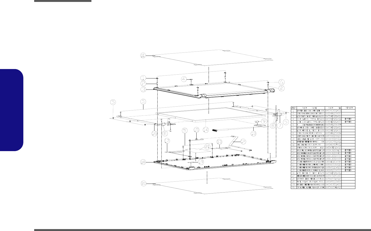
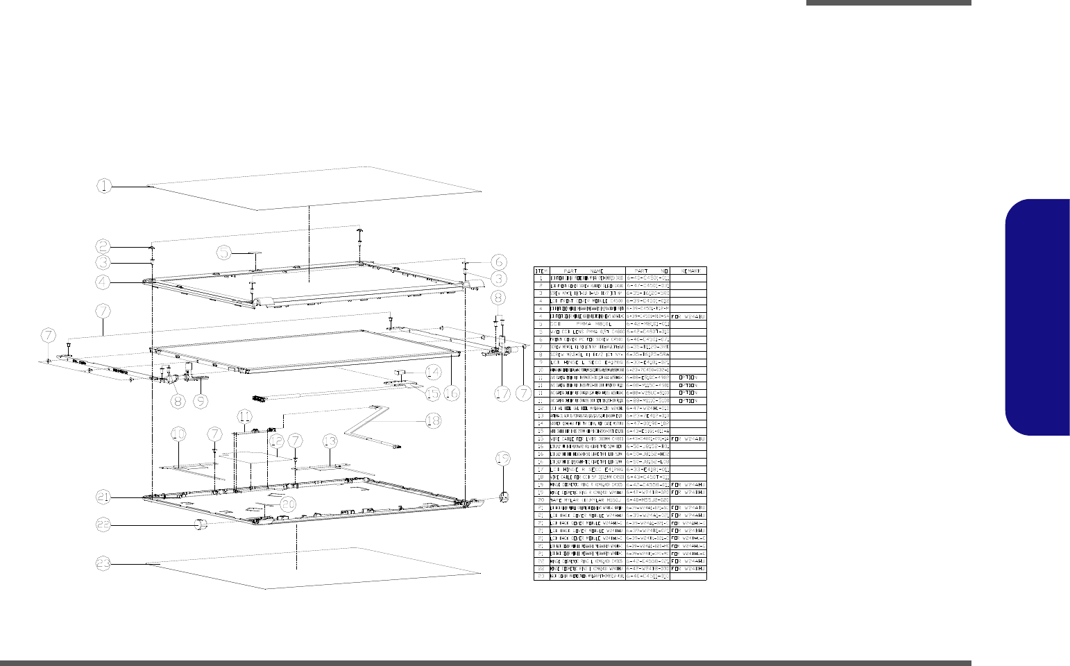
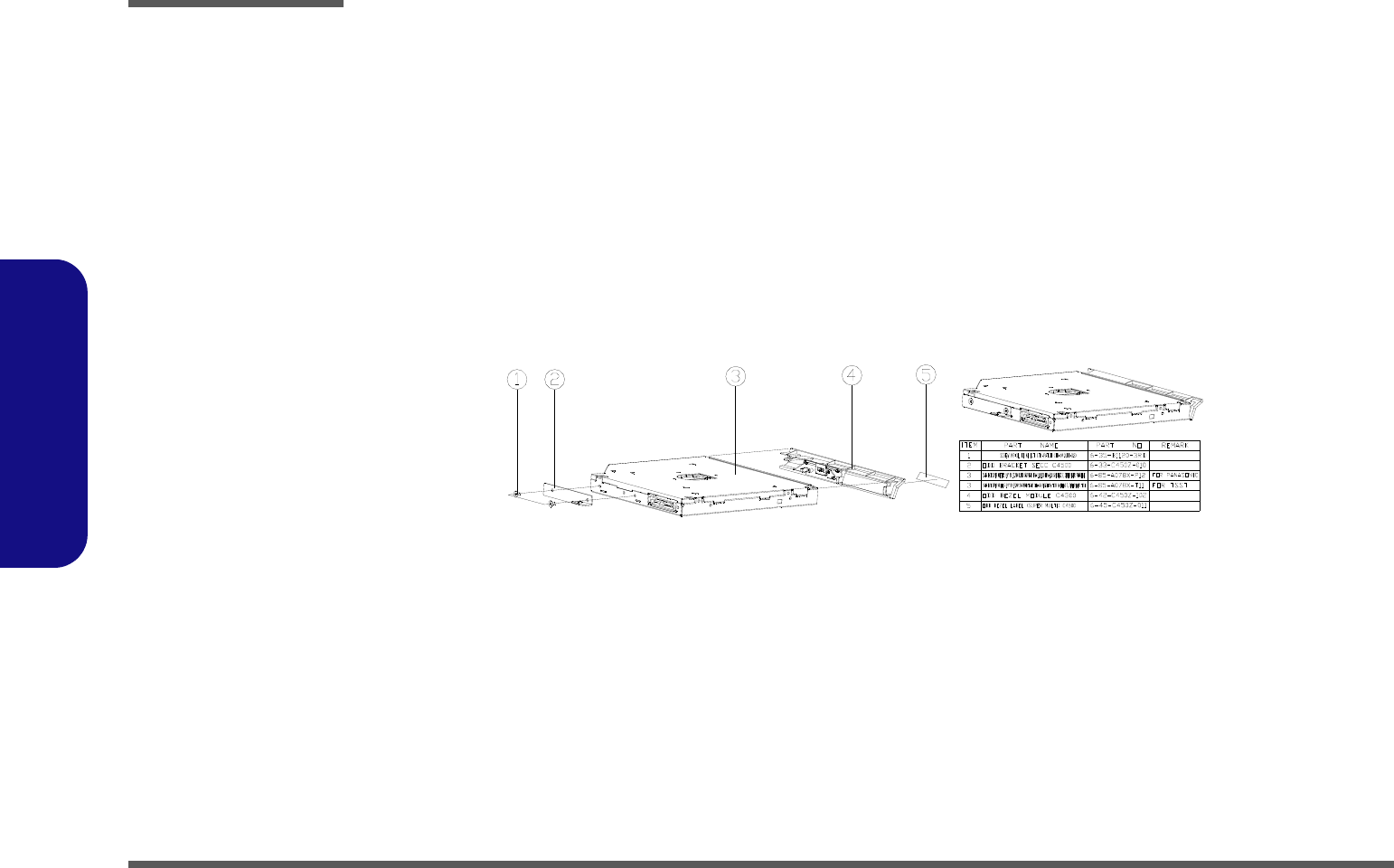
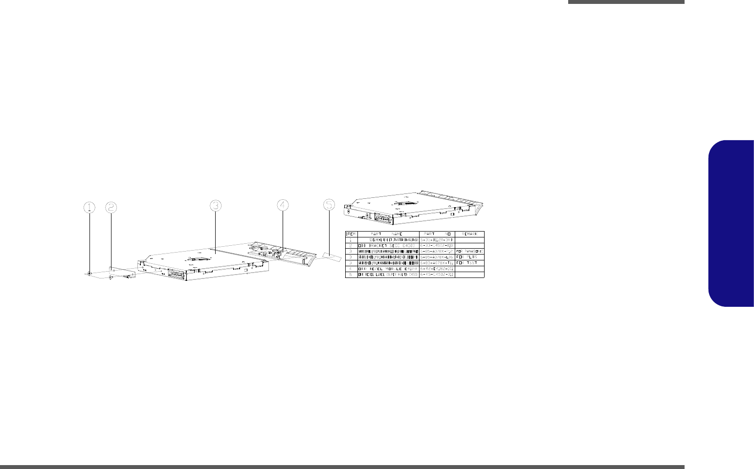
Part Lists ..................................................A-1
Part List Illustration Location ........................................................A-2
Top (W245CUQ, W246CUQ) .......................................................A-3
Top (W247CUQ) ............................................................................A-4
Top (W24ACU, W24BCU) ........................................................... A-5
Bottom 3.5W (W245CUQ, W246CUQ) ....................................... A-6
Bottom 3.5W - No SIM (W245CUQ, W246CUQ) ....................... A-7
Bottom 3.5W (W24ACU, W24BCU) ............................................ A-8
Bottom 6.5W (W245CUQ, W246CUQ) ....................................... A-9
Bottom 6.5W - No SIM (W245CUQ, W246CUQ) ..................... A-10
Bottom 6.5W (W24ACU, W24BCU) .......................................... A-11
LCD (W245CUQ) ....................................................................... A-12
LCD (W246CUQ) ....................................................................... A-13
LCD (W247CUQ) ....................................................................... A-14
LCD (W24ACU, W24BCU) ....................................................... A-15
SATA-DVD (W245CUQ, W246CUQ) ....................................... A-16
SATA-DVD (W24ACU, W24BCU) ........................................... A-17
Schematic Diagrams.................................B-1
System Block Diagram ...................................................................B-2
CEDARVIEW CPU PART-D ........................................................B-3
CEDARVIEW CPU PART-A-C-F .................................................B-4
CEDARVIEW CPU PART-B ........................................................B-5
CEDARVIEW CPU PART-E .........................................................B-6
DDR3 SO-DIMM 1 ........................................................................B-7
DDR3 SO-DIMM 2 ........................................................................B-8
IDT CLOCK ...................................................................................B-9
Tigerpoint PART-A-B ..................................................................B-10
Tigerpoint PART-C ......................................................................B-11
Tigerpoint PART-D ......................................................................B-12
Tigerpoint PART-E-F ...................................................................B-13
LVDS, INVERTER ......................................................................B-14
CRT, HDMI ..................................................................................B-15
TPM, SATA HDD, ODD, FAN ...................................................B-16
AUDIO CODEC VT1802P ..........................................................B-17

Preface
X
Preface
CARD READER JMB261C ........................................................ B-18
KBC-ITE IT8518E, SPI ...............................................................B-19
3G, WLAN, BT ............................................................................B-20
USB PORT & USB CHARGER ..................................................B-21
CONN, CCD, LED .......................................................................B-22
PWR VDD3, VDD5V, SYS15V .................................................. B-23
PWR SW, 3V, 5V, 3VS, 5VS, 1.5VS .......................................... B-24
PWR 1.05VS ................................................................................ B-25
PWR 1.5V, 0.75V ........................................................................B-26
PWR VCORE ............................................................................... B-27
PWR AC_IN, CHARGE ..............................................................B-28
CLICK BOARD ...........................................................................B-29
AUDIO BOARD/USB .................................................................B-30
POWER SWITCH & LID BOARD ............................................. B-31
EXTERNAL ODD BOARD ........................................................ B-32
Updating the FLASH ROM BIOS......... C-1

Introduction
Overview 1 - 1
1.Introduction
Chapter 1: Introduction
Overview
This manual covers the information you need to service or upgrade the W245CUQ/W246CUQ/W247CUQ/W24ACU/
W24BCU series notebook computer. Information about operating the computer (e.g. getting started, and the Setup utility)
is in the User’s Manual. Information about drivers (e.g. VGA & audio) is also found in User’s Manual. That manual is
shipped with the computer.
Operating systems (e.g. Windows 7 etc.) have their own manuals as do application software (e.g. word processing and
database programs). If you have questions about those programs, you should consult those manuals.
The W245CUQ/W246CUQ/W247CUQ/W24ACU/W24BCU series notebook is designed to be upgradeable. See Disas-
sembly on page 2 - 1 for a detailed description of the upgrade procedures for each specific component. Please note the
warning and safety information indicated by the “” symbol.
The balance of this chapter reviews the computer’s technical specifications and features.
Models Differences
This notebook series includes different models that vary slightly in design style, color and general appearance. Note that though your
computer may look slightly different from that pictured throughout this documentation, all ports, jacks, indicators, specifications and
general functions are the same for all the design styles.
Introduction
1 - 2 Specifications
1.Introduction
Specifications
Latest Specification Information
The specifications listed here are correct at the
time of sending them to the press. Certain items
(particularly processor types/speeds) may be
changed, delayed or updated due to the manu-
facturer's release schedule. Check with your
service center for more details.
CPU
The CPU is not a user serviceable part. Ac-
cessing the CPU in any way may violate your
warranty.
Processor
Intel® Atom® Processor N2600
1.60 GHz, 1MB L2 Cache & 800MHz FSB, TDP 3.5W -
BGA Package, 32nm (32 Nanometer) Process
Technology
Intel® Atom® Processor N2800
1.86 GHz, 1MB L2 Cache & 1066MHz FSB, TDP 6.5W -
BGA Package, 32nm (32 Nanometer) Process
Technology
Core Logic
Intel® NM10 Express Chipset
Display
14.0” (35.56cm) HD (1366 * 768) 16:9 Panel
3.6mm thick panel Model A Design II
Memory
Single DDR3 Data Channel
One 204 Pin SO-DIMM Socket Supporting DDRIII (DDR3)
1066/1333MHz (Real Operational Frequency Depends on
Processor) Memory
*2nd 204 Pin SO-DIMM Socket Supporting DDRIII
(DDR3) 1066/1333MHz (Real Operational Frequency
Depends on Processor) Memory
*Note that the 2nd Memory Socket is only supported
by the Atom® N2800
Memory Expandable up to 4GB
(Using 1GB/2GB/4GB Modules)
Atom® N2600 Processors Only Support Up to 2GB of
Memory
Video Adapter for N2800 Processor
Intel® GMA 3650@640MHz Video Integrated with the
N2800 Processor
Total Available Graphics Memory of up to 384MB
Supports DirectX® 9
Video Adapter for N2600 Processor
Intel® GMA 3600@400MHz Video Integrated with the
N2600 Processor
Total Available Graphics Memory of up to 384MB
Supports DirectX® 9
BIOS
One 16Mb SPI Flash ROM
Phoenix™ BIOS
Storage
One Changeable 2.5" 9.5 mm (h) SATA (Serial) Hard Disk
Drive
External Super-Multi Optical Device Drive with USB
Interface (Factory Option)
Security
Kensington Lock
BIOS Password
Audio
High Definition Audio Compliant Interface
2 * Built-In Speakers
Built-In Microphone
Introduction
Specifications 1 - 3
1.Introduction
Keyboard & Pointing Device
Isolated WinKey Keyboard
Built-in TouchPad with Multi-Gesture Functionality
Some Designs Only:
Three Instant Keys for WWW, E-Mail & Silent Mode
(except for some model designs in this series)
Interface
Three USB 2.0 Ports
One HDMI-Out (High-Definition Multimedia Interface) 1.3a
Port
One External Monitor Port
One Headphone-Out Jack
One Microphone-In Jack
One RJ-45 LAN Jack
One DC-in Jack
Card Reader
Embedded Multi-In-1 Card Reader
- MMC/ RS MMC
- SD/ Mini SD / SDHC / SDXC
- MS/ MS Pro/ MS Duo
Note: RS MMC/ Mini SD/ MS Duo Cards require a PC
adapter
Slot
Two Mini-Card Slots (USB & PCIe)
Slot 1:
for WLAN Combo Half Mini-Card Module with PCIe &
USB Interface
Slot 2 (Factory Option): for
UMTS/HSPDA-based 3.75G/
HSPA
Module
(Half Mini-Card) with USB Interface
Communication
10Mb/100Mb Base-TX Ethernet LAN
802.11b/g/n Wireless LAN Half Mini-Card Module
(Factory Option)
Combo WLAN
(802.11b/g/n)
and Bluetooth
v3.0 + HS
Half
Mini-Card Module with PCIe & USB Interface (Factory
Option)
Intel
®
Centrino
®
Wireless-N 100
(1*1 802.11 b/g/n) Half
Mini-Card PCIe WLAN Module (
Factory Option
)
Intel
®
Centrino
®
Wireless-N 130
(1*1 802.11 b/g/n+) Half
Mini-Card PCIe WLAN & Bluetooth 3.0 Combo Module (
Fac-
tory Option
)
Intel
®
Centrino
®
Wireless-N 1030
(1*2 802.11 b/g/n) Half
Mini-Card PCIe WLAN & Bluetooth 3.0 Combo Module (
Fac-
tory Option
)
UMTS/HSPDA-based 3.75G/HSPA
(Half Mini-Card) Module
(
Factory Option
)
300K/1.3M Pixel USB PC Camera Module
(
Factory
Option
)
Operating Systems
Windows® 7 (with Service Pack 1)
Power Management
Wake On LAN
Wake On USB
Energy Star 5.2 Ready
Power
Full Range AC/DC Adapter
AC Input: 100 - 240V, 50 - 60Hz
DC Output: 19V, 1.58A (30 Watts)
Battery
Removable 6 Cell Smart Lithium-Ion Battery Pack
48.84WH
Removable 3 Cell Smart Lithium-Ion Battery Pack
24.42WH
(
Factory Option
)
Design Feature
IMR (Injected Molded Resin) or Painted Style LCD Back
Covers for Some Model Designs
LED Indicators
Power/Suspend, HDD/ODD, WLAN/Bluetooth, Num Lock,
Caps Lock, Scroll Lock
Note: Num Lock, Caps Lock, Scroll Lock indicators are not
available for some designs
Environmental Spec
Temperature
Operating: 5°C - 35°C
Non-Operating: -20°C - 60°C
Relative Humidity
Operating: 20% - 80%
Non-Operating: 10% - 90%
Dimensions & Weight
Design I:
340mm (w) * 238mm (d) * 13.9 - 31.8mm (h)
2.0kg with 6 Cell Battery & ODD
Design II:
340mm (w) * 238mm (d) * 12 - 30.2mm (h)
1.9kg with 6 Cell Battery & ODD
Design III:
341mm (w) * 238.5mm (d) * 16- 34mm (h)
1.9kg with 6 Cell Battery & ODD
Introduction
1 - 4 External Locator - Top View with LCD Panel Open
1.Introduction
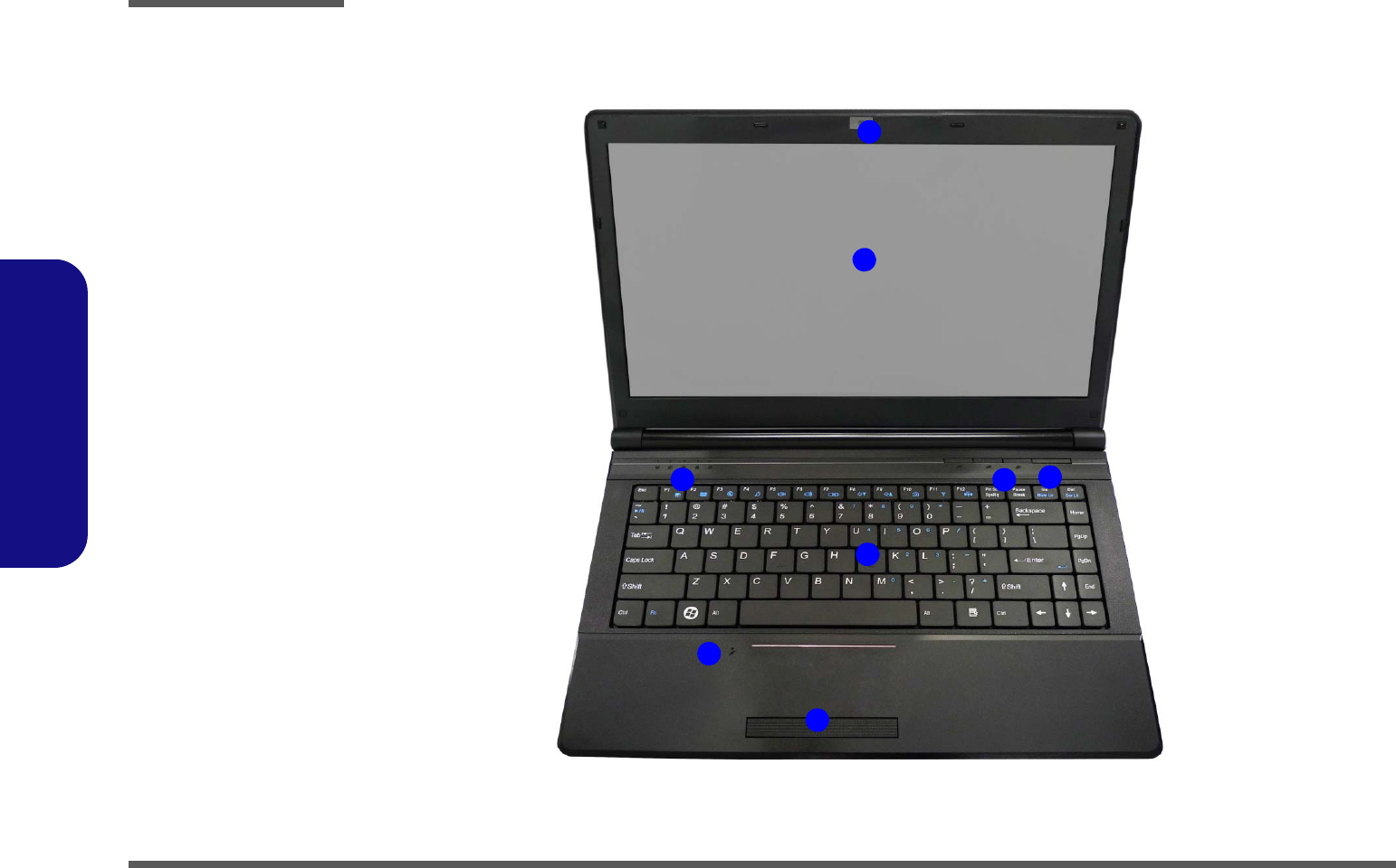
External Locator - Top View with LCD Panel Open
Figure 1
Top View
1. Optional Built-In
PC Camera
2. LCD
3. Power Button
4. Hot Key Buttons
(for some designs
only)
5. LED Status
Indicators
6. Keyboard
7. Built-In
Microphone
8. Touchpad &
Buttons
2
4
1
6
7
3
5
8
Introduction
External Locator - Front & Right side Views 1 - 5
1.Introduction
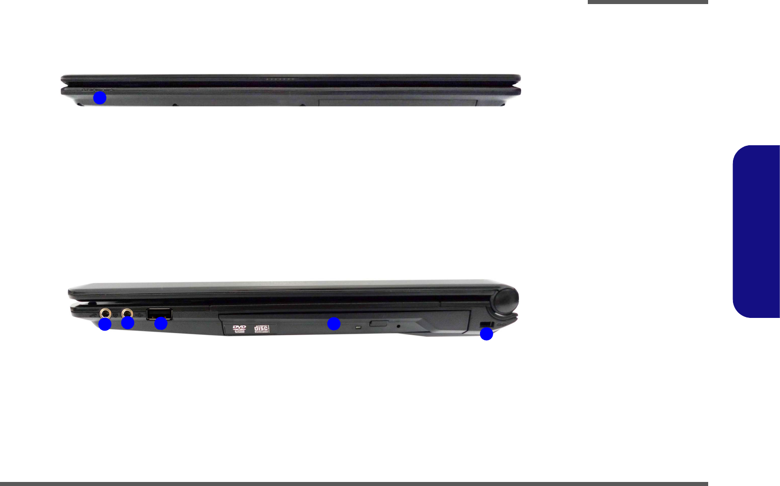
External Locator - Front & Right side Views
Figure 2
Front Views
1. LED Power
Indicators
Figure 3
Right Side Views
1. Microphone-In
Jack
2. Headphone-Out
Jack
3. USB 2.0 Port
4. Optical Device
Drive Bay
5. Security Lock
Slot
1
14
235
Introduction
1 - 6 External Locator - Left Side & Rear View
1.Introduction
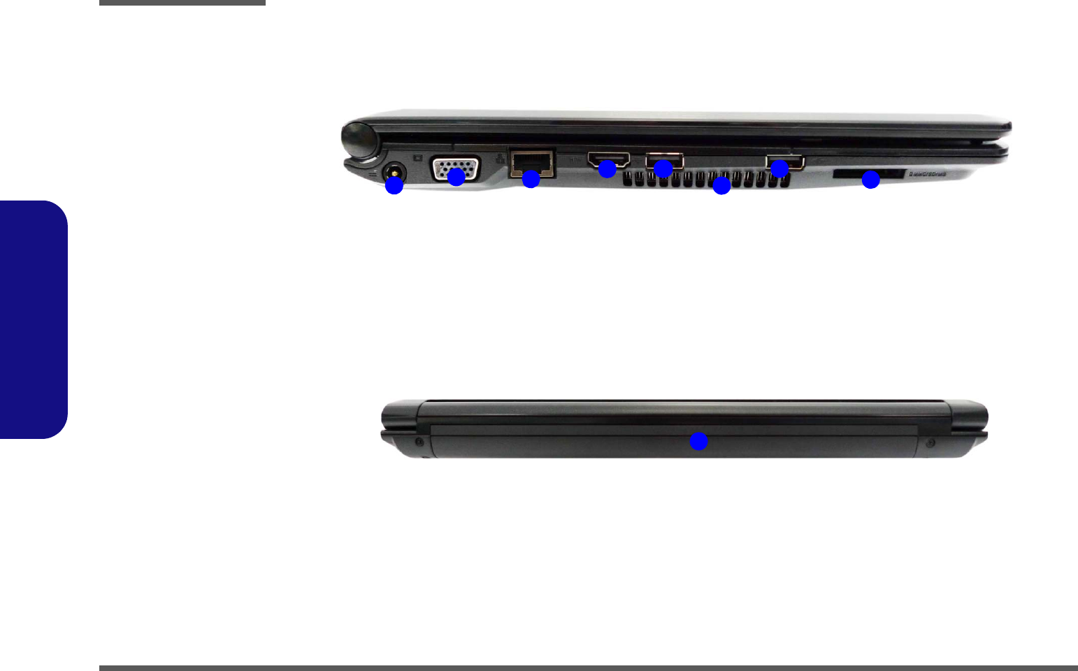
External Locator - Left Side & Rear View
Figure 4
Left Side View
1. DC-In Jack
2. External Monitor
Port
3. RJ-45 LAN Jack
4. HDMI-Out Port
5. 2 * USB 2.0 Ports
6. Vent
7. Multi-in-1 Card
Reader
14
36
25 5 7
Figure 5
Rear View
1. Battery
1
Introduction
External Locator - Bottom View 1 - 7
1.Introduction
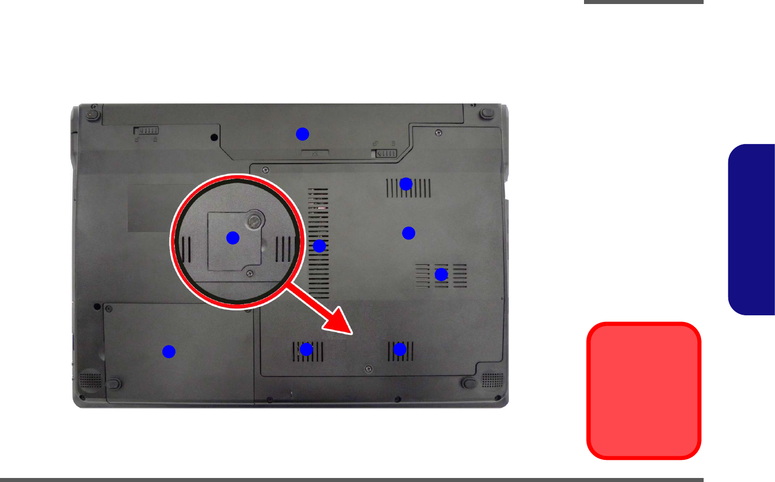
External Locator - Bottom View
Figure 6
Bottom View
1. Battery
2. Component Bay
Cover
3. Vent/Fan Intake/
Outlet
4. Hard Disk Bay
Cover
5. 3.75G/HSPA
USIM Card
Cover (optional)
Overheating
To prevent your com-
puter from overheating
make sure nothing
blocks the vent/fan in-
takes while the com-
puter is in use.
2
3
1
4
3
3
5
3 3
Introduction
1 - 8 Mainboard Overview - Top (Key Parts)
1.Introduction
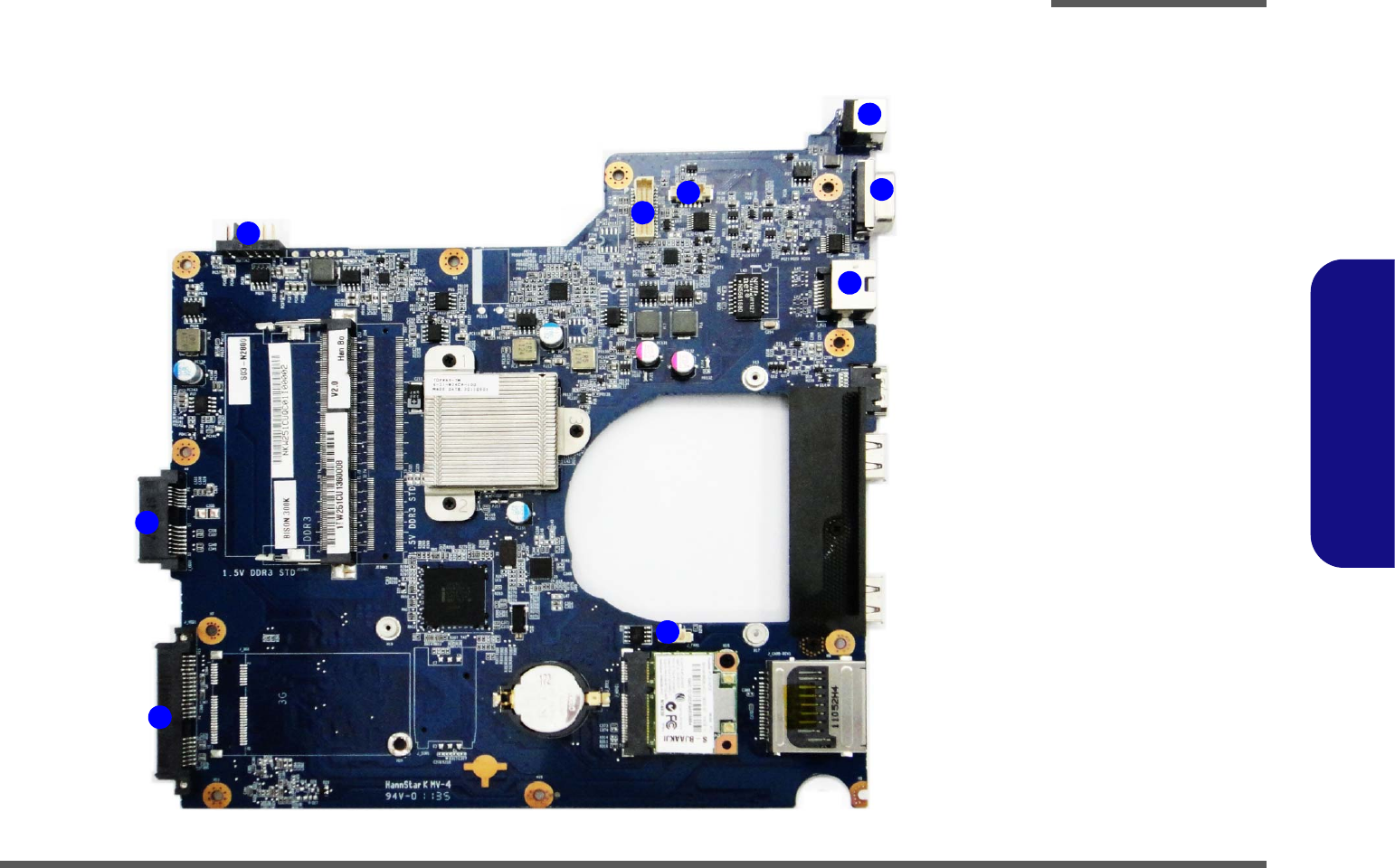
Mainboard Overview - Top (Key Parts)
Figure 7
Mainboard Top
Key Parts
1. JMC261
2. ITE 8518E
3. AZALIA Codec
3
2
1
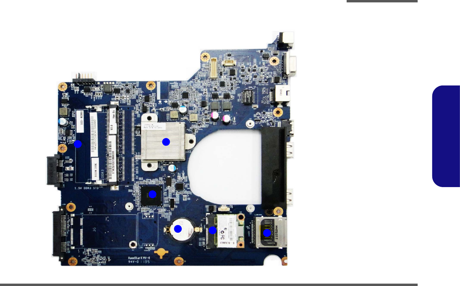
Introduction
Mainboard Overview - Bottom (Key Parts) 1 - 9
1.Introduction
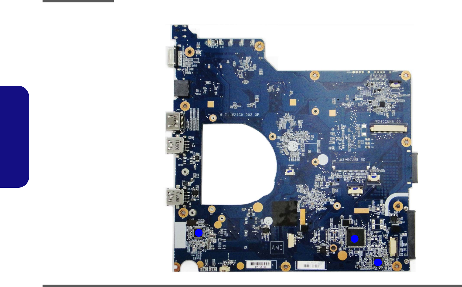
Mainboard Overview - Bottom (Key Parts)
12
3
456
Figure 8
Mainboard Bottom
Key Parts
1. Memory Slots
DDR3 SO-DIMM
2. Accelerated
Processing Unit
3. Intel NM10 PCH
4. CMOS Battery
5. Mini-Card
Connector (WLAN
Module)
6. Card Reader
Socket
Introduction
1 - 10 Mainboard Overview - Top (Connectors)
1.Introduction
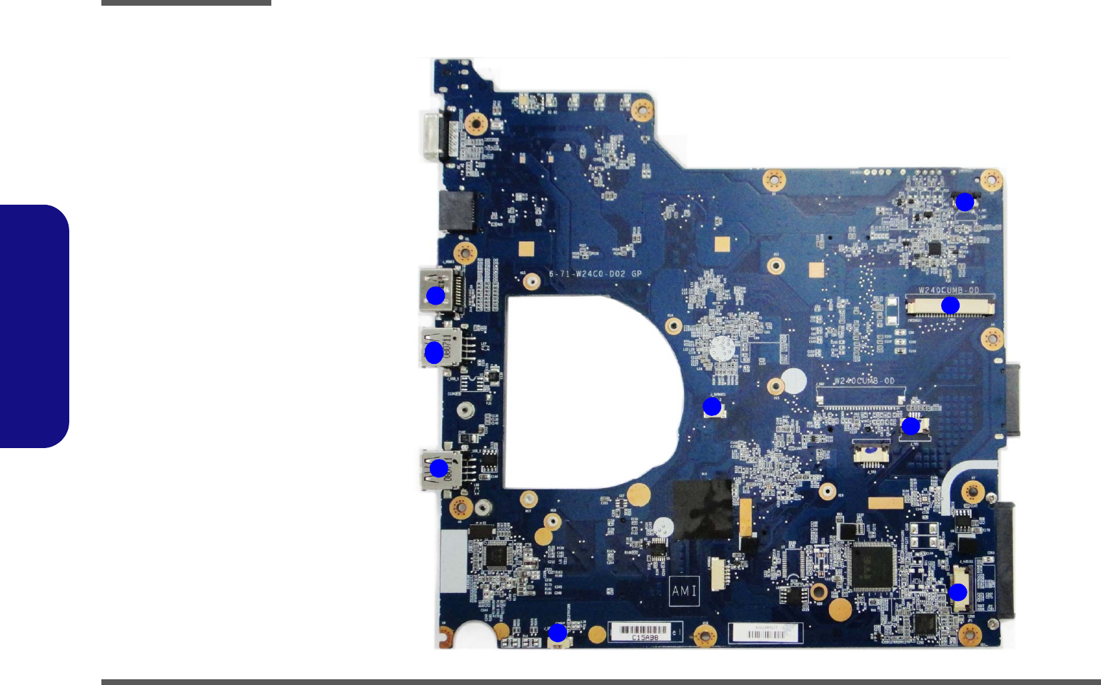
Mainboard Overview - Top (Connectors)
Figure 9
Mainboard Top
Connectors
1. HDMI-Out Port
2. USB Port 2.0
3. Speaker Cable
Connector
4. Microphone
Cable Connector
5. Audio Board
Connector
6. TouchPad Cable
Connector 1
7. Keyboard Cable
Connector
8. Switch Board
Cable Connector
1
2
8
2
3
46
7
5
Introduction
Mainboard Overview - Bottom (Connectors) 1 - 11
1.Introduction
Mainboard Overview - Bottom (Connectors)
Figure 10
Mainboard Bottom
Connectors
1. Battery
Connector
2. ODD Connector
3. HDD Connector
4. CPU Fan Cable
Connector
5. RJ-45 LAN Jack
6. External Monitor
Port
7. DC-In Jack
8. CCD Cable
Connector
9. LCD Cable
Connector
1
2
4
5
6
7
8
9
3

Introduction
1-12
1.Introduction

Disassembly
Overview 2 - 1
2.Disassembly
Chapter 2: Disassembly
Overview
This chapter provides step-by-step instructions for disassembling the W245CUQ/W246CUQ/W247CUQ/W24ACU/
W24BCU series notebook’s parts and subsystems. When it comes to reassembly, reverse the procedures (unless other-
wise indicated).
We suggest you completely review any procedure before you take the computer apart.
Procedures such as upgrading/replacing the RAM, optical device and hard disk are included in the User’s Manual but are
repeated here for your convenience.
To make the disassembly process easier each section may have a box in the page margin. Information contained under
the figure # will give a synopsis of the sequence of procedures involved in the disassembly procedure. A box with a
lists the relevant parts you will have after the disassembly process is complete. Note: The parts listed will be for the dis-
assembly procedure listed ONLY, and not any previous disassembly step(s) required. Refer to the part list for the previ-
ous disassembly procedure. The amount of screws you should be left with will be listed here also.
A box with a will also provide any possible helpful information. A box with a contains warnings.
An example of these types of boxes are shown in the sidebar.
Information
Warning

Disassembly
2 - 2 Overview
2.Disassembly
NOTE: All disassembly procedures assume that the system is turned OFF, and disconnected from any power supply (the
battery is removed too).
Maintenance Tools
The following tools are recommended when working on the notebook PC:
• M3 Philips-head screwdriver
• M2.5 Philips-head screwdriver (magnetized)
• M2 Philips-head screwdriver
• Small flat-head screwdriver
• Pair of needle-nose pliers
• Anti-static wrist-strap
Connections
Connections within the computer are one of four types:
Locking collar sockets for ribbon connectors To release these connectors, use a small flat-head screwdriver to
gently pry the locking collar away from its base. When replac-
ing the connection, make sure the connector is oriented in the
same way. The pin1 side is usually not indicated.
Pressure sockets for multi-wire connectors To release this connector type, grasp it at its head and gently
rock it from side to side as you pull it out. Do not pull on the
wires themselves. When replacing the connection, do not try to
force it. The socket only fits one way.
Pressure sockets for ribbon connectors To release these connectors, use a small pair of needle-nose pli-
ers to gently lift the connector away from its socket. When re-
placing the connection, make sure the connector is oriented in
the same way. The pin1 side is usually not indicated.
Board-to-board or multi-pin sockets To separate the boards, gently rock them from side to side as
you pull them apart. If the connection is very tight, use a small
flat-head screwdriver - use just enough force to start.

Disassembly
Overview 2 - 3
2.Disassembly
Maintenance Precautions
The following precautions are a reminder. To avoid personal injury or damage to the computer while performing a re-
moval and/or replacement job, take the following precautions:
1. Don't drop it. Perform your repairs and/or upgrades on a stable surface. If the computer falls, the case and other
components could be damaged.
2. Don't overheat it. Note the proximity of any heating elements. Keep the computer out of direct sunlight.
3. Avoid interference. Note the proximity of any high capacity transformers, electric motors, and other strong mag-
netic fields. These can hinder proper performance and damage components and/or data. You should also monitor
the position of magnetized tools (i.e. screwdrivers).
4. Keep it dry. This is an electrical appliance. If water or any other liquid gets into it, the computer could be badly
damaged.
5. Be careful with power. Avoid accidental shocks, discharges or explosions.
•Before removing or servicing any part from the computer, turn the computer off and detach any power supplies.
•When you want to unplug the power cord or any cable/wire, be sure to disconnect it by the plug head. Do not pull on the wire.
6. Peripherals – Turn off and detach any peripherals.
7. Beware of static discharge. ICs, such as the CPU and main support chips, are vulnerable to static electricity.
Before handling any part in the computer, discharge any static electricity inside the computer. When handling a
printed circuit board, do not use gloves or other materials which allow static electricity buildup. We suggest that
you use an anti-static wrist strap instead.
8. Beware of corrosion. As you perform your job, avoid touching any connector leads. Even the cleanest hands pro-
duce oils which can attract corrosive elements.
9. Keep your work environment clean. Tobacco smoke, dust or other air-born particulate matter is often attracted
to charged surfaces, reducing performance.
10. Keep track of the components. When removing or replacing any part, be careful not to leave small parts, such as
screws, loose inside the computer.
Cleaning
Do not apply cleaner directly to the computer, use a soft clean cloth.
Do not use volatile (petroleum distillates) or abrasive cleaners on any part of the computer.
Power Safety
Warning
Before you undertake
any upgrade proce-
dures, make sure that
you have turned off the
power, and discon-
nected all peripherals
and cables (including
telephone lines). It is
advisable to also re-
move your battery in
order to prevent acci-
dentally turning the
machine on.

Disassembly
2 - 4 Disassembly Steps
2.Disassembly
Disassembly Steps
The following table lists the disassembly steps, and on which page to find the related information. PLEASE PERFORM
THE DISASSEMBLY STEPS IN THE ORDER INDICATED.
To remove the Battery:
1. Remove the battery page 2 - 5
To remove the HDD:
1. Remove the battery page 2 - 5
2. Remove the HDD page 2 - 6
To remove the Optical Device:
1. Remove the battery page 2 - 5
2. Remove the optical device page 2 - 8
To remove the System Memory:
1. Remove the battery page 2 - 5
2. Remove the system memory page 2 - 9
To remove the WLAN Module:
1. Remove the battery page 2 - 5
2. Remove the wireless LAN page 2 - 10
To remove the 3.75G Module:
1. Remove the battery page 2 - 5
2. Remove the 3.75G page 2 - 11
To remove the Keyboard:
1. Remove the battery page 2 - 5
2. Remove the keyboard page 2 - 12
Disassembly
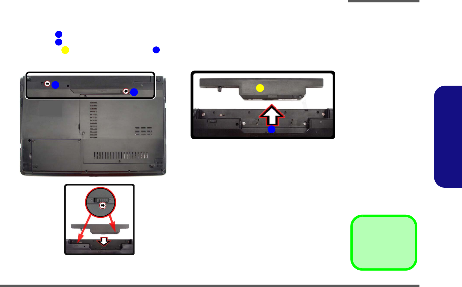
Removing the Battery 2 - 5
2.Disassembly
Removing the Battery
1. Turn the computer off, and turn it over.
2. Slide the latch in the direction of the arrow (Figure 1a).
3. Slide the latch in the direction of the arrow, and hold it in place (Figure 1a).
4. Slide the battery in the direction of the arrow (Figure 1b).
3. Battery
1
2
6
3
4
Figure 1
Battery Removal
a. Slide the latch and hold it
in place.
b. Slide the battery in the di-
rection of the arrow.
1
a. b.
3
2
4
Disassembly
2 - 6 Removing the Hard Disk Drive
2.Disassembly
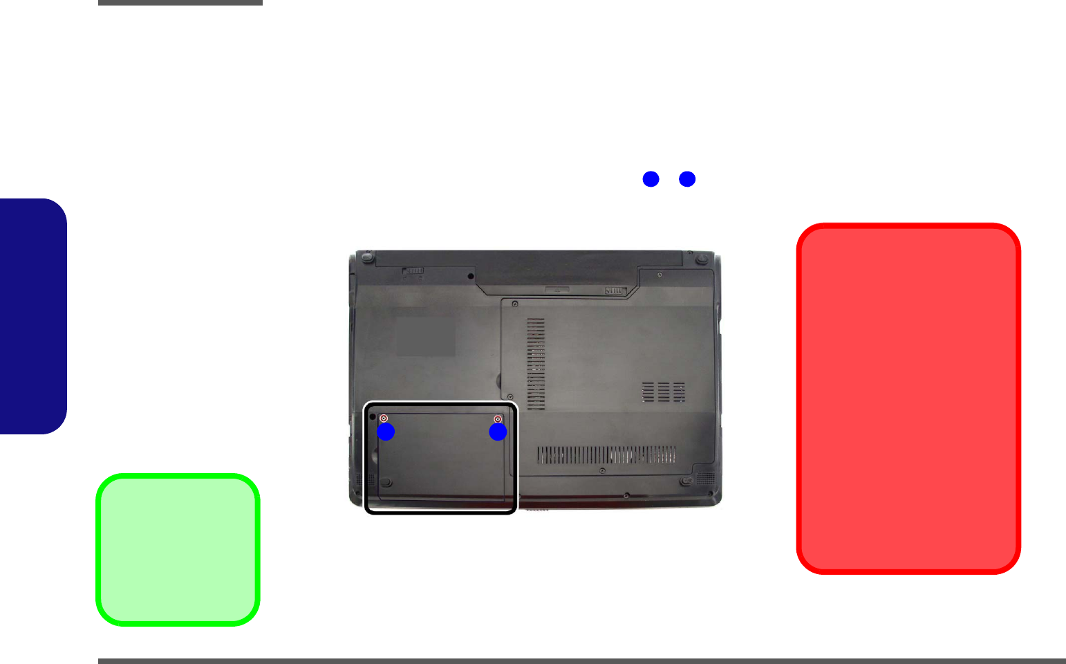
Removing the Hard Disk Drive
The hard disk drive can be taken out to accommodate other 2.5" serial (SATA) hard disk drives with a height of 9.5mm
(h). Follow your operating system’s installation instructions, and install all necessary drivers and utilities (as outlined in
Chapter 4 of the User’s Manual) when setting up a new hard disk.
Hard Disk Upgrade Process
1. Turn off the computer, and remove the battery (page 2 - 5).
2. Locate the hard disk bay cover and remove screws & (Figure 2a).
Figure 2
HDD Assembly
Removal
a. Locate the HDD bay cover
and remove the screws.
•2 Screws
1
2
a.
HDD System Warning
New HDD’s are blank. Before you
begin make sure:
You have backed up any data
you want to keep from your old
HDD.
You have all the CD-ROMs and
FDDs required to install your op-
erating system and programs.
If you have access to the internet,
download the latest application
and hardware driver updates for
the operating system you plan to
install. Copy these to a remov-
able medium.
2
1

Disassembly
Removing the Hard Disk Drive 2 - 7
2.Disassembly
3. Remove the hard disk bay cover (Figure 3b).
4. Grip the tab and slide the hard disk in the direction of arrow (Figure 3c).
5. Lift the hard disk assembly out of the bay (Figure 3d).
6. Remove the screw - and the mylar cover from the hard disk (Figure 3e).
7. Reverse the process to install a new hard disk (do not forget to replace all the screws and covers).
6
3
4
6
5
6
7
10
11
12
4
b.
c.
6
9
d.
3
e.
11
8
7
12
5
10
3
4
5
6
3. HDD Bay Cover
5. HDD Assembly
11. Mylar Cover
12. HDD
•4 Screws
Figure 3
HDD Assembly
Removal (cont’d.)
b. Remove the HDD bay
cover.
c. Grip the tab and slide the
HDD assembly in the di-
rection of the arrow.
d. Lift the HDD assembly
out of the bay.
e. Remove the screws and
mylar cover.
Disassembly
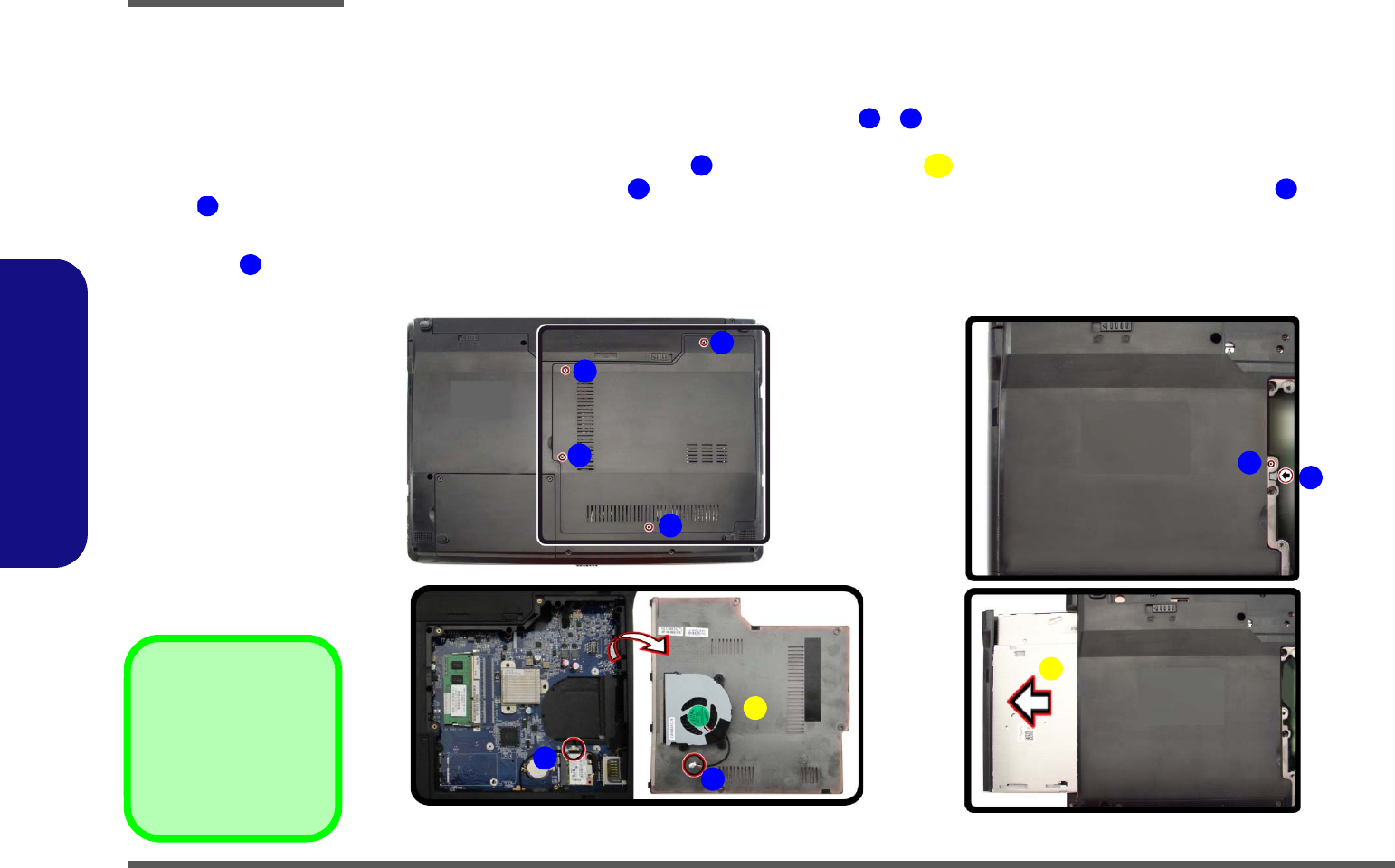
2 - 8 Removing the Optical (CD/DVD) Device
2.Disassembly
Removing the Optical (CD/DVD) Device
1. Turn off the computer, remove the battery (page 2 - 5).
2. Locate the component bay cover and remove screws - (Figure 4a).
3. Carefully (a fan and cable are attached to the under side of the cover) lift up the bay cover.
4. Carefully disconnect the fan cable , and remove the cover (Figure 4b).
5. Remove the screw at point , and use a screwdriver to carefully push out the optical device at point (Figure
4c).
6. Insert the new device and carefully slide it into the computer (the device only fits one way. DO NOT FORCE IT; The
screw holes should line up).
7. Restart the computer to allow it to automatically detect the new device.
Figure 4
Optical Device
Removal
a. Remove the screws.
b. Remove the bay cover.
c. Remove the screw at
point and use a
screwdriver to carefully
push out the optical de-
vice at point .
d. Remove the optical de-
vice.
7
8
1
4
5
6
7
8
6. Component Bay Cov-
er
9. Optical Device
•4 Screws
1
d.
9
b.
78
2
3
4
55
c.
a.
6
Disassembly
Removing the System Memory (RAM) 2 - 9
2.Disassembly
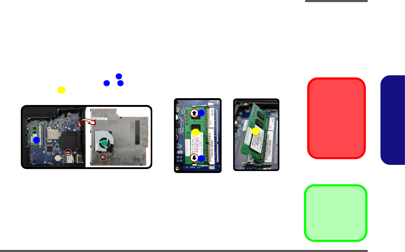
Removing the System Memory (RAM)
The computer has one memory socket for 200 pin Small Outline Dual In-line Memory Modules (SO-DIMM) supporting
DDR3 1333/ 1066MHz. The main memory can be expanded up to 4GB. The SO-DIMM modules supported are 1GB,
2GB and 4GB and DDRIII Modules. The total memory size is automatically detected by the POST routine once you turn
on your computer.
Memory Upgrade Process
1. Turn off the computer, remove the battery (page 2 - 5) and the component bay cover (page 2 - 8).
2. The RAM modules will be visible at point on the main board.
3. Gently pull the two release latches ( & ) on the sides of the memory socket.
4. The RAM module will pop-up, and you can then remove it.
5. Insert a new module holding it at about a 30° angle and fit the connectors firmly into the memory slot.
6. The module’s pin alignment will allow it to only fit one way. Make sure the module is seated as far into the slot as it
will go. DO NOT FORCE the module; it should fit without much pressure.
7. Press the module in and down towards the mainboard until the slot levers click into place to secure the module.
8. Replace the bay cover and screws (make sure you reconnect the fan cable before screwing down the bay
cover).
9. Restart the computer to allow the BIOS to register the new memory configuration as it starts up.
Figure 5
RAM Module
Removal
a. Locate the memory
socket.
b. Remove the mod-
ule.
Contact Warning
Be careful not to touch
the metal pins on the
module’s connecting
edge. Even the clean-
est hands have oils
which can attract parti-
cles, and degrade the
module’s perfor-
mance.
1
2
3
4
b.
a.
14
2
3
4
4. RAM Module
Disassembly
2 - 10 Removing the Wireless LAN Module
2.Disassembly
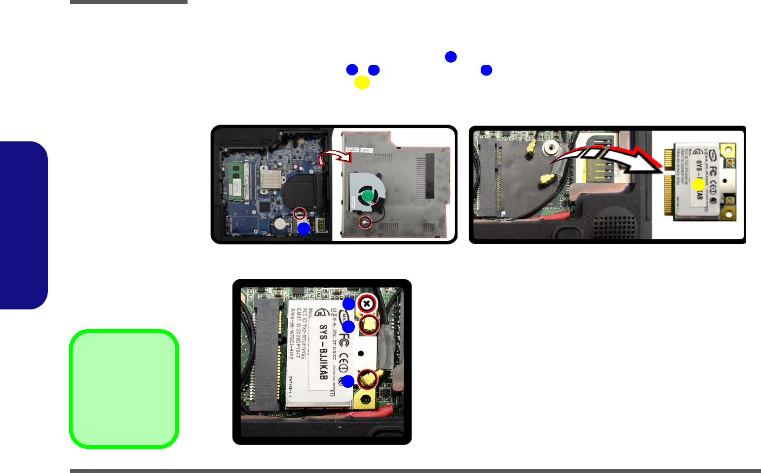
Removing the Wireless LAN Module
1. Turn off the computer, remove the battery (page 2 - 5) and the component bay cover (page 2 - 8).
2. The Wireless LAN module will be visible at point on the mainboard.
3. Carefully disconnect cables - , then remove screw from the module socket (Figure 6b).
4. Lift the Wireless LAN module (Figure 6c) up and off the computer.
Figure 6
Wireless LAN
Module Removal
a. Remove the cover.
b. Disconnect the cables
and remove the screw.
c. Lift the WLAN module
out.
Note: Make sure you
reconnect the antenna
cable to ‘’1’’ +
‘’2’’socket (Figure
6b).
1
2
3
4
5
b.
a.
2
3
5
1
c.
4
5. WLAN Module.
•1 Screw
Disassembly
Removing the 3.75G Module 2 - 11
2.Disassembly
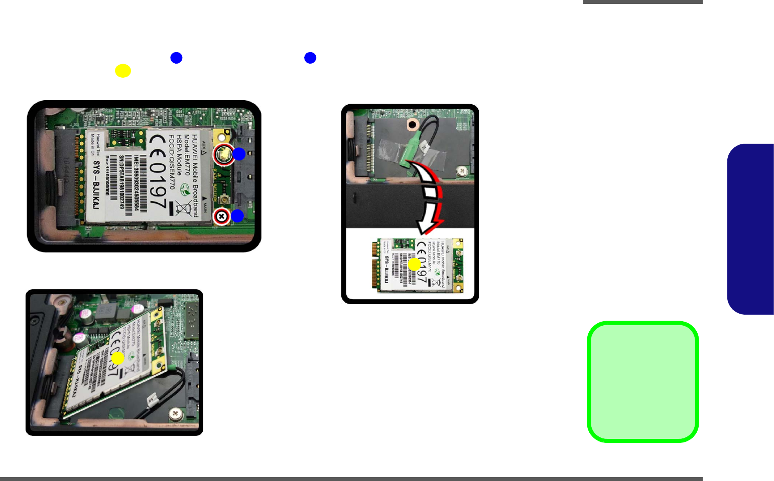
Removing the 3.75G Module
1. Turn off the computer, remove the battery (page 2 - 5) and the component bay cover (page 2 - 8).
2. Carefully disconnect the cable , then remove the screw from the module socket.
3. The 3.75G module will pop-up.
4. Lift the 3.75G module (Figure 7d) up and off the computer.
Figure 7
3.75G Module
Removal
a. Disconnect the cable
and remove the screw.
b. The 3.75G module will
pop up.
c. Lift the 3.75G module
out.
1
2
3
3
b.
a.
d.
1
2
3
c.
4. 3.75G Module.
•1 Screw
Disassembly
2 - 12 Removing the Keyboard
2.Disassembly
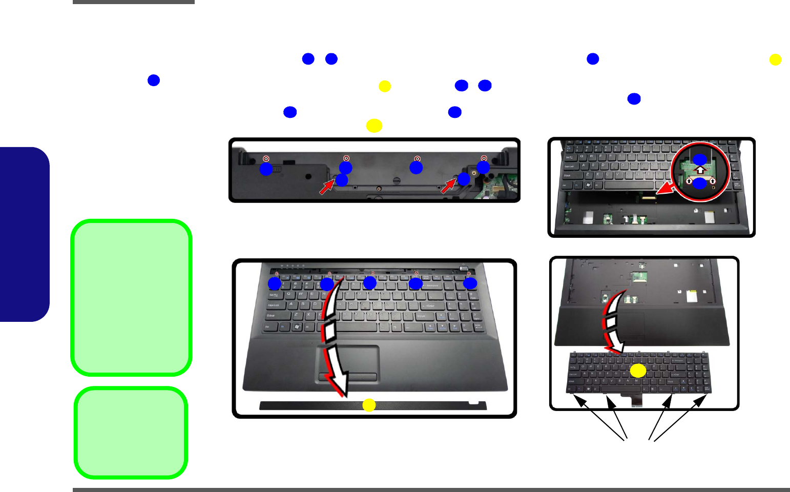
Removing the Keyboard
1. Turn off the computer, and remove the battery (page 2 - 5).
2. Remove screws - from the bottom of the computer. Press at points to unsnap the LED cover module
(you may need to use the Eject Pin Tool to do this (Figure 8a).
3. Remove the LED cover module and screws - from the keyboard (Figure 8b).
4. Carefully lift the keyboard up, being careful not to bend the keyboard ribbon cable . Disconnect the keyboard
ribbon cable from the locking collar socket (Figure 8c)
5. Carefully lift up the keyboard (Figure 8d) off the computer.
Figure 8
Keyboard Removal
a. Remove screws from the
bottom of the computer.
Press at points to un-
snap the LED cover
module.
b. Remove the LED cover
module and screws
from the keyboard.
c. Carefully lift the key-
board up and disconnect
the keyboard ribbon ca-
ble from the locking col-
lar socket.
d. Remove the keyboard.
5
1
4
5
6
6
7
11
12
12
13
14
Re-Inserting the
Keyboard
When re-inserting the
keyboard firstly align the
four keyboard tabs at
the bottom (Figure 8c) at
the bottom of the key-
board with the slots in the
case.
a.
Keyboard Tabs
13
24
7
5
c.
b. d.
89
14
10 11
12
6
513
6. LED Cover Module
14. Keyboard
•9 Screws

Part Lists
A-1
A.Part Lists
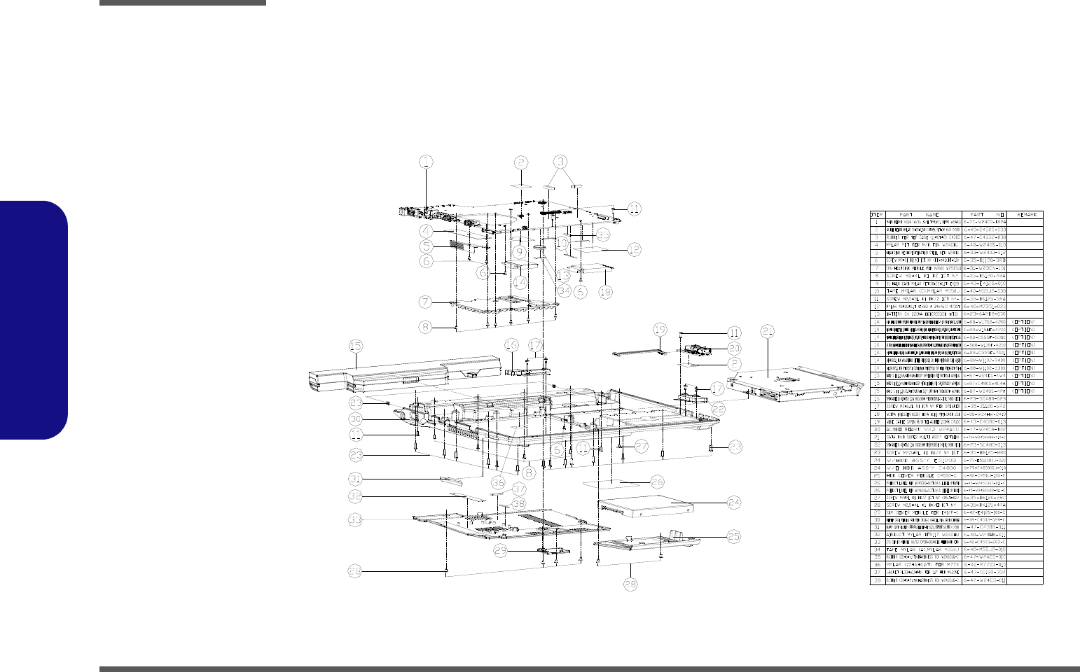
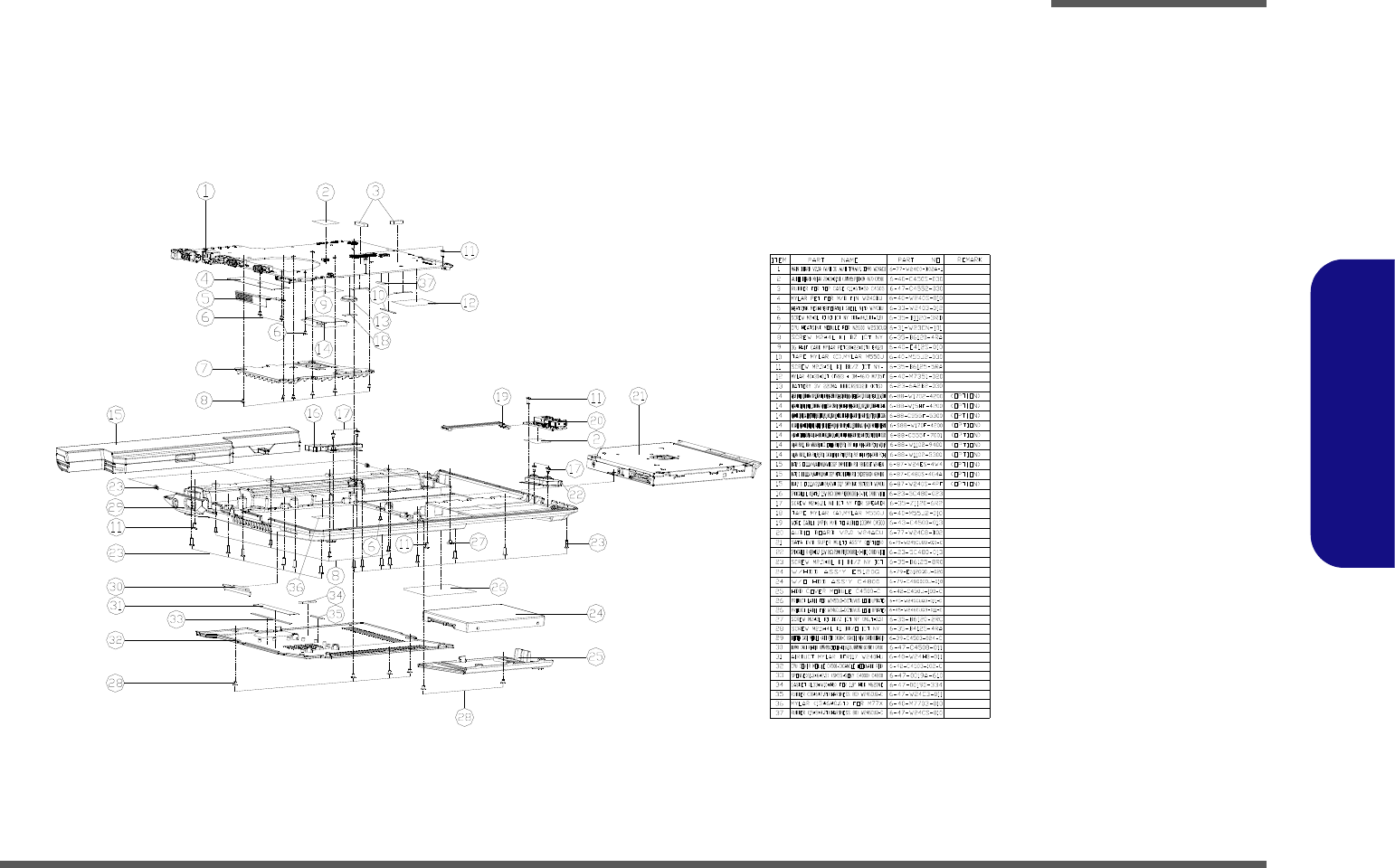
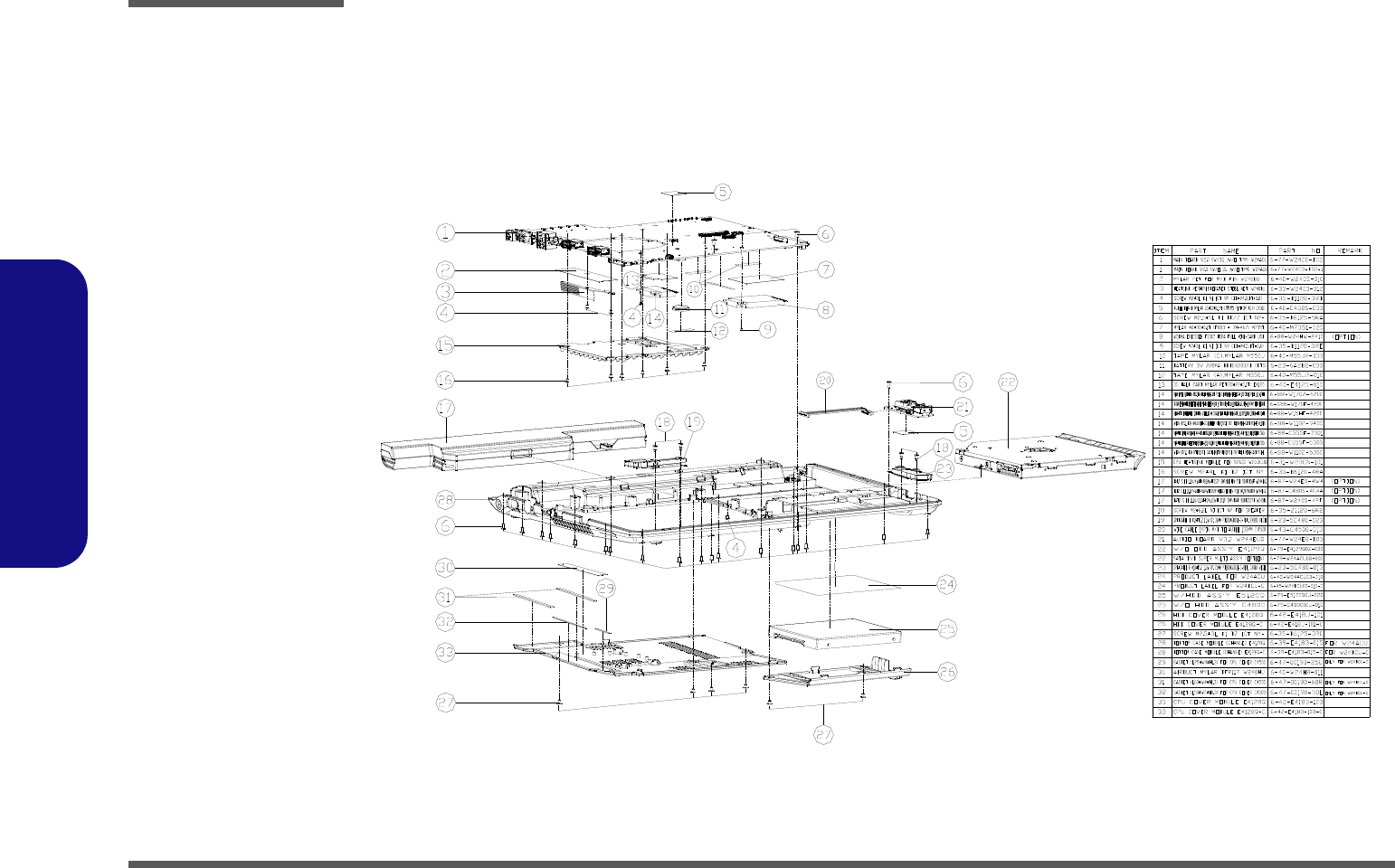
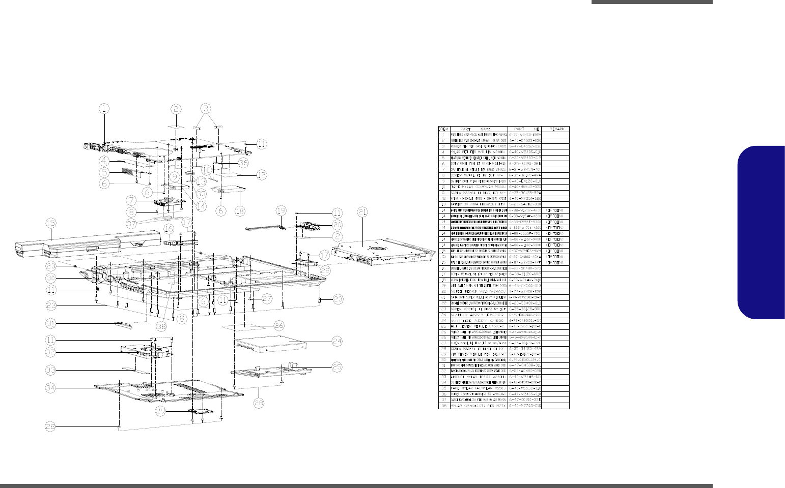
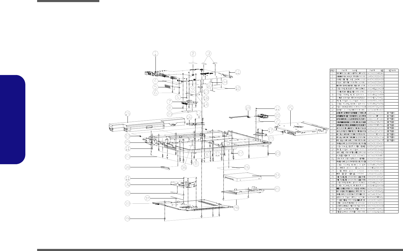
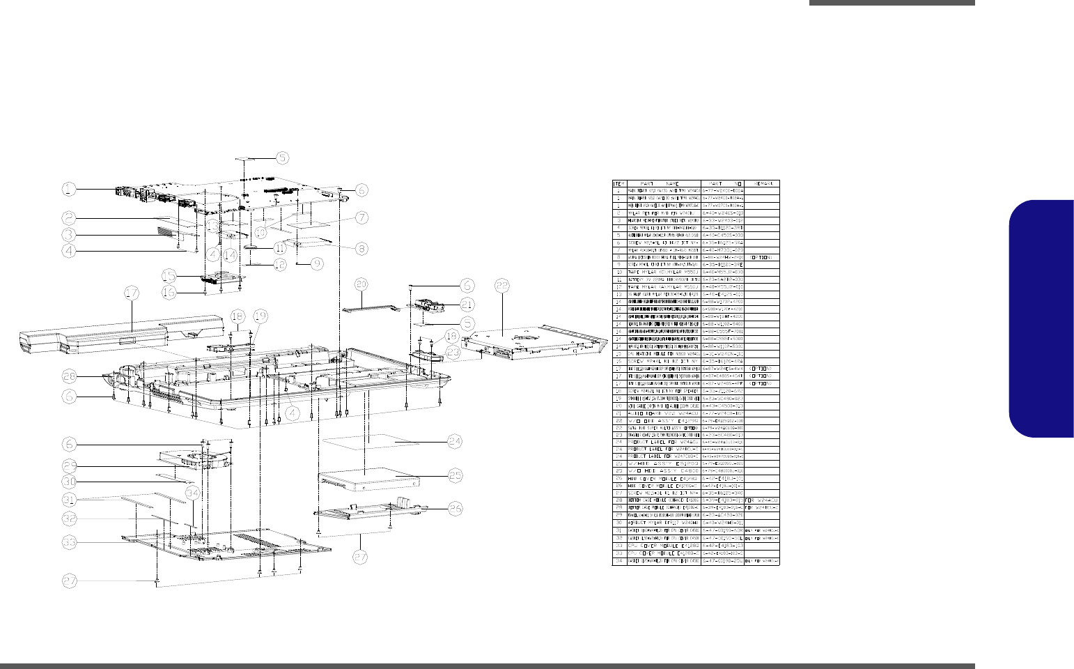
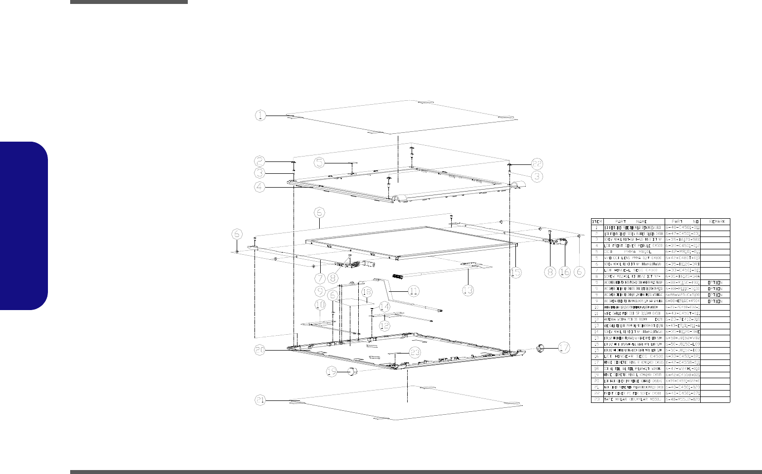
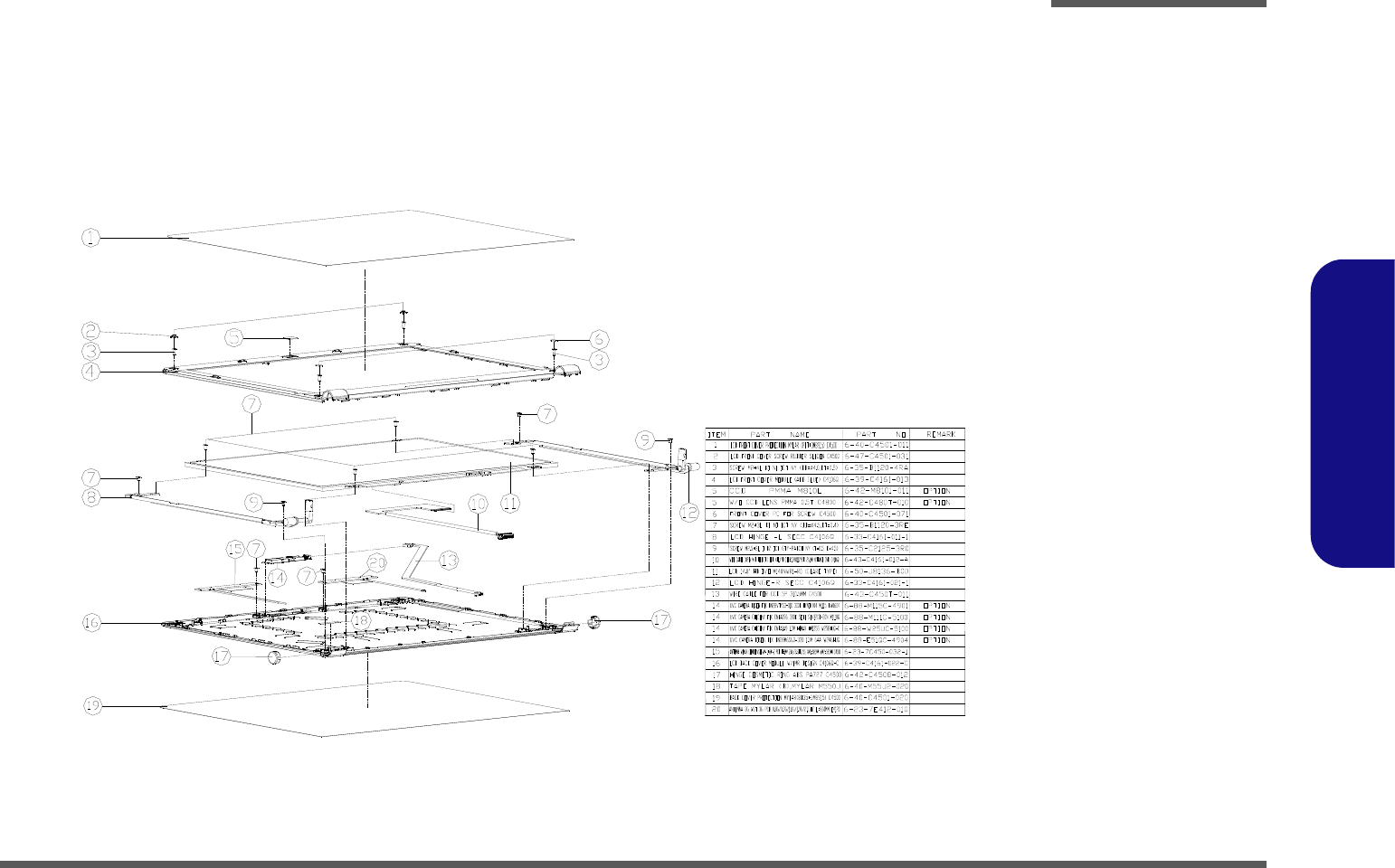
Appendix A: Part Lists
This appendix breaks down the W245CUQ/W246CUQ/W247CUQ/W24ACU/W24BCU series notebook’s construction
into a series of illustrations. The component part numbers are indicated in the tables opposite the drawings.
Note: This section indicates the manufacturer’s part numbers. Your organization may use a different system, so be sure
to cross-check any relevant documentation.
Note: Some assemblies may have parts in common (especially screws). However, the part lists DO NOT indicate the
total number of duplicated parts used.
Note: Be sure to check any update notices. The parts shown in these illustrations are appropriate for the system at the
time of publication. Over the product life, some parts may be improved or re-configured, resulting in new part numbers.
Part Lists
A - 2 Part List Illustration Location
A.Part Lists
Part List Illustration Location
The following table indicates where to find the appropriate part list illustration.
Table A- 1
Part List Illustration
Location
Parts W245CUQ W246CUQ W247CUQ W24ACU W24BCU
Top page A - 3 page A - 4 page A - 5
Bottom (3.5W) page A - 6 page A - 8
Bottom - No SIM (3.5W) page A - 7
Bottom (6.5W) page A - 9 page A - 11
Bottom - No SIM (6.5W) page A - 10
LCD page A - 12 page A - 13 page A - 14 page A - 15
SATA DVD page A - 16 page A - 17
Part Lists
Top (W245CUQ, W246CUQ) A - 3
A.Part Lists
Top (W245CUQ, W246CUQ)
(灰色) (尚盟)
黑色
度 黑色
頭徑 頭厚 號
(今皓)
(今皓)
導電布
Figure A - 1
Top (W245CUQ,
W246CUQ)
Part Lists
A - 4 Top (W247CUQ)
A.Part Lists
Top (W247CUQ)
(灰色)
黑色
非耐落
度 黑色
今皓
今皓
今皓
Figure A - 2
Top (W247CUQ)
Part Lists
Top (W24ACU, W24BCU) A - 5
A.Part Lists
Top (W24ACU, W24BCU)
灰色 尚盟
黑色
頭徑 頭厚 號穴 鍍白鎳 I頭
Figure A - 3
Top (W24ACU,
W24BCU)
Part Lists
A - 6 Bottom 3.5W (W245CUQ, W246CUQ)
A.Part Lists
Bottom 3.5W (W245CUQ, W246CUQ)
Figure A - 4
Bottom 3.5W
(W245CUQ,
W246CUQ)
Part Lists
Bottom 3.5W - No SIM (W245CUQ, W246CUQ) A - 7
A.Part Lists
Bottom 3.5W - No SIM (W245CUQ, W246CUQ)
Figure A - 5
Bottom 3.5W
(W245CUQ,
W246CUQ)
Part Lists
A - 8 Bottom 3.5W (W24ACU, W24BCU)
A.Part Lists
Bottom 3.5W (W24ACU, W24BCU)
Figure A - 6
Bottom 3.5W
(W24ACU,
W24BCU)
Part Lists
Bottom 6.5W (W245CUQ, W246CUQ) A - 9
A.Part Lists
Bottom 6.5W (W245CUQ, W246CUQ)
Figure A - 7
Bottom 6.5W
(W245CUQ,
W246CUQ)
Part Lists
A - 10 Bottom 6.5W - No SIM (W245CUQ, W246CUQ)
A.Part Lists
Bottom 6.5W - No SIM (W245CUQ, W246CUQ)
Figure A - 8
Bottom 6.5W
(W245CUQ,
W246CUQ)
Part Lists
Bottom 6.5W (W24ACU, W24BCU) A - 11
A.Part Lists
Bottom 6.5W (W24ACU, W24BCU)
Figure A - 9
Bottom 6.5W
(W24ACU,
W24BCU)
Part Lists
A - 12 LCD (W245CUQ)
A.Part Lists
LCD (W245CUQ)
銘板
精乘
精乘
Figure A - 10
LCD (W245CUQ)
Part Lists
LCD (W246CUQ) A - 13
A.Part Lists
LCD (W246CUQ)
(華力)
銘板
Figure A - 11
LCD (W246CUQ)
Part Lists
A - 14 LCD (W247CUQ)
A.Part Lists
LCD (W247CUQ)
(華力)
非耐落
無鉛
精乘
設變
Figure A - 12
LCD (W247CUQ)
Part Lists
LCD (W24ACU, W24BCU) A - 15
A.Part Lists
LCD (W24ACU, W24BCU)
銘板
Figure A - 13
LCD (W24ACU,
W24BCU)
Part Lists
A - 16 SATA-DVD (W245CUQ, W246CUQ)
A.Part Lists
SATA-DVD (W245CUQ, W246CUQ)
*(非耐落) 無鉛
Figure A - 14
SATA-DVD
(W245CUQ,
W246CUQ)
Part Lists
SATA-DVD (W24ACU, W24BCU) A - 17
A.Part Lists
SATA-DVD (W24ACU, W24BCU)
*(非耐落)
Figure A - 15
SATA-DVD
(W24ACU,
W24BCU)

Part Lists
A - 18
A.Part Lists
Schematic Diagrams
B-1
B.Schematic Diagrams
Appendix B: Schematic Diagrams
This appendix has circuit diagrams of the W245CUQ/W246CUQ/W247CUQ/W24ACU/W24BCU notebook’s PCB’s.
The following table indicates where to find the appropriate schematic diagram.
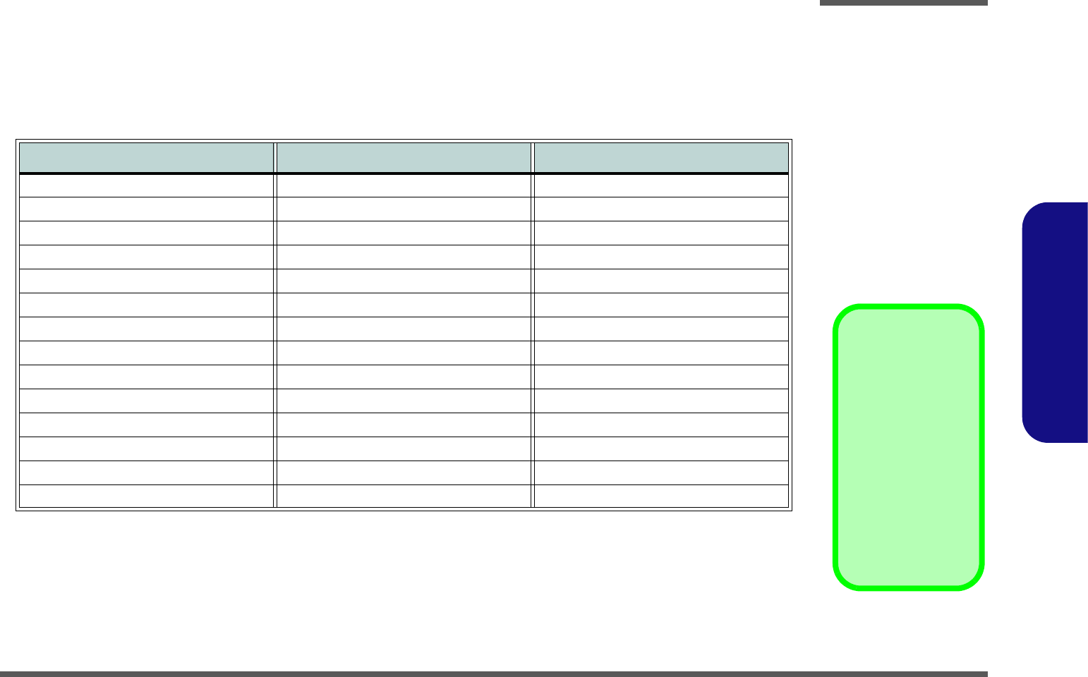
Diagram - Page Diagram - Page Diagram - Page
System Block Diagram - Page B - 2 TPM, SATA HDD, ODD, FAN - Page B - 16 AUDIO BOARD/USB - Page B - 30
CEDARVIEW CPU PART-D - Page B - 3 AUDIO CODEC VT1802P - Page B - 17 POWER SWITCH & LID BOARD - Page B - 31
CEDARVIEW CPU PART-A-C-F - Page B - 4 CARD READER JMB261C - Page B - 18
CEDARVIEW CPU PART-B - Page B - 5 KBC-ITE IT8518E, SPI - Page B - 19
CEDARVIEW CPU PART-E - Page B - 6 3G, WLAN, BT - Page B - 20
DDR3 SO-DIMM 1 - Page B - 7 USB PORT & USB CHARGER - Page B - 21
DDR3 SO-DIMM 2 - Page B - 8 CONN, CCD, LED - Page B - 22
IDT CLOCK - Page B - 9 PWR VDD3, VDD5V, SYS15V - Page B - 23
Tigerpoint PART-A-B - Page B - 10 PWR SW, 3V, 5V, 3VS, 5VS, 1.5VS - Page B - 24
Tigerpoint PART-C - Page B - 11 PWR 1.05VS - Page B - 25
Tigerpoint PART-D - Page B - 12 PWR 1.5V, 0.75V - Page B - 26
Tigerpoint PART-E-F - Page B - 13 PWR VCORE - Page B - 27
LVDS, INVERTER - Page B - 14 PWR AC_IN, CHARGE - Page B - 28
CRT, HDMI - Page B - 15 CLICK BOARD - Page B - 29
Table B - 1
Schematic
Diagrams
Version Note
The schematic dia-
grams in this chapter
are based upon ver-
sion 6-7P-W24C5-
003. If your main-
board (or other
boards) are a later
version, please
check with the Serv-
ice Center for updat-
ed diagrams (if
required).
Schematic Diagrams
B - 2 System Block Diagram
B.Schematic Diagrams
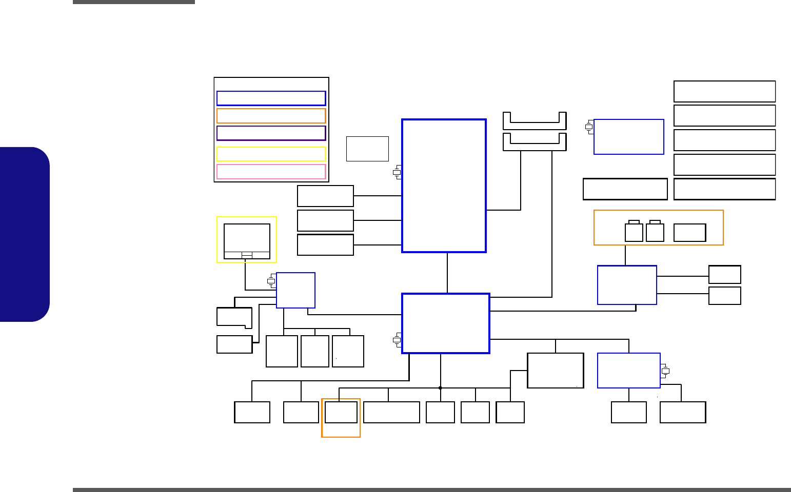
System Block Diagram
Sheet 1 of 31
System Block
Diagram
W24HU AUDIO/B
AUDIO/B
(Charge USB)
MB:6-71-W24C0-D02A (W24ACU)
AUDIO: 6-71-W24C8-D02(W24ACU)
PWR SW:6-71-W24ES-D03(W244EU)
Colck Generator
14.318 MHz
17.1mm*8.1mm*1.2mm
TSSOP 64PIN
IDT 9VRS4338
AC-IN,CHARGER
CLICK:6-71-W24E2-D01 (W244EU)
G711ST9U
HP
OUT
THERMAL
SENSOR
SOUTH BRIDGE
Intel
Cedarview 32nm
TDP 3.5W
480 Mbps
32.768KHz
INT SPK L
USB2.0
VDD3,VDD5
17mm*17mm*1.06mm
PCIE
48pins QFN
VCORE+ GFX
DDR3 One Channel
360 MMAP
1920x1200
<6"
SMART
BATTERY
24 MHz
1.5V,0.75VS(VTT_MEM)
LPC
Direct X10.1
100 MHz
9*9*1.6mm
1GB & 2GB
0.1"~13"
SATA I/II 3.0Gb/s
INT MIC
10 Gbits/s
22mm*22mm*2.35mm
FCBGA 559 pin
32.768 KHz
C0/C1/C2/C3/C4
<7.5"
CLEVO Cedar Trail-M System Block Diagram
CRT OUT
1280x800
X4/X2-GEN1
INT. K/B
1"~12"
DMI
EC SMBUS
VT1802
800/1067MT/s
PROCESSOR
33 MHz
<12"
Azalia Codec
AZALIA LINK
Tiger Point
1.05VS,1.5VS
SMART
FAN
<6"
MIC
IN
CLICK BOARD
TOUCH PAD
SYSTEM SMBUS
SO-DIMM1
LCD CONNECTOR
<10"
27MHz
Socket
25
MHz
Card Reader
CARD READER
RJ-45
10M/100M LAN
INT SPK R
ODD:6-71-W25UN-D01(W255EU)
CCD
(USB7)
Bluetooth(USB5)
Mini Card
WLAN
SHEET 19
3.3V,5V,3VS,5VS,1.8VS
LPC ROM
EC
14*14*1.6mm
128pins LQFP
ITE 8518
SATA ODD
Use EDP LCD
NB 1366x768
ELD 1920x1080
1.65Gb/s
NB 2X
ELD 4X
<10.8"
HDMI CONNECTOR
Port_1
(USB1)
Port_0
(USB0)
3G CARD (USB4)
Mini PCIE
JMC261C
Port_2
(USB2)
SATA HDD
SO-DIMM2
SODIMM2¤@©w-n¤W
Schematic Diagrams
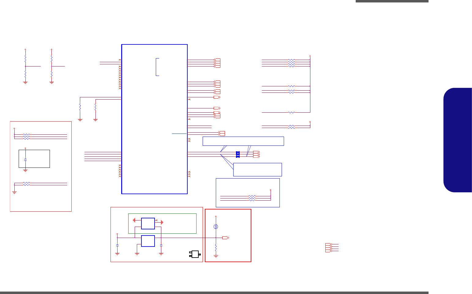
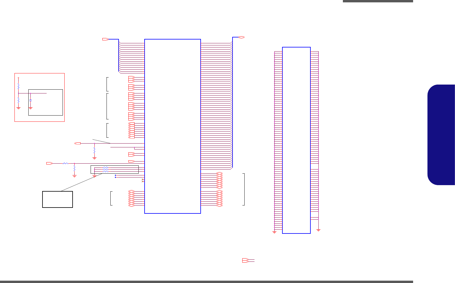
CEDARVIEW CPU PART-D B - 3
B.Schematic Diagrams
CEDARVIEW CPU PART-D
Sheet 2 of 31
CEDARVIEW CPU
PART-D
R69
49.9_1%_04
R62 1K_04
C325
*0.1u_10V_X7R_04
R252 51_04
R76
2.2K_04
R63 *1K_04
H_RSVD_K28
R88 *51_04
H_CPU_SVIDCLK 26
H_CPU_SVIDALRT# 26
H_CPU_SVIDDAT 26
R70 51_04
C334
*0.1u_10V_X7R_04
R82
*220_04
R67 *1K_04
R65 *1K_04
Q15
*G711ST9U
OUT 1
VCC
2
GND
3
R72 51_04
C314
*0.1u_16V_Y5V_04
R85 51_04
R64 *1K_04
R86
2.2K_04
R66
49.9_1%_04 R249 100_04
R251 *1K_04
R73 51_04
R87
*220_04
R245 75_1%_04
R68 *1K_04
CPU
CEDARVIEW
ICH
4 OF 6
1.10
U15D
CDV_22MM_REV1P10_5
CPUSLP# B22
RSVD_N25
N25 RSVD_N24
N24 RSVD_W26
W26 RSVD_W25
W25 RSVD_R6
R6 RSVD_R5
R5
TRST#
B24 TMS
D24 TDO
B25 TDI
C24 TCLK
C25
MV_GPI O_RCOMP
K23 HV_GPIO_RCOMP
K24
RSVD_H30
H30 RSVD_J31
J31 RSVD_K29
K29 RSVD_L30
L30 RSVD_L29
L29 RSVD_K30
K30 RSVD_H27
H27 RSVD_K27
K27 RSVD_K26
K26 RSVD_J28
J28 RSVD_K25
K25 STRAP_K28
K28 STRAP_L27
L27 RSVD_L26
L26
RSVD_L24 L24
RSVD_L22 L22
RSVD_K21 K21
SVID_DATA C16
SVID_CLK D18
SVID_ALERT# B16
RSVD_F19 F19
RSVD_E19 E19
HPLL_REFCLK K19
HPLL_REFCLK_P J19
PREQ# G29
PRDY# H29
DBR# E30
RESET# G30
PWRGOOD D23
PROCHOT# A19
PBE# C20
RSVD_L11 L11
TH ER M TRI P # B20
INTR/LINT00 D20
INIT# A23
DPLSLP# B21
DPRSTP# C21
STPCLK# D22
RSVD_C18 C18
NMI/LINT10 C22
SMI# B18
R247 110_1%_04
R71 51_04
R248 *54.9_1%_04
LAYOUT NOTE:
H_CPUSLP#
Place term ination near CPU
H_INIT#
H_PROCHOT#
H_INTR
H_NMI
H_SMI#
H_A20M#
H_STPCLK#
H_RSVD_H 29
Q16
*TMP20
NC 1
GND 2
VO 3
GND
5
VCC
4
H_TCK
H_TRST#
SC70-5 & SC70-3
Co-lay
H_THERMTRIP# 10
H_PROCHOT# 26
H_FERR# 10
H_TMS
H_TDI
Thermal IC
H_RSVD_G29
H_RSVD_L27
HV_GPIO_RCOMP
3/8
3.3V
3.3V
INTEL Recommend
H_PROCHOT# 100_04
INTEL Recommend
H_CPU_SVIDALRT# 75_04
H_CPU_SVIDDAT 110_04
H_RSVD_H29
H_RSVD_K28
MV_GPIO_RCOMP
H_A20M# 10
H_DPRSTP# 11
H_SMI# 10
H_INTR 10
H_DPSLP# 11
H_PWRGD 11
H_STPCLK# 10
3.3V9,11,12,13,17,18,19,21,23,24,26
H_INIT# 10
H_NMI 10
CLK_CPU_HPL# 8
PLTRST# 11
3.3VS3,6,7,8,9,10,11,12,13,14,15,16,17,18,21,23 1.05VS5, 8,10, 11,12,24,26
1.8VS5,18,23
H_CPUSLP# 10
CLK_CPU_HPL 8
H_STPCLK#
CAD Note: H_CPU_SVIDALRT#_R,H_CPU_SVIDDAT_R
Place the PU resistors close to CPU
H_CPU_SVI DDAT_R
CAD Note: H_CPU_SVIDCLK_R
Place the PU
resistors close to VR
H_CPU_SVIDCLK_R
H_CPU_SVIDALRT#_R
1.05VS
PROCHOT# m ust be te rminated w ith a 56-£[,
pull-up resistor to VCCP even if it is not used.
8/30
1:2 (4mils:8mils)
PLACE NEAR CPU
3
2
1
PTH3
10K_NTC_06
12
H_RSVD_G29
R244 *10mil_short
R261
10K_1%_04
Analog Thermal
IC¤£¤W,§ï¤W¼ö±Ó¹qªý 7/7
H_RSVD_L27
SVID Signals
H_CPU_SVIDALRT#_R
H_CPU_SVI DDAT_R
H_CPU_SVIDCLK_R
THERM_VOLT 18
1.05VS
1.05VS
EM I
1.8VS
1.05VS
1.8VS 1. 8VS
H_CPUSLP#
H_TCK
H_TDO
H_TDI
H_TDO
R250 *10mil_short
H_TRST#
H_TMS R246 *10mil_short
H_INIT#
H_PROCHOT#
H_A20M#
H_INTR
H_NMI
H_SMI#
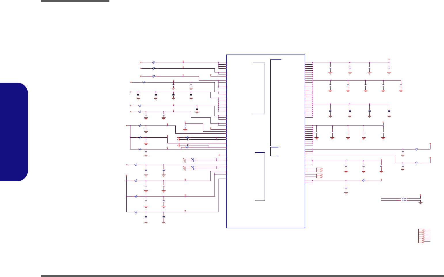
Schematic Diagrams
B - 4 CEDARVIEW CPU PART-A-C-F
B.Schematic Diagrams
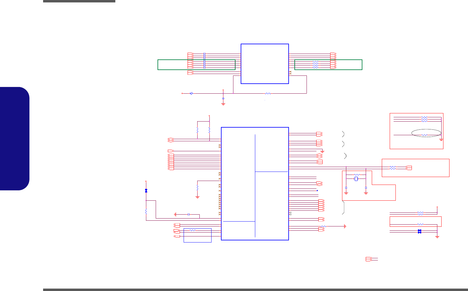
CEDARVIEW CPU PART-A-C-F
DMI_TXP_3
DMI_TXN_2
DMI_TXP_2
DMI_TXN_3
DMI_TXP_0
DMI_TXN_0
DMI_TXN_1
DMI_RXP_0
DMI_RXN_0
DMI_RXP_1
DMI_RXN_1
BREF_REXT
DAC_RED
DAC_GREEN
DAC_BLUE
PORTC_HPC#14
HDMI Signal Group
Zdiff = 90 Ohm ¡Ó17.5%
signal / space : 4.5 / 6
length < 1000 mils
C49
22p_50V_NPO_04
C69 1U_6.3V_X5R_04
R36 * 0_04
CEDARVIEW
DMI
1 OF 6
1.10
U15A
CD V_22MM_REV1P10_5
DMI_REFCLKP
N9
DMI_REFCLKN
N8
DMI_REF1P5
T2
DMI_RXN3
P3 DMI_RXP3
P2 DMI_RXN2
N1 DMI_RXP2
N2 DMI_RXN1
M2 DMI_RXP1
M3 DMI_RXN0
L2 DMI_RXP0
L3
DMI_RCOMP T1
RSVD_TP_R7 R7
RSVD_TP_R8 R8
DMI_TXN3 N6
DMI_TXP3 N5
DMI_TXN2 L8
DMI_TXP2 L9
DMI_TXN1 L6
DMI_TXP1 L5
DMI_TXN0 K5
DMI_TXP0 K6
C305 0. 1u_10V_X7R_04
R239 7.5K_1%_04
R43 * 0_04
C304 0. 1u_10V_X7R_04
C309
1u_6.3V_X5R_04
R78 33_04
R61
7.5K_1%_04
R240 150_1%_04
C307 0. 1u_10V_X7R_04
R84 2.2K_04
R241 150_1%_04
X5 FSX8L_27MHz
1 2
DMI_TXP_1
IHDA
DDI
CEDARVIEW
LVDS
VGA
3 OF 6
1.10
U15C
CD V_22MM_REV1P10_5
DPL_REFCLKP B9
DPL_REFCLKN A9
AZIL_RST#
E21
AZIL_SDO
F21 AZIL_SDI
E22
AZIL_SYNC
F22 AZIL_BCLK
H21
BREFREXT
F15 BREF1P5V
E15
RSVD_TP_H17
H17 RSVD_TP_J17
J17
DDI1_TXN3
K13 DDI1_TXP3
J13 DDI1_TXN2
E13 DDI1_TXP2
F13 DDI1_TXN1
H11 DDI1_TXP1
J11 DDI1_TXN0
F11 DDI1_TXP0
E11
DDI1_HPD
D26
DDI1_AUXN
C10 DDI1_AUXP
D10
DDI1_DDC_SDA
G27 DDI1_DDC_SCL
F25
RSVD_TP_J15
J15 RSVD_TP_H15
H15
DDI0_TXN3
A7 DDI0_TXP3
B7 DDI0_TXN2
C3 DDI0_TXP2
D4 DDI0_TXN1
F2 DDI0_TXP1
F3 DDI0_TXN0
G3 DDI0_TXP0
G2
DDI0_HPD
H22
DDI0_AUXN
B8 DDI0_AUXP
C8
DDI0_DDC_SDA
J22 DDI0_DDC_SCL
H25
PANEL_VDDEN F29
PANEL_BKLTEN E25
PANEL_BKLTCTL G22
LVDS_CLKN J4
LVDS_CLKP H4
LVDS_TXN3 G6
LVDS_TXP3 G5
LVDS_TXN2 H8
LVDS_TXP2 H7
LVDS_TXN1 E8
LVDS_TXP1 F8
LVDS_TXN0 H10
LVDS_TXP0 G10
LVDS_VREFL H3
LVDS_VREFH H2
LVDS_VBG F10
LVDS_IBG E10
LVDS_DDC_DATA H24
LVDS_DDC_CLK G24
LVDS_CTRL_DATA E24
LVDS_CTRL_CLK F28
DPL_REFSSCCLKN E17
DPL_REFSSCCLKP F17
CRT_DDC_CLK E27
CRT_DDC_DATA E29
CRT_IREF A13
CRT_IRTN D12
CRT_BLUE C11
CRT_GREEN B11
CRT_RED B12
CRT_VSYNC C14
CRT_HSYNC D14
3.3VS
R242 150_1%_04
C306 0. 1u_10V_X7R_04
C303 *0.1u_10V_X7R_04
HDMIC_C1CN
HDMIC_C1CP
HDMIC_C2CP
HDMIC_CLKCP
HDMIC_CLKCN
HDMIC_C0CN
HDMIC_C0CP
HDMIC_C2CN R45 * 0_04
L41 *HCB1005KF-121T20_short
R79 * 10K_04
R50 *0_04 CLK_DOT96 8
CLK_DOT96# 8
DMI_ICH_IT_MR1_DN9
DMI_ICH_IT_MR0_DP9
R77
2.2K_04
CLK_CPU_DMI#8
DMI_ICH_IT_MR1_DP9DMI_ICH_IT_MR0_DN9
DPL_R EFCLKN
R49 1M_04
DMI_ICH_IT_MR3_DN9
DMI_ICH_IT_MR2_DP9
CLK_CPU_DMI8
DPL_R EFCLKP
C53
22p_50V_NPO_04
DMI_ICH_IT_MR3_DP9DMI_ICH_IT_MR2_DN9C308 *0.1u_10V_X7R_04 R39 * 0_04
T4
R260
10K_04 R243 619_1%_04
R57 2.37K_1%_04
V GA RGB re sis to rs cols e to M CH ball
Zo = 37.5 Ohm ¡Ó15%
signal : 8.5 mils
length < 300 mils
Two VGA RGB resistors between
Zo = 50 Ohm ¡Ó15%
signal : 5 m ils
length < 8100 mils
C302 *0.1u_10V_X7R_04
R259
10K_04
DAC_GREEN 14
DAC_VSYNC 14
DAC_HSYNC 14
DAC_BLUE 14
DAC_RED 14
R83 2.2K_04
LVDS-L1N 13
LVDS-L2P 13
R44 * 0_04
MC H _BLO N 1 3
LVDS-LCLKP 13
LVDS-L2N 13
C310 *0.1u_10V_X7R_04
LVDS-L1P 13
P_DDC_CLK 13
NB_ENAVDD 13,18
LVDS-L0N 13
LVDS-LCLKN 13
LVDS-L0P 13
DDI1 DISABLE: 2.2K TO GND
R60
*10mil_short
R41 * 10mil_short
R48 * 10mil_short
Improve RGB High-Voltage to over 665mV
LVD_VREFL_OUT_R
LVD_VREFH_OUT_R
LVD_I BG
D02A
AZ_SDIN111
3.3VS6,7,8,9, 10,11,12, 13,14, 15,16,17,18,21,23
CLK_DREFSS 8
CLK_DREFSS# 8
1.5VS5, 8,9,12,23
DMI_RCOMP
Trace 5m il; Spacing 20m il
OPTION
Zdiff = 95 Ohm ¡Ó17.5%
signal / space : 4 / 6.5 m ils
length < 10800 m ils
(1)
(2)
LVDS Control Signal Group
LBKLT_CTL,LBKLT_EN,LVDD_EN
(1)
LVDS Clock & Data Signal Group
Zo = 50 Ohm
¡Ó15%
signal : 5 m ils
length < 6000 mils
LVD_VREFH_OUT_R
TP_LVD_VBG
LVD_I BG
LVD_VREFL_OUT_R
LCTLA_C LK
LVDS_BKLTCTL
LC TL B_ DA TA
H_AZIL_SDI
H_AZIL_BCLK11
DAC_BLUE
DAC_GREEN
DAC_RED
DM I_ RCOM P
length <500mils
HDMI_CTRLCLK14HDMI_CTRLDATA14
LC TL B_ DA TA
H_AZIL_SYNC11
Zdiff = 80 Ohm ¡Ó17.5%
length =breakout(<=500mils)+(<= 6000 mils)
DMI Signal Group
BREF_1P5V
DACREFSET
H_AZIL_SDO11
DMI_ICH_MT_IR1_DP 9
DMI_ICH_MT_IR0_DN 9
DMI_ICH_MT_IR1_DN 9
DMI_ICH_MT_IR0_DP 9
LCTLA_CLK
DMI_ICH_MT_IR3_DN 9
DMI_ICH_MT_IR2_DP 9
DMI_ICH_MT_IR3_DP 9
DMI_ICH_MT_IR2_DN 9
H_AZIL_RST#11
DDI_DDC_SDA
R599, R600 must be placed very close 27MHz
If HDMI/DVI is not im plem ented, 27MHz can be e lim inated, and
R599/R600 must be m ounted.
LAYOUT NOTE:
Place VGA RGB resistors close to MCH
< 800 mils to MCH ball
27 MHz Crystal Oscillator is mandatory for HDMI.
Close to CPU
P_DDC_DATA 13
DAC_DDCADATA 14
DAC_DDCACLK 14
3.3VS
1.5VS_DMIREF
1.5VS
1.5VS
DMI_RXN_3
DMI_RXP_2
DMI_RXN_2
DMI_RXP_3
(1)
(2)
(3)
HDMIC_C1CP14
HDMIC_CLKCN14 HDMIC_CLKCP14
HDMIC_C2CP14 HDMIC_C1CN14
HDMIC_C0CN14 HDMIC_C0CP14
HDMIC_C2CN14
(2)
CRT Sync Signal Group
DAC_HSYNC,DAC_VSYNC
Zo = 50 Ohm ¡Ó15%
signal : 5 m ils
length < 13000 m ils
(1)
CRT DAC Signal Group
CRT_RED,CRT_GREEN,CRT_BL UE
(3)
CRT Control Signal Group
CRT_DDC_C LK,CRT_DDC _DATA
Zo = 50 Ohm
¡Ó15%
signal : 5 m ils
length < 15000
mils
DACREFSET
LAYOUT NOTE:
Place DACREFSET re sistor clos e to MCH
< 500 mils to MCH ball
PORTC_HPC#
Sheet 3 of 31
CEDARVIEW CPU
PART-A-C-F
Schematic Diagrams
CEDARVIEW CPU PART-B B - 5
B.Schematic Diagrams
CEDARVIEW CPU PART-B
Place resistors and CAP
close to DDR_VREF pin
LAYOUT NOTE:
LAYOUT NOTE:
Maximum via 2
Width 5mil
Spacing 10 mil
< 2"inch
Width 8mil
Spacing 8 mil
< 300mil
Zdiff = 68 Ohm ¡Ó 10
%
Width 4mil
Spacing 5
mil
Zdiff = 37 Ohm ¡Ó 10
%
Zdiff = 34 Ohm ¡Ó 10
%
Zdiff = 50 Ohm ¡Ó 10
%
Zdiff = 50 Ohm ¡Ó 10
%
Zdiff = 81 Ohm ¡Ó 10
%
DDR3_DQPU
M_A_DQ 58
M_A_DQ 27
M_A_A13
M_A_DQ 19
M_A_DQ 44
M_A_DQ 33
M_A_DQ 25
M_A_DQ 18
M_A_DQ 17
M_A_DQ 37
M_A_A4
M_A_A10
M_A_DQ 4
M_A_DQ 20
M_A_DQ 8
M_A_DQ 23
M_A_DQ 26
M_A_DQ 57
M_A_DQ 60
M_A_DQ 52
M_A_DQ 30
M_A_A1
M_A_DQ 9
M_A_A8
M_A_DQ 10
M_A_DQ 2
M_A_DQ 62
M_A_DQ 28
M_A_DQ 51
M_A_DQ 29
M_A_DQ 39
M_A_DQ 55
M_A_DQ 38
M_A_DQ 54
M_A_DQ 41
M_A_DQ 45
M_A_DQ 24
M_A_DQ 42
M_A_DQ 35
M_A_DQ 11
M_A_DQ 31
M_A_A2
M_A_DQ 43
M_A_DQ 22
M_A_DQ 40
M_A_DQ 49
M_A_DQ 63
M_A_DQ 53
M_A_DQ 3
M_A_DQ 36
M_A_DQ 50
M_A_DQ 13
M_A_DQ 34
M_A_A9
M_A_DQ 48
M_A_A11
M_A_DQ 46
M_A_DQ 59
M_A_A7
M_A_DQ 1
M_A_DQ 21
M_A_A5
M_A_DQ 32
M_A_DQ 0
M_A_DQ 7
M_A_DQ 14
M_A_DQ 5
M_A_DQ 16
M_A_DQ 56
M_A_DQ 47
M_A_DQ 15
M_A_DQ 6
M_A_A3
M_A_A12
M_A_A6
M_C LK_DDR 2#7M_C LK_DD R 27
M_A_DQ 61
M_C LK_DDR 0#6M_C LK_DD R 06
M_C LK_DDR 3#7M_C LK_DD R 37
M_A_DQ 12
M_C LK_DDR 1#6M_C LK_DD R 16
DDR3_DRAM_PWROK11
DDR3_DRAMRST#6,7
M_A_A15
R257
1K_1%_04
R256 33.2_1%_04
R31
10K_1%_04
T5
R254 22.6_1%_04
T6
C318
0.1u_16V_Y5V_04
R255 274_1%_04
R253
100K_04
MCH_VREF
M_A_A[ 15:0]6,7
M_A_RAS#6,7
M_A_BS06,7
M_A_CAS#6,7
M_A_BS26,7
M_ A_ W E#6,7
M_A_BS16,7
CLK_DDR3REF_CLK8
1.5V5,6,7,11,23,25
CLK_DDR3REF_CLK#8
M_CS2#7M_C S3 #7
M_ OD T27
M_CKE37M_C KE27
M_CS0#6M_C S1 #6
DELAY_ALL_SYS_PWRGD11,18
M_ OD T37
M_CKE16M_C KE06
M_ OD T06M_O D T16
GND
CEDARVIEW
6 OF 6
1.10
U15F
CDV_22MM_REV1P10_5
VSS
H13 VSS
G8 VSS
G31 VSS
G21 VSS
G19 VSS
G17 VSS
G15 VSS
G13 VSS
G11 VSS
G1 VSS
F4 VSS
F24 VSS
E7 VSS
E5 VSS
E2 VSS
D9 VSS
D8 VSS
D28 VSS
D19 VSS
C7 VSS
C30 VSS
C26 VSS
C12 VSS
B23 VSS
B19 VSS
B14 VSS
B10 VSS
AL7 VSS
AL25 VSS
AL23 VSS
AL19 VSS
AL13 VSS
AK9 VSS
AK28 VSS
AK19 VSS
AK13 VSS
AJ3 VSS
AJ2 VSS
AH9 VSS
AH6 VSS
AH28 VSS
AH26 VSS
AG5 VSS
AG22 VSS
AF7 VSS
AF28 VSS
AF24 VSS
AF21 VSS
AF13 VSS
AF11 VSS
AE31 VSS
AE3 VSS
AE19 VSS
AE17 VSS
AE15 VSS
AE11 VSS
AE10 VSS
AE1 VSS
AD8 VSS
AD5 VSS
AD26 VSS
AD24 VSS
AD21 VSS
AD19 VSS
AC4 VSS
AC28 VSS
AC22 VSS
AC13 VSS
AC11 VSS
AC10 VSS
AC1 VSS
AB29 VSS
AB23 VSS
AB17 VSS
AB15 VSS
AA9 VSS
AA7 VSS
AA29 VSS
AA27 VSS
AA26 VSS
AA23 VSS
AA21 VSS
AA19 VSS
AA13 VSS
AA10 VSS
AA1 VSS
A25 VSS
A21 VSS
A16 VSS
A11
VSSA_CRTDAC D13
VSS_CDVDET L14
VSS E1
VSS C31
VSS C2
VSS C1
VSS B31
VSS B3
VSS B2
VSS AL5
VSS AL30
VSS AL3
VSS AL29
VSS AL2
VSS AK31
VSS AK30
VSS AK2
VSS AK1
VSS AJ31
VSS AJ1
VSS AH1
VSS A3
VSS A29
VSS A27
VSS Y4
VSS W6
VSS W5
VSS W30
VSS W27
VSS W24
VSS W23
VSS W22
VSS W21
VSS W2
VSS W19
VSS W14
VSS W10
VSS V2
VSS U9
VSS U6
VSS U5
VSS T3
VSS T18
VSS T14
VSS P4
VSS P16
VSS P14
VSS N7
VSS N4
VSS N28
VSS N27
VSS N26
VSS N23
VSS N22
VSS N21
VSS N19
VSS N14
VSS N10
VSS M4
VSS M29
VSS L7
VSS L31
VSS L25
VSS L23
VSS L13
VSS L10
VSS L1
VSS K9
VSS K8
VSS K7
VSS K3
VSS K15
VSS K11
VSS J30
VSS J21
VSS J2
VSS J10
VSS H6
VSS H28
VSS H26
VSS H19
DDR3
CEDARVIEW
2 OF 6
1.10
U15B
CDV_22MM_REV1P10_5
DDR3_WE#
AH10
DDR3_VREF
AJ27
DDR3_VCCA_PWROK
W7
DDR3_REFP
AC19
DDR3_REFN
AB19
DDR3_RAS#
AJ11
DDR3_ODTPU
AJ26
DDR3_ODT3
AJ7 DDR3_ODT2
AL9 DDR3_ODT1
AK7 DDR3_ODT0
AK10
RSVD_TP_AF19
AF19
RSVD_TP_AG19
AG19
RSVD_TP_AB11
AB11
RSVD_TP_AB13
AB13
DDR3_MA9
AH20 DDR3_MA8
AJ20 DDR3_MA7
AK20 DDR3_MA6
AJ18 DDR3_MA5
AH18 DDR3_MA4
AK18 DDR3_MA3
AJ16 DDR3_MA2
AJ14
DDR3_MA15
AJ22 DDR3_MA14
AH22 DDR3_MA13
AJ8 DDR3_MA12
AJ21 DDR3_MA11
AK21 DDR3_MA10
AJ12
DDR3_MA1
AK16 DDR3_MA0
AK14
DDR3_DRAMRST#
AK25
DDR3_DRAM_PWROK
AA5
DDR3_DQS#7 AA2
DDR3_DQS#6 AB7
DDR3_DQS#5 AF3
DDR3_DQS#4 AF10
DDR3_DQS#3 AF22
DDR3_DQS#2 AF29
DDR3_DQS#1 AB25
DDR3_DQS#0 AA31
DDR3_DQS7 Y3
DDR3_DQS6 AB6
DDR3_DQS5 AF4
DDR3_DQS4 AG10
DDR3_DQS3 AE22
DDR3_DQS2 AF30
DDR3_DQS1 AB24
DDR3_DQS0 AA30
DDR3_DQPU
AK27
DDR3_DQ9 AA22
DDR3_DQ8 AA24
DDR3_DQ7 AB30
DDR3_DQ63 W1
DDR3_DQ62 Y2
DDR3_DQ61 AB3
DDR3_DQ60 AC2
DDR3_DQ6 AB28
DDR3_DQ59 V3
DDR3_DQ58 W4
DDR3_DQ57 AB4
DDR3_DQ56 AB2
DDR3_DQ55 AA8
DDR3_DQ54 AB9
DDR3_DQ53 AE5
DDR3_DQ52 AE8
DDR3_DQ51 AB5
DDR3_DQ50 AA6
DDR3_DQ5 W28
DDR3_DQ49 AD6
DDR3_DQ48 AD7
DDR3_DQ47 AD4
DDR3_DQ46 AE2
DDR3_DQ45 AK3
DDR3_DQ44 AH4
DDR3_DQ43 AD3
DDR3_DQ42 AD2
DDR3_DQ41 AG3
DDR3_DQ40 AH2
DDR3_DQ4 W31
DDR3_DQ39 AF8
DDR3_DQ38 AD10
DDR3_DQ37 AE13
DDR3_DQ36 AG13
DDR3_DQ35 AG7
DDR3_DQ34 AG8
DDR3_DQ33 AD11
DDR3_DQ32 AD13
DDR3_DQ31 AE21
DDR3_DQ30 AG21
DDR3_DQ3 AC31
DDR3_DQ29 AG25
DDR3_DQ28 AG27
DDR3_DQ27 AC21
DDR3_DQ26 AD22
DDR3_DQ25 AG24
DDR3_DQ24 AE24
DDR3_DQ23 AJ29
DDR3_DQ22 AG30
DDR3_DQ21 AD30
DDR3_DQ20 AD28
DDR3_DQ2 AC30
DDR3_DQ19 AK29
DDR3_DQ18 AJ30
DDR3_DQ17 AE29
DDR3_DQ16 AD29
DDR3_DQ15 AD27
DDR3_DQ14 AD25
DDR3_DQ13 AA25
DDR3_DQ12 AB27
DDR3_DQ11 AE26
DDR3_DQ10 AE27
DDR3_DQ1 Y29
DDR3_DQ0 Y30
DDR3_DM7
AA3 DDR3_DM6
AB8 DDR3_DM5
AG2 DDR3_DM4
AG11 DDR3_DM3
AB21 DDR3_DM2
AE30 DDR3_DM1
AB26 DDR3_DM0
Y28
DDR3_CS#3
AK8 DDR3_CS#2
AK11 DDR3_CS#1
AH8 DDR3_CS#0
AH12
DDR3_CMDPU
AJ25
DDR3_CKE3
AH24 DDR3_CKE2
AK24 DDR3_CKE1
AJ24 DDR3_CKE0
AH23
DDR3_CK#3
AD15
DDR3_CK#2
AC17
DDR3_CK#1
AG17
DDR3_CK#0
AF15
DDR3_CK3
AC15
DDR3_CK2
AD17
DDR3_CK1
AF17
DDR3_CK0
AG15
DDR3_CAS#
AJ10
DDR3_BS2
AK22 DDR3_BS1
AH13 DDR3_BS0
AK12
DDR3_VREF_NCTF
AL28
R258
1K_1%_04
R30 12K_1%_04
M_A_A14
CPU_RSVD_TP_03
CPU_RSVD_TP_04
3.3V2,9,11,12,13,17,18,19,21,23,24,26
MC H _V RE F
M_A_A0
M_A_DQS4# 6, 7
M_A_DM06,7
M_A_DM76,7
M_A_DQS0 6,7
M_A_DQS4 6,7
M_A_DQS3 6,7
M_A_DM16,7 M_A_D Q S1# 6, 7
M_A_DQS6# 6, 7
M_A_DQS7# 6, 7
M_A_DM26,7 M_A_D M36,7
M_A_DQS0# 6, 7
M_A_DQS5# 6, 7M_A_DM56,7
M_A_DQS7 6,7
M_A_DQS6 6,7
M_A_DQ[63:0] 6,7
M_A_DM46,7
M_A_DQS2# 6, 7
M_A_DQS2 6,7
M_A_DQS5 6,7
M_A_DM66,7
M_A_DQS3# 6, 7
M_A_DQS1 6,7
1.5V
DDR3_ODTPU
DDR3_CMDPU
Sheet 4 of 31
CEDARVIEW CPU
PART-B
Schematic Diagrams
B - 6 CEDARVIEW CPU PART-E
B.Schematic Diagrams
CEDARVIEW CPU PART-E
VCCSENSE
VSSSENSE
C64
1u_6.3V_X5R_04
1.5V
VCCAGPIO
VCCD MPL
C73
1u_6.3V_X5R_04
VSSGFXSENSE 26
VCC SENSE 26
VSSSENSE 26
VCC GFXSENSE 26
C104
1u_6.3V_X5R_04
VCCAGLVDS
1.5VS3,8,9,12,23
VCORE26 VGFX26
1.8VS2,18,23
1.05VS2,8,10,11,12,24,26
3.3VS_PRIME12,18,23 1.5V4,6,7,11,23,25
VCCSFRMPL
C100
1u_6.3V_X5R_04
L23 *HCB1005KF-121T20_short
C114
*0. 1u_16V_Y5V_04
C301
22u_6.3V_X5R_08
L15 HCB1005KF-121T20
L14 *HCB1005KF-121T20_short
C99
1u_6.3V_X5R_04
C41
1u_6.3V_X5R_04
L24 *HCB1005KF-121T20_short
DDR
PLL
CEDARVIEW
POWER
DMI
CPU
5 OF 6
1.10
U15E
CDV_22MM_REV1P10_5
V_SM_7
AL21
VCCAHPLL
B26
VCCPLLCPU1_2
B30 VCCPLLC PU1_1
C29 VCCPLLC PU 0
B27
VCCDMPL
AA11 VC CSFRMPL
AA18
VCCAZI LAON_2
A30 VCCAZILAON_1
B29
VCCDIO
L21
VCCDLVDS
J1 VCCALVDS
H5
VCCADAC
B13
VCCAGPIO_2
D31 VCCAGPIO_1
D30
VCCAGPIO_D I O
N18 VCCAGPIO_REF
L16 VCCAGPIO_LV
L19
VCCADP1_SFR
L18 VCCADP0_SFR
K17
VCCADP_3
D6 VCCADP_2
C6 VCCADP_1
B5
V_SM_8
AG31
V_SM_6
AL16 V_SM_5
AL11 V_SM_4
AK5 V_SM_3
AK23 V_SM_2
AH19 V_SM_1
AH14
VCCCKDD R_2
AK6 VCCCKDDR_1
AJ6
VCCADLLDDR_2
W13 VCCADLLDDR_1
W11
VCCACKDDR_2
W9 VCCACKDDR_1
W8
V C CR A MXXX_ 3
V4 V C CR A MXXX_ 2
N31 V C C R AM XXX_ 1
N30
VCCADDR_4
W18 VCCADDR_3
W16 VCCADDR_2
AA16 VCCADDR_1
AA14
VCCTHRM_2 K2
VCCTHRM_1 N16
VSS_GFXSENSE U7
VCC_GFXSENSE U8
VSS_C PUSENSE M30
VCC_CPUSENSE M28
VCCFHV_3 V14
VCCFHV_2 T16
VCCFHV_1 V16
VCCADMI_PLLSFR K4
VCCADMI_3 A4
VCCADMI_2 C5
VCCADMI_1 B4
VCC_GFX_11 V13
VCC_GFX_10 V11
VCC_GFX_09 U10
VCC_GFX_08 T13
VCC_GFX_07 T11
VCC_GFX_06 R9
VCC_GFX_05 R10
VCC_GFX_04 P13
VCC_GFX_03 P11
VCC_GFX_02 N13
VCC_GFX_01 N11
VCC_CPU_29 V30
VCC_CPU_28 V29
VCC_CPU_27 V28
VCC_CPU_26 V21
VCC_CPU_25 V19
VCC_CPU_24 V18
VCC_CPU_23 U27
VCC_CPU_22 U26
VCC_CPU_21 U25
VCC_CPU_20 U24
VCC_CPU_19 U23
VCC_CPU_18 U22
VCC_CPU_17 T31
VCC_CPU_16 T30
VCC_CPU_15 T29
VCC_CPU_14 T21
VCC_CPU_13 T19
VCC_CPU_12 R27
VCC_CPU_11 R26
VCC_CPU_10 R25
VCC_CPU_09 R24
VCC_CPU_08 R23
VCC_CPU_07 R22
VCC_CPU_06 P30
VCC_CPU_05 P29
VCC_CPU_04 P28
VCC_CPU_03 P21
VCC_CPU_02 P19
VCC_CPU_01 P18
C127 2.2u_6.3V_X5R_06
L20 *HCB1005KF-121T20_short
C80
10u_6.3V_X5R_06
C79
1u_6.3V_X5R_04
L43 *HCB1005KF-121T20_short
C323
*1u_6.3V_X5R_04
C110
* 0.1u_ 16V_Y 5V_ 04
R81 10_1%_04
C45 4.7u_6.3V_X5R_06
L9
*HCB1005KF-121T20_short
L10 HCB1005KF-121T20
C92
1u_6.3V_X5R_04
C125
10u_6.3V_X5R_06
C85
10u_6.3V_X5R_06
C118
1u_6.3V_X5R_04
L7
*H CB1005KF-121T20_short
C332
*22u_6.3V_X5R_08
C128
*1u_6.3V_X5R_04
C328
*22u_6.3V_X5R_08
R80 10_1%_04
L16 HCB1005KF -121T20
C124
1u_6.3V_X5R_04
C123
*0. 1u_16V_Y5V_04
C122
10u_6.3V_X5R_06
L17 *HCB1005KF-121T20_short
L8 *HCB1005KF-121T20_short
C93
1u_6.3V_X5R_04
C312
0.1u_16V_Y 5V_04
L18 *HCB1005KF -121T20_short
C316
10u_6.3V_X5R_06
1.05VS
VGFX
VCORE
VCORE
1.8VS
1.8VS
C300
22u_6.3V_X5R_08
1.05VS_EAST
1.05VS
1.05VS
1.05VS_RSENSE
1.5VS
1.5V
1.05VS_EAST
1.05VS_VCC ADP
1.05VS
1.05VS_EAST
1.05VS_RSENSE
1.05VS_VCCDDR
1.5V_VCCKDDR
C313
22u_6.3V_X5R_08
VCCAGPIO_DIO
1.05VS_RSENSE
1.5VS_VCC ADP
VCCADAC
1.5VS
C76
1u_6.3V_X5R_04
3.3VS_PRI ME
3.3VS_PRI ME
1.5VS
C83
1u_6.3V_X5R_04
1.05VS_VCC AHPLL
1.05VS_VCC PLLCPU1
1.05VS_VCC PLLCPU0
1.05VS
1.05VS_RSENSE
VCCLVDS
1.05VS_RSENSE
1.5VS
C51
1u_6.3V_X5R_04
C315
1u_6.3V_X5R_04
L12
*HCB1005KF-121T20_short
L11 *HCB1005KF -121T20_short
C84
*1u_6.3V_X5R_04
L42 *HCB1608KF-121T25_short C120
*1u_6. 3V_X5R_04
C40
*1u_6. 3V_X5R_04
C317 2.2u_6.3V_X5R_06
C75
1u_6.3V_X5R_04
L13 *HCB1005KF-121T20_short
C322
1u_6.3V_X5R_04
C70
10u_6.3V_X5R_06
L19 *HCB1005KF-121T20_short
C66 2.2u_6.3V_X5R_06
L44 *HCB1005KF-121T20_short
C67
1u_6.3V_X5R_04
C327
*22u_6.3V_X5R_08
C324
22u_6.3V_X5R_08
C43
1u_6.3V_X5R_04
C47
1u_6.3V_X5R_04
C333
*0.1u_16V_Y5V_04
C91
0.1u_10V_X7R_04
L22 *HCB1005KF-121T20_short
C74
1u_6.3V_X5R_04
Sheet 5 of 31
CEDARVIEW CPU
PART-E
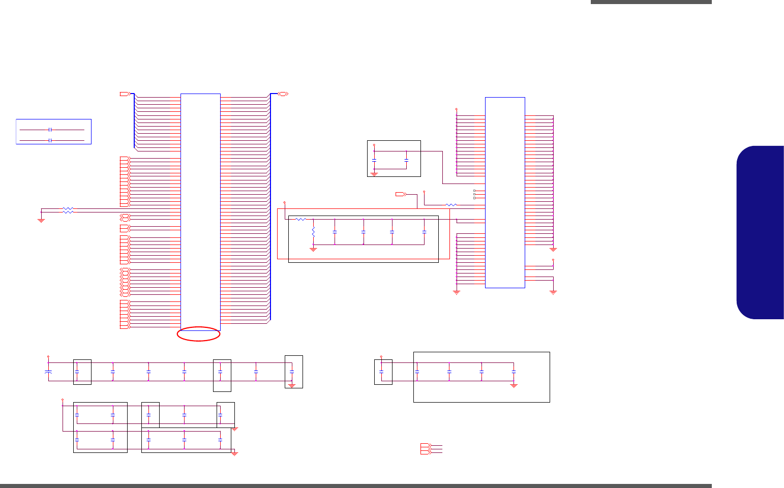
Schematic Diagrams
DDR3 SO-DIMM 1 B - 7
B.Schematic Diagrams
DDR3 SO-DIMM 1
One DIMM ¤£¤W¥ó
DDR3_DRAMRST#4,7
7/8 ¸É¤W220uf x1 ,10uf x1 ,1uf x2
C38
2.2u_16V_X5R_06
One DIMM ¤£¤W¥ó
One DIMM ¤£¤W¥ó
One DIMM ¤£¤W¥ó
M_A_DQ36
M_A_DQ35
M_A_DQ34
M_A_DQ33
M_A_DQ32
M_A_DQ31
M_A_DQ30
M_A_DQ29
M_A_DQ4
M_A_DQ3
M_A_DQ2
M_A_DQ1
M_A_DQ52
M_A_DQ51
M_A_DQ28
M_A_DQ50
M_A_DQ49
M_A_DQ38
M_A_DQ47
M_A_DQ46
M_A_DQ45
M_A_DQ44
M_A_DQ43
M_A_DQ42
M_A_DQ41
M_A_DQ40
M_A_DQ39
M_A_DQ37
M_A_DQ8
M_A_DQ7
M_A_DQ59
M_A_DQ63
M_A_DQ62
M_A_DQ61
M_A_DQ60
M_A_DQ58
M_A_DQ57
M_A_DQ56
M_A_DQ6
M_A_DQ5
M_A_DQ48
M_A_DQ55
M_A_DQ54
M_A_DQ53
M_A_DQ21
M_A_DQ10
M_A_DQ19
M_A_DQ18
M_A_DQ17
M_A_DQ16
M_A_DQ15
M_A_DQ14
M_A_DQ13
M_A_DQ12
M_A_DQ11
M_A_DQ9
M_A_DQ26
M_A_DQ25
M_A_DQ24
M_A_DQ23
M_A_DQ0
M_A_DQ22
M_A_DQ20
M_A_DQ27
M_A _D M7
SA1_DIM0
SA0_DIM0
Z0702
M_A _D M0
M_A _D M2
M_A _D M1
M_A _D M3
M_A _D M4
M_A _D M5
M_A _D M6
M_A_A9
M_A_A10
M_A_A12
M_A_A11
M_A_A13
M_A_A14
M_A_A0
M_A_A1
M_A_A2
M_A_A3
M_A_A4
M_A_A6
M_A_A5
M_A_A7
M_A_A8
M_A _D QS 3
M_A _D QS 2
M_A _D QS 1
M_A _D QS 0
M_A _D QS 1#
M_A _D QS 0#
M_A _D QS 7
M_A _D QS 6
M_A _D QS 5
M_A _D QS 4
M_A _D QS 7#
M_A _D QS 6#
M_A _D QS 5#
M_A _D QS 4#
M_A _D QS 3#
M_A _D QS 2#
Z0701
M_A_A15
C37
0.1u_16V_Y5V_04
JDIMM1A
*DDRSK-20401-TR9D
A0
98
A1
97
A2
96
A3
95
A4
92
A5
91
A6
90
A7
86
A8
89
A9
85
A10/AP
107
A11
84
A12/BC#
83
A13
119
A14
80
A15
78
DQ0 5
DQ1 7
DQ2 15
DQ3 17
DQ4 4
DQ5 6
DQ6 16
DQ7 18
DQ8 21
DQ9 23
DQ10 33
DQ11 35
DQ12 22
DQ13 24
DQ14 34
DQ15 36
DQ16 39
DQ17 41
DQ18 51
DQ19 53
DQ20 40
DQ21 42
DQ22 50
DQ23 52
DQ24 57
DQ25 59
DQ26 67
DQ27 69
DQ28 56
DQ29 58
DQ30 68
DQ31 70
DQ32 129
DQ33 131
DQ34 141
DQ35 143
DQ36 130
DQ37 132
DQ38 140
DQ39 142
DQ40 147
DQ41 149
DQ42 157
DQ43 159
DQ44 146
DQ45 148
DQ46 158
DQ47 160
DQ48 163
DQ49 165
DQ50 175
DQ51 177
DQ52 164
DQ53 166
DQ54 174
DQ55 176
DQ56 181
DQ57 183
DQ58 191
DQ59 193
DQ60 180
DQ61 182
DQ62 192
DQ63 194
BA0
109
BA1
108
RAS#
110
WE#
113
CAS#
115
S0#
114
S1#
121
CKE0
73
CKE1
74
CK0
101
CK0#
103
CK1
102
CK1#
104
SDA
200 SCL
202 SA1
201 SA0
197
DM0
11
DM1
28
DM2
46
DM3
63
DM4
136
DM5
153
DM6
170
DM7
187
DQS0
12
DQS1
29
DQS2
47
DQS3
64
DQS4
137
DQS5
154
DQS6
171
DQS7
188
DQS0#
10
DQS1#
27
DQS2#
45
DQS3#
62
DQS4#
135
DQS5#
152
DQS6#
169
DQS7#
186
ODT0
116
ODT1
120
BA2
79
C95
*0.1u_16V_Y5V_04
C62
*0.1u_16V_Y5V_04
C319
*10u_6.3V_X5R_08
C115
*0.1u_16V_Y5V_04
One DIMM ¤£¤W¥ó
C106
*0.1u_16V_Y5V_04
C31
*1U_6.3V_X5R_04
C97
*1U_6.3V_Y5V_04
C121
*1U_6.3V_Y5V_04
C102
*0.1u_16V_Y5V_04
+
C311
220U_4V_D
C111
*0.1u_16V_Y5V_04
C60
*1U_6.3V_Y5V_04
R25 *10K_04
C68
*0.1u_16V_Y5V_04
C54
*2.2u_16V_X5R_06
C117
*0.1u_16V_Y5V_04
R94
*1K_1%_04
C87
*0.1u_16V_Y5V_04
C141
*2.2u_16V_X5R_06
C33
*1U_6.3V_X5R_04
C138
*0.1u_10V_X5R_04
C320
*10u_6.3V_X5R_08
JDIMM1B
*DDRSK-20401-TR9D
VDD1
75
VDD2
76
VDD3
81
VDD4
82
VDD5
87
VDD6
88
VDD7
93
VDD8
94
VDD9
99
VDD10
100
VDD11
105
VDD12
106
VDDSPD
199
NC1
77
NC2
122
NCTEST
125
VREF_D Q
1
VSS1
2
VSS2
3
VSS3
8
VSS4
9
VSS5
13
VSS6
14
VSS7
19
VSS8
20
VSS9
25
VSS10
26
VSS11
31
VSS12
32
VSS13
37
VSS14
38
VSS15
43
VSS16 44
VSS17 48
VSS18 49
VSS19 54
VSS20 55
VSS21 60
VSS22 61
VSS23 65
VSS24 66
VSS25 71
VSS26 72
VSS27 127
VSS28 128
VSS29 133
VSS30 134
VSS31 138
VSS32 139
VSS33 144
VSS34 145
VSS35 150
VSS36 151
VSS37 155
VSS38 156
VSS39 161
VSS40 162
VSS41 167
VSS42 168
VSS43 172
VSS44 173
VSS45 178
VSS46 179
VSS47 184
VSS48 185
VSS49 189
VSS50 190
VSS51 195
VSS52 196
G2 GND2
G1 GND1
VTT2 204
VTT1 203
VREF_C A
126
RESET#
30 EVENT#
198
VDD13
111
VDD14
112
VDD16
118 VDD15
117
VDD17
123
VDD18
124
C71
*1U_6.3V_Y5V_04
R233 *10K_04
R232 *10K_04
C34
*1U_6.3V_X5R_04
C28
*10u_6.3V_X5R_06
C321
*10u_6.3V_X5R_08
C32
*1U_6.3V_X5R_04
C55
*0.1u_16V_Y5V_04
C105
*0.1u_16V_Y5V_04
R55 *1K_1%_04
CLOSE TO SO-DIMM_1
SO-DIMM 1 CLOSE TO CPU
One DIMM ¤£¤W¥ó
3.3VS3,7,8,9,10,11,12,13,14,15,16,17,18,21,23 1.5V4,5,7,11,23,25 VTT_MEM7,25
H=9.2mm 7/25
M_A_DQ[63:0] 4,7
SMBCLK07,8,11
M_A_DQS04,7
M_A_DQS24,7 M_A_DQS14,7
SMBDAT07,8,11
M_A_DQS54,7 M_A_DQS44,7 M_A_DQS34,7
M_A_DQS74,7 M_A_DQS64,7
One DIMM ¤£¤W¥ó
VTT_MEM
3.3VS
1.5V VTT_MEM
1.5V
3.3VS
1.5V
1.5V
VREF_DQ/VREF_CA ¤À¶}PULL UP 2.2uf/0.1uf 7/7
C89 *10p_50V_NPO_04
One DIMM ¤£¤W¥ó
C94 *10p_50V_NPO_04
One DIMM ¤£¤W¥ó
M_CLK_DDR1 M_CLK_DDR1#
M_CLK_DDR0 M_CLK_DDR0#
One DIMM ¤£¤W¥ó
M_A_DQS6#4,7 M_A_DQS5#4,7 M_A_DQS4#4,7
M_A_BS14,7
M_CLK_DDR14
M_A_DQS7#4,7
M_CLK_DDR1#4
M_ODT14
M_A_RAS#4,7
M_ODT04
M_A_BS04,7
M_A_WE#4,7
M_A_CAS#4,7
M_A_BS24,7
M_CKE04
M_CLK_DDR04M_CLK_DDR0#4
M_CS1#4
M_CKE14
M_A_D M14,7
M_A_A[15:0]4,7
M_CS0#4
M_A_DQS0#4,7
M_A_D M24,7 M_A_DM34,7
M_A_D M74,7
M_A_D M54,7
One DIMM ¤£¤W¥ó
M_A_D M04,7
M_A_D M44,7
M_A_D M64,7
M_A_DQS3#4,7 M_A_DQS2#4,7 M_A_DQS1#4,7
Sheet 6 of 31
DDR3 SO-DIMM 1
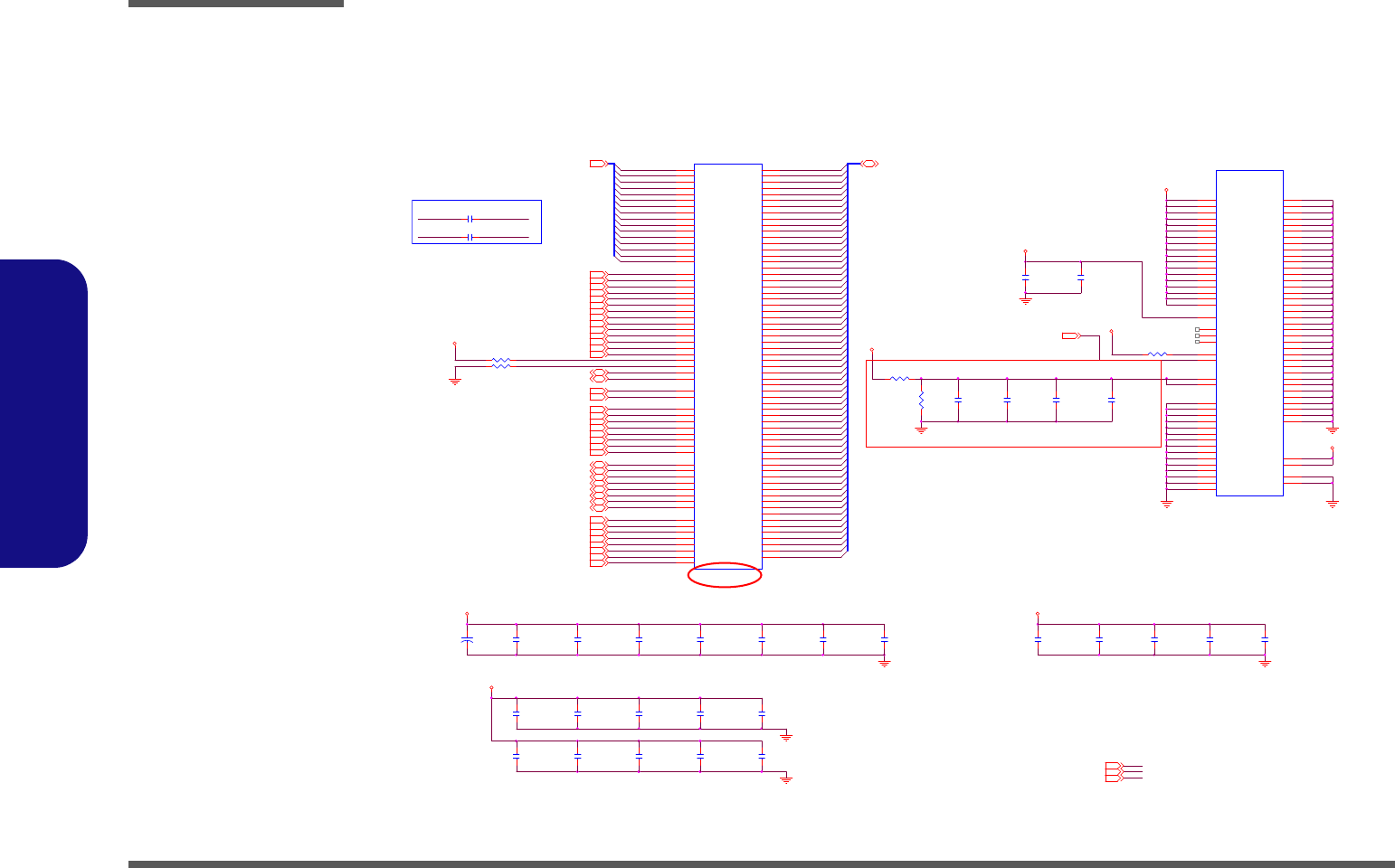
Schematic Diagrams
B - 8 DDR3 SO-DIMM 2
B.Schematic Diagrams
DDR3 SO-DIMM 2
+
C61
*220U_4V_D
R93
1K_1%_04
C30
1U_6.3V_X5R_04
R56 1K_1%_04
C116
10u_6.3V_X5R_08
C88
0.1u_16V_Y5V_04
C98
0.1u_16V_Y5V_04
R26 10K_04
C58
0.1u_16V_Y5V_04
C72
0.1u_16V_Y5V_04
C63
1U_6.3V_Y 5V_04
C137
2.2u_16V_X5R_06
C65
1U_6.3V_Y5V_04
C109
0.1u_16V_Y5V_04
C77
*0 .1u_16V _Y 5V_ 04
C78
0.1u_16V_Y5V_04
C103
0.1u_16V_Y5V_04
C108
*10u_6.3V_X5R_08
C96
*10u_6.3V_X5R_08
JDIMM2B
DDRSK-20401-TR5B
VDD1
75
VDD2
76
VDD3
81
VDD4
82
VDD5
87
VDD6
88
VDD7
93
VDD8
94
VDD9
99
VDD10
100
VDD11
105
VDD12
106
VDDSPD
199
NC1
77
NC2
122
NCTEST
125
VREF_DQ
1
VSS1
2
VSS2
3
VSS3
8
VSS4
9
VSS5
13
VSS6
14
VSS7
19
VSS8
20
VSS9
25
VSS10
26
VSS11
31
VSS12
32
VSS13
37
VSS14
38
VSS15
43
VSS16 44
VSS17 48
VSS18 49
VSS19 54
VSS20 55
VSS21 60
VSS22 61
VSS23 65
VSS24 66
VSS25 71
VSS26 72
VSS27 127
VSS28 128
VSS29 133
VSS30 134
VSS31 138
VSS32 139
VSS33 144
VSS34 145
VSS35 150
VSS36 151
VSS37 155
VSS38 156
VSS39 161
VSS40 162
VSS41 167
VSS42 168
VSS43 172
VSS44 173
VSS45 178
VSS46 179
VSS47 184
VSS48 185
VSS49 189
VSS50 190
VSS51 195
VSS52 196
G2 GND2
G1 GND1
VTT2 204
VTT1 203
VREF_CA
126
RESET#
30 EVENT#
198
VDD13
111
VDD14
112
VDD16
118 VDD15
117
VDD17
123
VDD18
124
C107
0.1u_16V_Y5V_04
C295
1U_6.3V_X5R_04
R24 10K_04
C35
0.1u_16V_Y5V_04
C119
0.1u_16V_Y5V_04
C101
1U_6.3V_Y5V_04
JDIMM2A
DDRSK-20401-TR5B
A0
98
A1
97
A2
96
A3
95
A4
92
A5
91
A6
90
A7
86
A8
89
A9
85
A10/AP
107
A11
84
A12/BC#
83
A13
119
A14
80
A15
78
DQ0 5
DQ1 7
DQ2 15
DQ3 17
DQ4 4
DQ5 6
DQ6 16
DQ7 18
DQ8 21
DQ9 23
DQ10 33
DQ11 35
DQ12 22
DQ13 24
DQ14 34
DQ15 36
DQ16 39
DQ17 41
DQ18 51
DQ19 53
DQ20 40
DQ21 42
DQ22 50
DQ23 52
DQ24 57
DQ25 59
DQ26 67
DQ27 69
DQ28 56
DQ29 58
DQ30 68
DQ31 70
DQ32 129
DQ33 131
DQ34 141
DQ35 143
DQ36 130
DQ37 132
DQ38 140
DQ39 142
DQ40 147
DQ41 149
DQ42 157
DQ43 159
DQ44 146
DQ45 148
DQ46 158
DQ47 160
DQ48 163
DQ49 165
DQ50 175
DQ51 177
DQ52 164
DQ53 166
DQ54 174
DQ55 176
DQ56 181
DQ57 183
DQ58 191
DQ59 193
DQ60 180
DQ61 182
DQ62 192
DQ63 194
BA0
109
BA1
108
RAS#
110
WE#
113
CAS#
115
S0#
114
S1#
121
CKE0
73
CKE1
74
CK0
101
CK0#
103
CK1
102
CK1#
104
SDA
200 SCL
202 SA1
201 SA0
197
DM0
11
DM1
28
DM2
46
DM3
63
DM4
136
DM5
153
DM6
170
DM7
187
DQS0
12
DQS1
29
DQS2
47
DQS3
64
DQS4
137
DQS5
154
DQS6
171
DQS7
188
DQS0#
10
DQS1#
27
DQS2#
45
DQS3#
62
DQS4#
135
DQS5#
152
DQS6#
169
DQS7#
186
ODT0
116
ODT1
120
BA2
79
C135
0.1u_10V_X5R_04
C293
1U_6.3V_X5R_04
C112
0.1u_16V_Y5V_04
C29
1U_6.3V_X5R_04
R27 10K_04
C57
2.2u_16V_X5R_06
C296
10u_6.3V_X5R_06
DDR3_DRAMRST#4,6
C113
1U_6.3V_Y5V_04
H=5.2mm 7/25
7/8 ¸É¤W,10uf x1 ,1uf x4
SMBCLK06,8,11
M_A_DQS04,6 M_A_DQS14,6
SMBDAT06,8,11
M_A_DQ[63:0] 4,6
M_A_DQS44,6 M_A_DQS34,6 M_A_DQS24,6
M_A_DQS64,6 M_A_DQS54,6
M_A_DQS74,6
VTT_MEM6,25
3.3VS3,6,8,9,10,11,12,13,14,15,16,17,18,21,23 1.5V4,5,6,11,23,25
1.5V
1.5V
VTT_MEM
3.3VS
1.5V VTT_MEM
3.3VS
3.3VS 1.5V
C90 *10p_50V_NPO_04
M_CLK_DDR3
M_CLK_DDR2#
M_CLK_DDR3#
C86 *10p_50V_NPO_04
M_CLK_DDR2
SO-DIMM 2
C36
2.2u_16V_X5R_06
M_A_DQ29
M_A_DQ4
M_A_DQ3
M_A_DQ2
M_A_DQ1
M_A_DQ34
M_A_DQ33
M_A_DQ32
M_A_DQ31
M_A_DQ30
M_A_DQ40
M_A_DQ39
M_A_DQ37
M_A_DQ36
M_A_DQ35
M_A_DQ46
M_A_DQ45
M_A_DQ44
M_A_DQ43
M_A_DQ42
M_A_DQ41
M_A_DQ28
M_A_DQ50
M_A_DQ49
M_A_DQ38
M_A_DQ47
M_A_DQ55
M_A_DQ54
M_A_DQ53
M_A_DQ52
M_A_DQ51
M_A_DQ58
M_A_DQ57
M_A_DQ56
M_A_DQ6
M_A_DQ5
M_A_DQ48
M_A_DQ59
M_A_DQ63
M_A_DQ62
M_A_DQ61
M_A_DQ60
M_A_DQ12
M_A_DQ11
M_A_DQ9
M_A_DQ8
M_A_DQ7
M_A_DQ16
M_A_DQ15
M_A_DQ14
M_A_DQ13
M_A_DQ10
M_A_DQ19
M_A_DQ18
M_A_DQ17
M_A_DQ21
M_A_DQ23
M_A_DQ0
M_A_DQ22
M_A_DQ27
M_A_DQ26
M_A_DQ25
M_A_DQ24
M_A_DQ20
CLOSE TO SO-DIMM_0
SA0_DIM1
M_ A_D M6
M_ A_D M7
SA1_DIM1
M_ A_D M2
M_ A_D M1
M_ A_D M3
M_ A_D M4
M_ A_D M5
Z0602
M_ A_D M0
M_A_A9
M_A_A6
M_A_A5
M_A_A7
M_A_A8
M_A_A3
M_A_A4
M_A_A14
M_A_A0
M_A_A1
M_A_A2
M_A_A13
M_A_A10
M_A_A12
M_A_A11
M_A_DQS1
M_A_DQS0
M_A_DQS2
M_A_DQS3
M_A_DQS4
M_A_DQS5
M_A_DQS1#
M_A_DQS0#
M_A_DQS7
M_A_DQS6
M_A_DQS4#
M_A_DQS3#
M_A_DQS2#
M_A_DQS7#
M_A_DQS6#
M_A_DQS5#
M_A_A15
Z0601
VREF_DQ/VREF_CA ¤À¶}PULL UP 2.2uf/0.1uf 7/7
M_A_DQS4#4,6
M_A_DQS7#4,6 M_A_DQS6#4,6 M_A_DQS5#4,6
M_A_RAS#4,6
M_A_BS14,6
M_CLK_DDR34
M_A_CAS#4,6
M_CLK_DDR3#4
M_ODT34
M_CLK_DDR24
M_ODT24
M_A_BS04,6
M_A_WE#4,6
M_CKE34
M_A_BS24,6
M_CKE24
M_CS2#4
M_CLK_DDR2#4
M_CS3#4
M_A_DM34,6
M_A_DM14,6
M_A_A[ 15:0]4,6
M_A_DQS0#4,6
M_A_DM24,6
M_A_DM64,6 M_A_DM74,6
M_A_DM54,6
M_A_DQS1#4,6
M_A_DM04,6
M_A_DM44,6
M_A_DQS3#4,6 M_A_DQS2#4,6
Sheet 7 of 31
DDR3 SO-DIMM 2
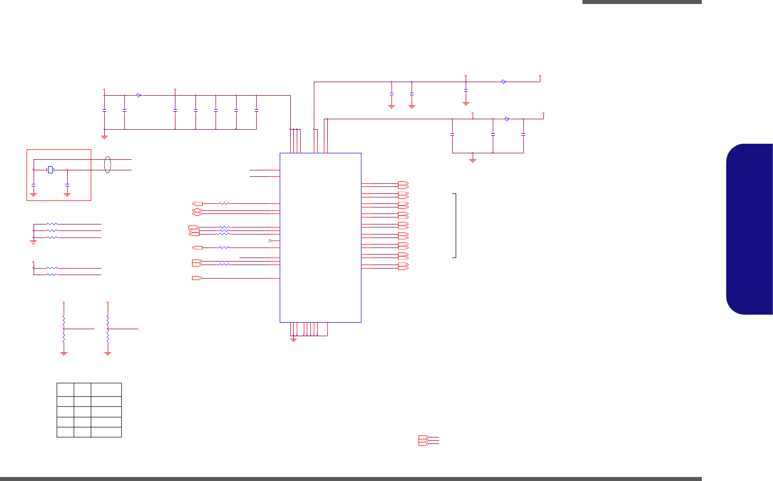
Schematic Diagrams
IDT CLOCK B - 9
B.Schematic Diagrams
IDT CLOCK
FSLB
167MHz
200MHz
01
11
10
CLK_DOT96 3
CLK_DOT96# 3
PM_STPPCI#
CLK_ICH
FSLC
Zo = 95 Ohm
¡Ó17.5%
SRC Clock - 100MHz
Zo = 95 Ohm
¡Ó17.5%
PCLK_ICH9
CLK_ICH489
CLK_ICH1411
CLK_CPU_HPL# 2
CLK_DREFSS# 3
CLK_DREFSS 3
CLK_DDR3REF_CLK 4
CLK_DDR3REF_CLK# 4
CLK_CPU_HPL 2
CLK_ICH_DMI# 9
CLK_SATA 10
CLK_SATA# 10
CLK_PCIE_WLAN# 19
CLK_CPU_DMI# 3
CLK_CPU_DMI 3
CLK_PCIE_JMC261# 17
CLK_PCIE_WLAN 19
CLK_PCIE_JMC261 17
CLK_ICH_DMI 9
KBC_PCLK18 PCLK_TPM15
CLKICH48
R265 10K_04
C351
0.1u_16V_Y5V_04
C344
0.1u_16V_Y5V_04
FSLC
C353
*10u_6.3V_X5R_06
FSLB
C347
*0.1u_16V_Y5V_04
C354
1u_10V_Y5V_06
R272
*10K_04
R270 33_04
L46
*HCB1608KF-121T25_short
C338
*10u_6.3V_X5R_06
R266 10K_04
L47
*HCB1608KF-121T25_short
R274 33_04
SMBUS
Zo = 50 Ohm
¡Ó15%
PCI - 33MHz
Zo = 50 Ohm
¡Ó15%
R273 33_04
R263 10K_04
C345
27p_50V_NPO_04
R275 10K_04
10 mils
X6
FSX8L_14.31818MHz
1 2
14MHz
Zo = 50 Ohm
¡Ó15%
PLACE CRYSTAL WITHIN
500 MILS OF CK505
C350
0.1u_16V_Y5V_04
C348
0.1u_16V_Y5V_04
DOT Clock - 96MHz
Zo = 95 Ohm
¡Ó17.5%
USB - 33MHz
Zo = 50 Ohm
¡Ó15%
R267
10K_04
C342
27p_50V_NPO_04
R262 *0_04
R271 10K_04
C346
0.1u_16V_Y5V_04
R276 33_04
R264
*10K_04
R268 33_04
R269
10K_04
C352
*0.1u_16V_Y5V_04
ALL_SYS_PWRGD11,18
PM_STPPCI#11 PM_STPCPU#11
1.5VS3,5,9,12,23 3.3VS3,6,7,9,10,11,12,13,14,15,16,17,18,21,23 1.05VS2,5,10,11,12,24,26
CLK_ICH
PMSTPCPU#
CLKREQB#
CLKREQA#
PM_STPPCI#
Frequency
Hos t C lockFSL C
100MHz
0 0 133MHz
U16
IDT 9VRS4338
X2
1
X1
2
VDDREF 3
REF0_2X/FSLC
4
SDATA
5
SCLK
6
VDDPCI_3.3 7
ITP_EN/PCICLK_F0_2X
8
FSLB/PCILK1_2X
9
CLKREQA#/PC ICLK2_2X
10
GNDPCI
11
GND25
12
v SEL_PCI/ 25M_PCICLK3_2x
13
VDD25 14
VDD48 15
v SATA_SEL/USB_48Mhz_2x
16
GND 48
17
CLKREQB#
18
DOT96_LRS/SRC4_LRS 19
DOT96#_LRS/SRC4#_LRS 20
VDD_CORE_1.5 21
LCD100_LRS 22
LCD100#_LRS 23
GNDLCD
24
GNDSATA
25
SATA#_LRS 26
SATA_LRS 27
SRC3#_LRS 28
SRC3_LRS 29
VDDSRC_LVIO 30
PCI_STOP#_3.3
31
SRC2#_LRS 32
SRC2_LRS 33
GND SRC
34
SRC1#_LRS 35
SRC1_LRS 36
CPU_STOP#_3.3
37
CPU_ITP#/SRC0#_LRS 38
CPU_ITP/SRC0_LRS 39
VDD_CORE_1.5 40
VDDC PU_LVIO 41
CPU1#_LRS 42
CPU1_LRS 43
GNDCPU
44
CPU0#_LRS 45
CPU0_LRS 46
CLKPWRGD/PD#_3.3
47
GNDREF
48
THERMAL PAD
49
C343
0.1u_16V_Y5V_04
XTA L_O U T
XTA L_I N
C349
0.1u_16V_Y5V_04
SMBCLK06,7,11 SMBDAT06,7,11
C339
*1u_10V_Y5V_06
3.3VS
3.3VS_C LK3.3VS
3.3VS
1.5VS_CLK 1.5VS
1.05VS_CLK 1.05VS
3.3VS
CLKREQA#
L45
*HC B1608KF-121T25_short
XTAL_OUT
XTAL_IN
PMSTPCPU#
CLKREQB#
FSLB
Sheet 8 of 31
IDT CLOCK
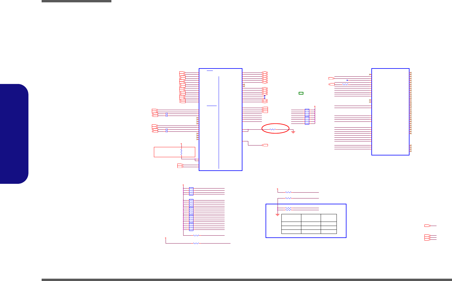
Schematic Diagrams
B - 10 Tigerpoint PART-A-B
B.Schematic Diagrams
Tigerpoint PART-A-B
Sheet 9 of 31
Tigerpoint PART-A-
B
Z0907
USB_OC#2
PERR#
SERR#
STOP#
FRAME#
TRDY#
PLOC K#
RN13
10K_8P4R_04
1
2
3
45
6
7
8
FLASH_SEL1
FLASH_SEL0
GPIO22
Zdiff = 90 Ohm ¡Ó17.5%
signal / space : 4.5 / 6 mils
USB Signal Group
INTB#
INTF#
USB_OC#6
INTA#
INTC#
INTEL Recommend 22.6_1%_04
REQ#1
IRDY#
TRDY #
PLOCK#
USB_OC #1 20
USB_OC#0
PCI_PME#
Zo = 50 Ohm ¡Ó15%
signal : 5 mils
Length < 500 mil to resistor
LAYOUT NOTE:
USB0 USB Por t 0
USB1 USB Por t 1
USB2 USB Por t 2
USB3 X
USB4 3G (PCIE M ini Card)
USB5 C om bo Bule to oth+WL AN
USB6 X
USB7 CCD
PCLK_ICH8
DMI_ICH_MT_IR1_DP3
CLK_ICH48 8
DMI_ICH_MT_IR0_DN3
CLK_ICH_DMI8
DMI_ICH_MT_IR1_DN3
DMI_ICH_MT_IR0_DP3
PCIE_RXP1_WLAN19
PCIE_RXP5_CARD17
CLK_ICH_DMI#8
PCIE_RXN1_WLAN19
DMI_ICH_MT_IR2_DN3
PCIE_RXN5_CARD17
DMI_ICH_MT_IR3_DP3DMI_ICH_MT_IR3_DN3
DMI_ICH_MT_IR2_DP3
PME#17,18
PCIE_TXN5_CARD17
PCIE_TXN1_WLAN19 PCIE_TXP1_WLAN19
DMI_ICH_IT_MR0_DP3DMI_ICH_IT_MR0_DN3
PCIE_TXP5_CARD17
DMI_ICH_IT_MR2_DP3DMI_ICH_IT_MR2_DN3
DMI_ICH_IT_MR1_DP3DMI_ICH_IT_MR1_DN3
DMI_ICH_IT_MR3_DP3DMI_ICH_IT_MR3_DN3
USB_OC#7
USB_OC #2 20
Zdiff = 80 Ohm ¡Ó10%
signal / space : 5.5 / 5 m ils
PCIE Signal Group
USB_OC#1
IRDY #
PERR#
RSVD02
PCIRST#
STOP#
FLASH_SEL0
FLASH_SEL1
LAYOUT NOTE:
< 500 mils to TPT ball
3.3VS3,6,7,8, 10,11, 12,13,14,15,16,17,18,21,23
3.3VS_PR I ME_VC C 310,11,12
1.5VS3,5,8,12,23
3.3V2,11,12,13, 17,18,19,21,23,24,26
T15
R297 *10K_04
1 OF 6
Tigerpoint
PCI
U19A
NM10-EXPRESS
AD0 B22
AD1 D18
AD2 C17
AD3 C18
AD4 B17
AD5 C19
AD6 B18
AD7 B19
AD8 D16
AD9 D15
AD10 A13
AD11 E14
AD12 H14
AD13 L14
AD14 J14
AD15 E10
AD16 C11
AD17 E12
AD18 B9
AD19 B13
AD20 L12
AD21 B8
AD22 A3
AD23 B5
AD24 A6
AD25 G12
AD26 H12
AD27 C8
AD28 D9
AD29 C7
AD30 C1
AD31 B1
C/BE0# H16
C/BE1# M15
C/BE2# C13
C/BE3# L16
PAR
A5
PME#
C22
PLOCK#
A8
FRAME#
A16
STRAP0#
D11
RSVD01
K9
REQ1#
G16
RSVD02
M13
GPIO1
C9
PIRQA#
B2
PIRQB#
D7
PIRQC#
B3
PIRQD#
H10
PIRQE#/GPIO2
E8
PIRQF#/GPIO3
D6
PIRQG#/GPIO4
H8
PIRQH#/GPIO5
F8
REQ2#
A20
GNT2#
E16 GNT1#
A18
TRDY#
A10
SERR#
B11
IRDY#
B7 PCIRST#
A23 PCICLK
J12 DEVSEL#
B15
GPIO22
C15 GPIO17/STRAP2#
A2
STOP#
F14
PERR#
D10
GPIO48/STRAP1#
G14
T14
R127 *1K_04
INTE#
PCI-E
DMI
USB
Tigerpoint
2 OF 6
U19B
NM10-EXPRESS
DMI2TXN
U23
DMI1TXN
T24
DMI1TXP
T25
DMI2RXN
T19
OC0# D4
OC2# D3
OC3# D2
OC1# C5
OC4# E5
OC5#/GPIO29 E6
OC6#/GPIO30 C2
DMI_CLKP
W24 DMI_CLKN
W23
DMI_IRCOMP
J22 DMI_ZCOMP
H24
PETP4
N24 PETN4
N25 PERP4
P18 PERN4
P17 PETP3
M21 PETN3
L22 PERP3
L24 PERN3
L23 PETP2
K25 PETN2
K24 PERP2
M19 PERN2
M18 PETP1
J24 PETN1
J23 PERP1
K22 PERN1
K21
DMI3TXP
V23 DMI3TXN
V24 DMI3RXP
V20
DMI2TXP
U24
DMI2RXP
T18
DMI1RXP
T20 DMI1RXN
T21 DMI0TXP
P20 DMI0TXN
P21 DMI0RXP
R24 DMI0RXN
R23
CLK48 F4
USBRBIAS# G3
USBRBIAS G2
OC7#/GPIO31 C3
USBP7P N2
USBP7N N1
USBP6P M5
USBP6N M6
USBP5P L3
USBP5N L2
USBP4P K2
USBP4N K1
USBP3P K5
USBP3N K6
USBP2P J3
USBP2N J2
USBP1P H2
USBP1N H3
USBP0P H6
USBP0N H7
DMI3RXN
V21
INTH#
INTG#
INTD#
RN12
8.2K_8P4R_04
1
2
3
45
6
7
8
RN10
8.2K_8P4R_04
1
2
3
45
6
7
8
REQ#2
R149 8.2K_04
R299 *1K_04
C154 0.1u_10V_X7R_04
SERR#
R141 8.2K_04
GPIO22
RN4
8.2K_8P4R_04
1
2
3
45
6
7
8
DEVSEL#
FRAME#
RN11
8.2K_8P4R_04
1
2
3
45
6
7
8
R301 1K_04
RN5
8.2K_8P4R_04
1
2
3
45
6
7
8
C357 0.1u_10V_X7R_04
R108
24.9_1%_04
R307 18.2_1%_04
C356 0.1u_10V_X7R_04
C153 0.1u_10V_X7R_04
RN14
10K_8P4R_04
1
2
3
45
6
7
8
T37
PCI_PME#
R298 *0_04
RSVD01
STRAP0#
USB_OC#7
Z0901
Z0902
USB_OC#5
INTA#
INTC#
D02A
INTD#
GPIO1
INTE#
INTF#
INTG#
USB_OC#3
INTH#
TOP BLOCK SWAP OV ERRIDE
USB_RBIAS
STRAP0#
RSVD01
RSVD02
1
USB_OC#3
GPIO1
USB_OC#6
INTB#
USB_PN1 20
USB_PP4 19
USB_PP5 19
USB_PP0 20
USB_PN4 19
USB_PN5 19
USB_PN7 21
USB_PP7 21
USB_PP2 20
USB_PP1 20
USB_PN0 20
USB_PN2 20
3.3VS
3.3V
3.3VS_PRIME_VCC3
3.3V
1.5VS
USB_OC#4
Z0903
Z0905
Z0904
Z0906
1
0
USB_OC#4
SPI
FL A SH_SEL 1
LPC
FLASH_SEL0
PCI
0
MODE
1
1
GPIO48/STRAP1#GPIO17/STRAP2#
DEVSEL#
REQ#1
REQ#2
USB_OC#5
USB_OC #0 20
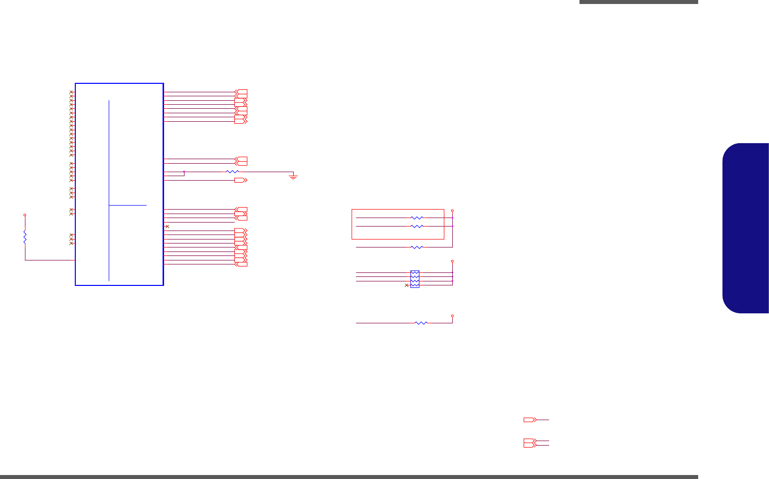
Schematic Diagrams
Tigerpoint PART-C B - 11
B.Schematic Diagrams
Tigerpoint PART-C
Sheet 10 of 31
Tigerpoint PART-C
SATARBIAS#
H_A20M# 2
SATA_LED# 21
H_FERR# 2
H_INTR 2
H_INIT# 2
KBC_GA20#
H_SMI# 2
LPC_SIRQ 15,18
H_NMI 2
SATATXN0 15
SATATXP0 15
H_STPCLK# 2
SATATXN1 15
SATATXP1 15
H_FERR#
H_FERR#
KBC_RST#
DBGSTRP_SETUP H_THERMTRIP#
THE SV_DETECT
KBC_GA20# 18
CLK_SATA# 8
CLK_SATA 8
1.05VS2,5,8,11,12,24,26 3.3VS3,6,7,8,9,11,12,13,14,15,16,17,18,21,23
H_THERMTRIP# 2
SATARXN0 15
SATARXP0 15
3.3VS_PRIME_VCC39,11,12
H_CPUSLP# 2
KBC_RST# 18
SATARXN1 15
SATARXP1 15
3/5
KBC_RST#
LPC_SIRQ
KBC_GA20#
R133 24.9_1%_04
R120 60. 4_04
R286
10K_04
R121 60. 4_04
3 OF 6
Tigerpoint
HOST
SATA
U19C
NM10-EXPRESS
SATA0RXN AE6
SATA0RXP AD6
SATA0TXN AC7
SATA0TXP AD7
SATA1RXN AE8
SATA1RXP AD8
SATA1TXN AD9
SATA1TXP AC9
SATA_CLKN AD4
GPIO36
AD23
A20M# Y20
CPUSLP# Y21
IGNNE# Y18
INIT3_3V# AD21
INIT# AC25
INTR AB24
FERR# Y22
NMI T17
RCIN# AC21
SERIRQ AA16
SMI# AA21
STPCLK# V18
THERMTRIP# AA20
RSVD03
R12
RSVD04
AE20
RSVD05
AD17
RSVD06
AC15
RSVD07
AD18
RSVD08
Y12
RSVD09
AA10
RSVD10
AA12
RSVD11
Y10
RSVD12
AD15
RSVD13
W10
RSVD14
V12
RSVD15
AE21
RSVD16
AE18
RSVD17
AD19
RSVD18
U12
RSVD19
AC17
RSVD20
AB13
RSVD21
AC13
RSVD22
AB15
RSVD23
Y14
RSVD24
AB16
RSVD25
AE24
RSVD26
AE23
RSVD27
AA14
RSVD28
V14
RSVD29
AD16
SATA_CLKP AC4
SATARBIAS# AD11
SATARBIAS AC11
SATALED# AD25
RSVD31
AB10
A20GATE U16
RSVD30
AB11
R287 10K_04
RN7
10K_8P4R_04
1
2
3
45
6
7
8
SATA ODD
SATA HDD
SATA Signal Group
Zdiff = 95 Ohm ¡Ó17.5%
signal / space : 4 / 6.5 mils
LPC_SIRQ
H_THERMTRIP#
1.05VS
3.3VS
3.3VS
3.3VS_PRIME_VCC3
R125 1K_04
H_IGNNE#
H_IGNNE#
LAYOUT NOTE:
Zo = 50 Ohm ¡Ó15%
signal : 5 mils
Length < 500 mil to resistor
Place resietor close to TPT
SATA_LED#
SATA_LED#
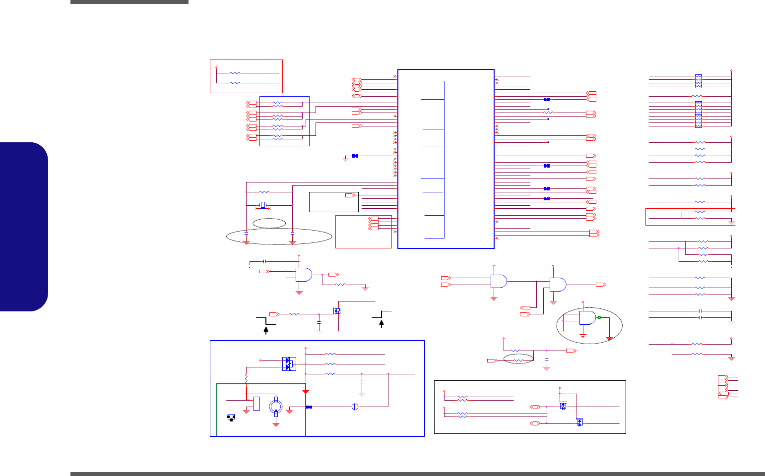
Schematic Diagrams
B - 12 Tigerpoint PART-D
B.Schematic Diagrams
Tigerpoint PART-D
Sheet 11 of 31
Tigerpoint PART-D
PN: 6-20-41100-002
HSPI_SCLK18
HSPI_MSI18 HSPI_MSO18
HSPI_CE#18
VCC_RTC12
3.3V
ON
Q5
MTN7002ZHS3
G
DS
GFX_PWRGD
ON
D02A
NM10_GPIO1119
R277
1K_04
H_DPRSTP# 2
PLTRST# 2
H_PWRGD 2
PM_STPCPU# 8
ICH_SPKR 16
PM_STPPCI# 8
H_DPSLP# 2
AZ_BITCLK_R16
SB_BLON 13
SUSC# 18,25
ALL_SYS_PWRGD8,18
SUSB# 18,23
ICH_PWROK 13
DDR3_DRAM_PWROK 4
S4_STATE# 15
BUF_PLT_RST# 15,17,18,19
R308 90.9_04
R305 90.9_04
R309 90.9_04
H_AZIL_BCLK3R306 90.9_04
D02A
RTC
J_RTC1
AAA-BAT-022-K01
-
2+1
AZ_SDIN016
KBC_SMI# 18
THERM_ALERT# 18
KBC_SCI# 18
PCIE_WAKE# 17,19
CLK_ICH148
KBC_PWRBTN# 18
KBC_R SMRST# 18
1.05VS2,5,8,10,12,24,26
3.3V2,9,12,13,17,18,19,21,23,24,26 VDD315,17,18,19,22,23,27
3.3VS3,6, 7,8, 9,10,12,13,14,15, 16,17,18,21, 23
ALL_SYS_PWRGD 8,18
KBC_SWI# 18
DELAY_ALL_SYS_PWRGD4,18
PLTRST#2
1.8VS_PWRGD18
AZ_SDIN13
3.3VS_PRIME_VCC39,10,12
SUSBL23,24, 25
SMLINK0
SMLINK1
C190
2.2u_16V_X5R_06
R28 *0_04
ICH_RTCRST#
Z1101
Z1102
BKLTSEL1#
ICH_SYNC#
1.5V_PWRGD25
AZ_RST#
ICH_SPKR
SMLALERT#
KBC_SWI#
ICH_INTVRMEN
PLTRST_R#
KBC_SMI#
DBG_STRAP_DET
LCD_PID0
ICH_SMBCLK0
ICH_RTCX1ICH_RTCX1
CONFIG_MODE#
PCI E_WAKE#
ICH_SMBDAT0
SMLINK1
KBC_RSMRST#
PM_STPPCI#_R
KBC_CLKRUN#
BATLOW#
GPIO8
SUSCLK
AZ_SYNC
H_DPSLP#
LAN_RST#LAN_RST#
BRDID2
H_DPRSTP#
SMLINK0
ICH_RI
AZ_SDOUT
FP_RST#
ICH_RTCRST#
IMVP6_PWRGD_R
PLTRST#
NM10_GPIO11
SUSC#
BRDID1
ICH_RTCX2ICH_RTCX2
GPIO0
GPIO9 LCD_PID0
KBC_SMI#
KBC_SCI#
KBC_SWI#
ICH_SMBDAT0
ICH_SMBCLK0
KBC_SCI#GPIO13
ICH_PWROKGFX_PWRGD
ICH_PWROKICH_PWROK_R
SM_INTRUDER#
ALL_SYS_PWRGD
AZ_SYNC
AZ_SDOUT
ICH_SMBDAT0
SMBDAT0
SMBCLK0
ICH_SMBCLK0
LDRQ0#
ICH_PWROK
BKLTSEL1#
ICH_SPKR
PLTRST#
CONFIG_MODE#
H_DPRSTP#
LDRQ0#
ICH_SYNC#
KBC_RSMRST#
BRDID1
KBC_CLKRUN#
BRDID2
GPIO0
SUSCLK
H_DPSLP#
BATLOW#
FP_RST#
GPIO9
SMLALERT#
NM10_GPIO11
PCIE_WAKE#
ICH_RI
GPIO8
PLTRST#
SB_MUTE#
PM_DPRSLPVR
C219 *0.1u_16V_Y5V_04
R152 10K_04
T7
T41
R97 2.2K_04
R292 10K_04
C366
12P_NPO_ 50V_04
R123 * 56_04
RN2
10K_8P4R_04
1
2
3
45
6
7
8
R302 10K_04
R280 *10K_04
U5C
74LVC08PW
9
10 8
147
R279 *10K_04
R107 *1K_04
R304 *1K_04
R124 *100K_04
R289 1K_04
R288 10K_04
R153 330K_04
R98 *10mil_short
R283 *0_04
R112 2.2K_04
U5D
74LVC08PW
12
13 11
147
PJ6
8mil
1 2
R151 *10mil_short
R150 *1K_04
C363 *10p_50V_NPO_04
RN9
10K_8P4R_04
1
2
3
45
6
7
8
U5A
74LVC08PW
1
23
147
R291 *10K_04
U5B
74LVC08PW
4
56
147
R156 *10mil_short
R294 1K_04
S
D
G
Q4A
MTDN7002ZHS6R
2
61
C165 *150P_50V_NPO_04
R100 2.2K_04
R103 10K_04
C
A
A
D21
BAT54CWGH
1
23
R142 *10mil_short
R296 *10mil_short
R303 *1K_04
RN8
10K_8P4R_04
1
2
3
45
6
7
8
R137 1M_04
R132 10K_04
R285 10K_04
R300 10M_04
T42
X8 MC-306_32.768KHz
1 4
32
R131 20K_1%_04
C358
1u_10V_Y5V_06
R117 * 56_04
S
D
G
Q4B
MTDN7002ZHS6R
5
34
R284 1K_04
C365
12P_NPO_ 50V_04
R129 * 10K_04
EPROM
Tigerpoint
MISC
RTC
SMB
SPI
LPC
AUDIO
LAN
4 OF 6
U19D
NM10-EXPRESS
DPRSTP# AB23
DPSLP# AA18
RSVD 31 F20
GPIO8 K18
GPIO9 H19
GPIO10 M17
GPIO12 A24
GPIO13 C23
GPIO14 P5
GPIO15 E24
DPRSLPVR AB20
STP_PCI# Y16
STP_CPU# AB19
GPIO24 R3
GPIO25 C24
GPIO26 D19
GPIO27 D20
GPIO28 F22
CLKRUN# AC19
GPIO33 U14
GPIO34 AC1
GPIO38 AC23
GPIO39 AC24
CPUPWRGD/GPIO49 AB22
TH R M# AB17
VRMPWR GD V16
MC H _SY N C # AC18
PWRBTN# E21
RI# H23
SUS_STAT#/LPC PD # G22
SUSCLK D22
SYS_RESET# G18
PLTRSTB G23
WAKE# C25
INTRUDER# T8
PWROK U10
RSMRST# AC3
INTVRMEN AD3
SPKR J16
SLP_S3# H20
SLP_S4# E25
SLP_S5# F21
BATLOW# B25
LDRQ1#/GPIO23
AA5
LAD0/F WH0
V6
LAD1/F WH1
AA6
LAD2/F WH2
Y5
LAD3/F WH3
W8
LFRAME#
Y4
HDA_RST#
U2
HDA_SDI0
W2
HDA_SDIN1
V2
HDA_SDIN2
P8
HDA_SDOUT
AA1
HDA_SYNC
Y1
CLK14
AA3
EE_CS
U3
EE_DI N
AE2
EE_DOU T
T6
EE_SHCLK
V3
LAN_CLK
T4
LANR_STSYNC
P7
LAN_RST#
B23
LAN_RXD0
AA2
LAN_RXD1
AD1
LAN_RXD2
AC2
LAN_TXD0
W3
LAN_TXD1
T7
LAN_TXD2
U4
RTCX1
W4
RTCX2
V5
RTCRST#
T5
SMBALERT#/GPIO11
E20
SMBCLK
H18
SMBDATA
E23
SMLALER T#
H21
SMLIN K0
F25
SMLIN K1
F24
SPI_MISO
R2
SPI_MOSI
T1
SPI_C S#
M8
SPI_C LK
P9
SPI_AR B
R4
GPIO6 W16
GPIO7 W14
BM_BUSY#/GPIO0 T1 5
HDA_BIT_CLK
P6
LDRQ0#
Y8
D02a
GFX_PWRGD23,26
R128 *10mil_short
R99 2.2K_04
R290 4.7K_04
PCIE PORT CONF BIT0
R29
10K_04
PCIE PORT CONF BIT1
Clear CMOS
Zo = 50 Ohm
¡Ó15%
signal : 4 m ils
Length < 1000
mils
SPKR STUFF R For Safe M ode.
DC COUPLING SELETION
BOARD ID
D03 7/1
§ïLAYOUT
FOR¦@¥Î³]-pWLAN
0323
ICH_INTVRMEN
2
1
3
4
5
SM_INTRUDER#
C39
1u_10V_Y 5V_06
AZ_BITCLK
D02A
H_AZIL_SYNC3
6
AZ_SYNC_R16
H_AZIL_SDO3AZ_SDOUT_R16
H_AZIL_RST#3
D02
AZ_RST#_R16
Zo = 55 Ohm
¡Ó15%
signal : 4 mils
LPC Signal Group
R311 22_04
R136 1K_04
LPC_AD215,18
LPC_AD015,18 LPC_AD115,18
1.5V4,5,6,7,23, 25
R313 22_04
LPC_FRAME#15,18
LPC_AD315,18
KBC_CLKRUN# 15,18
SMBDAT06,7,8
SMBCLK06,7,8
Zo = 50 Ohm ¡Ó15%
signal / spacing : 5 / 6 mils
Length < 10"
R312 22_04
VDD3
VCC_RTC
3.3V
3.3VS
3.3V
3.3V
3.3VS
3.3V
1.05VS
3.3VS_PRIME_VCC3
3.3VS
3.3VS
3.3VS
3.3V
3.3V
1.5V
AZ_RST#16
Layout Note:
Close to PCH
VCC_RTC1
10mil
W/O Modem®É,
¥Î¦¹ RTC Conn.
2
J_RTC1
1
J_RTC2
*85205-02701
1
2
RTC Signal Gro up
RTCX1,RTCX2,RTCRST#
Zo = 50 Ohm
¡Ó15%
signal : 4 m ils
HDA Signal Group
R310 22_04
C180
2200p_50 V_X7R_04
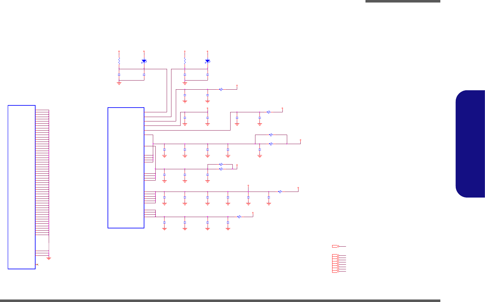
Schematic Diagrams
Tigerpoint PART-E-F B - 13
B.Schematic Diagrams
Tigerpoint PART-E-F
L51 *HCB1005KF-121T20_short
R157
10_1%_04
C182
1u_6.3V_X5R_04
L26
*HCB1005KF-121T20_short
C150
1u_10V_Y5V_06
C174
1u_6.3V_X5R_04
C178
0.1u_16V_Y5V_04
C198
0.1u_10V_X5R_04
C175
10u_6.3V_X5R_06
VCC1_05
2mA
VCC_RTC11 1.05VS2,5,8,10,11,24,26 1.5VS3,5,8,9,23 3.3VS3,6,7, 8,9,10,11,13, 14,15,16,17,18,21,23 3.3V2,9,11,13,17,18,19,21,23, 24,26
3.3VS_PRIME_VCC39,10,11
3.3VS_PRIME5,18,23
5VS14,15,16, 21,23 5V20,23,24,25,26
VCCSUS3_3
VCCDMIPLL
VCC5REF
L27
*HCB1005KF-121T20_short
V5REF_SUS
L28 *HCB1005KF-121T20_short
L50
*HCB1005KF-121T20_short
0.98A
1.3A
0.13A
0.29A
1.05VS
3.3VS_PRIME
1.5VS
3.3V5V
6mA
5VS 3.3VS
1.5VS
3.3V
1.5VS
14mA
10mA
3.3VS_PRIME_VCC3
VCC_RTC
10mA
50mA
50mA
VCCSATAPLL
C162
10u_6.3V_X5R_06
C214
1u_10V_Y5V_06
C173
1u_6.3V_X5R_04
C152
0.01u_16V_X7R_04
C207
*1u_6.3V_X5R_04
C181
0.1u_16V_Y5V_04
POWER
Tigerpoint
5 OF 6
U19E
NM10-EXPRESS
VCC1_5_2 M9
VCC1_5_3 M20
VCC1_5_4 N22
VCC1_05_4 V10
V_CPU_I O W18
VCC1_5_1 AA8
VCCSUS3_3_4 F1
VCCSUS3_3_3 K7
VCCSUS3_3_2 N4
VCCSUS3_3_1 F18
VCC3_3_6 T9
VCC3_3_5 R10
VCC3_3_4 G10
VCC3_3_3 F10
VCC3_3_2 AD13
VCC3_3_1 H25
VCC1_05_3 P15
VCC1_05_2 K17
VCC1_05_1 J10
VCCUSBPLL F6
VCCDMIPLL Y25
VCCRTC AE3
VCCSATAPLL Y6
VCC5REF_SUS F5
VCC5REF F12
D12
RB751S-40C2
AC
C146
0.1u_16V_Y5V_04
C161
*0.1u_10V_X5R_04
C151
*4.7u_6.3V_X5R_06
C164
1u_6.3V_X5R_04
C155
1u_6.3V_X5R_04
C149
0.1u_16V_Y5V_04
C205
*1u_6.3V_X5R_04
C372
0.1u_16V_Y5V_04
C371
0.01u_16V_X7R_04
R119
100_1%_04
C183
0.1u_16V_Y5V_04
C222
*1u_10V_Y5V_06
VCC1_5
L32
*HCB1608KF-121T25_short
C189
0.1u_16V_Y5V_04
L29
*HCB1005KF-121T20_short
C193
*1u_6.3V_X5R_04
C221
*10u_6.3V_X5R_06
C202
10u_6.3V_X5R_06
C225
*1u_10V_Y5V_06
L33
*HCB1608KF-121T25_short
D22
RB751S-40C2
AC
Tigerpoint
GND
6 OF 6
U19F
NM10-EXPRESS
VSS59 F2
VSS58 AE13
VSS57 G24
VSS56 AE25
VSS55 AE10
VSS54 AE1
VSS53 AD24
VSS52 AD20
VSS51 AD10
VSS50 AD2
VSS49 AC8
VSS48 AB8
VSS47 AB7
VSS46 AB6
VSS45 AB4
VSS44 Y24
VSS43 Y2
VSS42 W22
VSS41 W12
VSS40 V25
VSS39 V22
VSS38 V19
VSS37 V8
VSS36 V7
VSS35 V1
VSS34 T22
VSS33 T2
VSS32 R22
VSS31 R14
VSS30 P19
VSS29 P13
VSS28 P11
VSS27 N23
VSS26 N14
VSS25 N13
VSS24 N12
VSS23 N3
VSS22 M11
VSS21 M7
VSS20 L4
VSS19 K20
VSS18 K19
VSS17 K11
VSS16 K8
VSS15 K4
VSS14 H5
VSS13 H4
VSS12 H1
VSS11 G8
VSS10 G4
VSS09 F16
VSS08 E18
VSS07 B24
VSS06 B20
VSS05 B16
VSS04 B10
VSS03 B6
VSS02 A25
VSS01 A1
RSVD32 AE16
Sheet 12 of 31
Tigerpoint PART-E-
F
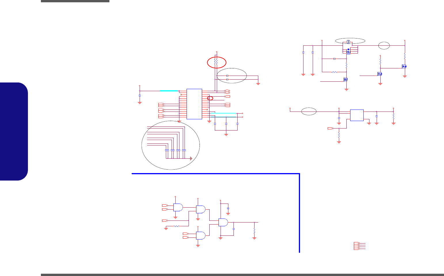
Schematic Diagrams
B - 14 LVDS, INVERTER
B.Schematic Diagrams
LVDS, INVERTER
C396*22p_50V_NPO_04 C395*22p_50V_NPO_04
C18
*0.1u_16V_Y5V_04
C20
*0.1u_50V_Y5V_06
R11
100K_04
C397*22p_50V_NPO_04
PANEL CONNECTOR
C398*22p_50V_NPO_04
C400*22p_50V_NPO_04 C399*22p_50V_NPO_04
Z1303
Z1302 INV_BLON
Z1301
D02A
U12B
74LVC08PW
4
56
147
NB_ENAVDD3,18
U12A
74LVC 08PW
1
23
147
U12D
74LVC08PW
12
13 11
147
R9 *100K_04
S
D
G
Q8B
*MTDN7002ZH S6R
5
34
S
D
G
Q8A
*MTDN7002ZHS6R
2
61
C286
*0.1u_16V_Y5V_04
3.3VS_LC D
R12
100K_04
C9
*100p_50V_NPO_04
U12C
74LVC08PW
9
10 8
147
BACKLIGHT ON CONTROL
LVDS-L1P3
LVD S-L2P 3
LVD S-L2N 3
LVDS-L1N3
LVDS-L0P3LVDS-L0N3
LVDS-LCLKP3LVDS-LCLKN3
>100mil
PLVDD
HI LVDS:3.3V
2A
2A
>100 mil
LVDS-LCLKN
LVDS-L1P
LVDS-L1N
LVDS-L0P
LVDS-L0N
LVDS-LCLKP
BKL_EN18
3.3VS PLVDD
ICH_PWROK11
SB_BLON11
LID _SW #18,21
3.3V2,9,11,12,17,18,19,21,23,24,26
VIN21,22,23,25,26,27
3.3VS3,6,7,8,9,10,11,12,14,15,16,17,18,21,23
MC H _BL ON3
LCD_BRIGHTNESS 18
5VS12,14,15,16,21,23
D02
D02
D02
D02
D02
D02
Close to J_LCD1
U13
G5243A
VIN
4
VIN
5
EN
3
VOUT 1
GND 2
C19
1u_10V_Y5V_06
LVDS-L2N
LVDS-L2P
Q10
*MTN7002ZHS3
G
DS
C15
1u_10V_Y5V_06
PJ18 OPEN-2mm
1 2
D02A
P_DDC_CLK 3
P_DDC_DATA 3
3.3V
VLED
3.3V 3.3V
3.3V
VIN VLED
3.3V
3.3VS_LCD
3.3VS_LCD
PLVDD
Follow Common Design 7/25
Follow W210CUQ 8/1
C393*22p_50V_NPO_04
C420 27p_50V_NPO_04
C421 *27p_50V_NPO_04
D02A
C394*22p_50V_NPO_04
Q9
*P2003EVG
4
62 5
73
1
8
R14
*100K_04
LVDS-L0P
LVDS-L0N
INV_BLON
LVDS-L2P
LVDS-L2N
J_LCD1
87216-3006
1
122
3
344
5
566
7
788
9
910 10
11
11 12 12
13
13 14 14
15
15 16 16
17
17 18 18
19
19 20 20
21
21 22 22
23
23 24 24
25
25 26 26
27
27 28 28
29
29 30 30
LVDS-L1P
LVDS-L1N
C13
*0.1u_16V_Y 5V_04
LVDS-LCLKN
2A
LVDS-LCLKP
C287
*4.7u_10V_Y5V_08
2A
NB_ENAVDD
Z1304
R221
*10K_04
NB_ENAVDD#
R214
*220_06
C290 *0.22u_50V_Y 5V_06
NB_ENAVDD
R224
*1M_04
R225 *100K_04
C1
0.1u_50V_Y5V_06
1A
2A
C21
*0.1u_50V_Y5V_06
30Pin
R211
10K_04
R210
10K_04
Sheet 13 of 31
LVDS, INVERTER
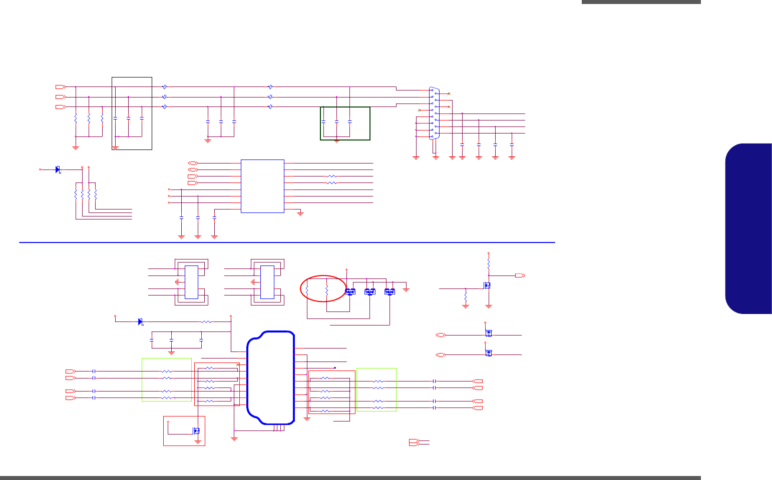
Schematic Diagrams
CRT, HDMI B - 15
B.Schematic Diagrams
CRT, HDMI
R32 0_04
C299
470p_04
R38 0_04
R42 0_04
TMDS_DATA2#
HDMIC_CLKCN3
HDMIC_C1CP3
HDMIC_C2CN 3
HDMIC_CLKCP3
HDMIC_C0CP 3
HDMIC_C1CN3HDMIC_C2CP 3
HDMIC_C0CN 3
R329
2.2K_04
TMDS_DATA0#
R330
2.2K_04
R331
2.2K_04
R59 0_04
R332
2.2K_04
R54 0_04
3.3VS
3.3VS
3.3VS
3.3VS
TMDS_DATA2#-R
DAC_DDCACLK
DAC_DDCADATA
CRT_DDCACLK
CRT_DDCADAT
D6
RB751S-40C2
A C
VGA RGB resistors colse to Connecter
Zo = 50 Ohm ¡Ó15%
signal : 4 mils
leng th < 500 mils
CRT
TMDS_DATA0#-R
CRT_BLUE
CRT_GREEN
CRT_RED
CRT DAC Signal Group
CRT _ RED,C RT _GREEN,CRT_BLUE
DAC_RED3
DAC_BLUE3
DAC_GREEN3
DAC_VSYNC3
DAC_HSYNC3
5VS12,15, 16,21,23
3.3VS3,6,7,8,9,10,11,12,13,15,16,17,18,21,23
5VS_HDMI
5VS_HDMI
5VS
TMDS_DATA0
CRT_DDCACLKDAC_DDCACLK
CRT_DDCADATDAC_DDCADATA
FBLU
FGRN
CRT_HSYNC_R
CRT_VSYNC_R
M:PN: 6-02-07019-B20
TPD7S019
S:PN: 6-02-47721-B60
IP4772CZ16
Resistors < 500 mils
to IP4772CZ16
LAYOUT NOTE:
BYP
FRED
CRT_HSYNC
CRT_VSYNC
C289
0.22u_10V_Y5V_04
R223 33_04
U14
TPD7S019
VCC _SYNC
1
VCC _VIDEO
2
VIDEO_1 3
VIDEO_2 4
VIDEO_3 5
GND 6
VCC _DDC
7
BYP
8
DDC_OUT1 9
DDC_IN1
10
DDC_IN2
11 DDC_OUT2 12
SYNC_IN1
13 SYNC_OUT1 14
SYNC_IN2
15 SYNC_OUT2 16
C288
0.22u_10V_Y5V_04
C285
0.22u_10V_Y5V_04
D02a
R222 33_04
TMDS_D A TA1#
FOR W240CU
PN: 6-20-14X20-015
108AH15FST04A1CC
FGRN
D17 RB551V-30S2
A C
HDMI_CTRLCLK3
HDMI_CTRLDATA3
PN: 6-06-75140-065
TMDS_CLOCK-R
TMDS_CLOCK#
TMDS_DATA0-R
For EMI Request
For EMI Request
Design Guide
R52 0_04
L5
FCM1005MF-600T01
C11
10p_50V_NPO_04
L2
FCM1005MF-600T01
C10
20p_50V_NPO_04
C17
10p_50V_NPO_04
C6
10p_50V_NPO_04
C16
20p_50V_NPO_04
L4
FCM1005MF-600T01
EM I
C5
20p_50V_NPO_04
3.3VS
5VS_CRT
3.3VS
3.3VS
5VS
R47 0_04
FOR W240C U
PN: 6-21-14A10-019
C12817-119A5-L
TMDS_DATA2
5VS_CRT
Follow W210CUQ 8/1
J_CRT1
108AH15FST04A1CC
8
7
6
5
4
3
2
19
10
11
12
13
14
15
GND2
GND1
L6 *FCM1005MF-600T01-short
R10
150_1%_04
L3 *FCM1005MF-600T01-short
C4
220p_50V_NPO_04
C3
220p_50V_NPO_04
C8
1000p_50V_X7R_04
CRT_DDCADAT
R8
150_1%_04
CRT_VSYNC_R
CRT_HSYNC_R
FRED
FBLU
HDMI_CEC
HDMI_SDA-C
TMDS_D ATA1#-R
HDMI_SCL-C
HDMI_HPD-C
C14
*10p_50V_NPO_04
TMDS_D ATA1-R
C12
*10p_50V_NPO_04
HDMIGND
PIN GND1~4=GND
R13
150_1%_04
TMDS_CLOCK
HDMI CONNECTOR
C7
*10p_50V_NPO_04
C2
1000p_50V_X7R_04
R236
10K_04
DAC_DDCADATA3
C46 0. 1u_10V_X7R_04
C297
22u_6.3V_X5R_08
DAC_DDCACLK3
R235
10K_04
R33 620_1%_04
Q12
MTN7002ZHS3
G
DS
C52 0. 1u_10V_X7R_04
L1 *FCM1005MF-600T01-short
PORTC_HPC# 3
R34 620_1%_04
R237
10K_04
Q11
MTN7002ZHS3
G
DS
EMI
R46 620_1%_04
C50 0. 1u_10V_X7R_04
R37 620_1%_04
C56 0. 1u_10V_X7R_04
R53 620_1%_04
D19
*BAV99 RECTIFIER
A
C
AC
R234 1_04
C59 0. 1u_10V_X7R_04
C44 0. 1u_10V_X7R_04
HDMIGND
D20
*BAV99 RECTIFIER
A
C
AC
Q14
MTN7002ZHS3
G
DS
R51 620_1%_04
R238
1M_04
D18
*BAV99 RECTIFIER
A
C
AC
C42 0. 1u_10V_X7R_04
R40 620_1%_04
J_HDMI1
C12817-119A5-L
SHI ELD2
2
TMDS DATA1+
4
TMDS DATA1-
6
SHI ELD0
8
TMDS CLOC K+
10
TMDS CLOC K-
12
RESERVED
14
SDA
16
+5V
18
TMDS DATA2+ 1
TMDS DATA2 - 3
SHIELD1 5
TMDS DATA0+ 7
TMDS DATA0 - 9
CLK SHIELD 11
CEC 13
SCL 15
DDC/CEC GND 17
HOT PLUG DETECT 19
GND
GND1
GND
GND2
GND
GND3
GND
GND4
Q13
MTN7002ZHS3
G
DS
C298
*10u_10V_Y5V_08
R58 620_1%_04
C48 0. 1u_10V_X7R_04
FOR W/O LEVEL SHIFT
HDMI_SCL-C
HDMI_SDA-CHDMI_CTRLDATA
HDMI_CTRLCLK
TMDS _DATA1
TMDS_D A TA0
TMDS_DATA1#
TMDS_DATA2
TMDS_DATA1
TMDS_C LOCK #
TMDS_C LOCK
TMDS_DATA2# TMD S_DATA0#
D9
*RCLAMP_0524P
1
2
3
4
5 6
7
9
10
D10
*RCLAMP_0524P
1
2
3
4
5 6
7
9
10
HDMI_HPD-C
R35 0_04
HDMI_SCL-C
For ESD
HDMI_HPD-C
HDMI_SDA-C
TMDS_CLOCK#-R
5VS_HDMI_I N
TMDS_DATA2-R
CRT_DDCACLK
Sheet 14 of 31
CRT, HDMI
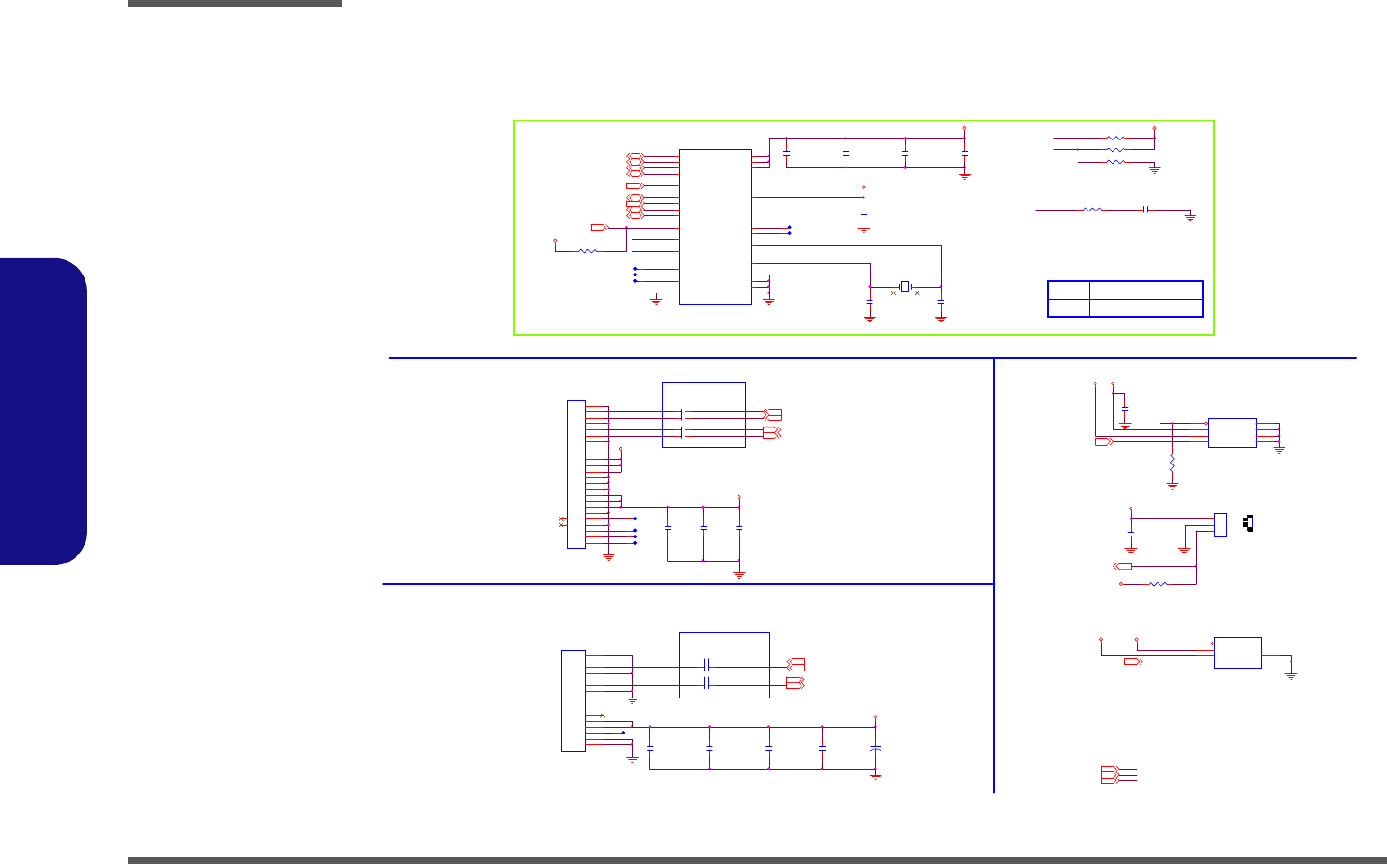
Schematic Diagrams
B - 16 TPM, SATA HDD, ODD, FAN
B.Schematic Diagrams
TPM, SATA HDD, ODD, FAN
+
C335
*100u_6.3V_B_A
C359
1u_10V_Y5V_06
SATATXN1 10
SATATXP1 10
W240CU
PN: 6-20-43770-122
AT22J36BA0057
W250CU
PN: 6-20-43750-022
B-5F2610-AAR5RA1AA
C195
*22p_50V_NPO_04
C188
*22p_50V_NPO_04
C206
*0.1u_16V_Y5V_04
R162 * 10K_04
SATARXN0 10
C211
*0.1u_16V_Y5V_04
N2800¤W¥ó(CPU GROUP)
6-77-W24ACU-CPU-6.5W
6-77-W255CU-CPU-6.5W
6-77-W253CUQ-CPU-6.5W
SATARXP0 10
R155 * 10K_04
C231
*10p_50V_NPO_04
R161
*33_04
C230
*0.1u_16V_Y5V_04
5VS
C229
*0.1u_16V_Y5V_04
R140 *10K_04
R158 * 10K_04
3
PN: 6-20-51130-103
85205-03701
PN: 6-20-51150-103
1
TPM
U7
*SLB9635TT
LAD3
17
LAD0
26
LAD1
23
LAD2
20
VDD1 10
XTA L I 13
VDD3 24
VDD2 19
LFRAME#
22
LCLK
21
LRESET#
16
SERIRQ
27
CLKRUN#
15
GND_1 4
GND_2 11
GND_3 18
GND_4 25
GPIO 6
GPIO2 2
XTAL O 14
TESTI
8
TESTBI/BAD D
9
PP
7
NC_1
1
NC_2
3
NC_3
12
LPCPD#
28
VSB 5
J_FAN1
C210
*1u_16V_X5R_06
PN:
6-21-C4700-013
C18553-11305-L
2nd Source
¹w¯dcost down solution
AX995B(SOT23-6) & APE8872
Co-Layout
PN:APE8874
5VS12,14,16, 21,23 3.3VS3,6,7,8,9,10,11,12,13,14,16,17,18,21,23
BUF _PLT_RST#11,17,18,19
SATATXN0 10
SATATXP0 10
VDD311,17,18,19,22,23,27
SATA HDD
LPC_AD211, 18 LPC_AD111, 18
LPC_AD311, 18
KBC_CLKRUN#11,18
LPC_AD011, 18
LPC_FRAME#11,18
U17
*AX995B
VOUT
1
GND 5
VIN
3FON#
4
VSET
6GND 2
FON#
6-02-03940-B20
6-02-00995-B20
6-02-99011-B20
5VS
CPU_FAN18
5VS_FAN
SATA ODD
J_FAN1
85205-03701
1
2
3
C341 0.01u_16V_X7R_04
C355
10u_6.3V_X5R_06
R278 4.7K_04
C340 0.01u_16V_X7R_04
C337 0.01u_16V_X7R_04
C336 0.01u_16V_X7R_04
FAN CONTROL
SATARXP1_R
R293
*0_04
SATARXN1_R
SATATXP1_R
SATATXN1_R
Z1505
FON#
C331
1u_6.3V_Y5V_04
C329
0.1u_16V_Y5V_04
C326
10u_10V_Y5V_08
C330
0.1u_16V_Y5V_04
U18
AX995SA
VOUT
3
GND 5
VIN
2FON
1
VSET
4GND 6
GND 7
GND 8
J_ODD1
C18553-11305-L
GND 1 S1
A+ S2
A- S3
GND 2 S4
B- S5
B+ S6
GND 3 S7
DP P1
V_50 P2
V_50_1 P3
MD P4
GND 4 P5
GND 5 P6
Z1501
Z1502
Z1503
Z1504
CPU_FANSEN18
LPC_SIRQ10,18
5VS
3.3VS
5VS_FAN
5VS
3.3VS
5VS_FAN
X2 *32.768KHz
14
3 2
PCLK_TPM8
Close to the ODD
Connector.
¹s¥ó¸m©ó°T¸¹¤À¤ä³B
TPM_PP
TPM_BADD
XTAL I
TPM1505
TPM1502
TPM_BADD
TPM_PP
TPM1504
TPM1501
XTAL O
TPM1503
SATARXP1 10
SATARXN1 10
PCLK_TPM PCLK_TPM1
Asserted before entering S3
LPC reset timing:
HI: 4E/ 4F H
LOW: 2E/ 2F H
TPM_PP
TPM _BA DD
HI: ACCESS
LOW: NORMAL ( Internal PD )
TPM 1.2
LPCPD# inactive to LRST# inactive 32~96us
3.3VS
VDD3
3.3VS 3.3VS
S4_STATE#11
(¤£¤W¥ó,D01,»â®Æ¥x¥_ÅçÃÒ)
CPU_FAN18
SATARXP0_R
SATARXN0_R
C368
10u_6.3V_X5R_06
C364
1u_10V_Y5V_06
C375 0.01u_16V_X7R_04
C380 0.01u_16V_X7R_04
J_HDD1
AT22J36BA0057
S1
S2
S3
S4
S5
S6
S7
P1
P2
P3
P4
P5
P6
P7
P8
P9
P10
P11
P12
P13
P14
P15
NC1
NC2
C367
0.1u_16V_Y5V_04
C379 0.01u_16V_X7R_04
C376 0.01u_16V_X7R_04
PIN GND1~2=GND
Close to the HDD
Connector.
SATATXN0_R
SATATXP0_R
Sheet 15 of 31
TPM, SATA HDD,
ODD, FAN
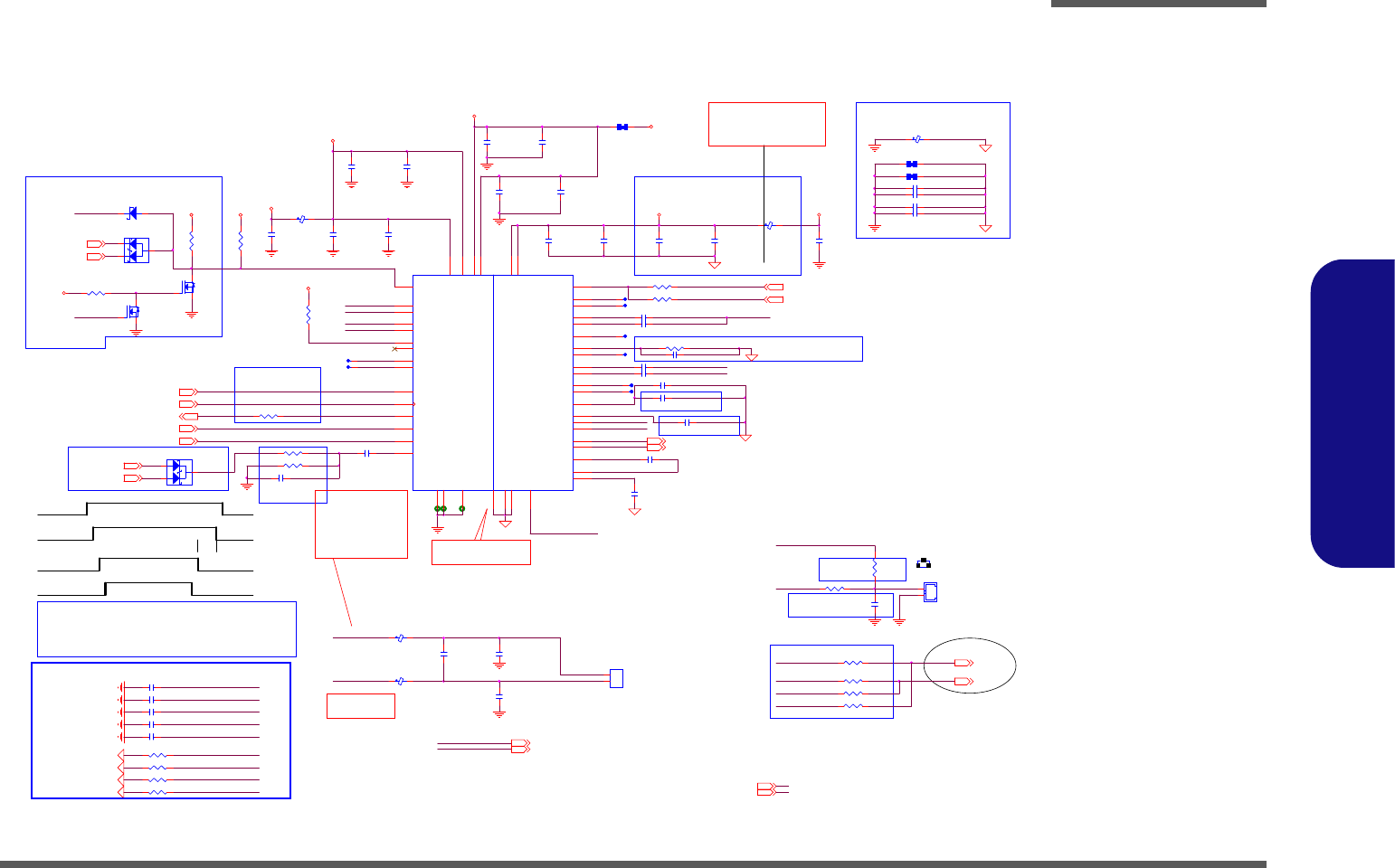
Schematic Diagrams
AUDIO CODEC VT1802P B - 17
B.Schematic Diagrams
AUDIO CODEC VT1802P
0323
0323
MI C 2- R
MI C 2- L
MI C 1- L _R
MI C 1- R _R
R324 *1M_04
R208 *1M_04
R325 *1M_04
SPKOUTR+
SPKOUTR-
R207 *1M_04
PVDD1_2
AUDG
AUDG
AUDG
AUDG
D24 *RB751S-40C2
AC
L37
*FCM1608K-121T06_short
L36
*FCM1608K-121T06_short
0323
VT1802P
AZ_SDIN 011
3.3VS3, 6, 7,8,9,10,11,12,13,14,15,17,18,21, 23
Very close to
Audio Codec
5VS12,14,15,21,23
HP_SENSE 20
MIC_S EN SE 20
ICH _SPKR11
AZ_RST#11
KBC_MUTE#18
KBC _BEEP18
AZ_SDOUT_R11
AZ_BITCLK_R11
AZ_SYNC_R11
AZ_RST#_R11
D02
J_INTMIC1
ALC269
4.7K_04
PN: 6-20-63120-102
2
ALC269
680P
1
J_INTMIC1
88266-02001
2
1
AZ_BITCLK_R
C386
10u_6.3V_X5R_06
AZ_SYNC_R
C382
*10u_6.3V_X5R_06 C381
*1u_6.3V_Y5V_04
R328 39.2K_1%_04
C390 10u_6.3V_X5R_06
R320
*10K_04
R200 33_04
L35
HCB1005KF-121T20
R327 20K_1%_04
R321 1K_04
C392 *100p_50V_NPO_04
Q18
*BSS138_NL
G
DS
C274 0.1u_16V_Y 5V_04
C389 10u_6.3V_X5R_06
AZ_SDOUT_R
C388
100p_50V_NPO_04
C391
10u_6.3V_X5R_06
R322 *100K_04
C266
*180p_50V_NPO_04
C277
0.1u_16V_Y 5V_04
C258
0.1u_16V_Y 5V_04
INT_MIC
MIC 2-VREFO
MIC2-L
Q17
*2N7002W
G
DS
MIC2-R
DMIC-CLK
DMIC-DAT
C253
0.1u_16V_Y 5V_04
R196 1K_04
PCBEEPBEEP_R
MIC1-VREFO-R
LDO_CAP
SPKOUTL-
C257
0.1u_16V_Y5V_04
MIC 2-VREFO
SPKOUTL+
C
A
A
D14
BAT54CWGH
1
23CBP-ALC269
CBN-AL269
OPVEE-ALC269
R323
3.3K_1%_04
LINE1-L
LINE1-R
R205 47K_04
MONO-OUT
SENSE-B
LINE2-R
SPKOUTL+_L
LINE2-L
SPKOUTR+
SPKOUTL+
C273
0.1u_16V_Y 5V_04
SPKOUTL-
SPKOUTR-
R199 1K_04
MIC1_L
MIC1_R
C270
*180p_50V_NPO_04
Layout note:
Close to codec
C254
0.1u_16V_Y 5V_04
INT_MIC
DIGITAL ANALOG
U10
VT1802P
DVDD1 1
GPIO0-DMIC-DAT
2
GPIO1-DMIC-CLK
3
PD#
4
SDATA-OUT
5
BIT-CLK
6
DVSS2
7
SDATA-IN
8
DVDD-IO 9
SY NC
10
RESET#
11
PCBEEP
12
Sense A 13
LINE2-L 14
LINE2-R 15
MIC 2-L 16
MI C 2-R 17
Sense-B 18
JDREF 19
MONO-OUT 20
MIC 1-L 21
MI C 1-R 22
LINE1-L 23
LINE1-R 24
AVSS1
26
VREF 27
LDO_CAP 28
MIC2-VREFO 29
MIC1-VREFO-R 30
MIC1-VREFO-L
31
HP-OUT-L 32
AVSS2
37
OPVEE 34
CBN 35
CBP 36
HP-OUT-R 33
PVD D1 39
SPK-L+
40
SPK-L-
41
PVSS1
42
PVSS2
43
SPK-R+
45 SPK-R-
44
PVDD2 46
SPDIFC2/EAPD
47
SPDIFO
48
AVDD2 38
AVDD1 25
GND
49
BEEP
MIC1-VREFO-L
NEAR CODEC
Speaker 8 ohm------> 20mils
Speaker 4 ohm------> 40mils
C256
10u_6.3V_X5R_06
EMI Require
L48
*HCB1005KF-121T20
ANALOG
C259
2.2u_6.3V_X5R_06
DIGITAL
R319
*15mil_short _06
C279 1u_6.3V_X5R_04
C278 100p_50V_NPO_04
AZ_RST#
5VS
Speaker wire length less than 8000mils , It don't need LC Filter.
Layout note:
GND and AUDG space is
60mils ~ 100mils
Thermal Pad place 9
Via hole.
PD#
20m s
R206 4.7K_04
C271 *10u_6.3V_X5R_06
SPKOUTR+,R-,L+,L- Trace width
3.3VS_AUD
5VS5VS_AUD 5VS_AUD
5VS
3.3VS_AUD
3.3VS
3.3VS_AUD
5VS_AU D
C387 10u_6.3V_X5R_06
EAPD_MODE
6-03-02695-030
C384
10u_6.3V_X5R_06
R326 5.1K_1%_04
VREF-ALC269
C267 10u_6.3V_X5R_06
SENSE_A
AZ_RST#-C-PD
C
A
A
D23
BAT54AWGH
1
23
R197 3.3K_1%_04
C252
0.1u_16V_Y5V_04
AZ_RST#
AZ_RST# For 3.3V
HDA Link De-pop
AZ_RST# For 1.5V
HDA Link De-pop
PD# Control
EAPD_MODE
C275 10u_6.3V_X5R_06
C268
*1u_16V_X5R_06
VT1802P ¤£¤W¥ó
VT1802P 5.1K_1%_04
JDREF
R198 3.3K_1%_04
VT1802P 10u
C383
*10u_6.3V_X5R_06
VT1802P NC PIN
C255 2.2u_6.3V_X5R_06
FOR VOLUMN
ADJUST
CODEC (ALC269 & VT1802P)
6-03-02696-030
AUDG
AUDG
0323
Very close to
Audio Codec
Layout Note:
PC BEEP
AUD G
AUDG
R192
100K_04
AUDG
AZ_SDIN0_R
Please Let LC Filter
together and close to
Codec.IF Speaker
wire length is less
than 8000mils It don't
need the LC Filter.
MIC1_R
MIC1_L
MIC 1-VREFO-L
MIC 1-VREFO-R
VT1802P 75_1%_04
ALC269 2.2K_1%_04
L49 HCB1005KF-121T20
JP2 *10mil_short
JP1 *10mil_short
C260 0.1u_16V_Y5V_04
C385 0.1u_16V_Y5V_04
EMI Require
AUDG
AUDG
C264 22p_50V_NPO_04
0325
0325
AZ_BITCLK_R
AZ_S Y NC _R
AZ_RST#_R
AZ_SDOUT_R
AZ_SDIN0
C265 22p_50V_NPO_04
C272 22p_50V_NPO_04
C276 22p_50V_NPO_04
AZ_RST#_R
MIC1-L_R
MIC1-R _R
C269 22p_50V_NPO_04
INTMIC-IN
HEAD PHONE-L 20
HEAD PHONE-R 20
MI C 1- L_ R 2 0
MIC1-R_R 20
SPKOUTR+ 20
SPKOUTR- 20
SPKOUTL-_L
J_SPKL1
85204-02001
1
2
0309
R195
10K_04
PD#
3.3VS_AUD
HP_SENSE
MIC_SENSE
C281 *0.1u_16V_Y5V_04
PN:6-03-01802-031
C280 *0.1u_16V_Y5V_04
Sheet 16 of 31
AUDIO CODEC
VT1802P
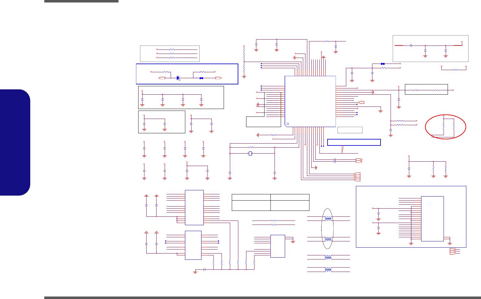
Schematic Diagrams
B - 18 CARD READER JMB261C
B.Schematic Diagrams
CARD READER JMB261C
C236
0.1u_16V_Y5V_04
SD_D1
SD_D2
REGLX
PME#
SD_CLK_R
SD_D3
SD_BS
SD_D0
C213
10u_6.3V_X5R_08
MDI O10
MDI O9
C248
10u_6.3V_X5R_06
MDIO7
SDXC_POWER
SD_CD #
SD_WP
MS_IN S#
L39
*GST5009 LF-G
TCT1
1
TD1+
2TD1-
3
TCT2
4
TD2+
5TD2-
6
TCT3
7
TD3+
8TD3-
9
TCT4
10
TD4+
11 TD4-
12 MX4- 13
MX4+ 14
MCT4 15
MX3- 16
MX3+ 17
MCT3 18
MX2- 19
MX2+ 20
MCT2 21
MX1- 22
MX1+ 23
MCT1 24
LANXOUT
LANXIN
R169
*4.7K_04
C194
22p_50V_NPO_04
Close to JMC251C
Pin#31
(>20mil)
Pin#31
R143 *1M_04
C235
0.1u_16V_Y5V_04
C370
0.1u_16V_Y5V_04
C218
0.1u_16V_Y 5V_04
C223
0.1u_16V_Y5V_04
REGLX
MS_ I N S#
CR_CD1N
R177 *4.7K_04
3.3V
DVDD
ISON_251C
C24
*0.1u_10V_X5R_04
PJS-08SL3B
J_RJ1
DD-
8DD+
7
DB-
6
DC-
5DC+
4
DB+
3DA-
2DA+
1shield GN D1
shield GN D2
(LQFP 64)
JMC261 C
U6
JMC261C
REXT
1
AVDD 33
2
XIN
3
XOUT
4
GND
10
LX 33
AVDD 12
7
CPPEN 23
CLKN
5
CLKP
6
AVDD12
13
RXP
8
GND 22
TXN
11
TXP
12
PWRCR 30
RSTN 24
WAKEN 27
MPD 28
ISON 45
LAN_LED2 26
CR_CD1N
16
CR_CD0N 17
RXN
9
MDIO8
51
LAN_LED0 47
MDIO7
15
MDI O6 20
GND 44
MDIO5 41
MDIO4 40
MDIO3 39
VDDIO 43
MDIO2 38
MDIO1 37
MDIO0 36
MDIO9
50 MDIO10
49
MDIO11 48
MDI O12 19
VDDREG 32
MDIO13
14
MDI O14 18
CR_LED 25
TEST 29
VDDIO 21
GND 34
VCC3V 31
FB12 35
LAN_LED1 46
VDDO 42
VDD
52
VIP_1
53
VIN_1
54
AVDD12
55
VIP_2
56
VIN_2
57
GND
58
AVDD33
59
VIP_3
60
VIN_3
61
AVDD12
62
VIP_4
63
VIN_4
64
Near Cardreader CONN
For Safety LPS.
Card Reader Power
30 mil
LP4
*WCM2012F2S-161T03
1
4
2
3
C212
0.1u_16V_Y5V_04
R171 10K_04
Pin#32
R18
75_1%_04
VDDREG
C249
*10u_6.3V_X5R_08
R21
75_1%_04
C187
*0.1u_16V_Y 5V_04
C200
0.1u_16V_Y5V_04
VCC_CARD
C209 0.1u_10V_X7R_04
Close to PIN41
Card Reader Pull High/Low Resistors
3.3V_LAN
R176
*4.7K_04
SD_C LK
X1 FSX-8L_25MHz
1 2
MDI O11
R181
150_06
REXT
R230 0_04
C294
1000p_2KV_X7R_12
R20
75_1%_04
C203 0.1u_10V_X7R_04
SD_D2
L66
*WCM2012F2S-161T03-short
1
4
2
3
C197
*10u_6.3V_X5R_06
SD_D0
SD_D3
SD_D0
SD_BS
SD_D1
C243
10u_6.3V_X5R_06
SD_D1
SD_D3
SD_D2
C227
10u_6.3V_X5R_08
C22
*0.1u_10V_X5R_04
SD_CLK
SD_WP
SD_BS
C191
2.2u_6.3V_X5R_06
MS_IN S#
SD_CLK
SD_CD #
C168
0.1u_16V_Y5V_04
3 IN 1 SOCKET SD/MMC/MS
PWRCR
C369
*10p_50V_NPO_04
R16
*75_1%_04
C228
0.1u_16V_Y 5V_04
R159 1K_04
C292
0.01u_50V_X7R_04
R148 0_04
C176
*0.1u_16V_Y5V_04
Pin#33
(>20mil)
Pin#33
For JMC251/261 only
R134 12K_1%_04
(>20mil)
Reserve 7/13
Switching Regulator close to PIN33
LP3
*WCM2012F2S-161T03
1
4
2
3
C185
22p_50V_NPO_04
C238
10u_6.3V_X5R_08
R168 1K_04
.
L31
*SWF2520CF-4R7M-M
VDD3
L40
NS681680
RD+
1
RD-
2RX+ 16
RX- 15
RD_CT
3RX_CT 14
NC
4NC 12
NC
5
TD_CT
6
TD+
7
NC 13
TX- 9
TD-
8
TX_CT 11
TX+ 10
R135
*100K_1%_04
C245
0.1u_16V_Y5V_04
R231 0_04
C167
0.1u_16V_Y 5V_04
R167 *4.7K_04
R175 0.2_06
C179
0.1u_16V_Y5V_04
C234
0.1u_16V_Y5V_04
C291
*0.01u_50V_X7R_04
C192
*0.1u_16V_Y5V_04 C169
0.1u_16V_Y 5V_04
J_CARD-REV1
MDR019-A0-1072
DAT2_SD
P2
VSS_MS
P21
CD/D AT3_SD
P3
CMD_SD
P4
VSS_SD
P5
VDD_SD
P6
CLK_SD
P7
VSS_SD
P8
DAT0_SD
P9
DAT1_SD
P10
WP_SD
P11
VSS_MS
P12
VCC_MS
P13
SCLK_MS
P14
DAT3_MS
P15
INS_MS
P16
DAT2_MS
P17
SDIO/DAT0_MS
P18
DAT1_MS
P19
BS_MS
P20
CD_SD
P1
GND P23
GND P22
PCIE_RXN5_CARD 9
PCIE_RXP5_CARD 9
(>10mil)
PME# 9,18PCIE_WAKE#11,19
D13 RB751S-40C2
A C R174 *10mil_short
3.3V
3.3V_LAN
3.3V_LAN
CLK_PCIE_JMC261# 8
CLK_PCIE_JMC261 8
PCI E_TXP5_CARD 9
3.3VS3,6,7,8,9,10,11,12, 13, 14,15,16,18,21,23
BUF_PLT_RST# 11,15,18,19
PCIE_TXN5_CARD 9
3.3V2,9,11,12,13,18,19, 21,23,24,26
VCC_CARD
R163 *15mil_short_06
R166 *0_06
R170 10K_04 R185 *0_06
CardReader Signal
Zo = 50 Ohm ¡Ó15%
Zo = 100 Ohm ¡Ó10%
Signal / Spacing: 4 /8.5 mils
Length < 12"
CardReader Signal
Zo = 50 Ohm ¡Ó15%
L65
*WCM2012F2S-161T03-short
1
4
2
3
3.3V_LAN
DVDD
DVDD
3.3VS
DVDD 3.3V_LAN
3.3VS
3.3V_LAN 3.3V_LAN
3.3V_LAN
DVDD
3.3V_LAN
3.3V
VDD3
3.3VS
VDD3
DVDD
PWRCR
VCC_CARD
3.3VS
3.3V_LAN
DVDDDVDDDVDD
3.3V_LAN
DVDD
DVDD
DVDD
DVDDDVDD
VDD311,15,18,19,22,23,27
PN: 6-21-G4030-123
M DR019 -A 0-107 2
PN: 6-21-G4040-123
M DR019 -A 0-107 2
R180 10K_04
Pin#2 Pin#21Pin#59 Pin#59
LAN_SCL
Place all capacitors closed to chip.
LAN_SDA
Pin#2Pin#2
(>20mil)
Pin#43 Pin#43
For JMC251C
VCC_CARD
VCC_CARD
D02
LAN_LED0
LAN_LED1
MLMX2-
MLMX2+
MLMX0-
MLMX3-
MLMX1+_ R
MLMX0+
MLMX1+
MC T_ 1
LAN_MDIP1
CT MC T_ 0 MLM X3+
MLMX1-
Z1703
Z1702
LAN_MDIN1
LAN_MDIP0 MLMX0-_R
MLMX1-_R
MLMX1+_R
MLMX0+_ R
Z1701
MLMX1- _R
Z1704
LAN_MDIN0
MLMX0+MLMX0+_R
MLMX0- _R
MLMX1+
MLMX0-
MLMX3-_R
MLMX2+_ R
MLMX3+_ R
MLMX2-_R
LAN_MDIP2
LAN_MDIN1
LAN_MDIN3
LAN_MDIN2
LAN_MDIP3
LAN_MDIN0
LAN_MDIP0
LAN_MDIP1
W240CU
PN: 6-21-B4000-008
PJS-08SL3B
W250CU
PN: 6-21-B4040-008
PJS-08SO1B
MLMX3+
MLMX2+MLMX2+_R
MLMX2- _R
MLMX3- _R MLMX3-
MLMX2-
MLMX3+_R
CT
FOR JMB251 GIGA LAN PARTS
L58,LP1,LP2,LP3,LP4
R400, R401,R402,R403,R404,R405
C617, C611
FOR JMB261 10M/100M LAN PARTS
MCT_R
MLMX1-
MC T_ 2 ML MX2+
MC T_ 3
MC T_ 1 MLMX2-
MLMX0+_ R
MLMX3+ MLMX3-
MLMX0-_R
MC T_ 0
L59,LP1,LP2
R395,R396,R400,R401,R404,R405
C617,C616
MLMX1+_ R
EMI
MLMX1-_R
4/15
NOTICE:
near Pin#41
6-22-25R00-1B4
6-22-25R00-1B5
(>20mil)
Pin#32
JMC261C
Close to JMC251C
PCIe Differential
Pairs = 100 Ohm
R184
150_06
Close to JMC251C
(>20mil)
C240
*10u_6.3V_X5R_08
Pin#62
JMC251C Pin14 & Pin16 Swap solution for
MS card detection.
Pin#52
Pin#55
meet falling time
<1ms
GIGA LAN (JMC251C)
R17
75_1%_04
Pin#30
Reserved
Pin#7Pin#7
R173 0.2_06
Pin#13
LAN_MDIP0
LAN_MDIP1
LAN_MDIN1
R15
*75_1%_04
LAN_MDIN0
LAN_MDIN2
LAN_MDIP2
LAN_MDIP3
C166
0.1u_16V_Y5V_04
MDI O8
SD_CD#
MPD
CPPEN
MD I O1 4
MD I O1 2
SD_WP
LAN_MDIN3
R139
0_04
LAN_SDA
LAN_SCL
Sheet 17 of 31
CARD READER
JMB261C
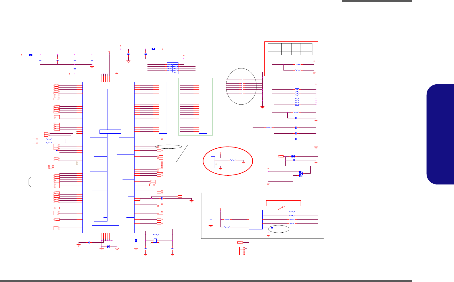
Schematic Diagrams
KBC-ITE IT8518E, SPI B - 19
B.Schematic Diagrams
KBC-ITE IT8518E, SPI
U9
MX25L1606EM2I-12G
CE# 1
SO 2
WP#
3
VSS 4
SI 5
SCK 6
HOLD#
7
VDD
8
C216
*0.1u_16V_Y5V_04
RN6
2.2K_8P4R_04
1
2
3
45
6
7
8
C413 *100p_50V_NPO_04
R178 1K_04
R130 *100K_04
C172 *0. 1u_16V_Y5V_04
C239
0.1u_16V_Y 5V_04
C157
0.1u_16V_Y5V_04
R187
*10mil_short
C215 0.1u_16V_Y5V_04
R182 15_1%_04
C246
*15p_50V_NPO_04
C171
0.1u_16V_Y 5V_04 RP1
*10P8RX10K
10
9
8
7
6
1
2
3
4
5
C199
*0. 1u_16V_Y5V_04
R190 15_1%_04
C401 *100p_50V_NPO_04
R179 4. 7K_04
X4 *MC-306_32.768KHz
1 4
32
C186 0.1u_16V_Y5V_04
KBC_AGND
KBC_AGND
Keyboard ©³¤U»Ý-n¯d¬ù5X5mm ¤j¤pÅS»ÉGround
Pad.(©PÃäºÉ¶q¤£-n¦³¹s¥ó)¦]¥¼¨Ó·|¶Kgasket.
»Ý-n¾÷ºc°t¦X¶}¤Õ¤~¦æ.
C402 *100p_50V_NPO_04
KBC_SPI_SO
3.3V
SMC_BAT
KBC_SPI_SI
KBC_SPI_CE#
¦PW210CU 15 ohm 7/5
pin68 to
1.8v
pin93 active
higt
C414 *100p_50V_NPO_04
80CLKR165 *20K_04
VDD3
J_80DBG1
*88266-05001
1
2
3
4
5
3IN1
6-20-63100-105
KBC_SPI_HOLD# C419
22p_50V_NPO_04
LED_PWR21
KBC_RSMRST# 11
KBC_SPI_SCLK_R
R138 100K_04
LED_BAT_FULL21
80CLK19
LED_ACIN21
KBC_PWRBTN#11
KBC_SCI#11 KBC_SMI#11
KBC_GA20#10
KBC_SPI_SO_R
WLAN_EN19,21
LED_BAT_CHG21
KBC_BEEP16
3G_EN19
3IN119
KBC_MUTE#16
LED_NUM#21
LCD_BRIGHTNESS13
CPU_FAN15
LED_CAP#21
LED_SCROLL#21
SUSB# 11,23
PME# 9,17
THERM_ALERT#11
WLAN_DET#19
BT_DET#19
ALL_SYS_PWRGD 8,11
AP_KEY # 21
TOTAL _CU R27 TH ER M_VOLT2
CPU_FANSEN 15
3G_DET#19
SMC_BAT
C408 *100p_50V_NPO_04
C403 *100p_50V_NPO_04
PN: 6-20-94AF0-124
LCD_BRIGHTNESS
SMC_CPU_VCORESET
J_KB1
*85208-24051
24
23
22
14
12
11
21
8
20
19
6
5
18
4
17
10
9
7
3
2
1
16
15
13
KB-SO5
KB-SI7
KB-SO14
KB-SO12
KB-SO1
KB-SO2
KB-SI5
KB-SI3
KB-SO4
KB-SO15
KB-SO8
KB-SO9
KB-SO7
KB-SI4
KB-SO13
KB-SI6
KB-SI0
KB-SO3
KB-SO10
KB-SO6
KB-SI1
KB-SI2
KB-SO0
KB-SO11
KB-SO10
KB-SO15
KB-SO14
W240CU
KB-SO8
KB-SO0
KB-SO1
KB-SO4
W250CU
KB-SO6
KB-SI6
KB-SI3
KB-SI0
KB-SO7
KB-SI7
KB-SI1
KB-SO11
KB-SI2
KB-SI5
KB-SO12
KB-SO5
KB-SI4
KB-SO3
KB-SO13
KB-SO2
KB-SO9
VDD311,15,17,19,22,23,27
3.3VS3,6,7,8,9,10,11,12,13, 14,15,16,17, 21,23
SUSC# 11,25
BUF_PLT_RST#11,15,17,19
AC_IN#27
BAT_DET27
PWR_SW#23
KBC_PCLK8
3.3V2,9,11,12,13,17,19,21,23,24,26
5VS12,14,15,16,21,23
BAT_VOLT27
1.05VS_PWRGD24
3.3VS_PRIME5,12,23
3.3VS_PRIME5,12,23
1.8VS2,5,23
C415 *100p_50V_NPO_04
WEB_EMAIL#21
C409 *100p_50V_NPO_04
D02A
¾aªñJ_KB2
NB_ENAVDD 3,13
1.8VS_PWRGD11
C404 *100p_50V_NPO_04
3.3VS_PRIME_R
KBC_PCLK
BT_DET#
IT8518
AP_KEY #
SPI EEROM
WEB_WWW# 21
SMD_BAT
C416 *100p_50V_NPO_04
KBC_WR ESET#
KBC_SPI_CE#
KBC_PCLK_R
C410 *100p_50V_NPO_04
AC_IN#
BAT_VOLT
C405 *100p_50V_NPO_04
KBC_PCLK
KBC_SPI_WP#
BRIGH TNESS
Z1801
3G_DET#
BAT_DET
KBC_SPI_SI
D02
AC_I N#
W24ACU
W255CU
LPC_AD0
BT_EN 19,21
BKL_EN 13
KBC_RST# 10
KBC_SWI# 11
CCD_EN 21
DELAY_ALL_SYS_PWRGD 4,11
CHG_RST 27
DD_ON 20,23
3G_PWR_EN 19
VCORE_ON 26
KBC_CLKRUN# 11,15
BAT_VOLT
CCD_DET#
KBC_SPI_SO
3G_DET#
BRIGHTNESS
BAT_DET
LPC_AD1
HSPI_MSO 11
KBC_CK32KE
KBC_CK32K
LPC_AD2
KBC_SPI_SCLK
LPC_AD3 C411 *100p_50V_NPO_04
C406 *100p_50V_NPO_04
3IN1
LPC_FRAME#11,15 LPC_SIRQ10,15
3.3VS
KBC_AVDD
VDD3
LPC_AD111,15 LPC_AD211,15 LPC_AD311,15
VDD3
VDD 3
VDD3_EC VDD3
VDD3
SMD_BAT27 SMC_BAT27
LPC_AD011,15
VDD3
SMD_CPU_VCORESET26 SMC_CPU_VCORESET26
TP_CLK21 TP_DATA21
3/8
µL«OÅ@
6-03-08518-0P2
HSPI_CE# 11
HSPI_MSI 11
USB_CHARGE_EN 22,23
SMD_CPU_VCORESET
MODEL_ID
BT_DET#
Change BOARD ID 8/1
C412 *100p_50V_NPO_04
C407 *100p_50V_NPO_04
SMC_CPU_VCORESET
KB-SO14
KB-SO12
KB-SO1
KB-SO2
KB-SO5
KB-SO4
KB-SO15
KB-SO8
KB-SO9
KB-SO7
KB-SO10
KB-SO6
KB-SO0
KB-SO13
KB-SO3
KB-SO11
SMD_CPU_VCORESET
SMD_BAT
D11
*BAV99
A
CAC
KB-SI4
RN3
10K_8P4R_04
1
2
3
45
6
7
8
KB-SI5
KB-SI6
R186 15_1%_04
KB-SI7
KB-SI0
KB-SI1
C250
*15p_50V_NPO_04
KB-SI2
KB-SI3
R189 15_1%_04
16Mbit
C237
10u_10V_Y5V_08 R145 10K_04
PN: 6-20-94AF0-124
R164 *10_04
R154 *10mil_short
KBC_SPI_*_R = 0.1"~0.5"
J_KB2
85208-24051
24
23
22
14
12
11
21
8
20
19
6
5
18
4
17
10
9
7
3
2
1
16
15
13
HSPI_SCLK 11
L34
*HCB1005KF-121T20_10mil_short
KBC_SPI_CE#_R
KBC_SPI_SI_R
C217
0.1u_16V_Y5V_04
R144 10K_04
80CLK
C242 *0.1u_16V_Y5V_04
KBC_WRESET#
C224 *10p_50V_NPO_04
L30
*HCB1005KF-121T20_10mil_short
C241
0.1u_16V_Y 5V_04
Change Debug CON as W110EN 7/4
MODEL_ID
LOW ACTIVE
K/B MATRIX
FLASH
LPC
SMBUS
PS/2
PWM
UART
DAC
CLOCK
IT8518
CIR
ADC
WAKE UP
PWM/COUNTER
LPC/WAKE UP
EXT GPIO
GP INTERRUPT
WAKE UP
GPIO
U8
IT8518E VER:C
WRST#
14
LPCCLK
13
LAD0
10
LAD1
9
LAD2
8
LAD3
7
LFRAME#
6
( PD )LPCPD#/WUI6/GPE6 17
SERIRQ
5
ECSMI#/GPD4( PU )
15 ECSCI#/GPD3( PU )
23
GA20/GPB5
126
KBRST#/GPB6( PU )
4
KSI0/STB# 58
KSI1/AFD# 59
KSI2/INIT# 60
KSI3/SLIN# 61
KSI4 62
KSI5 63
KSI6 64
KSI7 65
KSO0/PD0 36
KSO1/PD1 37
KSO2/PD2 38
KSO3/PD3 39
KSO4/PD4 40
KSO5/PD5 41
KSO6/PD6 42
KSO7/PD7 43
KSO8/ACK# 44
KSO9/BUSY 45
KSO10/PE 46
KSO11/ERR# 51
KSO12/SLCT 52
KSO13 53
KSO14 54
KSO15 55
VCC 11
VSTBY 26
VSTBY 50
VSTBY 92
VSTBY 114
VSTBY 127
VSTBY 121
VBAT 3
AVCC 74
PS2CLK0/GPF0( PU )
85
PS2DAT0/GPF1( PU )
86
PS2CLK1/GPF2( PU )
87
( PD )TMRI0/WUI2/GPC4 120
( PD )TMRI1/WUI3/GPC6 124
LPCRST#/WUI4/GPD2( PU )
22
( PD )WUI5/GPE5 35
PWRSW/GPE4( PU )
125
RI1#/WUI0/GPD0( PU )
18
RI2#/WUI1/GPD1( PU )
21
( PD )RING#/PWRFAIL#/LPCRST#/GPB7 112
TXD/ GPB1( PU )
109 RXD/GPB0( PU )
108
( PD )CTX/GPB2 123
PS2DAT1/GPF3( PU )
88
PS2CLK2/GPF4( PU )
89
PS2DAT2/GPF5( PU )
90
( PD )TACH0/GPD6 47
( PD )TACH1/GPD7 48
PWM0/GPA0( PU )
24
PWM1/GPA1( PU )
25
PWM2/GPA2( PU )
28
PWM3/GPA3( PU )
29
PWM4/GPA4( PU )
30
PWM5/GPA5( PU )
31
PWM6/GPA6( PU )
32
PWM7/GPA7( PU )
34
ADC0/GPI0
66
ADC1/GPI1
67
ADC2/GPI2
68
ADC3/GPI3
69
ADC4/GPI4
70
ADC5/GPI5
71
ADC6/GPI6
72
ADC7/GPI7
73
VSS
1
VSS
12
VSS
27
VSS
49
VSS
122 VSS
113
AVSS
75
CK32KE 2
CK32K 128
DAC3/GPJ3
79 DAC2/GPJ2
78 GPJ1
77 GPJ0
76
( PD )EGCS#/GPE2 83
( PD )EGCLK/GPE3 84
( PD )EGAD/GPE1 82
GINT/GPD5( PU )
33
L80LLAT/GPE7( PU )
20
VSS
91
DAC5/GPJ5
81 DAC4/GPJ4
80
PWUREQ#/GPC7( PU )
16
( PD )CRX/GPC0 119
( PD )KSO16/GPC3 56
( PD )KSO17/GPC5 57
( PD )GPH0/ID0 93
( PD )GPH1/ID1 94
( PD )GPH2/ID2 95
( PD )GPH3/ID3 96
( PD )GPH4/ID4 97
( PD )GPH5/ID5 98
( PD )GPH6/ID6 99
( PD )GPG1/ID7 107
SMCLK0/ GPB3
110
SMDAT0/GPB4
111
SMCLK1/ GPC 1
115
SMDAT1/GPC2
116
SMCLK2/ GPF 6( PU )
117
SMDAT2/GPF7( PU )
118
FLFRAME#/GPG2 100
FLAD0/SCE# 101
FLAD 1/ SI 102
FLAD2/SO 103
FLAD3/GPG6 104
FLCLK/SCK 105
( PD )FLRST#/WUI7/GPG0/TM 106
( PD )L80HLAT/GPE0 19
0323
KBC_SPI_SCLK
D02
10K
10K
RA
RBRA
X
X
RB
MODEL_ID
NC1 NC_04
C233
0.1u_16V_Y5V_04
R183 *10M_04
R160 100K_04
C201
0.1u_16V_Y5V_04
LID_SW#13,21
C208 *0.1u_16V_Y5V_04
Sheet 18 of 31
KBC-ITE IT8518E,
SPI
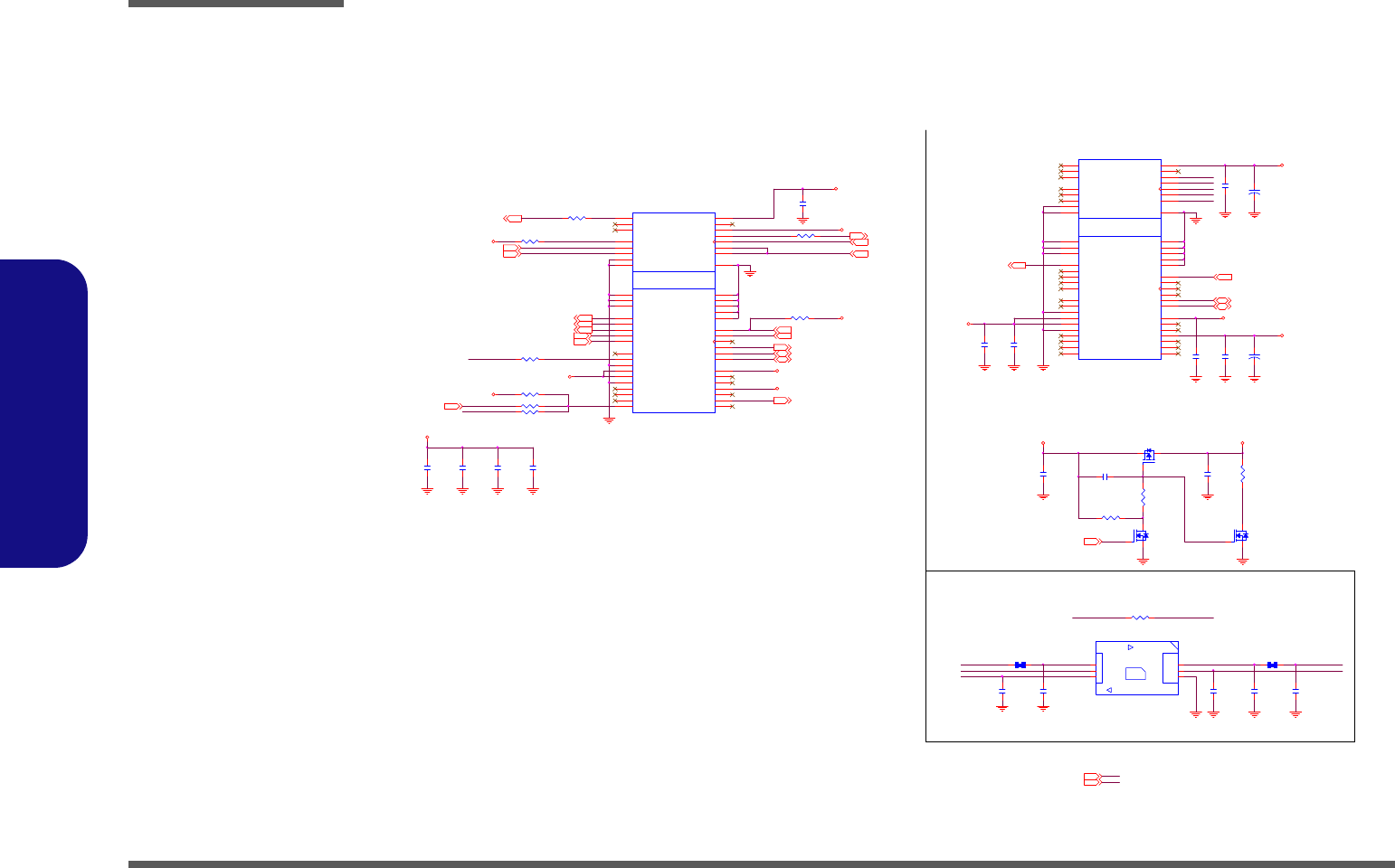
Schematic Diagrams
B - 20 3G, WLAN, BT
B.Schematic Diagrams
3G, WLAN, BT
BT_SBD#
(TOP VIEW)
LOCK
OPEN
J_SIM1
C1770661-1
UIM_DATA C7
UIM_VPP C6
UIM_GND C5
UIM_PWR
C1 UIM_RST
C2 UIM_CLK
C3
80CLK 18
UIM_VPP
UIM_DATA
UIM_PWR
UIM_RST
UIM_CLK
3G CARD
MINI-PCIE CARD AND Debug Port
UIM_VPP
PCIE_R XN1_WLAN9WLAN_DET#18
PCIE_WAKE#11,17
BT_DET# 18
WLAN_LED# 21
3G_DET#18
PCIE_RXP1_WLAN9BUF_PLT_RST# 11,15,17, 18
WLAN_EN 18,21
PCIE_TXN1_WLAN9PCIE_TXP1_WLAN9
CLK_PCIE_WLAN8CLK_PCIE_WLAN#8
NM10_GPIO11_R
PN: 6-21-84DH 0-226
MPCEC-S00F1-TP00
PN: 6-21-84D90-226
PN: 6-21-84D70-226
PN :6-21-84DF0-226
PN: 6-21-84DG0-226
3G_EN 18
3G_PWR_EN18
3.3V2,9,11,12,13,17,18,21,23,24,26
BT_EN18,21
VDD311,15,17,18,22,23,27
Pin#24Pin#2 Pin#52Pin#39,41
C361
*22p_50V_NPO_04
Q6
MTP3415KN3
G
DS
C196
0.1u_16V_Y5V_04
C244
1u_10V_Y5V_06
C247
*0.1u_16V_Y5V_04
C378
*22p_50V_NPO_04
R314 *10K_04
R172
10_06
R317 *4.7K_04
C251
1u_6.3V_X5R_04
R146 *0_04
VDD3
KEY
J_3G1
MPCEC-S00F1-TP00
COEX1
3
COEX2
5
CLKREQ#
7
GND0
9
REFCLK-
11
REFCLK+
13
WAKE#
1
GND1
15
PETn0
23
PETp0
25
GND2
21
GND3
27
PERn0
31
PERp0
33
GND4
29
Reserved0
17
Reserved1
19
W_DISABLE# 20
GND12
37
3.3VAUX_3
39
3.3VAUX_4
41
GND13
43
Reserved2
45
Reserved3
47
Reserved4
49
Reserved5
51 LED_WLAN# 44
LED_WWAN# 42
GND6 18
UIM_VPP 16
UIM_RESET 14
3.3VAUX_0 2
UIM_CLK 12
UIM_DATA 10
UIM_PWR 8
1.5V_0 6
GND5 4
PERSET# 22
3.3VAUX_1 24
GND7 26
1.5V_1 28
SMB_CLK 30
SMB_DATA 32
GND8 34
USB_D- 36
USB_D+ 38
GND9 40
LED_WPAN# 46
1.5V_2 48
GND10 50
3.3VAUX_2 52
GND11
35
R318 *10mil_short
C158
*0.1u_16V_Y5V_04
R188
20K_1%_04
+
C177
220U_4V_D2_D
C204
0.1u_16V_Y5V_04
R191 100K_04
KEY
J_MINI1
MPCEC-S00F1-TP00
COEX1
3
COEX2
5
CLKREQ#
7
GND0
9
REFCLK-
11
REFCLK+
13
WAKE#
1
GND1
15
PETn0
23
PETp0
25
GND2
21
GND3
27
PERn0
31
PERp0
33
GND4
29
Reserved0
17
Reserved1
19
W_DISABLE# 20
GND12
37
3.3VAUX_3
39
3.3VAUX_4
41
GND13
43
Reserved2
45
Reserved3
47
Reserved4
49
Reserved5
51 LED_WLAN# 44
LED_WWAN# 42
GND6 18
UIM_VPP 16
UIM_RESET 14
3.3VAUX_0 2
UIM_CLK 12
UIM_DATA 10
UIM_PWR 8
1.5V_0 6
GND5 4
PERSET# 22
3.3VAUX_1 24
GND7 26
1.5V_1 28
SMB_CLK 30
SMB_DATA 32
GND8 34
USB_D- 36
USB_D+ 38
GND9 40
LED_WPAN# 46
1.5V_2 48
GND10 50
3.3VAUX_2 52
GND11
35
C360
*22p_50V_NPO_04
C226
0.1u_16V_Y5V_04
C220
*4.7u_6.3V_X5R_06
R122 10K_04 R126 *0_04
C362
*22p_50V_NPO_04
C184
10u_10V_Y5V_08
S
D
G
Q7A
MTDN7002ZHS6R
2
61
C156
0.1u_16V_Y5V_04
C373
0.1u_16V_Y 5V_04
S
D
G
Q7B
MTDN7002ZHS6R
5
34
C377
*0. 1u_16V_Y5V_04
R316 0_04
C232
*0.1u_16V_Y5V_04
R147 *10K_04
R315 *0_04
+
C163
220U_4V_D2_D
R295 *10mil_short
C374
*0.1u_16V_Y5V_04
3A
WLAN_CLKREQ#
3A
3G POWER
BT_EN
NM10_GPIO11
60mils
60mils
PN: 6-21-84DH0-226
MPCEC-S00F1-TP00
PN: 6-21-84D90-226
PN: 6-21-84D70-226
PN :6-21-84DF0-226
PN: 6-21-84DG0-226
60mils
R118 *0_04
SIM CONN
PN: 6-86-2B006-001
C1770661-1
LAYOUT NOTE:
1. SIM¤§©Ò¦³«H¸¹½u¥[²Ê(10mil)
2. ©Ò¦³«H¸¹½u¤§¶¡¥[GND
3. SIM
HOLD¥»Åé¥|©P¥[GND³ò¶
3.3V
3.3V 3.3V
3.3V
3.3V
3.3V_3G
3.3V_3G
3.3V_3G 3.3V_3G
3.3V
3.3V
3.3V
3.3V_3G
3.3V
USB_PN5 9
USB_PP5 9
UIM_C_R
UIM_PWR
BT_EN_R
3G02
3G01
UIM_D_R
NM10_GPIO11 11
UIM_CLK
UIM_RST
UIM_PWR UIM_DATA
BT_EN
USB_PN4 9
USB_PP4 9
3G03
3IN1 18
UIM_DATA
Sheet 19 of 31
3G, WLAN, BT
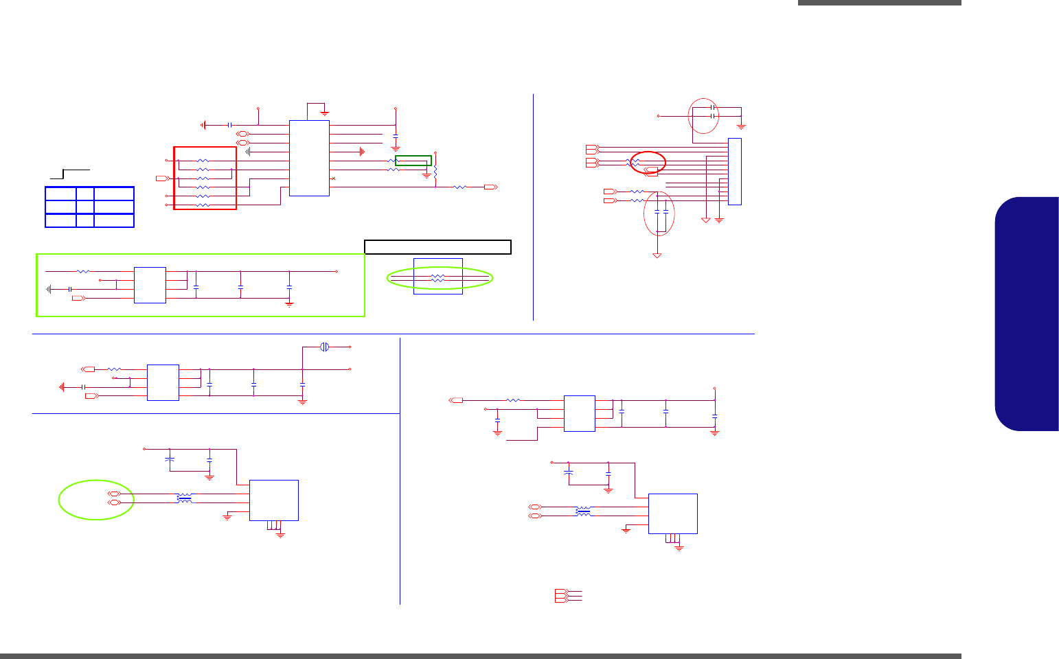
Schematic Diagrams
USB PORT & USB CHARGER B - 21
B.Schematic Diagrams
USB PORT & USB CHARGER
R194 75_04
R193 75_04
HEADPHONE-R16 H EADPHONE-L16
W/O USB Charge¤W¥óU4,R281,R282
VDD5 USBVCC_A
USB_PN09
VDD 5
USBVCC_0
5V
USBVCC_1
R115 *0_04
L68
*WCM2012F2S-161T03-short
1
4
2
3
G_OC#1
PJ5
OPEN-2m m
1 2
USB_OC#19
USBVCC_1
D02A
Reserve Power IC for Port 0&1
R89 *0_04
USB_OC#09
100mils
J_AUDIO1
87213-1400G
1
2
3
4
5
6
7
8
10
11
12
13
14
9
C422 0.01u_16V_X7R_04
USBVCC_A
100mils
USB_PP2_R
USB_PN2_R
AUDG
C418 3300p_50V_NPO_04
R333 0_04
Audio B'd CONN
USB_PN2_R
C417 3300p_50V_NPO_04
R334 0_04
R281 0_04
USB_PN2
USB_PP2 USB_PP2_R
R282 0_04
¹s¥ó¸m©ó°T¸¹¤À¤ä³B
100mils
SPKOUTR+16
TI2540_CTL2
TI2540_CTL3 SPKOUTR-16
Change R193/R194 to
improve HP full-scale
USB_PP09
USB_PN_0
Port 1
100 mil
USB_PP2_R
TI2540_ILIM1
TI2540_ILIM0
USB_PN2_R
USB PORT_0&1
USB Charge PORT
AUDG
3.3V2,9,11,12,13,17,18,19,21,23,24,26 5V12,23,24,25,26 VDD522,23
80mils
2.4A->2A
To South Bridge OC Pin.
M_PQFP16
80mils
1.5A 80mils
USBVCC_1
DD_ON#
C144
10u_10V_Y5V_08
C139
0.1u_16V_Y5V_04
R116 *0_04
USB_OC#2 G_OC#2
C160
0.1u_16V_Y5V_04
C143
10u_10V_Y5V_08
100mils
U2
SY6288DFAC
VOUT1 6
VOUT3 8
VIN2
3
VIN1
2VOUT2 7
GND 1
EN#
4
FLG#
5
C159
0.1u_16V_Y 5V_04
C170
10u_10V_Y5V_08
5V
USBVCC_A
C140
0.1u_16V_Y5V_04
C147 0.1u_16V_Y 5V_04
DD_ON#
U4
SY6288DFAC
VOUT1 6
VOUT3 8
VIN2
3
VIN1
2VOUT2 7
GND 1
EN#
4
FLG#
5
C82
*0.1u_16V_Y5V_04
C126
*0.1u_16V_Y5V_04
DD_ON#23
-ì±µ¨ìTPS2540,Port0¤£charge§ï¦^±µPCH
C148
*0.1u_16V_Y5V_04
R102 *33K_1%_04
C145
*10u_10V_Y5V_08
R101 *10K_04
R106 *10K_04
USB_PP_0
R104 *10K_04
USB PORT_2
R110 *10K_04
R105 *10K_04 R113
*10K_04
U3
*TPS2540
CTL1
6
NC 9
DM_IN 11
DM_O
2
DP_IN 10
IN
1
EN/ DSC
5
DP_O
3
ILIM_SEL
4
CTL2
7
CTL3
8
OUT 12
FAULT# 13
GND 14
ILIM1 15
ILIM0 16
PPAD 17
G_OC#0
Battery
USB_AC_IN
L
FUNCTION
AC/DC
Discharge
C261 *10u_10V_Y 5V_08
H
Port 0
FOR W240CU
PN: 6-21-B49D0-104
317DE4PSA7A2C
FOR W250CU
PN: 6-21-B4410-004
B-315120-0805RA5SA
MODEL
MIC1-L_R16 MIC1-R _R16
Charge
USB_OC#2_R
R111 *10K_04
R114 *10K_04
TI2540_CTL1
C129
*10u_10V_Y5V_08
VDD5
VDD5
VDD5
W/O Charge(TPS2540) ®É¤W¦¹USB Power IC
D02A
100 mil
FOR W240CU
PN: 6-21-B49D0-104
317DE4PSA7A2C
FOR W250CU
PN: 6-21-B4410-004
B-315120-0805RA5SA
USB Charge Port ¬°Port2
(Audio Board)
USBVCC_0
5V
R109 *0_04
DD_ON#
C134 *0.1u_16V_Y5V_04
U1
*SY6288DFAC
VOUT1 6
VOUT3 8
VIN2
3
VIN1
2VOUT2 7
GND 1
EN#
4
FLG#
5
MIC_SENSE16 H P_SENSE16
USB_OC#2 9
CTL1 CTL2 CTL3: 0 0 0-----> Out discharge,power switch off (Power off & Discharge)
CTL1 CTL2 CTL3: 1 x 1-----> Dedicated charging port ,auto-detect (Power off & charge)
CTL1 CTL2 CTL3: 1 0 1-----> Dedicated charging port ,Divider Mode only (Power off & charge)
CTL1 CTL2 CTL3: 1 1 1-----> Charging downstream port BC1.2 (Power on & charge)
TI2540_EN
USB_PP29
USB_PN29
DD_ON18,23
USB_PP19
USB_PN19
DD_ON#23
L67
*WC M2012F2S-161T03-short
1
4
2
3
C81
0.1u_16V_Y 5V_04
J_USB_1
317DE4PSA7A2C
V+
1
shield
GND1
DATA_L
2
DATA_H
3
GND
4
shield
GND2
shield
GND3
shield
GND4
+
C130
100u_6.3V_B_A
USB_PN_1
USB_PP_1
U1«O¯d¦ì¸m¤WPJ5 ,U2¨ÑÀ³Port 0/1 ¹q·½
J_USB_2
317DE4PSA7A2C
V+
1
shield
GND1
DATA_L
2
DATA_H
3
GND
4
shield
GND2
shield
GND3
shield
GND4
+
C142
100u_6.3V_B_A
C136
0.1u_16V_Y5V_04
Sheet 20 of 31
USB PORT & USB
CHARGER
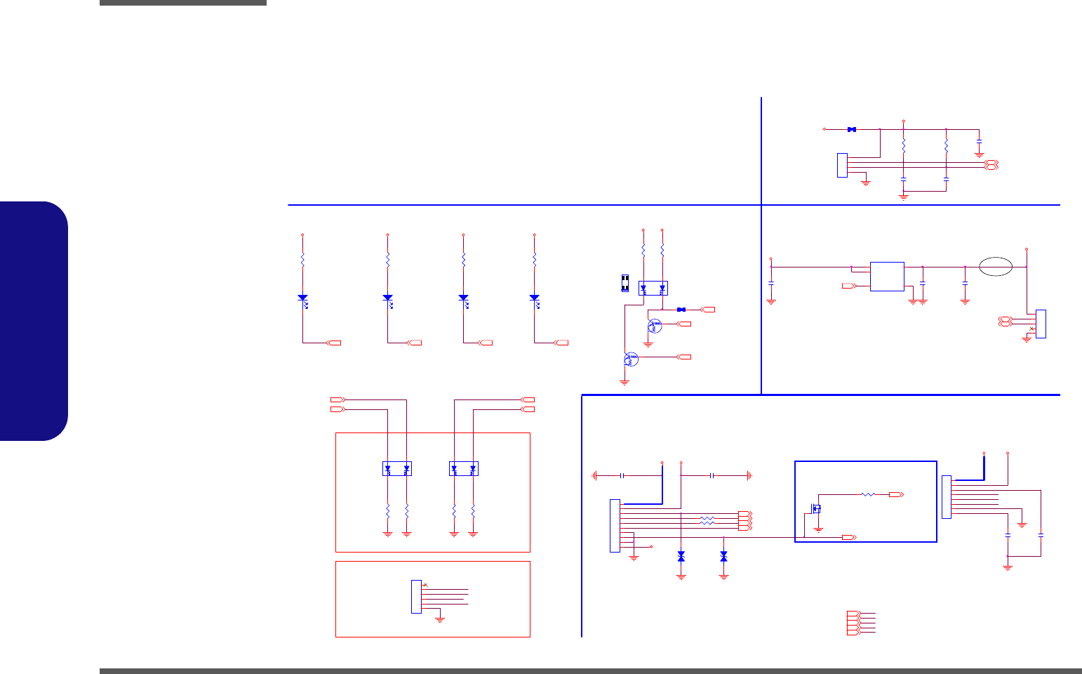
Schematic Diagrams
B - 22 CONN, CCD, LED
B.Schematic Diagrams
CONN, CCD, LED
Z2107
Z2112
3
Z2111
WLAN
LED
BT
LED
24
1
R6
220_04
Q1
DTC114EUA
CE
B
Q2
*DTC114EUA
CE
B
Z2106
SG
Y
D1
KPB-3025YSGC
1
3
2
4
BT_EN
Z2105
R7
220_04
R1
*10mil_04
CCD_EN18
LED_NUM# 18 LED_CAP# 18 LED_SCROLL# 18
From H8 default HI
WLAN_LED# 19
BT_EN 18,19
WLAN_EN 18,19
LED_BAT_FULL 18
LED_PWR18
LED_ACIN18
5VS12,14,15,16,23 1.5V4,5,6,7,11,23,25
LED_BAT_CHG 18
3.3VS3,6,7,8, 9,10,11,12,13,14,15,16,17,18,23 3. 3V2,9,11,12,13,17,18, 19,23,24,26
D02A
J_SW2
*50500-01041-001L
1
2
3
4
5
6
7
8
9
10
J_CCD1
85205-05001
1
2
3
4
5
C284
2.2u_6.3V_Y 5V_06
C283
0.1u_16V_Y 5V_04
C282
1u_10V_Y5V_06
CCD CONN.
1A 1A
LED_PWR
LED_ACIN
LED_BAT_CHG
LED_BAT_FULL
LED_BAT_CHG
J_TP2
*85201-06051
1
2
3
4
5
6
LED_BAT_FULL
LED_PWR
For W25xx/W27xx serial
Z2110
Z2109
Z2108
R202
220_04
R201
220_04
BAT LEDPOWER ON
LED
SG
Y
D15
KPB-3025YSGC
1
3
2
4
SG
Y
D16
KPB-3025YSGC
1
3
2
4
LED_ACIN
R203
220_04
For W24xx serial
R204
220_04
3.3VS
U11
G5243A
VIN
4
VIN
5
EN
3
VOUT 1
GND 2
WEB_EMAIL# 18
M_BTN # 23
AP_ON 23
LID_SW# 13,18
WEB_WWW# 18
AP_KEY # 18
3.3VS
5VS_CCD
5VS
5VS_TP
5VS
VIN
3.3V
3.3VS 3.3VS3.3VS
3.3V3. 3VS
3.3VS 3.3VS
USB_PN79USB_PP79
VIN13,22,23,25,26,27
C132
47p_50V_NPO_04
R90 *28mil_06
C131
1u_6.3V_Y5V_04
R92
10K_04
J_TP1
85201-04051
1
2
3
4C133
47p_50V_NPO_04
R91
10K_04
CLICK B'd CONN
WEB_WWW#_R AP_KEY #_R
LED
AP_ON
R22 1K_04
LID_SW#
D8
*V15AVLC0402
12
WEB_EMAIL#_R
C26
0.01u_16V_X7R_04
Q3
*MTN7002ZHS3
G
DS
C25
0.01u_16V_X7R_04
R23 1K_04
M_BTN#
R19 1K_04
AP_KEY #_ R
D7
*V15AVLC0402
12
J_SW1
88486-0801
1
2
3
4
5
6
7
8
POWER SWITCH B'd CONN
C23
*0.1u_16V_Y5V_04
C27
*0. 1u_50V_Y5V_06
If system has AP ON function, uses J_SW1
If system has no AP ON function, uses J_SW2
M_ BTN #
LID_SW#
WEB_EMAIL#_R
WEB_WWW#_R
6-52-52001-027 6-52-52001-027
Z2101
6-52-52001-027
Z2104
Z2103
Z2102
NUM
LOCK
LED
CAPS
LOCK
LED
D4
RY-SP170YG34-5M
AC
R3
220_04
SCROLL
LOCK
LED
R4
220_04
D3
RY-SP170YG34-5M
AC
R5
220_04
20mil
D5
RY-SP170YG34-5M
AC
5/13
6-52-52001-027
R2
220_04
HDD/ODD
LED
D2
RY-SP170YG34-5M
AC
TP_CLK 18
TP_D ATA 18
CLOSE TO J_SW1
5/13
SATA_LED# 10
20mil
Sheet 21 of 31
CONN, CCD, LED
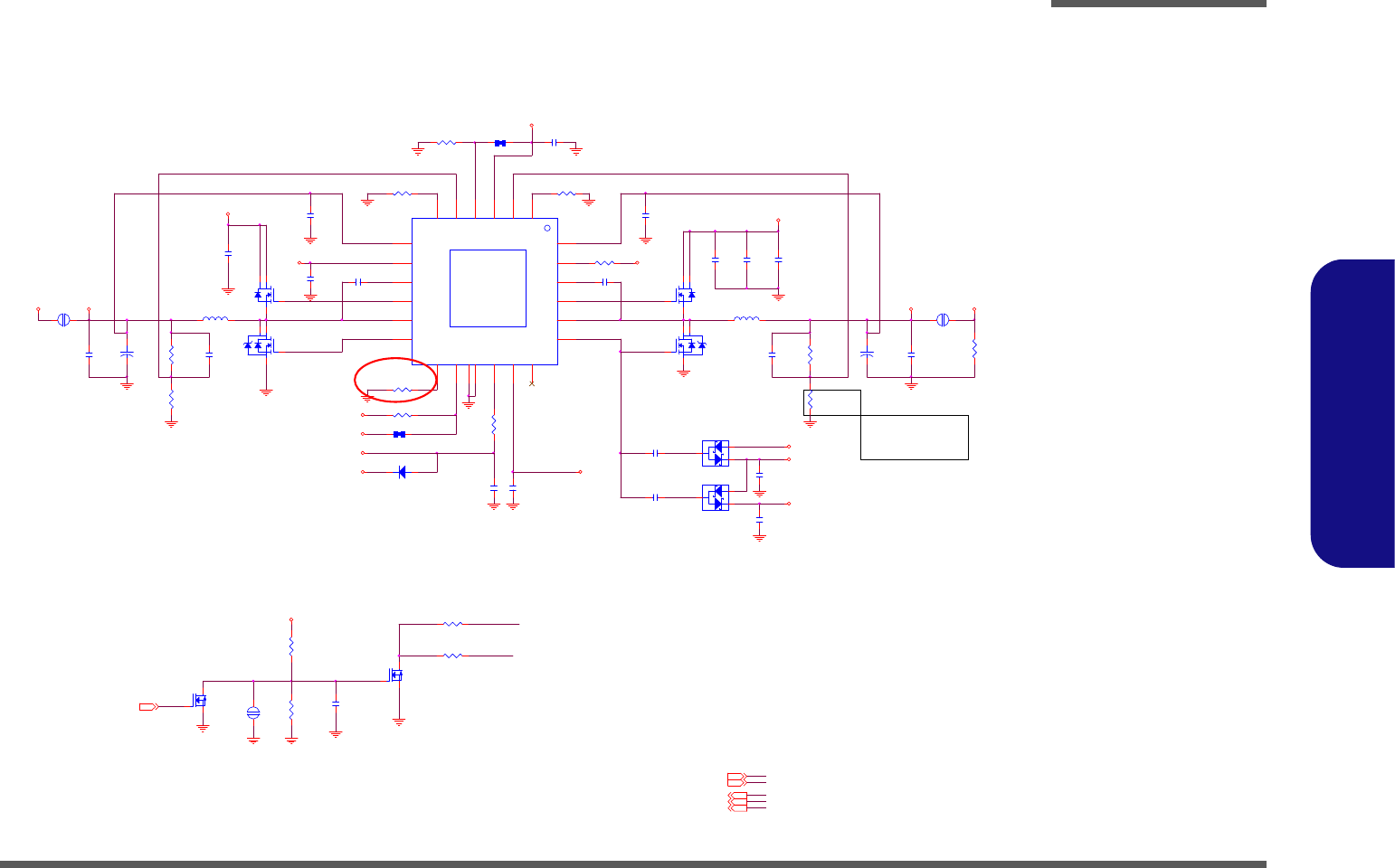
Schematic Diagrams
PWR VDD3, VDD5V, SYS15V B - 23
B.Schematic Diagrams
PWR VDD3, VDD5V, SYS15V
P0301
P0317
P0316
P0309
D02A DEL PR75 for
G5608/uP6182
EN_ALL
P0307
P0310
VDD520,23
SYS15V23 VDD311,15,17,18,19,23,27
P0303
D02A Change G5608 to uP6182(6-02-06182-CQ0)
P0304
PR58
100K_04
P0312
VIN
VIN123 VIN13,21,23,25,26,27
USB_CHARGE_EN18,23
P0306
Ra
5A
D02A
Rb
VREG5
5A
P0311
P0308
PC28
0.1u_16V_Y5V_04
EN_5V
PC63
0.1u_10V_X7R_04
PQ16
MTN7002ZHS3
G
DS
PL6
BCIHP0730-4R7M
1 2
PC108
4.7u_25V_X5R_08
PC109
4.7u_25V_X5R_08
PR60 120K_1%_04
PC29
0.1u_16V_Y5V_04
PR2 *0_04
C
A
A
PD10
BAT54SWGH
1
2
3
PC54
1000p_50V_X7R_04
PC3
1u_10V_06
PJ14
OPEN-3mm
1 2
PR75
*680K_1%_04
C
A
A
PD8
BAT54SWGH
1
2
3
+
PC132
220u_6.3V_6.3* 6_E
PL7
BCIHP0730-4R7M
1 2
PU2
G5608
VREF 3
EN1 1
VFB1 2
TONSEL 4
LDO5
17
LGATE1 19
PHASE1 20
VFB2 5
UGATE2
10
VCLK
18
BOOT2
9
EN2 6
VO2
7
LDO3
8
PHASE2
11
LGATE2
12
EN0
13
SKIPSEL
14
GND
15
VIN
16
UGATE1 21
BOOT1 22
POK 23
VO1 24
GND PAD
25
PQ27A
PD1503YVS
7
8
1
2
PR28
30.1K_1%_04
PQ15
MTN7002ZHS3
G
DS
PC47
100p_50V_NPO_04
PR59
10K_04
PC68
0.01u_50V_X7R_04
PR 53 120K_1%_04
P0313
PR63
1K_04
PC4
1u_10V_Y5V_06
PC70
4.7u_25V_X5R_08
PC73
0.01u_50V_X7R_04
PR54
*10mil_short
PR74 *10mil_short
PC9
0.1u_50V_Y5V_06
PQ26B
PD1503YVS
4
3
5
6
PC61
1u_10V_Y5V_06
+
PC131
220u_6.3V_6.3* 6_E
PC27
100p_50V_NPO_04
PC58
2200 p_50V_X7R _04
PC48
1000p_50V_X7R_04
PJ15
OPEN-3mm
12
PR132
*100K_04
PR30
19.1K_1%_06
PQ26A
PD1503YVS
7
8
1
2
PR26
13K_1%_06
PC59
1u_10V_Y5V_06
PR78
2.2_06
PC110
4.7u_25V_X5R_08
PR55 *0_04
PJ9
*40mil
12
PQ27B
PD1503YVS
4
3
5
6
POK
PC71
2200 p_50V_X7R _04
PR52 0_04
PR24
20K_1%_04
PC52
*0.1u_16V_Y5V_04
P0314
SYS5V
SYS15V
SYS5V
VREG5
VDD5
VREF
SYS5V
VREF
VDD3
VIN1
SYS3V
VREG5
VIN
SYS10V
VIN
VREG3
PD11
RB0540S2
AC
EN_3V
PR51 *0_04 EN_3V
P0302
stuff 18.7K Voutput 5.21V
stuff 19.6K Voutput 5.1V
stuff 20K Voutput 5.04V
MAX 8A
EN_5V
DDON_EN_VDD
Sheet 22 of 31
PWR VDD3,
VDD5V, SYS15V
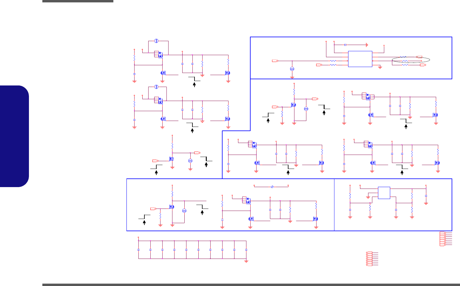
Schematic Diagrams
B - 24 PWR SW, 3V, 5V, 3VS, 5VS, 1.5VS
B.Schematic Diagrams
PWR SW, 3V, 5V, 3VS, 5VS, 1.5VS
PC133
2200p_50V_X7R_04
PR134
*100K_04
PR 109 100K_04
PQ10
P2703BAG
3
2 4
1
5
6
PR38
*100K_04
PC136
*1000p_50V_X7R_04
PC134
10u_10V_Y5V_08
PR43
1M_04
PR131
100K_04
PJ8
8mil
12
PR39
*100K_04
PC42
1000p_50V_X7R_04
PC122
0.1u_16V_Y5V_04
PC39
10u_10V_Y5V_08
PC2
0.1u_50V_Y5V_06
PC37
0.1u_16V_Y5V_04
PR46
100K_04
PQ40
MTN7002ZHS3
G
DS
PR47
100K_04
PR138
10K_04
PC97
0.1u_50V_Y5V_06
PR122
*10_06
S
D
G
PQ38B
MTDN7002ZHS6R
5
34
PQ39
P2703BAG
3
2 4
1
5
6
PR114 10K_04
PC137
0.01u_16V_X7R_04
PJ7
8mil
12
PQ12
P2703BAG
3
2 4
1
5
6
PC142
1u_10V_06
PC40
10u_10V_Y5V_08
PC1
0.1u_50V_Y5V_06
EMI
PR123
1M_04
PR44
*100K_04
PR137
*Rb
PR118 1K_04
PC41
680p_50V_X7R_04
PR136
*1M_04
PC36
0.1u_16V_Y5V_04
PR128
*100K_04
PU5
P2808B0
VA
1
VIN
2
M_BTN#
3
INSTANT-ON
4GND 5
PWR_SW# 6
DD_ON_LATCH 7
VIN1 8
PQ30
MTN7002ZHS3
G
DS
PC20
0.1u_50V_Y5V_06
PU6
AX6607-18BA
VIN
1
GND
2
SD#
3
VOUT 5
BYP 4
PC120
4700p_50V_X7R_04
PJ11
8mil
12
S
D
G
PQ9A
MTDN7002ZHS6R
2
61
PC49
0.1u_50V_Y5V_06
PR125
*100K_04
PC75
*0.1u_50V_Y5V_06
DL_5VS
S
D
G
PQ11A
MTDN7002ZHS6R
2
61
PC96 0.1u_50V_Y5V_06
PC126
10u_10V_Y5V_08
PC19
0.1u_50V_Y5V_06
PR41
1M_04
PR135
*Ra
PC10
*0. 1u_50V_Y5V_06
PR133
10_06
PQ32
*MTN7002ZHS3
G
DS
PJ1 OPEN -2m m
1 2
PJ2 OPEN -2m m
1 2
PJ12
8mil
12
PC8
0.1u_50V_Y5V_06
.
PL11
*0_06
PC11
0.1u_50V_Y5V_06
PR40
10_06
S
D
G
PQ11B
MTDN7002ZHS6R
5
34
PQ19
MTN7002ZHS3
G
DS
ON
PR130
1M_04
PQ8
*MTN7002ZHS3
G
DS
S
D
G
PQ38A
MTDN7002ZHS6R
2
61
1.8VS
S
D
G
PQ9B
MTDN7002ZHS6R
5
34
PR42
*10_06
Power Plane
200mA
PR113 1K_04
Vout=Vref(1+Ra/Rb)
500mA
PC135
0.1u_16V_Y5V_04
PWR_SW#_R
SUSBL 11,24,25
5VS12,14,15, 16,21
3.3VS3,6,7,8,9,10,11,12,13,14,15, 16,17,18,21
1.5VS3,5,8,9,12 1.8VS2,5,18
DD_ON# 20
PWR_SW# 18
3.3VS
Power Plane
SUSB#11,18
3A
GFX_PWRGD11,26
M_B TN #21
USB_C HARGE_EN 18,22
AP_ON21
3A
PQ36
MDS2655
4
6 2
5
7 3
1
8
SUSBL
ON
VIN122 VA27 SYS15V22
VIN13,21,22,25,26, 27
DD_ON18,20
VDD311,15,17,18, 19,22,27
EN_1.5VS
SUSBL
DDON_LATCH
ON
VDD3
SUSBL
PQ18
MTN7002ZHS3
G
DS
PC44
10u_10V_Y5V_08
3.3V
PQ13
P2703BAG
3
2 4
1
5
6
ON
3.3V_EN
PC50
1000P_50V_X7R_04
DD_ON# PQ17
*MTN7002ZHS3
G
DS
SY S15V
PR45
*100K_04
PR49
*10_06
PC45
0.1u_16V_Y5V_04
ON
PR56
1M_04
DD_ON#
ON
DL_1.5VS
EN_5VSEN_3.3VS
3.3VS_PRIME
CPU_PWRGD#
3A 250mA
EN_3.3VS_PRIME
DL_3.3VS_PRIME
CPU_PWRGD#
Power Plane
D02
DD_ON#
CPU_PWRGD#
ON
ON
ON
PR119 1K_04
3V
5V
DL_3.3VS
EM I
P2808
3.3VS
VDD3 VDD5
VDD3
SYS15V
3.3VS_PRI ME
SY S15V 5VS
1.5VS
2A
1.8VS
1.5V 1.5VS
SY S15V
VDD3
3A
VDD3 3.3VS
VDD 3SY S15V 3.3VS_PRIME
VIN
SY S15V 5V
3.3VS_PRIME3.3VS
VDD3
Power Plane
VDD5
VIN VA
VIN1
6-15-02655-7B0(M)
6-15-03006-7B0(S)
SUSBL SUSBL
SUSBL
D02A
VDD520,22
PR48
*10_06
PC43
0.1u_16V_Y5V_04
PQ21
MTN7002ZHS3
G
DS
PR57
100K_04 PR50
*100K_04
PC51
220p_50V_NPO_04 PQ20
*MTN7002ZHS3
G
DS
PC46
10u_10V_Y5V_08
PQ14
P2703BAG
3
2 4
1
5
6
5V_EN
DD_ON# DD_ON#
Power Plane
5A
5VS
2A
5A
Power Plane
5A
1.5V4,5,6,7,11,25
ON
SUSBL
3.3V2,9,11,12,13,17,18,19,21,24,26
3.3VS_PRIME5,12,18
1.8VS_SD#
5V12,20,24,25,26
Power Plane
ON
5A 5A
Sheet 23 of 31
PWR SW, 3V, 5V,
3VS, 5VS, 1.5VS
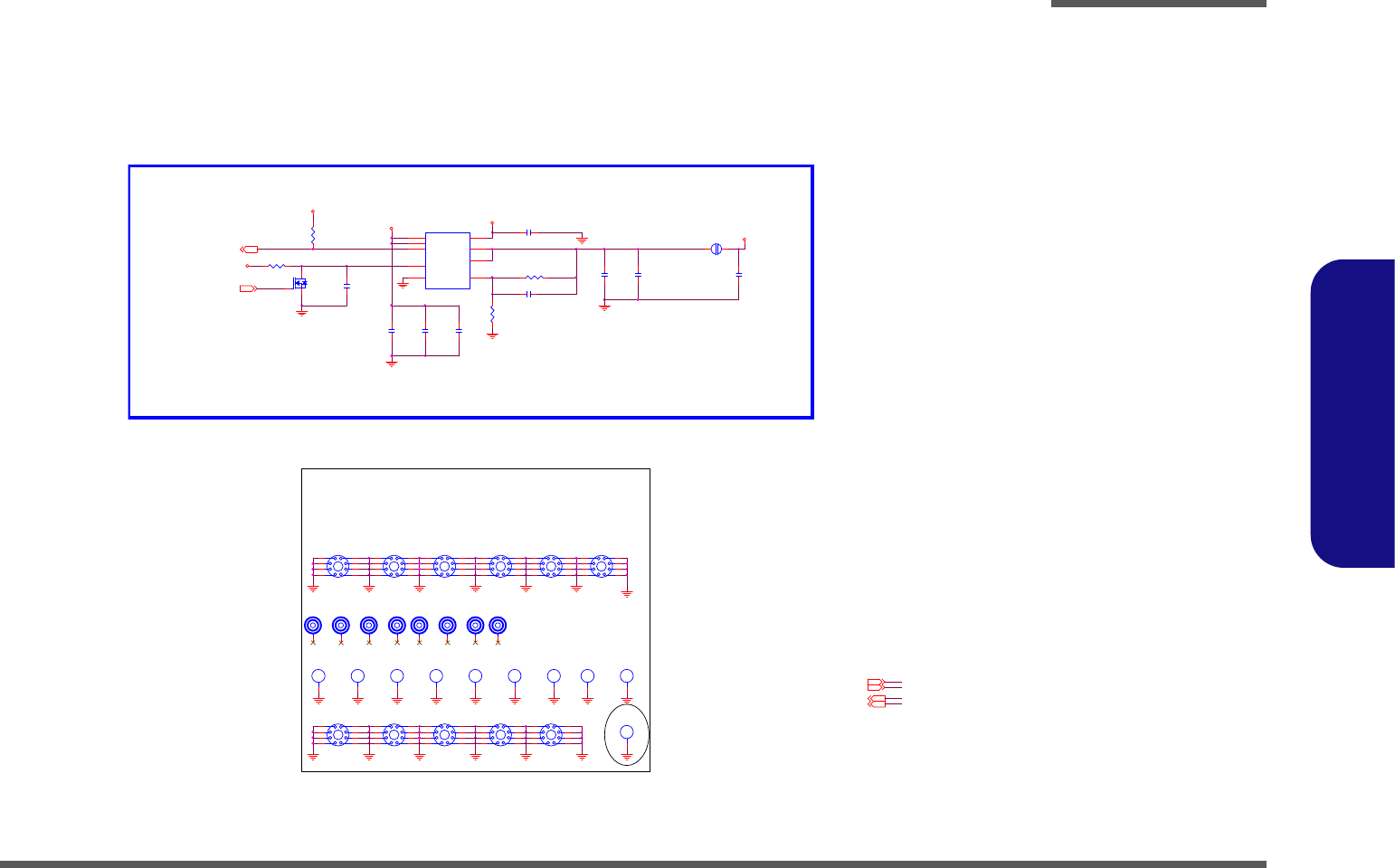
Schematic Diagrams
PWR 1.05VS B - 25
B.Schematic Diagrams
PWR 1.05VS
Sheet 24 of 31
PWR 1.05VS
H14
H7_0B6_0D3_7
VDD Q25 1.05VS2,5,8,10,11,12,26
SUSBL11,23,25
©w¦ì¤Õ
¥ú¾ÇÂI
H12
H7_0B6_0D3_7
5V12,20,23,25,26 3.3V2,9,11,12,13,17,18,19,21,23,26
Ra
LDO_1.05VS
P0515
2A
Rb
1
H5
MTH315D111
2
3
4
5 6
7
8
9
PN: 6-02-06615-320
H21
H7_0B6_0D3_7
H20
H7_0B6_0D3_7
H19
H7_0B6_0D3_7
Vout=0.8(1+Ra/Rb)
0324
H15
H7_0B6_0D3_7
1.05VS
1.05VS_PWR GD18
5V
VDD Q
1.05VS
5V
H17
H7_0B6_0D3_7 H13
H7_0B6_0D3_7
D02
3.3V
H16
H7_0B6_0D3_7
1.05VS_EN
M1
M-MARK1
PJ16
OPEN-2mm
1 2
PC148
0.22u_10V_X5R_04
PC143
0.1u_16V_Y5V_04
M6
M-MARK1
1
H2
MTH315D111
2
3
4
5 6
7
8
9
PC141
0.1u_16V_Y5V_04
M4
M-MARK1
1
H10
MTH315D111
2
3
4
5 6
7
8
9
M7
M-MARK1
PC139
10u_6.3V_X5R_06
PC140
10u_6.3V_X5R_06
PC145
10u_6.3V_X5R_06
1
H1
MTH315D111
2
3
4
5 6
7
8
9
1
H3
MTH315D111
2
3
4
5 6
7
8
9
1
H8
MTH315D111
2
3
4
5 6
7
8
9
PR142 100K_04
1
H4
MTH315D111
2
3
4
5 6
7
8
9
M3
M-MARK1
1
H11
MTH315D111
2
3
4
5 6
7
8
9
PC146 1u_10V_Y5V_06
1
H7
MTH315D111
2
3
4
5 6
7
8
9
PC147 82p_50V_NPO_04
1
H9
MTH315D111
2
3
4
5 6
7
8
9
1
H6
MTH315D111
2
3
4
5 6
7
8
9
PU7
AX6615ESA
GND
1
VCNTL 6
VOUT 3
VIN
5
VOUT 4
VFB 2
POK
7
EN
8
VIN
9
PR 139 1K_1%_04
M5
M-MAR K 1
PC144
10u_6.3V_X5R_06
PQ41
MTN7002ZHS3
G
DS
M8
M-MARK1
PR140
3.01K_1%_04
M2
M-MARK1
PR141
10K_04
H18
H7_0B6_0D3_7
PN: 6-13-11311-28C
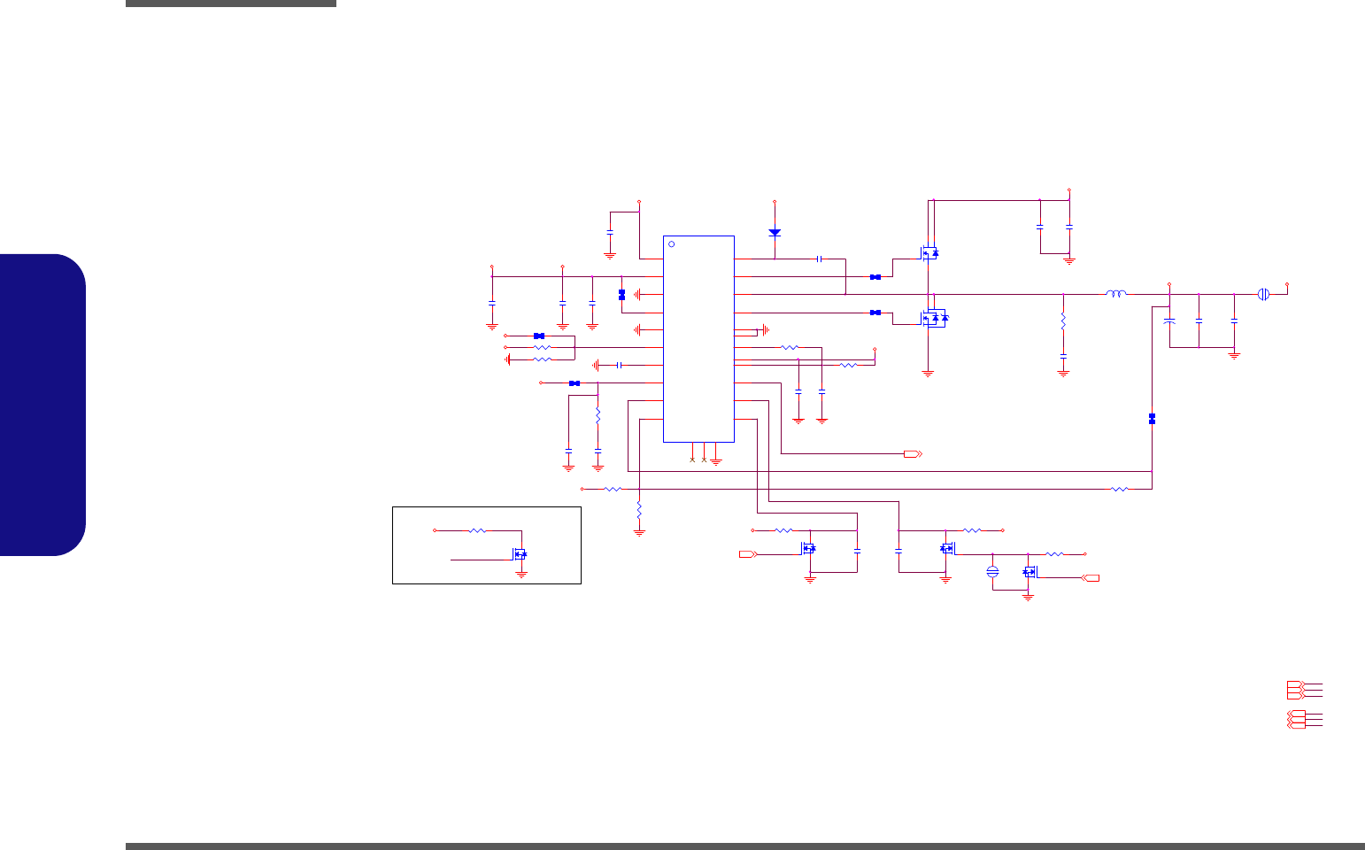
Schematic Diagrams
B - 26 PWR 1.5V, 0.75V
B.Schematic Diagrams
PWR 1.5V, 0.75V
6.5A
FOR DDR3
P0406
P0407
P0402
P0404
VDD Q24
VTT_MEM6,7 1.5V4, 5,6,7,11,23
1.5V_PWRGD 11
1.5VS3,5,8,9,12,23
SUSBL11,23,24
SUSC# 11,18
P0412
VIN13,21,22,23,26,27 5V12,20,23,24,26
SUSBL
P0409
P0411
P0414
FROM 14K_1%_04 CHANGE TO
14.3K_1%_04
FOR DDR3
VTT_EN 1.5V_EN
PQ4
*MTN2306AN3
G
DS
PR21 *22_04
VTT_MEM
S3 circuit:-
P0401
P0416
P0403
3A
MAX 8A
FOR DDR3
VIN
VDDQ
VDDQ
5V
5V
5V
5V
VDDQ 1. 5V
5V
VTT_MEM VTT_MEM
5V
5V 5V
P0415
P0405
P0410
PJ3
8mil
12
PR20 10K_1%_04
PR31 2.2_06
PR19 *10mil_short
PC22
10u_6.3V_X5R_06
PC16
*1000p_50V_X7R_04
PR13 *10_04
PC84
0.1u_50V_Y5V_06
PR16
*10mil_short
PC26
0.01u_50V_X7R_04
+
PC138
560u_2.5V_6.6*6. 6*5.9
PR14 *0_04
PR29
*15mil_short
PC17
*1000p_50V_X7R_04
PC30
0.1u_10V_X7R_04
P0413
PC95
4.7u_25V_X5R_08
PQ5
MTN7002Z HS3
G
DS
P0408
PL10
TMPC0603H-1R5M-Z01
1 2
PQ34A
PD1503YVS
7
8
1
2
PD6
RB0540S2
AC
PR22
9.53K_1%_06
PC31
1u_10V_06
FOR DDR3
PR27 10K_04
PC25
10u_6.3V_X5R _06
PR18 *10mil_short
PC21
*10u_6. 3V_X5R_06
PR129
5.1_06
PU1
G5616
VTTGND
1
VLDOIN
23
VTT
24
VTTSNS
2
GND
3
MODE
4
VTTREF
5VCC5 14
PGOOD 13
S5 11
S3 10
VDDQSET
9
VDDQSNS
8
COMP
6
CS 16
PGND 18
DRVL 19
LL 20
DRVH 21
VBST 22
PVCC5 15
CS_GND 17
NC
7
NC
12
GND
25
PJ4
OPEN-3mm
1 2
PR23
*10K_1%_04
PR32 12K_1%_04 PC127
1000p_50V_X7R_04
PR33
*15mil_short
PR34 100K_04
PC32
1u_10V_06
S
D
G
PQ6A
MTDN7002ZHS6R
2
61
PC33
0.01u_50V_X7R _04
PR17
*10mil_short
PC34
0.1u_16V_Y5V_04
PC18 0.1u_10V_X7R_04
PC24
0.01u_50V_X7R _04
PR25 10K_04
PR15 *0_04
S
D
G
PQ6B
MTDN7002ZHS6R
5
34
PQ34B
PD1503Y VS
4
3
5
6
PC23
10u_6.3V_X5R_06
P0417
Sheet 25 of 31
PWR 1.5V, 0.75V
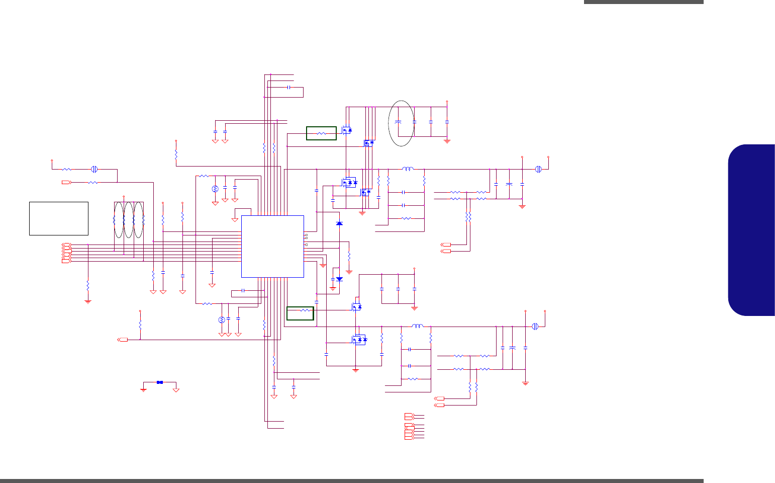
Schematic Diagrams
PWR VCORE B - 27
B.Schematic Diagrams
PWR VCORE
+
PC113
330u_CAR315L
CSPA
4A
6-07-56214-3A0
RSPB
CSPA
CSNA
RSP_LLB
LDRA1
COMPB
CSPB
CSNB
LXB
CSNB1
RSPB
RSNA
CSPA
RSPA
VDDA
PGB
TEMPB
BSTB
COMPA
CSNA
HDRB
5V
RSP_LLA
CSNA1
INTEL Recommend
H_CPU_SVIDCLK 55_04
H_CPU_SVIDDAT 110_04
H_PROCHOT# 100_04
VR_EN
CSNB
HDRA1
CSPB
TEMPA
OZ8293_VREF
BSTA1
RSNB
LDRB
RSNB
RSNA
RSPA
VCCSENSE5
H_CPU_SVIDALRT#2
VCORE5
VSSGFXSENSE5
VCCGFXSENSE5
VSSSENSE5
GFX_PWRGD11,23
VCORE_ON18
CPU_PWRGD
EMI
EMI
VIN13,21,22,23,25,27 5V12,20, 23,24,25
3.3V2,9,11,12,13, 17,18,19, 21,23,24
VCORE5VGF X5
H_PROCHOT#2
1.05VS2,5,8,10,11,12,24
PR96
10_04
PD12
RB0540S2
A C
PC99
1000p_50V_X7R_04
PC150
1000p_50V_X7R_04
PR971.3k_1%_04
PC116
0.22u_10V_X7R_06
PR126
2_06
PR81
*0_04
PC130
0.1u_16V_Y5V_04
PC105
22p_50V_NPO_04
PC13
4700PF_50V_X7R_04
PTH2
100K_NTC_06_B
12
PC98
2200p_50V_X7R_04
PD13
RB0540S2
AC
PC78
1000p_50V_X7R_04
PR108
71.5K_1%_04
PTH1
100K_NTC_06_B
12
PC119
4.7u_25V_X5R_08
PC104
1000P_50V_X7R_04
3A
PR1071.74k_1%_04
PC106
0.01u_50V_X7R_04
PC69
1u_16V_X5R_06
PR99
10_04
PJ17
*5mm
1 2
PQ33A
PD1503YVS
7
8
1
2
PR68
10K_04
PC129
1000p_50V_X7R_04
PR101
10_04
PC114
*2200p_50V_X7R_04
PC115
0.22u_10V_X7R_06
PC118
4.7u_25V_X5R_08
PR127 2_06
PR100
10_04
PC107
*0.01u_50V_X7R_04
PR90
10_04
PR86
10_04
PC15
0.1u_50V_Y5V_06
PJ10 8mil
1 2
PC88
1000p_50V_X7R_04
PR79
10K_1%_04
¥¿ºÝ¬°PIN 2 ¡A-tºÝ¬°PIN1
PJ13
OPEN-2mm
1 2
PR110
46.4K_1%_06
PC125
2200p_50V_X7R_04
PC92
4.7u_25V_X5R_08
PC124
4.7u_25V_X5R_08
PR8
0_04
PC121
*2200p_50V_X7R_04
PR94
0_04
+
PC151
560u_2.5V_6.6*6.6*5. 9
PR112
10K_04
PC76
470p_50V_X7R_04
PC149
0.1u_16V_Y5V_04
PL8
TMPC0603H-1R5M-Z01
1 2
PR102
1.96k_1%_04
PR83 100_04
PU4
OZ8293
VDDP 25
GNDP 22
HDRB
20
PGB
18
LDRB 23
BSTB 21
LXB
19
CSPB
17 CSNA 35
CSNB
16 RSPA 36
RSPB
15 RSNA 37
RSNB
14 RSP_LLA 38
RSP_LLB
13 TEMPA 39
TEMPB
12 COMPA 40
COMPB
11
LXA2 27
LDRA1 24
ALRTb
7
VDI O
8
VREF
3
GNDA 41
VR_TTb
10
VIN
1
SDA
6
VDDA
2
VR_EN
4
SCL
5
VCLK
9
HDRA2 28
LDRA2 26
BSTA2 29
BSTA1 30
HDRA1 31
LXA1 32
PGA 33
CSPA 34
PR87
4.87K_1%_06
PR66
1K_04
PR98
10_04
PR92
0_04
PC77
0.1u_16V_Y5V_04
PR93
0_04
PQ33B
PD1503YVS
4
3
5
6
PR70 *75_1%_04
+
PC128
560u_2.5V_6.6*6.6*5.9
PL9
TMPC0603H-1R5M-Z01
1 2
PC117
1u_25V_08
PR9
71.5K_1%_04
PC82
1000p_50V_X7R_04
PC123
2200p_50V_X7R_04
PR80
22_04
PC14
*0.01u_50V_X7R_04
PR95
0_04
PR103
51_1%_06
PC91
2200p_50V_X7R_04
PR111
51_1%_06
PR71 54.9_1%_04
PR117
10K_04
PC81
0.1u_50V_Y5V_06
PQ31A
PD1503Y VS
7
8
1
2
PQ31B
PD1503Y VS
4
3
5
6
PR116
46.4K_1%_06
PR88
10_04
PR77
4.87K_1%_06
PR89
0_04
PC79
1000p_50V_X7R_04
PC112
22p_50V_NPO_04
PR82 110_1%_04
PR69
1K_04
LXA1
PR121 0_06
EC SIDE PU
D02
5VVIN
1.05VS
PR76 *10mil_short
VIN
VIN
VCOREV_CORE
VGFX
V_GFX
H_CPU_SVIDCLK2
SMC_CPU_VCORESET18 SMD_CPU_VCORESET18
H_CPU_SVIDDAT2
60mils
3.3V
3.3V
3.3V
Iout=4 A
OCP=11A
150mils
Iout=3A
OCP=9A
150mils
PQ28
*ME4410AD-G
4
62 5
73
1
8
D02A
PQ35
*ME4410AD-G
4
62 5
73
1
8
+5V CHANGE TO 5V
+V5S CHANGE TO +V5
60mils
PR124 0_06
Sheet 26 of 31
PWR VCORE
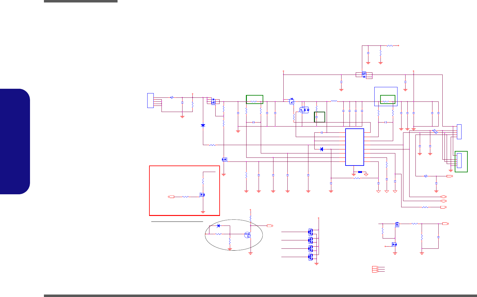
Schematic Diagrams
B - 28 PWR AC_IN, CHARGE
B.Schematic Diagrams
PWR AC_IN, CHARGE
PQ1
DTC114EUA
CE
B
VDD3
VDD3
VA
PC7
30p_50V_NPO_04
TOTAL_CUR 18
BAT_DET 18
CHG_RST18
D02
D02
VDD311,15,17,18,19,22,23
VIN13,21,22,23,25,26 VA23
W250CU
JBATTA1
BTD-05TI1G
1
2
3
4
5
W240CU
PN: 6-21-D3460-105
BTD-05TI1G
2ND
PN: 6-21-D3490-105
BA05Q16BCCA40
PN: 6-21-D34B0-105
BTD-05TC1
VDD3
PD4
ZD5245BS2
AC
EMI
PR64
*5.1_06
PC56
*2200p_50V_X7R_04
JACK1
JDD-52048AS1F- 165
GND2
GND1
2
1
3
PC80
*0. 1u_50V_Y5V_06
PC53
*0.1u_50V_Y5V_06
PC86
*0.1u_50V_Y5V_06
PQ3
MTN7002ZHS3
G
DS
PC65 4. 7u_25V_X5R_08
SMD_BAT_R
FOR 65W
PN: 6-20-B3410-003
50932-00301-001
FOR 35W
PN: 6-20-B3Z40-004
JDD-52048AS1F- 165
JBATTA2
*BTD-05TC1B
1
2
3
4
5
PC100 4.7u_25V_X5R_08
PU3
OZ8681
LX
14
LDR
16
BST
12
VAC
1
VDDP
15
IACM
3
VDDA 6
SDA 11
ICHP 5
ICHM 4
COMP 8
HDR 13
BASE
17
SCL 10
IAC 7
IACP
2
ACAV
9
PR36
15K_04
PC101
*1u_25V_08
PC102
*1u_25V_08
PD1
*BAV99 RECTIFIER
A
C
AC
PR85 *15mil_short
PR61
100K_04
PQ24
MEP4435Q8
4
62 5
73
1
8
PC60
4.7u_25V_X5R_08
PC85
1u_10V_06
PR65
100_04
PR5
*200K_1%_04
PC111 4. 7u_25V_X5R_08
PC90
4.7u_25V_X5R_08
PC62
1000P_50V_X7R_04
PC83
1u_10V_06
PR11
60.4K_1%_04
PR12
100K_1%_04
PR10
300K_1%_04
PL4
HCB4532K-800_18
3/22
PR115 10_06
PC64 *4.7u_25V_X5R_08
PR84 10_06
PQ23
MTN7002ZHS3 G
DS
PC5
30p_50V_NPO_04
PC67 0.1u_50V_Y5V_06
PC87
4.7u_25V_X5R_08
PC12
0.1u_16V_Y5V_04
PC38 4.7u_25V_X5R_08
PC35
0.1u_50V_Y5V_06
PR3
10K_04
PR73
0_04
PR62 100K_04
PR104 10_06
PL1 HCB1005KF-121T20
PR120 10_06
PL5
BCIHP-0730 8R2M
PD2
*BAV99 RECTIFIER
A
C
AC
PD3
*BAV99 RECTIFIER
A
C
AC
PC72
0.47u_10V_Y5V_04
PC74
47p_50V_NPO_04
PD5
*BAV99 RECTIFIER
A
C
AC
PC94
4700p_50V_X7R_04
PQ22
MTN7002ZHS3
G
DS
PR7
0_04
PR6 *1M_04
PQ25B
PD1503YVS
4
3
5
6
PR1
0.01_1%_32
PR4 *470K_04
PR106
33_06
PQ7
MEP4435Q8
4
6 2
5
7 3
1
8
PR105 10_06
PC89
4.7u_25V_X5R_08
PC93
4700p_50V_X7R_04
PR91
100_04
PC103
1u_25V_08
PQ25A
PD1503YVS
7
8
1
2
PC66 4. 7u_25V_X5R_08
PC57 0.1u_50V_Y5V_06
PR67
0.01_1%_32
PR35
10K_04
PD9 R B0540S2
AC
PD7
MDL914S2
AC
PR37
100K_04
SMC_BAT_R
PC55
0.1u_50V_Y5V_06
PQ2
MTP3403N3
G
DS
PC6
30p_50V_NPO_04
VA
VA
VIN BAT
SMD_BAT 18
SMC_BAT 18
BAT_VOLT 18
AC_IN# 18
IACP
SMC_BAT
COMP
LDR
AC AV
3S / 2K
2S / 10K / NT1908
BAT DET(BATTERY INTERNAL) :
2S / 5K / NT1912
4S/2800mAH /7.15K
3S/2800mAH / 4.02K
4S / 390
PL2 HCB1005KF-121T20
SMD_BAT
BAT_DET
VAC
VA_IN
LX
PR72
0_06
PL3 HCB1005KF-121T20
SMC_BAT
# -YAdapter ¨Ï¥Î120W(§t),«e«áºÝ¹jÂ÷½Ð¨Ï¥Î2PCS MOSFET,180W~220W : 3PCS , 300W: 4PCS , 360W: 5PCS
Reset circuit
BAT_VOLT
PCB Layout notes
1) All pow er traces should be routed on the outer layers
GNDP, VAD, VSYS, LX, VCHG, VBATT
2) Use Kelvin connections for R3, R4
(seperate force and measurement traces)
3) R23 and R24 are dummy resistors, for layout purposes only
(serves as single point connection betw een GNDP & GNDA)
4) Footprint TO-236 is equivalent to SOT-23
5) Footprint SIP/1P is a single hole axial pad
6) All resisitors, capacitors and semiconductors are SMD
7) Potentiometers, and test points are axial devices
ICHM
VDDP
ICHP
IACM IAC1
BAT
¾aªñJ_MBAT1
Sheet 27 of 31
PWR AC_IN,
CHARGE
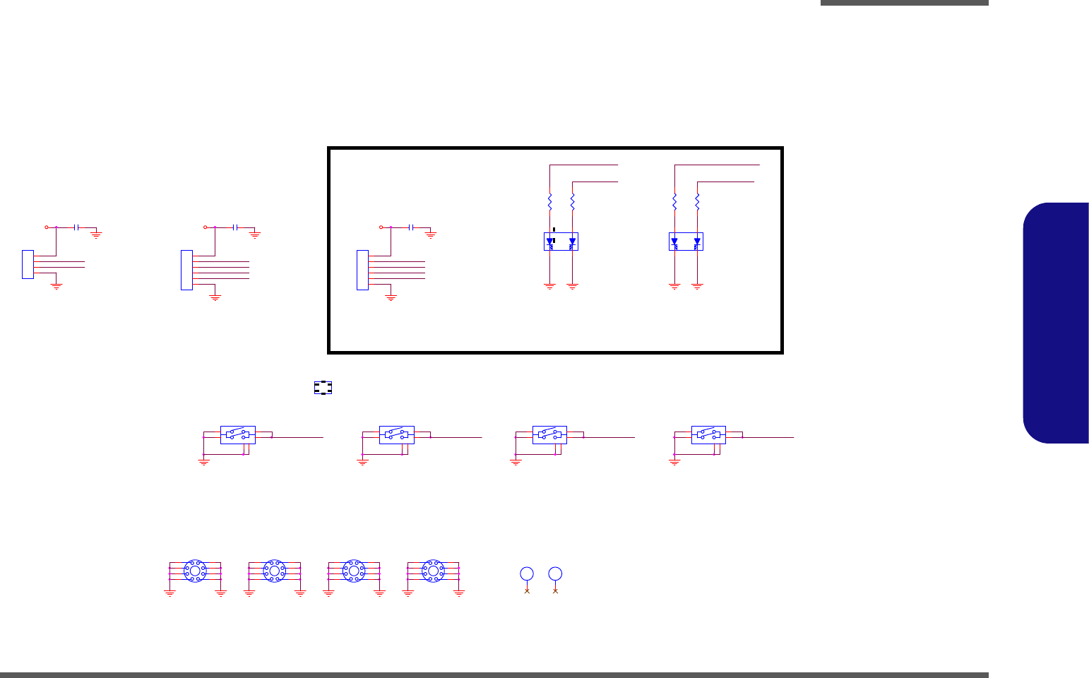
Schematic Diagrams
CLICK BOARD B - 29
B.Schematic Diagrams
CLICK BOARD
¿O¸¹¦PW255EU,ºñ¶ÀRY-SP155HYYG4-1
CLED_BAT_FULL
CLED_BAT_CHG
CLED_PWR
CLED_ACIN
CLED_BAT_FULL
6-20-94A50-104
6-21-91A20-1066-21-91A20-106 6-21-91A00-1066-21-91A00-106
6-53-3050B-0426-53-3050B-0426-53-3050B-042
6-20-94A70-104
6-20-94AA0-104
1
6-53-3050B-042
BAT LED
POWER ON
LED
2
CLED_ACIN
6-52-55002-04E
6-52-55002-042
CLED_BAT_CHG
CLICK BOARD
CTPBUTTON_RCTPBUTTON_L CTPBUTTON_RCTPBUTTON _L
RIGHT
KEY
LIFT
KEY
LIFT
KEY
1
RIGHT
KEY
CSW1~4
3
4
6-52-55002-04E
6-52-55002-042
2
CTP_DATACTP_CLK
CTPBUTTON_R
CTP_CLKCTP_DATA
CTPBUTTON_L
CLED_PWR
CH6
HO-165X94_5NP
CC1
0.1u_16V_Y5V_04
1
CH3
MTH237D91
2
3
4
5 6
7
8
9
SG
Y
CD27
*RY-SP155HYYG4-1
1
3
2
4
CC2
*0.1u_16V_Y5V_04
CR4
*220_04
CR2
*220_04
CJ_TP2
85201-06051
1
2
3
4
5
6
CR1
*220_04
CR3
*220_04
CJ_TP3
*85201-06051
1
2
3
4
5
6
CC3
*0.1u_16V_Y5V_04
1
CH1
MTH237D 91
2
3
4
5 6
7
8
9
CSW1
TJG-533-S-T/R
3
14
2
5
6
CSW3
*TJG-533-S-T/R
3
14
2
5
6
1
CH2
MTH 23 7D 91
2
3
4
5 6
7
8
9
1
CH4
MTH237D91
2
3
4
5 6
7
8
9
CSW4
*TJG-533-S-T/R
3
14
2
5
6
SG
Y
CD26
*RY-SP155HYYG4-1
1
3
2
4
CH5
C95D95
CSW2
TJG-533-S-T/R
3
14
2
5
6
CJ_TP1
85201-04051
1
2
3
4
CGNDCGND CGND
CGND
CGNDCGNDCGND CGND
CGND
CGND
CGND
CGND
CGNDCGND
CGND
CGND
C5VS C5VS
CGND
CGNDCGND CGND
CVDD3
CGND
CGND
W24ACU ¤£¤W¥ó
W25xCU ¤W¥ó
Sheet 28 of 31
CLICK BOARD
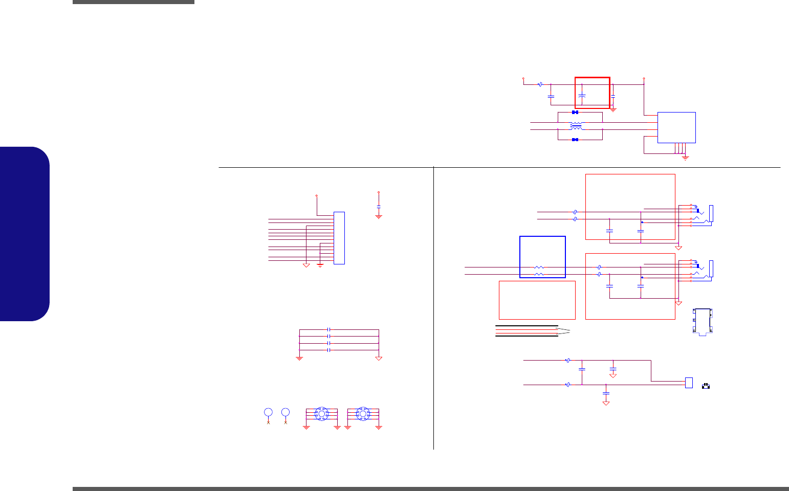
Schematic Diagrams
B - 30 AUDIO BOARD/USB
B.Schematic Diagrams
AUDIO BOARD/USB
AGND
AGND
AGND
AGND A_AU DG
A_AUDG
A_AUDG
A_AUDG
A_AUDG
A_USBVCC
ASPKOUTR+
ASPKOUTR-
D02A
6-20-53A00-114
AJ_AUDIO1
87213-1400G
1
2
3
4
5
6
7
8
9
10
11
12
13
14
AMIC1-R
AUSB_PP2
AUSB_PN2 AUSB_PN2_R
AUSB_PP2_R
MIC1_OUT_L
NC_MIC1
AMIC_SENSE
MIC1_OUT_R
AMIC1-L
AHEADPHONE-L
AHEADPHONE-R
PHONE_OUT_LPHONE-L
PHONE_OUT_RPHONE-R
ASPK_HP#
AHP_SENSE
ASPKOUTR-_R
ASPKOUTR+
ASPKOUTR- ASPKOUTR+_R
AMIC1-L
AMIC1-R
60 mil
USB PORT
HEADPHONE
MIC IN
AUDIO JACK
BLACK
BLACK
TO M/B
6-21-B49C0-104
6-20-B2800-106
6-20-B2800-106
EMI Require
5
3
2
6
14
HP-L
VT1802P
33_1%_04
EMI Require
GND
3*R/L½u¼e
GND
Headphone°T¸¹½u¼e > 10mils
¶ZÂ÷phone jack¶V»·
½u®|´N¥²¶·¶V¼e
R/L¥²¶·¥]ÂÐGND¥B¶¡¶Z¬°3*½u¼e
Resistor 32 or 33_04
meet WLK Test
HP-R
Layout note:
1
J_SPK1
2
6-20-43110-102
6-20-43150-102
10/28 Modify value
AHEADPH ONE-R
AHEADPH ONE-L
AHP_SENSE
AMIC_SENSE
A_AUDG AGND
AUSB_PN2
AUSB_PP2
AC5
10u_10V_Y5V_08 AL124
FCM1005KF-121T03
1 2
AC797
*180p_50V_NPO_04
AL125
FCM1005KF-121T03
1 2
AH1
C59D59
AL123
FCM1005KF-121T03
1 2
AL126
FCM1005KF-121T03
1 2
AC8 0.1u_16V_Y5V_04
AC792
*100p_50V_NPO_04
AR2 *10mil_04
AJ_SPKR1
85204-02001
PCB Footprint = 85204-02R
1
2
R
L
AJ_MIC1
2SJ-T351-S23
2
6
5
3
1
4
AC794
*100p_50V_NPO_04
AC9 0.1u_16V_Y5V_04
AC6 0.1u_16V_Y5V_04
AR1 *10mil_04
+
AC1
100u_6.3V_B_B
R
L
AJ_HP1
2SJ-T351-S23
2
6
5
3
1
4
AR569 33.2_1%_04
AL122
*WCM2012F2S-161T03
1
4
2
3
1
AH2
MTH276D111
2
3
4
5 6
7
8
9
AC10
*22u_6.3V_X5R_08
AR570 33.2_1%_04
AC796
*1u_10V_Y 5V_06
AL128
*FCM1608K-121T06_short
AH3
C59D59
AJ_USB1
US04036BCA081
V+
1
GND1
GND 1
DATA_L
2
DATA_H
3
GND
4
GND2
GND2
GND4
GND4 GND3
GND3
1
AH4
MTH276D111
2
3
4
5 6
7
8
9
AL127
*FCM1608K-121T06_short
AL1
HCB1608KF-121T25
AC795
*100p_50V_NPO_04
AC7 0.1u_16V_Y5V_04
AC798
*180p_50V_NPO_04
AC2
0.1u_16V_Y5V_04
A_USBVCC A_USBVCC2
AC793
*100p_50V_NPO_04
A_USBVCC
AGND
AGND AGND AGND
Sheet 29 of 31
AUDIO BOARD/
USB
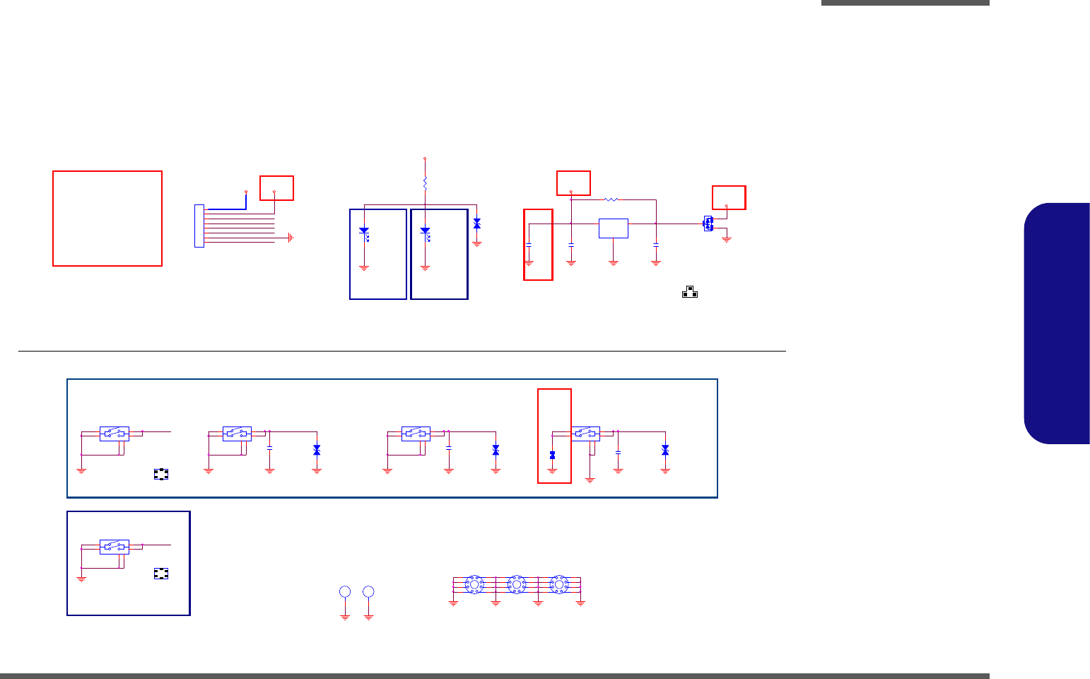
Schematic Diagrams
POWER SWITCH & LID BOARD B - 31
B.Schematic Diagrams
POWER SWITCH & LID BOARD
SLID_SW#
SLID_SW#
SAP_ON
SWEB_WWW#
SWEB_EMAIL#
SM_BTN#
SM_BTN#
SM_BTN# SWEB_WWW# SAP_ONSWEB_EMAIL#
SPWR_SW1
TJG-533-S-T/R
3
14
2
5
6
1
SMH4
MTH237D118
2
3
4
5 6
7
8
9
SC3
0.1u_16V_Y5V_04
SD1
HT-150NB-DT
AC
SMAIL_SW1
TJG-533-S-T/R
3
14
2
5
6
1
SMH3
MTH237D87
2
3
4
5 6
7
8
9
SC1
*100p_50V_NPO_04
SC4
0.1u_16V_Y5V_04
1
SMH1
MTH237D87
2
3
4
5 6
7
8
9
SR2
220_04
SAP_SW1
TJG-533-S-T/R
3
14
2
5
6
SJ_SW2
88486-0801
1
2
3
4
5
6
7
8
SR4
*20mil_04
SD5
*V15AVLC0402
12
SC5
0.1u_16V_Y5V_04
SC2
0.1u_10V_X5R_04
SD6
*V15AVLC0402
12
SD3
*HT-150NB-DT
AC
SPWR_SW2
*TJG-533-S-T/R
3
14
2
5
6
SWWW_SW1
TJG-533-S-T/R
3
14
2
5
6
SD4
*V15AVLC0402
12
SC6
*1u_10V_Y5V_06
SR1 100K_04
SMH2
H7_0D2_3
SU1 MH248-ALFA-ESO
VCC
1OUT 2
GND
3
SD2
*BAV99 RECTIFIER
A
C
AC
SMH5
H7_0D2_3
SD7
*V15AVLC0402
12
SMGND
S_VDD3
SMGND
S_VDD3
SMGND
S_3.3VS
SMGND
S_3.3VS
SMGND
SMGND
SMGND
SMGNDSMGND
SMGNDSMGND SMGNDSMGND
SMGNDSMGND SMGNDSMGND
SMGND
SMGNDSMGNDSMGND SMGNDSMGND
20mil
SMGND
S_VDD3
SMGND
SMGND
SMGND
3
1
SU1, SU2
2
6-20-94K10-108
POWER BUTTON
FOR E5128Q FOR E4120Q/
E5120Q
20mil
POWER
SWITCH
LED
20mil
6-02-00268-LC1
6-02-00248-LC2
LID SWITCH IC
6-53-3150B-245
31
2
4
PSW1~8
POWER BUTTON
FOR E4120Q/E5120Q
5/13
HOT KEY
POWER SW & LED & HOT KEY
FOR E5128Q
6-53-3050B-240
6-53-3050B-241
1
2
WEB_EMAIL#
4
WEB_WWW#
PSW1~8
6-53-3050B-241
6-53-3150B-245
6-53-3050B-240
6-53-3050B-241
6-53-3150B-245
6-53-3050B-240
6-53-3050B-241
6-53-3150B-245
6-53-3050B-240
6-53-3050B-241
6-53-3150B-245
AP_KEY#
3
LED P/N
6-52-56001-022
6-52-56000-020
6-52-56001-028
6-52-56001-023
6-53-3050B-240
Sheet 30 of 31
POWER SWITCH &
LID BOARD
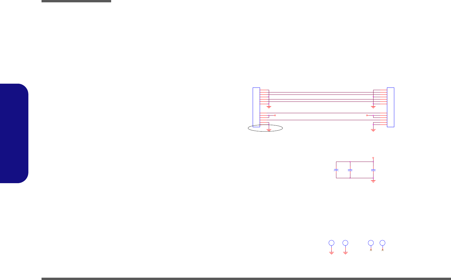
Schematic Diagrams
B - 32 EXTERNAL ODD BOARD
B.Schematic Diagrams
EXTERNAL ODD BOARD
+
QC3
*220u_6.3V_6.3*6.3*4.2
QJ_SATA_TXP1
QJ_SATA_ODD_DA#
QJ_SATA_TXN1
QJ_SATA_RXP1
QJ_SATA_RXN1
QJ_ODD_DETECT#
PIN
GND1~2=WGND
ODD BOARD FOR E5120Q
PIN
GND1~3=QGND
6-21-14030-013
6-21-14020-013
6-21-14010-013
6-21-13A00-013
QC1
0.1u_16V_Y5V_04
QJ_ODD1
242001-1
S1
S2
S3
S4
S5
S6
S7
P1
P2
P3
P4
P5
P6
QJ_ODD2
B-5F2510-AAQ5RA1AA
S1
S2
S3
S4
S5
S6
S7
P1
P2
P3
P4
P5
P6
QH4
C237D91
QH3
C67D67 QH2
C67D67
QC2
0.1u_16V_Y5V_04
QH1
C237D91
Q_5VS
QGND
QGND
QGND QGND
Q_5VS
Q_5VS
QGND
QGND
QGND
¦PW255EU¥Î®Æ 7/13
Follow 255EU Design,
Reserve 220uf 7/14
Sheet 31 of 31
EXTERNAL ODD
BOARD

BIOS Update
C-1
C:BIOS Update
Appendix C:Updating the FLASH ROM BIOS
To update the FLASH ROM BIOS, you must:
• Download the BIOS update from the web site.
• Unzip the files onto a bootable CD/DVD/USB Flash Drive.
• Reboot your computer from an external CD/DVD/USB Flash Drive.
• Use the flash tools to update the flash BIOS using the commands indicated below.
• Restart the computer booting from the HDD and press F2 at startup enter the BIOS.
• Load setup defaults from the BIOS and save the default settings and exit the BIOS to restart the computer.
• After rebooting the computer you may restart the computer again and make any required changes to the default BIOS
settings.
Download the BIOS
1. Go to www.clevo.com.tw and point to E-Services and click E-Channel.
2. Use your user ID and password to access the appropriate download area (BIOS), and download the latest BIOS files
(the BIOS file will be contained in a batch file that may be run directly once unzipped) for your computer model
(see sidebar for important information on BIOS versions).
Unzip the downloaded files to a bootable CD/DVD/ or USB Flash drive
1. Insert a bootable CD/DVD/USB flash drive into the CD/DVD drive/USB port of the computer containing the
downloaded files.
2. Use a tool such as Winzip or Winrar to unzip all the BIOS files and refresh tools to your bootable CD/DVD/USB
flash drive (you may need to create a bootable CD/DVD with the files using a 3rd party software).
Set the computer to boot from the external drive
1. With the bootable CD/DVD/USB flash drive containing the BIOS files in your CD/DVD drive/USB port, restart the
computer and press F2 (in most cases) to enter the BIOS.
2. Use the arrow keys to highlight the Boot menu.
3. Use the “+” and “-” keys to move boot devices up and down the priority order.
4. Make sure that the CD/DVD drive/USB flash drive is set first in the boot priority of the BIOS.
5. Press F10 to save any changes you have made and exit the BIOS to restart the computer.
BIOS Version
Make sure you down-
load the latest correct
version of the BIOS ap-
propriate for the com-
puter model you are
working on.
You should only
download BIOS ver-
sions that are
V1.01.XX or higher as
appropriate for your
computer model.
Note that BIOS versions
are not backward com-
patible and therefore
you may not down-
grade your BIOS to an
older version after up-
grading to a later ver-
sion (e.g if you upgrade
a BIOS to ver 1.01.05,
you MAY NOT then go
back and flash the BIOS
to ver 1.01.04).

BIOS Update
C - 2
C:BIOS Update
Use the flash tools to update the BIOS
1. Make sure you are not loading any memory management programs such as HIMEM by holding the F8 key as you
see the message “Starting MS-DOS”. You will then be prompted to give “Y” or “N” responses to the programs
being loaded by DOS. Choose “N” for any memory management programs.
2. You should now be at the DOS prompt e.g: DISK C:\> (C is the designated drive letter for the CD/DVD drive/USB
flash drive).
3. Type the following command at the DOS prompt:
C:\> Flash.bat
4. The utility will then proceed to flash the BIOS.
5. You should then be prompted to press any key to restart the system or turn the power off, and then on again but
make sure you remove the CD/DVD/USB flash drive from the CD/DVD drive/USB port before the computer
restarts.
Restart the computer (booting from the HDD)
1. With the CD/DVD/USB flash drive removed from the CD/DVD drive/USB port the computer should restart from
the HDD.
2. Press F2 as the computer restarts to enter the BIOS.
3. Use the arrow keys to highlight the Exit menu.
4. Select Load Setup Defaults (or press F9) and select “Yes” to confirm the selection.
5. Press F10 to save any changes you have made and exit the BIOS to restart the computer.
Your computer is now running normally with the updated BIOS
You may now enter the BIOS and make any changes you require to the default settings.