Clevo W251BLQ, W253BLQ, W253BZQ, W258BZQ Service Manual. Www.s Manuals.com. Manual
User Manual: Notebook Clevo W253BLQ - Service manuals and Schematics, Disassembly / Assembly. Free.
Open the PDF directly: View PDF ![]() .
.
Page Count: 89
- Manual
- Preface
- Chapter 1: Introduction
- Overview
- Specifications
- External Locator - Top View with LCD Panel Open
- External Locator - Front & Right Side Views
- External Locator - Left Side & Rear View
- External Locator - Bottom View
- Mainboard Overview - Top (Key Parts)
- Mainboard Overview - Bottom (Key Parts)
- Mainboard Overview - Top (Connectors)
- Mainboard Overview - Bottom (Connectors)
- Chapter 2: Disassembly
- Overview
- Maintenance Tools
- Connections
- Maintenance Precautions
- Disassembly Steps
- Removing the Battery
- Removing the Hard Disk Drive
- Removing the Optical (CD/DVD) Device
- Removing the System Memory (RAM)
- Removing the Wireless LAN Module
- Removing the Keyboard
- Appendix A: Part Lists
- Appendix B: Schematic Diagrams
- System Block Diagram
- Ontario MEM & PCIE I/F, AP
- Ontario Display/CLK/MISC
- Ontario Power & Decoupling
- NAGUA DDR3 SO-DIMMS A
- NAGUA DDR3 SO-DIMMS B
- HUDSON PCIE/PCI/CLOCK/FCH
- HUDSON GPIO/USB/STRAP
- HUDSON SATA/DEBUG IO/SPI
- HUDSON Power Decoupling
- POWERGOOD/TPM
- ANX3110 ASIC
- LVDS/Inverter
- HDMI/CRT
- CCD/3G
- CardReader/LAN RTL8402
- Mini PCIE/SATA HDD/ODD
- Audio Codec VT1802P
- USB 3.0/USB Charge
- KBC-ITE IT8518
- LED/MDC/BT
- Fan/TP/Multi CON
- 5VS/3.3VS/1.8VS/1.5VS/1.1VS
- Power VDD3, VDD5
- Power 1.5V/0.75V
- Power 1.1V/1VS
- Power 1.8VS
- APU Core/NB Core
- Charger, DC In
- Click Board
- Audio Board/USB
- Power Switch & LID Board
- External ODD Board
- Appendix C: Updating the FLASH ROM BIOS

W251BLQ / W253BLQ / W253BZQ / W258BZQ

Preface
I
Preface
Notebook Computer
W251BLQ / W253BLQ / W253BZQ / W258BZQ
Service Manual

Preface
II
Preface
Notice
The company reserves the right to revise this publication or to change its contents without notice. Information contained
herein is for reference only and does not constitute a commitment on the part of the manufacturer or any subsequent ven-
dor. They assume no responsibility or liability for any errors or inaccuracies that may appear in this publication nor are
they in anyway responsible for any loss or damage resulting from the use (or misuse) of this publication.
This publication and any accompanying software may not, in whole or in part, be reproduced, translated, transmitted or
reduced to any machine readable form without prior consent from the vendor, manufacturer or creators of this publica-
tion, except for copies kept by the user for backup purposes.
Brand and product names mentioned in this publication may or may not be copyrights and/or registered trademarks of
their respective companies. They are mentioned for identification purposes only and are not intended as an endorsement
of that product or its manufacturer.
Version 1.0
October 2012
Trademarks
Intel and Intel Core are trademarks of Intel Corporation.
Windows® is a registered trademark of Microsoft Corporation.
Other brand and product names are trademarks and /or registered trademarks of their respective companies.

Preface
III
Preface
About this Manual
This manual is intended for service personnel who have completed sufficient training to undertake the maintenance and
inspection of personal computers.
It is organized to allow you to look up basic information for servicing and/or upgrading components of the W251BLQ /
W253BLQ / W253BZQ / W258BZQ series notebook PC.
The following information is included:
Chapter 1, Introduction, provides general information about the location of system elements and their specifications.
Chapter 2, Disassembly, provides step-by-step instructions for disassembling parts and subsystems and how to upgrade
elements of the system.
Appendix A, Part Lists
Appendix B, Schematic Diagrams
Appendix C, Updating the FLASH ROM BIOS

Preface
IV
Preface
IMPORTANT SAFETY INSTRUCTIONS
Follow basic safety precautions, including those listed below, to reduce the risk of fire, electric shock and injury to per-
sons when using any electrical equipment:
1. Do not use this product near water, for example near a bath tub, wash bowl, kitchen sink or laundry tub, in a wet
basement or near a swimming pool.
2. Avoid using a telephone (other than a cordless type) during an electrical storm. There may be a remote risk of elec-
trical shock from lightning.
3. Do not use the telephone to report a gas leak in the vicinity of the leak.
4. Use only the power cord and batteries indicated in this manual. Do not dispose of batteries in a fire. They may
explode. Check with local codes for possible special disposal instructions.
5. This product is intended to be supplied by a Listed Power Unit with an AC Input of 100 - 240V, 50 - 60Hz, DC Output
of 19V, 1.58A (30W) or 19V, 3.42A or 18.5V, 3.5A (65W) minimum AC/DC Adapter.
CAUTION
This Computer’s Optical Device is a Laser Class 1 Product
FCC Statement
This device complies with Part 15 of the FCC Rules. Operation is subject to the following two conditions:
This device may not cause harmful interference.
This device must accept any interference received, including interference that may cause undesired operation.
Preface
V
Preface
Instructions for Care and Operation
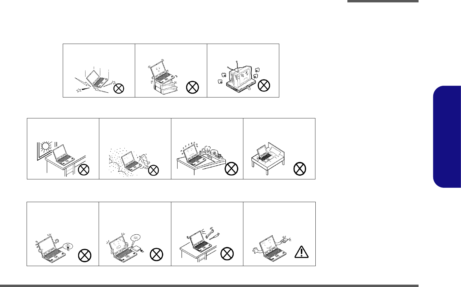
The notebook computer is quite rugged, but it can be damaged. To prevent this, follow these suggestions:
1. Don’t drop it, or expose it to shock. If the computer falls, the case and the components could be damaged.
2. Keep it dry, and don’t overheat it. Keep the computer and power supply away from any kind of heating element. This
is an electrical appliance. If water or any other liquid gets into it, the computer could be badly damaged.
3. Follow the proper working procedures for the computer. Shut the computer down properly and don’t forget to save
your work. Remember to periodically save your data as data may be lost if the battery is depleted.
Do not expose the computer
to any shock or vibration. Do not place it on an unstable
surface. Do not place anything heavy
on the computer.
Do not expose it to excessive
heat or direct sunlight. Do not leave it in a place
where foreign matter or mois-
ture may affect the system.
Don’t use or store the com-
puter in a humid environment. Do not place the computer on
any surface which will block
the vents.
Do not turn off the power
until you properly shut down
all programs.
Do not turn off any peripheral
devices when the computer is
on.
Do not disassemble the com-
puter by yourself. Perform routine maintenance
on your computer.
Preface
VI
Preface
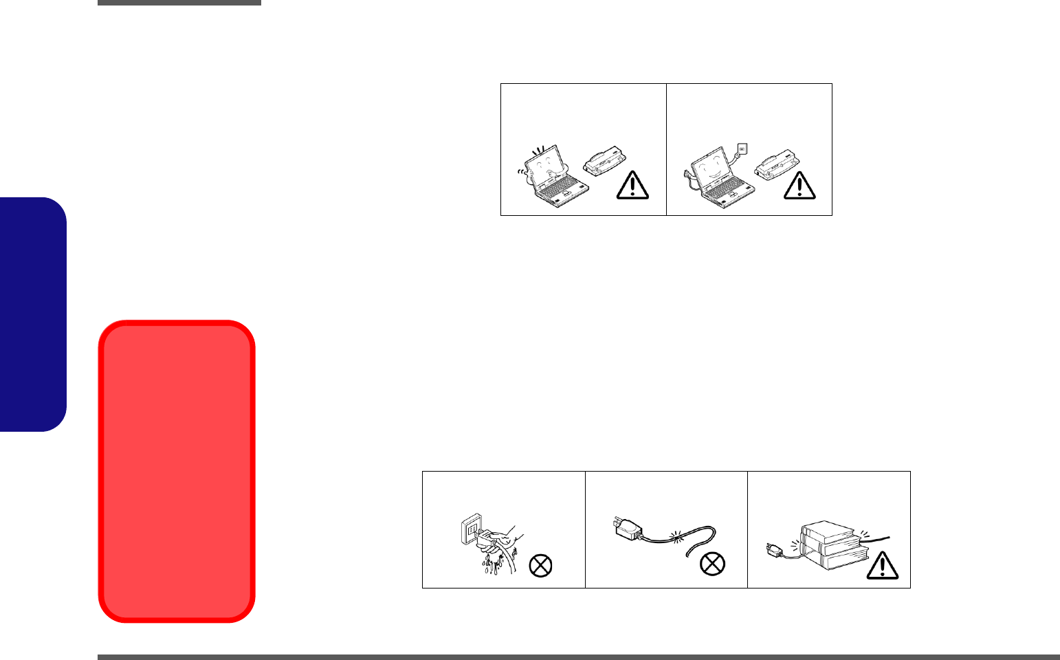
4. Avoid interference. Keep the computer away from high capacity transformers, electric motors, and other strong mag-
netic fields. These can hinder proper performance and damage your data.
5. Take care when using peripheral devices.
Power Safety
The computer has specific power requirements:
• Only use a power adapter approved for use with this computer.
• Your AC adapter may be designed for international travel but it still requires a steady, uninterrupted power supply. If you are
unsure of your local power specifications, consult your service representative or local power company.
• The power adapter may have either a 2-prong or a 3-prong grounded plug. The third prong is an important safety feature; do
not defeat its purpose. If you do not have access to a compatible outlet, have a qualified electrician install one.
• When you want to unplug the power cord, be sure to disconnect it by the plug head, not by its wire.
• Make sure the socket and any extension cord(s) you use can support the total current load of all the connected devices.
• Before cleaning the computer, make sure it is disconnected from any external power supplies.
Use only approved brands of
peripherals. Unplug the power cord before
attaching peripheral devices.
Do not plug in the power
cord if you are wet. Do not use the power cord if
it is broken. Do not place heavy objects
on the power cord.
Power Safety
Warning
Before you undertake
any upgrade proce-
dures, make sure that
you have turned off the
power, and discon-
nected all peripherals
and cables (including
telephone lines). It is
advisable to also re-
move your battery in
order to prevent acci-
dentally turning the
machine on.

Preface
VII
Preface
Battery Precautions
• Only use batteries designed for this computer. The wrong battery type may explode, leak or damage the computer.
• Do not continue to use a battery that has been dropped, or that appears damaged (e.g. bent or twisted) in any way. Even if the
computer continues to work with a damaged battery in place, it may cause circuit damage, which may possibly result in fire.
• Recharge the batteries using the notebook’s system. Incorrect recharging may make the battery explode.
• Do not try to repair a battery pack. Refer any battery pack repair or replacement to your service representative or qualified service
personnel.
• Keep children away from, and promptly dispose of a damaged battery. Always dispose of batteries carefully. Batteries may explode
or leak if exposed to fire, or improperly handled or discarded.
• Keep the battery away from metal appliances.
• Affix tape to the battery contacts before disposing of the battery.
• Do not touch the battery contacts with your hands or metal objects.
Battery Guidelines
The following can also apply to any backup batteries you may have.
• If you do not use the battery for an extended period, then remove the battery from the computer for storage.
• Before removing the battery for storage charge it to 60% - 70%.
• Check stored batteries at least every 3 months and charge them to 60% - 70%.
Battery Disposal
The product that you have purchased contains a rechargeable battery. The battery is recyclable. At the end of its useful life, under var-
ious state and local laws, it may be illegal to dispose of this battery into the municipal waste stream. Check with your local solid waste
officials for details in your area for recycling options or proper disposal.
Caution
Danger of explosion if battery is incorrectly replaced. Replace only with the same or equivalent type recommended by the manufacturer.
Discard used battery according to the manufacturer’s instructions.
Battery Level
Click the battery icon in the taskbar to see the current battery level and charge status. A battery that drops below a level of 10%
will not allow the computer to boot up. Make sure that any battery that drops below 10% is recharged within one week.

Preface
VIII
Preface
Related Documents
You may also need to consult the following manual for additional information:
User’s Manual on CD/DVD
This describes the notebook PC’s features and the procedures for operating the computer and its ROM-based setup pro-
gram. It also describes the installation and operation of the utility programs provided with the notebook PC.
System Startup
1. Remove all packing materials.
2. Place the computer on a stable surface.
3. Insert the battery and make sure it is locked in position.
4. Securely attach any peripherals you want to use with the computer
(e.g. keyboard and mouse) to their ports.
5. Attach the AC/DC adapter to the DC-In jack on the left of the
computer, then plug the AC power cord into an outlet, and connect
the AC power cord to the AC/DC adapter.
6. Use one hand to raise the
lid/LCD to a comfortable viewing angle
(do
not exceed 130 degrees)
;
use the other hand (as illustrated in Figure
1) to support the base of the computer (Note: Never lift the computer
by the lid/LCD).
7. Press the power button to turn the computer “on”.
Shut Down
Note that you should al-
ways shut your com-
puter down by
choosing Shut Down
from the Start Menu.
This will help prevent
hard disk or system
problems.
130
Figure 1
Opening the Lid/LCD/
Computer with AC/DC
Adapter Plugged-In

Preface
IX
Preface
Contents
Introduction ..............................................1-1
Overview .........................................................................................1-1
Specifications ..................................................................................1-2
External Locator - Top View with LCD Panel Open ......................1-4
External Locator - Front & Right Side Views .................................1-5
External Locator - Left Side & Rear View .....................................1-6
External Locator - Bottom View .....................................................1-7
Mainboard Overview - Top (Key Parts) .........................................1-8
Mainboard Overview - Bottom (Key Parts) ....................................1-9
Mainboard Overview - Top (Connectors) .....................................1-10
Mainboard Overview - Bottom (Connectors) ...............................1-11
Disassembly ...............................................2-1
Overview .........................................................................................2-1
Maintenance Tools ..........................................................................2-2
Connections .....................................................................................2-2
Maintenance Precautions .................................................................2-3
Disassembly Steps ...........................................................................2-4
Removing the Battery ......................................................................2-5
Removing the Hard Disk Drive .......................................................2-6
Removing the Optical (CD/DVD) Device ......................................2-8
Removing the System Memory (RAM) ..........................................2-9
Removing the Wireless LAN Module ...........................................2-11
Removing the Keyboard ................................................................2-12
Part Lists ..................................................A-1
Part List Illustration Location ........................................................A-2
Top (W251BLQ) ............................................................................A-3
Top (W253BLQ / W253BZQ) .......................................................A-4
Top (W258BZQ) ............................................................................A-5
Bottom (W251BLQ) ......................................................................A-6
Bottom (W253BLQ) ...................................................................... A-7
Bottom (W253BZQ) ...................................................................... A-8
Bottom (W258BZQ) ...................................................................... A-9
DVD (W251BLQ) ....................................................................... A-10
DVD (W253BLQ / W253BZQ) .................................................. A-11
DVD (W258BZQ) ....................................................................... A-12
LCD (W251BLQ) ........................................................................ A-13
LCD (W253BLQ) ........................................................................ A-14
LCD (W253BZQ) ........................................................................ A-15
LCD (W258BZQ) ........................................................................ A-16
Schematic Diagrams.................................B-1
System Block Diagram ...................................................................B-2
Ontario MEM & PCIE I/F, AP .......................................................B-3
Ontario Display/CLK/MISC ...........................................................B-4
Ontario Power & Decoupling .........................................................B-5
NAGUA DDR3 SO-DIMMS A ......................................................B-6
NAGUA DDR3 SO-DIMMS B ......................................................B-7
HUDSON PCIE/PCI/CLOCK/FCH ...............................................B-8
HUDSON GPIO/USB/STRAP .......................................................B-9
HUDSON SATA/DEBUG IO/SPI ...............................................B-10
HUDSON Power Decoupling .......................................................B-11
POWERGOOD/TPM ...................................................................B-12
ANX3110 ASIC ............................................................................B-13
LVDS/Inverter ..............................................................................B-14
HDMI/CRT ...................................................................................B-15
CCD/3G ........................................................................................B-16
CardReader/LAN RTL8402 .........................................................B-17
Mini PCIE/SATA HDD/ODD ......................................................B-18
Audio Codec VT1802P .................................................................B-19
USB 3.0/USB Charge ...................................................................B-20

Preface
X
Preface
KBC-ITE IT8518 ......................................................................... B-21
LED/MDC/BT .............................................................................. B-22
Fan/TP/Multi CON ....................................................................... B-23
5VS/3.3VS/1.8VS/1.5VS/1.1VS ..................................................B-24
Power VDD3, VDD5 ................................................................... B-25
Power 1.5V/0.75V ........................................................................B-26
Power 1.1V/1VS ...........................................................................B-27
Power 1.8VS ................................................................................. B-28
APU Core/NB Core ...................................................................... B-29
Charger, DC In .............................................................................B-30
Click Board .................................................................................. B-31
Audio Board/USB ........................................................................B-32
Power Switch & LID Board .........................................................B-33
External ODD Board ....................................................................B-34
Updating the FLASH ROM BIOS......... C-1
Download the BIOS ....................................................................... C-1
Unzip the downloaded files to a bootable CD/DVD/ or
USB Flash drive ............................................................................. C-1
Set the computer to boot from the external drive ........................... C-1
Use the flash tools to update the BIOS ..........................................C-2
Restart the computer (booting from the HDD) .............................. C-2

Introduction
Overview 1 - 1
1.Introduction
Chapter 1: Introduction
Overview
This manual covers the information you need to service or upgrade the W251BLQ / W253BLQ / W253BZQ / W258BZQ
series notebook computer. Information about operating the computer (e.g. getting started, and the Setup utility) is in the
User’s Manual. Information about dri-vers (e.g. VGA & audio) is also found in the User’s Manual. The manual is
shipped with the computer.
Operating systems (e.g. Windows 7, etc.) have their own manuals as do application softwares (e.g. word processing and
database programs). If you have questions about those programs, you should consult those manuals.
The W251BLQ / W253BLQ / W253BZQ / W258BZQ series notebook is designed to be upgradeable. See Disassembly
on page 2 - 1 for a detailed description of the upgrade procedures for each specific component. Please take note of the
warning and safety information indicated by the “” symbol.
The balance of this chapter reviews the computer’s technical specifications and features.

Introduction
1 - 2 Specifications
1.Introduction
Specifications
Latest Specification Information
The specifications listed here are correct at the
time of sending them to the press. Certain items
(particularly processor types/speeds) may be
changed, delayed or updated due to the manu-
facturer's release schedule. Check with your
service center for more details.
CPU
The CPU is not a user serviceable part. Ac-
cessing the CPU in any way may violate your
warranty.
Processor Options
AMD-E Series Accelerated Processing Unit - E2-1800
(1.7GHz)
1MB L2 Cache, 40nm, DDR3-1333MHz, TDP 18W
AMD-E Series Accelerated Processing Unit - E1-1200
(1.4GHz)
1MB L2 Cache, 40nm, DDR3-1066MHz, TDP 18W
AMD-C Series (Dual-Core) Accelerated Processing Unit -
C-70 (1.0GHz)
1MB L2 Cache, 40nm, DDR3-1066MHz, TDP 9W
BIOS
AMI BIOS (One 32Mb SPI Flash ROM)
LCD Options
15.6" (39.62cm) HD TFT LCD
Memory
Two 204 Pin SO-DIMM Sockets Supporting DDR3 1066/
1333MHz Memory
Memory Expandable up to 8GB
Video Adapter
AMD Radeon™ HD 7290 (C-70 APU Integrated)
Shared Memory Architecture of up to 1469MB
Microsoft® DirectX11 Compatible
AMD Radeon™ HD 7310 (E1-1200 APU Integrated)
Shared Memory Architecture of up to 1469MB
Microsoft® DirectX11 Compatible
AMD Radeon™ HD 7340 (E2-1800 APU Integrated)
Shared Memory Architecture of up to 1469MB
Microsoft® DirectX11 Compatible
Core Logic
AMD A68M Chipset
Storage
(Factory Option) One Changeable 12.7mm(h) Super Multi
Optical Device Drive
One Changeable 2.5" 9.5mm (h) SATA HDD
Audio
High Definition Audio Compliant Interface
2 * Built-In Speakers
Built-In Microphone
Keyboard
Full-size “WinKey” keyboard (with numeric keypad)
Pointing Device
Built-in Touchpad
Interface
Two USB 3.0 Ports
One USB 2.0 Port
One HDMI-Out Port
One Headphone-Out Jack
One Microphone-In Jack
One RJ-45 LAN Jack
One External Monitor Port
One DC-in Jack
Card Reader
Embedded Multi-In-1 Card Reader
MMC (MultiMedia Card) / RS MMC
SD (Secure Digital) / Mini SD / SDHC/ SDXC
MS (Memory Stick) / MS Pro / MS Duo
Mini Card Slots
Slot 1 for WLAN Module or WLAN and Bluetooth Combo
Module
(Factory Option) Slot 2 for 3G Module
Communication
Built-In 10Mb/100Mb Ethernet LAN
(Factory Option) 300K Pixels/2M HD PC Camera Module
(Factory Option) 3G Mini-Card Module
WLAN/ Bluetooth Half Mini-Card Modules:
(Factory Option) Third-Party Wireless LAN (802.11b/g/n) +
Bluetooth 4.0
(Factory Option) Third-Party Wireless LAN (802.11b/g/n)
Security
Security (Kensington® Type) Lock Slot
BIOS Password

Introduction
Specifications 1 - 3
1.Introduction
Environmental Spec
Temperature
Operating: 5°C - 35°C
Non-Operating: -20°C - 60°C
Relative Humidity
Operating: 20% - 80%
Non-Operating: 10% - 90%
Power
(for C-70 APU)
6 Cell Smart Lithium-Ion Battery Pack, 48.84WH
(Factory Option) 6 Cell Smart Lithium-Ion Battery Pack,
62.16WH
Full Range AC/DC Adapter
AC Input: 100 - 240V, 50 - 60Hz
DC Output: 19V, 1.58A (30W)
Or
(for E1-1200, E2-1800 APU)
6 Cell Smart Lithium-Ion Battery Pack, 48.84WH
(Factory Option) 6 Cell Smart Lithium-Ion Battery Pack,
62.16WH
Full Range AC/DC Adapter
AC Input: 100 - 240V, 50 - 60Hz
DC Output: 19V, 3.42A or 18.5V, 3.5A (65W)
Dimensions & Weight
374mm (w) * 250mm (d) * 14.3 - 34.1mm (h)
2.25kg (with 48.84WH Battery and ODD)
Or
374mm (w) * 250mm (d) * 20 - 37.2mm (h)
2.45kg (with 48.84WH Battery and ODD)
Introduction
1 - 4 External Locator - Top View with LCD Panel Open
1.Introduction
External Locator - Top View with LCD Panel Open
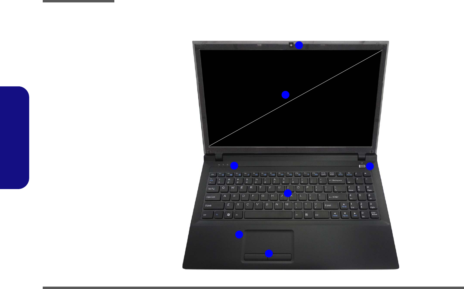
Figure 1
Top View
1. PC Camera
(Optional)
2. LCD
3. Power Button
4. LED Status
Indicators
5. Keyboard
6. Built-In
Microphone
7. Touchpad &
Buttons
5
3
4
6
1
7
15.6” (39.62cm)
2
Introduction
External Locator - Front & Right Side Views 1 - 5
1.Introduction
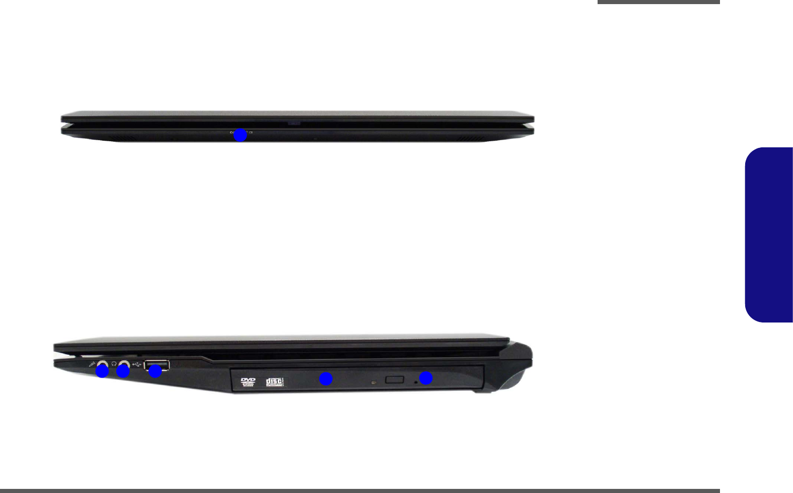
External Locator - Front & Right Side Views
Figure 2
Front View
1. LED Power
Indicator
Figure 3
Right Side View
1. Microphone-In
Jack
2. Headphone-Out
Jack
3. USB 2.0 Port
4. Optical Device
Drive Bay
5. Emergency Eject
Hole
FRONT VIEW
1
RIGHT SIDE VIEW
1 2 3 5
4
Introduction
1 - 6 External Locator - Left Side & Rear View
1.Introduction
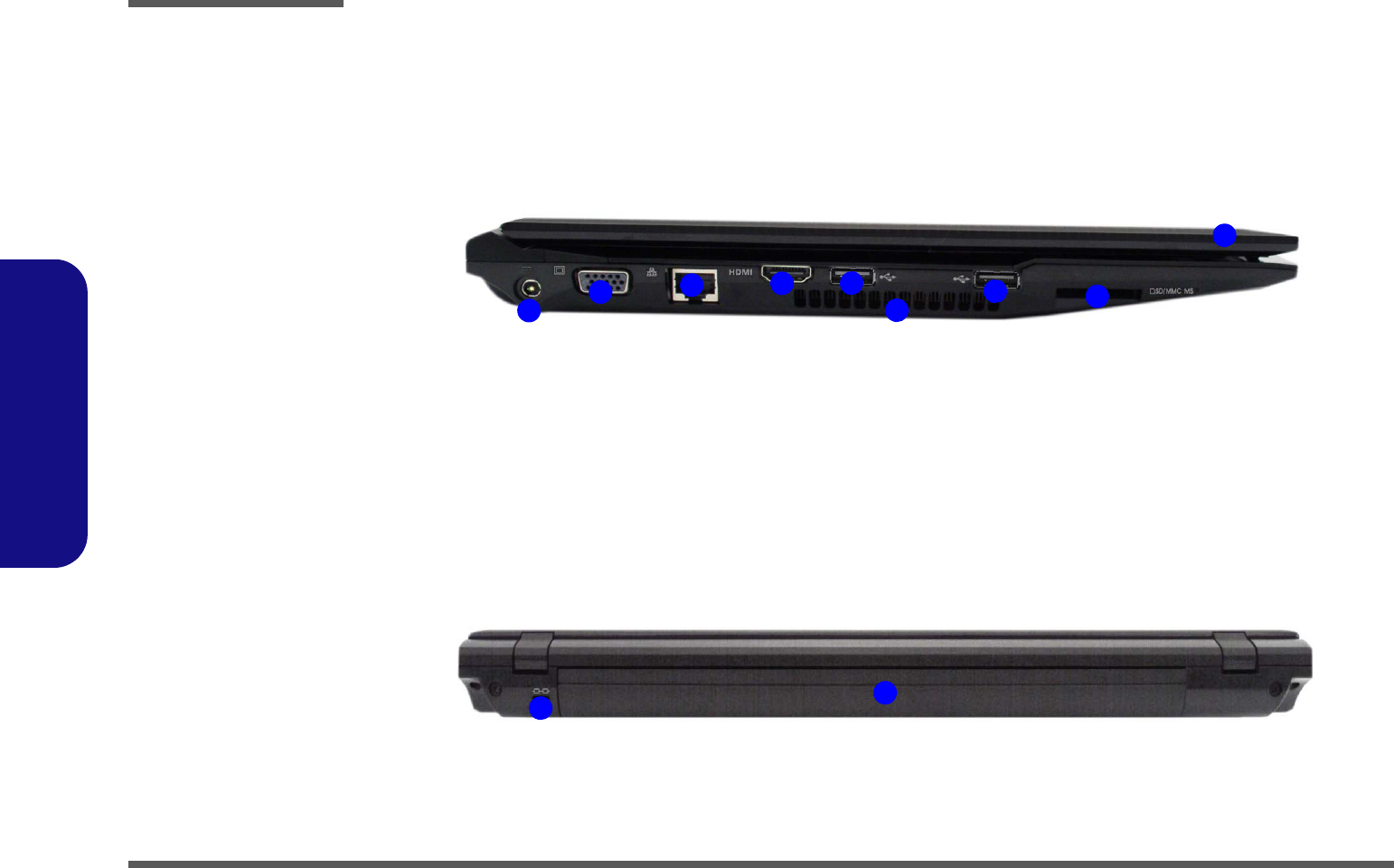
External Locator - Left Side & Rear View
/
Figure 4
Left Side View
1. DC-In Jack
2. External Monitor
Port
3. RJ-45 LAN Jack
4. HDMI-Out Port
5. USB 3.0 Port
6. Vent
7. Multi-in-1 Card
Reader
LEFT SIDE VIEW
12345
67
8
5
Figure 5
Rear View
1. Security Lock Slot
2. Battery
REAR VIEW
12
Introduction
External Locator - Bottom View 1 - 7
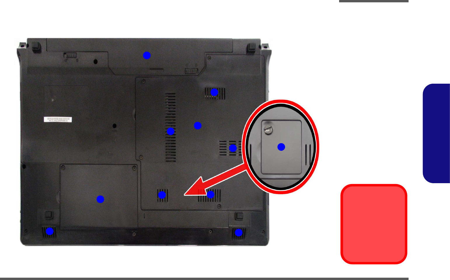
1.Introduction
External Locator - Bottom View
Figure 6
Bottom View
1. Battery
2. Component Bay
Cover
3. Vent
4. Hard Disk Bay
Cover
5. Speakers
6. USIM Card Cover
Overheating
To prevent your com-
puter from overhea-
ting, make sure no-
thing blocks any vent
while the computer is
in use.
2
3
1
4
3
3
5
5
3
3
6
Introduction
1 - 8 Mainboard Overview - Top (Key Parts)
1.Introduction
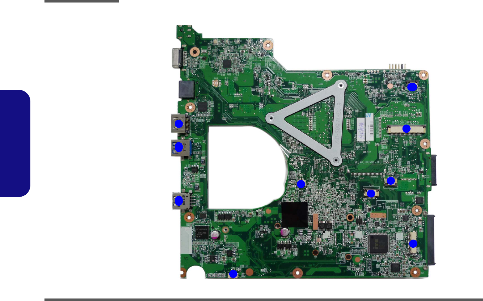
Mainboard Overview - Top (Key Parts)
Figure 7
Mainboard Top
Key Parts
1. KBC-ITE IT8518
2. Audio Codec
VT1802P
1
2
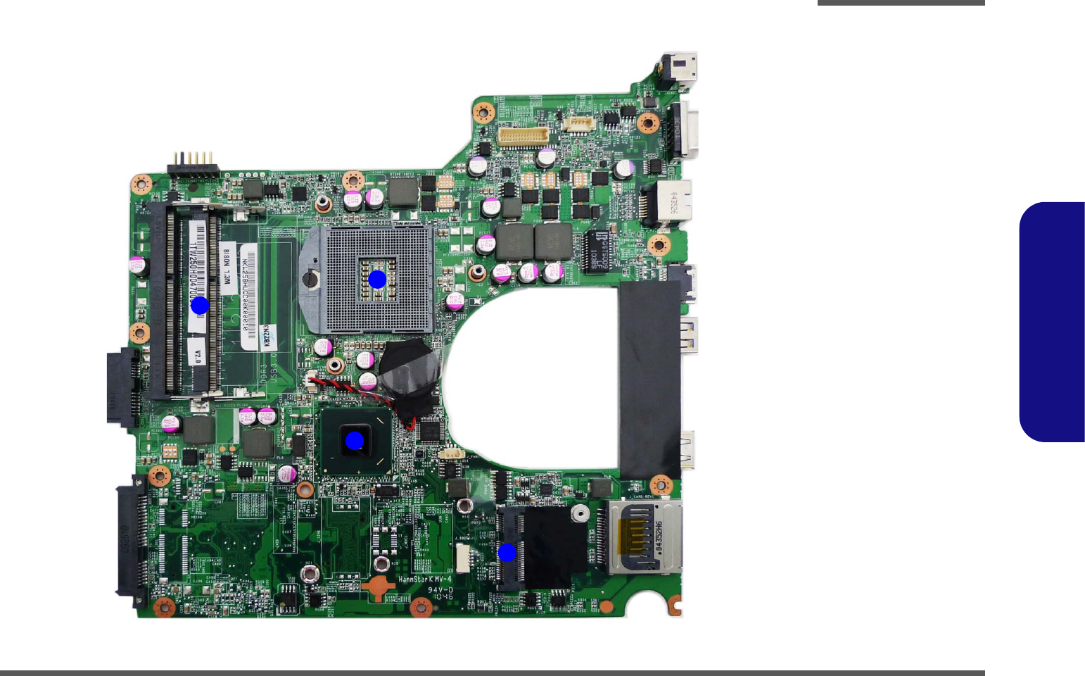
1
2
3
4
Figure 8
Mainboard Bottom
Key Parts
1. Memory Slots
DDR3 SO-DIMM
2. CPU Socket (no
CPU installed)
3. Platform Controller
Hub
4. Mini-Card
Connector (WLAN
Module)
Introduction
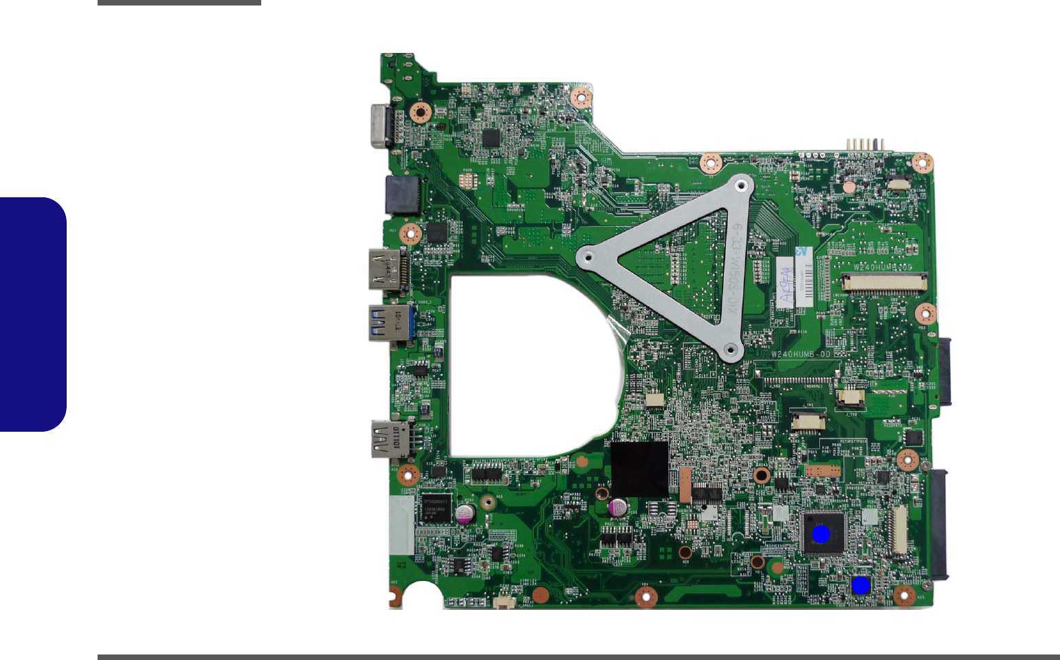
Mainboard Overview - Bottom (Key Parts) 1 - 9
1.Introduction
Mainboard Overview - Bottom (Key Parts)
Introduction
1 - 10 Mainboard Overview - Top (Connectors)
1.Introduction
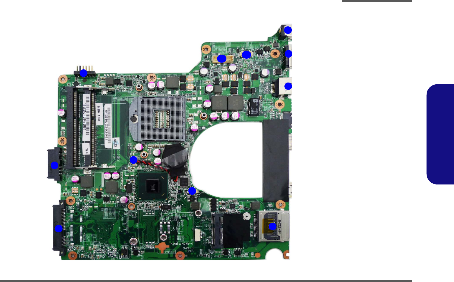
Mainboard Overview - Top (Connectors)
Figure 9
Mainboard Top
Connectors
1. HDMI-Out Port
2. USB 3.0 Port
3. Speaker Cable
Connector
4. Microphone
Cable Connector
5. Audio Board
Connector
6. TouchPad Cable
Connector 1
7. TouchPad Cable
Connector 2
8. Keyboard Cable
Connector
9. Switch Board
Cable Connector
7
1
2
8
3
4
5
6
9
2
Introduction
Mainboard Overview - Bottom (Connectors) 1 - 11
1.Introduction
Mainboard Overview - Bottom (Connectors)
Figure 10
Mainboard Bottom
Connectors
1. Battery
Connector
2. ODD Connector
3. HDD Connector
4. CMOS Battery
Connector
5. CPU Fan Cable
Connector
6. Multi-in-1 Card
Reader
7. RJ-45 LAN Jack
8. External Monitor
Port
9. DC-In Jack
10. CCD Cable
Connector
11. LCD Cable
Connector
1
24
5
6
7
8
9
3
10
11

Introduction
1 - 12
1.Introduction

Disassembly
Overview 2 - 1
2.Disassembly
Chapter 2: Disassembly
Overview
This chapter provides step-by-step instructions for disassembling the W251BLQ / W253BLQ / W253BZQ / W258BZQ
series notebook’s parts and subsystems. When it comes to reassembly, reverse the procedures (unless otherwise indicat-
ed).
We suggest you completely review any procedure before you take the computer apart.
Procedures such as upgrading/replacing the RAM, optical device and hard disk are included in the User’s Manual but are
repeated here for your convenience.
To make the disassembly process easier each section may have a box in the page margin. Information contained under
the figure # will give a synopsis of the sequence of procedures involved in the disassembly procedure. A box with a
lists the relevant parts you will have after the disassembly process is complete. Note: The parts listed will be for the dis-
assembly procedure listed ONLY, and not any previous disassembly step(s) required. Refer to the part list for the previ-
ous disassembly procedure. The amount of screws you should be left with will be listed here also.
A box with a will also provide any possible helpful information. A box with a contains warnings.
An example of these types of boxes are shown in the sidebar.
Information
Warning

Disassembly
2 - 2 Overview
2.Disassembly
NOTE: All disassembly procedures assume that the system is turned OFF, and disconnected from any power supply (the
battery is removed too).
Maintenance Tools
The following tools are recommended when working on the notebook PC:
• M3 Philips-head screwdriver
• M2.5 Philips-head screwdriver (magnetized)
• M2 Philips-head screwdriver
• Small flat-head screwdriver
• Pair of needle-nose pliers
• Anti-static wrist-strap
Connections
Connections within the computer are one of four types:
Locking collar sockets for ribbon connectors To release these connectors, use a small flat-head screwdriver to
gently pry the locking collar away from its base. When replac-
ing the connection, make sure the connector is oriented in the
same way. The pin1 side is usually not indicated.
Pressure sockets for multi-wire connectors To release this connector type, grasp it at its head and gently
rock it from side to side as you pull it out. Do not pull on the
wires themselves. When replacing the connection, do not try to
force it. The socket only fits one way.
Pressure sockets for ribbon connectors To release these connectors, use a small pair of needle-nose pli-
ers to gently lift the connector away from its socket. When re-
placing the connection, make sure the connector is oriented in
the same way. The pin1 side is usually not indicated.
Board-to-board or multi-pin sockets To separate the boards, gently rock them from side to side as
you pull them apart. If the connection is very tight, use a small
flat-head screwdriver - use just enough force to start.

Disassembly
Overview 2 - 3
2.Disassembly
Maintenance Precautions
The following precautions are a reminder. To avoid personal injury or damage to the computer while performing a re-
moval and/or replacement job, take the following precautions:
1. Don't drop it. Perform your repairs and/or upgrades on a stable surface. If the computer falls, the case and other
components could be damaged.
2. Don't overheat it. Note the proximity of any heating elements. Keep the computer out of direct sunlight.
3. Avoid interference. Note the proximity of any high capacity transformers, electric motors, and other strong mag-
netic fields. These can hinder proper performance and damage components and/or data. You should also monitor
the position of magnetized tools (i.e. screwdrivers).
4. Keep it dry. This is an electrical appliance. If water or any other liquid gets into it, the computer could be badly
damaged.
5. Be careful with power. Avoid accidental shocks, discharges or explosions.
•Before removing or servicing any part from the computer, turn the computer off and detach any power supplies.
•When you want to unplug the power cord or any cable/wire, be sure to disconnect it by the plug head. Do not pull on the wire.
6. Peripherals – Turn off and detach any peripherals.
7. Beware of static discharge. ICs, such as the CPU and main support chips, are vulnerable to static electricity.
Before handling any part in the computer, discharge any static electricity inside the computer. When handling a
printed circuit board, do not use gloves or other materials which allow static electricity buildup. We suggest that
you use an anti-static wrist strap instead.
8. Beware of corrosion. As you perform your job, avoid touching any connector leads. Even the cleanest hands pro-
duce oils which can attract corrosive elements.
9. Keep your work environment clean. Tobacco smoke, dust or other air-born particulate matter is often attracted
to charged surfaces, reducing performance.
10. Keep track of the components. When removing or replacing any part, be careful not to leave small parts, such as
screws, loose inside the computer.
Cleaning
Power Safety
Warning
Before you undertake
any upgrade proce-
dures, make sure that
you have turned off the
power, and discon-
nected all peripherals
and cables (including
telephone lines). It is
advisable to also re-
move your battery in
order to prevent acci-
dentally turning the
machine on.
Do not apply cleaner directly to the computer, use a soft clean cloth.
Do not use volatile (petroleum distillates) or abrasive cleaners on any part of the computer.

Disassembly
2 - 4 Disassembly Steps
2.Disassembly
Disassembly Steps
The following table lists the disassembly steps, and on which page to find the related information. PLEASE PERFORM
THE DISASSEMBLY STEPS IN THE ORDER INDICATED.
To remove the Battery:
1. Remove the battery page 2 - 5
To remove the HDD:
1. Remove the battery page 2 - 5
2. Remove the HDD page 2 - 6
To remove the Optical Device:
1. Remove the battery page 2 - 5
2. Remove the Optical device page 2 - 8
To remove the System Memory:
1. Remove the battery page 2 - 5
2. Remove the system memory page 2 - 9
To remove the Wireless LAN Module:
1. Remove the battery page 2 - 5
2. Remove the WLAN module page 2 - 11
To remove the Keyboard:
1. Remove the battery page 2 - 5
2. Remove the keyboard page 2 - 12
Disassembly
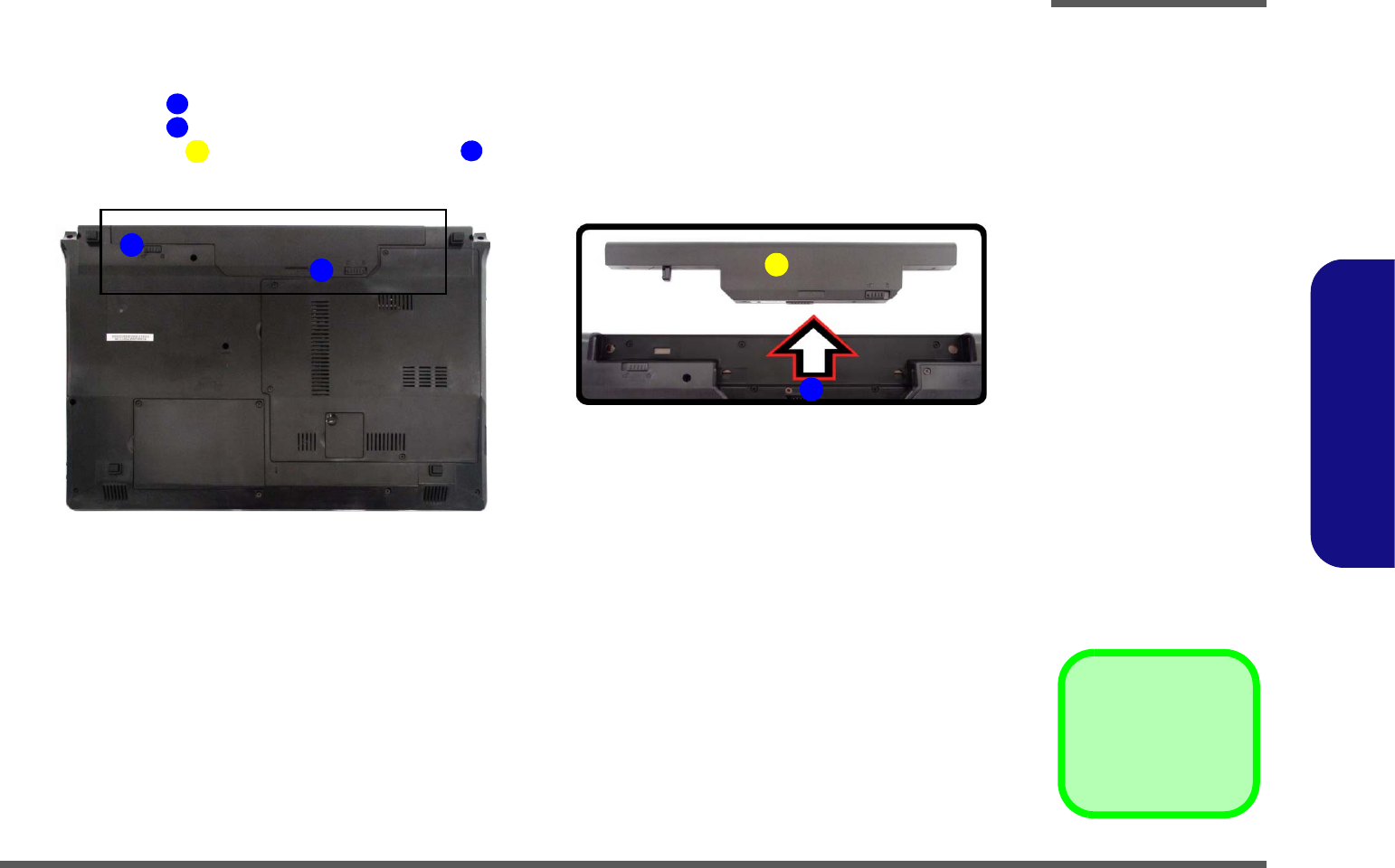
Removing the Battery 2 - 5
2.Disassembly
Removing the Battery
3. Battery
1. Turn the computer off, and turn it over.
2. Slide the latch in the direction of the arrow (Figure 1a).
3. Slide the latch in the direction of the arrow, and hold it in place (Figure 1a).
4. Slide the battery in the direction of the arrow (Figure 1b).
1
2
6
3
4
Figure 1
Battery Removal
a. Slide the latch and hold it
in place.
b. Slide the battery in the di-
rection of the arrow.
1
a. b.
3
2
4
Disassembly
2 - 6 Removing the Hard Disk Drive
2.Disassembly
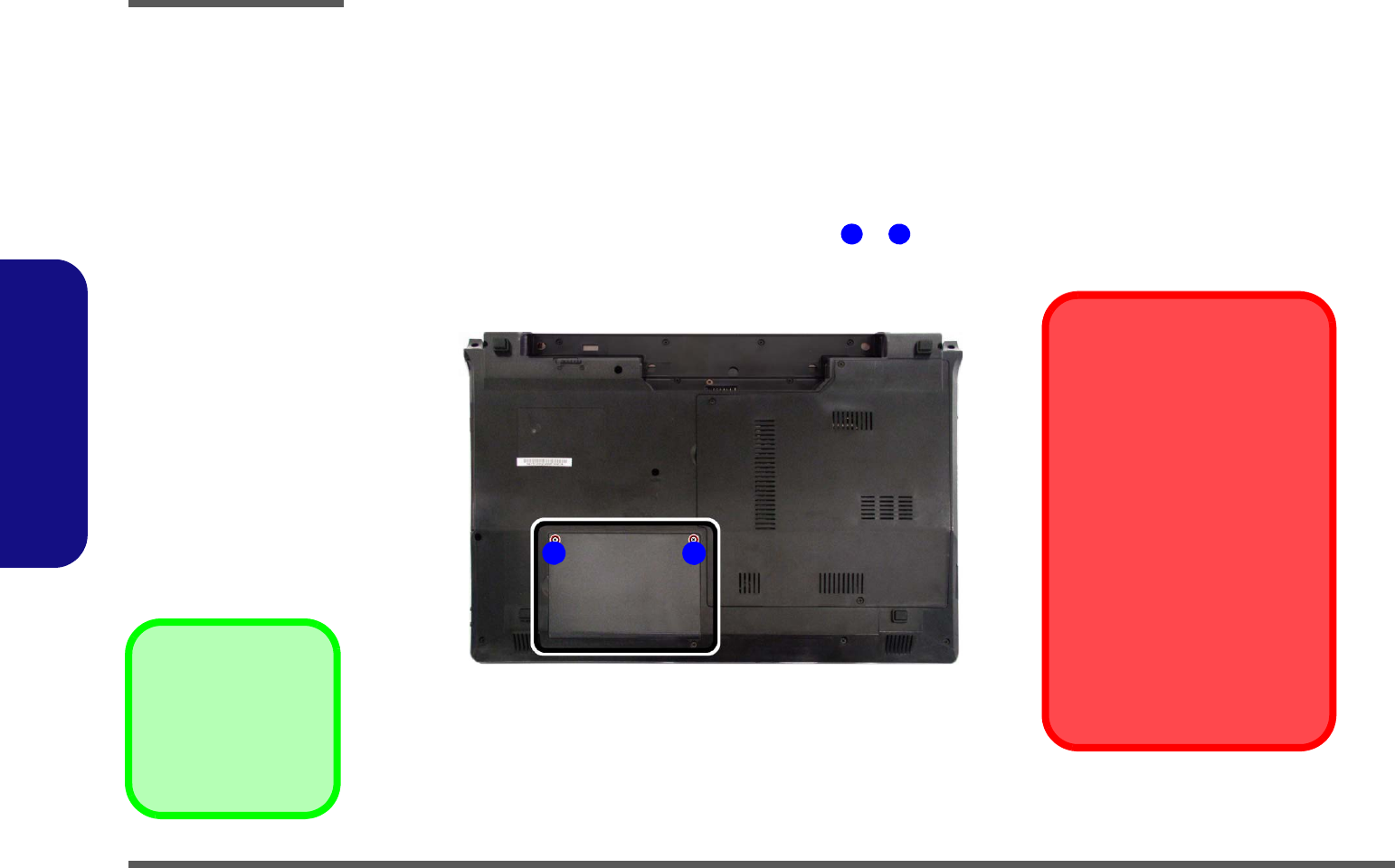
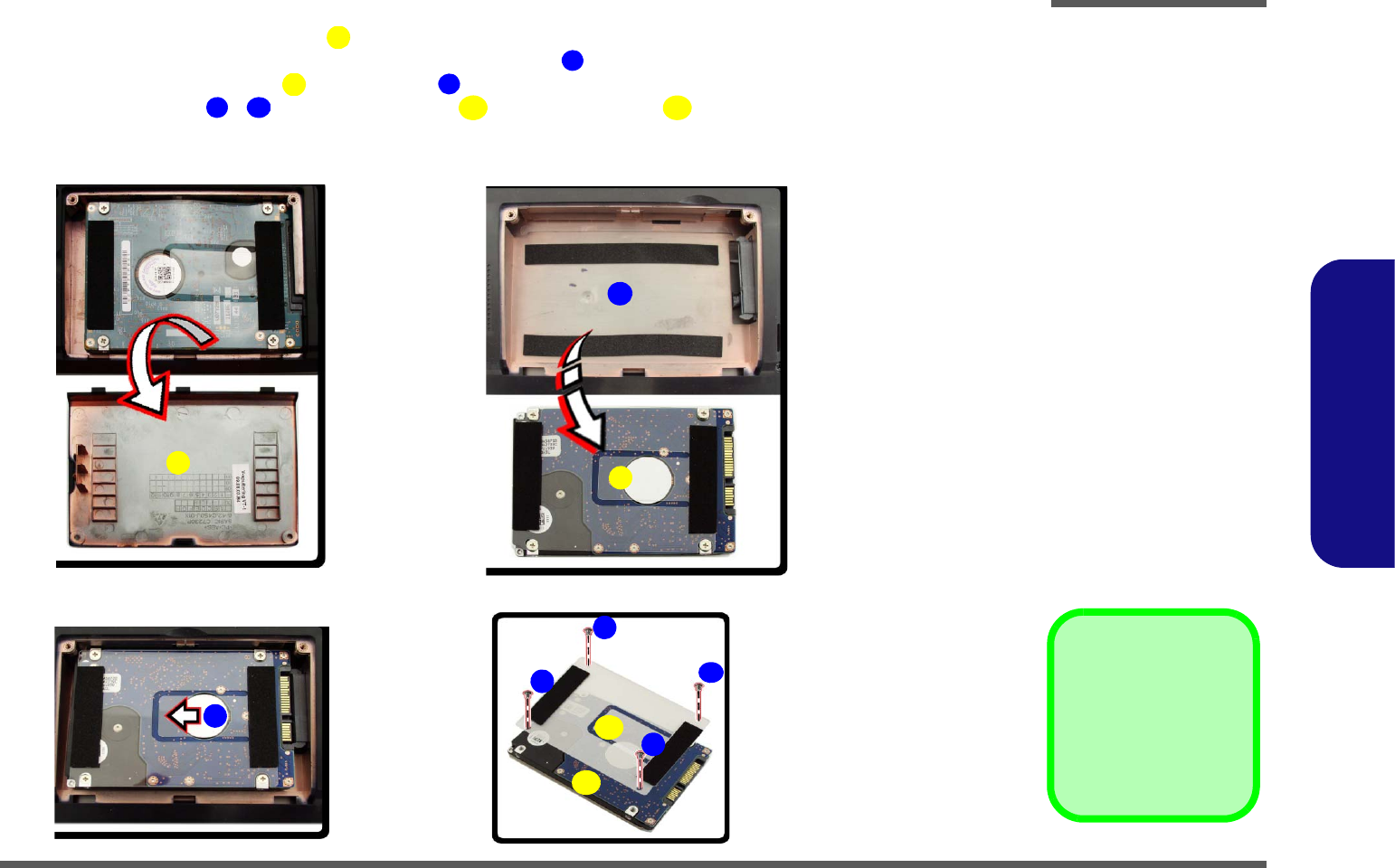
Removing the Hard Disk Drive
The hard disk drive can be taken out to accommodate other 2.5" serial (SATA) hard disk drives with a height of 9.5mm
(h). Follow your operating system’s installation instructions, and install all necessary drivers and utilities (as outlined in
Chapter 4 of the User’s Manual) when setting up a new hard disk.
Hard Disk Upgrade Process
Figure 2
HDD Assembly
Removal
a. Locate the HDD bay cover
and remove the screws.
•2 Screws
1. Turn off the computer, and remove the battery (page 2 - 5).
2. Locate the hard disk bay cover and remove screws & (Figure 2a).
1
2
2
1
a.
HDD System Warning
New HDD’s are blank. Before you
begin make sure:
You have backed up any data
you want to keep from your old
HDD.
You have all the CD-ROMs and
FDDs required to install your op-
erating system and programs.
If you have access to the internet,
download the latest application
and hardware driver updates for
the operating system you plan to
install. Copy these to a remov-
able medium.
Disassembly
Removing the Hard Disk Drive 2 - 7
2.Disassembly
3. Remove the hard disk bay cover (Figure 3b).
4. Grip the tab and slide the hard disk in the direction of arrow (Figure 3c).
5. Lift the hard disk assembly out of the bay (Figure 3d).
6. Remove the screw - and the mylar cover from the hard disk (Figure 3e).
7. Reverse the process to install a new hard disk (do not forget to replace all the screws and covers).
6
3
4
6
5
6
7
10
11
12
4
b.
c.
6
9
d.
3
e.
11
8
7
12
5
10
3
4
5
6
3. HDD Bay Cover
5. HDD Assembly
11. Mylar Cover
12. HDD
•4 Screws
Figure 3
HDD Assembly
Removal (cont’d.)
b. Remove the HDD bay
cover.
c. Grip the tab and slide the
HDD assembly in the di-
rection of the arrow.
d. Lift the HDD assembly
out of the bay.
e. Remove the screws and
mylar cover.
Disassembly
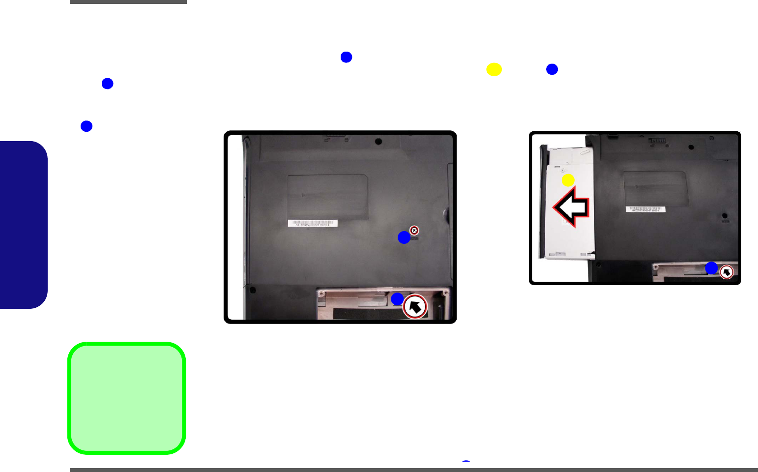
2 - 8 Removing the Optical (CD/DVD) Device
2.Disassembly
Removing the Optical (CD/DVD) Device
Figure 4
Optical Device
Removal
a. Remove the screw at
point .
b. Use a screwdriver to
carefully push out the
optical device at point
.
1
2
1. Turn off the computer, remove the battery (page 2 - 5) and hard disk (page 2 - 6).
2. Remove the screw at point (Figure 4a).
3. Use a screwdriver to carefully push out the optical device at point (Figure 4b).
4. Insert the new device and carefully slide it into the computer (the device only fits one way. DO NOT FORCE IT; The
screw holes should line up).
5. Restart the computer to allow it to automatically detect the new device.
1
3
2
3. Optical Device
•1 Screw
1
b.
3
a.
2
2
Disassembly
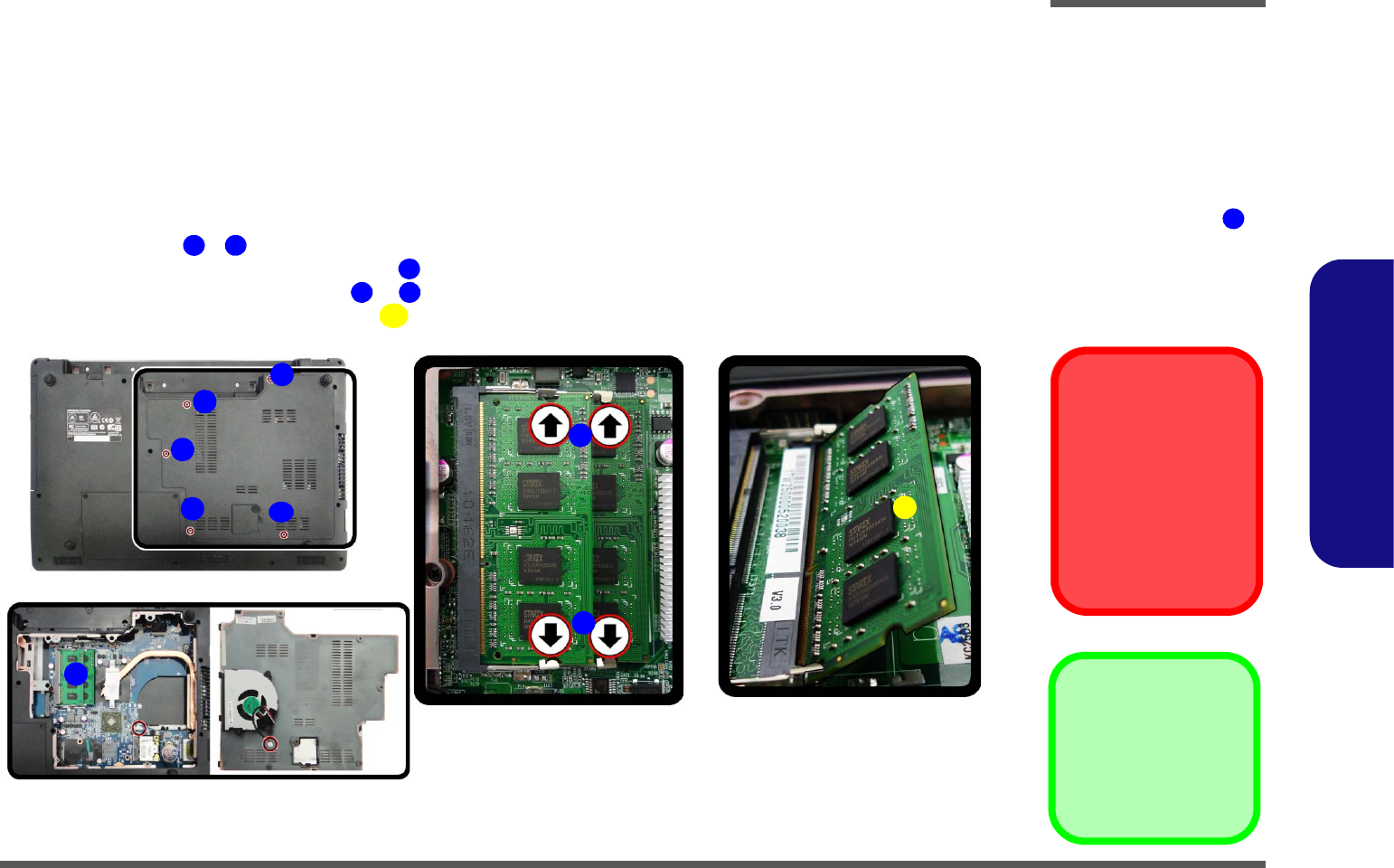
Removing the System Memory (RAM) 2 - 9
2.Disassembly
Removing the System Memory (RAM)
Figure 5
RAM Module
Removal
a. Remove the screws
and component bay
cover.
b. The RAM modules will
be visible at point
on the mainboard.
c. Pull the release lat-
ches.
d. Remove the module.
Contact Warning
Be careful not to touch
the metal pins on the
module’s connecting
edge. Even the cleanest
hands have oils which
can attract particles, and
degrade the module’s
performance.
5
The computer has two memory sockets for 204 pin Small Outline Dual In-line Memory Modules (SO-DIMM) supporting
DDRIII (DDR3) Up to 1066/1333 MHz. The main memory can be expanded up to 8GB. The SO-DIMM modules sup-
ported are 1024MB and 2048MB DDRIII Modules. The total memory size is automatically detected by the POST rou-
tine once you turn on your computer.
Memory Upgrade Process
9. RAM Module
•5 Screws
1. Turn off the computer, turn it over and remove the battery (page 2 - 5).
2. Remove screws - and the component bay cover (Figure 5a).
3. The RAM modules will be visible at point on the mainboard (Figure 5b).
4. Gently pull the two release latches ( & ) on the sides of the memory socket in the direction indicated by the
arrows (Figure 5c). The RAM module will pop-up (Figure 5d), and you can then remove it.
1
5
6
7
8
9
a. c. d.
8
7
9
b.
1
2
3
45
6
Disassembly
2 - 10 Removing the System Memory (RAM)
2.Disassembly
5. Pull the latches to release the second module if necessary.
6. Insert a new module holding it at about a 30° angle and fit the connectors firmly into the memory slot.
7. The module will only fit one way as defined by its pin alignment. Make sure the module is seated as far into the slot
as it will go. DO NOT FORCE IT; it should fit without much pressure.
8. Press the module in and down towards the mainboard until the slot levers click into place to secure the module.
9. Replace the bay cover and screws (make sure you reconnect the fan cable before screwing down the bay
cover).
Note that there are four cover pins which need to be aligned with slots in the case, to insure a proper cover fit,
before screwing down the bay cover (Figure 6d).
10. Restart the computer to allow the BIOS to register the new memory configuration as it starts up.
e.
Figure 6
RAM Module
Removal (cont’d.)
e. Properly re-insert the
bay cover pins.

Disassembly
Removing the Wireless LAN Module 2 - 11
2.Disassembly
Removing the Wireless LAN Module
Figure 7
Wireless LAN
Module Removal
a. Locate the WLAN.
b. Disconnect the cable
and remove the screw.
c. The WLAN module will
pop up.
d. Remove the Wireless
LAN module.
Note: Make sure you
reconnect the antenna
cable to the “1 + 2”
socket (Figure 7b).
1. Turn off the computer, turn it over, and remove the battery (page 2 - 5) and the component bay cover (page 2 - 9).
2. The Wireless LAN module will be visible at point on the mainboard (Figure 7a).
3. Carefully disconnect the cable , and then remove the screw (Figure 7b).
4. The Wireless LAN module (Figure 7c) will pop-up, and you can remove it from the computer (Figure 7d).
1
2
3
4
b.
c.
a.
2
3
d.
4
4
1
4.Wireless LAN Module
•1 Screw
Disassembly
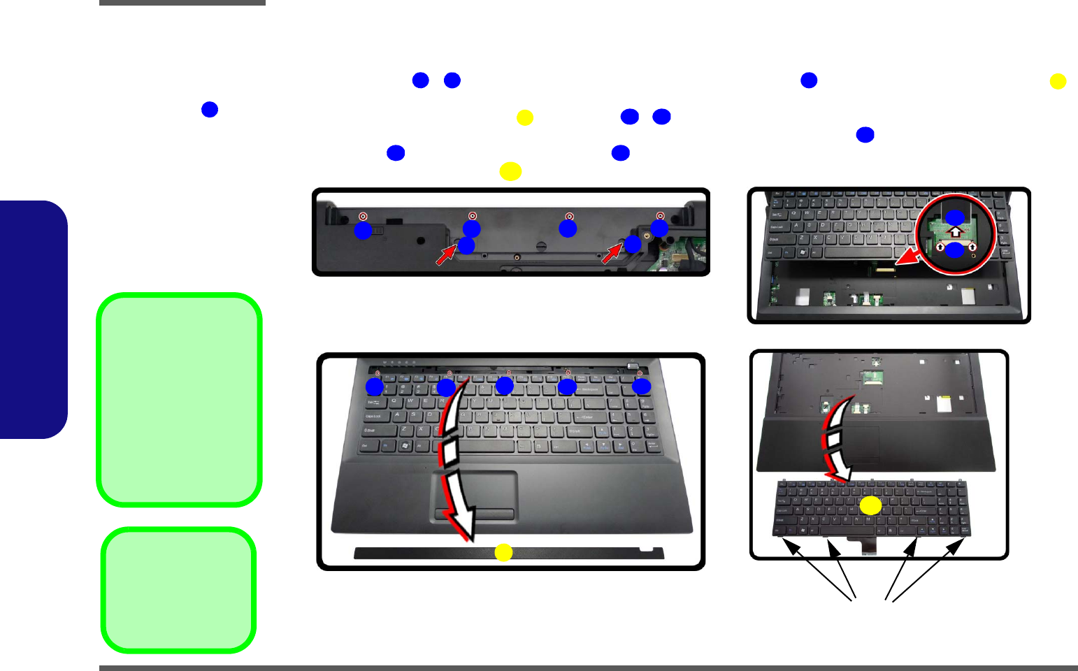
2 - 12 Removing the Keyboard
2.Disassembly
Removing the Keyboard
Figure 8
Keyboard Removal
a. Remove screws from the
bottom of the computer.
Press at points to un-
snap the LED cover
module.
b. Remove the LED cover
module and screws
from the keyboard.
c. Carefully lift the key-
board up and disconnect
the keyboard ribbon ca-
ble from the locking col-
lar socket.
d. Remove the keyboard.
5
1. Turn off the computer, and remove the battery (page 2 - 5).
2. Remove screws - from the bottom of the computer. Press at points to unsnap the LED cover module
(you may need to use the Eject Pin Tool to do this (Figure 8a).
3. Remove the LED cover module and screws - from the keyboard (Figure 8b).
4. Carefully lift the keyboard up, being careful not to bend the keyboard ribbon cable . Disconnect the keyboard
ribbon cable from the locking collar socket (Figure 8c)
5. Carefully lift up the keyboard (Figure 8d) off the computer.
1
4
5
6
6
7
11
12
12
13
14
Re-Inserting the
Keyboard
When re-inserting the
keyboard firstly align the
four keyboard tabs at the
bottom (Figure 8c) at the
bottom of the keyboard
with the slots in the case.
a.
Keyboard Tabs
13
24
7
5
c.
b. d.
89
14
10 11
12
6
513
6. LED Cover Module
14. Keyboard
•9 Screws

A - 1
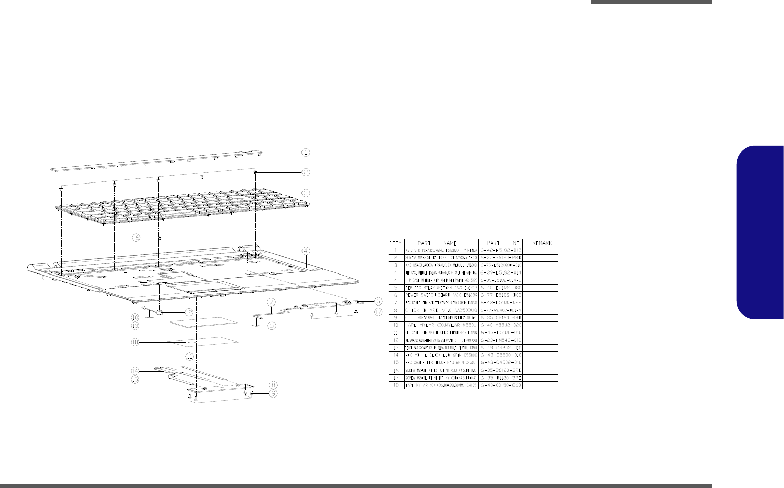
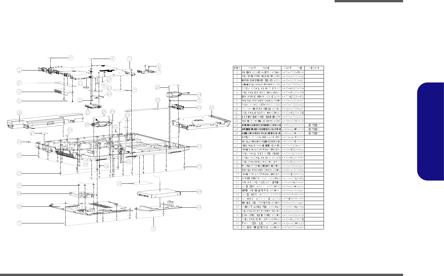
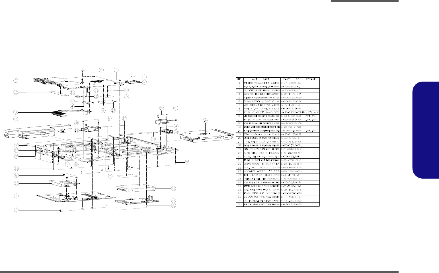
A.Part Lists
Appendix A:Part Lists
This appendix breaks down the W251BLQ / W253BLQ / W253BZQ / W258BZQ series notebook’s construction into a
series of illustrations. The component part numbers are indicated in the tables opposite the drawings.
Note: This section indicates the manufacturer’s part numbers. Your organization may use a different system, so be sure
to cross-check any relevant documentation.
Note: Some assemblies may have parts in common (especially screws). However, the part lists DO NOT indicate the
total number of duplicated parts used.
Note: Be sure to check any update notices. The parts shown in these illustrations are appropriate for the system at the
time of publication. Over the product life, some parts may be improved or re-configured, resulting in new part numbers.
A - 2
A.Part Lists
Part List Illustration Location
The following table indicates where to find the appropriate part list illustration.
Table A - 1
Part List Illustration
Location Part W251BLQ W253BLQ W253BZQ W258BZQ
Top page A - 3 page A - 4 page A - 5
Bottom page A - 6 page A - 7 page A - 8 page A - 9
DVD Dual Drive page A - 10 page A - 11 page A - 12
LCD page A - 13 page A - 14 page A - 15 page A - 16
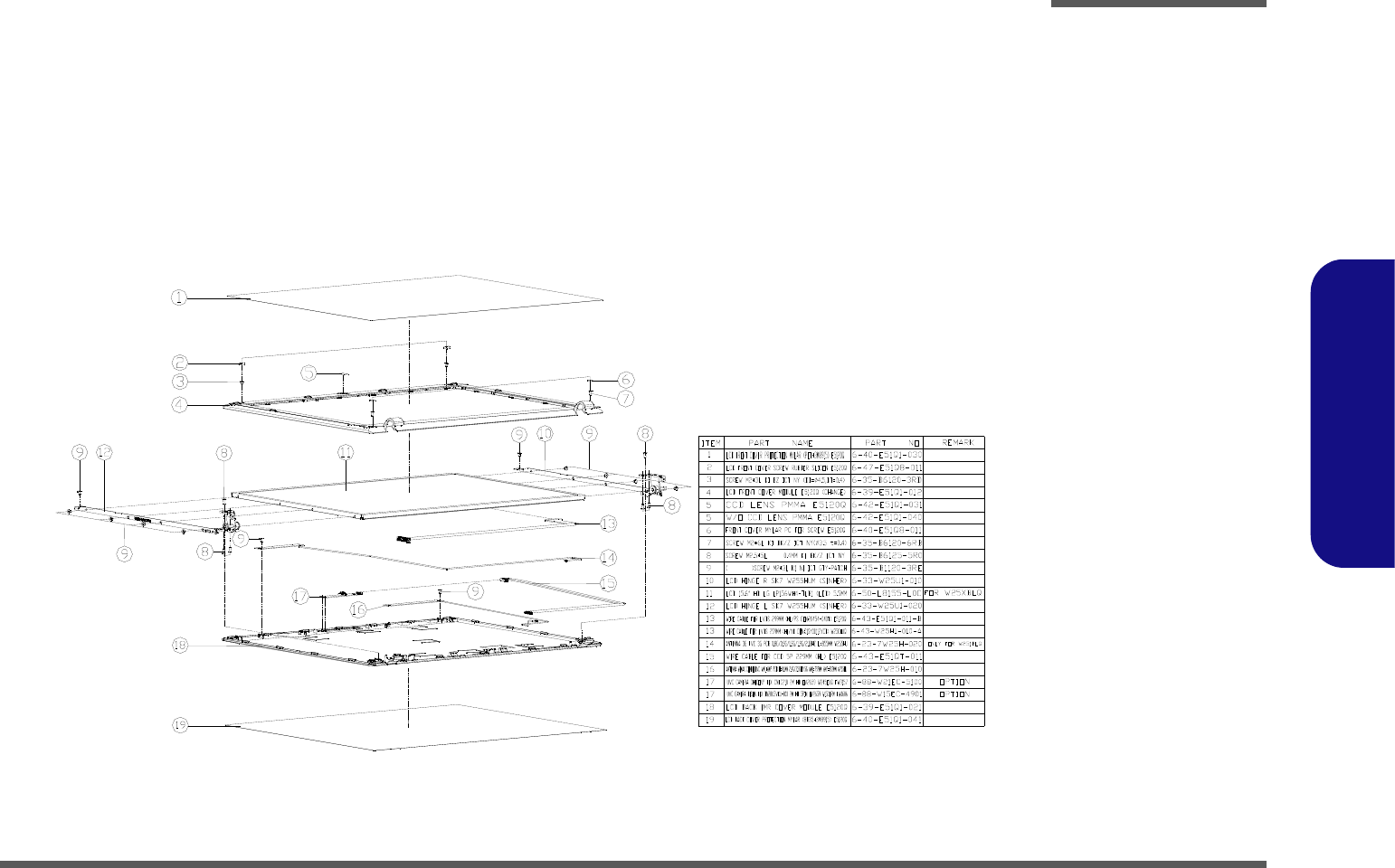
Top (W251BLQ) A - 3
A.Part Lists
Top (W251BLQ)
(灰色) (尚盟)
非耐落
Figure A - 1
Top (W251BLQ)
A - 4 Top (W253BLQ / W253BZQ)
A.Part Lists
Top (W253BLQ / W253BZQ)
Figure A - 1
Top (W251BLQ /
W253BLQ /
W253BZQ /
W258BZQ)
Top (W258BZQ) A - 5
A.Part Lists
Top (W258BZQ)
灰色
非耐落
Figure A - 1
Top (W258BZQ)
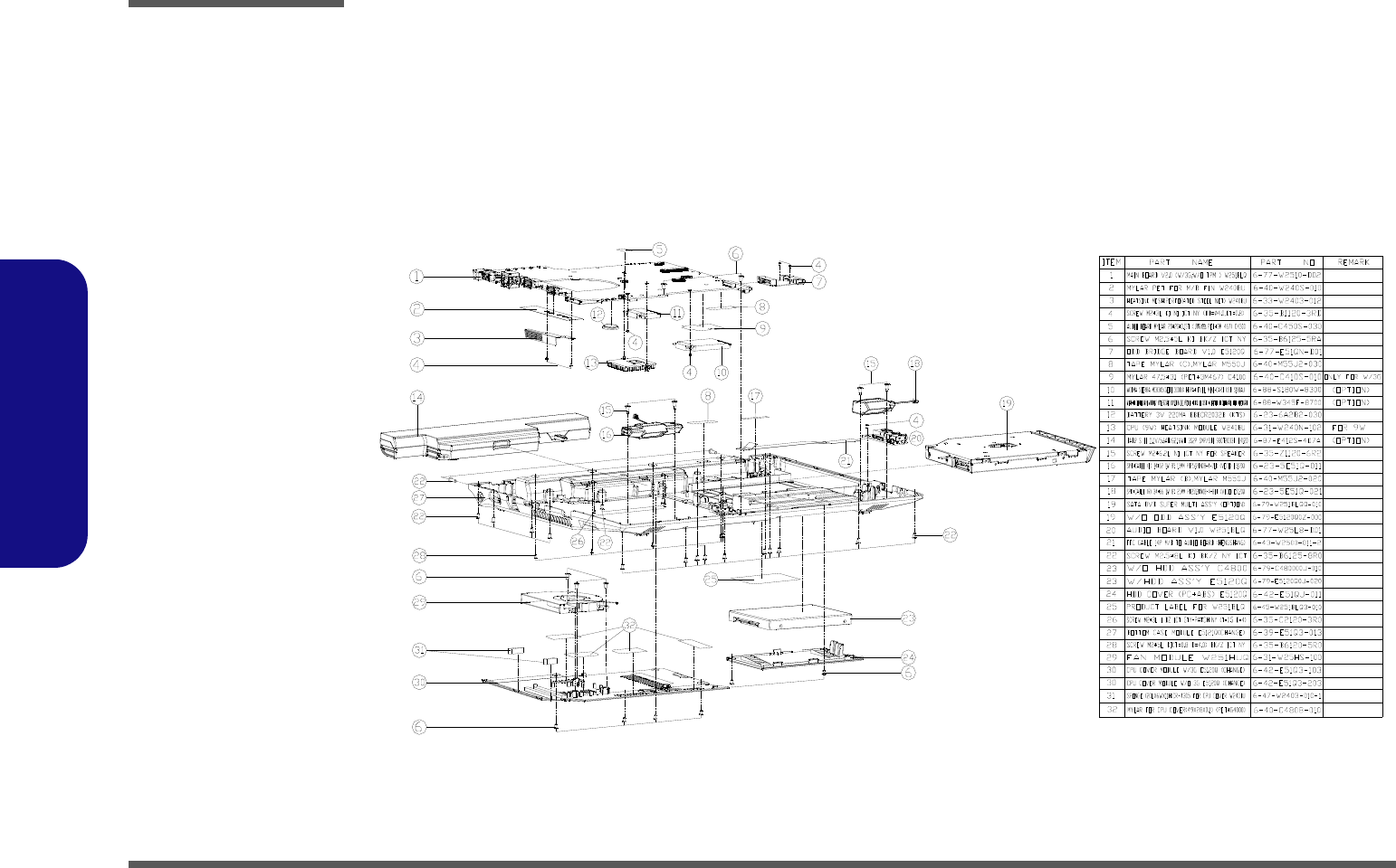
A - 6 Bottom (W251BLQ)
A.Part Lists
Bottom (W251BLQ)
Figure A - 2
Bottom
(W251BLQ)
Bottom (W253BLQ) A - 7
A.Part Lists
Bottom (W253BLQ)
Figure A - 3
Bottom
(W253BLQ)
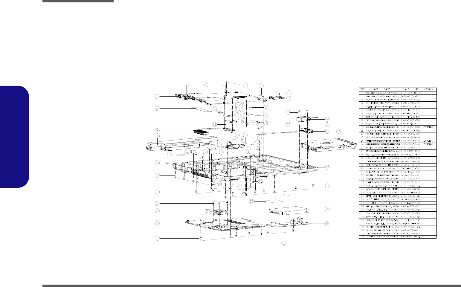
A - 8 Bottom (W253BZQ)
A.Part Lists
Bottom (W253BZQ)
Figure A - 4
Bottom
(W253BZQ)
Bottom (W258BZQ) A - 9
A.Part Lists
Bottom (W258BZQ)
Figure A - 5
Bottom
(W258BZQ)
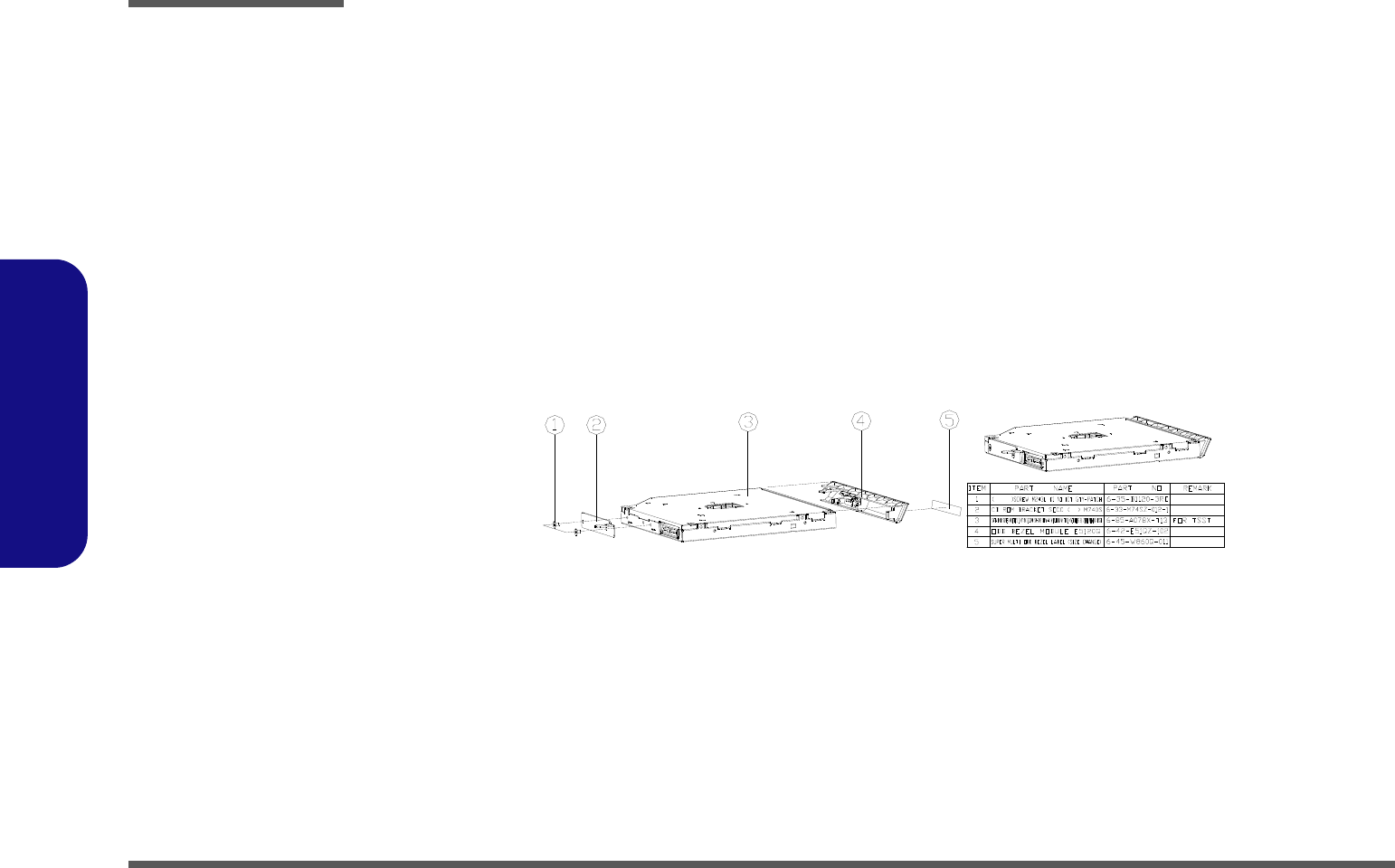
A - 10 DVD (W251BLQ)
A.Part Lists
DVD (W251BLQ)
非耐落
志精
Figure 6
DVD (W251BLQ)
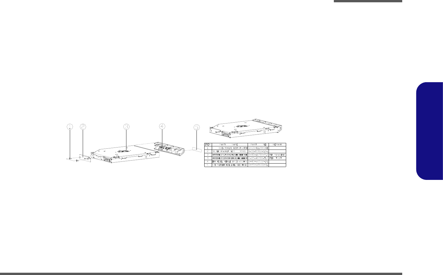
DVD (W253BLQ / W253BZQ) A - 11
A.Part Lists
DVD (W253BLQ / W253BZQ)
非耐落
志精
Figure 7
DVD (W253BLQ /
W253BZQ)
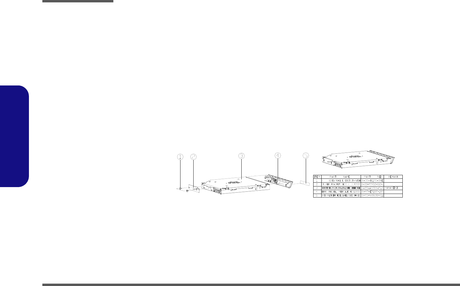
A - 12 DVD (W258BZQ)
A.Part Lists
DVD (W258BZQ)
Figure A - 8
DVD (W258BZQ)
非耐落
志精
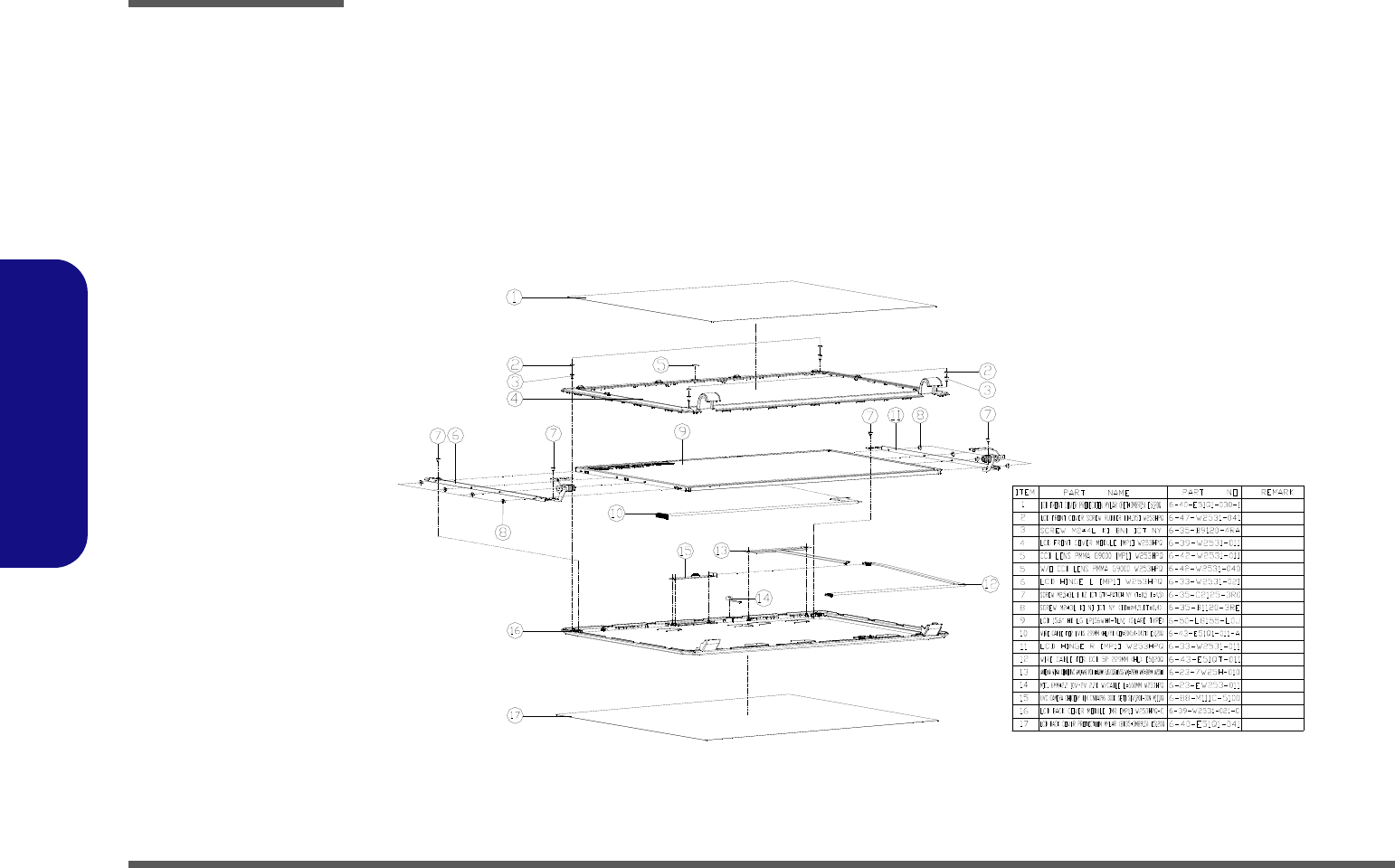
LCD (W251BLQ) A - 13
A.Part Lists
LCD (W251BLQ)
頭厚
非耐落
Figure A - 9
LCD (W251BLQ)
A - 14 LCD (W253BLQ)
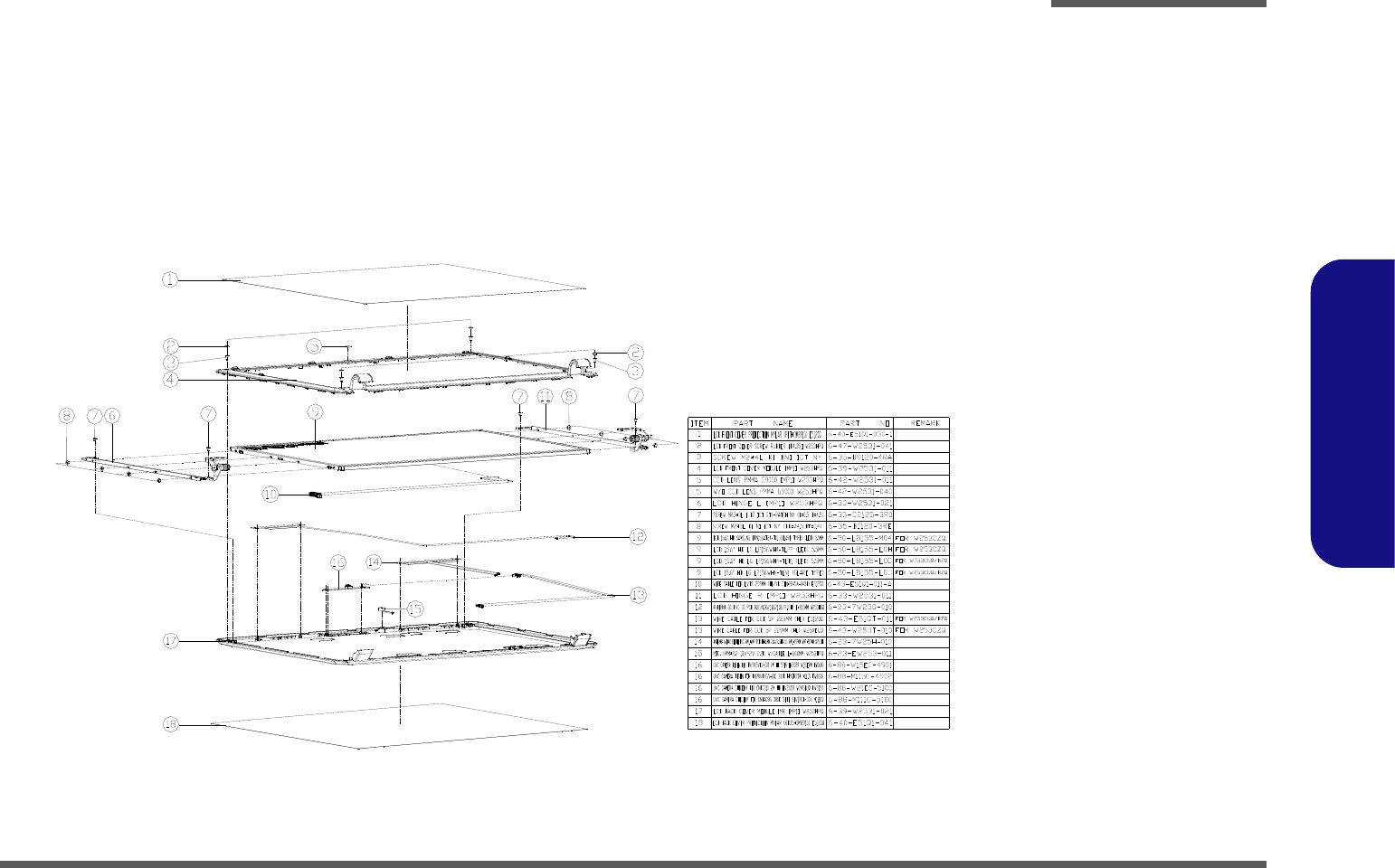
A.Part Lists
LCD (W253BLQ)
Figure A - 10
LCD (W253BLQ)
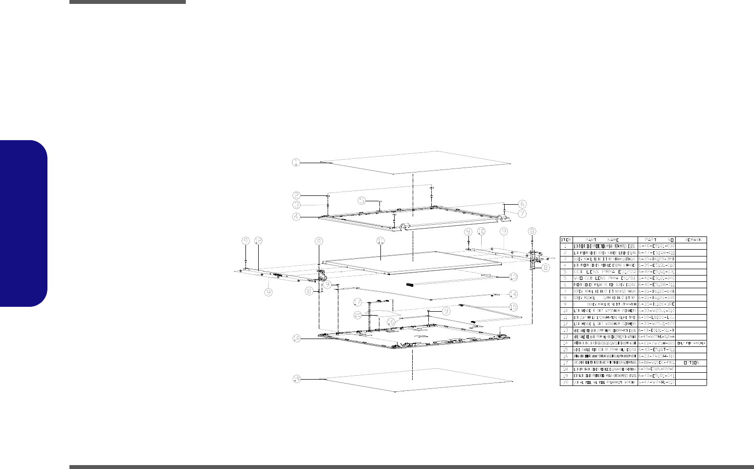
LCD (W253BZQ) A - 15
A.Part Lists
LCD (W253BZQ)
Figure A - 11
LCD (W253BZQ)
A - 16 LCD (W258BZQ)
A.Part Lists
LCD (W258BZQ)
Figure A - 12
LCD (W258BZQ)
頭厚
非耐落
Schematic Diagrams
B - 1
B.Schematic Diagrams
Appendix B: Schematic Diagrams
Table B - 1
SCHEMATIC
DIAGRAMS
This appendix has circuit diagrams of the W251BLQ / W253BLQ / W253BZQ / W258BZQ notebook’s PCB’s. The fol-
lowing table indicates where to find the appropriate schematic diagram.
Diagram - Page Diagram - Page
System Block Diagram - Page B - 2 Audio Codec VT1802P - Page B - 19
Ontario MEM & PCIE I/F, AP - Page B - 3 USB 3.0/USB Charge - Page B - 20
Ontario Display/CLK/MISC - Page B - 4 KBC-ITE IT8518 - Page B - 21
Ontario Power & Decoupling - Page B - 5 LED/MDC/BT - Page B - 22
NAGUA DDR3 SO-DIMMS A - Page B - 6 Fan/TP/Multi CON - Page B - 23
NAGUA DDR3 SO-DIMMS B - Page B - 7 5VS/3.3VS/1.8VS/1.5VS/1.1VS - Page B - 24
HUDSON PCIE/PCI/CLOCK/FCH - Page B - 8 Power VDD3, VDD5 - Page B - 25
HUDSON GPIO/USB/STRAP - Page B - 9 Power 1.5V/0.75V - Page B - 26
HUDSON SATA/DEBUG IO/SPI - Page B - 10 Power 1.1V/1VS - Page B - 27
HUDSON Power Decoupling - Page B - 11 Power 1.8VS - Page B - 28
POWERGOOD/TPM - Page B - 12 APU Core/NB Core - Page B - 29
ANX3110 ASIC - Page B - 13 Charger, DC In - Page B - 30
LVDS/Inverter - Page B - 14 Click Board - Page B - 31
HDMI/CRT - Page B - 15 Audio Board/USB - Page B - 32
CCD/3G - Page B - 16 Power Switch & LID Board - Page B - 33
CardReader/LAN RTL8402 - Page B - 17 External ODD Board - Page B - 34
Mini PCIE/SATA HDD/ODD - Page B - 18
Version Note
The schematic dia-
grams in this chapter
are based upon ver-
sion 6-7P-W25L5-002.
If your mainboard (or
other boards) are a lat-
er version, please
check with the Service
Center for updated di-
agrams (if required).
Schematic Diagrams
B - 2 System Block Diagram
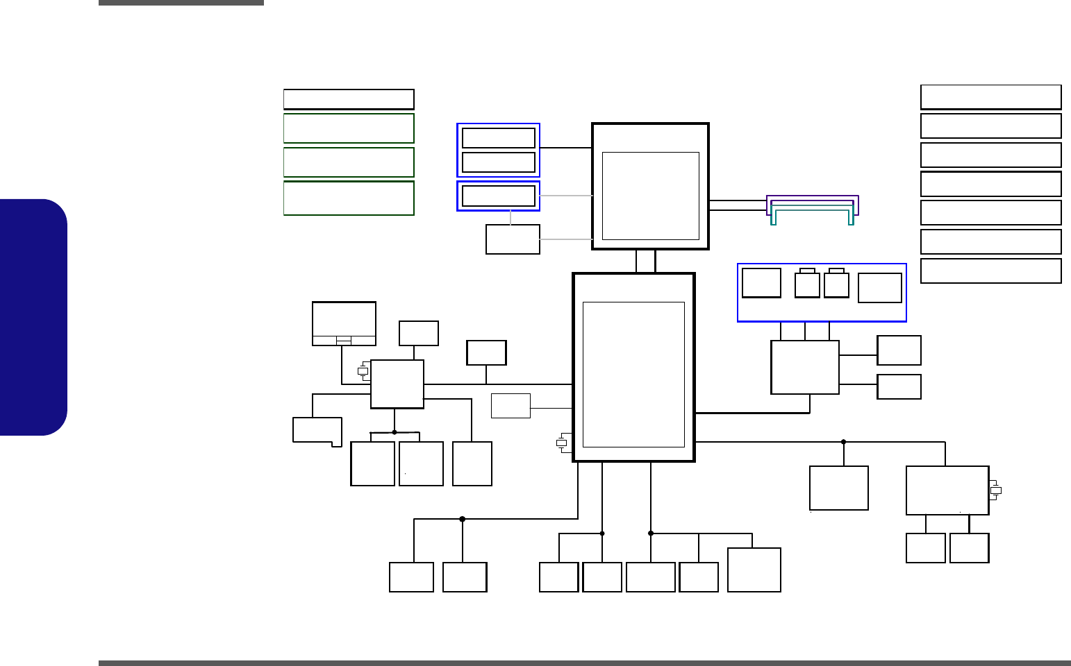
B.Schematic Diagrams
System Block Diagram
Sheet 1 of 33
System Block
Diagram
(USB2)
TOUCH PAD
LPC
CARD
READER
SO-DIMM1
HP
OUT INT SPK R
CLICK BOARD
SOCKET
PCIE 2.0
480 Mbps
DDRIII
Mini PCIE
SPI
DDRIII
INT MIC
25
MHz
LCD Connector
AMD FUSION APU
CRT Connector
HDMI Connector
24 MHz
MIC
IN
128pins LQFP
SO-DIMM2
32.768KHz
(USB6)
Bluetooth
1.1V, 1VS
EC SMBUS
USB 3.0
AZALIA LINK
(USB10) (USB11)
USB 3.0
SATA ODDSATA HDD
BIOS
SPI
LAN
ITE 8518
INT. K/B
Azalia Codec
EC
(Reserve W25XBLQ/W25XBZQ/W27XBZQ) 5V,3V,5VS,3.3VS
1.5V,0.75VS
USB2.0
ANX3110
VDD3,VDD5
UMI*4
G711ST9U
32.768 KHz
REALTEK
APU_CORE,NB_CORE
SHEET 7,8,9,10
SATA I/II 3.0Gb/s
1066MHz
DDR3 / 1.5V
(Reserve)
TPM
CCD
(USB5)
VT1802P
33 MHz
THERMAL
SENSOR
100 MHz
14*14*1.6mm
SMART
FAN
SMART
BATTERY
AC-IN
RTL 8402
W24XBL/BZ System Block Diagram
RJ-45 7IN1
SOCKET
INT SPKER
POWER SWITCH+HOTKEY X 3
6-71-E51QS-D02
CLICK BOARD
EXT. ODD
EXTERNAL ODD BOARD
6-71-W2402-D02
POWER SWITCH BOARD
USB+EARPHONE+EXT.MIC
AUDIO BOARD
6-71-E51QN-D01
6-71-W25L8-D01
(USB3)
USB PORT
Ontario FT1
413-BALL
19mmX19mm BGA
VGA DAC
DISPLAY PORT X2
4 X1 PCIE GEN2 GPP
1 X4 UMI-LINK GEN1
SINGLE CHANNEL DDR3
DX11 IGP
AMD HUDSON-M3L
24.5mmX24.5mm BGA
HW MONITOR
GB MAC
656-BALL
AZALIA HD AUDIO
SPI I/F
INT. CLKGEN
USB2.0(10) + USB3.0(2)
PCIE GE N2 I/F (4 x1)
LPC I/F
SATAII (2 PORTS)
CHARGER,DC IN
USB3.0
3G CARD
(USB7)
(Optional)
WLAN
1.8VS
1.5VS,1.1VS
Schematic Diagrams
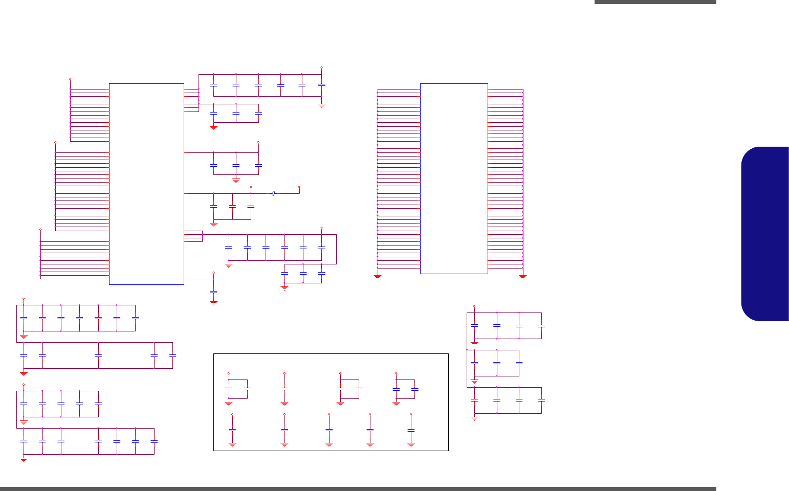
Ontario MEM & PCIE I/F, AP B - 3
B.Schematic Diagrams
Ontario MEM & PCIE I/F, AP
Sheet 2 of 33
Ontario MEM &
PCIE I/F, AP
MEM_DATA63
C10 0.1u_10V_X7R_04
MEM_DATA4
C11 0.1u_10V_X7R_04
C12 0.1u_10V_X7R_04
MEM_DATA35
C13 0.1u_10V_X7R_04
C472
*1u_6.3V_Y5V_04
C_UMI_P_RX07
C14 0.1u_10V_X7R_04
C_UMI_N_RX07
MEM_DATA5
C_UMI_P_RX17C_UMI_N_RX17
C_UMI_N_RX27C_UMI_P_RX27
C15 0.1u_10V_X7R_04
C_UMI_P_RX37C_UMI_N_RX37C16 0.1u_10V_X7R_04
MEM_DATA36
C842
10u_6.3V_X5R_06
C_UMI_P_TX0 7
C_UMI_N_TX0 7
C_UMI_N_TX1 7
C_UMI_P_TX1 7
C_UMI_N_TX2 7
C_UMI_P_TX2 7
C_UMI_N_TX3 7
C_UMI_P_TX3 7
MEM_DATA6
R1 1.27K_1%_04
MEM_DATA37
MEM_DATA7
MEM_D QS_H05,6
MEM_EVENT#5,6
MEM_ AD DR [1 5: 0]5,6
MEM_DATA39
MEM_CLK_H05
MEM_DATA8
MEM_DATA38
MEM_DATA9
MEM_BANK15,6 MEM_BANK25,6
3.3V PTH3
10K_1%_N TC _06
1 2
R201
10K_1%_04
6-17-10300-730
MEM_DATA40
MEM_DATA10
ONTARIO (2.0)
PART 1 OF 5
MEMORY I/F
U1E
ONTARIO_APU
V17
M_WE_L
V19
M_CAS_L
U18
M_RAS_L
V16
M1_CS_L1
U17
M1_CS_L0
W16
M0_CS_L1
T17
M0_CS_L0
W15
M1_ODT1
U19
M1_ODT0
V15
M0_ODT1
W19
M0_ODT0
E15
M_CKE1
F15
M_CKE0
N17
M_EVENT_L
L23
M_RESET_L
L17
M_CLK_L3
L18
M_CLK_H3
N19
M_CLK_L2
N18
M_CLK_H2
M18
M_CLK_L1
M19
M_CLK_H1
M16
M_CLK_L0
M17
M_CLK_H0
AC16
M_DQS_L7
AB16
M_DQS_H7
AC21
M_DQS_L6
AC20
M_DQS_H6
V22
M_DQS_L5
W22
M_DQS_H5
P22
M_DQS_L4
R22
M_DQS_H4
J23
M_DQS_L3
J22
M_DQS_H3
E22
M_DQS_L2
E23
M_DQS_H2
A20
M_DQS_L1
B20
M_DQS_H1
B16
M_DQS_L0
A16
M_DQS_H0
AA16
M_DM7
AB20
M_DM6
V23
M_DM5
P23
M_DM4
H22
M_DM3
D21
M_DM2
B19
M_DM1
D15
M_DM0
F16
M_BANK2
T18
M_BANK1
R18
M_BANK0
G15
M_ADD15
E16
M_ADD14
W17
M_ADD13
E18
M_ADD12
F17
M_ADD11
T19
M_ADD10
E19
M_ADD9
F19
M_ADD8
G18
M_ADD7
H15
M_ADD6
G17
M_ADD5
H17
M_ADD4
H18
M_ADD3
J17
M_ADD2
H19
M_ADD1
R17
M_ADD0
M22
M_Z VD DIO _MEM_S
M23
M_VREF
AC15
M_DATA63
AB15
M_DATA62
AB18
M_DATA61
AC18
M_DATA60
AC14
M_DATA59
AB14
M_DATA58
Y16
M_DATA57
AC17
M_DATA56
Y18
M_DATA55
AB19
M_DATA54
AA20
M_DATA53
AA23
M_DATA52
AA18
M_DATA51
AC19
M_DATA50
AB22
M_DATA49
Y20
M_DATA48
Y21
M_DATA47
W23
M_DATA46
U23
M_DATA45
T21
M_DATA44
Y22
M_DATA43
Y23
M_DATA42
V21
M_DATA41
V20
M_DATA40
T22
M_DATA39
R23
M_DATA38
P20
M_DATA37
M20
M_DATA36
T23
M_DATA35
T20
M_DATA34
P21
M_DATA33
N23
M_DATA32
K23
M_DATA31
K20
M_DATA30
H20
M_DATA29
G23
M_DATA28
K21
M_DATA27
K22
M_DATA26
H23
M_DATA25
H21
M_DATA24
F21
M_DATA23
F20
M_DATA22
D22
M_DATA21
C22
M_DATA20
F22
M_DATA19
F23
M_DATA18
D23
M_DATA17
C23
M_DATA16
C20
M_DATA15
A21
M_DATA14
B18
M_DATA13
A18
M_DATA12
D20
M_DATA11
B21
M_DATA10
A19
M_DATA9
C18
M_DATA8
D16
M_DATA7
C16
M_DATA6
C14
M_DATA5
A14
M_DATA4
D18
M_DATA3
A17
M_DATA2
A15
M_DATA1
B14
M_DATA0
MEM_CLK_L15
MEM_CLK_L26MEM_CLK_H26
MEM_CLK_L36MEM_CLK_H36
MEM_DATA41
MEM_DATA11
be directly to the plane without a long trace
R6 connection to 1.5V should
MEM_DATA12
MEM_DATA42
MEM_C KE15,6 MEM_C KE05,6
ONTARIO (2.0)
PART 2 OF 5
UMI I/F PCIE I/F
U1A
ONTARIO_APU
AB7
P_UM I _R XN3
AC7
P_UMI_RXP3
AC10
P_UM I _R XN2
AB10
P_UMI_RXP2
Y10
P_UM I _R XN1
AA10
P_UMI_RXP1
Y12
P_UM I _R XN0
AA12
P_UMI_RXP0
Y14
P_ZVDD_10
Y3
P_GPP_RXN3
Y4
P_GPP_RXP3
AA2
P_GPP_RXN2
AA1
P_GPP_RXP2
AC4
P_GPP_RXN1
AB4
P_GPP_RXP1
Y6
P_GPP_RXN0
AA6
P_GPP_RXP0
AC8
P_UMI _T XN3
AB8
P_UMI_T XP3
Y8
P_UMI _T XN2
AA8
P_UMI_T XP2
AB11
P_UMI _T XN1
AC11
P_UMI_T XP1
AC12
P_UMI _T XN0
AB12
P_UMI_T XP0
AA14
P_ZVSS
V4
P_GPP_TXN3
V3
P_GPP_TXP3
Y2
P_GPP_TXN2
Y1
P_GPP_TXP2
AC3
P_GPP_TXN1
AB3
P_GPP_TXP1
AC6
P_GPP_TXN0
AB6
P_GPP_TXP0
C844
0.1u_10V_X7R_04
R82 *68_1%_04
R81 *68_1%_04
MEM_C KE 1
MEM_C KE 0
MEM_DATA13
MEM_DATA43
DI MM0_ODT15D IMM0_OD T05
DI MM1_ODT16D IMM1_OD T06
MEM_CLK_L05
DI MM0_C S#15DI MM0_C S#05
DI MM1_C S#16DI MM1_C S#06
MEM_DATA14
MEM_DATA44
PLACE NEAR U1
MEM_DATA15
D02
MEM_DATA45
1:2 (4mils:8mils)
THERM_VOLT 20
1.5V
MEM_DATA16
MEM_DATA46
MEM_DATA17
MEM_DATA47
ON_ZVSSON_ZVDD
ROUTE A-LINK DIFF PAIR @ 85 OHM +/- 10%
MEM_R AS#5,6
MEM_WE#5,6 MEM_C AS#5,6
MEM_DATA18
1VS
MEM_DATA48
MEM_DATA19
MEM_DATA49
MEM_DATA20
MEM_ADD R0
MEM_AD DR10
MEM_AD DR12
MEM_AD DR11
MEM_AD DR13
MEM_AD DR14
Close to APU
MEM_AD DR2
MEM_AD DR3
MEM_AD DR5
MEM_AD DR15
MEM_AD DR4
MEM_AD DR1
MEM_AD DR8
MEM_AD DR7
MEM_AD DR9
MEM_AD DR6
MEM_DATA50
MEM_RESET#5,6
MEM_D M1
MEM_D M3
MEM_D M0
MEM_D M2
C843
1000p_50V_X7R_04
MEM_D M7
MEM_D M5
MEM_D M6
MEM_D M4
R2 2K_1%_04
MEM_DATA21
MEM_Z VD DIO
MEM_DATA51
R678
1K_1%_04
MEM_D QS_H15,6 MEM_DQS_L05,6
MEM_D QS_L25,6 MEM_DQS_ H 25,6 MEM_DQS_L15,6
MEM_D QS_H45,6 MEM_DQS_L35,6 MEM_DQS_H35,6
MEM_D QS_H55,6 MEM_DQS_L45,6
MEM_D QS_L65,6 MEM_DQS_ H 65,6 MEM_DQS_L55,6
MEM_D QS_L75,6 MEM_DQS_ H 75,6
MEM_DATA22
MEM_DM[7:0]5,6
MEM_BANK05,6
MEM_DATA[63:0] 5,6
MEM_DATA52
MEM_DATA23
ONTARIO MEM & PCIE I/F, AP
MEM_DATA53
MEM_DATA24
MEM_DATA55
MEM_DATA25
MEM_DATA54
MEM_DATA26
R6 39.2_1%_04
MEM_CLK_H15
R681
1K_1%_04
W/O CPU THERMAL IC®,
PCB
MEM_DATA56
MEM_DATA27
MEM_DATA28
MEM_DATA0
MEM_DATA57
MEM_DATA29
MEM_DATA58
MEM_DATA30
MEM_DATA59
MEM_DATA31
MEM_DATA60
MEM_DATA1
MEM_DATA32
MEM_DATA61
MEM_DATA2
MEM_DATA33
MEM_DATA62
MEM_DATA3
1.5V
C9 0.1u_10V_X7R_04
MEM_DATA34
Schematic Diagrams
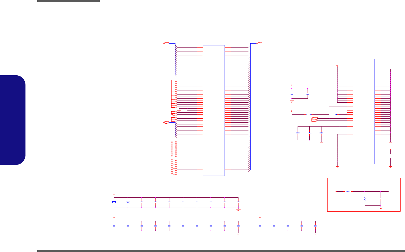
B - 4 Ontario Display/CLK/MISC
B.Schematic Diagrams
Ontario Display/CLK/MISC
APU_TEST28_H_PLLCHARZ
1.8VS R51
1K_04
CPU_SVD
APU_PWRGD
R593 100K_04
R54 *1K_04
R53 *1K_04
R35 *10mil_s hort_04
R36 *10mil_s hort_04
R71 *0_04
J108_PLLTST1 APU_TEST18_PLLTEST1
APU_TEST19_PLLTEST0J108_PLLTST0 R70 *0_04
R42 51_04
D02
R43 51_04
DBREQ# R69 1K_04
DBRDY
3.3VS
ONTARIO DISPLAY/CLK/MISC
APU_TEST36
R40 510_1%_04
CPU_THERMTRIP#8
APU_CLKP7
CPU_SVD28 CPU_SVC28
HDT+ HEADER / PLAC E ON TOP
PORTC_HPD 14
APU_CLKN7
1.8VS
R33 *10mil_short_04
R34 *10mil_short_04
R31 *0_04
R60 ON,R62 OFF W/0 ANX3110
R32 *0_04
1.8VS
R60 OFF,R62 ON WITH ANX3110
1.8VS
APU_SI D
APU_TEST28_L_PLLCHARZ
APU_PWRGD7, 28 LD T_RST#7
R65 *0_04
R59
1K_04
LDT_RST#
R66 *10K_04
D02
R41 510_1%_04
R44 *1K_04
APU_TALERT#9,20
R591 100K_04
ALLOW_LDTSTP 7
R58 1K_04
1.8VS
APU_TEST37_GIO_TSTDTM0_CLKINIT
R598 *10mil_short _04
R16 *10mil_short _04
1.8VS
C23 0.1u_16V_Y 5V_04
C24 0.1u_16V_Y 5V_04
1.8VS
D02
R97 *1K_04
R50 *10mil_short_04
LD T_RST#
J1
*HDR 10X2 - BLUE - VERTICAL PLUG
1
CPU_VDDIO
2
CPU_TCK
3
GND
4
CPU_T MS
5
GND
6
CPU_TDI
7
GND
8
CPU_T DO
9
CPU_ T RST_L
10
CPU_PWRO K_BUF
11
CPU_DBRDY3
12
CPU_RST_L_BUF
13
CPU_DBRDY2
14
CPU_DBRDY0
15
CPU_DBRDY1
16
CPU_DBREQ _L
17
GND
18
CPU_PLLTEST0
19
CPU_VDDIO
20
CPU_PLLTEST1
APU_SI D8APU_SIC8
ONTARIO (2.0)
PART 3 OF 5
TES T VGA DAC
JTAG CTRL SER
CLK
DP MISC
DISPLAYPORT 0 DISPLAYPORT 1
ANALOG/DISPLAY/MISC
U1B
ONTARIO_APU
V5
RSVD_3
W11
RSVD_2
B4
RSVD_1
F1
VSS_SENSE
F3
VDDIO_MEM_S_SENSE
G1
VDDCR_CPU_SENSE
F4
VDDCR_NB_SENSE
M1
DBREQ _L
M3
DBRDY
M4
TRST_L
P2
TMS
P1
TCK
N1
TDO
N2
TDI
T2
ALERT_L
U2
THERMTRIP_L
U1
PROCHOT _L
T4
PWROK
T3
RESET_L
P4
SID
P3
SIC
J2
SVD
J1
SVC
D1
DISP _CLKIN_L
D2
DISP _CLKIN_H
V1
CLKIN_L
V2
CLKIN_H
C8
LTDP 0_TXN3
D8
LTDP0_TXP3
B6
LTDP 0_TXN2
A6
LTDP0_TXP2
C6
LTDP 0_TXN1
D6
LTDP0_TXP1
A5
LTDP 0_TXN0
B5
LTDP0_TXP0
B10
TDP1_TXN3
A10
TDP1_TXP3
C10
TDP1_TXN2
D10
TDP1_TXP2
A9
TDP1_TXN1
B9
TDP1_TXP1
B8
TDP1_TXN0
A8
TDP1_TXP0
T1
DMAACT I V E_L
K3
TEST38
R5
TEST37
N5
TEST36
H4
TEST35
T15
TEST34_L
U15
TEST34_H
J19
TEST33_L
J18
TEST33_H
M21
TEST31
M5
TEST28_L
L5
TEST28_H
K2
TEST25_L
K1
TEST25_H
M2
TEST19
L2
TEST18
L1
TEST17
K4
TEST16
E4
TEST15
T5
TEST14
R6
TEST6
R2
TEST5
R1
TEST4
D12
DAC_ZVSS
D4
DAC_ SDA
F2
DAC_SCL
E2
DAC_VSYNC
E1
DAC_HSYNC
B13
DAC_BLUEB
A13
DAC_BLUE
B12
DAC_GREENB
A12
DAC_GREEN
D13
DAC_REDB
C12
DAC_RED
D3
LTDP0_HPD
B3
LTDP0_AUXN
A3
LTDP0_AUXP
C1
TDP1_HPD
C2
TDP1_AUXN
B2
TDP1_AUXP
H1
DP_VARY_BL
H2
DP_DIGON
G2
DP_BLON
H3
DP_ZVSS
ON_VARY 12
DAC_HSYNC 14
DAC_VSYNC 14
DAC_DDCADATA 14
DAC_DDCACLK 14
APU_TRST#
APU_SI C
R19 1K_04
R15 *1K_04
3.3VS
APU_THERMTRIP#
APU_SIC
APU_SID
R98
*1K_04
3.3V
APU_TALERT#
R22 1K_04
R24 1K_04
R20 1K_04
R17 1K_04 PROCHOT#
ON_VARY
ON_DI GON
ON_BLON
HDMI_DDC_CLK 14
HDMI_DDC_DATA 14
HDMI_DDC_DATA
HDMI_DDC_CLK
R67 *10K_04
R68 *10K_04
R56
1K_04
C22
*150pF_NPO_50V_0402
C21
*150pF_NPO_50V_0402
R52
1K_04
LDTRST_R
LDTPWRGD _R
R37 1K_04
Reserve
R61 1K_04
APU_TCK
1.8VS
APU_TDI
APU_TMS
APU_TCK
APU_TDO
APU_TRST#
R63 1K_04
APU_TMS
R64 1K_04
APU_SIC
APU_SID
APU_TDI
R38 *10mil_short_04
APU_TDO
R30 499_1%_04
DBRDY
DBREQ#
DP_HPD 12
SB_PR OCHOT#9
CPU_VDDNB_RUN_FB_H28
PROCHOT#
APU_BP1_TSTUPD _USC LK1
APU_PWRGD
APU_TEST18_PLLTEST1
APU_TEST25_L_BYPASSCLK
APU_TEST19_PLLTEST0
APU_TEST25_H_BY PASSCLK
APU_TEST33_L_M_CLKTST_L
APU_TEST33_H_M_CLKTST_H
APU_TEST35
APU_THERMDA
R62 100K_04
APU_THERMDC
APU_THERMTRIP#
CPU_VDDNB_RUN_FB_L28 CPU_VDD0_RUN_FB_L28
LVDS_DDC_DATA 12,13
LVDS_DDC_CLK 12,13
LVDS_DDC_DATA
LVDS_DDC_CLK
DAC_RSET
LDTRST_R
LDTPWRGD_R
ON_DIGON
LDT_RST#
ON_VARY
ON_BLON
PROCHOT#
ONDP_CALR
ON_DMAACTIVE#
VDDCR_CPU_SENSE
VDDIO_SUS_SENSE
VDDCR_NB_SENSE
VSS_SENSE
R39 1K_04
R21 150_1%_04R12 1K_04
R592 100K_04
R14 300_1%_04
R60 *100K_04
PROCHOT#7
R11 1K_04
APU_PWRGD
HDMIB_D2BP14
LVDS-LCLKP13 LVDS-LCLKN13
HDMIB_D1BP14 HDMIB_D1BN14
HDMIB_D2BN14
HDMIB_CLKBN14
HDMIB_D0BP14 HDMIB_D0BN14
LVDS-L2P12,13 LVDS-L2N12,13
HDMIB_CLKBP14
LVDS-L0N13 LVDS-L0P13
LVDS-L1N12,13 LVDS-L1P12,13
LVDS
HDMI
U44 *74AHC1G08GW
1
2
5
4
3
LD T_RST#_BUF
APU_PWRGD_BUF
LDT_RST#_BUF
1.8VS
R25 *10mil_short _04
NB_ENAVD D 13
R13
300_1%_04 SMC_CPU_THERM 8,9,20
SMD_CPU_THERM 8,9,20
R45 *10mil_s hort_04
CPU_VDD0_RUN_FB_H28
C840
0.1u_16V_Y5V_04
BLON 13
R46 *10mil_s hort_04
CPU_SVC
HD T_TRST#
DAC_RED 14
DAC_BLUE 14
DAC_GREEN 14
R27 150_1%_04
R28 150_1%_04
R48 *10mil_s hort_04
R29 150_1%_04
APU_PWRGD_BUF
R57 *51_04
R47 *51_04
DISP_CLKN7DISP_CLKP7
C25 *0.1u_16V_Y5V_04
C57 *0.1u_16V_Y5V_04
R49 *10mil_s hort_04
U45 *74AHC1G08GW
1
2
5
4
3
1.8VS
Sheet 3 of 33
Ontario Display/
CLK/MISC
1.8VS
C84
180P_50V_NPO_04
C77
*10u_6.3V_X5R_06
C76
*10u_6.3V_X5R_06
C78
*10u_6.3V_X5R_06
C79
10u_6.3V_X5R_06
VDDCR_CPU
C85
180P_50V_NPO_04
C30
10u_6.3V_X5R_06
C89
1u_6.3V_X5R_04
C46
*10u_6.3V_X5R_06
C45
10u_6.3V_X5R_06
C96
0.1u_10V_X5R_04
C47
*10u_6.3V_X5R_06
C94
0.1u_10V_X5R_04
C48
10u_6.3V_X5R_06
C50
*10u_6.3V_X5R_06
C49
*10u_6.3V_X5R_06
C95
*0.1u_10V_X5R_04
C91
1u_6.3V_X5R_04
C68
180P_50V_NPO_04
C86
180P_50V_NPO_04
VDDCR_CPU
3.3VS
C87
180P_50V_NPO_04
1.5V
C37
*10u_6.3V_X5R_06
C38
10u_6.3V_X5R_06
C70
180P_50V_NPO_04
C39
*1u_6.3V_X5R_04
C41
0.1u_10V_X5R_04
C40
1u_6.3V_X5R_04
C42
0.1u_10V_X5R_04
.
L63
HCB1608KF-121T25
C43
1u_6.3V_X5R_04
C55
1u_6.3V_X5R_04
C59
0.1u_10V_X5R_04
C88
0.1u_10V_X5R_04
C63
0.1u_10V_X5R_04
C62
0.1u_10V_X5R_04
EMC CAPS
1.5V
VDDPL_10 1VS
1VS
ONTARIO (2.0)
PART 5 O F 5
GROUND
U1D
ONTARIO_APU
N11
VSS_49
N8
VSS_48
N6
VSS_47
N4
VSS_46
M7
VSS_45
L22
VSS_44
L20
VSS_43
L13
VSS_42
L11
VSS_41
L8
VSS_40
L6
VSS_39
L4
VSS_38
K14
VSS_37
K10
VSS_36
J20
VSS_35
J7
VSS_34
J5
VSS_33
J4
VSS_32
H13
VSS_31
H11
VSS_30
H6
VSS_29
G22
VSS_28
G20
VSS_27
G12
VSS_26
G9
VSS_25
G7
VSS_24
G5
VSS_23
G4
VSS_22
F13
VSS_21
F11
VSS_20
F8
VSS_19
E20
VSS_18
E12
VSS_17
E9
VSS_16
E7
VSS_15
D19
VSS_14
D17
VSS_13
B15
VSS_12
D14
VSS_11
D11
VSS_10
D9
VSS_9
D7
VSS_8
D5
VSS_7
C4
VSS_6
B22
VSS_5
B17
VSS_4
B11
VSS_3
B7
VSS_2
A7
VSS_1
A11
VSSBG_DAC
AC13
VSS_97
AC9
VSS_96
AC5
VSS_95
AB21
VSS_94
AB17
VSS_93
AB13
VSS_92
AB9
VSS_91
AB5
VSS_90
AB2
VSS_89
AA22
VSS_88
AA4
VSS_87
Y19
VSS_86
Y17
VSS_85
Y15
VSS_84
Y13
VSS_83
Y11
VSS_82
Y9
VSS_81
Y7
VSS_80
Y5
VSS_79
W20
VSS_78
W12
VSS_77
W7
VSS_76
W5
VSS_75
W4
VSS_74
W2
VSS_73
W1
VSS_72
V13
VSS_71
V11
VSS_70
V9
VSS_69
V8
VSS_68
U22
VSS_67
U20
VSS_66
U12
VSS_65
U7
VSS_64
U5
VSS_63
U4
VSS_62
T13
VSS_61
T11
VSS_60
T9
VSS_59
T6
VSS_58
R20
VSS_57
R7
VSS_56
R4
VSS_55
P14
VSS_54
P10
VSS_53
N22
VSS_52
N20
VSS_51
N13
VSS_50
ONTARIO (2.0)
PART 4 O F 5
POWER
U1C
ONTARIO_APU
U16
VDDIO_MEM_S_11
W18
VDDIO_MEM_S_10
R19
VDDIO_MEM_S_9
R16
VDDIO_MEM_S_8
N16
VDDIO_MEM_S_7
L19
VDDIO_MEM_S_6
L16
VDDIO_MEM_S_5
J16
VDDIO_MEM_S_4
E17
VDDIO_MEM_S_3
G19
VDDIO_MEM_S_2
G16
VDDIO_MEM_S_1
P13
VDDCR_NB_22
P11
VDDCR_NB_21
N14
VDDCR_NB_20
N12
VDDCR_NB_19
N10
VDDCR_NB_18
M13
VDDCR_NB_17
M12
VDDCR_NB_16
M11
VDDCR_NB_15
L14
VDDCR_NB_14
L12
VDDCR_NB_13
L10
VDDCR_NB_12
K13
VDDCR_NB_11
K11
VDDCR_NB_10
H12
VDDCR_NB_9
H9
VDDCR_NB_8
G13
VDDCR_NB_7
G11
VDDCR_NB_6
F12
VDDCR_NB_5
F9
VDDCR_NB_4
E13
VDDCR_NB_3
E11
VDDCR_NB_2
E8
VDDCR_NB_1
R8
VDD CR_CPU_15
N7
VDD CR_CPU_14
M8
VDD CR_CPU_13
M6
VDD CR_CPU_12
L7
VDD CR_CPU_11
J8
VDD CR_CPU_10
J6
VDD CR_CPU_9
H7
VDD CR_CPU_8
H5
VDD CR_CPU_7
G8
VDD CR_CPU_6
G6
VDD CR_CPU_5
F7
VDD CR_CPU_4
F5
VDD CR_CPU_3
E6
VDD CR_CPU_2
E5
VDD CR_CPU_1
A4
VDD_33
T12
VDD_10_4
V12
VDD_10_3
W13
VDD_10_2
U13
VDD_10_1
U11
VDDPL_10
W9
VDD_18_DAC
V7
VDD_18_7
T7
VDD_18_6
W6
VDD_18_5
U9
VDD_18_4
U6
VDD_18_3
W8
VDD_18_2
U8
VDD_18_1
C93
1u_6.3V_X5R_04
C56
1u_6.3V_X5R_04
C873
*10u_6.3V_X5R_06
C27
*1u_6. 3V_X5R_04
VDDCR_CPU
VDDCR_NB
C71
180P_50V_NPO_04
C72
*180P_50V_NPO_04
3.3VS
VDDPL_10
C874
*10u_6.3V_X5R_06
1VS
1.8VS
C29
1u_6.3V_X5R_04
C51
*10u_6.3V_X5R_06
C64
*0.1u_10V_X5R_04
C80
*1u_6.3V_X5R_04
C875
*10u_6.3V_X5R_06
C53
*22u_6.3V_X5R_08
C44
*10u_6.3V_X5R_06
1.5V
C52
10u_6.3V_X5R_06
C73
0.1u_10V_X5R_04
C54
*22u_6.3V_X5R_08
C28
*1u_6.3V_X5R_04
1.8VS
C872
*10u_6.3V_X5R_06
C75
10u_6.3V_X5R_06
VDDCR_NB
C871
*10u_6.3V_X5R_06
C869
*10u_6.3V_X5R_06
C870
*10u_6.3V_X5R_06
C74
*0.1u_10V_X7R_04
C35
1u_6.3V_X5R_04
C34
10u_6.3V_X5R_06
C36
0.1u_10V_X5R_04
VDDCR_NB
C26
1u_6.3V_X5R_04
ONTARIO POWER & DECOUPLING
1.5V
1.8VS
C90
*1u_6.3V_X5R_04
C31
0.1u_10V_X5R_04
C67
*180P_50V_NPO_04
C65
0.1u_10V_X5R_04
C66
*0.1u_10V_X7R_04
C81
1u_6.3V_X5R_04
C82
1u_6.3V_X5R_04
C32
10u_6.3V_X5R_06
C33
1u_6.3V_X5R_04
C83
*1u_6.3V_X5R_04
Sheet 4 of 33
Ontario Power &
Decoupling
Schematic Diagrams
Ontario Power & Decoupling B - 5
B.Schematic Diagrams
Ontario Power & Decoupling
Schematic Diagrams
B - 6 NAGUA DDR3 SO-DIMMS A
B.Schematic Diagrams
NAGUA DDR3 SO-DIMMS A
+
C104
*150u_4V_B_A
MEM_ADD R[ 15: 0]2,6
INAGUA DDR3 SO-DIMMS A
SO-DIMM A
MEM_DATA3
MEM_DATA2
MEM_DATA1
MEM_DATA32
MEM_DATA31
MEM_DATA30
MEM_DATA29
MEM_DATA4
MEM_DATA39
MEM_DATA37
MEM_DATA36
MEM_DATA35
MEM_DATA34
MEM_DATA33
MEM_DATA44
MEM_DATA43
MEM_DATA42
MEM_DATA41
MEM_DATA40
MEM_DATA49
MEM_DATA38
MEM_DATA47
MEM_DATA46
MEM_DATA45
MEM_DATA54
MEM_DATA53
MEM_DATA52
MEM_DATA51
MEM_DATA28
MEM_DATA50
MEM_DATA56
MEM_DATA6
MEM_DATA5
MEM_DATA48
MEM_DATA55
MEM_DATA62
MEM_DATA61
MEM_DATA60
MEM_DATA58
MEM_DATA57
MEM_DATA11
MEM_DATA9
MEM_DATA8
MEM_DATA7
MEM_DATA59
MEM_DATA63
MEM_DATA16
MEM_DATA15
MEM_DATA14
MEM_DATA13
MEM_DATA12
MEM_DATA21
MEM_DATA10
MEM_DATA19
MEM_DATA18
MEM_DATA17
MEM_DATA26
MEM_DATA25
MEM_DATA24
MEM_DATA23
MEM_DATA0
MEM_DATA22
MEM_DATA20
MEM_DATA27
MEM_BANK02,6
MEM_BANK22,6 MEM_BANK12,6
C117
*0.1u_16V_Y5V_04
+
C105
*220u_4V_V_A
C123
0.1u_16V_Y5V_04
C111
*1u_6.3V_X5R_04
C120
0.1u_16V_Y5V_04
C112
1u_6.3V_X5R_04
C107
10u_10V_Y 5V_08
C110
*1u_6.3V_X5R_04
C116
0.1u_16V_Y5V_04
C121
0.1u_16V_Y5V_04
C114
0.1u_16V_Y5V_04
C109
1u_6.3V_X5R_04
C126
1u_6.3V_X5R_04
C119
0.1u_16V_Y5V_04
C99
0.1u_16V_Y5V_04
C106
*10u_10V_Y5V_08
C127
1u_6.3V_X5R_04
R75 1K_04
C124
10u_10V_Y5V_08
C108
10u_10V_Y5V_08
JDIMM1A
DDRRK-20401-TR4B
A0
98
A1
97
A2
96
A3
95
A4
92
A5
91
A6
90
A7
86
A8
89
A9
85
A10/AP
107
A11
84
A12/BC#
83
A13
119
A14
80
A15
78
DQ0 5
DQ1 7
DQ2 15
DQ3 17
DQ4 4
DQ5 6
DQ6 16
DQ7 18
DQ8 21
DQ9 23
DQ10 33
DQ11 35
DQ12 22
DQ13 24
DQ14 34
DQ15 36
DQ16 39
DQ17 41
DQ18 51
DQ19 53
DQ20 40
DQ21 42
DQ22 50
DQ23 52
DQ24 57
DQ25 59
DQ26 67
DQ27 69
DQ28 56
DQ29 58
DQ30 68
DQ31 70
DQ32 129
DQ33 131
DQ34 141
DQ35 143
DQ36 130
DQ37 132
DQ38 140
DQ39 142
DQ40 147
DQ41 149
DQ42 157
DQ43 159
DQ44 146
DQ45 148
DQ46 158
DQ47 160
DQ48 163
DQ49 165
DQ50 175
DQ51 177
DQ52 164
DQ53 166
DQ54 174
DQ55 176
DQ56 181
DQ57 183
DQ58 191
DQ59 193
DQ60 180
DQ61 182
DQ62 192
DQ63 194
BA0
109
BA1
108
RAS#
110
WE#
113
CAS#
115
S0#
114
S1#
121
CKE0
73
CKE1
74
CK0
101
CK0#
103
CK1
102
CK1#
104
SDA
200 SCL
202 SA1
201 SA0
197
DM0
11
DM1
28
DM2
46
DM3
63
DM4
136
DM5
153
DM6
170
DM7
187
DQS0
12
DQS1
29
DQS2
47
DQS3
64
DQS4
137
DQS5
154
DQS6
171
DQS7
188
DQS0#
10
DQS1#
27
DQS2#
45
DQS3#
62
DQS4#
135
DQS5#
152
DQS6#
169
DQS7#
186
ODT0
116
ODT1
120
BA2
79
C113
1u_6.3V_X5R_04
C128
*1u_6.3V_X5R_04
C98
*1u_6.3V_X5R_04
C115
0.1u_16V_Y5V_04
C118
*0.1u_16V_Y5V_04
C125
1u_6.3V_X5R_04
JDIMM1B
DDRR K-20401-TR4B
VDD1
75
VDD2
76
VDD3
81
VDD4
82
VDD5
87
VDD6
88
VDD7
93
VDD8
94
VDD9
99
VDD10
100
VDD11
105
VDD12
106
VDDSPD
199
NC1
77
NC2
122
NCTEST
125
VREF_DQ
1
VSS1
2
VSS2
3
VSS3
8
VSS4
9
VSS5
13
VSS6
14
VSS7
19
VSS8
20
VSS9
25
VSS10
26
VSS11
31
VSS12
32
VSS13
37
VSS14
38
VSS15
43
VSS16 44
VSS17 48
VSS18 49
VSS19 54
VSS20 55
VSS21 60
VSS22 61
VSS23 65
VSS24 66
VSS25 71
VSS26 72
VSS27 127
VSS28 128
VSS29 133
VSS30 134
VSS31 138
VSS32 139
VSS33 144
VSS34 145
VSS35 150
VSS36 151
VSS37 155
VSS38 156
VSS39 161
VSS40 162
VSS41 167
VSS42 168
VSS43 172
VSS44 173
VSS45 178
VSS46 179
VSS47 184
VSS48 185
VSS49 189
VSS50 190
VSS51 195
VSS52 196
G2 GND2
G1 GND1
VTT2 204
VTT1 203
VREF_CA
126
RESET#
30 EVENT#
198
VDD13
111
VDD14
112
VDD16
118 VDD15
117
VDD17
123
VDD18
124
C122
*0.1u_16V_Y5V_04
3.3VS
1.5V
1.5V
1.5V
VTT_MEM
VTT_MEM
1.5V
MEM_RAS#2,6
MEM_CLK_H 12
MEM_RESET#2,6DIMM0_ODT12
MEM_WE#2,6
MEM_CAS#2,6
MEM_CLK_L12
DIMM0_ODT02
MEM_CKE02,6
MEM_CLK_H 02
MEM_DATA[63:0] 2,6
MEM_CKE12,6
MEM_EVENT#2,6
MEM_CLK_L02
SDATA06,8
ME M_D M[ 7: 0 ]2, 6
20mils
MEM_ADDR 1
R76 1K_1%_04
R77
1K_1%_04
CLOSE TO SO-DIMM A
C103
0.1u_10V_X5R_04
1.5V MVREF_DIMM0
(REV)4.0mm
MEM_DQS_L02,6
MEM_DQS_L72,6
MEM_DQS_H72,6
MEM_DQS_L52,6
MEM_DQS_L12,6
MEM_DQS_H12,6 MEM_DQS_H22,6
MEM_DQS_H62,6
MEM_DQS_L22,6
MEM_DQS_H42,6 MEM_DQS_H52,6
MEM_DQS_L62,6
MEM_DQS_L32,6
MEM_DQS_H02,6
MEM_DQS_H32,6
MEM_DQS_L42,6
MEM_ADDR 2
MEM_ADDR 3
MEM_ADDR 4
MEM_ADDR 5
DIMM0_CS#12DIMM0_CS#02
MEM_ADDR 6
MEM_ADDR 7
MEM_ADDR 8
MEM_ADDR 9
MEM_ADDR 10
MEM_ADDR 11
MEM_ADDR 12
MEM_ADDR 13
MEM_ADDR 14
SCLK06,8
MEM_ADDR 15
MEM_D M5
MEM_D M6
MEM_D M7
MEM_D M0
MEM_D M2
MEM_D M1
MEM_D M3
MEM_D M4
MVREF_DIMM0
MEM_ADDR 0
C100
1u_6.3V_X5R_04
C101
0.1u_10V_X7R_04
C102
1000p_50V_X7R_04
Sheet 5 of 33
NAGUA DDR3 SO-
DIMMS A
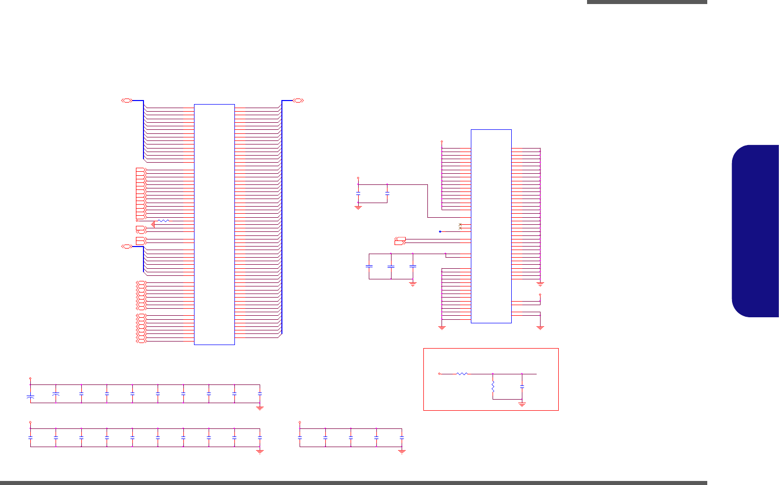
Schematic Diagrams
NAGUA DDR3 SO-DIMMS B B - 7
B.Schematic Diagrams
NAGUA DDR3 SO-DIMMS B
MEM_DATA34
MEM_DATA33
MEM_DATA32
MEM_DATA31
MEM_DATA30
MEM_DATA29
MEM_DATA4
MEM_DATA3
MEM_DATA2
MEM_DATA1
MEM_DATA28
MEM_DATA50
MEM_DATA49
MEM_DATA38
MEM_DATA47
MEM_DATA46
MEM_DATA45
MEM_DATA44
MEM_DATA43
MEM_DATA42
MEM_DATA41
MEM_DATA40
MEM_DATA39
MEM_DATA37
MEM_DATA36
MEM_DATA35
MEM_DATA59
MEM_DATA63
MEM_DATA62
MEM_DATA61
MEM_DATA60
MEM_DATA58
MEM_DATA57
MEM_DATA56
MEM_DATA6
MEM_DATA5
MEM_DATA48
MEM_DATA55
MEM_DATA54
MEM_DATA53
MEM_DATA52
MEM_DATA51
MEM_DATA0
MEM_DATA22
MEM_DATA21
MEM_DATA10
MEM_DATA19
MEM_DATA18
MEM_DATA17
MEM_DATA16
MEM_DATA15
MEM_DATA14
MEM_DATA13
MEM_DATA12
MEM_DATA11
MEM_DATA9
MEM_DATA8
MEM_DATA7
MEM_D M0
MEM_D M2
MEM_D M1
MEM_D M3
MEM_D M4
MEM_D M5
MEM_D M6
MEM_D M7
MEM_DATA20
MEM_DATA27
MEM_DATA26
MEM_DATA25
MEM_DATA24
MEM_DATA23
MEM_ADDR0
MEM_ADDR4
MEM_ADDR3
MEM_ADDR2
MEM_ADDR1
MEM_ADDR15
MEM_ADDR14
MEM_ADDR13
MEM_ADDR12
MEM_ADDR11
MEM_ADDR10
MEM_ADDR9
MEM_ADDR8
MEM_ADDR7
MEM_ADDR6
MEM_ADDR5
MVREF_DIMM1
MVREF_DIMM1
R80
1K_1%_04
C156
1u_6.3V_X5R_04
C134
0.1u_10V_X5R_04
C158
1u_6.3V_X5R_04
C142
*1u_6.3V_X5R_04
C137
10u_10V_Y5V_08
C138
10u_10V_Y 5V_08
J D IMM2 B
DDRRK-20401-TP8D
VDD1
75
VDD2
76
VDD3
81
VDD4
82
VDD5
87
VDD6
88
VDD7
93
VDD8
94
VDD9
99
VDD10
100
VDD11
105
VDD12
106
VDDSPD
199
NC1
77
NC2
122
NCTEST
125
VREF_DQ
1
VSS1
2
VSS2
3
VSS3
8
VSS4
9
VSS5
13
VSS6
14
VSS7
19
VSS8
20
VSS9
25
VSS10
26
VSS11
31
VSS12
32
VSS13
37
VSS14
38
VSS15
43
VSS16 44
VSS17 48
VSS18 49
VSS19 54
VSS20 55
VSS21 60
VSS22 61
VSS23 65
VSS24 66
VSS25 71
VSS26 72
VSS27 127
VSS28 128
VSS29 133
VSS30 134
VSS31 138
VSS32 139
VSS33 144
VSS34 145
VSS35 150
VSS36 151
VSS37 155
VSS38 156
VSS39 161
VSS40 162
VSS41 167
VSS42 168
VSS43 172
VSS44 173
VSS45 178
VSS46 179
VSS47 184
VSS48 185
VSS49 189
VSS50 190
VSS51 195
VSS52 196
G2 GND2
G1 GND1
VTT2 204
VTT1 203
VREF_CA
126
RESET#
30 EVENT#
198
VDD13
111
VDD14
112
VDD16
118 VDD15
117
VDD17
123
VDD18
124
C133
1000p_50V_X7R_04
C148
*0.1u_16V_Y5V_04
C144
1u_6.3V_X5R_04
JDIMM2A
DDRRK-20401-TP8D
A0
98
A1
97
A2
96
A3
95
A4
92
A5
91
A6
90
A7
86
A8
89
A9
85
A10/AP
107
A11
84
A12/BC#
83
A13
119
A14
80
A15
78
DQ0 5
DQ1 7
DQ2 15
DQ3 17
DQ4 4
DQ5 6
DQ6 16
DQ7 18
DQ8 21
DQ9 23
DQ10 33
DQ11 35
DQ12 22
DQ13 24
DQ14 34
DQ15 36
DQ16 39
DQ17 41
DQ18 51
DQ19 53
DQ20 40
DQ21 42
DQ22 50
DQ23 52
DQ24 57
DQ25 59
DQ26 67
DQ27 69
DQ28 56
DQ29 58
DQ30 68
DQ31 70
DQ32 129
DQ33 131
DQ34 141
DQ35 143
DQ36 130
DQ37 132
DQ38 140
DQ39 142
DQ40 147
DQ41 149
DQ42 157
DQ43 159
DQ44 146
DQ45 148
DQ46 158
DQ47 160
DQ48 163
DQ49 165
DQ50 175
DQ51 177
DQ52 164
DQ53 166
DQ54 174
DQ55 176
DQ56 181
DQ57 183
DQ58 191
DQ59 193
DQ60 180
DQ61 182
DQ62 192
DQ63 194
BA0
109
BA1
108
RAS#
110
WE#
113
CAS#
115
S0#
114
S1#
121
CKE0
73
CKE1
74
CK0
101
CK0#
103
CK1
102
CK1#
104
SDA
200 SCL
202 SA1
201 SA0
197
DM0
11
DM1
28
DM2
46
DM3
63
DM4
136
DM5
153
DM6
170
DM7
187
DQS0
12
DQS1
29
DQS2
47
DQS3
64
DQS4
137
DQS5
154
DQS6
171
DQS7
188
DQS0#
10
DQS1#
27
DQS2#
45
DQS3#
62
DQS4#
135
DQS5#
152
DQS6#
169
DQS7#
186
ODT0
116
ODT1
120
BA2
79
C143
1u_6.3V_X5R_04
C131
1u_6.3V_X5R_04
C151
0.1u_1 6V_Y 5V_04
C140
1u_6.3V_X5R_04
C141
*1u_6.3V_X5R_04
C145
0.1u_16V_Y5V_04
+
C136
*220u_4V_V_A
C157
1u_6.3V_X5R_04
C129
*1u_6.3V_X5R_04
C139
*10u_10V_Y5V_08
C159
*1u_6.3V_X5R_04
C150
0.1u_16V_Y5V_04
C132
0.1u_10V_X7R_04
C154
0.1u_16V_Y5V_04
C155
10u_10V_Y5V_08
C152
0.1u_16V_Y 5V_04
C130
0.1u_16V_Y5V_04
C149
0.1u_16V_Y5V_04
C146
*0.1u_16V_Y5V_04
R79 1K_1%_04
C147
0.1u_16V_Y5V_04
C153
*0.1u_16V_Y 5V_04
1.5V
3.3VS
1.5V
VTT_MEM
VTT_MEM
1.5V
1.5V
DIMM1_ODT12
MEM_R AS#2,5
MEM_C LK_H32
MEM_C AS#2,5
MEM_C LK_L32
MEM_RESET#2,5
MEM_C LK_H22
DIMM1_ODT02
MEM_W E #2,5
MEM_DATA[63:0] 2, 5
MEM_C KE12,5 MEM_C KE02,5
SDATA05,8
MEM_EVENT#2,5
MEM_C LK_L22
MEM_BANK02,5
MEM_ADDR[15:0]2,5
ME M_D M[ 7: 0]2,5
DIMM1_C S#12DIMM1_C S#02MEM_BANK22,5 MEM_BAN K12,5
MEM_DQS_H 72,5 MEM_DQS_H 62,5
MEM_DQS_H 42,5
MEM_DQS_H 22,5
MEM_DQS_L62,5
MEM_DQS_L42,5
MEM_DQS_L22,5
MEM_DQS_H 32,5
MEM_DQS_L72,5
MEM_DQS_L02,5 MEM_D QS_L12,5
MEM_DQS_H 12,5
MEM_DQS_L52,5
MEM_DQS_H 52,5
MEM_DQS_L32,5
MEM_DQS_H 02,5
CLOSE TO SO-DIMM B
INAGUA DDR3 SO-DIMMS B
20mils
SO-DIMM B
3.3VS
+
C135
560u_2.5V_6.6*6.6*5.9
SCLK05,8
R78 4.7K_04
(REV)8.0mm
SN:6-86-24204-XXX
Sheet 6 of 33
NAGUA DDR3 SO-
DIMMS B
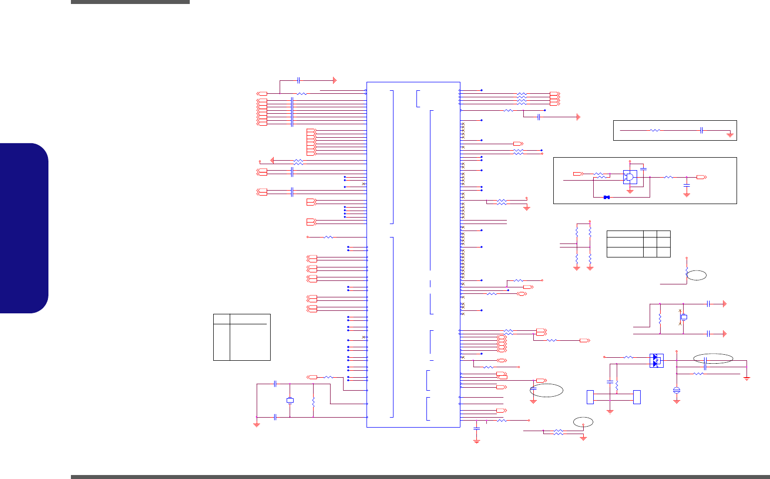
Schematic Diagrams
B - 8 HUDSON PCIE/PCI/CLOCK/FCH
B.Schematic Diagrams
HUDSON PCIE/PCI/CLOCK/FCH
R255
20K_04
3.3VS
R252 *10mil_short_04
PCI_CLKRUN# 11
25M_X1
C_UMI_N_RX12C_UMI_P_RX12C_UMI_N_RX02
C_UMI_P_RX32C_UMI_N_RX22C_UMI_P_RX22
C_UMI_N_RX32
D02
C_UMI_P_TX02
C845
*0.1u_16V_Y5V_04
GPIO31
DISP_CLKP3
APU_CLKN3APU_CLKP3
DISP_CLKN3
CLK_PCIE_LAN16
CLK_PCIE_WLAN#17 CLK_PCIE_WLAN17
CLK_PCIE_LAN #16
0
0
0
NEAR M3L
U17
*74AHC1G08GW
1
2
5
4
3
3.3VS
J_RTC1
*85205-02701
1
2
R257
*20K_04
1.8VS
C466
*1u_6.3V_X5R_04
R705 * 2.2K_04
R704 10K_04
3.3V
32K_X2
32K_X1
S5_CORE_EN 24
C453 0.1u_10V_X7R_04
PCIE_RXN3_WLAN17 PCIE_RXP3_WLAN17
X5
FSX5L_25MHZ
12
R258
*20K_04
5 N A NA
7 USB3.0 7
2 N A NA
GFX_CLK NA G
FCH_GPP DEVICE CLKREQ#
1 WLAN 1
8 N A NA
6 N A NA
0 JMC261C 0
4 N A NA
R247 20K_04
APU
CLOCK GENERATOR
PCI CLKS
S5 PLUS
LPC PCI INTERFACE
HUDSON - M3L
Part 1 of 5
PCI EXPRESS INTERFACES
AMD A68M
U19A
C33
25M_X2
C31
25M_X1
J26
14M_25M_48M_OSC
R27
GPP_CLK8N
N27
GPP_CLK8P
R24
GPP_CLK7N
R23
GPP_CLK7P
N26
GPP_CLK6N
N25
GPP_CLK6P
M26
GPP_CLK5N
M27
GPP_CLK5P
M24
GPP_CLK4N
M23
GPP_CLK4P
E31
GPP_CLK3N
E33
GPP_CLK3P
F31
GPP_CLK2N
F33
GPP_CLK2P
K26
GPP_CLK1N
J27
GPP_CLK1P
H28
GPP_CLK0N
H27
GPP_CLK0P
K29
SLT_GFX_CLKN
J30
SLT_GFX_CLKP
T23
APU_CLKN
T24
APU_CLKP
H31
DI SP2_CLKN
H33
DI SP2_CLKP
T26
DISP_CLKN
R26
DISP_CLKP
G28
PCIE_RCLKN
G30
PCIE_RCLKP
F27
CLK_ CALRN
W23
GPP_RX3N
W24
GPP_RX3P
W26
GPP_RX2N
V26
GPP_RX2P
V27
GPP_RX1N
W27
GPP_RX1P
AA26
GPP_RX0N
AA27
GPP_RX0P
AA23
GPP_TX3N
AA24
GPP_TX3P
AB27
GPP_TX2N
AB26
GPP_TX2P
W32
GPP_TX1N
W30
GPP_TX1P
V31
GPP_TX0N
V33
GPP_TX0P
AF31
PCIE_CALRN
AF29
PCIE_CALRP
Y29
UMI _RX 3N
Y28
UMI _RX 3P
Y31
UMI _RX 2N
Y33
UMI _RX 2P
AB29
UMI _RX 1N
AB28
UMI _RX 1P
AB31
UMI _RX 0N
AB33
UMI _RX 0P
AC32
UMI _T X3N
AC30
UMI _T X3P
AD29
UMI _T X2N
AD28
UMI _T X2P
AD31
UMI _T X1N
AD33
UMI _T X1P
AE32
UMI _T X0N
AE30
UMI _T X0P
AD5
A_RST#
AE2
PCIE_RST#
E6
VDDBT _RTC_G
F3
INT RUDER_ALERT #
F1
RTCCLK
H7
S5_CORE_EN
G4
32K_X2
G2
32K_X1
F26
APU_RST#
G26
LDT_STP#
E26
APU_PG
E28
PROCHOT#
G25
DMA_ACTIVE#
AE19
SERI RQ/ GP IO 48
AE27
LDRQ1#/CLK_REQ6#/ GPI O49
B27
LDRQ0#
A31
LFRAM E#
A29
LAD3
A26
LAD2
C28
LAD1
D27
LAD0
D25
LPCCLK1
B25
LPCCLK0
AD18
INTH#/GPIO35
AC16
INTG#/GPIO34
AE18
INTF#/GPIO33
AF18
INTE#/GPIO32
AH9
LOCK#
AD19
CLKRUN#
AK17
GNT3#/CLK_REQ7#/GPIO46
AD21
GNT2#/SD_LED/GPO45
AD13
GNT1#/GPO44
AD16
GNT0#
AM17
REQ 3 #/ C LK _RE Q 5#/ GP I O 42
AF15
REQ 2 #/ C LK _RE Q 8#/ GP I O 41
AG13
REQ 1#/ GP IO 40
AG15
REQ 0#
AH8
SERR#
AM9
PERR#
AH1
STOP#
AE10
PAR
AF10
TRDY#
AL10
IRDY#
AK9
DEVSEL#
AG10
FRAME#
AD12
CBE3#
AN10
CBE2#
AJ8
CBE1#
AN3
CBE0#
AE16
AD31/GPI O31
AC15
AD30/GPI O30
AD15
AD29/GPI O29
AH14
AD28/GPI O28
AH13
AD27/GPI O27
AF13
AD26/GPI O26
AE13
AD25/GPI O25
AC12
AD24/GPI O24
AE12
AD23/GPI O23
AG12
AD22/GPI O22
AN12
AD21/GPI O21
AK11
AD20/GPI O20
AL12
AD19/GPI O19
AJ10
AD18/GPI O18
AM11
AD17/GPI O17
AG9
AD16/GPI O16
AN8
AD15/GPI O15
AK7
AD14/GPI O14
AJ6
AD13/GPI O13
AM7
AD12/GPI O12
AL3
AD11/GPI O11
AL8
AD10/GPI O10
AJ1
AD9/GPI O9
AN6
AD8/GPI O8
AN5
AD7/GPI O7
AL1
AD6/GPI O6
AJ5
AD5/GPI O5
AH3
AD4/GPI O4
AL6
AD3/GPI O3
AG4
AD2/GPI O2
AL5
AD1/GPI O1
AJ3
AD0/GPI O0
AB5
PCIRST#
AF6
PCICLK4/14M_OSC/GPO39
AG2
PCICLK3/GPO38
AF5
PCICLK2/GPO37
AF1
PCICLK1/GPO36
AF3
PCI CLK0
25M_X2
C_UMI_P_TX22
C_UMI_P_TX12
C_UMI_P_TX32
C_UMI_N_TX02
C_UMI_N_TX22
C_UMI_N_TX12
LPC_AD0 11,20
C_UMI_N_TX32
LPC_AD3 11,20
LPC_AD1 11,20
LPC_AD2 11,20
R805 *0_04
1
GPIO30
C721 *1u_10V_Y5V_06
D02
Zo=
50£[¡Ó15%
GPIO30
R242 22_04
R240 22_04
R243 22_04
R244 22_04 PCI _CLK3 8
PCI _CLK2 8
PCLK_KBC 8
PCI _CLK4 8
MODEL
W240BL/W240BZ
R260
10M_04
C462
22p_50V_NPO_04
C449 *150pF_NPO_50V_0402
C463
22p_50V_NPO_04
HUDSON PCIE/PCI/CLOCK/FCH
1.1VS
32K_X1
INTRUDER_ALERT#
W251BLQ/W251BZQ
PCLK_KBC_RPCLK_KBC R513 *10_04 C750
*10p_50V_N PO_06
R279 *4.7K_04
C465 22P_50V_NPO_04
SUS_STAT#
R595 *10K_04
ANX3110_CLKN12 ANX3110_CLKP12
R263 1K_04
LPC_FRAME# 11,20
C444 0.1u_10V_X7R_04
D02
PCI_CLK2_R
PCLK_TPM 11
LPCCLK_0
PCI_CLK3_R
R687 * 10K_04
LPCCLK_1
MXM_PRESEN T1#
PCI_CLK4_R
LDT_STP#
INTRUDER_ALERT#
USB30_CLKREQ#
PCIRST#_R
MXM_PRESEN T2#
PCI_CLK1_R
GPIO31
GPIO30
R688 * 10K_04
SERIRQ
R249 590
RTC_VBAT_1
GPIO31
3 N A NA
R256
*20K_04
R259
20K_04
LDT_STP#
R271 0_04
3.3VS
10mils
20mils 20mils
3.3VS
R250 2K_1%_04
R806 *0_04
C467 22P_50V_NPO_04
R266
1K_04
Reserve
1.1VS
VBAT_I N
X4
1TJS125DJ4A420P_32.768KHz
14
3 2
R265
*1M_04
C822 0.1u_10V_X7R_04
C823 0.1u_10V_X7R_04
PCIE_RXP0_LAN16 PCIE_RXN0_LAN16
A_RST#_C
PCI E_RST#_GATE8
C464 *1u_6.3V_Y5V_04
C445 0.1u_10V_X7R_04
BT_ON 17,21
FCH_GPPTXN3
FCH_GPPTXN0
FCH_GPPTXP0
VDD3
A_VBAT
FCH_GPPTXP3
C443 0.1u_10V_X7R_04
DISP_CLK : CPU (non-spread)
C446 0.1u_10V_X7R_04
C450 0.1u_10V_X7R_04
C448 0.1u_10V_X7R_04
J_RTC2
BAT-063-P01
1
2
C451 0.1u_10V_X7R_04
C447 0.1u_10V_X7R_04
PCIE_RST# IS FOR PCI E DEVICES ON HU DSON
PCIE_RST#_C
SUS_STAT# 11
PCI_RST#
RTC_CLK
PCIE_TXP0_LAN16
CALRN
CALRP
U_RX0N_C
U_RX1P_C
U_RX2N_C
U_RX0P_C
U_RX1N_C
U_RX3P_C
U_RX3N_C
U_RX2P_C
3.3V
A_VBAT
R268 510_1%_04
R245 *33_04
C457
150pF_NPO_50V_0402
PCIE_RST#_C
R267
1M_04
PCIE_RCLK : (Spread, FUSION MODE)
PCIE_TXN0_LAN16
JOPEN1
*OPEN_10mil-1MM
12
W270BZQ
32K_X2
R253 2K_1%_04
C468
1u_6.3V_X5R_04
R241 33_04
R812 22_04
C_UMI_P_RX02
C441 150pF_NPO_50V_0402
R251 33_04 BUF_PLT_RST# 11,16,17,20
EC_RST#12,20
R689 22_04
PCIE_TXP3_WLAN17
C452 0.1u_10V_X7R_04
PCIE_TXN3_WLAN17
RTC_CLK
3.3V
C460
*0.1u_16V_Y5V_04
LPC_CLK0 8,20
LPC_CLK1 8
R261 22_04
R262 22_04
C
A
A
D46
BAT54CWGH
1
23
D02
LAN_25MHz16
SERIRQ 11,20
PROCHOT# 3
ALLOW_LDTSTP 3
R686 *0_04
LDT_R ST# 3
APU_PWRGD 3,28
Sheet 7 of 33
HUDSON PCIE/PCI/
CLOCK/FCH
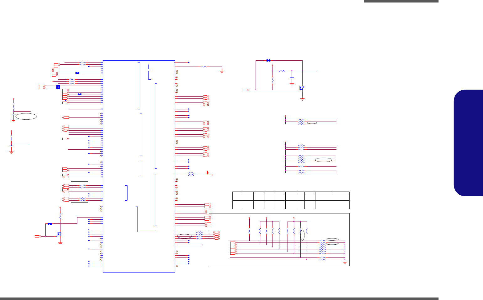
Schematic Diagrams
HUDSON GPIO/USB/STRAP B - 9
B.Schematic Diagrams
HUDSON GPIO/USB/STRAP
R270 *10mil_short_04
USB_SS_TX1P 19
C470
*0.1u_16V_Y 5V_04
USB_PP2 17
USB_PN2 17
USB_ PN6 21
USB_ PP6 21
HDA_SDIN018
R310 10K_04
WLAN_CLKREQ#17
R312 10K_04
R313 *2.2K_04
R703 1K_04
R702 1K_04
R314 *2.2K_04
PCLK_KBC7PCI_CLK27
LPC_CLK07,20 PCI_CLK47
LPC_CLK17
PCI _CLK37
R384 *2.2K_04
R382 10K_04
R385 2.2K_04
D02
R381 10K_04
R383 *10K_04
R379 *10K_04
R380 10K_04
R377 *10K_04
R378 *10K_04
HDA_SDOUT
VDD IO_AZ
R469 33_04
3.3VS
R695 33_04
R473 33_04
R470 33_04
3.3V
USB_SS_RX1P 19
STRAP PINS
R369
10K_04
R371
*10K_04
R368
*10K_04
R372
*10K_04
R370
*10K_04
R373
*10K_04
R374
10K_04
R376
*10K_04
R375
*10K_04
D02
MINI PCIE_SLT2_EN#
USB_ PP7 15
USB_ PN7 15 USB7 3G
EC
Timer
P C IE G e n 2
SB_BLON13
PCI_CLK4
H, L = SPI ROM
LPC_CLK0
CLOCK MODE
IGNORE
DEFAULT
ALLOW
PULL
DEFAULT
PCI_CLK1
FCH_VDD_11_SSUSB_S
PCI _CLK 2
FO RCE
STRAP
MINI PCIE_SLT2_EN#
DE F AUL TSTRAP
CLOCK MODE DISABLED
USE
DEF AULT
DEFAULT
AZ_SDOUT
L, H = L PC ROM ( DEFAUL T)
LPC_CLK1
DEBUG
ENABLED
PCIE Gen1
DE F AUL T
MODE
H, H = Reser ved
HIGH
Timer
Disabled
GPIO199
DEF AULT
GPIO200non_ Fus ion E CLOW POWER CLK G E N
Enabled
MODE
PULL
MI NIPCI E_SLT 3_EN#
PERF ORMANCE
R731 *10mil_short_04
DEBUG
LOW
ENABLED
DI SABLED
Watc hdog
Watc hdog CLK G E NFUSION
PCI_CLK3
L,L = FWH ROM
KBC_RST#20 GA2020 Q6
*MTN7002ZHS3
G
DS
EC_SMI#20 EC_SCI#20
PCIE_WAKE#16,17
CPU_THERMTRIP#3USB0 PORT 0
USB1 PORT 1
SUSB#11,12,20,23
3.3VS
SUSC#20,23,25
R276 2.2K_04
MINI PCIE_SLT3_EN#
R277 2.2K_04
R278 *4.7K_04 SDATA0
NB_PWRGD
SCLK0
3.3V
WF_RADIO
R284 2.2K_04
RSMRST_GATE#20
HDA_SYNC18
R274
*20K_04
SCLK1
SDATA1
PWR_BTN#20
USB_ PP5 15
USB_ PN5 15
D02
Q8
*MTN7002ZHS3
G
DS
SB_AC_OK
3.3V
R807
*10K_04
R696
*10mil_short_04
AC_IN#20,29
R691 *10mil_short_04
Closed to SB.
PCIE_RST#_GATE7
USB6 BLUE TOOTH
USB2 MINI CARD
USB5 CCD
D02
SWI #20
HUDSON GPIO/USB/AUDIO/STRAP
SDATA05,6 SCLK05,6 HDA_SPKR18
USB_SS_RX1N 19
SWI #
3.3V
C471
*1u_6.3V_Y5V_04
R282
10K_04
3.3V
SYS_RST#
R692 *10mil_s hort_04
HDA_RST#18
ODD_DA#_FCH17
PLACE CLOSE TO SOUTH BRIDGE
APU_SID 3
R728 *0_04
R291 10K_04
R752 *0_04
R693 *0_04
USB_OCP0_1#19
R694 *0_04
SDATA2
MINIPCIE_SLT2_EN#
SCLK3 SMD_CPU_THERM 3,9,20
SDATA3
SCLK2
MINIPCIE_SLT3_EN#
APU_SIC 3
SMC_CPU_THERM 3,9,20
R742 *2.2K_04
SYS_RST#
R281 *2.2K_04
USB30_PWR_EN19
HDA_BITCLK18
USB4 PORT 3
USB_ PP3 22
USB_ PN3 22
R743 *2.2K_04
R744 *2.2K_04
EC_SCI#
R292 10K_04 EC_SMI#
R293 10K_04
3.3V
3.3V
R280
*20K_04
R273 *22K_04
C469
*2.2u_6.3V_X5R_04
USB_ PN0 19
USB_ PN1 19
USB_ PP0 19
USB_ PP1 19
R690 *0_04
R730 *0_04
LID_SW#13,20,22
SWI#
D02
USB 3.0
EMBEDDED CT RL
USB MISCUSB 1.1
USB OC
HD AUDIO
GPIO
ACPI / WAKE UP EVENTS
HUDSON-M3L
Part 4 of 5
USB 2.0
AMD A68M
U19D
D17
KSO_17/XDB3/GPI O226
A24
KSO_16/XDB2/GPI O225
B17
KSO_15/XDB1/GPI O224
B19
KSO_14/XDB0/GPI O223
C18
KSO_13/GPI O222
A18
KSO_12/GPI O221
D19
KSO_11/GPI O220
K18
KSO_10/GPI O219
B21
KSO_9/GPI O218
G18
KSO_8/GPI O217
H18
KSO_7/GPI O216
J18
KSO_6/GPI O215
A20
KSO_5/GPI O214
E18
KSO_4/GPI O213
A22
KSO_3/GPI O212
F20
KSO_2/GPI O211
E20
KSO_1/GPI O210
F21
KSO_0/GPI O209
C22
PS2M_CLK/G PI O192
D23
PS2M_DAT/GPIO191
C20
PS2KB_CLK/GPIO 190
D21
PS2KB_DAT/GPI O189
J21
SPI_CS2#/G BE_STAT2/GPI O166
J19
PS2_CLK/CEC/SCL4/GPIO188
K19
PS2_DAT/SDA4/GPI O187
AE4
AZ_RST#
AD6
AZ_SYNC
Y1
AZ _SDI N3/ GPI O170
Y3
AZ _SDI N2/ GPI O169
Y5
AZ _SDI N1/ GPI O168
AA2
AZ _SDI N0/ GPI O167
AB1
AZ_SDOUT
AB3
AZ_BITCLK
T8
USB_OC0#/GEVENT12#/TRST#
J7
USB_OC1#/TDI/ GEVENT13#
P5
USB_OC2#/TCK/GEVENT14#
F5
USB_OC3#/AC_PRES/TDO/GEVENT15#
P6
USB_OC4#/IR_RX0/GEVENT16#
T1
USB_OC5#/IR_TX0/GEVENT17#
R8
USB_OC6#/IR_TX1/GEVENT6#
M7
BLINK/USB_OC7#/GEVENT18#
AF25
CLK_REQ G#/ GP I O65/ O SCI N/ IDL EEXI T #
AA8
GBE_STAT0/GEVENT11#
V10
GBE_LED2/GEVENT10#
Y6
SPI_HOLD#/GBE_LED1/GEVENT9#
W8
GBE_LED0/GPIO183
V8
DDR3_RST#/GEVENT7#
AG26
SMARTVOLT2/SHUTDOWN#/GPIO51
J2
IR_LED#/ LLB#/ GPI O 184
AG22
CLK_REQ 1#/ FA NOUT 4/ GPI O6 1
AG25
CLK_REQ 2#/ FA NIN4 /G PI O 62
R7
SDA1/GPIO228
T7
SCL1/GPIO227
AD25
SDA0/GPIO47
AD26
SCL0/GPIO43
AF24
SPKR/ GPIO 66
AG18
FA NIN3 /G PI O59
AH17
FA NOUT3/ G PIO 55
AF22
CLK_REQ0#/SATA_IS3#/GPIO60
AE26
SMARTVOLT1/SAT A_IS2#/GPI O50
AE24
CLK_REQ3#/SATA_IS1#/GPIO63
AG24
CLK_REQ4#/SATA_IS0#/GPIO64
U2
RSMRST #
AF19
WD_PWRGD
R10
THRMTRIP#/SMBALERT#/GEVENT2#
V7
IR_RX1/GEVENT20#
K1
WAKE#/ GEVENT 8#
U4
SYS_RESET#/GEVENT19#
T5
LPC_PD#/GEVENT5#
C26
LPC_SMI#/GEVENT23#
R9
PME#/ GEVENT3#
AG19
KBRST#/GEVENT1#
AE22
GA20IN/GEVENT0#
V9
TEST2
T10
TEST1/TMS
T9
TEST0
N7
PWR_GOOD
J4
PWR_BTN#
W2
SLP_S5#
T3
SLP_S3#
W7
SPI_CS3#/G BE_STAT1/GEVENT21#
R2
RI#/GEVENT22#
AB6
PCIE_RST2#/GEVENT4#
F18
KSI_7/ GPIO 208
C24
KSI_6/ GPIO 207
B23
KSI_5/ GPIO 206
E24
KSI_4/ GPIO 205
F24
KSI_3/ GPIO 204
F22
KSI_2/ GPIO 203
K22
KSI_1/ GPIO 202
K21
KSI_0/ GPIO 201
H21
EC_PWM3/EC_TI MER3/ GPIO 200
J22
EC_PWM2/EC_TIMER2/W OL_EN/GPI O199
H22
EC_PWM1/EC_TI MER1/ GPIO 198
E22
EC_PWM0/EC_TI MER0/ GPIO 197
G21
SDA3_LV/GPI O196
G22
SCL3_LV/ GPIO195
G19
SDA2/ GPIO194
H19
SCL2/GPI O193
K15
USB_SS_RX0N
J15
USB_SS_RX0P
H16
USB_SS_TX0N
J16
USB_SS_TX0P
G13
USB_SS_RX1N
H13
USB_SS_RX1P
G15
USB_SS_TX1N
F15
USB_SS_TX1P
F14
NC
E14
NC
B15
NC
D15
NC
A12
NC
C12
NC
C14
NC
A14
NC
A16
USBSS_CALRN
C16
USBSS_CALRP
E3
USB_HSD0N
E1
USB_HSD0P
C3
USB_HSD1N
C1
USB_HSD1P
A5
USB_HSD2N
C5
USB_HSD2P
A6
USB_HSD3N
C6
USB_HSD3P
E8
NC
F8
NC
C8
USB_HSD5N
A8
USB_HSD5P
G9
USB_HSD6N
H9
USB_HSD6P
A10
USB_HSD7N
C10
USB_HSD7P
F10
USB_HSD8N
E10
USB_HSD8P
D11
NC
NC
B11
K13
USB_HSD10N
K12
USB_HSD10P
F12
USB_HSD11N
G12
USB_HSD11P
J12
NC
K10
NC
G10
NC
H10
NC
H5
NC
H6
NC
H3
NC
H1
NC
B9
USB_RCOMP
G8
USBCLK/ 14M_25M_48M_OSC
ODD_DETECT#17
RSMRST#
SCLK3
SCLK2
SDATA3
SDATA2
SB_PWRGD11
RSMRST#
GEVENT0#
USB_RCOMP
SYS_RST#
GEVENT1#
SCLK1
JM_D3MODE
SDATA1
WF_RADIO
NB_PWRGD
SYS_RST#11
USB_SS_TX1N 19
R272 11K_1%_04
HDA_SDOUT18
D02
R288 2.2K_04
USB_SS_RX0P 19
USB_SS_TX0P 19
USB_SS_TX0N 19
USB_SS_RX0N 19
D02
R275 *10mil_short_04
Sheet 8 of 33
HUDSON GPIO/
USB/STRAP
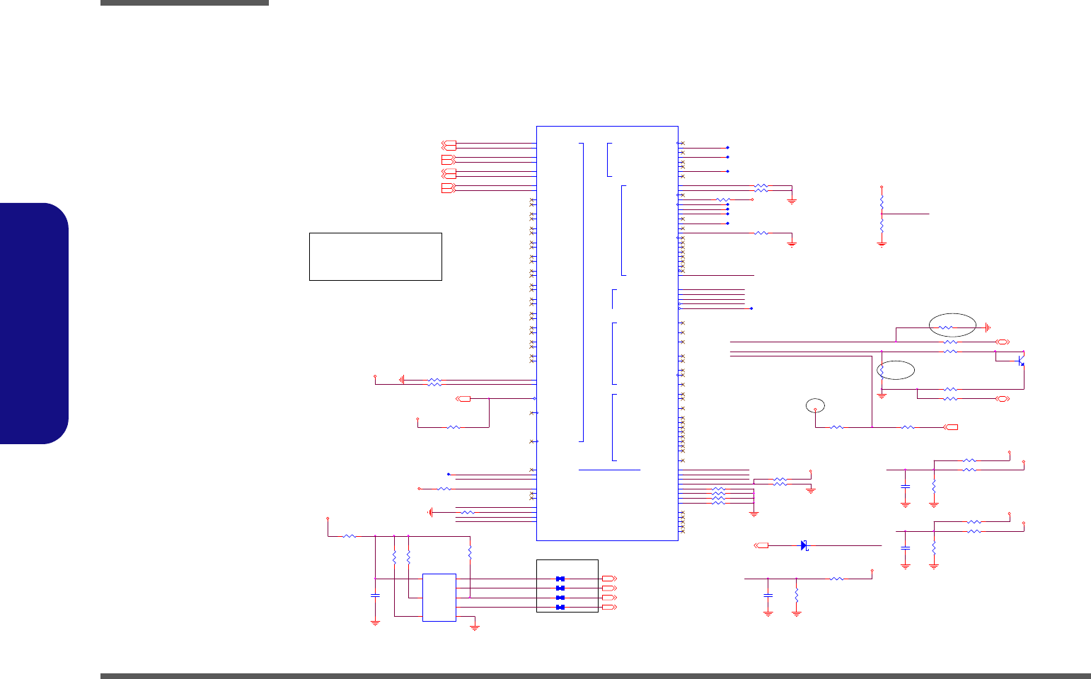
Schematic Diagrams
B - 10 HUDSON SATA/DEBUG IO/SPI
B.Schematic Diagrams
HUDSON SATA/DEBUG IO/SPI
R283 10K_04
D02
SATARXN017 SATARXP017
SATATXN017
R333 *0_04
SATARXP117
SATATXP117 SATATXN117
SATATXP017
SATARXN117
R798 10K_04
R335 *0_04
SB_PROCHOT#_C
SB_PR OCH OT#3
C488
*0.1u_16V_Y 5V_04
SATA_LED#21
R576 *10K_04
3.3VS
R340 *11K_1%_04
R336 *0_04
R337 *0_04
R341 *10K_04
APU_TALERT# 3,20
SPI_CS#_SEL
SPI_CLK
HUDSON_ROM_RST#
SPI_DATAOUT
SPI_DATAIN
GBE_RXERR
SB_TALERT#
SMD_CPU_THERM 3,8,20
SMC_CPU_THERM 3,8,20
R331 1K_1%_04
R332 931_1%_04
1.1VS
SATA_CALN
SATA_CALP
D02
C490
*0.1u_16V_Y 5V_04
R349
10K_04
R799 10K_04
R810 *10K_04
3.3V
VGA MAINLINK VGA DAC
GBE LAN
HW MO NITO R
SPI ROM
SERIAL ATA
HUDSON - M3L
Part 2 of 5
SD CA RD
AMD A68M
U19B
M6
TEMPI N3/ TALE RT#/G PI O174
K3
TEMPIN2/GPIO173
K5
TEMPIN1/GPIO172
K6
TEMPIN0/GPIO171
AL16
FANIN2/GPIO58
AN16
FANIN1/GPIO57
AK15
FANIN0/GPIO56
AJ16
FANOUT 2/ GPI O54
AM15
FANOUT 1/ GPI O53
AH16
FANOUT 0/ GPI O52
AG21
SATA_X2
AF21
SATA_X1
AD22
SATA_ACT#/ GPI O67
AF27
SATA_CALRN
AF28
SATA_CALRP
AJ31
NC13
AJ33
NC12
AH31
NC11
AH33
NC10
AL33
NC9
AL31
NC8
AN31
NC7
AL29
NC6
AM27
NC
AK27
NC
AL28
NC
AN29
NC
AH26
NC
AJ26
NC
AN26
NC
AL26
NC
AL24
NC
AN24
NC
AJ24
NC
AH24
NC
AK23
NC
AM23
NC
AH22
NC
AJ22
NC
AJ20
SATA_RX1P
AH20
SATA_RX1N
AL22
SATA_TX1N
AN22
SATA_TX1P
AN20
SATA_RX0P
AL20
SATA_RX0N
AM19
SATA_TX0N
AK19
SATA_TX0P
L4
NC5
G27
NC4
A28
NC3
AH10
NC2
AG16
NC1
M5
VIN7/G BE_LED3/GPI O182
M1
VIN6/GBE_STAT3/GPIO181
P3
VI N5/ SCLK _1/ GPI O 180
P1
VIN4/SLOAD_1/GPIO179
N4
VI N3/ SDAT O_1/ GPI O178
L2
VI N2/ SDA TI _1/ GP I O177
M3
VIN1/GPI O176
N2
VIN0/GPI O175
C29
NC
P28
NC
P29
NC
R30
NC
R32
NC
T28
NC
T29
NC
T33
NC
T31
NC
U28
NC
V29
NC
V28
NC
K31
NC
N32
NC
M33
NC
N30
NC
M28
NC
M29
NC
L32
NC
L30
NC
V1
ROM_RST#/SPI_WP#/GPIO161
T6
SPI_CS1#/GPIO165
V3
SPI_CLK/ GPI O162
V5
SPI_DO/GPI O163
V6
SPI_DI/GPIO164
W9
GBE_PHY_INTR
AA7
GBE_PHY_RST#
AC2
GBE_PHY_PD
AB9
GBE_TXCTL/TXEN
AD8
GBE_TXD0
AE8
GBE_TXD1
AG6
GBE_TXD2
AF9
GBE_TXD3
AB7
GBE_TXCLK
AD1
GBE_RXERR
AG8
GBE_RXCTL/RXDV
AD7
GBE_RXD0
AE7
GBE_RXD1
AF7
GBE_RXD2
AH7
GBE_RXD3
AB8
GBE _RX CLK
W10
GBE_MDIO
AD9
GBE_MDCK
AD3
GBE_CRS
AC4
GBE_COL
AJ14
SD_DATA3/GPIO80
AH15
SD_DATA2/GPIO79
AM13
SD_DATA1/SDATO_0/ GPI O78
AK13
SD_DATA0/ SDATI _0/G PI O77
AH12
SD_WP/GPIO76
AJ12
SD_CD#/GPI O75
AN14
SD_CMD/SLOAD_0/GPIO74
AL14
SD_CLK/S CLK_0/G PI O73
R330 *10K_04
3.3VS
3.3V
GBE_PHY _INTR
R285 10K_04
R286 10K_04
R290
*10K_04
3.3V
GBE_PHY_INTR
R289
10K_04
R351 *10K_04
VIN_VDDCR
HUDSON_FANTACH0
HUDSON SATA/DEBUG IO/SPI
ODD_PWR
SB_PROCHOT#_C
TEMPIN0
C492
*0.1u_16V_Y5V_04
R352
10K_04
VIN_VDDIO_SUS
R287 10K_04
3.3V
R800 10K_04
R802 10K_04
R801 10K_04
R803 10K_04
R697 10K_04
Q9
*2N3904
B
E C
R342
10K_04
HSPI _MSO 20
HSPI _MSI 20
HSPI_SCLK 20
R350
*10K_04
HSPI _CE# 20
3.3V
NEAR U19
SPI_CS#_SEL
R386 *10mil_short_04
R573 *10mil_short_04
R572 *10mil_short_04
R571 *10mil_short_04
R732 *0_04
U21
*25VF032B
CE# 1
SO 2
WP#
3
VSS 4
SI 5
SCK 6
HOLD#
7
VDD
8
SPI_DATAIN
SPI_DATAOUT
C491
*0. 1u_16V_Y 5V_04
R347
*10K_04
R346
*1K_04
SPI_CLK
R338 *0_04
R348 10K_04
1.8VS
VDDCR_CPU
VDDCR_NB
1VS
MB_THRMDA_SB
D02
R343
10K_04
1.5V
to get af fected with 2 v ias. AMD platf orms are v alidated
GBE_CRS
GBE_COL
cus tomers can use 2v ias with GND v ia within 150mils of
meet s SATA logo requirements. Return loss is expected
signal via as long as they can ensure that their platform
SATA trace should use only 1v ia on t he
trace.
with one v ia only
MB_THRMDA_SB
TE MPI N 0
SB_TALERT# R344 *4. 99K_1%_04
R345 *4. 99K_1%_04
MB_THRMDC_SB
D22 RB751V
A C
VIN_VDDNB
VIN_VDDCR
VIN_VDDIO_SUS
VIN_VDDNB
Sheet 9 of 33
HUDSON SATA/
DEBUG IO/SPI
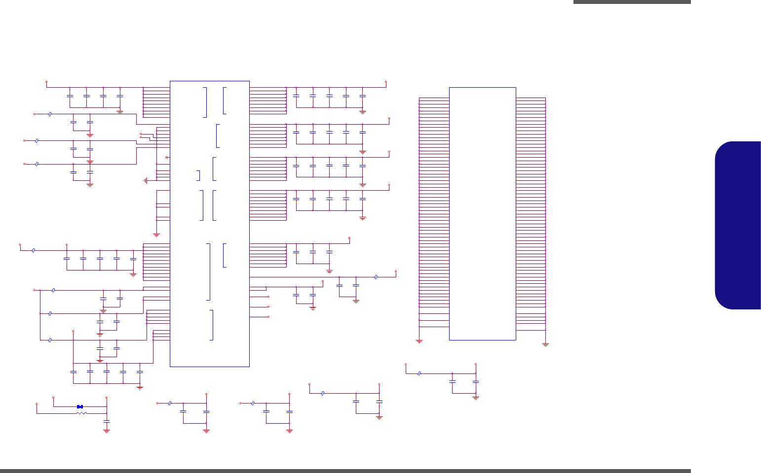
1008mA
FCH_VDD_11_SSUSB_S
C503
0.1u_10V_X5R_04
70mA
C531
*1u_10V_Y5V_06
C530
1u_10V_Y5V_06
C529
*0.1u_10V_X7R_04
340mA
VDDPL_1.1V
102mA
.
L96 HCB1005KF-121T20
C555
1u_10V_Y5V_06
C556
*0.1u_10V_X7R_04
VDDIO_AZ
42mA
1007mA
140mA
59mA
C557
1u_10V_Y5V_06
C515
10u_6.3V_X5R_08
C514
1u_6.3V_X5R_04
C526
0.1u_10V_X5R_04
C516
*1u_6.3V_X5R_04
C572
0.1u_10V_X5R_04
1.1VS
VDDAN_1.1_USB_S
C549
0.1u_10V_X5R_04
C550
1u_10V_Y5V_06
.
L93 HCB1005KF-121T20
1.1V
R362 *10mil_short_04
C552
0.1u_10V_X5R_04
.
L94 HCB1005KF-121T20
1337mA
C551
*1u_10V_Y5V_06
C494
10u_6.3V_X5R_08
C496
0.1u_10V_X5R_04
C495
0.1u_10V_X5R_04
.
L114 HCB1005KF-121T20
C627
1u_10V_Y5V_06
C628
*0.1u_10V_X7R_04
3.3V
FCH_VDDPL_33_SSUSB_S
3.3VS
C573
1u_6.3V_X5R_04
C575
*1u_6.3V_X5R_04
C574
10u_6.3V_X5R_08
C607
0.1u_10V_X5R_04
C576
0.1u_10V_X5R_04
1.1VS
.
L108 HCB1005KF-121T20
C623
1u_10V_Y5V_06
C624
*0.1u_10V_X7R_04
FCH_VDDPL_33_USB_S
AVDD_USB
R363 *0_04
.
L88 HCB1005KF-121T20
C538
1u_6.3V_X5R_04
12mA
C537
1u_6.3V_X5R_04
C528
1u_10V_Y5V_06
C527
*0. 1u_10V_X7R_04
1.1V
3.3VS VDDPL_3.3V_SATA
FCH_VDDPL_33_SSUSB_S
C498
10u_6.3V_X5R_08
C510
1u_6.3V_X5R_04
C508
*1u_6.3V_X5R_04
C507
0.1u_10V_X5R_04
C505
0.1u_10V_X5R_04
C499
*1u_6.3V_X5R_04
C501
10u_6.3V_X5R_08
C502
0.1u_10V_X5R_04
C622
1u_10V_Y5V_06
C621
0.1u_10V_X5R_04
3.3VS VDDPL_3.3V
.
L87 HCB1005KF-121T20
12mA
424mA
USB
MAIN LINK
GBE LAN
CLKGEN I/O
USB SS
SERIAL ATA
PCI EXPRESS
3.3V_S5 I/ O CORE S0
PCI/GPIO I/O
PO WE R
HUDSON-M3L
Part 3 of 5
AMD A68M
U19C
M17
VDDCR_11_SSUSB_S _4
P17
VDDCR_11_SSUSB_S _3
N17
VDDCR_11_SSUSB_S _2
N16
VDDCR_11_SSUSB_S _1
P14
VDDAN_11_SSUSB_S_5
P13
VDDAN_11_SSUSB_S_4
N14
VDDAN_11_SSUSB_S_3
M14
VDDAN_11_SSUSB_S_2
P16
VDDAN_11_SSUSB_S_1
T13
VDDCR_11_USB_S_2
VDDCR_11_USB_S_1
T12
U13
VDDAN_11_USB_S_ 2
U12
VDDAN_11_USB_S_ 1
M11
VDDAN_33_USB_S_ 12
N12
VDDAN_33_USB_S_ 11
M12
VDDAN_33_USB_S_ 10
N10
VDDAN_33_USB_S_ 9
N9
VDDAN_33_USB_S_ 8
M10
VDDAN_33_USB_S_ 7
M9
VDDAN_33_USB_S_ 6
K9
VDDAN_33_USB_S_ 5
K8
VDDAN_33_USB_S_ 4
J8
VDDAN_33_USB_S_ 3
H8
VDDAN_33_USB_S_ 2
G7
VDDAN_33_USB_S_ 1
AA10
VDDIO_GBE_S_2
AA9
VDDIO_GBE_S_1
AA11
VDDCR_11_G BE_S_2
AB11
VDDCR_11_G BE_S_1
AB10
VDDI O_3 3_GBE_ S
V25
VSS
V24
VSS
V23
VSS
Y22
VSS
V21
VSS
M31
NC
AG28
VDDPL_33_SATA
AH29
VDDPL_3 3_PCI E
D7
VDDPL_33_USB_S
L18
VDDPL_33_SSUSB_S
T22
VSS
U22
VSS
V22
VSS
H24
VDDPL_33_SYS
AB16
VDDI O_3 3_PCI GP_1 0
AB14
VDDI O_3 3_PCI GP_9
AB13
VDDI O_3 3_PCI GP_8
AB12
VDDI O_3 3_PCI GP_7
AC13
VDDI O_3 3_PCI GP_6
AG7
VDDI O_3 3_PCI GP_5
AD10
VDDI O_3 3_PCI GP_4
AE9
VDDI O_3 3_PCI GP_3
AB18
VDDI O_3 3_PCI GP_2
AB17
VDDI O_3 3_PCI GP_1
AA4
VDDIO_A Z_S
M8
VDDAN_33_HWM_S
J24
VDDPL_11_SYS_S
M20
VDDCR_11_S_2
N20
VDDCR_11_S_1
G24
VDDXL_33_S
W11
VDDIO _33_S_8
Y13
VDDIO _33_S_7
Y12
VDDIO _33_S_6
V13
VDDIO _33_S_5
V12
VDDIO _33_S_4
M18
VDDIO _33_S_3
L19
VDDIO _33_S_2
N18
VDDIO _33_S_1
AC1 9
VDDAN_11_SA TA_10
AB20
VDDAN_11_SATA_9
AA18
VDDAN_11_SATA_8
AA20
VDDAN_11_SATA_7
AC2 1
VDDAN_11_SATA_6
AC2 2
VDDAN_11_SATA_5
AB22
VDDAN_11_SATA_3
AB21
VDDAN_11_SATA_2
Y20
VDDAN_11_SATA_4
AA21
VDDAN_11_SATA_1
AG27
VDDAN_11_PCIE_8
AF26
VDDAN_11_PCIE_7
AA22
VDDAN_11_PCIE_6
AB23
VDDAN_11_PCIE_5
AD2 4
VDDAN_11_PCIE_4
AE25
VDDAN_11_PCIE_3
Y21
VDDAN_11_PCIE_2
AB24
VDDAN_11_PCIE_1
P22
VDDAN_11_CLK_8
N22
VDDAN_11_CLK_7
N21
VDDAN_11_CLK_6
M22
VDDAN_11_CLK_5
L22
VDDAN_11_CLK_4
K24
VDDAN_11_CLK_3
J25
VDDAN_11_CLK_2
H26
VDDAN_11_CLK_1
Y17
VDDCR_11_9
V20
VDDCR_11_8
V17
VDDCR_11_7
V14
VDDCR_11_6
U18
VDDCR_11_5
U16
VDDCR_11_4
T20
VDDCR_11_3
T17
VDDCR_11_2
T14
VDDCR_11_1
VDDCR_1.1V_USB
C608
0.1u_10V_X5R_04
C609
1u_10V_Y5V_06
.
L97 HCB1005KF-121T20
FCH_VDDPL_33_USB_S
.
L107 HCB1005KF-121T20
C493
0.1u_10V_X5R_04
HUDSON POWER DECOUPLING
Part 5 of 5
GRO UND
HUDSON-M3L
AMD A68M
U19E
H25
VSSPL_SYS
K25
VSSXL
N8
VSSAN_HWM
T18
VSS
T16
VSS
T11
VSS
R28
VSS
R25
VSS
R11
VSS
R4
VSS
P33
VSS
P31
VSS
P21
VSS
P20
VSS
P18
VSS
P12
VSS
N24
VSS
N23
VSS
N13
VSS
N11
VSS
N6
VSS
M25
VSS
M21
VSS
M16
VSS
M13
VSS
L21
VSS
L16
VSS
L15
VSS
L13
VSS
L12
VSS
L6
VSS
K28
VSS
K27
VSS
K16
VSS
K7
VSS
J32
VSS
J28
VSS
J13
VSS
J10
VSS
J9
VSS
J6
VSS
H29
VSS
H15
VSS
H12
VSS
G32
VSS
G16
VSS
G6
VSS
F29
VSS
F25
VSS
F23
VSS
F19
VSS
F17
VSS
F16
VSS
F13
VSS
F11
VSS
F9
VSS
F7
VSS
E29
VSS
E16
VSS
E12
VSS
E5
VSS
D13
VSS
D9
VSS
B13
VSS
B7
VSS
A33
VSS
A3
VSS
R6
VSS
N28
VSS
K33
VSS
L28
VSS
T21
VSS
AN3 3
VSS
AN2 8
VSS
AN1 8
VSS
AN1
VSS
AM25
VSS
AM21
VSS
AL18
VSS
AK25
VSS
AK21
VSS
AJ29
VSS
AJ28
VSS
AJ18
VSS
AH2 7
VSS
AH2 5
VSS
AH2 3
VSS
AH2 1
VSS
AH1 9
VSS
AH1 8
VSS
AH1 1
VSS
AH5
VSS
AG32
VSS
AG30
VSS
AF33
VSS
AF16
VSS
AF12
VSS
AF8
VSS
AE28
VSS
AE21
VSS
AE15
VSS
AE6
VSS
AD2 7
VSS
AC2 8
VSS
AC1 8
VSS
AC6
VSS
AB25
VSS
AA32
VSS
AA30
VSS
AA28
VSS
AA25
VSS
AA17
VSS
AA16
VSS
AA14
VSS
AA13
VSS
AA12
VSS
AA6
VSS
Y18
VSS
Y16
VSS
Y14
VSS
W28
VSS
W25
VSS
W6
VSS
W4
VSS
V18
VSS
V16
VSS
V11
VSS
U32
VSS
U30
VSS
U21
VSS
U20
VSS
U17
VSS
U14
VSS
U6
VSS
T27
VSS
T25
VSS
47mA
FCH_VDD_11_SSUSB_S
C619
1u_10V_Y5V_06
C618
0.1u_10V_X5R_04
C500
1u_6.3V_X5R_04
VDDAN_3.3V_HWM
5mA
3.3V
VDDXL_3.3V
.
L92 HCB1005KF-121T20
C548
1u_10V_Y5V_06
C547
0.1u_10V_X5R_04
C543
*1u_6.3V_X5R_04
470mA
C545
*10u_6.3V_X5R_08
.
L91 HCB1005KF-121T20
C542
1u_6.3V_X5R_04
AVDD _USB
C546
0.1u_10V_X5R_04
C544
10u_6.3V_X5R_08
3.3V
1.5V
VDDIO_AZ3.3V
VDDPL_1.1V1.1V
3.3V VDDAN_3.3V_HWM
3.3V
1.1VS
1.1VS
282mA
C533
*1u_6.3V_X5R_04
C534
1u_6.3V_X5R_04
C532
10u_6.3V_X5R_08
C536
0.1u_10V_X5R_04
C535
0.1u_10V_X5R_04
C512
0.1u_10V_X5R_04
C511
1u_10V_Y5V_06
11mA
VDDPL_3.3V_PCI E
.
L86 HCB1005KF-121T20
3.3VS
Sheet 10 of 33
HUDSON Power
Decoupling
Schematic Diagrams
HUDSON Power Decoupling B - 11
B.Schematic Diagrams
HUDSON Power Decoupling
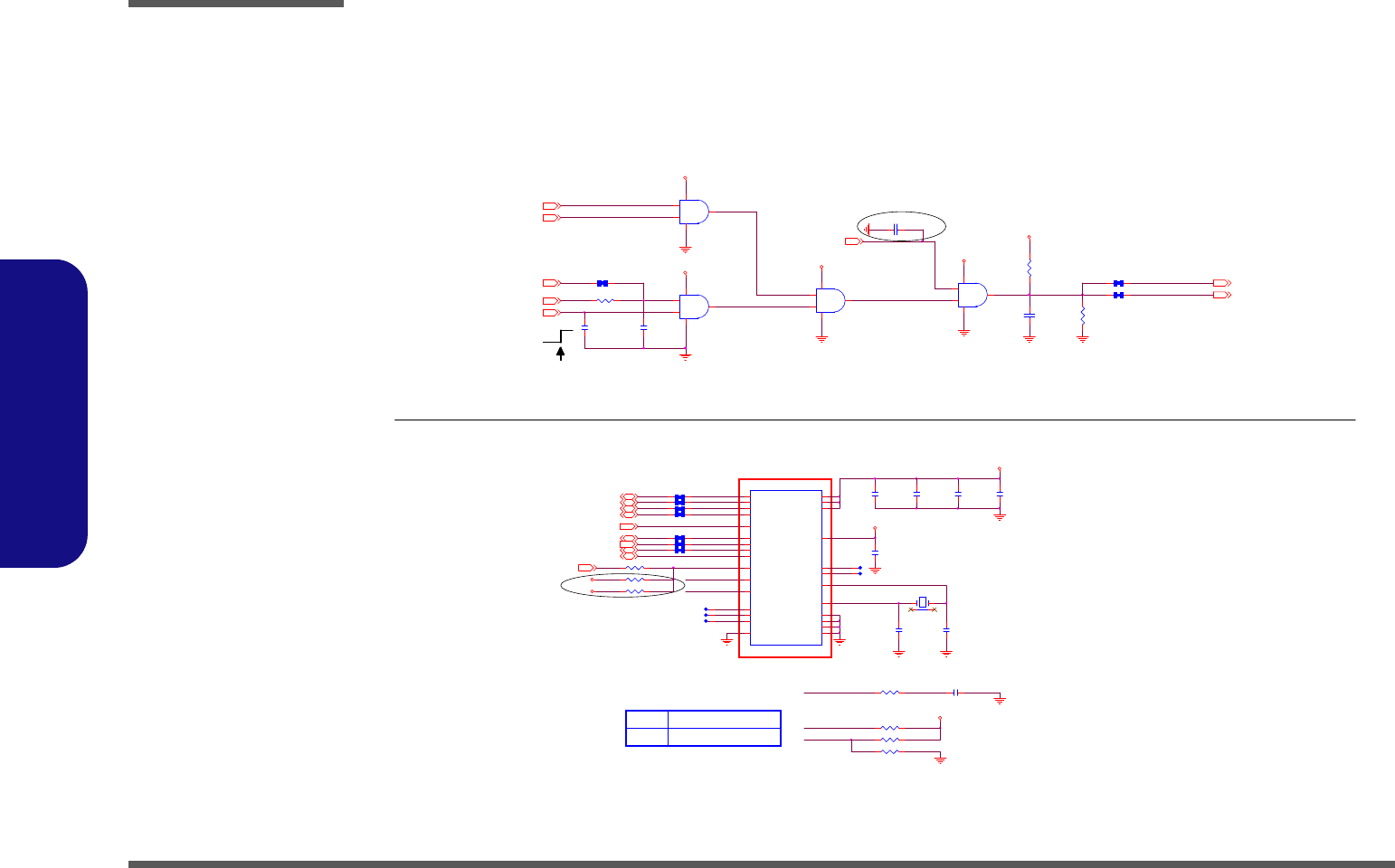
Schematic Diagrams
B - 12 POWERGOOD/TPM
B.Schematic Diagrams
POWERGOOD/TPM
R776 *0_04
PWRGD_VCORE28
3.3V
SYS_PW ROK
SB_PWROK
R819 *10mil_short_04
BUF_PLT_RST#7,16,17,20
LPC_AD37,20
LPC_AD17,20 LPC_AD07,20
PCLK_TPM7
LPC_FRAME#7,20
LPC_AD27,20
PCI_CLKRUN#7
R816 *10mil_short_04
C841
1u_6.3V_Y5V_04
VDD3 R248 *10K_04
R239 10K_04
3.3VS
3.3VS to VDD3 3/9
C848 *0.1u_16V_Y 5V_04
R815 *10mil_short_04
1.1V_PWRGD26
C913
*0. 01u_16V_X7R_04
D02
ON
C915
*0.01u_16V_X7R_04
3.3V
SUSB#8, 12,20,23
R774
10K_04
R775 *10mil_short
R264 *0_04
SUS_STAT#7
R364 *10mil_short
R365 *10mil_short
3.3V
DDR1.5V_PWRGD25,28
SERIR Q7,20
C882
15p_50V_NPO_04
XTALO
X12 MC-306_32.768KHz
14
3 2
XTALI
C881
15p_50V_NPO_04
R824 *10K_04
TPM_PP
PCLK_TPM
R823 10K_04
R821 *33_04
R822 *10K_04
LPC reset timing:
TPM 1.2
HI: 4E/ 4F H
LOW: 2E/ 2F H
TPM_PP
TPM_BADD
LPCPD# inactive to LRST# inactive 32~96us
Asserted before entering S3
HI: ACCESS
LOW: NORMAL ( Internal PD )
C883 *10p_50V_04
3.3VS
C876
0.1u_16V_Y 5V_04
3.3VS
VDD3
C877
0.1u_16V_Y5V_04
C878
0.1u_16V_Y 5V_04
C879
1u_16V_X5R_06
C880
0.1u_16V_Y 5V_04
TPM3005
TPM_BAD D
TPM
U50
SLB9635TT
LAD3
17
LAD0
26
LAD1
23
LAD2
20
VDD1 10
XTA L I 13
VDD3 24
VDD2 19
LFRAME#
22
LCLK
21
LRESET#
16
SERIRQ
27
CLKRUN#
15
GND_1 4
GND_2 11
GND_3 18
GND_4 25
GPIO 6
GPIO2 2
XTALO 14
TESTI
8
TESTBI/BADD
9
PP
7
NC_1
1
NC_2
3
NC_3
12
LPCPD #
28
VSB 5
TPM3002
TPM3004
TPM_PP
TPM3003
TPM3001
TPM_BAD D
R817 *10mil_short_04
R814 *10mil_short_04
R818 *10mil_short_04
U22B
74LVC08PW
4
56
147
3.3V
SY S_R ST#8
R367
*10K_04
R820 *10mil_short_04
U22C
74LVC08PW
9
10 8
147
U22A
74LVC08PW
1
23
147
3.3V
SB_PWRGD 8
ALL_SYS_PWRGD 13, 20
D02
U22D
74LVC08PW
12
13 11
147
1.8V_PWRGD27
Sheet 11 of 33
POWERGOOD/TPM
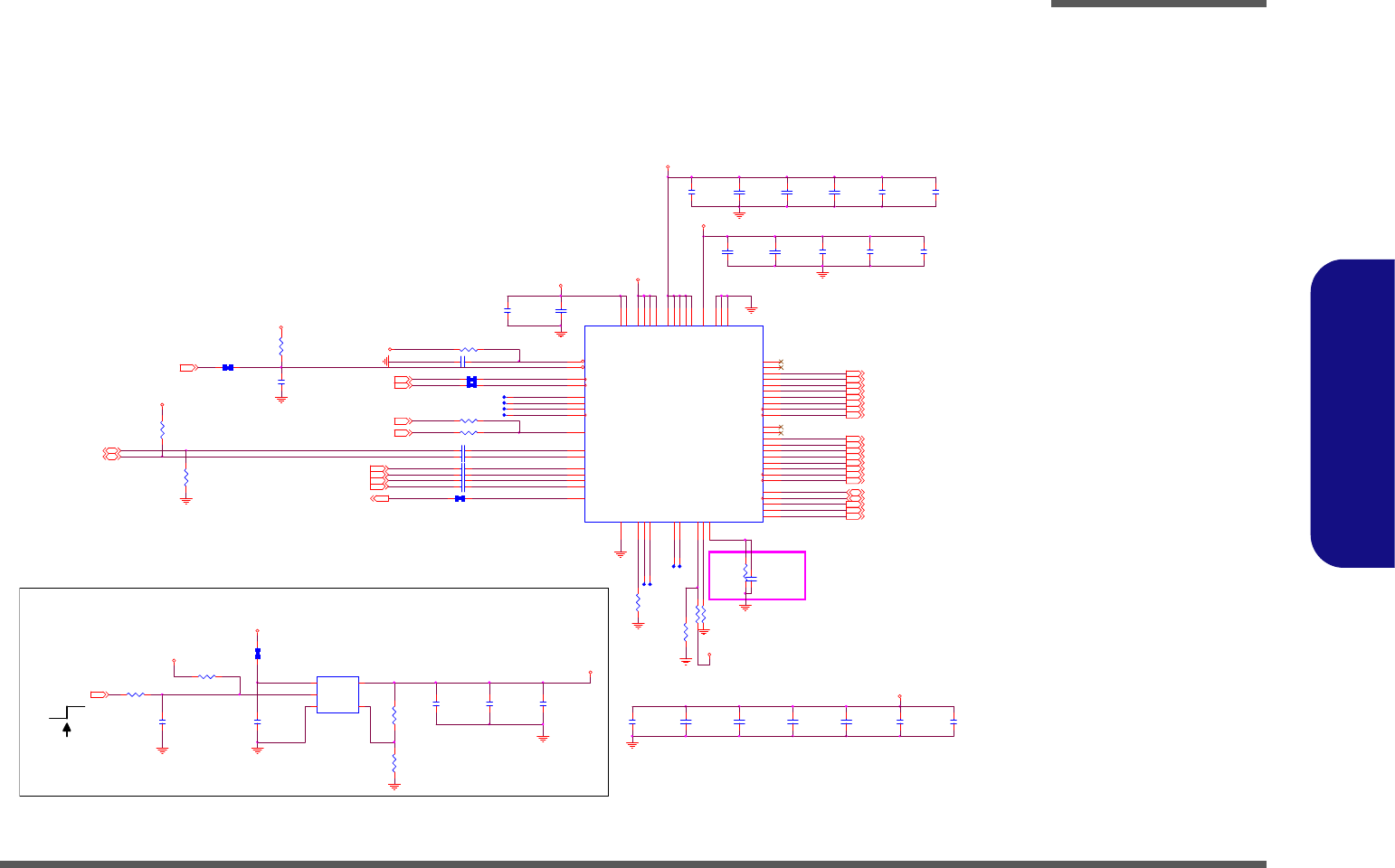
Sheet 12 of 33
ANX3110 ASIC
Schematic Diagrams
ANX3110 ASIC B - 13
B.Schematic Diagrams
ANX3110 ASIC
LVDS-L1P
LVDS-L2P
LVDS-L2N
XLT_ B LON _ P WM
LVDS-L1N
need to close to chip
1.2VS
ANX3110 ASIC
DP_HPD
R1
Vo=Vref*(R2+R1)/R2
LVDS-L2P3,13
R2
200mA
Fixed : P1 OPEN, R2 short to GND
ON
LVDS-L2N3,13 LVDS-L1P3,13
RST#
LVDS-L1N3,13
PR241
*15mil_short _06
C895
2.2u_6.3V_X5R_06
PWM_VARY_BL
R859
*10K_04
BRIGHTNESS13,20
R837
*10mil_short_04
R838
*10mil_short_04
R842 *0_04
C884
2.2u_6.3V_X5R_06
GPIO_2
C892
2.2u_6.3V_X5R_06
R856
*100K_04
C898
*3.3u_6.3V_X5R_06
3.3VS
CLK_SEL
LVDS_DDC_DATA3,13 LVDS_DDC_CLK3,13
LVDS_DDC_DATA
LVDS_DDC_CLK
C906
2.2u_6.3V_X5R_06
PC239
2.2u_6.3V_X5R_06
C893
0.01u_16V_X7R_04
R841
*1M_04
C891
0.1u_10V_X5R_04
C886
0.1u_10V_X5R_04
C899 0.1u_10V_X5R_04
C911
0.01u_16V_X7R_04
PC242
1u_16V_X5R_06
R851
12K_1%_04
C903 0.1u_10V_X5R_04
PU13
APL5317-12BI-TRG
VIN
1
GND
2
EN
3
SET 4
VOUT 5
R839
*1M_04
PC241
0.1u_16V_Y5V_04 C912
0.01u_16V_X7R_04
R854
*10K_04
R835 1M_04
C887
0.1u_10V_X5R_04
C896
0.1u_10V_X5R_04
C900 0.1u_10V_X5R_04
PR220
*10K_04
C897 0.1u_10V_X5R_04
C885
0.1u_10V_X5R_04
3.3V
C894
0.01u_16V_X7R_04
ANX3110
U51
ANX3110
EPAD
65
POR
34
RESET_L
12
OSC_IN
30
OSC_OUT
31
TD O
54
TD I
55
TMS
57
TC K
56
CPU_VARY_BL
48
DPRX_AUX_N
60
DPRX_AUX_P
61
DPRX_L0_P
3
DPRX_L0_N
4
DPRX_L1_P
6
DPRX_L1_N
7
DPRX_HPD
58
LVDS_U3_P 45
LVDS_U3_N 44
LVDS_CLKU_P 43
LVDS_CLKU_N 42
LVDS_U2_P 41
LVDS_U2_N 40
LVDS_U1_P 38
LVDS_U1_N 37
LVDS_U0_P 36
LVDS_U0_N 35
LVDS_L3_P 29
LVDS_L3_N 28
LVDS_CLKL_P 27
LVD S_CLKL_N 26
LVDS_L2_P 24
LVDS_L2_N 23
LVDS_l1_P 22
LVDS_l1_N 21
LVDS_L0_P 20
LVDS_L0_N 19
DDC_DATA 50
DDC_C LK 49
VARY _BL 47
BL_EN 15
DIGON 14
DVDD33_1 13
DVDD33_2 53
DVDD12_1 9
DVDD12_2 32
DVDD12_3 46
DVDD12_4 59
AVDD33_1 8
AVDD33_2 25
AVDD33_3 33
AVDD33_4 39
AVDD33_5 63
AVDD12_1 1
AVSS_1 2
AVSS_2 5
AVSS_3 62
GPIO_0
16
GPIO_1
17
GPIO_2
18
CFG_SDA
52
CFG_SCL
51
CLK_SEL
10
TEST_EN
11
R_BIAS
64
C902 0.1u_10V_X5R_04
PC243
1u_10V_Y5V_06
C909
0.1u_10V_X5R_04
R853
10K_04
R852
10K_04
R840 *0_04
C907
0.1u_10V_X5R_04
C910
0.1u_10V_X5R_04
C888
0.01u_16V_X7R_04
C890
0.1u_10V_X5R_04
C889
0.01u_16V_X7R_04
C901 0.1u_10V_X5R_04
PR222
0_04
C904 0.1u_10V_X5R_04
PC240
*10u_6.3V_X5R_06
PR221
*8.2K_1%_04
C905
100p_50V_NPO_04
C908
0.1u_10V_X5R_04
R855 100K_1%_04
1.2VS
3.3VS
3.3VS
3.3VS
1.2VS
1.2VS
1.2VS
3.3VS
3.3VS
TXOUT_U1N 13
TXOUT_U1P 13
3.3VS
TXCLK_LP 13
TXCLK_UP 13
TXCLK_UN 13
SDA 13
TXOUT_L1N 13
TXOUT_L1P 13
TXCLK_LN 13
XLT_DIGON 13
XLT_BLEN 13
SCL 13
ANX3110_CLKN7ANX3110_CLKP7
DP_HPD3
SUSB#8,11,20,23
EC_RST#7,20
ON_VARY3
TXOUT_U0P 13
TXOUT_U2N 13
TXOUT_U2P 13
TXOUT_L0P 13
TXOUT_L0N 13
TXOUT_U0N 13
TXOUT_L2P 13
TXOUT_L2N 13
XLT_ BLON _ PWM 13
TEST_EN
GPIO_1
GPIO_0
OSC_IN
OSC_OUT
POR#
TCK
TMS
TDI
TDO
R843
*10mil_short_04
R836
*10mil_short_04
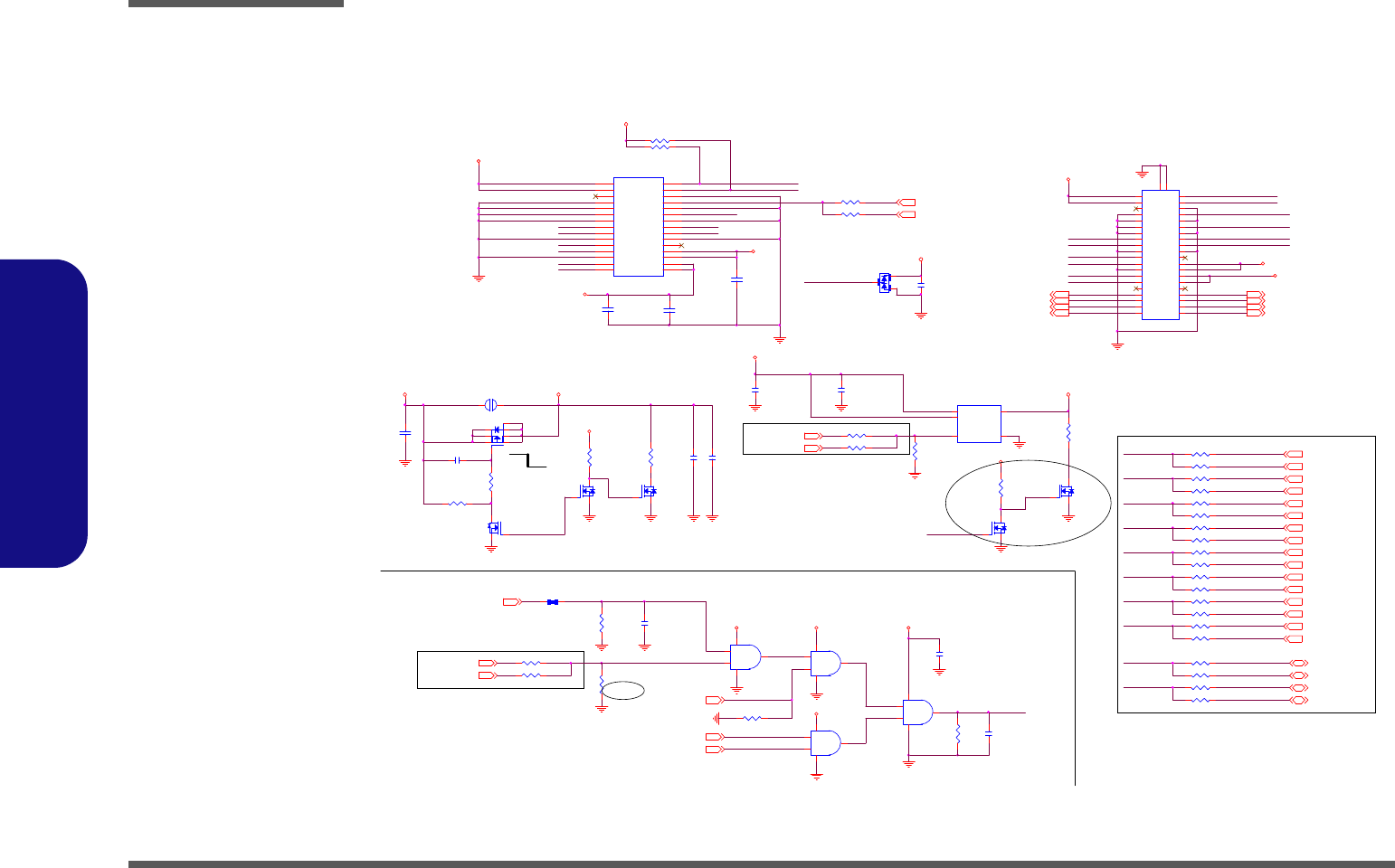
Schematic Diagrams
B - 14 LVDS/Inverter
B.Schematic Diagrams
LVDS/Inverter
U25C
74LVC08PW
9
10 8
147
R621 0_04
R613 0_04
R390
*100K_04
R608 *0_04
R610 *0_04
D23
*BAV99 RECTIFIER
A
C
AC
C565
0.1u_16V_Y 5V_04
C566
*0. 1u_16V_Y5V_04
C567
*0. 47u_10V_Y5V_04
R618 *0_04
R577 4.7K_04
C563
0.1u_16V_Y5V_04
R616 *0_04
U24
APL3512A
VIN
4
VIN
5
EN
3
VOUT 1
GND 2
3.3V
VIN_LCD
3.3V
3.3V
3.3V
J_LCD2 For dual channel
J_LCD1 For single channel
3.3VS
PLVDD
3.3VS
PLVDD
3.3VS
3.3V
VIN_LCD
3.3VS
PLVDD
LID_SW#8,20,22
ALL_SY S_PWRGD11,20
BRIGHTNESS 12,20
BKL_EN20
LVDS-L1P 3,12
LVDS-L1N 3,12
SCL 12
NB_ENAVDD3
TXCLK_LP 12
LVDS-L0P 3
LVDS-L0N 3
LVDS-LCLKP 3
LVDS-L2N 3,12
TXOUT_L1P 12
TXOUT_L0N 12
LVDS-L2P 3,12
LVDS-LCLKN 3
TXOUT_L0P 12
TXOUT_L2P 12
TXOUT_L2N 12
LVDS_DDC _D ATA 3,12
SDA 12
TXOUT_L1N 12
TXCLK_LN 12
LVDS_DDC _C LK 3, 12
TXOUT_U0N 12
TXOUT_U0P 12
TXOUT_U2N 12
TXOUT_U2P 12
RLVDS-L2P
C5590. 1u_50V_Y5V_06
C5600.01u_50V_X7R_04
30pin for W24/W25
40pin for W270BZQ
D02
D02
C17
*0.22u_50V_06
R858 *0_04
R_BRIGHTNESS
R238
*10K_04
S
D
G
Q45B
*MTDN7002ZHS6R
5
34
R228
*200_1%_04
Q49
*MTN7002ZHS3 G
DS
S
D
G
Q45A
*MTDN7002Z HS6R
2
61
3.3V
Q46
*P2003EVG
4
62 5
73
1
8
3A
VIN_LCD
ENAVDD
VIN
1108
LVDS_DATA
LVDS_CLK
R_BRIGHTNESS
RLVDS-L2N
INV_BLON
2A
RLVDS-L1N
RLVDS-L1P
S
D
G
Q50A
*MTDN7002ZHS6R
2
61
C18
0.1u_50V_Y5V_06
RLVDS-L0N
RLVDS-L0P
XLT_BLEN12
Default W270BZQ
R229
*1K_04
PJ11
OPEN_2A
12
R9 *100K_04
TXOUT_U1N12 TXOUT_U1P12
RLVDS-LCLKP
RLVDS-LCLKN
TXCLK_UP12 TXCLK_UN12
SB_BLON8
ENAVDD
PANEL CONNECTOR
2A
RLVDS-L0P
LVDS_DATA
RLVDS-L1P
RLVDS-LCLKN RLVDS-L2N
RLVDS-L1N
INV_BLON
RLVDS-L0N
RLVDS-LCLKP RLVDS-L2P
LVDS_DDC_DATA
SDA
R698 *0_04
80mils
LVDS_DATA
EDID Mode
LVDS_DDC_CLK
SCL
LVDS_CLK
LVDS_CLK
ENAVDD
2A
LVDS-L1P
TXOUT_L1P
S
D
G
Q50B
*MTDN7002ZHS6R
5
34
PANEL POWER
RLVDS-L1P
R_BRI GHTNESS
TXOUT_L0N
XLT_DIGON12
LVDS-L2N
TXOUT_L2N
RLVDS-L2N
LVDS-L2P
TXOUT_L2P
LVDS-L0N
LVDS-L0P
TXOUT_L0P
RLVDS-L2P
RLVDS-L0P
LVDS-LCLKN
TXCLK_LN
RLVDS-LCLKN
LVDS-L1N
TXOUT_L1N
3/10
RLVDS-L0N
RLVDS-L1N
LVDS-LCLKP
TXCLK_LP
RLVDS-LCLKP
R701 on, R700 off for W270BZQ
R699 on, R698 off for W270BZQ
XLT_BLON_PWM 12
3.3V
R699 0_04
R857 0_04
R246
*10K_04
INV_BLON
BKL_EN_R
Z1201
BACKLIGHT ENABLE
R586
*1M_04
BLON3R700 *0_04
R701 0_04
Z1202
Z1203
R611 0_04
R391 *100K_04
R602 *0_04
R392
*1M_04
C569
0.1u_16V_Y5V_04
R620 *0_04
U25B
74LVC08PW
4
56
147
R603 0_04
R388 *10mil_short_04
R578 4.7K_04
U25D
74LVC08PW
12
13 11
147
R606 *0_04
R609 0_04
C564
*0. 01u_16V_X7R_04
C561
0.1u_16V_Y5V_04
R619 0_04
U25A
74LVC08PW
1
23
147
R387
100K_04
J_LCD1
*87216-3006
1
122
3
344
5
566
7
788
9
910 10
11
11 12 12
13
13 14 14
15
15 16 16
17
17 18 18
19
19 20 20
21
21 22 22
23
23 24 24
25
25 26 26
27
27 28 28
29
29 30 30
C562
4.7u_6.3V_X5R_06
R607 0_04
R617 0_04
R615 0_04
R604 *0_04
R614 *0_04
J_LCD2
87216-4006
1
3
5
7
9
11
13
15
17
19
21
23
25
27
29
31
33
35
37
39
2
4
6
8
10
12
14
16
18
20
22
24
26
28
30
32
34
36
38
40
Gnd 1 G1
Gnd 2 G2
R389
*100K_04
R605 0_04
C568
*0.1u_16V_Y 5V_04
R612 *0_04
Sheet 13 of 33
LVDS/Inverter
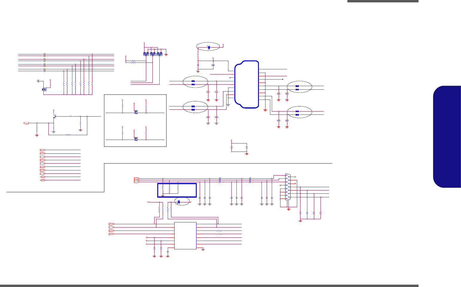
Schematic Diagrams
HDMI/CRT B - 15
B.Schematic Diagrams
HDMI/CRT
HDMIB_D2BP
HDMIB_D2BN
HDMIB_D1BN
HDMIB_CLKBN
HDMIB_D0BP
HDMIB_D1BP
R721 * 0_04
HDMIB_CLKBP
CRT PORT
IP4772CZ16 6-02-47721-B60
TPD7S019 6-02-07019-B20
DDCLKDAC_DDCACLK
CRT_HSYNC
DDCDATA
BLUE
GRN
DAC_VSYNC
DAC_HSYNC
VSYNCCRT_VSYNC
RED
DAC_DDCADATA
HSYNC
D02
HDMI_DDC_DATA
D02
R720
*100K_04
R653 499_1%_04
R654 499_1%_04
D02
R406
*LVAR0402-240E0R 05P-LF
RD1
*BAV99 RECTIFIER
A
C
AC
.
L104 FCM1005MF-600T01
C589
0.22u_10V_Y5V_04
C582 10p_50V_NPO_04
C583 10p_50V_N PO_04
C591
0.22u_10V_Y5V_04
RD2
*BAV99 RECTIFIER
A
C
AC
R579 2. 2K_04
HDMIB_DATA1P
J_CRT1
108AH15FST04A1CC
8
7
6
5
4
3
2
19
10
11
12
13
14
15
GND2
GND1
R415 33_04
R398
*LVAR0402-240E0R 05P-LF
R400
*LVAR0402-240 E0R05P-LF
.
L103 FCM1005MF-600T01
HDMIB_EXT1_SCL
HDMIB_DATA1N
R405
*LVAR0402-240E0R 05P-LF
C578
*0.1u_16V_Y 5V_04
HDMI PORT
U27
TPD 7S01 9
VCC_SYNC
1
VCC_VIDEO
2
VIDEO_1 3
VIDEO_2 4
VIDEO_3 5
GND 6
VCC_DDC
7
BYP
8
DDC_OUT1 9
DDC_IN1
10
DDC_IN2
11 DDC_OUT2 12
SYNC_IN1
13 SYNC_OUT1 14
SYNC_IN2
15 SYNC_OUT2 16
HDMIB_DATA0P C570
10u_10V_Y5V_08
HDMIB_DATA0N
R407
*LVAR0402-240E0R 05P-LF
R416 33_04
C586 220p_50V_NPO_04
R397
*LVAR0402-240E0R 05P-LF
HDMIB_EXT1_HPD
For ESD
HDMIB_EXT1_SDA
C58 7 220p_50V_NPO_04
R580 2. 2K_04
C585 1000p_50V_X7R_04
R404
*LVAR0402-240E0R 05P-LF
.
L105 FCM1005MF-600T01
J_HDMI1
C12817-119A5-L
SHIELD 2
2
TMDS DATA1+
4
TMDS DATA1-
6
SHIELD 0
8
TMDS CLOCK+
10
TMDS CLOCK-
12
RESERVED
14
SDA
16
+5V
18
TMD S DA TA2+ 1
TMDS DATA2- 3
SHI ELD1 5
TMD S DA TA0+ 7
TMDS DATA0- 9
CLK SHIELD 11
CEC 13
SCL 15
DDC/CEC GND 17
HOT PLUG DETECT 19
C571
*22u_6.3V_X5R_08
C5 84 10p_50V_NPO_04
C590
0.22u_10V_Y5V_04
C577
0.1u_16V_Y 5V_04
R393
1_04
RD3
*BAV99 RECTIFIER
A
C
AC
R395
*LVAR0402-240E 0R05P-LF
C588 1000p_50V_X7R_04
5VS_HDMI
5VS_HD MI
5VS
3.3VS
3.3VS
5VS
3.3VS
3.3VS 5VS
HDMIB_DATA2P
HDMIB_CLOCKP
R647 499_1%_04
HDMIB_DATA2N
HDMIB_CLOCKN
D02
C579 10p_50V_NPO_04
C5 81 10p_50V_NPO_04
R414
150_1%_04
C580 10p_50V_N PO_04
R413
150_1%_04
R412
150_1%_04
DAC_BLUE
DAC_GREEN
DAC_RED
R862 2. 2K_04
DDCDATA
RED
DDCLK
VSYNC
HSYNC
24 mil
GRN
BLUE
6-20-14X30-015
R860 2. 2K_04
Q27
2N3904
B
E C
R658
10K_04
R55 200K_04
R657
*200K_04
3.3VS
CLOSE TO HDMI CONN.
HDMI_DDC_CLK
HDMIB_EXT1_SD A
5VS
Q26
MTN7002ZHS3
G
DS
R656
*2.2K_04
R659
4.7K_04
R655
4.7K_04
HDMIB_EXT1_SC L
DAC_VSYNC3
3.3VS
3.3VS
DAC_HSYNC3
3.3VS
3.3VS
Q28
MTN7002ZHS3
G
DS
DAC_BLUE3
DAC_DDCADATA3
5VS
R660
*2.2K_04
DAC_RED3DAC_GREEN3
DAC_DDCACLK3
HDMI_DDC_CLK3
HD MIB_D2BN3
HD MIB_C LKBN3
HD MIB_D1BN3
HD MIB_D0BN3
HD MIB_D2BP3
HD MIB_D1BP3
HD MIB_C LKBP3
HD MIB_D0BP3
HDMI_DDC_DATA3
HDMIB_CLKBN
HDMIB_D2BN
HDMIB_D2BP
HDMIB_D1BP
HDMIB_D0BN
HDMIB_CLKBP
HDMIB_D1BN
HDMIB_D0BP
HDMIB_D0BN
C865 22p_50V_N PO_04
C867 22p_50V_NPO_04
C86 6 22p_50V_NPO_04
C836 0.1u_10V_X7R_04
C829 0.1u_10V_X7R_04
C831 0.1u_10V_X7R_04
C830 0.1u_10V_X7R_04
C833 0.1u_10V_X7R_04
C832 0.1u_10V_X7R_04
C834 0.1u_10V_X7R_04
C835 0.1u_10V_X7R_04
PORTC_HPD3
D6
RB551V-30S2
AC
HDMIB_EXT1_HPD
3.3VS
Q25 MTN7002ZHS3
G
D S
R648 499_1%_04
R649 499_1%_04
R650 499_1%_04
HDMIB_DATA0N
HDMIB_DATA2N
HDMIB_DATA1N
HDMIB_EXT1_SCL
HDMIB_DATA0P
HD MIB_EXT1_SDA
HDMIB_EXT1_HPD
HDMI_CEC
HDMIB_DATA1P
HDMIB_CLOCKN
HDMIB_CLOCKP
HDMIB_DATA2P
5VS_HDMI
R863 2. 2K_04
L99 *10mil_short_04
L119 *10mil_short_04
.
L139 FCM1005MF-600T01
.
L137 FCM1005MF-600T01
.
L138 FCM1005MF-600T01
R861 2. 2K_04
D02
HDMI_DDC_DATA
R652 499_1%_04
R651 499_1%_04
HDMI_DDC_CLK
L101 *10mil_short_04
L120 *10mil_short_04
L122 *10mil_short_04
L102 *10mil_short_04
D7
RB551V-30S2
AC
D02
L100 *10mil_short_04
L121 *10mil_short_04
Sheet 14 of 33
HDMI/CRT
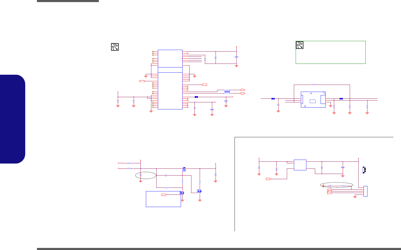
Schematic Diagrams
B - 16 CCD/3G
B.Schematic Diagrams
CCD/3G
+
C601
*220u_4V_V_B
D02
60mils
D02
+
C593
*220u_4V_V_B
Layout Show "3.5G(HSDPA)" Note
48 mil
CCD_DET#
5
MJ_CCD1
1
CCD
From H8 default HI
CCD_EN20 CCD_EN
C611 *15p_50V_NPO_04
UIM_DATA
MINI CARD 3G(Port 6)
UIM_VPP
UIM_PWR
UIM_RST
UIM_CLK
Q32
*AO3415
G
DS
C599
*10u_10V_Y5V_08
S
D
G
Q33A
*RT3K44M
2
61
(TOP VIEW)
LOCK
OPEN
J_SIM1
*C1770661-1
UIM_DATA C7
UIM_VPP C6
UIM_GND C5
UIM_PWR
C1 UIM_RST
C2 UIM_CLK
C3
C595
*0.1u_16V_Y5V_04
C610
1u_6.3V_Y5V_04
C598
*0.1u_16V_Y5V_04
C592
*0.1u_16V_Y5V_04
R792
*10_06
C602
*22p_50V_NPO_04
C857 *1u_6.3V_Y5V_04
C603
*22p_50V_NPO_04
C604
*22p_50V_NPO_04
R422
*10mil_short_04
R790 *0_06
L106 *WCM2012F2S-161T03-short
1
4
2
3
J_CCD1
85205-05001
1
2
3
4
5
C613
0.1u_16V_Y5V_04
C846
*1u_6.3V_Y5V_04
R793 *100K_04
S
D
G
Q33B
*RT3K44M
5
34
UIM_VPP
R789 *0_06
UIM_CLK UIM_DATA
UIM_RST
UIM_PWR
KEY
J_3G1
*MPCEC-S00F1-TP00
COEX1
3
COEX2
5
CLKREQ#
7
GND0
9
REFCLK-
11
REFCLK+
13
WAKE#
1
GND1
15
PETn0
23
PETp0
25
GND2
21
GND3
27
PERn0
31
PERp0
33
GND4
29
Res erv ed0
17
Res erv ed1
19
W_D ISABLE# 20
GND12
37
3.3VAUX_3
39
3.3VAUX_4
41
GND13
43
Res erv ed2
45
Res erv ed3
47
Res erv ed4
49
Res erv ed5
51 LED_WLAN# 44
LED_WWAN# 42
GND6 18
UIM_VPP 16
UIM_RESET 14
3.3VAUX_0 2
UIM_CLK 12
UIM_DATA 10
UIM_PWR 8
1.5V_0 6
GND5 4
PERSET# 22
3.3VAUX_1 24
GND7 26
1.5V_1 28
SMB_CLK 30
SMB_DATA 32
GND8 34
USB_D- 36
USB_D+ 38
GND9 40
LED_WPAN# 46
1.5V_2 48
GND10 50
3.3VAUX_2 52
GND11
35
C605
*22p_50V_NPO_04
C600
*0.1u_16V_Y5V_04
R421
*10mil_short_04
C594
*0.1u_16V_Y5V_04
R791
*20K_1%_04
R419 *15mil_short_06
R420 *4.7K_04
3G_3.3V
3G_3.3V
3G_3.3V
5V
3G_3.3V
5V_CCD
3.3V
3G_3.3V
3.3V_3G
3.3VS
USB_PN7 8
3G_EN 20
3G_DET#20
CCD_DET#20 USB_PP58USB_PN58
USB_PP7 8
3G_POWER20
SIMLOCK
SIM CONN
C614
10u_10V_Y5V_08
U18
NCT3522U
VIN
4
VIN
5
EN
3
VOUT 1
GND 2
3A 120mils
From SB GPIO Pin default HI
Power Plane: Suspend
S3: Defined
C596
*1u_6.3V_X5R_04
AO3409(90mohm) Change
to AO3415(45mohm).
3G POWER
AO3409¤£¨Ï¥Î
ADD R1 28,Q2
Solution For
PDA
BUG- When
Batt e ry
discharge to
shutdown,
the CMOS
sometimes
loss .
3A 120mils
R794 *300_04
48 mil
M:NCT3522U: 6-02-03522-9C0
S:G5243A: 6-02-05243-9C0
AP2821KTR-G1:6-02-02821-9C0
60mils
C868
*0.1u_16V_Y5V_04
Sheet 15 of 33
CCD/3G
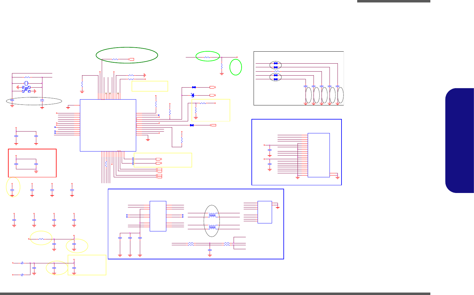
Schematic Diagrams
CardReader/LAN RTL8402 B - 17
B.Schematic Diagrams
CardReader/LAN RTL8402
C522
0.1u_16V_Y5V_04
C616
*4.7u_6.3V_X5R_06
C160
0.1u_16V_Y5V_04
C161
0.1u_16V_Y5V_04
C558
0.1u_16V_Y5V_04
C617
*4.7u_6. 3V_X5R_06
C523
1u_6.3V_X5R_04
C524
0.1u_16V_Y5V_04
.
L34
*HCB1608KF-121T25
R84 *0_06
C525
0.1u_16V_Y5V_04
.
L39
HCB1608KF-121T25
VDD 33/18VDD 33/ 18 VDD33/18VDD33/18
EVDD10
VDD 10
3.3V
DVDD33
VDD3
Pin#26
PIN18PIN18
PIN6
VDD3 meet rising time
>1ms
PIN1
60 mil
The DVDD33 rise time must be
controlled between 1mS and
100mS.
PIN31
Close to chip
Pin#40Pin#26 Pin#40
R296 *10mil_short_04
R298 *10mil_short_04
SD_CMD
L60
*WCM2012F2S-161T03-short
1
4
2
3
FOR EMI
LAN_MDIP1
LED1/EESK
PIN47PIN34
LAN_MDIN 1
SD_D1
EECS
LED2/EEDI
LED_CR
Near Cardreader CONN
SD_D7
C615
*4.7u_6.3V_X5R_06
X6 FSX5L_25MHZ
12
R729
10K_04
C69
1u_6.3V_X5R_04
C327
0.1u_16V_Y5V_04
T117
R188 *10mil_short
R123
15K_04
C295 0.1u_10V_X7R_04
C60
1u_6.3V_X5R_ 04
R394 *1K_04
R187 1M_04
PERSTB
R366 *10K_04
U3
RTL8402
MS_D0/xD_D1 43
MS_D4/xD_D0 42
LED0/SPICSB 39
GPO 38
XD_CD# 44
SD_CD#/MS_D5/xD_ALE 41
LED1/SPISCK 37
DVDD10 47
SD_CMD/MS_D6/xD_D3
15
SD _D3/MS_D 2/xD _D 2
16
SD_D2/xD_D7
17
GND 25
HSIP
19
HSIN
20
REFCLK_P
21
REFCLK_N
22
EVDD 10
18
HSOP
23
HSON
24
SDA/SPIDI 36
SCL/LED_CR 35
DVDD10 34
LAN WAKEB 33
ISOLATEB 32
PERSTB 30
CLKREQB 29
SD_WP/MS_D1/x D_WP# 28
MS_BS/xD_CLE 27
RSET 48
CKXTAL2 46
CKXTAL1 45
VDD33/18 26
GND
49
AVDD33
1
MDI P0
2
MDI N0
3
MDI P1
4
MDI N1
5
DVDD33
6
Card_3V3
7
SD_D7/xD_RDY
8
SD_D6/MS_INS#/xD_RE#
9
SD_D5/xD_CE#
10
SD_D4/xD_WE#
11
SD_D1/MS_CLK/xD_D6
12
SD_D0/MS_D7/xD_D5
13
SD_CLK/MS_D3/xD_D4
14
DVDD33 31
VDD33/18 40
R185
*150_06
D34 RB751S-40C2
AC
SD_D0
R112 1K_04
X7
*HSX321S_25MHZ
1 2
34
T111
R396
*1.5K_04
T118
C274
18p_50V_NPO_04
C97
0.1u_16V_Y5V_04
T119
C326
0. 1u_16V_ Y 5V_04
R717 0.2_06
R83
2.49K_1%_04
C296
18p_50V_NPO_04
CARD_3V3
C61
0.1u_16V_Y5V_04
C294 0.1u_10V_X7R_04
R401
10K_04
C322
0. 1u_16V_ Y 5V_04
DVDD33
CARD_3V3
DVDD33 3.3VS
DVDD33
VCC_CARD
DVDD33
EVDD10
DVDD33
CARD_3V3
VDD10
VDD10
VDD33/18
DVDD33
VDD33/ 18
DVDD33
3.4A-קï
VCC_CARD
VCC_CARD
VDD10VDD 10VD D10
PCIE_WAKE# 8,17
PCIE_RXP0_LAN 7
PCIE_RXN0_LAN 7
CLK_PCIE_LAN 7
LAN_PCIE_WAKE# 20
PCIE_TXN0_LAN 7
PCIE_TXP0_LAN 7
BUF_PLT_RST# 7,11,17,20
CLK_PCIE_LAN# 7
PIN47
R114 *0_04 LAN_25MHz 7
meet realtek Freq tolerance 50ppm
Fr om PCH LAN_25M Hz
XTAL1
XTAL2
meet realtek Freq tolerance 50ppm
SD_D3
SD_D5
SD_D2 MS_D0
FOR S5 WA KE UP ON LAN
TO SB PCH WAKE#.
TO EC8518 PIN123 PME#.
PIN7
V3.6 DEL
LANWAKEB
SD_CLK
ISOLATEB
XTAL2
Crystal 8045 & 3225 Co-lay
XTAL1
RTL8402 incorporates a linear Low dropout regulator
BIOS pulls high or low to GPO pin,
Pkease refer to LAN/PHY Disable
Application Note.
SD_WP/MS_D1MS _I N S# CLKREQB
Remind that R112 using the
main power (S0 power).
C292 & C293 capacitors must be close to pin side.
RSET
SD_D0
C430
*5p_50V_NPO_04
SD_D4
R295 0_04
C431
*5p_50V_NPO_04
LAN_MDIN 0
LAN_MDIP0
MS_BS
C433
*5p_50V_NPO_04
SD_C D #
LAN (RTL8402)
·íÃö³¬host¹q·½/ CARD ©Þ´¡®É,VCC_CARD
¹qÀ£À³§C©ó0.5¥ñ¯S,³Ì¤Ö»Ý-n1ms´Á¶¡
C426
*5p_50V_NPO_04
Close to chip
C440
*5p_50V_NPO_04
SD_D0_R;SD_D1/M S_CLK_R;SD_D2_R;SD_D3/M S_D2;SD_CLK/MS_D3_R ¨«¤º¼h.
SD_CLK
SD_D0_R
RTL8402 command
SD_D1
SD_D3 SD _D 3/MS _D 2
SD _D1/MS_CLK_R
SD_D2_R
SD_CLK/MS_D3_R
SD_D2 R297 *10mil_short_04
R72 *10mil_short_04
D02
R299
0_04
J_CARD-REV1
MDR019-C0-1042
DAT2_SD
P2
VSS_MS
P21
CD/DAT3_SD
P3
CMD_SD
P4
VSS_SD
P5
VDD_SD
P6
CLK_SD
P7
VSS_SD
P8
DAT0_SD
P9
DAT1_SD
P10
WP_SD
P11
VSS_MS
P12
VCC_MS
P13
SCLK_MS
P14
DAT3_MS
P15
INS_MS
P16
DAT2_MS
P17
SDIO/DAT0_MS
P18
DAT1_MS
P19
BS_MS
P20
CD_SD
P1
GND P23
GND P22
SD_WP/MS_D1
SD _D3/MS_D2
SD_CMD
SD_CLK/MS_D3_R
MS_D0
SD_D2_R
SD_CD#
SD_D1/MS_CLK_R
SD_CLK/MS_D3_R
MS_INS#
SD_D0_R
MS_BS
SD _D3/MS_D2
SD_WP/MS_D1
SD/MMC/MS/MS PRO---Card Reader
SD_D1/MS_CLK_R
(MDR019-C0-1042) REVERSE
C606
0.1u_16V_Y5V_04
C597
0.1u_16V_Y5V_04
VCC_CARD
VCC_CARD
C170
1000p_2KV_X7R_12
L59
*WCM2012F2S-161T03-short
1
4
2
3
R12575_1%_04
L30
NS681680
RD+
1
RD-
2RX+ 16
RX- 15
RD_CT
3RX_CT 14
NC
4
NC 12
NC
5
TD_C T
6
TD+
7
NC 13
TX- 9
TD-
8
TX_C T 11
TX+ 10
R85 75_1%_04
C202
0.01u_16V_X7R_04
C182
*0.01u_16V_X7R_04
R9675_1%_04
C192
*0.01u_16V_X7R_04
R86 75_1%_04
LMX2+
LMX1-
DLMX4-
DLMX3-
FOR 10/100M RTL8402®É¨Ï¥Î(DEFAULT)
DLMX4+
DLMX4+
DLMX2-
DLMX4-
DLMX3-
NMCT_2
NMCT_1
DLMX3+
DLMX3+
LMX1+
NMCT_R
DLMX1+DLMX1+
DLMX2+DLMX2+
DLMX1-DLMX1-
40 mil
LAN _MDIP0
LAN_MDIP1
NS_NC3
TCT
LAN_MDIN1 LMX2+
LMX2-
LMX1+
NS_NC4
LMX1-LAN _MDIN 0
NMCT_1
NMCT_2
DLMX2+
LMX2- DLMX2-
DLMX1+
NS_NC1
NS_NC2 DLMX1-
D02
R294 *10mil_short_04
W240BX 6-21-B4030-008
130451-0M
J_RJ1
DD-
8DD+
7
DB-
6
DC-
5DC+
4
DB+
3DA-
2DA+
1shield GN D1
shield GN D2
W251BXQ 6-21-B4060-008
D02
D02
D02
Sheet 16 of 33
CardReader/LAN
RTL8402
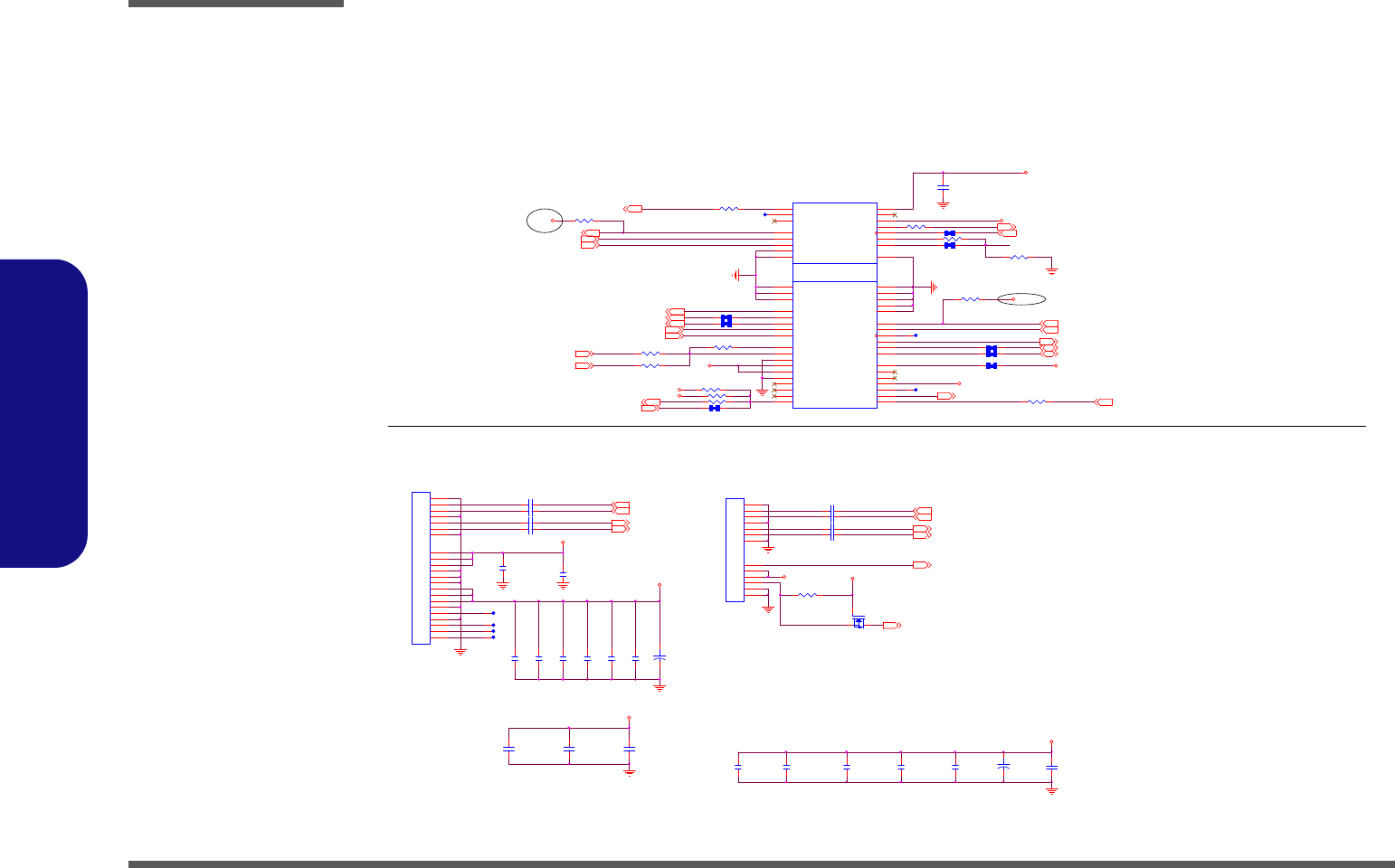
Schematic Diagrams
B - 18 Mini PCIE/SATA HDD/ODD
B.Schematic Diagrams
Mini PCIE/SATA HDD/ODD
ODD_DETECT#
SATA_TXP0
SATA_TXN0
HDD_NC1
HDD_NC2
HDD_NC3
HDD_NC0
SATA HDD
SATA_TXN1
SATA_RXN1
SATA_TXP1
SATA_RXP1
PIN GND1~2=GND
SATA ODD
W25/W27 6-20-43750-022
W24 6-20-43730-122
20 mil
20 mil
D02
SATA_RXN0
R727 *15mil_short_06
SATA_RXP0
WLAN_CLKREQ#
PCIE_WAKE#
3.3VAUX_1
BUF_PLT_RST#
20 mil
Port 2
20 mil
Layout Show "WLAN(Wim ax, 802.11N)" Note
R494 *10K_04
SATATXN0 9
SATATXP0 9
SATARXN0 9
SATARXP0 9
SATATXP1 9
SATARXP1 9
SATARXN1 9
SATATXN1 9
R496 *10mil_short_04
R508 *10mil_short_04
3IN1
R458 *10mil_short_04
3IN1
C655 0.01u_16V_X7R_04
R452 *0_04
R454 *0_04
C672 *0.1u_16V_Y5V_04
+
C670 220u_6.3V_6.3*6_E
R456 *10K_04
J_ODD1
C18553-11305-L
S1
S2
S3
S4
S5
S6
S7
P1
P2
P3
P4
P5
P6
KEY
J_MINI1
MPCEC-S00F1-TP00
COEX1
3
COEX2
5
CLKREQ#
7
GND0
9
REFCLK-
11
REFCLK+
13
WAKE#
1
GND1
15
PETn0
23
PETp0
25
GND2
21
GND3
27
PERn0
31
PERp0
33
GND4
29
Reserved0
17
Reserved1
19
W_D ISABLE# 20
GND12
37
3.3VAUX_3
39
3.3VAUX_4
41
GND13
43
Reserved2
45
Reserved3
47
Reserved4
49
Reserved5
51 LED_WLAN# 44
LED_WWAN# 42
GND6 18
UIM_VPP 16
UIM_RESET 14
3.3VAUX_0 2
UIM_CLK 12
UIM_DATA 10
UIM_PWR 8
1.5V_0 6
GND5 4
PERSET# 22
3.3VAUX_1 24
GND7 26
1.5V_1 28
SMB_CLK 30
SMB_DATA 32
GND8 34
USB_D - 36
USB_D+ 38
GND9 40
LED_WPAN# 46
1.5V_2 48
GND10 50
3.3VAUX_2 52
GND11
35
C653 0.01u_16V_X7R_04
R722 *100K_04
C675 *22u_6.3V_X5R_08
R451 10K_04
C656 0.01u_16V_X7R_04
C674 1u_6.3V_Y5V_04
C665
*0.1u_16V_Y5V_04
Q7*MTN7002ZHS3
G
DS
C673 0.1u_16V_Y5V_04
C662
*10u_10V_Y5V_08
C666
1u_6.3V_Y5V_04
J_HDD1
1-162-100561
S1
S2
S3
S4
S5
S6
S7
P1
P2
P3
P4
P5
P6
P7
P8
P9
P10
P11
P12
P13
P14
P15
C669
*0.1u_16V_Y5V_04
C671 0.1u_16V_Y5V_04
C654 0.01u_16V_X7R_04
C677
*0.01u_16V_X7R_04
R723 * 10m il_short
R726 *10mil_short
R725 *10mil_short
R724 * 10m il_short
C678
0.01u_16V_X7R_04
+
C668
*220u_6.3V_6.6*5.7
D02
C659 0.01u_16V_X7R_04
C663
*0.1u_16V_Y5V_04
C658 0.01u_16V_X7R_04
C847
0.1u_16V_Y5V_04
R457 *0_04
C657 0.01u_16V_X7R_04
R453
*10K_04
C661
*0.01u_16V_X7R_04
C667
10u_10V_Y5V_08
R738 *0_04
C679
*0.01u_16V_X7R_04
C660 0.01u_16V_X7R_04
C664
0.1u_16V_Y5V_04
C676 22u_6.3V_X5R_08
R706 *10K_04
R739 *0_04
5VS
5VS
3.3VS
5VS
3.3VS
5VS
3.3V
3.3V
3.3V
3.3V
3.3V
3.3V
VDD3
3.3V
ODD_DA#_FCH 8
ODD_D ETECT# 8
BT_EN20,21
BT_ON 7,21
WLAN_DET#20
CLK_PCIE_WLAN#7WLAN_CLKREQ#8
BT_DET# 20,21
USB_PN2 8
CLK_PCIE_WLAN7
WLAN_LED# 20,21
USB_PP2 8
WLAN_EN 20,21
BUF_PLT_RST# 7,11,16,20
PCIE_WAKE#8,16
80CLK 20
PCIE_RXN3_WLAN7
PCIE_TXN3_WLAN7PCIE_TXP3_WLAN7
BT_EN20,21
3IN120
BT_ON7,21
PCIE_RXP3_WLAN7
80CLK 20
R455 * 10K_04
R509 *0_04
R459 *20K_04
MINI CARD (WLAN,Port 5)
VDD3
Sheet 17 of 33
Mini PCIE/SATA HDD/
ODD
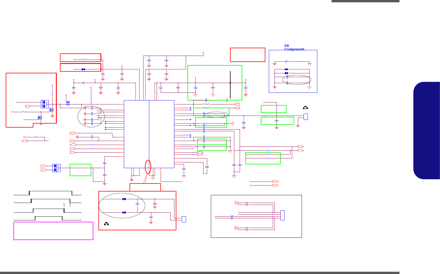
Sheet 18 of 33
Audio Codec
VT1802P
Schematic Diagrams
Audio Codec VT1802P B - 19
B.Schematic Diagrams
Audio Codec VT1802P
L113 *15mil_short_06
SPKOUTL-
AUDG
AUDG SPKOUTR+
SPKOUTR-
C785
*22n_16V_X7R_04
For Mic noise issue (Resrve) 3/11
R464 39.2K_1%_04
L109 *HCB1005KF-121T20
1 2
R468 5.1K_1%_04
C691
0.1u_16V_Y5V_04
C712
*180p_50V_NPO_04
R461 *10mil_short
2'ND SOURCE:6-03-01802-031
L111
*H CB1005KF-121T20
1 2
R465
3.3K_04
C694
10u_10V_Y5V_08
R460 *0_04
R476 3.3K_1%_04
J_INTMIC1
88266-02001
PCB Footprint = 88266-2L
1
2
C692
10u_10V_Y5V_08
C689
10u_10V_Y 5V_08
JP1 *10mil_short
C704 10u_6.3V_X5R_06
C706
1u_6.3V_X5R_04
C690
0.1u_16V_Y5V_04
C
A
A
D28
BAT54CWGH
1
23
R466 *100K_04
C686 *0.1u_16V_Y5V_04
L110
HCB1005KF-121T20
1 2
R463 20K_1%_04
R472 1K_04
C710
*1u_10V_Y5V_06
C683
0.1u_16V_Y 5V_04 C685
*0.1u_16V_Y5V_04
C707
2.2u_6.3V_X5R_06
R474 1K_04
C696 10u_6.3V_X5R_06
R471 22_04
C697 10u_6.3V_X5R_06
C711
*180p_50V_NPO_04
D02
C702 22p_50V_NPO_04
C680
10u_10V_Y5V_08
DIGITAL ANALOG
U32
VT1802P
DVDD1 1
GPIO0-DMIC-DAT
2
GPIO1-DMIC-CLK
3
PD#
4
SDATA-OUT
5
BIT-CLK
6
DVSS2
7
SDATA-IN
8
DVDD-IO 9
SYNC
10
RESET#
11
PCBEEP
12
Sense A 13
LINE2-L 14
LINE2-R 15
MIC2-L 16
MI C 2- R 17
Sense-B 18
JDREF 19
MON O - OU T 20
MIC1-L 21
MI C 1- R 22
LINE1-L 23
LINE1-R 24
AVSS1
26
VREF 27
LDO_CAP 28
MIC2-VREFO 29
MI C 1- VR E F O- R 30
MIC1-VREFO-L
31
HP-OUT-L 32
AVSS2
37
OPVEE 34
CBN 35
CBP 36
HP-OUT-R 33
PVDD1 39
SPK-L+
40
SPK-L-
41
PVSS1
42
PVSS2
43
SPK-R+
45 SPK-R-
44
PVDD2 46
SPDI FC2/EAPD
47
SPDI FO
48
AVDD2 38
AVDD1 25
GND
49
C699 100p_50V_NPO_04
C688
0.1u_16V_Y5V_04
C687 *0.1u_16V_Y5V_04
C698
100p_50V_NPO_04
R475 3.3K_1%_04
R478
4.7K_04
C709
100p_50V_NPO_04
R467 1K_04
C681
0.1u_16V_Y5V_04
C684
*10u_10V_Y5V_08
C693
0.1u_16V_Y5V_04
JP2 *10mil_short
R477 47K_04
R462
*10K_04
C695
*1u_6.3V_X5R_04
C703 0.1u_16V_Y5V_04
C700 10u_6.3V_X5R_06
C705 *10u_10V_Y5V_08
C682
10u_10V_Y 5V_08
C701 10u_6.3V_X5R_06
J_SPKL1
85204-02001
PCB Footprint = 85204-02R
1
2
Q12
*BSS138_NL
G
DS
C708
2.2u_6.3V_X5R_06
5VS
DVDD_IO
5VS
AUDG
3.3VS_AUD
AUDG
5VS
AUD G
3.3VS_AUD
AUD G
AUDG
3.3VS
1.5VS
5VS_AUD
AUDG
AUDG
AUDG
KBC_MUTE#20
HEADPHONE-L 22
HDA_SPKR8
HDA_SDI N08
HDA_RST#8
H DA_SY NC8
MIC_SEN SE 22
KBC_BEEP20
HEADPHONE-R 22
HP_SEN SE 22
HDA_SDOUT8
HDA_BITCLK8
SPKOUTR- 22
MIC1-L M 22
MIC1-R M 22
SPKOUTR+ 22
C786
*22n_16V_X7R_04
For 3.3V HDA Link.
L136 *FCM1608K-121T06_short
L135 *FCM1608K-121T06_short
VT1802P 10u
Speaker 8 ohm------> 20mils
VT1802P
SPKOUTR+,R-,L+,L- Trace width
2
AZ_RST#
AZ_RST# For 3.3V
HDA Link De-pop
AUDIO CODEC
1
Layout note:
VT1802P
L111,C695¤£¤W¥ó
Speaker 4 ohm------> 40mils
C92
*0.022u_16V_X7R_04
For 1.5V HDA Link.
FOR VOLUMN
ADJUST
5VS
DIGITAL
20m s
EMI Require
GND and AUDG space is
60mils ~ 100mils
PD#
Speaker wire length less than 8000mils , It don't need LC Filter.
INT_MIC_OUT
3.3VS_AUD
PC BEEP
MI C 2- VR E FO
ALC269 VB2
EAPD
CODEC_GPIO1
CODEC_GPIO0
SPDIFO
HDA_RST#
Thermal Pad place 9
Via hole.
BEEP_R
AZ_SDI N0_R
SPKOUTL+
MIC1-VREFO-R
MIC2-VR EFO
VT1802P NC PIN
HEADPHONE-R
HEADPHONE-L
CODEC_CBN
LINE1_R
MIC1_R _C
LINE1_L
ANALOG
MIC1-VREFO-L
MIC1-VREFO-R
MI C 1-R
SENSE_B
MONO_OUT
MIC1_L_C
HP_SENSE
MIC_SENSE
SPKOUTL+_L
MIC2_R
LINE2_L
MIC2_L
LINE2_R
J_SPK1
BEEP
SPKOUTR-
SPKOUTL+
SPKOUTR+
SPKOUTL-
EMI Require
AZ_RST# For 1.5V
HDA Link De-pop
PD# Control
VT1802P 5.1K_1%_04
R479
10K_04
C720 *180p_50V_NPO_04
MIC1-VREFO-L
EAPD22
AUDG
AUDG
SPKOUTL-_L
C236 *180p_50V_NPO_04
PN: 6-20-43130-104
C239 *180p_50V_NPO_04
C237 *180p_50V_NPO_04
J_SPK1
*85204-04001
1
2
3
4
C246 *180p_50V_NPO_04
SPKOUTR+_R
C
A
A
D33
BAT54AWGH
1
23
C717 *180p_50V_NPO_04
BEEP_C
MIC1-R_M
MIC1-L_M
SENSE_A
HDA_RST#
SPKOUTL-_L
CODEC_VREF
Q13
*MTN7002ZHS3
G
DS
SPKOUTR+
D02
HDA_RST#
R480 0_04
NEAR AUDIO CODEC
SPKOUTR-_R
SPKOUTL+_L
VT1802P 10u
MAIN SOURCE:6-03-01802-032
R140 100K_04
C716 100p_50V_NPO_04
VT1802P 3.3K_1%_04
Reserve
LDO_CAP
JDREF
21
J_INTMIC1
VT1802P
3.3K_04
C718 *180p_50V_NPO_04
VT1802P
100P
3.3VS_AUD
EAPD
INT_MIC
PD#
3.3VS_AUD
SPKOUTR-
MI C 1-L
5VS
C719 *180p_50V_NPO_04
L112 *15mil_short_06
D02
D02
CODEC_CBP
3.3VS_AUD
Q15
*MTN7002ZH S3
G
DS
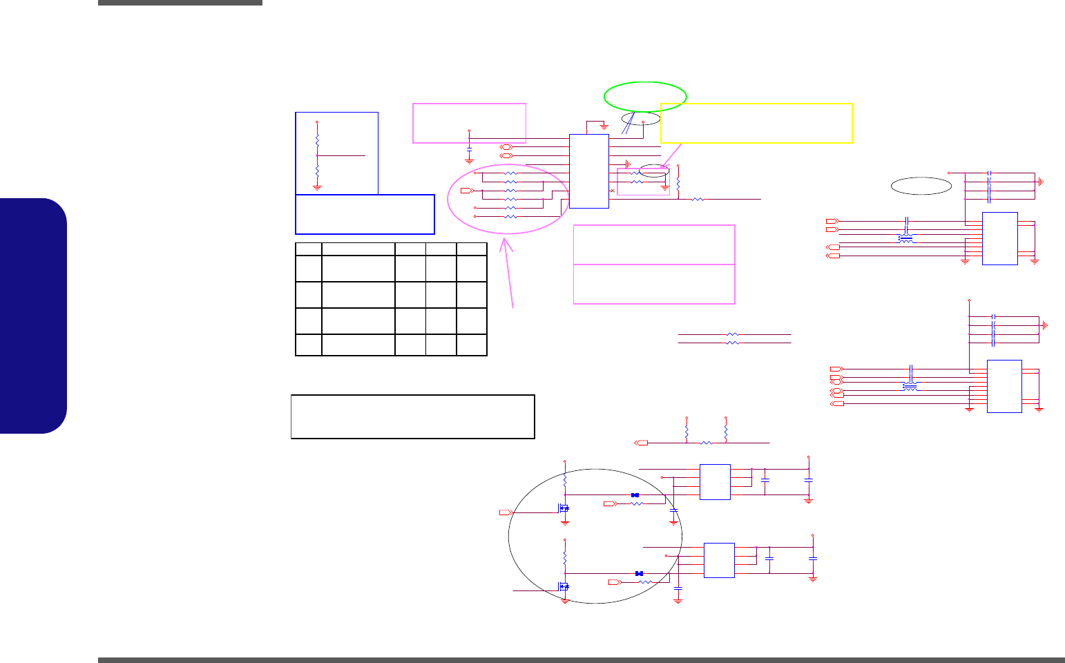
Sheet 19 of 33
USB 3.0/USB
Charge
R8 0_04
USB_SS_RX0P8
USB_SS_TX0N8
USB_SS_TX0P8
USB_SS_RX1P8
USB_SS_RX0N8
USB_SS_RX1N8
USB_SS_TX1N8
USB_SS_TX1P8
USB_PN08USB_PN0
VDD5
+
C650 *100u_6.3V_B_B
USB_PP0_R
USB_PN0_R
R168 0_04
R171 0_04
USB_PP0
USB_PN0
USB_PN18
D02
USB_PP18
C649 *0.1u_16V_Y5V_04
Standard-A
J_USB3_2
C19007-90905-L
PCB Footprint = USB-C19005
VBUS
1
D-
2
D+
3
GND_D
7
SSRX-
5
SSRX+
6
GND
4
SSTX-
8
SSTX+
9SHIELD GND1
SHIELD GND2
SHIELD GND3
SHIELD GND4
USB_SS_TX1P_R
USB_SS_TX1N_R
USB_PN1_R
USB_PP1_R
C652 0.1u_10V_X7R_04
C651 0. 1u_10V_X7R_04
USBVCC_2
L67
*WCM2012F2S-SHORT
1
4
2
3
C165 22u_6.3V_X5R_08
C166 22u_6.3V_X5R_08
D02
VDD5
USB_PP08USB_PP0
C163 22u_6.3V_X5R_08
R552
10K_04 R553
*10K_04
R554 *0_04
USB_OCP0_1#8
D02
3.3V3.3V
3.3V
USB_FLG#USB_OCP0_1#
Q30
*MTN7002ZHS3
G
DS
C248
10u_10V_Y 5V_08
R100
*100K_04
USB30_PWR_EN
C193
*0.1u_16V_Y5V_04
C164 22u_6.3V_X5R_08
C197
0.1u_16V_Y5V_04
U14
SY6288DCAC
VOUT1 6
VOUT3 8
VIN2
3
VIN1
2VOUT2 7
GND 1
EN#
4
FLG#
5
USB PORT Charge
USBVC C_2
DD_ON#23,25,26
5V
100 MIL
USB_FLG#
2A/90mohm
Q31
*MTN7002ZHS3
G
DS
3.3V
R101
*100K_04
USB30_PWR_EN
C247
10u_10V_Y 5V_08
USB30_PWR_EN8
C191
*0.1u_16V_Y5V_04
C196
0.1u_16V_Y 5V_04
U13
SY6288DCAC
VOUT1 6
VOUT3 8
VIN 2
3
VIN 1
2VOUT2 7
GND 1
EN#
4
FLG#
5
5V
USBVCC1
DD_ON#23,25,26
100 MIL
USB_FLG#
2A/90mohm
+
C513 *100u_6.3V_B_B
R10 0_04
R73 *0_04
TPS254X_ILIM_SEL
R74 *10K_04
C19
*10u_10V_Y5V_08
CTL1 CTL2 CTL3: 1 1 1-----> Charging downstream port, BC1.2.
CTL1 CTL2 CTL3: 0 x 1-----> Dedicated charging port, auto-detect
CTL1 CTL2 CTL3: 0 0 0-----> Out discharge, power switch Off
Mode 4
CTL1 CTL2 CTL3: 1 0 1-----> Dedicated charging port, Divider Mode only
USBVCC1
Power off & Charge
Power on & Charge 111
R87 *10K_04
R88 *10K_04
R3.7
G_OC#01
¤£±µOC Pin,
R73¤£¤W¥ó.
100 mil 100 mil
Power
¥i¤ä´©²Ä¤G-ÓUSB2.0
Port
WITH VPRO --> VDD5_USBCHG
WITHOUT VPRO --> VDD5
To South Bridge OC Pin.
FAULT OD PIN, PULL HIGH
PULL HIGH--> VDD5
VDD5 POWER)
FOLLOW CHIPSET
¹q¬y³]©w= 48000/LIM¹qªý
ILIM_SEL LOW-->¨Ï¥ÎILIM0 (DEFAULT)
ILIM_SEL HIGH-->¨Ï¥ÎILIM1
¥i·L½Õ
CTL3CTL2CTL1
R18 *10mil_short_04
Mode 3
Mode 2
Mode 1 000Power off & Discharge
10
Power off & Charge 110
R89 *10K_04
1
USB_OCP0_1#
DD_ON20,23,24
U10
*TPS2540A
CTL1
6
NC 9
DM_IN 11
DM_O
2
DP_IN 10
IN
1
EN/DSC
5
DP_O
3
ILIM_SEL
4
CTL2
7
CTL3
8
OUT 12
FAULT# 13
GND 14
ILIM1 15
ILIM0 16
PPAD 17
R90 *10K_04
R92
*0_04
R91
*10K_04
VDD5
TPS254X_ILIM_SEL
R740
*10K_04
USBVCC1
ILIM_SEL
( FOR TPS2543/TPS2540 ¦³¤£¦P)
ILIM_SEL=HI , FOR TPS2543
ILIM SEL=LOW, FOR TPS2540A
VDD3
3.4A
R94 *10K_04
R93 *40.2K_04
R95 * 24K_1%_04
USB_PN0_R
USB_PP0_R
R7 *10mil_s hort_04
VDD5
VDD5
6-21-B4A30-009
D02
L64
*WCM2012F2S-SHORT
1
4
2
3
6-21-B4A30-009
C162 *0.1u_16V_Y 5V_04
Standard-A
J_USB3_1
C19007-90905-L
PCB Footprint = USB-C19005
VBUS
1
D-
2
D+
3
GND_D
7
SSRX-
5
SSRX+
6
GND
4
SSTX-
8
SSTX+
9SHIELD GND1
SHIELD GND2
SHIELD GND3
SHIELD GND4
USB_SS_TX0P_R
USB_PN0_A
C625 0.1u_10V_X7R_04
C626 0.1u_10V_X7R_04
USB_SS_TX0N_R
USB_PP0_AUSB_PP0_R
USB_PN0_R
Schematic Diagrams
B - 20 USB 3.0/USB Charge
B.Schematic Diagrams
USB 3.0/USB Charge
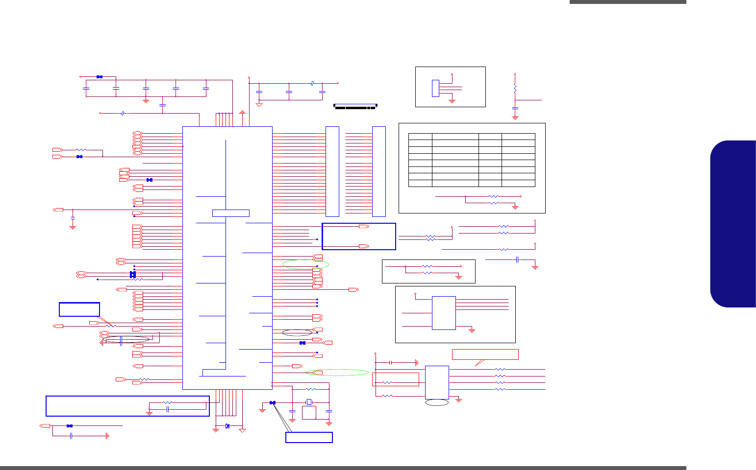
Schematic Diagrams
KBC-ITE IT8518 B - 21
B.Schematic Diagrams
KBC-ITE IT8518
KBC_WRESET#
W244_D ET
R532 4.7K_04
R528 1K_04
C752
0.1u_16V_Y5V_04
R530 47_04
R526 47_04
R529 15_1%_04
U37
*AT25F512AN
CE# 1
SO 2
WP#
3
VSS 4
SI 5
SCK 6
HOLD#
7
VDD
8
U39
25VF032B
CE# 1
SO 2
WP#
3
VSS 4
SI 5
SCK 6
HOLD#
7
VDD
8
R527 15_1%_04
VDD3
VDD 3
D02
KBC_SPI_SO_R KBC_SPI_SO
KBC_HOLD#
KBC_SPI_CE#_R
KBC_SPI_SI
KBC_F LASH
KBC_SPI_SCLK_R
KBC_SPI_CE#
KBC_SPI_SCLK
KBC_SPI_SI_R
µL«OÅ@
For 8512E
U37 U39 Co-layout
KBC_SPI_*_R = 0.1"~0.5"
KBC_FLASH
KBC_SPI _SO_R
KBC_SPI _SI_R
KBC_SPI_CE#_R
KBC_SPI _SCLK_R
KBC_HOLD#
For 8502E
U37 U39 Co-layout
EC_VCC
WLAN_LED#
PMOSFET_CONTROL# 29
D01
D01
60K / 10K
20K / 10K
R710 *10mil_short_04
10K / 20K
R708 *10mil_short_04
0.47V
6-20-41120-104
1.1V
3IN1
J_80DEBUG1
*85205-04001
1
2
3
4
80CLK
VDD3
2.2V
R808 2.2K_04
X11
*1TJS125DJ4A420P_32.768KHz
1 4
32
D01
( BEEP )
R510 *10K_04
SMD_BAT
SMC_BAT
R506 10K_04
R507 *10K_04
.
L118
HCB1005KF-121T20
R502
100K_04
C856
0.1u_16V_Y5V_04
C742
10u_10V_Y5V_08
C754
*12p_50V_NPO_04
R501 *15mil_short_06
J_KB1
85201-24051
24
23
22
14
12
11
21
8
20
19
6
5
18
4
17
10
9
7
3
2
1
16
15
13
C753 0.1u_16V_Y 5V_04
R533 *0_04
R535 *10mil_short_04
C751 1u_6.3V_X5R_04
R503 2.49K_1%_04
D02
K/B MATRIX
FLASH
LPC
SMBUS
PS/2
PWM
UART
DAC
CLOCK
IT8518
CIR
ADC
WAKE UP
PWM/COUNTER
LPC/WAKE UP
EXT GPIO
GP INTERRUPT
WAKE UP
GPIO
U38
IT8518E VER:C
WRST#
14
LPCCLK
13
LAD0
10
LAD1
9
LAD2
8
LAD3
7
LFRAME#
6
( PD )LPCPD#/WUI6/GPE6 17
SERIRQ
5
ECSMI#/GPD4( PU )
15 ECSCI#/GPD3( PU )
23
GA20/GPB5
126
KBRST#/GPB6( PU )
4
KSI0/STB# 58
KSI1/AFD# 59
KSI2/INIT# 60
KSI3/SLIN# 61
KSI4 62
KSI5 63
KSI6 64
KSI7 65
KSO0/PD0 36
KSO1/PD1 37
KSO2/PD2 38
KSO3/PD3 39
KSO4/PD4 40
KSO5/PD5 41
KSO6/PD6 42
KSO7/PD7 43
KSO8/ACK# 44
KSO9/BUSY 45
KSO10/PE 46
KSO11/ERR# 51
KSO12/SLCT 52
KSO13 53
KSO14 54
KSO15 55
VCC 11
VSTBY 26
VSTBY 50
VSTBY 92
VSTBY 114
VSTBY 127
VSTBY 121
VBAT 3
AVCC 74
PS2CLK0/GPF0( PU )
85
PS2DAT0/GPF1( PU )
86
PS2CLK1/GPF2( PU )
87
( PD )TMRI0/WUI2/GPC4 120
( PD )TMRI1/WUI3/GPC6 124
LPCRST#/WUI4/GPD2( PU )
22
( PD )WUI5/GPE5 35
PWRSW/GPE4( PU )
125
RI1#/WUI0/GPD0( PU )
18
RI2#/WUI1/GPD1( PU )
21
( PD )RING#/ PWRFAIL#/LPCRST#/GPB7 112
TXD/ GPB1( PU )
109 RXD/GPB0( PU )
108
( PD )CTX/GPB2 123
PS2DAT1/GPF3( PU )
88
PS2CLK2/GPF4( PU )
89
PS2DAT2/GPF5( PU )
90
( PD )TACH0/GPD6 47
( PD )TACH1/GPD7 48
PWM0/GPA0( PU )
24
PWM1/GPA1( PU )
25
PWM2/GPA2( PU )
28
PWM3/GPA3( PU )
29
PWM4/GPA4( PU )
30
PWM5/GPA5( PU )
31
PWM6/GPA6( PU )
32
PWM7/GPA7( PU )
34
ADC0/GPI0
66
ADC1/GPI1
67
ADC2/GPI2
68
ADC3/GPI3
69
ADC4/GPI4
70
ADC5/GPI5
71
ADC6/GPI6
72
ADC7/GPI7
73
VSS
1
VSS
12
VSS
27
VSS
49
VSS
122 VSS
113
AVSS
75
CK32KE 2
CK32K 128
DAC3/GPJ3
79 DAC2/GPJ2
78 GPJ1
77 GPJ0
76
( PD )EGCS#/GPE2 83
( PD )EGCLK/GPE3 84
( PD )EGAD/GPE1 82
GINT/GPD 5( PU )
33
L80LLAT/GPE7( PU )
20
VSS
91
DAC5/GPJ5
81 DAC4/GPJ4
80
PWUREQ#/GPC7( PU )
16
( PD )CRX/GPC0 119
( PD )KSO16/GPC3 56
( PD )KSO17/GPC5 57
( PD )GPH0/ID0 93
( PD )GPH1/ID1 94
( PD )GPH2/ID2 95
( PD )GPH3/ID3 96
( PD )GPH4/ID4 97
( PD )GPH5/ID5 98
( PD )GPH6/ID6 99
( PD )GPG1/ID7 107
SMCLK0/GPB3
110
SMDAT0/GPB4
111
SMCLK1/GPC 1
115
SMDAT1/GPC2
116
SMCLK2/GPF6( PU )
117
SMDAT2/GPF7( PU )
118
FLFRAME#/GPG2 100
FLAD0/SCE# 101
FLAD1/SI 102
FLAD2/SO 103
FLAD3/GPG6 104
FLCLK/SCK 105
( PD )FLRST#/WUI7/GPG0/TM 106
( PD )L80HLAT/GPE0 19
R505 10K_04
C745
*0. 1u_16V_Y 5V_04
C748
0.1u_16V_Y5V_04
LAN_PCIE_WAKE# 16
C743
0.1u_16V_Y5V_04
C749
1u_6.3V_X5R_04
C746
*0.1u_16V_Y5V_04
C741
*0.1u_16V_Y5V_04
R531 *10M_04
.
L117
HCB1005KF-121T20
C744
*0. 1u_16V_Y5V_04
R787 1K_04
C756 *0.1u_16V_Y 5V_04
NC2 SHORT
R785 *0_04
LCD_BRIGHTNESS
J_KB2
*85201-24051
24
23
22
14
12
11
21
8
20
19
6
5
18
4
17
10
9
7
3
2
1
16
15
13
D02
R809 2.2K_04
R523 *0_04
C755
*12p_50V_NPO_04
R504 7.5K_1%_04
C747
0.1u_16V_Y5V_04
C855
0.1u_16V_Y5V_04
VDD3
VDD3
3.3VS
VDD3
VDD3
KBC_AGND
KBC_AVD D
KBC_AGND
3.3VS
VDD3
VDD3
WEB_WWW#22
SUSC# 8,23,25
HSPI_CE# 9
3IN117
SMD_CPU_THERM3,8,9
HSPI_MSO 9
HSPI_SCLK 9
HSPI_MSI 9
CCD_EN 15
PWR_SW#23
BT_EN 17,21
LED_CAP#21
PWR_BTN#8
LID_SW#8,13,22
SMD_BAT29
KBC_BEEP18
CCD_DET#15
LED_PWR21
BKL_EN 13
LPC_AD07,11
LPC_AD37,11 LPC_AD27, 11
3G_POWER 15
LPC_FRAME#7, 11
LPC_AD17,11
VCORE_ON 28
SUSB# 8,11,12,23
BU F_P LT_RST#7,11,16,17
WLAN_DET#17
RSMRST_GATE# 8
WLAN_LED#17,21
WEB_EMAIL#22
DD_ON 19,23,24
CPU_FANSEN 22
BAT_DET29
KBC_MUTE#18
CPU_FAN22
80PORT
R503 / R504
0V
LED_SCROLL#21
EC_RST#7,12
AP_KEY#22
LED_BAT_CHG21
EC MODULE CHOOSE (FOR DIFFERENCE CPU TYPE)
3G_EN15
AC_I N#8,29
SWI # 8
BT_DET#17,21
10K / X
MODEL_ID
LED_ACIN21
EC_SCI#8
3G_DET#15
MODEL_ID
Value modify 3/23
3.3V
W240BL(9W)
THERM_VOLT2
80CLK17
WLAN_EN17,21
VER. VOLTAGE
SMC_CPU_THERM3,8,9
LED_NUM#21
W240BZ(18W)
TP_D ATA22
LED_BAT_FULL21
TP_CLK22
TOTAL_C U R29
LPC_CLK07,8
EC_SMI#8
KBC_RST# 8
SERIRQ7,11
GA208
SMC_BAT29
ALL_SYS_PWRGD 11,13
BRIGHTNESS12,13
BAT_VOLT29
BAT_VOLT
R786 *10mil_short_04
W251BZQ(18W)
R709 *10mil_short_04
D01
R511 10K_04
R797 *10mil_short_04
1.65V
CK32KE
FOR W244
CK32K
6-22-32R76-0B4
2.5V
D01
W251BLQ(9W)
D02
R829 *0_04
3.3VS
1J_KB1
X / 10K
24
80DET#
Pin100,104&106 EXT ¤£¯à Pull hi
& Pull Low.
D01
KBC_SPI_SO
KBC_SPI_CE#
KBC_SPI_SCLK
VCH G_SEL
KBC_SPI_SI
CPU_FAN
VGA_FAN
USB_PWR_EN#
KBC_WRESET#
3G_DET#
CCD_DET#
KBC_BEEP
SMD_BAT
CCD_DET#
( SCI# )
( SMI# )
R534 For IT8518BX&
IT8519BX Only.
Pin87 3IN1 multi
function pin
BAT_DET
3G_DET#
( 3G_PWR_EN )
BAT_VOLT
H_PECI
FOR W25FOR W24/W27
KB-SI1
KB-SO11
KB-SO6
KB-SI7
KB-SI3
KB-SI0
KB-SO10
KB-SO5
KB-SO15
KB-SO4
KB-SO7
KB-SO0
KB-SO13
KB-SI2
KB-SO2
KB-SO3
KB-SO8
KB-SO14
KB-SO9
KB-SO12
KB-SI4
KB-SO1
KB-SI 2
KB-SO11
KB-SI 3
KB-SO5
KB-SI5
KB-SI6
KB-SO2
KB-SI 4
KB-SI 7
KB-SO1
KB-SO15
KB-SO9
KB-SO14
KB-SO13
KB-SO10
KB-SI 0
KB-SI 1
KB-SO8
KB-SO12
KB-SO3
KB-SO4
KB-SO0
( WEB1# )
KB-SI 6
KB-SO7
KB-SI 5
KB-SO6
ME_WE#
( 80PORT_D ET# )
10K / 10K
WLAN_EN
LCD_BRIGHTNESS
CELL_CONTROL
80CLK
( PM_PWROK )
( WEB2# ) W244_DET
( APKEY# )
MODEL_ID
GA20
SMC_BAT
WEB1#---WEB_EMAIL#
WEB2#---WEB_WWW#
EC_R ESET
2.49K / 7.5K
0_04 FOR IT8512CX/EX
0.1U_04 FOR ITE8512-J(ITE8502-J W/0 CIR)
EC Cost Down
EC_VSS
C167 180P_50V_NPO_04
D01
R534 *10mil_short
ICPPE#
OCPPE#
W270BZQ(9W)
C168 *180P_50V_NPO_04
W270BZQ(18W)
APU_TALERT#3,9
Reserve
Sheet 20 of 33
KBC-ITE IT8518
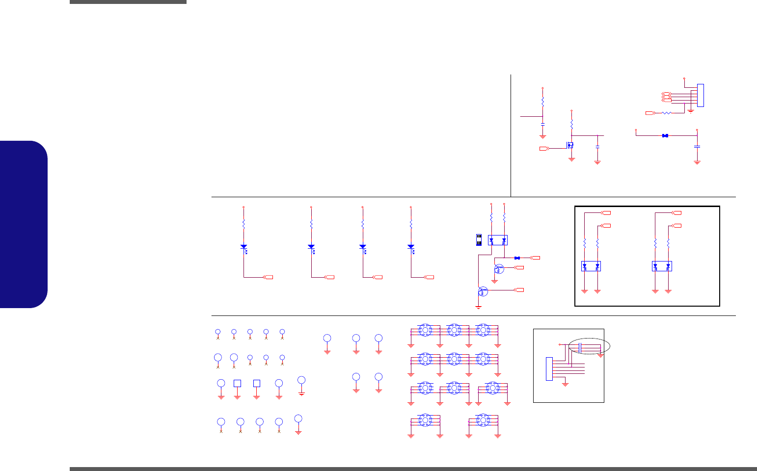
Schematic Diagrams
B - 22 LED/MDC/BT
B.Schematic Diagrams
LED/MDC/BT
C761 0. 1u_16V_Y5V_04
LED_BAT_FULL
LED_BAT_CHG
LED _ACI N
C762 0. 1u_16V_Y5V_04
BT_EN#
50mil 50mil
1
H25
MTH315D 111
3
4
5 6
7
8
9
M5
M-MARK1
1
H7
MTH315D111
3
4
5 6
7
8
9
R540
220_04
M2
M-MARK1
H36
ht6_0b7_0d3_7
M1
M- MAR K 1 H35
HC6_0d3_7
Q17
DTC114EUA
CE
B
C757
*180p_50V_NPO_04
R542
*220_04
J_TP4
85201-06051
1
2
3
4
5
6
H21
C110D110NP
SG
Y
D13
*KPB-3025YSGC
1
3
2
4
1
H13
MTH315D111
3
4
5 6
7
8
9
C759
*10u_10V_Y 5V_08
1
H24
MTH315D111
3
4
5 6
7
8
9
R537 *0_04
C758
*180p_50V_NPO_04
H34
ht6_0b7_0d3_7
R548
220_04
Q14
*MTN7002ZHS3
G
DS
R539
*15mil_short _06
1
H5
MTH315D 111
3
4
5 6
7
8
9
H15
H4_7B6_0D3_7
H23
C67D67
SG
Y
D14
*KPB-3025Y SGC
1
3
2
4
C760 0. 1u_16V_Y5V_04
H29
H4_7B6_0D3_7
D2
RY-SP170YG34-5M
AC
H18
H6_0D3_7
R536
47K_04
H33
HT6_0BS1D3_7
J_BT1
*87212-06G0
1
2
3
4
5
6
R549
220_04
H19
H4_0B7_0D3_7
1
H11
mth315d111_3
3
4
5 6
1
H14
MTH315D111
3
4
5 6
7
8
9
1
H3
MTH315D111
3
4
5 6
7
8
9
R538
*10K_04
D5
RY-SP170YG34-5M
AC
1
H4
MTH315D111
3
4
5 6
7
8
9
S2
SMD80X80
1
1
H2
C110D110NP
M7
M-MAR K1
H20
C110D110NP
M3
M-MAR K1 M4
M-MARK1
R546
220_04
M8
M-MAR K1
R545
*220_04
S1
SMD80X80
1
1
R550
*10mil_short_04
D4
RY-SP170YG34-5M
AC
R541
220_04
R544
*220_04
M6
M-MAR K1
D3
RY-SP170YG34-5M
AC
H1
C110D110NP
H17
*H4_7B6_0D3_7
SG
Y
D1
KPB-3025YSGC
1
3
2
4
R543
*220_04
H6
C67D67
R547
220_04
Q16
*D TC114EUA
CE
B
1
H9
MTH315D 111
3
4
5 6
7
8
9
3.3VS
3.3VS 3.3VS3.3VS
3V_BT3.3V
3.3VS 3.3VS
3.3V
3.3V
3V_BT
GND
VDD3
GND
W24 Off, W25/W27 On
LED_NUM# 20
BT_EN 17,20
WLAN_EN 17,20
BT_ON7,17
LED_CAP# 20 LED_SCROLL# 20
USB_PP68USB_PN68
BT_DET#17,20
SATA_LED# 9
WLAN_LED# 17,20
BT_EN17,20
LED_BAT_FU LL 20
LED_BAT_CHG 20
LED_PWR 20
LED_ACIN 20
1
H26
MTH315D111
3
4
5 6
7
8
9
6-52-52001-027 6-52-52001-027 6-52-52001-027 6-52-52001-027
BT_EN#
Bluetooth
BT_DET#
NUM
LOCK
LED
2
CAPS
LOCK
LED
LED
BAT LED
SCROLL
LOCK
LED POWER ON
LED
31
WLAN
LED
24
BT
LED
HDD/ODD
LED
D02
W24 On, W25/W27 Off
LED _PW R
Sheet 21 of 33
LED/MDC/BT
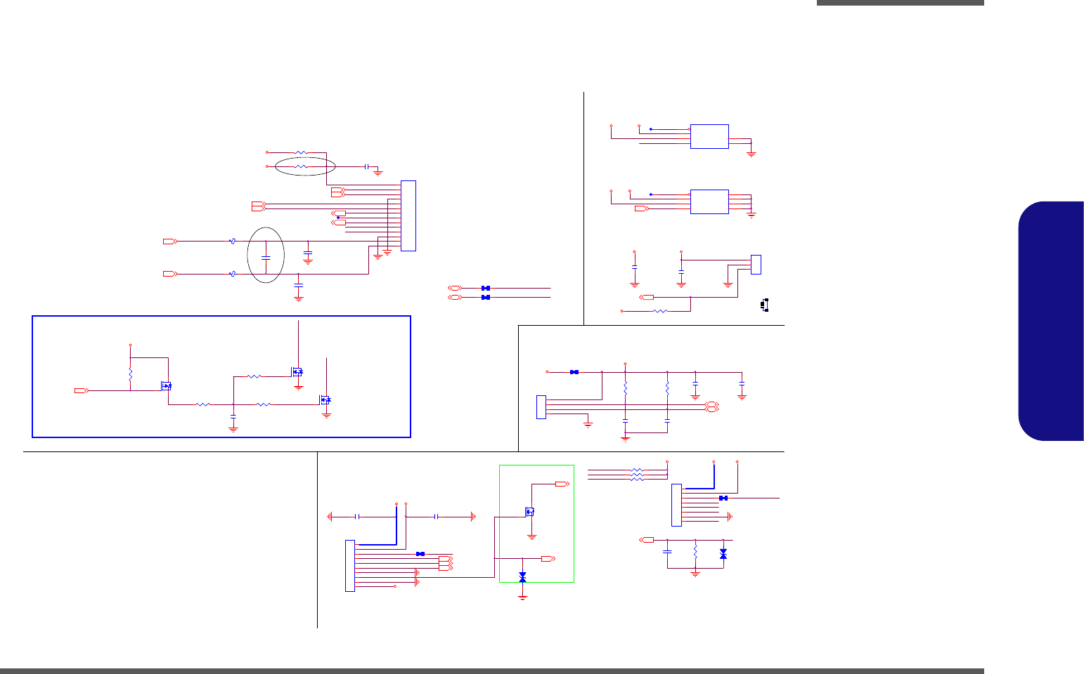
Schematic Diagrams
Fan/TP/Multi CON B - 23
B.Schematic Diagrams
Fan/TP/Multi CON
Q4
*MTN7002ZHS3
G
DS
U52
*AX995B
VOUT
1
GND 5
VIN
3FON#
4
VSET
6GND 2
5VS FON#
5VS_FAN
CPU_FAN
PN:APE88742nd Source
AX995B(SOT23-6) & APE8872
Co-Layout
Q5
*MTN7002ZHS3
G
DS
R733 *0_06
1.1A 60mils
HP_SENSE
SPK_HP#
MIC1-L M
HEADPHONE-L
MIC_SENSE
HEADPHONE-R
USBP4_R
USBN4_R
MIC1-R M
Audio/B CONN.(Port 2)
C778 0.01u_16V_X7R_04
USBP4_R
USBN4_R
R561 *10mil_short_04
J_AUDIO1
85201-14051-01
1
2
3
4
5
6
7
8
10
11
12
13
14
9
R562 *10mil_short_04
5V
MIC_SENSE18
MIC1-R M18 MIC1-L M18
HP_SENSE18
HEADPHONE-R18
USB_PP38
USB_PN38
R734 0_06
HEADPHONE-L18
USBVCC1
PR215
*47K_04
PC230
*0.1u_50V_Y5V_06
NEAR CONN
Q34
*MTP3403N3
G
DS
VDD3
D02
C772
*10u_10V_Y5V_08
R564 *4.7K_04
R832 *10K_04
WEB_WWW#
PN:AX995SA--6-02-99011-B20
PN:G990--6-02-99011-B20
PN:APE8872--6-02-08872-FC0
2nd Source
2nd Source
PV1
*V15AVLC0402
12
De-pop circuit
3.3VS
AP_KEY# R831 10K_04
R559
*220K_04
CLICK CONN
M_BTN #23
C777
0.01u_16V_X7R_04
J_FAN1
85205-03701
1
2
3
C766
10u_10V_Y5V_08
R558 *10mil_short_04
R560
*10mil_short_04
R557
10K_04
C774
47p_50V_NPO_04
R556
10K_04
NEAR CONN
3/9
U41
AX995SA
VOUT
3
GND 5
VIN
2FON
1
VSET
4GND 6
GND 7
GND 8
C770
*10u_10V_Y5V_08
J_TP1
85201-04051
1
2
3
4
R833 *10K_04
Q18
*MTN7002ZHS3
G
DS
WEB_EMAIL#
C765
0.1u_16V_Y5V_04
C776
0.01u_16V_X7R_04
J_SW1
*50500-01041-001L
1
2
3
4
5
6
7
8
9
10
C771
1u_6.3V_X5R_04
R551 4.7K_04
R555 *15mil_short_06
J_SW2
88486-0801
1
2
3
4
5
6
7
8
C775
47p_50V_NPO_04
5VS
5VS
3.3VS
5VS_FAN
5VS_FAN
5VS_TP
5VS
3.3V3.3VS
VIN
3.3V3.3VS
CPU_FANSEN20
CPU_FAN20
TP_CLK 20
TP_DATA 20
AP_KEY# 20
WEB_WWW# 20
LID_SW# 8,13,20
WEB_EMAIL# 20 AP_ON 23
L115
FCM1608K-121T06
SPKOUTR +
FAN CONTROL
FON#
JFAN
3
1
R565 *1K_04
AP_ON
R566 *1K_04
D02
EAPD18
L116
FCM1608K-121T06
SPKOUTR-
LID_SW#
M_B TN# _R M_BTN#
AP_KEY#
WEB_WWW#
WEB_EMAIL#
POWER SWITCH CONN.
20mil
CLOSE TO J_SW1
M_BTN #
D02
WEB_EMAIL#
LID_SW#
WEB_WWW#
AP_KEY #
MBTN
20mil
SPKOUTR-18
SPKOUTR+18
C714
*1u_10V_Y5V_06
C713
180p_50V_NPO_04
C715
180p_50V_NPO_04
SPKOUTR+_CSPKOUTR+
SPKOUTR- SPKOUTR-_C
If system has APON function, uses J_SW1
If system has no APON function, uses J_SW2
M_BTN#
PV2
*V15AVLC0402
12
Sheet 22 of 33
Fan/TP/Multi CON
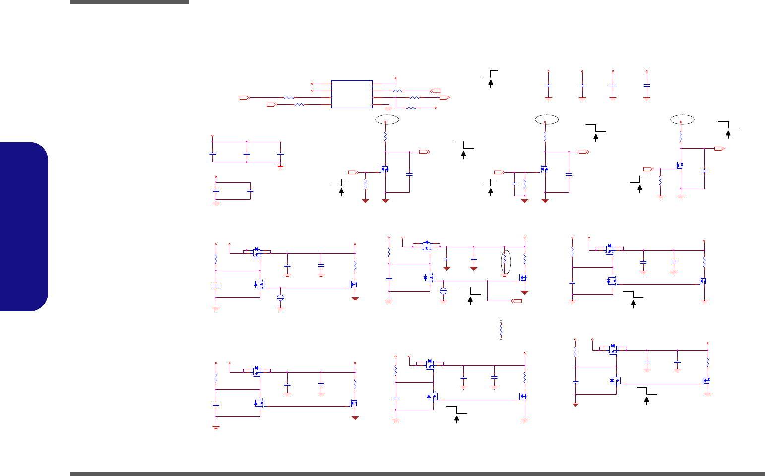
SUSB
ON
PR20
10K_04
D02
ON
ON
PC22
10u_10V_Y 5V_08
PQ2
MTN7002ZHS3
G
DS
PR208
100_1%_04
PR6
10K_04
PR17
1M_04
PR207
*100_1%_04
PJ1
40mil
12
PC229
10u_10V_Y 5V_08
PC227
10u_10V_Y 5V_08
PR3 10K_04
PQ62
MTN7002ZHS3
G
DS
PQ60
*MTN7002ZHS3
G
DS
PQ7
*MTN7002ZHS3
G
DS
PQ8B
MTNN20N03Q8
6
5
4
PQ5B
*MTNN20N03Q8
6
5
4
PR15
*100_1%_04
PQ6B
MTNN20N03Q8
6
5
4
PR19
100_1%_04
PQ13
*MTN7002Z HS3
G
DS
C779
*0. 01u_16V_X7R_04
PC14
*10u_10V_Y 5V_08
PR11
1M_04
PR4
10K_04
PQ8A
MTNN20N03Q8
1
3
728
PC16
10u_10V_Y5V_08
PC20
0.01u_16V_X7R_04
PC18
470p_50V_X7R_04
PQ9A
MTNN20N03Q8
1
3
728
PR7
100K_04
PC21
0.1u_16V_Y5V_04
PC10
*0.1u_16V_Y 5V_04
PC19
*0.1u_10V_X7R_04
PR16
1M_04
PQ3A
MTNN20N03Q8
1
3
728
PR13
1M_04
PC226
0.1u_16V_Y5V_04
PQ5A
*MTNN20N 03Q8
1
3
728
PC17
470p_50V_X7R_04
PR211 1K_04
PQ10
MTN7002ZHS3
G
DS
PC8
0.1u_50V_Y5V_06
PC6
0.1u_50V_Y 5V_06
PC9
*0.1u_16V_Y 5V_04
PQ6A
MTNN20N0 3Q8
1
3
728
C781
0.01u_16V_X7R_04
PR5
10K_04
PC25
2200p_50V_X7R_04
PR10
1M_04
PQ4B
MTNN20N03Q8
6
5
4
PC15
0.1u_16V_Y 5V_04
PR12
*1M_04
PC11
*0. 1u_16V_Y 5V_04
C780
*0. 01u_16V_X7R_04
C784
0.01u_16V_X7R_04
C783
*0.01u_16V_X7R_04
PR9
100K_04
PC12
0.1u_16V_Y 5V_04
PQ61
*MTN7002ZHS3
G
DS
PQ9B
MTNN20N03Q8
6
5
4
R563 100K_04
PC225
10u_10V_Y5V_08
PR8
100K_04
PC26
2200p_50V_X7R_04
PJ2
40mil
12
S
D
G
PQ1A
MTDN7002ZHS6R
2
61
S
D
G
PQ1B
MTDN7002ZHS6R
5
34
PC7
0.1u_50V_Y 5V_06
PC228
0.1u_16V_Y5V_04
PQ3B
MTNN20N03Q8
6
5
4
PQ4A
MTNN20N03Q8
1
3
728
C782
0.01u_16V_X7R_04
PR14
*100_1%_04
PU1
P2808B0
VA
1
VIN
2
M_BTN #
3
INSTANT-ON
4GND 5
PWR _SW# 6
DD_ON_LATCH 7
VIN1 8
PR206
*100_1%_04
PR210 1K_04
PC13
*0. 1u_16V_Y5V_04
VDD5
3.3VS
VDD3
SY S15V
SYS15V
5VSSYS15V
SY S15V VD D3
VDD5
VIN1
VIN
VA
SYS15V 1.5V
VINVA
1.5VS
VDD3
VIN1
5V
3.3V
3.3VS
VDD3
VDD3
1.1V
SYS15V 1.1VS
VDD3
3.3V
5V
PWR_SW# 20M_BTN#22
AP_ON22
DD_ON# 19,25,26
SUSC#8,20,25
SUSB#8,11,12,20
SUSB 25,26,27 SUSC 26,28
DD_ON19,20, 24
DD_ON 19,20,24
SUSB 25,26,27
SUSB
PR18 1K_04
DD_ON#
NMOS
1.1VS
NMOS
ON
SUSB
1.5VS
3A
3A 3A
3A
Power Plane
Power Plane
3.3VS
5VS
3.3V
5V
ON
DD_ON "L" TO
"H" FROM EC
ON
ON
NMOS
NMOS
ON
C914
*0. 01u_16V_X7R_04
ON
ON
SUSB
DD_ON#
D02D02D02
DD_ON#
SUSB
SUSC
ON
PR81
10K_04
Schematic Diagrams
B - 24 5VS/3.3VS/1.8VS/1.5VS/1.1VS
B.Schematic Diagrams
5VS/3.3VS/1.8VS/1.5VS/1.1VS
Sheet 23 of 33
5VS/3.3VS/1.8VS/
1.5VS/1.1VS
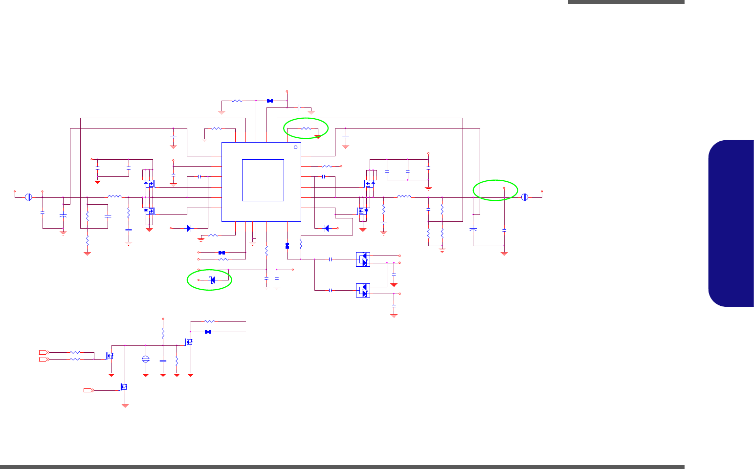
PU2
uP6182
VREF 3
EN1 1
VFB1 2
TONSEL 4
LDO5
17
LGATE1 19
PHASE1 20
VFB2 5
UGATE2
10
VCLK
18
BOOT2
9
EN2 6
VO2
7
LDO3
8
PHASE2
11
LGATE2
12
EN0
13
SKI PSEL
14
GND
15
VIN
16
UGATE1 21
BOOT1 22
POK 23
VO1 24
GND PAD
25
PR30
*680K_1%_04
PC46
0.01u_50V_X7R_04
PC48
4.7u_25V_X5R_08
PR28
19.1K_1%_06
PC238
2200p_50V_X7R_04
PC36
1u_10V_Y 5V_06
+
PC40
220u_6.3V_6.3*6.3* 4. 2
PC47
2200p_50V_X7R_04
+
PC45
220u_6.3V_6. 3*6.3*4.2
C
A
A
PD6
BAT54SW GH
1
2
3
PC28
1u_10V_Y5V_06
PC35
0.1u_10V_X7R_04
PC44
0.1u_16V_Y 5V_04
PR21 *0_04
PR37
10K_04 PR38 *10mil_short_04
PQ14
P1203BV
4
62 5
73
1
8
PC41
1000p_50V_X7R_04
PC49
1u_10V_Y5V_06
PR36 *0_04
PJ5
*6mil
12
PR61 *0_04
PC42
100p_50V_NPO_04
PC33
4.7u_25V_X5R_08
PC174
2200p_50V_X7R_04
PR33
2.2_06
PC38
*4.7u_25V_X5R_08
PR34 *10mil_short _04
PR 24
120K_04
PJ3
*5mm
12
PR29
20K_1%_04
PR31
*10m il_s hort_04
PD3
*R B0540S2
A C
PC29
1000p_50V_X7R_04
PC50
0.01u_50V_X7R_04
PC37
0.1u_50V_Y 5V_06
PL1
TMPC0603H-4R7M-Z01
12
PR152
5.1_06
PC55 0.1u_10V_X7R_04
PD4
*RB0540S2
AC
PC32
4.7u_25V_X5R_08
PQ22
*MTN7002ZHS3
G
DS
C
A
A
PD5
BAT54SW GH
1
2
3
PQ16
P1203BV
4
62 5
73
1
8
PC34
1u_10V_Y5V_06
PR23
100K_04
PR39 100K_04
PR146
5.1_06
SYS5V
SYS15V
VREF
VDD3
VIN
SYS10V
VDD5
VIN
SYS3V
VREG5
VREG3
VREF
VREG5VIN1
VIN
VREG5
SYS5V
VREG5 VREG5
SY S5V
ACIN29
DD_ON19,20,23
S5_CORE_EN7
W27 5.7 --> 220u_6.3V_6.3*6.3*4.2
5A
EN_ALL
Rb
7A
Ra
EN_3V
EN_5V
EN_3V EN _5V
Z2418
W24/W25 --> 220u_6.3V_6.6*57
PQ19
MTN7002ZHS3
G
DS
PR32
*0_04
PR22 *10mil_short_04
PR27
13K_1%_06
PR216
680K_1%_06
PQ17
P1203BV
4
62 5
73
1
8
PR79 0_04
PR35 *0_04
PJ4
*5mm
1 2
PQ18
MTN7002ZHS3
G
DS
PR25 *10K_04
PC30
1000p_50V_X7R_04
PQ15
P1203BV
4
62 5
73
1
8
PC31
*4.7u_25V_X5R_08
PD7
RB751S-40C2
AC
PC39
0.1u_16V_Y5V_04
PC51
2200p_50V_X7R_04
PL2
TMPC0603H-4R7M-Z01
1 2
PR26
30K_1%_06
Sheet 24 of 33
Power VDD3, VDD5
Schematic Diagrams
Power VDD3, VDD5 B - 25
B.Schematic Diagrams
Power VDD3, VDD5
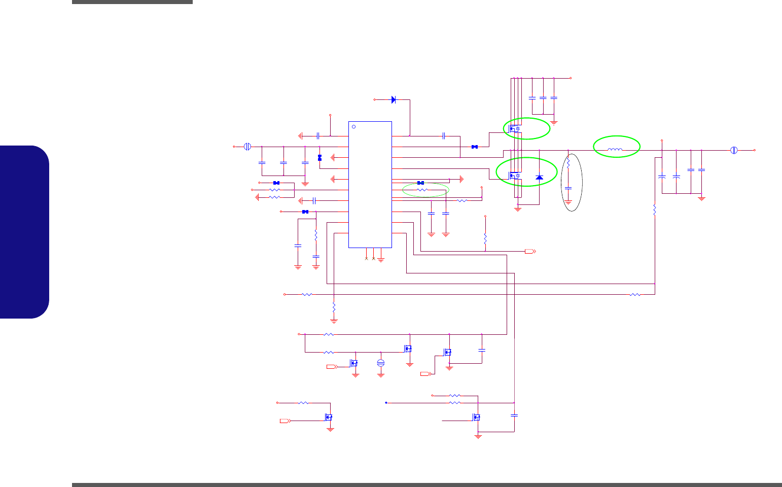
Schematic Diagrams
B - 26 Power 1.5V/0.75V
B.Schematic Diagrams
Power 1.5V/0.75V
PC75 0.1u_16V_Y5V_04
PR49 *15mil_s hort_06 PR52 *15mil_short_06
PR53 *0_04
PR66 100K_04 PQ25
MTN7002Z HS3
G
DS
PR65 47K_04
PC 68 *4.7u_25V_X5R _08
PJ9
*6mil
1 2
PR69 *100K_04
PC 70 0.1u_10V_X7R_04
PR48
*15mil_s hort_06
PQ23
MDS1526
4
62 73 8
5
1
PR47 *15mil_short_06
PQ24
MDS1521
4
62 73 8
5
1
PC72
10u_10V_Y5V_08
PR62
*10K_1%_04
PR60
100K_04
PQ27
MTN7002ZHS3
G
DS
+
PC79
560u_2.5V_6.6*6.6*5.9
PC84
*1000p_50V_X7R_04
PC86
0. 1u_16V_Y 5V _04
+
PC76
*560u_2.5V_6.6*6.6*5.9
PR67 100K_04
PD13C SOD 140SH
A C
PR64
10K_1%_06
PC67 *4.7u_25V_X5R_08
PC81
1u_10V_Y5V_06
PC82
1u_10V_Y5V_06
PC85
0.1u_16V_Y 5V_04
PU4
uP6163
VTTGND
1
VLDOIN
23
VTT
24
VTTSNS
2
GND
3
MODE
4
VTTREF
5VCC5 14
PGOOD 13
S5 11
S3 10
VDDQSET
9
VDDQSNS
8
COMP
6
CS 16
PGND 18
DRVL 19
LL 20
DRVH 21
VBST 22
PVCC5 15
CS_GND 17
NC
7
NC
12
GND
25
PR57
0_06
PC83
*1000p_50V_X7R_04
PR63 10K_1%_06
PQ28
*MTN7002ZHS3
G
DS
PC69
10u_10V_Y 5V_08
PD12
RB0540S2
A C
PC73
*1 0u_10V_Y 5V_08
PC77 0.01u_16V_X7R_04
PR 59 *10_04
PC66 *0.1u_50V_Y5V_06
PQ26
*MTN7002ZHS3
G
DS
PR68 *22_04
PQ29
MTN 700 2Z H S3
G
DS
PC71
10u_10V_Y 5V_08
PR55 *0_04
PJ7
*OPEN_2A
12 PL4
2.2UH _10*10*4.0
1 2
PC80 0.1u_10V_X7R_04
PR54 8.2K_1%_04
PJ8
*OPEN_8A
1 2
PR56 2.2_04
PR58 *15mil_short_06
5V
VDDQ 5V
VDD Q
5V
5V
5V
VIN
VTT_MEM 1.5V
VDDQ
5V
3.3V
DDR1.5V_PWRGD 11,28
VTT_MEM
5V
SUSB23,26,27
SUSC#8,20,23
DD_ON#19,23,26
PR50
*5.1_06
D02
PC74
*2200p_50V_X7R_06
Z2621
1.5VEN
+1.5S_CPU_PWRGD
SUSB
VTTEN
SUSB
10A
1.5V
DDR1.5V_PWRGD
Sheet 25 of 33
Power 1.5V/0.75V
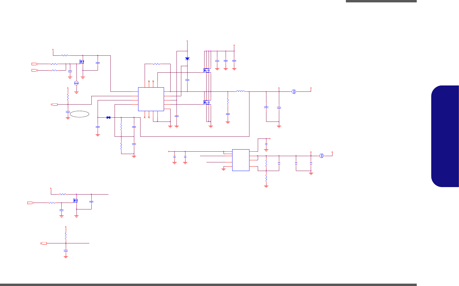
Schematic Diagrams
Power 1.1V/1VS B - 27
B.Schematic Diagrams
Power 1.1V/1VS
1.1VS_VTT=0.75 X (1+PR101 / PR102)
OCP=10uA X RILIM / Rdson
SUSC
5A
1.1V
EN_1.1V
3A
EN_1VS
1VS_PWRGD
Vout = 0.8V ( 1 + Ra / Rb )
Ra
Rb
3A
SUSB
EN_1VS
10/22 1.0V=>1.054V
1VS_PWRGD
Change value 3/24
PR77
100K_1%_04
PC96
1u_10V_Y5V_06
PC78
2200p_50V_X7R_04
PC91
0.1u_10V_X5R_04
PC97
0.01u_16V_X7R_04
PC216
10u_6.3V_X5R_06
PC104
0.1u_10V_X5R_04
PR72 *62K_1%_04
PC100
0.1u_10V_X7R_04
PJ18
3mm
1 2
PR73
220K_1%_04
PC215
10u_6.3V_X5R_06
PL5
TMPC0603H-4R7M-Z01
1 2
PR196
3.24K_1%_04
PD14
RB0540S2
AC
PC98
*20p_50V_N PO_04
PC108
*0.1u_10V_X7R_04
+
PC93
560u_2.5V_6.6*6.6*5.9
PU5
uP6127
LX 1
BST 2
VCC 3
DL 4
GND
5
RTN
6
N.C
7
N.C
8
FB
9
VOUT
10
PGD
11
EN
12
ILIM 13
N.C 14
N.C 15
DH 16
PAD 17
PR75
10K_1%_04
PC94 0.1u_16V_Y5V_04
PJ10
5mm
1 2
PJ23
OPEN-1mm
12
PR70
100K_1%_04 PC90
*4.7u_25V_X5R_08
PC214
82p_50V_NPO_04
PQ30
MTN7002ZH S3
G
DS
PR 78 62K_1%_04
PR71 10K_1%_04
PR195
10.2K_1%_04
PC89
0.1u_10V_X7R_04
PR197 62K_1%_04
PC87
4.7u_25V_X5R_08
PQ33
MTN7002ZHS3
G
DS
PC92
0.1u_10V_X7R_04
PC88
0.1u_50V_Y5V_06
PC99
300K_1%_04
PC219
10u_6. 3V_X5R_06
PR74
*10mil_short
PR80
220K_1%_04
PR51
5.1_06
PU11
AX6615ESA
GND
1
VCNTL 6
VOUT 3
VIN
5
VOUT 4
VFB 2
POK
7
EN
8
VIN
9
PC95
*0.1u_10V_X7R_04
PR76
21K_1%_04
PC218
0.1u_16V_Y5V_04
PQ31
P1203BV
4
62 73 8
5
1
PC213
1u_10V_Y5V_06
PQ32
P1203BV
4
62 73 8
5
1
VIN
1.1V
3.3V
5V
V1.1
5V
3.3V
V1S_REG
5V
5V
D02
1VS
1.5V
SUSB23,25,27
1.1V_PWRGD11
1VS_PWRGD28
DD_ON#19,23,25
SUSC23,28
Sheet 26 of 33
Power 1.1V/1VS
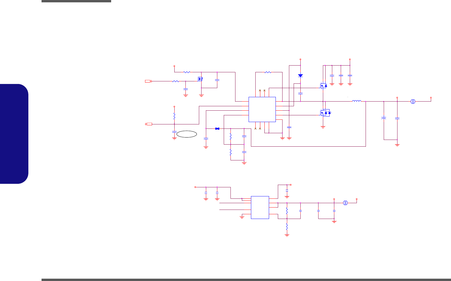
D02
EN_1.8V
3A
3A
Vout = 0.8V ( 1 + Ra / Rb )
Rb
Ra
1.8V_PWRGD
EN_1.8V
1.8V_PWRGD
SUSB
1.8VS
OCP=10uA X RILIM / Rdson
4A
PC220
10u_6.3V_X5R_06
PR45
*14K_1%_04
PL3
*TMPC0603H-4R7M-Z01
1 2
PC61
*1u_10V_Y5V_06
PJ6
5mm
1 2
PU3
*uP6127
LX 1
BST 2
VCC 3
DL 4
GND
5
RTN
6
N.C
7
N.C
8
FB
9
VOUT
10
PGD
11
EN
12
ILIM 13
N.C 14
N.C 15
DH 16
PAD 17
+
PC59
*560u_2.5V_6.6*6.6*5.9
PC63
*20p_50V_NPO_04
PR46
*10K_1%_04
PC64
*0.01u_16V_X7R_04
PU12
AX6615ESA
GND
1
VCNTL 6
VOUT 3
VIN
5
VOUT 4
VFB 2
POK
7
EN
8
VIN
9
PC53
*4.7u_25V_X5R_08
PR44
*10mil_short
PQ21A
*AP6901GSM
7
8
1
2
PC58
*0.1u_10V_X7R_04
PQ20
MTN7002ZHS3
G
DS
PC62
*0. 1u_10V_X7R_04
PC56
*0.1u_10V_X7R_04
PD10
*RB0540S2
AC
PC224
1u_10V_Y5V_06
PR204
12.7K_1%_1/16W_04
PC223
10u_6.3V_X5R_06
PC221
0.1u_16V_Y 5V_04
PR43
220K_1%_04
PC54
*4.7u_25V_X5R_08
PR205
10K_1%_04
PR41 *15K_1%_04
PC222
82p_50V_NPO_04
PJ22
3mm
1 2
PQ21B
*AP6901GSM
4
3
5
6
PC60
*0.1u_16V_Y5V_04
PC57
0.01u_16V_X7R_04
PC217
10u_6.3V_X5R_06
PC52
*.1u_50V_Y5V_06
PR42 10K_1%_04
PC65
*20p_50V_NPO_04
PR40
100K_1%_04
VIN
1.8VS
V1.8S
3.3V
5V
5V
V1.8S_REG
5V
1.8VS
3.3V
SUSB23,25,26
1.8V_PWRGD11
Sheet 27 of 33
Power 1.8VS
Schematic Diagrams
B - 28 Power 1.8VS
B.Schematic Diagrams
Power 1.8VS
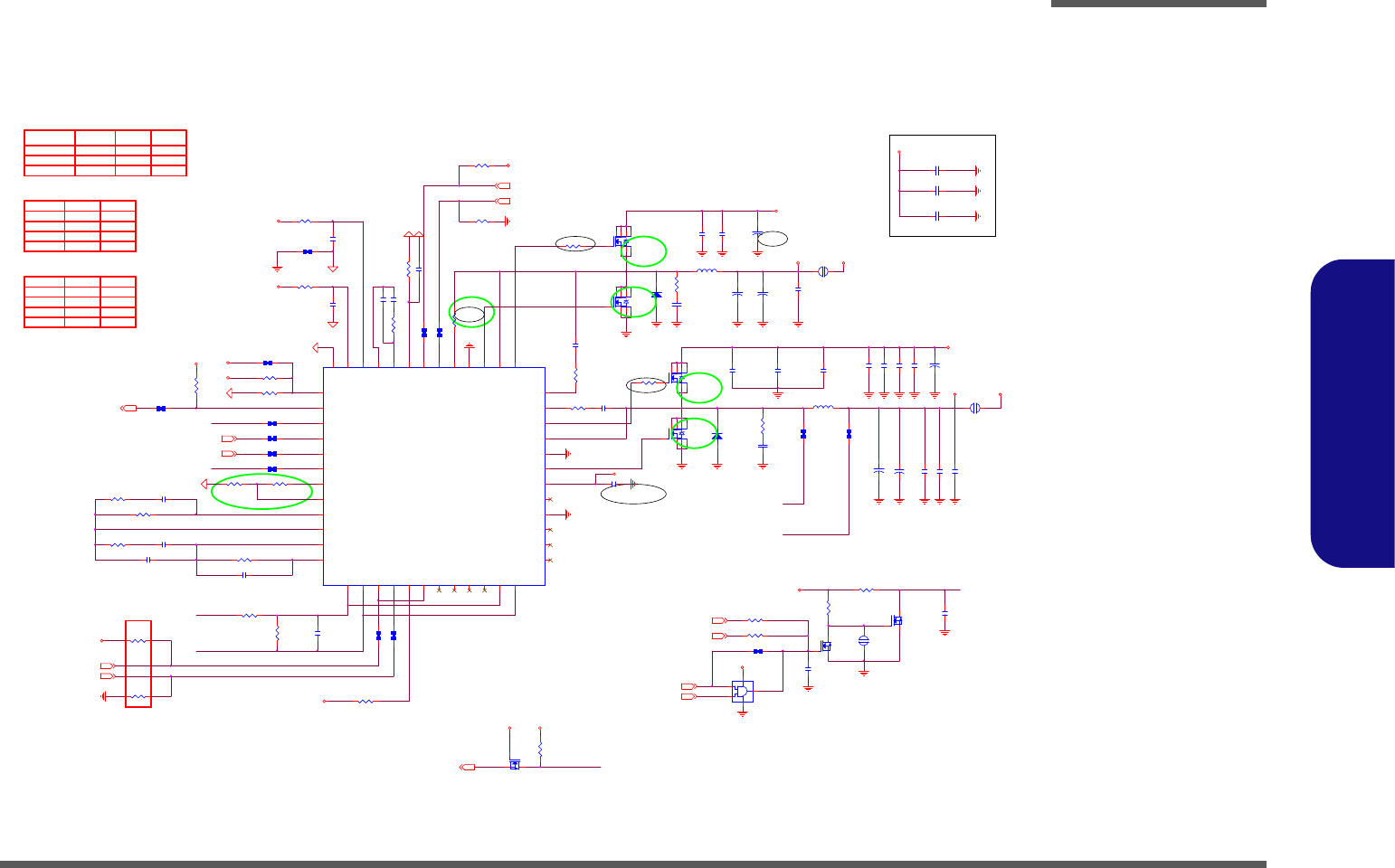
D02
PR83 2.2_06
APU_PW RGD_R
PHASE_NB
O
X
SVI
Z3301
1
0.9
O
0
SVC
1
1.0
0
1.1
SVD
0
Output
0
0.811
EN_VCORE
Metal VID Codes
11A
SVC
VFIXEN VID Codes
0.8
0
Output
1.4
1.0
1.2
1
1
1 1
SVD
0
0
0
+5V
Pin 49 is GND Pin
O
LGATE_N B
ISP_0
X
ISP_1
ISN_0
ISP_0
APU_PWRGD_R
OFS/VFIXEN
GND
Offset &
Droop
PHASE_0
X
ISN_1
O
Close to
CPU
socket
X
+3.3V
VFIX
ISN_0
UGATE_0
X
10A
LGATE_0
EMI
UGATE_NB
EN_VCORE
D02
PR113 22K_1%_04
PL8 TMPC0603H-R68M-Z01
1 2
PR217
5.1_06
PR131 *15mil_s hort_06
PR120
1_1%_06
PC162 0.01u_50V_X7R_04
+
PC164 *330u_2.5V_V_A
PC153
*4.7u_25V_X5R _08
PC169
0.1u_50V_Y 5V_06
PQ44
MDS1526
4
62 73 8
5
1
D02
PR147 *0_04
PD20
*CSOD140SH
A C
+
PC143
560u_2.5V_6.6*6.6*5.9
PL9
TMPC0603H-R68M-Z01
1 2
PJ16
OPEN-1mm
12
PR126 *10mil_short
PC150
*4. 7u_25V_X5R_08
PR138 7.5K_1%_04
PQ43
MDS1521
4
62 73 8
5
1
PD21
*CSOD140SH
A C
+
PC144
*330u_2. 5V_V_A
PC168 1000p_50V_X7R_04
PC156
*0.1 u_50V_Y 5V_06
PR129
*10mil_short
PR209 *10mil_short_04
PC167
180p_50V_NPO_04
PR124 *10mil_short
PR121
10K_04
PC139
*4.7u_25V_X5R _08
C791 0.1u_10V_X5R_04
PR218
5.1_06
PC151
*4.7u_25V_X5R _08
PR134
255_1%_04
PR133
90.9K_1%_04
C790 *0.01u_16V_X7R_04
PC147 33p_50V_NPO_04
PC146
0.1u_50V_Y5V_06
PJ20
*8mm
1 2
PC234
2200p_50V_X7R_0 4
D02
U46 *74AHC1G08GW
1
2
5
4
3
PU9
ISL6265C
PGND_1 28
PGND_NB 40
PHASE_NB 38
UGATE_NB 37
PGND_0 32
RTN_1
17
PHASE_0 33
PHASE_1 27
UGATE_0 34
VSEN_1
18
RBIAS
7
ISN_0
14
COMP_0
11
VDIFF_0
9
VW_0
12
OCSET
8
ISP_0
13
VSEN_0
15
ENABLE
6
RTN_0
16
SVC
5
PGOOD
2
SVD
4
UGATE_1 26
FB_0
10
LGATE_1 29
OFS/VFIXEN
1
PVCC 30
LGATE_0 31
BOOT_NB 36
BOOT_0 35
GND 49
PWROK
3
VDIFF_1
19
FB_1
20
COMP_1
21
LGATE_NB 39
VW_1
22
ISP_1
23
ISN_1
24
BOOT_1 25
OCSET_NB 41
RTN_NB 42
VSEN_NB 43
FSET_NB 44
COMP_NB 45
FB_NB 46
VCC 47
VIN 48
PC159 10u_6.3V_X5R_08
PR149
10_04
PR114
10_06
C789 0.1u_10V_X5R_04
PR127 *10mil_short
PR119 *15m il_short_06
PC158
2200p_50V_X7R_04
PR117 *10mil_short
PC157
*0.1u _50V_Y 5V_06
+
PC140
*330U F
12
PR130 *10mil_short
PJ19
*8mm
1 2
PQ47
MTN7002ZHS3
G
DS
PR137 6.8K_1%_04
PR140
4.02K_1%_04
PR143
*10m il_short
PR118 *10mil_short
PR112
*10m il_sh ort
PC171
*0.1u_10V_X7R_04
PC160 0.22u_10V_Y5V_04
PR82 2.2_06
PC152
*4.7u_25V_X5R _08
PQ46
MTN7002ZHS3
G
DS
PC155
0.22u_16V_06
PR110
10_06
PR132
26.1K_1%_04
PC172
0.1u_10V_X7R_04
PC163
2.2u_6.3V_X5R_06
PC141 1000p_50V_X7R_04
PR111
10_04
PC166
1000p_50V_X7R_04
PC148
0.22u_16V_06
PR116
8.2K_04
PR144 *0_04
PR141
10_04
PC145
10u_6.3V_X5R_0 8
+
PC161 560u_2.5V_6.6*6.6*5.9
PQ45
MDS1521
4
62 73 8
5
1
PQ42
MDS1526
4
62 73 8
5
1
PC137
1u_10V_Y 5V_06
R682
10K_04
PR145
100K_04
PC165
4700p_50V_X7R_ 04
PR136
54.9K_1%_04
PR148 10K_1%_04
PR139 510K_04
PR125
1_1%_06
PR115
44.2K_1%_04
PR109
10_04
Q29MTN7002ZHS3
G
DS
PR128
*10mil_short
PC142 1000p_50V_X7R_04
+
PC154
*15u_25V_6.3*4.4_C
PR135 1K_1%_04
PC149
0.1u_50V_Y5V_06
PR123 *10K_06
PC138
*4.7u_25V_X5R_08
PR122 *0_06
PR142
*10mil_short
VDDCR_CPU
NB_VDDCR
VDDCR_CPU
5V
SGND5
SGND5
SGND5
SGND5
SGND5
VIN
3.3VS
SGND5
SGND5
5VS
VIN
5VS
CPU_VDDCR
VIN
5VS
3.3VS
CPU_VDDCR
1.8VS
1.5V
NB_VDDCR VDDCR_NB
CPU_SVC3
3.3VS
3.3VS
CPU_VDD0_RUN_FB_H3
PWRGD_VCORE11
CPU_SVD3
CPU_VDDNB_RUN_FB_H 3
CPU_VDDNB_RUN_FB_L 3
CPU_VDD0_RUN_FB_L3
APU_PWRGD3,7
SUSC23,26
VCORE_ON20
DDR1.5V_PWRGD11,25
1VS_PWRGD26
D02
Noise issue 3/9
Sheet 28 of 33
APU Core/NB Core
Schematic Diagrams
APU Core/NB Core B - 29
B.Schematic Diagrams
APU Core/NB Core
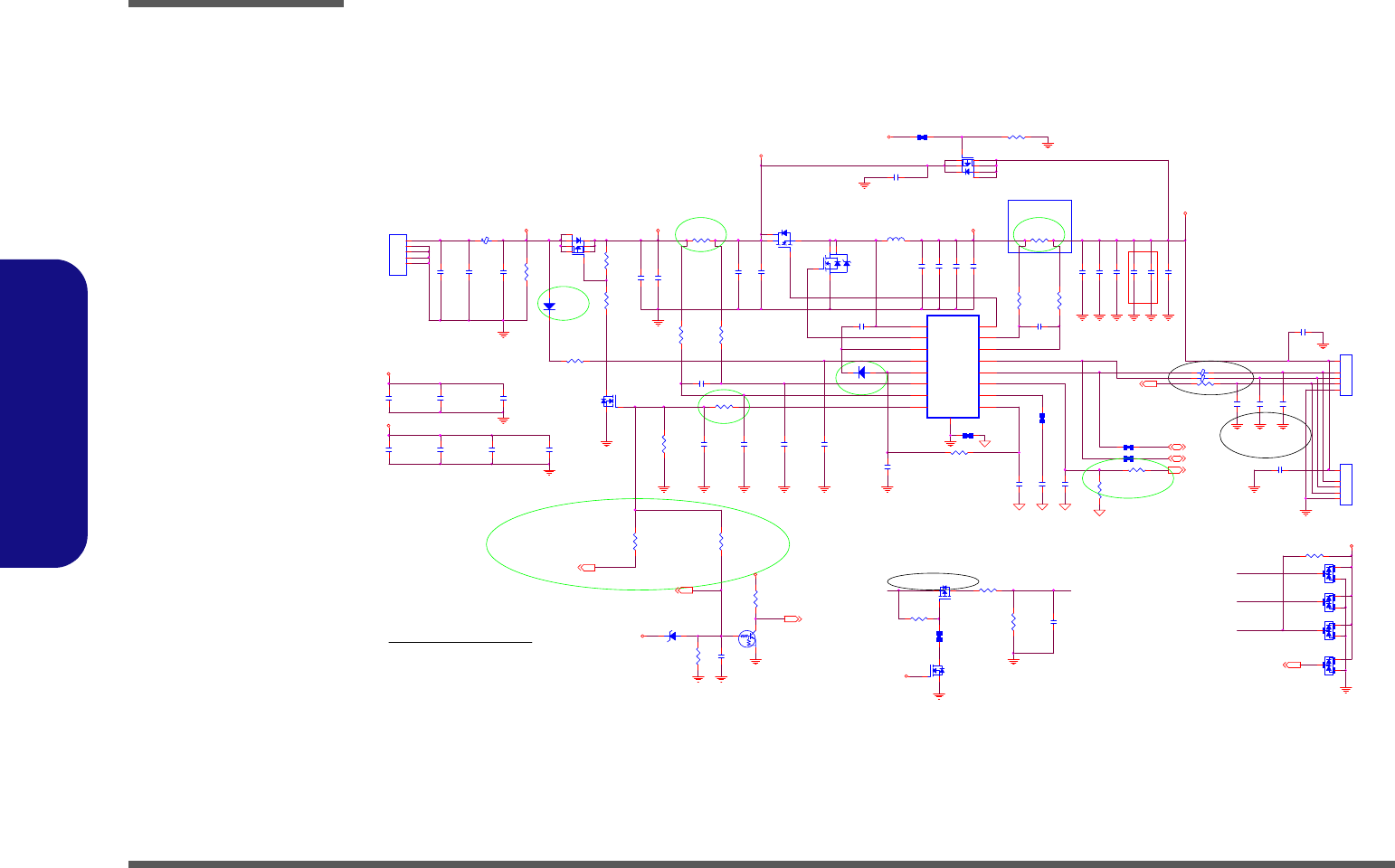
Schematic Diagrams
B - 30 Charger, DC In
B.Schematic Diagrams
Charger, DC In
D02
PD25
ZD 5245BS2
AC
PQ51
DTC114EUA
CE
B
TP SW _G
SMC_BATTERY
BAT_DET
TPCS
SMD_BATTERY
CHARGER
# Charge Voltage 12.6V
# Charge Current 1.5A
PCB Layout notes
1) All pow er traces should be routed on the outer layers
GNDP, VAD, VSYS, LX, VCHG, VBATT
2) Use Kelvin connections for R3, R4
(seperate force and measurement traces)
3) R23 and R24 are dummy resistors, for layout purposes only
(serves as single point connection between GNDP & GNDA)
4) Footprint TO-236 is equivalent to SOT-23
5) Footprint SIP/1P is a s ingle hole axial pad
6) All resisitors, capacitors and semiconductors are SMD
7) Potentiometers , and test points are axial devices
W25/W27
W24
6-21-D34B0-105
¾aªñJBATTA1
FOR 4S BATTERY USE
6-20-B3410-003 for 65W
6-20-B3Z40-004 for 30W
Modify 3/16
D02
PR156
10K_04
PC200
0.1u_50V_Y 5V_06
PR230 10_06
PC177
0.1u_50V_Y5V _06
PC188
4.7u_25V_X5R_08
PR227 10_06
PC247
4.7u_25V_X5R _08
PC244 4.7u_25V_X5R_08
PR236
100_04
PR235 *10mil_short_04
PR233
*15mil_short_06
PC252
0.1u_50V_Y 5V_06
PC237
0.1u_50V _Y 5V_06
JBATTA1
BTD-05TC1B
1
2
3
4
5
PC197
0.1u_50V_Y 5V_06
PR231
10_06
D30
*BAV99 RECTIFIER
A
C
AC
PR181
60.4K_1%_04
PC211
0.1u_50V_Y 5V_06
R568 10K_04
PR178
300K_1%_04
PC1 82
*4.7u_25V_X5R_08
PC175
0.1u_50V_Y5V_0 6
PC251
4.7u_25V_X5R_08
PC250
4.7u_25V_X5R_08
PC256
0.1u_50V_Y 5V_06
D32
*BAV99 RECTIFIER
A
C
AC
PC231
0.01u_50V_X7R_04
PC233
30p_50V_NPO_04
PC249
4.7u_25V_X5R _08
PD23
RB0540S2
AC
PC194
0.1u_50V_Y 5V_06
PC257
0. 1u_50V_Y 5V_06
PC232
30p_50V_N PO_04
JACK1
DC 069HS-2-PA9T-1
GND2
GND1
2
1
3
PC261
0.47u_10V_Y5V_04
PU14
OZ8681
LX
14
LDR
16
BST
12
VAC
1
VDDP
15
IACM
3
VDDA 6
SDA 11
ICHP 5
ICHM 4
COMP 8
HDR 13
BASE
17
SCL 10
IAC 7
IACP
2
ACAV
9
PR229 10_06
PC245 4.7u_25V_X5R_08
PR153
0.01_1%_32
PR171
*200K_04
PR228 10_06
PC258
1u_25V_08
PR237 *10mil_short_04
PC236 0.1u_50V_Y5V_06
PQ50
P2003EVG
4
6 2
5
7 3
1
8
PC176
0.1u_50V_Y5V_06
PC260
1u_10V_Y 5V_06
.
PL12 HCB1005KF-121T20
PR238 10_04PC259
1u_10V_Y 5V_06
PR243
*0_04
PC248
4.7u_25V_X5R _08
PR225
100K_04
PR226
15K_04
PQ65B
PD1503Y VS
4
3
5
6
PC193
0.1u_50V_Y 5V_06
PQ52
MTP3403N3 / QM3009K P-CH 30V
G
DS
PR234
100K_04
D29
*BAV99 RECTIFIER
A
C
AC
PR224 *470K_04
PC254
2200P_X7R _50V_06
PC255
1000P_50V_X7R_04
PR242 *0_04
PR180
200K_1%_04
PC205
*0.1u_50V_Y5V_06
PR239
24K_1%_04
PC235 0. 1u_50V _Y 5V_06
PC246
4.7u_25V_X5R_08
PC189
4.7u_25V_X5R_08
PL15
BCIHP-0730 8R2M
PC196
0.1u_50V_Y5V_06
PR155
0.01_1%_32
PL10
HC B4532K-800_18
PC253
2200P_X7R _50V_06
PC192
0.1u_50V_Y 5V_06
PC180
4.7u_25V_X5R_08
PQ66
MTN7002ZHS3 G
DS
PC262
47p_50V_NPO_04
D31
*BAV99 RECTIFIER
A
C
AC
PC187
4.7u_25V_X5R_08
PD24 MDL914S2
AC
PC201
0.1u_50V_Y 5V_06
PQ53
MTN7002ZHS3
G
DS
PR223 *10mil_short_04
PC190
0.1u_50V_Y5V _06
JBATTA2
*BTD-05TI1G
1
2
3
4
5
PR244
0_04
PR232
*10mil_short_04
PR166
10K_04
PQ48
P2003EVG
4
62 5
73
1
8
PR182
*10mil_short _04
PQ65A
PD1503YVS
7
8
1
2
VA
VIN
VA
VA
VDD3
SYS3V
V_BAT
V_BAT
VIN
TPCS
ACIN24
CCS
VDD3
SMD_BAT 20
BAT_DET20
AC_IN# 8,20
TOTAL_CUR 20
BAT_VOLT20
SMC_BAT 20
PMOSFET_CONTROL#20
IACP COMP
D02
SMD_BATTERY
BAT_DET
LDR
SMC_BATTERY
VAC
LX
VDDP
ICHM
ICHP
IACM IAC1 PL14 0_04
V_BAT BAT_VOLT
.
PL13 HCB1005KF-121T20
Sheet 29 of 33
Charger, DC In
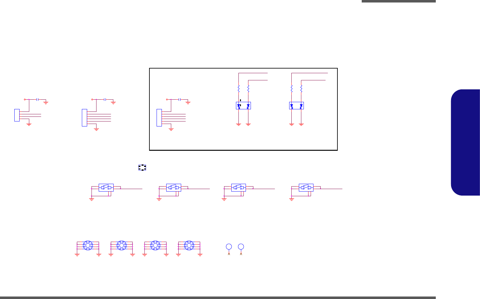
Schematic Diagrams
Click Board B - 31
B.Schematic Diagrams
Click Board
CLED_BAT_CHG
CLED_PWR
CLED_ACIN
CLED_BAT_FULL
CLED_BAT_FULL
6-20-94A50-104
6-21-91A20-1066-21-91A20-106 6-21-91A00-1066-21-91A00-106
6-53-3050B-0416-53-3050B-0416-53-3050B-0416-53-3050B-041
6-20-94A70-104
6-20-94AA0-104
1
BAT LED
POWER ON
LED
2
For W25/W27
CLED_ACIN
6-52-55002-04E
6-52-55002-042
CLED_BAT_CHG
CH5
C95D95 CH6
HO-165X94_5NP
CJ_TP3
85201-06051
1
2
3
4
5
6
1
CH1
MTH237D91
2
3
4
5 6
7
8
9
CC2
*0.1u_16V_Y 5V_04
CR3
220_04
CSW2
TJG-533-S-T/R
3
14
2
5
6
CC1
0.1u_16V_Y5V_04
CR1
220_04
CSW3
*TJG-533-S-T/R
3
14
2
5
6
CLICK BOARD
1
CH4
MTH237D 91
2
3
4
5 6
7
8
9
CSW4
*TJG-533-S-T/R
3
14
2
5
6
CC3
*0.1u_16V_Y5V_04
CJ_TP1
85201-04051
1
2
3
4
CJ_TP2
85201-06051
1
2
3
4
5
6
CSW1
TJG-533-S-T/R
3
14
2
5
6
SG
Y
CD26
KPB-3025Y SGC
1
3
2
4
CR4
220_04
1
CH2
MTH 237 D9 1
2
3
4
5 6
7
8
9
SG
Y
CD27
KPB-3025Y SGC
1
3
2
4
CR2
220_04
1
CH3
MTH237D91
2
3
4
5 6
7
8
9
CGND
CGND
CGND CGND
CGND
CGNDCGND
CGNDCGND
CGNDCGNDCGND
C5VS
CGNDCGND
CGND
CGND
CGND
CVDD3
CGND
CGND
C5VS
CGND CGNDCGND
CTPBUTTON_RCTPBUTTON_L CTPBUTTON_RCTPBUTTON_L
LIFT
KEY
RIGHT
KEY
LIFT
KEY
1
RIGHT
KEY
3
42
CSW1~4
6-52-55002-04E
6-52-55002-042
CTP_CLK
CTP_DATA
CTP_DATA
CTPBUTTON_L
CTP_CLK
CTPBUTTON_R
CLED_PWR
Sheet 30 of 33
Click Board
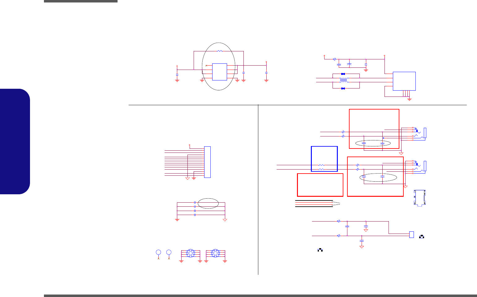
AMIC1-R
ASPKOUTR+_R
AHP_SENSE
AHEADPHONE-R
AHEADPHONE-L
AUSB_PN2
ASPKOUTR+
AMIC1-L
AMIC1-R
AMIC_SENSE
ASPKOUTR-
AUSB_PP2
AUSB_PP2
AUSB_PN2
1
J_SPK1
J_SPK1
2
2
AR735 *0_06
6-20-43110-102
AUSB_PP2_R
6-20-43150-102
1
AUSB_PN2_R
A_AUDG
EMI Require
6-21-B49C0-104
D02
AUDIO JACK
AC10
22u_6.3V_X5R_08
BLACK
BLACK
PHONE_OUT_R
AMIC1-L NC_MIC1
MIC1_OUT_L
PHONE_OUT_L
MIC1_OUT_R
AMIC_SENSE
PHONE-R
PHONE-L
AHEADPHONE-R
AHEADPHONE-L
AHP_SENSE
ASPKOUTR-
ASPKOUTR+
ASPKOUTR-_R
3
5
2
4
1
6
6-20-B2800-106
HP-L
6-20-B2800-106
GND
EMI Require
VT1802P
33_1%_04
3*R/L½u¼e
AL122
*WC M2012F2S-161T03
1
4
2
3
AC6 *0.1u_16V_Y5V_04
GND
AL126 FCM1005KF-121T03
1 2
Headphone°T¸¹½u¼e > 10mils
¶ZÂ÷phone jack¶V»·
½u®|´N¥²¶·¶V¼e
R/L¥²¶·¥]ÂÐGND¥B¶¡¶Z¬°3*½u¼e
AJ_USB1
US04036BCA081
V+
1
GND1
GND 1
DATA_L
2
DATA_H
3
GND
4
GND2
GND2
GND4
GND4 GND3
GND3
AC5
10u_10V_Y5V_08
AC797
*180p_50V_NPO_04
AC3
*0.1u_16V_Y5V_04
AC795
180p_50V_NPO_04
Resistor 32 or 33_04
meet WLK Test
AU1
RT9715BGS
VOUT1 6
VOUT3 8
VIN2
3
VIN1
2VOUT2 7
GND 1
EN#
4
FLG#
5AC2
0.1u_16V_Y5V_04
HP-R
AR2 *10mil_short_04
AL128
*FCM1608K-121T06_short
Layout note:
AC4
0.1u_16V_Y5V_04
R
L
AJ_HP1
2SJ-T351-S23
2
6
5
3
1
4
AR1 *10mil_short_04
AJ_SPKR1
85204-02001
PCB Footprint = 85204-02R
1
2
AC794
180p_50V_NPO_04
AC7 *0.1u_16V_Y5V_04
AC8 0.1u_16V_Y5V_04
AC9 0.1u_16V_Y5V_04
AL1
HCB1608KF-121T25
AC793
180p_50V_NPO_04
AH1
C59D59
AC798
*180p_50V_NPO_04
AC792
180p_50V_NPO_04
AL123 FCM1005KF-121T03
1 2
AH3
C59D59
1
AH2
MTH276D111
2
3
4
5 6
7
8
9
AR570 33_1%_04
AR569 33_1%_04
R
L
AJ_MIC1
2SJ-T351-S23
2
6
5
3
1
4
50mils
AL125 FCM1005KF-121T03
1 2
1
AH4
MTH276D111
2
3
4
5 6
7
8
9
AJ_AUDIO1
85201-14051-01
1
2
3
4
5
6
7
8
9
10
11
12
13
14
AC796
*1u_10V_06
AL127
*FCM1608K-121T06_short
AL124 FCM1005KF-121T03
1 2
A_USBVCC
A_USBVCC 2A_USBVCC
AGNDAGNDAGND
AGND
A_5V
AGND AGNDAGND AGND AGND
AGND
D02
AGND
A_5V
A_AUDG AGND
AGND
A_AUDG
A_AUDG
A_AUDG
A_AUDG
6-02-09715-920
ASPK_HP#
50mils
60 mil
USB PORT
HEADPHONE
ASPK_HP#
D02
Reverse
TO M/B
D02
+
AC1
*100u_6.3V_B_A
MIC IN
Sheet 31 of 33
Audio Board/USB
Schematic Diagrams
B - 32 Audio Board/USB
B.Schematic Diagrams
Audio Board/USB
20mil
10 pin & 8 pin co-lay
20mil
SWEB_WWW#
SWEB_EMAIL#
SM_BTN#
SAP_ON SLID_SW#
SAP_ON
SWEB_EMAIL#
SM_BTN#
SLID_SW#
SWEB_WWW#
6-20-94K10-108
HOT KEY
20mil
SU1, SU2
2
3
1
LID SWITCH IC
SLID_SW#
6-02-00268-LC1
6-02-00248-LC2
SWEB_EMAIL#SWEB_WWW#
SM_BTN# SAP_ON
POWER SW & LED & HOT KEY
SPWR_SW1
TJG-533-S-T/R
3
14
2
5
6
SWWW_SW1
*TJG-533-S-T/R
3
14
2
5
6
SR4
*0_04
SPWR_SW2
*TJG-533-S-T/R
3
14
2
5
6
1
SMH4
MTH237D118
2
3
4
5 6
7
8
9
SC6
*0.1u_10V_X7R_04
SR3
*100K_1%_04
SR2
220_04
SC4
*0.1u_16V_Y5V_04
SC5
*0. 1u_16V_Y5V_04
SC3
*0. 1u_16V_Y 5V_04
SMAIL_SW1
*TJG-533-S-T/R
3
14
2
5
6
SR1 100K_04
SU1
MH248-ALFA-ESO
VCC
1OUT 2
GND
3
SJ_SW1
*50500-01041-001L
1
2
3
4
5
6
7
8
9
10
SAP_SW1
*TJG-533-S-T/R
3
14
2
5
6
SC2
0.1u_16V_Y 5V_04
SD3
*HT-150NB-DT
AC
SR5
*47K_04
SJ_SW2
88486-0801
1
2
3
4
5
6
7
8
SD2
*BAV99 RECTIFIER
C
AC
A
SC1
*100p_50V_NPO_04
SMH5
H7_0D2_3
SMH2
H7_0D2_3
1
SMH3
MTH237D87
2
3
4
5 6
7
8
9
1
SMH1
MTH237D87
2
3
4
5 6
7
8
9
SMGND SMGND
SMGNDSMGND SMGNDSMGND SMGND
S_VIN
SMGND
SMGND
S_VIN
S_3.3V
S_3.3V
SMGND
SMGND
S_3.3VS
S_3.3V
SMGND
S_3.3VS
SMGND SMGND SMGND
S_3.3V
SMGND
SMGND
SMGNDSMGND
SMGND
S_3.3VS
SMGND
SMGND
SMGNDSMGND SMGNDSMGND
SD1
HT-150NB-DT
AC
SMH6
T158B118X87D118X87
SM_BTN#
POWER BUTTON
PSW1~8
4
31
2
6-53-3050B-241
6-53-3150B-245
6-53-3050B-240
Z4301
6-52-56001-022
6-52-56000-020
6-52-56001-028
6-52-56001-023
POWER
SWITCH
LED
20mil
FOR E5128Q
SMH7
T158B91D91
POWER BUTTON
FOR E5128Q FOR E4120Q/E5120Q
PSW1~8
WEB_WWW#
42
WEB_EMAIL#
1
AP_KEY#
3
FOR E5120Q
6-52-56001-028
6-52-56001-023
6-52-56001-022
6-52-56000-020
6-53-3150B-245
6-53-3050B-240
6-53-3050B-241
6-53-3150B-245
6-53-3050B-240
6-53-3050B-241
6-53-3050B-240
6-53-3050B-241
6-53-3150B-245
6-53-3050B-241
6-53-3150B-245
6-53-3050B-240
Sheet 32 of 33
Power Switch & LID
Board
Schematic Diagrams
Power Switch & LID Board B - 33
B.Schematic Diagrams
Power Switch & LID Board
Schematic Diagrams
B - 34 External ODD Board
B.Schematic Diagrams
External ODD Board
QJ_SATA_TXP1
PIN
GND1~3=QGND
QJ_SATA_ODD_DA#
QJ_SATA_TXN1
ODD BOARD
PIN
GND1~2=WGND
QJ_SATA_RXP1
QJ_SATA_RXN1
QJ_ODD_DETECT#
QC2
0.1u_16V_Y5V_04
QJ_ODD1
242001-1
S1
S2
S3
S4
S5
S6
S7
P1
P2
P3
P4
P5
P6
QH1
C237D91
QC1
*0.1u_16V_Y5V_04
QJ_ODD2
1-162-100562
S1
S2
S3
S4
S5
S6
S7
P1
P2
P3
P4
P5
P6
QH2
C67D67
QH3
C67D67
QH4
C237D91
QGND
QGND
QGND QGND
Q_5VS
Q_5VS
QGND
QGND
Q_5VS
QGND
6-21-14030-013
6-21-14020-013
6-21-14010-013
6-21-13A00-013
Sheet 33 of 33
External ODD
Board

BIOS Update
C - 1
C:BIOS Update
Appendix C:Updating the FLASH ROM BIOS
BIOS Version
Make sure you down-
load the latest correct
version of the BIOS ap-
propriate for the com-
puter model you are
working on.
You should only
download BIOS ver-
sions that are
V1.01.XX or higher as
appropriate for your
computer model.
Note that BIOS versions
are not backward com-
patible and therefore
you may not down-
grade your BIOS to an
older version after up-
grading to a later ver-
sion (e.g if you upgrade
a BIOS to ver 1.01.05,
you MAY NOT then go
back and flash the BIOS
to ver 1.01.04).
To update the FLASH ROM BIOS you must:
• Download the BIOS update from the web site.
• Unzip the files onto a bootable CD/DVD/USB Flash Drive.
• Reboot your computer from an external CD/DVD/USB Flash Drive.
• Use the flash tools to update the flash BIOS using the commands indicated below.
• Restart the computer booting from the HDD and press F2 at startup enter the BIOS.
• Load setup defaults from the BIOS and save the default settings and exit the BIOS to restart the computer.
• After rebooting the computer you may restart the computer again and make any required changes to the default BIOS
settings.
Download the BIOS
1. Go to www.clevo.com.tw and point to E-Services and click E-Channel.
2. Use your user ID and password to access the appropriate download area (BIOS), and download the latest BIOS files
(the BIOS file will be contained in a batch file that may be run directly once unzipped) for your computer model
(see sidebar for important information on BIOS versions).
Unzip the downloaded files to a bootable CD/DVD/ or USB Flash drive
1. Insert a bootable CD/DVD/USB flash drive into the CD/DVD drive/USB port of the computer containing the
downloaded files.
2. Use a tool such as Winzip or Winrar to unzip all the BIOS files and refresh tools to your bootable CD/DVD/USB
flash drive (you may need to create a bootable CD/DVD with the files using a 3rd party software).
Set the computer to boot from the external drive
1. With the bootable CD/DVD/USB flash drive containing the BIOS files in your CD/DVD drive/USB port, restart the
computer and press F2 (in most cases) to enter the BIOS.
2. Use the arrow keys to highlight the Boot menu.
3. Use the “+” and “-” keys to move boot devices up and down the priority order.
4. Make sure that the CD/DVD drive/USB flash drive is set first in the boot priority of the BIOS.
5. Press F10 to save any changes you have made and exit the BIOS to restart the computer.

BIOS Update
C - 2
C:BIOS Update
Use the flash tools to update the BIOS
1. Make sure you are not loading any memory management programs such as HIMEM by holding the F8 key as you
see the message “Starting MS-DOS”. You will then be prompted to give “Y” or “N” responses to the programs
being loaded by DOS. Choose “N” for any memory management programs.
2. You should now be at the DOS prompt e.g: DISK C:\> (C is the designated drive letter for the CD/DVD drive/USB
flash drive).
3. Type the following command at the DOS prompt:
C:\> Flash.bat
4. The utility will then proceed to flash the BIOS.
5. You should then be prompted to press any key to restart the system or turn the power off, and then on again but
make sure you remove the CD/DVD/USB flash drive from the CD/DVD drive/USB port before the computer
restarts.
Restart the computer (booting from the HDD)
1. With the CD/DVD/USB flash drive removed from the CD/DVD drive/USB port the computer should restart from
the HDD.
2. Press F2 as the computer restarts to enter the BIOS.
3. Use the arrow keys to highlight the Exit menu.
4. Select Load Setup Defaults (or press F9) and select “Yes” to confirm the selection.
5. Press F10 to save any changes you have made and exit the BIOS to restart the computer.
Your computer is now running normally with the updated BIOS
You may now enter the BIOS and make any changes you require to the default settings.