CM6802A, CM6802B, CM6802AH, CM6802BH Datasheet. Www.s Manuals.com. Cm6802a Cm6802b Cm6802ah R1.5 Champion
User Manual: Datasheets CM6802, CM6802AGIP, CM6802AGIS, CM6802AHGIP, CM6802AHGIS, CM6802AHXIP, CM6802AHXIS, CM6802AXIP, CM6802AXIS, CM6802BGIP, CM6802BGIS, CM6802BHGIP, CM6802BHGIS, CM6802BHXIP, CM6802BHXIS, CM6802BXIP, CM6802BXIS, CM6802IP, CM6802IS.
Open the PDF directly: View PDF ![]() .
.
Page Count: 26

CM6802A/B/AH/BH (Dynamic Soft PFC/Green PWM)
http://www.championmicro.com.tw EPA/80++ ZVS-Like PFC/PWM COMBO CONTROLLER
Design for High Efficient Power Supply at both Full Load and Light Load
2012/05/10 Rev. 1.5 Champion Microelectronic Corporation 1
GENERAL DESCRIPTION FEATURES
Switching to CM6802A/B/AH/BH from your existing
CM6800 family boards can gain the following advanced
performances:
1.) Around 2% efficiency gain when the output load is
below 40% of the full load.
2.) Hold Up time can be increased ~ 30% from the
existing 6800 power supply.
3.) 420V bulk capacitor value may be reduced PFC
boost ripple current can be reduced; therefore, the
boost inductor core size maybe reduced.
4.) No Load Consumption can be reduced 290mW at
270VAC.
5.) PWM transformer size can be smaller.
6.) To design 12V, 5V and 3.3V output filters can be
easy.
7.) The stress over the entire external power device is
reduced and EMI noise maybe reduced.
8.) Monotonic Output design is easy and more…Of
cause, the cost will be reduced.
CM6802A/B/AH/BH is pin to pin compatible with CM6800
family.
Beside all the goodies in the CM6800, it is designed to meet
the EPA/80+ regulation. With the proper design, its
efficiency of power supply can easily approach 85%.
To start evaluating CM6802A/B/AH/BH from the exiting
CM6800,CM6800A or ML4800 board, 6 things need to be
taken care before doing the fine tune:
1.) Change RAC resistor (on pin 2, IAC) from the old
value to a higher resistor value between 4.7 Mega
ohms to 8 Mega ohms.
2.) Change RTCT pin (pin 7) from the existing value to
RT=7.75K ohm and CT=1000pF to have
fpfc=55Khz, fpwm=55Khz, frtct=220Khz.
3.) Adjust all high voltage resistor around 5 mega ohm
or higher.
4.) VRMS pin (pin 4) needs to be 1.125V at
VIN=85VAC for universal input application from line
input from 85VAC to 270VAC. Both poles for the
Vrms of the CM6802A/B/AH/BH needs to
substantially slow than CM6800 about 5 to 10 times.
5.) At full load, the average Veao needs to around 4.5V
and the ripple on the Veao needs to be less than
250mV.
6.) Soft Start pin (pin 5), the soft start current has been
reduced from CM6800’s 20uA to
CM6802A/B/AH/BH’s 10uA.Soft Start capacitor can
be reduced to 1/2 from your original CM6800
capacitor.
Patents Pending
Pin to pin compatible with CM6800,CM6800A,
ML4800 and FAN4800.
23V Bi-CMOS process.
Designed for EPA/80++ efficiency.
CM6802A/B : Selectable Boost output from 380V to
300V during light load.
CM6802AH/BH: Selectable Boost output from 380V to
342V during light load.
All high voltage resistors can be greater than 4.7 Mega
ohm (4.7 Mega to 8 Mega ohm) to improve the no load
consumption.
Rail to rail CMOS Drivers with on, 60 ohm and off, 30
ohm for both PFC and PWM with two 17V zeners.
Fast Start-UP Circuit without extra bleed resistor to aid
VCC reaches 13V sooner.
Low start-up current (55uA typ.)
Low operating current (2.5mA typ.)
16.5V VCC shunt regulator
Leading Edge Blanking for both PFC and PWM.
fRTCT = 4*fpfc =4*fpwm for CM6802A//AH
fRTCT = 4*fpfc =2*fpwm for CM6802B/BH
Dynamic Soft PFC to ease the stress of the Power
Device and Ease the EMI filter design.
PFC Brown Out and PWM Brown Out
Internally synchronized leading edge PFC and trailing
edge PWM in one IC to Reduces ripple current in the
420V storage capacitor between the PFC and PWM
sections.
Low total harmonic distortion, THD and Power Factor
approaches 1.0.
Average current, continuous or discontinuous boost
leading edge PFC.
PWM configurable for current mode or feed-forward
voltage mode operation.
Current fed Gain Modulator for improved noise immunity.
Gain Modulator is a constant maximum power limiter.
Brown-out control, over-voltage protection, UVLO, and
soft start, and Reference OK.
PWM Short Circuit Protection
Power Fold Back Protection
Green Mode PWM for less no load consumption.
CM6802A/B/AH/BH (Dynamic Soft PFC/Green PWM)
http://www.championmicro.com.tw EPA/80++ ZVS-Like PFC/PWM COMBO CONTROLLER
Design for High Efficient Power Supply at both Full Load and Light Load
2012/05/10 Rev. 1.5 Champion Microelectronic Corporation 2
APPLICATIONS PIN CONFIGURATION
EPA/80++ related Power Supply
Desktop PC Power Supply
Internet Server Power Supply
LCD Power Supply
PDP Power Supply
IPC Power Supply
UPS
Battery Charger
DC Motor Power Supply
Monitor Power Supply
Telecom System Power Supply
Distributed Power
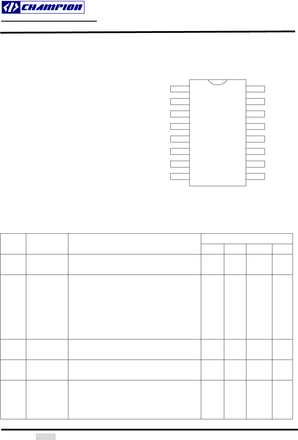
SOP-16 (S16) / PDIP-16 (P16)
1
2
3
4
5
6
7
8
16
15
14
13
12
11
10
9
IEAO
IAC
ISENSE
VRMS
SS
VDC
RAMP1
RAMP2
VEAO
VFB
VREF
VCC
PFC OUT
PWM OUT
GND
DC ILIMIT
PIN DESCRIPTION
Operating Voltage
Pin No. Symbol Description Min. Typ. Max. Unit
1 IEAO PFC transconductance current error amplifier output
(Gmi). 0 VREF V
2 IAC
IAC has 2 functions:
1. PFC gain modulator reference input.
2. At start up, IAC is connected to VCC and it helps to
reduce the startup time and it helps to reduce the no
load consumption. Typical RAC resistor is about 6 Mega
ohm to sense the line.
0 100 uA
3 ISENSE PFC Current Sense: for both Gain Modulator and PFC
ILIMIT comparator. -1.2 0.7 V
4 VRMS Line Input Sense pin and also, it is the brown out sense
pin. 0 VCC+0.3 V
5 SS
Soft start capacitor pin; can use it to on/off the boost
follower function; it is pulled down by 300 ohm internal
resistor when DCILIMIT reach 1V; the power is limited
during the PWM Brown out.
0 10 V

CM6802A/B/AH/BH (Dynamic Soft PFC/Green PWM)
http://www.championmicro.com.tw EPA/80++ ZVS-Like PFC/PWM COMBO CONTROLLER
Design for High Efficient Power Supply at both Full Load and Light Load
2012/05/10 Rev. 1.5 Champion Microelectronic Corporation 3
6 VDC DC to DC PWM voltage feedback input. 0 10 V
7
RAMP 1
(RTCT) Oscillator timing node; timing set by RT and CT 0.8 4 V
8 RAMP 2
(PWM RAMP)
In current mode, this pin functions as the current sense
input; when in voltage mode, it is the feed-forward sense
input from PFC output 380V (feed forward ramp). 0 VDCmax-1.8 V
9 DC ILIMIT PWM current limit comparator input 0 1 V
10 GND
Ground
11 PWM OUT
PWM driver output 0 VCC V
12 PFC OUT
PFC driver output 0 VCC
V
13 VCC Positive supply for CM6802A/B/AH/BH 10 15 18 V
14 VREF
Maximum 4mA buffered output for the internal 7.5V
reference when VCC=14V 7.5 V
15 VFB PFC transconductance voltage error amplifier input 0 2.5 3 V
16 VEAO
PFC transconductance voltage error amplifier output
(GmV) 0 6 V
ORDERING INFORMATION
Part Number Temperature Range Package
CM6802A/B/AH/BHGIP* -40℃ to 125℃ 16-Pin PDIP (P16)
CM6802A/B/AH/BHGIS* -40℃ to 125℃ 16-Pin Narrow SOP (S16)
CM6802A/B/AH/BHGISTR* -40℃ to 125℃ 16-Pin Narrow SOP (S16)
CM6802A/B/AH/BHXIP* -40℃ to 125℃ 16-Pin PDIP (P16)
CM6802A/B/AH/BHXIS* -40℃ to 125℃ 16-Pin Narrow SOP (S16)
CM6802A/B/AH/BHXISTR* -40℃ to 125℃ 16-Pin Narrow SOP (S16)
*Note: G : Suffix for Pb Free Product
TR : Package is Typing Reel
X : Suffix for Halogen Free Product
CM6802A/B/AH/BH (Dynamic Soft PFC/Green PWM)
http://www.championmicro.com.tw EPA/80++ ZVS-Like PFC/PWM COMBO CONTROLLER
Design for High Efficient Power Supply at both Full Load and Light Load
2012/05/10 Rev. 1.5 Champion Microelectronic Corporation 4
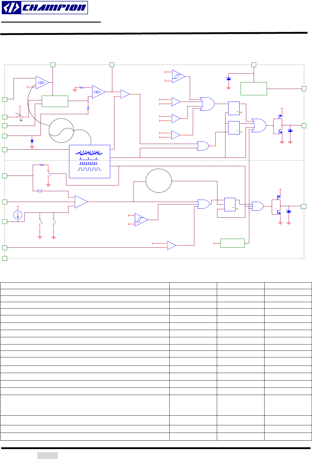
Simplified Block Diagram (CM6802A/B/AH/BH)
VFB
VFB
15
ZENER
17V
NPFC
ISENSE
3VEAO MNPFC
S
R
Q
Q
VFB
0.5V
+
-
PFC Tri-Fault
IAC
2PFC OUT
12
VFB
-1.0V
PPWM
ZENER
17V
2.36V
RAMP1
7
S
R
Q
Q
VREF14
5
REF-OK
VRMS
4
REFERENCE
7.5V
VCC
+
-
PFC CMP
Rmul
380V-OK
+
-
.
RAMP2
8
ISENSE
IEAO
1
PWM OUT
11
+
-
PFC ILIMIT
UVLO
1.0V
+
-
Green PFC
GND
10
0.3V
GMv
-
+
.
VEAO
16
VCC
VCC
VCC
1.8V
Green PWM
10uA
300
S
R
Q
Q
S
+
-
DC ILIMIT
VDC
6
PFC OVP
+
-
.
VCC
13
2.5V
MPPFC
GMi
+
-
.
VREF+2.5V
2.85V
PFCCLK
PWMCLK
.
.
PFC RAMP
SW SPST
+
-
-
PFC
MODULATOR
GAIN
380-OK
DC ILIMIT
9
Rmul Zener
16.5V
1 2
ABSOLUTE MAXIMUM RATINGS
Absolute Maximum ratings are those values beyond which the device could be permanently damaged.
Parameter Min. Max. Units
VCC 18 V
IEAO 0 VREF+0.3 V
ISENSE Voltage -5 0.7 V
GND – 0.3 VCC + 0.3 V
GND – 0.3 VCC + 0.3 V
PFC OUT
PWMOUT
Voltage on Any Other Pin GND – 0.3 VCC + 0.3 V
IREF 5 mA
IAC Input Current 1 mA
Peak PFC OUT Current, Source or Sink 0.5 A
Peak PWM OUT Current, Source or Sink 0.5 A
PFC OUT, PWM OUT Energy Per Cycle 1.5 μJ
Junction Temperature 150 ℃
Storage Temperature Range -65 150 ℃
Operating Temperature Range -40 125 ℃
Lead Temperature (Soldering, 10 sec) 260 ℃
Thermal Resistance (θJA)
Plastic DIP
Plastic SOIC
80
105
℃/W
℃/W
Power Dissipation (PD) TA<50℃ 800 mW
ESD Capability, HBM Model 5.5 KV
ESD Capability, CDM Model 1250 V
CM6802A/B/AH/BH (Dynamic Soft PFC/Green PWM)
http://www.championmicro.com.tw EPA/80++ ZVS-Like PFC/PWM COMBO CONTROLLER
Design for High Efficient Power Supply at both Full Load and Light Load
2012/05/10 Rev. 1.5 Champion Microelectronic Corporation 5
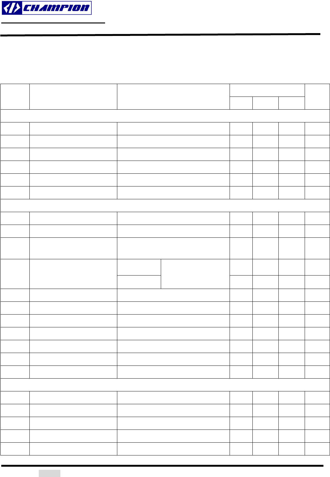
ELECTRICAL CHARACTERISTICS:
Unless otherwise stated, these specifications apply Vcc=+14V, RT = 7.75K kΩ, CT = 1000pF, TA=Operating Temperature
Range (Note 1)
CM6802A/B/AH/BH Symbol Parameter Test Conditions
Min. Typ. Max.
Unit
PFC Brown Out
VRMS Threshold High Room Temperature=25℃ 1.19 1.25 1.32 V
VRMS Threshold Low Room Temperature=25℃ 0.97 1.05 1.13 V
Hysteresis 170 216 260 mV
AC High Line Sweep Vrms Pin 2.15 2.25 2.35 V
AC Low Line Sweep Vrms Pin 1.85 2 2.12 V
Hysteresis 200 300 mV
Voltage Error Amplifier (gmv)
Input Voltage Range 0 3 V
Transconductance VNONINV = VINV, VEAO = 2.25V @ T=25℃ 53 69 88
μmho
Feedback Reference Voltage
(High)
SS < VREF and Veao > 2.5V 2.43 2.51 2.58 V
CM6802A/B 1.9 2 2.1 V
Feedback Reference Voltage
(Low) CM6802AH/BH
SS>VREF and Veao <
1.75V and Vrms < 2V 2.19 2.26 2.33 V
Input Bias Current Note 2 -1.0 -0.05 μA
Output High Voltage 5.8 6.0 V
Output Low Voltage 0.1 0.4 V
Sink Current VFB = 3V, VEAO = 1.5V -25 -18 -12 μA
Source Current VFB = 1.5V, VEAO = 2.45V 8 15 25 μA
Open Loop Gain DC gain 30 40 dB
Power Supply Rejection Ratio 11V < VCC < 16.5V 60 75 dB
Current Error Amplifier (gmi)
Input Voltage Range (Isense pin) -1.2 0.7 V
Transconductance VNONINV = VINV, IEAO = 1.5V @ T=25℃ 53 69 85
μmho
Input Offset Voltage VEAO=0V, IAC is open -10 50 mV
Output High Voltage 6.8 7.4 7.7 V
Output Low Voltage 0.1 0.4 V
CM6802A/B/AH/BH (Dynamic Soft PFC/Green PWM)
http://www.championmicro.com.tw EPA/80++ ZVS-Like PFC/PWM COMBO CONTROLLER
Design for High Efficient Power Supply at both Full Load and Light Load
2012/05/10 Rev. 1.5 Champion Microelectronic Corporation 6
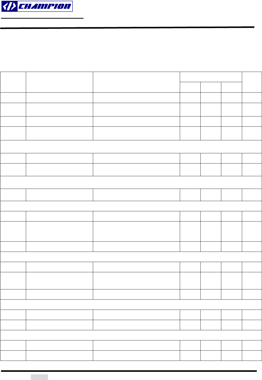
ELECTRICAL CHARACTERISTICS:
(Conti.) Unless otherwise stated, these specifications apply Vcc=+14V, RT = 7.75 kΩ, CT = 1000pF,
TA=Operating Temperature Range (Note 1)
CM6802A/B/AH/BH
Symbol Parameter Test Conditions
Min. Typ. Max.
Unit
Sink Current ISENSE = -0.5V, IEAO = 1.5V -42 -33 -30 μA
Source Current ISENSE = +0.5V, IEAO = 4.0V 28 31 42 μA
Open Loop Gain DC Gain 30 40 dB
Power Supply Rejection Ratio 11V < VCC < 16.5V 60 75 dB
PFC OVP Comparator
Threshold Voltage 2.70 2.85 3.0 V
Hysteresis 200 300 mV
PFC Green Power Detect Comparator
Veao Threshold Voltage 0.15 0.25 0.35 V
Tri-Fault Detect
Fault Detect HIGH 2.70 2.85 3.0 V
Time to Fault Detect HIGH VFB=VFAULT DETECT LOW to
VFB=OPEN, 470pF from VFB to GND
2 4 ms
Fault Detect LOW 0.4 0.5 0.6 V
PFC ILIMIT Comparator
Threshold Voltage -1.10 -1.00 -0.90 V
(PFCILIMIT– Gain Modulator
Output) 100 200 mV
Delay to Output (Note 4) Overdrive Voltage = -100mV 700 ns
DC ILIMIT Comparator
Threshold Voltage 0.92 1.0 1.08 V
Delay to Output (Note 4) Overdrive Voltage = 100mV 700 ns
DC to DC PWM Brown Out Comparator
OK Threshold Voltage 2.20 2.36 2.52 V
Hysteresis 900 950 1000 mV
CM6802A/B/AH/BH (Dynamic Soft PFC/Green PWM)
http://www.championmicro.com.tw EPA/80++ ZVS-Like PFC/PWM COMBO CONTROLLER
Design for High Efficient Power Supply at both Full Load and Light Load
2012/05/10 Rev. 1.5 Champion Microelectronic Corporation 7
ELECTRICAL CHARACTERISTICS:
(Conti.) Unless otherwise stated, these specifications apply Vcc=+14V, RT = 7.75 kΩ, CT = 1000pF,
TA=Operating Temperature Range (Note 1)
CM6802A/B/AH/BH
Symbol Parameter Test Conditions
Min. Typ. Max.
Unit
GAIN Modulator
Gain1 (Note 3)
IAC = 20 μA, VRMS =1.125, VFB = 2.375V @
T=25℃ SS<VREF 4.5 5 6
Gain2 (Note )3
IAC = 20 μA, VRMS = 1.45588V, VFB =
2.375V @ T=25℃ SS<VREF 4.2 4.65 5.1
Gain3 (Note 3)
IAC = 20 μA, VRMS =2.91V, VFB = 2.375V @
T=25℃ SS<VREF 1.45 1.75
Gain4 (Note 3)
IAC = 20 μA, VRMS = 3.44V, VFB = 2.375V
@ T=25℃ SS<VREF 1.0 1.45
Bandwidth (Note 4) IAC = 40 μA 1 MHz
Output Voltage = Rmul *
(ISENSE-IOFFSET)
IAC = 50 μA, VRMS = 1.125V, VFB = 2.0V
SS<VREF
0.7 0.78 0.87 V
Oscillator (Measuring fpfc)
Initial fpfc Accuracy 1
RT = 7.75 kΩ, CT = 1000pF, TA = 25℃
IAC=0uA
51 55.5 60 kHz
Voltage Stability 11V < VCC < 16.5V 2 %
Temperature Stability 2 %
Total Variation Line, Temp 48 62 kHz
Ramp Valley to Peak Voltage VEAO=6V and IAC=20uA 2.5 V
PFC Dead Time (Note 4) 500 900 ns
CT Discharge Current VRAMP2 = 0V, VRAMP1 = 2.5V 10 11 12 mA
Light Load Veao Threshold
Light Load Threshold (High) Room Temperature=25℃ 2.325 2.50 2.658 V
Light Load Threshold (Low) Room Temperature=25℃ 1.625 1.75 1.88 V
Hysteresis 700 850 mV
CM6802A/B/AH/BH (Dynamic Soft PFC/Green PWM)
http://www.championmicro.com.tw EPA/80++ ZVS-Like PFC/PWM COMBO CONTROLLER
Design for High Efficient Power Supply at both Full Load and Light Load
2012/05/10 Rev. 1.5 Champion Microelectronic Corporation 8
ELECTRICAL CHARACTERISTICS
(Conti.) Unless otherwise stated, these specifications apply Vcc=+14V, RT = 7.75kΩ, CT = 1000pF, TA=Operating
Temperature Range (Note 1)
CM6802A/B/AH/BH
Symbol Parameter Test Conditions Min. Typ. Max.
Unit
Reference
Output Voltage TA = 25℃, I(VREF) = 0mA 7.3 7.5 7.7 V
Line Regulation 11V < VCC < 16.5V@ T=25℃ 3 5 mV
VCC=10.5V,0mA < I(VREF) < 2mA;
@ T=25℃ 25 50 mV
Load Regulation VCC=14V,0mA < I(VREF) < 3.5mA;
TA = -40℃~85℃ 25 50 mV
Temperature Stability 0.4 %
Total Variation Line, Load, Temp 7.2 7.8 V
Long Term Stability TJ = 125℃, 1000HRs 5 25 mV
PFC
Minimum Duty Cycle IEAO > 4.5V 0 %
Maximum Duty Cycle VIEAO < 1.2V 95 97 %
IOUT = -20mA @ T=25℃ 11.5 15 ohm
IOUT = -100mA @ T=25℃ 18 ohm
Output Low Rdson
IOUT = 10mA, VCC = 9V @ T=25℃ 0.5 1 V
IOUT = 20mA @ T=25℃ 24 30 ohm
Output High Rdson IOUT = 100mA @ T=25℃ 40 ohm
Rise/Fall Time (Note 4) CL = 100pF @ T=25℃ 50 ns
PWM
Duty Cycle Range 0-49.5 0-50 %
IOUT = -20mA @ T=25℃ 11.5 15 ohm
IOUT = -100mA @ T=25℃ 18 ohm
Output Low Rdson
IOUT = 10mA, VCC = 9V 0.5 1 V
IOUT = 20mA @ T=25℃ 26.5 40 ohm
Output High Rdson IOUT = 100mA @ T=25℃ 40 ohm
Rise/Fall Time (Note 4) CL = 100pF 50 ns
PWM Comparator Level Shift 1.6 1.8 2 V
Soft Start
Soft Start Current Room Temperature=25℃ 7 8.5 10.5
μA
Supply
Start-Up Current VCC = 12V, CL = 0 @ T=25℃ 50 65
μA
Operating Current 14V, CL = 0 2.5 3.5 mA
Undervoltage Lockout Threshold CM6802A/B/AH/BH 12.35 12.85 13.45 V
Undervoltage Lockout Hysteresis CM6802A/B/AH/BH 2.8 2.95 3.1 V
Shunt Regulator (VCC zener)
Zener Threshold Voltage Apply VCC with Iop=20mA 16.2 16.8 17.4 V
Note 1: Limits are guaranteed by 100% testing, sampling, or correlation with worst-case test conditions.
Note 2: Includes all bias currents to other circuits connected to the VFB pin.
Note 3: Gain ~ K x 5.3V; K = (ISENSE – IOFFSET) x [IAC (VEAO – 0.7)]-1; VEAOMAX = 6V
Note 4: Guaranteed by design, not 100% production test.
CM6802A/B/AH/BH (Dynamic Soft PFC/Green PWM)
http://www.championmicro.com.tw EPA/80++ ZVS-Like PFC/PWM COMBO CONTROLLER
Design for High Efficient Power Supply at both Full Load and Light Load
2012/05/10 Rev. 1.5 Champion Microelectronic Corporation 9
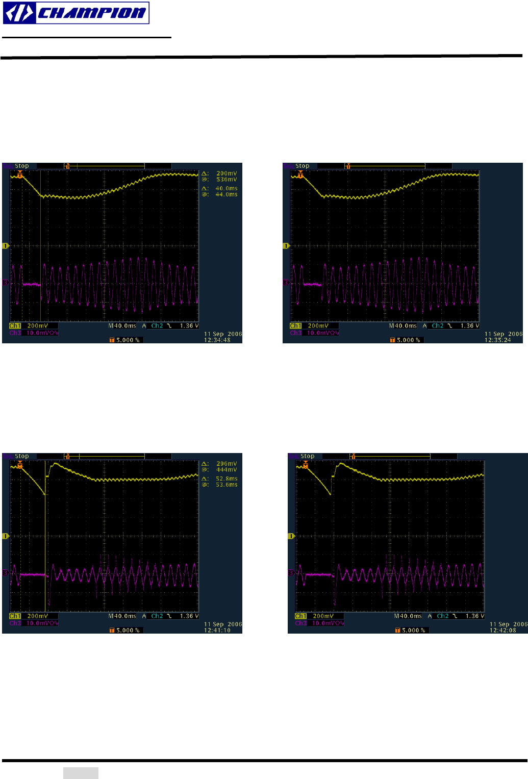
TYPICAL PERFORMANCE CHARACTERISTIC:
PFC Soft Diagram :
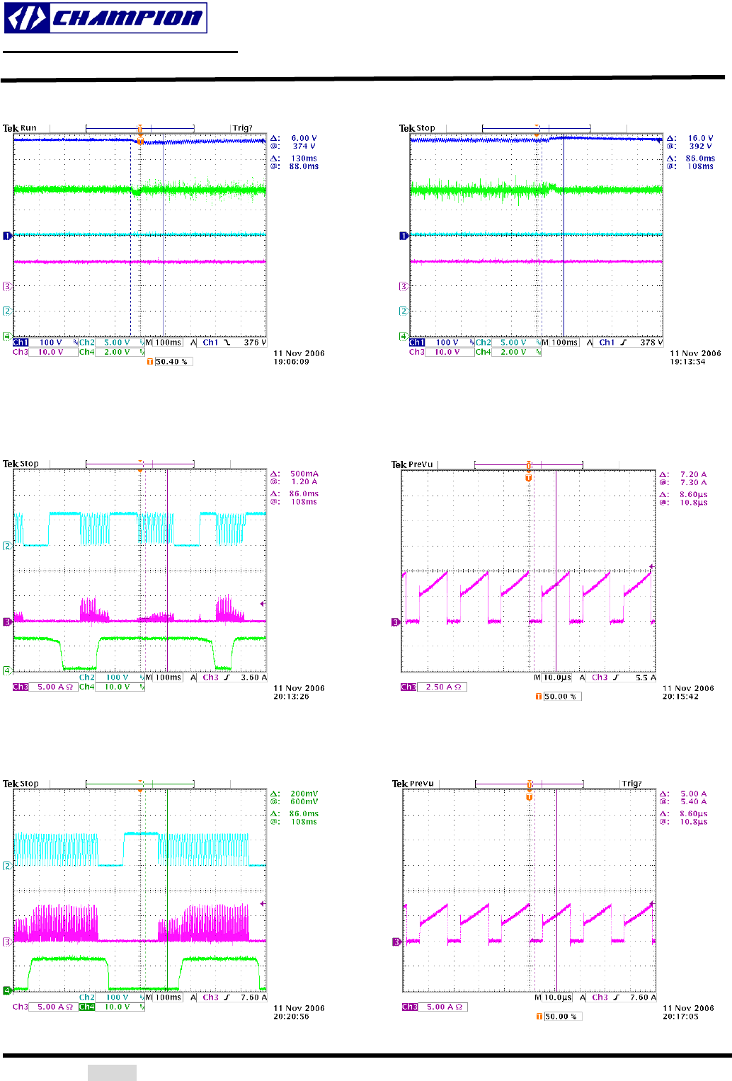
Dynamic Soft PFC Performance @ Vin=110 Vac
Ch1 is 380V bulk cap voltage which is 100V/div.
Ch3 is Input Line Current which is 1A/div.
Input Line Voltage (110 Vac) was turned off for 40mS before reaching PWM Brownout which is 209Vdc. When the bulk cap voltage goes below
209V, the system will reset the PWM soft start. The result of the CM6802A/B/AH/BH Input Line Current has a clean Off and softly On even the
system does not reset PWM soft-start.
Dynamic Soft PFC Performance @ Vin=220 Vac
Ch1 is 380V bulk cap voltage which is 100V/div.
Ch3 is Input Line Current which is 1A/div.
Input Line Voltage (220 Vac) was turned off for 40mS before reaching PWM Brownout which is 209Vdc when Bulk cap voltage drops below
209V. When the bulk cap voltage goes below 209V, the system will reset the PWM soft start. The result of the CM6802A/B/AH/BH Input Line
Current has a clean Off and softly On even the system does not reset itself. The first peak current at the beginning of the On time is the inrush
current.
CM6802A/B/AH/BH (Dynamic Soft PFC/Green PWM)
http://www.championmicro.com.tw EPA/80++ ZVS-Like PFC/PWM COMBO CONTROLLER
Design for High Efficient Power Supply at both Full Load and Light Load
2012/05/10 Rev. 1.5 Champion Microelectronic Corporation 10
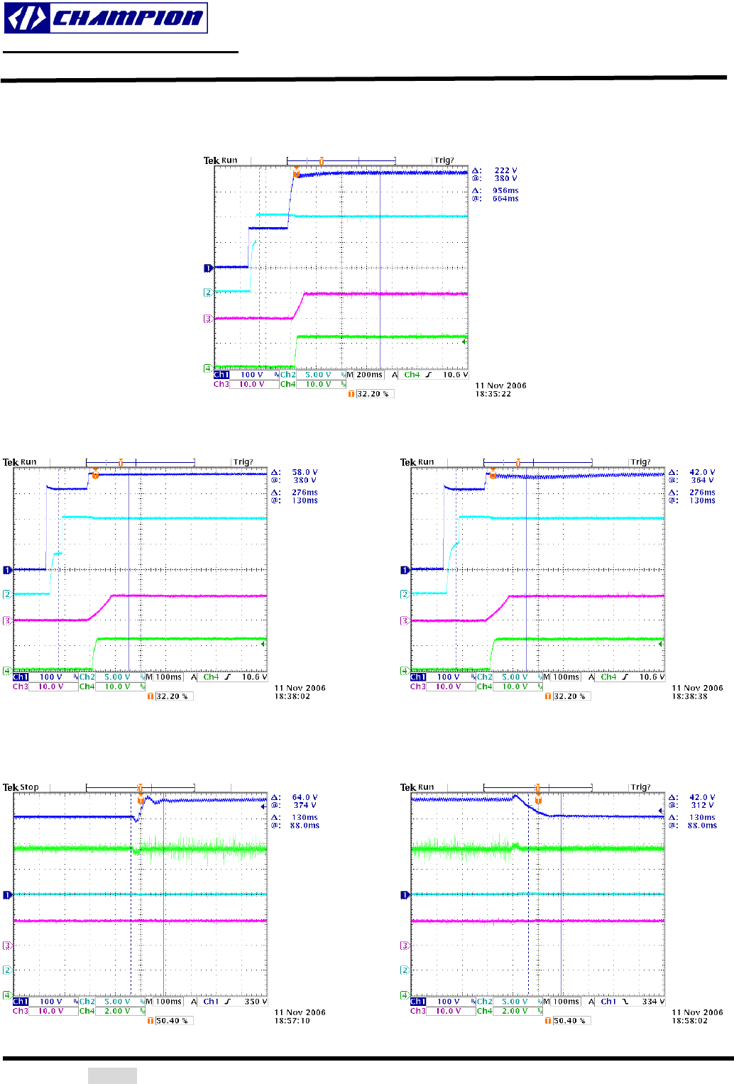
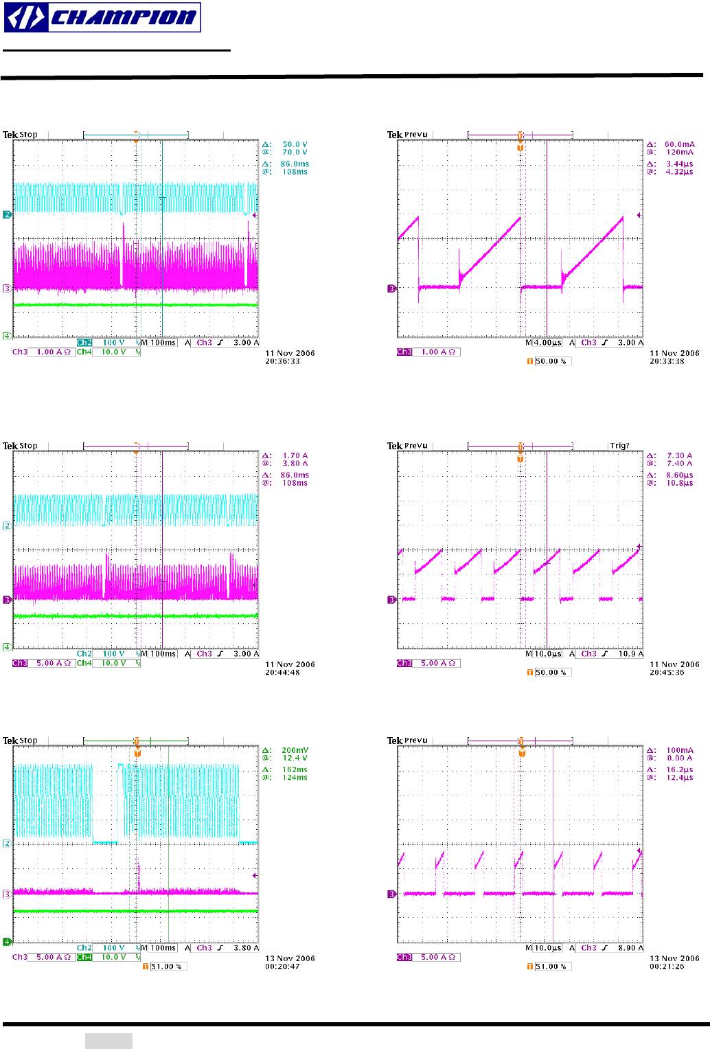
Turn on Timing :
Output 50% and 100% load turn on waveform at 110Vac
Ch1 is 380V bulk cap voltage which is 100V/div.
Ch2 is VCC,Ch3 is SS(soft start pin),CH4 is Vo(12V).
Output 10% and 20% load turn on waveform at 230Vac Output 50% and 100% load turn on waveform at 230Vac
Ch1 is 380V bulk cap voltage which is 100V/div. Ch1 is 380V bulk cap voltage which is 100V/div.
Ch2 is VCC,Ch3 is SS(soft start pin),CH4 is Vo(12V) Ch2 is VCC,Ch3 is SS(soft start pin),CH4 is Vo(12V)
Dynamic load:
Output step load 10% to 100% load at 90Vac Output step 100% load to 10% load at 90Vac
Ch1 is 380V bulk cap voltage which is 100V/div. Ch1 is 380V bulk cap voltage which is 100V/div.
Ch2 is VCC,Ch3 is SS(soft start pin),CH4 is Vo(12V) Ch2 is VCC,Ch3 is SS(soft start pin),CH4 is Vo(12V)
CM6802A/B/AH/BH (Dynamic Soft PFC/Green PWM)
http://www.championmicro.com.tw EPA/80++ ZVS-Like PFC/PWM COMBO CONTROLLER
Design for High Efficient Power Supply at both Full Load and Light Load
2012/05/10 Rev. 1.5 Champion Microelectronic Corporation 11
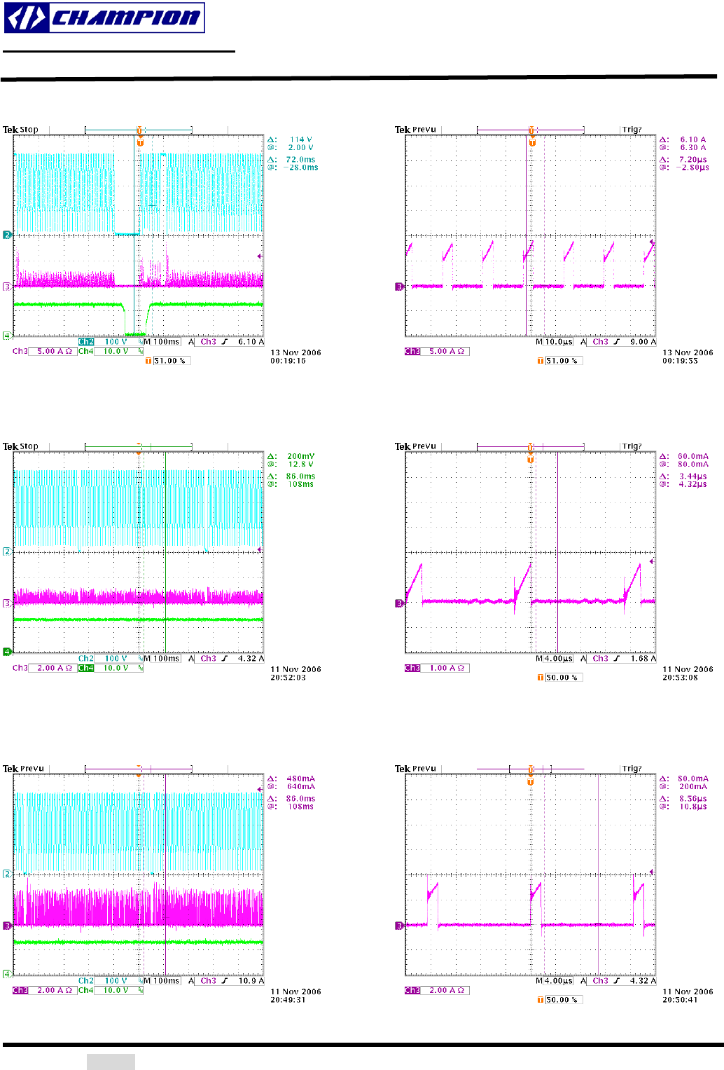
Output step load 10% to 100% load at 230Vac Output step 100% load to 10% load at 230Vac
Ch1 is 380V bulk cap voltage which is 100V/div. Ch1 is 380V bulk cap voltage which is 100V/div.
Ch2 is VCC,Ch3 is SS(soft start pin),CH4 is Vo(12V) Ch2 is VCC,Ch3 is SS(soft start pin),CH4 is Vo(12V)
AC power cycling :
90VAC turn on 500ms turn off 100ms at 10%LOAD
Ch2 is AC input voltage which is 100V/div. Ch3 is PFC stage Mosfet Drain current(zoom out)
Ch3 is PFC stage Mosfet drain current, CH4 is Vo(12V)
90VAC turn on 500ms turn off 100ms at 100%LOAD
Ch2 is AC input voltage which is 100V/div. Ch3 is PFC stage Mosfet Drain current(zoom out)
Ch3 is PFC stage Mosfet drain current, CH4 is Vo(12V)
CM6802A/B/AH/BH (Dynamic Soft PFC/Green PWM)
http://www.championmicro.com.tw EPA/80++ ZVS-Like PFC/PWM COMBO CONTROLLER
Design for High Efficient Power Supply at both Full Load and Light Load
2012/05/10 Rev. 1.5 Champion Microelectronic Corporation 12
90VAC turn on 500ms turn off 10ms at 10%LOAD
Ch2 is AC input voltage which is 100V/div. Ch3 is PFC stage Mosfet Drain current (zoom out)
Ch3 is PFC stage Mosfet drain current, CH4 is Vo (12V)
90VAC turn on 500ms turn off 10ms at 100%LOAD
Ch2 is AC input voltage which is 100V/div. Ch3 is PFC stage Mosfet Drain current (zoom out)
Ch3 is PFC stage Mosfet drain current, CH4 is Vo (12V)
230VAC turn on 500ms turn off 100ms at 10%LOAD
Ch2 is AC input voltage which is 100V/div. Ch3 is PFC stage Mosfet Drain current (zoom out)
Ch3 is PFC stage Mosfet drain current, CH4 is Vo (12V)
CM6802A/B/AH/BH (Dynamic Soft PFC/Green PWM)
http://www.championmicro.com.tw EPA/80++ ZVS-Like PFC/PWM COMBO CONTROLLER
Design for High Efficient Power Supply at both Full Load and Light Load
2012/05/10 Rev. 1.5 Champion Microelectronic Corporation 13
230VAC turn on 500ms turn off 100ms at 100%LOAD
Ch2 is AC input voltage which is 100V/div. Ch3 is PFC stage Mosfet Drain current (zoom out)
Ch3 is PFC stage Mosfet drain current, CH4 is Vo (12V)
230VAC turn on 500ms turn off 10ms at 10%LOAD
Ch2 is AC input voltage which is 100V/div. Ch3 is PFC stage Mosfet Drain current (zoom out)
Ch3 is PFC stage Mosfet drain current, CH4 is Vo (12V)
230VAC turn on 500ms turn off 10ms at 100%LOAD
Ch2 is AC input voltage which is 100V/div. Ch3 is PFC stage Mosfet Drain current (zoom out)
Ch3 is PFC stage Mosfet drain current, CH4 is Vo (12V)

CM6802A/B/AH/BH (Dynamic Soft PFC/Green PWM)
http://www.championmicro.com.tw EPA/80++ ZVS-Like PFC/PWM COMBO CONTROLLER
Design for High Efficient Power Supply at both Full Load and Light Load
2012/05/10 Rev. 1.5 Champion Microelectronic Corporation 14
Getting Start:
To start evaluating CM6802A/B/AH/BH from the exiting
CM6800 or ML4800 board, 6 things need to be taken care
before doing the fine tune:
1.) Change RAC resistor (on pin 2, IAC) from the old value
to a higher resistor value between 4.7 Mega ohms to 8
Mega ohms.
2.) Change RTCT pin (pin 7) from the existing value to
RT=7.0K ohm and CT=1000pF to have fpfc=55 Khz,
fpwm=55Khz, fRTCT=220Khz for CM6802A/AH and
fpfc=55 Khz, fpwm=110Khz, fRTCT=220Khz for
CM6802B/BH.
3.) Adjust all high voltage resistor around 5 mega ohm or
higher.
4.) VRMS pin (pin 4) needs to be 1.125V at VIN=85VAC for
universal input application from line input from 85VAC to
270VAC. Both poles for the Vrms of the
CM6802A/B/AH/BH needs to substantially slow than
CM6800 about 5 to 10 times.
5.) At full load, the average Veao needs to around 4.5V and
the ripple on the Veao needs to be less than 250mV.
6.) Soft Start pin (pin 5), the soft start current has been
reduced from CM6800’s 20uA to CM6802A/B/AH/BH’s
10uA.Soft Start capacitor can be reduced to 1/2 from your
original CM6800 capacitor.
Functional Description
CM6802A/B/AH/BH is designed for high efficient power
supply for both full load and light load. It is a popular
EPA/80++ PFC-PWM power supply controller.
The CM6802A/B/AH/BH consists of an average current
controlled, continuous/discontinuous boost Power Factor
Correction (PFC) front end and a synchronized Pulse Width
Modulator (PWM) back end. The PWM can be used in either
current or voltage mode. In voltage mode, feed-forward from
the PFC output bus can be used to improve the PWM’s line
regulation. In either mode, the PWM stage uses conventional
trailing edge duty cycle modulation, while the PFC uses
leading edge modulation. This patented leading/trailing edge
modulation technique results in a higher usable PFC error
amplifier bandwidth, and can significantly reduce the size of
the PFC DC buss capacitor.
The synchronized of the PWM with the PFC simplifies the
PWM compensation due to the controlled ripple on the PFC
output capacitor (the PWM input capacitor).
In addition to power factor correction, a number of
protection features have been built into the
CM6802A/B/AH/BH. These include soft-start, PFC
over-voltage protection, peak current limiting, brownout
protection, duty cycle limiting, and under-voltage lockout.
Power Factor Correction
Power factor correction makes a nonlinear load look like a
resistive load to the AC line. For a resistor, the current drawn
from the line is in phase with and proportional to the line voltage,
so the power factor is unity (one). A common class of nonlinear
load is the input of most power supplies, which use a bridge
rectifier and capacitive input filter fed from the line. The
peak-charging effect, which occurs on the input filter capacitor in
these supplies, causes brief high-amplitude pulses of current to
flow from the power line, rather than a sinusoidal current in
phase with the line voltage. Such supplies present a power
factor to the line of less than one (i.e. they cause significant
current harmonics of the power line frequency to appear at their
input). If the input current drawn by such a supply (or any other
nonlinear load) can be made to follow the input voltage in
instantaneous amplitude, it will appear resistive to the AC line
and a unity power factor will be achieved.
To hold the input current draw of a device drawing power from
the AC line in phase with and proportional to the input voltage, a
way must be found to prevent that device from loading the line
except in proportion to the instantaneous line voltage. The PFC
section of the CM6802A/B/AH/BH uses a boost-mode DC-DC
converter to accomplish this. The input to the converter is the full
wave rectified AC line voltage. No bulk filtering is applied
following the bridge rectifier, so the input voltage to the boost
converter ranges (at twice line frequency) from zero volts to the
peak value of the AC input and back to zero. By forcing the
boost converter to meet two simultaneous conditions, it is
possible to ensure that the current drawn from the power line is
proportional to the input line voltage. One of these conditions is
that the output voltage of the boost converter must be set higher
than the peak value of the line voltage. A commonly used value
is 385VDC, to allow for a high line of 270VACrms. The other
condition is that the current drawn from the line at any given
instant must be proportional to the line voltage. Establishing a
suitable voltage control loop for the converter, which in turn
drives a current error amplifier and switching output driver
satisfies the first of these requirements. The second requirement
is met by using the rectified AC line voltage to modulate the
output of the voltage control loop. Such modulation causes the
current error amplifier to command a power stage current that
varies directly with the input voltage. In order to prevent ripple,
which will necessarily appear at the output of boost circuit
(typically about 10VAC on a 385V DC level); from introducing
distortion back through the voltage error amplifier, the bandwidth
of the voltage loop is deliberately kept low. A final refinement is
to adjust the overall gain of the PFC such to be proportional to
1/(Vin x Vin), which linearizes the transfer function of the system
as the AC input to voltage varies.
Since the boost converter topology in the CM6802A/B/AH/BH
PFC is of the current-averaging type, no slope compensation is
required.
More exactly, the output current of the gain modulator is given
by:
CM6802A/B/AH/BH (Dynamic Soft PFC/Green PWM)
http://www.championmicro.com.tw EPA/80++ ZVS-Like PFC/PWM COMBO CONTROLLER
Design for High Efficient Power Supply at both Full Load and Light Load
2012/05/10 Rev. 1.5 Champion Microelectronic Corporation 15
Dynamic Soft PFC (patent pending)
Besides all the goodies from CM6800A, Dynamic Soft PFC
is the main feature of CM6802A/B/AH/BH. Dynamic Soft PFC
is to improve the efficiency, to reduce power device stress, to
ease EMI, and to ease the monotonic output design while it
has the more protection such as the short circuit with power
fold back protection. Its unique sequential control maximizes
the performance and the protections among steady state,
transient and the power on/off conditions.
PFC Section:
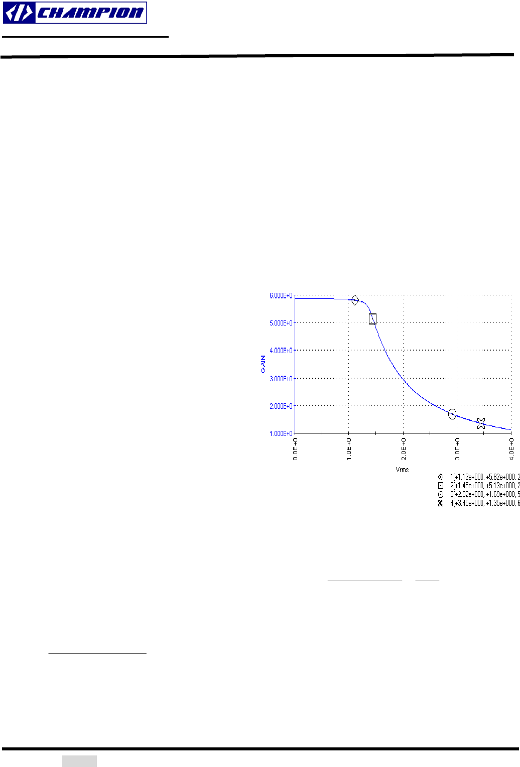
Gain Modulator
Figure 1 shows a block diagram of the PFC section of the
CM6802A/B/AH/BH. The gain modulator is the heart of the
PFC, as it is this circuit block which controls the response of
the current loop to line voltage waveform and frequency, rms
line voltage, and PFC output voltages. There are three inputs
to the gain modulator. These are:
1. A current representing the instantaneous input voltage
(amplitude and wave-shape) to the PFC. The rectified AC
input sine wave is converted to a proportional current via a
resistor and is then fed into the gain modulator at IAC.
Sampling current in this way minimizes ground noise, as is
required in high power switching power conversion
environments. The gain modulator responds linearly to this
current.
2. A voltage proportional to the long-term RMS AC line
voltage, derived from the rectified line voltage after scaling
and filtering. This signal is presented to the gain modulator
at VRMS. The gain modulator’s output is inversely
proportional to VRMS2 (except at unusually low values of
VRMS where special gain contouring takes over, to limit
power dissipation of the circuit components under heavy
brownout conditions). The relationship between VRMS and
gain is called K, and is illustrated in the Typical
Performance Characteristics.
3. The output of the voltage error amplifier, VEAO. The gain
modulator responds linearly to variations in this voltage.
The output of the gain modulator is a current signal, in the
form of a full wave rectified sinusoid at twice the line
frequency. This current is applied to the virtual-ground
(negative) input of the current error amplifier. In this way the
gain modulator forms the reference for the current error loop,
and ultimately controls the instantaneous current draw of the
PFC from the power line. The general formula of the output of
the gain modulator is:
I
mul = 2
RMS
AC
V
0.7V)-VEAOI (×x constant (1)
Gain=Imul/Iac
K=Gain/(VEAO-0.7V)
Imul = K x (VEAO – 0.7V) x IAC
Where K is in units of [V-1]
Note that the output current of the gain modulator is limited
around 100 μA and the maximum output voltage of the gain
modulator is limited to 100uA x 7.75K=~0.8V. This 0.8V also will
determine the maximum input power.
However, IGAINMOD cannot be measured directly from ISENSE.
ISENSE = IGAINMOD-IOFFSET and IOFFSET can only be measured when
VEAO is less than 0.5V and IGAINMOD is 0A. Typical IOFFSET is
around 33uA.
IAC=20uA, Veao=6V
Gain vs. VRMS (pin4)
When VRMS below 1V, the PFC is shut off. Designer needs to
design 85VAC with VRMS average voltage=1.125V.
AC
MUL
AC
OFFSETSENSE
I
I
I
II =
−
=Gain
Selecting RAC for IAC pin
IAC pin is the input of the gain modulator. IAC also is a current
mirror input and it requires current input. By selecting a proper
resistor RAC, it will provide a good sine wave current derived
from the line voltage and it also helps program the maximum
input power and minimum input line voltage.
RAC=Vin min peak x 39.09K. For example, if the minimum line
voltage is 85VAC, the RAC=85 x 1.414 x 39.09K = 4.7 Mega
ohm.

CM6802A/B/AH/BH (Dynamic Soft PFC/Green PWM)
http://www.championmicro.com.tw EPA/80++ ZVS-Like PFC/PWM COMBO CONTROLLER
Design for High Efficient Power Supply at both Full Load and Light Load
2012/05/10 Rev. 1.5 Champion Microelectronic Corporation 16
Vrms Description:
VRMS pin is designed for the following functions:
1. VRMS is used to detect the AC Brown Out (Also, we
can call it PFC brown out.). When VRMS is less than 1.0
V +/-5%, PFCOUT will be turned off and VEAO will be
softly discharged toward 0 Volt. When VRMS is greater
than 1.25V +/-5%, PFCOUT is enabled and VEAO is
released.
2. VRMS also is used to determine if the AC Line is high
line or it is low line. If VRMS is above 2.5V +/- 5%, IC
will recognize it is high line the. If VRMS is below 2.25V
+/- 5%, it is low line. Between 2V <=~ Vrms <=~ 2.25V,
it is the hysteresis.
3. At High Line and Light Load, 380V to 304V (Vfb
threshold moves from 2.5V to 2V) is prohibited of
CM6802A/B ; 380V to 342V (Vfb threshold moves from
2.5V to 2.25V) is prohibited of CM6802AH/BH.
At Low Line and Light Load, 380V to 304V (Vfb
threshold moves from 2.5V to 2V) is enable of
CM6802A/B ; 380V to 342V (Vfb threshold moves from
2.5V to 2.25V) is enable of CM6802AH/BH. It provides
ZVS-Like performance.
Current Error Amplifier, IEAO
The current error amplifier’s output controls the PFC duty
cycle to keep the average current through the boost inductor
a linear function of the line voltage. At the inverting input to
the current error amplifier, the output current of the gain
modulator is summed with a current which results from a
negative voltage being impressed upon the ISENSE pin. The
negative voltage on ISENSE represents the sum of all currents
flowing in the PFC circuit, and is typically derived from a
current sense resistor in series with the negative terminal of
the input bridge rectifier.
In higher power applications, two current transformers are
sometimes used, one to monitor the IF of the boost diode. As
stated above, the inverting input of the current error amplifier
is a virtual ground. Given this fact, and the arrangement of
the duty cycle modulator polarities internal to the PFC, an
increase in positive current from the gain modulator will
cause the output stage to increase its duty cycle until the
voltage on ISENSE is adequately negative to cancel this
increased current. Similarly, if the gain modulator’s output
decreases, the output duty cycle will decrease, to achieve a
less negative voltage on the ISENSE pin.
Error Amplifier Compensation
The PWM loading of the PFC can be modeled as a
negative resistor; an increase in input voltage to the PWM
causes a decrease in the input current. This response
dictates the proper compensation of the two
transconductance error amplifiers. Figure 2 shows the types
of compensation networks most commonly used for the
voltage and current error amplifiers, along with their
respective return points.
The current loop compensation is returned to VREF to produce
a soft-start characteristic on the PFC: as the reference voltage
comes up from zero volts, it creates a differentiated voltage on
IEAO which prevents the PFC from immediately demanding a full
duty cycle on its boost converter.
PFC Brown Out (PFC Brown Out Comparator)
The PFC Brown Out comparator monitors the Vrms (pin 4)
voltage and inhibits the PFC and PFC error amplifier output,
Veao is pulled down during the Vrms is lower than threshold. If
this voltage on Vrms is less than its nominal 1.25V. Once this
voltage reaches 1.25V, which corresponds to the PFC input rms
is around 88Vac. It is a hysteresis comparator and its lower
threshold is 1V. After PFC Brown Out conditions are removed,
the system will initiate the start up sequence with the proper soft
start rate set by SS (pin 5).
Cycle-By-Cycle Current Limiter and
Selecting RSENSE
The ISENSE pin, as well as being a part of the current feedback
loop, is a direct input to the cycle-by-cycle current limiter for the
PFC section. Should the input voltage at this pin ever be more
negative than –1V, the output of the PFC will be disabled until
the protection flip-flop is reset by the clock pulse at the start of
the next PFC power cycle.
RSis the sensing resistor of the PFC boost converter. During
the steady state, line input current x RSENSE = Imul x 7.75K. Since
the maximum output voltage of the gain modulator is Imul max x
7.75K≒ 0.8V during the steady state, RSENSE x line input current
will be limited below 0.8V as well. When VEAO reaches
maximum VEAO which is 6V, Isense can reach 0.8V. At 100%
load, VEAO should be around 4.5V and ISENSE average peak
is 0.6V. It will provide the optimal dynamic response + tolerance
of the components.
Therefore, to choose RSENSE, we use the following equation:
RSENSE + RParasitic =0.6V x Vinpeak / (2 x Line Input power)
For example, if the minimum input voltage is 80VAC, and the
maximum input rms power is 200Watt, RSENSE + RParasitic = (0.6V
x 80V x 1.414) / (2 x 200) = 0.169 ohm. The designer needs to
consider the parasitic resistance and the margin of the power
supply and dynamic response. Assume RParasitic = 30 mOhm,
RSENSE = 139 mOhm.
PFC OVP
In the CM6802A/B/AH/BH, PFC OVP comparator serves to
protect the power circuit from being subjected to excessive
voltages if the load should suddenly change. A resistor divider
from the high voltage DC output of the PFC is fed to VFB. When
the voltage on VFB exceeds ~ 2.85V, the PFC output driver is
shut down. The PWM section will continue to operate. The OVP
comparator has 250mV of hysteresis, and the PFC will not
restart until the voltage at VFB drops below ~ 2.55V. The VFB
power components and the CM6802A/B/AH/BH are within their
safe operating voltages, but not so low as to interfere with the
boost voltage regulation loop.

CM6802A/B/AH/BH (Dynamic Soft PFC/Green PWM)
http://www.championmicro.com.tw EPA/80++ ZVS-Like PFC/PWM COMBO CONTROLLER
Design for High Efficient Power Supply at both Full Load and Light Load
2012/05/10 Rev. 1.5 Champion Microelectronic Corporation 17
PFC Voltage Loop
There are two major concerns when compensating the
voltage loop error amplifier, VEAO; stability and transient
response. Optimizing interaction between transient response
and stability requires that the error amplifier’s open-loop
crossover frequency should be 1/2 that of the line frequency,
or 23Hz for a 47Hz line (lowest anticipated international
power frequency).
deviate from its 2.5V (nominal) value. If this happens, the
transconductance of the voltage error amplifier, GMv will
increase significantly, as shown in the Typical Performance
Characteristics. This raises the gain-bandwidth product of the
voltage loop, resulting in a much more rapid voltage loop
response to such perturbations than would occur with a
conventional linear gain characteristics.
The Voltage Loop Gain (S)
CVV
DCEAO
2
OUTDC
IN
FB
EAO
OUT
FB
EAO
OUT
Z*GM*
C*S*ΔV*V
2.5V*P
ΔV
ΔV
*
ΔV
ΔV
*
ΔV
ΔV
≈
=
ZCV: Compensation Net Work for the Voltage Loop
GMv: Transconductance of VEAO
PIN: Average PFC Input Power
VOUTDC: PFC Boost Output Voltage; typical designed value is
380V.
CDC: PFC Boost Output Capacitor
PFC Current Loop
The current transcondutance amplifier, GMi, IEAO
compensation is similar to that of the voltage error amplifier,
VEAO with exception of the choice of crossover frequency.
The crossover frequency of the
current amplifier should be at least 10 times that of
the voltage amplifier, to prevent interaction with the voltage
loop. It should also be limited to less than 1/6th that of the
switching frequency, e.g. 8.33kHz for a 50kHz switching
frequency.
The Current Loop Gain (S)
CI
I
S
OUTDC
SENSE
EAO
EAO
OFF
OFF
ISENSE
Z*GM*
2.5V*L*S
R*V
ΔI
ΔI
*
ΔI
ΔD
*
ΔD
ΔV
≈
=
ZCI: Compensation Net Work for the Current Loop
GMI: Transconductance of IEAO
VOUTDC:PFC Boost Output Voltage; typical designed value is
380V and we use the worst condition to calculate the ZCI
RSENSE: The Sensing Resistor of the Boost Converter
2.5V: The Amplitude of the PFC Leading Edge Modulation
Ramp(typical)
L: The Boost Inductor
The gain vs. input voltage of the CM6802A/B/AH/BH’s voltage
error amplifier, VEAO has a specially shaped non-linearity such
that under steady-state operating conditions the
transconductance of the error amplifier, GMv is at a local
minimum. Rapid perturbation in line or load conditions will cause
the input to the voltage error amplifier (VFB) to
ISENSE Filter, the RC filter between RSENSE and ISENSE :
There are 2 purposes to add a filter at ISENSE pin:
1.) Protection: During start up or inrush current conditions, it will
have a large voltage cross Rs which is the sensing resistor
of the PFC boost converter. It requires the ISENSE Filter to
attenuate the energy.
2.) To reduce L, the Boost Inductor: The ISENSE Filter To reduce
L, the Boost Inductor: The ISENSE Filter also can reduce the
Boost Inductor value since the ISENSE Filter behaves like an
integrator before going ISENSE which is the input of the
current error amplifier, IEAO.
The ISENSE Filter is a RC filter. The resistor value of the ISENSE
Filter is between 100 ohm and 50 ohm because IOFFSET x the
resistor can generate an offset voltage of IEAO. By selecting
RFILTER equal to 50 ohm will keep the offset of the IEAO less than
5mV. Usually, we design the pole of ISENSE Filter at
fpfc/6=8.33Khz, one sixth of the PFC switching frequency.
Therefore, the boost inductor can be reduced 6 times without
disturbing the stability. Therefore, the capacitor of the ISENSE
Filter, CFILTER, will be around 381nF.
CM6802A/B/AH/BH (Dynamic Soft PFC/Green PWM)
http://www.championmicro.com.tw EPA/80++ ZVS-Like PFC/PWM COMBO CONTROLLER
Design for High Efficient Power Supply at both Full Load and Light Load
2012/05/10 Rev. 1.5 Champion Microelectronic Corporation 18
PFC
IEAO
1
0.3V
VFB
15
RAMP1
7
VCC
PFC OVP
+
-
.
ISENSE
-1.0V
Rmul
VRMS
4PFC OUT
12
MPPFC
2.5V
GMv
-
+
.
S
R
Q
Q
+
-
PFC ILIMIT
ZENER
17V
VEAO
+
-
Green PFC
MODULATOR
GAIN
+
-
PFC CMP VREF14
2.85V
VCC
PFC RAMP
ISENSE
3
PFCCLK
.
VEAO
16
VFB
GMi
+
-
.
0.5V
MNPFC
S
R
Q
Q
Rmul
Zener
16.5V
1 2
+
-
PFC Tri-Fault
REFERENCE
7.5V
VFB VCC
13
IAC
2
Figure 1. PFC Section Block Diagram
CM6802A/B/AH/BH (Dynamic Soft PFC/Green PWM)
http://www.championmicro.com.tw EPA/80++ ZVS-Like PFC/PWM COMBO CONTROLLER
Design for High Efficient Power Supply at both Full Load and Light Load
2012/05/10 Rev. 1.5 Champion Microelectronic Corporation 19
Oscillator (RAMP1, or called RTCT)
In CM6802A/AH, fRTCT=4xfpwm=4xfpfc fRTCT=200Khz,
fpwm=50Khz and fpfc=50Khz when VEAO=0V, it provides
the best performance in the PC application.
In CM6802B/BH, fRTCT=2xfpwm=4xfpfc fRTCT=200Khz,
fpwm=100Khz and fpfc=50Khz when VEAO=0V, it provides
the best performance in the PC application.
The oscillator frequency, fRTCT is the similar formula in
CM6800:
fRTCT =
DEADTIMERAMP tt
1
+
The dead time of the oscillator is derived from the
following equation:
t
RAMP = CT x RT x In
3.75V
1.25V
REF
REF
−
−
at VREF = 7.5V:
t
RAMP = CT x RT x 0.51
The dead time of the oscillator may be determined using:
t
DEADTIME =
4.216mA
2.5V x CT = 593 x CT
The dead time is so small (tRAMP >> tDEADTIME ) that the
operating frequency can typically be approximately by:
fRTCT =
RAMP
t
1
Ct should be greater than 470pF.
Let us use 1000PF Solving for RT yields 7.75K. Selecting
standard components values, CT = 1000pF, and RT=
7.75kΩ
The dead time of the oscillator determined two things:
1.) PFC minimum off time which is the dead time
2.) PWM skipping reference duty cycle: when the PWM
duty cycle is less than the dead time, the next cycle
will be skipped and it reduces no load consumption
in some applications.
PWM Section
Pulse Width Modulator
The PWM section of the CM6802A/B/AH/BH is
straightforward, but there are several points which should
be noted. Foremost among these is its inherent
synchronization to the PFC section of the device, from
which it also derives its basic timing. The PWM is capable
of current-mode or voltage-mode operation.
In current-mode applications, the PWM ramp (RAMP2) is usually
derived directly from a current sensing resistor or current
transformer in the primary of the output stage, and is thereby
representative of the current flowing in the converter’s output
stage. DCILIMIT, which provides cycle-by-cycle current limiting, is
typically connected to RAMP2 in such applications. For
voltage-mode, operation or certain specialized applications,
RAMP2 can be connected to a separate RC timing network to
generate a voltage ramp against which VDC will be compared.
Under these conditions, the use of voltage feed-forward from the
PFC buss can assist in line regulation accuracy and response. As
in current mode operation, the DC ILIMIT input is used for output
stage over-current protection.
No voltage error amplifier is included in the PWM stage of the
CM6802A/B/AH/BH, as this function is generally performed on
the output side of the PWM’s isolation boundary. To facilitate the
design of opto-coupler feedback circuitry, an offset has been built
into the PWM’s RAMP2 input which allows VDC to command a
zero percent duty cycle for input voltages below around 1.8V.
PWM Current Limit (DCILIMIT)
The DC ILIMIT pin is a direct input to the cycle-by-cycle current
limiter for the PWM section. Should the input voltage at this pin
ever exceed 1V, the output flip-flop is reset by the clock pulse at
the start of the next PWM power cycle. Beside, the cycle-by-cycle
current, when the DC ILIMIT triggered the cycle-by-cycle current.
It will limit PWM duty cycle mode. Therefore, the power
dissipation will be reduced during the dead short condition.
When DCILIMIT pin is connected with RAMP2 pin, the
CM6802A/B/AH/BH’s PWM section becomes a current mode
PWM controller. Sometimes, network between DCILIMIT and
RAMP2 is a resistor divider so the DCILIMIT’s 1V threshold can
be amplified to 1.5V or higher for easy layout purpose.
PWM Brown Out (380V-OK Comparator)
The 380V-OK comparator monitors the DC output of the PFC
and inhibits the PWM if this voltage on VFB is less than its nominal
2.36V. Once this voltage reaches 2.36V, which corresponds to
the PFC output capacitor being charged to its rated boost voltage,
the soft-start begins. It is a hysteresis comparator and its lower
threshold is 1.35V.

CM6802A/B/AH/BH (Dynamic Soft PFC/Green PWM)
http://www.championmicro.com.tw EPA/80++ ZVS-Like PFC/PWM COMBO CONTROLLER
Design for High Efficient Power Supply at both Full Load and Light Load
2012/05/10 Rev. 1.5 Champion Microelectronic Corporation 20
PWM Control (RAMP2)
When the PWM section is used in current mode, RAMP2 is
generally used as the sampling point for a voltage
representing the current on the primary of the PWM’s output
transformer, derived either by a current sensing resistor or a
current transformer. In voltage mode, it is the input for a ramp
voltage generated by a second set of timing components
(RRAMP2, CRAMP2),that will have a minimum value of zero volts
and should have a peak value of approximately 5V. In voltage
mode operation, feed-forward from the PFC output buss is an
excellent way to derive the timing ramp for the PWM stage.
Soft Start (SS)
Start-up of the PWM is controlled by the selection of the
external capacitor at SS. A current source of 10 μA supplies
the charging current for the capacitor, and start-up of the
PWM begins at SS~1.4V. Start-up delay can be programmed
by the following equation:
C
SS = tDELAY x 1.8V
A10
μ
where CSS is the required soft start capacitance, and the tDEALY
is the desired start-up delay.
It is important that the time constant of the PWM soft-start
allow the PFC time to generate sufficient output power for the
PWM section. The PWM start-up delay should be at least
5ms.
Solving for the minimum value of CSS:
C
SS = 5ms x 1.8V
A10
μ
≒ 27nF
Caution should be exercised when using this minimum soft
start capacitance value because premature charging of the
SS capacitor and activation of the PWM section can result if
VFB is in the hysteresis band of the 380V-OK comparator at
start-up. The magnitude of VFB at start-up is related both to
line voltage and nominal PFC output voltage. Typically, a
0.05 μF soft start capacitor will allow time for VFB and PFC
out to reach their nominal values prior to activation of the
PWM section at line voltages between 90Vrms and 265Vrms.
Generating VCC
After turning on CM6802A/B/AH/BH at 13V, the operating
voltage can vary from 10V to 17.9V. That’s the two ways to
generate VCC. One way is to use auxiliary power supply
around 15V, and the other way is to use bootstrap winding to
self-bias CM6802A/B/AH/BH system. The bootstrap winding
can be either taped from PFC boost choke or from the
transformer of the DC to DC stage. The ratio of winding
transformer for the bootstrap should be set between 18V and
15V.
A filter network is recommended between VCC (pin 13) and
bootstrap winding. The resistor of the filter can be set as
following.
RFILTER x IVCC ~ 2V, IVCC = IOP + (QPFCFET + QPWMFET ) x fsw
IOP = 3mA (typ.)
If anything goes wrong, and VCC goes beyond 19.4V, the
PFC gate (pin 12) drive goes low and the PWM gate drive (pin
11) remains function. The resistor’s value must be chosen to
meet the operating current requirement of the
CM6802A/B/AH/BH itself (5mA, max.) plus the current required
by the two gate driver outputs.
EXAMPLE:
With a wanting voltage called, VBIAS ,of 18V, a VCC of 15V
and the CM6802A/B/AH/BH driving a total gate charge of 90nC
at 100kHz (e.g. 1 IRF840 MOSFET and 2 IRF820 MOSFET),
the gate driver current required is:
I
GATEDRIVE = 100kHz x 90nC = 9mA
R
BIAS =
GCC
CCBIAS
II
VV
+
−
R
BIAS =
9mA 5mA
15V18V
+
−
Choose RBIAS = 214Ω
The CM6802A/B/AH/BH should be locally bypassed with a
1.0 μF ceramic capacitor. In most applications, an electrolytic
capacitor of between 47 μF and 220 μF is also required
across the part, both for filtering and as part of the start-up
bootstrap circuitry.
Leading/Trailing Modulation
Conventional Pulse Width Modulation (PWM) techniques
employ trailing edge modulation in which the switch will turn on
right after the trailing edge of the system clock. The error
amplifier output is then compared with the modulating ramp up.
The effective duty cycle of the trailing edge modulation is
determined during the ON time of the switch. Figure 4 shows a
typical trailing edge control scheme.
CM6802A/B/AH/BH (Dynamic Soft PFC/Green PWM)
http://www.championmicro.com.tw EPA/80++ ZVS-Like PFC/PWM COMBO CONTROLLER
Design for High Efficient Power Supply at both Full Load and Light Load
2012/05/10 Rev. 1.5 Champion Microelectronic Corporation 21
In case of leading edge modulation, the switch is turned
OFF right at the leading edge of the system clock. When the
modulating ramp reaches the level of the error amplifier output
voltage, the switch will be turned ON. The effective duty-cycle
of the leading edge modulation is determined during OFF time
of the switch.
Figure 5 shows a leading edge control scheme.
One of the advantages of this control technique is that it
required only one system clock. Switch 1(SW1) turns off and
switch 2 (SW2) turns on at the same instant to minimize the
momentary “no-load” period, thus lowering ripple voltage
generated by the switching action. With such synchronized
switching, the ripple voltage of the first stage is reduced.
Calculation and evaluation have shown that the 120Hz
component of the PFC’s output ripple voltage can be reduced
by as much as 30% using this method.
CM6802A/B/AH/BH (Dynamic Soft PFC/Green PWM)
http://www.championmicro.com.tw EPA/80++ ZVS-Like PFC/PWM COMBO CONTROLLER
Design for High Efficient Power Supply at both Full Load and Light Load
2012/05/10 Rev. 1.5 Champion Microelectronic Corporation 22
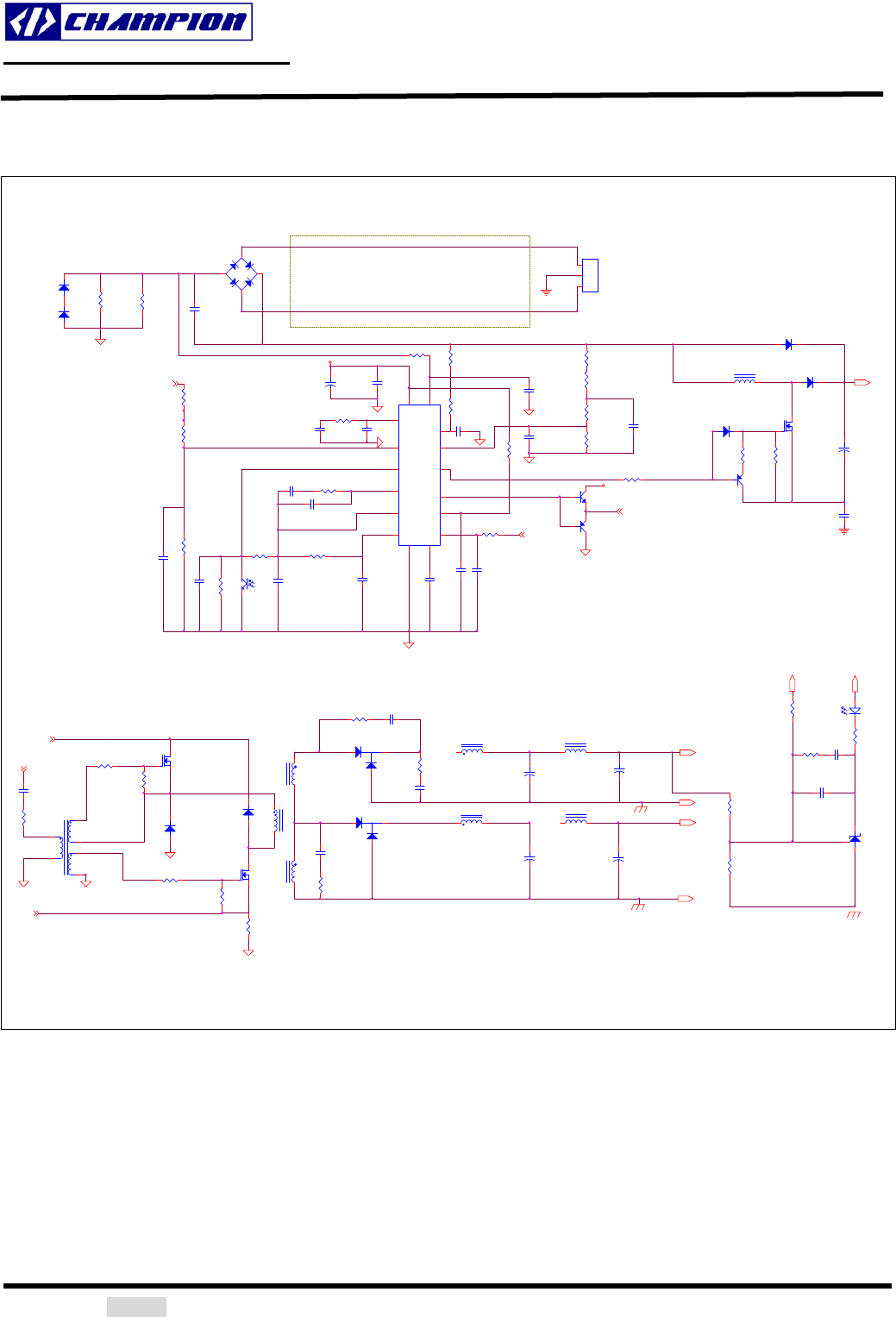
CM6802A/B/AH/BH APPLICATION CIRCUIT (Voltage Mode)
1M 1%
10
PWM IS
2N2907
470pF
30L30
380VDC
L4
R5*25
14K 1%
10K
47
ISO1A
817C
BYV-26EGP
EMI Circuit
0.47uF/16V
0.47uF
L3
R5*25
20N60
1
32
470
+
150uF/450V
0.22 2W (s)
2.49K 1%
L 1
APS27950
1M
BYV-26EGP
+
2200uF/10V
TL431
2 3
1
IN5406
PWM OUT
+
2200uF/16V
20N60
0.1uf/25v
1000PF
470pF
(SPARE)
1M
1N4148
10.2K 1%
470pF/250V
0.2/2W(S)
+
2200uF/16V
0.47UF
3M1%
8A/600V
2 1
+12V
AC INLET
L
FG
N
-
+
GBL408
2
1
3
4
1M 1%
0.1uF
+12V
VCC
200K 1% 3M 1%
0.047uF
10
1000pF
1000PF
PWM IS
10K
0.1uF
4.75K 1% 1/8W
L1A
28TS
2200PF
1N5406
20
20N60 4.7K
380VDC
4700pF
+5V
10K
ERL-35
0.2 2W (s)
MPS751
C
B
E
470pF
39.2K 1%
0.047uF
820pF
PWM OUT
L1B
12TS
30.1K
13K 1%
20
GND
GND
ERL-35
22K
243K
16
15
6
1
14
7
10 5
9
8
11
12
4
2
313
VEAO
VFB
VDC
IEAO
VRE F
RAMP1
GND SS
DCIlim
RAMP2
PWM OUT
PFC OUT
Vrms
IAC
ISENSEVCC
2K 1%
1000PF
EI10 PC40
+5V
1uF/400V
ISO1A
817C
+
22uF/25V
VRE F
+
2200uF/6.3V
1000pF
2N2222
36.5K
GND
2200PF
B+
10
1uF
1K
10
R16
10
VCC
55Ts
0.47uF
IN5406
10

CM6802A/B/AH/BH (Dynamic Soft PFC/Green PWM)
http://www.championmicro.com.tw EPA/80++ ZVS-Like PFC/PWM COMBO CONTROLLER
Design for High Efficient Power Supply at both Full Load and Light Load
2012/05/10 Rev. 1.5 Champion Microelectronic Corporation 23
CM6802A/B/AH/BH APPLICATION CIRCUIT (Current Mode)
0.2/2W(S)
36.5K
2K 1%
10
ISO1A
817C
243K
4.75K 1% 1/8W
30.1K
0.1uF
PWM IS
1uF/400V
470pF/250V
10
1M 1%
+
2200uF/16V
10
BYV-26EGP
L3
R5*25
BYV-26EGP
2200PF
IN5406
10.2K 1%
(SPARE)
-
+
GBL408
2
1
3
4
10K
0.047uF
L4
R5*25
820pF
1M
470pF
EMI Circuit
2N2907
VCC
+5V
1N4148
+
2200uF/16V
L1B
12TS
14K 1%
55Ts
1N5406
L 1
APS27950
0.47uF
470pF
10
MPS751
C
B
E
1M
1M 1%
2.49K 1%
0.22 2W (s) AC INLET
L
FG
N
0.1uF
TL431
2 3
1
+
150uF/450V
380VDC
0.47uF
0.2 2W (s)
B+
20N60
+
2200uF/10V
PWM OUT
20N60
1
32
1000pF
VCC
L1A
28TS
39.2K 1%
470
3M1%
380VDC
2N2222
0.047uF
+
22uF/25V
22K
200K 1%
4700pF
PWM OUT
2200PF
10
20
GND
470
GND
1000PF
0.1uf/25v
GND
+12V
ISO1A
817C
+5V
4.7K
0.47UF
1000PF
20
13K 1%
IN5406
3M 1%
1uF
+12V
+
2200uF/6.3V
30L30
10K
EI10 PC40
16
15
6
1
14
7
10 5
9
8
11
12
4
2
313
VEAO
VFB
VDC
IEAO
VRE F
RAMP1
GND SS
DCIlim
RAMP2
PWM OUT
PFC OUT
Vrms
IAC
ISENSEVCC
10K
47
0.47uF/16V
1000pF
470pF
1K
8A/600V
2 1
R16
10
ERL-35
VRE F
1000PF
PWM IS
20N60
ERL-35
CM6802A/B/AH/BH (Dynamic Soft PFC/Green PWM)
http://www.championmicro.com.tw EPA/80++ ZVS-Like PFC/PWM COMBO CONTROLLER
Design for High Efficient Power Supply at both Full Load and Light Load
2012/05/10 Rev. 1.5 Champion Microelectronic Corporation 24
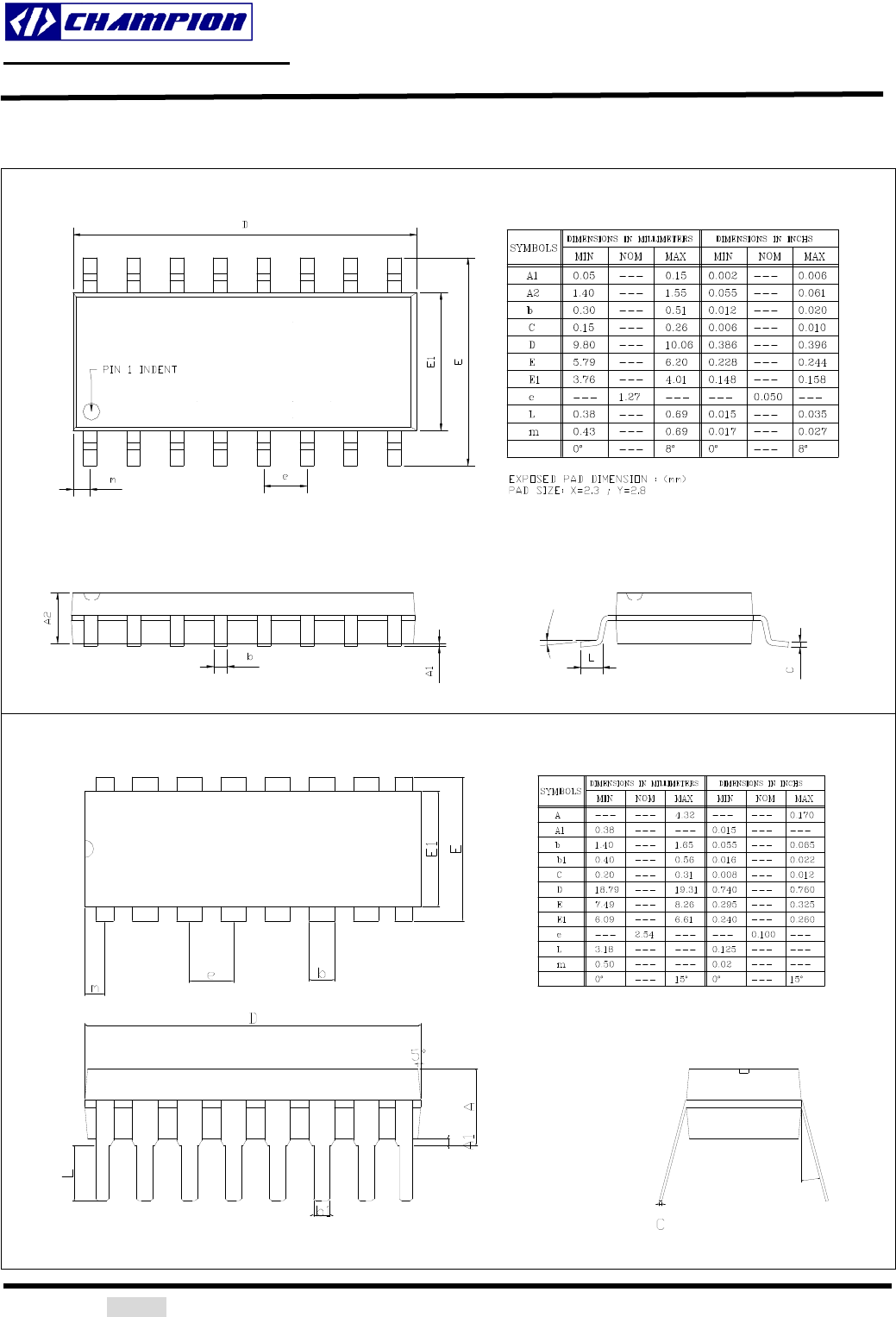
PACKAGE DIMENSION
16-PIN SOP (S16)
θ
θ
16-PIN PDIP (P16)
θ
PIN 1 ID
θ

CM6802A/B/AH/BH (Dynamic Soft PFC/Green PWM)
http://www.championmicro.com.tw EPA/80++ ZVS-Like PFC/PWM COMBO CONTROLLER
Design for High Efficient Power Supply at both Full Load and Light Load
2012/05/10 Rev. 1.5 Champion Microelectronic Corporation 25
IMPORTANT NOTICE
Champion Microelectronic Corporation (CMC) reserves the right to make changes to its products or to
discontinue any integrated circuit product or service without notice, and advises its customers to obtain
the latest version of relevant information to verify, before placing orders, that the information being relied
on is current.
A few applications using integrated circuit products may involve potential risks of death, personal injury,
or severe property or environmental damage. CMC integrated circuit products are not designed,
intended, authorized, or warranted to be suitable for use in life-support applications, devices or systems
or other critical applications. Use of CMC products in such applications is understood to be fully at the
risk of the customer. In order to minimize risks associated with the customer’s applications, the
customer should provide adequate design and operating safeguards.
HsinChu Headquarter Sales & Marketing
5F, No. 11, Park Avenue II,
Science-Based Industrial Park,
HsinChu City, Taiwan
21F., No. 96, Sec. 1, Sintai 5th Rd., Sijhih City,
Taipei County 22102,
Taiwan, R.O.C.
T E L : +886-3-567 9979 T E L : +886-2-2696 3558
FAX : +886-3-567 9909 F A X : +886-2-2696 3559
http://www.champion-micro.com