CR6848 Datasheet. Www.s Manuals.com. Chip Rail
User Manual: Datasheets CR6848S, CR6848T.
Open the PDF directly: View PDF ![]() .
.
Page Count: 15

Dec, 2006 V1.5 1/14
Chengdu Chip-Rail Tech.Co.Ltd. http://www.chiprail.com
CR6848
Novel Low Cost Green-Power PWM Controller
Features
z Low Cost, PWM&PFM&CRM
z Low Start-up Current (about 10µA)
z Low Operating Current (about 2mA)
z Current Mode Operation
z Under Voltage Lockout (UVLO)
z Built-in Synchronized Slope
Compensation
z Programmable PWM Frequency
z Leading edge Blanking on Sense input
z Constant output power limiting for
universal AC input
z Cycle-by-cycle current limiting
z Clamped gate output voltage 16.5V
z Over voltage protect 26.7V
z High-Voltage CMOS Process with ESD
z SOT-23-6L、SOP-8 & DIP-8 Pb-Free
Packaging
z Compatible with SG5701 & SG5848 &
LD7535 &OB22632/63
Applications
z Switching AC/DC Adaptor
z Battery Charger
z Open Frame Switching Power Supply
z 384X Replacement
General Description
The CR6848 is a highly integrated low cost
current mode PWM controller, which is ideal
for small power current mode of offline
AC-DC fly-back converter applications.
Making use of external resistors, the IC
changes the operating frequency and
automatically enters the PFM/CRM under
light-load/zero-load conditions. This can
minimize standby power consumption and
achieve green-power functions. With a very
low start-up current, the CR6848 could use
a large value start-up resistor (1.5Mohm).
Built-in synchronized slope compensation
enhances the stability of the system and
avoids sub-harmonic oscillation. Dynamic
peak limiting circuit minimizes output power
change caused by delay time of the system
over a universal AC input range. Leading
edge blanking circuit on current sense input
could remove the signal glitch due to
snubber circuit diode reverse recovery and
thus greatly reduces the external
component count and system cost in the
design. Pulse-by-pulse current limiting
ensures safe operation even during
short-circuit.
The CR6848 offers more protection like
OVP (Over Voltage Protection) and OCP
(Over current protection). The CR6848’s
output driver is clamped to maximum 16.5V
to protect the power MOSFET. Excellent
EMI performance is achieved soft switching
control at the totem pole gate driver output.
CR6848 is offered in SOT-23-6, SOP-8 and
DIP-8 packages.
CR6848
Dec, 2006 V1.5 2/14
Chengdu Chip-Rail Tech.Co.Ltd. http://www.chiprail.com
CR68XX Series
Part
Number PWM
Frequency Package Description
CR6848 External
Adjustable
DIP-8、SOP8
SOT-23-6L
PWM&PFM&CRM 、Current Mode 、Slope
Compensation Leading-edge Blanking 、Gate
Clamped、Over-voltage Protection、Over-current
Protection、 Soft Drive.
CR6850 External
Adjustable
DIP-8、SOP8
SOT-23-6L
With All Functions of CR6848 、Gate soft
Clamped
CR6851 External
Adjustable
DIP-8、SOP8
SOT-23-6L
With All Functions of CR6850、Frequency jitter、
Soft start、Sense Fault Protect、OLP、SCP、
OTP
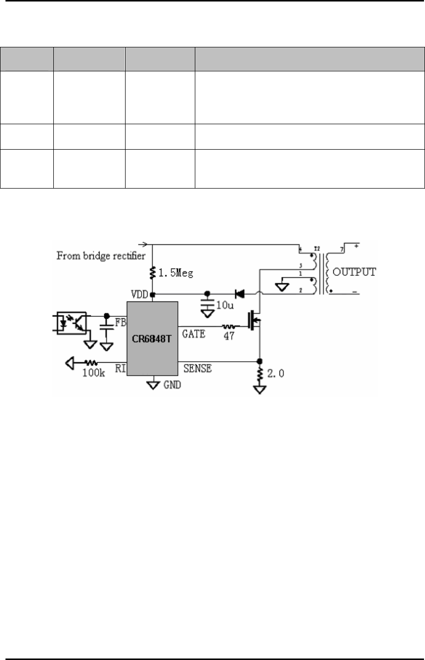
TYPICAL APPLICATION
CR6848
Dec, 2006 V1.5 3/14
Chengdu Chip-Rail Tech.Co.Ltd. http://www.chiprail.com
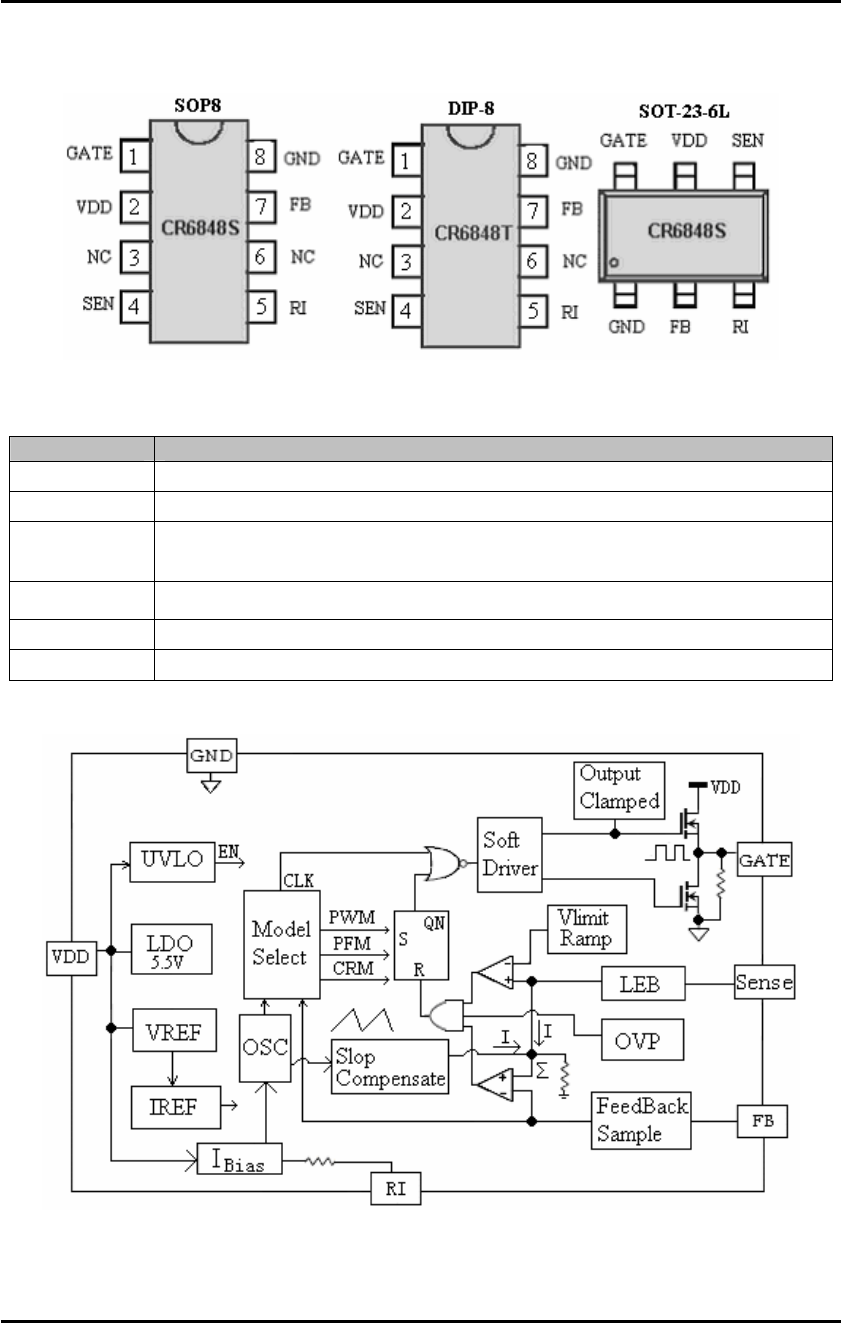
Pin Assignment
Pin Descriptions
Name Description
GND GND Pin
FB Analog Input. Voltage feedback pin (same as the COMP pin in UC384X),
RI This pin is to program the switching frequency. By connecting a resistor
to ground to set the switching frequency.
SEN Current sense pin, connect to sense the MOSFET current.
VDD Supply voltage pin.
GATE Gate output to drive the external power MOSFET.
Block Diagram
Simplified Internal Circuit Architecture

CR6848
Dec, 2006 V1.5 4/14
Chengdu Chip-Rail Tech.Co.Ltd. http://www.chiprail.com
Absolute Maximum Ratings
Symbol Parameter Rating Unit
VDD Supply voltage Pin Voltage 40 V
IOVP VDD OVP maximal enter current 20 mA
VFB Input Voltage to FB Pin -0.3 to 6V V
VSEN Input Voltage to SEN Pin -0.3 to 6V V
PD Power Dissipation 300 mW
ESD Capability, HBM Model 2000 V
ESD Capability, Machine Model 200 V
20 second
SOT-23-6L 220 ℃
TL
Lead Temperature
(Soldering) 10 second
DIP-8 260 ℃
TSTG Storage Temperature Range -55 to + 150 ℃
RECOMMENDED OPERATION CONDITION
Symbol Parameter Min ~ Max Unit
VDD VDD Supply Voltage 11~20 V
RI RI PIN Resistor Value 58~120 K ohm
TOA Operation Ambient Temperature -20~85 ℃
PO Output Power 0~60 W
FPWM Frequency of PWM 48~100 kHz

CR6848
Dec, 2006 V1.5 5/14
Chengdu Chip-Rail Tech.Co.Ltd.
http://www.chiprail.com
Electrical Characteristics (Ta=25°C unless otherwise noted, VDD = 15V.)
Symbol Parameter Conditions Min. Typ. Max. Unit
Supply Voltage (VDD Pin)
IST Startup Current 10 µA
VFB=0V 2.8 mA
VFB=3V 2.3 mA
ISS Operating Current
VFB=Open 1.46 mA
VDDON Turn-on Threshold Voltage 16.1 V
VDDOFF Turn-off Threshold Voltage 11.1 V
VDCLAMP VDD Clamp Voltage IVDD=20mA 26.7 V
Voltage Feedback (FB Pin)
IFB Short Circuit Current VFB=0V 2.8 mA
VFB Open Loop Voltage VFB=Open 4.8 V
IPFM Enter PFM, FB current 0.92 mA
ICRM Enter CRM, FB current 1.5 mA
Current Sensing (SEN Pin)
VTH_L Minimum Voltage Lever 0.83 0.87 V
VTH_H Maximum Voltage Lever 1.0 1.05 V
TPD Delay to Output 300 ns
RCS Input Impedance 50 KΩ
Oscillator (RI Pin)
FOSC Normal Frequency RI=100Kohm 53 58 63 KHz
FPFM PFM Frequency RI=100Kohm 11.6 KHZ
DCMAX Maximum Duty Cycle RI=100Kohm 75 %
ΔFTEMP Frequency Temp. Stability -30-85℃ 5 %
TBLANK Leading-Edge Blanking Time 300 nS
GATE Drive Output (GATE Pin)
VOL Output Low Level VDD=15V, IO=20mA 1 V
VOH Output High Level VDD=15V, IO=20mA 8 V
TR Rising Time CL=1000pF 450 ns
TF Falling Time CL=1000pF 130 ns
VGCLAMP Output Clamp Voltage VDD=20V 16.5 V
CR6848
Dec, 2006 V1.5 6/14
Chengdu Chip-Rail Tech.Co.Ltd.
http://www.chiprail.com
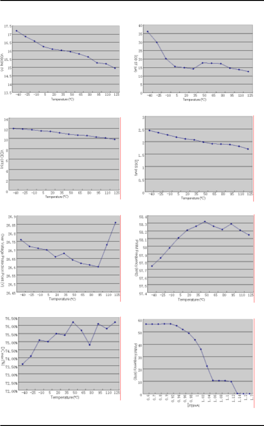
TYPICAL CHARACTERISTICS
VDD startup Current VS Temperature
VDD (OFF) VS Temperature
OVP VS Temperature
Duty cycle VS Temperature
VDD startup Current VS Temperature
VDD Operation Current VS Temperature
PWM frequency VS Temperature
FOSC VS FB Current
CR6848
Dec, 2006 V1.5 7/14
Chengdu Chip-Rail Tech.Co.Ltd.
http://www.chiprail.com
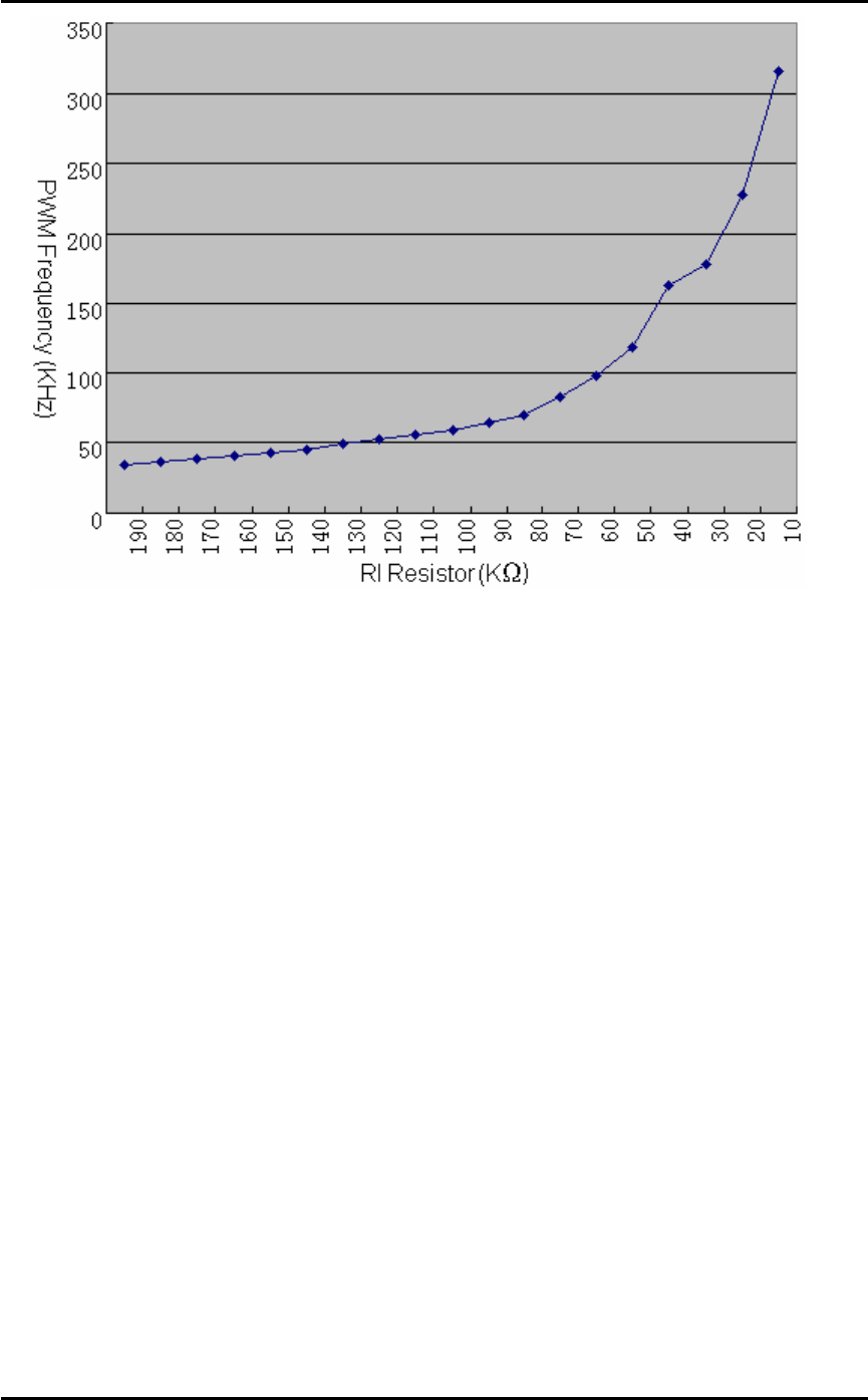
FOSC VS RI pin resistor
CR6848
Dec, 2006 V1.5 8/14
Chengdu Chip-Rail Tech.Co.Ltd. http://www.chiprail.com
OPERATION DESCRIPTION
Current Model
Compared to voltage model control,
current model control has a current
feedback loop. When the voltage of the
sense resistor peak current of the primary
winding reaches the internal setting value
VTH, comparator reverse, register reset and
power MOSFET cut-off. So that to detect
and modulate the peak current cycle by
cycle could control the output of the power
supply. The current feedback has a good
linear modulation rate and a fast input and
output dynamic impact avoid the pole that
the output filter inductance brings and the
second class system descends to first class
and so it widens the frequency range and
optimizes overload protection and short
circuit protection.
Startup Current and Under Voltage
Lockout
The startup current of CR6848 is set to be
very low so that a large value startup
resistor can therefore be used to minimize
the power loss. For AC to DC adaptor with
universal input range design, a 1.5 MΩ, 1/8
W startup resistor and a 10uF/25V VDD
hold capacitor could be used.
The turn-on and turn-off threshold of the
CR6848 is designed to 16.1V/11.1V. During
startup, the hold-up capacitor must be
charge to 16.1V through the startup resistor.
The hysteresis is implemented to prevent
the shutdown from the voltage dip during
startup.
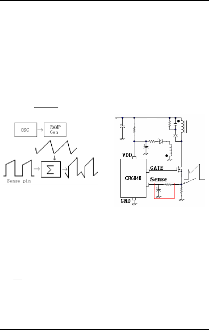
Internal Bias and OSC Operation
A resistor connected between RI pin and
GND pin set the internal constant current
source to charge or discharge the internal
fixed cap. The charge time and discharge
time determine the internal clock speed and
the switching frequency. Increasing the
resistance will reduce the value of the input
current and reduce the switching frequency.
The relationship between RI pin and PWM
switching frequency follows the below
equation within the RI allowed range.
)(
)(
5800 kHz
KRI
FOSC Ω
=
For example, a 100kΩ resistor RI could
generate a 50uA constant current and a
58kHz PWM switching frequency. The
suggested operating frequency range of
CR6848 is within 48KHz to 100KHz.
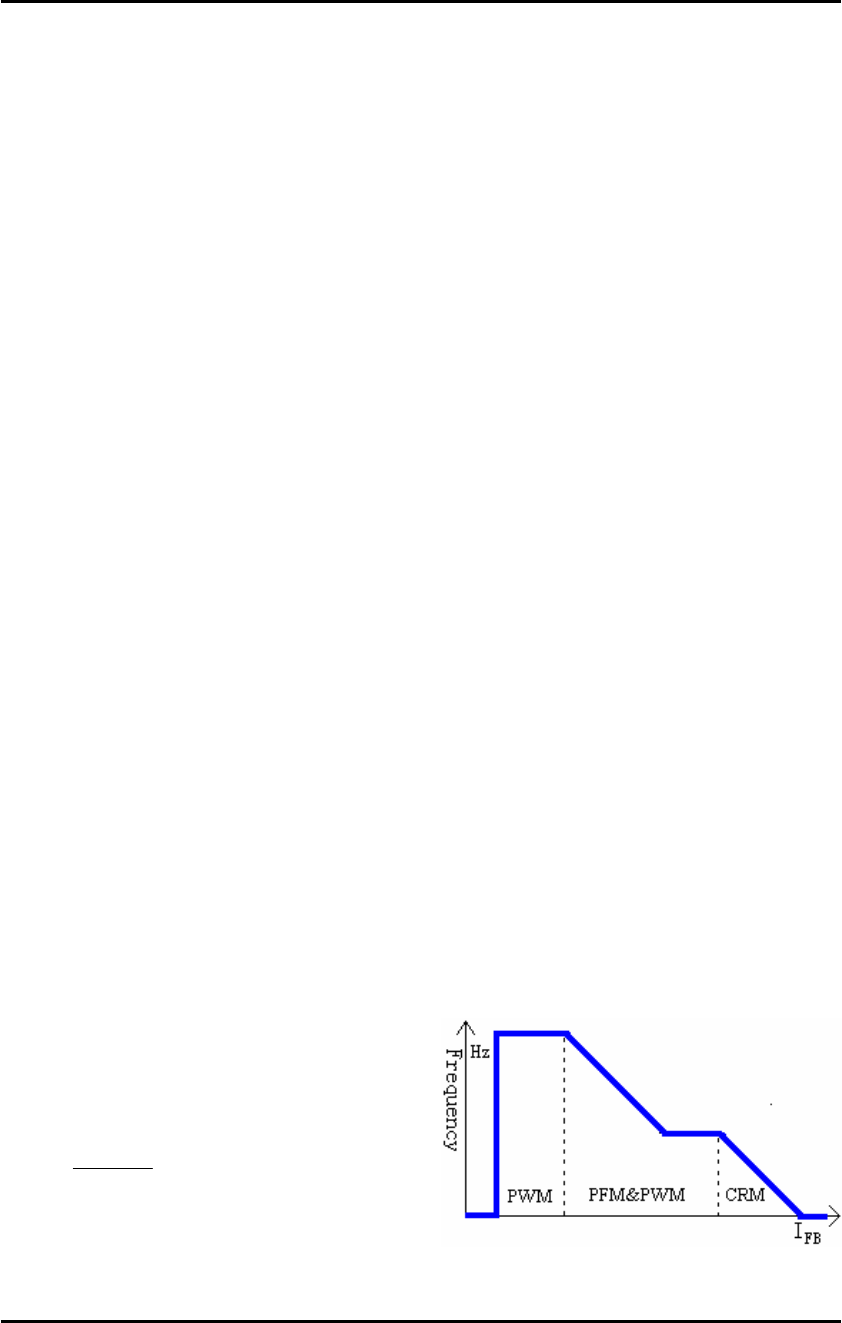
Green Power Operation
The power dissipation of switching mode
power supply is very important in zero load
or light load condition. The major dissipation
result from conduction loss、switching loss
and consume of the control circuit. However,
all of them related to the switching
frequency. There are many difference
topologies has been implemented in
different chip. The basic operation theory of
all these approaches intended to reduce the
switching frequency under light-load or
no-load condition.
CR6848`s green power function adapts
PWM、PFM and CRM combining modulation.
When RI resistor is 100k, the PWM
frequency is 58kHz in medium or heavy load
operation. Through modifying the pulse
width, CR6848 could control output voltage.
The current of FB pin increases when the
load is in light condition and the internal
mode controller enters PFM&PWM when
the feedback current is over 0.92mA. The
operation frequency of oscillator is to
descend gradually. The invariable frequency
of oscillator is 11.6kHz when the feedback
current is over 1.05mA. To decrease the
standby consumption of the power supply ,
Chip-Rail introduces the Cycle Reset Mode
technology;If the feedback current were
over 1.1mA, mode controller of CR6848
would reset internal register all the time and
cut off the gate pin, while the output voltage
is lower than the set value, it would set
register, gate pin operating again. Although
the frequency of the internal OSC is
invariable, the register would reset some
pulses so that the practical frequency is
decreased at the gate pin.
CR6848 Green-Power Function
CR6848
Dec, 2006 V1.5 9/14
Chengdu Chip-Rail Tech.Co.Ltd. http://www.chiprail.com
Internal Synchronized Slop
Compensation
Although there are more advantages of the
current mode control than conventional
voltage mode control, there are still several
drawbacks of peak-sensing current-mode
converter. Especially the open loop
instability when it operates in higher than
50% of the duty-cycle. CR6848 is introduced
an internal slope compensation adding
voltage ramp to the current sense input
voltage for PWM generation to solve this
problem. It improves the close loop stability
greatly at CCM, prevents the sub-harmonic
oscillation and thus reduces the output
ripple voltage.
DUTY
DUTY
DUTY
V
MAX
SLOP ×=×= 4389.033.0
Current Sensing & Dynamic peak
limiting
The current flowing by the power MOSFET
comes in to being a voltage VSENSE on the
sense pin cycle by cycle, which compares to
the internal reference voltage, controls the
reverse of the internal register, limits the
peak current IMAX of the primary of the
transformer. The energy 2
2
1
MAX
ILE ××=
deposited by the transformer. So adjusting
the RSENSE can set the Max output power of
the power supple mode. The current flowing
by the power MOSFET has an extra value
D
P
IN T
L
V
I×=∆ due to the system delay T
that the current detected from the sense pin
to power MOSFET cut off in the CR6848
(Among these, VIN is the primary winding
voltage of the transformer and LP is the
primary wind inductance. IN
V ranges from
85VAC to 264VAC. To guarantee the output
power is a constant for universal input AC
voltage, there is a dynamic peak limit circuit
to compensate the system delay T that the
system delay brings on.
Leading-edge Blanking (LEB)
Each time the power MOSFET is switched
on, a turn-on spike will inevitably occur at
the sense pin, which would disturb the
internal signal from the sampling of the
RSENSE. There is a 300n sec leading edge
blanking time built in to avoid the effect of
the turn-on spike and the power MOSFET
cannot be switched off during this time. So
that the conventional external RC filtering on
sense input is no longer required.
Over Voltage Protection (OVP)
There is a 26.7V over-voltage protection
circuit in the CR6848 to improve the
credibility and extend the life of the chip. The
GATE is to shutdown immediately when the
voltage of the VDD is over 26.7V and the
voltage of VDD is to descend rapidly.
Gate Driver & Soft Clamped
CR6848’ output designs a totem pole to
drive a periphery power MOSFET. The dead
time is introduced to minimize the transfixion
current when the output is drove. The
NMOS is shut off when the other NMOS is
turned on. The clamp technology is
introduced to protect the periphery power
MOSFET from breaking down.
CR6848
Dec, 2006 V1.5 10/14
Chengdu Chip-Rail Tech.Co.Ltd. http://www.chiprail.com
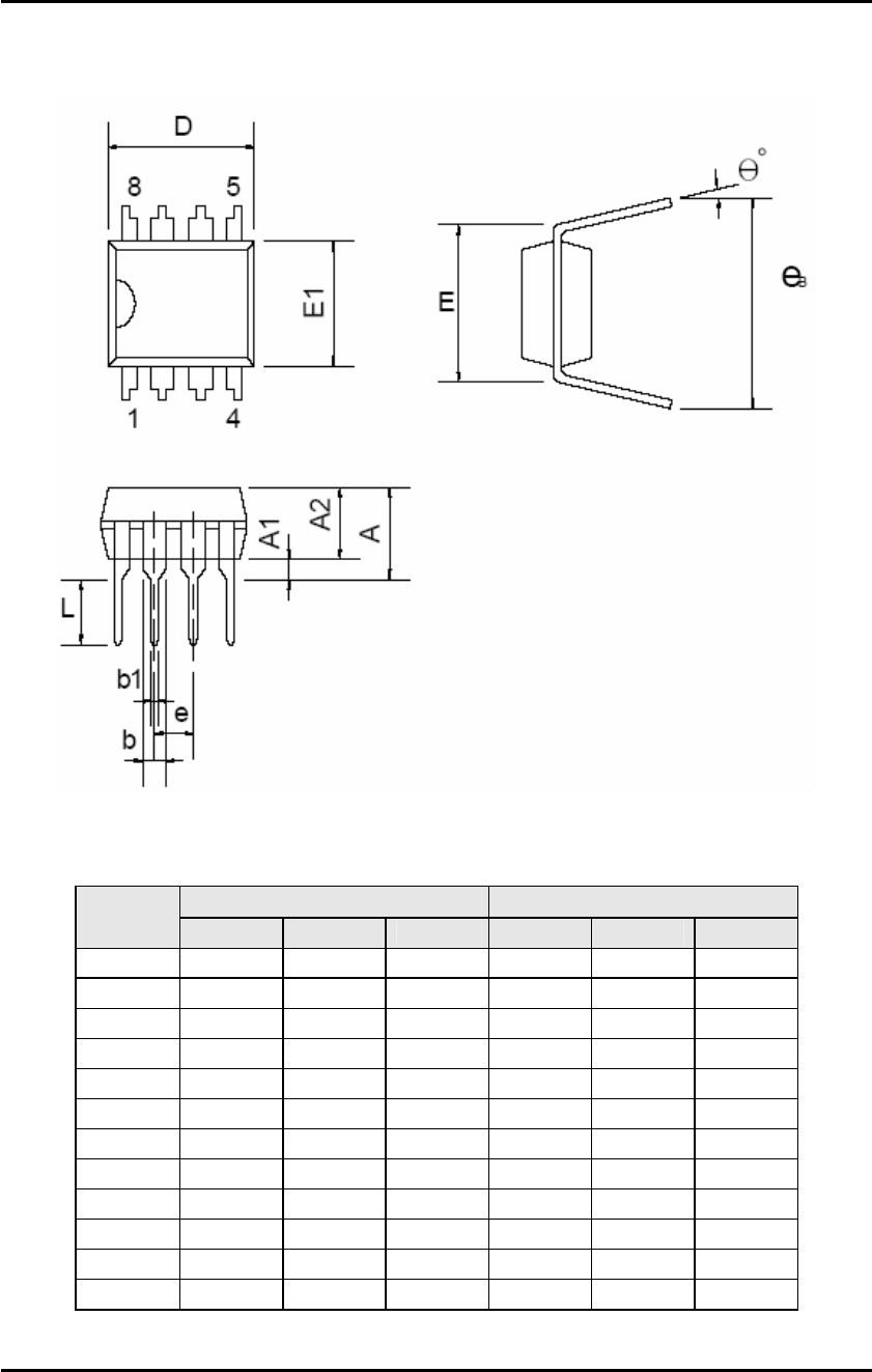
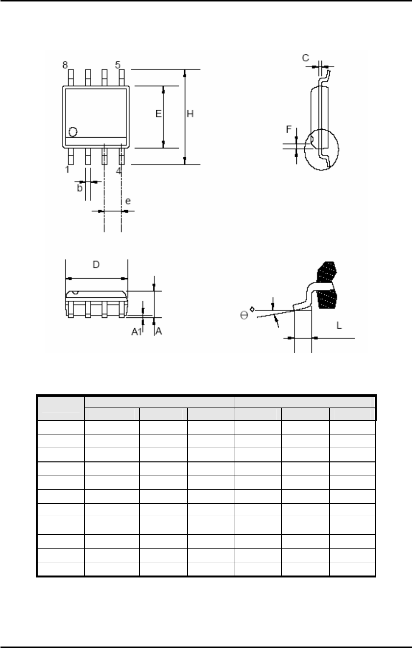
PACKAGE DEMENSIONS
DIP-8L
Dimensions
Millimeters Inches
Symbol Min. Typ. Max. Min. Typ. Max.
A
5.334
0.210
A1 0.381
0.015
A2 3.175 3.302 3.429 0.125 0.130 0.135
b 1.524
0.060
b1 0.457
0.018
D 9.017 9.271 10.160 0.355 0.365 0.400
E 7.620
0.300
E1 6.223 6.350 6.477 0.245 0.250 0.255
e 2.540
0.100
L 2.921 3.302 3.810 0.115 0.130 0.150
eB 8.509 9.017 9.525 0.335 0.355 0.375
θ˚ 0˚ 7˚ 15˚ 0˚ 7˚ 15˚
CR6848
Dec, 2006 V1.5 11/14
Chengdu Chip-Rail Tech.Co.Ltd. http://www.chiprail.com
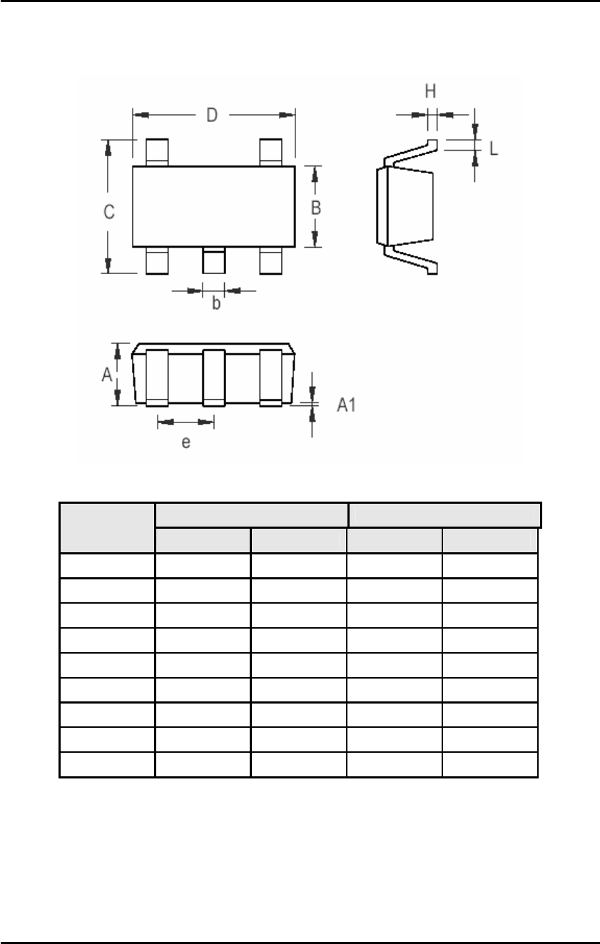
SOT-23-6L
Dimensions In Millimeters Dimensions In Inches
Symbol Min Max Min Max
A 0.700 1.000 0.028 0.039
A1 0.000 0.100 0.000 0.004
B 1.397 1.803 0.055 0.071
b 0.300 0.559 0.012 0.022
C 2.591 3.000 0.102 0.118
D 2.692 3.099 0.106 0.122
e 0.838 1.041 0.033 0.041
H 0.080 0.254 0.003 0.010
L 0.300 0.610 0.012 0.024
CR6848
Dec, 2006 V1.5 12/14
Chengdu Chip-Rail Tech.Co.Ltd. http://www.chiprail.com
SOP-8L
Dimensions DISCLAIMERS
Millimeter Inch
Symbol Min. Typ. Max. Min. Typ. Max.
A 1.346 1.752 0.053 0.069
A1 0.101 0.254 0.004 0.010
b 0.406
0.016
c 0.203
0.008
D 4.648 4.978 0.183 0.196
E 3.810 3.987 0.150 0.157
e 1.016 1.270 1.524 0.040 0.050 0.060
F 0.381X45
°
0.015X45
°
H 5.791 6.197 0.228 0.244
L 0.406 1.270 0.016 0.050
θ˚ 0° 8° 0° 8°
CR6848
Dec, 2006 V1.5 13/14
Chengdu Chip-Rail Tech.Co.Ltd. http://www.chiprail.com
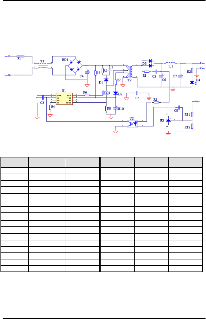
REFERENCE CIRCUIT 1
CR6848 drives a periphery Power MOSFET.
5V/6A 30W Power Supply
Quantity Part Number Description Quantity Part Number Description
1 C1 102/1000V
1 F1 0.25A
1 C2 103/1000V
1 L1 10uH
1 C3 104
1 R1 20R
1 C4 33uF/400V
2 R2、R3 1K
1 C5 223/1000V
1 R4 100K
1 C7 103/1000V
1 R5 100K/0.5W
1 C8 102/100V
1 R6 47R
2 C6、C7 1000 uF/25V 1 R7 1.5M
1 C8 104
1 R8 0R51
1 BD1 KBL406
1 R9 20R
1 D1 FR107
2 R11、R12 3.3K
1 D2 1N4007
1 U1 CR6848
1 D3 Y2010D
1 U2 PC817
1 D4 LED
1 U3 TL431
1 T1 20mH
1 Q1 2N60
1 T2 EI-22
Notice: Q1 is a Power MOSFET
CR6848
Dec, 2006 V1.5 14/14
Chengdu Chip-Rail Tech.Co.Ltd. http://www.chiprail.com
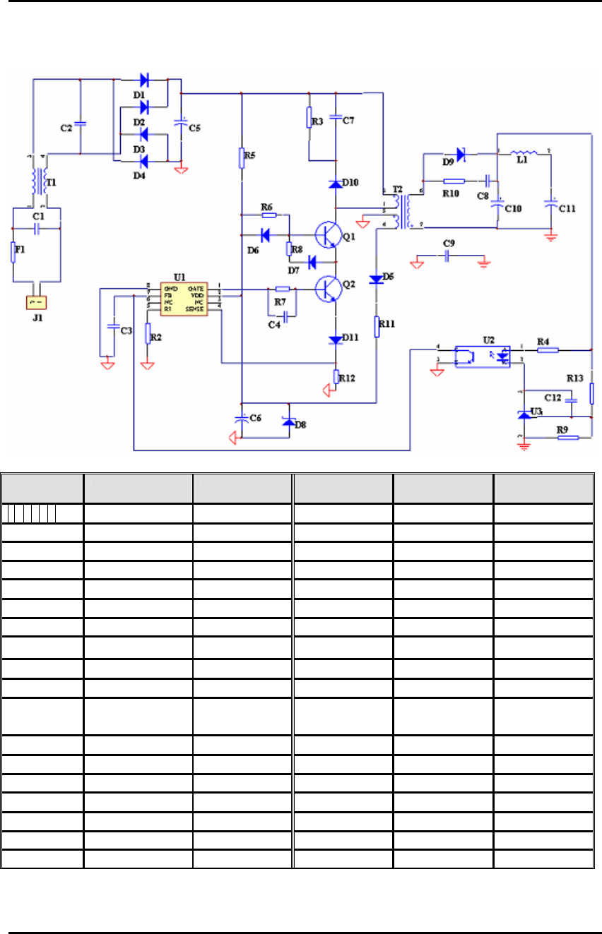
REFERENCE CIRCUIT 2
CR6848 drives a periphery Power BJT(5V/3A 15W Power Supply)
Notice: Q1 is a Power BJT
Quantity Part Number Description Quantity Part Number Description
2 C1、C2 104/400V 1 R2 100K
1 C3 472
1 R3 100K/0.5W
1 C4 102
1 R4 1K
1 C5 33uF/400V
1 R5 1.5M
1 C6 10uF/50V
2 R6、R7 220R/1W
1 C7 103/1000V
1 R8 220R
1 C8 102/100V
1 R9 20K
1 C9 223/1000V
2 R10、R11 20R
2 C10、C11 220uF/16V 1 R12 1R2/1W
1 C12 1.0uF/16V
1 R13 20K
5 D1、D2、D3、
D4、D5 1N4007
1 R14 2K2
2 D6、D7 1N4148 1 U1 CR6848
1 D8 18V
1 U2 PC817
1 D9 SB560
1 U3 TL431
2 D10、D11 FR107 1 U4 LM358
1 T1 20mH
1 Q1 13003
1 T2 EI-22
1 Q2 9013
1 F1 0.25A
Quantity Part Number Description Quantity Part Number Description
2 C1、C2 104/400V 1 R2 100K