View / The Volume D06uservol1
User Manual: View / the Volume DL06 User Manual
Open the PDF directly: View PDF ![]() .
.
Page Count: 532 [warning: Documents this large are best viewed by clicking the View PDF Link!]

DL06 Micro PLC User Manual
Volume 1 of 2
Manual Number: D0-06USER-M

DL06 Micro PLC User Manual, 3rd Edition, Rev. D

~ WARNING ~
Thank you for purchasing automation equipment from Automationdirect.com®, doing business as,
AutomationDirect. We want your new automation equipment to operate safely. Anyone who installs or
uses this equipment should read this publication (and any other relevant publications) before installing or
operating the equipment.
To minimize the risk of potential safety problems, you should follow all applicable local and national
codes that regulate the installation and operation of your equipment. These codes vary from area to area
and usually change with time. It is your responsibility to determine which codes should be followed, and
to verify that the equipment, installation, and operation is in compliance with the latest revision of these
codes.
At a minimum, you should follow all applicable sections of the National Fire Code, National Electrical
Code, and the codes of the National Electrical Manufacturer’s Association (NEMA). There may be local
regulatory or government offices that can also help determine which codes and standards are necessary for
safe installation and operation.
Equipment damage or serious injury to personnel can result from the failure to follow all applicable
codes and standards. We do not guarantee the products described in this publication are suitable for
your particular application, nor do we assume any responsibility for your product design, installation, or
operation.
Our products are not fault-tolerant and are not designed, manufactured or intended for use or resale as
on-line control equipment in hazardous environments requiring fail-safe performance, such as in the
operation of nuclear facilities, aircraft navigation or communication systems, air traffic control, direct life
support machines, or weapons systems, in which the failure of the product could lead directly to death,
personal injury, or severe physical or environmental damage (“High Risk Activities”). AutomationDirect
specifically disclaims any expressed or implied warranty of fitness for High Risk Activities.
For additional warranty and safety information, see the Terms and Conditions section of our catalog.
If you have any questions concerning the installation or operation of this equipment, or if you need
additional information, please call us at 770-844-4200.
This publication is based on information that was available at the time it was printed. At
AutomationDirect we constantly strive to improve our products and services, so we reserve the right to
make changes to the products and/or publications at any time without notice and without any obligation.
This publication may also discuss features that may not be available in certain revisions of the product.
Trademarks
This publication may contain references to products produced and/or offered by other companies. The
product and company names may be trademarked and are the sole property of their respective owners.
AutomationDirect disclaims any proprietary interest in the marks and names of others.
Copyright 2016, Automationdirect.com Incorporated
All Rights Reserved
No part of this manual shall be copied, reproduced, or transmitted in any way without the prior, written
consent of Automationdirect.com Incorporated. AutomationDirect retains the exclusive rights to all
information included in this document.

~AVERTISSEMENT ~
Nous vous remercions d’avoir acheté l’équipement d’automatisation de Automationdirect.comMC, en faisant des
affaires comme, AutomationDirect. Nous tenons à ce que votre nouvel équipement d’automatisation fonctionne en
toute sécurité. Toute personne qui installe ou utilise cet équipement doit lire la présente publication (et toutes les
autres publications pertinentes) avant de l’installer ou de l’utiliser.
Afin de réduire au minimum le risque d’éventuels problèmes de sécurité, vous devez respecter tous les codes locaux
et nationaux applicables régissant l’installation et le fonctionnement de votre équipement. Ces codes diffèrent d’une
région à l’autre et, habituellement, évoluent au fil du temps. Il vous incombe de déterminer les codes à respecter et
de vous assurer que l’équipement, l’installation et le fonctionnement sont conformes aux exigences de la version la
plus récente de ces codes.
Vous devez, à tout le moins, respecter toutes les sections applicables du Code national de prévention des incendies,
du Code national de l’électricité et des codes de la National Electrical Manufacturer’s Association (NEMA). Des
organismes de réglementation ou des services gouvernementaux locaux peuvent également vous aider à déterminer
les codes ainsi que les normes à respecter pour assurer une installation et un fonctionnement sûrs.
L’omission de respecter la totalité des codes et des normes applicables peut entraîner des dommages à l’équipement
ou causer de graves blessures au personnel. Nous ne garantissons pas que les produits décrits dans cette publication
conviennent à votre application particulière et nous n’assumons aucune responsabilité à l’égard de la conception, de
l’installation ou du fonctionnement de votre produit.
Nos produits ne sont pas insensibles aux défaillances et ne sont ni conçus ni fabriqués pour l’utilisation ou la revente
en tant qu’équipement de commande en ligne dans des environnements dangereux nécessitant une sécurité absolue,
par exemple, l’exploitation d’installations nucléaires, les systèmes de navigation aérienne ou de communication, le
contrôle de la circulation aérienne, les équipements de survie ou les systèmes d’armes, pour lesquels la défaillance du
produit peut provoquer la mort, des blessures corporelles ou de graves dommages matériels ou environnementaux
(«activités à risque élevé»). La société AutomationDirect nie toute garantie expresse ou implicite d’aptitude à
l’emploi en ce qui a trait aux activités à risque élevé.
Pour des renseignements additionnels touchant la garantie et la sécurité, veuillez consulter la section Modalités et
conditions de notre documentation. Si vous avez des questions au sujet de l’installation ou du fonctionnement de cet
équipement, ou encore si vous avez besoin de renseignements supplémentaires, n’hésitez pas à nous téléphoner au
770-844-4200.
Cette publication s’appuie sur l’information qui était disponible au moment de l’impression. À la société
AutomationDirect, nous nous efforçons constamment d’améliorer nos produits et services. C’est pourquoi nous
nous réservons le droit d’apporter des modifications aux produits ou aux publications en tout temps, sans préavis ni
quelque obligation que ce soit. La présente publication peut aussi porter sur des caractéristiques susceptibles de ne
pas être offertes dans certaines versions révisées du produit.
Marques de commerce
La présente publication peut contenir des références à des produits fabriqués ou offerts par d’autres entreprises. Les
désignations des produits et des entreprises peuvent être des marques de commerce et appartiennent exclusivement à
leurs propriétaires respectifs. AutomationDirect nie tout intérêt dans les autres marques et désignations.
Copyright 2016, Automationdirect.com Incorporated
Tous droits réservés
Nulle partie de ce manuel ne doit être copiée, reproduite ou transmise de quelque façon que ce soit sans le
consentement préalable écrit de la société Automationdirect.com Incorporated. AutomationDirect conserve les
droits exclusifs à l’égard de tous les renseignements contenus dans le présent document.
DL06 Micro PLc USER MANUAL
Please include the Manual Number and the Manual Issue, both shown below,
when communicating with Technical Support regarding this publication.
Manual Number: D0-06USER-M
Issue: 3rd Edition, Rev. D
Issue Date: 6/16
Publication History
Issue Date Description of Changes
First Edition 7/02 Original
Rev. A 10/02 Updated drawing images and made minor corrections.
Rev. B 6/03 Added new PLC and made numerous corrections.
2nd Edition 3/04 Added two appendices, removed discrete module data and made numerous
corrections.
3rd Edition 3/07
Corrected all tables, many corrections to Chapters 2, 3, 4, 5, 6, and 7; Chapter 3
(HSIO) was moved to the Appendices and Chapter 4 was divided into Chapters 3 &
4; added DS5 Intelligent Boxes to Chapter 5; added Ramp/Soak example to Chapter
8; Numbering Systems and Serial Communications were added to Appendices; many
minor corrections were made throughout manual.
Rev. A 5/07 Minor corrections and updates.
Rev. B 6/11 Updated Chapter 5 with current DirectSOFT dialog views, corrected number of
registers needed to use the print message instruction, removed fuses and corrected
I/O wiring drawings, and other minor corrections and updates.
Rev. C 2/13 Added H0-CTRIO2 references.
Minor corrections and updates.
Added transient suppression for inductive loads.
Rev. D 6/16 Corrections and updates.

DL06 Micro PLC User Manual
Notes

Table of ConTenTs
Chapter 1: Getting Started
Introduction ............................................................................................................... 1–2
The Purpose of this Manual ...................................................................................... 1–2
Supplemental Manuals ............................................................................................. 1–2
Technical Support ....................................................................................................1–2
Conventions Used ......................................................................................................1–3
Key Topics for Each Chapter .....................................................................................1–3
DL06 Micro PLC Overview .........................................................................................1–4
The DL06 PLC Features ............................................................................................1–4
DirectSOFT Programming for Windows™ ................................................................1–4
Handheld Programmer ............................................................................................. 1–5
I/O Quick Selection Guide ......................................................................................... 1–5
Quick Start .................................................................................................................1–6
Steps to Designing a Successful System .................................................................1–10
Questions and Answers about DL06 Micro PLCs ....................................................1–12
Chapter 2: Installation, Wiring, and Specifications
Safety Guidelines .......................................................................................................2–2
Plan for Safety ..........................................................................................................2–2
Three Levels of Protection ........................................................................................2–3
Emergency Stops ......................................................................................................2–3
Emergency Power Disconnect ..................................................................................2–4
Orderly System Shutdown ........................................................................................2–4
Class 1, Division 2 Approval .....................................................................................2–4
Orientation to DL06 Front Panel ..............................................................................2–5
Terminal Block Removal ...........................................................................................2–6
Mounting Guidelines ................................................................................................. 2–7

DL06 Micro PLC User Manual, 3rd Edition, Rev. D
ii
Table of Contents
Unit Dimensions .......................................................................................................2–7
Enclosures ................................................................................................................2–7
Panel Layout & Clearances .......................................................................................2–8
Using Mounting Rails ...............................................................................................2–9
Environmental Specifications ..................................................................................2–10
Agency Approvals ...................................................................................................2–10
Marine Use .............................................................................................................2–10
Wiring Guidelines ....................................................................................................2–11
External Power Source ............................................................................................2–12
Planning the Wiring Routes ....................................................................................2–12
Fuse Protection for Input and Output Circuits ........................................................2–13
I/O Point Numbering .............................................................................................2–13
System Wiring Strategies ........................................................................................2–14
PLC Isolation Boundaries ........................................................................................2–14
Connecting Operator Interface Devices .................................................................. 2–15
Connecting Programming Devices .........................................................................2–15
Sinking / Sourcing Concepts ..................................................................................2–16
I/O “Common” Terminal Concepts ........................................................................2–17
Connecting DC I/O to “Solid State” Field Devices ..................................................2–18
Solid State Input Sensors ........................................................................................ 2–18
Solid State Output Loads ........................................................................................2–18
Relay Output Wiring Methods ................................................................................ 2–20
Relay Outputs-Transient Suppression For Inductive Loads in a Control System .......2–21
Prolonging Relay Contact Life ................................................................................2–26
DC Input Wiring Methods ...................................................................................... 2–27
DC Output Wiring Methods ................................................................................... 2–28
High-Speed I/O Wiring Methods ............................................................................ 2–29
Wiring Diagrams and Specifications ....................................................................... 2–30
D0–06AA I/O Wiring Diagram ................................................................................ 2–30
D0–06AR I/O Wiring Diagram ................................................................................2–32
D0–06DA I/O Wiring Diagram ...............................................................................2–34
D0–06DD1 I/O Wiring Diagram ............................................................................. 2–36
D0–06DD2 I/O Wiring Diagram ............................................................................. 2–38
D0–06DR I/O Wiring Diagram ................................................................................2–40
D0–06DD1–D I/O Wiring Diagram .........................................................................2–42
D0–06DD2–D I/O Wiring Diagram .........................................................................2–44
D0–06DR–D I/O Wiring Diagram ...........................................................................2–46

DL06 Micro PLC User Manual, 3rd Edition, Rev. D iii
Table of Contents
Glossary of Specification Terms ..............................................................................2–48
Chapter 3: CPU Specifications and Operation
Overview 3–2
DL06 CPU Features ..................................................................................................3–2
CPU Specifications .....................................................................................................3–3
CPU Hardware Setup .................................................................................................3–4
Communication Port Pinout Diagrams .....................................................................3–4
Connecting the Programming Devices ..................................................................... 3–5
CPU Setup Information ............................................................................................3–5
Status Indicators .......................................................................................................3–6
Mode Switch Functions ............................................................................................ 3–6
Changing Modes in the DL06 PLC ...........................................................................3–7
Mode of Operation at Power-up ..............................................................................3–7
Using Battery Backup ................................................................................................3–8
Battery Backup .........................................................................................................3–8
Auxiliary Functions ...................................................................................................3–9
Clearing an Existing Program ...................................................................................3–9
Initializing System Memory ......................................................................................3–9
Setting Retentive Memory Ranges .......................................................................... 3–10
Using a Password ...................................................................................................3–11
CPU Operation .........................................................................................................3–12
CPU Operating System ...........................................................................................3–12
Program Mode ....................................................................................................... 3–13
Run Mode ..............................................................................................................3–13
Read Inputs ............................................................................................................3–14
Service Peripherals and Force I/O ...........................................................................3–14
CPU Bus Communication .......................................................................................3–15
Update Clock, Special Relays and Special Registers .................................................3–15
Solve Application Program .....................................................................................3–16
Solve PID Loop Equations .......................................................................................3–16
Write Outputs ........................................................................................................3–16
Write Outputs to Specialty I/O ...............................................................................3–16
Diagnostics .............................................................................................................3–17
I/O Response Time ..................................................................................................3–17
Is Timing Important for Your Application? ..............................................................3–17

DL06 Micro PLC User Manual, 3rd Edition, Rev. D
iv
Table of Contents
Normal Minimum I/O Response ............................................................................. 3–18
Normal Maximum I/O Response ............................................................................3–18
Improving Response Time ......................................................................................3–19
CPU Scan Time Considerations ...............................................................................3–20
Reading Inputs .......................................................................................................3–20
Writing Outputs .....................................................................................................3–20
Service Peripherals ..................................................................................................3–21
CPU Bus Communication .......................................................................................3–21
Update Clock/Calendar, Special Relays, Special Registers .......................................3–21
Application Program Execution ..............................................................................3–22
PLC Numbering Systems ........................................................................................ 3–23
PLC Resources ........................................................................................................3–23
V–Memory .............................................................................................................3–24
Binary-Coded Decimal Numbers ............................................................................3–24
Hexadecimal Numbers ...........................................................................................3–24
Memory Map ...........................................................................................................3–25
Octal Numbering System .......................................................................................3–25
Discrete and Word Locations ..................................................................................3–25
V-memory Locations for Discrete Memory Areas ....................................................3–25
Input Points (X Data Type) ..................................................................................... 3–26
Output Points (Y Data Type) ..................................................................................3–26
Control Relays (C Data Type) .................................................................................3–26
Timers and Timer Status Bits (T Data Type) ............................................................3–26
Timer Current Values (V Data Type) .......................................................................3–27
Counters and Counter Status Bits (CT Data type) ...................................................3–27
Counter Current Values (V Data Type) ...................................................................3–27
Word Memory (V Data Type) .................................................................................3–28
Stages (S Data type) ...............................................................................................3–28
Special Relays (SP Data Type) ................................................................................. 3–28
DL06 System V-memory ..........................................................................................3–29
System Parameters and Default Data Locations (V Data Type) ...............................3–29
DL06 Aliases ............................................................................................................. 3–31
DL06 Memory Map ..................................................................................................3–32
X Input/Y Output Bit Map ......................................................................................3–33
Stage Control/Status Bit Map ................................................................................. 3–34
Control Relay Bit Map .............................................................................................3–36

DL06 Micro PLC User Manual, 3rd Edition, Rev. D v
Table of Contents
Timer Status Bit Map ...............................................................................................3–38
Counter Status Bit Map ........................................................................................... 3–38
GX and GY I/O Bit Map ..........................................................................................3–39
Chapter 4: System Design and Configuration
DL06 System Design Strategies ................................................................................4–2
I/O System Configurations .......................................................................................4–2
Networking Configurations ......................................................................................4–2
Module Placement .....................................................................................................4–3
Slot Numbering........................................................................................................4–3
Automatic I/O Configuration ....................................................................................4–4
Manual I/O Configuration ........................................................................................4–4
Power Budgeting ....................................................................................................... 4–5
Power supplied .......................................................................................................4–5
Power required by base unit ...................................................................................4–5
Power required by option cards ..............................................................................4–5
Configuring the DL06’s Comm Ports ........................................................................4–7
DL06 Port Specifications ...........................................................................................4–7
DL06 Port Pinouts ....................................................................................................4–7
Choosing a Network Specification ............................................................................4–8
RS-232 Network ....................................................................................................... 4–8
RS-422 Network ....................................................................................................... 4–8
RS-485 Network ....................................................................................................... 4–8
Connecting to MODBUS and DirectNET Networks ..................................................4–9
MODBUS Port Configuration ....................................................................................4–9
DirectNET Port Configuration .................................................................................4–10
Non–Sequence Protocol (ASCII In/Out and PRINT) ............................................... 4–11
Non-Sequence Port Configuration ..........................................................................4–11
Network Slave Operation ........................................................................................ 4–12
MODBUS Function Codes Supported ..................................................................... 4–12
Determining the MODBUS Address ........................................................................4–12
If Your Host Software Requires the Data Type and Address ....................................4–13
Example 1: V2100 .................................................................................................. 4–14
Example 2: Y20 ......................................................................................................4–14
Example 3: T10 Current Value ................................................................................4–14

DL06 Micro PLC User Manual, 3rd Edition, Rev. D
vi
Table of Contents
Example 4: C54 ......................................................................................................4–14
If Your MODBUS Host Software Requires an Address ONLY ...................................4–15
Example 1: V2100 584/984 Mode .........................................................................4–16
Example 2: Y20 584/984 Mode .............................................................................4–16
Example 3: T10 Current Value 484 Mode ..............................................................4–17
Example 4: C54 584/984 Mode ............................................................................. 4–17
Network Master Operation .....................................................................................4–17
Step 1: Identify Master Port # and Slave #..............................................................4–18
Step 2: Load Number of Bytes to Transfer ..............................................................4–18
Step 3: Specify Master Memory Area ......................................................................4–19
Step 4: Specify Slave Memory Area ........................................................................4–20
Communications from a Ladder Program ...............................................................4–21
Multiple Read and Write Interlocks ......................................................................... 4–21
Network Master Operation (using MRX and MWX Instructions) .........................4–22
MODBUS Function Codes Supported ..................................................................... 4–22
MODBUS Read from Network(MRX) ......................................................................4–23
MRX Slave Memory Address ...................................................................................4–24
MRX Master Memory Addresses ............................................................................. 4–24
MRX Number of Elements ...................................................................................... 4–24
MRX Exception Response Buffer .............................................................................4–24
MODBUS Write to Network (MWX) .......................................................................4–25
MWX Slave Memory Address .................................................................................4–26
MWX Master Memory Addresses ............................................................................4–26
MWX Number of Elements .....................................................................................4–26
MWX Exception Response Buffer ............................................................................4–26
MRX/MWX Example in DirectSOFT ........................................................................4–27
Multiple Read and Write Interlocks ......................................................................... 4–27
Chapter 5: Standard RLL Instructions
Introduction ............................................................................................................... 5–2
Using Boolean Instructions .......................................................................................5–5
END Statement ........................................................................................................5–5
Simple Rungs ...........................................................................................................5–5
Normally Closed Contact .........................................................................................5–6
Contacts in Series ..................................................................................................... 5–6
Midline Outputs ....................................................................................................... 5–6

DL06 Micro PLC User Manual, 3rd Edition, Rev. D vii
Table of Contents
Parallel Elements .......................................................................................................5–7
Joining Series Branches in Parallel ............................................................................. 5–7
Joining Parallel Branches in Series ............................................................................. 5–7
Combination Networks ............................................................................................5–7
Comparative Boolean ...............................................................................................5–8
Boolean Stack ...........................................................................................................5–8
Immediate Boolean ..................................................................................................5–9
Boolean Instructions ...............................................................................................5–10
Comparative Boolean ..............................................................................................5–26
Immediate Instructions ...........................................................................................5–32
Timer, Counter and Shift Register Instructions ......................................................5–39
Using Timers ..........................................................................................................5–39
Timer Example Using Discrete Status Bits ...............................................................5–41
Timer Example Using Comparative Contacts .......................................................... 5–41
Accumulating Timer Example using Discrete Status Bits .........................................5–43
Accumulator Timer Example Using Comparative Contacts .....................................5–43
Using Counters.......................................................................................................5–44
Counter Example Using Discrete Status Bits ...........................................................5–46
Counter Example Using Comparative Contacts ......................................................5–46
Stage Counter Example Using Discrete Status Bits ..................................................5–48
Stage Counter Example Using Comparative Contacts ............................................5–48
Up / Down Counter Example Using Discrete Status Bits ......................................... 5–50
Up / Down Counter Example Using Comparative Contacts ....................................5–50
Accumulator/Stack Load and Output Data Instructions ........................................5–52
Using the Accumulator ...........................................................................................5–52
Copying Data to the Accumulator ..........................................................................5–52
Changing the Accumulator Data ............................................................................ 5–53
Using the Accumulator Stack ..................................................................................5–54
Using Pointers ........................................................................................................5–55
Logical Instructions (Accumulator) .........................................................................5–69
Math Instructions ....................................................................................................5–86
Transcendental Functions......................................................................................5–118
Bit Operation Instructions ..................................................................................... 5–120
Number Conversion Instructions (Accumulator) ..................................................5–127
Shuffle Digits Block Diagram ................................................................................5–139

DL06 Micro PLC User Manual, 3rd Edition, Rev. D
viii
Table of Contents
Table Instructions ..................................................................................................5–141
Copy Data From a Data Label Area to V-memory .................................................5–143
Clock/Calendar Instructions .................................................................................. 5–171
CPU Control Instructions .......................................................................................5–173
Program Control Instructions ...............................................................................5–175
Interrupt Instructions ............................................................................................5–183
Message Instructions ............................................................................................. 5–186
Move Block Instruction (MOVBLK) .......................................................................5–189
Copy Data From a Data Label Area to V-memory .................................................5–189
Intelligent I/O Instructions ....................................................................................5–194
Read from Intelligent Module (RD) .......................................................................5–194
Write to Intelligent Module (WT) .........................................................................5–195
Network Instructions ............................................................................................. 5–196
Direct Text Entry ..................................................................................................5–200
Embedding date and/or time variables .................................................................5–201
Embedding V-memory data .................................................................................5–201
Data Format Suffixes for Embedded V-memory Data............................................5–202
Text Entry from V-memory ................................................................................... 5–203
MODBUS RTU Instructions ...................................................................................5–204
MRX Slave Address Ranges ...................................................................................5–205
MWX Slave Address Ranges..................................................................................5–208
MWX Master Memory Address Ranges .................................................................5–208
MWX Number of Elements ................................................................................5–208
MWX Exception Response Buffer ..........................................................................5–208
ASCII Instructions ..................................................................................................5–210
Reading ASCII Input Strings ..................................................................................5–210
Writing ASCII Output Strings ................................................................................5–210
Managing the ASCII Strings .................................................................................5–211
Intelligent Box (IBox) Instructions ........................................................................5–230
Chapter 6: Drum Instruction Programming
Introduction ............................................................................................................... 6–2

DL06 Micro PLC User Manual, 3rd Edition, Rev. D ix
Table of Contents
Purpose .................................................................................................................... 6–2
Drum Terminology ...................................................................................................6–2
Drum Chart Representation ......................................................................................6–3
Output Sequences ....................................................................................................6–3
Step Transitions ......................................................................................................... 6–4
Drum Instruction Types ............................................................................................ 6–4
Timer-Only Transitions .............................................................................................6–4
Timer and Event Transitions .....................................................................................6–5
Event-Only Transitions ..............................................................................................6–6
Counter Assignments ...............................................................................................6–6
Last Step Completion ............................................................................................... 6–7
Overview of Drum Operation ...................................................................................6–8
Drum Instruction Block Diagram ..............................................................................6–8
Powerup State of Drum Registers .............................................................................6–9
Drum Control Techniques .......................................................................................6–10
Drum Control Inputs .............................................................................................. 6–10
Self-Resetting Drum................................................................................................6–11
Initializing Drum Outputs ....................................................................................... 6–11
Using Complex Event Step Transitions ...................................................................6–11
Drum Instruction .....................................................................................................6–12
Timed Drum with Discrete Outputs (DRUM) ..........................................................6–12
Event Drum (EDRUM) ............................................................................................6–14
Handheld Programmer Drum Mnemonics ..............................................................6–16
Masked Event Drum with Discrete Outputs (MDRMD) ...........................................6–19
Masked Event Drum with Word Output (MDRMW) ...............................................6–21
Volume Two:
Table of ConTenTs

DL06 Micro PLC User Manual, 3rd Edition, Rev. D
x
Table of Contents
Chapter 7: RLLPLUS Stage Programming
Introduction to Stage Programming ........................................................................7–2
Overcoming “Stage Fright” ......................................................................................7–2
Learning to Draw State Transition Diagrams ........................................................... 7–3
Introduction to Process States ..................................................................................7–3
The Need for State Diagrams ...................................................................................7–3
A 2–State Process .....................................................................................................7–3
RLL Equivalent .......................................................................................................... 7–4
Stage Equivalent .......................................................................................................7–4
Let’s Compare .......................................................................................................... 7–5
Initial Stages .............................................................................................................7–5
What Stage Bits Do ..................................................................................................7–6
Stage Instruction Characteristics ...............................................................................7–6
Using the Stage Jump Instruction for State Transitions ..........................................7–7
Stage Jump, Set, and Reset Instructions ....................................................................7–7
Stage Program Example: Toggle On/Off Lamp Controller ......................................7–8
A 4–State Process .....................................................................................................7–8
Four Steps to Writing a Stage Program ...................................................................7–9
1. Write a Word Description of the application. .......................................................7–9
2. Draw the Block Diagram. .....................................................................................7–9
3. Draw the State Transition Diagram. .....................................................................7–9
4. Write the Stage Program. .....................................................................................7–9
Stage Program Example: A Garage Door Opener ..................................................7–10
Garage Door Opener Example ...............................................................................7–10
Draw the Block Diagram ........................................................................................7–10
Draw the State Diagram .........................................................................................7–11
Add Safety Light Feature ........................................................................................7–12
Modify the Block Diagram and State Diagram .......................................................7–12
Using a Timer Inside a Stage ..................................................................................7–13
Add Emergency Stop Feature .................................................................................7–14
Exclusive Transitions ............................................................................................... 7–14
Stage Program Design Considerations ................................................................... 7–15
Stage Program Organization ..................................................................................7–15
How Instructions Work Inside Stages ...................................................................... 7–16
Using a Stage as a Supervisory Process ................................................................... 7–17

DL06 Micro PLC User Manual, 3rd Edition, Rev. D xi
Table of Contents
Stage Counter ........................................................................................................ 7–17
Power Flow Transition Technique ........................................................................... 7–18
Stage View in DirectSOFT .......................................................................................7–18
Parallel Processing Concepts ...................................................................................7–19
Parallel Processes .................................................................................................... 7–19
Converging Processes .............................................................................................7–19
Convergence Stages (CV) .......................................................................................7–19
Convergence Jump (CVJMP) ...................................................................................7–20
Convergence Stage Guidelines ............................................................................... 7–20
RLLPLUS (Stage) Instructions ....................................................................................7–21
Stage (SG) ..............................................................................................................7–21
Initial Stage (ISG) ...................................................................................................7–22
Jump (JMP).............................................................................................................7–22
Not Jump (NJMP) ...................................................................................................7–22
Converge Stage (CV) and Converge Jump (CVJMP) ...............................................7–23
Block Call (BCALL) ..................................................................................................7–25
Block (BLK) .............................................................................................................7–25
Block End (BEND) ...................................................................................................7–25
Questions and Answers about Stage Programming ..............................................7–27
Chapter 8: PID Loop Operation
DL06 PID Control .......................................................................................................8–2
DL06 PID Control Features .......................................................................................8–2
Introduction to PID Control ...................................................................................... 8–4
What is PID Control? ................................................................................................ 8–4
Introducing DL06 PID Control ..................................................................................8–6
Process Control Definitions .......................................................................................8–8
PID Loop Operation ...................................................................................................8–9
Position Form of the PID Equation ............................................................................8–9
Reset Windup Protection ........................................................................................8–10
Freeze Bias .............................................................................................................8–11
Adjusting the Bias ...................................................................................................8–11
Step Bias Proportional to Step Change in SP ..........................................................8–12
Eliminating Proportional, Integral or Derivative Action ...........................................8–12
Velocity Form of the PID Equation ..........................................................................8–12

DL06 Micro PLC User Manual, 3rd Edition, Rev. D
xii
Table of Contents
Bumpless Transfer ..................................................................................................8–13
Loop Alarms ...........................................................................................................8–13
Loop Operating Modes ..........................................................................................8–14
Special Loop Calculations ....................................................................................... 8–14
Ten Steps to Successful Process Control.................................................................8–16
PID Loop Setup ........................................................................................................8–18
Some Things to Do and Know Before Starting .......................................................8–18
PID Error Flags ........................................................................................................8–18
Establishing the Loop Table Size and Location .......................................................8–18
Loop Table Word Definitions .................................................................................. 8–20
PID Mode Setting 1 Bit Descriptions (Addr + 00) ...................................................8–21
PID Mode Setting 2 Bit Descriptions (Addr + 01) ...................................................8–22
Mode/Alarm Monitoring Word (Addr + 06) ...........................................................8–23
Ramp/Soak Table Flags (Addr + 33) .......................................................................8–23
Ramp/Soak Table Location (Addr + 34) .................................................................. 8–24
Ramp/Soak Table Programming Error Flags (Addr + 35).........................................8–24
Configure the PID Loop..........................................................................................8–25
PID Loop Tuning ......................................................................................................8–40
Open-Loop Test .....................................................................................................8–40
Manual Tuning Procedure ......................................................................................8–41
Alternative Manual Tuning Procedures by Others ...................................................8–44
Tuning PID Controllers ........................................................................................... 8–44
Auto Tuning Procedure ..........................................................................................8–45
Use DirectSOFT 5 Data View with PID View ...........................................................8–49
Open a New Data View Window ............................................................................8–49
Open PID View .......................................................................................................8–50
Using the Special PID Features ...............................................................................8–53
How to Change Loop Modes .................................................................................8–53
Operator Panel Control of PID Modes ....................................................................8–54
PLC Modes Effect on Loop Modes ..........................................................................8–54
Loop Mode Override .............................................................................................. 8–54
PV Analog Filter ......................................................................................................8–55
Creating an Analog Filter in Ladder Logic ...............................................................8–56
Use the DirectSOFT Filter Intelligent Box Instructions ............................................. 8-57
FilterB Example ....................................................................................................... 8-57
Ramp/Soak Generator ............................................................................................. 8–58

DL06 Micro PLC User Manual, 3rd Edition, Rev. D xiii
Table of Contents
Introduction ...........................................................................................................8–58
Ramp/Soak Table ...................................................................................................8–59
Ramp/Soak Table Flags ...........................................................................................8–61
Ramp/Soak Generator Enable ................................................................................. 8–61
Ramp/Soak Controls ...............................................................................................8–61
Ramp/Soak Profile Monitoring ................................................................................8–62
Ramp/Soak Programming Errors .............................................................................8–62
Testing Your Ramp/Soak Profile ..............................................................................8–62
DirectSOFT Ramp/Soak Example ............................................................................. 8-63
Setup the Profile in PID Setup ................................................................................ 8-63
Program the Ramp/Soak Control in Relay Ladder ................................................... 8-63
Test the Profile ....................................................................................................... 8-64
Cascade Control .......................................................................................................8–65
Introduction ...........................................................................................................8–65
Cascaded Loops in the DL06 CPU ..........................................................................8–66
Tuning Cascaded Loops .........................................................................................8–67
Time-Proportioning Control ....................................................................................8–68
On/Off Control Program Example ..........................................................................8–69
Feedforward Control ...............................................................................................8–70
Feedforward Example ............................................................................................. 8–71
PID Example Program .............................................................................................8–72
Program Setup for the PID Loop ............................................................................8–72
Troubleshooting Tips...............................................................................................8–75
Glossary of PID Loop Terminology .........................................................................8–77
Bibliography ...........................................................................................................8–79
Chapter 9: Maintenance and Troubleshooting
Hardware System Maintenance ................................................................................9–2
Standard Maintenance .............................................................................................9–2
Diagnostics .................................................................................................................9–2
Diagnostics ...............................................................................................................9–2
Fatal Errors ...............................................................................................................9–2
Non-fatal Errors ........................................................................................................ 9–2
V-memory Error Code Locations ...............................................................................9–3
Special Relays (SP) Corresponding to Error Codes ....................................................9–3

DL06 Micro PLC User Manual, 3rd Edition, Rev. D
xiv
Table of Contents
DL06 Micro PLC Error Codes ....................................................................................9–4
Program Error Codes ................................................................................................ 9–5
CPU Indicators ...........................................................................................................9–6
PWR Indicator ..........................................................................................................9–6
RUN Indicator ..........................................................................................................9–7
CPU Indicator ...........................................................................................................9–7
Communications Problems .......................................................................................9–7
I/O Point Troubleshooting ........................................................................................9–8
Possible Causes ........................................................................................................9–8
Some Quick Steps ....................................................................................................9–8
Handheld Programmer Keystrokes Used to Test an Output Point .............................9–9
Noise Troubleshooting ............................................................................................9–10
Electrical Noise Problems ........................................................................................9–10
Reducing Electrical Noise........................................................................................9–10
Machine Startup and Program Troubleshooting ...................................................9–11
Syntax Check .........................................................................................................9–11
Special Instructions .................................................................................................9–12
Duplicate Reference Check ..................................................................................... 9–13
Run Time Edits .......................................................................................................9–14
Run Time Edit Example ..........................................................................................9–15
Forcing I/O Points ..................................................................................................9–16
Regular Forcing with Direct Access .........................................................................9–18
Bit Override Forcing ...............................................................................................9–19
Bit Override Indicators ............................................................................................9–19
Reset the PLC to Factory Defaults ........................................................................... 9–20
Chapter 10: LCD Display Panel
Introduction to the DL06 LCD Display Panel .........................................................10–2
Keypad .. 10–2
Snap-in installation ..................................................................................................10–3
Display Priority ........................................................................................................10–4
Menu Navigation ..................................................................................................... 10–5
Confirm PLC Type, Firmware Revision Level, Memory Usage, Etc. .......................10–6
Examining Option Slot Contents ............................................................................10–8

DL06 Micro PLC User Manual, 3rd Edition, Rev. D xv
Table of Contents
Menu 2, M2:SYSTEM CFG. ....................................................................................10–8
Monitoring and Changing Data Values ................................................................ 10–10
Menu 3, M3:MONITOR ......................................................................................10–10
Data Monitor .......................................................................................................10–10
V-memory values ..................................................................................................10–10
Pointer values ....................................................................................................... 10–12
Bit Monitor ............................................................................................................10–13
Bit status ..............................................................................................................10–13
Changing Date and Time ......................................................................................10–14
Menu 4, M4 : CALENDAR R/W .............................................................................10–14
Setting Password and Locking ..............................................................................10–17
Menu 5, M5 : PASSWORD R/W ............................................................................ 10–17
Reviewing Error History .........................................................................................10–20
Menu 6, M6 : ERR HISTORY .................................................................................10–20
Toggle Light and Beeper, Test Keys .....................................................................10–21
Menu 7, M7 : LCD TEST&SET ..............................................................................10–21
PLC Memory Information for the LCD Display Panel ..........................................10–22
Data Format Suffixes for Embedded V-memory Data............................................10–22
Reserved memory registers for the LCD Display Panel ..........................................10–23
V7742 bit definitions ............................................................................................ 10–24
Changing the Default Screen ................................................................................10–25
Example program for setting the default screen message .....................................10–25
DL06 LCD Display Panel Instruction (LCD) ...........................................................10–26
Source of message ...............................................................................................10–26
ASCII Character Codes .........................................................................................10–27
Example program: alarm with embedded date/time stamp .................................10–28
Example program: alarm with embedded V-memory data ...................................10–29
Example program: alarm text from V-memory with embedded V-memory data ..10–30
Appendix A: Auxiliary Functions
Introduction ...............................................................................................................A–2
Purpose of Auxiliary Functions .................................................................................. A–2
Accessing AUX Functions via DirectSOFT ..................................................................A–3
Accessing AUX Functions via the Handheld Programmer ..........................................A–3

DL06 Micro PLC User Manual, 3rd Edition, Rev. D
xvi
Table of Contents
AUX 2* — RLL Operations .........................................................................................A–4
AUX 21 Check Program ...........................................................................................A–4
AUX 22 Change Reference .......................................................................................A–4
AUX 23 Clear Ladder Range .....................................................................................A–4
AUX 24 Clear Ladders ..............................................................................................A–4
AUX 3* — V-memory Operations ..............................................................................A–4
AUX 31 Clear V-memory ..........................................................................................A–4
AUX 4* — I/O Configuration .....................................................................................A–5
AUX 41 Show I/O Configuration ..............................................................................A–5
AUX 5* — CPU Configuration ...................................................................................A–5
AUX 51 Modify Program Name ................................................................................A–5
AUX 53 Display Scan Time .......................................................................................A–5
AUX 54 Initialize Scratchpad ....................................................................................A–5
AUX 55 Set Watchdog Timer ...................................................................................A–5
AUX 56 CPU Network Address .................................................................................A–6
AUX 57 Set Retentive Ranges ...................................................................................A–6
AUX 58 Test Operations ...........................................................................................A–6
AUX 59 Bit Override ................................................................................................. A–7
AUX 5B Counter Interface Configuration .................................................................. A–7
AUX 5D Select PLC Scan Mode ................................................................................A–7
AUX 6* — Handheld Programmer Configuration ....................................................A–8
AUX 61 Show Revision Numbers .............................................................................. A–8
AUX 62 Beeper On/Off .............................................................................................A–8
AUX 65 Run Self Diagnostics ....................................................................................A–8
AUX 7* — EEPROM Operations .................................................................................A–8
Transferrable Memory Areas .....................................................................................A–8
AUX 71 CPU to HPP EEPROM ...................................................................................A–8
AUX 72 HPP EEPROM to CPU ...................................................................................A–9
AUX 73 Compare HPP EEPROM to CPU ...................................................................A–9
AUX 74 HPP EEPROM Blank Check ........................................................................... A–9
AUX 75 Erase HPP EEPROM ...................................................................................... A–9
AUX 76 Show EEPROM Type .................................................................................... A–9
AUX 8* — Password Operations ...............................................................................A–9
AUX 81 Modify Password .........................................................................................A–9
AUX 82 Unlock CPU ...............................................................................................A–10
AUX 83 Lock CPU...................................................................................................A–10

DL06 Micro PLC User Manual, 3rd Edition, Rev. D xvii
Table of Contents
Appenedix B: DL06 Error codes
DL06 Error Codes .......................................................................................................B–2
Appendix C: Instruction Execution Times
Introduction ...............................................................................................................C–2
V-Memory Data Registers .........................................................................................C–2
V-Memory Bit Registers ............................................................................................C–2
How to Read the Tables ...........................................................................................C–2
Instruction Execution Times ......................................................................................C–3
Boolean Instructions .................................................................................................C–3
Comparative Boolean Instructions ............................................................................C–4
Immediate Instructions ...........................................................................................C–11
Bit of Word Boolean Instructions ............................................................................C–12
Timer, Counter and Shift Register...........................................................................C–13
Accumulator Data Instructions ...............................................................................C–14
Logical Instructions.................................................................................................C–15
Math Instructions ...................................................................................................C–16
Differential Instructions ..........................................................................................C–19
Bit Instructions .......................................................................................................C–19
Number Conversion Instructions ............................................................................C–20
Table Instructions ...................................................................................................C–20
CPU Control Instructions ........................................................................................C–22
Program Control Instructions .................................................................................C–22
Interrupt Instructions ..............................................................................................C–22
Network Instructions ..............................................................................................C–22
Intelligent I/O Instructions ......................................................................................C–23
Message Instructions ..............................................................................................C–23
RLLPLUS Instructions .................................................................................................C–23
Drum Instructions ..................................................................................................C–23
Clock/Calendar Instructions ....................................................................................C–24
MODBUS Instructions .............................................................................................C–24
ASCII Instructions ...................................................................................................C–24
Appendix D: Special Relays
DL06 PLC Special Relays ........................................................................................... D–2
Startup and Real-Time Relays .................................................................................. D–2

DL06 Micro PLC User Manual, 3rd Edition, Rev. D
xviii
Table of Contents
CPU Status Relays .................................................................................................... D–2
System Monitoring .................................................................................................. D–3
Accumulator Status ................................................................................................. D–3
HSIO Input Status .................................................................................................... D–4
HSIO Pulse Output Relay ......................................................................................... D–4
Communication Monitoring Relay ........................................................................... D–4
Option Slot Communication Monitoring Relay ........................................................ D–4
Option Slot Special Relay ........................................................................................ D–4
Counter 1 Mode 10 Equal Relays ............................................................................ D–5
Counter 2 Mode 10 Equal Relays ............................................................................ D–6
Appendix E: High-speed Input and Pulse Output Features
Introduction ............................................................................................................... E–2
Built-in Motion Control Solution .............................................................................. E–2
Availability of HSIO Features ..................................................................................... E–2
Dedicated High- Speed I/O Circuit ........................................................................... E–3
Wiring Diagrams for Each HSIO Mode ..................................................................... E–3
Choosing the HSIO Operating Mode ........................................................................ E–4
Understanding the Six Modes .................................................................................. E–4
Default Mode ........................................................................................................... E–5
Configuring the HSIO Mode .................................................................................... E–6
Configuring Inputs X0 – X3 ...................................................................................... E–6
Mode 10: High-Speed Counter ................................................................................. E–7
Purpose .................................................................................................................... E–7
Functional Block Diagram ......................................................................................... E–7
Wiring Diagram ........................................................................................................ E–8
Interfacing to Counter Inputs ................................................................................... E–8
Setup for Mode 10 ................................................................................................... E–9
Presets and Special Relays ........................................................................................ E–9
Absolute and Incremental Presets ........................................................................... E–10
Preset Data Starting Location ................................................................................. E–11
Using Fewer than 24 Presets .................................................................................. E–11
Equal Relay Numbers ............................................................................................. E–12
Calculating Your Preset Values ................................................................................ E–13
X Input Configuration ............................................................................................ E–14
Writing Your Control Program ................................................................................ E–15
Program Example 1: Counter Without Presets ........................................................ E–16
Program Example 2: Counter With Presets ............................................................. E–18

DL06 Micro PLC User Manual, 3rd Edition, Rev. D xix
Table of Contents
Program Example 3: Counter With Preload ............................................................ E–21
Troubleshooting Guide for Mode 10 ...................................................................... E–23
Symptom: The counter does not count. ................................................................. E–23
Symptom: The counter counts but the presets do not function. ............................ E–23
Symptom: The counter counts up but will not reset. ............................................. E–23
Mode 20: Up/Down Counter .................................................................................. E–24
Purpose .................................................................................................................. E–24
Functional Block Diagram ....................................................................................... E–24
Quadrature Encoder Signals ................................................................................... E–25
Wiring Diagram ...................................................................................................... E–25
Interfacing to Encoder Outputs .............................................................................. E–26
Setup for Mode 20 ................................................................................................. E–27
Presets and Special Relays ...................................................................................... E–27
X Input Configuration ............................................................................................ E–28
Mode 20 Up/Down Counter .................................................................................. E–28
Writing Your Control Program ................................................................................ E–29
Program Example 1: Quadrature Counting with an Interrupt ................................. E–30
Program Example 2: Up/Down Counting with Standard Inputs ............................. E–32
Program Example 3: Quadrature Counting ............................................................ E–34
Troubleshooting Guide for Mode 20 ...................................................................... E–37
Symptom: The counter does not count. ................................................................. E–37
Symptom: The counter counts in the wrong direction .......................................... E–37
Symptom: The counter counts up and down but will not reset. ............................. E–37
Mode 30: Pulse Output ........................................................................................... E–38
Purpose .................................................................................................................. E–38
Functional Block Diagram ....................................................................................... E–39
Wiring Diagram ...................................................................................................... E–40
Interfacing to Drive Inputs ...................................................................................... E–40
Motion Profile Specifications .................................................................................. E–41
Physical I/O Configuration ...................................................................................... E–41
Logical I/O Functions ............................................................................................. E–41
Setup for Mode 30 ................................................................................................. E–42
Profile/Velocity Select Register ................................................................................ E–43
Profile Parameter Table ........................................................................................... E–43
Automatic Trapezoidal Profile ................................................................................. E–43
Step Trapezoidal Profile .......................................................................................... E–44
Velocity Control ..................................................................................................... E–44

DL06 Micro PLC User Manual, 3rd Edition, Rev. D
xx
Table of Contents
Step Trapezoidal Profile .......................................................................................... E–44
Choosing the Profile Type ...................................................................................... E–45
Automatic Trapezoidal Profile Defined .................................................................... E–45
Step Trapezoidal Profiles Defined ........................................................................... E–46
Velocity Control Defined ........................................................................................ E–46
Automatic Trapezoidal Profile Operation ................................................................ E–47
Program Example 1: Automatic Trapezoidal Profile without External Interrupt ....... E–48
Preload Position Value ............................................................................................ E–49
Program Example 2: Automatic Trapezoidal Profile with External Interrupt ............ E–50
Program Example 3: Automatic Trapezoidal Profile with Home Search ................... E–53
Step Trapezoidal Profile Operation ......................................................................... E–58
Program Example 4: Step Trapezoidal Profile ........................................................ E–59
Velocity Profile Operation ....................................................................................... E–62
Program Example 5: Velocity Profile ....................................................................... E–63
Automatic Trapezoidal Profile Error Codes .............................................................. E–65
Troubleshooting Guide for Mode 30 ...................................................................... E–65
Symptom: The stepper motor does not rotate. ...................................................... E–65
Symptom: The motor turns in the wrong direction. ............................................... E–66
Mode 40: High-Speed Interrupts ............................................................................ E–67
Purpose .................................................................................................................. E–67
Functional Block Diagram ....................................................................................... E–67
Setup for Mode 40 ................................................................................................. E–68
Interrupts and the Ladder Program ........................................................................ E–68
External Interrupt Timing Parameters ..................................................................... E–69
Timed Interrupt Parameters .................................................................................... E–69
X Input/Timed INT Configuration .......................................................................... E–69
Program Example 1: External Interrupt .................................................................. E–70
Program Example 2: Timed Interrupt .................................................................... E–71
Mode 50: Pulse Catch Input .................................................................................... E–72
Purpose .................................................................................................................. E–72
Functional Block Diagram ....................................................................................... E–72
Pulse Catch Timing Parameters .............................................................................. E–72
Setup for Mode 50 ................................................................................................. E–73
X Input Configuration ............................................................................................ E–74
Program Example 1: Pulse Catch ........................................................................... E–75
Mode 60: Discrete Inputs with Filter ...................................................................... E–76
Purpose .................................................................................................................. E–76

DL06 Micro PLC User Manual, 3rd Edition, Rev. D xxi
Table of Contents
Functional Block Diagram ....................................................................................... E–76
Input Filter Timing Parameters ............................................................................... E–76
Setup for Mode 60 ................................................................................................. E–77
X Input Configuration ............................................................................................ E–77
Program Example: Filtered Inputs .......................................................................... E–78
Appendix F: PLC Memory
DL06 PLC Memory ...................................................................................................... F-2
Non-volatile V-memory in the DL06 .......................................................................... F-3
Appendix G: ASCII Table
ASCII Conversion Table ............................................................................................G-2
Appendix H: Product Weights
Product Weight Table .............................................................................................. H–2
Appendix I: Numbering Systems
Introduction ................................................................................................................ I–2
Binary Numbering System .........................................................................................I–2
Hexadecimal Numbering System ............................................................................... I–3
Octal Numbering System ...........................................................................................I–4
Binary Coded Decimal (BCD) Numbering System ....................................................I–5
Real (Floating Point) Numbering System ..................................................................I–5
BCD/Binary/Decimal/Hex/Octal -What is the Difference? ........................................I–6
Data Type Mismatch...................................................................................................I–7
Signed vs. Unsigned Integers .....................................................................................I–8
AutomationDirect.com Products and Data Types .....................................................I–9
DirectLOGIC PLCs...................................................................................................... I–9
C-more/C-more Micro-Graphic Panels ....................................................................... I–9
Appendix J: European Union Directives (CE)
European Union (EU) Directives ................................................................................ J-2
Member Countries .....................................................................................................J-2

DL06 Micro PLC User Manual, 3rd Edition, Rev. D
xxii
Table of Contents
Applicable Directives ..................................................................................................J-2
Compliance ................................................................................................................J-2
General Safety ............................................................................................................J-3
Special Installation Manual .........................................................................................J-4
Other Sources of Information .....................................................................................J-4
Basic EMC Installation Guidelines .............................................................................. J-5
Enclosures ..................................................................................................................J-5
Electrostatic Discharge (ESD) ......................................................................................J-5
AC Mains Filters .........................................................................................................J-6
Suppression and Fusing ..............................................................................................J-6
Internal Enclosure Grounding .....................................................................................J-6
Equi–potential Grounding ..........................................................................................J-7
Communications and Shielded Cables .......................................................................J-7
Analog and RS232 Cables ..........................................................................................J-8
Multidrop Cables ........................................................................................................J-8
Shielded Cables within Enclosures ..............................................................................J-8
Analog Modules and RF Interference ..........................................................................J-9
Network Isolation .......................................................................................................J-9
DC Powered Versions .................................................................................................J-9
Items Specific to the DL06 .......................................................................................J-10
Appendix K: Introduction to Serial Communications
Introduction to Serial Communications ..................................................................K–2
Wiring Standards ......................................................................................................K–2
Communications Protocols .......................................................................................K–3
DL06 Port Specifications ...........................................................................................K–5
DL06 Port Pinouts ....................................................................................................K–5
Port Setup Using DirectSOFT 5 or Ladder Logic Instructions ....................................K–6
Port 2 Setup for RLL Using K-Sequence, DirectNET or MODBUS RTU ....................... K–7
K-Sequence Communications .................................................................................K–10
DirectNET Communications ...................................................................................K–10
Step 1: Identify Master Port # and Slave #..............................................................K–10
Step 2: Load Number of Bytes to Transfer .............................................................. K–10
Step 3: Specify Master Memory Area ......................................................................K–11
Step 4: Specify Slave Memory Area ........................................................................K–12
Communications from a Ladder Program ...............................................................K–13
Multiple Read and Write Interlocks ......................................................................... K–13

DL06 Micro PLC User Manual, 3rd Edition, Rev. D xxiii
Table of Contents
MODBUS RTU Communications .............................................................................K–14
ASCII Communications ...........................................................................................K–14
Index

DL06 Micro PLC User Manual, 3rd Edition, Rev. D
xxiv
Table of Contents
Notes

GettinG Started 1
1
1
Chapter
Chapter
Chapter
In This Chapter...
Introduction ..................................................................................... 1–2
Conventions Used ............................................................................ 1–3
DL06 Micro PLC Overview ............................................................... 1–4
I/O Quick Selection Guide ................................................................ 1–5
Quick Start ....................................................................................... 1–6
Steps to Designing a Successful System ......................................... 1–10
Questions and Answers about DL06 Micro PLCs ............................ 1–12

DL06 Micro PLC User Manual, 3rd Edition, Rev. D
Chapter 1: Getting Started
1
2
3
4
5
6
7
8
9
10
11
12
13
14
A
B
C
D
1-2
Introduction
The Purpose of this Manual
Thank you for purchasing a DL06 Micro PLC. This manual shows you how to install,
program, and maintain all PLCs in the DL06 family. It also helps you understand how
to interface them to other devices in a control system.This manual contains important
information for personnel who will install DL06 PLCs and for the PLC programmer. This
user manual will provide the information you need to get and keep your system up and
running.
Supplemental Manuals
The D0–OPTIONS–M manual contains technical information about the option cards
available for the DL06 PLCs. This information includes specifications and wiring diagrams
that will be indispensable if you use any of the optional I/O or communications cards. If
you have purchased one of our operator interface panels or DirectSOFT™ programming
software, you will want to refer to the manuals that are written for these products.
Technical Support
We strive to make our manuals the best in the industry. We rely on your feedback to let
us know if we are reaching our goal. If you cannot find the solution to your particular
application, or, if for any reason you need technical assistance, please call us at
770–844–4200
Our technical support group will work with you to answer your questions. They are available
Monday through Friday from 9:00 A.M. to 6:00 P.M. Eastern Time. We also encourage you
to visit our web site where you can find technical and non-technical information about our
products and our company.
http://www.automationdirect.com
If you have a comment, question or suggestion about any of our products, services, or
manuals, please fill out and return the Suggestions card included with this manual.
1
2
3
4
5
6
7
8
9
10
11
12
13
14
A
B
C
D
DL06 Micro PLC User Manual, 3rd Edition, Rev. D
Chapter 1: Getting Started
1
2
3
4
5
6
7
8
9
10
11
12
13
14
A
B
C
D
1-3
Conventions Used
1
2
3
4
5
6
7
8
9
10
11
12
13
14
A
B
C
D
Getting Started
CHAPTER
1
In This Chapter...
.................................................................1-2
...........................................................................1-4Specifications
General Information
Key Topics for Each Chapter
The beginning of each chapter will list the key topics
that can be found in that chapter.
When you see the exclamation point icon in the left-hand margin, the paragraph to
its immediate right will be a warning. This information could prevent injury, loss
of property, or even death in extreme cases. Any warning in this manual should be
regarded as critical information that should be read in its entirety.
The word WARNING in boldface type will mark the beginning of the text.
When you see the notepad icon in the left-hand margin, the paragraph to its
immediate right will be a special note. Notes represent information that may make
your work quicker or more efficient.
The word NOTE in boldface type will mark the beginning of the text.
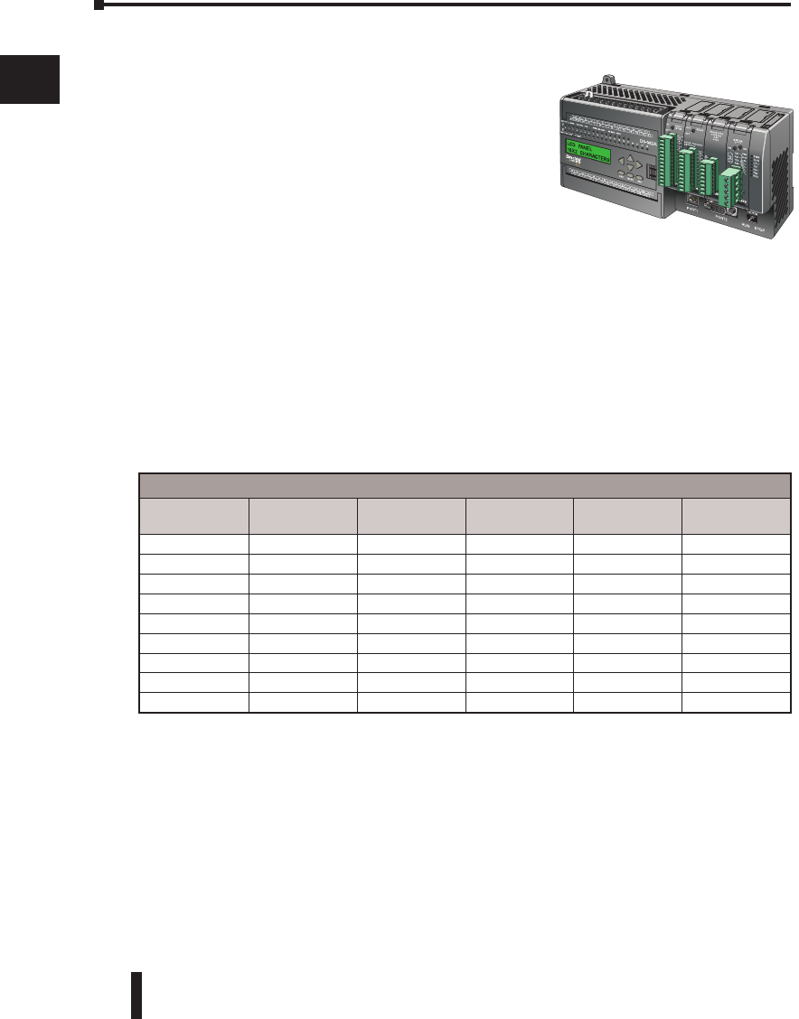
DL06 Micro PLC User Manual, 3rd Edition, Rev. D
Chapter 1: Getting Started
1
2
3
4
5
6
7
8
9
10
11
12
13
14
A
B
C
D
1-4
DL06 Micro PLC Overview
The DL06 micro PLC family is a versatile product line that
combines powerful features and a very compact footprint.
The DL06 PLCs offer expandable I/O, high-speed
counter, floating point, PID, etc. There are a number of
communication options and an optional LCD display.
The DL06 PLC Features
The DL06 Micro PLC family includes nine different
versions. All have the same appearance and CPU
performance. The CPU offers an instruction set very similar to our powerful new DL260
CPU including new easy to use ASCII and MODBUS instructions. All DL06 PLCs have
two built-in communications ports that can be used for programming, operator interface,
networking, etc.
Units with DC inputs have selectable high-speed input features on four input points. Units
with DC outputs offer selectable pulse output capability on the first and second output
points. Details of these features and more are covered in Chapter 3, CPU Specifications and
Operation. There are nine versions of the DL06 PLC. The most common industrial I/O
types and power supply voltages are available. Consult the following table to find the model
number of the PLC that best fits your application.
DirectSOFT 5 Programming for Windows™
The DL06 Micro PLC can be programmed with DirectSOFT, a Windows-based software
package that supports familiar features such as cut-and-paste between applications, point-and-
click editing, viewing and editing multiple application programs at the same time, floating
views, intelligent boxes, etc. Firmware version 2.10 is needed in order to use the intelligent
boxes.
1
2
3
4
5
6
7
8
9
10
11
12
13
14
A
B
C
D
DL06 Micro PLC Family
DL06 Part
Number
Discrete Input
Type
Discrete Output
Type External Power High-Speed
Input Pulse Output
D0–06AA AC AC 95–240 VAC No No
D0–06AR AC Relay 95–240 VAC No No
D0–06DA DC AC 95–240 VAC Yes No
D0–06DD1 DC DC Sinking 95–240 VAC Yes Yes
D0–06DD2 DC DC Sourcing 95–240 VAC Yes Yes
D0–06DR DC Relay 95–240 VAC Yes No
D0–06DD1–D DC DC Sinking 12–24 VDC Yes Yes
D0–06DD2–D DC DC Sourcing 12–24 VDC Yes Yes
D0–06DR–D DC Relay 12–24 VDC Yes No
DL06 Micro PLC User Manual, 3rd Edition, Rev. D
Chapter 1: Getting Started
1
2
3
4
5
6
7
8
9
10
11
12
13
14
A
B
C
D
1-5
DirectSOFT (part number PC-DSOFTx) supports the DirectLOGIC CPU families.
You can use DirectSOFT 5 to program the DL05, DL06, DL105, DL205, DL305, and
DL405 CPUs. A separate manual discusses DirectSOFT programming software. Earlier
programming software versions such as DirectSOFT32, version 4.0 can also be used to
program the DL06.
Handheld Programmer
All DL06 Micro PLCs have a built-in programming port for use with the handheld
programmer (D2–HPP), the same programmer used with the DL05, DL105 and DL205
families. The handheld programmer can be used to create, modify and debug your
application program. A separate manual discusses the Handheld Programmer. Only D2–
HPPs with firmware version 2.0 or later will program the DL06.
NOTE: Not all instructions are available to use with the HPP - the real number instructions, for
example. DirectSOFT will be needed to program instructions such as these.
I/O Quick Selection Guide
The nine versions of the DL06 have input/output circuits which can interface to a wide
variety of field devices. In several instances a particular input or output circuit can interface
to either DC or AC voltages, or both sinking and sourcing circuit arrangements. Check this
guide to find the proper DL06 Micro PLC to interface to the field devices in your application.
1
2
3
4
5
6
7
8
9
10
11
12
13
14
A
B
C
D
I/O Selection Guide
DL06 Part
Number
INPUTS OUTPUTS
I/O type/
commons Sink/Source Voltage
Ranges
I/O type/
commons Sink/Source Voltage/ Current Ratings*
D0–06AA AC / 5 –90 – 120 VAC AC / 4 – 17 – 240 VAC, 50/60 Hz 0.5A
D0–06AR AC / 5 –90 – 120 VAC Relay / 4 Sink or Source 6 – 27VDC, 2A
6 – 240 VAC, 2A
D0–06DA DC / 5 Sink or Source 12 – 24 VDC AC / 4 – 17 – 240 VAC, 50/60 Hz 0.5A
D0–06DD1 DC / 5 Sink or Source 12 – 24 VDC DC / 4 Sink 6 – 27 VDC, 0.5A (Y0–Y1)
6 – 27 VDC, 1.0A (Y2–Y17)
D0–06DD2 DC / 5 Sink or Source 12 – 24 VDC DC / 4 Source 12 – 24 VDC, 0.5A (Y0–Y1)
12 – 24 VDC, 1.0A (Y2–Y17)
D0–06DR DC / 5 Sink or Source 12 – 24 VDC Relay / 4 Sink or Source 6 – 27VDC, 2A
6 – 240 VAC, 2A
D0–06DD1–D DC / 5 Sink or Source 12 – 24 VDC DC / 4 Sink 6 – 27 VDC, 0.5A (Y0–Y1)
6 – 27 VDC, 1.0A (Y2–Y17)
D0–06DD2–D DC / 5 Sink or Source 12 – 24 VDC DC / 4 Source 12 – 24 VDC, 0.5A (Y0–Y1)
12 – 24 VDC, 1.0A (Y2–Y17)
D0–06DR–D DC / 5 Sink or Source 12 – 24 VDC Relay / 4 Sink or Source 6 – 27 VDC, 2A
6 – 240 VAC, 2A
* See Chapter 2, Specifications for more information about a particular DL06 version.
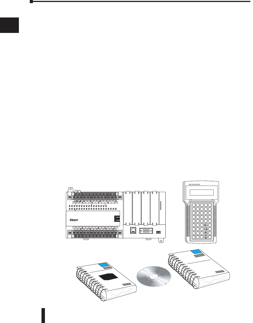
DL06 Micro PLC User Manual, 3rd Edition, Rev. D
Chapter 1: Getting Started
1
2
3
4
5
6
7
8
9
10
11
12
13
14
A
B
C
D
1-6
Quick Start
This example is not intended to tell you everything you need to know about programming
and starting up a complex control system. It is only intended to give you an opportunity
to demonstrate to yourself and others the basic steps necessary to power up the PLC and
confirm its operation. Please look for warnings and notes throughout this manual for
important information you will not want to overlook.
Step 1: Unpack the DL06 Equipment
Unpack the DL06 and gather the parts necessary to build this demonstration system. The
recommended components are:
• DL06 Micro PLC
• AC power cord or DC power supply
• Toggle switches (see Step 2 on next page)
• Hook-up wire, 16-22 AWG
• DL06 User Manual (this manual)
• A small screwdriver, 5/8” flat or #1 Philips type
You will need at least one of the following programming options:
• DirectSOFT Programming Software V5.0 or later (PC-DSOFTx), DirectSOFT Programming
Software Manual (included with the software), and a programming cable (D2-DSCBL connects the
DL06 to a personal computer).
or
• D2-HPP Handheld Programmer, firmware version 2.0 or later, (comes with programming cable).
Please purchase Handheld Programmer Manual D2-HPP-M separately.
1
2
3
4
5
6
7
8
9
10
11
12
13
14
A
B
C
D
LOGIC
Koyo
06
C0 C4C2X1 X3 X4 X6 X11X13 X14X16 X21X23 N.C.
C1 C3X2 X5 X7 X10X12 X15 X17X20 X22X0 N.C.
AC(N)24V
0V
N.C.
C1 C3Y0 Y15Y12Y10Y17Y7Y5Y2
C0 C2 Y16Y14Y13Y11Y6Y4Y3Y1
LG
G
AC(L)
D0-06DR
2.0AOUTPUT: 6-240V 50 - 60Hz 2.0A, 6 - 27V
INPUT: 12 - 24V 3 - 15mA
Y
X
40VA50-60HzPWR: 100-240V
01 2345 6710 11 12 13 14 15 16 17 20 21 22 23
PORT1PORT2
TERM
RUN STOP
PWR
RUN
CPU
TX1
RX1
TX2
RX2
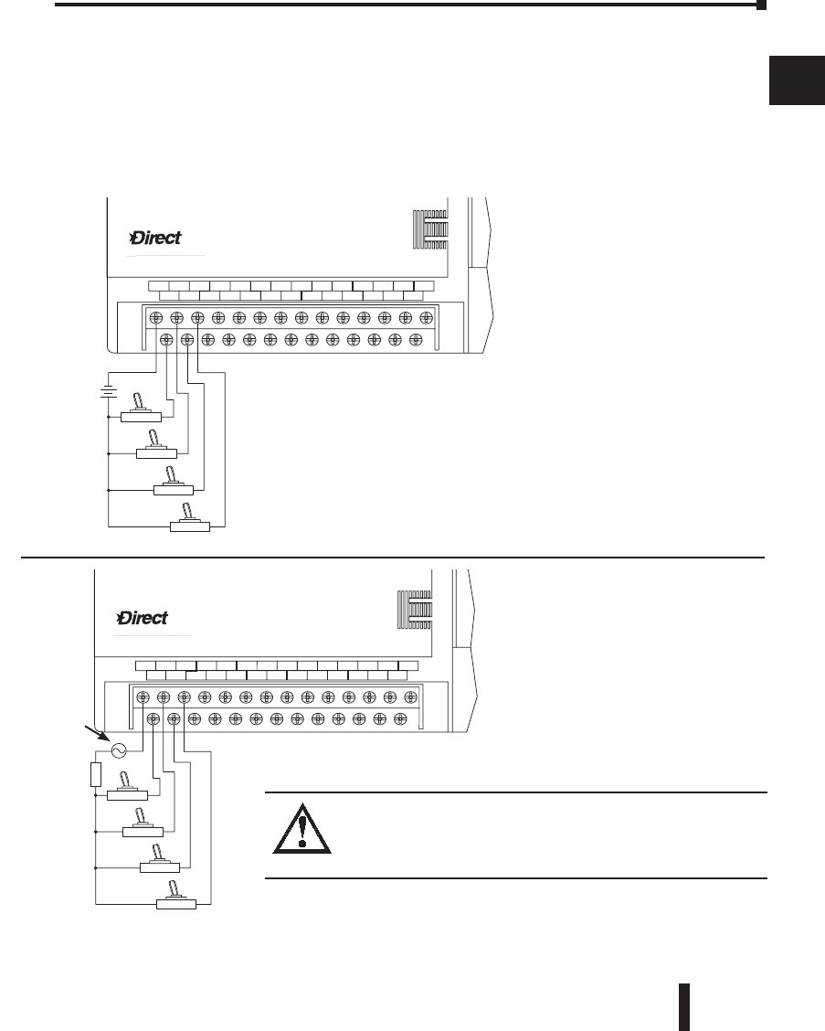
DL06 Micro PLC User Manual, 3rd Edition, Rev. D
Chapter 1: Getting Started
1
2
3
4
5
6
7
8
9
10
11
12
13
14
A
B
C
D
1-7
Step 2: Connect Switches to Input Terminals
To proceed with this quick-start exercise or to follow other examples in this manual, you
will need to connect one or more input switches as shown below. If you have DC inputs
on an AC-supply DL06, you can use the auxiliary 24VDC supply on the output terminal
block or other external 12-24VDC power supply. Be sure to follow the instructions in the
accompanying WARNING on this page.
1
2
3
4
5
6
7
8
9
10
11
12
13
14
A
B
C
D
LOGIC
Koyo
06
fuse
C0 C4C2X1 X3 X4 X6 X11 X13 X14 X16 X21 X23 N.C.
C1 C3X2 X5 X7 X10 X12 X15 X17 X20 X22X0 N.C.
AC(N)24V
0V
+V
C1 C3Y0 Y15Y12Y10 Y17Y7Y5Y2
C0 C2 Y16Y14Y13Y11Y6Y4Y3Y1
LGG
AC(L)
OUTPUT: Sinking Output 6 - 27V 1.0A
INPUT: 12 - 24V 3 - 15mA
Y
X
D0-06DD1
40VA50-60HzPWR: 100-240V
+24 VDC
+
-
LLLL LLLLLLLL LLLL
012345671011121314151617202122 23
12 - 24 VDC
+
-
LOGIC
Koyo
06
C0 C4C2X1 X3 X4 X6 X11 X13 X14 X16 X21X23 N.C.
C1 C3X2 X5 X7 X10X12 X15 X17 X20X22X0 N.C.
fuse
AC(N)24V
0V
N.C.
C1 C3Y0 Y15Y12Y10Y17Y7Y5Y2
C0 C2 Y16Y14Y13Y11Y6Y4Y3Y1
LG
G
AC(L)
D0-06AA
40VA50-60HzPWR: 100-240VOUTPUT: 17-240V 50 - 60Hz0.5A
Y
X
7 - 15mAINPUT: 90 - 120V
01 23456710 11 12 13 14 15 16 17 20 21 22 23
fuse
WARNING: Remove power and unplug the DL06 when wiring
the switches. Use only UL-approved switches rated for at
least 250VAC, 1A for AC inputs. Firmly mount the switches
before using.
D0-06AA and D0-06AR
AC input only
D0-06DA, D0-06DD1,
D0-06DD2, D0-06DR,
D0-06DD1-D, and
D0-06DR1-D DC Input
Toggle Switches
UL Listed
Toggle Switches
UL Listed
90 - 120 VAC
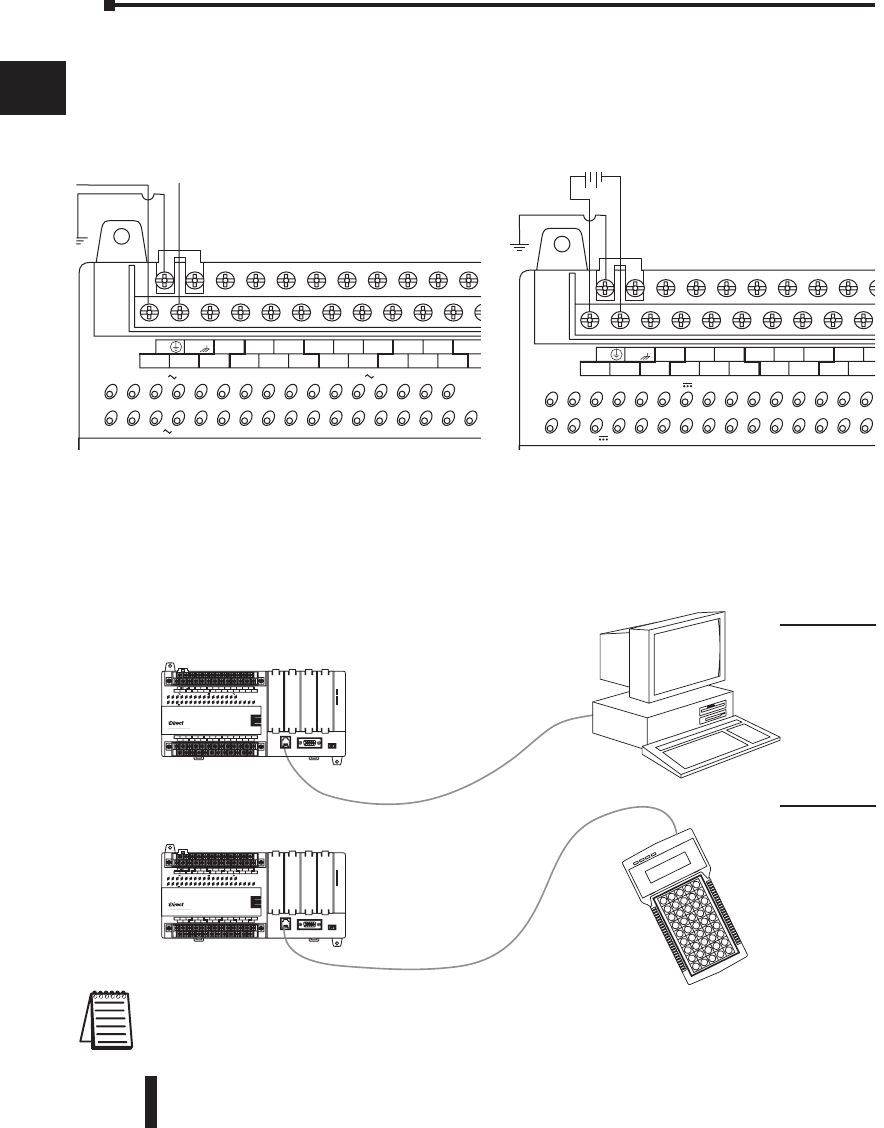
DL06 Micro PLC User Manual, 3rd Edition, Rev. D
Chapter 1: Getting Started
1
2
3
4
5
6
7
8
9
10
11
12
13
14
A
B
C
D
1-8
Step 3: Connect the Power Wiring
Connect the power input wiring for the DL06. Observe all precautions stated earlier
in this manual. For more details on wiring, see Chapter 2 on Installation, Wiring, and
Specifications. When the wiring is complete, close the connector covers. Do not apply power
at this time.
Step 4: Connect the Programming Device
Most programmers will use DirectSOFT programming software, installed on a personal
computer. An alternative, if you need a compact portable programming device, is the
Handheld Programmer (firmware version 2.20 or later). Both devices will connect to COM
port 1 of the DL06 via the appropriate cable.
NOTE: The
Handheld
Programmer
cannot create
or access
LCD, ASCII
or MODBUS
instructions.
1
2
3
4
5
6
7
8
9
10
11
12
13
14
A
B
C
D
LOGIC
Koyo
06
C0 C4C2X1 X3 X4 X6 X11 X13 X14 X16 X21 X23 N.C.
C1 C3X2 X5 X7 X10 X12 X15 X17 X20 X22X0 N.C.
AC(N)24V
0V
N.C.
C1 C3Y0
Y15
Y12Y10
Y17
Y7Y5Y2
C0 C2
Y16Y14
Y13Y11Y6Y4Y3Y1
LGG
AC(L)
D0-06AA
40VA50-60HzPWR: 100-240VOUTPUT: 17-240V 50 - 60Hz 0.5A
Y
X
7 - 15mAINPUT: 90 - 120V
01234567101112131415161
7202122 23
fuse
110/220 VAC Power Input
LOGIC
Koyo
06
DC
Supply
C0 C4C2X1 X3 X4 X6 X11 X13 X14 X16 X21 X23 N.C.
C1 C3X2 X5 X7 X10 X12 X15 X17 X20 X22X0 N.C.
C1
C3
Y0
Y15Y12
Y10
Y17
Y7Y5Y2
C0 C2
Y16Y14Y13
Y11Y6Y4Y3Y1
+V
+
-
LG
N.C.
N.C.G
OUTPUT: Sinking Output 6 - 27V 1.0A
INPUT: 12 - 24V 3 - 15mA
Y
X
PWR: 12-24 20W
D0-06DD1-D
0123456710111213141
51617202122 23
+
-
12 - 24 VDC
12/24 VDC Power Input
Use cable part #
D2–DSCBL
For replacement
cable, use part #
DV–1000CBL
(cable comes with HPP)
LOGIC
Koyo
06
C0 C4C2X1 X3 X4 X6 X11X13 X14X16 X21X23 N.C.
C1 C3X2 X5 X7 X10X12 X15X17 X20X22X0 N.C.
AC(N)24V
0V
N.C.
C1 C3Y0 Y15Y12Y10Y17Y7Y5Y2
C0 C2 Y16Y14Y13Y11Y6Y4Y3Y1
LG
G
AC(L)
D0-06DR
2.0AOUTPUT: 6-240V 50 - 60Hz 2.0A, 6 - 27V
INPUT: 12 - 24V3 - 15mA
Y
X
40VA50-60HzPWR: 100-240V
0123456710 11 12 13 14 15 16 17 20 21 22 23
PORT1PORT2
TERM
RUN STOP
PWR
RUN
CPU
TX1
RX1
TX2
RX2
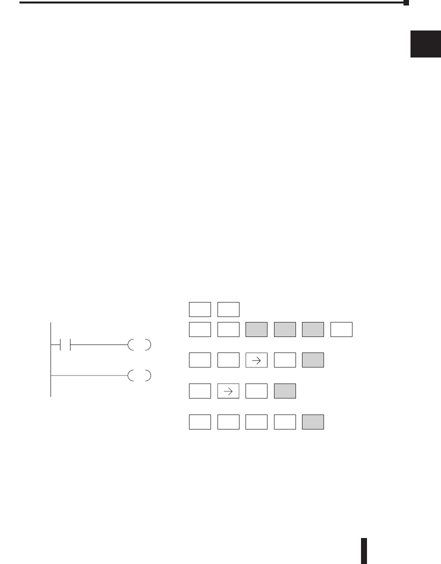
DL06 Micro PLC User Manual, 3rd Edition, Rev. D
Chapter 1: Getting Started
1
2
3
4
5
6
7
8
9
10
11
12
13
14
A
B
C
D
1-9
Step 5: Switch on the System Power
Apply power to the system and ensure the PWR indicator on the DL06 is on. If not, remove
power from the system and check all wiring and refer to the troubleshooting section in
Chapter 9 for assistance.
Step 6: Initialize Scratchpad Memory
It’s a good precaution to always clear the system memory (scratchpad memory) on a new
DL06. There are two ways to clear the system memory:
• In DirectSOFT, select the PLC menu, then Setup and Initialize Scratch Pad. Initializing Scratch
Pad will return secondary comm port settings and retentive range settings to default. If you have
made any changes to these, you will need to note these changes and re-enter them after initializing
Scratchpad.
• For the Handheld Programmer, use the AUX key and execute AUX 54.
See the Handheld Programmer Manual for additional information.
Step 7: Enter a Ladder Program
At this point, DirectSOFT programmers need to refer to Chapter 2 (Quick Start) in the
DirectSOFT Programming Software Manual. There you will learn how to establish a
communications link with the DL06 PLC, change CPU modes to Run or Program, and enter
a program.
If you are learning how to program with the Handheld Programmer, make sure the CPU is
in Program Mode (the RUN LED on the front of the DL06 should be off). If the RUN LED
is on, use the MODE key on the Handheld Programmer to put the PLC in Program Mode,
then switch to TERM.
Enter the following keystrokes on the Handheld Programmer.
After entering the simple example program, put the PLC in Run mode by using the Mode
key on the Handheld Programmer.
The RUN indicator on the PLC will illuminate, indicating the CPU has entered the Run
mode. If not, repeat this step, ensuring the program is entered properly or refer to the
troubleshooting guide in chapter 9.
After the CPU enters the run mode, the output status indicator for Y0 should follow the
switch status on input channel X0. When the switch is on, the output will be on.
1
2
3
4
5
6
7
8
9
10
11
12
13
14
A
B
C
D
ENT CLR
3
D
TMR
N
4
E
SHFT
CLR CLR
2
C
4
EAUX ENT
NEXT STR
$
0
AENT
OUT
GX
0
AENT
ENT
Clear the Program
Move to the first
address and enter
X0 contact
Enter output Y0
Enter the END
statement
END
X0
OUT
Y0
Equivalent
Direct SOFT display
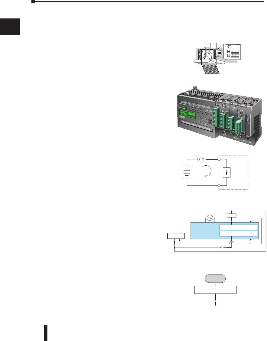
DL06 Micro PLC User Manual, 3rd Edition, Rev. D
Chapter 1: Getting Started
1
2
3
4
5
6
7
8
9
10
11
12
13
14
A
B
C
D
1-10
Steps to Designing a Successful System
Step 1: Review the Installation Guidelines
1
2
3
4
5
6
7
8
9
10
11
12
13
14
A
B
C
D
+
–
Input
Sensing
PLC
Input
Common
20 Inputs Commons
Commons16 Outputs
Power Input
PLC
DL06
+–
Loads
+24 VDC
AC
Power
Power Up
Initialize Hardware
Step 5: Understand the System Operation
Before you begin to enter a program, it is very
helpful to understand how the DL06 system
processes information. This involves not only
program execution steps, but also involves
the various modes of operation and memory
layout characteristics.
Step 4: Choose a System Wiring Strategy
It is important to understand the various
system design options that are available before
wiring field devices and field-side power
supplies to the Micro PLC.
Always make safety the first priority in any system
design. Chapter 2 provides several guidelines that will
help you design a safer, more reliable system. This
chapter also includes wiring guidelines for the various
versions of the DL06 PLC.
Step 2: Understand the PLC Setup Procedures
The PLC is the heart of your automation system.
Make sure you take time to understand the various
features and setup requirements.
Step 3: Review the I/O Selection Criteria
There are many considerations involved when you
select your I/O type and field devices. Take time
to understand how the various types of sensors and
loads can affect your choice of I/O type.
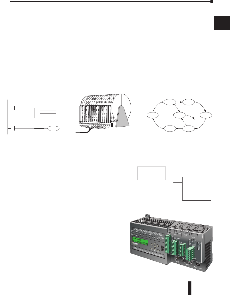
DL06 Micro PLC User Manual, 3rd Edition, Rev. D
Chapter 1: Getting Started
1
2
3
4
5
6
7
8
9
10
11
12
13
14
A
B
C
D
1-11
Step 6: Review the Programming Concepts
The DL06 PLC instruction set provides for three main approaches to solving the application
program, depicted in the figure below.
• RLL diagram-style programming is the best tool for solving boolean logic and general CPU register/
accumulator manipulation. It includes dozens of instructions, which will also be needed to augment
drums and stages.
• The Timer/Event Drum Sequencer features up to 16 steps and offers both time and/or event-based
step transitions. The DRUM instruction is best for a repetitive process based on a single series of
steps.
• Stage programming (also called RLLplus) is based on state-transition diagrams. Stages divide the
ladder program into sections which correspond to the states in a flow chart you draw for your
process.
After reviewing the programming concepts above, you’ll be equipped with a variety of tools to
write your application program.
1
2
3
4
5
6
7
8
9
10
11
12
13
14
A
B
C
D
TMR T1
K30 CNT
CT3
K10
Standard RLL Programming
(see Chapter 5)
X0 LDD
V1076
CMPD
K309482
SP62
OUT
Y0
Timer/Event Drum Sequencer
(see Chapter 6)
Push–
DOWN
Push–UP
UP
DOWN
LOWER
RAISE
LIGHT
Stage Programming
(see Chapter 7)
Step 8: Understand the Maintenance and
Troubleshooting Procedures
Sometimes equipment failures occur when we
least expect it. Switches fail, loads short and need
to be replaced, etc. In most cases, the majority
of the troubleshooting and maintenance time is
spent trying to locate the problem. The DL06
Micro PLC has many built-in features, such as
error codes, that can help you quickly identify
problems.
Step 7: Choose the Instructions
Once you have installed the Micro PLC and
understand the main programming concepts, you
can begin writing your application program. At
that time you will begin to use one of the most
powerful instruction sets available in a small PLC.

DL06 Micro PLC User Manual, 3rd Edition, Rev. D
Chapter 1: Getting Started
1
2
3
4
5
6
7
8
9
10
11
12
13
14
A
B
C
D
1-12
1
2
3
4
5
6
7
8
9
10
11
12
13
14
A
B
C
D
Questions and Answers about DL06 Micro PLCs
Q. What is the instruction set like?
A. The instruction set is very close to that of our DL260 CPU. The DL06 instructions
include the drum sequencing instruction, networking, ASCII, MODBUS, LCD,
intelligent boxes and High-Speed I/O capabilities. High-Speed inputs are available on
units with DC inputs only; high-speed outputs are available on units with DC outputs
only.
Q. Do I have to buy the full DirectSOFT programming package to program the
DL06?
A. Yes. The part number for DirectSOFT (PC-DSOFT6) is now used for all PLCs in the
DirectLOGIC family, and the price is very affordable.
Q. Is the DL06 expandable?
A. Yes, the DL06 series function as stand-alone PLCs. However, option card slots allow you
to expand the system without changing the footprint.
Q. Does the DL06 have motion control capability?
A. Yes, the DL06 has limited motion control capabilities. The High-Speed I/O features offer
either encoder inputs with high-speed counting and presets with interrupt, or a pulse/
direction output for stepper control. Three types of motion profiles are available, which are
explained in Appendix E. The H0-CTRIO(2) option module can also be used to provide
more motion functionality.
Q. Are the ladder programs stored in a removable EEPROM?
A. No. The DL06 contains a non-removable FLASH memory for program storage, which
may be written and erased thousands of times. You may transfer programs to/from
DirectSOFT on a PC.
Q. Does the DL06 contain fuses for its outputs?
A. There are no output circuit fuses. Therefore, we recommend fusing each channel, or fusing
each common. See Chapter 2 for I/O wiring guidelines.
Q. Is the DL06 Micro PLC U.L. approved?
A. The Micro PLC has met the requirements of UL (Underwriters’ Laboratories, Inc.),
and CUL (Canadian Underwriters’ Laboratories, Inc.). See our website, www.
Automationdirect.com, for complete details.
Q. Does the DL06 Micro PLC comply with European Union (EU) Directives?
A. The Micro PLC has met the requirements of the European Union Directives (CE). See
our website, www.Automationdirect.com, for complete details.

DL06 Micro PLC User Manual, 3rd Edition, Rev. D
Chapter 1: Getting Started
1
2
3
4
5
6
7
8
9
10
11
12
13
14
A
B
C
D
1-13
Q. Which devices can I connect to the communication ports of the DL06?
A. Port 1: The port is RS-232C, fixed at 9600 baud, odd parity, address 1, and uses the
proprietary K-sequence protocol. The DL06 can also connect to MODBUS RTU and
DirectNET networks as a slave device through port 1. The port communicates with the
following devices:
• DV-1000 Data Access Unit, C-more, DirectTouch, LookoutDirect, DSData or Optimation
Operator interface panels
• DirectSOFT (running on a personal computer)
• D2-HPP handheld programmer
• Other devices which communicate via K-sequence, Directnet, MODBUS RTU protocols should
work with the DL06 Micro PLC. Contact the vendor for details.
A. Port 2: This is a multi-function port. It supports RS-232C, RS422, or RS485, with
selective baud rates (300 - 38,400 bps), address and parity. It also supports the proprietary
K-sequence protocol as well as DirectNet and MODBUS RTU, ASCII In/Out and
non-sequence/print protocols.
Q. Can the DL06 accept 5VDC inputs?
A. No. 5 volts is lower than the DC input ON threshold. However, many TTL logic circuits
can drive the inputs if they are wired as open collector (sinking) inputs. See Chapter 2 for I/O
wiring guidelines.
1
2
3
4
5
6
7
8
9
10
11
12
13
14
A
B
C
D

DL06 Micro PLC User Manual, 3rd Edition, Rev. D
Chapter 1: Getting Started
1
2
3
4
5
6
7
8
9
10
11
12
13
14
A
B
C
D
1-14
1
2
3
4
5
6
7
8
9
10
11
12
13
14
A
B
C
D
Notes

InstallatIon, WIrIng,
and specIfIcatIons 2
2
2
Chapter
Chapter
Chapter
InstallatIon, WIrIng,
and specIfIcatIons 2
2
2
Chapter
Chapter
Chapter
In This Chapter...
Safety Guidelines .............................................................................. 2–2
Orientation to DL06 Front Panel ...................................................... 2–5
Mounting Guidelines ....................................................................... 2–7
Wiring Guidelines ........................................................................... 2–11
System Wiring Strategies ................................................................ 2–14
Wiring Diagrams and Specifications ............................................... 2–30
Glossary of Specification Terms ...................................................... 2–48
DL06 Micro PLC User Manual, 3rd Edition, Rev. D
Chapter 2: Installation, Wiring, and Specifications
1
2
3
4
5
6
7
8
9
10
11
12
13
14
A
B
C
D
2-2
Safety Guidelines
NOTE: Products with CE marks perform their required functions safely and adhere to relevant
standards as specified by CE directives, provided they are used according to their intended purpose,
and the instructions in this manual are strictly followed. The protection provided by the equipment
may be impaired if this equipment is used in a manner not specified in this manual. A listing of our
international affiliates is available on our Web site: http://www.automationdirect.com
WARNING: Providing a safe operating environment for personnel and equipment is your
responsibility and should be your primary goal during system planning and installation.
Automation systems can fail and may result in situations that can cause serious injury to
personnel and/or damage equipment. Do not rely on the automation system alone to provide
a safe operating environment. Sufficient emergency circuits should be provided to stop the
operation of the PLC or the controlled machine or process, either partially or totally. These
circuits should be routed outside the PLC in the event of controller failure, so that independent
and rapid shutdown are available. Devices, such as mushroom switches or end of travel limit
switches, should operate motor starter, solenoids, or other devices without being processed
by the PLC. These emergency circuits should be designed using simple logic with a minimum
number of highly reliable electromechanical components. Every automation application is
different, so there may be special requirements for your particular application. Make sure all
national, state, and local government requirements are followed for the proper installation and
use of your equipment.
Plan for Safety
The best way to provide a safe operating environment is to make personnel and equipment
safety part of the planning process. You should examine every aspect of the system to
determine which areas are critical to operator or machine safety. If you are not familiar with
PLC system installation practices, or your company does not have established installation
guidelines, you should obtain additional information from the following sources.
• NEMA — The National Electrical Manufacturers Association, located in Washington, D.C.,
publishes many different documents that discuss standards for industrial control systems. You can
order these publications directly from NEMA. Some of these include:
ICS 1, General Standards for Industrial Control and Systems
ICS 3, Industrial Systems
ICS 6, Enclosures for Industrial Control Systems
• NEC — The National Electrical Code provides regulations concerning the installation and use of
various types of electrical equipment. Copies of the NEC Handbook can often be obtained from your
local electrical equipment distributor or your local library.
• Local and State Agencies — many local governments and state governments have additional
requirements above and beyond those described in the NEC Handbook. Check with your local
Electrical Inspector or Fire Marshall office for information.
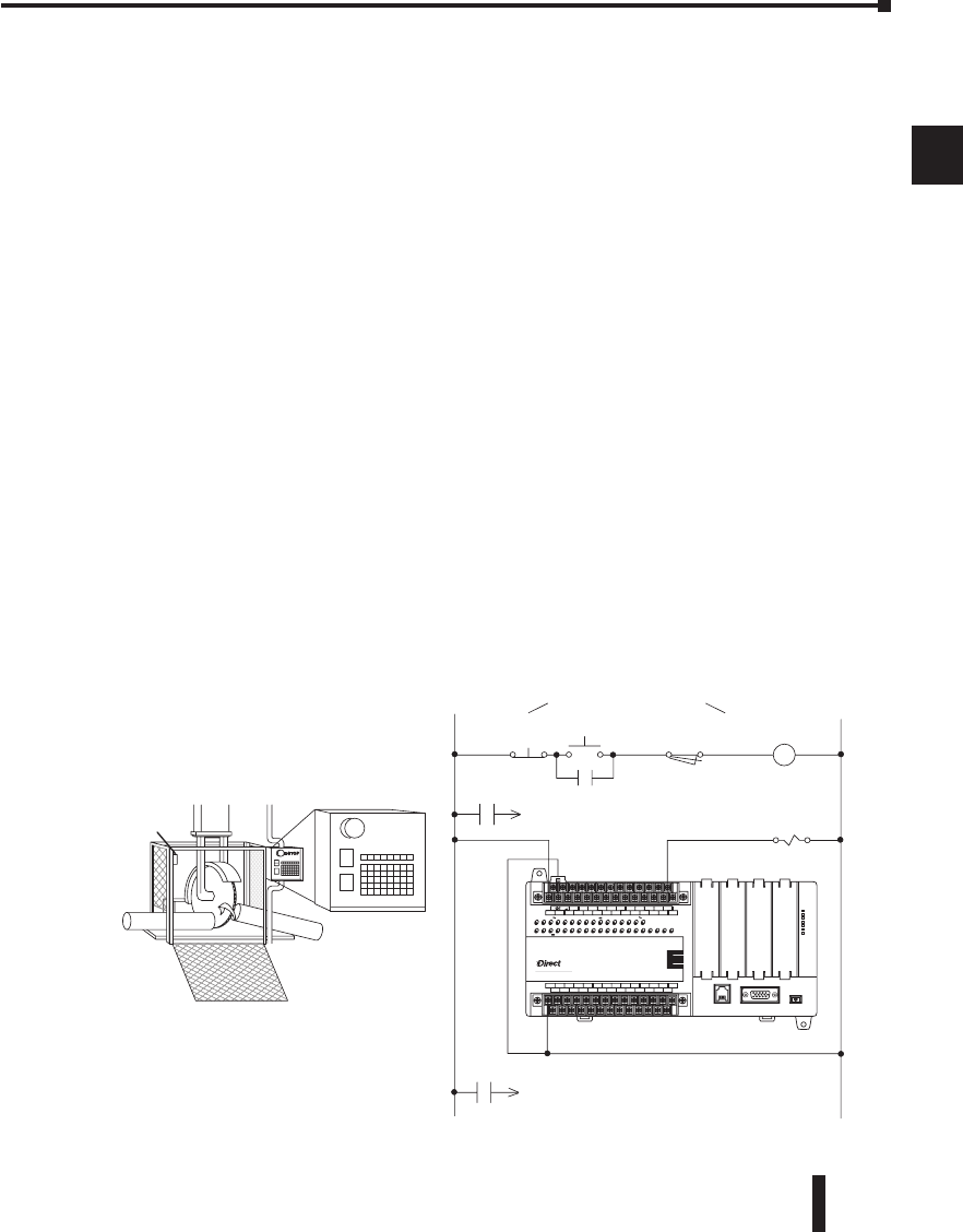
DL06 Micro PLC User Manual, 3rd Edition, Rev. D
Chapter 2: Installation, Wiring, and Specifications
1
2
3
4
5
6
7
8
9
10
11
12
13
14
A
B
C
D
2-3
Three Levels of Protection
The publications mentioned provide many ideas and requirements for system safety.
At a minimum, you should follow these regulations. Also, you should use the following
techniques, which provide three levels of system control.
• Emergency stop switch for disconnecting system power
• Mechanical disconnect for output module power
• Orderly system shutdown sequence in the PLC control program
Emergency Stops
It is recommended that emergency stop circuits be incorporated into the system for every
machine controlled by a PLC. For maximum safety in a PLC system, these circuits must not
be wired into the controller, but should be hardwired external to the PLC. The emergency
stop switches should be easily accessed by the operator and are generally wired into a master
control relay (MCR) or a safety control relay (SCR) that will remove power from the PLC
I/O system in an emergency.
MCRs and SCRs provide a convenient means for removing power from the I/O system
during an emergency situation. By de-energizing an MCR (or SCR) coil, power to the input
(optional) and output devices is removed. This event occurs when any emergency stop switch
opens. However, the PLC continues to receive power and operate even though all its inputs
and outputs are disabled.
The MCR circuit could be extended by placing a PLC fault relay (closed during normal
PLC operation) in series with any other emergency stop conditions. This would cause the
MCR circuit to drop the PLC I/O power in case of a PLC failure (memory error, I/O
communications error, etc.).
Emergency
Stop
Guard Line Switch Saw
Arbor
E STOP Power On
Use E-Stop and Master Relay
Guard
Link
L O G I
C
K o y
o
0 6
C0 C4 C2 X1 X3 X4 X6 X11 X13 X14 X16 X21 X23 N.C.
C1 C3 X2 X5 X7 X10 X12 X15 X17 X20 X22 X0 N.C.
AC(N) 24V
0V
N.C.
C1 C3 Y0 Y15 Y12 Y10 Y17 Y7 Y5 Y2
C0 C2 Y16 Y14 Y13 Y11 Y6 Y4 Y3 Y1
LG G
AC(L)
D0-06DR
2.0A OUTPUT: 6-240V 50 - 60Hz 2.0A, 6 - 27V
INPUT: 12 - 24V 3 - 15mA
Y
X
40VA 50-60Hz PWR: 100-240V
0 1 2 3 4 5 6 7 10 11 12 13 14 15 16 17 20 21 22 23
PORT1 PORT2
TERM
RUN STOP
PWR
RUN
CPU
TX1
RX1
TX2
RX2
Master
Control
Relay
MCR
L1 to Input Supply
(optional)
MCR
L1 to Output Supply
HOT NEUTRAL
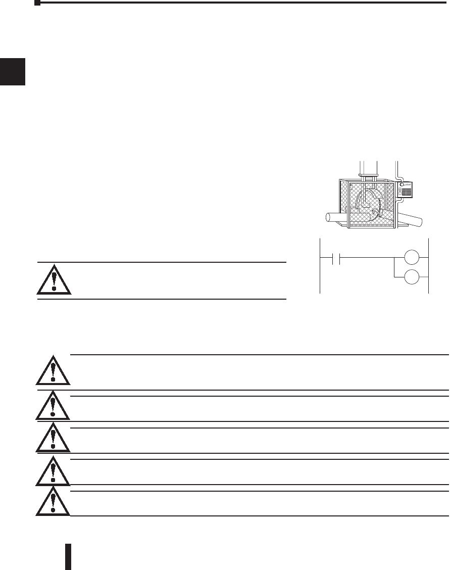
DL06 Micro PLC User Manual, 3rd Edition, Rev. D
Chapter 2: Installation, Wiring, and Specifications
1
2
3
4
5
6
7
8
9
10
11
12
13
14
A
B
C
D
2-4
Emergency Power Disconnect
A properly rated emergency power disconnect should be used to power the PLC controlled
system as a means of removing the power from the entire control system. It may be necessary
to install a capacitor across the disconnect to protect against a condition known as outrush.
This condition occurs when the output Triacs are turned off by powering off the disconnect,
thus causing the energy stored in the inductive loads to seek the shortest distance to ground,
which is often through the Triacs.
After an emergency shutdown or any other type of power interruption, there may be
requirements that must be met before the PLC control program can be restarted. For
example, there may be specific register values that must be established (or maintained from
the state prior to the shutdown) before operations can resume. In this case, you may want
to use retentive memory locations, or include constants in the control program to insure a
known starting point.
Orderly System Shutdown
Class 1, Division 2 Approval
This equipment is suitable for use in Class 1, Zone 2, Division 2, groups A, B, C and D or
non-hazardous locations only.
WARNING: Explosion Hazard! Substitution of components may impair suitability for Class 1, Division 2.
Do not disconnect equipment unless power has been switched off or area is known to be non-
hazardous.
WARNING: Explosion Hazard! Do not disconnect equipment unless power has been switched off or the
area is known to be non-hazardous.
WARNING: All models used with connector accessories must use R/C (ECBT2) mating plug for all
applicable models. All mating plugs shall have suitable ratings for device.
WARNING: This equipment is designed for use in Pollution Degree 2 environments (installed within an
enclosure rated at least IP54).
WARNING: Transient suppression must be provided to prevent the rated voltage from being exceeded
by 140%.
1
2
3
4
5
6
7
8
9
10
11
12
13
14
a
B
c
d
Jam
Detect
RST
RST
Retract
Arm
Turn off
Saw
WARNING: The control program must not be the only
form of protection for any problems that may result in
a risk of personal injury or equipment damage.
Ideally, the first level of fault detection is the PLC
control program, which can identify machine
problems. Certain shutdown sequences should be
performed. The types of problems are usually things
such as jammed parts, etc., that do not pose a risk
of personal injury or equipment damage.
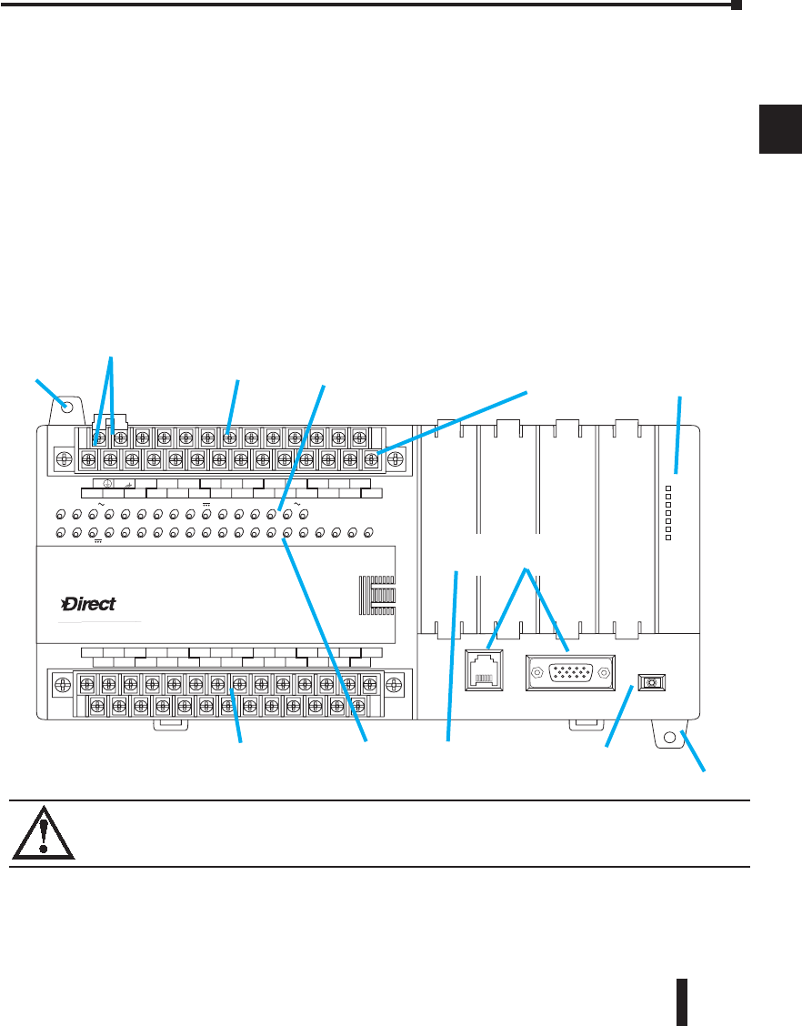
DL06 Micro PLC User Manual, 3rd Edition, Rev. D
Chapter 2: Installation, Wiring, and Specifications
1
2
3
4
5
6
7
8
9
10
11
12
13
14
A
B
C
D
2-5
1
2
3
4
5
6
7
8
9
10
11
12
13
14
a
B
c
d
WARNING: For some applications, field device power may still be present on the terminal block
even though the Micro PLC is turned off. To minimize the risk of electrical shock, check all field
device power before you expose or remove either connector.
LOGIC
Koyo
06
C0 C4C2X1 X3 X4 X6 X11 X13 X14 X16 X21X23 N.C.
C1 C3X2 X5 X7 X10 X12 X15X17 X20X22X0 N.C.
AC(N)24V
0V
N.C.
C1 C3Y0 Y15Y12Y10Y17Y7Y5Y2
C0 C2 Y16Y14Y13Y11Y6Y4Y3Y1
LG
G
AC(L)
D0-06DR
2.0AOUTPUT: 6-240V 50 - 60Hz 2.0A, 6 - 27V
INPUT: 12 - 24V3 - 15mA
Y
X
40VA50-60HzPWR: 100-240V
01234567101112131415161720212223
PORT1PORT2
TERM
RUN STOP
PWR
RUN
CPU
TX1
RX1
TX2
RX2
Mode SwitchOption Slots
Output Status
Indicators
Communication
Ports
Output Circuit
Power Input
(for DC output versions only)
Input Status
Indicators
Status
Indicators
Power Inputs
Discrete Outputs
Discrete Inputs
Mounting Tab
Mounting Tab
Orientation to DL06 Front Panel
Most connections, indicators and labels on the DL06 Micro PLCs are located on its front
panel. The communication ports are located on front of the PLC, as are the option card
slots and the mode selector switch. Please refer to the drawing below.
The output and power connector accepts external power and logic and chassis ground
connections on the indicated terminals. The remaining terminals are for connecting
commons and output connections Y0 through Y17. The sixteen output terminals are
numbered in octal, Y0-Y7 and Y10-Y17. On DC output units, the end terminal on the
right accepts power for the output stage. The input side connector provides the location for
connecting the inputs X0 and X23 and the associated commons.
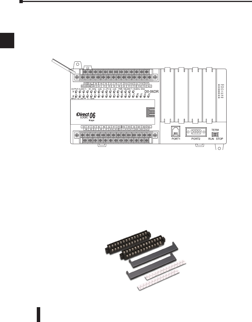
DL06 Micro PLC User Manual, 3rd Edition, Rev. D
Chapter 2: Installation, Wiring, and Specifications
1
2
3
4
5
6
7
8
9
10
11
12
13
14
A
B
C
D
2-6
1
2
3
4
5
6
7
8
9
10
11
12
13
14
a
B
c
d
Terminal Block Removal
The DL06 terminals are divided into two groups. Each group has its own terminal block. The
outputs and power wiring are on one block, and the input wiring is on the other. In some
instances, it may be desirable to remove the terminal block for easy wiring. The terminal block is
designed for easy removal with just a small screwdriver. The drawing below shows the procedure
for removing one of the terminal blocks.
1. Loosen the retention screws on each end of the connector block.
2. From the center of the connector block, pry upward with the screwdriver until the
connector is loose.
The terminal blocks on DL06 PLCs have regular (m3 size) screw terminals, which will accept
either standard blade-type or #1 Philips screwdriver tips. Use No. 16 to 22 AWG solid/
stranded wire. Be careful not to over-tighten; maximum torque is 0.882 to 1.020 Nm (7.806
to 9.028 inch-lbs).
Spare terminal blocks are available in an accessory kit. Please refer to part number
D0-ACC-2. You can find this and other accessories on our web site.
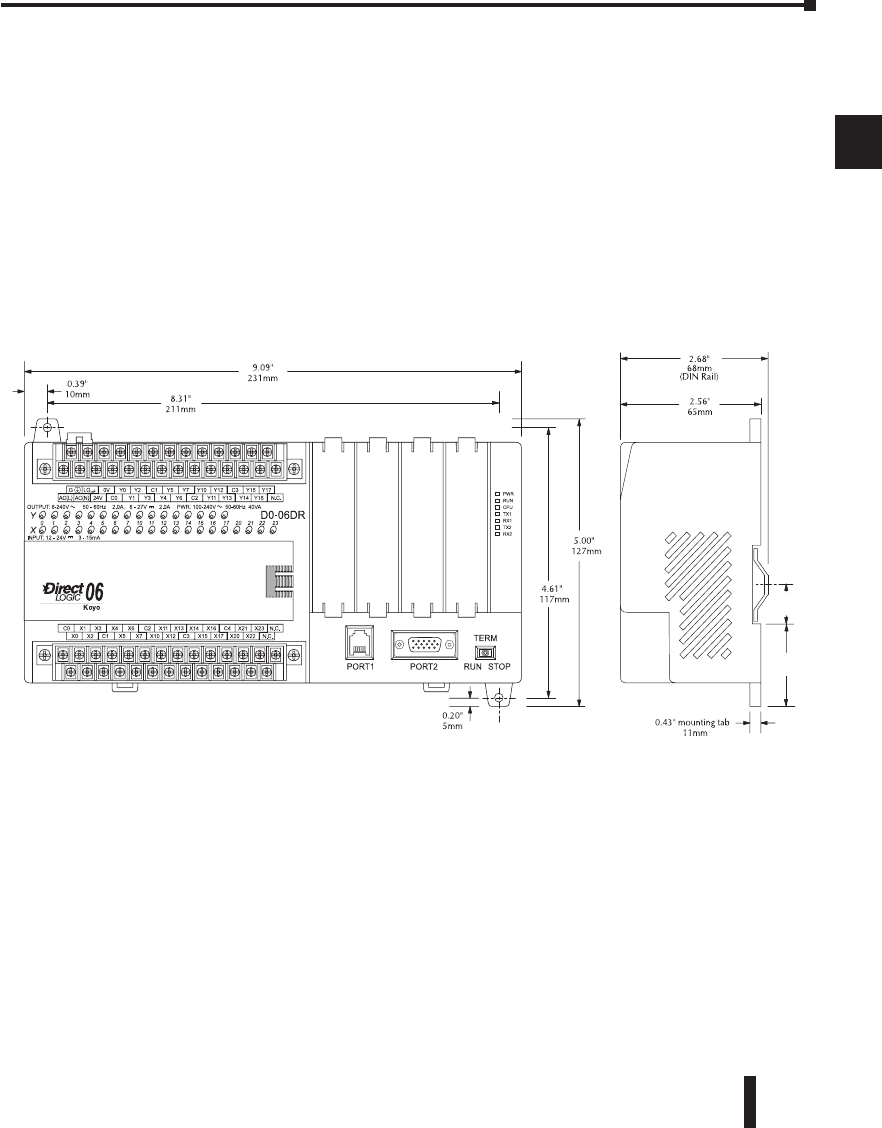
DL06 Micro PLC User Manual, 3rd Edition, Rev. D
Chapter 2: Installation, Wiring, and Specifications
1
2
3
4
5
6
7
8
9
10
11
12
13
14
A
B
C
D
2-7
Mounting Guidelines
In addition to the panel layout guidelines, other specifications can affect the installation of a
PLC system. Always consider the following:
• Environmental Specifications
• Power Requirements
• Agency Approvals
• Enclosure Selection and Component Dimensions
Unit Dimensions
The following diagram shows the outside dimensions and mounting hole locations for all
versions of the DL06. Make sure you follow the installation guidelines to allow proper
spacing from other components.
Enclosures
Your selection of a proper enclosure is important to ensure safe and proper operation of your
DL06 system. Applications of DL06 systems vary and may require additional features. The
minimum considerations for enclosures include:
• Conformance to electrical standards
• Protection from the elements in an industrial environment
• Common ground reference
• Maintenance of specified ambient temperature
• Access to equipment
• Security or restricted access
• Sufficient space for proper installation and maintenance of equipment
1
2
3
4
5
6
7
8
9
10
11
12
13
14
a
B
c
d
1.46"
37mm
0.71"
18mm
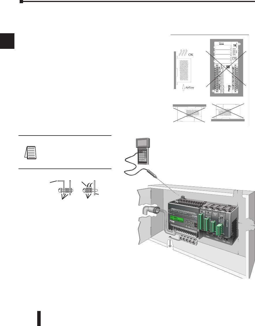
DL06 Micro PLC User Manual, 3rd Edition, Rev. D
Chapter 2: Installation, Wiring, and Specifications
1
2
3
4
5
6
7
8
9
10
11
12
13
14
A
B
C
D
2-8
1
2
3
4
5
6
7
8
9
10
11
12
13
14
a
B
c
d
Panel Layout & Clearances
There are many things to consider when designing the panel layout. The following items
correspond to the diagram shown. Note: there may be additional requirements, depending on
your application and use of other components in the cabinet.
NOTE: There is a minimum clearance
requirement of 1.5” (38 mm)
between the panel door (or any
devices mounted in the panel door)
and the nearest DL06 component.
1.5"
38mm
min
1.5"
38mm
min
1.5"
38mm
min
Panel
Star Washers
Earth Ground
Ground braid
copper lugs
Star Washers
Temperature Probe
Power Source
Panel Ground Terminal
Panel or single
point ground
1. Mount the PLCs horizontally as shown below to provide
proper ventilation. You cannot mount the DL06 units
vertically, upside down, or on a flat horizontal surface. If
you place more than one unit in a cabinet, there must be a
minimum of 7.2” (183 mm) between the units.
2. Provide a minimum clearance of 1.5” (39 mm) between
the unit and all sides of the cabinet. Remember to allow for
any operator panels or other items mounted in the door.
3. There should also be at least 3” (78 mm) of clearance
between the unit and any wiring ducts that run parallel to
the terminals.
4. The ground terminal on the DL06 base must be
connected to a single point ground. Use copper stranded
wire to achieve a low impedance. Copper eye lugs should
be crimped and soldered to the ends of the stranded wire to
ensure good surface contact.
5. There must be a single point ground (i.e., copper bus bar) for all devices in the panel
requiring an earth ground return. The single point of ground must be connected to the panel
ground termination. The panel ground termination must be connected to earth ground.
Minimum wire sizes, color coding, and general safety practices should comply with appropriate
electrical codes and standards for your area.
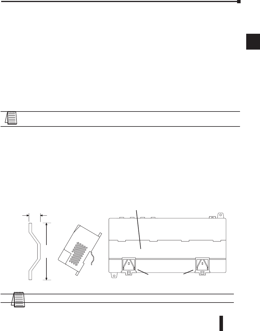
DL06 Micro PLC User Manual, 3rd Edition, Rev. D
Chapter 2: Installation, Wiring, and Specifications
1
2
3
4
5
6
7
8
9
10
11
12
13
14
A
B
C
D
2-9
6. A good common ground reference (Earth ground) is essential for proper operation of the DL06.
One side of all control and power circuits and the ground lead on flexible shielded cable must be
properly connected to Earth ground. There are several methods of providing an adequate common
ground reference, including:
a) Installing a ground rod as close to the panel as possible
b) Connection to incoming power system ground
7. Evaluate any installations where the ambient temperature may approach the lower or upper
limits of the specifications. If you suspect the ambient temperature will not be within the operating
specification for the DL06 system, measures such as installing a cooling/heating source must be taken
to get the ambient temperature within the range of specifications.
8. The DL06 systems are designed to be powered by 95-240 VAC or 12–24 VDC normally available
throughout an industrial environment. Electrical power in some areas where the PLCs are installed is
not always stable and storms can cause power surges. Due to this, powerline filters are recommended
for protecting the DL06 PLCs from power surges and EMI/RFI noise. The Automation Powerline
Filter, for use with 120 VAC and 240 VAC, 1–5 Amps, is an excellent choice (locate at www.
automationdirect.com); however, you can use a filter of your choice. These units install easily
between the power source and the PLC.
NOTE: If you are using other components in your system, make sure you refer to the appropriate
manual to determine how those units can affect mounting dimensions.
Using Mounting Rails
DL06 Micro PLCs can be secured to a panel by using mounting rails. We recommend rails
that conform to DIN EN standard 50022. They are approximately 35 mm high, with a
depth of 7 mm. If you mount the Micro PLC on a rail, do consider using end brackets on
each side of the PLC. The end bracket helps keep the PLC from sliding horizontally along the
rail, reducing the possibility of accidentally pulling the wiring loose. On the bottom of the
PLC are two small retaining clips. To secure the PLC to a DIN rail, place it onto the rail and
gently push up on the clips to lock it onto the rail. To remove the PLC, pull down on the
retaining clips, lift up on the PLC slightly, then pull it away from the rail.
1
2
3
4
5
6
7
8
9
10
11
12
13
14
a
B
c
d
35mm
7mm
DIN Rail Dimensions
Retaining Clip
DIN rail slot is designed for 35 mm x 7 mm rail
conforming to DIN EN 50022
NOTE: Refer to our catalog or web site for a complete listing of DINnector connection systems.
DL06 Micro PLC User Manual, 3rd Edition, Rev. D
Chapter 2: Installation, Wiring, and Specifications
1
2
3
4
5
6
7
8
9
10
11
12
13
14
A
B
C
D
2-10
1
2
3
4
5
6
7
8
9
10
11
12
13
14
a
B
c
d
Environmental Specifications
The following table lists the environmental specifications that generally apply to DL06
Micro PLCs. The ranges that vary for the Handheld Programmer are noted at the bottom of
this chart. Certain output circuit types may have derating curves, depending on the ambient
temperature and the number of outputs ON. Please refer to the appropriate section in this
chapter pertaining to your particular DL06 PLC.
* Operating temperature for the Handheld Programmer and the DV–1000 is 32° to 122°F (0° to 50°C) Storage temperature
for the Handheld Programmer and the DV–1000 is –4° to 158°F (–20° to 70°C).
**Equipment will operate down to 5% relative humidity; however, static electricity problems occur much more frequently
at low humidity levels (below 30%). Make sure you take adequate precautions when you touch the equipment. Consider
using ground straps, anti-static floor coverings, etc. if you use the equipment in low-humidity environments.
Agency Approvals
Some applications require agency approvals for particular components. The DL06 Micro
PLC agency approvals are listed below:
• UL (Underwriters’ Laboratories, Inc.)
• CUL (Canadian Underwriters’ Laboratories, Inc.)
• CE (European Economic Union)
Marine Use
American Bureau of Shipping (ABS) certification requires flame-retarding insulation as
per 4-8-3/5.3.6(a). ABS will accept Navy low smoke cables, cable qualified to NEC
Plenum rated (fire resistant level 4), or other similar flammability resistant rated cables. Use
cable specifications for your system that meet a recognized flame retardant standard (i.e.,
UL, IEEE, etc.), including evidence of cable test certification (i.e., tests certificate, UL file
number, etc.).
NOTE: Wiring must be low smoke per the above paragraph. Teflon coated wire is also
recommended.
Environmental Specifications
Specification Rating
Storage temperature –4°F to 158°F (–20°C to 70°C)
Ambient operating temperature* 32°F to 131°F (0°C to 55°C)
Ambient humidity** 5% – 95% relative humidity (non–condensing)
Vibration resistance MIL STD 810C, Method 514.2
Shock resistance MIL STD 810C, Method 516.2
Noise immunity NEMA (ICS3–304)
Atmosphere No corrosive gases
Agency approvals UL, CE (C1D2), FCC class A
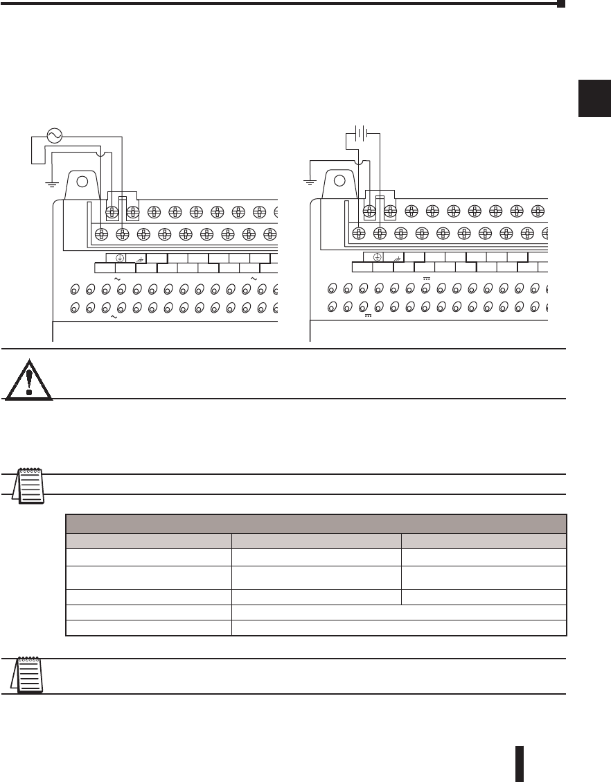
DL06 Micro PLC User Manual, 3rd Edition, Rev. D
Chapter 2: Installation, Wiring, and Specifications
1
2
3
4
5
6
7
8
9
10
11
12
13
14
A
B
C
D
2-11
Wiring Guidelines
Connect the power input wiring for the DL06. Observe all precautions stated earlier in this
manual. When the wiring is complete, close the connector covers. Do not apply power at this
time.
WARNING: Once the power wiring is connected, secure the terminal block cover in the closed
position. There is a risk of electrical shock if you accidentally touch the connection terminals or
power wiring when the cover is open.
External Power Source
The power source must be capable of suppling voltage and current complying with individual
Micro PLC specifications, according to the following specifications:
NOTE: The rating between all internal circuits is BASIC INSULATION ONLY.
NOTE: Recommended wire size for field devices is 16 - 22 AWG solid/stranded. Tighten terminal
screws to 7.81 lb-in (0.882 N*m) to 9.03 lb-in (1.02 N*m).
1
2
3
4
5
6
7
8
9
10
11
12
13
14
a
B
c
d
LOGIC
Koyo
06
C0 C4C2X1 X3 X4 X6 X11 X13 X14 X16 X21 X23 N.C.
C1 C3X2 X5 X7 X10 X12 X15 X17 X20 X22X0 N.C.
AC(N)24V
0V
N.C.
C1
C3
Y0
Y15Y12Y10 Y17
Y7Y5Y2
C0 C2
Y16Y14Y13Y11
Y6Y4Y3Y1
LGG
AC(L)
D0-06AA
40VA50-60Hz
PWR: 100-240VOUTPUT: 17-240V 50 - 60Hz 0.5A
Y
X
7 - 15mAINPUT: 90 - 120V
01234567101112131
4151617202122 23
fuse
LOGIC
Koyo
06
DC
Supply
C0 C4C2X1 X3 X4 X6 X11 X13 X14 X16 X21 X23 N.C.
C1 C3X2 X5 X7 X10 X12 X15 X17 X20 X22X0 N.C.
C1
C3
Y0
Y15Y12
Y10
Y17
Y7Y5Y2
C0 C2
Y16Y14Y13Y11
Y6Y4Y3Y1
+V
+
-
LG
N.C.
N.C.G
OUTPUT: Sinking Output 6 - 27V 1.0A
INPUT: 12 - 24V 3 - 15mA
Y
X
PWR: 12-24 20W
D0-06DD1-D
0123456710111213141
51617202122 23
+
-
12 - 24 VDC
110/220 VAC Power Input 12/24 VDC Power Input
Power Source Specifications
Item DL06 AC Powered Units DL06 DC Powered Units
Input Voltage Range 110/220 VAC (100–240 VAC/50-60 Hz) 12–24 VDC (10.8–26.4 VDC)
Maximum Inrush Current 13 A, 1ms (100–240 VAC)
15 A, 1ms (240–264 VAC) 10A
Maximum Power 40 VA 20 W
Voltage Withstand (dielectric) 1 minute @ 1500 VAC between primary, secondary, field ground
Insulation Resistance > 10 Mq at 500 VDC

DL06 Micro PLC User Manual, 3rd Edition, Rev. D
Chapter 2: Installation, Wiring, and Specifications
1
2
3
4
5
6
7
8
9
10
11
12
13
14
A
B
C
D
2-12
Planning the Wiring Routes
The following guidelines provide general information on how to wire the I/O connections to
DL06 Micro PLCs. Refer to the corresponding specification sheet which appears later in this
chapter for specific information on wiring a particular PLC .
1. Each terminal connection of the DL06 PLC can accept one 16 AWG wire or two 18 AWG size
wires. Do not exceed this recommended capacity.
2. Always use a continuous length of wire. Do not splice wires to attain a needed length.
3. Use the shortest possible wire length.
4. Use wire trays for routing where possible.
5. Avoid running wires near high energy wiring.
6. Avoid running input wiring close to output wiring where possible.
7. To minimize voltage drops when wires must run a long distance, consider using multiple wires for
the return line.
8. Avoid running DC wiring in close proximity to AC wiring where possible.
9. Avoid creating sharp bends in the wires.
10. Install the recommended powerline filter to reduce power surges and EMI/RFI noise.
1
2
3
4
5
6
7
8
9
10
11
12
13
14
a
B
c
d
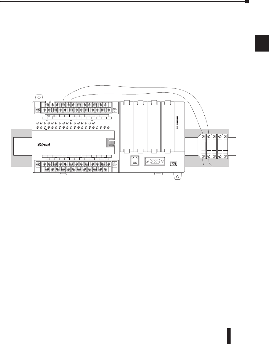
DL06 Micro PLC User Manual, 3rd Edition, Rev. D
Chapter 2: Installation, Wiring, and Specifications
1
2
3
4
5
6
7
8
9
10
11
12
13
14
A
B
C
D
2-13
Fuse Protection for Input and Output Circuits
Input and Output circuits on DL06 Micro PLCs do not have internal fuses. In order to
protect your Micro PLC, we suggest you add external fuses to your I/O wiring. A fast-blow
fuse, with a lower current rating than the I/O bank’s common current rating, can be wired to
each common. Or, a fuse with a rating of slightly less than the maximum current per output
point can be added to each output. Refer to the Micro PLC specification sheets further in
this chapter to find the maximum current per output point or per output common. Adding
the external fuse does not guarantee the prevention of Micro PLC damage, but it will provide
added protection.
I/O Point Numbering
All DL06 Micro PLCs have a fixed I/O configuration. It follows the same octal numbering
system used on other DirectLogic family PLCs, starting at X0 and Y0. The letter X is always
used to indicate inputs and the letter Y is always used for outputs.
The I/O numbering always starts at zero and does not include the digits 8 or 9. The addresses
are typically assigned in groups of 8 or 16, depending on the number of points in an I/O
group. For the DL06, the twenty inputs use reference numbers X0 – X23. The sixteen output
points use references Y0 – Y17.
Additional I/O modules can be installed in the four option slots. See the DL05/06 Option
Modules User Manual, D0-OPTIONS-M, for a complete selection of modules and how to
addresss them in the DL06. This manual can either be ordered from Automationdirect or
downloaded from our website.
1
2
3
4
5
6
7
8
9
10
11
12
13
14
a
B
c
d
LOGIC
Koyo
06
C0 C4C2X1 X3 X4 X6 X11 X13 X14 X16 X21 X23N.C.
C1 C3X2 X5 X7 X10 X12 X15 X17 X20 X22X0 N.C.
AC(N)24V
0V
N.C.
C1 C3Y0 Y15Y12Y10Y17Y7Y5Y2
C0 C2 Y16Y14Y13Y11Y6Y4Y3Y1
LG
G
AC(L)
D0-06DR
2.0AOUTPUT: 6-240V 50 - 60Hz 2.0A, 6 - 27V
INPUT: 12 - 24V 3 - 15mA
Y
X
40VA50-60HzPWR: 100-240V
01 23456710 11 12 13 14 15 16 17 20 21 22 23
PORT1PORT2
TERM
RUN STOP
PWR
RUN
CPU
TX1
RX1
TX2
RX2
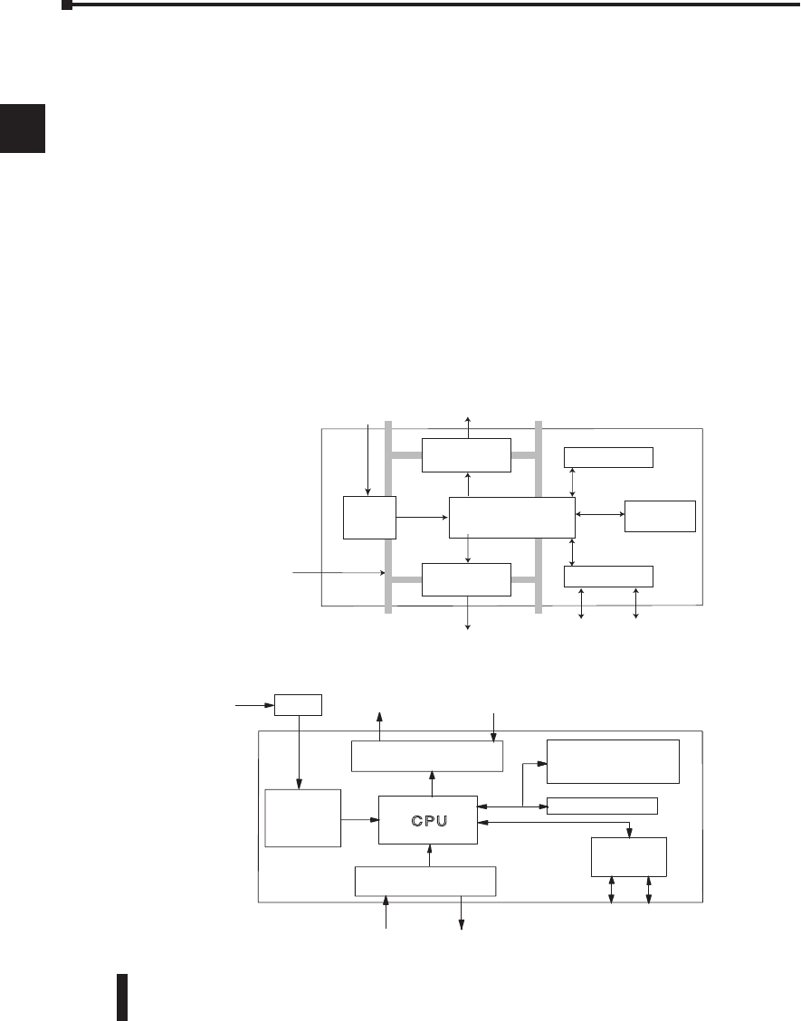
DL06 Micro PLC User Manual, 3rd Edition, Rev. D
Chapter 2: Installation, Wiring, and Specifications
1
2
3
4
5
6
7
8
9
10
11
12
13
14
A
B
C
D
2-14
1
2
3
4
5
6
7
8
9
10
11
12
13
14
a
B
c
d
System Wiring Strategies
The DL06 Micro PLC is very flexible and will work in many different wiring configurations.
By studying this section before actual installation, you can probably find the best wiring
strategy for your application. This will help to lower system cost and wiring errors, and avoid
safety problems.
PLC Isolation Boundaries
PLC circuitry is divided into three main regions separated by isolation boundaries, shown
in the drawing below. Electrical isolation provides safety, so that a fault in one area does not
damage another. A powerline filter will provide isolation between the power source and the
power supply. A transformer in the power supply provides magnetic isolation between the
primary and secondary sides. Opto-couplers provide optical isolation in Input and Output
circuits. This isolates logic circuitry from the field side, where factory machinery connects.
Note that the discrete inputs are isolated from the discrete outputs, because each is isolated
from the logic side. Isolation boundaries protect the operator interface (and the operator)
from power input faults or field wiring faults. When wiring a PLC, it is extremely important to
avoid making external connections that connect logic side circuits to any other.
The next figure shows the internal layout of DL06 PLCs, as viewed from the front panel.
LCD monitor
4 Optional
card slots
2 comm. ports
Power
Input 16 Discrete Outputs
To programming device
or Operator interface20 discrete Inputs
Isolation
boundary
Output circuit
Input circuit
Power
Supply CPU
Output Circuit
Input Circuit
C P U
2Comm.
Ports
Main
Power
Supply
To Programming De-
vice,Operator Interface
or networking
20 Discrete
InputsCommons
Commons
16 DiscreteOutputs
PLC
DL06
Optional
Filter
Power
Input
Card Slots
LCD Monitor
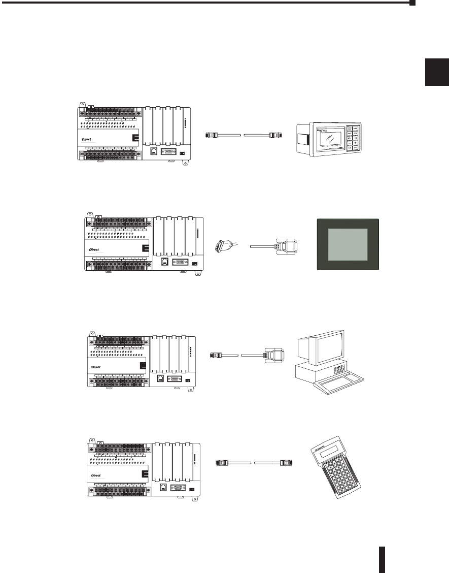
DL06 Micro PLC User Manual, 3rd Edition, Rev. D
Chapter 2: Installation, Wiring, and Specifications
1
2
3
4
5
6
7
8
9
10
11
12
13
14
A
B
C
D
2-15
1
2
3
4
5
6
7
8
9
10
11
12
13
14
a
B
c
d
Connecting Operator Interface Devices
Operator interfaces require data and power connections. Some operator interfaces usually
require separate AC power. However, other operator interface devices like the popular
DV-1000 Data Access Unit may be powered directly from the DL06 Micro PLC. Connect
the DV-1000 to communication port 1 on the DL06 Micro PLC using the cable shown
below. A single cable contains transmit/receive data wires and +5 V power.
C-more operator interface touch panels use a provided 24 VDC plug-in power supply.
Connect the DL06 to the serial connector on the rear of the C-more panel using the cable
shown below.
Connecting Programming Devices
DL06 Micro PLCs can be programmed with either a handheld programmer or with
DirectSOFT on a PC. Connect the DL06 to a PC using the cable shown below.
The D2-HPP Handheld Programmer comes with a communications cable. For a replacement
part, use the cable shown below.
DL06 Micro PLC
DV-1000
Use cable part no.
DV–1000CBL
RJ12
phone style
RJ12
phone style
LOGIC
Koyo
06
C0 C4C2X1 X3 X4 X6 X11X13 X14X16 X21X23 N.C.
C1 C3X2 X5 X7 X10X12 X15X17 X20X22X0 N.C.
AC(N)24V
0V
N.C.
C1 C3Y0 Y15Y12Y10Y17Y7Y5Y2
C0 C2 Y16Y14Y13Y11Y6Y4Y3Y1
LG
G
AC(L)
D0-06DR
2.0AOUTPUT: 6-240V 50 - 60Hz 2.0A, 6 - 27V
INPUT: 12 - 24V 3 - 15mA
Y
X
40VA50-60HzPWR: 100-240V
012345 6710 11 12 13 14 15 16 17 20 21 22 23
PORT1PORT2
TERM
RUN STOP
PWR
RUN
CPU
TX1
RX1
TX2
RX2
Use cable part no.
EA-2CBL-1
15-pin D-shell
male
15-pin
VGA male
DL06 Micro PLC
L
OGIC
Koyo
06
C0 C4C2X1 X3 X4 X6 X11X13 X14X16 X21X23 N.C.
C1 C3X2 X5 X7 X10X12 X15X17 X20X22X0 N.C.
AC(N)24V
0V
N.C.
C1 C3Y0 Y15Y12Y10Y17Y7Y5Y2
C0 C2 Y16Y14Y13Y11Y6Y4Y3Y1
LGG
AC(L)
D0-06DR
2.0AOUTPUT: 6-240V 50 - 60Hz 2.0A,6 - 27V
INPUT: 12 - 24V 3 - 15mA
Y
X
40VA50-60HzPWR: 100-240V
012345 6710 11 12 13 14 15 16 17 20 21 22 23
PORT1 PORT2
TERM
RUN STOP
PWR
RUN
CPU
TX1
RX1
TX2
RX2
Use cable part no.
D2–DSCBL
9-pin D-shell
female
RJ12
phone style
DL06 Micro PLC
L
OGIC
Koyo
06
C0 C4C2X1 X3 X4 X6 X11X13 X14X16 X21X23 N.C.
C1 C3X2 X5 X7 X10X12 X15X17 X20X22X0 N.C.
AC(N)24V
0V
N.C.
C1 C3Y0 Y15Y12Y10Y17Y7Y5Y2
C0 C2 Y16Y14Y13Y11Y6Y4Y3Y1
LG
G
AC(L)
D0-06DR
2.0AOUTPUT: 6-240V 50 - 60Hz 2.0A, 6 - 27V
INPUT: 12 - 24V 3 - 15mA
Y
X
40VA50-60HzPWR: 100-240V
012345 6710 11 12 13 14 15 16 17 20 21 22 23
PORT1PORT2
TERM
RUN STOP
PWR
RUN
CPU
TX1
RX1
TX2
RX2
For replacement
cable, use part no.
DV–1000CBL
RJ12
phone style
RJ12
phone style
(cable comes with HPP)
D2–HPP
DL06 Micro PLC
L
OGIC
Koyo
06
C0 C4C2X1 X3 X4 X6 X11X13 X14X16 X21X23 N.C.
C1 C3X2 X5 X7 X10X12 X15X17 X20X22X0 N.C.
AC(N)24V
0V
N.C.
C1 C3Y0 Y15Y12Y10Y17Y7Y5Y2
C0 C2 Y16Y14Y13Y11Y6Y4Y3Y1
LG
G
AC(L)
D0-06DR
2.0AOUTPUT: 6-240V 50 - 60Hz 2.0A, 6 - 27V
INPUT: 12 - 24V 3 - 15mA
Y
X
40VA50-60HzPWR: 100-240V
012345 6710 11 12 13 14 15 16 17 20 21 22 23
PORT1PORT2
TERM
RUN STOP
PWR
RUN
CPU
TX1
RX1
TX2
RX2
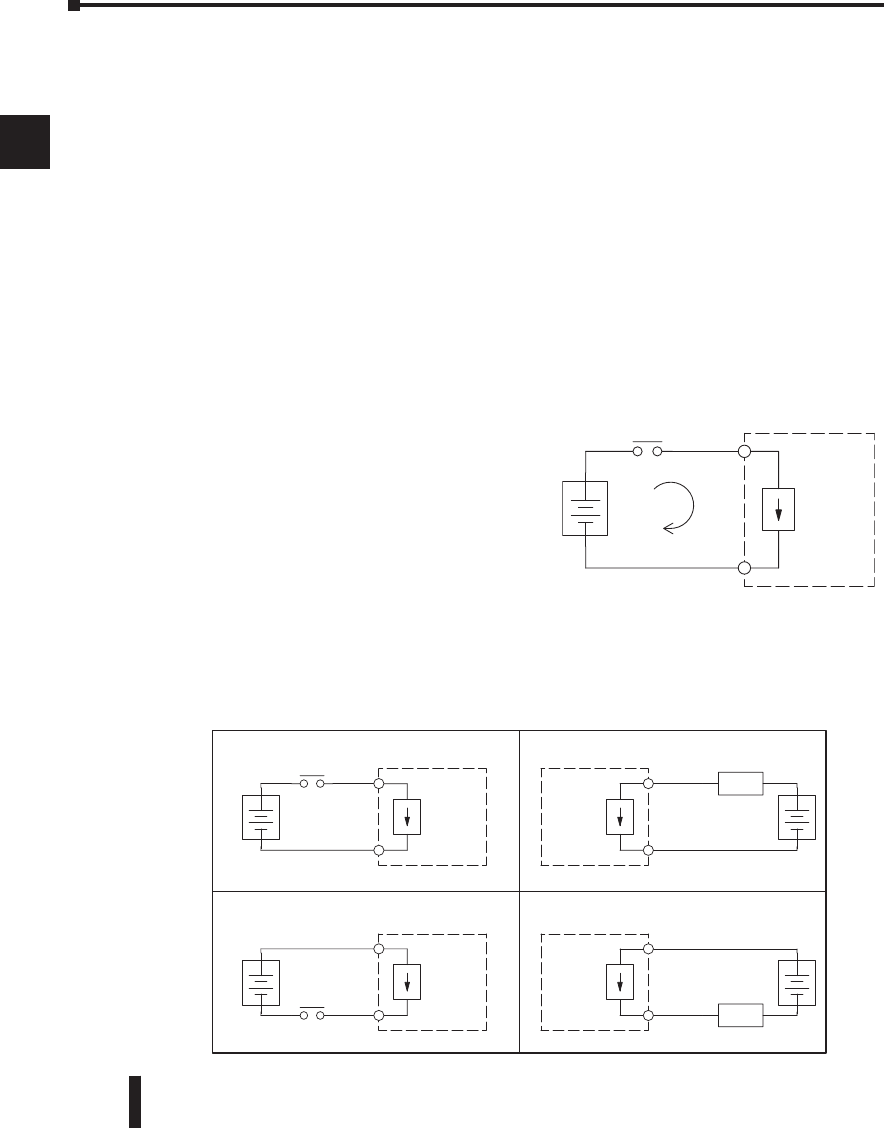
DL06 Micro PLC User Manual, 3rd Edition, Rev. D
Chapter 2: Installation, Wiring, and Specifications
1
2
3
4
5
6
7
8
9
10
11
12
13
14
A
B
C
D
2-16
Sinking / Sourcing Concepts
Before going further in our presentation of wiring strategies, we need to introduce the
concepts of sinking and sourcing. These terms apply to typical input or output circuits. It is
the goal of this section to make these concepts easy to understand. First, we give the following
short definitions, followed by practical applications.
Sinking = Path to supply ground (–)
Sourcing = Path to supply source (+)
Notice the reference to (+) and (–) polarities. Sinking and sourcing terminology applies only
to DC input and output circuits. Input and output points that are either sinking or sourcing
can conduct current in only one direction. This means it is possible to connect the external
supply and field device to the I/O point with current trying to flow in the wrong direction,
and the circuit will not operate. However, we can successfully connect the supply and field
device every time by understanding sourcing and sinking.
For example, the figure to the right depicts a sinking input. To properly connect the external
supply, we just have to connect it so the input provides a path to ground (–). So, we start at
the PLC input terminal, follow through the input
sensing circuit, exit at the common terminal, and
connect the supply (–) to the common terminal.
By adding the switch, between the supply (+) and
the input, we have completed the circuit. Current
flows in the direction of the arrow when the switch
is closed.
By applying the circuit principle above to the four
possible combinations of input/output sinking/sourcing types, we have the four circuits
as shown below. The DC-powered DL06 Micro PLCs have selectable sinking or sourcing
inputs and either sinking or sourcing outputs. Any pair of input/output circuits shown below
is possible with one of the DL06 models.
1
2
3
4
5
6
7
8
9
10
11
12
13
14
a
B
c
d
+
–
Input
Sensing
PLC
Common
Input
(sinking)
+
–
Input
Sensing
Load
Sinking Input Sinking Output
Sourcing Input Sourcing Output
PLC
Input
Common
+
–
Output
Switch
PLC Output
Common
+
–
Input
Sensing
Load
PLC
Input
Common
+
–
Output
Switch
PLC
Output
Common
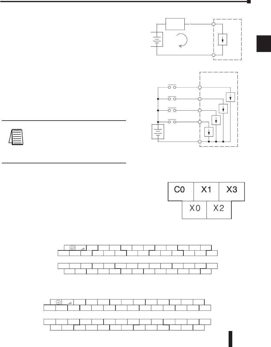
DL06 Micro PLC User Manual, 3rd Edition, Rev. D
Chapter 2: Installation, Wiring, and Specifications
1
2
3
4
5
6
7
8
9
10
11
12
13
14
A
B
C
D
2-17
Most DL06 input and output circuits are grouped into banks that share a common return
path. The best indication of I/O common grouping is on the wiring label. The I/O common
groups are separated by a bold line. A thinner line
separates the inputs associated with that common. To
the right, notice that X0, X1, X2, and X3 share the
common terminal C0, located to the left of X1.
The following complete set of labels shows five banks of four inputs and four banks of four
outputs. One common is provided for each bank.
This set of labels is for DC (sinking) output versions such as the D0-06DD1 and
D0-06DD1-D. One common is provided for each group of four outputs, and one designated
terminal on the output side accepts power for the output stage.
1
2
3
4
5
6
7
8
9
10
11
12
13
14
a
B
c
d
+
–
I/O
Circuit
Return Path
Main Path
(I/O point)
Field
Device
PLC
+
–
Input Sensing
Input 4
Common
Input 3
Input 2
PLC
Input 1
C0 C4C2X1 X3 X4 X6 X11X13 X14X16 X21X23 N.C.
C1 C3X2 X5 X7 X10X12 X15X17 X20X22X0 N.C.
AC(N)24V
0V
N.C.
C1 C3Y0 Y15Y12Y10Y17Y7Y5Y2
C0 C2 Y16Y14Y13Y11Y6Y4Y3Y1
LG
G
AC(L)
C0 C4C2X1 X3 X4 X6 X11X13 X14X16 X21X23 N.C.
C1 C3X2 X5 X7 X10X12 X15X17 X20X22X0 N.C.
AC(N)24V
0V
+V
C1 C3Y0 Y15Y12Y10Y17Y7Y5Y2
C0 C2 Y16Y14Y13Y11Y6Y4Y3Y1
LG
G
AC(L)
I/O Common Terminal Concepts
In order for a PLC I/O circuit to operate,
current must enter at one terminal and exit
at another. This means at least two terminals
are associated with every I/O point. In the
figure to the right, the input or output
terminal is the main path for the current.
One additional terminal must provide the
return path to the power supply.
Most input or output point groups on PLCs
share the return path among two or more
I/O points. The figure to the right shows
a group (or bank) of 4 input points which
share a common return path. In this way,
the four inputs require only five terminals
instead of eight.
NOTE: In the circuit to the right, the
current in the common path is 4 times any
channel’s input current when all inputs are
energized. This is especially important in
output circuits, where heavier gauge wire is
sometimes necessary on commons.
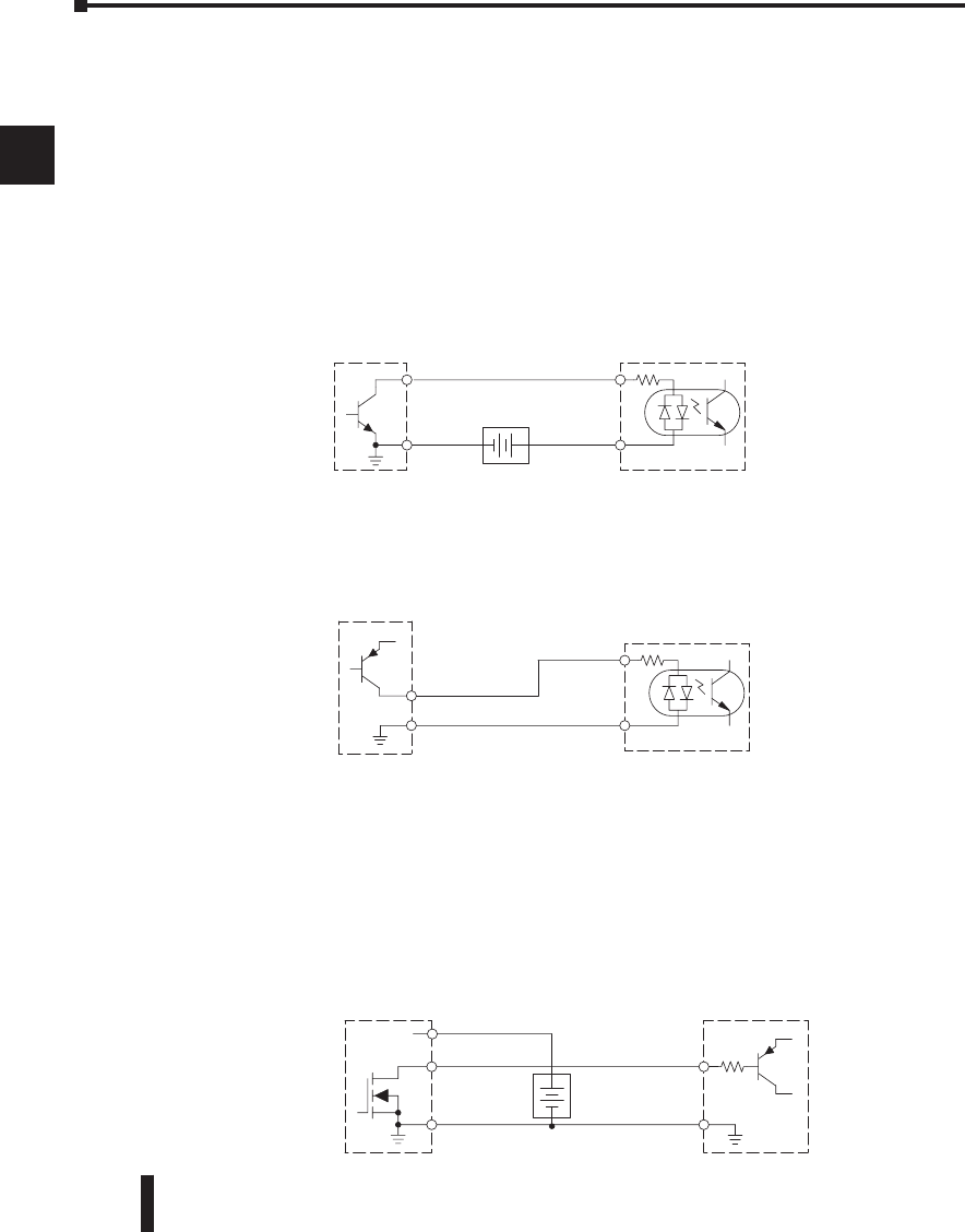
DL06 Micro PLC User Manual, 3rd Edition, Rev. D
Chapter 2: Installation, Wiring, and Specifications
1
2
3
4
5
6
7
8
9
10
11
12
13
14
A
B
C
D
2-18
1
2
3
4
5
6
7
8
9
10
11
12
13
14
a
B
c
d
Connecting DC I/O to Solid State Field Devices
In the previous section on sinking and sourcing concepts, we discussed DC I/O circuits that
only allow current to flow one way. This is also true for many of the field devices which have
solid-state (transistor) interfaces. In other words, field devices can also be sourcing or sinking.
When connecting two devices in a series DC circuit (as is the case when wiring a field device to a
PLC DC input or output), one must be wired as sourcing and the other as sinking.
Solid State Input Sensors
The DL06’s DC inputs are flexible in that they detect current flow in either direction, so they
can be wired as either sourcing or sinking. In the following circuit, a field device has an open-
collector NPN transistor output. It sinks current from the PLC input point, which sources
current. The power supply can be the included auxiliary 24 VDC power supply or another
supply (+12 VDC or +24 VDC), as long as the input specifications are met.
In the next circuit, a field device has an open-emitter PNP transistor output. It sources
current to the PLC input point, which sinks the current back to ground. Since the field
device is sourcing current, no additional power supply is required between the device and the
PLC DC Input.
Solid State Output Loads
Sometimes an application requires connecting a PLC output point to a solid state input on
a device. This type of connection is usually made to carry a low-level signal, not to send DC
power to an actuator.
The DL06 PLC family offers DC outputs that are sinking only or DC outputs that are
sourcing. All sixteen outputs have the same electrical common, even though there are four
common terminal screws. In the following circuit, the PLC output point sinks current to the
output common when energized. It is connected to a sourcing input of a field device input.
Field Device
+–
PLC DC Input
Output
Ground
Common
Supply
(sinking)
Input
(sourcing)
Field Device
PLC DC Input
Output (sourcing)
Ground Common
=>
Input
(sinking)
Field Device
Output
Common
=>
PLC DC Output
+DC Power
+
–
(sourcing)
(sinking)
Power
2 .25
>
Input
Ground
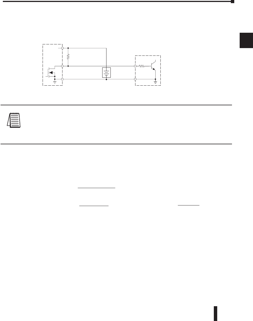
DL06 Micro PLC User Manual, 3rd Edition, Rev. D
Chapter 2: Installation, Wiring, and Specifications
1
2
3
4
5
6
7
8
9
10
11
12
13
14
A
B
C
D
2-19
1
2
3
4
5
6
7
8
9
10
11
12
13
14
a
B
c
d
In the next example we connect a PLC DC output point to the sinking input of a field
device. This is a bit tricky, because both the PLC output and field device input are sinking
type. Since the circuit must have one sourcing and one sinking device, we add sourcing
capability to the PLC output by using a pull-up resistor. In the circuit below, we connect
Rpull-up from the output to the DC output circuit power input.
NOTE 1: DO NOT attempt to drive a heavy load (>25 mA) with this pull-up method.
NOTE 2: Using the pull-up resistor to implement a sourcing output has the effect of inverting the
output point logic. In other words, the field device input is energized when the PLC output is OFF,
from a ladder logic point-of-view. Your ladder program must comprehend this and generate an
inverted output. Or, you may choose to cancel the effect of the inversion elsewhere, such as in the
field device.
It is important to choose the correct value of Rpull-up. In order to do so, we need to know the
nominal input current to the field device (Iinput) when the input is energized. If this value
is not known, it can be calculated as shown (a typical value is 15 mA). Then use Iinput and
the voltage of the external supply to compute Rpull-up. Then calculate the power Ppull-up (in
watts), in order to size Rpull-up properly.
Field Device
Output
Ground
Input
Common
PLC DC Output
+DC pwr
+
–
(sourcing)
(sinking)
Power
(sinking)
pull-up
Supply
R
input
R
pull-up
Rinput
R
=supply
V – 0.7 –
input
I
input
I=input (turn–on)
V
input
R
pull-up
P=supply
V2
pullup
R
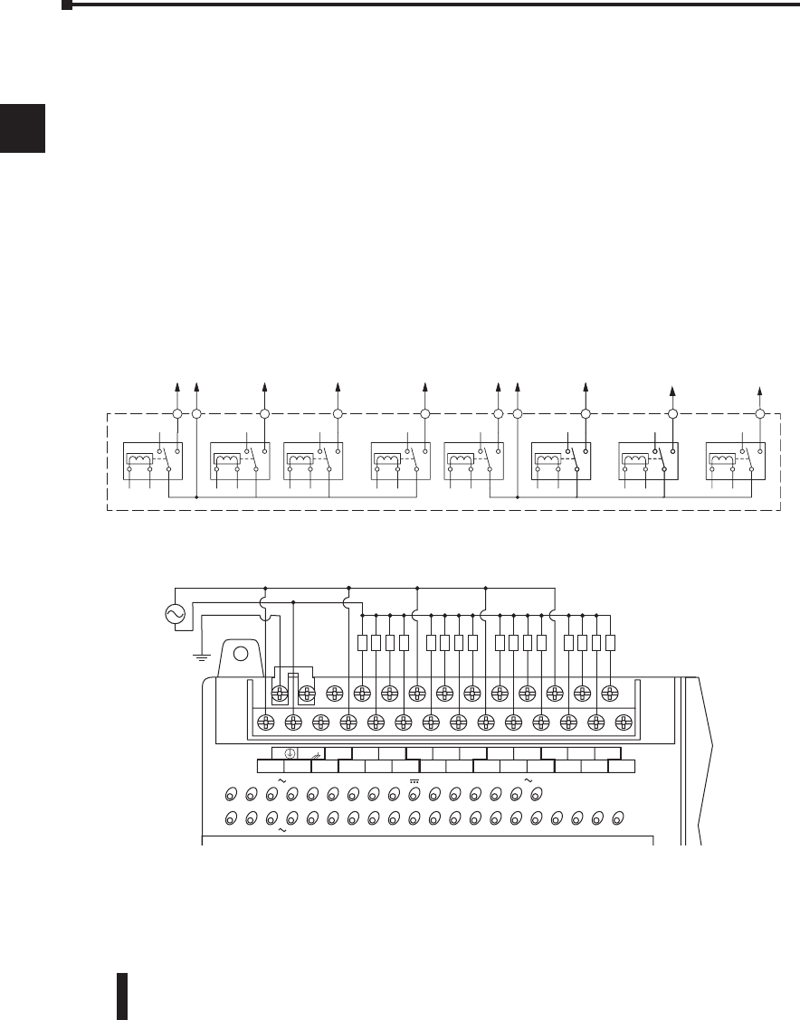
DL06 Micro PLC User Manual, 3rd Edition, Rev. D
Chapter 2: Installation, Wiring, and Specifications
1
2
3
4
5
6
7
8
9
10
11
12
13
14
A
B
C
D
2-20
1
2
3
4
5
6
7
8
9
10
11
12
13
14
a
B
c
d
Relay Output Wiring Methods
The D0–06AR and the D0–06DR models feature relay outputs. Relays are best for the
following applications:
• Loads that require higher currents than the solid-state DL06 outputs can deliver
• Cost-sensitive applications
• Some output channels need isolation from other outputs (such as when some loads require AC
while others require DC)
Some applications in which NOT to use relays:
• Loads that require currents under 10 mA
• Loads which must be switched at high speed and duty cycle
This section presents various ways to wire relay outputs to the loads. The relay output DL06s
have sixteen normally-open SPST relays available. They are organized with four relays per
common. The figure below shows the relays and the internal wiring of the PLC. Note that
each group is isolated from the other group of outputs.
In the circuit below, all loads use the same AC power supply which powers the DL06 PLC.
In this example, all commons are connected together.
In the circuit on the following page, loads for Y0 – Y3 use the same AC power supply which
powers the DL06 PLC. Loads for Y4 – Y7 use a separate DC supply. In this example, the
commons are separated according to which supply powers the associated load.
Y0 Common Y1 Y2 Y3 Y4 Common Y5 Y6 Y7
LOGIC
Koyo
06
AC
Supply
LLLL
C0 C4C2X1 X3 X4 X6 X11 X13 X14 X16 X21 X23 N.C.
C1 C3X2 X5 X7 X10 X12 X15 X17 X20 X22X0 N.C.
LLLLLLLL LLLL
AC(N)24V
0V
N.C.
C1 C3Y0 Y15Y12Y10 Y17Y7Y5Y2
C0 C2 Y16Y14Y13Y11Y6Y4Y3Y1
LGG
AC(L)
D0-06AR
40VA50-60HzPWR: 100-240V2.0AOUTPUT: 6-240V 50 - 60Hz 2.0A, 6 - 27V
Y
X
7 - 15mAINPUT: 90 - 120V
012345671011121314151617202122 23
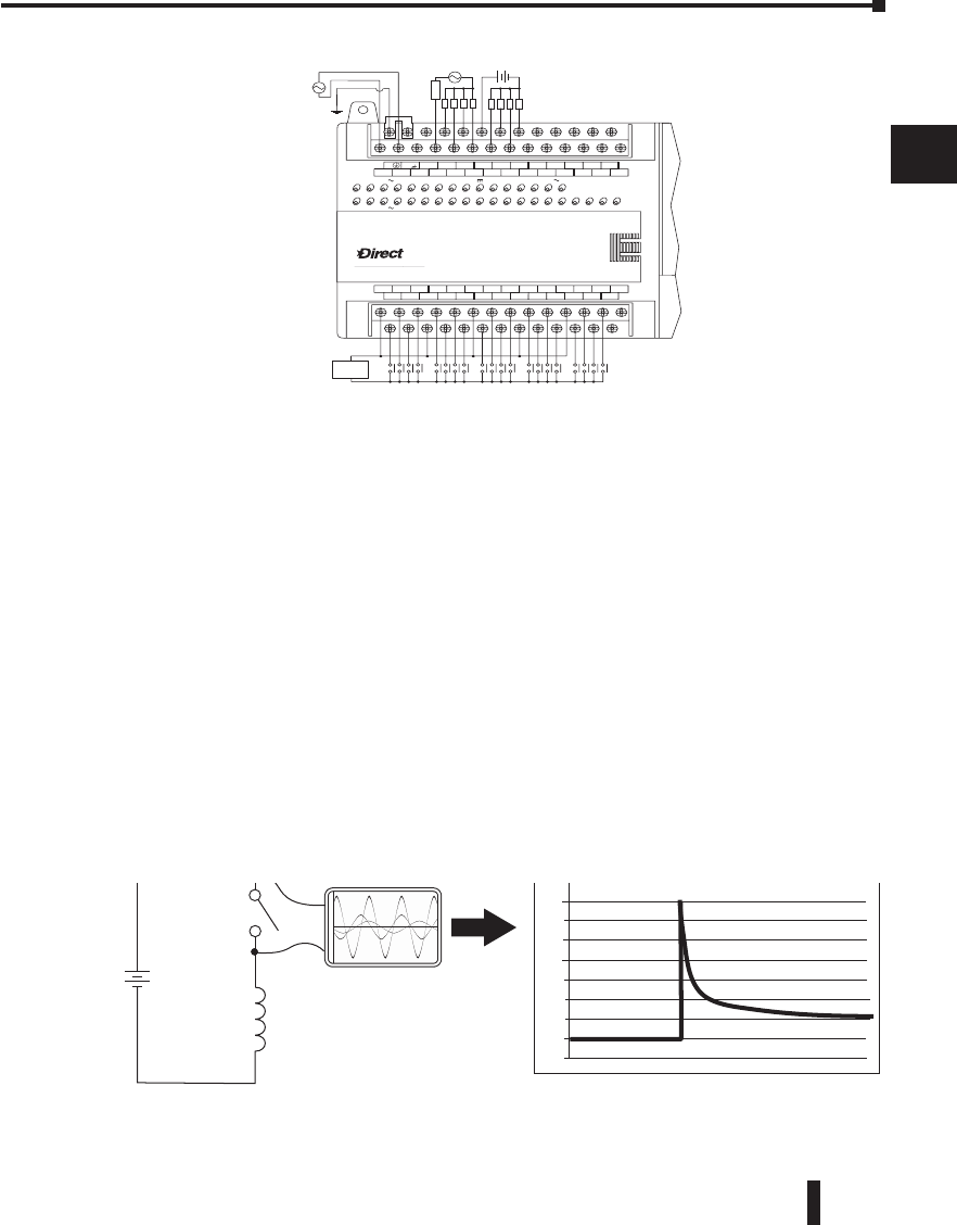
DL06 Micro PLC User Manual, 3rd Edition, Rev. D
Chapter 2: Installation, Wiring, and Specifications
1
2
3
4
5
6
7
8
9
10
11
12
13
14
A
B
C
D
2-21
1
2
3
4
5
6
7
8
9
10
11
12
13
14
a
B
c
d
Relay Outputs – Transient Suppression for Inductive Loads in a Control System
The following pages are intended to give a quick overview of the negative effects of transient
voltages on a control system and provide some simple advice on how to effectively minimize
them. The need for transient suppression is often not apparent to the newcomers in the
automation world. Many mysterious errors that can afflict an installation can be traced back to
a lack of transient suppression.
What is a Transient Voltage and Why is it Bad?
Inductive loads (devices with a coil) generate transient voltages as they transition from being
energized to being de-energized. If not suppressed, the transient can be many times greater
than the voltage applied to the coil. These transient voltages can damage PLC outputs or other
electronic devices connected to the circuit, and cause unreliable operation of other electronics
in the general area. Transients must be managed with suppressors for long component life and
reliable operation of the control system.
This example shows a simple circuit with a small 24 V/125 mA/3 W relay. As you can see,
when the switch is opened, thereby de-energizing the coil, the transient voltage generated across
the switch contacts peaks at 140 V.
LOGIC
Koyo
06
AC
Supply
LLLL
C0 C4C2X1 X3 X4 X6 X11 X13 X14 X16 X21 X23 N.C.
C1 C3X2 X5 X7 X10 X12 X15 X17 X20 X22X0 N.C.
LLLL
AC(N)24V
0V
N.C.
C1 C3Y0 Y15Y12Y10 Y17Y7Y5Y2
C0 C2 Y16Y14Y13Y11Y6Y4Y3Y1
LGG
AC(L)
D0-06AR
40VA50-60HzPWR: 100-240V2.0AOUTPUT: 6-240V 50 - 60Hz 2.0A, 6 - 27V
Y
X
7 - 15mAINPUT: 90 - 120V
012345671011121314151617202122 23
fuse
+24 VDC
+
-
NL
Oscilloscope
Relay Coil
(24V/125mA/3W,
AutomationDirect part no.
750-2C-24D)
24 VDC
+
-
160
140
120
100
40
20
-20
Volts
80
60
0
Example: Circuit with no Suppression
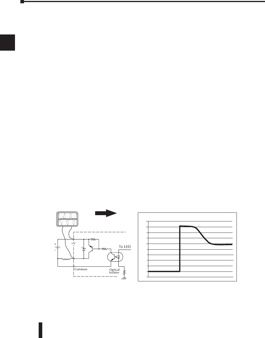
DL06 Micro PLC User Manual, 3rd Edition, Rev. D
Chapter 2: Installation, Wiring, and Specifications
1
2
3
4
5
6
7
8
9
10
11
12
13
14
A
B
C
D
2-22
In the same circuit on the previous page, replacing the relay with a larger 24 V/290 mA/7 W relay
will generate a transient voltage exceeding 800 V (not shown). Transient voltages like this can
cause many problems, including:
• Relay contacts driving the coil may experience arcing, which can pit the contacts and reduce the
relay’s lifespan.
• Solid state (transistor) outputs driving the coil can be damaged if the transient voltage exceeds the
transistor’s ratings. In extreme cases, complete failure of the output can occur the very first time a coil
is de-energized.
• Input circuits, which might be connected to monitor the coil or the output driver, can also be
damaged by the transient voltage.
A very destructive side-effect of the arcing across relay contacts is the electromagnetic interference
(EMI) it can cause. This occurs because the arcing causes a current surge, which releases RF
energy. The entire length of wire between the relay contacts, the coil, and the power source carries
the current surge and becomes an antenna that radiates the RF energy. It will readily couple into
parallel wiring and may disrupt the PLC and other electronics in the area. This EMI can make an
otherwise stable control system behave unpredictably at times.
1
2
3
4
5
6
7
8
9
10
11
12
13
14
a
B
c
d
PLC’s Integrated Transient Suppressors
Although the PLC’s outputs typically have integrated suppressors to protect against transients,
they are not capable of handling them all. It is usually necessary to have some additional
transient suppression for an inductive load.
Here is another example using the same 24 V/125 mA/3 W relay used earlier. This example
measures the PNP transistor output of a D0-06DD2 PLC, which incorporates an integrated
Zener diode for transient suppression. Instead of the 140V peak in the first example, the
transient voltage here is limited to about 40 V by the Zener diode. While the PLC will probably
tolerate repeated transients in this range for some time, the 40 V is still beyond the module’s
peak output voltage rating of 30 V.
5HOD\
&RLO
9'&
2VFLOORVFRSH
)RUWKLVH[DPSOHD9P$:
UHOD\LVXVHG$XWRPDWLRQ'LUHFW
SDUWQR&'
9ROWV
Example: Small Inductive Load with Only Integrated Suppression
The next example uses the same circuit as above, but with a larger 24 V/290 mA/7 W relay,
thereby creating a larger inductive load. As you can see, the transient voltage generated is much
worse, peaking at over 50 V. Driving an inductive load of this size without additional transient
suppression is very likely to permanently damage the PLC output.
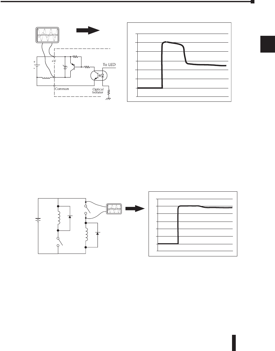
DL06 Micro PLC User Manual, 3rd Edition, Rev. D
Chapter 2: Installation, Wiring, and Specifications
1
2
3
4
5
6
7
8
9
10
11
12
13
14
A
B
C
D
2-23
1
2
3
4
5
6
7
8
9
10
11
12
13
14
a
B
c
d
Example: Larger Inductive Load with Only Integrated Suppression
5HOD\
&RLO
9'&
2VFLOORVFRSH
)RUWKLVH[DPSOHDP$:
UHOD\LVXVHG$XWRPDWLRQ'LUHFW
SDUWQR6&(*9'&
9ROWV
Additional transient suppression should be used in both these examples. If you are unable
to measure the transients generated by the connected loads of your control system, using
additional transient suppression on all inductive loads would be the safest practice.
Types of Additional Transient Protection
DC Coils:
The most effective protection against transients from a DC coil is a flyback diode. A flyback
diode can reduce the transient to roughly 1V over the supply voltage, as shown in this example.
Oscilloscope
24 VDC
DC Flyback Circuit
Sinking Sourcing
+
_
30
25
20
15
10
5
0
-5
Volts
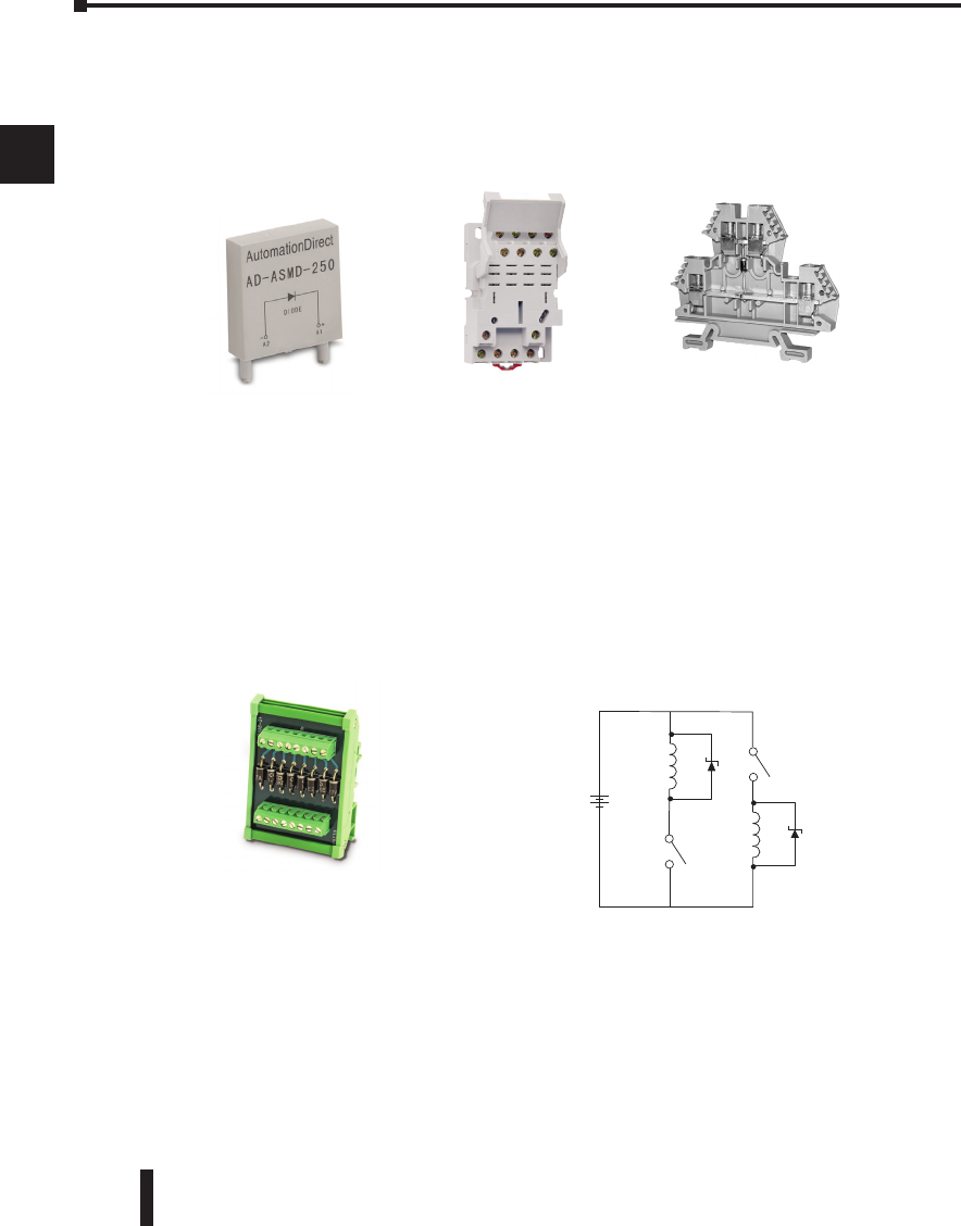
DL06 Micro PLC User Manual, 3rd Edition, Rev. D
Chapter 2: Installation, Wiring, and Specifications
1
2
3
4
5
6
7
8
9
10
11
12
13
14
A
B
C
D
2-24
1
2
3
4
5
6
7
8
9
10
11
12
13
14
a
B
c
d
Many AutomationDirect socketed relays and motor starters have add-on flyback diodes
that plug or screw into the base, such as the AD-ASMD-250 protection diode module and
784-4C-SKT-1 socket module shown below. If an add-on flyback diode is not available for
your inductive load, an easy way to add one is to use AutomationDirect’s DN-D10DR-A
diode terminal block, a 600 VDC power diode mounted in a slim DIN rail housing.
DN-D10DR-A
Diode Terminal Block
AD-ASMD-250
Protection Diode Module
784-4C-SKT-1
Relay Socket
ZL-TSD8-24
Transorb Module
Two more common options for DC coils are Metal Oxide Varistors (MOV) or TVS diodes.
These devices should be connected across the driver (PLC output) for best protection as shown
below. The optimum voltage rating for the suppressor is the lowest rated voltage available that
will NOT conduct at the supply voltage, while allowing a safe margin.
AutomationDirect’s ZL-TSD8-24 transorb module is a good choice for 24 VDC circuits. It is
a bank of 8 uni-directional 30 V TVS diodes. Since they are uni-directional, be sure to observe
the polarity during installation. MOVs or bi-directional TVS diodes would install at the same
location, but have no polarity concerns.
24 VDC
DC MOV or TVS Diode Circuit
Sinking Sourcing
+
_
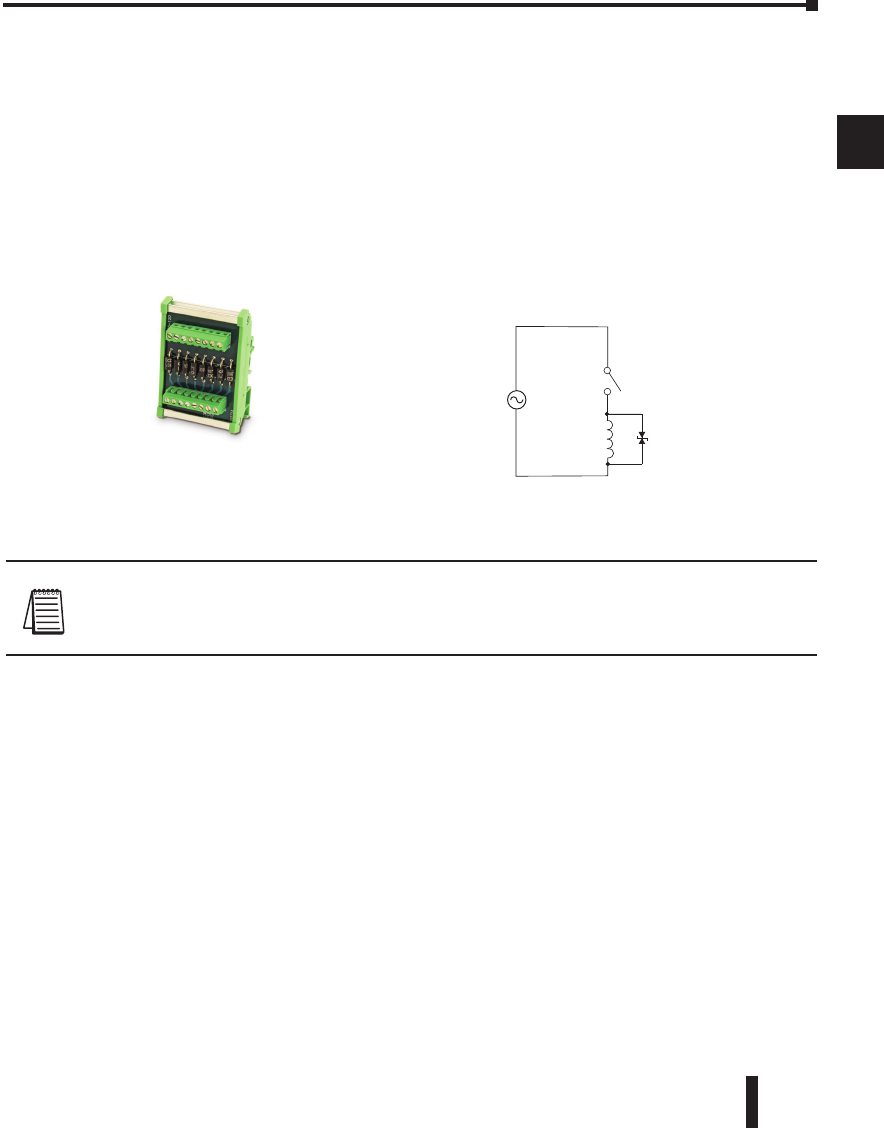
DL06 Micro PLC User Manual, 3rd Edition, Rev. D
Chapter 2: Installation, Wiring, and Specifications
1
2
3
4
5
6
7
8
9
10
11
12
13
14
A
B
C
D
2-25
1
2
3
4
5
6
7
8
9
10
11
12
13
14
a
B
c
d
AC Coils:
Two options for AC coils are MOVs or bi-directional TVS diodes. These devices are most
effective at protecting the driver from a transient voltage when connected across the driver
(PLC output) but are also commonly connected across the coil. The optimum voltage rating
for the suppressor is the lowest rated voltage available that will NOT conduct at the supply
voltage, while allowing a safe margin.
AutomationDirect’s ZL-TSD8-120 transorb module is a good choice for 120 VAC circuits. It
is a bank of eight bi-directional 180 V TVS diodes.
ZL-TSD8-120
Transorb Module
NOTE: Manufacturers of devices with coils frequently offer MOV or TVS diode suppressors as an
add-on option which mount conveniently across the coil. Before using them, carefully check the
suppressor’s ratings. Just because the suppressor is made specifically for that part does not mean it
will reduce the transient voltages to an acceptable level.
For example, a MOV or TVS diode rated for use on 24-48 VDC coils would need to have a
high enough voltage rating to NOT conduct at 48 V. That suppressor might typically start
conducting at roughly 60 VDC. If it were mounted across a 24 V coil, transients of roughly
84 V (if sinking output) or -60 V (if sourcing output) could reach the PLC output. Many
semiconductor PLC outputs cannot tolerate such levels.
VAC
A
C MOV or Bi-Directional Diode Circuit
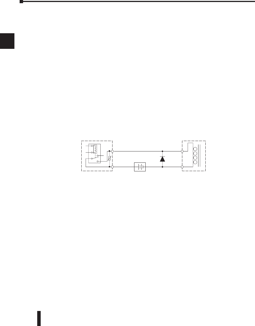
DL06 Micro PLC User Manual, 3rd Edition, Rev. D
Chapter 2: Installation, Wiring, and Specifications
1
2
3
4
5
6
7
8
9
10
11
12
13
14
A
B
C
D
2-26
Prolonging Relay Contact Life
Relay contacts wear according to the amount of relay switching, amount of spark created at
the time of open or closure, and presence of airborne contaminants. There are some steps you
can take to help prolong the life of relay contacts, such as switching the relay on or off only
when it is necessary, and if possible, switching the load on or off at a time when it will draw
the least current. Also, take measures to suppress inductive voltage spikes from inductive DC
loads such as contactors and solenoids.
For inductive loads in DC circuits we recommend using a suppression diode as shown in the
following diagram (DO NOT use this circuit with an AC power supply). When the load is
energized the diode is reverse-biased (high impedance). When the load is turned off, energy
stored in its coil is released in the form of a negative-going voltage spike. At this moment the
diode is forward-biased (low impedance) and shunts the energy to ground. This protects the
relay contacts from the high voltage arc that would occur just as the contacts are opening.
Place the diode as close to the inductive field device as possible. Use a diode with a peak
inverse voltage rating (PIV) at least 100 PIV, 3 A forward current or larger. Use a fast-
recovery type (such as Schottky type). DO NOT use a small-signal diode such as 1N914,
1N941, etc. Be sure the diode is in the circuit correctly before operation. If installed
backwards, it short-circuits the supply when the relay energizes.
1
2
3
4
5
6
7
8
9
10
11
12
13
14
a
B
c
d
Inductive Field Device
+–
PLC Relay Output
Output
Common
Input
Common
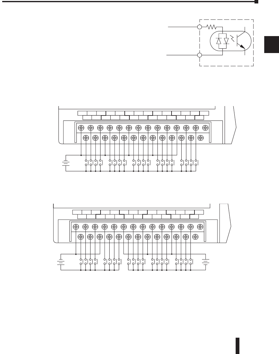
DL06 Micro PLC User Manual, 3rd Edition, Rev. D
Chapter 2: Installation, Wiring, and Specifications
1
2
3
4
5
6
7
8
9
10
11
12
13
14
A
B
C
D
2-27
DC Input Wiring Methods
DL06 Micro PLCs with DC inputs are particularly
flexible because they can be wired as either sinking
or sourcing. The dual diodes (shown to the right)
allow 10.8 – 26.4 VDC. The target applications are
+12 VDC and +24 VDC. You can actually wire each
group of inputs associated common group of inputs
as DC sinking and the other half as DC sourcing.
Inputs grouped by a common must be all sinking or all
sourcing.
In the first and simplest example below, all commons are connected together and all inputs
are sinking.
In the next example, the first eight inputs are sinking, and the last twelve are sourcing.
1
2
3
4
5
6
7
8
9
10
11
12
13
14
a
B
c
d
PLC DC Input
Common
Input
LOGIC
Koyo
06
fuse
C0 C4C2X1 X3 X4 X6 X11 X13 X14 X16 X21X23 N.C.
C1 C3X2 X5 X7 X10X12 X15X17 X20X22X0 N.C.
AC(N)24V
0V
+V
C1 C3Y0 Y15Y12Y10Y17Y7Y5Y2
C0 C2 Y16Y14Y13Y11Y6Y4Y3Y1
LG
G
AC(L)
OUTPUT: Sinking Output 6 - 27V1.0A
INPUT: 12 - 24V 3 - 15mA
Y
X
D0-06DD1
40VA50-60HzPWR: 100-240V
+24 VDC
+
-
L LL L L LL LL LL L L LL L
+24 VDC
+
-
LOGIC
Koyo
06
fuse
C0 C4C2X1 X3 X4 X6 X11 X13 X14 X16 X21X23 N.C.
C1 C3X2 X5 X7 X10X12 X15X17 X20X22X0 N.C.
AC(N)24V
0V
+V
C1 C3Y0 Y15Y12Y10Y17Y7Y5Y2
C0 C2 Y16Y14Y13Y11Y6Y4Y3Y1
LG
G
AC(L)
OUTPUT: Sinking Output 6 - 27V1.0A
INPUT: 12 - 24V 3 - 15mA
Y
X
D0-06DD1
40VA50-60HzPWR: 100-240V
+24 VDC
+
-
L LL L L LL LL LL L L LL L
+12 VDC
+
-
+24 VDC
+
-
+
-
+12 VDC
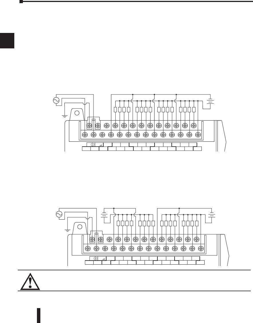
DL06 Micro PLC User Manual, 3rd Edition, Rev. D
Chapter 2: Installation, Wiring, and Specifications
1
2
3
4
5
6
7
8
9
10
11
12
13
14
A
B
C
D
2-28
1
2
3
4
5
6
7
8
9
10
11
12
13
14
a
B
c
d
DC Output Wiring Methods
DL06 DC output circuits are high-performance transistor switches with low on-resistance
and fast switching times. Please note the following characteristics which are unique to the DC
output type:
• There is only one electrical common for all sixteen outputs. All sixteen outputs belong to one bank.
• The output switches are current-sinking only or current sourcing only. Refer to the detailed
specifications in this manual to determine which type output is present on a particular model.
• The output circuit inside the PLC requires external power. The supply (–) must be connected to
a common terminal, and the supply (+) connects the right-most terminal on the upper connector
(+V).
In the example below, all sixteen outputs share a common supply.
In the next example below, the outputs have split supplies. The first eight outputs are using a
+12 VDC supply, and the last eight are using a +24 VDC supply. However, you can split the
outputs among any number of supplies, as long as:
• all supply voltages are within the specified range
• all output points are wired as sinking
• all source (–) terminals are connected together
Warning: The maximum output current from the Auxiliary 24 VDC power depends on the I/O
configuration. Refer to Chapter 4, page 4-6, to determine how much current can be drawn from
the Auxiliary 24 VDC power for your particular I/O configuration.
LOGIC
Koyo
06
DC
Supply
C0 C4C2X1 X3 X4 X6 X11 X13 X14 X16 X21 X23 N.C.
C1 C3X2 X5 X7 X10 X12 X15 X17 X20 X22X0 N.C.
AC(N)24V
0V
+V
C1 C3Y0 Y15Y12Y10 Y17Y7Y5Y2
C0 C2 Y16Y14Y13Y11Y6Y4Y3Y1
LGG
AC(L)
OUTPUT: Sinking Output 6 - 27V 1.0A
INPUT: 12 - 24V 3 - 15mA
Y
X
D0-06DD1
40VA50-60HzPWR: 100-240V
+24 VDC
+
-
LLLL LLLLLLLL LLLL
01 2345 6710 11 12 13 14 15 16 17 20 21 22 23
LOGIC
Koyo
06
C0 C4C2X1 X3 X4 X6 X11 X13 X14 X16 X21 X23 N.C.
C1 C3X2 X5 X7 X10 X12 X15 X17 X20 X22X0 N.C.
AC(N)24V
0V
+V
C1 C3Y0 Y15Y12Y10 Y17Y7Y5Y2
C0 C2 Y16Y14Y13Y11Y6Y4Y3Y1
LGG
AC(L)
OUTPUT: Sinking Output 6 - 27V 1.0A
INPUT: 12 - 24V 3 - 15mA
Y
X
D0-06DD1
40VA50-60HzPWR: 100-240V
+24 VDC
+
-
LLLL LLLLLLLL LLLL
012345671011121314151617202122 23
+12 VDC
+
-
+24 VDC
+
-
+
-
+12 VDC
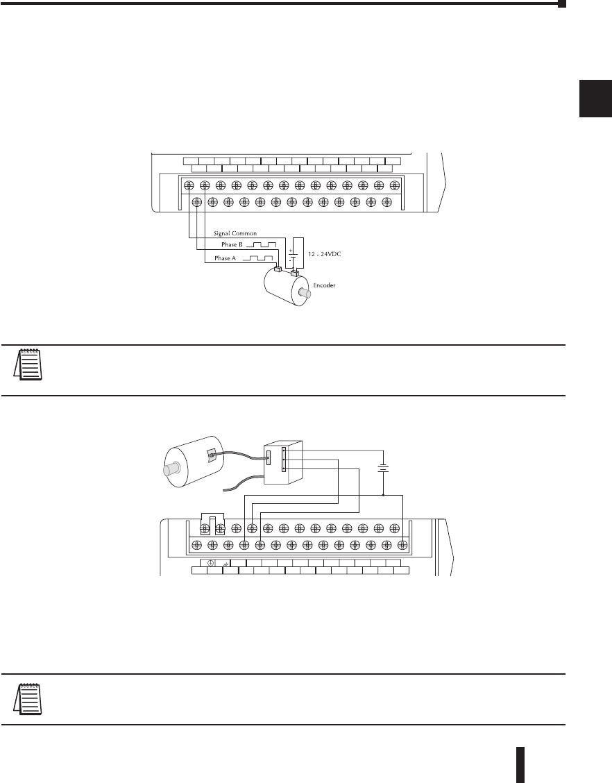
DL06 Micro PLC User Manual, 3rd Edition, Rev. D
Chapter 2: Installation, Wiring, and Specifications
1
2
3
4
5
6
7
8
9
10
11
12
13
14
A
B
C
D
2-29
High-Speed I/O Wiring Methods
DL06 versions with DC type input or output points contain a dedicated High-Speed I/O
circuit (HSIO). The circuit configuration is programmable, and it processes specific I/O
points independently from the CPU scan. Appendix E discusses the programming options for
HSIO. While the HSIO circuit has six modes, we show wiring diagrams for two of the most
popular modes in this chapter. The high-speed input interfaces to points X0 – X3. Properly
configured, the DL06 can count quadrature pulses at up to 7 kHz from an incremental
encoder as shown below.
NOTE: Do not use this drawing to wire your device. This is a general example and is not specific
to any PLC model, stepper or encoder. Always refer to the device documentaion for proper wiring
connections.
DL06 versions with DC type output points can use the High Speed I/O Pulse Output
feature. It can generate high-speed pulses at up to 10 kHz for specialized control such as
stepper motor / intelligent drive systems. Output Y0 and Y1 can generate pulse and direction
signals, or it can generate CCW and CW pulse signals respectively. See Appendix E on high-
speed input and pulse output options.
NOTE: Do not use this drawing to wire your device. This is a general example and is not specific
to any PLC model, stepper or encoder. Always refer to the device documentaion for proper wiring
connections.
1
2
3
4
5
6
7
8
9
10
11
12
13
14
a
B
c
d
LOGIC
Koyo
06
C0 C4C2X1 X3 X4 X6 X11X13 X14X16 X21 X23 N.C.
C1 C3X2 X5 X7 X10 X12 X15 X17 X20X22X0 N.C.
AC(N)24V
0V
+V
C1 C3Y0 Y15Y12Y10Y17Y7Y5Y2
C0 C2 Y16Y14Y13Y11Y6Y4Y3Y1
LG
G
AC(L)
OUTPUT: Sinking Output 6 - 27V 1.0A
INPUT: 12 - 24V 3 - 15mA
Y
X
D0-06DD1
40VA50-60HzPWR: 100-240V
01 2345 6710 11 12 13 14 15 16 17 20 21 22 23
+
-
+24 VDC
Motor
Power Input
Amplifier
Signal Common
Pulse
Direction
Phase A = X0
Phase B = X1
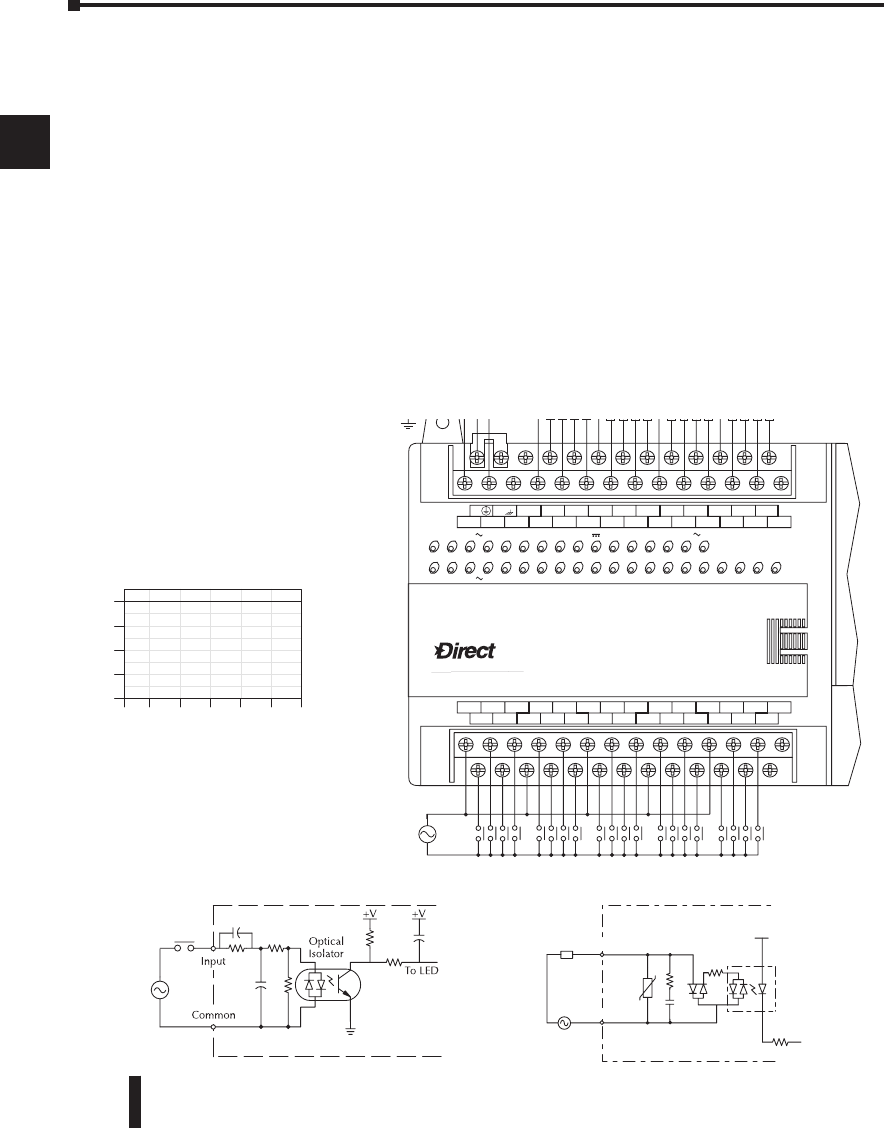
DL06 Micro PLC User Manual, 3rd Edition, Rev. D
Chapter 2: Installation, Wiring, and Specifications
1
2
3
4
5
6
7
8
9
10
11
12
13
14
A
B
C
D
2-30
1
2
3
4
5
6
7
8
9
10
11
12
13
14
a
B
c
d
Wiring Diagrams and Specifications
The remainder of this chapter provides detailed technical information for the DL06 PLCs. A basic
wiring diagram, equivalent I/O circuits, and specification tables are laid out for each PLC.
D0–06AA I/O Wiring Diagram
The D0–06AA PLC has twenty AC inputs and sixteen AC outputs. The following diagram shows a
typical field wiring example. The AC external power connection uses four terminals as shown.
Inputs are organized into five banks of four. Each bank has an isolated common terminal. The
wiring example below shows all commons connected together, but separate supplies and common
circuits may be used. The equivalent input circuit shows one channel of a typical bank.
Outputs are organized into four banks of four triac switches. Each bank has a common terminal. The
wiring example below shows all commons connected together, but separate supplies and common
circuits may be used. The equivalent output circuit shows one channel of a typical bank.
LOGIC
Koyo
06
LLLL
C0 C4C2X1 X3 X4 X6 X11 X13 X14 X16 X21 X23 N.C.
C1 C3X2 X5 X7 X10 X12 X15 X17 X20 X22X0 N.C.
LLLLLLLL LLLL
AC(N)24V
0V
N.C.
C1 C3Y0 Y15Y12Y10 Y17Y7Y5Y2
C0 C2 Y16Y14Y13Y11Y6Y4Y3Y1
LGG
AC(L)
D0-06AA
40VA50-60HzPWR: 100-240V2.0AOUTPUT: 6-240V 50 - 60Hz 2.0A, 6 - 27V
Y
X
7 - 15mAINPUT: 90 - 120V
012345671011121314151617202122 23
OUTPUT
point wiring
17-240V
VAC
POWER
input wiring
100-240V
VAC
INPUT point wiring
90-120V
VAC
9$&
Equivalent Input Circuit
Optical
Isolator
To LED
Internal module circuitry
L
+V
OUTPUT
COM
Equivalent Output Circuit
0
4
12
16
Points
Ambient Temperature ( ˚C/˚F)
0
32
10
50
20
68
30
86
40
104
50
122
55˚C
131˚F
Y0 - Y7
0.5 A
Y10 - Y17
8
AA
Derating Chart for AC Outputs
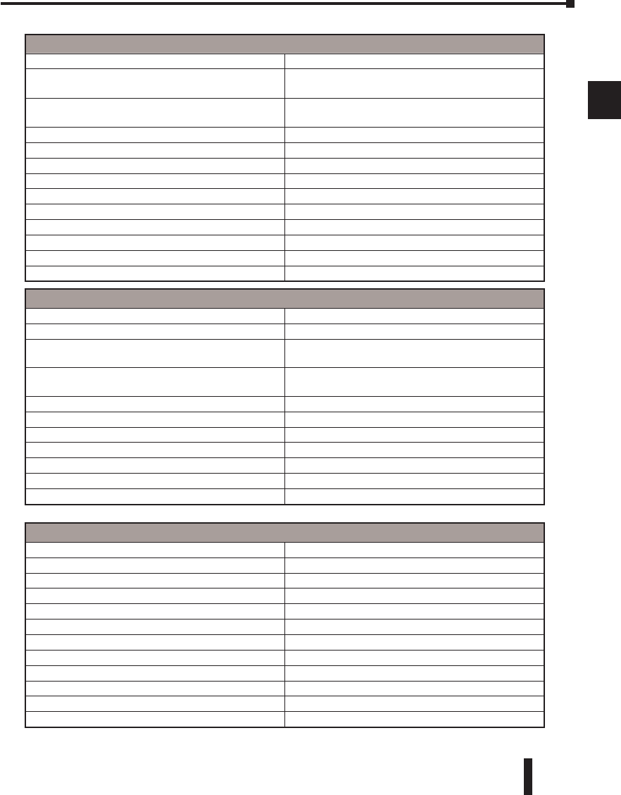
DL06 Micro PLC User Manual, 3rd Edition, Rev. D
Chapter 2: Installation, Wiring, and Specifications
1
2
3
4
5
6
7
8
9
10
11
12
13
14
A
B
C
D
2-31
1
2
3
4
5
6
7
8
9
10
11
12
13
14
a
B
c
d
D0-06AA General Specifications
External Power Requirements 100– 240 VAC/50-60 Hz, 40 VA maximum
Communication Port 1 9600 baud (Fixed),
8 data bits, 1 stop bit odd parity K–Sequence (Slave), DirectNET (Slave), MODBUS (Slave)
Communication Port 2 9600 baud (default)
8 data bits, 1 stop bit odd parity
K–Sequence (Slave),DirectNET (Master/Slave), MODBUS
(Master/Slave), Non-sequence / print, ASCII in/out
Programming cable type D2–DSCBL
Operating Temperature 32 to 131°F (0 to 55°C)
Storage Temperature –4 to 158°F (–20 to 70°C)
Relative Humidity 5 to 95% (non-condensing)
Environmental air No corrosive gases permitted
Vibration MIL STD 810C 514.2
Shock MIL STD 810C 516.2
Noise Immunity NEMA ICS3–304
Terminal Type Removable
Wire Gauge One 16 AWG or two 18 AWG, 24 AWG minimum
AC Input Specifications
Input Voltage Range (Min. - Max.) 80 – 132 VAC, 47 - 63 Hz
Operating Voltage Range 90 – 120 VAC, 47 - 63 Hz
Input Current 8 mA @100 VAC at 50 Hz
10 mA @100 VAC at 60 Hz
Max. Input Current 12 mA @132 VAC at 50 Hz
15 mA @132 VAC at 60 Hz
Input Impedance 14Kq @50 Hz, 12Kq @60Hz
ON Current/Voltage > 6 mA @ 75 VAC
OFF Current/Voltage < 2 mA @ 20 VAC
OFF to ON Response < 40 ms
ON to OFF Response < 40 ms
Status Indicators Logic Side
Commons 4 channels / common x 5 banks (isolated)
AC Output Specifications
Output Voltage Range (Min. - Max.) 15 – 264 VAC, 47 – 63 Hz
Operating Voltage 17 – 240 VAC, 47 – 63 Hz
On Voltage Drop 1.5 VAC (>50mA) 4.0 VAC (<50mA)
Max Current 0.5 A / point, 1.5 A / common
Max leakage current <4 mA @ 264 VAC
Max inrush current 10 A for 10 ms
Minimum Load 10 mA
OFF to ON Response 1 ms
ON to OFF Response 1 ms +1/2 cycle
Status Indicators Logic Side
Commons 4 channels / common x 4 banks (isolated)
Fuses None (external recommended)
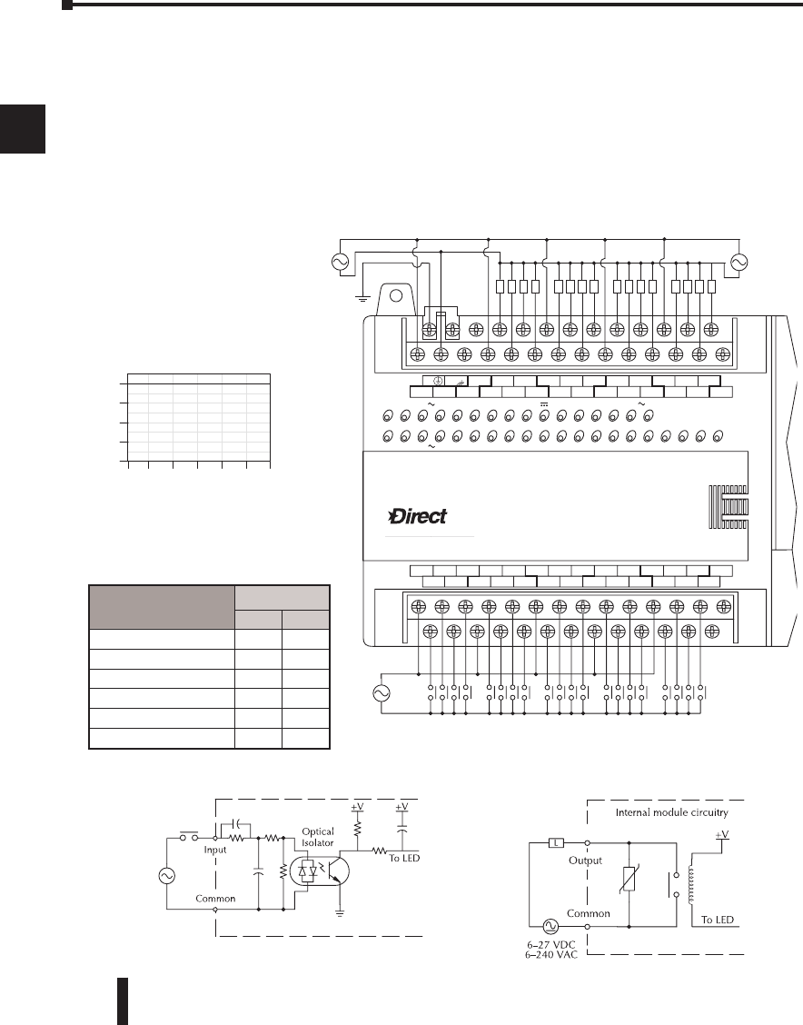
DL06 Micro PLC User Manual, 3rd Edition, Rev. D
Chapter 2: Installation, Wiring, and Specifications
1
2
3
4
5
6
7
8
9
10
11
12
13
14
A
B
C
D
2-32
D0–06AR I/O Wiring Diagram
The D0–06AR PLC has twenty AC inputs and sixteen relay contact outputs. The following
diagram shows a typical field wiring example. The AC external power connection uses four
terminals at the left as shown.
The twenty AC input channels use terminals on the bottom of the connector. Inputs are
organized into five banks of four. Each bank has a common terminal. The wiring example
below shows all commons connected together, but separate supplies and common circuits
may be used. The equivalent input circuit shows one channel of a typical bank.
1
2
3
4
5
6
7
8
9
10
11
12
13
14
a
B
c
d
LOGIC
Koyo
06
LLLL
C0 C4C2X1 X3 X4 X6 X11 X13 X14 X16 X21 X23 N.C.
C1 C3X2 X5 X7 X10 X12 X15 X17 X20 X22X0 N.C.
LLLLLLLL LLLL
AC(N)24V
0V
N.C.
C1 C3Y0 Y15Y12Y10 Y17Y7Y5Y2
C0 C2 Y16Y14Y13Y11Y6Y4Y3Y1
LGG
AC(L)
D0-06AR
40VA50-60HzPWR: 100-240V2.0AOUTPUT: 6-240V 50 - 60Hz 2.0A, 6 - 27V
Y
X
7 - 15mAINPUT: 90 - 120V
012345671011121314151617202122 23
OUTPUT point wiring
6-240
VAC
or
6-27
VDC
POWER
input wiring
100-240V
VAC
INPUT point wiring
90-120V
VAC
0
4
12
16
Points
Ambient Temperature ( ˚C/ ˚F)
0
32
10
50
20
68
30
86
40
104
50
122
55˚C
131˚F
Y0 - Y7
2.0A
Y10 - Y17
8
AR
Derating Chart for Relay Outputs
9$&
Equivalent Input Circuit Equivalent Output Circuit
Typical Relay Life (Operations) at
Room Temperature
Voltage & Load
Type
Load Current
At 1A At 2A
24VDC Resistive 500K 250K
24VDC Inductive 100K 50K
110VAC Resistive 500K 250K
110VAC Inductive 200K 100K
220VAC Resistive 350K 200K
220VAC Inductive 100K 50K
DL06 Micro PLC User Manual, 3rd Edition, Rev. D
Chapter 2: Installation, Wiring, and Specifications
1
2
3
4
5
6
7
8
9
10
11
12
13
14
A
B
C
D
2-33
The sixteen relay output channels use terminals on the right side top connector. Outputs are
organized into four banks of four normally-open relay contacts. Each bank has a common
terminal. The wiring example on the last page shows all commons connected together, but
separate supplies and common circuits may be used. The equivalent output circuit shows one
channel of a typical bank. The relay contacts can switch AC or DC voltages. 1
2
3
4
5
6
7
8
9
10
11
12
13
14
a
B
c
d
D0-06AR General Specifications
External Power Requirements 100– 240 VAC/50-60 Hz, 40 VA maximum
Communication Port 1 9600 baud (Fixed), 8 data
bits, 1 stop bit, odd parity K–Sequence (Slave), DirectNET (Slave), MODBUS (Slave)
Communication Port 2 9600 baud (default), 8 data
bits, 1 stop bit, odd parity
K–Sequence (Slave), DirectNET (Master/Slave), MODBUS
(Master/Slave), Non-sequence / print, ASCII in/out
Programming cable type D2–DSCBL
Operating Temperature 32 to 131°F (0 to 55°C)
Storage Temperature –4 to 158°F (–20 to 70°C)
Relative Humidity 5 to 95% (non-condensing)
Environmental air No corrosive gases permitted
Vibration MIL STD 810C 514.2
Shock MIL STD 810C 516.2
Noise Immunity NEMA ICS3–304
Terminal Type Removable
Wire Gauge One 16 AWG or two 18 AWG, 24 AWG minimum
AC Input Specifications X0-X23
Input Voltage Range (Min. - Max.) 80 – 132 VAC, 47 - 63 Hz
Operating Voltage Range 90 – 120 VAC, 47 -63 Hz
Input Current 8 mA @ 100 VAC at 50 Hz 10 mA @ 100 VAC at 60 Hz
Max. Input Current 12 mA @ 132 VAC at 50 Hz 15 mA @ 132 VAC at 60 Hz
Input Impedance 14Kq @50 Hz, 12Kq @60 Hz
ON Current/Voltage >6 mA @ 75 VAC
OFF Current/Voltage <2 mA @ 20 VAC
OFF to ON Response < 40 ms
ON to OFF Response < 40 ms
Status Indicators Logic Side
Commons 4 channels / common x 5 banks (isolated)
Relay Output Specifications Y0-Y17
Output Voltage Range (Min. – Max.) 5 – 264 VAC (47 -63 Hz), 5 – 30 VDC
Operating Voltage Range 6 – 240 VAC (47 -63 Hz), 6 – 27 VDC
Output Current 2A / point, 6A / common
Max. leakage current 0.1 mA @264VAC
Smallest Recommended Load 5 mA @5 VDC
OFF to ON Response < 15 ms
ON to OFF Response < 10 ms
Status Indicators Logic Side
Commons 4 channels / common x 4 banks (isolated)
Fuses None (external recommended)
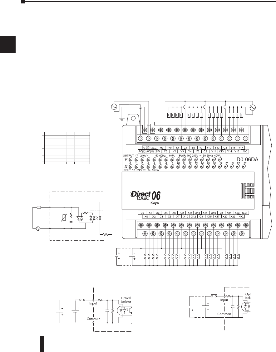
DL06 Micro PLC User Manual, 3rd Edition, Rev. D
Chapter 2: Installation, Wiring, and Specifications
1
2
3
4
5
6
7
8
9
10
11
12
13
14
A
B
C
D
2-34
D0–06DA I/O Wiring Diagram
The D0–06DA PLC has twenty DC inputs and sixteen AC outputs. The following diagram shows
a typical field wiring example. The AC external power connection uses four terminals as shown.
Inputs are organized into five banks of four. Each bank has an isolated common terminal, and
may be wired as sinking or sourcing. The wiring example below shows all commons connected
together, but separate supplies and common circuits may be used. The equivalent circuit for
standard inputs is shown below, and the high-speed input circuit is shown to the left.
Outputs are organized into four banks of four triac switches. Each bank has a common terminal.
The wiring example below shows all commons connected together, but separate supplies and
common circuits may be used. The equivalent output circuit shows one channel of a typical bank.
1
2
3
4
5
6
7
8
9
10
11
12
13
14
a
B
c
d
9'&
6LQN6RXUFH
High Speed Inputs (X0-X3)
9'&
6LQN
6RXUFH
Standard Inputs (X4-X23)
Power
input wiring
Input point wiring
Output point wiring
100-240 VAC
17-240
VAC
12-24
VDC SinkSource
0
4
12
16
Points
Ambient Temperature (
˚
C/
˚
F)
0
32
10
50
20
68
30
86
40
104
50
122
55˚C
131˚F
Y0 - Y7
0.5 A
Y10 - Y17
8
Derating Chart for AC Outputs
Optical
Isolator
To
LED
Internal module circuitry
L
+V
OUTPUT
COM
Equivalent Output Circuit
DL06 Micro PLC User Manual, 3rd Edition, Rev. D
Chapter 2: Installation, Wiring, and Specifications
1
2
3
4
5
6
7
8
9
10
11
12
13
14
A
B
C
D
2-35
1
2
3
4
5
6
7
8
9
10
11
12
13
14
a
B
c
d
D0-06DA General Specifications
External Power Requirements 100– 240 VAC/50-60 Hz, 40 VA maximum
Communication Port 1 9600 baud (Fixed), 8 data
bits, 1 stop bit, odd parity
K–Sequence (Slave), DirectNET (Slave),
MODBUS (Slave)
Communication Port 2 9600 baud (default), 8 data
bits, 1 stop bit, odd parity
K–Sequence (Slave), DirectNET (Master/Slave),
MODBUS (Master/Slave), Non-sequence/print, ASCII in/out
Programming cable type D2–DSCBL
Operating Temperature 32 to 131°F (0 to 55°C)
Storage Temperature –4 to 158°F (–20 to 70°C)
Relative Humidity 5 to 95% (non-condensing)
Environmental air No corrosive gases permitted
Vibration MIL STD 810C 514.2
Shock MIL STD 810C 516.2
Noise Immunity NEMA ICS3–304
Terminal Type Removable
Wire Gauge One 16 AWG or two 18 AWG, 24 AWG minimum
DC Input Specifications
Parameter High–Speed Inputs, X0 – X3 Standard DC Inputs X4 – X23
Input Voltage Range 10.8 – 26.4 VDC 10.8 – 26.4 VDC
Operating Voltage Range 12 – 24 VDC 12 – 24 VDC
Maximum Voltage 30 VDC (7 kHz maximum frequency) 30 VDC
Minimum Pulse Width 70 µs N/A
ON Voltage Level > 10 VDC > 10 VDC
OFF Voltage Level < 2.0 VDC < 2.0 VDC
Input Impedance 1.8 kq @ 12 – 24 VDC 2.8 kq @ 12 – 24 VDC
Minimum ON Current >5 mA >4 mA
Maximum OFF Current < 0.5 mA <0.5 mA
OFF to ON Response <70 µs 2 – 8 ms, 4 ms typical
ON to OFF Response <70 µs 2 – 8 ms, 4 ms typical
Status Indicators Logic side Logic side
Commons 4 channels / common x 5 bank (isolated)
AC Output Specifications
Output Voltage Range (Min. - Max.) 15 – 264 VAC, 47 – 63 Hz
Operating Voltage 17 – 240 VAC, 47 – 63 Hz
On Voltage Drop 1.5 VAC @> 50mA, 4 VAC @< 50mA
Max Current 0.5 A / point, 1.5 A / common
Max leakage current < 4 mA @ 264 VAC, 60Hz
Max inrush current 10 A for 10 ms
Minimum Load 10 mA
OFF to ON Response 1 ms
ON to OFF Response 1 ms +1/2 cycle
Status Indicators Logic Side
Commons 4 channels / common x 4 banks (isolated)
Fuses None (external recommended)
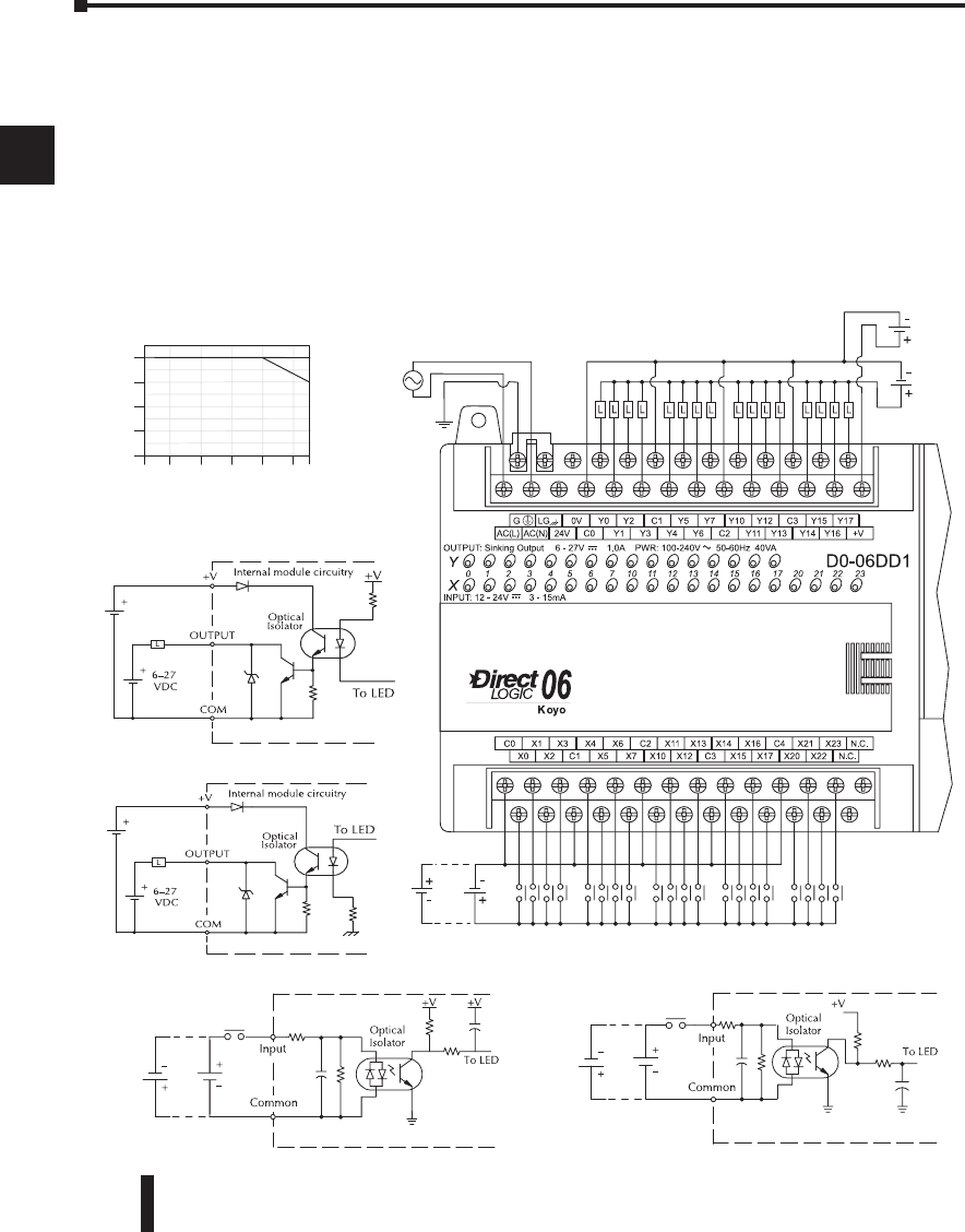
DL06 Micro PLC User Manual, 3rd Edition, Rev. D
Chapter 2: Installation, Wiring, and Specifications
1
2
3
4
5
6
7
8
9
10
11
12
13
14
A
B
C
D
2-36
1
2
3
4
5
6
7
8
9
10
11
12
13
14
a
B
c
d
9'&
6LQN
6RXUFH
DC Standard Inputs (X4-X23)
9'&
DC Pulse Outputs (Y0-Y1)
9'&
DC Standard Outputs (Y2-Y17)
9'&
6LQN6RXUFH
High Speed Inputs (X0-X3)
0
4
12
16
Points
Ambient Temperature ( °C/°F)
0
32
10
50
20
68
30
86
40
104
50
122
55°C
131°F
1.0 A
Y0-Y17
8
0.75A
Derating Chart for DC Outputs
D0–06DD1 I/O Wiring Diagram
The D0-06DD1 PLC has twenty sinking/sourcing DC inputs and sixteen sinking DC outputs. The
following diagram shows a typical field wiring example. The AC external power connection uses four
terminals as shown.
Inputs are organized into five banks of four. Each bank has an isolated common terminal,
and may be wired as either sinking or sourcing inputs. The wiring example below shows all
commons connected together, but separate supplies and common circuits may be used.
Outputs all share the same common. Note the requirement for external power.
Power
input wiring
Input point wiring
Output point wiring
6-27
VDC
20-28
VDC
12-24 VDC
100-240
VAC
SinkSource
DL06 Micro PLC User Manual, 3rd Edition, Rev. D
Chapter 2: Installation, Wiring, and Specifications
1
2
3
4
5
6
7
8
9
10
11
12
13
14
A
B
C
D
2-37
1
2
3
4
5
6
7
8
9
10
11
12
13
14
a
B
c
d
D0-06DD1 General Specifications
External Power Requirements 100– 240 VAC/50-60 Hz, 40 VA maximum
Communication Port 1 9600 baud (Fixed),
8 data bits, 1 stop bit, odd parity
K–Sequence (Slave), DirectNET (Slave),
MODBUS (Slave)
Communication Port 2 9600 baud (default),
8 data bits, 1 stop bit, odd parity
K–Sequence (Slave), DirectNET (Master/Slave),
MODBUS (Master/Slave), Non-sequence / print, ASCII in/out
Programming cable type D2–DSCBL
Operating Temperature 32 to 131°F (0 to 55°C)
Storage Temperature –4 to 158°F (–20 to 70°C)
Relative Humidity 5 to 95% (non-condensing)
Environmental air No corrosive gases permitted
Vibration MIL STD 810C 514.2
Shock MIL STD 810C 516.2
Noise Immunity NEMA ICS3–304
Terminal Type Removable
Wire Gauge One 16 AWG or two 18 AWG, 24 AWG minimum
DC Input Specifications
Parameter High–Speed Inputs, X0 – X3 Standard DC Inputs X4 – X23
Min. - Max. Voltage Range 10.8 – 26.4 VDC 10.8 – 26.4 VDC
Operating Voltage Range 12 – 24 VDC 12 – 24 VDC
Peak Voltage 30 VDC (7 kHz maximum frequency) 30 VDC
Minimum Pulse Width 100 µs N/A
ON Voltage Level > 10.0 VDC > 10.0 VDC
OFF Voltage Level < 2.0 VDC < 2.0 VDC
Max. Input Current 6mA @12VDC, 13mA @24VDC 4mA @12VDC, 8.5mA @24VDC
Input Impedance 1.8 qk @ 12 – 24 VDC 2.8 qk @ 12 – 24 VDC
Minimum ON Current >5 mA >4 mA
Maximum OFF Current < 0.5 mA <0.5 mA
OFF to ON Response <70 µs 2 – 8 ms, 4 ms typical
ON to OFF Response <70 µs 2 – 8 ms, 4 ms typical
Status Indicators Logic side Logic side
Commons 4 channels / common x 5 banks isolated
DC Output Specifications
Parameter Pulse Outputs Y0 – Y1 Standard Outputs Y2 – Y17
Min. - Max. Voltage Range 5 – 30 VDC 5 – 30 VDC
Operating Voltage 6 – 27 VDC 6 – 27 VDC
Peak Voltage < 50 VDC (10 kHz max. frequency) < 50 VDC
On Voltage Drop 0.3 VDC @ 1 A 0.3 VDC @ 1 A
Max Current (resistive) 0.5 A / pt., 1A / pt. as standard pt. 1.0 A / point
Max leakage current 15µA @ 30 VDC 15µA @ 30 VDC
Max inrush current 2 A for 100 ms 2 A for 100 ms
External DC power required 20 - 28 VDC Max 150mA 20 - 28 VDC Max 280mA (Aux. 24VDC
powers V+ terminal (sinking outputs)
OFF to ON Response < 10 µs < 10 µs
ON to OFF Response < 20 µs < 60 µs
Status Indicators Logic Side Logic Side
Commons 4 channels / common x 4 banks non-isolated
Fuses None (external recommended)
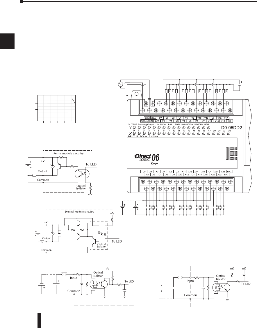
DL06 Micro PLC User Manual, 3rd Edition, Rev. D
Chapter 2: Installation, Wiring, and Specifications
1
2
3
4
5
6
7
8
9
10
11
12
13
14
A
B
C
D
2-38
1
2
3
4
5
6
7
8
9
10
11
12
13
14
a
B
c
d
D0–06DD2 I/O Wiring Diagram
The D0–06DD2 PLC has twenty sinking/sourcing DC inputs and sixteen sourcing DC outputs. The
following diagram shows a typical field wiring example. The AC external power connection uses four
terminals as shown.
Inputs are organized into four banks of four. Each bank has an isolated common terminal,
and may be wired as either sinking or sourcing inputs. The wiring example below shows all
commons connected together, but separate supplies and common circuits may be used.
All outputs share the same common. Note the requirement for external power.
9'&
6LQN
6RXUFH
DC Standard Inputs (X4-X23)
9'&
DC Pulse Outputs (Y0-Y1)
9'&
DC Standard Outputs (Y2-Y17)
Power input wiring
Input point wiring
Output point wiring
100-240
VAC12-24
VDC
12-24 VDC
SinkSource
0
4
12
16
Points
Ambient Temperature (
˚
C/
˚
F)
0
32
10
50
20
68
30
86
40
104
50
122
55˚C
131˚F
Y0 - Y7
1.0 A Y10 - Y17
8
0.75A
Derating Chart for DC Outputs
9'&
6LQN6RXUFH
High Speed Inputs (X0-X3)
DL06 Micro PLC User Manual, 3rd Edition, Rev. D
Chapter 2: Installation, Wiring, and Specifications
1
2
3
4
5
6
7
8
9
10
11
12
13
14
A
B
C
D
2-39
1
2
3
4
5
6
7
8
9
10
11
12
13
14
a
B
c
d
D0-06DD2 General Specifications
External Power Requirements 100– 240 VAC/50-60 Hz, 40 VA maximum
Communication Port 1 9600 baud (Fixed),
8 data bits, 1 stop bit, odd parity
K–Sequence (Slave), DirectNET (Slave),
MODBUS (Slave)
Communication Port 2 9600 baud (default),
8 data bits, 1 stop bit, odd parity
K–Sequence (Slave), DirectNET (Master/Slave),
MODBUS (Master/Slave), Non-sequence / print, ASCII in/out
Programming cable type D2–DSCBL
Operating Temperature 32 to 131°F (0 to 55°C)
Storage Temperature –4 to 158°F (–20 to 70°C)
Relative Humidity 5 to 95% (non-condensing)
Environmental air No corrosive gases permitted
Vibration MIL STD 810C 514.2
Shock MIL STD 810C 516.2
Noise Immunity NEMA ICS3–304
Terminal Type Removable
Wire Gauge One 16 AWG or two 18 AWG, 24 AWG minimum
DC Input Specifications
Parameter High–Speed Inputs, X0 – X3 Standard DC Inputs X4 – X23
Min. - Max. Voltage Range 10.8 – 26.4 VDC 10.8 – 26.4 VDC
Operating Voltage Range 12 – 24 VDC 12 – 24 VDC
Peak Voltage 30 VDC (7 kHz maximum frequency) 30 VDC
Minimum Pulse Width 70 µs N/A
ON Voltage Level > 10.0 VDC > 10.0 VDC
OFF Voltage Level < 2.0 VDC < 2.0 VDC
Max. Input Current 6mA @12VDC, 13mA @24VDC 4mA @12VDC, 8.5mA @24VDC
Input Impedance 1.8 qk @ 12 – 24 VDC 2.8 qk @ 12 – 24 VDC
Minimum ON Current >5 mA >4 mA
Maximum OFF Current < 0.5 mA <0.5 mA
OFF to ON Response <70 µs 2 – 8 ms, 4 ms typical
ON to OFF Response <70 µs 2 – 8 ms, 4 ms typical
Status Indicators Logic side Logic side
Commons 4 channels/common x 5 banks (isolated)
DC Output Specifications
Parameter Pulse Outputs Y0 – Y1 Standard Outputs Y2 – Y17
Min. - Max. Voltage Range 10.8 -26.4 VDC 10.8 -26.4 VDC
Operating Voltage 12-24 VDC 12-24 VDC
Peak Voltage < 50 VDC (10 kHz max. frequency) < 50 VDC
On Voltage Drop 0.5VDC @ 1 A 1.2 VDC @ 1 A
Max Current (resistive) 0.5 A / pt., 1A / pt. as standard pt. 1.0 A / point
Max leakage current 15 µA @ 30 VDC 15 µA @ 30 VDC
Max inrush current 2 A for 100 ms 2 A for 100 ms
External DC power required 12 - 24 VDC 12 -24 VDC
OFF to ON Response < 10µs < 10 µs
ON to OFF Response < 20 µs < 0.5 µs
Status Indicators Logic Side Logic Side
Commons 4 channels / common x 4 banks (non-isolated)
Fuses None (external recommended)
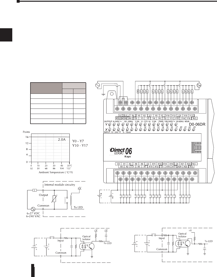
DL06 Micro PLC User Manual, 3rd Edition, Rev. D
Chapter 2: Installation, Wiring, and Specifications
1
2
3
4
5
6
7
8
9
10
11
12
13
14
A
B
C
D
2-40
1
2
3
4
5
6
7
8
9
10
11
12
13
14
a
B
c
d
D0–06DR I/O Wiring Diagram
The D0–06DR PLCs feature twenty DC inputs and sixteen relay contact outputs. The following diagram
shows a typical field wiring example. The AC external power connection uses four terminals as shown.
Inputs are organized into five banks of four. Each bank has an isolated common terminal, and
may be wired as either sinking or sourcing inputs. The wiring example below shows all commons
connected together, but separate supplies and common circuits may be used. The equivalent
circuit for standard inputs is shown below, and the high-speed input circuit is shown to the left.
Outputs are organized into four banks of four normally-open relay contacts. Each bank has
a common terminal. The wiring example below shows all commons connected together, but
separate supplies and common circuits may be used. The equivalent output circuit shows one
channel of a typical bank. The relay contacts can switch AC or DC voltages.
Power input wiring
Input point wiring
Output point wiring
100-240
VAC
6-240
VAC
or
6-27
VDC
12-24
VDC SinkSource
9'&
6LQN6RXUFH
Equivalent Circuit, High-speed Inputs (X0-X3)
F
Derating Chart for Relay Outputs
Typical Relay Life (Operations) at Room
Temperature
9'&
6LQN
6RXUFH
Equivalent Circuit, Standard Inputs (X4-X23)
Voltage & Load
Type
Load Current
At 1A At 2A
24VDC Resistive 500K 250K
24VDC Inductive 100K 50K
110VAC Resistive 500K 250K
110VAC Inductive 200K 100K
220VAC Resistive 350K 200K
220VAC Inductive 100K 50K
Equivalent Output Circuit
DL06 Micro PLC User Manual, 3rd Edition, Rev. D
Chapter 2: Installation, Wiring, and Specifications
1
2
3
4
5
6
7
8
9
10
11
12
13
14
A
B
C
D
2-41
1
2
3
4
5
6
7
8
9
10
11
12
13
14
a
B
c
d
D0-06DR General Specifications
External Power Requirements 100– 240 VAC/50-60 Hz, 40 VA maximum
Communication Port 1 9600 baud (Fixed), 8 data
bits, 1 stop bit, odd parity K–Sequence (Slave), DirectNET (Slave), MODBUS (Slave)
Communication Port 2 9600 baud (default), 8 data
bits, 1 stop bit, odd parity
K–Sequence (Slave), DirectNET (Master/Slave), MODBUS
(Master/Slave), Non-sequence /print, ASCII in/out
Programming cable type D2–DSCBL
Operating Temperature 32 to 131°F (0 to 55°C)
Storage Temperature –4 to 158°F (–20 to 70°C)
Relative Humidity 5 to 95% (non-condensing)
Environmental air No corrosive gases permitted
Vibration MIL STD 810C 514.2
Shock MIL STD 810C 516.2
Noise Immunity NEMA ICS3–304
Terminal Type Removable
Wire Gauge One 16 AWG or two 18 AWG, 24 AWG minimum
DC Input Specifications
Parameter High–Speed Inputs, X0 – X3 Standard DC Inputs X4 – X23
Min. - Max. Voltage Range 10.8 – 26.4 VDC 10.8 – 26.4 VDC
Operating Voltage Range 12 -24 VDC 12 -24 VDC
Peak Voltage 30 VDC (7 kHz maximum frequency) 30 VDC
Minimum Pulse Width 70 µs N/A
ON Voltage Level > 10 VDC > 10 VDC
OFF Voltage Level < 2.0 VDC < 2.0 VDC
Input Impedance 1.8 kq @ 12 – 24 VDC 2.8 kq @ 12 – 24 VDC
Max. Input Current 6mA @12VDC 13mA @24VDC 4mA @12VDC 8.5mA @24VDC
Minimum ON Current >5 mA >4 mA
Maximum OFF Current < 0.5 mA <0.5 mA
OFF to ON Response <70 µs 2 – 8 ms, 4 ms typical
ON to OFF Response <70 µs 2 – 8 ms, 4 ms typical
Status Indicators Logic side Logic side
Commons 4 channels / common x 5 banks (isolated)
Relay Output Specifications
Output Voltage Range (Min. - Max.) 5 -264 VAC (47 -63 Hz), 5 - 30 VDC
Operating Voltage 6 -240 VAC (47 -63 Hz), 6 - 27 VDC
Output Current 2A / point 6A / common
Maximum Voltage 264 VAC, 30 VDC
Max leakage current 0.1 mA @264 VAC
Smallest Recommended Load 5 mA
OFF to ON Response < 15 ms
ON to OFF Response < 10 ms
Status Indicators Logic Side
Commons 4 channels / common x 4 banks (isolated)
Fuses None (external recommended)
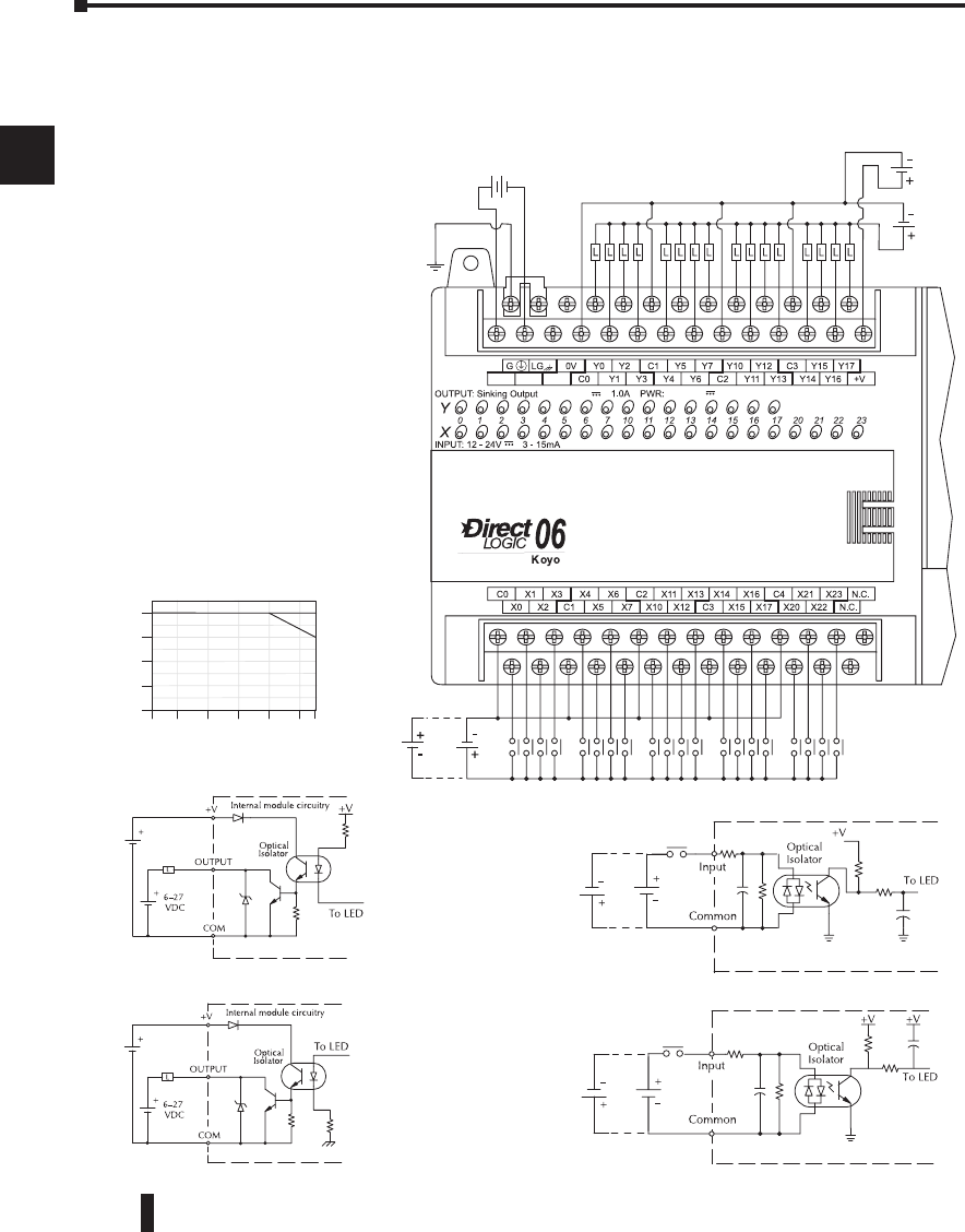
DL06 Micro PLC User Manual, 3rd Edition, Rev. D
Chapter 2: Installation, Wiring, and Specifications
1
2
3
4
5
6
7
8
9
10
11
12
13
14
A
B
C
D
2-42
1
2
3
4
5
6
7
8
9
10
11
12
13
14
a
B
c
d
D0–06DD1–D I/O Wiring Diagram
These micro PLCs feature twenty DC inputs and sixteen sinking DC outputs. The following
diagram shows a typical field wiring example. The DC external power connection uses four
terminals at the left as shown.
Inputs are organized into
five banks of four. Each
bank has an isolated
common terminal, and
may be wired as either
sinking or sourcing
inputs. The wiring
example below shows
all commons connected
together, but separate
supplies and common
circuits may be used.
All outputs actually share
the same common. Note
the requirement for
external power.
0
4
12
16
Points
Ambient Temperature (
°
C/
°
F)
0
32
10
50
20
68
30
86
40
104
50
122
55°C
131°F
1.0 A
Y0-Y17
8
0.75A
Derating Chart for DC Outputs
Power
input wiring
Input point wiring
Output point wiring
D0-06DD1-D
+
-
12 - 24 VDC
+-N.C.
12-24V
12-24V 20W
6-27
VDC
20-28
VDC
12-24 VDC
SinkSource
9'&
DC Pulse Outputs (Y0-Y1)
9'&
DC Standard Outputs (Y2-Y17)
9'&
6LQN
6RXUFH
Standard Input Circuit (X4-X23)
9'&
6LQN6RXUFH
High Speed Inputs (X0-X3)
DL06 Micro PLC User Manual, 3rd Edition, Rev. D
Chapter 2: Installation, Wiring, and Specifications
1
2
3
4
5
6
7
8
9
10
11
12
13
14
A
B
C
D
2-43
1
2
3
4
5
6
7
8
9
10
11
12
13
14
a
B
c
d
D0-06DD1-D General Specifications
External Power Requirements 12 – 24 VDC, 20 W maximum,
Communication Port 1: 9600 baud (Fixed),
8 data bits, 1 stop bit, odd parity
K–Sequence (Slave), DirectNET (Slave),
MODBUS (Slave)
Communication Port 2: 9600 baud (default),
8 data bits, 1 stop bit,odd parity
K–Sequence (Slave), DirectNET (Master/Slave),
MODBUS (Master/Slave), Non-sequence/print, ASCII in/out
Programming cable type D2–DSCBL
Operating Temperature 32 to 131°F (0 to 55°C)
Storage Temperature –4 to 158°F (–20 to 70°C)
Relative Humidity 5 to 95% (non-condensing)
Environmental air No corrosive gases permitted
Vibration MIL STD 810C 514.2
Shock MIL STD 810C 516.2
Noise Immunity NEMA ICS3–304
Terminal Type Removable
Wire Gauge One 16 AWG or two 18 AWG, 24 AWG minimum
DC Input Specifications
Parameter High–Speed Inputs, X0 – X3 Standard DC Inputs X4 – X23
Min. - Max. Voltage Range 10.8 – 26.4 VDC 10.8 – 26.4 VDC
Operating Voltage Range 12 – 24 VDC 12 – 24 VDC
Peak Voltage 30 VDC (7 kHz maximum frequency) 30 VDC
Minimum Pulse Width 70 µs N/A
ON Voltage Level >10.0 VDC > 10.0 VDC
OFF Voltage Level < 2.0 VDC < 2.0 VDC
Max. Input Current 6mA @12VDC, 13mA @24VDC 4mA @12VDC, 8.5mA @24VDC
Input Impedance 1.8 kq @ 12 – 24 VDC 2.8 kq @ 12 – 24 VDC
Minimum ON Current >5 mA >4 mA
Maximum OFF Current < 0.5 mA <0.5 mA
OFF to ON Response <70 µs 2 – 8 ms, 4 ms typical
ON to OFF Response <70 µs 2 – 8 ms, 4 ms typical
Status Indicators Logic side Logic side
Commons 4 channels / common x 5 banks (isolated)
DC Output Specifications
Parameter Pulse Outputs, Y0 – Y1 Standard Outputs, Y2 – Y17
Min. - Max. Voltage Range 5 – 30 VDC 5 – 30 VDC
Operating Voltage 6 – 27 VDC 6 – 27 VDC
Peak Voltage < 50 VDC (10 kHz max. frequency) < 50 VDC
On Voltage Drop 0.3 VDC @ 1 A 0.3 VDC @ 1 A
Max Current (resistive) 0.5 A / pt., 1A / pt. as standard pt. 1.0 A / point
Max leakage current 15 µA @ 30 VDC 15 µA @ 30 VDC
Max inrush current 2 A for 100 ms 2 A for 100 ms
External DC power required 20 - 28 VDC Max 150mA 20 - 28 VDC Max 150mA
OFF to ON Response < 10 µs < 10 µs
ON to OFF Response < 20 µs < 60 µs
Status Indicators Logic Side Logic Side
Commons 4 channels / common x 4 banks (non-isolated)
Fuses None (external recommended)
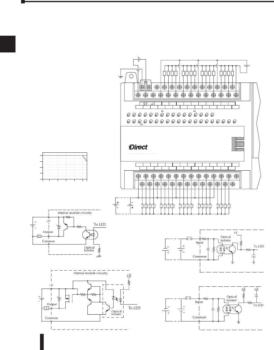
DL06 Micro PLC User Manual, 3rd Edition, Rev. D
Chapter 2: Installation, Wiring, and Specifications
1
2
3
4
5
6
7
8
9
10
11
12
13
14
A
B
C
D
2-44
1
2
3
4
5
6
7
8
9
10
11
12
13
14
a
B
c
d
D0–06DD2–D I/O Wiring Diagram
These micro PLCs feature twenty DC inputs and sixteen sourcing DC outputs. The
following diagram shows a typical field wiring example. The DC external power connection
uses four terminals at the left as shown.
Inputs are organized into five banks of four. Each bank has an isolated common terminal,
and may be wired as either sinking or sourcing inputs. The wiring example below
shows all commons
connected together,
but separate supplies and
common circuits may be
used.
All outputs actually share
the same common. Note
the requirement for
external power.
LOGIC
Koyo
06
C0 C4C2X1 X3 X4 X6 X11 X13 X14 X16 X21 X23 N.C.
C1 C3X2 X5 X7 X10 X12 X15 X17 X20 X22X0 N.C.
V1 V3Y0 Y15Y12Y10 Y17Y7Y5Y2
V0 V2 Y16Y14Y13Y11Y6Y4Y3Y1 C0
+
-
LG
N.C.
N.C.G
OUTPUT: Sourcing Output 12-24V 1.0A
INPUT: 12 - 24V 3 - 15mA
Y
X
PWR: 12-24V 20W D0-06DD2-D
12 - 24
VDC
+
-
LLLL LLLLLLLL LLLL
01 2345 6710 11 12 13 14 15 16 17 20 21 22 23
+
-
12 - 24 VDC
Power
input wiring
Input point wiring
Output point wiring
12-24 VDC
SinkSource
9'&
6LQN
6RXUFH
Standard Input Circuit (X4-X23)
High Speed Inputs (X0-X3)
9'&
6LQN6RXUFH
9'&
DC Pulse Outputs (Y0-Y1)
0
4
12
16
Points
Ambient Temperature (
˚
C/
˚
F)
0
32
10
50
20
68
30
86
40
104
50
122
55˚C
131˚F
Y0 - Y7
1.0 A Y10 - Y17
8
0.75A
Derating Chart for DC Outputs
9'&
DC Standard Outputs (Y2-Y17)
DL06 Micro PLC User Manual, 3rd Edition, Rev. D
Chapter 2: Installation, Wiring, and Specifications
1
2
3
4
5
6
7
8
9
10
11
12
13
14
A
B
C
D
2-45
1
2
3
4
5
6
7
8
9
10
11
12
13
14
a
B
c
d
D0-06DD2-D General Specifications
External Power Requirements 12 – 24 VDC, 20 W maximum,
Communication Port 1: 9600 baud (Fixed),
8 data bits, 1 stop bit, odd parity
K–Sequence (Slave), DirectNET (Slave),
MODBUS (Slave)
Communication Port 2: 9600 baud (default),
8 data bits, 1 stop bit, odd parity
K–Sequence (Slave), DirectNET (Master/Slave),
MODBUS (Master/Slave), Non-sequence/print, ASCII in/out
Programming cable type D2–DSCBL
Operating Temperature 32 to 131°F (0 to 55°C)
Storage Temperature –4 to 158°F (–20 to 70°C)
Relative Humidity 5 to 95% (non-condensing)
Environmental air No corrosive gases permitted
Vibration MIL STD 810C 514.2
Shock MIL STD 810C 516.2
Noise Immunity NEMA ICS3–304
Terminal Type Removable
Wire Gauge One 16 AWG or two 18 AWG, 24 AWG minimum
DC Input Specifications
Parameter High–Speed Inputs, X0 – X3 Standard DC Inputs X4 – X23
Min. - Max. Voltage Range 10.8 – 26.4 VDC 10.8 – 26.4 VDC
Operating Voltage Range 12 – 24 VDC 12 – 24 VDC
Peak Voltage 30 VDC (7 kHz maximum frequency) 30 VDC
Minimum Pulse Width 70 µs N/A
ON Voltage Level >10.0 VDC > 10.0 VDC
OFF Voltage Level < 2.0 VDC < 2.0 VDC
Max. Input Current 15mA @26.4VDC 11mA @26.4VDC
Input Impedance 1.8 kq @ 12 – 24 VDC 2.8 kq @ 12 – 24 VDC
Minimum ON Current 5 mA 3 mA
Maximum OFF Current 0.5 mA 0.5 mA
OFF to ON Response <70 µs 2 – 8 ms, 4 ms typical
ON to OFF Response <70 µs 2 – 8 ms, 4 ms typical
Status Indicators Logic side Logic side
Commons 4 channels / common x 5 banks (isolated)
DC Output Specifications
Parameter Pulse Outputs, Y0 – Y1 Standard Outputs, Y2 – Y17
Min. - Max. Voltage Range 10.8 – 26.4 VDC 10.8 – 26.4 VDC
Operating Voltage 12 – 24 VDC 12 – 24 VDC
Peak Voltage 30 VDC (10 kHz max. frequency) 30 VDC
On Voltage Drop 0.5 VDC @ 1 A 1.2 VDC @ 1 A
Max Current (resistive) 0.5 A / pt., 1A / pt. as standard pt. 1.0 A / point
Max leakage current 15 µA @ 30 VDC 15 µA @ 30 VDC
Max inrush current 2 A for 100 ms 2 A for 100 ms
External DC power required N/A N/A
OFF to ON Response < 10 µs < 10 µs
ON to OFF Response < 20 µs < 0.5 ms
Status Indicators Logic Side Logic Side
Commons 4 channels / common x 4 banks (non-isolated)
Fuses None (external recommended)
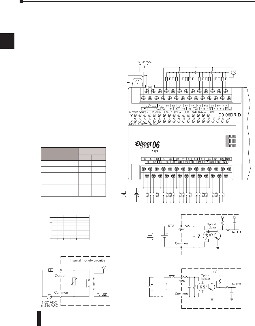
DL06 Micro PLC User Manual, 3rd Edition, Rev. D
Chapter 2: Installation, Wiring, and Specifications
1
2
3
4
5
6
7
8
9
10
11
12
13
14
A
B
C
D
2-46
D0–06DR–D I/O Wiring Diagram
The D0–06DR–D PLC has twenty DC inputs and sixteen relay contact outputs. The
following diagram shows a typical field wiring example. The DC external power connection
uses three terminals as shown.
Inputs are organized into five banks of four. Each bank has an isolated common terminal,
and may be wired as either sinking or sourcing inputs. The wiring example above shows all
commons connected together, but separate supplies and common circuits may be used.
Outputs are organized into
four banks of four normally-
open relay contacts. Each
bank has a common terminal.
The wiring example above
shows all commons connected
together, but separate supplies
and common circuits may
be used. The equivalent
output circuit shows one
channel of a typical bank. The
relay contacts can switch AC or
DC voltages.
1
2
3
4
5
6
7
8
9
10
11
12
13
14
a
B
c
d
9'&
6LQN
6RXUFH
Standard Input Circuit (X4-X23)
Standard Output Circuit
3RZHU
LQSXWZLULQJ
,QSXWSRLQWZLULQJ
2XWSXWSRLQWZLULQJ
9$&
RU
9'&
9'&
6LQN6RXUFH
0
4
12
16
Points
Ambient Temperature ( ˚C/ ˚F)
0
32
10
50
20
68
30
86
40
104
50
122
55˚C
131˚F
Y0 - Y7
2.0A
Y10 - Y17
8
DR-D
Derating Chart for Relay Outputs
High-speed Input Circuit (X0-X3)
9'&
6LQN6RXUFH
Typical Relay Life (Operations) at
Room Temperature
Voltage & Load
Type
Load Current
At 1A At 2A
24VDC Resistive 500K 250K
24VDC Inductive 100K 50K
110VAC Resistive 500K 250K
110VAC Inductive 200K 100K
220VAC Resistive 350K 200K
220VAC Inductive 100K 50K
DL06 Micro PLC User Manual, 3rd Edition, Rev. D
Chapter 2: Installation, Wiring, and Specifications
1
2
3
4
5
6
7
8
9
10
11
12
13
14
A
B
C
D
2-47
1
2
3
4
5
6
7
8
9
10
11
12
13
14
a
B
c
d
D0-06DR-D General Specifications
External Power Requirements 12 – 24 VDC, 20 W maximum,
Communication Port 1 9600 baud (Fixed),
8 data bits, 1 stop bit, odd parity K–Sequence (Slave), DirectNET (Slave), MODBUS (Slave)
Communication Port 2 9600 baud (default),
8 data bits, 1 stop bit, odd parity
K–Sequence (Slave), DirectNET (Master/Slave),
MODBUS (Master/Slave),Non-sequence/print, ASCII in/out
Programming cable type D2–DSCBL
Operating Temperature 32 to 131°F (0 to 55°C)
Storage Temperature –4 to 158°F (–20 to 70°C)
Relative Humidity 5 to 95% (non-condensing)
Environmental air No corrosive gases permitted
Vibration MIL STD 810C 514.2
Shock MIL STD 810C 516.2
Noise Immunity NEMA ICS3–304
Terminal Type Removable
Wire Gauge One 16 AWG or two 18AWG, 24AWG minimum
DC Input Specifications
Parameter High–Speed Inputs, X0 – X3 Standard DC Inputs X4 – X23
Min. - Max. Voltage Range 10.8 – 26.4 VDC 10.8 – 26.4 VDC
Operating Voltage Range 12 -24 VDC 12 -24 VDC
Peak Voltage 30 VDC (7 kHz maximum frequency) 30 VDC
Minimum Pulse Width 70 µs N/A
ON Voltage Level > 10 VDC > 10 VDC
OFF Voltage Level < 2.0 VDC < 2.0 VDC
Input Impedance 1.8 kq @ 12 – 24 VDC 2.8 kq @ 12 – 24 VDC
Max. Input Current 6mA @12VDC 13mA @24VDC 4mA @12VDC 8.5mA @24VDC
Minimum ON Current >5 mA >4 mA
Maximum OFF Current < 0.5 mA <0.5 mA
OFF to ON Response <70 µs 2 – 8 ms, 4 ms typical
ON to OFF Response < 70 µs 2 – 8 ms, 4 ms typical
Status Indicators Logic side Logic side
Commons 4 channels / common x 5 banks (isolated)
Relay Output Specifications
Output Voltage Range (Min. - Max.) 5 -264 VAC (47 -63 Hz), 5 - 30 VDC
Operating Voltage 6 -240 VAC (47 -63 Hz), 6 - 27 VDC
Output Current 2A / point 6A / common
Maximum Voltage 264 VAC, 30 VDC
Max leakage current 0.1 mA @264 VAC
Smallest Recommended Load 5 mA
OFF to ON Response < 15 ms
ON to OFF Response < 10 ms
Status Indicators Logic Side
Commons 4 channels / common x 4 banks isolated commons
Fuses None (external recommended)

DL06 Micro PLC User Manual, 3rd Edition, Rev. D
Chapter 2: Installation, Wiring, and Specifications
1
2
3
4
5
6
7
8
9
10
11
12
13
14
A
B
C
D
2-48
Glossary of Specification Terms
Discrete Input
One of twenty input connections to the PLC which converts an electrical signal from a field
device to a binary status (off or on), which is read by the internal CPU each PLC scan.
Discrete Output
One of sixteen output connections from the PLC which converts an internal ladder program
result (0 or 1) to turn On or Off an output switching device. This enables the program to turn
on and off large field loads.
I/O Common
A connection in the input or output terminals which is shared by multiple I/O circuits. It
usually is in the return path to the power supply of the I/O circuit.
Input Voltage Range
The operating voltage range of the input circuit.
Maximum Voltage
Maximum voltage allowed for the input circuit.
ON Voltage Level
The minimum voltage level at which the input point will turn ON.
OFF Voltage Level
The maximum voltage level at which the input point will turn OFF
Input Impedance
Input impedance can be used to calculate input current for a particular operating voltage.
Input Current
Typical operating current for an active (ON) input.
Minimum ON Current
The minimum current for the input circuit to operate reliably in the ON state.
Maximum OFF Current
The maximum current for the input circuit to operate reliably in the OFF state.
OFF to ON Response
The time the module requires to process an OFF to ON state transition.
ON to OFF Response
The time the module requires to process an ON to OFF state transition.
Status Indicators
The LEDs that indicate the ON/OFF status of an input or output point. All LEDs on DL06
Micro PLCs are electrically located on the logic side of the input or output circuit.
1
2
3
4
5
6
7
8
9
10
11
12
13
14
a
B
c
d

CPU SPeCifiCationS and
oPeration 3
3
Chapter
Chapter
Chapter
CPU SPeCifiCationS and
oPeration
In This Chapter
Overview.......................................................................................... 3–2
CPU Specifications ........................................................................... 3–3
CPU Hardware Setup ....................................................................... 3–4
Using Battery Backup ....................................................................... 3–8
CPU Operation ............................................................................... 3–12
I/O Response Time ......................................................................... 3–17
CPU Scan Time Considerations ...................................................... 3–20
Memory Map ................................................................................. 3–25
DL06 System V-memory ................................................................ 3–29
DL06 Aliases ................................................................................... 3–31
DL06 Memory Map ....................................................................... 3–32
X Input/Y Output Bit Map .............................................................. 3–33
Stage Control/Status Bit Map ......................................................... 3–34
Control Relay Bit Map .................................................................... 3–36
Timer Status Bit Map ..................................................................... 3–38
Counter Status Bit Map .................................................................. 3–38
GX and GY I/O Bit Map ................................................................. 3–39
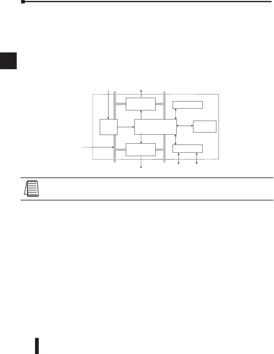
DL06 Micro PLC User Manual, 3rd Edition, Rev. D
3-2
Chapter 3: CPU Specifications and Operation
1
2
3
4
5
6
7
8
9
10
11
12
13
14
A
B
C
D
Overview
The Central Processing Unit (CPU) is the heart of the Micro PLC. Almost all PLC
operations are controlled by the CPU, so it is important that it is set up correctly. This
chapter provides the information needed to understand:
• Steps required to set up the CPU
• Operation of ladder programs
• Organization of Variable Memory
NOTE: The High-Speed I/O function (HSIO) consists of dedicated but configurable hardware in the
DL06. It is not considered part of the CPU because it does not execute the ladder program. For more
on HSIO operation, see Appendix E.
DL06 CPU Features
The DL06 Micro PLC has 14.8K words of memory comprised of 7.6K of ladder memory
and 7.6K words of V-memory (data registers). Program storage is in the FLASH memory
which is a part of the CPU board in the PLC. In addition, there is RAM with the CPU which
will store system parameters, V-memory, and other data not in the application program. The
RAM is backed up by a super-capacitor, storing the data for several hours in the event of a
power outage. The capacitor automatically charges during powered operation of the PLC.
The DL06 supports fixed I/O which includes twenty discrete input points and sixteen output
points.
Over 220 different instructions are available for program development as well as extensive
internal diagnostics that can be monitored from the application program or from an operator
interface. Chapters 5, 6, and 7 provide detailed descriptions of the instructions.
The DL06 provides two built-in communication ports, so you can easily connect a handheld
programmer, operator interface, or a personal computer without needing any additional
hardware.
LCD monitor
4 Optional
card slots
2 comm. ports
Power
Input16 Discrete Outputs
To programming device
or Operator interface20 discrete Inputs
Isolation
boundary
Output circuit
Input circuit
Power
Supply CPU
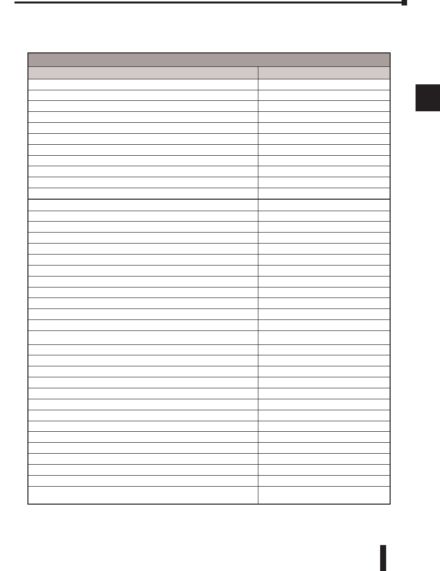
DL06 Micro PLC User Manual, 3rd Edition, Rev. D 3-3
Chapter 3: CPU Specifications and Operation
1
2
3
4
5
6
7
8
9
10
11
12
13
14
A
B
C
D
CPU Specifications
Specifications
Feature DL06
Total Program memory (words) 14.8K
Ladder memory (words) 7680
Total V-memory (words) 7616
User V-memory (words) 7488
Non-volatile V Memory (words) 128
Contact execution (boolean) <0.6us
Typical scan (1k boolean) 1-2ms
RLL Ladder style Programming Yes
RLL and RLLPLUS Programming Yes
Run Time Edits Yes
Supports Overrides Yes
Scan Variable / fixed
Handheld programmer Yes
DirectSOFT programming for Windows Yes
Built-in communication ports (RS232C) Yes
FLASH Memory Standard on CPU
Local Discrete I/O points available 36
Local Analog input / output channels maximum None
High-Speed I/O (quad., pulse out, interrupt, pulse catch, etc.) Yes, 2
I/O Point Density 20 inputs, 16 outputs
Number of instructions available (see Chapter 5 for details) 229
Control relays 1024
Special relays (system defined) 512
Stages in RLLPLUS 1024
Timers 256
Counters 128
Immediate I/O Yes
Interrupt input (external / timed) Yes
Subroutines Yes
For/Next Loops Yes
Math (Integer and floating point) Yes
Drum Sequencer Instruction Yes
Time of Day Clock/Calendar Yes
Internal diagnostics Yes
Password security Yes
System error log Yes
User error log Yes
Battery backup Optional D2-BAT-1 available
(not included with unit)
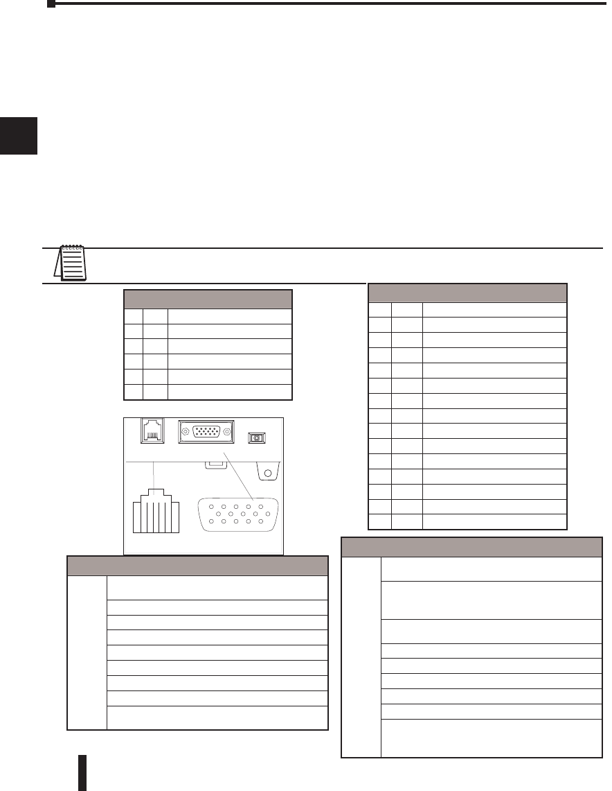
DL06 Micro PLC User Manual, 3rd Edition, Rev. D
3-4
Chapter 3: CPU Specifications and Operation
1
2
3
4
5
6
7
8
9
10
11
12
13
14
A
B
C
D
CPU Hardware Setup
Communication Port Pinout Diagrams
Cables are available that allow you to quickly and easily connect a Handheld Programmer or
a personal computer to the DL06 PLCs. However, if you need to build your cable(s), use the
pinout descriptions shown below, or use the Tech Support/Cable Wiring Diagrams located
on our website. The DL06 PLCs require an RJ-12 phone plug for port 1 (D2-DSCBL) and a
15-pin SVGA DSub for port 2 (D2-DSCBL-1).
The DL06 PLC has two built-in serial communication ports. Port 1 (RS232C only) is
generally used for connecting to a D2-HPP, Direct SOFT, operator interface, MODBUS
slave only, or a Direct NET slave only. The baud rate is fixed at 9600 baud for port 1. Port
2 (RS232C/RS422/RS485) can be used to connect to a D2-HPP, Direct SOFT, operator
interface, MODBUS master/slave, Direct NET master/slave or ASCII in/out. Port 2 has a
range of speeds from 300 baud to 38.4K baud.
NOTE: The 5V pins are rated at 220mA maximum, primarily for use with some operator interface
units.
Port 2 Pin Descriptions
15V Power (+) connection
2TXD Transmit data (RS-232C)
3RXD Receive data (RS-232C)
4RTS Ready to send
5CTS Clear to send
6RXD- Receive data (-) (RS-422/485)
70V Power (-) connection (GND)
80V Power (-) connection (GND)
9TXD+ Transmit data (+) (RS-422/485)
10 TXD- Transmit data (-) (RS-422/485)
11 RTS+ Ready to send (+) (RS-422/485)
12 RTS- Ready to send (-) (RS-422/485)
13 RXD+ Receive data (+) (RS-422/485)
14 CTS+ Clear to send (+) (RS-422/485)
15 CTS- Clear to send (-) (RS-422/485)
Communications Port 2
Com 2
Connects to HPP, DirectSOFT, operator interfaces,
etc.
15-pin, multifunction port, RS232C, RS422, RS485
(RS485 with 2-wire is only available for MODBUS
and Non-sequence.)
Communication speed (baud): 300, 600, 1200,
2400, 4800, 9600, 19200, 38400
Parity: odd (default), even, none
Station Address: 1 (default)
8 data bits
1 start, 1 stop bit
Asynchronous, half-duplex, DTE
Protocol (auto-select): K-sequence (slave only),
DirectNET (master/slave), MODBUS (master/slave),
non-sequence/print/ASCII in/out
Port 1 Pin Descriptions
10V Power (-) connection (GND)
25V Power (-) 220 mA max
3RXD Receive data (RS-232C)
4TXD Transmit data (RS-232C)
55V Power (+) connection
60V Power (-) connection (GND)
Communications Port 1
Com 1
Connects to HPP, DirectSOFT, operator interfaces,
etc.
6-pin, RS232C
Communication speed (baud): 9600 (fixed)
Parity: odd (fixed)
Station Address: 1 (fixed)
8 data bits
1 start, 1 stop bit
Asynchronous, half-duplex, DTE
Protocol (auto-select): K-sequence (slave only),
DirectNET (slave only), MODBUS (slave only)
PORT1 PORT2
TERM
RUNSTOP
PORT1 PORT2
16
3425
15
610
1115
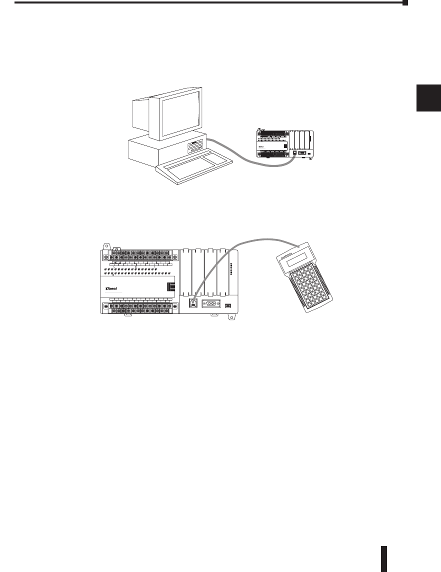
DL06 Micro PLC User Manual, 3rd Edition, Rev. D 3-5
Chapter 3: CPU Specifications and Operation
1
2
3
4
5
6
7
8
9
10
11
12
13
14
A
B
C
D
Connecting the Programming Devices
If you’re using a Personal Computer with the DirectSOFT programming package, you
can connect the computer to either of the DL06’s serial ports. For an engineering office
environment (typical during program development), this is the preferred method of
programming.
The Handheld programmer D2-HPP is connected to the CPU with a handheld programmer
cable. This device is ideal for maintaining existing installations or making small program
changes. The handheld programmer is shipped with a cable, which is approximately 6.5 feet
(200 cm) long.
CPU Setup Information
Even if you have years of experience using PLCs, there are a few things you need to do before
you can start entering programs. This section includes some basic things, such as changing
the CPU mode, but it also includes some things that you may never have to use. Here’s a
brief list of the items that are discussed:
• Using Auxiliary Functions
• Clearing the program (and other memory areas)
• How to initialize system memory
• Setting retentive memory ranges
The following paragraphs provide the setup information necessary to get the CPU ready for
programming. They include setup instructions for either type of programming device you
are using. The D2–HPP Handheld Programmer Manual provides the Handheld keystrokes
required to perform all of these operations. The DirectSOFT Manual provides a description
of the menus and keystrokes required to perform the setup procedures via DirectSOFT.
For replacement
cable, use part no.
DV–1000CBL
LOGIC
Koyo
06
C0 C4C2X1 X3 X4 X6 X11X13 X14X16 X21X23 N.C.
C1 C3X2 X5 X7 X10X12 X15X17 X20X22X0 N.C.
AC(N)24V
0V
N.C.
C1 C3Y0 Y15Y12Y10Y17Y7Y5Y2
C0 C2 Y16Y14Y13Y11Y6Y4Y3Y1
LG
G
AC(L)
D0-06DR
2.0AOUTPUT: 6-240V50 - 60Hz2.0A, 6 - 27V
INPUT: 12 - 24V 3 - 15mA
Y
X
40VA50-60HzPWR: 100-240V
01 2345 6710 11 12 13 14 15 16 17 20 21 22 23
PORT1PORT2
TERM
RUN STOP
PWR
RUN
CPU
TX1
RX1
TX2
RX2
Use cable part no.
D2–DSCBL
LOGIC
Koyo
06
C0 C4C2X1 X3 X4 X6 X11X13 X14X16 X21X23 N.C.
C1 C3X2 X5 X7 X10X12 X15X17 X20X22X0 N.C.
AC(N)24V
0V
N.C.
C1 C3Y0 Y15Y12Y10Y17Y7Y5Y2
C0 C2 Y16Y14Y13Y11Y6Y4Y3Y1
LG
G
AC(L)
D0-06DR
2.0AOUTPUT: 6-240V 50 - 60Hz 2.0A, 6 - 27V
INPUT: 12 - 24V3 - 15mA
Y
X
40VA50-60HzPWR: 100-240V
0123456710 11 12 13 14 15 16 17 20 21 22 23
PORT1PORT2
TERM
RUN STOP
PWR
RUN
CPU
TX1
RX1
TX2
RX2
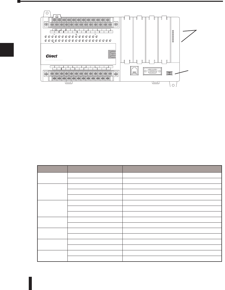
DL06 Micro PLC User Manual, 3rd Edition, Rev. D
3-6
Chapter 3: CPU Specifications and Operation
1
2
3
4
5
6
7
8
9
10
11
12
13
14
A
B
C
D
Status Indicators
The status indicator LEDs on the CPU front panels have specific functions which can help in
programming and troubleshooting.
Mode Switch Functions
The mode switch on the DL06 PLC provides positions for enabling and disabling program
changes in the CPU. Unless the mode switch is in the TERM position, RUN and STOP
mode changes will not be allowed by any interface device, (handheld programmer,
DirectSOFT programming package or operator interface). Programs may be viewed or
monitored but no changes may be made. If the switch is in the TERM position and no
program password is in effect, all operating modes as well as program access will be allowed
through the connected programming or monitoring device.
LOGIC
Koyo
06
C0 C4C2X1 X3 X4 X6 X11 X13 X14 X16 X21X23 N.C.
C1 C3X2 X5 X7 X10 X12 X15X17 X20X22X0 N.C.
AC(N)24V
0V
N.C.
C1 C3Y0 Y15Y12Y10Y17Y7Y5Y2
C0 C2 Y16Y14Y13Y11Y6Y4Y3Y1
LG
G
AC(L)
D0-06DR
2.0AOUTPUT: 6-240V 50 - 60Hz2.0A, 6 - 27V
INPUT: 12 - 24V 3 - 15mA
Y
X
40VA50-60HzPWR: 100-240V
01234567101112131415161720212223
PORT1PORT2
TERM
RUN STOP
PWR
RUN
CPU
TX1
RX1
TX2
RX2
Indicator Status Meaning
PWR ON Power good
OFF Power failure
RUN
ON CPU is in Run Mode
OFF CPU is in Stop or Program Mode
Blinking CPU is in firmware upgrade mode
CPU
ON CPU self diagnostics error
OFF CPU self diagnostics good
Blinking The CPU indicator will blink if the battery is less than 2.5 VDC
TX1 ON Data is being transmitted by the CPU - Port 1
OFF No data is being transmitted by the CPU - Port 1
RX1 ON Data is being received by the CPU - Port 1
OFF No data is being received by the CPU - Port 1
TX2 ON Data is being transmitted by the CPU - Port 2
OFF No data is being transmitted by the CPU - Port 2
RX2 ON Data is being received by the CPU - Port 2
OFF No data is being received by the CPU - Port 2
status indicators
mode switch
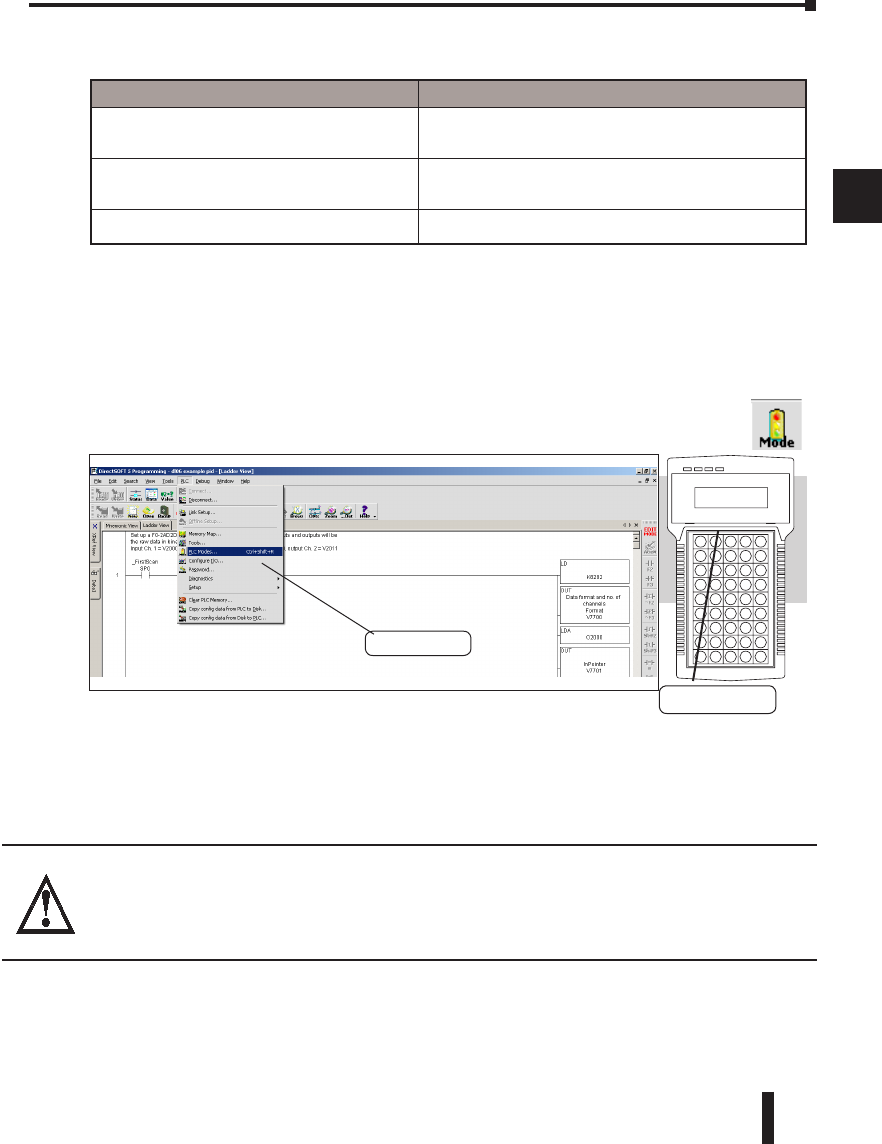
DL06 Micro PLC User Manual, 3rd Edition, Rev. D 3-7
Chapter 3: CPU Specifications and Operation
1
2
3
4
5
6
7
8
9
10
11
12
13
14
A
B
C
D
Changing Modes in the DL06 PLC
There are two ways to change the CPU mode. You can use the CPU mode switch to select
the operating mode, or you can place the mode switch in the TERM position and use a
programming device to change operating modes. With the switch in this position, the CPU
can be changed between Run and Program modes. You can use either DirectSOFT or the
Handheld Programmer to change the CPU mode of operation. With DirectSOFT use the
PLC menu option PLC > Mode or use the Mode button located on the Online
toolbar. With the Handheld Programmer, you use the MODE key.
Mode of Operation at Power-up
The DL06 CPU will normally power-up in the mode that it was in just prior to the
power interruption. For example, if the CPU was in Program Mode when the power was
disconnected, the CPU will power-up in Program Mode (see warning note below).
WARNING: Once the super capacitor has discharged, the system memory may not retain the
previous mode of operation. When this occurs, the PLC can power-up in either Run or Program
Mode if the mode switch is in the term position. There is no way to determine which mode will
be entered as the startup mode. Failure to adhere to this warning greatly increases the risk of
unexpected equipment startup.
The mode which the CPU will power-up in is also determined by the state of B7633.13. If
the bit is set and the Mode Switch is in the TERM position, the CPU will power-up in RUN
mode. If B7633.13 is not set with the Mode Switch in TERM position, then the CPU will
power-up in the state it was in when it was powered-down.
Mode Switch Position CPU Action
RUN (Run Program) CPU is forced into the RUN mode if no errors are encountered.
No changes are allowed by the attached programming/
monitoring device.
TERM (Terminal) RUN PROGRAM and the TEST modes are available. Mode and
program changes are allowed by the programming/monitoring
device.
STOP CPU is forced into the STOP mode. No changes are allowed by
the programming/monitoring device.
PLC Menu
MODE Key
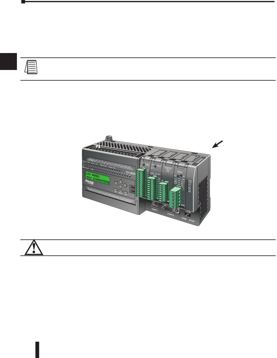
DL06 Micro PLC User Manual, 3rd Edition, Rev. D
3-8
Chapter 3: CPU Specifications and Operation
1
2
3
4
5
6
7
8
9
10
11
12
13
14
A
B
C
D
Using Battery Backup
An optional lithium battery is available to maintain the system RAM retentive memory when
the DL06 system is without external power. Typical CPU battery life is five years, which
includes PLC runtime and normal shutdown periods. However, consider installing a fresh
battery if your battery has not been changed recently and the system will be shut down for a
period of more than ten days.
NOTE: Before installing or replacing your CPU battery, back-up your V-memory and system
parameters. You can do this by using DirectSOFT to save the program, V-memory, and system
parameters to hard/floppy disk on a personal computer.
To install the D2–BAT–1 CPU battery in the DL06 CPU:
1. Press the retaining clip on the battery door down and swing the battery door open.
2. Place the battery into the coin–type slot with the +, or larger, side out.
3. Close the battery door making sure that it locks securely in place.
4. Make a note of the date the battery was installed
WARNING: Do not attempt to recharge the battery or dispose of an old battery by fire. The battery
may explode or release hazardous materials.
Battery Backup
The battery backup is available immediately after the battery has been installed. The CPU
indicator will blink if the battery is low (refer to the table on page 3-6). Special Relay 43
(SP43) will also be set when the battery is low. The low battery indication is enabled by
setting bit 12 of V7633 (B7633.12). If the low battery feature is not desired, do not set bit
V7633.12. The super capacitor will retain memory IF it is configured as retentive regardless
of the state of B7633.12. The battery will do the same, but for a much longer time.
Battery door
DL06 Micro PLC User Manual, 3rd Edition, Rev. D 3-9
Chapter 3: CPU Specifications and Operation
1
2
3
4
5
6
7
8
9
10
11
12
13
14
A
B
C
D
Auxiliary Functions
Many CPU setup tasks involve the use of Auxiliary (AUX) Functions. The AUX Functions
perform many different operations, ranging from clearing ladder memory, displaying the scan
time, copying programs to EEPROM in the handheld programmer, etc. They are divided into
categories that affect different system parameters. Appendix A provides a description of the
AUX functions.
You can access the AUX Functions from DirectSOFT or from the D2–HPP Handheld
Programmer. The manuals for those products provide step-by-step procedures for accessing
the AUX Functions. Some of these AUX Functions are designed specifically for the Handheld
Programmer setup, so they will not be needed (or available) with the DirectSOFT package.
The following table shows a list of the Auxiliary functions for the Handheld Programmer.
Clearing an Existing Program
Before you enter a new program, be sure to always clear ladder memory. You can use AUX
Function 24 to clear the complete program.You can also use other AUX functions to clear
other memory areas.
• AUX 23 — Clear Ladder Range • AUX 24 — Clear all Ladders • AUX 31 — Clear V-memory
Initializing System Memory
The DL06 Micro PLC maintains system parameters in a memory area often referred to as the
scratchpad. In some cases, you may make changes to the system setup that will be stored in system
memory. For example, if you specify a range of Control Relays (CRs) as retentive, these changes
are stored in system memory. AUX 54 resets the system memory to the default values.
Auxiliary Functions (cont’d)
57 Set Retentive Ranges
58 Test Operations
59 Override Setup
5B HSIO Configuration
5C Display Error History
5D Scan Control Setup
AUX 6* — Handheld Programmer Configuration
61 Show Revision Numbers
62 Beeper On / Off
65 Run Self Diagnostics
AUX 7* — EEPROM Operations
71 Copy CPU memory to HPP EEPROM
72 Write HPP EEPROM to CPU
73 Compare CPU to HPP EEPROM
74 Blank Check (HPP EEPROM)
75 Erase HPP EEPROM
76 Show EEPROM Type (CPU and HPP)
AUX 8* — Password Operations
81 Modify Password
82 Unlock CPU
83 Lock CPU
Auxiliary Functions
AUX 2* — RLL Operations
21 Check Program
22 Change Reference
23 Clear Ladder Range
24 Clear All Ladders
AUX 3* — V-Memory Operations
31 Clear V-memory
AUX 4* — I/O Configuration
41 Show I/O Configuration
42 I/O Diagnostics
44 Power Up I/O Configuration check
45 Select Configuration
46 Configure I/O
AUX 5* — CPU Configuration
51 Modify Program Name
52 Display/Change Calendar
53 Display Scan Time
54 Initialize Scratchpad
55 Set Watchdog Timer
56 Set Communication Port 2
DL06 Micro PLC User Manual, 3rd Edition, Rev. D
3-10
Chapter 3: CPU Specifications and Operation
1
2
3
4
5
6
7
8
9
10
11
12
13
14
A
B
C
D
WARNING: You may never have to use this feature unless you want to clear any setup information
that is stored in system memory. Usually, you’ll only need to initialize the system memory if you
are changing programs and the old program required a special system setup. You can usually
load in new programs without ever initializing system memory.
Remember, this AUX function will reset all system memory. If you have set special
parameters such as retentive ranges, for example, they will be erased when AUX 54 is used.
Make sure that you have considered all ramifications of this operation before you select it. See
Appendix F for additional information in reference to PLC memory.
Setting Retentive Memory Ranges
The DL06 PLCs provide certain ranges of retentive memory by default. The default ranges
are suitable for many applications, but you can change them if your application requires
additional retentive ranges or no retentive ranges at all. The default settings are:
You can use AUX 57 to set the retentive ranges. You can also use DirectSOFT menus
to select the retentive ranges. Appendix A contains detailed information about auxiliary
functions.
WARNING: The DL06 CPUs do not come with a battery. The super capacitor will retain the
values in the event of a power loss, but only for a short period of time, depending on conditions
(typically 4 to 7 days). If the retentive ranges are important for your application, make sure you
obtain the optional battery.
Memory Area DL06
Default Range Available Range
Control Relays C1000 – C1777 C0 – C1777
V-Memory V400 – V37777 V0 – V37777
Timers None by default T0 – T377
Counters CT0 – CT177 CT0 – CT177
Stages None by default S0 – S1777
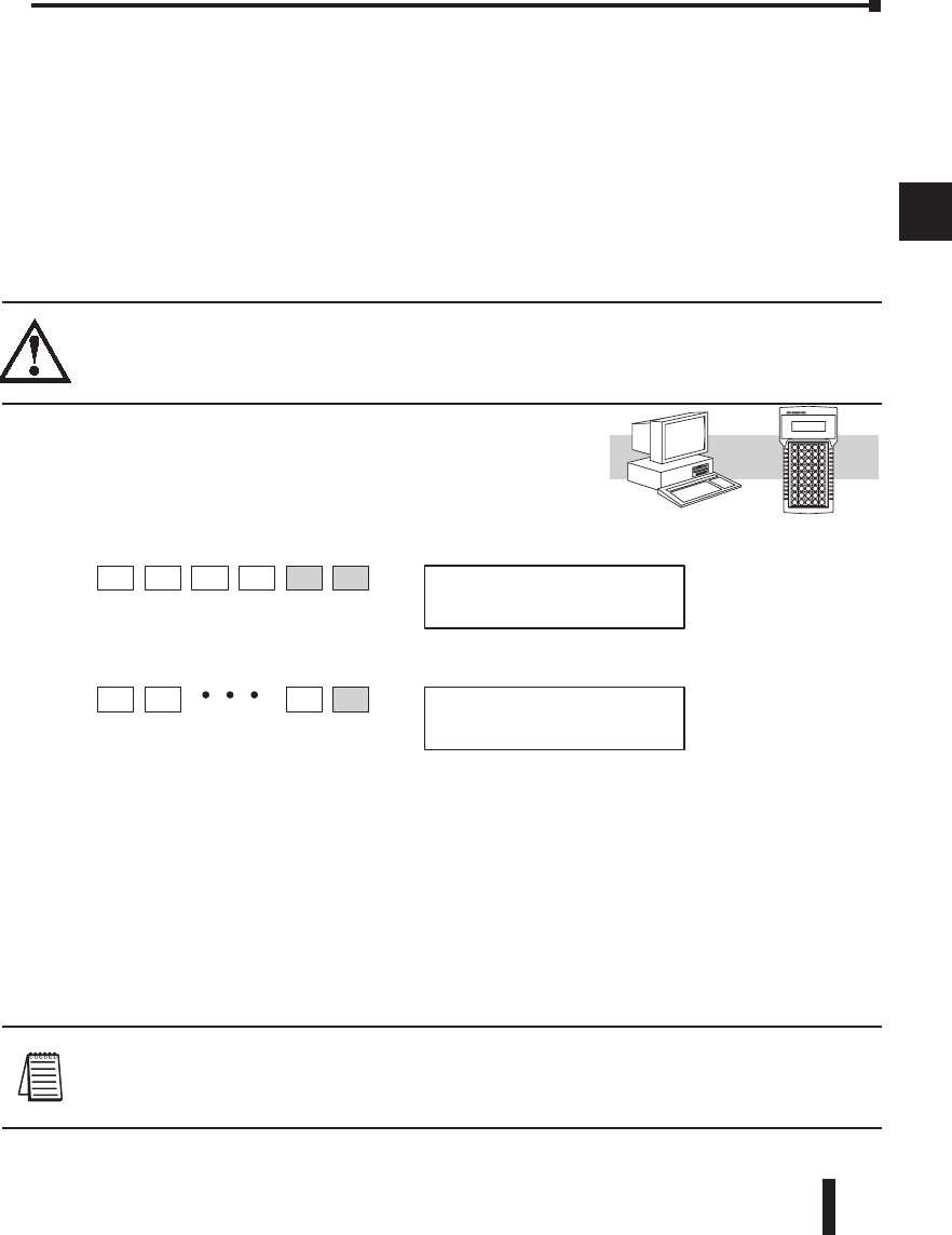
DL06 Micro PLC User Manual, 3rd Edition, Rev. D 3-11
Chapter 3: CPU Specifications and Operation
1
2
3
4
5
6
7
8
9
10
11
12
13
14
A
B
C
D
Using a Password
The DL06 PLCs allow you to use a password to help minimize the risk of unauthorized
program and/or data changes. Once you enter a password you can lock the PLC against
access. Once the CPU is locked you must enter the password before you can use a
programming device to change any system parameters.
You can select an 8-digit numeric password. The Micro PLCs are shipped from the factory
with a password of 00000000. All zeros removes the password protection. If a password
has been entered into the CPU you cannot just enter all zeros to remove it. Once you enter
the correct password, you can change the password to all zeros to remove the password
protection.
WARNING: Make sure you remember your password. If you forget your password you will not
be able to access the CPU. The Micro PLC must be returned to the factory to have the password
(along with the ladder project) removed. It is the policy of Automationdirect to require the
memory of the PLC to be cleared along with the password.
There are three ways to lock the CPU once the password has been entered.
1. If the CPU power is disconnected, the CPU will be automatically locked against access.
2. If you enter the password with DirectSOFT, the CPU will be automatically locked against access
when you exit DirectSOFT.
3. Use AUX 83 to lock the CPU.
When you use DirectSOFT, you will be prompted for a password if the CPU has been
locked. If you use the Handheld Programmer, you have to use AUX 82 to unlock the CPU.
Once you enter AUX 82, you will be prompted to enter the password.
NOTE: The DL06 CPUs support multi-level password protection of the ladder program. This allows
password protection while not locking the communication port to an operator interface. The multi-
level password can be invoked by creating a password with an upper case A followed by seven
numeric characters (e.g. A1234567).
D2–HPPDirectSOFT
PASSWORD
00000000
PASSWORD
XXXXXXXX
CLR CLR AUX
8
I
1
BENT
X X ENTX
Select AUX 81
Enter the new 8-digit password
Press CLR to clear the display
You can use the D2–HPP Handheld Programmer or
DirectSOFT. to enter a password. The following diagram
shows how you can enter a password with the Handheld
Programmer.
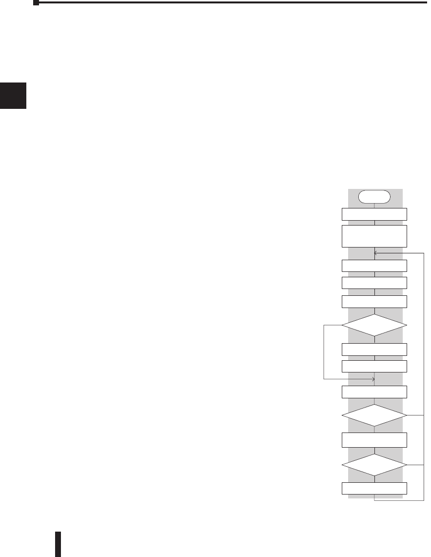
DL06 Micro PLC User Manual, 3rd Edition, Rev. D
3-12
Chapter 3: CPU Specifications and Operation
1
2
3
4
5
6
7
8
9
10
11
12
13
14
A
B
C
D
CPU Operation
Achieving the proper control for your equipment or process requires a good understanding
of how DL06 CPUs control all aspects of system operation. There are four main areas to
understand before you create your application program:
• CPU Operating System — the CPU manages all aspects of system control. A quick overview of all
the steps is provided in the next section.
• CPU Operating Modes — The two primary modes of operation are Program Mode and Run
Mode.
• CPU Timing — The two important areas we discuss are the I/O response time and the CPU scan
time.
• CPU Memory Map — DL06 CPUs offer a wide variety of resources, such as timers, counters,
inputs, etc. The memory map section shows the organization and availability of these data types.
CPU Operating System
At powerup, the CPU initializes the internal electronic
hardware. Memory initialization starts with examining
the retentive memory settings. In general, the contents of
retentive memory is preserved, and non-retentive memory is
initialized to zero (unless otherwise specified).
After the one-time powerup tasks, the CPU begins the cyclical
scan activity. The flowchart to the right shows how the tasks
differ, based on the CPU mode and the existence of any errors.
The scan time is defined as the average time around the task
loop. Note that the CPU is always reading the inputs, even
during program mode. This allows programming tools to
monitor input status at any time.
The outputs are only updated in Run mode. In program mode,
they are in the off state.
Error detection has two levels. Non-fatal errors are reported, but
the CPU remains in its current mode. If a fatal error occurs, the
CPU is forced into program mode and the outputs go off.
YES
Power up
Initialize hardware
Initialize various memory
based on retentive
configuration
Update input
Service peripheral
PGM Mode?
RUN
Execute program
Update output
Do diagnostics
NO
NO
Fatal error
Force CPU into
PGM mode
OK?
Report error , set flag
register , turn on LED
YES
Update Special Relays
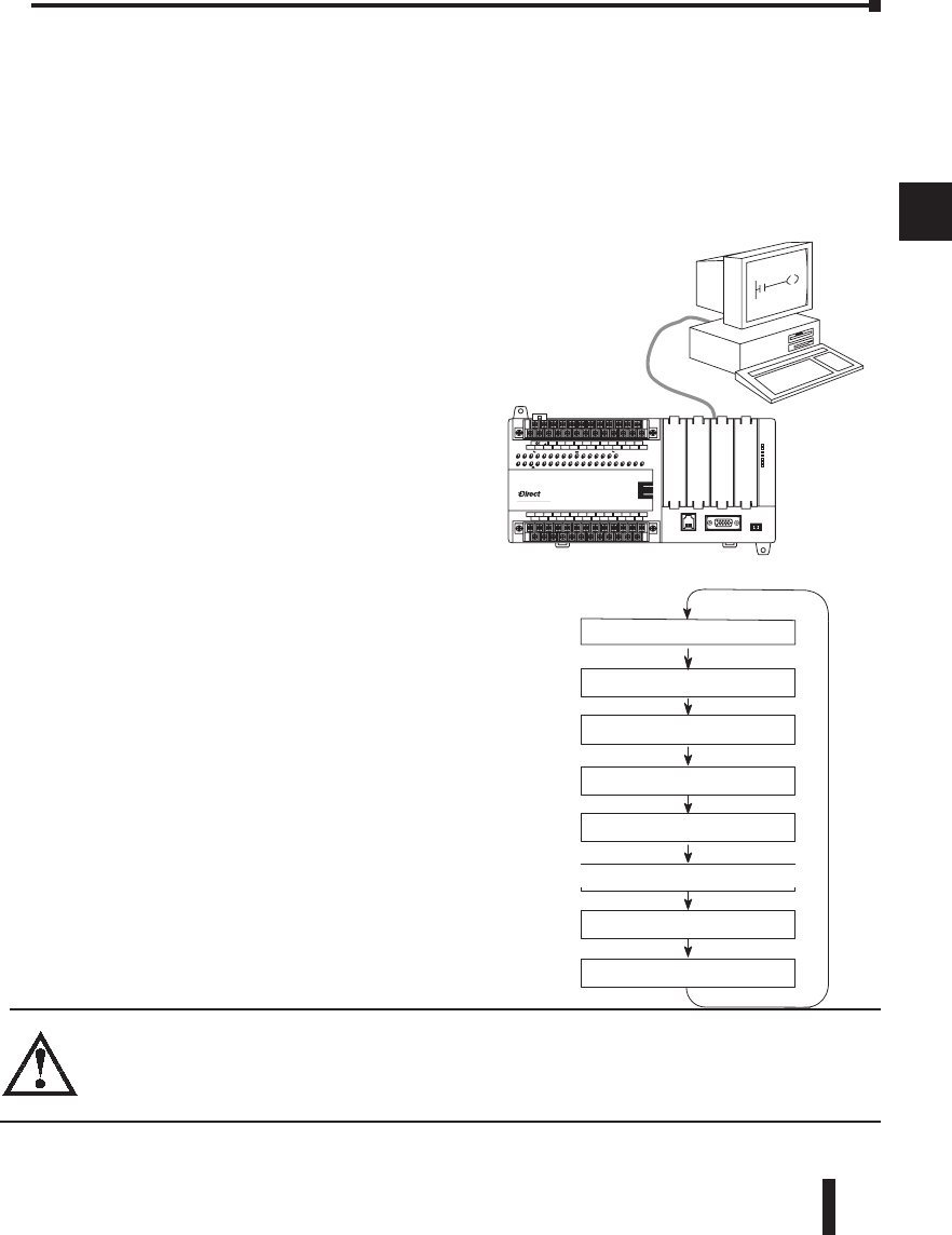
DL06 Micro PLC User Manual, 3rd Edition, Rev. D 3-13
Chapter 3: CPU Specifications and Operation
1
2
3
4
5
6
7
8
9
10
11
12
13
14
A
B
C
D
Program Mode
In Program Mode, the CPU does not execute the application program or update the output
points. The primary use for Program Mode is to enter or change an application program.
You also use program mode to set up the CPU parameters, such as HSIO features, retentive
memory areas, etc.
You can use a programming device, such as DirectSOFT, the D2–HPP (Handheld
Programmer) or the CPU mode switch to place the CPU in Program Mode.
Run Mode
WARNING: Only authorized personnel fully familiar with all aspects of the application should make
changes to the program. Changes during Run Mode become effective immediately. Make sure you
thoroughly consider the impact of any changes to minimize the risk of personal injury or damage
to equipment.
Download
Program
LOGIC
Koyo
06
C0 C4C2X1 X3 X4 X6 X11X13 X14X16 X21X23 N.C.
C1 C3X2 X5 X7 X10X12 X15X17 X20X22X0 N.C.
AC(N)24V
0V
N.C.
C1 C3Y0 Y15Y12Y10Y17Y7Y5Y2
C0 C2 Y16Y14Y13Y11Y6Y4Y3Y1
LG
G
AC(L)
D0-06DR
2.0AOUTPUT: 6-240V50 - 60Hz 2.0A, 6 - 27V
INPUT: 12 - 24V 3 - 15mA
Y
X
40VA50-60HzPWR: 100-240V
0123456710 11 12 13 14 15 16 17 20 21 22 23
PORT1PORT2
TERM
RUN STOP
PWR
RUN
CPU
TX1
RX1
TX2
RX2
Read Inputs
Read Inputs from Specialty I/O
Solve the Application Program
Write Outputs
Diagnostics
Service Peripherals
Write Outputs to Specialty I/O
Update Clock, Special Relays
Write Outputs
Normal Run mode scan
In Run Mode, the CPU executes the
application program and updates the I/O
system. You can perform many operations
during Run Mode. Some of these include:
• Monitor and change I/O point status
• Change timer/counter preset values
• Change variable memory locations
Run Mode operation can be divided into
several key areas. For the vast majority of
applications, some of these execution segments
are more important than others. For example,
you need to understand how the CPU updates
the I/O points, handles forcing operations, and
solves the application program. The remaining
segments are not that important for most
applications.
You can use DirectSOFT, the D2–HPP
(Handheld Programmer) or the CPU mode
switch to place the CPU in Run Mode.
You can also edit the program during Run
Mode. The Run Mode Edits are not bumpless
to the outputs. Instead, the CPU ignores the
inputs and maintains the outputs in their
last state while it accepts the new program
information. If an error is found in the new
program, then the CPU will turn all the
outputs off and enter the Program Mode. This
feature is discussed in more detail in Chapter 9.

DL06 Micro PLC User Manual, 3rd Edition, Rev. D
3-14
Chapter 3: CPU Specifications and Operation
1
2
3
4
5
6
7
8
9
10
11
12
13
14
A
B
C
D
Read Inputs
The CPU reads the status of all inputs, then stores it in the image register. Input image
register locations are designated with an X followed by a memory location. Image register
data is used by the CPU when it solves the application program.
Of course, an input may change after the CPU has just read the inputs. Generally, the
CPU scan time is measured in milliseconds. If you have an application that cannot wait
until the next I/O update, you can use Immediate Instructions. These do not use the status
of the input image register to solve the application program. The Immediate instructions
immediately read the input status directly from the I/O modules. However, this lengthens
the program scan since the CPU has to read the I/O point status again. A complete list of the
Immediate instructions is included in Chapter 5.
Service Peripherals and Force I/O
After the CPU reads the inputs from the input modules, it reads any attached peripheral
devices. This is primarily a communications service for any attached devices. For example, it
would read a programming device to see if any input, output, or other memory type status
needs to be modified. There are two basic types of forcing available with the DL06 CPUs:
• Forcing from a peripheral – not a permanent force, good only for one scan
• Bit Override – holds the I/O point (or other bit) in the current state. Valid bits are X, Y, C, T, CT,
and S. (These memory types are discussed in more detail later in this chapter).
Regular Forcing — This type of forcing can temporarily change the status of a discrete bit.
For example, you may want to force an input on, even though it is really off. This allows you
to change the point status that was stored in the image register. This value will be valid until
the image register location is written to during the next scan. This is primarily useful during
testing situations when you need to force a bit on to trigger another event.
Bit Override — Bit override can be enabled on a point-by-point basis by using AUX 59 from
the Handheld Programmer or, by a menu option from within DirectSOFT. Bit override
basically disables any changes to the discrete point by the CPU. For example, if you enable bit
override for X1, and X1 is off at the time, then the CPU will not change the state of X1. This
means that even if X1 comes on, the CPU will not acknowledge the change. So, if you used
X1 in the program, it would always be evaluated as Off in this case. Of course, if X1 was on
when the bit override was enabled, then X1 would always be evaluated as On.
There is an advantage available when you use the bit override feature. The regular forcing
is not disabled because the bit override is enabled. For example, if you enabled the Bit
Override for Y0 and it was off at the time, then the CPU would not change the state of Y0.
However, you can still use a programming device to change the status. Now, if you use the
programming device to force Y0 on, it will remain on and the CPU will not change the state
of Y0. If you then force Y0 off, the CPU will maintain Y0 as off. The CPU will never update
the point with the results from the application program or from the I/O update until the bit
override is removed. The following diagram shows a brief overview of the bit override feature.
Notice the CPU does not update the Image Register when bit override is enabled.
DL06 Micro PLC User Manual, 3rd Edition, Rev. D 3-15
Chapter 3: CPU Specifications and Operation
1
2
3
4
5
6
7
8
9
10
11
12
13
14
A
B
C
D
WARNING: Only authorized personnel fully familiar with all aspects of the application should
make changes to the program. Make sure you thoroughly consider the impact of any changes to
minimize the risk of personal injury or damage to equipment.
CPU Bus Communication
It is possible to transfer data to and from the CPU over the CPU bus on the backplane. This
data is more than standard I/O point status. This type of communications can only occur on
the CPU (local) base. There is a portion of the execution cycle used to communicate with
these modules. The CPU performs both read and write requests during this segment.
Update Clock, Special Relays and Special Registers
The DL06 CPUs have an internal real-time clock and calendar timer which is accessible to
the application program. Special V-memory locations hold this information. This portion
of the execution cycle makes sure these locations get updated on every scan. Also, there are
several different Special Relays, such as diagnostic relays, for example, that are also updated
during this segment.
Input Update
Result of Program
Solution
OFF
Image Register (example)
Y1
Y2
...Y128
ON
ON...OFF
C0C1C2...C377
OFFOFFON...OFF
Y0
OFF
X1
X2...X128
ON
ON...OFF
X0
Bit Override OFF Force from
Programmer
Input Update
Result of Program
Solution
Bit Override ON
Force from
Programmer
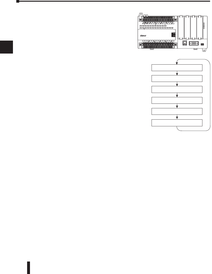
DL06 Micro PLC User Manual, 3rd Edition, Rev. D
3-16
Chapter 3: CPU Specifications and Operation
1
2
3
4
5
6
7
8
9
10
11
12
13
14
A
B
C
D
Solve Application Program
The CPU evaluates each instruction in the
application program during this segment of the
scan cycle. The instructions define the relationship
between the input conditions and the desired
output response. The CPU uses the output image
register area to store the status of the desired action
for the outputs. Output image register locations
are designated with a Y followed by a memory
location. The actual outputs are updated during the
write outputs segment of the scan cycle. There are
immediate output instructions available that will
update the output points immediately instead of
waiting until the write output segment. A complete
list of the Immediate instructions is provided in
Chapter 5.
The internal control relays (C), the stages (S), and
the variable memory (V) are also updated in this
segment.
You may recall that you can force various types
of points in the system, discussed earlier in this
chapter. If any I/O points or memory data have been
forced, the output image register also contains this
information.
Solve PID Loop Equations
The DL06 CPU can process up to 8 PID loops. The loop calculations are run as a separate
task from the ladder program execution, immediately following it. Only loops which have
been configured are calculated, and then only according to a built-in loop scheduler. The
sample time (calculation interval) of each loop is programmable. Please refer to Chapter 8,
PID Loop Operation, for more on the effects of PID loop calculation on the overall CPU
scan time.
Write Outputs
Once the application program has solved the instruction logic and constructed the output
image register, the CPU writes the contents of the output image register to the corresponding
output points. Remember, the CPU also made sure that any forcing operation changes were
stored in the output image register, so the forced points get updated with the status specified
earlier.
Write Outputs to Specialty I/O
After the CPU updates the outputs in the local and expansion bases, it sends the output point
information that is required by any Specialty modules which are installed. Specialty modules
have built-in microprocessors which communicate to the CPU via the backplane. Some
of these modules can process data. Refer to the specific Specialty module user manual for
detailed information.
Download
Program
Read Inputs from Specialty I/O
Solve the Application Program
Write Outputs
Diagnostics
Update Special Relays
Service Peripherals
Normal Run mode scan
LOGIC
Koyo
06
C0 C4C2X1 X3 X4 X6 X11X13 X14X16 X21X23 N.C.
C1 C3X2 X5 X7 X10X12 X15X17 X20X22X0 N.C.
AC(N)24V
0V
N.C.
C1 C3Y0 Y15Y12Y10Y17Y7Y5Y2
C0 C2 Y16Y14Y13Y11Y6Y4Y3Y1
LG
G
AC(L)
D0-06DR
2.0AOUTPUT: 6-240V50 - 60Hz 2.0A, 6 - 27V
INPUT: 12 - 24V 3 - 15mA
Y
X
40VA50-60HzPWR: 100-240V
0123456710 11 12 13 14 15 16 17 20 21 22 23
PORT1PORT2
TERM
RUN STOP
PWR
RUN
CPU
TX1
RX1
TX2
RX2
LOGIC
Koyo
06
C0 C4C2X1 X3 X4 X6 X11X13 X14X16 X21X23 N.C.
C1 C3X2 X5 X7 X10X12 X15X17 X20X22X0 N.C.
AC(N)24V
0V
N.C.
C1 C3Y0 Y15Y12Y10Y17Y7Y5Y2
C0 C2 Y16Y14Y13Y11Y6Y4Y3Y1
LG
G
AC(L)
D0-06DR
2.0AOUTPUT: 6-240V 50 - 60Hz 2.0A, 6 - 27V
INPUT: 12 - 24V3 - 15mA
Y
X
40VA50-60HzPWR: 100-240V
01 234567101112131415161720212223
PORT1PORT2
TERM
RUN STOP
PWR
RUN
CPU
TX1
RX1
TX2
RX2
from Specialty I/O

DL06 Micro PLC User Manual, 3rd Edition, Rev. D 3-17
Chapter 3: CPU Specifications and Operation
1
2
3
4
5
6
7
8
9
10
11
12
13
14
A
B
C
D
Diagnostics
During this part of the scan, the CPU performs all system diagnostics and other tasks such as
calculating the scan time and resetting the watchdog timer. There are many different error
conditions that are automatically detected and reported by the DL06 PLCs. Appendix B
contains a listing of the various error codes.
Probably one of the more important things that occurs during this segment is the scan time
calculation and watchdog timer control. The DL06 CPU has a watchdog timer that stores
the maximum time allowed for the CPU to complete the solve application segment of the
scan cycle. If this time is exceeded, the CPU will enter the Program Mode and turn off all
outputs. The default value set from the factory is 200 ms. An error is automatically reported.
For example, the Handheld Programmer would display the following message “E003 S/W
TIMEOUT” when the scan overrun occurs.
You can use AUX 53 to view the minimum, maximum, and current scan time. Use AUX 55
to increase or decrease the watchdog timer value.
I/O Response Time
Is Timing Important for Your Application?
I/O response time is the amount of time required for the control system to sense a change in
an input point and update a corresponding output point. In the majority of applications, the
CPU performs this task in such a short period of time that you may never have to concern
yourself with the aspects of system timing. However, some applications do require extremely
fast update times. In these cases, you may need to know how to determine the amount of
time spent during the various segments of operation.
There are four things that can affect the I/O response time.
• The point in the scan cycle when the field input changes states
• Input Off to On delay time
• CPU scan time
• Output Off to On delay time
The next paragraphs show how these items interact to affect the response time.
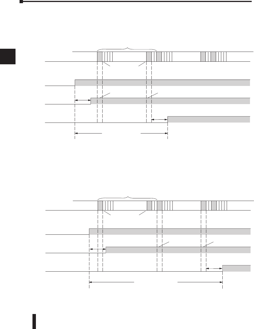
DL06 Micro PLC User Manual, 3rd Edition, Rev. D
3-18
Chapter 3: CPU Specifications and Operation
1
2
3
4
5
6
7
8
9
10
11
12
13
14
A
B
C
D
Normal Minimum I/O Response
The I/O response time is shortest when the input changes just before the Read Inputs portion
of the execution cycle. In this case the input status is read, the application program is solved,
and the output point gets updated. The following diagram shows an example of the timing
for this situation.
In this case, you can calculate the response time by simply adding the following items:
Input Delay + Scan Time + Output Delay = Response Time
Normal Maximum I/O Response
The I/O response time is longest when the input changes just after the Read Inputs portion
of the execution cycle. In this case the new input status is not read until the following scan.
The following diagram shows an example of the timing for this situation.
In this case, you can calculate the response time by simply adding the following items:
Input Delay +(2 x Scan Time) + Output Delay = Response Time
Chapter 3: CPU Specifications and Operation
Solve
Program
Read
Inputs
Write
Outputs
Solve
Program
Scan
Solve
Program
Field Input
Input
Off/On Delay
CPU Reads
Inputs
Output
Off/On Delay
I/O Response Time
Scan
Solve
Program
CPU Writes
Outputs
Solve
Program
Read
Inputs
Write
Outputs
Solve
Program
Scan
Solve
Program
Field Input
Input
Off/On Delay
CPU Reads
Inputs
Output
Off/On Delay
I/O Response Time
Scan
Solve
Program
CPU Writes
Outputs
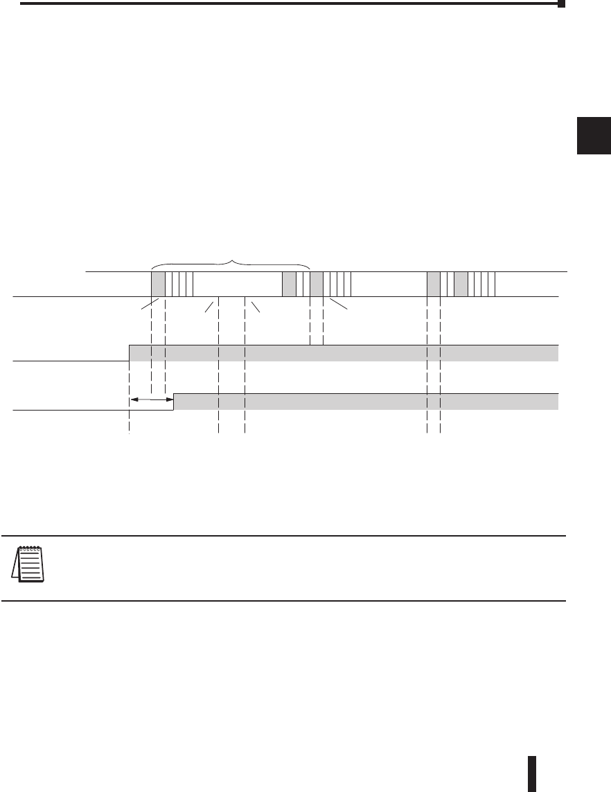
DL06 Micro PLC User Manual, 3rd Edition, Rev. D 3-19
Chapter 3: CPU Specifications and Operation
1
2
3
4
5
6
7
8
9
10
11
12
13
14
A
B
C
D
Improving Response Time
There are a few things you can do to help improve throughput.
• You can choose instructions with faster execution times
• You can use immediate I/O instructions (which update the I/O points during the program
execution)
• You can use the HSIO Mode 50 Pulse Catch features designed to operate in high-speed
environments. See Appendix E for details on using this feature.
• You can change Mode 60 filter to 0 msec for X0, X1, X2, and X3.
Of these three things the Immediate I/O instructions are probably the most important
and most useful. The following example shows how an immediate input instruction
and immediate output instruction would affect the response time.
In this case, you can calculate the response time by simply adding the following items.
Input Delay + Instruction Execution Time + Output Delay = Response Time
The instruction execution time would be calculated by adding the time for the immediate
input instruction, the immediate output instruction, and any other instructions in between
the two.
NOTE: Even though the immediate instruction reads the most current status from I/O, it only uses
the results to solve that one instruction. It does not use the new status to update the image register.
Therefore, any regular instructions that follow will still use the image register values. Any immediate
instructions that follow will access the I/O again to update the status.
Chapter 3: CPU Specifications and Operation
Solve
Program
Read
Input
Immediate
Normal
Write
Outputs
Solve
Program
Scan
Solve
Program
Field Input
Input
Off/On Delay
Output
Off/On Delay
I/O Response Time
Scan
Solve
Program
Normal
Read
Input
Write
Output
Immediate
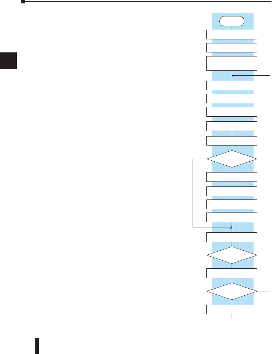
DL06 Micro PLC User Manual, 3rd Edition, Rev. D
3-20
Chapter 3: CPU Specifications and Operation
1
2
3
4
5
6
7
8
9
10
11
12
13
14
A
B
C
D
CPU Scan Time Considerations
The scan time covers all the cyclical tasks that are performed
by the operating system. You can use DirectSOFT or
the Handheld Programmer to display the minimum,
maximum, and current scan times that have occurred since
the previous Program Mode to Run Mode transition. This
information can be very important when evaluating the
performance of a system. As we’ve shown previously there
are several segments that make up the scan cycle. Each
of these segments requires a certain amount of time to
complete. Of all the segments, the following are the most
important:
• Input Update
• Peripheral Service
• Program Execution
• Output Update
• Timed Interrupt Execution
The one you have the most control over is the amount of
time it takes to execute the application program. This is
because different instructions take different amounts of
time to execute. So, if you think you need a faster scan,
then you can try to choose faster instructions.
Your choice of I/O type and peripheral devices can also
affect the scan time. However, these things are usually
dictated by the application.
The following paragraphs provide some general information
on how much time some of the segments can require.
Reading Inputs
The time required during each scan to read the input status
of built-in inputs is 52.6 µs. Don’t confuse this with the
I/O response time that was discussed earlier.
Writing Outputs
The time required to write the output status of built-in
outputs is 41.1 µS. Don’t confuse this with the I/O
response time that was discussed earlier.
YES
Power up
Initialize hardware
Check I/O module
config. and verify
Initialize various memory
based on retentive
configuration
Update input
Read input data from
Specialty and Remote I/O
Service peripheral
PGM Mode?
RUN
Execute ladder program
Update output
Write output data to
Specialty and Remote I/O
Do diagnostics
OK
NO
NO
Fatal error
Force CPU into
PGM mode
OK?
Report the error, set flag,
register, turn on LED
YES
CPU Bus Communication
Update Clock / Calendar
PID Equations (DL250)
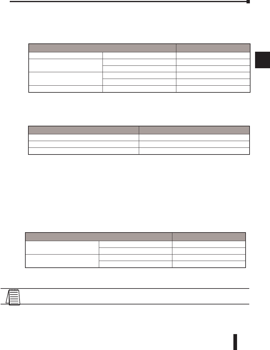
DL06 Micro PLC User Manual, 3rd Edition, Rev. D 3-21
Chapter 3: CPU Specifications and Operation
1
2
3
4
5
6
7
8
9
10
11
12
13
14
A
B
C
D
Service Peripherals
Communication requests can occur at any time during the scan, but the CPU only logs the
requests for service until the Service Peripherals portion of the scan. The CPU does not spend
any time on this if there are no peripherals connected.
During the Service Peripherals portion of the scan, the CPU analyzes the communications
request and responds as appropriate. The amount of time required to service the peripherals
depends on the content of the request.
CPU Bus Communication
Some specialty modules can also communicate directly with the CPU via the CPU bus.
During this portion of the cycle the CPU completes any CPU bus communications. The
actual time required depends on the type of modules installed and the type of request being
processed.
Update Clock/Calendar, Special Relays, Special Registers
The clock, calendar, and special relays are updated and loaded into special V-memory
locations during this time. This update is performed during both Run and Program Modes.
NOTE: The Clock/Calendar is updated while there is energy on the super-capacitor. If the super-
capacitor is discharged, the real time and date is lost.
To Log Request (anytime) DL06
Nothing Connected Min. & Max 0µs
Port 1 Send Min. / Max. 5.8/11.8 µs
Rec. Min. / Max. 12.5/25.2 µs
Port 2 Send Min. / Max. 6.2/14.3 µs
Rec. Min. / Max. 14.2/31.9 µs
LCD Min. / Max. 4.8/49.2 µs
To Service Request DL06 DL06
Minimum 9 µs
Run Mode Max. 412 µs
Program Mode Max. 2.5 second
Modes DL06
Program Mode Minimum 12.0 µs
Maximum 12.0 µs
Run Mode Minimum 20.0 µs
Maximum 27.0 µs
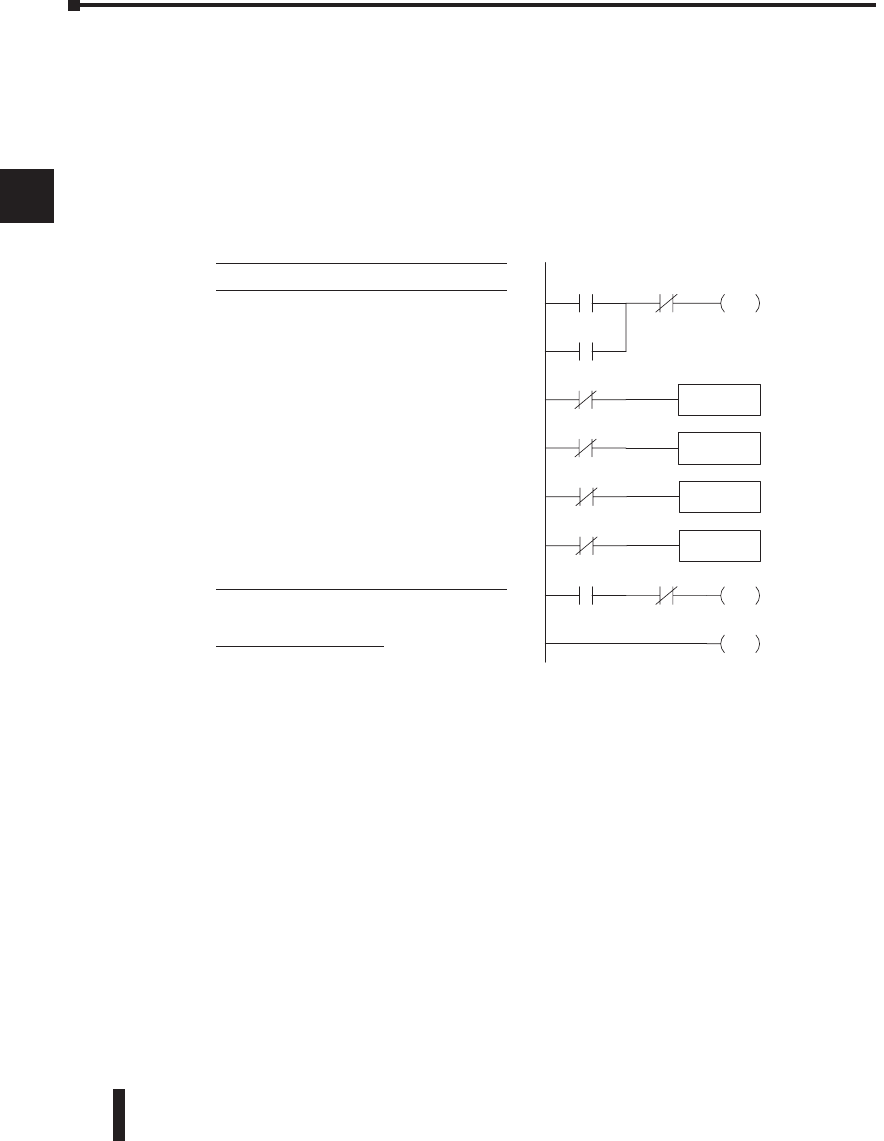
DL06 Micro PLC User Manual, 3rd Edition, Rev. D
3-22
Chapter 3: CPU Specifications and Operation
1
2
3
4
5
6
7
8
9
10
11
12
13
14
A
B
C
D
Application Program Execution
The CPU processes the program from address 0 to the END instruction. The CPU executes
the program left to right and top to bottom. As each rung is evaluated the appropriate image
register or memory location is updated. The time required to solve the application program
depends on the type and number of instructions used, and the amount of execution overhead.
Just add the execution times for all the instructions in your program to determine to total
execution time. Appendix C provides a complete list of the instruction execution times for
the DL06 Micro PLC. For example, the execution time for running the program shown
below is calculated as follows:
TOTAL TIME = (Program execution time + Overhead) x 1.18
The program above takes only 51.11 µs to execute during each scan. The DL06 spends
0.18ms on internal timed interrupt management, for every 1ms of instruction time. The
total scan time is calculated by adding the program execution time to the overhead (shown
above) and multiplying the result (ms) by 1.18. Overhead includes all other housekeeping
and diagnostic tasks. The scan time will vary slightly from one scan to the next, because of
fluctuation in overhead tasks.
Program Control Instructions — the DL06 CPUs offer additional instructions that can
change the way the program executes. These instructions include FOR/NEXT loops,
Subroutines, and Interrupt Routines. These instructions can interrupt the normal program
flow and affect the program execution time. Chapter 5 provides detailed information on how
these different types of instructions operate.
X0 X1 Y0
OUT
C0
C100 LD
K10
C101 OUT V2002
C102 LD
K50
C103 OUT V2006
X5 X10 Y3
OUT
END
Instruction Time
STR X0 .67 µs
OR C0 .51 µs
ANDN X1 .51 µs
OUT Y0 1.82 µs
STRN C100 .67 µs
LD K10 9.00 µs
STRN C101 .67 µs
OUT V2002 9.3 µs
STRN C102 .67 µs
LD K50 9.00 µs
STRN C103 .67 µs
OUT V2006 1.82 µs
STR X5 .67 µs
ANDN X10 .51 µs
OUT Y3 1.82 µs
END 12.80 µs
SUBTOTAL 51.11 µs
Overhead DL06
Minimum 746.2 µs
Maximum 4352.4 µs
TOTAL TIME = (Program execution time + Overhead) x 1.18

DL06 Micro PLC User Manual, 3rd Edition, Rev. D 3-23
Chapter 3: CPU Specifications and Operation
1
2
3
4
5
6
7
8
9
10
11
12
13
14
A
B
C
D
PLC Numbering Systems
As any good computer does, PLCs store and manipulate numbers in binary form - just ones
and zeros. So, why do we have to deal with numbers in so many different forms? Numbers
have meaning, and some representations are more convenient than others for particular
purposes. Sometimes we use numbers to represent a size or amount of something. Other
numbers refer to locations or addresses, or to time. In science we attach engineering units to
numbers to give a particular meaning (see Appendix I for numbering system details).
PLC Resources
PLCs offer a fixed amount of resources, depending on the model and configuration. We use
the word resources to include variable memory (V-memory), I/O points, timers, counters,
etc. Most modular PLCs allow you to add I/O points in groups of eight. In fact, all the
resources of our PLCs are counted in octal. It’s easier for computers to count in groups of
eight than ten, because eight is an even power of 2 (see Appendix I for more details).
In the figure below, we have two groups of eight circles. Counting in octal we have 20 items,
meaning 2 groups of eight, plus 0 individuals Don’t say “twenty”, say “two–zero octal”. This
makes a clear distinction between number systems.
After counting PLC resources, it’s time to access PLC resources (there’s a difference). The
CPU instruction set accesses resources of the PLC using octal addresses. Octal addresses are
the same as octal quantities, except they start counting at zero. The number zero is significant
to a computer, so we don’t skip it.
Our circles are in an array of square containers to
the right. To access a resource, our PLC instruction
will address its location using the octal references
shown. If these were counters, CT14 would access
the black circle location.
1482
0402
1001011011
7
3
3A9
??
?
?
BCD
binary
decimal
octal
hexadecimal
ASCII
1011
–961428
177 ?
–300124
A72B
?
01234567
2 X
1 X
X
X=
Decimal 12345678
Octal 123456710
910111213141516
11 12 13 14 15 16 17 20
Decimal
123456
78
Octal 123456710
If you are a new PLC user or are using
AutomationDirect PLCs for the first time, please
take a moment to study how our PLCs use numbers.
You’ll find that each PLC manufacturer has their
own conventions on the use of numbers in their
PLCs. We want to take just a moment to familiarize
you with how numbers are used in AutomationDirect
PLCs. The information you learn here applies to all
of our PLCs.
Octal means simply counting in groups of eight things
at a time. In the figure to the right, there are eight
circles. The quantity in decimal is 8, but in octal it is
10 (8 and 9 are not valid in octal). In octal, 10 means 1
group of 8 plus 0 (no individuals)
DL06 Micro PLC User Manual, 3rd Edition, Rev. D
3-24
Chapter 3: CPU Specifications and Operation
1
2
3
4
5
6
7
8
9
10
11
12
13
14
A
B
C
D
V–Memory
Variable memory (V-memory) stores data for the ladder program and for configuration
settings. V-memory locations and V-memory addresses are the same thing, and are numbered
in octal. For example, V2073 is a valid location, while V1983 is not valid (9 and 8 are not
valid octal digits).
Each V-memory location is one data word wide, meaning 16 bits. For configuration registers,
our manuals will show each bit of a V-memory word. The least significant bit (LSB) will be
on the right, and the most significant bit (MSB) on the left. We use the word “significant”,
referring to the relative binary weighting of the bits.
V-memory data is 16-bit binary, but we rarely program the data registers one bit at a time.
We use instructions or viewing tools that let us work with decimal, octal, and hexadecimal
numbers. All these are converted and stored as binary for us.
A frequently-asked question is “How do I tell if a number is octal, BCD, or hex?” The answer
is that we usually cannot tell just by looking at the data ... but it does not really matter.
What matters is, the source or mechanism which writes data into a V-memory location and
the thing which later reads it must both use the same data type (i.e., octal, hex, binary, or
whatever). The V-memory location is just a storage box ... that’s all. It does not convert or
move the data on its own.
Binary-Coded Decimal Numbers
Since humans naturally count in
decimal (10 fingers, 10 toes), we
prefer to enter and view PLC data in decimal as well. However, computers are more efficient
in using pure binary numbers. A compromise solution between the two is Binary-Coded
Decimal (BCD) representation. A BCD digit ranges from 0 to 9, and is stored as four binary
bits (a nibble). This permits each V-memory location to store four BCD digits, with a range
of decimal numbers from 0000 to 9999.
In a pure binary sense, a 16-bit word can represent numbers from 0 to 65535. In storing
BCD numbers, the range is reduced to only 0 to 9999. Many math instructions use Binary-
Coded Decimal (BCD) data, and DirectSOFT and the handheld programmer allow us to
enter and view data in BCD.
Hexadecimal Numbers
Hexadecimal numbers are similar to BCD numbers, except they utilize all possible binary
values in each 4-bit digit. They are base-16 numbers so we need 16 different digits. To extend
our decimal digits 0 through 9, we use A through F as shown.
A 4-digit hexadecimal number can represent all 65536 values in a V-memory word. The
range is from 0000 to FFFF (hex). PLCs often need this full range for sensor data, etc.
Hexadecimal is just a convenient way for humans to view full binary data.
0 1 0 0 1 1 1 0 0 0 1 0 1 0 01
MSB LSB
V-memory data
(binary)
V-memory address
(octal)
V2017
0 1 0 0 1 0 0 1 0 0 1 1 0 1
10
49
36
V-memory storage
BCD number
1 0 1 0 0 1 1 1 1 1 1 1 0 1 00
A7 F4
V-memory storage
Hexadecimal number
8910 11 12 13 14 1501 234567
89ABCDE F01 234567
Decimal
Hexadecimal
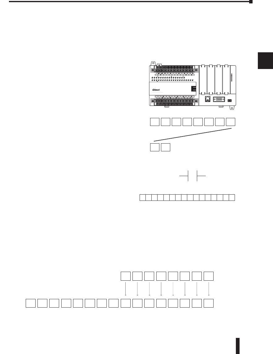
DL06 Micro PLC User Manual, 3rd Edition, Rev. D 3-25
Chapter 3: CPU Specifications and Operation
1
2
3
4
5
6
7
8
9
10
11
12
13
14
A
B
C
D
Memory Map
With any PLC system, you generally have many different types of information to process.
This includes input device status, output device status, various timing elements, parts counts,
etc. It is important to understand how the system represents and stores the various types of
data. For example, you need to know how the system identifies input points, output points,
data words, etc. The following paragraphs discuss the various memory types used in DL06
Micro PLCs. A memory map overview for the CPU
follows the memory descriptions.
.
V-memory Locations for Discrete Memory Areas
The discrete memory area is for inputs, outputs, control relays, special relays, stages, timer
status bits and counter status bits. However, you can also access the bit data types as a
V-memory word. Each V-memory location contains 16 consecutive discrete locations. For
example, the following diagram shows how the X input points are mapped into V-memory
locations.
These discrete memory areas and their corresponding V-memory ranges are listed in the
memory area table for DL06 Micro PLCs on the following pages.
X0 X1 X2 X3 X4 X5 X6 X7
X10 X11
LOGIC
Koyo
06
C0 C4C2X1 X3 X4 X6 X11X13 X14X16 X21X23 N.C.
C1 C3X2 X5 X7 X10X12 X15X17 X20X22X0 N.C.
AC(N)24V
0V
N.C.
C1 C3Y0 Y15Y12Y10Y17Y7Y5Y2
C0 C2 Y16Y14Y13Y11Y6Y4Y3Y1
LG
G
AC(L)
D0-06DR
2.0AOUTPUT: 6-240V50 - 60Hz 2.0A, 6 - 27V
INPUT: 12 - 24V 3 - 15mA
Y
X
40VA50-60HzPWR: 100-240V
01 23456710 11 12 13 14 15 16 17 20 21 22 23
PORT1PORT2
TERM
RUN STOP
PWR
RUN
CPU
TX1
RX1
TX2
RX2
X0
Discrete – On or Off, 1 bit
0 110100000010010
Word Locations – 16 bits
X0X1X2X3X4X5X6X7
0123456789101112131415 V40400
Bit #
8 Discrete (X) Input Points
Octal Numbering System
All memory locations and resources
are numbered in Octal (base 8). For
example, the diagram shows how the octal
numbering system works for the discrete
input points. Notice the octal system does
not contain any numbers with the digits
8 or 9.
Discrete and Word Locations
As you examine the different memory
types, you’ll notice two types of memory
in the DL06, discrete and word memory.
Discrete memory is one bit that can be
either a 1 or a 0. Word memory is referred
to as V-memory (variable) and is a 16-bit
location normally used to manipulate
data/numbers, store data/numbers, etc.
Some information is automatically stored
in V-memory. For example, the timer
current values are stored in V-memory.
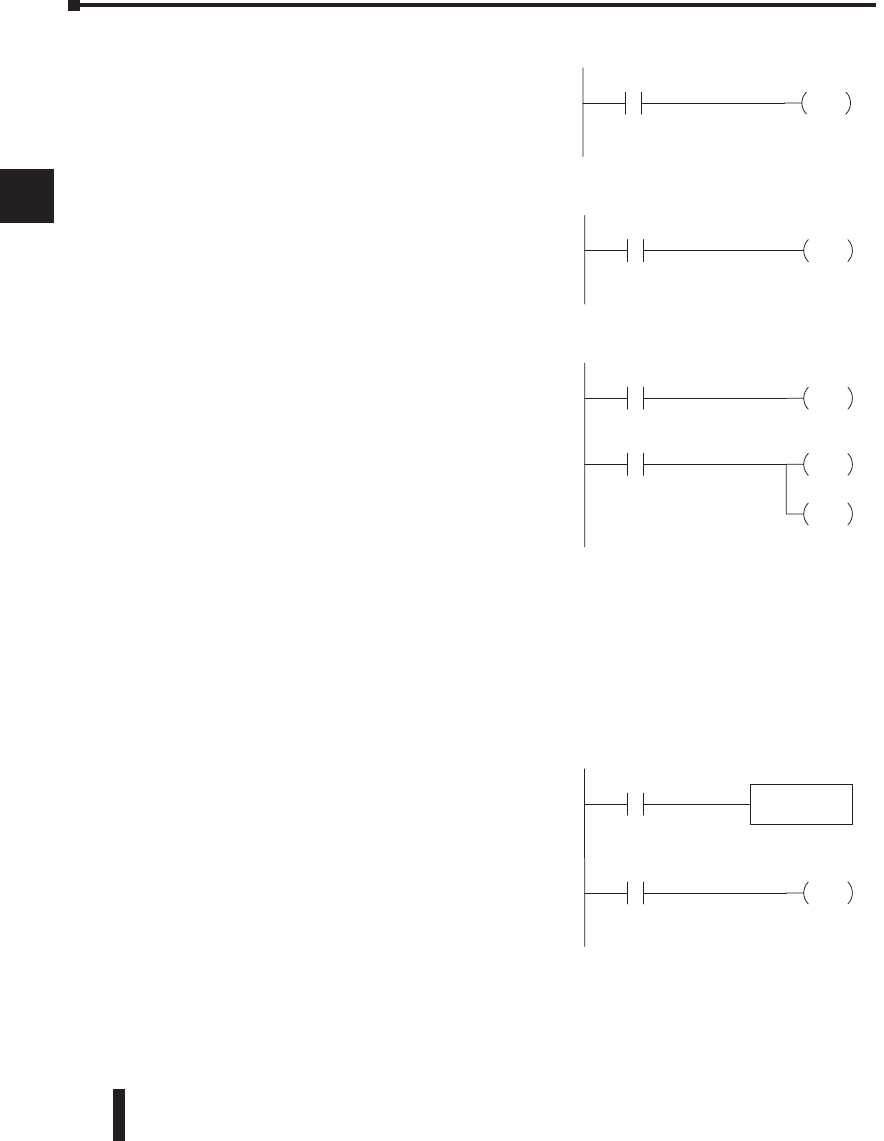
DL06 Micro PLC User Manual, 3rd Edition, Rev. D
3-26
Chapter 3: CPU Specifications and Operation
1
2
3
4
5
6
7
8
9
10
11
12
13
14
A
B
C
D
Y0
OUT
X0
Y1
OUT
X1
C5
OUT
X6
Y10
OUT
C5
Y20
OUT
Y12
OUT
T1
TMR T1
K30
X0
Input Points (X Data Type)
The discrete input points are noted by an X data
type. There are 20 discrete input points and 256
discrete input addresses available with DL06
CPUs. In this example, the output point Y0 will
be turned on when input X0 energizes.
Output Points (Y Data Type)
The discrete output points are noted by a Y data
type. There are 16 discrete outputs and 256
discrete output addresses available with DL06
CPUs. In this example, output point Y1 will be
turned on when input X1 energizes.
Control Relays (C Data Type)
Control relays are discrete bits normally used to
control the user program. The control relays do
not represent a real world device, that is, they
cannot be physically tied to switches, output
coils, etc. There are 1024 control relays internal
to the CPU. Because of this, control relays can
be programmed as discrete inputs or discrete
outputs. These locations are used in programming
the discrete memory locations (C) or the
corresponding word location which contains 16
consecutive discrete locations.
In this example, memory location C5 will energize
when input X6 turns on. The second rung shows
a simple example of how to use a control relay as
an input.
Timers and Timer Status Bits (T Data Type)
There are 256 timers available in the CPU. Timer
status bits reflect the relationship between the
current value and the preset value of a specified
timer. The timer status bit will be on when the
current value is equal or greater than the preset
value of a corresponding timer.
When input X0 turns on, timer T1 will start.
When the timer reaches the preset of 3 seconds (K
of 30) timer status contact T1 turns on. When T1
turns on, output Y12 turns on. Turning off X0
resets the timer.
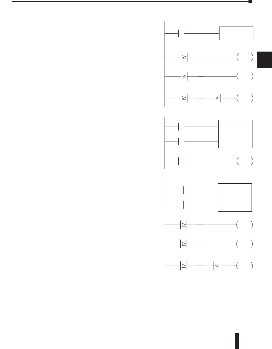
DL06 Micro PLC User Manual, 3rd Edition, Rev. D 3-27
Chapter 3: CPU Specifications and Operation
1
2
3
4
5
6
7
8
9
10
11
12
13
14
A
B
C
D
Timer Current Values (V Data Type)
As mentioned earlier, some information is automatically
stored in V-memory. This is true for the current values
associated with timers. For example: V0 holds the
current value for Timer 0; V1 holds the current value for
Timer 1; and so on. These can also be designated as
TA0 (Timer Accumulated) for Timer 0, and TA1 for
Timer 1.
The primary reason for this is programming flexibility.
The example shows how you can use relational contacts
to monitor several time intervals from a single timer.
Counters and Counter Status Bits (CT Data type)
There are 128 counters available in the CPU. Counter
status bits that reflect the relationship between the
current value and the preset value of a specified counter.
The counter status bit will be on when the current
value is equal to or greater than the preset value of a
corresponding counter.
Each time contact X0 transitions from off to on, the
counter increments by one. (If X1 comes on, the counter
is reset to zero.) When the counter reaches the preset of
10 counts (K of 10) counter status contact CT3 turns on.
When CT3 turns on, output Y2 turns on.
Counter Current Values (V Data Type)
Just like the timers, the counter current values are also
automatically stored in V-memory. For example, V1000
holds the current value for Counter CT0, V1001 holds
the current value for Counter CT1, etc. These can also
be designated as CTA0 (Counter Accumulated) for
Counter 0 and CTA01 for Counter 1.
The primary reason for this is programming flexibility.
The example shows how you can use relational contacts
to monitor the counter values.
V1 K100
TMR T1
K1000
X0
V1 K30 Y2
OUT
V1 K50 Y3
OUT
V1 K75 Y4
OUT
Y2
OUT
CT3
X0 CNT CT3
K10
X1
V1003 K8
V1003 K1 Y2
OUT
V1003 K3 Y3
OUT
V1003 K5 Y4
OUT
X0 CNT CT3
K10
X1
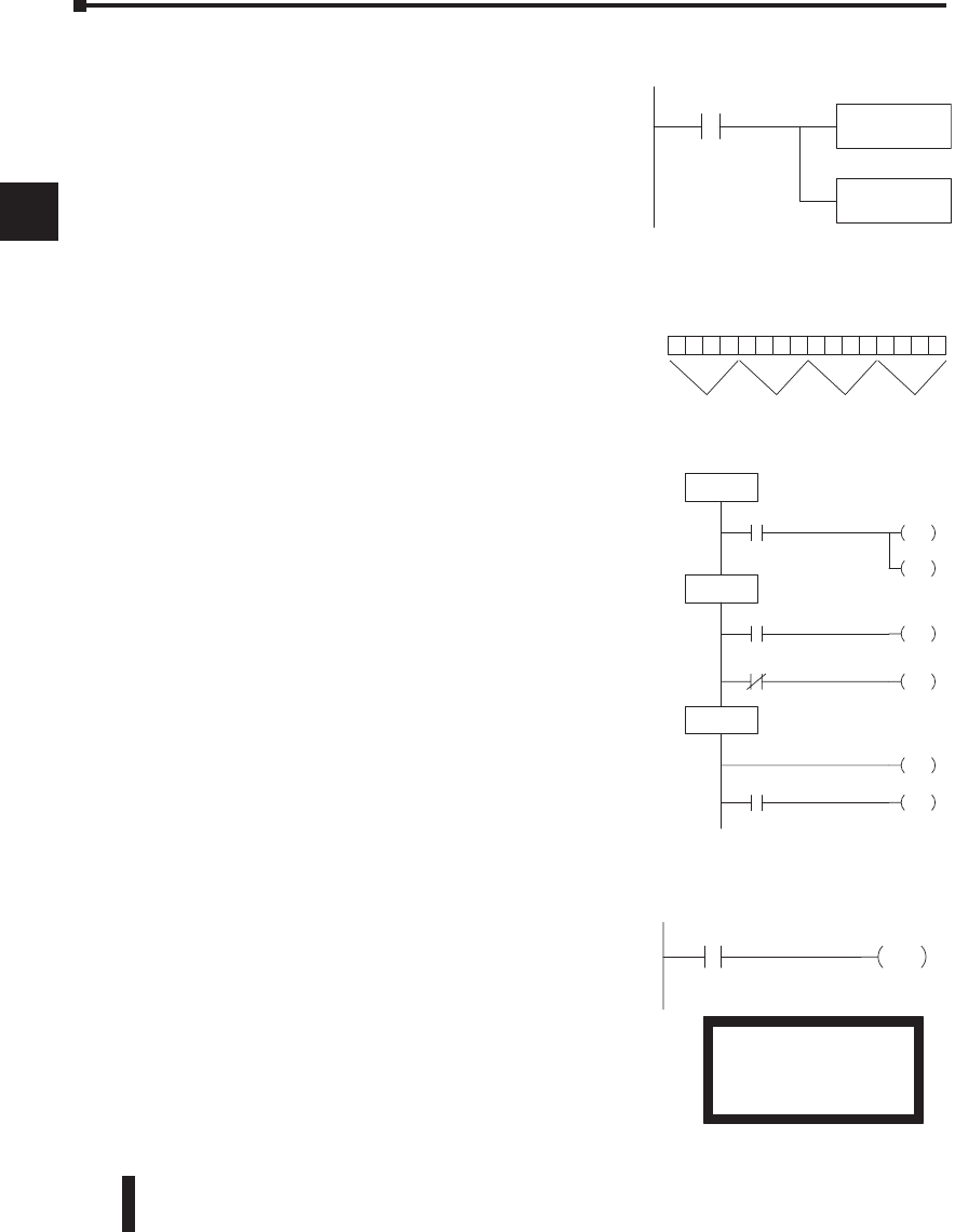
DL06 Micro PLC User Manual, 3rd Edition, Rev. D
3-28
Chapter 3: CPU Specifications and Operation
1
2
3
4
5
6
7
8
9
10
11
12
13
14
A
B
C
D
X0 LD
K1345
OUT V2000
0 100100110100010
Word Locations – 16 bits
1 3
45
Ladder Representation
ISG
S0000
Start S1
JMP
SG
S0001
Present S2
JMP
Part
X1
X0
S6
JMP
Present
Part
X1
SG
S0002
Clamp
SET
S3
JMP
Locked
Part
X2
S400
Wait for Start
Check for a Part
Clamp the part
S500
JMP
C10
OUT
SP5
SP4: 1 second clock
SP5: 100 ms clock
SP6: 50 ms clock
Word Memory (V Data Type)
Word memory is referred to as V-memory (variable)
and is a 16-bit location normally used to manipulate
data/numbers, store data/numbers, etc. Some
information is automatically stored in V-memory.
For example, the timer current values are stored in
V-memory. The example shows how a four-digit
BCD constant is loaded into the accumulator and
then stored in a V-memory location.
Stages (S Data type)
Stages are used in RLLPLUS programs to create a
structured program, similar to a flowchart. Each
program Stage denotes a program segment. When
the program segment, or Stage, is active, the logic
within that segment is executed. If the Stage is
off, or inactive, the logic is not executed and the
CPU skips to the next active Stage. (See Chapter
7 for a more detailed description of RLLPLUS
programming.)
Each Stage also has a discrete status bit that can
be used as an input to indicate whether the Stage
is active or inactive. If the Stage is active, then the
status bit is on. If the Stage is inactive, then the
status bit is off. This status bit can also be turned
on or off by other instructions, such as the SET
or RESET instructions. This allows you to easily
control stages throughout the program.
Special Relays (SP Data Type)
Special relays are discrete memory locations with
pre-defined functionality. There are many different
types of special relays. For example, some aid in
program development, others provide system
operating status information, etc. Appendix D
provides a complete listing of the special relays.
In this example, control relay C10 will energize for
50 ms and de-energize for 50 ms because SP5 is a
pre–defined relay that will be on for 50 ms and off
for 50 ms.
DL06 Micro PLC User Manual, 3rd Edition, Rev. D 3-29
Chapter 3: CPU Specifications and Operation
1
2
3
4
5
6
7
8
9
10
11
12
13
14
A
B
C
D
DL06 System V-memory
System Parameters and Default Data Locations (V Data Type)
The DL06 PLCs reserve several V-memory locations for storing system parameters or certain
types of system data. These memory locations store things like the error codes, High-Speed
I/O data, and other types of system setup information.
System
V-memory Description of Contents Default Values /
Ranges
Read
Only
R/W
V700-V707 Sets the V-memory location for option card in slot 1 N/A R/W
V710-V717 Sets the V-memory location for option card in slot 2 N/A R/W
V720-V727 Sets the V-memory location for option card in slot 3 N/A R/W
V730-V737 Sets the V-memory location for option card in slot 4 N/A R/W
V3630–V3707 The default location for multiple preset values for UP/DWN and UP Counter 1 or pulse catch
function N/A R/W
V3710-V3767 The default location for multiple preset values for UP/DWN and UP Counter 2 N/A R/W
V7620 DV-1000 Sets the V-memory location that contains the value V0 – V3760 R/W
V7621 DV-1000 Sets the V-memory location that contains the message V0 – V3760 R/W
V7622 DV-1000 Sets the total number (1 – 32) of V-memory locations to be displayed 1 - 32 R/W
V7623 DV-1000 Sets the V-memory location containing the numbers to be displayed V0 – V3760 R/W
V7624 DV-1000 Sets the V-memory location that contains the character code to be displayed V0 – V3760 R/W
V7625 DV-1000 Contains the function number that can be assigned to each key V-memory for X, Y, or C R/W
V7626 DV-1000 Powerup operational mode 0,1, 2, 3, 12 R/W
V7627 Change preset value 0000 to 9999 R/W
V7630 Starting location for the multi–step presets for channel 1. The default value is 3630, which
indicates the first value should be obtained from V3630. Since there are 24 presets available,
the default range is V3630 – V3707. You can change the starting point if necessary.
Default: V3630
Range: V0- V3710 R/W
V7631 Starting location for the multi–step presets for channel 2. The default value is 3710, which
indicates the first value should be obtained from V3710. Since there are 24 presets available,
the default range is V3710 – V3767. You can change the starting point if necessary.
Default: V3710
Range: V0- V3710 R/W
V7632 Setup Register for Pulse Output N/A R/W
V7633 Sets the desired function code for the high speed counter, interrupt, pulse catch, pulse train,
and input filter.
This location can also be used to set the power-up in Run Mode option.
Default: 0060
Lower Byte Range: Range:
10 – Counter 20 – Quadrature
30 – Pulse Out 40 – Interrupt
50 – Pulse Catch 60 – Filtered
discrete In. Upper Byte
Range: Bits 8–11, 14, 15:
Unused, Bit 13: Power–up
in RUN, only if Mode Switch
is inTERM position. Bit 12 is
used to enable the low battery
indications.
R/W
V7634 X0 Setup Register for High-Speed I/O functions for input X0 Default: 1006 R/W
V7635 X1 Setup Register for High-Speed I/O functions for input X1 Default: 1006 R/W
V7636 X2 Setup Register for High-Speed I/O functions for input X2 Default: 1006 R/W
V7637 X3 Setup Register for High-Speed I/O functions for input X3 Default: 1006 R/W
V7640 PID Loop table beginning address V1200 - V7377
V10000-V17777 R/W
V7641 Number of PID loops enabled 1-8 R/W
V7642 Error Code - PID Loop Table R
V7643-V7646 DirectSoft I-Box instructions work area R
V7647 Timed Interrupt R/W
V7653 Port 2: Terminate code setting Non-procedure R/W
V7655 Port 2: Setup for the protocol, time-out, and the response delay time R/W

DL06 Micro PLC User Manual, 3rd Edition, Rev. D
3-30
Chapter 3: CPU Specifications and Operation
1
2
3
4
5
6
7
8
9
10
11
12
13
14
A
B
C
D
System
V-memory Description of Contents
Default
Values /
Ranges
Read
Only
R/W
V7656 Port 2: Setup for the station number, baud rate, STOP bit, and parity R/W
V7657 Port 2: Setup completion code used to notify the completion of the parameter setup 0400h reset
port 2 R/W
V7660 Scan control setup: Keeps the scan control mode R/W
V7661 Setup timer over counter R
V7662–V7710 Reserved R/W
V7711-V7717 DirectSOFT I-Box instructions work area R
V7720–V7722 Locations for DV–1000 operator interface parameters R/W
V7720 location for DV-1000 operation interface Titled Timer preset value pointer R/W
V7721 DV-1000: Title Counter preset value pointer R/W
V7722 DV-1000: Hibyte-Titled, Lobyte-Timer preset block size R/W
V7723–V7725 DirectSOFT I-Box instructions work area R
V7726 Reserved R/W
V7727 Version No R
V7730-V7737 D0-DCM Module Slot0 Auto Reset Timeout R/W
V7731 D0-DCM Module Slot1 Auto Reset Timeout R/W
V7732 D0-DCM Module Slot2 Auto Reset Timeout R/W
V7733 D0-DCM Module Slot3 Auto Reset Timeout R/W
V7734-V7737 Reserved R/W
V7740 Port 2: Communication Auto Reset Timer Setup Default: 3030 R/W
V7741 Reserved R/W
V7742 LCD Various LCD setting flags R/W
V7743 V Memory address in which the default display message is stored as set R/W
V7744-V7746 Reserved R/W
V7747 Location contains a 10 ms counter (0-99). This location increments once every 10 ms R
V7750 Reserved R/W
V7751 Fault Message Error Code R
V7752 I/O Configuration Error: stores the module ID code for the module that does not the current
configuration R
V7753 I/O Configuration Error: stores the module ID code R
V7754 I/O Configuration Error: identifies the base and slot number R
V7755 Error code — stores the fatal error code R
V7756 Error code — stores the major error code R
V7757 Error code — stores the minor error code R
V7760–V7762 Reserved R/W
V7763 Program address where syntax error exists R
V7764 Syntax error code R
V7765 Scan counter — stores the total number of scan cycles that have occurred since the last Program
Mode to Run Mode transition (in decimal) R
V7766 Contains the number of seconds on the clock (00-59) R
V7767 Contains the number of minutes on the clock (00-59) R
V7770 Contains the number of hours on the clock (00-23) R
V7771 Contains the day of the week (Mon., Tues., Wed., etc.) R
V7772 Contains the day of the month (01, 02, etc.) R
V7773 Contains the month (01 to 12) R
V7774 Contains the year (00 to 99) R
V7775 Scan — stores the current scan time (milliseconds) R
V7776 Scan — stores the minimum scan time that has occurred since the last Program Mode to Run
Mode transition (milliseconds) R
V7777 Scan — stores the maximum scan rate since the last power cycle (milliseconds) R
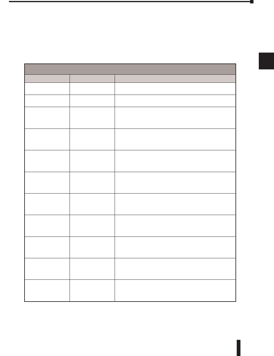
DL06 Micro PLC User Manual, 3rd Edition, Rev. D 3-31
Chapter 3: CPU Specifications and Operation
1
2
3
4
5
6
7
8
9
10
11
12
13
14
A
B
C
D
DL06 Aliases
An alias is an alternate way of referring to certain memory types, such as timer/counter
current values, V-memory locations for I/O points, etc., which simplifies understanding the
memory address. The use of the alias is optional, but some users may find the alias to be
helpful when developing a program. The table below shows how the aliases can be used.
DL06 Aliases
Address Start Alias Start Example
V0 TA0 V0 is the timer accumulator value for timer 0, therefore, its
alias is TA0. TA1 is the alias for V1, etc..
V1000 CTA0 V1000 is the counter accumulator value for counter 0,
therefore, its alias is CTA0. CTA1 is the alias for V1001, etc.
V40000 VGX
V40000 is the word memory reference for discrete bits GX0
through GX17, therefore, its alias is VGX0. V40001 is the
word memory reference for discrete bits GX20 through GX 37,
therefore, its alias is VGX20.
V40200 VGY
V40200 is the word memory reference for discrete bits GY0
through GY17, therefore, its alias is VGY0. V40201 is the
word memory reference for discrete bits GY20 through GY 37,
therefore, its alias is VGY20.
V40400 VX0
V40400 is the word memory reference for discrete bits X0
through X17, therefore, its alias is VX0. V40401 is the word
memory reference for discrete bits X20 through X37, therefore,
its alias is VX20.
V40500 VY0
V40500 is the word memory reference for discrete bits Y0
through Y17, therefore, its alias is VY0. V40501 is the word
memory reference for discrete bits Y20 through Y37, therefore,
its alias is VY20.
V40600 VC0
V40600 is the word memory reference for discrete bits C0
through C17, therefore, its alias is VC0. V40601 is the word
memory reference for discrete bits C20 through C37, therefore,
its alias is VC20.
V41000 VS0
V41000 is the word memory reference for discrete bits S0
through S17, therefore, its alias is VS0. V41001 is the word
memory reference for discrete bits S20 through S37, therefore,
its alias is VS20.
V41100 VT0
V41100 is the word memory reference for discrete bits T0
through T17, therefore, its alias is VT0. V41101 is the word
memory reference for discrete bits T20 through T37, therefore,
its alias is VT20.
V41140 VCT0
V41140 is the word memory reference for discrete bits CT0
through CT17, therefore, its alias is VCT0. V41141 is the
word memory reference for discrete bits CT20 through CT37,
therefore, its alias is VCT20.
V41200 VSP0
V41200 is the word memory reference for discrete bits SP0
through SP17, therefore, its alias is VSP0. V41201 is the
word memory reference for discrete bits SP20 through SP37,
therefore, its alias is VSP20.
DL06 Micro PLC User Manual, 3rd Edition, Rev. D
3-32
Chapter 3: CPU Specifications and Operation
1
2
3
4
5
6
7
8
9
10
11
12
13
14
A
B
C
D
DL06 Memory Map
Memory Type
Discrete Memory
Reference
(octal)
Word Memory
Reference
(octal)
Decimal Symbol
Input Points X0 – X777 V40400 - V40437 512 X0
Output Points Y0 – Y777 V40500 – V40537 512
Y0
Control Relays C0 – C1777 V40600 - V40677 1024
C0C0
Special Relays SP0 – SP777 V41200 – V41237 512
SP0
Timers T0 – T377 V41100 – V41117 256 TMR
K100
T0
Timer Current Values None V0 – V377 256 V0 K100
Timer Status Bits T0 – T377 V41100 – V41117 256
T0
Counters CT0 – CT177 V41140 – V41147 128
CNT
K10
CT0
Counter
Current Values None V1000 – V1177 128 V1000 K100
Counter Status Bits CT0 – CT177 V41140 – V41147 128 CT0
Data Words
(See Appendix F) None
V400-V677
V1200 – V7377
V10000 - V17777
192
3200
4096
None specific, used with many
instructions.
Data Words
EEPROM
(See Appendix F)
None V7400 – V7577 128
None specific, used with many
instructions.
May be non-volatile if MOV inst. is used.
Data can be rewritten to EEPROM at least
100,000 times before it fails.
Stages S0 – S1777 V41000 – V41077 1024 SP0
SG
S001
Remote I/O (future use)
(See Note 1)
GX0-GX3777
GY0-GY3777
V40000-V40177
V40200-V40377
2048
2048
GX0 GY0
System parameters None
V700-V777
V7600 – V7777
V36000-V37777
64
128
1024
None specific, used for various purposes
NOTE 1: This area can be used for additional Data Words.
NOTE 2: The DL06 systems have 20 fixed discrete inputs and 16 fixed discrete outputs, but the total
can be increased by up to 64 inputs or 64 outputs, or a combination of both.
DL06 Micro PLC User Manual, 3rd Edition, Rev. D 3-33
Chapter 3: CPU Specifications and Operation
1
2
3
4
5
6
7
8
9
10
11
12
13
14
A
B
C
D
X Input/Y Output Bit Map
This table provides a listing of individual input and output points associated with each
V-memory address bit for the DL06’s twenty integrated physical inputs and 16 integrated
physical outputs in addition to up to 64 inputs and 64 outputs for option cards. Actual
available references are X0 to X777 (V40400 – V40437) and Y0 to Y777 (V40500 -
V40537).
617 616 615 614 613 612 611 610 607 606 605 604 603 602 601 600 V40430 V40530
637 636 635 634 633 632 631 630 627 626 625 624 623 622 621 620 V40431 V40531
657 656 655 654 653 652 651 650 647 646 645 644 643 642 641 640 V40432 V40532
677 676 675 674 673 672 671 670 667 666 665 664 663 662 661 660 V40433 V40533
717 716 715 714 713 712 711 710 707 706 705 704 703 702 701 700 V40434 V40534
737 736 735 734 733 732 731 730 727 726 725 724 723 722 721 720 V40435 V40535
757 756 755 754 753 752 751 750 747 746 745 744 743 742 741 740 V40436 V40536
777 776 775 774 773 772 771 770 767 766 765 764 763 762 761 760 V40437 V40537
217 216 215 214 213 212 211 210 207 206 205 204 203 202 201 200 V40410 V40510
237 236 235 234 233 232 231 230 227 226 225 224 223 222 221 220 V40411 V40511
257 256 255 254 253 252 251 250 247 246 245 244 243 242 241 240 V40412 V40512
277 276 275 274 273 272 271 270 267 266 265 264 263 262 261 260 V40413 V40513
317 316 315 314 313 312 311 310 307 306 305 304 303 302 301 300 V40414 V40514
337 336 335 334 333 332 331 330 327 326 325 324 323 322 321 320 V40415 V40515
357 356 355 354 353 352 351 350 347 346 345 344 343 342 341 340 V40416 V40516
377 376 375 374 373 372 371 370 367 366 365 364 363 362 361 360 V40417 V40517
MSB DL06 Input (X) and Output (Y) Points LSB X Input
Address
Y Output
Address
15 14 13 12 11 10 9 8 7 6 5 4 3 2 1 0
017 016 015 014 013 012 011 010 007 006 005 004 003 002 001 000 V40400 V40500
037 036 035 034 033 032 031 030 027 026 025 024 023 022 021 020 V40401 V40501
057 056 055 054 053 052 051 050 047 046 045 044 043 042 041 040 V40402 V40502
077 076 075 074 073 072 071 070 067 066 065 064 063 062 061 060 V40403 V40503
117 116 115 114 113 112 111 110 107 106 105 104 103 102 101 100 V40404 V40504
137 136 135 134 133 132 131 130 127 126 125 124 123 122 121 120 V40405 V40505
157 156 155 154 153 152 151 150 147 146 145 144 143 142 141 140 V40406 V40506
177 176 175 174 173 172 171 170 167 166 165 164 163 162 161 160 V40407 V40507
417 416 415 414 413 412 411 410 407 406 405 404 403 402 401 400 V40420 V40520
437 436 435 434 433 432 431 430 427 426 425 424 423 422 421 420 V40421 V40521
457 456 455 454 453 452 451 450 447 446 445 444 443 442 441 440 V40422 V40522
477 476 475 474 473 472 471 470 467 466 465 464 463 462 461 460 V40423 V40523
517 516 515 514 513 512 511 510 507 506 505 504 503 502 501 500 V40424 V40524
537 536 535 534 533 532 531 530 527 526 525 524 523 522 521 520 V40425 V40525
557 556 555 554 553 552 551 550 547 546 545 544 543 542 541 540 V40426 V40526
577 576 575 574 573 572 571 570 567 566 565 564 563 562 561 560 V40427 V40527
DL06 Micro PLC User Manual, 3rd Edition, Rev. D
3-34
Chapter 3: CPU Specifications and Operation
1
2
3
4
5
6
7
8
9
10
11
12
13
14
A
B
C
D
Stage Control/Status Bit Map
This table provides a listing of individual Stage control bits associated with each V-memory
address bit.
This table is continued on the next page.
MSB DL06 Stage (S) Control Bits LSB Address
15 14 13 12 11 10 9 8 7 6 5 4 3 2 1 0
017 016 015 014 013 012 011 010 007 006 005 004 003 002 001 000 V41000
037 036 035 034 033 032 031 030 027 026 025 024 023 022 021 020 V41001
057 056 055 054 053 052 051 050 047 046 045 044 043 042 041 040 V41002
077 076 075 074 073 072 071 070 067 066 065 064 063 062 061 060 V41003
117 116 115 114 113 112 111 110 107 106 105 104 103 102 101 100 V41004
137 136 135 134 133 132 131 130 127 126 125 124 123 122 121 120 V41005
157 156 155 154 153 152 151 150 147 146 145 144 143 142 141 140 V41006
177 176 175 174 173 172 171 170 167 166 165 164 163 162 161 160 V41007
217 216 215 214 213 212 211 210 207 206 205 204 203 202 201 200 V41010
237 236 235 234 233 232 231 230 227 226 225 224 223 222 221 220 V41011
257 256 255 254 253 252 251 250 247 246 245 244 243 242 241 240 V41012
277 276 275 274 273 272 271 270 267 266 265 264 263 262 261 260 V41013
317 316 315 314 313 312 311 310 307 306 305 304 303 302 301 300 V41014
337 336 335 334 333 332 331 330 327 326 325 324 323 322 321 320 V41015
357 356 355 354 353 352 351 350 347 346 345 344 343 342 341 340 V41016
377 376 375 374 373 372 371 370 367 366 365 364 363 362 361 360 V41017
417 416 415 414 413 412 411 410 407 406 405 404 403 402 401 400 V41020
437 436 435 434 433 432 431 430 427 426 425 424 423 422 421 420 V41021
457 456 455 454 453 452 451 450 447 446 445 444 443 442 441 440 V41022
477 476 475 474 473 472 471 470 467 466 465 464 463 462 461 460 V41023
517 516 515 514 513 512 511 510 507 506 505 504 503 502 501 500 V41024
537 536 535 534 533 532 531 530 527 526 525 524 523 522 521 520 V41025
557 556 555 554 553 552 551 550 547 546 545 544 543 542 541 540 V41026
577 576 575 574 573 572 571 570 567 566 565 564 563 562 561 560 V41027
617 616 615 614 613 612 611 610 607 606 605 604 603 602 601 600 V41030
637 636 635 634 633 632 631 630 627 626 625 624 623 622 621 620 V41031
657 656 655 654 653 652 651 650 647 646 645 644 643 642 641 640 V41032
677 676 675 674 673 672 671 670 667 666 665 664 663 662 661 660 V41033
717 716 715 714 713 712 711 710 707 706 705 704 703 702 701 700 V41034
737 736 735 734 733 732 731 730 727 726 725 724 723 722 721 720 V41035
757 756 755 754 753 752 751 750 747 746 745 744 743 742 741 740 V41036
777 776 775 774 773 772 771 770 767 766 765 764 763 762 761 760 V41037
DL06 Micro PLC User Manual, 3rd Edition, Rev. D 3-35
Chapter 3: CPU Specifications and Operation
1
2
3
4
5
6
7
8
9
10
11
12
13
14
A
B
C
D
MSB DL06 Stage (S) Control Bits (cont’d) LSB Address
15 14 13 12 11 10 9 8 7 6 5 4 3 2 1 0
1017 1016 1015 1014 1013 1012 1011 1010 1007 1006 1005 1004 1003 1002 1001 1000 V41040
1037 1036 1035 1034 1033 1032 1031 1030 1027 1026 1025 1024 1023 1022 1021 1020 V41041
1057 1056 1055 1054 1053 1052 1051 1050 1047 1046 1045 1044 1043 1042 1041 1040 V41042
1077 1076 1075 1074 1073 1072 1071 1070 1067 1066 1065 1064 1063 1062 1061 1060 V41043
1117 1116 1115 1114 1113 1112 1111 1110 1107 1106 1105 1104 1103 1102 1101 1100 V41044
1137 1136 1135 1134 1133 1132 1131 1130 1127 1126 1125 1124 1123 1122 1121 1120 V41045
1157 1156 1155 1154 1153 1152 1151 1150 1147 1146 1145 1144 1143 1142 1141 1140 V41046
1177 1176 1175 1174 1173 1172 1171 1170 1167 1166 1165 1164 1163 1162 1161 1160 V41047
1217 1216 1215 1214 1213 1212 1211 1210 1207 1206 1205 1204 1203 1202 1201 1200 V41050
1237 1236 1235 1234 1233 1232 1231 1230 1227 1226 1225 1224 1223 1222 1221 1220 V41051
1257 1256 1255 1254 1253 1252 1251 1250 1247 1246 1245 1244 1243 1242 1241 1240 V41052
1277 1276 1275 1274 1273 1272 1271 1270 1267 1266 1265 1264 1263 1262 1261 1260 V41053
1317 1316 1315 1314 1313 1312 1311 1310 1307 1306 1305 1304 1303 1302 1301 1300 V41054
1337 1336 1335 1334 1333 1332 1331 1330 1327 1326 1325 1324 1323 1322 1321 1320 V41055
1357 1356 1355 1354 1353 1352 1351 1350 1347 1346 1345 1344 1343 1342 1341 1340 V41056
1377 1376 1375 1374 1373 1372 1371 1370 1367 1366 1365 1364 1363 1362 1361 1360 V41057
1417 1416 1415 1414 1413 1412 1411 1410 1407 1406 1405 1404 1403 1402 1401 1400 V41060
1437 1436 1435 1434 1433 1432 1431 1430 1427 1426 1425 1424 1423 1422 1421 1420 V41061
1457 1456 1455 1454 1453 1452 1451 1450 1447 1446 1445 1444 1443 1442 1441 1440 V41062
1477 1476 1475 1474 1473 1472 1471 1470 1467 1466 1465 1464 1463 1462 1461 1460 V41063
1517 1516 1515 1514 1513 1512 1511 1510 1507 1506 1505 1504 1503 1502 1501 1500 V41064
1537 1536 1535 1534 1533 1532 1531 1530 1527 1526 1525 1524 1523 1522 1521 1520 V41065
1557 1556 1555 1554 1553 1552 1551 1550 1547 1546 1545 1544 1543 1542 1541 1540 V41066
1577 1576 1575 1574 1573 1572 1571 1570 1567 1566 1565 1564 1563 1562 1561 1560 V41067
1617 1616 1615 1614 1613 1612 1611 1610 1607 1606 1605 1604 1603 1602 1601 1600 V41070
1637 1636 1635 1634 1633 1632 1631 1630 1627 1626 1625 1624 1623 1622 1621 1620 V41071
1657 1656 1655 1654 1653 1652 1651 1650 1647 1646 1645 1644 1643 1642 1641 1640 V41072
1677 1676 1675 1674 1673 1672 1671 1670 1667 1666 1665 1664 1663 1662 1661 1660 V41073
1717 1716 1715 1714 1713 1712 1711 1710 1707 1706 1705 1704 1703 1702 1701 1700 V41074
1737 1736 1735 1734 1733 1732 1731 1730 1727 1726 1725 1724 1723 1722 1721 1720 V41075
1757 1756 1755 1754 1753 1752 1751 1750 1747 1746 1745 1744 1743 1742 1741 1740 V41076
1777 1776 1775 1774 1773 1772 1771 1770 1767 1766 1765 1764 1763 1762 1761 1760 V41077
DL06 Micro PLC User Manual, 3rd Edition, Rev. D
3-36
Chapter 3: CPU Specifications and Operation
1
2
3
4
5
6
7
8
9
10
11
12
13
14
A
B
C
D
Control Relay Bit Map
This table provides a listing of the individual control relays associated with each V-memory
address bit.
This table is continued on the next page.
MSB DL06 Control Relays (C) LSB Address
15 14 13 12 11 10 9876543210
017 016 015 014 013 012 011 010 007 006 005 004 003 002 001 000 V40600
037 036 035 034 033 032 031 030 027 026 025 024 023 022 021 020 V40601
057 056 055 054 053 052 051 050 047 046 045 044 043 042 041 040 V40602
077 076 075 074 073 072 071 070 067 066 065 064 063 062 061 060 V40603
117 116 115 114 113 112 111 110 107 106 105 104 103 102 101 100 V40604
137 136 135 134 133 132 131 130 127 126 125 124 123 122 121 120 V40605
157 156 155 154 153 152 151 150 147 146 145 144 143 142 141 140 V40606
177 176 175 174 173 172 171 170 167 166 165 164 163 162 161 160 V40607
617 616 615 614 613 612 611 610 607 606 605 604 603 602 601 600 V40630
637 636 635 634 633 632 631 630 627 626 625 624 623 622 621 620 V40631
657 656 655 654 653 652 651 650 647 646 645 644 643 642 641 640 V40632
677 676 675 674 673 672 671 670 667 666 665 664 663 662 661 660 V40633
717 716 715 714 713 712 711 710 707 706 705 704 703 702 701 700 V40634
737 736 735 734 733 732 731 730 727 726 725 724 723 722 721 720 V40635
757 756 755 754 753 752 751 750 747 746 745 744 743 742 741 740 V40636
777 776 775 774 773 772 771 770 767 766 765 764 763 762 761 760 V40637
417 416 415 414 413 412 411 410 407 406 405 404 403 402 401 400 V40620
437 436 435 434 433 432 431 430 427 426 425 424 423 422 421 420 V40621
457 456 455 454 453 452 451 450 447 446 445 444 443 442 441 440 V40622
477 476 475 474 473 472 471 470 467 466 465 464 463 462 461 460 V40623
517 516 515 514 513 512 511 510 507 506 505 504 503 502 501 500 V40624
537 536 535 534 533 532 531 530 527 526 525 524 523 522 521 520 V40625
557 556 555 554 553 552 551 550 547 546 545 544 543 542 541 540 V40626
577 576 575 574 573 572 571 570 567 566 565 564 563 562 561 560 V40627
217 216 215 214 213 212 211 210 207 206 205 204 203 202 201 200 V40610
237 236 235 234 233 232 231 230 227 226 225 224 223 222 221 220 V40611
257 256 255 254 253 252 251 250 247 246 245 244 243 242 241 240 V40612
277 276 275 274 273 272 271 270 267 266 265 264 263 262 261 260 V40613
317 316 315 314 313 312 311 310 307 306 305 304 303 302 301 300 V40614
337 336 335 334 333 332 331 330 327 326 325 324 323 322 321 320 V40615
357 356 355 354 353 352 351 350 347 346 345 344 343 342 341 340 V40616
377 376 375 374 373 372 371 370 367 366 365 364 363 362 361 360 V40617
DL06 Micro PLC User Manual, 3rd Edition, Rev. D 3-37
Chapter 3: CPU Specifications and Operation
1
2
3
4
5
6
7
8
9
10
11
12
13
14
A
B
C
D
MSB DL06 Control Relays (C) (cont’d) LSB Address
15 14 13 12 11 10 9876543210
1017 1016 1015 1014 1013 1012 1011 1010 1007 1006 1005 1004 1003 1002 1001 1000 V40640
1037 1036 1035 1034 1033 1032 1031 1030 1027 1026 1025 1024 1023 1022 1021 1020 V40641
1057 1056 1055 1054 1053 1052 1051 1050 1047 1046 1045 1044 1043 1042 1041 1040 V40642
1077 1076 1075 1074 1073 1072 1071 1070 1067 1066 1065 1064 1063 1062 1061 1060 V40643
1117 1116 1115 1114 1113 1112 1111 1110 1107 1106 1105 1104 1103 1102 1101 1100 V40644
1137 1136 1135 1134 1133 1132 1131 1130 1127 1126 1125 1124 1123 1122 1121 1120 V40645
1157 1156 1155 1154 1153 1152 1151 1150 1147 1146 1145 1144 1143 1142 1141 1140 V40646
1177 1176 1175 1174 1173 1172 1171 1170 1167 1166 1165 1164 1163 1162 1161 1160 V40647
1617 1616 1615 1614 1613 1612 1611 1610 1607 1606 1605 1604 1603 1602 1601 1600 V40670
1637 1636 1635 1634 1633 1632 1631 1630 1627 1626 1625 1624 1623 1622 1621 1620 V40671
1657 1656 1655 1654 1653 1652 1651 1650 1647 1646 1645 1644 1643 1642 1641 1640 V40672
1677 1676 1675 1674 1673 1672 1671 1670 1667 1666 1665 1664 1663 1662 1661 1660 V40673
1717 1716 1715 1714 1713 1712 1711 1710 1707 1706 1705 1704 1703 1702 1701 1700 V40674
1737 1736 1735 1734 1733 1732 1731 1730 1727 1726 1725 1724 1723 1722 1721 1720 V40675
1757 1756 1755 1754 1753 1752 1751 1750 1747 1746 1745 1744 1743 1742 1741 1740 V40676
1777 1776 1775 1774 1773 1772 1771 1770 1767 1766 1765 1764 1763 1762 1761 1760 V40677
1417 1416 1415 1414 1413 1412 1411 1410 1407 1406 1405 1404 1403 1402 1401 1400 V40660
1437 1436 1435 1434 1433 1432 1431 1430 1427 1426 1425 1424 1423 1422 1421 1420 V40661
1457 1456 1455 1454 1453 1452 1451 1450 1447 1446 1445 1444 1443 1442 1441 1440 V40662
1477 1476 1475 1474 1473 1472 1471 1470 1467 1466 1465 1464 1463 1462 1461 1460 V40663
1517 1516 1515 1514 1513 1512 1511 1510 1507 1506 1505 1504 1503 1502 1501 1500 V40664
1537 1536 1535 1534 1533 1532 1531 1530 1527 1526 1525 1524 1523 1522 1521 1520 V40665
1557 1556 1555 1554 1553 1552 1551 1550 1547 1546 1545 1544 1543 1542 1541 1540 V40666
1577 1576 1575 1574 1573 1572 1571 1570 1567 1566 1565 1564 1563 1562 1561 1560 V40667
1217 1216 1215 1214 1213 1212 1211 1210 1207 1206 1205 1204 1203 1202 1201 1200 V40650
1237 1236 1235 1234 1233 1232 1231 1230 1227 1226 1225 1224 1223 1222 1221 1220 V40651
1257 1256 1255 1254 1253 1252 1251 1250 1247 1246 1245 1244 1243 1242 1241 1240 V40652
1277 1276 1275 1274 1273 1272 1271 1270 1267 1266 1265 1264 1263 1262 1261 1260 V40653
1317 1316 1315 1314 1313 1312 1311 1310 1307 1306 1305 1304 1303 1302 1301 1300 V40654
1337 1336 1335 1334 1333 1332 1331 1330 1327 1326 1325 1324 1323 1322 1321 1320 V40655
1357 1356 1355 1354 1353 1352 1351 1350 1347 1346 1345 1344 1343 1342 1341 1340 V40656
1377 1376 1375 1374 1373 1372 1371 1370 1367 1366 1365 1364 1363 1362 1361 1360 V40657
DL06 Micro PLC User Manual, 3rd Edition, Rev. D
3-38
Chapter 3: CPU Specifications and Operation
1
2
3
4
5
6
7
8
9
10
11
12
13
14
A
B
C
D
Timer Status Bit Map
This table provides a listing of individual timer contacts associated with each V-memory
address bit.
Counter Status Bit Map
This table provides a listing of individual counter contacts associated with each V-memory
address bit.
MSB DL06 Counter (CT) Contacts LSB Address
15 14 13 12 11 10 9876543210
017 016 015 014 013 012 011 010 007 006 005 004 003 002 001 000 V41140
037 036 035 034 033 032 031 030 027 026 025 024 023 022 021 020 V41141
057 056 055 054 053 052 051 050 047 046 045 044 043 042 041 040 V41142
077 076 075 074 073 072 071 070 067 066 065 064 063 062 061 060 V41143
117 116 115 114 113 112 111 110 107 106 105 104 103 102 101 100 V41144
137 136 135 134 133 132 131 130 127 126 125 124 123 122 121 120 V41145
157 156 155 154 153 152 151 150 147 146 145 144 143 142 141 140 V41146
177 176 175 174 173 172 171 170 167 166 165 164 163 162 161 160 V41147
MSB DL06 Timer (T) Contacts LSB Address
15 14 13 12 11 10 9876543210
017 016 015 014 013 012 011 010 007 006 005 004 003 002 001 000 V41100
037 036 035 034 033 032 031 030 027 026 025 024 023 022 021 020 V41101
057 056 055 054 053 052 051 050 047 046 045 044 043 042 041 040 V41102
077 076 075 074 073 072 071 070 067 066 065 064 063 062 061 060 V41103
117 116 115 114 113 112 111 110 107 106 105 104 103 102 101 100 V41104
137 136 135 134 133 132 131 130 127 126 125 124 123 122 121 120 V41105
157 156 155 154 153 152 151 150 147 146 145 144 143 142 141 140 V41106
177 176 175 174 173 172 171 170 167 166 165 164 163 162 161 160 V41107
217 216 215 214 213 212 211 210 207 206 205 204 203 202 201 200 V41110
237 236 235 234 233 232 231 230 227 226 225 224 223 222 221 220 V41111
257 256 255 254 253 252 251 250 247 246 245 244 243 242 241 240 V41112
277 276 275 274 273 272 271 270 267 266 265 264 263 262 261 260 V41113
317 316 315 314 313 312 311 310 307 306 305 304 303 302 301 300 V41114
337 336 335 334 333 332 331 330 327 326 325 324 323 322 321 320 V41115
357 356 355 354 353 352 351 350 347 346 345 344 343 342 341 340 V41116
377 376 375 374 373 372 371 370 367 366 365 364 363 362 361 360 V41117
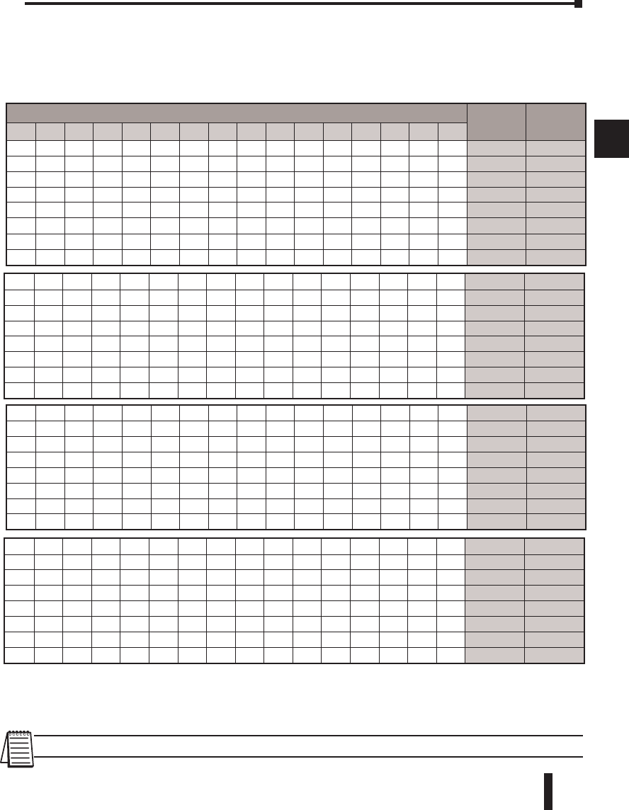
DL06 Micro PLC User Manual, 3rd Edition, Rev. D 3-39
Chapter 3: CPU Specifications and Operation
1
2
3
4
5
6
7
8
9
10
11
12
13
14
A
B
C
D
GX and GY I/O Bit Map
This table provides a listing of the individual global I/O points associated with each
V-memory address bit.
This table is continued on the next page.
NOTE: This memory area can be used for additional Data Words.
MSB DL06 GX and GY I/O Points LSB GX
Address
GY
Address
15 14 13 12 11 10 9876543210
017 016 015 014 013 012 011 010 007 006 005 004 003 002 001 000 V40000 V40200
037 036 035 034 033 032 031 030 027 026 025 024 023 022 021 020 V40001 V40201
057 056 055 054 053 052 051 050 047 046 045 044 043 042 041 040 V40002 V40202
077 076 075 074 073 072 071 070 067 066 065 064 063 062 061 060 V40003 V40203
117 116 115 114 113 112 111 110 107 106 105 104 103 102 101 100 V40004 V40204
137 136 135 134 133 132 131 130 127 126 125 124 123 122 121 120 V40005 V40205
157 156 155 154 153 152 151 150 147 146 145 144 143 142 141 140 V40006 V40206
177 176 175 174 173 172 171 170 167 166 165 164 163 162 161 160 V40007 V40207
217 216 215 214 213 212 211 210 207 206 205 204 203 202 201 200 V40010 V40210
237 236 235 234 233 232 231 230 227 226 225 224 223 222 221 220 V40011 V40211
257 256 255 254 253 252 251 250 247 246 245 244 243 242 241 240 V40012 V40212
277 276 275 274 273 272 271 270 267 266 265 264 263 262 261 260 V40013 V40213
317 316 315 314 313 312 311 310 307 306 305 304 303 302 301 300 V40004 V40214
337 336 335 334 333 332 331 330 327 326 325 324 323 322 321 320 V40015 V40215
357 356 355 354 353 352 351 350 347 346 345 344 343 342 341 340 V40016 V40216
377 376 375 374 373 372 371 370 367 366 365 364 363 362 361 360 V40007 V40217
617 616 615 614 613 612 611 610 607 606 605 604 603 602 601 600 V40030 V40230
637 636 635 634 633 632 631 630 627 626 625 624 623 622 621 620 V40031 V40231
657 656 655 654 653 652 651 650 647 646 645 644 643 642 641 640 V40032 V40232
677 676 675 674 673 672 671 670 667 666 665 664 663 662 661 660 V40033 V40233
717 716 715 714 713 712 711 710 707 706 705 704 703 702 701 700 V40034 V40234
737 736 735 734 733 732 731 730 727 726 725 724 723 722 721 720 V40035 V40235
757 756 755 754 753 752 751 750 747 746 745 744 743 742 741 740 V40036 V40236
777 776 775 774 773 772 771 770 767 766 765 764 763 762 761 760 V40037 V40237
417 416 415 414 413 412 411 410 407 406 405 404 403 402 401 400 V40020 V40220
437 436 435 434 433 432 431 430 427 426 425 424 423 422 421 420 V40021 V40221
457 456 455 454 453 452 451 450 447 446 445 444 443 442 441 440 V40022 V40222
477 476 475 474 473 472 471 470 467 466 465 464 463 462 461 460 V40023 V40223
517 516 515 514 513 512 511 510 507 506 505 504 503 502 501 500 V40024 V40224
537 536 535 534 533 532 531 530 527 526 525 524 523 522 521 520 V40025 V40225
557 556 555 554 553 552 551 550 547 546 545 544 543 542 541 540 V40026 V40226
577 576 575 574 573 572 571 570 567 566 565 564 563 562 561 560 V40027 V40227
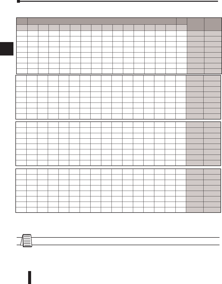
DL06 Micro PLC User Manual, 3rd Edition, Rev. D
3-40
Chapter 3: CPU Specifications and Operation
1
2
3
4
5
6
7
8
9
10
11
12
13
14
A
B
C
D
This table is continued on the next page.
NOTE: This memory area can be used for additional Data Words.
MSB DL06 GX and GY I/O Points (cont’d) LSB GX
Address
GY
Address
15 14 13 12 11 10 9876543210
1017 1016 1015 1014 1013 1012 1011 1010 1007 1006 1005 1004 1003 1002 1001 1000 V40040 V40240
1037 1036 1035 1034 1033 1032 1031 1030 1027 1026 1025 1024 1023 1022 1021 1020 V40041 V40241
1057 1056 1055 1054 1053 1052 1051 1050 1047 1046 1045 1044 1043 1042 1041 1040 V40042 V40242
1077 1076 1075 1074 1073 1072 1071 1070 1067 1066 1065 1064 1063 1062 1061 1060 V40043 V40243
1117 1116 1115 1114 1113 1112 1111 1110 1107 1106 1105 1104 1103 1102 1101 1100 V40044 V40244
1137 1136 1135 1134 1133 1132 1131 1130 1127 1126 1125 1124 1123 1122 1121 1120 V40045 V40245
1157 1156 1155 1154 1153 1152 1151 1150 1147 1146 1145 1144 1143 1142 1141 1140 V40046 V40246
1177 1176 1175 1174 1173 1172 1171 1170 1167 1166 1165 1164 1163 1162 1161 1160 V40047 V40247
1617 1616 1615 1614 1613 1612 1611 1610 1607 1606 1605 1604 1603 1602 1601 1600 V40070 V40270
1637 1636 1635 1634 1633 1632 1631 1630 1627 1626 1625 1624 1623 1622 1621 1620 V40071 V40271
1657 1656 1655 1654 1653 1652 1651 1650 1647 1646 1645 1644 1643 1642 1641 1640 V40072 V40272
1677 1676 1675 1674 1673 1672 1671 1670 1667 1666 1665 1664 1663 1662 1661 1660 V40073 V40273
1717 1716 1715 1714 1713 1712 1711 1710 1707 1706 1705 1704 1703 1702 1701 1700 V40074 V40274
1737 1736 1735 1734 1733 1732 1731 1730 1727 1726 1725 1724 1723 1722 1721 1720 V40075 V40275
1757 1756 1755 1754 1753 1752 1751 1750 1747 1746 1745 1744 1743 1742 1741 1740 V40076 V40276
1777 1776 1775 1774 1773 1772 1771 1770 1767 1766 1765 1764 1763 1762 1761 1760 V40077 V40277
1417 1416 1415 1414 1413 1412 1411 1410 1407 1406 1405 1404 1403 1402 1401 1400 V40060 V40260
1437 1436 1435 1434 1433 1432 1431 1430 1427 1426 1425 1424 1423 1422 1421 1420 V40061 V40261
1457 1456 1455 1454 1453 1452 1451 1450 1447 1446 1445 1444 1443 1442 1441 1440 V40062 V40262
1477 1476 1475 1474 1473 1472 1471 1470 1467 1466 1465 1464 1463 1462 1461 1460 V40063 V40263
1517 1516 1515 1514 1513 1512 1511 1510 1507 1506 1505 1504 1503 1502 1501 1500 V40064 V40264
1537 1536 1535 1534 1533 1532 1531 1530 1527 1526 1525 1524 1523 1522 1521 1520 V40065 V40265
1557 1556 1555 1554 1553 1552 1551 1550 1547 1546 1545 1544 1543 1542 1541 1540 V40066 V40266
1577 1576 1575 1574 1573 1572 1571 1570 1567 1566 1565 1564 1563 1562 1561 1560 V40067 V40267
1217 1216 1215 1214 1213 1212 1211 1210 1207 1206 1205 1204 1203 1202 1201 1200 V40050 V40250
1237 1236 1235 1234 1233 1232 1231 1230 1227 1226 1225 1224 1223 1222 1221 1220 V40051 V40251
1257 1256 1255 1254 1253 1252 1251 1250 1247 1246 1245 1244 1243 1242 1241 1240 V40052 V40252
1277 1276 1275 1274 1273 1272 1271 1270 1267 1266 1265 1264 1263 1262 1261 1260 V40053 V40253
1317 1316 1315 1314 1313 1312 1311 1310 1307 1306 1305 1304 1303 1302 1301 1300 V40054 V40254
1337 1336 1335 1334 1333 1332 1331 1330 1327 1326 1325 1324 1323 1322 1321 1320 V40055 V40255
1357 1356 1355 1354 1353 1352 1351 1350 1347 1346 1345 1344 1343 1342 1341 1340 V40056 V40256
1377 1376 1375 1374 1373 1372 1371 1370 1367 1366 1365 1364 1363 1362 1361 1360 V40057 V40257
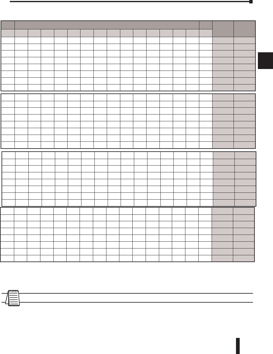
DL06 Micro PLC User Manual, 3rd Edition, Rev. D 3-41
Chapter 3: CPU Specifications and Operation
1
2
3
4
5
6
7
8
9
10
11
12
13
14
A
B
C
D
This table is continued on the next page.
NOTE: This memory area can be used for additional Data Words.
MSB DL06 GX and GY I/O Points (cont’d) LSB GX
Address
GY
Address
15 14 13 12 11 10 987 6 5 4 3 2 1 0
2017 2016 2015 2014 2013 2012 2011 2010 2007 2006 2005 2004 2003 2002 2001 2000 V40100 V40300
2037 2036 2035 2034 2033 2032 2031 2030 2027 2026 2025 2024 2023 2022 2021 2020 V40101 V40301
2057 2056 2055 2054 2053 2052 2051 2050 2047 2046 2045 2044 2043 2042 2041 2040 V40102 V40302
2077 2076 2075 2074 2073 2072 2071 2070 2067 2066 2065 2064 2063 2062 2061 2060 V40103 V40303
2117 2116 2115 2114 2113 2112 2111 2110 2107 2106 2105 2104 2103 2102 2101 2100 V40104 V40304
2137 2136 2135 2134 2133 2132 2131 2130 2127 2126 2125 2124 2123 2122 2121 2120 V40105 V40305
2157 2156 2155 2154 2153 2152 2151 2150 2147 2146 2145 2144 2143 2142 2141 2140 V40106 V40306
2177 2176 2175 2174 2173 2172 2171 2170 2167 2166 2165 2164 2163 2162 2161 2160 V40107 V40307
2617 2616 2615 2614 2613 2612 2611 2610 2607 2606 2605 2604 2603 2602 2601 2600 V40130 V40330
2637 2636 2635 2634 2633 2632 2631 2630 2627 2626 2625 2624 2623 2622 2621 2620 V40131 V40331
2657 2656 2655 2654 2653 2652 2651 2650 2647 2646 2645 2644 2643 2642 2641 2640 V40132 V40332
2677 2676 2675 2674 2673 2672 2671 2670 2667 2666 2665 2664 2663 2662 2661 2660 V40133 V40333
2717 2716 2715 2714 2713 2712 2711 2710 2707 2706 2705 2704 2703 2702 2701 2700 V40134 V40334
2737 2736 2735 2734 2733 2732 2731 2730 2727 2726 2725 2724 2723 2722 2721 2720 V40135 V40335
2757 2756 2755 2754 2753 2752 2751 2750 2747 2736 2735 2734 2733 2732 2731 2730 V40136 V40336
2777 2776 2775 2774 2773 2772 2771 2770 2767 2766 2765 2764 2763 2762 2761 2760 V40137 V40337
2417 2416 2415 2414 2413 2412 2411 2410 2407 2406 2405 2404 2403 2402 2401 2400 V40120 V40320
2437 2436 2435 2434 2433 2432 2431 2430 2427 2426 2425 2424 2423 2422 2421 2420 V40121 V40321
2457 2456 2455 2454 2453 2452 2451 2450 2447 2446 2445 2444 2443 2442 2441 2440 V40122 V40322
2477 2476 2475 2474 2473 2472 2471 2470 2467 2466 2465 2464 2463 2462 2461 2460 V40123 V40323
2517 2516 2515 2514 2513 2512 2511 2510 2507 2506 2505 2504 2503 2502 2501 2500 V40124 V40324
2537 2536 2535 2534 2533 2532 2531 2530 2527 2526 2525 2524 2523 2522 2521 2520 V40125 V40325
2557 2556 2555 2554 2553 2552 2551 2550 2547 2546 2545 2544 2543 2542 2541 2540 V40126 V40326
2577 2576 2575 2574 2573 2572 2571 2570 2567 2566 2565 2564 2563 2562 2561 2560 V40127 V40327
2217 2216 2215 2214 2213 2212 2211 2210 2207 2206 2205 2204 2203 2202 2201 2200 V40110 V40310
2237 2236 2235 2234 2233 2232 2231 2230 2227 2226 2225 2224 2223 2222 2221 2220 V40111 V40311
2257 2256 2255 2254 2253 2252 2251 2250 2247 2246 2245 2244 2243 2242 2241 2240 V40112 V40312
2277 2276 2275 2274 2273 2272 2271 2270 2267 2266 2265 2264 2263 2262 2261 2260 V40113 V40313
2317 2316 2315 2314 2313 2312 2311 2310 2307 2306 2305 2304 2303 2302 2301 2300 V40114 V40314
2337 2336 2335 2334 2333 2332 2331 2330 2327 2326 2325 2324 2323 2322 2321 2320 V40115 V40315
2357 2356 2355 2354 2353 2352 2351 2350 2347 2346 2345 2344 2343 2342 2341 2340 V40116 V40316
2377 2376 2375 2374 2373 2372 2371 2370 2367 2366 2365 2364 2363 2362 2361 2360 V40117 V40317
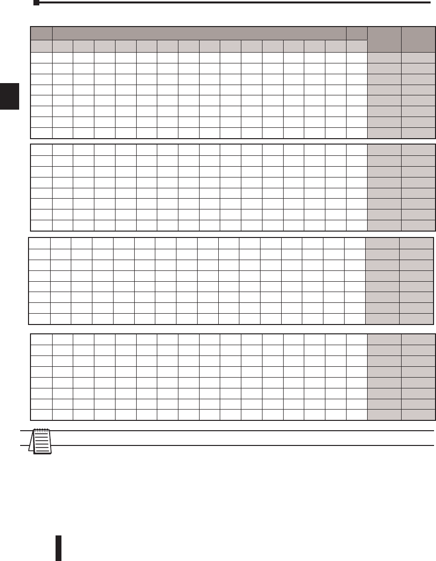
DL06 Micro PLC User Manual, 3rd Edition, Rev. D
3-42
Chapter 3: CPU Specifications and Operation
1
2
3
4
5
6
7
8
9
10
11
12
13
14
A
B
C
D
NOTE: This memory area can be used for additional Data Words.
MSB DL06 GX and GY I/O Points (cont’d) LSB GX
Address
GY
Address
15 14 13 12 11 10 9 8 7 6 5 4 3 2 1 0
3017 3016 3015 3014 3013 3012 3011 3010 3007 3006 3005 3004 3003 3002 3001 3000 V40140 V40340
3037 3036 3035 3034 3033 3032 3031 3030 3027 3026 3025 3024 3023 3022 3021 3020 V40141 V40341
3057 3056 3055 3054 3053 3052 3051 3050 3047 3046 3045 3044 3043 3042 3041 3040 V40142 V40342
3077 3076 3075 3074 3073 3072 3071 3070 3067 3066 3065 3064 3063 3062 3061 3060 V40143 V40343
3117 3116 3115 3114 3113 3112 3111 3110 3107 3106 3105 3104 3103 3102 3101 3100 V40144 V40344
3137 3136 3135 3134 3133 3132 3131 3130 3127 3126 3125 3124 3123 3122 3121 3120 V40145 V40345
3157 3156 3155 3154 3153 3152 3151 3150 3147 3146 3145 3144 3143 3142 3141 3140 V40146 V40346
3177 3176 3175 3174 3173 3172 3171 3170 3167 3166 3165 3164 3163 3162 3161 3160 V40147 V40347
3617 3616 3615 3614 3613 3612 3611 3610 3607 3606 3605 3604 3603 3602 3601 3600 V40170 V40370
3637 3636 3635 3634 3633 3632 3631 3630 3627 3626 3625 3624 3623 3622 3621 3620 V40171 V40371
3657 3656 3655 3654 3653 3652 3651 3650 3647 3646 3645 3644 3643 3642 3641 3640 V40172 V40372
3677 3676 3675 3674 3673 3672 3671 3670 3667 3666 3665 3664 3663 3662 3661 3660 V40173 V40373
3717 3716 3715 3714 3713 3712 3711 3710 3707 3706 3705 3704 3703 3702 3701 3700 V40174 V40374
3737 3736 3735 3734 3733 3732 3731 3730 3727 3726 3725 3724 3723 3722 3721 3720 V40175 V40375
3757 3756 3755 3754 3753 3752 3751 3750 3747 3746 3745 3744 3743 3742 3741 3740 V40176 V40376
3777 3776 3775 3774 3773 3772 3771 3770 3767 3766 3765 3764 3763 3762 3761 3760 V40177 V40377
3417 3416 3415 3414 3413 3412 3411 3410 3407 3406 3405 3404 3403 3402 3401 3400 V40160 V40360
3437 3436 3435 3434 3433 3432 3431 3430 3427 3426 3425 3424 3423 3422 3421 3420 V40161 V40361
3457 3456 3455 3454 3453 3452 3451 3450 3447 3446 3445 3444 3443 3442 3441 3440 V40162 V40362
3477 3476 3475 3474 3473 3472 3471 3470 3467 3466 3465 3464 3463 3462 3461 3460 V40163 V40363
3517 3516 3515 3514 3513 3512 3511 3510 3507 3506 3505 3504 3503 3502 3501 3500 V40164 V40364
3537 3536 3535 3534 3533 3532 3531 3530 3527 3526 3525 3524 3523 3522 3521 3520 V40165 V40365
3557 3556 3555 3554 3553 3552 3551 3550 3547 3546 3545 3544 3543 3542 3541 3540 V40166 V40366
3577 3576 3575 3574 3573 3572 3571 3570 3567 3566 3565 3564 3563 3562 3561 3560 V40167 V40367
3217 3216 3215 3214 3213 3212 3211 3210 3207 3206 3205 3204 3203 3202 3201 3200 V40150 V40350
3237 3236 3235 3234 3233 3232 3231 3230 3227 3226 3225 3224 3223 3222 3221 3220 V40151 V40351
3257 3256 3255 3254 3253 3252 3251 3250 3247 3246 3245 3244 3243 3242 3241 3240 V40152 V40352
3277 3276 3275 3274 3273 3272 3271 3270 3267 3266 3265 3264 3263 3262 3261 3260 V40153 V40353
3317 3316 3315 3314 3313 3312 3311 3310 3307 3306 3305 3304 3303 3302 3301 3300 V40154 V40354
3337 3336 3335 3334 3333 3332 3331 3330 3327 3326 3325 3324 3323 3322 3321 3320 V40155 V40355
3357 3356 3355 3354 3353 3352 3351 3350 3347 3346 3345 3344 3343 3342 3341 3340 V40156 V40356
3377 3376 3375 3374 3373 3372 3371 3370 3367 3366 3365 3364 3363 3362 3361 3360 V40157 V40357

SyStem deSign and
configuration 4
4
4
Chapter
Chapter
Chapter
In This Chapter
DL06 System Design Strategies ........................................................ 4–2
Module Placement ........................................................................... 4–3
Power Budgeting ............................................................................. 4–5
Configuring the DL06’s Comm Ports ............................................... 4–7
Connecting to MODBUS and DirectNET Networks ........................... 4–9
Non–Sequence Protocol (ASCII In/Out and PRINT) ........................ 4–11
Network Slave Operation ............................................................... 4–12
Network Master Operation ............................................................ 4–18
Network Master Operation (using MRX and MWX Instructions) .... 4–22

DL06 Micro PLC User Manual; 3rd Edition Rev. D
4–2
Chapter 4: System Design and Configuration
1
2
3
4
5
6
7
8
9
10
11
12
13
14
A
B
C
D
DL06 System Design Strategies
I/O System Configurations
The DL06 PLCs offer a number of different I/O configurations. Choose the configuration
that is right for your application, and keep in mind that the DL06 PLCs offer the ability to
add I/O with the use of option cards. Although remote I/O isn’t available, there are many
option cards available. For instance:
• Various A/C and D/C I/O modules
• Combination I/O modules
• Analog I/O modules
• Combination Analog I/O modules
A DL06 system can be developed using several different arrangements using the option
modules. See our DL05/06 Options Modules User Manual (D0-OPTIONS-M) on the
website, www.automationdirect.com for detailed selection information.
Networking Configurations
The DL06 PLCs offers the following ways to add networking:
• Ethernet Communications Module s connects a DL06 to high-speed peer-to-peer networks. Any
PLC can initiate communications with any other PLC or operator interfaces, such as C-more, when
using the ECOM modules.
• Data Communications Modules s connects a DL06 to devices using either DeviceNet or Profibus
to link to master controllers, as well as a D0-DCM.
• Communications Port 1 s The DL06 has a 6-pin RJ12 connector on Port 1 that supports (as
slave) K-sequence, MODBUS RTU or DirectNET protocols.
• Communications Port 2 s The DL06 has a 15-pin connector on Port 2 that supports either
master/slave MODBUS RTU or DirectNET protocols, or K-sequence protocol as slave. (MRX
and MWX instructions allow you to enter native MODBUS addressing in your ladder program
with no need to perform octal to decimal conversions). Port 2 can also be used for ASCII IN/OUT
communictions.
1
2
3
4
5
6
7
8
9
10
11
12
13
14
A
B
C
D
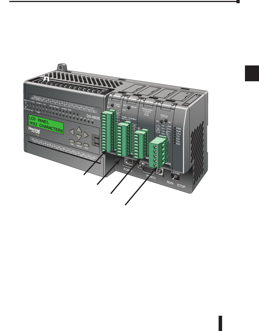
DL06 Micro PLC User Manual; 3rd Edition Rev. D 4–3
Chapter 4: System Design and Configuration
1
2
3
4
5
6
7
8
9
10
11
12
13
14
A
B
C
D
Module Placement
Slot Numbering
The DL06 has four slots, which are numbered as follows:
1
2
3
4
5
6
7
8
9
10
11
12
13
14
A
B
C
D
Slot 1
Slot 2
Slot 3
Slot 4
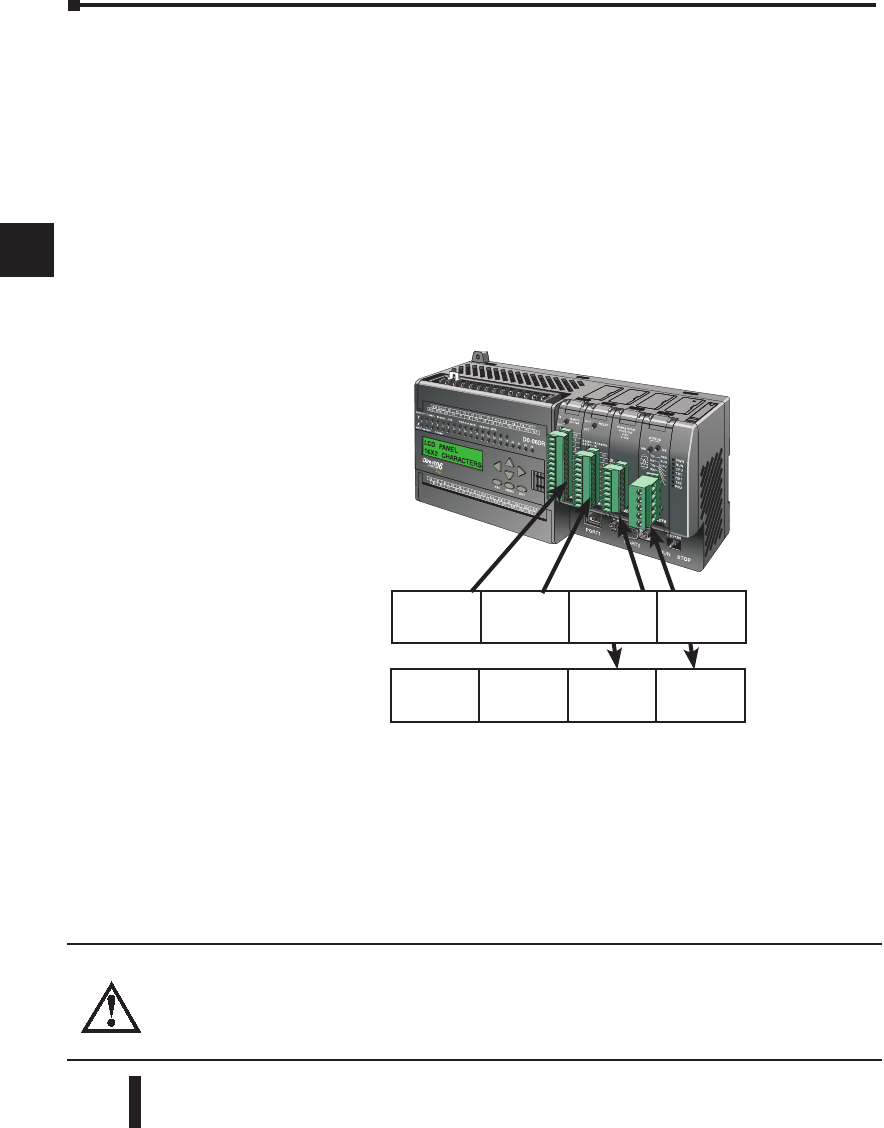
DL06 Micro PLC User Manual; 3rd Edition Rev. D
4–4
Chapter 4: System Design and Configuration
1
2
3
4
5
6
7
8
9
10
11
12
13
14
A
B
C
D
Chapter 4: System Design and Configuration
1
2
3
4
5
6
7
8
9
10
11
12
13
14
A
B
C
D
Automatic I/O Configuration
The DL06 CPUs automatically detect any installed I/O modules (including specialty
modules) at powerup, and establish the correct I/O configuration and addresses. This applies
to modules located in the local base. For most applications, you will never have to change the
configuration.
I/O addresses use octal numbering, starting at X100 and Y100 in the slot next to the CPU.
The addresses are assigned in groups of 8, or 16 depending on the number of points for
the I/O module. The discrete input and output modules can be mixed in any order. The
following diagram shows the I/O numbering convention for an example system. Both
the Handheld Programmer and DirectSOFT 5 provide AUX functions that allow you
to automatically configure the I/O. For example, with the Handheld Programmer AUX
46 executes an automatic configuration, which allows the CPU to examine the installed
modules and determine the I/O configuration and addressing.With DirectSOFT 5, the PLC
Configure I/O menu option would be used.
Automatic
Manual
Manual I/O Configuration
It may never become necessary, but DL06 CPUs allow manual I/O address assignments
for any I/O slot(s) . You can manually modify an auto configuration to match arbitrary
I/O numbering. For example, two adjacent input modules can have starting addresses at
X100 and X200.Use DirectSOFT 5 PLC Configure I/O menu option to assign manual
I/O address. In automatic configuration, the addresses are assigned on 8-point boundaries.
Manual configuration, however, assumes that all modules are at least 16 points, so you can
only assign addresses that are a multiple of 20 (octal). You can still use 8 point modules, but
16 addresses will be assigned and the upper eight addresses will be unused.
WARNING: If you manually configure an I/O slot, the I/O addressing for the other modules
may change. This is because the DL06 CPUs do not allow you to assign duplicate I/O addresses.
You must always correct any I/O configuration errors before you place the CPU in RUN mode.
Uncorrected errors can cause unpredictable machine operation that can result in a risk of personal
injury or damage to equipment.
Slot 1
8pt. Input
X100–X107
Slot 2
16pt. Output
Y100–Y117
Slot 3
16pt. Input
X110–X127
Slot 4
8pt. Input
X130–X137
Slot 1
8pt. Input
X100–X107
Slot 2
16pt. Output
Y100–Y117
Slot 3
16pt. Input
X200–X217
Slot 4
8pt. Input
X120–X127

DL06 Micro PLC User Manual; 3rd Edition Rev. D 4–5
Chapter 4: System Design and Configuration
1
2
3
4
5
6
7
8
9
10
11
12
13
14
A
B
C
D
Power Budgeting
The DL06 has four option card slots. To determine whether the combination of cards you
select will have sufficient power, you will need to perform a power budget calculation.
Power supplied
Power is supplied from two sources, the internal base unit power supply and, if required, an
external supply (customer furnished). The D0-06xx (AC powered) PLCs supply a limited
amount of 24VDC power. The 24VDC output can be used to power external devices.
For power budgeting, start by considering the power supplied by the base unit. All DL06
PLCs supply the same amount of 5VDC power. Only the AC units offer 24VDC auxiliary
power. Be aware of the trade-off between 5VDC power and 24VDC power. The amount
of 5VDC power available depends on the amount of 24VDC power being used, and the
amount of 24VDC power available depends on the amount of 5VDC power consumed.
Determine the amount of internally supplied power from the table on the following page.
Power required by base unit
Because of the different I/O configurations available in the DL06 family, the power
consumed by the base unit itself varies from model to model. Subtract the amount of power
required by the base unit from the amount of power supplied by the base unit. Be sure to
subtract 5VDC and 24VDC amounts.
Power required by option cards
Next, subtract the amount of power required by the option cards you are planning to use.
Again, remember to subtract both 5VDC and 24VDC. If your power budget analysis shows
surplus power available, you should have a workable configuration.
Chapter 4: System Design and Configuration
1
2
3
4
5
6
7
8
9
10
11
12
13
14
A
B
C
D
DL06 Micro PLC User Manual; 3rd Edition Rev. D
4–6
Chapter 4: System Design and Configuration
1
2
3
4
5
6
7
8
9
10
11
12
13
14
A
B
C
D
Chapter 4: System Design and Configuration
1
2
3
4
5
6
7
8
9
10
11
12
13
14
A
B
C
DNOTE 1: Auxiliary 24VDC used to power V+ terminal of D0-06DD1/-D sinking outputs.
NOTE 2: If the PLC’s auxiliary 24VDC power source is used to power the sinking outputs, use power
choice A, above.
Power Budgeting Example
Power Source 5VDC
power (mA)
24VDC
power (mA)
D0-06DD1
(select row
A or row B)
A1500mA 300mA
B2000mA 200mA
Current Required 5VDC
power (mA)
24VDC
power (mA)
D0-06DD1 600mA 280mA, note 1
D0-16ND3 35mA 0
D0-10TD1 150mA 0
D0-08TR 280mA 0
F0-4AD2DA-2 100mA 0
D0-06LCD 50mA 0
Total Used 1215mA 280mA
Remaining A285mA 20mA
B 785mA note 2
DL06 Power Supplied by Base Units
Part Number 5 VDC (mA) 24 VDC (mA)
D0-06xx <1500mA 300mA
<2000mA 200mA
D0-06xx-D 1500mA none
DL06 Power Consumed by Other Devices
Part Number 5 VDC (mA) 24 VDC (mA)
D0-06LCD 50mA none
D2-HPP 200mA none
DV-1000 150mA none
EA1-S3ML 210mA none
EA1-S3MLW 210mA none
DL06 Base Unit Power Required
Part Number 5 VDC (mA) 24 VDC (mA)
D0-06AA 800mA none
D0-06AR 900mA none
D0-06DA 800mA none
D0-06DD1 600mA 280mA, note 1
D0-06DD2 600mA none
D0-06DR 950mA none
D0-06DD1-D 600mA 280mA, note 1
D0-06DD2-D 600mA none
D0-06DR-D 950mA none
If the 5VDC loading is less than 2000mA, but more than
1500mA, then available 24VDC supply current is 200mA.
If the 5VDC loading is less than 1500mA, then the
available 24VDC current is 300mA.
NOTE: See the DL05/DL06 OPTIONS
manual for the module data for your project.
DL06 Power Consumed
by Option Cards
Part Number 5 VDC (mA) 24 VDC (mA)
D0-07CDR 130mA none
D0-08CDD1 100mA none
D0-08TR 280mA none
D0-10ND3 35mA none
D0-10ND3F 35mA none
D0-10TD1 150mA none
D0-10TD2 150mA none
D0-16ND3 35mA none
D0-16TD1 200mA none
D0-16TD2 200mA none
D0-DCM 250mA none
D0-DEVNETS 45mA none
F0-04TRS 250mA none
F0-08NA-1 5mA none
F0-04AD-1 50mA none
F0-04AD-2 75mA none
F0-04DAH-1 25mA 150mA
F0-04DAH-2 25mA 30mA
F0-08ADH-1 25mA 25mA
F0-08ADH-2 25mA 25mA
F0-08DAH-1 25mA 220mA
F0-08DAH-2 25mA 30mA
F0-2AD2DA-2 50mA 30mA
F0-4AD2DA-1 100mA 40mA
F0-4AD2DA-2 100mA none
F0-04RTD 70mA none
F0-04THM 30mA none
F0-CP128 150mA none
H0-CTRIO(2) 250mA none
H0-ECOM 250mA none
H0-ECOM100 300mA none
H0-PSCM 530mA none
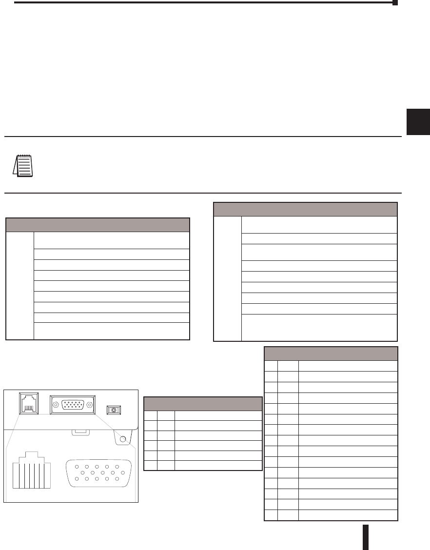
DL06 Micro PLC User Manual; 3rd Edition Rev. D 4–7
Chapter 4: System Design and Configuration
1
2
3
4
5
6
7
8
9
10
11
12
13
14
A
B
C
D
Chapter 4: System Design and Configuration
1
2
3
4
5
6
7
8
9
10
11
12
13
14
A
B
C
D
DL06 Port Pinouts
Configuring the DL06’s Comm Ports
This section describes how to configure the CPU’s built-in networking ports for either
MODBUS or DirectNET. This will allow you to connect the DL06 PLC system directly to
MODBUS networks using the RTU protocol, or to other devices on a DirectNET network.
MODBUS masters on the network must be capable of issuing the MODBUS commands
to read or write the appropriate data. For details on the MODBUS protocol, please refer
to the Gould MODBUS Protocol reference Guide (P1–MBUS–300 Rev. B). In the event
a more recent version is available, check with your MODBUS supplier before ordering the
documentation. For more details on DirectNET, order our DirectNET manual, part number
DA–DNET–M.
NOTE: For information about the MODBUS protocol see the Group Schneider Web site at: www.
schneiderautomation.com. At the main menu, select Support/Services, Modbus, Modbus Technical Manuals,
PI-MBUS-300 Modbus Protocol Reference Guide or search for PIMBUS300. For more information about
the DirectNET protocol, order our DirectNET user manual, part number DA–DNET–M, or download it
free from our Web site: www.automationdirect.com. Select Documentation/Misc./DA-DNET-M.
Communications Port 2
Port 2
Connects to HPP, DirectSOFT 5, operator
interfaces, etc.
15-pin, multifunction port, RS232C, RS422, RS485
Communication speed (baud): 300, 600, 1200,
2400, 4800, 9600, 19200, 38400
Parity: odd (default), even, none
Station Address: 1 (default)
8 data bits
1 start, 1 stop bit
Asynchronous, half-duplex, DTE
Protocol (auto-select): K-sequence (slave only),
DirectNET (master/slave), MODBUS (master/slave),
non-sequence/print/ASCII in/out
Port 1 Pin Descriptions
10V Power (-) connection (GND)
25V Power (+) connection
3RXD Receive data (RS-232C)
4TXD Transmit data (RS-232C)
55V Power (+) connection
60V Power (-) connection (GND)
Port 2 Pin Descriptions
15V Power (+) connection
2TXD Transmit data (RS-232C)
3RXD Receive data (RS-232C)
4RTS Ready to send (RS-232C)
5CTS Clear to send (RS232C)
6RXD- Receive data (-) (RS-422/485)
70V Power (-) connection (GND)
80V Power (-) connection (GND)
9TXD+ Transmit data (+) (RS-422/485)
10 TXD- Transmit data (-) (RS-422/485)
11 RTS+ Ready to send (+) (RS-422/485)
12 RTS- Ready to send (-) (RS-422/485)
13 RXD+ Receive data (+) (RS-422/485)
14 CTS+ Clear to send (+) (RS-422/485)
15 CTS- Clear to send (-) (RS-422/485)
Communications Port 1
Port 1
Connects to HPP, DirectSOFT 5, operator
interfaces, etc.
6-pin, RS232C
Communication speed (baud): 9600 (fixed)
Parity: odd (fixed)
Station Address: 1 (fixed)
8 data bits
1 start, 1 stop bit
Asynchronous, half-duplex, DTE
Protocol (auto-select): K-sequence (slave only),
DirectNET (slave only), MODBUS (slave only)
DL06 Port Specifications
PORT1 PORT2
TERM
RUN STOP
P
ORT
1
PORT
2
R
R
PORT1 PORT2
16
3425
15
610
1115
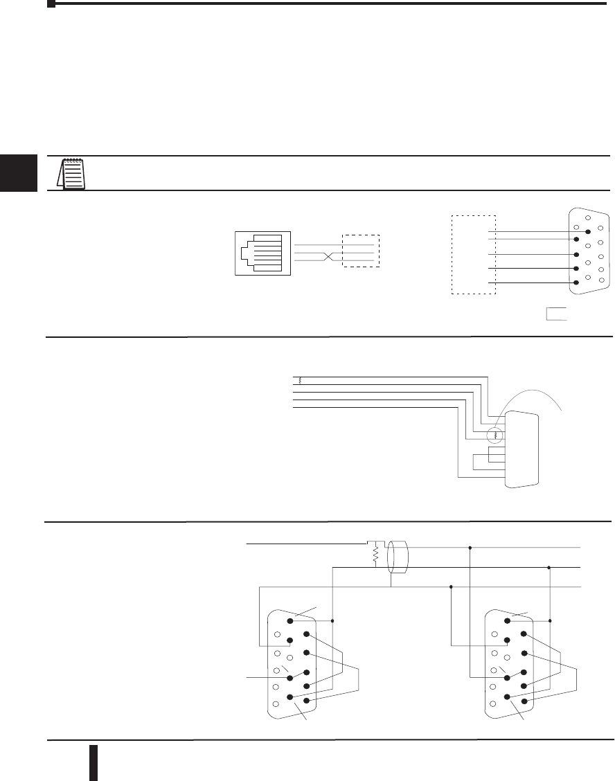
DL06 Micro PLC User Manual; 3rd Edition Rev. D
4–8
Chapter 4: System Design and Configuration
1
2
3
4
5
6
7
8
9
10
11
12
13
14
A
B
C
D
1
2
3
4
5
6
7
8
9
10
11
12
13
14
A
B
C
D
RS-232 Network
Normally, the RS-232
signals are used for
shorter distances (15
meters maximum),
for communications
between two devices.
Choosing a Network Specification
The DL06 PLC’s multi-function port gives you the option of using RS-232C, RS-422, or
RS-485 specifications. First, determine whether the network will be a 2-wire RS–232C type,
a 4-wire RS–422 type, or a 2-wire/4-wire RS-485 type.
The RS–232C specification is simple to implement for networks of shorter distances (15
meters max) and where communication is only required between two devices. The RS–422
and RS-485 signals are for networks that cover longer distances (1000 meters max.) and for
multi-drop networks (from 2 to 247 devices).
NOTE: Termination resistors are required at both ends of RS–422 and RS-485 networks. It is necessary to
select resistors that match the impedance rating of the cable (between 100 and 500 ohms).
DL06 CPU Port 2
TXD+ / RXD+
TXD– / RXD–
Termination
Resistor
Signal GND
Connect shield
to signal ground
TXD+
TXD–
RXD–
RXD+
0V
TXD+
TXD–
RXD–
RXD+
0V
TXD+ / RXD+
TXD– / RXD–
Signal GND
TXD+ / RXD+
TXD– / RXD–
Signal GND
RTS+
RTS–
CTS+
CTS–
RTS+
RTS–
CTS+
CTS–
DL06 CPU Port 2
1
6
11
1
6
11
5
10
15
5
10
15
The recommended cable for
RS422 is AutomationDirect L19954
(Belden 9842) or equivalent.
RXD+
RXD–
TXD+
TXD–
Signal GND
PORT 2
Master
9 TXD+
10 TXD–
13 RXD+
6 RXD–
1 1 R TS+
12 R TS–
14 CTS+
15 CTS–
70 V
T ermination
Resistor at
both ends of
network
The recommended cable for RS422 is
AutomationDirect L19772 (Belden 8102)
or equivalent.
Signal GND
RXD
TXD
TXD
RXD
GND
RTS
CTS
RTS
CTS
RTS
CTS
OR
Loop
Back
PORT1
6P6C
Phone Jack
Point-to-point
DTE Device
Signal GND
RXD RXD
TXD TXD
0V
1
4
3
1
6
11
5
10
15
Connections on Port 2
Connections on Port 1
RS-422 Network
RS-422 signals are for
long distances ( 1000
meters maximum). Use
terminator resistors at both
ends of RS-422 network
wiring, matching the
impedence rating of the
cable (between 100 and
500 ohms).
RS-485 Network
RS-485 signals are for
longer distances (1000
meters max) and for
multi-drop networks.
Use termination resistors
at both ends of RS-485
network wiring, matching
the impedance rating of
the cable (between 100
and 500 ohms).
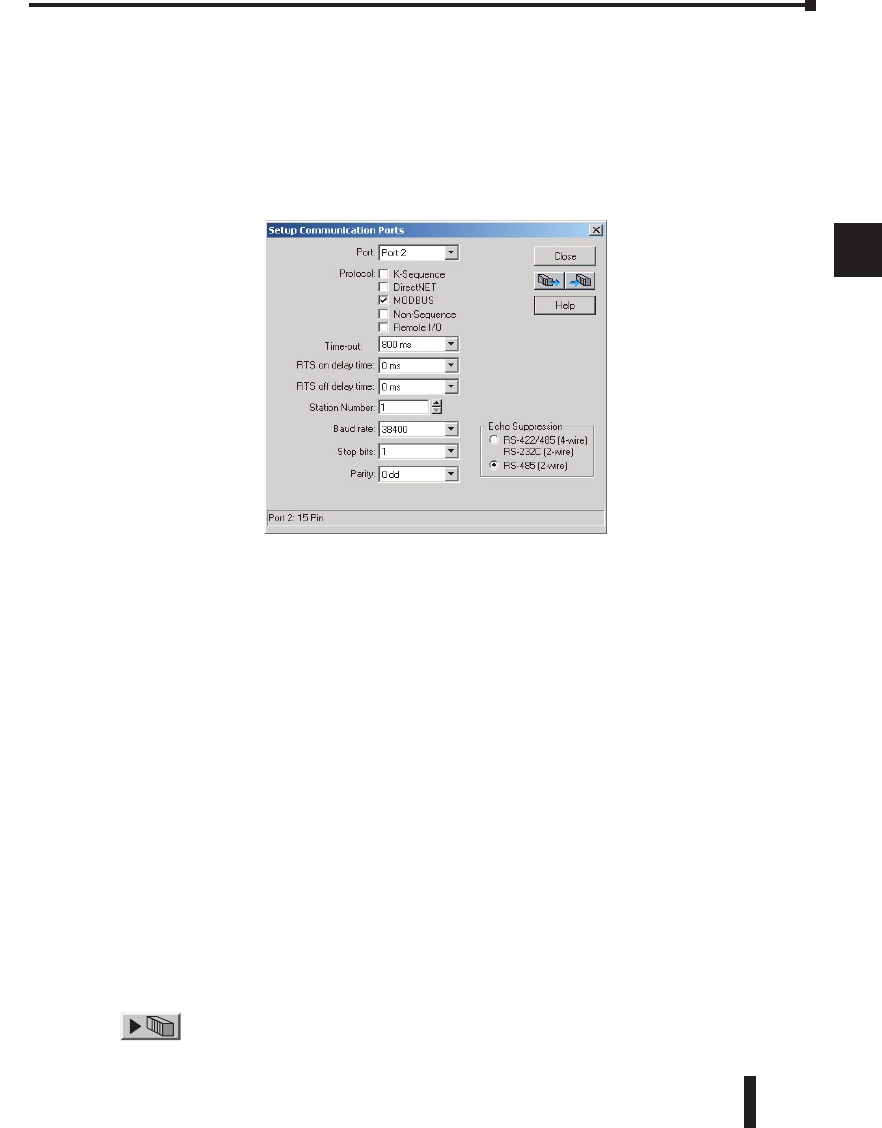
DL06 Micro PLC User Manual; 3rd Edition Rev. D 4–9
Chapter 4: System Design and Configuration
1
2
3
4
5
6
7
8
9
10
11
12
13
14
A
B
C
D
1
2
3
4
5
6
7
8
9
10
11
12
13
14
A
B
C
D
Connecting to MODBUS and DirectNET Networks
MODBUS Port Configuration
In DirectSOFT 5, choose the PLC menu, then Setup, then “Secondary Comm Port”.
• Port: From the port number list box at the top, choose “Port 2”.
• Protocol: Check the box to the left of “MODBUS” (use AUX 56 on the HPP, and select
“MBUS”), and then you’ll see the box below.
• Timeout: amount of time the port will wait after it sends a message to get a response before logging
an error.
• RTS ON / OFF Delay Time: The RTS ON Delay Time specifies the time the DL06 waits to send
the data after it has raised the RTS signal line. The RTS OFF Delay Time specifies the time the
DL06 waits to release the RTS signal line after the data has been sent. When using the DL06 on a
multi-drop network, the RTS ON Delay time must be set to 5ms or more and the RTS OFF Delay time
must be set to 2ms or more. If you encounter problems, the time can be increased.
• Station Number: For making the CPU port a MODBUS master, choose “1”. The possible range
for MODBUS slave numbers is from 1 to 247, but the DL06 network instructions used in Master
mode will access only slaves 1 to 99. Each slave must have a unique number. At powerup, the port
is automatically a slave, unless and until the DL06 executes ladder logic network instructions which
use the port as a master. Thereafter, the port reverts back to slave mode until ladder logic uses the
port again.
• Baud Rate: The available baud rates include 300, 600, 1200, 2400, 4800, 9600, 19200, and 38400
baud. Choose a higher baud rate initially, reverting to lower baud rates if you experience data errors
or noise problems on the network. Important: You must configure the baud rates of all devices on
the network to the same value. Refer to the appropriate product manual for details.
• Stop Bits: Choose 1 or 2 stop bits for use in the protocol.
• Parity: Choose none, even, or odd parity for error checking.
•Echo Suppression: Select the appropriate wiring configuration used on Port 2.
Then click the button indicated to send the Port configuration to the CPU, and click
Close.
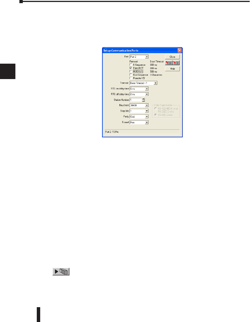
DL06 Micro PLC User Manual; 3rd Edition Rev. D
4–10
Chapter 4: System Design and Configuration
1
2
3
4
5
6
7
8
9
10
11
12
13
14
A
B
C
D
DirectNET Port Configuration
In DirectSOFT 5, choose the PLC menu, then Setup, then “Secondary Comm Port”.
• Port: From the port number list box, choose “Port 2 ”.
• Protocol: Check the box to the left of “DirectNET” (use AUX 56 on the HPP, then select
“DNET”), and then you’ll see the dialog below.
• Timeout: Amount of time the port will wait after it sends a message to get a response before logging
an error.
• RTS ON / OFF Delay Time: The RTS ON Delay Time specifies the time the DL06 waits to send
the data after it has raised the RTS signal line. The RTS OFF Delay Time specifies the time the
DL06 waits to release the RTS signal line after the data has been sent. When using the DL06 on a
multi-drop network, the RTS ON Delay time must be set to 5ms or more and the RTS OFF Delay time
must be set to 2ms or more. If you encounter problems, the time can be increased.
• Station Number: For making the CPU port a DirectNET master, choose “1”. The allowable range
for DirectNET slaves is from 1 to 90 (each slave must have a unique number). At powerup, the port
is automatically a slave, unless and until the DL06 executes ladder logic instructions which attempt
to use the port as a master. Thereafter, the port reverts back to slave mode until ladder logic uses the
port again.
• Baud Rate: The available baud rates include 300, 600, 1200, 2400, 4800, 9600, 19200, and 38400
baud. Choose a higher baud rate initially, reverting to lower baud rates if you experience data errors
or noise problems on the network. Important: You must configure the baud rates of all devices on
the network to the same value.
• Stop Bits: Choose 1 or 2 stop bits for use in the protocol.
• Parity: Choose none, even, or odd parity for error checking.
• Format: Choose between hex or ASCII formats.
Then click the button indicated to send the Port configuration to the CPU, and click
Close.
1
2
3
4
5
6
7
8
9
10
11
12
13
14
A
B
C
D
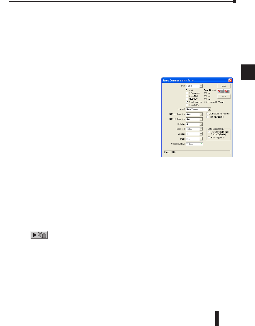
DL06 Micro PLC User Manual; 3rd Edition Rev. D 4–11
Chapter 4: System Design and Configuration
1
2
3
4
5
6
7
8
9
10
11
12
13
14
A
B
C
D
1
2
3
4
5
6
7
8
9
10
11
12
13
14
A
B
C
D
Non–Sequence Protocol (ASCII In/Out and PRINT)
Non-Sequence Port Configuration
Configuring port 2 on the DL06 for Non–Sequence allows the CPU to use port 2 to
either read or write raw ASCII strings using the ASCII instructions. See the ASCII In/Out
instructions and the PRINT instruction in chapter 5.
In DirectSOFT 5, choose the PLC menu, then Setup, then “Secondary Comm Port”.
• Port: From the port number list box at the top, choose “Port 2”.
• Protocol: Check the box to the left of “Non–Sequence”.
• Timeout: Amount of time the port will wait after it sends a
message to get a response before logging an error.
• RTS On Delay Time: The amount of time between raising
the RTS line and sending the data.
• RTS Off Delay Time: The amount of time between resetting
the RTS line after sending the data.
• Data Bits: Select either 7–bits or 8–bits to match the number
of data bits specified for the connected devices.
• Baud Rate: The available baud rates include 300,
600, 900, 2400, 4800, 9600, 19200, and 38400
baud. Choose a higher baud rate initially, reverting to
lower baud rates if you experience data errors or noise
problems on the network. Important: You must configure the
baud rates of all devices on the network to the same value.
Refer to the appropriate product manual for details.
• Stop Bits: Choose 1 or 2 stop bits to match the number of stop bits specified for the connected
devices.
• Parity: Choose none, even, or odd parity for error checking. Be sure to match the parity specified
for the connected devices.
• Echo Suppression: Select the appropriate radio button based on the wiring configuration used on
port 2.
• Xon/Xoff Flow Control: Choose this selection if you have Port 2 wired for Hardware Flow Control
(Xon/Xoff) with RTS and CTS signal connected between all devices.
• RTS Flow Control: Choose this selection if you have Port 2 RTS signal wired between all devices.
Click the button indicated to send the port configuration to the CPU, and click Close.
• Memory Address: Please choose a memory address with 64 words of contiguous free memory for
use by Non-Sequence Protocol.
DL06 Micro PLC User Manual; 3rd Edition Rev. D
4–12
Chapter 4: System Design and Configuration
1
2
3
4
5
6
7
8
9
10
11
12
13
14
A
B
C
D
Network Slave Operation
This section describes how other devices on a network can communicate with a CPU port
that you have configured as a DirectNET slave or MODBUS slave (DL06). A MODBUS
host must use the MODBUS RTU protocol to communicate with the DL06 as a slave. The
host software must send a MODBUS function code and MODBUS address to specify a PLC
memory location the DL06 comprehends. The DirectNET host uses normal I/O addresses to
access applicable DL06 CPU and system. No CPU ladder logic is required to support either
MODBUS slave or DirectNET slave operation.
NOTE: For more intformation on DirectNET proprietary protocol, see the DirectNET reference
manual, DA-DNET-M, available on our website.
MODBUS Function Codes Supported
The MODBUS function code determines whether the access is a read or a write, and whether
to access a single data point or a group of them. The DL06 supports the MODBUS function
codes described below.
Determining the MODBUS Address
There are typically two ways that most host software conventions allow you to specify a PLC
memory location. These are:
• By specifying the MODBUS data type and address
• By specifying a MODBUS address only
1
2
3
4
5
6
7
8
9
10
11
12
13
14
A
B
C
D
MODBUS Function Code Function DL06 Data Types Available
01 Read a group of coils Y, CR, T, CT
02 Read a group of inputs X, SP
05 Set / Reset a single coil Y, CR, T, CT
15 Set / Reset a group of coils Y, CR, T, CT
03, 04 Read a value from one or more registers V
06 Write a value into a single register V
16 Write a value into a group of registers V
DL06 Micro PLC User Manual; 3rd Edition Rev. D 4–13
Chapter 4: System Design and Configuration
1
2
3
4
5
6
7
8
9
10
11
12
13
14
A
B
C
D
If Your Host Software Requires the Data Type and Address
Many host software packages allow you to specify the MODBUS data type and the
MODBUS address that corresponds to the PLC memory location. This is the easiest method,
but not all packages allow you to do it this way.
The actual equation used to calculate the address depends on the type of PLC data you are
using. The PLC memory types are split into two categories for this purpose.
• Discrete – X, SP, Y, CR, S, T, C (contacts)
• Word – V, Timer current value, Counter current value
In either case, you basically convert the PLC octal address to decimal and add the appropriate
MODBUS address (if required). The table below shows the exact equation used for each
group of data.
1
2
3
4
5
6
7
8
9
10
11
12
13
14
A
B
C
D
DL06 Memory Type QTY
(Decimal)
PLC Range
(Octal)
MODBUS Address
Range
(Decimal)
MODBUS Data Type
For Discrete Data Types .... Convert PLC Addr. to Dec. + Start of Range + Data Type
Inputs (X) 512 X0 – X777 2048 – 2559 Input
Special Relays(SP) 512 SP0 – SP777 3072 – 3583 Input
Outputs (Y) 512 Y0 – Y777 2048 – 2559 Coil
Control Relays (CR) 1024 C0 – C1777 3072 – 4095 Coil
Timer Contacts (T) 256 T0 – T377 6144 – 6399 Coil
Counter Contacts (CT) 128 CT0 – CT177 6400 – 6527 Coil
Stage Status Bits(S) 1024 S0 – S1777 5120 – 6143 Coil
For Word Data Types .... Convert PLC Addr. to Dec. + Data Type
Timer Current Values (V) 256 V0 – V377 0 – 255 Input Register
Counter Current Values (V) 128 V1000 – V1177 512 – 639 Input Register
V-Memory, user data (V) 3200 V1200 – V7377 640 – 3839 Holding Register
4096 V10000 - V17777 4096 - 8191 Holding Register
V-Memory, non-volatile (V) 128 V7400 – V7577 3840 – 3967 Holding Register
DL06 Micro PLC User Manual; 3rd Edition Rev. D
4–14
Chapter 4: System Design and Configuration
1
2
3
4
5
6
7
8
9
10
11
12
13
14
A
B
C
D
1
2
3
4
5
6
7
8
9
10
11
12
13
14
A
B
C
D
The following examples show how to generate the MODBUS address and data type for hosts
which require this format.
Example 1: V2100
Find the MODBUS address for User V location V2100.
1. Find V-memory in the table.
2. Convert V2100 into decimal (1088).
3. Use the MODBUS data type from the table.
Example 2: Y20
Find the MODBUS address for output Y20.
1. Find Y outputs in the table.
2. Convert Y20 into decimal (16).
3. Add the starting address for the range (2048).
4. Use the MODBUS data type from the table.
Example 3: T10 Current Value
Find the MODBUS address to obtain the current value from Timer T10.
1. Find Timer Current Values in the table.
2. Convert T10 into decimal (8).
3. Use the MODBUS data type from the table.
Example 4: C54
Find the MODBUS address for Control Relay C54.
1. Find Control Relays in the table.
2. Convert C54 into decimal (44).
3. Add the starting address for the range (3072).
4. Use the MODBUS data type from the table.
V-memory, user data (V) 3200 V1200 – V7377 640 – 3839 Holding Register
Control Relays (CR) 512 C0 – C77 3072 – 3583 Coil
Outputs (V) 256 Y0 – Y377 2048 - 2303 Coil
Timer Current Values (V) 128 V0 – V177 0 - 127 Input Register
Coil 2064
Coil 3116
Holding Reg 1088
Input Reg. 8
DL06 Micro PLC User Manual; 3rd Edition Rev. D 4–15
Chapter 4: System Design and Configuration
1
2
3
4
5
6
7
8
9
10
11
12
13
14
A
B
C
D
1
2
3
4
5
6
7
8
9
10
11
12
13
14
A
B
C
D
If Your MODBUS Host Software Requires an Address ONLY
Some host software does not allow you to specify the MODBUS data type and address.
Instead, you specify an address only. This method requires another step to determine the
address, but it’s still fairly simple. Basically, MODBUS also separates the data types by
address ranges as well. So this means an address alone can actually describe the type of
data and location. This is often referred to as “adding the offset”. One important thing to
remember here is that two different addressing modes may be available in your host software
package. These are:
• 484 Mode
• 584/984 Mode
We recommend that you use the 584/984 addressing mode if your host software allows
you to choose. This is because the 584/984 mode allows access to a higher number of
memory locations within each data type. If your software only supports 484 mode, then there
may be some PLC memory locations that will be unavailable. The actual equation used to
calculate the address depends on the type of PLC data you are using. The PLC memory types
are split into two categories for this purpose.
• Discrete – X, SP, Y, CR, S, T (contacts), C (contacts)
• Word – V, Timer current value, Counter current value
In either case, you basically convert the PLC octal address to decimal and add the appropriate
MODBUS addresses (as required). The table below shows the exact equation used for each
group of data.
Discrete Data Types
DL06 Memory Type PLC Range
(Octal)
Address (484
Mode)
Address (584/984
Mode)
MODBUS Data
Type
Global Inputs (GX) GX0-GX1746 1001 - 1999 10001 - 10999 Input
GX1747-GX3777 --- 11000 - 12048 Input
Inputs (X) X0 – X1777 --- 12049 - 13072 Input
Special Relays (SP) SP0 – SP777 --- 13073 - 13584 Input
Global Outputs (GY) GY0 - GY3777 1 - 2048 1 - 2048 Output
Outputs (Y) Y0 – Y1777 2049 - 3072 2049 - 3072 Output
Control Relays (CR) C0 – C3777 3073 - 5120 3073 - 5120 Output
Timer Contacts (T) T0 – T377 6145 - 6400 6145 - 6400 Output
Counter Contacts (CT) CT0 – CT377 6401 - 6656 6401 - 6656 Output
Stage Status Bits (S) S0 – S1777 5121 - 6144 5121 - 6144 Output
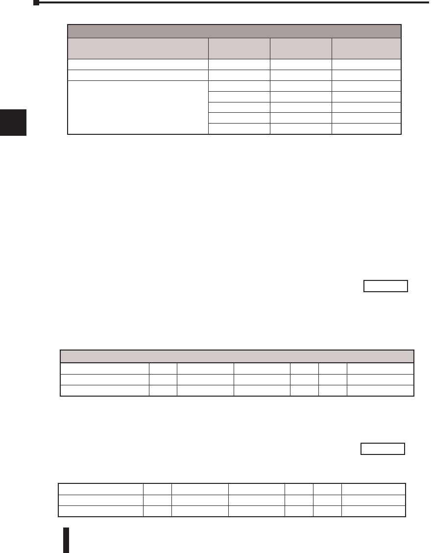
DL06 Micro PLC User Manual; 3rd Edition Rev. D
4–16
Chapter 4: System Design and Configuration
1
2
3
4
5
6
7
8
9
10
11
12
13
14
A
B
C
D
1
2
3
4
5
6
7
8
9
10
11
12
13
14
A
B
C
D
Example 1: V2100 584/984 Mode
Example 1: V2100 584/984 Mode
Find the MODBUS address for User V location V2100. PLC Address (Dec.) + Mode Address
1. Find V-memory in the table. V2100 = 1088 decimal
2. Convert V2100 into decimal (1088). 1088 + 40001 =
3. Add the MODBUS starting address for the
mode (40001).
Example 2: Y20 584/984 Mode
Find the MODBUS address for output Y20. PLC Addr. (Dec.) + Start Address + Mode
1. Find Y outputs in the table. Y20 = 16 decimal
2. Convert Y20 into decimal (16). 16 + 2048 + 1 =
3. Add the starting address for the range (2048).
4. Add the MODBUS address for the mode (1).
Word Data Types
Registers PLC Range
(Octal)
Input/Holding
(484 Mode)*
Input/Holding
(584/984 Mode)*
V-memory (Timers) V0 - V377 3001/4001 30001/40001
V-memory (Counters) V1000 - V1177 3513/4513 30513/40513
V-memory (Data Words)
V1200 - V1377 3641/4641 30641/40641
V1400 - V1746 3769/4769 30769/40769
V1747 - V1777 --- 31000/41000
V2000 - V7377 --- 41025
V10000 - V17777 --- 44097
1. Refer to your PLC user manual for the correct memory mapping size of your PLC. Some of
the addresses shown above might not pertain to your particular CPU.
2. For an automated MODBUS/Koyo address conversion utility, go to our
website, www.automationdirect.com, and down load download the EXCEL file
modbus_conversion.xls located at: Tech Support > Technical Support Home page.
41089
For Word Data Types.... PLC Address (Dec.) + Appropriate Mode Address
Timer Current Values (V) 128 V0 – V177 0 – 127 3001 30001 Input Register
Counter Current Values (V) 128 V1200 – V7377 640 – 3839 3001 30001 Input Register
V-memory, user data (V) 1024 V2000 – V3777 1024 – 2047 4001 40001 Holding Register
2065
Outputs (Y) 320 Y0 - Y477 2048 – 2367 1 1 Coil
Control Relays (CR) 256 C0 - C377 3072 – 3551 1 1 Coil
Timer Contacts (T) 128 T0 - T177 6144 – 6271 1 1 Coil
*MODBUS: Function 04
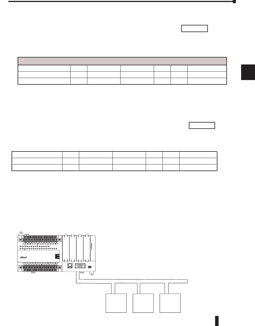
DL06 Micro PLC User Manual; 3rd Edition Rev. D 4–17
Chapter 4: System Design and Configuration
1
2
3
4
5
6
7
8
9
10
11
12
13
14
A
B
C
D
1
2
3
4
5
6
7
8
9
10
11
12
13
14
A
B
C
D
Example 3: T10 Current Value 484 Mode
Find the MODBUS address to obtain the PLC Address (Dec.) + Mode Address
current value from Timer T10. TA10 = 8 decimal
1. Find Timer Current Values in the table. 8 + 3001
=
2. Convert T10 into decimal (8).
3. Add the MODBUS starting address for the mode (3001).
Example 4: C54 584/984 Mode
Find the MODBUS address for Control Relay C54. PLC Addr. (Dec.) + Start Address + Mode
1. Find Control Relays in the table. C54 = 44 decimal
2. Convert C54 into decimal (44). 44 + 3072 + 1
=
3. Add the starting address for the range (3072).
4. Add the MODBUS address for the mode (1).
Network Master Operation
This section describes how the DL06 can communicate on a MODBUS or DirectNET
network as a master. For MODBUS networks, it uses the MODBUS RTU protocol, which
must be interpreted by all the slaves on the network. Both MODBUS and DirectNet are
single master/multiple slave networks. The master is the only member of the network that can
initiate requests on the network. This section teaches you how to design the required ladder
logic for network master operation.
For Word Data Types.... PLC Address (Dec.) + Appropriate Mode Address
Timer Current Values (V) 128 V0 – V177 0 – 127 3001 30001 Input Register
Counter Current Values (V) 128 V1200 – V7377 512 – 639 3001 30001 Input Register
V-memory, user data (V) 1024 V2000 – V3777 1024 – 2047 4001 40001 Holding Register
Outputs (Y) 320 Y0 – Y477 2048 – 2367 1 1 Coil
Control Relays (CR) 256 C0 – C377 3072 – 3551 1 1 Coil
Timer Contacts (T) 128 T0– T177 6144 – 6271 1 1 Coil
3009
3117
Slave #1 Slave #3
Master M
O
DB
US
,
RTU Protocol, or DirectNET
,
Slave #2
LOGIC
Koyo
06
C0 C4C2X1 X3 X4 X6 X11X13 X14X16 X21X23 N.C.
C1 C3X2 X5 X7 X10X12 X15 X17X20 X22X0 N.C.
AC(N)24V
0V
N.C.
C1 C3Y0 Y15Y12Y10Y17Y7Y5Y2
C0 C2 Y16Y14Y13Y11Y6Y4Y3Y1
LGG
AC(L)
D0-06DR
2.0AOUTPUT: 6-240V 50 - 60Hz 2.0A,6 - 27V
INPUT: 12 - 24V 3 - 15mA
Y
X
40VA50-60HzPWR: 100-240V
01 2345 6710 11 12 13 14 15 16 17 20 21 22 23
PORT1PORT2
TERM
RUNSTOP
PWR
RUN
CPU
TX1
RX1
TX2
RX2
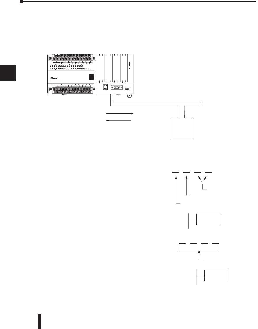
DL06 Micro PLC User Manual; 3rd Edition Rev. D
4–18
Chapter 4: System Design and Configuration
1
2
3
4
5
6
7
8
9
10
11
12
13
14
A
B
C
D
1
2
3
4
5
6
7
8
9
10
11
12
13
14
A
B
C
D
When using the DL06 PLC as the master station, simple RLL instructions are used to initiate
the requests. The WX instruction initiates network write operations, and the RX instruction
initiates network read operations. Before executing either the WX or RX commands, we will
need to load data related to the read or write operation onto the CPU’s accumulator stack.
When the WX or RX instruction executes, it uses the information on the stack combined with
data in the instruction box to completely define the task, which goes to the port.
The following step-by-step procedure will provide you the information necessary to set up
your ladder program to receive data from a network slave.
Slave
Master
WX
(write)
RX (read)
Network
LOGIC
Koyo
06
C0 C4C2X1 X3 X4 X6 X11X13 X14X16 X21X23 N.C.
C1 C3X2 X5 X7 X10X12 X15 X17X20 X22X0 N.C.
AC(N)24V
0V
N.C.
C1 C3Y0 Y15Y12Y10Y17Y7Y5Y2
C0 C2 Y16Y14Y13Y11Y6Y4Y3Y1
LG
G
AC(L)
D0-06DR
2.0AOUTPUT: 6-240V 50 - 60Hz 2.0A, 6 - 27V
INPUT: 12 - 24V3 - 15mA
Y
X
40VA50-60HzPWR: 100-240V
01 2345 6710 11 12 13 14 15 16 17 20 21 22 23
PORT1 PORT2
TERM
RUN STOP
PWR
RUN
CPU
TX1
RX1
TX2
RX2
2 0 1F
Internal port (hex)
Port number (BCD)
Slave address (BCD)
LD
KF201
6 4 (BCD)
# of bytes to transfer
LD
K64
Step 2: Load Number of Bytes to Transfer
The second Load (LD) instruction determines
the number of bytes which will be transferred
between the master and slave in the subsequent
WX or RX instruction. The value to be loaded
is in BCD format (decimal), from 1 to 128
bytes.
Step 1: Identify Master Port # and Slave #
The first Load (LD) instruction identifies the
communications port number on the network
master (DL06) and the address of the slave
station. This instruction can address up to 99
MODBUS slaves, or 90 DirectNET slaves.
The format of the word is shown to the right.
The “F2” in the upper byte indicates the use of
the right port of the DL06 PLC, port number
2. The lower byte contains the slave address
number in BCD (01 to 99).
DL06 Micro PLC User Manual; 3rd Edition Rev. D 4–19
Chapter 4: System Design and Configuration
1
2
3
4
5
6
7
8
9
10
11
12
13
14
A
B
C
D
1
2
3
4
5
6
7
8
9
10
11
12
13
14
A
B
C
D
DL05 / 06 / 205 / 350 / 405 Memory Bits per unit Bytes
V-memory
T / C current value
16
16
2
2
Inputs (X, SP) 8 1
Outputs
(Y, C, Stage, T/C bits) 8 1
Scratch Pad Memory 8 1
Diagnostic Status 8 1
DL330 / 340 Memory Bits per unit Bytes
Data registers
T / C accumulator
8
16
1
2
I/O, internal relays, shift register bits, T/C
bits, stage bits 1 1
Scratch Pad Memory 8 1
Diagnostic Status(5 word R/W) 16 10
The number of bytes specified also depends on the type of data you want to obtain. For
example, the DL06 Input points can be accessed by V-memory locations or as X input
locations. However, if you only want X0 – X27, you’ll have to use the X input data type
because the V-memory locations can only be accessed in 2-byte increments. The following
table shows the byte ranges for the various types of DirectLOGIC products.
NOTE: Since V-memory words are always 16 bits, you may not always use the whole word. For example,
if you only specify 3 bytes and you are reading Y outputs from the slave, you will only get 24 bits of data. In
this case, only the 8 least significant bits of the last word location will be modified. The remaining 8 bits are
not affected.
6 0 00
(octal)
LDA
O40600
4
Starting address of
master transfer area
V40600
MSB LSB
0
15
V40601
MSB LSB
015
Step 3: Specify Master Memory Area
The third instruction in the RX or WX sequence
is a Load Address (LDA) instruction. Its purpose
is to load the starting address of the memory area
to be transferred. Entered as an octal number, the
LDA instruction converts it to hex and places the
result in the accumulator.
For a WX instruction, the DL06 CPU sends
the number of bytes previously specified from
its memory area beginning at the LDA address
specified.
For an RX instruction, the DL06 CPU reads the
number of bytes previously specified from the
slave, placing the received data into its memory
area beginning at the LDA address specified.
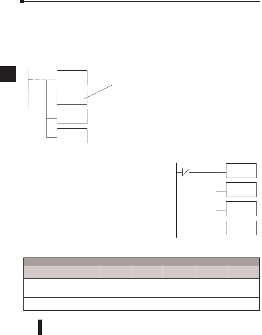
DL06 Micro PLC User Manual; 3rd Edition Rev. D
4–20
Chapter 4: System Design and Configuration
1
2
3
4
5
6
7
8
9
10
11
12
13
14
A
B
C
D
1
2
3
4
5
6
7
8
9
10
11
12
13
14
A
B
C
D
DL305 Series CPU Memory Type–to–MODBUS Cross Reference (excluding 350 CPU)
PLC Memory Type PLC Base
Address
MODBUS
Base Address
PLC Memory
Type
PLC Base
Address
MODBUS
Base Address
TMR/CNT Current Values R600 V0 TMR/CNT Status
Bits CT600 GY600
I/O Points IO 000 GY0 Control Relays CR160 GY160
Data Registers R401,R400 V100 Shift Registers SR400 GY400
Stage Status Bits (D3-330P only) S0 GY200
LD
KF201
LD
K64
LDA
O40600
RX
SP116
Y0
Step 4: Specify Slave Memory Area
The last instruction in our sequence is the WX or RX
instruction itself. Use WX to write to the slave, and
RX to read from the slave. All four of our instructions
are shown to the right. In the last instruction, you
must specify the starting address and a valid data type
for the slave.
• DirectNET slaves – specify the same address in the WX
and RX instruction as the slave’s native I/O address
• MODBUS DL405, DL205, or DL06 slaves – specify
the same address in the WX and RX instruction as the
slave’s native I/O address
• MODBUS 305 slaves – use the following table to
convert DL305 addresses to MODBUS addresses
LDK101
LD
K4128
LDA
O4000
RX
V0
The Maximum constant possible is 4128. This
is due to the 128 maximum number of Bytes
that the RX/WX instruction can allow. The
value of 4 in the most significant position of
the word will cause the RX to use function 04
(30001 range).
The DL05/06, DL250-1/260, DL350 and DL450 will support function 04, read input
register (Address 30001). To use function 04, put the number ‘4’ into the most significant
position (4xxx). Four digits must be entered for the intruction to work properly with this
mode.
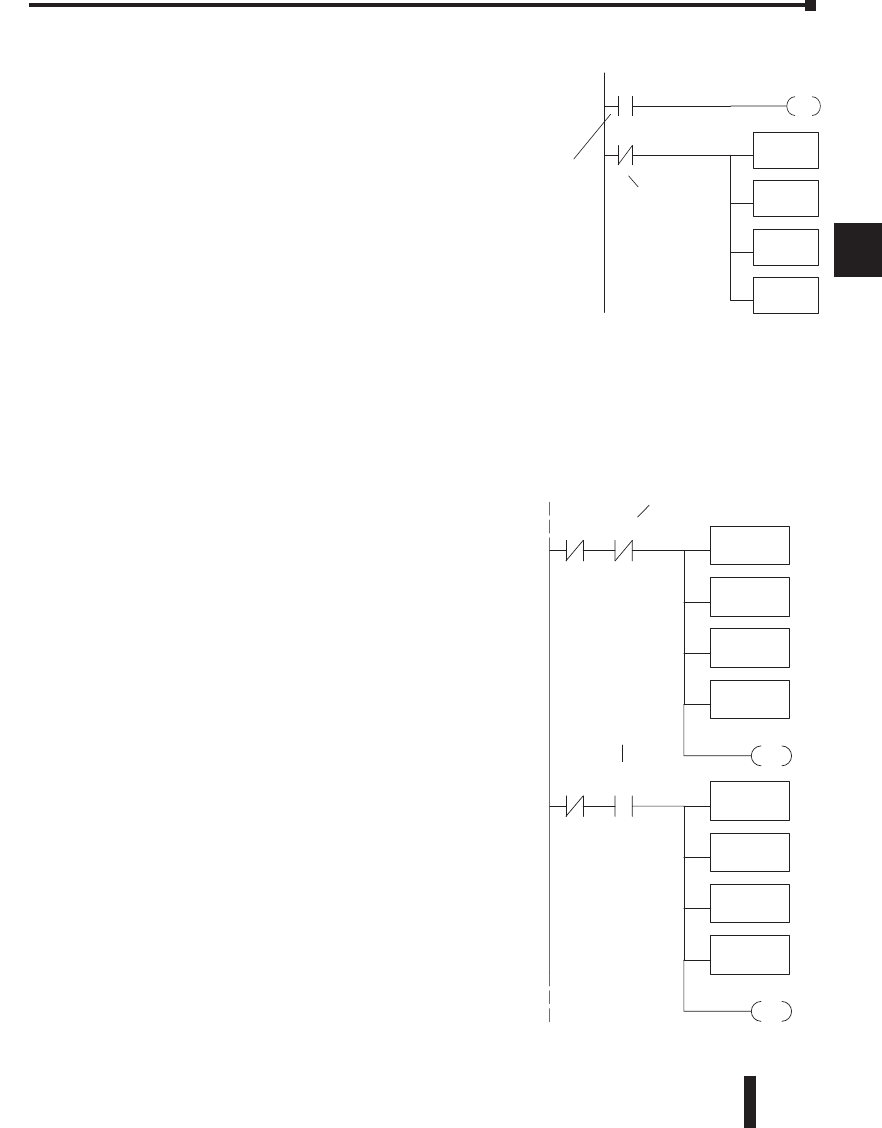
DL06 Micro PLC User Manual; 3rd Edition Rev. D 4–21
Chapter 4: System Design and Configuration
1
2
3
4
5
6
7
8
9
10
11
12
13
14
A
B
C
D
1
2
3
4
5
6
7
8
9
10
11
12
13
14
A
B
C
D
Port Communication Error
LD
KF201
LD
K0003
LDA
O40600
RX
Y0
SP116
Port Busy
SP117
SET
Y1
Interlocking Relay
LD
KF201
LD
K0003
LDA
O40600
RX
VY0
SP116
SET
C100
C100
LD
KF201
LD
K0003
LDA
O40400
WX
VY0
SP116
RST
C100
C100
Interlocking
Relay
Multiple Read and Write Interlocks
If you are using multiple reads and writes
in the RLL program, you have to interlock
the routines to make sure all the routines are
executed. If you don’t use the interlocks, then
the CPU will only execute the first routine.
This is because each port can only handle one
transaction at a time.
In the example to the right, after the RX
instruction is executed, C100 is set. When the
port has finished the communication task, the
second routine is executed and C100 is reset.
If you’re using RLLPLUS Stage Programming,
you can put each routine in a separate program
stage to ensure proper execution and switch
from stage to stage allowing only one of them
to be active at a time.
Communications from a Ladder Program
Typically network communications will last
longer than 1 scan. The program must wait
for the communications to finish before
starting the next transaction.
Port 2, which can be a master, has two
Special Relay contacts associated with it (see
Appendix D for comm port special relays).
One indicates “Port busy”(SP116), and
the other indicates ”Port Communication
Error”(SP117). The example above shows the
use of these contacts for a network master that
only reads a device (RX). The “Port Busy”
bit is on while the PLC communicates with
the slave. When the bit is off the program can
initiate the next network request.
The “Port Communication Error” bit turns
on when the PLC has detected an error. Use
of this bit is optional. When used, it should
be ahead of any network instruction boxes
since the error bit is reset when an RX or WX
instruction is executed
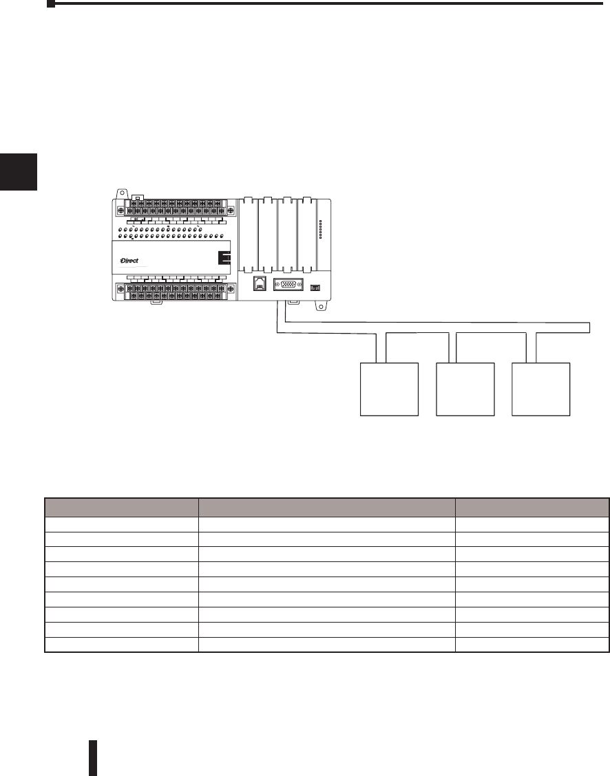
DL06 Micro PLC User Manual; 3rd Edition Rev. D
4–22
Chapter 4: System Design and Configuration
1
2
3
4
5
6
7
8
9
10
11
12
13
14
A
B
C
D
Network Master Operation (using MRX and MWX
Instructions)
This section describes how the DL06 can communicate on a MODBUS RTU network as a
master using the MRX and MWX read/write instructions. These instructions allow you to
enter native MODBUS addressing in your ladder logic program with no need to perform
octal to decimal conversions. MODBUS is a single master/multiple slave network. The
master is the only member of the network that can initiate requests on the network. This
section teaches you how to design the required ladder logic for network master operation.
MODBUS Function Codes Supported
The MODBUS function code determines whether the access is a read or a write, and whether
to access a single data point or a group of them. The DL06 supports the MODBUS function
codes described below.
1
2
3
4
5
6
7
8
9
10
11
12
13
14
A
B
C
D
MODBUS Function Code Function DL06 Data Types Available
01 Read a group of coils Y, CR, T, CT
02 Read a group of inputs X, SP
05 Set / Reset a single coil (slave only) Y, CR, T, CT
15 Set / Reset a group of coils Y, CR, T, CT
03, 04 Read a value from one or more registers V
06 Write a value into a single register (slave only) V
07 Read Exception Status V
08 Diagnostics V
16 Write a value into a group of registers V
Slave #1 Slave #3
Master M
O
DB
US
,
RTU Protocol, or DirectNET
,
Slave #2
LOGIC
Koyo
06
C0 C4C2X1 X3 X4 X6 X11X13 X14X16 X21X23 N.C.
C1 C3X2 X5 X7 X10X12 X15 X17X20 X22X0 N.C.
AC(N)24V
0V
N.C.
C1 C3Y0 Y15Y12Y10Y17Y7Y5Y2
C0 C2 Y16Y14Y13Y11Y6Y4Y3Y1
LGG
AC(L)
D0-06DR
2.0AOUTPUT: 6-240V 50 - 60Hz 2.0A,6 - 27V
INPUT: 12 - 24V 3 - 15mA
Y
X
40VA50-60HzPWR: 100-240V
01 2345 6710 11 12 13 14 15 16 17 20 21 22 23
PORT1PORT2
TERM
RUNSTOP
PWR
RUN
CPU
TX1
RX1
TX2
RX2
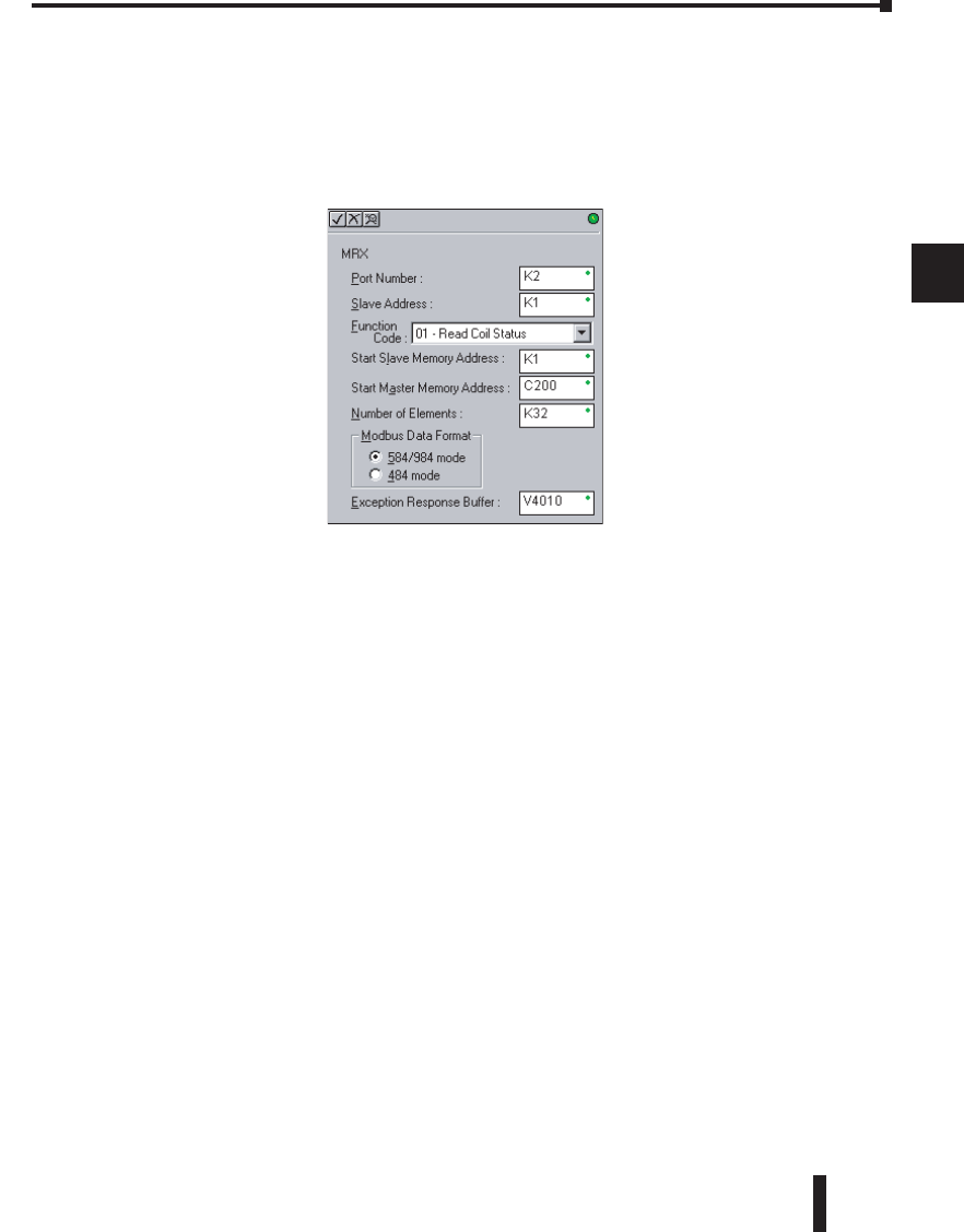
DL06 Micro PLC User Manual; 3rd Edition Rev. D 4–23
Chapter 4: System Design and Configuration
1
2
3
4
5
6
7
8
9
10
11
12
13
14
A
B
C
D
MODBUS Read from Network(MRX)
The MODBUS Read from Network (MRX) instruction is used by the DL06 network master
to read a block of data from a connected slave device and to write the data into V–memory
addresses within the master. The instruction allows the user the to specify the MODBUS
Function Code, slave station address, starting master and slave memory addresses, number of
elements to transfer, MODBUS data format and the Exception Response Buffer.
• Port Number: must be DL06 Port 2 (K2)
• Slave Address: specify a slave station address (0–247)
• Function Code: The following MODBUS function codes are supported by the MRX
instruction:
01 – Read a group of coils
02 – Read a group of inputs
03 – Read holding registers
04 – Read input registers
07 – Read Exception status
08 – Diagnostics
• Start Slave Memory Address: specifies the starting slave memory address of the data to be
read. See the table on the following page.
• Start Master Memory Address: specifies the starting memory address in the master where
the data will be placed. See the table on the following page.
• Number of Elements: specifies how many coils, input, holding registers or input register
will be read. See the table on the following page.
• MODBUS Data Format: specifies MODBUS 584/984 or 484 data format to be used
• Exception Response Buffer: specifies the master memory address where the Exception
Response will be placed. See the table on the following page.
1
2
3
4
5
6
7
8
9
10
11
12
13
14
A
B
C
D
DL06 Micro PLC User Manual; 3rd Edition Rev. D
4–24
Chapter 4: System Design and Configuration
1
2
3
4
5
6
7
8
9
10
11
12
13
14
A
B
C
D
MRX Slave Memory Address
MRX Master Memory Addresses
MRX Number of Elements
MRX Exception Response Buffer
1
2
3
4
5
6
7
8
9
10
11
12
13
14
A
B
C
D
MRX Slave Address Ranges
Function Code MODBUS Data Format Slave Address Range(s)
01 – Read Coil 484 Mode 1–999
01 – Read Coil 584/984 Mode 1–65535
02 – Read Input Status 484 Mode 1001–1999
02 – Read Input Status 584/984 Mode 10001–19999 (5 digit) or 100001–165535
(6 digit)
03 – Read Holding Register 484 Mode 4001–4999
03 – Read Holding Register 584/984 40001–49999 (5 digit) or 4000001–465535
(6 digit)
04 – Read Input Register 484 Mode 3001–3999
04 – Read Input Register 584/984 Mode 30001–39999 (5 digit) or 3000001–365535
(6 digit)
07 – Read Exception Status 484 and 584/984 Mode n/a
08 – Diagnostics 484 and 584/984 Mode 0–65535
MRX Master Memory Address Ranges
Operand Data Type DL06 Range
Inputs X 0–1777
Outputs Y 0–1777
Control Relays C 0–3777
Stage Bits S 0–1777
Timer Bits T 0–377
Counter Bits CT 0–377
Special Relays SP 0–777
V–memory V All
Global Inputs GX 0–3777
Global Outputs GY 0–3777
MRX Number of Elements
Operand Data Type DL06 Range
V–memory V All
Constant K 1–2000
MRX Exception Response Buffer
Operand Data Type DL06 Range
V–memory V All
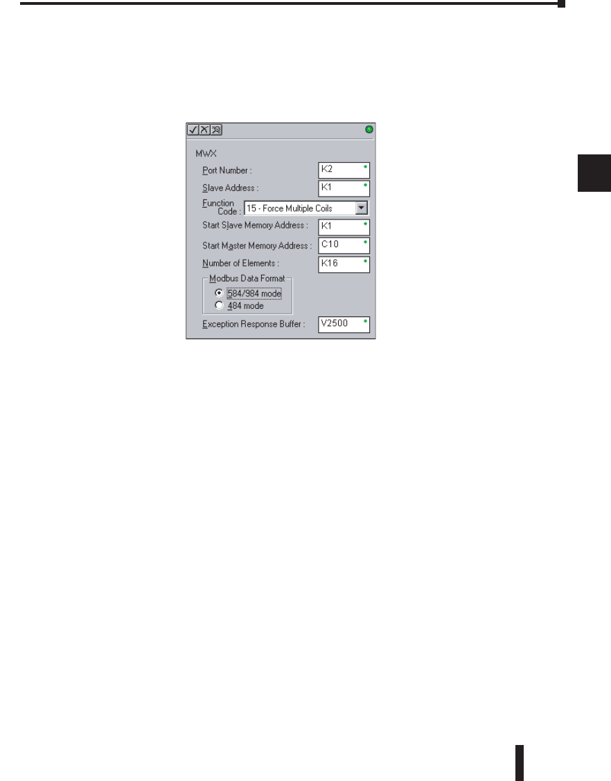
DL06 Micro PLC User Manual; 3rd Edition Rev. D 4–25
Chapter 4: System Design and Configuration
1
2
3
4
5
6
7
8
9
10
11
12
13
14
A
B
C
D
MODBUS Write to Network (MWX)
The MODBUS Write to Network (MWX) instruction is used to write a block of data from
the network masters’s (DL06) memory to MODBUS memory addresses within a slave device
on the network. The instruction allows the user to specify the MODBUS Function Code,
slave station address, starting master and slave memory addresses, number of elements to
transfer, MODBUS data format and the Exception Response Buffer.
• Port Number: must be DL06 Port 2 (K2)
• Slave Address: specify a slave station address (0–247)
• Function Code: The following MODBUS function codes are supported by the MWX
instruction:
05 – Force Single coil
06 – Preset Single Register
08 – Diagnostics
15 – Force Multiple Coils
16 – Preset Multiple Registers
• Start Slave Memory Address: specifies the starting slave memory address where the data
will be written.
• Start Master Memory Address: specifies the starting address of the data in the master that is
to written to the slave.
• Number of Elements: specifies how many consecutive coils or registers will be written to.
This field is only active when either function code 15 or 16 is selected.
• MODBUS Data Format: specifies MODBUS 584/984 or 484 data format to be used.
• Exception Response Buffer: specifies the master memory address where the Exception
Response will be placed.
1
2
3
4
5
6
7
8
9
10
11
12
13
14
A
B
C
D
DL06 Micro PLC User Manual; 3rd Edition Rev. D
4–26
Chapter 4: System Design and Configuration
1
2
3
4
5
6
7
8
9
10
11
12
13
14
A
B
C
D
MWX Slave Memory Address
MWX Master Memory Addresses
MWX Number of Elements
MWX Exception Response Buffer
Chapter 4: System Design and Configuration
1
2
3
4
5
6
7
8
9
10
11
12
13
14
A
B
C
D
MWX Slave Address Ranges
Function Code MODBUS Data Format Slave Address Range(s)
05 – Force Single Coil 484 Mode 1–999
05 – Force Single Coil 584/984 Mode 1–65535
06 – Preset Single Register 484 Mode 4001–4999
06 – Preset Single Register 84/984 Mode 40001–49999 (5 digit) or 400001–
465535 (6 digit)
08 – Diagnostics 484 and 584/984 Mode 0–65535
15 – Force Multiple Coils 484 1–999
15 – Force Multiple Coils 585/984 Mode 1–65535
16 – Preset Multiple Registers 484 Mode 4001–4999
16 – Preset Multiple Registers 584/984 Mode 40001–49999 (5 digit) or 4000001–
465535 (6 digit)
MWX Number of Elements
Operand Data Type DL06 Range
V–memory V All
Constant K 1–2000
MWX Exception Response Buffer
Operand Data Type DL06 Range
V–memory V All
MWX Master Memory Address Ranges
Operand Data Type DL06 Range
Inputs X 0–777
Outputs Y 0–777
Control Relays C 0–1777
Stage Bits S 0–1777
Timer Bits T 0–377
Counter Bits CT 0–177
Special Relays SP 0–777
V–memory V All
Global Inputs GX 0–3777
Global Outputs GY 0–3777

DL06 Micro PLC User Manual; 3rd Edition Rev. D 4–27
Chapter 4: System Design and Configuration
1
2
3
4
5
6
7
8
9
10
11
12
13
14
A
B
C
D
Chapter 4: System Design and Configuration
1
2
3
4
5
6
7
8
9
10
11
12
13
14
A
B
C
D
MRX/MWX Example in DirectSOFT 5
DL06 port 2 has two Special Relay contacts associated with it (see Appendix D for comm
port special relays). One indicates “Port busy”(SP116), and the other indicates ”Port
Communication Error”(SP117). The “Port Busy” bit is on while the PLC communicates
with the slave. When the bit is off the program can initiate the next network request. The
“Port Communication Error” bit turns on when the PLC has detected an error and use
of this bit is optional. When used, it should be ahead of any network instruction boxes
since the error bit is reset when an MRX or MWX instruction is executed. Typically
network communications will last longer than 1 CPU scan. The program must wait for the
communications to finish before starting the next transaction.
The “Port Communication Error” bit turns on when the PLC has detected an error. Use of
this bit is optional. When used, it should be ahead of any network instruction boxes since the
error bit is reset when an RX or WX instruction is executed.
Multiple Read and Write Interlocks
If you are using multiple reads and writes in the RLL program, you have to interlock the
routines to make sure all the routines are executed. If you don’t use the interlocks, then
the CPU will only execute the first routine. This is because each port can only handle one
transaction at a time. In the example below, after the MRX instruction is executed, C100
is set. When the port has finished the communication task, the second routine is executed
and C100 is reset. If you’re using RLLplus Stage Programming, you can put each routine in
a separate program stage to ensure proper execution and switch from stage to stage allowing
only one of them to be active at a time.
See example on the next page.
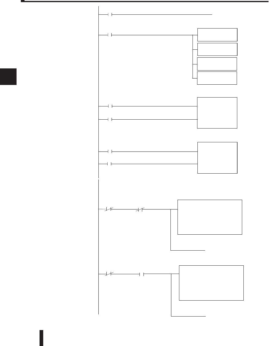
DL06 Micro PLC User Manual; 3rd Edition Rev. D
4–28
Chapter 4: System Design and Configuration
1
2
3
4
5
6
7
8
9
10
11
12
13
14
A
B
C
D
1
2
3
4
5
6
7
8
9
10
11
12
13
14
A
B
C
D
SP116 C100
SP116 C100
Port Number: K2
Slave Address: K1
Function Code: 06 - Preset Single Register
Start Slave Memory Address: 40001
Number of Elements: n/a
Modbus Data Type: 584/984 Mode
Exception Response Buffer: V400
Instruction interlock bit
C100
( SET )
( RST )
C100
Instruction interlock bit
MRX
Port Number: K2
Slave Address: K1
Function Code: 01 - Read Coil Status
Start Slave Memory Address: 1
Start Master Memory Address: C0
Number of Elements: 32
Modbus Data Type: 584/984 Mode
Exception Response Buffer: V400
This rung does a MODBUS write to the first holding register 40001 of slave address number one.
It writes the values over that reside in V2000. This particular function code only writes to one
register. Use function code 16 to write to multiple registers. Only one Network Instruction
(WX, RX, MWX, MRX) can be enabled in one scan. That is the reason for the interlock bits. For using
many network instructions on the same port, use the Shift Register instruction.
This rung does a MODBUS read from the first 32 coils of slave address number one.
It will place the values into 32 bits of the master starting at C0.
3
4
MWX
Port 2 busy bit
Port 2 busy bit
Port 2 busy bit
SP116
Port 2 error bit
SP117
Pulse/Minute
C20
CT1
K9999
CNT
Number of errors
per minute
CT2
K9999
SP116 pulses on every transaction - CT1 counts the transactions per minute.
The counter is reset every minute.
SP117 pulses on every transaction - CT2 counts the errors per minute.
The counter is reset every minute.
3
4
CNT
Number of
transactions per
minute
_1Minute
SP3 C20
( PD )
C20
Calculation of communication transfer quantity per minute between PLC and device.
CTA1
LD
V3600
OUT
CTA2
LD
V3601
OUT
Transactions/Min
Errors/Minute
Pulse/Minute
C20
1
2
Pulse/Minute
Pulse/Minute

Standard rLL
InStructIonS 5
5
5
Chapter
Chapter
Chapter
Standard rLL
InStructIonS 5
5
5
Chapter
Chapter
Chapter
In This Chapter
Introduction ..................................................................................... 5–2
Using Boolean Instructions ............................................................... 5–5
Boolean Instructions ...................................................................... 5–10
Comparative Boolean ..................................................................... 5–26
Immediate Instructions ................................................................... 5–32
Timer, Counter and Shift Register Instructions ............................... 5–39
Accumulator/Stack Load and Output Data Instructions .................. 5–52
Logical Instructions (Accumulator) ................................................. 5–69
Math Instructions ........................................................................... 5–86
Transcendental Functions ............................................................. 5–118
Bit Operation Instructions ............................................................ 5–120
Number Conversion Instructions (Accumulator) ........................... 5–127
Table Instructions ......................................................................... 5–141
Clock/Calendar Instructions ......................................................... 5–171
CPU Control Instructions .............................................................. 5–173
Program Control Instructions ....................................................... 5–175
Interrupt Instructions ................................................................... 5–183
Message Instructions .................................................................... 5–186
Intelligent I/O Instructions ........................................................... 5–194
Network Instructions .................................................................... 5–196
MODBUS RTU Instructions .......................................................... 5–204
ASCII Instructions ......................................................................... 5–210
Intelligent Box (IBox) Instructions ................................................ 5–230

DL06 Micro PLC User Manual, 3rd Edition, Rev. D
5-2
1
2
3
4
5
6
7
8
9
10
11
12
13
14
A
B
C
D
Introduction
DL06 Micro PLCs offer a wide variety of instructions to perform many different types of
operations. This chapter shows you how to use each standard Relay Ladder Logic (RLL)
instruction. In addition to these instructions, you may also need to refer to the Drum
instruction in Chapter 6, the Stage programming instructions in Chapter 7, PID in Chapter
8, LCD in Chapter 10 and programming for analog modules in D0-OPTIONS-M.
There are two ways to quickly find the instruction you need.
• If you know the instruction category (Boolean, Comparative Boolean, etc.), just use the title at the
top of the page to find the pages that discuss the instructions in that category.
• If you know the individual instruction name, use the following table to find the page(s) that
discusses the instruction.
Chapter 5: Standard RLL Instructions
1
2
3
4
5
6
7
8
9
10
11
12
13
14
a
B
c
d
Accumulating Fast Timer (TMRAF) 5–42
Accumulating Timer (TMRA) 5–42
Add (ADD) 5–86
Add Binary (ADDB) 5–99
Add Binary Double (ADDBD) 5–100
Add Binary Top of Stack (ADDBS) 5–114
Add Double (ADDD) 5–87
Add Formatted (ADDF) 5–106
Add Real (ADDR) 5–88
Add to Top (ATT) 5–162
Add Top of Stack (ADDS) 5–110
And (AND) 5–14
And Bit-of-Word (AND) 5–15
And (AND) 5–31
AND (AND logical) 5–69
And Double (ANDD) 5–70
And Formatted (ANDF) 5–71
And If Equal (ANDE) 5–28
And If Not Equal (ANDNE) 5–28
And Immediate (ANDI) 5–33
AND Move (ANDMOV) 5–167
And Negative Differential (ANDND) 5–22
And Not (ANDN) 5–14
And Not Bit-of-Word (ANDN) 5–15
And Not (ANDN) 5–31
And Not Immediate (ANDNI) 5–33
And Positive Differential (ANDPD) 5–22
And Store (AND STR) 5–16
And with Stack (ANDS) 5–72
Arc Cosine Real (ACOSR) 5–119
Arc Sine Real (ASINR) 5–118
Arc Tangent Real (ATANR) 5–119
ASCII Clear Buffer (ACRB) 5–228
ASCII Compare (CMPV) 5–220
ASCII Constant (ACON) 5–187
ASCII Extract (AEX) 5–219
ASCII Find (AFIND) 5–216
ASCII Input (AIN) 5–212
ASCII Print from V–memory (PRINTV) 5–226
ASCII Print to V–memory (VPRINT) 5–221
ASCII Swap Bytes (SWAPB) 5–227
ASCII to HEX (ATH) 5–134
Binary (BIN) 5–127
Binary Coded Decimal (BCD) 5–128
Binary to Real Conversion (BTOR) 5–131
Compare (CMP) 5–81
Compare Double (CMPD) 5–82
Compare Formatted (CMPF) 5–83
Compare Real Number (CMPR) 5–85
Compare with Stack (CMPS) 5–84
Cosine Real (COSR) 5–118
Counter (CNT) 5–45
Data Label (DLBL) 5–187
Date (DATE) 5–171
Instruction Page Instruction Page

DL06 Micro PLC User Manual, 3rd Edition, Rev. D 5-3
1
2
3
4
5
6
7
8
9
10
11
12
13
14
A
B
C
D
Chapter 5: Standard RLL Instructions
1
2
3
4
5
6
7
8
9
10
11
12
13
14
a
B
c
d
Decode (DECO) 5–126
Decrement (DEC) 5–98
Decrement Binary (DECB) 5–105
Degree Real Conversion (DEGR) 5–133
Disable Interrupts (DISI) 5–184
Divide (DIV) 5–95
Divide Binary (DIVB) 5–104
Divide Binary by Top OF Stack (DIVBS) 5–117
Divide by Top of Stack (DIVS) 5–113
Divide Double (DIVD) 5–96
Divide Formatted (DIVF) 5–109
Divide Real (DIVR) 5–97
Enable Interrupts (ENI) 5–183
Encode (ENCO) 5–125
End (END) 5–173
Exclusive Or (XOR) 5–77
Exclusive Or Double (XORD) 5–78
Exclusive Or Formatted (XORF) 5–79
Exclusive OR Move (XORMOV) 5–167
Exclusive Or with Stack (XORS) 5–80
Fault (FAULT) 5–186
Fill (FILL) 5–146
Find (FIND) 5–147
Find Block (FINDB) 5–169
Find Greater Than (FDGT) 5–148
For / Next (FOR) (NEXT) 5–176
Goto Label (GOTO) (LBL) 5–175
Goto Subroutine (GTS) (SBR) 5–178
Gray Code (GRAY) 5–138
HEX to ASCII (HTA) 5–135
Increment (INC) 5–98
Increment Binary (INCB) 5–105
Interrupt (INT) 5–183
Interrupt Return (IRT) 5–183
Interrupt Return Conditional (IRTC) 5–183
Invert (INV) 5–129
LCD 5–200
Load (LD) 5–57
Load Accumulator Indexed (LDX) 5–61
Load Accumulator Indexed from Data Constants (LDSX) 5–62
Load Address (LDA) 5–60
Load Double (LDD) 5–58
Load Formatted (LDF) 5–59
Load Immediate (LDI) 5–37
Load Immediate Formatted (LDIF) 5–38
Load Label (LDLBL) 5–142
Load Real Number (LDR) 5–63
Master Line Reset (MLR) 5–181
Master Line Set (MLS) 5–181
MODBUS Read from Network (MRX) 5–204
MODBUS Write to Network (MWX) 5–207
Move Block (MOVBLK) 5-189
Move (MOV) 5–141
Move Memory Cartridge (MOVMC) 5–142
Multiply (MUL) 5–92
Multiply Binary (MULB) 5–103
Multiply Binary Top of Stack (MULBS) 5–116
Multiply Double (MULD) 5–93
Multiply Formatted (MULF) 5–108
Multiply Real (MULR) 5–94
Multiply Top of Stack (MULS) 5–112
No Operation (NOP) 5–173
Not (NOT) 5–19
Numerical Constant (NCON) 5–187
Or (OR) 5–12
Or (OR) 5–30
Or (OR logical) 5–73
Or Bit-of-Word (OR) 5–13
Or Double (ORD) 5–74
Or Formatted (ORF) 5–75
Or If Equal (ORE) 5–27
Or If Not Equal (ORNE) 5–27
Or Immediate (ORI) 5–32
OR Move (ORMOV) 5–167
Or Negative Differential (ORND) 5–21
Or Not (ORN) 5–12
Or Not (ORN) 5–30
Or Not Bit-of-Word (ORN) 5–13
Instruction Page Instruction Page

DL06 Micro PLC User Manual, 3rd Edition, Rev. D
5-4
1
2
3
4
5
6
7
8
9
10
11
12
13
14
A
B
C
D
Or Not Immediate (ORNI) 5–32
Or Out (OROUT) 5–17
Or Out Immediate (OROUTI) 5–34
Or Positive Differential (ORPD) 5–21
Or Store (ORSTR) 5–16
Or with Stack (ORS) 5–76
Out (OUT) 5–17
Out Bit-of-Word (OUT) 5–18
Out (OUT) 5–64
Out Double (OUTD) 5–64
Out Formatted (OUTF) 5–65
Out Immediate (OUTI) 5–34
Out Immediate Formatted (OUTIF) 5–35
Out Indexed (OUTX) 5–67
Out Least (OUTL) 5–68
Out Most (OUTM) 5–68
Pause (PAUSE) 5–25
Pop (POP) 5–65
Positive Differential (PD) 5–19
Print Message (PRINT) 5–190
Radian Real Conversion (RADR) 5–133
Read from Intelligent I/O Module (RD) 5-194
Read from Network (RX) 5–196
Real to Binary Conversion (RTOB) 5–132
Remove from Bottom (RFB) 5–153
Remove from Table (RFT) 5–159
Reset (RST) 5–23
Reset Bit-of-Word (RST) 5–24
Reset Immediate (RSTI) 5–36
Reset Watch Dog Timer (RSTWT) 5–174
Rotate Left (ROTL) 5–123
Rotate Right (ROTR) 5–124
RSTBIT 5–144
Segment (SEG) 5–137
Set (SET) 5–23
Set Bit-of-Word (SET) 5–24
Set Immediate (SETI) 5–36
SETBIT 5–144
Shift Left (SHFL) 5–121
Shift Register (SR) 5–51
Shift Right (SHFR) 5–122
Shuffle Digits (SFLDGT) 5–139
Sine Real (SINR) 5–118
Source to Table (STT) 5–156
Square Root Real (SQRTR) 5–119
Stage Counter (SGCNT) 5–47
Stop (STOP) 5–173
Store (STR) 5–10
Store (STR) 5–29
Store Bit-of-Word (STRB) 5–11
Store If Equal (STRE) 5–26
Store If Not Equal (STRNE) 5–26
Store Immediate (STRI) 5–32
Store Negative Differential (STRND) 5–20
Store Not (STRN) 5–29
Store Not (STRN) 5–10
Store Not Bit-of-Word (STRNB) 5–11
Store Not Immediate (STRNI) 5–32
Store Positive Differential (STRPD) 5–20
Subroutine Return (RT) 5–178
Subroutine Return Conditional (RTC) 5–178
Subtract (SUB) 5–89
Subtract Binary (SUBB) 5–101
Subtract Binary Double (SUBBD) 5–102
Subtract Binary Top of Stack (SUBBS) 5–115
Subtract Double (SUBD) 5–90
Subtract Formatted (SUBF) 5–107
Subtract Real (SUBR) 5–91
Subtract Top of Stack (SUBS) 5–111
Sum (SUM) 5–120
Swap (SWAP) 5–170
Table Shift Left (TSHFL) 5–165
Table Shift Right (TSHFR) 5–165
Table to Destination (TTD) 5–150
Tangent Real (TANR) 5–118
Ten’s Complement (BCDCPL) 5–130
Time (TIME) 5–172
Timer (TMR) and Timer Fast (TMRF) 5–40
Up Down Counter (UDC) 5–49
Write to Intelligent I/O Module (WT) 5-195
Write to Network (WX) 5–198
Chapter 5: Standard RLL Instructions
1
2
3
4
5
6
7
8
9
10
11
12
13
14
a
B
c
d
Instruction Page Instruction Page
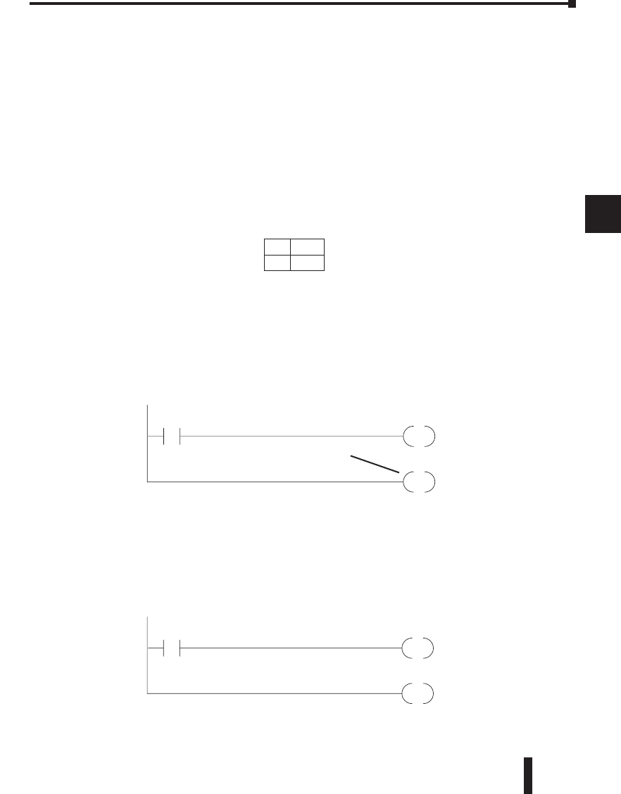
DL06 Micro PLC User Manual, 3rd Edition, Rev. D 5-5
1
2
3
4
5
6
7
8
9
10
11
12
13
14
A
B
C
D
Using Boolean Instructions
Do you ever wonder why so many PLC manufacturers always quote the scan time for a 1K
Boolean program? Simple. Most programs utilize many Boolean instructions. These are
typically very simple instructions designed to join input and output contacts in various series
and parallel combinations. Our DirectSOFT software is a similar program. It uses graphic
symbols to develop a program; therefore, you don’t necessarily have to know the instruction
mnemonics in order to develop your program.
Many of the instructions in this chapter are not program instructions used in DirectSOFT,
but are implied. In other words, they are not actually keyboard commands, however, they
can be seen in a Mnemonic View of the program once the DirectSOFT program has been
developed and accepted (compiled). Each instruction listed in this chapter will have a small
chart to indicate how the instruction is used with DirectSOFT and the HPP.
The following paragraphs show how these instructions are used to build simple ladder
programs.
END Statement
All DL06 programs require an END statement as the last instruction. This tells the CPU that
this is the end of the program. Normally, any instructions placed after the END statement
will not be executed. There are exceptions to this, such as interrupt routines, etc. This chapter
will discuss the instruction set in detail.
Simple Rungs
You use a contact to start rungs that contain both contacts and coils. The boolean instruction
that does this is called a Store or, STR instruction. The output point is represented by the
Output or, OUT instruction. The following example shows how to enter a single contact and
a single output coil.
Chapter 5: Standard RLL Instructions - Boolean Instructions
OUT
Y0X0
END
Handheld Mnemonics
STR X0
OUT Y0
END
DirectSOFT32 Example
OUT
Y0
X0
END
DirectSOFT32 Example
All programs must have
an END statement
1
2
3
4
5
6
7
8
9
10
11
12
13
14
a
B
c
d
DS Implied
HPP Used
DirectSOFT
DirectSOFT
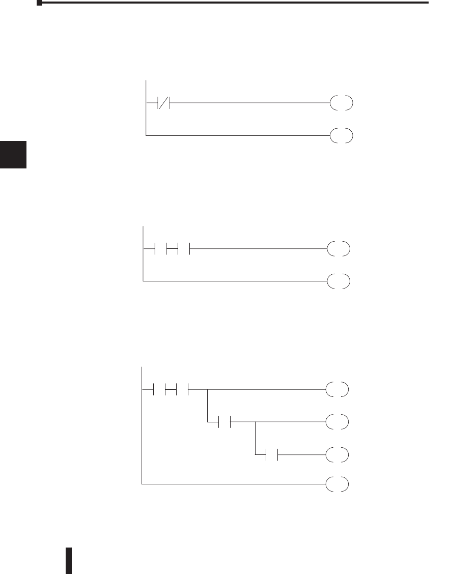
DL06 Micro PLC User Manual, 3rd Edition, Rev. D
5-6
1
2
3
4
5
6
7
8
9
10
11
12
13
14
A
B
C
D
Normally Closed Contact
Normally closed contacts are also very common. This is accomplished with the Store Not,
or STRN instruction. The following example shows a simple rung with a normally closed
contact.
Contacts in Series
Use the AND instruction to join two or more contacts in series. The following example
shows two contacts in series and a single output coil. The instructions used would be STR
X0, AND X1, followed by OUT Y0.
Midline Outputs
Sometimes, it is necessary to use midline outputs to get additional outputs that are
conditional on other contacts. The following example shows how you can use the AND
instruction to continue a rung with more conditional outputs.
Chapter 5: Standard RLL Instructions - Boolean Instructions
1
2
3
4
5
6
7
8
9
10
11
12
13
14
a
B
c
d
OUT
Y0
X0
END
X1
Direct SOFT32 Example Handheld Mnemonics
STR X0
AND X1
OUT Y0
AND X2
OUT Y1
AND X3
OUT Y2
END
X2
OUT
Y1
X3
OUT
Y2
OUT
Y0
X0
END
X1
Direct SOFT32 Example Handheld Mnemonics
STR X0
AND X1
OUT Y0
END
OUT
Y0X0
END
DirectSOFT Example Handheld Mnemonics
STRN X0
OUT Y0
END
DirectSOFT
DirectSOFT
DirectSOFT
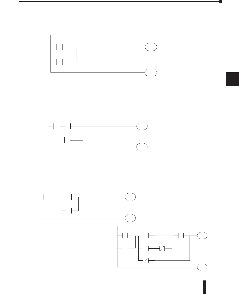
DL06 Micro PLC User Manual, 3rd Edition, Rev. D 5-7
1
2
3
4
5
6
7
8
9
10
11
12
13
14
A
B
C
D
Parallel Elements
You may also have to join contacts in parallel. The OR instruction allows you to do this. The
following example shows two contacts in parallel and a single output coil. The instructions
would be STR X0, OR X1, followed by OUT Y0.
Quite often, it is necessary to join several groups of series elements in parallel. The Or Store
(ORSTR) instruction allows this operation. The following example shows a simple network
consisting of series elements joined in parallel.
You can also join one or more parallel branches in series. The And Store (ANDSTR)
instruction allows this operation. The following example shows a simple network with
contact branches in series with parallel contacts.
Chapter 5: Standard RLL Instructions - Boolean Instructions
1
2
3
4
5
6
7
8
9
10
11
12
13
14
a
B
c
d
OUT
Y0
X0
END
X2
X3X1 X4
X5
X6
OUT
Y0
X0
END
X1
X2
Direct SOFT32 Example Handheld Mnemonics
STR X0
STR X1
OR X2
ANDSTR
OUT Y0
END
OUT
Y0
X0
END
X2
X1
X3
Direct SOFT32 ExampleHandheld Mnemonics
STR X0
AND X1
STR X2
AND X3
ORSTR
OUT Y0
END
OUT
Y0
X0
END
X1
Direct SOFT32 Example Handheld Mnemonics
STR X0
OR X1
OUT Y0
END
DirectSOFT
DirectSOFT
DirectSOFT
Combination Networks
You can combine the various types
of series and parallel branches
to solve almost any application
problem.The following example
shows a simple combination
network.
Joining Series Branches in Parallel
Joining Parallel Branches in Series
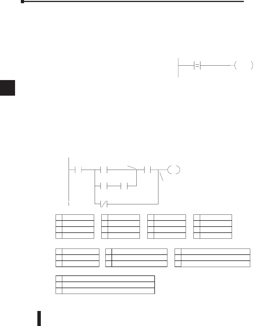
DL06 Micro PLC User Manual, 3rd Edition, Rev. D
5-8
1
2
3
4
5
6
7
8
9
10
11
12
13
14
A
B
C
D
Comparative Boolean
Some PLC manufacturers make it really difficult to do a simple comparison of two numbers.
Some of them require you to move the data all over the place before you can actually perform
the comparison. The DL06 Micro PLCs provide Comparative Boolean instructions that
allow you to quickly and easily solve this problem. The Comparative Boolean provides
evaluation of two BCD values using boolean contacts. The valid evaluations are: equal to, not
equal to, equal to or greater than, and less than.
In the example, when the BCD value in V-memory
location V1400 is equal to the constant value 1234, Y3
will energize.
Boolean Stack
There are limits to how many elements you can include in a rung. This is because the DL06
PLCs use an 8-level boolean stack to evaluate the various logic elements. The boolean
stack is a temporary storage area that solves the logic for the rung. Each time the program
encounters a STR instruction, the instruction is placed on the top of the stack. Any other
STR instructions already on the boolean stack are pushed down a level. The ANDSTR, and
ORSTR instructions combine levels of the boolean stack when they are encountered. An
error will occur during program compilation if the CPU encounters a rung that uses more
than the eight levels of the boolean stack.
The following example shows how the boolean stack is used to solve boolean logic.
Chapter 5: Standard RLL Instructions - Boolean Instructions
1
2
3
4
5
6
7
8
9
10
11
12
13
14
a
B
c
d
X1 or (X2 AND X3)
STR X0 STR X1 STR X2
1 STR X0
2
3
4
1 STR X1
2 STR X0
3
4
1 STR X2
STR X1
2
3 STR X0
4
AND X3
1 X2 AND X3
2STR X1
3 STR X0
4
ORSTR
1
2 STR X0
3
OUT
Y0
X0 X1
X2 X3
X4
X5
STR
OR
AND
ORSTR
ANDSTR
Output
STR
STR
AND
X4 AND {X1 or (X2 AND X3)}
AND X4
1
2 STR X0
3
NOT X5 OR X4 AND {X1 OR (X2 AND X3)}
STR X0
ORNOT X5
1
2
3
ANDSTR
XO AND (NOT X5 or X4) AND {X1 or (X2 AND X3)}
1
2
3
Y3
OUT
V1400 K1234
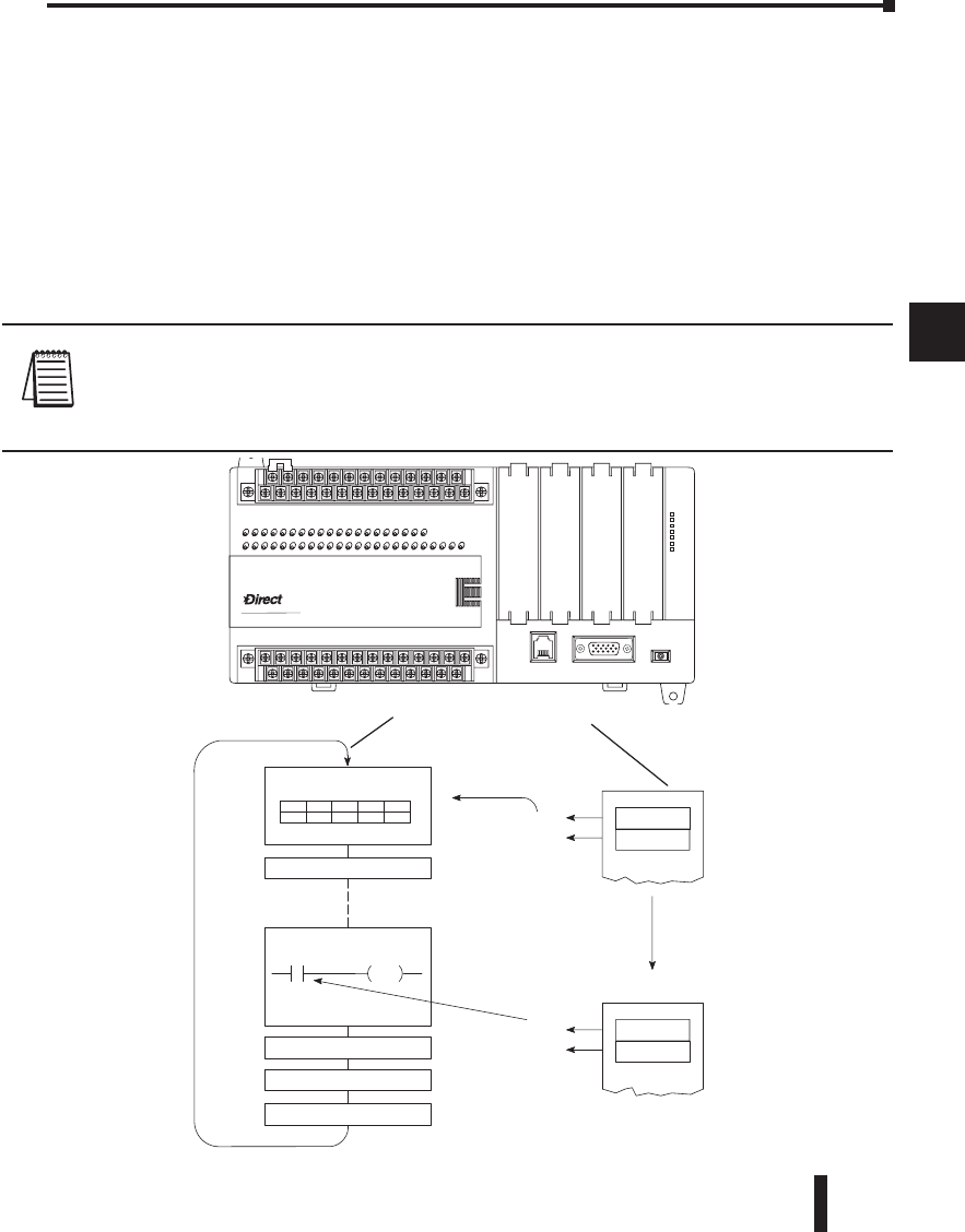
DL06 Micro PLC User Manual, 3rd Edition, Rev. D 5-9
1
2
3
4
5
6
7
8
9
10
11
12
13
14
A
B
C
D
Immediate Boolean
The DL06 Micro PLCs can usually complete an operation cycle in a matter of milliseconds.
However, in some applications you may not be able to wait a few milliseconds until the
next I/O update occurs. The DL06 PLCs offer Immediate input and outputs which are
special boolean instructions that allow reading directly from inputs and writing directly to
outputs during the program execution portion of the CPU cycle. You may recall that this is
normally done during the input or output update portion of the CPU cycle. The immediate
instructions take longer to execute because the program execution is interrupted while the
CPU reads or writes the I/O point. This function is not normally done until the read inputs
or the write outputs portion of the CPU cycle.
NOTE: Even though the immediate input instruction reads the most current status from the input
point, it only uses the results to solve that one instruction. It does not use the new status to update
the image register. Therefore, any regular instructions that follow will still use the image register
values. Any immediate instructions that follow will access the I/O again to update the status. The
immediate output instruction will write the status to the I/O and update the image register.
Chapter 5: Standard RLL Instructions - Boolean Instructions
1
2
3
4
5
6
7
8
9
10
11
12
13
14
a
B
c
d
X0
OFF
X1
OFF
CPU Scan
Read Inputs
Diagnostics
Input Image Register,
The CPU reads the inputs from the local
base and stores the status in an input
image register.
X0 Y0
X0X1X2...X11
OFFOFFON...OFF
Solve the Application Program
Read Inputs from Specialty I/O
Write Outputs
Write Outputs to Specialty I/O
X0
ON
X1
OFF
I/O Point X0 Changes
I
PORT1PORT2
TERM
RUN STOP
PWR
RUN
CPU
TX1
RX1
TX2
RX2
012345678910 11 12 13 14 15 16 17 18 19 20 21 22 23
06
LOGIC
Koyo
Immediate instruction does not use the
input image register, but instead reads
the status from the module immediately.
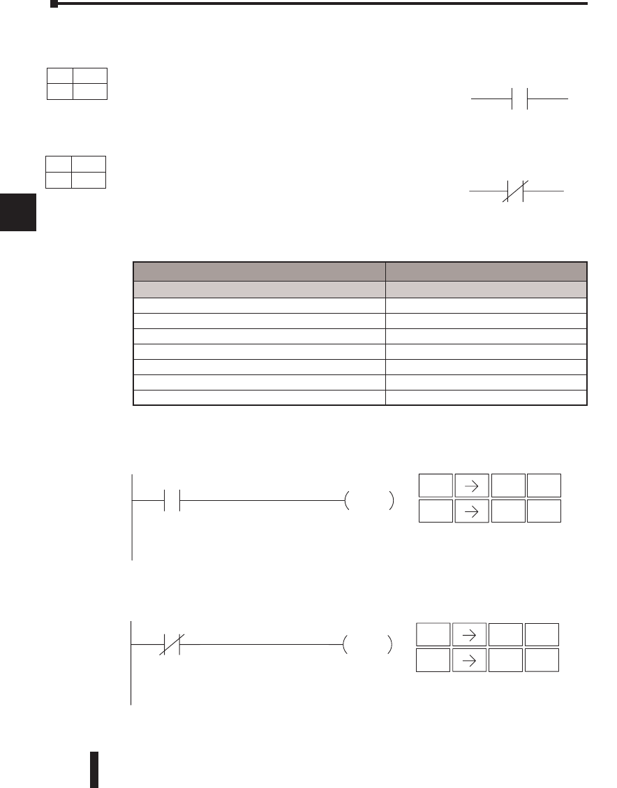
DL06 Micro PLC User Manual, 3rd Edition, Rev. D
5-10
1
2
3
4
5
6
7
8
9
10
11
12
13
14
A
B
C
D
Boolean Instructions
Store (STR)
The Store instruction begins a new rung or an additional branch
in a rung with a normally open contact. Status of the contact will
be the same state as the associated image register point or memory
location.
Store Not (STRN)
The Store Not instruction begins a new rung or an additional
branch in a rung with a normally closed contact. Status of the
contact will be opposite the state of the associated image register
point or memory location.
In the following Store example, when input X1 is on, output Y2 will energize.
In the following Store Not example, when input X1 is off output Y2 will energize.
Chapter 5: Standard RLL Instructions - Boolean Instructions
1
2
3
4
5
6
7
8
9
10
11
12
13
14
a
B
c
d
Aaaa
Aaaa
STR
$
1
BENT
OUT
GX
2
CENT
Handheld Programmer KeystrokesDirect SOFT32
Y2
OUT
X1
STRN
SP
1
BENT
OUT
GX
2
CENT
Y2
OUT
X1
Handheld Programmer KeystrokesDirect SOFT32
Operand Data Type DL06 Range
A aaa
Inputs X 0–777
Outputs Y 0–777
Control Relays C 0–1777
Stage S 0–1777
Timer T 0–377
Counter C CT 0–177
Special Relay SP 0–777
DS Used
HPP Used
DS Used
HPP Used
DirectSOFT
DirectSOFT
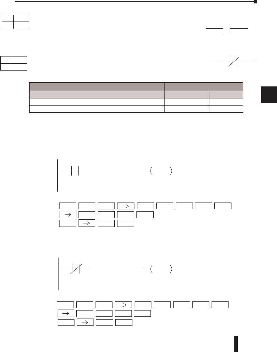
DL06 Micro PLC User Manual, 3rd Edition, Rev. D 5-11
1
2
3
4
5
6
7
8
9
10
11
12
13
14
A
B
C
D
Store Bit-of-Word (STRB)
The Store Bit-of-Word instruction begins a new rung or an additional
branch in a rung with a normally open contact. Status of the contact
will be the same state as the bit referenced in the associated memory
location.
Store Not Bit-of-Word (STRNB)
The Store Not instruction begins a new rung or an additional branch in a
rung with a normally closed contact. Status of the contact will be opposite
the state of the bit referenced in the associated memory location.
These instructions look like the STR and STRN instructions only the address is different.
Take note how the address is set up in the following Store Bit-of-Word example.
When bit 12 of V-memory location V1400 is on, output Y2 will energize.
In the following Store Not Bit-of-Word example, when bit 12 of V-memory location V1400
is off, output Y2 will energize.
Chapter 5: Standard RLL Instructions - Boolean Instructions
1
2
3
4
5
6
7
8
9
10
11
12
13
14
a
B
c
d
Aaaa.bb
Aaaa.bb
Operand Data Type DL06 Range
A aaa bb
V-memory B See memory map 0 to 15
Pointer PB See memory map 0 to 15
Handheld Programmer Keystrokes
DirectSOFT32
Y2
OUT
B1400.12
STR V 1
OUT 2
SHFT 4 0 0
1 2 ENT
ENT
K
B
Y2
OUT
B1400.12
DirectSOFT32
OUT 2 ENT
Handheld Programmer Keystrokes
STRN V 1SHFT 4 0 0
1 2 ENT
K
B
DS Used
HPP Used
DS Used
HPP Used
DirectSOFT
DirectSOFT
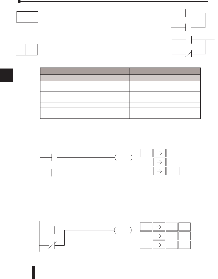
DL06 Micro PLC User Manual, 3rd Edition, Rev. D
5-12
1
2
3
4
5
6
7
8
9
10
11
12
13
14
A
B
C
D
Or (OR)
The Or instruction will logically OR a normally open contact in
parallel with another contact in a rung. The status of the contact will
be the same state as the associated image register point or memory
location.
Or Not (ORN)
The Or Not instruction will logically OR a normally closed contact
in parallel with another contact in a rung. The status of the contact
will be opposite the state of the associated image register point or
memory location.
In the following Or example, when input X1 or X2 is on, output Y5 will energize.
In the following Or Not example, when input X1 is on or X2 is off, output Y5 will energize.
Chapter 5: Standard RLL Instructions - Boolean Instructions
1
2
3
4
5
6
7
8
9
10
11
12
13
14
a
B
c
d
Aaaa
Aaaa
STR
$
1
BENT
OR
Q
2
CENT
OUT
GX
5
FENT
Y5
OUT
X1
X2
Handheld Programmer KeystrokesDirect SOFT32
STR
$
1
BENT
2
CENT
OUT
GX
5
FENT
ORN
R
X1 Y5
OUT
X2
Handheld Programmer KeystrokesDirect SOFT32
Operand Data Type DL06 Range
A aaa
Inputs X 0-777
Outputs Y 0-777
Control Relays C 0–1777
Stage S 0–1777
Timer T 0–377
Counter CT 0–177
Special Relay SP 0-777
DS Implied
HPP Used
DS Implied
HPP Used
DirectSOFT
DirectSOFT
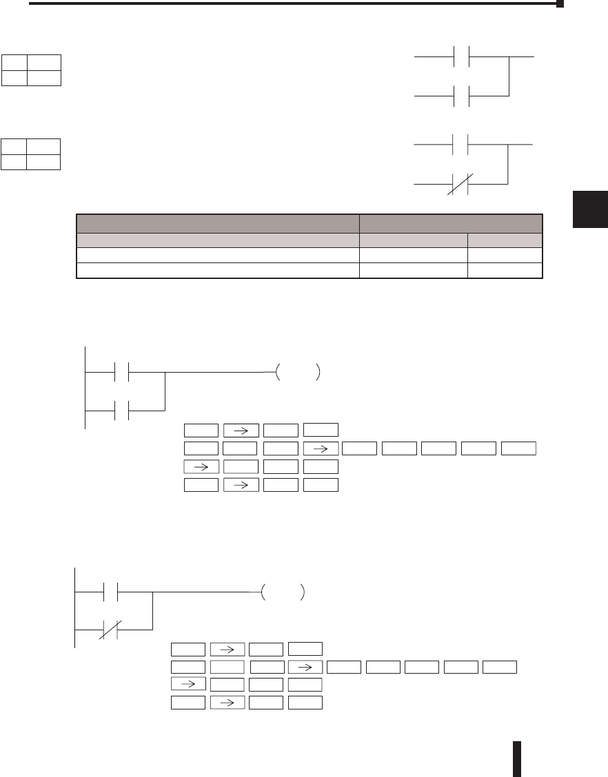
DL06 Micro PLC User Manual, 3rd Edition, Rev. D 5-13
1
2
3
4
5
6
7
8
9
10
11
12
13
14
A
B
C
D
Or Bit-of-Word (OR)
The Or Bit-of-Word instruction will logically OR a normally
open contact in parallel with another contact in a rung. Status
of the contact will be the same state as the bit referenced in the
associated memory location.
Or Not Bit-of-Word (ORN)
The Or Not Bit-of-Word instruction will logically OR a
normally closed contact in parallel with another contact in a
rung. Status of the contact will be opposite the state of the bit
referenced in the associated memory location.
In the following Or Bit-of-Word example, when input X1 or bit 7 of V1400 is on, output Y5
will energize.
In the following Or Bit-of-Word example, when input X1 is on or bit 7 of V1400 is off,
output Y7 will energize.
Chapter 5: Standard RLL Instructions - Boolean Instructions
1
2
3
4
5
6
7
8
9
10
11
12
13
14
a
B
c
d
Aaaa.bb
Aaaa.bb
Y7
OUT
X1
B1400.7
STR 1
Handheld Programmer Keystrokes
DirectSOFT32
OR V 1
OUT 7
SHFT 4 0 0
7
ENT
ENT
ENT
K
B
Y7
OUT
X1
STR 1
Handheld Programmer Keystrokes
DirectSOFT32
ORN V 1
OUT 7
4 0 0
7
B1400.7
ENT
ENT
ENT
K
SHFT B
Operand Data Type DL06 Range
A aaa bb
V-memory B See memory map 0 to 15
Pointer PB See memory map 0 to 15
DS Implied
HPP Used
DS Implied
HPP Used
DirectSOFT
DirectSOFT
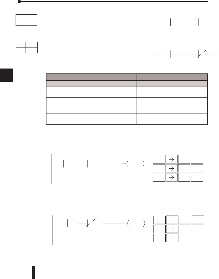
DL06 Micro PLC User Manual, 3rd Edition, Rev. D
5-14
1
2
3
4
5
6
7
8
9
10
11
12
13
14
A
B
C
D
AND (AND)
The AND instruction logically ands a normally open
contact in series with another contact in a rung. The
status of the contact will be the same state as the
associated image register point or memory location.
AND NOT (ANDN)
The AND NOT instruction logically ands a normally
closed contact in series with another contact in a rung.
The status of the contact will be opposite the state of the
associated image register point or memory location.
In the following And example, when input X1 and X2 are on output Y5 will energize.
In the following And Not example, when input X1 is on and X2 is off output Y5 will
energize.
Chapter 5: Standard RLL Instructions - Boolean Instructions
1
2
3
4
5
6
7
8
9
10
11
12
13
14
a
B
c
d
Aaaa
Aaaa
STR
$
1
BENT
2
CENT
OUT
GX
5
FENT
AND
V
Y5
OUT
X1 X2
Handheld Programmer KeystrokesDirect SOFT32
ANDN
W
STR
$
1
BENT
2
CENT
OUT
GX
5
FENT
X1 Y5
OUT
X2
Handheld Programmer KeystrokesDirect SOFT32
Operand Data Type DL06 Range
A aaa
Inputs X 0–777
Outputs Y 0–777
Control Relays C 0–1777
Stage S 0–1777
Timer T 0–377
Counter CT 0–177
Special Relay SP 0–777
DS Implied
HPP Used
DS Implied
HPP Used
DirectSOFT
DirectSOFT
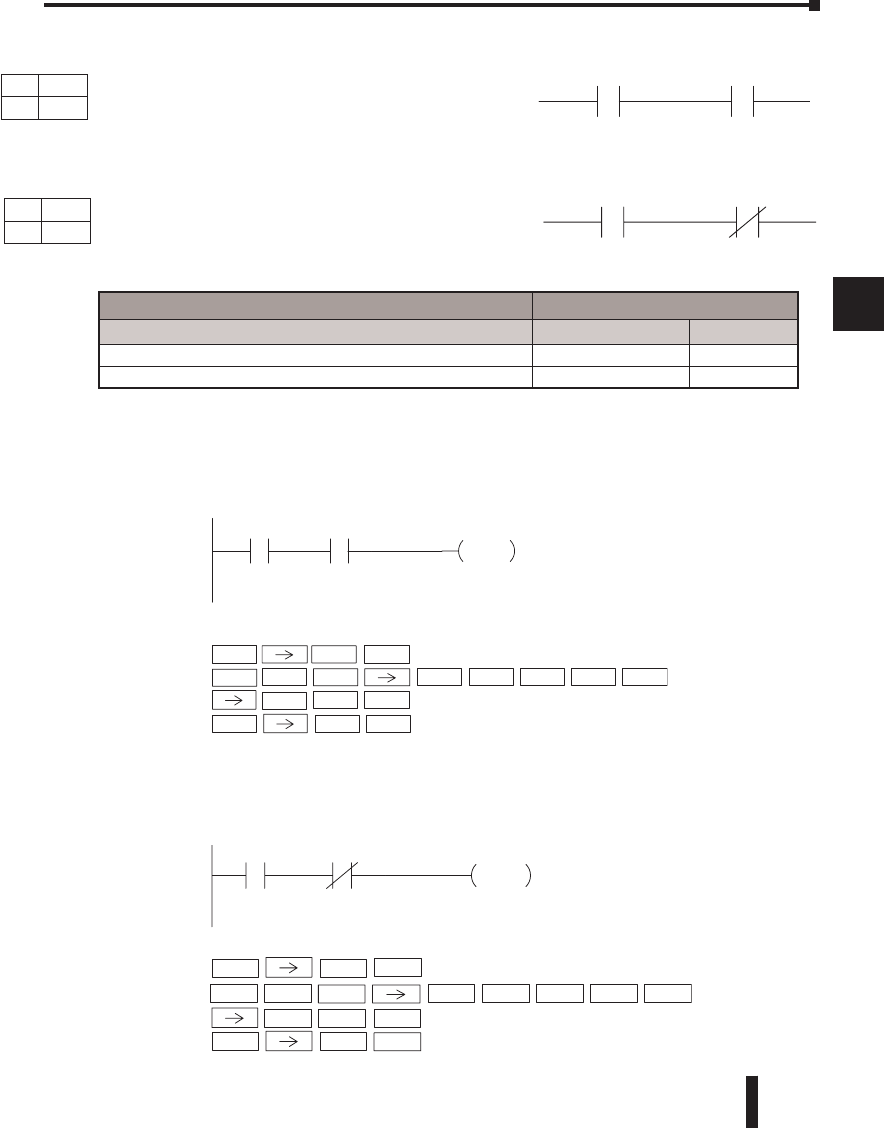
DL06 Micro PLC User Manual, 3rd Edition, Rev. D 5-15
1
2
3
4
5
6
7
8
9
10
11
12
13
14
A
B
C
D
AND Bit-of-Word (AND)
The And Bit-of-Word instruction logically ands a
normally open contact in series with another contact in
a rung. The status of the contact will be the same state as
the bit referenced in the associated memory location.
AND Not Bit-of-Word (ANDN)
The And Not Bit-of-Word instruction logically ands a
normally closed contact in series with another contact in
a rung. The status of the contact will be opposite the state
of the bit referenced in the associated memory location.
In the following And Bit-of-Word example, when input X1 and bit 4 of V1400 is on output
Y5 will energize.
In the following And Not Bit-of-Word example, when input X1 is on and bit 4 of V1400 is
off output Y5 will energize.
Chapter 5: Standard RLL Instructions - Boolean Instructions
1
2
3
4
5
6
7
8
9
10
11
12
13
14
a
B
c
d
Aaaa.bb
Aaaa.bb
Operand Data Type DL06 Range
A aaa bb
V-memory B See memory map 0 to 15
Pointer PB See memory map 0 to 15
Y5
OUT
X1 B1400.4
DirectSOFT32
OUT 5 ENT
Handheld Programmer Keystrokes
V 1SHFT 4 0 0
4 ENT
K
B
STR 1 ENT
AND
X1 Y5
OUT
B1400.4
DirectSOFT32
STR 1
Handheld Programmer Keystrokes
OUT 5
ANDN V 1SHFT 4 0 0
4 ENT
K
B
ENT
ENT
DS Implied
HPP Used
DS Implied
HPP Used
DirectSOFT
DirectSOFT
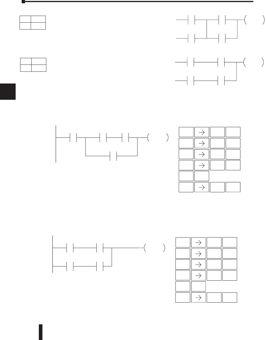
DL06 Micro PLC User Manual, 3rd Edition, Rev. D
5-16
1
2
3
4
5
6
7
8
9
10
11
12
13
14
A
B
C
D
And Store (ANDSTR)
The And Store instruction logically ands two branches
of a rung in series. Both branches must begin with the
Store instruction.
OR Store (ORSTR)
The Or Store instruction logically ORs two branches
of a rung in parallel. Both branches must begin with
the Store instruction.
In the following And Store example, the branch consisting of contacts X2, X3, and X4 have
been anded with the branch consisting of contact X1.
In the following Or Store example, the branch consisting of X1 and X2 have been ored with
the branch consisting of X3 and X4.
Chapter 5: Standard RLL Instructions - Boolean Instructions
1
2
3
4
5
6
7
8
9
10
11
12
13
14
a
B
c
d
OUT
1 2
OUT
1
2
STR
$
1
BENT
STR
$ENT
2
C
AND
VENT
3
D
OR
QENT
4
E
ANDST
LENT
OUT
GX
5
FENT
Y5
OUT
X1 X2
X4
X3
Handheld Programmer KeystrokesDirect SOFT32
STR
$
1
BENT
STR
$ENT
AND
VENT
OUT
GX
5
FENT
2
C
3
D
AND
VENT
4
E
ORST
MENT
Y5
OUT
X1 X2
X3 X4
Handheld Programmer KeystrokesDirect SOFT32
DS Implied
HPP Used
DS Implied
HPP Used
DirectSOFT
DirectSOFT
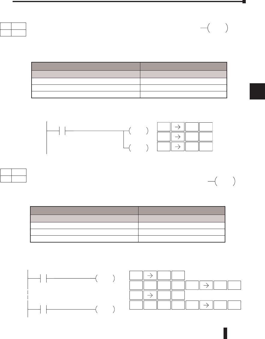
DL06 Micro PLC User Manual, 3rd Edition, Rev. D 5-17
1
2
3
4
5
6
7
8
9
10
11
12
13
14
A
B
C
D
Out (OUT)
The Out instruction reflects the status of the rung (on/off) and outputs
the discrete (on/off) state to the specified image register point or memory
location.
Multiple Out instructions referencing the same discrete location should not be used since only
the last Out instruction in the program will control the physical output point. Instead, use the
next instruction, the Or Out.
In the following Out example, when input X1 is on, output Y2 and Y5 will energize.
Or Out (OROUT)
The Or Out instruction allows more than one rung of discrete logic to
control a single output. Multiple Or Out instructions referencing the same
output coil may be used, since all contacts controlling the output are logically
OR’d together. If the status of any rung is on, the output will also be on.
In the following example, when X1 or X4 is on, Y2 will energize.
Chapter 5: Standard RLL Instructions - Boolean Instructions
1
2
3
4
5
6
7
8
9
10
11
12
13
14
a
B
c
d
Aaaa
OUT
STR
$
1
BENT
STR
$ENT
4
E
Y2
OR OUT
X1
Y2
OR OUT
X4
Handheld Programmer KeystrokesDirect SOFT32
INST#
O
5
F
3
DENT ENT 2
CENT
2
CENT
INST#
O
5
F
3
DENT ENT
A aaa
OROUT
STR
$
1
BENT
OUT
GX
2
CENT
OUT
GX ENT
5
F
Y2
OUT
X1
Y5
OUT
Handheld Programmer KeystrokesDirect SOFT32
Operand Data Type DL06 Range
A aaa
Inputs X 0–777
Outputs Y 0–777
Control Relays C 0–1777
Operand Data Type DL06 Range
A aaa
Inputs X 0–777
Outputs Y 0-777
Control Relays C 0–1777
DS Usied
HPP Used
DS Used
HPP Used
DirectSOFT
DirectSOFT
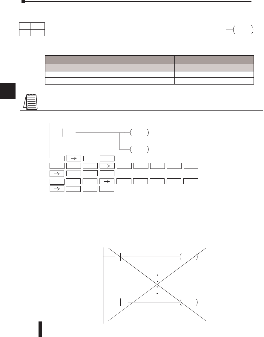
DL06 Micro PLC User Manual, 3rd Edition, Rev. D
5-18
1
2
3
4
5
6
7
8
9
10
11
12
13
14
A
B
C
D
NOTE: If the Bit-of-Word is entered as V1400.3 in DirectSOFT, it will be converted to B1400.3. Bit-of-
Word can also be entered as B1400.3.
In the following Out Bit-of-Word example, when input X1 is on, bit 3 of V1400 and bit 6 of
V1401 will turn on.
The following Out Bit-of-Word example contains two Out Bit-of-Word instructions
using the same bit in the same memory word. The final state bit 3 of V1400 is ultimately
controlled by the last rung of logic referencing it. X1 will override the logic state controlled
by X0. To avoid this situation, multiple outputs using the same location must not be used in
programming.
Chapter 5: Standard RLL Instructions - Boolean Instructions
1
2
3
4
5
6
7
8
9
10
11
12
13
14
a
B
c
d
Aaaa.bb
OUT
B1400.3
OUT
X1
B1401.6
OUT
DirectSOFT32
STR 1
Handheld Programmer Keystrokes
OUT V 1SHFT 4 0 0
3 ENT
K
B
ENT
OUT V 1SHFT 4 0 1
6 ENT
K
B
B1400.3
OUT
X0
B1400.3
OUT
X1
Operand Data Type DL06 Range
A aaa bb
V-memory B See memory map 0 to 15
Pointer PB See memory map 0 to 15
DS Used
HPP Used
DirectSOFT
Out Bit-of-Word (OUT)
The Out Bit-of-Word instruction reflects the status of the rung
(on/off) and outputs the discrete (on/off) state to the specified bit
in the referenced memory location. Multiple Out Bit-of-Word
instructions referencing the same bit of the same word generally
should not be used since only the last Out instruction in the
program will control the status of the bit.
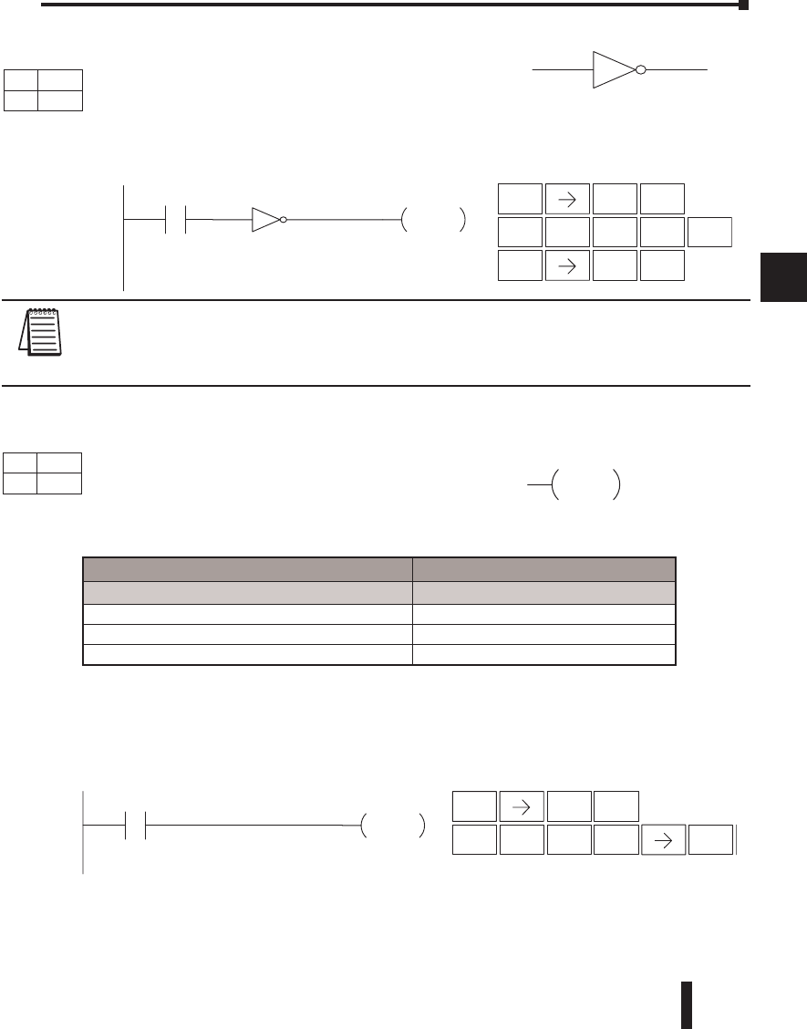
DL06 Micro PLC User Manual, 3rd Edition, Rev. D 5-19
1
2
3
4
5
6
7
8
9
10
11
12
13
14
A
B
C
D
Not (NOT)
The Not instruction inverts the status of the rung at the point
of the instruction.
In the following example, when X1 is off, Y2 will energize. This is because the Not instruction
inverts the status of the rung at the Not instruction.
NOTE: DirectSOFT Release 1.1i and later supports the use of the NOT instruction. The above example
rung is merely intended to show the visual representation of the NOT instruction. The NOT instruction
can only be selected in DirectSOFT from the Instruction Browser. The rung cannot be created or
displayed in DirectSOFT versions earlier than 1.1i.
In the following example, every time X1 makes an Off-to-On transition, C0 will energize for
one scan.
Chapter 5: Standard RLL Instructions - Boolean Instructions
Y2
OUT
X1
Handheld Programmer KeystrokesDirectSOFT32
STR
$
1
BENT
SHFT TMR
N
INST#
O
MLR
TENT
OUT
GX
2
CENT
A aaa
PD
STR
$
1
BENT
SHFT CV
P
3
D
SHFT 0
A
ENT
C0
PD
X1
Handheld Programmer Keystrokes
DirectSOFT32
1
2
3
4
5
6
7
8
9
10
11
12
13
14
a
B
c
d
Operand Data Type DL06 Range
A aaa
Inputs X 0–777
Outputs Y 0–777
Control Relays C 0–1777
DS Used
HPP Used
DS Used
HPP Used
DirectSOFT
DirectSOFT
Positive Differential (PD)
The Positive Differential instruction is typically
known as a one shot. When the input logic
produces an off to on transition, the output will
energize for one CPU scan.
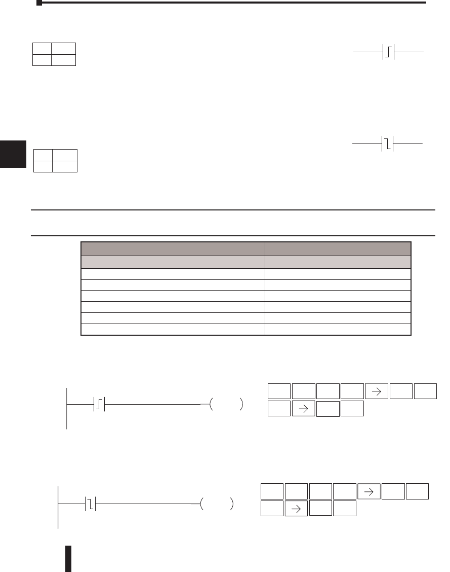
DL06 Micro PLC User Manual, 3rd Edition, Rev. D
5-20
1
2
3
4
5
6
7
8
9
10
11
12
13
14
A
B
C
D
NOTE: When using DirectSOFT, these instructions can only be entered from the Instruction
Browser.
In the following example, each time X1 makes an Off-to-On transition, Y4 will energize for
one scan.
In the following example, each time X1 makes an On-to-Off transition, Y4 will energize for
one scan.
Chapter 5: Standard RLL Instructions - Boolean Instructions
1
2
3
4
5
6
7
8
9
10
11
12
13
14
a
B
c
d
Aaaa
Aaaa
Y4
OUT
DirectSOFT32
X1 STR
$
CV
P
ENT
OUT
GX
3
D
SHFT 1
BENT
Handheld Programmer Keystrokes
4
E
Y4
OUT
DirectSOFT32
X1 STR
$
TMR
N
ENT
OUT
GX
3
D
SHFT 1
BENT
Handheld Programmer Keystrokes
4
E
Operand Data Type DL06 Range
A aaa
Inputs X 0–777
Outputs Y 0–777
Control Relays C 0–1777
Stage S 0–1777
Timer T 0–377
Counter CT 0–177
DS Used
HPP Used
DS Used
HPP Used
DirectSOFT
DirectSOFT
Store Positive Differential (STRPD)
The Store Positive Differential instruction begins a new rung
or an additional branch in a rung with a contact. The contact
closes for one CPU scan when the state of the associated image
register point makes an Off-to-On transition. Thereafter, the
contact remains open until the next Off-to-On transition (the
symbol inside the contact represents the transition). This function
is sometimes called a “one-shot”. This contact will also close on a
program-to-run transition if it is within a retentative range.
Store Negative Differential (STRND)
The Store Negative Differential instruction begins a new rung
or an additional branch in a rung with a contact. The contact
closes for one CPU scan when the state of the associated image
register point makes an On-to-Off transition. Thereafter, the
contact remains open until the next On-to-Off transition (the
symbol inside the contact represents the transition).
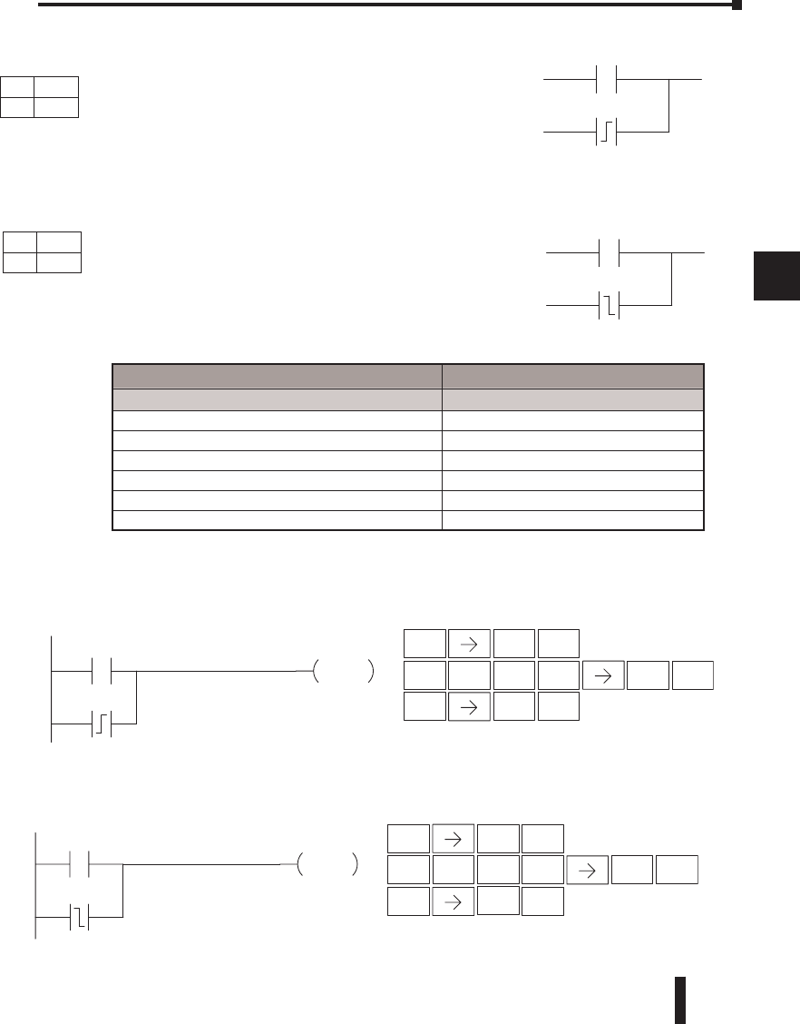
DL06 Micro PLC User Manual, 3rd Edition, Rev. D 5-21
1
2
3
4
5
6
7
8
9
10
11
12
13
14
A
B
C
D
In the following example, Y 5 will energize whenever X1 is on, or for one CPU scan when X2
transitions from Off to On.
In the following example, Y 5 will energize whenever X1 is on, or for one CPU scan when X2
transitions from On to Off.
Chapter 5: Standard RLL Instructions - Boolean Instructions
1
2
3
4
5
6
7
8
9
10
11
12
13
14
a
B
c
d
Aaaa
Aaaa
Y5
OUT
X1
DirectSOFT32
X2
STR
$
CV
P
ENT
OUT
GX
3
D
SHFT
1
BENT
Handheld Programmer Keystrokes
5
F
OR
Q
2
CENT
X1 Y5
OUT
DirectSOFT32
X2
STR
$
TMR
N
ENT
OUT
GX
3
D
SHFT
1
BENT
Handheld Programmer Keystrokes
5
F
OR
Q
2
CENT
Operand Data Type DL06 Range
A aaa
Inputs X 0–777
Outputs Y 0–777
Control Relays C 0–1777
Stage S 0–1777
Timer T 0–377
Counter CT 0–177
DS Implied
HPP Used
DS Implied
HPP Used
DirectSOFT
DirectSOFT
Or Positive Differential (ORPD)
The Or Positive Differential instruction logically ors a
contact in parallel with another contact in a rung. The
status of the contact will be open until the associated
image register point makes an Off-to-On transition,
closing it for one CPU scan. Thereafter, it remains
open until another Off-to-On transition.
Or Negative Differential (ORND)
The Or Negative Differential instruction logically
ors a contact in parallel with another contact in a
rung. The status of the contact will be open until the
associated image register point makes an On-to-Off
transition, closing it for one CPU scan. Thereafter, it
remains open until another On-to-Off transition.
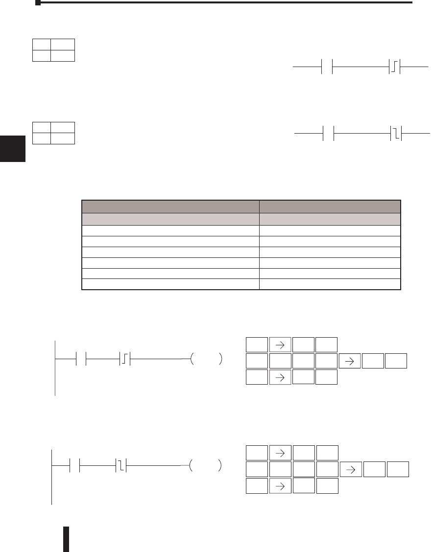
DL06 Micro PLC User Manual, 3rd Edition, Rev. D
5-22
1
2
3
4
5
6
7
8
9
10
11
12
13
14
A
B
C
D
And Positive Differential (ANDPD)
The And Positive Differential instruction logically ands
a normally open contact in series with another contact
in a rung. The status of the contact will be open until
the associated image register point makes an Off-to-On
transition, closing it for one CPU scan. Thereafter, it
remains open until another Off-to-On transition.
And Negative Differential (ANDND)
The And Negative Differential instruction logically ands
a normally open contact in series with another contact
5-22in a rung.The status of the contact will be open
until the associated image register point makes an On-to-
Off transition, closing it for one CPU scan. Thereafter, it
remains open until another On-to-Off transition.
Chapter 5: Standard RLL Instructions - Boolean Instructions
1
2
3
4
5
6
7
8
9
10
11
12
13
14
a
B
c
d
Aaaa
Aaaa
Y5
OUT
X1
DirectSOFT32
X2 STR
$
CV
P
ENT
OUT
GX
3
D
SHFT
1
BENT
Handheld Programmer Keystrokes
5
F
OR
Q
2
CENT
X1 Y5
OUT
DirectSOFT32
X2 STR
$
TMR
N
ENT
OUT
GX
3
D
SHFT
1
BENT
Handheld Programmer Keystrokes
5
F
OR
Q
2
CENT
Operand Data Type DL06 Range
A aaa
Inputs X 0–777
Outputs Y 0–777
Control Relays C 0–1777
Stage S 0–1777
Timer T 0–377
Counter CT 0–177
DS Implied
HPP Used
DS Implied
HPP Used
DirectSOFT
DirectSOFT
In the following example, Y5 will energize for one CPU scan whenever X1 is on and
X2 transitions from Off to On.
In the following example, Y5 will energize for one CPU scan whenever X1 is on and
X2 transitions from On to Off.
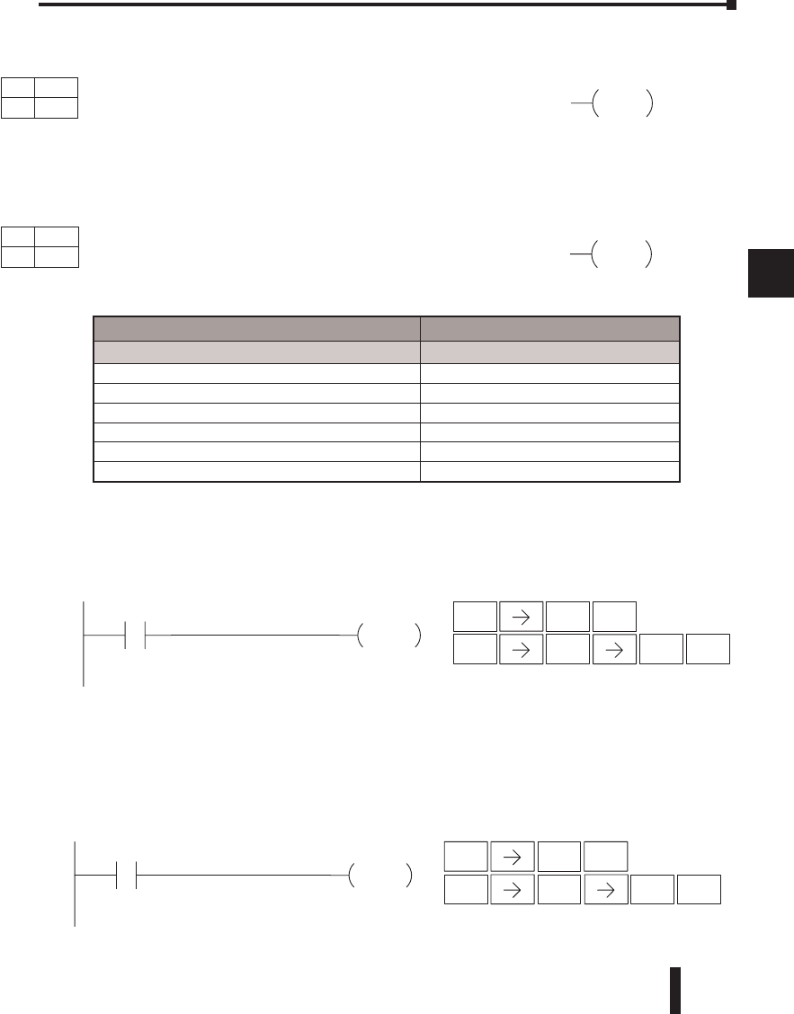
DL06 Micro PLC User Manual, 3rd Edition, Rev. D 5-23
1
2
3
4
5
6
7
8
9
10
11
12
13
14
A
B
C
D
In the following example when X1 is on, Y2 through Y5 will energize.
In the following example when X1 is on, Y2 through Y5 will be reset or de–energized.
Chapter 5: Standard RLL Instructions - Boolean Instructions
1
2
3
4
5
6
7
8
9
10
11
12
13
14
a
B
c
d
SET
X1 Y2 Y5
Handheld Programmer KeystrokesDirectSOFT32
STR
$
1
BENT
SET
XENT
2
C
5
F
A aaa
SET
aaa
Optional
memory range
A aaa
RST
aaa
Optional
Memory range
.
STR
$
1
BENT
RST
S
2
C
RST
X2 Y2 Y5
Handheld Programmer KeystrokesDirectSOFT32
ENT
5
F
Operand Data Type DL06 Range
A aaa
Inputs X 0–777
Outputs Y 0–777
Control Relays C 0–1777
Stage S 0–1777
Timer T 0–377
Counter CT 0–177
DS Used
HPP Used
DS Used
HPP Used
DirectSOFT
DirectSOFT
Set (SET)
The Set instruction sets or turns on an image register point/
memory location or a consecutive range of image register points/
memory locations. Once the point/location is set it will remain
on until it is reset using the Reset instruction. It is not necessary
for the input controlling the Set instruction to remain on.
Reset (RST)
The Reset instruction resets or turns off an image register point/
memory location or a range of image registers points/memory
locations. Once the point/location is reset, it is not necessary for
the input to remain on.
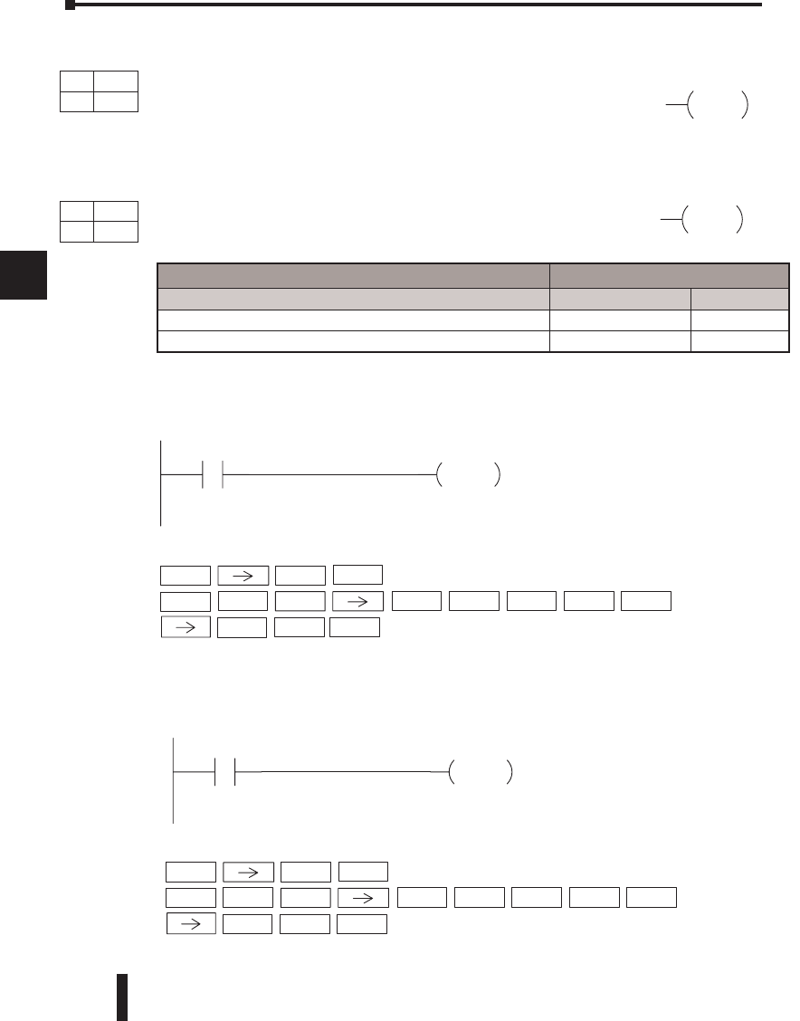
DL06 Micro PLC User Manual, 3rd Edition, Rev. D
5-24
1
2
3
4
5
6
7
8
9
10
11
12
13
14
A
B
C
D
In the following example. when X1 turns on, bit 1 in V1400 is set to the on state.
In the following example, when X2 turns on, bit 1 in V1400 is reset to the off state.
Chapter 5: Standard RLL Instructions - Boolean Instructions
1
2
3
4
5
6
7
8
9
10
11
12
13
14
a
B
c
d
Aaaa.bb
SET
A aaa.bb
RST
SET
X1 B1400.1
DirectSOFT32
STR 1
Handheld Programmer Keystrokes
SET V 1SHFT 4 0 0
1 ENT
K
B
ENT
RST
X2 B1400.1
DirectSOFT32
Handheld Programmer Keystrokes
STR 2
RST V 1SHFT 4 0 0
1 ENT
K
B
ENT
Operand Data Type DL06 Range
A aaa bb
V-memory B See memory map 0 to 15
Pointer PB See memory map 0 to 15
DS Used
HPP Used
DS Used
HPP Used
DirectSOFT
DirectSOFT
Set Bit-of-Word (SET)
The Set Bit-of-Word instruction sets or turns on a bit in a
V-memory location. Once the bit is set, it will remain on
until it is reset using the Reset Bit-of-Word instruction. It is
not necessary for the input controlling the Set Bit-of-Word
instruction to remain on.
Reset Bit-of-Word (RST)
The Reset Bit-of-Word instruction resets or turns off a bit in a
V-memory location. Once the bit is reset. it is not necessary for
the input to remain on.
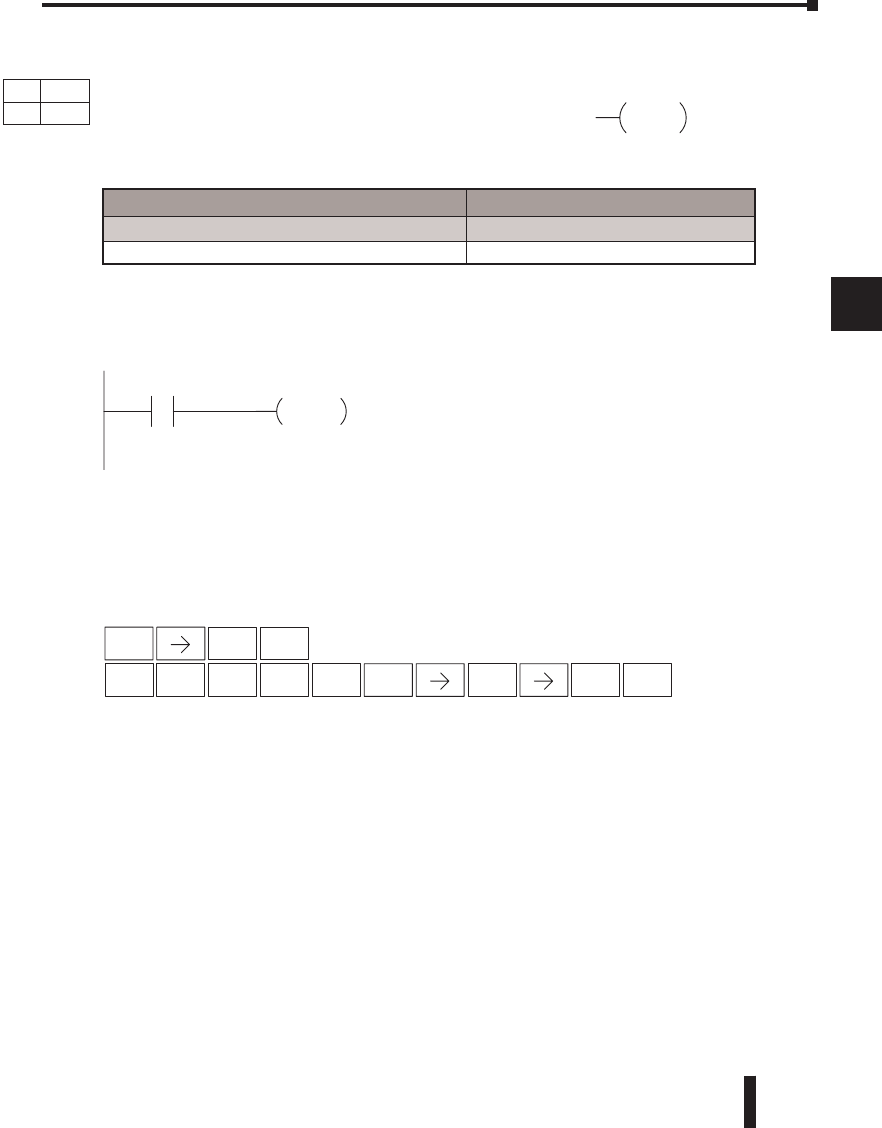
DL06 Micro PLC User Manual, 3rd Edition, Rev. D 5-25
1
2
3
4
5
6
7
8
9
10
11
12
13
14
A
B
C
D
In the following example, when X1 is ON, Y5–Y7 will be turned OFF. The execution of the
ladder program will not be affected.
Since the D2–HPP Handheld Programmer does not have a specific Pause key, you can use
the corresponding instruction number for entry (#960), or type each letter of the command.
In some cases, you may want certain output points in the specified pause range to operate
normally. In that case, use Aux 58 to over-ride the Pause instruction.
Chapter 5: Standard RLL Instructions - Boolean Instructions
DirectSOFT32
PAUSE
X1 Y5 Y7
STR
$
1
BENT
Handheld Programmer Keystrokes
5
FENT
INST#
O
9
J
6
G
0
AENT ENT 3
D
1
2
3
4
5
6
7
8
9
10
11
12
13
14
a
B
c
d
Operand Data Type DL06 Range
A aaa
Outputs Y 0–777
DS Used
HPP Used
DirectSOFT
Pause (PAUSE)
The Pause instruction disables the output update on a
range of outputs. The ladder program will continue to
run and update the image register. However, the outputs
in the range specified in the Pause instruction will be
turned off at the output points.
aaaaaaY
PAUSE
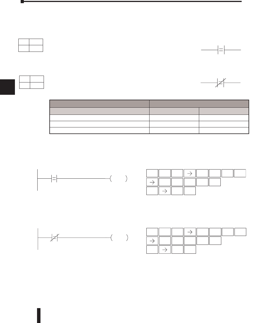
DL06 Micro PLC User Manual, 3rd Edition, Rev. D
5-26
1
2
3
4
5
6
7
8
9
10
11
12
13
14
A
B
C
D
Comparative Boolean
In the following example, when the BCD value in V-memory location V2000 = 4933, Y3
will energize.
In the following example, when the value in V-memory location V2000 /= 5060, Y3 will
energize.
Chapter 5: Standard RLL Instructions - Comparative Boolean
1
2
3
4
5
6
7
8
9
10
11
12
13
14
a
B
c
d
V aaa B bbb
V aaa B bbb
Operand Data Type DL06 Range
B aaa bbb
V-memory V See memory map See memory map
Pointer P See memory map See memory map
Constant K –– 0–9999
V2000 K4933 Y3
OUT
DirectSOFT32 Handheld Programmer Keystrokes
STR
$SHFT 4
E
2
C
0
A
0
A
0
A
4
E
9
J
3
D
3
DENT
OUT
GX ENT
3
D
Y3
OUT
V2000 K5060
DirectSOFT32 Handheld Programmer Keystrokes
SHFT
OUT
GX ENT
3
D
4
E
2
C
0
A
0
A
0
A
STRN
SP
5
F
0
AENT
6
G
0
A
DS Implied
HPP Used
DS Implied
HPP Used
DirectSOFT
DirectSOFT
Store If Equal (STRE)
The Store If Equal instruction begins a new rung or
additional branch in a rung with a normally open
comparative contact. The contact will be on when Vaaa
equals Bbbb .
Store If Not Equal (STRNE)
The Store If Not Equal instruction begins a new rung
or additional branch in a rung with a normally closed
comparative contact. The contact will be on when Vaaa
does not equal Bbbb.
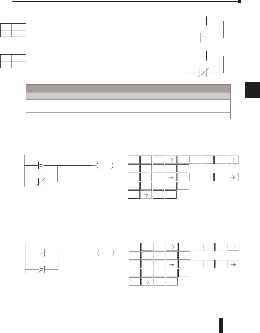
DL06 Micro PLC User Manual, 3rd Edition, Rev. D 5-27
1
2
3
4
5
6
7
8
9
10
11
12
13
14
A
B
C
D
In the following example, when the BCD value in V-memory location V2000 = 4500 or
V2002 /= 2500, Y3 will energize.
In the following example, when the BCD value in V-memory location V2000 = 3916 or
V2002 /= 2500, Y3 will energize.
Chapter 5: Standard RLL Instructions - Comparative Boolean
1
2
3
4
5
6
7
8
9
10
11
12
13
14
a
B
c
d
2
C
5
FENT
0
A
0
A
3
D
9
JENT
1
B
6
G
4
E
Y3
OUT
V2000 K3916
V2002 K2500
DirectSOFT32 Handheld Programmer Keystrokes
STR
$SHFT 2
C
0
A
0
A
0
A
ORN
RSHFT 4
E
2
C
0
A
0
A
2
C
OUT
GX ENT
3
D
2
C
3
D
4
E
5
FENT
4
E
5
FENT
0
A
0
A
Y3
OUT
V2002 K2500
V2000 K4500
DirectSOFT32 Handheld Programmer Keystrokes
SHFT 4
E
2
C
0
A
0
A
0
A
STR
$
OR
QSHFT 4
E
2
C
0
A
0
A
2
C
OUT
GX ENT
3
D
V aaa B bbb
V aaa B bbb
Operand Data Type DL06 Range
B aaa bbb
V-memory V See memory map See memory map
Pointer P See memory map See memory map
Constant K –– 0–9999
DS Implied
HPP Used
DS Implied
HPP Used
DirectSOFT
DirectSOFT
Or If Equal (ORE)
The Or If Equal instruction connects a normally
open comparative contact in parallel with another
contact. The contact will be on when Vaaa =
Bbbb.
Or If Not Equal (ORNE)
The Or If Not Equal instruction connects a
normally closed comparative contact in parallel
with another contact. The contact will be on
when Vaaa does not equal Bbbb.
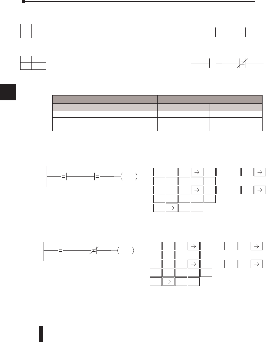
DL06 Micro PLC User Manual, 3rd Edition, Rev. D
5-28
1
2
3
4
5
6
7
8
9
10
11
12
13
14
A
B
C
D
In the following example, when the BCD value in V-memory location V2000 = 5000 and
V2002 = 2345, Y3 will energize.
In the following example, when the BCD value in V-memory location V2000 = 5000 and
V2002 /= 2345, Y3 will energize.
Chapter 5: Standard RLL Instructions - Comparative Boolean
1
2
3
4
5
6
7
8
9
10
11
12
13
14
a
B
c
d
V aaa B bbb
V aaa B bbb
2
C
3
D
4
E
5
FENT
5
F
0
AENT
0
A
0
A
2
C
STR
$SHFT 4
E
0
A
0
A
0
A
AND
VSHFT 4
E
2
C
0
A
0
A
2
C
OUT
GX ENT
3
D
Y3
OUT
V2002 K2345V2000 K5000
DirectSOFT32 Handheld Programmer Keystrokes
2
C
3
D
4
E
5
FENT
5
F
0
AENT
0
A
0
A
2
C
STR
$SHFT 4
E
0
A
0
A
0
A
AND
VSHFT 4
E
2
C
0
A
0
A
2
C
OUT
GX ENT
3
D
Y3
OUT
V2002 K2345V2000 K5000
DirectSOFT32 Handheld Programmer Keystrokes
Operand Data Type DL06 Range
B aaa bbb
V-memory V See memory map See memory map
Pointer P See memory map See memory map
Constant K –– 0–9999
DS Implied
HPP Used
DS Implied
HPP Used
DirectSOFT
DirectSOFT
And If Equal (ANDE)
The And If Equal instruction connects a
normally open comparative contact in series with
another contact. The contact will be on when
Vaaa = Bbbb.
And If Not Equal (ANDNE)
The And If Not Equal instruction connects a
normally closed comparative contact in series
with another contact. The contact will be on
when Vaaa does not equal Bbbb
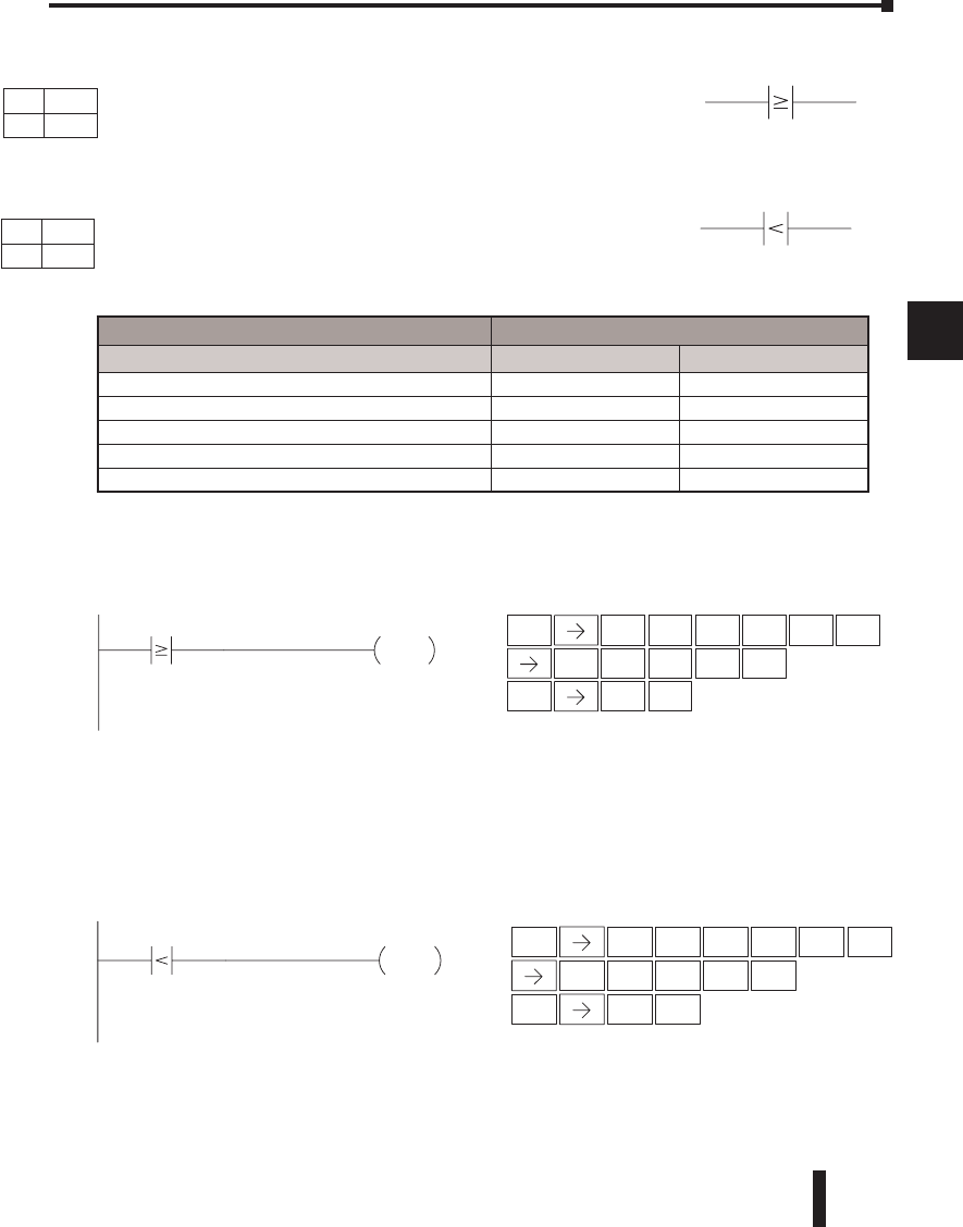
DL06 Micro PLC User Manual, 3rd Edition, Rev. D 5-29
1
2
3
4
5
6
7
8
9
10
11
12
13
14
A
B
C
D
In the following example, when the BCD value in V-memory location V2000 M 1000, Y3
will energize.
In the following example, when the value in V-memory location V2000 < 4050, Y3 will
energize.
Chapter 5: Standard RLL Instructions - Comparative Boolean
1
2
3
4
5
6
7
8
9
10
11
12
13
14
a
B
c
d
A aaa B bbb
A aaa B bbb
Operand Data Type DL06 Range
A/B aaa bbb
V-memory V See memory map See memory map
Pointer p See memory map See memory map
Constant K –– 0–9999
Timer TA 0–377
Counter CTA 0–177
ENT
3
D
Y3
OUT
V2000 K1000
DirectSOFT32 Handheld Programmer Keystrokes
STR
$
ENT
OUT
GX
SHFT AND
V
2
C
0
A
0
A
0
A
1
B
0
A
0
A
0
A
ENT
3
D
0
AENT
0
A
4
E
5
F
Y3
OUT
V2000 K4050
DirectSOFT32 Handheld Programmer Keystrokes
OUT
GX
STRN
SP SHFT AND
V
2
C
0
A
0
A
0
A
DS Implied
HPP Used
DS Implied
HPP Used
DirectSOFT
DirectSOFT
Store (STR)
The Comparative Store instruction begins a new rung or
additional branch in a rung with a normally open comparative
contact. The contact will be on when Aaaa is equal to or
greater than Bbbb.
Store Not (STRN)
The Comparative Store Not instruction begins a new rung
or additional branch in a rung with a normally closed
comparative contact. The contact will be on when Aaaa <
Bbbb
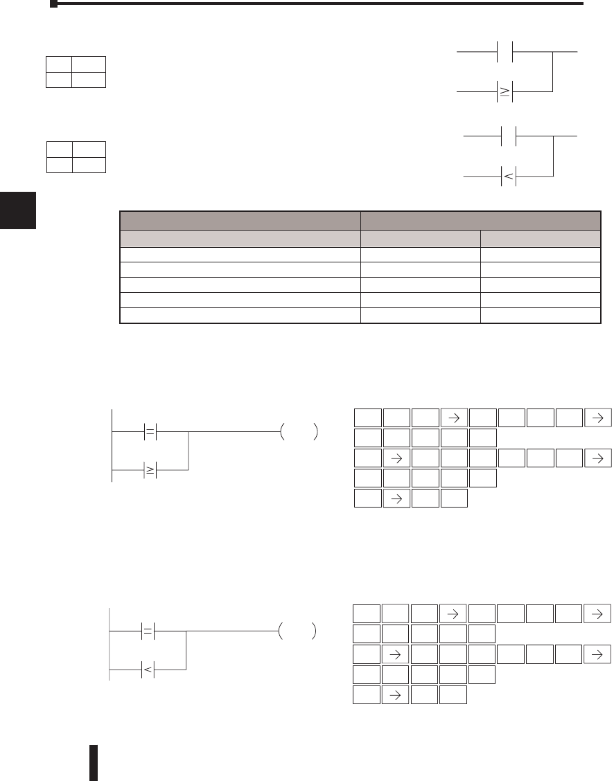
DL06 Micro PLC User Manual, 3rd Edition, Rev. D
5-30
1
2
3
4
5
6
7
8
9
10
11
12
13
14
A
B
C
D
In the following example, when the BCD value in V-memory location V2000 = 6045 or
V2002 M 2345, Y3 will energize.
In the following example when the BCD value in V-memory location V2000 = 1000 or
V2002 < 2500, Y3 will energize.
Chapter 5: Standard RLL Instructions - Comparative Boolean
1
2
3
4
5
6
7
8
9
10
11
12
13
14
a
B
c
d
A aaa B bbb
A aaa B bbb
2
C
3
D
4
E
5
FENT
6
G
0
A
Y3
OUT
V2000 K6045
V2002 K2345
DirectSOFT32 Handheld Programmer Keystrokes
SHFT 4
E
2
C
0
A
0
A
0
A
ENT
STR
$
OR
Q
OUT
GX ENT
3
D
4
E
5
F
SHFT AND
V
2
C
0
A
0
A
2
C
ENT
3
D
2
C
5
FENT
0
A
0
A
ENT
1
B
0
A
0
A
0
A
4
E
Y3
OUT
V2000 K1000
V2002 K2500
DirectSOFT32 Handheld Programmer Keystrokes
STR
$SHFT 2
C
0
A
0
A
0
A
ORN
R
OUT
GX
SHFT AND
V
2
C
0
A
0
A
2
C
Operand Data Type DL06 Range
A/B aaa bbb
V-memory V See memory map See memory map
Pointer p See memory map See memory map
Constant K –– 0–9999
Timer TA 0–377
Counter CTA 0–177
DS Implied
HPP Used
DS Implied
HPP Used
DirectSOFT
DirectSOFT
Or (OR)
The Comparative Or instruction connects a
normally open comparative contact in parallel
with another contact. The contact will be on
when Aaaa is equal to or greater than Bbbb.
Or Not (ORN)
The Comparative Or Not instruction connects a
normally closed comparative contact in parallel
with another contact. The contact will be on when
Aaaa < Bbbb.
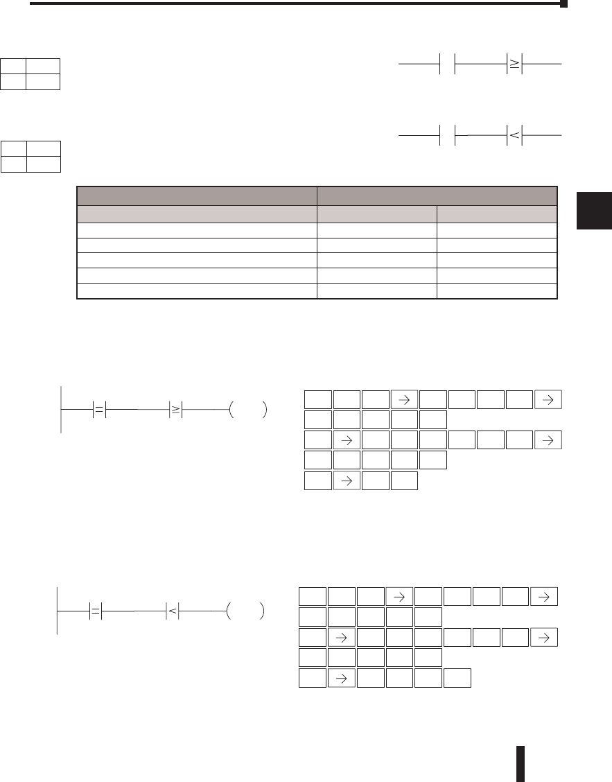
DL06 Micro PLC User Manual, 3rd Edition, Rev. D 5-31
1
2
3
4
5
6
7
8
9
10
11
12
13
14
A
B
C
D
In the following example, when the value in BCD V-memory location V2000 = 5000, and
V2002 M 2345, Y3 will energize.
In the following example, when the value in V-memory location V2000 = 7000 and
V2002 < 2500, Y3 will energize.
Chapter 5: Standard RLL Instructions - Comparative Boolean
1
2
3
4
5
6
7
8
9
10
11
12
13
14
a
B
c
d
A aaa B bbb
A aaa B bbb
ENT
3
D
2
C
3
D
4
E
5
FENT
ENT
0
A
0
A
5
F
0
A
2
C
Y3
OUT
V2000 K5000 V2002 K2345
DirectSOFT32 Handheld Programmer Keystrokes
STR
$SHFT 4
E
0
A
0
A
0
A
AND
V
OUT
GX
SHFT AND
V
2
C
0
A
0
A
2
C
2
C
5
FENT
0
A
0
A
7
HENT
0
A
0
A
0
A
2
C
Y3
OUT
V2000 K7000 V2002 K2500
DirectSOFT32 Handheld Programmer Keystrokes
STR
$SHFT 4
E
2
C
0
A
0
A
0
A
ANDN
W
OUT
GX SHFT AND
YENT
3
D
SHFT AND
V
2
C
0
A
0
A
Operand Data Type DL06 Range
A/B aaa bbb
V-memory V See memory map See memory map
Pointer p See memory map See memory map
Constant K –– 0–9999
Timer TA 0–377
Counter CTA 0–177
DS Implied
HPP Used
DS Implied
HPP Used
DirectSOFT
DirectSOFT
And (AND)
The Comparative And instruction connects a normally
open comparative contact in series with another contact.
The contact will be on when Aaaa is equal to or greater
than Bbbb.
And Not (ANDN)
The Comparative And Not instruction connects a
normally closed comparative contact in series with another
contact. The contact will be on when Aaaa < Bbbb.
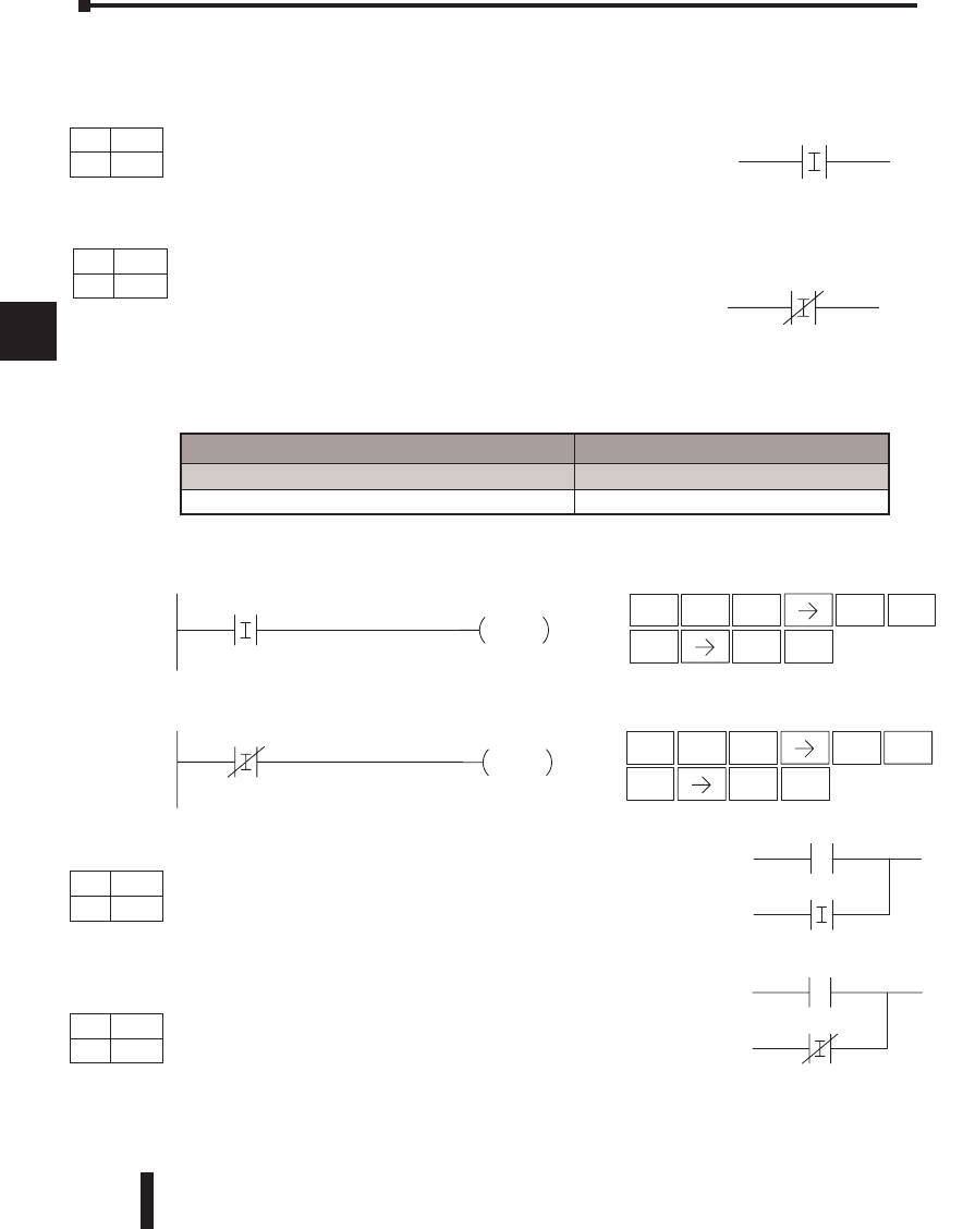
DL06 Micro PLC User Manual, 3rd Edition, Rev. D
5-32
1
2
3
4
5
6
7
8
9
10
11
12
13
14
A
B
C
D
Chapter 5: Standard RLL Instructions - Immediate Instructions
1
2
3
4
5
6
7
8
9
10
11
12
13
14
a
B
c
d
aaaX
aaaX
ENT
2
C
1
BENT
X1 Y2
OUT
Handheld Programmer KeystrokesDirectSOFT32
STR
$SHFT 8
I
OUT
GX
ENT
2
C
1
BENT
X1 Y2
OUT
Handheld Programmer Keystrokes
DirectSOFT32
STRN
SP SHFT 8
I
OUT
GX
aaaX
aaaX
Operand Data Type DL06 Range
aaa
Inputs X 0–777
DS Implied
HPP Used
DS Implied
HPP Used
DS Implied
HPP Used
DS Implied
HPP Used
DirectSOFT
DirectSOFT
In the following example, when X1 is on, Y2 will energize.
In the following example, when X1 is off, Y2 will energize.
Immediate Instructions
Store Immediate (STRI)
The Store Immediate instruction begins a new rung or
additional branch in a rung. The status of the contact will be
the same as the status of the associated input point at the time
the instruction is executed. The image register is not updated.
Store Not Immediate (STRNI)
The Store Not Immediate instruction begins a new rung or
additional branch in a rung. The status of the contact will be
opposite the status of the associated input point at the time the
instruction is executed. The image register is not update
Or Immediate (ORI)
The Or Immediate connects two contacts in parallel.
The status of the contact will be the same as the status
of the associated input point at the time the instruction is
executed. The image register is not updated.
Or Not Immediate (ORNI)
The Or Not Immediate connects two contacts in parallel.
The status of the contact will be opposite the status of
the associated input point at the time the instruction is
executed. The image register is not updated.
DL06 Micro PLC User Manual, 3rd Edition, Rev. D 5-33
1
2
3
4
5
6
7
8
9
10
11
12
13
14
A
B
C
D
Chapter 5: Standard RLL Instructions - Immediate Instructions
1
2
3
4
5
6
7
8
9
10
11
12
13
14
a
B
c
d
In the following example, when X1 or X2 is on, Y5 will energize.
In the following example, when X1 is on or X2 is off, Y5 will energize.
In the following example, when X1 and X2 are on, Y5 will energize.
In the following example, when X1 is on and X2 is off, Y5 will energize.
1
BENT
ENT
2
C
ENT
5
F
X1
X2
Y5
OUT
Handheld Programmer KeystrokesDirectSOFT32
STR
$
OR
QSHFT 8
I
OUT
GX
ENT
5
F
ENT
2
C
1
BENT
X1
X2
Y5
OUT
Handheld Programmer Keystrokes
DirectSOFT32
STR
$
SHFT 8
I
ORN
R
OUT
GX
aaaX
aaaX
OUT
GX
X1 X2 Y5
OUT
Handheld Programmer KeystrokesDirectSOFT32
STR
$
1
BENT
AND
VSHFT 8
IENT
2
C
ENT
5
F
X1 X2 Y5
OUT
Handheld Programmer KeystrokesDirectSOFT32
STR
$
ANDN
WSHFT 8
I
OUT
GX
1
BENT
ENT
2
C
ENT
5
F
Operand Data Type DL06 Range
aaa
Inputs X 0–777
Operand Data Type DL06 Range
aaa
Inputs X 0–777
DS Implied
HPP Used
DS Implied
HPP Used
DirectSOFT
DirectSOFT
DirectSOFT
DirectSOFT
And Immediate (ANDI)
The And Immediate instruction connects two contacts
in series. The status of the contact will be the same as
the status of the associated input point at the time the
instruction is executed. The image register is not updated.
And Not Immediate (ANDNI)
The And Not Immediate instruction connects two
contacts in series. The status of the contact will be
opposite the status of the associated input point at the
time the instruction is executed. The image register is not
updated.
DL06 Micro PLC User Manual, 3rd Edition, Rev. D
5-34
1
2
3
4
5
6
7
8
9
10
11
12
13
14
A
B
C
D
In the following example, when X1 is on, output point Y2 on the output module will turn
on. For instruction entry on the Handheld Programmer, you can use the instruction number
(#350) as shown, or type each letter of the command.
In the following example, when X1 or X4 is on, Y2 will energize.
Chapter 5: Standard RLL Instructions - Immediate Instructions
1
2
3
4
5
6
7
8
9
10
11
12
13
14
a
B
c
d
Y aaa
OUTI
OROUTI
Y aaa
1
BENT
X1 Y2
OUTI
DirectSOFT32 Handheld Programmer Keystrokes
STR
$
INST#
O
5
F
3
D
0
AENT ENT
2
CENT
STR
$
X1
X4
Y2
OR OUTI
Y2
OR OUTI
DirectSOFT32 Handheld Programmer Keystrokes
STR
$
1
BENT
ENT
4
E
INST#
O
5
F
3
D
0
AENT ENT
2
CENT
INST#
O
5
F
3
D
0
AENT ENT
2
CENT
Operand Data Type DL06 Range
aaa
Outputs Y 0–777
DS Used
HPP Used
DS Used
HPP Used
DirectSOFT
DirectSOFT
Out Immediate (OUTI)
The Out Immediate instruction reflects the status of the
rung (on/off) and outputs the discrete (on/off) status to the
specified module output point and the image register at the
time the instruction is executed. If multiple Out Immediate
instructions referencing the same discrete point are used, it
is possible for the module output status to change multiple
times in a CPU scan. See Or Out Immediate.
Or Out Immediate (OROUTI)
The Or Out Immediate instruction has been designed to use
more than 1 rung of discrete logic to control a single output.
Multiple Or Out Immediate instructions referencing the
same output coil may be used, since all contacts controlling
the output are ored together. If the status of any rung is on
at the time the instruction is executed, the output will also be
on.
DL06 Micro PLC User Manual, 3rd Edition, Rev. D 5-35
1
2
3
4
5
6
7
8
9
10
11
12
13
14
A
B
C
D
In the following example, when C0 is on,the binary pattern for X10 –X17 is loaded into the
accumulator using the Load Immediate Formatted instruction. The binary pattern in the
accumulator is written to Y30–Y37 using the Out Immediate Formatted instruction. This
technique is useful to quickly copy an input pattern to outputs (without waiting for the CPU
scan).
Chapter 5: Standard RLL Instructions - Immediate Instructions
1
2
3
4
5
6
7
8
9
10
11
12
13
14
a
B
c
d
bbbK
Yaaa
OUTIF
LDIF X10
K8
K8X10
00000000101101010000000000000000
15 14 13 12 11 10 98765 4321031 30 29 28 27 26 25 24 23 22 21 20 19 18 17 1631 30 29 28 27 26 25 24 23 22 21 20 19 18 17 16
K8Y30
X10
X11X12X13X14X15X16X17
ONOFFONOFFONONOFFON
Y30Y31Y32Y33Y34Y35Y36Y37
ONOFFONOFFONONOFFON
K8
Load the value of 8
consecutive locations into the
accumulator, starting with X10.
OUTIF Y30
Copy the value in the lower
8 bits of the accumulator to
Y30-Y37
Unused accumulator bits
are set to zero
Location Constant
Acc.
Location Constant
C0
DirectSOFT 5
OUT
GX
Handheld Programmer Keystrokes
STR
$
0
AENT
5
F
3
D
0
A
3
D
ANDST
L
8
IENT
ENT
NEXT NEXT NEXT NEXT
SHFT 5
F
1
B
0
A
8
I
SHFT 8
I
8
I
Operand Data Type DL06 Range
aaa
Outputs Y 0-777
Constant K 1-32
DS Used
HPP Used
DirectSOFT
Out Immediate Formatted (OUTIF)
The Out Immediate Formatted instruction outputs a 1–32
bit binary value from the accumulator to specified output
points at the time the instruction is executed. Accumulator
bits that are not used by the instruction are set to zero.
DL06 Micro PLC User Manual, 3rd Edition, Rev. D
5-36
1
2
3
4
5
6
7
8
9
10
11
12
13
14
A
B
C
D
In the following example, when X1 is on, Y2 through Y5 will be set on in the image register
and on the corresponding output points.
In the following example, when X1 is on, Y5 through Y22 will be reset (off) in the image
register and on the corresponding output module(s).
Chapter 5: Standard RLL Instructions - Immediate Instructions
1
2
3
4
5
6
7
8
9
10
11
12
13
14
a
B
c
d
aaaY aaa
SETI
aaaY aaa
RSTI
1
BENT
X1 Y2
SETI
Y5
DirectSOFT32 Handheld Programmer Keystrokes
STR
$
SET
XSHFT 8
IENT
2
C
5
F
1
BENT
X1 Y5
RSTI
Y22
DirectSOFT32
Handheld Programmer Keystrokes
STR
$
SHFT 8
I
5
F
2
C
2
CENT
RST
S
Operand Data Type DL06 Range
aaa
Ouputs Y 0–777
DS Used
HPP Used
DS Used
HPP Used
DirectSOFT
DirectSOFT
Set Immediate (SETI)
The Set Immediate instruction immediately sets, or
turns on an output or a range of outputs in the image
register and the corresponding output point(s) at the
time the instruction is executed. Once the outputs are
set, it is not necessary for the input to remain on. The
Reset Immediate instruction can be used to reset the
outputs.
Reset Immediate (RSTI)
The Reset Immediate instruction immediately resets,
or turns off, an output or a range of outputs in the
image register and the output point(s) at the time the
instruction is executed. Once the outputs are reset, it is
not necessary for the input to remain on.
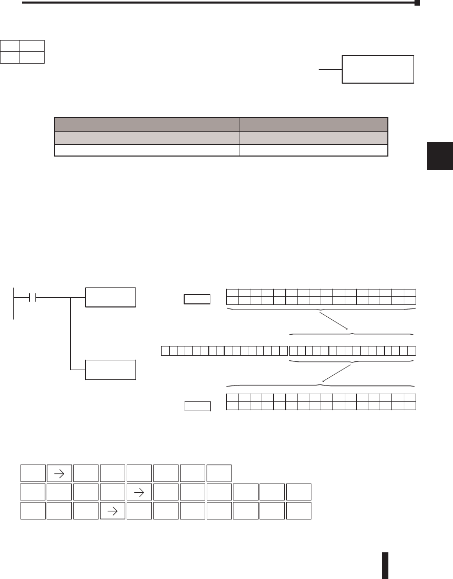
DL06 Micro PLC User Manual, 3rd Edition, Rev. D 5-37
1
2
3
4
5
6
7
8
9
10
11
12
13
14
A
B
C
D
In the following example, when C0 is on, the binary pattern of X0–X17 will be loaded into
the accumulator using the Load Immediate instruction. The Out Immediate instruction
could be used to copy the 16 bits in the accumulator to output points, such as Y40–Y57.
This technique is useful to quickly copy an input pattern to output points (without waiting
for a full CPU scan to occur).
Chapter 5: Standard RLL Instructions - Immediate Instructions
1
2
3
4
5
6
7
8
9
10
11
12
13
14
a
B
c
d
Vaaa
LDI
C0
OUTI
V40400
10110100101101010000000000000000
15 14 13 12 11 10 98765 43210
31 30 29 28 27 26 25 24 23 22 21 20 19 18 17 1631 30 29 28 27 26 25 24 23 22 21 20 19 18 17 16
Acc.
V40502
X10
X11X12X13X14X15X16X17
OFFOFFONOFFONONOFFON
Y50Y51Y52Y53Y54Y55Y56Y57
OFFOFFONOFFONONOFFON
DirectSOFT32
X0X1X2X3X4X5X6X7
ONOFFONOFFONONOFFON
Y40Y41Y42Y43Y44Y45Y46Y47
ONOFFONOFFONONOFFON
LDI
V40400
V40502
Load the inputs from X0 to
X17 into the accumulator,
immediately
Output the value in the
accumulator to output points
Y40 to Y57
Location
Unused accumulator bits
are set to zero
Location
OUT
GX
Handheld Programmer Keystrokes
STR
$
0
AENT
3
D
ANDST
L
8
IENT
ENT
NEXT NEXT NEXT NEXT
SHFT 4
E
0
A
SHFT 8
I
4
E
0
A
0
A
NEXT 4
E
0
A
5
F
0
A
2
C
Operand Data Type DL06 Range
aaa
Inputs V 40400-40437
DS Used
HPP Used
DirectSOFT
Load Immediate (LDI)
The Load Immediate instruction loads a 16-bit V-memory value
into the accumulator. The valid address range includes all input
point addresses on the local base. The value reflects the current
status of the input points at the time the instruction is executed. This
instruction may be used instead of the LDIF instruction, which
requires you to specify the number of input points.
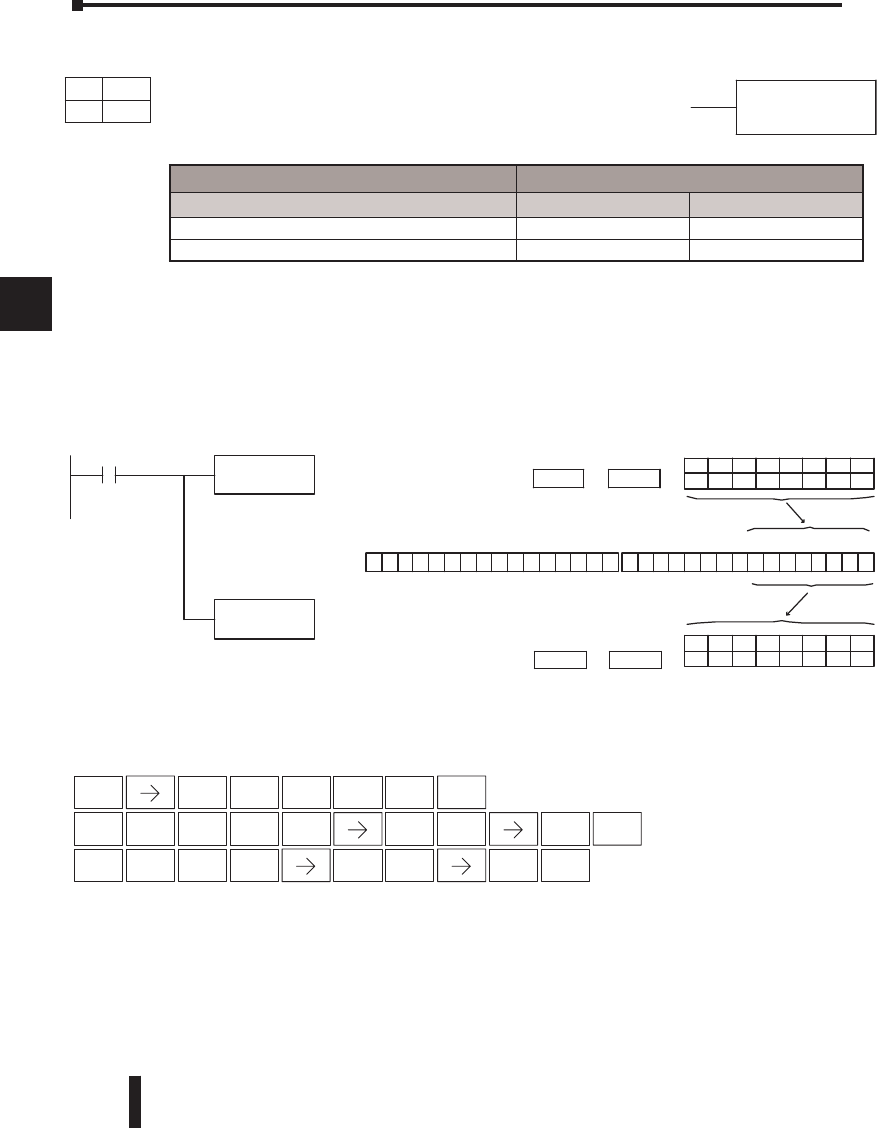
DL06 Micro PLC User Manual, 3rd Edition, Rev. D
5-38
1
2
3
4
5
6
7
8
9
10
11
12
13
14
A
B
C
D
Load Immediate Formatted (LDIF)
The Load Immediate Formatted instruction loads a 1–32 bit
binary value into the accumulator. The value reflects the current
status of the input module(s) at the time the instruction is executed.
Accumulator bits that are not used by the instruction are set to zero.
In the following example, when C0 is on, the binary pattern of X10–X17 will be loaded
into the accumulator using the Load Immediate Formatted instruction. The Out Immediate
Formatted instruction could be used to copy the specified number of bits in the accumulator
to the specified outputs on the output module, such as Y30–Y37. This technique is useful to
quickly copy an input pattern to outputs (without waiting for the CPU scan).
Chapter 5: Standard RLL Instructions - Immediate Instructions
1
2
3
4
5
6
7
8
9
10
11
12
13
14
a
B
c
d
Kbbb
XaaaLDIF
LDIF X10
K8
C0
Load thevalue of 8
consecutivelocationintothe
accumulatorstartingwith
X10
OUTIFY30
K8
Copy thevalue of thelower
8bitsofthe accumulatorto
Y30--Y37
K8
X10
LocationConstant
00000000101101
01
0000000000000000
15 14 13 12 11 10 98765 4321031 30 29 28 27 26 25 24 23 22 21 20 19 18 17 1631 30 29 28 27 26 25 24 23 22 21 20 19 18 17 16
Acc.
K8Y30
LocationConstant
X10
X11X12X13X14X15X16X17
ONOFFONOFFONONOFFON
Y30Y31Y32Y33Y34Y35Y36Y37
ONOFFONOFFONONOFFON
DirectSOFT32
Unused accumulatorbits
areset to zero
Operand Data Type DL06 Range
aaa bbb
Inputs X 0-777 - -
Constant K - - 1-32
OUT
GX
Handheld Programmer Keystrokes
STR
$
0
AENT
5
F
3
D
0
A
3
D
ANDST
L
8
IENT
ENT
NEXT NEXT NEXT NEXT
SHFT 5
F
1
B
0
A
8
I
SHFT 8
I
8
I
DS Used
HPP Used
DirectSOFT
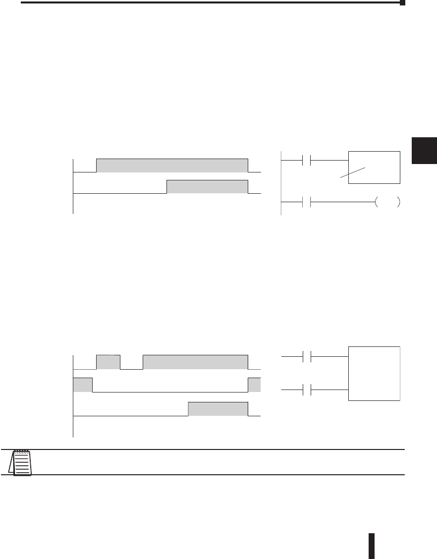
DL06 Micro PLC User Manual, 3rd Edition, Rev. D 5-39
1
2
3
4
5
6
7
8
9
10
11
12
13
14
A
B
C
D
Timer, Counter and Shift Register Instructions
Using Timers
Timers are used to time an event for a desired period. The single input timer will time as long
as the input is on. When the input changes from on to off, the timer current value is reset to
0. There is a tenth of a second and a hundredth of a second timer available with a maximum
time of 999.9 and 99.99 seconds respectively. There is a discrete bit associated with each
timer to indicate that the current value is equal to or greater than the preset value. The timing
diagram below shows the relationship between the timer input, associated discrete bit, current
value and timer preset.
There are those applications that need an accumulating timer, meaning it has the ability
to time, stop, and then resume from where it previously stopped. The accumulating timer
works similarly to the regular timer, but two inputs are required. The enable input starts and
stops the timer. When the timer stops, the elapsed time is maintained. When the timer starts
again, the timing continues from the elapsed time. When the reset input is turned on, the
elapsed time is cleared and the timer will start at 0 when it is restarted. There is a tenth of a
second and a hundredth of a second timer available with a maximum time of 9999999.9 and
999999.99 seconds respectively. The timing diagram below shows the relationship between
the timer input, timer reset, associated discrete bit, current value and timer preset.
NOTE: Decimal points are not used in these timers, but the decimal point is implied. The preset and
current value for all four timers is in BCD format.
Chapter 5: Standard RLL Instructions - Timer, Counter and Shift Register Instructions
X1
X1
T0
123456 780
01010203040500
Current
Value
TMRA T0
K30
X2
X2
Reset Input
Enable
Seconds
1/10 Seconds
TMR T1
K30
X1
X1
T1
123456 780
01020304050600
Current
Value
T1 Y0
OUT
Seconds
1/10 Seconds
Timer Preset
1
2
3
4
5
6
7
8
9
10
11
12
13
14
a
B
c
d
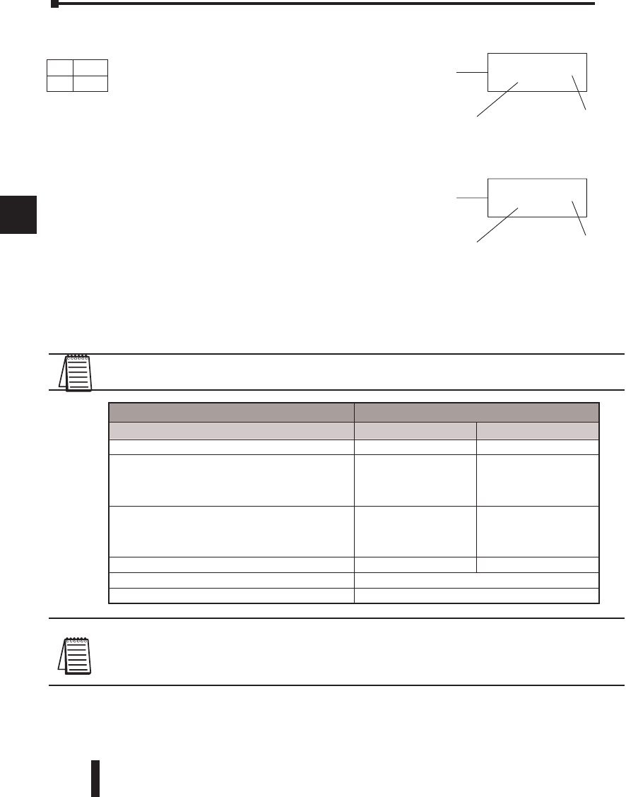
DL06 Micro PLC User Manual, 3rd Edition, Rev. D
5-40
1
2
3
4
5
6
7
8
9
10
11
12
13
14
A
B
C
D
Timer (TMR) and Timer Fast (TMRF)
The Timer instruction is a 0.1 second single input timer that times to a maximum of 999.9
seconds. The Timer Fast instruction is a 0.01 second single
input timer that times up to a maximum of 99.99 seconds.
These timers will be enabled if the input logic is true (on) and
will be reset to 0 if the input logic is false (off). Both timers
use single word BCD values for the preset and current value.
The decimal place is implied.
Instruction Specifications
Timer Reference (Taaa): Specifies the timer number.
Preset Value (Bbbb): Constant value (K) or a V-memory
location specified in BCD.
Current Value: Timer current values, in BCD format,
are accessed by referencing the associated V or T memory
location*. For example, the timer current value for T3
physically resides in V-memory location V3.
Discrete Status Bit: The discrete status bit is referenced by the associated T memory location.
Operating as a “timer done bit”, it will be on if the current value is equal to or greater than
the preset value. For example, the discrete status bit for Timer 2 is T2.
NOTE: A V-memory preset is required only if the ladder program or an Operator Interface unit must
change the preset.
NOTE: *May be non-volatile if MOV instruction is used.
** With the HPP, both the Timer discrete status bits and current value are accessed with the same
data reference. DirectSOFT uses separate references, such as “T2” for discrete status bit for Timer
T2, and “TA2” for the current value of Timer T2.
You can perform functions when the timer reaches the specified preset using the discrete
status bit. Or, use comparative contacts to perform functions at different time intervals, based
on one timer. The examples on the following page show these two methods of programming
timers.
Chapter 5: Standard RLL Instructions - Timer, Counter and Shift Register Instructions
1
2
3
4
5
6
7
8
9
10
11
12
13
14
a
B
c
d
T aaa
aaa
T
TMR
B bbb
Preset
Timer #
TMRF
B bbb
Preset Timer #
Operand Data Type DL06 Range
A/B aaa bbb
Timers T 0–777 ––
V-memory for preset values V ––
400-677
1200–7377
7400–7577
10000-17777
Pointers (preset only) P ––
400-677
1200–7377
7400–7577*
10000-17777
Constants (preset only) K –– 0–9999
Timer discrete status bits T/V 0–377 or V41100–41117
Timer current values V /T** 0–377
DS Used
HPP Used
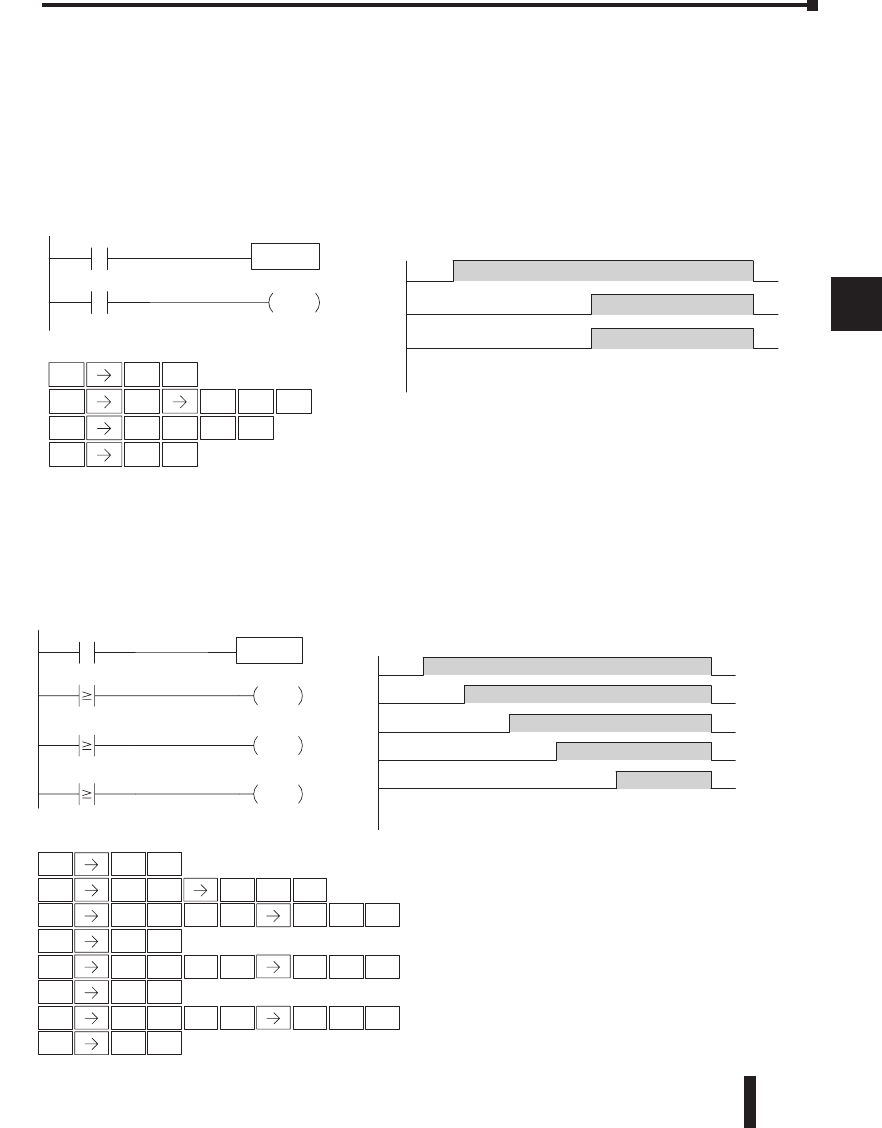
DL06 Micro PLC User Manual, 3rd Edition, Rev. D 5-41
1
2
3
4
5
6
7
8
9
10
11
12
13
14
A
B
C
D
Timer Example Using Discrete Status Bits
In the following example, a single input timer is used with a preset of 3 seconds. The timer
discrete status bit (T2) will turn on when the timer has timed for 3 seconds. The timer is reset
when X1 turns off, turning the discrete status bit off and resetting the timer current value to
0.
Timer Example Using Comparative Contacts
In the following example, a single input timer is used with a preset of 4.5 seconds.
Comparative contacts are used to energize Y3, Y4, and Y5 at one second intervals respectively.
When X1 is turned off, the timer will be reset to 0 and the comparative contacts will turn off
Y3, Y4, and Y5.
Chapter 5: Standard RLL Instructions - Timer, Counter and Shift Register Instructions
1
2
3
4
5
6
7
8
9
10
11
12
13
14
a
B
c
d
STR
$
TMR
N
2
C
STR
$SHFT MLR
T
2
CENT
OUT
GX
Handheld Programmer Keystrokes
X1 TMR T2
K30
T2 Y0
OUT
X1
T2
123456
78
0
01020304050600
Current
Value
Y0
Timing Diagram
Direct SOFT32
Seconds
1
BENT
3
D
0
AENT
ENT
0
A
1
BENT
Handheld Programmer Keystrokes
X1 TMR T20
K45
TA20 K10
TA20 K20
TA20 K30
Y4
OUT
Y3
OUT
Y5
OUT
X1
Y3
123456 78
0
01020304050600
Current
Value
Y4
Timing Diagram
Y5
T2
Direct SOFT32
Seconds
STR
$
TMR
N
2
CENT
0
A
4
E
5
F
STR
$SHFT MLR
T
2
C
0
A
1
BENT
OUT
GX ENT
3
D
STR
$SHFT MLR
T
2
C
0
AENT
OUT
GX ENT
2
C
4
E
STR
$SHFT MLR
T
2
C
0
AENT
OUT
GX ENT
3
D
5
F
0
A
0
A
0
A
1/10th Seconds
1/10th Seconds
DirectSOFT
DirectSOFT
DL06 Micro PLC User Manual, 3rd Edition, Rev. D
5-42
1
2
3
4
5
6
7
8
9
10
11
12
13
14
A
B
C
D
Accumulating Timer (TMRA)
The Accumulating Timer is a 0.1 second two input timer that
will time to a maximum of 9999999.9. The TMRA uses two timer
registers in V-memory.
Accumulating Fast Timer (TMRAF)
The Accumulating Fast Timer is a 0.01 second two-input timer that
will time to a maximum of 99999.99. The TMRA uses two timer
registers in V-memory.
Each timer uses two timer registers in V-memory. The preset and
current values are in double word BCD format, and the decimal
point is implied. These timers have two inputs, an enable and a
reset. The timer starts timing when the enable is on and stops when
the enable is off (without resetting the count). The reset will reset
the timer when on and allow the timer to time when off.
Timer Reference (Taaa): Specifies the timer number.
Preset Value (Bbbb): Constant value (K) or V-memory.
Current Value: Timer current values are accessed by referencing the associated V or T
memory location*. For example, the timer current value for T3 resides in V-memory, V3.
Discrete Status Bit: The discrete status bit is accessed by referencing the associated T
memory location. Operating as a “timer done bit,” it will be on if the current value is equal to
or greater than the preset value. For example, the discrete status bit for timer 2 would be T2.
NOTE: The accumulating timer uses two consecutive V-memory locations for the 8-digit value,
therefore two consecutive timer locations. For example, if TMRA T1 is used, the next available timer
number is T3.
NOTE: *May be non-volatile if MOV instruction is used.
** With the HPP, both the Timer discrete status bits and current value are accessed with the same
data reference. DirectSOFT uses separate references, such as “T2” for discrete status bit for Timer
T2, and “TA2” for the current value of Timer T2.
Chapter 5: Standard RLL Instructions - Timer, Counter and Shift Register Instructions
1
2
3
4
5
6
7
8
9
10
11
12
13
14
a
B
c
d
T aaa
T aaa
TMRA
B bbb
Enable
Reset
Preset Timer #
TMRAF
B bbb
Enable
Reset
Preset Timer #
Operand Data Type DL06 Range
A/B aaa bbb
Timers T 0–777 ––
V-memory for preset values V ––
400-677
1200–7377
7400–7577
10000-17777
Pointers (preset only) P ––
400-677
1200–7377
7400–7577*
10000-17777
Constants (preset only) K –– 0–99999999
Timer discrete status bits T/V 0–377 or V41100–41117
Timer current values V /T** 0–377
DS Used
HPP Used
DS Used
HPP Used
NOTE: A V-Memory preset is required if the ladder program or an OIP must be used to change the
preset.
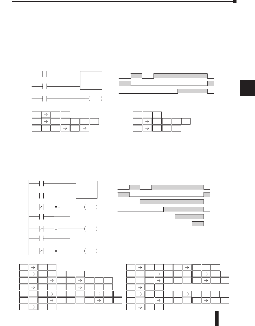
DL06 Micro PLC User Manual, 3rd Edition, Rev. D 5-43
1
2
3
4
5
6
7
8
9
10
11
12
13
14
A
B
C
D
Accumulating Timer Example using Discrete Status Bits
In the following example, a two input timer (accumulating timer) is used with a preset of
3 seconds. The timer discrete status bit (T6) will turn on when the timer has timed for 3
seconds. Notice, in this example, that the timer times for 1 second, stops for one second, then
resumes timing. The timer will reset when C10 turns on, turning the discrete status bit off
and resetting the timer current value to 0.
Accumulator Timer Example Using Comparative Contacts
In the following example, a single input timer is used with a preset of 4.5 seconds.
Comparative contacts are used to energized Y3, Y4, and Y5 at one second intervals
respectively. The comparative contacts will turn off when the timer is reset.
Chapter 5: Standard RLL Instructions - Timer, Counter and Shift Register Instructions
1
2
3
4
5
6
7
8
9
10
11
12
13
14
a
B
c
d
Handheld Programmer Keystrokes
X1
T6
TMRA T6
K30
C10
Y7
OUT
X1
C10
123456 78
0
01010203040500
Current
Value
T6
Timing Diagram
Direct SOFT32
Seconds
Handheld Programmer Keystrokes (cont)
STR
$
STR
$SHFT ENT
2
C
1
B
0
A
TMR
NSHFT 0
A
3
D
0
AENT
STR
$SHFT MLR
TENT
OUT
GX ENT
0
A
6
G
1
B
1
BENT
6
G
Handheld Programmer Keystrokes
TA20 K10
TA21 K1
TA20 K20
Y3
OUT
Y4
OUT
X1
TMRA T20
K45
C10
X1
C10
123456 780
01010203040500
Current
Value
Timing Diagram
Y3
Y4
Y5
T20
DirectSOFT
Handheld Programmer Keystrokes (cont’d)
Seconds
AND
VSHFT
4
E
MLR
T
OUT
GX ENT
1
B
4
E
STR
$SHFT MLR
T
2
C
0
A
OUT
GX ENT
5
F
STR
$
1
BENT
ENT
4
E
5
F
STR
$SHFT MLR
T
2
C
0
A
1
BENT
OUT
GX ENT
3
D
STR
$SHFT ENT
2
C
1
B
0
A
2
C
0
A
TMR
NSHFT 0
A
0
A
0
A
Contacts
TA21 K1
TA20 K30 Y5
OUT
TA21 K0
TA21 K0
TA21 K1
OR
QSHFT
4
E
MLR
T
1
B
1
B
ENT
ENT
SHFT
SHFT
2
C
2
C
STR
$SHFT MLR
T
2
C
0
A
AND
VSHFT
4
E
MLR
T
1
B
0
A
OR
QSHFT
4
E
MLR
T
1
B
1
B
ENT
ENT
SHFT
SHFT
2
C
2
C
ENT
2
C
0
A
ENT
3
D
0
A
AND
VSHFT
4
E
MLR
T
1
B
1
BENTSHFT 2
C
1/10 Seconds
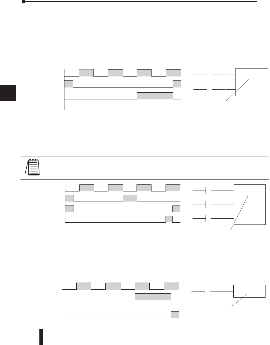
DL06 Micro PLC User Manual, 3rd Edition, Rev. D
5-44
1
2
3
4
5
6
7
8
9
10
11
12
13
14
A
B
C
D
Using Counters
Counters are used to count events . The counters available are up counters, up/down
counters, and stage counters (used with RLLPLUS programming).
The up counter (CNT) has two inputs, a count input and a reset input. The maximum count
value is 9999. The timing diagram below shows the relationship between the counter input,
counter reset, associated discrete bit, current value, and counter preset. The CNT counter
preset and current value are bothe single word BCD values.
The up down counter (UDC) has three inputs, a count up input, count down input and
reset input. The maximum count value is 99999999. The timing diagram below shows the
relationship between the counter up and down inputs, counter reset, associated discrete
bit, current value, and counter preset. The UDC counter preset and current value are both
double word BCD values.
NOTE: The UDC uses two consecutive V-memory locations for the 8-digit value, therefore, two
consecutive timer locations. For example, if UDC CT1 is used, the next available counter number is
CT3.
The stage counter (SGCNT) has a count input and is reset by the RST instruction. This
instruction is useful when programming using the RLLPLUS structured programming. The
maximum count value is 9999. The timing diagram below shows the relationship between
the counter input, associated discrete bit, current value, counter preset and reset instruction.
Chapter 5: Standard RLL Instructions - Timer, Counter and Shift Register Instructions
1
2
3
4
5
6
7
8
9
10
11
12
13
14
a
B
c
d
X1
X1
CT1
12340
Current
alue
CNT CT1
K3
X2
X2
Counter preset
Up
Reset
Counts
X1
X1
CT2
12340
Current
Value
SGCNT CT2
K3
RST
CT2
Counts Counter preset
X1
X1
CT2
1212 30
Current
Value
X2
X2
UDC CT2
K3
X3
X3
Counter Preset
Up
Down
Reset
Counts
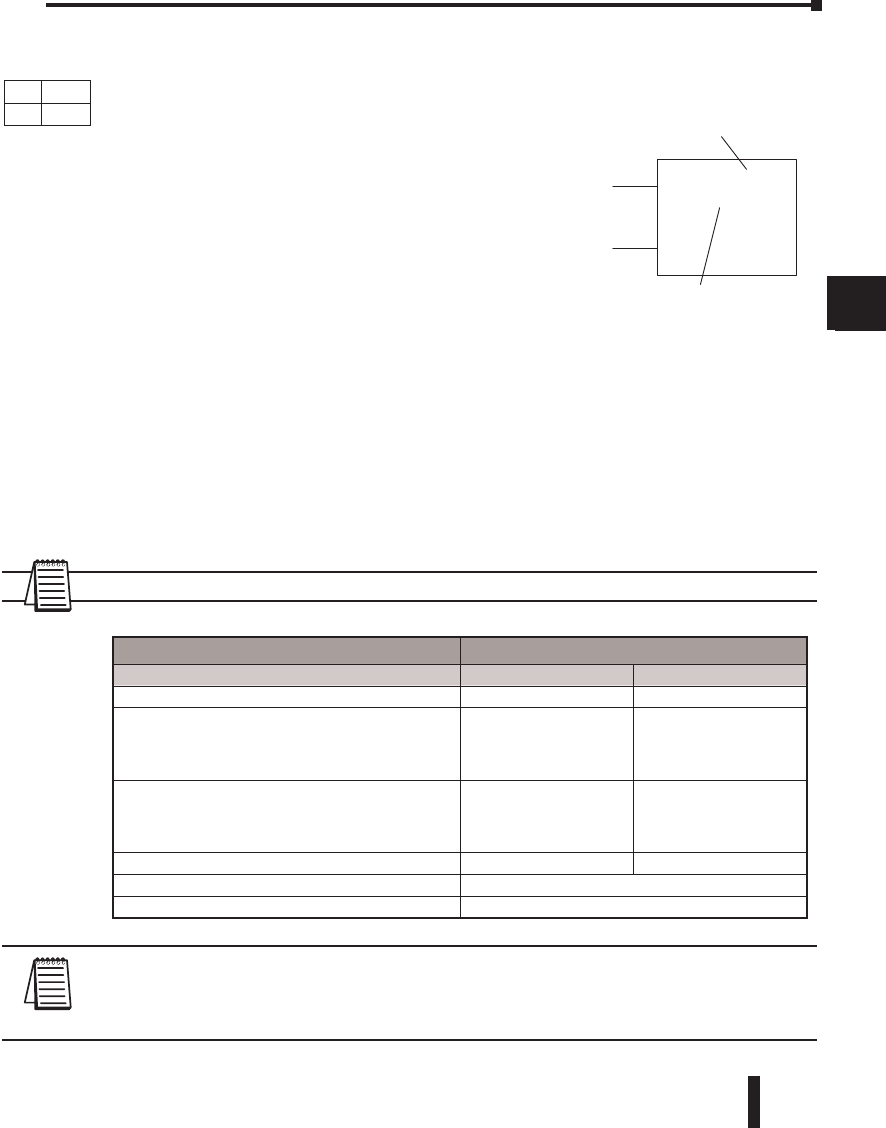
DL06 Micro PLC User Manual, 3rd Edition, Rev. D 5-45
1
2
3
4
5
6
7
8
9
10
11
12
13
14
A
B
C
D
Discrete Status Bit: The discrete status bit is accessed by referencing the associated CT
memory location. It will be On if the value is equal to or greater than the preset value. For
example the discrete status bit for counter 2 would be CT2.
NOTE: A V-memory preset is required if the ladder program or OIP must change the preset.
NOTE: *May be non-volatile if MOV instruction is used.
** With the HPP, both the Counter discrete status bits and current value are accessed with the
same data reference. DirectSOFT uses separate references, such as “CT2” for discrete status bit for
Counter CT2, and “CTA2” for the current value of Counter CT2.
Chapter 5: Standard RLL Instructions - Timer, Counter and Shift Register Instructions
1
2
3
4
5
6
7
8
9
10
11
14
a
B
c
d
CT aaa
CNT
B bbb
Count
Reset
Counter #
Preset
Operand Data Type DL06 Range
A/B aaa bbb
Counters CT 0–177 ––
V-memory (preset only) V ––
400-677
1200–7377
7400–7577
10000-17777
Pointers (preset only) P ––
400-677
1200–7377
7400–7577*
10000-17777
Constants (preset only) K –– 0–9999
Counter discrete status bits CT/V 0–177 or V41140–41147
Counter current values V /CT** 1000-1177
DS Used
HPP Used
Counter (CNT)
The Counter is a two-input counter that increments when the
count input logic transitions from Off to On. When the counter
reset input is On, the counter resets to 0. When the current value
equals the preset value, the counter status bit comes On and the
counter continues to count up to a maximum count of 9999. The
maximum value will be held until the counter is reset.
Instruction Specifications
Counter Reference (CTaaa): Specifies the counter number.
Preset Value (Bbbb): Constant value (K) or a V-memory location.
Current Values: Counter current values are accessed by
referencing the associated V or CT memory locations.* The
V-memory location is the counter location + 1000. For example,
the counter current value for CT3 resides in V-memory location
V1003.
DL06 Micro PLC User Manual, 3rd Edition, Rev. D
5-46
1
2
3
4
5
6
7
8
9
10
11
12
13
14
A
B
C
D
Counter Example Using Discrete Status Bits
In the following example, when X1 makes an Off-to-On transition, counter CT2 will
increment by one. When the current value reaches the preset value of 3, the counter status bit
CT2 will turn on and energize Y7. When the reset C10 turns on, the counter status bit will
turn off and the current value will be 0. The current value for counter CT2 will be held in
V-memory location V1002.
Counter Example Using Comparative Contacts
In the following example, when X1 makes an Off-to-On transition, counter CT2 will
increment by one. Comparative contacts are used to energize Y3, Y4, and Y5 at different
counts. When the reset C10 turns on, the counter status bit will turn off and the counter
current value will be 0, and the comparative contacts will turn off.
Chapter 5: Standard RLL Instructions - Timer, Counter and Shift Register Instructions
1
2
3
4
5
6
7
8
9
10
11
12
13
14
a
B
c
d
2
C
Handheld Programmer Keystrokes
CT2
X1
CNT CT2
K3
C10
Y7
OUT
X1
CT2 or
Y7
12
34
0
Current Value
C10
Counting diagram
DirectSOFT32
STR
$
1
BENT
3
DENT
STR
$SHFT ENT
2
C
1
B
0
A
CNT
GY
STR
$SHFT ENT
OUT
GX ENT
0
A
1
B
2
C
MLR
T
2
C
Handheld Programmer Keystrokes (cont)
SHFT
Handheld Programmer Keystrokes
X1
CNT CT2
K3
C10
X1
Y3
12 340
Current
Value
C10
Counting diagram
CTA2 K1
CTA2 K2
CTA2 K3
Y4
OUT
Y3
OUT
Y5
OUT
Y4
Y5
DirectSOFT32
Handheld Programmer Keystrokes (cont)
STR
$SHFT
ENT
OUT
GX ENT
2
C
4
E
STR
$SHFT 2
C
ENT
OUT
GX ENT
3
D
5
F
STR
$
1
BENT
2
C
STR
$SHFT
1
BENT
OUT
GX ENT
3
D
STR
$SHFT ENT
2
C
1
B
0
A
CNT
GY ENT
3
D
MLR
T
2
C
2
C
MLR
T
2
C
2
C
MLR
T
2
C
SHFT
SHFT
SHFT
DirectSOFT
DirectSOFT
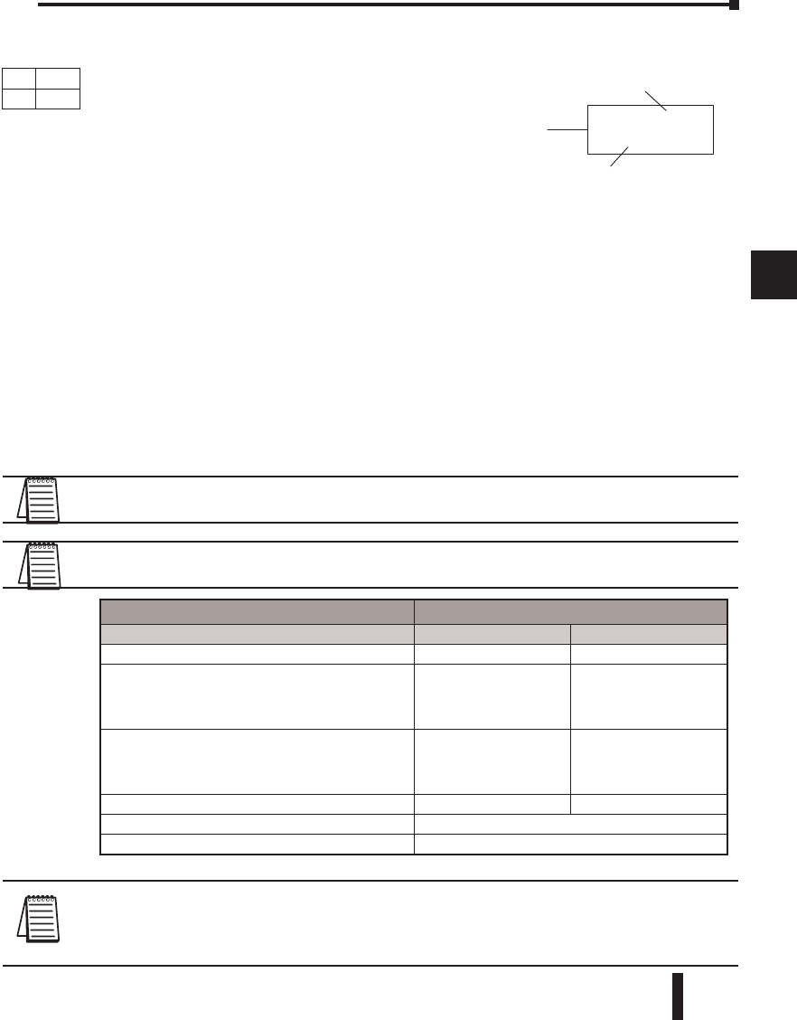
DL06 Micro PLC User Manual, 3rd Edition, Rev. D 5-47
1
2
3
4
5
6
7
8
9
10
11
12
13
14
A
B
C
D
Instruction Specifications
Counter Reference (CTaaa): Specifies the counter number.
Preset Value (Bbbb): Constant value (K) or a V-memory location.
Current Values: Counter current values are accessed by referencing the associated V or CT
memory locations*. The V-memory location is the counter location + 1000. For example, the
counter current value for CT3 resides in V-memory location V1003.
Discrete Status Bit: The discrete status bit is accessed by referencing the associated CT
memory location. It will be on if the value is equal to or greater than the preset value. For
example, the discrete status bit for counter 2 would be CT2.
NOTE: In using a counter inside a stage, the stage must be active for one scan before the input to the
counter makes a 0-1 transition. Otherwise, there is no real transition and the counter will not count.
NOTE: A V-memory preset is required only if the ladder program or an Operator Interface unit must
change the preset.
NOTE: *May be non-volatile if MOV instruction is used.
** With the HPP, both the Counter discrete status bits and current value are accessed with the
same data reference. DirectSOFT uses separate references, such as “CT2” for discrete status bit for
Counter CT2, and “CTA2” for the current value of Counter CT2.
Chapter 5: Standard RLL Instructions - Timer, Counter and Shift Register Instructions
1
2
3
4
5
6
7
8
9
10
11
12
13
14
a
B
c
d
CT aaa
SGCNT
B bbb
Preset
Counter #
Operand Data Type DL06 Range
A/B aaa bbb
Counters CT 0–177 ––
V-memory (preset only) V ––
400-677
1200–7377
7400–7577
10000-17777
Pointers (preset only) P ––
400-677
1200–7377
7400–7577*
10000-17777
Constants (preset only) K –– 0–9999
Counter discrete status bits CT/V 0–177 or V41140–41147
Counter current values V /CT** 1000-1177
DS Used
HPP Used
Stage Counter (SGCNT)
The Stage Counter is a single input counter that
increments when the input logic transitions from off
to on. This counter differs from other counters since
it will hold its current value until reset using the RST
instruction. The Stage Counter is designed for use in
RLLPLUS programs but can be used in relay ladder
logic programs. When the current value equals the
preset value, the counter status bit turns on and the
counter continues to count up to a maximum count
of 9999. The maximum value will be held until the
counter is reset.
DL06 Micro PLC User Manual, 3rd Edition, Rev. D
5-48
1
2
3
4
5
6
7
8
9
10
11
12
13
14
A
B
C
D
Stage Counter Example Using Discrete Status Bits
In the following example, when X1 makes an off-to-on transition, stage counter CT7 will
increment by one. When the current value reaches 3, the counter status bit CT7 will turn on
and energize Y7. The counter status bit CT7 will remain on until the counter is reset using
the RST instruction. When the counter is reset, the counter status bit will turn off and the
counter current value will be 0. The current value for counter CT7 will be held in V-memory
location V1007.
Stage Counter Example Using Comparative Contacts
In the following example, when X1 makes an off-to-on transition, counter CT2 will
increment by one. Comparative contacts are used to energize Y3, Y4, and Y5 at different
counts. Although this is not shown in the example, when the counter is reset using the Reset
instruction, the counter status bit will turn off and the current value will be 0. The current
value for counter CT2 will be held in V-memory location V1002 (CTA2).
Chapter 5: Standard RLL Instructions - Timer, Counter and Shift Register Instructions
1
2
3
4
5
6
7
8
9
10
11
12
13
14
a
B
c
d
3
D
7
H
Handheld Programmer Keystrokes
X1
C5 CT7
SGCNT CT7
K3
RST
X1
Y7
12340
Current
Value
RST
CT7
CT7 Y7
OUT
Counting diagram
DirectSOFT32
STR
$
1
BENT
CNT
GY
STR
$SHFT ENT
OUT
GX ENT
0
A
1
B
2
C
MLR
T
7
H
STR
$SHFT ENT
2
C
5
F
RST
SSHFT 2
C
7
HENT
SHFT RST
S
6
GSHFT
ENT
Handheld Programmer Keystrokes (cont)
SHFT
SHFT
SHFT MLR
T
Handheld Programmer Keystrokes
X1
X1
Y3
12 340
Current
Value
Counting diagram
CTA2 K1
CTA2 K2
CTA2 K3
Y4
OUT
Y3
OUT
Y5
OUT
Y4
Y5
SGCNT CT2
K10
DirectSOFT32
Handheld Programmer Keystrokes (cont)
STR
$
1
BENT
CNT
GY
SHFT RST
S
6
GSHFT
ENT
2
C
1
B
0
A
STR
$SHFT
1
BENT
OUT
GX ENT
3
D
MLR
T
2
C
2
C
STR
$SHFT
ENT
OUT
GX ENT
2
C
4
E
STR
$SHFT 2
C
ENT
OUT
GX ENT
3
D
5
F
MLR
T
2
C
2
C
MLR
T
2
C
SHFT
SHFT
SHFT
RST
CT2
DirectSOFT
DirectSOFT
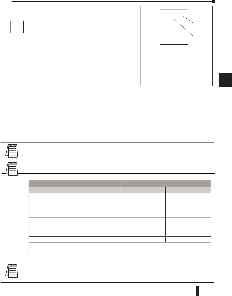
DL06 Micro PLC User Manual, 3rd Edition, Rev. D 5-49
1
2
3
4
5
6
7
8
9
10
11
12
13
14
A
B
C
D
Chapter 5: Standard RLL Instructions - Timer, Counter and Shift Register Instructions
1
2
3
4
5
6
7
8
9
10
11
12
13
14
a
B
c
d
Up Down Counter (UDC)
This Up/Down Counter counts up on each off to on
transition of the Up input and counts down on each
off-to-on transition of the Down input. The counter is
reset to 0 when the Reset input is on. The count range is
0–99999999. The count input not being used must be
off in order for the active count input to function.
Instruction Specification
Counter Reference (CTaaa): Specifies the counter
number.
Preset Value (Bbbb): Constant value (K) or two
consecutive V-memory locations, in BCD.
Current Values: Current count is a double word value
accessed by referencing the associated V or CT memory
locations* in BCD. The V-memory location is the counter location + 1000. For example, the
counter current value for CT5 resides in V-memory location V1005 and V1006.
Discrete Status Bit: The discrete status bit is accessed by referencing the associated CT
memory location. Operating as a “counter done bit” it will be on if the value is equal to or
greater than the preset value. For example the discrete status bit for counter 2 would be CT2.
NOTE: The UDC uses two consecutive V-memory locations for the 8-digit value, therefore two
consecutive timer locations. For example, if UDC CT1 is used, the next available counter number is
CT3.
NOTE: *May be non-volatile if MOV instruction is used.
** With the HPP, both the Counter discrete status bits and current value are accessed with the
same data reference. DirectSOFT uses separate references, such as “CT2” for discrete status bit for
Counter CT2, and “CTA2” for the current value of Counter CT2.
CT aaa
UDC
B bbb
Up
Down
Reset
Caution: The UDC uses two
V memory locations for the 8 digit
current value. This means that the
UDC uses two consecutive
counter locations. If UDC CT1 is
used in the program, the next
available counter is CT3.
Preset
Counter #
Operand Data Type DL06 Range
A/B aaa bbb
Counters CT 0–177 ––
V-memory (preset only) V ––
400-677
1200–7377
7400–7577
10000-17777
Pointers (preset only) P ––
400-677
1200–7377*
7400–7577
10000-17777
Constants (preset only) K –– 0–99999999
Counter discrete status bits CT/V 0–177 or V41140–41147
Counter current values V /CT** 1000-1177
Caution: The UDC uses two V-memory
locations for the 8 digit current value.
This means that the UDC uses two
consecutive counter locations. If UDC
CT1 is used in the program, the next
available counter is CT3.
DS Used
HPP Used
NOTE: A V-memory preset is required only if the ladder program or an Operator Interface unit must
change the preset.
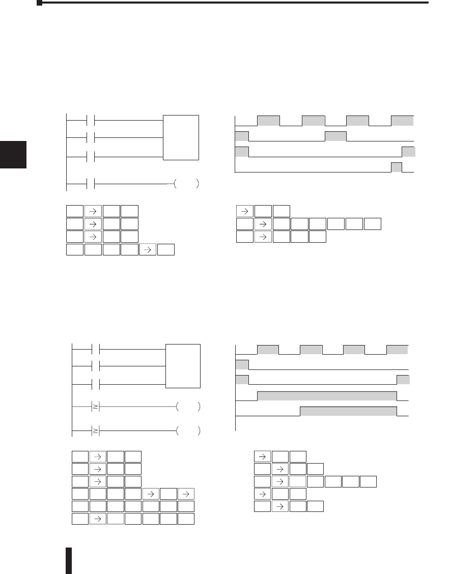
DL06 Micro PLC User Manual, 3rd Edition, Rev. D
5-50
1
2
3
4
5
6
7
8
9
10
11
12
13
14
A
B
C
D
Up / Down Counter Example Using Discrete Status Bits
In the following example, if X2 and X3 are off, the counter will increment by one when X1
toggles from Off to On . If X1 and X3 are off, the counter will decrement by one when X2
toggles from Off to On. When the count value reaches the preset value of 3, the counter
status bit will turn on. When the reset X3 turns on, the counter status bit will turn off and
the current value will be 0.
Up / Down Counter Example Using Comparative Contacts
In the following example, when X1 makes an off-to-on transition, counter CT2 will
increment by one. Comparative contacts are used to energize Y3 and Y4 at different counts.
When the reset (X3) turns on, the counter status bit will turn off, the current value will be 0,
and the comparative contacts will turn off.
Chapter 5: Standard RLL Instructions - Timer, Counter and Shift Register Instructions
1
2
3
4
5
6
7
8
9
10
11
12
13
14
a
B
c
d
3
DENT
Handheld Programmer Keystrokes
X1
UDC CT2
K3
X2
X3
CT2 Y7
OUT
X1
CT2
1212 30
Current
Value
X2
X3
Counting Diagram
Direct
SOFT32
Handheld Programmer Keystrokes (cont)
STR
$
1
BENT
STR
$
2
C
STR
$
3
D
SHFT ISG
U
3
D
2
C
2
C
ENT
ENT STR
$SHFT ENT
OUT
GX ENT
0
A
1
B
2
C
MLR
T
2
C
SHFT
AND
V
Handheld Programmer Keystrokes
X1
UDC CT2
V2000
X2
X3
X1
X2
X3
Counting Diagram
CTA2 K1
CTA2 K2 Y4
OUT
Y3
OUT
Y3
12 340
Current
Value
Y4
DirectSOFT32
Handheld Programmer Keystrokes (cont)
STR
$
1
BENT
STR
$
2
C
STR
$
3
D
SHFT ISG
U
3
D
2
C
2
C
ENT
ENT
SHFT ENT
2
C
0
A
0
A
0
A
STR
$SHFT
1
BENT
OUT
GX ENT
3
D
MLR
T
2
C
2
C
STR
$SHFT
ENT
OUT
GX ENT
MLR
T
2
C
2
C
2
C
4
E
SHFT
SHFT
DirectSOFT
DirectSOFT
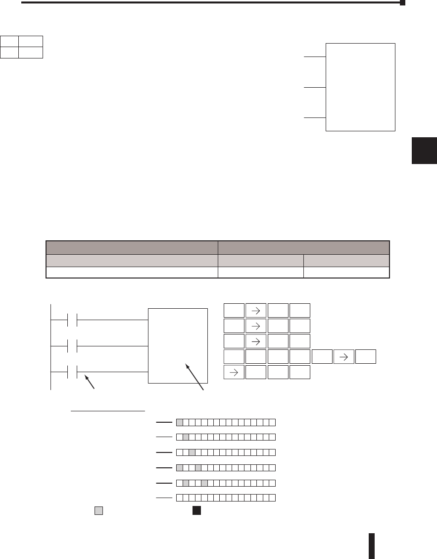
DL06 Micro PLC User Manual, 3rd Edition, Rev. D 5-51
1
2
3
4
5
6
7
8
9
10
11
12
13
14
A
B
C
D
With each off-to-on transition of the clock input, the bits which make up the shift register
block are shifted by one bit position and the status of the data input is placed into the starting
bit position in the shift register. The direction of the shift depends on the entry in the From
and To fields. From C0 to C17 would define a block of sixteen bits to be shifted from left to
right. From C17 to C0 would define a block of sixteen bits to be shifted from right to left.
The maximum size of the shift register block depends on the number of available control
relays. The minimum block size is 8 control relays.
Chapter 5: Standard RLL Instructions - Timer, Counter and Shift Register Instructions
1
2
3
4
5
6
7
8
9
10
11
12
13
14
a
B
c
d
SR
aaaFrom A
bbbTo B
DATA
CLOCK
RESET
Data Input
Clock Input
Reset Input
Shift Register Bits
C0 C17
Data Reset
1 0-1-0 0
0 0-1-0 0
0 0-1-0 0
1 0-1-0 0
0 0-1-0 0
001
Inputs on Successive Scans
X1
X2
SR
C0From
C17
X3 To
Handheld Programmer KeystrokesDirect SOFT 5
STR
$
1
BENT
STR
$
2
C
STR
$
3
D
SHFT
ENT
ENT
RST
S
ORN
RSHFT 0
A
1
B
7
HENT
SHFT
Indicates
ON
Indicates
OFF
Clock
Operand Data Type DL06 Range
A/B aaa bbb
Control Relay C 0–1777 0–1777
DS Used
HPP Used
DirectSOFT
Shift Register (SR)
The Shift Register instruction shifts data through a
predefined number of control relays. The control ranges in
the shift register block must start at the beginning of an 8 bit
boundary and must use 8-bit blocks.
The Shift Register has three contacts.
• Data — determines the value (1 or 0) that will enter the register
• Clock — shifts the bits one position on each low to high
transition
• Reset —resets the Shift Register to all zeros.
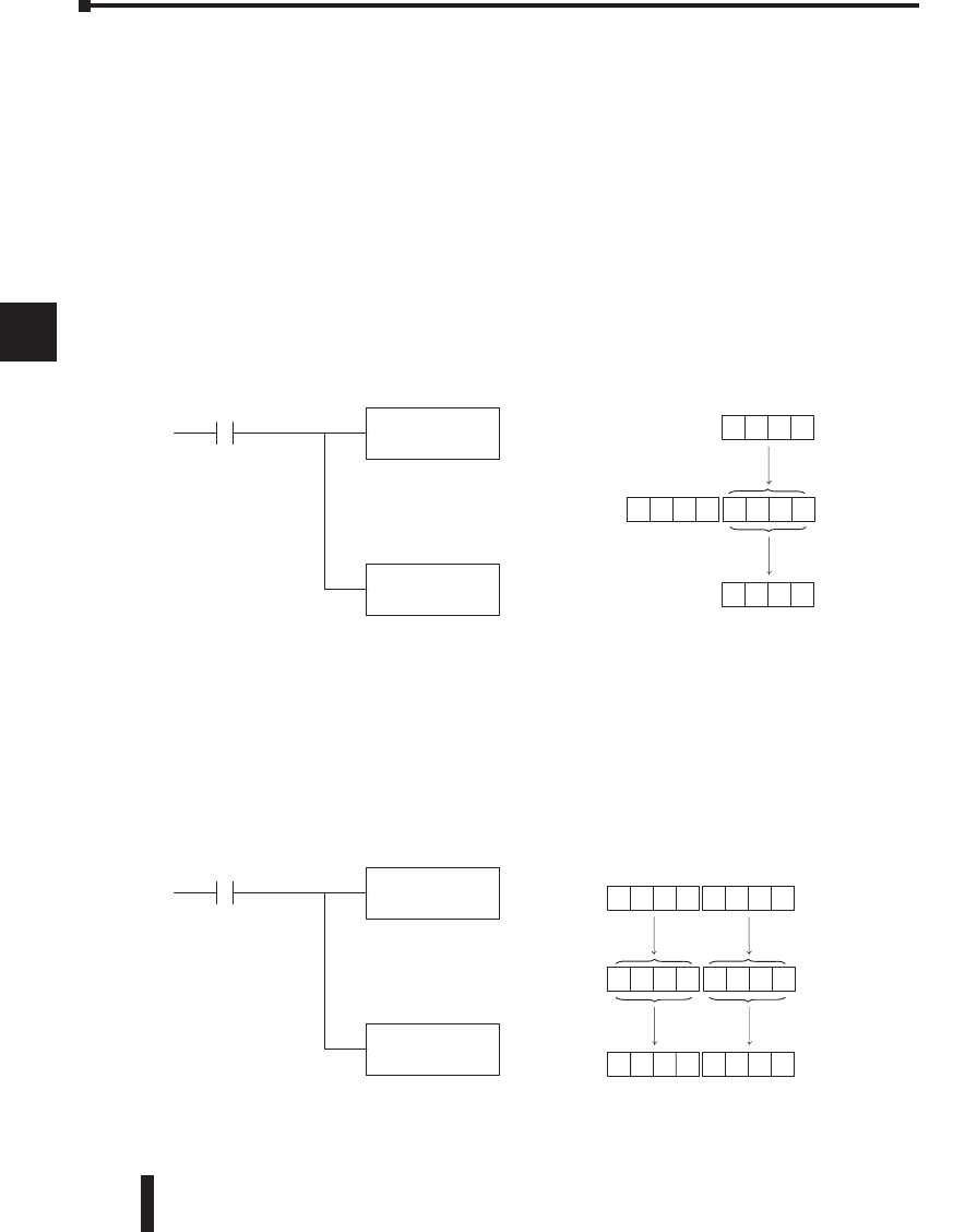
DL06 Micro PLC User Manual, 3rd Edition, Rev. D
5-52
1
2
3
4
5
6
7
8
9
10
11
12
13
14
A
B
C
D
Accumulator/Stack Load and Output Data Instructions
Using the Accumulator
The accumulator in the DL06 internal CPUs is a 32-bit register which is used as a temporary
storage location for data that is being copied or manipulated in some manner. For example,
you have to use the accumulator to perform math operations such as add, subtract, multiply,
etc. Since there are 32 bits, you can use up to an 8-digit BCD number. The accumulator is
reset to 0 at the end of every CPU scan.
Copying Data to the Accumulator
The Load and Out instructions and their variations are used to copy data from a V-memory
location to the accumulator, or to copy data from the accumulator to V-memory. The
following example copies data from V-memory location V2000 to V-memory location
V2010.
Since the accumulator is 32 bits and V-memory locations are 16 bits, the Load Double and
Out Double (or variations thereof) use two consecutive V-memory locations or 8 digit BCD
constants to copy data either to the accumulator from a V-memory address or from a
V-memory address to the accumulator. For example, if you wanted to copy data from V2000
and V2001 to V2010 and V2011 the most efficient way to perform this function would be as
follows:
Chapter 5: Standard RLL Instructions - Accumulator/Stack Load and Output Data
1
2
3
4
5
6
7
8
9
10
11
12
13
14
a
B
c
d
LD
V2000
X1
Copy data from V2000 to the
lower 16 bits of the accumu-
lator
Copy data from the lower 16 bits
of the accumulator to V2010
OUT
V2010
V2010
Acc.
8935
8935
00008935 8935
Unused accumulator bits
are set to zero
V2000
LDD
V2000
Copy data from V2000 and
V2001 to the accumulator
Copy data from the accumulator to
V2010 and V2011
OUTD
V2010
V2010
Acc.
V2000
67395026 5026
X1
V2001
67395026
V2011
67395026
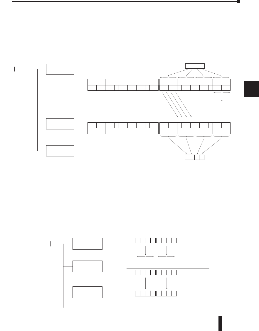
DL06 Micro PLC User Manual, 3rd Edition, Rev. D 5-53
1
2
3
4
5
6
7
8
9
10
11
12
13
14
A
B
C
D
Changing the Accumulator Data
Instructions that manipulate data also use the accumulator. The result of the manipulated
data resides in the accumulator. The data that was being manipulated is cleared from the
accumulator. The following example loads the constant value 4935 into the accumulator,
shifts the data right 4 bits, and outputs the result to V2010.
Some of the data manipulation instructions use 32 bits. They use two consecutive V-memory
locations or an 8 digit BCD constant to manipulate data in the accumulator.
In the following example, when X1 is on, the value in V2000 and V2001 will be loaded into
the accumulator using the Load Double instruction. The value in the accumulator is added
with the value in V2006 and V2007 using the Add Double instruction. The value in the
accumulator is copied to V2010 and V2011 using the Out Double instruction.
Chapter 5: Standard RLL Instructions - Accumulator/Stack Load and Output Data
1
2
3
4
5
6
7
8
9
10
11
12
13
14
a
B
c
d
LD
K4935
X1
Load the value 4935 into the
accumulator
Shift the data in the accumulator
4 bits (K4) to the right
Output the lower 16 bits of the ac-
cumulator to V2010
010010010011010 1
Constant
V2010
000001001001001 10000010000000000
15 14 13 12 11 10 987654321031 30 29 28 27 26 25 24 23 22 21 20 19 18 17 16
Shifted out of
accumulator
0493
4935
SHFR
K4
OUT
V2010
0000000000000000
31 30 29 28 27 26 25 24 23 22 21 20 19 18 17 16
0000000000000000
The upper 16 bits of the accumulator
will be set to 0
15 14 13 12 11 10 9876543210
31 30 29 28 27 26 25 24 23 22 21 20 19 18 17 1631 30 29 28 27 26 25 24 23 22 21 20 19 18 17 16
Acc.
Acc.
67395026
LDD
V2000
X1
Load the value in V2000 and
V2001 into the accumulator
ADDD
V2006
Add the value in the
accumulator with the value
in V2006 and V2007
OUTD
V2010
Copy the value in the
accumulator to V2010 and
V2011
V2010
V2000
V2001
67395026
V2011
87399072
(Accumulator)
(V2006 & V2007)
20004046 +
87399072
Acc.
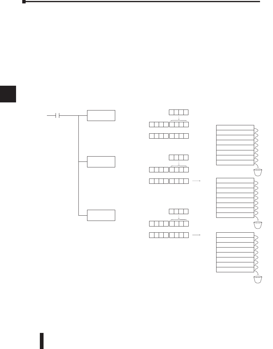
DL06 Micro PLC User Manual, 3rd Edition, Rev. D
5-54
1
2
3
4
5
6
7
8
9
10
11
12
13
14
A
B
C
D
Using the Accumulator Stack
The accumulator stack is used for instructions that require more than one parameter to
execute a function or for user-defined functionality. The accumulator stack is used when
more than one Load instruction is executed without the use of an Out instruction. The first
load instruction in the scan places a value into the accumulator. Every Load instruction
thereafter without the use of an Out instruction places a value into the accumulator and
the value that was in the accumulator is placed onto the accumulator stack. The Out
instruction nullifies the previous load instruction and does not place the value that was in the
accumulator onto the accumulator stack when the next load instruction is executed. Every
time a value is placed onto the accumulator stack the other values in the stack are pushed
down one location. The accumulator is eight levels deep (eight 32-bit registers). If there is a
value in the eighth location when a new value is placed onto the stack, the value in the eighth
location is pushed off the stack and cannot be recovered.
The POP instruction rotates values upward through the stack into the accumulator. When a
POP is executed, the value which was in the accumulator is cleared and the value that was on
top of the stack is in the accumulator. The values in the stack are shifted up one position in
the stack.
Chapter 5: Standard RLL Instructions - Accumulator/Stack Load and Output Data
1
2
3
4
5
6
7
8
9
10
11
12
13
14
a
B
c
d
Acc.
Load the value 3245 into the accumu-
lator
Load the value 5151 into the accumu-
lator, pushing the value 3245 onto the
stack
Load the value 6363 into the accumu-
lator, pushing the value 5151 to the 1st
stack location and the value 3245 to
the 2nd stack location
LD
K3245
X1
LD
K5151
LD
K6363
Constant
Acc. XXXXX XXXX
Current Acc. value
Previous Acc. value
XXXXXXXX
XXXXXXX
XXXXXXX
Level 1
XXXXXXXX
Level 2
XXXXXXXX
Level 3
XXXXXXXX
Level 4
XXXXXXXX
Level 5
XXXXXXXX
Level 6
XXXXXXXX
Level 7
XXXXXXXX
Level 8
Accumulator Stack
00003245
Level 1
XXXXXXXX
Level 2
XXXXXXXX
Level 3
XXXXXXXX
Level 4
XXXXXXXX
Level 5
XXXXXXXX
Level 6
XXXXXXXX
Level 7
XXXXXXXX
Level 8
Accumulator Stack
Acc.
Constant 5151
00005 5151
Acc. 00003245 3245
Current Acc. value
Previous Acc. value
00005151
0000
Level 1
00003245
Level 2
XXXXXXXX
Level 3
XXXXXXXX
Level 4
XXXXXXXX
Level 5
XXXXXXXX
Level 6
XXXXXXXX
Level 7
XXXXXXXX
Level 8
Accumulator Stack
Acc.
Constant 6363
00006363 6363
Acc. 00005 5151
Current Acc. value
Previous Acc. value
Bucket
Bucket
Bucket
3245
00003245
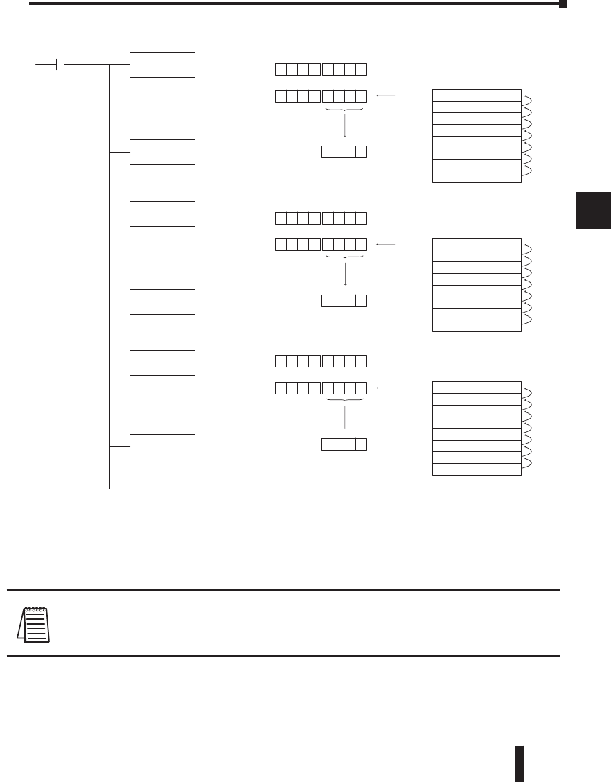
DL06 Micro PLC User Manual, 3rd Edition, Rev. D 5-55
1
2
3
4
5
6
7
8
9
10
11
12
13
14
A
B
C
D
Using Pointers
Many of the DL06 series instructions will allow V-memory pointers as operands
(commonly known as indirect addressing). Pointers allow instructions to obtain data from
V-memory locations referenced by the pointer value.
NOTE: DL06 V-memory addressing is in octal. However, the pointers reference a V-memory
location with values viewed as HEX. Use the Load Address (LDA) instruction to move an
address into the pointer location. This instruction performs the Octal to Hexadecimal conversion
automatically.
In the following example we are using a pointer operand in a Load instruction. V-memory
location 2000 is being used as the pointer location. V2000 contains the value 440 which
the CPU views as the Hex equivalent of the Octal address V-memory location V2100. The
CPU will copy the data from V2100, which (in this example) contains the value 2635, into
the lower word of the accumulator.
Chapter 5: Standard RLL Instructions - Accumulator/Stack Load and Output Data
1
2
3
4
5
6
7
8
9
10
11
12
13
14
a
B
c
d
Acc.
POP the 1st value on the stack into the
accumulator and move stack values
up one location
POP
X1
POP
POP
V2000 4545
XXXXXXX XXXX
Acc. 000045 4545
Previous Acc. value
Current Acc. value
00003792
Level 1
00007930
Level 2
XXXXXXXX
Level 3
XXXXXXXX
Level 4
XXXXXXXX
Level 5
XXXXXXXX
Level 6
XXXXXXXX
Level 7
XXXXXXXX
Level 8
Accumulator Stack
00007930
Level 1
XXXXXXXX
Level 2
XXXXXXXX
Level 3
XXXXXXXX
Level 4
XXXXXXXX
Level 5
XXXXXXXX
Level 6
XXXXXXXX
Level 7
XXXXXXXX
Level 8
Accumulator Stack
XXXXXXXX
Level 1
XXXXXXXX
Level 2
XXXXXXXX
Level 3
XXXXXXXX
Level 4
XXXXXXXX
Level 5
XXXXXXXX
Level 6
XXXXXXXX
Level 7
XXXXXXXX
Level 8
Accumulator Stack
POP the 1st value on the stack into the
accumulator and move stack values
up one location
POP the 1st value on the stack into the
accumulator and move stack values
up one location
OUT
V2000
OUT
V2001
Acc.
V2001 3792
00004545 4545
Acc. 00003792 3792
Previous Acc. value
Current Acc. value
Acc.
V2002 7930
00003460 3792
Acc. XXXX7930 7930
Previous Acc. value
Current Acc. value
OUT
V2002
Copy data from the accumulator to
V2000
Copy data from the accumulator to
V2001.
Copy data from the accumulator to
Copy data from the accumulator to
V2002
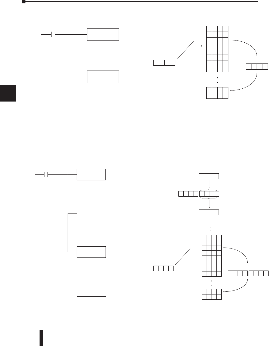
DL06 Micro PLC User Manual, 3rd Edition, Rev. D
5-56
1
2
3
4
5
6
7
8
9
10
11
12
13
14
A
B
C
D
The following example is identical to the one above, with one exception. The LDA (Load
Address) instruction automatically converts the Octal address to Hex.
Chapter 5: Standard RLL Instructions - Accumulator/Stack Load and Output Data
1
2
3
4
5
6
7
8
9
10
11
12
13
14
a
B
c
d
V2000 (P2000) contains the value 440
HEX. 440 HEX. = 2100 Octal which
contains the value 2635.
LD
P2000
X1
OUT
V2200
Copy the data from the lower 16 bits of
the accumulator to V2200.
0440
V2076 XXXX
V2077 XXXX
V2100 2635
V2101 XXXX
V2102 XXXX
V2103 XXXX
V2104 XXXX
V2105 XXXX
V2200 2635
V2201 XXXX
2635
Accumulator
V2000
V2000 (P2000) contains the value 440
Hex. 440 Hex. = 2100 Octal which
contains the value 2635
LDA
O 2100
X1
OUT
V 2000
Copy the data from the lower 16 bits of
the accumulator to V2000
V2100
0440
V2076 XXXX
V2077 XXXX
V2100 2635
V2101 XXXX
V2102 XXXX
V2103 XXXX
V2104 XXXX
V2105 XXXX
V2200 2635
V2201 XXXX
LD
P 2000
OUT
V 2200
Copy the data from the lower 16 bits of
the accumulator to V2200
Load the lower 16 bits of the
accumulator with Hexadecimal
equivalent to Octal 2100 (440)
V2000
Acc.
2100
0440
00000440 0440
2100 Octal is converted to Hexadecimal
440 and loaded into the accumulator
Accumulator
00002635 2635
Unused accumulator bits
are set to zero
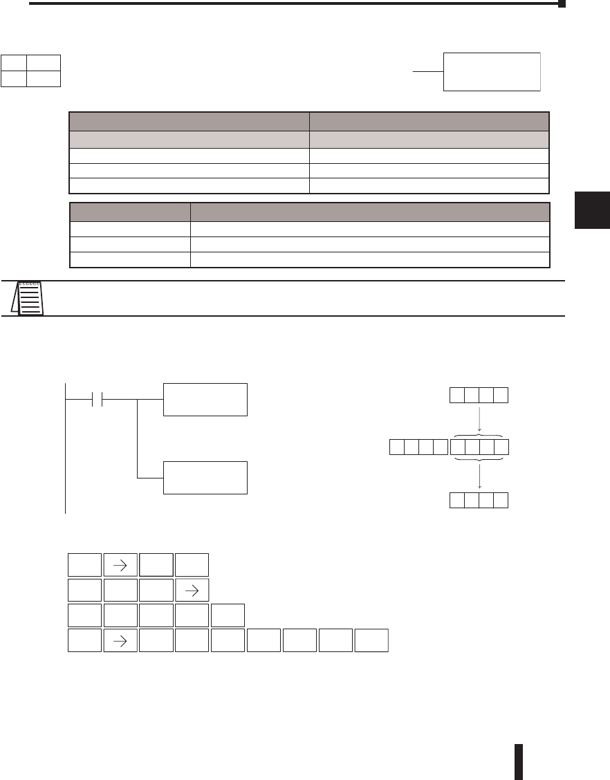
DL06 Micro PLC User Manual, 3rd Edition, Rev. D 5-57
1
2
3
4
5
6
7
8
9
10
11
12
13
14
A
B
C
D
Load (LD)
The Load instruction is a 16 bit instruction that loads the
value (Aaaa), which is either a V-memory location or a 4 digit
constant, into the lower 16 bits of the accumulator. The upper
16 bits of the accumulator are set to 0.
NOTE: Two consecutive Load instructions will place the value of the first load instruction onto the
accumulator stack.
In the following example, when X1 is on, the value in V2000 will be loaded into the
accumulator and output to V2010.
Chapter 5: Standard RLL Instructions - Accumulator/Stack Load and Output Data
1
2
3
4
5
6
7
8
9
10
11
12
13
14
a
B
c
d
LD
A aaa
Operand Data Type DL06 Range
Aaaa
V-memory V See memory map
Pointer P See memory map
Constant K 0–FFFF
LD
V2000
X1
Load the value in V2000 into
the lower 16 bits of the
accumulator
OUT
V2010
Copy the value in the lower
16 bits of the accumulator to
V2010 V2010
Acc.
V2000
8935
8935
00008935 8935
Direct SOFT32
The unused accumulator
bits are set to zero
1
B
2
C
0
A
0
A
0
AENT
Handheld Programmer Keystrokes
STR
$
SET
X
SHFT ANDST
L
3
D
OUT
GX SHFT AND
V
2
C
0
A
1
B
0
AENT
DS Used
HPP Used
Discrete Bit Flags Description
SP53 On when the pointer is outside of the available range.
SP70 On anytime the value in the accumulator is negative.
SP76 On when any instruction loads a value of zero into the accumulator.
DirectSOFT
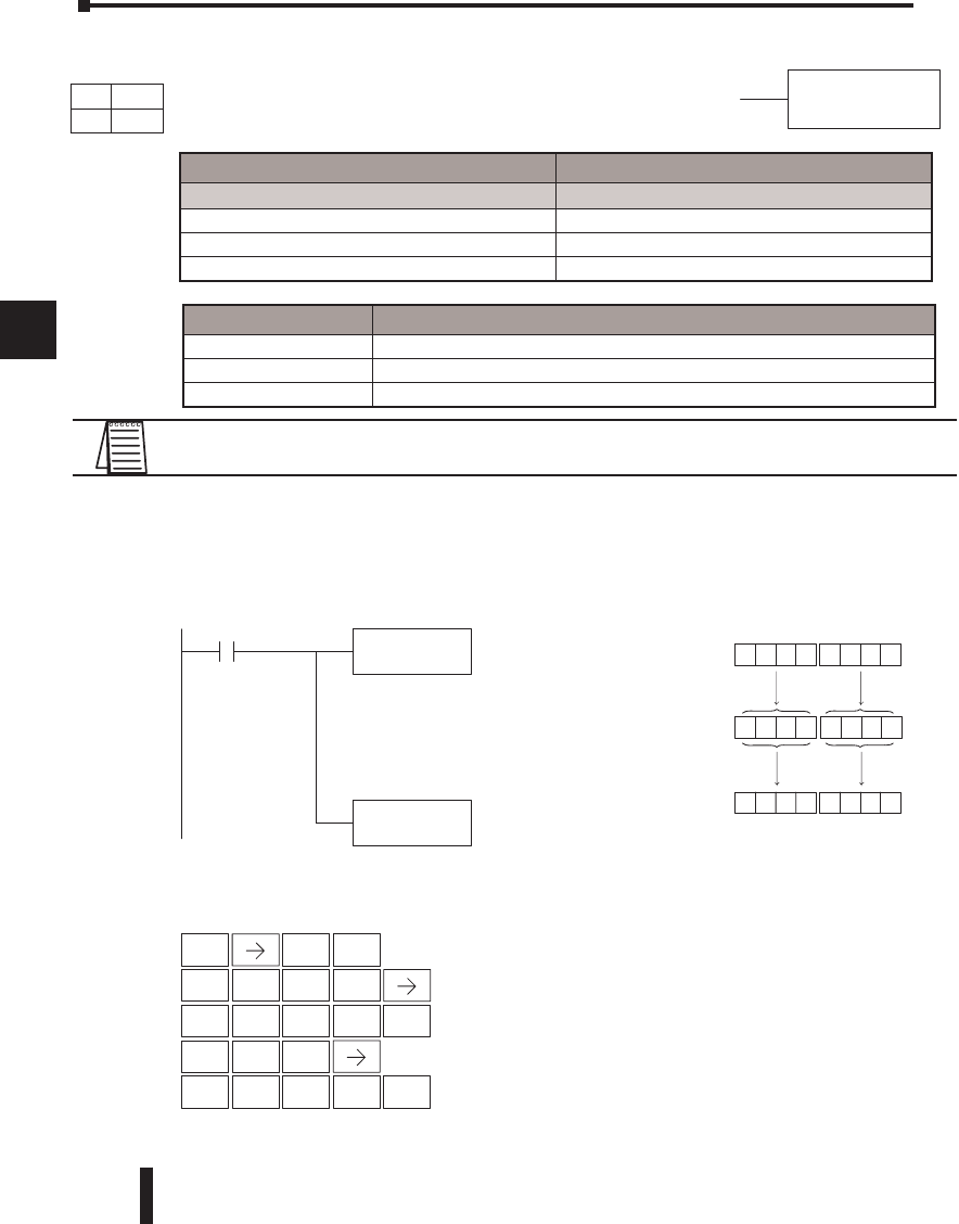
DL06 Micro PLC User Manual, 3rd Edition, Rev. D
5-58
1
2
3
4
5
6
7
8
9
10
11
12
13
14
A
B
C
D
Load Double (LDD)
The Load Double instruction is a 32-bit instruction that loads the
value (Aaaa), which is either two consecutive V-memory locations
or an 8 digit constant value, into the accumulator.
NOTE: Two consecutive Load instructions will place the value of the first load instruction onto the
accumulator stack.
In the following example, when X1 is on, the 32-bit value in V2000 and V2001 will be
loaded into the accumulator and output to V2010 and V2011.
Chapter 5: Standard RLL Instructions - Accumulator/Stack Load and Output Data
1
2
3
4
5
6
7
8
9
10
11
12
13
14
a
B
c
d
Operand Data Type DL06 Range
Aaaa
V-memory V See memory map
Pointer P See memory map
Constant K 0–FFFFFFFF
Discrete Bit Flags Description
SP53 On when the pointer is outside of the available range.
SP70 On anytime the value in the accumulator is negative.
SP76 On when any instruction loads a value of zero into the accumulator.
LDD
A aaa
1
BENT
2
C
0
A
0
A
0
AENT
2
C
0
A
1
B
0
AENT
Handheld Programmer Keystrokes
Direct SOFT32
LDD
V2000
X1
Load the value in V2000 and
V2001 into the 32 bit
accumulator
OUTD
V2010
Copy the value in the 32 bit
accumulator to V2010 and
V2011
V2010
Acc.
V2000
67396026
5026
V2001
67395026
V2011
67395026
STR
$
SHFT ANDST
L
3
D
3
D
OUT
GX SHFT 3
D
DS Used
HPP Used
DirectSOFT
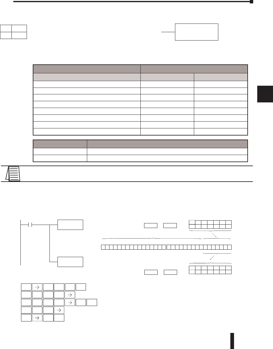
DL06 Micro PLC User Manual, 3rd Edition, Rev. D 5-59
1
2
3
4
5
6
7
8
9
10
11
12
13
14
A
B
C
D
Load Formatted (LDF)
The Load Formatted instruction loads 1–32
consecutive bits from discrete memory locations into
the accumulator. The instruction requires a starting
location (Aaaa) and the number of bits (Kbbb) to be
loaded. Unused accumulator bit locations are set to zero.
NOTE: Two consecutive Load instructions will place the value of the first load instruction onto the
accumulator stack.
In the following example, when C0 is on, the binary pattern of C10–C16 (7 bits) will be
loaded into the accumulator using the Load Formatted instruction. The lower 7 bits of the
accumulator are output to Y0–Y6 using the Out Formatted instruction.
Chapter 5: Standard RLL Instructions - Accumulator/Stack Load and Output Data
1
2
3
4
5
6
7
8
9
10
11
12
13
14
a
B
c
d
bbbK
LDF A aaa
Operand Data Type DL06 Range
A aaa bbb
Inputs X 0–777 ––
Outputs Y 0–777 ––
Control Relays C 0–1777 ––
Stage Bits S 0–1777 ––
Timer Bits T 0–377 ––
Counter Bits CT 0–177 ––
Special Relays SP 0–777 ––
Constant K –– 1–32
Discrete Bit Flags Description
SP70 On anytime the value in the accumulator is negative.
SP76 On when any instruction loads a value of zero into the accumulator.
0
A
7
HENT
Handheld Programmer Keystrokes
LDF C10
K7
C0
Load the status of 7
consecutive bits (C10–C16)
into the accumulator
OUTF Y0
K7
Copy the value from the
specified number of bits in
the accumulator to Y0 – Y6
K7 C10
Location Constant
00000000000011100000000000000000
15 14 13 12 11 10 9876543210
31 30 29 28 27 26 25 24 23 22 21 20 19 18 17 1631 30 29 28 27 26 25 24 23 22 21 20 19 18 17 16
Acc.
K7Y0
Location Constant
C16 C15 C14 C13 C12 C11 C10
OFFONONONOFFOFFOFF
Y6 Y5 Y4 Y3 Y2 Y1 Y0
OFFONONONOFFOFFOFF
The unused accumulator bits are set to zero
Direct SOFT32
STR
$SHFT ENT
2
C
0
A
SHFT ANDST
L
3
D
5
F
SHFT 2
C
1
B
0
A
7
HENT
OUT
GX SHFT 5
F
DS Used
HPP Used
DirectSOFT
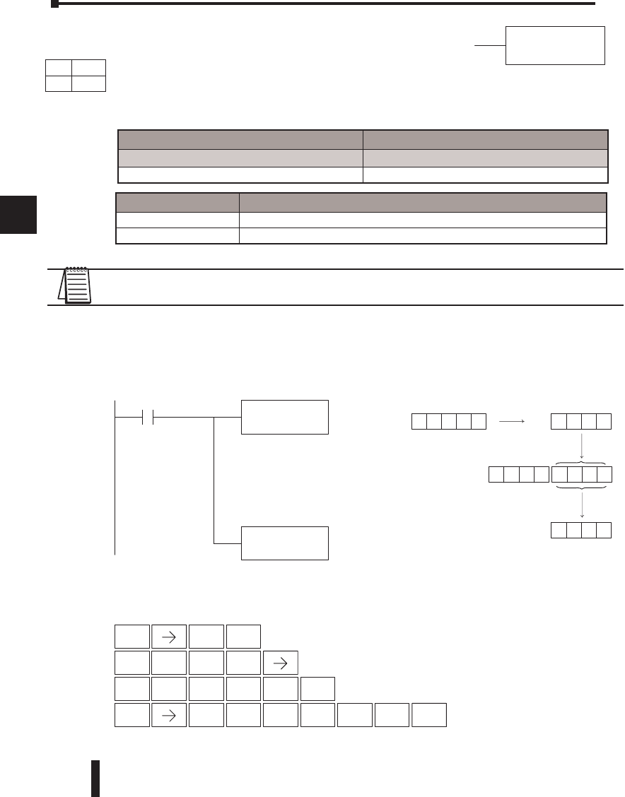
DL06 Micro PLC User Manual, 3rd Edition, Rev. D
5-60
1
2
3
4
5
6
7
8
9
10
11
12
13
14
A
B
C
D
Load Address (LDA)
The Load Address instruction is a 16-bit instruction. It converts
any octal value or address to the HEX equivalent value and loads
the HEX value into the accumulator. This instruction is useful
when an address parameter is required, since all addresses for the DL06 system are in octal.
NOTE: Two consecutive Load instructions will place the value of the first load instruction onto the
accumulator stack.
In the following example, when X1 is on, the octal number 40400 will be converted to a
HEX 4100 and loaded into the accumulator using the Load Address instruction. The value in
the lower 16 bits of the accumulator is copied to V2000 using the Out instruction.
Chapter 5: Standard RLL Instructions - Accumulator/Stack Load and Output Data
1
2
3
4
5
6
7
8
9
10
11
12
13
14
a
B
c
d
O aaa
LDA
Operand Data Type DL06 Range
aaa
Octal Address O See memory map
1
BENT
4
E
0
A
4
E
0
A
0
AENT
Handheld Programmer Keystrokes
Direct SOFT32
LDA
O 40400
X1
Load The HEX equivalent to
the octal number into the
lower 16 bits of the
accumulator
OUT
V2000
Copy the value in lower 16
bits of the accumulator to
V2000
V2000
Acc.
Hexadecimal
4100
4100
0000 4100
Octal
40400
The unused accumulator
bits are set to zero
STR
$
SHFT ANDST
L
3
D
0
A
OUT
GX SHFT AND
V
2
C
0
A
0
AENT
0
A
Discrete Bit Flags Description
SP70 On anytime the value in the accumulator is negative.
SP76 On when any instruction loads a value of zero into the accumulator.
DS Used
HPP Used
DirectSOFT
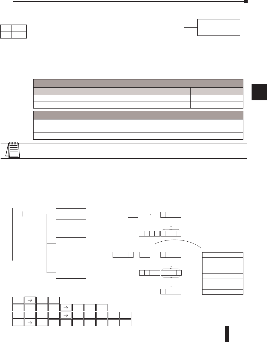
DL06 Micro PLC User Manual, 3rd Edition, Rev. D 5-61
1
2
3
4
5
6
7
8
9
10
11
12
13
14
A
B
C
D
Helpful Hint: — The Load Address instruction can be used to convert an octal address to a
HEX address and load the value into the accumulator.
NOTE: Two consecutive Load instructions will place the value of the first load instruction onto the
accumulator stack.
In the following example, when X1 is on, the HEX equivalent for octal 25 will be loaded into
the accumulator (this value will be placed on the stack when the Load Accumulator Indexed
instruction is executed). V-memory location V1410 will be added to the value in the first
level of the stack and the value in this location (V1435 = 2345) is loaded into the lower 16
bits of the accumulator using the Load Accumulator Indexed instruction. The value in the
lower 16 bits of the accumulator is output to V1500 using the Out instruction.
Chapter 5: Standard RLL Instructions - Accumulator/Stack Load and Output Data
1
2
3
4
5
6
7
8
9
10
11
12
13
14
a
B
c
d
A aaa
LDX
Operand Data Type DL06 Range
A aaa aaa
V-memory V See memory map See memory map
Pointer P See memory map See memory map
Copy the value in the lower
16 bits of the accumulator
to V1500
LDA
O 25
X1
LDX
V1410
OUT
V1500
Acc. 000 0 001 5
Hexadecimal
001 5
Octal
2 5
The unused accumulator
bits are set to zero
V1500
Acc.
Octal
143 5
234 5
000 0 234 5
V
Octal
141 0
The unused accumulator
bits are set to zero
+1 5
HEX Value in 1st
stack location
00000015
Level 1
XXXXXXXX
Level 2
XXXXXXXX
Level 3
XXXXXXXX
Level 4
XXXXXXXX
Level 5
XXXXXXXX
Level 6
XXXXXXXX
Level 7
XXXXXXXX
Level 8
Accumulator Stack
V
=
Load The HEX equivalent to
octal 25 into the lower 16
bits of the accumulator
Move the offset to the stack.
Load the accumulator with
the address to be offset
The value in V1435
is 2345
Handheld Programmer Keystrokes
STR
$
SHFT ANDST
L
3
D
SHFT
1
BENT
2
C
0
A
ENT
1
B
5
F
0
A
0
A
PREV
ANDST
L
3
DENT
5
F
OUT
GX
SET
X
1
B
4
E
1
B
0
A
PREV PREV
ENT
Discrete Bit Flags Description
SP53 On when the pointer is outside of the available range.
SP70 On anytime the value in the accumulator is negative.
SP76 On when any instruction loads a value of zero into the accumulator.
DS Used
HPP Used
Load Accumulator Indexed (LDX)
Load Accumulator Indexed is a 16-bit instruction that specifies
a source address (V-memory) which will be offset by the value
in the first stack location. This instruction interprets the value
in the first stack location as HEX. The value in the offset
address (source address + offset) is loaded into the lower 16 bits
of the accumulator. The upper 16 bits of the accumulator are
set to 0.
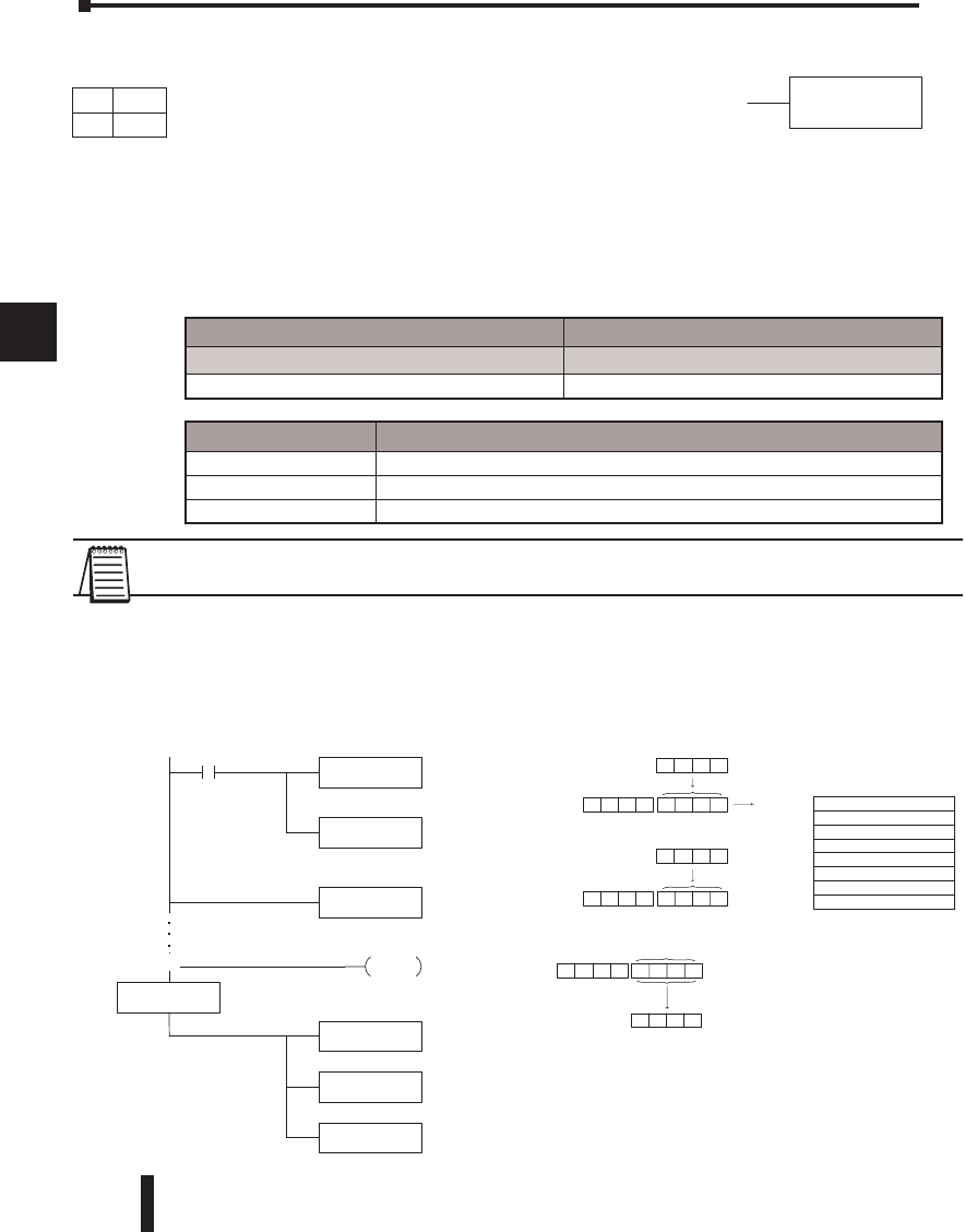
DL06 Micro PLC User Manual, 3rd Edition, Rev. D
5-62
1
2
3
4
5
6
7
8
9
10
11
12
13
14
A
B
C
D
The LDSX instruction uses the value in the first level of the accumulator stack as an offset
to determine which numerical or ASCII constant within the Data Label Area will be loaded
into the accumulator. The LDSX instruction interprets the value in the first level of the
accumulator stack as a HEX value.
Helpful Hint: — The Load Address instruction can be used to convert octal to HEX and
load the value into the accumulator.
NOTE: Two consecutive Load instructions will place the value of the first load instruction onto the
accumulator stack.
In the following example when X1 is on, the offset of 1 is loaded into the accumulator. This
value will be placed into the first level of the accumulator stack when the LDSX instruction
is executed. The LDSX instruction specifies the Data Label (DLBL K2) where the numerical
constant(s) are located in the program and loads the constant value, indicated by the offset in
the stack, into the lower 16 bits of the accumulator.
Chapter 5: Standard RLL Instructions - Accumulator/Stack Load and Output Data
1
2
3
4
5
6
7
8
9
10
11
12
13
14
a
B
c
d
LDSX
K aaa
Operand Data Type DL06 Range
aaa
Constant K 1-FFFF
LD
K1
X1
Load the offset value of 1 (K1) into the lower 16
bits of the accumulator.
LDSX
K2
Move the offset to the stack.
Load the accumulator with the data label
number
END
K2
NCON
K3333
NCON
K2323
NCON
K4549
Acc. 000 0 000 1
Hexadecimal
000 1
The unused accumulator
bits are set to zero
Value in 1st. level of stack is
used as offset. The value is 1
Offset 0
Offset 1
Offset 2
V2000
Acc.
232 3
000 0 232 3
00000001
Level 1
XXXXXXXX
Level 2
XXXXXXXX
Level 3
XXXXXXXX
Level 4
XXXXXXXX
Level 5
XXXXXXXX
Level 6
XXXXXXXX
Level 7
XXXXXXXX
Level 8
Accumulator Stack
Acc. 000 0 000 2
K
Constant
000 2
The unused accumulator
bits are set to zero
The unused accumulator
bits are set to zero
Copy the value in the lower
16 bits of the accumulator
to V2000
OUT
V2000
DLBL
DLBL
Discrete Bit Flags Description
SP53 On when the pointer is outside of the available range.
SP70 On anytime the value in the accumulator is negative.
SP76 On when any instruction loads a value of zero into the accumulator.
DS Used
HPP Used
Load Accumulator Indexed from Data Constants (LDSX)
The Load Accumulator Indexed from Data Constants is a 16-bit
instruction. The instruction specifies a Data Label Area (DLBL)
where numerical or ASCII constants are stored. This value will
be loaded into the lower 16 bits.
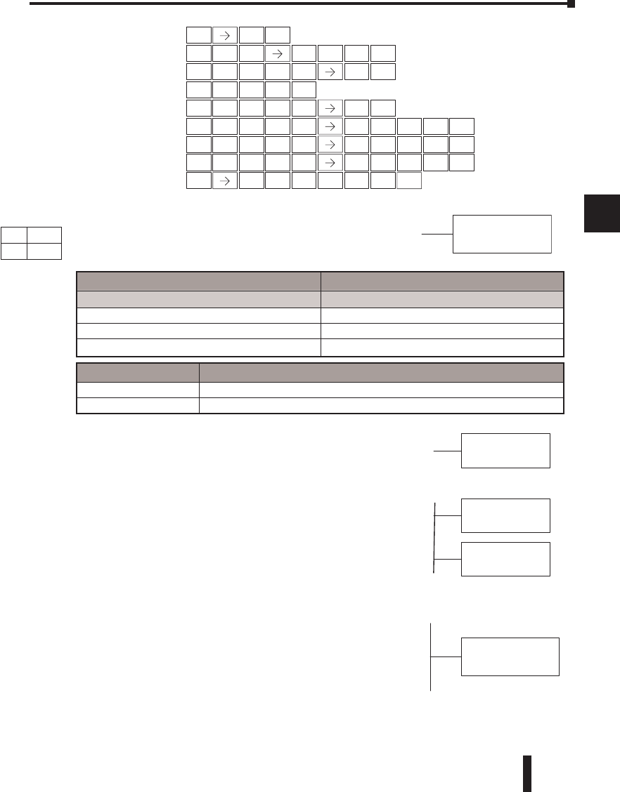
DL06 Micro PLC User Manual, 3rd Edition, Rev. D 5-63
1
2
3
4
5
6
7
8
9
10
11
12
13
14
A
B
C
D
Load Real Number (LDR)
The Load Real Number instruction loads a real number
contained in two consecutive V-memory locations, or an 8-digit
constant into the accumulator.
Chapter 5: Standard RLL Instructions - Accumulator/Stack Load and Output Data
1
2
3
4
5
6
7
8
9
10
11
12
13
14
a
B
c
d
Operand Data Type DL06 Range
A aaa
V-memory V See memory map
Pointer P See memory map
Real Constant R -3.402823E+38 to + -3.402823E+38
1
BENT
ENT
2
C
Handheld Programmer Keystrokes
STR
$
SHFT ANDST
L
3
DSHFT JMP
K
1
BENT
SHFT ANDST
L
3
D
RST
S
SET
X
SHFT 4
E
TMR
N
3
DENT
SHFT 3
D
ANDST
L
1
B
ANDST
L
2
CENT
SHFT TMR
N
2
C
INST#
O
TMR
N
3
D
3
D
3
D
3
DENT
SHFT TMR
N
2
C
INST#
O
TMR
N
3
D
3
DENT
2
C
2
C
SHFT TMR
N
2
C
INST#
O
TMR
NENT
4
E
5
F
4
E
9
J
OUT
GX SHFT AND
V
2
C
0
A
0
AENT
0
A
A aaa
LDR
R3.14159
LDR
R5.3E6
LDR
V1400
OUTD
V1400
LDR
Discrete Bit Flags Description
SP70 On anytime the value in the accumulator is negative.
SP76 On when any instruction loads a value of zero into the accumulator.
DS Used
HPP N/A
DirectSOFT allows you to enter real numbers directly, by using
the leading “R” to indicate a real number entry. You can enter a
constant such as Pi, shown in the example to the right. To enter
negative numbers, use a minus (–) after the “R”.
For very large numbers or very small numbers, you can use
exponential notation. The number to the right is 5.3 million.
The OUTD instruction stores it in V1400 and V1401.
These real numbers are in the IEEE 32-bit floating point format,
so they occupy two V-memory locations, regardless of how big
or small the number may be! If you view a stored real number
in hex, binary, or even BCD, the number shown will be very
difficult to decipher. Just like all other number types, you must
keep track of real number locations in memory, so they can be
read with the proper instructions later.
The previous example above stored a real number in V1400 and
V1401. Suppose that now we want to retrieve that number. Just
use the Load Real with the V data type, as shown to the right.
Next we could perform real math on it, or convert it to a binary
number.
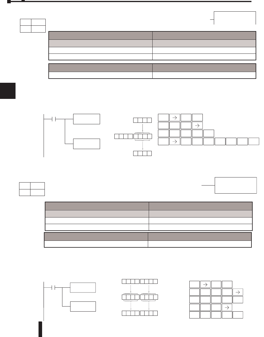
DL06 Micro PLC User Manual, 3rd Edition, Rev. D
5-64
1
2
3
4
5
6
7
8
9
10
11
12
13
14
A
B
C
D
Out (OUT)
The Out instruction is a 16-bit instruction that copies the value in the
lower 16 bits of the accumulator to a specified V-memory location
(Aaaa).
In the following example, when X1 is on, the value in V2000 will be loaded into the lower
16 bits of the accumulator using the Load instruction. The value in the lower 16 bits of the
accumulator are copied to V2010 using the OUT instruction.
Out Double (OUTD)
The Out Double instruction is a 32 bit instruction that copies the
value in the accumulator to two consecutive V-memory locations
at a specified starting location (Aaaa).
In the following example, when X1 is on, the 32-bit value in V2000 and V2001 will
be loaded into the accumulator using the Load Double instruction. The value in the
accumulator is output to V2010 and V2011 using the OUTD instruction.
Chapter 5: Standard RLL Instructions - Accumulator/Stack Load and Output Data
1
2
3
4
5
6
7
8
9
10
11
12
13
14
a
B
c
d
OUT
A aaa
Operand Data Type DL06 Range
A aaa
V-memory V See memory map
Pointer P See memory map
Operand Data Type DL06 Range
A aaa
V-memory V See memory map
Pointer P See memory map
Discrete Bit Flags Description
SP53 On if CPU cannot solve the logic.
Discrete Bit Flags Description
SP53 On if CPU cannot solve the logic.
2
C
0
A
0
A
0
AENT
1
BENT
Handheld Programmer Keystrokes
LD
V2000
X1
Load the value in V2000 into
the lower 16 bits of the
accumulator
OUT
V2010
Copy the value in the lower
16 bits of the accumulator to
V2010 V2010
Acc.
V2000
8935
8935
00008935 8935
Direct SOFT32
The unused accumulator
bits are set to zero
STR
$
SHFT ANDST
L
3
D
OUT
GX SHFT AND
V
2
C
0
A
1
B
0
AENT
OUTD
A aaa
2
C
0
A
0
A
0
AENT
2
C
0
A
1
B
0
AENT
1
BENT
Handheld Programmer Keystrokes
V2010
Acc.
V2000
67395026 5026
V2001
67395026
V2011
67395026
Load the value in V2000 and
V2001 into the accumulator
LDD
OUTD
Copy the value in the
accumulator to V2010 and
V2011
V2000
X1
V2010
Direct SOFT32
STR
$
SHFT ANDST
L
3
D
3
D
OUT
GX SHFT 3
D
DS Used
HPP Used
DS Used
HPP Used
DirectSOFT
DirectSOFT
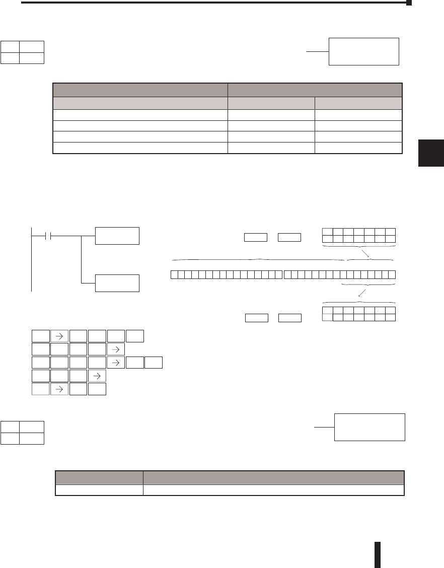
DL06 Micro PLC User Manual, 3rd Edition, Rev. D 5-65
1
2
3
4
5
6
7
8
9
10
11
12
13
14
A
B
C
D
Out Formatted (OUTF)
The Out Formatted instruction outputs 1–32 bits from the
accumulator to the specified discrete memory locations. The
instruction requires a starting location (Aaaa) for the destination
and the number of bits (Kbbb) to be output.
In the following example, when C0 is on, the binary pattern of C10–C16 (7 bits) will be
loaded into the accumulator using the Load Formatted instruction. The lower 7 bits of the
accumulator are output to Y0–Y6 using the OUTF instruction.
Pop (POP)
The Pop instruction moves the value from the first level of the
accumulator stack (32 bits) to the accumulator and shifts each value
in the stack up one level.
Chapter 5: Standard RLL Instructions - Accumulator/Stack Load and Data
1
2
3
4
5
6
7
8
9
10
11
12
13
14
a
B
c
d
Discrete Bit Flags Description
SP63 ON when the result of the instruction causes the value in the accumulator to be zero.
bbbK
OUTF A aaa
Operand Data Type DL06 Range
A aaa bbb
Inputs X 0–777 ––
Outputs Y 0–777 ––
Control Relays C 0–1777 ––
Constant K –– 1–32
0
A
7
HENT
Handheld Programmer Keystrokes
LDF C10
K7
C0
Load the status of 7
consecutive bits (C10–C16)
into the accumulator
OUTF Y20
K7
Copy the value of the
specified number of bits
from the accumulator to
Y20–Y26
K7C10
Location Constant
00000000000011100000000000000000
15 14 13 12 11 10 9876543210
31 30 29 28 27 26 25 24 23 22 21 20 19 18 17 1631 30 29 28 27 26 25 24 23 22 21 20 19 18 17 16
K7 Y20
Location Constant
C16 C15 C14 C13 C12 C11 C10
OFFONONONOFFOFF OFF
Y21 Y20 Y23 Y22 Y26 Y25 Y24
OFFONONONOFFOFFOFF
The unused accumulator bits are set to zero
Accumulator
Direct SOFT32
STR
$SHFT ENT
2
C
0
A
SHFT ANDST
L
3
D
5
F
SHFT 2
C
1
B
0
A
7
HENT
OUT
GX SHFT 5
F
POP
DS Used
HPP Used
DS Used
HPP Used
DirectSOFT
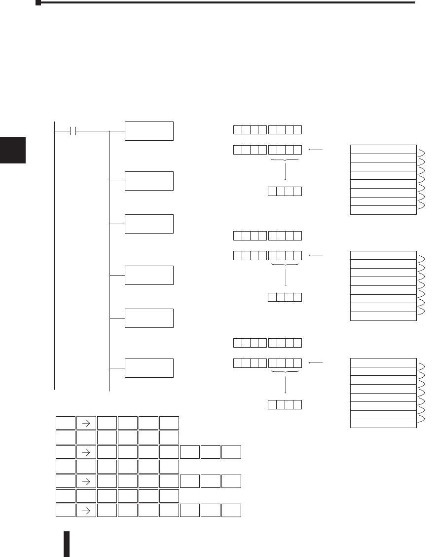
DL06 Micro PLC User Manual, 3rd Edition, Rev. D
5-66
1
2
3
4
5
6
7
8
9
10
11
12
13
14
A
B
C
D
Pop Instruction (cont’d)
In the example below, when C0 is on, the value 4545 that was on top of the stack is moved
into the accumulator using the Pop instruction The value is output to V2000 using the OUT
instruction. The next Pop moves the value 3792 into the accumulator and outputs the value
to V2001. The last Pop moves the value 7930 into the accumulator and outputs the value to
V2002. Please note if the value in the stack were greater than 16 bits (4 digits) the OUTD
instruction would be used and 2 V-memory locations for each OUTD must be allocated.
Chapter 5: Standard RLL Instructions - Accumulator/Stack Load and Output Data
1
2
3
4
5
6
7
8
9
10
11
12
13
14
a
B
c
d
Handheld Programmer Keystrokes
Acc.
Pop the 1st. value on the stack into the
accumulator and move stack values
up one location
POP
C0
POP
POP
V2000 4545
XXXXXXXX XXXX
Acc. 00004545 4545
Previous Acc. value
Current Acc. value
00003792
00
Level 1
00007930
Level 2
XXXXXXXX
Level 3
XXXXXXXX
Level 4
XXXXXXXX
Level 5
XXXXXXXX
Level 6
XXXXXXXX
Level 7
XXXXXXXX
Level 8
Accumulator Stack
00007930
Level 1
XXXXXXXX
Level 2
XXXXXXXX
Level 3
XXXXXXXX
Level 4
XXXXXXXX
Level 5
XXXXXXXX
Level 6
XXXXXXXX
Level 7
XXXXXXXX
Level 8
Accumulator Stack
XXXXXXXX
Level 1
XXXXXXXX
Level 2
XXXXXXXX
Level 3
XXXXXXXX
Level 4
XXXXXXXX
Level 5
XXXXXXXX
Level 6
XXXXXXXX
Level 7
XXXXXXXX
Level 8
Accumulator Stack
Pop the 1st. value on the stack into the
accumulator and move stack values
up one location
Pop the 1st. value on the stack into the
accumulator and move stack values
up one location
OUT
V2000
OUT
V2001
Acc.
V2001 3792
00004545 4545
Acc. 0000 3792
Previous Acc. value
Current Acc. value
Acc.
V2002 7930
0000 3792
Acc. 0000 7930
Previous Acc. value
Current Acc. value
OUT
V2002
Copy the value in the lower 16 bits of
the accumulator to V2000
Copy the value in the lower 16 bits of
the accumulator to V2001
Copy the value in the lower 16 bits of
the accumulator to V2002
Direct SOFT32
STR
$SHFT 2
C
0
AENT
SHFT CV
P
INST#
O
CV
PENT
OUT
GX SHFT AND
V
2
C
0
A
0
AENT
0
A
SHFT CV
P
INST#
O
CV
PENT
OUT
GX SHFT AND
V
2
C
0
AENT
0
A
1
B
SHFT CV
P
INST#
O
CV
PENT
OUT
GX SHFT AND
V
2
C
0
AENT
0
A
2
C
SHFT
SHFT
SHFT
DirectSOFT
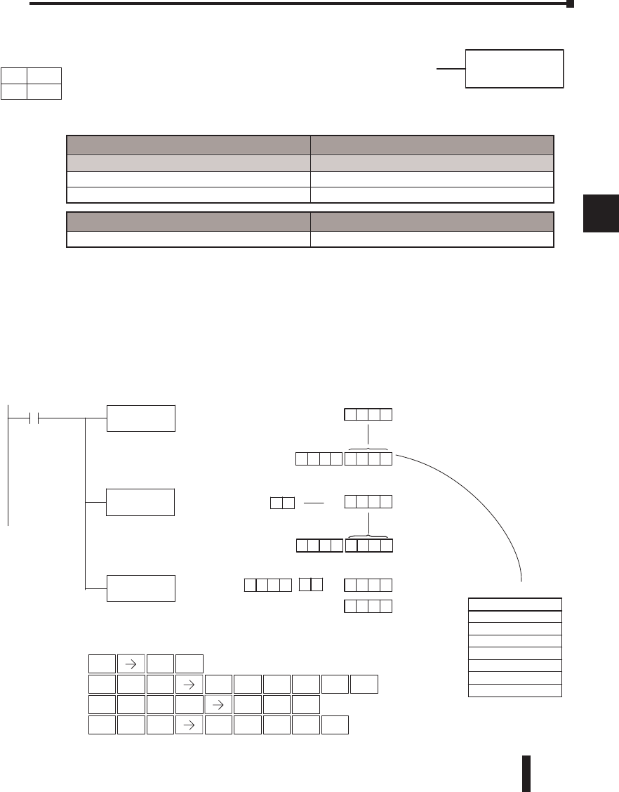
DL06 Micro PLC User Manual, 3rd Edition, Rev. D 5-67
1
2
3
4
5
6
7
8
9
10
11
12
13
14
A
B
C
D
Chapter 5: Standard RLL Instructions - Accumulator/Stack Load and Output Data
1
2
3
4
5
6
7
8
9
10
11
12
13
14
a
B
c
d
Out Indexed (OUTX)
The OUTX instruction is a 16 bit instruction. It copies a 16 bit or
4 digit value from the first level of the accumulator stack to a source
address offset by the value in the accumulator(V-memory + offset).
This instruction interprets the offset value as a HEX number. The
upper 16 bits of the accumulator are set to zero.
In the following example, when X1 is on, the constant value 3544 is loaded into the
accumulator. This is the value that will be output to the specified offset V-memory location
(V1525). The value 3544 will be placed onto the stack when the LDA instruction is executed.
Remember, two consecutive LD instructions places the value of the first load instruction
onto the stack. The LDA instruction converts octal 25 to HEX 15 and places the value in the
accumulator. The OUTX instruction outputs the value 3544 which resides in the first level of
the accumulator stack to V1525.
aaaA
OUTX
2 5
X1
OUTX
00003544
Constant
3544
Acc.
3544
0000001 5
Theunused accumulator
bits areset to zero
00003544
Level 1
XXXXXXXXLevel 2
XXXXXXXX
Level 3
XXXXXXXXLevel 4
XXXXXXXX
Level 5
XXXXXXXXLevel 6
XXXXXXXX
Level 7
XXXXXXXXLevel 8
0015
2 5
DirectSOFT32
V152515 0 0V+
=
The unused accumulator
bits are set to zero
Acc.
Octal HEX
Octal Octal Octal
The hex 15 converts
to 25 octal, which is
added to the base
address of V1500 to yield
the final answer
V1525
LD
LDA
K3544
O25
V1500
Load the accumulator with
the value 3544
Load the HEX equivalent to
octal 25 into the lower 16 bits
of the accumulator. This is the
offset for the Out Indexed
instruction, which determines
the final destinaltion address
Copy the value in the first
level of the stack to the
offset address 1525
(V1500+25)
Accumulator Stack
Handheld Programmer Keystrokes
STR
$
SHFT ANDST
L
3
D
SHFT
1
BENT
ENT
2
C
0
A
ENT
1
B
5
F
0
A
0
A
PREV
ANDST
L
3
DENT
5
F
3
D
5
F
4
E
4
E
OUT
GX SHFT SET
X
Operand Data Type DL06 Range
A aaa
V-memory V See memory map
Pointer P See memory map
Discrete Bit Flags Description
SP53 On if CPU cannot solve the logic.
DS Used
HPP Used
DirectSOFT
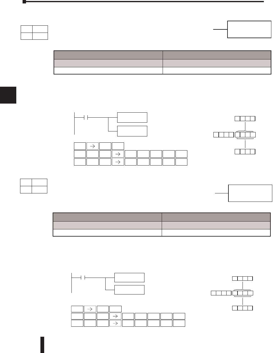
DL06 Micro PLC User Manual, 3rd Edition, Rev. D
5-68
1
2
3
4
5
6
7
8
9
10
11
12
13
14
A
B
C
D
Out Least (OUTL)
The OUTL instruction copies the value in the lower eight bits of
the accumulator to the lower eight bits of the specified V-memory
location (i.e., it copies the low byte of the low word of the
accumulator).
In the following example, when X1 is on, the value in V1400 will be loaded into the lower
16 bits of the accumulator using the LD instruction. The value in the lower 8 bits of the
accumulator is copied to V1500 using the OUTL instruction.
Out Most (OUTM)
The OUTM instruction copies the value in the upper eight bits of
the lower sixteen bits of the accumulator to the upper eight bits of
the specified V-memory location (i.e., it copies the high byte of the
low word of the accumulator).
In the following example, when X1 is on, the value in V1400 will be loaded into the lower 16
bits of the accumulator using the LD instruction. The value in the upper 8 bits of the lower
16 bits of the accumulator is copied to V1500 using the OUTM instruction.
Chapter 5: Standard RLL Instructions - Accumulator/Stack Load and Output Data
1
2
3
4
5
6
7
8
9
10
11
12
13
14
a
B
c
d
Aaaa
OUTL
LD
Acc.
8935
0035
00008935
DirectSOFT32
X1
V1400
OUTL
V1500
Load the value in V1400 into
the lower 16 bits of the
accumulater
Copy the value in the lower
8 bits of the accumulator to
V1500
The unused accumulator
bits are set to zero
V1400
V1500
Handheld Programmer Keystrokes
1
BENT
1
B
4
E
0
A
0
AENT
STR
$
SHFT ANDST
L
3
D
OUT
GX SHFT ANDST
L
1
B
5
F
0
A
0
AENT
Aaaa
OUTM
Aaaa
OUTM
Operand Data Type DL06 Range
A aaa
V-memory V See memory map
LD
Acc.
8935
8900
00008935
DirectSOFT32
Handheld Programmer Keystrokes
1
BENT
1
B
4
E
0
A
0
AENT
STR
$
SHFT ANDST
L
3
D
OUT
GX SHFT ORST
M
1
B
5
F
0
A
0
AENT
X1
V1400
OUTM
V1500
Load the value in V1400 into
the lower 16 bits of the
accumulator
Copy the value in the upper
8 bits of the lower 16 bits of
the accumulator to 1500
The unused accumulator
bits are set to zero
V1400
V1500
Operand Data Type DL06 Range
A aaa
V-memory V See memory map
DS Used
HPP Used
DS Used
HPP Used
DirectSOFT
DirectSOFT
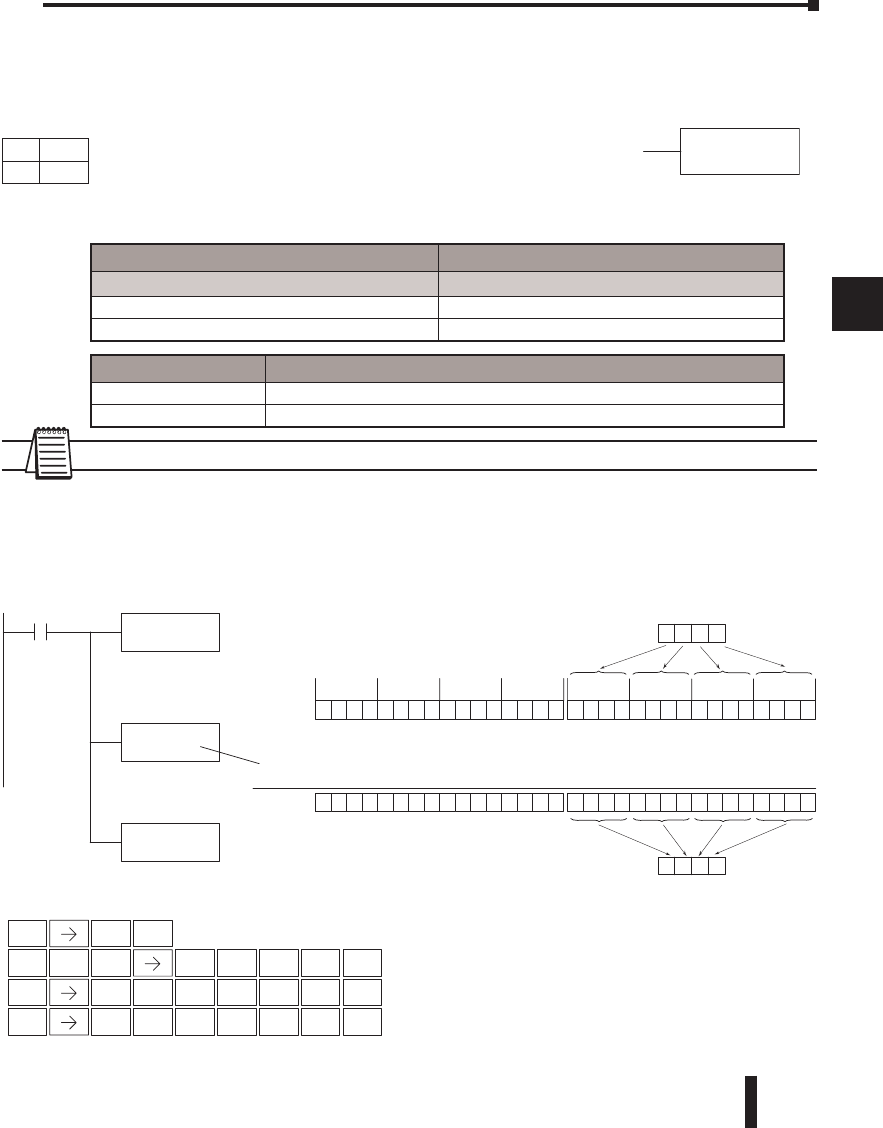
DL06 Micro PLC User Manual, 3rd Edition, Rev. D 5-69
1
2
3
4
5
6
7
8
9
10
11
12
13
14
A
B
C
D
Logical Instructions (Accumulator)
And (AND logical)
The AND instruction is a 16-bit instruction that logically ANDs
the value in the lower 16 bits of the accumulator with a specified
V-memory location (Aaaa). The result resides in the accumulator. The
discrete status flag indicates if the result of the AND is zero.
NOTE: Status flags are valid only until another instruction uses the same flag.
In the following example, when X1 is on, the value in V2000 will be loaded into the
accumulator using the LD instruction. The value in the accumulator is ANDed with the
value in V2006 using the AND instruction. The value in the lower 16 bits of the accumulator
is output to V2010 using the OUT instruction.
Chapter 5: Standard RLL Instructions - Logical
1
2
3
4
5
6
7
8
9
10
11
12
13
14
a
B
c
d
AND
A aaa
AND (V2006)
Handheld Programmer Keystrokes
LD
V2000
X1
Load the value in V2000 into
the lower 16 bits of the
accumulator
AND
V2006
AND the value in the
accumulator with
the value in V2006
OUT
V2010
Copy the lower 16 bits of the
accumulator to V2010
0010100001111010
0010100000111000
0000010000000000
V2000
287A
0000000000000000
0000000000000000
The upper 16 bits of the accumulator
will be set to 0
15 14 13 12 11 10 9876543210
31 30 29 28 27 26 25 24 23 22 21 20 19 18 17 1631 30 29 28 27 26 25 24 23 22 21 20 19 18 17 16
Acc.
Acc.
00101000011110100000000000000000
Acc.
01101010001110000000000000000000
6A38
V2010
2838
Direct SOFT32
STR
$
SHFT ANDST
L
3
D
SHFT AND
V
2
C
0
A
0
AENT
6
G
OUT
GX SHFT AND
V
2
C
0
A
1
B
0
AENT
AND
V
1
BENT
2
C
0
A
0
A
0
AENT
Operand Data Type DL06 Range
A aaa
V-memory V See memory map
Pointer P See memory map
Discrete Bit Flags Description
SP63 ON if the result in the accumulator is zero.
SP70 ON when the value loaded into the accumulator is zero.
DS Used
HPP Used
DirectSOFT
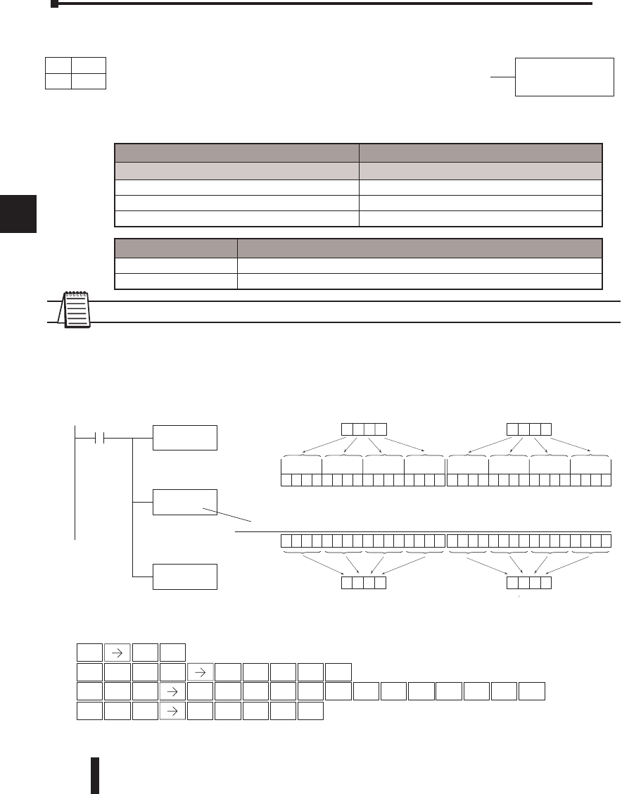
DL06 Micro PLC User Manual, 3rd Edition, Rev. D
5-70
1
2
3
4
5
6
7
8
9
10
11
12
13
14
A
B
C
D
And Double (ANDD)
ANDD is a 32-bit instruction that logically ANDs the value in the
accumulator with two consecutive V-memory locations or an 8 digit
(max.) constant value (Aaaa). The result resides in the accumulator.
Discrete status flags indicate if the result of the ANDD is zero or a
negative number (the most significant bit is on).
NOTE: Status flags are valid only until another instruction uses the same flag.
In the following example, when X1 is on, the value in V2000 and V2001 will be loaded into
the accumulator using the LDD instruction. The value in the accumulator is ANDed with
36476A38 using the ANDD instruction. The value in the accumulator is output to V2010
and V2011 using the OUTD instruction.
Chapter 5: Standard RLL Instructions - Logical
1
2
3
4
5
6
7
8
9
10
11
12
13
14
a
B
c
d
K aaa
ANDD
Operand Data Type DL06 Range
aaa
V-memory V See memory map
Pointer P See memory map
Constant K 0–FFFFFFFF
AND 36476A38
Handheld Programmer Keystrokes
LDD
V2000
X1
Load the value in V2000 and
V2001 into the accumulator
ANDD
K36476A38
AND the value in the
accumulator with
the constant value
36476A38
OUTD
V2010
Copy the value in the
accumulator to V2010 and
V2011
001010000111 1010
001010000011 10000000010000000000
287A
0001010001000110
0101010001111110
15 14 13 12 11 10 9876543210
31 30 29 28 27 26 25 24 23 22 21 20 19 18 17 1631 30 29 28 27 26 25 24 23 22 21 20 19 18 17 16
Acc.
Acc.
Acc.
V2010
2838
547E ?
V2011
1446
01010100011111100010100001111010
011010100011 10000011 011001000111
STR
$
SHFT ANDST
L
3
D
SHFT
OUT
GX
3
D
SHFT 3
D
AND
VSHFT 3
D
8
I
3
D
SHFT
SHFT
JMP
K
0
A
3
D
6
G
4
E
7
H
6
GENT
1
BENT
2
C
0
A
1
B
0
AENT
2
C
0
A
0
AENT
0
A
V2000 V2000
DirectSOFT 5
Discrete Bit Flags Description
SP63 ON if the result in the accumulator is zero.
SP70 ON if the result in the accumulator is negative
DS Used
HPP Used
DirectSOFT
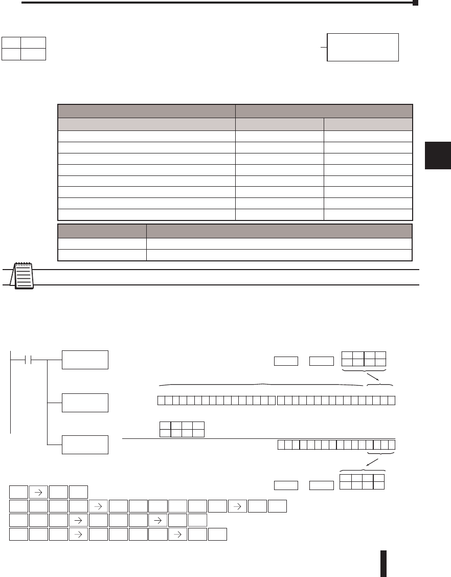
DL06 Micro PLC User Manual, 3rd Edition, Rev. D 5-71
1
2
3
4
5
6
7
8
9
10
11
12
13
14
A
B
C
D
Chapter 5: Standard RLL Instructions - Logical
1
2
3
4
5
6
7
8
9
10
11
12
13
14
a
B
c
d
And Formatted (ANDF)
The ANDF instruction logically ANDs the binary value in the
accumulator with a specified range of discrete memory bits (1–32).
The instruction requires a starting location (Aaaa) and number of
bits (Kbbb) to be ANDed. Discrete status flags indicate if the result
is zero or a negative number (the most significant bit =1).
NOTE: Status flags are valid only until another instruction uses the same flag.
In the following example, when X1 is on, the LDF instruction loads C10–C13 (4 binary bits)
into the accumulator. The accumulator contents is logically ANDed with the bit pattern from
Y20–Y23 using the ANDF instruction. The OUTF instruction outputs the accumulator’s
lower four bits to C20–C23.
bbbK
ANDF Aaaa
Operand Data Type DL06 Range
B aaa bbb
Inputs X 0-777 -
Outputs Y 0-777 -
Control Relays C 0-1777 -
Stage Bits S 0-1777 -
Timer Bits T 0-377 -
Counter Bits CT 177 -
Special Relays SP 0-777 -
Constant K -1-32
Discrete Bit Flags Description
SP63 ON if the result in the accumulator is zero.
SP70 ON if the result in the accumulator is negative
ndardRLL
C10
K4
X1
K4
K4C10
00000000000011100000000000000000
15 14 13 12 11 10 98765 4321031 30 29 28 27 26 25 24 23 22 21 20 19 18 17 1631 30 29 28 27 26 25 24 23 22 21 20 19 18 17 16
C10C11C12C13
Y20Y21Y22Y23
Accumulator
0000000000001000
Acc.
Acc. 0000000000000000 0000000000001110
1000
C20C21C22C23
DirectSOFT32
Load the status of 4
consecutive bits (C10-C13)
into the accumulator
ANDF Y20
K4
And the binary bit pattern
(Y20-Y23) with the value in
the accumulator
OUTF C20
Copy the value in the lower
4 bits in accumulator to
C20-C23
AND (Y20-Y23)
The unused accumulator bits are set to zero
Location Constant
ConstantLocation
ON ON ON OFF
ON OFFOFFOFF
ON OFFOFFOFF
C20 K4
LDF
Handheld Programmer Keystrokes
1
BENT
1
B
4
E
0
A
0
A
ENT
STR
$
SHFT ANDST
L
3
D
OUT
GX SHFT 5
F
5
F
AND
VSHFT 5
F
NEXT NEXT NEXT NEXT
NEXT 2
C
4
EENT
PREV PREV 0
A
2
C
4
EENT
DS Used
HPP Used
DirectSOFT
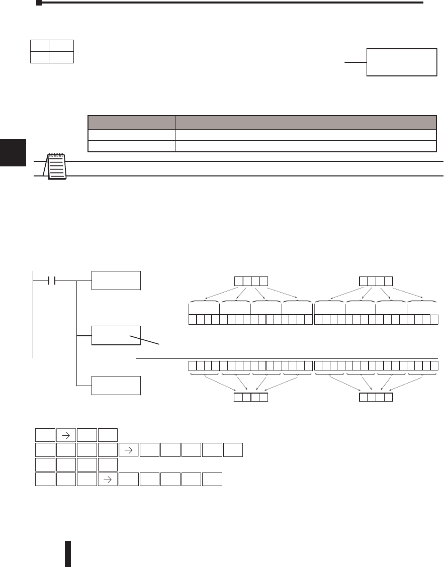
DL06 Micro PLC User Manual, 3rd Edition, Rev. D
5-72
1
2
3
4
5
6
7
8
9
10
11
12
13
14
A
B
C
D
And with Stack (ANDS)
The ANDS instruction is a 32-bit instruction that logically ANDs the value in the
accumulator with the first level of the accumulator stack. The
result resides in the accumulator. The value in the first level of
the accumulator stack is removed from the stack and all values are
moved up one level. Discrete status flags indicate if the result of the
ANDS is zero or a negative number (the most significant bit is on).
NOTE: Status flags are valid only until another instruction uses the same flag.
In the following example, when X1 is on, the binary value in the accumulator will be ANDed
with the binary value in the first level or the accumulator stack. The result resides in the
accumulator. The 32-bit value is then output to V1500 and V1501.
Chapter 5: Standard RLL Instructions - Logical
1
2
3
4
5
6
7
8
9
10
11
12
13
14
a
B
c
d
ANDS
AND
X1
0010100001111010
0010100000111
00
00000010000000000
V1400
287A
0001010001000110
0101010001111110
15 14 13 12 11 10 9876543210
31 30 29 28 27 26 25 24 23 22 21 20 19 18 17 1631 30 29 28 27 26 25 24 23 22 21 20 19 18 17 16
Acc.
Acc.
Acc.
V1500
2838
547E
1446
0101010001111110 0010100001111010
D
ir
e
ctSOFT
3
2
01101010001110000011011001000111
LDD
V1400
Load the value in V1400 and
1401 into the accumulator
ANDS
AND the value in the
accumulator with the
first level of the
accumulator stack
OUTD
V1500
(top of stack)
36476A38
V1501
V1401
Copy the value in the
accumulator to V1500
and 1501
Handheld Programmer Keystrokes
1
BENT
1
B
4
E
0
A
0
AENT
STR
$
SHFT ANDST
L
3
D
OUT
GX SHFT 3
D
1
B
5
F
0
A
0
AENT
3
D
AND
VSHFT RST
SENT
Discrete Bit Flags Description
SP63 ON if the result in the accumulator is zero.
SP70 ON if the result in the accumulator is negative
DS Used
HPP Used
DirectSOFT
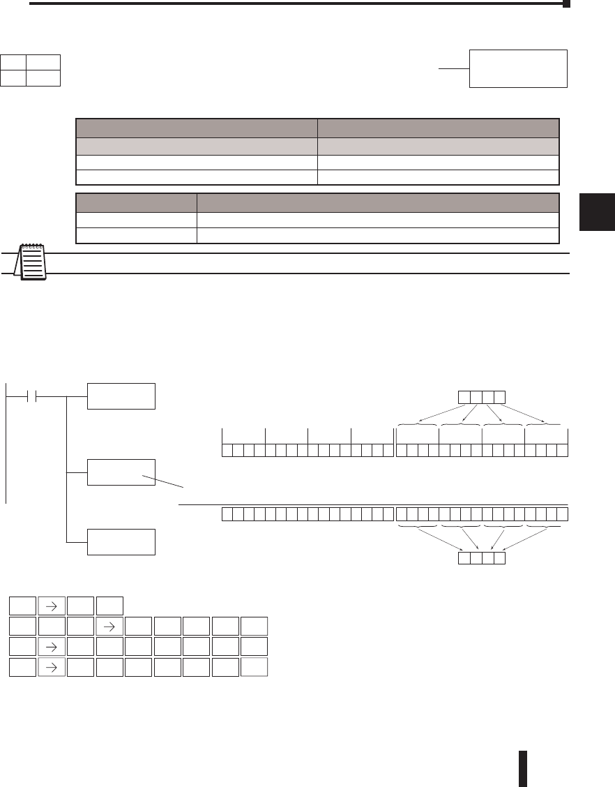
DL06 Micro PLC User Manual, 3rd Edition, Rev. D 5-73
1
2
3
4
5
6
7
8
9
10
11
12
13
14
A
B
C
D
Or (OR)
The Or instruction is a 16-bit instruction that logically ORs the
value in the lower 16 bits of the accumulator with a specified
V-memory location (Aaaa). The result resides in the accumulator.
The discrete status flag indicates if the result of the OR is zero.
NOTE: Status flags are valid only until another instruction uses the same flag.
In the following example, when X1 is on, the value in V2000 will be loaded into the
accumulator using the Load instruction. The value in the accumulator is ORed with V2006
using the OR instruction. The value in the lower 16 bits of the accumulator is output to
V2010 using the Out instruction.
Chapter 5: Standard RLL Instructions - Logical
1
2
3
4
5
6
7
8
9
10
11
12
13
14
a
B
c
d
OR
A aaa
3
D
OR (V2006)
Handheld Programmer Keystrokes
LD
V2000
X1
Load the value in V2000 into
the lower 16 bits of the
accumulator
OR
V2006
Or the value in the
accumulator with
the value in V2006
OUT
V2010
Copy the value in the lower
16 bits of the accumulator to
V2010
00101000011110
10
0110101001111010
0000010000000000
V2000
287A
0000000000000000
0000000000000000
The upper 16 bits of the accumulator
will be set to 0
15 14 13 12 11 10 987654321
31 30 29 28 27 26 25 24 23 22 21 20 19 18 17 1631 30 29 28 27 26 25 24 23 22 21 20 19 18 17 16
Acc.
Acc.
0010100001111010
0000000000000000
Acc.
0110101000111000
0000000000000000
6A38
V2010
6A7A
Direct SOFT32
STR
$
1
BENT
SHFT ANDST
L
2
C
0
A
0
A
0
AENT
SHFT AND
V
2
C
0
A
0
AENT
6
G
OUT
GX SHFT AND
V
2
C
0
A
1
B
0
AENT
OR
Q
0
Operand Data Type DL06 Range
A aaa
V-memory V See memory map
Pointer P See memory map
Discrete Bit Flags Description
SP63 ON if the result in the accumulator is zero.
SP70 ON if the result in the accumulator is negative
DS Used
HPP Used
DirectSOFT
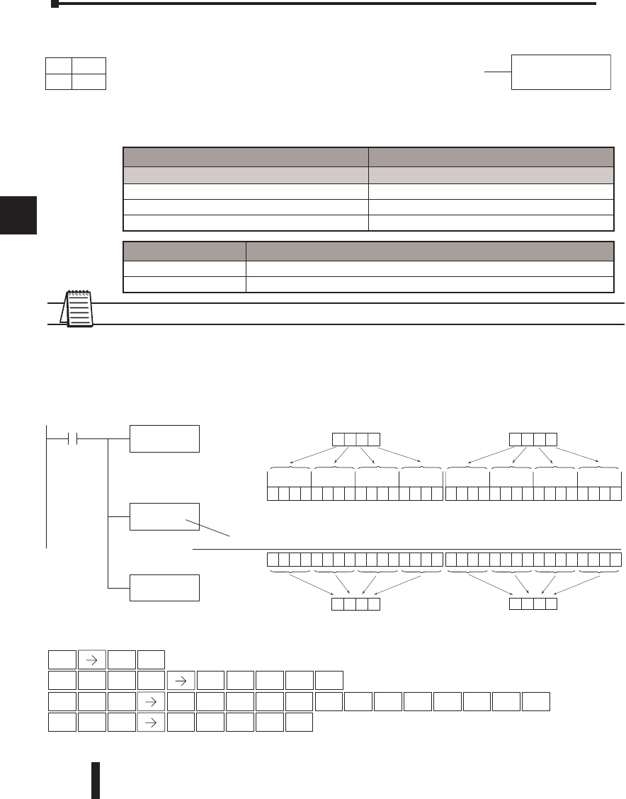
DL06 Micro PLC User Manual, 3rd Edition, Rev. D
5-74
1
2
3
4
5
6
7
8
9
10
11
12
13
14
A
B
C
D
Or Double (ORD)
ORD is a 32-bit instruction that logically ORs the value in the
accumulator with the value (Aaaa), which is either two consecutive
V-memory locations or an 8-digit (max.) constant value. The result
resides in the accumulator. Discrete status flags indicate if the result of the ORD is zero or a
negative number (the most significant bit is on).
NOTE: Status flags are valid only until another instruction uses the same flag.
In the following example, when X1 is on, the value in V2000 and V2001 will be loaded into
the accumulator using the LDD instruction. The value in the accumulator is ORed with
36476A38 using the ORD instruction. The value in the accumulator is output to V2010 and
V2011 using the OUTD instruction.
Chapter 5: Standard RLL Instructions - Logical
1
2
3
4
5
6
7
8
9
10
11
12
13
14
a
B
c
d
K aaa
ORD
JMP
K
OR 36476A38
Handheld Programmer Keystrokes
LDD
V2000
X1
Load the value in V2000 and
V2001 into accumulator
ORD
K36476A38
OR the value in the
accumulator with
the constant value
36476A38
OUTD
V2010
Copy the value in the
accumulator to V2010 and
V2011
0010100001111010
0110101001111010
0000010000000000
287A
0111011001111111
0101010001111110
15 14 13 12 11 10 9876543210
31 30 29 28 27 26 25 24 23 22 21 20 19 18 17 1631 30 29 28 27 26 25 24 23 22 21 20 19 18 17 16
Acc.
Acc.
Acc.
V2010
6A7A
547E
V2011
767F
01010100011111100010100001111010
Direct SOFT32
0110101000111000
0011011001000111
STR
$
SHFT ANDST
L
3
D
SHFT
OUT
GX
3
D
SHFT 3
D
SHFT 3
D
OR
Q
8
I
3
D
SHFTSHFT 0
A
3
D
6
G
4
E
7
H
6
GENT
1
BENT
2
C
0
A
0
A
0
AENT
2
C
0
A
1
B
0
AENT
V2000
V2001
Operand Data Type DL06 Range
aaa
V-memory V See memory map
Pointer P See memory map
Constant K 0–FFFFFFFF
Discrete Bit Flags Description
SP63 ON if the result in the accumulator is zero.
SP70 ON if the result in the accumulator is negative
DS Used
HPP Used
DirectSOFT
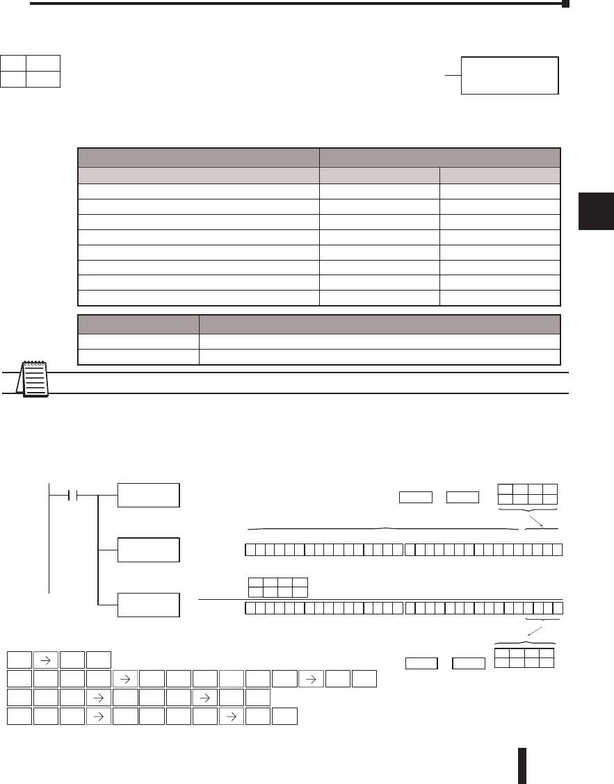
DL06 Micro PLC User Manual, 3rd Edition, Rev. D 5-75
1
2
3
4
5
6
7
8
9
10
11
12
13
14
A
B
C
D
Or Formatted (ORF)
The ORF instruction logically ORs the binary value in the
accumulator and a specified range of discrete bits (1–32). The
instruction requires a starting location (Aaaa) and the number of bits
(Kbbb) to be ORed. Discrete status flags indicate if the result is zero
or negative (the most significant bit =1).
NOTE: Status flags are valid only until another instruction uses the same flag.
In the following example, when X1 is on, the LDF instruction loads C10–C13 (4 binary
bits) into the accumulator. The ORF instruction logically ORs the accumulator contents
with Y20–Y23 bit pattern. The ORF instruction outputs the accumulator’s lower four bits to
C20–C23.
Chapter 5: Standard RLL Instructions - Logical
1
2
3
4
5
6
7
8
9
10
11
12
13
14
a
B
c
d
bbbK
ORFAaaa
Operand Data Type DL06 Range
A/B aaa bbb
Inputs X 0-777 - -
Outputs Y 0-777 - -
Control Relays C 0-1777 - -
Stage Bits S 0-1777 - -
Timer Bits T 0-377 - -
Counter Bits CT 0-177 - -
Special Relays SP 0-777 - -
Constant K - 1-32
X1
K4C10
00000000000001100000000000000000
15 14 13 12 11 10 98765 43210
31 30 29 28 27 26 25 24 23 22 21 20 19 18 17 1631 30 29 28 27 26 25 24 23 22 21 20 19 18 17 16
Acc.
Y20Y21Y22Y23
Theunused accumulatorbitsare settozero
OR (Y20 --Y23)
0000000000001110
1000
DirectSOFT32
000000000000000 0Acc.
Constant
C20 K4 ON ON ON
OFF
OFF
OFFON ON
C13 C12 C11 C10
C23 C22 C21 C20
ON OFF OFF OFF
Location Constant
Location
LDF C10
K4
ORF Y20
K4
OUTF C20
K4
Load the status fo 4
consecutive bits (C10-C13)
into the accumulator
OR the binary bit pattern
(Y20 - Y23) with the value in
the accumulator
Copy the specified number
of bits from the accumulator
to C20-C23
Handheld Programmer Keystrokes
1
BENT
1
B
4
E
0
A
0
A
ENT
STR
$
SHFT ANDST
L
3
D
OUT
GX SHFT 5
F
5
F
OR
QSHFT 5
F
NEXT NEXT NEXT NEXT
NEXT 2
C
4
EENT
PREV PREV 0
A
2
C
4
EENT
Discrete Bit Flags Description
SP63 ON if the result in the accumulator is zero.
SP70 ON if the result in the accumulator is negative
DS Used
HPP Used
DirectSOFT
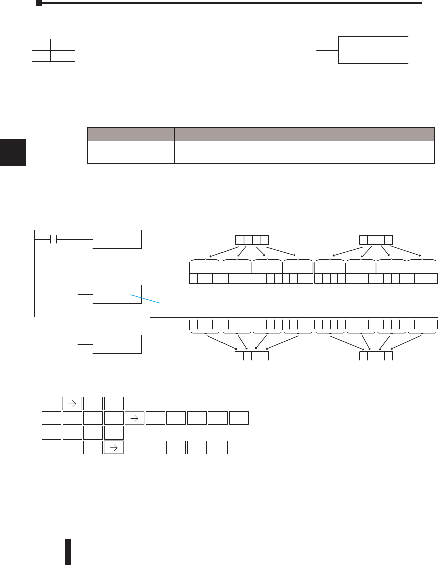
DL06 Micro PLC User Manual, 3rd Edition, Rev. D
5-76
1
2
3
4
5
6
7
8
9
10
11
12
13
14
A
B
C
D
In the following example when X1 is on, the binary value in the accumulator will be ORed
with the binary value in the first level of the stack. The result resides in the accumulator.
Chapter 5: Standard RLL Instructions - Logical
1
2
3
4
5
6
7
8
9
10
11
12
13
14
a
B
c
d
ORS
LDD
V1400
0010100001111010
01101010011110100000010000000000
V1400
287A
0111011001111111
0101010001111110
15 14 13 12 11 10 9876543210
31 30 29 28 27 26 25 24 23 22 21 20 19 18 17 1631 30 29 28 27 26 25 24 23 22 21 20 19 18 17 16
Acc.
Acc.
Acc.
V1500
6A7 A
V1401
547E
V1501
767F
0101010001111110 0010100001111010
01101010001110000011011001000111
DirectSOFT32
X1
Load the value in V1400 and
V1401 in the accumulator
ORS
OR the value in the
accumulator with the value
in the first level of the
accumulator stack
OUTD
V1500
36476A38
OR (top of stack)
Copy the value in the
accumulator to V1500 and
V1501
Handheld Programmer Keystrokes
1
BENT
1
B
4
E
0
A
0
AENT
STR
$
SHFT ANDST
L
3
D
OUT
GX SHFT 3
D
1
B
5
F
0
A
0
AENT
3
D
OR
QSHFT RST
SENT
Discrete Bit Flags Description
SP63 ON if the result in the accumulator is zero.
SP70 ON if the result in the accumulator is negative.
DS Used
HPP Used
DirectSOFT
Or with Stack (ORS)
The ORS instruction is a 32-bit instruction that logically
ORs the value in the accumulator with the first level of the
accumulator stack. The result resides in the accumulator.
The value in the first level of the accumulator stack is
removed from the stack and all values are moved up one
level. Discrete status flags indicate if the result of the ORS is
zero or a negative number (the most significant bit is on).
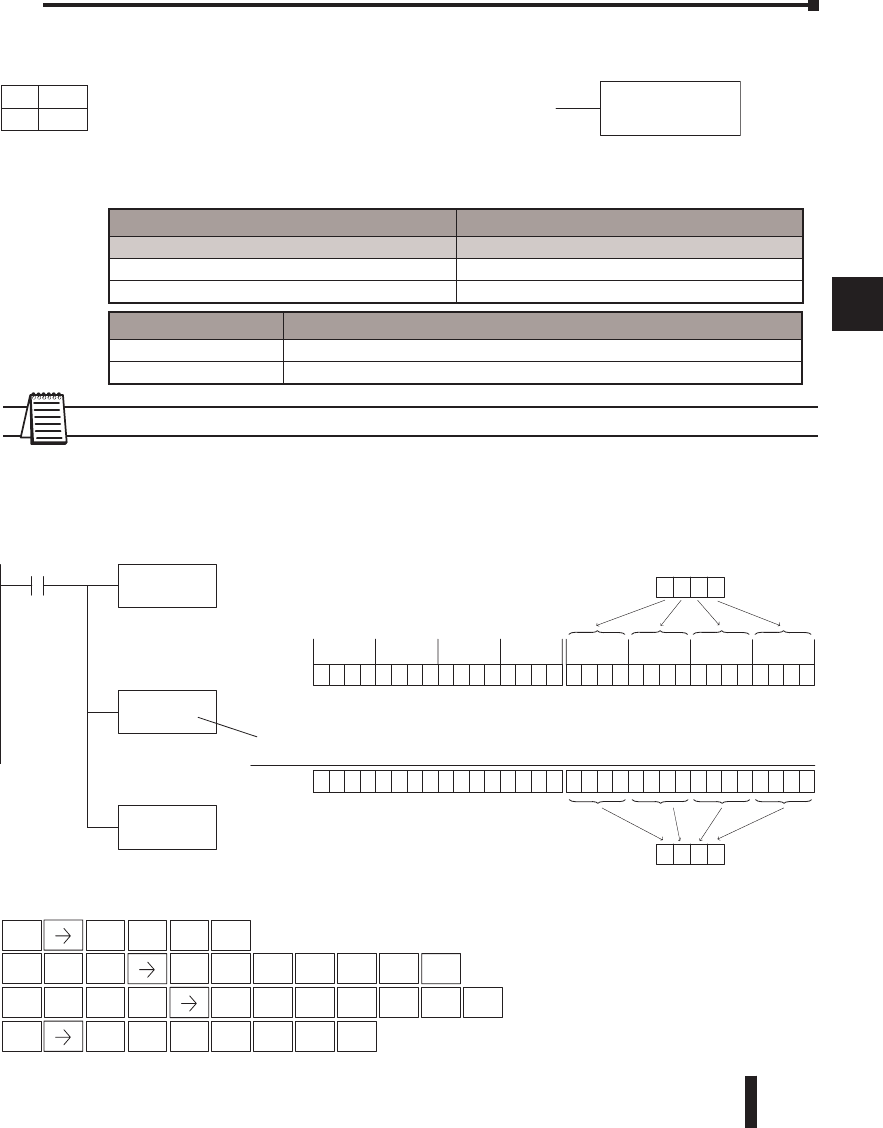
DL06 Micro PLC User Manual, 3rd Edition, Rev. D 5-77
1
2
3
4
5
6
7
8
9
10
11
12
13
14
A
B
C
D
Exclusive Or (XOR)
The XOR instruction is a 16-bit instruction that performs
an exclusive OR of the value in the lower 16 bits of the
accumulator and a specified V-memory location (Aaaa).
The result resides in the in the accumulator. The discrete
status flag indicates if the result of the XOR is zero.
NOTE: Status flags are valid only until another instruction uses the same flag.
In the following example, when X1 is on, the value in V2000 will be loaded into the
accumulator using the LD instruction. The value in the accumulator is exclusive ORed with
V2006 using the XOR instruction. The value in the lower 16 bits of the accumulator is
output to V2010 using the OUT instruction.
Chapter 5: Standard RLL Instructions - Logical
1
2
3
4
5
6
7
8
9
10
11
12
13
14
a
B
c
d
XOR
A aaa
XOR (V2006)
Handheld Programmer Keystrokes
LD
V2000
X1
Load the value in V2000 into
the lower 16 bits of the
accumulator
XOR
V2006
XOR the value in the
accumulator with
the value in V2006
OUT
V2010
Copy the lower 16 bits of the
accumulator to V2010
0010 100001111010
01000010010000100000010000000000
V2000
287A
0000000000000000
0000000000000000
The upper 16 bits of the accumulator
will be set to 0
15 14 13 12 11 10 9876543210
31 30 29 28 27 26 25 24 23 22 21 20 19 18 17 1631 30 29 28 27 26 25 24 23 22 21 20 19 18 17 16
Acc.
Acc.
00101000011110100000000000000000
Acc.
6A38
V2010
4242
Direct SOFT32
01101010001110000000000000000000
STR
$SHFT SET
X
1
BENT
SHFT ANDST
L
3
DSHFT AND
V
2
C
0
A
0
A
0
AENT
SHFT AND
V
2
C
0
A
0
AENT
6
G
OUT
GX SHFT AND
V
2
C
0
A
1
B
0
AENT
OR
Q
SHFT SHFT
SET
X
Operand Data Type DL06 Range
A aaa
V-memory V See memory map
Pointer P See memory map
Discrete Bit Flags Description
SP63 ON if the result in the accumulator is zero.
SP70 ON if the result in the accumulator is negative.
DS Used
HPP Used
DirectSOFT
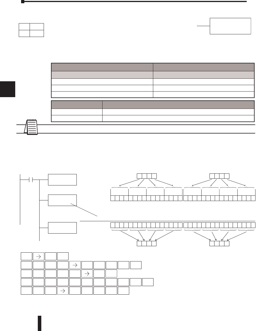
DL06 Micro PLC User Manual, 3rd Edition, Rev. D
5-78
1
2
3
4
5
6
7
8
9
10
11
12
13
14
A
B
C
D
NOTE: Status flags are valid only until another instruction uses the same flag.
In the following example, when X1 is on, the value in V2000 and V2001 will be loaded into
the accumulator using the LDD instruction. The value in the accumulator is exclusively
ORed with 36476A38 using the XORD instruction. The value in the accumulator is output
to V2010 and V2011 using the OUTD instruction.
Chapter 5: Standard RLL Instructions - Logical
1
2
3
4
5
6
7
8
9
10
11
12
13
14
a
B
c
d
K aaa
XORD
JMP
K
SHFTSHFT 3
D
OR
Q
XORD 36476A38
Handheld Programmer Keystrokes
LDD
V2000
X1
Load the value in V2000 and
V2001 into the accumulator
XORD
K36476A38
XORD the value in the
accumulator with
the constant value
36476A38
OUTD
V2010
Copy the value in the
accumulator to V2010
and V2011
0010100001111010
0100001001000010
0000010000000000
V2000
287A
0110001000111001
0101010001111110
15 14 13 12 11 10 987654
3210
31 30 29 28 27 26 25 24 23 22 21 20 19 18 17 1631 30 29 28 27 26 25 24 23 22 21 20 19 18 17 16
Acc.
Acc.
Acc.
V2010
4242
V2001
547E
V2011
6239
01010100011111100010100001111010
Direct SOFT32
0110101000111000
0011011001000111
STR
$
SHFT ANDST
L
3
D
3
D
SHFT SET
X
OUT
GX SHFT 3
D
3
D
6
G
4
E
8
I
3
D
SHFTSHFT 0
A
7
H
6
GENT
1
BENT
2
C
0
A
0
A
0
AENT
2
C
0
A
1
B
0
AENT
Operand Data Type DL06 Range
Aaaa
V-memory V See memory map
Pointer P See memory map
Constant K 0–FFFFFFFF
Discrete Bit Flags Description
SP63 ON if the result in the accumulator is zero.
SP70 ON if the result in the accumulator is negative
DS Used
HPP Used
DirectSOFT
Exclusive Or Double (XORD)
The XORD is a 32-bit instruction that performs an exclusive
OR of the value in the accumulator and the value (Aaaa),
which is either two consecutive V-memory locations or an 8
digit (max.) constant. The result resides in the accumulator.
Discrete status flags indicate if the result of the XORD is zero
or a negative number (the most significant bit is on).
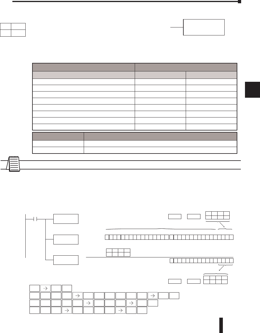
DL06 Micro PLC User Manual, 3rd Edition, Rev. D 5-79
1
2
3
4
5
6
7
8
9
10
11
12
13
14
A
B
C
D
Exclusive Or Formatted (XORF)
The XORF instruction performs an exclusive OR of the
binary value in the accumulator and a specified range of
discrete memory bits (1–32).
The instruction requires a starting location (Aaaa) and the number of bits (Bbbb) to be
exclusive OR’d. Discrete status flags indicate if the result of the XORF is zero or negative (the
most significant bit =1).
NOTE: Status flags are valid only until another instruction uses the same flag.
In the following example, when X1 is on, the binary pattern of C10–C13 (4 bits) will be
loaded into the accumulator using the LDF instruction. The value in the accumulator will
be logically exclusive ORed with the bit pattern from Y20–Y23 using the XORF instruction.
The value in the lower 4 bits of the accumulator is output to C20–C23 using the OUTF
instruction.
Chapter 5: Standard RLL Instructions - Logical
1
2
3
4
5
6
7
8
9
10
11
12
13
14
a
B
c
d
XORF Aaaa
bbbK
StandardRLL
K4C10
00000000000001100000000000000000
15 14 13 12 11 10 98765 4321031 30 29 28 27 26 25 24 23 22 21 20 19 18 17 1631 30 29 28 27 26 25 24 23 22 21 20 19 18 17 16
C10C11C12C13
OFFONONOFF
Y20Y21Y22Y23
OFFONOFFON
Accumulator
0000000000001100
Acc.
Acc. 0000000000000000 0000000000000110
1010
C20C21C22C23
OFF
OFF
ONON
K4C20
Handheld Programmer Keystrokes
1
BENT
1
B
4
E
0
A
0
A
ENT
STR
$
SHFT ANDST
L
3
D
OUT
GX SHFT 5
F
5
F
OR
Q
SHFT SET
XSHFT 5
F
NEXT NEXT NEXT NEXT
NEXT 2
C
4
EENT
PREV PREV 0
A
2
C
4
EENT
Location Constant
Location Constant
The unused accumulator bits are set to zero
DirectSOFT32
X1 LDF C10
K4
X0RF Y20
K4
OUTF C20
K4
Load the status of 4
consecutive bits (C10-C13)
into the accumulator
Exclusive OR the binary bit
pattern (Y20-Y23) with the
value in the accumulator
Copy the specified number
of bits from the accumulator
to C20-C23
XORF (Y20-Y23)
Operand Data Type DL06 Range
A/B aaa bbb
Inputs X 0-777 -
Outputs Y 0-777 -
Control Relays C 0-1777 -
Stage Bits S 0-1777 -
Timer Bits T 0-377 -
Counter Bits CT 177 -
Special Relays SP 0-777 -
Constant K -1-32
Discrete Bit Flags Description
SP63 ON if the result in the accumulator is zero.
SP70 ON if the result in the accumulator is negative
DS Used
HPP Used
DirectSOFT
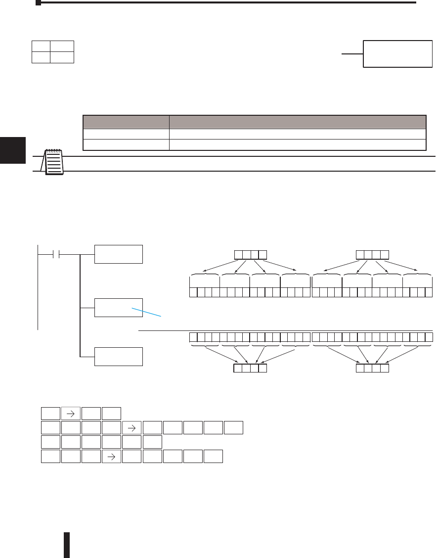
DL06 Micro PLC User Manual, 3rd Edition, Rev. D
5-80
1
2
3
4
5
6
7
8
9
10
11
12
13
14
A
B
C
D
NOTE: Status flags are valid only until another instruction uses the same flag.
In the following example, when X1 is on, the value in V1400 and V1401 will be loaded into
the accumulator using the LDD instruction. The binary value in the accumulator will be
exclusively ORed with 36476A38 using the XORS instruction. The value in the accumulator
is output to V1500 and V1501 using the OUTD instruction.
Chapter 5: Standard RLL Instructions - Logical
1
2
3
4
5
6
7
8
9
10
11
12
13
14
a
B
c
d
XORS
X1
0010100001111010
0100001001000
010
0000010000000000
V1400
287A
0110001000111001
0101010001111110
15 14 13 12 11 10 987654
3210
31 30 29 28 27 26 25 24 23 22 21 20 19 18 17 1631 30 29 28 27 26 25 24 23 22 21 20 19 18 17 16
Acc.
Acc.
Acc.
V1500
4242
V1401
547E
V1501
6239
0101010001111110 0010100001111
010
0110101000111
000
0011011001000111
D
ir
e
ctSOFT
3
2
Handheld Programmer Keystrokes
1
BENT
1
B
4
E
0
A
0
AENT
STR
$
SHFT ANDST
L
3
D
OUT
GX SHFT 3
D
1
B
5
F
0
A
0
AENT
3
D
OR
Q
SHFT SET
XENTSHFT RST
S
Copy the value in the
accumulator to V1500 and V1501
OUTD
V1500
Exclusive OR the value
in the accumulator
with the value in the
first level of the
accumulator stack
LDD
V1400
Load the value in V1400 and
V1401 into the accumulator
36476A38
XOR (1st level of Stack)
XORS
Discrete Bit Flags Description
SP63 ON if the result in the accumulator is zero.
SP70 ON if the result in the accumulator is negative
DS Used
HPP Used
DirectSOFT
Exclusive Or with Stack (XORS)
The XORS instruction is a 32-bit instruction that performs an
Exclusive Or of the value in the accumulator with the first level
of the accumulator stack. The result resides in the accumulator.
The value in the first level of the accumulator stack is removed
from the stack and all values are moved up one level. Discrete
status flags indicate if the result of the XORS is zero or a negative
number (the most significant bit is on).
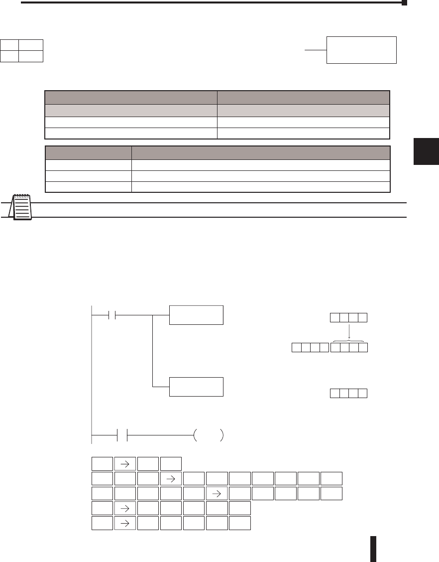
DL06 Micro PLC User Manual, 3rd Edition, Rev. D 5-81
1
2
3
4
5
6
7
8
9
10
11
12
13
14
A
B
C
D
Compare (CMP)
The CMP instruction is a 16-bit instruction that compares the
value in the lower 16 bits of the accumulator with the value in a
specified V-memory location (Aaaa). The corresponding status flag
will be turned on indicating the result of the comparison. The data
format for this instruction is BCD/Hex, Decimal and Binary.
NOTE: Status flags are valid only until another instruction uses the same flag.
In the following example when X1 is on, the constant 4526 will be loaded into the lower 16
bits of the accumulator using the LD instruction. The value in the accumulator is compared
with the value in V2000 using the CMP instruction. The corresponding discrete status flag
will be turned on indicating the result of the comparison. In this example, if the value in
the accumulator is less than the value specified in the CMP instruction, SP60 will turn on,
energizing C30.
Chapter 5: Standard RLL Instructions - Logical
1
2
3
4
5
6
7
8
9
10
11
12
13
14
a
B
c
d
CMP
A aaa
Discrete Bit Flags Description
SP60 On when the value in the accumulator is less than the instruction value.
SP61 On when the value in the accumulator is equal to the instruction value.
SP62 On when the value in the accumulator is greater than the instruction value.
Handheld Programmer Keystrokes
V2000
Acc.
CONSTANT
4526 ?
8945
000045264526 ??
LD
Compare the value in the
accumulator with the value
in V2000
Load the constant value
4526 into the lower 16 bits of
the accumulator
K4526
CMP
X1
V2000
Compared
with
SP60 C30
DirectSOFT
The unused accumulator
bits are set to zero
STR
$
SHFT ANDST
L
3
DSHFT JMP
K
4
E
5
F
2
C
6
GENT
SHFT 2
C
ORST
M
CV
P
STR
$SHFT ENT
STRN
SP
6
G
0
A
OUT
GX SHFT 2
C
3
D
0
AENT
1
BENT
2
C
0
A
0
A
0
AENTSHFT
OUT
Operand Data Type DL06 Range
A aaa
V-memory V See memory map
Pointer P See memory map
DS Used
HPP Used
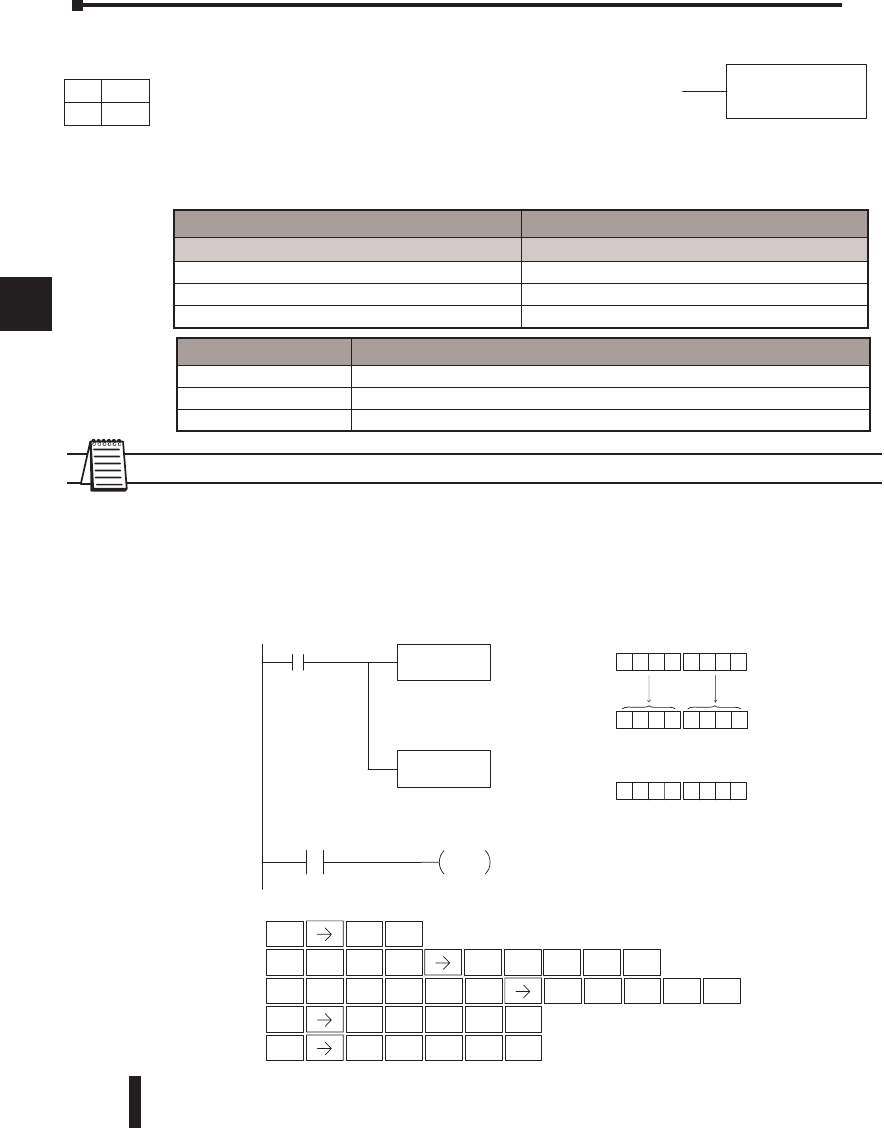
DL06 Micro PLC User Manual, 3rd Edition, Rev. D
5-82
1
2
3
4
5
6
7
8
9
10
11
12
13
14
A
B
C
D
Compare Double (CMPD)
The Compare Double instruction is a 32–bit instruction that
compares the value in the accumulator with the value (Aaaa), which
is either two consecutive V-memory locations or an 8–digit (max.)
constant. The corresponding status flag will be turned on indicating
the result of the comparison. The data format for this instruction is BCD/Hex, Decimal and
Binary.
NOTE: Status flags are valid only until another instruction uses the same flag.
In the following example, when X1 is on, the value in V2000 and V2001 will be loaded
into the accumulator using the Load Double instruction. The value in the accumulator
is compared with the value in V2010 and V2011 using the CMPD instruction. The
corresponding discrete status flag will be turned on, indicating the result of the comparison.
In this example, if the value in the accumulator is less than the value specified in the Compare
instruction, SP60 will turn on energizing C30.
Chapter 5: Standard RLL Instructions - Logical
1
2
3
4
5
6
7
8
9
10
11
12
13
14
a
B
c
d
CMPD
A aaa
Handheld Programmer Keystrokes
LDD
Compare the value in the
accumulator with the value
in V2010 and V2011
Load the value in V2000 and
V2001 into the accumulator
V2000
CMPD
X1
V2010
Compared
with
SP60 C30
V2010
Acc.
V2000
4526 7299
V2001
45267299
V2011
67395026
DirectSOFT
STR
$
SHFT ANDST
L
3
D
SHFT 2
C
ORST
M
CV
P
STR
$SHFT ENT
STRN
SP
6
G
0
A
OUT
GX SHFT 2
C
3
D
0
AENT
3
D
3
D
1
BENT
ENT
2
C
0
A
0
AENT
2
C
0
A
0
A
0
A
1
B
SHFT
OUT
Operand Data Type DL06 Range
Aaaa
V-memory V See memory map
Pointer P See memory map
Constant K 0–FFFFFFFF
Discrete Bit Flags Description
SP60 On when the value in the accumulator is less than the instruction value.
SP61 On when the value in the accumulator is equal to the instruction value.
SP62 On when the value in the accumulator is greater than the instruction value.
DS Used
HPP Used
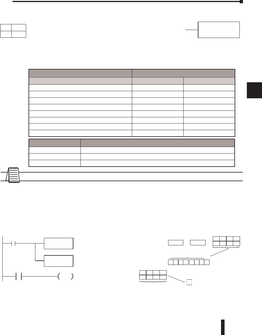
DL06 Micro PLC User Manual, 3rd Edition, Rev. D 5-83
1
2
3
4
5
6
7
8
9
10
11
12
13
14
A
B
C
D
Compare Formatted (CMPF)
The Compare Formatted instruction compares the value in the
accumulator with a specified number of discrete locations (1–32).
The instruction requires a starting location (Aaaa) and the number
of bits (Kbbb) to be compared. The corresponding status flag will
be turned on, indicating the result of the comparison. The data format for this instruction is
BCD/Hex, Decimal and Binary.
NOTE: Status flags are valid only until another instruction uses the same flag.
In the following example, when X1 is on, the Load Formatted instruction loads the binary
value (6) from C10–C13 into the accumulator. The CMPF instruction compares the value
in the accumulator to the value in Y20–Y23 (E hex). The corresponding discrete status flag
will be turned on, indicating the result of the comparison. In this example, if the value in the
accumulator is less than the value specified in the Compare instruction, SP60 will turn on
energizing C30.
Chapter 5: Standard RLL Instructions - Logical
1
2
3
4
5
6
7
8
9
10
11
12
13
14
a
B
c
d
bbbK
CMPF Aaaa
K4C10
LocationConstant C10C11C12C13
OFFONONOFF
Theunused accumulator
bits areset to zero
Y20Y21Y22Y23
OFFONONON
Compared
with
Acc. 000000 0 6
E
LDF
Comparethe valueinthe
accumulatorwiththe value
of thespecifieddiscrete
location (Y20 --Y23)
Load thevalue of the
specifieddiscretelocations
(C10 --C13) into the
accumulator
C10
K4
CMPF
X1
Y20
K4
SP60
DirectSOFT32
C30
OUT
Operand Data Type DL06 Range
A/B aaa bbb
Inputs X 0-777 -
Outputs Y 0-777 -
Control Relays C 0-1777 -
Stage Bits S 0-1777 -
Timer Bits T 0-377 -
Counter Bits CT 0-177 -
Special Relays SP 0-777 -
Constant K -1-32
Discrete Bit Flags Description
SP60 On when the value in the accumulator is less than the instruction value.
SP61 On when the value in the accumulator is equal to the instruction value.
SP62 On when the value in the accumulator is greater than the instruction value.
DS Used
HPP Used
DirectSOFT
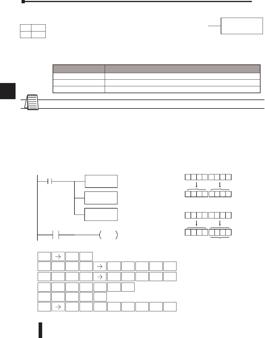
DL06 Micro PLC User Manual, 3rd Edition, Rev. D
5-84
1
2
3
4
5
6
7
8
9
10
11
12
13
14
A
B
C
D
Chapter 5: Standard RLL Instructions - Logical
1
2
3
4
5
6
7
8
9
10
11
12
13
14
a
B
c
d
Compare with Stack (CMPS)
The Compare with Stack instruction is a 32-bit instruction that
compares the value in the accumulator with the value in the first
level of the accumulator stack. The data format for this instruction is
BCD/Hex, Decimal and Binary.
The corresponding status flag will be turned on, indicating the result of the comparison. This
does not affect the value in the accumulator.
NOTE: Status flags are valid only until another instruction uses the same flag.
In the following example, when X1 is on, the value in V1400 and V1401 is loaded into the
accumulator using the Load Double instruction. The value in V1410 and V1411 is loaded
into the accumulator using the Load Double instruction. The value that was loaded into the
accumulator from V1400 and V1401 is placed on top of the stack when the second Load
instruction is executed. The value in the accumulator is compared with the value in the first
level of the accumulator stack using the CMPS instruction. The corresponding discrete status
flag will be turned on indicating the result of the comparison. In this example, if the value in
the accumulator is less than the value in the stack, SP60 will turn on, energizing C30.
CMPS
X1
Acc. 65003544
V1400
354 4
SP60C30
OUT
V1401
6500
Acc. 55003544
V1410
354 4
V1411
5500
DirectSOFT32
Handheld Programmer Keystrokes
STR
$
SHFT ANDST
L
3
D
SHFT 2
C
ORST
M
CV
P
STR
$PREV ENT
6
G
0
A
OUT
GX SHFT 2
C
3
D
0
AENT
3
D
RST
S
1
BENT
ENTSHFT
1
B
4
E
0
A
0
AENT
SHFT ANDST
L
3
D
3
D
1
B
4
E
1
B
0
AENT
NEXT NEXT NEXT
Compared with
Top of Stack
LDD
V1400
LDD
V1410
CMPS
Load the value in V1400 and
V1401 into the accumulator
Load the value in V1410 and
V1411 into the accumulator
Compare the value in the
accumulator with the value
in the first level of the
accumulator stack
Discrete Bit Flags Description
SP60 On when the value in the accumulator is less than the instruction value.
SP61 On when the value in the accumulator is equal to the instruction value.
SP62 On when the value in the accumulator is greater than the instruction value.
DS Used
HPP Used
DirectSOFT
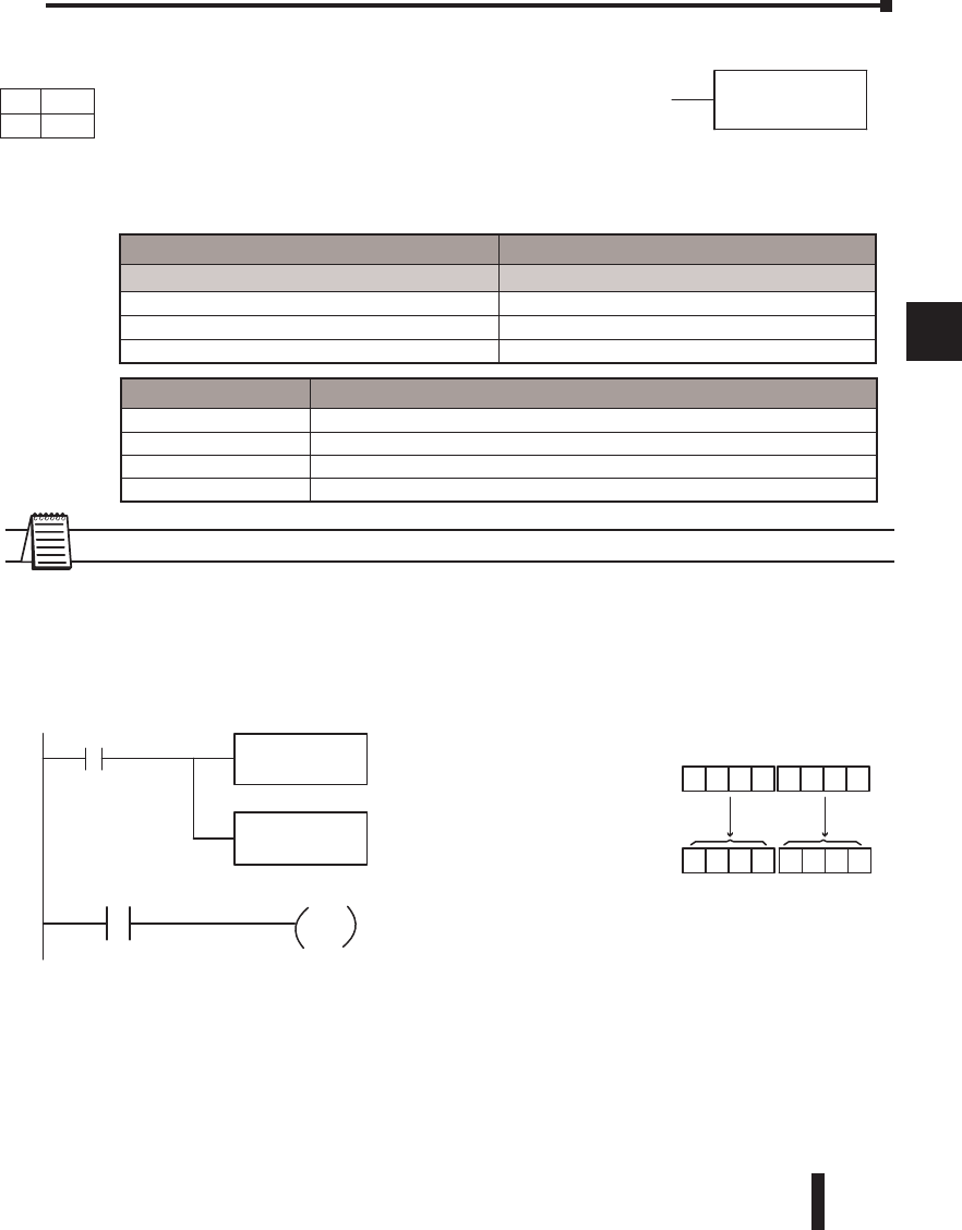
DL06 Micro PLC User Manual, 3rd Edition, Rev. D 5-85
1
2
3
4
5
6
7
8
9
10
11
12
13
14
A
B
C
D
Chapter 5: Standard RLL Instructions - Logical
1
2
3
4
5
6
7
8
9
10
11
12
13
14
a
B
c
d
Compare Real Number (CMPR)
The Compare Real Number instruction compares a real number
value in the accumulator with two consecutive V-memory locations
containing a real number. The corresponding status flag will be
turned on, indicating the result of the comparison. Both numbers
being compared are 32 bits long.
NOTE: Status flags are valid only until another instruction uses the same flag.
In the following example, when X1 is on, the LDR instruction loads the real number
representation for 7 decimal into the accumulator. The CMPR instruction compares
the accumulator contents with the real representation for decimal 6. Since 7 > 6, the
corresponding discrete status flag is turned on (special relay SP62), turning on control relay
C1.
X1
0000
40D0 0000
40E0
DirectSOFT32
SP62
LDR
R7.0
CMPR
R6.0
C1
OUT
CMPR
Acc.
Load the real number
representation for decimal 7
into the accumulator
Compare the value with the
real number representation
for decimal 6
CMPR
Aaaa
Operand Data Type DL06 Range
A aaa
V-memory V See memory map
Pointer P See memory map
Constant R -3.402823E+ 038 to + -3.402823E+ 038
Discrete Bit Flags Description
SP60 On when the value in the accumulator is less than the instruction value.
SP61 On when the value in the accumulator is equal to the instruction value.
SP62 On when the value in the accumulator is greater than the instruction value.
SP71 On anytime the V-memory specified by a pointer (P) is not valid
DS Used
HPP Used
DirectSOFT
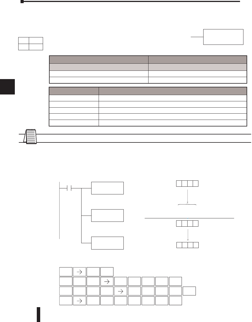
DL06 Micro PLC User Manual, 3rd Edition, Rev. D
5-86
1
2
3
4
5
6
7
8
9
10
11
12
13
14
A
B
C
D
Math Instructions
Add (ADD)
Add is a 16-bit instruction that adds a BCD value in the
accumulator with a BCD value in a V-memory location (Aaaa).
(You cannot use a constant as the parameter in the box.) The
result resides in the accumulator.
NOTE: Status flags are valid only until another instruction uses the same flag.
In the following example, when X1 is on, the value in V2000 will be loaded into the
accumulator using the Load instruction. The value in the lower 16 bits of the accumulator
is added to the value in V2006 using the Add instruction. The value in the accumulator is
copied to V2010 using the Out instruction.
Chapter 5: Standard RLL Instructions - Math
1
2
3
4
5
6
7
8
9
10
11
12
13
14
a
B
c
d
ADD
A aaa
Discrete Bit Flags Description
SP63 On when the result of the instruction causes the value in the accumulator to be zero.
SP66 On when the 16-bit addition instruction results in a carry.
SP67 On when the 32-bit addition instruction results in a carry.
SP70 On anytime the value in the accumulator is negative.
SP75 On when a BCD instruction is executed and a NON–BCD number was encountered.
Direct SOFT32
Handheld Programmer Keystrokes
LD
V2000
X1
Load the value in V2000 into
the lower 16 bits of the
accumulator
ADD
V2006
Add the value in the lower
16 bits of the accumulator
with the value in V2006
OUT
V2010
Copy the value in the lower
16 bits of the accumulator to
V2010
V2010
V2000
4935
7435
00004935
+2500
Acc. 7435
(V2006)
(Accumulator)
The unused accumulator
bits are set to zero
SHFT ANDST
L
3
D
STR
$
SHFT 0
A
3
D
3
D
OUT
GX SHFT AND
V
2
C
0
A
1
B
0
AENT
1
BENT
2
C
0
A
0
A
0
AENT
2
C
0
A
0
AENT
6
G
Operand Data Type DL06 Range
A aaa
V-memory V See memory map
Pointer P See memory map
DS Used
HPP Used
DirectSOFT
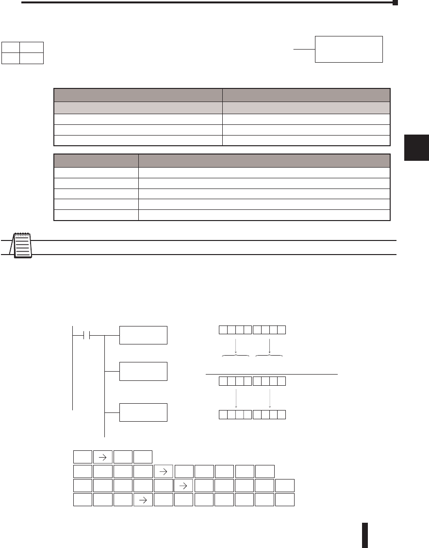
DL06 Micro PLC User Manual, 3rd Edition, Rev. D 5-87
1
2
3
4
5
6
7
8
9
10
11
12
13
14
A
B
C
D
Add Double (ADDD)
Add Double is a 32-bit instruction that adds the BCD value in
the accumulator with a BCD value (Aaaa), which is either two
consecutive V-memory locations or an 8–digit (max.) BCD
constant. The result resides in the accumulator.
NOTE: Status flags are valid only until another instruction uses the same flag.
In the following example, when X1 is on, the value in V2000 and V2001 will be loaded into
the accumulator using the Load Double instruction. The value in the accumulator is added
with the value in V2006 and V2007 using the Add Double instruction. The value in the
accumulator is copied to V2010 and V2011 using the Out Double instruction.
Chapter 5: Standard RLL Instructions - Math
1
2
3
4
5
6
7
8
9
10
11
12
13
14
a
B
c
d
ADDD
A aaa
67395026
Direct SOFT
Handheld Programmer Keystrokes
LDD
V2000
X1
Load the value in V2000 and
V2001 into the accumulator
ADDD
V2006
Add the value in the
accumulator with the value
in V2006 and V2007
OUTD
V2010
Copy the value in the
accumulator to V2010 and
V2011
V2010
V2000
V2001
67395026
V2001
87399072
(V2006 and V2007)
(Accumulator)
20004046 +
87399072
Acc.
STR
$
1
B
SHFT 0
A
3
D
3
D
SHFT ANDST
L
3
D
3
D
3
D
OUT
GX SHFT 3
D
AND
V
2
C
0
A
1
B
0
AENTSHFT
ENT
2
C
0
A
0
AENT
6
G
2
C
0
A
0
A
0
AENT
Discrete Bit Flags Description
SP63 On when the result of the instruction causes the value in the accumulator to be zero.
SP66 On when the 16-bit addition instruction results in a carry.
SP67 On when the 32-bit addition instruction results in a carry.
SP70 On anytime the value in the accumulator is negative.
SP75 On when a BCD instruction is executed and a NON–BCD number was encountered.
Operand Data Type DL06Range
A aaa
V-memory V See memory map
Pointer P See memory map
Constant K 0–99999999
DS Used
HPP Used
DirectSOFT
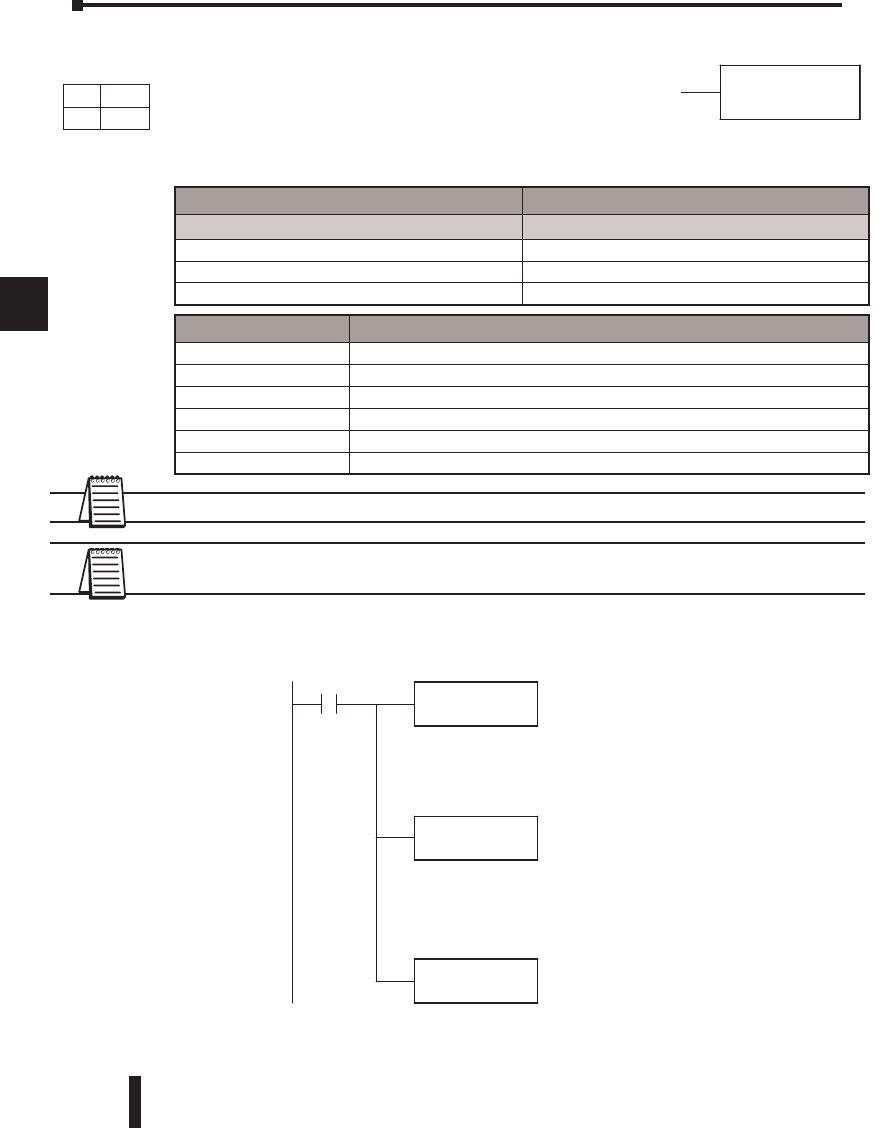
DL06 Micro PLC User Manual, 3rd Edition, Rev. D
5-88
1
2
3
4
5
6
7
8
9
10
11
12
13
14
A
B
C
D
Chapter 5: Standard RLL Instructions - Math
1
2
3
4
5
6
7
8
9
10
11
12
13
14
a
B
c
d
Add Real (ADDR)
The Add Real instruction adds a real number in the accumulator with
either a real constant or a real number occupying two consecutive
V-memory locations. The result resides in the accumulator. Both
numbers must be Real data type (IEEE floating point format).
NOTE: Status flags are valid only until another instruction uses the same flag.
NOTE: The current HPP does not support real number entry with automatic conversion to the 32-bit
IEEE format. You must use DirectSOFT for this feature.
ADDR
Aaaa
ADDR
Aaaa
Discrete Bit Flags Description
SP63 On when the result of the instruction causes the value in the accumulator to be zero.
SP70 On anytime the value in the accumulator is negative.
SP71 On anytime the V-memory specified by a pointer (P) is not valid.
SP72 On anytime the value in the accumulator is an invalid floating point number.
SP73 On when a signed addition or subtraction results in a incorrect sign bit.
SP74 On anytime a floating point math operation results in an underflow error.
LDR
R7.0
X1
Loadthe real num ber7.0
into theaccumulator
ADDR
R15.0
Addthe real number 15.0to
theaccumulatorcontents,
whichisinreal number
format.
Copy theresultinthe accumulator
to V1400 and V1401.
OUTD
V1400
DirectSOFT 5
Operand Data Type DL06 Range
A aaa
V-memory V See memory map
Pointer P See memory map
Constant R -3.402823E+ 38 to + -3.402823E+ 38
DS Used
HPP Used
DirectSOFT
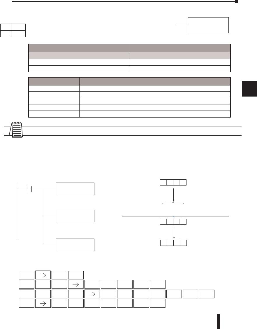
DL06 Micro PLC User Manual, 3rd Edition, Rev. D 5-89
1
2
3
4
5
6
7
8
9
10
11
12
13
14
A
B
C
D
Subtract (SUB)
Subtract is a 16-bit instruction that subtracts the BCD value
(Aaaa) in a V-memory location from the BCD value in the
lower 16 bits of the accumulator. The result resides in the
accumulator.
NOTE: Status flags are valid only until another instruction uses the same flag.
In the following example, when X1 is on, the value in V2000 will be loaded into the
accumulator using the Load instruction. The value in V2006 is subtracted from the value in
the accumulator using the Subtract instruction. The value in the accumulator is copied to
V2010 using the Out instruction.
Chapter 5: Standard RLL Instructions - Math
1
2
3
4
5
6
7
8
9
10
11
12
13
14
a
B
c
d
SUB
A aaa
Direct SOFT32
Handheld Programmer Keystrokes
LD
V2000
X1
Load the value in V2000 into
the lower 16 bits of the
accumulator
SUB
V2006
Subtract the value in V2006
from the value in the lower
16 bits of the accumulator
OUT
V2010
Copy the value in the lower
16 bits of the accumulator to
V2010
V2010
2
0
0
_
V2000
475
883
00002475
1592
Acc. 883
The unused accumulator
bits are set to zero
SHFT ANDST
L
3
D
STR
$
SHFT SHFT AND
V
2
C
0
A
0
AENT
6
G
OUT
GX SHFT AND
V
2
C
0
A
1
B
0
AENT
RST
S
ISG
U
1
B
1
BENT
2
C
0
A
0
A
0
AENT
Operand Data Type DL06Range
A aaa
V-memory V See memory map
Pointer P See memory map
Discrete Bit Flags Description
SP63 On when the result of the instruction causes the value in the accumulator to be zero.
SP64 On when the 16-bit subtraction instruction results in a borrow
SP65 On when the 32-bit subtraction instruction results in a borrow
SP70 On anytime the value in the accumulator is negative.
SP75 On when a BCD instruction is executed and a NON–BCD number was encountered.
DS Used
HPP Used
DirectSOFT
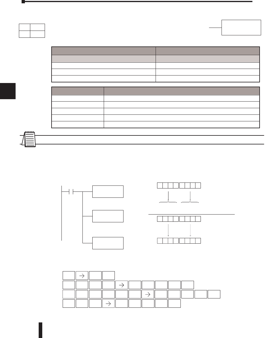
DL06 Micro PLC User Manual, 3rd Edition, Rev. D
5-90
1
2
3
4
5
6
7
8
9
10
11
12
13
14
A
B
C
D
Chapter 5: Standard RLL Instructions - Math
1
2
3
4
5
6
7
8
9
10
11
12
13
14
a
B
c
d
Subtract Double (SUBD)
Subtract Double is a 32-bit instruction that subtracts the BCD value
(Aaaa), which is either two consecutive V-memory locations or an
8-digit (max.) constant, from the BCD value in the accumulator.
NOTE: Status flags are valid only until another instruction uses the same flag.
In the following example, when X1 is on, the value in V2000 and V2001 will be loaded
into the accumulator using the Load Double instruction. The value in V2006 and V2007
is subtracted from the value in the accumulator. The value in the accumulator is copied to
V2010 and V2011 using the Out Double instruction.
SUBD
A aaa
Direct SOFT32
Handheld Programmer Keystrokes
LDD
V2000
X1
Load the value in V2000 and
V2001 into the accumulator
SUBD
V2006
The in V2006 and V2007 is
subtracted from the value in
the accumulator
OUTD
V2010
Copy the value in the
accumulator to V2010 and
V2011
00390899
01063274
0 1 0 6 3 2 7 4
V2010
V2000
V2001
V2011
00390899
672375
ACC.
STR
$
SHFT
SHFT ANDST
L
3
D
3
D
3
D
OUT
GX SHFT 3
D
RST
S
ISG
U
1
B
1
BENT
2
C
0
A
0
AENT
6
G
2
C
0
A
0
A
0
AENT
2
C
0
A
1
B
0
AENT
SHFT
_
Discrete Bit Flags Description
SP63 On when the result of the instruction causes the value in the accumulator to be zero.
SP64 On when the 16- bit subtraction instruction results in a borrow
SP65 On when the 32-bit subtraction instruction results in a borrow
SP70 On anytime the value in the accumulator is negative.
SP75 On when a BCD instruction is executed and a NON–BCD number was encountered.
Operand Data Type DL06 Range
A aaa
V-memory V See memory map
Pointer P See memory map
Constant K 0–99999999
DS Used
HPP Used
DirectSOFT
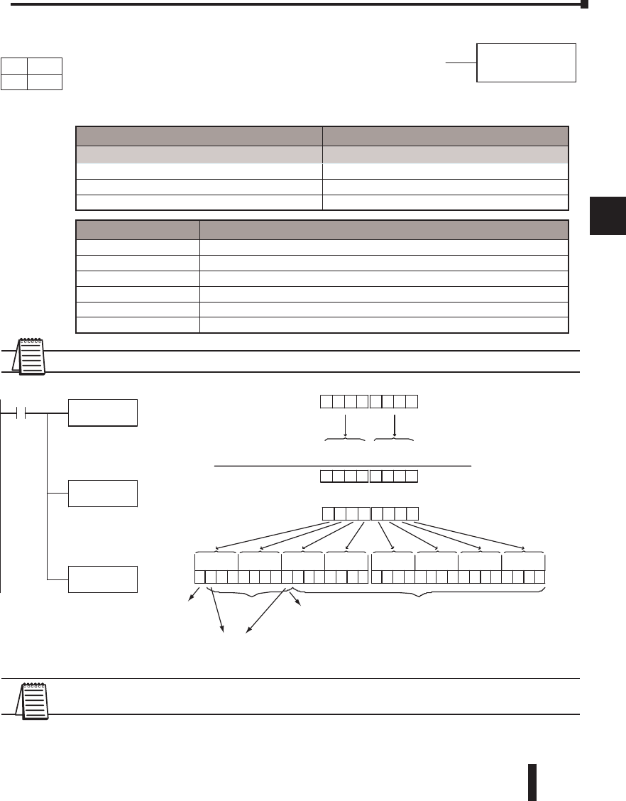
DL06 Micro PLC User Manual, 3rd Edition, Rev. D 5-91
1
2
3
4
5
6
7
8
9
10
11
12
13
14
A
B
C
D
Subtract Real (SUBR)
The Subtract Real is a 32-bit instruction that subtracts a real
number, which is either two consecutive V-memory locations or a
32-bit constant, from a real number in the accumulator. The result is
a 32-bit real number that resides in the accumulator. Both numbers
must be Real data type (IEEE floating point format).
NOTE: Status flags are valid only until another instruction uses the same flag.
NOTE: The current HPP does not support real number entry with automatic conversion to the 32-bit
IEEE format. You must use DirectSOFT for this feature
1
2
3
4
5
6
7
8
9
10
11
12
13
14
a
B
c
d
SUBR
Aaaa
ndar
dRLL
structions
LDR
R22.0
X1
Load thereal number 22.0
into theaccumulator.
SUBR
R15.0
Subtract thereal number
15.0fromthe accululator
contents, whichisinreal
number format.
00000000000000000100000011100000
8421842184218421
8421842184218421
Acc.
40 E 0 0000
V1400V1401
Real Value
Copy theresultinthe accumulator
to V1400 and V1401.
OUTD
V1400
Implies2(exp 2)
129 -- 127 =2
(Hex number)
Mantissa (23bits)Sign Bit
41B00000
000041B0
(SUBR)
(Accumulator)
4170 0000+
000040E0
Acc.
22 (decimal)
--15
7
1.11 x2(exp 2) =111.binary= 7decimal128 +1=129
DirectSOFT32
Exponent (8 bits)
Operand Data Type DL06 Range
Aaaa
V-memory V See memory map
Pointer P See memory map
Constant R -3.402823E + 38 to+-3.402823E + 38
Discrete Bit Flags Description
SP63 On when the result of the instruction causes the value in the accumulator to be zero.
SP70 On anytime the value in the accumulator is negative.
SP71 On anytime the V-memory specified by a pointer (P) is not valid.
SP72 On anytime the value in the accumulator is an invalid floating point number.
SP73 On when a signed addition or subtraction results in a incorrect sign bit.
SP74 On anytime a floating point math operation results in an underflow error.
Chapter 5: Standard RLL Instructions - Math
DS Used
HPP N/A
DirectSOFT
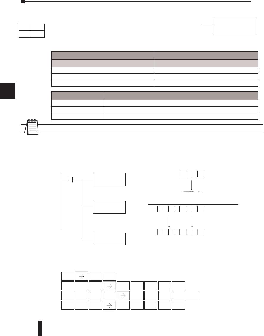
DL06 Micro PLC User Manual, 3rd Edition, Rev. D
5-92
1
2
3
4
5
6
7
8
9
10
11
12
13
14
A
B
C
D
Multiply (MUL)
Multiply is a 16-bit instruction that multiplies the BCD value
(Aaaa), which is either a V-memory location or a 4–digit
(max.) constant, by the BCD value in the lower 16 bits of the
accumulator The result can be up to 8 digits and resides in the
accumulator.
NOTE: Status flags are valid only until another instruction uses the same flag.
In the following example, when X1 is on, the value in V2000 will be loaded into the
accumulator using the Load instruction. The value in V2006 is multiplied by the value in
the accumulator. The value in the accumulator is copied to V2010 and V2011 using the Out
Double instruction.
Chapter 5: Standard RLL Instructions- - Math
1
2
3
4
5
6
7
8
9
10
11
12
13
14
a
B
c
d
MUL
A aaa
Direct SOFT32
Handheld Programmer Keystrokes
LD
V2000
X1
Load the value in V2000 into
the lower 16 bits of the
accumulator
MUL
V2006
The value in V2006 is
multiplied by the value in the
accumulator
OUTD
V2010
Copy the value in the
accumulator to V2010 and
V2011
00025000
0
X
0 0 0 0 1 0 0 0
V2010
1
V2000
0
00025000
25
The unused accumulator
bits are set to zero
Acc.
STR
$
SHFT ANDST
L
3
D
SHFT ORST
M
ISG
U
ANDST
L
OUT
GX SHFT 3
D
1
BENT
2
C
0
A
0
A
0
AENT
2
C
0
A
0
AENT
6
G
2
C
0
A
1
B
0
AENT
0
V2011
(Accumulator)
(V2006)
Discrete Bit Flags Description
SP63 On when the result of the instruction causes the value in the accumulator to be zero.
SP70 On anytime the value in the accumulator is negative.
SP75 On when a BCD instruction is executed and a NON–BCD number was encountered.
Operand Data Type DL06 Range
A aaa
V-memory V See memory map
Pointer P See memory map
Constant K 0–9999
DS Used
HPP Used
DirectSOFT
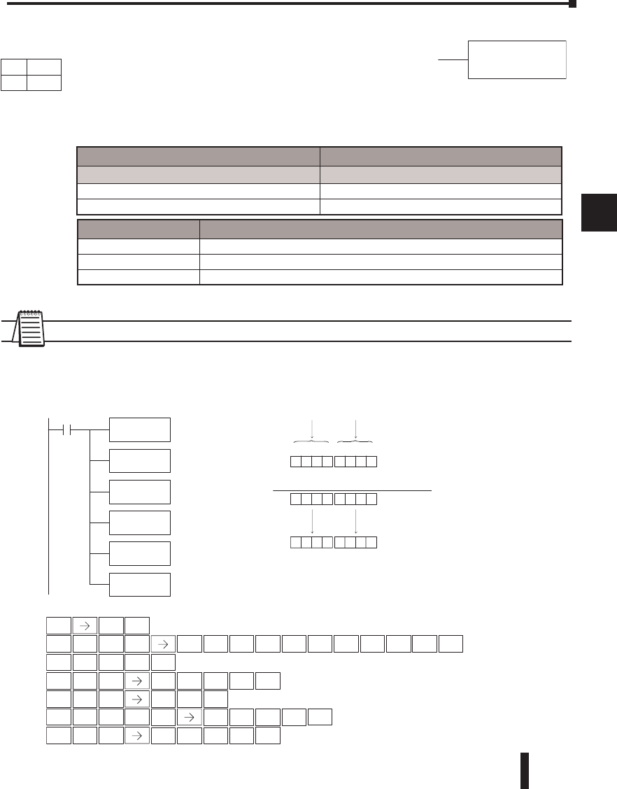
DL06 Micro PLC User Manual, 3rd Edition, Rev. D 5-93
1
2
3
4
5
6
7
8
9
10
11
12
13
14
A
B
C
D
Multiply Double (MULD)
Multiply Double is a 32-bit instruction that multiplies the 8-digit
BCD value in the accumulator by the 8-digit BCD value in the two
consecutive V-memory locations specified in the instruction. The
lower 8 digits of the results reside in the accumulator. Upper digits
of the result reside in the accumulator stack.
NOTE: Status flags are valid only until another instruction uses the same flag.
In the following example, when X1 is on, the constant Kbc614e hex will be loaded into the
accumulator. When converted to BCD the number is ”12345678”. That number is stored in
V1400 and V1401. After loading the constant K2 into the accumulator, we multiply it times
12345678, which
gives us 24691356.
1
2
3
4
5
6
7
8
9
10
11
12
13
14
a
B
c
d
MULD
A aaa
Operand Data Type DL06 Range
A aaa
V-memory V See memory map
Pointer P See memory map
Discrete Bit Flags Description
SP63 On when the result of the instruction causes the value in the accumulator to be zero.
SP70 On anytime the value in the accumulator is negative.
SP75 On when a BCD instruction is executed and a NON–BCD number was encountered.
Chapter 5: Standard RLL Instructions - Math
Direct SOFT32 Display
LDD
Kbc614e
X1 Load the hex equivalent
of 12345678 decimal into
the accumulator.
BCD Convert the value to
BCD format. It will
occupy eight BCD digits
(32 bits).
OUTD
V1400
Output the number to
V1400 and V1401 using
the OUTD instruction. 3562469
678
(Accumulator)
1 2 3 4 5 6 7 8
1
(Accumulator)
V1402
1
5
V1400
356
V1403
2469
2
Acc.
LD
K2
Load the constant K2
into the accumulator.
MULD
V1400
Multiply the accumulator
contents (2) by the
8-digit number in V1400
and V1401.
OUTD
V1402
Move the result in the
accumulator to V1402
and V1403 using the
OUTD instruction.
2341
V1401
X
Handheld Programmer Keystrokes
STR
$
SHFT ANDST
L
3
D
SHFT ORST
M
ISG
U
ANDST
L
OUT
GX SHFT 3
D
1
BENT
6
G
1
B
4
EENT
ENT
ENT
3
DPREV SHFT 1
B
2
CSHFT SHFT 4
E
SHFT 1
B
2
C
3
D
OUT
GX SHFT 3
D
1
B
4
E
0
AENT
0
A
ENT
SHFT ANDST
L
3
DPREV ENT
2
C
3
D
1
B
4
E
0
A
0
A
1
B
4
E
0
A
2
C
DS Used
HPP Used
DirectSOFT
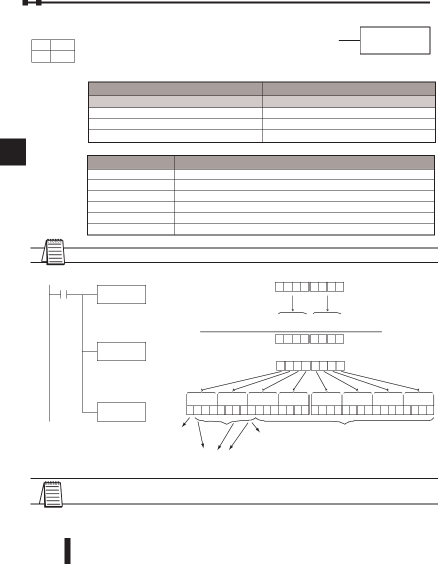
DL06 Micro PLC User Manual, 3rd Edition, Rev. D
5-94
1
2
3
4
5
6
7
8
9
10
11
12
13
14
A
B
C
D
Multiply Real (MULR)
The Multiply Real instruction multiplies a real number in the
accumulator with either a real constant or a real number occupying
two consecutive V-memory locations. The result resides in the
accumulator. Both numbers must be Real data type (IEEE floating
point format).
NOTE: Status flags are valid only until another instruction uses the same flag.
NOTE: The current HPP does not support real number entry with automatic conversion to the 32-bit
IEEE format. You must use DirectSOFT for this feature.
Chapter 5: Standard RLL Instructions - Math
1
2
3
4
5
6
7
8
9
10
11
12
13
14
a
B
c
d
MULR
Aaaa
DirectSOFT32 Display
LDR
R7.0
X1
Load thereal number 7.0
into theaccumulator.
MULR
R15.0
Multiply theaccumulator
contentsbythe real number
15.0
00000000000000000100001011010010
8421842184218421
8421842184218421
Acc.
42D20000
V1400V1401
Real Value
Copy theresultinthe accumulator
to V1400 and V1401.
OUTD
V1400
Implies2(exp 6)
133 -- 127 =6
(Hex number)
Sign Bit
40E00000
000040E0
(MULR)
(Accumulator)
4170 0000X
000042D 2
Acc.
7(decimal)
x15
105
1.101001 x2(exp 6) =1101001. binary= 105 decimal128 +4+1=133
Exponent (8 bits) Mantissa (23 bits)
Operand Data Type DL06 Range
Aaaa
V-memory V See memory map
Pointer P See memory map
Real Constant R -3.402823E +38 to + -3.402823E +38
Discrete Bit Flags Description
SP63 On when the result of the instruction causes the value in the accumulator to be zero.
SP70 On anytime the value in the accumulator is negative.
SP71 On anytime the V-memory specified by a pointer (P) is not valid.
SP72 On anytime the value in the accumulator is an invalid floating point number.
SP73 On when a signed addition or subtraction results in an incorrect sign bit.
SP74 On anytime a floating point math operation results in an underflow error.
DS Used
HPP Used
DirectSOFT
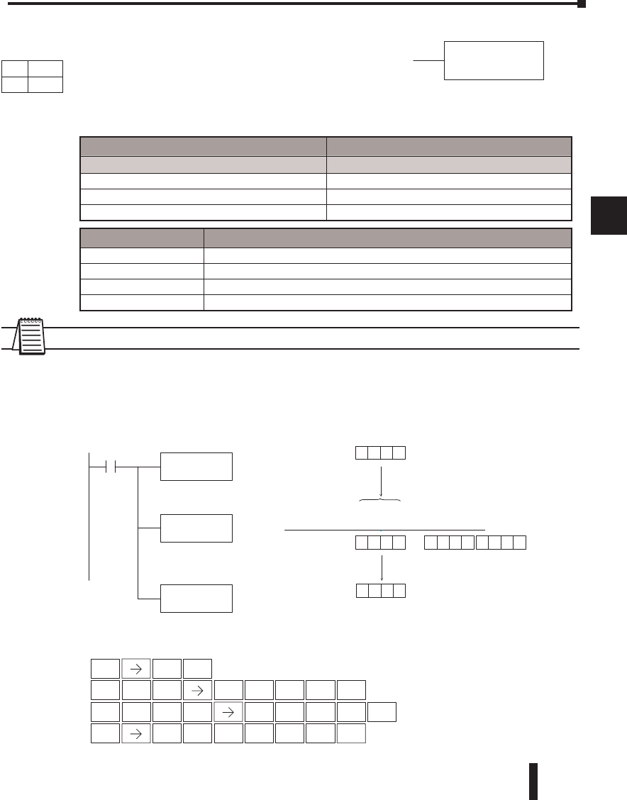
DL06 Micro PLC User Manual, 3rd Edition, Rev. D 5-95
1
2
3
4
5
6
7
8
9
10
11
12
13
14
A
B
C
D
Divide (DIV)
Divide is a 16-bit instruction that divides the BCD value in
the accumulator by a BCD value (Aaaa), which is either a
V-memory location or a 4-digit (max.) constant. The first part
of the quotient resides in the accumulator and the remainder
resides in the first stack location.
NOTE: Status flags are valid only until another instruction uses the same flag.
In the following example, when X1 is on, the value in V2000 will be loaded into the
accumulator using the Load instruction. The value in the accumulator will be divided by
the value in V2006 using the Divide instruction. The value in the accumulator is copied to
V2010 using the Out instruction.
Chapter 5: Standard RLL Instructions - Math
1
2
3
4
5
6
7
8
9
10
11
12
13
14
a
B
c
d
DIV
A aaa
Discrete Bit Flags Description
SP53 On when the value of the operand is larger than the accumulator can work with.
SP63 On when the result of the instruction causes the value in the accumulator to be zero.
SP70 On anytime the value in the accumulator is negative.
SP75 On when a BCD instruction is executed and a NON–BCD number was encountered.
Direct SOFT32
Handheld Programmer Keystrokes
LD
V2000
X1
Load the value in V2000 into
the lower 16 bits of the
accumulator
DIV
V2006
The value in the
accumulator is divided by
the value in V2006
OUT
V2010
Copy the value in the lower
16 bits of the accumulator to
V2010
V2010
0
5
V2000
000
0005000
49
Acc. 102
The unused accumulator
bits are set to zero
00000002
First stak location contains
the remainder
STR
$
SHFT ANDST
L
3
D
SHFT 3
D
8
I
AND
V
OUT
GX SHFT
AND
V
2
C
0
A
1
B
0
AENT
1
BENT
2
C
0
A
0
A
0
AENT
2
C
0
A
0
AENT
6
G
(Accumulater)
V2006
÷
120
Operand Data Type DL06 Range
Aaaa
V-memory V See memory map
Pointer P See memory map
Constant K 0–9999
DS Used
HPP Used
DirectSOFT
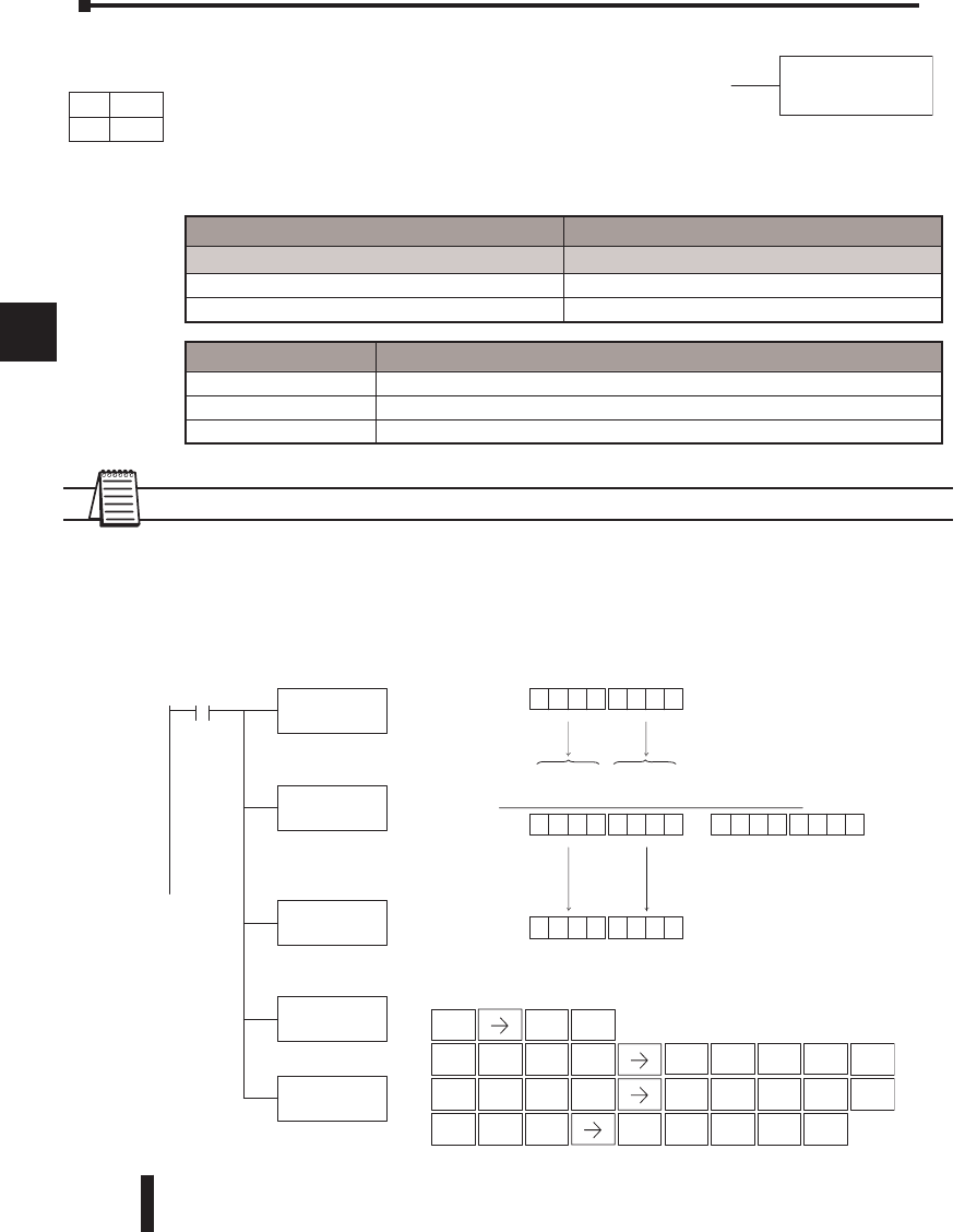
DL06 Micro PLC User Manual, 3rd Edition, Rev. D
5-96
1
2
3
4
5
6
7
8
9
10
11
12
13
14
A
B
C
D
Chapter 5: Standard RLL Instructions - Math
1
2
3
4
5
6
7
8
9
10
11
12
13
14
a
B
c
d
NOTE: Status flags are valid only until another instruction uses the same flag.
In the following example, when X1 is on, the value in V1400 and V1401 will be loaded into
the accumulator using the Load Double instruction. The value in the accumulator is divided
by the value in V1420 and V1421 using the Divide Double instruction. The first part of the
quotient resides in the accumulator and the remainder resides in the first stack location. The
value in the accumulator is copied to V1500 and V1501 using the Out Double instruction.
DIVD
A aaa
Handheld Programmer Keystrokes
LDD
V1400
X1
Load the value in V1400 and
V1401 into the accumulator
DIVD
V1420
The value in the accumulator
is divided by the value in
V1420 and V1421
OUTD
V1500
Copy the value in the
accumulator to V1500
and V1501
0000003
0000150
0(Accumulator)
(V1421 and V1420)
0
?0
150 0000
0
V1500
V1400
0
000
V1401
V1501
0003
0000050
0000000 0
First stack location contains
the remainder
The unused accumulator
bits are set to zero
Acc.
STR
$
SHFT ANDST
L
3
D
SHFT 3
D
8
I
AND
V
OUT
GX SHFT 0
AENT
1
BENT
2
CENT
0
A
3
DENT
1
B
4
E
0
A
0
A
1
B
4
E
3
D
1
B
5
F
0
A
POP
Retrieve the remainder
OUTD
V1502
Copy the value into
V1502 and V1503
Operand Data Type DL06 Range
A aaa
V-memory V See memory map
Pointer P See memory map
Discrete Bit Flags Description
SP63 On when the result of the instruction causes the value in the accumulator to be zero.
SP70 On anytime the value in the accumulator is negative.
SP75 On when a BCD instruction is executed and a NON–BCD number was encountered.
DS Used
HPP Used
DirectSOFT
Divide Double (DIVD)
Divide Double is a 32-bit instruction that divides the BCD
value in the accumulator by a BCD value (Aaaa), which
must be obtained from two consecutive V-memory locations.
(You cannot use a constant as the parameter in the box.) The
first part of the quotient resides in the accumulator and the
remainder resides in the first stack location.
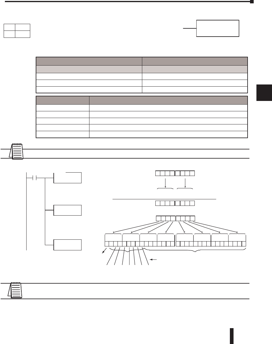
DL06 Micro PLC User Manual, 3rd Edition, Rev. D 5-97
1
2
3
4
5
6
7
8
9
10
11
12
13
14
A
B
C
D
Chapter 5: Standard RLL Instructions - Math
1
2
3
4
5
6
7
8
9
10
11
12
13
14
a
B
c
d
Divide Real (DIVR)
The Divide Real instruction divides a real number in the
accumulator by either a real constant or a real number
occupying two consecutive V-memory locations. The result
resides in the accumulator. Both numbers must be Real data
type (IEEE floating point format).
NOTE: Status flags are valid only until another instruction uses the same flag.
NOTE: The current HPP does not support real number entry with automatic conversion to the 32-bit
IEEE format. You must use DirectSOFT for this feature.
DIVR
Aaaa
ndardRLL
DirectSOFT32Display
LDR
R15.0
X1
Load thereal number 15.0
into theaccumulator.
DIVR
R10.0
Dividethe accumulatorcontents
by thereal number 10.0.
00000000000000000011111111000000
8421842184218421
8421842184218421
Acc.
3FC 0 0000
V1400V1401
Real Value
Copy theresul tinthe accumulator
to V1400 and V1401.
OUTD
V1400
Implies2(exp 0)
127 -- 127 =0
(Hex number)
Mantissa (23bits)Sign Bit
4170 0000
00004170
(DIVR)
(Accumulator)
4120 0000
¸
00003FC 0
Acc.
15 (decimal)
10
1
1.1x2(exp0)=1.1binary= 1.5 decimal64 +32+16 +8+4+2+1=127
Exponent (8 bits)
¸
5.
Discrete Bit Flags Description
SP63 On when the result of the instruction causes the value in the accumulator to be zero.
SP70 On anytime the value in the accumulator is negative.
SP71 On anytime the V-memory specified by a pointer (P) is not valid.
SP72 On anytime the value in the accumulator is an invalid floating point number.
SP74 On anytime a floating point math operation results in an underflow error.
Operand Data Type DL06 Range
Aaaa
V-memory V See memory map
Pointer P See memory map
Real Constant R -3.402823E + 38 to + -3.402823E + 38
DS Used
HPP N/A
DirectSOFT
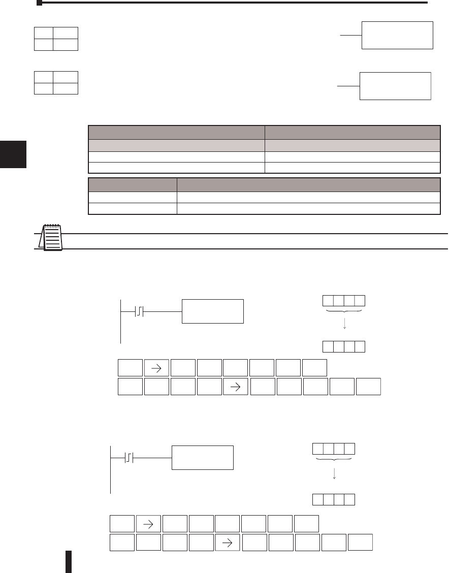
DL06 Micro PLC User Manual, 3rd Edition, Rev. D
5-98
1
2
3
4
5
6
7
8
9
10
11
12
13
14
A
B
C
D
Increment (INC)
The Increment instruction increments a BCD value in a specified
V-memory location by “1” each time the instruction is executed.
Decrement (DEC)
The Decrement instruction decrements a BCD value in a
specified V-memory location by “1” each time the instruction is
executed.
NOTE: Status flags are valid only until another instruction uses the same flag.
In the following increment example, when C5 makes an Off-to-On transition the value in
V1400 increases by one.
In the following decrement example, when C5 makes an Off-to-On transition the value in
V1400 is decreased by one.
Chapter 5: Standard RLL Instructions - Math
1
2
3
4
5
6
7
8
9
10
11
12
13
14
a
B
c
d
A aaa
INC
A aaa
DEC
DirectSOFT
C5 INC
V1400
Increment the value in
V1400 by “1”.
V1400
8935
V1400
8936
Handheld Programmer Keystrokes
STR
$
5
FENT
8
IENT
NEXT NEXT NEXT NEXT
SHFT
TMR
N
1
B
4
E
0
A
0
A
2
C
Operand Data Type DL06 Range
A aaa
V-memory V See memory map
Pointer P See memory map
Discrete Bit Flags Description
SP63 On when the result of the instruction causes the value in the accumulator to be zero.
SP75 On when a BCD instruction is executed and a NON–BCD number was encountered.
DirectSOFT
C5 DEC
V1400
Decrement the value in
V1400 by “1”.
V1400
8935
V1400
8934
Handheld Programmer Keystrokes
STR
$
5
FENT
3
DENT
NEXT NEXT NEXT NEXT
SHFT
4
E
1
B
4
E
0
A
0
A
2
C
DS Used
HPP Used
DS Used
HPP Used
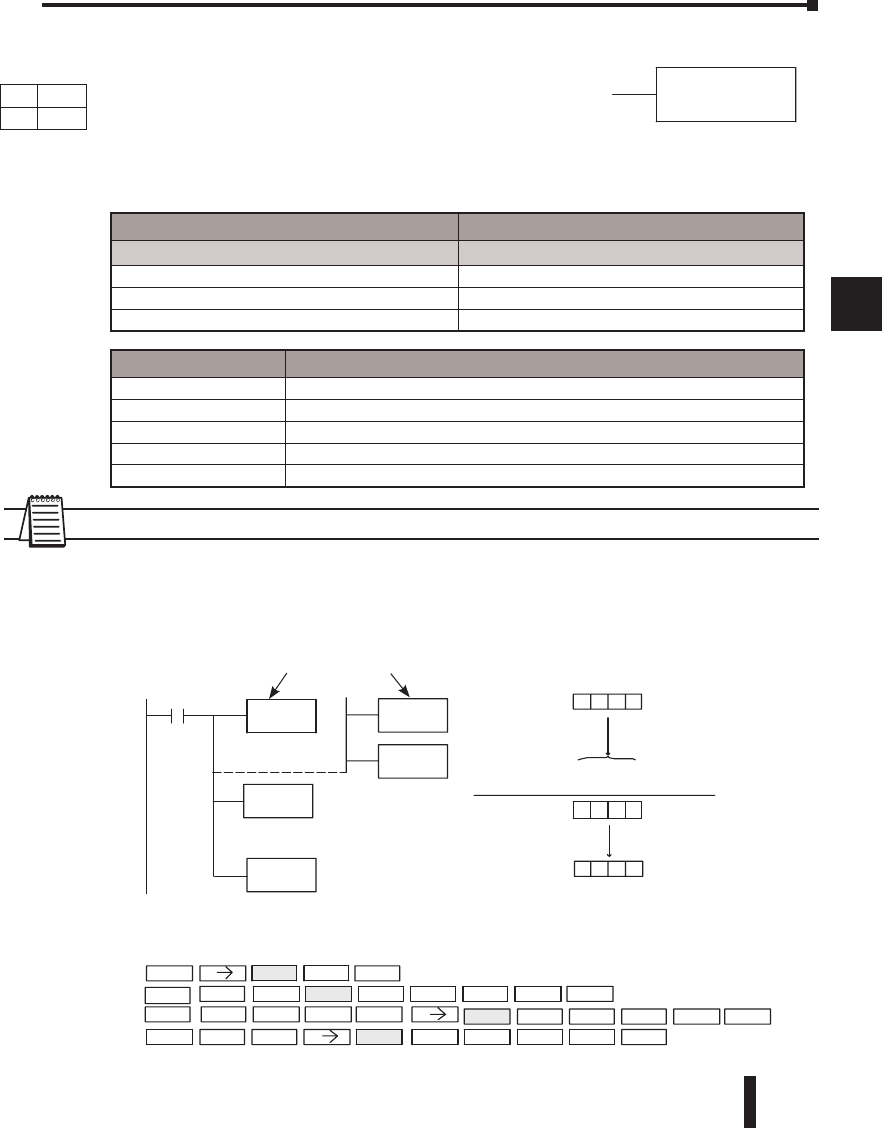
DL06 Micro PLC User Manual, 3rd Edition, Rev. D 5-99
1
2
3
4
5
6
7
8
9
10
11
12
13
14
A
B
C
D
NOTE: Status flags are valid only until another instruction uses the same flag.
In the following example, when X1 is on, the value in V1400 will be loaded into the
accumulator using the Load instruction. The binary value in the accumulator will be added to
the binary value in V1420 using the Add Binary instruction. The value in the accumulator is
copied to V1500 and V1501 using the Out Double instruction.
Chapter 5: Standard RLL Instructions - Math
1
2
3
4
5
6
7
8
9
10
11
12
13
14
a
B
c
d
ADDB
Aaaa
Handheld ProgrammerKeystrokes
LD
X1
+1
1
(Accumulator)00
1
0A05
CC 9
000 A05
2C4
Acc. CC 9
STRX(IN)1
DV1400
OUTV1500
V140
A2
SHFT B
Theunused accumulator
bits areset to zero
SHFT D
ENT
SHFT LENT
DD ENT
ENT
Load the value in V1400
into the lower 16 bits of
the accumulator
LD
BIN
ADDB
OUTD
V1500
K2565
Use either OR Constant
V-memory
V1420
V1400
(V1420)
V1500
V1400
The binary value in the
accumulator is added to the
binary value in V1420
Copy the value in the lower
16bits of the accumulator to
V1500 and V1501
DirectSOFT
Operand Data Type DL06 Range
Aaaa
V-memory V See memory map
Pointer P See memory map
Constant K 0-FFFF, h=65636
Discrete Bit Flags Description
SP63 On when the result of the instruction causes the value in the accumulator to be zero.
SP66 On when the 16-bit addition instruction results in a carry.
SP67 On when the 32-bit addition instruction results in a carry.
SP70 On anytime the value in the accumulator is negative.
SP73 On when a signed addition or subtraction results in an incorrect sign bit.
DS Used
HPP Used
Add Binary (ADDB)
Add Binary is a 16-bit instruction that adds the
binary value in the lower 16 bits of the accumulator
with a binary value (Aaaa), which is either a
V-memory location or a 16-bit constant. The result
can be up to 32 bits and resides in the accumulator.
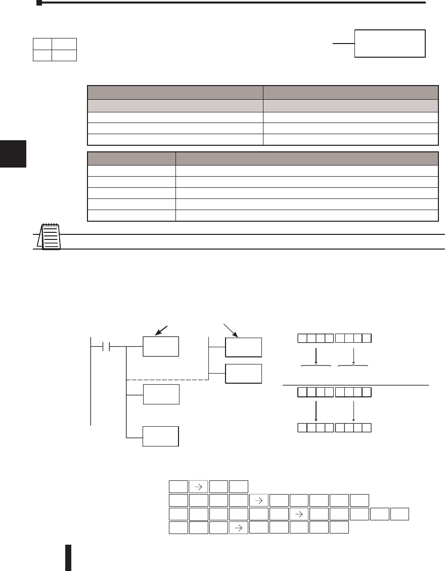
DL06 Micro PLC User Manual, 3rd Edition, Rev. D
5-100
1
2
3
4
5
6
7
8
9
10
11
12
13
14
A
B
C
D
Add Binary Double (ADDBD)
Add Binary Double is a 32-bit instruction that adds the binary
value in the accumulator with the value (Aaaa), which is either
two consecutive V-memory locations or an 8-digit (max.) binary
constant. The result resides in the accumulator.
NOTE: Status flags are valid only until another instruction uses the same flag.
In the following example, when X1 is on, the value in V1400 and V1401 will be loaded into
the accumulator using the Load Double instruction. The binary value in the accumulator is
added with the binary value in V1420 and V1421 using the Add Binary Double instruction.
The value in the accumulator is copied to V1500 and V1501 using the Out Double
instruction.
Chapter 5: Standard RLL Instructions - Math
1
2
3
4
5
6
7
8
9
10
11
12
13
14
a
B
c
d
ADDBD
Aaaa
LDD
V1400
X1
ADDBD
V1420
Thebinar yvalue in the
accumulatorisadded withthe
valueinV1420 and V1421
OUTD
V1500
Copy thevalue in the
accumulatortoV1500
and V1501
111000
010000
A
A
(Accumulator)
+1
0
0 0
C
00A0 1
V1500
0
(V1421 and V1420)
C
V1400
A11
V1401
V1501
1000
000 C010
Acc.
Load the value in V1400
and V1401 into the
accumulator
LD D
BIN
K2561
Use either OR Constant
V-memory
DirectSOFT
Handheld ProgrammerKeystrokes
STRX(IN)1
LD V1400
OUTV1 500
V140ADD 2
SHFT DSHFT
SHFT DSHFT
SHFT DSHFT
B
Operand Data Type DL06 Range
Aaaa
V-memory V See memory map
Pointer P See memory map
Constant K 0-FFFF FFFF
Discrete Bit Flags Description
SP63 On when the result of the instruction causes the value in the accumulator to be zero.
SP66 On when the 16-bit addition instruction results in a carry.
SP67 On when the 32-bit addition instruction results in a carry.
SP70 On anytime the value in the accumulator is negative.
SP73 On when a signed addition or subtraction results in an incorrect sign bit.
Handheld Programmer Keystrokes
STR
$
SHFT 3
D
3
D
OUT
GX SHFT 3
D
1
BENT
3
D
1
B
0
A
1
B
4
E
2
C
0
AENT
SHFT ANDST
L
3
D
1
B
4
E
0
A
0
AENT
3
D
1
B
5
F
0
A
0
AENT
DS Used
HPP Used
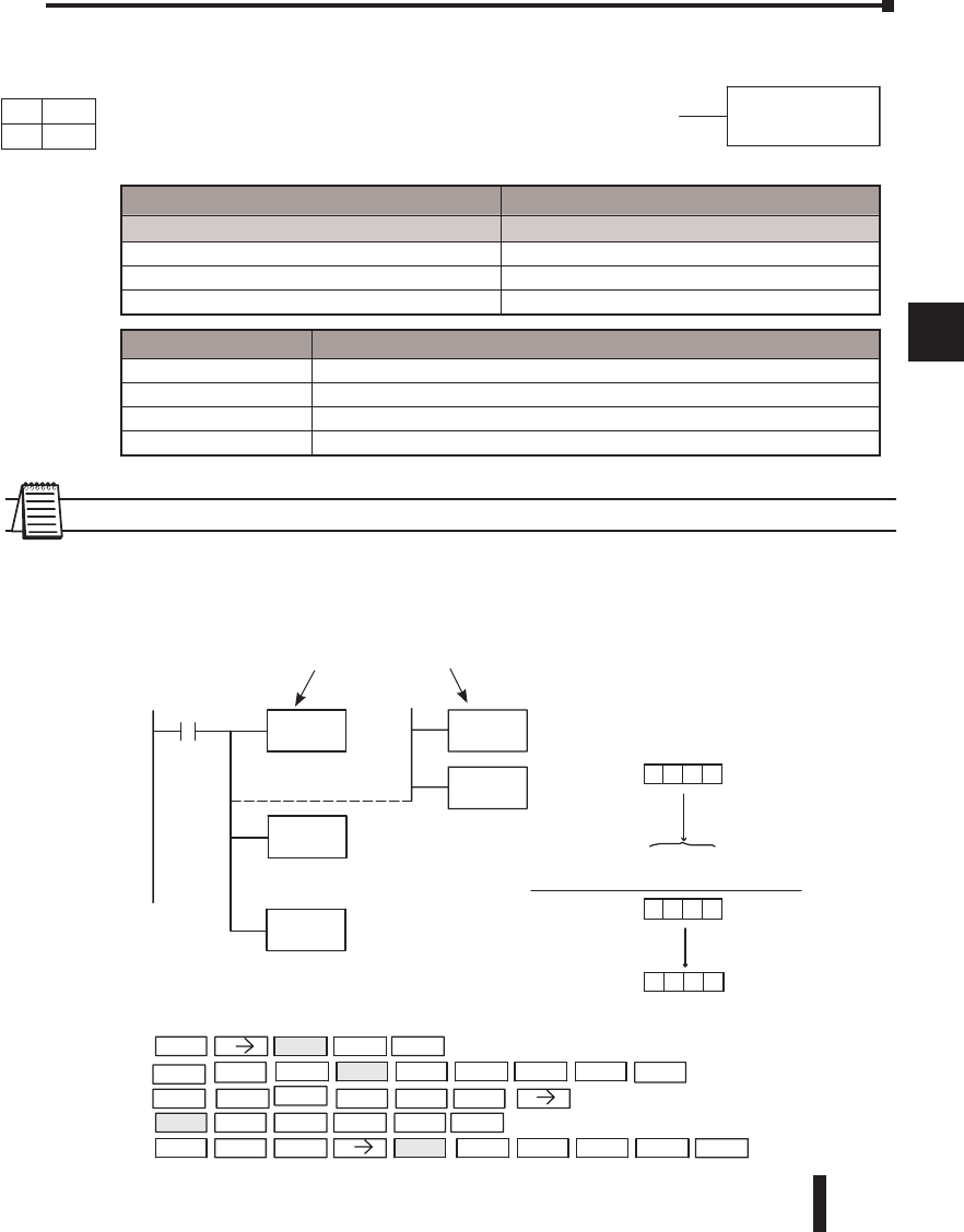
DL06 Micro PLC User Manual, 3rd Edition, Rev. D 5-101
1
2
3
4
5
6
7
8
9
10
11
12
13
14
A
B
C
D
Chapter 5: Standard RLL Instructions - Math
1
2
3
4
5
6
7
8
9
10
11
12
13
14
a
B
c
d
Subtract Binary (SUBB)
Subtract Binary is a 16-bit instruction that subtracts the binary
value (Aaaa), which is either a V-memory location or a 4-digit
(max.) binary constant, from the binary value in the accumulator.
The result resides in the accumulator.
NOTE: Status flags are valid only until another instruction uses the same flag.
In the following example, when X1 is on, the value in V1400 will be loaded into the
accumulator using the Load instruction. The binary value in V1420 is subtracted from the
binary value in the accumulator using the Subtract Binary instruction. The value in the
accumulator is copied to V1500 using the Out instruction.
SUBB
Aaaa
HandheldProgr ammerKeystrokes
LD
V1400
X1
SUBB
V1420
Thebinar yvalue in V1420 is
subtracted from thevalue in
theaccumulator
OUT
V1500
Copy thevalue in thelower 16
bits of theaccumulatortoV1500
V1500
(V1420)
0
1(Accumulator)
0
1
0
0
V1400
024
61 9
000 02 4
A0 B
Acc. 619
Theunused accumulator
bits areset to zero
STRX(IN)1
D V 140 0
OUT V 1500
V140
S
2
SHFT B
SHFT D
ENT
SHFT LENT
UB
ENT
ENT
SHFT
Use either OR Constant
V-memory
LD
BIN
K1024
Load the value in V1400
into the lower 16 bits of
the accumulator
-
DirectSOFT
Discrete Bit Flags Description
SP63 On when the result of the instruction causes the value in the accumulator to be zero.
SP64 On when the 16-bit subtraction instruction results in a borrow.
SP65 On when the 32-bit subtraction instruction results in a borrow.
SP70 On anytime the value in the accumulator is negative.
Operand Data Type DL06 Range
Aaaa
V-memory V See memory map
Pointer P See memory map
Constant K 0-FFFF, h=65636
DS Used
HPP Used
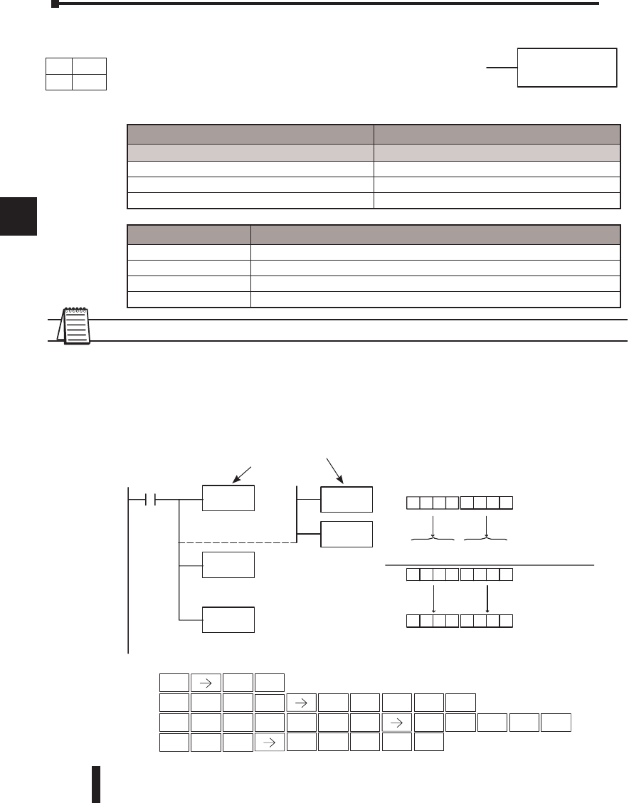
DL06 Micro PLC User Manual, 3rd Edition, Rev. D
5-102
1
2
3
4
5
6
7
8
9
10
11
12
13
14
A
B
C
D
Subtract Binary Double (SUBBD)
Subtract Binary Double is a 32-bit instruction that subtracts the
binary value (Aaaa), which is either two consecutive V-memory
locations or an 8-digit (max.) binary constant, from the binary
value in the accumulator. The result resides in the accumulator.
NOTE: Status flags are valid only until another instruction uses the same flag.
In the following example, when X1 is on, the value in V1400 and V1401 will be loaded into
the accumulator using the Load Double instruction. The binary value in V1420 and V1421
is subtracted from the binary value in the accumulator using the Subtract Binary Double
instruction. The value in the accumulator is copied to V1500 and V1501 using the Out
Double instruction.
Chapter 5: Standard RLL Instructions - Math
1
2
3
4
5
6
7
8
9
10
11
12
13
14
a
B
c
d
SUBBD
Aaaa
LDD
V1400
X1
SUBBD
V1420
Thebinaryvalue in V1420 and
V1421 is subtracted from the
binaryvalue in theaccumulator
OUTD
V1500
Copy theval ue in the
accumulatortoV1500
and V1501
FE0005
FF0006
6
0
(V1421 and V1420)
0
0
E
00
E
600FF(Accumulator)
V1500
0
V1400
6FE
V1401
V1501
0005
00 01A0 1
Acc.
Use either OR Constant
V-memory
LD D
BIN
K393471
Load the value in V1400
and V1401 into the
accumulator
-
DirectSOFT
HandheldProgr ammerKeystrokes
STRX(IN) 1
D V 1 4 0 0
OUT V 1 5 0 0
V 1 4 0
S
2
SHFT B
SHFT D
ENT
SHFT LENT
U B
ENT
ENT
SHFT
Operand Data Type DL06 Range
Aaaa
V-memory V See memory map
Pointer P See memory map
Constant K 0-FFFF FFFF
Discrete Bit Flags Description
SP63 On when the result of the instruction causes the value in the accumulator to be zero.
SP64 On when the 16-bit subtraction instruction results in a borrow.
SP65 On when the 32-bit subtraction instruction results in a borrow.
SP70 On anytime the value in the accumulator is negative.
Handheld Programmer Keystrokes
STR
$
SHFT ISG
U
1
B
OUT
GX SHFT 3
D
1
BENT
3
D
1
B
RST
SSHFT 1
B
4
E
2
C
0
AENT
SHFT ANDST
L
3
D
1
B
4
E
0
A
0
AENT
3
D
1
B
5
F
0
A
0
AENT
DS Used
HPP Used
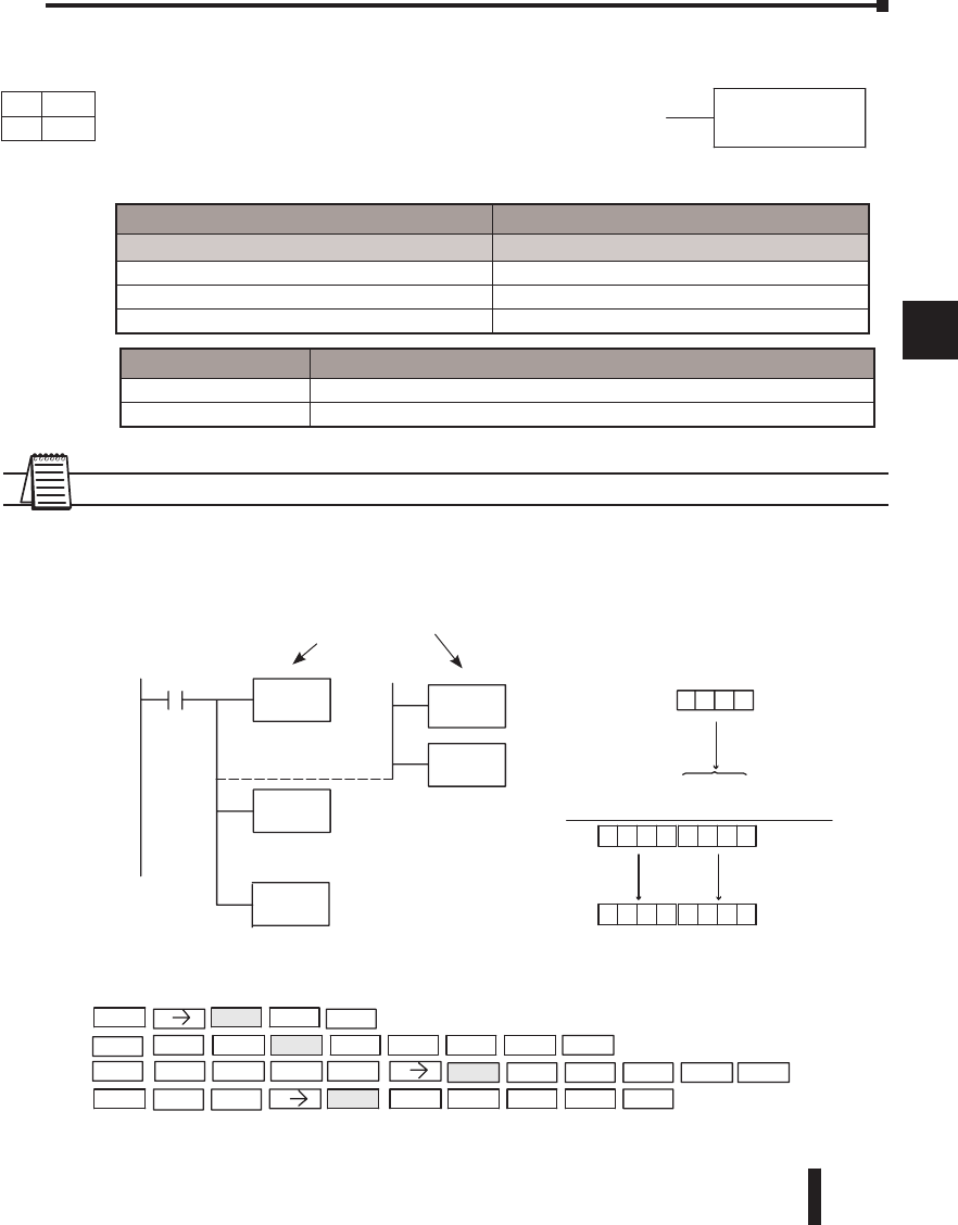
DL06 Micro PLC User Manual, 3rd Edition, Rev. D 5-103
1
2
3
4
5
6
7
8
9
10
11
12
13
14
A
B
C
D
Chapter 5: Standard RLL Instructions - Math
1
2
3
4
5
6
7
8
9
10
11
12
13
14
a
B
c
d
Multiply Binary (MULB)
Multiply Binary is a 16-bit instruction that multiplies the binary
value (Aaaa), which is either a V-memory location or a 4-digit
(max.) binary constant, by the binary value in the accumulator.
The result can be up to 32 bits and resides in the accumulator.
NOTE: Status flags are valid only until another instruction uses the same flag.
In the following example, when X1 is on, the value in V1400 will be loaded into the
accumulator using the Load instruction. The binary value in V1420 is multiplied by the
binary value in the accumulator using the Multiply Binary instruction. The value in the
accumulator is copied to V1500 using the Out instruction.
MULB
Aaaa
DirectSOFT32Display
HandheldProgr ammerKeystrokes
LD
V1400
X1
MULB
V1420
Thebinar yvalue in V1420 is
multipliedbythe binar y
valueinthe accumulator
OUTD
V1500
0(Accumulator)
0
0
0
(V1420)
V1400
A01
000 A0 1
02 E
Theunused accumulator
bits ar eset to zero
2E0001 C
C
C
V1500
C2 E
V1501
0001
Acc.
STRX1
D V 1400
O
UT V1500
V140
M2
SHFT B
SHFT D
ENT
SHFT LENT
UL ENT
ENT
Copy the value of the accumulator
to V1500 and V1501
Use either OR Constant
V-memory
LD
BIN
K2561
Load the value in V1400
into the lower 16 bits of
the accumulator
x
Operand Data Type DL06 Range
Aaaa
V-memory V See memory map
Pointer P See memory map
Constant K 0-FFFF
Discrete Bit Flags Description
SP63 On when the result of the instruction causes the value in the accumulator to be zero.
SP70 On anytime the value in the accumulator is negative.
DS Used
HPP Used
DirectSOFT
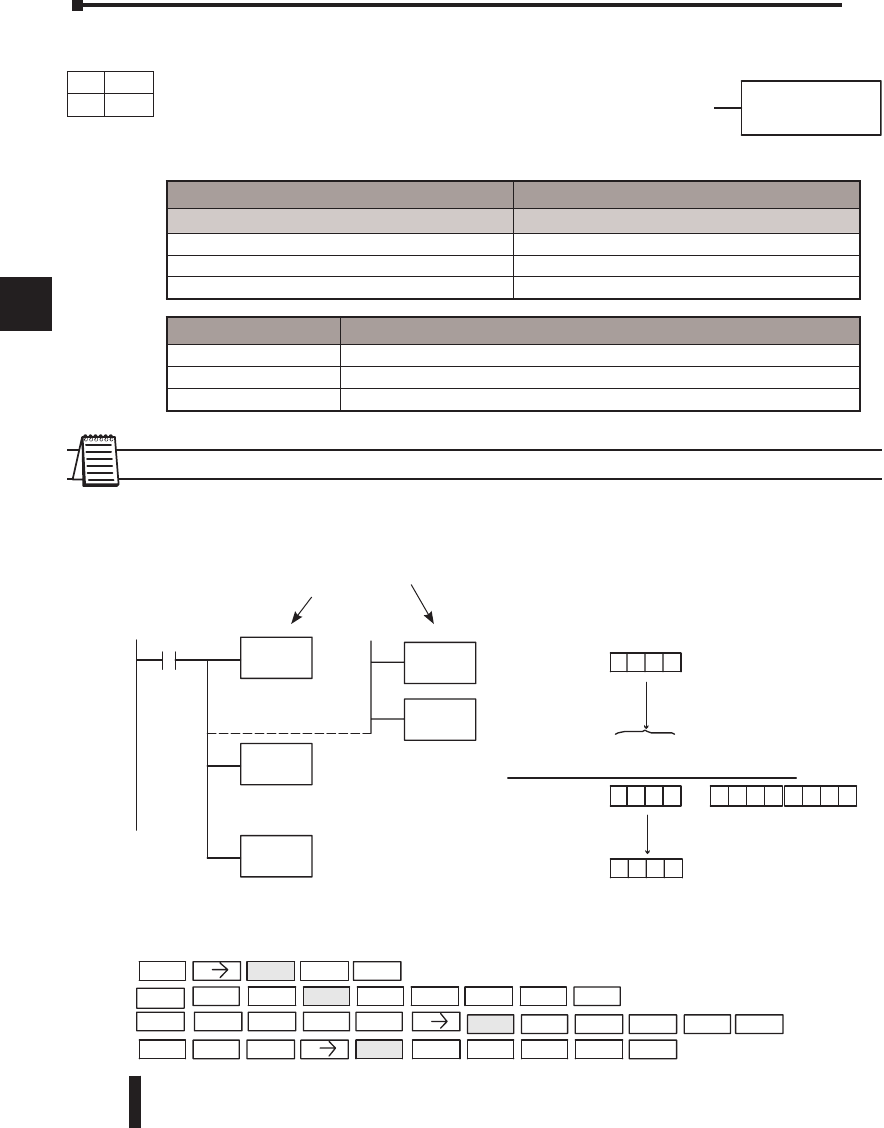
DL06 Micro PLC User Manual, 3rd Edition, Rev. D
5-104
1
2
3
4
5
6
7
8
9
10
11
12
13
14
A
B
C
D
Divide Binary (DIVB)
Divide Binary is a 16-bit instruction that divides the binary value in
the accumulator by a binary value (Aaaa), which is either a V-memory
location or a 16-bit (max.) binary constant. The first part of the
quotient resides in the accumulator and the remainder resides in the
first stack location.
NOTE: Status flags are valid only until another instruction uses the same flag.
In the following example, when X1 is on, the value in V1400 will be loaded into the
accumulator using the Load instruction. The binary value in the accumulator is divided by
the binary value in V1420 using the Divide Binary instruction. The value in the accumulator
is copied to V1500 using the Out instruction.
Chapter 5: Standard RLL Instructions - Math
1
2
3
4
5
6
7
8
9
10
11
12
13
14
a
B
c
d
DIVB
Aaaa
DirectSOFT32Display
HandheldProgrammerKeystrokes
LD
V1400
X1
DIVB
V1420
Thebinaryvalue in th
accumulatorisdivided by
thebinaryvalue in V1420
OUT
V1500
Copy thevalue in thelower 16
bits of theaccumulatortoV1500 V1500
0(Accumulator)F
0
0
F
(V1420)
0
V1400
A01
320
000 A0 1
05 0
Acc. 320
Theunused accumulator
bits ar eset to zero
00 00000 0
Firststack location contains
therem ainder
STRX1
D V 140 0
OUTV1500
V140
D2
SHFT B
SHFT D
ENT
SHFT LENT
IV ENT
ENT
_
.
.
Use either OR Constant
V-memory
LD D
BIN
K64001
Load the value in V1400
into the lower 16 bits of
the accumulator
Operand Data Type DL06 Range
Aaaa
V-memory V See memory map
Pointer P See memory map
Constant K 0-FFFF
Discrete Bit Flags Description
SP53 On when the value of the operand is larger than the accumulator can work with.
SP63 On when the result of the instruction causes the value in the accumulator to be zero.
SP70 On anytime the value in the accumulator is negative.
DS Used
HPP Used
DirectSOFT
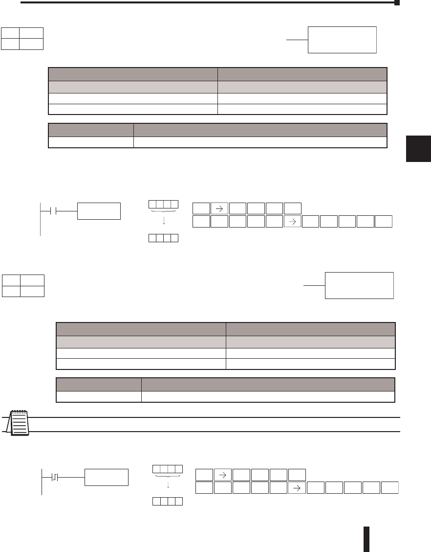
DL06 Micro PLC User Manual, 3rd Edition, Rev. D 5-105
1
2
3
4
5
6
7
8
9
10
11
12
13
14
A
B
C
D
Chapter 5: Standard RLL Instructions - Math
1
2
3
4
5
6
7
8
9
10
11
12
13
14
a
B
c
d
In the following example when C5 is on, the binary value in V2000 is increased by 1.
Decrement Binary (DECB)
The Decrement Binary instruction decrements a binary value in
a specified V-memory location by “1” each time the instruction is
executed.
NOTE: Status flags are valid only until another instruction uses the same flag.
In the following example when C5 is on, the value in V2000 is decreased by 1.
A aaa
INCB
Handheld Programmer Keystrokes
Direct SOFT32
C5 INCB
V2000
Increment the binary value
in V2000 by“1”
4A3C
4A3D
STR
$
2
C
5
F
SHFT ENT
SHFT 8
I
TMR
N
2
C
1
B
2
C
0
A
0
A
0
AENT
V2000
V2000
Handheld Programmer Keystrokes
DirectSOFT
C5 DECB
V2000
Decrement the binary value
in V2000 by“1”
V2000
4A3C?
V2000
4A3B?
STR
$
2
C
5
F
SHFT ENT
SHFT 2
C
3
D
4
E
1
B
2
C
0
A
0
A
0
AENT
Operand Data Type DL06 Range
A aaa
V-memory V See memory map
Pointer P See memory map
Discrete Bit Flags Description
SP63 On when the result of the instruction causes the value in the accumulator to be zero.
A aaa
DECB
Operand Data Type DL06 Range
A aaa
V-memory V See memory map
Pointer P See memory map
Discrete Bit Flags Description
SP63 On when the result of the instruction causes the value in the accumulator to be zero.
DS Used
HPP Used
DS Used
HPP Used
DirectSOFT
Increment Binary (INCB)
The Increment Binary instruction increments a
binary value in a specified V-memory location by
“1” each time the instruction is executed.
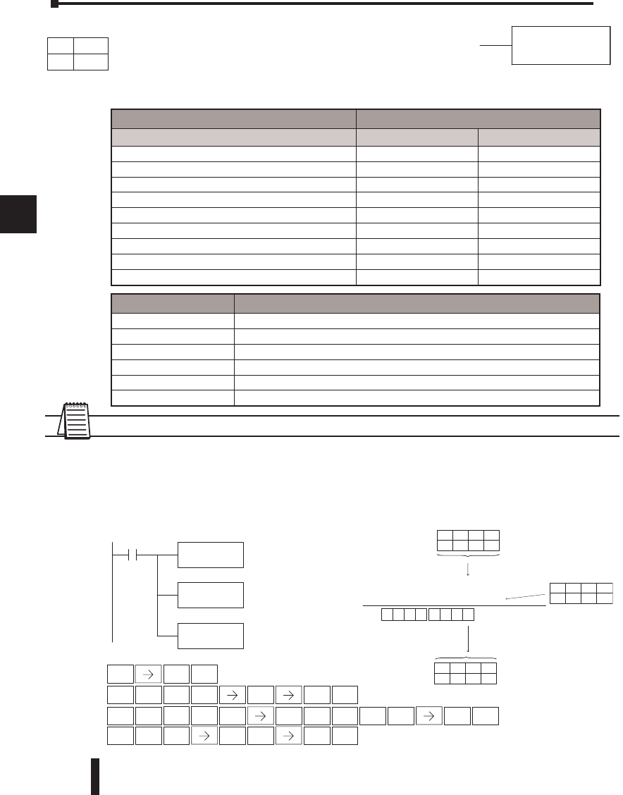
DL06 Micro PLC User Manual, 3rd Edition, Rev. D
5-106
1
2
3
4
5
6
7
8
9
10
11
12
13
14
A
B
C
D
NOTE: Status flags are valid only until another instruction uses the same flag.
In the following example, when X6 is on, the BCD value formed by discrete locations X0–X3
is loaded into the accumulator using the LDF instruction. The BCD value formed by discrete
locations C0–C3 is added to the value in the accumulator using the ADDF instruction.
The value in the lower four bits of the accumulator is copied to Y10–Y13 using the OUTF
instruction.
Chapter 5: Standard RLL Instructions - Math
1
2
3
4
5
6
7
8
9
10
11
12
13
14
a
B
c
d
bbbK
ADDF Aaaa
Discrete Bit Flags Description
SP63 On when the result of the instruction causes the value in the accumulator to be zero.
SP66 On when the 16-bit addition instruction results in a carry.
SP67 On when the 32 bit addition instruction results in a carry.
SP70 On anytime the value in the accumulator is negative.
SP73 On when a signed addition or subtraction results in an incorrect sign bit.
SP75 On when a BCD instruction is executed and a NON-BCD number was encountered.
Operand Data Type DL06 Range
A aaa bbb
Inputs X 0–777 ––
Outputs Y 0–777 ––
Control Relays C 0–1777 ––
Stage Bits S 0–1777 ––
Timer Bits T 0–377 ––
Counter Bits CT 0–177 ––
Special Relays SP 0-137 320-717 ––
Global I/O GX 0-3777 ––
Constant K –– 1–32
DirectSOFT32 Display
LDF X0
K4
X6 Load the BCD value represented
by discrete locations X0–X3
into the accumulator
ADDF C0
K4
Add the BCD value in the
accumulator with the value
represented by discrete
location C0–C3
OUTF Y10
K4
Copy the lower 4 bits of the
accumulator to discrete
locations Y10–Y13
+
0000000
8
(C0-C3)
(Accumulator)
3
X0X1X2X3
OFFOFF
OFF
ON
C0C1C2 C3
ONONOFFOFF
Y10Y11Y12Y13
ONOFFOFFOFF
The unused accumulator
bits are set to zero
Acc.
Handheld Programmer Keystrokes
STR
$
SHFT 3
D
3
D
OUT
GX SHFT 5
F
0
A
4
EENT
6
GENT
1
B
4
E
0
AENT
SHFT ANDST
L
3
D
0
A
4
EENT
5
F
5
F
0
ANEXT NEXT NEXTNEXT
01100 000
DS Used
HPP Used
DirectSOFT
Add Formatted (ADDF)
Add Formatted is a 32-bit instruction that adds the
BCD value in the accumulator with the BCD value
(Aaaa) which is a range of discrete bits. The specified
range (Kbbb) can be 1 to 32 consecutive bits. The
result resides in the accumulator.
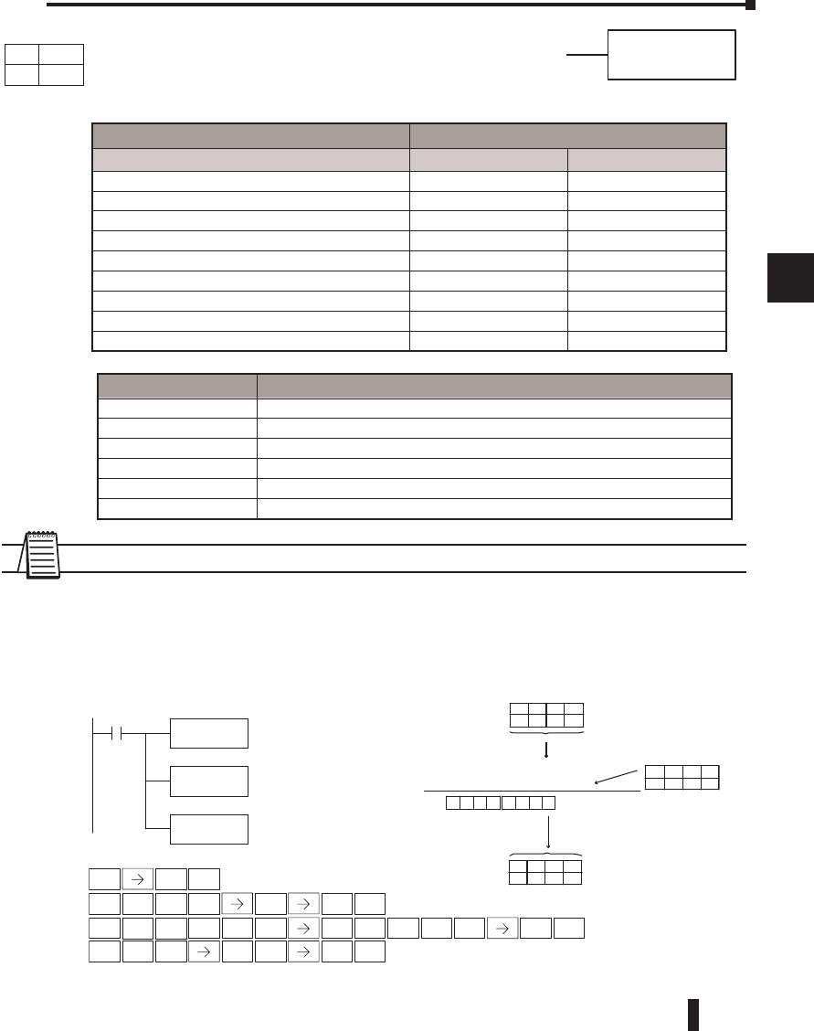
DL06 Micro PLC User Manual, 3rd Edition, Rev. D 5-107
1
2
3
4
5
6
7
8
9
10
11
12
13
14
A
B
C
D
Chapter 5: Standard RLL Instructions - Math
1
2
3
4
5
6
7
8
9
10
11
12
13
14
a
B
c
d
Subtract Formatted (SUBF)
Subtract Formatted is a 32-bit instruction that subtracts the BCD
value (Aaaa), which is a range of discrete bits, from the BCD value
in the accumulator. The specified range (Kbbb) can be 1 to 32
consecutive bits. The result resides in the accumulator.
NOTE: Status flags are valid only until another instruction uses the same flag.
In the following example, when X6 is on, the BCD value formed by discrete locations X0–X3
is loaded into the accumulator using the LDF instruction. The BCD value formed by discrete
location C0–C3 is subtracted from the BCD value in the accumulator using the SUBF
instruction. The value in the lower four bits of the accumulator is copied to Y10–Y13 using
the OUTF instruction.
bbbK
SUBF Aaaa
DirectSOFT32Display
LDFX0
K4
X6
SUBF C0
K4
OUTF Y10
K4
Copy thelower 4bitsofthe
accumulatortodiscrete
locations Y10--Y13
010000 0
y
000
0
00009
(C0--C3)
(Accumulator)
8
X0X1X2X3
ONOFFOFFON
C0C1C2C3
OFFOFFOFFON
Y10Y11Y12Y13
ONOFFOFFOFF
Theunused accumulator
bits areset to zero
ACC.
Handheld Programmer Keystrokes
STR
$
SHFT ISG
U
1
B
OUT
GX SHFT 5
F
0
A
4
EENT
6
GENT
1
B
4
E
0
AENT
SHFT ANDST
L
3
D
0
A
4
EENT
5
F
5
F
RST
SNEXT NEXT NEXTNEXT
SHFT
Load the BCD value represented
by discrete locations X0-X3 into
the accumulator
Subtract the BCD value
represented by C0-C3 from
the value in the accumulator
Operand Data Type DL06 Range
A aaa bbb
Inputs X 0–777 ––
Outputs Y 0–777 ––
Control Relays C 0–1777 ––
Stage Bits S 0–1777 ––
Timer Bits T 0–377 ––
Counter Bits CT 0–177 ––
Special Relays SP 0-137 320-717 ––
Global I/O GX 0-3777 ––
Constant K –– 1–32
Discrete Bit Flags Description
SP63 On when the result of the instruction causes the value in the accumulator to be zero.
SP64 On when the 16-bit subtraction instruction results in a borrow.
SP65 On when the 32 bit subtraction instruction results in a borrow
SP70 On any time the value in the accumulator is negative.
SP73 On when a signed addition or subtraction results in an incorrect sign bit.
SP75 On when a BCD instruction is executed and a NON-BCD number was encountered.
DS Used
HPP Used
DirectSOFT
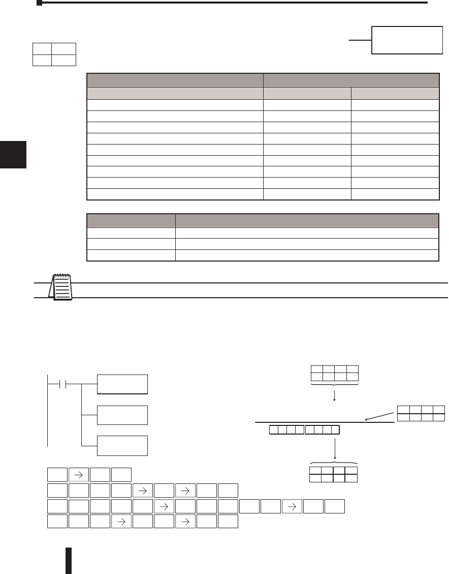
DL06 Micro PLC User Manual, 3rd Edition, Rev. D
5-108
1
2
3
4
5
6
7
8
9
10
11
12
13
14
A
B
C
D
Multiply Formatted (MULF)
Multiply Formatted is a 16-bit instruction that multiplies the
BCD value in the accumulator by the BCD value (Aaaa) which is
a range of discrete bits. The specified range (Kbbb) can be 1 to 16
consecutive bits. The result resides in the accumulator.
NOTE: Status flags are valid only until another instruction uses the same flag.
In the following example, when X6 is on, the value formed by discrete locations X0–X3 is
loaded into the accumulator using the Load Formatted instruction. The value formed by
discrete locations C0–C3 is multiplied by the value in the accumulator using the Multiply
Formatted instruction. The value in the lower four bits of the accumulator is copied to Y10–
Y13 using the Out Formatted instruction.
Chapter 5: Standard RLL Instructions - Math
1
2
3
4
5
6
7
8
9
10
11
12
13
14
a
B
c
d
bbbK
MULF Aaaa
DirectSOFT32Display
LDFX0
K4
X6 Load thevalue repr esented
by discretelocations X0 --X3
into theaccumulator
MULF C0
K4
Multiply thevalue in the
accumulatorwiththe value
represented by discrete
locations C0--C3
OUTF Y10
K4
Copy thelower 4bitsofthe
accumulatortodiscrete
locations Y10--Y13
060000 0
000
0
00003
(C0--C3)
(Accumulator)
2
X0X1X2X3
ONONOFFOFF
C0C1C2C3
OFFONOFFOFF
Y10Y11Y12Y13
OFFONONOFF
Theunused accumulator
bits areset to zero
Acc.
Handheld Programmer Keystrokes
STR
$
SHFT ISG
U
ANDST
L
OUT
GX SHFT 5
F
0
A
4
EENT
6
GENT
1
B
4
E
0
AENT
SHFT ANDST
L
3
D
0
A
4
EENT
5
F
5
F
ORST
MNEXT NEXT NEXTNEXT
X
Operand Data Type DL06 Range
A aaa bbb
Inputs X 0–777 ––
Outputs Y 0–777 ––
Control Relays C 0–1777 ––
Stage Bits S 0–1777 ––
Timer Bits T 0–377 ––
Counter Bits CT 0–177 ––
Special Relays SP 0-137 320-717 ––
Global I/O GX 0-3777 ––
Constant K –– 1–16
Discrete Bit Flags Description
SP63 On when the result of the instruction causes the value in the accumulator to be zero.
SP70 On any time the value in the accumulator is negative.
SP75 On when a BCD instruction is executed and a NON-BCD number was encountered.
DS Used
HPP Used
DirectSOFT
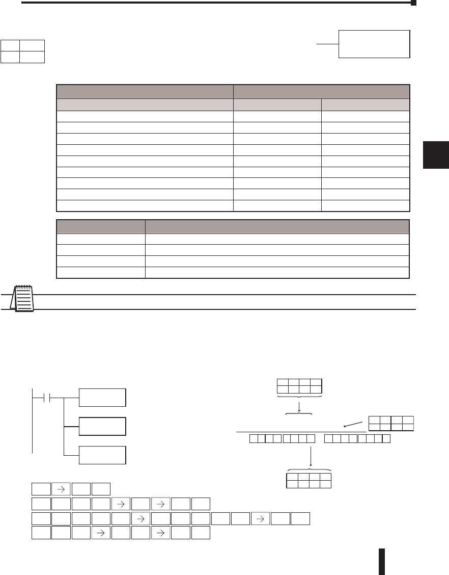
DL06 Micro PLC User Manual, 3rd Edition, Rev. D 5-109
1
2
3
4
5
6
7
8
9
10
11
12
13
14
A
B
C
D
Divide Formatted (DIVF)
Divide Formatted is a 16-bit instruction that divides the BCD value
in the accumulator by the BCD value (Aaaa), a range of discrete
bits. The specified range (Kbbb) can be 1 to 16 consecutive bits.
The first part of the quotient resides in the accumulator and the
remainder resides in the first stack location.
NOTE: Status flags are valid only until another instruction uses the same flag.
In the following example, when X6 is on, the value formed by discrete locations X0–X3
is loaded into the accumulator using the Load Formatted instruction. The value in the
accumulator is divided by the value formed by discrete location C0–C3 using the Divide
Formatted instruction. The value in the lower four bits of the accumulator is copied to Y10–
Y13 using the Out Formatted instruction.
Chapter 5: Standard RLL Instructions - Math
1
2
3
4
5
6
7
8
9
10
11
12
13
14
a
B
c
d
bbbK
DIVF Aaaa
DirectSOFT32Display
LDFX0
K4
X6 Load theval ue represented
by discretelocations X0 --X3
into theaccumulator
DIVF C0
K4
Dividethe valueinthe
accumulatorwiththe value
represented by di screte
location C0--C3
OUTF Y10
K4
Copy thelower 4bitsofthe
accumulatortodiscrete
locations Y10--Y13
040000 0
000
0
0000 8
(C0--C3)
(Accumulator)
2
X0X1X2X3
OFFOFFOFFON
C0C1C2C3
OFFONOFFOFF
Y10Y11Y12Y13
OFFOFFONOFF
Theunused accumulator
bits areset to zero
00 00000 0
Fi rststack location contains
therem aind er
Acc.
Handheld Programmer Keystrokes
STR
$
SHFT 8
I
AND
V
OUT
GX SHFT 5
F
0
A
4
EENT
6
GENT
1
B
4
E
0
AENT
SHFT ANDST
L
3
D
0
A
4
EENT
5
F
5
F
3
DNEXT NEXT NEXTNEXT
_
.
.
Operand Data Type DL06 Range
A aaa bbb
Inputs X 0–777 ––
Outputs Y 0–777 ––
Control Relays C 0–1777 ––
Stage Bits S 0–1777 ––
Timer Bits T 0–377 ––
Counter Bits CT 0–177 ––
Special Relays P 0-137 320-717 ––
Global I/O X 0-3777 ––
Constant K –– 1–16
Discrete Bit Flags Description
SP53 On when the value of the operand is larger than the accumulator can work with.
SP63 On when the result of the instruction causes the value in the accumulator to be zero.
SP70 On any time the value in the accumulator is negative.
SP75 On when a BCD instruction is executed and a NON-BCD number was encountered.
DS Used
HPP Used
DirectSOFT
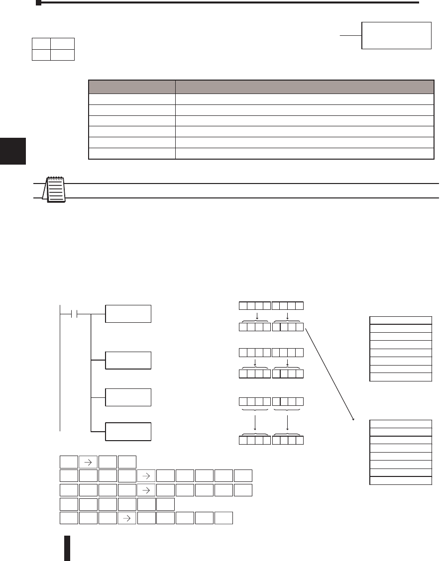
DL06 Micro PLC User Manual, 3rd Edition, Rev. D
5-110
1
2
3
4
5
6
7
8
9
10
11
12
13
14
A
B
C
D
NOTE: Status flags are valid only until another instruction uses the same flag.
In the following example, when X1 is on, the value in V1400 and V1401 will be loaded
into the accumulator using the Load Double instruction. The value in V1420 and V1421
is loaded into the accumulator using the Load Double instruction, pushing the value
previously loaded in the accumulator onto the accumulator stack. The value in the first level
of the accumulator stack is added with the value in the accumulator using the Add Stack
instruction. The value in the accumulator is copied to V1500 and V1501 using the Out
Double instruction.
Chapter 5: Standard RLL Instructions - Math
1
2
3
4
5
6
7
8
9
10
11
12
13
14
a
B
c
d
ADDS
DirectSOFT32 Display
LDD
V1400
X1 Load thevalue in V1400 and
V1401 into theaccumulator
LDD
V1420
Load thevalue in V1420 and
V1421 into theaccumulator
OUTD
V1500
Copy thevalue in the
accumulatortoV1500
andV1501
XXXX
XXXX
Level1
XXXX
XXXX
Level2
XXXX
XXXX
Level3
XXXX
XXXX
Level4
XXXX
XXXX
Level5
XXXX
XXXX
Level6
XXXX
XXXX
Level7
XXXX
XXXX
Level8
0039
5026
Level1
XXXX
XXXX
Level2
XXXX
XXXX
Level3
XXXX
XXXX
Level4
XXXX
XXXX
Level5
XXXX
XXXX
Level6
XXXX
XXXX
Level7
XXXX
XXXX
Level 8
ADDS Addthe valueinthe
accumulatorwiththe value
in thefirstlevelofthe
accumulatorstack
Acc.
V1400
502 6
003 9 5026
V1401
003 9
Acc.
V1420
205 6
001 7 2056
V1421
001 7
Accumulatorstack
after1stLDD
Accumulatorstack
after2nd LDD
Acc. 005 6 7082
005 6 7082
Handheld Programmer Keystrokes
SHFT ANDST
L
3
D
STR
$
SHFT 3
D
3
D
OUT
GX SHFT 3
D
1
B
5
F
0
A
0
AENT
1
BENT
1
B
4
E
0
A
0
AENT
ENT
SHFT ANDST
L
3
D
1
B
4
E
2
C
0
AENT
3
D
RST
S
3
D
0
A
V1501 V1500
Discrete Bit Flags Description
SP63 On when the result of the instruction causes the value in the accumulator to be zero.
SP66 On when the 16-bit addition instruction results in a carry.
SP67 On when the 32 bit addition instruction results in a carry.
SP70 On anytime the value in the accumulator is negative.
SP73 On when a signed addition or subtraction results in an incorrect sign bit.
SP75 On when a BCD instruction is executed and a NON-BCD number was encountered.
DS Used
HPP Used
DirectSOFT
Add Top of Stack (ADDS)
Add Top of Stack is a 32-bit instruction that adds the BCD
value in the accumulator with the BCD value in the first
level of the accumulator stack. The result resides in the
accumulator. The value in the first level of the accumulator
stack is removed and all stack values are moved up one level.
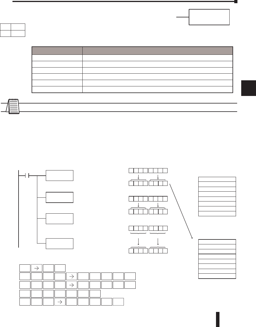
DL06 Micro PLC User Manual, 3rd Edition, Rev. D 5-111
1
2
3
4
5
6
7
8
9
10
11
12
13
14
A
B
C
D
NOTE: Status flags are valid only until another instruction uses the same flag.
In the following example, when X1 is on, the value in V1400 and V1401 will be loaded
into the accumulator using the Load Double instruction. The value in V1420 and V1421 is
loaded into the accumulator using the Load Double instruction, pushing the value previously
loaded into the accumulator onto the accumulator stack. The BCD value in the first level
of the accumulator stack is subtracted from the BCD value in the accumulator using the
Subtract Stack instruction. The value in the accumulator is copied to V1500 and V1501
using the Out Double instruction.
Chapter 5: Standard RLL Instructions - Math
1
2
3
4
5
6
7
8
9
10
11
12
13
14
a
B
c
d
SUBS
Sta
DirectSOFT32Display
LDD
V1400
X1 Load thevalue in V1400 and
V1401 into theaccumulator
LDD
V1420
Load thevalue in V1420 and
V1421 into theaccumulator
OUTD
V1500
Copy thevalue in the
accumulatortoV1500
and V1501
XXXXXXXXLevel 1
XXXXXXXXLevel 2
XXXXXXXXLevel 3
XXXXXXXXLevel 4
XXXXXXXXLevel 5
XXXXXXXXLevel 6
XXXXXXXXLevel 7
XXXXXXXXLevel 8
00172056Level 1
XXXXXXXX
Level 2
XXXXXXXXLevel 3
XXXXXXXX
Level 4
XXXXXXXXLevel 5
XXXXXXXX
Level 6
XXXXXXXXLevel 7
XXXXXXXX
Level 8
SUBS Subtract thevalue in thefirst
levelofthe accumulator
stackfromthe valueinthe
accumulator
Acc.
V1400
20 5 6
001 7 2056
V1401
001 7
Acc.
V1420
50 2 6
003 9 5026
V1421
003 9
Accumulatorstack
after1st LD D
Accumulatorstack
after2nd LDD
Acc. 002 2 2970
002 2 2970
Handheld Programmer Keystrokes
SHFT ANDST
L
3
D
STR
$
SHFT ISG
U
1
B
OUT
GX SHFT 3
D
1
B
5
F
0
A
0
AENT
1
BENT
1
B
4
E
0
A
0
AENT
ENT
SHFT ANDST
L
3
D
1
B
4
E
2
C
0
AENT
3
D
RST
S
3
D
RST
SSHFT
V1501 V1500
Discrete Bit Flags Description
SP63 On when the result of the instruction causes the value in the accumulator to be zero.
SP64 On when the 16-bit subtraction instruction results in a borrow.
SP65 On when the 32 bit subtraction instruction results in a borrow.
SP70 On anytime the value in the accumulator is negative.
SP73 On when a signed addition or subtraction results in an incorrect sign bit.
SP75 On when a BCD instruction is executed and a NON-BCD number was encountered.
DS Used
HPP Used
DirectSOFT
Subtract Top of Stack (SUBS)
Subtract Top of Stack is a 32-bit instruction that subtracts
the BCD value in the first level of the accumulator stack from
the BCD value in the accumulator. The result resides in the
accumulator. The value in the first level of the accumulator
stack is removed and all stack values are moved up one level.
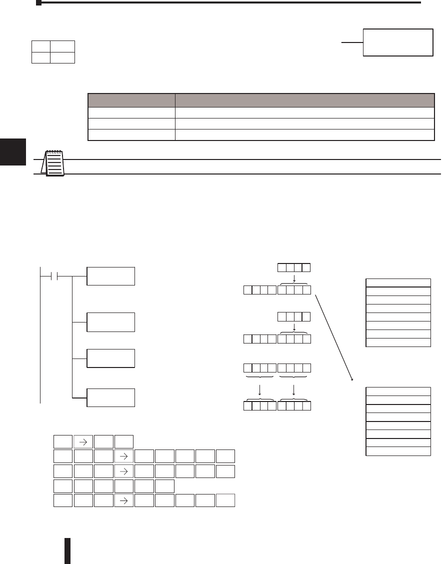
DL06 Micro PLC User Manual, 3rd Edition, Rev. D
5-112
1
2
3
4
5
6
7
8
9
10
11
12
13
14
A
B
C
D
Multiply Top of Stack (MULS)
Multiply Top of Stack is a 16-bit instruction that multiplies a
4-digit BCD value in the first level of the accumulator stack by a
4-digit BCD value in the accumulator. The result resides in the
accumulator. The value in the first level of the accumulator stack is
removed and all stack values are moved up one level.
NOTE: Status flags are valid only until another instruction uses the same flag.
In the following example, when X1 is on, the value in V1400 will be loaded into the
accumulator using the Load instruction. The value in V1420 is loaded into the accumulator
using the Load instruction, pushing the value previously loaded in the accumulator onto the
accumulator stack. The BCD value in the first level of the accumulator stack is multiplied
by the BCD value in the accumulator using the Multiply Stack instruction. The value in the
accumulator is copied to V1500 and V1501 using the Out Double instruction.
Chapter 5: Standard RLL Instructions - Math
1
2
3
4
5
6
7
8
9
10
11
12
13
14
a
B
c
d
MULS
StandardRLL
DirectSOFT32Display
LD
V1400
X1 Load thevalue in V1400 into
theaccumulator
LD
V1420
Load thevalue in V1420 into
theaccumulator
OUTD
V1500
Copy thevalue in the
accumulatortoV1500
and V1501
XXXXXXXXLevel 1
XXXXXXXXLevel 2
XXXXXXXXLevel 3
XXXXXXXXLevel 4
XXXXXXXXLevel 5
XXXXXXXXLevel 6
XXXXXXXXLevel 7
XXXXXXXXLevel 8
00005000Level 1
XXXXXXXX
Level 2
XXXXXXXXLevel 3
XXXXXXXX
Level 4
XXXXXXXXLevel 5
XXXXXXXX
Level 6
XXXXXXXXLevel 7
XXXXXXXX
Level 8
MULS Multiply thevalue in the
accumulatorwiththe value
in thefirst levelofthe
accumulatorstack
Acc.
V1400
5000
00005000
Acc.
V1420
0200
00000200
Accumulatorstack
after1st LD D
Accumulatorstack
after2nd LDD
Acc. 01000000
01000000
V1500V1501
Theunused accumulator
bits areset to zero
Theunused accumulator
bits areset to zero
Handheld Programmer Keystrokes
SHFT ANDST
L
3
D
STR
$
SHFT ORST
M
ISG
U
ANDST
L
OUT
GX SHFT 3
D
1
B
5
F
0
A
0
AENT
1
BENT
1
B
4
E
0
A
0
AENT
ENT
SHFT ANDST
L
3
D
1
B
4
E
2
C
0
A
RST
S
ENT
Discrete Bit Flags Description
SP63 On when the result of the instruction causes the value in the accumulator to be zero.
SP70 On any time the value in the accumulator is negative.
SP75 On when a BCD instruction is executed and a NON-BCD number was encountered.
DS Used
HPP Used
DirectSOFT
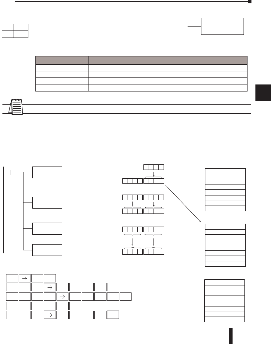
DL06 Micro PLC User Manual, 3rd Edition, Rev. D 5-113
1
2
3
4
5
6
7
8
9
10
11
12
13
14
A
B
C
D
Divide by Top of Stack (DIVS)
Divide Top of Stack is a 32-bit instruction that divides the
8-digit BCD value in the accumulator by a 4-digit BCD value
in the first level of the accumulator stack. The result resides in
the accumulator and the remainder resides in the first level of the
accumulator stack.
NOTE: Status flags are valid only until another instruction uses the same flag.
In the following example, when X1 is on, the Load instruction loads the value in V1400 into
the accumulator. The value in V1420 is loaded into the accumulator using the Load Double
instruction, pushing the value previously loaded in the accumulator onto the accumulator
stack. The BCD value in the accumulator is divided by the BCD value in the first level of the
accumulator stack using the Divide Stack instruction. The Out Double instruction copies the
value in the accumulator to V1500 and V1501.
Chapter 5: Standard RLL Instructions - Math
1
2
3
4
5
6
7
8
9
10
11
12
13
14
a
B
c
d
DIVS
DirectSOFT32Display
LD
V1400
X1 Load thevalue in V1400 into
theaccumulator
LDD
V1420
Load thevalue in V1420 and
V1421 into theaccumulator
OUTD
V1500
Copy thevalue in the
accumulatortoV1500
and V1501
XXXXXXXX
Level 1
XXXXXXXXLevel 2
XXXXXXXX
Level 3
XXXXXXXXLevel 4
XXXXXXXX
Level 5
XXXXXXXXLevel 6
XXXXXXXX
Level 7
XXXXXXXXLevel 8
00000020
Level 1
XXXXXXXXLevel 2
XXXXXXXX
Level 3
XXXXXXXXLevel 4
XXXXXXXX
Level 5
XXXXXXXXLevel 6
XXXXXXXX
Level 7
XXXXXXXXLevel 8
DIVS Dividethe valueinthe
accumulatorbythe valuein
thefirst levelofthe
accumulatorstack
Acc.
V1400
0020
0000002 0
Acc.
V1420
0000
0050000 0
V1421
005 0
Accumulatorstack
after1st LD D
Accumulatorstack
after2nd LDD
Acc. 0002500 0
0002500 0
V1500V1501
Theunused accumulator
bits areset to e ro
00000000Level 1
XXXXXXXX
Level 2
XXXXXXXXLevel 3
XXXXXXXXLevel 4
XXXXXXXXLevel 5
XXXXXXXXLevel 6
XXXXXXXXLevel 7
XXXXXXXXLevel 8
Theremai nder resides in the
firststack location
andheldrorammereystrokes
SFT ADST
L
3
D
ST
SFT 8
I
AD
V
OUT
X SFT 3
D
1
5
F
0
A
0
A T
1
T
1
4
0
A
0
A T
T
SFT ADST
L
3
D
1
4
2
C
0
AT
3
D
ST
S
3
D
Discrete Bit Flags Description
SP53 On when the value of the operand is larger than the accumulator can work with.
SP63 On when the result of the instruction causes the value in the accumulator to be zero.
SP70 On any time the value in the accumulator is negative.
SP75 On when a BCD instruction is executed and a NON-BCD number was encountered.
DS Used
HPP Used
DirectSOFT
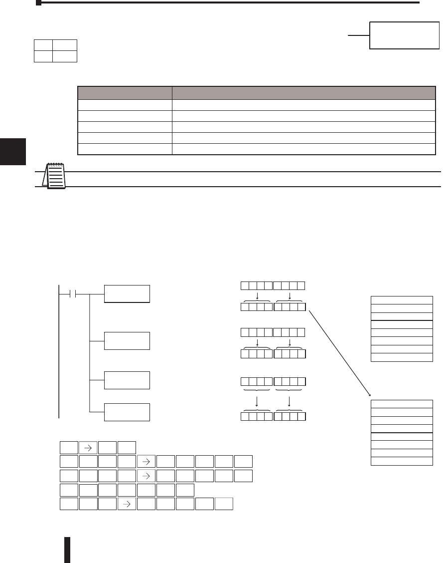
DL06 Micro PLC User Manual, 3rd Edition, Rev. D
5-114
1
2
3
4
5
6
7
8
9
10
11
12
13
14
A
B
C
D
NOTE: Status flags are valid only until another instruction uses the same flag.
In the following example, when X1 is on, the value in V1400 and V1401 will be loaded
into the accumulator using the Load Double instruction. The value in V1420 and V1421 is
loaded into the accumulator using the Load Double instruction, pushing the value previously
loaded in the accumulator onto the accumulator stack. The binary value in the first level of
the accumulator stack is added with the binary value in the accumulator using the Add Stack
instruction. The value in the accumulator is copied to V1500 and V1501 using the Out
Double instruction.
Chapter 5: Standard RLL Instructions - Math
1
2
3
4
5
6
7
8
9
10
11
12
13
14
a
B
c
d
ADDBS
Standard RLL
DirectSOFT32 Display
LDD
V1400
X1 Load thevalue in V1400 and
V1401 into theaccumulator
LDD
V1420
Load thevalue in V1420 and
V1421 into theaccumulator
OUTD
V1500
Copy thevalue in the
accumulatortoV1500
andV1501
XXXXXXXXLevel1
XXXXXXXXLevel2
XXXXXXXXLevel3
XXXXXXXXLevel4
XXXXXXXXLevel5
XXXXXXXXLevel6
XXXXXXXXLevel7
XXXXXXXXLevel8
003A50C6Level1
XXXXXXXX
Level2
XXXXXXXXLevel3
XXXXXXXX
Level4
XXXXXXXXLevel5
XXXXXXXX
Level6
XXXXXXXXLevel7
XXXXXXXX
Level 8
ADDBSAddthe bi nary valueinthe
accumulatorwiththe binary
valueinthe firstlevel of the
accumulatorstack
Acc.
V1400
50C 6
003A50C 6
V1401
003A
Acc.
V1420
B05 F
0017B0 5 F
V1421
0017
Accumulatorstack
after1stLDD
Accumulatorstack
after2nd LDD
Acc. 005201 2 5
005201 2 5
Handheld Programmer Keystrokes
SHFT ANDST
L
3
D
STR
$
SHFT 3
D
3
D
OUT
GX SHFT 3
D
1
B
5
F
0
A
0
AENT
1
BENT
1
B
4
E
0
A
0
AENT
ENT
SHFT ANDST
L
3
D
1
B
4
E
2
C
0
AENT
3
D
1
B
RST
S
3
D
0
A
Discrete Bit Flags Description
SP63 On when the result of the instruction causes the value in the accumulator to be zero.
SP66 On when the 16-bit addition instruction results in a carry.
SP67 On when the 32 bit addition instruction results in a carry.
SP70 On anytime the value in the accumulator is negative.
SP73 On when a signed addition or subtraction results in an incorrect sign bit.
DS Used
HPP Used
DirectSOFT
Add Binary Top of Stack (ADDBS)
Add Binary Top of Stack instruction is a 32-bit instruction that
adds the binary value in the accumulator with the binary value in
the first level of the accumulator stack. The result resides in the
accumulator. The value in the first level of the accumulator stack
is removed and all stack values are moved
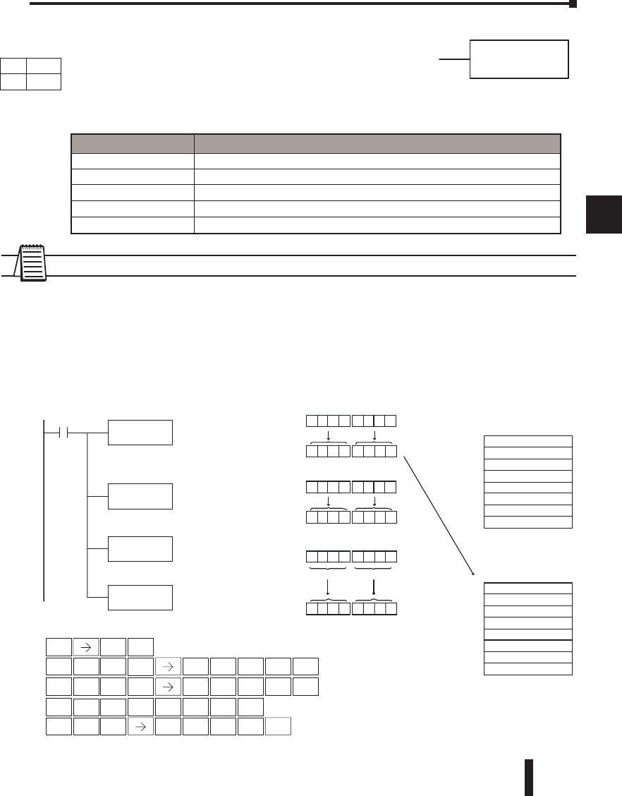
DL06 Micro PLC User Manual, 3rd Edition, Rev. D 5-115
1
2
3
4
5
6
7
8
9
10
11
12
13
14
A
B
C
D
Subtract Binary Top of Stack (SUBBS)
Subtract Binary Top of Stack is a 32-bit instruction that subtracts
the binary value in the first level of the accumulator stack from
the binary value in the accumulator. The result resides in the
accumulator. The value in the first level of the accumulator stack is
removed and all stack locations are moved up one level.
NOTE: Status flags are valid only until another instruction uses the same flag.
In the following example, when X1 is on, the value in V1400 and V1401 will be loaded
into the accumulator using the Load Double instruction. The value in V1420 and V1421 is
loaded into the accumulator using the Load Double instruction, pushing the value previously
loaded in the accumulator onto the accumulator stack. The binary value in the first level
of the accumulator stack is subtracted from the binary value in the accumulator using the
Subtract Stack instruction. The value in the accumulator is copied to V1500 and V1501
using the Out Double instruction.
Chapter 5: Standard RLL Instructions - Math
1
2
3
4
5
6
7
8
9
10
11
12
13
14
a
B
c
d
SUBBS
DirectSOFT32Display
LDD
V1400
X1 Load theval ue in V1400 and
V1401 into theaccumulator
LDD
V1420
Load theval ue in V1420 and
V1421 into theaccumulator
OUTD
V1500
Copy theval ue in the
accumulatortoV1500
and V1501
XXXXXXXXLevel 1
XXXXXXXXLevel 2
XXXXXXXXLevel 3
XXXXXXXXLevel 4
XXXXXXXXLevel 5
XXXXXXXXLevel 6
XXXXXXXXLevel 7
XXXXXXXXLevel 8
001A205BLevel 1
XXXXXXXX
Level 2
XXXXXXXXLevel 3
XXXXXXXX
Level 4
XXXXXXXXLevel 5
XXXXXXXX
Level 6
XXXXXXXXLevel 7
XXXXXXXX
Level 8
SUBBS Subtract thebinaryvalue in
thefirst levelofthe
accumulatorstack from the
binaryvalue in the
accumulator
Acc.
V1400
205B
001A205 B
V1401
001A
Acc.
V1420
50C 6
003A50C 6
V1421
003A
Accumulatorstack
after1st LDD
Accumulatorstack
after2nd LDD
Acc. 0020306 B
0020306 B
Handheld Programmer Keystrokes
SHFT ANDST
L
3
D
STR
$
SHFT ISG
U
1
B
OUT
GX SHFT 3
D
1
B
5
F
0
A
0
AENT
1
BENT
1
B
4
E
0
A
0
AENT
ENT
SHFT ANDST
L
3
D
1
B
4
E
2
C
0
AENT
3
D
1
B
RST
S
3
D
RST
SSHFT
V1501 V1500
Discrete Bit Flags Description
SP63 On when the result of the instruction causes the value in the accumulator to be zero.
SP64 On when the 16-bit subtraction instruction results in a borrow.
SP65 On when the 32-bit subtraction instruction results in a borrow.
SP70 On any time the value in the accumulator is negative.
SP73 On when a signed addition or subtraction results in an incorrect sign bit.
DS Used
HPP Used
DirectSOFT
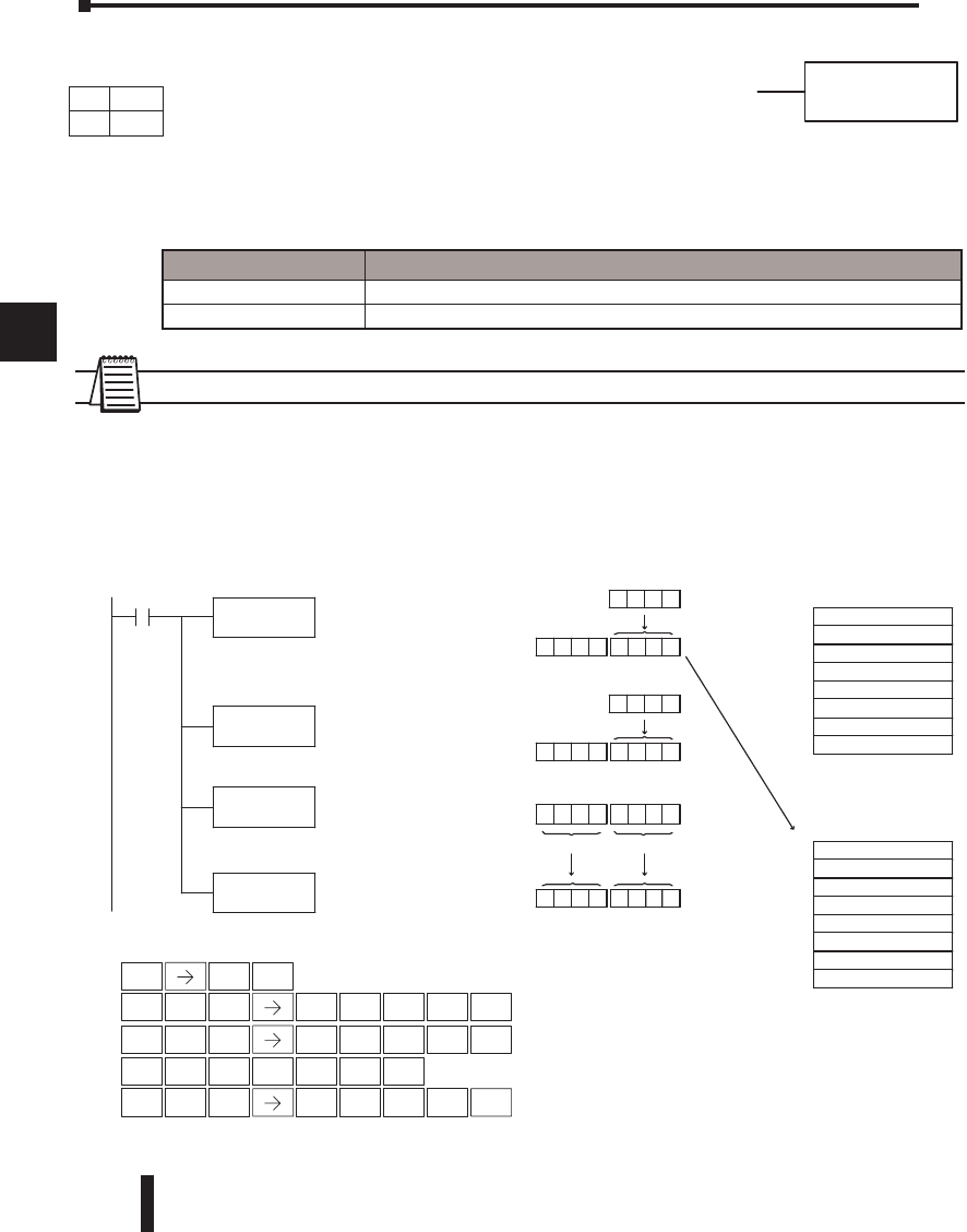
DL06 Micro PLC User Manual, 3rd Edition, Rev. D
5-116
1
2
3
4
5
6
7
8
9
10
11
12
13
14
A
B
C
D
NOTE: Status flags are valid only until another instruction uses the same flag.
In the following example, when X1 is on, the Load instruction moves the value in V1400
into the accumulator. The value in V1420 is loaded into the accumulator using the Load
instruction, pushing the value previously loaded in the accumulator onto the stack. The
binary value in the accumulator stack’s first level is multiplied by the binary value in the
accumulator using the Multiply Binary Stack instruction. The Out Double instruction copies
the value in the accumulator to V1500 and V1501.
Chapter 5: Standard RLL Instructions - Math
1
2
3
4
5
6
7
8
9
10
11
12
13
14
a
B
c
d
MULBS
StandardRLL
Instructions
DirectSOFT32Display
LD
V1400
X1 Load thevalue in V1400 into
theaccumulator
LD
V1420
Load thevalue in V1420 into
theaccumulator
OUTD
V1500
Copy thevalue in the
accumulatortoV1500
and V1501
XXXXXXXXLevel 1
XXXXXXXXLevel 2
XXXXXXXXLevel 3
XXXXXXXXLevel 4
XXXXXXXXLevel 5
XXXXXXXXLevel 6
XXXXXXXXLevel 7
XXXXXXXXLevel 8
0000C350Level 1
XXXXXXXX
Level 2
XXXXXXXXLevel 3
XXXXXXXX
Level 4
XXXXXXXXLevel 5
XXXXXXXX
Level 6
XXXXXXXXLevel 7
XXXXXXXX
Level 8
MULBSMultiply thebinaryvalue in
theaccumulatorwiththe
binaryvalue in thefirst level
of theaccumulatorstack
Acc.
V1400
C350
0000C350
Acc.
V1420
0014
000 0 0014
Accumulatorstack
after1st LDD
Accumulatorstack
after2nd LDD
Acc. 000 F 4240
000 F 4240
V1500V1501
Theunused accumulator
bits areset to zero
Theunused accumulator
bits areset to zero
Handheld Programmer Keystrokes
SHFT ANDST
L
3
D
STR
$
SHFT ORST
M
ISG
U
ANDST
L
OUT
GX SHFT 3
D
1
B
5
F
0
A
0
AENT
1
BENT
1
B
4
E
0
A
0
AENT
ENT
SHFT ANDST
L
3
D
1
B
4
E
2
C
0
A
1
B
RST
S
ENT
Discrete Bit Flags Description
SP63 On when the result of the instruction causes the value in the accumulator to be zero.
SP70 On any time the value in the accumulator is negative.
DS Used
HPP Used
DirectSOFT
Multiply Binary Top of Stack (MULBS)
Multiply Binary Top of Stack is a 16-bit instruction that
multiplies the 16-bit binary value in the first level of
the accumulator stack by the 16-bit binary value in the
accumulator. The result resides in the accumulator and
can be 32 bits (8 digits max.). The value in the first level
of the accumulator stack is removed and all stack locations
are moved up one level
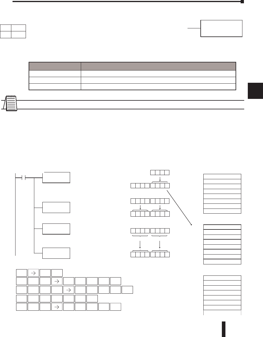
DL06 Micro PLC User Manual, 3rd Edition, Rev. D 5-117
1
2
3
4
5
6
7
8
9
10
11
12
13
14
A
B
C
D
Divide Binary by Top OF Stack (DIVBS)
Divide Binary Top of Stack is a 32-bit instruction that divides the
32-bit binary value in the accumulator by the 16-bit binary value
in the first level of the accumulator stack. The result resides in
the accumulator and the remainder resides in the first level of the
accumulator stack.
NOTE: Status flags are valid only until another instruction uses the same flag.
In the following example, when X1 is on, the value in V1400 will be loaded into the
accumulator using the Load instruction. The value in V1420 and V1421 is loaded into the
accumulator using the Load Double instruction also, pushing the value previously loaded in
the accumulator onto the accumulator stack. The binary value in the accumulator is divided
by the binary value in the first level of the accumulator stack using the Divide Binary Stack
instruction. The value in the accumulator is copied to V1500 and V1501 using the Out
Double instruction.
Chapter 5: Standard RLL Instructions - Math
1
2
3
4
5
6
7
8
9
10
11
12
13
14
a
B
c
d
Dir
e
ctSOFT
3
2
Display
LD
V1400
X1 Load theval ue in V1400 into
theaccumulator
LDD
V1420
Load theval ue in V1420 and
V1421 into theaccumulator
OUTD
V1500
Copy theval ue in the
accumulatortoV1500
and V1501
XXXXXXXXLevel 1
XXXXXXXX
Level 2
XXXXXXXXLevel 3
XXXXXXXX
Level 4
XXXXXXXXLevel 5
XXXXXXXX
Level 6
XXXXXXXXLevel 7
XXXXXXXXLevel 8
00000014Level 1
XXXXXXXX
Level 2
XXXXXXXXLevel 3
XXXXXXXX
Level 4
XXXXXXXXLevel 5
XXXXXXXX
Level 6
XXXXXXXXLevel 7
XXXXXXXX
Level 8
DIVBS Dividethe binar yvalue in
theaccumulatorbythe
binaryvalue in thefirst level
of theaccumulatorstack
Acc.
V
1
4
0
0
0014
00000014
Acc.
V1420
C350
0000C350
V1421
0000
A
ccumulatorstac
k
after1st LDD
Accumulatorstack
after2nd LDD
Acc. 000009C4
000009C 4
V1500V1501
Theunused accumulator
bits areset to zero
00000000
Level 1
XXXXXXXXLevel 2
XXXXXXXX
Level 3
XXXXXXXXLevel 4
XXXXXXXX
Level 5
XXXXXXXXLevel 6
XXXXXXXX
Level 7
XXXXXXXXLevel 8
Theremai nder resides in the
firststack location
Handheld Programmer Keystrokes
SHFT ANDST
L
3
D
STR
$
SHFT 3
D
8
I
AND
V
OUT
GX SHFT 3
D
1
B
5
F
0
A
0
AENT
1
BENT
1
B
4
E
0
A
0
AENT
ENT
SHFT ANDST
L
3
D
1
B
4
E
2
C
0
AENT
3
D
1
B
RST
S
DIVBS
Discrete Bit Flags Description
SP53 On when the value of the operand is larger than the accumulator can work with.
SP63 On when the result of the instruction causes the value in the accumulator to be zero.
SP70 On any time the value in the accumulator is negative.
DS Used
HPP Used
DirectSOFT
DL06 Micro PLC User Manual, 3rd Edition, Rev. D
5-118
1
2
3
4
5
6
7
8
9
10
11
12
13
14
A
B
C
D
Transcendental Functions
The DL06 CPU features special numerical functions to complement its real number
capability. The transcendental functions include the trigonometric sine, cosine, and tangent,
and also their inverses (arc sine, arc cosine, and arc tangent). The square root function is also
grouped with these other functions.
The transcendental math instructions operate on a real number in the accumulator (it
cannot be BCD or binary). The real number result resides in the accumulator. The square
root function operates on the full range of positive real numbers. The sine, cosine and
tangent functions require numbers expressed in radians. You can work with angles expressed
in degrees by first converting them to radians with the Radian (RADR) instruction, then
performing the trig function. All transcendental functions utilize the following flag bits.
Sine Real (SINR)
The Sine Real instruction takes the sine of the real number stored
in the accumulator. The result resides in the accumulator. Both
the original number and the result must be Real data type (IEEE
floating point format).
Cosine Real (COSR)
The Cosine Real instruction takes the cosine of the real number
stored in the accumulator. The result resides in the accumulator.
Both the original number and the result must be Real data type
(IEEE floating point format)..
Tangent Real (TANR)
The Tangent Real instruction takes the tangent of the real number
stored in the accumulator. The result resides in the accumulator.
Both the original number and the result must be Real data type
(IEEE floating point format).
Arc Sine Real (ASINR)
The Arc Sine Real instruction takes the inverse sine of the real
number stored in the accumulator. The result resides in the
accumulator. Both the original number and the result must be Real
data type (IEEE floating point format).
Chapter 5: Standard RLL Instructions - Transcendental Functions
1
2
3
4
5
6
7
8
9
10
11
12
13
14
a
B
c
d
SINR
COSR
TANR
AS INR
Discrete Bit Flags Description
SP53 On when the value of the operand is larger than the accumulator can work with.
SP63 On when the result of the instruction causes the value in the accumulator to be zero.
SP70 On anytime the value in the accumulator is negative.
SP72 On anytime the value in the accumulator is an invalid floating point number
SP73 On when a signed addition or subtraction results in an incorrect sign bit.
SP75 On when a real number instruction is executed and a non-real number encountered.
DS Used
HPP N/A
DS Used
HPP N/A
DS Used
HPP N/A
DS Used
HPP N/A
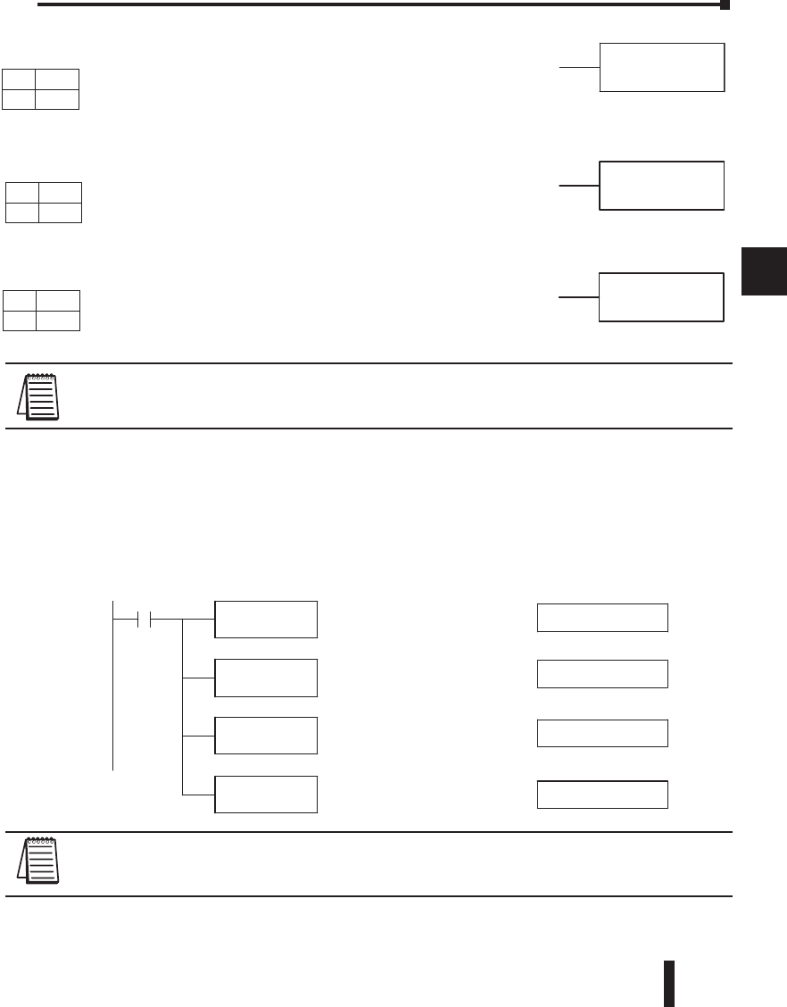
DL06 Micro PLC User Manual, 3rd Edition, Rev. D 5-119
1
2
3
4
5
6
7
8
9
10
11
12
13
14
A
B
C
D
Arc Cosine Real (ACOSR)
The Arc Cosine Real instruction takes the inverse cosine of the
real number stored in the accumulator. The result resides in the
accumulator. Both the original number and the result must be Real
data type (IEEE floating point format).
Arc Tangent Real (ATANR)
The Arc Tangent Real instruction takes the inverse tangent of the
real number stored in the accumulator. The result resides in the
accumulator. Both the original number and the result must be Real
data type (IEEE floating point format).
Square Root Real (SQRTR)
The Square Root Real instruction takes the square root of the
real number stored in the accumulator. The result resides in the
accumulator. Both the original number and the result must be Real
data type (IEEE floating point format).
NOTE: The square root function can be useful in several situations. However, if you are trying to do
the square-root extract function for an orifice flow meter measurement, as the PV to a PID loop, note
that the PID loop already has the square-root extract function built in.
The following example takes the sine of 45 degrees. Since these transcendental functions
operate only on real numbers, we do an LDR (load real) 45. The trig functions operate only
in radians, so we must convert the degrees to radians by using the RADR command. After
using the SINR (Sine Real) instruction, we use an OUTD (Out Double) instruction to move
the result from the accumulator to V-memory. The result is 32-bits wide, requiring the Out
Double to move it.
NOTE: The current HPP does not support real number entry with automatic conversion to the 32-bit
IEEE format. You must use DirectSOFT for entering real numbers, using the LDR (Load Real)
instruction.
Chapter 5: Standard RLL Instructions - Transcendental Functions
1
2
3
4
5
6
7
8
9
10
11
12
13
14
a
B
c
d
ACOSR
ATANR
SQRTR
DirectSOFT 5
LDR
R45
X1 Load thereal num ber 45 into
theaccumulator.
RADR Conver tthe degrees into radians,
leavingthe result in the
accumulator.
OUTD
V2000
Copy thevalue in the
accumulatortoV2000
and V2001.
45.000000
Accumulatorcontents
(viewedasreal number)
0.7358981
SINR Take thesineofthe number in
theaccumulator, whichisin
radians.
0.7071067
0.7071067
DS Used
HPP N/A
DS Used
HPP N/A
DS Used
HPP N/A
DirectSOFT
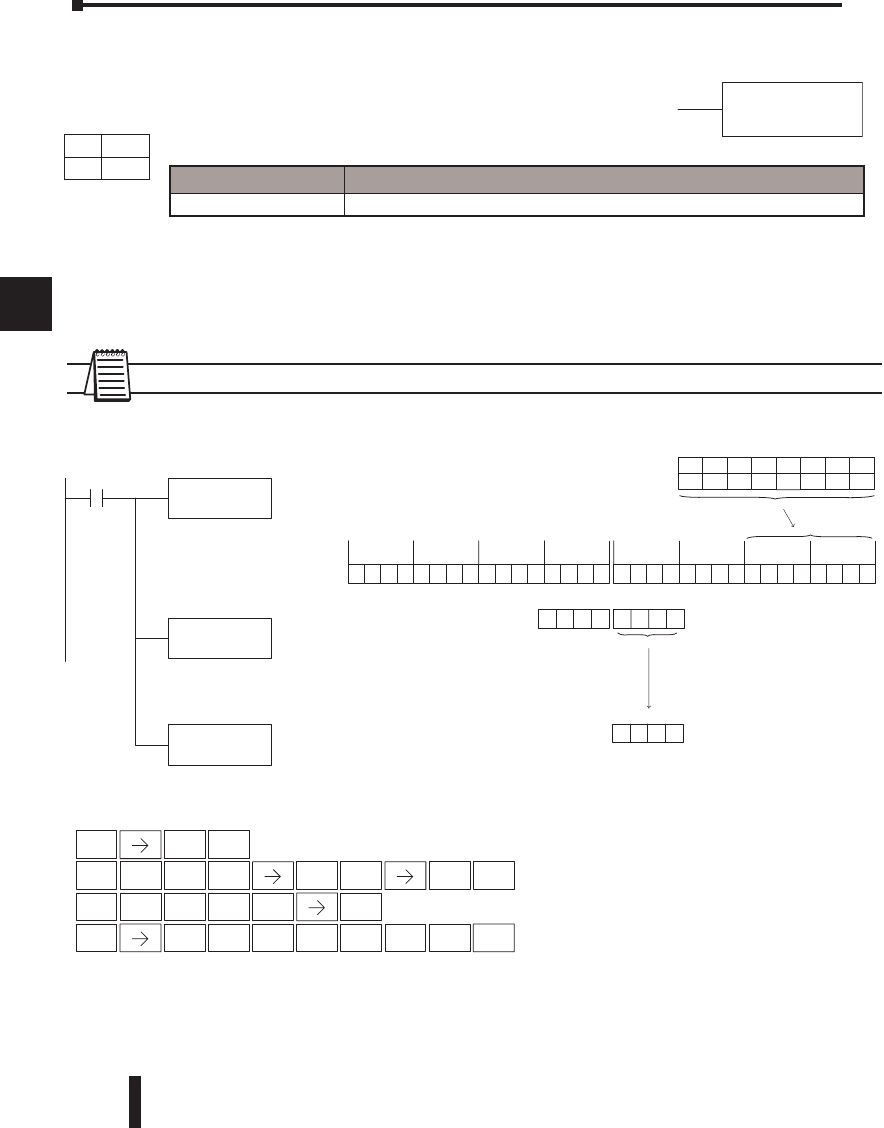
DL06 Micro PLC User Manual, 3rd Edition, Rev. D
5-120
1
2
3
4
5
6
7
8
9
10
11
12
13
14
A
B
C
D
Bit Operation Instructions
Sum (SUM)
The Sum instruction counts number of bits that are set to “1” in
the accumulator. The HEX result resides in the accumulator.
In the following example, when X1 is on, the value formed by discrete locations X10–X17 is
loaded into the accumulator using the Load Formatted instruction. The number of bits in the
accumulator set to “1” is counted using the Sum instruction. The value in the accumulator is
copied to V1500 using the Out instruction.
NOTE: Status flags are valid only until another instruction uses the same flag.
Chapter 5: Standard RLL Instructions - Bit Operation
1
2
3
4
5
6
7
8
9
10
11
12
13
14
a
B
c
d
SUM
Direct SOFT32 Display
LDF X10
K8
X1
Load the value represented by
discrete locations X10–X17
into the accumulator
SUM
Sum the number of bits in
the accumulator set to “1”
OUT
V1500
Copy the value in the lower
16 bits of the accumulator
to V1500
X10X11X12X13
ONONOFFON
X14X15X16X17
OFFOFFONON
00000000110010
11
0000000000000000
15 14 13 12 11 10 9 87654
3210
31 30 29 28 27 26 25 24 23 22 21 20 19 18 17 1631 30 29 28 27 26 25 24 23 22 21 20 19 18 17 16
Acc.
V1500
Acc.
000 5
000 0 000 5
The unused accumulator
bits are set to zero
STR
$ENT
SHFT ANDST
L
3
D
5
F
SHFT RST
S
ISG
U
ORST
MENT
1
B
1
B
0
A
8
IENT
SHFT
OUT
GX PREV 1
B
5
F
0
A
0
AENTPREV PREV
Handheld Programmer Keystrokes
Discrete Bit Flags Description
SP63 On when the result of the instruction causes the value in the accumulator to be zero.
DS Used
HPP Used
DirectSOFT
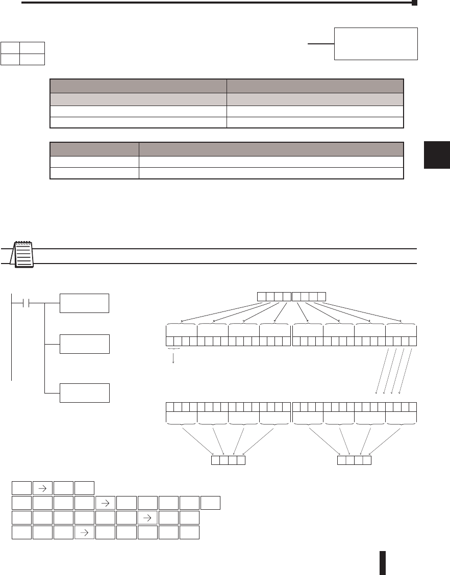
DL06 Micro PLC User Manual, 3rd Edition, Rev. D 5-121
1
2
3
4
5
6
7
8
9
10
11
12
13
14
A
B
C
D
Shift Left (SHFL)
Shift Left is a 32-bit instruction that shifts the bits in the
accumulator a specified number (Aaaa) of places to the left. The
vacant positions are filled with zeros and the bits shifted out of
the accumulator are discarded.
In the following example, when X1 is on, the value in V2000 and V2001 will be loaded
into the accumulator using the Load Double instruction. The bit pattern in the accumulator
is shifted 2 bits to the left using the Shift Left instruction. The value in the accumulator is
copied to V2010 and V2011 using the Out Double instruction.
NOTE: Status flags are valid only until another instruction uses the same flag.
Chapter 5: Standard RLL Instructions - Bit Operation
1
2
3
4
5
6
7
8
9
10
11
12
13
14
a
B
c
d
2
CENT
Handheld Programmer Keystrokes
Direct SOFT32
LDD
V2000
X1
Load the value in V2000 and
V2001 into the accumulator
SHFL
K2
The bit pattern in the
accumulator is shifted 2 bit
positions to the left
OUTD
V2010
Copy the value in the
accumulator to V2010 and
V2011
00110001000000
01
V2010
11000100000001
00
0000010000000000
15 14 13 12 11 10 987654
3210
31 30 29 28 27 26 25 24 23 22 21 20 19 18 17 16
C404
. . . .
1001110000010100
31 30 29 28 27 26 25 24 23 22 21 20 19 18 17 16
0110011100000101
15 14 13 12 11 10 987654
3210
31 30 29 28 27 26 25 24 23 22 21 20 19 18 17 1631 30 29 28 27 26 25 24 23 22 21 20 19 18 17 16
Acc.
Acc.
V2011
9C14
67053310 3101
Shifted out of the
accumulator
V2000V2001
STR
$
SHFT ANDST
L
3
D
3
D
SHFT RST
S
7
H
5
F
ANDST
L
OUT
GX SHFT 3
D
1
BENT
2
C
0
A
0
A
0
AENT
2
C
0
A
1
B
0
AENT
SHFT
Operand Data Type DL06 Range
Aaaa
V-memory V See memory map
Constant K 1-32
Discrete Bit Flags Description
SP63 On when the result of the instruction causes the value in the accumulator to be zero.
SP70 On anytime the value in the accumulator is negative.
SHFL
A aaa
DS Used
HPP Used
DirectSOFT
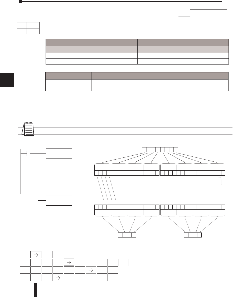
DL06 Micro PLC User Manual, 3rd Edition, Rev. D
5-122
1
2
3
4
5
6
7
8
9
10
11
12
13
14
A
B
C
D
Shift Right (SHFR)
Shift Right is a 32-bit instruction that shifts the bits in the
accumulator a specified number (Aaaa) of places to the right. The
vacant positions are filled with zeros and the bits shifted out of the
accumulator are lost.
In the following example, when X1 is on, the value in V2000 and V2001 will be loaded into
the accumulator using the Load Double instruction. The bit pattern in the accumulator is
shifted 2 bits to the right using the Shift Right instruction. The value in the accumulator is
copied to V2010 and V2011 using the Out Double instruction.
NOTE: Status flags are valid only until another instruction uses the same flag.
Chapter 5: Standard RLL Instructions - Bit Operation
1
2
3
4
5
6
7
8
9
10
11
12
13
14
a
B
c
d
SHFR
A aaa
Handheld Programmer Keystrokes
Direct SOFT32
LDD
V2000
X1
Load the value in V2000 and
V2001 into the accumulator
SHFR
K2
The bit pattern in the
accumulator is shifted 2 bit
positions to the right
OUTD
V2010
Copy the value in the
accumulator to V2010 and
V2011
0011000100000001
V2010
01001100010000000000010000000000
15 14 13 12 11 10 987654321031 30 29 28 27 26 25 24 23 22 21 20 19 18 17 16
4C40
. . .
0001100111000001
31 30 29 28 27 26 25 24 23 22 21 20 19 18 17 16
0110011100000101
15 14 13 12 11 10 9876543210
31 30 29 28 27 26 25 24 23 22 21 20 19 18 17 1631 30 29 28 27 26 25 24 23 22 21 20 19 18 17 16
Acc.
Acc.
V2011
19C1
Constant 67053101 3101
Shifted out of the
accumulator
V2001 V2000
STR
$
SHFT ANDST
L
3
D
3
D
SHFT RST
S
7
H
5
F
2
CENT
OUT
GX SHFT 3
D
ORN
R
SHFT
1
BENT
2
C
0
A
0
A
0
AENT
2
C
0
A
1
B
0
AENT
.
Operand Data Type DL06 Range
Aaaa
V-memory V See memory map
Constant K 1-32
Discrete Bit Flags Description
SP63 On when the result of the instruction causes the value in the accumulator to be zero.
SP70 On anytime the value in the accumulator is negative.
DS Used
HPP Used
DirectSOFT
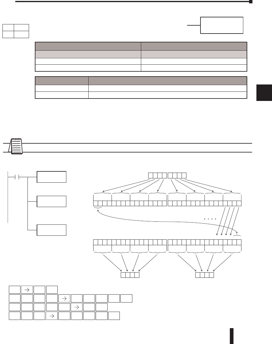
DL06 Micro PLC User Manual, 3rd Edition, Rev. D 5-123
1
2
3
4
5
6
7
8
9
10
11
12
13
14
A
B
C
D
Rotate Left (ROTL)
Rotate Left is a 32-bit instruction that rotates the bits in the
accumulator a specified number (Aaaa) of places to the left.
In the following example, when X1 is on, the value in V1400 and V1401 will be loaded
into the accumulator using the Load Double instruction. The bit pattern in the accumulator
is rotated 2 bit positions to the left using the Rotate Left instruction. The value in the
accumulator is copied to V1500 and V1501 using the Out Double instruction.
NOTE: Status flags are valid only until another instruction uses the same flag.
Chapter 5: Standard RLL Instructions - Bit Operation
1
2
3
4
5
6
7
8
9
10
11
12
13
14
a
B
c
d
ROTL
Aaaa
DirectSOFT32 Display
Handheld Programmer Keystrokes
STR
$
SHFT ANDST
L
3
D
3
D
SHFT ORN
R
MLR
T
ANDST
LENT
OUT
GX SHFT 3
D
1
BENT
INST#
O
ENT
1
B
4
E
0
A
0
AENT
2
C
1
B
5
F
0
A
0
A
X1 LDD
V1400
ROTL
K2
OUTD
V1500
Load the value in V1400 and
V1401 into the accumulator
The bit pattern in the
accumulator is rotated 2
bit positions to the left
Copy the value in the
accumulator to V1500
and V1501
17
00000000001 11111
1618192021222324252627282930
31
9C14
V1501
Acc.
Acc.
1
10000000010 01011
0234567891011121314
15
C405
V1500
10000011110 0001
11
0000010100 0010 0
17 161819202122232425262728293031 10234567891011121314
15
67 053101
V1401 V1400
Operand Data Type DL06 Range
Aaaa
V-memory V See memory map
Constant K 1-32
Discrete Bit Flags Description
SP63 On when the result of the instruction causes the value in the accumulator to be zero.
SP70 On anytime the value in the accumulator is negative.
DS Used
HPP Used
DirectSOFT
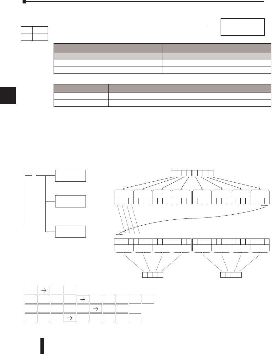
DL06 Micro PLC User Manual, 3rd Edition, Rev. D
5-124
1
2
3
4
5
6
7
8
9
10
11
12
13
14
A
B
C
D
Rotate Right (ROTR)
Rotate Right is a 32-bit instruction that rotates the bits in the
accumulator a specified number (Aaaa) of places to the right.
In the following example, when X1 is on, the value in V1400 and V1401 will be loaded
into the accumulator using the Load Double instruction. The bit pattern in the accumulator
is rotated 2 bit positions to the right using the Rotate Right instruction. The value in the
accumulator is copied to V1500 and V1501 using the Out Double instruction.
Chapter 5: Standard RLL Instructions- - Bit Operation
1
2
3
4
5
6
7
8
9
10
11
12
13
14
a
B
c
d
ROTR
Aaaa
Handheld Programmer Keystrokes
Direct SOFT Display
LDD
V1400
X1
Load the value in V1400 and
V1401 into the accumulator
ROTR
K2
The bit pattern in the
accumulator is rotated 2
bit positions to the right
OUTD
V1500
Copy the value in the
accumulator to V1500
and V1501
0011000100000001
V1500
01001100010000000000010000000000
15 14 13 12 11 10 987654321031 30 29 28 27 26 25 24 23 22 21 20 19 18 17 16
4C4 0
0101100111000001
31 30 29 28 27 26 25 24 23 22 21 20 19 18 17 16
0110011100000101
15 14 13 12 11 10 9876543210
31 30 29 28 27 26 25 24 23 22 21 20 19 18 17 1631 30 29 28 27 26 25 24 23 22 21 20 19 18 17 16
Acc.
Acc.
V1501
59C 1
670 5 310 1
V1400V1401
STR
$
SHFT ANDST
L
3
D
3
D
SHFT ORN
R
MLR
T
ORN
RENT
OUT
GX SHFT 3
D
1
BENT
INST#
O
ENT
1
B
4
E
0
A
0
AENT
2
C
1
B
5
F
0
A
0
A
Operand Data Type DL06 Range
Aaaa
V-memory V See memory map
Constant K 1-32
Discrete Bit Flags Description
SP63 On when the result of the instruction causes the value in the accumulator to be zero.
SP70 On anytime the value in the accumulator is negative.
DS Used
HPP Used
DirectSOFT
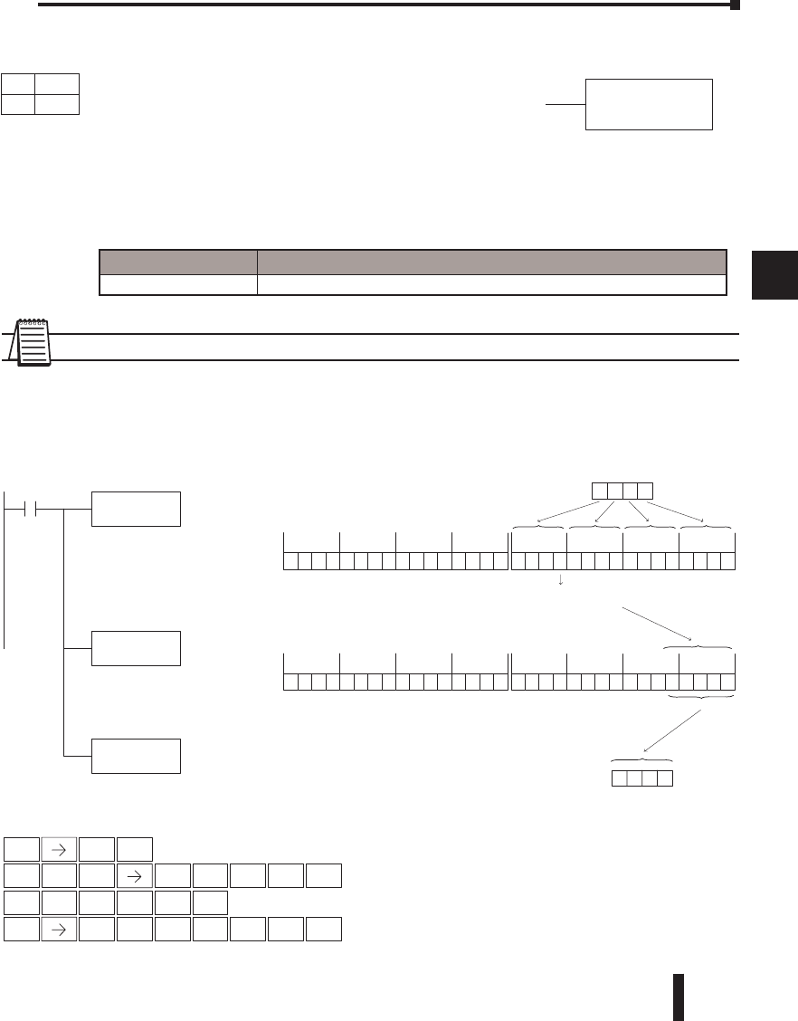
DL06 Micro PLC User Manual, 3rd Edition, Rev. D 5-125
1
2
3
4
5
6
7
8
9
10
11
12
13
14
A
B
C
D
NOTE: The status flags are only valid until another instruction that uses the same flags is executed.
In the following example, when X1 is on, The value in V2000 is loaded into the accumulator
using the Load instruction. The bit position set to a “1” in the accumulator is encoded to the
corresponding 5 bit binary value using the Encode instruction. The value in the lower 16 bits
of the accumulator is copied to V2010 using the Out instruction.
Chapter 5: Standard RLL Instructions - Bit Operation
1
2
3
4
5
6
7
8
9
10
11
12
13
14
a
B
c
d
ENCO
Handheld Programmer Keystrokes
Direct SOFT32
LD
V2000
X1
Load the value in V2000 into
the lower 16 bits of the
accumulator
ENCO
Encode the bit position set
to “1” in the accumulator to a
5 bit binary value
00010000000000000000000000000000
15 14 13 12 11 10 9876543210
31 30 29 28 27 26 25 24 23 22 21 20 19 18 17 1631 30 29 28 27 26 25 24 23 22 21 20 19 18 17 16
Acc.
00000000000011000000000000000000
15 14 13 12 11 10 9876543210
31 30 29 28 27 26 25 24 23 22 21 20 19 18 17 1631 30 29 28 27 26 25 24 23 22 21 20 19 18 17 16
Acc.
V2000
1000
Bit postion 12 is
converted
to binary
Copy the value in the lower 16 bits
of the accumulator to V2010
OUT
V2010
V2010
000C
Binary value
for 12.
STR
$
1
BENT
SHFT
OUT
GX SHFT AND
V
2
C
0
A
1
B
0
AENT
4
E
TMR
N
2
C
INST#
OENT
SHFT ANDST
L
3
D
2
C
0
A
0
A
0
AENT
Discrete Bit Flags Description
SP53 On when the value of the operand is larger than the accumulator can work with.
DS Used
HPP Used
DirectSOFT
Encode (ENCO)
The Encode instruction encodes the bit position in
the accumulator having a value of 1, and returns the
appropriate binary representation. If the most significant
bit is set to 1 (Bit 31), the Encode instruction would place
the value HEX 1F (decimal 31) in the accumulator. If the
value to be encoded is 0000 or 0001, the instruction will
place a zero in the accumulator. If the value to be encoded
has more than one bit position set to a “1”, the least
significant “1” will be encoded and SP53 will be set on.
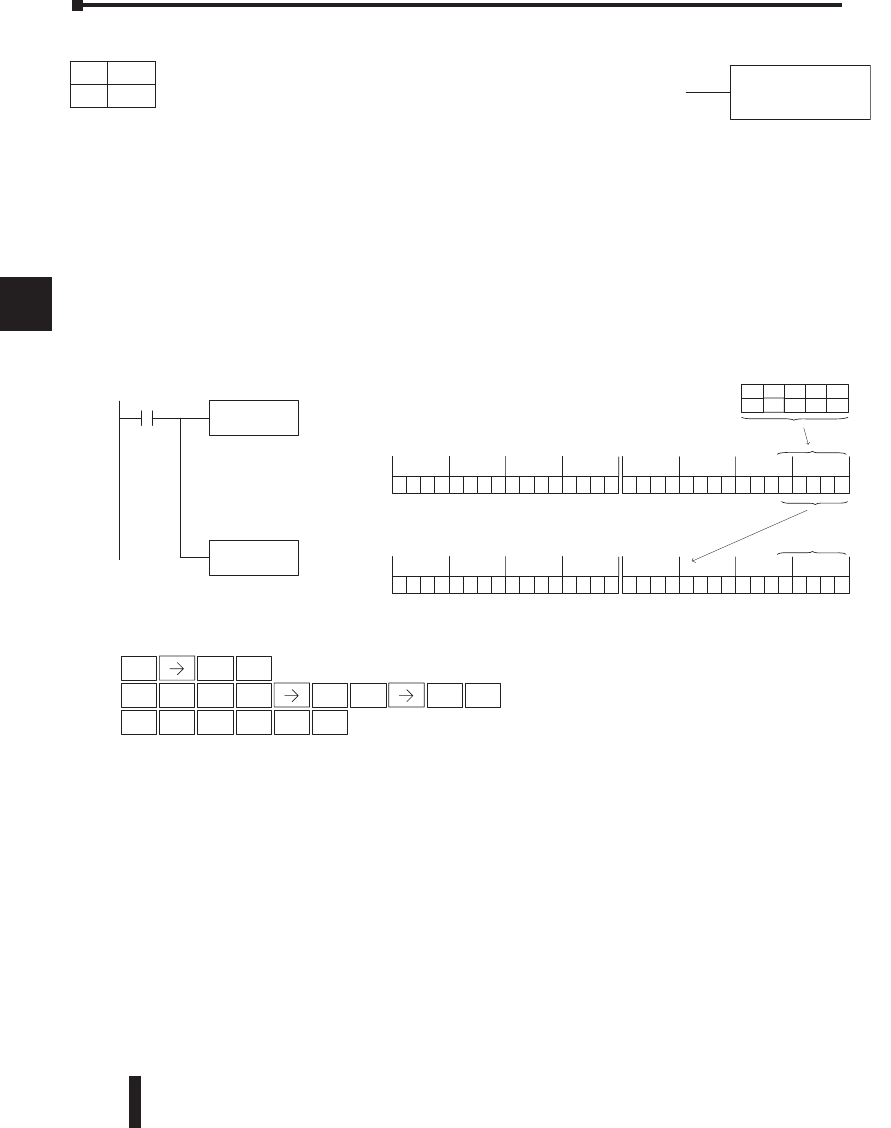
DL06 Micro PLC User Manual, 3rd Edition, Rev. D
5-126
1
2
3
4
5
6
7
8
9
10
11
12
13
14
A
B
C
D
In the following example when X1 is on, the value formed by discrete locations X10–X14 is
loaded into the accumulator using the Load Formatted instruction. The 5- bit binary pattern
in the accumulator is decoded by setting the corresponding bit position to a “1” using the
Decode instruction.
Chapter 5: Standard RLL Instructions - Bit Operation
1
2
3
4
5
6
7
8
9
10
11
12
13
14
a
B
c
d
Handheld Programmer Keystrokes
Direct SOFT32
LDF X10
K5
X1
Load the value in
represented by discrete
locations X10–X14 into the
accumulator
DECO
Decode the five bit binary
pattern in the accumulator
and set the corresponding
bit position to a “1”
X10 X11 X13 X12
ON ON OFF
X14
OFF ON
00000000000010110000000000000000
15 14 13 12 11 10 9 876543210
31 30 29 28 27 26 25 24 23 22 21 20 19 18 17 1631 30 29 28 27 26 25 24 23 22 21 20 19 18 17 16
Acc.
00001000000000000000000000000000
15 14 13 12 11 10 9 876543210
31 30 29 28 27 26 25 24 23 22 21 20 19 18 17 1631 30 29 28 27 26 25 24 23 22 21 20 19 18 17 16
Acc.
The binary vlaue
is converted to
bit position 11.
STR
$ENT
SHFT ANDST
L
3
D
5
F
1
B
1
B
0
AENT
5
F
SHFT 2
C
INST#
OENT
3
D
4
E
DECO
DS Used
HPP Used
DirectSOFT
Decode (DECO)
The Decode instruction decodes a 5-bit binary value of 0–31
(0–1Fh) in the accumulator by setting the appropriate bit
position to a 1. If the accumulator contains the value Fh (HEX),
bit 15 will be set in the accumulator. If the value to be decoded
is greater than 31, the number is divided by 32 until the value is
less than 32 and then the value is decoded.
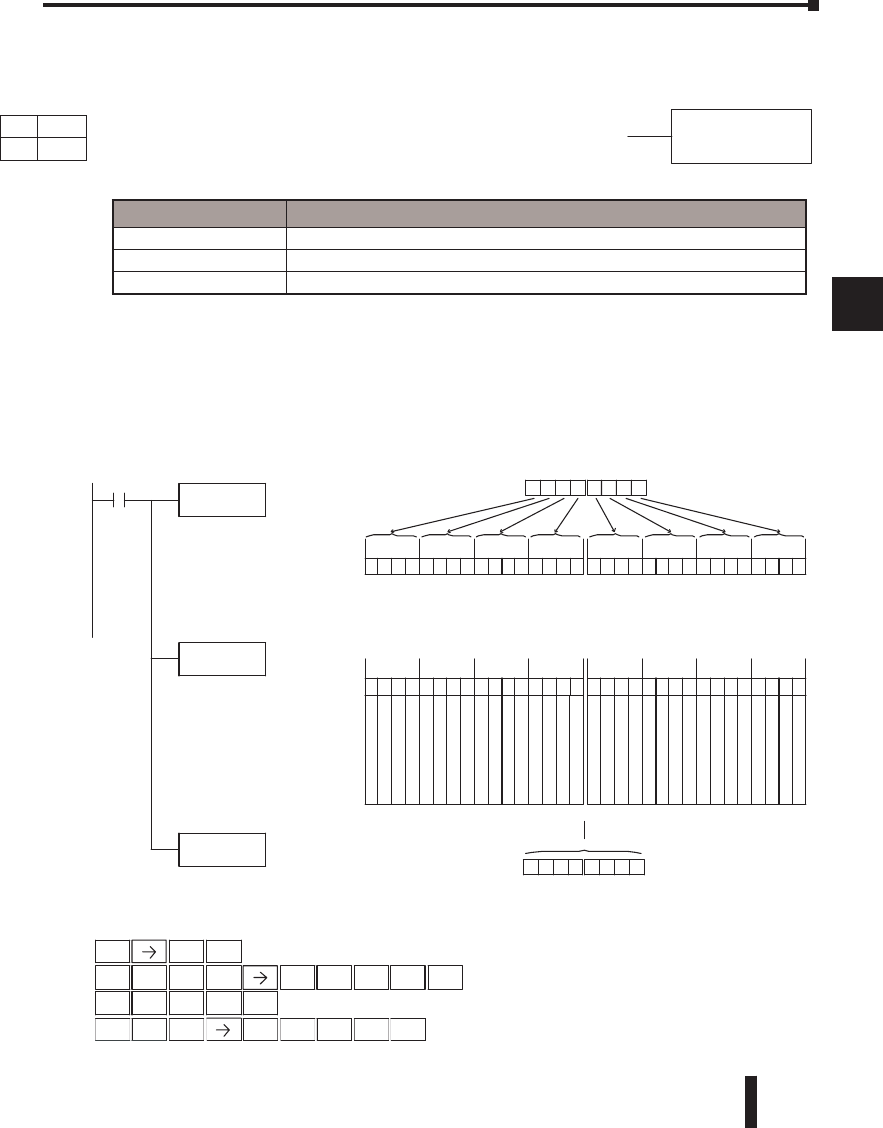
DL06 Micro PLC User Manual, 3rd Edition, Rev. D 5-127
1
2
3
4
5
6
7
8
9
10
11
12
13
14
A
B
C
D
Number Conversion Instructions (Accumulator)
Binary (BIN)
The Binary instruction converts a BCD value in the accumulator
to the equivalent binary, or decimal, value. The result resides in the
accumulator.
In the following example, when X1 is on, the value in V2000 and V2001 is loaded into
the accumulator using the Load Double instruction. The BCD value in the accumulator is
converted to the binary (HEX) equivalent using the BIN instruction. The binary value in
the accumulator is copied to V2010 and V2011 using the Out Double instruction. (The
handheld programmer will display the binary value in V2010 and V2011 as a HEX value.)
Chapter 5: Standard RLL Instructions - Number Conversion
1
2
3
4
5
6
7
8
9
10
11
12
13
14
a
B
c
d
BIN
Standard RLL
Instructions
STR
$
0
A
OUT
GX SHF T 3
D
2
C
0
A
1
BENT
00006F7 1
V2010V201
1
Handheld ProgrammerKeystrokes
DirectSOF
T
32
LDD
V2000
X1
BIN
10000101001010010 000000000000010
84218421842184218421842184218421
Acc.
00 0 2 8529
V2000V2001
01101111011100010000000000000000
15 14 13 12 11 10 987654321031 30 29 28 27 26 25 24 23 22 21 20 19 18 17 1631 30 29 28 27 26 25 24 23 22 21 20 19 18 17 16
Acc.
12481
6
3
2
6
4
1
2
8
2
5
6
5
1
2
1
0
2
4
2
0
4
8
4
0
9
6
8
1
9
2
1
6
3
8
4
3
2
7
6
8
6
5
5
3
6
1
3
1
0
7
2
2
6
2
1
4
4
5
2
4
2
8
8
1
0
4
8
5
7
6
2
0
9
7
1
5
2
4
1
9
4
3
0
4
8
3
8
8
6
0
8
1
6
7
7
7
2
1
6
3
3
5
5
4
4
3
2
6
7
1
0
8
8
6
4
1
3
4
2
1
7
7
2
8
2
6
8
4
3
5
4
5
6
5
3
6
8
7
0
9
1
2
1
0
7
3
7
4
1
8
2
4
2
1
4
7
4
4
8
3
6
4
8
OUTD
V2010
28529 =16384 +8192 +2048 +1024 +512 +256 +64+32 +16+1
1
BENT
SHF T ANDST
L
3
D
3
D
2
C
0
A
0
A
0
AENT
SHF T 1
B
8
I
TMR
NENT
Copy the binary data in the
accumulator to V2010 and V2011
Convert the BCD value in
the accumulator to the
binary equivalent value
Load the value in V2000 and
V2001 into the accumulator
BCD Value
Binary Equivalent Value
The Binary (HEX)
value copied to
V2010
Discrete Bit Flags Description
SP63 On when the result of the instruction causes the value in the accumulator to be zero.
SP70 On anytime the value in the accumulator is negative.
SP75 On when a BCD instruction is executed and a NON–BCD number was encountered.
DS Used
HPP Used
DirectSOFT
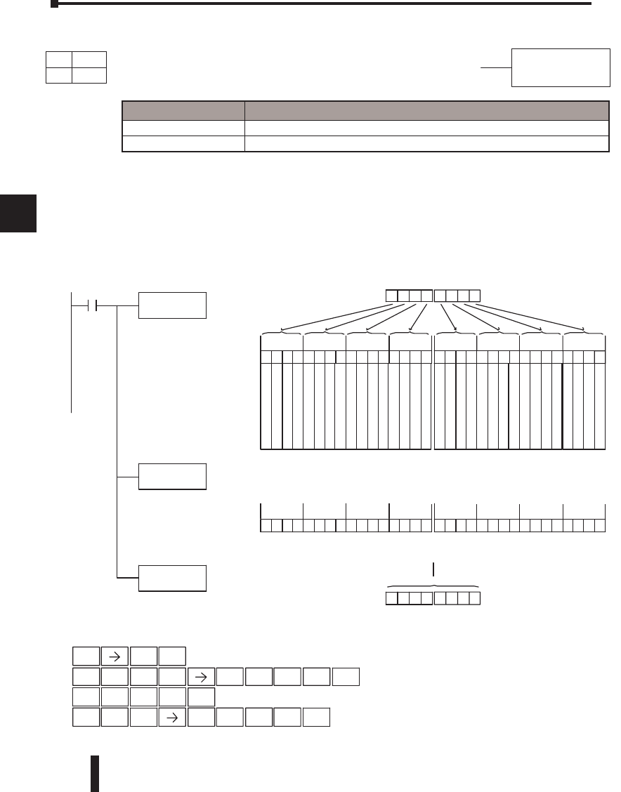
DL06 Micro PLC User Manual, 3rd Edition, Rev. D
5-128
1
2
3
4
5
6
7
8
9
10
11
12
13
14
A
B
C
D
Binary Coded Decimal (BCD)
The Binary Coded Decimal instruction converts a binary, or
decimal, value in the accumulator to the equivalent BCD value.
The result resides in the accumulator.
In the following example, when X1 is on, the binary, or decimal, value in V2000 and
V2001 is loaded into the accumulator using the Load Double instruction. The value in the
accumulator is converted to the BCD equivalent value using the BCD instruction. The BCD
value in the accumulator is copied to V2010 and V2011 using the Out Double instruction.
Chapter 5: Standard RLL Instructions - Number Conversion
1
2
3
4
5
6
7
8
9
10
11
12
13
14
a
B
c
d
BCD
3
D
HandheldProgr ammerKeystrokes
DirectSOFT 5
LDD
V2000
X1
Load thevalue in V2000 and
V2001 into theaccumulator
BCD
01101111011100010000000000000000
15 14 13 12 11 10 98765 4321031 30 29 28 27 26 25 24 23 22 21 20 19 18 17 1631 30 29 28 27 26 25 24 23 22 21 20 19 18 17 16
Acc.
0000 6F71
V2000V2001
BCDEquivalent Value
BinaryValue
10000101001010010000000000000010Acc.
12481
6
3
2
6
4
1
2
8
2
5
6
5
1
2
1
0
2
4
2
0
4
8
4
0
9
6
8
1
9
2
1
6
3
8
4
3
2
7
6
8
6
5
5
3
6
1
3
1
0
7
2
2
6
2
1
4
4
5
2
4
2
8
8
1
0
4
8
5
7
6
2
0
9
7
1
5
2
4
1
9
4
3
0
4
8
3
8
8
6
0
8
1
6
7
7
7
2
1
6
3
3
5
5
4
4
3
2
6
7
1
0
8
8
6
4
1
3
4
2
1
7
7
2
8
2
6
8
4
3
5
4
5
6
5
3
6
8
7
0
9
1
2
1
0
7
3
7
4
1
8
2
4
2
1
4
7
4
4
8
3
6
4
8
Copy theBCD valueinthe
accumulatortoV2010 and V2011
OUTD
V2010
TheBCD value
copied to
V2010 and V2011
0002 8529
V2010V2011
8421842184218421
8421842184218421
16384 +8192 +2048 +1024 +512 +256 +64+32 +16+1=28529
STR
$
1
BENT
SHFT ANDST
L
3
D
3
D
2
C
0
A
0
A
0
AENT
SHFT 1
BENT
OUT
GX SHFT 2
C
0
A
1
B
0
AENT
2
C
3
D
Convert the binary, or decimal,
value in the accumulator to the
BCD equivalent value
Discrete Bit Flags Description
SP63 On when the result of the instruction causes the value in the accumulator to be zero.
SP70 On anytime the value in the accumulator is negative.
DS Used
HPP Used
DirectSOFT
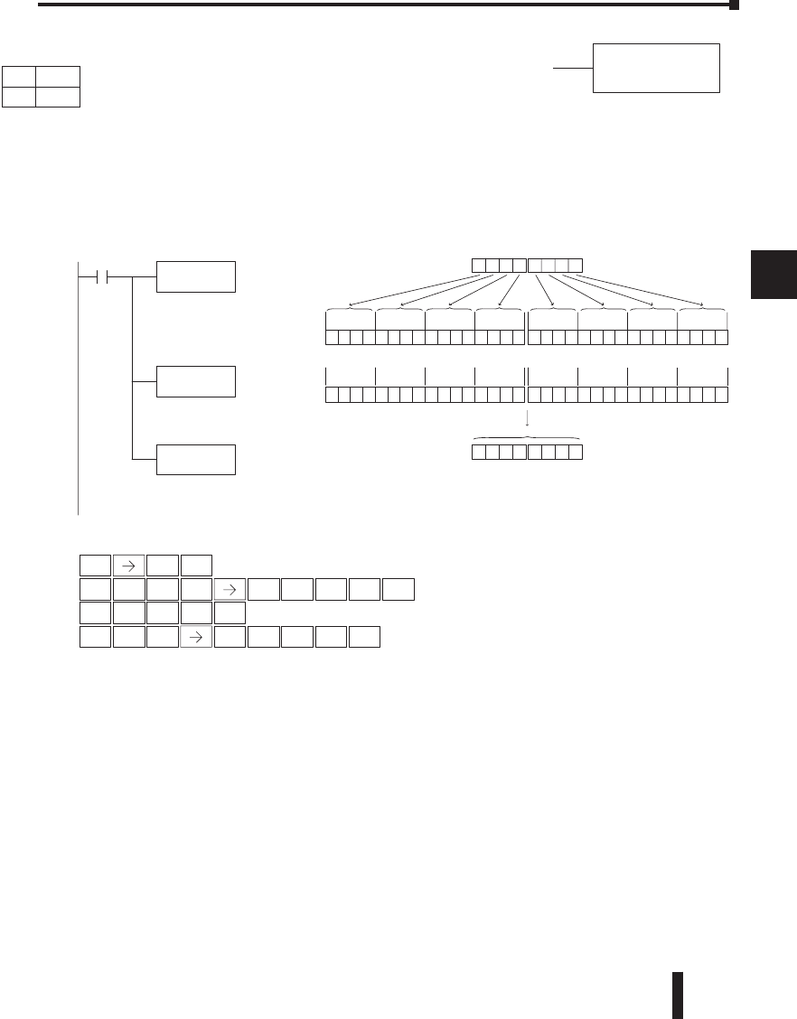
DL06 Micro PLC User Manual, 3rd Edition, Rev. D 5-129
1
2
3
4
5
6
7
8
9
10
11
12
13
14
A
B
C
D
Invert (INV)
The Invert instruction inverts or takes the one’s complement
of the 32-bit value in the accumulator. The result resides in the
accumulator.
In the following example, when X1 is on, the value in V2000 and V2001 will be loaded into
the accumulator using the Load Double instruction. The value in the accumulator is inverted
using the Invert instruction. The value in the accumulator is copied to V2010 and V2011
using the Out Double instruction.
Chapter 5: Standard RLL Instructions - Number Conversion
1
2
3
4
5
6
7
8
9
10
11
12
13
14
a
B
c
d
INV
Handheld Programmer Keystrokes
Direct SOFT32
LDD
V2000
X1
Load the value in V2000 and
V2001 into the accumulator
INV
Invert the binary bit pattern
in the accumulator
OUTD
V2010
Copy the value in the
accumulator to V2010 and
V2011
000000100101000 00000010000000101
15 14 13 12 11 10 9876543210
31 30 29 28 27 26 25 24 23 22 21 20 19 18 17 1631 30 29 28 27 26 25 24 23 22 21 20 19 18 17 16
Acc.
04050250 0250
V2000 V2001
V2010 V2011
11111101101011111111101111111010
15 14 13 12 11 10 9876543210
31 30 29 28 27 26 25 24 23 22 21 20 19 18 17 1631 30 29 28 27 26 25 24 23 22 21 20 19 18 17 16
Acc.
FBFAFDAF
STR
$
SHFT ANDST
L
3
D
3
D
SHFT ENT
OUT
GX SHFT 3
D
8
I
TMR
N
AND
V
1
BENT
2
C
0
A
0
A
0
AENT
2
C
0
A
1
B
0
AENT
DS Used
HPP Used
DirectSOFT
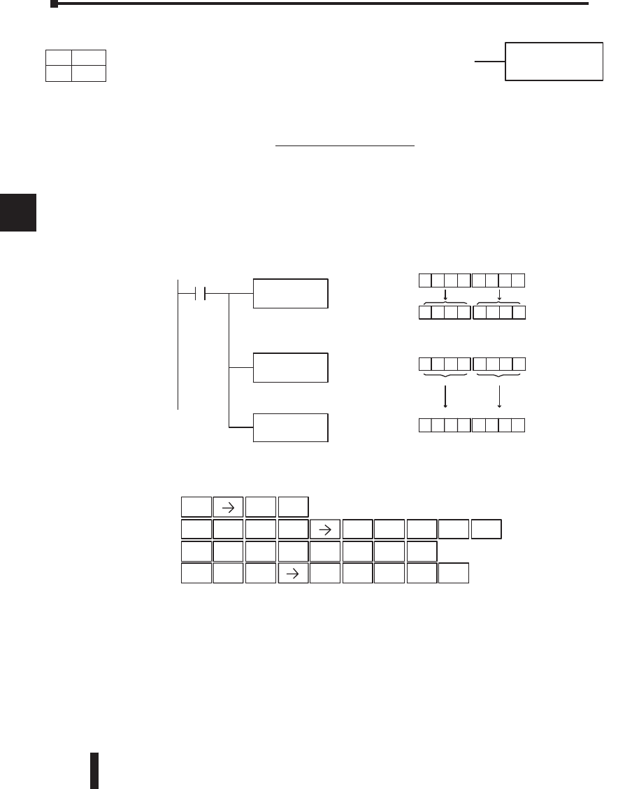
DL06 Micro PLC User Manual, 3rd Edition, Rev. D
5-130
1
2
3
4
5
6
7
8
9
10
11
12
13
14
A
B
C
D
Ten’s Complement (BCDCPL)
The Ten’s Complement instruction takes the 10’s complement
(BCD) of the 8 digit accumulator. The result resides in the
accumulator. The calculation for this instruction is :
100000000
s accumulator
10’s complement value
In the following example when X1 is on, the value in V2000 and V2001 is loaded into the
accumulator. The 10’s complement is taken for the 8 digit accumulator using the Ten’s
Complement instruction. The value in the accumulator is copied to V2010 and V2011 using
the Out Double instruction.
Chapter 5: Standard RLL Instructions - Number Conversion
1
2
3
4
5
6
7
8
9
10
11
12
13
14
a
B
c
d
BCDCPL
3
D
Handheld ProgrammerKeystrokes
DirectSOFT32
LDD
V2000
X1
Load thevalue in V2000 and
V2001 into theaccumulator
BCDCPL
Takesa10’scomplementof
thevalue in theaccumulator
OUTD
V2010
Copy thevalue in the
accumulatortoV2010 and
V2011
Acc.
V2000
0087
0000008 7
V2001
0000
V2010
Acc.
9913
9999991 3
V201
1
9999
STR
$
1
BENT
SHF T ANDST
L
3
D
3
D
2
C
0
A
0
A
0
AENT
SHF T ENT
OUT
GX SHFT2
C
0
A
1
B
0
AENT
1
B
2
C
3
D
2
C
C V
P
ANDST
L
DS Used
HPP Used
DirectSOFT
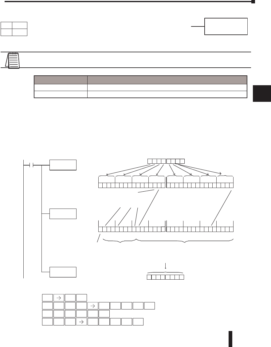
DL06 Micro PLC User Manual, 3rd Edition, Rev. D 5-131
1
2
3
4
5
6
7
8
9
10
11
12
13
14
A
B
C
D
Binary to Real Conversion (BTOR)
The Binary-to-Real instruction converts a binary, or decimal, value
in the accumulator to its equivalent real number (floating point)
format. The result resides in the accumulator. Both the binary and
the real number may use all 32 bits of the accumulator.
NOTE: This instruction only works with unsigned binary, or decimal, values. It will not work with
signed decimal values.
In the following example, when X1 is on, the value in V1400 and V1401 is loaded into the
accumulator using the Load Double instruction. The BTOR instruction converts the binary,
or decimal, value in the accumulator to the equivalent real number format. The binary weight
of the MSB is converted to the real number exponent by adding it to 127 (decimal). Then
the remaining bits are copied to the mantissa as shown. The value in the accumulator is
copied to V1500 and V1501 using the Out Double instruction. The handheld programmer
would display the binary value in V1500 and V1501 as a HEX value.
Chapter 5: Standard RLL Instructions - Number Conversion
1
2
3
4
5
6
7
8
9
10
11
12
13
14
a
B
c
d
BTOR
48AE4820
V1500V1501
Direct SOFT
LDD
V1400
X1
Load thevalue in V1400 and
V1401 into theaccumulator
BTOR
01110010001000010000000000000101
84218421842184218421842184218421
Acc.
0005 7241
V1400V1401
BinaryValue
Copy thereal valueinthe
accumulatortoV1500 and V1501
OUTD
V1500
Thereal number(HEX) value
copied to V1500
00101000001000000100100010101110Acc.
Real Number Format
Mantissa (23bits)Exponent (8 bits)Sign Bit
2(exp18)
127 +18=145
145 =128 +16+1
STR
$
SHFT ANDST
L
3
D
3
D
SHFT 1
B
MLR
T
ORN
RENT
OUT
GX SHFT
3
D
1
BENT
INST#
O
ENT
1
B
4
E
0
A
0
AENT
1
B
5
F
0
A
0
A
Handheld Programmer Keystrokes
Convert the binary, or decimal,
value in the accumulator to the
real number equivalent format
Discrete Bit Flags Description
SP63 On when the result of the instruction causes the value in the accumulator to be zero.
SP70 On anytime the value in the accumulator is negative.
DS Used
HPP Used
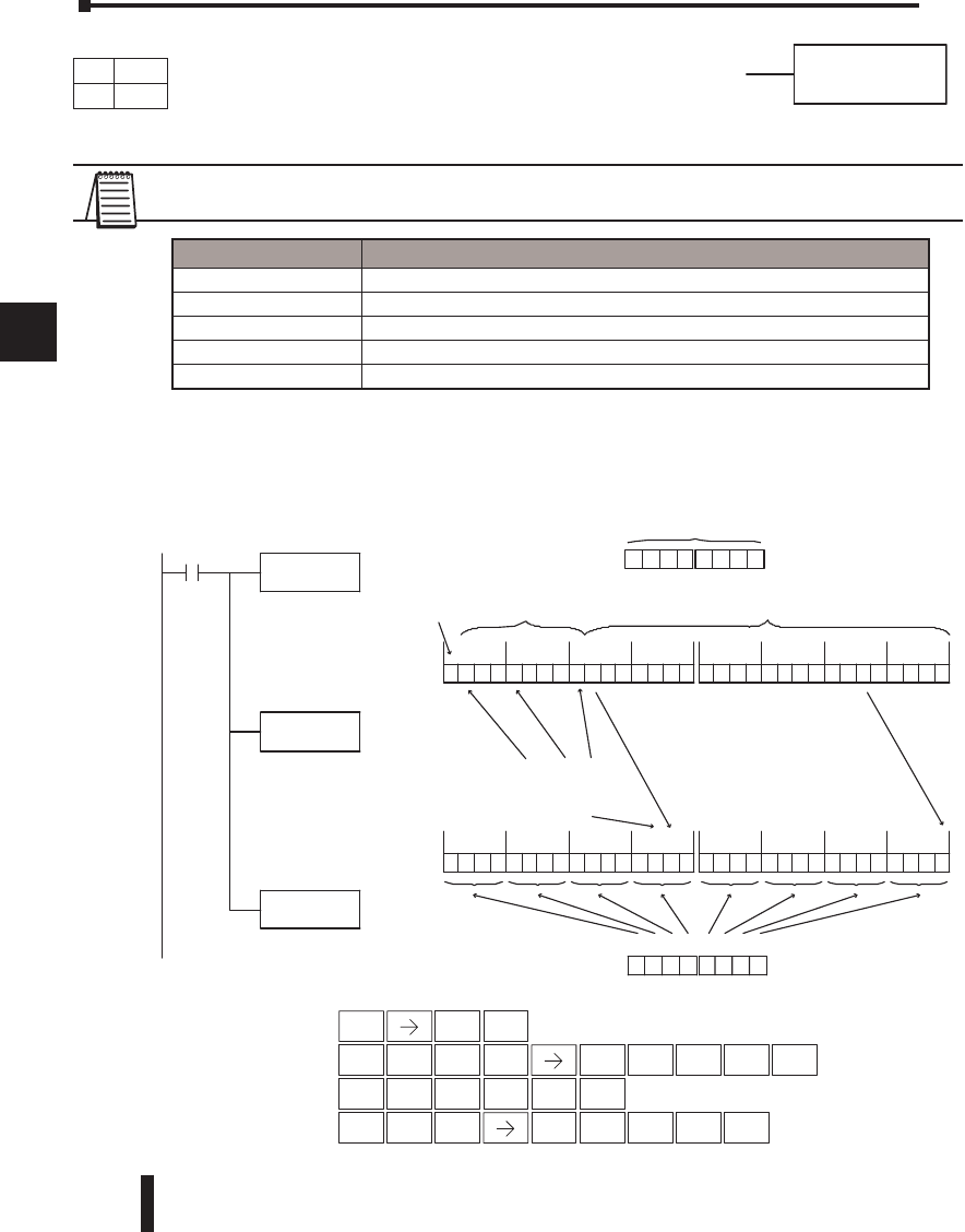
DL06 Micro PLC User Manual, 3rd Edition, Rev. D
5-132
1
2
3
4
5
6
7
8
9
10
11
12
13
14
A
B
C
D
Real to Binary Conversion (RTOB)
The Real-to-Binary instruction converts the real number in
the accumulator to a binary value. The result resides in the
accumulator. Both the binary and the real number may use all 32
bits of the accumulator.
NOTE1: The decimal portion of the result will be rounded down (14.1 to 14; -14.1 to -15).
NOTE2: if the real number is negative, it becomes a signed decimal value.
In the following example, when X1 is on, the value in V1400 and V1401 is loaded into the
accumulator using the Load Double instruction. The RTOB instruction converts the real
value in the accumulator the equivalent binary number format. The value in the accumulator
is copied to V1500 and V1501 using the Out Double instruction. The handheld programmer
would display the binary value in V1500 and V1501 as a HEX value.
Chapter 5: Standard RLL Instructions - Number Conversion
1
2
3
4
5
6
7
8
9
10
11
12
13
14
a
B
c
d
RTOB
48AE4820
V1400V1401
DirectSOFT32
LDD
V1400
X1
Load theval ue in V1400 and
V1401 into theaccumulator
RTOB
Convertthe real num ber in
theaccumulatortobinar y
format.
01110010001000010000000000000101
84218421842184218421842184218421
Acc.
00 0 5 7241
V1500V1501
BinaryVal ue
Copy thereal valueinthe
accumulatortoV1500 and V1501
OUTD
V1500
Thebinarynum bercop iedto
V1500.
00101000001000000 100100010101110
Acc.
Real Number Format
Mantissa (23bits)Exponent (8 bits)Sign Bit
2(exp18)
127 +18=145
128 +16+1=145
Discrete Bit Flags Description
SP63 On when the result of the instruction causes the value in the accumulator to be zero.
SP70 On anytime the value in the accumulator is negative.
SP72 On anytime the value in the accumulator is an invalid floating point number.
SP73 On when a signed addition or subtraction results in an incorrect sign bit.
SP75 On when a number cannot be converted to binary.
STR
$
SHFT ANDST
L
3
D
3
D
SHFT 1
B
MLR
T
ORN
RENT
OUT
GX SHFT 3
D
1
BENT
INST#
O
ENT
1
B
4
E
0
A
0
AENT
1
B
5
F
0
A
0
A
Handheld Programmer Keystrokes
DS Used
HPP Used
DirectSOFT
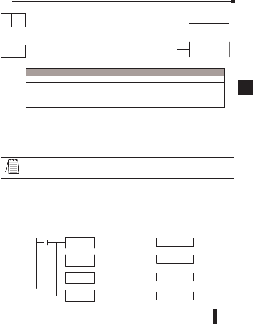
DL06 Micro PLC User Manual, 3rd Edition, Rev. D 5-133
1
2
3
4
5
6
7
8
9
10
11
12
13
14
A
B
C
D
Radian Real Conversion (RADR)
The Radian Real Conversion instruction converts the real degree
value stored in the accumulator to the equivalent real number in
radians. The result resides in the accumulator.
Degree Real Conversion (DEGR)
The Degree Real instruction converts the degree real radian value
stored in the accumulator to the equivalent real number in degrees.
The result resides in the accumulator.
The two instructions described above convert real numbers into the accumulator from degree
format to radian format, and vice-versa. In degree format, a circle contains 360 degrees. In
radian format, a circle contains 2f (about 6.28) radians. These convert between both positive
and negative real numbers, and for angles greater than a full circle. These functions are very
useful when combined with the transcendental trigonometric functions (see the section on
math instructions).
NOTE: The current HPP does not support real number entry with automatic conversion to the 32-bit
IEEE format. You must use DirectSOFT for entering real numbers, using the LDR (Load Real)
instruction.
The following example takes the sine of 45 degrees. Since transcendental functions operate
only on real numbers, we do an LDR (load real) 45. The trig functions operate only in
radians, so we must convert the degrees to radians by using the RADR command. After using
the SINR (Sine Real) instruction, we use an OUTD (Out Double) instruction to move the
result from the accumulator to V-memory. The result is 32-bits wide, requiring the Out
Double to move it.
Chapter 5: Standard RLL Instructions - Number Conversion
1
2
3
4
5
6
7
8
9
10
11
12
13
14
a
B
c
d
RADR
DEGR
DirectSOFT32
LDR
R45
X1 Load thereal number 45 into
theaccumulator.
RADR Convertthe degr ees into radians,
leavingthe result in the
accumulator.
OUTD
V2000
Copy thevalue in the
accumulatortoV2000
and V2001.
45.000000
Accumulatorcontents
(viewedasreal number)
0.7853982
SINR Take thesineofthe num ber in
theaccumulator, whichisin
radians.0.7071067
0.7071067
Discrete Bit Flags Description
SP63 On when the result of the instruction causes the value in the accumulator to be zero.
SP70 On anytime the value in the accumulator is negative.
SP72 On anytime the value in the accumulator is an invalid floating point number.
SP73 On when a signed addition or subtraction results in an incorrect sign bit.
SP75 On when a number cannot be converted to binary.
DS Used
HPP N/A
DS32 Used
HPP N/A
DirectSOFT
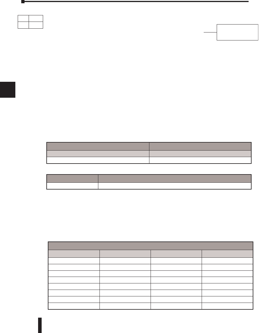
DL06 Micro PLC User Manual, 3rd Edition, Rev. D
5-134
1
2
3
4
5
6
7
8
9
10
11
12
13
14
A
B
C
D
Step 1: Load the number of V-memory locations for the ASCII table into the first level of the
accumulator stack.
Step 2: Load the starting V-memory location for the ASCII table into the accumulator. This
parameter must be a HEX value.
Step 3: Specify the starting V-memory location (Vaaa) for the HEX table in the ATH
instruction.
Helpful Hint: — For parameters that require HEX values when referencing memory
locations, the LDA instruction can be used to convert an octal address to the HEX equivalent
and load the value into the accumulator.
In the example on the following page, when X1 is ON the constant (K4) is loaded into the
accumulator using the Load instruction and will be placed in the first level of the accumulator
stack when the next Load instruction is executed. The starting location for the ASCII table
(V1400) is loaded into the accumulator using the Load Address instruction. The starting
location for the HEX table (V1600) is specified in the ASCII to HEX instruction. The table
below lists valid ASCII values for ATH conversion.
Chapter 5: Standard RLL Instructions - Number Conversion
1
2
3
4
5
6
7
8
9
10
11
12
13
14
a
B
c
d
aaa
ATH
V
Operand Data Type DL06 Range
aaa
V-memory V See memory map
Discrete Bit Flags Description
SP53 On when the value of the operand is larger than the accumulator can work with.
ASCII Values Valid for ATH Conversion
ASCII Value Hex Value ASCII Value Hex Value
30 0 38 8
31 1 39 9
32 2 41 A
33 3 42 B
34 4 43 C
35 5 44 D
36 6 45 E
37 7 46 F
DS Used
HPP N/A
ASCII to HEX (ATH)
The ASCII TO HEX instruction converts a table of ASCII values to
a specified table of HEX values. ASCII values are two digits and their
HEX equivalents are one digit. This means an ASCII table of four
V-memory locations would only require two V-memory locations
for the equivalent HEX table. The function parameters are loaded
into the accumulator stack and the accumulator by two additional
instructions. Listed below are the steps necessary to program an ASCII
to HEX table function. The example on the following page shows a
program for the ASCII to HEX table function.
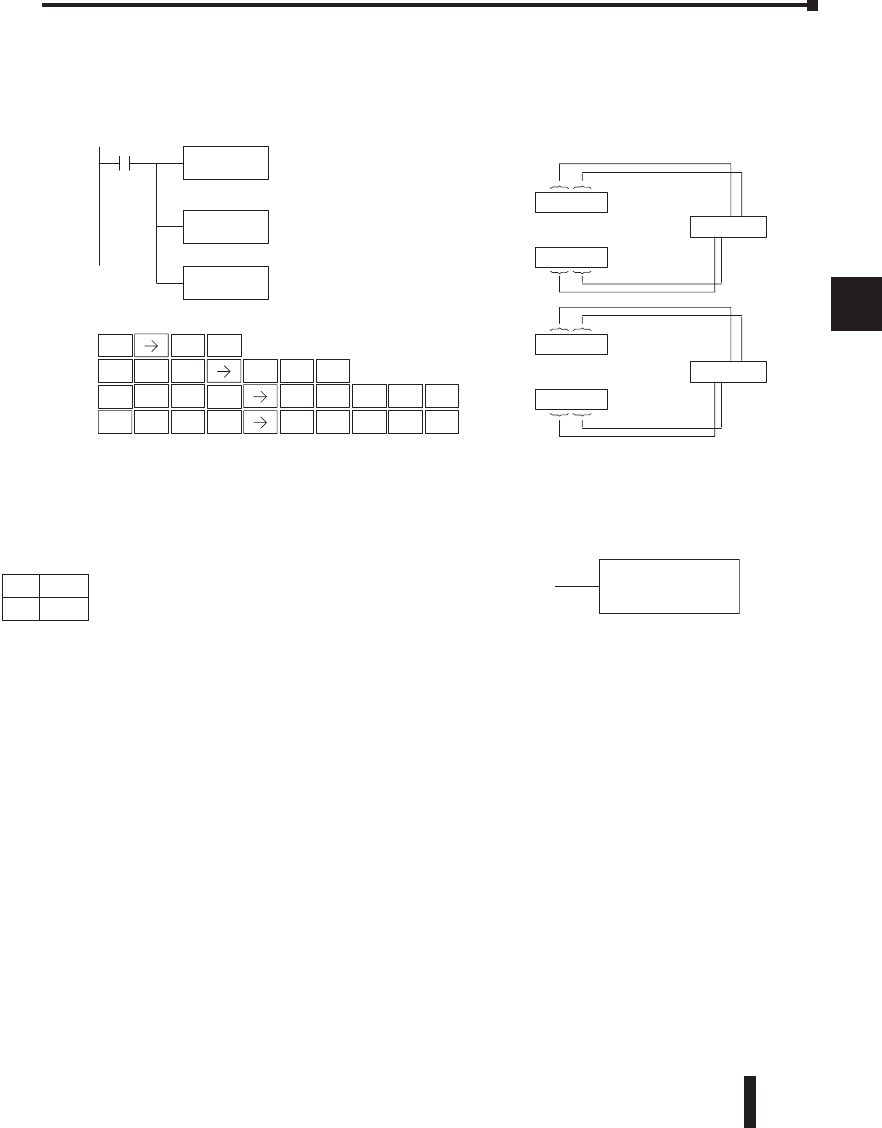
DL06 Micro PLC User Manual, 3rd Edition, Rev. D 5-135
1
2
3
4
5
6
7
8
9
10
11
12
13
14
A
B
C
D
HEX to ASCII (HTA)
The HEX to ASCII instruction converts a table of HEX
values to a specified table of ASCII values. HEX values are
one digit and their ASCII equivalents are two digits.
This means a HEX table of two V-memory locations would require four V-memory locations
for the equivalent ASCII table. The function parameters are loaded into the accumulator
stack and the accumulator by two additional instructions. Listed below are the steps necessary
to program a HEX to ASCII table function. The example on the following page shows a
program for the HEX to ASCII table function.
Step 1: Load the number of V-memory locations in the HEX table into the first level
of the accumulator stack.
Step 2: Load the starting V-memory location for the HEX table into the accumulator.
This parameter must be a HEX value.
Step 3: Specify the starting V-memory location (Vaaa) for the ASCII table in the HTA
instruction.
Helpful Hint: — For parameters that require HEX values when referencing memory
locations, the LDA instruction can be used to convert an octal address to the HEX equivalent
and load the value into the accumulator.
Chapter 5: Standard RLL Instructions - Number Conversion
1
2
3
4
5
6
7
8
9
10
11
12
13
14
a
B
c
d
Direct SOFT32
LD
K4
X1 Load the constant value
into the lower 16 bits of the
accumulator. This value
defines the number of V
memory location in the
ASCII table
LDA
O 1400
Convert octal 1400 to HEX
300 and load the value into
the accumulator
ATH
V1600
V1600 is the starting
location for the HEX table
ASCII T ABLE
Hexadecimal
Equivalents
1234
33 34
V1400
5678
31 32
V1401
37 38
V1402
35 36
V1403
V1600
V1601
STR
$
SHFT ANDST
L
3
D
7
H
SHFT
MLR
T
SHFT
1
BENT
ENT
4
E
0
A
0
A
ENT
1
B
6
G
0
A
0
A
Handheld Programmer Keystrokes
PREV
ANDST
L
3
DENT
1
B
4
E
0
A
0
A
aaaV
HTA
DS Used
HPP N/A
DirectSOFT
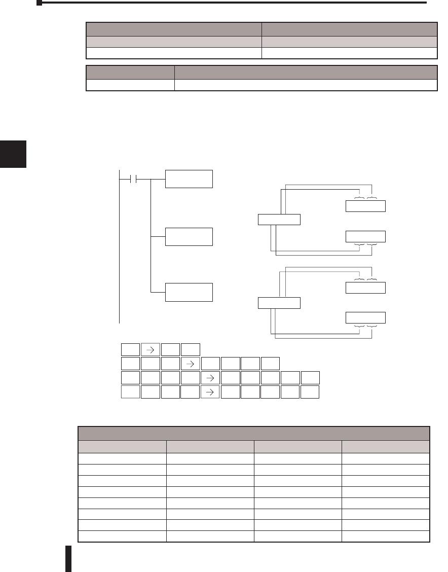
DL06 Micro PLC User Manual, 3rd Edition, Rev. D
5-136
1
2
3
4
5
6
7
8
9
10
11
12
13
14
A
B
C
D
In the following example, when X1 is ON, the constant (K2) is loaded into the accumulator
using the Load instruction. The starting location for the HEX table (V1500) is loaded into
the accumulator using the Load Address instruction. The starting location for the ASCII table
(V1400) is specified in the HEX to ASCII instruction.
The table below lists valid ASCII values for HTA conversion.
Chapter 5: Standard RLL Instructions - Number Conversion
1
2
3
4
5
6
7
8
9
10
11
12
13
14
a
B
c
d
Direct SOFT32
Handheld Programmer Keystrokes
LD
K2
X1
Load the constant value into
the lower 16 bits of the
accumulator. This value
defines the number of V
locations in the HEX table.
LDA
O 1500
Convert octal 1500 to HEX
340 and load the value into
the accumulator
HTA
V1400
V1400 is the starting
location for the ASCII table.
The conversion is executed
by this instruction.
ASCII T ABLE
Hexadecimal
Equivalents
1234
33 34 V1400
5678
31 32 V1401
37 38 V1402
35 36 V1403
V1500
V1501
STR
$
SHFT ANDST
L
3
DSHFT JMP
K
4
EENT
SHFT ANDST
L
3
D
0
A
0
A
0
AENT
SHFT
1
BENT
0
A
0
AENT
1
B
5
F
0
A
MLR
T
7
H
1
B
4
E
ASCII Values Valid for HTA Conversion
Hex Value ASCII Value Hex Value ASCII Value
0 30 8 38
1 31 9 39
2 32 A 41
3 33 B 42
4 34 C 43
5 35 D 44
6 36 E 45
7 37 F 46
Operand Data Type DL06 Range
aaa
V-memory V See memory map
Discrete Bit Flags Description
SP53 On when the value of the operand is larger than the accumulator can work with.
DirectSOFT
DL06 Micro PLC User Manual, 3rd Edition, Rev. D 5-137
1
2
3
4
5
6
7
8
9
10
11
12
13
14
A
B
C
D
Segment (SEG)
The BCD / Segment instruction converts a four digit HEX value in
the accumulator to seven segment display format. The result resides
in the accumulator.
In the following example, when X1 is on, the value in V1400 is loaded into the lower 16
bits of the accumulator using the Load instruction. The HEX value in the accumulator is
converted to seven segment format using the Segment instruction. The bit pattern in the
accumulator is copied to Y20–Y57 using the Out Formatted instruction.
Chapter 5: Standard RLL Instructions - Number Conversion
1
2
3
4
5
6
7
8
9
10
11
12
13
14
a
B
c
d
SEG
--gfedcba--gfedc ba --gfedc ba
Dir
e
ctSOFT
3
2
Display
SEG
X1
Convertthe binary(HEX)
valueinthe accumulatorto
sevensegment display
format
OUTF Y20
K32
Copy thevalue in the
accumulatortoY20 --Y57
LD
V1400
Load thevalue in V1400 ntothe
lower16bitsofthe accumulator
01101111011100010000000000000000
15 14 13 12 11 10 9876543210
31 30 29 28 27 26 25 24 23 22 21 20 19 18 17 1631 30 29 28 27 26 25 24 23 22 21 20 19 18 17 16
Acc.
6F7 1
V1400
00000111000001100111110101110001
15 14 13 12 11 10 987654321031 30 29 28 27 26 25 24 23 22 21 20 19 18 17 1631 30 29 28 27 26 25 24 23 22 21 20 19 18 17 16
Acc.
Y20Y21Y22Y23
OFFONONOFF
Y24
OFF
Y53Y54Y55Y56
ONONONON
Y57
OFF
--gfedcb a Segmen
t
Labels
a
g
f
e
d
c
b
Segment
Labels
Handheld Programmer Keystrokes
STR
$
ANDST
L
3
D
SHFT
1
BENT
2
C
0
A
4
E
RST
S
3
D
ENT
6
G
5
F
ENT
1
B
4
E
0
A
0
A
SHFT
OUT
GX SHFT 2
CENT
DS Used
HPP Used
DirectSOFT
DL06 Micro PLC User Manual, 3rd Edition, Rev. D
5-138
1
2
3
4
5
6
7
8
9
10
11
12
13
14
A
B
C
D
Gray Code (GRAY)
The Gray code instruction converts a 16-bit gray code
value to a BCD value. The BCD conversion requires 10
bits of the accumulator. The upper 22 bits are set to “0”.
This instruction is designed for use with devices (typically
encoders) that use the gray code numbering scheme. The Gray Code instruction will directly
convert a gray code number to a BCD number for devices having a resolution of 512 or 1024
counts per revolution. If a device having a resolution of 360 counts per revolution is to be
used, you must subtract a BCD value of 76 from the converted value to obtain the proper
result. For a device having a resolution of 720 counts per revolution, you must subtract a
BCD value of 152.
In the following example, when X1 is ON, the binary value represented by X10–X27 is
loaded into the accumulator using the Load Formatted instruction. The gray code value in
the accumulator is converted to BCD using the Gray Code instruction. The value in the
lower 16 bits of the accumulator is copied to V2010.
Chapter 5: Standard RLL Instructions - Number Conversion
1
2
3
4
5
6
7
8
9
10
11
12
13
14
a
B
c
d
GRAY
Handheld Programmer Keystrokes
Direct SOFT32
LDF K16
X10
X1
Load the value represented
by X10–X27 into the lower
16 bits of the accumulator
GRAY
Convert the 16 bit grey code
value in the accumulator to a
BCD value
OUT
V2010
Copy the value in the lower
16 bits of the accumulator to
V2010 0000000000
Gray Code BCD
0000000001
0000000011
0000000010
0000000110
0000000111
0000000101
0000000100
1000000001
1000000000
0000
0001
0002
0003
0004
0005
0006
0007
1022
1023
X10X11X12
ONOFFON
000000000000010 10000000000000000
15 14 13 12 11 10 9876543210
31 30 29 28 27 26 25 24 23 22 21 20 19 18 17 1631 30 29 28 27 26 25 24 23 22 21 20 19 18 17 16
Acc.
000000000000011 00000000000000000
15 14 13 12 11 10 9876543210
31 30 29 28 27 26 25 24 23 22 21 20 19 18 17 1631 30 29 28 27 26 25 24 23 22 21 20 19 18 17 16
Acc.
X25X26X27
OFFOFFOFF
V2010
000 6
STR
$
SHFT ANDST
L
3
D
5
F
SHFT 6
G
ORN
R
0
A
MLS
YENT
OUT
GX SHFT AND
V
2
C
0
A
1
B
0
AENT
ENT
1
B
1
B
0
AENT
1
B
6
G
Discrete Bit Flags Description
SP63 On when the result of the instruction causes the value in the accumulator to be zero.
SP70 On anytime the value in the accumulator is negative.
DS Used
HPP Used
DirectSOFT
DL06 Micro PLC User Manual, 3rd Edition, Rev. D 5-139
1
2
3
4
5
6
7
8
9
10
11
12
13
14
A
B
C
D
Chapter 5: Standard RLL Instructions - Number Conversion
1
2
3
4
5
6
7
8
9
10
11
12
13
14
a
B
c
d
Shuffle Digits (SFLDGT)
The Shuffle Digits instruction shuffles a maximum of 8 digits,
rearranging them in a specified order. This function requires
parameters to be loaded into the first level of the accumulator stack
and the accumulator with two additional instructions. Listed below are the steps necessary to
use the shuffle digit function. The example on the following page shows a program for the
Shuffle Digits function.
Step 1: Load the value (digits) to be shuffled into the first level of the accumulator
stack.
Step 2: Load the order that the digits will be shuffled to into the accumulator.
Step 3: Insert the SFLDGT instruction.
NOTE: If the number used to specify the order contains a 0 or 9–F, the corresponding position
will be set to 0.
Shuffle Digits Block Diagram
There are a maximum of 8 digits that can be shuffled. The bit positions in the first level of
the accumulator stack define the digits to be shuffled. They correspond to the bit positions in
the accumulator that define the order the digits will be shuffled. The digits are shuffled and
the result resides in the accumulator.
Digits to be
shuffled (first stack location)
Specified order (accumulator)
DE F09ABC
36541287
Result (accumulator)
0DA9BCEF
43218765
Bit Positions
SFLDGT
Discrete Bit Flags Description
SP63 On when the result of the instruction causes the value in the accumulator to be zero.
SP70 On anytime the value in the accumulator is negative.
DS Used
HPP Used
DL06 Micro PLC User Manual, 3rd Edition, Rev. D
5-140
1
2
3
4
5
6
7
8
9
10
11
12
13
14
A
B
C
D
In the following example, when X1 is on, the value in the first level of the accumulator stack
will be reorganized in the order specified by the value in the accumulator.
Example A shows how the shuffle digits works when 0 or 9–F is not used when specifying the
order the digits are to be shuffled. Also, there are no duplicate numbers in the specified order.
Example B shows how the Shuffle Digits works when a 0 or 9–F is used when specifying the
order the digits are to be shuffled. Notice when the Shuffle Digits instruction is executed, the
bit positions in the first stack location that had a corresponding 0 or 9–F in the accumulator
(order specified) are set to “0”.
Example C shows how the Shuffle Digits works when duplicate numbers are used specifying
the order the digits are to be shuffled. Notice when the Shuffle Digits instruction is executed,
the most significant duplicate number in the order specified is used in the result.
Chapter 5: Standard RLL Instructions - Number Conversion
1
2
3
4
5
6
7
8
9
10
11
12
13
14
a
B
c
d
DE F09ABC
Handheld Programmer Keystrokes
Direct SOFT32
LDD
V2000
X1
Load the value in V2000 and
V2001 into the accumulator
LDD
V2006
Load the value in V2006 and
V2007 into the accumulator
OUTD
V2010
Copy the value in the
accumulator to V2010 and
V2011
SFLDGT
Shuf fle the digits in the first
level of the accumulator
stack based on the pattern
in the accumulator. The
result is in the accumulator .
V2010
Acc.
0DA 9
9AB C DE F 0
V2011
BCE F
Acc.
365 4
128 7 365 4
128 7
Acc.
BCE F 0DA 9
V2000V2001
V2006V2007
CBA90FED
V2010
Acc.
EDA 9
0FE D CB A 9
V2011
000 0
Acc.
002 1
004 3 0021
004 3
Acc.
000 0 ED A 9
V2000V2001
V2006V2007
DE F09ABC
V2010
Acc.
9AB C
9AB C DE F 0
V2011
000 0
Acc.
432 1
432 1 432 1
432 1
Acc.
000 0 9AB C
V2000V2001
V2006V2007
ABC
Original
bit
Positions
43218765 43218765 43218765
Specified
order 43218765 43218765 43218765
New bit
Positions 43218765 43218765 43218765
STR
$
SHFT ANDST
L
3
D
3
D
SHFT ANDST
L
3
D
3
D
SHFT RST
S
5
F
ANDST
L
3
D
6
G
MLR
TENT
OUT
GX SHFT 3
D
1
BENT
2
C
0
A
0
A
0
AENT
2
C
0
A
0
AENT
6
G
2
C
0
A
1
B
0
AENT
SHFT
DirectSOFT
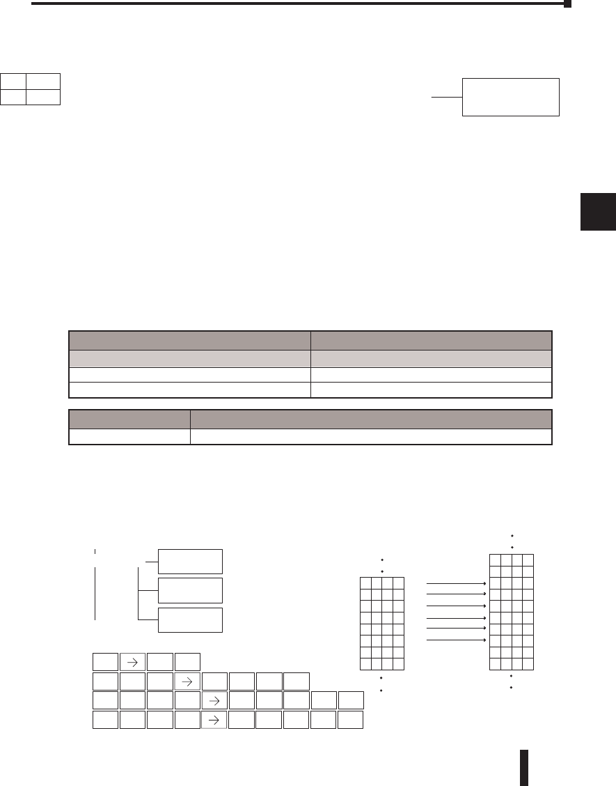
DL06 Micro PLC User Manual, 3rd Edition, Rev. D 5-141
1
2
3
4
5
6
7
8
9
10
11
12
13
14
A
B
C
D
Table Instructions
Move (MOV)
The Move instruction moves the values from a V-memory
table to another V-memory table the same length (a table being
a consecutive group of V-memory locations). The function
parameters are loaded into the first level of the accumulator stack
and the accumulator by two additional instructions. The MOV instruction can be used to
write data to non-volatile V-memory (see Appendix F). Listed below are the steps necessary to
program the MOV function.
• Step 1 Load the number of V-memory locations to be moved into the first level of the accumulator
stack. This parameter is a HEX value (KFFF max, 7777 octal, 4096 decimal).
• Step 2 Load the starting V-memory location for the locations to be moved into the accumulator.
This parameter is a HEX value.
• Step 3 Insert the MOV instruction which specifies starting V-memory location (Vaaa) for the
destination table.
Helpful Hint: — For parameters that require HEX values when referencing memory
locations, the LDA instruction can be used to convert an octal address to the HEX equivalent
and load the value into the accumulator.
In the following example, when X1 is on, the constant value (K6) is loaded into the
accumulator using the Load instruction. This value specifies the length of the table and
is placed in the first stack location after the Load Address instruction is executed. The
octal address 2000 (V2000), the starting location for the source table, is loaded into the
accumulator. The destination table location (V2030) is specified in the Move instruction.
Chapter 5: Standard RLL Instructions - Table Instructions
1
2
3
4
5
6
7
8
9
10
11
12
13
14
a
B
c
d
V aaa
MOV
Direct SOFT32
LD
K6
X1 Load the constant value 6
(HEX) into the lower 16 bits
of the accumulator
LDA
O 2000
Convert octal 2000 to HEX
400 and load the value into
the accumulator
MOV
V2030
Copy the specified table
locations to a table
beginning at location V2030
V2030
0123
V2031
0500
V2032
9999
V2033
3074
V2034
8989
V2035
1010
V2036
XXXX
V2037
XXXX
V2026
XXXX
V2027
XXXX
V2000
0123
V2001
0500
V2002
9999
V2003
3074
V2004
8989
V2005
1010
V2006
XXXX
V2007
XXXX
Handheld Programmer Keystrokes
STR
$
SHFT ANDST
L
3
DSHFT JMP
K
6
GENT
SHFT ANDST
L
3
D
0
A
2
C
0
A
0
A
0
AENT
SHFT ORST
M
INST#
O
1
BENT
2
C
0
A
0
AENT
3
D
AND
V
Discrete Bit Flags Description
SP53 On when the value of the operand is larger than the accumulator can work with.
Operand Data Type DL06 Range
aaa
V-memory V See memory map
Pointer P See memory map
DS Used
HPP Used
DirectSOFT
DL06 Micro PLC User Manual, 3rd Edition, Rev. D
5-142
1
2
3
4
5
6
7
8
9
10
11
12
13
14
A
B
C
D
Move Memory Cartridge (MOVMC)
Load Label (LDLBL)
The Move Memory Cartridge instruction is used to copy data
between V-memory and program ladder memory. The Load Label
instruction is only used with the MOVMC instruction when copying
data from program ladder memory to V-memory.
To copy data between V-memory and program ladder memory,
the function parameters are loaded into the first two levels of
the accumulator stack and the accumulator by two additional
instructions. Listed below are the steps necessary to program the
MOVMC and LDLBL functions.
• Step 1: Load the number of words to be copied into the second level of the accumulator stack.
• Step 2: Load the offset for the data label area in ladder memory and the beginning of the V-memory
block into the first level of the stack.
• Step 3: Load the source data label (LDLBL Kaaa) into the accumulator when copying data from
ladder memory to V-memory. Load the source address into the accumulator when copying
data from V-memory to ladder memory. This is where the value will be copied from. If the
source address is a V-memory location, the value must be entered in HEX.
• Step 4: Insert the MOVMC instruction which specifies destination in V-memory (Vaaa). This is
the copy destination.
NOTE: Refer to page 5-188 for an example.
WARNING: The offset for this usage of the instruction starts at 0, but may be any number that
does not result in data outside of the source data area being copied into the destination table.
When an offset is outside of the source information boundaries, then unknown data values will be
transferred into the destination table.
Chapter 5: Standard RLL Instructions - Table Instructions
1
2
3
4
5
6
7
8
9
10
11
12
13
14
a
B
c
d
V aaa
MOVMC
LDLBL
aaaK
Operand Data Type DL06 Range
Aaaa
V-memory V See memory map
DS Used
HPP Used
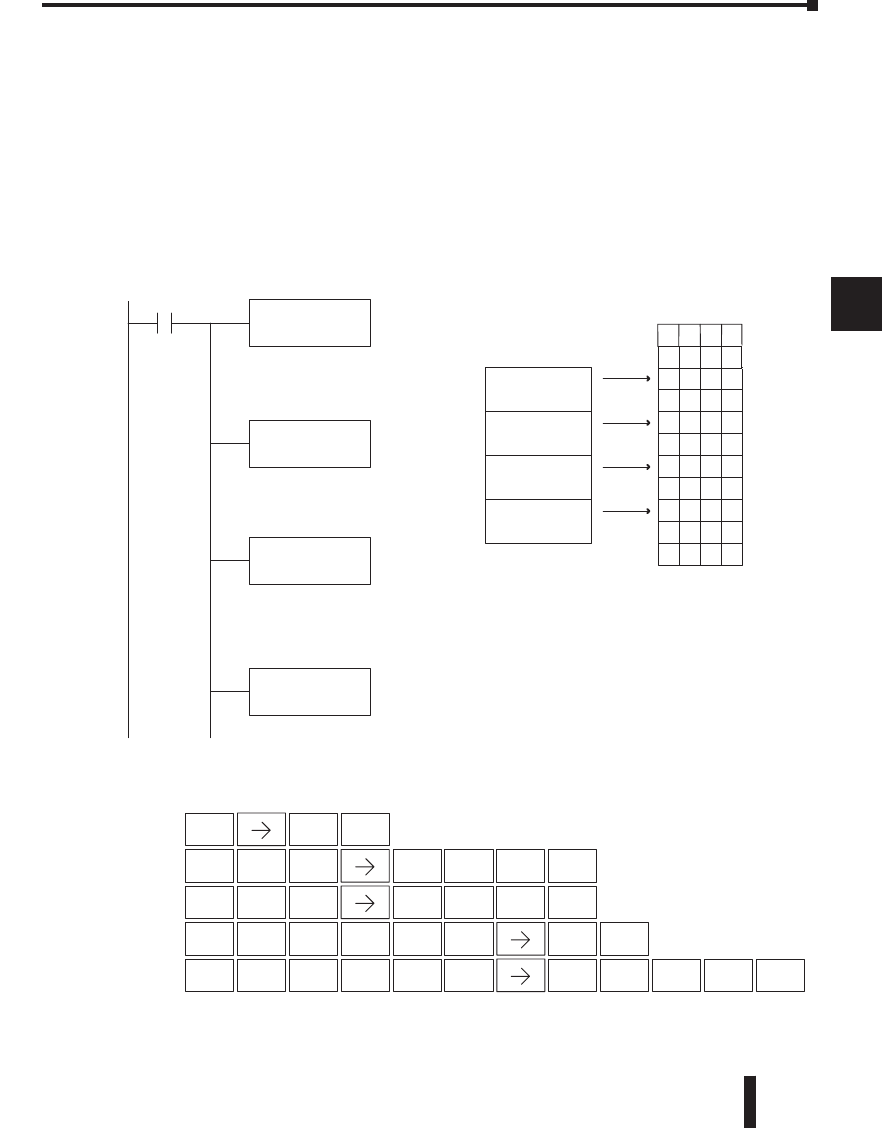
DL06 Micro PLC User Manual, 3rd Edition, Rev. D 5-143
1
2
3
4
5
6
7
8
9
10
11
12
13
14
A
B
C
D
Copy Data From a Data Label Area to V-memory
In the example below, data is copied from a Data Label Area to V-memory. When X1 is on,
the constant value (K4) is loaded into the accumulator using the Load (LD) instruction. This
value specifies the length of the table and is placed in the second stack location after the next
Load and Load Label (LDLBL) instructions are executed. The constant value (K0) is loaded
into the accumulator, specifying the offset for the source and destination data. It is placed
in the first stack location after the LDLBL instruction is executed. The source address where
data is being copied from is loaded into the accumulator using the LDLBL instruction. The
MOVMC instruction specifies the destination starting location and executes the copying of
data from the Data Label Area to V-memory.
Chapter 5: Standard RLL Instructions - Table Instructions
1
2
3
4
5
6
7
8
9
10
11
12
13
14
a
B
c
d
Direct SOFT32
LD
K4
X1
Load the value 4 into the
accumulator specifying the
number of locations to be
copied.
LD
K0
Load the value 0 into the
accumulator specifying the
offset for source and
destination locations
LDLBL
K1
Load the value 1 into the
accumulator specifying the
Data Label Area K1 as the
starting address of the data
to be copied.
MOVMC
V2000
V2000 is the destination
starting address for the data
to be copied.
1234
4532
6151
8845
K
NCON
K
NCON
K
NCON
K
NCON
V2001
4532
V2002
6151
V2003
8845
V2004
XXXX
.
.
.
.
V2000
1234
Data label area
programmed after
the END instruction
DLBL
Handheld Programmer Keystrokes
STR
$
SHFT ANDST
L
3
DSHFT JMP
KENT
SHFT ANDST
L
3
D
ANDST
L
1
B
ANDST
L
SHFT ORST
M
AND
V
INST#
O
ORST
M
2
C
1
BENT
ENT
1
B
2
C
0
A
0
A
0
AENT
SHFT ANDST
L
3
DSHFT JMP
K
0
AENT
4
E
K1
V1777
XXXX
DirectSOFT
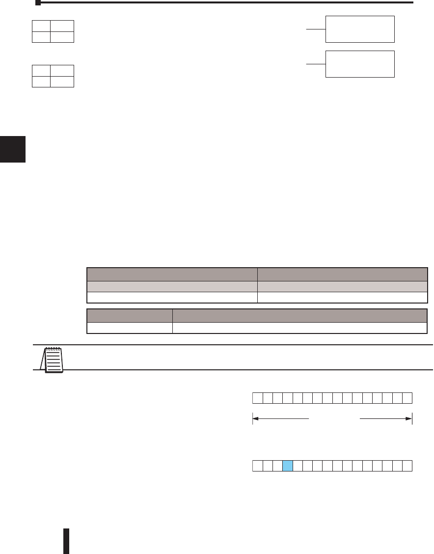
DL06 Micro PLC User Manual, 3rd Edition, Rev. D
5-144
1
2
3
4
5
6
7
8
9
10
11
12
13
14
A
B
C
D
SETBIT
The Set Bit instruction sets a single bit to one within a
range of V-memory locations.
RSTBIT
The Reset Bit instruction resets a single bit to zero within a
range of V-memory locations.
The following description applies to both the Set Bit and Reset Bit table instructions.
Step 1: Load the length of the table (number of V-memory locations) into the first level of
the accumulator stack. This parameter must be a HEX value, 0 to FF.
Step 2: Load the starting V-memory location for the table into the accumulator. This
parameter must be a HEX value. You can use the LDA instruction to convert an octal
address to hex.
Step 3: Insert the Set Bit or Reset Bit instruction. This specifies the reference for the bit
number of the bit you want to set or reset. The bit number is in octal, and the first bit
in the table is number “0”.
Helpful hint: — Remember that each V-memory location contains 16 bits. So, the bits of
the first word of the table are numbered from 0 to 17 octal. For example, if the table length
is six words, then 6 words = (6 x 16) bits, = 96 bits (decimal), or 140 octal. The permissible
range of bit reference numbers would be 0 to 137 octal. SP 53 will be set if the bit specified is
outside the range of the table.
NOTE: Status flags are only valid until the end of the scan or until another instruction that uses the
same flag is executed.
Chapter 5: Standard RLL Instructions - Table Instructions
1
2
3
4
5
6
7
8
9
10
11
12
13
14
a
B
c
d
A aaa
SETBIT
Aaaa
RSTBIT
MS
BL
SB
V3000
MS
BL
SB
V3001
1
7
01
6
1
5
1
4
1
3
1
2
1
1
1
0
7654321
16 bits
Operand Data Type DL06 Range
aaa
V-memory V See memory map
Discrete Bit Flags Description
SP53 On when the specified bit is outside the range of the table.
DS Used
HPP Used
DS Used
HPP Used
For example, suppose we have a table
starting at V3000 that is two words long,
as shown to the right. Each word in
the table contains 16 bits, or 0 to 17 in
octal. To set bit 12 in the second word,
we use its octal reference (bit 14). Then
we compute the bit’s octal address from
the start of the table, so 17 + 14 = 34
octal. The following program shows how
to set the bit as shown to a “1”.
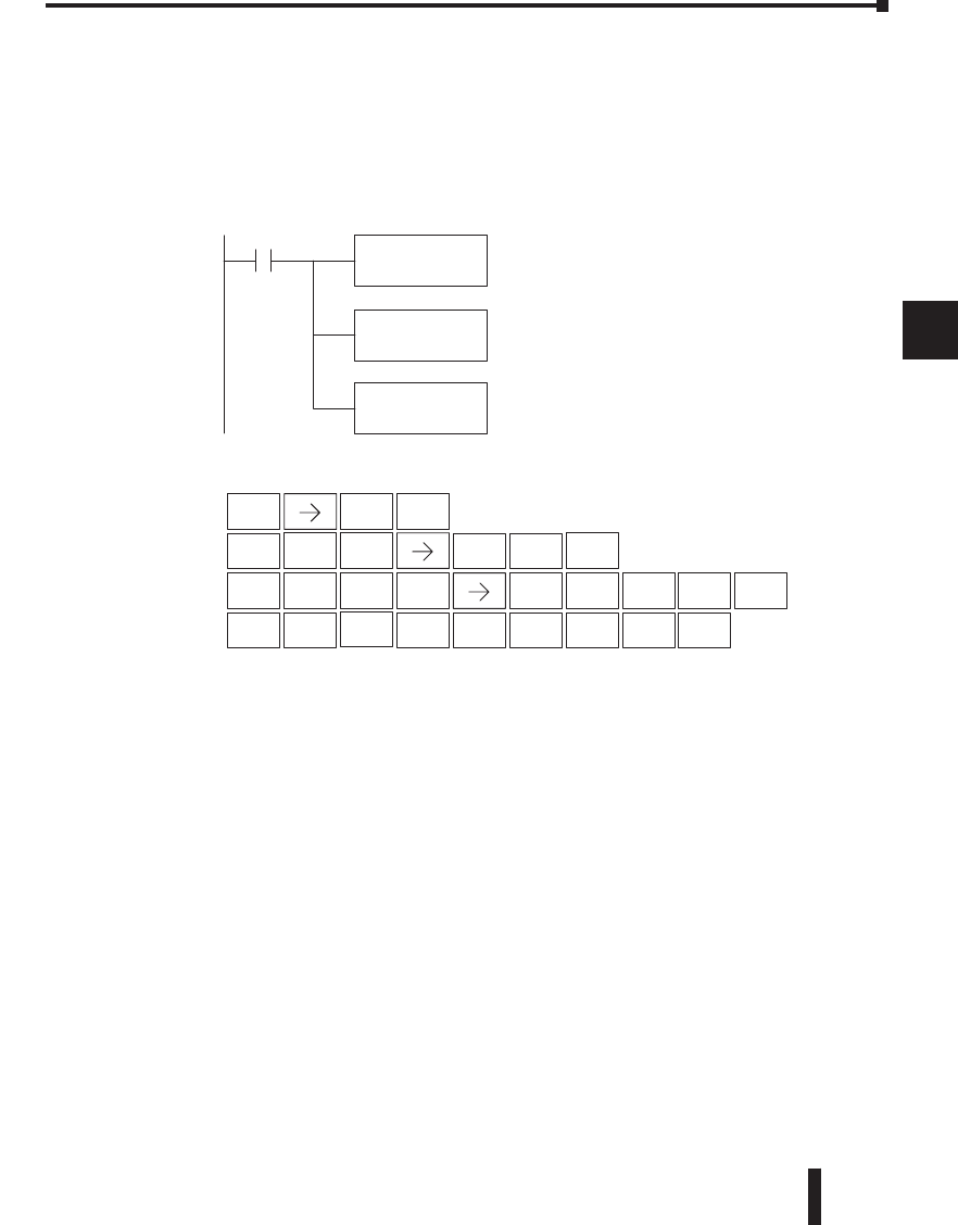
DL06 Micro PLC User Manual, 3rd Edition, Rev. D 5-145
1
2
3
4
5
6
7
8
9
10
11
12
13
14
A
B
C
D
In this ladder example, we will use input X0 to trigger the Set Bit operation. First, we will
load the table length (2 words) into the accumulator stack. Next, we load the starting address
into the accumulator. Since V3000 is an octal number, we have to convert it to hex by using
the LDA command. Finally, we use the Set Bit (or Reset Bit) instruction and specify the octal
address of the bit (bit 34), referenced from the table.
1
2
3
4
5
6
7
8
9
10
11
12
13
14
a
B
c
d
Chapter 5: Standard RLL Instructions - Table Instructions
Handheld Programmer Keystrokes
Direct SOFT Display32
LD
K2
X0 Load the constant value 2
(Hex.) into the lower 16 bits
of the accumulator.
LDA
O 3000
SETBIT
O 34
Set bit 34 (octal) in the table
to a ”1”.
Convert octal 3000 to HEX
and load the value into the
accumulator. This is the
table beginning.
STR
$
SHFT ANDST
L
3
D
SHFT
0
AENT
2
C
0
A
ENT
8
I
MLR
T
0
A
0
A
ANDST
L
3
DENT
SET
X
3
D
4
E
1
B
0
A
PREV
NEXT
ENT
SHFT 3
D
DirectSOFT
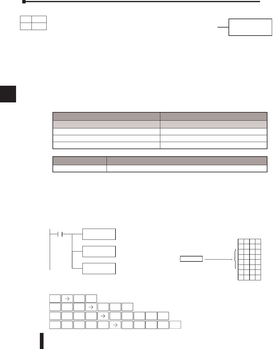
DL06 Micro PLC User Manual, 3rd Edition, Rev. D
5-146
1
2
3
4
5
6
7
8
9
10
11
12
13
14
A
B
C
D
Fill (FILL)
The Fill instruction fills a table of up to 255 V-memory locations
with a value (Aaaa), which is either a V-memory location or a 4-digit
constant. The function parameters are loaded into the first level of the
accumulator stack and the accumulator by two additional instructions.
Listed below are the steps necessary to program the Fill function.
Step 1: Load the number of V-memory locations to be filled into the first level of the
accumulator stack. This parameter must be a HEX value, 0–FF.
Step 2: Load the starting V-memory location for the table into the accumulator. This
parameter must be a HEX value.
Step 3: Insert the Fill instruction which specifies the value to fill the table with. Helpful Hint:
— For parameters that require HEX values when referencing memory locations, the
LDA instruction can be used to convert an octal address to the HEX equivalent and
load the value into the accumulator.
In the following example, when X1 is on, the constant value (K4) is loaded into the
accumulator using the Load instruction. This value specifies the length of the table and
is placed on the first level of the accumulator stack when the Load Address instruction is
executed. The octal address 1600 (V1600) is the starting location for the table and is loaded
into the accumulator using the Load Address instruction. The value to fill the table with
(V1400) is specified in the Fill instruction.
1
2
3
4
5
6
7
8
9
10
11
12
13
14
a
B
c
d
Chapter 5: Standard RLL Instructions - Table Instructions
FILL
Aaaa
Handheld ProgrammerKeystrokes
DirectSOFT32
LD
K4
X1 Load thecons tant value 4
(HEX)intothe lower16bits
of the accumulator
LDA
O1600
Convertthe octaladdres s
1600 to HE X380 andloadthe
value into the accumulator
FILL
V1400
Fill thetable with the value
in V1400
V1576XXXX
V1577
XXXX
V1600
2500
V16012500
V1602
2500
V16032500
V1604
XXXX
V1605
XXXX
S
S
S
S
2500
V1400
Operand Data Type DL06 Range
Aaaa
V-memory V See memory map
Pointer P See memory map
Constant K 0–FF
Handheld Programmer Keystrokes
STR
$
SHFT ANDST
L
3
D
SHFT 5
F
8
I
ANDST
L
PREV
ANDST
L
1
BENT
4
E
0
A
0
A
ENT
SHFT ANDST
L
3
D
1
B
6
G
0
AENT
0
A
1
B
4
E
0
AENT
Discrete Bit Flags Description
SP53 On if the V-memory address is out of range.
DS Used
HPP Used
DirectSOFT
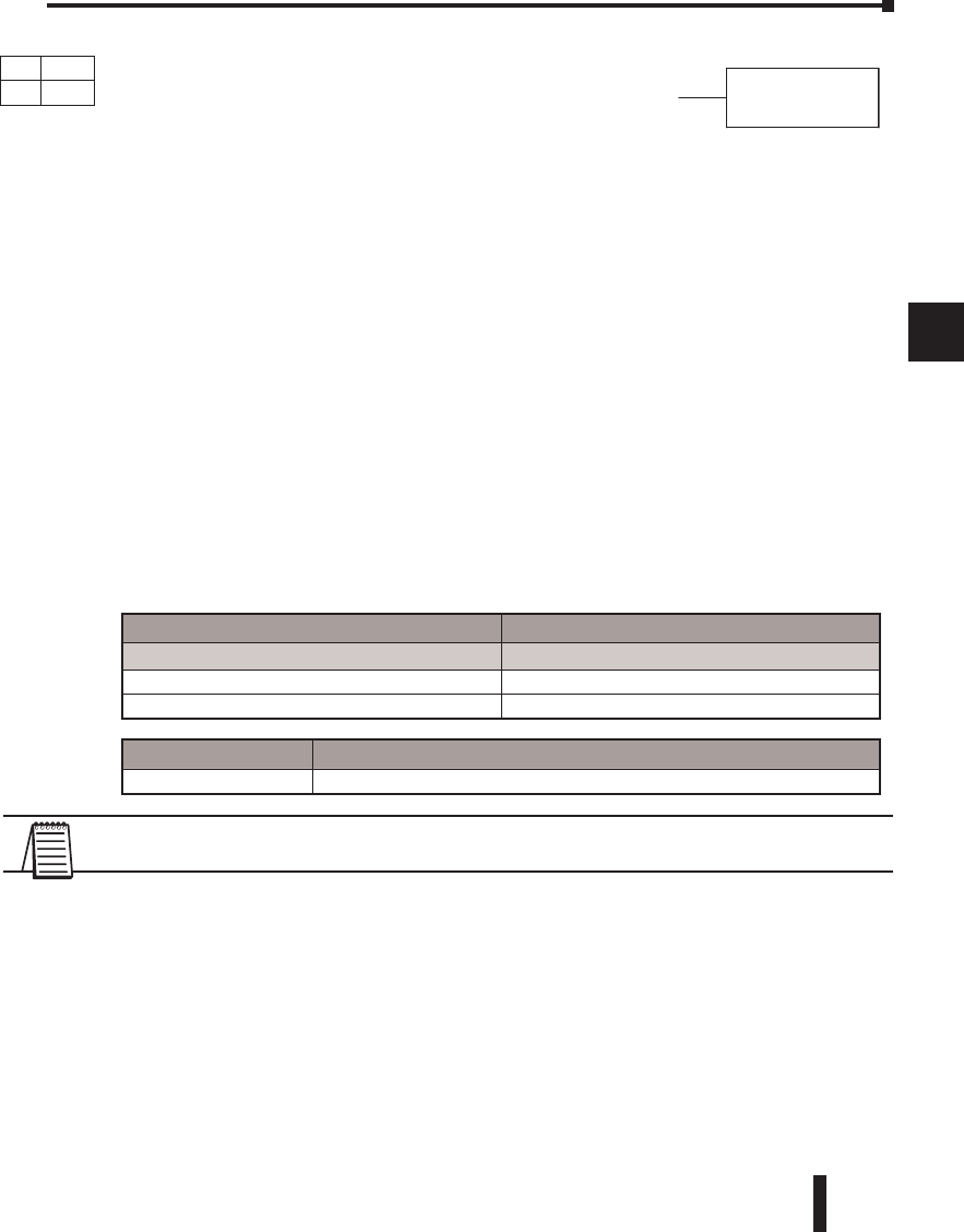
DL06 Micro PLC User Manual, 3rd Edition, Rev. D 5-147
1
2
3
4
5
6
7
8
9
10
11
12
13
14
A
B
C
D
Find (FIND)
The Find instruction is used to search for a specified value in a
V-memory table of up to 255 locations. The function parameters
are loaded into the first and second levels of the accumulator stack
and the accumulator by three additional instructions. Listed below
are the steps necessary to program the Find function.
Step 1: Load the length of the table (number of V-memory locations) into the second level of
the accumulator stack. This parameter must be a HEX value, 0–FF.
Step 2: Load the starting V-memory location for the table into the first level of the
accumulator stack. This parameter must be a HEX value.
Step 3: Load the offset from the starting location to begin the search. This parameter must be
a HEX value.
Step 4: Insert the Find instruction which specifies the first value to be found in the table.
Results:— The offset from the starting address to the first V-memory location which contains
the search value (in HEX) is returned to the accumulator. SP53 will be set On if an address
outside the table is specified in the offset or the value is not found. If the value is not found 0
will be returned in the accumulator.
Helpful Hint: — For parameters that require HEX values when referencing memory
locations, the LDA instruction can be used to convert an octal address to the HEX equivalent
and load the value into the accumulator.
NOTE: Status flags are only valid until another instruction that uses the same flags is executed. The
pointer for this instruction starts at 0 and resides in the accumulator.
In the following example, when X1 is on, the constant value (K6) is loaded into the
accumulator using the Load instruction. This value specifies the length of the table and is
placed in the second stack location when the following Load Address and Load instruction is
executed. The octal address 1400 (V1400) is the starting location for the table and is loaded
into the accumulator. This value is placed in the first level of the accumulator stack when the
following Load instruction is executed. The offset (K2) is loaded into the lower 16 bits of the
accumulator using the Load instruction. The value to be found in the table is specified in the
Find instruction. If a value is found equal to the search value, the offset (from the starting
location of the table) where the value is located will reside in the accumulator.
1
2
3
4
5
6
7
8
9
10
11
12
13
14
a
B
c
d
Chapter 5: Standard RLL Instructions - Table Instructions
FIND
Aaaa
Discrete Bit Flags Description
SP53 On if there is no value in the table that is equal to the search value.
Operand Data Type DL06 Range
Aaaa
V-memory V See memory map
Constant K 0–FF
DS Used
HPP Used
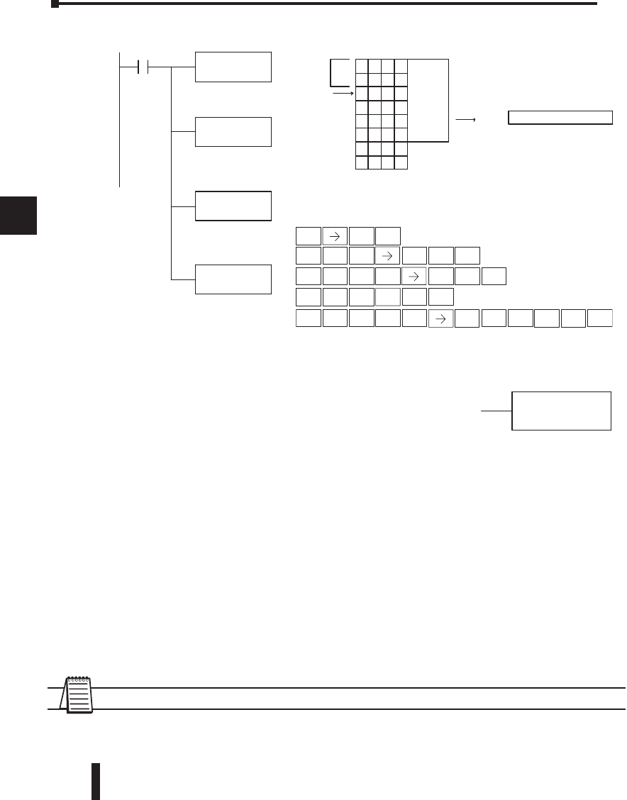
DL06 Micro PLC User Manual, 3rd Edition, Rev. D
5-148
1
2
3
4
5
6
7
8
9
10
11
12
13
14
A
B
C
D
Step 1: Load the length of the table (up to 255 locations) into the first level of the
accumulator stack. This parameter must be a HEX value, 0–FF.
Step 2: Load the starting V-memory location for the table into the accumulator. This
parameter must be a HEX value.
Step 3: Insert the FDGT instruction which specifies the greater than search value.
Results:— The offset from the starting address to the first V-memory location
which contains the greater than search value (in HEX) which is returned to
the accumulator. SP53 will be set On if the value is not found and 0 will be
returned in the accumulator.
Helpful Hint: — For parameters that require HEX values when referencing memory
locations, the LDA instruction can be used to convert an octal address to the HEX equivalent
and load the value into the accumulator.
NOTE: This instruction does not have an offset, such as the one required for the FIND instruction.
Chapter 5: Standard RLL Instructions - Table Instructions
1
2
3
4
5
6
7
8
9
10
11
12
13
14
a
B
c
d
DirectSOFT32 Display
LD
K6
X1
Load theconstantvalue 6
(HEX)intothe lower16bits
of theaccumulator
LDA
O1400
LD
K2
Load theconstantvalue
2intothe lower16bits
of theaccumulator
FIND
K8989
Find theloc ationinthe ta ble
wherethe value8989 resides
V1400
0123
V1401
0500
V1402
9999
V1403
3074
V1404
8989
V1405
1010
V1406
XXXX
V1407
XXXX
S
S
S
S
Offs et
Ta blelength
V1404 contains theloc ation
wherethe matc hwas found.
Thevalue 8989 wasthe 4th
location afterthe startofthe
specifiedtable.
0004
Accumulator
0000
Convertoctal 1400 to HEX
300 andloadthe valueinto
theaccumulator.
Beginhere
1
2
3
4
0
5
FDGT
Aaaa
Handheld Programmer Keystrokes
STR
$
SHFT ANDST
L
3
D
SHFT 5
F
8
I
TMR
N
PREV
3
D
1
BENT
6
G
0
A
0
A
ENT
SHFT ANDST
L
3
D
1
B
4
E
2
CENT
8
I
9
JENT
SHFT ANDST
L
3
DPREV
NEXT 8
I
9
J
DirectSOFT
Find Greater Than (FDGT)
The Find Greater Than instruction is used to search for the first
occurrence of a value in a V-memory table that is greater than
the specified value (Aaaa), which can be either a V-memory
location or a 4-digit constant. The function parameters are
loaded into the first level of the accumulator stack and the
accumulator by two additional instructions. Listed below are the
steps necessary to program the Find Greater Than function.
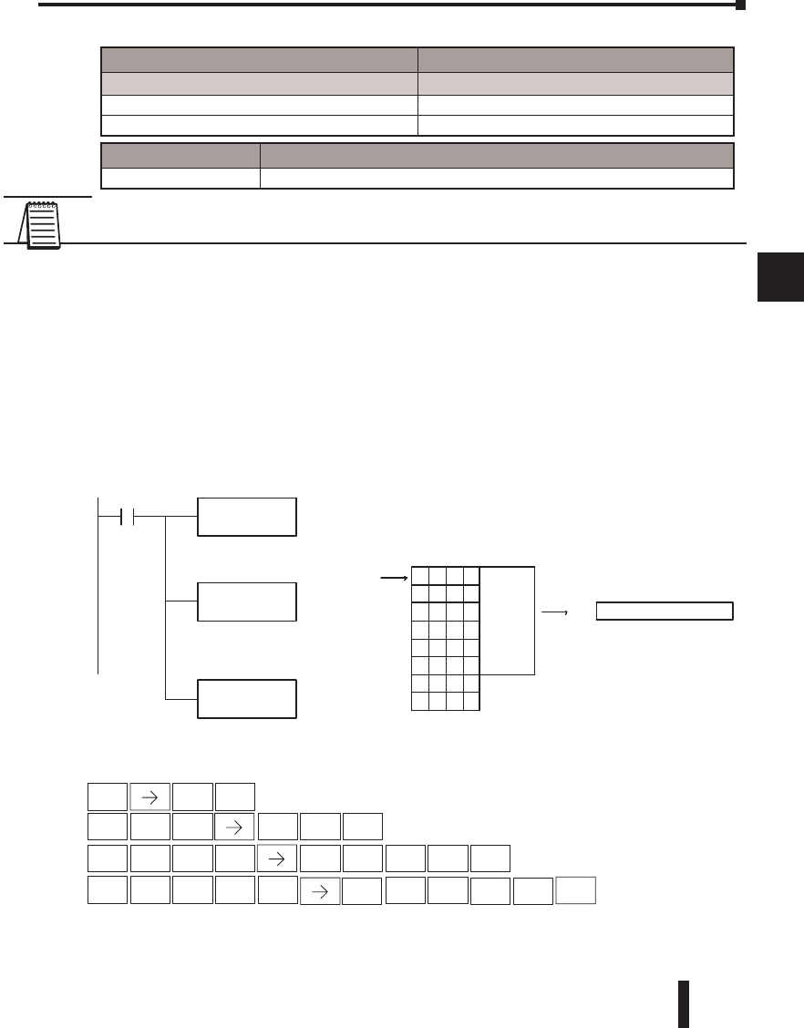
DL06 Micro PLC User Manual, 3rd Edition, Rev. D 5-149
1
2
3
4
5
6
7
8
9
10
11
12
13
14
A
B
C
D
1
2
3
4
5
6
7
8
9
10
11
12
13
14
a
B
c
d
Chapter 5: Standard RLL Instructions - Table Instructions
NOTE: Status flags are only valid until another instruction that uses the same flags is executed. The
pointer for this instruction starts at 0 and resides in the accumulator.
In the following example, when X1 is on, the constant value (K6) is loaded into the
accumulator using the Load instruction. This value specifies the length of the table and is
placed in the first stack location after the Load Address instruction is executed. The octal
address 1400 (V1400) is the starting location for the table and is loaded into the accumulator.
The Greater Than search value is specified in the Find Greater Than instruction. If a value is
found greater than the search value, the offset (from the starting location of the table) where
the value is located will reside in the accumulator. If there is no value in the table that is
greater than the search value, a zero is stored in the accumulator and SP53 will come ON.
Handheld ProgrammerKeystrokes
STRX(IN) 1
LD K(CON) 6
LDSHFTA OC T 1 4 0 0
SHFT F D G T SHFT K(CON ) 8 9 8 9
DirectSOF
T
32 Display
LD
K6
X1
Load theconstantvalue 6
(HEX)intothe lower16bits
of theaccumulator
LDA
O1400
Convertoctal 1400 to HEX
300 andloadthe valueinto
theaccumulator.
FDGT
K8989
Find thevalue in thetable
greaterthanthe specifiedvalue
V1400
012 3
V1401050 0
V1402
999 9
V1403
307 4
V1404
898 9
V1405
101 0
V1406
XXX X
V1407
XXX X
S
S
S
S
Ta blelength
0002
Accumulator
V1402 contains theloc ation
wherethe firstvalue greater
than thesearchvalue was
found. 9999 wasthe 2nd
location afterthe startofthe
specifiedtable.
0000
Beginhere0
1
2
3
4
5
Handheld Programmer Keystrokes
STR
$
SHFT ANDST
L
3
D
SHFT 5
F
3
D
6
G
PREV
MLR
T
1
BENT
6
G
0
A
0
A
ENT
SHFT ANDST
L
3
D
1
B
4
E
0
AENT
8
I
9
JENT
NEXT 8
I
9
J
Operand Data Type DL06 Range
Aaaa
V-memory V See memory map
Constant K 0–FF
Discrete Bit Flags Description
SP53 On if there is no value in the table that is equal to the search value.
DirectSOFT
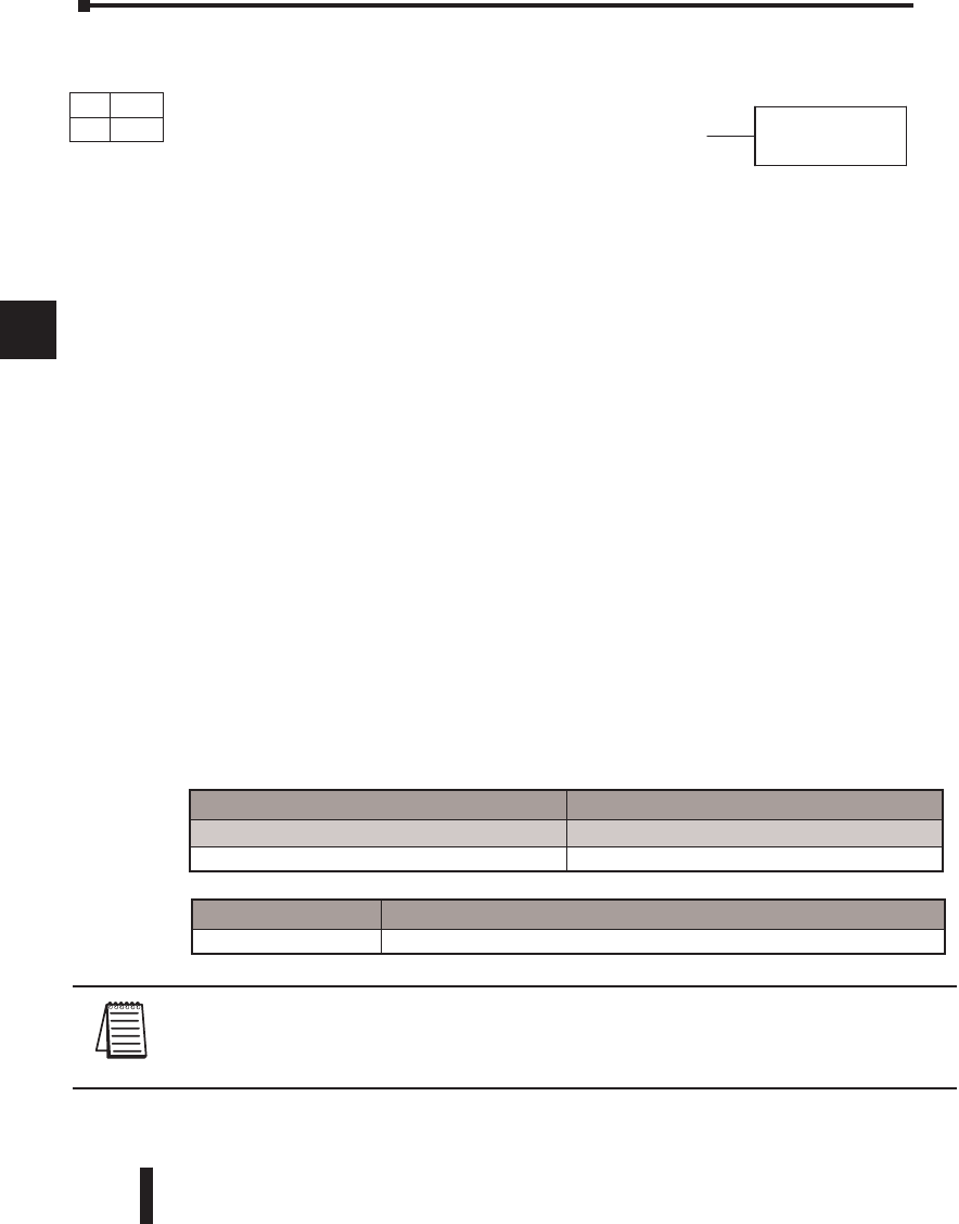
DL06 Micro PLC User Manual, 3rd Edition, Rev. D
5-150
1
2
3
4
5
6
7
8
9
10
11
12
13
14
A
B
C
D
Step 1: Load the length of the data table (number of V-memory locations) into the
first level of the accumulator stack. This parameter must be a HEX value, 0 to
FF.
Step 2: Load the starting V-memory location for the table into the accumulator.
(Remember, the starting location of the table is used as the table pointer.)
This parameter must be a HEX value.
Step 3: Insert the TTD instruction which specifies destination V-memory location
(Vaaa).
Helpful Hint: — For parameters that require HEX values when referencing memory
locations, the LDA instruction can be used to convert an octal address to the HEX equivalent
and load the value into the accumulator.
Helpful Hint: — The instruction will be executed every scan if the input logic is on. If you
do not want the instruction to execute for more than one scan, a one-shot (PD) should be
used in the input logic.
Helpful Hint: — The pointer location should be set to the value where the table operation
will begin. The special relay SP0 or a one-shot (PD) should be used so the value will only be
set in one scan and will not affect the instruction operation.
NOTE: Status flags (SPs) are only valid until another instruction that uses the same flag is executed,
or the end of the scan. The pointer for this instruction starts at 0 and resets when the table length is
reached. At first glance it may appear that the pointer should reset to 0. However, it resets to 1,
not 0.
Chapter 5: Standard RLL Instructions - Table Instructions
1
2
3
4
5
6
7
8
9
10
11
12
13
14
a
B
c
d
TTD
aaa
A
TTD
aaaA
Operand Data Type DL06 Range
Aaaa
V-memory V See memory map
Discrete Bit Flags Description
SP56 On when the table pointer equals the table length.
DS Used
HPP Used
Table to Destination (TTD)
The Table To Destination instruction moves a value from a
V-memory table to a V-memory location and increments the
table pointer by 1. The first V-memory location in the table
contains the table pointer which indicates the next location
in the table to be moved. The instruction will be executed
once per scan provided the input remains on. The table
pointer will reset to 1 when the value equals the last location
in the table. The function parameters are loaded into the first
level of the accumulator stack and the accumulator by two
additional instructions. Listed below are the steps necessary
to program the Table To Destination function.
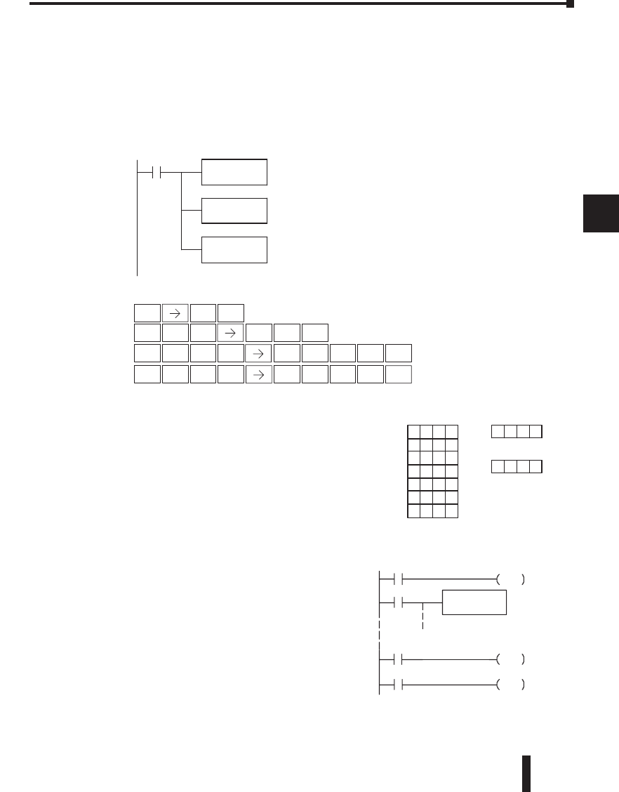
DL06 Micro PLC User Manual, 3rd Edition, Rev. D 5-151
1
2
3
4
5
6
7
8
9
10
11
12
13
14
A
B
C
D
1
2
3
4
5
6
7
8
9
10
11
12
13
14
a
B
c
d
In the following example, when X1 is on, the constant value (K6) is loaded into the
accumulator using the Load instruction. This value specifies the length of the table and is
placed in the first stack location after the Load Address instruction is executed. The octal
address 1400 (V1400) is the starting location for the source table and is loaded into the
accumulator. Remember, V1400 is used as the pointer location, and is not actually part of the
table data source. The destination location (V1500) is specified in the Table to Destination
instruction. The table pointer (V1400 in this case) will be increased by “1” after each
execution of the TTD instruction.
Chapter 5: Standard RLL Instructions - Table Instructions
DirectSOFT32
X1 LD
K6
LDA
0 1400
TTD
V1500
Load the constant value 6
(HEX) into the lower 16 bits
of the accumulator
Convert octal 1400 to HEX
300 and load the value into
the accumulator. This is the
table pointer location
Copy the specified value from
the table to the specified
destination (V1500)
Handheld Programmer Keystrokes
STR
$
SHFT ANDST
L
3
D
SHFT MLR
T
MLR
T
3
D
PREV
1
BENT
6
G
0
A
0
A
ENT
SHFT ANDST
L
3
D
1
B
4
E
0
AENT
0
A
1
B
5
F
0
AENT
V1401 050 0
V1402 999 9
V1403 307 4
V1404 898 9
V1405 101 0
V1406 204 6
V1407 XXX X
S
S
V150
0
XXX X
06
1
2
3
4
5
Destination
V140
0
000 0
TablePointerTable
DirectSOFT32(optional latch example using SP56)
X1
C1
C0
SP56
C0
PD
C1
SET
C1
RST
LD
K6
Load the constant value 6
(HEX) into the lower 16 bits
of the accumulator
Since Special Relays are
reset at the end of the scan,
this latch must follow the TTD
instruction in the program
DirectSOFT
DirectSOFT
It is important to understand how the table
locations are numbered. If you examine the
example table, you’ll notice that the first data
location, V1401, will be used when the pointer
is equal to zero, and again when the pointer is
equal to six. Why? Because the pointer is only
equal to zero before the very first execution.
From then on, it increments from one to six,
and then resets to one.
Also, our example uses a normal input contact
(X1) to control the execution. Since the
CPU scan is extremely fast, and the pointer
increments automatically, the table would cycle
through the locations very quickly. If this is a
problem, you have an option of using SP56 in
conjunction with a one-shot (PD) and a latch
(C1 for example) to allow the table to cycle
through all locations one time and then stop.
The logic shown here is not required, it’s just an
optional method.
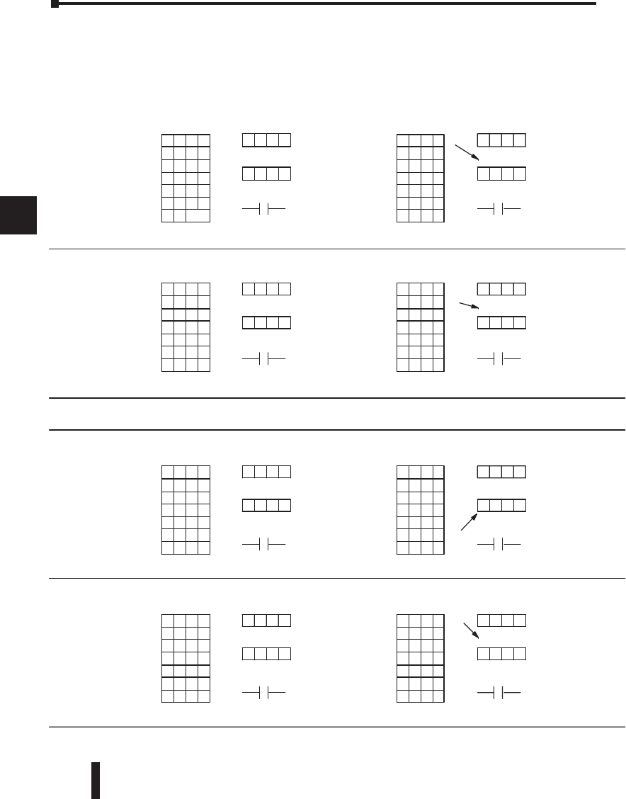
DL06 Micro PLC User Manual, 3rd Edition, Rev. D
5-152
1
2
3
4
5
6
7
8
9
10
11
12
13
14
A
B
C
D
The following diagram shows the scan-by-scan results of the execution for our example
program. Notice how the pointer automatically cycles from 0 – 6, and then starts over at 1
instead of 0. Also, notice how SP56 is only on until the end of the scan.
1
2
3
4
5
6
7
8
9
10
11
12
13
14
a
B
c
d
Chapter 5: Standard RLL Instructions - Table Instructions
TablePointer (Automatically Incremented)
TablePointer (Automatically Incremented)
V1401 0500
V1402 9999
V1403 3074
V1404 8989
V1405 1010
V1406 2046
V1407 XXXX
V1500
XXXX
Before TTD Execution AfterTTD ExecutionScan N
06
1
2
3
4
5
AfterTTD Execution
Scan N+1
AfterTTD ExecutionScan N+5
Destination
V1400
0000
TablePointerTable
V1401 0500
V1402 9999
V1403 3074
V1404 8989
V1405 1010
V1406 2046
V1407 XXXX
V1500
0500
0
1
2
3
4
5
Destination
V1400
0001
TablePointer (Automatically Incremented)Table
V1401 0500
V1402 9999
V1403 3074
V1404 8989
V1405 1010
V1406 2046
V1407 XXXX
V15009999
06
1
2
3
4
5
Destination
V14000002
Table
V1401 0500
V1402 9999
V1403 3074
V1404 8989
V1405 1010
V1406 2046
V1407 XXXX
V15002046
06
1
2
3
4
5
Destination
V14000006
Table
Before TTD Execution
V1401 0500
V1402 9999
V1403 3074
V1404 8989
V1405 1010
V1406 2046
V1407 XXXX
V15000500
06
1
2
3
4
5
Destination
V14000001
TablePointerTable
V1401 0500
V1402 9999
V1403 3074
V1404 8989
V1405 1010
V1406 2046
V1407 XXXX
V15001010
06
1
2
3
4
5
Destination
V14000005
TablePointerTable
Before TTD Execution
SP56=OFF
SP56
SP56=OFF
SP56
SP56=ON
SP56
TablePointer (Resetsto1,not 0)
AfterTTD ExecutionScan N+6
V1401 0500
V1402 9999
V1403 3074
V1404 8989
V1405 1010
V1406 2046
V1407 XXXX
V15000500
1
2
3
4
5
Destination
V1400
0001
Table
V1401 0500
V1402 9999
V1403 3074
V1404 8989
V1405 1010
V1406 2046
V1407 XXXX
V15002046
06
1
2
3
4
5
Destination
V1400
0006
TablePointerTable
Before TTD Execution
SP56=OFF
SP56
SP56=OFF
SP56
SP56=OFF
SP56
SP56=OFF
SP56
SP56=OFF
SP56
6
06
until endofscan
or next instruction
that uses SP56
.
..
.
.
..
.
.
..
.
.
.
.
.
.
.
.
.
DL06 Micro PLC User Manual, 3rd Edition, Rev. D 5-153
1
2
3
4
5
6
7
8
9
10
11
12
13
14
A
B
C
D
Chapter 5: Standard RLL Instructions - Table Instructions
1
2
3
4
5
6
7
8
9
10
11
12
13
14
a
B
c
d
Step 1: Load the length of the table (number of V-memory locations) into the first level of
the accumulator stack. This parameter must be a HEX value, 0 to FF.
Step 2: Load the starting V-memory location for the table into the accumulator. (Remember,
the starting location of the table blank is used as the table pointer.) This parameter must be a
HEX value.
Step 3: Insert the RFB instruction which specifies destination V-memory location (Vaaa).
Helpful Hint: — For parameters that require HEX values when referencing memory
locations, the LDA instruction can be used to convert an octal address to the HEX equivalent
and load the value into the accumulator.
Helpful Hint: — The instruction will be executed every scan if the input logic is on. If you
do not want the instruction to execute for more than one scan, a one-shot (PD) should be
used in the input logic.
Helpful Hint: — The pointer location should be set to the value where the table operation
will begin. The special relay SP0 or a one-shot (PD) should be used so the value will only be
set in one scan and will not affect the instruction operation.
NOTE: Status flags (SPs) are only valid until another instruction that uses the same flag is executed
or the end of the scan The pointer for this instruction can be set to start anywhere in the table. It is
not set automatically. You must load a value into the pointer somewhere in your program.
aaaA
RFB
Operand Data Type DL06 Range
Aaaa
V-memory V See memory map
Discrete Bit Flags Description
SP56 On when the table pointer equals zero..
DS Used
HPP Used
Remove from Bottom (RFB)
The Remove From Bottom instruction moves a value from
the bottom of a V-memory table to a V-memory location and
decrements a table pointer by 1. The first V-memory location
in the table contains the table pointer which indicates the next
location in the table to be moved. The instruction will be executed
once per scan provided the input remains on. The instruction
will stop operation when the pointer equals 0. The function
parameters are loaded into the first level of the accumulator stack
and the accumulator by two additional instructions. Listed below
are the steps necessary to program the Remove From Bottom
function.
DL06 Micro PLC User Manual, 3rd Edition, Rev. D
5-154
1
2
3
4
5
6
7
8
9
10
11
12
13
14
A
B
C
D
In the following example, when X1 is on, the constant value (K6) is loaded into the
accumulator using the Load instruction. This value specifies the length of the table and is
placed in the first stack location after the Load Address instruction is executed. The octal
address 1400 (V1400) is the starting location for the source table and is loaded into the
accumulator. Remember, V1400 is used as the pointer location, and is not actually part of the
table data source. The destination location (V1500) is specified in the Remove From Bottom.
The table pointer (V1400 in this case) will be decremented by “1” after each execution of the
RFB instruction.
Chapter 5: Standard RLL Instructions - Table Instructions
1
2
3
4
5
6
7
8
9
10
11
12
13
14
a
B
c
d
DirectSOFT32
X1
Handheld Programmer Keystrokes
STR
$
SHFT ANDST
L
3
D
SHFT ORN
R
5
F
1
B
PREV
1
BENT
6
G
0
A
0
A
ENT
SHFT ANDST
L
3
D
1
B
4
E
0
AENT
0
A
1
B
5
F
0
AENT
LD
K6
LDA
0 1400
RFB
V1500
Load the constant value 6
(HEX) into the lower 16 bits
of the accumulator
Convert octal 1400 to HEX
300 and load the value into
the accumulator. This is the
table pointer location
Copy the specified value from
the table to the specified
destination (V1500)
V1401 050 0
V1402 999 9
V1403 307 4
V1404 898 9
V1405 101 0
V1406 204 6
V1407 XXX X
S
S
V150
0
XXX X
1
2
3
4
5
6
Destination
V140
0
000 0
TablePointerTable
DirectSOFT32Display (optional one-shot method)
LD
K6
C0
X
1C
0
PD
Load theconstant value6
(HEX) into thelower 16 bits
of theaccumulator
LDA
O1400
Conver toctal 1400 to HEX
300 and load thevalue into
theaccumulator. This is the
tablepointer location.
DirectSOFT32Display (optional one-shot method)
LD
K6
C0
X
1C
0
PD
Load theconstant value6
(HEX) into thelower 16 bits
of theaccumulator
LDA
O1400
Conver toctal 1400 to HEX
300 and load thevalue into
theaccumulator. This is the
tablepointer location.
DirectSOFT (optional one-shot metod)
DirectSOFT
It is important to understand how the table
locations are numbered. If you examine the
example table, you’ll notice that the first data
location, V1401, will be used when the pointer
is equal to one. The second data location,
V1402, will be used when the pointer is equal
to two, etc.
Also, our example uses a normal input contact
(X1) to control the execution. Since the
CPU scan is extremely fast, and the pointer
decrements automatically, the table would cycle
through the locations very quickly. If this is
a problem for your application, you have an
option of using a
one-shot (PD) to remove one value each time
the input contact transitions from low to high.
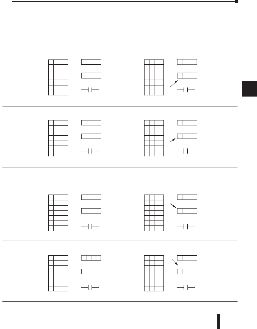
DL06 Micro PLC User Manual, 3rd Edition, Rev. D 5-155
1
2
3
4
5
6
7
8
9
10
11
12
13
14
A
B
C
D
The following diagram shows the scan-by-scan results of the execution for our example
program. Notice how the pointer automatically decrements from 6 to 0. Also, notice how
SP56 is only on until the end of the scan.
Chapter 5: Standard RLL Instructions -Table Instructions
1
2
3
4
5
6
7
8
9
10
11
12
13
14
a
B
c
d
Before RFBExecution AfterRFB Execution
Before RFBExecution AfterRFB Execution
Before RFBExecution AfterRFB Execution
1
2
3
4
5
6
1
2
3
4
5
6
1
2
3
4
5
6
1
2
3
4
5
6
Tabl ePointer (Autom atically Decremented)
Tabl ePointer (Autom atically Decremented)
V1401 0500
V1402 9999
V1403 3074
V1404 8989
V1405 1010
V1406 2046
V1407 XXXX
.
V1500
XXXX
Before RFBExecution AfterRFB Execution
ExampleofExecution
Scan N
1
2
3
4
5
6
Scan N+1
Scan N+4
Destination
V1400
0006
Tabl ePointerTabl e
V1401 0500
V1402 9999
V1403 3074
V1404 8989
V1405 1010
V1406 2046
V1407 XXXX
V1500
2046
Destination
V1400
0005
Tabl ePointer (Autom atically Decremented)Table
V1401 0500
V1402 9999
V1403 3074
V1404 8989
V1405 1010
V1406 2046
V1407 XXXX
V1500
1010
Destination
V1400
0004
Tabl e
V1401 0500
V1402 9999
V1403 3074
V1404 8989
V1405 1010
V1406 2046
V1407 XXXX
V1500
9999
Destination
V1400
0001
Tabl e
V1401 0500
V1402 9999
V1403 3074
V1404 8989
V1405 1010
V1406 2046
V1407 XXXX
V1500
2046
1
2
3
4
5
6
Destination
V1400
0005
Tabl ePointerTabl e
V1401 0500
V1402 9999
V1403 3074
V1404 8989
V1405 1010
V1406 2046
V1407 XXXX
V1500
3074
1
2
3
4
5
6
Destination
V1400
0002
Tabl ePointerTabl e
SP56=OFF
SP56
SP56=OFF
SP56
SP56=OFF
SP56
Tabl ePointer
Scan N+5
V1401 0500
V1402 9999
V1403 3074
V1404 8989
V1405 1010
V1406 2046
V1407 XXXX
V1500
0500
Destination
V1400
0000
Tabl e
V1401 0500
V1402 9999
V1403 3074
V1404 8989
V1405 1010
V1406 2046
V1407 XXXX
V1500
9999
1
2
3
4
5
6
Destination
V1400
0001
Tabl ePointerTabl e
SP56=ON
SP56
SP56=OFF
SP56
SP56=OFF
SP56
SP56=OFF
SP56
SP56=OFF
SP56
until end of scan
or nextinstruction
that uses SP56
..
.
.
.
.
.
.
.
.
.
.
.
.
.
.
.
.
DL06 Micro PLC User Manual, 3rd Edition, Rev. D
5-156
1
2
3
4
5
6
7
8
9
10
11
12
13
14
A
B
C
D
Step 1: Load the length of the table (number of V-memory locations) into the first
level of the accumulator stack. This parameter must be a HEX value, 0 to FF.
Step 2: Load the starting V-memory location for the table into the accumulator.
(Remember, the starting location of the table is used as the table pointer.)
This parameter must be a HEX value.
Step 3: Insert the STT instruction which specifies the source V-memory location
(Vaaa). This is where the value will be moved from.
Helpful Hint: — For parameters that require HEX values when referencing memory
locations, the LDA instruction can be used to convert an octal address to the HEX equivalent
and load the value into the accumulator.
Helpful Hint:— The instruction will be executed every scan if the input logic is on. If you do
not want the instruction to execute for more than one scan, a one-shot (PD) should be used
in the input logic.
Helpful Hint: — The table counter value should be set to indicate the starting point for the
operation. Also, it must be set to a value that is within the length of the table. For example,
if the table is 6 words long, then the allowable range of values that could be in the pointer
should be between 0 and 6. If the value is outside of this range, the data will not be moved.
Also, a one-shot (PD) should be used so the value will only be set in one scan and will not
affect the instruction operation.
NOTE: Status flags (SPs) are only valid until another instruction that uses the same flag is executed,
or the end of the scan. The pointer for this instruction starts at 0 and resets to 1 automatically when
the table length is reached.
Chapter 5: Standard RLL Instructions - Table Instructions
1
2
3
4
5
6
7
8
9
10
11
12
13
14
a
B
c
d
aaaV
STT
Operand Data Type DL06 Range
Aaaa
V-memory V See memory map
Discrete Bit Flags Description
SP56 On when the table pointer equals the table length.
DS Used
HPP Used
Source to Table (STT)
The Source To Table instruction moves a value from
a V-memory location into a V-memory table and
increments a table pointer by 1. When the table pointer
reaches the end of the table, it resets to 1. The first
V-memory location in the table contains the table pointer
which indicates the next location in the table to store a
value. The instruction will be executed once per scan,
provided the input remains on. The function parameters
are loaded into the first level of the accumulator stack and
the accumulator with two additional instructions. Listed
below are the steps necessary to program the Source To
Table function.
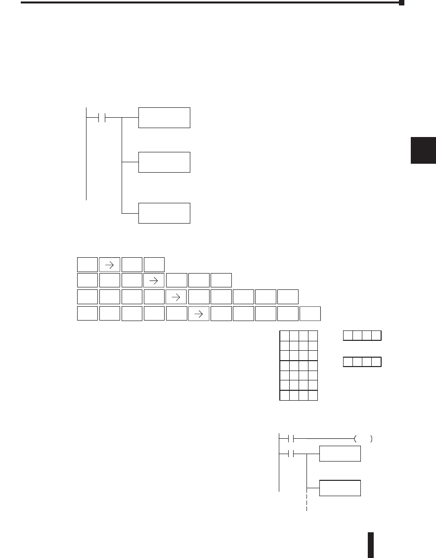
DL06 Micro PLC User Manual, 3rd Edition, Rev. D 5-157
1
2
3
4
5
6
7
8
9
10
11
12
13
14
A
B
C
D
In the following example, when X1 is on, the constant value (K6) is loaded into the
accumulator using the Load instruction. This value specifies the length of the table and is
placed in the first stack location after the Load Address instruction is executed. The octal
address 1400 (V1400), which is the starting location for the destination table and table
pointer, is loaded into the accumulator. The data source location (V1500) is specified in the
Source to Table instruction. The table pointer will be increased by “1” after each time the
instruction is executed.
Chapter 5: Standard RLL Instructions -Table Instructions
1
2
3
4
5
6
7
8
9
10
11
12
13
14
a
B
c
d
DirectSOFT32
X1
Handheld Programmer Keystrokes
STR
$
SHFT ANDST
L
3
D
SHFT RST
S
MLR
T
MLR
T
PREV
1
BENT
6
G
0
A
0
A
ENT
SHFT ANDST
L
3
D
1
B
4
E
0
AENT
0
A
1
B
5
F
0
AENTSHFT
LD
K6
LDA
0 1400
STT
V1500
Load the constant value 6
(HEX) into the the lower 16 bits
of the accumulator
Convert octal 1400 to HEX
300 and load the value into
the accumulator
Copy the specified value
from the source location
(V1500) to the table
V1401 XXX X
V1402 XXX X
V1403 XXX X
V1404 XXX X
V1405 XXX X
V1406 XXX X
V1407 XXX X
S
S
V150
0
050 0
06
1
2
3
4
5
Data Sour ce
V140
0
000 0
TablePointerTable
DirectSOFT32(optional one-shot method)
LD
K6
C0
X
1C
0
PD
Load theconstant value6
(HEX)intothe lower16bits
of theaccumulator
LDA
O1400
Conver toctal 1400 to HEX
300 and load thevalue into
theaccumulator. This is the
starting tablelocation.
DirectSOFT
DirectSOFT
It is important to understand how the table locations
are numbered. If you examine the example table,
you’ll notice that the first data storage location,
V1401, will be used when the pointer is equal to
zero, and again when the pointer is equal to six.
Why? Because the pointer is only equal to zero
before the very first execution. From then on, it
increments from one to six, and then resets to one.
Also, our example uses a normal input contact
(X1) to control the execution. Since the CPU
scan is extremely fast, and the pointer increments
automatically, the source data would be moved
into all the table locations very quickly. If this is a
problem for your application, you have an option of
using a one-shot (PD) to move one value each time
the input contact transitions from low to high.
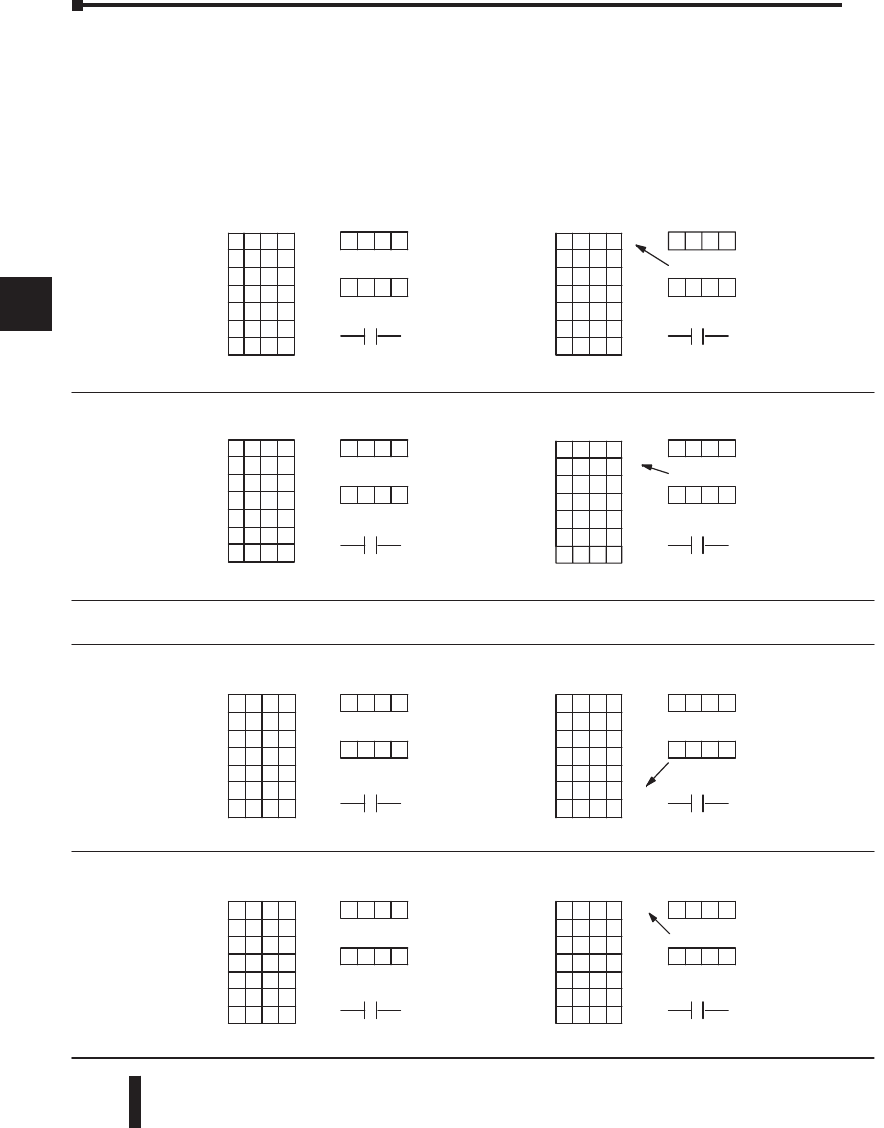
DL06 Micro PLC User Manual, 3rd Edition, Rev. D
5-158
1
2
3
4
5
6
7
8
9
10
11
12
13
14
A
B
C
D
The following diagram shows the scan-by-scan results of the execution for our example
program. Notice how the pointer automatically cycles from 0 to 6, and then starts over at 1
instead of 0. Also, notice how SP56 is affected by the execution. Although our example does
not show it, we are assuming that there is another part of the program that changes the value
in V1500 (data source) prior to the execution of the STT instruction. This is not required,
but it makes it easier to see how the data source is copied into the table.
Chapter 5: Standard RLL Instructions - Table Instructions
1
2
3
4
5
6
7
8
9
10
11
12
13
14
a
B
c
d
V1401 0500
V1402 9999
V1403 XXXX
V1404 XXXX
V1405 XXXX
V1406 XXXX
V1407 XXXX
Tabl e
V1401 0500
V1402 XXXX
V1403 XXXX
V1404 XXXX
V1405 XXXX
V1406 XXXX
V1407 XXXX
Tabl e
V1401 0500
V1402 XXXX
V1403 XXXX
V1404 XXXX
V1405 XXXX
V1406 XXXX
V1407 XXXX
Tabl e
V1401 XXXX
V1402 XXXX
V1403 XXXX
V1404 XXXX
V1405 XXXX
V1406 XXXX
V1407 XXXX
06
1
2
3
4
5
Tabl e
AfterSTT Execution
AfterSTT Execution
AfterSTT Execution
Before STTExecution
Before STTExecution
Tabl ePointer (Autom atically Increm ented)
Tabl ePointer (Autom atically Increm ented)
.
.
V1500
0500
Before STTExecution AfterSTT Execution
Scan N
1
2
3
4
5
Scan N+1
Scan N+5
Source
V1400
0000
Tabl ePointer
V1500
0500
0
1
2
3
4
5
Source
V1400
0001
Tabl ePointer (Autom atically Increm ented)
V1500
9999
06
1
2
3
4
5
Source
V1400
0002
V1401 0500
V1402 9999
V1403 3074
V1404 8989
V1405 1010
V1406 2046
V1407 XXXX
V1500
2046
06
1
2
3
4
5
Source
V1400
0006
Tabl e
Before STTExecution
V1500
9999
06
1
2
3
4
5
Source
V1400
0001
Tabl ePointer
V1401 0500
V1402 9999
V1403 3074
V1404 8989
V1405 1010
V1406 XXXX
V1407 XXXX
V1500
2046
06
1
2
3
4
5
Source
V1400
0005
Tabl ePointerTable
SP56=OFF
SP56
SP56=OFF
SP56
SP56=ON
SP56
Tabl ePointer (Resetsto1,not 0)
Scan N+6
V1401 1234
V1402 9999
V1403 3074
V1404 8989
V1405 1010
V1406 2046
V1407 XXXX
V1500
1234
1
2
3
4
5
Source
V1400
0001
Tabl e
V1401 0500
V1402 9999
V1403 3074
V1404 8989
V1405 1010
V1406 2046
V1407 XXXX
V1500
1234
06
1
2
3
4
5
Source
V1400
0006
Tabl ePointerTable
SP56=OFF
SP56
SP56=OFF
SP56
SP56=OFF
SP56
SP56=OFF
SP56
SP56=OFF
SP56
6
06
until end of scan
or nextinstruction
that uses SP56
.
.
.
.
.
.
.
.
.
.
.
.
.
.
.
..
.
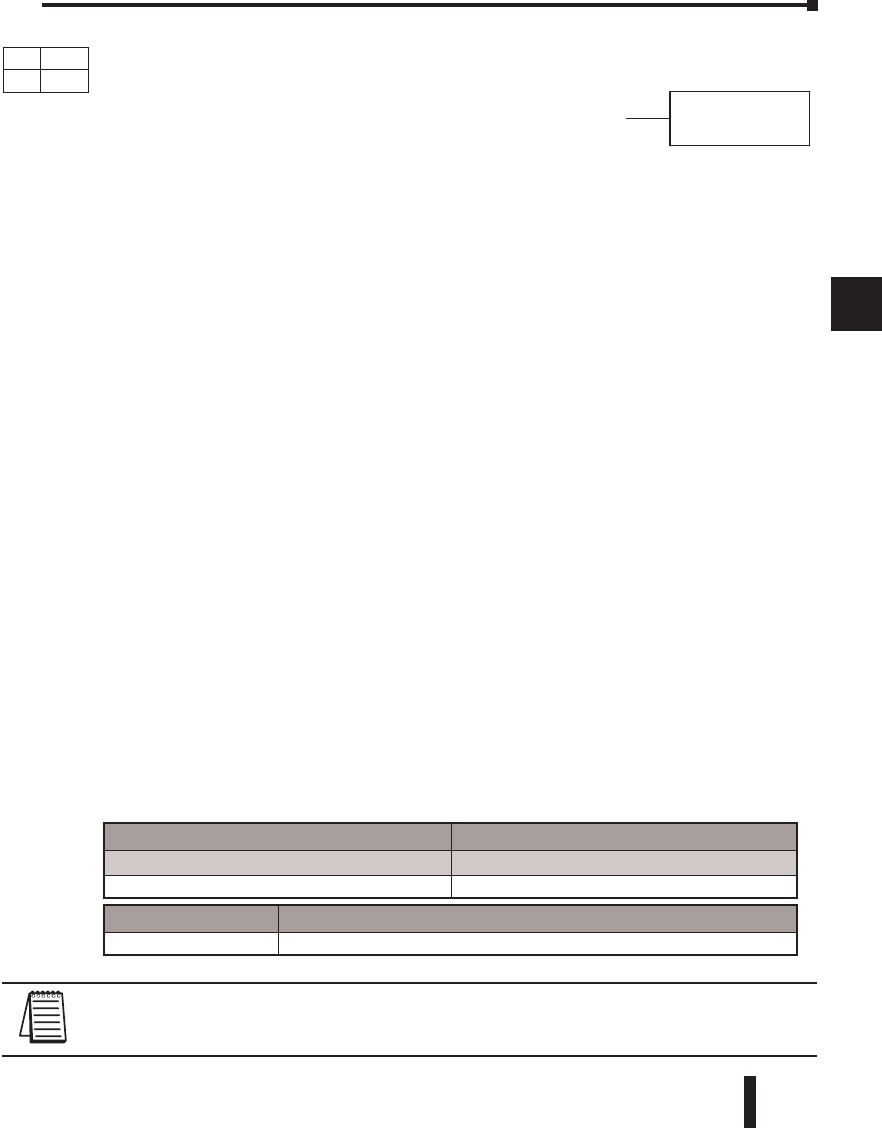
DL06 Micro PLC User Manual, 3rd Edition, Rev. D 5-159
1
2
3
4
5
6
7
8
9
10
11
12
13
14
A
B
C
D
The instruction will be executed once per scan, provided the input remains on. The function
parameters are loaded into the first level of the accumulator stack and the accumulator by two
additional instructions. Listed below are the steps necessary to program the Remove From
Table function.
Step 1: Load the length of the table (number of V-memory locations) into the first
level of the accumulator stack. This parameter must be a HEX value, 0 to FF.
Step 2: Load the starting V-memory location for the table into the accumulator.
(Remember, the starting location of the table is used as the table length
counter.) This parameter must be a HEX value.
Step 3: Insert the RFT instructions which specifies destination V-memory location
(Vaaa). This is where the value will be moved to.
Helpful Hint: — For parameters that require HEX values when referencing memory
locations, the LDA instruction can be used to convert an octal address to the HEX equivalent
and load the value into the accumulator.
Helpful Hint:— The instruction will be executed every scan if the input logic is on. If you do
not want the instruction to execute for more than one scan, a one-shot (PD) should be used
in the input logic.
Helpful Hint: — The table counter value should be set to indicate the starting point for the
operation. Also, it must be set to a value that is within the length of the table. For example, if
the table is 6 words long, then the allowable range of values that could be in the table counter
should be between 1 and 6. If the value is outside of this range or zero, the data will not be
moved from the table. Also, a one-shot (PD) should be used so the value will only be set in
one scan and will not affect the instruction operation.
NOTE: Status flags (SPs) are only valid until another instruction that uses the same flag is executed,
or the end of the scan The pointer for this instruction can be set to start anywhere in the table. It is
not set automatically. You must load a value into the pointer somewhere in your program.
Chapter 5: Standard RLL Instructions - Table Instructions
1
2
3
4
5
6
7
8
9
10
11
12
13
14
a
B
c
d
aaaV
RFT
Operand Data Type DL06 Range
Aaaa
V-memory V See memory map
Discrete Bit Flags Description
SP56 On when the table pointer equals zero.
DS Used
HPP Used
Remove from Table (RFT)
The Remove From Table instruction pops a value off a table and
stores it in a V-memory location. When a value is removed from
the table all other values are shifted up 1 location. The first
V-memory location in the table contains the table length
counter. The table counter decrements by 1 each time the
instruction is executed. If the length counter is zero or greater
than the maximum table length (specified in the first level of the
accumulator stack) the instruction will not execute and SP56
will be On.
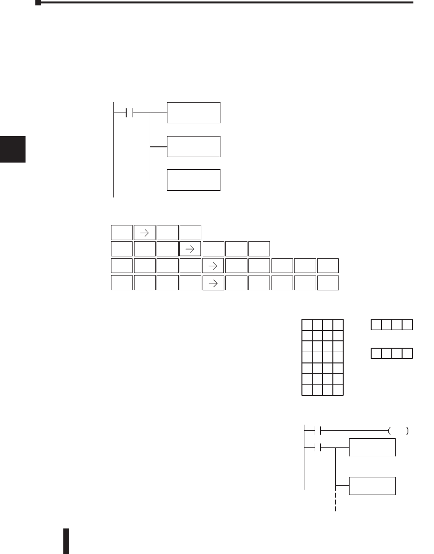
DL06 Micro PLC User Manual, 3rd Edition, Rev. D
5-160
1
2
3
4
5
6
7
8
9
10
11
12
13
14
A
B
C
D
In the following example, when X1 is on, the constant value (K6) is loaded into the
accumulator using the Load instruction. This value specifies the length of the table and is
placed in the first stack location after the Load Address instruction is executed. The octal
address 1400 (V1400) is the starting location for the source table and is loaded into the
accumulator. The destination location (V1500) is specified in the Remove from Table
instruction. The table counter will be decreased by “1” after the instruction is executed.
Chapter 5: Standard RLL Instructions - Table Instructions
1
2
3
4
5
6
7
8
9
10
11
12
13
14
a
B
c
d
DirectSOFT32Display
LD
K6
X1 Load theconstant value6
(Hex.) into thelow er 16 bits
of theaccumulator
LDA
O1400
RFT
V1500
Copy thespecifiedvalue
from thetabletothe
specifiedlocation(V1500)
Convertoctal 1400 to HEX
300 and load thevalue into
theaccumulator
Handheld Programmer Keystrokes
STR
$
SHFT ANDST
L
3
D
SHFT ORN
R
5
F
MLR
T
PREV
1
BENT
6
G
0
A
0
A
ENT
SHFT ANDST
L
3
D
1
B
4
E
0
AENT
0
A
1
B
5
F
0
AENT
V1401 050 0
V1402 999 9
V1403 307 4
V1404 898 9
V1405 101 0
V1406 204 6
V1407 XXX X
S
S
V150
0
XXX X
1
2
3
4
5
6
Destination
V140
0
000 6
TableCounterTable
DirectSOFT32Display (optional one-shot method)
LD
K6
C0
X
1C
0
PD
Load theconstant value6
(HEX) into thelower 16 bits
of theaccumulator
LDA
O1400
Conver toctal 1400 to HEX
300 and load thevalue into
theaccumulator. This is the
tablepointer location.
DirectSOFT
Since the table counter specifies the range of data
that will be removed from the table, it is important to
understand how the table locations are numbered. If
you examine the example table, you’ll notice that the
data locations are numbered from the top of the table.
For example, if the table counter started at 6, then
all six of the locations would be affected during the
instruction execution.
Also, our example uses a normal input contact (X1) to
control the execution. Since the CPU scan is extremely
fast, and the pointer decrements automatically, the data
would be removed from the table very quickly. If this is
a problem for your application, you have an option of
using a one-shot (PD) to remove one value each time
the input contact transitions from low to high.
DL06 Micro PLC User Manual, 3rd Edition, Rev. D 5-161
1
2
3
4
5
6
7
8
9
10
11
12
13
14
A
B
C
D
The following diagram shows the scan-by-scan results of the execution for our example
program. In our example, we show the table counter set to 4, initially. (Remember, you can
set the table counter to any value that is within the range of the table.) The table counter
automatically decrements from 4 to 0 as the instruction is executed. Notice how the last two
table positions, 5 and 6, are not moved up through the table. Also, notice that SP56, which
comes on when the table counter is zero, is only on until the end of the scan.
Chapter 5: Standard RLL Instructions - Table Instructions
1
2
3
4
5
6
7
8
9
10
11
12
13
14
a
B
c
d
V1401 8989
V1402 8989
V1403 8989
V1404 8989
V1405 1010
V1406 2046
V1407 XXXX
V1401 8989
V1402 8989
V1403 8989
V1404 8989
V1405 1010
V1406 2046
V1407 XXXX
V1401 8989
V1402 8989
V1403 8989
V1404 8989
V1405 1010
V1406 2046
V1407 XXXX
V1401 4079
V1402 8989
V1403 8989
V1404 8989
V1405 1010
V1406 2046
V1407 XXXX
V1401 9999
V1402 4079
V1403 8989
V1404 8989
V1405 1010
V1406 2046
V1407 XXXX
1
2
3
4
5
6
1
2
3
4
5
6
V1401 0500
V1402 9999
V1403 3074
V1404 8989
V1405 1010
V1406 2046
V1407 XXXX
V1500
XXXX
1
2
3
4
5
6
V1400
0004 V1401 9999
V1402 4079
V1403 8989
V1404 8989
V1405 1010
V1406 2046
V1407 XXXX
V1500
0500
Destination
V1400
0003
V1500
9999
Destination
V1400
0002
V1500
4079
V1400
0001
V15000500
1
2
3
4
5
6
V1400
0003
V1500
9999
1
2
3
4
5
6
V1400
0002
SP56=OFF
SP56
SP56=OFF
SP56
SP56=OFF
SP56
V1500
8989
V1400
0000
V1500
4079
1
2
3
4
5
6
V1400
0001
SP56
SP56=OFF
SP56
SP56=OFF
SP56
SP56=OFF
SP56
SP56=OFF
SP56
Tabl eCounter
(Automatically decrem ented)
V1401 4079
V1402 8989
V1403 8989
V1404 8989
V1405 1010
V1406 2046
V1407 XXXX
1
2
3
4
5
6
0500
9999
4079
1
2
3
4
5
6
8989
Before RFT Execution
TableTa ble Counter
Destination
Table Counter
indicates that
these 4
positions will
be
used
After RFT Execution
Table
Before RFT Execution
Table
After RFT Execution
Table
Before RFT Execution
Table
After RFT Execution
Table
Before RFT Execution
Table
After RFT Execution
Table
Table Counter
Table Counter
Table Counter
Destinatio
Destination
Destination
Start here
Start here
Start here
Start here
Scan N+3
Scan N+2
Scan N+1
Scan N
Destination
Destination
SP56 = ON
until end of scan
or next instruction
that uses SP56
Table Counter
(Automatically decremented)
Table Counter
(Automatically decremented)
Table Counter
(Automatically decremented)
.
..
.
.
..
.
.
.
.
.
.
..
.
DL06 Micro PLC User Manual, 3rd Edition, Rev. D
5-162
1
2
3
4
5
6
7
8
9
10
11
12
13
14
A
B
C
D
Add to Top (ATT)
The Add To Top instruction pushes a value on to a V-memory
table from a V-memory location. When the value is added to the
table all other values are pushed down 1 location.
The instruction will be executed once per scan, provided the input remains on. The function
parameters are loaded into the first level of the accumulator stack and the accumulator by
two additional instructions. Listed below are the steps necessary to program the Add To Top
function.
Step 1: Load the length of the table (number of V-memory locations) into the first
level of the accumulator stack. This parameter must be a HEX value, 0 to FF.
Step 2: Load the starting V-memory location for the table into the accumulator.
(Remember, the starting location of the table is used as the table length
counter.) This parameter must be a HEX value.
Step 3: Insert the ATT instructions which specifies source V-memory location (Vaaa).
This is where the value will be moved from.
Helpful Hint:— The instruction will be executed every scan if the input logic is on. If you do
not want the instruction to execute for more than one scan, a one-shot (PD) should be used
in the input logic.
Helpful Hint: — For parameters that require HEX values when referencing memory
locations, the LDA instruction can be used to convert an octal address to the HEX equivalent
and load the value into the accumulator.
Helpful Hint: — The table counter value should be set to indicate the starting point for the
operation. Also, it must be set to a value that is within the length of the table. For example, if
the table is 6 words long, then the allowable range of values that could be in the table counter
should be between 1 and 6. If the value is outside of this range or zero, the data will not be
moved into the table. Also, a one-shot (PD) should be used so the value will only be set in
one scan and will not affect the instruction operation.
NOTE: Status flags (SPs) are only valid until another instruction that uses the same flag is executed
or the end of the scan. The pointer for this instruction can be set to start anywhere in the table. It is
not set automatically. You must load a value into the pointer somewhere in your program.
Chapter 5: Standard RLL Instructions - Table Instructions
1
2
3
4
5
6
7
8
9
10
11
12
13
14
a
B
c
d
aaaV
AT T
Operand Data Type DL06 Range
Aaaa
V-memory V See memory map
Discrete Bit Flags Description
SP56 On when the table pointer equal to the table size.
DS Used
HPP Used
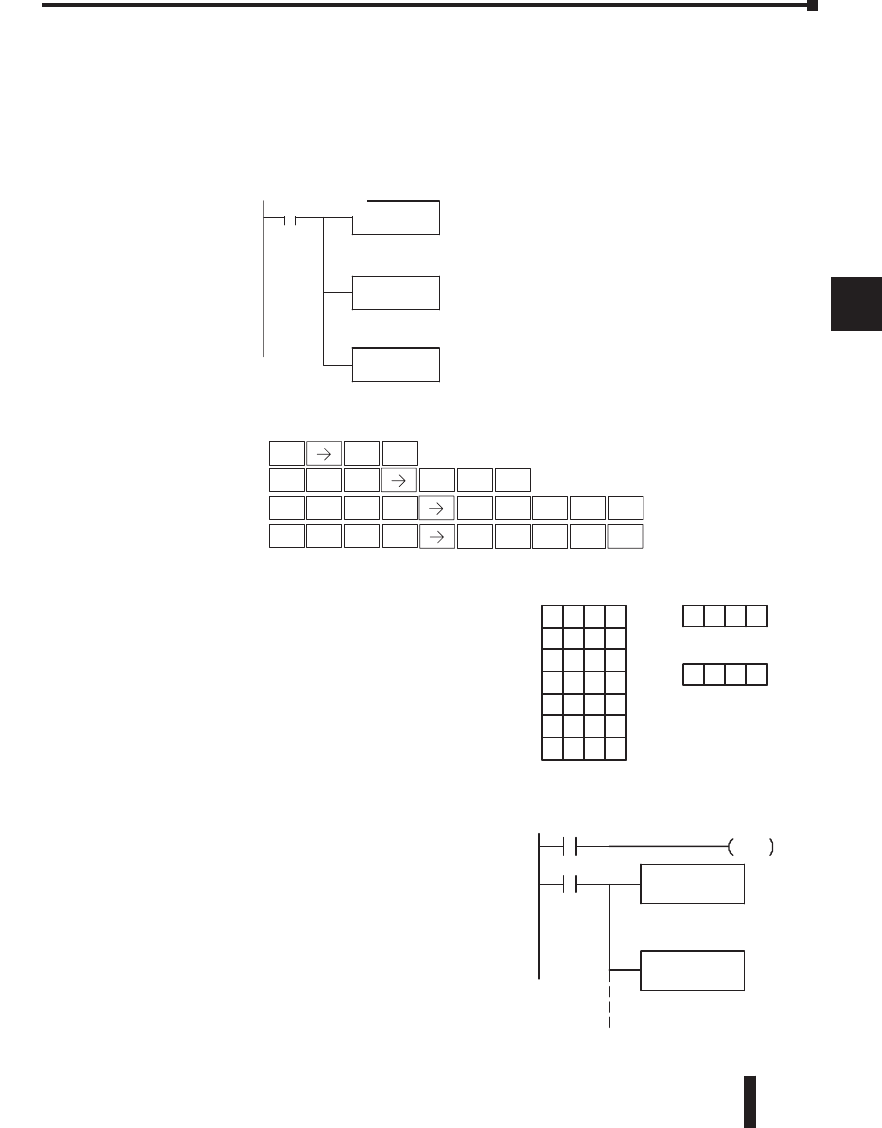
DL06 Micro PLC User Manual, 3rd Edition, Rev. D 5-163
1
2
3
4
5
6
7
8
9
10
11
12
13
14
A
B
C
D
In the following example, when X1 is on, the constant value (K6) is loaded into the
accumulator using the Load instruction. This value specifies the length of the table and is
placed in the first stack location after the Load Address instruction is executed. The octal
address 1400 (V1400), which is the starting location for the destination table and table
counter, is loaded into the accumulator. The source location (V1500) is specified in the
Add to Top instruction. The table counter will be increased by “1” after the instruction is
executed.
Chapter 5: Standard RLL Instructions - Table Instructions
1
2
3
4
5
6
7
8
9
10
11
12
13
14
a
B
c
d
DirectSOFT32Display
LD
K6
X1
Load theconstant value6
(Hex.) into thelower 16 bits
of theaccumulator
LDA
O1400
AT T
V1500
Copy thespecifiedvalue
from V1500 to thetable
Conver toctal 1400 to HEX
300 and load theval ue into
theaccumulator
Handheld Programmer Keystrokes
STR
$
SHFT ANDST
L
3
D
SHFT 0
A
MLR
T
MLR
T
PREV
1
BENT
6
G
0
A
0
A
ENT
SHFT ANDST
L
3
D
1
B
4
E
0
AENT
0
A
1
B
5
F
0
AENT
V1401 050 0
V1402 999 9
V1403 307 4
V1404 898 9
V1405 101 0
V1406 204 6
V1407 XXX X
V150
0
XXX X
1
2
3
4
5
6
Data Source
V140
0
000 2
TableCounterTable
(e.g.: 6--2=4)
DirectSOFT32Display (optional one-shot method)
LD
K6
C0
X
1C
0
PD
Load theconstant value6
(HEX) into thelower 16 bits
of theaccumulator
LDA
O1400
Conver toctal 1400 to HEX
300 and load thevalue into
theaccumulator. This is the
starting tablelocation.
DirectSOFT (optional one-shot method)
DirectSOFT
For the ATT instruction, the table counter
determines the number of additions that can be
made before the instruction will stop executing.
So, it is helpful to understand how the system
uses this counter to control the execution.
For example, if the table counter was set to 2, and
the table length was 6 words, then there could
only be 4 additions of data before the execution
was stopped. This can easily be calculated by:
Table length – table counter = number of executions
Also, our example uses a normal input contact
(X1) to control the execution. Since the CPU
scan is extremely fast, and the table counter
increments automatically, the data would be
moved into the table very quickly. If this is a
problem for your application, you have an option
of using a one-shot (PD) to add one value each
time the input contact transitions from low to
high.
DL06 Micro PLC User Manual, 3rd Edition, Rev. D
5-164
1
2
3
4
5
6
7
8
9
10
11
12
13
14
A
B
C
D
The following diagram shows the scan-by-scan results of the execution for our example
program. The table counter is set to 2 initially, and it will automatically increment from 2
to 6 as the instruction is executed. Notice how SP56 comes on when the table counter is
6, which is equal to the table length. Plus, although our example does not show it, we are
assuming that there is another part of the program that changes the value in V1500 (data
source) prior to the execution of the ATT instruction.
Chapter 5: Standard RLL Instructions - Table Instructions
1
2
3
4
5
6
7
8
9
10
11
12
13
14
a
B
c
d
V1401 7777
V1402 4343
V1403 5678
V1404 1234
V1405 0500
V1406 9999
V1407 XXXX
1
2
3
4
5
6
7777
V1401 4343
V1402 5678
V1403 1234
V1404 0500
V1405 9999
V1406 3074
V1407 XXXX
V1401 4343
V1402 5678
V1403 1234
V1404 0500
V1405 9999
V1406 3074
V1407 XXXX
1
2
3
4
5
6
V1401 5678
V1402 1234
V1403 0500
V1404 9999
V1405 3074
V1406 8989
V1407 XXXX
V1401 5678
V1402 1234
V1403 0500
V1404 9999
V1405 3074
V1406 8989
V1407 XXXX
V1401 1234
V1402 0500
V1403 9999
V1404 3074
V1405 8989
V1406 1010
V1407 XXXX
1
2
3
4
5
6
V1401 0500
V1402 9999
V1403 3074
V1404 8989
V1405 1010
V1406 2046
V1407 XXXX
V1500
1234
1
2
3
4
5
6
V1400
0002 V1401 1234
V1402 0500
V1403 9999
V1404 3074
V1405 8989
V1406 1010
V1407 XXXX
V1500
1234
V1400
0003
Tabl e
V15005678
Data Source
V14000004
V1500
4343
V1400
0005
V15005678
1
2
3
4
5
6
V14000003
V1500
4334
1
2
3
4
5
6
V1400
0004
SP56= OFF
SP56
SP56= OFF
SP56
SP56=
SP56
V1500
7777
V1400
0006
V1500
7777
1
2
3
4
5
6
V1400
0005
SP56=
SP56
SP56= OFF
SP56
SP56= OFF
SP56
SP56= OFF
SP56
SP56= OFF
SP56
1234
1
2
3
4
5
6
5678
3074
8989
2046
1010
Discard Bucket
Discard Bucket
343
4
Table
After ATT Execution Table counter
(Automatically Incremented)
Data Source
Discard Bucket
OFF
Discard Bucket
Data Source
ON
until end of scan
or next instruction
that uses SP56
Table counter
(Automatically Incremented)
Table counter
(Automatically Incremented)
Table counter
(Automatically Incremented)
Data Source
After ATT Execution
After ATT Execution
Table
After ATT Execution
Table
Before ATT Execution
Table
Before ATT Execution
Table
Before ATT Execution
Table
Before ATT Execution
TableTable counter
Data Source
Table counter
Data Source
Table counter
Data Source
Data Source
Table counter
Example of Execution
Scan N
Scan N+1
Scan N+2
Scan N+3
.
..
.
.
..
.
.
.
.
.
.
.
.
.
DL06 Micro PLC User Manual, 3rd Edition, Rev. D 5-165
1
2
3
4
5
6
7
8
9
10
11
12
13
14
A
B
C
D
Table Shift Left (TSHFL)
The Table Shift Left instruction shifts all the bits in a
V-memory table to the left, the specified number of bit
positions.
Table Shift Right (TSHFR)
The Table Shift Right instruction shifts all the bits in a
V-memory table to the right, a specified number of bit
positions.
The following description applies to both the Table Shift Left and Table Shift Right
instructions. A table is just a range of V-memory locations. The Table Shift Left and Table
Shift Right instructions shift bits serially throughout the entire table. Bits are shifted out the
end of one word and into the opposite end of an adjacent word. At the ends of the table,
bits are either discarded, or zeros are shifted into the table. The example tables below are
arbitrarily four words long.
Step 1: Load the length of the table (number of V-memory locations) into the first level of
the accumulator stack. This parameter must be a HEX value, 0 to FF.
Step 2: Load the starting V-memory location for the table into the accumulator. This
parameter must be a HEX value. You can use the LDA instruction to convert
an octal address to hex.
Step 3: Insert the Table Shift Left or Table shift Right instruction. This specifies the
number of bit positions you wish to shift the entire table. The number of bit
positions must be in octal.
Helpful hint: — Remember that each V-memory location contains 16 bits. So, the bits of the
first word of the table are numbered from 0 to 17 octal. If you want to shift the entire table
by 20 bits, that is 24 octal. SP 53 will be set if the number of bits to be shifted is larger than
the total bits contained within the table. Flag 67 will be set if the last bit shifted (just before it
is discarded) is a “1”.
Chapter 5: Standard RLL Instructions - Table Instructions
1
2
3
4
5
6
7
8
9
10
11
12
13
14
a
B
c
d
Aaaa
TSHFL
Aaaa
TSHFR
Table Shift Left Table Shift Right
Discard Bit
s
Shift in zeros
Discard Bits
V - xxxx + 2
V - xxxx + 1
V - xxxx Shift in zeros
Operand Data Type DL06 Range
Aaaa
V-memory V See memory map
DS Used
HPP Used
DS Used
HPP Used
DL06 Micro PLC User Manual, 3rd Edition, Rev. D
5-166
1
2
3
4
5
6
7
8
9
10
11
12
13
14
A
B
C
D
The following ladder example assumes the data at V3000 to V3004 already exists as shown
above. We will use input X0 to trigger the Table Shift Right operation. First, we will load the
table length (5 words) into the accumulator stack. Next, we load the starting address into the
accumulator. Since V3000 is an octal number, we have to convert it to hex by using the LDA
command. Finally, we use the Table Shift Right instruction and specify the number of bits to
be shifted (12 decimal), which is 14 octal.
Chapter 5: Standard RLL Instructions - Table Instructions
1
2
3
4
5
6
7
8
9
10
11
12
13
14
a
B
c
d
1234
5678
1122
3344
6 7 8 1
1 2 2 5
3 4 4 1
5 6 6 3
5566 0005
V3000 V3000
DirectSOFT 32
X0 LD
K5
LDA
0 3000
TSHFR
0 14
Load the constant value 5
(Hex.) into the lower 16 bits
of the accumulator.
Convert octal 3000 to HE
X
and load the value into the
accumulator. This is the
table beginning.
Do a table shift right by 12
bits, which is 14 octal.
Handheld Programmer Keystrokes
STR
$
SHFT ANDST
L
3
D
SHFT MLR
T
RST
S
7
H
PREV
0
AENT
5
F
0
A
0
A
ENT
SHFT ANDST
L
3
D
3
D
0
A
0
AENT
1
B
4
EENTSHFT 5
F
ORN
RNEXT
Discrete Bit Flags Description
SP53 On when the number of bits to be shifted is larger than the total bits contained within the table
SP67 On when the last bit shifted (just before it is discarded) is a 1
DirectSOFT
The example table to the right contains
BCD data as shown (for demonstration
purposes). Suppose we want to do a
table shift right by 3 BCD digits (12
bits). Converting to octal, 12 bits is
14 octal. Using the Table Shift Right
instruction and specifying a shift by octal
14, we have the resulting table shown
at the far right. Notice that the 2–3–4
sequence has been discarded, and the
0–0–0 sequence has been shifted in at
the bottom.
NOTE: Status flags are only valid until the end of the scan or another instruction that uses the same
flag is executed.
DL06 Micro PLC User Manual, 3rd Edition, Rev. D 5-167
1
2
3
4
5
6
7
8
9
10
11
12
13
14
A
B
C
D
AND Move (ANDMOV)
The AND Move instruction copies data from a table to the
specified memory location, ANDing each word with the
accumulator data as it is written.
OR Move (ORMOV)
Exclusive OR Move (XORMOV)
The Exclusive OR Move instruction copies data from a table
to the specified memory location, XORing each word with the
accumulator value as it is written.
The following description applies to the AND Move, OR Move, and Exclusive OR Move
instructions. A table is just a range of V-memory locations. These instructions copy the data
of a table to another specified location, preforming a logical operation on each word with the
accumulator contents as the new table is written.
Step 1: Load the length of the table (number of V-memory locations) into the first
level of the accumulator stack. This parameter must be a HEX value, 0 to FF.
Step 2: Load the starting V-memory location for the table into the accumulator. This
parameter must be a HEX value. You can use the LDA instruction to convert
an octal address to hex.
Step 3: Load the BCD/hex bit pattern into the accumulator which will be logically
combined with the table contents as they are copied.
Step 4: Insert the AND Move, OR Move, or XOR Move instruction. This specifies
the starting location of the copy of the original table. This new table will
automatically be the same length as the original table.
The example table to the right contains BCD
data as shown (for demonstration purposes).
Suppose we want to move a table of two
words at V3000 and AND it with K6666.
The copy of the table at V3100 shows the
result of the AND operation for each word.
The program on the next page performs the ANDMOV operation example above. It assumes
that the data in the table at V3000 – V3001 already exists. First we load the table length (two
words) into the accumulator. Next we load the starting address of the source table, using the
LDA instruction. Then we load the data into the accumulator to be ANDed with the table.
In the ANDMOV command, we specify the table destination, V3100.
Chapter 5: Standard RLL Instructions - Table Instructions
1
2
3
4
5
6
7
8
9
10
11
12
13
14
a
B
c
d
Aaaa
ANDMOV
Aaaa
ANDMOV
Aaaa
ORMOV
Aaaa
XORMOV
3333
FFFF
2222
6 6
66
V3000 V3100
ANDMOV
K6666
Operand Data Type DL06 Range
Aaaa
V-memory V See memory map
DS Used
HPP Used
DS Used
HPP Used
DS Used
HPP Used
The OR Move instruction copies data from a table to the
specified memory location, ORing each word with the
accumulator contents as it is written
DL06 Micro PLC User Manual, 3rd Edition, Rev. D
5-168
1
2
3
4
5
6
7
8
9
10
11
12
13
14
A
B
C
D
The example to the right shows a table of two words at V3000 and
logically ORs it with K8888. The copy of the table at V3100 shows
the result of the OR operation for each word.
The program to the right performs the ORMOV example above.
It assumes that the data in the table at V3000 – V3001 already
exists. First we load the table length (two words) into the
accumulator. Next we load the starting address of the source
table, using the LDA instruction. Then we load the data
into the accumulator to be ORed with the table. In the
ORMOV command, we specify the table destination, V3100.
The example to the right shows a table of two words at V3000
and logically XORs it with K3333. The copy of the table at
V3100 shows the result of the XOR operation for each word.
The ladder program example for the XORMOV is similar to the
one above for the ORMOV. Just use the XORMOV instruction.
On the handheld programmer, you must use the SHFT key and
spell “XORMOV” explicitly.
Chapter 5: Standard RLL Instructions - Table Instructions
1
2
3
4
5
6
7
8
9
10
11
12
13
14
a
B
c
d
1 1 1 1
1 1 1 1
9 9 9 9
9 9 99
V3000 V3100
ORMOV
K8888
X0
DirectSOFT 32
LD
K2
LDA
0 3000
LD
K8888
ORMOV
0 3100
Load the constant value 2
(Hex) into the lower 16 bits
of the accumulator.
Convert octal 3000 to HEX
and load the value into the
accumulator. This is the
table beginning.
Load the constant value
8888 (Hex.) into the lower
16 bits of the accumulator.
Copy the table to V3100,
ORing its contents with the
accumulator as it is written.
Handheld Programmer Keystrokes
STR
$
SHFT ANDST
L
3
D
ORST
M
INST#
O
PREV
0
AENT
2
C
0
A
0
A
ENT
SHFT ANDST
L
3
D
3
D
0
A
0
AENT
SHFT ANDST
L
3
DPREV 8
IENT
8
I
8
I
8
I
OR
Q
3
D
SHFT AND
V
1
B
0
A
0
AENT
1 1 1 1
1 1 1 1
2 2 2 2
2 2 22
V3000 V3100
XORMOV
K3333
Handheld Programmer Keystrokes
STR
$
SHFT ANDST
L
3
D
ORST
M
INST#
O
PREV
0
AENT
2
C
0
A
0
A
ENT
SHFT ANDST
L
3
D
3
D
0
A
0
AENT
SHFT ANDST
L
3
DPREV 6
GENT
6
G
6
G
6
G
AND
V
3
D
SHFT AND
V
1
B
0
A
0
AENT
DirectSOFT
LD
K2
X0
DirectSOFT 5
Load the constant value 2
(Hex.) into the lower 16
bits of the accumulator.
Convert otal 3000 to HEX
and load the value into the
accumulator. This is the
table beginning.
Load the constant value
6666 (Hex.) into the lower
16 bits of the accumulator.
Copy the table to V3100,
ANDing its contents with the
accumulator as it is written.
LDA
0 3000
LD
K6666
ANDMOV
0 3100
DirectSOFT
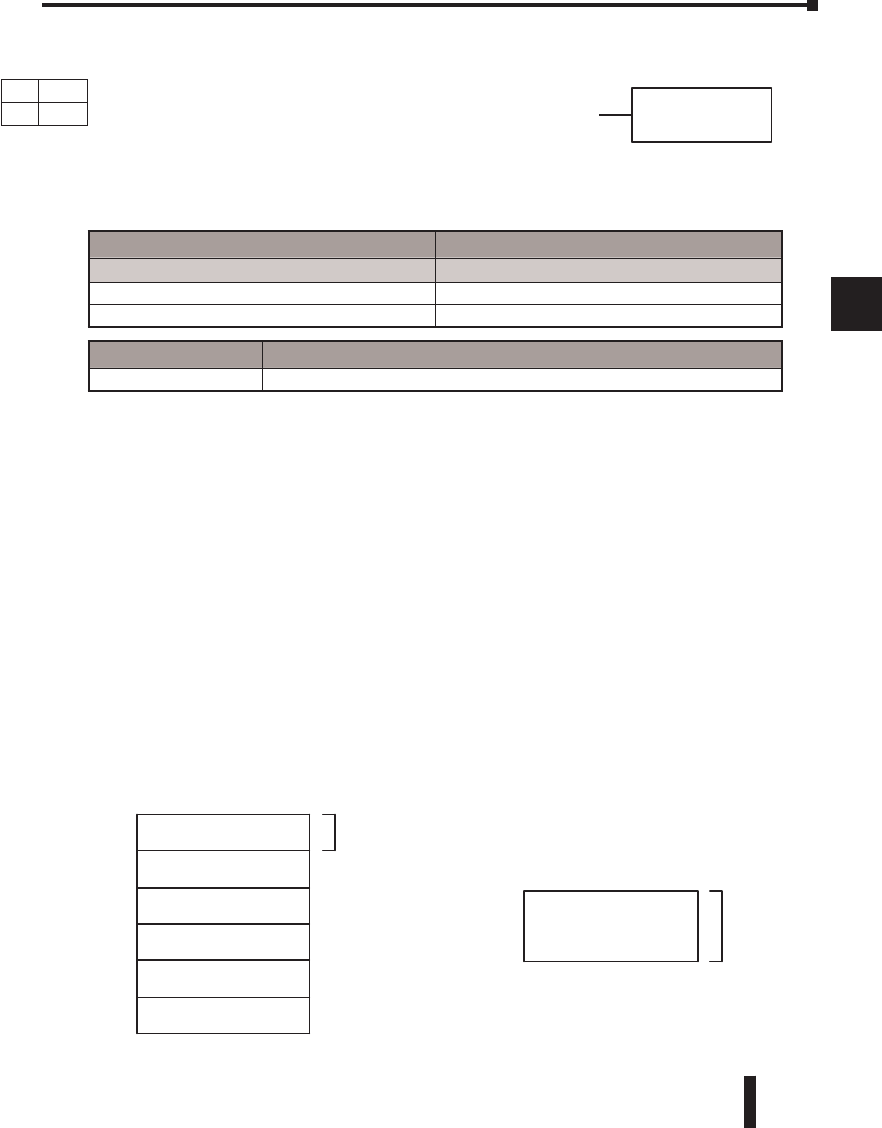
DL06 Micro PLC User Manual, 3rd Edition, Rev. D 5-169
1
2
3
4
5
6
7
8
9
10
11
12
13
14
A
B
C
D
The steps listed below are the steps necessary to program the Find Block function.
Step 1: Load the number of bytes in the block to be located. This parameter must be
a HEX value, 0 to FF.
Step 2: Load the length of a table (number of words) to be searched. The Find Block
will search multiple tables that are adjacent in V-memory. This parameter
must be a HEX value, 0 to FF.
Step 3: Load the ending location for all the tables into the accumulator. This
parameter must be a HEX value. You can use the LDA instruction to convert
an octal address to hex.
Step 4: Load the table starting location for all the tables into the accumulator. This
parameter must be a HEX value. You can use the LDA instruction to convert
an octal address to hex.
Step 5: Insert the Find Block instruction. This specifies the starting location of the
block of data you are trying to locate.
Chapter 5: Standard RLL Instructions - Table Instructions
1
2
3
4
5
6
7
8
9
10
11
12
13
14
a
B
c
d
FINDB
Aaaa
Table1
Table2
Table3
Tablen
Block
StartAddr.
EndAddr.
Number
of bytes
StartAddr.
Number
of words
Operand Data Type DL06 Range
Aaaa
V-memory V See memory map
V-memory P See memory map
Discrete Bit Flags Description
SP56 On when the specified block is not found.
DS Used
HPP N/A
Find Block (FINDB)
The Find Block instruction searches for an occurrence
of a specified block of values in a V-memory table. The
function parameters are loaded into the first and second
levels of the accumulator stack and the accumulator by
three additional instructions. If the block is found, its
starting address will be stored in the accumulator. If the
block is not found, flag SP53 will be set.
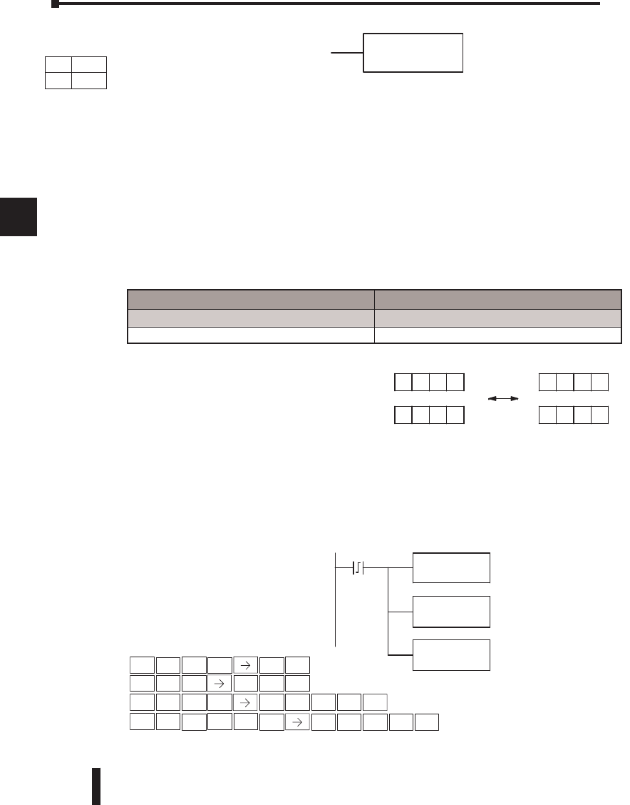
DL06 Micro PLC User Manual, 3rd Edition, Rev. D
5-170
1
2
3
4
5
6
7
8
9
10
11
12
13
14
A
B
C
D
Swap (SWAP)
The Swap instruction exchanges the
data in two tables of equal length.
Step 1: Load the length of the tables (number of V-memory locations) into the first level of
the accumulator stack. This parameter must be a HEX value, 0 to FF. Remember that
the tables must be of equal length.
Step 2: Load the starting V-memory location for the first table into the accumulator. This
parameter must be a HEX value. You can use the LDA instruction to convert an octal
address to hex.
Step 3: Insert the Swap instruction. This specifies the starting address of the second table.
This parameter must be a HEX value. You can use the LDA instruction to convert an
octal address to hex.
Helpful hint: — The data swap occurs within a single scan. If the instruction executes on
multiple consecutive scans, it will be difficult to know the actual contents of either table at
any particular time. So, remember to swap just on a single scan.
The example to the right shows a table of two
words at V3000. We will swap its contents with
another table of two words at 3100 by using the
Swap instruction. The required ladder program is
given below.
The example program below uses a PD contact (triggers for one scan for off-to-on transition).
First, we load the length of the tables (two words) into the accumulator. Then we load the
address of the first table (V3000) into the accumulator using the LDA instruction, converting
the octal address to hex. Note that it does not matter which table we declare “first”, because
the swap results will be the same.
Chapter 5: Standard RLL Instructions - Table Instructions
1
2
3
4
5
6
7
8
9
10
11
12
13
14
a
B
c
d
Aaaa
SWAP
1 2 3 4
5 6 7 8
A B C D
0 0 00
V3000 V3100
SWAP
Operand Data Type DL06 Range
aaa
V-memory V See memory map
Handheld Programmer Keystrokes
STR
$
SHFT ANDST
L
3
D
SHFT RST
S
ANDN
W
0
A
PREV
CV
PENT
2
C
0
A
0
A
ENT
SHFT ANDST
L
3
D
3
D
0
A
0
AENT
SHFT CV
P
SHFT 3
D
0
A
0
A
3
D
1
B
0
AENT
DS Used
HPP Used
DirectSOFT 32
X0 LD
K2
LDA
0 3000
SWAP
0 3100
Load the constant value 2
(Hex.) into the lower 16 bits
of the accumulator.
Convert octal 3000 to HE
X
and load the value into the
accumulator. This is the
table beginning.
Swap the contents of the
table in the previous
instruction with the one
at V3100.
DirectSOFT
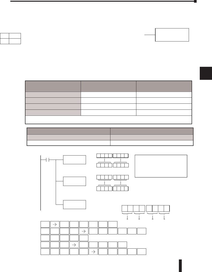
DL06 Micro PLC User Manual, 3rd Edition, Rev. D 5-171
1
2
3
4
5
6
7
8
9
10
11
12
13
14
A
B
C
D
Clock/Calendar Instructions
Date (DATE)
The Date instruction can be used to set the date in the CPU. The
instruction requires two consecutive V-memory locations (Vaaa)
to set the date. If the values in the specified locations are not
valid, the date will not be set. The current date can be read from
4 consecutive V-memory locations (V7771–V7774).
In the following example, when C0 is on, the constant value (K94010301) is loaded into the
accumulator using the Load Double instruction (C0 should be a contact from a one-shot
(PD) instruction). The value in the accumulator is output to V2000 using the Out Double
instruction. The Date instruction uses the value in V2000 to set the date in the CPU.
Chapter 5: Standard RLL Instructions - Clock/Calendar Instructions
1
2
3
4
5
6
7
8
9
10
11
12
13
14
a
B
c
d
Vaaa
DATE
V2000
Acc.
0301
0301
94010301
9401
V2001
9401
Acc. 94010301
03019401
V2001 V2000
DirectSOFT 32
C0 LDD
K94010301
OUTD
V2000
DATE
V2000
Constant (K)
In this example, the Date
instruction uses the value set in
V2000 and V2001 to set the date
in the appropriate V memory
locations (V7771-V7774).
Format
Year Month Day Day of Week
Handheld Programmer Keystrokes
0
AENT
1
B
4
E
0
A
0
A
ENT
STR
$
SHFT ANDST
L
3
D
SHFT
MLR
T
3
D
OUT
GX SHFT 3
D
NEXT NEXT NEXT NEXT
2
CENT
PREV
0
A
9
0
A
3
D
1
B
0
AENT
0
A
3
D
0
A
4
E
0
A
2
CENT
0
A
0
A
Load the constant
value (K94010301)
into the accumulator
Copy the value in
the accumulator to
V2000 and V2001
Set the date in the CPU
using the value in V2000
and 2001
Date Range V-memory Location (BCD)
(READ Only)
Year 0-99 V7774
Month 1-12 V7773
Day 1-31 V7772
Day of Week 0-06 V7771
The values entered for the day of week are:
0=Sunday, 1=Monday, 2=Tuesday, 3=Wednesday, 4=Thursday, 5=Friday, 6=Saturday
Operand Data Type DL06 Range
aaa
V-memory V See memory map
DS Used
HPP Used
DirectSOFT
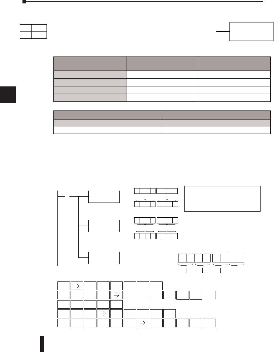
DL06 Micro PLC User Manual, 3rd Edition, Rev. D
5-172
1
2
3
4
5
6
7
8
9
10
11
12
13
14
A
B
C
D
Time (TIME)
The Time instruction can be used to set the time (24 hour clock)
in the CPU. The instruction requires two consecutive V-memory
locations (Vaaa) which are used to set the time. If the values in the
specified locations are not valid, the time will not be set. The current
time can be read from memory locations V7747 and V7766–V7770.
In the following example, when C0 is on, the constant value (K73000) is loaded into the
accumulator using the Load Double instruction (C0 should be a contact from a one-shot
(PD) instruction). The value in the accumulator is output to V2000 using the Out Double
instruction. The Time instruction uses the value in V2000 to set the time in the CPU.
Chapter 5: Standard RLL Instructions - Clock/Calendar Instructions
1
2
3
4
5
6
7
8
9
10
11
12
13
14
a
B
c
d
Vaaa
TIME
V2000
Acc.
3000
3000
0007 3000
0007
V2001
0007
Acc. 0007 3000
30000007
V2001 V2000
DirectSOFT 32
C0 LDD
K73000
OUTD
V2000
TIME
V2000
Constant (K)
Format
Not
Used
Hour Minutes Seconds
The TIME instruction uses the
value set in V2000 and V2001 to
set the time in the appropriate
V-memory locations (V7766-V7770)
Handheld Programmer Keystrokes
0
AENT
7
H
0
A
0
A
ENT
STR
$
SHFT ANDST
L
3
D
SHFT MLR
T
3
D
OUT
GX SHFT 3
D
NEXT NEXT NEXT NEXT
2
CENT
PREV
0
A
3
D
0
A
3
D
1
B
0
AENT
0
A
ORST
M
8
I
4
E
0
A
2
CENT
0
A
0
A
0
A
0
A
SHFT
Date Range VMemory Location (BCD)
(READ Only)
1/100 seconds (10ms) 0-99 V7747
Seconds 0-59 V7766
Minutes 0-59 V7767
Hour 0-23 V7770
Operand Data Type DL06 Range
aaa
V-memory V See memory map
DS Used
HPP Used
DirectSOFT
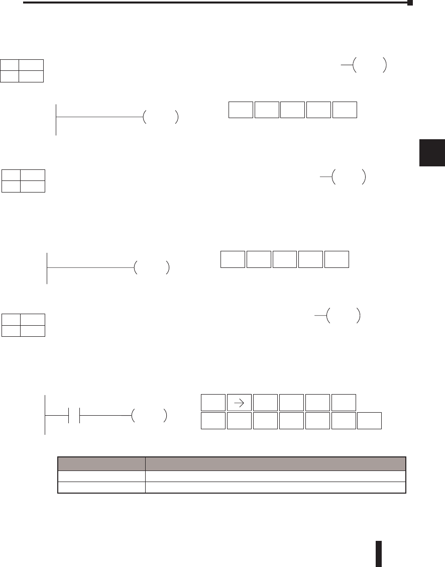
DL06 Micro PLC User Manual, 3rd Edition, Rev. D 5-173
1
2
3
4
5
6
7
8
9
10
11
12
13
14
A
B
C
D
CPU Control Instructions
No Operation (NOP)
The No Operation is an empty (not programmed) memory location.
End (END)
The End instruction marks the termination point of the normal
program scan. An End instruction is required at the end of the main
program body. If the End instruction is omitted, an error will occur
and the CPU will not enter the Run Mode. Data labels, subroutines and interrupt routines
are placed after the End instruction. The End instruction is not conditional; therefore, no
input contact is allowed.
Stop (STOP)
The Stop instruction changes the operational mode of the CPU
from Run to Program (Stop) mode. This instruction is typically
used to stop PLC operation in an error condition.
In the following example, when C0 turns on, the CPU will stop operation and switch to the
program mode.
Chapter 5: Standard RLL Instructions - CPU Control Instructions
1
2
3
4
5
6
7
8
9
10
11
12
13
14
a
B
c
d
NOP
END
Direct SOFT32 Handheld Programmer Keystrokes
END
SHFT 4
E
TMR
N
3
DENT
STOP
DirectSOFT32 Handheld Programmer Keystrokes
STOP
C0 STR
$SHFT ENT
2
C
0
A
SHFT RST
S
MLR
T
INST#
O
CV
PENTSHFT
Discrete Bit Flags Description
SP16 On when the DL06 goes into the TERM_PRG mode.
SP53 On when the DL06 goes into the PRG mode.
Direct SOFT32 Handheld Programmer Keystrokes
NOP
SHFT TMR
N
INST#
O
CV
PENT
DS Used
HPP Used
DS Used
HPP Used
DS Used
HPP Used
DirectSOFT
DirectSOFT
DirectSOFT
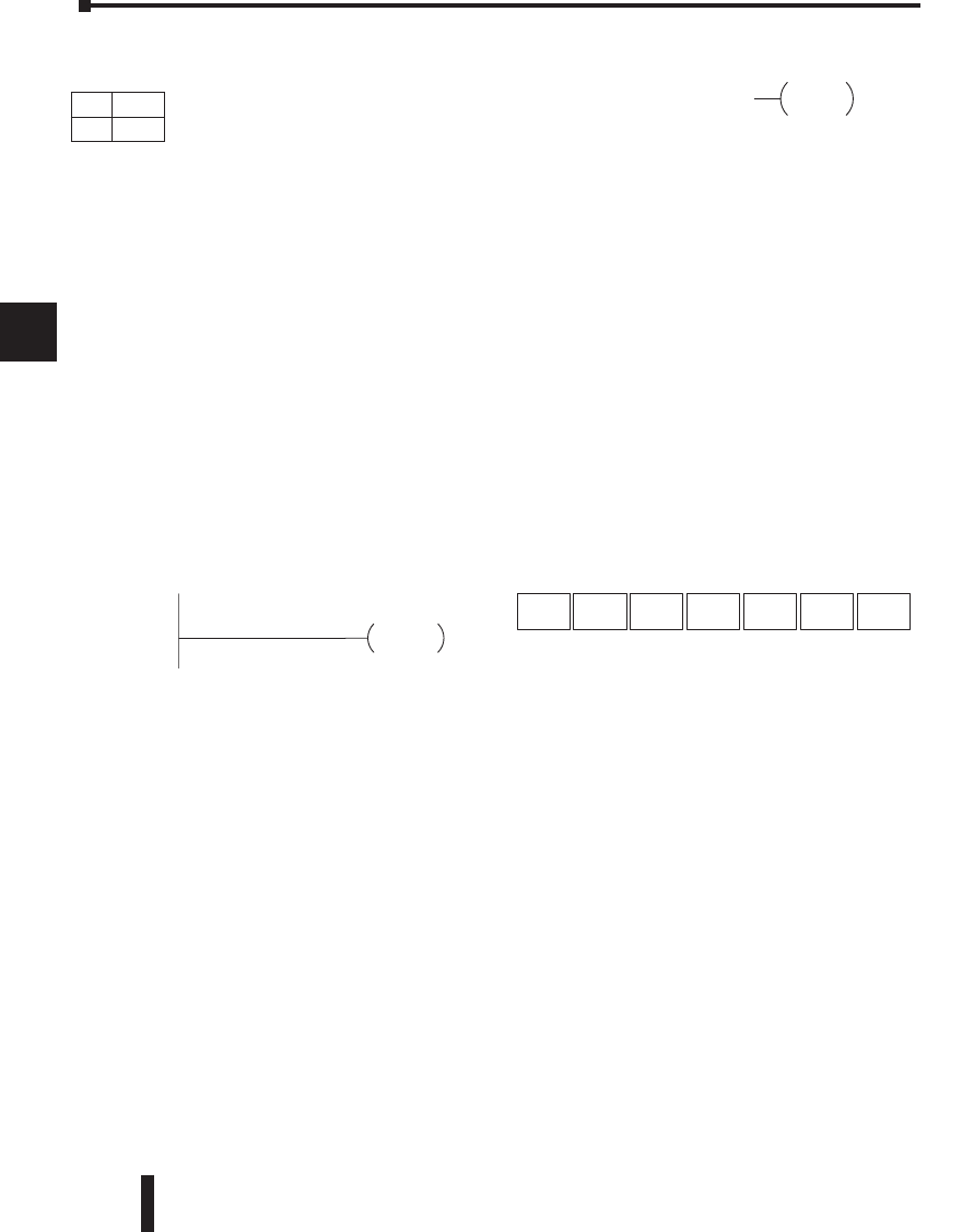
DL06 Micro PLC User Manual, 3rd Edition, Rev. D
5-174
1
2
3
4
5
6
7
8
9
10
11
12
13
14
A
B
C
D
A software timeout error (E003) will occur and the CPU will enter the program mode if the
scan time exceeds the watch dog timer setting. Placement of the RSTWT instruction in the
program is very important. The instruction has to be executed before the scan time exceeds
the watch dog timer’s setting.
If the scan time is consistently longer than the watch dog timer’s setting, the timeout value
may be permanently increased from the default value of 200ms by AUX 55 on the HPP or
the appropriate auxiliary function in your programming package. This eliminates the need for
the RSTWT instruction.
In the following example, the CPU scan timer will be reset to 0 when the RSTWT
instruction is executed. See the For/Next instruction for a detailed example.
Chapter 5: Standard RLL Instructions - CPU Control Instructions
1
2
3
4
5
6
7
8
9
10
11
12
13
14
a
B
c
d
RSTWT
Direct SOFT 32 Handheld Programmer Keystrokes
RSTWT
SHFT ORN
R
RST
S
MLR
T
ANDN
W
MLR
TENT
DS Used
HPP Used
DirectSOFT
Reset Watch Dog Timer (RSTWT)
The Reset Watch Dog Timer instruction resets the CPU scan
timer. The default setting for the watch dog timer is 200ms.
Scan times very seldom exceed 200ms, but it is possible.
For/next loops, subroutines, interrupt routines, and table
instructions can be programmed such that the scan becomes
longer than 200ms. When instructions are used in a manner
that could exceed the watch dog timer setting, this instruction
can be used to reset the timer.
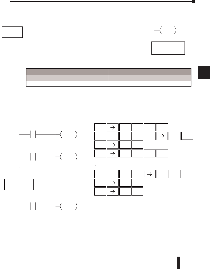
DL06 Micro PLC User Manual, 3rd Edition, Rev. D 5-175
1
2
3
4
5
6
7
8
9
10
11
12
13
14
A
B
C
D
Program Control Instructions
In the following example, when C7 is on, all the program logic between the GOTO and
the corresponding LBL instruction (designated with the same constant Kaaa value) will be
skipped. The instructions being skipped will not be executed by the CPU.
Chapter 5: Standard RLL Instructions - Program Control Instructions
1
2
3
4
5
6
7
8
9
10
11
12
13
14
a
B
c
d
K aaa
GOTO
KaaaLBLKaaaLBL
DirectSOFT32 Handheld ProgrammerKeys trokes
LBLK
5
C7 K5
GOTO
X1 C2
OUT
X5Y2
OUT
STR
$SHFT 2
CENT
7
H
SHFT 6
G
INS T#
O
MLR
T
INS T#
O
5
F
STR
$
OUT
GX SHF T 2
C
2
CENT
SHFTANDS T
L
1
B
ANDS T
L
5
FENT
STR
$
OUT
GX
1
BENT
ENT
5
F
2
CENT
ENT
Operand Data Type DL06 Range
aaa
Constant K 1-FFFF
DS Used
HPP Used
DirectSOFT
Goto Label (GOTO) (LBL)
The Goto / Label skips all instructions between the Goto and
the corresponding LBL instruction. The operand value for the
Goto and the corresponding LBL instruction are the same. The
logic between Goto and LBL instruction is not executed when
the Goto instruction is enabled. Up to 256 Goto instructions
and 256 LBL instructions can be used in the program.
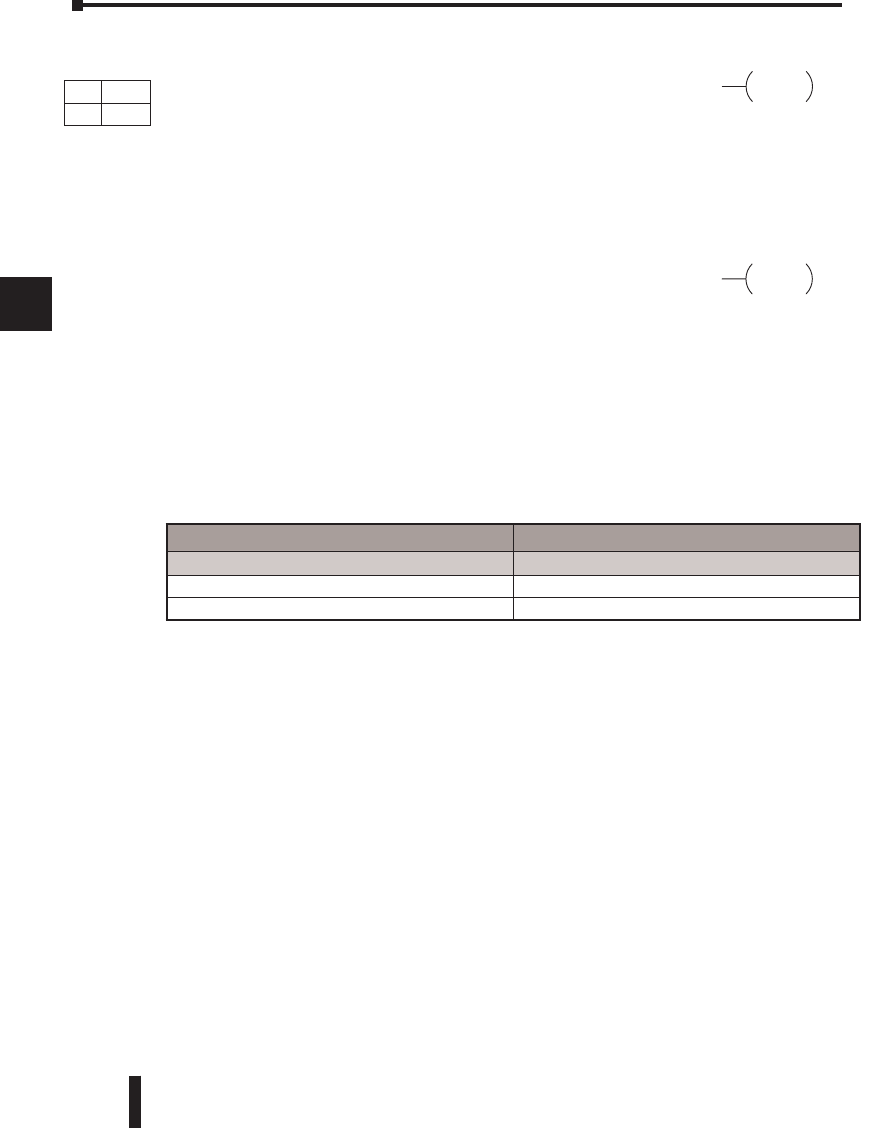
DL06 Micro PLC User Manual, 3rd Edition, Rev. D
5-176
1
2
3
4
5
6
7
8
9
10
11
12
13
14
A
B
C
D
Chapter 5: Standard RLL Instructions - Program Control Instructions
1
2
3
4
5
6
7
8
9
10
11
12
13
14
a
B
c
d
A aaa
FOR
NEXT
Operand Data Type DL06 Range
aaa
V-memory V See memory map
Constant K 1-9999
DS Used
HPP Used
For / Next (FOR) (NEXT)
The For and Next instructions are used to execute a section of
ladder logic between the For and Next instruction a specified
numbers of times. When the For instruction is enabled, the
program will loop the specified number of times. If the For
instruction is not energized, the section of ladder logic between
the For and Next instructions is not executed.
For / Next instructions cannot be nested. The normal I/O
update and CPU housekeeping are suspended while executing
the For / Next loop. The program scan can increase significantly,
depending on the amount of times the logic between the For and
Next instruction is executed. With the exception of immediate
I/O instructions, I/O will not be updated until the program
execution is completed for that scan. Depending on the length
of time required to complete the program execution, it may be
necessary to reset the watch dog timer inside of the For / Next
loop using the RSTWT instruction.
DL06 Micro PLC User Manual, 3rd Edition, Rev. D 5-177
1
2
3
4
5
6
7
8
9
10
11
12
13
14
A
B
C
D
In the following example, when X1 is on, the application program inside the For / Next loop
will be executed three times. If X1 is off, the program inside the loop will not be executed.
The immediate instructions may or may not be necessary, depending on your application.
Also, The RSTWT instruction is not necessary if the For / Next loop does not extend the
scan time beyond the Watch Dog Timer setting. For more information on the Watch Dog
Timer, refer to the RSTWT instruction.
Chapter 5: Standard RLL Instructions - Program Control Instructions
1
2
3
4
5
6
7
8
9
10
11
12
13
14
a
B
c
d
X1
Direct SOFT32
Handheld Programmer Keystrokes
K3
FOR
RSTWT
X20 Y5
OUT
NEXT
12
3
STR
$
SHFT 5
F
INST#
O
ORN
R
SHFT ORN
R
RST
S
MLR
T
ANDN
W
MLR
TENT
STR
$SHFT 8
I
2
C
0
AENT
OUT
GX
SHFT TMR
N
4
E
SET
X
MLR
TENT
1
BENT
3
DENT
5
FENT
DirectSOFT
DL06 Micro PLC User Manual, 3rd Edition, Rev. D
5-178
1
2
3
4
5
6
7
8
9
10
11
12
13
14
A
B
C
D
By placing code in a subroutine it is only scanned and executed when needed, since it resides
after the End instruction. Code which is not scanned does not impact the overall scan time of
the program.
Subroutine Return (RT)
Chapter 5: Standard RLL Instructions - Program Control Instructions
1
2
3
4
5
6
7
8
9
10
11
12
13
14
a
B
c
d
K aaa
GTS
K aaa
SBR
RT
RTC
Operand Data Type DL06 Range
aaa
Constant K 1-FFFF
DS Used
HPP Used
DS Used
HPP Used
DS Used
HPP Used
Goto Subroutine (GTS) (SBR)
The Goto Subroutine instruction allows a section of ladder logic
to be placed outside the main body of the program, to execute
only when needed. There can be a maximum of 256 GTS
instructions and 256 SBR instructions used in a program. The
GTS instructions can be nested up to 8 levels. An error E412
will occur if the maximum limits are exceeded. Typically this will
be used in an application where a block of program logic may be
slow to execute and is not required to execute every scan. The
subroutine label and all associated logic is placed after the End
statement in the program. When the subroutine is called from
the main program, the CPU will execute the subroutine (SBR)
with the same constant number (K) as the GTS instruction
which called the subroutine.
When a Subroutine Return is executed in the subroutine
the CPU will return to the point in the main body of the
program from which it was called. The Subroutine Return
is used as termination of the subroutine. It must be the
last instruction in the subroutine and is a stand alone
instruction (no input contact on the rung).
Subroutine Return Conditional (RTC)
The Subroutine Return Conditional instruction is
an optional instruction used with an input contact to
implement a conditional return from the subroutine. The
Subroutine Return (RT) is still required for termination of
the Subroutine.
DL06 Micro PLC User Manual, 3rd Edition, Rev. D 5-179
1
2
3
4
5
6
7
8
9
10
11
12
13
14
A
B
C
D
In the following example, when X1 is on, Subroutine K3 will be called. The CPU will jump
to the Subroutine Label K3 and the ladder logic in the subroutine will be executed. If X35 is
on, the CPU will return to the main program at the RTC instruction. If X35 is not on, Y0–
Y17 will be reset to off and the CPU will return to the main body of the program.
Chapter 5: Standard RLL Instructions - Program Control Instructions
1
2
3
4
5
6
7
8
9
10
11
12
13
14
a
B
c
d
Direct SOFT32 Display
Handheld Programmer Keystrokes
SBR K3
X1 K3
GTS
END
Y5
OUTI
X20
Y10
OUTI
X21
X35
RT C
X35
RSTI
Y0 Y17
RT
K10
LD
C0
STR
$
SHFT 6
G
MLR
T
RST
S
SHFT RST
S
1
B
ORN
R
STR
$SHFT 8
I
2
C
0
AENT
OUT
GX
STR
$
SHFT 8
I
3
DENT
5
F
OUT
GX
SHFT ORN
R
MLR
TENT
SHFT 4
E
TMR
N
3
DENT
1
BENT
3
DENT
3
DENT
5
FENT
ENT
1
B
0
A
SHFT
SHFT 8
I
SHFT 8
I
2
C
STR
$SHFT 8
I
2
CENT
1
B
STRN
SP
RST
SSHFT 8
I
0
A
1
B
7
HENT
SHFT 8
I
3
DENT
5
F
SHFT ORN
R
MLR
TENT
DirectSOFT
DL06 Micro PLC User Manual, 3rd Edition, Rev. D
5-180
1
2
3
4
5
6
7
8
9
10
11
12
13
14
A
B
C
D
In the following example, when X1 is on, Subroutine K3 will be called. The CPU will jump
to the Subroutine Label K3 and the ladder logic in the subroutine will be executed. The CPU
will return to the main body of the program after the RT instruction is executed.
Chapter 5: Standard RLL Instructions - Program Control Instructions
1
2
3
4
5
6
7
8
9
10
11
12
13
14
a
B
c
d
Direct SOFT32
Handheld Programmer Keystrokes
SBR K3
X1 K3
GTS
END
Y5
OUT
X20
Y10
OUT
X21
RT
STR
$
SHFT 6
G
MLR
T
RST
S
SHFT RST
S
1
B
ORN
R
STR
$SHFT 8
I
2
C
0
AENT
OUT
GX
STR
$SHFT 8
I
2
CENT
1
B
OUT
GX
SHFT ORN
R
MLR
TENT
SHFT 4
E
TMR
N
3
DENT
1
BENT
3
DENT
3
DENT
5
FENT
ENT
1
B
0
A
SHFT
DirectSOFT
DL06 Micro PLC User Manual, 3rd Edition, Rev. D 5-181
1
2
3
4
5
6
7
8
9
10
11
12
13
14
A
B
C
D
Master Line Set (MLS)
The Master Line Set instruction allows the program to control
sections of ladder logic by forming a new power rail controlled
by the main left power rail. The main left rail is always master
line 0. When an MLS K1 instruction is used, a new power rail is created at level
1. Master Line Sets and Master Line Resets can be used to nest power rails up to seven levels
deep.
Master Line Reset (MLR)
The Master Line Reset instruction marks the end of control
for the corresponding MLS instruction. The MLR reference is
one less than the corresponding MLS.
Understanding Master Control Relays
The Master Line Set (MLS) and Master Line Reset (MLR) instructions allow you to quickly
enable (or disable) sections of the RLL program. This provides program control flexibility.
The following example shows how the MLS and MLR instructions operate by creating a sub
power rail for control logic.
Chapter 5: Standard RLL Instructions - Program Control Instructions
1
2
3
4
5
6
7
8
9
10
11
12
13
14
a
B
c
d
K aaa
MLS
K aaa
MLR
X0
X1
X2
OUT
Y7
X3
MLS
X10
K1
K2
K0
K1
MLS
OUT
MLR
MLR
OUT
Y10
Y11
Direct SOFT32
When contact X0 is ON, logic under the first MLS
will be executed.
When contact X0 and X2 are ON, logic under the
second MLS will be executed.
The MLR instructions note the end of the Master
Control area.
Operand Data Type DL06 Range
aaa
Constant K 1-FFFF
Operand Data Type DL06 Range
aaa
Constant K 1-FFFF
DS Used
HPP Used
DS Used
HPP Used
DirectSOFT
DL06 Micro PLC User Manual, 3rd Edition, Rev. D
5-182
1
2
3
4
5
6
7
8
9
10
11
12
13
14
A
B
C
D
MLS/MLR Example
In the following MLS/MLR example logic between the first MLS K1 (A) and MLR K0 (B)
will function only if input X0 is on. The logic between the MLS K2 (C) and MLR K1 (D)
will function only if input X10 and X0 is on. The last rung is not controlled by either of the
MLS coils.
Chapter 5: Standard RLL Instructions - Program Control Instructions
1
2
3
4
5
6
7
8
9
10
11
12
13
14
a
B
c
d
K1
MLS
X0
C0
OUT
X1
C1
OUT
X2
Y0
OUT
X3
K2
MLS
X10
Y1
OUT
X5
Y2
OUT
X4
K1
MLR
C2
OUT
X5
Y3
OUT
X6
K0
MLR
Y4
OUT
X7
DirectSOFT32
Handheld Programmer Keystrokes
STR
$ENT
0
A
MLS
Y
1
BENT
STR
$
1
BENT
OUT
GX SHFT ENT
2
C
0
A
STR
$ENT
2
C
OUT
GX SHFT ENT
2
C
1
B
STR
$ENT
3
D
OUT
GX ENT
0
A
STR
$ENT
0
A
1
B
MLS
YENT
2
C
STR
$ENT
5
F
OUT
GX ENT
1
B
STR
$ENT
OUT
GX ENT
4
E
2
C
MLR
T
1
BENT
STR
$ENT
5
F
OUT
GX SHFT ENT
2
C
2
C
STR
$ENT
OUT
GX ENT
6
G
3
D
MLR
TENT
0
A
STR
$ENT
OUT
GX
4
E
7
H
ENT
2
C
A
C
D
B
DirectSOFT
DL06 Micro PLC User Manual, 3rd Edition, Rev. D 5-183
1
2
3
4
5
6
7
8
9
10
11
12
13
14
A
B
C
D
Interrupt Instructions
Interrupt (INT)
Typically, interrupts are used in an application when a fast response to an input is needed or
a program section must execute faster than the normal CPU scan. The interrupt label and all
associated logic must be placed after the End statement in the program. When an interrupt
occurs, the CPU will complete execution of the current instruction it is processing in ladder
logic, then execute the interrupt routine. After interrupt routine execution, the ladder
program resumes from the point at which it was interrupted.
See Chapter 3, the section on Mode 40 (Interrupt) Operation for more details on interrupt
configuration. In the DL06, only one software interrupt is available. The software interrupt
uses interrupt #00 (INT 0), which means the hardware interrupt #0 and the software
interrupt cannot be used together. Hardware interrupts are labeled in octal to correspond
with the hardware input signal (e.g. X1 will initiate INT 1).
Interrupt Return (IRT)
An Interrupt Return is normally executed as the last instruction
in the interrupt routine. It returns the CPU to the point in the
main program from which it was called. The Interrupt Return is
a stand-alone instruction (no input contact on the rung).
Interrupt Return Conditional (IRTC)
The Interrupt Return Conditional instruction is a optional
instruction used with an input contact to implement a
conditional return from the interrupt routine. The Interrupt
Return is required to terminate the interrupt routine.
Enable Interrupts (ENI)
The Enable Interrupt instruction is placed in the main ladder
program (before the End instruction), enabling the interrupt.
The interrupt remains enabled until the program executes a
Disable Interrupt instruction.
Chapter 5: Standard RLL Instructions - Interrupt Instructions
1
2
3
4
5
6
7
8
9
10
11
12
13
14
a
B
c
d
O aaa
INT
IRT
IRTC
ENI
Operand Data Type DL06 Range
aaa
Constant O 1-FFFF
DS Used
HPP Used
DS Used
HPP Used
DS Used
HPP Used
DS Used
HPP Used
The Interrupt instruction allows a section of ladder logic to be
placed below the main body of the program and executed only
when needed. High-Speed I/O Modes 10, 20, and 40 can generate
an interrupt. With Mode 40, you may select an external interrupt
(input X0), or a time-based interrupt (3–999 ms).
DL06 Micro PLC User Manual, 3rd Edition, Rev. D
5-184
1
2
3
4
5
6
7
8
9
10
11
12
13
14
A
B
C
D
Disable Interrupts (DISI)
A Disable Interrupt instruction in the main body of the application
program (before the End instruction) will disable the interrupt (either
external or timed). The interrupt remains disabled until the program
executes an Enable Interrupt instruction.
External Interrupt Program Example
In the following example, we do some initialization on the first scan, using the first-scan
contact SP0. The interrupt feature is the HSIO Mode 40. Then, we configure X0 as the
external interrupt by writing to its configuration register, V7634. See Appendix E, Mode 40
Operation for more details.
During program execution, when X2 is on, the interrupt is enabled. When X2 is off, the
interrupt will be disabled. When an interrupt signal (X0) occurs, the CPU will jump to
the interrupt label INT O 0. The application ladder logic in the interrupt routine will be
performed. The CPU will return to the main body of the program after the IRT instruction
is executed.
Chapter 5: Standard RLL Instructions - Interrupt Instructions
1
2
3
4
5
6
7
8
9
10
11
12
13
14
a
B
c
d
DISI
DirectSOFT
O 0
X2
ENI
DISI
X2
END
Y5
SETI
X1
Y7
SETI
X3
IRT
Handheld Programmer Keystrokes
8
I
ORN
R
MLR
T
STR
$SHFT 8
I
1
BENT
SHFT 8
I
5
FENT
STR
$SHFT 8
I
3
DENT
SHFT 8
IENT
7
H
SHFT 4
E
TMR
N
3
DENT
STR
$ENT
2
C
SHFT 4
E
TMR
N
8
IENT
STRN
SP ENT
2
C
SHFT 8
I
TMR
N
MLR
T
0
AENT
SHFT ENT
SHFT ENT
3
D
8
I
RST
S
8
I
SET
X
SET
X
LD
K40
SP0 Load the constant value
(K40) into the lower 16 bits
of the accumulator
OUT
V7633
Copy the value in the lower
16 bits of the accumulator to
V7633
LD
K4
Load the constant value (K4)
into the lower 16 bits of the
accumulator
OUT
V7634
Copy the value in the lower
16 bits of the accumulator to
V7634
STR
$
SHFT ANDST
L
3
DSHFT
OUT
GX SHFT AND
VENT
JMP
KENT
7
H
6
G
3
D
4
E
SHFT ANDST
L
3
DSHFT 0
A
OUT
GX SHFT AND
VENT
JMP
K
4
EENT
7
H
6
G
3
D
3
D
4
E
SHFT ENT
STRN
SP
0
A
INT
DS Used
HPP Used
DL06 Micro PLC User Manual, 3rd Edition, Rev. D 5-185
1
2
3
4
5
6
7
8
9
10
11
12
13
14
A
B
C
D
Timed Interrupt Program Example
In the following example, we do some initialization on the first scan, using the first-scan
contact SP0. The interrupt feature is the HSIO Mode 40. Then we configure the HSIO
timer as a 10 mS interrupt by writing K104 to the configuration register for X0 (V7634). See
Appendix E, Mode 40 Operation for more details.
When X4 turns on, the interrupt will be enabled. When X4 turns off, the interrupt will be
disabled. Every 10 mS the CPU will jump to the interrupt label INT O 0. The application
ladder logic in the interrupt routine will be performed. If X3 is not on, Y0–Y7 will be reset to
off and then the CPU will return to the main body of the program.
Chapter 5: Standard RLL Instructions - Interrupt Instructions
1
2
3
4
5
6
7
8
9
10
11
12
13
14
a
B
c
d
Direct SOFT32
INT O0
X4
ENI
DISI
X4
END
Y5
SETI
X2
X3
RSTI
Y0 Y7
IRT
Handheld Programmer Keystrokes
LD
K40
SP0 Load the constant value
(K40) into the lower 16 bits
of the accumulator
OUT
V7633
Copy the value in the lower
16 bits of the accumulator to
V7633
STR
$
SHFT ANDST
L
3
DSHFT 0
A
OUT
GX SHFT AND
VENT
JMP
K
1
BENT
7
H
6
G
3
D
4
E
STR
$
SHFT 4
E
TMR
N
8
IENT
STRN
SP
SHFT ENT
3
D
8
I
RST
S
8
I
8
I
ORN
R
MLR
T
STR
$SHFT 8
I
2
CENT
SHFT 8
I
5
FENT
SHFT 8
IENT
SHFT 8
IENT
0
A
SHFT 4
E
TMR
N
3
DENT
SHFT 8
I
TMR
N
MLR
TENT
SHFT ENT
0
A
1
BENT
ENT
ENT
4
E
4
E
7
H
3
D
SET
X
SET
X
STRN
SP
LD
K104
Load the constant value
(K10) into the lower 16 bits
of the accumulator
OUT
V7634
Copy the value in the lower
16 bits of the accumulator to
V7634
SHFT ANDST
L
3
DSHFT 0
A
OUT
GX SHFT AND
VENT
JMP
K
4
EENT
7
H
6
G
3
D
3
D
4
E
DirectSOFT
DL06 Micro PLC User Manual, 3rd Edition, Rev. D
5-186
1
2
3
4
5
6
7
8
9
10
11
12
13
14
A
B
C
D
Message Instructions
Fault (FAULT)
The Fault instruction is used to display a message on the handheld
programmer, the optional LCD display or in the DirectSOFT
status bar. The message has a maximum of 23 characters and can
be either V-memory data, numerical constant data or ASCII text.
To display the value in a V-memory location, specify the V-memory location in the
instruction. To display the data in ACON (ASCII constant) or NCON (Numerical constant)
instructions, specify the constant (K) value for the corresponding data label area.
See Appendix G for the ASCII conversion table.
Fault Example
In the following example when X1 is on, the message SW 146 will display on the handheld
programmer. The NCONs use the HEX ASCII equivalent of the text to be displayed. (The
HEX ASCII for a blank is 20, a 1 is 31, 4 is 34 ...)
Chapter 5: Standard RLL Instructions - Message Instructions
1
2
3
4
5
6
7
8
9
10
11
12
13
14
a
B
c
d
FAULT
A aaa
Direct SOFT32
DLBL
K1
END
FAULT
K1
X1
ACON
A SW
NCON
K 2031
NCON
K 3436
Handheld Programmer Keystrokes
STR
$
SHFT 4
E
TMR
N
3
DENT
SHFT 3
D
ANDST
L
1
B
ANDST
L
1
BENT
SHFT 0
A
2
C
INST#
O
TMR
N
SHFT TMR
N
2
C
INST#
O
TMR
N
SHFT TMR
N
2
C
INST#
O
TMR
N
1
BENT
ENT
ENT
3
D
3
D
4
E
6
G
ENT
3
D
2
C
0
A
1
B
RST
S
ANDN
W
SHFT ISG
U
MLR
T
ANDST
L
5
F
0
A
1
BENT
FAULT :
*SW 146
Operand Data Type DL06 Range
aaa
V-memory V See memory map
Constant K 1-FFFF
Discrete Bit Flags Description
SP50 On when the FAULT instruction is executed
DS Used
HPP Used
DirectSOFT
DL06 Micro PLC User Manual, 3rd Edition, Rev. D 5-187
1
2
3
4
5
6
7
8
9
10
11
12
13
14
A
B
C
D
Chapter 5: Standard RLL Instructions - Message Instructions
1
2
3
4
5
6
7
8
9
10
11
12
13
14
a
B
c
d
Data Label (DLBL)
The Data Label instruction marks the beginning of
an ASCII/numeric data area. DLBLs are programmed
after the End statement. A maximum of 64 DLBL
instructions can be used in a program. Multiple NCONs and
ACONs can be used in a DLBL area.
Numerical Constant (NCON)
The Numerical Constant instruction is used with the
DLBL instruction to store the HEX ASCII equivalent
of numerical data for use with other instructions. Two
digits can be stored in an NCON instruction.
K aaa
DLBL
A aaa
ACON
K aaa
NCON
Operand Data Type DL06 Range
aaa
Constant K 1-FFFF
Operand Data Type DL06 Range
aaa
Constant K 1-FFFF
Operand Data Type DL06 Range
aaa
ASCII A 0-9 A-Z
DS Used
HPP Used
DS Used
HPP Used
DS Used
HPP Used
ASCII Constant (ACON)
The ASCII Constant instruction is used
with the DLBL instruction to store ASCII
text for use with other instructions. Two
ASCII characters can be stored in an ACON
instruction. If only one character is stored in a
ACON a leading space will be inserted.
DL06 Micro PLC User Manual, 3rd Edition, Rev. D
5-188
1
2
3
4
5
6
7
8
9
10
11
12
13
14
A
B
C
D
Data Label Example
In the following example, an ACON and two NCON instructions are used within a DLBL
instruction to build a text message. See the FAULT instruction for information on displaying
messages. The DV-1000 Manual also has information on displaying messages.
Chapter 5: Standard RLL Instructions - Message Instructions
1
2
3
4
5
6
7
8
9
10
11
12
13
14
a
B
c
d
Direct SOFT32
Handheld Programmer Keystrokes
DLBL
K1
END
ACON
A SW
NCON
K 2031
NCON
K 3436
SHFT 4
E
TMR
N
3
DENT
SHFT 3
D
ANDST
L
1
B
ANDST
L
1
BENT
SHFT 0
A
2
C
INST#
O
TMR
N
SHFT TMR
N
2
C
INST#
O
TMR
N
SHFT TMR
N
2
C
INST#
O
TMR
N
ENT
3
D
3
D
4
E
6
G
ENT
3
D
2
C
0
A
1
B
ENT
RST
S
ANDN
W
DirectSOFT
DL06 Micro PLC User Manual, 3rd Edition, Rev. D 5-189
1
2
3
4
5
6
7
8
9
10
11
12
13
14
A
B
C
D
Move Block Instruction (MOVBLK)
The Move Block instruction copies a specified number of words from
a Data Label Area of program memory (ACON, NCON) to the
specified V-memory location. Below are the steps for using the Move
Block function:
• Step 1: Load the number of words (octal) to be copied into the 1st level of the accumulator stack.
• Step 2: Load the source data label (LDLBL Kaaa) into the accumulator. This is where the data will
be copied from.
• Step 3: Insert the MOVBLK instruction that specifies the V-memory destination. This is where the
data will be copied to.
Copy Data From a Data Label Area to V-memory
In the example below, data is copied from a Data Label Area to V-memory. When X1 is
on, the octal value (O4) is copied to the first level of the accumulator stack using the Load
Address (LDA) instruction. This value specifies the number of words to be copied. Load
Label (LDLBL) instruction will load the source data address (K1) into the accumulator. This
is where the data will be copied from. The MOVBLK instruction specifies the destination
starting location and executes the copying of data from the Data Label Area to V-memory.
Chapter 5: Standard RLL Instructions - Message Instructions
1
2
3
4
5
6
7
8
9
10
11
12
13
14
a
B
c
d
V aaa
MOVBLK
DS Used
HPP Used
DirectSOFT
X1 LDA
O4
Load the value 4 into the
accumulator specifying the
number of words to be copied.
LDLBL
K1
Load the value 1 into the
accumulator specifying the
Data Label Area K1 as the
starting address of the data
to be copied.
MOVBLK
V2000
V2000 is the destination
starting address for the data
to be copied.
1234
4532
6151
8845
K
NCON
K
NCON
K
NCON
K
NCON
V2001
4532
V2002
6151
V2003
8845
V2004
XXXX
.
.
.
.
V2000
1234
Data label area
to be copied
DLBL
Handheld Programmer Keystrokes
STR
$
SHFT ANDST
L
3
D
JMP
K
ENT
SHFT ANDST
L
3
D
ANDST
L
1
B
ANDST
L
SHFT ORST
M
AND
V
INST#
O
1
BENT
ENT
1
B
2
C
0
A
0
A
0
AENT
4
E
K1
V1777
XXXX
0
A
1
B
ANDST
L
DL06 Micro PLC User Manual, 3rd Edition, Rev. D
5-190
1
2
3
4
5
6
7
8
9
10
11
12
13
14
A
B
C
D
Print Message (PRINT)
The Print Message instruction prints the embedded text
or text/data variable message (maximum 128 characters)
to the specified communications port (Port 2 on the
DL06 CPU), which must have the communications port
configured.
You may recall, from the CPU specifications in Chapter 3, that the DL06’s ports are capable
of several protocols. Port 1 cannot be configured for the non-sequence protocol. To configure
port 2 using the Handheld Programmer, use AUX 56 and follow the prompts, making the
same choices as indicated below on this page. To configure a port in DirectSOFT, choose the
PLC menu, then Setup, then Setup Secondary Comm Port.
• Port: From the port number list box at the top, choose Port 2.
• Protocol: Click the check box to the left of Non-sequence, and then you’ll see the dialog box
shown below.
• Baud Rate: Choose the baud rate that matches your printer.
• Stop Bits, Parity: Choose number of stop bits and parity setting to match your printer.
• Memory Address: Choose a V-memory address for DirectSOFT to use to store the port setup
information. You will need to reserve 66 continguous words in V-memory for this purpose.
Chapter 5: Standard RLL Instructions - Message Instructions
1
2
3
4
5
6
7
8
9
10
11
12
13
14
a
B
c
d
PRINT A aaa
“Hello, this is a PLC message”
Operand Data Type DL06 Range
aaa
Constant K 2
DS Used
HPP N/A
Before ending the setup, click the button indicated to send Port 2
configuration to the CPU, and click Close. See Chapter 3 for port
wiring information, in order to connect your printer to the DL06.
DL06 Micro PLC User Manual, 3rd Edition, Rev. D 5-191
1
2
3
4
5
6
7
8
9
10
11
12
13
14
A
B
C
D
Port 2 on the DL06 has standard RS232 levels, and should work with most printer serial
input connections.
Text element – this is used for printing character strings. The character strings are defined
as the character (more than 0) ranged by the double quotation marks. Two hex numbers
preceded by the dollar sign means an 8-bit ASCII character code. Also, two characters
preceded by the dollar sign is interpreted according to the following table:
The following examples show various syntax conventions and the length of the output to the
printer.
Example:
” ” Length 0 without character
”A” Length 1 with character A
” ” Length 1 with blank
” $” ” Length 1 with double quotation mark
” $ R $ L ” Length 2 with one CR and one LF
” $ 0 D $ 0 A ” Length 2 with one CR and one LF
” $ $ ” Length 1 with one $ mark
In printing an ordinary line of text, you will need to include double quotation marks before
and after the text string. Error code 499 will occur in the CPU when the print instruction
contains invalid text or no quotations. It is important to test your PRINT instruction data
during the application development.
The following example prints the message to port 2. We use a PD contact, which causes the
message instruction to be active for just one scan. Note the $N at the end of the message,
which produces a carriage return / line feed on the printer. This prepares the printer to print
the next line, starting from the left margin.
Chapter 5: Standard RLL Instructions - Message Instructions
1
2
3
4
5
6
7
8
9
10
11
12
13
14
a
B
c
d
# Character code Description
1 $$ Dollar sign ($)
2 $” Double quotation (”)
3 $L or $l Line feed (LF)
4 $N or $n Carriage return line feed (CRLF)
5 $P or $p Form feed
6 $R or $r Carriage return (CR)
7 $T or $t Tab
X1 Print the message to Port 2 when
X1 makes an off-to-on transition.
PRINT K2
“Hello, this is a PLC message.$N”
DL06 Micro PLC User Manual, 3rd Edition, Rev. D
5-192
1
2
3
4
5
6
7
8
9
10
11
12
13
14
A
B
C
D
V-memory element - this is used for printing V-memory contents in the integer format or
real format. Use V-memory number or V-memory number with “:” and data type. The data
types are shown in the table below. The Character code must be capital letters.
NOTE: There must be a space entered before and after the V-memory address to separate it from the
text string. Failure to do this will result in an error code 499.
Example:
V2000 Print binary data in V2000 for decimal number
V2000 : B Print BCD data in V2000
V2000 : D Print binary number in V2000 and V2001 for decimal number
V2000 : D B Print BCD data in V2000 and V2001
V2000 : R Print floating point number in V2000/V2001 as real number
V2000 : E Print floating point number in V2000/V2001 as real number with exponent
Example: The following example prints a message containing text and a variable. The
“reactor temperature” labels the data, which is at V2000. You can use the : B qualifier after
the V2000 if the data is in BCD format, for example. The final string adds the units of
degrees to the line of text, and the $N adds a carriage return / line feed.
V-memory text element - This is used for printing text stored in V-memory. Use the %
followed by the number of characters after V-memory number for representing the text.
If you assign “0” as the number of characters, the print function will read the character
count from the first location. Then it will start at the next V-memory location and read that
number of ASCII codes for the text from memory.
Example:
V2000 % 16 16 characters in V2000 to V2007 are printed.
V2000 % 0 The characters in V2001 to Vxxxx (determined by the number in V2000)
will be printed.
Chapter 5: Standard RLL Instructions - Message Instructions
1
2
3
4
5
6
7
8
9
10
11
12
13
14
a
B
c
d
# Character code Description
1none 16-bit binary (decimal number)
2: B 4 digit BCD
3: D 32-bit binary (decimal number)
4: D B 8 digit BCD
5: R Floating point number (real number)
6: E Floating point number (real number with exponent)
X1 Print the message to Port 2
when X1 makes an off-to-on
transition.
PRINT K2
“Reactor temperature = ” V2000 “deg. $N”
⊥⊥
Message will read:
Reactor temperature = 0156 deg.
⊥ represents a space
DL06 Micro PLC User Manual, 3rd Edition, Rev. D 5-193
1
2
3
4
5
6
7
8
9
10
11
12
13
14
A
B
C
D
Chapter 5: Standard RLL Instructions - Message Instructions
1
2
3
4
5
6
7
8
9
10
11
12
13
14
a
B
c
d
Bit element
This is used for printing the state of the designated bit in V-memory or a relay bit. The bit
element can be assigned by the designating point (.) and bit number preceded by the
V-memory number or relay number. The output type is described as shown in the table
below.
Example:
V2000 . 15 Prints the status of bit 15 in V2000, in 1/0 format
C100 Prints the status of C100 in 1/0 format
C100 : BOOL Prints the status of C100 in TRUE/FALSE format
C100 : ON/OFF Prints the status of C100 in ON/OFF format
V2000.15 : BOOL Prints the status of bit 15 in V2000 in TRUE/FALSE format
The maximum numbers of characters you can print is 128. The number of characters for
each element is listed in the table below:
The handheld programmer’s mnemonic is “PRINT” followed by the DEF field.
Special relay flags SP116 and SP117 indicate the status of the DL06 CPU ports (busy, or
communications error). See the appendix on special relays for a description.
NOTE: You must use the appropriate special relay in conjunction with the PRINT command to
ensure the ladder program does not try to PRINT to a port that is still busy from a previous PRINT or
WX or RX instruction.
# Data Format Description
1 none Print 1 for an ON state, and 0 for an
OFF state
2 :BOOL Print “TRUE” for an ON state, and
“FALSE” for an OFF state
3 :ONOFF Print “ON” for an ON state, and
“OFF” for an OFF state
Element Type Maximum Characters
Text, 1 character 1
16 bit binary 6
32 bit binary 11
4 digit BCD 4
8 digit BCD 8
Floating point (real number) 12
Floating point (real with exponent) 12
V-memory/text 2
Bit (1/0 format) 1
Bit (TRUE/FALSE format) 5
Bit (ON/OFF format) 3
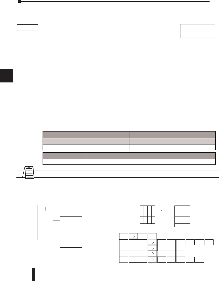
DL06 Micro PLC User Manual, 3rd Edition, Rev. D
5-194
1
2
3
4
5
6
7
8
9
10
11
12
13
14
A
B
C
D
Chapter 5: Standard RLL Instructions - Intelligent I/O Instructions
1
2
3
4
5
6
7
8
9
10
11
12
13
14
a
B
c
d
Intelligent I/O Instructions
Read from Intelligent Module (RD)
The Read from Intelligent Module instruction reads a block of
data (1-128 bytes maximum) from an intelligent I/O module
into the CPU’s V-memory. It loads the function parameters into
the first and second level of the accumulator stack and the accumulator by three additional
instructions.
Listed below are the steps to program the Read from Intelligent module function.
Step 1: Load the base number (0-3) into the first byte and the slot number (0-7) into the
second byte of the second level of the accumulator stack.
Step 2: Load the number of bytes to be transferred into the first level of the accumulator
stack (maximum of 128 bytes).
Step 3: Load the address from which the data will be read into the accumulator. This
parameter must be a HEX value.
Step 4: Insert the RD instruction which specifies the starting V-memory location (Vaaa)
where the data will be read into.
Helpful Hint: S Use the LDA instruction to convert an octal address to its HEX equivalent
and load it into the accumulator when the HEX format is required.
NOTE: Status flags are valid only until another instruction uses the same flag.
In the following example, when X1 is ON, the RD instruction will read six bytes of data from
a intelligent module in base 1, slot 2, starting at address 0 in the intelligent module, and copy
the information into V-memory loacations V1400-V1402.
DS32 Used
HPP Used V aaa
RD
Operand Data Type DL06 Range
aaa
V-memory V See memory map
Discrete Bit Flags Description
SP54 On when RX, WX RD, WT instructions are executed with the wrong parameters.
Direct SOFT 5
Handheld Programmer Keystrokes
LD
K0102
X1 The constant value K0102
specifies the base number
(01) and the base slot
number (02).
LD
K6
The constant value K6
specifies the number of
bytes to be read.
LD
K0
RD
V1400
V1400 is the starting location
in the CPU where the specified
data will be stored.
Address 2
Address 3
19
Address 4
0
Address 5
Address 0
Address 1
34
7
V1402
6
V1403
V1404
V1400
V1401
STR
$
SHFT ANDST
L
3
DPREV
SHFT ANDST
L
3
D
6
GENT
SHFT ORN
R
1
BENT
0
AENT
4
E
0
A
0
AENT
SHFT ANDST
L
3
DPREV 0
A
0
AENT
2
C
CPU
The constant value K0
specifies the starting address
in the intelligent module.
1 2
85
0
XXXX
XXXX
12
56
34
78
90
01
{
1
B
PREV
1
B
}
Intelligent Module
Data
3
D
DirectSOFT
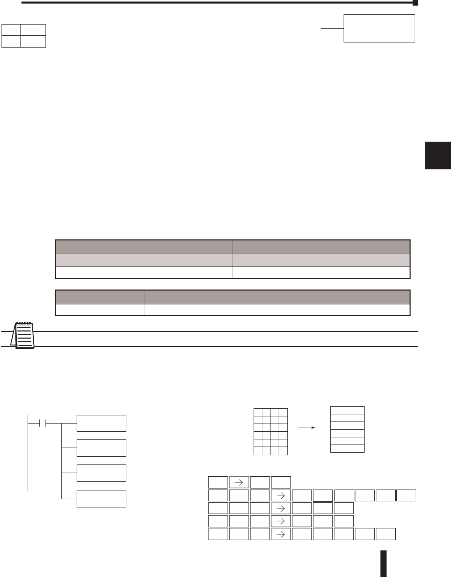
DL06 Micro PLC User Manual, 3rd Edition, Rev. D 5-195
1
2
3
4
5
6
7
8
9
10
11
12
13
14
A
B
C
D
Write to Intelligent Module (WT)
The Write to Intelligent Module instruction writes a block of data
(1-128 bytes maximum) to an intelligent I/O module from a block
of V-memory in the CPU. The function parameters are loaded into
the first and second level of the accumulator stack and the accumulator by three additional
instructions.
Listed below are the steps to program the Read from Intelligent module function.
Step 1: Load the base number (0-3) into the first byte and the slot number (0-7) into the
second byte of the second level of the accumulator stack.
Step 2: Load the number of bytes to be transferred into the first level of the accumulator
stack (maximum of 128 bytes).
Step 3: Load the intelligent module address which will receive the data into the accumulator.
This parameter must be a HEX value.
Step 4: Insert the WT instruction which specifies the starting V-memory location (Vaaa)
where the data will be written from in the CPU.
Helpful Hint: S Use the LDA instruction to convert an octal address to its HEX equivalent
and load it into the accumulator when the HEX format is required.
NOTE: Status flags are valid only until another instruction uses the same flag.
In the following example, when X1 is on, the WT instruction will write six bytes of data to an
intelligent module in base 1, slot 2,starting at address 0 in the intelligent module, and copy
the data from V-memory locations V1400-V1402.
Chapter 5: Standard RLL Instructions - Intelligent I/O Instructions
1
2
3
4
5
6
7
8
9
10
11
12
13
14
a
B
c
d
V aaa
WT
DS32 Used
HPP Used
Direct SOFT 5
Handheld Programmer Keystrokes
LD
K0102
X1 The constant value K0102
specifies the base number
(01) and the base slot
number (02).
LD
K6
The constant value K6
specifies the number of
bytes to be written.
LD
K0
WT
V1400
V1400 is the starting location
in the CPU where the specified
data will be written from.
Address 2
Address 3
19
Address 4
0
Address 5
Address 0
Address 1
34
7
V1402
6
V1403
V1404
V1400
V1401
STR
$
SHFT ANDST
L
3
DPREV
SHFT ANDST
L
3
D
6
GENT
SHFT ANDN
W
1
BENT
0
AENT
4
E
0
A
0
AENT
SHFT ANDST
L
3
DPREV 0
A
0
AENT
2
C
CPU
The constant value K0
specifies the starting address
in the intelligent module.
1 2
85
0
XXXX
XXXX
12
56
34
78
90
01
{
1
B
PREV
1
B
}
Intelligent Module
Data
MLR
T
V1377 XXXX
Operand Data Type DL06 Range
aaa
V-memory V See memory map
Discrete Bit Flags Description
SP54 On when RX, WX RD, WT instructions are executed with the wrong parameters.
DirectSOFT
DL06 Micro PLC User Manual, 3rd Edition, Rev. D
5-196
1
2
3
4
5
6
7
8
9
10
11
12
13
14
A
B
C
D
Network Instructions
Read from Network (RX)
The Read from Network instruction is used by the master device on a
network to read a block of data from a slave device on the same network.
The function parameters are loaded into the first and second level of
the accumulator stack and the accumulator by three additional instructions. Listed below are the steps
necessary to program the Read from Network function.
• Step 1: Load the slave address (0-- 90 BCD) into the first byte and the PLC internal port (KF2) or
slot number of the master DCM or ECOM (0-- 7) into the second byte of the second level
of the accumulator stack.
• Step 2: Load the number of bytes to be transferred into the first level of the accumulator stack.
• Step 3: Load the address of the data to be read into the accumulator. This parameter requires a
HEX value.
• Step 4: Insert the RX instruction which specifies the starting Vmemory location (Aaaa) where the
data will be read from in the slave.
Helpful Hint: — For parameters that require HEX values, the LDA instruction can be used
to convert an octal address to the HEX equivalent and load the value into the accumulator.
Chapter 5: Standard RLL Instructions - Network Instructions
1
2
3
4
5
6
7
8
9
10
11
12
13
14
a
B
c
d
Operand Data Type DL06 Range
A aaa
V-memory V See memory map
Pointer P See memory map
Inputs X 0–777
Outputs Y 0–777
Control Relays C 0–1777
Stage S 0–1777
Timer T 0–377
Counter CT 0–177
Special Relay SP 0–777
Program Memory $ 0–7680 (2K program mem.)
A aaa
RX
DS32 Used
HPP Used
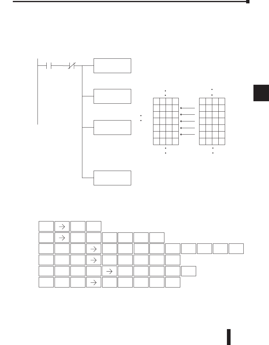
DL06 Micro PLC User Manual, 3rd Edition, Rev. D 5-197
1
2
3
4
5
6
7
8
9
10
11
12
13
14
A
B
C
D
In the following example, when X1 is on and the port busy relay SP116 (see special relays) is
not on, the RX instruction will access port 2 operating as a master. Ten consecutive bytes of
data (V2000 – V2004) will be read from a CPU at station address 5 and copied into
V-memory locations V2300–V2304 in the CPU with the master port.
Chapter 5: Standard RLL Instructions - Network Instructions
1
2
3
4
5
6
7
8
9
10
11
12
13
14
a
B
c
d
Direct SOFT32
Handheld Programmer Keystrokes
LD
KF205
X1
The constant value KF205
specifies the port number (2)
and the slave address (5)
LD
K10
The constant value K10
specifies the number of
bytes to be read
LDA
O 2300
Octal address 2300 is
converted to 4C0 HEX and
loaded into the accumulator.
V2300 is the starting
location for the Master CPU
where the specified data will
be read into
RX
V2000
V2000 is the starting
location in the for the Slave
CPU where the specified
data will be read from
V2001
8534
V2002
1936
V2003
9571
V2004
1423
V1777
XXXX
V2000
3457
Master
SP116
V2005
XXXX
V2301 8534
V2302 1936
V2303 9571
V2304 1423
V2277 XXXX
V2300 3457
V2305 XXXX
Slave
CPU
STR
$
SHFT ANDST
L
3
DSHFT JMP
K
SHFT ANDST
L
3
D
ANDN
WSHFT STRN
SP
1
B
1
B
6
GENT
1
B
0
AENT
0
A
SHFT ORN
R
SET
X
1
BENT
2
C
3
D
0
A
0
AENT
2
C
0
A
0
A
0
AENT
SHFT ANDST
L
3
DSHFT JMP
K
0
AENT
2
C
5
F
SHFT SHFT
5
F
CPU
DirectSOFT
DL06 Micro PLC User Manual, 3rd Edition, Rev. D
5-198
1
2
3
4
5
6
7
8
9
10
11
12
13
14
A
B
C
D
Chapter 5: Standard RLL Instructions - Network Instructions
1
2
3
4
5
6
7
8
9
10
11
12
13
14
a
B
c
d
Write to Network (WX)
The Write to Network instruction is used to write a block
of data from the master device to a slave device on the
same network. The function parameters are loaded into the
accumulator and the first and second levels of the stack. Listed below are the program steps
necessary to execute the Write to Network function.
Step 1: Load the slave address (0–90 BCD) into the low byte and “F2” into the high
byte of the accumulator (the next two instructions push this word down to the
second layer of the stack).
Step 2: Load the number of bytes to be transferred into the accumulator (the next
instruction pushes this word onto the top of the stack).
Step 3: Load the starting Master CPU address into the accumulator. This is the
memory location where the data will be written from. This parameter requires
a HEX value.
Step 4: Insert the WX instruction which specifies the starting V-memory location
(Aaaa) where the data will be written to in the slave.
Helpful Hint: — For parameters that require HEX values, the LDA instruction can be used
to convert an octal address to the HEX equivalent and load the value into the accumulator.
A aaa
WX
Operand Data Type DL06 Range
A aaa
V-memory V See memory map
Pointer P See memory map
Inputs X 0–777
Outputs Y 0–777
Control Relays C 0–1777
Stage S 0–1777
Timer T 0–377
Counter CT 0–177
Special Relay SP 0–777
Program Memory $ 0–7680 (2K program mem.)
DS Used
HPP Used
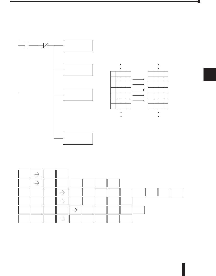
DL06 Micro PLC User Manual, 3rd Edition, Rev. D 5-199
1
2
3
4
5
6
7
8
9
10
11
12
13
14
A
B
C
D
In the following example, when X1 is on and the module busy relay SP116 (see special relays)
is not on, the WX instruction will access port 2 operating as a master. Ten consecutive bytes
of data are read from the Master CPU and copied to V-memory locations V2000–V2004 in
the slave CPU at station address 5.
Chapter 5: Standard RLL Instructions - Network Instructions
1
2
3
4
5
6
7
8
9
10
11
12
13
14
a
B
c
d
Direct SOFT32
Handheld Programmer Keystrokes
LD
KF205
X1
The constant value KF205
specifies the port number (2)
and the slave address (5)
LD
K10
The constant value K10
specifies the number of
bytes to be written
LDA
O 2300
WX
V2000
V2000 is the starting
location in the for the Slave
CPU where the specified
data will be written to
V2001
853 4
V2002
193 6
V2003
957 1
V2004
142 3
V1777
XXX X
V2000
345 7
Master
CPU
SP116
V2005
XXX X
V2301 853 4
V2302 193 6
V2303 957 1
V2304 142 3
V2277 XXX X
V2300 345 7
V2305 XXX X
Slave
CPU
Octal address 2300 is
converted to 4C0 HEX and
loaded into the accumulator.
V2300 is the starting
location for the Master CPU
where the specified data will
be read from.
STR
$
SHFT ANDST
L
3
DSHFT JMP
K
SHFT ANDST
L
3
D
ANDN
WSHFT STRN
SP
1
B
1
C
6
EENT
1
B
0
AENT
SHFT
0
A
5
F
2
C
3
D
0
A
0
AENT
SHFT
SHFT
2
C
0
A
0
A
0
AENT
SET
X
ANDN
W
SHFT ANDST
L
3
DSHFT JMP
K
0
AENT
2
C
5
F
1
BENT
DirectSOFT
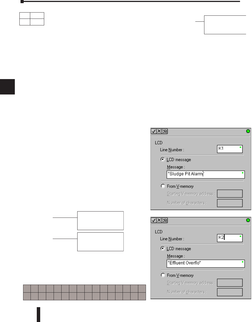
DL06 Micro PLC User Manual, 3rd Edition, Rev. D
5-200
1
2
3
4
5
6
7
8
9
10
11
12
13
14
A
B
C
D
Chapter 5: Standard RLL Instructions - LCD
1
2
3
4
5
6
7
8
9
10
11
12
13
14
a
B
c
d
LCD
When enabled, the LCD instruction causes a user-defined text
message to be displayed on the LCD Display Panel. The display is
16 characters wide by 2 rows high so a total of 32 characters can be
displayed. Each row is addressed separately; the maximum number
of characters the instruction will accept is 16.
The text message can be entered directly into the message field of the instruction set-up
dialog, or it can be located anywhere in user V-memory. If the text is located in V-memory,
the LCD instruction is used to point to the memory location where the desired text
originates. The length of the text string is also required.
From the DirectSOFT project folder, use the Instruction Browser to locate the LCD
instruction. When you select the LCD instruction and click OK, the LCD dialog will appear,
as shown in the examples. The LCD instruction is inserted into the ladder program via this
set-up dialog box.
Display text strings can include embedded variables. Date and time settings and V-memory
values can be embedded in the displayed text. Examples of each are shown.
Direct Text Entry
The two dialogs to the right show the
selections necessary to create the two ladder
instructions below. Double quotation
marks are required to delineate the text
string. In the first dialog, the text “Sludge
Pit Alarm“ uses sixteen character spaces and
will appear on line 1 when the instruction
is enabled. Note, the line number is K1.
Clicking the “check” button causes the
instruction to be inserted into the ladder
program.
By identifying the second Line Number
as K2, the text string “Effluent Overflow”
will appear on the second line of the display
when the second instruction is enabled.
"text message"
LCD
Line Number:
Kn
S l u d g e P i t A l a r m
E f f l u e n t O v e r f l o
"Effluent Overflo"
"Sludge Pit Alarm"
LCD
Line Number: K1
LCD
Line Number: K2
DS Used
HPP N/A
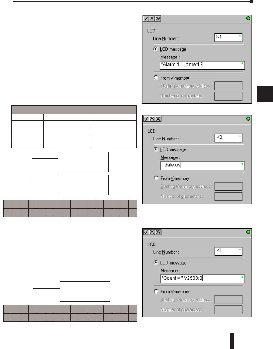
DL06 Micro PLC User Manual, 3rd Edition, Rev. D 5-201
1
2
3
4
5
6
7
8
9
10
11
12
13
14
A
B
C
D
Chapter 5: Standard RLL Instructions - LCD
1
2
3
4
5
6
7
8
9
10
11
12
13
14
a
B
c
d
Embedding date and/or time variables
The date and/or time can be embedded in
the displayed text by using the variables
listed in the table below. These variables can
be included in the LCD message field of
the LCD dialog. In the example, the time
variable (12 hour format) is embedded by
adding _time:12. This time format uses a
maximum of seven character spaces. The
second dialog creates an instruction that
prints the date on the second line of the
display, when enabled.
A l a r m 1 1 1 : 2 1 P M
0 5 - 0 8 - 0 2
Date and Time Variables and Formats
_date:us US format MM/DD/YY
_date:e European format DD/MM/YY
_date:a Asian format YY/MM/DD
_time:12 12 hour format HH:MMAM/PM
_time:24 24 hour format HH:MM:SS
_date:us
"Alarm 1 "
LCD
Line Number: K1
LCD
Line Number: K2
_time:12
Embedding V-memory data
Any V-memory data can be displayed in
any one of six available data formats. An
example appears to the right. A list of data
formats and modifiers is on the next page.
Note that different data formats require
differing numbers of character positions
on the display.
"Count = " V2500:B
LCD
Line Number: K1
C o u n t = 0 4 1 2
DL06 Micro PLC User Manual, 3rd Edition, Rev. D
5-202
1
2
3
4
5
6
7
8
9
10
11
12
13
14
A
B
C
D
Chapter 5: Standard RLL Instructions - LCD
1
2
3
4
5
6
7
8
9
10
11
12
13
14
a
B
c
d
Data Format Suffixes for Embedded V-memory Data
Several data formats are available for displaying V-memory data on the LCD. The choices are
shown in the table below. A colon is used to separate the embedded V-memory location from
the data format suffix and modifier. An example appears on the previous page.
The S, C0, and 0 modifiers alter the presentation of leading zeros and spaces. S removes
leading spaces and left justifies the result. C0 replaces leading spaces with leading zeros.
0 is a modification of C0. 0 eliminates any leading zeros in the C0 format version and
converts them to spaces.
Data Format Modifier Example Displayed Characters
none
(16-bit format)
V2000 = 0000 0000 0001 0010 1234
V2000 1 8
[:S] V2000:S 1 8
[:C0] V2000:C0 0018
[:0] V2000:0 1 8
:B
(4 digit BCD)
V2000 = 0000 0000 0001 0010 1234
[:B] V2000:B 0012
[:BS] V2000:BS 1 2
[:BC0] V2000:BC0 0012
[:B0] V2000:B0 1 2
:D
(32-bit decimal)
V2000 = 0000 0000 0000 0000 Double Word
V2001 = 0000 0000 0000 0001 12345678910 11
[:D] V2000:D 65536
[:DS] V2000:DS 65536
[:DC0] V2000:DC0 00000065536
[:D0] V2000:D0 65536
:DB
(8 digit BCD)
V2000 = 0000 0000 0000 0000 Double Word
V2001 = 0000 0000 0000 0011 12345678
[:DB] V2000:DB 00030000
[:DBS] V2000:DBS 30000
[:DBC0] V2000:DBC0 00030000
[:DB0] V2000:DB0 30000
:R
(DWord floating
point number)
V2001/V2000 = 222.11111
(real number)
Double Word
12345678910 11 12 13
[:R] V2000:R f 2 2 2 . 1 1 1 1 1
[:RS] V2000:RS f 222.11111
[:RC0] V2000:RC0 f000222.11111
[:R0] V2000:R0 f 2 2 2 . 1 1 1 1 1
:E
(DWord floating
point number
with exponent)
V2001/V2000 = 222.1
(real number)
Double Word
12345678910 11 12 13
[:E] V2000:E f2. 22100E+02
[:ES] V2000:ES f2.22100E+02
[:EC0] V2000:EC0 f 2 .22100E+02
[:E0] V2000:E0 f 2.22100E+02
f = plus/minus flag (plus = no symbol, minus = - )
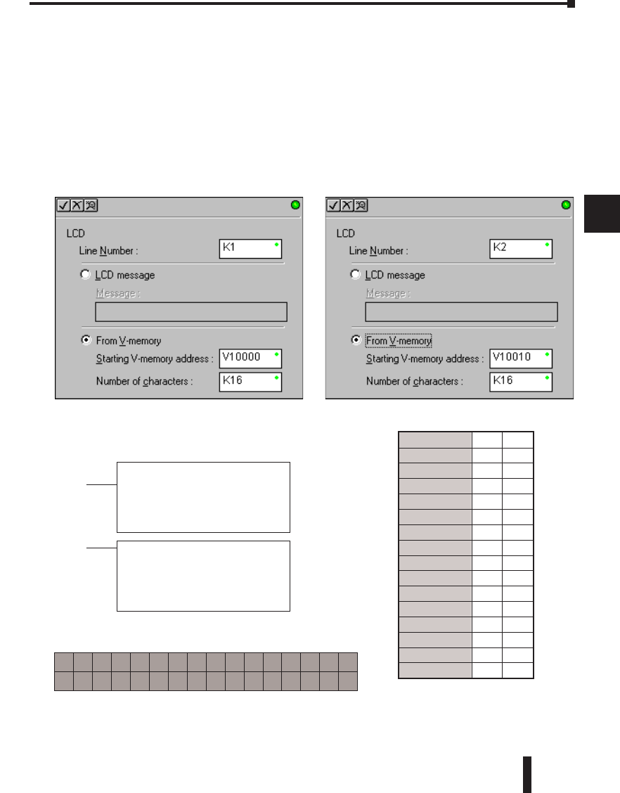
DL06 Micro PLC User Manual, 3rd Edition, Rev. D 5-203
1
2
3
4
5
6
7
8
9
10
11
12
13
14
A
B
C
D
Chapter 5: Standard RLL Instructions - LCD
1
2
3
4
5
6
7
8
9
10
11
12
13
14
a
B
c
d
V10000
LCD
Line Number: K1
Starting V Memory Address:
Number of Characters:
V10010
LCD
Line Number: K2
Starting V Memory Address:
Number of Characters:
K16
K16
Text Entry from V-memory
Alternatively, text that resides in V-memory can be displayed on the LCD following the
example on this page. The LCD dialog is used twice, once for each line on the display. The
dialog requires the address of the first character to be displayed and the number of characters
to be displayed.
For example, the two dialogs shown on this page would create the two LCD instructions
below. When enabled, these instructions would cause the ASCII characters in V10000 to
V10017 to be displayed. The ASCII characters and their corresponding memory locations are
shown in the table below.
V10000 d A
V10001 i m
V10002 n
V10003 f O
V10004 i f
V10005 e c
V10006
V10007
V10010 i H
V10011 h g
V10012 T
V10013 m e
V10014 p
V10015 l A
V10016 r a
V10017 m
A d m i n O f f i c e
H i g h T e m p A l a r m
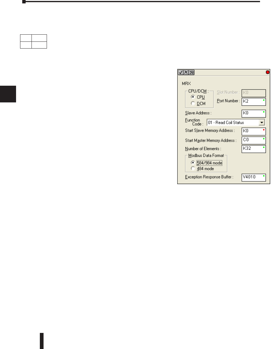
DL06 Micro PLC User Manual, 3rd Edition, Rev. D
5-204
1
2
3
4
5
6
7
8
9
10
11
12
13
14
A
B
C
D
MODBUS RTU Instructions
MODBUS Read from Network (MRX)
The MODBUS Read from Network (MRX) instruction is used by the DL06 network master
to read a block of data from a connected slave device and to write the data into V–memory
addresses within the master. The instruction allows the user to specify the MODBUS
Function Code, slave station address, starting master and slave memory addresses, number of
elements to transfer, MODBUS data format and the Exception Response Buffer.
• CPU/DCM: select either CPU or DCM module
for communications
• Slot Number: select PLC option slot number if
using a DCM module.
• Port Number: must be DL06 Port 2 (K2)
• Slave Address: specify a slave station address
(0–247)
• Function Code: The following MODBUS function
codes are supported by the MRX instruction:
01 – Read a group of coils
02 – Read a group of inputs
03 – Read holding registers
04 – Read input registers
07 – Read Exception status
• Start Slave Memory Address: specifies the starting slave memory address of the data to be
read. See the table on the following page.
• Start Master Memory Address: specifies the starting memory address in the master where
the data will be placed. See the table on the following page.
• Number of Elements: specifies how many coils, inputs, holding registers or input register
will be read. See the table on the following page.
• MODBUS Data Format: specifies MODBUS 584/984 or 484 data format to be used
• Exception Response Buffer: specifies the master memory address where the Exception Response will
be placed (6-bytes in length). See the table on the following page.The exception response buffer uses 3
words. These bytes are swapped in the MRX/MWX exception response buffer V-memory so:
V-Memory 1 Hi Byte = Function Code Byte (Most Significant Bit Set)
V-Memory 1 Lo Byte = Address Byte
V-Memory 2 Hi Byte = One of the CRC Bytes
V-Memory 2 Lo Byte = Exception Code
V-Memory 3 Hi Byte = 0
V-Memory 3 Lo Byte = Other CRC Byte
Chapter 5: Standard RLL Instructions - MODBUS
1
2
3
4
5
6
7
8
9
10
11
12
13
14
a
B
c
d
DS Used
HPP N/A
DL06 Micro PLC User Manual, 3rd Edition, Rev. D 5-205
1
2
3
4
5
6
7
8
9
10
11
12
13
14
A
B
C
D
MRX Slave Address Ranges
Chapter 5: Standard RLL Instructions - MODBUS
1
2
3
4
5
6
7
8
9
10
11
12
13
14
a
B
c
d
Function Code MODBUS Data Format Slave Address Range(s)
01 – Read Coil 484 Mode 1–999
01 – Read Coil 584/984 Mode 1–65535
02 – Read Input Status 484 Mode 1001–1999
02 – Read Input Status 584/984 Mode 10001–19999 (5 digit) or 100001–
165535 (6 digit)
03 – Read Holding Register 484 Mode 4001–4999
03 – Read Holding Register 584/984 Mode 40001–49999 (5 digit) or 4000001–
465535 (6 digit)
04 – Read Input Register 484 Mode 3001–3999
04 – Read Input Register 584/984 Mode 30001–39999 (5 digit) or 3000001–
365535 (6 digit)
07 – Read Exception Status 484 and 584/984 Mode N/A
MRX Master Memory Address Ranges
Operand Data Type DL06 Range
Inputs X 0–1777
Outputs Y 0–1777
Control Relays C 0–3777
Stage Bits S 0–1777
Timer Bits T 0–377
Counter Bits CT 0–377
Special Relays SP 0–777
V–memory V all
Global Inputs GX 0–3777
Global Outputs GY 0–3777
Number of Elements
Operand Data Type DL06 Range
V–memory V all
Constant K Bits: 1–2000 Registers: 1–125
Exception Response Buffer
Operand Data Type DL06 Range
V–memory V all
DL06 Micro PLC User Manual, 3rd Edition, Rev. D
5-206
1
2
3
4
5
6
7
8
9
10
11
12
13
14
A
B
C
D
MRX Example
DL06 port 2 has two Special Relay contacts associated with it (see Appendix D for comm
port special relays). One indicates “Port busy”(SP116), and the other indicates ”Port
Communication Error”(SP117). The “Port Busy” bit is on while the PLC communicates
with the slave. When the bit is off, the program can initiate the next network request.
The “Port Communication Error” bit turns on when the PLC has detected an error. Use
of this bit is optional. When used, it should be ahead of any network instruction boxes,
since the error bit is reset when an MRX or MWX instruction is executed. Typically,
network communications will last longer than 1 CPU scan. The program must wait for the
communications to finish before starting the next transaction.
NOTE: See Chapter 4, page 4-21, for an RLL example using multiple Read and Write interlocks with
MRX/MWX instructions.
Chapter 5: Standard RLL Instructions - MODBUS
1
2
3
4
5
6
7
8
9
10
11
12
13
14
a
B
c
d
DL06 Micro PLC User Manual, 3rd Edition, Rev. D 5-207
1
2
3
4
5
6
7
8
9
10
11
12
13
14
A
B
C
D
MODBUS Write to Network (MWX)
The MODBUS Write to Network (MWX) instruction is used to write a block of data from
the network masters’s (DL06) memory to MODBUS memory addresses within a slave device
on the network. The instruction allows the user to specify the MODBUS Function Code,
slave station address, starting master and slave memory addresses, number of elements to
transfer, MODBUS data format and the Exception Response Buffer.
• CPU/DCM: select either CPU or DCM module for
communications
• Slot Number: select PLC option slot number if
using a DCM module
• Port Number: must be DL06 Port 2 (K2)
• Slave Address: specify a slave station address
(0–247)
• Function Code: MODBUS function codes
supported by the MWX instruction:
05 – Force Single coil
06 – Preset Single Register
15 – Force Multiple Coils
16 – Preset Multiple Registers
• Start Slave Memory Address: specifies the starting
slave memory address where the data will be written
• Start Master Memory Address: specifies the starting address of the data in the master that is
to be written to the slave
• Number of Elements: specifies how many consecutive coils or registers will be written to.
This field is only active when either function code 15 or 16 is selected.
• MODBUS Data Format: specifies MODBUS 584/984 or 484 data format to be used
• Exception Response Buffer: specifies the master memory address where the Exception Response will
be placed (6-bytes in length). See the table on the following page.The exception response buffer uses 3
words. These bytes are swapped in the MRX/MWX exception response buffer V-memory so:
V-Memory 1 Hi Byte = Function Code Byte (Most Significant Bit Set)
V-Memory 1 Lo Byte = Address Byte
V-Memory 2 Hi Byte = One of the CRC Bytes
V-Memory 2 Lo Byte = Exception Code
V-Memory 3 Hi Byte = 0
V-Memory 3 Lo Byte = Other CRC Byte
Chapter 5: Standard RLL Instructions - MODBUS
1
2
3
4
5
6
7
8
9
10
11
12
13
14
a
B
c
d
DS Used
HPP N/A
DL06 Micro PLC User Manual, 3rd Edition, Rev. D
5-208
1
2
3
4
5
6
7
8
9
10
11
12
13
14
A
B
C
D
MWX Slave Address Ranges
Chapter 5: Standard RLL Instructions - MODBUS
1
2
3
4
5
6
7
8
9
10
11
12
13
14
a
B
c
d
MWX Slave Address Ranges
Function Code MODBUS Data Format Slave Address Range(s)
05 – Force Single Coil 484 Mode 1–999
05 – Force Single Coil 584/984 Mode 1–65535
06 – Preset Single Register 484 Mode 4001–4999
06 – Preset Single Register 584/984 Mode 40001–49999 (5 digit) or 400001–
465535 (6 digit)
15 – Force Multiple Coils 484 Mode 1–999
15 – Force Multiple Coils 585/984 Mode 1–65535
16 – Preset Multiple Registers 484 Mode 4001–4999
16 – Preset Multiple Registers 584/984 Mode 40001–49999 (5 digit) or 4000001–
465535 (6 digit)
MWX Master Memory Address Ranges
Operand Data Type DL06 Range
Inputs X 0–1777
Outputs Y 0–1777
Control Relays C 0–3777
Stage Bits S 0–1777
Timer Bits T 0–377
Counter Bits CT 0–377
Special Relays SP 0–777
V–memory V all
Global Inputs GX 0–3777
Global Outputs GY 0–3777
Number of Elements
Operand Data Type DL06 Range
V–memory V all
Constant K Bits: 1–2000 Registers: 1–125
Number of Elements
Operand Data Type DL06 Range
V–memory V all
MWX Number of
Elements
MWX Exception
Response Buffer
MWX Master
Memory Address
Ranges
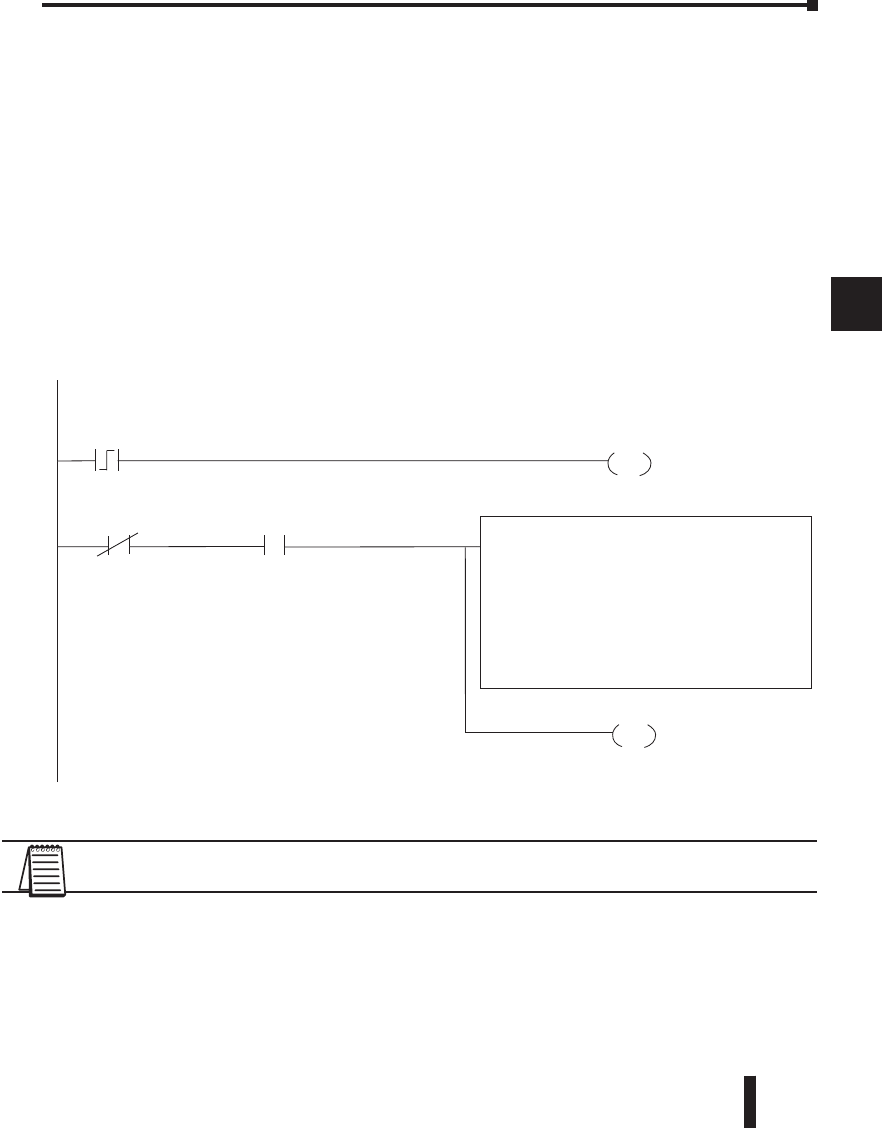
DL06 Micro PLC User Manual, 3rd Edition, Rev. D 5-209
1
2
3
4
5
6
7
8
9
10
11
12
13
14
A
B
C
D
MWX Example
DL06 port 2 has two Special Relay contacts associated with it (see Appendix D for comm
port special relays). One indicates “Port busy”(SP116), and the other indicates ”Port
Communication Error”(SP117). The “Port Busy” bit is on while the PLC communicates
with the slave. When the bit is off, the program can initiate the next network request. The
“Port Communication Error” bit turns on when the PLC has detected an error. Use of this
bit is optional. When used, it should be ahead of any network instruction boxes since the
error bit is reset when an MRX or MWX instruction is executed.
Typically, network communications will last longer than 1 CPU scan. The program must
wait for the communications to finish before starting the next transaction.
NOTE: See Chapter 4, page 4-21, for an RLL example using multiple Read and Write interlocks with
MRX/MWX instructions.
Chapter 5: Standard RLL Instructions - MODBUS
1
2
3
4
5
6
7
8
9
10
11
12
13
14
a
B
c
d
Instruction Interlock bit
C100
MWX
Port Number: K2
Slave Address: K6
Function Code: 06-Preset Single Register
Start Slave Memory Address: 40001
Start Master Memory Address: V2000
Number of Elements: n/a
Modbus Data type: 584/984 Mode
Exception Response Buffer: V400
SP116 C100
This rung does a MODBUS write to the first holding register 40001 of slave address
number six. It will write the values over that reside in V2000. This particular function
code only writes to 1 register. Use Function Code 16 to write to multiple registers.
Only one Network instruction (WX, RX, MWX, MRX) can be enabled in one scan.
That is the reason for the interlock bits.
3
Port 2 busy bit Instruction Interlock bit
2
RST
X1 C100
SET

DL06 Micro PLC User Manual, 3rd Edition, Rev. D
5-210
1
2
3
4
5
6
7
8
9
10
11
12
13
14
A
B
C
D
ASCII Instructions
The DL06 CPU supports several instructions and methods that allow ASCII strings to be
read into and written from the PLC communications ports. Specifically, port 2 on the DL06
can be used for either reading or writing raw ASCII strings, but cannot be used for both at
the same time. The DL06 can also decipher ASCII embedded within a supported protocol
(K–Sequence, DirectNet, Modbus) via the CPU port.
Reading ASCII Input Strings
There are several methods that the DL06 can use to read ASCII input strings.
1) ASCII IN (AIN) – This instruction configures port 2 for raw ASCII input strings with
parameters such as fixed and variable length ASCII strings, termination characters, byte
swapping options, and instruction control bits. Use barcode scanners, weight scales, etc. to
write raw ASCII input strings into port 2 based on the (AIN) instruction’s parameters.
2) Write embedded ASCII strings directly to V–memory from an external HMI or similar
master device via a supported communications protocol using the CPU ports. The AIN
instruction is not used in this case. 3) If a DL06 PLC is a master on a network, the
Network Read instruction (RX) can be used to read embedded ASCII data from a slave
device via a supported communications protocol using port 2. The RX instruction places
the data directly into V–memory.
Writing ASCII Output Strings
The following instructions can be used to write ASCII output strings:
1) Print from V–memory (PRINTV) – Use this instruction to write raw ASCII strings out
of port 2 to a display panel or a serial printer, etc. The instruction features the starting
V–memory address, string length, byte swapping options, etc. When the instruction’s
permissive bit is enabled, the string is written to port 2.
2) Print to V–memory (VPRINT) – Use this instruction to create pre–coded ASCII strings
in the PLC (i.e. alarm messages). When the instruction’s permissive bit is enabled, the
message is loaded into a pre–defined V–memory address location. Then the (PRINTV)
instruction may be used to write the pre–coded ASCII string out of port 2. American,
European and Asian Time/Date stamps are supported.
Additionally, if a DL06 PLC is a master on a network, the Network Write instruction (WX)
can be used to write embedded ASCII data to an HMI or slave device directly from V–
memory via a supported communications protocol using port 2.
Chapter 5: Standard RLL Instructions - ASCII
1
2
3
4
5
6
7
8
9
10
11
12
13
14
a
B
c
d

DL06 Micro PLC User Manual, 3rd Edition, Rev. D 5-211
1
2
3
4
5
6
7
8
9
10
11
12
13
14
A
B
C
D
Managing the ASCII Strings
The following instructions can be helpful in managing the ASCII strings within the CPUs
V–memory:
• ASCII Find (AFIND) – Finds where a specific portion of the ASCII string is located in
continuous V–memory addresses. Forward and reverse searches are supported.
• ASCII Extract (AEX) – Extracts a specific portion (usually some data value) from the ASCII
find location or other known ASCII data location.
• Compare V–memory (CMPV) – This instruction is used to compare two blocks of V–
memory addresses and is usually used to detect a change in an ASCII string. Compared data
types must be of the same format (i.e., BCD, ASCII, etc.).
• Swap Bytes (SWAPB) – usually used to swap V–memory bytes on ASCII data that
was written directly to V–memory from an external HMI or similar master device via
a communications protocol. The AIN and AEX instructions have a built–in byte swap
feature.
Chapter 5: Standard RLL Instructions - ASCII
1
2
3
4
5
6
7
8
9
10
11
12
13
14
a
B
c
d
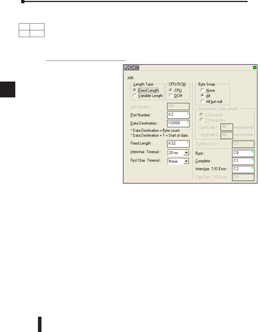
DL06 Micro PLC User Manual, 3rd Edition, Rev. D
5-212
1
2
3
4
5
6
7
8
9
10
11
12
13
14
A
B
C
D
Chapter 5: Standard RLL Instructions - ASCII
1
2
3
4
5
6
7
8
9
10
11
12
13
14
a
B
c
d
ASCII Input (AIN)
The ASCII Input instruction allows the CPU to receive ASCII strings through the specified
communications port and places the string into a series of specified V–memory registers.
The ASCII data can be received as a fixed number of bytes or as a variable length string with
specified termination character(s). Other features include, Byte Swap preferences, Character
Timeout, and user defined flag bits for Busy, Complete and Timeout Error.
AIN Fixed Length Configuration
• Length Type: select fixed
length based on the length of
the ASCII string that will be
sent to the CPU port
• Port Number: must be DL06
port 2 (K2)
• Data Destination: specifies
where the ASCII string will be
placed in V–memory
• Fixed Length: specifies the
length, in bytes, of the fixed
length ASCII string the port
will receive
• Inter–character Timeout: if
the amount of time between
incoming ASCII characters
exceeds the set time, the
specified Timeout Error bit
will be set. No data will be stored at the Data Destination V–memory location. The bit
will reset when the AIN instruction permissive bits are disabled. 0ms selection disables this
feature.
• First Character Timeout: if the amount of time from when the AIN is enabled to the time
the first character is received exceeds the set time, the specified First Character Timeout bit
will be set. The bit will reset when the AIN instruction permissive bits are disabled. 0ms
selection disables this feature.
• Byte Swap: swaps the high–byte and low–byte within each V–memory register of the Fixed
Length ASCII string. See the SWAPB instruction for details.
• Busy Bit: is ON while the AIN instruction is receiving ASCII data
• Complete Bit: is set once the ASCII data has been received for the specified fixed length
and reset when the AIN instruction permissive bits are disabled.
• Inter–character Timeout Error Bit: is set when the Character Timeout is exceeded. See
Character Timeout explanation above.
• First Character Timeout Error Bit: is set when the First Character Timeout is exceeded.
See First Character Timeout explanation above.
DS Used
HPP N/A
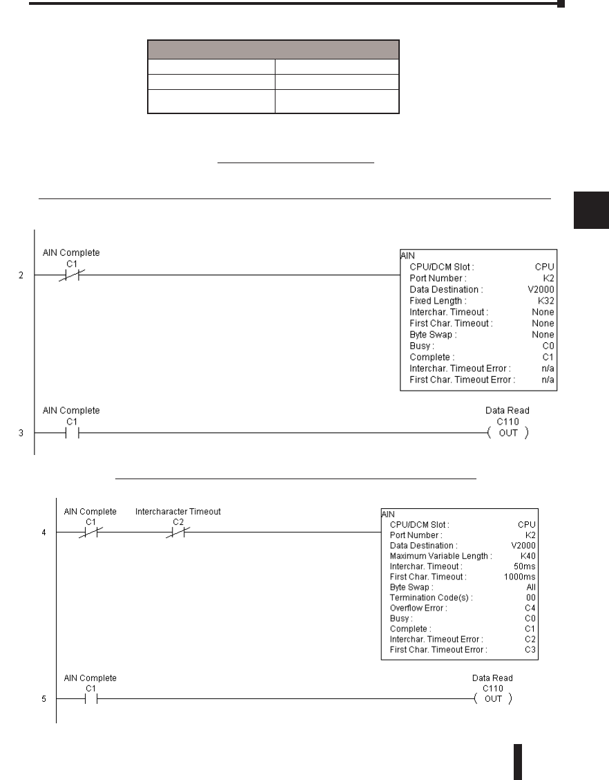
DL06 Micro PLC User Manual, 3rd Edition, Rev. D 5-213
1
2
3
4
5
6
7
8
9
10
11
12
13
14
A
B
C
D
Chapter 5: Standard RLL Instructions - ASCII
1
2
3
4
5
6
7
8
9
10
11
12
13
14
a
B
c
d
Parameter
Data Destination All V–memory
Fixed Length K1–128
Bits: Busy, Complete,
Timeout Error, Overflow C0–3777
AIN Fixed Length Examples
Fixed Length example when the PLC is reading the port continuously and timing is not critical
Fixed Length example when character to character timing is critical
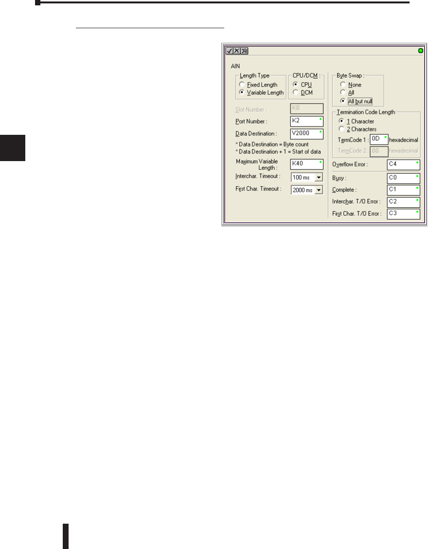
DL06 Micro PLC User Manual, 3rd Edition, Rev. D
5-214
1
2
3
4
5
6
7
8
9
10
11
12
13
14
A
B
C
D
Chapter 5: Standard RLL Instructions - ASCII
1
2
3
4
5
6
7
8
9
10
11
12
13
14
a
B
c
d
AIN Variable Length Configuration:
• Length Type: select Variable Length if the ASCII string length followed by termination
characters will vary in length
• Port Number: must be DL06 port
2 (K2)
• Data Destination: specifies where
the ASCII string will be placed in
V–memory
• Maximum Variable Length:
specifies, in bytes, the maximum
length of a Variable Length ASCII
string the port will receive
• Inter–character Timeout: if the
amount of time between incoming
ASCII characters exceeds the set
time, the Timeout Error bit will
be set. No data will be stored at
the Data Destination V–memory
location. The Timeout Error bit will reset when the AIN instruction permissive bits are
disabled. 0ms selection disables this feature.
• First Character Timeout: if the amount of time from when the AIN is enabled to the time
the first character is received exceeds the set time, the specified First Character Timeout bit
will be set. The bit will reset when the AIN instruction permissive bits are disabled. 0ms
selection disables this feature.
• Byte Swap: swaps the high–byte and low–byte within each V–memory register of the
Variable Length ASCII string. See the SWAPB instruction for details.
• Termination Code Length: consists of either 1 or 2 characters. Refer to Appendix G,
ASCII Table.
• Busy Bit: is ON while the AIN instruction is receiving ASCII data
• Complete Bit: is set once the ASCII data has been received up to the termination code
characters. It will be reset when the AIN instruction permissive bits are disabled.
• Inter–character Timeout Error Bit: is set when the Character Timeout is exceeded. See
Character Timeout explanation above.
• First Character Timeout Error Bit: is set when the First Character Timeout is exceeded.
See First Character Timeout explanation above.
• Overflow Error Bit: is set when the ASCII data received exceeds the Maximum Variable
Length specified.
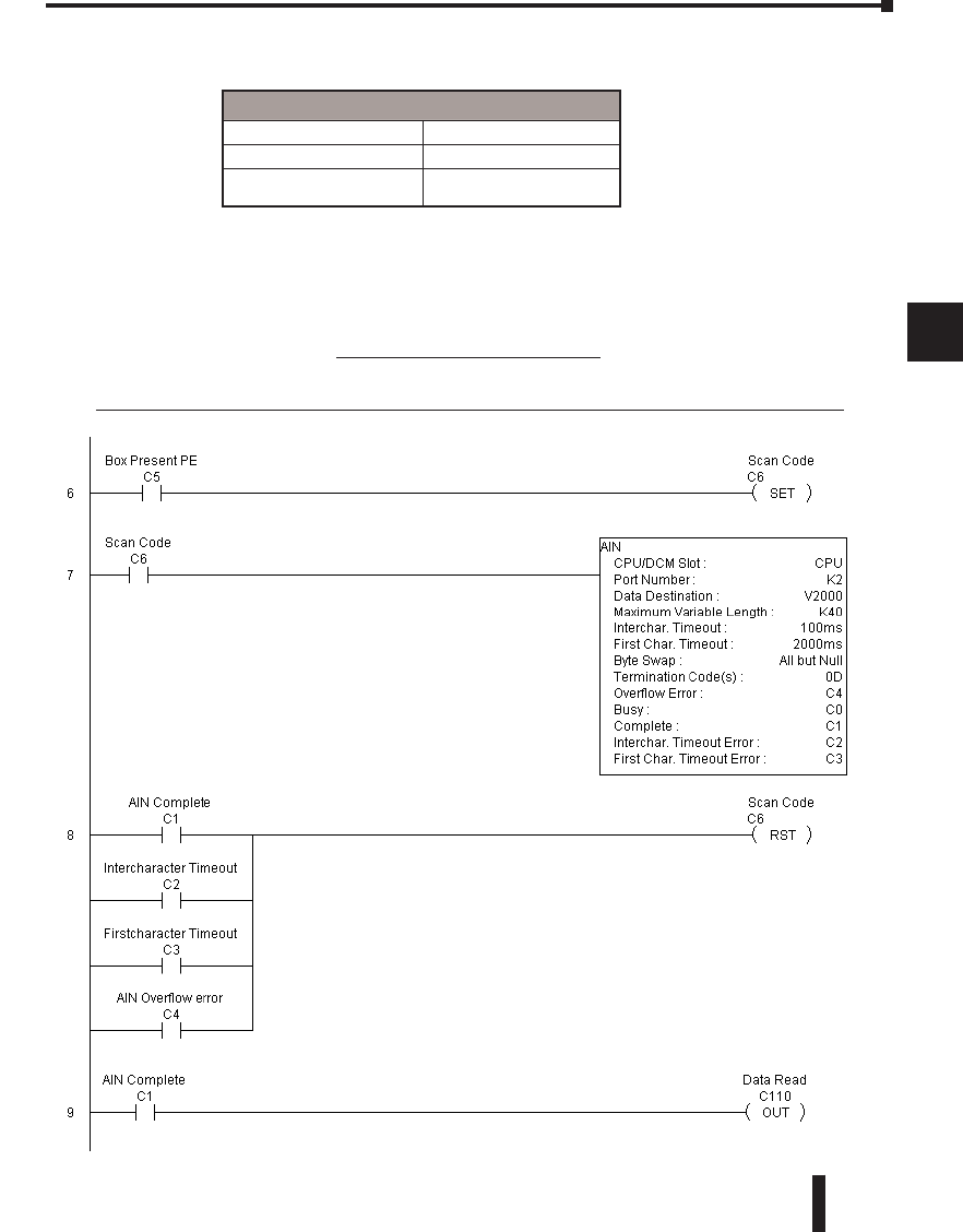
DL06 Micro PLC User Manual, 3rd Edition, Rev. D 5-215
1
2
3
4
5
6
7
8
9
10
11
12
13
14
A
B
C
D
Chapter 5: Standard RLL Instructions - ASCII
1
2
3
4
5
6
7
8
9
10
11
12
13
14
a
B
c
d
AIN Variable Length Example
AIN variable length example used to read barcodes on boxes (PE = photoelectric sensor)
Parameter
Data Destination All V–memory
Fixed Length K1–128
Bits: Busy, Complete,
Timeout Error, Overflow C0–3777
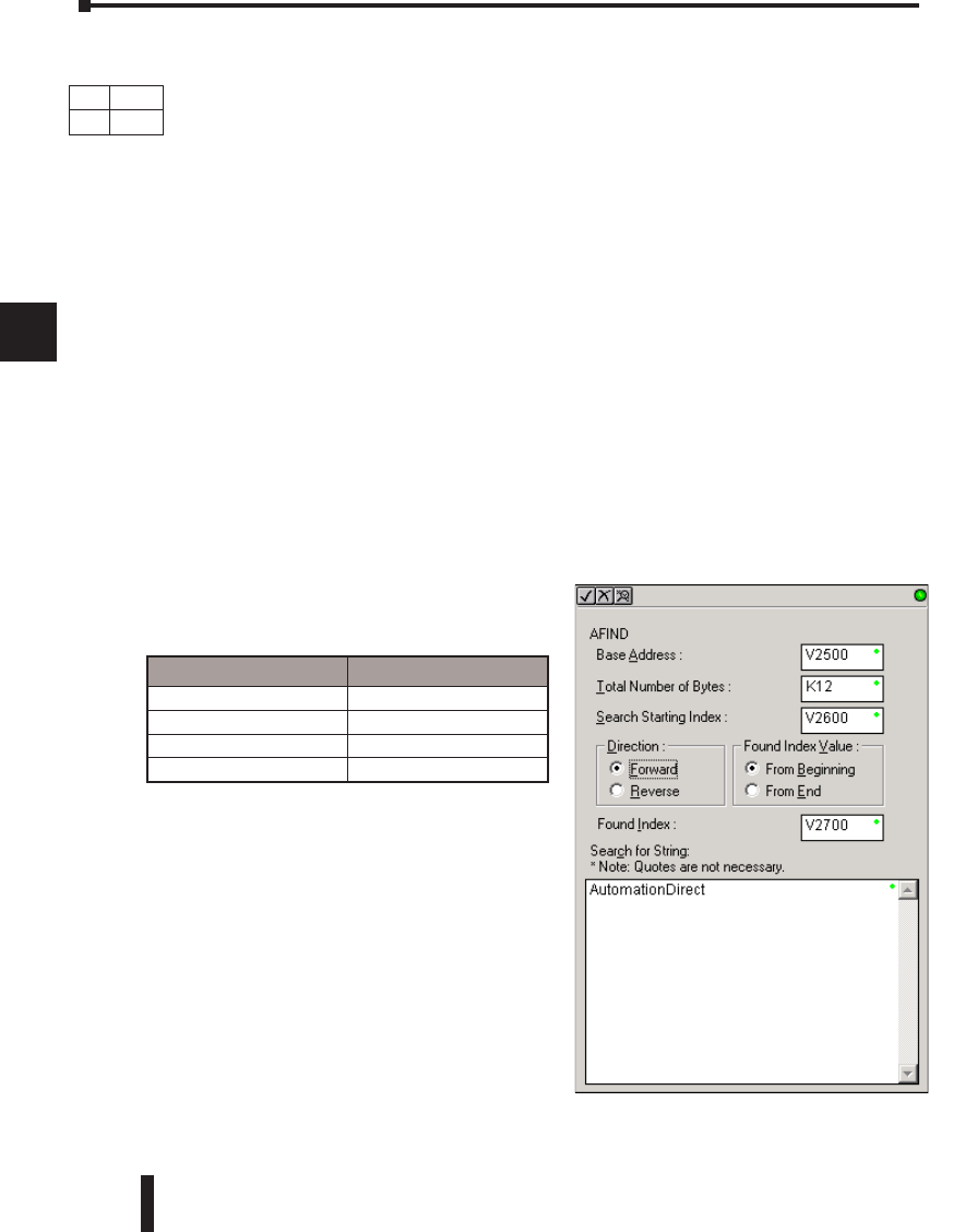
DL06 Micro PLC User Manual, 3rd Edition, Rev. D
5-216
1
2
3
4
5
6
7
8
9
10
11
12
13
14
A
B
C
D
ASCII Find (AFIND)
The ASCII Find instruction locates a specific ASCII string or portion of an ASCII string
within a range of V–memory registers and places the string’s Found Index number (byte
number where desired string is found), in Hex, into a specified V–memory register. Other
features include, Search Starting Index number for skipping over unnecessary bytes before
beginning the FIND operation, Forward or Reverse direction search, and From Beginning
and From End selections to reference the Found Index Value.
• Base Address: specifies the beginning V–memory register where the entire ASCII string is
stored in memory
• Total Number of Bytes: specifies the total number of bytes to search for the desired ASCII
string
• Search Starting Index: specifies which byte to skip to (with respect to the Base Address)
before beginning the search
• Direction: Forward begins the search from lower numbered V–memory registers to higher
numbered V–memory registers. Reverse does the search from higher numbered V–memory
registers to lower numbered V–memory registers.
• Found Index Value: specifies whether the Beginning or the End byte of the ASCII string
found will be loaded into the Found Index register
• Found Index: specifies the V–memory register where the Found Index Value will be stored.
A value of FFFF will result if the desired string is not located in the memory registers
specified.
• Search for String: up to 128 characters.
Chapter 5: Standard RLL Instructions - ASCII
1
2
3
4
5
6
7
8
9
10
11
12
13
14
a
B
c
d
Parameter DL06 Range
Base Address All V–memory
Total Number of Bytes All V–memory or K1–128
Search Starting Index All V–memory or K0–127
Found Index All V–memory
DS Used
HPP N/A
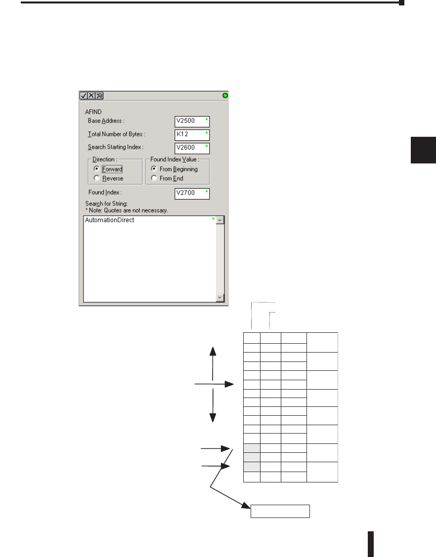
DL06 Micro PLC User Manual, 3rd Edition, Rev. D 5-217
1
2
3
4
5
6
7
8
9
10
11
12
13
14
A
B
C
D
AFIND Search Example
In the following example, the AFIND instruction is used to search for the “day” portion
of “Friday” in the ASCII string “Today is Friday.”, which had previously been loaded into
V–memory. Note that a Search Starting Index of constant (K) 5 combined with a Forward
Direction Search is used to prevent finding the “day” portion of the word “Today”. The
Found Index will be placed into V4000.
Chapter 5: Standard RLL Instructions - ASCII
1
2
3
4
5
6
7
8
9
10
11
12
13
14
a
B
c
d
Base Address T
o
d
a
y
s
F
r
i
d
a
y
.
54h
6Fh
64h
61h
79h
20h
69h
73h
20h
46h
72h
69h
64h
61h
79h
2Eh
Low
Low
Low
Low
Low
Low
Low
Low
High
High
High
High
High
High
High
High
V3000
V3001
V3002
V3003
V3004
V3005
V3006
V3007
i
Reverse Direction Search
Forward Direction Search
0
3
2
6
5
4
1
7
8
9
10
11
12
13
14
15
Search start Index Number
Beginning Index Number
End Index Number
Found Index Number = V40000012
ASCII Characters
HEX Equivalent
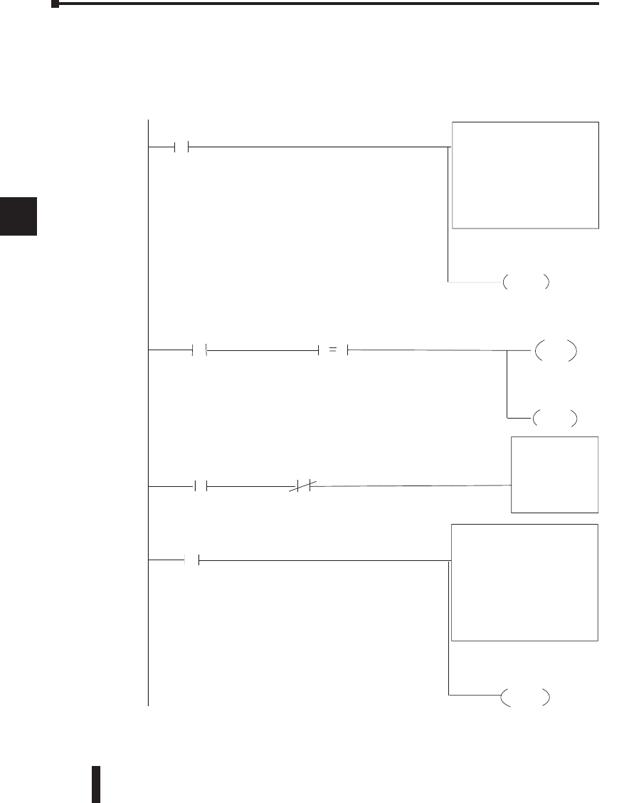
DL06 Micro PLC User Manual, 3rd Edition, Rev. D
5-218
1
2
3
4
5
6
7
8
9
10
11
12
13
14
A
B
C
D
AFIND Example Combined with AEX Instruction
When an AIN instruction has executed, its Complete bit can be used to trigger an AFIND
instruction to search for a desired portion of the ASCII string. Once the string is found, the
AEX instruction can be used to extract the located string.
Chapter 5: Standard RLL Instructions - ASCII
1
2
3
4
5
6
7
8
9
10
11
12
13
14
a
B
c
d
AIN Complete
C1
Give delay time for
AFIND instruction
to complete
C7
Give delay time for
AFIND instruction
to complete
Give delay time for
AFIND instruction
to complete
Give delay time for
AFIND instruction
to complete
Delay for
AFIND to complete
Give delay time for
AFIND instruction
to complete
Delay time for
AFIND to complete
T0
C10
Search string not found
in table
V2200 Kffff
Data not found with
AFIND
C7
C7
C7
C10
SET
SET
RST
TMR
T0
K2
RST
AEX
Source Base Address: V2001
Extract at Index: K0
Number of Bytes: K4
Shift ASCII Option: None
Byte Swap: All
Convert ASCII: To BCD (HEX)
Destination Base Address: V3000
AFIND
Base Address: V2001
Total Number of Bytes: K32
Search Starting Index: K0
Direction: Forward
Found Index Value: From Beginning
Found Index: V2200
Code 39
Data not found with
AFIND
15
16
17
18
C7
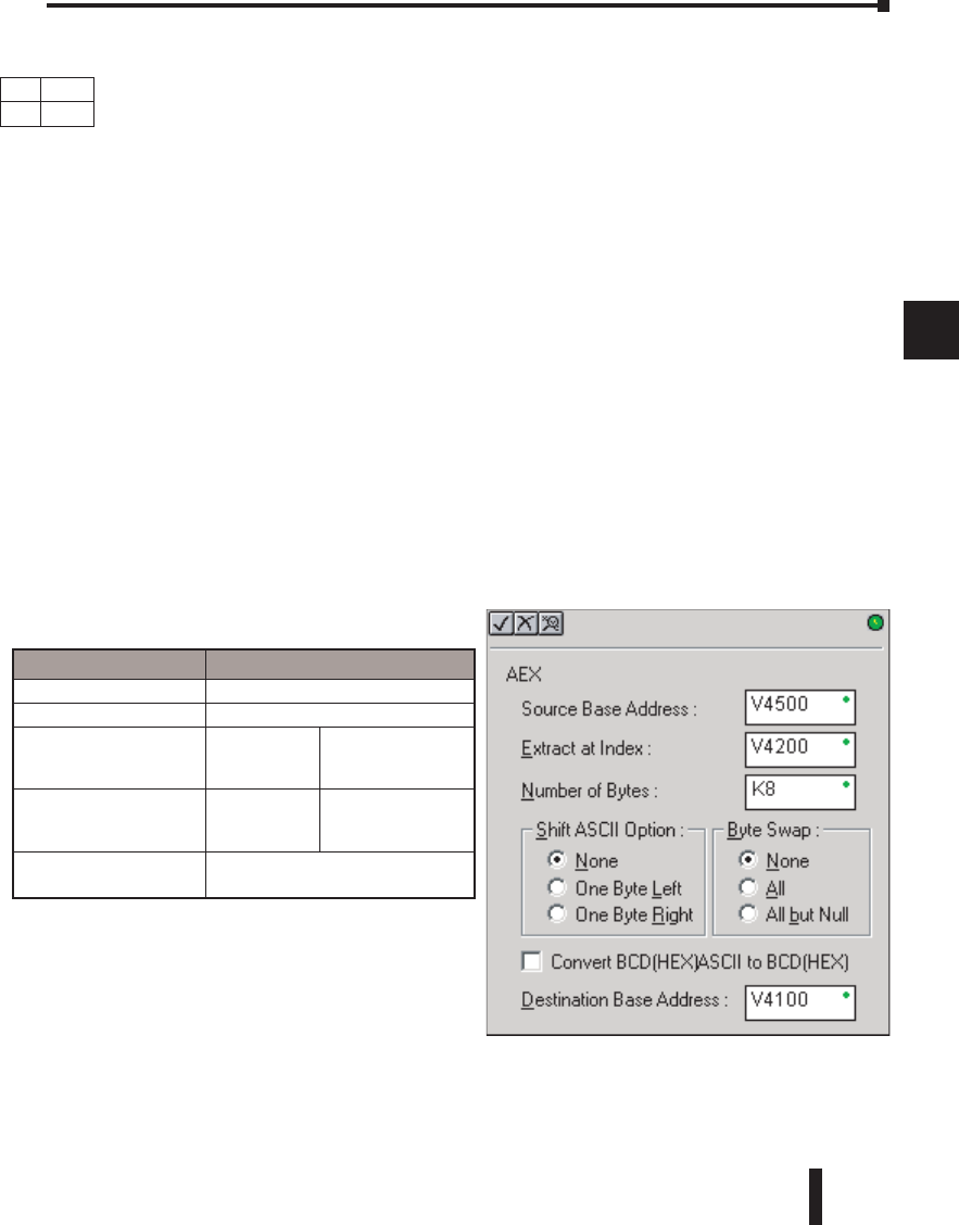
DL06 Micro PLC User Manual, 3rd Edition, Rev. D 5-219
1
2
3
4
5
6
7
8
9
10
11
12
13
14
A
B
C
D
ASCII Extract (AEX)
The ASCII Extract instruction extracts a specified number of bytes of ASCII data from one
series of V–memory registers and places it into another series of V–memory registers. Other
features include, Extract at Index for skipping over unnecessary bytes before beginning the
Extract operation, Shift ASCII Option, for One Byte Left or One Byte Right, Byte Swap and
Convert data to a BCD format number.
• Source Base Address: specifies the beginning V–memory register where the entire ASCII
string is stored in memory
• Extract at Index: specifies which byte to skip to (with respect to the Source Base Address)
before extracting the data
• Number of Bytes: specifies the number of bytes to be extracted
• Shift ASCII Option: shifts all extracted data one byte left or one byte right to displace
“unwanted” characters if necessary
• Byte Swap: swaps the high–byte and the low–byte within each V–memory register of the
extracted data. See the SWAPB instruction for details.
• Convert BCD(Hex) ASCII to BCD (Hex): if enabled, this will convert ASCII numerical
characters to Hexadecimal numerical values
• Destination Base Address: specifies the V–memory register where the extracted data will be
stored
See the previous page for an example using the AEX instruction.
Chapter 5: Standard RLL Instructions - ASCII
1
2
3
4
5
6
7
8
9
10
11
12
13
14
a
B
c
d
Parameter DL06 Range
Source Base Address All V–memory
Extract at Index All V–memory or K0–127
Number of Bytes
“Convert BCD (HEX) ASCII”
not checked
Constant range:
K1–128 V-memory location
containing BCD value:
1–128
Number of Bytes
“Convert BCD (HEX) ASCII”
checked
Constant range:
K1–4
V-memory location
containing BCD value:
1–4
Destination Base
Address All V–memory
DS Used
HPP N/A
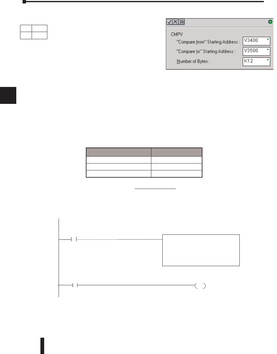
DL06 Micro PLC User Manual, 3rd Edition, Rev. D
5-220
1
2
3
4
5
6
7
8
9
10
11
12
13
14
A
B
C
D
ASCII Compare (CMPV)
The ASCII Compare instruction compares two
groups of V–memory registers. The CMPV
will compare any data type (ASCII to ASCII,
BCD to BCD, etc.) of one series (group) of
V–memory registers to another series of V–
memory registers for a specified byte length.
• “Compare from” Starting Address: specifies
the beginning V–memory register of the first
group of V–memory registers to be compared
from.
• “Compare to” Starting Address: specifies the beginning V–memory register of the second
group of V–memory registers to be compared to.
• Number of Bytes: specifies the length of each V–memory group to be compared
Chapter 5: Standard RLL Instructions - ASCII
1
2
3
4
5
6
7
8
9
10
11
12
13
14
a
B
c
d
Parameter DL06 Range
Compare from Starting Address All V–memory
Compare to Starting Address All V–memory
Number of Bytes K0–127
Strings are equal
C1
OUT
AIN Complete
CMPV
"Compare from" Starting Address: V2001
"Compare to" Starting Address: V10001
Number of Bytes: K32
C11
SP61
CMPV Example
The CMPV instruction executes when the AIN instruction is complete. If the compared V–
memory tables are equal, SP61 will turn ON.
DS Used
HPP N/A
SP61 = 1, the result is equal
SP61 = 0, the result is not equal
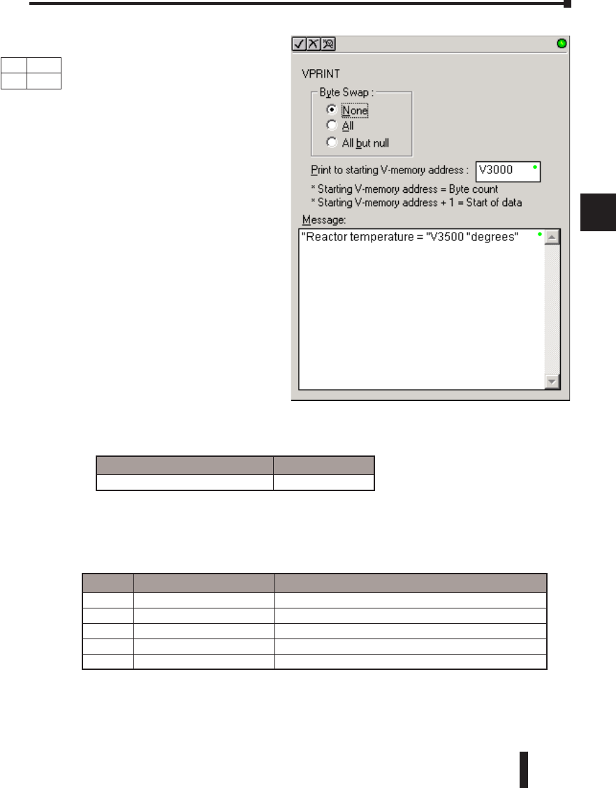
DL06 Micro PLC User Manual, 3rd Edition, Rev. D 5-221
1
2
3
4
5
6
7
8
9
10
11
12
13
14
A
B
C
D
ASCII Print to V–memory (VPRINT)
The ASCII Print to V–memory
instruction will write a specified ASCII
string into a series of V–memory
registers. Other features include Byte
Swap, options to suppress or convert
leading zeros or spaces, and _Date and
_Time options for U.S., European, and
Asian date formats and 12 or 24 hour
time formats.
• Byte Swap: swaps the high–byte and
low–byte within each V–memory
register the ASCII string is printed to.
See the SWAPB instruction for details.
• Print to Starting V–memory Address:
specifies the beginning of a series of
V–memory addresses where the ASCII
string will be placed by the VPRINT
instruction.
• Starting V–memory Address: the
first V–memory register of the series
of registers specified will contain the
ASCII string’s length in bytes.
• Starting V–memory Address +1: the
2nd and subsequent registers will
contain the ASCII string printed to V–memory.
VPRINT Time/Date Stamping– the codes in the table below can be used in the VPRINT
ASCII string message to “print to V–memory” the current time and/or date.
Chapter 5: Standard RLL Instructions - ASCII
1
2
3
4
5
6
7
8
9
10
11
12
13
14
a
B
c
d
# Character code Date / Time Stamp Options
1_date:us American standard (month/day/2 digit year)
2_date:e European standard (day/month/2 digit year)
3_date:a Asian standard (2 digit year/month/day)
4_time:12 standard 12 hour clock (0–12 hour:min am/pm)
5_time:24 standard 24 hour clock (0–23 hour:min am/pm)
Parameter DL06 Range
Print to Starting V–memory Address All V–memory
DS Used
HPP N/A
DL06 Micro PLC User Manual, 3rd Edition, Rev. D
5-222
1
2
3
4
5
6
7
8
9
10
11
12
13
14
A
B
C
D
VPRINT V-memory element – the following modifiers can be used in the VPRINT ASCII
string message to “print to V–memory” register contents in integer format or real format. Use
V-memory number or V-memory number with “:” and data type. The data types are shown in
the table below. The Character code must be capital letters.
NOTE: There must be a space entered before and after the V-memory address to separate it from the
text string. Failure to do this will result in an error code 499.
Examples:
V2000 Print binary data in V2000 for decimal number
V2000 : B Print BCD data in V2000
V2000 : D Print binary number in V2000 and V2001 for decimal number
V2000 : D B Print BCD data in V2000 and V2001
V2000 : R Print floating point number in V2000/V2001 as real number
V2000 : E Print floating point number in V2000/V2001 as real number with exponent
The following modifiers can be added to any of the modifies above to suppress or convert
leading zeros or spaces. The character code must be capital letters.
Example with V2000 = 0018 (binary format)
Example with V2000 = sp sp18 (binary format) where sp = space
Chapter 5: Standard RLL Instructions - ASCII
1
2
3
4
5
6
7
8
9
10
11
12
13
14
a
B
c
d
V–memory Register
with Modifier
Number of Characters
1 2 3 4
V2000 sp sp 1 8
V2000:B sp sp 1 2
V2000:BS 1 2
V2000:BC0 0 0 1 2
V–memory Register
with Modifier
Number of Characters
1 2 3 4
V2000 0 0 1 8
V2000:B 0 0 1 2
V2000:B0 1 2
# Character code Description
1 S Suppresses leading spaces
2 C0 Converts leading spaces to zeros
3 0 Suppresses leading zeros
# Character code Description
1 none 16-bit binary (decimal number)
2: B 4 digit BCD
3: D 32-bit binary (decimal number)
4 : D B 8 digit BCD
5: R Floating point number (real number)
6: E Floating point number (real number with exponent)
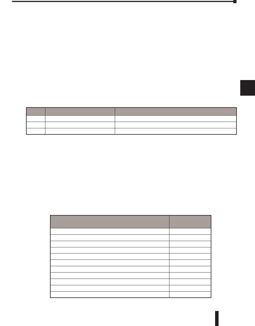
DL06 Micro PLC User Manual, 3rd Edition, Rev. D 5-223
1
2
3
4
5
6
7
8
9
10
11
12
13
14
A
B
C
D
VPRINT V-memory text element – the following is used for “printing to V–memory” text
stored in registers. Use the % followed by the number of characters after V-memory number
for representing the text. If you assign “0” as the number of characters, the function will read
the character count from the first location. Then it will start at the next V-memory location
and read that number of ASCII codes for the text from memory.
Example:
V2000 % 16 16 characters in V2000 to V2007 are printed.
V2000 % 0 The characters in V2001 to Vxxxx (determined by the number in V2000) will be
printed.
VPRINT Bit element – the following is used for “printing to V–memory” the state of the
designated bit in V-memory or a control relay bit. The bit element can be assigned by the
designating point (.) and bit number preceded by the V-memory number or relay number.
The output type is described as shown in the table below.
Example:
V2000 . 15 Prints the status of bit 15 in V2000, in 1/0 format
C100 Prints the status of C100 in 1/0 format
C100 : BOOL Prints the status of C100 in TRUE/FALSE format
C100 : ON/OFF Prints the status of C100 in ON/OFF format
V2000.15 : BOOL Prints the status of bit 15 in V2000 in TRUE/FALSE format
The maximum numbers of characters you can VPRINT is 128. The number of characters
required for each element, regardless of whether the :S, :C0 or :0 modifiers are used, is listed
in the table below.
Chapter 5: Standard RLL Instructions - ASCII
1
2
3
4
5
6
7
8
9
10
11
12
13
14
a
B
c
d
Element type Maximum
Characters
Text, 1 character 1
16 bit binary 6
32 bit binary 11
4 digit BCD 4
8 digit BCD 8
Floating point (real number) 3
Floating point (real with exponent) 13
V-memory/text 2
Bit (1/0 format) 1
Bit (TRUE/FALSE format) 5
Bit (ON/OFF format) 3
# Data format Description
1 none Print 1 for an ON state, and 0 for an OFF state
2 : BOOL Print “TRUE” for an ON state, and “FALSE” for an OFF state
3: ONOFF Print “ON” for an ON state, and “OFF” for an OFF state
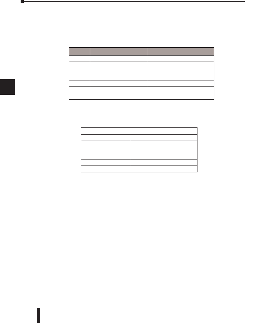
DL06 Micro PLC User Manual, 3rd Edition, Rev. D
5-224
1
2
3
4
5
6
7
8
9
10
11
12
13
14
A
B
C
D
Chapter 5: Standard RLL Instructions - ASCII
1
2
3
4
5
6
7
8
9
10
11
12
13
14
a
B
c
d
Text element – the following is used for “printing to V–memory” character strings. The
character strings are defined as the character (more than 0) ranged by the double quotation
marks. Two hex numbers preceded by the dollar sign means an 8-bit ASCII character code.
Also, two characters preceded by the dollar sign is interpreted according to the following
table:
The following examples show various syntax conventions and the length of the output to the
printer.
In printing an ordinary line of text, you will need to include double quotation marks before
and after the text string. Error code 499 will occur in the CPU when the print instruction
contains invalid text or no quotations. It is important to test your VPRINT instruction data
during the application development.
#Character code Description
1 $$ Dollar sign ($)
2 $” Double quotation (”)
3 $Lor $l Line feed (LF)
4 $N or $n Carriage return line feed (CRLF)
5 $P or $p Form feed
6$R or $r Carriage return (CR)
7 $T or $t Tab
” ” Length 0 without character
”A” Length 1 with character A
” ” Length 1 with blank
” $” ” Length 1 with double quotation mark
” $ R $ L ” Length 2 with one CR and one LF
” $ 0 D $ 0 A ” Length 2 with one CR and one LF
” $ $ ” Length 1 with one $ mark
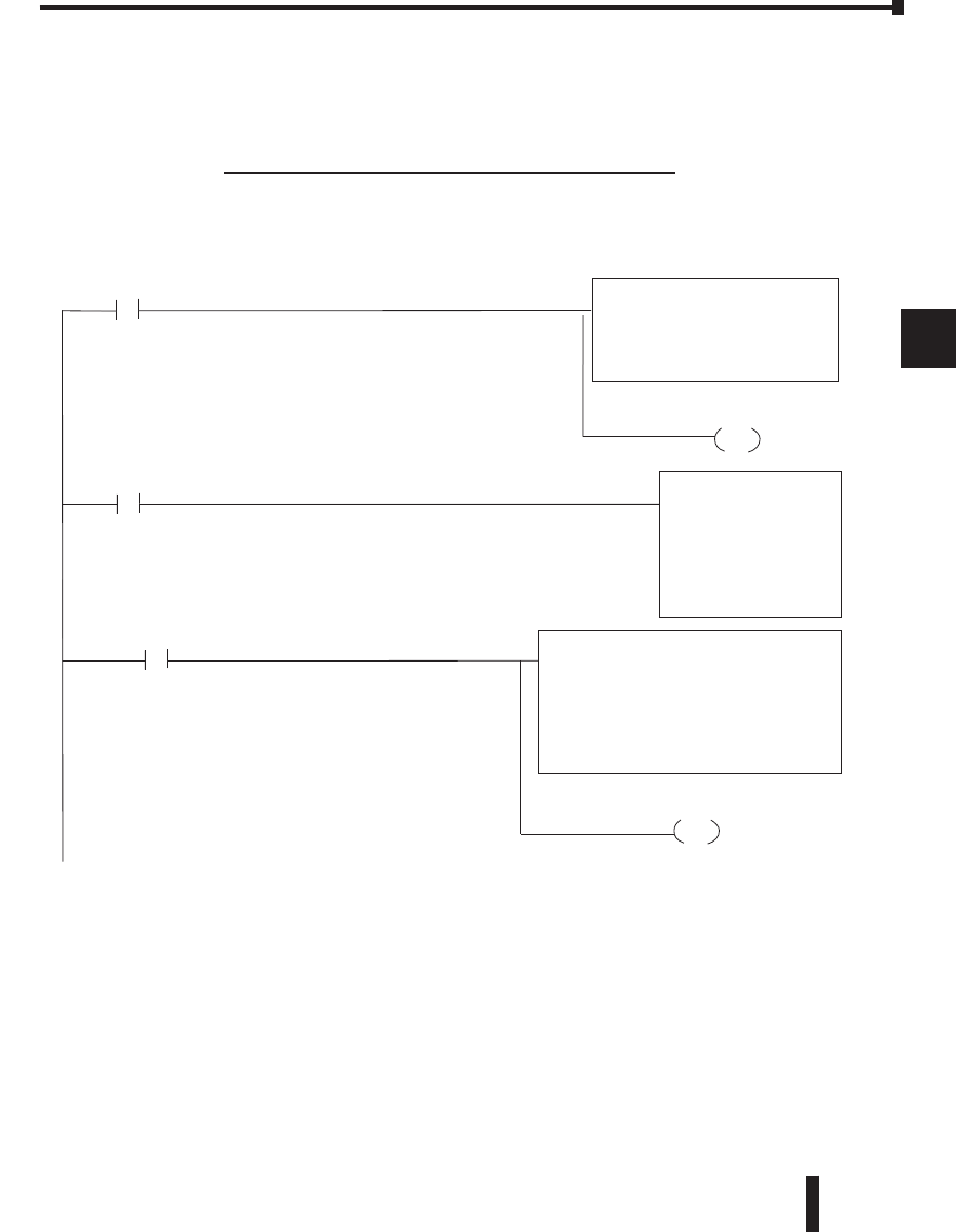
DL06 Micro PLC User Manual, 3rd Edition, Rev. D 5-225
1
2
3
4
5
6
7
8
9
10
11
12
13
14
A
B
C
D
Chapter 5: Standard RLL Instructions - ASCII
1
2
3
4
5
6
7
8
9
10
11
12
13
14
a
B
c
d
The VPRINT instruction is used to create a string in V–memory. The PRINTV is used to print the string out
of port 2.
VPRINT Example Combined with PRINTV Instruction
Delay Permissive for
RST
Delay permissive for
VPRINT
Create String Permissive
SET
PRINTV
Port Number: K2
Start Address: V4001
Number of Bytes: V4000
Append: None
Byte Swap: None
Busy: C15
Complete: C16
VPRINT
C13
TMR
Delay for VPRINT
to complete
T1
K10
Delay for Vprint to
complete
T1
Delay permissive for
VPRINT
C13
C12
C13
VPRINT
Byte Swap: All
"Print to" Address V4000
"STX" V3000:B"$0D"
28
29
30
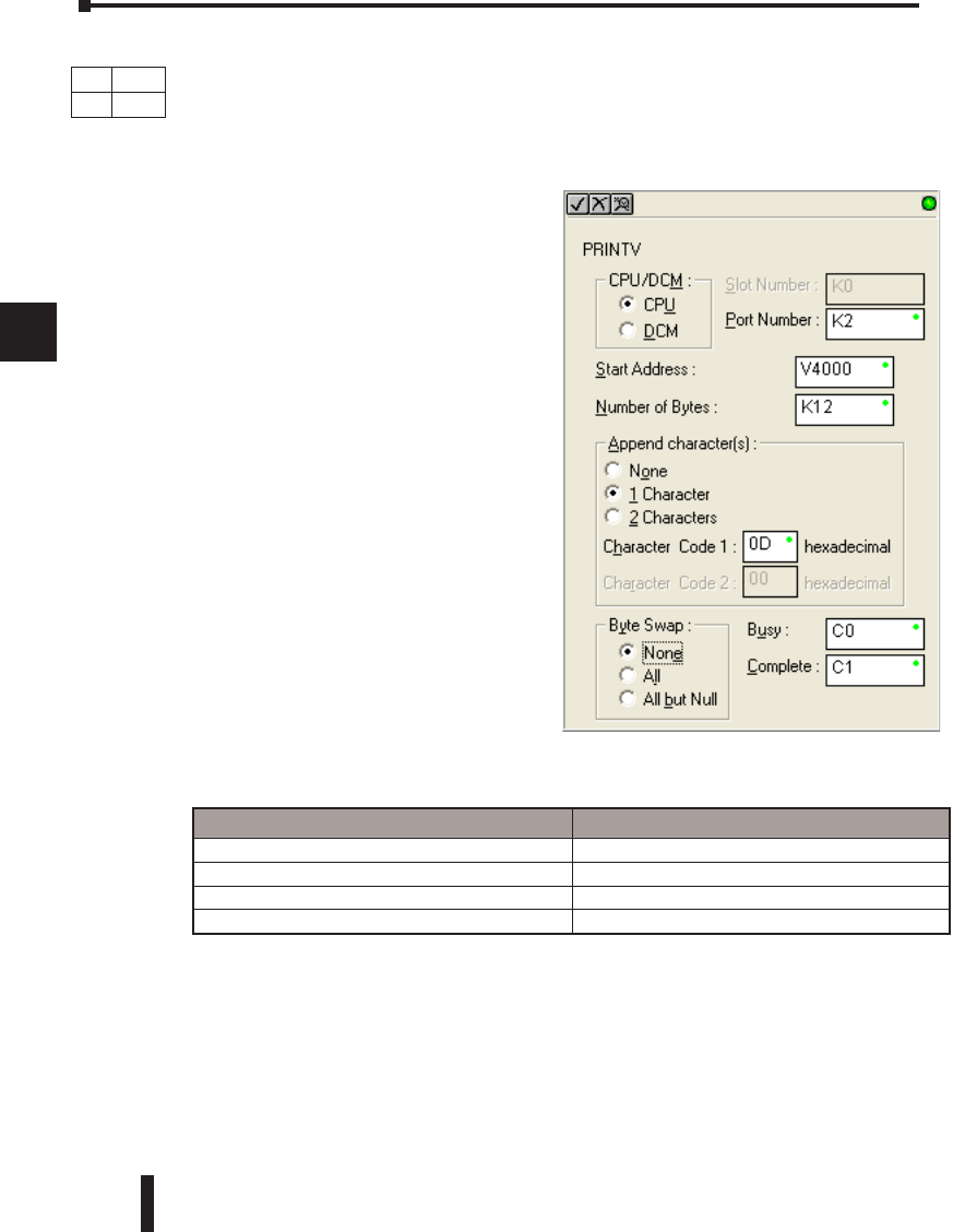
DL06 Micro PLC User Manual, 3rd Edition, Rev. D
5-226
1
2
3
4
5
6
7
8
9
10
11
12
13
14
A
B
C
D
Chapter 5: Standard RLL Instructions - ASCII
1
2
3
4
5
6
7
8
9
10
11
12
13
14
a
B
c
d
ASCII Print from V–memory (PRINTV)
The ASCII Print from V–memory instruction will send an ASCII string out of the designated
communications port from a specified series of V–memory registers for a specified length in
number of bytes. Other features include user specified Append Characters to be placed after
the desired data string for devices that require specific termination character(s), Byte Swap
options, and user specified flags for Busy and Complete.
• Port Number: must be DL06 port 2 (K2)
• Start Address: specifies the beginning of
series of V–memory registers that contain
the ASCII string to print
• Number of Bytes: specifies the length of
the string to print
• Append Characters: specifies ASCII
characters to be added to the end of the
string for devices that require specific
termination characters
• Byte Swap: swaps the high–byte
and low–byte within each V–
memory register of the string while
printing. See the SWAPB instruction for
details.
• Busy Bit: will be ON while the instruction is
printing ASCII data
• Complete Bit: will be set
once the ASCII data has been printed
and reset when the PRINTV instruction
permissive bits are disabled.
See the previous page for an example using the PRINTV instruction.
Parameter DL06 Range
Port Number port 2 (K2)
Start Address All V–memory
Number of Bytes All V–memory or k1–128
Bits: Busy, Complete C0–3777
DS Used
HPP N/A
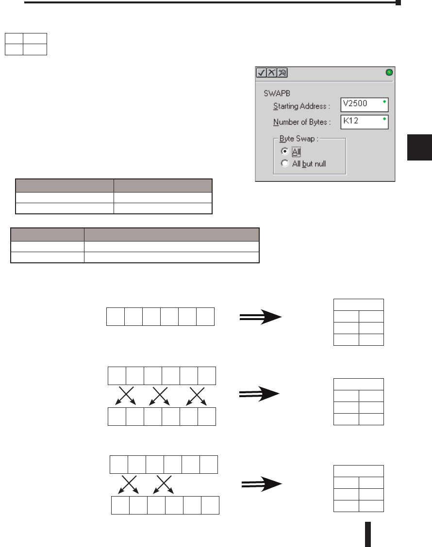
DL06 Micro PLC User Manual, 3rd Edition, Rev. D 5-227
1
2
3
4
5
6
7
8
9
10
11
12
13
14
A
B
C
D
Chapter 5: Standard RLL Instructions - ASCII
1
2
3
4
5
6
7
8
9
10
11
12
13
14
a
B
c
d
ASCII Swap Bytes (SWAPB)
The ASCII Swap Bytes instruction swaps byte positions (high–byte to low–byte and low–
byte to high–byte) within each V–memory register of a series of V–memory registers for a
specified number of bytes.
• Starting Address: specifies the beginning of a series
of V–memory registers the instruction will use to
begin byte swapping
• Number of Bytes: specifies the number of bytes,
beginning with the Starting Address, to byte swap.
• Byte Swap:
All - swap all bytes specified.
All but null - swap all bytes specified except the
bytes with a null
DS Used
HPP N/A
A B C D E xx
V2477
V2500
V2501
V2502
Byte
High Low
0005h
B A
D C
xx E
No Byte Swapping
(AIN, AEX, PRINTV, VPRINT)
B A D C xx E
A B C D E xx
A B C D E xx
B A D C E xx
V2477
V2500
V2501
V2502
V2477
V2500
V2501
V2502
0005h
A B
C D
E xx
0005h
B A
D C
xx E
Byte
High Low
Byte
High Low
Byte Swap All
Byte Swap All but Null
Discrete Bit Flags Description
SP53 On if the CPU cannot execute the instruction.
SP71 On when a value used by the instruction is invalid.
Parameter DL06 Range
Starting Address All V–memory
Number of Bytes All V–memory or K1–128
Byte Swap
Preferences
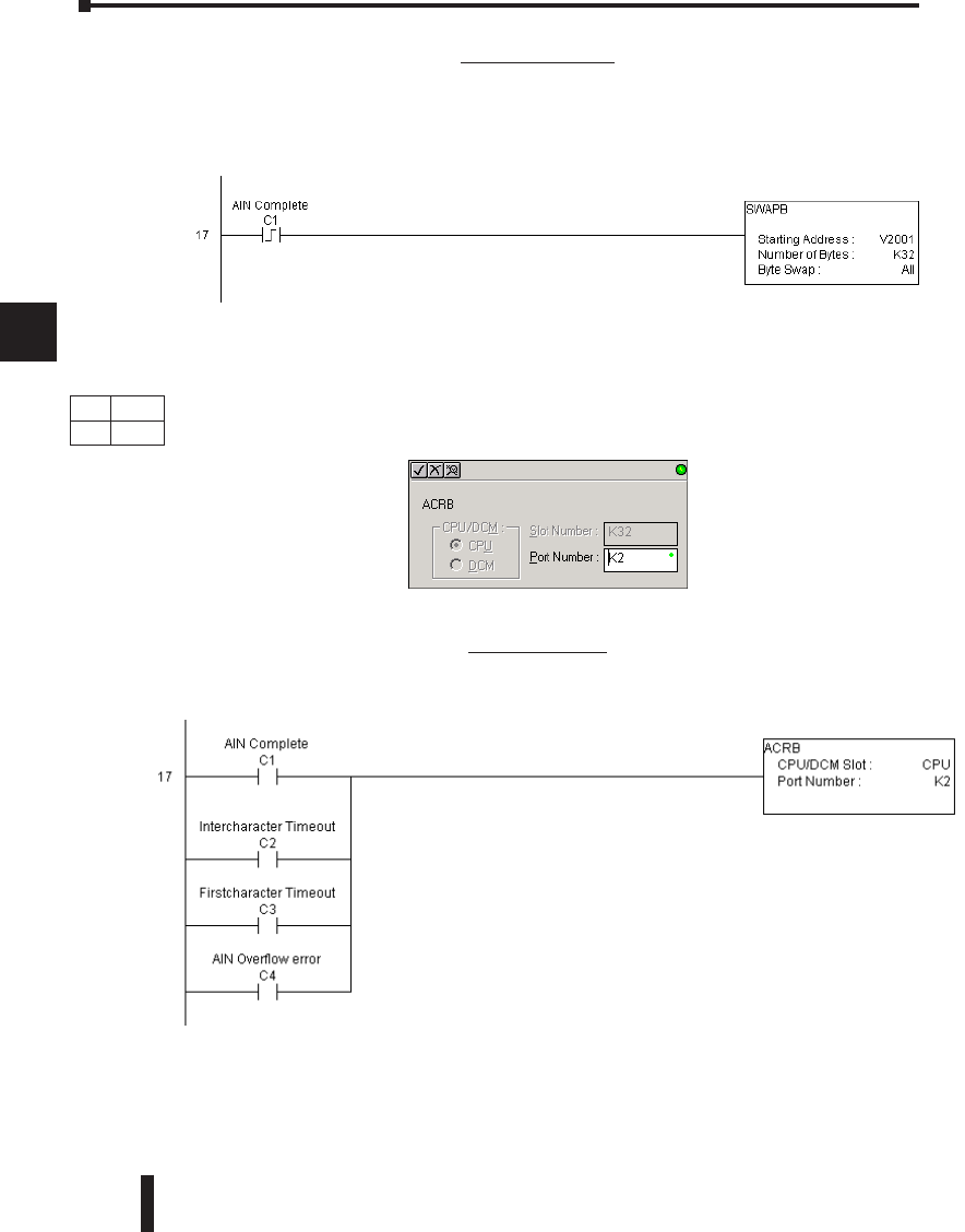
DL06 Micro PLC User Manual, 3rd Edition, Rev. D
5-228
1
2
3
4
5
6
7
8
9
10
11
12
13
14
A
B
C
D
SWAPB Example
The AIN Complete bit is used to trigger the SWAPB instruction. Use a one–shot so the
SWAPB only executes once.
ASCII Clear Buffer (ACRB)
The ASCII Clear Buffer instruction will clear the ASCII receive buffer of the specified
communications port number. Port Number: must be DL06 port 2 (K2)
ACRB Example
The AIN Complete bit or the AIN diagnostic bits are used to clear the ASCII buffer.
Chapter 5: Standard RLL Instructions - ASCII
1
2
3
4
5
6
7
8
9
10
11
12
13
14
a
B
c
d
DS Used
HPP N/A

DL06 Micro PLC User Manual, 3rd Edition, Rev. D 5-229
1
2
3
4
5
6
7
8
9
10
11
12
13
14
A
B
C
D
Chapter 5: Standard RLL Instructions
1
2
3
4
5
6
7
8
9
10
11
12
13
14
a
B
c
d
This page intentionally left blank.
DL06 Micro PLC User Manual, 3rd Edition, Rev. D
5-230
1
2
3
4
5
6
7
8
9
10
11
12
13
14
A
B
C
D
Intelligent Box (IBox) Instructions
The Intelligent Box Instructions (IBox) listed in this section are additional instructions
made available when using DirectSOFT to program your DL06 PLC (the DL06 CPU
requires firmware version v2.10 or later to use the new features in DirectSOFT). For more
information on DirectSOFT and to download a free demo version, please visit our Web site
at: www.automationdirect.com.
Chapter 5: Intelligent Box (IBox) Instructions
1
2
3
4
5
6
7
8
9
10
11
12
13
14
a
B
c
d
Analog Helper IBoxes
Instruction Ibox # Page
Analog Input / Output Combo Module Pointer Setup (ANLGCMB) IB-462 5-232
Analog Input Module Pointer Setup (ANLGIN) IB-460 5-234
Analog Output Module Pointer Setup (ANLGOUT) IB-461 5-236
Analog Scale 12 Bit BCD to BCD (ANSCL) IB-423 5-238
Analog Scale 12 Bit Binary to Binary (ANSCLB) IB-403 5-239
Filter Over Time - BCD (FILTER) IB-422 5-240
Filter Over Time - Binary (FILTERB) IB-402 5-242
Hi/Low Alarm - BCD (HILOAL) IB-421 5-244
Hi/Low Alarm - Binary (HILOALB) IB-401 5-246
Discrete Helper IBoxes
Instruction Ibox # Page
Off Delay Timer (OFFDTMR) IB-302 5-248
On Delay Timer (ONDTMR) IB-301 5-250
One Shot (ONESHOT) IB-303 5-252
Push On / Push Off Circuit (PONOFF) IB-300 5-253
Memory IBoxes
Instruction Ibox # Page
Move Single Word (MOVEW) IB-200 5-254
Move Double Word (MOVED) IB-201 5-255
Math IBoxes
Instruction Ibox # Page
BCD to Real with Implied Decimal Point (BCDTOR) IB-560 5-256
Double BCD to Real with Implied Decimal Point (BCDTORD) IB-562 5-257
Math - BCD (MATHBCD) IB-521 5-258
Math - Binary (MATHBIN) IB-501 5-260
Math - Real (MATHR) IB-541 5-262
Real to BCD with Implied Decimal Point and Rounding (RTOBCD) IB-561 5-263
Real to Double BCD with Implied Decimal Point and Rounding (RTOBCDD) IB-563 5-264
Square BCD (SQUARE) IB-523 5-265
Square Binary (SQUAREB) IB-503 5-266
Square Real(SQUARER) IB-543 5-267
Sum BCD Numbers (SUMBCD) IB-522 5-268
Sum Binary Numbers (SUMBIN) IB-502 5-269
Sum Real Numbers (SUMR) IB-542 5-270
DL06 Micro PLC User Manual, 3rd Edition, Rev. D 5-231
1
2
3
4
5
6
7
8
9
10
11
12
13
14
A
B
C
D
Chapter 5: Intelligent Box (IBox) Instructions
1
2
3
4
5
6
7
8
9
10
11
12
13
14
a
B
c
d
Communication IBoxes
Instruction Ibox # Page
ECOM100 Configuration (ECOM100) IB-710 5-272
ECOM100 Disable DHCP (ECDHCPD) IB-736 5-274
ECOM100 Enable DHCP (ECDHCPE) IB-735 5-276
ECOM100 Query DHCP Setting (ECDHCPQ) IB-734 5-278
ECOM100 Send E-mail (ECEMAIL) IB-711 5-280
ECOM100 Restore Default E-mail Setup (ECEMRDS) IB-713 5-283
ECOM100 E-mail Setup (ECEMSUP) IB-712 5-286
ECOM100 IP Setup (ECIPSUP) IB-717 5-290
ECOM100 Read Description (ECRDDES) IB-726 5-292
ECOM100 Read Gateway Address (ECRDGWA) IB-730 5-294
ECOM100 Read IP Address (ECRDIP) IB-722 5-296
ECOM100 Read Module ID (ECRDMID) IB-720 5-298
ECOM100 Read Module Name (ECRDNAM) IB-724 5-300
ECOM100 Read Subnet Mask (ECRDSNM) IB-732 5-302
ECOM100 Write Description (ECWRDES) IB-727 5-304
ECOM100 Write Gateway Address (ECWRGWA) IB-731 5-306
ECOM100 Write IP Address (ECWRIP) IB-723 5-308
ECOM100 Write Module ID (ECWRMID) IB-721 5-310
ECOM100 Write Name (ECWRNAM) IB-725 5-312
ECOM100 Write Subnet Mask (ECWRSNM) IB-733 5-314
ECOM100 RX Network Read (ECRX) IB-740 5-316
ECOM100 WX Network Write(ECWX) IB-741 5-319
NETCFG Network Configuration (NETCFG) IB-700 5-322
Network RX Read (NETRX) IB-701 5-324
Network WX Write (NETWX) IB-702 5-327
Counter I/O IBoxes (Works with H0-CTRIO and H0-CTRIO2)
Instruction Ibox # Page
CTRIO Configuration (CTRIO) IB-1000 5-330
CTRIO Add Entry to End of Preset Table (CTRADPT) IB-1005 5-332
CTRIO Clear Preset Table (CTRCLRT) IB-1007 5-335
CTRIO Edit Preset Table Entry (CTREDPT) IB-1003 5-338
CTRIO Edit Preset Table Entry and Reload (CTREDRL) IB-1002 5-342
CTRIO Initialize Preset Table (CTRINPT) IB-1004 5-346
CTRIO Initialize Preset Table (CTRINTR) IB-1010 5-350
CTRIO Load Profile (CTRLDPR) IB-1001 5-354
CTRIO Read Error (CTRRDER) IB-1014 5-357
CTRIO Run to Limit Mode (CTRRTLM) IB-1011 5-359
CTRIO Run to Position Mode (CTRRTPM) IB-1012 5-362
CTRIO Velocity Mode (CTRVELO) IB-1013 5-365
CTRIO Write File to ROM (CTRWFTR) IB-1006 5-368
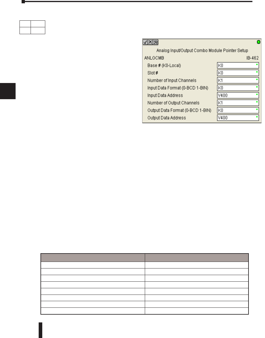
DL06 Micro PLC User Manual, 3rd Edition, Rev. D
5-232
1
2
3
4
5
6
7
8
9
10
11
12
13
14
A
B
C
D
Analog Input/Output Combo Module Pointer Setup (ANLGCMB) (IB-462)
The Analog Input/Output Combo Module Pointer Setup instruction generates the logic to
configure the pointer method for an analog input/output combination module on the first
PLC scan following a Program to Run transition.
The ANLGCMB IBox instruction
determines the data format and Pointer
addresses based on the CPU type, the
Base# and the module Slot#.
The Input Data Address is the starting
location in user V-memory where the
analog input data values will be stored,
one location for each input channel
enabled.
The Output Data Address is the starting
location in user V-memory where the
analog output data values will be placed
by ladder code or external device, one location for each output channel enabled.
Since the IBox logic only executes on the first scan, the instruction cannot have any input logic.
ANLGCMB Parameters
• Base # (K0-Local): must be 0 for DL06 PLC
• Slot #: specifies which PLC option slot is occupied by the analog module (1–4)
• Number of Input Channels: specifies the number of analog input channels to scan
• Input Data Format (0-BCD 1-BIN): specifies the analog input data format (BCD or Binary) - the
binary format may be used for displaying data on some OI panels
• Input Data Address: specifies the starting V-memory location that will be used to store the analog
input data
• Number of Output Channels: specifies the number of analog output channels that will be used
• Output Data Format (0-BCD 1-BIN): specifies the format of the analog output data (BCD or
Binary)
• Output Data Address: specifies the starting V-memory location that will be used to source the
analog output data
Chapter 5: Intelligent Box (IBox) Instructions
1
2
3
4
5
6
7
8
9
10
11
12
13
14
a
B
c
d
DS Used
HPP N/A
Parameter DL06 Range
Base # (K0-Local) K K0 (local base only)
Slot # K K1-4
Number of Input Channels K K1-8
Input Data Format (0-BCD 1-BIN) K BCD: K0; Binary: K1
Input Data Address V See DL06 V-memory map - Data Words
Number of Output Channels K K1-8
Output Data Format (0-BCD 1-BIN) K BCD: K0; Binary: K1
Output Data Address V See DL06 V-memory map - Data Words
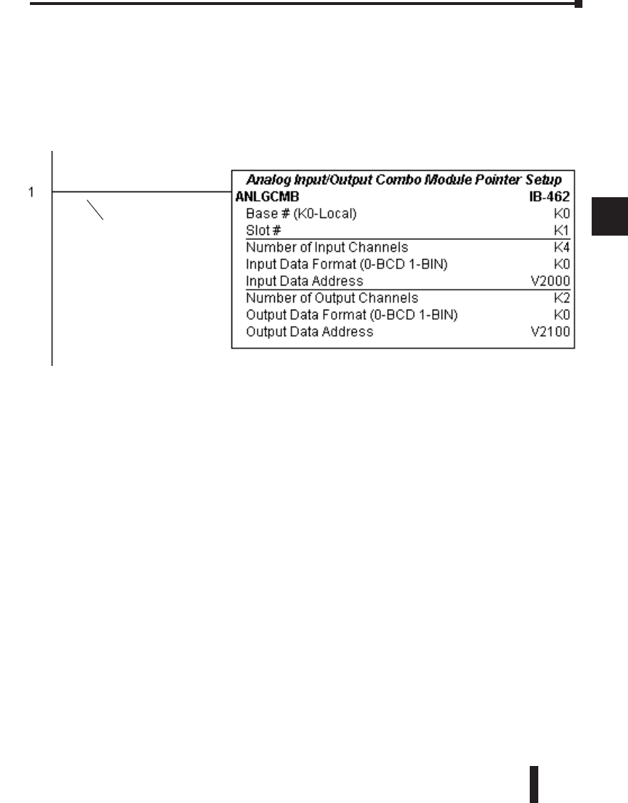
DL06 Micro PLC User Manual, 3rd Edition, Rev. D 5-233
1
2
3
4
5
6
7
8
9
10
11
12
13
14
A
B
C
D
ANLGCMB Example
In the following example, the ANLGCMB instruction is used to setup the pointer method
for an analog I/O combination module that is installed in option slot 2. Four input channels
are enabled and the analog data will be written to V2000 - V2003 in BCD format. Two
output channels are enabled and the analog values will be read from V2100 - V2101 in BCD
format.
Chapter 5: Intelligent Box (IBox) Instructions
1
2
3
4
5
6
7
8
9
10
11
12
13
14
a
B
c
d
Permissive contacts or input
logic cannot be used with this
instruction.
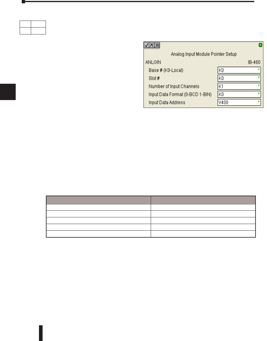
DL06 Micro PLC User Manual, 3rd Edition, Rev. D
5-234
1
2
3
4
5
6
7
8
9
10
11
12
13
14
A
B
C
D
Analog Input Module Pointer Setup (ANLGIN) (IB-460)
Analog Input Module Pointer Setup generates the logic to configure the pointer method for
one analog input module on the first PLC scan following a Program to Run transition.
This IBox determines the data format and Pointer addresses based on the CPU type, the
Base#, and the Slot#.
The Input Data Address is the starting
location in user V-memory where the
analog input data values will be stored,
one location for each input channel
enabled.
Since this logic only executes on the first
scan, this IBox cannot have any input
logic.
ANLGIN Parameters
• Base # (K0-Local): must be 0 for DL06 PLC
• Slot #: specifies which PLC option slot is occupied by the analog module (1–4)
• Number of Input Channels: specifies the number of input channels to scan
• Input Data Format (0-BCD 1-BIN): specifies the analog input data format (BCD or Binary) - the
binary format may be used for displaying data on some OI panels
• Input Data Address: specifies the starting V-memory location that will be used to store the analog
input data
Chapter 5: Intelligent Box (IBox) Instructions
1
2
3
4
5
6
7
8
9
10
11
12
13
14
a
B
c
d
DS Used
HPP N/A
Parameter DL06 Range
Base # (K0-Local) K K0 (local base only)
Slot # K K1-4
Number of Input Channels K K1-8
Input Data Format (0-BCD 1-BIN) K BCD: K0; Binary: K1
Input Data Address V See DL06 V-memory map - Data Words
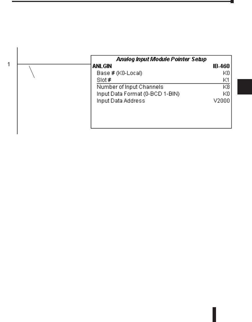
DL06 Micro PLC User Manual, 3rd Edition, Rev. D 5-235
1
2
3
4
5
6
7
8
9
10
11
12
13
14
A
B
C
D
ANLGIN Example
In the following example, the ANLGIN instruction is used to setup the pointer method for
an analog input module that is installed in option slot 1. Eight input channels are enabled
and the analog data will be written to V2000 - V2007 in BCD format.
Chapter 5: Intelligent Box (IBox) Instructions
1
2
3
4
5
6
7
8
9
10
11
12
13
14
a
B
c
d
Permissive contacts or input logic
cannot be used with this instruction.
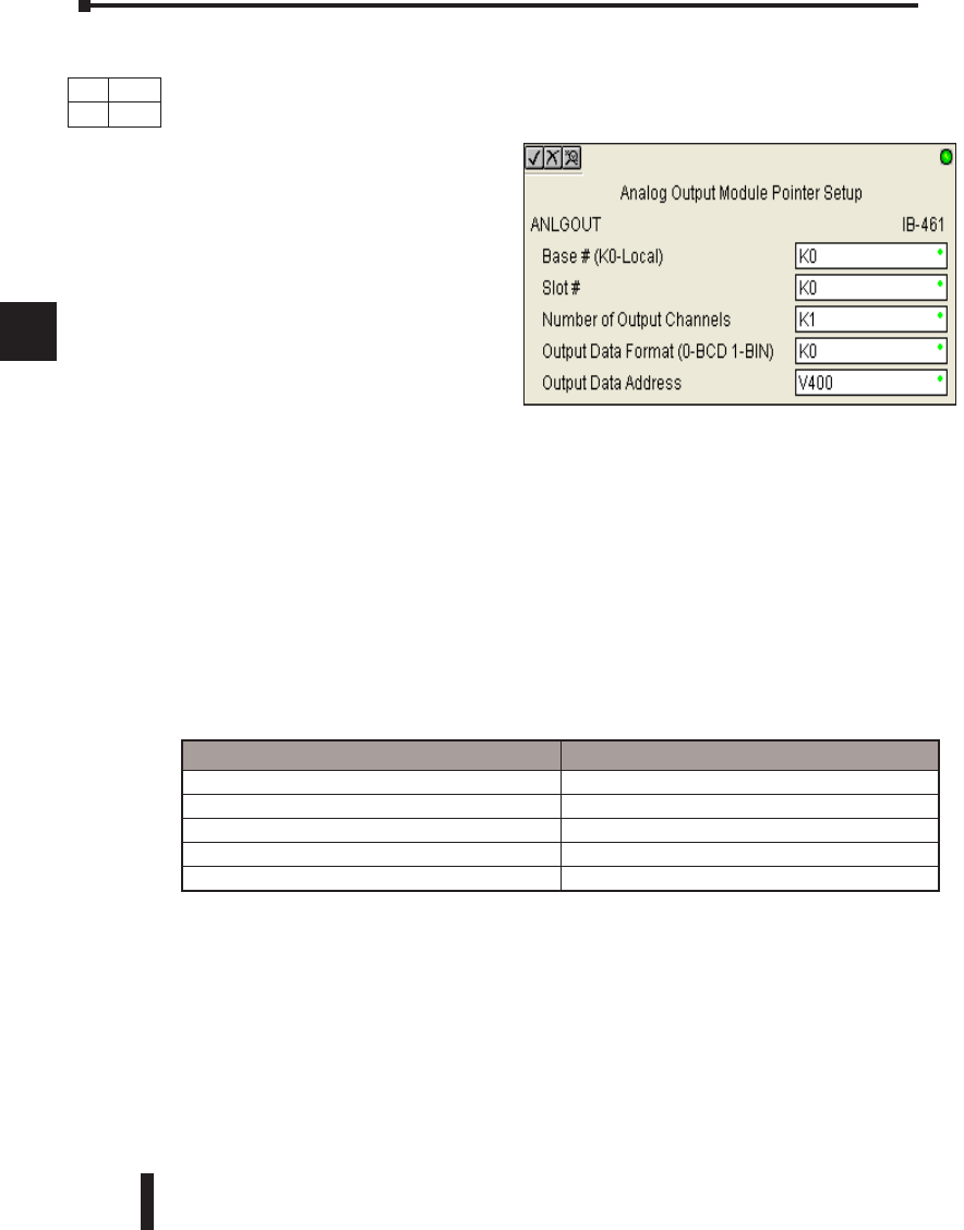
DL06 Micro PLC User Manual, 3rd Edition, Rev. D
5-236
1
2
3
4
5
6
7
8
9
10
11
12
13
14
A
B
C
D
Analog Output Module Pointer Setup (ANLGOUT) (IB-461)
Analog Output Module Pointer Setup generates the logic to configure the pointer method for
one analog output module on the first PLC scan following a Program to Run transition.
This IBox determines the data format
and Pointer addresses based on the CPU
type, the Base#, and the Slot#.
The Output Data Address is the starting
location in user V-memory where the
analog output data values will be placed
by ladder code or external device, one
location for each output channel enabled.
Since this logic only executes on the first
scan, this IBox cannot have any input
logic.
ANLGOUT Parameters
• Base # (K0-Local): must be 0 for DL06 PLC
• Slot #: specifies which PLC option slot is occupied by the analog module (1–4)
• Number of Output Channels: specifies the number of analog output channels that will be used
• Output Data Format (0-BCD 1-BIN): specifies the format of the analog output data (BCD or
Binary)
• Output Data Address: specifies the starting V-memory location that will be used to source the
analog output data
Chapter 5: Intelligent Box (IBox) Instructions
1
2
3
4
5
6
7
8
9
10
11
12
13
14
a
B
c
d
DS Used
HPP N/A
Parameter DL06 Range
Base # (K0-Local) K K0 (local base only)
Slot # K K1-4
Number of Output Channels K K1-8
Output Data Format (0-BCD 1-BIN) K BCD: K0; Binary: K1
Output Data Address V See DL06 V-memory map - Data Words
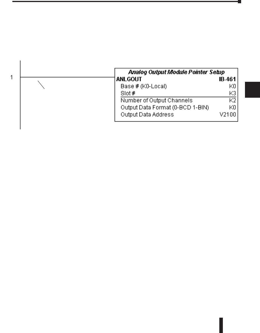
DL06 Micro PLC User Manual, 3rd Edition, Rev. D 5-237
1
2
3
4
5
6
7
8
9
10
11
12
13
14
A
B
C
D
ANLGOUT Example
In the following example, the ANLGOUT instruction is used to setup the pointer method
for an analog output module that is installed in option slot 3. Two output channels are
enabled and the analog data will be read from V2100 - V2101 in BCD format.
Chapter 5: Intelligent Box (IBox) Instructions
1
2
3
4
5
6
7
8
9
10
11
12
13
14
a
B
c
d
Permissive contacts or input logic cannot
be used with this instruction.
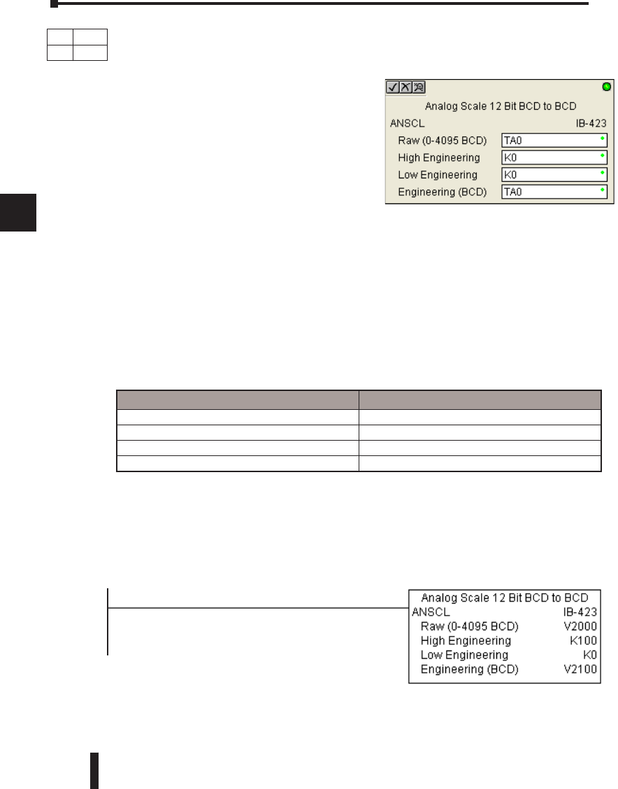
DL06 Micro PLC User Manual, 3rd Edition, Rev. D
5-238
1
2
3
4
5
6
7
8
9
10
11
12
13
14
A
B
C
D
Analog Scale 12 Bit BCD to BCD (ANSCL) (IB-423)
Analog Scale 12 Bit BCD to BCD scales a 12 bit BCD analog value (0-4095 BCD) into
BCD engineering units. You specify the engineering unit high value (when raw is 4095), and
the engineering low value (when raw is 0), and the output V-Memory address you want the
to place the scaled engineering unit value. The
engineering units are generated as BCD and can
be the full range of 0 to 9999 (see ANSCLB -
Analog Scale 12 Bit Binary to Binary if your raw
units are in Binary format).
Note that this IBox only works with unipolar
unsigned raw values. It does NOT work with
bipolar or sign plus magnitude raw values.
ANSCL Parameters
• Raw (0-4095 BCD): specifies the V-memory location of the unipolar unsigned raw 0-4095
unscaled value
• High Engineering: specifies the high engineering value when the raw input is 4095
• Low Engineering: specifies the low engineering value when the raw input is 0
• Engineering (BCD): specifies the V-memory location where the scaled engineering BCD value will
be placed
ANSCL Example
In the following example, the ANSCL instruction is used to scale a raw value (0-4095 BCD)
that is in V2000. The engineering scaling range is set 0-100 (low engineering value - high
engineering value). The scaled value will be placed in V2100 in BCD format.
Chapter 5: Intelligent Box (IBox) Instructions
1
2
3
4
5
6
7
8
9
10
11
12
13
14
a
B
c
d
DS Used
HPP N/A
Parameter DL06 Range
Raw (0-4095 BCD) V,P See DL06 V-memory map - Data Words
High Engineering K K0-9999
Low Engineering K K0-9999
Engineering (BCD) V,P See DL06 V-memory map - Data Words
1
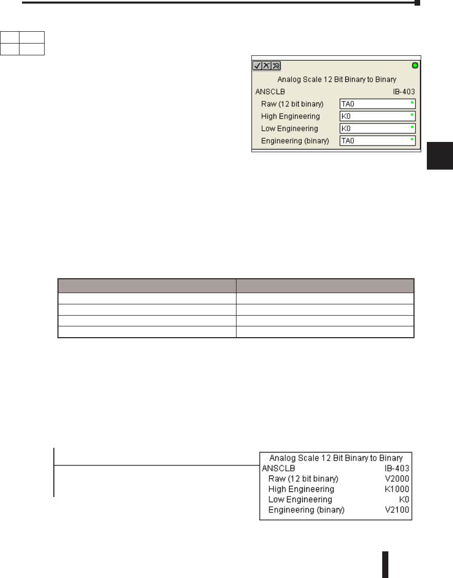
DL06 Micro PLC User Manual, 3rd Edition, Rev. D 5-239
1
2
3
4
5
6
7
8
9
10
11
12
13
14
A
B
C
D
Analog Scale 12 Bit Binary to Binary (ANSCLB) (IB-403)
Analog Scale 12 Bit Binary to Binary scales a 12 bit binary analog value (0-4095 decimal)
into binary (decimal) engineering units. You specify the engineering unit high value (when
raw is 4095), and the engineering low value (when
raw is 0), and the output V-Memory address you
want to place the scaled engineering unit value.
The engineering units are generated as binary and
can be the full range of 0 to 65535 (see ANSCL
- Analog Scale 12 Bit BCD to BCD if your raw
units are in BCD format).
Note that this IBox only works with unipolar
unsigned raw values. It does NOT work with
bipolar, sign plus magnitude, or signed 2’s complement raw values.
ANSCLB Parameters
• Raw (12 bit binary): specifies the V-memory location of the unipolar unsigned raw decimal
unscaled value (12 bit binary = 0-4095 decimal)
• High Engineering: specifies the high engineering value when the raw input is 4095 decimal
• Low Engineering: specifies the low engineering value when the raw input is 0 decimal
• Engineering (binary): specifies the V-memory location where the scaled engineering decimal value
will be placed
ANSCLB Example
In the following example, the ANSCLB instruction is used to scale a raw value (0-4095
binary) that is in V2000. The engineering scaling range is set 0-1000 (low engineering value -
high engineering value). The scaled value will be placed in V2100 in binary format.
Chapter 5: Intelligent Box (IBox) Instructions
1
2
3
4
5
6
7
8
9
10
11
12
13
14
a
B
c
d
Parameter DL06 Range
Raw (12 bit binary) V,P See DL06 V-memory map - Data Words
High Engineering K K0-65535
Low Engineering K K0-65535
Engineering (binary) V,P See DL06 V-memory map - Data Words
DS Used
HPP N/A
1
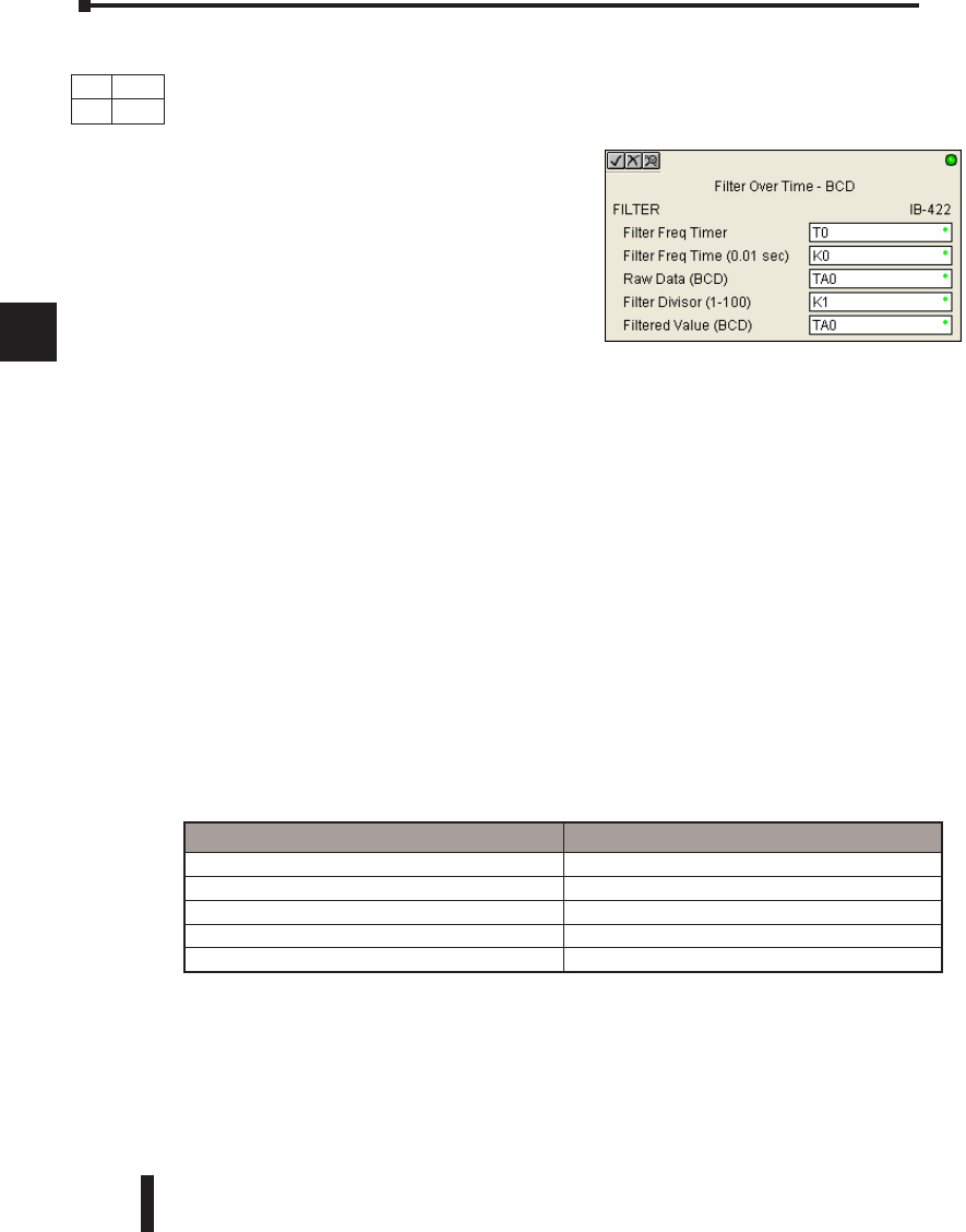
DL06 Micro PLC User Manual, 3rd Edition, Rev. D
5-240
1
2
3
4
5
6
7
8
9
10
11
12
13
14
A
B
C
D
Filter Over Time - BCD (FILTER) (IB-422)
Filter Over Time BCD will perform a first-order filter on the Raw Data on a defined time
interval. The equation is:
New = Old + [(Raw - Old) / FDC]
where,
New: New Filtered Value
Old: Old Filtered Value
FDC: Filter Divisor Constant
Raw: Raw Data
The Filter Divisor Constant is an integer in the
range K1 to K100, such that if it equaled K1 then
no filtering would be done.
The rate at which the calculation is performed is specified by time in hundredths of a
second (0.01 seconds) as the Filter Freq Time parameter. Note that this Timer instruction is
embedded in the IBox and must NOT be used anywhere else in your program. Power flow
controls whether the calculation is enabled. If it is disabled, the Filter Value is not updated.
On the first scan from Program to Run mode, the Filter Value is initialized to 0 to give the
calculation a consistent starting point.
FILTER Parameters
• Filter Frequency Timer: specifies the Timer (T) number which is used by the Filter instruction
• Filter Frequency Time (0.01sec): specifies the rate at which the calculation is performed
• Raw Data (BCD): specifies the V-memory location of the raw unfiltered BCD value
• Filter Divisor (1-100): this constant used to control the filtering effect. A larger value will increase
the smoothing effect of the filter. A value of 1 results with no filtering.
• Filtered Value (BCD): specifies the V-memory location where the filtered BCD value will be placed
Chapter 5: Intelligent Box (IBox) Instructions
1
2
3
4
5
6
7
8
9
10
11
12
13
14
a
B
c
d
DS Used
HPP N/A
Parameter DL06 Range
Filter Frequency Timer T T0-377
Filter Frequency Time (0.01 sec) K K0-9999
Raw Data (BCD) V See DL06 V-memory map - Data Words
Filter Divisor (1-100) K K1-100
Filtered Value (BCD) V See DL06 V-memory map - Data Words
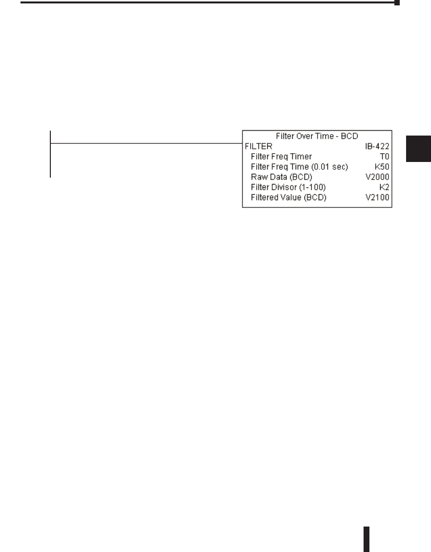
DL06 Micro PLC User Manual, 3rd Edition, Rev. D 5-241
1
2
3
4
5
6
7
8
9
10
11
12
13
14
A
B
C
D
FILTER Example
In the following example, the Filter instruction is used to filter a BCD value that is in V2000.
Timer(T0) is set to 0.5 sec, the rate at which the filter calculation will be performed. The
filter constant is set to 2. A larger value will increase the smoothing effect of the filter. A value
of 1 results with no filtering. The filtered value will be placed in V2100.
Chapter 5: Intelligent Box (IBox) Instructions
1
2
3
4
5
6
7
8
9
10
11
12
13
14
a
B
c
d
1
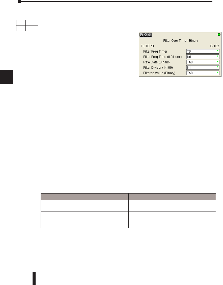
DL06 Micro PLC User Manual, 3rd Edition, Rev. D
5-242
1
2
3
4
5
6
7
8
9
10
11
12
13
14
A
B
C
D
Filter Over Time - Binary (FILTERB) (IB-402)
Filter Over Time in Binary (decimal) will perform a first-order filter on the Raw Data on a
defined time interval. The equation is
New = Old + [(Raw - Old) / FDC] where
New: New Filtered Value
Old: Old Filtered Value
FDC: Filter Divisor Constant
Raw: Raw Data
The Filter Divisor Constant is an integer in the
range K1 to K100, such that if it equaled K1 then
no filtering would be done.
The rate at which the calculation is performed is specified by time in hundredths of a
second (0.01 seconds) as the Filter Freq Time parameter. Note that this Timer instruction is
embedded in the IBox and must NOT be used any other place in your program. Power flow
controls whether the calculation is enabled. If it is disabled, the Filter Value is not updated.
On the first scan from Program to Run mode, the Filter Value is initialized to 0 to give the
calculation a consistent starting point.
FILTERB Parameters
• Filter Frequency Timer: specifies the Timer (T) number which is used by the Filter instruction
• Filter Frequency Time (0.01sec): specifies the rate at which the calculation is performed
• Raw Data (Binary): specifies the V-memory location of the raw unfiltered binary (decimal) value
• Filter Divisor (1-100): this constant used to control the filtering effect. A larger value will increase
the smoothing effect of the filter. A value of 1 results with no filtering.
• Filtered Value (Binary): specifies the V-memory location where the filtered binary (decimal) value
will be placed
Chapter 5: Intelligent Box (IBox) Instructions
1
2
3
4
5
6
7
8
9
10
11
12
13
14
a
B
c
d
DS Used
HPP N/A
Parameter DL06 Range
Filter Frequency Timer T T0-377
Filter Frequency Time (0.01 sec) K K0-9999
Raw Data (Binary) V See DL06 V-memory map - Data Words
Filter Divisor (1-100) K K1-100
Filtered Value (Binary) V See DL06 V-memory map - Data Words
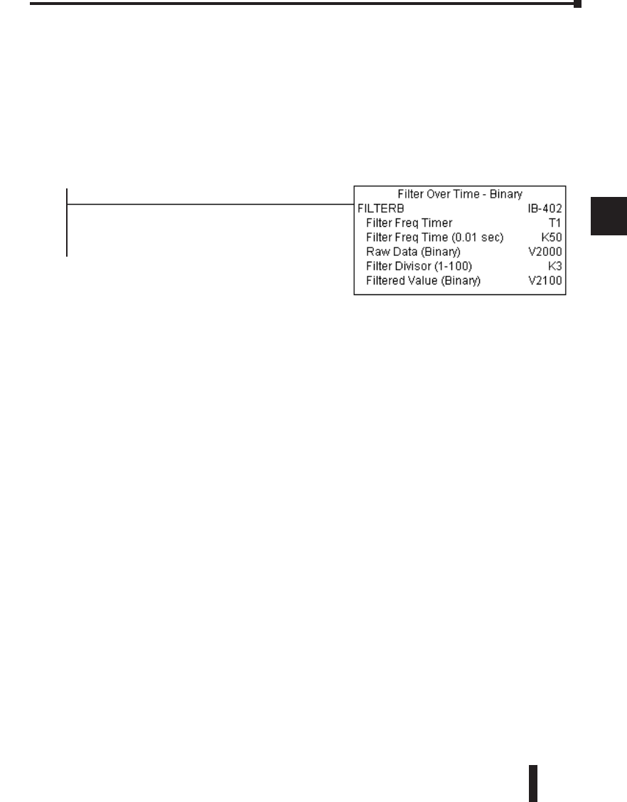
DL06 Micro PLC User Manual, 3rd Edition, Rev. D 5-243
1
2
3
4
5
6
7
8
9
10
11
12
13
14
A
B
C
D
FILTERB Example
In the following example, the FILTERB instruction is used to filter a binary value that is in
V2000. Timer (T1) is set to 0.5 sec, the rate at which the filter calculation will be performed.
The filter constant is set to 3.0. A larger value will increase the smoothing effect of the filter.
A value of 1 results with no filtering. The filtered value will be placed in V2100
Chapter 5: Intelligent Box (IBox) Instructions
1
2
3
4
5
6
7
8
9
10
11
12
13
14
a
B
c
d
1
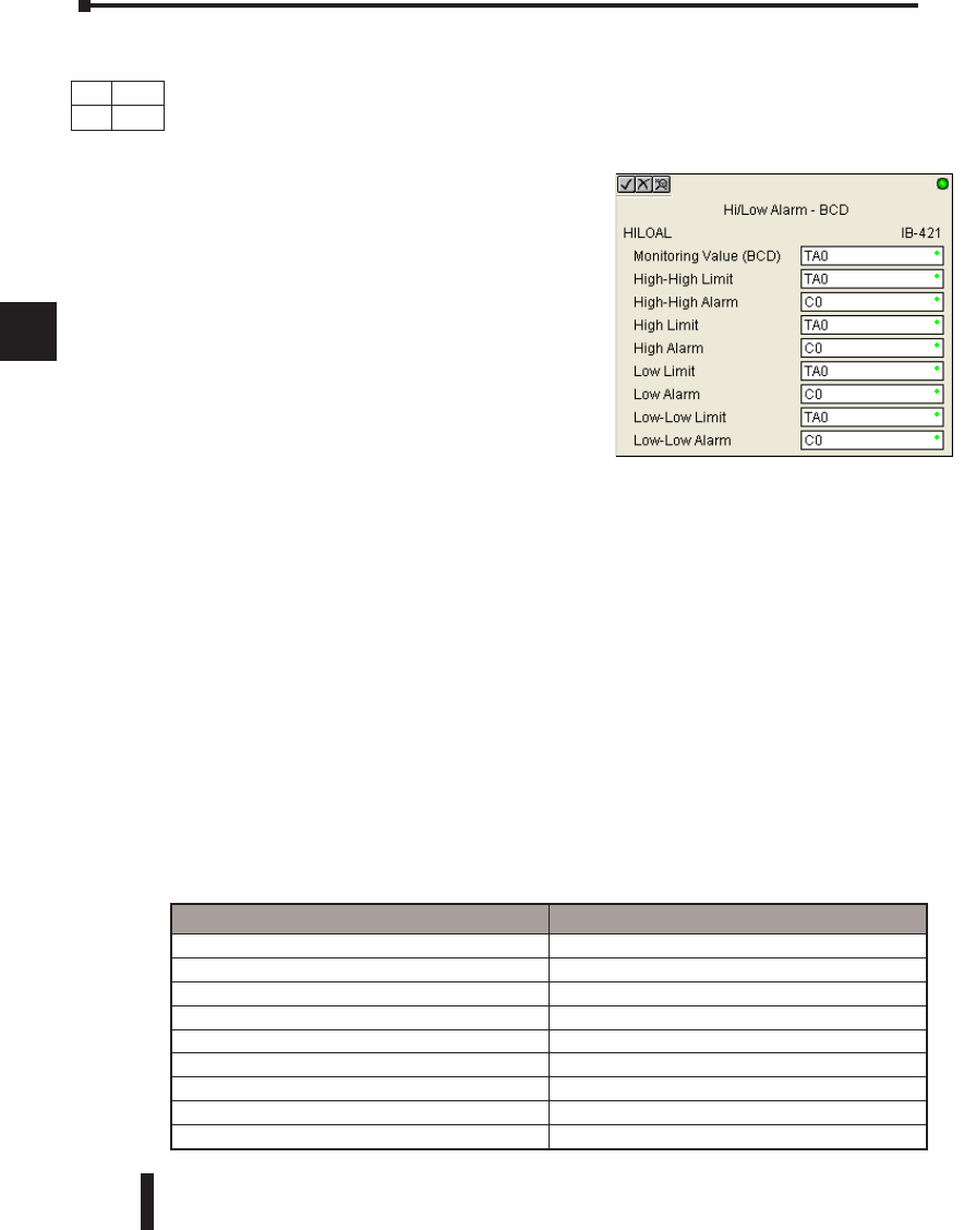
DL06 Micro PLC User Manual, 3rd Edition, Rev. D
5-244
1
2
3
4
5
6
7
8
9
10
11
12
13
14
A
B
C
D
Hi/Low Alarm - BCD (HILOAL) (IB-421)
Hi/Low Alarm - BCD monitors a BCD value V-Memory location and sets four possible
alarm states, High-High, High, Low, and Low-Low whenever the IBox has power flow. You
enter the alarm thresholds as constant K BCD values (K0-K9999) and/or BCD value
V-Memory locations.
You must ensure that threshold limits are valid, that
is HH >= H > L >= LL. Note that when the High-
High or Low-Low alarm condition is true, that the
High and Low alarms will also be set, respectively.
This means you may use the same threshold limit
and same alarm bit for the High-High and the High
alarms in case you only need one “High” alarm. Also
note that the boundary conditions are inclusive.
That is, if the Low boundary is K50, and the
Low-Low boundary is K10, and if the Monitoring
Value equals 10, then the Low Alarm AND the
Low-Low alarm will both be ON. If there is no power flow to the IBox, then all alarm bits
will be turned off regardless of the value of the Monitoring Value parameter.
HILOAL Parameters
• Monitoring Value (BCD): specifies the V-memory location of the BCD value to be monitored
• High-High Limit: V-memory location or constant specifies the high-high alarm limit
• High-High Alarm: On when the high-high limit is reached
• High Limit: V-memory location or constant specifies the high alarm limit
• High Alarm: On when the high limit is reached
• Low Limit: V-memory location or constant specifies the low alarm limit
• Low Alarm: On when the low limit is reached
• Low-Low Limit: V-memory location or constant specifies the low-low alarm limit
• Low-Low Alarm: On when the low-low limit is reached
Chapter 5: Intelligent Box (IBox) Instructions
1
2
3
4
5
6
7
8
9
10
11
12
13
14
a
B
c
d
DS Used
HPP N/A
Parameter DL06 Range
Monitoring Value (BCD) V See DL06 V-memory map - Data Words
High-High Limit V, K K0-9999; or see DL06 V-memory map - Data Words
High-High Alarm X, Y, C, GX,GY, B See DL06 V-memory map
High Limit V, K K0-9999; or see DL06 V-memory map - Data Words
High Alarm X, Y, C, GX,GY, B See DL06 V-memory map
Low Limit V, K K0-9999; or see DL06 V-memory map - Data Words
Low Alarm X, Y, C, GX,GY,B See DL06 V-memory map
Low-Low Limit V, K K0-9999; or see DL06 V-memory map - Data Words
Low-Low Alarm X, Y, C, GX,GY, B See DL06 V-memory map
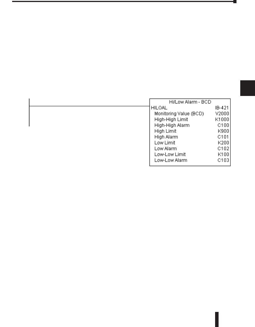
DL06 Micro PLC User Manual, 3rd Edition, Rev. D 5-245
1
2
3
4
5
6
7
8
9
10
11
12
13
14
A
B
C
D
HILOAL Example
In the following example, the HILOAL instruction is used to monitor a BCD value that is
in V2000. If the value in V2000 meets/exceeds the high limit of K900, C101 will turn on. If
the value continues to increase to meet/exceed the high-high limit, C100 will turn on. Both
bits would be on in this case. The high and high-high limits and alarms can be set to the same
value if one “high” limit or alarm is desired to be used.
If the value in V2000 meets or falls below the low limit of K200, C102 will turn on. If the
value continues to decrease to meet or fall below the low-low limit of K100, C103 will turn
on. Both bits would be on in this case. The low and low-low limits and alarms can be set to
the same value if one “low” limit or alarm is desired to be used.
Chapter 5: Intelligent Box (IBox) Instructions
1
2
3
4
5
6
7
8
9
10
11
12
13
14
a
B
c
d
1
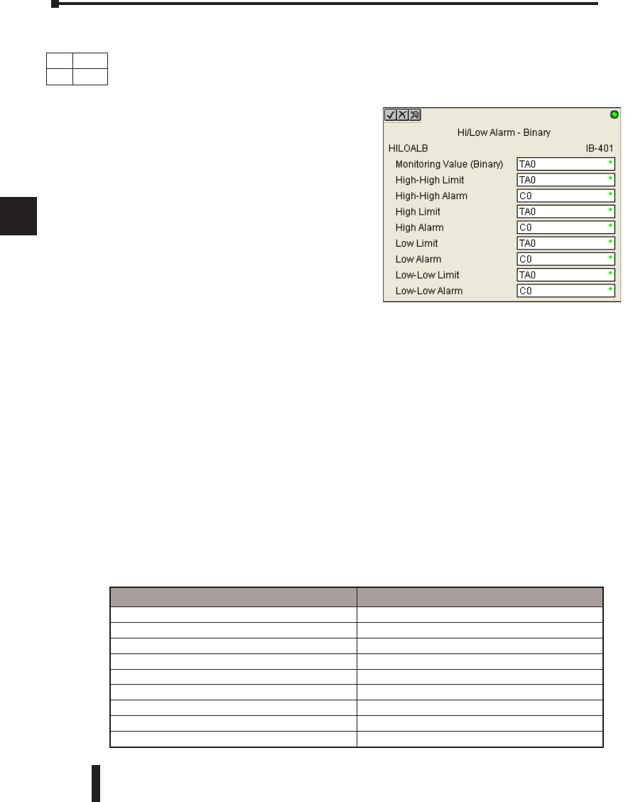
DL06 Micro PLC User Manual, 3rd Edition, Rev. D
5-246
1
2
3
4
5
6
7
8
9
10
11
12
13
14
A
B
C
D
Hi/Low Alarm - Binary (HILOALB) (IB-401)
Hi/Low Alarm - Binary monitors a binary (decimal) V-Memory location and sets four
possible alarm states, High-High, High, Low, and Low-Low whenever the IBox has power
flow. You enter the alarm thresholds as constant K decimal values (K0-K65535) and/or
binary (decimal) V-Memory locations.
You must ensure that threshold limits are valid,
that is HH >= H > L >= LL. Note that when the
High-High or Low-Low alarm condition is true,
that the High and Low alarms will also be set,
respectively. This means you may use the same
threshold limit and same alarm bit for the High-
High and the High alarms in case you only need
one “High” alarm. Also note that the boundary
conditions are inclusive. That is, if the Low
boundary is K50, and the Low-Low boundary
is K10, and if the Monitoring Value equals 10,
then the Low Alarm AND the Low-Low alarm will both be ON. If there is no power flow to
the IBox, then all alarm bits will be turned off regardless of the value of the Monitoring Value
parameter.
HILOALB Parameters
• Monitoring Value (Binary): specifies the V-memory location of the Binary value to be monitored
• High-High Limit: V-memory location or constant specifies the high-high alarm limit
• High-High Alarm: On when the high-high limit is reached
• High Limit: V-memory location or constant specifies the high alarm limit
• High Alarm: On when the high limit is reached
• Low Limit: V-memory location or constant specifies the low alarm limit
• Low Alarm: On when the low limit is reached
• Low-Low Limit: V-memory location or constant specifies the low-low alarm limit
• Low-Low Alarm: On when the low-low limit is reached
Chapter 5: Intelligent Box (IBox) Instructions
1
2
3
4
5
6
7
8
9
10
11
12
13
14
a
B
c
d
Parameter DL06 Range
Monitoring Value (Binary) V See DL06 V-memory map - Data Words
High-High Limit V, K K0-65535; or see DL06 V-memory map - Data Words
High-High Alarm X, Y, C, GX,GY, B See DL06 V-memory map
High Limit V, K K0-65535; or see DL06 V-memory map - Data Words
High Alarm X, Y, C, GX,GY, B See DL06 V-memory map
Low Limit V, K K0-65535; or see DL06 V-memory map - Data Words
Low Alarm X, Y, C, GX,GY,B See DL06 V-memory map
Low-Low Limit V, K K0-65535; or see DL06 V-memory map - Data Words
Low-Low Alarm X, Y, C, GX,GY, B See DL06 V-memory map
DS Used
HPP N/A
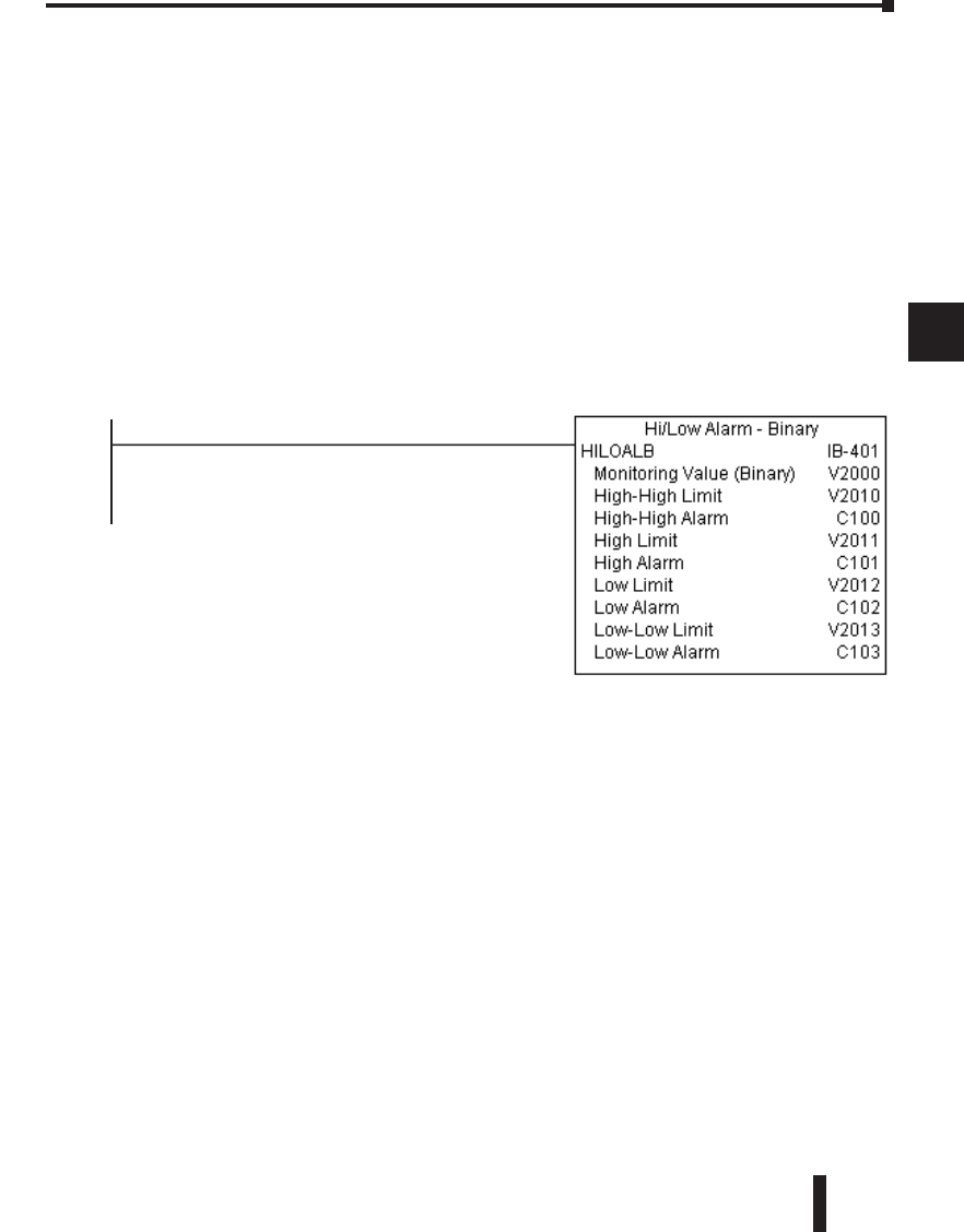
DL06 Micro PLC User Manual, 3rd Edition, Rev. D 5-247
1
2
3
4
5
6
7
8
9
10
11
12
13
14
A
B
C
D
HILOALB Example
In the following example, the HILOALB instruction is used to monitor a binary value that is
in V2000. If the value in V2000 meets/exceeds the high limit of the binary value in V2011,
C101 will turn on. If the value continues to increase to meet/exceed the high-high limit value
in V2010, C100 will turn on. Both bits would be on in this case. The high and high-high
limits and alarms can be set to the same V-memory location/value if one “high” limit or
alarm is desired to be used.
If the value in V2000 meets or falls below the low limit of the binary value in V2012, C102
will turn on. If the value continues to decrease to meet or fall below the low-low limit in
V2013, C103 will turn on. Both bits would be on in this case. The low and low-low limits
and alarms can be set to the same V-memory location/value if one “low” limit or alarm is
desired to be used.
Chapter 5: Intelligent Box (IBox) Instructions
1
2
3
4
5
6
7
8
9
10
11
12
13
14
a
B
c
d
1
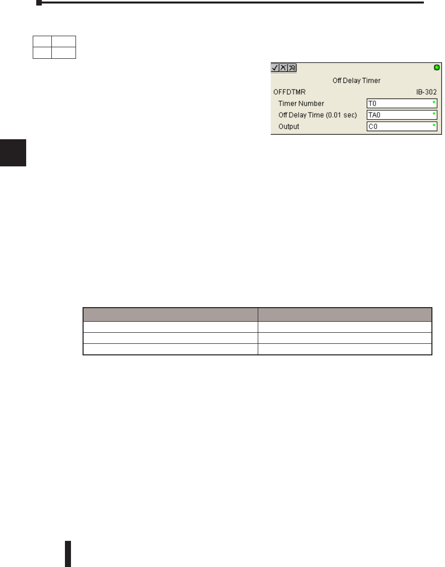
DL06 Micro PLC User Manual, 3rd Edition, Rev. D
5-248
1
2
3
4
5
6
7
8
9
10
11
12
13
14
A
B
C
D
Off Delay Timer (OFFDTMR) (IB-302)
Off Delay Timer will delay the “turning off” of the Output parameter by the specified Off
Delay Time (in hundredths of a second) based on the power flow into the IBox. Once the
IBox receives power, the Output bit will turn on
immediately. When the power flow to the IBox
turns off, the Output bit WILL REMAIN ON
for the specified amount of time (in hundredths
of a second). Once the Off Delay Time has
expired, the output will turn Off. If the power
flow to the IBox comes back on BEFORE the
Off Delay Time, then the timer is RESET and
the Output will remain On - so you must continuously have NO power flow to the IBox for
AT LEAST the specified Off Delay Time before the Output will turn Off.
This IBox utilizes a Timer resource (TMRF), which cannot be used anywhere else in your
program.
OFFDTMR Parameters
• Timer Number: specifies the Timer(TMRF) number which is used by the OFFDTMR instruction
• Off Delay Time (0.01sec): specifies how long the Output will remain on once power flow to the
Ibox is removed
• Output: specifies the output that will be delayed “turning off” by the Off Delay Time.
Chapter 5: Intelligent Box (IBox) Instructions
1
2
3
4
5
6
7
8
9
10
11
12
13
14
a
B
c
d
Parameter DL06 Range
Timer Number T T0-377
Off Delay Time K,V K0-9999; See DL06 V-memory map - Data Words
Output X, Y, C, GX,GY, B See DL06 V-memory map
DS Used
HPP N/A
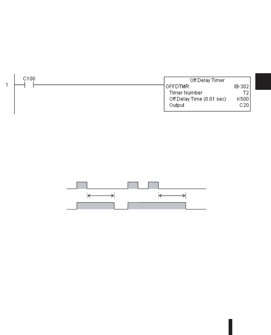
DL06 Micro PLC User Manual, 3rd Edition, Rev. D 5-249
1
2
3
4
5
6
7
8
9
10
11
12
13
14
A
B
C
D
OFFDTMR Example
In the following example, the OFFDTMR instruction is used to delay the “turning off”of
output C20. Timer 2 (T2) is set to 5 seconds, the “off-delay” period.
When C100 turns on, C20 turns on and will remain on while C100 is on. When C100 turns
off, C20 will remain for the specified Off Delay Time (5s), and then turn off.
1
2
3
4
5
6
7
8
9
10
11
12
13
14
a
B
c
d
Chapter 5: Intelligent Box (IBox) Instructions
C100
C20
5 sec 5 sec
Example timing diagram
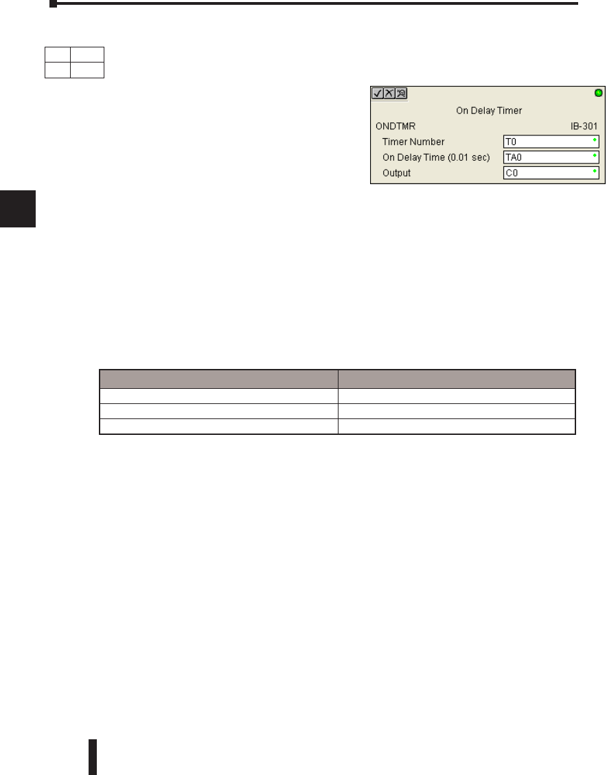
DL06 Micro PLC User Manual, 3rd Edition, Rev. D
5-250
1
2
3
4
5
6
7
8
9
10
11
12
13
14
A
B
C
D
On Delay Timer (ONDTMR) (IB-301)
On Delay Timer will delay the “turning on” of the Output parameter by the specified
amount of time (in hundredths of a second) based on the power flow into the IBox. Once
the IBox loses power, the Output is turned
off immediately. If the power flow turns off
BEFORE the On Delay Time, then the timer
is RESET and the Output is never turned on,
so you must have continuous power flow to the
IBox for at least the specified On Delay Time
before the Output turns On.
This IBox utilizes a Timer resource (TMRF),
which cannot be used anywhere else in your program.
ONDTMR Parameters
• Timer Number: specifies the Timer(TMRF) number which is used by the ONDTMR instruction
• On Delay Time (0.01sec): specifies how long the Output will remain off once power flow to the
Ibox is applied.
• Output: specifies the output that will be delayed “turning on” by the On Delay Time.
Chapter 5: Intelligent Box (IBox) Instructions
1
2
3
4
5
6
7
8
9
10
11
12
13
14
a
B
c
d
Parameter DL06 Range
Timer Number T T0-377
On Delay Time K,V K0-9999; See DL06 V-memory map - Data Words
Output X, Y, C, GX,GY, B See DL06 V-memory map
DS Used
HPP N/A
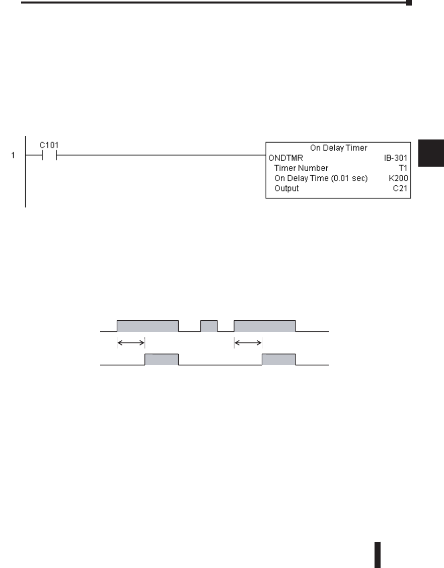
DL06 Micro PLC User Manual, 3rd Edition, Rev. D 5-251
1
2
3
4
5
6
7
8
9
10
11
12
13
14
A
B
C
D
ONDTMR Example
In the following example, the ONDTMR instruction is used to delay the “turning on” of
output C21. Timer 1 (T1) is set to 2 seconds, the “on-delay” period.
When C101 turns on, C21 is delayed turning on by 2 seconds. When C101 turns off, C21
turns off immediately.
Chapter 5: Intelligent Box (IBox) Instructions
1
2
3
4
5
6
7
8
9
10
11
12
13
14
a
B
c
d
C101
C21
2
sec
2
sec
Example timing diagram
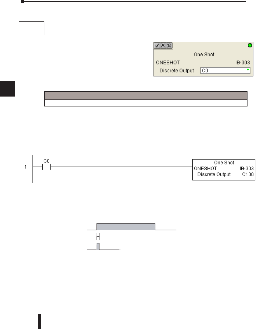
DL06 Micro PLC User Manual, 3rd Edition, Rev. D
5-252
1
2
3
4
5
6
7
8
9
10
11
12
13
14
A
B
C
D
One Shot (ONESHOT) (IB-303)
One Shot will turn on the given bit output parameter for one scan on an OFF to ON
transition of the power flow into the IBox. This IBox is simply a different name for the PD
Coil (Positive Differential).
ONESHOT Parameters
• Discrete Output: specifies the output that will
be on for one scan
ONESHOT Example
In the following example, the ONESHOT instruction is used to turn C100 on for one PLC
scan after C0 goes from an off to on transition. The input logic must produce an off to on
transition to execute the One Shot instruction.
Chapter 5: Intelligent Box (IBox) Instructions
1
2
3
4
5
6
7
8
9
10
11
12
13
14
a
B
c
d
C0
C100
Scan time
Example timing diagram
Parameter DL06 Range
Discrete Output X, Y, C See DL06 V-memory map
DS Used
HPP N/A
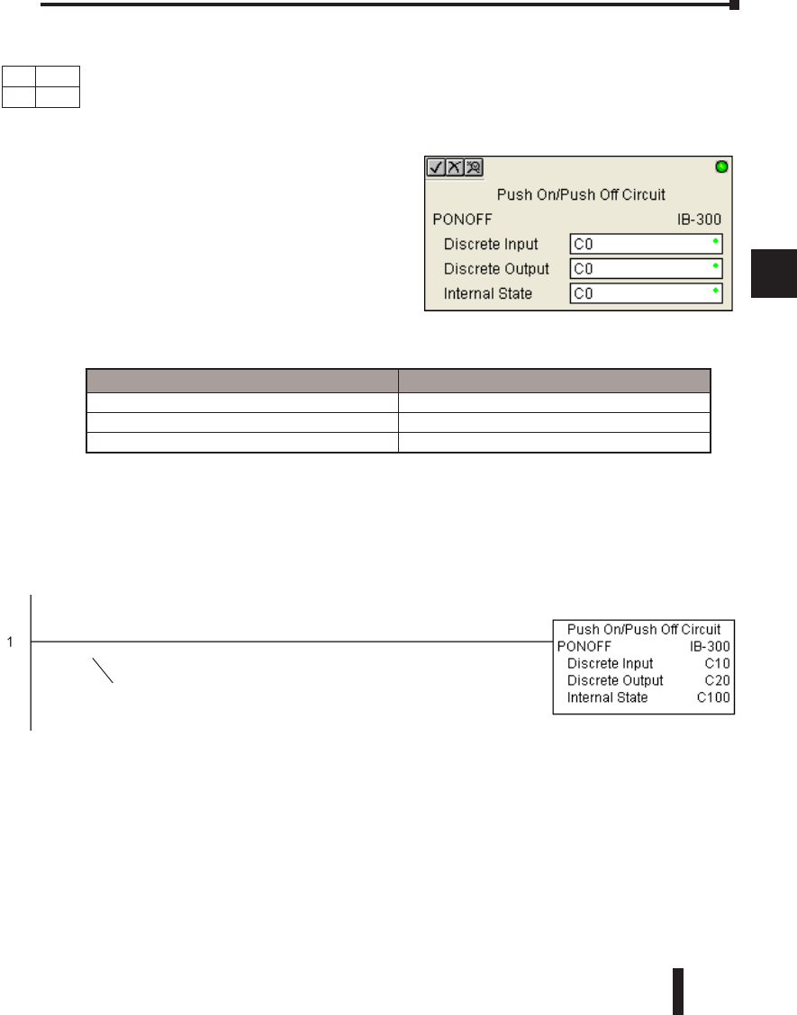
DL06 Micro PLC User Manual, 3rd Edition, Rev. D 5-253
1
2
3
4
5
6
7
8
9
10
11
12
13
14
A
B
C
D
Push On / Push Off Circuit (PONOFF) (IB-300)
Push On/Push Off Circuit toggles an output state whenever its input power flow transitions
from off to on. Requires an extra bit parameter for scan-to-scan state information. This extra
bit must NOT be used anywhere else in the program. This is also known as a “flip-flop
circuit”. The PONOFF IBox cannot have any input logic.
PONOFF Parameters
• Discrete Input: specifies the input that will toggle
the specified output
• Discrete Output: specifies the output that will be
“turned on/off” or toggled
• Internal State: specifies a work bit that is used by
the instruction
PONOFF Example
In the following example, the PONOFF instruction is used to control the on and off states
of the output C20 with a single input C10. When C10 is pressed once, C20 turns on. When
C10 is pressed again, C20 turns off. C100 is an internal bit used by the instruction.
Chapter 5: Intelligent Box (IBox) Instructions
1
2
3
4
5
6
7
8
9
10
11
12
13
14
a
B
c
d
Parameter DL06 Range
Discrete Input X,Y,C,S,T,CT,GX,GY,SP,B,PB See DL06 V-memory map
Discrete Output X,Y,C,GX,GY,B See DL06 V-memory map
Internal State X, Y, C See DL06 V-memory map
DS Used
HPP N/A
Permissive contacts or input logic are not
used with this instruction.
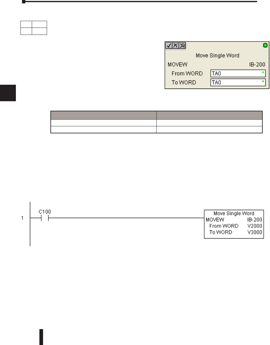
DL06 Micro PLC User Manual, 3rd Edition, Rev. D
5-254
1
2
3
4
5
6
7
8
9
10
11
12
13
14
A
B
C
D
Move Single Word (MOVEW) (IB-200)
Move Single Word moves (copies) a word to a memory location directly or indirectly via a
pointer, either as a HEX constant, from a memory location, or indirectly through a pointer
MOVEW Parameters
• From WORD: specifies the word that will be
moved to another location
• To WORD: specifies the location where the
“From WORD” will be move to
MOVEW Example
In the following example, the MOVEW instruction is used to move 16-bits of data from
V2000 to V3000 when C100 turns on.
Chapter 5: Intelligent Box (IBox) Instructions
1
2
3
4
5
6
7
8
9
10
11
12
13
14
a
B
c
d
Parameter DL06 Range
From WORD V,P,K K0-FFFF; See DL06 V-memory map - Data Words
To WORD V,P See DL06 V-memory map - Data Words
DS Used
HPP N/A
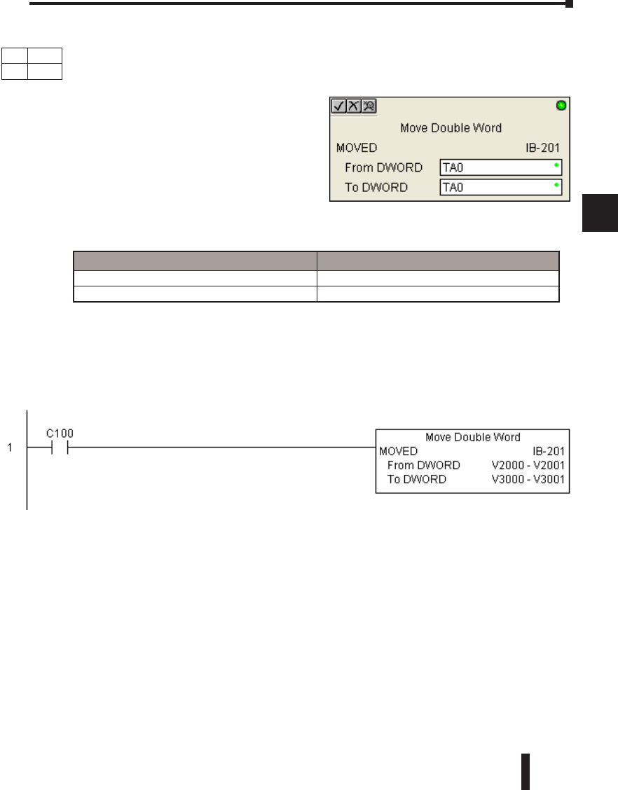
DL06 Micro PLC User Manual, 3rd Edition, Rev. D 5-255
1
2
3
4
5
6
7
8
9
10
11
12
13
14
A
B
C
D
Move Double Word (MOVED) (IB-201)
Move Double Word moves (copies) a double word to two consecutive memory locations
directly or indirectly via a pointer, either as a double HEX constant, from a double memory
location, or indirectly through a pointer to a double memory location.
MOVED Parameters
• From DWORD: specifies the double word that
will be moved to another location
• To DWORD: specifies the location where the
“From DWORD” will be move to
MOVED Example
In the following example, the MOVED instruction is used to move 32-bits of data from
V2000 and V2001 to V3000 and V3001 when C100 turns on.
Chapter 5: Intelligent Box (IBox) Instructions
1
2
3
4
5
6
7
8
9
10
11
12
13
14
a
B
c
d
Parameter DL06 Range
From DWORD V,P,K K0-FFFFFFFF; See DL06 V-memory map - Data Words
To DWORD V,P See DL06 V-memory map - Data Words
DS Used
HPP N/A
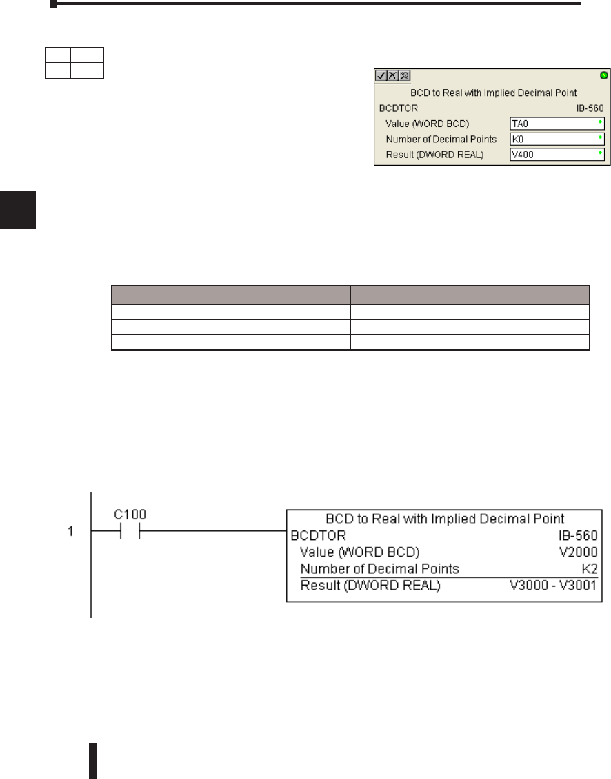
DL06 Micro PLC User Manual, 3rd Edition, Rev. D
5-256
1
2
3
4
5
6
7
8
9
10
11
12
13
14
A
B
C
D
BCD to Real with Implied Decimal Point (BCDTOR) (IB-560)
BCD to Real with Implied Decimal Point converts the given 4 digit WORD BCD value
to a Real number, with the implied number of
decimal points (K0-K4).
For example, BCDTOR K1234 with an implied
number of decimal points equal to K1, would
yield R123.4
BCDTOR Parameters
• Value (WORD BCD): specifies the word or constant that will be converted to a Real number
• Number of Decimal Points: specifies the number of implied decimal points in the Result DWORD
• Result (DWORD REAL): specifies the location where the Real number will be placed
BCDTOR Example
In the following example, the BCDTOR instruction is used to convert the 16-bit data in
V2000 from a 4-digit BCD data format to a 32-bit REAL (floating point) data format and
stored into V3000 and V3001 when C100 turns on.
K2 in the Number of Decimal Points implies the data will have two digits to the right of the
decimal point.
Chapter 5: Intelligent Box (IBox) Instructions
1
2
3
4
5
6
7
8
9
10
11
12
13
14
a
B
c
d
Parameter DL06 Range
Value (WORD BCD) V,P,K K0-9999; See DL06 V-memory map - Data Words
Number of Decimal Points K K0-4
Result (DWORD REAL) V See DL06 V-memory map - Data Words
DS Used
HPP N/A
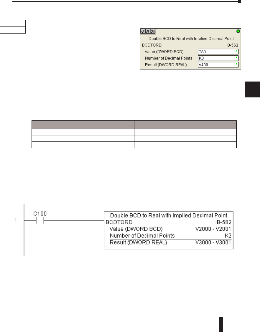
DL06 Micro PLC User Manual, 3rd Edition, Rev. D 5-257
1
2
3
4
5
6
7
8
9
10
11
12
13
14
A
B
C
D
Double BCD to Real with Implied Decimal Point (BCDTORD) (IB-562)
Double BCD to Real with Implied Decimal Point converts the given 8 digit DWORD
BCD value to a Real number, given an implied
number of decimal points (K0-K8).
For example, BCDTORD K12345678 with an
implied number of decimal points equal to K5,
would yield R123.45678
BCDTORD Parameters
• Value (DWORD BCD): specifies the Dword or constant that will be converted to a Real number
• Number of Decimal Points: specifies the number of implied decimal points in the Result DWORD
• Result (DWORD REAL): specifies the location where the Real number will be placed
BCDTORD Example
In the following example, the BCDTORD instruction is used to convert the 32-bit data in
V2000 from an 8-digit BCD data format to a 32-bit REAL (floating point) data format and
stored into V3000 and V3001 when C100 turns on.
K2 in the Number of Decimal Points implies the data will have two digits to the right of the
decimal point.
Chapter 5: Intelligent Box (IBox) Instructions
1
2
3
4
5
6
7
8
9
10
11
12
13
14
a
B
c
d
Parameter DL06 Range
Value (DWORD BCD) V,P,K K0-99999999; See DL06 V-memory map - Data Words
Number of Decimal Points K K0-8
Result (DWORD REAL) V See DL06 V-memory map - Data Words
DS Used
HPP N/A
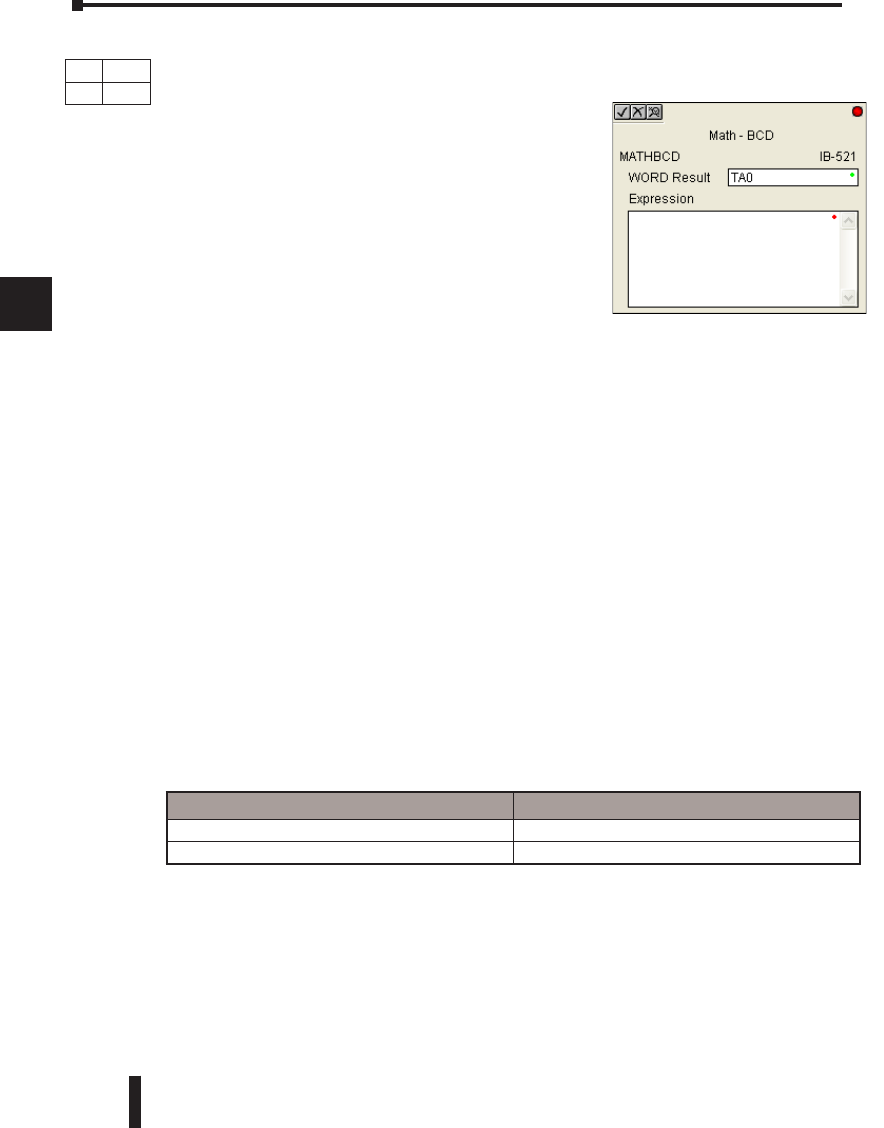
DL06 Micro PLC User Manual, 3rd Edition, Rev. D
5-258
1
2
3
4
5
6
7
8
9
10
11
12
13
14
A
B
C
D
Math - BCD (MATHBCD) (IB-521)
Math - BCD Format lets you enter complex mathematical expressions like you would in
Visual Basic, Excel, or C++ to do complex calculations, nesting parentheses up to 4 levels
deep. In addition to + - * /, you can do Modulo (% aka
Remainder), Bit-wise And (&) Or (|) Xor (^), and some
BCD functions - Convert to BCD (BCD), Convert to
Binary (BIN), BCD Complement (BCDCPL), Convert
from Gray Code (GRAY), Invert Bits (INV), and BCD/
HEX to Seven Segment Display (SEG).
Example: ((V2000 + V2001) / (V2003 - K100)) *
GRAY(V3000 & K001F)
Every V-memory reference MUST be to a single word BCD formatted value. Intermediate
results can go up to 32 bit values, but as long as the final result fits in a 16 bit BCD word,
the calculation is valid. Typical example of this is scaling using multiply then divide, (V2000
* K1000) / K4095. The multiply term most likely will exceed 9999 but fits within 32 bits.
The divide operation will divide 4095 into the 32-bit accumulator, yielding a result that will
always fit in 16 bits.
You can reference binary V-memory values by using the BCD conversion function on a
V-Memory location but NOT an expression. That is BCD(V2000) is okay and will convert
V2000 from Binary to BCD, but BCD(V2000 + V3000) will add V2000 as BCD, to V3000
as BCD, then interpret the result as Binary and convert it to BCD - NOT GOOD.
Also, the final result is a 16 bit BCD number and so you could do BIN around the entire
operation to store the result as Binary.
MATHBCD Parameters
• WORD Result: specifies the location where the BCD result of the mathematical expression will be
placed (result must fit into 16 bit single V-memory location)
• Expression: specifies the mathematical expression to be executed and the result is stored in specified
WORD Result. Each V-memory location used in the expression must be in BCD format.
Chapter 5: Intelligent Box (IBox) Instructions
1
2
3
4
5
6
7
8
9
10
11
12
13
14
a
B
c
d
Parameter DL06 Range
WORD Result V See DL06 V-memory map - Data Words
Expression Text
DS Used
HPP N/A
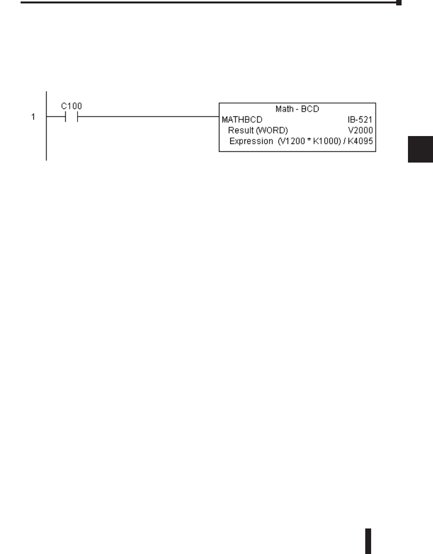
DL06 Micro PLC User Manual, 3rd Edition, Rev. D 5-259
1
2
3
4
5
6
7
8
9
10
11
12
13
14
A
B
C
D
MATHBCD Example
In the following example, the MATHBCD instruction is used to calculate the math
expression which multiplies the BCD value in V1200 by 1000 then divides by 4095 and
loads the resulting value in V2000 when C100 turns on.
Chapter 5: Intelligent Box (IBox) Instructions
1
2
3
4
5
6
7
8
9
10
11
12
13
14
a
B
c
d
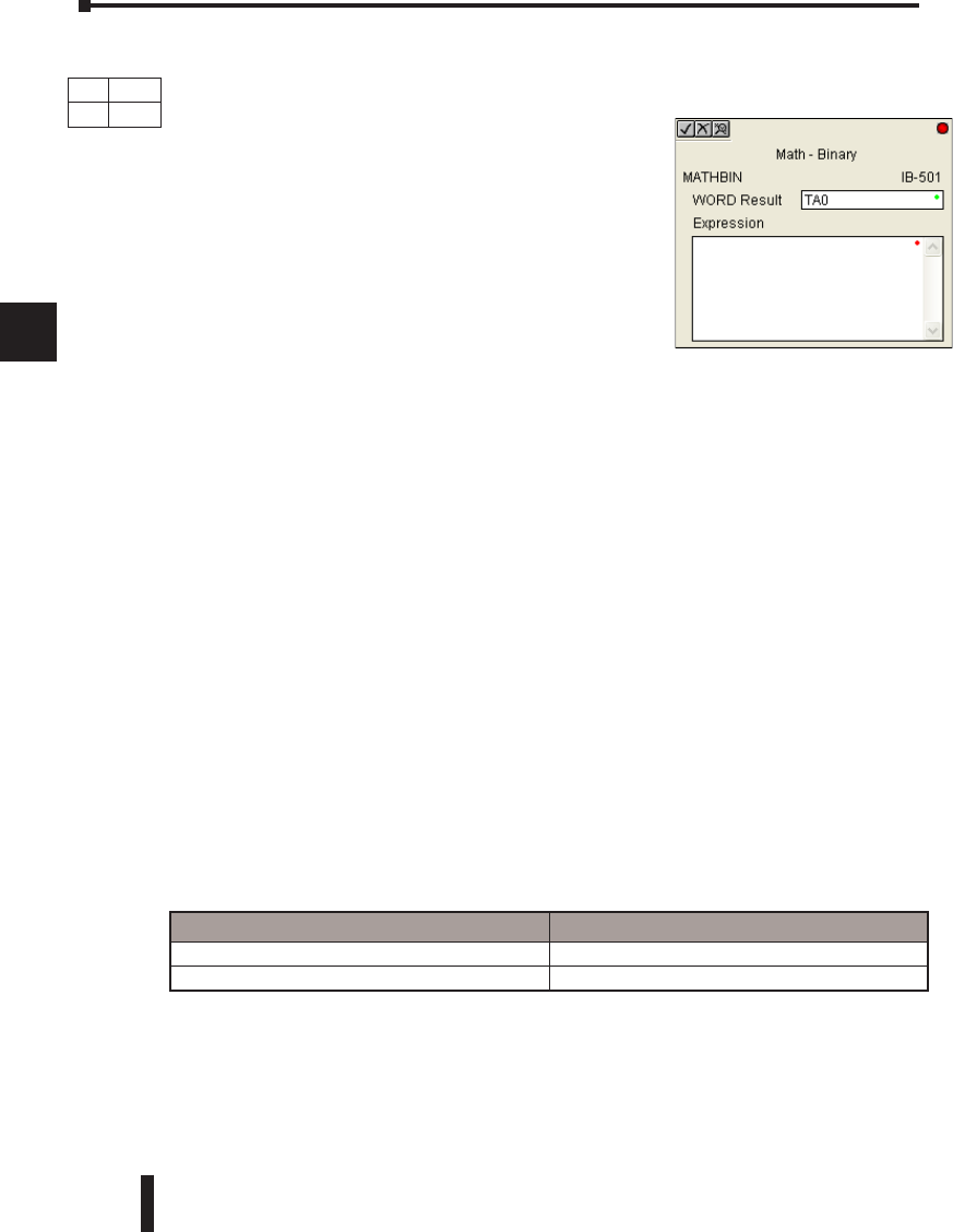
DL06 Micro PLC User Manual, 3rd Edition, Rev. D
5-260
1
2
3
4
5
6
7
8
9
10
11
12
13
14
A
B
C
D
Math - Binary (MATHBIN) (IB-501)
Math - Binary Format lets you enter complex mathematical expressions like you would in
Visual Basic, Excel, or C++ to do complex calculations, nesting parentheses up to 4 levels
deep. In addition to + - * /, you can do Modulo (% aka
Remainder), Shift Right (>>) and Shift Left (<<), Bit-
wise And (&) Or (|) Xor (^), and some binary functions
- Convert to BCD (BCD), Convert to Binary (BIN),
Decode Bits (DECO), Encode Bits (ENCO), Invert Bits
(INV), HEX to Seven Segment Display (SEG), and Sum
Bits (SUM).
Example: ((V2000 + V2001) / (V2003 - K10)) *
SUM(V3000 & K001F)
Every V-memory reference MUST be to a single word binary formatted value. Intermediate
results can go up to 32 bit values, but as long as the final result fits in a 16 bit binary word,
the calculation is valid. Typical example of this is scaling using multiply then divide, (V2000
* K1000) / K4095. The multiply term most likely will exceed 65535 but fits within 32 bits.
The divide operation will divide 4095 into the 32-bit accumulator, yielding a result that will
always fit in 16 bits.
You can reference BCD V-Memory values by using the BIN conversion function on a
V-memory location but NOT an expression. That is, BIN(V2000) is okay and will convert
V2000 from BCD to Binary, but BIN(V2000 + V3000) will add V2000 as Binary, to V3000
as Binary, then interpret the result as BCD and convert it to Binary - NOT GOOD.
Also, the final result is a 16 bit binary number and so you could do BCD around the entire
operation to store the result as BCD.
MATHBIN Parameters
• WORD Result: specifies the location where the binary result of the mathematical expression will be
placed (result must fit into 16 bit single V-memory location)
• Expression: specifies the mathematical expression to be executed and the result is stored in specified
WORD Result. Each V-memory location used in the expression must be in binary format.
Chapter 5: Intelligent Box (IBox) Instructions
1
2
3
4
5
6
7
8
9
10
11
12
13
14
a
B
c
d
Parameter DL06 Range
WORD Result V See DL06 V-memory map - Data Words
Expression Text
DS Used
HPP N/A

DL06 Micro PLC User Manual, 3rd Edition, Rev. D 5-261
1
2
3
4
5
6
7
8
9
10
11
12
13
14
A
B
C
D
MATHBIN Example
In the following example, the MATHBIN instruction is used to calculate the math expression
which multiplies the Binary value in V1200 by 1000 then divides by 4095 and loads the
resulting value in V2000 when C100 turns on.
Chapter 5: Intelligent Box (IBox) Instructions
1
2
3
4
5
6
7
8
9
10
11
12
13
14
a
B
c
d
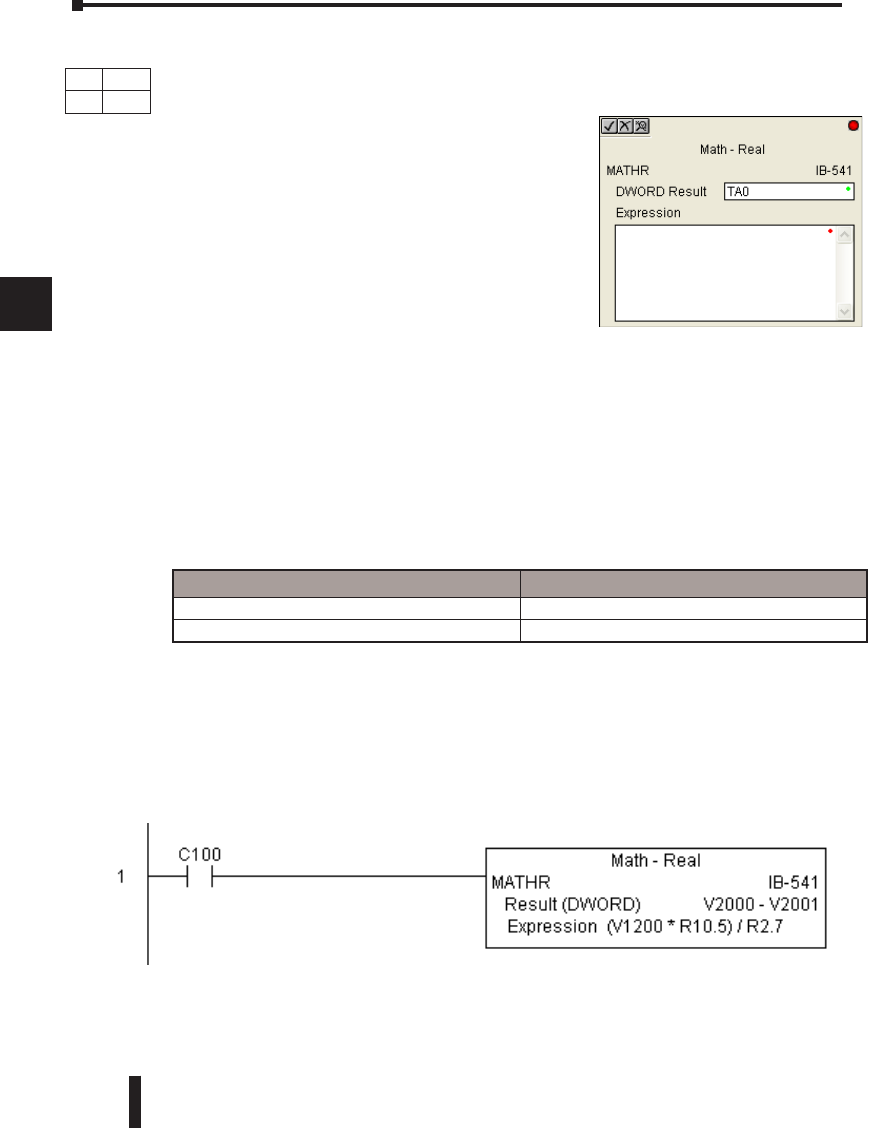
DL06 Micro PLC User Manual, 3rd Edition, Rev. D
5-262
1
2
3
4
5
6
7
8
9
10
11
12
13
14
A
B
C
D
Math - Real (MATHR) (IB-541)
Math - Real Format lets you enter complex mathematical expressions like you would
in Visual Basic, Excel, or C++ to do complex calculations, nesting parentheses up
to 4 levels deep. In addition to + - * /, you can
do Bit-wise And (&) Or (|) Xor (^), and many
Real functions - Arc Cosine (ACOSR), Arc
Sine (ASINR), Arc Tangent (ATANR), Cosine
(COSR), Convert Radians to Degrees (DEGR),
Invert Bits (INV), Convert Degrees to Radians
(RADR), HEX to Seven Segment Display (SEG),
Sine (SINR), Square Root (SQRTR), Tangent (TANR).
Example: ((V2000 + V2002) / (V2004 - R2.5)) *
SINR(RADR(V3000 / R10.0))
Every V-memory reference MUST be able to fit into a double word Real formatted value.
MATHR Parameters
• DWORD Result: specifies the location where the Real result of the mathematical expression will be
placed (result must fit into a double word Real formatted location)
• Expression: specifies the mathematical expression to be executed and the result is stored in specified
DWORD Result location. Each V-memory location used in the expression must be in Real format.
MATHR Example
In the following example, the MATHR instruction is used to calculate the math expression
which multiplies the REAL (floating point) value in V1200 by 10.5 then divides by 2.7 and
loads the resulting 32-bit value in V2000 and V2001 when C100 turns on.
Chapter 5: Intelligent Box (IBox) Instructions
1
2
3
4
5
6
7
8
9
10
11
12
13
14
a
B
c
d
Parameter DL06 Range
DWORD Result V See DL06 V-memory map - Data Words
Expression Text
DS Used
HPP N/A
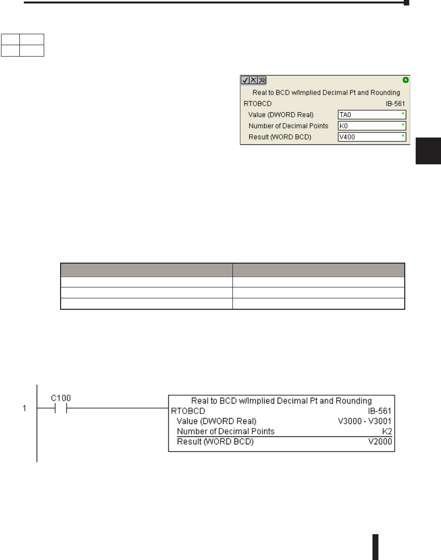
DL06 Micro PLC User Manual, 3rd Edition, Rev. D 5-263
1
2
3
4
5
6
7
8
9
10
11
12
13
14
A
B
C
D
Real to BCD with Implied Decimal Point and Rounding (RTOBCD) (IB-561)
Real to BCD with Implied Decimal Point and Rounding converts the absolute value of
the given Real number to a 4 digit BCD number, compensating for an implied number of
decimal points (K0-K4) and performs rounding.
For example, RTOBCD R56.74 with an implied
number of decimal points equal to K1, would
yield 567 BCD. If the implied number of decimal
points was 0, then the function would yield 57
BCD (note that it rounded up).
If the Real number is negative, the Result will
equal its positive, absolute value.
RTOBCD Parameters
• Value (DWORD Real): specifies the Real Dword location or number that will be converted and
rounded to a BCD number with decimal points
• Number of Decimal Points: specifies the number of implied decimal points in the Result WORD
• Result (WORD BCD): specifies the location where the rounded/implied decimal points BCD value
will be placed
RTOBCD Example
In the following example, the RTOBCD instruction is used to convert the 32-bit REAL
(floating point) data format in V3000 and V3001 to the 4-digit BCD data format and stored
in V2000 when C100 turns on.
K2 in the Number of Decimal Points implies the data will have two implied decimal points.
Chapter 5: Intelligent Box (IBox) Instructions
1
2
3
4
5
6
7
8
9
10
11
12
13
14
a
B
c
d
Parameter DL06 Range
Value (DWORD Real) V,P,R R ; See DL06 V-memory map - Data Words
Number of Decimal Points K K0-4
Result (WORD BCD) V See DL06 V-memory map - Data Words
DS Used
HPP N/A
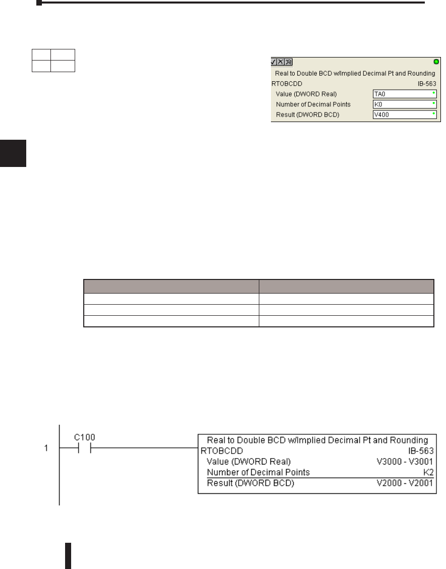
DL06 Micro PLC User Manual, 3rd Edition, Rev. D
5-264
1
2
3
4
5
6
7
8
9
10
11
12
13
14
A
B
C
D
Real to Double BCD with Implied Decimal Point and Rounding (RTOBCDD)
(IB-563)
Real to Double BCD with Implied Decimal
Point and Rounding converts the absolute value
of the given Real number to an 8 digit DWORD
BCD number, compensating for an implied
number of decimal points (K0-K8) and performs
rounding.
For example, RTOBCDD R38156.74 with an
implied number of decimal points equal to K1, would yield 381567 BCD. If the implied
number of decimal points was 0, then the function would yield 38157 BCD (note that it
rounded up).
If the Real number is negative, the Result will equal its positive, absolute value.
RTOBCDD Parameters
• Value (DWORD Real): specifies the Dword Real number that will be converted and rounded to a
BCD number with decimal points
• Number of Decimal Points: specifies the number of implied decimal points in the Result DWORD
• Result (DWORD BCD): specifies the location where the rounded/implied decimal points
DWORD BCD value will be placed
RTOBCDD Example
In the following example, the RTOBCDD instruction is used to convert the 32-bit REAL
(floating point) data format in V3000 and V3001 to the 8-digit BCD data format and stored
in V2000 and V2001 when C100 turns on.
K2 in the Number of Decimal Points implies the data will have two implied decimal points.
Chapter 5: Intelligent Box (IBox) Instructions
1
2
3
4
5
6
7
8
9
10
11
12
13
14
a
B
c
d
Parameter DL06 Range
Value (DWORD Real) V,P,R R ; See DL06 V-memory map - Data Words
Number of Decimal Points K K0-8
Result (DWORD BCD) V See DL06 V-memory map - Data Words
DS Used
HPP N/A
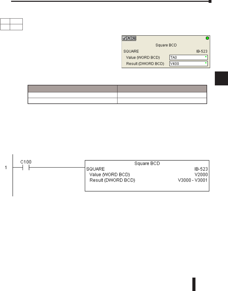
DL06 Micro PLC User Manual, 3rd Edition, Rev. D 5-265
1
2
3
4
5
6
7
8
9
10
11
12
13
14
A
B
C
D
Square BCD (SQUARE) (IB-523)
Square BCD squares the given 4-digit WORD BCD number and writes it in as an 8-digit
DWORD BCD result.
SQUARE Parameters
• Value (WORD BCD): specifies the BCD Word
or constant that will be squared
• Result (DWORD BCD): specifies the location
where the squared DWORD BCD value will be
placed
SQUARE Example
In the following example, the SQUARE instruction is used to square the 4-digit BCD value
in V2000 and store the 8-digit double word BCD result in V3000 and V3001 when C100
turns on.
Chapter 5: Intelligent Box (IBox) Instructions
1
2
3
4
5
6
7
8
9
10
11
12
13
14
a
B
c
d
Parameter DL06 Range
Value (WORD BCD) V,P,K K0-9999 ; See DL06 V-memory map - Data Words
Result (DWORD BCD) V See DL06 V-memory map - Data Words
DS Used
HPP N/A
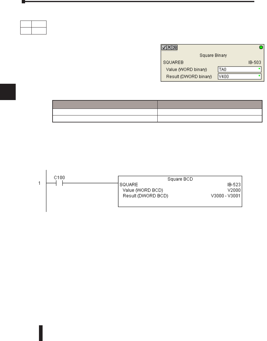
DL06 Micro PLC User Manual, 3rd Edition, Rev. D
5-266
1
2
3
4
5
6
7
8
9
10
11
12
13
14
A
B
C
D
Square Binary (SQUAREB) (IB-503)
Square Binary squares the given 16-bit WORD Binary number and writes it as a 32-bit
DWORD Binary result.
SQUAREB Parameters
• Value (WORD Binary): specifies the binary
Word or constant that will be squared
• Result (DWORD Binary): specifies the location
where the squared DWORD binary value will be
placed
SQUAREB Example
In the following example, the SQUAREB instruction is used to square the single word Binary
value in V2000 and store the 8-digit double word Binary result in V3000 and V3001 when
C100 turns on.
Chapter 5: Intelligent Box (IBox) Instructions
1
2
3
4
5
6
7
8
9
10
11
12
13
14
a
B
c
d
Parameter DL06 Range
Value (WORD Binary) V,P,K K0-65535; See DL06 V-memory map - Data Words
Result (DWORD Binary) V See DL06 V-memory map - Data Words
DS Used
HPP N/A
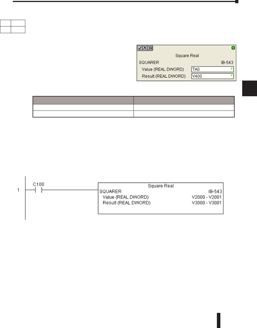
DL06 Micro PLC User Manual, 3rd Edition, Rev. D 5-267
1
2
3
4
5
6
7
8
9
10
11
12
13
14
A
B
C
D
Square Real (SQUARER) (IB-543)
Square Real squares the given REAL DWORD number and writes it to a REAL DWORD
result.
SQUARER Parameters
• Value (REAL DWORD): specifies the Real
DWORD location or number that will be
squared
• Result (REAL DWORD): specifies the location
where the squared Real DWORD value will be
placed
SQUARER Example
In the following example, the SQUARER instruction is used to square the 32-bit floating
point REAL value in V2000 and V2001 and store the REAL value result in V3000 and
V3001 when C100 turns on.
Chapter 5: Intelligent Box (IBox) Instructions
1
2
3
4
5
6
7
8
9
10
11
12
13
14
a
B
c
d
Parameter DL06 Range
Value (REAL DWORD) V,P,R R ; See DL06 V-memory map - Data Words
Result (REAL DWORD) V See DL06 V-memory map - Data Words
DS Used
HPP N/A
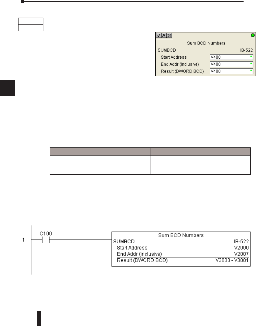
DL06 Micro PLC User Manual, 3rd Edition, Rev. D
5-268
1
2
3
4
5
6
7
8
9
10
11
12
13
14
A
B
C
D
Sum BCD Numbers (SUMBCD) (IB-522)
Sum BCD Numbers sums up a list of consecutive 4-digit WORD BCD numbers into an
8-digit DWORD BCD result.
You specify the group’s starting and ending V-
memory addresses (inclusive). When enabled,
this instruction will add up all the numbers
in the group (so you may want to place a
differential contact driving the enable).
SUMBCD could be used as the first part of
calculating an average.
SUMBCD Parameters
• Start Address: specifies the starting address of a block of V-memory location values to be added
together (BCD)
• End Addr (inclusive): specifies the ending address of a block of V-memory location values to be
added together (BCD)
• Result (DWORD BCD): specifies the location where the sum of the block of V-memory BCD
values will be placed
SUMBCD Example
In the following example, the SUMBCD instruction is used to total the sum of all BCD
values in words V2000 thru V2007 and store the resulting 8-digit double word BCD value in
V3000 and V3001 when C100 turns on.
Chapter 5: Intelligent Box (IBox) Instructions
1
2
3
4
5
6
7
8
9
10
11
12
13
14
a
B
c
d
Parameter DL06 Range
Start Address V See DL06 V-memory map - Data Words
End Address (inclusive) V See DL06 V-memory map - Data Words
Result (DWORD BCD) V See DL06 V-memory map - Data Words
DS Used
HPP N/A
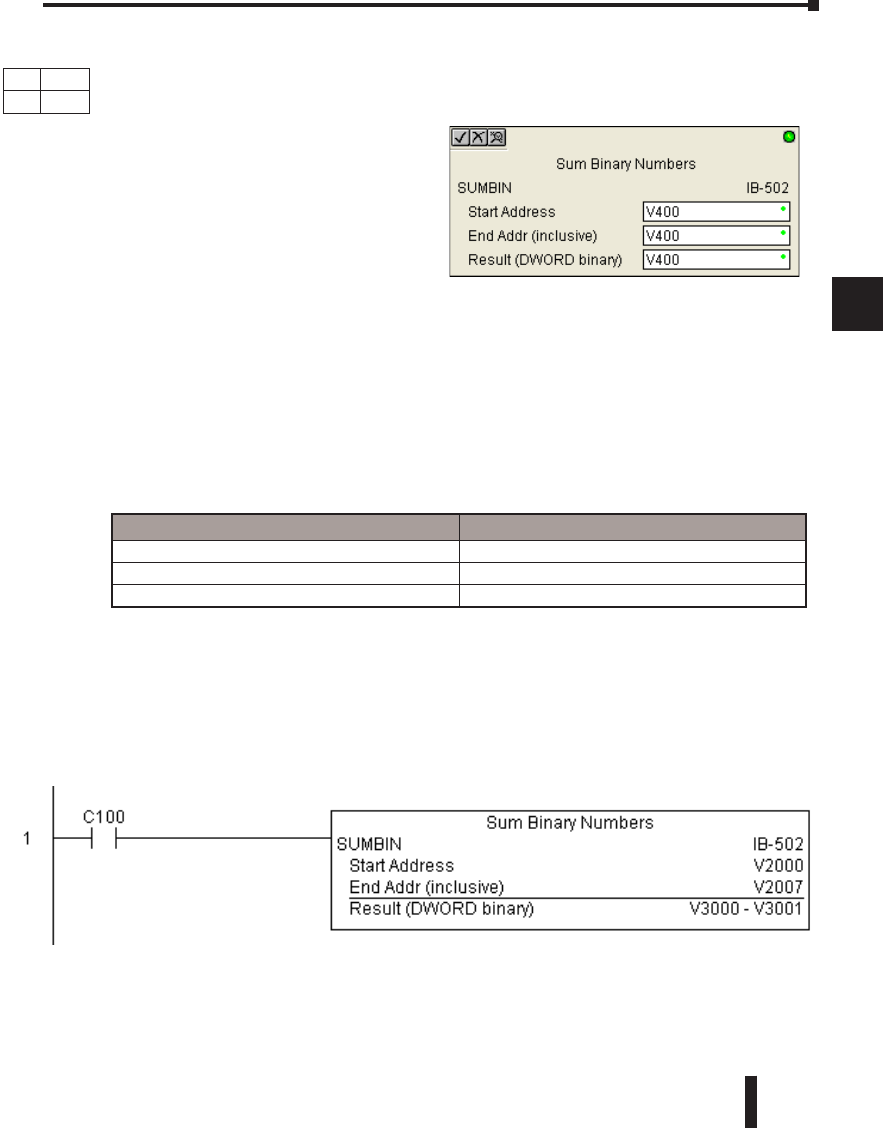
DL06 Micro PLC User Manual, 3rd Edition, Rev. D 5-269
1
2
3
4
5
6
7
8
9
10
11
12
13
14
A
B
C
D
Sum Binary Numbers (SUMBIN) (IB-502)
Sum Binary Numbers sums up a list of consecutive 16-bit WORD Binary numbers into a
32-bit DWORD binary result.
You specify the group’s starting and
ending V- memory addresses (inclusive).
When enabled, this instruction will
add up all the numbers in the group
(so you may want to place a differential
contact driving the enable).
SUMBIN could be used as the first part of
calculating an average.
SUMBIN Parameters
• Start Address: specifies the starting address of a block of V-memory location values to be added
together (Binary)
• End Addr (inclusive): specifies the ending address of a block of V-memory location values to be
added together (Binary)
• Result (DWORD Binary): specifies the location where the sum of the block of V-memory binary
values will be placed
SUMBIN Example
In the following example, the SUMBIN instruction is used to total the sum of all Binary
values in words V2000 thru V2007 and store the resulting 8-digit double word Binary value
in V3000 and V3001 when C100 turns on.
Chapter 5: Intelligent Box (IBox) Instructions
1
2
3
4
5
6
7
8
9
10
11
12
13
14
a
B
c
d
Parameter DL06 Range
Start Address V See DL06 V-memory map - Data Words
End Address (inclusive) V See DL06 V-memory map - Data Words
Result (DWORD Binary) V See DL06 V-memory map - Data Words
DS Used
HPP N/A
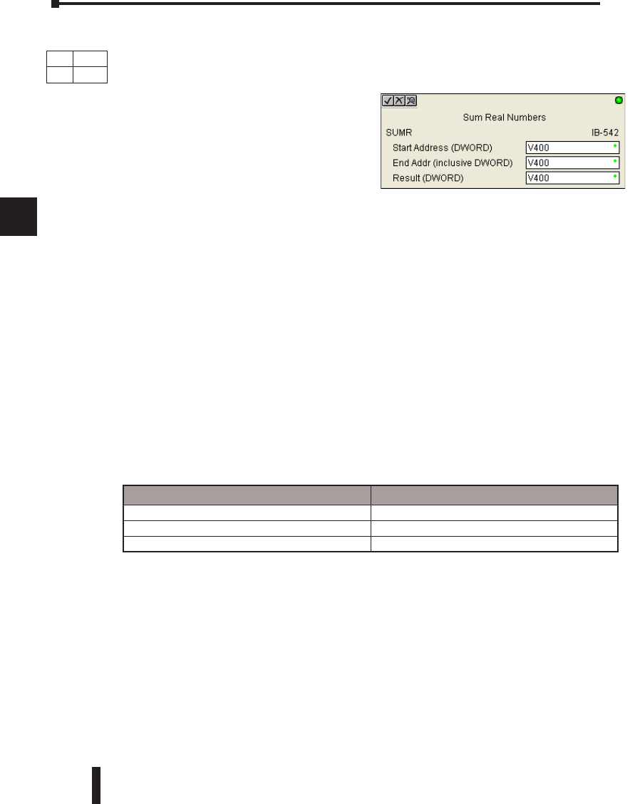
DL06 Micro PLC User Manual, 3rd Edition, Rev. D
5-270
1
2
3
4
5
6
7
8
9
10
11
12
13
14
A
B
C
D
Sum Real Numbers (SUMR) (IB-542)
Sum Real Numbers sums up a list of consecutive REAL DWORD numbers into a REAL
DWORD result.
You specify the group’s starting and ending V-
memory addresses (inclusive).
Remember that Real numbers are DWORDs
and occupy 2 words of V-Memory each, so the
number of Real values summed up is equal to
half the number of memory locations. Note that
the End Address can be EITHER word of the 2
word ending address, for example, if you wanted to add the 4 Real numbers stored in V2000
thru V2007 (V2000, V2002, V2004, and V2006), you can specify V2006 OR V2007 for the
ending address and you will get the same result.
When enabled, this instruction will add up all the numbers in the group (so you may want to
place a differential contact driving the enable).
SUMR could be used as the first part of calculating an average.
SUMR Parameters
• Start Address (DWORD): specifies the starting address of a block of V-memory location values to
be added together (Real)
• End Addr (inclusive) (DWORD): specifies the ending address of a block of V-memory location
values to be added together (Real)
• Result (DWORD): specifies the location where the sum of the block of V-memory Real values will
be placed
Chapter 5: Intelligent Box (IBox) Instructions
1
2
3
4
5
6
7
8
9
10
11
12
13
14
a
B
c
d
Parameter DL06 Range
Start Address (inclusive DWORD) V See DL06 V-memory map - Data Words
End Address (inclusive DWORD) V See DL06 V-memory map - Data Words
Result (DWORD) V See DL06 V-memory map - Data Words
DS Used
HPP N/A
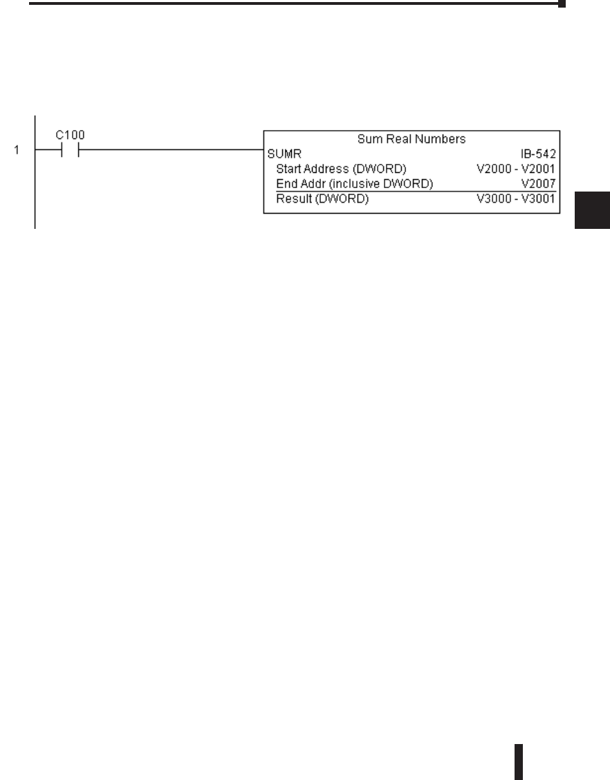
DL06 Micro PLC User Manual, 3rd Edition, Rev. D 5-271
1
2
3
4
5
6
7
8
9
10
11
12
13
14
A
B
C
D
SUMR Example
In the following example, the SUMR instruction is used to total the sum of all floating point
REAL number values in words V2000 thru V2007 and store the resulting 32-bit floating
point REAL number value in V3000 and V3001 when C100 turns on.
Chapter 5: Intelligent Box (IBox) Instructions
1
2
3
4
5
6
7
8
9
10
11
12
13
14
a
B
c
d
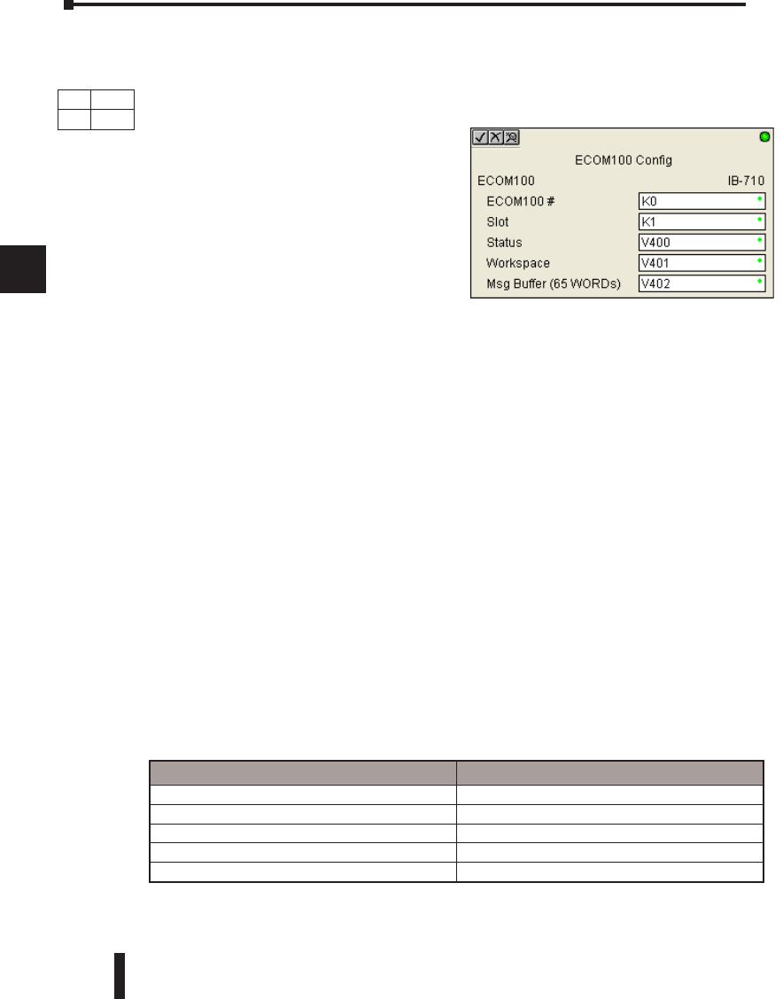
DL06 Micro PLC User Manual, 3rd Edition, Rev. D
5-272
1
2
3
4
5
6
7
8
9
10
11
12
13
14
A
B
C
D
ECOM100 Configuration (ECOM100) (IB-710)
ECOM100 Configuration defines the parameters other ECOM100 IBoxes will use when
working with this specific ECOM100 module. Each ECOM100 module that will be used
with IBox instructions will require a unique
ECOM1000 Configuration instruction. The
addresses used become workspaces for the IBox
instruction to use. .
The addresses used in this instruction must not
be used elsewhere in the program.
The instructions must be placed at the top of
ladder, without a contact. The instruction will
inherently run only once, on the first scan.
IBoxes ECEMAIL, ECRX, ECIPSUP and others require an ECOM100 Configuration before
they will operate properly.
In order for MOST ECOM100 IBoxes to function, DIP switch 7 on the ECOM100 circuit
board must be ON DIP switch 7 can remainOFF if ECOM100 Network Read and Write
IBoxes (ECRX, ECWX) are the only IBoxes that will be used.
ECOM100 Configuration Parameters
• ECOM100#: specify a logical number to be associated with this particular ECOM100 module. All
other ECxxxx IBoxes that need to reference this ECOM1000 module must reference this logical
number
• Slot: specifies the option slot the module occupies
• Status: specifies a V-memory location that will be used by the instruction
• Workspace: specifies a V-memory location that will be used by the instruction
• Msg Buffer: specifies the starting address of a 65 word buffer that will be used by the module for
configuration
Chapter 5: Intelligent Box (IBox) Instructions
1
2
3
4
5
6
7
8
9
10
11
12
13
14
a
B
c
d
DS Used
HPP N/A
Parameter DL06 Range
ECOM100# K K0-255
Slot K K1-4
Status V See DL06 V-memory map - Data Words
Workspace V See DL06 V-memory map - Data Words
Msg Buffer (65 words used) V See DL06 V-memory map - Data Words
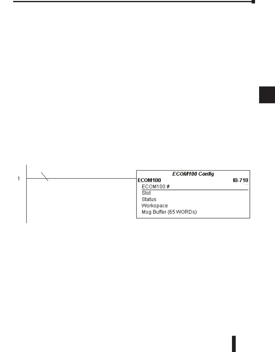
DL06 Micro PLC User Manual, 3rd Edition, Rev. D 5-273
1
2
3
4
5
6
7
8
9
10
11
12
13
14
A
B
C
D
ECOM100 Example
The ECOM100 Config IBox coordinates all of the interaction with other ECOM100 based
IBoxes (ECxxxx). You must have an ECOM100 Config IBox for each ECOM100 module
in your system. Configuration IBoxes must be at the top of your program and must execute
every scan.
This IBox defines ECOM100# K0 to be in slot 3. Any ECOM100 IBoxes that need to
reference this specific module (such as ECEMAIL, ECRX, ...) would enter K0 for their
ECOM100# parameter.
The Status register is for reporting any completion or error information to other ECOM100
IBoxes. This V-Memory register must not be used anywhere else in the entire program.
The Workspace register is used to maintain state information about the ECOM100, along
with proper sharing and interlocking with the other ECOM100 IBoxes in the program. This
V-Memory register must not be used anywhere else in the entire program.
The Message Buffer of 65 words (130 bytes) is a common pool of memory that is used
by other ECOM100 IBoxes (such as ECEMAIL). This way, you can have a bunch of
ECEMAIL IBoxes, but only need 1 common buffer for generating and sending each EMail.
These V-Memory registers must not be used anywhere else in your entire program.
Chapter 5: Intelligent Box (IBox) Instructions
1
2
3
4
5
6
7
8
9
10
11
12
13
14
a
B
c
d
K1
K0
V400
V401
V402 - V502
Permissive contacts or input logic cannot
be used with this instruction.
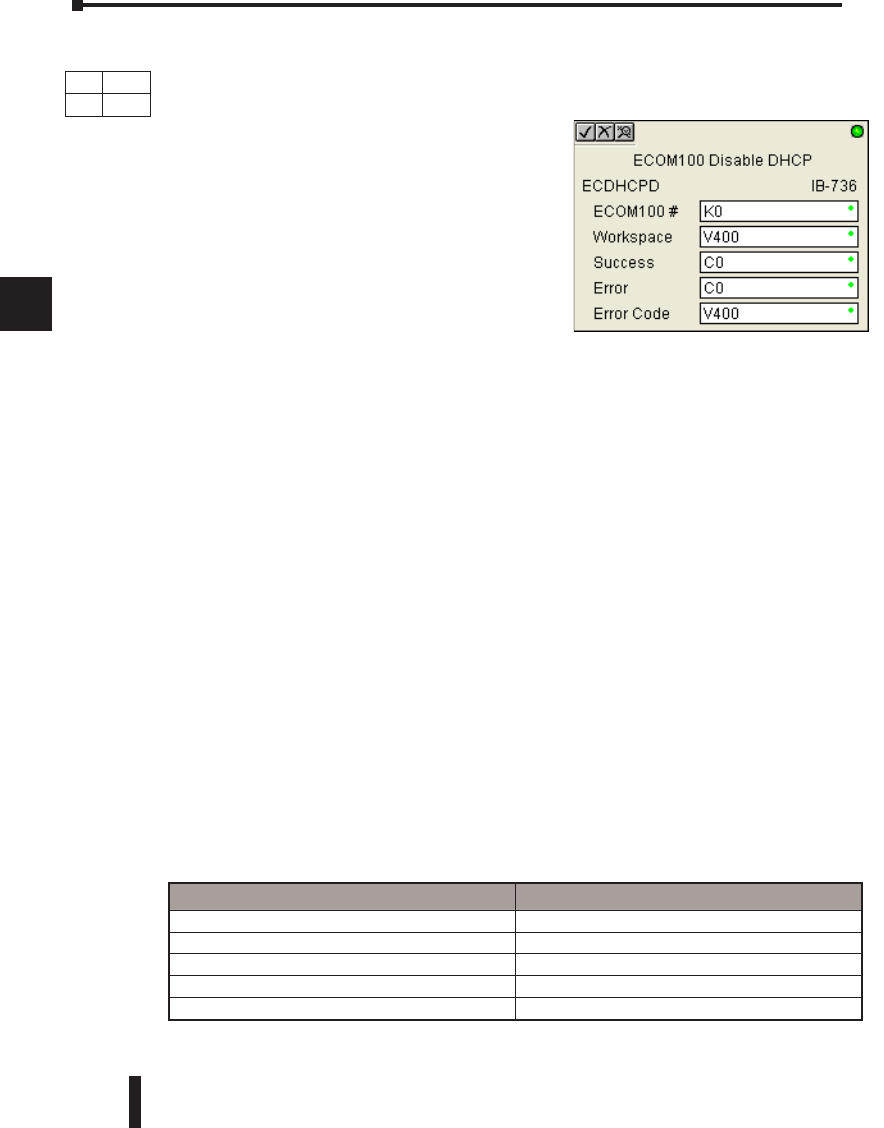
DL06 Micro PLC User Manual, 3rd Edition, Rev. D
5-274
1
2
3
4
5
6
7
8
9
10
11
12
13
14
A
B
C
D
ECOM100 Disable DHCP (ECDHCPD) (IB-736)
ECOM100 Disable DHCP will setup the ECOM100 to use its internal TCP/IP
settings on a leading edge transition to the IBox. To configure the ECOM100’s TCP/
IP settings manually, use the NetEdit3 utility, or
you can do it programmatically from your PLC
program using the ECOM100 IP Setup (ECIPSUP),
or the individual ECOM100 IBoxes: ECOM Write
IP Address (ECWRIP), ECOM Write Gateway
Address (ECWRGWA), and ECOM100 Write
Subnet Mask (ECWRSNM).
The Workspace parameter is an internal, private
register used by this IBox and MUST BE UNIQUE
in this one instruction and MUST NOT be used
anywhere else in your program.
Either the Success or Error bit parameter will turn on once the command is complete. If there
is an error, the Error Code parameter will report an ECOM100 error code (less than 100), or
a PLC logic error (greater than 1000).
The “Disable DHCP” setting is stored in Flash-ROM in the ECOM100 and the execution
of this IBox will disable the ECOM100 module for at least a half second until it writes the
Flash-ROM. Therefore, it is HIGHLY RECOMMENDED that you only execute this IBox
ONCE, on first scan. Since it requires a LEADING edge to execute, use a NORMALLY
CLOSED SP0 (STR NOT First Scan) to drive the power flow to the IBox.
In order for this ECOM100 IBox to function, you must turn ON dip switch 7 on the
ECOM100 circuit board.
ECDHCPD Parameters
• ECOM100#: this is a logical number associated with this specific ECOM100 module in the
specified slot. All other ECxxxx IBoxes that need to reference this ECOM100 module must
reference this logical number
• Workspace: specifies a V-memory location that will be used by the instruction
• Success: specifies a bit that will turn on once the request is completed successfully
• Error: specifies a bit that will turn on if the instruction is not successfully completed
• Error Code: specifies the location where the Error Code will be written
Chapter 5: Intelligent Box (IBox) Instructions
1
2
3
4
5
6
7
8
9
10
11
12
13
14
a
B
c
d
Parameter DL06 Range
ECOM100# K K0-255
Workspace V See DL06 V-memory map - Data Words
Success X,Y,C,GX,GY,B See DL06 V-memory map
Error X,Y,C,GX,GY,B See DL06 V-memory map
Error Code V See DL06 V-memory map - Data Words
DS Used
HPP N/A
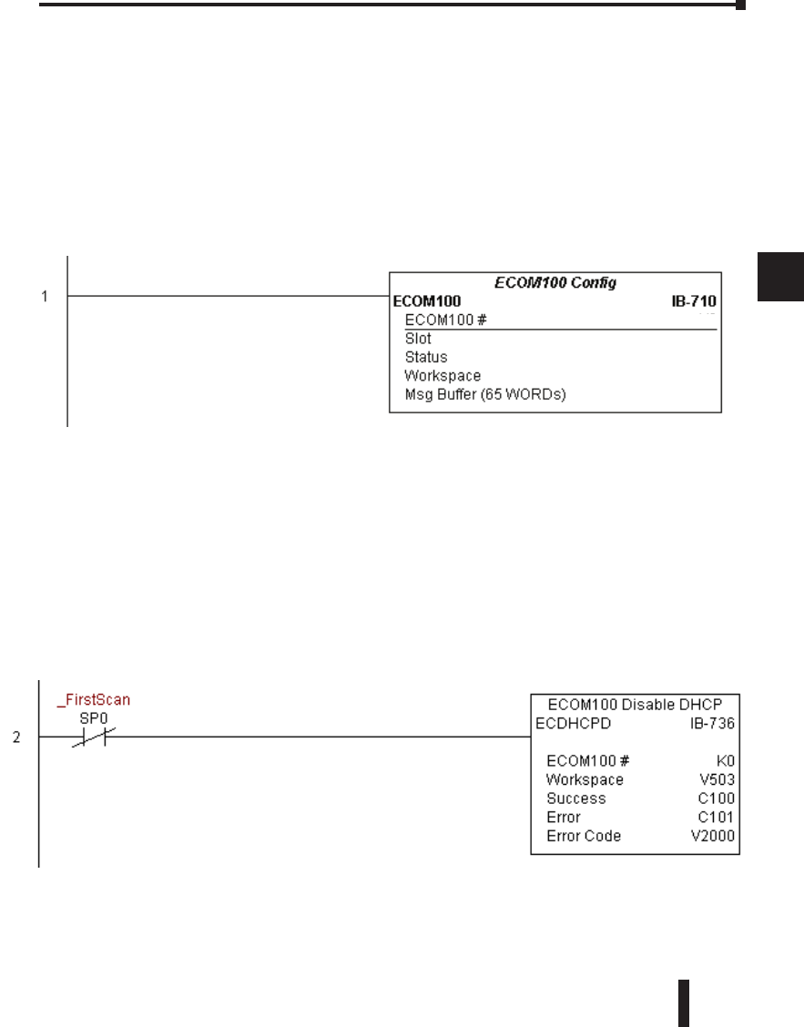
DL06 Micro PLC User Manual, 3rd Edition, Rev. D 5-275
1
2
3
4
5
6
7
8
9
10
11
12
13
14
A
B
C
D
ECDHCPD Example
Rung 1: The ECOM100 Config IBox is responsible for coordination/interlocking of all
ECOM100 type IBoxes for one specific ECOM100 module. Tag the ECOM100 in slot 1
as ECOM100# K0. All other ECxxxx IBoxes refer to this module # as K0. If you need to
move the module in the base to a different slot, then you only need to change this one IBox.
V400 is used as a global result status register for the other ECxxxx IBoxes using this specific
ECOM100 module. V401 is used to coordinate/interlock the logic in all of the other ECxxxx
IBoxes using this specific ECOM100 module. V402-V502 is a common 130 byte buffer
available for use by the other ECxxxx IBoxes using this specific ECOM100 module.
Rung 2: On the 2nd scan, disable DHCP in the ECOM100. DHCP is the same protocol
used by PCs for using a DHCP Server to automatically assign the ECOM100’s IP Address,
Gateway Address, and Subnet Mask. Typically disabling DHCP is done by assigning a hard-
coded IP Address either in NetEdit or using one of the ECOM100 IP Setup IBoxes, but
this IBox allows you to disable DHCP in the ECOM100 using your ladder program. The
ECDHCPD is leading edge triggered, not power-flow driven (similar to a counter input leg).
The command to disable DHCP will be sent to the ECOM100 whenever the power flow
into the IBox goes from OFF to ON. If successful, turn on C100. If there is a failure, turn on
C101. If it fails, you can look at V2000 for the specific error code.
Chapter 5: Intelligent Box (IBox) Instructions
1
2
3
4
5
6
7
8
9
10
11
12
13
14
a
B
c
d
K1
K0
V400
V401
V402 - V502
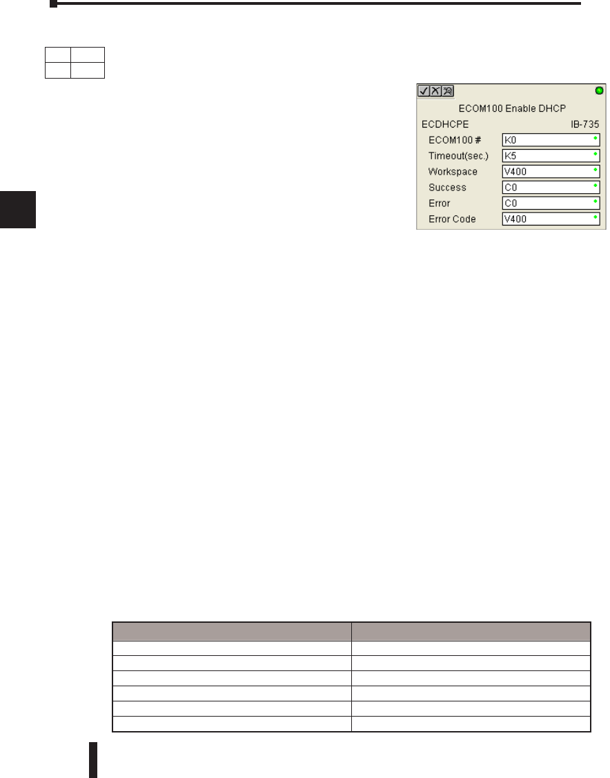
DL06 Micro PLC User Manual, 3rd Edition, Rev. D
5-276
1
2
3
4
5
6
7
8
9
10
11
12
13
14
A
B
C
D
ECOM100 Enable DHCP (ECDHCPE) (IB-735)
ECOM100 Enable DHCP will tell the ECOM100 to obtain its TCP/IP setup from a DHCP
Server on a leading edge transition to the IBox.
The IBox will be successful once the ECOM100
has received its TCP/IP settings from the DHCP
server. Since it is possible for the DHCP server to be
unavailable, a Timeout parameter is provided so that
the IBox can complete, but with an Error (Error Code =
1004 decimal).
See also the ECOM100 IP Setup (ECIPSUP) IBox
717 to directly setup ALL of the TCP/IP parameters
in a single instruction - IP Address, Subnet Mask, and
Gateway Address.
The Workspace parameter is an internal, private register used by this IBox and MUST BE
UNIQUE in this one instruction and MUST NOT be used anywhere else in your program.
Either the Success or Error bit parameter will turn on once the command is complete. If there
is an error, the Error Code parameter will report an ECOM100 error code (less than 100), or
a PLC logic error (greater than 1000).
The “Enable DHCP” setting is stored in Flash-ROM in the ECOM100 and the execution
of this IBox will disable the ECOM100 module for at least a half second until it writes the
Flash-ROM. Therefore, it is HIGHLY RECOMMENDED that you only execute this IBox
ONCE, on first scan. Since it requires a LEADING edge to execute, use a NORMALLY
CLOSED SP0 (STR NOT First Scan) to drive the power flow to the IBox.
In order for this ECOM100 IBox to function, you must turn ON dip switch 7 on the
ECOM100 circuit board.
ECDHCPE Parameters
• ECOM100#: this is a logical number associated with this specific ECOM100 module in the
specified slot. All other ECxxxx IBoxes that need to reference this ECOM100 module must
reference this logical number
• Timeout(sec): specifies a timeout period so that the instruction may have time to complete
• Workspace: specifies a V-memory location that will be used by the instruction
• Success: specifies a bit that will turn on once the request is completed successfully
• Error: specifies a bit that will turn on if the instruction is not successfully completed
• Error Code: specifies the location where the Error Code will be written
Chapter 5: Intelligent Box (IBox) Instructions
1
2
3
4
5
6
7
8
9
10
11
12
13
14
a
B
c
d
Parameter DL06 Range
ECOM100# K K0-255
Timeout (sec) K K5-127
Workspace V See DL06 V-memory map - Data Words
Success X,Y,C,GX,GY,B See DL06 V-memory map
Error X,Y,C,GX,GY,B See DL06 V-memory map
Error Code V See DL06 V-memory map - Data Words
DS Used
HPP N/A
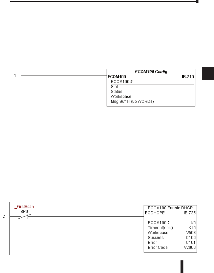
DL06 Micro PLC User Manual, 3rd Edition, Rev. D 5-277
1
2
3
4
5
6
7
8
9
10
11
12
13
14
A
B
C
D
ECDHCPE Example
Rung 1: The ECOM100 Config IBox is responsible for coordination/interlocking of all
ECOM100 type IBoxes for one specific ECOM100 module. Tag the ECOM100 in slot 1
as ECOM100# K0. All other ECxxxx IBoxes refer to this module # as K0. If you need to
move the module in the base to a different slot, then you only need to change this one IBox.
V400 is used as a global result status register for the other ECxxxx IBoxes using this specific
ECOM100 module.V401 is used to coordinate/interlock the logic in all of the other ECxxxx
IBoxes using this specific ECOM100 module. V402-V502 is a common 130 byte buffer
available for use by the other ECxxxx IBoxes using this specific ECOM100 module.
Rung 2: On the 2nd scan, enable DHCP in the ECOM100. DHCP is the same protocol
used by PCs for using a DHCP Server to automatically assign the ECOM100’s IP Address,
Gateway Address, and Subnet Mask. Typically this is done using NetEdit, but this IBox
allows you to enable DHCP in the ECOM100 using your ladder program. The ECDHCPE
is leading edge triggered, not power-flow driven (similar to a counter input leg). The
commands to enable DHCP will be sent to the ECOM100 whenever the power flow into
the IBox goes from OFF to ON. The ECDHCPE does more than just set the bit to enable
DHCP in the ECOM100, but it then polls the ECOM100 once every second to see if the
ECOM100 has found a DHCP server and has a valid IP Address. Therefore, a timeout
parameter is needed in case the ECOM100 cannot find a DHCP server. If a timeout does
occur, the Error bit will turn on and the error code will be 1005 decimal. The Success bit will
turn on only if the ECOM100 finds a DHCP Server and is assigned a valid IP Address. If
successful, turn on C100. If there is a failure, turn on C101. If it fails, you can look at V2000
for the specific error code.
Chapter 5: Intelligent Box (IBox) Instructions
1
2
3
4
5
6
7
8
9
10
11
12
13
14
a
B
c
d
K1
K0
V400
V401
V402 - V502
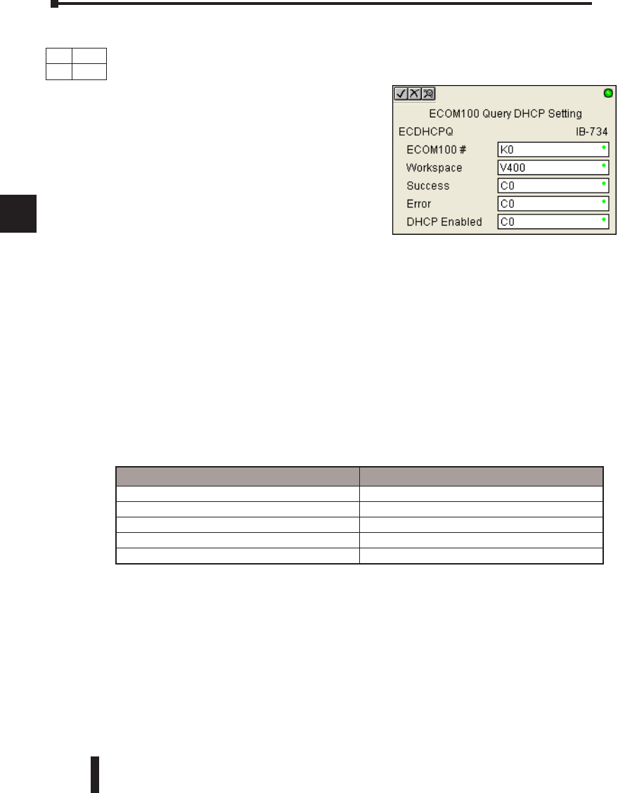
DL06 Micro PLC User Manual, 3rd Edition, Rev. D
5-278
1
2
3
4
5
6
7
8
9
10
11
12
13
14
A
B
C
D
ECOM100 Query DHCP Setting (ECDHCPQ) (IB-734)
ECOM100 Query DHCP Setting will determine if DHCP is enabled in the ECOM100 on a
leading edge transition to the IBox. The DHCP Enabled bit parameter will be ON if DHCP
is enabled, OFF if disabled.
The Workspace parameter is an internal, private
register used by this IBox and MUST BE
UNIQUE in this one instruction and MUST NOT
be used anywhere else in your program.
Either the Success or Error bit parameter will turn
on once the command is complete.
In order for this ECOM100 IBox to function, you
must turn ON dip switch 7 on the ECOM100
circuit board.
ECDHCPQ Parameters
• ECOM100#: this is a logical number associated with this specific ECOM100 module in the
specified slot. All other ECxxxx IBoxes that need to reference this ECOM100 module must
reference this logical number
• Workspace: specifies a V-memory location that will be used by the instruction
• Success: specifies a bit that will turn on once the instruction is completed successfully
• Error: specifies a bit that will turn on if the instruction is not successfully completed
• DHCP Enabled: specifies a bit that will turn on if the ECOM100’s DHCP is enabled or remain
off if disabled - after instruction query, be sure to check the state of the Success/Error bit state along
with DHCP Enabled bit state to confirm a successful module query
Chapter 5: Intelligent Box (IBox) Instructions
1
2
3
4
5
6
7
8
9
10
11
12
13
14
a
B
c
d
Parameter DL06 Range
ECOM100# K K0-255
Workspace V See DL06 V-memory map - Data Words
Success X,Y,C,GX,GY,B See DL06 V-memory map
Error X,Y,C,GX,GY,B See DL06 V-memory map
DHCP Enabled X,Y,C,GX,GY,B See DL06 V-memory map
DS Used
HPP N/A
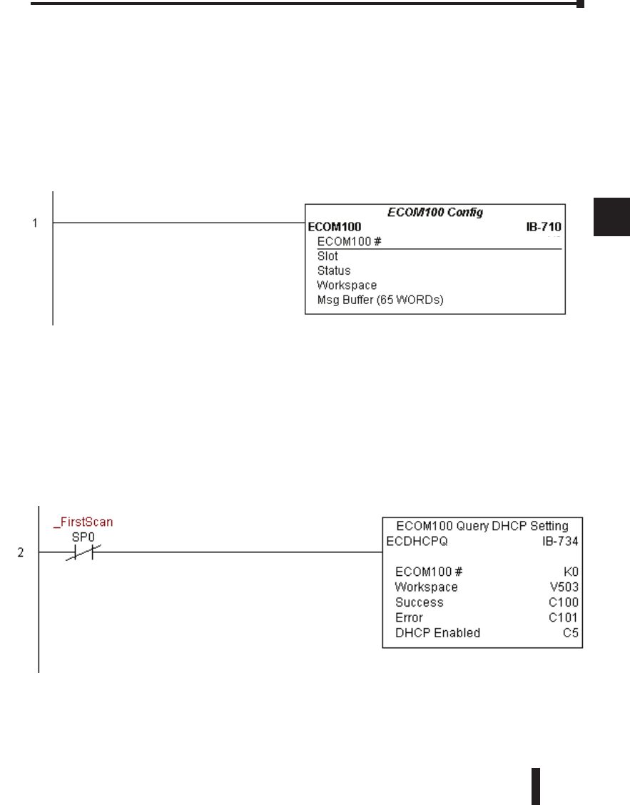
DL06 Micro PLC User Manual, 3rd Edition, Rev. D 5-279
1
2
3
4
5
6
7
8
9
10
11
12
13
14
A
B
C
D
ECDHCPQ Example
Rung 1: The ECOM100 Config IBox is responsible for coordination/interlocking of all
ECOM100 type IBoxes for one specific ECOM100 module. Tag the ECOM100 in slot 1
as ECOM100# K0. All other ECxxxx IBoxes refer to this module # as K0. If you need to
move the module in the base to a different slot, then you only need to change this one IBox.
V400 is used as a global result status register for the other ECxxxx IBoxes using this specific
ECOM100 module.V401 is used to coordinate/interlock the logic in all of the other ECxxxx
IBoxes using this specific ECOM100 module. V402-V502 is a common 130 byte buffer
available for use by the other ECxxxx IBoxes using this specific ECOM100 module.
Rung 2: On the 2nd scan, read whether DHCP is enabled or disabled in the ECOM100
and store it in C5. DHCP is the same protocol used by PCs for using a DHCP Server to
automatically assign the ECOM100’s IP Address, Gateway Address, and Subnet Mask. The
ECDHCPQ is leading edge triggered, not power-flow driven (similar to a counter input
leg). The command to read (Query) whether DHCP is enabled or not will be sent to the
ECOM100 whenever the power flow into the IBox goes from OFF to ON. If successful, turn
on C100. If there is a failure, turn on C101.
Chapter 5: Intelligent Box (IBox) Instructions
1
2
3
4
5
6
7
8
9
10
11
12
13
14
a
B
c
d
K1
K0
V400
V401
V402 - V502
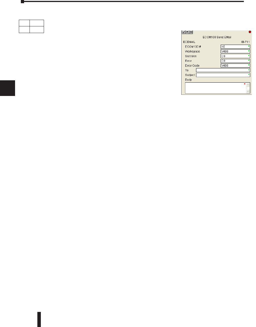
DL06 Micro PLC User Manual, 3rd Edition, Rev. D
5-280
1
2
3
4
5
6
7
8
9
10
11
12
13
14
A
B
C
D
ECOM100 Send E-mail (ECEMAIL) (IB-711)
ECOM100 Send EMail, on a leading edge transition, will behave as an EMail client and
send an SMTP request to your SMTP Server to send the EMail message to the EMail
addresses in the To: field and also to those listed in the
Cc: list hard coded in the ECOM100. It will send the
SMTP request based on the specified ECOM100#, which
corresponds to a specific unique ECOM100 Configuration
(ECOM100) at the top of your program.
The Body: field supports what the PRINT and VPRINT
instructions support for text and embedded variables,
allowing you to embed real-time data in your EMail (e.g.
“V2000 = “ V2000:B).
The Workspace parameter is an internal, private register
used by this IBox and MUST BE UNIQUE in this one instruction and MUST NOT be
used anywhere else in your program.
Either the Success or Error bit parameter will turn on once the request is complete. If there is
an error, the Error Code parameter will report an ECOM100 error code (less than 100), an
SMPT protocol error (between 100 and 999), or a PLC logic error (greater than 1000).
Since the ECOM100 is only an EMail Client and requires access to an SMTP Server,
you MUST have the SMTP parameters configured properly in the ECOM100 via the
ECOM100’s Home Page and/or the EMail Setup instruction (ECEMSUP). To get to the
ECOM100’s Home Page, use your favorite Internet browser and browse to the ECOM100’s
IP Address, e.g. http://192.168.12.86
You are limited to approximately 100 characters of message data for the entire instruction,
including the To: Subject: and Body: fields. To save space, the ECOM100 supports a hard
coded list of EMail addresses for the Carbon Copy field (cc:) so that you can configure those
in the ECOM100, and keep the To: field small (or even empty), to leave more room for the
Subject: and Body: fields.
In order for this ECOM100 IBox to function, you must turn ON dip switch 7 on the
ECOM100 circuit board.
ECEMAIL Parameters
• ECOM100#: this is a logical number associated with this specific ECOM100 module in the
specified slot. All other ECxxxx IBoxes that need to reference this ECOM100 module must
reference this logical number
• Workspace: specifies a V-memory location that will be used by the instruction
• Success: specifies a bit that will turn on once the request is completed successfully
• Error: specifies a bit that will turn on if the instruction is not successfully completed
• Error Code: specifies the location where the Error Code will be written
• To: specifies an E-mail address that the message will be sent to
• Subject: subject of the e-mail message
• Body: supports what the PRINT and VPRINT instructions support for text and embedded
variables, allowing you to embed real-time data in the EMail message
Chapter 5: Intelligent Box (IBox) Instructions
1
2
3
4
5
6
7
8
9
10
11
12
13
14
a
B
c
d
DS Used
HPP N/A
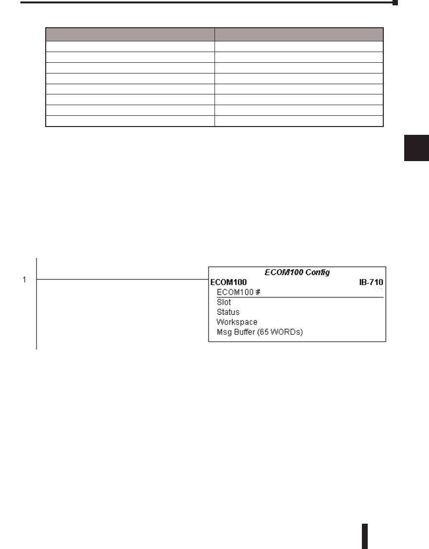
DL06 Micro PLC User Manual, 3rd Edition, Rev. D 5-281
1
2
3
4
5
6
7
8
9
10
11
12
13
14
A
B
C
D
ECEMAIL Example
Rung 1: The ECOM100 Config IBox is responsible for coordination/interlocking of all
ECOM100 type IBoxes for one specific ECOM100 module. Tag the ECOM100 in slot 1
as ECOM100# K0. All other ECxxxx IBoxes refer to this module # as K0. If you need to
move the module in the base to a different slot, then you only need to change this one IBox.
V400 is used as a global result status register for the other ECxxxx IBoxes using this specific
ECOM100 module.V401 is used to coordinate/interlock the logic in all of the other ECxxxx
IBoxes using this specific ECOM100 module. V402-V502 is a common 130 byte buffer
available for use by the other ECxxxx IBoxes using this specific ECOM100 module.
Chapter 5: Intelligent Box (IBox) Instructions
1
2
3
4
5
6
7
8
9
10
11
12
13
14
a
B
c
d
Parameter DL06 Range
ECOM100# K K0-255
Workspace V See DL06 V-memory map - Data Words
Success X,Y,C,GX,GY,B See DL06 V-memory map
Error X,Y,C,GX,GY,B See DL06 V-memory map
Error Code V See DL06 V-memory map
To: Text
Subject: Text
Body: See PRINT and VPRINT instructions
K1
K0
V400
V401
V402 - V502
(example continued on next page)
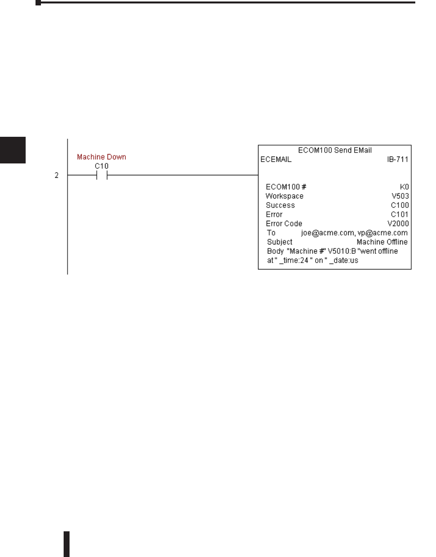
DL06 Micro PLC User Manual, 3rd Edition, Rev. D
5-282
1
2
3
4
5
6
7
8
9
10
11
12
13
14
A
B
C
D
ECEMAIL Example (cont’d)
Rung 2: When a machine goes down, send an email to Joe in maintenance and to the VP
over production showing what machine is down along with the date/time stamp of when it
went down.
The ECEMAIL is leading edge triggered, not power-flow driven (similar to a counter input
leg). An email will be sent whenever the power flow into the IBox goes from OFF to ON.
This helps prevent self inflicted spamming.
If the EMail is sent, turn on C100. If there is a failure, turn on C101. If it fails, you can look
at V2000 for the SMTP error code or other possible error codes.
Chapter 5: Intelligent Box (IBox) Instructions
1
2
3
4
5
6
7
8
9
10
11
12
13
14
a
B
c
d
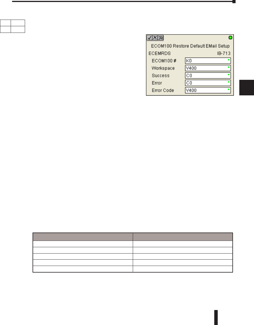
DL06 Micro PLC User Manual, 3rd Edition, Rev. D 5-283
1
2
3
4
5
6
7
8
9
10
11
12
13
14
A
B
C
D
ECOM100 Restore Default E-mail Setup (ECEMRDS) (IB-713)
ECOM100 Restore Default EMail Setup, on a leading edge transition, will restore the
original EMail Setup data stored in the ECOM100 back to the working copy based on
the specified ECOM100#, which corresponds
to a specific unique ECOM100 Configuration
(ECOM100) at the top of your program.
When the ECOM100 is first powered up, it copies
the EMail setup data stored in ROM to the working
copy in RAM. You can then modify this working
copy from your program using the ECOM100
EMail Setup (ECEMSUP) IBox. After modifying the
working copy, you can later restore the original setup
data via your program by using this IBox.
The Workspace parameter is an internal, private register used by this IBox and MUST BE
UNIQUE in this one instruction and MUST NOT be used anywhere else in your program.
Either the Success or Error bit parameter will turn on once the command is complete. If there
is an error, the Error Code parameter will report an ECOM100 error code (less than 100), or
a PLC logic error (greater than 1000).
In order for this ECOM100 IBox to function, you must turn ON dip switch 7 on the
ECOM100 circuit board.
ECEMRDS Parameters
• ECOM100#: this is a logical number associated with this specific ECOM100 module in the
specified slot. All other ECxxxx IBoxes that need to reference this ECOM100 module must
reference this logical number
• Workspace: specifies a V-memory location that will be used by the instruction
• Success: specifies a bit that will turn on once the request is completed successfully
• Error: specifies a bit that will turn on if the instruction is not successfully completed
• Error Code: specifies the location where the Error Code will be written
Chapter 5: Intelligent Box (IBox) Instructions
1
2
3
4
5
6
7
8
9
10
11
12
13
14
a
B
c
d
DS Used
HPP N/A
Parameter DL06 Range
ECOM100# K K0-255
Workspace V See DL06 V-memory map - Data Words
Success X,Y,C,GX,GY,B See DL06 V-memory map
Error X,Y,C,GX,GY,B See DL06 V-memory map
Error Code V See DL06 V-memory map - Data Words
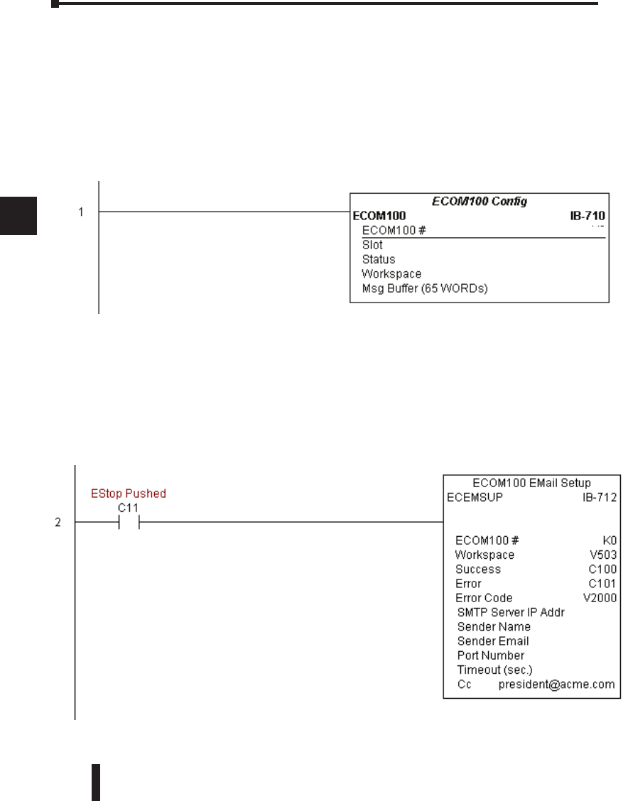
DL06 Micro PLC User Manual, 3rd Edition, Rev. D
5-284
1
2
3
4
5
6
7
8
9
10
11
12
13
14
A
B
C
D
ECEMRDS Example
Rung 1: The ECOM100 Config IBox is responsible for coordination/interlocking of all
ECOM100 type IBoxes for one specific ECOM100 module. Tag the ECOM100 in slot 1
as ECOM100# K0. All other ECxxxx IBoxes refer to this module # as K0. If you need to
move the module in the base to a different slot, then you only need to change this one IBox.
V400 is used as a global result status register for the other ECxxxx IBoxes using this specific
ECOM100 module.V401 is used to coordinate/interlock the logic in all of the other ECxxxx
IBoxes using this specific ECOM100 module. V402-V502 is a common 130 byte buffer
available for use by the other ECxxxx IBoxes using this specific ECOM100 module.
Rung 2: Whenever an EStop is pushed, ensure that president of the company gets copies of
all EMails being sent.
The ECOM100 EMail Setup IBox allows you to set/change the SMTP EMail settings stored
in the ECOM100.
Chapter 5: Intelligent Box (IBox) Instructions
1
2
3
4
5
6
7
8
9
10
11
12
13
14
a
B
c
d
K1
K0
V400
V401
V402 - V502
(example continued on next page)
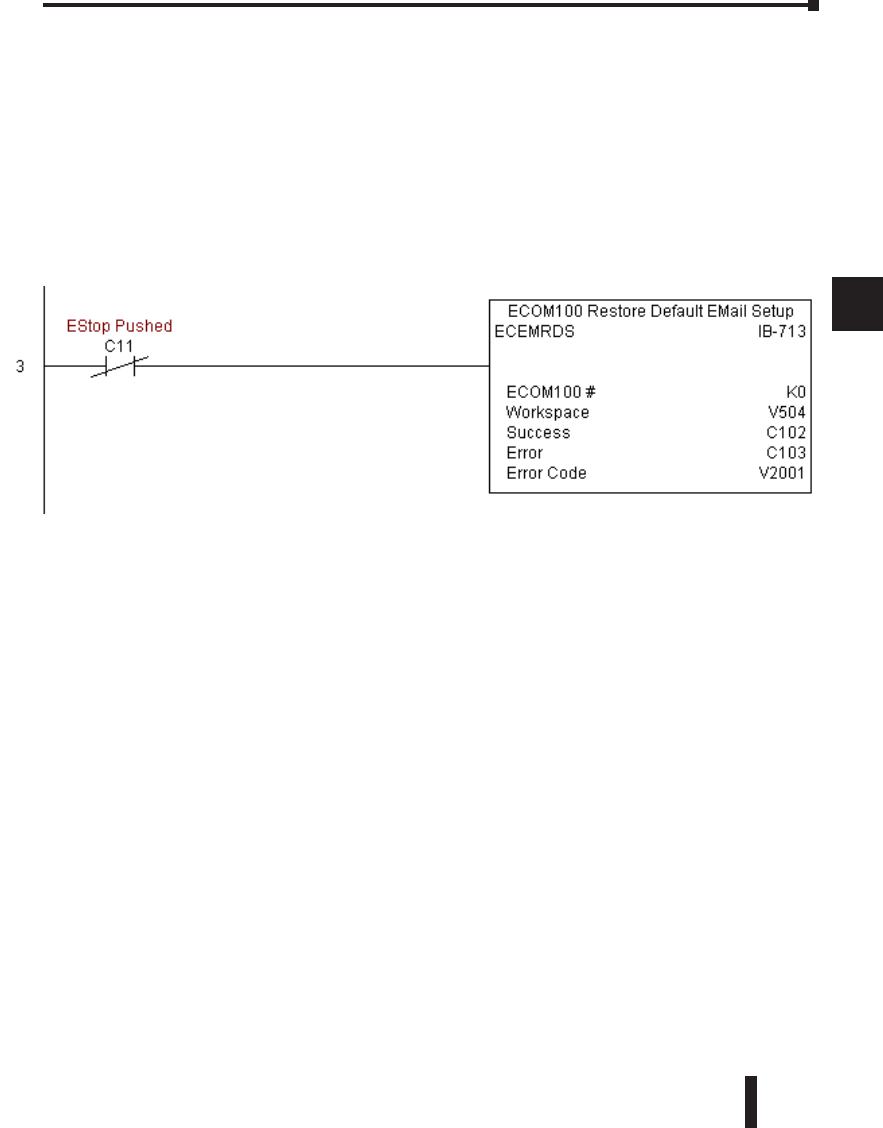
DL06 Micro PLC User Manual, 3rd Edition, Rev. D 5-285
1
2
3
4
5
6
7
8
9
10
11
12
13
14
A
B
C
D
ECEMRDS Example (cont’d)
Rung 3: Once the EStop is pulled out, take the president off the cc: list by restoring the
default EMail setup in the ECOM100.
The ECEMRDS is leading edge triggered, not power-flow driven (similar to a counter input
leg). The ROM based EMail configuration stored in the ECOM100 will be copied over the
“working copy” whenever the power flow into the IBox goes from OFF to ON (the working
copy can be changed by using the ECEMSUP IBox).
If successful, turn on C102. If there is a failure, turn on C103. If it fails, you can look at
V2001 for the specific error code.
Chapter 5: Intelligent Box (IBox) Instructions
1
2
3
4
5
6
7
8
9
10
11
12
13
14
a
B
c
d
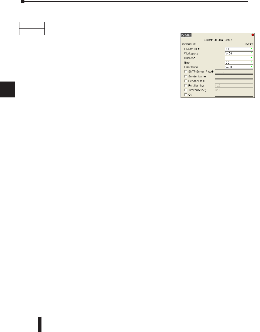
DL06 Micro PLC User Manual, 3rd Edition, Rev. D
5-286
1
2
3
4
5
6
7
8
9
10
11
12
13
14
A
B
C
D
ECOM100 E-mail Setup (ECEMSUP) (IB-712)
ECOM100 EMail Setup, on a leading edge transition, will modify the working copy of
the EMail setup currently in the ECOM100 based on the specified ECOM100#, which
corresponds to a specific unique ECOM100 Configuration
(ECOM100) at the top of your program.
You may pick and choose any or all fields to be modified
using this instruction. Note that these changes are
cumulative: if you execute multiple ECOM100 EMail
Setup IBoxes, then all of the changes are made in the
order they are executed. Also note that you can restore
the original ECOM100 EMail Setup that is stored in the
ECOM100 to the working copy by using the ECOM100
Restore Default EMail Setup (ECEMRDS) IBox.
The Workspace parameter is an internal, private register used by this IBox and MUST BE
UNIQUE in this one instruction and MUST NOT be used anywhere else in your program.
Either the Success or Error bit parameter will turn on once the command is complete. If there
is an error, the Error Code parameter will report an ECOM100 error code (less than 100), or
a PLC logic error (greater than 1000).
You are limited to approximately 100 characters/bytes of setup data for the entire instruction.
So if needed, you could divide the entire setup across multiple ECEMSUP IBoxes on a field-
by-field basis, for example do the Carbon Copy (cc:) field in one ECEMSUP IBox and the
remaining setup parameters in another.
In order for this ECOM100 IBox to function, you must turn ON dip switch 7 on the
ECOM100 circuit board.
ECEMSUP Parameters
• ECOM100#: this is a logical number associated with this specific ECOM100 module in the
specified slot. All other ECxxxx IBoxes that need to reference this ECOM100 module must
reference this logical number
• Workspace: specifies a V-memory location that will be used by the instruction
• Success: specifies a bit that will turn on once the request is completed successfully
• Error: specifies a bit that will turn on if the instruction is not successfully completed
• Error Code: specifies the location where the Error Code will be written
• SMTP Server IP Addr: optional parameter that specifies the IP Address of the SMTP Server on the
ECOM100’s network
• Sender Name: optional parameter that specifies the sender name that will appear in the “From:”
field to those who receive the e-mail
• Sender EMail: optional parameter that specifies the sender EMail address that will appear in the
“From:” field to those who receive the e-mail
Chapter 5: Intelligent Box (IBox) Instructions
1
2
3
4
5
6
7
8
9
10
11
12
13
14
a
B
c
d
DS Used
HPP N/A
DL06 Micro PLC User Manual, 3rd Edition, Rev. D 5-287
1
2
3
4
5
6
7
8
9
10
11
12
13
14
A
B
C
D
ECEMSUP Parameters (cont’d)
• Port Number: optional parameter that specifies the TCP/IP Port Number to send SMTP requests;
usually this does not to be configured (see your network administrator for information on this
setting)
• Timeout (sec): optional parameter that specifies the number of seconds to wait for the SMTP
Server to send the EMail to all the recipients
• Cc: optional parameter that specifies a list of “carbon copy” Email addresses to send all EMails to
Chapter 5: Intelligent Box (IBox) Instructions
1
2
3
4
5
6
7
8
9
10
11
12
13
14
a
B
c
d
Parameter DL06 Range
ECOM100# K K0-255
Workspace V See DL06 V-memory map - Data Words
Success X,Y,C,GX,GY,B See DL06 V-memory map
Error X,Y,C,GX,GY,B See DL06 V-memory map
Error Code V See DL06 V-memory map - Data Words
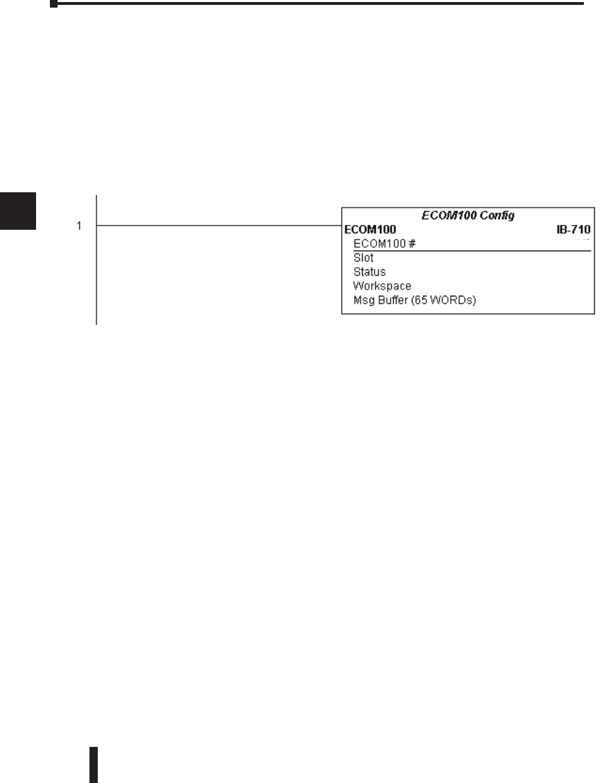
DL06 Micro PLC User Manual, 3rd Edition, Rev. D
5-288
1
2
3
4
5
6
7
8
9
10
11
12
13
14
A
B
C
D
ECEMSUP Example
Rung 1: The ECOM100 Config IBox is responsible for coordination/interlocking of all
ECOM100 type IBoxes for one specific ECOM100 module. Tag the ECOM100 in slot 1
as ECOM100# K0. All other ECxxxx IBoxes refer to this module # as K0. If you need to
move the module in the base to a different slot, then you only need to change this one IBox.
V400 is used as a global result status register for the other ECxxxx IBoxes using this specific
ECOM100 module.V401 is used to coordinate/interlock the logic in all of the other ECxxxx
IBoxes using this specific ECOM100 module. V402-V502 is a common 130 byte buffer
available for use by the other ECxxxx IBoxes using this specific ECOM100 module.
Chapter 5: Intelligent Box (IBox) Instructions
1
2
3
4
5
6
7
8
9
10
11
12
13
14
a
B
c
d
K1
K0
V400
V401
V402 - V502
(example continued on next page)
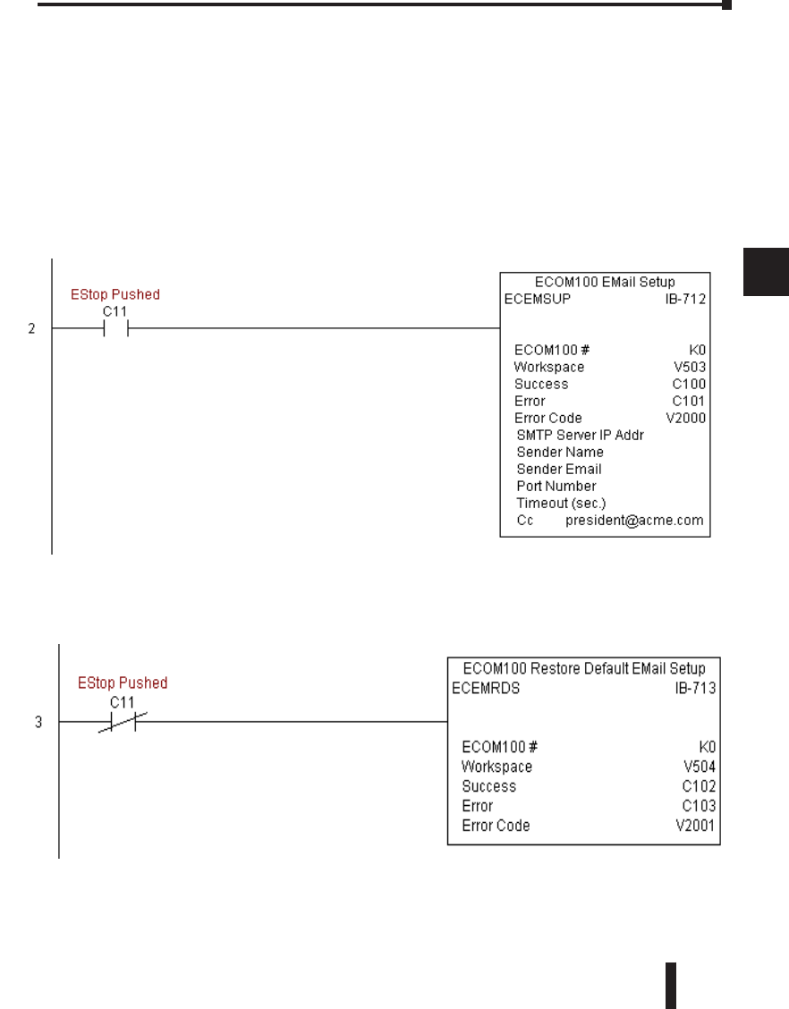
DL06 Micro PLC User Manual, 3rd Edition, Rev. D 5-289
1
2
3
4
5
6
7
8
9
10
11
12
13
14
A
B
C
D
ECEMSUP Example (cont’d)
Rung 2: Whenever an EStop is pushed, ensure that president of the company gets copies
of all EMails being sent.The ECOM100 EMail Setup IBox allows you to set/change the
SMTP EMail settings stored in the ECOM100. The ECEMSUP is leading edge triggered,
not power-flow driven (similar to a counter input leg). At power-up, the ROM based EMail
configuration stored in the ECOM100 is copied to a RAM based “working copy”. You can
change this working copy by using the ECEMSUP IBox. To restore the original ROM based
configuration, use the Restore Default EMail Setup ECEMRDS IBox.
If successful, turn on C100. If there is a failure, turn on C101. If it fails, you can look at
V2000 for the specific error code.
Rung 3: Once the EStop is pulled out, take the president off the cc: list by restoring the
default EMail setup in the ECOM100.
Chapter 5: Intelligent Box (IBox) Instructions
1
2
3
4
5
6
7
8
9
10
11
12
13
14
a
B
c
d
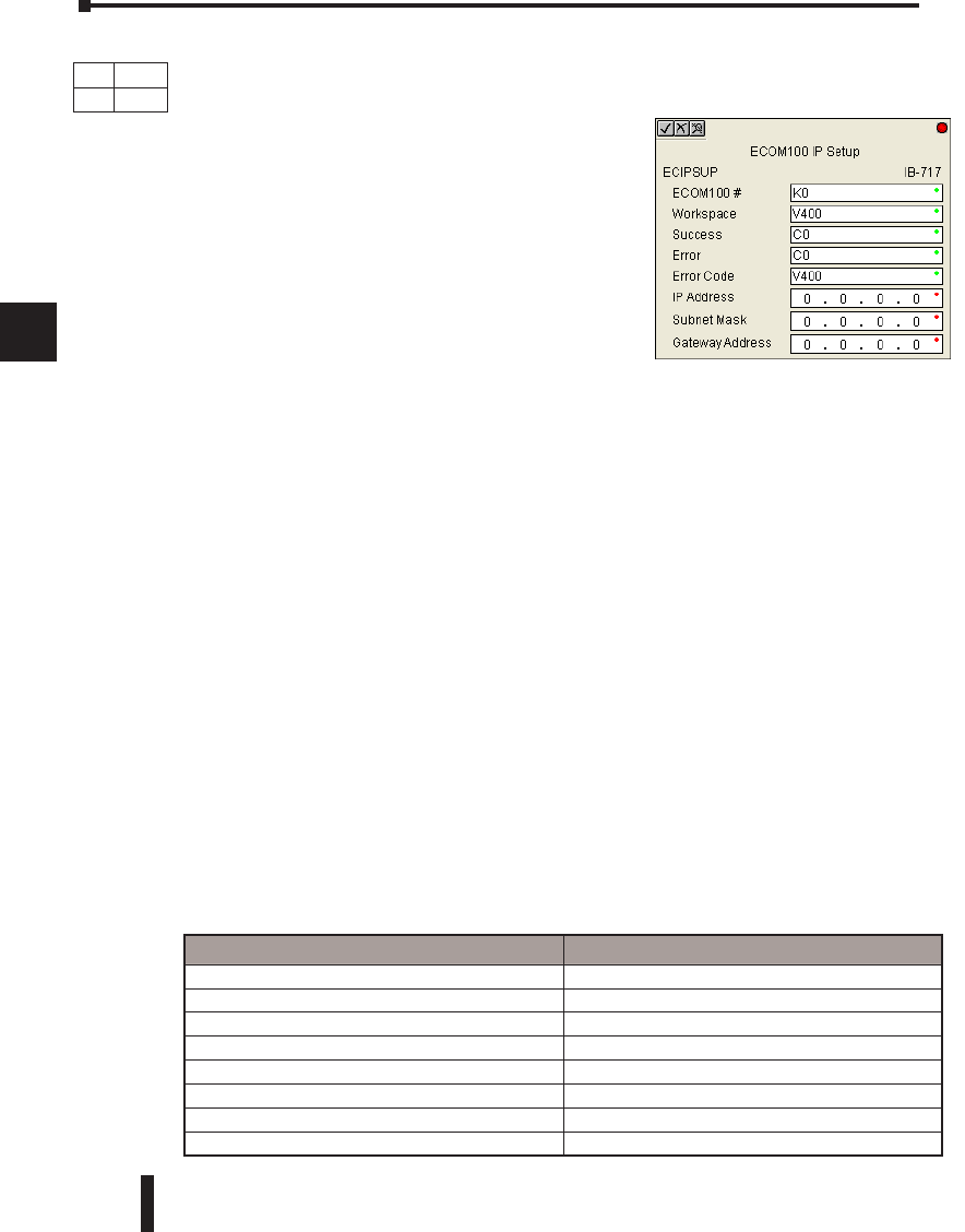
DL06 Micro PLC User Manual, 3rd Edition, Rev. D
5-290
1
2
3
4
5
6
7
8
9
10
11
12
13
14
A
B
C
D
ECOM100 IP Setup (ECIPSUP) (IB-717)
ECOM100 IP Setup will configure the three TCP/IP parameters in the ECOM100: IP
Address, Subnet Mask, and Gateway Address, on a leading edge transition to the IBox.
The ECOM100 is specified by the ECOM100#,
which corresponds to a specific unique ECOM100
Configuration (ECOM100) IBox at the top of your
program.
The Workspace parameter is an internal, private register
used by this IBox and MUST BE UNIQUE in this one
instruction and MUST NOT be used anywhere else in
your program.
Either the Success or Error bit parameter will turn on
once the command is complete. If there is an error, the
Error Code parameter will report an ECOM100 error
code (less than 100), or a PLC logic error (greater than 1000).
This setup data is stored in Flash-ROM in the ECOM100 and will disable the ECOM100
module for at least a half second until it writes the Flash-ROM. Therefore, it is HIGHLY
RECOMMENDED that you only execute this IBox ONCE on first scan. Since it requires
a LEADING edge to execute, use a NORMALLY CLOSED SP0 (NOT First Scan) to drive
the power flow to the IBox.
In order for this ECOM100 IBox to function, you must turn ON dip switch 7 on the
ECOM100 circuit board.
ECIPSUP Parameters
• ECOM100#: this is a logical number associated with this specific ECOM100 module in the
specified slot. All other ECxxxx IBoxes that need to reference this ECOM100 module must
reference this logical number
• Workspace: specifies a V-memory location that will be used by the instruction
• Success: specifies a bit that will turn on once the request is completed successfully
• Error: specifies a bit that will turn on if the instruction is not successfully completed
• Error Code: specifies the location where the Error Code will be written
• IP Address: specifies the module’s IP Address
• Subnet Mask: specifies the Subnet Mask for the module to use
• Gateway Address: specifies the Gateway Address for the module to use
Chapter 5: Intelligent Box (IBox) Instructions
1
2
3
4
5
6
7
8
9
10
11
12
13
14
a
B
c
d
DS Used
HPP N/A
Parameter DL06 Range
ECOM100# K K0-255
Workspace V See DL06 V-memory map - Data Words
Success X,Y,C,GX,GY,B See DL06 V-memory map
Error X,Y,C,GX,GY,B See DL06 V-memory map
Error Code V See DL06 V-memory map - Data Words
IP Address IP Address 0.0.0.1. to 255.255.255.254
Subnet Mask Address IP Address Mask 0.0.0.1. to 255.255.255.254
Gateway Address IP Address 0.0.0.1. to 255.255.255.254
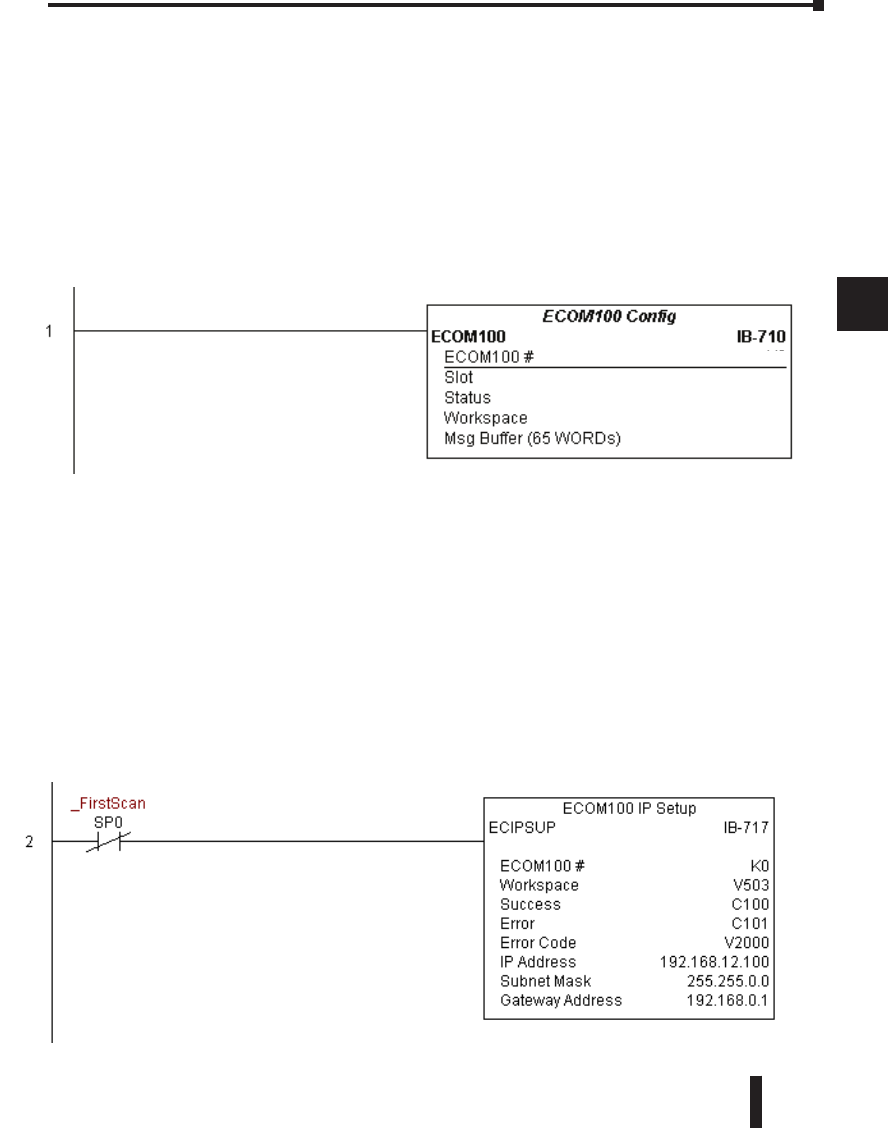
DL06 Micro PLC User Manual, 3rd Edition, Rev. D 5-291
1
2
3
4
5
6
7
8
9
10
11
12
13
14
A
B
C
D
ECIPSUP Example
Rung 1: The ECOM100 Config IBox is responsible for coordination/interlocking of all
ECOM100 type IBoxes for one specific ECOM100 module. Tag the ECOM100 in slot 1
as ECOM100# K0. All other ECxxxx IBoxes refer to this module # as K0. If you need to
move the module in the base to a different slot, then you only need to change this one IBox.
V400 is used as a global result status register for the other ECxxxx IBoxes using this specific
ECOM100 module.V401 is used to coordinate/interlock the logic in all of the other ECxxxx
IBoxes using this specific ECOM100 module. V402-V502 is a common 130 byte buffer
available for use by the other ECxxxx IBoxes using this specific ECOM100 module.
Rung 2: On the 2nd scan, configure all of the TCP/IP parameters in the ECOM100:
IP Address: 192.168. 12.100
Subnet Mask: 255.255. 0. 0
Gateway Address: 192.168. 0. 1
The ECIPSUP is leading edge triggered, not power-flow driven (similar to a counter input
leg). The command to write the TCP/IP configuration parameters will be sent to the
ECOM100 whenever the power flow into the IBox goes from OFF to ON.
If successful, turn on C100. If there is a failure, turn on C101. If it fails, you can look at
V2000 for the specific error code.
Chapter 5: Intelligent Box (IBox) Instructions
1
2
3
4
5
6
7
8
9
10
11
12
13
14
a
B
c
d
K1
K0
V400
V401
V402 - V502
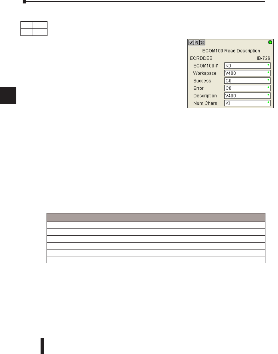
DL06 Micro PLC User Manual, 3rd Edition, Rev. D
5-292
1
2
3
4
5
6
7
8
9
10
11
12
13
14
A
B
C
D
ECOM100 Read Description (ECRDDES) (IB-726)
ECOM100 Read Description will read the ECOM100’s Description field up to the number
of specified characters on a leading edge transition to the IBox.
The Workspace parameter is an internal, private register
used by this IBox and MUST BE UNIQUE in this one
instruction and MUST NOT be used anywhere else in
your program.
Either the Success or Error bit parameter will turn on
once the command is complete.
In order for this ECOM100 IBox to function, you must
turn ON dip switch 7 on the ECOM100 circuit board.
ECRDDES Parameters
• ECOM100#: this is a logical number associated with this specific ECOM100 module in the
specified slot. All other ECxxxx IBoxes that need to reference this ECOM100 module must
reference this logical number
• Workspace: specifies a V-memory location that will be used by the instruction
• Success: specifies a bit that will turn on once the request is completed successfully
• Error: specifies a bit that will turn on if the instruction is not successfully completed
• Description: specifies the starting buffer location where the ECOM100’s Module Name will be
placed
• Num Char: specifies the number of characters (bytes) to read from the ECOM100’s Description
field
Chapter 5: Intelligent Box (IBox) Instructions
1
2
3
4
5
6
7
8
9
10
11
12
13
14
a
B
c
d
DS Used
HPP N/A
Parameter DL06 Range
ECOM100# K K0-255
Workspace V See DL06 V-memory map - Data Words
Success X,Y,C,GX,GY,B See DL06 V-memory map
Error X,Y,C,GX,GY,B See DL06 V-memory map
Description V See DL06 V-memory map - Data Words
Num Chars K K1-128
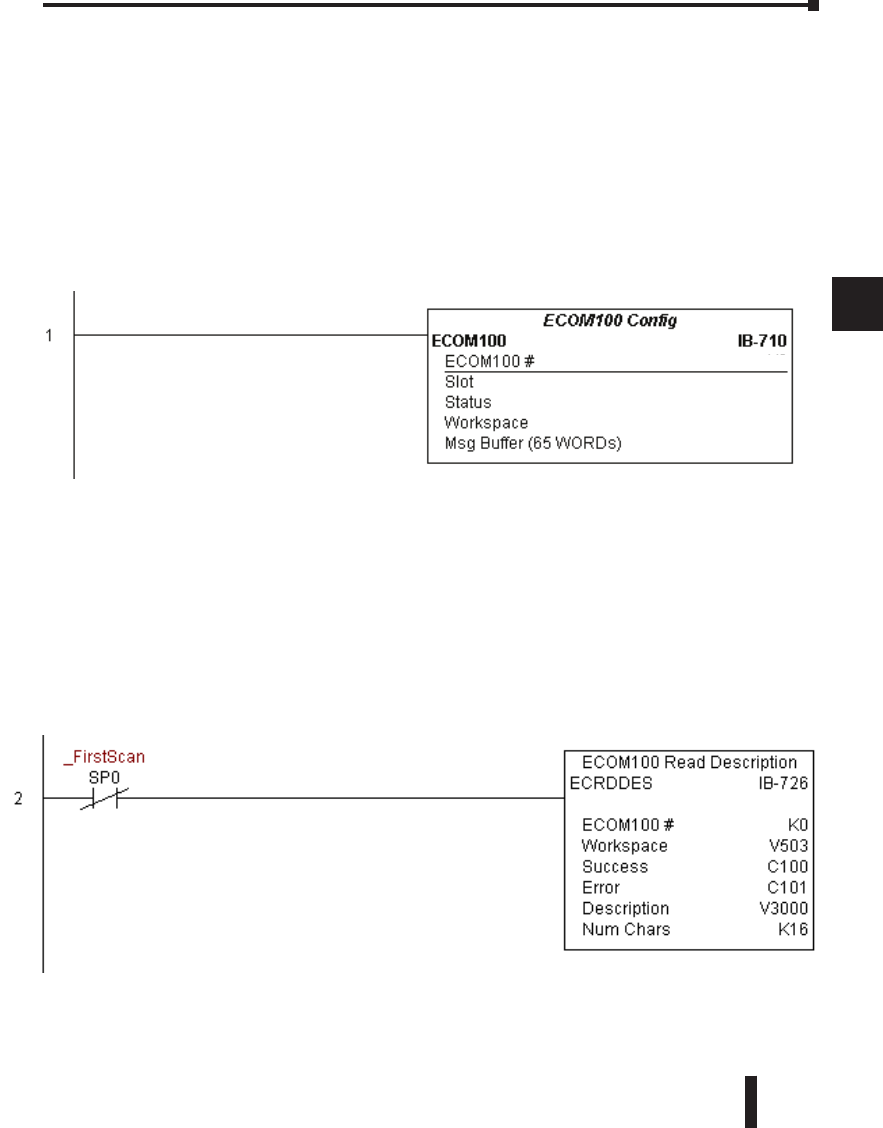
DL06 Micro PLC User Manual, 3rd Edition, Rev. D 5-293
1
2
3
4
5
6
7
8
9
10
11
12
13
14
A
B
C
D
ECRDDES Example
Rung 1: The ECOM100 Config IBox is responsible for coordination/interlocking of all
ECOM100 type IBoxes for one specific ECOM100 module. Tag the ECOM100 in slot 1
as ECOM100# K0. All other ECxxxx IBoxes refer to this module # as K0. If you need to
move the module in the base to a different slot, then you only need to change this one IBox.
V400 is used as a global result status register for the other ECxxxx IBoxes using this specific
ECOM100 module.V401 is used to coordinate/interlock the logic in all of the other ECxxxx
IBoxes using this specific ECOM100 module. V402-V502 is a common 130 byte buffer
available for use by the other ECxxxx IBoxes using this specific ECOM100 module.
Rung 2: On the 2nd scan, read the Module Description of the ECOM100 and store it in
V3000 thru V3007 (16 characters). This text can be displayed by an HMI.
The ECRDDES is leading edge triggered, not power-flow driven (similar to a counter input
leg). The command to read the module description will be sent to the ECOM100 whenever
the power flow into the IBox goes from OFF to ON.
If successful, turn on C100. If there is a failure, turn on C101.
Chapter 5: Intelligent Box (IBox) Instructions
1
2
3
4
5
6
7
8
9
10
11
12
13
14
a
B
c
d
K1
K0
V400
V401
V402 - V502
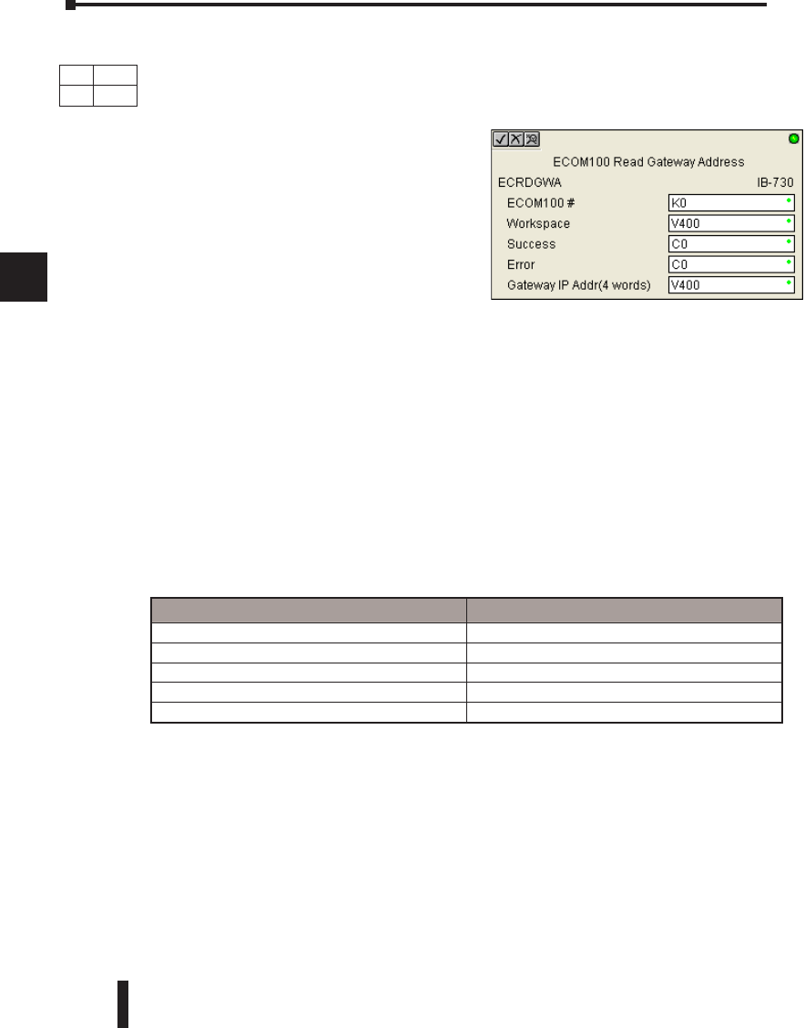
DL06 Micro PLC User Manual, 3rd Edition, Rev. D
5-294
1
2
3
4
5
6
7
8
9
10
11
12
13
14
A
B
C
D
ECOM100 Read Gateway Address (ECRDGWA) (IB-730)
ECOM100 Read Gateway Address will read the 4 parts of the Gateway IP address and store
them in 4 consecutive V-Memory locations in decimal format, on a leading edge transition to
the IBox.
The Workspace parameter is an internal, private
register used by this IBox and MUST BE
UNIQUE in this one instruction and MUST
NOT be used anywhere else in your program.
Either the Success or Error bit parameter will
turn on once the command is complete.
In order for this ECOM100 IBox to function,
you must turn ON dip switch 7 on the
ECOM100 circuit board.
ECRDGWA Parameters
• ECOM100#: this is a logical number associated with this specific ECOM100 module in the
specified slot. All other ECxxxx IBoxes that need to reference this ECOM100 module must
reference this logical number
• Workspace: specifies a V-memory location that will be used by the instruction
• Success: specifies a bit that will turn on once the request is completed successfully
• Error: specifies a bit that will turn on if the instruction is not successfully completed
• Gateway IP Addr: specifies the starting address where the ECOM100’s Gateway Address will be
placed in 4 consecutive V-memory locations
Chapter 5: Intelligent Box (IBox) Instructions
1
2
3
4
5
6
7
8
9
10
11
12
13
14
a
B
c
d
DS Used
HPP N/A
Parameter DL06 Range
ECOM100# K K0-255
Workspace V See DL06 V-memory map - Data Words
Success X,Y,C,GX,GY,B See DL06 V-memory map
Error X,Y,C,GX,GY,B See DL06 V-memory map
Gateway IP Address (4 Words) V See DL06 V-memory map - Data Words
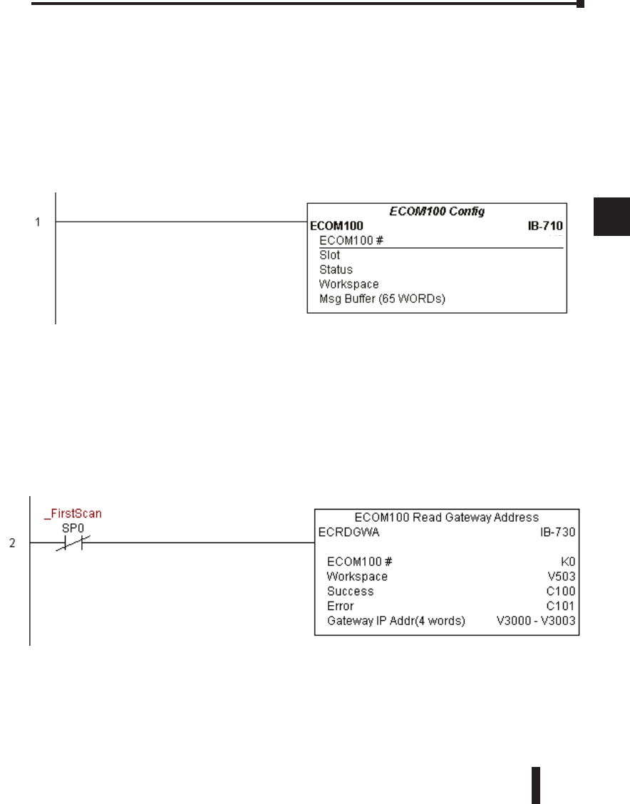
DL06 Micro PLC User Manual, 3rd Edition, Rev. D 5-295
1
2
3
4
5
6
7
8
9
10
11
12
13
14
A
B
C
D
ECRDGWA Example
Rung 1: The ECOM100 Config IBox is responsible for coordination/interlocking of all
ECOM100 type IBoxes for one specific ECOM100 module. Tag the ECOM100 in slot 1
as ECOM100# K0. All other ECxxxx IBoxes refer to this module # as K0. If you need to
move the module in the base to a different slot, then you only need to change this one IBox.
V400 is used as a global result status register for the other ECxxxx IBoxes using this specific
ECOM100 module.V401 is used to coordinate/interlock the logic in all of the other ECxxxx
IBoxes using this specific ECOM100 module. V402-V502 is a common 130 byte buffer
available for use by the other ECxxxx IBoxes using this specific ECOM100 module.
Rung 2: On the 2nd scan, read the Gateway Address of the ECOM100 and store it in V3000
thru V3003 (4 decimal numbers). The ECOM100’s Gateway Address could be displayed by
an HMI.
The ECRDGWA is leading edge triggered, not power-flow driven (similar to a counter input
leg). The command to read the Gateway Address will be sent to the ECOM100 whenever the
power flow into the IBox goes from OFF to ON.
If successful, turn on C100. If there is a failure, turn on C101.
Chapter 5: Intelligent Box (IBox) Instructions
1
2
3
4
5
6
7
8
9
10
11
12
13
14
a
B
c
d
K1
K0
V400
V401
V402 - V502

DL06 Micro PLC User Manual, 3rd Edition, Rev. D
5-296
1
2
3
4
5
6
7
8
9
10
11
12
13
14
A
B
C
D
ECOM100 Read IP Address (ECRDIP) (IB-722)
ECOM100 Read IP Address will read the 4 parts of the IP address and store them in 4
consecutive V-Memory locations in decimal format, on a leading edge transition to the IBox.
The Workspace parameter is an internal,
private register used by this IBox and MUST
BE UNIQUE in this one instruction and
MUST NOT be used anywhere else in your
program.
Either the Success or Error bit parameter will
turn on once the command is complete.
In order for this ECOM100 IBox to function,
you must turn ON dip switch 7 on the
ECOM100 circuit board.
ECRDIP Parameters
• ECOM100#: this is a logical number associated with this specific ECOM100 module in the
specified slot. All other ECxxxx IBoxes that need to reference this ECOM100 module must
reference this logical number
• Workspace: specifies a V-memory location that will be used by the instruction
• Success: specifies a bit that will turn on once the request is completed successfully
• Error: specifies a bit that will turn on if the instruction is not successfully completed
• IP Address: specifies the starting address where the ECOM100’s IP Address will be placed in 4
consecutive V-memory locations
Chapter 5: Intelligent Box (IBox) Instructions
1
2
3
4
5
6
7
8
9
10
11
12
13
14
a
B
c
d
DS Used
HPP N/A
Parameter DL06 Range
ECOM100# K K0-255
Workspace V See DL06 V-memory map - Data Words
Success X,Y,C,GX,GY,B See DL06 V-memory map
Error X,Y,C,GX,GY,B See DL06 V-memory map
IP Address (4 Words) V See DL06 V-memory map - Data Words
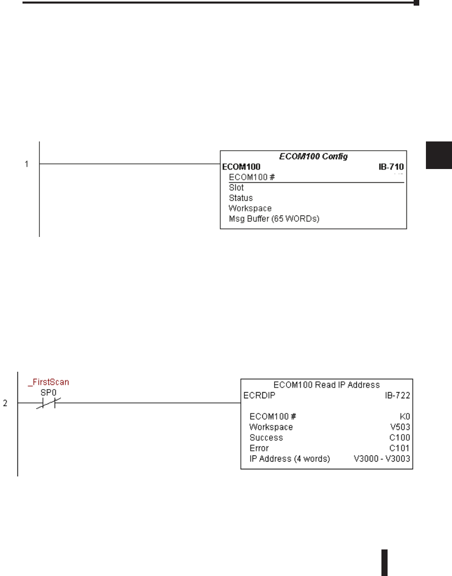
DL06 Micro PLC User Manual, 3rd Edition, Rev. D 5-297
1
2
3
4
5
6
7
8
9
10
11
12
13
14
A
B
C
D
ECRDIP Example
Rung 1: The ECOM100 Config IBox is responsible for coordination/interlocking of all
ECOM100 type IBoxes for one specific ECOM100 module. Tag the ECOM100 in slot 1
as ECOM100# K0. All other ECxxxx IBoxes refer to this module # as K0. If you need to
move the module in the base to a different slot, then you only need to change this one IBox.
V400 is used as a global result status register for the other ECxxxx IBoxes using this specific
ECOM100 module.V401 is used to coordinate/interlock the logic in all of the other ECxxxx
IBoxes using this specific ECOM100 module. V402-V502 is a common 130 byte buffer
available for use by the other ECxxxx IBoxes using this specific ECOM100 module.
Rung 2: On the 2nd scan, read the IP Address of the ECOM100 and store it in V3000 thru
V3003 (4 decimal numbers). The ECOM100’s IP Address could be displayed by an HMI.
The ECRDIP is leading edge triggered, not power-flow driven (similar to a counter input
leg). The command to read the IP Address will be sent to the ECOM100 whenever the
power flow into the IBox goes from OFF to ON.
If successful, turn on C100. If there is a failure, turn on C101.
Chapter 5: Intelligent Box (IBox) Instructions
1
2
3
4
5
6
7
8
9
10
11
12
13
14
a
B
c
d
K1
K0
V400
V401
V402 - V502

DL06 Micro PLC User Manual, 3rd Edition, Rev. D
5-298
1
2
3
4
5
6
7
8
9
10
11
12
13
14
A
B
C
D
ECOM100 Read Module ID (ECRDMID) (IB-720)
ECOM100 Read Module ID will read the binary (decimal) WORD sized Module ID on a
leading edge transition to the IBox.
The Workspace parameter is an internal, private
register used by this IBox and MUST BE UNIQUE
in this one instruction and MUST NOT be used
anywhere else in your program.
Either the Success or Error bit parameter will turn
on once the command is complete.
In order for this ECOM100 IBox to function, you
must turn ON dip switch 7 on the ECOM100
circuit board.
ECRDMID Parameters
• ECOM100#: this is a logical number associated with this specific ECOM100 module in the
specified slot. All other ECxxxx IBoxes that need to reference this ECOM100 module must
reference this logical number
• Workspace: specifies a V-memory location that will be used by the instruction
• Success: specifies a bit that will turn on once the request is completed successfully
• Error: specifies a bit that will turn on if the instruction is not successfully completed
• Module ID: specifies the location where the ECOM100’s Module ID (decimal) will be placed
Chapter 5: Intelligent Box (IBox) Instructions
1
2
3
4
5
6
7
8
9
10
11
12
13
14
a
B
c
d
DS Used
HPP N/A
Parameter DL06 Range
ECOM100# K K0-255
Workspace V See DL06 V-memory map - Data Words
Success X,Y,C,GX,GY,B See DL06 V-memory map
Error X,Y,C,GX,GY,B See DL06 V-memory map
Module ID V See DL06 V-memory map - Data Words
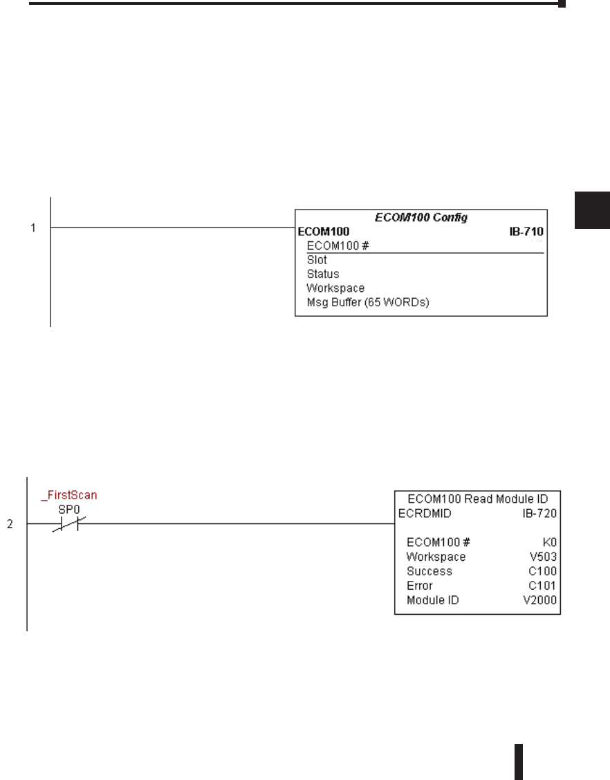
DL06 Micro PLC User Manual, 3rd Edition, Rev. D 5-299
1
2
3
4
5
6
7
8
9
10
11
12
13
14
A
B
C
D
ECRDMID Example
Rung 1: The ECOM100 Config IBox is responsible for coordination/interlocking of all
ECOM100 type IBoxes for one specific ECOM100 module. Tag the ECOM100 in slot 1
as ECOM100# K0. All other ECxxxx IBoxes refer to this module # as K0. If you need to
move the module in the base to a different slot, then you only need to change this one IBox.
V400 is used as a global result status register for the other ECxxxx IBoxes using this specific
ECOM100 module.V401 is used to coordinate/interlock the logic in all of the other ECxxxx
IBoxes using this specific ECOM100 module. V402-V502 is a common 130 byte buffer
available for use by the other ECxxxx IBoxes using this specific ECOM100 module.
Rung 2: On the 2nd scan, read the Module ID of the ECOM100 and store it in V2000.
The ECRDMID is leading edge triggered, not power-flow driven (similar to a counter input
leg). The command to read the module ID will be sent to the ECOM100 whenever the
power flow into the IBox goes from OFF to ON.
If successful, turn on C100. If there is a failure, turn on C101.
Chapter 5: Intelligent Box (IBox) Instructions
1
2
3
4
5
6
7
8
9
10
11
12
13
14
a
B
c
d
K1
K0
V400
V401
V402 - V502
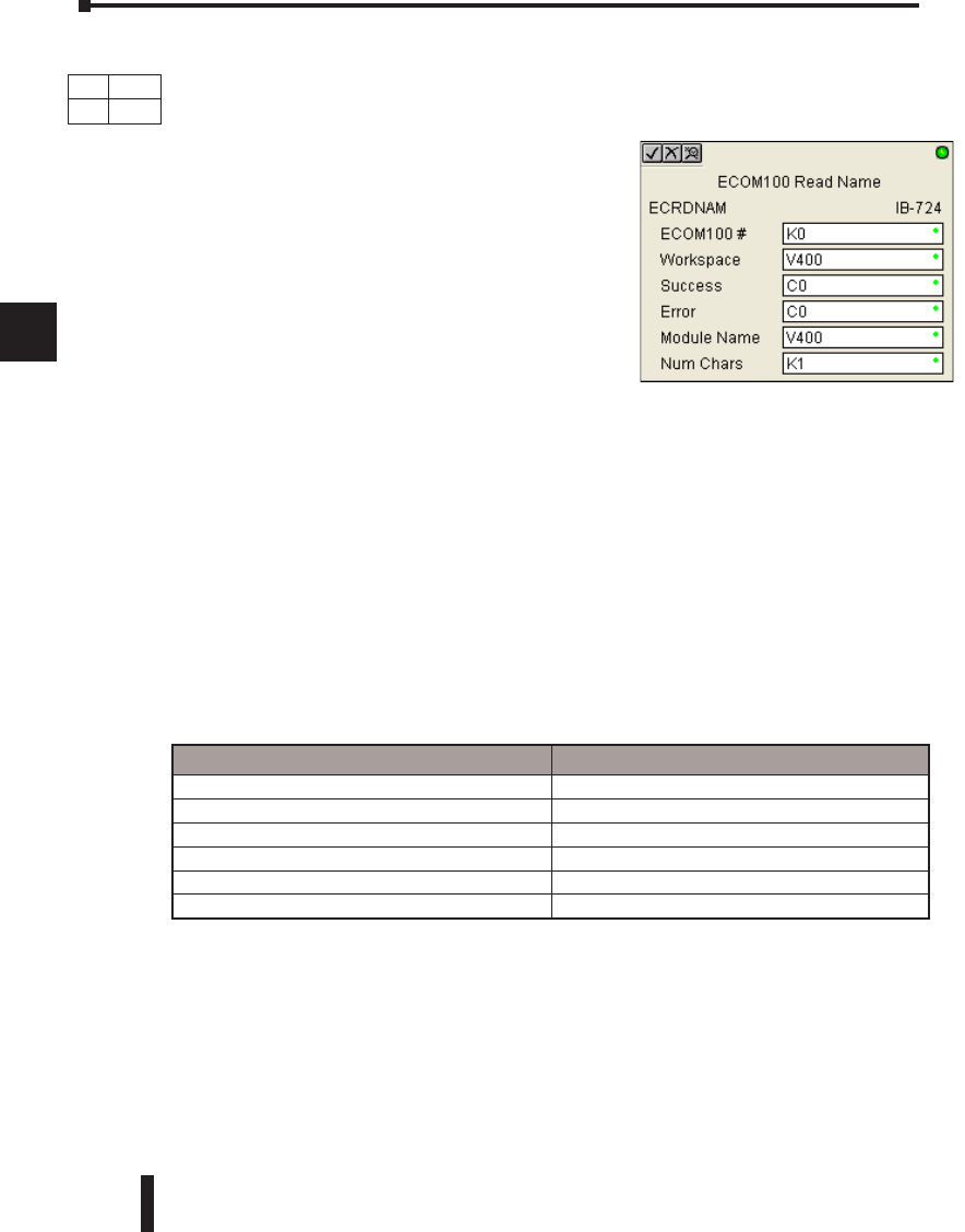
DL06 Micro PLC User Manual, 3rd Edition, Rev. D
5-300
1
2
3
4
5
6
7
8
9
10
11
12
13
14
A
B
C
D
ECOM100 Read Module Name (ECRDNAM) (IB-724)
ECOM100 Read Name will read the Module Name up to the number of specified characters
on a leading edge transition to the IBox.
The Workspace parameter is an internal, private
register used by this IBox and MUST BE UNIQUE
in this one instruction and MUST NOT be used
anywhere else in your program.
Either the Success or Error bit parameter will turn on
once the command is complete.
In order for this ECOM100 IBox to function, you
must turn ON dip switch 7 on the ECOM100 circuit
board.
ECRDNAM Parameters
• ECOM100#: this is a logical number associated with this specific ECOM100 module in the
specified slot. All other ECxxxx IBoxes that need to reference this ECOM100 module must
reference this logical number
• Workspace: specifies a V-memory location that will be used by the instruction
• Success: specifies a bit that will turn on once the request is completed successfully
• Error: specifies a bit that will turn on if the instruction is not successfully completed
• Module Name: specifies the starting buffer location where the ECOM100’s Module Name will be
placed
• Num Chars: specifies the number of characters (bytes) to read from the ECOM100’s Name field
Chapter 5: Intelligent Box (IBox) Instructions
1
2
3
4
5
6
7
8
9
10
11
12
13
14
a
B
c
d
DS Used
HPP N/A
Parameter DL06 Range
ECOM100# K K0-255
Workspace V See DL06 V-memory map - Data Words
Success X,Y,C,GX,GY,B See DL06 V-memory map
Error X,Y,C,GX,GY,B See DL06 V-memory map
Module Name V See DL06 V-memory map - Data Words
Num Chars K K1-128
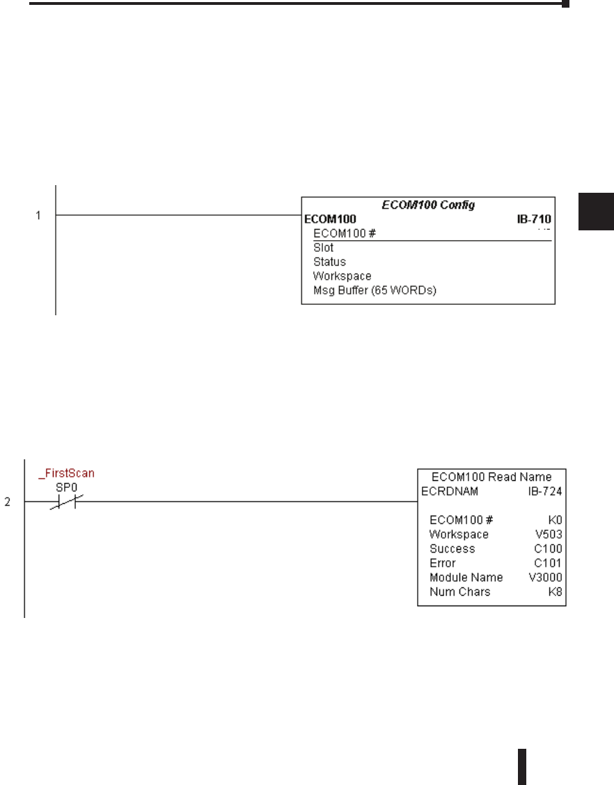
DL06 Micro PLC User Manual, 3rd Edition, Rev. D 5-301
1
2
3
4
5
6
7
8
9
10
11
12
13
14
A
B
C
D
ECRDNAM Example
Rung 1: The ECOM100 Config IBox is responsible for coordination/interlocking of all
ECOM100 type IBoxes for one specific ECOM100 module. Tag the ECOM100 in slot 1
as ECOM100# K0. All other ECxxxx IBoxes refer to this module # as K0. If you need to
move the module in the base to a different slot, then you only need to change this one IBox.
V400 is used as a global result status register for the other ECxxxx IBoxes using this specific
ECOM100 module.V401 is used to coordinate/interlock the logic in all of the other ECxxxx
IBoxes using this specific ECOM100 module. V402-V502 is a common 130 byte buffer
available for use by the other ECxxxx IBoxes using this specific ECOM100 module.
Rung 2: On the 2nd scan, read the Module Name of the ECOM100 and store it in V3000
thru V3003 (8 characters). This text can be displayed by an HMI.
The ECRDNAM is leading edge triggered, not power-flow driven (similar to a counter input
leg). The command to read the module name will be sent to the ECOM100 whenever the
power flow into the IBox goes from OFF to ON.
If successful, turn on C100. If there is a failure, turn on C101.
Chapter 5: Intelligent Box (IBox) Instructions
1
2
3
4
5
6
7
8
9
10
11
12
13
14
a
B
c
d
K1
K0
V400
V401
V402 - V502
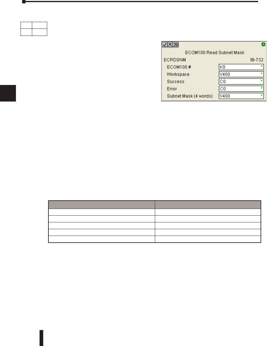
DL06 Micro PLC User Manual, 3rd Edition, Rev. D
5-302
1
2
3
4
5
6
7
8
9
10
11
12
13
14
A
B
C
D
ECOM100 Read Subnet Mask (ECRDSNM) (IB-732)
ECOM100 Read Subnet Mask will read the 4 parts of the Subnet Mask and store them in 4
consecutive V-Memory locations in decimal format, on a leading edge transition to the IBox.
The Workspace parameter is an internal,
private register used by this IBox and MUST
BE UNIQUE in this one instruction and
MUST NOT be used anywhere else in your
program.
Either the Success or Error bit parameter will
turn on once the command is complete.
In order for this ECOM100 IBox to function,
you must turn ON dip switch 7 on the
ECOM100 circuit board.
ECRDSNM Parameters
• ECOM100#: this is a logical number associated with this specific ECOM100 module in the
specified slot. All other ECxxxx IBoxes that need to reference this ECOM100 module must
reference this logical number
• Workspace: specifies a V-memory location that will be used by the instruction
• Success: specifies a bit that will turn on once the request is completed successfully
• Error: specifies a bit that will turn on if the instruction is not successfully completed
• Subnet Mask: specifies the starting address where the ECOM100’s Subnet Mask will be placed in 4
consecutive V-memory locations
Chapter 5: Intelligent Box (IBox) Instructions
1
2
3
4
5
6
7
8
9
10
11
12
13
14
a
B
c
d
DS Used
HPP N/A
Parameter DL06 Range
ECOM100# K K0-255
Workspace V See DL06 V-memory map - Data Words
Success X,Y,C,GX,GY,B See DL06 V-memory map
Error X,Y,C,GX,GY,B See DL06 V-memory map
Subnet Mask (4 Words) V See DL06 V-memory map - Data Words
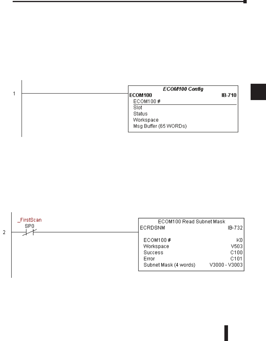
DL06 Micro PLC User Manual, 3rd Edition, Rev. D 5-303
1
2
3
4
5
6
7
8
9
10
11
12
13
14
A
B
C
D
ECRDSNM Example
Rung 1: The ECOM100 Config IBox is responsible for coordination/interlocking of all
ECOM100 type IBoxes for one specific ECOM100 module. Tag the ECOM100 in slot 1
as ECOM100# K0. All other ECxxxx IBoxes refer to this module # as K0. If you need to
move the module in the base to a different slot, then you only need to change this one IBox.
V400 is used as a global result status register for the other ECxxxx IBoxes using this specific
ECOM100 module.V401 is used to coordinate/interlock the logic in all of the other ECxxxx
IBoxes using this specific ECOM100 module. V402-V502 is a common 130 byte buffer
available for use by the other ECxxxx IBoxes using this specific ECOM100 module.
Rung 2: On the 2nd scan, read the Subnet Mask of the ECOM100 and store it in V3000
thru V3003 (4 decimal numbers). The ECOM100’s Subnet Mask could be displayed by an
HMI.
The ECRDSNM is leading edge triggered, not power-flow driven (similar to a counter input
leg). The command to read the Subnet Mask will be sent to the ECOM100 whenever the
power flow into the IBox goes from OFF to ON.
If successful, turn on C100. If there is a failure, turn on C101.
Chapter 5: Intelligent Box (IBox) Instructions
1
2
3
4
5
6
7
8
9
10
11
12
13
14
a
B
c
d
K1
K0
V400
V401
V402 - V502
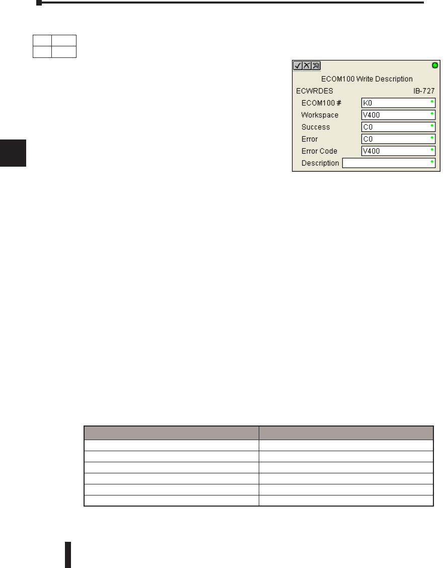
DL06 Micro PLC User Manual, 3rd Edition, Rev. D
5-304
1
2
3
4
5
6
7
8
9
10
11
12
13
14
A
B
C
D
ECOM100 Write Description (ECWRDES) (IB-727)
ECOM100 Write Description will write the given Description to the ECOM100 module
on a leading edge transition to the IBox. If you use a dollar sign ($) or double quote (“), use
the PRINT/VPRINT escape sequence of TWO dollar
signs ($$) for a single dollar sign or dollar sign-double
quote ($”) for a double quote character.
The Workspace parameter is an internal, private
register used by this IBox and MUST BE UNIQUE
in this one instruction and MUST NOT be used
anywhere else in your program.
Either the Success or Error bit parameter will turn on
once the command is complete. If there is an error,
the Error Code parameter will report an ECOM100
error code (less than 100), or a PLC logic error
(greater than 1000).
The Description is stored in Flash-ROM in the ECOM100 and the execution of this IBox
will disable the ECOM100 module for at least a half second until it writes the Flash-ROM.
Therefore, it is HIGHLY RECOMMENDED that you only execute this IBox ONCE on
first scan. Since it requires a LEADING edge to execute, use a NORMALLY CLOSED SP0
(STR NOT First Scan) to drive the power flow to the IBox.
In order for this ECOM100 IBox to function, you must turn ON dip switch 7 on the
ECOM100 circuit board.
ECWRDES Parameters
• ECOM100#: this is a logical number associated with this specific ECOM100 module in the
specified slot. All other ECxxxx IBoxes that need to reference this ECOM100 module must
reference this logical number
• Workspace: specifies a V-memory location that will be used by the instruction
• Success: specifies a bit that will turn on once the request is completed successfully
• Error: specifies a bit that will turn on if the instruction is not successfully completed
• Error Code: specifies the location where the Error Code will be written
• Description: specifies the Description that will be written to the module
Chapter 5: Intelligent Box (IBox) Instructions
1
2
3
4
5
6
7
8
9
10
11
12
13
14
a
B
c
d
DS Used
HPP N/A
Parameter DL06 Range
ECOM100# K K0-255
Workspace V See DL06 V-memory map - Data Words
Success X,Y,C,GX,GY,B See DL06 V-memory map
Error X,Y,C,GX,GY,B See DL06 V-memory map
Error Code V See DL06 V-memory map - Data Words
Description Text
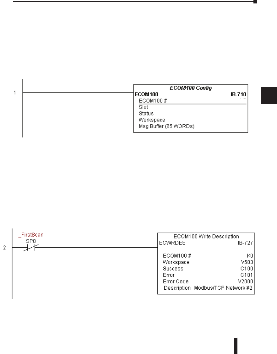
DL06 Micro PLC User Manual, 3rd Edition, Rev. D 5-305
1
2
3
4
5
6
7
8
9
10
11
12
13
14
A
B
C
D
ECWRDES Example
Rung 1: The ECOM100 Config IBox is responsible for coordination/interlocking of all
ECOM100 type IBoxes for one specific ECOM100 module. Tag the ECOM100 in slot 1
as ECOM100# K0. All other ECxxxx IBoxes refer to this module # as K0. If you need to
move the module in the base to a different slot, then you only need to change this one IBox.
V400 is used as a global result status register for the other ECxxxx IBoxes using this specific
ECOM100 module.V401 is used to coordinate/interlock the logic in all of the other ECxxxx
IBoxes using this specific ECOM100 module. V402-V502 is a common 130 byte buffer
available for use by the other ECxxxx IBoxes using this specific ECOM100 module.
Rung 2: On the 2nd scan, set the Module Description of the ECOM100. Typically this is
done using NetEdit, but this IBox allows you to configure the module description in the
ECOM100 using your ladder program.
The EWRDES is leading edge triggered, not power-flow driven (similar to a counter input
leg). The command to write the module description will be sent to the ECOM100 whenever
the power flow into the IBox goes from OFF to ON.
If successful, turn on C100. If there is a failure, turn on C101. If it fails, you can look at
V2000 for the specific error code.
Chapter 5: Intelligent Box (IBox) Instructions
1
2
3
4
5
6
7
8
9
10
11
12
13
14
a
B
c
d
K1
K0
V400
V401
V402 - V502
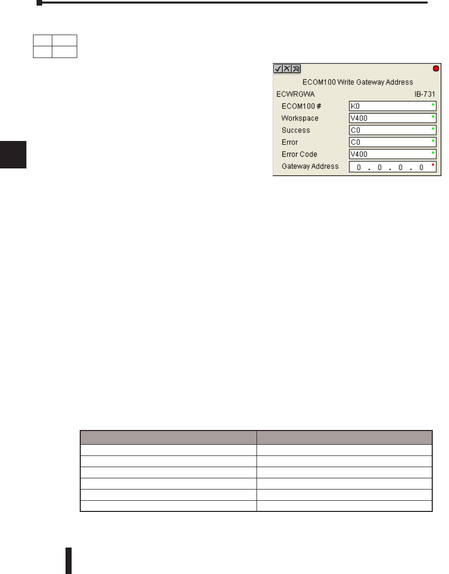
DL06 Micro PLC User Manual, 3rd Edition, Rev. D
5-306
1
2
3
4
5
6
7
8
9
10
11
12
13
14
A
B
C
D
ECOM100 Write Gateway Address (ECWRGWA) (IB-731)
ECOM100 Write Gateway Address will write the given Gateway IP Address to the
ECOM100 module on a leading edge transition to the IBox. See also ECOM100 IP Setup
(ECIPSUP) IBox 717 to setup ALL of the
TCP/IP parameters in a single instruction - IP
Address, Subnet Mask, and Gateway Address.
The Workspace parameter is an internal, private
register used by this IBox and MUST BE
UNIQUE in this one instruction and MUST
NOT be used anywhere else in your program.
Either the Success or Error bit parameter will
turn on once the command is complete. If there
is an error, the Error Code parameter will report
an ECOM100 error code (less than 100), or a
PLC logic error (greater than 1000).
The Gateway Address is stored in Flash-ROM in the ECOM100 and the execution of this
IBox will disable the ECOM100 module for at least a half second until it writes the Flash-
ROM. Therefore, it is HIGHLY RECOMMENDED that you only execute this IBox
ONCE, on first scan. Since it requires a LEADING edge to execute, use a NORMALLY
CLOSED SP0 (STR NOT First Scan) to drive the power flow to the IBox.
In order for this ECOM100 IBox to function, you must turn ON dip switch 7 on the
ECOM100 circuit board.
ECWRGWA Parameters
• ECOM100#: this is a logical number associated with this specific ECOM100 module in the
specified slot. All other ECxxxx IBoxes that need to reference this ECOM100 module must
reference this logical number
• Workspace: specifies a V-memory location that will be used by the instruction
• Success: specifies a bit that will turn on once the request is completed successfully
• Error: specifies a bit that will turn on if the instruction is not successfully completed
• Error Code: specifies the location where the Error Code will be written
• Gateway Address: specifies the Gateway IP Address that will be written to the module
Chapter 5: Intelligent Box (IBox) Instructions
1
2
3
4
5
6
7
8
9
10
11
12
13
14
a
B
c
d
DS Used
HPP N/A
Parameter DL06 Range
ECOM100# K K0-255
Workspace V See DL06 V-memory map - Data Words
Success X,Y,C,GX,GY,B See DL06 V-memory map
Error X,Y,C,GX,GY,B See DL06 V-memory map
Error Code V See DL06 V-memory map - Data Words
Gateway Address 0.0.0.1. to 255.255.255.254
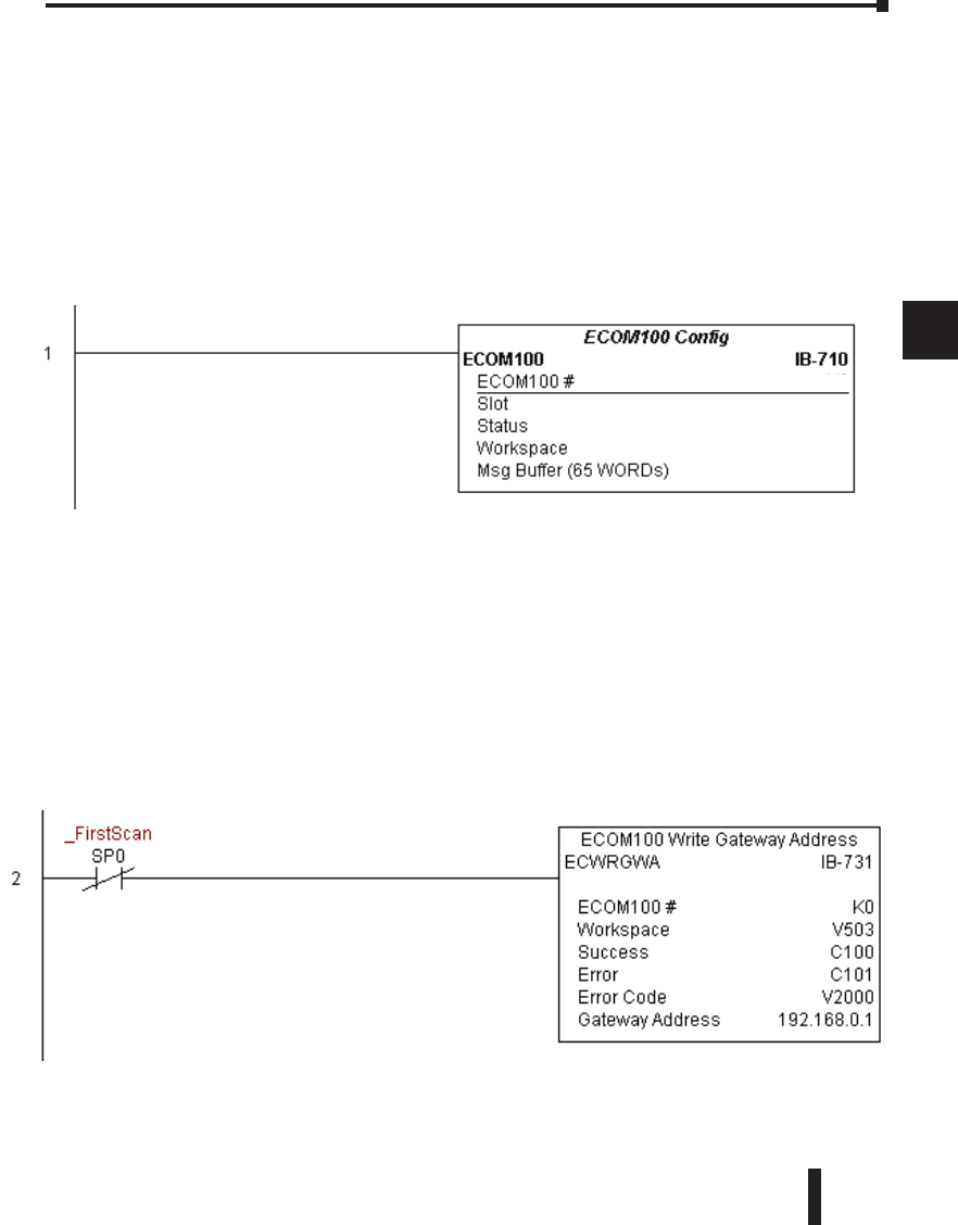
DL06 Micro PLC User Manual, 3rd Edition, Rev. D 5-307
1
2
3
4
5
6
7
8
9
10
11
12
13
14
A
B
C
D
ECWRGWA Example
Rung 1: The ECOM100 Config IBox is responsible for coordination/interlocking of all
ECOM100 type IBoxes for one specific ECOM100 module. Tag the ECOM100 in slot 1
as ECOM100# K0. All other ECxxxx IBoxes refer to this module # as K0. If you need to
move the module in the base to a different slot, then you only need to change this one IBox.
V400 is used as a global result status register for the other ECxxxx IBoxes using this specific
ECOM100 module.V401 is used to coordinate/interlock the logic in all of the other ECxxxx
IBoxes using this specific ECOM100 module. V402-V502 is a common 130 byte buffer
available for use by the other ECxxxx IBoxes using this specific ECOM100 module.
Rung 2: On the 2nd scan, assign the Gateway Address of the ECOM100 to 192.168.0.1
The ECWRGWA is leading edge triggered, not power-flow driven (similar to a counter input
leg). The command to write the Gateway Address will be sent to the ECOM100 whenever
the power flow into the IBox goes from OFF to ON.
If successful, turn on C100. If there is a failure, turn on C101. If it fails, you can look at
V2000 for the specific error code.
To configure all of the ECOM100 TCP/IP parameters in one IBox, see the ECOM100 IP
Setup (ECIPSUP) IBox.
Chapter 5: Intelligent Box (IBox) Instructions
1
2
3
4
5
6
7
8
9
10
11
12
13
14
a
B
c
d
K1
K0
V400
V401
V402 - V502
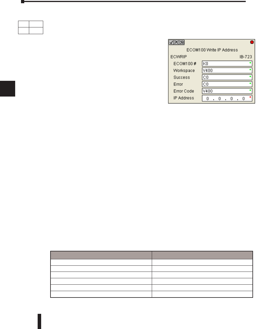
DL06 Micro PLC User Manual, 3rd Edition, Rev. D
5-308
1
2
3
4
5
6
7
8
9
10
11
12
13
14
A
B
C
D
ECOM100 Write IP Address (ECWRIP) (IB-723)
ECOM100 Write IP Address will write the given IP Address to the ECOM100 module on
a leading edge transition to the IBox. See also ECOM100 IP Setup (ECIPSUP) IBox 717 to
setup ALL of the TCP/IP parameters in a single instruction - IP Address, Subnet Mask, and
Gateway Address.
The Workspace parameter is an internal, private
register used by this IBox and MUST BE UNIQUE
in this one instruction and MUST NOT be used
anywhere else in your program.
Either the Success or Error bit parameter will turn on
once the command is complete. If there is an error,
the Error Code parameter will report an ECOM100
error code (less than 100), or a PLC logic error
(greater than 1000).
The IP Address is stored in Flash-ROM in the ECOM100 and the execution of this IBox
will disable the ECOM100 module for at least a half second until it writes the Flash-ROM.
Therefore, it is HIGHLY RECOMMENDED that you only execute this IBox ONCE on
first scan. Since it requires a LEADING edge to execute, use a NORMALLY CLOSED SP0
(STR NOT First Scan) to drive the power flow to the IBox.
In order for this ECOM100 IBox to function, you must turn ON dip switch 7 on the
ECOM100 circuit board.
ECWRIP Parameters
• ECOM100#: this is a logical number associated with this specific ECOM100 module in the
specified slot. All other ECxxxx IBoxes that need to reference this ECOM100 module must
reference this logical number
• Workspace: specifies a V-memory location that will be used by the instruction
• Success: specifies a bit that will turn on once the request is completed successfully
• Error: specifies a bit that will turn on if the instruction is not successfully completed
• Error Code: specifies the location where the Error Code will be written
• IP Address: specifies the IP Address that will be written to the module
Chapter 5: Intelligent Box (IBox) Instructions
1
2
3
4
5
6
7
8
9
10
11
12
13
14
a
B
c
d
DS Used
HPP N/A
Parameter DL06 Range
ECOM100# K K0-255
Workspace V See DL06 V-memory map - Data Words
Success X,Y,C,GX,GY,B See DL06 V-memory map
Error X,Y,C,GX,GY,B See DL06 V-memory map
Error Code V See DL06 V-memory map - Data Words
IP Address 0.0.0.1. to 255.255.255.254
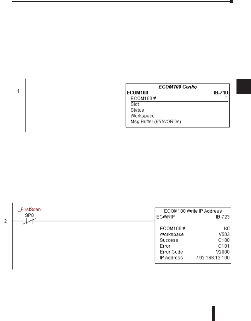
DL06 Micro PLC User Manual, 3rd Edition, Rev. D 5-309
1
2
3
4
5
6
7
8
9
10
11
12
13
14
A
B
C
D
ECWRIP Example
Rung 1: The ECOM100 Config IBox is responsible for coordination/interlocking of all
ECOM100 type IBoxes for one specific ECOM100 module. Tag the ECOM100 in slot 1
as ECOM100# K0. All other ECxxxx IBoxes refer to this module # as K0. If you need to
move the module in the base to a different slot, then you only need to change this one IBox.
V400 is used as a global result status register for the other ECxxxx IBoxes using this specific
ECOM100 module.V401 is used to coordinate/interlock the logic in all of the other ECxxxx
IBoxes using this specific ECOM100 module. V402-V502 is a common 130 byte buffer
available for use by the other ECxxxx IBoxes using this specific ECOM100 module.
Rung 2: On the 2nd scan, assign the IP Address of the ECOM100 to 192.168.12.100
The ECWRIP is leading edge triggered, not power-flow driven (similar to a counter input
leg). The command to write the IP Address will be sent to the ECOM100 whenever the
power flow into the IBox goes from OFF to ON.
If successful, turn on C100. If there is a failure, turn on C101. If it fails, you can look at
V2000 for the specific error code.
To configure all of the ECOM100 TCP/IP parameters in one IBox, see the ECOM100 IP
Setup (ECIPSUP) IBox.
Chapter 5: Intelligent Box (IBox) Instructions
1
2
3
4
5
6
7
8
9
10
11
12
13
14
a
B
c
d
K1
K0
V400
V401
V402 - V502
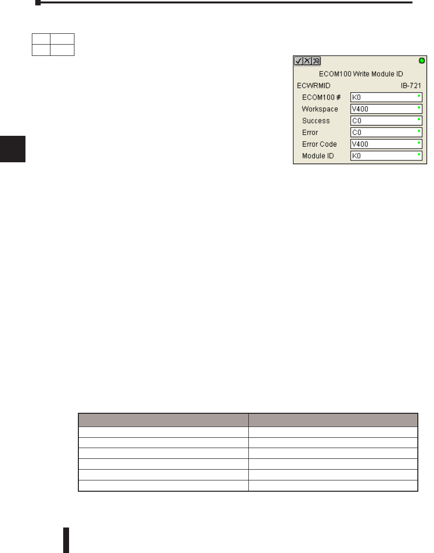
DL06 Micro PLC User Manual, 3rd Edition, Rev. D
5-310
1
2
3
4
5
6
7
8
9
10
11
12
13
14
A
B
C
D
ECOM100 Write Module ID (ECWRMID) (IB-721)
ECOM100 Write Module ID will write the given Module ID on a leading edge transition to
the IBox
If the Module ID is set in the hardware using the
dipswitches, this IBox will fail and return error code
1005 (decimal).
The Workspace parameter is an internal, private register
used by this IBox and MUST BE UNIQUE in this one
instruction and MUST NOT be used anywhere else in
your program.
Either the Success or Error bit parameter will turn on
once the command is complete. If there is an error, the
Error Code parameter will report an ECOM100 error
code (less than 100), or a PLC logic error (greater than 1000).
The Module ID is stored in Flash-ROM in the ECOM100 and the execution of this IBox
will disable the ECOM100 module for at least a half second until it writes the Flash-ROM.
Therefore, it is HIGHLY RECOMMENDED that you only execute this IBox ONCE on
first scan. Since it requires a LEADING edge to execute, use a NORMALLY CLOSED SP0
(STR NOT First Scan) to drive the power flow to the IBox.
In order for this ECOM100 IBox to function, you must turn ON dip switch 7 on the
ECOM100 circuit board.
ECWRMID Parameters
• ECOM100#: this is a logical number associated with this specific ECOM100 module in the
specified slot. All other ECxxxx IBoxes that need to reference this ECOM100 module must
reference this logical number
• Workspace: specifies a V-memory location that will be used by the instruction
• Success: specifies a bit that will turn on once the request is completed successfully
• Error: specifies a bit that will turn on if the instruction is not successfully completed
• Error Code: specifies the location where the Error Code will be written
• Module ID: specifies the Module ID that will be written to the module
Chapter 5: Intelligent Box (IBox) Instructions
1
2
3
4
5
6
7
8
9
10
11
12
13
14
a
B
c
d
DS Used
HPP N/A
Parameter DL06 Range
ECOM100# K K0-255
Workspace V See DL06 V-memory map - Data Words
Success X,Y,C,GX,GY,B See DL06 V-memory map
Error X,Y,C,GX,GY,B See DL06 V-memory map
Error Code V See DL06 V-memory map - Data Words
Module ID K0-65535
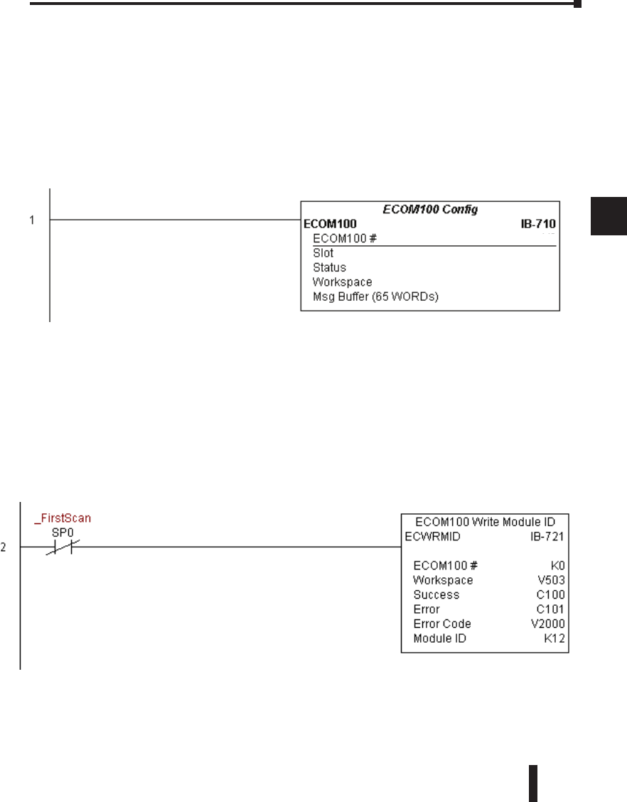
DL06 Micro PLC User Manual, 3rd Edition, Rev. D 5-311
1
2
3
4
5
6
7
8
9
10
11
12
13
14
A
B
C
D
ECWRMID Example
Rung 1: The ECOM100 Config IBox is responsible for coordination/interlocking of all
ECOM100 type IBoxes for one specific ECOM100 module. Tag the ECOM100 in slot 1
as ECOM100# K0. All other ECxxxx IBoxes refer to this module # as K0. If you need to
move the module in the base to a different slot, then you only need to change this one IBox.
V400 is used as a global result status register for the other ECxxxx IBoxes using this specific
ECOM100 module.V401 is used to coordinate/interlock the logic in all of the other ECxxxx
IBoxes using this specific ECOM100 module. V402-V502 is a common 130 byte buffer
available for use by the other ECxxxx IBoxes using this specific ECOM100 module.
Rung 2: On the 2nd scan, set the Module ID of the ECOM100. Typically this is done using
NetEdit, but this IBox allows you to configure the module ID of the ECOM100 using your
ladder program.
The EWRMID is leading edge triggered, not power-flow driven (similar to a counter input
leg). The command to write the module ID will be sent to the ECOM100 whenever the
power flow into the IBox goes from OFF to ON.
If successful, turn on C100. If there is a failure, turn on C101. If it fails, you can look at
V2000 for the specific error code.
Chapter 5: Intelligent Box (IBox) Instructions
1
2
3
4
5
6
7
8
9
10
11
12
13
14
a
B
c
d
K1
K0
V400
V401
V402 - V502
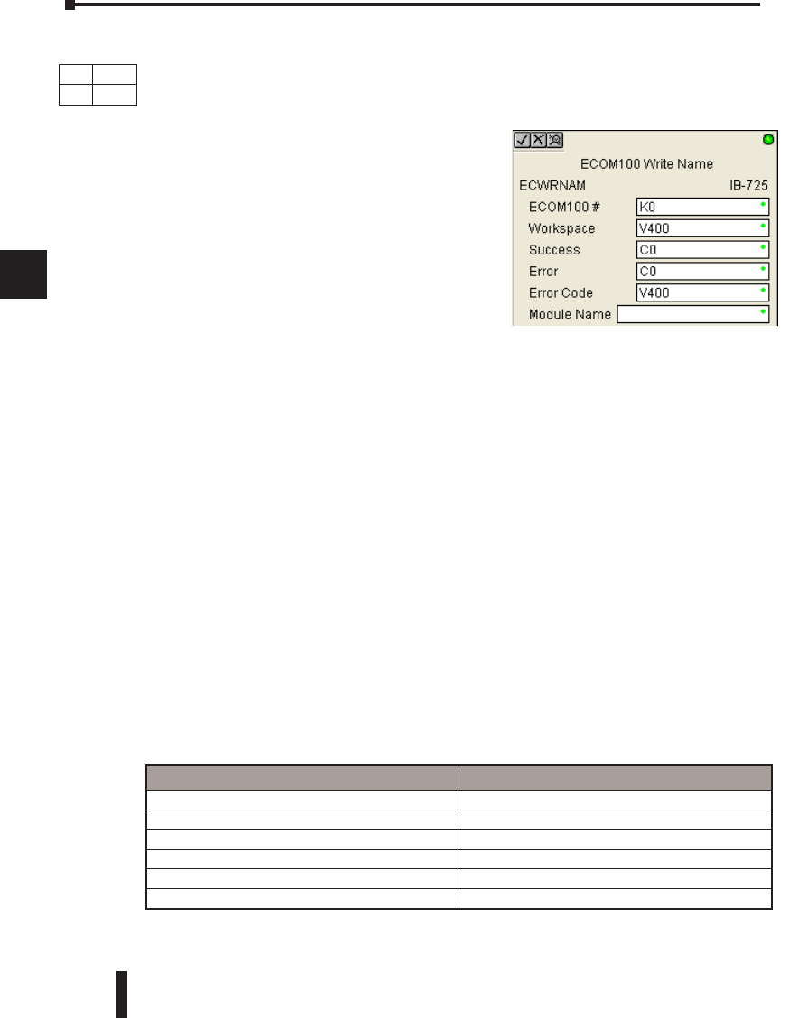
DL06 Micro PLC User Manual, 3rd Edition, Rev. D
5-312
1
2
3
4
5
6
7
8
9
10
11
12
13
14
A
B
C
D
ECOM100 Write Name (ECWRNAM) (IB-725)
ECOM100 Write Name will write the given Name to the ECOM100 module on a leading
edge transition to the IBox. If you use a dollar sign ($) or double quote (“), use the PRINT/
VPRINT escape sequence of TWO dollar signs ($$) for a single dollar sign or dollar sign-
double quote ($”) for a double quote character.
The Workspace parameter is an internal, private
register used by this IBox and MUST BE UNIQUE
in this one instruction and MUST NOT be used
anywhere else in your program.
Either the Success or Error bit parameter will turn on
once the command is complete. If there is an error,
the Error Code parameter will report an ECOM100
error code (less than 100), or a PLC logic error
(greater than 1000).
The Name is stored in Flash-ROM in the ECOM100 and the execution of this IBox will
disable the ECOM100 module for at least a half second until it writes the Flash-ROM.
Therefore, it is HIGHLY RECOMMENDED that you only execute this IBox ONCE on
first scan. Since it requires a LEADING edge to execute, use a NORMALLY CLOSED SP0
(STR NOT First Scan) to drive the power flow to the IBox.
In order for this ECOM100 IBox to function, you must turn ON dip switch 7 on the
ECOM100 circuit board.
ECWRNAM Parameters
• ECOM100#: this is a logical number associated with this specific ECOM100 module in the
specified slot. All other ECxxxx IBoxes that need to reference this ECOM100 module must
reference this logical number
• Workspace: specifies a V-memory location that will be used by the instruction
• Success: specifies a bit that will turn on once the request is completed successfully
• Error: specifies a bit that will turn on if the instruction is not successfully completed
• Error Code: specifies the location where the Error Code will be written
• Module Name: specifies the Name that will be written to the module
Chapter 5: Intelligent Box (IBox) Instructions
1
2
3
4
5
6
7
8
9
10
11
12
13
14
a
B
c
d
DS Used
HPP N/A
Parameter DL06 Range
ECOM100# K K0-255
Workspace V See DL06 V-memory map - Data Words
Success X,Y,C,GX,GY,B See DL06 V-memory map
Error X,Y,C,GX,GY,B See DL06 V-memory map
Error Code V See DL06 V-memory map - Data Words
Module Name Text
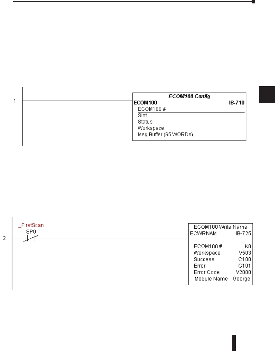
DL06 Micro PLC User Manual, 3rd Edition, Rev. D 5-313
1
2
3
4
5
6
7
8
9
10
11
12
13
14
A
B
C
D
ECWRNAM Example
Rung 1: The ECOM100 Config IBox is responsible for coordination/interlocking of all
ECOM100 type IBoxes for one specific ECOM100 module. Tag the ECOM100 in slot 1
as ECOM100# K0. All other ECxxxx IBoxes refer to this module # as K0. If you need to
move the module in the base to a different slot, then you only need to change this one IBox.
V400 is used as a global result status register for the other ECxxxx IBoxes using this specific
ECOM100 module.V401 is used to coordinate/interlock the logic in all of the other ECxxxx
IBoxes using this specific ECOM100 module. V402-V502 is a common 130 byte buffer
available for use by the other ECxxxx IBoxes using this specific ECOM100 module.
Rung 2: On the 2nd scan, set the Module Name of the ECOM100. Typically this is done
using NetEdit, but this IBox allows you to configure the module name of the ECOM100
using your ladder program.
The EWRNAM is leading edge triggered, not power-flow driven (similar to a counter input
leg). The command to write the module name will be sent to the ECOM100 whenever the
power flow into the IBox goes from OFF to ON.
If successful, turn on C100. If there is a failure, turn on C101. If it fails, you can look at
V2000 for the specific error code.
Chapter 5: Intelligent Box (IBox) Instructions
1
2
3
4
5
6
7
8
9
10
11
12
13
14
a
B
c
d
K1
K0
V400
V401
V402 - V502
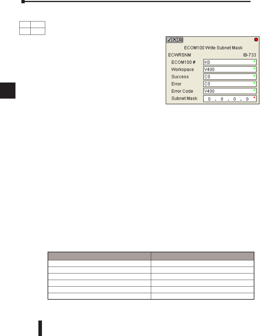
DL06 Micro PLC User Manual, 3rd Edition, Rev. D
5-314
1
2
3
4
5
6
7
8
9
10
11
12
13
14
A
B
C
D
ECOM100 Write Subnet Mask (ECWRSNM) (IB-733)
ECOM100 Write Subnet Mask will write the given Subnet Mask to the ECOM100
module on a leading edge transition to the IBox. See also ECOM100 IP Setup (ECIPSUP)
IBox 717 to setup ALL of the TCP/IP
parameters in a single instruction - IP Address,
Subnet Mask, and Gateway Address.
The Workspace parameter is an internal, private
register used by this IBox and MUST BE
UNIQUE in this one instruction and MUST NOT
be used anywhere else in your program.
Either the Success or Error bit parameter will turn
on once the command is complete. If there is an
error, the Error Code parameter will report an
ECOM100 error code (less than 100), or a PLC
logic error (greater than 1000).
The Subnet Mask is stored in Flash-ROM in the ECOM100 and the execution of this IBox
will disable the ECOM100 module for at least a half second until it writes the Flash-ROM.
Therefore, it is HIGHLY RECOMMENDED that you only execute this IBox ONCE on
first scan. Since it requires a LEADING edge to execute, use a NORMALLY CLOSED SP0
(STR NOT First Scan) to drive the power flow to the IBox.
In order for this ECOM100 IBox to function, you must turn ON dip switch 7 on the
ECOM100 circuit board.
ECWRSNM Parameters
• ECOM100#: this is a logical number associated with this specific ECOM100 module in the
specified slot. All other ECxxxx IBoxes that need to reference this ECOM100 module must
reference this logical number
• Workspace: specifies a V-memory location that will be used by the instruction
• Success: specifies a bit that will turn on once the request is completed successfully
• Error: specifies a bit that will turn on if the instruction is not successfully completed
• Error Code: specifies the location where the Error Code will be written
• Subnet Mask: specifies the Subnet Mask that will be written to the module
Chapter 5: Intelligent Box (IBox) Instructions
1
2
3
4
5
6
7
8
9
10
11
12
13
14
a
B
c
d
DS Used
HPP N/A
Parameter DL06 Range
ECOM100# K K0-255
Workspace V See DL06 V-memory map - Data Words
Success X,Y,C,GX,GY,B See DL06 V-memory map
Error X,Y,C,GX,GY,B See DL06 V-memory map
Error Code V See DL06 V-memory map - Data Words
Subnet Mask Masked IP Address
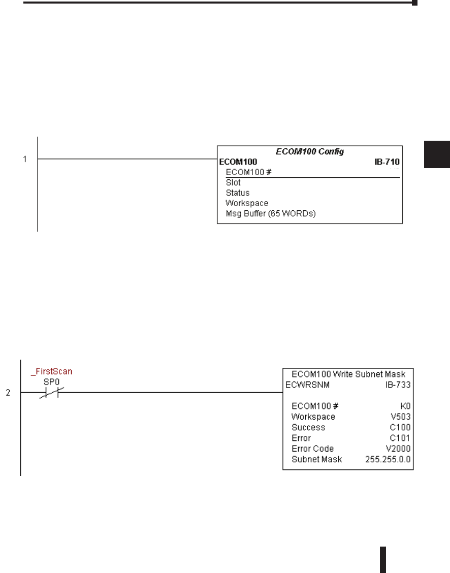
DL06 Micro PLC User Manual, 3rd Edition, Rev. D 5-315
1
2
3
4
5
6
7
8
9
10
11
12
13
14
A
B
C
D
ECWRSNM Example
Rung 1: The ECOM100 Config IBox is responsible for coordination/interlocking of all
ECOM100 type IBoxes for one specific ECOM100 module. Tag the ECOM100 in slot 1
as ECOM100# K0. All other ECxxxx IBoxes refer to this module # as K0. If you need to
move the module in the base to a different slot, then you only need to change this one IBox.
V400 is used as a global result status register for the other ECxxxx IBoxes using this specific
ECOM100 module.V401 is used to coordinate/interlock the logic in all of the other ECxxxx
IBoxes using this specific ECOM100 module. V402-V502 is a common 130 byte buffer
available for use by the other ECxxxx IBoxes using this specific ECOM100 module.
Rung 2: On the 2nd scan, assign the Subnet Mask of the ECOM100 to 255.255.0.0
The ECWRSNM is leading edge triggered, not power-flow driven (similar to a counter input
leg). The command to write the Subnet Mask will be sent to the ECOM100 whenever the
power flow into the IBox goes from OFF to ON.
If successful, turn on C100. If there is a failure, turn on C101. If it fails, you can look at
V2000 for the specific error code.
To configure all of the ECOM100 TCP/IP parameters in one IBox, see the ECOM100 IP
Setup (ECIPSUP) IBox.
Chapter 5: Intelligent Box (IBox) Instructions
1
2
3
4
5
6
7
8
9
10
11
12
13
14
a
B
c
d
K1
K0
V400
V401
V402 - V502
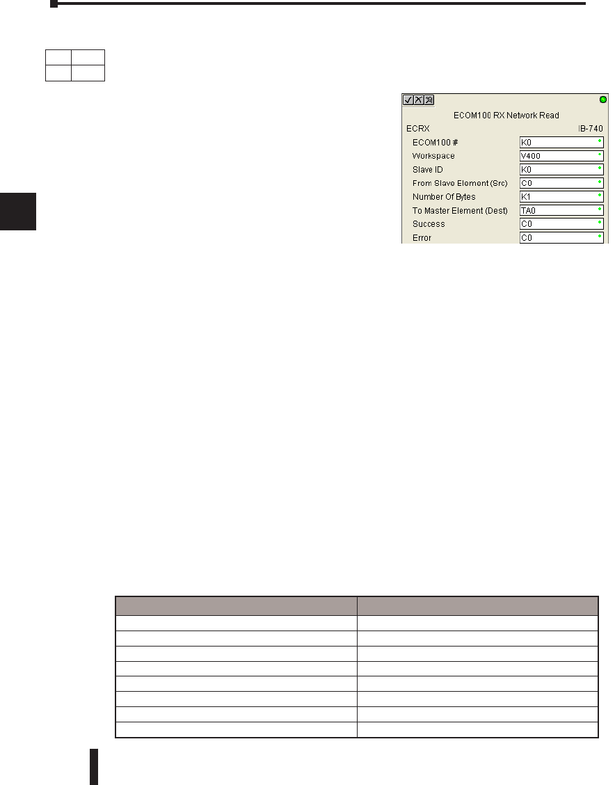
DL06 Micro PLC User Manual, 3rd Edition, Rev. D
5-316
1
2
3
4
5
6
7
8
9
10
11
12
13
14
A
B
C
D
ECOM100 RX Network Read (ECRX) (IB-740)
ECOM100 RX Network Read performs the RX instruction with built-in interlocking with
all other ECOM100 RX (ECRX) and ECOM100 WX (ECWX) IBoxes in your program to
simplify communications networking. It will perform the RX on the specified ECOM100#’s
network, which corresponds to a specific unique
ECOM100 Configuration (ECOM100) IBox at the
top of your program.
The Workspace parameter is an internal, private
register used by this IBox and MUST BE UNIQUE
in this one instruction and MUST NOT be used
anywhere else in your program.
Whenever this IBox has power, it will read element
data from the specified slave into the given destination
V-Memory buffer, giving other ECOM100 RX and
ECOM100 WX IBoxes on that ECOM100# network a chance to execute.
For example, if you wish to read and write data continuously from 5 different slaves, you can
have all of these ECRX and ECWX instructions in ONE RUNG driven by SP1 (Always On).
They will execute round-robin style, automatically.
ECRX Parameters
• ECOM100#: this is a logical number associated with this specific ECOM100 module in the
specified slot. All other ECxxxx IBoxes that need to reference this ECOM100 module must
reference this logical number
• Workspace: specifies a V-memory location that will be used by the instruction
• Slave ID: specifies the slave ECOM(100) PLC that will be targeted by the ECRX instruction
• From Slave Element (Src): specifies the slave address of the data to be read
• Number of Bytes: specifies the number of bytes to read from the slave ECOM(100) PLC
• To Master Element (Dest): specifies the location where the slave data will be placed in the master
ECOM100 PLC
• Success: specifies a bit that will turn on once the request is completed successfully
• Error: specifies a bit that will turn on if the instruction is not successfully completed
Chapter 5: Intelligent Box (IBox) Instructions
1
2
3
4
5
6
7
8
9
10
11
12
13
14
a
B
c
d
DS Used
HPP N/A
Parameter DL06 Range
ECOM100# K K0-255
Workspace V See DL06 V-memory map - Data Words
Slave ID K K0-90
From Slave Element (Src) X,Y,C,S,T,CT,GX,GY,V,P See DL06 V-memory map
Number of Bytes K K1-128
To Master Element (Dest) V See DL06 V-memory map - Data Words
Success X,Y,C,GX,GY,B See DL06 V-memory map
Error X,Y,C,GX,GY,B See DL06 V-memory map
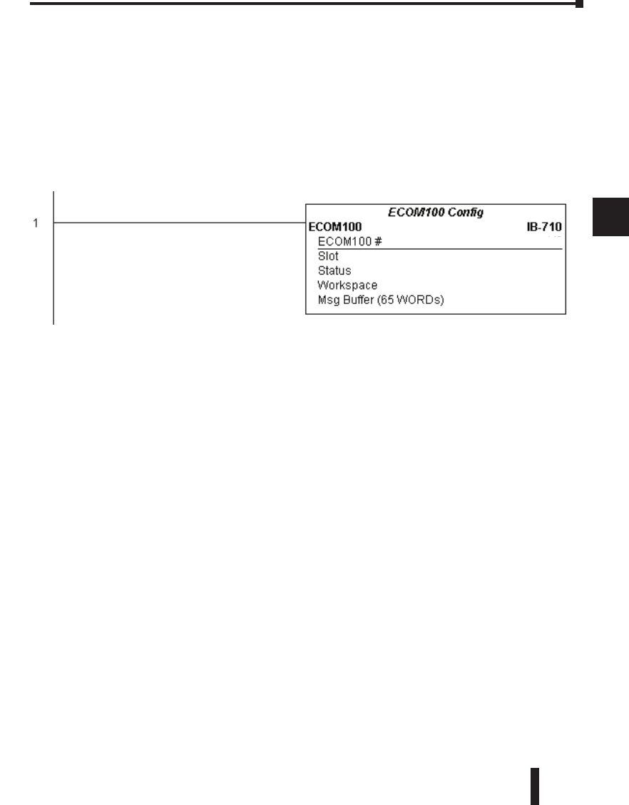
DL06 Micro PLC User Manual, 3rd Edition, Rev. D 5-317
1
2
3
4
5
6
7
8
9
10
11
12
13
14
A
B
C
D
ECRX Example
Rung 1: The ECOM100 Config IBox is responsible for coordination/interlocking of all
ECOM100 type IBoxes for one specific ECOM100 module. Tag the ECOM100 in slot 1
as ECOM100# K0. All other ECxxxx IBoxes refer to this module # as K0. If you need to
move the module in the base to a different slot, then you only need to change this one IBox.
V400 is used as a global result status register for the other ECxxxx IBoxes using this specific
ECOM100 module.V401 is used to coordinate/interlock the logic in all of the other ECxxxx
IBoxes using this specific ECOM100 module. V402-V502 is a common 130 byte buffer
available for use by the other ECxxxx IBoxes using this specific ECOM100 module.
Chapter 5: Intelligent Box (IBox) Instructions
1
2
3
4
5
6
7
8
9
10
11
12
13
14
a
B
c
d
K1
K0
V400
V401
V402 - V502
(example continued on next page)
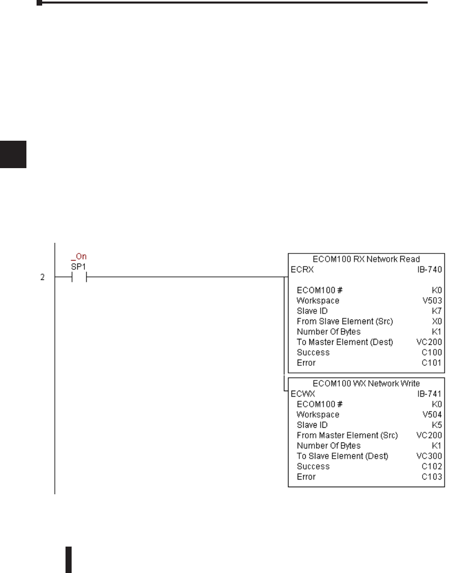
DL06 Micro PLC User Manual, 3rd Edition, Rev. D
5-318
1
2
3
4
5
6
7
8
9
10
11
12
13
14
A
B
C
D
ECRX Example (cont’d)
Rung 2: Using ECOM100# K0, read X0-X7 from Slave K7 and write them to slave K5 as
fast as possible. Store them in this local PLC in C200-C207, and write them to C300-C307
in slave K5.
Both the ECRX and ECWX work with the ECOM100 Config IBox to simplify all
networking by handling all of the interlocks and proper resource sharing. They also provide
very simplified error reporting. You no longer need to worry about any SP “busy bits” or
“error bits”, or what slot number a module is in, or have any counters or shift registers or any
other interlocks for resource management.
In this example, SP1 (always ON) is driving both the ECRX and ECWX IBoxes in the same
rung. On the scan that the Network Read completes, the Network Write will start that same
scan. As soon as the Network Write completes, any pending operations below it in the
program would get a turn. If there are no pending ECOM100 IBoxes below the ECWX,
then the very next scan the ECRX would start its request again.
Using the ECRX and ECWX for all of your ECOM100 network reads and writes is the
fastest the PLC can do networking. For local Serial Ports, DCM modules, or the original
ECOM modules, use the NETCFG and NETRX/NETWX IBoxes.
Chapter 5: Intelligent Box (IBox) Instructions
1
2
3
4
5
6
7
8
9
10
11
12
13
14
a
B
c
d
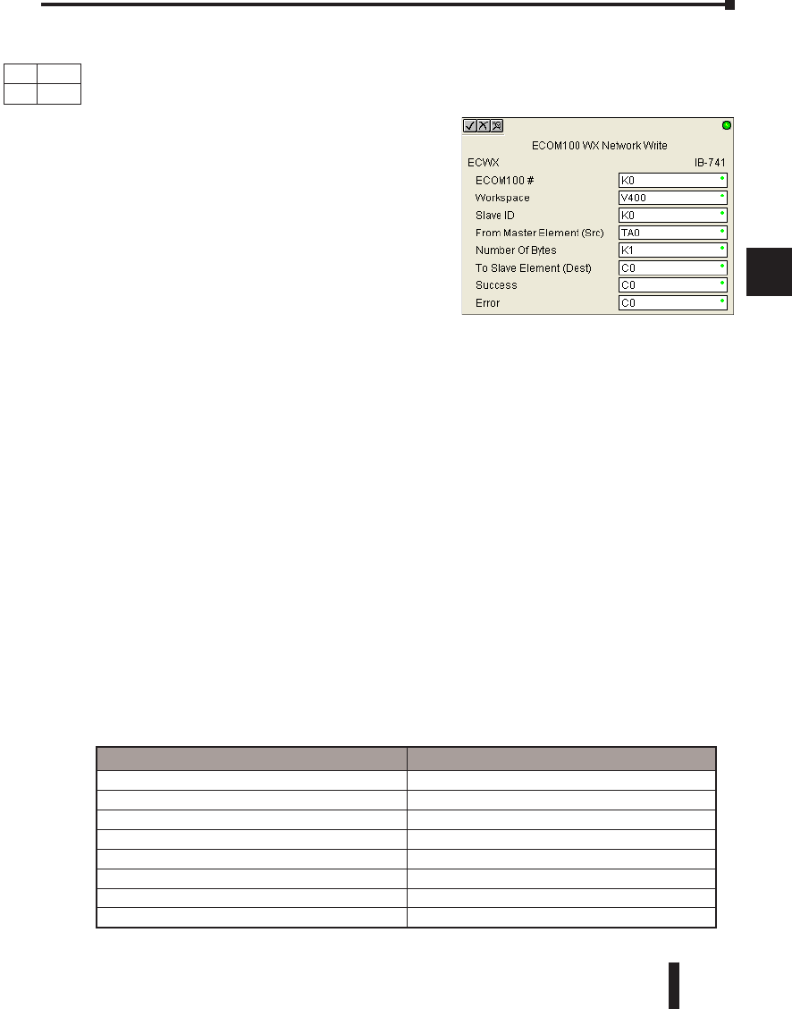
DL06 Micro PLC User Manual, 3rd Edition, Rev. D 5-319
1
2
3
4
5
6
7
8
9
10
11
12
13
14
A
B
C
D
ECOM100 WX Network Write(ECWX) (IB-741)
ECOM100 WX Network Write performs the WX instruction with built-in interlocking with
all other ECOM100 RX (ECRX) and ECOM100 WX (ECWX) IBoxes in your program to
simplify communications networking. It will perform the WX on the specified ECOM100#’s
network, which corresponds to a specific unique
ECOM100 Configuration (ECOM100) IBox at the
top of your program.
The Workspace parameter is an internal, private
register used by this IBox and MUST BE UNIQUE
in this one instruction and MUST NOT be used
anywhere else in your program.
Whenever this IBox has power, it will write data
from the master’s V-Memory buffer to the specified
slave starting with the given slave element, giving
other ECOM100 RX and ECOM100 WX IBoxes on that ECOM100# network a chance to
execute.
For example, if you wish to read and write data continuously from 5 different slaves, you can
have all of these ECRX and ECWX instructions in ONE RUNG driven by SP1 (Always On).
They will execute round-robin style, automatically.
ECWX Parameters
• ECOM100#: this is a logical number associated with this specific ECOM100 module in the
specified slot. All other ECxxxx IBoxes that need to reference this ECOM100 module must
reference this logical number
• Workspace: specifies a V-memory location that will be used by the instruction
• Slave ID: specifies the slave ECOM(100) PLC that will be targeted by the ECWX instruction
• From Master Element (Src): specifies the location in the master ECOM100 PLC where the data
will be sourced from
• Number of Bytes: specifies the number of bytes to write to the slave ECOM(100) PLC
• To Slave Element (Dest): specifies the slave address the data will be written to
• Success: specifies a bit that will turn on once the request is completed successfully
• Error: specifies a bit that will turn on if the instruction is not successfully completed
Chapter 5: Intelligent Box (IBox) Instructions
1
2
3
4
5
6
7
8
9
10
11
12
13
14
a
B
c
d
DS Used
HPP N/A
Parameter DL06 Range
ECOM100# K K0-255
Workspace V See DL06 V-memory map - Data Words
Slave ID K K0-90
From Master Element (Src) V See DL06 V-memory map - Data Words
Number of Bytes K K1-128
To Slave Element (Dest) X,Y,C,S,T,CT,GX,GY,V,P See DL06 V-memory map
Success X,Y,C,GX,GY,B See DL06 V-memory map
Error X,Y,C,GX,GY,B See DL06 V-memory map
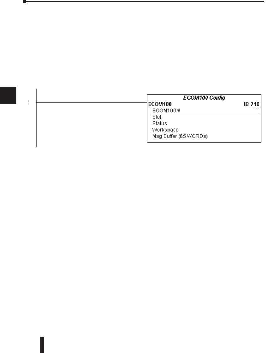
DL06 Micro PLC User Manual, 3rd Edition, Rev. D
5-320
1
2
3
4
5
6
7
8
9
10
11
12
13
14
A
B
C
D
ECWX Example
Rung 1: The ECOM100 Config IBox is responsible for coordination/interlocking of all
ECOM100 type IBoxes for one specific ECOM100 module. Tag the ECOM100 in slot 1
as ECOM100# K0. All other ECxxxx IBoxes refer to this module # as K0. If you need to
move the module in the base to a different slot, then you only need to change this one IBox.
V400 is used as a global result status register for the other ECxxxx IBoxes using this specific
ECOM100 module.V401 is used to coordinate/interlock the logic in all of the other ECxxxx
IBoxes using this specific ECOM100 module. V402-V502 is a common 130 byte buffer
available for use by the other ECxxxx IBoxes using this specific ECOM100 module.
Chapter 5: Intelligent Box (IBox) Instructions
1
2
3
4
5
6
7
8
9
10
11
12
13
14
a
B
c
d
K1
K0
V400
V401
V402 - V502
(example continued on next page)
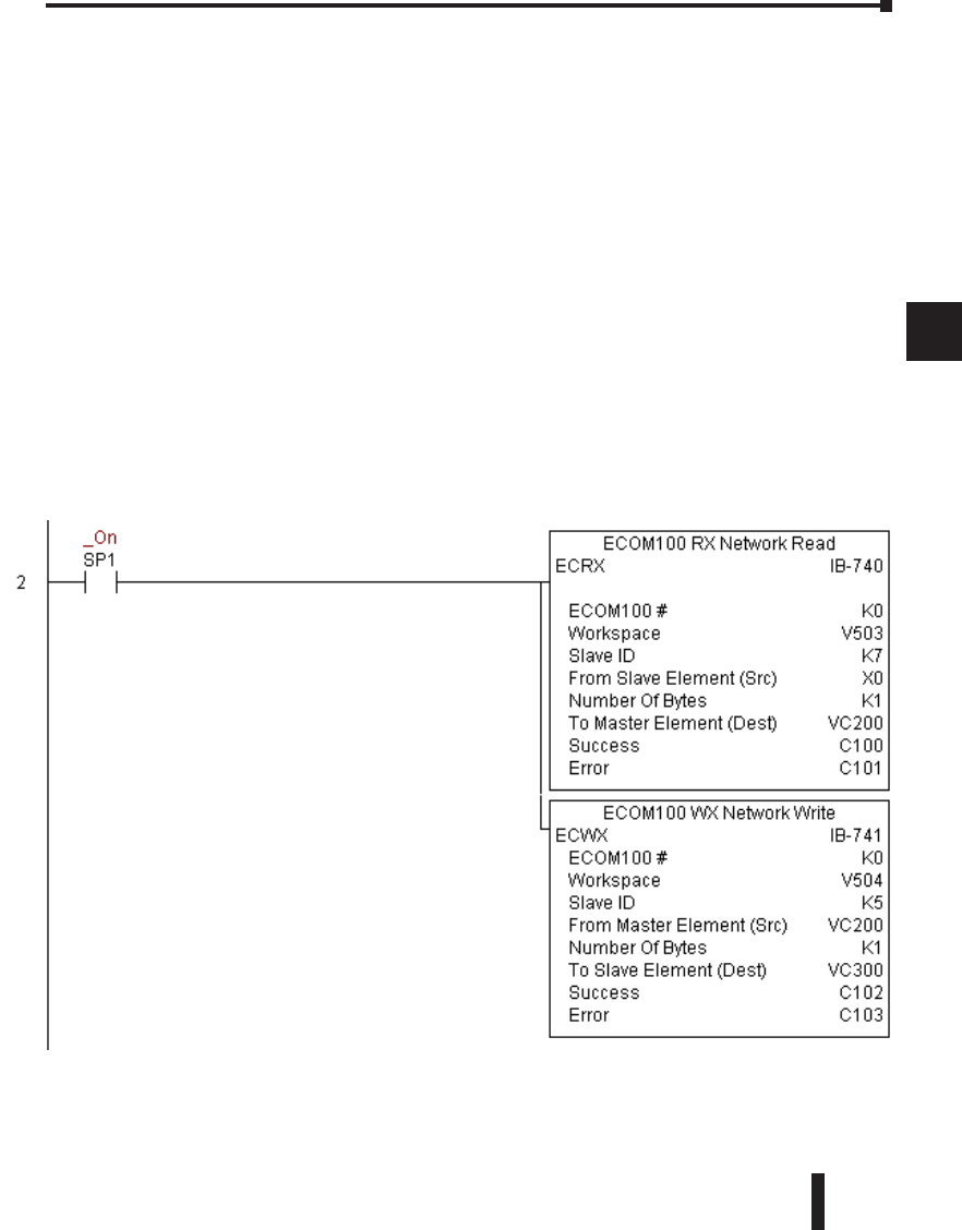
DL06 Micro PLC User Manual, 3rd Edition, Rev. D 5-321
1
2
3
4
5
6
7
8
9
10
11
12
13
14
A
B
C
D
ECWX Example (cont’d)
Rung 2: Using ECOM100# K0, read X0-X7 from Slave K7 and write them to slave K5 as
fast as possible. Store them in this local PLC in C200-C207, and write them to C300-C307
in slave K5.
Both the ECRX and ECWX work with the ECOM100 Config IBox to simplify all
networking by handling all of the interlocks and proper resource sharing. They also provide
very simplified error reporting. You no longer need to worry about any SP “busy bits” or
“error bits”, or what slot number a module is in, or have any counters or shift registers or any
other interlocks for resource management.
In this example, SP1 (always ON) is driving both the ECRX and ECWX IBoxes in the same
rung. On the scan that the Network Read completes, the Network Write will start that
same scan. As soon as the Network Write completes, any pending operations below it in the
program would get a turn. If there are no pending ECOM100 IBoxes below the ECWX, then
the very next scan the ECRX would start its request again.
Using the ECRX and ECWX for all of your ECOM100 network reads and writes is the
fastest the PLC can do networking. For local Serial Ports, DCM modules, or the original
ECOM modules, use the NETCFG and NETRX/NETWX IBoxes.
Chapter 5: Intelligent Box (IBox) Instructions
1
2
3
4
5
6
7
8
9
10
11
12
13
14
a
B
c
d
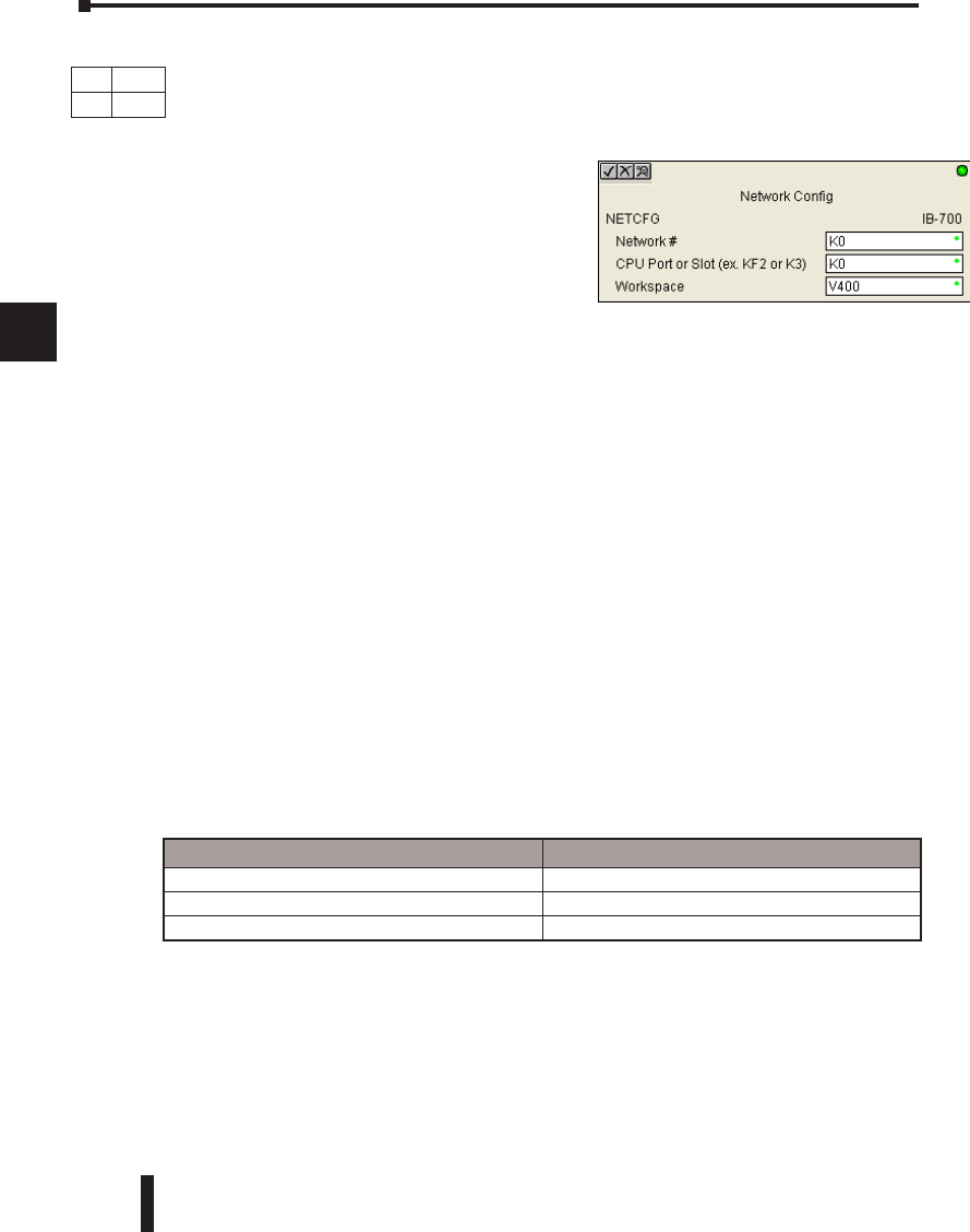
DL06 Micro PLC User Manual, 3rd Edition, Rev. D
5-322
1
2
3
4
5
6
7
8
9
10
11
12
13
14
A
B
C
D
NETCFG Network Configuration (NETCFG) (IB-700)
Network Config defines all the common information necessary for performing RX/WX
Networking using the NETRX and NETWX IBox instructions via a local CPU serial port,
DCM or ECOM module.
You must have the Network Config instruction
at the top of your ladder/stage program with any
other configuration IBoxes.
If you use more than one local serial port, DCM
or ECOM in your PLC for RX/WX Networking,
you must have a different Network Config
instruction for EACH RX/WX network in your
system that utilizes any NETRX/NETWX IBox instructions.
The Workspace parameter is an internal, private register used by the Network Config IBox
and MUST BE UNIQUE in this one instruction and MUST NOT be used anywhere else in
your program.
The 2nd parameter “CPU Port or Slot” is the same value as in the high byte of the first LD
instruction if you were coding the RX or WX rung yourself. This value is CPU and port
specific (check your PLC manual). Use KF2 for the DL06 CPU serial port 2. If using a DCM
or ECOM module, use Kx, where x equals the slot where the module is installed.
Since this logic only executes on the first scan, this IBox cannot have any input logic.
NETCFG Parameters
• Network#: specifies a unique # for each ECOM(100) or DCM network to use
• CPU Port or Slot: specifies the CPU port number or slot number of DCM/ECOM(100) used
• Workspace: specifies a V-memory location that will be used by the instruction
Chapter 5: Intelligent Box (IBox) Instructions
1
2
3
4
5
6
7
8
9
10
11
12
13
14
a
B
c
d
DS Used
HPP N/A
Parameter DL06 Range
Network# K K0-255
CPU Port or Slot K K0-FF
Workspace V See DL06 V-memory map - Data Words
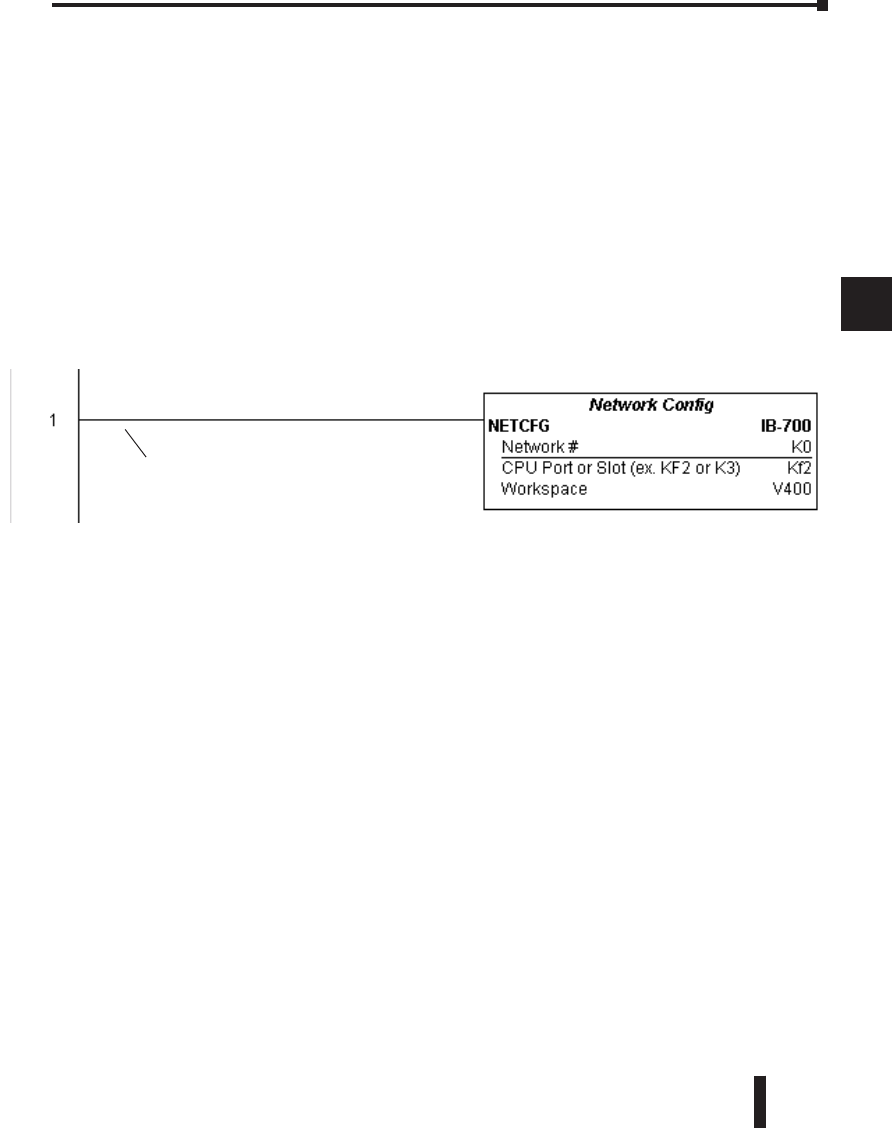
DL06 Micro PLC User Manual, 3rd Edition, Rev. D 5-323
1
2
3
4
5
6
7
8
9
10
11
12
13
14
A
B
C
D
NETCFG Example
The Network Configuration IBox coordinates all of the interaction with other Network
IBoxes (NETRX/NETWX). You must have a Network Configuration IBox for each serial
port network, DCM module network, or original ECOM module network in your system.
Configuration IBoxes must be at the top of your program and must execute every scan.
This IBox defines Network# K0 to be for the local CPU serial port #2 (KF2). For local
CPU serial ports or DCM/ECOM modules, use the same value you would use in the most
significant byte of the first LD instruction in a normal RX/WX rung to reference the port or
module. Any NETRX or NETWX IBoxes that need to reference this specific network would
enter K0 for their Network# parameter.
The Workspace register is used to maintain state information about the port or module,
along with proper sharing and interlocking with the other NETRX and NETWX IBoxes in
the program. This V-memory register must not be used anywhere else in the entire program.
Chapter 5: Intelligent Box (IBox) Instructions
1
2
3
4
5
6
7
8
9
10
11
12
13
14
a
B
c
d
Permissive contacts or input logic
cannot be used with this instruction.
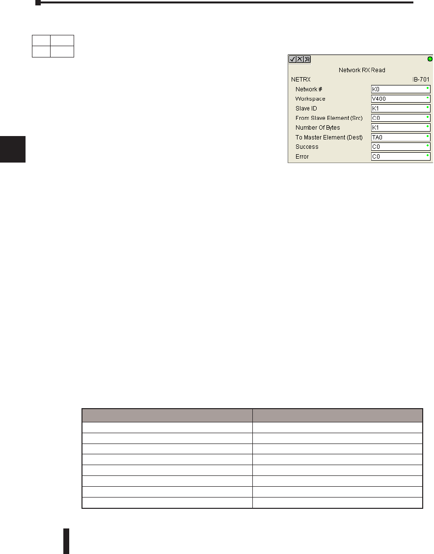
DL06 Micro PLC User Manual, 3rd Edition, Rev. D
5-324
1
2
3
4
5
6
7
8
9
10
11
12
13
14
A
B
C
D
Network RX Read (NETRX) (IB-701)
Network RX Read performs the RX instruction with built-in interlocking with all other
Network RX (NETRX) and Network WX (NETWX) IBoxes in your program to simplify
communications networking. It will perform the RX
on the specified Network #, which corresponds to a
specific unique Network Configuration (NETCFG) at
the top of your program.
The Workspace parameter is an internal, private
register used by this IBox and MUST BE UNIQUE
in this one instruction and MUST NOT be used
anywhere else in your program.
Whenever this IBox has power, it will read element
data from the specified slave into the given destination
V-Memory buffer, giving other Network RX and Network WX IBoxes on that Network # a
chance to execute.
For example, if you wish to read and write data continuously from 5 different slaves, you can
have all of these NETRX and NETWX instructions in ONE RUNG driven by SP1 (Always
On). They will execute round-robin style, automatically.
NETRX Parameters
• Network#: specifies the (CPU port’s, DCM’s, ECOM’s) Network # defined by the NETCFG
instruction
• Workspace: specifies a V-memory location that will be used by the instruction
• Slave ID: specifies the slave PLC that will be targeted by the NETRX instruction
• From Slave Element (Src): specifies the slave address of the data to be read
• Number of Bytes: specifies the number of bytes to read from the slave device
• To Master Element (Dest): specifies the location where the slave data will be placed in the master
PLC
• Success: specifies a bit that will turn on once the request is completed successfully
• Error: specifies a bit that will turn on if the instruction is not successfully completed
Chapter 5: Intelligent Box (IBox) Instructions
1
2
3
4
5
6
7
8
9
10
11
12
13
14
a
B
c
d
DS Used
HPP N/A
Parameter DL06 Range
Network# K K0-255
Workspace V See DL06 V-memory map - Data Words
Slave ID K, V K0-90: See DL06 V-memory map
From Slave Element (Src) X,Y,C,S,T,CT,GX,GY,V,P See DL06 V-memory map
Number of Bytes K K1-128
To Master Element (Dest) V See DL06 V-memory map - Data Words
Success X,Y,C,GX,GY,B See DL06 V-memory map
Error X,Y,C,GX,GY,B See DL06 V-memory map

DL06 Micro PLC User Manual, 3rd Edition, Rev. D 5-325
1
2
3
4
5
6
7
8
9
10
11
12
13
14
A
B
C
D
NETRX Example
Rung 1: The Network Configuration IBox coordinates all of the interaction with other
Network IBoxes (NETRX/NETWX). You must have a Network Configuration IBox for
each serial port network, DCM module network, or original ECOM module network in your
system. Configuration IBoxes must be at the top of your program and must execute every
scan.
This IBox defines Network# K0 to be for the local CPU serial port #2 (KF2). For local
CPU serial ports or DCM/ECOM modules, use the same value you would use in the most
significant byte of the first LD instruction in a normal RX/WX rung to reference the port or
module. Any NETRX or NETWX IBoxes that need to reference this specific network would
enter K0 for their Network# parameter.
The Workspace register is used to maintain state information about the port or module,
along with proper sharing and interlocking with the other NETRX and NETWX IBoxes in
the program. This V-Memory register must not be used anywhere else in the entire program.
Chapter 5: Intelligent Box (IBox) Instructions
1
2
3
4
5
6
7
8
9
10
11
12
13
14
a
B
c
d
(example continued on next page)
Permissive contacts or input logic cannot
be used with this instruction.

DL06 Micro PLC User Manual, 3rd Edition, Rev. D
5-326
1
2
3
4
5
6
7
8
9
10
11
12
13
14
A
B
C
D
NETRX Example (cont’d)
Rung 2: Using Network# K0, read X0-X7 from Slave K7 and write them to slave K5 as fast
as possible. Store them in this local PLC in C200-C207, and write them to C300-C307 in
slave K5.
Both the NETRX and NETWX work with the Network Config IBox to simplify all
networking by handling all of the interlocks and proper resource sharing. They also provide
very simplified error reporting. You no longer need to worry about any SP “busy bits” or
“error bits”, or what port number or slot number a module is in, or have any counters or shift
registers or any other interlocks for resource management.
In this example, SP1 (always ON) is driving both the NETRX and NETWX IBoxes in the
same rung. On the scan that the Network Read completes, the Network Write will start that
same scan. As soon as the Network Write completes, any pending operations below it in the
program would get a turn. If there are no pending NETRX or NETWX IBoxes below this
IBox, then the very next scan the NETRX would start its request again.
Using the NETRX and NETWX for all of your serial port, DCM, or original ECOM
network reads and writes is the fastest the PLC can do networking. For ECOM100 modules,
use the ECOM100 and ECRX/ECWX IBoxes.
Chapter 5: Intelligent Box (IBox) Instructions
1
2
3
4
5
6
7
8
9
10
11
12
13
14
a
B
c
d
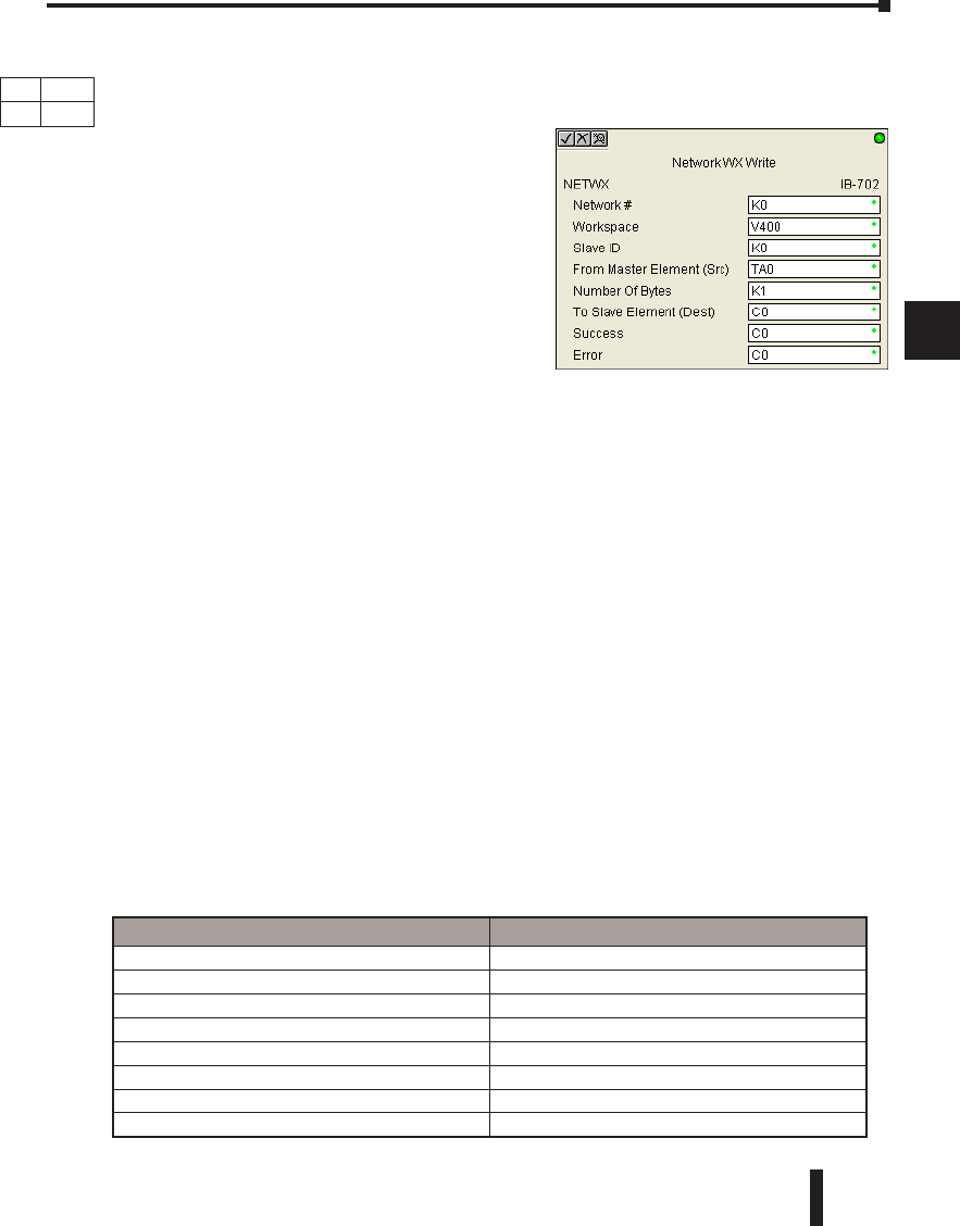
DL06 Micro PLC User Manual, 3rd Edition, Rev. D 5-327
1
2
3
4
5
6
7
8
9
10
11
12
13
14
A
B
C
D
Network WX Write (NETWX) (IB-702)
Network WX Write performs the WX instruction with built-in interlocking with all other
Network RX (NETRX) and Network WX (NETWX) IBoxes in your program to simplify
communications networking. It will perform the WX
on the specified Network #, which corresponds to a
specific unique Network Configuration (NETCFG)
at the top of your program.
The Workspace parameter is an internal, private
register used by this IBox and MUST BE UNIQUE
in this one instruction and MUST NOT be used
anywhere else in your program.
Whenever this IBox has power, it will write data from
the master’s V-Memory buffer to the specified slave
starting with the given slave element, giving other Network RX and Network WX IBoxes on
that Network # a chance to execute.
For example, if you wish to read and write data continuously from 5 different slaves, you can
have all of these NETRX and NETWX instructions in ONE RUNG driven by SP1 (Always
On). They will execute round-robin style, automatically.
NETWX Parameters
• Network#: specifies the (CPU port’s, DCM’s, ECOM’s) Network # defined by the NETCFG
instruction
• Workspace: specifies a V-memory location that will be used by the instruction
• Slave ID: specifies the slave PLC that will be targeted by the NETWX instruction
• From Master Element (Src): specifies the location in the master PLC where the data will be sourced
from
• Number of Bytes: specifies the number of bytes to write to the slave PLC
• To Slave Element (Dest): specifies the slave address the data will be written to
• Success: specifies a bit that will turn on once the request is completed successfully
• Error: specifies a bit that will turn on if the instruction is not successfully completed
Chapter 5: Intelligent Box (IBox) Instructions
1
2
3
4
5
6
7
8
9
10
11
12
13
14
a
B
c
d
DS Used
HPP N/A
Parameter DL06 Range
Network# K K0-255
Workspace V See DL06 V-memory map - Data Words
Slave ID K,V K0-90: See DL06 V-memory map
From Master Element (Src) V See DL06 V-memory map - Data Words
Number of Bytes K K1-128
To Slave Element (Dest) X,Y,C,S,T,CT,GX,GY,V,P See DL06 V-memory map
Success X,Y,C,GX,GY,B See DL06 V-memory map
Error X,Y,C,GX,GY,B See DL06 V-memory map
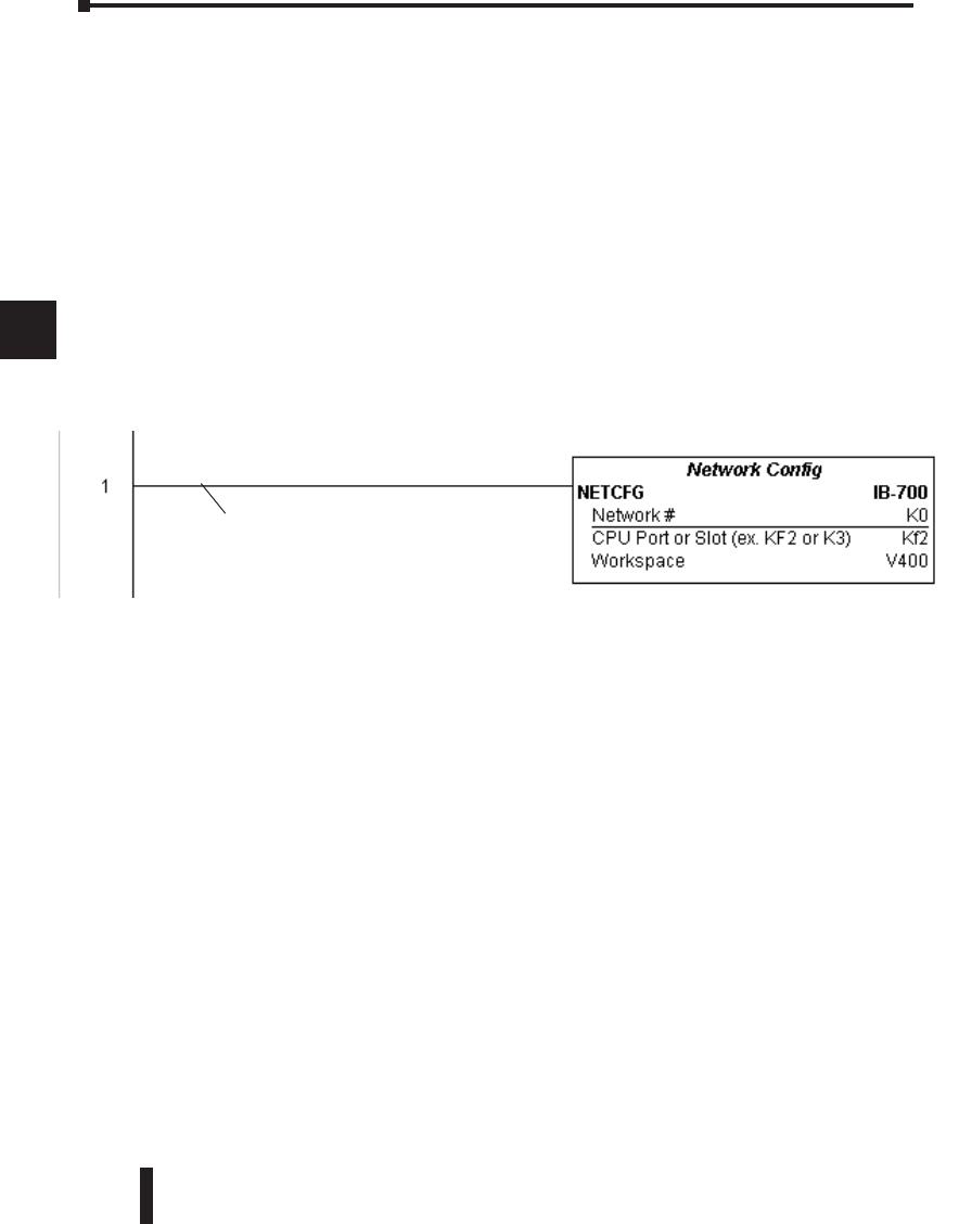
DL06 Micro PLC User Manual, 3rd Edition, Rev. D
5-328
1
2
3
4
5
6
7
8
9
10
11
12
13
14
A
B
C
D
NETWX Example
Rung 1: The Network Configuration IBox coordinates all of the interaction with other
Network IBoxes (NETRX/NETWX). You must have a Network Configuration IBox for
each serial port network, DCM module network, or original ECOM module network in your
system. Configuration IBoxes must be at the top of your program and must execute every
scan.
This IBox defines Network# K0 to be for the local CPU serial port #2 (KF2). For local
CPU serial ports or DCM/ECOM modules, use the same value you would use in the most
significant byte of the first LD instruction in a normal RX/WX rung to reference the port or
module. Any NETRX or NETWX IBoxes that need to reference this specific network would
enter K0 for their Network# parameter.
The Workspace register is used to maintain state information about the port or module,
along with proper sharing and interlocking with the other NETRX and NETWX IBoxes in
the program. This V-Memory register must not be used anywhere else in the entire program.
Chapter 5: Intelligent Box (IBox) Instructions
1
2
3
4
5
6
7
8
9
10
11
12
13
14
a
B
c
d
(example continued on next page)
Permissive contacts or input logic cannot
be used with this instruction.

DL06 Micro PLC User Manual, 3rd Edition, Rev. D 5-329
1
2
3
4
5
6
7
8
9
10
11
12
13
14
A
B
C
D
NETWX Example (cont’d)
Rung 2: Using Network# K0, read X0-X7 from Slave K7 and write them to slave K5 as fast
as possible. Store them in this local PLC in C200-C207, and write them to C300-C307 in
slave K5.
Both the NETRX and NETWX work with the Network Config IBox to simplify all
networking by handling all of the interlocks and proper resource sharing. They also provide
very simplified error reporting. You no longer need to worry about any SP “busy bits” or
“error bits”, or what port number or slot number a module is in, or have any counters or shift
registers or any other interlocks for resource management.
In this example, SP1 (always ON) is driving both the NETRX and NETWX IBoxes in the
same rung. On the scan that the Network Read completes, the Network Write will start that
same scan. As soon as the Network Write completes, any pending operations below it in the
program would get a turn. If there are no pending NETRX or NETWX IBoxes below this
IBox, then the very next scan the NETRX would start its request again.
Using the NETRX and NETWX for all of your serial port, DCM, or original ECOM
network reads and writes is the fastest the PLC can do networking. For ECOM100 modules,
use the ECOM100 and ECRX/ECWX IBoxes.
Chapter 5: Intelligent Box (IBox) Instructions
1
2
3
4
5
6
7
8
9
10
11
12
13
14
a
B
c
d
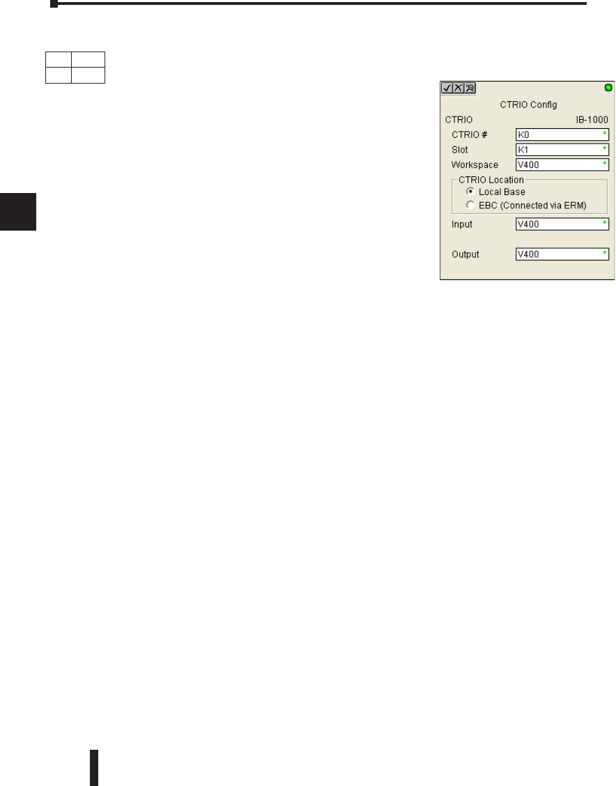
DL06 Micro PLC User Manual, 3rd Edition, Rev. D
5-330
1
2
3
4
5
6
7
8
9
10
11
12
13
14
A
B
C
D
CTRIO Configuration (CTRIO) (IB-1000)
CTRIO Config defines all the common information for one specific CTRIO module which
is used by the other CTRIO IBox instructions (for example, CTRLDPR - CTRIO Load
Profile, CTREDRL - CTRIO Edit and Reload Preset Table,
CTRRTLM - CTRIO Run to Limit Mode, ...).
The Input/Output parameters for this instruction can be
copied directly from the CTRIO Workbench configuration
for this CTRIO module. Since the behavior is slightly
different when the CTRIO module is in an EBC Base via an
ERM, you must specify whether the CTRIO module is in a
local base or in an EBC base. The DL06 PLC only supports
local base operation at this time.
You must have the CTRIO Config IBox at the top of your
ladder/stage program along with any other configuration
IBoxes.
If you have more than one CTRIO in your PLC, you must have a different CTRIO Config
IBox for EACH CTRIO module in your system that utilizes any CTRIO IBox instructions.
Each CTRIO Config IBox must have a UNIQUE CTRIO# value. This is how the CTRIO
IBoxes differentiate between the different CTRIO modules in your system.
The Workspace parameter is an internal, private register used by the CTRIO Config IBox
and MUST BE UNIQUE in this one instruction and MUST NOT be used anywhere else in
your program.
Since this logic only executes on the first scan, this IBox cannot have any input logic.
CTRIO Parameters
• CTRIO#: specifies a specific CTRIO module based on a user defined number
• Slot: specifies which PLC option slot the CTRIO module occupies
• Workspace: specifies a V-memory location that will be used by the instruction
• CTRIO Location: specifies where the module is located (local base only for DL06)
• Input: This needs to be set to the same V-memory register as is specified in CTRIO Workbench as
‘Starting V address for inputs’ for this unique CTRIO.
• Output: This needs to be set to the same V-memory register as is specified in CTRIO Workbench
as ‘Starting V address for outputs’ for this unique CTRIO.
Chapter 5: Intelligent Box (IBox) Instructions
1
2
3
4
5
6
7
8
9
10
11
12
13
14
a
B
c
d
DS Used
HPP N/A
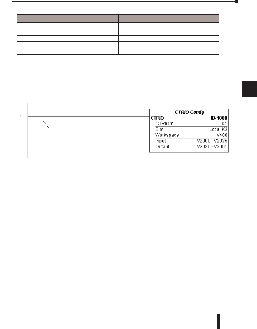
DL06 Micro PLC User Manual, 3rd Edition, Rev. D 5-331
1
2
3
4
5
6
7
8
9
10
11
12
13
14
A
B
C
D
CTRIO Example
Rung 1: This sets up the CTRIO card in slot 2 of the local base. Each CTRIO in the system
will need a separate CTRIO I-box before any CTRxxxx I-boxes can be used for them. The
CTRIO has been configured to use V2000 through V2025 for its input data, and V2030
through V2061 for its output data.
Chapter 5: Intelligent Box (IBox) Instructions
1
2
3
4
5
6
7
8
9
10
11
12
13
14
a
B
c
d
Parameter DL06 Range
CTRIO# K K0-255
Slot K K1-4
Workspace V See DL06 V-memory map - Data Words
Input V See DL06 V-memory map - Data Words
Output V See DL06 V-memory map - Data Words
Permissive contacts or input logic cannot
be used with this instruction
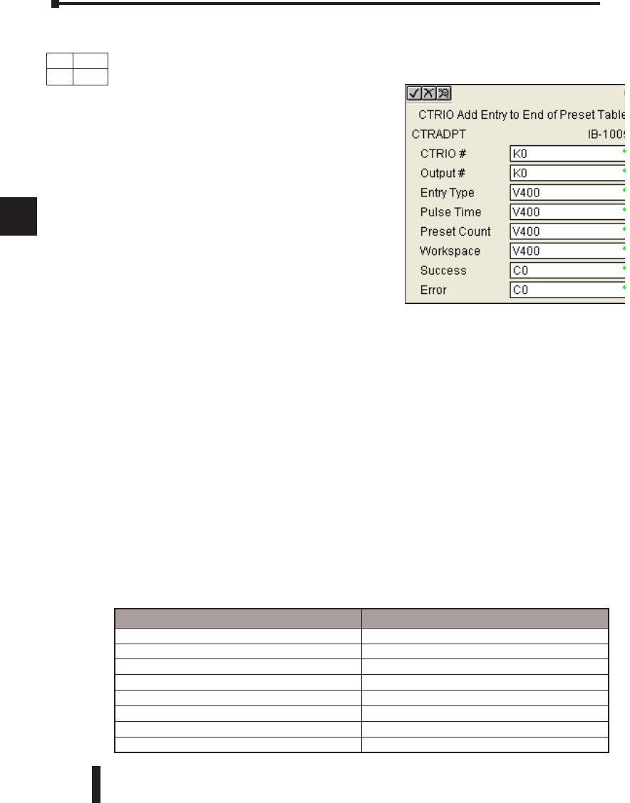
DL06 Micro PLC User Manual, 3rd Edition, Rev. D
5-332
1
2
3
4
5
6
7
8
9
10
11
12
13
14
A
B
C
D
CTRIO Add Entry to End of Preset Table (CTRADPT) (IB-1005)
CTRIO Add Entry to End of Preset Table, on a leading edge transition to this IBox, will
append an entry to the end of a memory based Preset Table on a specific CTRIO Output
resource. This IBox will take more than 1 PLC
scan to execute. Either the Success or Error bit will
turn on when the command is complete. If the
Error Bit is on, you can use the CTRIO Read Error
Code (CTRRDER) IBox to get extended error
information.
Entry Type:
K0: Set
K1: Reset
K2: Pulse On (uses Pulse Time)
K3: Pulse Off (uses Pulse Time)
K4: Toggle
K5: Reset Count
Note that the Pulse Time parameter is ignored by some Entry Types.
The Workspace register is for internal use by this IBox instruction and MUST NOT be used
anywhere else in your program.
CTRAPT Parameters
• CTRIO#: specifies a specific CTRIO module based on a user defined number (see CTRIO Config)
• Output#: specifies a CTRIO output to be used by the instruction
• Entry Type: specifies the Entry Type to be added to the end of a Preset Table
• Pulse Time: specifies a pulse time for the Pulse On and Pulse Off Entry Types
• Preset Count: specifies an initial count value to begin at after Reset
• Workspace: specifies a V-memory location that will be used by the instruction
• Success: specifies a bit that will turn on once the instruction has successfully completed
• Error: specifies a bit that will turn on if the instruction does not complete successfully
Chapter 5: Intelligent Box (IBox) Instructions
1
2
3
4
5
6
7
8
9
10
11
12
13
14
a
B
c
d
DS Used
HPP N/A
Parameter DL06 Range
CTRIO# K K0-255
Output# K K0-3
Entry Type V,K K0-5; See DL06 V-memory map - Data Words
Pulse Time V,K K0-65535; See DL06 V-memory map - Data Words
Preset Count V,K K0-2147434528; See DL06 V-memory map
Workspace V See DL06 V-memory map - Data Words
Success X,Y,C,GX,GY,B See DL06 V-memory map
Error X,Y,C,GX,GY,B See DL06 V-memory map
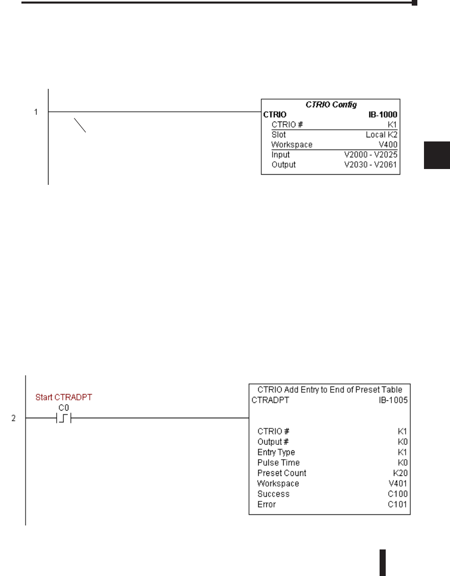
DL06 Micro PLC User Manual, 3rd Edition, Rev. D 5-333
1
2
3
4
5
6
7
8
9
10
11
12
13
14
A
B
C
D
CTRADPT Example
Rung 1: This sets up the CTRIO card in slot 2 of the local base. Each CTRIO in the system
will need a separate CTRIO I-box before any CTRxxxx I-boxes can be used for them. The
CTRIO has been configured to use V2000 through V2025 for its input data, and V2030
through V2061 for its output data.
Rung 2: This rung is a sample method for enabling the CTRADPT command. A C-bit is
used to allow the programmer to control the command from Data View for testing purposes.
Turning on C0 will cause the CTRADPT instruction to add a new preset to the preset table
for output #0 on the CTRIO in slot 2. The new preset will be a command to RESET (entry
type K1=reset), pulse time is left at zero as the reset type does not use this, and the count at
which it will reset will be 20.
Operating procedure for this example code is to load the CTRADPT_ex1.cwb file to your
CTRIO, then enter the code shown here, change to RUN mode, enable output #0 by turning
on C2 in Data View, turn encoder on CTRIO to value above 10 and output #0 light will
come on and stay on for all counts past 10. Now reset the counter with C1, enable C0 to
execute CTRADPT command to add a reset for output #0 at a count of 20, turn on C2 to
enable output #0, then turn encoder to value of 10+ (output #0 should turn on) and then
continue on to count of 20+ (output #0 should turn off).
Chapter 5: Intelligent Box (IBox) Instructions
1
2
3
4
5
6
7
8
9
10
11
12
13
14
a
B
c
d
(example continued on next page)
Permissive contacts or input logic cannot
be used with this instruction
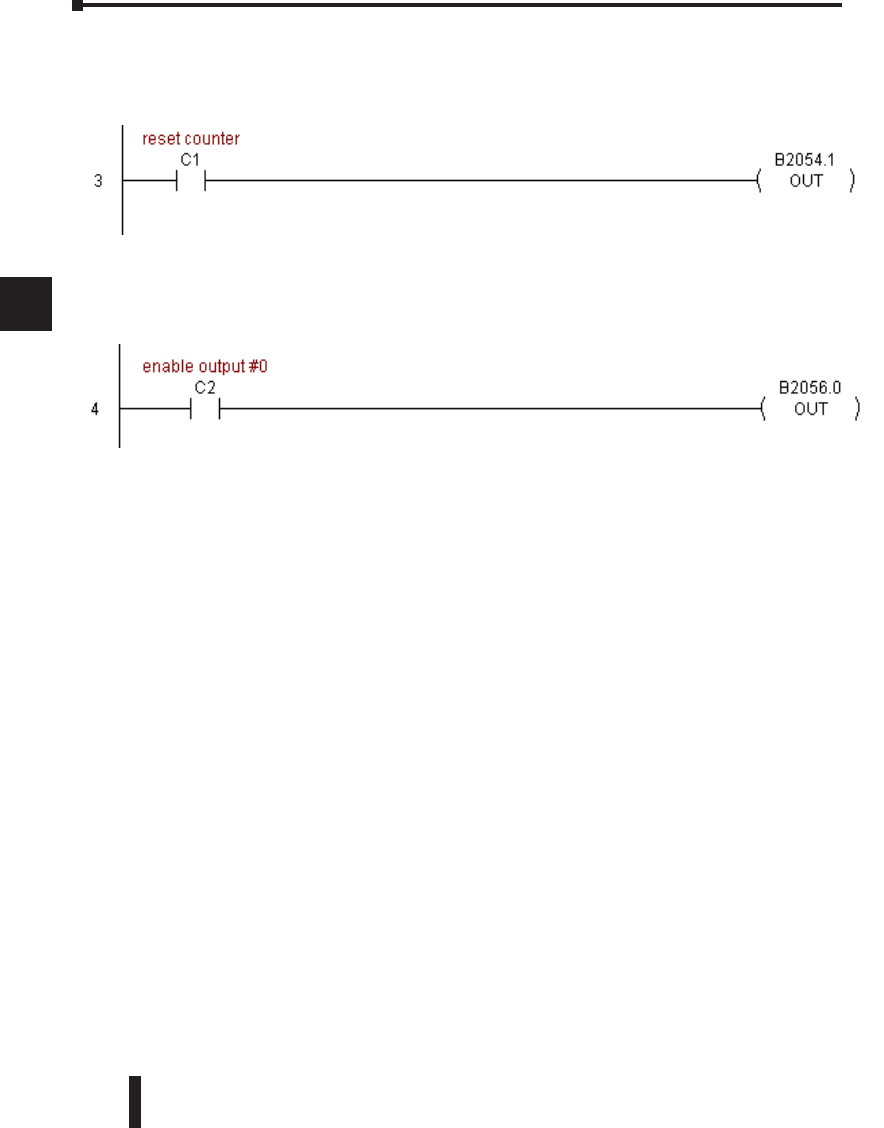
DL06 Micro PLC User Manual, 3rd Edition, Rev. D
5-334
1
2
3
4
5
6
7
8
9
10
11
12
13
14
A
B
C
D
CTRADPT Example (cont’d)
Rung 3: This rung allows the programmer to reset the counter from the ladder logic.
Rung 4: This rung allows the operator to enable output #0 from the ladder code.
Chapter 5: Intelligent Box (IBox) Instructions
1
2
3
4
5
6
7
8
9
10
11
12
13
14
a
B
c
d
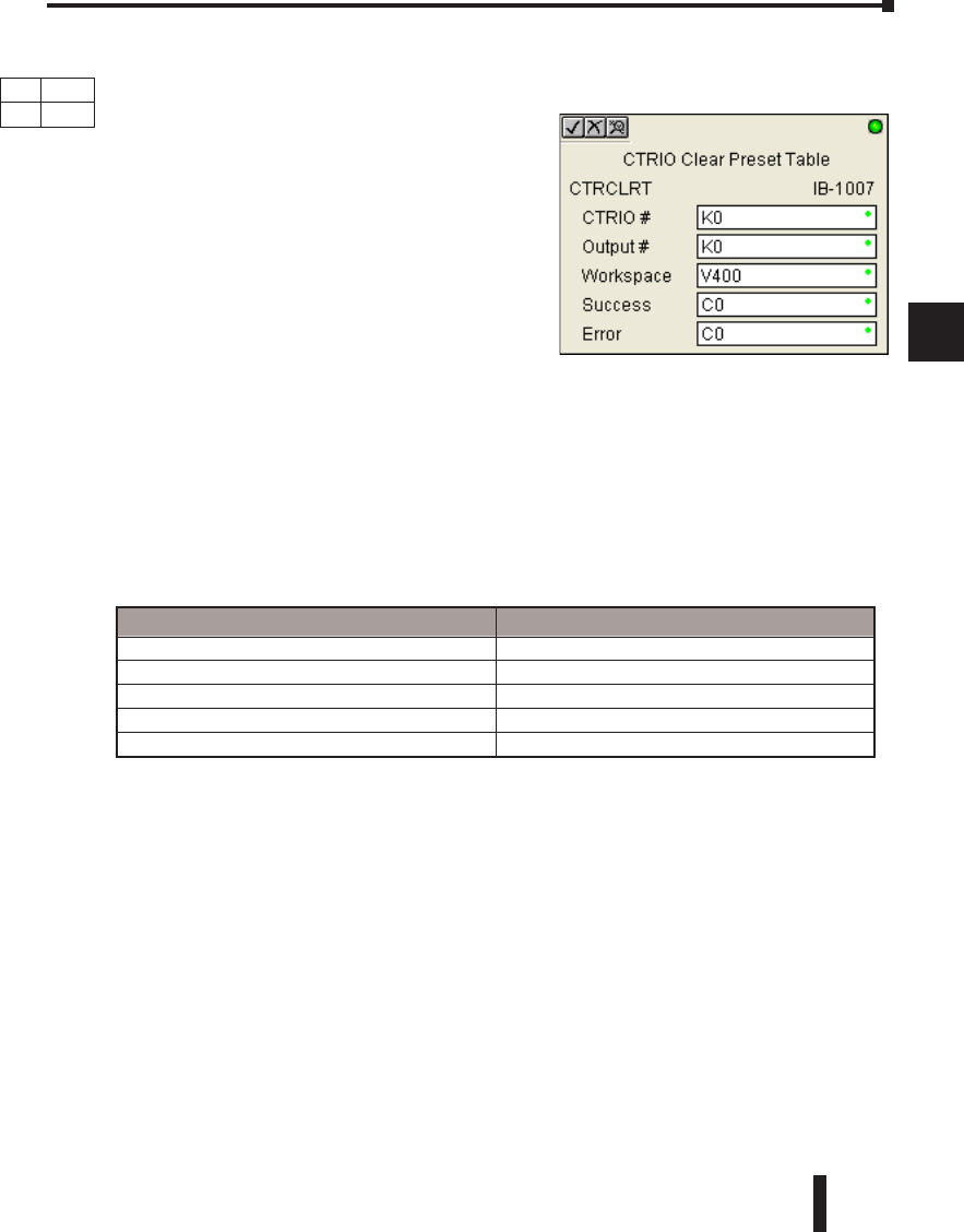
DL06 Micro PLC User Manual, 3rd Edition, Rev. D 5-335
1
2
3
4
5
6
7
8
9
10
11
12
13
14
A
B
C
D
CTRIO Clear Preset Table (CTRCLRT) (IB-1007)
CTRIO Clear Preset Table will clear the RAM based Preset Table on a leading edge
transition to this IBox. This IBox will take more than
1 PLC scan to execute. Either the Success or Error
bit will turn on when the command is complete. If
the Error Bit is on, you can use the CTRIO Read
Error Code (CTRRDER) IBox to get extended error
information.
The Workspace register is for internal use by this
IBox instruction and MUST NOT be used anywhere
else in your program.
CTRCLRT Parameters
• CTRIO#: specifies a specific CTRIO module based on a user defined number (see CTRIO Config)
• Output#: specifies a CTRIO output to be used by the instruction
• Workspace: specifies a V-memory location that will be used by the instruction
• Success: specifies a bit that will turn on once the instruction has successfully completed
• Error: specifies a bit that will turn on if the instruction does not complete successfully
Chapter 5: Intelligent Box (IBox) Instructions
1
2
3
4
5
6
7
8
9
10
11
12
13
14
a
B
c
d
DS Used
HPP N/A
Parameter DL06 Range
CTRIO# K K0-255
Output# K K0-3
Workspace V See DL06 V-memory map - Data Words
Success X,Y,C,GX,GY,B See DL06 V-memory map
Error X,Y,C,GX,GY,B See DL06 V-memory map
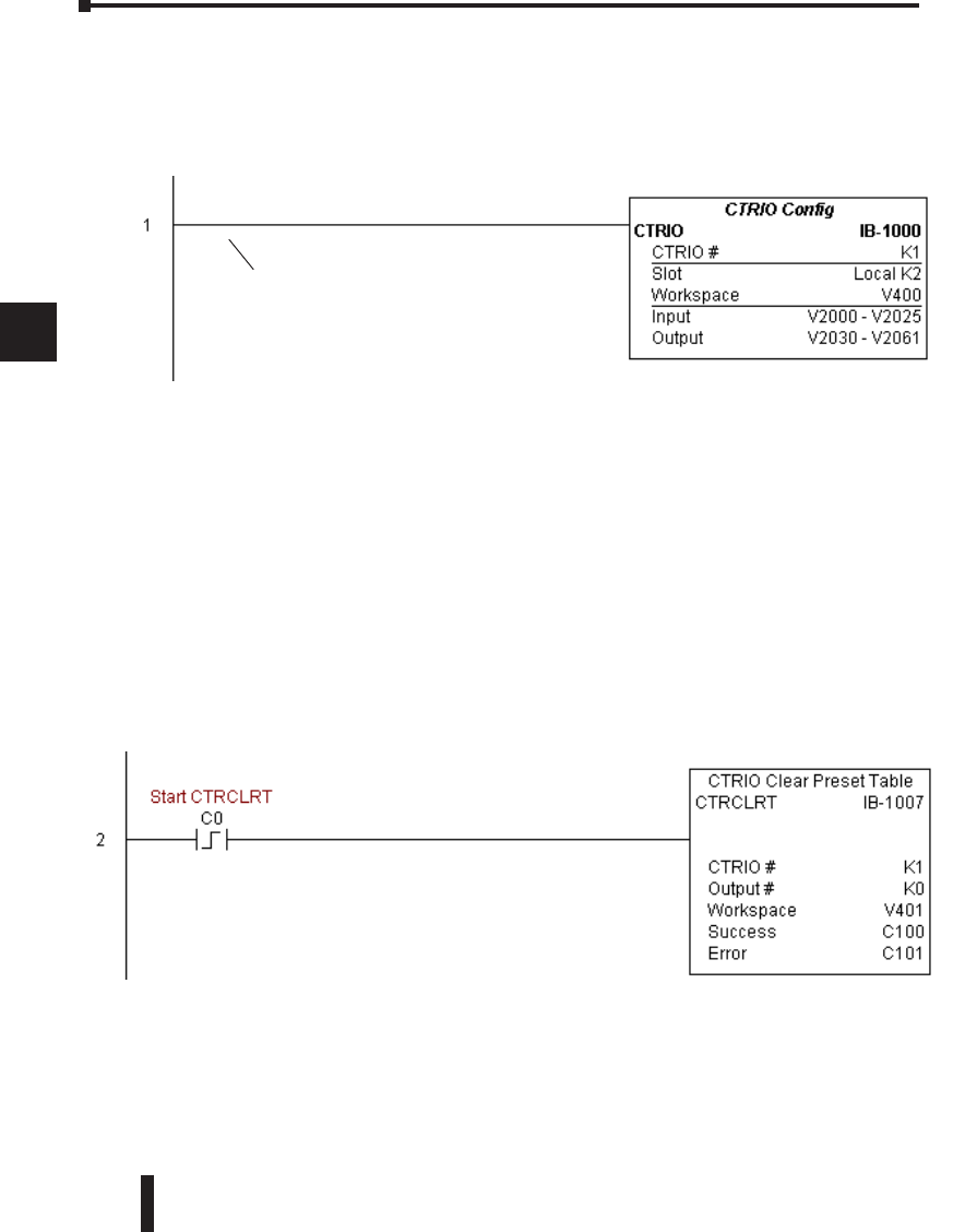
DL06 Micro PLC User Manual, 3rd Edition, Rev. D
5-336
1
2
3
4
5
6
7
8
9
10
11
12
13
14
A
B
C
D
CTRCLRT Example
Rung 1: This sets up the CTRIO card in slot 2 of the local base. Each CTRIO in the system
will need a separate CTRIO I-box before any CTRxxxx I-boxes can be used for them. The
CTRIO has been configured to use V2000 through V2025 for its input data, and V2030
through V2061 for its output data.
Rung 2: This rung is a sample method for enabling the CTRCLRT command. A C-bit is
used to allow the programmer to control the command from Data View for testing purposes.
Turning on C0 will cause the CTRCLRT instruction to clear the preset table for output #0
on the CTRIO in slot 2.
Operating procedure for this example code is to load the CTRCLRT_ex1.cwb file to your
CTRIO, then enter the code shown here, change to RUN mode, enable output #0 by turning
on C2 in Data View, turn encoder on CTRIO to value above 10 and output #0 light will
come on and stay on until a count of 20 is reached, where it will turn off. Now reset the
counter with C1, enable C0 to execute CTRCLRT command to clear the preset table, turn
on C2 to enable output #0, then turn encoder to value of 10+ (output #0 should NOT turn
on).
Chapter 5: Intelligent Box (IBox) Instructions
1
2
3
4
5
6
7
8
9
10
11
12
13
14
a
B
c
d
(example continued on next page)
Permissive contacts or input logic cannot
be used with this instruction.
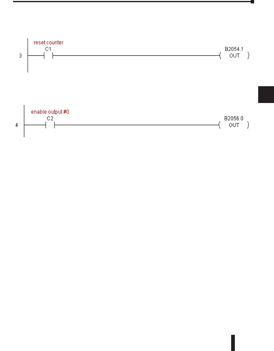
DL06 Micro PLC User Manual, 3rd Edition, Rev. D 5-337
1
2
3
4
5
6
7
8
9
10
11
12
13
14
A
B
C
D
CTRCLRT Example (cont’d)
Rung 3: This rung allows the programmer to reset the counter from the ladder logic.
Rung 4: This rung allows the operator to enable output #0 from the ladder code.
Chapter 5: Intelligent Box (IBox) Instructions
1
2
3
4
5
6
7
8
9
10
11
12
13
14
a
B
c
d
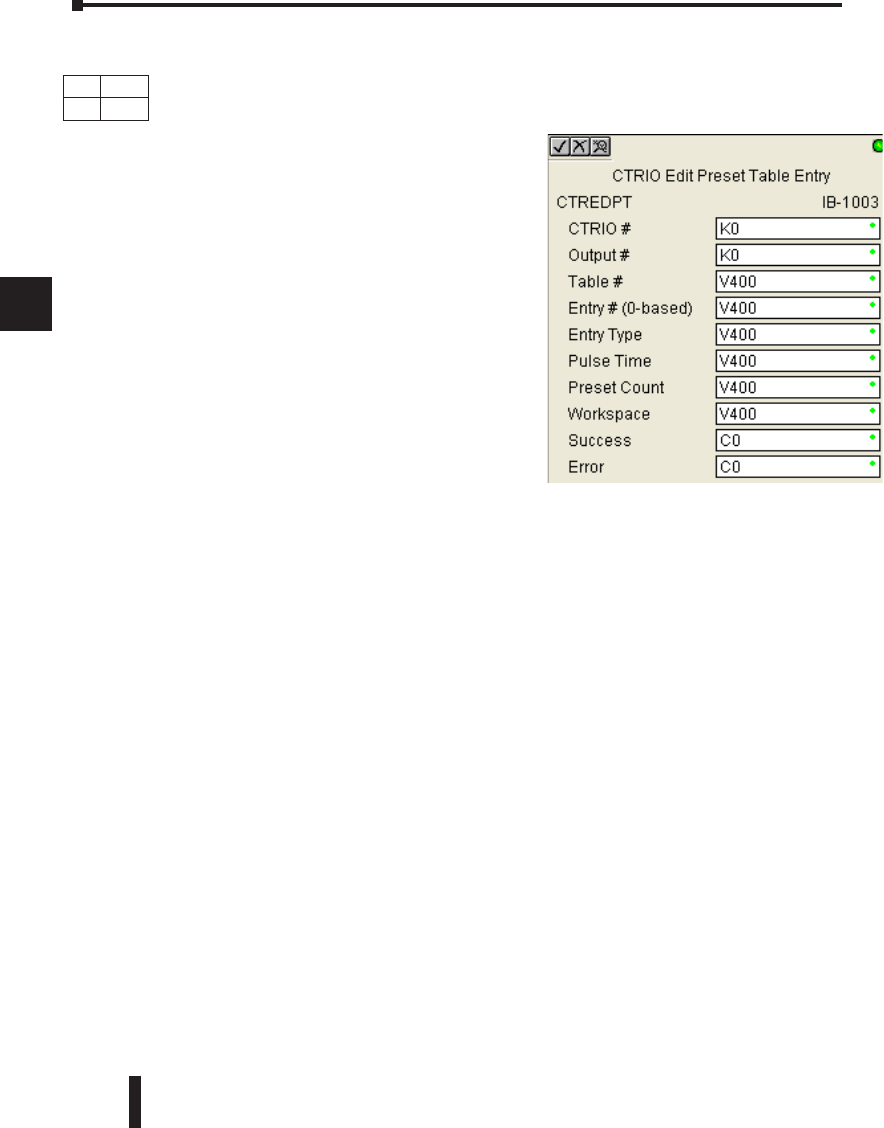
DL06 Micro PLC User Manual, 3rd Edition, Rev. D
5-338
1
2
3
4
5
6
7
8
9
10
11
12
13
14
A
B
C
D
CTRIO Edit Preset Table Entry (CTREDPT) (IB-1003)
CTRIO Edit Preset Table Entry, on a leading edge transition to this IBox, will edit a single
entry in a Preset Table on a specific CTRIO Output resource. This IBox is good if you are
editing more than one entry in a file at a time. If you wish to do just one edit and then reload
the table immediately, see the CTRIO Edit and
Reload Preset Table Entry (CTREDRL) IBox.
This IBox will take more than 1 PLC scan to
execute. Either the Success or Error bit will turn
on when the command is complete. If the Error
Bit is on, you can use the CTRIO Read Error
Code (CTRRDER) IBox to get extended error
information.
Entry Type:
K0: Set
K1: Reset
K2: Pulse On (uses Pulse Time)
K3: Pulse Off (uses Pulse Time)
K4: Toggle
K5: Reset Count
Note that the Pulse Time parameter is ignored by some Entry Types.
The Workspace register is for internal use by this IBox instruction and MUST NOT be used
anywhere else in your program.
CTREDPT Parameters
• CTRIO#: specifies a specific CTRIO module based on a user defined number (see CTRIO Config
Ibox)
• Output#: specifies a CTRIO output to be used by the instruction
• Table#: specifies the Table number of which an Entry is to be edited
• Entry#: specifies the Entry location in the Preset Table to be edited
• Entry Type: specifies the Entry Type to add during the edit
• Pulse Time: specifies a pulse time for the Pulse On and Pulse Off Entry Types
• Preset Count: specifies an initial count value to begin at after Reset
• Workspace: specifies a V-memory location that will be used by the instruction
• Success: specifies a bit that will turn on once the instruction has successfully completed
• Error: specifies a bit that will turn on if the instruction does not complete successfully
Chapter 5: Intelligent Box (IBox) Instructions
1
2
3
4
5
6
7
8
9
10
11
12
13
14
a
B
c
d
DS Used
HPP N/A
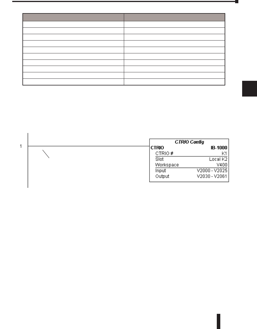
DL06 Micro PLC User Manual, 3rd Edition, Rev. D 5-339
1
2
3
4
5
6
7
8
9
10
11
12
13
14
A
B
C
D
CTREDPT Example
Rung 1: This sets up the CTRIO card in slot 2 of the local base. Each CTRIO in the system
will need a separate CTRIO I-box before any CTRxxxx I-boxes can be used for them. The
CTRIO has been configured to use V2000 through V2025 for its input data, and V2030
through V2061 for its output data.
Chapter 5: Intelligent Box (IBox) Instructions
1
2
3
4
5
6
7
8
9
10
11
12
13
14
a
B
c
d
Parameter DL06 Range
CTRIO# K K0-255
Output# K K0-3
Table# V,K K0-255; See DL06 V-memory map - Data Words
Entry# V,K K0-255; See DL06 V-memory map - Data Words
Entry Type V,K K0-5; See DL06 V-memory map - Data Words
Pulse Time V,K K0-65535; See DL06 V-memory map - Data Words
Preset Count V,K K0-2147434528; See DL06 V-memory map
Workspace V See DL06 V-memory map - Data Words
Success X,Y,C,GX,GY,B See DL06 V-memory map
Error X,Y,C,GX,GY,B See DL06 V-memory map
(example continued on next page)
Permissive contacts or input logic cannot
be used with this instruction
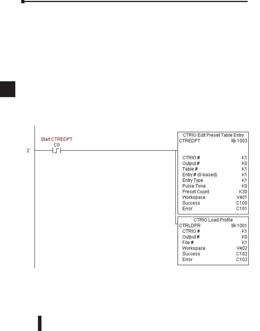
DL06 Micro PLC User Manual, 3rd Edition, Rev. D
5-340
1
2
3
4
5
6
7
8
9
10
11
12
13
14
A
B
C
D
CTREDPT Example (cont’d)
Rung 2: This rung is a sample method for enabling the CTREDPT command. A C-bit is
used to allow the programmer to control the command from Data View for testing purposes.
Turning on C0 will cause the CTREDPT instruction to change the second preset from a
reset at a count of 20 to a reset at a count of 30 for output #0 on the CTRIO in slot 2.
Operating procedure for this example code is to load the CTREDPT_ex1.cwb file to your
CTRIO, then enter the code shown here, change to RUN mode, enable output #0 by turning
on C2 in Data View, turn encoder on CTRIO to value above 10 and output #0 light will
come on and stay on until a count of 20 is reached, where it will turn off. Now reset the
counter with C1, enable C0 to execute CTREDPT command to change the second preset,
turn on C2 to enable output #0, then turn encoder to value of 10+ (output #0 should turn
on) and then continue past a count of 30 (output #0 should turn off).
Note that we must also reload the profile after changing the preset(s), this is why the
CTRLDPR command follows the CTREDPT command in this example.
Chapter 5: Intelligent Box (IBox) Instructions
1
2
3
4
5
6
7
8
9
10
11
12
13
14
a
B
c
d
(example continued on next page)
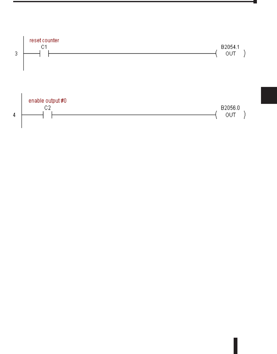
DL06 Micro PLC User Manual, 3rd Edition, Rev. D 5-341
1
2
3
4
5
6
7
8
9
10
11
12
13
14
A
B
C
D
CTREDPT Example (cont’d)
Rung 3: This rung allows the programmer to reset the counter from the ladder logic.
Rung 4: This rung allows the operator to enable output #0 from the ladder code.
Chapter 5: Intelligent Box (IBox) Instructions
1
2
3
4
5
6
7
8
9
10
11
12
13
14
a
B
c
d
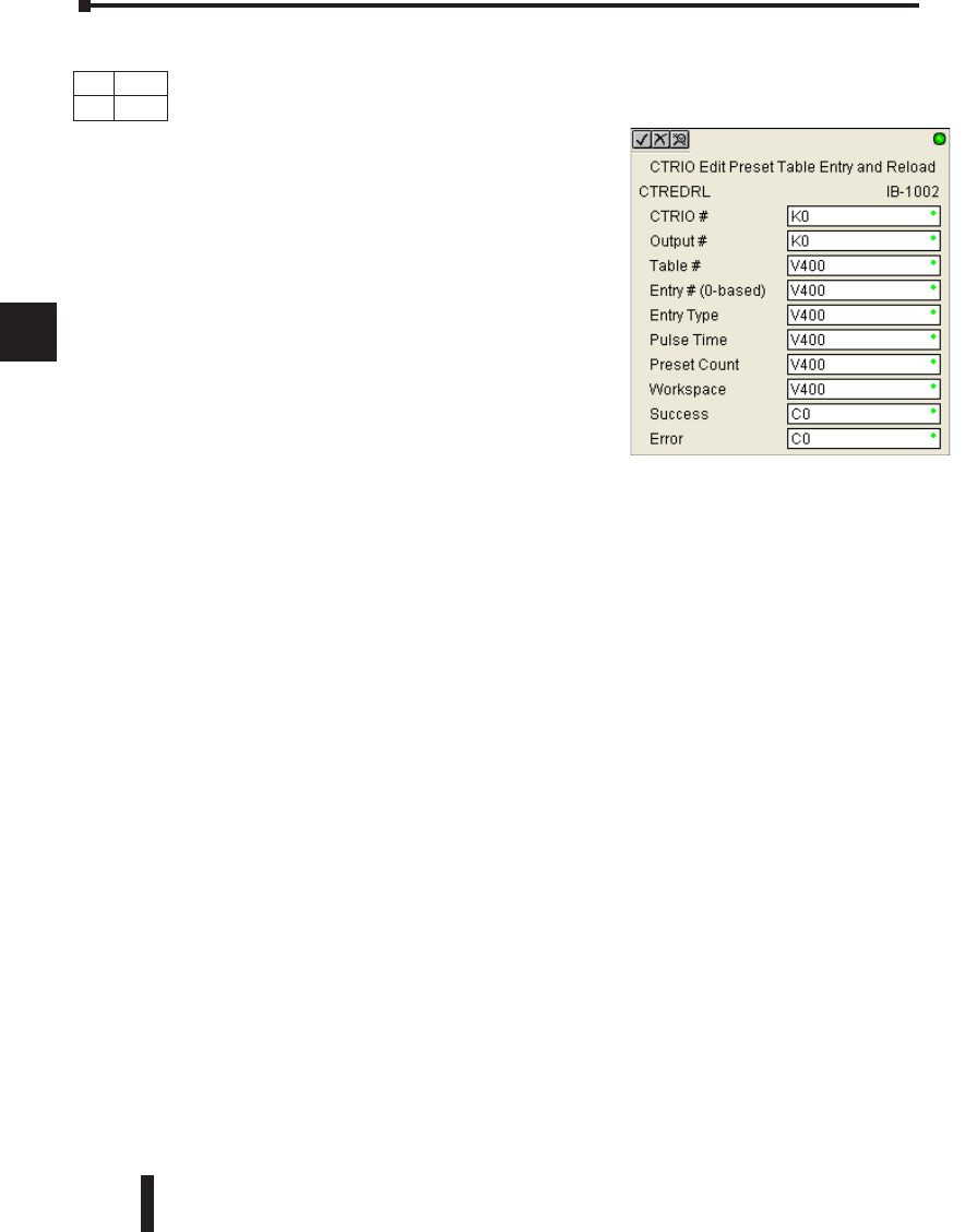
DL06 Micro PLC User Manual, 3rd Edition, Rev. D
5-342
1
2
3
4
5
6
7
8
9
10
11
12
13
14
A
B
C
D
CTRIO Edit Preset Table Entry and Reload (CTREDRL) (IB-1002)
CTRIO Edit Preset Table Entry and Reload, on a leading edge transition to this IBox,
will perform this dual operation to a CTRIO Output resource in one CTRIO command.
This IBox will take more than 1 PLC scan to
execute. Either the Success or Error bit will
turn on when the command is complete. If the
Error Bit is on, you can use the CTRIO Read
Error Code (CTRRDER) IBox to get extended error
information.
Entry Type:
K0: Set
K1: Reset
K2: Pulse On (uses Pulse Time)
K3: Pulse Off (uses Pulse Time)
K4: Toggle
K5: Reset Count
Note that the Pulse Time parameter is ignored by some Entry Types.
The Workspace register is for internal use by this IBox instruction and MUST NOT be used
anywhere else in your program.
CTREDRL Parameters
• CTRIO#: specifies a specific CTRIO module based on a user defined number (see CTRIO Config
Ibox)
• Output#: specifies a CTRIO output to be used by the instruction
• Table#: specifies the Table number of which an Entry is to be edited
• Entry#: specifies the Entry location in the Preset Table to be edited
• Entry Type: specifies the Entry Type to add during the edit
• Pulse Time: specifies a pulse time for the Pulse On and Pulse Off Entry Types
• Preset Count: specifies an initial count value to begin at after Reset
• Workspace: specifies a V-memory location that will be used by the instruction
• Success: specifies a bit that will turn on once the instruction has successfully completed
• Error: specifies a bit that will turn on if the instruction does not complete successfully
Chapter 5: Intelligent Box (IBox) Instructions
1
2
3
4
5
6
7
8
9
10
11
12
13
14
a
B
c
d
DS Used
HPP N/A
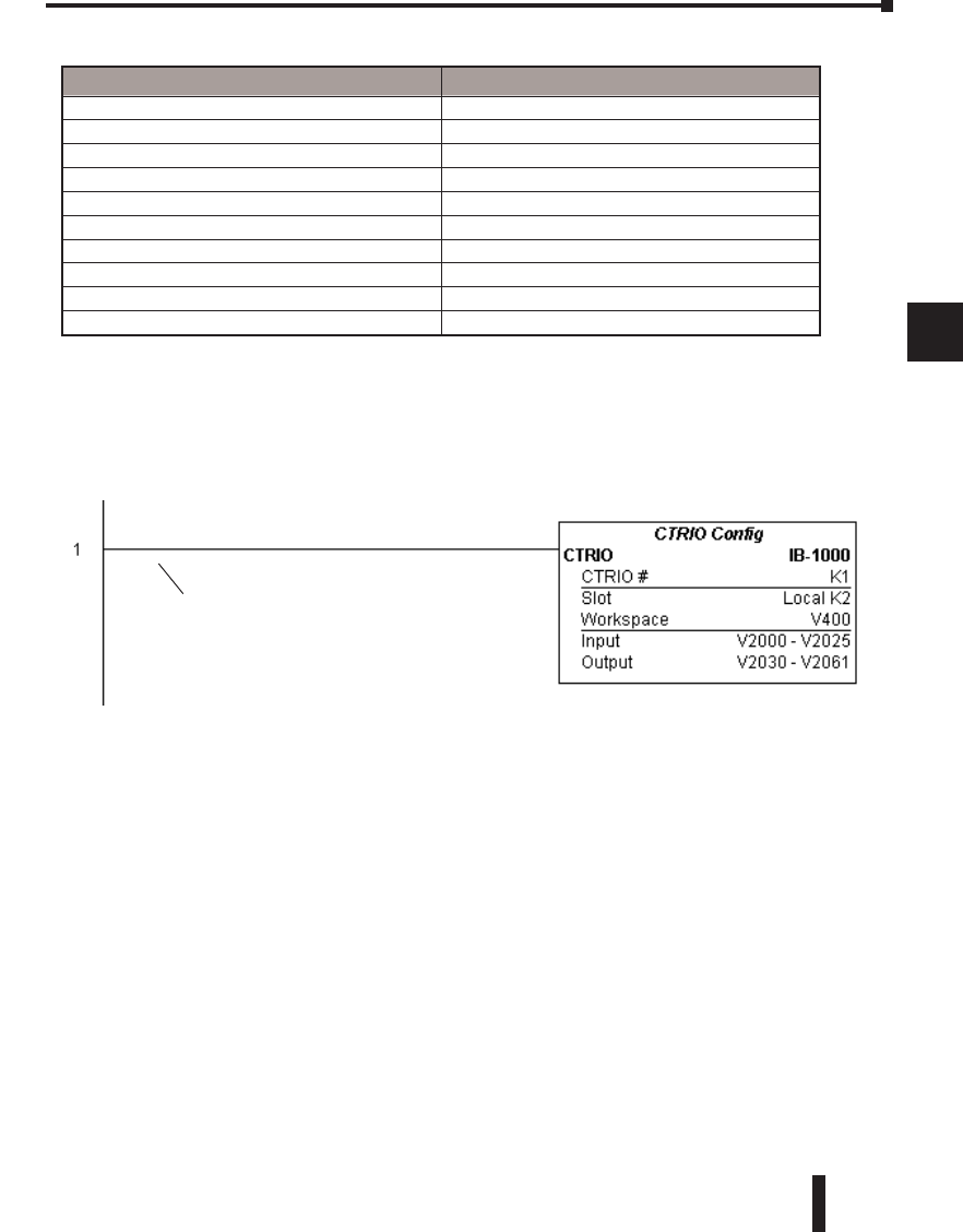
DL06 Micro PLC User Manual, 3rd Edition, Rev. D 5-343
1
2
3
4
5
6
7
8
9
10
11
12
13
14
A
B
C
D
CTREDRL Example
Rung 1: This sets up the CTRIO card in slot 2 of the local base. Each CTRIO in the system
will need a separate CTRIO I-box before any CTRxxxx I-boxes can be used for them. The
CTRIO has been configured to use V2000 through V2025 for its input data, and V2030
through V2061 for its output data.
Chapter 5: Intelligent Box (IBox) Instructions
1
2
3
4
5
6
7
8
9
10
11
12
13
14
a
B
c
d
Parameter DL06 Range
CTRIO# K K0-255
Output# K K0-3
Table# V,K K0-255; See DL06 V-memory map - Data Words
Entry# V,K K0-255; See DL06 V-memory map - Data Words
Entry Type V,K K0-5; See DL06 V-memory map - Data Words
Pulse Time V,K K0-65535; See DL06 V-memory map - Data Words
Preset Count V,K K0-2147434528; See DL06 V-memory map
Workspace V See DL06 V-memory map - Data Words
Success X,Y,C,GX,GY,B See DL06 V-memory map
Error X,Y,C,GX,GY,B See DL06 V-memory map
(example continued on next page)
Permissive contacts or input logic cannot
be used with this instruction
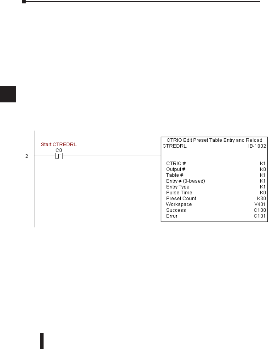
DL06 Micro PLC User Manual, 3rd Edition, Rev. D
5-344
1
2
3
4
5
6
7
8
9
10
11
12
13
14
A
B
C
D
CTREDRL Example (cont’d)
Rung 2: This rung is a sample method for enabling the CTREDRL command. A C-bit is
used to allow the programmer to control the command from Data View for testing purposes.
Turning on C0 will cause the CTREDRL instruction to change the second preset in file 1
from a reset at a value of 20 to a reset at a value of 30.
Operating procedure for this example code is to load the CTREDRL_ex1.cwb file to your
CTRIO, then enter the code shown here, change to RUN mode, enable output #0 by
turning on C2 in Data View, turn encoder on CTRIO to value above 10 and output #0
light will come on, continue to a count above 20 and the output #0 light will turn off. Now
reset the counter with C1, enable C0 to execute CTREDRL command to change the second
preset count value to 30, then turn encoder to value of 10+ (output #0 should turn on) and
continue on to a value of 30+ and the output #0 light will turn off.
Note that it is not necessary to reload this file separately, however, the command can only
change one value at a time.
Chapter 5: Intelligent Box (IBox) Instructions
1
2
3
4
5
6
7
8
9
10
11
12
13
14
a
B
c
d
(example continued on next page)
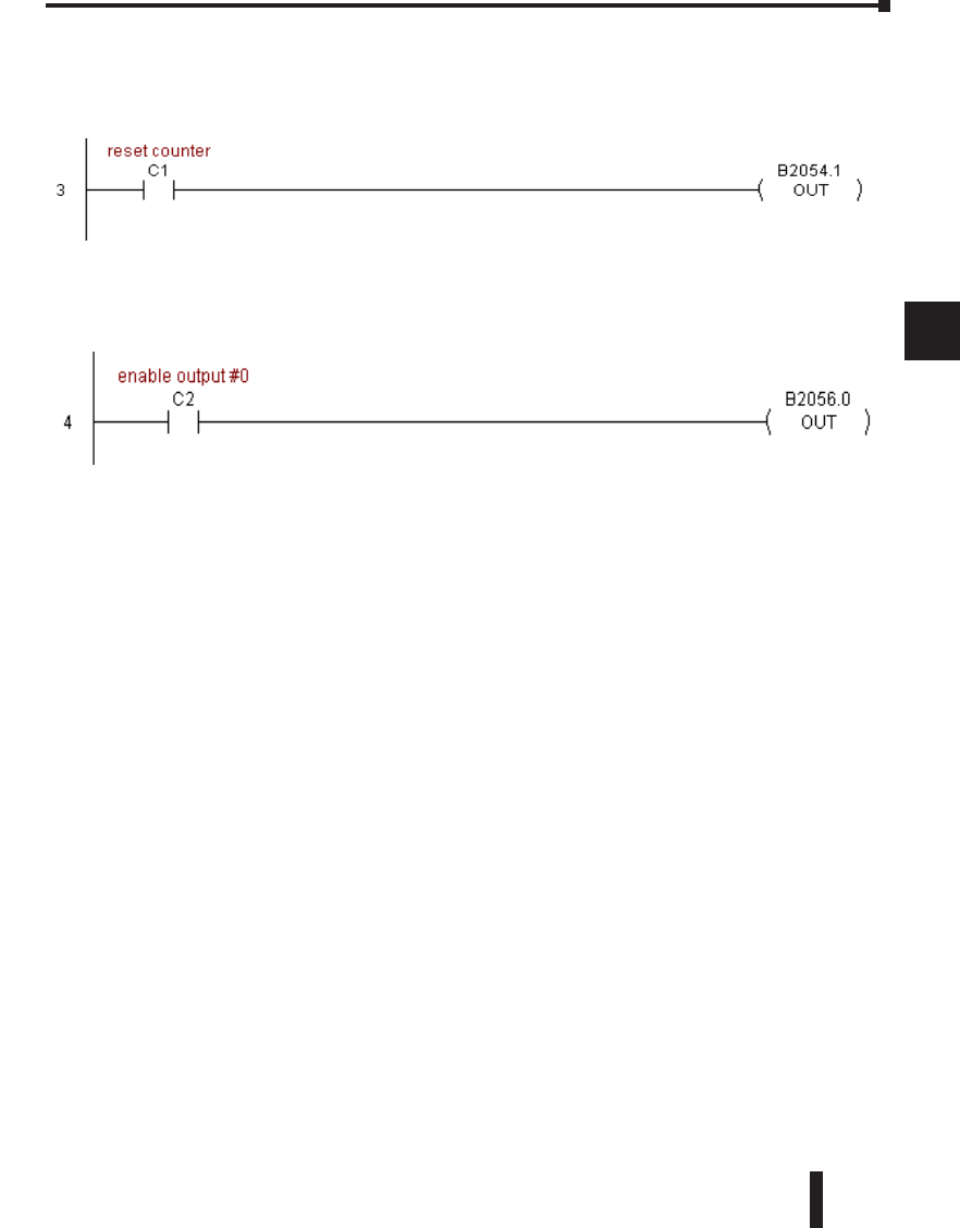
DL06 Micro PLC User Manual, 3rd Edition, Rev. D 5-345
1
2
3
4
5
6
7
8
9
10
11
12
13
14
A
B
C
D
CTREDRL Example (cont’d)
Rung 3: This rung allows the programmer to reset the counter from the ladder logic.
Rung 4: This rung allows the operator to enable output #0 from the ladder code.
Chapter 5: Intelligent Box (IBox) Instructions
1
2
3
4
5
6
7
8
9
10
11
12
13
14
a
B
c
d
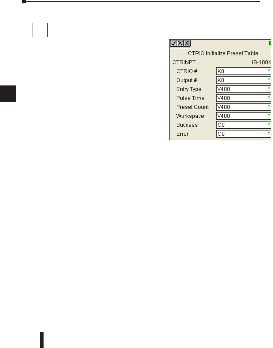
DL06 Micro PLC User Manual, 3rd Edition, Rev. D
5-346
1
2
3
4
5
6
7
8
9
10
11
12
13
14
A
B
C
D
CTRIO Initialize Preset Table (CTRINPT) (IB-1004)
CTRIO Initialize Preset Table, on a leading edge transition to this IBox, will create a single
entry Preset Table in memory but not as a file, on a specific CTRIO Output resource.
This IBox will take more than 1 PLC scan to
execute. Either the Success or Error bit will turn
on when the command is complete. If the Error
Bit is on, you can use the CTRIO Read Error
Code (CTRRDER) IBox to get extended error
information.
Entry Type:
K0: Set
K1: Reset
K2: Pulse On (uses Pulse Time)
K3: Pulse Off (uses Pulse Time)
K4: Toggle
K5: Reset Count
Note that the Pulse Time parameter is ignored by some Entry Types.
The Workspace register is for internal use by this IBox instruction and MUST NOT be used
anywhere else in your program.
CTRINPT Parameters
• CTRIO#: specifies a specific CTRIO module based on a user defined number (see CTRIO Config
Ibox)
• Output#: specifies a CTRIO output to be used by the instruction
• Entry Type: specifies the Entry Type to add during the edit
• Pulse Time: specifies a pulse time for the Pulse On and Pulse Off Entry Types
• Preset Count: specifies an initial count value to begin at after Reset
• Workspace: specifies a V-memory location that will be used by the instruction
• Success: specifies a bit that will turn on once the instruction has successfully completed
• Error: specifies a bit that will turn on if the instruction does not complete successfully
Chapter 5: Intelligent Box (IBox) Instructions
1
2
3
4
5
6
7
8
9
10
11
12
13
14
a
B
c
d
DS Used
HPP N/A
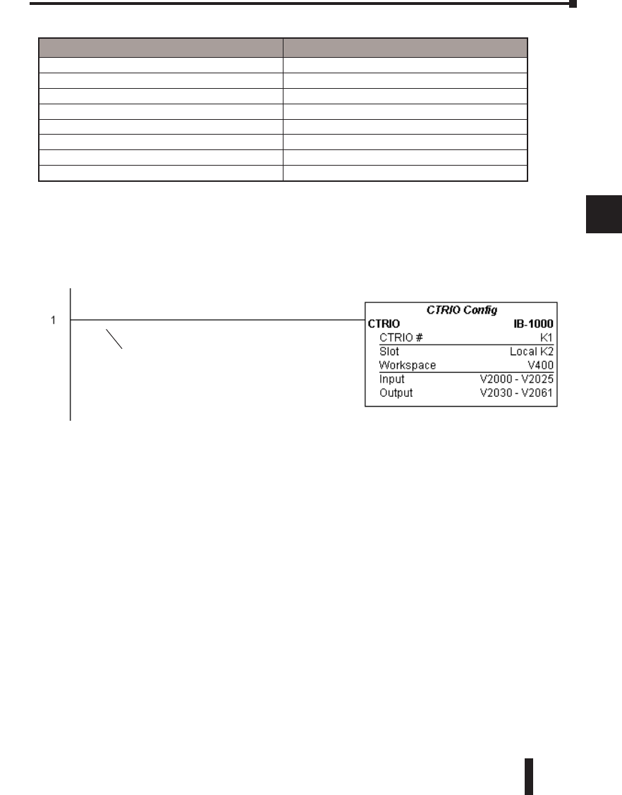
DL06 Micro PLC User Manual, 3rd Edition, Rev. D 5-347
1
2
3
4
5
6
7
8
9
10
11
12
13
14
A
B
C
D
CTRINPT Example
Rung 1: This sets up the CTRIO card in slot 2 of the local base. Each CTRIO in the system
will need a separate CTRIO I-box before any CTRxxxx I-boxes can be used for them. The
CTRIO has been configured to use V2000 through V2025 for its input data, and V2030
through V2061 for its output data.
Chapter 5: Intelligent Box (IBox) Instructions
1
2
3
4
5
6
7
8
9
10
11
12
13
14
a
B
c
d
Parameter DL06 Range
CTRIO# K K0-255
Output# K K0-3
Entry Type V,K K0-5; See DL06 V-memory map - Data Words
Pulse Time V,K K0-65535; See DL06 V-memory map - Data Words
Preset Count V,K K0-2147434528; See DL06 V-memory map
Workspace V See DL06 V-memory map - Data Words
Success X,Y,C,GX,GY,B See DL06 V-memory map
Error X,Y,C,GX,GY,B See DL06 V-memory map
(example continued on next page)
Permissive contacts or input logic cannot
be used with this instruction.
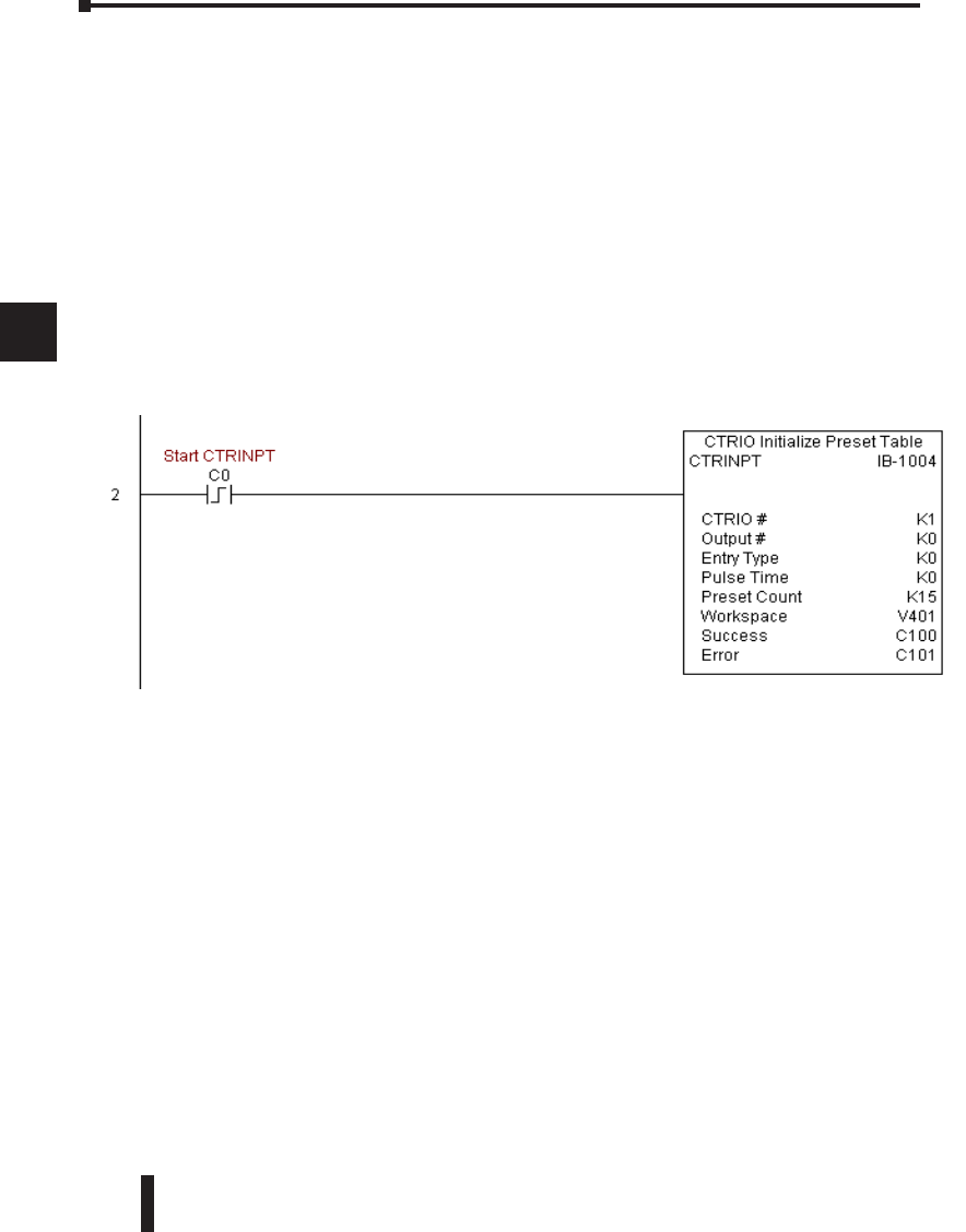
DL06 Micro PLC User Manual, 3rd Edition, Rev. D
5-348
1
2
3
4
5
6
7
8
9
10
11
12
13
14
A
B
C
D
CTRINPT Example (cont’d)
Rung 2: This rung is a sample method for enabling the CTRINPT command. A C-bit is used
to allow the programmer to control the command from Data View for testing purposes.
Turning on C0 will cause the CTRINPT instruction to create a single entry preset table, but
not as a file, and use it for the output #0. In this case the single preset will be a set at a count
of 15 for output #0.
Operating procedure for this example code is to load the CTRINPT_ex1.cwb file to your
CTRIO, then enter the code shown here, change to RUN mode, enable output #0 by turning
on C2 in Data View, turn encoder on CTRIO to value above 15 and output #0 light will
not come on. Now reset the counter with C1, enable C0 to execute CTRINPT command to
create a single preset table with a preset to set output #0 at a count of 15, then turn encoder
to value of 15+ (output #0 should turn on).
Chapter 5: Intelligent Box (IBox) Instructions
1
2
3
4
5
6
7
8
9
10
11
12
13
14
a
B
c
d
(example continued on next page)
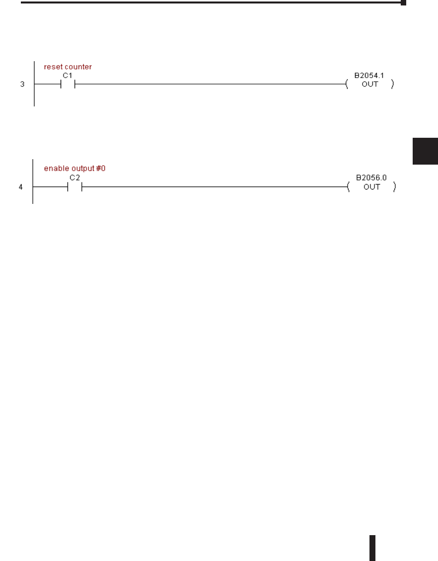
DL06 Micro PLC User Manual, 3rd Edition, Rev. D 5-349
1
2
3
4
5
6
7
8
9
10
11
12
13
14
A
B
C
D
CTRINPT Example (cont’d)
Rung 3: This rung allows the programmer to reset the counter from the ladder logic.
Rung 4: This rung allows the operator to enable output #0 from the ladder code.
Chapter 5: Intelligent Box (IBox) Instructions
1
2
3
4
5
6
7
8
9
10
11
12
13
14
a
B
c
d
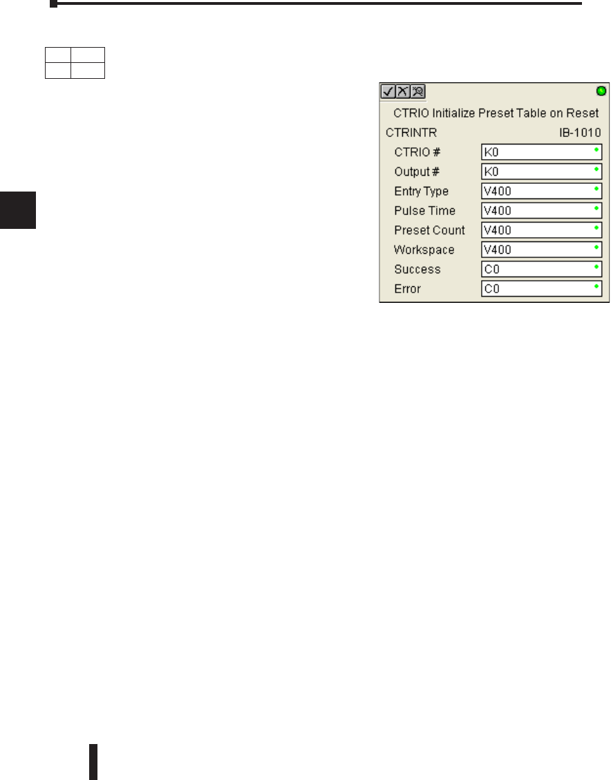
DL06 Micro PLC User Manual, 3rd Edition, Rev. D
5-350
1
2
3
4
5
6
7
8
9
10
11
12
13
14
A
B
C
D
CTRIO Initialize Preset Table (CTRINTR) (IB-1010)
CTRIO Initialize Preset Table, on a leading edge transition to this IBox, will create a single
entry Preset Table in memory but not as a file, on a specific CTRIO Output resource.
This IBox will take more than 1 PLC scan to
execute. Either the Success or Error bit will turn
on when the command is complete. If the Error
Bit is on, you can use the CTRIO Read Error
Code (CTRRDER) IBox to get extended error
information.
Entry Type:
K0: Set
K1: Reset
K2: Pulse On (uses Pulse Time)
K3: Pulse Off (uses Pulse Time)
K4: Toggle
K5: Reset Count
Note that the Pulse Time parameter is ignored by some Entry Types.
The Workspace register is for internal use by this IBox instruction and MUST NOT be used
anywhere else in your program.
CTRINTR Parameters
• CTRIO#: specifies a specific CTRIO module based on a user defined number (see CTRIO Config
Ibox)
• Output#: specifies a CTRIO output to be used by the instruction
• Entry Type: specifies the Entry Type to add during the edit
• Pulse Time: specifies a pulse time for the Pulse On and Pulse Off Entry Types
• Preset Count: specifies an initial count value to begin at after Reset
• Workspace: specifies a V-memory location that will be used by the instruction
• Success: specifies a bit that will turn on once the instruction has successfully completed
• Error: specifies a bit that will turn on if the instruction does not complete successfully
Chapter 5: Intelligent Box (IBox) Instructions
1
2
3
4
5
6
7
8
9
10
11
12
13
14
a
B
c
d
DS Used
HPP N/A
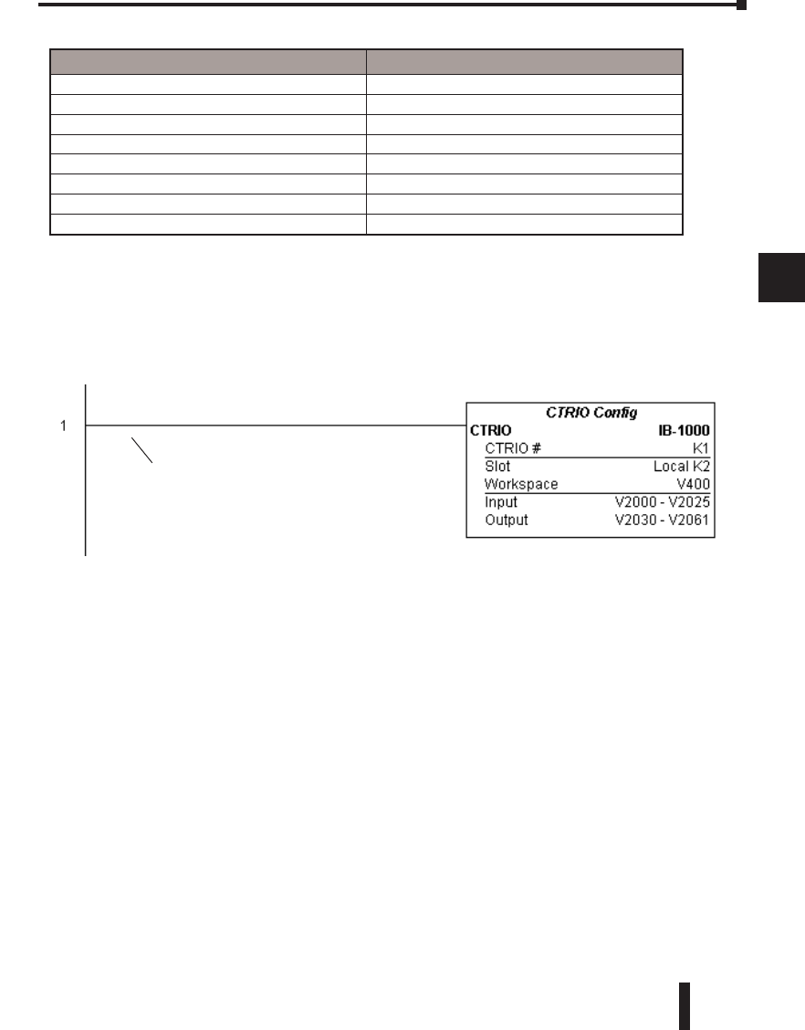
DL06 Micro PLC User Manual, 3rd Edition, Rev. D 5-351
1
2
3
4
5
6
7
8
9
10
11
12
13
14
A
B
C
D
CTRINTR Example
Rung 1: This sets up the CTRIO card in slot 2 of the local base. Each CTRIO in the system
will need a separate CTRIO I-box before any CTRxxxx I-boxes can be used for them. The
CTRIO has been configured to use V2000 through V2025 for its input data, and V2030
through V2061 for its output data.
Chapter 5: Intelligent Box (IBox) Instructions
1
2
3
4
5
6
7
8
9
10
11
12
13
14
a
B
c
d
Parameter DL06 Range
CTRIO# K K0-255
Output# K K0-3
Entry Type V,K K0-5; See DL06 V-memory map - Data Words
Pulse Time V,K K0-65535; See DL06 V-memory map - Data Words
Preset Count V,K K0-2147434528; See DL06 V-memory map
Workspace V See DL06 V-memory map - Data Words
Success X,Y,C,GX,GY,B See DL06 V-memory map
Error X,Y,C,GX,GY,B See DL06 V-memory map
(example continued on next page)
Permissive contacts or input logic cannot
be used with this instruction
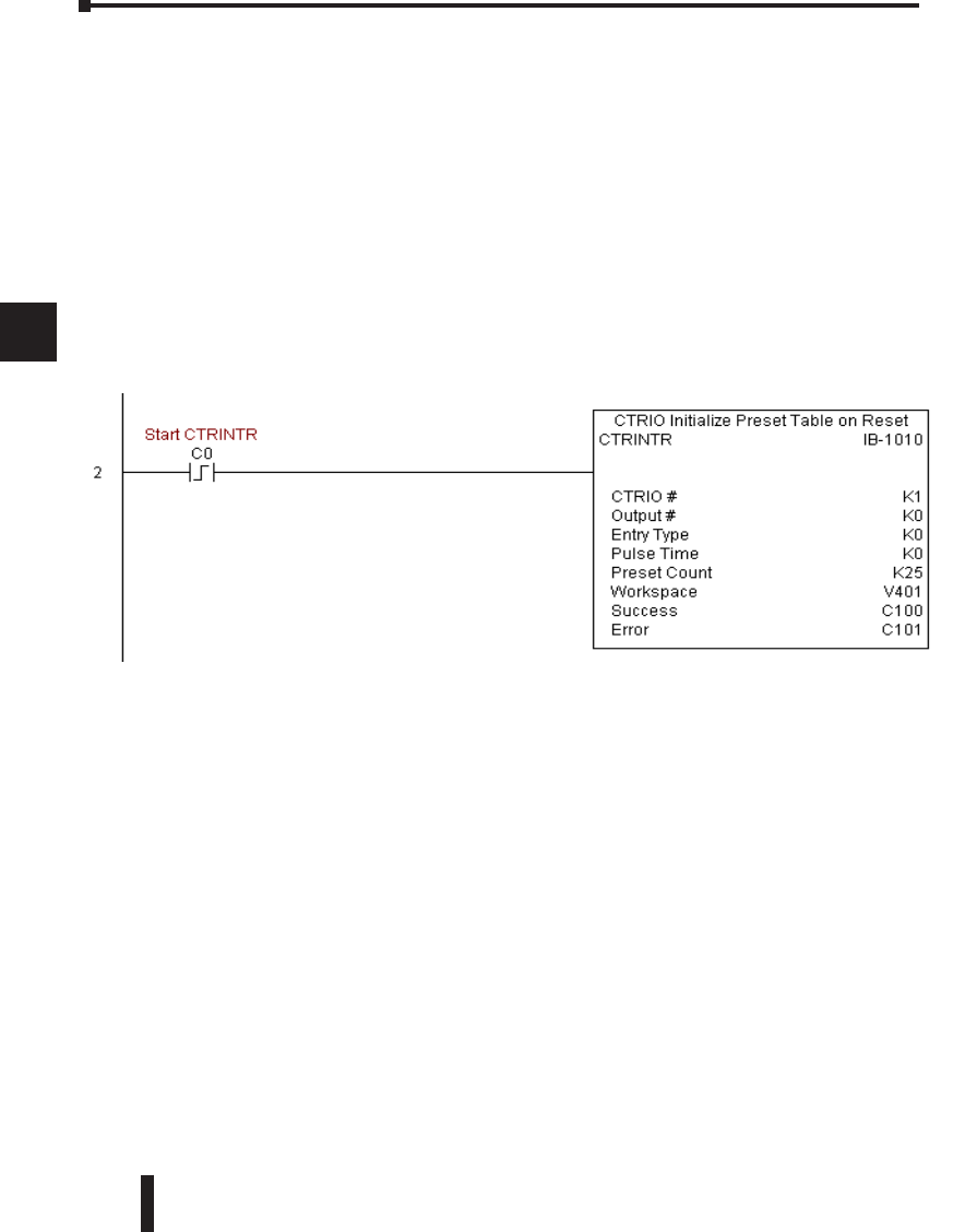
DL06 Micro PLC User Manual, 3rd Edition, Rev. D
5-352
1
2
3
4
5
6
7
8
9
10
11
12
13
14
A
B
C
D
CTRINTR Example (cont’d)
Rung 2: This rung is a sample method for enabling the CTRINTR command. A C-bit is
used to allow the programmer to control the command from Data View for testing purposes.
Turning on C0 will cause the CTRINTR instruction to create a single entry preset table, but
not as a file, and use it for output #0, the new preset will be loaded when the current count is
reset. In this case the single preset will be a set at a count of 25 for output #0.
Operating procedure for this example code is to load the CTRINTR_ex1.cwb file to your
CTRIO, then enter the code shown here, change to RUN mode, enable output #0 by turning
on C2 in Data View, turn encoder on CTRIO to value above 10 and output #0 light will
come on. Now turn on C0 to execute the CTRINTR command, reset the counter with C1,
then turn encoder to value of 25+ (output #0 should turn on).
Chapter 5: Intelligent Box (IBox) Instructions
1
2
3
4
5
6
7
8
9
10
11
12
13
14
a
B
c
d
(example continued on next page)
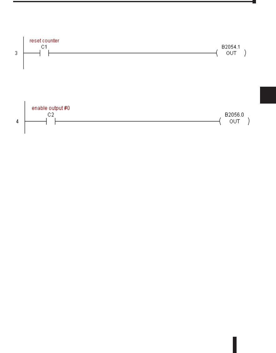
DL06 Micro PLC User Manual, 3rd Edition, Rev. D 5-353
1
2
3
4
5
6
7
8
9
10
11
12
13
14
A
B
C
D
CTRINTR Example (cont’d)
Rung 3: This rung allows the programmer to reset the counter from the ladder logic.
Rung 4: This rung allows the operator to enable output #0 from the ladder code.
Chapter 5: Intelligent Box (IBox) Instructions
1
2
3
4
5
6
7
8
9
10
11
12
13
14
a
B
c
d
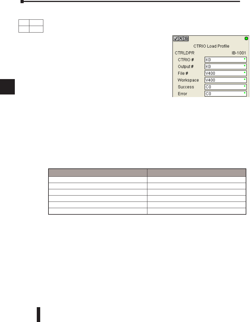
DL06 Micro PLC User Manual, 3rd Edition, Rev. D
5-354
1
2
3
4
5
6
7
8
9
10
11
12
13
14
A
B
C
D
CTRIO Load Profile (CTRLDPR) (IB-1001)
CTRIO Load Profile loads a CTRIO Profile File to a CTRIO Output resource on a leading
edge transition to this IBox. This IBox will take more than 1 PLC scan to execute. Either the
Success or Error bit will turn on when the command is
complete. If the Error Bit is on, you can use the CTRIO
Read Error Code (CTRRDER) IBox to get extended
error information.
The Workspace register is for internal use by this IBox
instruction and MUST NOT be used anywhere else in
your program.
CTRLDPR Parameters
• CTRIO#: specifies a specific CTRIO module based on a user defined number (see CTRIO Config)
• Output#: specifies a CTRIO output to be used by the instruction
• File#: specifies a CTRIO profile File number to be loaded
• Workspace: specifies a V-memory location that will be used by the instruction
• Success: specifies a bit that will turn on once the instruction has successfully completed
• Error: specifies a bit that will turn on if the instruction does not complete successfully
Chapter 5: Intelligent Box (IBox) Instructions
1
2
3
4
5
6
7
8
9
10
11
12
13
14
a
B
c
d
DS Used
HPP N/A
Parameter DL06 Range
CTRIO# K K0-255
Output# K K0-3
File# V,K K0-255; See DL06 V-memory map - Data Words
Workspace V See DL06 V-memory map - Data Words
Success X,Y,C,GX,GY,B See DL06 V-memory map
Error X,Y,C,GX,GY,B See DL06 V-memory map
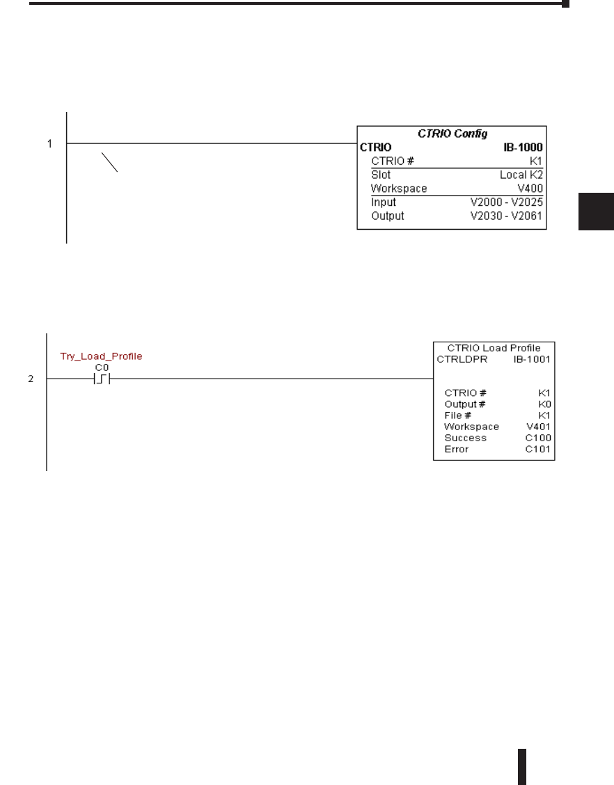
DL06 Micro PLC User Manual, 3rd Edition, Rev. D 5-355
1
2
3
4
5
6
7
8
9
10
11
12
13
14
A
B
C
D
CTRLDPR Example
Rung 1: This sets up the CTRIO card in slot 2 of the local base. Each CTRIO in the system
will need a separate CTRIO I-box before any CTRxxxx I-boxes can be used for them. The
CTRIO has been configured to use V2000 through V2025 for its input data, and V2030
through V2061 for its output data.
Rung 2: This CTRIO Load Profile IBox will load File #1 into the working memory of
Output 0 in CTRIO #1. This example program requires that you load CTRLDPR_IBox.cwb
into your Hx-CTRIO(2) module.
Chapter 5: Intelligent Box (IBox) Instructions
1
2
3
4
5
6
7
8
9
10
11
12
13
14
a
B
c
d
(example continued on next page)
Permissive contacts or input logic cannot
be used with this instruction.

DL06 Micro PLC User Manual, 3rd Edition, Rev. D
5-356
1
2
3
4
5
6
7
8
9
10
11
12
13
14
A
B
C
D
CTRLDPR Example (cont’d)
Rung 3: If the file is successfully loaded, set Profile_Loaded.
Chapter 5: Intelligent Box (IBox) Instructions
1
2
3
4
5
6
7
8
9
10
11
12
13
14
a
B
c
d
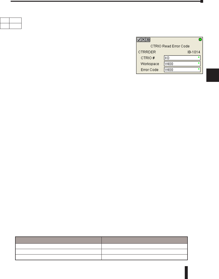
DL06 Micro PLC User Manual, 3rd Edition, Rev. D 5-357
1
2
3
4
5
6
7
8
9
10
11
12
13
14
A
B
C
D
CTRIO Read Error (CTRRDER) (IB-1014)
CTRIO Read Error Code will get the decimal error code value from the CTRIO module
(listed below) and place it into the given Error Code register, on a leading edge transition to
the IBox
Since the Error Code in the CTRIO is only maintained
until another CTRIO command is given, you must use
this instruction immediately after the CTRIO IBox that
reports an error via its Error bit parameter.
The Workspace register is for internal use by this IBox
instruction and MUST NOT be used anywhere else in
your program.
Error Codes:
0: No Error
100: Specified command code is unknown or unsupported
101: File number not found in the file system
102: File type is incorrect for specified output function
103: Profile type is unknown
104: Specified input is not configured as a limit on this output
105: Specified limit input edge is out of range
106: Specified input function is unconfigured or invalid
107: Specified input function number is out of range
108: Specified preset function is invalid
109: Preset table is full
110: Specified Table entry is out of range
111: Specified register number is out of range
112: Specified register is an unconfigured input or output
2001: Error reading Error Code - cannot access CTRIO via ERM
CTRRDER Parameters
• CTRIO#: specifies a specific CTRIO module based on a user defined number (see CTRIO Config)
• Workspace: specifies a V-memory location that will be used by the instruction
• Error Code: specifies the location where the Error Code will be written
Chapter 5: Intelligent Box (IBox) Instructions
1
2
3
4
5
6
7
8
9
10
11
12
13
14
a
B
c
d
DS Used
HPP N/A
Parameter DL06 Range
CTRIO# K K0-255
Workspace V See DL06 V-memory map - Data Words
Error Code V See DL06 V-memory map - Data Words
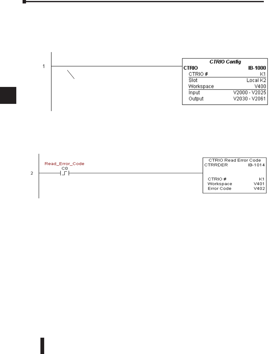
DL06 Micro PLC User Manual, 3rd Edition, Rev. D
5-358
1
2
3
4
5
6
7
8
9
10
11
12
13
14
A
B
C
D
CTRRDER Example
Rung 1: This sets up the CTRIO card in slot 2 of the local base. Each CTRIO in the system
will need a separate CTRIO I-box before any CTRxxxx I-boxes can be used for them. The
CTRIO has been configured to use V2000 through V2025 for its input data, and V2030
through V2061 for its output data.
Rung 2: This CTRIO Read Error Code IBox will read the Extended Error information from
CTRIO #1. This example program requires that you load CTRRDER_IBox.cwb into your
Hx-CTRIO(2) module.
Chapter 5: Intelligent Box (IBox) Instructions
1
2
3
4
5
6
7
8
9
10
11
12
13
14
a
B
c
d
Permissive contacts or input logic cannot
be used with this instruction
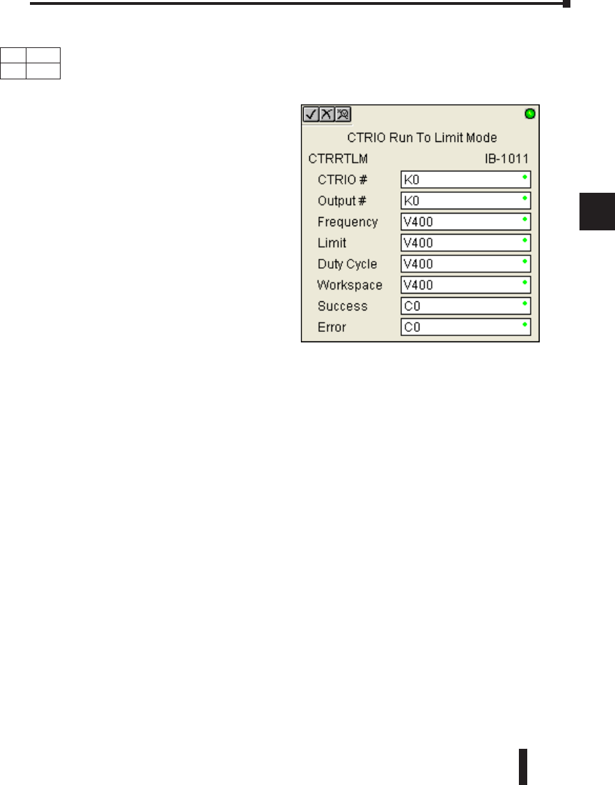
DL06 Micro PLC User Manual, 3rd Edition, Rev. D 5-359
1
2
3
4
5
6
7
8
9
10
11
12
13
14
A
B
C
D
CTRIO Run to Limit Mode (CTRRTLM) (IB-1011)
CTRIO Run To Limit Mode, on a leading edge transition to this IBox, loads the Run to
Limit command and given parameters on a specific Output resource. The CTRIO’s Input(s)
must be configured as Limit(s) for this function to work.
Valid Hexadecimal Limit Values:
K00 - Rising Edge of Ch1/C
K10 - Falling Edge of Ch1/C
K20 - Both Edges of Ch1/C
K01 - Rising Edge of Ch1/D
K11 - Falling Edge of Ch1/D
K21 - Both Edges of Ch1/D
K02 - Rising Edge of Ch2/C
K12 - Falling Edge of Ch2/C
K22 - Both Edges of Ch2/C
K03 - Rising Edge of Ch2/D
K13 - Falling Edge of Ch2/D
K23 - Both Edges of Ch2/D
This IBox will take more than 1 PLC scan to execute. Either the Success or Error bit will
turn on when the command is complete. If the Error Bit is on, you can use the CTRIO Read
Error Code (CTRRDER) IBox to get extended error information.
The Workspace register is for internal use by this IBox instruction and MUST NOT be used
anywhere else in your program.
CTRRTLM Parameters
• CTRIO#: specifies a specific CTRIO module based on a user defined number (see CTRIO Config
Ibox)
• Output#: specifies a CTRIO output to be used by the instruction
• Frequency: specifies the output pulse rate (H0-CTRIO: 20Hz - 25KHz / H0-CTRIO2: 20Hz -
250 KHz)
• Limit: the CTRIO’s Input(s) must be configured as Limit(s) for this function to operate
• Duty Cycle: specifies the % of on time versus off time. This is a hex number. Default of 0 is 50%,
also entering 50 will yield 50%. 50% duty cycle is defined as on half the time and off half the time
• Workspace: specifies a V-memory location that will be used by the instruction
• Success: specifies a bit that will turn on once the instruction has successfully completed
• Error: specifies a bit that will turn on if the instruction does not complete successfully
Chapter 5: Intelligent Box (IBox) Instructions
1
2
3
4
5
6
7
8
9
10
11
12
13
14
a
B
c
d
DS Used
HPP N/A
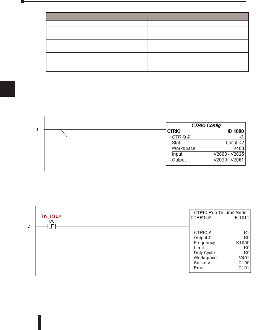
DL06 Micro PLC User Manual, 3rd Edition, Rev. D
5-360
1
2
3
4
5
6
7
8
9
10
11
12
13
14
A
B
C
D
CTRRTLM Example
Rung 1: This sets up the CTRIO card in slot 2 of the local base. Each CTRIO in the system
will need a separate CTRIO I-box before any CTRxxxx I-boxes can be used for them. The
CTRIO has been configured to use V2000 through V2025 for its input data, and V2030
through V2061 for its output data.
Rung 2: This CTRIO Run To Limit Mode IBox sets up Output #0 in CTRIO #1 to output
pulses at a Frequency of 1000 Hz until Llimit #0 comes on. This example program requires
that you load CTRRTLM_IBox.cwb into your Hx-CTRIO(2) module.
Chapter 5: Intelligent Box (IBox) Instructions
1
2
3
4
5
6
7
8
9
10
11
12
13
14
a
B
c
d
Parameter DL06 Range
CTRIO# K K0-255
Output# K K0-3
Frequency V,K K20-20000; See DL06 V-memory map - Data Words
Limit V,K K0-FF; See DL06 V-memory map - Data Words
Duty Cycle V,K K0-99; See DL06 V-memory map - Data Words
Workspace V See DL06 V-memory map - Data Words
Success X,Y,C,GX,GY,B See DL06 V-memory map
Error X,Y,C,GX,GY,B See DL06 V-memory map
(example continued on next page)
Permissive contacts or input logic cannot
be used with this instruction.
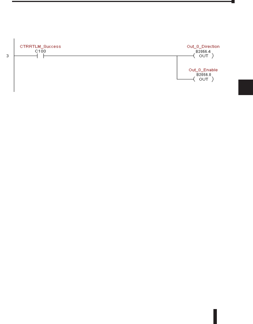
DL06 Micro PLC User Manual, 3rd Edition, Rev. D 5-361
1
2
3
4
5
6
7
8
9
10
11
12
13
14
A
B
C
D
CTRRTLM Example (cont’d)
Rung 3: If the Run To Limit Mode parameters are OK, set the Direction Bit and Enable the
output.
Chapter 5: Intelligent Box (IBox) Instructions
1
2
3
4
5
6
7
8
9
10
11
12
13
14
a
B
c
d
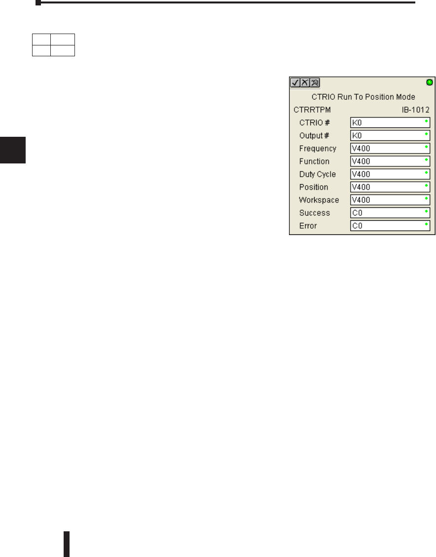
DL06 Micro PLC User Manual, 3rd Edition, Rev. D
5-362
1
2
3
4
5
6
7
8
9
10
11
12
13
14
A
B
C
D
CTRIO Run to Position Mode (CTRRTPM) (IB-1012)
CTRIO Run To Position Mode, on a leading edge transition to this IBox, loads the Run to
Position command and given parameters on a specific Output resource.
Valid Function Values are:
00: Less Than Ch1/Fn1
10: Greater Than Ch1/Fn1
01: Less Than Ch1/Fn2
11: Greater Than Ch1/Fn2
02: Less Than Ch2/Fn1
12: Greater Than Ch2/Fn1
03: Less Than Ch2/Fn2
13: Greater Than Ch2/Fn2
This IBox will take more than 1 PLC scan to execute.
Either the Success or Error bit will turn on when the
command is complete. If the Error Bit is on, you can
use the CTRIO Read Error Code (CTRRDER) IBox
to get extended error information.
The Workspace register is for internal use by this IBox instruction and MUST NOT be used
anywhere else in your program.
CTRRTPM Parameters
• CTRIO#: specifies a specific CTRIO module based on a user defined number (see CTRIO Config
Ibox)
• Output#: specifies a CTRIO output to be used by the instruction
• Frequency: specifies the output pulse rate (H0-CTRIO: 20Hz - 25KHz / H0-CTRIO2: 20Hz -
250 KHz)
• Duty Cycle: specifies the % of on time versus off time. This is a hex number. Default of 0 is 50%,
also entering 50 will yield 50%. 50% duty cycle is defined as on half the time and off half the time
• Position: specifies the count value, as measured on the encoder input, at which the output pulse
train will be turned off
• Workspace: specifies a V-memory location that will be used by the instruction
• Success: specifies a bit that will turn on once the instruction has successfully completed
• Error: specifies a bit that will turn on if the instruction does not complete successfully
Chapter 5: Intelligent Box (IBox) Instructions
1
2
3
4
5
6
7
8
9
10
11
12
13
14
a
B
c
d
DS Used
HPP N/A
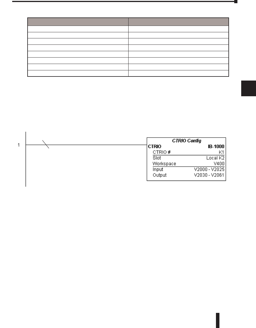
DL06 Micro PLC User Manual, 3rd Edition, Rev. D 5-363
1
2
3
4
5
6
7
8
9
10
11
12
13
14
A
B
C
D
CTRRTPM Example
Rung 1: This sets up the CTRIO card in slot 2 of the local base. Each CTRIO in the system
will need a separate CTRIO I-box before any CTRxxxx I-boxes can be used for them. The
CTRIO has been configured to use V2000 through V2025 for its input data, and V2030
through V2061 for its output data.
Chapter 5: Intelligent Box (IBox) Instructions
1
2
3
4
5
6
7
8
9
10
11
12
13
14
a
B
c
d
Parameter DL06 Range
CTRIO# K K0-255
Output# K K0-3
Frequency V,K K20-20000; See DL06 V-memory map - Data Words
Duty Cycle V,K K0-99; See DL06 V-memory map
Position V,K K0-2147434528; See DL06 V-memory map
Workspace V See DL06 V-memory map - Data Words
Success X,Y,C,GX,GY,B See DL06 V-memory map
Error X,Y,C,GX,GY,B See DL06 V-memory map
(example continued on next page)
Permissive contacts or input logic cannot
be used with this instruction.
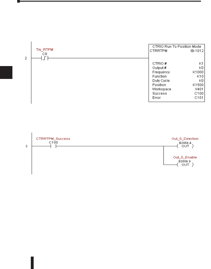
DL06 Micro PLC User Manual, 3rd Edition, Rev. D
5-364
1
2
3
4
5
6
7
8
9
10
11
12
13
14
A
B
C
D
CTRRTPM Example (cont’d)
Rung 2: This CTRIO Run To Position Mode IBox sets up Output #0 in CTRIO #1 to
output pulses at a Frequency of 1000 Hz, use the ‘Greater than Ch1/Fn1’ comparison
operator, until the input position of 1500 is reached. This example program requires that you
load CTRRTPM_IBox.cwb into your Hx-CTRIO(2) module.
Rung 3: If the Run To Position Mode parameters are OK, set the Direction Bit and Enable
the output.
Chapter 5: Intelligent Box (IBox) Instructions
1
2
3
4
5
6
7
8
9
10
11
12
13
14
a
B
c
d
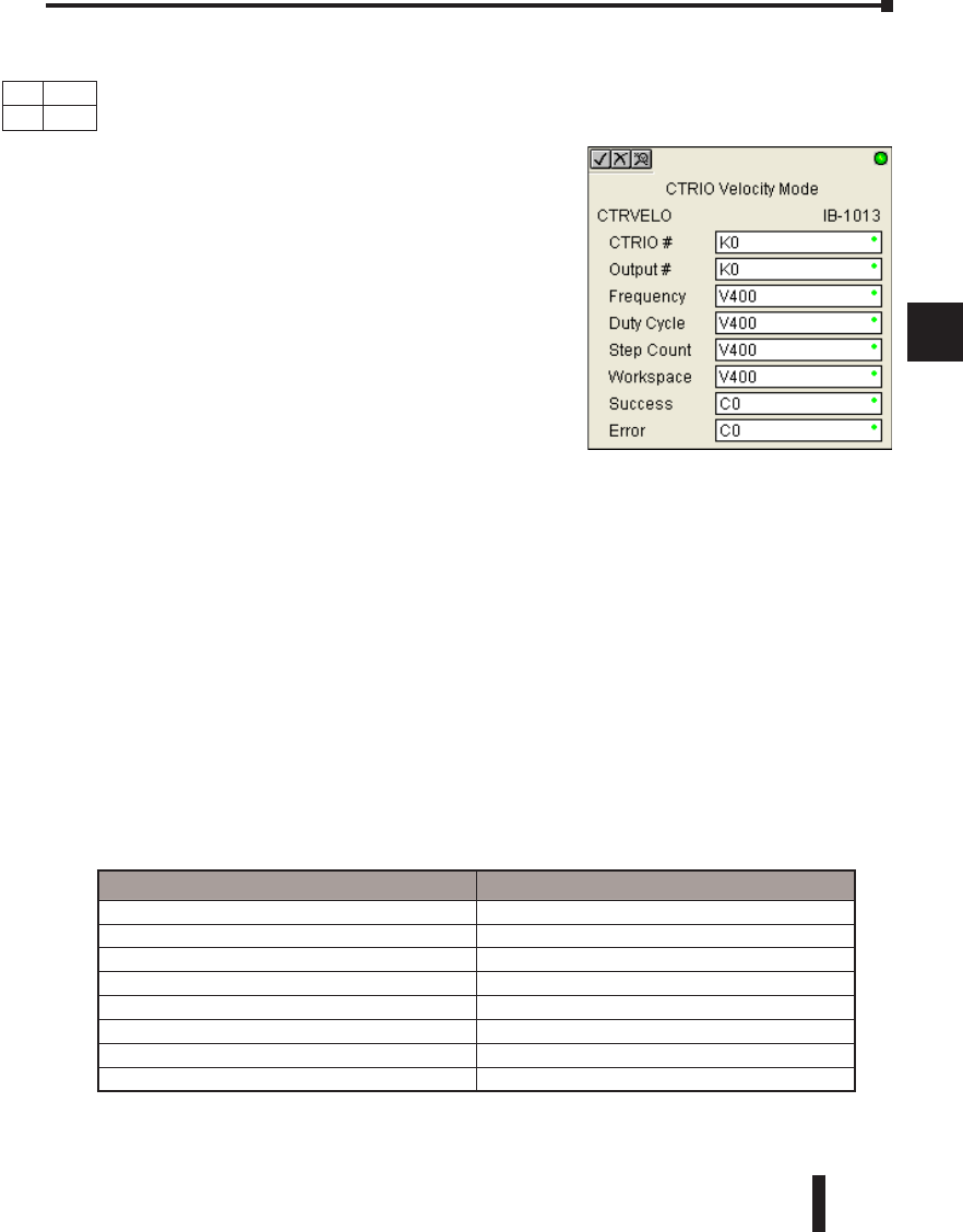
DL06 Micro PLC User Manual, 3rd Edition, Rev. D 5-365
1
2
3
4
5
6
7
8
9
10
11
12
13
14
A
B
C
D
CTRIO Velocity Mode (CTRVELO) (IB-1013)
CTRIO Velocity Mode loads the Velocity command and given parameters on a specific
Output resource on a leading edge transition to this IBox.
This IBox will take more than 1 PLC scan to execute.
Either the Success or Error bit will turn on when the
command is complete. If the Error Bit is on, you can use
the CTRIO Read Error Code (CTRRDER) IBox to get
extended error information.
The Workspace register is for internal use by this IBox
instruction and MUST NOT be used anywhere else in
your program.
CTRVELO Parameters
• CTRIO#: specifies a specific CTRIO module based on a
user defined number (see CTRIO Config Ibox)
• Output#: specifies a CTRIO output to be used by the instruction
• Frequency: specifies the output pulse rate (H0-CTRIO: 20Hz - 25KHz / H0-CTRIO2: 20Hz -
250 KHz)
• Duty Cycle: specifies the % of on time versus off time. This is a hex number. Default of 0 is 50%,
also entering 50 will yield 50%. 50% duty cycle is defined as on half the time and off half the time
• Step Count: This DWORD value specifies the number of pulses to output. A Step Count value of
-1 (or 0XFFFFFFFF) causes the CTRIO to output pulses continuously. Negative Step Count values
must be V-Memory references.
• Workspace: specifies a V-memory location that will be used by the instruction
• Success: specifies a bit that will turn on once the instruction has successfully completed
• Error: specifies a bit that will turn on if the instruction does not complete successfully
Chapter 5: Intelligent Box (IBox) Instructions
1
2
3
4
5
6
7
8
9
10
11
12
13
14
a
B
c
d
DS Used
HPP N/A
Parameter DL06 Range
CTRIO# K K0-255
Output# K K0-3
Frequency V,K K20-20000; See DL06 V-memory map - Data Words
Duty Cycle V,K K0-99; See DL06 V-memory map
Step Count V,K K0-2147434528; See DL06 V-memory map
Workspace V See DL06 V-memory map - Data Words
Success X,Y,C,GX,GY,B See DL06 V-memory map
Error X,Y,C,GX,GY,B See DL06 V-memory map
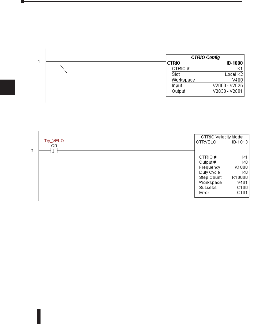
DL06 Micro PLC User Manual, 3rd Edition, Rev. D
5-366
1
2
3
4
5
6
7
8
9
10
11
12
13
14
A
B
C
D
CTRVELO Example
Rung 1: This sets up the CTRIO card in slot 2 of the local base. Each CTRIO in the system
will need a separate CTRIO I-box before any CTRxxxx I-boxes can be used for them. The
CTRIO has been configured to use V2000 through V2025 for its input data, and V2030
through V2061 for its output data.
Rung 2: This CTRIO Velocity Mode IBox sets up Output #0 in CTRIO #1 to output
10,000 pulses at a Frequency of 1000 Hz. This example program requires that you load
CTRVELO_IBox.cwb into your Hx-CTRIO(2) module.
Chapter 5: Intelligent Box (IBox) Instructions
1
2
3
4
5
6
7
8
9
10
11
12
13
14
a
B
c
d
(example continued on next page)
Permissive contacts or input logic cannot
be used with this instruction.
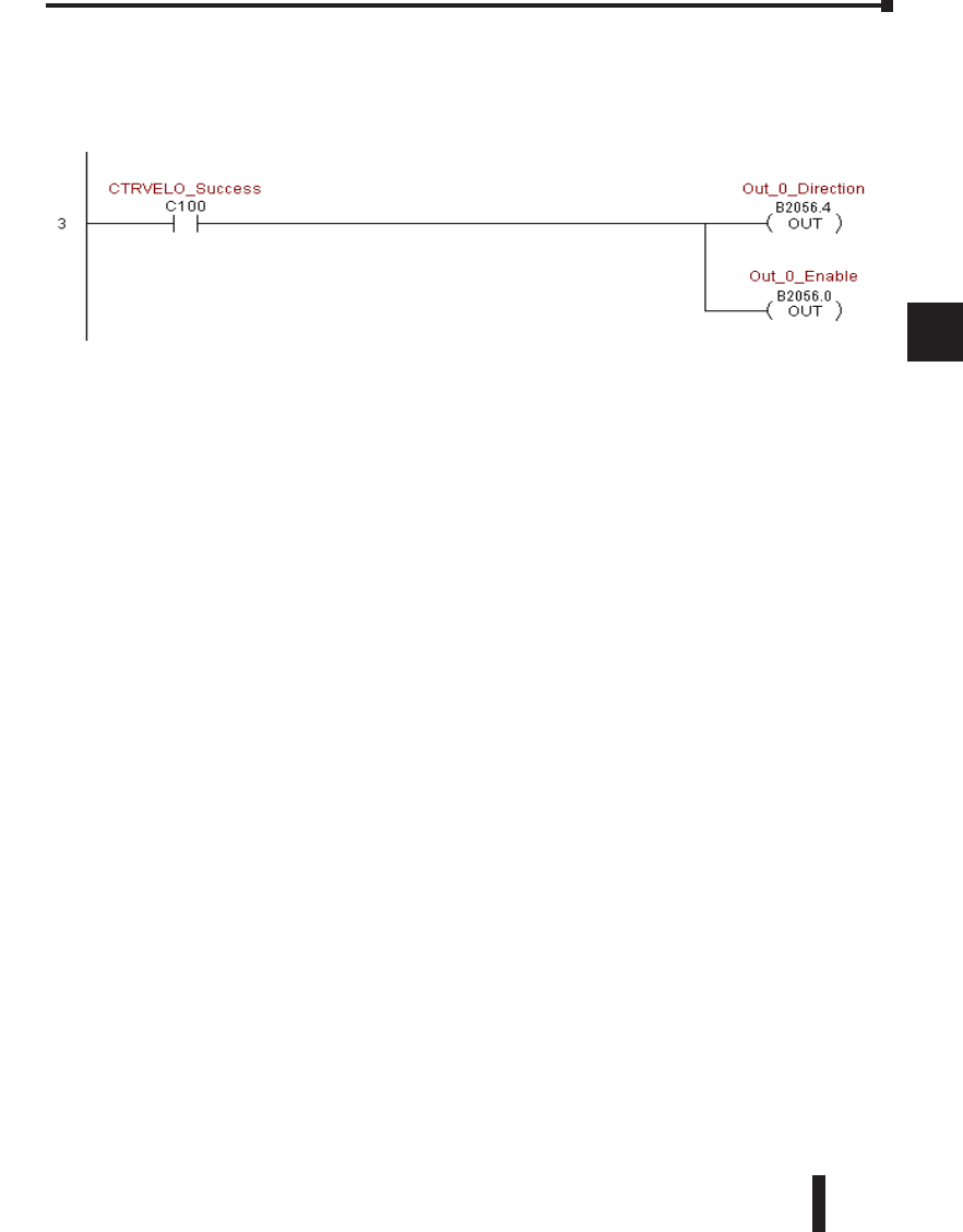
DL06 Micro PLC User Manual, 3rd Edition, Rev. D 5-367
1
2
3
4
5
6
7
8
9
10
11
12
13
14
A
B
C
D
CTRVELO Example (cont’d)
Rung 3: If the Velocity Mode parameters are OK, set the Direction Bit and Enable the
output.
Chapter 5: Intelligent Box (IBox) Instructions
1
2
3
4
5
6
7
8
9
10
11
12
13
14
a
B
c
d
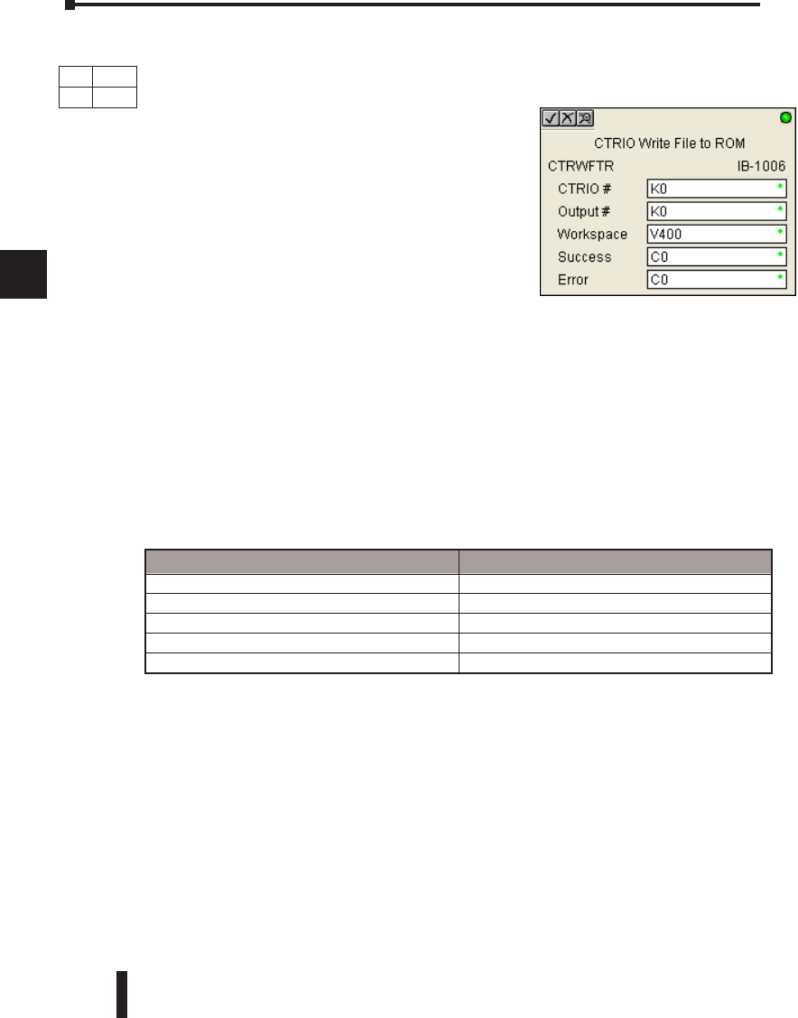
DL06 Micro PLC User Manual, 3rd Edition, Rev. D
5-368
1
2
3
4
5
6
7
8
9
10
11
12
13
14
A
B
C
D
CTRIO Write File to ROM (CTRWFTR) (IB-1006)
CTRIO Write File to ROM writes the runtime changes made to a loaded CTRIO Preset
Table back to Flash ROM on a leading edge transition to this IBox. This IBox will take
more than 1 PLC scan to execute. Either the Success or
Error bit will turn on when the command is complete.
If the Error Bit is on, you can use the CTRIO Read
Error Code (CTRRDER) IBox to get extended error
information.
The Workspace register is for internal use by this IBox
instruction and MUST NOT be used anywhere else in
your program.
CTRWFTR Parameters
• CTRIO#: specifies a specific CTRIO module based on a user defined number (see CTRIO Config
Ibox)
• Output#: specifies a CTRIO output to be used by the instruction
• Workspace: specifies a V-memory location that will be used by the instruction
• Success: specifies a bit that will turn on once the instruction has successfully completed
• Error: specifies a bit that will turn on if the instruction does not complete successfully
Chapter 5: Intelligent Box (IBox) Instructions
1
2
3
4
5
6
7
8
9
10
11
12
13
14
a
B
c
d
DS Used
HPP N/A
Parameter DL06 Range
CTRIO# K K0-255
Output# K K0-3
Workspace V See DL06 V-memory map - Data Words
Success X,Y,C,GX,GY,B See DL06 V-memory map
Error X,Y,C,GX,GY,B See DL06 V-memory map
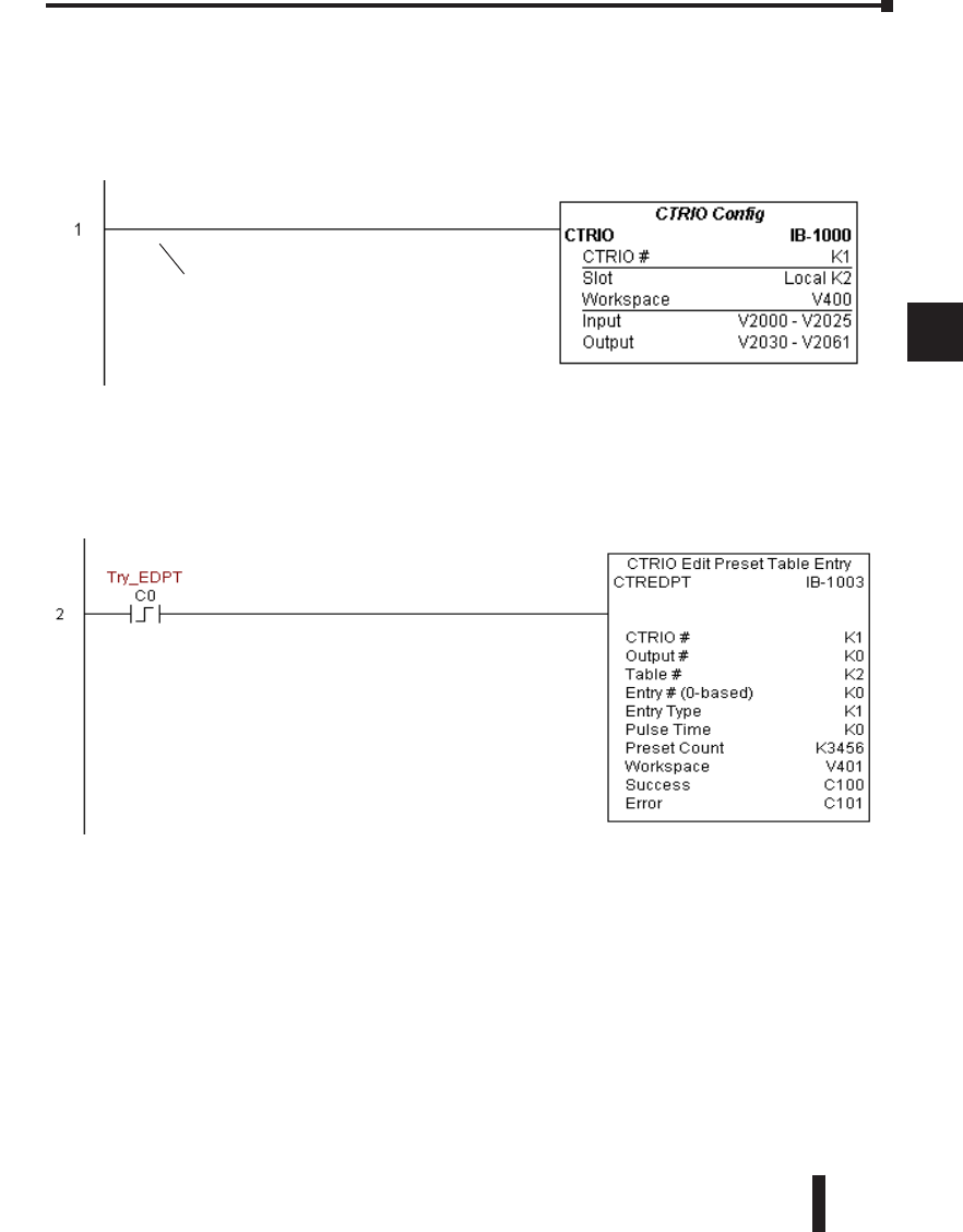
DL06 Micro PLC User Manual, 3rd Edition, Rev. D 5-369
1
2
3
4
5
6
7
8
9
10
11
12
13
14
A
B
C
D
CTRWFTR Example
Rung 1: This sets up the CTRIO card in slot 2 of the local base. Each CTRIO in the system
will need a separate CTRIO I-box before any CTRxxxx I-boxes can be used for them. The
CTRIO has been configured to use V2000 through V2025 for its input data, and V2030
through V2061 for its output data.
Rung 2: This CTRIO Edit Preset Table Entry IBox will change Entry 0 in Table #2 to be a
RESET at Count 3456. This example program requires that you load CTRWFTR_IBox.cwb
into your Hx-CTRIO(2) module.
Chapter 5: Intelligent Box (IBox) Instructions
1
2
3
4
5
6
7
8
9
10
11
12
13
14
a
B
c
d
(example continued on next page)
Permissive contacts or input logic cannot
be used with this instruction
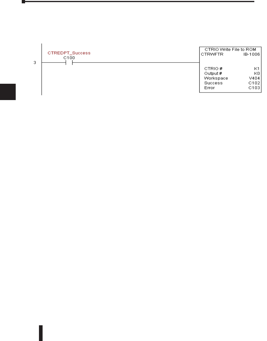
DL06 Micro PLC User Manual, 3rd Edition, Rev. D
5-370
1
2
3
4
5
6
7
8
9
10
11
12
13
14
A
B
C
D
CTRWFTR Example (cont’d)
Rung 3: If the file is successfully edited, use a Write File To ROM IBox to save the edited
table back to the CTRIO’s ROM, thereby making the changes retentive.
Chapter 5: Intelligent Box (IBox) Instructions
1
2
3
4
5
6
7
8
9
10
11
12
13
14
a
B
c
d
