DALC208SC6 Datasheet. Www.s Manuals.com. St
User Manual: Marking of electronic components, SMD Codes DA, DA*, DA**, DA***, DA-, DA-***, DA5, DAA, DAA**, DAB, DAB**, DACI, DAD**, DADI, DAE**, DAEI, DAF**, DAFI, DAG**, DAH**, DAI**, DAJ**, DAL, DALC, DAP, DAP6, DAP8A, DAQ, DAR, DAU, DAU**, DAV**, Da. Datasheets 2SD1664, AP131-15W, BAR43SFILM, BCW67A, BD49E27G, BD49K27G, BZX384-C11, DALC208SC6, DAP006, DMN5L06DMK, MAX6314US38D2-T, MMBZ4708-V, NCP1203D60R2 (analog), NCP1400ASN19T1, NCP1400ASN25T1, NCP1400ASN27T1, NCP1400ASN30T1, NCP1400ASN33T1, NCP1400ASN50T1, NCP140
Open the PDF directly: View PDF ![]() .
.
Page Count: 11
1/10
DALC208SC6
®
February 2002 - Ed: 5C
IEC61000-4-2 level 4
MIL STD 883C - Method 3015-6
(human body test) class 3
COMPLIES WITH THE FOLLOWING STANDARDS :
■PROTECTION OF 4 LINES
■PEAK REVERSE VOLTAGE:
VRRM = 9 V per diode
■VERY LOW CAPACITANCE PER DIODE:
C< 5pF
■VERY LOW LEAKAGE CURRENT: IR<1µA
FEATURES
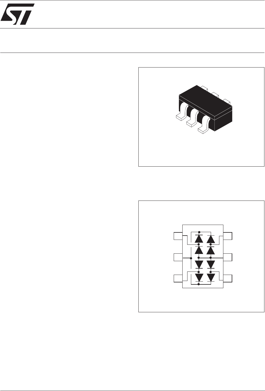
SOT23-6L (SC74)
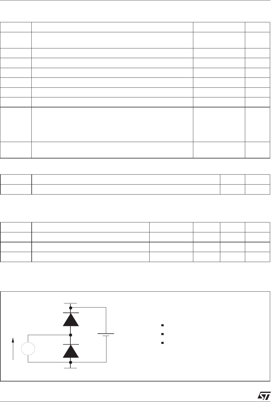
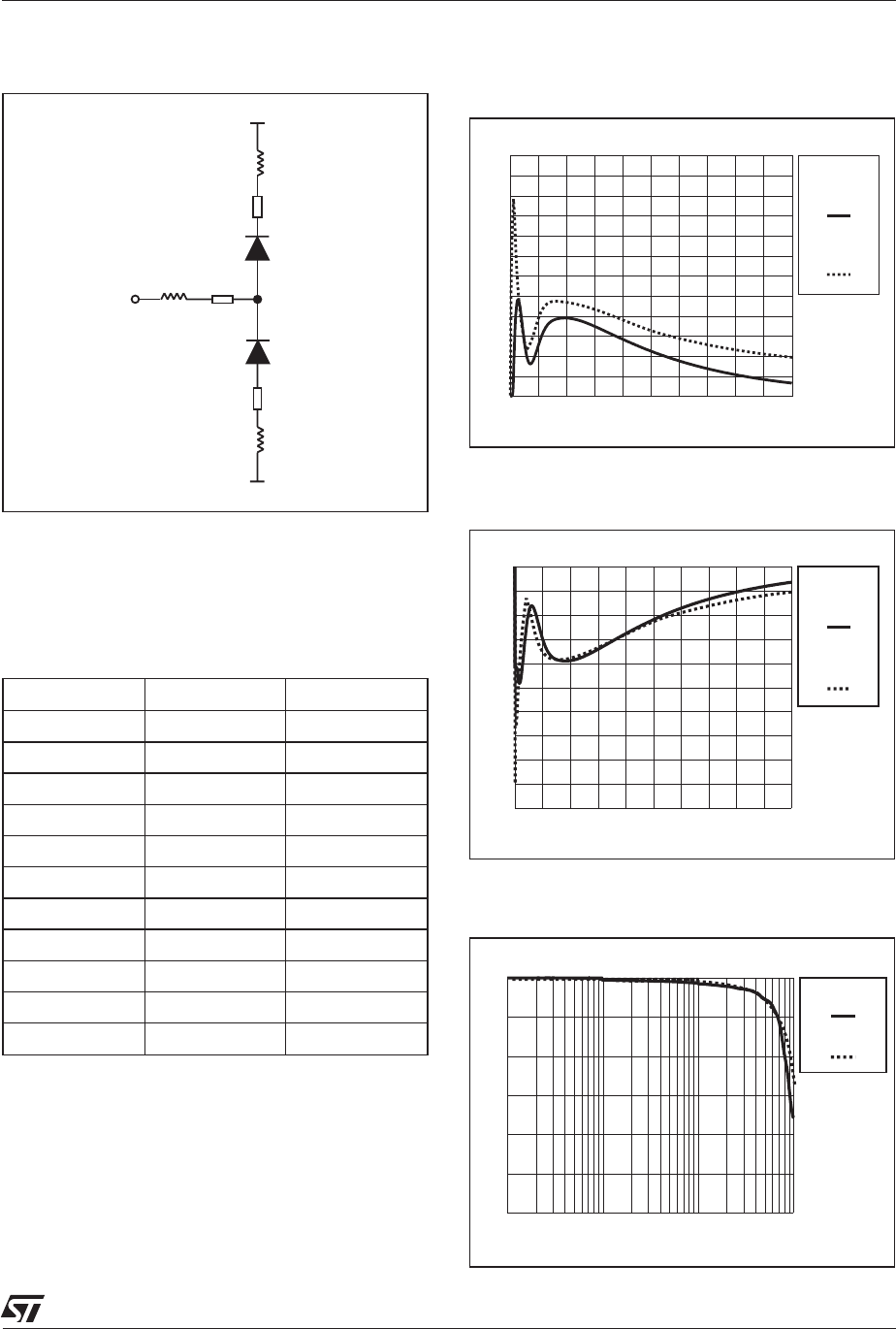
FUNCTIONAL DIAGRAM
I/O 1
I/O 2 I/O 3
I/O 4
REF 2 REF 1
LOW CAPACITANCE
DIODE ARRAY
Application Specific Discretes
A.S.D.TM
Where ESD and/or over and undershoot
protection for datalines is required :
■Sensitive logic input protection
■Microprocessor based equipment
■Audio / Video inputs
■Portable electronics
■Networks
■ISDN equipment
■USB interface
MAIN APPLICATIONS
The DALC208SC6 diode array is designed to
protect components which are connected to data
and transmission lines from overvoltages caused
by electrostatic discharge (ESD) or other
transients. It is a rail-to-rail protection device also
suited for overshoot and undershoot suppression
on sensitive logic inputs.
The low capacitance of the DALC208SC6
prevents from significant signal distortion.
DESCRIPTION
1
■Cost-effectiveness compared to discrete solution
■High efficiency in ESD suppression
■No significant signal distortion thanks to very low
capacitance
■High reliability offered by monolithic integration
■Lower PCB area consumption versus discrete
solution
BENEFITS
DALC208SC6
2/10
Symbol Parameter Value Unit
VPP IEC61000-4-2, air discharge
IEC61000-4-2, contact discharge 15
8kV
VRRM Peak reverse voltage per diode 9V
∆V
REF Reference voltage gap between VREF2 and VREF1 9V
V
In max. Maximum operating signal input voltage VREF2 V
VIn min. Minimum operating signal input voltage VREF1 V
IFContinuous forward current (single diode loaded) 200 mA
IFRM Repetitive peak forward current (tp=5µs,F=50kHz) 700 mA
IFSM Surge non repetitive forward current -
rectangular waveform (see curve on figure 1)
tp= 2.5 µs
tp=1ms
t
p= 100 ms
6
2
1
A
Tstg
Tj
Storage temperature range
Maximum junction temperature -55 to + 150
150 °C
°C
ABSOLUTE MAXIMUM RATINGS (Tamb = 25°C).
Symbol Parameter Conditions Typ. Max. Unit
VFForward voltage IF=50mA 1.2 V
I
RReverse leakage current per diode VR=5V 1 µA
CInput capacitance between Line and GND see note 3 7 10 pF
Note 2: The dynamical behavior is described in the Technical Information section, on page 4.
ELECTRICAL CHARACTERISTICS (Tamb = 25°C).
G
REF1
I/O +VCC
REF1 connected to GND
REF2 connected to +Vcc
Input applied :
Vcc = 5V, Vsign = 30 mV, F = 1 MHz
REF2
VR
Note 3: Input capacitance measurement
Symbol Parameter Value Unit
Rth(j-a) Junction to ambient (note 1) 500 °C/W
Note 1: device mounted on FR4 PCB with recommended footprint dimensions.
THERMAL RESISTANCE
DALC208SC6
3/10
0.001 0.01 0.1 1 10 100 1000
0
1
2
3
4
5
6
7
8
tp(ms)
IFSM(A)
I/O vs
REF1 or
REF2
Fig. 1: Maximum non-repetitive peak forward current
versus rectangular pulse duration (Tj initial = 25°C).
5 1015202530
0.1
1.0
2.0
Vcl(V)
Ipp(A)
tp=2.5µs
I/O vs REF1
or REF2
Fig. 2: Reverse clamping voltage versus peak
pulse current (Tj initial = 25°C), typical values.
Rectangular waveform tp = 2.5 µs.
25 50 75 100 125 150
0.01
0.1
1
10
100
Tj(°C)
IR(µA)
Fig. 3: Variation of leakage current versus junction
temperature (typical values).
012345
5.0
5.5
6.0
6.5
7.0
7.5
8.0
VR(V)
C(pF)
F=1MHz
Vsign=30mV
Vref1/ref2=5V
Fig. 4: Input capacitance versus reverse applied
voltage (typical values).
0 2 4 6 8 10 12 14 16 18 20
0.1
1.0
10.0
VFM(V)
IFM(A)
Tj=25°C
Tj=150°C
I/O vs REF 1
or REF2
Fig. 5: Peak forward voltage drop versus peak for-
ward current (typical values).
Rectangular waveform tp = 2.5 µs.
DALC208SC6
4/10
The DALC208SC6 is particularly optimized to
perform surge protection based on the rail to rail
topology.
The clamping voltage VCL can be calculated as
follow :
VCL+=V
REF2 +V
Ffor positive surges
VCL-=V
REF1 - VFfor negative surges
with : VF=V
t+ rd.Ip
(VFforward drop voltage) / (Vtforward drop
threshold voltage)
According to the curve Fig.5 on page 3, we
assume that the value of the dynamic resistance of
the clamping diode is typically rd = 0.7Ωand Vt=
1.2V.
For an IEC61000-4-2 surge Level 4 (Contact
Discharge: Vg=8kV, Rg=330Ω), VREF2 = +5V,
VREF1 = 0V, and if in first approximation, we
assume that : Ip=Vg/Rg ′24A.
So, we find:
VCL+′+23V
VCL-′-18V
Note: the calculations do not take into account
phenomena due to parasitic inductances
APPLICATION EXAMPLE
If we consider that the connections from the pin
REF2to VCC and from REF1to GND are done by
two tracks of 10mm long and 0.5mm large; we
assume that the parasitic inductances of these
tracks are about 6nH.
So when an IEC61000-4-2 surge occurs, due to
the rise time of this spike (tr=1ns), the voltage VCL
has an extra value equal to Lw.dI/dt.
The dI/dt is calculated as: di/dt = Ip/tr ′24 A/ns
The overvoltage due to the parasitic inductances
is: Lw.di/dt=6x24′144V
By taking into account the effect of these parasitic
inductances due to unsuitable layout, the clamping
voltage will be :
VCL+ = +23 + 144 ′167V
VCL- = -18 - 144 ′-162V
We can reduce as much as possible these
phenomena with simple layout optimization.
It’s the reason why some recommendations have
to be followed (
see paragraph “How to ensure a
good ESD protection”
).
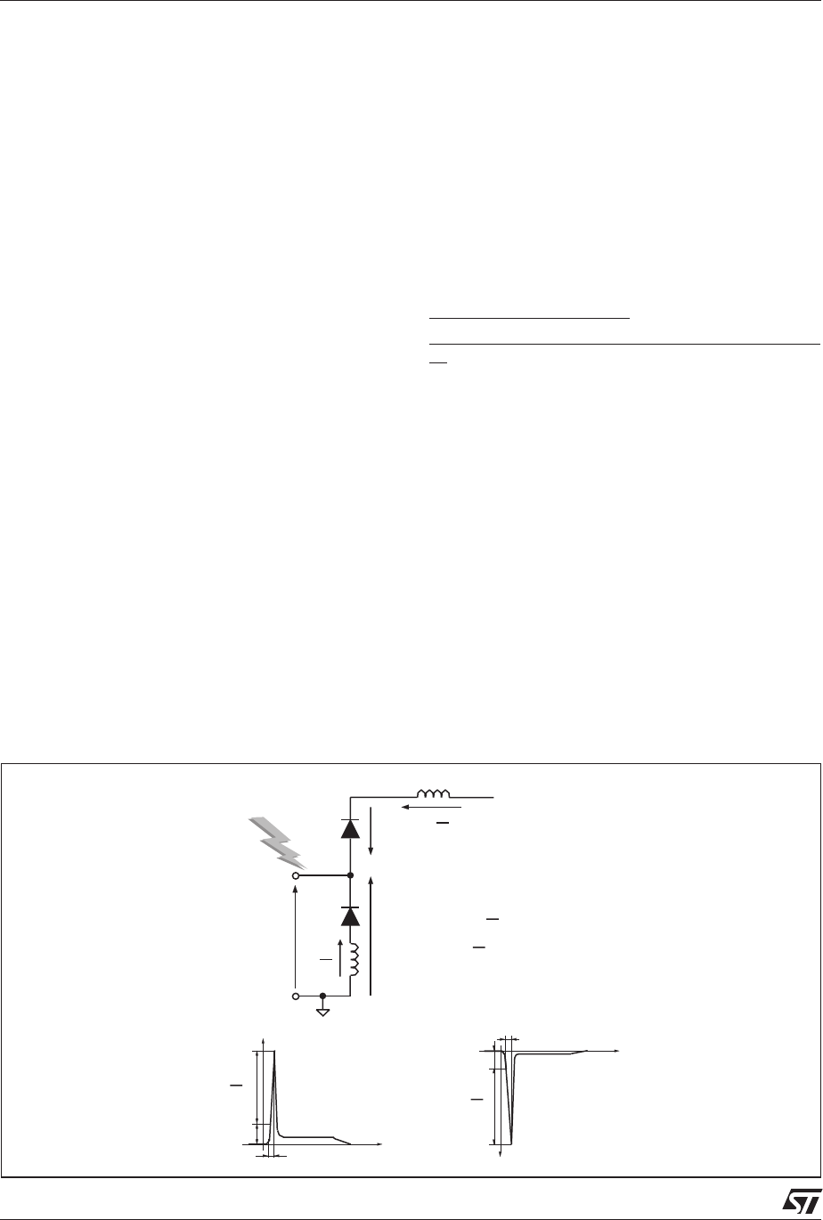
TECHNICAL INFORMATION
SURGE PROTECTION
Fig. A1: ESD behavior; parasitic phenomena due to unsuitable layout.
Lw
VI/O
ESD
SURGE
REF1=GND
I/O
REF2=+Vcc
Vf Lw di
dt
Lw di
dt
Vcl+ = Vcc+Vf+Lw di
dt surge >0
-Vf- Lw di
dt surge <0
Vcl- =
t
tr=1ns
Vcc+Vf
Lw di
dt
Vcl+
POSITIVE
SURGE
167V
-Lw di
dt
t
tr=1ns
-Vf
Vcl-
NEGATIVE
SURGE
-162V
DALC208SC6
5/10
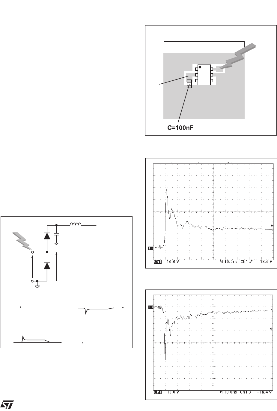
HOW TO ENSURE A GOOD ESD PROTECTION
While the DALC208SC6 provides a high immunity
to ESD surge, an efficient protection depends on
the layout of the board. In the same way, with the
rail to rail topology, the track from the VREF2 pin to
the power supply +VCC and from the VREF1 pin to
GND must be as short as possible to avoid
overvoltages due to parasitic phenomena (see Fig.
A1).
It’s often harder to connect the power supply near
to the DALC208SC6 unlike the ground thanks to
the ground plane that allows a short connection.
To ensure the same efficiency for positive surges
when the connections can’t be short enough, we
recommend to put close to the DALC208SC6,
between VREF2 and ground, a capacitance of
100nF to prevent from these kinds of overvoltage
disturbances (see Fig. A2).
The add of this capacitance will allow a better
protection by providing during surge a constant
voltage.
Fig. A3, A4a and A4b show the improvement of the
ESD protection according to the recommendations
described above.
REF1=GND
VI/O
ESD
SURGE
I/O
REF2=+Vcc
C=100nF
Lw
Vcl+ = Vcc+Vf
-Vf
surge >0
surge <0
Vcl- =
t
Vcl+
POSITIVE
SURGE
t
Vcl-
NEGATIVE
SURGE
Fig. A2: ESD behavior: optimized layout and add
of a capacitance of 100nF.
Important:
A main precaution to take is to put the protection
device closer to the disturbance source (generally
the connector).
+5V
TEST BOARD
DALC
208
ESD
SURGE
Fig. A3: ESD behavior: measurements conditions
(with coupling capacitance).
IEC61000-4-2
Air Discharge
(150pF/330Ω)
Vpp=15kV
Fig. A4a: Remaining voltage after the
DALC208SC6 during positive ESD surge.
IEC61000-4-2
Air Discharge
(150pF/330Ω)
Vpp=15kV
Fig. A4b: Remaining voltage after the
DALC208SC6 during negative ESD surge.
Note: The measurements have been done with the DALC208SC6
in open circuit.
DALC208SC6
6/10
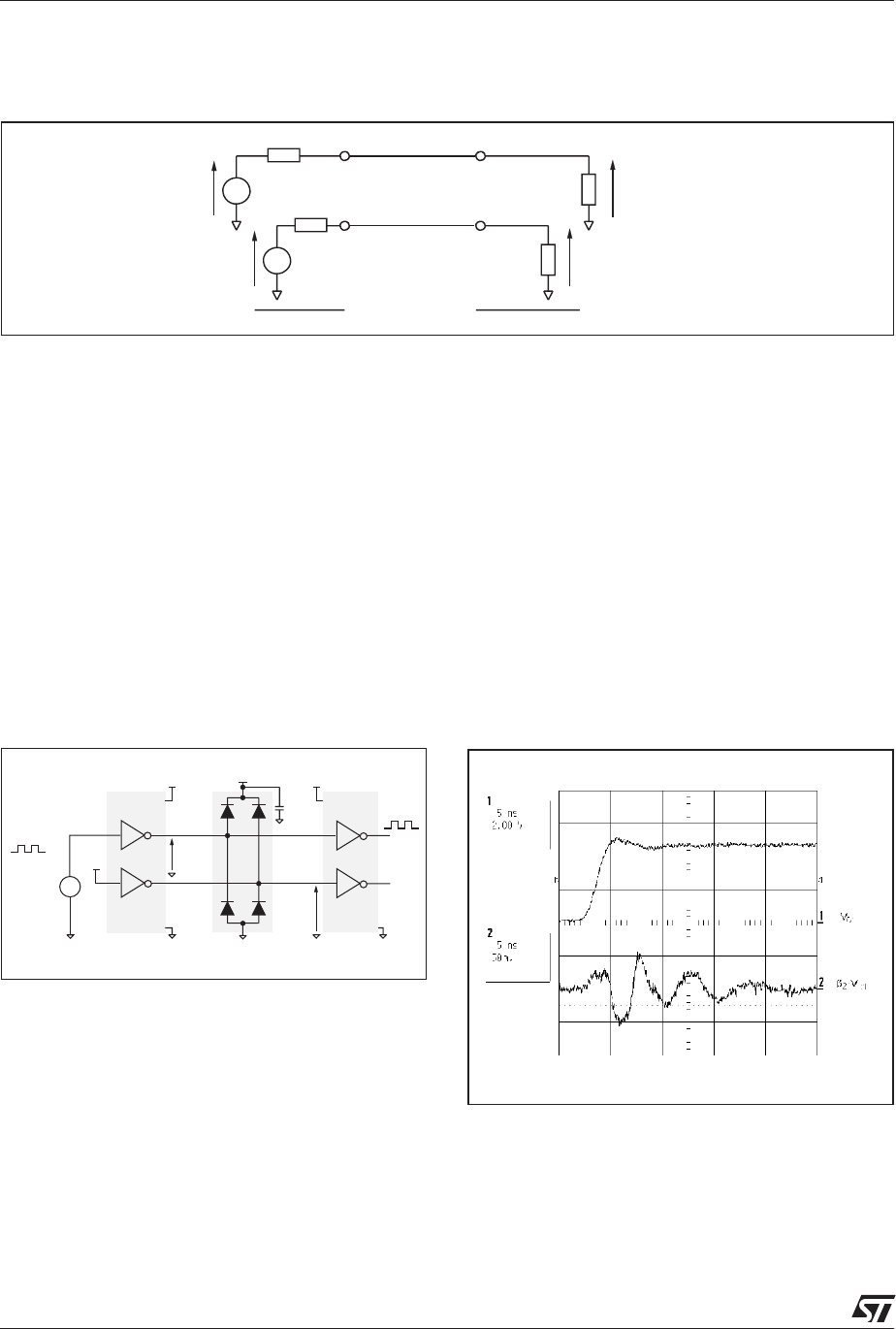
CROSSTALK BEHAVIOR
1- Crosstalk phenomena
The crosstalk phenomena are due to the coupling
between 2 lines. The coupling factor (β12 or β21)
increases when the gap across lines decreases,
particularly in silicon dice. In the example above
the expected signal on load RL2 is α2VG2, in fact
the real voltage at this point has got an extra value
β21VG1. This part of the VG1 signal represents the
effect of the crosstalk phenomenon of the line 1 on
the line 2. This phenomenon has to be taken into
account when the drivers impose fast digital data
or high frequency analog signals in the disturbing
line. The perturbed line will be more affected if it
works with low voltage signal or high load
impedance (few kΩ). The following chapters give
the value of both digital and analog crosstalk.
2- Digital Crosstalk
Figure A5 shows the measurement circuit used to
quantify the crosstalk effect in a classical digital
application.
Figure A6 shows that in such a condition: signal
from 0V to 5V and a rise time of 5 ns, the impact on
the disturbed line is less than 100mV peak to peak.
No data disturbance was noted on the concerned
line. The same results were obtained with falling
edges.
Note: The measurements have been done in the worst case i.e. on
two adjacent cells (I/O1 & I/O4).
Line 1
Line 2
VG1
VG2
RG1
RG2
DRIVERS
RL1
RL2
RECEIVERS
αβ
+
112
VG1 VG2
αβ
+
221
VG2 VG1
Fig. A4: Crosstalk phenomena.
DALC208SC6
100nF
+5V
Line 1
Line 2
VG1
β21 VG1
+5V +5V
74HC04
+5V
Square
Pulse
Generator
5KHz
74HC04
Fig. A5: Digital crosstalk measurements. Fig. A6: Digital crosstalk results.
DALC208SC6
7/10
1 10 100 1,000
-100
-80
-60
-40
-20
0
f(MHz)
dBm
Fig. A8: Analog crosstalk results.
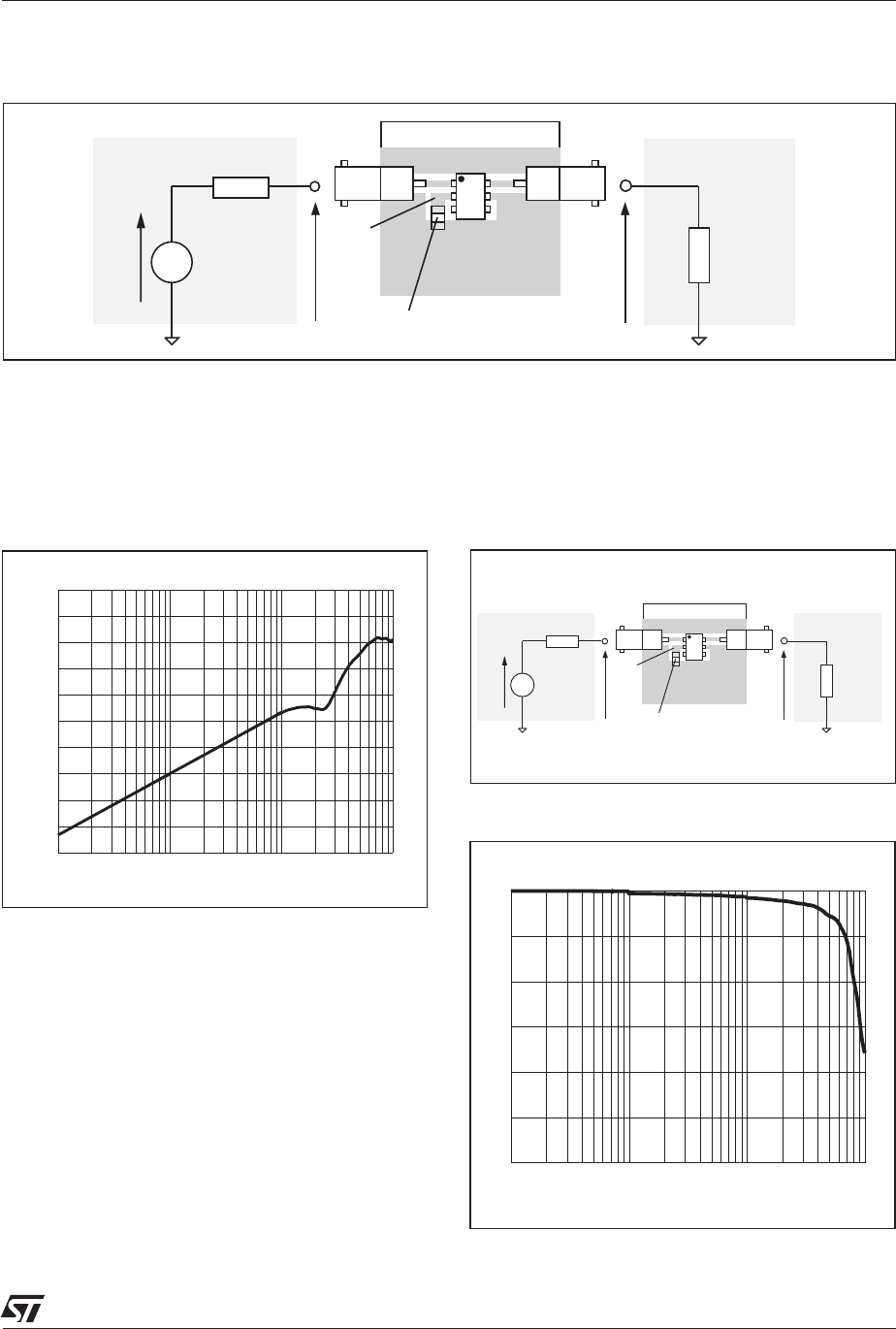
3- Analog Crosstalk
Figure A7 gives the measurement circuit for the
analog application. In usual frequency range of
analog signals (up to 100MHz) the effect on
disturbed line is less than -45 dBm (please see Fig.
SPECTRUM ANALYSER
Vout 50Ω
TRACKING GENERATOR
Vg Vin
50Ω
TEST BOARD
+5V
DALC
208
C=100nF
Fig. A7: Analog crosstalk measurements.
SPECTRUM ANALYSER
Vout 50Ω
TRACKING GENERATOR
Vg Vin
50Ω
TEST BOARD
+5V
DALC
208
C=100nF
Fig. A9: Measurement conditions.
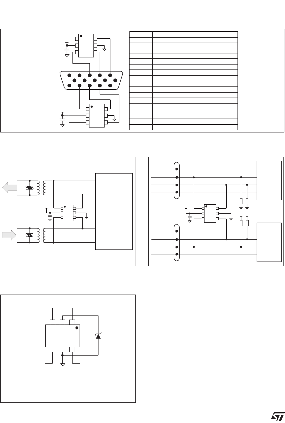
As the DALC208SC6 is designed to protect high
speed data lines, it must ensure a good
transmission of operating signals. The attenuation
curve give such an information.
Fig. A10 shows that the DALC208SC6 is well
suitable for data line transmission up to 100 Mbit/s
while it works as a filter for undesirable signals as
GSM (900MHz).
1 10 100 1,000
-30
-20
-10
0
f(MHz)
dBm
Fig. A10: DALC206SC6 attenuation.
DALC208SC6
8/10
APPLICATION EXAMPLES
■Video line protection
Pin N° Signal
1RED VIDEO
2 GREEN VIDEO
or COMPOSITE SYNC with GREEN VIDEO
3BLUE VIDEO
4GROUND
5DDC (Display Data Channel) GROUND
6RED GROUND
7 GREEN GROUND
8 BLUE GROUND
9 NC
10 SYNC GROUND
11 GROUND
12 SDA (Sérial Data)
13 HORIZONTAL SYNC
or COMPOSITE SYNC
14 VERTICAL SYNC (VCLK)
15 SCL (Serial Clock)
DALC
208
+Vcc
1
15
5
DALC
208
+Vcc
100nF
100nF
USB
TRANS-
CEIVER
USB
TRANS-
CEIVER
DALC
208 +V
1.5k
(1)
1.5k
(2)
+V
VBUS
D+
D-
GND
VBUS
D+
D-
GND
15k 15k (1) Full speed
only
(2) Low speed
only
100nF
■USB port protection
DALC
208
+Vcc
100nF
DATA
TRANSCEIVER
SMP75-8
SMP75-8
Tx
Rx
■T1/E1 protection
Note It's absolutely necessary to connect
the pin 5 (REF1) to GND !
DALC208
I/O2 I/O1
I/O3 I/O4
GND
■Another way to connect the DALC208SC6
DALC208SC6
9/10
PSPICE MODEL
Figure A11 shows the PSpice model of one
DALC208SC6 cell. In this model, the diodes are
defined by the PSpice parameters given in table
below (Fig A12).
Note: This simulation model is available only for an ambient tem-
perature of 27°C.
The simulations done (Fig. A13, A14, A15) shows
that the PSpice model is close to the product
behavior.
DPOS DNEG
BV 99
CJO 7p 7p
IBV 1u 1u
IKF 28.357E-3 1000
IS 118.78E-15 5.6524E-9
ISR 100E-12 472.3E-9
M0.3333 0.3333
N1.3334 2.413
NR 22
RS 0.68377 0.71677
VJ 0.6 0.6
Fig. A12: PSpice parameters.
Vref2
Vref1
I/O
Dpos
Dneg
0.3Ω
0.5Ω
0.8nH
1.45nH
0.8nH 0.3Ω
Fig. A11: PSpice model of one DALC208SC6 cell.
0 50 100
0
10
20
30
40
50
60
t(ns)
Current (A) / Voltage (V)
Current
Surge
I/O
Voltage
Fig. A13a: PSpice model simulation: surge > 0
IEC61000-4-2 contact discharge response.
0 50 100
-50
-40
-30
-20
-10
0
t(ns)
Current (A) / Voltage (V)
Current
Surge
I/O
Voltage
Fig. A13b: PSpice model simulation: surge < 0
IEC61000-4-2 contact discharge response.
1 10 100 1,000
-30
-20
-10
0
f(MHz)
dBm
Measured
PSpice
Fig. A14: Attenuation comparison.
DALC208SC6
10/10
PACKAGE MECHANICAL DATA
SOT23-6L (Plastic)
A2
A
L
H
b
E
D
e
e
A1
Cθ
Information furnished is believed to be accurate and reliable. However, STMicroelectronics assumes no responsibility for the consequences of
use of such information nor for any infringement of patents or other rights of third parties which may result from its use. No license is granted by
implication or otherwise under any patent or patent rights of STMicroelectronics. Specifications mentioned in this publication are subject to
change without notice. This publication supersedes and replaces all information previously supplied.
STMicroelectronics products are not authorized for use as critical components in life support devices or systems without express written ap-
proval of STMicroelectronics.
The ST logo is a registered trademark of STMicroelectronics
© 2002 STMicroelectronics - Printed in Italy - All rights reserved.
STMicroelectronics GROUP OF COMPANIES
Australia - Brazil - Canada - China - Finland - France - Germany
Hong Kong - India - Israel - Italy - Japan - Malaysia - Malta - Morocco - Singapore
Spain - Sweden - Switzerland - United Kingdom - United States.
http://www.st.com
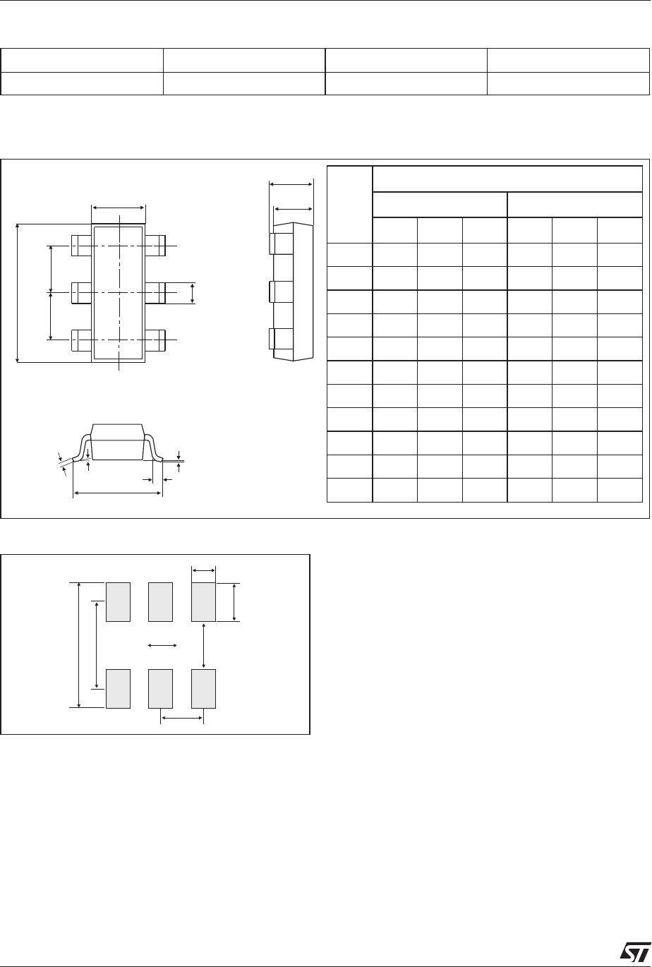
REF.
DIMENSIONS
Millimeters Inches
Min. Typ. Max. Min. Typ. Max.
A 0.90 1.45 0.035 0.057
A1 0 0.10 0 0.004
A2 0.90 1.30 0.035 0.0512
b 0.35 0.50 0.0137 0.02
c 0.09 0.20 0.004 0.008
D 2.80 3.00 0.11 0.118
E 1.50 1.75 0.059 0.0689
e 0.95 0.0374
H 2.60 3.00 0.102 0.118
L 0.10 0.60 0.004 0.024
θ10° 10°
mm
inch
3.50
0.138
0.60
0.024
1.20
0.047
1.10
0.043
0.95
0.037
2.30
0.090
FOOTPRINT DIMENSIONS (in millimeters)
Type Marking Order Code Packaging (Base Qty)
DALC208SC6 DALC DALC208SC6 tape & reel (3000)
MARKING