A2928604 D845WN Developer\specs\A2928604
User Manual: D845WN
Open the PDF directly: View PDF ![]() .
.
Page Count: 66

July 2004
Version 1.2
Order Number A29286-004
Front Panel I/O Connectivity
Design Guide

Revision History
Revision Revision History Date
1.2 Updated:
• Front Panel Audio Cable Cross Section drawing
• Audio Cable Wiring Diagram drawing
• URL links under Design Specifications
• USB Connectors section under Front Panel High Speed Serial Bus
Added:
• Front Panel Audio and Intel® High Definition Audio (Intel® HD Audio);
text, tables, and drawings
• Dual and Single Port USB cable information, text, tables, and drawings
July 2004
1.1 Updated:
• Audio Cable Cross-Section drawing
• Audio Cable Wiring diagram
• Front panel connector pinout
• Front panel, USB, and rear panel connectors pin descriptions
• Specification references
Added:
• Audio pull-up resistor information
• Fuse and filtering notes
• Manufacturer's part numbers
• "Top/bottom/ outside view" to graphics
December 2002
1.0 Initial release. October 2000
Information in this document is provided in connection with Intel® products. No license, express or implied, by estoppel or
otherwise, to any intellectual property rights is granted by this document. Except as provided in Intel's Terms and Conditions
of Sale for such products, Intel assumes no liability whatsoever, and Intel disclaims any express or implied warranty, relating
to sale and/or use of Intel products including liability or warranties relating to fitness for a particular purpose, merchantability,
or infringement of any patent, copyright or other intellectual property right. Intel products are not intended for use in medical,
life saving, or life sustaining applications.
Intel may make changes to guidelines and product descriptions at any time, without notice.
This guide may contain errors known as errata. Current characterized errata are available on request.
Copies of documents which have an ordering number and are referenced in this document, or other Intel literature, may be
obtained from:
Intel Corporation
P.O. Box 5937
Denver, CO 80217-9808
or call in North America 1-800-548-4725, Europe 44-0-1793-431-155, France 44-0-1793-421-777,
Germany 44-0-1793-421-333, other Countries 708-296-9333.
† Other names and brands may be claimed as the property of others.
Copyright © 2000-2004 Intel Corporation. All rights reserved.

iii
Preface
This guide describes connection and mechanical recommendations for all main boards having
internal connectors requiring external connection. Recommendations include (among others):
front panel I/O header pin-out definition, chassis I/O aperture size, I/O interface board dimensions
and main board to front panel board I/O cable shielding and size. Front panel I/O legacy
connectors, internal legacy and legacy-free connectors are also addressed. Specific to front panel
I/O the goal is for any particular setup of main board, interface board, interface cable and chassis
that meets the pinout and physical dimension recommendations of this design guide will be
physically compatible with another setup that also meets the requirements of this design guide.
Environmental and electrical compatibility testing should be conducted for all designs arising from
use of this design guide.
Intended Audience
The guide is intended to provide detailed, technical information to vendors, system integrators, and
other engineers and technicians who need this level of information. It is specifically not intended
for general audiences.
What This Document Contains
Chapter Description
1 Supporting Documentation
2 Front Panel Legacy I/O
3 Front Panel High Speed Serial Bus
4 Cabling Design Guidelines
5 Interface Board Design Guidelines
6 Chassis and I/O Shield Guidelines
7 Internal Legacy Connectors (Reference)
8 Internal Legacy-Free Connectors (Reference)
Intel Front Panel I/O Connectivity Design Guide
iv
Typographical Conventions
This section contains information about the conventions used in this guide. Not all of these
symbols and abbreviations appear in all guides of this type.
Notes, Cautions, and Warnings
NOTE
Notes call attention to important information.
CAUTION
Cautions are included to help you avoid damaging hardware or losing data.
WARNING
Warnings indicate conditions, which if not observed, can cause personal injury.
Other Common Notation
# Used after a signal name to identify an active-low signal (such as USBP0#)
(NxnX) When used in the description of a component, N indicates component type, xn are the relative
coordinates of its location on the board, and X is the instance of the particular part at that general
location. For example, J5J1 is a connector, located at 5J. It is the first connector in the 5J area.
KB Kilobyte (1024 bytes)
Kbit Kilobit (1024 bits)
MB Megabyte (1,048,576 bytes)
Mbit Megabit (1,048,576 bits)
GB Gigabyte (1,073,741,824 bytes)
xxh An address or data value ending with a lowercase h indicates a hexadecimal value.
x.x V Volts. All voltages are DC unless otherwise specified.
† This symbol is used to indicate third-party brands and names that are the property of their
respective owners.

v
Contents
1 Supporting Documentation........................................................................... 9
1.1 Online Support ...............................................................................................................9
1.2 Design Specifications...................................................................................................10
1.3 Recommended Roles of Suppliers...............................................................................13
1.3.1 Chassis Supplier............................................................................................13
1.3.2 Mainboard Manufacturer or Chassis Supplier ...............................................13
1.3.3 Third-Party Interface Board Supplier.............................................................13
2 Front Panel Legacy I/O ................................................................................ 15
2.1 Introduction ..................................................................................................................15
2.2 Switch/LED and IR Connectors....................................................................................15
2.2.1 Usage Models................................................................................................15
2.2.2 Switch/LED Connector Features ...................................................................16
2.2.3 IR Connector Features ..................................................................................17
2.2.4 Header Design...............................................................................................17
2.2.5 Pin Assignments............................................................................................18
2.3 Front Panel Audio ........................................................................................................19
2.3.1 Usage Model .................................................................................................19
2.3.2 Features ........................................................................................................19
2.3.3 Audio Design Considerations ........................................................................19
2.3.4 AC’97 Audio...................................................................................................19
2.3.5 Intel® High Definition Audio...........................................................................22
3 Front Panel High Speed Serial Bus ............................................................ 27
3.1 Introduction ..................................................................................................................27
3.2 USB Connectors ..........................................................................................................27
3.2.1 Usage Model .................................................................................................27
3.2.2 Features ........................................................................................................27
3.2.3 Dual Port USB Header ..................................................................................28
3.2.4 Dual Port USB Header Pin Assignments.......................................................28
3.2.5 Single Port USB Header................................................................................28
3.2.6 Single Port USB Header Pin Assignments....................................................29
3.2.7 Dual USB Header Usage...............................................................................29
3.2.8 Electrical Considerations...............................................................................29
3.3 IEEE-1394 Connector ..................................................................................................31
3.3.1 Usage Model .................................................................................................31
3.3.2 Features ........................................................................................................31
3.3.3 Header Design...............................................................................................32
3.3.4 Pin Assignments............................................................................................32
4 Cabling Design Guidelines.......................................................................... 33
4.1 Introduction ..................................................................................................................33
4.2 Switch/LED Cable ........................................................................................................33
4.3 Front Panel Audio Cable..............................................................................................34
4.3.1 Introduction....................................................................................................34
Intel Front Panel I/O Connectivity Design Guide
vi
4.3.2 Cable Drawings .............................................................................................34
4.4 USB Cabling (Mainboard to I/O Interface Board).........................................................37
4.4.1 Introduction....................................................................................................37
4.4.2 Cable Drawings .............................................................................................38
5 Interface Board Design Guidelines............................................................. 43
5.1 Introduction ..................................................................................................................43
5.2 Front Panel I/O Interface Board Dimensions ...............................................................45
6 Chassis and I/O Shield Guidelines ............................................................. 47
6.1 Introduction ..................................................................................................................47
6.2 Front Panel I/O Board Placement ................................................................................47
6.3 Front Panel I/O Reference Designs .............................................................................50
6.3.1 I/O Shield Reference Design.........................................................................50
6.3.2 Housing Reference Design............................................................................52
6.3.3 Housing and Shield Assembly Reference Design.........................................53
6.3.4 Supporting Structure Reference Design........................................................54
6.3.5 Supporting Structure and Shield Reference Design......................................55
7 Internal Legacy Connectors (Reference)................................................... 57
7.1 Introduction ..................................................................................................................57
7.2 Serial-WHQL Debug Connector...................................................................................57
7.2.1 Header Design...............................................................................................57
7.2.2 Pin Assignments............................................................................................57
7.3 Parallel Port Connectors ..............................................................................................58
7.3.1 Rear Panel Connector...................................................................................58
7.3.2 Stake-Pin Connector .....................................................................................60
8 Internal Legacy-Free Connectors (Reference) .......................................... 61
8.1 Introduction ..................................................................................................................61
8.2 LPC (Low Pin Count) Debug Connector ......................................................................61
8.2.1 Usage Model .................................................................................................61
8.2.2 Features ........................................................................................................62
8.2.3 Header Design...............................................................................................64
8.2.4 Pin Assignments............................................................................................66
8.2.5 LPC Debug Connector Pin Assignments.......................................................66
Contents
vii
Figures
Figure 1. Front Panel Switch/LED and IR Headers (Top View) .................................................17
Figure 2. AC’97 Front Panel Dongle Schematic ........................................................................20
Figure 3. Front Panel Audio Header (Top View)........................................................................21
Figure 4. Intel® HD Audio - Analog Front Panel Header ...........................................................22
Figure 5. Intel® HD Audio Front Panel Analog Header Motherboard Schematic ......................23
Figure 6. Intel® HD Audio Front Panel Dongle Implementation ................................................25
Figure 7. Dual Port USB Header (Top View) .............................................................................28
Figure 8. Front Panel Single Port USB Header (Top View).......................................................28
Figure 9. Front Panel IEEE-1394 Connector (Top View)...........................................................32
Figure 10. Switch/LED Cable.....................................................................................................33
Figure 11. Front Panel Audio Cable Dimensions.......................................................................34
Figure 12. Front Panel Audio Cable Cross-Section...................................................................35
Figure 13. Audio Cable Wiring Diagram ....................................................................................35
Figure 14. Dual Port USB Cable Cross Section.........................................................................38
Figure 15. Dual Port USB Cable Wiring Diagram ......................................................................38
Figure 16. Single Port USB Cable Cross Section......................................................................40
Figure 17. Single Port USB Cable Wiring Diagram....................................................................40
Figure 18. Front Panel I/O Aperture and Interface Board Placement Recommendations .........43
Figure 19. Front Panel I/O Interface Board Placement Recommendations...............................44
Figure 20. Front Panel I/O Board Dimensions (Top and Front Views) ......................................46
Figure 21. Front Panel I/O Board Dimensions (Bottom View) ...................................................46
Figure 22. Front Panel I/O Aperture and Interface Board Placement Recommendations .........49
Figure 23. Front Panel I/O Interface Board Placement Recommendations...............................49
Figure 24. Front Panel I/O Shield Reference Design.................................................................50
Figure 25. I/O Shield Reference Design ....................................................................................51
Figure 26. Front Panel I/O Housing Reference Design .............................................................52
Figure 27. Front Panel I/O Housing and Shield Assembly Reference Design...........................53
Figure 28. Front Panel I/O Interface Board Support Structure Reference Design.....................54
Figure 29. Front Panel I/O Board Support Structure Reference Design....................................55
Figure 30. Serial-WHQL Debug Connector (Top View).............................................................57
Figure 31. Mainboard Footprint for the Parallel Port Rear Panel Connector (Bottom View)......58
Figure 32. Parallel Port Rear Panel Connector (Outside View).................................................58
Figure 33. LPC Debug Connector Dimensions..........................................................................64
Figure 34. LPC Debug Connector Hole Layout .........................................................................65
Figure 35. LPC Debug Connector Keep-Out Zone....................................................................65
Figure 36. LPC Debug Connector Pin Numbering.....................................................................66
Intel Front Panel I/O Connectivity Design Guide
viii
Tables
Table 1. Specifications and Design Guidelines......................................................................10
Table 2. States for a Single-Color Power LED.......................................................................16
Table 3. States for a Dual-Color Power LED .........................................................................16
Table 4. IR Front Panel Electrical Connection.......................................................................18
Table 5. Switch/LED Front Panel Electrical Connection........................................................18
Table 6. AC’97 Front Panel Audio Header Signal Names .....................................................21
Table 7. Intel® HD Audio Front Panel Analog Header Signal Names ...................................22
Table 8. Dual Port USB Header Pin Assignments.................................................................28
Table 9. Dual Port USB Header Pin Assignments.................................................................29
Table 10. Front Panel IEEE-1394 Connector ..........................................................................32
Table 11. Front Panel Audio Cable and Connector Pin Assignments .....................................35
Table 12. Audio Cable Construction Recommendations .........................................................35
Table 13. Additional Audio Cable Recommendations..............................................................36
Table 14. Dual Port USB Cable and Connector Pin Assignments...........................................39
Table 15. Dual Port USB Cable Material List...........................................................................39
Table 16. Single Port USB Cable and Connector Pin Assignments ........................................40
Table 17. Single Port USB Cable Material List ........................................................................41
Table 18. USB Cable Recommendations ................................................................................41
Table 19. Serial-WHQL Debug Connector...............................................................................57
Table 20. Parallel Port Rear Panel Connector (Centronics Standard).....................................59
Table 21. Parallel Port Stake-Pin Connector ...........................................................................60
Table 22. LPC Debug Connector Features..............................................................................64
Table 23. LPC Debug Connector Pin Assignment...................................................................66

9
1 Supporting Documentation
What This Chapter Contains
1.1 Online Support ...............................................................................................................9
1.2 Design Specifications...................................................................................................10
1.3 Recommended Roles of Suppliers...............................................................................13
1.1 Online Support
Find information about Intel® mainboards under "Product" at these World Wide Web sites:
http://www.intel.com/design/motherbd
http://support.intel.com/support/motherboards/desktop
Find processor data sheets at this World Wide Web site:
http://appzone.intel.com/literature/index.asp
Find information about the ICH addressing at this World Wide Web site:
http://developer.intel.com/design/chipsets/datashts/
Find information about USB testing and compatibility at this World Wide Web site:
http://www.usb.org
Find information about USB 2.0 that can be downloaded from the USB-IF web site:
http://www.usb.org/developers/usb20
Find a white paper describing the signal quality compliance testing procedures for USB low speed
and full speed signaling at:
http://www.usb.org/developers/compliance/
Find a design guide for integrating a discrete USB 2.0 host controller onto a four-layer desktop
mainboard at:
http://developer.intel.com/technology/usb/techlit.htm

Intel Front Panel I/O Connectivity Design Guide
10
1.2 Design Specifications
Table 1 lists the specifications applicable to the signals present on the front panel connectors.
Table 1. Specifications and Design Guidelines
Reference
Name
Specification
Title
Version, Revision Date,
and Ownership
The information is
available from…
AC ‘97 Audio Codec ‘97 Version 2.3,
April, 2002
Intel Corporation.
http://developer.intel.com/ial/
scalableplatforms/audio/
index.htm
ACPI Advanced Configuration
and Power interface
Specification
Version 2.0a,
March 30, 2002
Compaq Computer Corporation,
Intel Corporation,
Microsoft Corporation,
Phoenix Technologies, LTD,
and Toshiba Corporation.
http://www.acpi.info/
spec.htm
APM Advanced Power
Management BIOS
Interface Specification
Version 1.2,
February 1996,
Intel Corporation,
Microsoft Corporation.
http://www.microsoft.com/
whdc/archive/amp_12.mspx
ATA-3 Information Technology -
AT Attachment-3
Interface,
X3T10/2008D
Version 6,
October 1995,
ASC X3T10 Technical
Committee
http://www.t13.org
ATAPI Information Technology
AT Attachment with
Packet Interface
Extensions
T13/1153D
Version 18,
August 19, 1998,
Contact: T13 Chair, Seagate
Technology
http://www.t13.org
ATX ATX Specification Version 2.01,
February 1997,
Intel Corporation.
http://developer.intel.com/
design/motherbd/atx.htm
IEEE† 1394 IEEE-1394 08-17-98 http://www.1394ta.org/
Technology/Specifications/
index.htm
OHCI OpenHCI Specification Release 1.0a
09/14/99
Compaq Computer Corporation
Microsoft Corporation
National Semiconductor, Inc.
ftp://ftp.compaq.com/pub/
supportinformation/papers/
hcir1_0a.pdf
PC-99 PC 99 System Design
Guide Revision 36 http://www.intel.com/
technology/easeofuse/
technotes/spec.htm
Plug and
Play Plug and Play BIOS
specification Version 1.0a,
May 5, 1994,
Compaq Computer Corp.,
Phoenix Technologies Ltd.,
and Intel Corporation.
http://www.microsoft.com/
hwdev/tech/pnp/default.asp
continued
Supporting Documentation
11

Intel Front Panel I/O Connectivity Design Guide
12
Table 1. Specifications and Design Guidelines (continued)
Reference
Name
Specification
Title
Version, Revision Date,
and Ownership
The information is
available from…
UHCI Universal Host Controller
Interface Design Guide Version 1.1,
March 1996,
Intel Corporation.
http://developer.intel.com/
design/USB/UHCI11D.htm
Universal Serial Bus
Specification Version 1.1,
September 23, 1998,
Compaq Computer Corporation,
Intel Corporation, Microsoft
Corporation, and NEC.
(This specification is superseded
by the USB 2.0 Specification and
should only be used for historical
reference.)
Search for the information at
either:
http://www.usb.org/
or
http://www.usb.org/
developers/docs/
Universal Serial Bus
Specification Version 2.0,
April 27, 2000
Compaq Computer Corporation,
Hewlett-Packard Co.,
Intel Corporation,
Lucent Technologies, Inc,
Microsoft Corporation,
NEC, and
Philips.
http://www.usb.org/
developers/docs/
USB
USB 2.0 Platform Design
Guideline Version 0.9 See below*
WfM Wired for Management
Baseline Version 2.0,
December 18, 1998,
Intel Corporation
http://www.intel.com/labs/
manage/wfm/wfmspecs.htm
* The USB 2.0 Platform Design Guideline, Rev. 0.9 provides guidelines for integrating a discrete USB 2.0 host controller
onto a four-layer desktop mainboard. The material covered can be separated into three main categories:
• Board design guidelines
• EMI/ESD guidelines
• Front panel USB guidelines
The USB 2.0 Platform Design Guideline also covers some background information on the routing experiments and
testing performed to validate the feasibility of 480 Megabits per second on an actual mainboard. Finally, it contains a
design checklist that lists each design recommendation described in the document.
USB 1.1 drop/droop testing may be available at: http://www.usb.org/developers/
USB 1.1 signal quality testing may be available at: http://www.usb.org/developers/
Supporting Documentation
13
1.3 Recommended Roles of Suppliers
1.3.1 Chassis Supplier
The chassis supplier should provide the front panel I/O board support structure and attachment
screws. Screws may not be necessary if a support structure implementing an I/O board with the
“snap-in” feature is used. A filler panel (or panels) to close-up the opening in the chassis and bezel
should also be provided in the event that the front panel I/O board feature is not used by a particular
customer.
1.3.2 Mainboard Manufacturer or Chassis Supplier
The mainboard manufacturer or chassis supplier should provide the interface board and the
following items:
• Interface cable(s)
• Front panel I/O shield
• Appropriate decorative plastic sticker to cover any unused ports in the I/O shield
The mainboard manufacturer or chassis supplier should test the interface board and cable(s) with
the mainboard to ensure compatibility.
1.3.3 Third-Party Interface Board Supplier
A generic interface board provided by a third-party vendor may not function correctly with a
particular mainboard. If a third-party supplier’s interface board is to be used, the mainboard
manufacturer should conduct testing to ensure the mainboard’s compatibility.

15
2 Front Panel Legacy I/O
What This Chapter Contains
2.1 Introduction ..................................................................................................................15
2.2 Switch/LED and IR Connectors....................................................................................15
2.3 Front Panel Audio ........................................................................................................19
2.1 Introduction
This chapter contains feature descriptions of the signals assigned to the 2x3-pin and 2x5-pin front
panel I/O connectors. This chapter also contains electrical connection information.
This guide does not specify designs for MIDI and diskette drive connectors. These interface types
are stable and well documented. Furthermore, as legacy reduction progresses, the functions of
these connectors will be assumed by newer interfaces such as USB.
CAUTION
Voltages supplied to the front panel connector such as VCC (+5 V) are not overcurrent protected
and should connect only to devices inside the computer’s chassis. Do not use these connectors to
power devices external to the computer’s chassis. A fault in the load presented by an external
device could cause damage to the computer, the interconnecting cable, and the external device
itself. It is strongly recommended that power provided to the external connector shall always
implement overcurrent protection.
2.2 Switch/LED and IR Connectors
2.2.1 Usage Models
2.2.1.1 Switch/LED Connector
The 2x5-pin front panel connector’s design supports the switch/LED compatibility among multiple
mainboard-chassis combinations. See Figure 1 for header pin layout and function.
2.2.1.2 IR Connector
Figure 1 also shows the 2x3-pin front panel connector’s IrDA† feature that supports wireless line-
of-sight peripherals such as remote controls for internal DVD drives, and IR keyboard and mouse
devices.
NOTE
The IrDA connector configuration described here may also be used to support consumer IR.

Intel Front Panel I/O Connectivity Design Guide
16
2.2.2 Switch/LED Connector Features
2.2.2.1 Hard Drive Activity LED
Connecting pins 1 and 3 to a front panel mounted LED provides visual indication that data is being
read from or written to the hard drive. For the LED to function properly, an IDE drive should be
connected to the onboard IDE interface. The LED will also show activity for devices connected to
the SCSI (hard drive activity LED) connector.
2.2.2.2 Power / Sleep / Message Waiting LED
Connecting pins 2 and 4 to a single- or dual-color, front panel mounted LED provides power on/off,
sleep, and message waiting indication. Table 2 shows the possible states for a single-color LED.
Table 3 shows the possible states for a dual-color LED.
2.2.2.3 Reset Switch
Supporting the reset function requires connecting pins 5 and 7 to a momentary-contact switch that
is normally open. When the switch is closed, the board resets and runs POST.
2.2.2.4 Power Switch
Supporting the power on/off function requires connecting pins 6 and 8 to a momentary-contact
switch that is normally open. The switch should maintain contact for at least 50 ms to signal the
power supply to switch on or off. The time requirement is due to internal debounce circuitry. After
receiving a power on/off signal, at least two seconds elapses before the power supply recognizes
another on/off signal.
Table 2. States for a Single-Color Power LED
LED State Description ACPI State
Off Sleeping or power off (not running) S1, S3, S5
Steady Green Running S0
Blinking Green Running/message waiting S0
Table 3. States for a Dual-Color Power LED
LED State Description ACPI State
Off Power off S5
Steady Green Running S0
Blinking Green Running/message waiting S0
Steady Yellow Sleeping S1, S3
Blinking Yellow Sleeping/message waiting S1, S3
NOTE
To use the message waiting function, ACPI should be enabled in the operating system and a
message-capturing application should be invoked.
Front Panel Legacy I/O
17
2.2.3 IR Connector Features
2.2.3.1 Infrared Port
Serial Port B can be configured to support an IrDA module connected to pins 1, 2, 3, 5, and 6 of the
2x3-pin header connector.
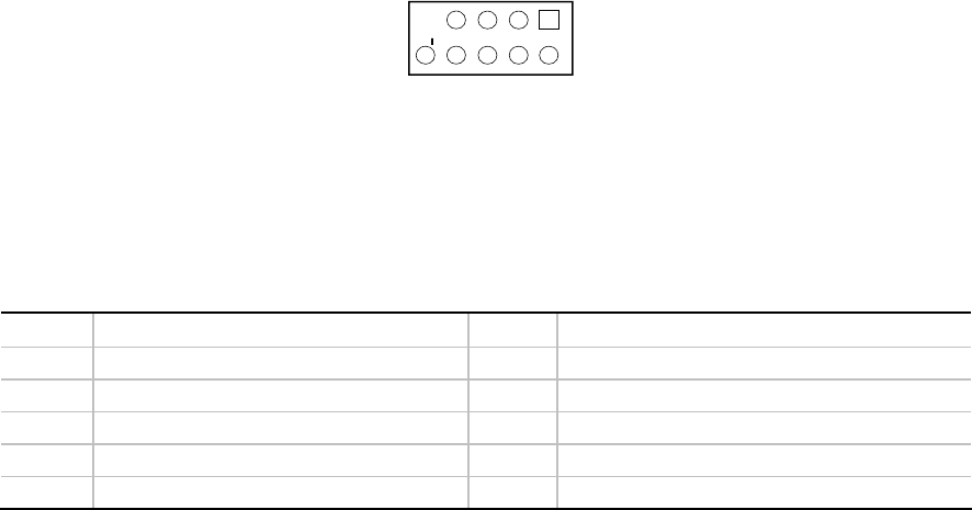
2.2.4 Header Design
OM14806
2
1
2
110
9
6
5
CB
DE
A
51 9
2
6
1
2
10
Header Description Item Pins Description Manufacturer's Part
Number Note
IR Front Panel Header
(see Table 4) A 1, 2, 3, 5,
and 6 Infrared port Wieson Electronic
2100C888-062
B 5 and 7 Reset switch
C 1 and 3 Hard drive activity LED
D 2 and 4 Power / Sleep /
Message waiting LED
Switch/LED Front Panel
Header (see Table 5)
E 6 and 8 Power switch
Wieson Electronic
2100C888-045
Note: Or approved equivalent.
Figure 1. Front Panel Switch/LED and IR Headers (Top View)

Intel Front Panel I/O Connectivity Design Guide
18
2.2.5 Pin Assignments
The following two tables list the pins for the IR and Switch/LED headers. To support a legacy
2x8-pin connector to connect to both headers, see Note 3 following Table 5.
Table 4. IR Front Panel Electrical Connection
Pin Signal Description Pin Signal Description
1 IRRX2 IrDA serial input 2 GND Ground
3 GND Ground 4 (No pin) Key
5 IRTX2 IrDA serial output 6 +5 V IR power
Table 5. Switch/LED Front Panel Electrical Connection
Pin Signal Description
1 HD_LED_P Hard disk LED pullup (330 Ω) to +5 V
2 FP PWR/SLP MSG LED pull-up (330 Ω) to +5 V Standby Note 1
3 HD_LED_N Hard disk active LED
4 FP PWR/SLP MSG LED pull-up (330 Ω) to +5 V Standby
5 RST_SW_N Reset switch tied to GND
6 PWR_SW_P Power switch high reference pull-up (2.2 kΩ) to +3.3 V Standby Note 2
7 RST_SW_P Reset switch high reference pull-up (1 kΩ to voltage appropriate for the
mainboard circuit, such as, +3.3 V for the ICH bridge)
8 PWR_SW_N Power switch tied to GND
9 RSVD_DNU Reserved. Note 3
Notes:
1. Standby voltage is the voltage that is active during a sleep state that your board supports.
2. If you want to tie this pin to +5 V Standby, adjust the pull-up resistor size (to 10 kΩ, for example).
3. If you want to support the legacy 2x8 connector, place a 0 ohm shorting resistor between pin 9 and +5 V.

Front Panel Legacy I/O
19
2.3 Front Panel Audio
2.3.1 Usage Model
The design options described below support standard front panel microphone and headphone usage
(for Standard AC’97 implementation) and also support new dynamic front panel jack detection and
re-tasking usage models (for Intel® High Definition Audio).
2.3.2 Features
The front panel audio connector is designed to support stereo audio output (headphone or amplified
speakers) and a microphone input. Designs using Intel® High Definition Audio (Intel® HD Audio)
permit the two front panel jacks to be dynamically reconfigured as input or outputs, depending
upon the desired application.
2.3.3 Audio Design Considerations
Front panel audio design in conjunction with motherboard audio header design is dependant upon
the type of audio CODEC being used on the motherboard. In the past, AC97 Integrated Audio
CODECs were prevalent. With the introduction of Intel High Definition Audio, many new
motherboard designs are switching over to High Definition (HD) audio CODECs. Designers
should note that AC’97 and Intel High Definition Audio front panel motherboards and I/O cards
implementations are different and may not be directly compatible or interchangeable
CAUTION
It is strongly recommended that motherboard designers only use Intel® HD Audio analog front
panel dongles with the Intel® HD Audio analog front panel header to insure that the jack detection
and dynamic re-tasking capability is preserved. Passive AC’97 analog front panel dongles (ones
which leave the 5V Analog pin-7 line unconnected on the dongle) may be used with the Intel® HD
Audio analog front panel header. But note that the front panel jack detection and re-tasking
functionality will be lost as the AC’97 jacks cannot support connection to the SENSE line. In
addition, software must be aware that an AC’97 dongle is being used with an Intel® HD Audio
analog header since the software might need to dedicate codec ports that are connected to the
header to meet the product’s intended functionality.
2.3.4 AC’97 Audio
2.3.4.1 AC’97 Audio Electrical Considerations
A standard AC’97 front panel audio dongle schematic is shown in Figure 2. The two front panel
audio outputs (FP_OUT_L and FP_OUT_R) send and the two front panel audio returns
(FP_RETURN_L and FP_RETURN_R) connect to a switching-type, 3.5mm (1/8-inch) ring-tip-
sleeve mini-phone jack mounted on the front panel. The signal path is such that the motherboard
CODEC or output amplifier feeds the front panel jacks via FP_RETURN_L and FP_RETURN_R.
When the front panel jack is not in use, these signals pass through the front panel jack shunt springs
to the back panel jack via the signals FP_RETURN_L and FP_RETURN_R. When headphones are
Intel Front Panel I/O Connectivity Design Guide
20
plugged into the front panel jack, these return signals which feed that back panel jack are
disconnected, thus muting the back panel output.
Note that the motherboard should not leave the back panel signal floating when front panel devices
are connected. Permitting the back panel signals to float could result in excessive noise at the back
panel jack when the front panel jack is in use.
The motherboard designer should put weak pull-down resistors (10K Ohm, for example) on the
FP_RETUN_R and FP_RETURN_L lines. If using a single supply for the output amplifier, ensure
that these resistors are located after the output capacitor to avoid loading down the amplifier bias.
The grounded side of these pulldowns should be connected to analog ground to prevent digital
noise from entering the audio sub-system.
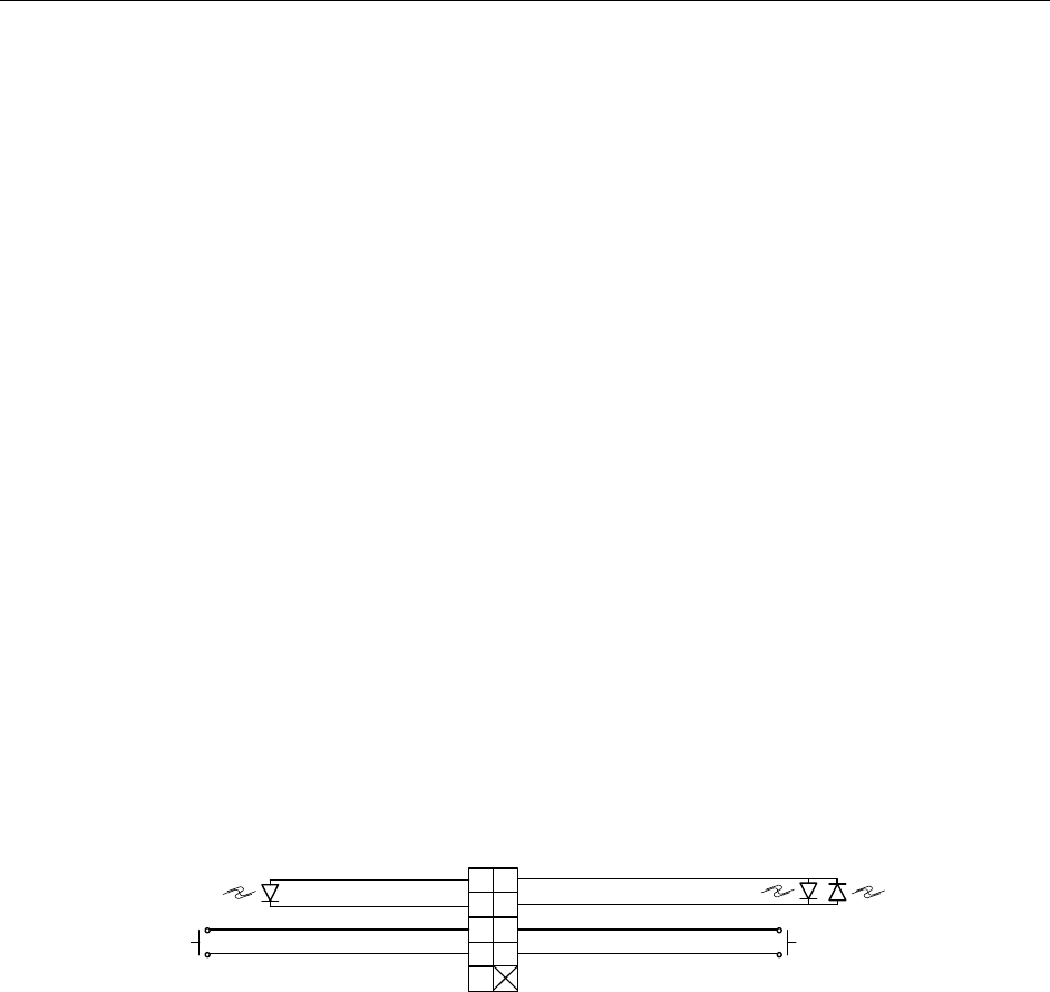
MIC AUD_GND
AC’97 Front Panel Dongle Schematic
JACK2 R
JACK2 L
12
34
56
7
910
JACK1 L
MIC BIAS
FP_OUT_R
FP_OUT_L
FP_RETURN_R
FP_RETURN_L
AUD_5V
MIC Jack
Headphone
Jack JACK1 L
Normally close shunt springs make
contact with the signal path and
cannot be used for Jack detection.
2X5 Stake Pin Header (100mil Pitch)
** Note: ZL should be 600Ω or greater @ 100MHz with a low Q (broad Impedance curve over frequency)
EMI Filter
ZL**
220pF
220pF
ZL**
ZL**
ZL**
220pF
220pF
AUD_GND
Figure 2. AC’97 Front Panel Dongle Schematic
Front Panel Legacy I/O
21
2.3.4.2 AC’97 Audio Header Design
OM10452
2
1
9
10
Figure 3. Front Panel Audio Header (Top View)
Manufacturer's Part Number: Wieson Electronic 2100C888-042 (or approved equivalent)
2.3.4.3 AC’97 Header Pin Assignments
Table 6. AC’97 Front Panel Audio Header Signal Names
Pin Signal Name Description
1 MIC Front panel microphone input signal (biased when supporting stereo
microphone)
2 AUD_GND Ground used by analog audio circuits
3 MIC_BIAS Microphone power / additional MIC input for stereo microphone support
4 AUD_GND Ground used by analog audio circuits
5 FP_OUT_R Right channel audio signal to front panel (headphone drive capable)
6 FP_RETURN_R Right channel audio signal return from front panel (when headphones
unplugged)
7 AUD_5V Filtered +5 V used by analog audio circuits
8 KEY No pin
9 FP_OUT_L Left channel audio signal to front panel (headphone drive capable)
10 FP_RETURN_L Left channel audio signal return from front panel (when headphones
unplugged)
2.3.4.4 AC’97 Header Pin Jumpers
The rear panel audio output jacks are disabled when headphones are plugged in. This feature is
implemented through the front panel audio header shown in Figure 3 and Table 6.
If the front panel interface board is not connected to the front panel audio header, jumpers should
be installed across header pin pairs 1-2, 3-4, 5-6, and 9-10. If these jumpers are not installed, the
rear panel line out connector will be inoperative and microphone input pins 1 and 3 will be left
floating, which could lead to elevated back panel microphone noise and cross talk.
NOTE
Motherboards that have the foot print for a front panel header, but depopulate the front panel
audio header must have 0 ohm resistors as options to connect the FP_OUT and FP_RETURN
signals. These resistors must be installed when the header is depopulated to insure audio is routed
to the back panel.
Intel Front Panel I/O Connectivity Design Guide
22
2.3.5 Intel® High Definition Audio
The Intel® High Definition Audio (Intel® HD Audio) analog front panel header design lets OEMs
and integrators place audio functionality on the front panel of a PC system via a cabled up front
panel dongle. Intel® HD Audio analog front panel dongles can support up to two analog audio
jacks, each of which signals user connection, or disconnection, to the operating system via the
SENSE_SEND signal. The signals for this header are defined in Table 7 and the physical header
pinout is shown in Figure 4.
Table 7. Intel® HD Audio Front Panel Analog Header Signal Names
Pin Signal Name Description
1 PORT 1L Analog Port 1 - left channel (Microphone)
2 GND Ground
3 PORT 1R Analog Port 1 - Right channel (Microphone)
4 PRESENCE# Active low signal that signals BIOS that an Intel® HD Audio dongle is connected
to the analog header. PRESENCE# = 0 when an Intel® HD Audio dongle is
connected.
5 PORT 2R Analog Port 2 - Right channel (Headphone)
6 SENSE1_RETURN Jack detection return for front panel (JACK1)
7 SENSE_SEND Jack detection sense line from the Intel® HD Audio CODEC jack detection
resistor network.
8 KEY Connector Key
9 PORT 2L Analog Port 2 - left channel (Headphone)
10 SENSE2_RETURN Jack detection return for front panel (JACK2)
PORT1 L
PORT1 R
PORT2 R
PORT2 L
SENSE_SEND
GND
PRESENCE#
SENSE1_RETURN
SENSE2_RETURN
12
34
56
7
910
2X5 Stake Pin Header (100mil Pitch)
Figure 4. Intel® HD Audio - Analog Front Panel Header
Manufacturer's Part Number: Wieson Electronic 2100C888-042 (or approved equivalent)
Front Panel Legacy I/O
23
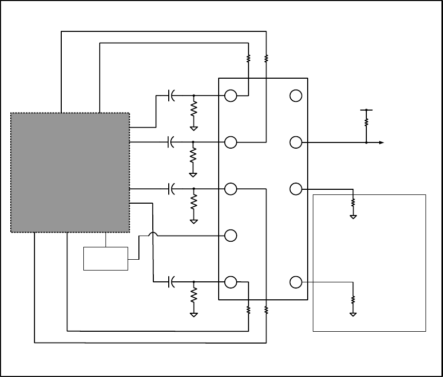
2.3.5.1 Intel® HD Audio CODEC Connections
In general, the CODEC ports selected for front panel use are connected to the Intel® HD Audio
header via series coupling capacitors C1 through C4. The resistors labeled Rbias are required if the
front panel jacks are required to support microphone functionality. Note that Figure 5 shows two
Vref output per CODEC port. The number of VREF outputs per PORT is a CODEC product
specific. Designers should consult their CODEC vendor’s datasheet for detailed information VREF
implementation, the details of the jack detection network, and selection of coupling capacitors.
VREF1_L VREF1_R
HD
CODEC
PORT1 L
PORT1 R
PORT2 R
PORT2 L
SENSE_SEND
GND
PRESENCE#
SENSE1_RETURN
To System GPI
DVDD
JACK2 R
JACK2 L
SENSEVREF2_R VREF2_L
JACK1 L
JACK1 R
Rbias Rbias
Rbias Rbias
10kΩ
Jack Detection
Network
12
34
56
7
910
C1
C2
C3
C4
Jack Detection Resistors
Rjd_port1**
SENSE2_RETURN
Rjd_port2**
** Values for jack detectiond resistors Rjd_port1 and Rjd_port2 should be chosen based on the which CODEC
ports are connected to header PORT1 and PORT2. See the HD Audio specification for more information on jack
detection resistor value assignment.
Figure 5. Intel® HD Audio Front Panel Analog Header Motherboard Schematic
Intel Front Panel I/O Connectivity Design Guide
24
2.3.5.1.1 Dongle Presence Detection
The PRESENCE# signal is used to inform BIOS that an Intel® HD Audio dongle is connect to the
motherboard. This signal should be wired to a system GPI and BIOS should poll the GPI to check
for the presence of the Intel® HD Audio dongle in the system during POST. Nominal motherboard
pullup value of 10K Ohm is required on this signal.
2.3.5.1.2 Jack Detection
Jack detection is accomplished with the use of the jack detection resistors Rjd_port1 and Rjd_port2.
The value of these resistors depends on which CODEC ports are tied to the Intel® HD Audio
analog header ports. Motherboard designers should consult the Intel® HD Audio specification for
more information on the assignment of these values for a give codec port.
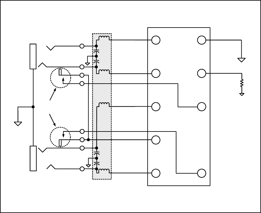
2.3.5.2 Intel® HD Audio Front Panel Connections
Figure 6 shows a Intel® HD Audio front panel dongle implementation and a Intel® HD Audio
front panel analog header schematic. The front panel dongle consists of JACK1 and JACK2, and
their associated signal pins, connected directly to their respective pins on the dongle stake pin
header. The SENSE_SEND signal is split and routed through the PORT1 and PORT2 isolated
switches. The other contact of each isolated switch, are routed to their respective sense return
signals, SENSE1_RETURN and SENSE2_RETURN. This functionality, together with the
Rjd_PORT1 and Rjd_PORT2 resistors on the motherboard as shown in Figure 5, informs the audio
driver of jack insertion or removal, which is necessary for dynamic re-taking of the front panel
jacks. Finally, a 1K Ohm pulldown is required on the PRESENCE# pin to signal BIOS that the
Intel® HD Audio front panel dongle is connected to the system.
Front Panel Legacy I/O
25
PORT1 L GND
JACK2 R
JACK2 L
12
34
56
7
910
PORT1 R
PORT2 R
PORT2 L
PRESENCE#
SENSE1_RETURN
SENSE_SEND
1kΩ
JACK 1
JACK 2
Normally Open
Isolated Switch
2X5 Stake Pin Header (100mil Pitch)
SENSE2_RETURN
EMI Filter
ZL**
220pF
220pF
ZL**
ZL**
ZL**
220pF
220pF
** Note: ZL should be 600Ω or greater @ 100MHz with a low Q (broad Impedance curve over frequency)
Figure 6. Intel® HD Audio Front Panel Dongle Implementation

27
3 Front Panel High Speed Serial Bus
What This Chapter Contains
3.1 Introduction ..................................................................................................................27
3.2 USB Connectors ..........................................................................................................27
3.3 IEEE-1394 Connector ..................................................................................................31
3.1 Introduction
This chapter contains electrical connection information for USB and IEEE 1394 front panel high-
speed serial bus connectors
3.2 USB Connectors
USB connectors must be compliant with the Universal Serial Bus 2.0 specification.
3.2.1 Usage Model
This design allows for a minimum of two front panel USB connections for access by frequent hot-
plug devices (such as cameras, game controllers, etc.).
3.2.2 Features
The USB front panel can support multiple USB ports that can be routed via a cable to the front
panel. Each 2x5 header supports two USB ports whereby each 1x5 header supports a single USB
port.
USB features include:
• Support for self-identifying peripherals that can be dynamically connected or disconnected
during computer operation (hot plugging)
• Dynamic device enumeration
• Support for isochronous and asynchronous transfer types over the same set of wires
• Support for up to 127 physical devices
• Error-handling and fault-recovery mechanisms built into the protocol
Intel Front Panel I/O Connectivity Design Guide
28
3.2.3 Dual Port USB Header
The Dual Port USB Header consists of a shrouded (Blue in color) 2x10 stake pin header (100mil
pitch) with key locations on pins 9 and 10.
Figure 7. Dual Port USB Header (Top View)
Manufacturer's Part Number: Wieson Electronic 2100C888-045 (or approved equivalent)
3.2.4 Dual Port USB Header Pin Assignments
USB ports may be assigned as needed.
Table 8. Dual Port USB Header Pin Assignments
Pin Signal names Description
1 VREG_FP_USBPWR Front panel USB power (Ports 0,1) [+5 V or +5 V Dual] Note
2 VREG_FP_USBPWR Front panel USB power (Ports 0,1) [+5 V or +5 V Dual]
3 USB_FP_P0- Front panel USB Port 0 negative signal
4 USB_FP_P1- Front panel USB Port 1 negative signal
5 USB_FP_P0+ Front panel USB Port 0 positive signal
6 USB_FP_P1+ Front panel USB Port 1 positive signal
7 Ground
8 Ground
9 Key
10 Key
Note: +5 V Dual switches between +5 V and +5V Standby depending on the current board state.
3.2.5 Single Port USB Header
The Single Port USB Header consists of a shrouded (Blue in color) 1x5 stake pin header (100mil
pitch) with key location on pin 5.
Figure 8. Front Panel Single Port USB Header (Top View)
Manufacturer's Part Number: Foxconn HF11050-UD5 (or approved equivalent)

Front Panel High Speed I/O Bus
29
3.2.6 Single Port USB Header Pin Assignments
Table 9. Dual Port USB Header Pin Assignments
Pin Signal names Description
1 VREG_FP_USBPWR Front panel USB power (Ports 0) [+5 V or +5 V Dual] Note 1
2 USB_FP_P0- Front panel USB Port 0 negative signal
3 USB_FP_P0+ Front panel USB Port 0 positive signal
4 Ground
5 Key
Note: +5 V Dual switches between +5 V and +5V Standby depending on the current board state.
3.2.7 Dual USB Header Usage
Motherboard designs that require the ability to support multiple single port USB cable connections
or the ability to be re-configured to support a Dual USB Header configuration will benefit from the
header shown in the Dual Port Header drawing (Figure X). This header can be used to support two
side by side single port USB cable connections, one single port USB cable connection, or a single
two port USB cable connection.
3.2.8 Electrical Considerations
Care should be taken when implementing USB designs such that signal quality and power delivery
are not compromised. Certain basic guidelines should be followed:
• There should be only one over current protection fuse between the motherboard and the USB
connector in the front panel USB dongle (see Section 3.2.8.1).
• EMI and ESD components should be included (see Sections 3.2.8.3 and 3.2.8.4).
• Front panel and rear panel USB connectors should use separate fuses.
The location of the Front Panel I/O header on the mainboard should take into account the trace
lengths on the mainboard and interface board as well as the front panel cable length, otherwise
signal quality could be affected. See the USB 2.0 specification for details and testing information.
3.2.8.1 Fuse Element
The fuse element used for USB power delivery must be placed down on the motherboard so the
following functions can be performed:
• Protects the motherboard from damage in case of a short between USBPRW and ground.
• Provides some measure of protection from damage if an unkeyed cable is inadvertently plugged
into the front panel USB connector and shorts USBPRW.
• Provides protection to the motherboard in the case where the front panel cable is cut or
damaged during assembly or manufacturing resulting in a short between the USBPWR and
ground.
Intel Front Panel I/O Connectivity Design Guide
30
NOTE
Ensure that fuse elements are not present on both the motherboard and the cabled solution.
Having fuse elements in both locations results in a voltage drop at the USB connector, which may
make the USB 2.0 solution non-compliant.
3.2.8.2 USBPWR Bypass Capacitance
Refer to the USB 2.0 Specification for details on the power distribution requirements. Voltage drop
and droop testing procedures are also available at:
http://www.usb.org/developers/
3.2.8.3 Filter Components
Filtering must be carefully addressed to ensure that the system meets EMC requirements.
NOTE
Ensure that filter components are not present on both the mainboard and the cable solution.
Systems with filter elements in both locations may not meet the USB Specification signal quality
requirements.
3.2.8.4 ESD Components
ESD suppression components should be included to ensure that the system meets applicable ESD
requirements.
3.2.8.5 Mainboard Power Requirements
See the USB 2.0 specification for the voltage and current requirements that must be maintained at
the front panel interface board’s USB connector.
3.2.8.6 Mainboard Signal Quality Requirements
The signal quality as measured at the USB front panel connectors must meet the requirements given
in the most recent USB Specification.
White papers describing the signal quality compliance testing procedures for USB Low Speed and
Full Speed signaling performed at USB Plugfests are available. See Section 1.1, page 9 for
additional information.
A design guide for integrating a discrete USB 2.0 host controller onto a four-layer desktop
mainboard is also available. See Section 1.1, page 9 for additional information.
Front Panel High Speed I/O Bus
31
3.3 IEEE-1394 Connector
3.3.1 Usage Model
IEEE-1394 connectivity allows for data transfer between the PC and consumer electronic devices
such as digital cameras and camcorders.
3.3.2 Features
This chapter summarizes the design recommendations for hardware using the IEEE 1394 standards.
The IEEE 1394 high-speed serial bus complements USB by providing enhanced PC connectivity
for a wide range of devices, including consumer audio/video (A/V) components, storage
peripherals, other PCs, and portable devices.
IEEE 1394 has been adopted by the consumer electronics industry and is expected to provide a
volume, Plug and Play-compatible expansion interface for the PC.
The 100-Mb/s, 200-Mb/s, and 400-Mb/s transfer rates currently specified in IEEE 1394 are well
suited to multi-streaming I/O requirements. Figure 9 and Table 10 show the header and pin
assignments for the IEEE-1394 connector.
3.3.2.1 Basic Requirements
The following is a summary of the IEEE 1394 design considerations related to PC systems:
• A front-panel port designed to support the IEEE 1394 standard
• Support for the 1394 Open HCI specification for controllers, specifically OHCI Revision 1.1
• Plug and Play support for device configuration, control and status registers (CSRs), connectors
and cabling, and connection fault-handling
• Cable power distribution, including requirements for source devices, sink devices, self-powered
devices, and supporting CSRs
• Device power management, CSRs, and soft-power protocols
• Device command protocols for audio, video imaging, still imaging, and storage device classes
• 12 V fused supply
• See the latest revision of the IEEE 1394 standard for voltage and current requirements.
Intel Front Panel I/O Connectivity Design Guide
32
3.3.3 Header Design
OM09486
2
1
10
9
Figure 9. Front Panel IEEE-1394 Connector (Top View)
Manufacturer's Part Number: Wieson Electronic 2100C888-046 (or approved equivalent)
3.3.4 Pin Assignments
Table 10. Front Panel IEEE-1394 Connector
Pin Signal Name Pin Signal Name
1 TPA+ 2 TPA-
3 Ground 4 Ground
5 TPB+ 6 TPB-
7 +12V (Fused) 8 +12V (Fused)
9 Key (no pin) 10 Ground
Note: IEEE-1394 ports may be assigned as needed.
33
4 Cabling Design Guidelines
What This Chapter Contains
4.1 Introduction ..................................................................................................................33
4.2 Switch/LED Cable ........................................................................................................33
4.3 Front Panel Audio Cable..............................................................................................34
4.4 USB Cabling (Mainboard to I/O Interface Board).........................................................37
4.1 Introduction
This chapter contains reference cable designs for the switch/LED and audio cable that are
compatible with the connector pinouts described in Chapters 2 and 3.
NOTE
To prevent cable unseating, cables should be secured within the system. Tie wraps and/or sheet
metal features could be used to implement this. Cables that are permanently attached to the front
panel interface board could also be implemented, however the interface to the mainboard should
remain as specified.
4.2 Switch/LED Cable
Figure 10 shows the proper use of the switch/LED header. Great flexibility in cabling is permitted
as long as this diagram is followed.
P1
21
3 4
65
87
9
(YELLOW)
HARD DRIVE LED
(GREEN) / (YELLOW)
POWER/SLEEP/MESSAGE WAITING LED
POWER
SWITCH
RESET
SWITCH
KEY
Figure 10. Switch/LED Cable
Intel Front Panel I/O Connectivity Design Guide
34
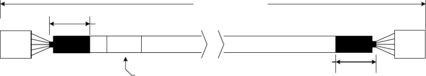
4.3 Front Panel Audio Cable
4.3.1 Introduction
This section details the design of an audio cable to be used in conjunction with the front panel I/O
board.
The shielding in this cable is important to reduce cross talk, signal degradation, and coupling of
electromagnetic interference. The shielding is especially important for the microphone circuit since
it is a low-level signal and is very sensitive to noise.
The suggested maximum length for this cable is 18 inches as shown in Figure 11. Figure 12 and
Figure 13 show the cable shielding details. Table 11 and Table 12 lists the pin assignments and
materials list. Table 13 provides additional information for the audio cable.
4.3.2 Cable Drawings
NOTE
Drawings are not shown to scale.
XXXXXX-
XXX
17.75 ± 0.25 in
1.0 in Max
1.0 in Max
P2
Item Identification
Number & Assembly
Vendor Identification
P1
Figure 11. Front Panel Audio Cable Dimensions
Cabling Design Guidelines
35
Twisted Signaling Pair D:
Twisted Signaling Pair C:
Cover Jacket
Inner Shield:
Aluminum Metalized Polyester
Shield:
> 65% Interwoven
Tinned Copper Braid
Twisted Signaling Pair B: Twisted Signaling Pair A:
A
ll Shields Tied Together
Figure 12. Front Panel Audio Cable Cross-Section
KEY
26
26
26
26
26
26
26
26
AWG
1
10
6
5
7
4
3
P1
9
2
2
2
2
2
8
P2
1
10
6
5
7
4
3
9
2
2
2
2
2
8KEY
A
D
B
C
Figure 13. Audio Cable Wiring Diagram
Table 11. Front Panel Audio Cable and Connector Pin Assignments
AWG Pairing PIN P1 / P2
26 A 1 / 1
N/A 2 / 2
26 A 3 / 3
26 B 4 / 4
26 C 5 / 5
26 C 6 / 6
26 B 7 / 7
N/A KEY 8 / 8
26 D 9 / 9
26 D 10 / 10
Table 12. Audio Cable Construction Recommendations
Part Qty Manufacturer's Part
NumberNote
Material Description Note
2X5 Header 2 Berg 65043-032 Header

Intel Front Panel I/O Connectivity Design Guide
36
Key 2 N/A Key
Heat-Shrink Tubing As req. N/A UL Heat-shrink Tube
26 AWG
(4 twisted pair
shielded wire)
As req. N/A UL Certified Conductor Wire
Part Label 1 N/A Manufacturer’s name and P/N
Note: Or approved equivalent.
Table 13. Additional Audio Cable Recommendations
Characteristic Specification
Flammability Rating UL-94 VW-1
Insulation Resistance 5000 ohms @ 300 VDC
Temperature Range - 55 °C to + 80 °C
Withstand Voltage 1000 VDC @ 60 Hz
Plating Per materials list.
Wire Per materials list.
Workmanship Parts shall be uniform in workmanship and appearance. There shall be
no excessive nicks, deep scratches, excessive burrs, or defects in
materials that may affect the function, serviceability, or appearance of this
part.
Contact retention equal to or greater than 2.0 oz. per contact, when
unmated force: from the proper connector.
Maximum Insertion Force: 10 pounds per connector.
Dimensioning and Tolerances Per ANSI Y14.5M unless otherwise noted on drawing.
UL Marking The cable manufacturer should supply UL recognized cables that are
certified under the UL wiring harness program (ZPFW2). The UL
recognition mark should be supplied with the smallest container or bundle
of cables with each shipment.
Recognition Mark The UL recognized wire’s insulation will have surface printing identifying
the style, flammability rating, manufacturer’s name, voltage and
temperature ratings, along with the UL mark.
Cabling Design Guidelines
37
4.4 USB Cabling (Mainboard to I/O Interface Board)
4.4.1 Introduction
This chapter provides some details of the design for a front panel USB 1.1 and 2.0 interface cable to
be used in conjunction with the front panel I/O interface board and main board. The interface cable
must be shielded as specified in Figure 14, for two reasons:
• To ensure the cable data lines meet the required differential characteristic impedance as given
in the most recent USB specification. Cables with an impedance variation outside of the USB
specification limits will degrade signal quality and could cause front panel USB devices to fail
to operate reliably.
• To shield the cable from RF emissions inside the chassis. Improperly shielded interface cables
can pick up these internally radiated signals and cause the system to fail EMI testing.
Figure 14 and Figure 15 show the recommended USB interface cable shielding details and pin
assignments. Pin assignments are further detailed in Table 14. The cable materials (including
connectors) and construction should enable the system to meet the performance requirements of the
most current USB 2.0 Specification and applicable safety and regulatory requirements.
Table 15 and Table 18 show some current recommendations regarding cable parts and materials.
The cable length (in combination with the trace lengths on the main board and front panel I/O
interface board) must be such that it will satisfy the signal quality requirements (propagation delay,
etc.) given in the most recent version of the USB 2.0 Specification.
Intel Front Panel I/O Connectivity Design Guide
38
4.4.2 Cable Drawings
Twisted Signaling Pair A:
White: USB_FP_P0-
Green: USB_FP_P0+
Twisted Signaling Pair B:
White: USB_FP_P1-
Green: USB_FP_P1+
Cover Jacket
Inner Shield:
Aluminum Metalized Polyester
Non-Twisted:
Red: VREG_FP_USBPWR0
Non-Twisted:
Black: GROUND
Outer Shield:
> 65% Interwoven
Tinned Copper Braid
Figure 14. Dual Port USB Cable Cross Section
KEY
Signal
20
20
VREG_FP_USBPWR0
GROUND
28
28
USB_FP_P1-
USB_FP_P1+
28
28
USB_FP_P0-
USB_FP_P0+
AWG
3
8
1
6
4
5
P1
10
7
7
7
7
9
P2
3
8
1
6
4
5
10
7
7
7
7
9KEY
A
B
2 2Unused Unused
GROUND (Shield)N/A
Twisted Pair
KEY KEY
Figure 15. Dual Port USB Cable Wiring Diagram

Cabling Design Guidelines
39
Table 14. Dual Port USB Cable and Connector Pin Assignments
Signal AWG Color PIN P1 / P2
VREG_FP_USBPWR 20 Red 1 / 1
VREG_FP_USBPWR 20 Red 2 / 2
USB_FP_P0- 28 White 3 / 3
USB_FP_P1- 28 White 4 / 4
USB_FP_P0+ 28 Green 5 / 5
USB_FP_P1+ 28 Green 6 / 6
GROUND (Shield) N/A N/A 7 / 7
GROUND 20 Black 8 / 8
KEY N/A N/A 9 / 9
KEY N/A N/A 10 / 10
Table 15. Dual Port USB Cable Material List
Part Qty Manufacturer's Part
NumberNote
Material Description Note
2X5 Header 2 Berg 65043-032 (or equivalent) Header
Key 2 N/A Key
Heat-Shrink Tubing As req. N/A UL Heat-shrink Tube
Shield cable consisting of:
2 28 AWG twisted pairs,
2 20 AWG discrete wires
As req. N/A UL Certified Conductor Wire
Part Label 1 N/A Manufacturer's name and P/N
Note: Or approved equivalent.
NOTE
Computer systems that have an unshielded cable attached to a USB port may not meet FCC
Class B requirements, even if no device or a low-speed USB device is attached to the cable. Use
shielded cable that meets the requirements for full-speed devices.
Intel Front Panel I/O Connectivity Design Guide
40
Twisted Signaling Pair A :
White: USB_FP_P0-
Green: USB_FP_P0+
Cover Jacket
Inner Shield:
Aluminum Metalized Polyester
Non-Twisted:
Red: VREG_FP_USBPWR0
Non-Twisted:
Black: GROUND
Outer Shield:
> 65% Interwoven
Tinned Copper Braid
Figure 16. Single Port USB Cable Cross Section
KEY
Signal
20
20
VREG_FP_USBPWR0
GROUND
28
28
USB_FP_P0-
USB_FP_P0+
AWG
2
1
3
P1
4
4
4
5
P2
KEY
A
GROUND (Shield)N/A
Twisted Pair
2
1
3
4
4
4
5
Figure 17. Single Port USB Cable Wiring Diagram
Table 16. Single Port USB Cable and Connector Pin Assignments
Signal AWG Color PIN P1 / P2
VREG_FP_USBPWR0 20 -28 Red 1 / 1
USB_FP_P0- 28 White 2 / 2
USB_FP_P0+ 28 White 3 / 3
GROUND 20 - 28 Black 4 / 4
GROUND (Shield) N/A N/A 4 / 4
KEY N/A N/A 5 / 5

Cabling Design Guidelines
41
Table 17. Single Port USB Cable Material List
Part Qty Manufacturer's Part
NumberNote
Material Description Note
1X5 Header 2 Foxconn* JWT: A2541H02-
1X5P (or equivalent) Header
Key 1 N/A Key
Heat-Shrink Tubing As req. N/A UL Heat-shrink Tube
Shield cable consisting of:
1 28 AWG twisted pairs,
2 20 – 28 AWG discrete
wires
As req. N/A UL Certified Conductor Wire
Part Label 1 N/A Manufacturer's name and P/N
Note: Or approved equivalent.
NOTE
Computer systems that have an unshielded cable attached to a USB port may not meet FCC
Class B requirements, even if no device or a low-speed USB device is attached to the cable. Use
shielded cable that meets the requirements for full-speed devices.
Table 18. USB Cable Recommendations
Characteristic Specification
Flammability Rating UL-94 VW-1
Insulation Resistance 5K ohms @ 300 VDC
Temperature Range - 55 °C to + 80 °C
Withstand Voltage 1000 VDC @ 60 Hz
Plating Per materials list.
Wire Per materials list.
Workmanship Parts shall be uniform in workmanship and appearance. There shall be
no excessive nicks, deep scratches, excessive burrs, or defects in
materials that may affect the function, serviceability, or appearance of this
part.
Contact Retention Force Equal to or greater than 2.0 ounces per contact, when unmated from the
proper connector.
Maximum Insertion Force 10 pounds per connector.
Dimensioning and Tolerances Per ANSI Y14.5M unless otherwise noted on drawing.
UL Marking The cable manufacturer should supply UL Recognized cables that are
certified under the UL wiring harness program (ZPFW2). The UL
recognition mark should be supplied with the smallest container or bundle
of cables with each shipment.
The UL recognized wire’s insulation will have surface printing identifying
the style, flammability rating, manufacturer’s name, operating voltage and
temperature ratings, along with the UL recognition mark.
43
5 Interface Board Design Guidelines
What This Chapter Contains
5.1 Introduction ..................................................................................................................43
5.2 Front Panel I/O Interface Board Dimensions ...............................................................45
5.1 Introduction
The following chapter defines the mechanical recommendations of a front-panel interface board.
The definition includes physical raw board size, mounting holes, keep-out zones and recommended
physical tolerances. A compliant front panel interface board can be used in any chassis design that
supports these key features. Figure 18 shows recommended dimensions of the front panel aperture
and interface board placement.
The front panel I/O guideline defines an I/O aperture opening area that is 3.875+/- 0.008 inch
(98.43 +/- 0.20 mm) wide by 1.000 +/- 0.008 inch (25.40+/- 0.20 mm) tall. To retain maximum
flexibility, the exact positioning and configuration of the connectors within the I/O connector zone
is left to the discretion of the designer. The connectors shown in Figure 18 are a reference design
and are shown here only as examples.
Figure 18. Front Panel I/O Aperture and Interface Board Placement Recommendations
Intel Front Panel I/O Connectivity Design Guide
44
Figure 19 shows the front panel I/O board interface recommendations. The face of the front panel
I/O board edge should be placed 0.053 +/- 0.010 inch (1.35 +/- 0.25 mm) from the inside of the
chassis front panel I/O shield and/or chassis housing. The connectors shown here are only
examples.
It is the front panel I/O board designer’s responsibility to properly place the connector to meet front
panel I/O aperture and interface recommendations. (The front panel I/O shield is not shown.)
Figure 19. Front Panel I/O Interface Board Placement Recommendations
Interface Board Design Guidelines
45
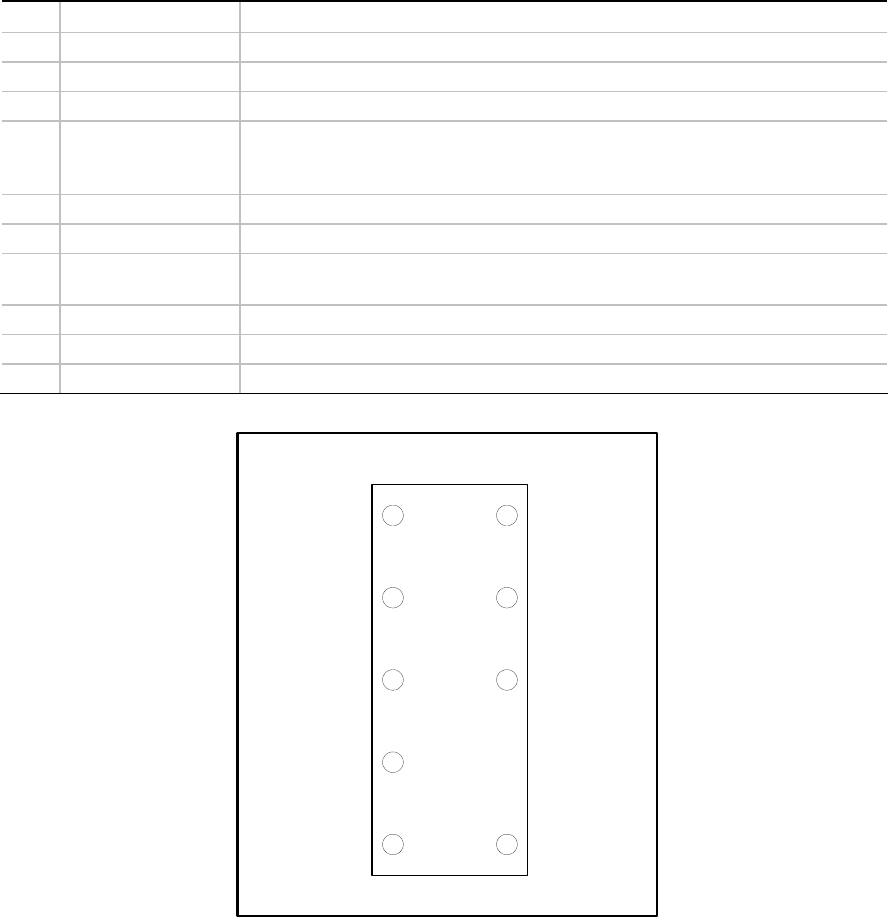
5.2 Front Panel I/O Interface Board Dimensions
The front panel I/O interface board guideline defines an I/O aperture opening area that is
3.875 +/- 0.008 inch (98.43 +/- 0.20 mm) wide by 1.000 +/- 0.008 inch (25.40 +/- 0.20 mm) tall.
This area allows the use of stacked connectors on the board to maximize the amount of available
I/O space.
As shown in Figure 20 and Figure 21, the front panel I/O board guideline defines several keep-out
zones that are necessary for chassis interface features. A typical, 0.062-inch (1.57 mm) thick board
has a 0.100 to 0.108-inch (2.5 to 2.7 mm) keepout zone defined around the perimeter of the board,
and on both sides of the board. The keep-out zones provide reserved areas that can be used to
interface with a chassis-dependent front I/O housing or supporting structures. The keep-out zones
should be used as ground contact areas to increase ground return for EMI attenuation.
No components, connectors or other features should be placed within the keepout zones. The
maximum component height on the primary component side of the board (including board
thickness) is not to exceed 0.763 inch. (19.37 mm). The maximum component height on the
secondary side of the board is not to exceed 0.043 inches (1.09 mm). If the keepout zones are
violated, the board forfeits compatibility with the front panel I/O board-compliant chassis as
detailed in Figure 18 and Figure 19.
As shown in Figure 20 and Figure 21, the front panel I/O board guideline defines a board width of
3.500 +/- 0.008 inch. (88.90 +/- 0.20 mm), a minimum board depth of 1.500 inches (38.10 mm) and
a maximum board depth of 2.500 inches (63.50 mm). This variable board depth is intended to
retain flexibility for present and future technologies.
For the best EMI attenuation and proper grounding performance, board connector placement should
be limited as shown in Figure 18 and Figure 19 to allow enough clearance between the connectors
and the chassis opening for the I/O shield and/or front I/O housing structures. The indented notches
provided in the board definition may be used for a screw-less and/or clip retention method.
Refer to Figure 20 and Figure 21 for other front panel I/O interface board dimension and tolerance
recommendations. The connectors shown here are only examples.
Intel Front Panel I/O Connectivity Design Guide
46
Figure 20. Front Panel I/O Board Dimensions (Top and Front Views)
Figure 21. Front Panel I/O Board Dimensions (Bottom View)

47
6 Chassis and I/O Shield Guidelines
What This Chapter Contains
6.1 Introduction ..................................................................................................................47
6.2 Front Panel I/O Board Placement ................................................................................47
6.3 Front Panel I/O Reference Designs .............................................................................50
6.1 Introduction
This chapter defines the chassis and I/O shield mechanical guidelines for the front panel I/O
interface. Typical chassis interfaces should adhere to the definitions of the front panel I/O board’s
keep-out zones, and mounting hole recommendations. Compliant front panel chassis interface
boards can be used in any chassis design that supports these key features.
Beyond the specific aperture opening and keep-out zones, the chassis and bezel implementation of
the front panel I/O board is not limited to specific features or locations.
NOTE
Figure 18 and Figure 19 are repeated as Figure 22 and Figure 23 in this chapter for convenience
only.
6.2 Front Panel I/O Board Placement
The exact location of the front panel I/O board is not specified. It is recommended that it be placed
in the front of the system in either a horizontal or a vertical orientation. When placing the front
panel I/O board, the designer should consider that the proper clearance should be provided for the
chassis peripheral bays and mainboard keepout recommendations. The system designer should also
take into consideration impact to system front airflow, venting, and full-length add-in board
retention features.
As shown in Figure 22, the bottom of the front panel opening is located 0.045 to 0.055 inches (1.15
to 1.39 mm) below the bottom of a typical, 0.062 inches (1.57 mm) thick board. Also, a 0.1 inches
(2.54 mm) minimum keepout zone has been defined around the perimeter of the aperture area, on
both inside and outside surfaces of the chassis front panel. The keepout zone provides a reserved
space that can be used to attach a chassis-independent front I/O shield into the chassis front panel.
No slots, tabs, notches, or other topographical features should be placed within the keepout zone.
Interface board connector placement should be limited as shown in Figure 22 and Figure 23 to
allow enough clearance between the connectors and the chassis opening for the I/O shield.
Intel Front Panel I/O Connectivity Design Guide
48
It is strongly recommended for the best EMI attenuation performance, paint should not be applied
within the 0.1 inches (2.54 mm) minimum keepout zone on the inside and outside surfaces of the
chassis front panel (Figure 22). Paint can prevent proper grounding of the I/O shield to the front
chassis panel. The list below shows some front panel I/O board highlights.
• Cutout size = 3.875 +/- 0.008 inches (98.43 +/- 0.20 mm) wide by 1.00 +/- 0.008 inches (25.4
+/- 0.20 mm) tall. See Figure 22.
• Distance from bottom of typical 0.062 inches (1.57 mm) thick board to bottom of I/O cutout
hole = 0.045 to 0.055 inches (1.14 to 1.39 mm). See Figure 22.
• Allowable thickness of the chassis front panel that the I/O shield can clip into is in the range
0.030 inches (0.76 mm) to 0.052 inches (1.32 mm).
The interface board’s width is 3.500 +/- 0.008 inches (88.90 +/- 0.20 mm), its minimum depth is
1.500 inches (38.10 mm), and its maximum depth is 2.500 inches (63.50 mm), see Figure 20 and
Figure 21.
• The corners of the I/O aperture can be rounded to a maximum radius of 0.030 inches (0.76 mm)
as shown in Figure 22. This allowable rounding of the corners helps chassis manufactures
extend the life of their hard tooling while still complying with this guide.
• The 0.1 inches (2.5 mm) minimum keepout zone around the I/O aperture area is used in a front
panel I/O interface board compliant chassis (see Figure 22). This allows front panel I/O
interface board- compliant I/O shields to fit into front panel I/O interface board compliant
chassis. The keepout area is used for the shield attachment points. Avoid paint application in
the area.
• The face of the Front Panel I/O board edge should be placed 0.053 +/- 0.010 inches (1.35 +/-
0.25 mm) from the inside of the chassis front panel I/O shield and/or chassis housing, as
defined in Figure 23.
• Chassis manufactures are not limited to an I/O shield implementation only. As long as the
chassis manufacturers comply with the definitions of this guide, they may choose to have
alternate methods of implementation, i.e., I/O shield or chassis dependent housing.
Figure 22 and Figure 23 detail the I/O connector zone. Compliance with this recommendation is
necessary to ensure enough clearance between the chassis aperture and the front panel I/O interface
board connectors for the I/O shield structure. This recommendation may be waived if the shield
provided with the board requires less than the recommended clearance. It is recommended that
system designers implement a universal design that would support a standard front panel I/O
aperture opening, as shown in Figure 22. To retain maximum flexibility, the exact positioning and
configuration of the connectors within the I/O connector zone is left to the discretion of the
designer. Connectors shown in Figure 22 are a reference design and are shown here only as an
example. Though it is not recommended for reasons of flexibility, a system designer may choose to
implement an integrated chassis housing and I/O shield to support and secure the front panel I/O
interface board. Then a supplied I/O shield may not be required.
Chassis and I/O Shield Guidelines
49
Figure 22. Front Panel I/O Aperture and Interface Board Placement Recommendations
Figure 23. Front Panel I/O Interface Board Placement Recommendations
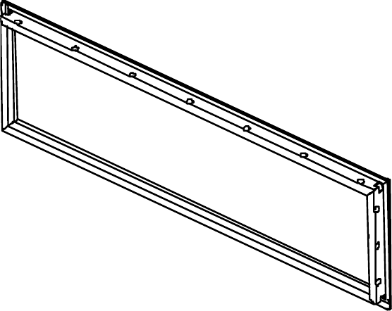
Intel Front Panel I/O Connectivity Design Guide
50
6.3 Front Panel I/O Reference Designs
Figure 24 through Figure 29 show several front panel I/O reference designs and implementations.
Additional connectors could be added if desired. These reference designs are only examples. The
front panel I/O interface board guide allows flexibility in the layout of the front panel I/O
connectors within the connector zone.
6.3.1 I/O Shield Reference Design
Figure 24 shows an example of a standard front panel I/O shield. A standard shield may
accommodate a complete connector layout to support several interface board definitions or stuffing
options. Multiple label designs could then be used to fit within the face of the shield to
accommodate board-specific layouts (label not shown).
Figure 24. Front Panel I/O Shield Reference Design
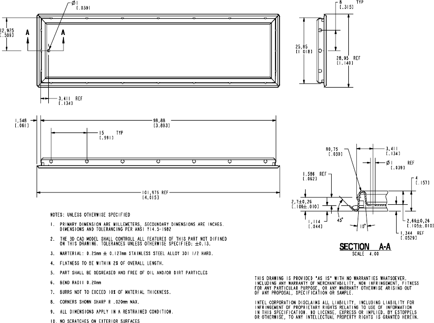
Chassis and I/O Shield Guidelines
51
Figure 25 shows an example of a standard I/O shield reference design. It is provided here as only a
reference for key features that may be used to design and secure front panel I/O shields into a
standard front panel I/O aperture opening. See Figure 18 and Figure 19 for recommended
dimensions of the front panel aperture and interface board placement.
Figure 25. I/O Shield Reference Design
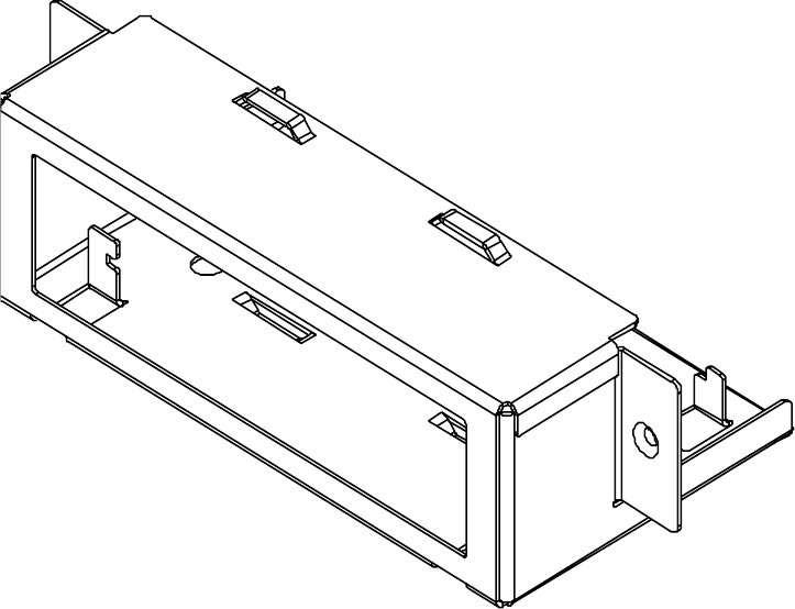
Intel Front Panel I/O Connectivity Design Guide
52
6.3.2 Housing Reference Design
Figure 26 shows an example of a chassis-dependant housing, featuring a standard front panel I/O
aperture opening. The housing would support any board, shield, and specific label combination.
Figure 26. Front Panel I/O Housing Reference Design
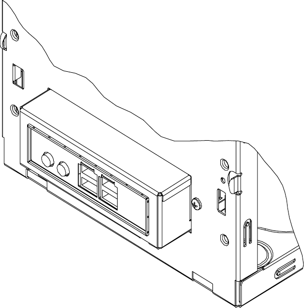
Chassis and I/O Shield Guidelines
53
6.3.3 Housing and Shield Assembly Reference Design
Figure 27 shows an example of a chassis-dependant housing assembly with standard front panel I/O
board and shield. The label is not shown in this example.
Figure 27. Front Panel I/O Housing and Shield Assembly Reference Design
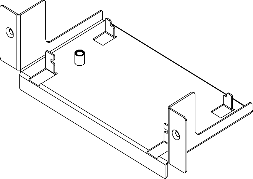
Intel Front Panel I/O Connectivity Design Guide
54
6.3.4 Supporting Structure Reference Design
Figure 28 shows an example of a chassis-dependant support structure, which should be used in
conjunction with a standard front panel I/O shield.
Figure 28. Front Panel I/O Interface Board Support Structure Reference Design
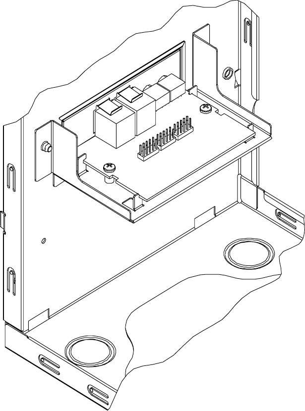
Chassis and I/O Shield Guidelines
55
6.3.5 Supporting Structure and Shield Reference Design
Figure 29 shows an example of a chassis-dependant support structure and a standard front panel I/O
shield assembled into a chassis front panel. This chassis front panel features a standard front panel
I/O aperture opening. The support structure would support any front panel I/O interface board,
shield, and specific label combination.
Figure 29. Front Panel I/O Board Support Structure Reference Design
Intel Front Panel I/O Connectivity Design Guide
56
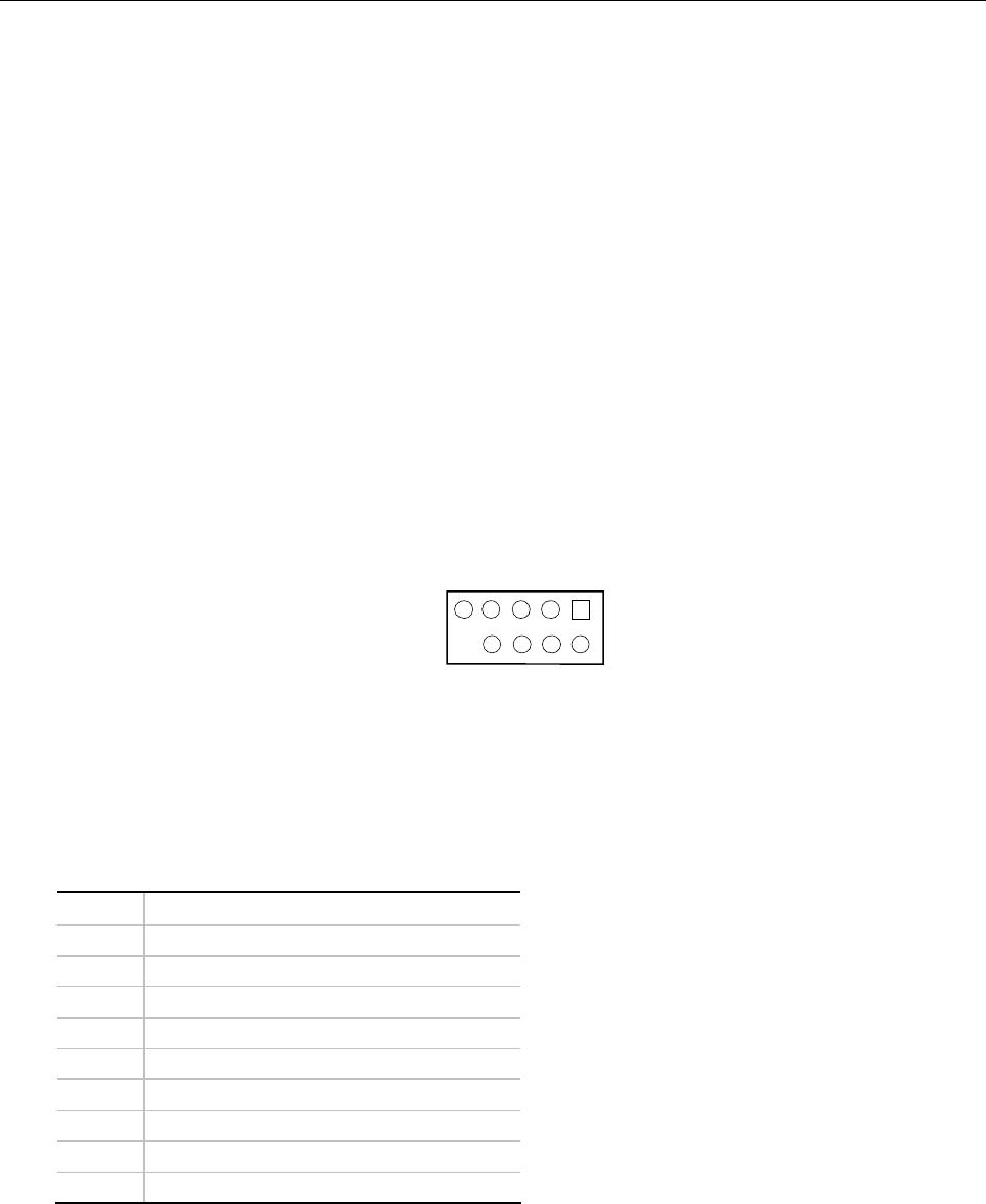
57
7 Internal Legacy Connectors (Reference)
What This Chapter Contains
7.1 Introduction ..................................................................................................................57
7.2 Serial-WHQL Debug Connector...................................................................................57
7.3 Parallel Port Connectors ..............................................................................................58
7.1 Introduction
This chapter contains electrical connection information for the internal legacy connectors.
7.2 Serial-WHQL Debug Connector
The serial-WHQL debug connector is an internal 9-pin serial port. The connector pins are listed in
Table 19. The port’s NS16C550-compatible UART supports data transfers at speeds up to
115.2 Kbits/sec with BIOS support. The port can be assigned as COM1 (3F8h), COM2 (2F8h),
COM3 (3E8h), or COM4 (2E8h).
7.2.1 Header Design
OM12197
2
1
10
9
Figure 30. Serial-WHQL Debug Connector (Top View)
Manufacturer's Part Number: Wieson Electronic 2100C888-045 (or approved equivalent)
7.2.2 Pin Assignments
Table 19. Serial-WHQL Debug Connector
Pin Signal Name
1 DCD (Data Carrier Detect)
2 DSR (Data Set Ready)
3 SIN # (Serial Data In)
4 RTS (Request to Send)
5 SOUT # (Serial Data Out)
6 CTS (Clear to Send)
7 DTR (Data Terminal Ready)
8 RI (Ring Indicator)
9 Ground
Intel Front Panel I/O Connectivity Design Guide
58
7.3 Parallel Port Connectors
Internal parallel port connection consists of:
• A 25-contact mainboard footprint for connection to a rear panel D-sub connector
• A 26 stake-pin connector on the mainboard
7.3.1 Rear Panel Connector
7.3.1.1 Connector Design
OM12198
1
14
13
25
Figure 31. Mainboard Footprint for the Parallel Port Rear Panel Connector (Bottom View)
OM12199
1
14
13
25
Figure 32. Parallel Port Rear Panel Connector (Outside View)
Manufacturer's Part Number: Foxconn DM11351-PR1 (or approved equivalent)

Internal Legacy Connectors (Reference)
59
7.3.1.2 Pin Assignments
Table 20. Parallel Port Rear Panel Connector (Centronics Standard)
Pin Standard Signal Name ECP Signal Name EPP Signal Name
1 STROBE# STROBE# WRITE#
2 PD0 PD0 PD0
3 PD1 PD1 PD1
4 PD2 PD2 PD2
5 PD3 PD3 PD3
6 PD4 PD4 PD4
7 PD5 PD5 PD5
8 PD6 PD6 PD6
9 PD7 PD7 PD7
10 ACK# ACK# INTR
11 BUSY BUSY#, PERIPHACK WAIT#
12 PERROR PE, ACKREVERSE# PE
13 SELECT SELECT SELECT
14 AUDOFD# AUDOFD#, HOSTACK DATASTB#
15 FAULT# FAULT#, PERIPHREQST# FAULT#
16 INIT# INIT#, REVERSERQST# RESET#
17 SLCTIN# SLCTIN# ADDRSTB#
18 – 25 GND GND GND

Intel Front Panel I/O Connectivity Design Guide
60
7.3.2 Stake-Pin Connector
7.3.2.1 Pin Assignments
Table 21. Parallel Port Stake-Pin Connector
Pin Standard Signal Name ECP Signal Name EPP Signal Name
1 STROBE# STROBE# WRITE#
2 AUDOFD# AUDOFD#, HOSTACK DATASTB#
3 PD0 PD0 PD0
4 FAULT# FAULT#, PERIPHREQST# FAULT#
5 PD1 PD1 PD1
6 INIT# INIT#, REVERSERQST# RESET#
7 PD2 PD2 PD2
8 SLCTIN# SLCTIN# ADDRSTB#
9 PD3 PD3 PD3
10 GND GND GND
11 PD4 PD4 PD4
12 GND GND GND
13 PD5 PD5 PD5
14 GND GND GND
15 PD6 PD6 PD6
16 GND GND GND
17 PD7 PD7 PD7
18 GND GND GND
10 ACK# ACK# INTR
20 GND GND GND
21 BUSY BUSY#, PERIPHACK WAIT#
22 GND GND GND
23 PERROR PE, ACKREVERSE# PE
24 GND GND GND
25 SELECT SELECT SELECT
26 N.C. N.C. N.C.

61
8 Internal Legacy-Free Connectors (Reference)
What This Chapter Contains
8.1 Introduction ..................................................................................................................61
8.2 LPC (Low Pin Count) Debug Connector ......................................................................61
8.1 Introduction
This chapter contains feature descriptions of the signals assigned to the internal connectors found
on legacy-free and legacy-reduced PC’s. This chapter also contains electrical connection
information.
8.2 LPC (Low Pin Count) Debug Connector
The PC-AT serial COM port has been used previously by low level debuggers (such as operating
system kernal debuggers) as the connection point between the PC under test and the debugger
console. Since the PC-AT serial COM port is no longer a feature on legacy-free and legacy-
reduced PCs, an LPC debug connector has been introduced for inclusion on main boards to provide
the debug interface.
8.2.1 Usage Model
Two types of debug connectors are considered here: the standard Debug Connector (16 pins) and
the Debug Connector with Legacy Extension (20 pins).
The 16-pin Debug Connector is intended for systems that will run a legacy-free operating system.
It consists of the minimum LPC bus signals, an I2C bus, a mechanical key, power, and ground.
The 20-pin Debug Connector with Legacy Extension is intended for use with both legacy and
legacy-free operating systems. It adds the 8042 controller legacy signals (RC# and A20GATE) and
a serial interrupt line which is used to route IRQ1 and IRQ12 to the main board. Power is required
as follows:
• 5 VDC and 3.3 VDC
• 3.3 VDC (required for the LPC interface and for the serial EEPROM)
• 5 VDC (required for the RS-232C drivers and receivers on the module)
The power pins should be de-coupled with capacitors on both the module and the main board.
De-coupling should take place at their respective connectors pins, to provide an AC signal return
path for the signals in the connecting cable.
The main board connector is a non-shrouded pin header. The main board connector uses a missing
pin at the position labeled KEYWAY to guarantee proper module cable alignment. The receptacle
connector on the module cable should have the KEYWAY location plugged to guarantee correct
installation.
Intel Front Panel I/O Connectivity Design Guide
62
8.2.2 Features
The following criteria were used to design the LPC debug module of which the LPC debug
connector (described here) is a part. The LPC debug module is to:
• Be available on all production hardware which does not include the PC-AT serial COM port
• Use standard interfaces to connect the debug console to the PC under test
• Use a no-silicon design for quick industry enabling
• Not limit the hardware configurations of the PC system under test
• Minimize the processor and memory overhead of the debug data stream of the PC under test
• Be a private resource for the operating system
• Be easily discovered and enumerated by the operating system
• Support one full duplex 57,600 bits per second serial data pipe (minimum)
The module consists of a serial communications port, implemented with a standard 16550 UART
register interface. The serial communications port registers are not allowed to appear at a legacy
COM port I/O addresses, and should be reported to the operating system using a new ACPI table.
To minimize the impact to the main board, the module interface is placed on the Intel® Low Pin
Controller (LPC) interface. Since no LPC 16550 UART is available commercially, an LPC Super
I/O device (SIO) should be used to implement the module.
The LPC SIO used should have the following attributes:
• Its registers should be plug and play compatible
• All legacy controllers (including the 8042) and interfaces in the SIO should be hardware
disabled following a PCI reset.
An I2C serial EEPROM is provided on the module to provide the BIOS with the information used
to configure the COM port in the SIO. This information and method is detailed in the BIOS
requirements section of the Intel® LPC Debug Module Requirements Specification (v1.0).
Using the serial EEPROM to specify the programming method allows any SIO that meets the above
requirements to be used on the debug module. The serial EEPROM can be assigned the I2C
addresses: 1010111xb – 1010100xb by the main board. Since only eight, I2C serial EEPROM
devices can occupy one SMBUS segment, system designers should insure there is no conflict
between the I2C address assigned to the debug module and other Serial EPROM devices in the
system.
The serial EEPROM device should be capable of being written for field upgrade support. A jumper
on the module for write-enable control is an acceptable way to implement this requirement.
The debug module is defined in such a way that it supports two operating environments:
• Operation with a legacy-free operating system
• Operation with a legacy operating system
Operation with a legacy-free operating system is the intended mode of operation of the Debug
module.
Operation with a legacy operating system may be required to support legacy-free early design
validation and manufacturing test flows. Two connector sizes are therefore recommended for the
module interface. The smaller connector only supports the debug port function. The larger
Internal Legacy-Free Connectors (Reference)
63
connector supports the signals needed to have full 8042 controller support: RC#, A20GATE, and
SERIRQ.
NOTE
Legacy operation should only be enabled for operation with a legacy operating system. This means
a BIOS setup option needs to be supported which turns legacy mode on and off. In legacy
operation mode, a PS/2† Keyboard and mouse would need to be attached to the debug module since
a legacy-free BIOS is not required to provide USB legacy keyboard emulation. In addition, when
operating the module in legacy mode, the COM port should be programmed by the BIOS to operate
as COM1.
A null modem cable is required to connect the debug module to the serial port on another PC. The
debug module uses a DB9-male connector that is wired in the standard way for a PC serial COM
port.
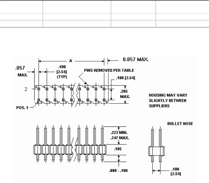
Intel Front Panel I/O Connectivity Design Guide
64
8.2.3 Header Design
8.2.3.1 Module to Mainboard Mechanical Interface
The only mechanical connection between the debug module and the main board is the LPC debug
connector. No mechanical guides or retention hardware are required.
8.2.3.2 LPC Debug Connector
The LPC debug connector for desktop systems is a vertical 0.1 inches x 0.1 inches stake-pin header
with 16 or 20 pins. Pin 4 is voided to allow keying with the mating cable. The pins are 0.025-inch
square posts or a round post with equivalent dimensioning as shown in Table 22 below.
Table 22. LPC Debug Connector Features
Connector Header Parameter “A” (inches) Number of Circuits Manufacturer's Part
Number Note
Debug 0.70 16 N/A
Legacy Extension 0.90 20 Molex 0870892016
Note: Or approved equivalent
The LPC debug connector’s physical dimensions are specified in Figure 33 below.
Figure 33. LPC Debug Connector Dimensions
The LPC debug connector’s hole pattern is shown in Figure 34 below.
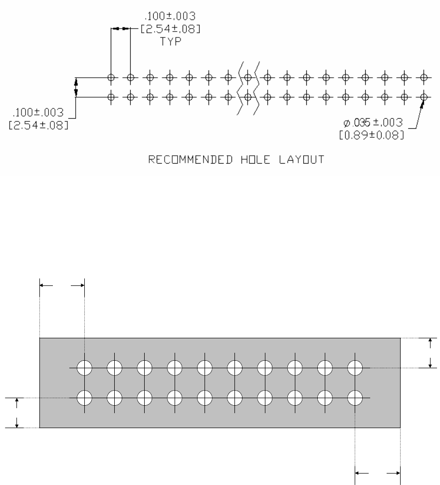
Internal Legacy-Free Connectors (Reference)
65
Figure 34. LPC Debug Connector Hole Layout
A physical keep-out around the LPC debug connector should be observed. The keep-out zone is
0.160 inches from the end of the connector hole pattern and 0.080 inches from the side of the
connector, measured from the center of any pin. The keep-out is used to allow the cable connector
to be attached without interference from adjacent components. The keep-out is shown in Figure 35.
0.160
0.080
0.080
0.160
Figure 35. LPC Debug Connector Keep-Out Zone
Intel Front Panel I/O Connectivity Design Guide
66
8.2.4 Pin Assignments
The LPC debug connector’s numbering scheme is specified in Figure 36 below.
12
3
5
7
9
11
13
15
14
17
4
6
8
10
12
16
18
12
3
5
7
9
11
13 14
4
6
8
10
12
Debug (Only) Debug with
Legacy Extension
Top View: Mating View of Connecto
r
15 16
19 20
Figure 36. LPC Debug Connector Pin Numbering
8.2.5 LPC Debug Connector Pin Assignments
The pin assignments for the LPC debug connector, and LPC debug connector with legacy extension
are shown in Table 23 below.
Table 23. LPC Debug Connector Pin Assignment
Pin Signal Pin Signal Notes
1 LCLK 2 VSS
3 LFRAME# 4 KEYWAY
5 LRST# 6 VCC5
7 LAD3# 8 LAD2#
9 VCC3 10 LAD1#
11 LAD0# 12 VSS
13 SCL 14 SDA
15 SPDA1 16 SPDA0
Debug (Only)
17 VSS 18 SERIRQ
19 RC# 20 A20GATE
Legacy Extension
