ESOMiMX7_Design_Guide E Con SOMi MX7 Carrier Board Design Guide
User Manual:
Open the PDF directly: View PDF ![]() .
.
Page Count: 61
eSOMiMX7
Version 1.0
e-con Systems
5/2/2018
Carrier Board Design Guide

© Copyright e-con Systems. 2017. All rights reserved. 1
Disclaimer
e-con Systems reserves the right to edit/modify this document without any prior
intimation of whatsoever.

2 eSOMiMX7 Carrier Board Design Guide
Contents
INTRODUCTION TO ESOMIMX7 5
ARCHITECTURE 6
NXP I.MX7 CPU 6
ON BOARD MEMORY 7
LPDDR3 SDRAM 7
EMMC OR NAND FLASH-STORAGE 7
DUAL 10/100/1GBPS ETHERNET PHY TRANSCEIVER 7
WI-FI AND BLUETOOTH COMBO 7
PIN NUMBERING 8
INTERFACE 13
MIPI DSI 13
MIPI DSI SIGNALS 14
REFERENCE SCHEMATICS AND LAYOUT GUIDELINES 14
UNUSED MIPI DSI SIGNALS TERMINATION 15
PARALLEL DISPLAY 15
PARALLEL DISPLAY SIGNALS 15
COLOUR MAPPING 16
PARALLEL DISPLAY INTERFACE SIGNALS TIMING DETAILS 17
LAYOUT GUIDELINES 17
UNUSED PARALLEL DISPLAY SIGNALS TERMINATION 17
ELECTROPHORETIC DISPLAY 18
ELECTROPHORETIC DISPLAY SIGNALS 18
EPDC INTERFACE SIGNALS TIMING DETAILS 19
UNUSED ELECTROPHORETIC DISPLAY SIGNALS TERMINATION 22
MIPI CSI 22
MIPI CSI SIGNALS 22
REFERENCE SCHEMATICS AND LAYOUT GUIDELINES 22
UNUSED MIPI CSI SIGNALS TERMINATION 23
PARALLEL CAMERA 23
PARALLEL CAMERA SIGNALS 24
UNUSED PARALLEL CAMERA SIGNALS TERMINATION 24
GIGABIT ETHERNET 24
GIGABIT ETHERNET SIGNALS 25
ETHERNET REFERENCE SCHEMATICS AND LAYOUT GUIDELINES 26
UNUSED ETHERNET SIGNALS TERMINATION 28
UNIVERSAL SERIAL BUS (USB) 28

© Copyright e-con Systems. 2017. All rights reserved. 3
UNIVERSAL SERIAL BUS SIGNALS 29
REFERENCE SCHEMATICS AND LAYOUT GUIDELINES 29
UNUSED UNIVERSAL SERIAL BUS SIGNALS TERMINATION 31
PCIE 31
PCI EXPRESS INTERFACE SIGNALS 31
REFERENCE SCHEMATICS AND LAYOUT GUIDELINES 32
UNUSED PCIE INTERFACE SIGNALS TERMINATION 32
USDHC INTERFACE 32
USDHC SIGNALS 33
USDHC INTERFACE SIGNALS TIMING DETAILS 35
UNUSED USDHC SIGNALS TERMINATION 36
SYNCHRONOUS AUDIO INTERFACE (SAI) 36
SAI SIGNALS 36
SAI INTERFACE SIGNALS TIMING DETAILS 37
UNUSED SYNCHRONOUS AUDIO INTERFACE SIGNALS TERMINATION 38
UART INTERFACE 38
UART INTERFACE SIGNALS 38
UART INTERFACE SIGNALS TIMING DETAILS 39
UNUSED UART INTERFACE SIGNALS TERMINATION 40
I2C INTERFACE 40
I2C INTERFACE SIGNALS 41
REFERENCE SCHEMATICS 41
I2C INTERFACE SIGNALS TIMING DETAILS 42
UNUSED I2C INTERFACE SIGNALS TERMINATION 43
FLEXCAN INTERFACE 43
FLEXCAN INTERFACE SIGNALS 44
REFERENCE SCHEMATICS 44
UNUSED FLEXCAN INTERFACE SIGNALS TERMINATION 44
ENHANCED CONFIGURABLE SPI INTERFACE 44
ECSPI INTERFACE SIGNALS 45
ECSPI INTERFACE SIGNALS TIMING DETAILS 45
UNUSED ECSPI INTERFACE SIGNALS TERMINATION 47
QUAD SERIAL PERIPHERAL INTERFACE 47
QSPI INTERFACE SIGNALS 48
QUAD SPI INTERFACE SIGNALS TIMING DETAILS 48
UNUSED QUAD SPI INTERFACE SIGNALS TERMINATION 50
PULSE WIDTH MODULATION 50
PULSE WIDTH MODULATION SIGNALS 50
PULSE WIDTH MODULATION SIGNALS TIMING DETAILS 51
UNUSED PULSE WIDTH MODULATION SIGNALS TERMINATION 51
UNUSED ANALOG INPUT SIGNALS TERMINATION 52
POWER AND CONTROL 53


© Copyright e-con Systems. 2017. All rights reserved. 5
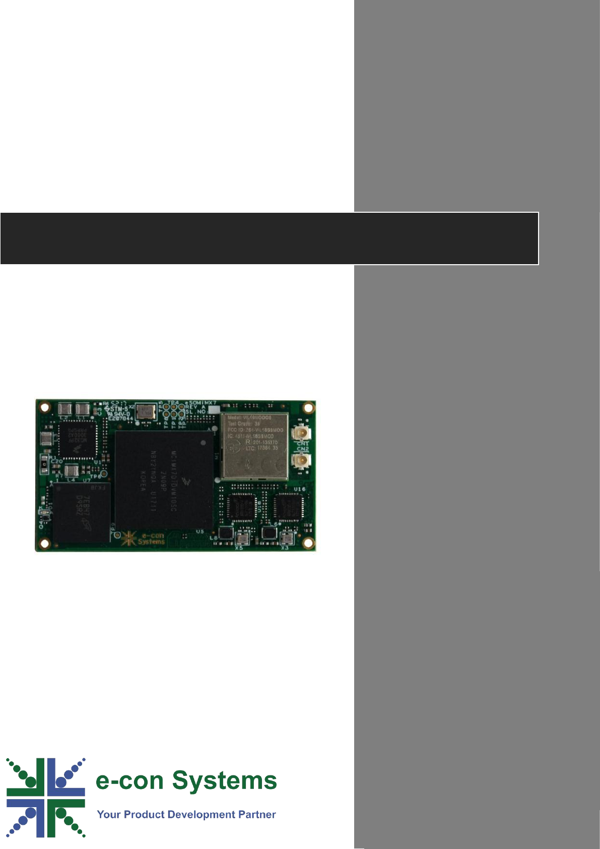
Introduction to eSOMiMX7
e-con Systems has developed an ultra-low power Computer/System-On-Module
eSOMiMX7, based on NXP®/NXP i.MX 7 embedded System on Chip (SoC) with the
basic peripherals in a compact form factor. The SoC features a single or dual-core
ARM® Cortex® A7 processor with an additional ARM Cortex M4 processor. The
eSOMiMX7 has iMX7 CPU running up to 1 GHz – Dual/Solo Core, LPDDR3-1066
SDRAM configurable up to 2 GB and eMMC configurable up to 64 GB (Only for Dual
Core) or a NAND Flash configurable up to 4 GB. The eSOMiMX7 module also has the
Wireless LAN and Bluetooth module.
This eSOMiMX7 is powered by Linux. As part of the Productized Services program of
e-con Systems, the eSOMiMX7 is aimed at reducing the time-to-market for our
customers by making use of the stabilized and ready-to-market eSOMiMX7 modules
in the customer applications. Being offered in a compact form factored modules
with various configurations and OS support, these modules will enable our
customers to focus on their application design. This enables customers to build
variety of base boards targeting various applications with a host of peripherals and
interfaces.
The module delivers state of the art technology, targeting low power systems that
still require high CPU Performance. It also offers all the interfaces needed in a
modern embedded device. It offers a wide range of interfaces from simple GPIOs,
industry standard I2C, SPI, CAN, and UART buses to high-speed USB 2.0 interfaces.
Besides the internal Flash Memory, there are several interfaces available for data
storage such as SD memory card. The CPU board also exposes the complete range of
interfaces provided by the iMX7 Application Processor through its connectors so
that the customers can access the complete functionality.
e-con Systems has a base board named Acacia built around eSOMiMX7 for
evaluation. The Acacia base board will be available for customers with complete
source code and other design inputs such as schematics, DXF etc. The complete
features of eSOMiMX7 and a variety of add-on modules supported by e-con Systems
are available on our website www.e-consystems.com. Interested customers can also
write to sales@e-consystems.com asking for specific details.
The scope of this document is to detail all the technical details of the module from
the hardware design perspective. This document will serve as a single point of
reference for hardware design of the customer application using eSOMiMX7. This
will provide the necessary details for the customers to integrate our eSOMiMX7 with
their application board design. The schematic designer and layout designer would
find this document useful.

6 eSOMiMX7 Carrier Board Design Guide
Architecture
The following figure shows the basic architecture of the eSOMiMX7 module.
Figure 1: Sample Architecture of eSOMiMX7 Module
The main hardware blocks of eSOMiMX7 are as follows:
• NXP i.MX7 CPU
• On Board Memory
• Dual 10/100/1Gbps Ethernet PHY Transceiver
• Wi-Fi + Bluetooth Combo
The following sections describe each of the main hardware blocks in detail.
NXP i.MX7 CPU
eSOMiMX7 is based on NXP’s i.MX7 Dual/Solo ARM™ Cortex-A7 core-based CPU
which can operate up to 1 GHz speed per core in the case of Dual core and up to 800
MHz in the case of Solo core.
For more information about the features, please refer to the following documents
from NXP:
• eSOMiMX7 Datasheet
• User Manual
• Application Notes

© Copyright e-con Systems. 2017. All rights reserved. 7
On Board Memory
The on-board memory types available in eSOMiMX7 are as follows:
• LPDDR3 SDRAM
• eMMC or NAND Flash-storage
LPDDR3 SDRAM
eSOMiMX7 supports the on-board memory of up to 2 GB. The iMX7 LPDDR3
interfaces up to 32-bits wide and operates at 533 MHz clock frequency.
eMMC or NAND Flash-Storage
eSOMiMX7 is available with 4GB of eMMC memory. This memory can be used for
porting OS image that is user defined storage and expandable up to 32 GB.
Note: Only the Dual core version supports eMMC.
eSOMiMX7 is available with NAND Flash as an alternate to the eMMC in the Solo
version of the SOM. NAND Flash can be expandable up to 4 GB.
Dual 10/100/1Gbps Ethernet PHY Transceiver
eSOMiMX7 features two gigabit Ethernet PHY. eSOMiMX7 can support (10Base-
T/100Base-TX/1000Base-T) for transmission and reception of data over standard
CAT-5 unshielded twisted pair (UTP) cable.
Note: Solo processor and Dual core processor with EPDC interface will support only
one Ethernet interface.
Wi-Fi and Bluetooth Combo
eSOMiMX7 contains Wi-Fi and Bluetooth module with the following features:
• IEEE STD 802.11a/b/g/n
• Bluetooth 4.1 and CSA2 Support
• Dual-Mode Bluetooth and BLE
• FCC certified module.
There are two on-Board UFL Connectors to which external antennas need to be
connected. The recommended Antennas are shown in the following table.
Table 1: Recommended Antennas
S.No
Part Number
Manufacturer
1
001-0012 , 080-0013
Laird – Wireless & Thermal solutions
2
CAF94505
Laird Technologies
8 eSOMiMX7 Carrier Board Design Guide
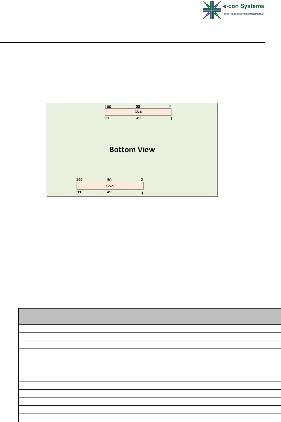
Pin Numbering
The SOM is provided with two board to board connectors on the bottom side. Each
connector consists of a hundred pin, summing up to a total of two hundred pins for
both the connectors. The pin number increases linearly with even numbers on one
side and odd numbers on the other side of each connector. The following figure
shows the sample pin numbering schema of the module.
Figure 2: Sample Pin Numbering Schema bottom side of Module
The connector used in eSOMiMX7 is as follows:
• Manufacturer Part Number: DF40C-100DP-0.4V(51)
• Manufacturer: Hirose Electric Co Ltd
The recommended mating connector for eSOMiMX7 is as follows:
• Manufacturer Part Number: DF40HC(3.0)-100DS-0.4V(51)
• Manufacturer: Hirose Electric Co Ltd
Table 2: eSOMiMX7 Connector Pin Out
CONN NO
Pin No
Pin Name
iMX7
Ball No
iMX7 Ball Name
IO Level
3
1
iMX7_CONN_QSPI_A_DATA0
P20
EPDC1_DATA00
3.3V
3
2
iMX7_CONN_QSPI_B_DATA0
M23
EPDC1_DATA08
3.3V
3
3
iMX7_CONN_QSPI_A_DATA3
N21
EPDC1_DATA03
3.3V
3
4
iMX7_CONN_QSPI_B_SS0_B
L20
EPDC1_DATA14
3.3V
3
5
iMX7_CONN_QSPI_A_DATA1
P21
EPDC1_DATA01
3.3V
3
6
iMX7_CONN_QSPI_B_DQS
L22
EPDC1_DATA12
3.3V
3
7
iMX7_CONN_QSPI_A_SS0_B
M21
EPDC1_DATA06
3.3V
3
8
iMX7_CONN_QSPI_B_DATA1
L25
EPDC1_DATA09
3.3V
3
9
iMX7_CONN_QSPI_A_DATA2
N20
EPDC1_DATA02
3.3V
3
10
iMX7_CONN_QSPI_B_DATA2
L24
EPDC1_DATA10
3.3V
3
11
iMX7_CONN_QSPI_A_DQS
N22
EPDC1_DATA04
3.3V
3
12
iMX7_CONN_QSPI_B_SS1_B
K25
EPDC1_DATA15
3.3V

© Copyright e-con Systems. 2017. All rights reserved. 9
3
13
iMX7_CONN_QSPI_A_SCLK
M20
EPDC1_DATA05
3.3V
3
14
iMX7_CONN_QSPI_B_DATA3
L23
EPDC1_DATA11
3.3V
3
15
iMX7_CONN_QSPI_A_SS1_B
M22
EPDC1_DATA07
3.3V
3
16
iMX7_CONN_QSPI_B_SCLK
L21
EPDC1_DATA13
3.3V
3
17
GROUND
3
18
ETHERNET_P2_ACT
J21
EPDC1_SDCLK *
3.3V
3
19
iMX7_CONN_EPDC_PWRCOM
H24
EPDC1_PWRCOM
3.3V
3
20
ETHERNET_P2_LED_1000M
J20
EPDC1_SDLE *
3.3V
3
21
iMX7_CONN_EPDC_PWRSTAT
K20
EPDC1_PWRSTAT
3
22
ETHERNET_P2_LED_100M
H21
EPDC1_SDOE *
3.3V
3
23
iMX7_CONN_EPDC_BDR1
K23
EPDC1_BDR1
3.3V
3
24
CONN_RGMII2_RXD3
H20
EPDC1_SDSHR *
3.3V
3
25
iMX7_CONN_EPDC_BDR0
K24
EPDC1_BDR0
3.3V
3
26
GROUND
3
27
iMX7_LCD_ENABLE
F25
LCD1_ENABLE
1.8V
3
28
CLK_iMX7_LCD_CLK
E20
LCD1_CLK
1.8V
3
29
LCD1_DATA11
G20
LCD1_DATA11
1.8V
3
30
GROUND
3
31
LCD1_DATA17
G21
LCD1_DATA17
1.8V
3
32
LCD1_DATA12
F21
LCD1_DATA12
1.8V
3
33
LCD1_DATA23
G23
LCD1_DATA23
1.8V
3
34
LCD1_DATA08
E21
LCD1_DATA08
1.8V
3
35
LCD1_DATA07
F20
LCD1_DATA07
1.8V
3
36
LCD1_DATA00
D21
LCD1_DATA00
1.8V
3
37
GROUND
3
38
LCD1_DATA04
C22
LCD1_DATA04
1.8V
3
39
iMX7_LCD_HSYNC
E25
LCD1_HSYNC
1.8V
3
40
LCD1_DATA02
B22
LCD1_DATA02
1.8V
3
41
iMX7_LCD_VSYNC
F24
LCD1_VSYNC
1.8V
3
42
LCD1_DATA15
C24
LCD1_DATA15
1.8V
3
43
LCD1_DATA14
D23
LCD1_DATA14
1.8V
3
44
GROUND
3
45
LCD1_DATA09
C23
LCD1_DATA09
1.8V
3
46
LCD1_DATA18
E23
LCD1_DATA18
1.8V
3
47
LCD1_DATA22
D25
LCD1_DATA22
1.8V
3
48
LCD1_DATA13
E22
LCD1_DATA13
1.8V
3
49
LCD1_DATA10
B24
LCD1_DATA10
1.8V
3
50
LCD1_DATA21
E24
LCD1_DATA21
1.8V
3
51
LCD1_DATA20
C25
LCD1_DATA20
1.8V
3
52
LCD1_DATA19
D24
LCD1_DATA19
1.8V
3
53
LCD1_DATA05
B23
LCD1_DATA05
1.8V
3
54
LCD1_DATA01
A22
LCD1_DATA01
1.8V
3
55
LCD1_DATA06
A24
LCD1_DATA06
1.8V
3
56
LCD1_DATA16
B25
LCD1_DATA16
1.8V
3
57
LCD1_DATA03
A23
LCD1_DATA03
1.8V
3
58
IMX7_CONN_LCD_RESET
C21
LCD1_RESET
1.8V
3
59
GROUND
3
60
GROUND
3
61
MIPI_DSI_D0_P_IMX7_CONN
B20
MIPI_DSI_D0_P
3
62
MIPI_CSI_D0_P_IMX7_CONN
B16
MIPI_CSI_D0_P

10 eSOMiMX7 Carrier Board Design Guide
3
63
MIPI_DSI_D0_N_IMX7_CONN
A20
MIPI_DSI_D0_N
3
64
MIPI_CSI_D0_N_IMX7_CONN
A16
MIPI_CSI_D0_N
3
65
GROUND
3
66
GROUND
3
67
MIPI_DSI_CLK_P_IMX7_CONN
B19
MIPI_DSI_CLK_P
3
68
MIPI_CSI_CLK_P_IMX7_CONN
B15
MIPI_CSI_CLK_P
3
69
MIPI_DSI_CLK_N_IMX7_CONN
A19
MIPI_DSI_CLK_N
3
70
MIPI_CSI_CLK_N_IMX7_CONN
A15
MIPI_CSI_CLK_N
3
71
GROUND
3
72
GROUND
3
73
MIPI_DSI_D1_P_IMX7_CONN
B18
MIPI_DSI_D1_P
3
74
MIPI_CSI_D1_P_IMX7_CONN
B14
MIPI_CSI_D1_P
3
75
MIPI_DSI_D1_N_IMX7_CONN
A18
MIPI_DSI_D1_N
3
76
MIPI_CSI_D1_N_IMX7_CONN
A14
MIPI_CSI_D1_N
3
77
GROUND
3
78
GROUND
3
79
P1MDIDN
3
80
P2MDIBN
H23
EPDC1_SDCE2 *
3.3V
3
81
P1MDIDP
3
82
P2MDIBP
H22
EPDC1_SDCE3 *
3.3V
3
83
GROUND
3
84
GROUND
3
85
P1MDIBN
3
86
P2MDIAP
J25
EPDC1_GDCLK *
3.3V
3
87
P1MDIBP
3
88
P2MDIAN
J24
EPDC1_GDOE *
3.3V
3
89
GROUND
3
90
GROUND
3
91
P1MDICN
3
92
P2MDICP
H25
EPDC1_GDSP *
3.3V
3
93
P1MDICP
3
94
P2MDICN
K21
EPDC1_GDRL *
3.3V
3
95
GROUND
3
96
GROUND
3
97
P1MDIAN
3
98
P2MDIDP
G24
EPDC1_SDCE1 *
3.3V
3
99
P1MDIAP
3
100
P2MDIDN
G25
EPDC1_SDCE0 *
3.3V
4
1
VCC_LICELL
4
2
VCC_3P3_IN
4
3
GROUND
4
4
VCC_3P3_IN
4
5
PCIe_RX_N_iMX7_CONN
AE11
PCIE_RX_N
4
6
VCC_3P3_IN
4
7
PCIe_RX_P_iMX7_CONN
AD11
PCIE_RX_P
4
8
VCC_3P3_IN
4
9
GROUND
4
10
VCC_3P3_IN
4
11
PCIe_TX_N_iMX7_CONN
AC11
PCIE_TX_N
4
12
VCC_3P3_IN

© Copyright e-con Systems. 2017. All rights reserved. 11
4
13
PCIe_TX_P_iMX7_CONN
AB11
PCIE_TX_P
4
14
VCC_3P3_IN
4
15
GROUND
4
16
VCC_3P3_IN
4
17
CLK_PCIe_CLK_N_iMX7_CONN
AC10
PCIE_REFCLKOUT_N
4
18
VCC_3P3_IN
4
19
CLK_PCIe_CLK_P_iMX7_CONN
AB10
PCIE_REFCLKOUT_P
4
20
VCC_3P3_IN
4
21
GROUND
4
22
VCC_3P3_IN
4
23
iMX7_CONN_TAMPER2
AB6
SNVS_TAMPER02
4
24
GROUND
4
25
iMX7_CONN_TAMPER1
Y8
SNVS_TAMPER01
4
26
ADC1_IN2_IMX7_CONN
AE2
ADC1_IN2
1.8V
4
27
iMX7_CONN_TAMPER0
AA7
SNVS_TAMPER00
4
28
ADC1_IN0_IMX7_CONN
AD1
ADC1_IN0
1.8V
4
29
VDD_SNVS_1P8_CAP
4
30
ADC1_IN3_IMX7_CONN
AE3
ADC1_IN3
1.8V
4
31
CPU_ONOFF
AC8
ONOFF
4
32
ADC1_IN1_IMX7_CONN
AD3
ADC1_IN1
1.8V
4
33
CPU_POR
R6
POR_B
4
34
ADC2_IN0_IMX7_CONN
AC1
ADC2_IN0
1.8V
4
35
CPU_BOOT_MODE1
P5
BOOT_MODE1
1.8V
4
36
ADC2_IN1_IMX7_CONN
AC2
ADC2_IN1
1.8V
4
37
CPU_BOOT_MODE0
P4
BOOT_MODE0
1.8V
4
38
ADC2_IN2_IMX7_CONN
AB1
ADC2_IN2
1.8V
4
39
GPIO1_IO13_IMX7_CONN
T3
GPIO1_IO13
1.8V
4
40
ADC2_IN3_IMX7_CONN
AB2
ADC2_IN3
1.8V
4
41
GPIO1_IO12_IMX7_CONN
T2
GPIO1_IO12
1.8V
4
42
GROUND
4
43
GPIO1_IO10_IMX7_CONN
R5
GPIO1_IO10
1.8V
4
44
SAI1_TXD_iMX7_CONN
E11
SAI1_TXD
3.3V
4
45
GPIO1_IO09_IMX7_CONN
R2
GPIO1_IO09
1.8V
4
46
SAI1_RXD_iMX7_CONN
E12
SAI1_RXD
3.3V
4
47
GPIO1_IO07_IMX7_CONN
P3
GPIO1_IO07
1.8V
4
48
SAI1_TXC_iMX7_CONN
C11
SAI1_TXC
3.3V
4
49
GPIO1_IO06_IMX7_CONN
P2
GPIO1_IO06
1.8V
4
50
SAI1_RXFS_iMX7_CONN
C12
SAI1_RXFS
3.3V
4
51
GPIO1_IO04_IMX7_CONN
N6
GPIO1_IO04
1.8V
4
52
SAI1_RXC_iMX7_CONN
D12
SAI1_RXC
3.3V
4
53
GPIO1_IO00_IMX7_CONN
N1
GPIO1_IO00
1.8V
4
54
SAI1_TXFS_iMX7_CONN
D11
SAI1_TXFS
3.3V
4
55
GPIO1_IO02_IMX7_CONN
N3
GPIO1_IO02
1.8V
4
56
GROUND
4
57
GROUND
4
58
CLK_SAI1_MCLK_iMX7_CONN
E10
SAI1_MCLK
3.3V
4
59
I2C4_DATA_IMX7_CONN
L2
I2C4_SDA
1.8V
4
60
GROUND
4
61
I2C4_CLK_IMX7_CONN
L1
I2C4_SCL
1.8V
4
62
UART3_RX_IMX7_CONN
M1
UART3_RXD
1.8V

12 eSOMiMX7 Carrier Board Design Guide
4
63
I2C2_DATA_IMX7_CONN
K3
I2C2_SDA
1.8V
4
64
UART1_RX_IMX7_CONN
L3
UART1_RXD
1.8V
4
65
I2C2_CLK_IMX7_CONN
K2
I2C2_SCL
1.8V
4
66
UART2_RX_IMX7_CONN
L5
UART2_RXD
1.8V
4
67
I2C3_DATA_IMX7_CONN
K6
I2C3_SDA
1.8V
4
68
UART1_TX_IMX7_CONN
L4
UART1_TXD
1.8V
4
69
I2C3_CLK_IMX7_CONN
K5
I2C3_SCL
1.8V
4
70
ETHERNET_P1_LED_1000M
4
71
SAI2_FS_iMX7_CONN
D9
SAI2_TXFS
3.3V
4
72
ETHERNET_P1_LED_ACT
4
73
SAI2_RXD_iMX7_CONN
E9
SAI2_RXD
3.3V
4
74
ETHERNET_P1_LED_100M
4
75
SAI2_TXD_iMX7_CONN
E8
SAI2_TXD
3.3V
4
76
VBUS_USB_OTG1
C8
USB_OTG1_VBUS
4
77
SAI2_TXC_iMX7_CONN
D8
SAI2_TXC
3.3V
4
78
USB_OTG1_ID_iMX7_CONN
B7
USB_OTG1_ID
3.3V
4
79
GROUND
4
80
USB_OTG2_ID_iMX7_CONN
B11
USB_OTG2_ID
3.3V
4
81
CLK_SD1_CLK_iMX7_CONN
B5
SD1_CLK
4
82
VBUS_USB_OTG2
C10
USB_OTG2_VBUS
4
83
GROUND
4
84
GROUND
4
85
SD1_DATA3_iMX7_CONN
D5
SD1_DATA3
VCC_SD
4
86
USB_OTG1_DP_iMX7_CONN
B8
USB_OTG1_DP
4
87
SD1_DATA1_iMX7_CONN
D6
SD1_DATA1
VCC_SD
4
88
USB_OTG1_DN_iMX7_CONN
A8
USB_OTG1_DN
4
89
SD1_DATA2_iMX7_CONN
A4
SD1_DATA2
VCC_SD
4
90
GROUND
4
91
SD1_CMD_iMX7_CONN
C5
SD1_CMD
VCC_SD
4
92
USB_OTG2_DP_iMX7_CONN
B10
USB_OTG2_DP
4
93
SD1_DATA0_iMX7_CONN
A5
SD1_DATA0
VCC_SD
4
94
USB_OTG2_DN_iMX7_CONN
A10
USB_OTG2_DN
4
95
nSD1_CD_iMX7_CONN
C6
SD1_CD_B
VCC_SD
4
96
GROUND
4
97
VCC_SD
4
98
NC
4
99
BASE_BOARD_PWR_EN
1.8V
4
100
NC
Note:
• *The mentioned Ethernet-2 pin muxing is applicable only on single Ethernet
configuration.
• NC – The NC pins are to be left unconnected and must not be connected to any
power lines or ground.

© Copyright e-con Systems. 2017. All rights reserved. 13
Interface
This section describes the interface signals, reference schematics with the examples
and unused interface signals termination of the various interfaces.
The interfaces are as follows:
• MIPI DSI
• Parallel Display
• Electrophoretic Display
• MIPI CSI
• Parallel Camera
• Gigabit Ethernet
• USB
• uSDHC NTERFACE
• Synchronous Audio Interface
• Medium Quality Sound (MQS)
• UART Interface
• I2C Interface
• FlexCAN Interface
• ECSPI
• Quad SPI
• Pulse Width Modulation
• Analog Input Signal
• PCIe
MIPI DSI
MIPI DSI interface features:
• Compliant with MIPI Alliance Specification for Display Serial Interface (DSI),
Version V1.01r11.
• Fully Compliant with MIPI Alliance Standard for Display Pixel Interface (DPI-2),
Version 2.00 15 September 2005 with Pixel Data bus width up to 24bits
• Supports up to 2 D-PHY Data Lanes:
▪ Maximum resolution: up to SXGA+(1400 x 11050 @ 60 Hz, 24 bpp)
▪ Video Mode Pixel Formats, 16 bpp, 18 bpp packed, 18 bpp loosely packed (3-
byte format), and 24 bpp.
• The control lines such as touch, enable, reset and so on can be achieved through
GPIOs. Depending on the I/O line of the display or camera, please select the I2C
that is to be used.
This interface covers the following sections in detail.

14 eSOMiMX7 Carrier Board Design Guide
• MIPI DSI Signals
• Reference Schematics and Layout guidelines
• Unused MIPI DSI Signals Termination
MIPI DSI Signals
The following table shows the MIPI DSI signals.
Table 3: MIPI DSI Signals
Pin
Name
I/O
Type
Power
Rail
Description
CN3.61
MIPI_DSI_D0_P_IMX7_CONN
O
DS
-
Positive DSI data 0 differential
CN3.63
MIPI_DSI_D0_N_IMX7_CONN
O
DS
-
Negative DSI data 0 differential
CN3.67
MIPI_DSI_CLK_P_IMX7_CONN
O
DS
-
Positive DSI clock differential
CN3.69
MIPI_DSI_CLK_N_IMX7_CONN
O
DS
-
Negative DSI clock differential
CN3.73
MIPI_DSI_D1_P_IMX7_CONN
O
DS
-
Positive DSI data 1 differential
CN3.75
MIPI_DSI_D1_N_IMX7_CONN
O
DS
-
Negative DSI data 1 differential
Reference Schematics and Layout Guidelines
Care must be taken while routing the differential signals so that the differential pair
lines are length matched with a tolerance of 5 mils, also the intra pair length must
also be matched with clock as reference and a tolerance of 100 mils. It is
recommended to maintain a differential impedance of 90 ohms on the differential
signals.
The following figure shows the MIPI DSI reference schematic.
Figure 3: MIPI DSI Reference Schematics

© Copyright e-con Systems. 2017. All rights reserved. 15
The number of GPIOs required apart from the MIPI signals can vary based on the
requirement of the MIPI Display used and must be suited to its needs.
In this case, the I2C signals required are of 3.3 V domain but the I2C from the
eSOMiMX7 are of 1.8 V and hence an I2C level translator is required.
Note: There are no pull-ups on the I2C lines in the eSOMiMX7 and hence the
external pull ups are required.
Unused MIPI DSI Signals Termination
All MIPI DSI signals can be left unconnected if not used.
Parallel Display
The parallel interface of iMX7 can be connected to a parallel display unit up to 24
bits. The numbers of bits per pixel can be configured to 16/18/24 bit. eSOMiMX7
also supports ITU-R BT.656 (DVI Mode) mode which allows the RGB to YCbCr 4:2:2
color space conversion to support 525/60 and 625/50 operations.
This interface covers the following sections in detail.
• Parallel Display Signals
• Colour Mapping
• Parallel Display Interface Signals Timing Details
• Layout Guidelines
• Unused Parallel Display Signals Termination
Parallel Display Signals
The following table shows the parallel display signals.
Table 4: Parallel Display Signals
Pin
Name
I/O
Power Rail
Description
CN3.27
iMX7_LCD_ENABLE
O
1.8V
Enable signal
CN3.41
iMX7_LCD_VSYNC
O
1.8V
Display vertical sync
CN3.39
iMX7_LCD_HSYNC
O
1.8V
Display horizontal sync
CN3.28
CLK_iMX7_LCD_CLK
O
1.8V
Display pixel clock
CN3.58
iMX7_LCD_RESET
O
1.8V
Reset signal
CN3.36
iMX7_LCD_DATA0
O
1.8V
Display data output 0
CN3.54
iMX7_LCD_DATA1
O
1.8V
Display data output 1
CN3.40
iMX7_LCD_DATA2
O
1.8V
Display data output 2
CN3.57
iMX7_LCD_DATA3
O
1.8V
Display data output 3
CN3.38
iMX7_LCD_DATA4
O
1.8V
Display data output 4
CN3.53
iMX7_LCD_DATA5
O
1.8V
Display data output 5
CN3.55
iMX7_LCD_DATA6
O
1.8V
Display data output 6
CN3.35
iMX7_LCD_DATA7
O
1.8V
Display data output 7
CN3.34
iMX7_LCD_DATA8
O
1.8V
Display data output 8
CN3.45
iMX7_LCD_DATA9
O
1.8V
Display data output 9

16 eSOMiMX7 Carrier Board Design Guide
CN3.49
iMX7_LCD_DATA10
O
1.8V
Display data output 10
CN3.29
MX7_LCD_DATA11
O
1.8V
Display data output 11
CN3.32
iMX7_LCD_DATA12
O
1.8V
Display data output 12
CN3.48
iMX7_LCD_DATA13
O
1.8V
Display data output 13
CN3.43
iMX7_LCD_DATA14
O
1.8V
Display data output 14
CN3.42
iMX7_LCD_DATA15
O
1.8V
Display data output 15
CN3.56
iMX7_LCD_DATA16
O
1.8V
Display data output 16
CN3.31
iMX7_LCD_DATA17
O
1.8V
Display data output 17
CN3.46
iMX7_LCD_DATA18
O
1.8V
Display data output 18
CN3.52
iMX7_LCD_DATA19
O
1.8V
Display data output 19
CN3.51
iMX7_LCD_DATA20
O
1.8V
Display data output 20
CN3.50
iMX7_LCD_DATA21
O
1.8V
Display data output 21
CN3.47
iMX7_LCD_DATA22
O
1.8V
Display data output 22
CN3.33
iMX7_LCD_DATA23
O
1.8V
Display data output 23
Colour Mapping
Colour mapping specifies the LCD lines that are to be used while configuring the
number of bits per pixel. Depending on the number of bits, the position of LSB
varies. MSB is fixed for all the 3 colours.
The following table shows the colour mapping for 16/18/24-bit interface.
Table 5: Parallel Display Signals Colour Mapping
Pin
Name
RGB Values
16 Bit
18 Bit
24 Bit
CN3.36
iMX7_LCD_DATA0
LCD_B0
B0
CN3.54
iMX7_LCD_DATA1
LCD_B1
B1
CN3.40
iMX7_LCD_DATA2
LCD_B2
B0
B2
CN3.57
iMX7_LCD_DATA3
LCD_B3
B0
B1
B3
CN3.38
iMX7_LCD_DATA4
LCD_B4
B1
B2
B4
CN3.53
iMX7_LCD_DATA5
LCD_B5
B2
B3
B5
CN3.55
iMX7_LCD_DATA6
LCD_B6
B3
B4
B6
CN3.35
iMX7_LCD_DATA7
LCD_B7
B4
B5
B7
CN3.34
iMX7_LCD_DATA8
LCD_G0
G0
CN3.45
iMX7_LCD_DATA9
LCD_G1
G1
CN3.49
iMX7_LCD_DATA10
LCD_G2
G0
G0
G2
CN3.29
MX7_LCD_DATA11
LCD_G3
G1
G1
G3
CN3.32
iMX7_LCD_DATA12
LCD_G4
G2
G2
G4
CN3.48
iMX7_LCD_DATA13
LCD_G5
G3
G3
G5
CN3.43
iMX7_LCD_DATA14
LCD_G6
G4
G4
G6
CN3.42
iMX7_LCD_DATA15
LCD_G7
G5
G5
G7
CN3.56
iMX7_LCD_DATA16
LCD_R0
R0
CN3.31
iMX7_LCD_DATA17
LCD_R1
R1
CN3.46
iMX7_LCD_DATA18
LCD_R2
R0
R2
CN3.52
iMX7_LCD_DATA19
LCD_R3
R0
R1
R3
CN3.51
iMX7_LCD_DATA20
LCD_R4
R1
R2
R4
CN3.50
iMX7_LCD_DATA21
LCD_R5
R2
R3
R5
CN3.47
iMX7_LCD_DATA22
LCD_R6
R3
R4
R6
CN3.33
iMX7_LCD_DATA23
LCD_R7
R4
R5
R7
© Copyright e-con Systems. 2017. All rights reserved. 17
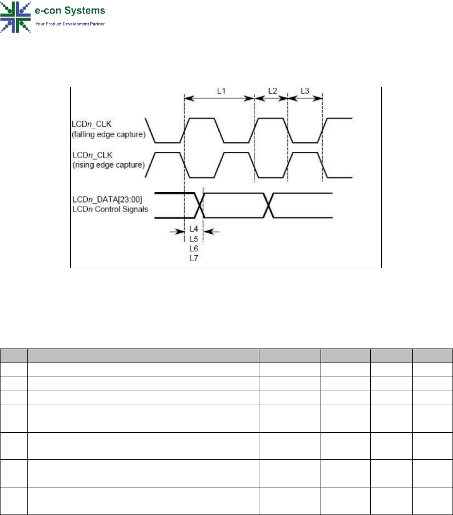
Parallel Display Interface Signals Timing Details
The following figure shows the timing details of the parallel display.
Figure 4: MIPI DSI Timing Diagram
The following table shows the timing details of the parallel display.
Table 6: MIPI DSI Timing Details
ID
Parameter
Symbol
Min
Max
Unit
L1
LCD pixel clock frequency
tCLK(LCD)
-
150
MHz
L2
LCD pixel clock high (falling edge capture)
tCLKH(LCD)
3
-
ns
L3
LCD pixel clock low (rising edge capture)
tCLKL(LCD)
3
—
ns
L4
LCD pixel clock high to data valid (falling edge
capture)
td(CLKH-
DV)
-1
1
ns
L5
LCD pixel clock low to data valid (rising edge
capture)
td(CLKL-
DV)
-1
1
ns
L6
LCD pixel clock high to control signals valid
(falling edge capture)
td(CLKH-
CTRLV)
-1
1
ns
L7
LCD pixel clock low to control signals valid (rising
edge capture)
td(CLKL-
CTRLV)
-1
1
ns
Layout Guidelines
Parallel display signals are to be treated as single ended signals with an impedance
of 50 ohms. The lines are to be length matched with clock as reference and with a
tolerance of 250 mils. Series terminations are recommended on these lines in order
to reduce electromagnetic emission. The serial resistor value is a trade-off between
reduction of electromagnetic radiation and signal quality.
Unused Parallel Display Signals Termination
All parallel display signals can be left unconnected if not used.

18 eSOMiMX7 Carrier Board Design Guide
Electrophoretic Display
eSOMiMX7 has an EPD controller. EPDC is used to interface e-paper displays. The
major advantage of e-paper display is that it needs very low power to operate. This
is because the display does not refresh the image unlike the LCD displays. Once an
image is written on display the image is retained until next image (refreshing) is
displayed on the display. Also, even if the power is cut the display retains the image.
Some of the features of EPDC are:
• Resolutions up to 4096 x 4096 pixels with 20 Hz refresh and resolutions up to
1650 x 2332 pixels at 106 Hz refresh.
• Dual-scan TFT drive mode to support ultra-high resolution/refresh rate displays.
• Supports LVDS and DDR mode data transfers.
• 16-bit parallel data interface.
This interface covers the following sections in detail.
• Electrophoretic Display Signals
• Electrophoretic Display Timing Details
• Unused Electrophoretic Display Signals Termination
Electrophoretic Display Signals
The following table shows the Electrophoretic Display signals.
Table 7: Electrophoretic Display Signals
Pin
Name
I/O
Power
Rail
Description
CN3.1
iMX7_CONN_QSPI_A_DATA0
O
3.3V
EPDC_DATA00
CN3.5
iMX7_CONN_QSPI_A_DATA1
O
3.3V
EPDC_DATA01
CN3.9
iMX7_CONN_QSPI_A_DATA2
O
3.3V
EPDC_DATA02
CN3.3
iMX7_CONN_QSPI_A_DATA3
O
3.3V
EPDC_DATA03
CN3.11
iMX7_CONN_QSPI_A_DQS
O
3.3V
EPDC_DATA04
CN3.13
iMX7_CONN_QSPI_A_SCLK
O
3.3V
EPDC_DATA05
CN3.7
iMX7_CONN_QSPI_A_SS0_B
O
3.3V
EPDC_DATA06
CN3.15
iMX7_CONN_QSPI_A_SS1_B
O
3.3V
EPDC_DATA07
CN3.2
iMX7_CONN_QSPI_B_DATA0
O
3.3V
EPDC_DATA08
CN3.8
iMX7_CONN_QSPI_B_DATA1
O
3.3V
EPDC_DATA09
CN3.10
iMX7_CONN_QSPI_B_DATA2
O
3.3V
EPDC_DATA10
CN3.14
iMX7_CONN_QSPI_B_DATA3
O
3.3V
EPDC_DATA11
CN3.6
iMX7_CONN_QSPI_B_DQS
O
3.3V
EPDC_DATA12
CN3.16
iMX7_CONN_QSPI_B_SCLK
O
3.3V
EPDC_DATA13
CN3.4
iMX7_CONN_QSPI_B_SS0_B
O
3.3V
EPDC_DATA14
CN3.12
iMX7_CONN_QSPI_B_SS1_B
O
3.3V
EPDC_DATA15
CN3.100
P2MDIDN*
O
3.3V
EPDC Source Driver-Chip-
enable/Start-Pulse
CN3.98
P2MDIDP*
O
3.3V
EPDC Source Driver-Chip-
enable/Start- Pulse

© Copyright e-con Systems. 2017. All rights reserved. 19
CN3.80
P2MDIBN*
O
3.3V
EPDC Source Driver-Chip-
enable/Start- Pulse
CN3.82
P2MDIBP*
O
3.3V
EPDC Source Driver-Chip-
enable/Start- Pulse
CN3.18
ETHERNET_P2_ACT*
O
3.3V
EPDC Source Driver-Shift Clock
CN3.20
ETHERNET_P2_LED_1000M*
O
3.3V
EPDC Source Driver-Latch Enable
CN3.22
ETHERNET_P2_LED_100M*
O
3.3V
EPDC Source Driver-Output Enable
CN3.24
CONN_RGMII2_RXD3
O
3.3V
EPDC Source Driver-Shift dir
CN3.86
P2MDIAP*
O
3.3V
EPDC Gate Driver-Clock
CN3.88
P2MDIAN*
O
3.3V
EPDC Gate Driver-Output Enable
CN3.94
P2MDICN*
O
3.3V
EPDC Gate Driver-Shift direction
CN3.92
P2MDICP*
O
3.3V
EPDC Gate Driver-Start Pulse
CN3.19
iMX7_CONN_EPDC_PWRCOM
O
3.3V
EPDC Panel-Power control
CN3.21
iMX7_CONN_EPDC_PWRSTAT
O
3.3V
EPDC Panel-Power status good
CN3.25
iMX7_CONN_EPDC_BDR0
O
3.3V
EPDC Panel-Border Control
CN3.23
iMX7_CONN_EPDC_BDR1
O
3.3V
EPDC Panel-Border Control
Note:
• *Ethernet2 is not a part of eSOMiMX7 Solo.
• *EPDC signals are multiplexed with Ethernet 2, so Ethernet 2 will not be
available in Dual core SOM with EPDC configuration.
EPDC Interface Signals Timing Details
In DDR mode the data is placed on both the rising and falling edge of the clock. The
timing parameters can be classified into two types:
• Line timing - data present in a line(Horizontal)
• Frame timing - data present in a complete frame(Vertical)
The following diagram shows the line timing diagram for EPDC in DDR mode0.
Figure 5: EPDC Line Timing Diagram (DDR Mode 0)
The following diagram shows the line timing in DDR mode1.

20 eSOMiMX7 Carrier Board Design Guide
Figure 6: EPDC Line Timing Diagram (DDR Mode 1)
The following diagram shows the frame timing (Vertical) for EPDC.
Figure 7: EPDC Vertical Frame Timing Diagram
The following equations define the timing of the panel scan frame (where LT = line-
timing and FT = frame-timing):
LT = TPIXCLK (LS + LB + ((HRES x Ratio + LE)/PIXELSPERSDCLK)
FT = LT x (FS + FB + VRES + LE)
The following table outlines the various configurations and clock ratios. It also lists
the relevant register settings for single scan mode configuration.
© Copyright e-con Systems. 2017. All rights reserved. 21
Table 8: Single Scan Mode
High Level
Mode
HW_
EPDC_
CTRL
EPDC_
DATA
Pins
used
HW_EPD
C_ FORM
AT
HW_EPDC_TCE_CTRL
C_TCE
_CTRL
Required
PIXCLK
(RATIO)
DUAL
_SCAN
TFT_PIXEL
_FORMAT
PIXELS_P
ER_SDCL
K
LVDS_
MODE
DDR_
MOD
E
SDDO_
WIDTH
2bpp, 8-bit
single
ended, SDR
0
[7:0]
4B[V]
4
0
0
8bit
SDCLK x 2
2bpp, 16-bit
single
ended, SDR
0
[15:0]
2B[V]
8
0
0
16bit
SDCLK x 4
2bpp, 8-bit,
DDR (LVDS
option)
0
[7:0],
[15:8]
2B[V]
8
1\0
1
8bit
SDCLK x 4
4bpp, 8-bit
single
ended, SDR
0
[7:0]
4B[V]
2
0
0
8bit
SDCLK x 2
4bpp, 16-
bit, single
ended SDR
0
[15:0]
4B[V]
4
0
0
16bit
SDCLK x 2
4bpp, 8-bit,
DDR (LVDS
option)
0
[7:0],
[15:8]
4B[V]
4
1\0
1
8bit
SDCLK x 4
4bpp, 16-
bit, single
ended, DDR
0
[15:0]
4B[V]
8
0
1
16bit
SDCLK x 4
The following table outlines the various configurations and clock ratios. It also lists
the relevant register settings for dual scan mode configuration.
Table 9: Dual Scan Mode
High Level
Mode
HW_
EPDC_
CTRL
EPDC_
DATA
pins
used
HW_EPDC
_ FORMAT
HW_EPDC_TCE_CTRL
C_TCE
_CTRL
Required
PIXCLK
(RATIO)
DUAL
_SCAN
TFT_PIXEL
_FORMAT
PIXELS_P
ER_SDCL
K
LVDS_
MODE
DDR_
MOD
E
SDDO_
WIDTH
2bpp, 8-bit
single
ended, SDR
1
[7:0],[
15:8]
2B[V]
4
0
0
8bit
SDCLK x 2
2bpp, 8-bit,
DDR
1
[7:0],
[15:8]
2B[V]
8
0
1
8bit
SDCLK x 4
4bpp, 8-bit
single
ended, SDR
1
[7:0],
[15:8]
4B[V]
2
0
0
8bit
SDCLK x 2
4bpp, 8-bit,
DDR
1
[7:0],
[15:8]
4B[V]
4
0
1
8bit
SDCLK x 4
22 eSOMiMX7 Carrier Board Design Guide
Unused Electrophoretic Display Signals Termination
All Unused electrophoretic display signals can be left unconnected.
MIPI CSI
eSOMiMX7 has a 2 lane CMOS Sensor interface. It can implement all protocol
functions defined in the MIPI CSI-2 Specification.
MIPI CSI interface features:
• Compatible to Protocol-to-PHY Interface (PPI) in MIPI D-PHY
• Supports various primary and secondary image formats such as:
▪ YUV420, YUV420, YUV420 (Legacy), YUV420 (CSPS), YUV422 of 8-bits and
10-bits
▪ RGB565, RGB666, RGB888
• The control lines such as enable, reset etc can be achieved through GPIOs.
Depending on the I/O line of the camera please select the I2C that is to be used.
This interface covers the following sections in detail.
• MIPI CSI Signals
• Reference Schematics and Layout guidelines
• Unused MIPI CSI Signals Termination
MIPI CSI Signals
The following table shows the MIPI CSI signals.
Table 10: MIPI CSI Signals
Pin
Name
I/O
Type
Power Rail
Description
CN3.62
MIPI_CSI_D0_P_IMX7_CONN
I
DS
-
Positive CSI-2 data 0 differential
CN3.64
MIPI_CSI_D0_N_IMX7_CONN
I
DS
-
Negative CSI-2 data 0 differential
CN3.68
MIPI_CSI_CLK_P_IMX7_CONN
I
DS
-
Positive CSI-2 clock differential
CN3.70
MIPI_CSI_CLK_N_IMX7_CONN
I
DS
-
Negative CSI-2 clock differential
CN3.74
MIPI_CSI_D1_P_IMX7_CONN
I
DS
-
Positive CSI-2 data 1 differential
CN3.76
MIPI_CSI_D1_N_IMX7_CONN
I
DS
-
Negative CSI-2 data 1 differential
Reference Schematics and Layout Guidelines
Care must be taken while routing the differential signals so that the differential pair
lines are length matched with a tolerance of 5 mils, also the intra pair length must
also be matched with clock as reference and a tolerance of 100 mils. It is
recommended to maintain a differential impedance of 90 ohms on the differential
signals.
The number of GPIOs required apart from the MIPI signals can vary based on the
requirement of the MIPI camera used and must be suited to its needs.

© Copyright e-con Systems. 2017. All rights reserved. 23
It is recommended to use an I2C level translator if the sensor does not support 1.8V
IO.
Note: There is no pull up on the I2C lines in the eSOMiMX7 and hence external pull
ups are required.
The following figure shows the MIPI CSI reference schematic.
Figure 8: MIPI CSI Reference Schematics
Unused MIPI CSI Signals Termination
All MIPI DSI signals can be left unconnected if not used.
Parallel Camera
The parallel camera interface of iMX7 can be connected to a parallel camera unit up
to 24 bits. It provides support for CCIR656 video interface as well as traditional
sensor interface with 8-bit / 16-bit / 24-bit data port for CyBC, YUV, or RGB data
input and 8-bit / 10-bit / 16-bit data port for Bayer data input. It also has
configurable master clock frequency output to sensor and provides 256 x 64 FIFO to
store received image pixel data.
This interface covers the following sections in detail.
• Parallel Camera Signals
• Unused Parallel Camera signals termination
24 eSOMiMX7 Carrier Board Design Guide
Parallel Camera Signals
The following table shows the parallel camera signals.
Table 11: Parallel Camera Signals
Pin
Signal Name
I/O
Power
Rail
Description
CN3.31
LCD1_DATA17
I
1.8V
CSI_DATA00, Data Sensor Signal
CN3.56
LCD1_DATA16
I
1.8V
CSI_DATA01, Data Sensor Signal
CN3.42
LCD1_DATA15
I
1.8V
CSI_DATA02, Data Sensor Signal
CN3.43
LCD1_DATA14
I
1.8V
CSI_DATA03, Data Sensor Signal
CN3.48
LCD1_DATA13
I
1.8V
CSI_DATA04, Data Sensor Signal
CN3.32
LCD1_DATA12
I
1.8V
CSI_DATA05, Data Sensor Signal
CN3.29
LCD1_DATA11
I
1.8V
CSI_DATA06, Data Sensor Signal
CN3.49
LCD1_DATA10
I
1.8V
CSI_DATA07, Data Sensor Signal
CN3.45
LCD1_DATA09
I
1.8V
CSI_DATA08, Data Sensor Signal
CN3.34
LCD1_DATA08
I
1.8V
CSI_DATA09, Data Sensor Signal
CN3.33
LCD1_DATA23
I
1.8V
CSI_DATA10, Data Sensor Signal
CN3.47
LCD1_DATA22
I
1.8V
CSI_DATA11, Data Sensor Signal
CN3.50
LCD1_DATA21
I
1.8V
CSI_DATA12, Data Sensor Signal
CN3.51
LCD1_DATA20
I
1.8V
CSI_DATA13, Data Sensor Signal
CN3.52
LCD1_DATA19
I
1.8V
CSI_DATA14, Data Sensor Signal
CN3.46
LCD1_DATA18
I
1.8V
CSI_DATA15, Data Sensor Signal
CN3.28
LCD1_CLK
I
1.8V
CSI_DATA16, Data Sensor Signal
CN3.27
LCD1_ENABLE
I
1.8V
CSI_DATA17, Data Sensor Signal
CN3.39
LCD1_HSYNC
I
1.8V
CSI_DATA18, Data Sensor Signal
CN3.41
LCD1_VSYNC
I
1.8V
CSI_DATA19, Data Sensor Signal
CN3.36
LCD1_DATA00
I
1.8V
CSI_DATA20, Data Sensor Signal
CN3.54
LCD1_DATA01
I
1.8V
CSI_DATA21, Data Sensor Signal
CN3.40
LCD1_DATA02
I
1.8V
CSI_DATA22, Data Sensor Signal
CN3.57
LCD1_DATA03
I
1.8V
CSI_DATA23, Data Sensor Signal
CN3.53
LCD1_DATA05
I
1.8V
Horizontal Sync (Blank Signal)
CN4.67
I2C3_DATA_IMX7_CONN
I
1.8V
Horizontal Sync (Blank Signal)
CN3.55
LCD1_DATA06
I
1.8V
Pixel Clock
CN4.61
I2C4_CLK_IMX7_CONN
I
1.8V
Pixel Clock
CN3.38
LCD1_DATA04
I
1.8V
Vertical Sync (Start of Frame)
CN4.69
I2C3_CLK_IMX7_CONN
I
1.8V
Vertical Sync (Start of Frame)
CN3.35
LCD1_DATA07
O
1.8V
CMOS Sensor Master Clock
CN4.59
I2C4_DATA_IMX7_CONN
O
1.8V
CMOS Sensor Master Clock
CN3.58
LCD1_RESET
I
1.8V
CSI Field Signal
Unused Parallel Camera Signals Termination
All parallel camera signals can be left unconnected if not used.
Gigabit Ethernet
eSOMiMX7 supports two Gigabit Ethernet (1000Base-T) interface port as standard
interfaces. The PHY of these interfaces are located on the module. Therefore, only

© Copyright e-con Systems. 2017. All rights reserved. 25
the magnetics and the connector are needed on the carrier board. The module
features the AR8035 Integrated 10/100/1000 Gigabit Ethernet Transceiver as PHY
which is connected over RGMII with the MAC in the Processor. The interface is
backward compatible with the 10/100Mbit Ethernet (10/100Base-TX) standard and
has the following features:
• 10BASE-Te/100BASE-Tx/1000 BASE-T IEEE 802.3 compliant
• Error-free operation up to 140 meters of CAT5 cable
• Fully integrated digital adaptive equalizers, echo cancellers, and near end
crosstalk (NEXT) cancellers
• A robust surge protection with ±750V/ differential mode and ±4KV/common
mode
• Jumbo frame supports up to 10KB (full duplex)
• All digital baseline wander correction
• Automatic polarity correction
• IEEE 802.3u compliant auto-negotiation
This interface covers the following sections in detail.
• Gigabit Ethernet Signals
• Ethernet Reference Schematics and Layout Guidelines
• Unused Gigabit Ethernet Signals Termination
Gigabit Ethernet Signals
The following table shows the Gigabit Ethernet signals.
Table 12: Gigabit Ethernet Signals
Pin
Signal Name
I/
O
Typ
e
Power
Rail
Description
CN3.97
P1MDIAN
DS
Ethernet1 Negative A differential lane
CN3.99
P1MDIAP
DS
Ethernet1 Positive A differential lane
CN3.85
P1MDIBN
DS
Ethernet1 Negative B differential lane
CN3.87
P1MDIBP
DS
Ethernet1 Positive B differential lane
CN3.91
P1MDICN
DS
Ethernet1 Negative C differential lane
CN3.93
P1MDICP
DS
Ethernet1 Positive C differential lane
CN3.79
P1MDIDN
DS
Ethernet1 Negative D differential lane
CN3.81
P1MDIDP
DS
Ethernet1 Positive D differential lane
CN4.74
ETHERNET_P1_LED_100M
O
3.3V
Ethernet1 LED Status for 10/100 BASE-
T link
CN4.70
ETHERNET_P1_LED_1000M
O
3.3V
Ethernet1 LED Status for 1000 BASE-T
link
CN4.72
ETHERNET_P1_ACT
IO
3.3V
Ethernet1 LED Status for link activity
CN3.88
P2MDIAN
DS
Ethernet2 Negative A differential lane
CN3.86
P2MDIAP
DS
Ethernet2 Positive A differential lane
CN3.80
P2MDIBN
DS
Ethernet2 Negative B differential lane
CN3.82
P2MDIBP
DS
Ethernet2 Positive B differential lane
CN3.94
P2MDICN
DS
Ethernet2 Negative C differential lane
CN3.92
P2MDICP
DS
Ethernet2 Positive C differential lane
26 eSOMiMX7 Carrier Board Design Guide
CN3.100
P2MDIDN
DS
Ethernet2 Negative D differential lane
CN3.98
P2MDIDP
DS
Ethernet2 Positive D differential lane
CN3.22
ETHERNET_P2_LED_100M
O
3.3V
Ethernet2 LED Status for 10/100 BASE-
T link
CN3.20
ETHERNET_P2_LED_1000M
O
3.3V
Ethernet2 LED Status for 1000 BASE-T
link
CN3.18
ETHERNET_P2_ACT
IO
3.3V
Ethernet2 LED Status for link activity
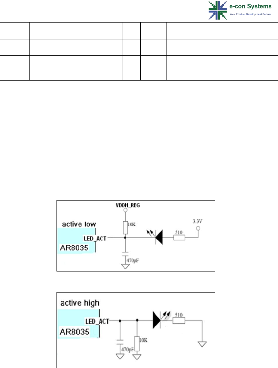
Ethernet Reference Schematics and Layout Guidelines
The Ethernet reference schematics and layout guidelines for the LED interfaces are
described in the following section.
LED Interface
The LED interface can either be controlled by the PHY or controlled manually,
independent of the state of the PHY. Three status LEDs are available. These can be
used to indicate operation speed, duplex mode, and link status. The LEDs can be
programmed to different status functions from their default value. They can also be
controlled directly from the MII register interface. The reference design schematics
for the ethernet LEDs are shown in the following figures.
Figure 9: Reference Design Schematic - Active Low
Figure 10: Reference Design Schematic - Active High
LED_ACT/LED_1000 active states depend on power on strapping mode. When
strapped high, active low. When strapped low, active high. LED_10_100 depends on
LED_1000 power on strapping mode. So, LED_10_100 and LED_1000 must have the
same LED design.
The following table shows the Gigabit Ethernet LED signal details.
© Copyright e-con Systems. 2017. All rights reserved. 27
Table 13: Gigabit Ethernet LED Signal Details
Symbol
10M Link
10M Active
100M Link
100M
Active
1000M
Link
1000M
Active
LED_10_100
Off
Off
On
On
Off
Off
LED_1000
Off
Off
Off
Off
On
On
LED_ACT
On
Blink
On
Blink
On
Blink
Ethernet Schematic Example
Ethernet connectors with integrated magnetics are preferable. If a design with
external magnetics is chosen, additional care must be taken to route the signals
between the magnetics and Ethernet connector.
The LED output signals can be connected directly to the LED of the Ethernet jack
with suitable serial resistors.
Each lane of the gigabit Ethernet is to be treated as differential pair signals
maintaining a differential impedance of 90 ohms. The differential pairs are to be
length matched with a tolerance of 5 mils.
It must be seen from the reference schematics that both the PHY has different PHY
ID configuration.
It is recommended to Pull up LED_ACT pin of Ethernet 1 to 3.3V and Pull-down
LED_ACT pin of Ethernet 2 so that PHY ID of Ethernet 1 will be 0X04 and PHY ID of
Ethernet 2 will be 0X00.
The following table shows the Gigabit Ethernet PHY address details.
Table 14: Gigabit Ethernet PHY Address Details
Configurations
Ethernet 1
Ethernet 2
LED_ACT
Pull up to 3.3V
Pull down
PHY ID
0X04
0X00
The following figure shows the Gigabit Ethernet reference schematic.
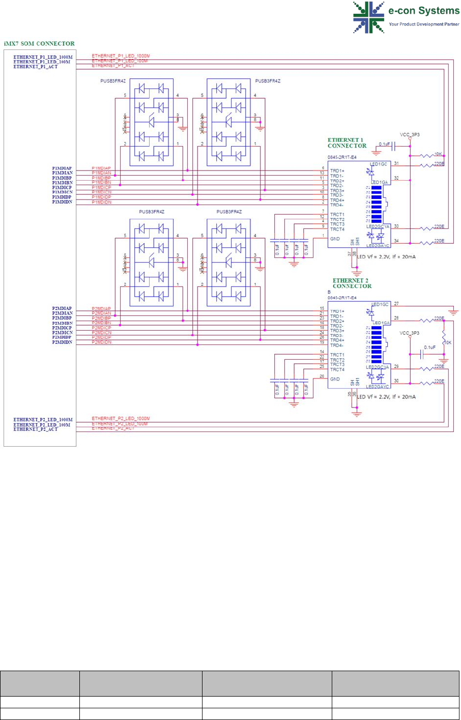
28 eSOMiMX7 Carrier Board Design Guide
Figure 11: Gigabit Ethernet Reference Schematic
Unused Ethernet Signals Termination
All Ethernet signals can be left unconnected if not used.
Universal Serial Bus (USB)
In eSOMiMX7, the USB controller block provides high performance USB functionality
that conforms to the USB specification, Rev. 2.0 and the On-The-Go and Embedded
host supplement to the USB Rev 2.0 specification. The various modes supported by
each controller is defined in the following table.
Table 15: USB Speed Details
eSOMiMX7 Port
1.5 Mbit/s Low Speed
(1.0)
12 Mbit/s Full Speed
(1.1)
480 Mbit/s High Speed
(2.0)
OTG1
(Host Mode only)
YES
YES
OTG2
(Host Mode only)
YES
YES
The following list provides features of each of the OTG controller cores:

© Copyright e-con Systems. 2017. All rights reserved. 29
• High-Speed/Full-Speed/Low-Speed OTG core.
• HS/FS/LS UTMI compliant interface connected to on-chip UTMI PHY.
• High Speed, Full Speed and Low Speed operation in Host mode (with UTMI
transceiver).
• High Speed, and Full Speed operation in Peripheral mode (with UTMI
transceiver).
• Hardware support for OTG signalling, Session Request Protocol (SRP), Host
Negotiation Protocol (HNP), and Attach Detection Protocol (ADP). ADP support
includes dedicated timer hardware and register interface.
• Up to 8 bidirectional endpoints.
• Supports charger detection with register interface only.
This interface covers the following sections in detail.
• Universal Serial Bus Signals
• Reference Schematics and Layout Guidelines
• Unused Universal Serial Bus Signals Termination
Universal Serial Bus Signals
Both the OTG controller provide a pair of differential signals and an ID pin to support
OTG feature. The USB 2.0 data signals do not support polarity inversion and hence
the data signals cannot be interchanged.
The following tables shows the USB OTG signals.
Table 16: Universal Serial Bus OTG Signals
Pin
Signal Name
I/O
Type
Power
Rail
Description
CN4.76
VBUS_USB_OTG1
Power
5V
OTG1 Power rail
CN4.86
USB_OTG1_DP_iMX7_CONN
DS
Positive USB OTG 1 data
CN4.88
USB_OTG1_DN_iMX7_CONN
DS
Negative USB OTG 1 data
CN4.78
USB_OTG1_ID_iMX7_CONN
I
3.3V
USB host / client identification
CN4.82
VBUS_USB_OTG2
Power
5V
OTG2 Power rail
CN4.92
USB_OTG2_DP_iMX7_CONN
DS
Positive USB OTG 2 data
CN4.94
USB_OTG2_DN_iMX7_CONN
DS
Negative USB OTG 2 data
CN4.80
USB_OTG2_ID_iMX7_CONN
I
3.3V
USB host / client identification
Reference Schematics and Layout Guidelines
The differential USB data signals require a common mode choke to be placed. Make
sure that the selected choke is certified for USB 2.0 High Speed. The same is also
required for the TVS diodes.
The following figure shows the USB OTG interface reference schematic.

30 eSOMiMX7 Carrier Board Design Guide
Figure 12 Universal Serial Bus Reference Schematic
The carrier board needs to provide 5V USB bus power on the USB host jacks.
According to the USB 2.0 specifications, the maximum current drawn per port is
limited by 500mA. The bus power needs to be in the range of 4.75V to 5.25V
measured at the USB host jack for any load current from 0mA to 500mA. To ensure
that an out of spec device or a defective device is not damaging the 5V power rail on
the carrier board, it is recommended adding a current limiting IC.
The inrush current needs to be considered while designing the USB bus power. USB
devices can have a maximum input capacitor at the bus power of 10μF. The
maximum inrush charge is limited to 50μC. This means that the power rail at the
USB host jack needs to be tolerant of this inrush current.
While routing the USB lines, care must be taken to ensure that the USB
specifications is met. The data signals are to be routed as differential lines. It must
be routed with minimum trace length possible and must be length matched with a

© Copyright e-con Systems. 2017. All rights reserved. 31
tolerance of 5 mils. The differential impedance of the lines must be maintained at 90
ohms.
Unused Universal Serial Bus Signals Termination
All USB Signals can be left unconnected if not used.
PCIe
eSOMiMX7 supports a single lane PCIe interface as a standard interface.
The following list the key features of the PCIe PHY:
• 1.5 / 2.5 / 3.0 / 5.0 / 6.0 Gbps Serializer / Deserializer
• Compliant with PCI Express Base Specification 2.1
• Compliant with PIPE Specification 2.0
• 8 / 16 / 20 / 40-bit CMOS Interface for Transmitter and Receiver
• 8B/10B Encoding / Decoding
• Receiver Detection
• Supports Spread Spectrum Clocking in Transmitter and Receiver
This interface covers the following sections in detail:
• PCI Express Interface Signals
• Reference Schematics and Layout Guidelines
• PCI Express Signals Termination
PCI Express Interface Signals
The following table shows the PCIe Interface signals.
Table 17: PCIe Interface Signals
Pin
Signal Name
I/O
Type
Power
Rail
Description
CN4.5
PCIe_RX_N_iMX7_CONN
I
DS
-
Negative-side transmitted
differential input
CN4.7
PCIe_RX_P_iMX7_CONN
I
DS
-
Positive-side transmitted
differential input
CN4.11
PCIe_TX_N_iMX7_CONN
O
DS
-
Negative-side transmitted
differential output
CN4.13
PCIe_TX_P_iMX7_CONN
O
DS
-
Positive-side transmitted
differential output
CN4.17
CLK_PCIe_CLK_N_iMX7_CONN
O
DS
-
Positive-side Reference Clock
Differential Output
CN4.19
CLK_PCIe_CLK_P_iMX7_CONN
O
DS
-
Negative-side Reference Clock
Differential Output

32 eSOMiMX7 Carrier Board Design Guide
Reference Schematics and Layout Guidelines
PCIe specification requires placing of a series capacitor on the transmitter and the
receiver lines, there is no capacitor on the eSOMiMX7 and hence must be placed on
the carrier board. A parallel termination of 49.9 Ohm on the clock line is
recommended as per the PCIe standard.
Care must be taken while routing the differential signals so that the differential pair
lines are length matched with a tolerance of 5 mils, also the intra pair length must
also be matched with clock as reference and a tolerance of 20 mils. It is
recommended to maintain a differential impedance of 85 ohms on the differential
signals.
The following figure shows the PCIe reference schematic.
Figure 13: PCIe Interface Reference Schematic
Unused PCIe Interface Signals Termination
All PCIe signals can be left unconnected if not used.
uSDHC Interface
eSOMIMX7 supports a Four-bit SD/SDIO/MMC interface as a standard feature that
can be used in the carrier board. The uSDHC interface provide up to 4 data bit which
can be used for interfacing SD and MMC cards as well as SDIO interface peripherals.
The IMX7 Dual Processor supports three SD/SDIO/MMC interfaces, out of which two
has been internally used in the eSOMIMX7 SOM for Wi-Fi SDIO module interface and
eMMC or NAND support in the SOM.
The SD cards know different bus speed modes. The required signal voltage depends
on the bus speed mode. For example, the SDR104 mode requires 1.8V signalling,
while Default speed requires 3.3 V signalling. For this purpose, ESOMIMX7 provides
a separate supply railing (VCC_SD) connected to an internal LDO which can be
© Copyright e-con Systems. 2017. All rights reserved. 33
switched between 1.8V and 3.3V as per the mode requirement. It is recommended
to use this supply for pull ups used on these lines.
The following table shows the Various SD mode speed details.
Various Bus Speed mode supported by the uSDHC interface are:
Table 18: Various SD Mode Speed Details
Bus Speed Mode
Max. Clock Frequency
Max. Bus Speed
Signal Voltage
Default Speed
25 MHz
12.5 MB/s
3.3V
High Speed
50 MHz
25 MB/s
3.3V
DDR50
50 MHz
50 MB/s
1.8V
SDR50
100 MHz
50 MB/s
1.8V
SDR104
208 MHz
104 MB/s
1.8V
• Conforms to the SD Host Controller Standard Specification version 3.0
• Compatible with the MMC System Specification version 4.2/4.3/4.4/4.41
This interface covers the following sections in detail:
• uSDHC Signals
• Reference Schematics and Layout Guidelines
• uSDHC Interface Signals Timing Details
• Unused uSDHC Signals Termination
uSDHC Signals
The following table shows the uSDHC signals.
Table 19: uSDHC Signals
Pin
Signal Name
I/O
Type
Power
Rail
Description
CN4.97
VCC_SD
Power
SD Power Supply railing
CN4.81
CLK_SD1_CLK_iMX7_CONN
O
VCC_SD
Clock for MMC/SD/SDIO card
CN4.91
SD1_CMD_iMX7_CONN
IO
VCC_SD
CMD line connect to card
CN4.93
SD1_DATA0_iMX7_CONN
IO
VCC_SD
DATA0 line in all modes, also used
to detect busy state.
CN4.87
SD1_DATA1_iMX7_CONN
IO
VCC_SD
DATA1 line in 4-bit mode, Also
used to detect interrupt in 1/4-bit
mode
CN4.89
SD1_DATA2_iMX7_CONN
IO
VCC_SD
DATA2 line or Read Wait in 4-bit
mode. Read Wait in 1-bit mode.
CN4.85
SD1_DATA3_iMX7_CONN
IO
VCC_SD
DATA3 line in 4-bit mode or
configured as card detection pin,
can be configured as card
detection pin in 1-bit mode
CN4.95
nSD1_CD_iMX7_CONN
I
VCC_SD
Card detection pin
Reference Schematics and Layout Guidelines
The uSDHC module requires pull-up resistors on the data and command lines, also
proper ESD must be placed on those lines. There is no dedicated write-protection
34 eSOMiMX7 Carrier Board Design Guide
signal available. Any free GPIO capable signal can be used if the write-protection
function is required. A low pass RC network in the clock line reduces the slew rate of
the Clock signals to reduces the electromagnetic radiation problem. The serial
resistor value and parallel capacitor is a trade-off between reduction of
electromagnetic radiation and signal quality. A good starting value is 22Ω and 22pF.
A series termination resistor is recommended on all the data and CMD lines to
reduce electromagnetic radiation.
The following routing guidelines are to be followed for the uSDHC signals.
All the four data signals and CMD are to be treated as single ended signals, routed
with an impedance of 50 ohms and must be length matched with a tolerance of 100
mils from the clock trace length.
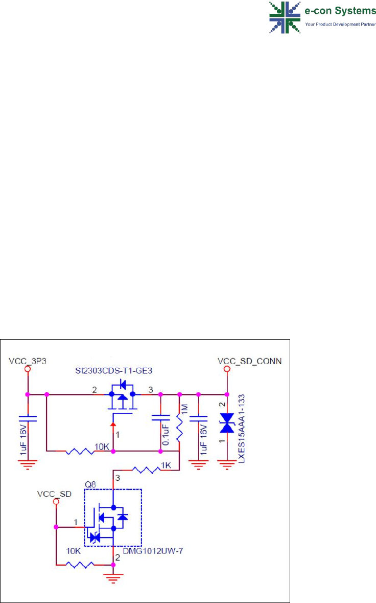
uSDHC Schematic Example
The uSDHC interface in eSOMiMX7 supports multiple speed modes and hence the
signal lines require the VCC SD Domain, but the card is to be powered by a 3.3V
supply, the same supply that powers the SOM. To avoid any ambiguity in power on
sequence, a power switch is implemented as shown in the following diagram.
Figure 14: SD Card Power Switch Diagram
The following figure shows the uSDHC reference schematic.

© Copyright e-con Systems. 2017. All rights reserved. 35
Figure 15: uSDHC Reference Schematic
uSDHC Interface Signals Timing Details
The following figure shows the timing details of the uSDHC interface.
Figure 16: uSDHC Timing Diagram
The following table shows the timing details of the uSDHC interface.
Table 20: uSDHC Timing Details
ID
Parameter
Symbols
Min
Max
Unit
Card Input Clock
SD1
Clock Frequency (Low Speed)
fpp1
0
400
kHz
Clock Frequency (SD/SDIO Full Speed/High
Speed)
fpp2
0
25/50
MHz
Clock Frequency (MMC Full Speed/High
Speed)
fpp3
0
20/52
MHz
Clock Frequency (Identification Mode)
fod
100
400
KHz
SD2
Clock Low Time
tWL
7
—
ns
SD3
Clock High Time
twh
7
—
ns
SD4
Clock Rise Time
tTLH
—
3
ns
SD5
Clock Fall Time
tTHL
—
3
ns
uSDHC Output/Card Inputs SD_CMD, SDx_DATAx (Reference to CLK)

36 eSOMiMX7 Carrier Board Design Guide
SD6
uSDHC Output Delay
tOD
-6.6
3.6
ns
uSDHC Input/Card Outputs SD_CMD, SDx_DATAx (Reference to CLK)
SD7
uSDHC Input Setup Time
tISU
2.5
—
ns
SD8
uSDHC Input Hold Time
TIH
1.5
—
ns
Unused uSDHC Signals Termination
The following table shows the unused uSDHC signals termination.
Table 21: Unused uSDHC Signals Termination
uSDHC Pin
uSDHC Signal Name
Recommended Termination
CN4.97
VCC_SD
To be left unconnected
CN4.81
CLK_SD1_CLK_iMX7_CONN
Can be left unconnected
CN4.91
SD1_CMD_iMX7_CONN
Can be left unconnected
CN4.93
SD1_DATA0_iMX7_CONN
Can be left unconnected
CN4.87
SD1_DATA1_iMX7_CONN
Can be left unconnected
CN4.89
SD1_DATA2_iMX7_CONN
Can be left unconnected
CN4.85
SD1_DATA3_iMX7_CONN
Can be left unconnected
CN4.95
nSD1_CD_iMX7_CONN
If not used (for the
embedded memory), tie low to
indicate there is a card attached.
Synchronous Audio Interface (SAI)
eSOMiMX7 has 2 synchronous audio interface (SAI) interface that can support full-
duplex serial interfaces with frame synchronization such as I2S and codec/DSP
interfaces.
This interface covers the following sections:
• SAI Signals
• SAI interface Signals Timing Details
• Unused Synchronous Audio Interface Signals Termination
SAI Signals
The following table shows the synchronous audio interface signals.
Table 22: SAI Signals
Pin
Signal Name
I/O
Power
Rail
Description
CN4.44
SAI1_TXD_iMX7_CONN
O
3.3V
Transmit data
CN4.46
SAI1_RXD_iMX7_CONN
I
3.3V
Receive data
CN4.48
SAI1_TXC_iMX7_CONN
I/O
3.3V
Transmit Bit Clock
CN4.50
SAI1_RXFS_iMX7_CONN
I/O
3.3V
Receive Frame Sync
CN4.52
SAI1_RXC_iMX7_CONN
I/O
3.3V
Receive Bit Clock
CN4.54
SAI1_TXFS_iMX7_CONN
I/O
3.3V
Transmit Frame Sync
CN4.58
CLK_SAI1_MCLK_iMX7_CONN
I/O
3.3V
Audio Master Clock
CN4.73
SAI2_RXD_iMX7_CONN
I
3.3V
Receive Data
© Copyright e-con Systems. 2017. All rights reserved. 37
CN4.75
SAI2_TXD_iMX7_CONN
O
3.3V
Transmit data
CN4.77
SAI2_TXC_iMX7_CONN
I/O
3.3V
Transmit Bit Clock
CN4.71
SAI2_FS_iMX7_CONN
I/O
3.3V
Transmit Frame Sync
CN4.55
GPIO1_IO02_IMX7_CONN
I/O
3.3V
Audio Master Clock
*SAI1 lines are muxed with NAND signals and hence cannot be used in SOMs with
NAND flash.
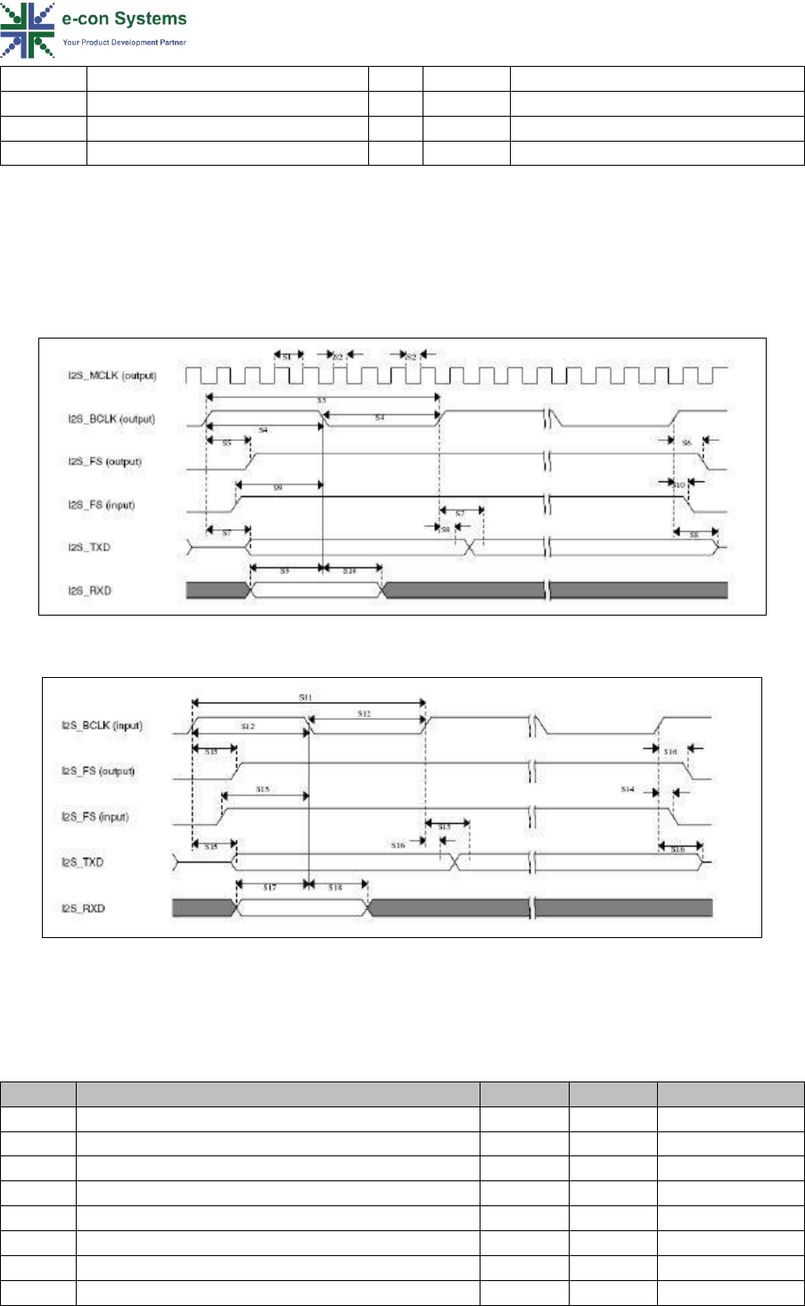
SAI Interface Signals Timing Details
The following figures show the timing details of the SAI interface.
Figure 17: SAI Timing Diagram-MASTER Mode
Figure 18: SAI Timing Diagram-SLAVE Mode
The following table shows the timing details of the SAI interface.
Table 23: Synchronous Audio Interface Timing Details
Num
Characteristics
Min
Max
Unit
S1
SAI_MCLK cycle time
20
—
ns
S2
SAI_MCLK pulse width high/low
60%
60%
MCLK period
S3
SAI_BCLK cycle time
40
—
ns
S4
SAI_BCLK pulse width high/low
40
60
BCLK Period
S5
SAI_BCLK to SAI_FS output valid
—
15
ns
S6
SAI_BCLK to SAI_FS output invalid
0
—
ns
S7
SAI_BCLK to SAI_TXD valid
—
15
ns
S8
SAI_BCLK to SAI_TXD invalid
0
—
ns

38 eSOMiMX7 Carrier Board Design Guide
S9
SAI_RXD/SAI_FS input setup before SAI_BCLK
15
—
ns
S10
SAI_RXD/SAI_FS input hold after SAI_BCLK
0
—
ns
S11
SAI_BCLK cycle time (input)
40
—
ns
S12
SAI_BCLK pulse width high/low (input)
40%
60%
BCLK period
S13
SAI_FS input setup before SAI_BCLK
10
—
ns
S14
SAI_FA input hold after SAI_BCLK
2
—
ns
S15
SAI_BCLK to SAI_TXD/SAI_FS output valid
—
20%
ns
S16
SAI_BCLK to SAI_TXD/SAI_FS output invalid
0
—
ns
S17
SAI_RXD setup before SAI_BCLK
10
—
ns
S18
SAI_RXD hold after SAI_BCLK
2
—
ns
Unused Synchronous Audio Interface Signals Termination
All SAI signals can be left unconnected if not used.
UART Interface
In eSOMiMX7, UART supports NRZ encoding format , RS485 compatible 9 bit data
format and IrDA compatible infrared slow data rate (SIR) format.It Provides Six UART
lines, out of which four of it has RTS and CTS as hardware flow control along with Rx
and Tx lines, while two of it supports only Rx and Tx lines.The UART includes the
following features:
• High-speed TIA/EIA-232-F compatible
• Serial IR interface low-speed, IrDA-compatible (up to 115.2 Kbit/s)
• 9-bit or Multidrop mode (RS-485) support (automatic slave address detection)
• 7 or 8 data bits for RS-232 characters, or 9-bit RS-485 format
• Hardware flow control support for request to send (RTS_B) and clear to send
(CTS_B) signals
• Auto baud rate detection (up to 115.2 Kbit/s)
• RTS_B, IrDA asynchronous wake (AIRINT), receive asynchronous wake (AWAKE)
interrupts wake the processor from STOP mode
• Two independent, 32-entry FIFOs for transmit and receive
The peripheral clock can be totally asynchronous with the module clock. The module
clock determines baud rate. This allows frequency scaling on peripheral clock (such
as during DVFS mode) while remaining the module clock frequency and baud rate.
This interface covers the following sections:
• UART Interface Signals
• UART Interface Signals Timing Details
• Unused UART Interface Signals Termination
UART Interface Signals
The following table shows the UART Interface signals.

© Copyright e-con Systems. 2017. All rights reserved. 39
Table 24: UART Interface Signals
Pin
Signal Name
I/O
Power
Rail
Description
CN4.68
UART1_TX_IMX7_CONN
O
1.8V
UART1 Transmitter line
CN4.64
UART1_RX_IMX7_CONN
I
1.8V
UART1 Receiver line
CN3.27
iMX7_LCD_ENABLE
O
1.8V
UART2 Transmitter line
CN4.66
UART2_RX_IMX7_CONN
I
1.8V
UART2 Receiver line
CN3.28
CLK_iMX7_LCD_CLK
I
1.8V
UART2 Receiver line
CN3.39
iMX7_LCD_HSYNC
I
1.8V
UART2 Ready to Send line
CN3.41
iMX7_LCD_VSYNC
O
1.8V
UART2 Clear to Send line
CN4.45
GPIO1_IO09_IMX7_CONN
O
1.8V
UART3 Transmitter line
CN4.62
UART3_RX_IMX7_CONN
I
1.8V
UART3 Receiver line
CN4.63
I2C2_DATA_IMX7_CONN
O
1.8V
UART4 Transmitter line
CN4.77
SAI2_TXC_iMX7_CONN
O
3.3V
UART4 Transmitter line
CN4.65
I2C2_CLK_IMX7_CONN
I
1.8V
UART4 Receiver line
CN4.71
SAI2_FS_iMX7_CONN
I
3.3V
UART4 Receiver line
CN4.75
SAI2_TXD_iMX7_CONN
I
3.3V
UART4 Ready to Send line
CN4.73
SAI2_RXD_iMX7_CONN
O
3.3V
UART4 Clear to Send line
CN4.59
I2C4_DATA_IMX7_CONN
O
1.8V
UART5 Transmitter line
CN4.47
GPIO1_IO07_IMX7_CONN
O
1.8V
UART5 Transmitter line
CN4.48
SAI1_TXC_iMX7_CONN
O
3.3V
UART5 Transmitter line
CN4.61
I2C4_CLK_IMX7_CONN
I
1.8V
UART5 Receiver line
CN4.46
SAI1_RXD_iMX7_CONN
I
3.3V
UART5 Receiver line
CN4.49
GPIO1_IO06_IMX7_CONN
I
1.8V
UART5 Receiver line
CN4.67
I2C3_DATA_IMX7_CONN
I
1.8V
UART5 Ready to Send line
CN4.44
SAI1_TXD_iMX7_CONN
I
3.3V
UART5 Ready to Send line
CN4.69
I2C3_CLK_IMX7_CONN
O
1.8V
UART5 Clear to Send line
CN4.51
GPIO1_IO04_IMX7_CONN
O
1.8V
UART5 Clear to Send line
CN4.54
SAI1_TXFS_iMX7_CONN
O
3.3V
UART5 Clear to Send line
CN4.87
SD1_DATA1_iMX7_CONN
O
VCC SD
UART7 Transmitter line
CN3.16
iMX7_CONN_QSPI_B_SCLK
O
3.3V
UART7 Transmitter line
CN4.93
SD1_DATA0_iMX7_CONN
I
VCC SD
UART7 Receiver line
CN3.6
iMX7_CONN_QSPI_B_DQS
I
3.3V
UART7 Receiver line
CN4.85
SD1_DATA3_iMX7_CONN
I
VCC SD
UART7 Ready to Send line
CN3.4
iMX7_CONN_QSPI_B_SS0_B
I
3.3V
UART7 Ready to Send line
CN4.89
SD1_DATA2_iMX7_CONN
O
VCC SD
UART7 Clear to Send line
CN3.12
iMX7_CONN_QSPI_B_SS1_B
O
3.3V
UART7 Clear to Send line
*SAI1 lines are muxed with NAND signals and hence cannot be used in SOMs with
NAND flash.
UART Interface Signals Timing Details
The following figure shows the timing details of the UART interface-transmitter.
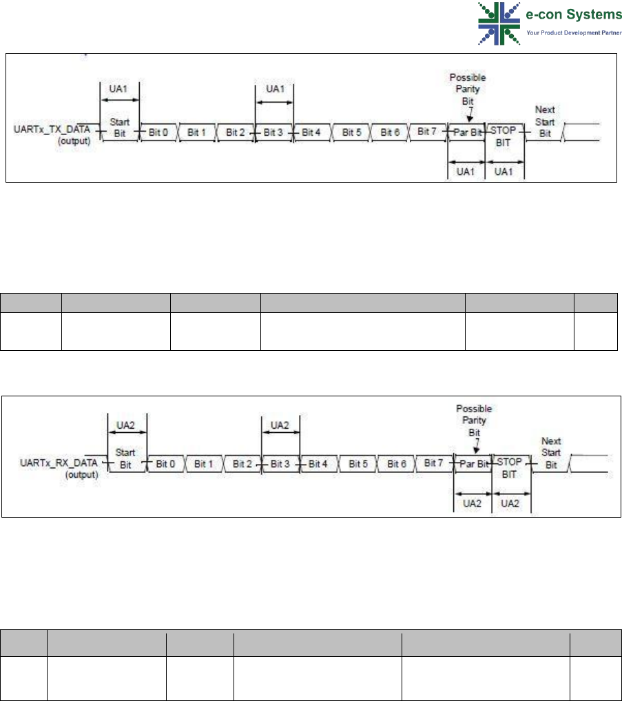
40 eSOMiMX7 Carrier Board Design Guide
Figure 19: UART Timing Diagram-Transmitter
The following table shows the timing details of the UART interface-transmitter.
Table 25: UART Interface Timing-Transmitter Details
ID
Parameter
Symbol
Min
Max
Unit
UA1
Transmit Bit
time
tTbit
1/Fbaud_rate - Tref_clk
1/Fbaud_rate
+ Tref_clk
—
The following figure shows the timing details of the UART interface-receiver.
Figure 20: UART Timing Diagram-Receiver
The following table shows the timing details of the UART interface-receiver.
Table 26: UART Interface Timing-Receiver Details
ID
Parameter
Symbol
Min
Max
Unit
UA1
Receive Bit time
tRbit
1/Fbaud_rate2 - 1/(16x
Fbaud_rate)
1/Fbaud_rate +1/(16 x
Fbaud_rate)
—
Unused UART Interface Signals Termination
All UART signals can be left unconnected if not used.
I2C Interface
eSOMiMX7 supports three I2C ports in the connector.The inter integrated circuit
(I2C) provides functionality of a standard I2C slave and master. The I2C is designed
to be compatible with the standard NXP I2C bus protocol.
The I2C has the following key features:
• Multimaster operation
• Software programmability for one of 64 different serial clock frequencies
• Software-selectable acknowledge bit

© Copyright e-con Systems. 2017. All rights reserved. 41
• Interrupt-driven, byte-by-byte data transfer
• Arbitration-lost interrupt with automatic mode switching from master to slave
• Calling address identification interrupt
• Start and stop signal generation/detection
• Repeated Start signal generation
• Acknowledge bit generation/detection
• Bus-busy detection
• In Standard mode, I2C supports the data transfer rates up to 100 kbits/s
This interface covers the following sections:
• I2C interface Signals
• Reference Schematics
• I2C interface Signals Timing Details
• Unused I2C Interface Signals Termination
I2C Interface Signals
The following table shows the I2C interface signals.
Table 27: I2C Interface Signals
Pin
Signal Name
I/O
Power Rail
Description
CN4.63
I2C2_DATA_IMX7_CONN
I/O
1.8V
I2C-2 Serial Data
CN4.47
GPIO1_IO07_IMX7_CONN
I/O
1.8V
I2C-2 Serial Data
CN4.65
I2C2_CLK_IMX7_CONN
O
1.8V
I2C-2 Serial Clock
CN4.49
GPIO1_IO06_IMX7_CONN
O
1.8V
I2C-2 Serial Clock
CN4.66
UART2_RX_IMX7_CONN
O
1.8V
I2C-2 Serial Clock
CN4.67
I2C3_DATA_IMX7_CONN
I/O
1.8V
I2C-3 Serial Data
CN3.50
LCD1_DATA21 iMX7_LCD_DATA[0:23]
I/O
1.8V
I2C-3 Serial Data
CN4.45
GPIO1_IO09_IMX7_CONN
I/O
1.8V
I2C-3 Serial Data
CN4.69
I2C3_CLK_IMX7_CONN
O
1.8V
I2C-3 Serial Clock
CN3.51
LCD1_DATA20 iMX7_LCD_DATA[0:23]
O
1.8V
I2C-3 Serial Clock
CN4.59
I2C4_DATA_IMX7_CONN
I/O
1.8V
I2C-4 Serial Data
CN4.52
SAI1_RXC_iMX7_CONN
I/O
3.3V
I2C-4 Serial Data
CN3.33
LCD1_DATA23 iMX7_LCD_DATA[0:23]
I/O
1.8V
I2C-4 Serial Data
CN4.61
I2C4_CLK_IMX7_CONN
O
1.8V
I2C-4 Serial Clock
CN4.43
GPIO1_IO10_IMX7_CONN
O
1.8V
I2C-4 Serial Clock
CN4.50
SAI1_RXFS_iMX7_CONN
O
3.3V
I2C-4 Serial Clock
CN3.47
LCD1_DATA22 iMX7_LCD_DATA[0:23]
O
1.8V
I2C-4 Serial Clock
*SAI1 lines are muxed with NAND signals and hence cannot be used in SOMs with
NAND flash.
Reference Schematics
The I2C signals are of 1.8V domain, if the application requirement is of 3.3V domain
an I2C level translator is required. Also, it must be noted that there are no pull ups
on the I2C lines in the eSOMiMX7 and hence external pull ups are required.
The following figure shows the I2C Interface reference schematic.
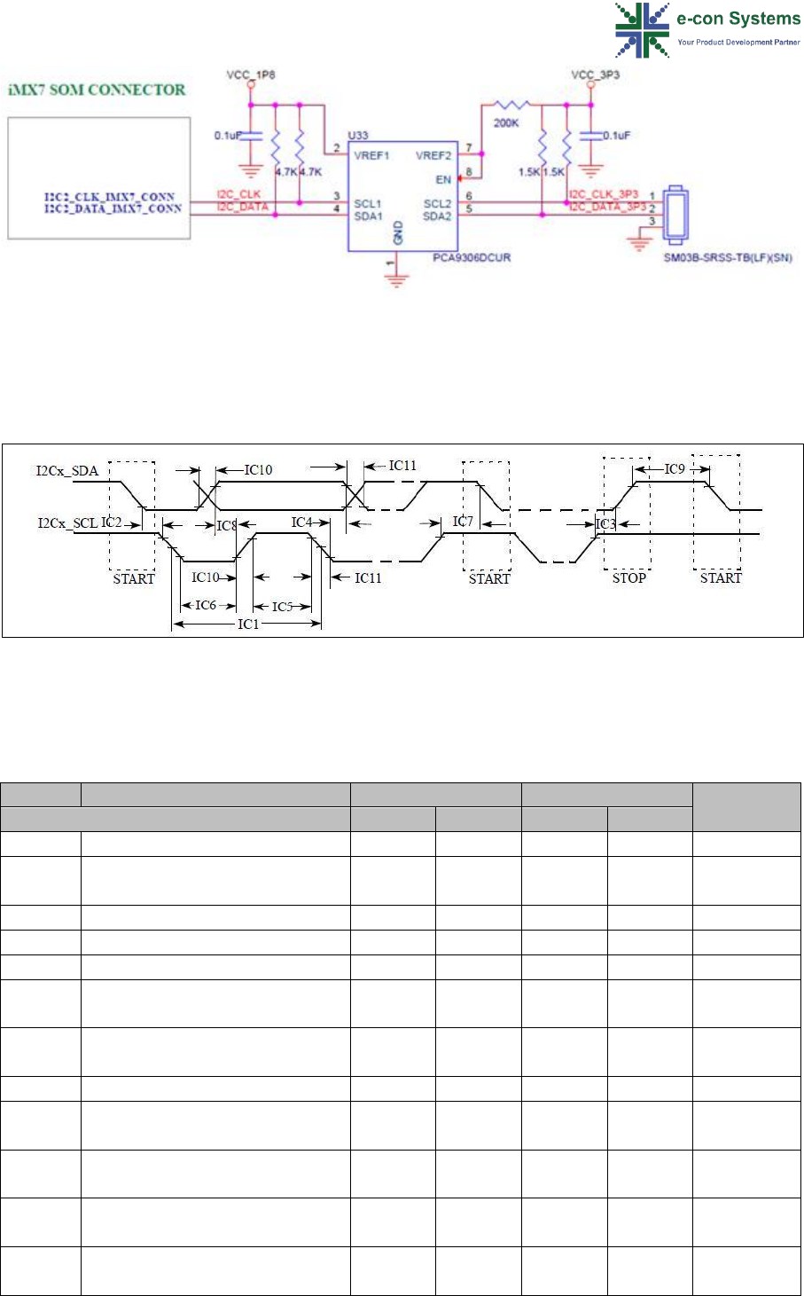
42 eSOMiMX7 Carrier Board Design Guide
Figure 21: I2C Interface Reference Schematic
I2C Interface Signals Timing Details
The following figure shows the timing details of the I2C interface.
Figure 22: I2C Timing Diagram
The following table shows the timing details of the I2C interface.
Table 28: I2C Interface Timing Details
ID
Parameter
Standard Mode
Fast Mode
Unit
Min
Max
Min
Max
I2C1
I2Cx_SCL cycle time
10
—
2.5
—
μs
I2C2
Hold time (repeated) START
condition
4
—
0.6
—
μs
I2C3
Set-up time for STOP condition
4
—
0.6
—
μs
I2C4
Data hold time
0^1
3.45^2
0^1
0.9^2
μs
I2C5
HIGH Period of I2Cx_SCL Clock
4
—
0.6
—
μs
I2C6
LOW Period of the I2Cx_SCL
Clock
4.7
—
1.3
—
μs
I2C7
Set-up time for a repeated
START condition
4.7
—
0.6
—
μs
I2C8
Data set-up time
250
—
100^3
—
ns
I2C9
Bus free time between a STOP
and START condition
4.7
—
1.3
—
μs
I2C10
Rise time of both I2Cx_SDA and
I2Cx_SCL signals
—
1000
20 +
0.1Cb^4
300
ns
I2C11
Fall time of both I2Cx_SDA and
I2Cx_SCL signals
—
300
20 +
0.1Cb^4
300
ns
I2C12
Capacitive load for each bus
line (Cb)
—
400
—
400
pF

© Copyright e-con Systems. 2017. All rights reserved. 43
Unused I2C interface Signals Termination
All I2C Signals can be left unconnected if not used.
FlexCAN Interface
The Flexible Controller Area Network (FlexCAN) module is a communication
controller implementing the CAN protocol according to the CAN 2.0B protocol
specification.
eSOMiMX7 has a single CAN Controller that can support data rates up to 1Mbps.The
FLEXCAN module is a full implementation of the CAN protocol specification, which
supports both standard and extended message frames. 64 Message Buffers are
supported.
Some of the features of FlexCAN are:
• Flexible Mailboxes of eight bytes data length.
• Each Mailbox is configurable as Rx or Tx, all supporting standard and extended
messages.
• Transmission abort capability.
• Backwards compatibility with previous FLEXCAN version.
• Listen only mode available.
• Programmable loop-back mode supporting self-test operation.
• Time Stamp based on 16-bit free-running timer.
• Maskable interrupts.
The operational modes are as follows:
• Functional modes
▪ Normal Mode (User or Supervisor)
▪ Freeze Mode
▪ Listen-Only Mode
▪ Loop-Back Mode
▪ Module Disable Mode
▪ Stop Mode
• Low Power Mode
▪ Disable Mode
▪ Stop Mode
This interface covers the following sections:
• FlexCAN Interface Signals
• Reference Schematics
• Unused FlexCAN Interface Signals Termination

44 eSOMiMX7 Carrier Board Design Guide
FlexCAN Interface Signals
The following table shows the FlexCAN interface signals.
Table 29 FlexCAN Interface Signals
Pin
Signal Name
I/O
Power
Rail
Description
CN4.41
GPIO1_IO12_IMX7_CONN
I
-
CAN1 Bus Receive
CN4.39
GPIO1_IO13_IMX7_CONN
O
-
CAN1 Bus Transmit
CN4.44
SAI1_TXD_iMX7_CONN
I
-
CAN2 Bus Receive
CN4.54
SAI1_TXFS_iMX7_CONN
O
-
CAN2 Bus Transmit
*SAI1 lines are muxed with NAND signals and hence cannot be used in SOMs with
NAND flash.
Reference Schematics
The following figure shows the UART Interface reference schematic.
Figure 23: FlexCAN Interface Reference Schematic
Unused FlexCAN Interface Signals Termination
All FlexCAN signals can be left unconnected if not used.
Enhanced Configurable SPI Interface
eSOMiMX7 has support for 2 SPI interfaces. It is a Full-duplex, synchronous serial
interface. It can be configured as both master as well as slave. Maximum operation
frequency is up to the reference clock frequency of 20MHz.
The features supported are as follows:
• Full-duplex synchronous serial interface
• Master or Slave configurable
• 32-bit wide by 64-entry FIFO for both transmit and receive data
• Polarity and phase of the Chip Select (SS) and SPI Clock (SCLK) are configurable
• Direct Memory Access (DMA) supported

© Copyright e-con Systems. 2017. All rights reserved. 45
This interface covers the following sections:
• ECSPI Interface Signals
• ECSPI Interface Signals Timing Details
• Unused ECSPI Interface Signals Termination
ECSPI Interface Signals
The following table shows the ECSPI interface signals.
Table 30: ECSPI Interface Signals
Pin
Signal Name
I/O
Power
Rail
Description
CN4.65
I2C2_CLK_IMX7_CONN
O
1.8V
SPI1 – SCLK
CN4.73
SAI2_RXD_iMX7_CONN
O
3.3V
SPI1 – SCLK
CN4.71
SAI2_FS_iMX7_CONN
O
3.3V
SPI1 – MOSI
CN4.77
SAI2_TXC_iMX7_CONN
I
3.3V
SPI1 – MOSI
CN4.63
I2C2_DATA_IMX7_CONN
O
1.8V
SPI1 – SS0
CN4.75
SAI2_TXD_iMX7_CONN
O
3.3V
SPI1 – SS0
CN4.85
SD1_DATA3_iMX7_CONN
O
VCC_SD
SPI1 – SS1
CN3.39
iMX7_LCD_HSYNC
O
1.8V
SPI2 – SCLK
CN3.28
CLK_iMX7_LCD_CLK
I
1.8V
SPI2 – MISO
CN4.95
nSD1_CD_iMX7_CONN
I
VCC_SD
SPI2 – MISO
CN3.27
iMX7_LCD_ENABLE
O
1.8V
SPI2 – MOSI
CN3.41
iMX7_LCD_VSYNC
O
1.8V
SPI2 – SS0
CN4.81
CLK_SD1_CLK_iMX7_CONN
O
VCC_SD
SPI2 – SS0
CN4.91
SD1_CMD_iMX7_CONN
O
VCC_SD
SPI2 – SS1
CN4.93
SD1_DATA0_iMX7_CONN
O
VCC_SD
SPI2 – SS2
CN4.87
SD1_DATA1_iMX7_CONN
O
VCC_SD
SPI2 – SS3
CN4.89
SD1_DATA2_iMX7_CONN
I
VCC_SD
SPI2 – Ready
*SAI1 lines are muxed with NAND signals and hence cannot be used in SOMs with
NAND flash.
ECSPI Interface Signals Timing Details
The following figure shows the Master Mode timing details of the ECSPI interface.
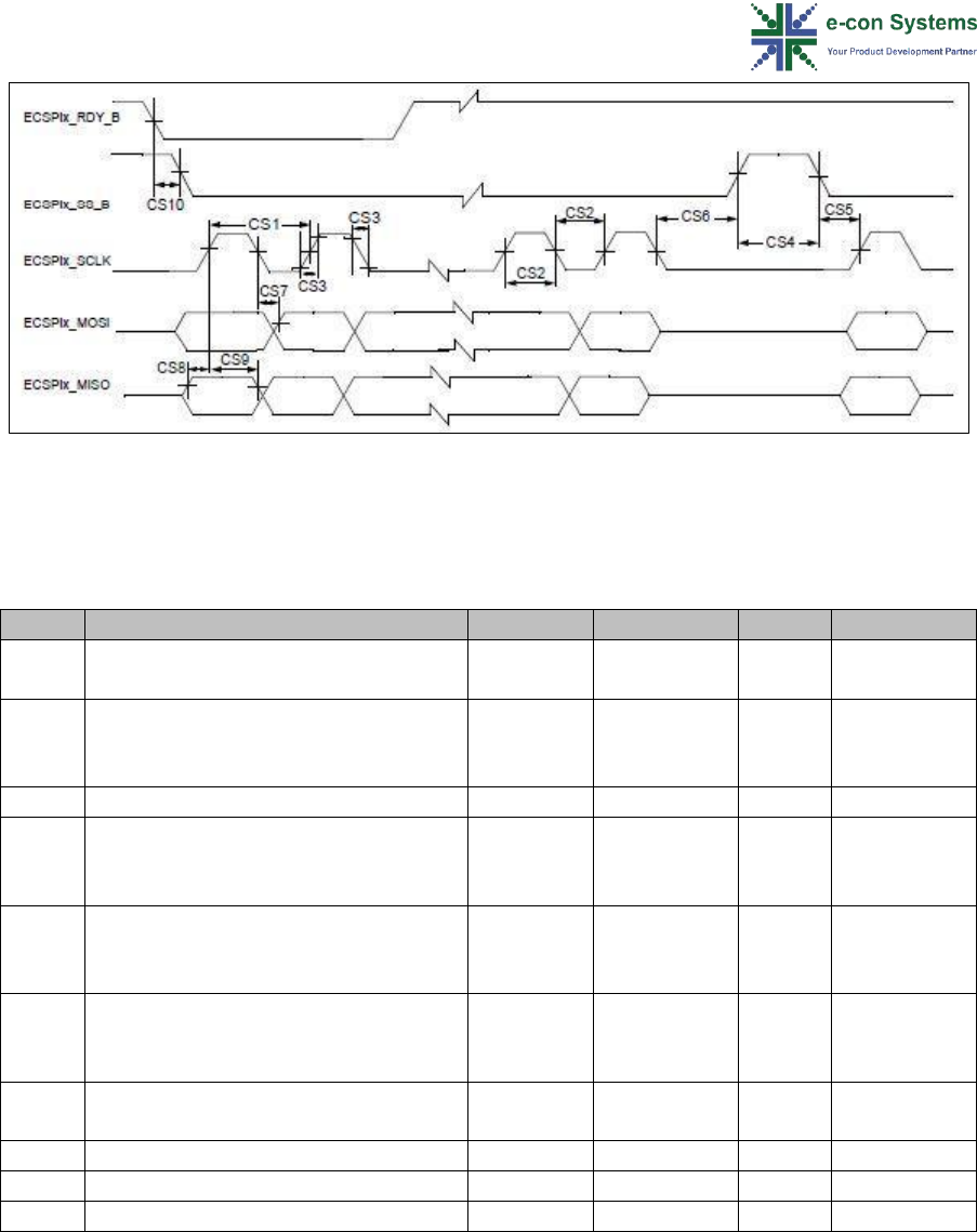
46 eSOMiMX7 Carrier Board Design Guide
Figure 24: ECSPI Timing Diagram - Master Mode
The following table shows the Master Mode timing details of the ECSPI interface.
Table 31: ECSPI Interface Timing Master Mode Details
ID
Parameter
Symbol
Min
Max
Unit
CS1
ECSPIx_SCLK Cycle Time–Read
ECSPIx_SCLK Cycle Time–Write
tclk
43
15
—
ns
CS2
ECSPIx_SCLK High or Low Time–Read
ECSPIx_SCLK High or Low Time–
Write
tSW
21.5
7
—
ns
CS3
ECSPIx_SCLK Rise or Fall1
tRISE/FALL
—
—
ns
CS4
ECSPIx_SS_B pulse width
tCSLH
Half
ECSPIx_SCLK
period
—
ns
CS5
ECSPIx_SS_B Lead Time (CS setup
time)
tSCS
Half
ECSPIx_SCLK
period - 4
—
ns
CS6
ECSPIx_SS_B Lag Time (CS hold time)
tHCS
Half
ECSPIx_SCLK
period - 2
—
ns
CS7
ECSPIx_MOSI Propagation Delay
(CLOAD = 20 pF)
tPDmosi
-1
1
ns
CS8
ECSPIx_MISO Setup Time
tSmiso
18
—
ns
CS9
ECSPIx_MISO Hold Time
tHmiso
0
—
ns
CS10
RDY to ECSPIx_SS_B Time2
tSDRY
5
—
ns
The following figure shows the Slave Mode timing details of the ECSPI interface.
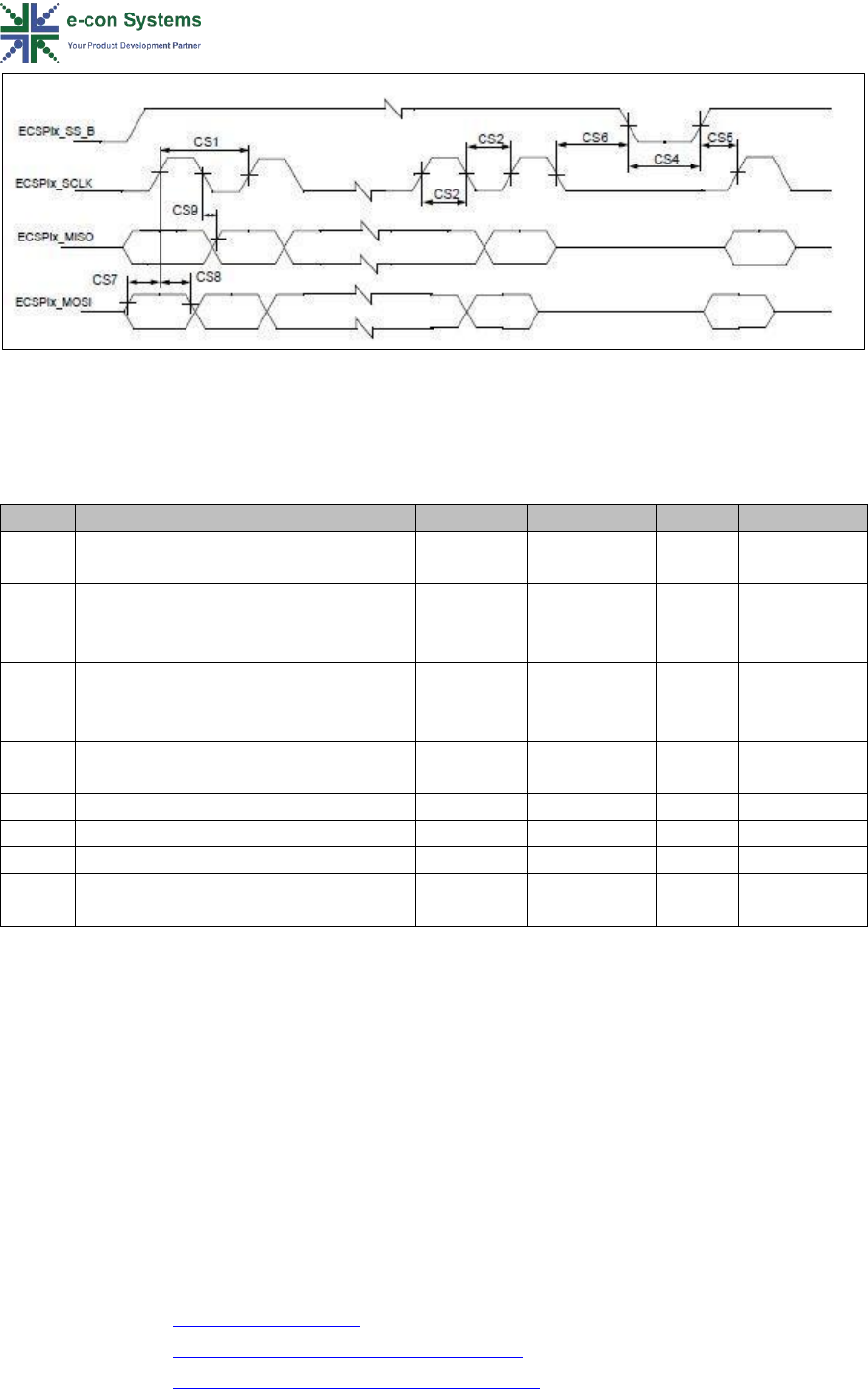
© Copyright e-con Systems. 2017. All rights reserved. 47
Figure 25: ECSPI Timing Diagram–Slave Mode
The following table shows the Slave Mode timing details of the ECSPI interface.
Table 32: ECSPI Interface Timing Slave Mode Details
ID
Parameter
Symbol
Min
Max
Unit
CS1
ECSPIx_SCLK Cycle Time–Read
ECSPI_SCLK Cycle Time–Write
tclk
15
43
—
ns
CS2
ECSPIx_SCLK High or Low Time–Read
ECSPIx_SCLK High or Low Time–
Write
tSW
7
21.5
—
ns
CS4
ECSPIx_SS_B pulse width
tCSLH
Half
ECSPIx_SCLK
period
—
ns
CS5
ECSPIx_SS_B Lead Time (CS setup
time)
tSCS
5
—
ns
CS6
ECSPIx_SS_B Lag Time (CS hold time)
tHCS
5
—
ns
CS7
ECSPIx_MOSI Setup Time
tSmosi
4
1
ns
CS8
ECSPIx_MOSI Hold TimetHmosi
tHmosi
4
—
ns
CS9
ECSPIx_MISO Propagation Delay
(CLOAD = 20 pF)
tPDmiso
4
19
ns
Unused ECSPI Interface Signals Termination
All ECSPI signals can be left unconnected if not used.
Quad Serial Peripheral Interface
The QSPI acts as an interface to one or two external serial flash devices, each with
up to four bidirectional data lines. Two identical serial flash devices can be
connected and accessed in parallel for data read operations, forming one (virtual)
flash memory with doubled readout bandwidth.
This interface covers the following sections:
• QSPI Interface Signals
• Quad SPI Interface Signals Timing Details
• Unused QSPI Interface Signals Termination
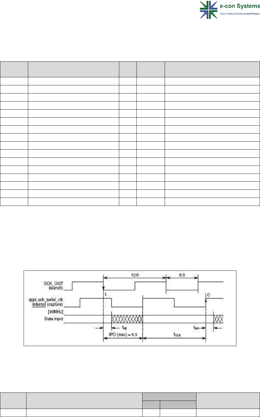
48 eSOMiMX7 Carrier Board Design Guide
QSPI Interface Signals
The following table shows the QSPI interface signals.
Table 33 QSPI Interface Signals
Pin
Signal Name
I/O
Power
Rail
Description
CN3.13
iMX7_CONN_QSPI_A_SCLK
O
3.3V
QSPI_A_SCLK
CN3.1
iMX7_CONN_QSPI_A_DATA0
IO
3.3V
QSPI_A_DATA0
CN3.5
iMX7_CONN_QSPI_A_DATA1
IO
3.3V
QSPI_A_DATA1
CN3.9
iMX7_CONN_QSPI_A_DATA2
IO
3.3V
QSPI_A_DATA2
CN3.3
iMX7_CONN_QSPI_A_DATA3
IO
3.3V
QSPI_A_DATA3
CN3.11
iMX7_CONN_QSPI_A_DQS
IO
3.3V
QSPI_A_DQS
CN3.7
iMX7_CONN_QSPI_A_SS0_B
O
3.3V
QSPI_A_SS0_B
CN3.15
iMX7_CONN_QSPI_A_SS1_B
O
3.3V
QSPI_A_SS1_B
CN3.16
iMX7_CONN_QSPI_B_SCLK
O
3.3V
QSPI_B_SCLK
CN3.2
iMX7_CONN_QSPI_B_DATA0
IO
3.3V
QSPI_B_DATA0
CN3.8
iMX7_CONN_QSPI_B_DATA1
IO
3.3V
QSPI_B_DATA1
CN3.10
iMX7_CONN_QSPI_B_DATA2
IO
3.3V
QSPI_B_DATA2
CN3.14
iMX7_CONN_QSPI_B_DATA3
IO
3.3V
QSPI_B_DATA3
CN3.6
iMX7_CONN_QSPI_B_DQS
IO
3.3V
QSPI_B_DQS
CN3.4
iMX7_CONN_QSPI_B_SS0_B
O
3.3V
QSPI_B_SS0_B
CN3.12
iMX7_CONN_QSPI_B_SS1_B
O
3.3V
QSPI_B_SS1_B
*SAI1 lines are muxed with NAND signals and hence cannot be used in SOMs with
NAND flash.
Quad SPI Interface Signals Timing Details
The following figure and table shows the timing details of the Quad SPI interface.
Quad SPI Input Timing (SDR Mode)
Figure 26: QSPI Timing Diagram - SDR Mode – Input
The following table shows the timing details of the Quad SPI interface.
Table 34: QSPI Interface Timing SDR Mode Input Details
Pin
Parameter
Value
Unit
Min
Max
TSUI
Setup time for incoming data
12.4
—
ns

© Copyright e-con Systems. 2017. All rights reserved. 49
THI
Hold time requirement for incoming data
4.5
—
ns
Quad SPI Output Timing (SDR Mode)
The following figure shows the timing details of the Quad SPI interface.
Figure 27: QSPI Timing Diagram - SDR Mode – Output
The following table shows the timing details of the Quad SPI interface.
Table 35: QSPI Interface Timing SDR Mode Output Details
Pin
Parameter
Value
Unit
Min
Max
TDV
Output Data Valid
—
12.4
ns
THo
Output Data Hold
4.5
—
ns
Quad SPI Timing Parameters (DDR Mode)
The following figure shows the timing details of the Quad SPI interface.
Figure 28: QSPI Timing Diagram - DDR Mode – Input
The following table shows the timing details of the Quad SPI interface.

50 eSOMiMX7 Carrier Board Design Guide
Table 36: QSPI Interface Timing DDR Mode Input Details
Parameter
Symbol
Min
Max
Unit
Setup time for incoming data
tCLK(LCD)
14.5
-
ns
Hold time requirement for incoming data
tCLKH(LCD)
4.5
-
ns
QuadSPI Output Timing (DDR Mode)
The following figure shows the timing details of the Quad SPI interface.
Figure 29: QSPI Timing Diagram - DDR Mode – Output
The following table shows the timing details of the Quad SPI interface.
Table 37: QSPI Interface Timing DDR Mode Output Details
Parameter
Symbol
Min
Max
Unit
Output Data Valid
TDV
-
6.4
ns
Output Data Hold
THO
0.7
-
ns
Unused Quad SPI Interface Signals Termination
All Quad SPI signals can be left unconnected if not used.
Pulse Width Modulation
eSOMiMX7 has 4 Pulse Width Modulation(PWM) signals. The PWM has a 16-bit
counter, it uses 16-bit resolution and a 4 x 16 data FIFO.
This interface covers the following sections:
• Pulse Width Modulation Signals
• Pulse Width Modulation Signals Timing Details
• Unused Pulse Width Modulation Signals Termination
Pulse Width Modulation Signals
The following table shows the PWM signals.
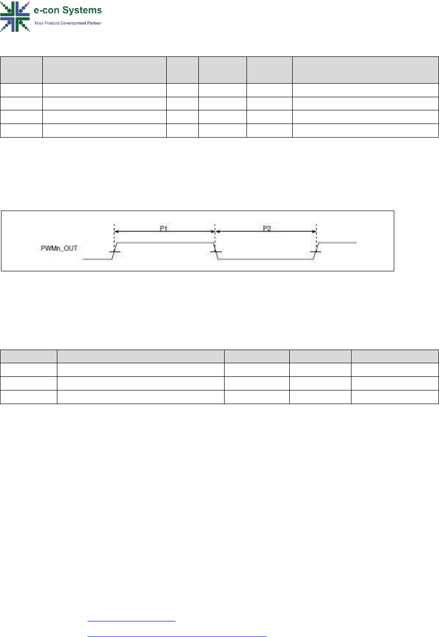
© Copyright e-con Systems. 2017. All rights reserved. 51
Table 38: Pulse Width Modulation Signals
Pin
Signal Name
I/O
Type
Power
Rail
Description
CN4.53
GPIO1_IO00_IMX7_CONN
O
PWM
1.8V
PWM1 – OUT
CN4.45
GPIO1_IO09_IMX7_CONN
O
PWM
1.8V
PWM2 – OUT
CN4.55
GPIO1_IO02_IMX7_CONN
O
PWM
1.8V
PWM2 – OUT
CN4.43
GPIO1_IO10_IMX7_CONN
O
PWM
1.8V
PWM3 – OUT
Pulse Width Modulation Signals Timing Details
The following figure shows the timing details of the Pulse Width Modulation
interface.
Figure 30: PWM Timing Diagram
The following table shows the timing details of the PWM interface.
Table 39: PWM Timing Details
ID
Parameter
Min
Max
Unit
PWM Module Clock Frequency
0
24
MHz
P1
PWM output pulse width high
15
—
ns
P2
PWM output pulse width high
15
—
ns
Unused Pulse Width Modulation Signals Termination
All PWM signals can be left unconnected if not used.
Analog Input Signal
Analog input signal is handled by an Analog to digital converter (ADC). In eSOMiMX7
will support 8 ADC with 12-bit resolution and maximum input voltage is 1.8V. It
supports conversion up to five logic groups and Support flexible 4, 8, 16, 32 number
of conversion data, configurable sample time and conversion speed / power and the
maximum sample rate of ADC is 1 MHz.
This interface covers the following sections:
• Analog Input Signals
• Unused Analog Input Signals Termination
Analog Input Signals
The following table shows the Analog input signals.
52 eSOMiMX7 Carrier Board Design Guide
Table 40: Analog Input Signals
Pin
Signal Name
I/O
Type
Power
Rail
Description
CN4.28
ADC1_IN0_IMX7_CONN
I
Analogue
1.8V
Analog input
CN4.32
ADC1_IN1_IMX7_CONN
I
Analogue
1.8V
Analog input
CN4.26
ADC1_IN2_IMX7_CONN
I
Analogue
1.8V
Analog input
CN4.30
ADC1_IN3_IMX7_CONN
I
Analogue
1.8V
Analog input
CN4.34
ADC2_IN0_IMX7_CONN
I
Analogue
1.8V
Analog input
CN4.36
ADC2_IN1_IMX7_CONN
I
Analogue
1.8V
Analog input
CN4.38
ADC2_IN2_IMX7_CONN
I
Analogue
1.8V
Analog input
CN4.40
ADC2_IN3_IMX7_CONN
I
Analogue
1.8V
Analog input
Unused Analog Input Signals Termination
The following table shows the unused Analog input signals termination.
Table 41: Unused Analog Input Signals Termination
Analog input signal Pin
Analog input signal Name
Recommended Termination
CN4.28
ADC1_IN0_IMX7_CONN
Tie to ground
CN4.32
ADC1_IN1_IMX7_CONN
Tie to ground
CN4.26
ADC1_IN2_IMX7_CONN
Tie to ground
CN4.30
ADC1_IN3_IMX7_CONN
Tie to ground
CN4.34
ADC2_IN0_IMX7_CONN
Tie to ground
CN4.36
ADC2_IN1_IMX7_CONN
Tie to ground
CN4.38
ADC2_IN2_IMX7_CONN
Tie to ground
CN4.40
ADC2_IN3_IMX7_CONN
Tie to ground

© Copyright e-con Systems. 2017. All rights reserved. 53
Power and Control
Power and Control signals
The following table shows the Power and Control signals.
Table 2: Power and Control signals
Pin
Signal Name
I/O
Power
Rail
Internal
Pull up
Description
CN4.99
BASE_BOARD_PWR_EN
O
1.8V
10K
Carrier board power enable signal.
CN4.37
CPU_BOOT_MODE0
I
1.8V
10K
Boot Mode Configuration Pin 1
CN4.35
CPU_BOOT_MODE1
I
1.8V
10K
Boot Mode Configuration Pin 2
CN4.31
CPU_ONOFF
I
3.0
100K
CPU Power on Switch
CN4.33
CPU_POR
I
3.0
100K
CPU Reset
Note: BASE_BOARD_PWR_EN is connected to 1.8V through a 10K Resistor.
Boot Options
eSOMiMX7 SOM uses two boot mode signals to select the boot type.
The following table lists the boot mode type selection details.
Table 43: Boot mode type selection
Boot Mode
Description
BOOT_MODE1
BOOT_MODE0
Boot From eFuses
In this mode, i.MX7 boot media is selected
by GPIO eFUSE settings
0
0
Serial
Downloader
Mode
In this mode, i.MX7 boot device can be
programmed through its USB OTG
interface using MFG Tool
0
1
Internal Boot
Mode (Default)
In this mode, i.MX7 boot media is selected
by GPIO Pin’s settings
1
0
Reserved
Not allowed to use this mode
1
1
Note:
• 1 – Pin need to be connected to logic high
• 0 – Pin need to be connected to logic low
CPU ONOFF
CPU_ONOFF has an internal Pull up to 3.0V. CPU_ONOFF signal is used to switch on and off
the system. Can be connected to a push button. Short connection to GND in OFF mode
causes internal power management state machine to change state to ON. In ON mode short
connection to GND generates interrupt (intended to SW controllable power down). Long
above ~5s connection to GND causes “forced” OFF. If not used, CPU_ONOFF can be left
unconnected.
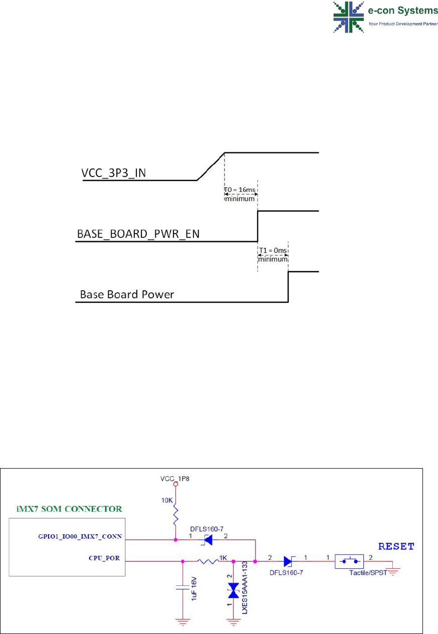
54 eSOMiMX7 Carrier Board Design Guide
Power on Sequence
The power on sequence begins with the VCC_3P3_IN supply to the SOM, this is the
first and foremost supply given to the SOM. After the completion of internal power
on sequence in the SOM, the BASE_BOARD_PWR_EN signal is pulled high. Only after
this the Base board supplies must be powered ON. It is mandatory to follow this
sequence to ensure the proper working of all the peripherals.
Figure 11: Power on Sequence
CPU Reset
The following reset circuit is recommended in order to perform a software initiated
reset or to perform a watchdog initiated reset. In the case of watchdog reset, the
GPIO1_IO00_IMX7_CONN must be used under ALT3_WDOG1_WDOG_B mux option
to control POR.
The following figure shows the reset circuit reference schematic diagram.
Figure 32: Reset Circuit Reference Schematic Diagram

© Copyright e-con Systems. 2017. All rights reserved. 55
What’s Next?
After understanding the designing concept of the carrier board, you can refer to the
following documents from the Developer Resources website to understand more
about the eSOMiMX7.
• eSOMiMX7 Datasheet
• Evaluation Board Schematics
• PinMUX Detail

56 eSOMiMX7 Carrier Board Design Guide
Glossary
ADC: Analogue to Digital Converter.
Auto-MDIX: Automatically Medium Dependent Interface Crossing, a PHY with Auto-
MDIX f can detect whether RX and TX need to be crossed (MDI or MDIX).
CAN: Controller Area Network, a bus that is manly used in automotive and industrial
environment.
CDMA: Code Division Multiple Access, abbreviation often used for a mobile phone
standard for data communication.
CPU: Central Processor Unit.
CSI: Camera Serial Interface.
DAC: Digital to Analogue Converter.
DSI: Display Serial Interface.
EMI: Electromagnetic Interference, high frequency disturbances.
eMMC: Embedded Multi Media Card, flash memory combined with MMC interface
controller in a BGA package, used as internal flash memory.
ESD: Electrostatic Discharge, high voltage spike or spark that can damage
electrostatic- sensitive devices.
GBE: Gigabit Ethernet, Ethernet interface with a maximum data rate of 1000Mbit/s.
GND: Ground.
GPIO: General Purpose Input/Output, pin that can be configured being an input or
output.
GSM: Global System for Mobile Communications.
HDMI: High-Definition Multimedia Interface, combines audio and video signal for
connecting monitors, TV sets or Projectors, electrical compatible with DVI-D.
I2C: Inter-Integrated Circuit, two wire interfaces for connecting low-speed
peripherals.
I2S: Integrated Interchip Sound, serial bus for connecting PCM audio data between
two devices.
IrDA: Infrared Data Association, infrared interface for connecting peripherals.
JTAG: Joint Test Action Group, widely used debug interface.

© Copyright e-con Systems. 2017. All rights reserved. 57
LCD: Liquid Crystal Display.
LSB: Least Significant Bit.
LVDS: Low-Voltage Differential Signaling, electrical interface standard that can
transport very high-speed signals over twisted-pair cables. Many interfaces like PCIe
or SATA use this interface. Since the first successful application was the Flat Panel
Display Link, LVDS became a synonymous for this interface. In this document, the
term LVDS is used for the FPD-Link interface.
MIPI: Mobile Industry Processor Interface Alliance.
MDIX: Medium Dependent Interface Crossed, an MDI interface with crossed RX and
TX interfaces.
mini PCIe: PCI Express Mini Card, card form factor for internal peripherals. The
interface features PCIe and USB 2.0 connectivity.
MMC: MultiMedia Card, flash memory card.
MSB: Most Significant Bit.
N/A: Not Available.
N/C: Not Connected.
OD: Open Drain.
OTG: USB On-The-Go, a USB host interface that can also act as USB client when
connected to another host interface.
OWR: One Wire (1-Wire), low-speed interface which needs just one data wire plus
ground.
PCB: Printed Circuit Board.
PCI: Peripheral Component Interconnect, parallel computer expansion bus for
connecting peripherals.
PCIe: PCI Express, high-speed serial computer expansion bus, replaces the PCI bus.
PCM: Pulse-Code Modulation, digitally representation of analogue signals, standard
interface for digital audio.
PD: Pull-Down Resistor.
PHY: Physical Layer of the OSI model.
PMIC: Power Management IC, integrated circuit that manages amongst others the
power sequence of a system.
PU: Pull-up Resistor.

58 eSOMiMX7 Carrier Board Design Guide
PWM: Pulse-Width Modulation.
RGB: Red Green Blue, color channels in common display interfaces.
RJ45: Registered Jack, common name for the 8P8C modular connector that is used
for Ethernet wiring.
RS232: Single ended serial port interface.
RS422: Differential Signaling serial port interface, full duplex.
RS485: Differential Signaling serial port interface, half duplex, multi drop
configuration possible.
S/PDIF: Sony/Philips Digital Interconnect Format, optical or coaxial interface for
audio signals.
SD: Secure Digital, flash memory card.
SIM: Subscriber Identification Module, identification card for GSM phones.
SoC: System on a Chip, IC which integrates the main component of a computer on a
single chip.
SPI: Serial Peripheral Interface Bus, synchronous four wire full duplex bus for
peripherals.
TMDS: Transition-Minimized Differential Signaling, serial high-speed transmitting
technology that is used by DVI and HDMI.
TVS Diode: Transient-Voltage-Suppression Diode, diode that is used to protect
interfaces against voltage spikes.
UART: Universal Asynchronous Receiver/Transmitter, serial interface, in
combination with a transceiver a RS232, RS422, RS485, IrDA or similar interface can
be achieved.
USB: Universal Serial Bus, serial interface for internal and external peripherals.
VCC: Positive supply voltage.
© Copyright e-con Systems. 2017. All rights reserved. 59
Support
Contact Us
If you need any support on eSOMiMX7 product, please contact us using the Live
Chat option available on our website - https://www.e-consystems.com/
Creating a Ticket
If you need to create a ticket for any type of issue, please visit the ticketing page on
our website - https://www.e-consystems.com/create-ticket.asp
RMA
To know about our Return Material Authorization (RMA) policy, please visit the RMA
Policy page on our website - https://www.e-consystems.com/RMA-Policy.asp
General Product Warranty Terms
To know about our General Product Warranty Terms, please visit the General
Warranty Terms page on our website - https://www.e-
consystems.com/warranty.asp

60 eSOMiMX7 Carrier Board Design Guide
Revision History
Rev
Date
Description
Author
1.0
02-05-2018
Initial Draft
HW Team
