EMD30 Datasheet. Www.s Manuals.com. Rohm
User Manual: Marking of electronic components, SMD Codes D3, D3*, D3***, D3-***, D3.9, D30, D31, D32, D33, D36, D38, D38*, D38NH02L, D39, D3A, D3B, D3C, D3L, D3Q. Datasheets 1SS187, CM1213A-04S7, EMD3, EMD30, EMD38, IMD3A, MMSZ5228, RB400D, RB420D, RB421D, RB425D, RB495D, RT9011-MFPQW, RT9011-SPPQWB, STD38NH02L-1, STD38NH02LT4, Si2323DS, TZT30AW, TZT33AW, TZT36AW, TZT39AW, TZT3V9AW, TZT43AW, TZT47AW, TZT51AW, UMD3N.
Open the PDF directly: View PDF ![]() .
.
Page Count: 7
EMD30
Transistors
Rev.A 1/5
General purpose transistor
(isolated transistors)
EMD30
DTB713Z and DTC114E A are housed independently in a EMT6 package.
z
Applications
DC / DC converter
Motor driver
z
Features
1) DTr
1
: PNP digital transistor
DTr
2
: NPN digital transistor
2) Mounting possible with EMT3 automatic mounting
machines.
z
Structure
PNP / NPN Silicon epitaxial planar digital transistor
The following characteristics apply to both DTr1 and
DTr2.
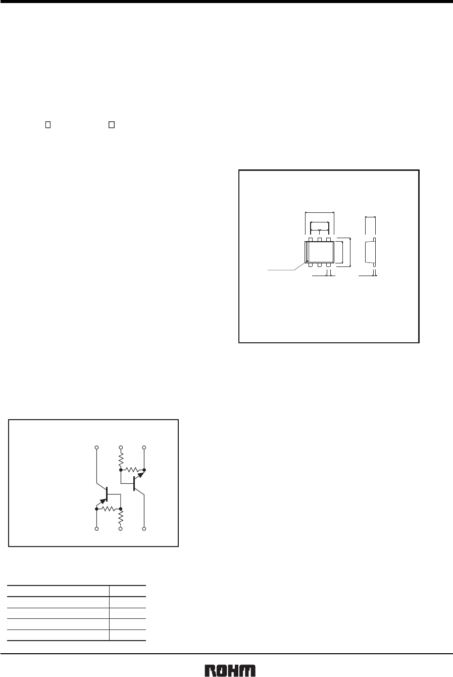
z
External dimensions (Unit : mm)
Abbreviated symbol : D30
Each lead has same dimensions
ROHM : EMT6
EMT6
0.22
1.2
1.6
(1)(2)
(5)
(3)
(6)(4)
0.13
0.5
0.5
0.5
1.0
1.6
1pin mark
z
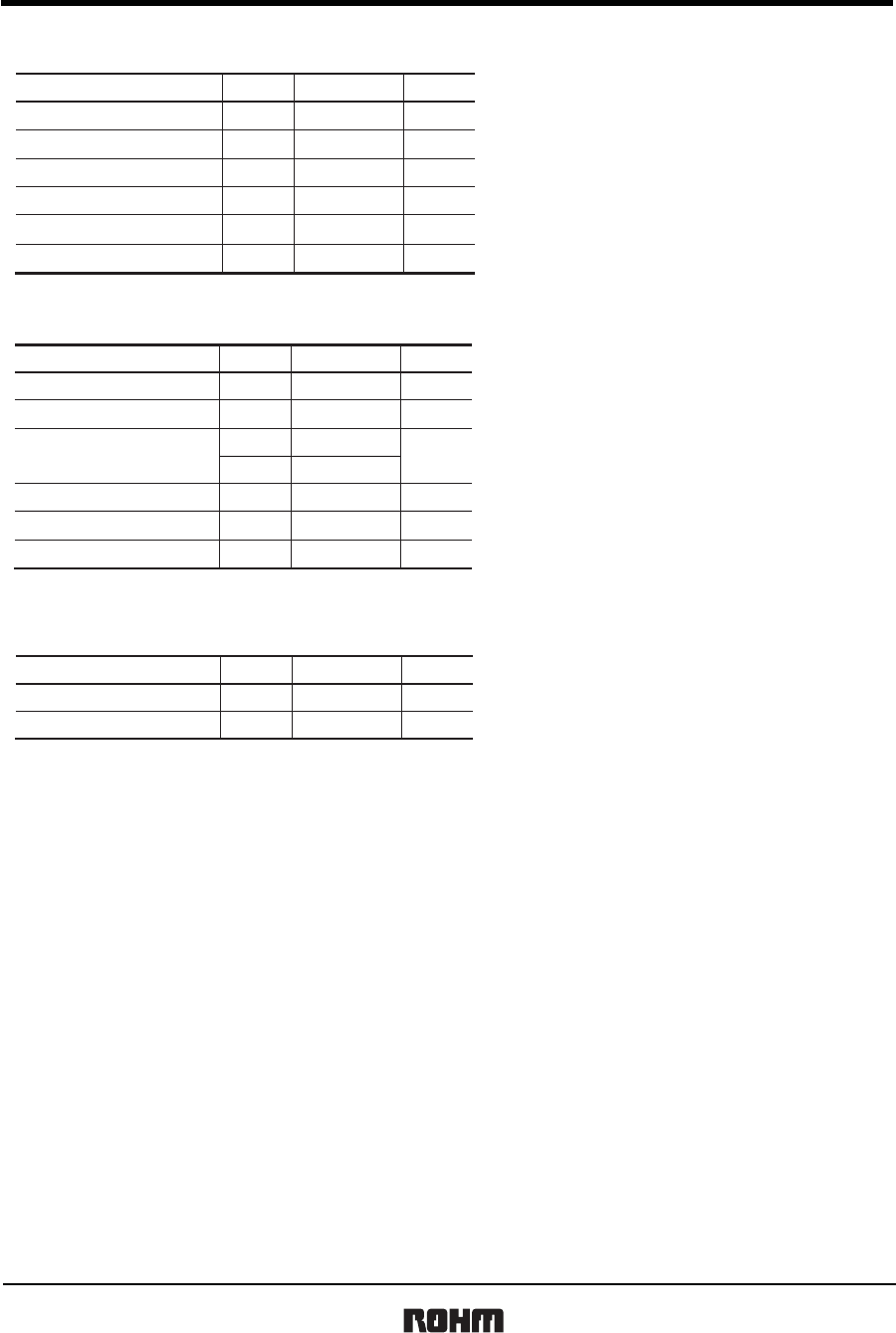
z
Equivalent circuit
EMD30
DTr2
DTr1
(3)(2)(1)
(4)(5)(6)
R1
R1 R2
R2
DTr
1
: R
1
/R
2
=1kΩ/10kΩ
DTr
2
: R
1
/R
2
=10kΩ/10kΩ
!
z
z
Packaging specifications
Type EMD30
EMT6
D30
T2R
8000
Package
Marking
Code
Basic ordering unit (pieces)
EMD30
Transistors
Rev.A 2/5
z
Absolute maximum ratings (Ta=25qC)
DTr1
Supply voltage
Input voltage
Output current
Power dissipation
Storage temperature
∗ Each terminal mounted on a recommended.
Parameter Symbol DTr1 Unit
V
CC
−30 V
−10 to +5VV
IN
mAI
C (MAX.)
Tstg −55 to +150 °C
Junction temperature Tj 150 °C
P
d
−200
120 mW
∗
DTr2
Supply voltage
Input voltage
Output current
Power dissipation
Storage temperature
∗ Each terminal mounted on a recommended.
Parameter Symbol DTr2 Unit
V
CC
50 V
−10 to +40 VV
IN
mA
I
C (MAX.)
Tstg −55 to +150 °C
Junction temperature Tj 150 °C
P
d
100
I
O
50
120 mW
∗
DTr1/DTr2
Power dissipation
Storage temperature
∗
Each terminal mounted on a recommended.
Parameter Symbol Limits Unit
Pd150(TOTAL) mW ∗
−55 to +125
°C
Tstg
EMD30
Transistors
Rev.A 3/5
z
Electrical characteristics (Ta=25qC)
DTr1
Parameter Symbol Min. Typ. Max. Unit Conditions
Resistance ratio R
2
/R
1
810 12 −−
−
Vl
(off)
−−−0.3 VV
CC
= −5V / Io= −100uA
Output voltage Vo
(on)
−−70 −300 mV I
O
= −50mA, I
I
= −2.5mA
Input voltage
I
I
−−−6.4 mA V
I
= −5V
Input current
I
O(off)
−−
−0.5 V
CC
= −30V / V
I
=0V
Output current
G
I
140 −−V
O
= −2V / Io= −100mA
DC current gain
f
T
−−MHz V
CE
= −10V / I
E
=5mA, f=100MHz
Transition frequency ∗
R
1
0.7 1.0 1.3 kΩ
Input resistance
260
μA
−
VI
(on)
−2.5 −−
VV
O
= −0.3V / Io= −20mA
∗ Characteristics of built-in transistor.
DTr2
Parameter Symbol Min. Typ. Max. Unit Conditions
Resistance ratio R2/R10.8 11.2 −−
−
Vl(off) −−0.5 VVCC=5V / Io=100uA
Output voltage Vo(on) −100 300 mV IO=10mA, II=0.5mA
Input voltage
II−−880 μAVI=5V
Input current
IO(off) −−
0.5 VCC=50V / V
I
=0V
Output current
GI30 −−VO=5V / Io=5mA
DC current gain
fT−−MHz VCE=10V / IE= −5mA, f=100MHz
Transition frequency ∗
R171013
kΩ
Input resistance
250
μA
−
VI(on) 3−−
VVO=0.3V / Io=2mA
∗
Characteristics of built-in transistor.
EMD30
Transistors
Rev.A 4/5
z
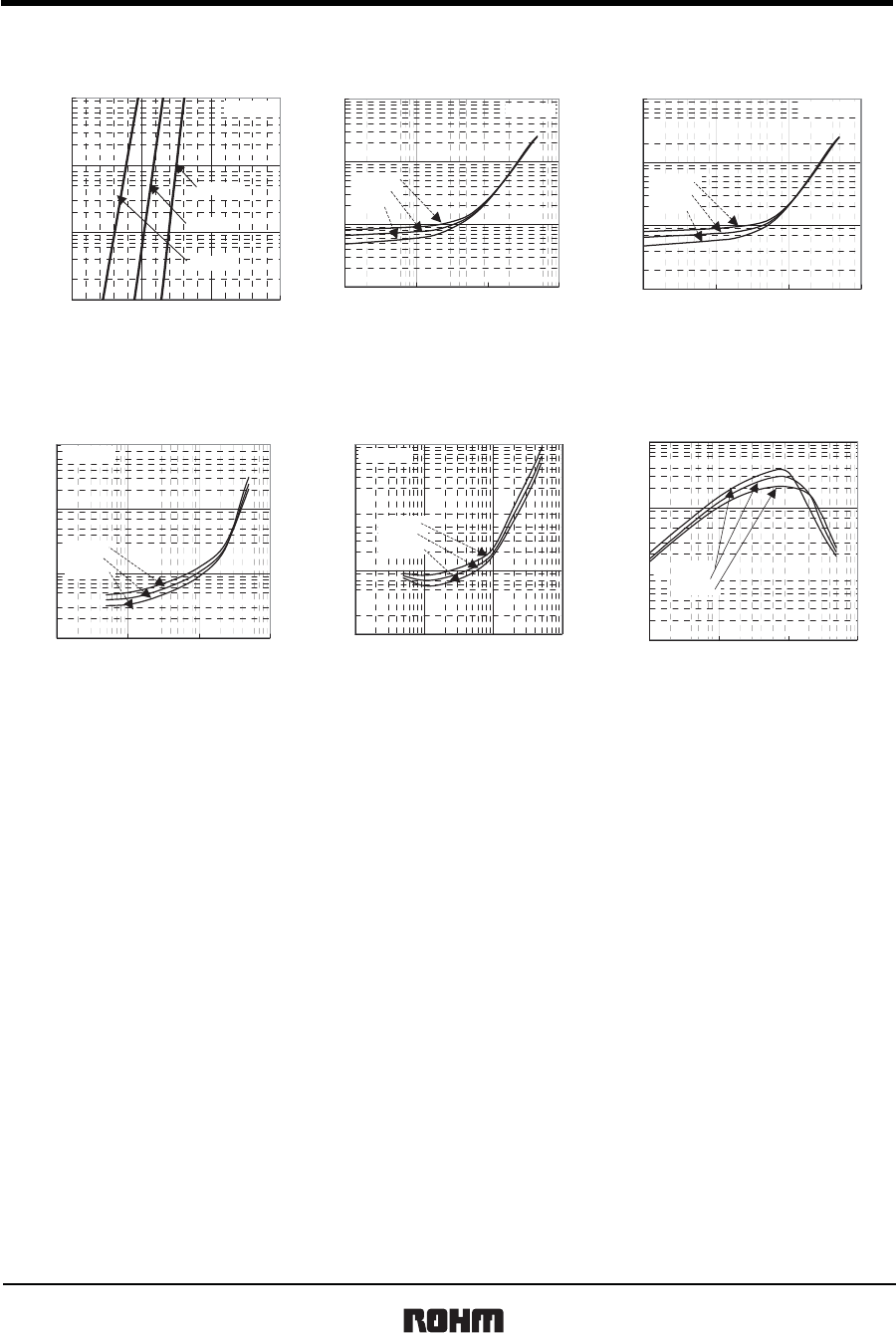
Electrical characteristic curves
DTr1
1
10
100
1000
00.511.5
INPUT VOLTAGE : V
I
(off) [ V ]
OUTPUT CURRENT : I
O
[
㱘
A]
V
CC
= 5 [V]
䎾䎃䏄䏗䎃䎐䎗䎓䛐䎃䏀
䎾䎃䏄䏗䎃䎕䎘䛐䎃䏀
䎾䎃䏄䏗䎃䎔䎓䎓䛐䎃䏀
㪝㫀㪾㪅㪈㩷㩷㪦㫌㫋㫇㫌㫋㩷㪺㫌㫉㫉㪼㫅㫋㩷㫍㫊㪅㩷㫀㫅㫇㫌㫋㩷㫍㫆㫃㫋㪸㪾㪼
㩷㩷㩷㩷㩷㩷㩷㩷㩿㪦㪝㪝㩷㪺㪿㪸㫉㪸㪺㫋㪼㫉㫀㫊㫋㫀㪺㫊㪀
㩿㪀
0.1
1
10
100
1 10 100 1000
OUTPUT CURRENT : I
O
[mA]
INPUT VOLTAGE : V
I
(on) [ V ]
V
O
= 0.2V
䎾䎃䏄䏗䎃䎐䎗䎓䛐䎃䏀
䎾䎃䏄䏗䎃䎕䎘䛐䎃䏀
䎾䎃䏄䏗䎃䎔䎓䎓䛐䎃䏀
0.1
1
10
100
1 10 100 1000
OUTPUT CURRENT : I
O
[mA]
INPUT VOLTAGE : V
I
(on) [ V ]
V
O
= 0.3V
䎾䎃䏄䏗䎃䎐䎗䎓䛐䎃䏀
䎾䎃䏄䏗䎃䎕䎘䛐䎃䏀
䎾䎃䏄䏗䎃䎔䎓䎓䛐䎃䏀
㪝㫀㪾㪅㪉㩷㩷㪠㫅㫇㫌㫋㩷㫍㫆㫃㫋㪸㪾㪼㩷㫍㫊㪅㩷㫆㫌㫋㫇㫌㫋㩷㪺㫌㫉㫉㪼㫅㫋
㩷㩷㩷㩷㩷㩷㩷㩷㩿㪦㪥㩷㪺㪿㪸㫉㪸㪺㫋㪼㫉㫀㫊㫋㫀㪺㫊㪀㩷,
㪝㫀㪾㪊㩷㩷㪠㫅㫇㫌㫋㩷㫍㫆㫃㫋㪸㪾㪼㩷㫍㫊㪅㩷㫆㫌㫋㫇㫌㫋㩷㪺㫌㫉㫉㪼㫅㫋
㩷㩷㩷㩷㩷㩷
㩿
㪦㪥㩷㪺㪿㪸㫉㪸㪺㫋㪼㫉㫀㫊㫋㫀㪺㫊
㪀
㩷,,
0.01
0.1
1
10
1 10 100 1000
OUTPUT CURRENT : I
O
[mA]
OUTPUT VOLTAGE : V
O
(on) [ V ]
0.01
0.10
1.00
10.00
1 10 100 1000
OUTPUT CURRENT : I
O
[mA]
OUTPUT VOLTAGE : V
O
(on) [ V ]
I
O
/I
I
= 50
䎾䎃䏄䏗䎃䎐䎗䎓䛐䎃䏀
䎾䎃䏄䏗䎃䎕䎘䛐䎃䏀
䎾䎃䏄䏗䎃䎔䎓䎓䛐䎃䏀 䎾䎃䏄䏗䎃䎐䎗䎓䛐䎃䏀
䎾䎃䏄䏗䎃䎕䎘䛐䎃䏀
䎾䎃䏄䏗䎃䎔䎓䎓䛐䎃䏀
㪝㫀㪾㪅㪋㩷㩷㪦㫌㫋㫇㫌㫋㩷㫍㫆㫃㫋㪸㪾㪼㩷㫍㫊㪅㩷㫆㫌㫋㫇㫌㫋㩷㪺㫌㫉㫉㪼㫅㫋㩷, 㪝㫀㪾㪅㪌㩷㪦㫌㫋㫇㫌㫋㩷㫍㫆㫃㫋㪸㪾㪼㩷㫍㫊㪅㩷㫆㫌㫋㫇㫌㫋㩷㪺㫌㫉㫉㪼㫅㫋㩷,,
I
O
/I
I
= 20
1
10
100
1000
1 10 100 1000
OUTPUT CURRENT : I
O
[mA]
DC CURRENT GAIN : G
I
䎾䎃䏄䏗䎃䎐䎗 䎓 䛐䎃䏀
䎾䎃䏄䏗䎃䎕䎘 䛐䎃䏀
䎾䎃䏄䏗䎃䎔䎓 䎓 䛐䎃䏀
㪝㫀㪾㪅㪍㩷㩷㪛㪚㩷㪺㫌㫉㫉㪼㫅㫋㩷㪾㪸㫀㫅㩷㫍㫊㪅㩷㫆㫌㫋㫇㫌㫋㩷㪺㫌㫉㫉㪼
㫅
EMD30
Transistors
Rev.A 5/5
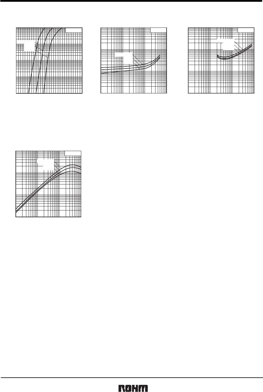
DTr2
INPUT VOLTAGE : V
I (off)
(V)
OUTPUT CURRENT : Io (A)
03
10m
1
μ
2m
5m
1m
200
μ
500
μ
100
μ
20
μ
50
μ
10
μ
2
μ
5
μ
0.5 1 1.5 2 2.5
V
CC
=5V
Ta=100˚C
25˚C
−40˚C
Fig.7 Output current vs. input voltage
(OFF characteristics)
INPUT VOLTAGE : V
I (on)
(V)
OUTPUT CURRENT : I
O
(A)
100μ200μ500μ1m 2m 5m 10m 20m 50m 100m
100
50
20
10
5
2
1
500m
200m
100m
V
O
=0.3V
Ta=−40˚C
25˚C
100˚C
Fig.8 Input voltage vs. output current
(ON characteristics)
OUTPUT CURRENT : IO
(A)
OUTPUT VOLTAGE : VO (on)
(V)
100
μ
200
μ
500
μ
1m 2m 5m 10m 20m 50m 100m
1
500m
200m
100m
50m
20m
10m
5m
2m
1m
lO/lI=20
Ta=100˚C
25˚C
−40˚C
Fig.9 Output voltage vs. output
current
OUTPUT CURRENT : IO (A)
DC CURRENT GAIN : GI
100μ200μ500μ1m 2m 5m 10m 20m 50m100m
1k
500
200
100
50
20
10
5
2
1
VO=5V
Ta=100˚C
25˚C
−40˚C
Fig.10 DC current gain vs. output
current

Appendix
Appendix1-Rev1.1
The products listed in this document are designed to be used with ordinary electronic equipment or devices
(such as audio visual equipment, office-automation equipment, communications devices, electrical
appliances and electronic toys).
Should you intend to use these products with equipment or devices which require an extremely high level of
reliability and the malfunction of with would directly endanger human life (such as medical instruments,
transportation equipment, aerospace machinery, nuclear-reactor controllers, fuel controllers and other
safety devices), please be sure to consult with our sales representative in advance.
Notes
No technical content pages of this document may be reproduced in any form or transmitted by any
means without prior permission of ROHM CO.,LTD.
The contents described herein are subject to change without notice. The specifications for the
product described in this document are for reference only. Upon actual use, therefore, please request
that specifications to be separately delivered.
Application circuit diagrams and circuit constants contained herein are shown as examples of standard
use and operation. Please pay careful attention to the peripheral conditions when designing circuits
and deciding upon circuit constants in the set.
Any data, including, but not limited to application circuit diagrams information, described herein
are intended only as illustrations of such devices and not as the specifications for such devices. ROHM
CO.,LTD. disclaims any warranty that any use of such devices shall be free from infringement of any
third party's intellectual property rights or other proprietary rights, and further, assumes no liability of
whatsoever nature in the event of any such infringement, or arising from or connected with or related
to the use of such devices.
Upon the sale of any such devices, other than for buyer's right to use such devices itself, resell or
otherwise dispose of the same, no express or implied right or license to practice or commercially
exploit any intellectual property rights or other proprietary rights owned or controlled by
ROHM CO., LTD. is granted to any such buyer.
Products listed in this document are no antiradiation design.
About Export Control Order in Japan
Products described herein are the objects of controlled goods in Annex 1 (Item 16) of Export Trade Control
Order in Japan.
In case of export from Japan, please confirm if it applies to "objective" criteria or an "informed" (by MITI clause)
on the basis of "catch all controls for Non-Proliferation of Weapons of Mass Destruction.