Man_beg Ezdsp5535 Manual
User Manual:
Open the PDF directly: View PDF ![]() .
.
Page Count: 44
- man_c1.pdf
- man_c2.pdf
- Table 1: C5535 eZdsp Connectors
- Table 2: C5535 eZdsp Mating Connectors
- Table 3: J1, USB Connector
- Table 4: J2, XDS100 USB Connector
- Table 5: J3, Audio In Connector
- Table 6: J4, Audio Out Connector
- Table 7: J5, LCD Interface
- Table 8: J6, Micro SD Card Connector
- Table 9: P1, Wireless Interface Connector
- Table 10: P3, Wireless Interface Connector
- Table 11: P2, Expansion Connector
- Table 12: System LEDs
- Table 13: Switches
- Table 14: Switch SW3
- Table 15: Switch SW3 Functions
- Table 16: Jumpers
- Table 17: Test Points

TMS320C5535 eZdspTM
2011 DSP Development Systems
Reference
Technical
TMS320C5535 eZdspTM
Technical Reference
514585-0001 Rev. A
August 2011
SPECTRUM DIGITAL, INC.
12502 Exchange Drive, Suite 440 Stafford, TX. 77477
Tel: 281.494.4505 Fax: 281.494.5310
sales@spectrumdigital.com www.spectrumdigital.com
IMPORTANT NOTICE
Spectrum Digital, Inc. reserves the right to make changes to its products or to discontinue any
product or service without notice. Customers are advised to obtain the latest version of relevant
information to verify that the data being relied on is current before placing orders.
Spectrum Digital, Inc. warrants performance of its products and related software to current
specifications in accordance with Spectrum Digital’s standard warranty. Testing and other quality
control techniques are utilized to the extent deemed necessary to support this warranty.
Please be aware that the products described herein are not intended for use in life-support
appliances, devices, or systems. Spectrum Digital does not warrant nor is Spectrum Digital liable for
the product described herein to be used in other than a development environment.
Spectrum Digital, Inc. assumes no liability for applications assistance, customer product design,
software performance, or infringement of patents or services described herein. Nor does Spectrum
Digital warrant or represent any license, either express or implied, is granted under any patent right,
copyright, or other intellectual property right of Spectrum Digital, Inc. covering or relating to any
combination, machine, or process in which such Digital Signal Processing development products or
services might be or are used.
WARNING
This equipment is intended for use in a laboratory test environment only. It generates, uses, and can
radiate radio frequency energy and has not been tested for compliance with the limits of computing
devices pursuant to subpart J of part 15 of FCC rules, which are designed to provide reasonable
protection against radio frequency interference. Operation of this equipment in other environments
may cause interference with radio communications, in which case the user at his own expense will be
required to take whatever measures necessary to correct this interference.
TRADEMARKS
Windows 2000, Windows XP, Windows Vista are registered trademarks of Microsoft Corp
Code Composer Studio IDE is a trademark of Texas Instruments
“eZdsp” is a trademark of Spectrum Digital, Inc.
Copyright © 2011 Spectrum Digital, Inc.

Contents
1 Introduction to the TMS320C5535 eZdsp . . . . . . . . . . . . . . . . . . . . . . . . . . . . . . . . . . 1-1
Provides a description of the TMS320C5535 eZdsp, and key features.
1.0 Overview of the TMS320C5535 eZdsp . . . . . . . . . . . . . . . . . . . . . . . . . . . . . . . . . . . . 1-2
1.2 Key Features of the TMS320C5535 eZdsp . . . . . . . . . . . . . . . . . . . . . . . . . . . . . . . . 1-3
1.3 C5535 eZdsp Block Diagram . . . . . . . . . . . . . . . . . . . . . . . . . . . . . . . . . . . . . . . . . . . . . 1-4
1.4 C5535 eZdsp Memory Map . . . . . . . . . . . . . . . . . . . . . . . . . . . . . . . . . . . . . . . . . . . . . 1-4
1.5 C5535 eZdsp I2C Addressing . . . . . . . . . . . . . . . . . . . . . . . . . . . . . . . . . . . . . . . . . . . . 1-5
2 Operation and Physical Specifications . . . . . . . . . . . . . . . . . . . . . . . . . . . . . . . . . . . . . . 2-1
Describes the operation and physical layout of the TMS320C5535 eZdsp and its connectors.
2.0 Board Layout . . . . . . . . . . . . . . . . . . . . . . . . . . . . . . . . . . . . . . . . . . . . . . . . . . . . . . . 2-2
2.1 Connector Index . . . . . . . . . . . . . . . . . . . . . . . . . . . . . . . . . . . . . . . . . . . . . . . . . . . . 2-3
2.1.1 J1, C5535 USB Connector . . . . . . . . . . . . . . . . . . . . . . . . . . . . . . . . . . . . . . . . . . 2-4
2.1.2 J2, XDS100 USB Connector . . . . . . . . . . . . . . . . . . . . . . . . . . . . . . . . . . . . . . . . 2-4
2.1.3 J3, Audio In Connector . . . . . . . . . . . . . . . . . . . . . . . . . . . . . . . . . . . . . . . . . . . . . 2-5
2.1.4 J4, Audio Out Connector . . . . . . . . . . . . . . . . . . . . . . . . . . . . . . . . . . . . . . . . . . . . 2-6
2.1.5 J5, LCD Interface . . . . . . . . . . . . . . . . . . . . . . . . . . . . . . . . . . . . . . . . . . . . . . . . . . 2-7
2.1.6 J6, Micro SD Card Connector . . . . . . . . . . . . . . . . . . . . . . . . . . . . . . . . . . . . . . . 2-7
2.1.7 P1, P3, Wireless Interface . . . . . . . . . . . . . . . . . . . . . . . . . . . . . . . . . . . . . . . . . . 2-8
2.1.6 P2, Expansion Connector . . . . . . . . . . . . . . . . . . . . . . . . . . . . . . . . . . . . . . . . . . . 2-9
2.2 System LEDs . . . . . . . . . . . . . . . . . . . . . . . . . . . . . . . . . . . . . . . . . . . . . . . . . . . . . 2-11
2.3 Switches . . . . . . . . . . . . . . . . . . . . . . . . . . . . . . . . . . . . . . . . . . . . . . . . . . . . . . . . . 2-11
2.3.1 SW1, SW2, Momentary Push Button Switches . . . . . . . . . . . . . . . . . . . . . . . . 2-11
2.3.2 SW3, 4 Position DIP Switch . . . . . . . . . . . . . . . . . . . . . . . . . . . . . . . . . . . . . . . 2-12
2.4 Jumpers . . . . . . . . . . . . . . . . . . . . . . . . . . . . . . . . . . . . . . . . . . . . . . . . . . . . . . . . . 2-13
2.5 Test Points . . . . . . . . . . . . . . . . . . . . . . . . . . . . . . . . . . . . . . . . . . . . . . . . . . . . . . . . 2-14
A Schematics . . . . . . . . . . . . . . . . . . . . . . . . . . . . . . . . . . . . . . . . . . . . . . . . . . . . . . . . . . . . . . A-1
Contains the schematics for the TMS320C5535 eZdsp
B Mechanical Information . . . . . . . . . . . . . . . . . . . . . . . . . . . . . . . . . . . . . . . . . . . . . . . . . . B-1
Contains the mechanical information about the TMS320C5535 eZdsp
About This Manual
This document describes the board level operations of the TMS320C5535 eZdsp.
The eZdsp is based on the Texas Instruments TMS320C5535 Digital Signal Processor.
The TMS320C5535 eZdsp is a USB based printed circuit board (PCB) that allows
engineers and software developers to evaluate certain characteristics of the
TMS320C5535 DSP.
Notational Conventions
This document uses the following conventions.
The TMS320C5535 eZdsp will sometimes be referred to as the C5535 eZdsp, or
eZdsp.
Program listings, program examples, and interactive displays are shown is a special
italic typeface. Here is a sample program listing.
equations
!rd = !strobe&rw;
Information About Cautions
This book may contain cautions.
This is an example of a caution statement.
A caution statement describes a situation that could potentially damage your software,
or hardware, or other equipment. The information in a caution is provided for your
protection. Please read each caution carefully.
Related Documents
Texas Instruments Code Composer Studio IDE Users Guide
Data sheet for the TMS320C5535

1-1
Chapter 1
Introduction to the
TMS320C5535 eZdsp
This chapter provides you with a description of the C5535 eZdsp along with the key
features.
Topic Page
1.0 Overview of the TMS320C5535 eZdsp 1-2
1.1 Key Features of the TMS320C5535 eZdsp 1-3
1.2 C5535 eZdsp Block Diagram 1-4
1.3 C5535 eZdsp Memory Map 1-4
1.4 C5535 eZdsp I2C Addressing 1-5
Spectrum Digital, Inc
1-2 TMS320C5535 eZdsp Technical Reference Manual
1.0 Overview of the C5535 eZdsp
The C5535 eZdsp is an evaluation tool for the Texas Instruments TMS320C5535
Digital Signal Processor (DSP). This USB bus powered tool allows the user to evaluate
the following items:
• The TMS320C5535 processor along with its peripherals
• The TLV320AIC3204 codec
• The Code Composer Studio IDETM software development tools
C5535 DSP
Expansion
Connector
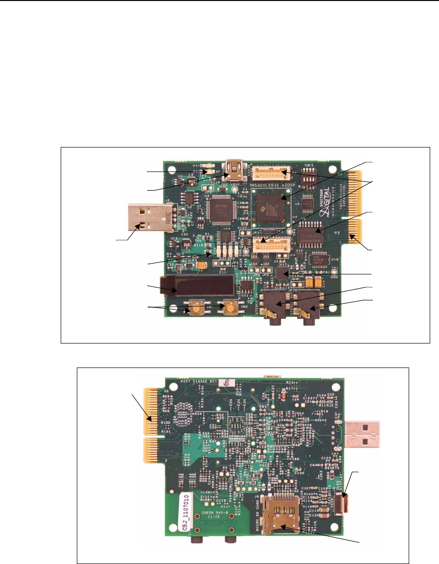
Figure 1-1, Key Features of the C5535 eZdsp (top)
USB connector
Wireless
XF LED
LEDs
Display
Pushbuttons
Stereo In
Stereo Out
SPI Flash
AIC3204
USB
Emulation
Connector
Interface
Expansion
Connector
Figure 1-2, Key Features of the C5535 eZdsp (bottom)
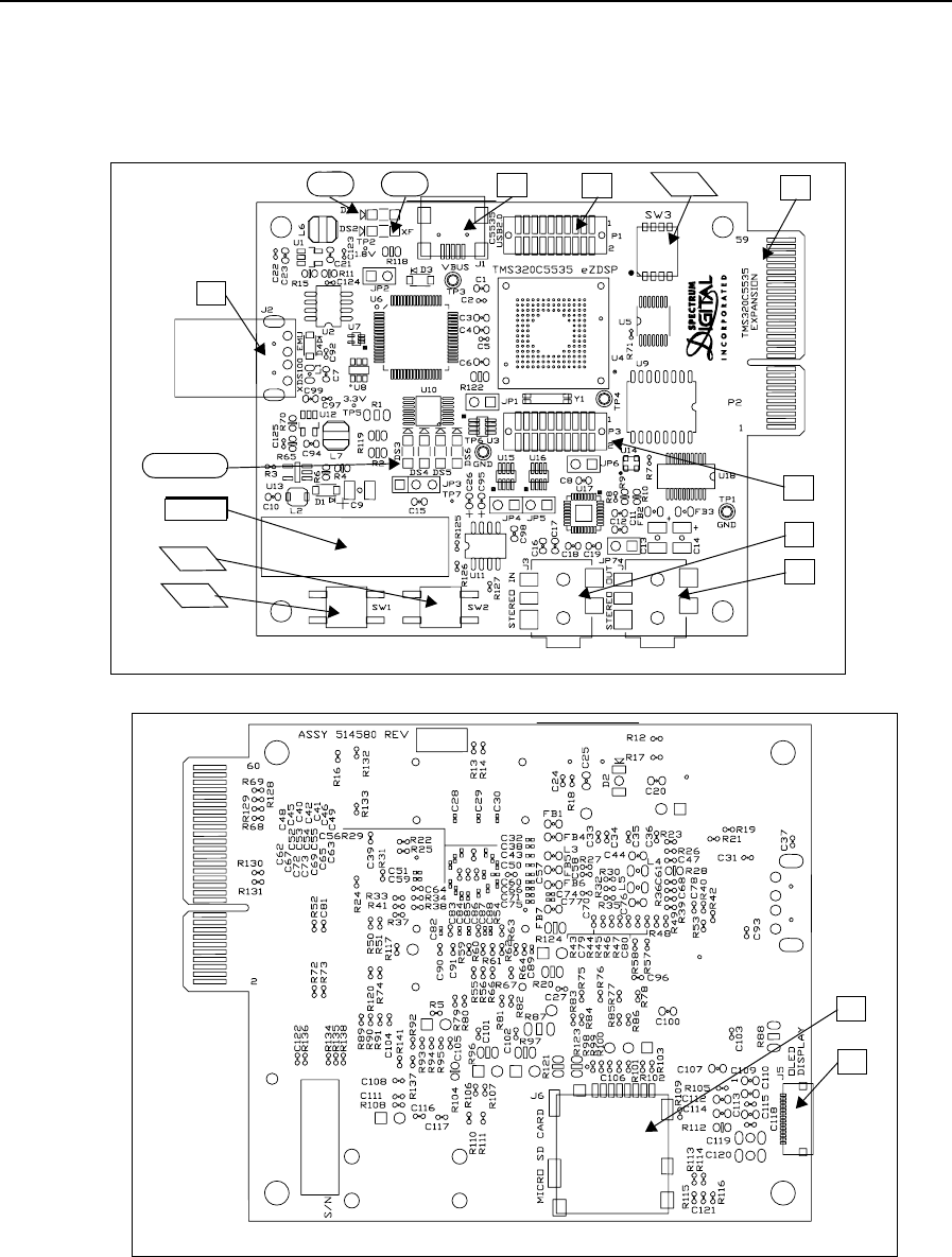
Display
Connector
MIcro SD
Card
Connector

Spectrum Digital, Inc
1-3
1.1 Key Features of the C5535 eZdsp
The C5535 eZdsp has the following features:
• Texas Instrument’s TMS320C5535 Digital Signal Processor
• Texas Instruments TLV320AIC3204 Stereo Codec (stereo in, stereo out)
• Micro SD card connector
• USB 2.0 interface to C5535 processor
• 8 Mbytes SPI flash
• I2C OLED display
• 5 user controlled LEDs
• 2 user readable push button switches
• 3 INA219 I2C Current/Power Monitors
• Embedded USB XDS100 JTAG emulator
• Wireless interface
• Expansion edge connector
• Power measurement test points
• Power provided by USB interface
• Compatible with Texas Instruments Code Composer Studio v4
• USB cable

Spectrum Digital, Inc
1-4 TMS320C5535 eZdsp Technical Reference Manual
1.2 C5535 eZdsp Block Diagram
The block diagram of the C5535 eZdsp is shown below.
1.3 C5535 eZdsp Memory Map
The C5535 eZdsp supports on chip DARAM, SARAM, and off chip SPI Flash. The
addressing for each of these memory blocks is shown in the figure below.
Note: MPNMC bit in ST3 Status Register is cleared(0) at RESET so the C5535 will
attempt to execute its boot load sequence.
Figure 1-3, C5535 eZdsp Block Diagram
I
2
C Bus
Stereo in
Stereo Out
96 x 16 pixel
OLED Display
P1
P3
LEDs
USB
USB
JTAG
I2S2
P2
Analog
Input 1
SW1 SW2
Embedded
XDS100 JTAG
SPI
Flash
AIC
3204
MicroSD
(
on back
)
USB
SPI
UART
GPIO
TMS320
C5535
3.3VIO
LDO
INA219
(MMR Reserved)
Internal DARAM
Internal SARAM
RESERVED
RESERVED
(if MPNMC=1)
ROM
(in MPNMC=0)
MEMORY BLOCKS
CPU Byte
Address
000000h
0000C0h
00FFFFh
010000h
04FFFFh
050000h
7FFFFFh
800000h
BFFFFFh
C00000h
DFFFFFh
E00000h
E03FFFh
F00000h
FDFFFFh
FE0000h
FFFFFFh
Figure 1-4, C5535 eZdsp Memory Map

Spectrum Digital, Inc
1-5
1.4 C5535 eZdsp I2C Addressing
The C5535 eZdsp has multiple I2C devices for different purposes. The table below
shows the addresses of these devices on the I2C bus.
Table 1: C5535 eZdsp I2C Addresses
eZdsp I2C Device I2C Address Function
TLV320AIC3204 0x18 Audio CODEC
OSD9616GLBBG01 0x3C OLED Display
U16, INA219IDCN 0x40 USB 3.3V Power Monitor
U15, INA219IDCN 0x44 VDD_IO 3.3V Power Monitor
U3, INA219IDCN 0x48 VDD Core Power Monitor

Spectrum Digital, Inc
1-6 TMS320C5535 eZdsp Technical Reference Manual

2-1
Chapter 2
Physical Description
This chapter describes the physical layout of the TMS320C5535 eZdsp.
Topic Page
2.0 Board Layout 2-2
2.1 Connector Index 2-3
2.1.1 J1, C5535 USB Connector 2-4
2.1.2 J2, XDS100 USB Connector 2-4
2.1.3 J3, Audio In Connector 2-5
2.1.4 J4, Audio Out Connector 2-6
2.1.5 J5, LCD Interface 2-7
2.1.6 J6, Micro SD Card Connector 2-7
2.1.7 P1, P3, Wireless Interface 2-8
2.1.8 P2, Expansion Connector 2-9
2.2 System LEDs 2-11
2.3 Switches 2-11
2.3.1 SW1, SW2, Momentary Push Button Switches 2-11
2.3.2 SW3, 4 Position DIP Switch 2-12
2.4 Jumpers 2-13
2.5 Test Points 2-14
Spectrum Digital, Inc
2-2 TMS320C5535 eZdsp Technical Reference Manual
2.0 Board Layout
The C5535 eZdsp is a 3.35 x 2.65 inch six (6) layer printed circuit board which is
powered off the USB bus of personal computer or laptop computer. This means this
board does not require an external power supply.
Figure 2-1, C5535 eZdsp (top)
J1
J2
J3
P1
DS1
J4
P3
P2
SW1
SW2
DS3-DS6
Display
SW3
DS2
Figure 2-2, C5535 eZdsp (bottom)
J5
J6

Spectrum Digital, Inc
2-3
2.1 Connector Index
The C5535 eZdsp has nine (9) connectors which provide the user access to various
signals on the eZdsp. These connectors are shown in the table below.
The following manufacturer and parts numbers can be used to interface to the
connectors on the C5535 eZdsp:
Table 1: C5535 eZdsp Connectors
Connector # Pins Function Schematic
Page Board
Side
J1 25 C5535 USB 2 Top
J2 6 Emulation USB 13 Top
J3 2 Audio In 10 Top
J4 2 Audio Out 10 Top
J5 14 LCD Interface 11 Bottom
J6 8 Micro SD Card Interface 7 Bottom
P1 20 Wireless Interface 6 Top
P2 30 x 2 Expansion Connector 12 Top/Bottom
P3 20 Wireless Interface 6 Top
Table 2: C5535 eZdsp Mating Connectors
Connector Manufacturer Part #
J1 PC or laptop
J2 PC or laptop
P1 CUI Inc CUI SP-3501, Digi-Key CP-3502-ND
P2 Samtec Samtec MEC1-120-02-S-D-A,
Digi-Key SAM8117-ND
P3 CUI Inc CUI SP-3501, Digi-Key CP-3502-ND

Spectrum Digital, Inc
2-4 TMS320C5535 eZdsp Technical Reference Manual
2.1.1 J1, C5535 USB Connector
The USB connector, J1, is attached the C5535 processor for use by C5535 software
applications. The signals on the pins of this connector are shown below.
2.1.2 J2, XDS100 USB Connector
The USB connector, J2, is used to attach the C5535 eZdsp to a personal computer or
laptop. This allows the user to develop and debug software on the C5535 eZdsp. The
signals on the pins of this connector are shown below.
Table 3: J1, USB Connector
Pin # Signal Name
1 USBVDD
2D-
3D+
4 ID / NC
5 USBVSS/GND
6,7,8,9 GND (shield)
Table 4: J2, XDS100 USB Connector
Pin # Signal Name
1 U7, Pin 1 (VCC), VCCUSB, 5V_USB
2 U7, Pin 5 (IO4), U6, Pin 7(DM), D-
3 U7, Pin 3(IO1), U6, Pin 8(DP), D+
4GND
5 GND, shield
6 GND, shield
Spectrum Digital, Inc
2-5
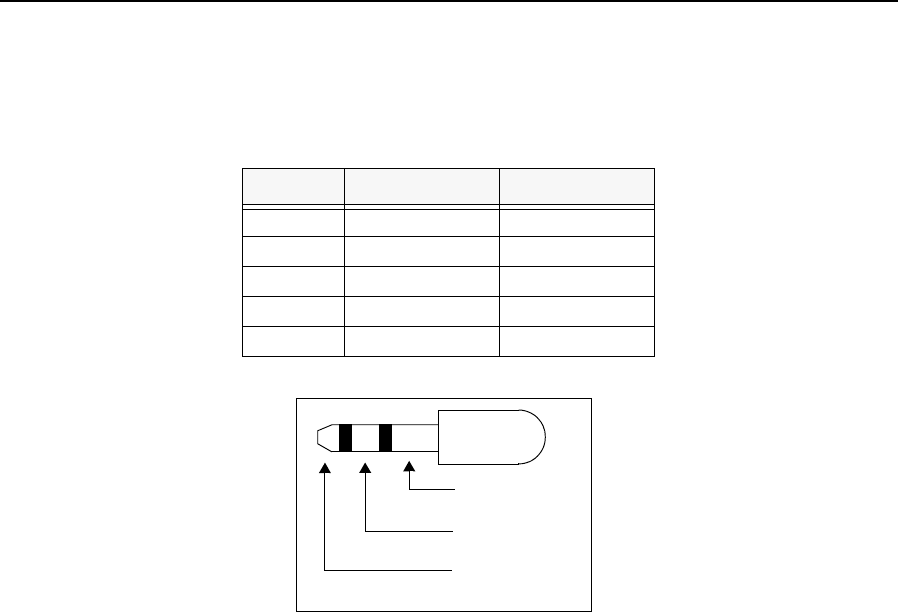
2.1.3 J3, Audio In Connector
The Stereo In connector, J3, is used to bring signals into the TLV320AIC3204 codec,
U17. The signals on the pins of this connector are shown below.
The figure below shows a typical stereo jack.
Table 5: J3, Audio In Connector
Pin # Signal Name AIC3204 Pin #
1GND-AIC
2 AIC_LINE2L U17, Pin 15
3 AIC_LINE2R U17, Pin 16
4 No connect
5 No connect
Figure 2-3, Audio In Jack
Left Line In
Ground
Right Line In
Spectrum Digital, Inc
2-6 TMS320C5535 eZdsp Technical Reference Manual
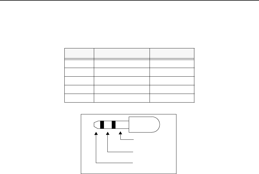
2.1.4 J4, Audio Out Connector
The Audio Out connector, J4, is used to bring signals from the TLV320AIC3204 codec,
U17. The signals on the pins of this connector are shown below.
The figure below shows a typical headphone jack.
Table 6: J4, Audio Out Connector
Pin # Signal Name AIC3204 Pin #
1GND-AIC
2 HEADPHONE_LOUT U17, Pin 25
3 HEADPHONE_ROUT U17, Pin 27
4 No connect
5 No connect
Left Line In
Ground
Figure 2-4, Audio Out Jack
Right Line In

Spectrum Digital, Inc
2-7
2.1.5 J5, LCD Interface
Connector, J5, is used to interface to an LCD character display. The signals on the pins
of this connector are shown below.
2.1.6 J6, Micro SD Card Connector
The Micro SD connector, J6, is used to interface the C5535 processor to a micro SD
card. The signals on the pins of this connector are shown below.
Table 7: J5, LCD Interface
Pin # Signal Name
1C2P
2C2N
3C1P
4C1N
5 VBAT
6 VBREF
7 VSS, GND
8 VDD, VCC_3V3
9 RESn, TARGET_PWR_GOOD
10 SCL, I2C_SCL
11 SDA, I2C_SDA
12 IREF
13 VCOMH
14 VCC, V13
Table 8: J6, Micro SD Card Connector
Pin # Signal Name
1 DAT2, SD_DATA2
2 DAT3, SD_DATA3
3CMD, SD_CMD
4 VDD, VCC_3V3
5 CLK, SD_CLK
6GND
7 DAT0, SD_DATA0
8 DAT1, SD_DATA1
9 INSERT, VCC_3V3
10 INSERT_COM, GND
11,12,13,14 NC

Spectrum Digital, Inc
2-8 TMS320C5535 eZdsp Technical Reference Manual
2.1.7 P1, P3, Wireless Interface
Connectors P1 and P3 are used to provide an interface to Texas Instruments Wireless
Interface modules. The signals on the pins of these connectors are shown in the tables
below.
Table 9: P1, Wireless Interface Connector
Pin # Signal Name Pin # Signal Name
1 GND 2 SD_DATA0
3 UART_RTS 4 SD_DATA1
5 RTC_CLKOUT 6 SD_DATA2
7UART_TX8SD_DATA3
9 UART_RX 10 GPIO10
11 I2C_SDA 12 GPIO11
13 I2C_SCL 14 SPI_CS2
15 SD_CLK 16 SPI_CLK
17 SD_CMD 18 SPI_TX
19 GND 20 SPI_RX
Table 10: P3, Wireless Interface Connector
Pin # Signal Name Pin # Signal Name
1NC2GND
3NC4NC
5NC6NC
7 VCC_3V3 8 I2S1_RX
9 VCC_3V3 10 I2S1_DX
11 I2S1_FS 12 NC
13 GPIO12 14 NC
15 GPIO14 16 NC
17 I2S1_CLK 18 UART_CTS
19 GPIO14 20 GPIO13
Spectrum Digital, Inc
2-9
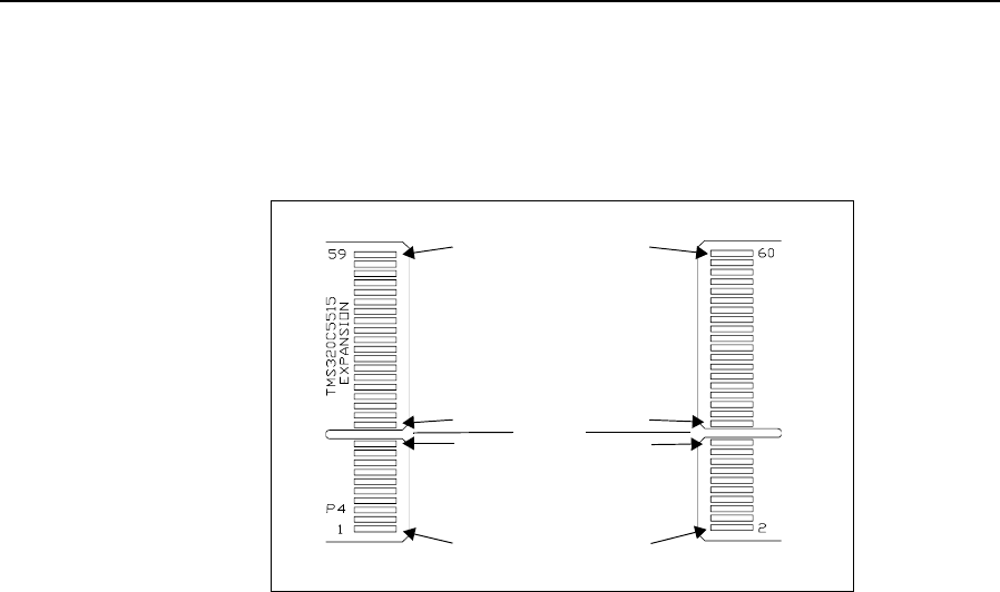
2.1.8 P2, Expansion Connector
The expansion edge connector, P2, provides the C5535 serial interface signals to
limitless user expansion boards. This edge connector has all of the odd number
(1,3,...,59) tabs on the top side of the board and all of the even number tabs (2,4,...,46)
on the bottom side of the board. The diagram below shows the position of these tabs.
Top Side View
Pin 1
Pin 19
Pin 23
Pin 59
Key
Pin 2
Pin 20
Pin 24
Pin 60
Bottom Side View
Figure 2-5, P2 Connector Tab Positions

Spectrum Digital, Inc
2-10 TMS320C5535 eZdsp Technical Reference Manual
The table below lists the signals that appear on each of the tabs of connector P2. The
signals on the pins of this connector are shown below.
Table 11: P2, Expansion Connector
Pin #
Top Signal Name Pin #
Bottom Signal Name
1GND2GND
3 SPI_CS1 4 GPIO13
5 SPI_CLK 6 GPIO12
7 SPI_TX 8 GPIO14
9 SPI_RX 10 GPIO15
11 GND 12 GND
13 GND 14 GND
15 GND 16 GND
17 I2C_SDA 18 GPIO16
19 I2C_SCL 20 GPIO17
Key Key
23 I2S2_CLK 24 GPIO11
25 I2S2_RX 26 GPIO10
27 I2S2_DX 28 GPIO5
29 I2S2_FS 30 GPIO4
31 GND 32 GND
33 I2S1_CLK 34 UART_RTS
35 I2S1_RX 36 UART_CTS
37 I2S1_DX 38 UART_RX
39 I2S1_FS 40 UART_TX
41 VCC_3V3 42 VCC_USB_DUAL
43 VCC_3V3 44 VCC_USB_DUAL
45 I2S0_CLK 46 SPI_CS3
47 I2S0_RX 48 VCC_USB_DUAL
49 I2S0_DX 50 GPAIN3
51 I2S0_FS 52 GPAIN2
53 SPI_CS2 54 GPAIN1
55 SPI_CS0 56 GPAIN0
57 VCC_3V3 58 VCC_USB_DUAL
59 VCC_3V3 60 VCC_USB_DUAL

Spectrum Digital, Inc
2-11
2.2 System LEDs
The C5535 eZdsp has 6 Light Emitting Diodes (LED). LEDs DS2- DS6 are under the
application software control running on the C5535 processor. The C5535 eZdsp LEDs
are shown in the table below.
2.3 Switches
The C5535 eZdsp has three switches, two push button switches, and one DIP
switch. These switches are shown in the table below.
2.3.1 SW1, SW2, Momentary Push Button Switches
Switches SW1, and SW2 are momentary push button switches read by the application
software running on the C5535 processor using the GPAIN1 port.
Table 12: System LEDs
LED # Color Schematic
Page Signal Name
DS1 Green 13 U6, Pin 60, PWREN#
DS2 Green 2 U4, Pin J3, XF
DS3 Green 11 U4, Pin P8, GPIO17
DS4 Red 11 U4, Pin P3, GPIO16
DS5 Yellow 11 U4, Pin N7, GPIO15
DS6 Blue 11 U4, Pin P2, GPIO14
Table 13: Switches
Switch # Schematic
Page Signal Name/Reading
SW1 only closed 11 GPAIN1, approximately 1.2 volts
SW2 only closed 11 GPAIN1, approximately 0.9 volts
SW3 5 4 position DIP switch
Spectrum Digital, Inc
2-12 TMS320C5535 eZdsp Technical Reference Manual
2.3.2 SW3, 4 Position DIP Switch
Switch SW3 is a 4 position DIP switch. The signals attached to each position are shown
in the table below.
The figure below shows switch SW3 default settings.
The table below shows the functions of the setting in each position of SW3.
* Note: GPIO15 can overwrite
Table 14: Switch SW3
Position Signal Name Default Setting
1 CLK_SEL OFF
2 UART_BUFF_EN ON
3 AIC3204I2C_ENn OFF
4 SPI_CS0 ON
Table 15: Switch SW3 Functions
Position Setting Function
1ON Select external 12 MHz. clock
OFF Select internal 32 MHz. RTC clock
2ON * Enable UART via J2 for VCP
OFF * Disable UART via J2
3ON Disable AIC3204 interface
OFF Enable AIC3204 interface
4ON Enable SPI Flash CS
OFF Disable SPI Flash CS
Figure 2-6, Switch SW3, Default Settings
1st position
SW3
Raised
Actuator
Spectrum Digital, Inc
2-13
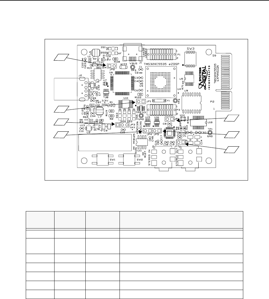
2.4 Jumpers
The C5535 eZdsp has 7 jumpers. The location of the jumpers are shown in the figure
below.
The function of these jumpers is shown in the table below.
Jumper JP2 is the power source select jumper. When this jumper is shorted the
C5535 eZdsp can be powered from the C5535 USB interface (J1). This jumper is
shipped in the “shorted” state from the factory.
Table 16: Jumpers
Jumper # of
positions Schematic
Page Jumper Function
JP1 2 4 Allows measurement of VCore
JP2 2 13 Power source select. Allows connection of
VCCUSB to VBUS_C5515
JP3 3 9 I2C Headers
JP4 2 4 Allows measurement of VDD_IO1 voltage
JP5 2 8 Allows measurement of USB 3.3V
JP6 2 10 Allows measurement of VCC_3V3 for AIC3204
JP7 2 10 Allows measurement of V3.3A for AIC3204
Figure 2-7, C5535 eZdsp Jumpers
JP1
JP2
JP3
JP4 JP5
JP6
JP7
Spectrum Digital, Inc
2-14 TMS320C5535 eZdsp Technical Reference Manual
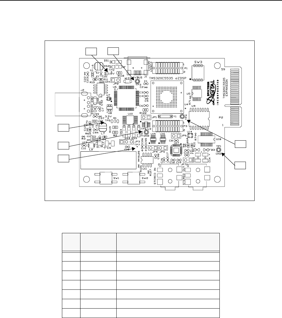
2.5 Test Points
The C5535 eZdsp has seven (7) test points for the monitoring of signals. The location
of the test points are shown in the figure below.
The signals on the test points are shown in the table below.
Table 17: Test Points
TP # Schematic
Page Signal Name
TP1 4 GND
TP2 8 VCC_1V8_TP
TP3 2 U4, Pin I14, VBUS/VBUS_C5535
TP4 2 U4, Pin A2, CLKOUT
TP5 8 VCC_3V3_TP
TP6 10 GND
TP7 9 U11, Pin 7,8, VCC_1V3, VCC_1V3_TP
Figure 2-8, C5535 eZdsp Test Points
TP1
TP2 TP3
TP4
TP5
TP6
TP7

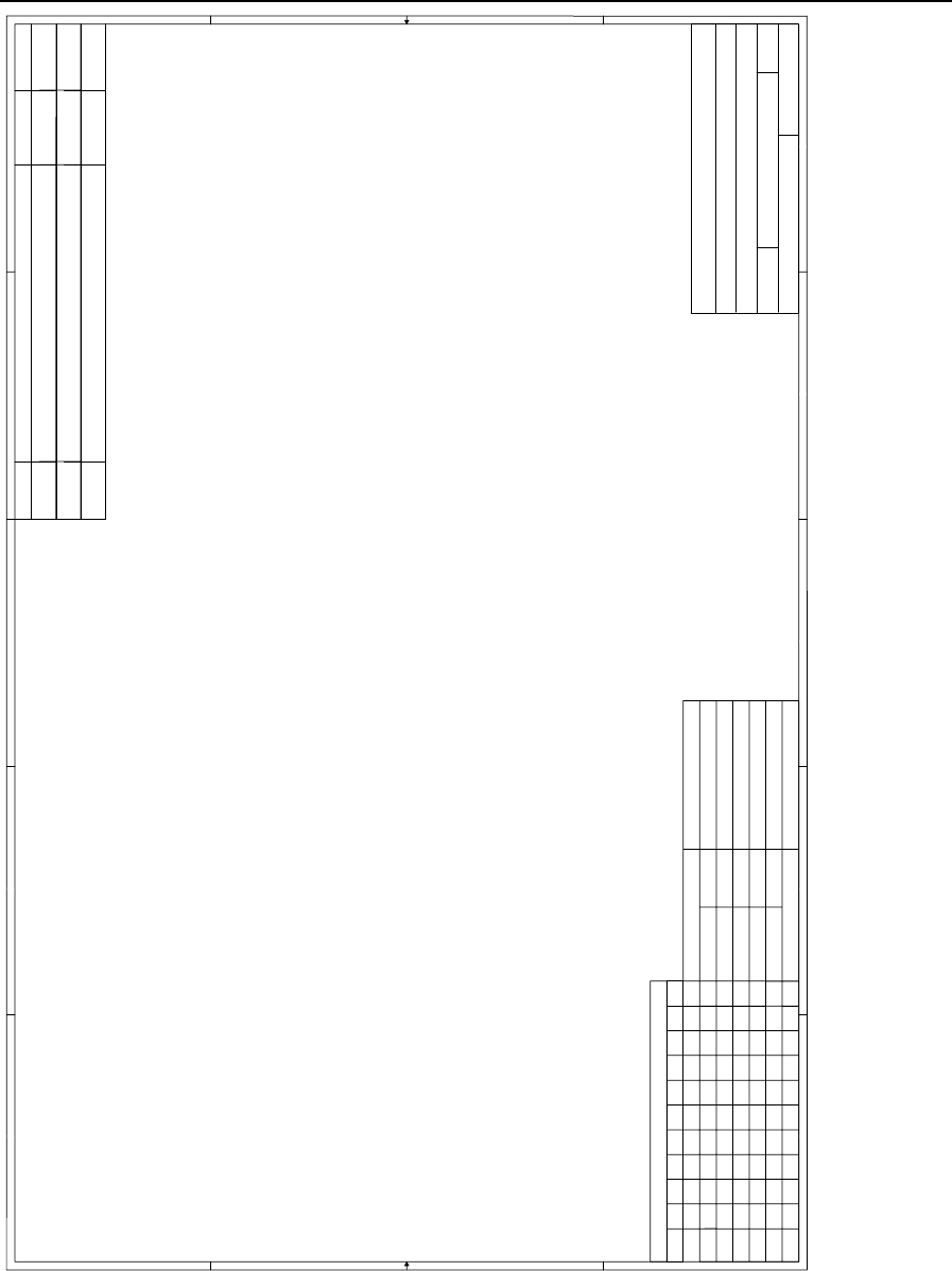
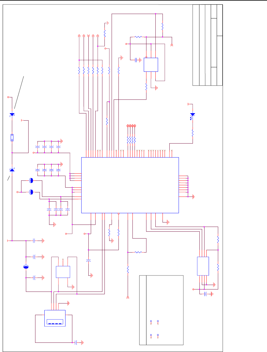
A-1
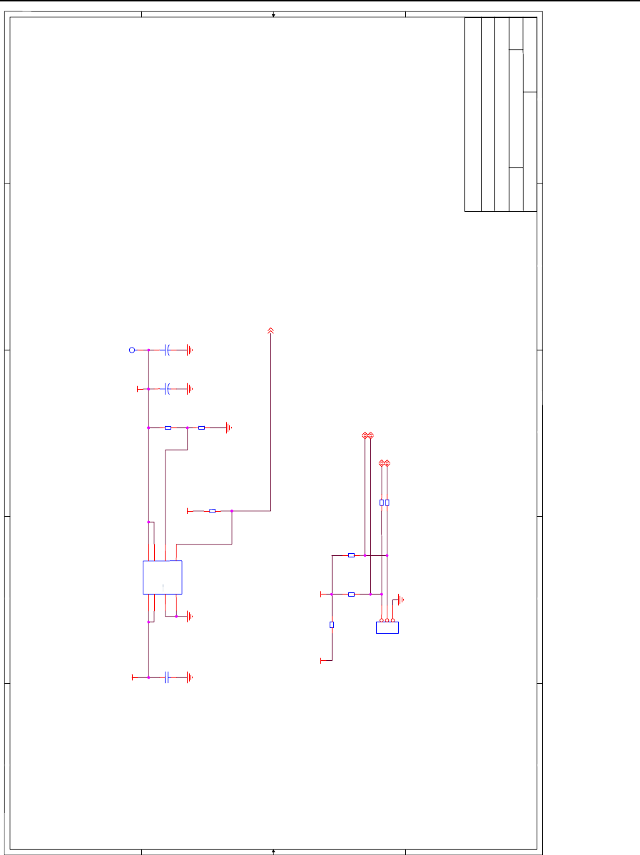
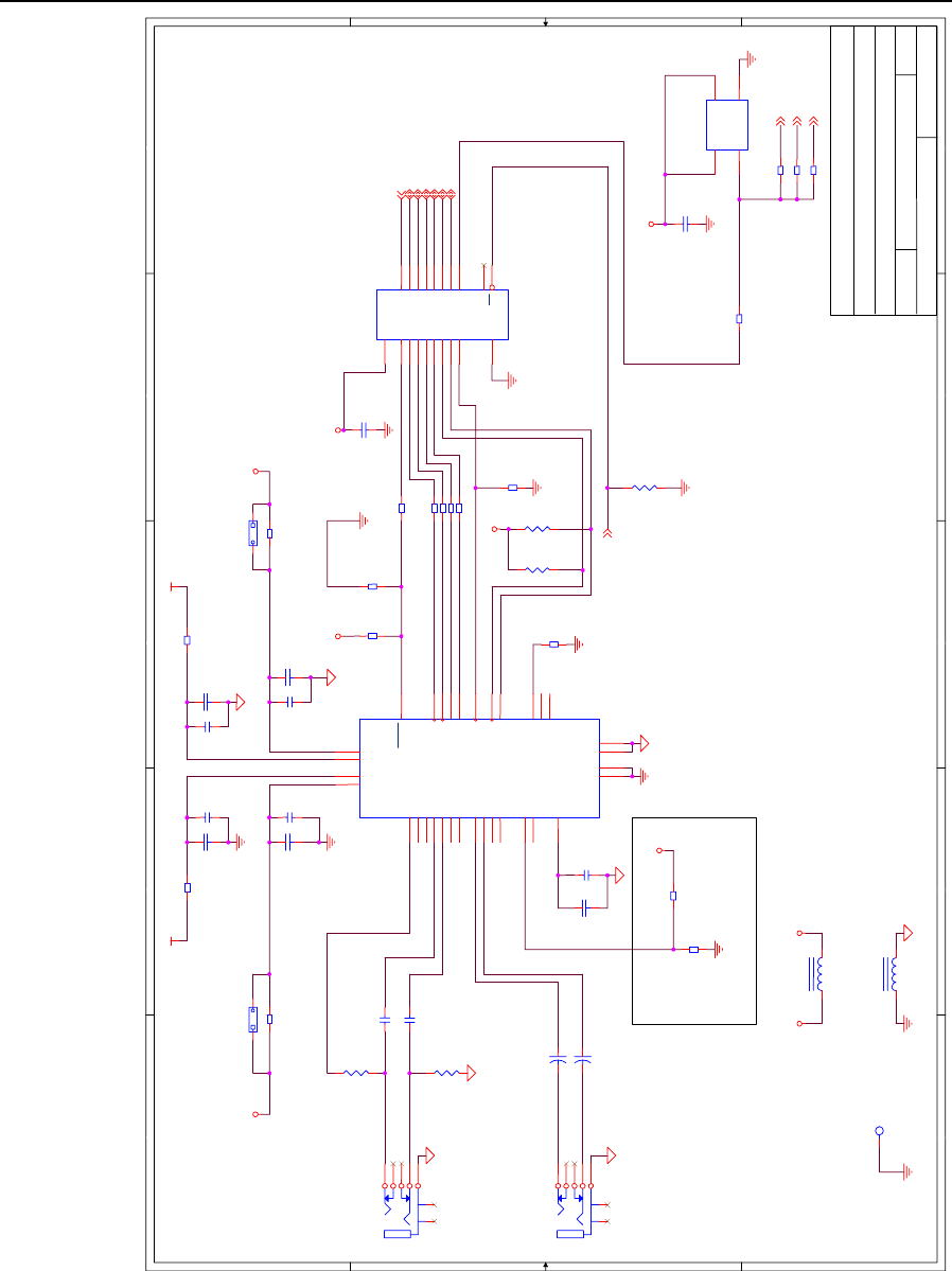
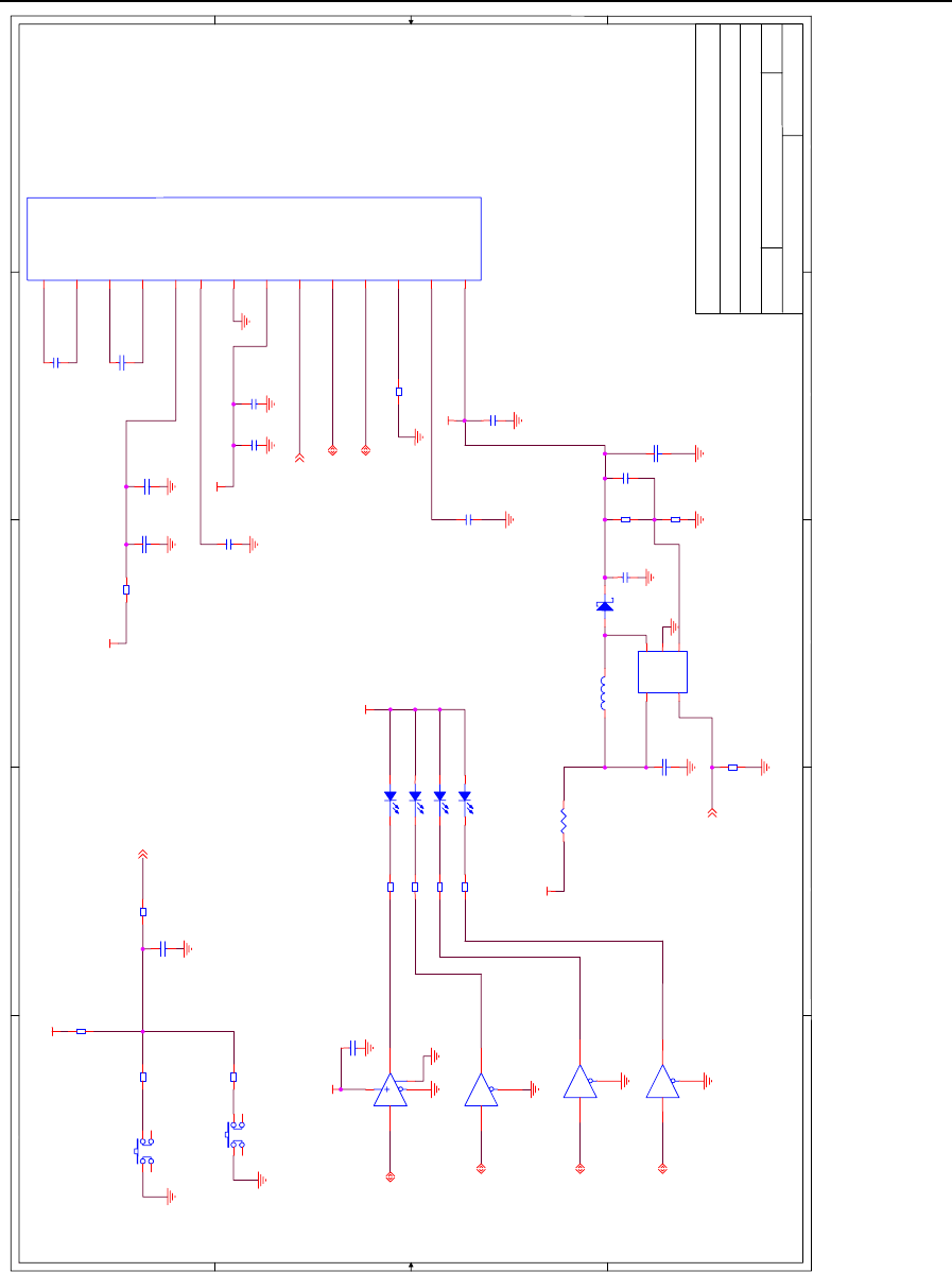
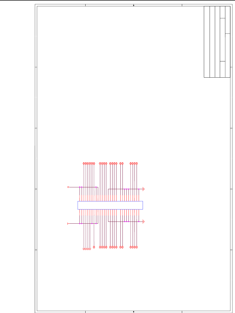
Appendix A
Schematics
This appendix contains the schematics for the TMS320C5535 eZdsp.
Spectrum Digital, Inc
A-2 TMS320C5535 eZdsp Technical Reference Manual
5
5
4
4
3
3
2
2
1
1
D D
C C
B B
A A
Size:
Date:
DWG NO Revision:
Sheet of
Title:
Page Contents:
C
SPECTRUM DIGITAL INCORPORATED
514582-0001
Tuesday, July 26, 2011 1 13
B
TMS320C5535 EZDSP MODULE
TITLE SHEET
4. ALL 0.1 uF AND 0.01uF CAPACITORS ARE DECOUPLING CAPS UNLESS
OTHERWISE NOTED. THEY ARE SHOWN ON THE PAGE WITH THE INTEGRATED
CIRCUITS THEY SHOULD BE PLACED NEAR.
NOTES, UNLESS OTHERWISE SPECIFIED:
1. RESISTANCE VALUES IN OHMS.
2. CAPACTITANCE VALUES IN MICROFARADS.
3. REFERENCE DESIGNATORS USED:
SCHEMATIC CONTENTS
01 - TITLE PAGE
02 - TMS320C5535 IO
03 - UART BUFFER
04 - TMS320C5535 POWER
05 - SPI FLASH
06 - CC BOARD INTERFACE
07 - MICRO SD INTERFACE
08 - POWER SUPPLIES
09 - AUDIO CODEC
10 - LCD/USER LEDS/SWITCHES
11 - EXPANSION CONNECTOR
12 - XDS100-v2 INTERFACE
SHEET
SHEET
SHEET
SHEET
REV
REV
REV
REV
ENGR
2
REVISION STATUS OF SHEETS
1
DATE
DATE
ENGR-MGR
MFG
7
DWN
DATE
8
DATE
DATE
CHK
RLSE
APPLICATION35
NEXT ASSY
DATE
6
DATE
9
QA
USED ON
4
BAA A
R.R.P.
T.W.K.
R.R.P.
R.R.P.
C.M.D.
R.R.P.
R.R.P.
10/15/2009
10/15/2009
10/15/2009
10/15/2009
10/15/2009
10/15/2009
10/15/2009
CA AAA
10
11 12
A
AA
Initial schematic for layout
DESCRIPTIONREV APPROVEDDATE
1/10/2011 RRP
A
BETA UPDATES 6/19/2011 RRP
B
PRODUCTION UNITS 7/19/2011 RRP
C
Spectrum Digital, Inc
A-3
5
5
4
4
3
3
2
2
1
1
D D
C C
B B
A A
GPAIN2
GPAIN1
GPAIN0
GPAIN3
TARGET_EMU1
TARGET_EMU0
CLKIN
USB_XI
USB_VBUS
USB_DM
USB_DP
I2C_SCL
I2C_SDA
SPI_CS0
SPI_CS1
SPI_CLK
SPI_CS2
SPI_CS3
UART_RX
UART_CTS
UART_RTS
UART_TX
GPIO12
GPIO13
GPIO14
GPIO15
GPIO16
GPIO17
I2S2_CLK
I2S2_FS
I2S2_RX
I2S2_DX
SPI_RX
SPI_TX
I2S1_DX
I2S1_FS
I2S1_CLK
I2S1_RX
GPIO10
GPIO11
SD_DATA1
SD_DATA0
SD_CMD
SD_CLK
SD_DATA3
SD_DATA2
WAKEUP
RTC_CLKOUT
CLKOUT
SD_DATA1
SD_DATA0
SD_CMD
SD_CLK
SD_DATA3
SD_DATA2
CLK_SEL
VDD_IO1
VDD_IO1
VCC_3V3_USB
VCC_1V3
VBUS_C5535
VDD_IO1
VDD_IO1
GPAIN312 GPAIN212 GPAIN111,12
TARGET_PWR_GOOD9,10,11,13
TARGET_TMS13
TARGET_TRSTn13
TARGET_TDI13
TARGET_TDO13
TARGET_TCK13
CPU_CLK_12MHZ10
USB_CLK_12MHZ10
I2C_SDA 6,9,10,11,12
I2C_SCL 6,9,10,11,12
SPI_CS3 12
SPI_CS2 6,12
UART_RX 3,6,12
UART_CTS 3,6,12
UART_RTS 3,6,12
UART_TX 3,6,12
I2S2_DX 10,12
I2S2_FS 10,12
I2S2_CLK 10,12
I2S2_RX 10,12
SPI_CS0 5,12
SPI_CLK 5,6,12
SPI_RX 5,6,12
SPI_TX 5,6,12
SPI_CS1 12
GPIO17 11,12
GPIO16 11,12
GPIO15 3,11,12
GPIO14 6,11,12
GPIO12 6,11,12
GPIO13 6,12
I2S1_DX 6,12
I2S1_FS 6,12
I2S1_CLK 6,12
I2S1_RX 6,12
GPIO10 6,12
GPIO11 6,12
SD_DATA2 6,7
SD_DATA3 6,7
SD_DATA0 6,7
SD_CLK 6,7
SD_CMD 6,7
SD_DATA1 6,7
RTC_CLKOUT6
I2S0_DX 12
I2S0_FS 12
I2S0_CLK 12
I2S0_RX 12
GPIO4 12
GPIO5 12
GPAIN012
CLK_SEL5
Size:
Date:
DWG NO Revision:
Sheet of
Title:
Page Contents:
B
SPECTRUM DIGITAL INCORPORATED
514582-0001
Friday, July 22, 2011 2 13
B
TMS320C5535 EZDSP MODULE
GPIO,MMC-SD,SPI,I2C,I2S
R34
NO-POP
R25
10K
TP3
VBUS
TP4
CLKOUT
R14
10K
R22
10K
R29
10K 1%
C84
0.1uF R59
10K
C82
0.1uF
J1
USBMINI_B
USBVDD
1
D+
3D-
2
USBVSS
5
ID
4
SHIELD1 6
SHIELD2 7
SHIELD3 8
SHIELD4 9
FB7
BLM18AG601SN1D
1206
1 2
R17 220
C83
1uF
R56
NO-POP
C6
10uF
R41
100K
C25
10uF
R54 0
C77
0.1uF
Y1
32.768KHz
1 4
2
3
DS2 LED_GRN
R117
10K
R55 0
C66
1000pF
C9133pF
C5535
U4-1
RSV10 H1
RSV11 E2
RSV7 E1
RSV8 F1
RSV9 G1
RSV12 G2
CLK_SEL
D1
CLKIN
C1
CLKOUT
A2
EMU0
L2
EMU1
M1
GPAIN0
A8
GPAIN1
B8
GPAIN2
A9
GPAIN3
A10
I2C_SCL C4
I2C_SDA A4
INT0
C2 INT1
B1
LCD_EN_RDB/SPI_CLK L3
LCD_CS0_E0/SPI_CS0 L1
LCD_CS_E1/SPI CS1 M2
LCD_RW_WRB/SPI_CS2 N2
LCD_RS/SPI_CS3 M5
LCD_D[0]/SPI_RX N4
LCD_D[1]/SPI_TX K1
LCD_D[10]/I2S2_RX/GP[20]/SPI_RX P9
LCD_D[11]/I2S2_DX/GP[27]/SPI_TX P11
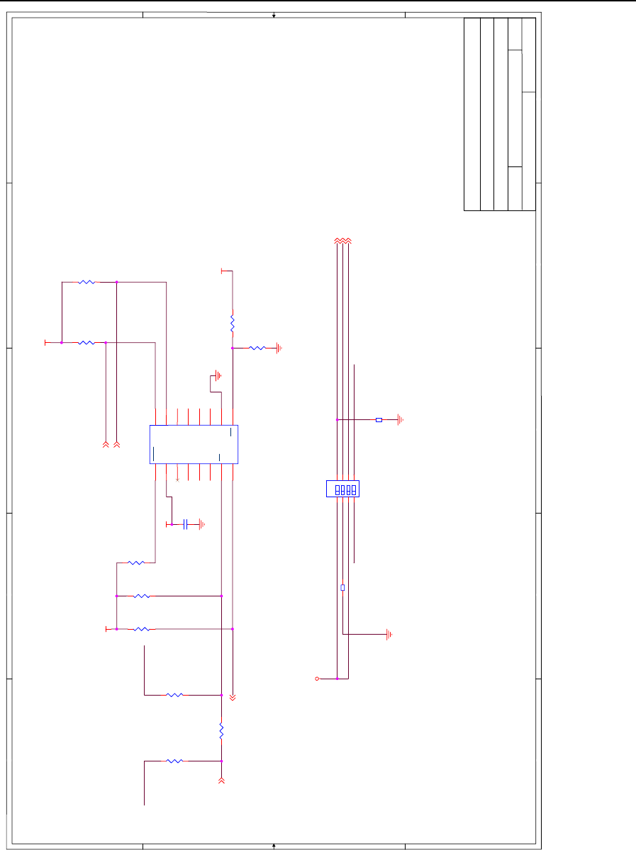
LCD_D[12]/UART_RTS/GP[28]/I2S3_CLK N12
LCD_D[13]/UART_CTS/GP[29]/I2S3_FS P12
LCD_D[14]/UART_RXD/GP[30]/I2S3_RX P13
LCD_D[15]/UART_TXD/GP[31]/I2S3_DX M11
LCD_D[2]/GP[12] J2
LCD_D[3]/GP[13] N5
LCD_D[4]/GP[14] P2
LCD_D[5]/GP[15] N7
LCD_D[6]/GP[16] P3
LCD_D[7]/GP[17] P8
LCD_D[8]/I2S2_CLK/GP[18]/SPI_CLK P5
LCD_D[9]/I2S2_FS/GP[19]/SPI_CS0 N10
RESETN
D2
RTC_CLKOUT
A3
RTCXI
A7
RTCXO
A6
MMC0_CLK/I2S0_CLK/GP[0] M8
MMC0_CMD/I2S0_FS/GP[1] M10
MMC0_D0/I2S0_DX/GP[2] J1
MMC0_D1/I2S0_RX/GP[3] P6
MMC0_D2/GP[4] N13
MMC0_D3/GP[5] P7
MMC1_CLK/I2S1_CLK/GP[6] M14
MMC1_CMD/I2S1_FS/GP[7] L11
MMC1_D0/I2S1_DX/GP[8] M13
MMC1_D1/I2S1_RX/GP[9] P10
MMC1_D2/GP[10] L12
MMC1_D3/GP[11] M12
TCK
N3
TDI
K2
TDO
N1
TMS
N6
TRSTN
P4
USB_DM J14
USB_DP H14
USB_R1 G14
USB_VBUS L14
USB_M12XI
E14
USB_M12XO
D14
WAKEUP
A5
XF
J3
VSS_RTC
C5
CVDD_RTC
B4
CVDD_RTC
B5
USB_VDDOSC
E13
USB_VSSOSC
D12
USB_VSSREF F12
DVDD_RTC
C3
R37
100K
R13
10K
R18
100K
R131 0
R130 0
R129 0
R38 0
R128 0
R69 0
R68 0
C9033pF
C24
0.1uF
D2
6.2V
Spectrum Digital, Inc
A-4 TMS320C5535 eZdsp Technical Reference Manual
5
5
4
4
3
3
2
2
1
1
D D
C C
B B
A A
VCC_3V3
VCC_3V3
TRGT_UART_TX 13
TRGT_UART_RX 13
TRGT_UART_RTS 13
TRGT_UART_CTS 13
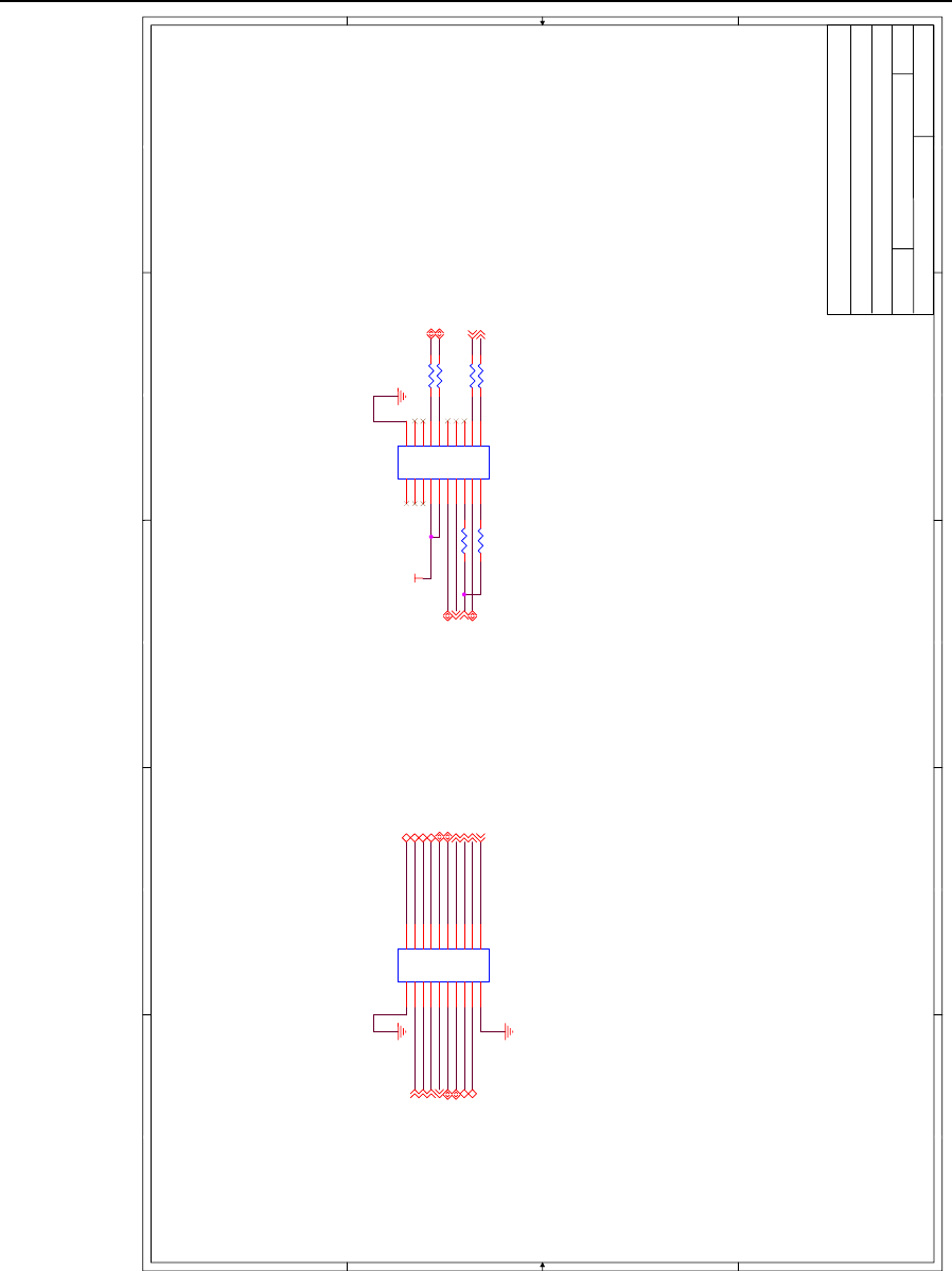
UART_RTS2,6,12UART_TX2,6,12
UART_CTS2,6,12
UART_RX2,6,12
GPIO152,11,12
UART_BUFF_EN5
Size:
Date:
DWG NO Revision:
Sheet of
Title:
Page Contents:
A
SPECTRUM DIGITAL INCORPORATED
514582-0001
Friday, July 22, 2011 3 13
B
TMS320C5535 EZDSP MODULE
UART BUFFER
R133 0
U5B
74CBTLV3125PWR
65
4
U5C
74CBTLV3125PWR
89
10
U5D
74CBTLV3125PWR
1112
13
R24
10K
U5A
74CBTLV3125PWR
32
1
714
C39
0.1uF
Spectrum Digital, Inc
A-5
5
5
4
4
3
3
2
2
1
1
D D
C C
B B
A A
DSP_LDO_OUT
RSV6
USB_LDO_OUT_REG
LDO_EN
LDO_EN
DSP_LDO_OUT_REG
I2C_SCL_PWR
I2C_SDA_PWR
I2C_SDA_PWR
I2C_SCL_PWR
AGND
AGND
VCC_3V3_USB
VCC_3V3_USB
USB_LDO_OUT
USB_LDO_OUT
ANA_LDO_OUT
ANA_LDO_OUT
ANA_LDO_OUT
AGND
AGND
AGND
AGND AGND
AGNDAGND
VCC_1V8 DSP_LDO_OUT_REG
V_PWR_MON
DSP_LDO_OUT
VDD_IO1_CPU VCC_3V3_PWR
V_PWR_MON
VDD_IO1_CPU
VCC_1V3
VCC_1V8
VCC_1V3
I2C_SDA_PWR 8,9
I2C_SCL_PWR 8,9
Size:
Date:
DWG NO Revision:
Sheet of
Title:
Page Contents:
A
SPECTRUM DIGITAL INCORPORATED
514582-0001
Tuesday, July 26, 2011 4 13
B
TMS320C5535 EZDSP MODULE
TMS320C5535 POWER
NO-POP
NO-POP
I2C ADDRESS
100 0000
I2C ADDRESS
100 0100
C51
0.01uF
R60
0
R122 0
C48
0.1uF
C75
0.1uF
C67
0.1uF
FB4
BLM18AG601SN1D
1206
1 2
C4
10uF
FB5
BLM18AG601SN1D
1206
1 2
C52
1uF
C43
0.01uF
C53
1uF
C3
10uF
C57
0.1uF
C29
0.1uF
C87
0.1uF
C63
0.1uF
C27
0.1uF
C55
0.01uF
U15
INA219IDCN
VIN+ 1
VIN- 2
GND
3
VS
4
SCL
5
SDA
6
A0
7A1
8
C85
0.1uF
C69
0.1uF
C102
0.1uF
R123 NO-POP
C59
0.1uF
C46
0.1uF
FB6
BLM18AG601SN1D
1206
1 2
C5
1uF
C45
0.1uF
C71
0.1uF
R124 0 R20 1 1%
C73
0.01uF
C5535
U4-2
LDOI
B10
ANA_LDOO
B9
DSP_LDO_EN C13
RSV6
B13
LDOI
B14
DSP_LDOO A13
RSV3
B12
RSV0
A12
LDOI
C14
USB_LDOO
D13
VDDA_ANA
B7
USB_VDD1P3
E12
USB_VDD1P3
F14
USB_VDD1P3
K13
USB_VDDPLL
G13
USB_VDDA1P3
H12
USB_VDDA3P3
G12
CVDD C11
CVDD D3
CVDD D11
CVDD F2
CVDD G3
CVDD H2
CVDD K11
CVDD M6
CVDD M9
CVDD N9
DVDDIO C6
DVDDIO L4
DVDDIO M3
DVDDIO M4
DVDDIO N8
DVDDIO N11
DVDDIO N14
VSS E3
RSV1 K12
RSV2 L13
VSS A14
VSS B2
VSS B3
VSS C8
VSS C12
VSS D4
VSS D5
VSS D10
VSS E4
VSS E11
VSS F3
VSS H3
VSS J13
VSS K3
VSS K4
VSS L5
VSS L10
VSS M7
VSS P1
VSS P14
VSSA_ANA
B6
USB_VSS1P3
K14
USB_VSSPLL
F13
VSSA_ANA
C9
USB_VSSA1P3
J12
USB_VSSA3P3
H13
BG_CAP
C10
VDDA_PLL C7
VSSA_PLL A1
RSV4 A11
RSV5 B11
C42
1uF
JP1
12
C62
0.1uF
C32
0.1uF
C88
0.1uF
R61
0
C89
0.01uF
FB1
BLM18AG601SN1D
1 2
R64
0
C74
1000pF
C28
0.1uF
L3
BLM18AG601SN1D
1206
1 2
C49
0.1uF
C64
1uF
C40
0.1uF
TP1
GND
C30
0.1uF
R62
NO-POP
C65
0.1uF
C54
1uF
R63
NO-POP
C60
0.1uF
JP4
1 2
C41
0.01uF
C56
1000pF
C2
1uF
C1
10uF
R971 1%
C38
0.01uF
R121 NO-POP
C86
1uF
C72
0.1uF
U3
INA219IDCN
VIN+ 1
VIN- 2
GND
3
VS
4
SCL
5SDA
6
A0
7
A1
8
C50
1000pF
Spectrum Digital, Inc
A-6 TMS320C5535 eZdsp Technical Reference Manual
5
5
4
4
3
3
2
2
1
1
D D
C C
B B
A A
SPI_HOLD
SPI_TX
SPI_CLK
SPI_RX SPI_WP
SPI_CS_SW_IN SPI_CS_SW_OUT
SPI_CS0_DEVn
SPI_CS_SW_IN SPI_CS_SW_OUT
VCC_3V3
VDD_IO1
VDD_IO1
VDD_IO1
VDD_IO1
SPI_TX2,6,12
SPI_RX2,6,12
SPI_CLK2,6,12
CLK_SEL 2
UART_BUFF_EN 3
AIC3204I2C_ENn 10
SPI_CS02,12
Size:
Date:
DWG NO Revision:
Sheet of
Title:
Page Contents:
C
SPECTRUM DIGITAL INCORPORATED
514582-0001
Tuesday, July 26, 2011 5 13
B
TMS320C5535 EZDSP MODULE
SPI FLASH
OR M25P64-VMF6TP
DIP Switch Defaults:
CLK_SEL = OFF (pulled down)
UART_BUFF_EN = ON (pulled down)
AIC3204I2C_ENn = OFF (pulled down)
U9
W25X64VSFIG
CS
7
DIO 15
GND 10
VCC
2
HOLD
1
WP 9
DO
8
SCLK 16
NC.3
3
NC.4
4
NC.5
5
NC.6
6NC.11 11
NC.12 12
NC.13 13
NC.14 14
1
2
3
4
ON
SW3
DIP_SWITCH
1
2
3
45
6
7
8
R52
10K
R7410K
R132 1K
R72
NO-POP
R16
0
R33
10K
R120
NO-POP
R50
NO-POP
R31 NO-POP
R73
NO-POP
R71
0
R51
NO-POP
C81
0.1uF
Spectrum Digital, Inc
A-7
5
5
4
4
3
3
2
2
1
1
D D
C C
B B
A A
GPIO10
GPIO11
VCC_3V3
I2C_SDA2,9,10,11,12 I2C_SCL2,9,10,11,12
UART_RTS2,3,12
UART_CTS 2,3,12
GPIO142,11,12
RTC_CLKOUT2
GPIO122,11,12
GPIO13 2,12
UART_TX2,3,12
UART_RX2,3,12
SPI_CS2 2,12
SPI_CLK 2,5,12
SPI_RX 2,5,12
SPI_TX 2,5,12
GPIO10 2,12
GPIO11 2,12
SD_DATA2 2,7
SD_DATA3 2,7
SD_DATA0 2,7
SD_CLK2,7 SD_CMD2,7
SD_DATA1 2,7
I2S1_DX 2,12
I2S1_FS2,12
I2S1_CLK2,12
I2S1_RX 2,12
Size:
Date:
DWG NO Revision:
Sheet of
Title:
Page Contents:
A
SPECTRUM DIGITAL INCORPORATED
514582-0001
Friday, July 22, 2011 6 13
B
TMS320C5535 EZDSP MODULE
CC BOARD INTERFACE
NOTE: DIMENSIONS AND LOCATIONS OF THESE CONNECTORS MUST MEET SPECIFICATION FOR INTERFACE MODULES
P1
HEADER 10X2
1
3
5
7
9
11
13
15
17
19
2
4
6
8
10
12
14
16
18
20
R79 33
R66 33
R80 33
R82 33R67 33
P3
HEADER 10X2
1
3
5
7
9
11
13
15
17
19
2
4
6
8
10
12
14
16
18
20
R81 33
Spectrum Digital, Inc
A-8 TMS320C5535 eZdsp Technical Reference Manual
5
5
4
4
3
3
2
2
1
1
D D
C C
B B
A A
SD_DATA1
SD_DATA0
SD_CMD
SD_DATA3
SD_DATA2
SD_CLK
VCC_3V3
VCC_3V3 VCC_3V3
SD_DATA22,6 SD_DATA32,6
SD_DATA02,6
SD_CLK2,6
SD_CMD2,6
SD_DATA12,6
Size:
Date:
DWG NO Revision:
Sheet of
Title:
Page Contents:
A
SPECTRUM DIGITAL INCORPORATED
514582-0001
Friday, July 22, 2011 7 13
B
TMS320C5535 EZDSP MODULE
MICRO SD CONNECTOR
+
C15
10uF
R99
10K
R100
10K
R109
10K
R103
10K R98
10K
R102
10K
J6
MicroSD_CARD
DAT3
2
CMD
3
VDD
4
CLK
5
VSS
6
DAT0
7
DAT1
8
DAT2
1INSERT 9
INSERT_COM 10
11
11 12 12
13 13
14 14
15
15
C106
0.1uF
R101
NO-POP
Spectrum Digital, Inc
A-9
5
5
4
4
3
3
2
2
1
1
D D
C C
B B
A A
I2C_SDA_PWR
I2C_SCL_PWR
VCC_3V3
FTDI_3V3
VCC_1V8
VDD_IO1
VCC_3V3_USB
V_PWR_MON
VCC_USB_DUAL
VCC_USB_DUAL VCC_3V3_PWR
I2C_SDA_PWR 4,9
I2C_SCL_PWR 4,9
Size:
Date:
DWG NO Revision:
Sheet of
Title:
Page Contents:
C
SPECTRUM DIGITAL INCORPORATED
514582-0001
Tuesday, July 26, 2011 8 13
B
TMS320C5535 EZDSP MODULE
POWER MANAGEMENT
NO-POP
I2C ADDRESS
100 1000
Vout = Vref x ( 1 + Rtop/RBottom ) ; VREF = 0.6
Vout = Vref x ( 1 + Rtop/RBottom ) ; VREF = 0.6
Vout = 0.6 x ( 1 +4.47 )
Vout = 0.6 x ( 1 + 2 )
L6 2.2uH
C101
0.1uF
C97
.1uF
C23
4.7uF
C125
2200pF
C99
4.7uF
R96 1 1%
C21
10uF
C100
4.7uF
JP5
12
C22
.1uF
C94
10uF
C123
.1uF
R65
8.06K 1%
R2 0
U16
INA219IDCN
VIN+ 1
VIN- 2
GND
3
VS
4
SCL
5SDA
6
A0
7
A1
8
R15
1.80K 1%
R119 0
R70
1.80K 1%
R1 0
R11
3.60K 1%
TP5
VCC_3V3_TP
C124
2200pF
U1
TPS62260DDCT
VIN1
1
GND
2
EN
3FB 4
SW 5
TP2
VCC_1V8_TP
U12
TPS62260DDCT
VIN1
1
GND
2
EN
3FB 4
SW 5
C20
4.7uF
R118 0
L7 2.2uH
Spectrum Digital, Inc
A-10 TMS320C5535 eZdsp Technical Reference Manual
5
5
4
4
3
3
2
2
1
1
D D
C C
B B
A A
I2C_SCL_PWR
I2C_SDA_PWR
VCC_3V3_PWR V_PWR_MON
VCC_1V3
VCC_3V3_PWR
VCC_3V3_PWR
I2C_SDA_PWR 4,8
I2C_SCL_PWR 4,8
I2C_SDA 2,6,10,11,12
I2C_SCL 2,6,10,11,12
TARGET_PWR_GOOD 2,10,11,13
Size:
Date:
DWG NO Revision:
Sheet of
Title:
Page Contents:
A
SPECTRUM DIGITAL INCORPORATED
514582-0001
Friday, July 22, 2011 9 13
B
TMS320C5535 EZDSP MODULE
POWER MANAGEMENT
Power Monitor I2C Probe Point Headers
RF1 = ( Vout/Vref - 1) * RF2
RF1 = ( 1.3/1.224 - 1) * 169K
R125
10.7K
+C95
4.7uF
R126
169K 1%
+C26
4.7uF
R127
220K
JP3
HEADER 3
1
2
3
R87 0
R83
NO-POP
R85
NO-POP
TP7
VCC_1V3_TP
U11
TPS76601
IN1
5
GND
3
EN
4FB 1
OUT2 8
IN2
6OUT1 7
PG 2
R860
C98
4.7uF
R840
Spectrum Digital, Inc
A-11
5
5
4
4
3
3
2
2
1
1
D D
C C
B B
A A
AIC_LINE2L AIC_IISCLK
AIC_IISFS
AIC_IISD0
AIC_IISD1
AIC_MODE_SEL
AIC_LINE2R
CONN_HP_LOUT
CONN_HP_ROUT
HEADPHONE_LOUT
HEADPHONE_ROUT
I2C_SCL_AIC
I2C_SDA_AIC
AIC_RST
I2C_SCL
I2C_SDA
V3.3AVCC_3V3
VCC_3V3
V3.3A
VCC_3V3
VCC_1V8
GND-AIC
GND-AIC
GND-AIC
GND-AIC
GND-AIC
GND-AIC
GND-AIC
VCC_1V8
GND-AIC
VCC_3V3
VCC_3V3
VCC_3V3
VCC_3V3
AIC3204I2C_ENn5
TARGET_PWR_GOOD 2,9,11,13
CLK_12MHZ 13
USB_CLK_12MHZ 2
CPU_CLK_12MHZ 2
I2C_SDA 2,6,9,11,12
I2C_SCL 2,6,9,11,12
I2S2_RX 2,12
I2S2_DX 2,12
I2S2_FS 2,12
I2S2_CLK 2,12
Size:
Date:
DWG NO Revision:
Sheet of
Title:
Page Contents:
A
SPECTRUM DIGITAL INCORPORATED
514582-0001
Friday, July 22, 2011 10 13
B
TMS320C5535 EZDSP MODULE
CODEC
Tie Analog Power to Digital Power through single
point connection or Ferrite Bead.
STEREO IN 1
HEADPHONES OUT
Select Internal LDO
I2C ADDRESS
001 1000
C108
0.1uF
R108 0
C16
0.47uF
R135
10K
C104
0.1uF
JP6
1 2
J3
SJ1-3515-SMT, 5PJACK STEREO
2
3
1
4
5
8
9
C17
0.47uF
FB2
BLM21AG151SN1D
1 2
C117
0.1uF
JP7
12
+
C13 100uF
R107 NO-POP
R93 0
C105
0.1uF
R138
10K
R110
1K
R9
NO-POP
C12
10uF
R94 0
R106 NO-POP
+
C14 100uF
C18
10uF
U17
TLV320AIC3204IRHBT
BCLK 2
WCLK 3
DIN 4
IOVSS
7
IN1_L
13
IN1_R
14
IN2_L
15
IN2_R
16
IN3_L
20
MICBIAS
19
IN3_R
21
LDO_IN 26
HPL
25
DVSS
28
LOR
23
AVDD 24
RESET 31
MCLK 1
DOUT 5
IOVDD 6
SCL/SSZ 9
SDA/MOSI 10
AVSS
17
LOL
22 HPR
27
DVDD 29
SCLK/MIC_DET 8
MISO 11
SPI_SEL 12
REF
18
LDO_SEL
30
GPIO
32
PPAD
33
R141
no-pop
R111
1K
R92 0
C11
10uF
C8
10uF
R900
C122
.1uF
R7 100
C116
0.1uF
R95 0
J4
SJ1-3515-SMT, 5PJACK STEREO
2
3
1
4
5
8
9
C111
0.1uF
R910
FB3
BLM21AG151SN1D
1 2
R10 4.7K
R104
4.7K
C19
10uF
R136
10K
U14
ASDM1-12.000MHZ-LC-T
OFFn 1
GND 2
VCC
4
CLK
3
TP6
GND
U18
SN74CBTLV3245APWR
1B
18
7A 8
2B
17
4A 5
3B
16
4B
15
8A 9
NC 1
1A 2
OE 19
5A 6
2A 3
3A 4
6A 7
VCC
20
GND
10
5B
14
6B
13
7B
12
8B
11
R8 0
R5 0
R137
220K
R134
10K
R890
Spectrum Digital, Inc
A-12 TMS320C5535 eZdsp Technical Reference Manual
5
5
4
4
3
3
2
2
1
1
D D
C C
B B
A A
LED1
LED2
LED3
LED0
VCC_3V3
VCC_3V3
VCC_3V3
VCC_3V3
V13
ANA_LDO_OUT
VCC_USB_DUAL
GPIO122,6,12
I2C_SDA2,6,9,10,12
I2C_SCL2,6,9,10,12
TARGET_PWR_GOOD2,9,10,13
GPAIN1 2,12
GPIO172,12
GPIO162,12
GPIO152,3,12
GPIO142,6,12
Size:
Date:
DWG NO Revision:
Sheet of
Title:
Page Contents:
A
SPECTRUM DIGITAL INCORPORATED
514582-0001
Friday, July 22, 2011 11 13
B
TMS320C5535 EZDSP MODULE
LCD INTERFACE
LCD POWER 13V
0SD9616GLBBG01
J5
FCI_10051922-1410ELF
C2P
1
C2N
2
C1P
3
C1N
4
VBAT
5
VBREF
6
VDD
8
VSS
7
RESn
9
SCL
10
SDA
11
IREF
12
VCOMH
13
VCC
14
U10D
SN74LV125
1112
13
C113
.1uF
C118
.1uF
L2 2.2uH
SW2
USER2
143 2
C96
.1uF
C10
10uF
C103
10pF
U10B
SN74LV125
65
4
C119
2.2uF
R116 20K
C107
1uF
DS6 LED BLUE
R113
10K
R114 100
D1
MBR0520
R3
10K
SW1
USER1
143 2
R76 220
U13
TPS61041
SW 1
GND 2
FB 3
EN
4
Vin
5
C120
2.2uF
C110
1uF
R115 10K
R75 220
C112
1uF
DS5 LED YELLOW
C115
.022uF
C109
1uF
R4
180K 1%
R77 220
R6
1.6M 1%
C121
NO-POP
DS4 LED RED
R112 392K 1%
R105 NO-POP
C114
1uF
U10A
SN74LV125
32
1
714
C9
10uF,16V
U10C
SN74LV125
89
10
DS3 LED GRN
R88 0
R78 220
Spectrum Digital, Inc
A-13
5
5
4
4
3
3
2
2
1
1
D D
C C
B B
A A
GPIO15
GPIO14
GPIO12
GPIO13 SPI_CS1
SPI_RX
SPI_TX
SPI_CLK
I2C_SDA
I2C_SCL
GPIO16
GPIO17
UART_RTS
UART_CTS
UART_RX
UART_TX
I2S2_CLK
I2S2_FS
I2S2_RX
I2S2_DX
SPI_CS0
SPI_CS2
SPI_CS3
I2S0_DX
I2S0_FS
I2S0_CLK
I2S0_RX
GPIO10
GPIO11
I2S1_DX
I2S1_FS
I2S1_CLK
I2S1_RX
VCC_3V3VCC_USB_DUAL
GPIO152,3,11 GPIO142,6,11 GPIO122,6,11 GPIO132,6 SPI_CS1 2
SPI_RX 2,5,6
SPI_TX 2,5,6
SPI_CLK 2,5,6
I2C_SDA 2,6,9,10,11
I2C_SCL 2,6,9,10,11
GPIO162,11 GPIO172,11
UART_RTS2,3,6 UART_CTS2,3,6 UART_RX2,3,6 UART_TX2,3,6
I2S2_DX 2,10
I2S2_FS 2,10
I2S2_CLK 2,10
I2S2_RX 2,10
GPAIN02GPAIN12,11 GPAIN22GPAIN32
SPI_CS0 2,5
SPI_CS2 2,6
SPI_CS32
I2S0_DX 2
I2S0_FS 2
I2S0_CLK 2
I2S0_RX 2
GPIO42GPIO52GPIO102,6 GPIO112,6
I2S1_DX 2,6
I2S1_FS 2,6
I2S1_CLK 2,6
I2S1_RX 2,6
Size:
Date:
DWG NO Revision:
Sheet of
Title:
Page Contents:
A
SPECTRUM DIGITAL INCORPORATED
514582-0001
Friday, July 22, 2011 12 13
B
TMS320C5535 EZDSP MODULE
EXPANSION CONNECTORS
P2
EDGE CONN 30X2
2
4
6
8
10
12
14
16
18
20
24
26
28
30
32
34
36
38
40
1
3
5
7
9
11
13
15
17
19
23
25
27
29
31
33
35
37
39
42
44
52
54
46
48
50
56
58
47
45
41
43
51
53
55
57
49
60 59
Spectrum Digital, Inc
A-14 TMS320C5535 eZdsp Technical Reference Manual
FT1.8V
PWR_DET SRST_N_IN
RTCK
TARGET_TMS
TARGET_TDO
TARGET_TDI
TARGET_TCK
TMS
TRSTN
TDO
DIS
TDI
TCK
TARGET_TRSTn
PWR_RST
SRST_N_OUT
VCCUSB
EECS
EESK
EEDATA
XTIN
FTDI_3V3
FTDI_3V3
FTDI_3V3
FT1.8V
FTDI_3V3
FTDI_3V3
FTDI_3V3
VBUS_C5535VCCUSB
VCC_USB_DUAL
VCC_USB_DUAL
TARGET_TCK 2
TARGET_TMS 2
TARGET_TRSTn 2
TARGET_TDO 2
TARGET_TDI 2
TARGET_PWR_GOOD2,9,10,11
CLK_12MHZ10 TRGT_UART_TX 3
TRGT_UART_RX 3
TRGT_UART_RTS 3
TRGT_UART_CTS 3
Size:
Date:
DWG NO Revision:
Sheet of
Title:
Page Contents:
A
SPECTRUM DIGITAL INCORPORATED
514582-0001
Friday, July 22, 2011 13 13
B
TMS320C5535 EZDSP MODULE
XDS100-V2 INTERFACE
LOCATE LED ALONG A BOARD
EDGE SO IT WILL BE MORE
VISIBLE.
EMU_EN
EMU0
EMU1
OPTIONAL: IF NOT USED CONNECT
PWR_GOOD TO PWR_DET.
Mounting holes 0.250 pad 0.125 drill
PLACE BY C5535 USB CONNECTOR
PLACE BY EMU USB CONNECTOR
C44 4.7uF
R21 2K2
C7
10uF
JP2
CON2
1 2
C47 100nF
C70
100nF
C35
100nF
C37
10nF
C78
.1uF
R39 47
R44 10K
C80
100nF
R36 10K
R45 47-NOPOP
J2
USB-A PLUG
5V_USB 1
D+ 3
D- 2
GND 4
S2 5
S1
6
R26
NO-POP
R47 47
U2
93C46_56_66
CS 1
SK 2
DIN 3
DOUT 4
VCC
8
NC1
7
NC2
6
GND
5
L5
BLM21P221SN
R23 0
C31
100nF
C36
100nF
C92
100nF
C58
10nF
C61 100nF
R49 47
L4
BLM21P221SN
L1
BLM21P221SN
R43 10K
R30 0
C33
10nF
Z1
1
R27 0
Z2
1
R58 47
R28 12K 1%
C34 100nF
U8
74LVC1G175-DBV6
CLK
1
GND
2
D
3Q4
VCC 5
CLR 6
R32 0
U6 FT2232HL
XTOUT
3
RESET#
14
EECS
63
EESK
62
EEDATA
61
AGND
10
GND.1
1
GND.2
5
TEST
13
VREGOUT
49
VPHY 4
VCORE.2 37
VCORE.1 12
DM
7
DP
8
XTIN
2
GND.3
11
GND.4
15
VCCIO.1 20
VCCIO.2 31
ADBUS0 16
ADBUS1 17
ADBUS2 18
ADBUS3 19
ADBUS4 21
ADBUS5 22
ADBUS6 23
ADBUS7 24
ACBUS0 26
ACBUS1 27
ACBUS2 28
ACBUS3 29
ACBUS4 30
ACBUS5 32
ACBUS6 33
ACBUS7 34
BCBUS0 48
BCBUS1 52
BCBUS2 53
BCBUS3 54
BCBUS4 55
BCBUS5 57
BCBUS6 58
BCBUS7 59
PWREN# 60
SUSPEND# 36
GND.5
25
GND.6
35
GND.7
47
GND.8
51
VREGIN
50
REF
6
VPLL 9
VCORE.3 64
VCCIO.3 42
VCCIO.4 56
BDBUS0 38
BDBUS1 39
BDBUS2 40
BDBUS3 41
BDBUS4 43
BDBUS5 44
BDBUS6 45
BDBUS7 46
C93
10nF
Z3
1
D3
MBR0520
Z4
1
C79
100nF
R57 10K
C68
100nF
R35 0
D4
MBR0520
DS1
GREEN
R12
220
R19 10K
U7
TPD2E001
VCC 1
NC 2
IO1 3
IO4
5
GND
4
R48 47
R46 47-NOPOP
C76 4.7uF
R40 NO-POP
R53 47
R42
10K

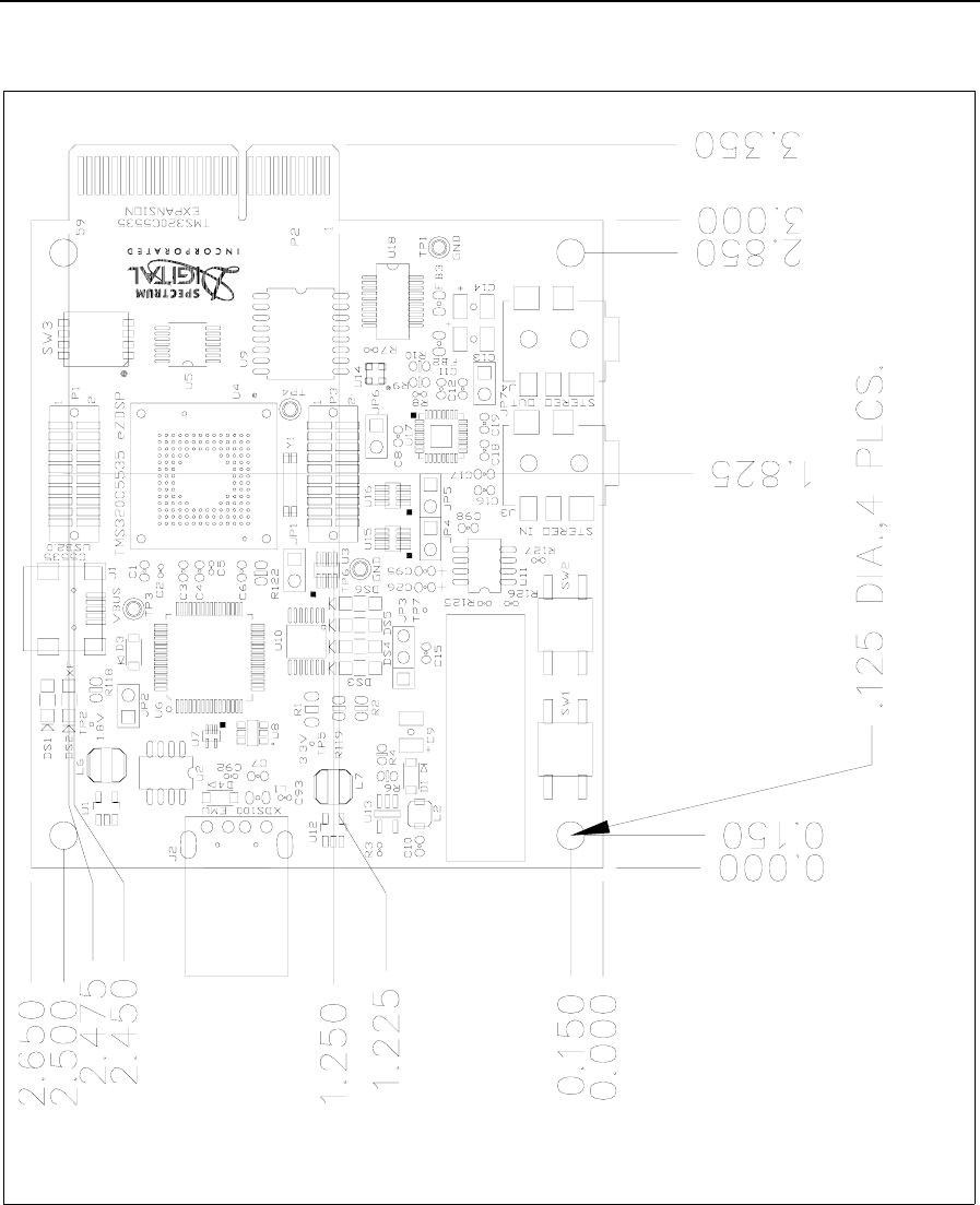
B-1
Appendix B
Mechanical Information
This appendix contains the mechanical information about the
TMS320C5535 eZdsp produced by Spectrum Digital.
Spectrum Digital, Inc
B-2 TMS320C5535 eZdsp Technical Reference Manual
THIS DRAWING IS NOT TO SCALE
ALL MEASUREMENTS ARE IN INCHES

Printed in U.S.A., August 2011
514585-0001 Rev. A
