FDG6301N Datasheet. Www.s Manuals.com. Fairchild
User Manual: Marking of electronic components, SMD Codes 01, 01**, 010*, 014N03LS, 014N03MS, 016N03LS, 016N03MS, 016N04LS, 016b*, 017**, 017N04NS, 018N04LS, 019N02KS, 019N04NS. Datasheets BSC014N03LS G, BSC014N03MS G, BSC016N03LS G, BSC016N03MS G, BSC016N04LS G, BSC017N04NS G, BSC018N04LS G, BSC019N02KS G, BSC019N04NS G, EC49016X-F, FDG6301N, MT2301, SE9017, SSTPAD100, STP7401S32RG.
Open the PDF directly: View PDF ![]() .
.
Page Count: 9
July 1999
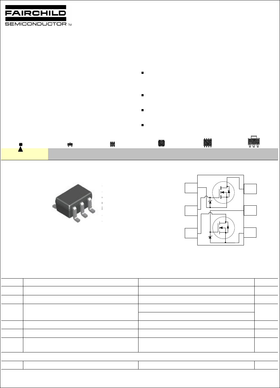
FDG6301N
Dual N-Channel, Digital FET
General Description Features
*The pinouts are symmetrical; pin 1 and 4 are interchangeable.
Units inside the carrier can be of either orientation and will not affect the functionality of the device.
Absolute Maximum Ratings TA = 25°C unless otherwise noted
Symbol Parameter FDG6301NUnits
VDSS Drain-Source Voltage 25 V
VGSS Gate-Source Voltage 8V
IDDrain/Output Current - Continuous 0.22 A
- Pulsed 0.65
PDMaximum Power Dissipation (Note 1)0.3 W
TJ,TSTG Operating and Storage Temperature Range -55 to 150 °C
ESD Electrostatic Discharge Rating MIL-STD-883D
Human Body Model(100 pF / 1500 Ω)
6.0 kV
THERMAL CHARACTERISTICS
RθJA Thermal Resistance, Junction-to-Ambient 415 °C/W
FDG6301N Rev.E1
25 V, 0.22 A continuous, 0.65 A peak.
RDS(ON) = 4 Ω @ VGS= 4.5 V,
RDS(ON) = 5 Ω @ VGS= 2.7 V.
Very low level gate drive requirements allowing direct
operation in 3 V circuits (VGS(th) < 1.5 V).
Gate-Source Zener for ESD ruggedness
(>6kV Human Body Model).
Compact industry standard SC70-6 surface mount
package.
These dual N-Channel logic level enhancement mode
field effect transistors are produced using Fairchild's
proprietary, high cell density, DMOS technology. This
very high density process is especially tailored to
minimize on-state resistance. This device has been
designed especially for low voltage applications as a
replacement for bipolar digital transistors and small
signal MOSFETs.
SOT-23 SuperSOTTM-8 SO-8 SOT-223
SC70-6 SuperSOTTM-6
1 or 4 *6 or 3
5 or 2
4 or 1 *
2 or 5
3 or 6
SC70-6
G1D2
S1
D1
S2
G2
.01
Electrical Characteristics (TA = 25 OC unless otherwise noted )
Symbol Parameter Conditions Min Typ Max Units
OFF CHARACTERISTICS
BVDSS Drain-Source Breakdown Voltage VGS = 0 V, ID = 250 µA 25 V
∆BVDSS/∆TJBreakdown Voltage Temp. Coefficient ID = 250 µA, Referenced to 25 o C25 mV / oC
IDSS Zero Gate Voltage Drain Current VDS = 20 V, VGS = 0 V 1µA
TJ = 55°C 10 µA
IGSS Gate - Body Leakage Current VGS = 8 V, VDS = 0 V 100 nA
ON CHARACTERISTICS (Note 2)
VGS(th) Gate Threshold Voltage VDS = VGS, ID = 250 µA0.65 0.85 1.5 V
∆VGS(th)/∆TJGate Threshold Voltage Temp.Coefficient ID = 250 µA, Referenced to 25 o C-2.1 mV / oC
RDS(ON) Static Drain-Source On-Resistance VGS = 4.5 V, ID = 0.22 A 2.6 4Ω
TJ =125°C 5.3 7
VGS = 2.7 V, ID = 0.19 A 3.7 5
ID(ON) On-State Drain Current VGS = 4.5 V, VDS = 5 V 0.22 A
gFS Forward Transconductance VDS = 5 V, ID= 0.22 A 0.2 S
DYNAMIC CHARACTERISTICS
Ciss Input Capacitance VDS = 10 V, VGS = 0 V,
f = 1.0 MHz 9.5 pF
Coss Output Capacitance 6 pF
Crss Reverse Transfer Capacitance 1.3 pF
SWITCHING CHARACTERISTICS (Note 2)
tD(on)Turn - On Delay Time VDD = 5 V, ID = 0.5 A,
VGS = 4.5 V, RGEN = 50 Ω510 ns
trTurn - On Rise Time 4.5 10 ns
tD(off) Turn - Off Delay Time 4 8 ns
tfTurn - Off Fall Time 3.2 7ns
QgTotal Gate Charge VDS = 5 V, ID = 0.22 A,
VGS = 4.5 V 0.29 0.4 nC
Qgs Gate-Source Charge 0.12 nC
Qgd Gate-Drain Charge 0.03 nC
DRAIN-SOURCE DIODE CHARACTERISTICS AND MAXIMUM RATINGS
ISMaximum Continuous Source Current 0.25 A
VSD Drain-Source Diode Forward Voltage VGS = 0 V, IS = 0.25 A (Note 2)0.8 1.2 V
Notes:
1. RθJA is the sum of the junction-to-case and case-to-ambient thermal resistance where the case thermal reference is defined as the solder mounting surface of the drain pins. RθJC is guaranteed
by design while RθCA is determined by the user's board design. RθJA = 415OC/W on minimum pad mounting on FR-4 board in still air.
2. Pulse Test: Pulse Width < 300µs, Duty Cycle < 2.0%.
FDG6301N Rev.E1
FDG6301N Rev.E1
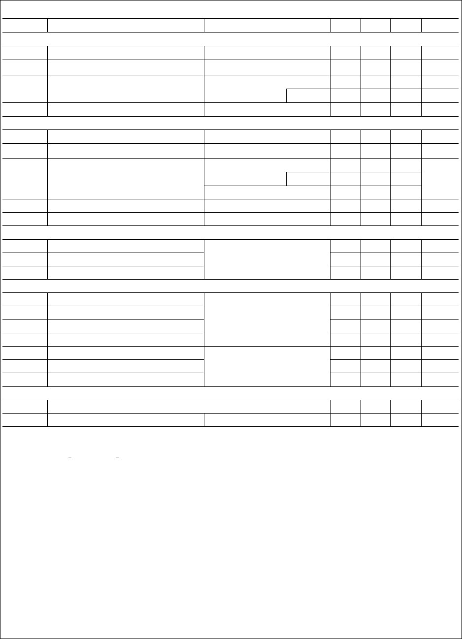
Typical Electrical Characteristics
Figure 1. On-Region Characteristics.Figure 2. On-Resistance Variation with
Drain Current and Gate Voltage.
Figure 3. On-Resistance Variation
with Temperature.
Figure 5. Transfer Characteristics.
Figure 4. On-Resistance Variation with
Gate-to-Source Voltage.
-50 -25 0 25 50 75 100 125 150
0.6
0.8
1
1.2
1.4
1.6
1.8
T , JUNCTION TEMPERATURE (°C)
DRAIN-SOURCE ON-RESISTANCE
J
R , NORMALIZED
DS(ON)
V = 4.5V
GS
I = 0.22A
D
012345
0
0.1
0.2
0.3
0.4
0.5
V , DRAIN-SOURCE VOLTAGE (V)
I , DRAIN-SOURCE CURRENT (A)
V =4.5V
GS
DS
D
2.5V
3.0V
2.0V
3.5V
2.7V
00.1 0.2 0.3 0.4
2
2.5
3
3.5
4
4.5
5
I , DRAIN CURRENT (A)
DRAIN-SOURCE ON-RESISTANCE
V = 2.5V
GS
D
R , NORMALIZED
DS(ON)
5.0V
4.5V
2.7V
4.0V
3.5V
3.0V
1 2 3 4 5
0
4
8
12
16
20
V ,GATE TO SOURCE VOLTAGE (V)
R , ON-RESISTANCE(OHM)
GS
DS(ON)
25°C
I = 0.10A
D
T =125°C
A
0.5 11.5 22.5 3
0
0.05
0.1
0.15
0.2
V , GATE TO SOURCE VOLTAGE (V)
I , DRAIN CURRENT (A)
V = 5V
DS
GS
D
T = -55°C
J
125°C
25°C
00.2 0.4 0.6 0.8 11.2
0.0001
0.001
0.01
0.1
0.4
V , BODY DIODE FORWARD VOLTAGE (V)
I , REVERSE DRAIN CURRENT (A)
25°C
-55°C
V = 0V
GS
SD
S
T = 125°C
J
Figure 6. Body Diode Forward Voltage
Variation with Source Current
and Temperature.
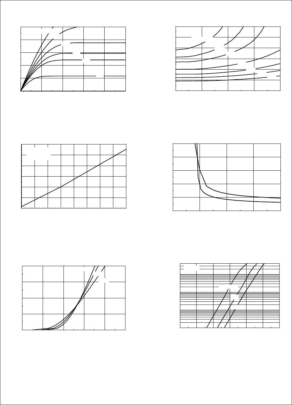
FDG6301N Rev.E1
Figure 10. Single Pulse Maximum Power
Dissipation.
Figure 8. Capacitance Characteristics.
Figure 7. Gate Charge Characteristics.
Figure 9. Maximum Safe Operating Area.
Typical Electrical Characteristics ( continued)
00.1 0.2 0.3 0.4 0.5 0.6
0
1
2
3
4
5
6
Q , GATE CHARGE (nC)
V , GATE-SOURCE VOLTAGE (V)
g
GS
I = 0.22A
DV = 5V
DS 10V
0.4 0.8 2 5 10 25 40
0.01
0.03
0.1
0.3
1
V , DRAIN-SOURCE VOLTAGE (V)
I , DRAIN CURRENT (A)
RDS(ON) LIMIT
D
DC
DS
10s
100ms
10ms
V = 4.5V
SINGLE PULSE
R = 415 °C/W
T = 25°C
θJA
GS
A
1s
0.1 0.3 1 3 10 25
2
3
5
8
15
30
V , DRAIN TO SOURCE VOLTAGE (V)
CAPACITANCE (pF)
DS
C
iss
f = 1 MHz
V = 0 V
GS
C
oss
C
rss
0.0001 0.001 0.01 0.1 110 200
0
10
20
30
40
50
SINGLE PULSE TIME (SEC)
POWER (W)
SINGLE PULSE
R =415°C/W
T = 25°C
θJA
A
0.0001 0.001 0.01 0.1 1 10 100 200
0.002
0.005
0.01
0.02
0.05
0.1
0.2
0.5
1
t , TIME (sec)
TRANSIENT THERMAL RESISTANCE
r(t), NORMALIZED EFFECTIVE
1
Single Pulse
D = 0.5
0.1
0.05
0.02
0.01
0.2
Duty Cycle, D = t / t
1 2
T - T = P * R (t)
A
J
P(pk)
t
1 t
2
θJA
R (t) = r(t) * R
R =415 °C/W
θJA
θJA
θJA
Figure 11. Transient Thermal Response Curve.
Thermal characterization performed using the conditions described in note 1.
Transient thermal response will change depending on the circuit board design.
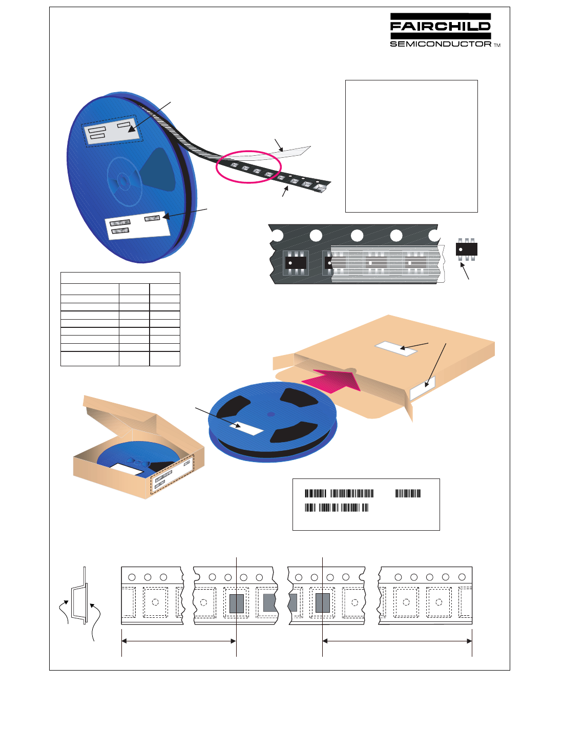
SC70-6 Unit Orientation
SC70-6 Packaging
Configuration: Figure 1.0
Components Leader Tape
500mm minimum or
125 empty pockets
Trailer Tape
300mm minimum or
75 empty pockets
SC70-6 Tape Leader and Trailer
Configuration: Figure 2.0
Cover Tape
Carrier Tape
Note/Comments
Packaging Option
SC70-6 Packaging Information
Standard
(no flow code) D87Z
Packaging type
Reel Size
TNR
7" Dia
TNR
13"
Qty per Reel/Tube/Bag 3,000 10,000
Box Dimension (mm) 184x187x47 343x343x64
Max qty per Box 9,000 30,000
Weight per unit (gm) 0.0055 0.0055
Weight per Reel (kg) 0.1140 0.3960
F63TNR
Label
Customized Label
Antistatic Cover Tape
184mm x 187mm x 47mm
Pizza Box for Standard Option
F63TNR
Label
F63TNR Barcode Label
F63TNR Label sample
343mm x 342mm x 64mm
Intermediate box for D87Z Option
21 21 21 21
F63TNR
Label
21
Pin 1
LOT: CBVK741B019
FSID: FDG6302P
D/C1: D9842 QTY1: SPEC REV:
SPEC:
QTY: 3000
D/C2: QTY2: CPN: N/F: F (F63TNR)3
Packaging Description:
SC70-6 parts are shipped in tape. The carrier tape is
made from a dissipative (carbon filled) polycarbonate
resin. The cover tape is a multilayer film (Heat Activated
Adhesive in nature) primarily composed of polyester film,
adhesive layer, sealant, and anti-static sprayed agent.
These reeled parts in standard option are shipped with
3,000 units per 7" or 177cm diameter reel. The reels are
dark blue in color and is made of polystyrene plastic (anti-
static coated). Other option comes in 10,000 units per 13"
or 330cm diameter reel. This and some other options are
described in the Packaging Information table.
These full reels are individually barcode labeled and
placed inside a pizza box (illustrated in figure 1.0) made of
recyclable corrugated brown paper with a Fairchild logo
printing. One pizza box contains three reels maximum.
And these pizza boxes are placed inside a barcode
labeled shipping box which comes in different sizes
depending on the number of parts shipped.
Static Dissipative
Embossed Carrier Tape
SC70-6 Tape and Reel Data and Package Dimensions
August 1999, Rev. C
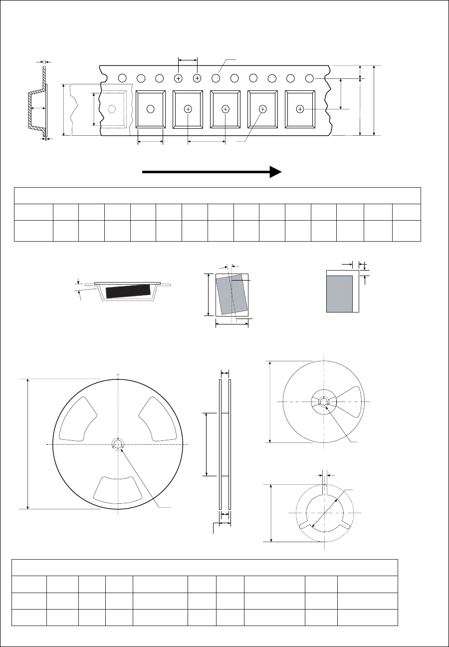
SC70-6 Tape and Reel Data and Package Dimensions, continued
July 1999, Rev. C
P1
A0 D1
P0
F
W
E1
D0
E2
B0
Tc
Wc
K0
T
Dimensions are in inches and millimeters
Tape Size Reel
Option Dim A Dim B Dim C Dim D Dim N Dim W1 Dim W2 Dim W3 (LSL-USL)
8mm 7" Dia 7.00
177.8 0.059
1.5 0.512 +0.020/-0.008
13 +0.5/-0.2 0.795
20.2 2.165
55 0.331 +0.059/-0.000
8.4 +1.5/0 0.567
14.4 0.311 – 0.429
7.9 – 10.9
8mm 13" Dia 13.00
330 0.059
1.5 0.512 +0.020/-0.008
13 +0.5/-0.2 0.795
20.2 4.00
100 0.331 +0.059/-0.000
8.4 +1.5/0 0.567
14.4 0.311 – 0.429
7.9 – 10.9
See detail AA
Dim A
max
13" Diameter Option
7" Diameter Option
Dim A
Max
See detail AA
W3
W2 max Measured at Hub
W1 Measured at Hub
Dim N
Dim D
min
Dim C
B Min
DETAIL AA
Notes: A0, B0, and K0 dimensions are determined with respect to the EIA/Jedec RS-481
rotational and lateral movement requirements (see sketches A, B, and C).
20 deg maximum component rotation
0.5mm
maximum
0.5mm
maximum
Sketch C (Top View)
Component lateral movement
Typical
component
cavity
center line
20 deg maximum
Typical
component
center line
B0
A0
Sketch B (Top View)
Component Rotation
Sketch A (Side or Front Sectional View)
Component Rotation
User Direction of Feed
SC70-6 Embossed Carrier Tape
Configuration: Figure 3.0
SC70-6 Reel Configuration: Figure 4.0
Dimensions are in millimeter
Pkg type
A0 B0 W D0 D1 E1 E2 F P1 P0 K0 T Wc Tc
SC70-6
(8mm)
2.24
+/-0.10 2.34
+/-0.10 8.0
+/-0.3 1.55
+/-0.05 1.125
+/-0.125 1.75
+/-0.10 6.25
min 3.50
+/-0.05 4.0
+/-0.1 4.0
+/-0.1 1.20
+/-0.10 0.255
+/-0.150 5.2
+/-0.3 0.06
+/-0.02
SC70-6 (FS PKG Code 76)
SC70-6 Tape and Reel Data and Package Dimensions, continued
September 1998, Rev. A1
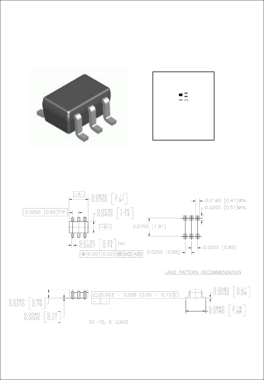
1:1
Scale 1:1 on letter size paper
Dimensions shown below are in:
inches [millimeters]
Part Weight per unit (gram): 0.0055
TRADEMARKS
ACEx™
CoolFET™
CROSSVOLT™
E2CMOSTM
FACT™
FACT Quiet Series™
FAST®
FASTr™
GTO™
HiSeC™
The following are registered and unregistered trademarks Fairchild Semiconductor owns or is authorized to use and is
not intended to be an exhaustive list of all such trademarks.
LIFE SUPPORT POLICY
FAIRCHILD’S PRODUCTS ARE NOT AUTHORIZED FOR USE AS CRITICAL COMPONENTS IN LIFE SUPPORT
DEVICES OR SYSTEMS WITHOUT THE EXPRESS WRITTEN APPROVAL OF FAIRCHILD SEMICONDUCTOR CORPORATION.
As used herein:
1. Life support devices or systems are devices or
systems which, (a) are intended for surgical implant into
the body, or (b) support or sustain life, or (c) whose
failure to perform when properly used in accordance
with instructions for use provided in the labeling, can be
reasonably expected to result in significant injury to the
user.
2. A critical component is any component of a life
support device or system whose failure to perform can
be reasonably expected to cause the failure of the life
support device or system, or to affect its safety or
effectiveness.
PRODUCT STATUS DEFINITIONS
Definition of Terms
Datasheet Identification Product Status Definition
Advance Information
Preliminary
No Identification Needed
Obsolete
This datasheet contains the design specifications for
product development. Specifications may change in
any manner without notice.
This datasheet contains preliminary data, and
supplementary data will be published at a later date.
Fairchild Semiconductor reserves the right to make
changes at any time without notice in order to improve
design.
This datasheet contains final specifications. Fairchild
Semiconductor reserves the right to make changes at
any time without notice in order to improve design.
This datasheet contains specifications on a product
that has been discontinued by Fairchild semiconductor.
The datasheet is printed for reference information only.
Formative or
In Design
First Production
Full Production
Not In Production
DISCLAIMER
FAIRCHILD SEMICONDUCTOR RESERVES THE RIGHT TO MAKE CHANGES WITHOUT FURTHER
NOTICE TO ANY PRODUCTS HEREIN TO IMPROVE RELIABILITY, FUNCTION OR DESIGN. FAIRCHILD
DOES NOT ASSUME ANY LIABILITY ARISING OUT OF THE APPLICATION OR USE OF ANY PRODUCT
OR CIRCUIT DESCRIBED HEREIN; NEITHER DOES IT CONVEY ANY LICENSE UNDER ITS PATENT
RIGHTS, NOR THE RIGHTS OF OTHERS.
TinyLogic™
UHC™
VCX™
ISOPLANAR™
MICROWIRE™
POP™
PowerTrench™
QFET™
QS™
Quiet Series™
SuperSOT™-3
SuperSOT™-6
SuperSOT™-8