FR9801 Datasheet. Www.s Manuals.com. R0.1 Fiti
User Manual: Marking of electronic components, SMD Codes B1, B1*, B1**, B1-, B1-**, B1-***, B10, B10A, B10B, B10C, B10D, B10E, B10F, B10G, B10H, B11, B113ZS, B1237, B1=***, B1G***, B1O, B1Y. Datasheets 1KSMB100A, 1KSMB110A, 1KSMB120A, 1KSMB130A, 1KSMB150A, 1KSMB160A, 1KSMB82A, 1KSMB91A, 2SB1237, BAS40, BD4745G, DTB113ZS, ELM9711NBA, EMB10, EMB11, FR9801S6CTR, IMB10A, IMB11A, KSC2715, RT9010-12GJ6, RT9010-12PJ6, RT9011-GSGQWC, RT9013-33PU5, RT9013A-33GY, RT9014A-PGPQV, RT9169-12GV, RT9169-12PV, RT9169-12PX, RT9903PQV, SS
Open the PDF directly: View PDF ![]() .
.
Page Count: 7
1
FR9801-Preliminary 0.1-SEP-2011
FR9801
85T
fitipower integrated technology lnc.
21V, 1.8A, 600KHz Synchronous Step-Down
DC/DC Converter
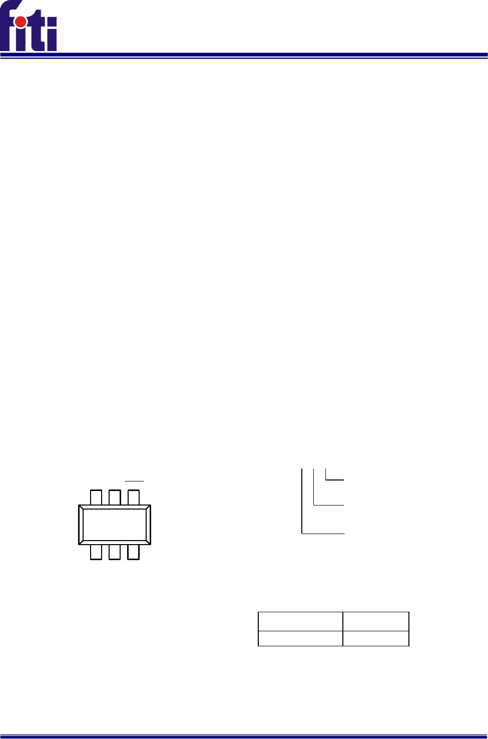
Pin Assignments
S6 Package (SOT-23-6)
2
13
6 4
5
(Marking)
BST
LX
GND FB
VIN SHDN
Figure 1. Pin Assignment of FR9801
Ordering Information
SOT-23-6 Marking
Part Number
Product Code
FR9801S6CTR
B1G
Description
The FR9801 is a synchronous step-down DC/DC
converter that provides wide 4.5V to 21V input
voltage range and 1.8A continuous load current
capability.
The FR9801 fault protection includes cycle-by-cycle
current limit, UVLO, output overvoltage protection
and thermal shutdown. The adjustable soft-start
function prevents inrush current at turn-on. This
device uses current mode control scheme which
provides fast transient response. Internal
Compensation function reduces external
compensation components and simplifies the design
process. In shutdown mode, the supply current is
less than 1μA.
The FR9801 is available in a SOT-23-6 package,
provides good thermal conductance.
Features
● High Efficiency up to 94%
● Low Rds(on) Integrated Power MOSFET
● Internal Compensation Function
● Wide Input Voltage Range: 4.5V to 21V
● Adjustable Output Voltage from 0.8V to 17.85V
● 1.8A Output Current
● Fixed 600KHz Switching Frequency
● Current Mode Operation
● Cycle-by-Cycle Current Limit
● Over-Temperature Protection with Auto Recovery
● Output Overvoltage Protection
● Under Voltage Lockout
● <1μA Shutdown Current
● SOT-23-6 Package
Applications
● STB (Set-Top-Box)
● LCD Displays, TVs
● Distributed Power Systems
● Networking, XDSL Modems
C: Green
TR: Tape / Reel
FR9801□□□
Package Type
S6: SOT-23-6
2
FR9801-Preliminary 0.1-SEP-2011
FR9801
85T
fitipower integrated technology lnc.
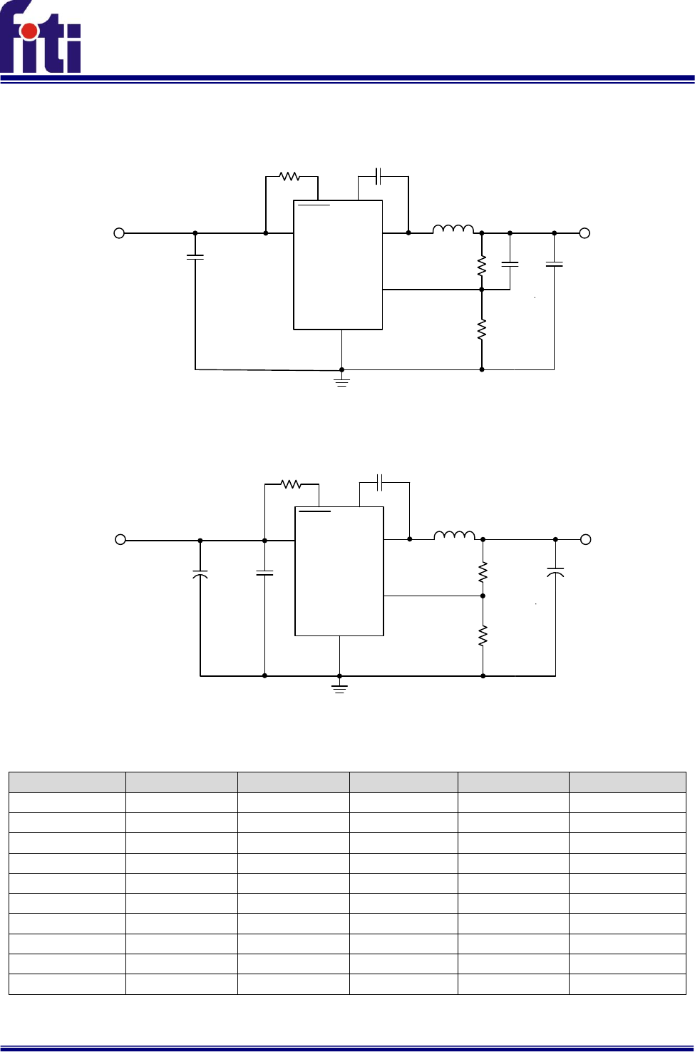
Typical Application Circuit
FR9801
GND
VIN
BST
FB
LX
VIN
4.5V to 21V
VOUT
10μF/25V
CERAMIC x 2 22μF/6.3V
CERAMIC x 2
L1
4.7μH
R2
R1
R3
100kΩ
1
56
2
3
4
C4
C1 C2
C3
0.1μF
SHDN
3.3V
9.76kΩ 1%
30.9kΩ 1% (optional)
Figure 2. CIN /COUT use Ceramic Capacitors Application Circuit
FR9801
GND
VIN
BST
FB
LX
VIN
4.5V to 21V
VOUT
0.1μF/25V
CERAMIC x 1
100μF/6.3V
EC x 1
R2
R1
1
56
2
3
4
C1 C2
100μF/25V
EC x 1
C4
L1
4.7μH
C3
0.1μF
R3
100kΩ
SHDN
3.3V
30.9kΩ 1%
9.76kΩ 1%
Figure 3. CIN /COUT use Electrolytic Capacitors Application Circuit
VOUT
R1
R2
C4
L1
COUT
1.2V
4.99kΩ
10kΩ
10pF~1nF
2.2μH
22μF MLCC x2
1.8V
4.99kΩ
3.92kΩ
10pF~1nF
2.2μH
22μF MLCC x2
2.5V
4.99kΩ
2.32kΩ
10pF~1nF
4.7μH
22μF MLCC x2
3.3V
30.9kΩ
9.76kΩ
10pF~1nF
4.7μH
22μF MLCC x2
5V
30.9kΩ
5.76kΩ
10pF~1nF
4.7μH
22μF MLCC x2
1.2V
4.99kΩ
10kΩ
--
2.2μH
100μF EC x1
1.8V
4.99kΩ
3.92kΩ
--
2.2μH
100μF EC x1
2.5V
4.99kΩ
2.32kΩ
--
4.7μH
100μF EC x1
3.3V
30.9kΩ
9.76kΩ
--
4.7μH
100μF EC x1
5V
30.9kΩ
5.76kΩ
--
4.7μH
100μF EC x1
Table 1. Recommended Component Values
3
FR9801-Preliminary 0.1-SEP-2011
FR9801
85T
fitipower integrated technology lnc.
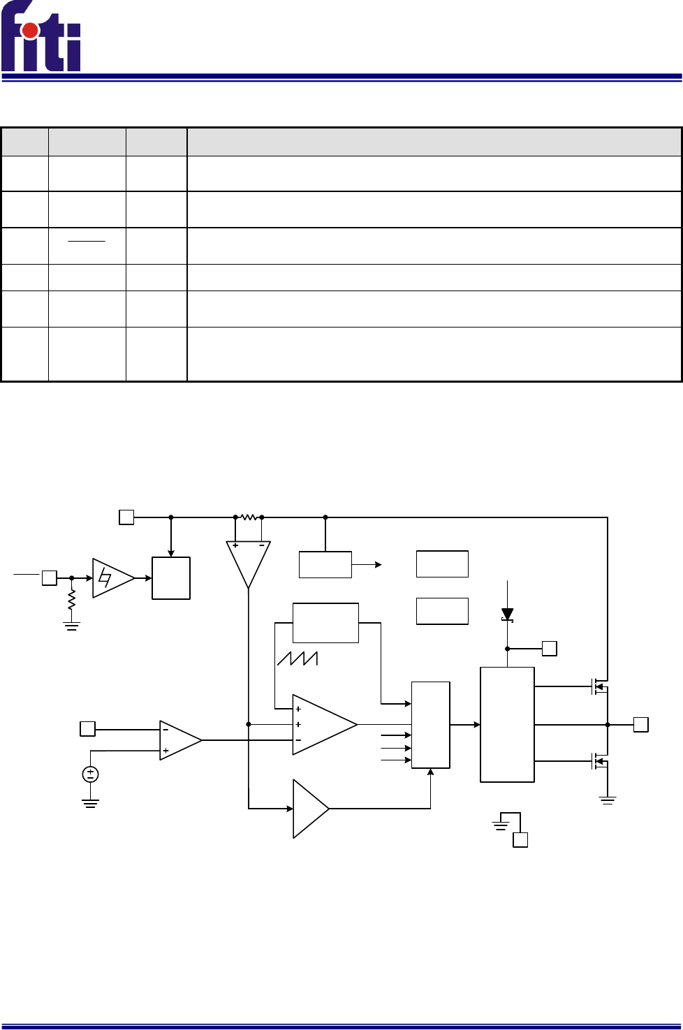
Functional Pin Description
I/O
Pin Name
Pin No.
Pin Function
I
FB
3
Voltage Feedback Input Pin. Connect FB and VOUT with a resistive voltage
divider. This IC senses feedback voltage via FB and regulates it at 0.8V.
I
VIN
5
Power Supply Input Pin. Drive VIN pin by 4.5V to 21V voltage to power on
the chip.
I
SHDN
4
Enable Input Pin. This pin is a digital control input that turns the converter on
or off. Connect to VIN with a 100KΩ resistor for self-startup.
I
GND
2
Ground Pin.
O
LX
6
Power Switching Output. LX is the output of the internal high side NMOS
switch.
O
BST
1
High Side Gate Drive Boost Pin. A 10nF or greater capacitor must be
connected from this pin to LX. It can boost the gate drive to fully turn on the
internal high side NMOS.
Block Diagram
PWM
Control
Driver
Logic
BST
LX
R
OTP
OVP
UVLO
Current
Comp
S
Oscillator
High-Side
MOSFET
Low-Side
MOSFET
ISEN
FB
0.8V
UVLO
&
POR
VIN
VCC
GND
Current
Limit
OTP
Internal
Regulator
VCC
OVP
1M
SHDN
Figure 4. Block Diagram of FR9801

4
FR9801-Preliminary 0.1-SEP-2011
FR9801
85T
fitipower integrated technology lnc.
Absolute Maximum Ratings (Note 1)
● Supply Voltage VIN -------------------------------------------------------------------------------------------
-0.3V to +23V
● Enable Voltage V
SHDN
--------------------------------------------------------------------------------------
-0.3V to +23V
● LX Voltage VLX (50ns) --------------------------------------------------------------------------------------
-1V to VIN+0.3V
● BST Pin Voltage VBST --------------------------------------------------------------------------------------
VLX-0.3V to VLX+6V
● All Other Pins Voltage -------------------------------------------------------------------------------------
-0.3V to +6V
● Maximum Junction Temperature (TJ) ------------------------------------------------------------------
+150°C
● Storage Temperature (TS) --------------------------------------------------------------------------------
-65°C to +150°C
● Lead Temperature (Soldering, 10sec.) ----------------------------------------------------------------
+260°C
● Power Dissipation @TA=25°C, (PD)
SOT-23-6 --------------------------------------------------------------------------------------------
+0.40W
● Package Thermal Resistance, (θJA):
SOT-23-6 --------------------------------------------------------------------------------------------
+250°C/W
● Package Thermal Resistance, (θJC):
SOT-23-6 --------------------------------------------------------------------------------------------
+130°C/W
Note 1:Stresses beyond this listed under “Absolute Maximum Ratings" may cause permanent damage to the device.
Recommended Operating Conditions
● Supply Voltage VIN -------------------------------------------------------------------------------------------
+4.5V to +21V
● Enable Voltage V
SHDN
--------------------------------------------------------------------------------------
0V to VIN
● Operation Temperature Range --------------------------------------------------------------------------
-40°C to +85°C
5
FR9801-Preliminary 0.1-SEP-2011
FR9801
85T
fitipower integrated technology lnc.
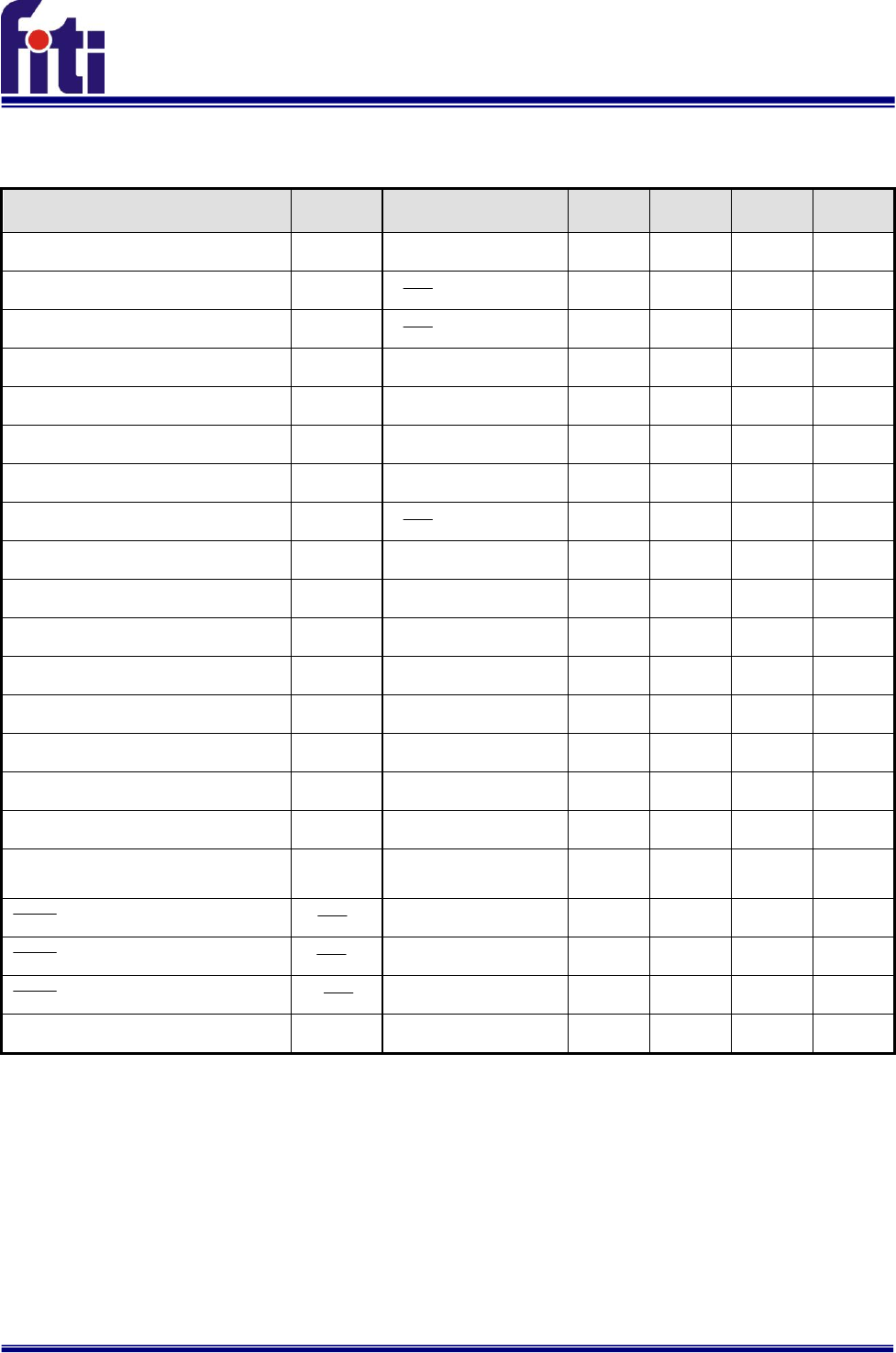
Electrical Characteristics
(VIN=12V, TA=25°C, unless otherwise specified.)
Parameter
Symbol
Conditions
Min
Typ
Max
Unit
VIN Input Supply Voltage
VIN
4.5
21
V
VIN Quiescent Current
IDDQ
V
SHDN
=1.8V, VFB=1.0V
2.5
mA
VIN Shutdown Supply Current
ISD
V
SHDN
=0V
1
μA
Feedback Voltage
VFB
4.5V≦VIN≦21V
0.779
0.8
0.821
V
Feedback OVP Threshold Voltage
VOVP
1.4
V
High-Side MOSFET RDS(ON)
(Note 2)
RDS(ON)
120
mΩ
Low-Side MOSFET RDS(ON)
(Note 2)
RDS(ON)
110
mΩ
High-Side MOSFET Leakage
Current
ILX(leak)
V
SHDN
=0V, VLX=0V
10
μA
High-Side MOSFET Current Limit
(Note 2)
ILIMIT(HS)
Minimum Duty
2.5
3
A
Low-Side MOSFET Current Limit
(Note 2)
ILIMIT(LS)
From Drain to Source
1.5
A
Error Amplifier Voltage Gain
(Note 2)
400
V/V
Oscillation frequency
FOSC
480
600
720
KHz
Short Circuit Oscillation Frequency
FOSC(short)
VFB=0V
140
KHz
Maximum Duty Cycle
DMAX
VFB=0.6V
90
%
Minimum On Time (Note 2)
TMIN
100
ns
Input UVLO Threshold
VUVLO(Vth)
VIN Rising
4.3
V
Under Voltage Lockout Threshold
Hysteresis
VUVLO(HYS)
400
mV
SHDN
Input Low Voltage
V
SHDN
(L)
0.4
V
SHDN
Input High Voltage
V
SHDN
(H)
2
V
SHDN
Input Current
I
SHDN
VIN =2V
2
μA
Thermal Shutdown Threshold
(Note 2)
TSD
170
°C
Note 2:Not production tested.
6
FR9801-Preliminary 0.1-SEP-2011
FR9801
85T
fitipower integrated technology lnc.
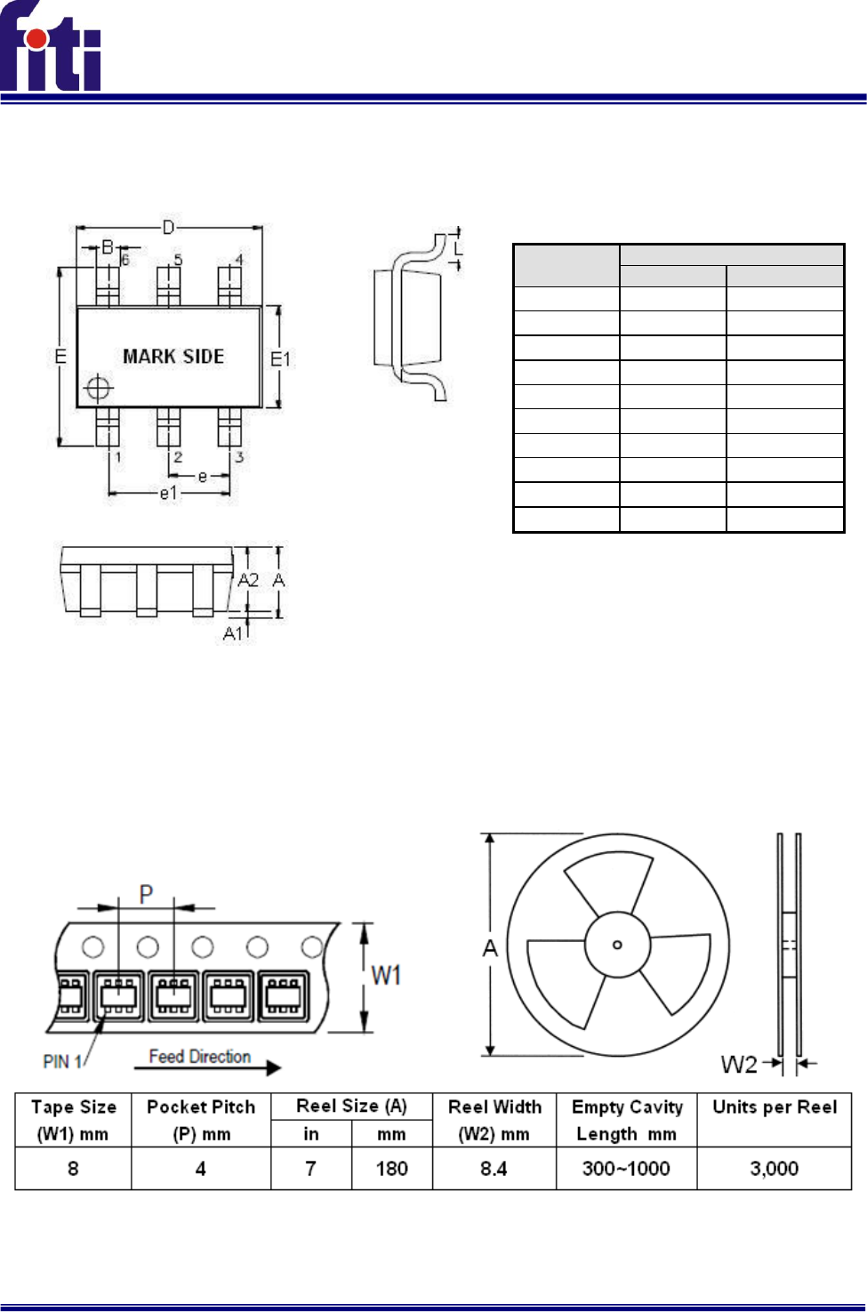
Outline Information
SOT-23-6 Package (Unit: mm)
SYMBOLS
UNIT
DIMENSION IN MILLIMEER
MIN
MAX
A
0.90
1.45
A1
0.00
0.15
A2
0.90
1.30
B
0.30
0.50
D
2.80
3.00
E
2.60
3.00
E1
1.50
1.70
e
0.90
1.00
e1
1.80
2.00
L
0.30
0.60
Note:Followed From JEDEC MO-178-C.
Carrier dimensions
Life Support Policy
Fitipower’s products are not authorized for use as critical components in life support devices or other medical systems.