G9661 Datatsheet. Www.s Manuals.com. R0.93 Gmt
User Manual: Marking of electronic components, SMD Codes 96, 961Ax, 9661-25, 9661A, 966TQ1. Datasheets DTC144TCA, DTC144TE, DTC144TKA, DTC144TM, DTC144TUA, G9661-25ADJF1, G9661-25ADJF6, G9661-25ADJRE, G9661-25ADJTP, TPS22966TDPURQ1.
Open the PDF directly: View PDF ![]() .
.
Page Count: 2
Ver: 0.93
Sep 10, 2013
TEL: 886-3-5788833
http://www.gmt.com.tw
1
G9661
Global Mixed-mode Technology
Peak 3A, Low Dropout Regulator with Enable
Features
Adjustable Output Low to 0.8V
Input Voltage as Low as 1.4V and VPP Voltage
5V
300mV Dropout @ 2A, VO 2.5V
Over Current and Over Temperature Protection
Enable Pin
Low Reverse Leakage (Output to Input )
TSOT-23-6, SOP-8(FD), MSOP-10(FD) and
TDFN3X3-10 Packages
±1.5% ADJ Voltage
VO Power OK Signal
2.5V Options by Setting ADJ Pin Below 0.2V
and Adjustable Externally Using Resistors
VO Pull Low Resistance when Disable
VO Soft Start When Enable
Applications
Motherboards
Peripheral Cards
Network Cards
Set Top Boxes
Notebook Computers
General Description
The G9661 is a high performance positive voltage
regulator designed for use in applications requiring
very low Input voltage and very low dropout voltage at
up to 2 amps. It operates with a VIN as low as 1.4V and
VPP voltage 5V with output voltage programmable as
low as 0.8V. The G9661 features ultra low dropout,
ideal for applications where VOUT is very close to VIN.
Additionally, the G9661 has an enable pin to further
reduce power dissipation while shutdown. The G9661
provides excellent regulation over variations in line,
load and temperature. The G9661 provides a power
OK signal to indicate if the voltage level of VO reaches
92% of its rating value.
The G9661 is available in the power TSOT-23-6,
SOP-8(FD), MSOP-10(FD) and TDFN3X3-10 package.
It is available with 2.5V internally preset outputs that
are also adjustable using external resistors.
Ordering Information
ORDER
NUMBER MARKING TEMP.
RANGE PACKAGE
(Green)
G9661-25ADJTP1U 961Ax -40°C~+85°C TSOT-23-6
G9661-25ADJF11U 9661-25 -40°C~+85°C SOP-8 (FD)
G9661-25ADJF61U 9661-25 -40°C~+85°C MSOP-10 (FD)
G9661-25ADJRE1U 9661A -40°C~+85°C TDFN3X3-10
Note:TP: TSOT-23-6 F1: SOP-8 (FD) F6: MSOP-10 (FD) RE: TDFN3X3-10
1:Bonding Code
U : Tape & Reel
e.g. 25 denotes the 2.5V output voltage
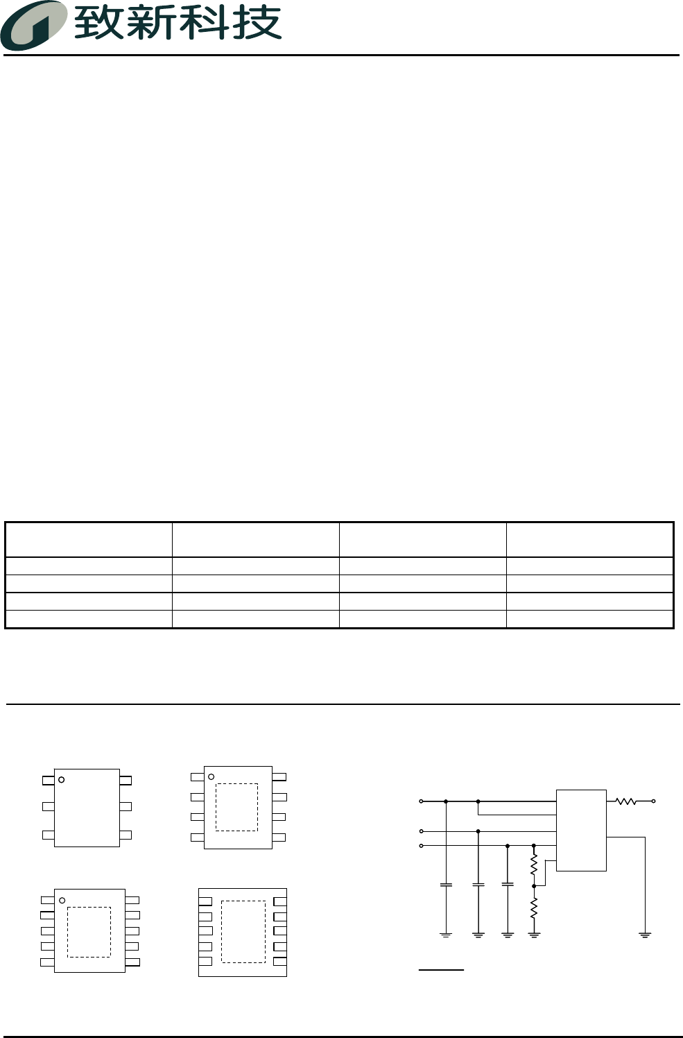
Pin Configuration Typical Application Circuit
VIN
VO
R1
R2
VEN
VIN
VO
ADJ
GND
G9661
0.8 (R1+R2)
VO = R2
Volts
C1
10µF
C2
10µF
R2<120kΩis recommended
VPPVPP (5V) POK VIN
10KΩ
C
PP
1µF
VIN
POK
VEN
VPP
GND
ADJ
VO
NC
SOP-8 (FD)
G9661
8
6
5
1
2
3
4
7
Thermal
Pad*
NC
10
8
7
1
2
3
4
POK
VEN
VIN
GND
ADJ
VO
VO
MSOP-10 (FD)
G9661
9
6
5
VPP NC
Thermal
Pad*
ADJ
VEN
VPP
GND
VO 1
2
34
5
6
G9661
VIN
TSOT-23-6
* Recommend connecting the Thermal Pad to the Ground for excellent power dissipation.
TDFN3X3-10
4
G9661
1
2
38
7
6
NC
VIN
5
9
10
ADJ
TDFN3X3-10
4
1
2
38
7
6
VO
NC
VO
VPP
VIN
5
9
10
POK VEN
Thermal
Pad*
(GND)
VIN
VO
R1
R2
VEN
VIN
VO
ADJ
GND
G9661
0.8 (R1+R2)
VO = R2
Volts
C1
10µF
C2
10µF
R2<120kΩis recommended
VPPVPP (5V) POK VIN
10KΩ
C
PP
1µF
VIN
POK
VEN
VPP
GND
ADJ
VO
NC
SOP-8 (FD)
G9661
8
6
5
1
2
3
4
7
Thermal
Pad*
NC
10
8
7
1
2
3
4
POK
VEN
VIN
GND
ADJ
VO
VO
MSOP-10 (FD)
G9661
9
6
5
VPP NC
Thermal
Pad*
ADJ
VEN
VPP
GND
VO 1
2
34
5
6
G9661
VIN
TSOT-23-6
* Recommend connecting the Thermal Pad to the Ground for excellent power dissipation.
TDFN3X3-10
4
G9661
1
2
38
7
6
NC
VIN
5
9
10
ADJ
TDFN3X3-10
4
1
2
38
7
6
VO
NC
VO
VPP
VIN
5
9
10
POK VEN
Thermal
Pad*
(GND)