PREPARATION OF PAPERS FOR THE 2003 IEEE INTERNATIONAL CONFERENCE ON High Energy Capacitor Characterization
User Manual: high-energy-capacitor-characterization Maxwell
Open the PDF directly: View PDF ![]() .
.
Page Count: 5

GENERAL ATOMICS ENERGY PRODUCTS
Engineering Bulletin
HIGH ENERGY DENSITY
CAPACITOR CHARACTERIZATION
Joel Ennis, Xiao Hui Yang, Fred MacDougall, Ken Seal
General Atomics Energy Products
General Atomics Electronic Systems, Inc.
4949 Greencraig Lane, San Diego, CA 92123-1675 USA
Juleigh Herbig
United Defense LP
Advanced Armament Systems
4800 East River Road, Minneapolis, MN 55421
Presented at:
IEEE International Power Modulator Conference
May 2004
www.gaep.com
High Energy Density Capacitor Characterization
Joel Ennis, Xiao Hui Yang, Fred MacDougall, Ken Seal
General Atomics Energy Products
General Atomics Electronic Systems, Inc.
4949 Greencraig Lane, San Diego, CA 92123-1675 USA
Juleigh Herbig
United Defense LP
Advanced Armament Systems
4800 East River Road, Minneapolis, MN 55421
Abstract
This paper will describe how film capacitors with
energy densities of greater than 1 J/cc and suitable for
millisecond discharge applications requiring limited life
have been characterized. A variety of polymer films were
tested in “model” capacitors storing and delivering
hundreds of Joules of energy at voltages of 2-10 kV. Self-
healing metallized film electrodes were utilized in these
designs to achieve electric fields greater than 500 MV/m.
Maximum operating voltage for short-term and long-term
use was determined. Life tests were then performed with
the goal of achieving at least 1000 charge/discharge
cycles at maximum energy density. Degradation and
failure of the capacitor samples was determined by
measurements of capacitance and dissipation factor.
Failure modes in continuous dc, normal charge/discharge
pulse service, and short-circuit fault conditions were
determined. Design modifications to increase life and
energy density were made based on those analyses.
Scale-up of the individual unit energy to 100 kJ is
underway.
I. INTRODUCTION
Capacitors are used as energy storage and energy
discharge components in many pulse power systems. For
high energy (>1 kJ), high voltage (> 1 kV), and high peak
current (>1 kA) requirements, wound film capacitors are
generally used. Very high peak power and average power
densities can be achieved using discrete foil electrodes in
combination with film dielectrics [1]. High energy
densities are obtained using self-healing metallized
electrodes vapor deposited on polymer film dielectrics.
The highest energy density film capacitors are generally
oil-filled (vacuum impregnated) with a liquid dielectric to
suppress partial discharges and surface arcing, as well as
to increase capacitance [2].
The energy density of a capacitor is given by the
equation
ED = PF * εo * K * E 2 (1)
Where PF is the packing factor (ratio of volume
actually storing energy to total volume), εo is the
permittivity of free space, K is the so-called dielectric
constant, and E is the effective voltage gradient within the
dielectric. The packing factor of large film capacitors is
typically in the range 50-70%. A limited range of high
quality polymer films are available from which to wind
capacitors, resulting in dielectric permittivity ranging
from 2 to perhaps 10 [3]. Depending on the application,
the choice of polymer films may be further limited by
constraints on energy efficiency (dielectric loss),
temperature range, and cost. Therefore, increasing the
energy density of film capacitors is often a matter of
increasing the voltage gradient, E. Due to the
phenomenon of dielectric aging, this is effectively trading
off lifetime for energy density.
In the present work, several metallized film dielectrics
that were developed for applications requiring lifetimes of
tens of thousands to millions of charge/discharge cycles
were tested for their energy density capability in pulse
power applications requiring a minimum of just 1000
charge/discharge cycles. The objective was to determine
the maximum energy density of these dielectrics under a
specific set of conditions.
II. SAMPLES
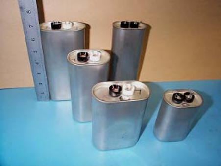
The capacitor samples selected for study were wound
metallized film, self-healing capacitors in drawn metal
cans. All were vacuum impregnated with an appropriate
dielectric liquid. In some cases, samples with two
different liquid impregnants were prepared for
comparison of the performance with this single change in
design. The dielectric materials included commercial and
custom-made polymer films, Kraft paper, and
combinations of Kraft paper with polymer films. The
nominal voltage ratings given to the samples for their
original, longer-life applications ranged from 1.6 kV to
5.3 kV. The energy stored in the individual samples at
their rated voltages ranged from 128 to 576 Joules.

Figure 1. Photograph showing capacitor samples
III. TEST METHODS
In order to determine the capability of each type of
capacitor, a variety of destructive tests were employed.
These tests were designed to stress the capacitor samples
in different ways and provide clear indication of how the
capacitor degraded with each type of stress. The tests
included a Maximum Voltage Test, a Short-Circuit
Current test, a Stepped Stress Pulse Life Test, a Fixed
Voltage Pulse Life Test, and a DC Life Test. Post
mortem failure analyses were performed to determine
modes of failure and provide a basis for improvement of
the designs and manufacturing processes.
A. Maximum-Voltage Test
The Maximum Voltage Test was designed to rapidly
determine the absolute maximum DC voltage capability
of each design. The test was a short-term, stepped-stress
test with voltage applied for 60 seconds at each step. The
initial step level was the rated voltage of the design, and
subsequent steps were 100 Volts greater than the
preceding step. The samples were discharged completely
between steps and measurements of capacitance and
dissipation factor (DF) were made to determine the level
of degradation of the sample resulting from loss of
electrode area. One sample of each design was tested.
B. Short-Circuit Test
Metallized electrode capacitors are susceptible to
current-related failure modes due to the small thickness of
the electrodes and the use of non-metallurgical bond
terminations (end spray or schooping). When subjected to
external fault modes, metallized electrode capacitors can
fail open-circuit, loose a significant fraction of their
capacitance, or increase in DF and ESR. The Short-
Circuit Test was used to measure the maximum current
density capability of the different capacitor samples. The
capacitors were charged to the initial test voltage,
typically 100 V, and discharged through a mechanical
relay type switch with no added resistance or inductance
in the circuit. The underdamped discharge was observed
using an oscilloscope and the peak current and other
waveform parameters were recorded. The
charge/discharge cycle was repeated five times at each
voltage level. The samples were then removed from the
circuit and their capacitance and DF were measured. The
charge voltage was increased by 100 Volts and the
process repeated, unless the measurements indicated
capacitor failure due to capacitance loss or increase in DF.
C. Stepped-Stress Pulse Life Test
While the Maximum Voltage Test would set an upper
limit for dielectric withstand voltage, the Stepped-Stress
Life Test was designed to measure the maximum voltage
at which a given design would perform reliably for 1000
charge-discharge cycles. The capacitor was charged to
voltage in under 5 seconds and held at voltage for 1
second prior to discharge. The charge/discharge sequence
was repeated just once per minute to avoid overheating.
The discharge circuit characteristics were not intended to
closely simulate a specific application, but only to ensure
that peak current densities in the metallized electrodes
were well below design values. This was intended to
ensure that failure modes would be voltage-driven and not
current-driven. The samples were tested for 1000 shots at
their rated voltage, capacitance and DF were measured,
and then the voltage was increased (by 100 or 200 Volts,
depending on rated voltage), and the process repeated.
The test on a sample was halted when capacitance loss
exceeded 5% of the initial value. Three samples of each
design were tested.
D. Fixed Voltage Pulse Life Test
The stepped-stress life test provided cycle life data that
could be used to estimate the maximum voltage at which
each capacitor design would reliably operate for 1000
charge/discharge cycles. The Fixed Voltage Life Test
was then performed at that voltage to measure the actual
cycle life. This additional step was considered necessary
because of the possibility of significant dielectric aging at
lower voltages, as well as the possibility of a voltage
conditioning effect on the dielectric, such as through
space-charge formation due to ionic conduction.
The same cycle timing and discharge circuit were used
for this test as were described for the Stepped-Stress Life
Test. Three samples of each design were tested initially.
E. DC Voltage Life Test
Selected designs were life tested at a fixed dc voltage
to determine the capability of these designs in
applications requiring longer charge time or hold time
during each cycle, and to determine the failure mode
under steady-state conditions. Comparison of the life and
failure mode with those obtained under pulse test
conditions was expected to provide useful information
about the fundamental aging process.

IV. RESULTS
A. Maximum-Voltage Test
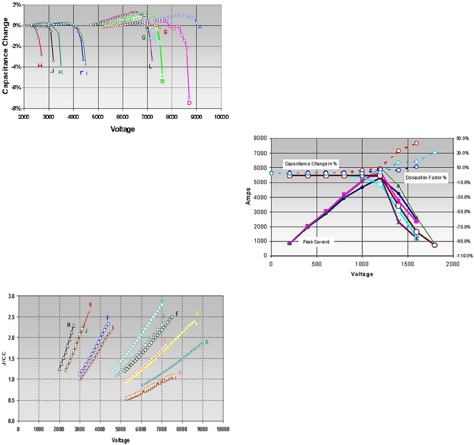
The capacitance measurements made during the
Maximum Voltage Test are shown in Figure 2.
Figure 2 Maximum Voltage Test
The capacitance initially increases as the applied
voltage produces electrostatic attraction between the
opposing electrodes, forcing them closer together. The
oil-filled space between films is constricted. (The effect
is observed after removal of the applied voltage, through
capacitance measurements made at low voltage using a
digital LCR meter, as relaxation occurs over hours or
even days.) Self-healing events begin to occur very
frequently at the highest voltages, resulting in measurable
capacitance loss.
Figure 3. Energy density versus voltage.
Because of the variety of dielectric types and dielectric
thicknesses used, it was found useful to plot the energy
density versus the test voltage, as shown in Figure 3. The
delivered energy, J, was estimated using J=1/2*Co*V2 ,
where Co was the capacitance value measured at low
voltage and V was the prior test voltage. The volume of
the capacitor samples was calculated using measurements
of the external dimensions, not including bushings or
small protruding features on the cans. There was one
exception, in which the sample wound element did not fit
tightly inside the can, for which an estimated volume for a
better package design was used in the calculation of
energy density.
B. Short-Circuit Test
Results of a typical short-circuit test are shown in
Figure 4. The capacitance and dissipation factor are
stable until a critical threshold peak current value is
reached, at which point capacitance decreases, DF
increases, and the peak current begins to decrease, even as
voltage is increased on subsequent steps of the test. High
current density in the metallized electrodes causes fusing
at defects and high resistance interfaces. Capacitance loss
results from areas of the electrodes becoming isolated due
to either “electrode fractures” or end spray disconnection.
DF increases are caused by the same phenomena, but
indicate that the current path lengths to the remaining
electrode areas have become elongated or even tortuous.
Figure 4. Typical Short-circuit Test results.
Analysis of the resulting data was complicated by the
fact that off-the-shelf units were used for these tests, and
construction techniques varied from design to design.
Specifically, some designs had end spray covering the
entire exposed edge of the metallized electrodes, while
others had portions that had been masked off to aid in
drying and impregnation. This results in enhanced current
densities at the edges of the end-sprayed areas.
Capacitors designed for maximum current-carrying
capability are fully end-sprayed. An additional variable is
the width of the metallized electrode, which determines
the aspect ratio of an element of a given electrode area
and, thus, capacitance. The wider the electrode, the
shorter the winding length, and the greater the density of
current at the end spray termination. In the present study,
the width of the metallized films ranged from 75 to
150mm.
C. Stepped-Stress Life Tests
During the stepped-stress life tests, an increase in
capacitance after 1000 cycles at rated voltage or even
higher than rated voltage was observed in some designs,
but not all. The rate of capacitance degradation with
increasing voltage tests varied significantly between
designs. In one case, a change in voltage from 3400 Volts

to 3500 Volts resulted in the three samples tested going
from zero capacitance loss to about 10% capacitance loss.
In another case, capacitance loss of about 1% was
observed after 1000 shots at 5000 Volts, 5% after 1000
shots at 5200 Volts, and 10% after 1000 shots at 5400
Volts.
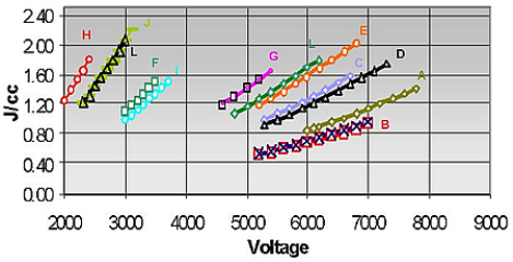
Figure 5. Energy density (J/cc) versus voltage in
Stepped – Stress Life Test.
The results of all the stepped-stress life tests, depicted
in terms of energy density versus voltage, are shown in
Figure 6. Whereas energy densities as high as 2.5 J/cc
were observed in the short-term Maximum Voltage Test,
the largest energy density achieved in the Stepped-Stress
Test was 2.2 J/cc.
D. Fixed Voltage Life Tests
Based on the results of the stepped-stress life tests,
voltages for each design were selected for Fixed-Voltage
Life Tests. The test voltage selection process was
exploratory in nature and therefore results varied from
500 to 2000 cycles life depending on the design. Energy
densities exceeding 2.2 J/cc for 1000 cycle life were
verified.
Additional fixed voltage life tests were performed on
Model E and G capacitors to determine life scaling with
voltage. In the case of Model G, in tests conducted at 6.4,
6.75, and 7.0 kV, the exponent, n, on the life scaling
equation, L ~1/V n , was found to be ~7.0. This value is
lower than observed in previous tests on metallized
capacitors, and is similar to that seen in foil electrode
capacitors. The observation from post mortems that
failure was driven by partial discharge erosion of the
metallized electrodes, rather than by self-healing
dielectric breakdowns, is probably related.
E. DC Life Tests
DC life tests were performed on Model G at 6.5 and
7.0 kV. Loss of 5% of capacitance at 7.0 kV occurred in
20 to 60 minutes, while the same level of degradation
took 210 to 330 minutes at 6.5 kV. Failure analyses have
not yet been performed.
V. SUMMARY
A methodology for characterizing pulse capacitors for
their maximum energy density capability in short-lifetime
applications has been described. A variety of metallized
dielectric systems were evaluated using this approach,
allowing the selection of a specific design for maximum
energy density in the target voltage range. Pulse
capacitors with energy densities exceeding 2.2 J/cc for
lifetimes of more than 1000 shots were demonstrated and
characterized. The selected dielectric is now being scaled
up to a 100-kJ size unit.
VI. ACKNOWLEDGEMENTS
This work has been partially supported by United
Defense LP under Subcontract 309640 as part of the
LOS/BLOS Electro-thermal Ignition Advanced
Technology Demonstrator contract to ARDEC.
The authors would like to acknowledge the excellent
work of the capacitor manufacturing team at GA-ESI in
building the samples tested here.
VII. REFERENCES
[1] J.B. Ennis, F. W. MacDougall, R.A. Cooper, J.F.
Bates, N. Ozkan. “Recent Developments In Pulse Power
Capacitors”. In Proc. of 2nd International Symposium on
Pulsed Power and Plasma Applications Korea
Electrotechnology Research Institute Chang-Won,
Kyung-Nam, Korea, October 2001.
[2] J.B. Ennis, F.W. MacDougall, R.A. Cooper, J.F.
Bates. “Self-Healing Pulse Capacitors For The National
Ignition Facility (NIF)”. In Proc. of IEEE Pulsed Power
Conference, June 1999.
[3] F.W. MacDougall, J.B. Ennis, R.A. Cooper, J.F.
Bates, N. Oskan. “Energy Density of Film Capacitors for
ETC Gun Applications”. presented at 18th Meeting of the
Electric Launcher Association, San Diego, California,
October 10th, 2001.