I.MX Reference Manual
User Manual:
Open the PDF directly: View PDF ![]() .
.
Page Count: 351 [warning: Documents this large are best viewed by clicking the View PDF Link!]
- Chapter 1: Introduction
- Chapter 2: System
- Machine-Specific Layer (MSL)
- Anatop Regulator Driver (only for i.MX 6 or i.MX 7)
- Power Management
- OProfile
- Pulse-Width Modulator (PWM)
- Remote Processor Messaging
- Thermal
- Sensors
- Watchdog (WDOG)
- Chapter 3: Storage
- Chapter 4: Connectivity
- ADC
- Bluetooth QCA9377-3 and QCA6174
- ENET IEEE-1588
- Enhanced Configurable Serial Peripheral Interface (ECSPI)
- Fast Ethernet Controller (FEC)
- FlexCAN
- Inter-IC (I2C)
- Media Local Bus
- PCI Express Root Complex
- USB
- Low Power Universal Asynchronous Receiver/Transmitter (LPUART)
- Wi-Fi QCA6174
- USB3
- Chapter 5: Graphics
- Chapter 6: Video
- Capture
- Display
- Display Processing Unit (DPU)
- Image Processing Unit (IPU)
- LVDS Display Bridge(LDB)
- LVDS
- Pixel Pipeline (PxP)
- Frame Buffer
- Electrophoretic Display Controller (EPDC)
- ELCDIF Frame Buffer
- High-Definition Multimedia Interface (HDMI) Overview
- MIPI DSI
- Video for Linux 2 (V4L2)
- Video Processing Unit (VPU)
- Chapter 7: Audio
- Advanced Linux Sound Architecture (ALSA) System on a Chip (ASoC) Sound
- Asynchronous Sample Rate Converter (ASRC)
- HDMI Audio
- The Sony/Philips Digital Interface (S/PDIF)
- Chapter 8: Security
- Cryptographic Acceleration and Assurance Module (CAAM)
- CAAM Device Driver Overview
- Configuration and Job Execution Level
- Control/Configuration Driver
- Job Ring Driver
- API Interface Level
- Driver Configuration
- Limitations
- Limitations in the Existing Implementation Overview
- Initialize Keystore Management Interface
- Detect Available Secure Memory Storage Units
- Establish Keystore in Detected Unit
- Release Keystore
- Allocate a Slot from the Keystore
- Load Data into a Keystore Slot
- Demo Image Update
- Decapsulate Data in the Keystore
- Read Data From a Keystore Slot
- Release a Slot back to the Keystore
- CAAM/SNVS - Security Violation Handling Interface Overview
- Operation
- Configuration Interface
- Install a Handler
- Remove an Installed Driver
- Driver Configuration CAAM/SNVS
- Display Content Integrity Checker (DCIC)
- Smart Card Interface - Subscriber Identification Module (SIM)
- Secure Non-Volatile Storage (SNVS)
- SNVS Real Time Clock (SRTC)
- Cryptographic Acceleration and Assurance Module (CAAM)
- Chapter 9: Unit Tests
- Advanced Linux Sound Architecture (ALSA) System on a Chip (ASoC) Sound
- Asynchronous Sample Rate Converter (ASRC)
- Display Content Integrity Checker (DCIC)
- Display
- Enhanced Configurable Serial Peripheral Interface (ECSPI)
- ENET IEEE-1588
- ETM
- Graphics Processing Unit (GPU)
- High-Definition Multimedia Interface (HDMI) Overview
- Inter-IC (I2C)
- IIM
- Keyboard
- Media Local Bus
- MMC/SD/SDIO Host
- MMDC
- OProfile
- Owire
- Power Management
- Remote Processor Messaging
- SATA
- SIM
- SNVS Real Time Clock (SRTC)
- Low Power Universal Asynchronous Receiver/Transmitter (LPUART)
- USB
- Video Processing Unit (VPU)
- Watchdog (WDOG)
- Chapter 10: Revision History

i.MX Reference Manual
Document Number: IMXLXRM
Rev. L4.9.88_2.0.0-ga, 05/2018

i.MX Reference Manual, Rev. L4.9.88_2.0.0-ga, 05/2018
2 NXP Semiconductors

Contents
Section number Title Page
Chapter 1
Introduction
1.1 Overview.........................................................................................................................................................................33
1.1.1 Software Base.................................................................................................................................................... 33
1.1.2 Features.............................................................................................................................................................. 34
1.2 Audience......................................................................................................................................................................... 37
1.2.1 Conventions....................................................................................................................................................... 38
1.2.2 Definitions, Acronyms, and Abbreviations........................................................................................................38
Chapter 2
System
2.1 Machine-Specific Layer (MSL)......................................................................................................................................43
2.1.1 Introduction........................................................................................................................................................43
2.1.2 Interrupts (Operation)........................................................................................................................................ 44
2.1.2.1 Interrupt Hardware Operation............................................................................................................44
2.1.2.2 Interrupt Software Operation (only for i.MX 6 or i.MX 7)............................................................... 44
2.1.2.3 Interrupt Features............................................................................................................................... 45
2.1.2.4 Interrupt Source Code Structure........................................................................................................ 45
2.1.2.5 Interrupt Programming Interface....................................................................................................... 45
2.1.3 Timer..................................................................................................................................................................45
2.1.3.1 Timer Software Operation................................................................................................................. 46
2.1.3.2 Timer Features................................................................................................................................... 46
2.1.3.3 Timer Programming Interface............................................................................................................46
2.1.4 Memory Map......................................................................................................................................................47
2.1.4.1 Memory Map Hardware Operation....................................................................................................47
2.1.4.2 Memory Map Software Operation (only for i.MX 6 or i.MX 7)....................................................... 47
2.1.4.3 Memory Map Features.......................................................................................................................47
2.1.4.4 Memory Map Source Code Structure (only for i.MX 6 or i.MX 7).................................................. 47
2.1.5 IOMUX.............................................................................................................................................................. 48
i.MX Reference Manual, Rev. L4.9.88_2.0.0-ga, 05/2018
NXP Semiconductors 3

Section number Title Page
2.1.5.1 IOMUX Hardware Operation............................................................................................................ 49
2.1.5.2 IOMUX Software Operation..............................................................................................................49
2.1.5.3 IOMUX Features................................................................................................................................49
2.1.5.4 IOMUX Source Code Structure.........................................................................................................49
2.1.5.5 IOMUX Programming Interface........................................................................................................50
2.1.5.6 IOMUX Control Through GPIO Module.......................................................................................... 51
2.1.5.6.1 GPIO Hardware Operation............................................................................................. 51
2.1.5.6.1.1 Muxing Control........................................................................................ 51
2.1.5.6.1.2 PULLUP Control......................................................................................51
2.1.5.6.2 GPIO Software Operation (general)............................................................................... 52
2.1.5.6.3 GPIO Implementation.....................................................................................................52
2.1.6 General Purpose Input/Output(GPIO)............................................................................................................... 52
2.1.6.1 GPIO Software Operation..................................................................................................................52
2.1.6.1.1 API for GPIO.................................................................................................................. 52
2.1.6.2 GPIO Features....................................................................................................................................53
2.1.6.3 GPIO Module Source Code Structure................................................................................................53
2.1.6.4 GPIO Programming Interface 2......................................................................................................... 53
2.2 Anatop Regulator Driver (only for i.MX 6 or i.MX 7)...................................................................................................53
2.2.1 Introduction........................................................................................................................................................54
2.2.1.1 Hardware Operation...........................................................................................................................54
2.2.2 Software Operation............................................................................................................................................ 54
2.2.2.1 Driver Features...................................................................................................................................54
2.2.2.2 Driver Interface Details......................................................................................................................55
2.2.2.3 Regulator APIs...................................................................................................................................55
2.2.2.4 Source Code Structure....................................................................................................................... 56
2.2.2.5 Menu Configuration Options............................................................................................................. 56
2.3 Power Management........................................................................................................................................................ 56
2.3.1 Low Level Power Management (PM)................................................................................................................56
2.3.1.1 Hardware Operation...........................................................................................................................56
i.MX Reference Manual, Rev. L4.9.88_2.0.0-ga, 05/2018
4 NXP Semiconductors

Section number Title Page
2.3.1.2 Software Operation............................................................................................................................ 57
2.3.1.2.1 Source Code Structure.................................................................................................... 59
2.3.1.2.2 Menu Configuration Options..........................................................................................59
2.3.1.2.3 Programming Interface................................................................................................... 60
2.3.2 PMIC PF Regulator............................................................................................................................................60
2.3.2.1 Introduction........................................................................................................................................60
2.3.2.1.1 Hardware Operation........................................................................................................60
2.3.2.2 Software Operation............................................................................................................................ 61
2.3.2.2.1 Driver Features................................................................................................................61
2.3.2.2.2 Regulator APIs................................................................................................................61
2.3.2.2.3 Driver Architecture......................................................................................................... 62
2.3.2.2.4 Driver Interface Details...................................................................................................64
2.3.2.2.5 Source Code Structure.................................................................................................... 64
2.3.2.2.6 Menu Configuration Options..........................................................................................64
2.3.3 CPU Frequency Scaling (CPUFREQ)............................................................................................................... 64
2.3.3.1 Introduction........................................................................................................................................65
2.3.3.2 Software Operation............................................................................................................................ 65
2.3.3.2.1 Source Code Structure.................................................................................................... 66
2.3.3.2.2 Menu Configuration Options..........................................................................................66
2.3.4 Dynamic Bus Frequency....................................................................................................................................67
2.3.4.1 Introduction........................................................................................................................................67
2.3.4.1.1 Operation.........................................................................................................................68
2.3.4.2 Software Operation............................................................................................................................ 68
2.3.4.2.1 Source Code Structure.................................................................................................... 69
2.3.4.2.2 Menu Configuration Options..........................................................................................70
2.3.5 Battery Charging................................................................................................................................................70
2.3.5.1 Introduction........................................................................................................................................70
2.3.5.2 Software Operation............................................................................................................................ 70
2.3.5.2.1 Source Code Structure.................................................................................................... 70
i.MX Reference Manual, Rev. L4.9.88_2.0.0-ga, 05/2018
NXP Semiconductors 5

Section number Title Page
2.3.5.2.2 Menu Configuration Options..........................................................................................70
2.4 OProfile...........................................................................................................................................................................70
2.4.1 Introduction........................................................................................................................................................70
2.4.1.1 Overview............................................................................................................................................71
2.4.1.2 Features.............................................................................................................................................. 71
2.4.1.3 Hardware Operation...........................................................................................................................71
2.4.1.4 Architecture-specific Components.....................................................................................................72
2.4.1.5 oprofilefs Pseudo Filesystem............................................................................................................. 72
2.4.1.6 Generic Kernel Driver........................................................................................................................73
2.4.1.7 OProfile Daemon............................................................................................................................... 73
2.4.1.8 Post Profiling Tools........................................................................................................................... 73
2.4.1.9 Interrupt Requirements...................................................................................................................... 73
2.4.2 Software Operation............................................................................................................................................ 74
2.4.2.1 Requirements..................................................................................................................................... 74
2.4.2.2 Source Code Structure....................................................................................................................... 74
2.4.2.3 Menu Configuration Options............................................................................................................. 74
2.4.2.4 Programming Interface...................................................................................................................... 74
2.4.2.5 Example Software Configuration.......................................................................................................75
2.5 Pulse-Width Modulator (PWM)..................................................................................................................................... 75
2.5.1 Introduction........................................................................................................................................................75
2.5.1.1 Hardware Operation...........................................................................................................................76
2.5.1.2 Clocks.................................................................................................................................................77
2.5.2 Software Operation............................................................................................................................................ 77
2.5.2.1 Driver Features...................................................................................................................................77
2.5.2.2 Source Code Structure....................................................................................................................... 78
2.5.2.3 Menu Configuration Options............................................................................................................. 78
2.6 Remote Processor Messaging......................................................................................................................................... 78
2.6.1 Introduction........................................................................................................................................................78
2.6.1.1 Features.............................................................................................................................................. 80
i.MX Reference Manual, Rev. L4.9.88_2.0.0-ga, 05/2018
6 NXP Semiconductors

Section number Title Page
2.6.2 Source Code....................................................................................................................................................... 80
2.6.2.1 Kernel Configurations........................................................................................................................81
2.6.2.2 Running i.MX RPMsg Test Programs............................................................................................... 81
2.7 Thermal...........................................................................................................................................................................83
2.7.1 Introduction........................................................................................................................................................83
2.7.1.1 Thermal Driver Overview..................................................................................................................83
2.7.1.2 Hardware Operation...........................................................................................................................84
2.7.2 Thermal Driver Software Operation.................................................................................................................. 84
2.7.2.1 Driver Features...................................................................................................................................84
2.7.2.2 Source Code Structure....................................................................................................................... 84
2.7.2.3 Menu Configuration Options............................................................................................................. 84
2.7.2.4 Programming Interface...................................................................................................................... 85
2.8 Sensors............................................................................................................................................................................85
2.8.1 Introduction........................................................................................................................................................85
2.8.1.1 Hardware Operation...........................................................................................................................85
2.8.2 Sensor Driver Software Operation.....................................................................................................................85
2.8.2.1 Source Code Structure....................................................................................................................... 86
2.8.2.2 Menu Configuration Options............................................................................................................. 86
2.9 Watchdog (WDOG)........................................................................................................................................................86
2.9.1 Introduction........................................................................................................................................................86
2.9.1.1 Hardware Operation...........................................................................................................................86
2.9.2 Software Operation............................................................................................................................................ 86
2.9.2.1 Generic WDOG..................................................................................................................................87
2.9.2.2 Driver Features...................................................................................................................................87
2.9.2.3 Source Code Structure....................................................................................................................... 87
2.9.2.4 Menu Configuration Options............................................................................................................. 87
2.9.2.5 Programming Interface...................................................................................................................... 88
Chapter 3
Storage
i.MX Reference Manual, Rev. L4.9.88_2.0.0-ga, 05/2018
NXP Semiconductors 7

Section number Title Page
3.1 AHB-to-APBH Bridge with DMA (APBH-Bridge-DMA)............................................................................................ 89
3.1.1 Overview............................................................................................................................................................89
3.1.1.1 Hardware Operation...........................................................................................................................89
3.1.2 Software Operation............................................................................................................................................ 90
3.1.2.1 Source Code Structure....................................................................................................................... 90
3.1.2.2 Menu Configuration Options............................................................................................................. 91
3.1.2.3 Programming Interface...................................................................................................................... 91
3.1.3 Usage Example.................................................................................................................................................. 91
3.2 EIM NOR........................................................................................................................................................................91
3.2.1 Introduction........................................................................................................................................................91
3.2.1.1 Hardware Operation...........................................................................................................................91
3.2.2 Software Operation............................................................................................................................................ 91
3.2.2.1 Source Code....................................................................................................................................... 92
3.2.2.2 Enabling the EIM NOR......................................................................................................................92
3.3 MMC/SD/SDIO Host..................................................................................................................................................... 92
3.3.1 Introduction........................................................................................................................................................92
3.3.1.1 Hardware Operation...........................................................................................................................92
3.4 NAND GPMI Flash........................................................................................................................................................ 93
3.4.1 Introduction........................................................................................................................................................93
3.4.1.1 Hardware Operation...........................................................................................................................94
3.4.2 Software Operation............................................................................................................................................ 94
3.4.2.1 Basic Operations: Read/Write............................................................................................................95
3.4.2.2 Backward Compatibility.................................................................................................................... 95
3.4.2.3 Error Correction................................................................................................................................. 96
3.4.2.4 Boot Control Block Management...................................................................................................... 96
3.4.2.5 Bad Block Handling...........................................................................................................................97
3.4.2.6 Source Code Structure....................................................................................................................... 97
3.4.2.7 Menu Configuration Options............................................................................................................. 97
3.5 Quad Serial Peripheral Interface (QuadSPI) ..................................................................................................................98
i.MX Reference Manual, Rev. L4.9.88_2.0.0-ga, 05/2018
8 NXP Semiconductors

Section number Title Page
3.5.1 Introduction........................................................................................................................................................98
3.5.1.1 Hardware Operation...........................................................................................................................98
3.5.2 Software Operation............................................................................................................................................ 99
3.5.2.1 Driver Features...................................................................................................................................99
3.5.2.2 Source Code Structure....................................................................................................................... 100
3.5.2.3 Menu Configuration Options............................................................................................................. 100
3.6 SATA..............................................................................................................................................................................100
3.6.1 Introduction........................................................................................................................................................100
3.6.1.1 Board Configuration Options.............................................................................................................100
3.6.2 Software Operation............................................................................................................................................ 100
3.6.2.1 Source Code Structure Configuration................................................................................................101
3.6.2.2 Menu Configuration Options............................................................................................................. 101
3.6.2.3 Programming Interface...................................................................................................................... 102
3.6.2.4 Usage Example.................................................................................................................................. 102
3.6.2.5 Usage Example.................................................................................................................................. 103
3.7 Smart Direct Memory Access (SDMA) API.................................................................................................................. 104
3.7.1 Overview............................................................................................................................................................104
3.7.1.1 Hardware Operation...........................................................................................................................104
3.7.2 Software Operation............................................................................................................................................ 104
3.7.2.1 Source Code Structure....................................................................................................................... 105
3.8 SPI NOR Flash Memory Technology Device (MTD)....................................................................................................106
3.8.1 Introduction........................................................................................................................................................106
3.8.1.1 Hardware Operation...........................................................................................................................106
3.8.2 Software Operation............................................................................................................................................ 106
3.8.2.1 Driver Features...................................................................................................................................107
3.8.2.2 Source Code Structure....................................................................................................................... 107
3.8.2.3 Menu Configuration Options............................................................................................................. 108
Chapter 4
Connectivity
i.MX Reference Manual, Rev. L4.9.88_2.0.0-ga, 05/2018
NXP Semiconductors 9

Section number Title Page
4.1 ADC................................................................................................................................................................................109
4.1.1 ADC Introduction.............................................................................................................................................. 109
4.1.1.1 ADC External Signals........................................................................................................................109
4.1.2 ADC Driver Overview.......................................................................................................................................110
4.1.2.1 ADC Driver File.................................................................................................................................110
4.1.2.2 Menu Configuration Options............................................................................................................. 110
4.1.2.3 Programming Interface...................................................................................................................... 111
4.2 Bluetooth QCA9377-3 and QCA6174............................................................................................................................111
4.2.1 Bluetooth Wireless Technology Introduction....................................................................................................111
4.2.1.1 Introduction........................................................................................................................................111
4.2.2 Software Operation............................................................................................................................................ 112
4.2.2.1 Bluetooth Driver Overview................................................................................................................112
4.2.2.2 Bluetooth Driver Files........................................................................................................................112
4.2.2.3 Bluetooth Stack..................................................................................................................................112
4.2.2.4 Menu Configuration Options............................................................................................................. 113
4.3 ENET IEEE-1588........................................................................................................................................................... 113
4.3.1 Introduction........................................................................................................................................................113
4.3.1.1 Transmit Timestamping..................................................................................................................... 114
4.3.1.2 Receive Timestamping.......................................................................................................................115
4.3.2 Software Operation............................................................................................................................................ 115
4.3.2.1 Source Code Structure....................................................................................................................... 115
4.3.2.2 Menu Configuration Options............................................................................................................. 115
4.3.2.3 Programming Interface...................................................................................................................... 116
4.3.3 1588 Stack Support............................................................................................................................................ 116
4.3.3.1 1588 Stack Introduction.....................................................................................................................116
4.3.3.2 Linuxptp Stack Features.....................................................................................................................116
4.3.3.3 How to Use the Stacks in Linux OS.................................................................................................. 116
4.4 Enhanced Configurable Serial Peripheral Interface (ECSPI)......................................................................................... 117
4.4.1 Introduction........................................................................................................................................................117
i.MX Reference Manual, Rev. L4.9.88_2.0.0-ga, 05/2018
10 NXP Semiconductors

Section number Title Page
4.4.1.1 Hardware Operation...........................................................................................................................117
4.4.2 Software Operation............................................................................................................................................ 118
4.4.2.1 SPI Sub-System in Linux OS.............................................................................................................118
4.4.2.2 Software Limitations..........................................................................................................................119
4.4.2.3 Standard Operations...........................................................................................................................119
4.4.2.4 ECSPI Synchronous Operation..........................................................................................................120
4.4.2.5 Driver Features...................................................................................................................................120
4.4.2.6 Source Code Structure....................................................................................................................... 120
4.4.2.7 Menu Configuration Options............................................................................................................. 121
4.4.2.8 Programming Interface...................................................................................................................... 121
4.4.2.9 Interrupt Requirements...................................................................................................................... 121
4.5 Fast Ethernet Controller (FEC).......................................................................................................................................122
4.5.1 Introduction........................................................................................................................................................122
4.5.1.1 Hardware Operation...........................................................................................................................122
4.5.2 Software Operation............................................................................................................................................ 124
4.5.2.1 Source Code Structure....................................................................................................................... 125
4.5.2.2 Menu Configuration Options............................................................................................................. 125
4.5.2.3 Programming Interface...................................................................................................................... 125
4.5.2.3.1 Device-Specific Definitions............................................................................................125
4.5.2.3.2 Getting a MAC Address..................................................................................................126
4.6 FlexCAN.........................................................................................................................................................................127
4.6.1 Introduction........................................................................................................................................................127
4.6.1.1 Hardware Operation...........................................................................................................................127
4.6.2 Software Operation............................................................................................................................................ 127
4.6.2.1 Source Code Structure....................................................................................................................... 128
4.6.2.2 Menu Configuration Options............................................................................................................. 128
4.7 Inter-IC (I2C)..................................................................................................................................................................129
4.7.1 Introduction........................................................................................................................................................129
4.7.1.1 LPI2C Bus Driver Overview..............................................................................................................129
i.MX Reference Manual, Rev. L4.9.88_2.0.0-ga, 05/2018
NXP Semiconductors 11

Section number Title Page
4.7.1.2 I2C Device Driver Overview............................................................................................................. 130
4.7.2 Software Operation............................................................................................................................................ 130
4.7.2.1 I2C Bus Driver Software Operation...................................................................................................130
4.7.2.2 I2C Device Driver Software Operation............................................................................................. 131
4.7.2.3 Driver Features...................................................................................................................................131
4.7.2.4 Source Code Structure....................................................................................................................... 131
4.7.2.5 Menu Configuration Options............................................................................................................. 131
4.7.2.6 Programming Interface...................................................................................................................... 132
4.8 Media Local Bus.............................................................................................................................................................132
4.8.1 Introduction........................................................................................................................................................132
4.8.1.1 MLB Device Module......................................................................................................................... 132
4.8.1.2 Supported Features.............................................................................................................................133
4.8.1.3 MLB Driver Overview.......................................................................................................................134
4.8.1.4 MLB Driver........................................................................................................................................134
4.8.1.5 MLB Driver Architecture...................................................................................................................134
4.8.2 Software Operation............................................................................................................................................ 136
4.8.2.1 Driver Files........................................................................................................................................ 137
4.8.2.2 Menu Configuration Options............................................................................................................. 137
4.9 PCI Express Root Complex............................................................................................................................................ 137
4.9.1 Introduction........................................................................................................................................................137
4.9.1.1 PCIe....................................................................................................................................................138
4.9.1.2 Terminology and Conventions...........................................................................................................138
4.9.1.3 PCIe Topology on i.MX.....................................................................................................................139
4.9.1.4 Features.............................................................................................................................................. 141
4.9.2 Linux OS PCI Subsystem and RC driver...........................................................................................................141
4.9.2.1 RC Driver Source Files......................................................................................................................142
4.9.3 System Resource: Memory Layout....................................................................................................................142
4.9.3.1 System Resource: Interrupt lines....................................................................................................... 144
4.10 USB.................................................................................................................................................................................144
i.MX Reference Manual, Rev. L4.9.88_2.0.0-ga, 05/2018
12 NXP Semiconductors

Section number Title Page
4.10.1 Introduction........................................................................................................................................................144
4.10.1.1 Architectural Overview......................................................................................................................145
4.10.1.2 Hardware Operation...........................................................................................................................146
4.10.2 Software Operation............................................................................................................................................ 146
4.10.2.1 Source Code Structure....................................................................................................................... 147
4.10.2.2 Menu Configuration Options............................................................................................................. 147
4.10.2.3 USB Wakeup Usage...........................................................................................................................148
4.10.2.4 How to Close the USB Child Device Power......................................................................................148
4.10.2.5 Changing the Controller Operation Mode......................................................................................... 148
4.10.2.6 Loadable Module Support..................................................................................................................149
4.10.2.7 USB Charger Detection..................................................................................................................... 149
4.10.3 Embeded Host Certification...............................................................................................................................149
4.10.3.1 Adding TPL-Support Property...........................................................................................................149
4.10.3.2 VBUS Control....................................................................................................................................150
4.11 Low Power Universal Asynchronous Receiver/Transmitter (LPUART)....................................................................... 150
4.11.1 Introduction........................................................................................................................................................150
4.11.1.1 Hardware Operation...........................................................................................................................151
4.11.2 Software Operation............................................................................................................................................ 152
4.11.2.1 Driver Features...................................................................................................................................152
4.11.2.2 Source Code Structure....................................................................................................................... 153
4.11.2.3 Configuration..................................................................................................................................... 153
4.11.2.4 Configuration Options........................................................................................................................153
4.11.2.5 Source Code Configuration Options..................................................................................................153
4.11.2.6 Programming Interface...................................................................................................................... 154
4.11.2.7 Interrupt Requirements...................................................................................................................... 154
4.12 Wi-Fi QCA6174..............................................................................................................................................................154
4.12.1 Hardware Operation...........................................................................................................................................154
4.12.2 Software Operation............................................................................................................................................ 154
4.12.2.1 Driver features....................................................................................................................................155
i.MX Reference Manual, Rev. L4.9.88_2.0.0-ga, 05/2018
NXP Semiconductors 13

Section number Title Page
4.12.2.2 Source Code Structure....................................................................................................................... 155
4.12.2.3 Menu Configuration Options............................................................................................................. 155
4.12.2.4 Device Tree Binding.......................................................................................................................... 155
4.12.2.5 Configuring WLAN from User Space............................................................................................... 156
4.12.2.5.1 Connecting AP in Station Mode..................................................................................... 156
4.12.2.5.2 Obtaining an IP address.................................................................................................. 156
4.13 USB3...............................................................................................................................................................................156
4.13.1 Introduction........................................................................................................................................................156
4.13.2 Supported features..............................................................................................................................................156
Chapter 5
Graphics
5.1 Graphics Processing Unit (GPU)....................................................................................................................................159
5.1.1 Introduction........................................................................................................................................................159
5.1.1.1 Driver Features...................................................................................................................................160
5.1.1.2 Hardware Operation...........................................................................................................................160
5.1.2 Software Operation............................................................................................................................................ 160
5.1.2.1 Source Code Structure ...................................................................................................................... 161
5.1.2.2 Library Structure ...............................................................................................................................161
5.1.2.3 API References.................................................................................................................................. 163
5.1.2.4 Menu Configuration Options............................................................................................................. 163
5.2 Wayland.......................................................................................................................................................................... 163
5.2.1 Introduction........................................................................................................................................................164
5.2.1.1 Hardware Operation...........................................................................................................................164
5.2.2 Software Operation............................................................................................................................................ 164
5.2.2.1 Yocto Build Instructions.................................................................................................................... 164
5.2.2.2 Customizing Weston..........................................................................................................................164
5.2.2.2.1 Multi display supported in Weston.................................................................................165
5.2.2.2.2 Multi buffer supported in Weston...................................................................................165
5.2.3 Running Weston.................................................................................................................................................166
i.MX Reference Manual, Rev. L4.9.88_2.0.0-ga, 05/2018
14 NXP Semiconductors

Section number Title Page
5.3 X Windows Acceleration................................................................................................................................................166
5.3.1 Introduction........................................................................................................................................................166
5.3.1.1 Hardware Operation...........................................................................................................................166
5.3.2 Software Operation............................................................................................................................................ 166
5.3.2.1 X-Windows Acceleration Architecture..............................................................................................167
5.3.2.2 i.MX Driver for X-Windows System.................................................................................................169
5.3.2.3 i.MX Direct Rendering Infrastructure (DRI) for X-Windows System.............................................. 170
5.3.2.4 EGL- X Library..................................................................................................................................172
5.3.2.5 xorg.conf for i.MX.............................................................................................................................172
5.3.2.6 Setup X-Windows System Acceleration on Yocto............................................................................174
5.3.2.7 Setup X Window System Acceleration .............................................................................................175
5.3.2.8 Troubleshooting ................................................................................................................................ 176
Chapter 6
Video
6.1 Capture............................................................................................................................................................................179
6.1.1 OmniVision Camera.......................................................................................................................................... 179
6.1.1.1 OV5640 Using MIPI CSI-2 interface................................................................................................ 179
6.1.1.1.1 Hardware Operation........................................................................................................179
6.1.1.1.2 Software Operation......................................................................................................... 180
6.1.1.1.3 Source Code Structure.................................................................................................... 180
6.1.1.1.4 Menu Configuration Options..........................................................................................180
6.1.1.2 OV5642 Using parallel interface....................................................................................................... 181
6.1.1.2.1 Hardware Operation........................................................................................................181
6.1.1.2.2 Software Operation......................................................................................................... 181
6.1.1.2.3 Source Code Structure.................................................................................................... 182
6.1.1.2.4 Menu Configuration Options..........................................................................................182
6.1.2 Camera Serial Interface (CSI) ...........................................................................................................................182
6.1.2.1 Introduction........................................................................................................................................182
6.1.2.1.1 Hardware Operation........................................................................................................182
i.MX Reference Manual, Rev. L4.9.88_2.0.0-ga, 05/2018
NXP Semiconductors 15

Section number Title Page
6.1.2.1.2 CSI Software Operation..................................................................................................183
6.1.2.1.2.1 Video for Linux 2 (V4L2) APIs............................................................... 183
6.1.2.1.2.2 V4L2 Capture Device...............................................................................183
6.1.2.1.2.3 Use of the V4L2 Capture APIs.................................................................184
6.1.2.1.3 Source Code Structure.................................................................................................... 184
6.1.2.1.4 Menu Configuration Options..........................................................................................184
6.1.3 MIPI Camera Serial Interface (MIPI CSI) ........................................................................................................185
6.1.3.1 Introduction........................................................................................................................................185
6.1.3.1.1 MIPI CSI2 Driver Overview...........................................................................................185
6.1.3.1.2 Hardware Operation........................................................................................................186
6.1.3.2 Software Operation............................................................................................................................ 186
6.1.3.2.1 MIPI CSI2 Driver Initialize Operation........................................................................... 186
6.1.3.2.2 MIPI CSI2 Common API Operation.............................................................................. 187
6.1.3.2.3 Driver Features................................................................................................................187
6.1.3.2.4 Source Code Structure.................................................................................................... 188
6.1.3.2.5 Menu Configuration Options..........................................................................................188
6.1.3.2.6 Programming Interface................................................................................................... 188
6.2 Display............................................................................................................................................................................189
6.2.1 Display Processing Unit (DPU) ........................................................................................................................ 189
6.2.1.1 Introduction .......................................................................................................................................189
6.2.1.2 Source Code Structure....................................................................................................................... 189
6.2.1.2.1 Menu Configuration Options..........................................................................................190
6.2.2 Image Processing Unit (IPU)............................................................................................................................. 190
6.2.2.1 Introduction........................................................................................................................................190
6.2.2.1.1 Hardware Operation........................................................................................................191
6.2.2.2 Software Operation............................................................................................................................ 192
6.2.2.2.1 IPU Frame Buffer Drivers Overview..............................................................................193
6.2.2.2.1.1 IPU Frame Buffer Hardware Operation................................................... 194
6.2.2.2.1.2 IPU Frame Buffer Software Operation.....................................................194
i.MX Reference Manual, Rev. L4.9.88_2.0.0-ga, 05/2018
16 NXP Semiconductors

Section number Title Page
6.2.2.2.1.3 Synchronous Frame Buffer Driver........................................................... 195
6.2.2.2.2 IPU Backlight Driver...................................................................................................... 196
6.2.2.2.3 IPU Device Driver.......................................................................................................... 196
6.2.2.2.4 Source Code Structure ................................................................................................... 197
6.2.2.2.5 Menu Configuration Options..........................................................................................198
6.2.2.3 Unit Test.............................................................................................................................................201
6.2.2.3.1 Framebuffer Tests........................................................................................................... 201
6.2.2.3.2 Video4Linux API test..................................................................................................... 202
6.2.2.3.3 IPU Device Unit test....................................................................................................... 203
6.2.3 LVDS Display Bridge(LDB)............................................................................................................................. 207
6.2.3.1 Introduction........................................................................................................................................207
6.2.3.1.1 Hardware Operation........................................................................................................207
6.2.3.2 Software Operation............................................................................................................................ 207
6.2.3.2.1 Source Code Structure.................................................................................................... 208
6.2.3.2.2 Menu Configuration Options..........................................................................................208
6.2.4 LVDS ................................................................................................................................................................ 208
6.2.4.1 Introduction........................................................................................................................................208
6.2.4.2 Software Operation ........................................................................................................................... 209
6.2.4.2.1 Source Code Structure.................................................................................................... 209
6.2.4.2.2 Menu Configuration Options..........................................................................................209
6.2.5 Pixel Pipeline (PxP)........................................................................................................................................... 210
6.2.5.1 Introduction........................................................................................................................................210
6.2.5.1.1 Hardware Operation........................................................................................................210
6.2.5.2 Software Operation............................................................................................................................ 210
6.2.5.2.1 Key Data Structs............................................................................................................. 210
6.2.5.2.2 Channel Management..................................................................................................... 211
6.2.5.2.3 Descriptor Management..................................................................................................211
6.2.5.2.4 Completion Notification................................................................................................. 211
6.2.5.2.5 Limitations......................................................................................................................212
i.MX Reference Manual, Rev. L4.9.88_2.0.0-ga, 05/2018
NXP Semiconductors 17

Section number Title Page
6.2.5.2.6 Menu Configuration Options..........................................................................................212
6.2.5.2.7 Source Code Structure.................................................................................................... 212
6.2.6 Frame Buffer......................................................................................................................................................212
6.2.6.1 Electrophoretic Display Controller (EPDC)...................................................................................... 213
6.2.6.1.1 Introduction.....................................................................................................................213
6.2.6.1.1.1 Hardware Operation................................................................................. 213
6.2.6.1.2 Software Operation......................................................................................................... 213
6.2.6.1.2.1 EPDC Frame Buffer Driver Overview.....................................................214
6.2.6.1.2.2 EPDC Frame Buffer Driver Extensions................................................... 214
6.2.6.1.2.3 EPDC Panel Configuration.......................................................................215
6.2.6.1.2.4 EPDC Waveform Loading....................................................................... 216
6.2.6.1.2.5 EPDC Panel Initialization.........................................................................218
6.2.6.1.2.6 Grayscale Framebuffer Selection............................................................. 218
6.2.6.1.2.7 Enabling an EPDC Splash Screen............................................................ 218
6.2.6.1.2.8 Source Code Structure .............................................................................219
6.2.6.1.2.9 Menu Configuration Options....................................................................220
6.2.6.1.2.10 Programming Interface.............................................................................221
6.2.6.2 ELCDIF Frame Buffer ......................................................................................................................225
6.2.6.2.1 Introduction.....................................................................................................................225
6.2.6.2.1.1 Hardware Operation................................................................................. 225
6.2.6.2.2 Software Operation......................................................................................................... 225
6.2.6.2.2.1 Menu Configuration Options....................................................................226
6.2.6.2.2.2 Source Code Structure..............................................................................226
6.3 High-Definition Multimedia Interface (HDMI) Overview.............................................................................................226
6.3.1 Introduction........................................................................................................................................................226
6.3.2 Software Operation............................................................................................................................................ 226
6.3.2.1 Core....................................................................................................................................................226
6.3.2.2 Display Device Registration and Initialization.................................................................................. 227
6.3.2.3 Hotplug Handling and Video Mode Changes....................................................................................228
i.MX Reference Manual, Rev. L4.9.88_2.0.0-ga, 05/2018
18 NXP Semiconductors

Section number Title Page
6.3.2.4 Audio..................................................................................................................................................228
6.3.2.5 CEC....................................................................................................................................................229
6.3.3 i.MX 6 On Chip High-Definition Multimedia Interface (HDMI)..................................................................... 230
6.3.3.1 Introduction........................................................................................................................................230
6.3.3.1.1 Hardware Operation........................................................................................................231
6.3.3.2 Software Operation............................................................................................................................ 233
6.3.3.2.1 Video...............................................................................................................................233
6.3.3.2.2 Source Code Structure.................................................................................................... 234
6.3.3.2.3 Menu Configuration Options..........................................................................................236
6.3.4 External HDMI for i.MX 6 Solo Lite................................................................................................................ 237
6.3.4.1 Introduction........................................................................................................................................237
6.3.4.1.1 Hardware Operation........................................................................................................237
6.3.4.2 Software Operation............................................................................................................................ 238
6.3.4.2.1 Source Code Structure.................................................................................................... 238
6.3.4.2.2 Menu Configuration Options..........................................................................................239
6.3.5 External HDMI for i.MX 7ULP EVK............................................................................................................... 239
6.3.5.1 Introduction........................................................................................................................................240
6.3.5.2 Software Operation............................................................................................................................ 240
6.3.5.2.1 Source Code Structure.................................................................................................... 240
6.3.5.2.2 Menu Configuration Options..........................................................................................241
6.4 MIPI DSI.........................................................................................................................................................................241
6.4.1 MIPI DSI Overview...........................................................................................................................................241
6.4.1.1 Introduction........................................................................................................................................241
6.4.1.1.1 Hardware Operation........................................................................................................242
6.4.1.1.2 Driver Features................................................................................................................242
6.4.1.1.3 MIPI DSI Display Panel Driver Overview..................................................................... 242
6.4.1.2 Software Operation............................................................................................................................ 242
6.4.1.2.1 MIPI DSI Display Panel Driver Software Operation..................................................... 243
6.4.1.2.2 Source Code Structure.................................................................................................... 243
i.MX Reference Manual, Rev. L4.9.88_2.0.0-ga, 05/2018
NXP Semiconductors 19

Section number Title Page
6.4.2 MIPI DSI for DPU............................................................................................................................................. 243
6.4.2.1 Introduction........................................................................................................................................243
6.4.2.1.1 MIPI DSI IP Driver Overview........................................................................................243
6.4.2.2 Software Operation............................................................................................................................ 244
6.4.2.2.1 MIPI DSI IP Driver Software Operation........................................................................ 244
6.4.2.2.2 Source Code Structure.................................................................................................... 244
6.4.2.2.3 Menu Configuration Options..........................................................................................245
6.4.2.2.4 Programming Interface................................................................................................... 245
6.4.3 MIPI DSI for IPU...............................................................................................................................................245
6.4.3.1 Introduction........................................................................................................................................245
6.4.3.1.1 MIPI DSI IP Driver Overview........................................................................................245
6.4.3.2 Software Operation............................................................................................................................ 246
6.4.3.2.1 MIPI DSI IP Driver Software Operation........................................................................ 246
6.4.3.2.2 Source Code Structure.................................................................................................... 247
6.4.3.2.3 Menu Configuration Options..........................................................................................247
6.4.3.2.4 Programming Interface................................................................................................... 247
6.4.4 MIPI DSI LCDIF............................................................................................................................................... 247
6.4.4.1 Introduction........................................................................................................................................247
6.4.4.1.1 MIPI DSI IP Driver Overview........................................................................................248
6.4.4.2 Software Operation............................................................................................................................ 248
6.4.4.2.1 MIPI DSI IP Driver Software Operation........................................................................ 248
6.4.4.2.2 Source Code Structure.................................................................................................... 249
6.4.4.2.3 Menu Configuration Options..........................................................................................249
6.4.4.2.4 Programming Interface................................................................................................... 249
6.5 Video for Linux 2 (V4L2)...............................................................................................................................................249
6.5.1 V4L2 Overview..................................................................................................................................................249
6.5.1.1 Introduction .......................................................................................................................................250
6.5.1.2 V4L2 Capture Device........................................................................................................................ 250
6.5.1.2.1 V4L2 Capture IOCTLs................................................................................................... 250
i.MX Reference Manual, Rev. L4.9.88_2.0.0-ga, 05/2018
20 NXP Semiconductors

Section number Title Page
6.5.1.2.2 Use of the V4L2 Capture APIs....................................................................................... 252
6.5.1.3 V4L2 Output Device..........................................................................................................................253
6.5.1.3.1 V4L2 Output IOCTLs.....................................................................................................253
6.5.1.3.2 Use of the V4L2 Output APIs.........................................................................................254
6.5.2 DPU Video for Linux 2 (V4L2).........................................................................................................................254
6.5.2.1 Introduction .......................................................................................................................................254
6.5.2.2 Source Code Structure....................................................................................................................... 255
6.5.2.2.1 Menu Configuration Options..........................................................................................255
6.5.3 IPU Video for Linux Two (V4L2).....................................................................................................................255
6.5.3.1 Introduction........................................................................................................................................255
6.5.3.2 Source Code Structure ...................................................................................................................... 256
6.5.3.2.1 Menu Configuration Options..........................................................................................257
6.5.4 PXP Video for Linux Two (V4L2)....................................................................................................................257
6.5.4.1 Introduction........................................................................................................................................257
6.5.4.2 Source Code Structure ...................................................................................................................... 258
6.5.4.2.1 Menu Configuration Options..........................................................................................258
6.5.5 Video Analog-to-Digital Converter (VADC).................................................................................................... 258
6.5.5.1 Introduction........................................................................................................................................258
6.5.5.1.1 Hardware Operation........................................................................................................259
6.5.5.2 Software Operation............................................................................................................................ 259
6.5.5.2.1 Source Code Structure.................................................................................................... 259
6.5.5.2.2 Menu Configuration Options..........................................................................................260
6.5.5.2.3 DTS Configuration .........................................................................................................260
6.5.5.3 Unit Test.............................................................................................................................................260
6.6 Video Processing Unit (VPU).........................................................................................................................................260
6.6.1 Introduction........................................................................................................................................................260
6.6.2 Software Operation............................................................................................................................................ 260
6.6.2.1 Menu Configuration Options............................................................................................................. 264
6.6.2.2 Programming Interface...................................................................................................................... 264
i.MX Reference Manual, Rev. L4.9.88_2.0.0-ga, 05/2018
NXP Semiconductors 21

Section number Title Page
6.6.2.3 Unit test..............................................................................................................................................264
Chapter 7
Audio
7.1 Advanced Linux Sound Architecture (ALSA) System on a Chip (ASoC) Sound ........................................................ 265
7.1.1 ALSA Sound Driver Introduction......................................................................................................................265
7.1.2 SoC Sound Card ................................................................................................................................................268
7.1.2.1 Stereo CODEC Features.................................................................................................................... 268
7.1.2.2 7.1 Audio Codec Features..................................................................................................................269
7.1.2.3 AM/FM Codec Features.....................................................................................................................269
7.1.2.4 Sound Card Information.....................................................................................................................269
7.1.3 Hardware Operation...........................................................................................................................................270
7.1.3.1 Stereo Audio CODEC........................................................................................................................270
7.1.3.2 7.1 Audio Codec................................................................................................................................ 271
7.1.3.3 AM/FM Codec................................................................................................................................... 271
7.1.4 Software Operation............................................................................................................................................ 271
7.1.4.1 ASoC Driver Source Architecture..................................................................................................... 272
7.1.4.2 Sound Card Registration.................................................................................................................... 273
7.1.4.3 Device Open.......................................................................................................................................274
7.1.4.4 Devicetree Binding............................................................................................................................ 274
7.1.4.5 Menu Configuration Options............................................................................................................. 275
7.1.5 Unit Test.............................................................................................................................................................275
7.1.5.1 Stereo Codec Unit Test...................................................................................................................... 275
7.1.5.2 7.1 Audio Codec Unit Test................................................................................................................ 277
7.1.5.3 AM/FM Codec Unit Test................................................................................................................... 278
7.2 Asynchronous Sample Rate Converter (ASRC).............................................................................................................279
7.2.1 Introduction........................................................................................................................................................279
7.2.1.1 Hardware Operation...........................................................................................................................279
7.2.2 Software Operation............................................................................................................................................ 280
7.2.2.1 Sequence for Memory to ASRC to Memory..................................................................................... 280
i.MX Reference Manual, Rev. L4.9.88_2.0.0-ga, 05/2018
22 NXP Semiconductors

Section number Title Page
7.2.2.2 Sequence for Memory to ASRC to Peripheral...................................................................................281
7.2.2.3 Source Code Structure....................................................................................................................... 281
7.2.2.4 Menu Configuration Options............................................................................................................. 282
7.2.2.5 Devicetree Binding............................................................................................................................ 282
7.2.2.6 Programming Interface (Exported API and IOCTLs)........................................................................283
7.2.3 Unit Test.............................................................................................................................................................284
7.2.3.1 Memory-to-ASRC-to-Peripheral....................................................................................................... 284
7.2.3.2 Memory-to-ASRC-to-Memory.......................................................................................................... 285
7.3 HDMI Audio...................................................................................................................................................................285
7.3.1 Introduction........................................................................................................................................................285
7.4 The Sony/Philips Digital Interface (S/PDIF)..................................................................................................................286
7.4.1 Introduction........................................................................................................................................................286
7.4.1.1 S/PDIF Overview...............................................................................................................................286
7.4.1.2 Hardware Overview........................................................................................................................... 287
7.4.1.3 Software Overview............................................................................................................................ 288
7.4.1.4 The ASoC layer..................................................................................................................................288
7.4.2 S/PDIF Tx Driver...............................................................................................................................................288
7.4.2.1 Driver Design.....................................................................................................................................289
7.4.2.2 Provided User Interface..................................................................................................................... 289
7.4.3 S/PDIF Rx Driver...............................................................................................................................................290
7.4.3.1 Driver Design.....................................................................................................................................291
7.4.3.2 Provided User Interface..................................................................................................................... 291
7.4.4 Source Code Structure ...................................................................................................................................... 293
7.4.4.1 Menu Configuration Options............................................................................................................. 294
7.4.4.2 Device Tree Bindings.........................................................................................................................294
7.4.4.3 Interrupts and Exceptions...................................................................................................................294
7.4.5 Unit Test Preparation......................................................................................................................................... 294
7.4.5.1 Tx test step......................................................................................................................................... 295
7.4.5.2 Rx test step.........................................................................................................................................295
i.MX Reference Manual, Rev. L4.9.88_2.0.0-ga, 05/2018
NXP Semiconductors 23

Section number Title Page
Chapter 8
Security
8.1 Cryptographic Acceleration and Assurance Module (CAAM)...................................................................................... 297
8.1.1 CAAM Device Driver Overview....................................................................................................................... 297
8.1.2 Configuration and Job Execution Level.............................................................................................................297
8.1.3 Control/Configuration Driver............................................................................................................................ 298
8.1.4 Job Ring Driver..................................................................................................................................................298
8.1.5 API Interface Level............................................................................................................................................299
8.1.6 Driver Configuration..........................................................................................................................................302
8.1.7 Limitations......................................................................................................................................................... 303
8.1.8 Limitations in the Existing Implementation Overview......................................................................................304
8.1.9 Initialize Keystore Management Interface.........................................................................................................304
8.1.10 Detect Available Secure Memory Storage Units............................................................................................... 305
8.1.11 Establish Keystore in Detected Unit.................................................................................................................. 305
8.1.12 Release Keystore................................................................................................................................................306
8.1.13 Allocate a Slot from the Keystore......................................................................................................................306
8.1.14 Load Data into a Keystore Slot..........................................................................................................................306
8.1.15 Demo Image Update.......................................................................................................................................... 307
8.1.16 Decapsulate Data in the Keystore...................................................................................................................... 308
8.1.17 Read Data From a Keystore Slot........................................................................................................................308
8.1.18 Release a Slot back to the Keystore...................................................................................................................309
8.1.19 CAAM/SNVS - Security Violation Handling Interface Overview....................................................................311
8.1.20 Operation............................................................................................................................................................311
8.1.21 Configuration Interface......................................................................................................................................312
8.1.22 Install a Handler.................................................................................................................................................312
8.1.23 Remove an Installed Driver............................................................................................................................... 312
8.1.24 Driver Configuration CAAM/SNVS................................................................................................................. 313
8.2 Display Content Integrity Checker (DCIC).................................................................................................................... 313
8.2.1 Introduction........................................................................................................................................................313
i.MX Reference Manual, Rev. L4.9.88_2.0.0-ga, 05/2018
24 NXP Semiconductors

Section number Title Page
8.2.1.1 Hardware Operation...........................................................................................................................313
8.2.2 Software Operation............................................................................................................................................ 313
8.2.2.1 Source Code Structure....................................................................................................................... 313
8.2.2.2 Menu Configuration Options............................................................................................................. 314
8.2.2.3 DTS Configuration.............................................................................................................................314
8.2.2.4 Programming Interface...................................................................................................................... 314
8.2.2.5 IOCTLs Functions..............................................................................................................................314
8.2.2.6 Structures........................................................................................................................................... 315
8.2.2.7 DCIC CRC Calculation Functions.....................................................................................................315
8.3 Smart Card Interface - Subscriber Identification Module (SIM)....................................................................................315
8.3.1 Introduction........................................................................................................................................................315
8.3.1.1 Modes of Operation........................................................................................................................... 315
8.3.1.2 External Signal Description............................................................................................................... 316
8.3.2 Source Code Structure....................................................................................................................................... 316
8.3.2.1 Menu Configuration Options............................................................................................................. 316
8.3.2.2 Software Framework..........................................................................................................................316
8.4 Secure Non-Volatile Storage (SNVS)............................................................................................................................ 318
8.4.1 Introduction........................................................................................................................................................318
8.5 SNVS Real Time Clock (SRTC).................................................................................................................................... 319
8.5.1 Introduction........................................................................................................................................................319
8.5.1.1 Hardware Operation...........................................................................................................................319
8.5.2 Software Operation............................................................................................................................................ 319
8.5.2.1 Driver Features...................................................................................................................................319
8.5.2.2 Source Code Structure....................................................................................................................... 319
8.5.2.3 Menu Configuration Options............................................................................................................. 320
Chapter 9
Unit Tests
9.1 Advanced Linux Sound Architecture (ALSA) System on a Chip (ASoC) Sound ........................................................ 321
9.1.1 Test Name.......................................................................................................................................................... 321
i.MX Reference Manual, Rev. L4.9.88_2.0.0-ga, 05/2018
NXP Semiconductors 25

Section number Title Page
9.1.1.1 Location............................................................................................................................................. 321
9.1.1.2 Functionality...................................................................................................................................... 321
9.1.1.3 Configuration..................................................................................................................................... 321
9.1.1.4 Use Case and Expected Output..........................................................................................................321
9.2 Asynchronous Sample Rate Converter (ASRC).............................................................................................................321
9.2.1 Test Name.......................................................................................................................................................... 322
9.2.1.1 Location............................................................................................................................................. 322
9.2.1.2 Functionality...................................................................................................................................... 322
9.2.1.3 Configuration..................................................................................................................................... 322
9.2.1.4 Use Case and Expected Output..........................................................................................................322
9.3 Display Content Integrity Checker (DCIC).................................................................................................................... 323
9.3.1 Test Name.......................................................................................................................................................... 323
9.3.1.1 Location............................................................................................................................................. 323
9.3.1.2 Functionality...................................................................................................................................... 323
9.3.1.3 Configuration..................................................................................................................................... 323
9.3.1.4 Use Case and Expected Output..........................................................................................................323
9.4 Display............................................................................................................................................................................324
9.4.1 Test Name.......................................................................................................................................................... 324
9.4.1.1 Location............................................................................................................................................. 324
9.4.1.2 Functionality...................................................................................................................................... 324
9.4.1.3 Configuration..................................................................................................................................... 325
9.4.1.4 Use Case and Expected Output..........................................................................................................326
9.5 Enhanced Configurable Serial Peripheral Interface (ECSPI)......................................................................................... 328
9.5.1 Test Name.......................................................................................................................................................... 328
9.5.1.1 Location............................................................................................................................................. 329
9.5.1.2 Functionality...................................................................................................................................... 329
9.5.1.3 Configuration..................................................................................................................................... 329
9.5.1.4 Use Case and Expected Output..........................................................................................................329
9.6 ENET IEEE-1588........................................................................................................................................................... 329
i.MX Reference Manual, Rev. L4.9.88_2.0.0-ga, 05/2018
26 NXP Semiconductors

Section number Title Page
9.6.1 Test Name.......................................................................................................................................................... 329
9.6.1.1 Location............................................................................................................................................. 330
9.6.1.2 Functionality...................................................................................................................................... 330
9.6.1.3 Configuration..................................................................................................................................... 330
9.6.1.4 Use Case and Expected Output..........................................................................................................330
9.7 ETM................................................................................................................................................................................330
9.7.1 Test Name.......................................................................................................................................................... 330
9.7.1.1 Location............................................................................................................................................. 330
9.7.1.2 Functionality...................................................................................................................................... 330
9.7.1.3 Configuration..................................................................................................................................... 331
9.7.1.4 Use Case and Expected Output..........................................................................................................331
9.8 Graphics Processing Unit (GPU)....................................................................................................................................331
9.8.1 Test Name.......................................................................................................................................................... 331
9.8.1.1 Location............................................................................................................................................. 331
9.8.1.2 Functionality...................................................................................................................................... 331
9.8.1.3 Configuration..................................................................................................................................... 332
9.8.1.4 Use Case and Expected Output..........................................................................................................332
9.9 High-Definition Multimedia Interface (HDMI) Overview.............................................................................................333
9.9.1 Test Name.......................................................................................................................................................... 333
9.9.1.1 Location............................................................................................................................................. 333
9.9.1.2 Functionality...................................................................................................................................... 333
9.9.1.3 Configuration..................................................................................................................................... 333
9.9.1.4 Use Case and Expected Output..........................................................................................................334
9.10 Inter-IC (I2C)..................................................................................................................................................................334
9.10.1 Test Name.......................................................................................................................................................... 334
9.10.1.1 Location............................................................................................................................................. 334
9.10.1.2 Functionality...................................................................................................................................... 334
9.10.1.3 Configuration..................................................................................................................................... 334
9.10.1.4 Use Case and Expected Output..........................................................................................................334
i.MX Reference Manual, Rev. L4.9.88_2.0.0-ga, 05/2018
NXP Semiconductors 27

Section number Title Page
9.11 IIM.................................................................................................................................................................................. 334
9.11.1 Test Name.......................................................................................................................................................... 334
9.11.1.1 Location............................................................................................................................................. 334
9.11.1.2 Functionality...................................................................................................................................... 335
9.11.1.3 Configuration..................................................................................................................................... 335
9.11.1.4 Use Case and Expected Output..........................................................................................................335
9.12 Keyboard.........................................................................................................................................................................335
9.12.1 Test Name.......................................................................................................................................................... 335
9.12.1.1 Location............................................................................................................................................. 335
9.12.1.2 Functionality...................................................................................................................................... 335
9.12.1.3 Configuration..................................................................................................................................... 336
9.12.1.4 Use Case and Expected Output..........................................................................................................336
9.13 Media Local Bus.............................................................................................................................................................336
9.13.1 Test Name.......................................................................................................................................................... 336
9.13.1.1 Location............................................................................................................................................. 336
9.13.1.2 Functionality...................................................................................................................................... 336
9.13.1.3 Configuration..................................................................................................................................... 336
9.13.1.4 Use Case and Expected Output..........................................................................................................337
9.14 MMC/SD/SDIO Host..................................................................................................................................................... 337
9.14.1 Test Name.......................................................................................................................................................... 337
9.14.1.1 Location............................................................................................................................................. 337
9.14.1.2 Functionality...................................................................................................................................... 337
9.14.1.3 Configuration..................................................................................................................................... 337
9.14.1.4 Use Case and Expected Output..........................................................................................................338
9.15 MMDC............................................................................................................................................................................338
9.15.1 Test Name.......................................................................................................................................................... 338
9.15.1.1 Location............................................................................................................................................. 338
9.15.1.2 Functionality...................................................................................................................................... 338
9.15.1.3 Configuration..................................................................................................................................... 338
i.MX Reference Manual, Rev. L4.9.88_2.0.0-ga, 05/2018
28 NXP Semiconductors

Section number Title Page
9.15.1.4 Use Case and Expected Output..........................................................................................................338
9.16 OProfile...........................................................................................................................................................................339
9.16.1 Test Name.......................................................................................................................................................... 339
9.16.1.1 Location............................................................................................................................................. 339
9.16.1.2 Functionality...................................................................................................................................... 339
9.16.1.3 Configuration..................................................................................................................................... 339
9.16.1.4 Use Case and Expected Output..........................................................................................................339
9.17 Owire...............................................................................................................................................................................339
9.17.1 Test Name.......................................................................................................................................................... 339
9.17.1.1 Location............................................................................................................................................. 340
9.17.1.2 Functionality...................................................................................................................................... 340
9.17.1.3 Configuration..................................................................................................................................... 340
9.17.1.4 Use Case and Expected Output..........................................................................................................340
9.18 Power Management........................................................................................................................................................ 340
9.18.1 Test Name.......................................................................................................................................................... 340
9.18.1.1 Location............................................................................................................................................. 340
9.18.1.2 Functionality...................................................................................................................................... 340
9.18.1.3 Configuration..................................................................................................................................... 341
9.19 Remote Processor Messaging......................................................................................................................................... 341
9.19.1 Test Name.......................................................................................................................................................... 341
9.19.1.1 Location............................................................................................................................................. 341
9.19.1.2 Functionality...................................................................................................................................... 341
9.19.1.3 Use Case and Expected Output..........................................................................................................341
9.20 SATA..............................................................................................................................................................................341
9.20.1 Test Name.......................................................................................................................................................... 341
9.20.1.1 Location............................................................................................................................................. 342
9.20.1.2 Functionality...................................................................................................................................... 342
9.20.1.3 Configuration..................................................................................................................................... 342
9.20.1.4 Use Case and Expected Output..........................................................................................................342
i.MX Reference Manual, Rev. L4.9.88_2.0.0-ga, 05/2018
NXP Semiconductors 29

Section number Title Page
9.21 SIM................................................................................................................................................................................. 342
9.21.1 Test Name.......................................................................................................................................................... 342
9.21.1.1 Location............................................................................................................................................. 342
9.21.1.2 Functionality...................................................................................................................................... 342
9.21.1.3 Configuration..................................................................................................................................... 343
9.21.1.4 Use Case and Expected Output..........................................................................................................343
9.22 SNVS Real Time Clock (SRTC).................................................................................................................................... 343
9.22.1 Test Name.......................................................................................................................................................... 343
9.22.1.1 Location............................................................................................................................................. 343
9.22.1.2 Functionality...................................................................................................................................... 343
9.22.1.3 Configuration..................................................................................................................................... 343
9.23 Low Power Universal Asynchronous Receiver/Transmitter (LPUART)....................................................................... 344
9.23.1 Test Name.......................................................................................................................................................... 344
9.23.1.1 Location............................................................................................................................................. 344
9.23.1.2 Functionality...................................................................................................................................... 344
9.23.1.3 Configuration..................................................................................................................................... 344
9.23.1.4 Use Case and Expected Output..........................................................................................................344
9.24 USB.................................................................................................................................................................................345
9.24.1 Test Name.......................................................................................................................................................... 345
9.24.1.1 Location............................................................................................................................................. 345
9.24.1.2 Functionality...................................................................................................................................... 345
9.24.1.3 Configuration..................................................................................................................................... 345
9.24.1.4 Use Case and Expected Output..........................................................................................................345
9.25 Video Processing Unit (VPU).........................................................................................................................................345
9.25.1 Test Name.......................................................................................................................................................... 346
9.25.1.1 Location............................................................................................................................................. 346
9.25.1.2 Functionality...................................................................................................................................... 346
9.25.1.3 Configuration..................................................................................................................................... 346
9.25.1.4 Use Case and Expected Output..........................................................................................................346
i.MX Reference Manual, Rev. L4.9.88_2.0.0-ga, 05/2018
30 NXP Semiconductors

Section number Title Page
9.26 Watchdog (WDOG)........................................................................................................................................................348
9.26.1 Test Name.......................................................................................................................................................... 348
9.26.1.1 Location............................................................................................................................................. 348
9.26.1.2 Functionality...................................................................................................................................... 348
9.26.1.3 Configuration..................................................................................................................................... 348
9.26.1.4 Use Case and Expected Output..........................................................................................................348
Chapter 10
Revision History
10.1 Revision History............................................................................................................................................................. 349
i.MX Reference Manual, Rev. L4.9.88_2.0.0-ga, 05/2018
NXP Semiconductors 31

i.MX Reference Manual, Rev. L4.9.88_2.0.0-ga, 05/2018
32 NXP Semiconductors

Chapter 1
Introduction
1.1 Overview
The i.MX family Linux Board Support Package (BSP) supports the Linux Operating
System (OS) on the i.MX application processors.
The purpose of this software package is to support Linux OS on the i.MX family of
Integrated Circuits (ICs) and their associated platforms. It provides the necessary
software to interface the standard open-source Linux kernel to the i.MX hardware. The
goal is to enable i.MX customers to rapidly build products based on i.MX devices that
use the Linux OS.
The BSP is not a platform or product reference implementation. It does not contain all of
the product-specific drivers, hardware-independent software stacks, Graphical User
Interface (GUI) components, Java Virtual Machine (JVM), and applications required for
a product. Some of these are made available in their original open-source form as part of
the base kernel.
The BSP is not intended to be used for silicon verification. While it can play a role in
this, the BSP functionality and the tests run on the BSP do not have sufficient coverage to
replace traditional silicon verification test suites.
1.1.1 Software Base
The i.MX BSP is based on version 4.9.88 of the Linux kernel from the official Linux
kernel website (www.kernel.org ). It is enhanced with the features provided by NXP.
On Linux to change the configuration using the menu configuration with a Yocto Project
environment, use bitbake like this:
bitbake linux-imx -c menuconfig
i.MX Reference Manual, Rev. L4.9.88_2.0.0-ga, 05/2018
NXP Semiconductors 33

1.1.2 Features
The table below describes the features supported by the BSP for specific platforms.
Table 1-1. BSP Supported Features
Feature Description Chapter Source Applicable
Platform
Machine-Specific Layer
MSL Machine-Specific Layer (MSL) supports
interrupts,Timer, Memory Map, GPIO/IOMUX, SPBA,
SDMA.
• Interrupts GIC: The Linux kernel contains
common ARM GIC interrupts handling code.
• Timer (GPT): The General Purpose Timer (GPT)
is set up to generate an interrupt as programmed
to provide OS ticks. Linux OS facilitates timer use
through various functions for timing delays,
measurement, events, alarms, high-resolution
timer features, and so on. Linux OS defines the
MSL timer API required for the OS-tick timer and
does not expose it beyond the kernel tick
implementation.
• GPIO/EDIO/IOMUX: The GPIO and EDIO
components in the MSL provide an abstraction
layer between the various drivers and the
configuration and utilization of the system,
including GPIO, IOMUX, and external board I/O.
The IO software module is board-specific, and
resides in the MSL layer as a self-contained set
of files. I/O configuration changes are centralized
in the GPIO module so that changes are not
required in the various drivers.
• SPBA: The Shared Peripheral Bus Arbiter
(SPBA) provides an arbitration mechanism
among multiple masters to allow access to the
shared peripherals. The SPBA implementation
under MSL defines the API to allow different
masters to take or release ownership of a shared
peripheral.
Machine-Specific Layer (MSL) All
General Drivers
Thermal Driver The thermal driver will monitor the SoC's temperature in
a certain frequency to protect the SoC. It defines three
trip points: critical, hot, and active.
Thermal Driver All
OProfile OProfile is a system-wide profiler for Linux systems,
capable of profiling all running code at low overhead.
OProfile All
Pulse Width
Modulator
The pulse-width modulator (PWM) has a 16-bit counter
and is optimized to generate sound from stored sample
audio images and generate tones.
Pulse-Width Modulator (PWM) All
Sensors Sensors cover accelerometer, ambient light and
magnetometer sensors.
Sensors All
Table continues on the next page...
Overview
i.MX Reference Manual, Rev. L4.9.88_2.0.0-ga, 05/2018
34 NXP Semiconductors

Table 1-1. BSP Supported Features (continued)
Feature Description Chapter Source Applicable
Platform
Watchdog The Watchdog Timer module protects against system
failures by providing an escape from unexpected hang
or infinite loop situations or programming errors.
Watchdog All
DMA Engine
SDMA API The Smart Direct Memory Access (SDMA) API driver
controls the SDMA hardware and provides an API to
other drivers for transferring data between MCU, DSP
and peripherals.
Smart Direct Memory Access
(SDMA) API
All
APBH-Bridge-
DMA
Both AHB-to-APBH and AHB-to-APBX DMA support
configurable DMA descript chain.
AHB-to-APBH Bridge with DMA
(APBH-Bridge-DMA)
All
Power Management Drivers
Low-level Power
Management
The low-level power management driver implements
hardware-specific operations to meet power
requirements and conserves power. Driver
implementations are often different for different
platforms. It is used by the DPM layer.
Low-level Power Management
(PM) Driver
All
Dynamic Bus
Frequency
The bus frequency driver dynamically manages the
various system frequencies to improve power
consumption.
Dynamic Bus Frequency Driver i.MX 6 and
i.MX 7
CPU Freq The CPU frequency scaling allows the clock speed of
CPU to be changed.
CPUFreq All
PMIC PF
Regulator
PF regulator driver provides the low-level control of the
power supply regulators, selection of voltage levels,
and enabling/disabling of regulators.
PF_Regulator All
Anatop Regulator The Anatop regulator drive provides low-level control of
power supply regulators.
Anatop Regulator i.MX 6 and
i.MX 7
Networking Drivers
ENET 1588
Stack
Implementation of the Precision Time Protocol (PTP)
according to IEEE standard 1588.
Fast Ethernet Controller (FEC)
Driver
All
Fast Ethernet
Controller
The ENET Driver performs the full set of IEEE 802.3/
Ethernet CSMA/CD media access control and channel
interface functions.
Fast Ethernet Controller (FEC)
Driver
All
FlexCAN The FlexCAN driver provides the interfaces to send and
receive CAN messages.
FlexCAN Driver i.MX 6Quad,
i.MX 6Dual,
i.MX
6DualLite,
i.MX 6Solo,
i.MX
6UltraLite,
i.MX 6SoloX
MediaLB MediaLB is an on-PCB or inter-chip communication bus
allowing applications to access the MOST Network data
or communicate with other applications.
MediaLB i.MX 6SoloX
i.MX 6Quad
i.MX 6Dual
PCIe PCI Express hardware module can either be configured
to act as a Root Complex or a PCIe Endpoint.
PCIe All
Video
Table continues on the next page...
Chapter 1 Introduction
i.MX Reference Manual, Rev. L4.9.88_2.0.0-ga, 05/2018
NXP Semiconductors 35

Table 1-1. BSP Supported Features (continued)
Feature Description Chapter Source Applicable
Platform
LCD The LCD interface driver supports the Samsung
LMS430xx 4.3" WQVGA LCD panel.
ELCDIF Frame Buffer Driver i.MX
6SoloLite,
i.MX
6UltraLite,
i.MX 7Dual
EPDC The Electrophoretic Display Controller (EPDC) is a
direct-drive active matrix EPD controller designed to
drive E Ink EPD panels supporting a wide variety of
TFT backplanes.
Electrophoretic Display Controller
(EPDC) Frame Buffer
i.MX
6DualLite,
i.MX 6Solo,
i.MX
6SoloLite,
i.MX 7Dual
HDMI On Chip HDMI enabled on chip. i.MX 6 HDMI
i.MX 8 HDMI
i.MX 6
QuadPlus/
Quad/Dual,
SoloLite
i.MX 8
External HDMI External HDMI i.MX 6 SoloLite HDMI
i.MX 7ULP HDMI
i.MX 6
SoloLite
i.MX 7ULP
LDB The LVDS display bridge (LDB) controls the LDB
module for external LVDS display devices.
LDB All
LVDS The LVDS supports the flow of synchronous RGB data
from display controller ot the external display devices.
LVDS i.MX 8
Camera Camera support for OV5640 MIPI CSI2 or OV5642
Parallel interfaces.
OV5640 MIPI-CSI2
OV5642 Parallel CSI
All
CSI The CSI interfaces to external CMOS sensors and
CCIR656 video sources.
CSI All
MIPI DSI with
DPU
The MIPI DSI uses the DPU Frame buffer for standard
MIPI DSI.
MIPI DSI on DPU All i.MX 8
VADC The video analog to digital converter (VADC) take
analog video and and converts to YUV444 formatted
data.
VADC All
V4L2 Output The DPU Video for Linux 2 (V4L2) output driver uses
the DPU post-processing functions for video output with
standard V4L2 API for output devices.
V4L2 on DPU All i.MX 8
V4L2 The Video for Linux 2 (V4L2) capture device includes
the capture interface and the overlay interface. The
capture interface records the video stream. The overlay
interface displays the preview video.
Video for Linux Two (V4L2) Driver All
VPU The Video Processing Unit (VPU) is a multistandard
video decoder and encoder that can perform decoding
and encoding of various video formats.
Video Processing Unit (VPU)
Driver
i.MX 6Quad,
i.MX 6Dual,
i.MX
6DualLite,
i.MX 6Solo
Audio Drivers
Table continues on the next page...
Overview
i.MX Reference Manual, Rev. L4.9.88_2.0.0-ga, 05/2018
36 NXP Semiconductors

Table 1-1. BSP Supported Features (continued)
Feature Description Chapter Source Applicable
Platform
ALSA Sound The Advanced Linux Sound Architecture (ALSA) is a
sound driver that provides ALSA and OSS compatible
applications with the means to perform audio playback
and recording functions.
ALSA Sound Driver All
ASRC The Asynchronous Sample Rate Converter (ASRC)
driver provides the interfaces to access the
asynchronous sample rate converter module.
Asynchronous Sample Rate
Converter (ASRC)
i.MX 6Quad,
i.MX 6Dual,
i.MX
6DualLite,
i.MX 6Solo
S/PDIF The S/PDIF driver is designed under the Linux ALSA
subsystem. It implements one playback device for Tx
and one capture device for Rx.
The Sony/Philips Digital Interface
(S/PDIF) Driver
All
Storage MTD Drivers
SPI NOR MTD The SPI NOR MTD driver provides the support to the
Atmel data Flash using the SPI interface.
SPI NOR Flash Memory
Technology Device (MTD) Driver
All
NAND MTD The NAND MTD driver interfaces with the integrated
NAND controller supporting UBIFS, CRAMFS and
JFFS2UBI and UBIFSCRAMFS and JFFS2 file
systems.
NAND GPMI Flash Driver i.MX 6Quad,
i.MX 6Dual,
i.MX
6DualLite,
i.MX 6Solo,
i.MX
6UltraLite,
i.MX 7Dual
SATA The SATA AHCI driver is based on the LIBATA layer of
the block device infrastructure of the Linux kernel.
SATA Driver i.MX
6QuadPlus,
i.MX 6Quad,
i.MX 6Dual
Input Device Drivers
Bus Drivers
I2C The Lower Power I2C bus driver interfaces with the I2C
bus to transfer data over the I2C bus.
Inter-IC (I2C) Driver All
CSPI The low-level Enhanced Configurable Serial Peripheral
Interface (ECSPI) driver interfaces a custom, kernel-
space API to both ECSPI modules.
Enhanced Configurable Serial
Peripheral Interface (ECSPI) Driver
All
MMC/SD/SDIO -
uSDHC
The MMC/SD/SDIO Host driver implements the
standard Linux driver interface to eSDHC.
MMC/SD/SDIO Host Driver All
Connectivity Drivers
UART The Universal Asynchronous Receiver/Transmitter
(UART) driver interfaces the serial driver API to all
UART ports.
Universal Asynchronous Receiver/
Transmitter (UART) Driver
All
USB The USB driver interfaces to the ARC USB-OTG
controller.
CHIPIDEA USB All
Chapter 1 Introduction
i.MX Reference Manual, Rev. L4.9.88_2.0.0-ga, 05/2018
NXP Semiconductors 37

1.2 Audience
This document is targeted to individuals who will port the i.MX Linux® OS Board
Support Package (BSP) to customer-specific products.
The audience is expected to have a working knowledge of the Linux kernel internals,
driver models, and i.MX processors.
1.2.1 Conventions
This document uses the following notational conventions:
• Courier monospaced type indicate commands, command parameters, code examples,
and file and directory names.
•Italic type indicates replaceable command or function parameters.
•Bold type indicates function names.
1.2.2 Definitions, Acronyms, and Abbreviations
The following table defines the acronyms and abbreviations used in this document.
Definitions and Acronyms
Term Definition
ADC Asynchronous Display Controller
address
translation
Address conversion from virtual domain to physical domain
API Application Programming Interface
ARM®Advanced RISC Machines processor architecture
AUDMUX Digital audio MUX-provides a programmable interconnection for voice, audio, and synchronous data routing
between host serial interfaces and peripheral serial interfaces
BCD Binary Coded Decimal
bus A path between several devices through data lines
bus load The percentage of time a bus is busy
CODEC Coder/decoder or compression/decompression algorithm-used to encode and decode (or compress and
decompress) various types of data
CPU Central Processing Unit-generic term used to describe a processing core
CRC Cyclic Redundancy Check-Bit error protection method for data communication
CSI Camera Sensor Interface
DFS Dynamic Frequency Scaling
DMA Direct Memory Access-an independent block that can initiate memory-to-memory data transfers
DPM Dynamic Power Management
Table continues on the next page...
Audience
i.MX Reference Manual, Rev. L4.9.88_2.0.0-ga, 05/2018
38 NXP Semiconductors

Term Definition
DRAM Dynamic Random Access Memory
DVFS Dynamic Voltage Frequency Scaling
EMI External Memory Interface-controls all IC external memory accesses (read/write/erase/program) from all the
masters in the system
Endian Refers to byte ordering of data in memory. Little endian means that the least significant byte of the data is
stored in a lower address than the most significant byte. In big endian, the order of the bytes is reversed
EPIT Enhanced Periodic Interrupt Timer-a 32-bit set and forget timer capable of providing precise interrupts at
regular intervals with minimal processor intervention
FCS Frame Checker Sequence
FIFO First In First Out
FIPS Federal Information Processing Standards-United States Government technical standards published by the
National Institute of Standards and Technology (NIST). NIST develops FIPS when there are compelling
Federal government requirements such as for security and interoperability but no acceptable industry
standards
FIPS-140 Security requirements for cryptographic modules-Federal Information Processing Standard 140-2(FIPS 140-2)
is a standard that describes US Federal government requirements that IT products should meet for Sensitive,
but Unclassified (SBU) use
Flash A non-volatile storage device similar to EEPROM, where erasing can be done only in blocks or the entire chip.
Flash path Path within ROM bootstrap pointing to an executable Flash application
Flush Procedure to reach cache coherency. Refers to removing a data line from cache. This process includes
cleaning the line, invalidating its VBR and resetting the tag valid indicator. The flush is triggered by a software
command
GPIO General Purpose Input/Output
hash Hash values are produced to access secure data. A hash value (or simply hash), also called a message
digest, is a number generated from a string of text. The hash is substantially smaller than the text itself, and is
generated by a formula in such a way that it is extremely unlikely that some other text produces the same hash
value.
I/O Input/Output
ICE In-Circuit Emulation
IP Intellectual Property
IPU Image Processing Unit -supports video and graphics processing functions and provides an interface to video/
still image sensors and displays
IrDA Infrared Data Association-a nonprofit organization whose goal is to develop globally adopted specifications for
infrared wireless communication
ISR Interrupt Service Routine
JTAG JTAG (IEEE® Standard 1149.1) A standard specifying how to control and monitor the pins of compliant
devices on a printed circuit board
Kill Abort a memory access
KPP KeyPad Port-16-bit peripheral used as a keypad matrix interface or as general purpose input/output (I/O)
line Refers to a unit of information in the cache that is associated with a tag
LRU Least Recently Used-a policy for line replacement in the cache
MMU Memory Management Unit-a component responsible for memory protection and address translation
MPEG Moving Picture Experts Group-an ISO committee that generates standards for digital video compression and
audio. It is also the name of the algorithms used to compress moving pictures and video
MPEG
standards
Several standards of compression for moving pictures and video:
Table continues on the next page...
Chapter 1 Introduction
i.MX Reference Manual, Rev. L4.9.88_2.0.0-ga, 05/2018
NXP Semiconductors 39

Term Definition
• MPEG-1 is optimized for CD-ROM and is the basis for MP3
• MPEG-2 is defined for broadcast video in applications such as digital television set-top boxes and DVD
• MPEG-3 was merged into MPEG-2
• MPEG-4 is a standard for low-bandwidth video telephony and multimedia on the World-Wide Web
MQSPI Multiple Queue Serial Peripheral Interface-used to perform serial programming operations necessary to
configure radio subsystems and selected peripherals
MSHC Memory Stick Host Controller
NAND Flash Flash ROM technology-NAND Flash architecture is one of two flash technologies (the other being NOR) used
in memory cards such as the Compact Flash cards. NAND is best suited to flash devices requiring high-
capacity data storage. NAND flash devices offer storage space up to 512-Mbyte and offers faster erase, write,
and read capabilities over NOR architecture
NOR Flash See NAND Flash
PCMCIA Personal Computer Memory Card International Association-a multicompany organization that has developed a
standard for small, credit card-sized devices, called PC Cards. There are three types of PCMCIA cards that
have the same rectangular size (85.6 by 54 millimeters), but different widths
physical
address
The address by which the memory in the system is physically accessed
PLL Phase Locked Loop-an electronic circuit controlling an oscillator so that it maintains a constant phase angle (a
lock) on the frequency of an input, or reference, signal
RAM Random Access Memory
RAM path Path within ROM bootstrap leading to the downloading and the execution of a RAM application
RGB The RGB color model is based on the additive model in which Red, Green, and Blue light are combined to
create other colors. The abbreviation RGB comes from the three primary colors in additive light models
RGBA RGBA color space stands for Red Green Blue Alpha. The alpha channel is the transparency channel, and is
unique to this color space. RGBA, like RGB, is an additive color space, so the more of a color placed, the
lighter the picture gets. PNG is the best known image format that uses the RGBA color space
RNGA Random Number Generator Accelerator-a security hardware module that produces 32-bit pseudo random
numbers as part of the security module
ROM Read Only Memory
ROM
bootstrap
Internal boot code encompassing the main boot flow as well as exception vectors
RTIC Real-Time Integrity Checker-a security hardware module
SCC SeCurity Controller-a security hardware module
SDMA Smart Direct Memory Access
SDRAM Synchronous Dynamic Random Access Memory
SoC System on a Chip
SPBA Shared Peripheral Bus Arbiter-a three-to-one IP-Bus arbiter, with a resource-locking mechanism
SPI Serial Peripheral Interface-a full-duplex synchronous serial interface for connecting low-/medium-bandwidth
external devices using four wires. SPI devices communicate using a master/slave relationship over two data
lines and two control lines: Also see SS, SCLK, MISO, and MOSI
SRAM Static Random Access Memory
SSI Synchronous-Serial Interface-standardized interface for serial data transfer
TBD To Be Determined
UART Universal Asynchronous Receiver/Transmitter-asynchronous serial communication to external devices
UID Unique ID-a field in the processor and CSF identifying a device or group of devices
Table continues on the next page...
Audience
i.MX Reference Manual, Rev. L4.9.88_2.0.0-ga, 05/2018
40 NXP Semiconductors

Term Definition
USB Universal Serial Bus-an external bus standard that supports high-speed data transfers. The USB 1.1
specification supports data transfer rates of up to 12 Mb/s and USB 2.0 has a maximum transfer rate of 480
Mbps. A single USB port can be used to connect up to 127 peripheral devices, such as mice, modems, and
keyboards. USB also supports Plug-and-Play installation and hot plugging
USBOTG USB On The Go-an extension of the USB 2.0 specification for connecting peripheral devices to each other.
USBOTG devices, also known as dual-role peripherals, can act as limited hosts or peripherals themselves
depending on how the cables are connected to the devices, and they also can connect to a host PC
word A group of bits comprising 32-bits
Chapter 1 Introduction
i.MX Reference Manual, Rev. L4.9.88_2.0.0-ga, 05/2018
NXP Semiconductors 41

Audience
i.MX Reference Manual, Rev. L4.9.88_2.0.0-ga, 05/2018
42 NXP Semiconductors

Chapter 2
System
2.1 Machine-Specific Layer (MSL)
2.1.1 Introduction
The Machine-Specific Layer (MSL) provides the Linux kernel with the machine-
dependent components found here.
• Interrupts including GPIO and EDIO (only on certain platforms)
• Timer
• Memory map
• General Purpose Input/Output (GPIO) including IOMUX on certain platforms
• Shared Peripheral Bus Arbiter (SPBA)
• Smart Direct Memory Access (SDMA)
• Enhance Direct Memory Access (EDMA)
These modules are normally available in the following directory:
arch/arm/mach-imx for the i.MX 6 and i.MX 7 platforms
drivers/soc/imx for the i.MX 8 platforms
The MSL layer contains not only the modules common to all the boards using the same
processor, such as the interrupts and timer, but it also contains modules specific to each
board, such as the memory map. The following sections describe the basic hardware and
software operation and the software interfaces for MSL modules. First, the common
modules, such as Interrupts and Timer are discussed. Next, the board-specific modules,
such as Memory Map and General Purpose Input/Output (GPIO) (including IOMUX on
some platforms) are detailed. Because of the complexity of the SDMA module, its design
is explained in SDMA relevant chapter.
Each of the following sections contains an overview of the hardware operation. For more
information, see the corresponding device documentation.
i.MX Reference Manual, Rev. L4.9.88_2.0.0-ga, 05/2018
NXP Semiconductors 43

2.1.2 Interrupts (Operation)
This section describes the hardware and software operation of interrupts on the device.
2.1.2.1 Interrupt Hardware Operation
The Interrupt Controller controls and prioritizes all internal and external interrupt
sources.
Each source can be enabled or disabled by configuring the Interrupt Enable Register or
using the Interrupt Enable/Disable Number Registers. When an interrupt source is
enabled and the corresponding interrupt source is asserted, the Interrupt Controller asserts
a normal or a fast interrupt request depending on the associated Interrupt Type Register
setting.
Interrupt Controller registers can only be accessed in supervisor mode. The Interrupt
Controller interrupt requests are prioritized in the following order: fast interrupts and
normal interrupts in order of highest priority level, then highest source number with the
same priority. There are sixteen normal interrupt levels for all interrupt sources, with
level zero being the lowest priority. The interrupt levels are configurable through eight
normal interrupt priority level registers. Those registers, along with the Normal Interrupt
Mask Register, support software-controlled priority levels for normal interrupts and
priority masking.
2.1.2.2 Interrupt Software Operation (only for i.MX 6 or i.MX 7)
For ARM architecture-based processors, normal interrupt and fast interrupt are two
different exception types. The exception vector addresses can be configured to start at
low address (0x0) or high address (0xFFFF0000) for i.MX 6 and i.MX 7 platforms.
The Linux OS implementation running on ARM architecture chooses the high-vector
address model.
The following file has a description of the ARM interrupt architecture.
linux/Documentation/arm/Interrupts
The software provides a processor-specific interrupt structure with callback functions
defined in the irqchip structure and exports one initialization function, which is called
during system startup.
Machine-Specific Layer (MSL)
i.MX Reference Manual, Rev. L4.9.88_2.0.0-ga, 05/2018
44 NXP Semiconductors

2.1.2.3 Interrupt Features
The interrupt implementation supports the following features:
• Interrupt Controller interrupt disable and enable
• Functions required by the Linux interrupt architecture as defined in the standard
ARM interrupt source code
2.1.2.4 Interrupt Source Code Structure
The interrupt module is implemented in the following file (located in the directory
drivers/irqchip:
irq-gic.c irq-gic-common.c (if CONFIG_ARM_GIC is selected)
irq-gic-v3.c irq-gic-common.c (if CONFIG_ARM_GIC_V3 is selected)
The table below lists the source files for interrupts.
Table 2-1. Interrupt Files
File Description
arm-gic.h, arm-gic-v3.h GIC register descriptions
irq-gic.c, irq-gic-v3.c, irq-gic-
common.c
Actual interrupt functions for GIC modules
2.1.2.5 Interrupt Programming Interface
The machine-specific interrupt implementation exports a single function.
This function initializes the Interrupt Controller hardware and registers functions for
interrupt enable and disable from each interrupt source.
This is done with the global structure irq_desc of type struct irqdesc. After the
initialization, the interrupt can be used by the drivers through the request_irq() function to
register device-specific interrupt handlers.
In addition to the native interrupt lines supported from the Interrupt Controller, the
number of interrupts is also expanded to support GPIO interrupt and (on some platforms)
EDIO interrupts. This allows drivers to use the standard interrupt interface supported by
ARM device running Linux OS, such as the request_irq() and free_irq() functions.
Chapter 2 System
i.MX Reference Manual, Rev. L4.9.88_2.0.0-ga, 05/2018
NXP Semiconductors 45

2.1.3 Timer
The Linux kernel relies on the underlying hardware to provide support for both the
system timer (which generates periodic interrupts) and the dynamic timers (to schedule
events).
After the system timer interrupt occurs, it does the following:
• Updates the system uptime
• Updates the time of day
• Reschedules a new process if the current process has exhausted its time slice
• Runs any dynamic timers that have expired
• Updates resource usage and processor time statistics
The timer hardware on most i.MX 6 and i.MX 7 platforms consists of either Enhanced
Periodic Interrupt Timer (EPIT) or general purpose timer (GPT) or both. GPT is
configured to generate a periodic interrupt at a certain interval (every 10 ms) and is used
by the Linux kernel.
For i.MX 8 platforms, Arm arch timer is used instead of GPT timer.
On i.MX 8MQuad and i.MX 8QuadXPlus, the GPT timer is not used, while the system
counter timer is used. The source code for this timer is: driver/clocksource/timer-imx-
sysctr.c.
2.1.3.1 Timer Software Operation
The timer software implementation provides an initialization function that initializes the
GPT with the proper clock source, interrupt mode and interrupt interval.
The timer then registers its interrupt service routine and starts timing. The interrupt
service routine is required to service the OS for the purposes mentioned in the previous
Section Timer. Another function provides the time elapsed as the last timer interrupt.
2.1.3.2 Timer Features
The timer implementation supports the following features:
• Functions required by Linux OS to provide the system timer and dynamic timers.
• Generates an interrupt every 10 ms for i.MX6/7 and every 4 ms for i.MX 8. This is
based on CONFIG_HZ_XXX.
Machine-Specific Layer (MSL)
i.MX Reference Manual, Rev. L4.9.88_2.0.0-ga, 05/2018
46 NXP Semiconductors

2.1.3.3 Timer Programming Interface
The timer module utilizes four hardware timers, to implement clock source and clock
event objects.
This is done with the clocksource_mxc structure of struct clocksource type and
clockevent_mxc structure of struct clockevent_device type. Both structures provide
routines required for reading current timer values and scheduling the next timer event.
The module implements a timer interrupt routine that services the Linux OS with timer
events for the purposes mentioned in the beginning of this chapter.
2.1.4 Memory Map
A predefined virtual-to-physical memory map table is required for the device drivers to
access to the device registers since the Linux kernel is running under the virtual address
space with the Memory Management Unit (MMU) enabled.
2.1.4.1 Memory Map Hardware Operation
The MMU, as part of the ARM core, provides the virtual to physical address mapping
defined by the page table. For more information, see the ARM Technical Reference
Manual (TRM) from ARM Limited.
2.1.4.2 Memory Map Software Operation (only for i.MX 6 or i.MX 7)
A table mapping the virtual memory to physical memory is implemented for i.MX 6 and
i.MX 7 platforms as defined in the arch/arm/mach-imx/pm-imx*.c file.
2.1.4.3 Memory Map Features
The Memory Map implementation programs the Memory Map module to creates the
physical to virtual memory map for all the I/O modules.
Chapter 2 System
i.MX Reference Manual, Rev. L4.9.88_2.0.0-ga, 05/2018
NXP Semiconductors 47

2.1.4.4 Memory Map Source Code Structure (only for i.MX 6 or i.MX 7)
The Memory Map module implementation is in pm-imx*.c under the platform-specific
MSL directory. The hardware.h header file is used to provide macros for all the I/O
module physical and virtual base addresses and physical to virtual mapping macros. For
i.MX 6 and i.MX 7, all of the memory map source code is in the following file:
arch/arm/mach-imx/pm-imx*.c
Table below lists the source file for the memory map for i.MX 6 and i.MX 7.
Table 2-2. Memory Map Files
File Description
mx6.h Header files for the i.MX 6 I/O module physical addresses
mx7.h Header file for the i.MX 7Dual I/O module physical addresses
mx7ulp.h Header file for the i.MX 7ULP I/O module physical addresses
hardware.h Memory map definition file
2.1.5 IOMUX
The limited number of pins of highly integrated processors can have multiple purposes.
The IOMUX module controls a pin usage so that the same pin can be configured for
different purposes and can be used by different modules.
This is a common way to reduce the pin count while meeting the requirements from
various customers. Platforms that do not have the IOMUX hardware module can do pin
muxing through the GPIO module.
The IOMUX module provides the multiplexing control so that each pin may be
configured either as a functional pin or as a GPIO pin. A functional pin can be subdivided
into either a primary function or alternate functions. The pin operation is controlled by a
specific hardware module. A GPIO pin, is controlled by the user through software with
further configuration through the GPIO module. For example, the TXD1 pin might have
the following functions:
• TXD1-internal UART1 Transmit Data. This is the primary function of this pin.
• UART2 DTR-alternate mode 3
• LCDC_CLS-alternate mode 4
• GPIO4[22]-alternate mode 5
• SLCDC_DATA[8]-alternate mode 6
Machine-Specific Layer (MSL)
i.MX Reference Manual, Rev. L4.9.88_2.0.0-ga, 05/2018
48 NXP Semiconductors

If the hardware modes are chosen at the system integration level, this pin is dedicated
only to that purpose and cannot be changed by software. Otherwise, the IOMUX module
needs to be configured to serve a particular purpose that is dictated by the system (board)
design. If the pin is connected to an external UART transceiver and therefore to be used
as the UART data transmit signal, it should be configured as the primary function. If the
pin is connected to an external Ethernet controller for interrupting the ARM core, then it
should be configured as GPIO input pin with interrupt enabled. Again, be aware that the
software does not have control over what function a pin should have. The software only
configures pin usage according to the system design.
2.1.5.1 IOMUX Hardware Operation
The following discussion applies only to those processors that have an IOMUX hardware
module.
The IOMUX controller registers are briefly described in this section.
For detailed information, see the pin multiplexing section of the IC Reference Manual.
• SW_MUX_CTL-Selects the primary or alternate function of a pin. Also enables
loopback mode when applicable.
• SW_SELECT_INPUT-Controls pin input path. This register is only required when
multiple pads drive the same internal port.
• SW_PAD_CTL-Control pad slew rate, driver strength, pull-up/down resistance, and
so on.
2.1.5.2 IOMUX Software Operation
The IOMUX software implementation provides an API to set up pin functionality and
pad features.
2.1.5.3 IOMUX Features
The IOMUX implementation programs the IOMUX module to configure the pins that are
supported by the hardware.
Chapter 2 System
i.MX Reference Manual, Rev. L4.9.88_2.0.0-ga, 05/2018
NXP Semiconductors 49

2.1.5.4 IOMUX Source Code Structure
Table below lists the source files for the IOMUX module. The files are in the following
directories:
• drivers/freescale/pinctrl/pinctrl-imx.c
• drivers/pinctrl/freescale/pinctrl-imx6q.c
• drivers/pinctrl/freescale/pinctrl-imx6dl.c
• drivers/pinctrl/freescale/pinctrl-imx6sl.c
• drivers/pinctrl/freescale/pinctrl-imx6sx.c
• drivers/pinctrl/freescale/pinctrl-imx6ul.c
• drivers/pinctrl/freescale/pinctrl-imx6sll.c
• drivers/pinctrl/freescale/pinctrl-imx7d.c
• drivers/pinctrl/freescale/pinctrl-imx7ulp.c
• drivers/pinctrl/freescale/pinctrl-imx8mq.c
Table 2-3. IOMUX Files
File Description
pinctrl-imx.c i.MX pinctrl core driver
pinctrl-im6sl.c i.MX 6SoloLite pinctrl driver
pinctrl-imx6q.c i.MX 6Quad/DualLite pinctrl driver
pinctrl-imx6sx.c i.MX 6SoloX pinctrl driver
pinctrl-imx6sll.c i.MX 6SLL pinctrl driver
pinctrl-imx6ul.c i.MX 6UltraLite and 6ULL pinctrl driver
pinctrl-imx7d.c i.MX 7Dual pinctrl driver
pinctrl-imx7ulp.c i.MX 7ULP pinctrl driver
pinctrl-imx8mq.c i.MX 8MQuad pinctrl driver
2.1.5.5 IOMUX Programming Interface
See pinctrl binding documents:
• imx-pinctrl.txt in Documentation/devicetree/bindings/pinctrl/fsl
• imx6q-pinctrl.txt in Documentation/devicetree/bindings/pinctrl/fsl
• imx6dl-pinctrl.txt in Documentation/devicetree/bindings/pinctrl/fsl
• imx6sl-pinctrl.txt in Documentation/devicetree/bindings/pinctrl/fsl
• imx6sx-pinctrl.txt in Documentation/devicetree/bindings/pinctrl/fsl
• imx6ul-pinctrl.txt in Documentation/devicetree/bindings/pinctrl/fsl
• imx7d-pinctrl.txt in Documentation/devicetree/bindings/pinctrl/fsl
• imx7ulp-pinctrl.txt in Documentation/devicetree/bindings/pinctrl/fsl
• imx8mq-pinctrl.txt in Documentation/devicetree/bindings/pinctrl/fsl
Machine-Specific Layer (MSL)
i.MX Reference Manual, Rev. L4.9.88_2.0.0-ga, 05/2018
50 NXP Semiconductors

2.1.5.6 IOMUX Control Through GPIO Module
For a multipurpose pin, the GPIO controller provides the multiplexing control so that
each pin may be configured either as a functional pin, or a GPIO pin.
The operation of the functional pin, which can be subdivided into either major function or
one alternate function, is controlled by a specific hardware module. If it is configured as a
GPIO pin, the pin is controlled by the user through software with further configuration
through the GPIO module. In addition, there are some special configurations for a GPIO
pin (such as output based A_IN, B_IN, C_IN or DATA register, but input based A_OUT
or B_OUT).
The following discussion applies to those platforms that control the muxing of a pin
through the general purpose input/output (GPIO) module.
If the hardware modes are chosen at the system integration level, this pin is dedicated
only to that purpose which cannot be changed by software. Otherwise, the GPIO module
needs to be configured properly to serve a particular purpose that is dictated with the
system (board) design. If this pin is connected to an external UART transceiver, it should
be configured as the primary function or if this pin is connected to an external Ethernet
controller for interrupting the core, then it should be configured as GPIO input pin with
interrupt enabled. The software does not have control over what function a pin should
have. The software only configures a pin for that usage according to the system design.
2.1.5.6.1 GPIO Hardware Operation
The GPIO controller module is divided into MUX control and PULLUP control sub
modules. The following sections briefly describe the hardware operation. For detailed
information, see the relevant device documentation.
2.1.5.6.1.1 Muxing Control
The GPIO In Use Registers control a multiplexer in the GPIO module.
The settings in these registers choose if a pin is utilized for a peripheral function or for its
GPIO function. One 32-bit general purpose register is dedicated to each GPIO port.
These registers may be used for software control of IOMUX block of the GPIO.
2.1.5.6.1.2 PULLUP Control
The GPIO module has a PULLUP control register (PUEN) for each GPIO port to control
every pin of that port.
Chapter 2 System
i.MX Reference Manual, Rev. L4.9.88_2.0.0-ga, 05/2018
NXP Semiconductors 51

2.1.5.6.2 GPIO Software Operation (general)
The GPIO software implementation provides an API to setup pin functionality and pad
features.
2.1.5.6.3 GPIO Implementation
The GPIO implementation programs the GPIO module to configure the pins that are
supported by the hardware.
2.1.6 General Purpose Input/Output(GPIO)
The GPIO module provides general-purpose pins that can be configured as either inputs
or outputs.
When configured as an output, the pin state (high or low) can be controlled by writing to
an internal register. When configured as an input, the pin input state can be read from an
internal register.
2.1.6.1 GPIO Software Operation
The general purpose input/output (GPIO) module provides an API to configure the i.MX
processor external pins and a central place to control the GPIO interrupts.
The GPIO utility functions should be called to configure a pin instead of directly
accessing the GPIO registers. The GPIO interrupt implementation contains functions,
such as the interrupt service routine (ISR) registration/un-registration and ISR
dispatching once an interrupt occurs. All driver-specific GPIO setup functions should be
made during device initialization in the MSL layer to provide better portability and
maintainability. This GPIO interrupt is initialized automatically during the system
startup.
If a pin is configured as GPIO by the IOMUX, the state of the pin should also be set since
it is not initialized by a dedicated hardware module. Setting the pad pull-up, pull-down,
slew rate and so on, with the pad control function may be required as well.
2.1.6.1.1 API for GPIO
API for GPIO lists the features supported by the GPIO implementation.
The GPIO implementation supports the following features:
Machine-Specific Layer (MSL)
i.MX Reference Manual, Rev. L4.9.88_2.0.0-ga, 05/2018
52 NXP Semiconductors

• An API for registering an interrupt service routine to a GPIO interrupt. This is made
possible as the number of interrupts defined by NR_IRQS is expanded to
accommodate all the possible GPIO pins that are capable of generating interrupts.
• Functions to request and free an IOMUX pin. If a pin is used as GPIO, another set of
request/free function calls are provided. The user should check the return value of the
request calls to see if the pin has already been reserved before modifying the pin
state. The free function calls should be made when the pin is not needed. See the API
document for more details.
• Aligned parameter passing for both IOMUX and GPIO function calls. In this
implementation the same enumeration for iomux_pins is used for both IOMUX and
GPIO calls and the user does not have to figure out in which bit position a pin is
located in the GPIO module.
• Minimal changes required for the public drivers such as Ethernet and UART drivers
as no special GPIO function call is needed for registering an interrupt.
2.1.6.2 GPIO Features
This GPIO implementation supports the following features:
• Implements the functions for accessing the GPIO hardware modules
• Provides a way to control GPIO signal direction and GPIO interrupts
2.1.6.3 GPIO Module Source Code Structure
All of the GPIO module source code is in the GPIO framework, in the following files,
located in the directories indicated at the beginning of this chapter:
Table 2-4. GPIO Files
File Description
drivers/gpio/gpio-mxc.c Function implementation
2.1.6.4 GPIO Programming Interface 2
For more information, see the Documentation/gpio/gpio.txt under Linux source code
directory for the programming interface.
Chapter 2 System
i.MX Reference Manual, Rev. L4.9.88_2.0.0-ga, 05/2018
NXP Semiconductors 53

2.2 Anatop Regulator Driver (only for i.MX 6 or i.MX 7)
2.2.1 Introduction
The Anatop regulator driver provides the low-level control of the power supply
regulators, and selection of voltage levels.
This device driver makes use of the regulator core driver to access the Anatop hardware
control registers.
2.2.1.1 Hardware Operation
The Power Management Unit on the die is built to simplify the external power interface
and allow the die to be configured in a power appropriate manner. The power system
consists of the input power sources and their characteristics, the integrated power
transforming and controlling elements, and the final load interconnection and
requirements.
Utilizing 7 LDO regulators, the number of external supplies is greatly reduced. If the
backup coin and USB inputs are neglected, then the number of external supplies is
reduced to two. Missing from this external supply total are the necessary external
supplies to power the desired memory interface. This will change depending on the type
of external memory selected. Other supplies might also be necessary to supply the
voltage to the different I/O power segments if their I/O voltage needs to be different than
what is provided above.
Some internal regulator can be bypassed , so that external pmic can supply these power
directly to decrease power number. such as VDD_SOC, VDD_ARM
2.2.2 Software Operation
The Anatop regulator client driver performs operations by reconfiguring the Anatop
hardware control registers. This is done by calling regulator core APIs with the required
register settings.
2.2.2.1 Driver Features
The Anatop regulator driver is based on regulator core driver. A list of services provided
for regulator control can be found here.
Anatop Regulator Driver (only for i.MX 6 or i.MX 7)
i.MX Reference Manual, Rev. L4.9.88_2.0.0-ga, 05/2018
54 NXP Semiconductors

• Switch ON/OFF all voltage regulators.
• Set the value for all voltage regulators.
• Get the current value for all voltage regulators.
2.2.2.2 Driver Interface Details
Access to the Anatop regulator is provided through the API of the regulator core driver.
The Anatop regulator driver provides the following regulator controls:
• Seven LDO regulators
• All of the regulator functions are handled by setting the appropriate Anatop hardware
register values. This is done by calling the regulator core APIs to access the Anatop
hardware registers.
2.2.2.3 Regulator APIs
The regulator power architecture is designed to provide a generic interface to voltage and
current regulators within the Linux kernel. It is intended to provide voltage and current
control to client or consumer drivers and also provide status information to user space
applications through a sysfs interface. The intention is to allow systems to dynamically
control regulator output to save power and prolong battery life. This applies to both
voltage regulators (where voltage output is controllable) and current sinks (where current
output is controllable).
For more details visit opensource.wolfsonmicro.com/node/15
Under this framework, most power operations can be done by the following unified API
calls:
•regulator_get used to lookup and obtain a reference to a regulator:
•struct regulator *regulator_get(struct device *dev, const char *id);
•regulator_put used to free the regulator source:
•void regulator_put(struct regulator *regulator, struct device *dev);
•regulator_enable used to enable regulator output:
•int regulator_enable(struct regulator *regulator);
•regulator_disable used to disable regulator output:
•int regulator_disable(struct regulator *regulator);
•regulator_is_enabled is the regulator output enabled:
•int regulator_is_enabled(struct regulator *regulator);
•regulator_set_voltage used to set regulator output voltage:
Chapter 2 System
i.MX Reference Manual, Rev. L4.9.88_2.0.0-ga, 05/2018
NXP Semiconductors 55

•int regulator_set_voltage(struct regulator *regulator, int uV);
•regulator_get_voltage used to get regulator output voltage:
•int regulator_get_voltage(struct regulator *regulator);
For more APIs and details in the regulator core source code inside the Linux kernel see:
drivers/regulator/core.c.
2.2.2.4 Source Code Structure
The Anatop regulator driver is located in the regulator device driver directory:
drivers/regulator
Table 2-5. Anatop Power Management Driver Files
File Description
core.c Linux kernel interface for regulators.
anatop-regulator.c Implementation of the Anatop regulator client driver
The Anatop regulators are registered in each SoC-specific dts file. For example, on the
i.MX 6Quad/6DualLite/6Solo, the DTS file is arch/arm/boot/dts/imx6qdl.dtsi.
2.2.2.5 Menu Configuration Options
In menu configuration enable the following module:
• Device Drivers > Voltage and Current regulator support > Anatop Regulator
Support.
• System Type > Freescale MXC Implementations > Internal LDO in i.MX 6Quad/
i.MX 6DualLite bypass.
2.3 Power Management
2.3.1 Low Level Power Management (PM)
2.3.1.1 Hardware Operation
Information found here describes the low-level Power Management (PM) driver which
controls the low-power modes.
Power Management
i.MX Reference Manual, Rev. L4.9.88_2.0.0-ga, 05/2018
56 NXP Semiconductors

The i.MX 6 supports four low power modes: RUN, WAIT, STOP, and DORMANT.
The i.MX 7 supports five low power modes: RUN, WAIT, STOP, DORMANT, and
LPSR.
The i.MX 8MQuad supports four power modes: RUN, IDLE, SUSPEND, and SNVS.
The System Controller (SC) provides an abstraction to many of the underlying features of
the hardware. This function runs on a Cortex-M processor that executes SC firmware
(SCFW).
Features include:
• System Initialization and Boot
• System Controller Communication
• Power Management
• Resource Management
• Pad Configuration
• Timers
• Interrupts
• Miscellaneous
Table below lists the detailed clock information for the different low power modes.
The i.MX 8QuadMax/8QuadXPlus does not have hardware low power modes. All the
low-power modes are implemented in SCFW using the software method.
Table 2-6. Low Power Modes
Mode Core Modules PLL CKIH/FPM CKIL
RUN Active Active, Idle or Disable On On On
WAIT Disable Active, Idle or Disable On On On
STOP Disable Disable Off On On
LPSR Power off Disable Off Off On
DORMANT Power off Disable Off Off On
For detailed information about low power modes, see the Applications Processor
Reference Manual associated with SoC.
2.3.1.2 Software Operation
The i.MX 6 and i.MX 7 PM driver maps the low-power modes to the kernel power
management states as listed below:
Chapter 2 System
i.MX Reference Manual, Rev. L4.9.88_2.0.0-ga, 05/2018
NXP Semiconductors 57

• Standby-maps to STOP mode, which offers significant power saving, as all blocks in
the system are put into a low-power state, except for ARM® core, which is still
powered on, and memory is placed in self-refresh mode to retain its contents.
• Mem (suspend to RAM) maps to DORMANT mode, which offers most significant
power saving, as all blocks in the system are put into a low-power state, except for
memory, which is placed in self-refresh mode to retain its contents. If there is
"fsl,enable-lpsr" defined in DTB ocrams node, mem is mapped to LPSR mode
instead of DORMANT, and all the blocks in the system are put into power off state,
except the LPSR, SNVS, and DRAM power domains.
• System idle maps to WAIT mode.
• If ARM Cortex®-M4 processor is alive together with ARM Cortex-A processor
before the kernel enters standby/mem mode, and if ARM Cortex-M4 processor is not
in its low-power idle mode, ARM Cortex-A processor triggers the SOC to enter
WAIT mode instead of STOP mode to make sure that ARM Cortex-M4 processor
can continue running.
The i.MX 6 and i.MX 7 PM driver performs the following steps to enter and exit low
power mode:
1. Allow the Cortex-A platform to issue a deep sleep mode request.
2. If STOP or DORMANT mode:
• Program i.MX 6 CCM_CLPCR or i.MX 7 GPC_LPCR_A7_BSC and
GPC_SLPCR registers to set low-power control register.
• If DORMANT mode, request switching off CPU power when pdn_req is
asserted.
• Request switching off embedded memory peripheral power when pdn_req is
asserted.
• Program GPC mask register to unmask wakeup interrupts.
3. Call cpu_do_idle to execute WFI pending instructions for wait mode.
4. Execute imx6_suspend or imx7_suspend in IRAM.
5. If in DORMANT mode, save ARM context, change the drive strength of DDR PADs
as "low" to minimize the power leakage in DDR PADs. Execute WFI pending
instructions for stop mode.
6. Generate a wakeup interrupt and exit low-power mode. If DORMANT mode, restore
ARM core and DDR drive strength.
In DORMANT mode, the i.MX 6 and i.MX 7 can assert the PMIC_STBY_REQ pin to
the PMIC and request a voltage change. The U-Boot or Machine-Specific Layer (MSL)
usually sets the standby voltage in STOP mode according to i.MX 6 and i.MX 7 data
sheet.
On i.MX 8MQuad:
Power Management
i.MX Reference Manual, Rev. L4.9.88_2.0.0-ga, 05/2018
58 NXP Semiconductors

• RUN Mode: In this mode, the Quad-A53 CPU core is active and running. Some
portions can be shut off for power saving.
• IDLE Mode: This mode is defined as a mode which CPU can automatically enter
when there is no thread running and all high-speed devices are not active. The CPU
can be put into power gated state but with L2 data retained, DRAM and bus clock are
reduced, and most of the internal logics are clock gated but still remain powered.
• SUSPEND Mode: This mode is defined as the most power saving mode where all the
clocks are off and all the unnecessary power supplies are off. Cortex-A53 CPU
platform is fully power gated. All the internal digital logics and analog circuits that
can be powered down will be off.
• SNVS Mode: This mode is also called RTC mode. In this mode, only the power for
the SNVS domain remains on to keep RTC and SNVS logic alive.
On i.MX 8QuadMax and i.MX 8QuadXPlus:
No hardware low-power mode is available. All low-power modes are implemented in
SCFW using software method. SCFW powers off clusters/CPUs when the system is
suspended.
2.3.1.2.1 Source Code Structure
Table below shows the i.MX 6 and i.MX 7 Power Management driver source files. These
files are available in:
arch/arm/mach-imx/
Table 2-7. PM Driver Files
File Description
pm-imx6.c and suspend-imx6.S Supports i.MX 6 suspend operation
pm-imx7.c and suspend-imx7.S Supports i.MX 7 suspend operation
pm-imx7ulp.c and suspend-imx7up.S Supports i.MX 7ULP suspend operation
2.3.1.2.2 Menu Configuration Options
In menu configuration enable the CONFIG_PM: CONFIG_PM builds support for power
management. By default, this option is Y In menuconfig, this option is available under:
Power management options > Power Management support.
In menu configuration enable the CONFIG_SUSPEND. CONFIG_SUSPEND builds
support for suspend. In menuconfig, this option is available under: Power management
options > Suspend to RAM and standby
Chapter 2 System
i.MX Reference Manual, Rev. L4.9.88_2.0.0-ga, 05/2018
NXP Semiconductors 59

2.3.1.2.3 Programming Interface
The i.MX 6 imx6q_set_lpm or i.MX 7Dual imx_gpcv2_set_lpm_mode API in the
system.c function is provided for low-power modes. This implements all the steps
required to put the system into WAIT and STOP modes.
2.3.2 PMIC PF Regulator
2.3.2.1 Introduction
PF100/200/300 is a PMIC chip.
PF200/PF3000 is based on PF100 with little change, since they share the same PF100
driver. PF100 regulator driver provides the low-level control of the power supply
regulators, selection of voltage levels, and enabling/disabling of regulators. This device
driver makes use of the PF100 regulator driver to access the PF100 hardware control
registers. PF100 regulator driver is based on regulator core driver and it is attached to
kernel I2C bus.
PF8100/8200 PMIC is designed for i.MX 8QuadMax/8QuadXPlus family and it is
controlled by SCFW since it is a system-level device. SCFW creates some specific power
resource for the Linux touch, such as "SC_R_BOARD_R0".
2.3.2.1.1 Hardware Operation
PMIC PF regulator provides reference and supply voltages for the application processor
and peripheral devices.
Four buck (step down) converters (up to 6 independent output) and one boost (step up)
converter are included. The buck converters provide the power supply to processor cores
and to other low voltage circuits such as memory. Dynamic voltage scaling is provided to
allow controlled supply rail adjustments for the processor cores and/or other circuitry.
Linear regulators are directly supplied from the battery or from the switchers and include
supplies for I/O and peripherals, audio, camera, BT, WLAN, and so on. Naming
conventions are suggestive of typical or possible use case applications, but the switchers
and regulators may be utilized for other system power requirements within the guidelines
of specified capabilities.
Power Management
i.MX Reference Manual, Rev. L4.9.88_2.0.0-ga, 05/2018
60 NXP Semiconductors

The only power on event of PF100 is PWRON is high, and the only power off event of
PF100 is PWRON is low. PMIC_ON_REQ pin of i.MX 6, which is controlled by SNVS
block of i.MX 6, will connect with PWRON pin of PF100 to control PF100 on/off, so
that system can power off.
2.3.2.2 Software Operation
PMIC PF regulator client driver performs operations by reconfiguring the PMIC
hardware control registers.
Some of the PMIC power management operations depend on the system design and
configuration. For example, if the system is powered by a power source other than the
PMIC, then turning off or adjusting the PMIC voltage regulators has no effect.
Conversely, if the system is powered by the PMIC, then any changes that use the power
management driver and the regulator client driver can affect the operation or stability of
the entire system.
2.3.2.2.1 Driver Features
PMIC PF regulator driver is based on regulator core driver. It provides the following
services for regulator control of the PMIC component:
• Switch ON/OFF all voltage regulators.
• Set the value for all voltage regulators.
• Get the current value for all voltage regulators.
2.3.2.2.2 Regulator APIs
The regulator power architecture is designed to provide a generic interface to voltage and
current regulators within the Linux kernel.
It is intended to provide voltage and current control to client or consumer drivers and to
provide status information to user space applications through a sysfs interface. The
intention is to allow systems to dynamically control regulator output to save power and
prolong battery life. This applies to both voltage regulators (where voltage output is
controllable) and current sinks (where current output is controllable).
For more details, see opensource.wolfsonmicro.com/node/15
Under this framework, most power operations can be done by the following unified API
calls:
•regulator_get is an unified API call to lookup and obtain a reference to a regulator:
Chapter 2 System
i.MX Reference Manual, Rev. L4.9.88_2.0.0-ga, 05/2018
NXP Semiconductors 61

struct regulator *regulator_get(struct device *dev, const char *id);
•regulator_put is an unified API call to free the regulator source:
void regulator_put(struct regulator *regulator, struct device *dev);
•regulator_enable is an unified API call to enable regulator output:
int regulator_enable(struct regulator *regulator);
•regulator_disable is an unified API call to disable regulator output:
int regulator_disable(struct regulator *regulator);
•regulator_is_enabled is the regulator output enabled:
int regulator_is_enabled(struct regulator *regulator);
•regulator_set_voltage is an unified API call to set regulator output voltage:
int regulator_set_voltage(struct regulator *regulator, int uV);
•regulator_get_voltage is an unified API call to get regulator output voltage:
int regulator_get_voltage(struct regulator *regulator);
You can find more APIs and details in the regulator core source code inside the Linux
kernel at:
drivers/regulator/core.c
Power Management
i.MX Reference Manual, Rev. L4.9.88_2.0.0-ga, 05/2018
62 NXP Semiconductors
2.3.2.2.3 Driver Architecture
The following figure shows the basic architecture of the PMIC PF regulator driver.
Regulator core driver
PF100 regulator driver
I2C or SPI driver
Device drivers
PF100 driver
Figure 2-1. PMIC PF Regulator Driver Architecture
Chapter 2 System
i.MX Reference Manual, Rev. L4.9.88_2.0.0-ga, 05/2018
NXP Semiconductors 63

2.3.2.2.4 Driver Interface Details
Access to PFUZE100 regulator is provided through the API of the regulator core driver.
PFUZE100 regulator driver provides the following regulator controls:
• 4 buck switch regulators on normal mode (up to 6 independent rails): SW1AB,
SW1C, SW2, SW3A, SW3B, and SW4.
• Buck switch can be programmed to a state of standby with specific register
(PFUZE100_SWxSTANDBY) in advance.
• 6 Linear Regulators: VGEN1, VGEN2, VGEN3, VGEN4, VGEN5, and VGEN6.
• 1 LDO/Switch supply for VSNVS support on i.MX processors.
• 1 Low current, high accuracy, voltage reference for DDR Memory reference voltage.
• 1 Boost regulator with USB OTG support.
• Most power rails from PFUZE100 have been programmed properly according to the
hardware design. Therefore, you can't find the kernel using PFUZE100 regulators.
PFUZE100 regulator driver has implemented these regulators so that customers can
use it freely if default PFUZE100 value can't meet their hardware design.
2.3.2.2.5 Source Code Structure
The PFUZE100 regulator driver is located in the regulator device driver directory:
drivers/regulator
Table 2-8. PFUZE100 core Driver Files
File Description
drivers/regulator/
pfuze100-regulator.c
Implementation of the PFUZE100 regulator client driver.
There is no board file related to PMIC. Some code moves to U-Boot, such as standby
voltage setting. Some code is implemented by DTS file. See PFUZE100 device node in
arch/arm/boot/dts/imx6qdl-sabresd.dtsi and arch/arm/boot/dts/imx6qdl-sabreauto.dtsi
2.3.2.2.6 Menu Configuration Options
In menu configuration enable the following module:
Device Drivers > Voltage and Current regulator support > Support regulators on
Freescale PF PMIC.
Power Management
i.MX Reference Manual, Rev. L4.9.88_2.0.0-ga, 05/2018
64 NXP Semiconductors

2.3.3 CPU Frequency Scaling (CPUFREQ)
2.3.3.1 Introduction
The CPU frequency scaling device driver allows the clock speed of the CPU to be
changed on the fly. Once the CPU frequency is changed, the voltage of the necessary
power supplies are changed to the voltage value defined in device tree scripts (DTS).
This method can reduce power consumption (thus saving battery power), because the
CPU uses less power as the clock speed is reduced.
2.3.3.2 Software Operation
The CPUFREQ device driver is designed to change the CPU frequency and voltage on
the fly.
If the frequency is not defined in DTS, the CPUFREQ driver changes the CPU frequency
to the nearest higher frequency in the array. The frequencies are manipulated using the
clock framework API, while the voltage is set using the regulators API. The CPU
frequencies in the array are based on the boot CPU frequency. Interactive CPU frequency
governor is used which cannot be changed manually. To change CPU frequency
manually, the userspace CPU frequency governor can be used. By default, the
conservative CPU frequency governor is used.
See the API document for more information on the functions implemented in the driver.
To view what values the CPU frequency can be changed to in KHz (the values in the first
column are the frequency values), use this command:
cat /sys/devices/system/cpu/cpu0/cpufreq/stats/time_in_state
To change the CPU frequency to a value that is given by using the command above (for
example, to 792 MHz) use this command:
echo 792000 > /sys/devices/system/cpu/cpu0/cpufreq/scaling_setspeed
The frequency 792000 is in KHz, which is 792 MHz.
The maximum frequency can be checked using this command:
cat /sys/devices/system/cpu/cpu0/cpufreq/scaling_max_freq
Use the following command to view the current CPU frequency in KHz:
Chapter 2 System
i.MX Reference Manual, Rev. L4.9.88_2.0.0-ga, 05/2018
NXP Semiconductors 65

cat /sys/devices/system/cpu/cpu0/cpufreq/cpuinfo_cur_freq
Use the following command to view available governors:
cat /sys/devices/system/cpu/cpu0/cpufreq/scaling_available_governors
Use the following command to change to interactive CPU frequency governor:
echo interactive > /sys/devices/system/cpu/cpu0/cpufreq/scaling_governor
2.3.3.2.1 Source Code Structure
Table below shows the source files and headers available in the following directory:
drivers/cpufreq/
Table 2-9. CPUFREQ Driver Files
File Description
imx6q-cpufreq.c/imx7-cpufreq.c/imx8mq-
cpufreq.c/imx8-cpufreq.c
CPUFREQ functions
For CPU frequency working point settings, see:
• arch/arm/boot/dts/imx6q.dtsi for i.MX 6Quad and i.MX 6QuadPlus
• arch/arm/boot/dts/imx6dl.dtsi for i.MX 6DualLite
• arch/arm/boot/dts/imx6sl.dtsi for i.MX 6SoloLite
• arch/arm/boot/dts/imx6sx.dtsi for i.MX 6SoloX
• arch/arm/boot/dts/imx6ul.dtsi for i.MX 6UltraLite
• arch/arm/boot/dts/imx7d.dtsi for i.MX 7Dual
• arch/arm/boot/dts/imx7ulp.dtsi for i.MX 7ULP
• arch/arm64/boot/dts/freescale/fsl-imx8qm.dtsi for i.MX 8QuadMax
• arch/arm64/boot/dts/freescale/fsl-imx8qxp.dtsi for i.MX 8QuadXPlus
• arch/arm64/boot/dts/freescale/fsl-imx8mq-evk.dts for i.MX 8MQuad
2.3.3.2.2 Menu Configuration Options
The following Linux kernel configuration is provided for this module:
• CONFIG_CPU_FREQ; In menuconfig, this option is located under:
Power Management
i.MX Reference Manual, Rev. L4.9.88_2.0.0-ga, 05/2018
66 NXP Semiconductors

• CPU Power Management > CPU Frequency scaling
• The following options can be selected:
• CPU Frequency scaling
• CPU frequency translation statistics
• Default CPU frequency governor (conservative)(interactive)
• Performance governor
• Powersave governor
• Userspace governor for userspace frequency scaling
• Interactive CPU frequency policy governor
• Conservative CPU frequency governor
• Schedutil CPU frequency governor
• CPU frequency driver for i.MX CPUs
2.3.4 Dynamic Bus Frequency
2.3.4.1 Introduction
To improve power consumption, the Bus Frequency driver dynamically manages the
various system frequencies for i.MX 6, i.MX 7, and i.MX 8MQuad platforms.
The frequency changes are transparent to the higher layers and require no intervention
from the drivers or middleware. Depending on activity of the peripheral devices and CPU
loading, the bus frequency driver varies the DDR frequency between 24 MHz and its
maximum frequency. Similarly, the AHB frequency is varied between 24 MHz and its
maximum frequency.
For i.MX 8MQuad:
The main purpose of this driver is to scale various operating frequencies of the system
clock, such as NOC, AHB, DDR, and AXI, based on peripheral activity and CPU
loading. The bus frequency depends on the request and release of device drivers for its
operation. Drivers will call bus frequency APIs to request or release the bus set-point
they want. The bus frequency will set the system frequency to the highest frequency set-
point based on the peripherals that are currently active.
The DDR and BUS frequency can be set as the following set-point to meet the system
performance request:
• High bus frequency mode: The DDRC core clock is set to 800 MHz, the DDRC APB
clock is set to 200 MHz, the NOC clock is set to 800 MHz, the main AXI cock is set
to 333 MHz, and the AHB clock is set to 133 MHz. This mode is used when
Chapter 2 System
i.MX Reference Manual, Rev. L4.9.88_2.0.0-ga, 05/2018
NXP Semiconductors 67

peripherals request high frequency mode for performance purpose. For example,
video playback or graphic processing.
• Audio bus frequency mode: The DDRC core clock is set to 25 MHz, the DDRC APB
clock is set to 20 MHz, the NOC clock is set to 100 MHz, the main AXI clock is set
to 25 MHz, and the AHB clock is set to 20 MHz. The DDR PLL is powered down
for power saving. This mode is used for audio playback when no peripheral device
request high frequency mode.
• Low bus frequency mode: The DDRC core clock is set to 25 MHz, the DDRC APB
clock is set to 20 MHz, the NOC clock is set to 100 MHz, the main AXI clock is set
to 25 MHz, and the AHB clock is set to 20MHz. The DDR PLL is powered down for
power saving. This mode is used when no peripheral device request high mode or
audio mode.
The DDR/BUS frequency can be enabled or disabled from user space as needed and it is
enabled by default when the system boots up.
To disable the DDR/BUS frequency scaling from user space, use the following
command:
echo 0 > /sys/devices/platform/busfreq/enable
To enable the DDR/BUS frequency scaling from user space, use the following command:
echo 1 > /sys/device/platform/busfreq/enable
The following table lists the source files and headers available on i.MX 8MQuad.
Table 2-10. Source Files and Headers Available on i.MX 8MQuad
File Description
arch/arm64/boot/dts/freescale/fsl-imx8mq.dtsi Bus Frequency mode defined in this file
driver/soc/imx/busfreq-imx8mq.c
busfreq-imx.h
Bus fequency driver implementation and API header file
2.3.4.1.1 Operation
The Bus Frequency driver is part of the power management module in the Linux BSP.
The main purpose of this driver is to scale the various operating frequency of the system
clocks (like AHB, DDR, AXI etc.) based on peripheral activity and CPU loading.
Power Management
i.MX Reference Manual, Rev. L4.9.88_2.0.0-ga, 05/2018
68 NXP Semiconductors

2.3.4.2 Software Operation
The bus frequency depends on the request and release of device drivers for its operation.
Drivers will call bus frequency APIs to request or release the bus setpoint they want. The
bus frequency will set the system frequency to highest frequency setpoint based on the
peripherals that are currently requesting.
If ARM Cortex-M4 processor is alive with ARM Cortex-A processor together, ARM
Cortex-M4 processor also requests or releases bus frequency high setpoint for its
operation. This means that ARM Cortex-A processor treats ARM Cortex-M4 processor
as one of its high-speed devices.
The following setpoints are defined for all i.MX 6 and i.MX 7Dual platforms:
1. High Frequency Setpoint: On i.MX 6, AHB is at 132 MHz, AXI is at 264 MHz. On
i.MX 7Dual, AHB is at 135 MHz, AXI is at 332 MHz, and DDR is at the maximum
frequency. This mode is used when most peripherals that need higher frequency for
good performance are active. For example, video playback and graphics processing.
2. Audio Playback setpoints: On i.MX 6, AHB is at 25 MHz, AXI is at 50 MHz, and
DDR is at 50 MHz for DDR3 and 100 MHz for LPDDR2. On i.MX 7Dual, AHB is
at 24 MHz, AXI is at 24 MHz, and DDR is at 100 MHz. This mode is used in audio
playback mode.
3. Low Frequency setpoint: AHB is at 24 MHz, AXI is at 24 MHz, and DDR is at 24
MHz. This mode is used when the system is idle waiting for user input (display is
off).
To enable the bus frequency driver, use the following command:
echo 1 > /sys/bus/platform/drivers/imx_busfreq/soc\:busfreq/enable
To disable the bus frequency driver, use the following command:
echo 0 > /sys/bus/platform/drivers/imx_busfreq/soc\:busfreq/enable
2.3.4.2.1 Source Code Structure
The following table lists the source files and headers available in the following directory:
arch/arm/mach-imx
Table 2-11. BusFrequency Driver Files
File Description
busfreq-imx.c Bus Frequency functions
busfreq_ddr3.c, busfreq_lpddr2.c,
ddr3_freq_imx6.S,
lpddr2_freq_imx6.S,
ddr3_freq_imx6sx.S,
DDR frequency change functions
Chapter 2 System
i.MX Reference Manual, Rev. L4.9.88_2.0.0-ga, 05/2018
NXP Semiconductors 69

Table 2-11. BusFrequency Driver Files
File Description
ddr3_freq_imx6sx.S,
ddr3_freq_imx7d.S,
lpddr3_freq_imx.S, smp_wfe.S
2.3.4.2.2 Menu Configuration Options
There are no menu configuration options for this driver. The Bus Frequency drivers are
included and enabled by default.
2.3.5 Battery Charging
2.3.5.1 Introduction
Battery Charing is supported by the max8903-charger for the i.MX 6 SABRE SD boards.
2.3.5.2 Software Operation
2.3.5.2.1 Source Code Structure
The battery charging driver is based in drivers/power/sabresd_battery.c
2.3.5.2.2 Menu Configuration Options
In menu configuration enable the following module:
Device Drivers > Power supply class support > Sabresd Board Battery DC-DC Charger
for USB and Adapter Power.
2.4 OProfile
2.4.1 Introduction
OProfile is a system-wide profiler capable of profiling all running code at low overhead.
OProfile
i.MX Reference Manual, Rev. L4.9.88_2.0.0-ga, 05/2018
70 NXP Semiconductors

OProfile consists of a kernel driver, a daemon for collecting sample data, and several
post-profiling tools for turning data into information.
2.4.1.1 Overview
OProfile leverages the hardware performance counters of the CPU to enable profiling of
a wide variety of interesting statistics, which can also be used for basic time-spent
profiling.
All code is profiled: hardware and software interrupt handlers, kernel modules, the
kernel, shared libraries, and applications.
2.4.1.2 Features
OProfile has the following features.
• Unobtrusive-No special recompilations or wrapper libraries are necessary. Even
debug symbols (-g option to gcc) are not necessary unless users want to produce
annotated source. No kernel patch is needed; just insert the module.
• System-wide profiling-All code running on the system is profiled, enabling analysis
of system performance.
• Performance counter support-Enables collection of various low-level data and
association for particular sections of code.
• Call-graph support-OProfile can provide gprof-style call-graph profiling data.
• Low overhead-OProfile has a typical overhead of 1-8% depending on the sampling
frequency and workload.
• Post-profile analysis-Profile data can be produced on the function-level or
instruction-level detail. Source trees, annotated with profile information, can be
created. A hit list of applications and functions that utilize the most CPU time across
the whole system can be produced.
• System support-Works with any i.MX supported kernel.
2.4.1.3 Hardware Operation
OProfile is a statistical continuous profiler.
Profiles are generated by regularly sampling the current registers on each CPU (from an
interrupt handler, the saved PC value at the time of interrupt is stored), and converting
that runtime PC value into something meaningful to the programmer.
Chapter 2 System
i.MX Reference Manual, Rev. L4.9.88_2.0.0-ga, 05/2018
NXP Semiconductors 71

OProfile achieves this by taking the stream of sampled PC values, along with the detail of
which task was running at the time of the interrupt, and converting the values into a file
offset against a particular binary file. Each PC value is thus converted into a tuple (group
or set) of binary-image offset. The userspace tools can use this data to reconstruct where
the code came from, including the particular assembly instructions, symbol, and source
line (through the binary debug information if present).
Regularly sampling the PC value like this approximates what actually was executed and
how often and, more often than not, this statistical approximation is good enough to
reflect reality. In common operation, the time between each sample interrupt is regulated
by a fixed number of clock cycles. This implies that the results reflect where the CPU is
spending the most time. This is a very useful information source for performance
analysis.
The ARM CPU provides hardware performance counters capable of measuring these
events at the hardware level. Typically, these counters increment once per each event and
generate an interrupt on reaching some pre-defined number of events. OProfile can use
these interrupts to generate samples and the profile results are a statistical approximation
of which code caused how many instances of the given event.
2.4.1.4 Architecture-specific Components
OProfile supports the hardware performance counters available on a particular
architecture. Code for managing the details of setting up and managing these counters can
be located in the kernel source tree in the relevant arch/arm/oprofile directory. The
architecture-specific implementation operates through filling in the oprofile_operations
structure at initialization. This provides a set of operations, such as setup(), start(), stop(),
and so on, that manage the hardware-specific details the performance counter registers.
The other important facility available to the architecture code is oprofile_add_sample().
This is where a particular sample taken at interrupt time is fed into the generic OProfile
driver code.
2.4.1.5 oprofilefs Pseudo Filesystem
OProfile implements a pseudo-filesystem known as oprofilefs, which is mounted from
userspace at /dev/oprofile. This consists of small files for reporting and receiving
configuration from userspace, as well as the actual character device that the OProfile
userspace receives samples from. At setup() time, the architecture-specific code may add
OProfile
i.MX Reference Manual, Rev. L4.9.88_2.0.0-ga, 05/2018
72 NXP Semiconductors

further configuration files related to the details of the performance counters. The
filesystem also contains a stats directory with a number of useful counters for various
OProfile events.
2.4.1.6 Generic Kernel Driver
The generic kernel driver resides in drivers/oprofile, and forms the core of how OProfile
operates in the kernel. The generic kernel driver takes samples delivered from the
architecture-specific code (through oprofile_add_sample()), and buffers this data (in a
transformed configuration) until releasing the data to the userspace daemon through
the /dev/oprofile/buffer character device.
2.4.1.7 OProfile Daemon
The OProfile userspace daemon takes the raw data provided by the kernel and writes it to
the disk. It takes the single data stream from the kernel and logs sample data against a
number of sample files (available in /var/lib/oprofile/samples/current/). For the benefit of
the separate functionality, the names and paths of these sample files are changed to
reflect where the samples were from. This can include thread IDs, the binary file path, the
event type used, and more.
After this final step from interrupt to disk file, the data is now persistent (that is, changes
in the running of the system do not invalidate stored data). This enables the post-profiling
tools to run on this data at any time (assuming the original binary files are still available
and unchanged).
2.4.1.8 Post Profiling Tools
The collected data must be presented to the user in a useful form. This is the job of the
post-profiling tools. In general, they collate a subset of the available sample files, load
and process each one correlated against the relevant binary file, and produce user
readable information.
2.4.1.9 Interrupt Requirements
The number of interrupts generated with respect to the OProfile driver are numerous. The
latency requirements are not needed.
The rate at which interrupts are generated depends on the event.
Chapter 2 System
i.MX Reference Manual, Rev. L4.9.88_2.0.0-ga, 05/2018
NXP Semiconductors 73

2.4.2 Software Operation
2.4.2.1 Requirements
OProfile has the following requirements.
• Add Oprofile support with Cortex-A7 Event Monitor
2.4.2.2 Source Code Structure
Oprofile platform-specific source files are available in the directory:
arch/arm/oprofile/
Table 2-12. OProfile Source Files
File Description
op_arm_model.h Header File with the register and bit definitions
common.c Source file with the implementation required for all platforms
The generic kernel driver for Oprofile is located under drivers/oprofile
2.4.2.3 Menu Configuration Options
The following Linux kernel configurations are provided for this module.
In menu configuration enable the following module:
• CONFIG_OPROFILE-configuration option for the oprofile driver. In the
menuconfig this option is available under
• General Setup > Profiling support (EXPERIMENTAL) > OProfile system profiling
(EXPERIMENTAL)
2.4.2.4 Programming Interface
This driver implements all the methods required to configure and control PMU and L2
cache EVTMON counters.
More information, see the Linux document generated from build: make htmldocs.
OProfile
i.MX Reference Manual, Rev. L4.9.88_2.0.0-ga, 05/2018
74 NXP Semiconductors

2.4.2.5 Example Software Configuration
The following steps show and example of how to configure the OProfile:
1. Use the command bitbake linux-imx -c menuconfig. On the screen, first, go to
Package list and select Oprofile.
2. Then, return to the first screen and select Configure Kernel, follow the instruction
from Menu Configuration Options, to enable Oprofile in the kernel space.
3. Save the configuration and start to build.
4. Copy Oprofile binaries to target rootfs. Copy vmlinux to /boot directory and run
Oprofile
root@ubuntu:/boot# opcontrol --separate=kernel --vmlinux=/boot/vmlinux
root@ubuntu:/boot# opcontrol --reset
Signalling daemon... done
root@ubuntu:/boot# opcontrol --setup --event=CPU_CYCLES:100000
root@ubuntu:/boot# opcontrol --start
Profiler running.
root@ubuntu:/boot# opcontrol --dump
root@ubuntu:/boot# opreport
Overflow stats not available
CPU: ARM V7 PMNC, speed 0 MHz (estimated)
Counted CPU_CYCLES events (Number of CPU cycles) with a unit mask of 0x00 (No un
it mask) count 100000
CPU_CYCLES:100000|
samples| %|
------------------
4 22.2222 grep
CPU_CYCLES:100000|
samples| %|
------------------
4 100.000 libc-2.9.so
2 11.1111 cat
CPU_CYCLES:100000|
samples| %|
------------------
1 50.0000 ld-2.9.so
1 50.0000 libc-2.9.so
...
root@ubuntu:/boot# opcontrol --stop
Stopping profiling.
2.5 Pulse-Width Modulator (PWM)
2.5.1 Introduction
The pulse-width modulator (PWM) has a 16-bit counter and is optimized to generate
sound from stored sample audio images and generate tones. The PWM also provides
control for the back light.
Chapter 2 System
i.MX Reference Manual, Rev. L4.9.88_2.0.0-ga, 05/2018
NXP Semiconductors 75
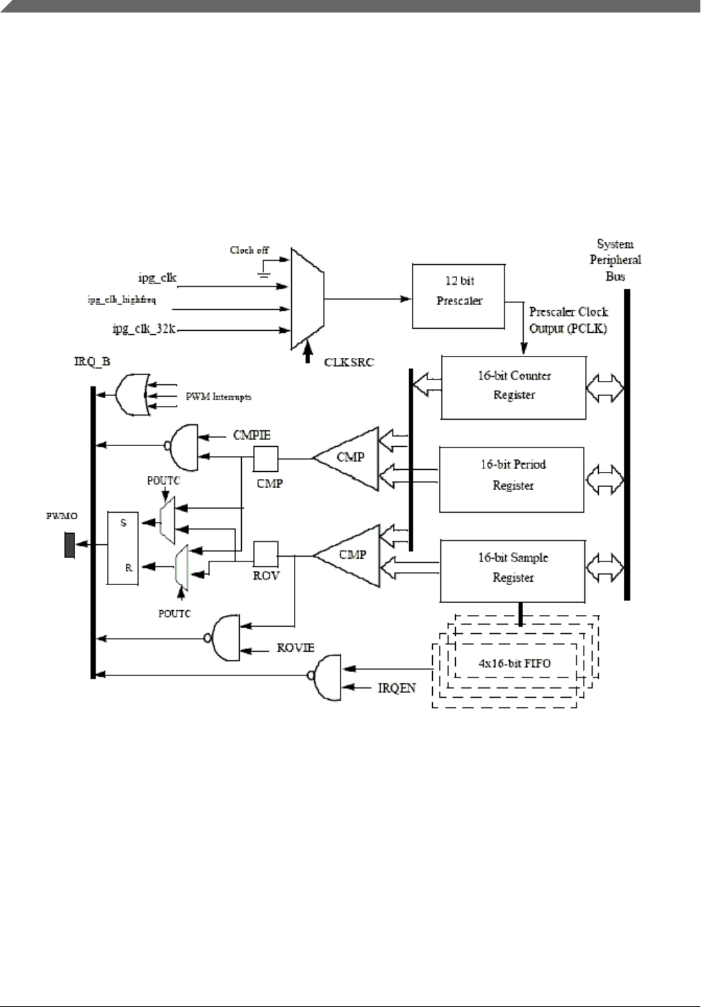
The PWM has 16-bit resolution and uses a 4x16 data FIFO to generate sound. The
software module is composed of a Linux driver that allows privileged users to control the
backlight by the appropriate duty cycle of the PWM Output (PWMO) signal.
2.5.1.1 Hardware Operation
The figure below shows the PWM block diagram.
Figure 2-2. PWM Block Diagram
The PWM follows IP Bus protocol for interfacing with the processor core. It does not
interface with any other modules inside the device except for the clock and reset inputs
from the Clock Control Module (CCM) and interrupt signals to the processor interrupt
handler. The PWM includes a single external output signal, PMWO. The PWM includes
the following internal signals:
• Three clock inputs
• Four interrupt lines
• One hardware reset line
Pulse-Width Modulator (PWM)
i.MX Reference Manual, Rev. L4.9.88_2.0.0-ga, 05/2018
76 NXP Semiconductors

• Four low power and debug mode signals
• Four scan signals
• Standard IP slave bus signals
2.5.1.2 Clocks
The clock that feeds the prescaler can be selected from:
• High frequency clock-provided by the CCM. The PWM can be run on this clock in
low power mode.
• Low reference clock - 32 KHz low reference clock provided by the CCM. The PWM
can be run on this clock in the low power mode.
• Global functional clock - for normal operations. In low power modes this clock can
be switched off.
The clock input source is determined by the CLKSRC field of the PWM control register.
The CLKSRC value should only be changed when the PWM is disabled.
2.5.2 Software Operation
The PWM device driver reduces the amount of power sent to a load by varying the width
of a series of pulses to the power source. One common and effective use of the PWM is
controlling the backlight of a QVGA panel with a variable duty cycle.
Table below provides a summary of the interface functions in source code.
Table 2-13. PWM Driver Summary
Function Description
struct pwm_device *pwm_get(struct device *dev, const char *con_id) Look up and request a PWM device
void pwm_put(struct pwm_device *pwm) Release a PWM device
int pwm_config(struct pwm_device *pwm, int duty_ns, int period_ns) Change a PWM device configuration
int pwm_enable(struct pwm_device *pwm) Start a PWM output toggling
int pwm_disable(struct pwm_device *pwm) Stop a PWM output toggling
The function pwm_config() includes most of the configuration tasks for the PWM
module, including the clock source option, period and duty cycle of the PWM output
signal. It is recommended to select the peripheral clock of the PWM module, rather than
the local functional clock, as the local functional clock can change.
Chapter 2 System
i.MX Reference Manual, Rev. L4.9.88_2.0.0-ga, 05/2018
NXP Semiconductors 77

2.5.2.1 Driver Features
The PWM driver includes the following software and hardware support:
• Duty cycle modulation
• Varying output intervals
• Two power management modes - full on and full off
2.5.2.2 Source Code Structure
Table below lists the source files and headers available in the following directories:
drivers/pwm/pwm-imx.c include/linux/pwm.h
Table 2-14. PWM Driver Files
File Description
pwm.h Functions declaration
pwm-imx.c Functions definition
2.5.2.3 Menu Configuration Options
In menu configuration enable the following module:
• Device Drivers > Pulse-Width Modulation (PWM) Support > i.MX PWM support
• Select the following option to enable the Backlight driver:
Device Drivers > Graphics support > Backlight & LCD device support > Generic
PWM based Backlight Driver
2.6 Remote Processor Messaging
2.6.1 Introduction
With the newest multicore architecture designed by using the ARM Cortex®-A series
processors and the ARM Cortex-M series processors, industrial applications can achieve
greater power efficiency for a reduced carbon footprint. This reduces power consumption
without performance deterioration.
Remote Processor Messaging
i.MX Reference Manual, Rev. L4.9.88_2.0.0-ga, 05/2018
78 NXP Semiconductors

A homogeneous SoC would traditionally run a single operating system (OS) that controls
all the memory. The OS or a hypervisor would handle task management among available
cores to maximize system utilization. Such a system is called Symmetric MultiProcessing
(SMP).
A heterogeneous multicore chip where different processing cores running different
instruction sets and different OSs. Each processing core handles a specific task as
required. Such a system is called Asymmetric Multiprocessing (AMP). To understand the
distinction between the SMP and AMP systems, it is possible for a homogeneous
multicore SoC to be an AMP system but a heterogeneous multicore SoC cannot be an
SMP system.
A multicore architecture brings new challenges to the system design, because the
software must be rewritten to distribute tasks across the available cores. In addition, all
the peripheral resources need to be properly allocated to avoid resource contention and
achieve efficient sharing of the data spaces between the cores. A multicore SoC also
needs mechanisms for reliable communication and synchronization among tasks running
on different processing cores.
RPMsg is a virtio-based messaging bus, which allows kernel drivers to communicate
with remote processors available on the system. In turn, drivers could then expose
appropriate user space interfaces if needed. Every RPMsg device is a communication
channel with a remote processor (so the RPMsg devices are called channels). Channels
are identified by a textual name and have a local ("source") RPMsg address, and remote
("destination") RPMsg address. For more information, see www.kernel.org/doc/
Documentation/rpmsg.txt.
As shown in the following figure, the messages pass between endpoints through
bidirectional connection-less communication channels.
Chapter 2 System
i.MX Reference Manual, Rev. L4.9.88_2.0.0-ga, 05/2018
NXP Semiconductors 79
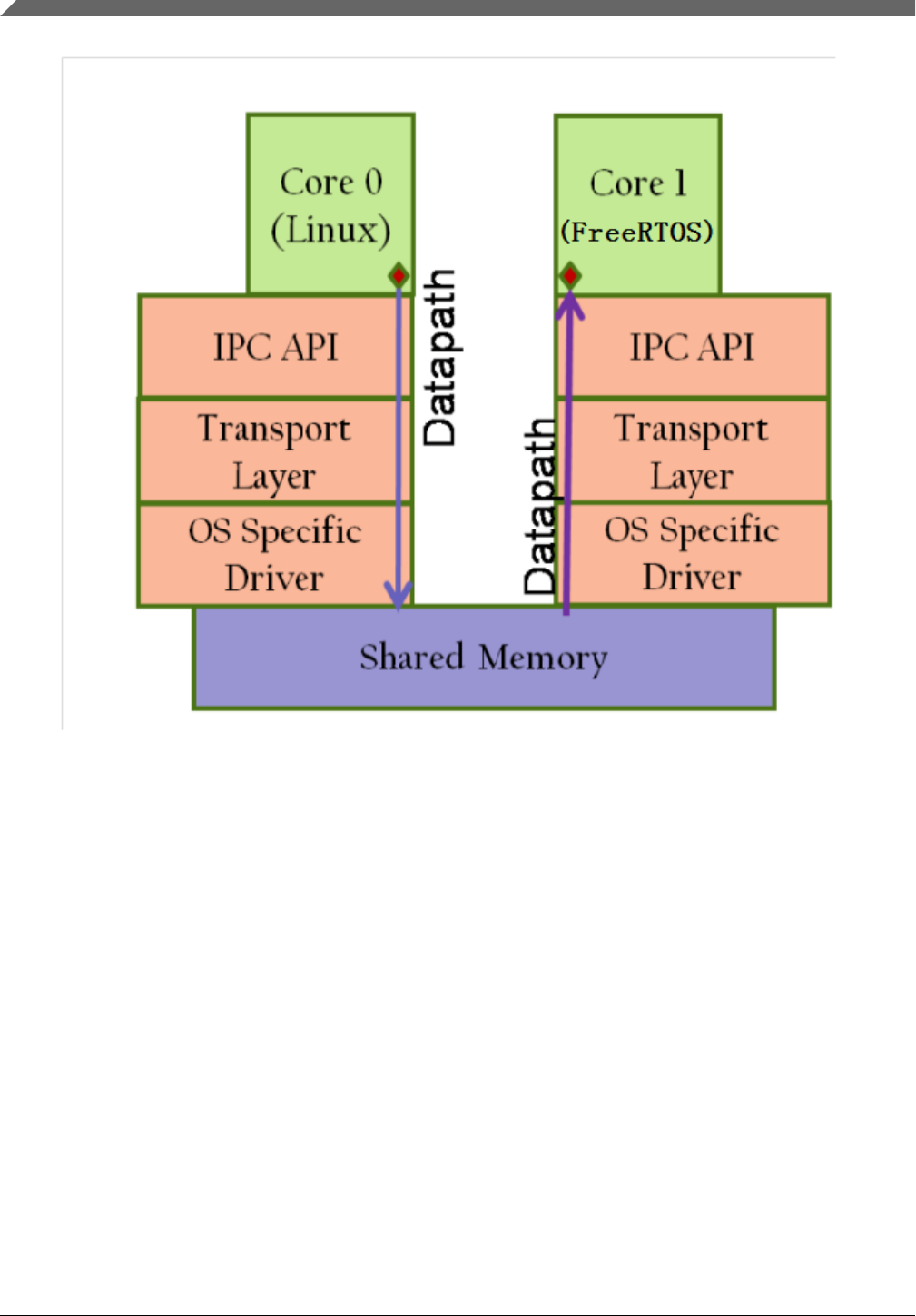
Figure 2-3. New multicore, multiOS architecture
2.6.1.1 Features
• Designed for low-latency and low overhead operation, and compliant with the Linux
RPMsg framework.
• Optimized for embedded environments with constrained CPU and memory
resources.
• Implementation by using shared memory without data translation or message
headers.
• Application communication by using a client-server methodology.
• Dynamic allocation of the RPMsg channels.
Remote Processor Messaging
i.MX Reference Manual, Rev. L4.9.88_2.0.0-ga, 05/2018
80 NXP Semiconductors

2.6.2 Source Code
• Common code:
drivers/rpmsg/virtio_rpmsg_bus.c
• i.MX platform-related code:
arch/arm/mach-imx/imx_rpmsg.c
• i.MX RPMsg ping-pong tests:
drivers/rpmsg/imx_rpmsg_pingpong.c
• i.MX RPMsg TTY driver
drivers/rpmsg/imx_rpmsg_tty.c
2.6.2.1 Kernel Configurations
For RPMSG pingpong test
Symbol: IMX_RPMSG_PINGPONG [=m]
Type : tristate
Prompt: IMX RPMSG pingpong driver
Location:
-> Device Drivers
-> Rpmsg drivers
-> RPMSG bus driver (RPMSG [=y])
For RPMSG TTY driver
Symbol: IMX_RPMSG_TTY [=m]
Type : tristate
Prompt: IMX RPMSG tty driver
Location:
-> Device Drivers
-> Rpmsg drivers
-> RPMSG bus driver (RPMSG [=y])
2.6.2.2 Running i.MX RPMsg Test Programs
To run the i.MX RPMsg test program, perform the following operations:
1. Make sure that the proper Cortex-M4 processor RTOS and Linux images are used.
For example on the i.MX 7Dual platforms:
• rpmsg_pingpong_sdk_7dsdb.bin -> ping-pong test used on the i.MX 7Dual SDB
board
• rpmsg_str_echo_sdk_7dsdb.bin -> tty string echo test used on the i.MX 7Dual
SDB board
Chapter 2 System
i.MX Reference Manual, Rev. L4.9.88_2.0.0-ga, 05/2018
NXP Semiconductors 81

• rpmsg_pingpong_sdk_7dval.bin -> ping-pong test used on the i.MX 7Dual
12x12 LPDDR3 ARM2 board
• rpmsg_str_echo_sdk_7dval.bin -> tty string echo test used on the i.MX 7Dual
12x12 LPDDR3 ARM2 board
2. Load the Cortex-M4 processor RTOS image, and kick it off in U-Boot.
Load the Cortex-M4 processor RTOS image by the TFTP server or by the bootable
SD card in U-Boot.
• Load the Cortex-M4 processor RTOS image by the TFTP server. For example,
1. Boot into U-Boot and stop.
2. Use the following command to TFTP the responding Cortex-M4 processor
RTOS image and boot it.
dhcp 0x7e0000 10.192.242.53:rpmsg_pingpong_sdk_7dval.bin; bootaux 0x7e0000
• Load the Cortex-M4 processor RTOS image by the SD card. For example,
1. Created A bootable SD card by the MFGtools. Then, copy the Cortex-M4
processor RTOS files to the first partition formatted by the VFAT file
system.
2. Change the default Cortex-M4 processor RTOS name of the U-Boot.
setenv m4image '<The name of the M4/RTOS image>';save
3. Set up a boot args used by the Cortex-M4 processor.
setenv run_m4_tcm 'if run loadm4image; then cp.b ${loadaddr} 0x7e0000 0x8000;
bootaux 0x7e0000; fi'; save
4. Modify the original bootcmd by adding run run_m4_tcm”.
setenv bootcmd "run run_m4_tcm; <original contents of the bootcmd>"; save
NOTE
“uart_from_osc” is mandatory required by i.MX 6SoloX
when the Cortex-M4 processor RTOS image is running.
Therefore, the mmcargs of U-Boot should be modified on
i.MX 6SoloX.
setenv mmcargs 'setenv bootargs console=${console},$
{baudrate} root=${mmcroot}, uart_from_osc';save
3. Run the RPMsg test program.
a. Make sure that imx_rpmsg_pingpong.ko and imx_rpmsg_tty.ko are built out.
b. Use insmod imx_rpmsg_pingpong.ko or insmod imx_rpmsg_tty.ko to run the test program.
NOTE
Do not run different test programs at the same time.
c. Run the following command and ensure that the RPMsg TTY receiving program
is running at backend when starting RPMsg TTY tests.
/unit_tests/mxc_mcc_tty_test.out /dev/ttyRPMSG30 115200 R 100 1000 &
Remote Processor Messaging
i.MX Reference Manual, Rev. L4.9.88_2.0.0-ga, 05/2018
82 NXP Semiconductors

Logs at the Linux OS side:
insmod imx_rpmsg_tty.ko
imx_rpmsg_tty rpmsg0: new channel: 0x400 -> 0x1!
Install rpmsg tty driver!
echo deadbeaf > /dev/ttyRPMSG30
imx_rpmsg_tty rpmsg0: msg(<- src 0x1) deadbeaf len 8
2.7 Thermal
2.7.1 Introduction
Thermal driver is a necessary driver for monitoring and protecting the SoC. The thermal
driver will monitor the SoC temperature in a certain frequency.
It defines two trip points: critical and passive. Cooling device will take actions to protect
the SoC according to the different trip points that SoC has reached:
• When reaching critical point, cooling device will shut down the system.
• When reaching passive point, cooling device will lower CPU frequency and notify
GPU/VPU to run at a lower frequency.
• When the temperature drops to 10 °C below passive point, cooling device will
release all the cooling actions.
Thermal driver has two parts:
• Thermal zone defines trip points and monitors the SoC's temperature.
• Cooling device takes the actions according to the different trip points.
The critical and passive points threshold are defined as follows:
• i.MX 6 and i.MX 7 platforms: drivers/thermal/imx_thermal.c
• i.MX 8QuadMax: arch/arm64/boot/dts/freescale/fsl-imx8qm.dtsi
• i.MX 8QuadXPlus: arch/arm64/boot/dts/freescale/fsl-imx8qxp.dtsi
• i.MX 8MQuad: arch/arm64/boot/dts/freescale/fsl-imx8mq.dtsi
2.7.1.1 Thermal Driver Overview
The thermal driver implements the SoC temperature monitor function and protection. It
creates a sys file interface of /sys/class/thermal/thermal_zoneX/ for user. Internally, the
thermal driver will monitor the SoC temperature and do necessary protection according to
the different trip points that SoC's temperature reaches.
Chapter 2 System
i.MX Reference Manual, Rev. L4.9.88_2.0.0-ga, 05/2018
NXP Semiconductors 83

2.7.1.2 Hardware Operation
The thermal driver uses internal thermal sensor to monitor the SoC temperature. The
cooling device uses the CPU frequency to protect the SoC.
All related modules are in the SoC.
2.7.2 Thermal Driver Software Operation
The thermal driver registers a thermal zone and a cooling device. A
structure,thermal_zone_device_ops, describes the necessary interface that the thermal
framework needs. The framework will call the related thermal zone interface to monitor
the SoC temperature and do the cooling protection.
2.7.2.1 Driver Features
The thermal driver supports the features found here.
• Thermal device monitors the SoC temperature.
• Cooling device protects the SoC when the temperature reaches passive or critical
points.
2.7.2.2 Source Code Structure
Table below shows the driver source files available in the directory:
drivers/thermal
Table 2-15. Thermal Driver Files
File Description
imx_thermal.c, device_cooling.c Thermal zone driver source file for i.MX 6 or i.MX 7
qoriq_thermal.c, device_cooling.c Thermal zone driver source files for i.MX 8MQuad
2.7.2.3 Menu Configuration Options
In menu configuration enable the following module:
Thermal
i.MX Reference Manual, Rev. L4.9.88_2.0.0-ga, 05/2018
84 NXP Semiconductors

• For i.MX6 and i.MX7: Device Drivers > Generic Thermal sysfs driver >
Temperature sensor driver for i.MX SoCs.
• For i.MX 8QuadMax and i.MX 8QuadXPlus: Device Drivers > Generic Thermal
sysfs driver > thermal sensor driver for NXP i.MX8 SoCs
2.7.2.4 Programming Interface
The thermal driver can be accessed through /sys/bus/platform/drivers/imx_thermal/ for
i.MX 6 and i.MX 7 platforms, through /sys/bus/platform/drivers/i.MX-sc-tsens/thermal-
sensor/ for i.MX 8QuadMax and i.MX 8QuadXPlus platforms, and through /sys/bus/
platform/drivers/qoriq_thermal/ for i.MX 8MQuad.
2.8 Sensors
2.8.1 Introduction
Sensors include a group of drivers for Accelerometer, Ambient Light, and Magnetometer.
i.MX supports accelerometers for the following SoC:
• i.MX 6SABRE-SD and i.MX 6SoloX use the MMX8451 sensor
• i.MX 6 SoloLite uses the MMX8450 sensor.
• i.MX 6UltraLite and 6ULL EVK use the FXLS8571Q seneor.
• i.MX 7Dual SABRE-SD uses the FX0S8700CQR1 sensor.
i.MX Supports ambient light sensor for the following SoC:
• i.MX supports the ISL29023 sensor on i.MX 6 SABRE and 6 SoloX.
i.MX supports magnetometer sensors for the following SoC:
• i.MX 6 SABRE, 6SoloLite, and 6SoloX supports the MAG3110FCR2 sensor.
• i.MX 6UltraLite EVK supports the FXLS8471 sensor.
• i.MX 7Dual supports the MPL3115A2, FXOs8700CQR1 and FXAS21002CQR1
sensors.
2.8.1.1 Hardware Operation
Chapter 2 System
i.MX Reference Manual, Rev. L4.9.88_2.0.0-ga, 05/2018
NXP Semiconductors 85

2.8.2 Sensor Driver Software Operation
2.8.2.1 Source Code Structure
Table below shows the driver source files available in the directory:
Table 2-16. Sensor Driver Files
File Description
drivers/hwmon/mxc_mma8451.c Acceleromater Sensor
drivers/input/misc/isl29023.c Ambient Light Sensor
drivers/hwmon/mag3110.c Magnetometer Sensor
2.8.2.2 Menu Configuration Options
2.9 Watchdog (WDOG)
2.9.1 Introduction
The Watchdog Timer module protects against system failures by providing an escape
from unexpected hang or infinite loop situations or programming errors.
Some platforms may have two WDOG modules with one of them having interrupt
capability.
On i.MX 8QuadMax and i.MX 8QuadXPlus, the software watchdog used in SCFW and
kernel call those interfaces by virtual watchdog driver imx8_wdt.c
2.9.1.1 Hardware Operation
After the WDOG timer is activated, it must be serviced by software on a periodic basis.
If servicing does not take place in time, the WDOG times out. Upon a time-out, the
WDOG either asserts the wdog_b signal or a wdog_rst_b system reset signal, depending
on software configuration. The watchdog module cannot be deactivated after it is
activated.
Watchdog (WDOG)
i.MX Reference Manual, Rev. L4.9.88_2.0.0-ga, 05/2018
86 NXP Semiconductors

2.9.2 Software Operation
The Linux OS has a standard WDOG interface that allows support of a WDOG driver for
a specific platform.
WDOG can be suspended/resumed in STOP/DOZE and WAIT modes independently.
Since some bits of the WDOG registers are only one-time programmable after booting,
ensure these registers are written correctly.
2.9.2.1 Generic WDOG
The generic WGOD driver is implemented in the drivers/watchdog/imx2_wdt.c file.
It provides functions for various IOCTLs and read/write calls from the user level program
to control the WDOG.
2.9.2.2 Driver Features
This WDOG implementation includes the following features:
• Generates the reset signal if it is enabled but not serviced within a predefined timeout
value (defined in milliseconds in one of the WDOG source files)
• Does not generate the reset signal if it is serviced within a predefined timeout value
• Provides IOCTL/read/write required by the standard WDOG subsystem
2.9.2.3 Source Code Structure
Table below shows the source files for WDOG drivers that are in the following directory:
drivers/watchdog
Table 2-17. WDOG Driver Files
File Description
imx2_wdt.c, imx8_wdt.c WDOG function implementations
Watchdog system reset function is located under arch/arm/mach-imx/system.c
2.9.2.4 Menu Configuration Options
In menu configuration enable the following module:
Chapter 2 System
i.MX Reference Manual, Rev. L4.9.88_2.0.0-ga, 05/2018
NXP Semiconductors 87

Device Drivers > Watchdog Timer Support > IMX2+ Watchdog
Device Drivers > Watchdog Timer Support > IMX8 Watchdog
2.9.2.5 Programming Interface
The following IOCTLs are supported in the WDOG driver:
• WDIOC_GETSUPPORT
• WDIOC_GETSTATUS
• WDIOC_GETBOOTSTATUS
• WDIOC_KEEPALIVE
• WDIOC_SETTIMEOUT
• WDIOC_GETTIMEOUT
For detailed descriptions about these IOCTLs, see Documentation/watchdog.
Watchdog (WDOG)
i.MX Reference Manual, Rev. L4.9.88_2.0.0-ga, 05/2018
88 NXP Semiconductors

Chapter 3
Storage
3.1 AHB-to-APBH Bridge with DMA (APBH-Bridge-DMA)
3.1.1 Overview
The AHB-to-APBH bridge provides the processor with an inexpensive peripheral
attachment bus running on the AHB's HCLK. The H in APBH denotes that the APBH is
synchronous to HCLK.
The AHB-to-APBH bridge includes the AHB-to-APB PIO bridge for a memory-mapped
I/O to the APB devices, as well as a central DMA facility for devices on this bus and a
vectored interrupt controller for the ARM core. Each one of the APB peripherals,
including the vectored interrupt controller, is documented in their own chapters elsewhere
in this document.
There is no separate DMA bus for these devices. Contention between the DMA's use of
the APBH bus and the AHB-to-APB bridge functions' use of the APBH is mediated by an
internal arbitration logic. For contention between these two units, the DMA is favored
and the AHB slave will report "not ready" through its HREADY output until the bridge
transfer can complete. The arbiter tracks repeated lockouts and inverts the priority,
guaranteeing the ARM platform every fourth transfer on the APB
3.1.1.1 Hardware Operation
The SDMA controller is responsible for transferring data between the MCU memory
space and peripherals and includes the following features.
• Multichannel DMA supporting up to 32 time-division multiplexed DMA channels
• Powered by a 16-bit Instruction-Set micro-RISC engine
• Each channel executes a specific script
• Very fast context-switching with two-level priority based preemptive multitasking
i.MX Reference Manual, Rev. L4.9.88_2.0.0-ga, 05/2018
NXP Semiconductors 89

• 4 Kbytes ROM containing startup scripts (that is, boot code) and other common
utilities that can be referenced by RAM-located scripts
• 8 Kbyte RAM area is divided into a processor context area and a code space area
used to store channel scripts that are downloaded from the system memory.
3.1.2 Software Operation
The DMA supports sixteen channels of DMA services, as shown in the following table.
The shared DMA resource allows each independent channel to follow a simple chained
command list. Command chains are built up using the general structure.
Table 3-1. APBH DMA Channel Assignments
APBH DMA CHANNEL # USAGE
0 GPMI0
1 GPMI1
2 GPMI2
3 GPMI3
4 GPMI4
5 GPMI5
6 GPMI6
7 GPMI7
8 EMPTY
9 EMPTY
10 EMPTY
11 EMPTY
12 EMPTY
13 EMPTY
14 EMPTY
15 EMPTY
3.1.2.1 Source Code Structure
The table below shows the source files available in the directory, drivers/dma/
Table 3-2. APBH DMA Source Files
File Description
mxs-dma.c APBH DMA implement driver
AHB-to-APBH Bridge with DMA (APBH-Bridge-DMA)
i.MX Reference Manual, Rev. L4.9.88_2.0.0-ga, 05/2018
90 NXP Semiconductors

3.1.2.2 Menu Configuration Options
The following Linux kernel configuration option is provided for this module:
• MXS_DMA -This is the configuration option for the APBH DMA driver. In
menuconfig, this option is available under:
• Device Drivers > DMA Engine support > MXS DMA support.
3.1.2.3 Programming Interface
The module implements standard DMA API. See the API documents, which are located
in the Linux documentation package, for more information on the functions implemented
in the driver such as GPMI NAND driver.
3.1.3 Usage Example
See one of the drivers, such as GPMI NAND driver, that uses the APBH DMA driver for
a usage example.
3.2 EIM NOR
3.2.1 Introduction
The External Interface Module (EIM) NOR driver supports the Parallel NOR flash.
3.2.1.1 Hardware Operation
By default, there is a parallel NOR in the i.MX 6Quad/6Dual SABRE-AI boards. The
parallel NOR has more pins than the SPI NOR. On some boards, the
M29W256GL7AN6E is equipped. Refer to the datasheet for details on the parallel NOR.
3.2.2 Software Operation
Similar to the SPI NOR, the parallel NOR uses the MTD subsystem. Because the parallel
NOR is very small, you may only use the jffs2 but cannot use the UBIFS for it.
Chapter 3 Storage
i.MX Reference Manual, Rev. L4.9.88_2.0.0-ga, 05/2018
NXP Semiconductors 91

3.2.2.1 Source Code
To set the proper timing only for the parallel NOR, refer to drivers/bus/imx-weim.c.
3.2.2.2 Enabling the EIM NOR
Refer to the DTS file to enable the EIM NOR: imx6q-sabreauto-gpmi-weim.dts or
imx6dl-sabreauto-gpmi-weim.dts.
3.3 MMC/SD/SDIO Host
3.3.1 Introduction
The MultiMediaCard (MMC)/ Secure Digital (SD)/ Secure Digital Input Output (SDIO)
Host driver implements a standard Linux driver interface to the ultra MMC/SD host
controller (uSDHC).
The host driver is part of the Linux kernel MMC framework.
The MMC driver has the following features:
• 1-bit or 4-bit operation for SD3.0 and SDIO 2.0 cards (so far we support SDIO v2.0
(AR6003 is verified)).
• Supports card insertion and removal detections.
• Supports the standard MMC commands.
• PIO and DMA data transfers.
• Supports power management.
• Supports 1/4 8-bit operations for MMC cards.
• For i.MX 6, USDHC supports eMMC4.4 SDR and DDR modes.
• For i.MX 7Dual, USDHC supports eMMC5.0, which includes HS400 and HS200.
• Supports SD3.0 SDR50 and SDR104 modes.
3.3.1.1 Hardware Operation
The MMC communication is based on an advanced 11-pin serial bus designed to operate
in a low voltage range. The uSDHC module supports MMC along with SD memory and
I/O functions. The uSDHC controls the MMC, SD memory, and I/O cards by sending
MMC/SD/SDIO Host
i.MX Reference Manual, Rev. L4.9.88_2.0.0-ga, 05/2018
92 NXP Semiconductors

commands to cards and performing data accesses to and from the cards. The SD memory
card system defines two alternative communication protocols: SD and SPI. The uSDHC
only supports the SD bus protocol.
The uSDHC command transfer type and uSDHC command argument registers allow a
command to be issued to the card. The uSDHC command, system control, and protocol
control registers allow the users to specify the format of the data and response and to
control the read wait cycle.
There are four 32-bit registers used to store the response from the card in the uSDHC.
The uSDHC reads these four registers to get the command response directly. The uSDHC
uses a fully configurable 128x32-bit FIFO for read and write. The buffer is used as
temporary storage for data being transferred between the host system and the card, and
vice versa. The uSDHC data buffer access register bits hold 32-bit data upon a read or
write transfer.
For receiving data, the steps are as follows:
1. The uSDHC controller generates a DMA request when there are more words
received in the buffer than the amount set in the RD_WML register
2. Upon receiving this request, DMA engine starts transferring data from the uSDHC
FIFO to system memory by reading the data buffer access register.
For transmitting data, the steps are as follows:
1. The uSDHC controller generates a DMA request whenever the amount of the buffer
space exceeds the value set in the WR_WML register.
2. Upon receiving this request, the DMA engine starts moving data from the system
memory to the uSDHC FIFO by writing to the Data Buffer Access Register for a
number of pre-defined bytes.
The read-only uSDHC Present State and Interrupt Status Registers provide uSDHC
operations status, application FIFO status, error conditions, and interrupt status.
When certain events occur, the module has the ability to generate interrupts as well as set
the corresponding Status Register bits. The uSDHC interrupt status enable and signal-
enable registers allow the user to control if these interrupts occur.
3.4 NAND GPMI Flash
Chapter 3 Storage
i.MX Reference Manual, Rev. L4.9.88_2.0.0-ga, 05/2018
NXP Semiconductors 93

3.4.1 Introduction
The NAND Flash Memory Technology Devices (MTD) driver is used in the Generic-
Purpose Media Interface (GPMI) controller on the i.MX 6 series and i.MX 7Dual.
Only the hardware-specific layer has to be implemented for the NAND MTD driver to
operate.
The rest of the functionality such as Flash read/write/erase is automatically handled by
the generic layer provided by the Linux MTD subsystem for NAND devices.
The NAND MTD driver interfaces with the integrated NAND controller supporting file
systems, such as UBIFS, CRAMFS and JFFS2UBI and UBIFSCRAMFS and JFFS2. The
driver implementation supports the lowest level operations on the external NAND Flash
chip, such as block read, block write and block erase as the NAND Flash technology only
supports block access. Because blocks in a NAND Flash are not guaranteed to be good,
the NAND MTD driver is also able to detect bad blocks and feed that information to the
upper layer to handle bad block management.
3.4.1.1 Hardware Operation
NAND Flash is a nonvolatile storage device used for embedded systems.
Driver does not support random accesses of memory as in the case of RAM or NOR
Flash. Reading or writing to NAND Flash must be done through the GPMI. NAND Flash
is a sequential access device appropriate for mass storage applications. Code stored on
NAND Flash cannot be executed from there. Code must be loaded into RAM memory
and executed from there. The i.MX 6 contains a hardware error-correcting block.
3.4.2 Software Operation
MTDs in Linux covers all memory devices such as RAM, ROM, and different kinds of
NOR/NAND Flashes.
The MTD subsystem provides uniform access to all such devices. Above the MTD
devices there could be either MTD block device emulation with a Flash file system
(JFFS2) or a UBI layer. The UBI layer in turn, can have either UBIFS above the volumes
or a Flash Translation Layer (FTL) with a regular file system (FAT, Ext2/3) above it. The
hardware-specific driver interfaces with the GPMI module on the i.MX 6. It implements
the lowest level operations such as read, write and erase. If enabled, it also provides
information about partitions on the NAND device-this information has to be provided by
platform code.
NAND GPMI Flash
i.MX Reference Manual, Rev. L4.9.88_2.0.0-ga, 05/2018
94 NXP Semiconductors

The NAND driver is the point where read/write errors can be recovered if possible.
Hardware error correction is performed by BCH blocks and is driven by NAND drivers
code.
Detailed information about NAND driver interfaces can be found at www.linux-
mtd.infradead.org.
3.4.2.1 Basic Operations: Read/Write
The NAND driver exports the following callbacks:
gpmi_ecc_read_page (with ECC)
gpmi_ecc_write_page (with ECC)
gpmi_read_byte (without ECC)
gpmi_read_buf (without ECC)
gpmi_write_buf (without ECC)
gpmi_ecc_read_oob (with ECC)
gpmi_ecc_write_oob (with ECC)
Since Kernel 4.1, the GPMI driver provides raw read/write modes, which exports these
callbacks:
• gpmi_ecc_read_page_raw (without ECC)
• gpmi_ecc_write_page_raw (without ECC)
• gpmi_ecc_read_oob_raw (without ECC)
• gpmi_ecc_write_oob_raw (without ECC)
These functions read the requested amount of data, with or without error correction. In
the case of read, the gpmi_read_page() function is called, which creates the DMA chain,
submits it to execute, and waits for completion. The write case is a bit more complex: the
data to be written is mapped and flushed out by calling gpmi_send_page().
3.4.2.2 Backward Compatibility
Users should know several major GPMI NAND driver changes in kernel 4.1, which may
cause incompatibility in Kernel upgrade.
• Exported necessary information to user space application (kobs-ng) through debugfs
• New BCH layout algorithm
• New raw read/write mode
In Kernel 4.1, the NAND GPMI driver exports necessary information to the upper layer
through debugfs. The most common case is for the NAND burning tool, kobs-ng.
Without enabling debugfs, kobs-ng may not fully use the new feature or may use
Chapter 3 Storage
i.MX Reference Manual, Rev. L4.9.88_2.0.0-ga, 05/2018
NXP Semiconductors 95

inappropriate parameters. The user needs to provide the correct BCH geometry
information and raw access mode to kobs-ng, if debugfs is not enabled in the customized
kernel.
BCH layout in the previous kernel may not meet the NAND chip minimum ECC
requirement. Since Kernel 4.1, the BCH layout algorithm, by default, uses the NAND
required ECC strength and step size, which are acquired from ONFI parameters, if it is
accessible. The change may not be compatible with the BCH layout settings in the
previous kernel. For backward compatibility, Kernel and U-boot provide switches to use
legacy BCH layout.
• For Kernel, add "fsl,legacy-bch-geometry" in the device tree file.
• For U-Boot, add "CONFIG_NAND_MXS_BCH_LEGACY_GEO" in the board
configuration file.
BCH legacy layout setting must be turned on/off simultaneously in both Kernel and U-
boot for alignment.
Kobs-ng checks either the Kernel version or raw mode flag in debugfs to determine
whether to use new raw mode to access the NAND chip. New kobs-ng fully backward is
compatible with the previous Kernel, while the old version kobs-ng cannot work on
Kernel 4.1.
3.4.2.3 Error Correction
When reading or writing data to Flash, some bits can be flipped. This is normal behavior,
and NAND drivers utilize various error correcting schemes to correct this. It could be
resolved with software or hardware error correction. The GPMI driver uses only a
hardware correction scheme with the help of an hardware accelerator-BCH.
For BCH, the page laylout of 2K page is (2k + 64), the page layout of 4K page is (4k +
218) the page layout of 8K page is (8K + 448).
3.4.2.4 Boot Control Block Management
During startup, the NAND driver scans the first block for the presence of a NAND
Control Block (NCB). Its presence is detected by magic signatures. When a signature is
found, the boot block candidate is checked for errors using Hamming code. If errors are
found, they are fixed, if possible. If the NCB is found, it is parsed to retrieve timings for
the NAND chip.
All boot control blocks are created when formatting the medium using the user space
application kobs-ng .
NAND GPMI Flash
i.MX Reference Manual, Rev. L4.9.88_2.0.0-ga, 05/2018
96 NXP Semiconductors

3.4.2.5 Bad Block Handling
When the driver begins, by default, it builds the bad block table. It is possible to
determine if a block is bad, dynamically, but to improve performance it is done at boot
time. The badness of the erase block is determined by checking a pattern in the beginning
of the spare area on each page of the block. However, if the chip uses hardware error
correction, the bad marks falls into the ECC bytes area. Therefore, if hardware error
correction is used, the bad block mark should be moved.
3.4.2.6 Source Code Structure
The NAND driver is located in the drivers/mtd/nand/ directory.
The following files are included in the NAND driver:
bch-regs.h
gpmi-lib.c
gpmi-nand.c
gpmi-nand.h
gpmi-regs.h
Makefile
3.4.2.7 Menu Configuration Options
To enable the NAND driver, the following options must be set:
• CONFIG_IMX_HAVE_PLATFORM_GPMI_NAND= [Y]
• CONFIG_MTD_NAND_GPMI_NAND= [Y | M]
In addition, these MTD options must be enabled:
• CONFIG_MTD_NAND = [y | m]
• CONFIG_MTD = y
• CONFIG_MTD_PARTITIONS = y
• CONFIG_MTD_CHAR = y
• CONFIG_MTD_BLOCK = y
In addition, these UBI options must be enabled:
• CONFIG_MTD_UBI=y
• CONFIG_MTD_UBI_WL_THRESHOLD=4096
• CONFIG_MTD_UBI_BEB_RESERVE=1
• CONFIG_UBIFS_FS=y
Chapter 3 Storage
i.MX Reference Manual, Rev. L4.9.88_2.0.0-ga, 05/2018
NXP Semiconductors 97

• CONFIG_UBIFS_FS_LZO=y
• CONFIG_UBIFS_FS_ZLIB=y
3.5 Quad Serial Peripheral Interface (QuadSPI)
3.5.1 Introduction
The Quad Serial Peripheral Interface (QuadSPI) block acts as an interface to one single or
two external serial flash devices, each with up to four bidirectional data lines.
It supports the following features:
• Flexible sequence engine to support various flash vendor devices.
• Single, dual, quad and octal mode of operation.
• DDR/DTR mode wherein the data is generated on every edge of the serial flash
clock.
• Support for flash data strobe signal for data sampling in DDR and SDR mode.
• DMA support to read RX Buffer data via AMBA AHB bus (64-bit width interface)
or IP registers space (32-bit access).
3.5.1.1 Hardware Operation
On some boards, the Quad SPI NOR - N25Q256A is equipped, while on some other
boards S25FL128S is equipped. Check the Quad SPI NOR type on the boards and then
configure it properly.
The N25Q256A is a high-performance multiple input/output serial Flash memory device.
The innovative, high-performance, dual and quad input/output instructions enable double
or quadruple the transfer bandwidth for READ and PROGRAM operations. The memory
is organized as 512 (64 KB) main sectors and can be erased 64 KB sectors at a time. The
device features 3-byte or 4-byte address modes to access memory beyond 128 MB. When
4-byte address mode is enabled, all commands requiring an address must be entered and
exited with a 4-byte address mode command: ENTER 4-BYTE ADDRESS MODE
command and EXIT 4-BYTE ADDRESS MODE command. The 4-byte address mode
can also be enabled through the nonvolatile configuration register. The memory can be
operated with three different protocols:Extended SPI (standard SPI protocol upgraded
with dual and quad operations), Dual I/O SPI and Quad I/O SPI. Each protocol contains
unique commands to perform READ operations in DTR mode. This enables high data
throughput while running at lower clock frequencies.
Quad Serial Peripheral Interface (QuadSPI)
i.MX Reference Manual, Rev. L4.9.88_2.0.0-ga, 05/2018
98 NXP Semiconductors
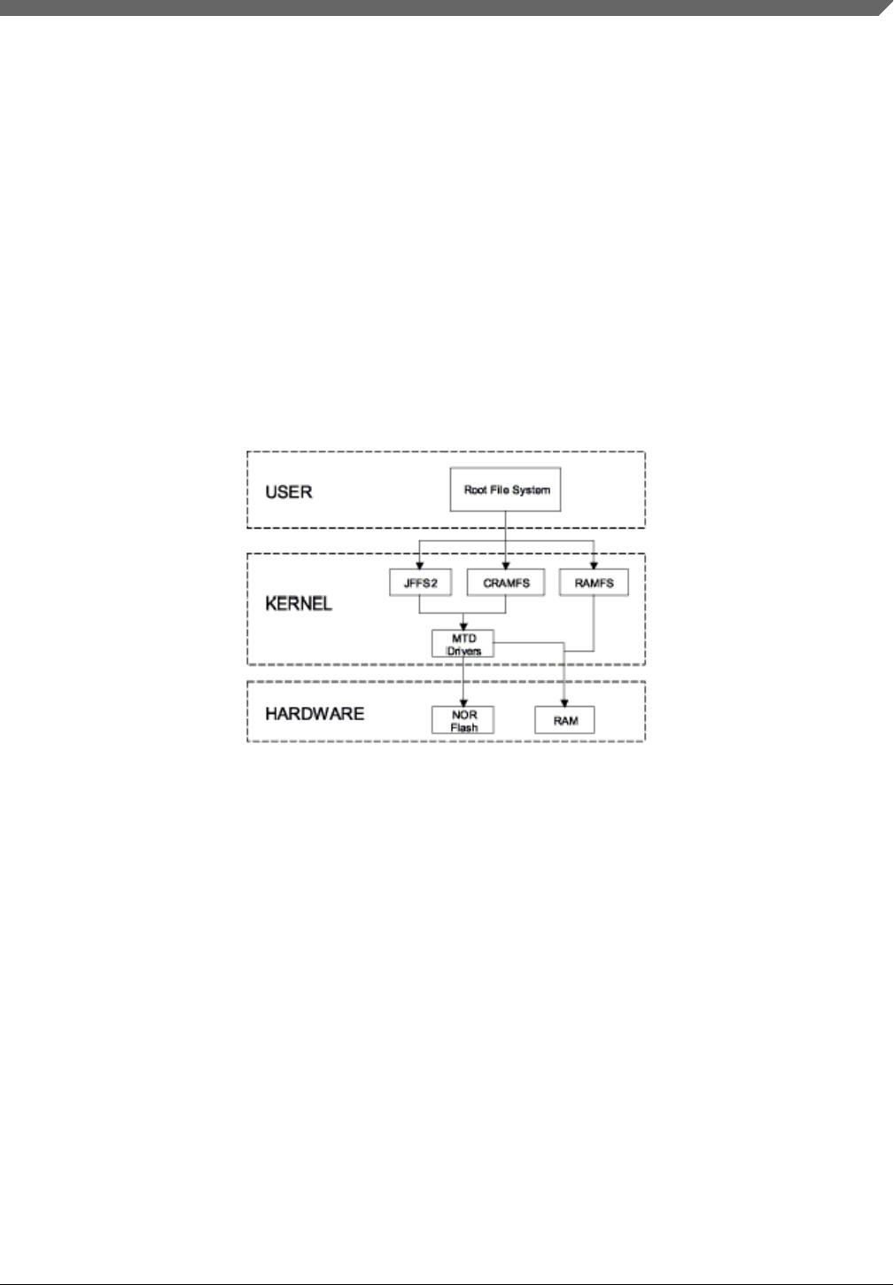
The S25FL128S device is flash non-volatile memory product. It connects to a host
system via a Serial Peripheral Interface (SPI). Traditional SPI single bit serial input and
output (SIngle I/O or SIO) is supported as well as optional two bit (Dual I/O or DIO) and
four bit (Quad I/O or QIO) serial commands. It also adds support for Double Data Rate
(DDR) read commands for SIO, DIO, and QIO that transfer address and read data on
both edges of the clock.
3.5.2 Software Operation
In a Flash-based embedded Linux system, a number of Linux technologies work together
to implement a file system. The following figure illustrates the relationships between
some of the standard components.
Figure 3-1. Components of a Flash-Based File System
The MTD subsystem for Linux OS is a generic interface to memory devices, such as
Flash and RAM, providing simple read, write, and erase access to physical memory
devices. Devices called mtdblock devices can be mounted by JFFS, JFFS2, and
CRAMFS file systems. The Quad SPI NOR MTD driver is based on the MTD data Flash
driver in the kernel by adding SPI access. In the initialization phase, the Quad SPI NOR
MTD driver detects a data Flash by reading the JEDEC ID. Then the driver adds the
MTD device. The SPI NOR MTD driver also provides the interfaces to read, write, and
erase NOR Flash.
3.5.2.1 Driver Features
This Quad NOR driver implementation supports the following feature:
• Provides necessary information for the upper-layer MTD driver.
Chapter 3 Storage
i.MX Reference Manual, Rev. L4.9.88_2.0.0-ga, 05/2018
NXP Semiconductors 99

3.5.2.2 Source Code Structure
The Quad SPI NOR driver is implemented in the following directory:
drivers/mtd/spi-nor/
Table below shows the driver file:
Table 3-3. SPI NOR MTD Driver File
File Description
spi-nor.c Source file, spi-nor framework
fsl-quadspi.c Source file, FSL Quad SPI Driver
3.5.2.3 Menu Configuration Options
To enable the Quad SPI driver, the following options must be set:
• CONFIG_MTD_SPI_NOR_BASE: This is the framework for the SPI NOR which
can be used by the SPI device drivers and the SPI-NOR device driver.
• CONFIG_SPI_FSL_QUADSPI: This enables support for the Quad SPI controller in
master mode.
3.6 SATA
3.6.1 Introduction
The SATA AHCI driver is based on the LIBATA layer of the block device infrastructure
of the Linux kernel. The detailed hardware operation of SATA is detailed in the
Synopsys DesignWare Cores SATA AHCI documentation, named
SATA_Data_Book.pdf.
3.6.1.1 Board Configuration Options
With the power off, install the SATA cable and hard drive.
SATA
i.MX Reference Manual, Rev. L4.9.88_2.0.0-ga, 05/2018
100 NXP Semiconductors

3.6.2 Software Operation
The details about the libata APIs, see the libATA Developer's Guide.
The SATA AHCI driver is based on the LIBATA layer of the block device infrastructure
of the Linux kernel. i.MX integrated AHCI linux driver combined the standard AHCI
drivers handle the details of the integrated i.MX SATA AHCI controller, while the
LIBATA layer understands and executes the SATA protocols. The SATA device, such as
a hard disk, is exposed to the application in user space by the /dev/sda* interface.
Filesystems are built upon the block device. The AHCI specified integrated DMA engine,
which assists the SATA controller hardware in the DMA transfer modes.
3.6.2.1 Source Code Structure Configuration
The source code of the i.MX AHCI SATA driver is located in the following folder:
<kernel_dir>/drivers/ata/ahci_imx.c
The standard AHCI and AHCI platform drivers are used to do the actual SATA
operations.
The source code of the standard AHCI and AHCI platform drivers are located in drivers/
ata/ folder, named as ahci.c and ahci-platform.c.
3.6.2.2 Menu Configuration Options
The following Linux kernel configurations are provided for SATA driver:
Symbol: AHCI_IMX
[=y]
Type :
tristate
Prompt: Freescale i.MX AHCI SATA
support
Location:
-> Device
Drivers
-> Serial ATA and Parallel ATA drivers (ATA
[=y])
-> Platform AHCI SATA support (SATA_AHCI_PLATFORM
[=y])
In busybox, enable "fdisk" under "Linux System Utilities".
Chapter 3 Storage
i.MX Reference Manual, Rev. L4.9.88_2.0.0-ga, 05/2018
NXP Semiconductors 101

3.6.2.3 Programming Interface
The application interface to the SATA driver is the standard POSIX device interface (for
example: open, close, read, write, and ioctl) on /dev/sda*.
3.6.2.4 Usage Example
NOTE
There may be a known error message when few kinds of SATA
disks are initialized, such as:
ata1.00: serial number mismatch '090311PB0300QKG3TB1A' !
= ''
ata1.00: revalidation failed (errno=-19)
This should be ignored.
1. After building the kernel and the SATA AHCI driver and deploying, boot the target,
and log in as root.
2. Make sure that the AHCI and AHCI platform drivers are built in the kernel or loaded
into the kernel.
You should see messages similar to the following:
ahci: SSS flag set, parallel bus scan disabled
ahci ahci: AHCI 0001.0300 32 slots 1 ports 3 Gbps 0x1 impl platform mode
ahci ahci: flags: ncq sntf stag pm led clo only pmp pio slum part ccc apst
scsi0 : ahci_platform
ata1: SATA max UDMA/133 mmio [mem 0x02200000-0x02203fff] port 0x100 irq 71
ata1: SATA link up 3.0 Gbps (SStatus 123 SControl 300)
ata1.00: ATA-8: SAMSUNG HM100UI, 2AM10001, max UDMA/133
ata1.00: 1953525168 sectors, multi 0: LBA48 NCQ (depth 31/32)
ata1.00: configured for UDMA/133
scsi 0:0:0:0: Direct-Access ATA SAMSUNG HM100UI 2AM1 PQ: 0 ANSI: 5
sd 0:0:0:0: [sda] 1953525168 512-byte logical blocks: (1.00 TB/931 GiB)
sd 0:0:0:0: [sda] 4096-byte physical blocks
sd 0:0:0:0: [sda] Write Protect is off
sd 0:0:0:0: [sda] Write cache: enabled, read cache: enabled, doesn't support DPO or FUA
sda: sda1
sd 0:0:0:0: [sda] Attached SCSI disk
You may use standard Linux utilities to partition and create a file system on the drive (for
example: fdisk and mke2fs) to be mounted and used by applications.
The device nodes for the drive and its partitions appears under /dev/sda*. For example, to
check basic kernel settings for the drive, execute hdparm /dev/sda.
SATA
i.MX Reference Manual, Rev. L4.9.88_2.0.0-ga, 05/2018
102 NXP Semiconductors

3.6.2.5 Usage Example
Create Partitons
The following command can be used to find out the capacities of the hard disk. If the
hard disk is pre-formatted, this command shows the size of the hard disk, partitions, and
filesystem type:
$fdisk -l /dev/sda
If the hard disk is not formatted, create the partitions on the hard disk using the following
command:
$fdisk /dev/sda
After the partition, the created files resemble /dev/sda[1-4].
Block Read/Write Test: The command, dd, is used for for reading/writing blocks. Note
this command can corrupt the partitions and filesystem on Hard disk.
To clear the first 5 KB of the card, do the following:
$dd if=/dev/zero of=/dev/sda1 bs=1024 count=5
The response should be as follows:
5+0 records in
5+0 records out
To write a file content to the card enter the following text, substituting the name of the
file to be written for file_name, do the following:
$dd if=file_name of=/dev/sda1
To read 1KB of data from the card enter the following text, substituting the name of the
file to be written for output_file, do the following:
$dd if=/dev/sda1 of=output_file bs=1024 count=1
Files System Tests
Format the hard disk partitons using mkfs.vfat or mkfs.ext2, depending on the filesystem:
$mkfs.ext2 /dev/sda1
$mkfs.vfat /dev/sda1
Mount the file system as follows:
$mkdir /mnt/sda1
$mount -t ext2 /dev/sda1 /mnt/sda1
Chapter 3 Storage
i.MX Reference Manual, Rev. L4.9.88_2.0.0-ga, 05/2018
NXP Semiconductors 103

After mounting, file/directory, operations can be performed in /mnt/sda1.
Unmount the filesystem as follows:
$umount /mnt/sda1
3.7 Smart Direct Memory Access (SDMA) API
3.7.1 Overview
The Smart Direct Memory Access (SDMA) API driver controls the SDMA hardware.
It provides an API to other drivers for transferring data between MCU memory space and
the peripherals. It supports the following features:
• Loading channel scripts from the MCU memory space into SDMA internal RAM
• Loading context parameters of the scripts
• Loading buffer descriptor parameters of the scripts
• Controlling execution of the scripts
• Callback mechanism at the end of script execution
3.7.1.1 Hardware Operation
The SDMA controller is responsible for transferring data between the MCU memory
space and peripherals and includes the following features:
• Multichannel DMA supporting up to 32 time-division multiplexed DMA channels.
• Powered by a 16-bit Instruction-Set micro-RISC engine.
• Each channel executes specific script.
• Very fast context-switching with two-level priority based preemptive multitasking.
• 4 Kbytes ROM containing startup scripts (that is, boot code) and other common
utilities that can be referenced by RAM-located scripts.
• 8 Kbyte RAM area is divided into a processor context area and a code space area
used to store channel scripts that are downloaded from the system memory.
Smart Direct Memory Access (SDMA) API
i.MX Reference Manual, Rev. L4.9.88_2.0.0-ga, 05/2018
104 NXP Semiconductors

3.7.2 Software Operation
The driver provides an API for other drivers to control SDMA channels. SDMA channels
run dedicated scripts according to peripheral and transfer types. The SDMA API driver is
responsible for loading the scripts into SDMA memory, initializing the channel
descriptors, and controlling the buffer descriptors and SDMA registers.
The table below provides a list of drivers that use SDMA and the number of SDMA
physical channels used by each driver. A driver can specify the SDMA channel number
that it wishes to use, static channel allocation, or can have the SDMA driver provide a
free SDMA channel for the driver to use, dynamic channel allocation. For dynamic
channel allocation, the list of SDMA channels is scanned from channel 32 to channel 1.
When a free channel is found, that channel is allocated for the requested DMA transfers.
Table 3-4. SDMA Channel Usage
Driver Name Number of
SDMA Channels
SDMA Channel Used
SDMA CMD 1 Static Channel allocation-uses SDMA channels 0
SSI 2 per device Dynamic channel allocation
UART 2 per device Dynamic channel allocation
SPDIF 2 per device Dynamic channel allocation
ESAI 2 per device Dynamic channel allocation
3.7.2.1 Source Code Structure
The dmaengine.h (header file for SDMA API) is available in the directory linux/include/
linux
The following table shows the source files available in the directory drivers/dma.
Table 3-5. SDMA API Source Files
File Description
dmaengine.c SDMA management routine
imx-sdma.c SDMA implement driver
The following table shows the image files available in the directory firmware/imx/sdma.
Table 3-6. SDMA Script Files
File Description
sdma-mx6q-to1.bin.ihex SDMA RAM scripts
Chapter 3 Storage
i.MX Reference Manual, Rev. L4.9.88_2.0.0-ga, 05/2018
NXP Semiconductors 105

3.8 SPI NOR Flash Memory Technology Device (MTD)
3.8.1 Introduction
The SPI NOR Flash Memory Technology Device (MTD) driver provides the support to
the data Flash though the SPI interface.
By default, the SPI NOR Flash MTD driver creates static MTD partitions to support data
Flash.
3.8.1.1 Hardware Operation
On some boards, the SPI NOR - AT45DB321D is equipped, while on some boards
M25P32 is equipped. Check the SPI NOR type on the boards and then configure it
properly.
The AT45DB321D is a 2.7 V, serial-interface sequential access Flash memory. The
AT45DB321D serial interface is SPI compatible for frequencies up to 66 MHz. The
memory is organized as 8,192 pages of 512 bytes or 528 bytes. The AT45DB321D also
contains two SRAM buffers of 512/528 bytes each which allow receiving of data while a
page in the main memory is being reprogrammed, as well as writing a continuous data
stream.
The M25P32 is a 32 Mbit (4M x 8) Serial Flash memory, with advanced write protection
mechanisms, accessed by a high-speed SPI-compatible bus up to 75 MHz. The memory
is organized as 64 sectors, each containing 256 pages. Each page is 256 bytes wide.
Therefore, the whole memory can be viewed as consisting of 16384 pages, or 4,194,304
bytes. The memory can be programmed 1 to 256 bytes at a time using the Page Program
instruction. The whole memory can be erased using the Bulk Erase instruction, or a sector
at a time, using the Sector Erase instruction.
Unlike conventional Flash memories that are accessed randomly, these two SPI NOR
access data sequentially. They operate from a single 2.7-3.6 V power supply for program
and read operations. They are enabled through a chip select pin and accessed through a
three-wire interface: Serial Input, Serial Output, and Serial Clock.
SPI NOR Flash Memory Technology Device (MTD)
i.MX Reference Manual, Rev. L4.9.88_2.0.0-ga, 05/2018
106 NXP Semiconductors
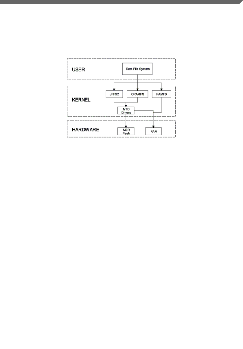
3.8.2 Software Operation
In a Flash-based embedded Linux system, a number of Linux technologies work together
to implement a file system. The figure below illustrates the relationships between some of
the standard components.
Figure 3-2. Components of a Flash-Based File System
The MTD subsystem for Linux OS is a generic interface to memory devices, such as
Flash and RAM, providing simple read, write, and erase access to physical memory
devices. Devices called mtdblock devices can be mounted by JFFS, JFFS2 and CRAMFS
file systems. The SPI NOR MTD driver is based on the MTD data Flash driver in the
kernel by adding SPI access. In the initialization phase, the SPI NOR MTD driver detects
a data Flash by reading the JEDEC ID. Then the driver adds the MTD device. The SPI
NOR MTD driver also provides the interfaces to read, write, and erase NOR Flash.
3.8.2.1 Driver Features
This NOR MTD implementation supports the following features:
• Provides necessary information for the upper layer MTD driver
3.8.2.2 Source Code Structure
The SPI NOR MTD driver is implemented in the following directory:
drivers/mtd/devices/
The following table shows the driver files:
Chapter 3 Storage
i.MX Reference Manual, Rev. L4.9.88_2.0.0-ga, 05/2018
NXP Semiconductors 107

Table 3-7. SPI NOR MTD Driver Files
File Description
m25p80.c Source file
3.8.2.3 Menu Configuration Options
In menu configuration enable the following module:
• CONFIG_MTD_M25P80: This config enables access to most modern SPI flash
chips, used for program and data storage.
• Device Drivers > Memory Technology Device (MTD) support >Self-contained MTD
device drivers > Support most SPI Flash chips (AT26DF, M25P, W25X, and so on)
SPI NOR Flash Memory Technology Device (MTD)
i.MX Reference Manual, Rev. L4.9.88_2.0.0-ga, 05/2018
108 NXP Semiconductors

Chapter 4
Connectivity
4.1 ADC
4.1.1 ADC Introduction
The features of the ADC-Digital are as follows:
• Two 12-bit ADCs
• Linear successive approximation algorithm with up to 12-bit resolution with 10/11
bit accuracy
• Up to 1 MS/s sampling rate
• Up to 8 single-ended external analog inputs
• Single or continuous conversion (automatic return to idle after single conversion)
• Output Modes: (in right-justified unsigned format)
• 12-bit
• 10-bit
• 8-bit
• Configurable sample time and conversion speed/power
• Conversion complete and hardware average complete flag and interrupt
• Input clock selectable from up to four sources
• Asynchronous clock source for lower noise operation with option to output the clock
• Selectable asynchronous hardware conversion trigger with hardware channel select
• Selectable voltage reference, Internal, External, or Alternate
• Operation in low power modes for lower noise operation
• Hardware average function
• Self-calibration mode
4.1.1.1 ADC External Signals
• ADC_VREFH: Voltage reference high
i.MX Reference Manual, Rev. L4.9.88_2.0.0-ga, 05/2018
NXP Semiconductors 109

• ADC_VREHL: Voltage reference low
• ADC1_IN0: Analog channel 1 input 0
• ADC1_IN1: Analog channel 1 input 1
• ADC1_IN2: Analog channel 1 input 2
• ADC1_IN3: Analog channel 1 input 3
• ADC2_IN0: Analog channel 2 input 0
• ADC2_IN1: Analog channel 2 input 1
• ADC2_IN2: Analog channel 2 input 2
• ADC2_IN3: Analog channel 2 input 3
The ADC pin settings should be done in the ADCx_PCTL register. No other extra
IOMUX settings are required.
4.1.2 ADC Driver Overview
The ADC driver is developed under the Linux IIO (Industrial I/O) driver frame. The
ADC driver only provides the basic functions. The following features are supported:
• Four external inputs for each ADC controller channel
• 12 bit ADC
• Single conversion
• Hardware average
• Low power mode of ADC
• Sample rate changes in the available sample rate group
4.1.2.1 ADC Driver File
The ADC driver file is drivers/iio/adc/vf610_adc.c for i.MX 6UltraLite and i.MX
6SoloX, drivers/iio/adc/imx7d_adc.c for i.MX 7Dual.
4.1.2.2 Menu Configuration Options
Configure the kernel option to enable the module by menuconfig:
Device Drivers > Industrial I/O support > Analog to digital converters > i.MX 7Dual
ADC driver
Device Drivers > Industrial I/O support> Analog to digital converters > Freescale vf610
ADC driver
ADC
i.MX Reference Manual, Rev. L4.9.88_2.0.0-ga, 05/2018
110 NXP Semiconductors

4.1.2.3 Programming Interface
Linux IIO provides some system interface to get the raw ADC data from the related
input. Users can also set the sample rate in the available sample rate group. The ADC
controllers system interface is located:
/sys/devices/soc0/soc.1/2200000.aips-bus/2280000.adc/iio:device0:
/sys/devices/soc0/soc.1/2200000.aips-bus/2284000.adc/iio:device1:
The following table lists the software interfaces.
Table 4-1. Software Interfaces
Software interface Description
in_voltage0_raw~ in_voltage3_raw cat in_voltage0_raw to get raw ADC data
sampling_frequency_available cat sampling_frequency_available to get available sample
rate group
in_voltage_sampling_frequency cat in_voltage_sampling_frequency to show current
sample rate
echo value > in_voltage_sampling_frequency to set the
sample rate
4.2 Bluetooth QCA9377-3 and QCA6174
4.2.1 Bluetooth Wireless Technology Introduction
Bluetooth technology is low-cost, low-power, short-range wireless technology. It was
designed as a replacement for cables and other short-range technologies like IrDA.
Bluetooth wireless technology operates in personal area range that typically extends up to
10 meters. For more information about Bluetooth wireless technology, see
www.bluetooth.com/.
Chapter 4 Connectivity
i.MX Reference Manual, Rev. L4.9.88_2.0.0-ga, 05/2018
NXP Semiconductors 111

4.2.1.1 Introduction
For i.MX 7ULP, the officially supported Wi-Fi chip with our BSP is Murata 1PJ module
based on Qualcomm QCA9377-3. The QCA9377-3 is a single-die wireless local area
network (WLAN) and Bluetooth (BT) combination solution to support 1 × 1 IEEE
802.11a/b/g/n/ac WLAN standards and BT 4.1 + HS, enabling seamless integration of
LAN/BT and lowenergy technology.
For i.MX 8MQuad, the officially supported Wi-Fi chip with our BSP is Murata 1CQ
module based on Qualcomm QCA6174. The QCA6174 is a single-die wireless local area
network (WLAN) and Bluetooth combo solution to support 2 x 2 multi-user multiple
input, multiple output (MU-MIMO) with two spatial streams IEEE802.11 a/b/g/n/ac
WLAN standards and Bluetooth 4.2 + HS, designed to deliver superior integration of
WLAN/Bluetooth and low energy technology.
4.2.2 Software Operation
4.2.2.1 Bluetooth Driver Overview
FSL BSP uses the open source Bluetooth driver. The Bluetooth software is divided into
four parts as follows:
• 4-wire UART and TTY driver: It is the communication interface with the Bluetooth
module.
• Bluetooth HCI device driver: UART (H4) is a serial protocol for communication
between the Bluetooth device and host. This protocol is required for most Bluetooth
devices with the UART interface.
• Bluetooth kernel stack: Bluetooth framework and protocols implementation.
• Bluetooth user stack: Supplies several user-space utilities and integrate many profiles
for use cases.
4.2.2.2 Bluetooth Driver Files
The Bluetooth driver source files are available in the kernel source directory.
• Bluetooth HCI device driver:
• drivers/bluetooth/hci_h4.c
• drivers/bluetooth/hci_ldisc.c
• Bluetooth kernel stack:
• net/bluetooth/*
Bluetooth QCA9377-3 and QCA6174
i.MX Reference Manual, Rev. L4.9.88_2.0.0-ga, 05/2018
112 NXP Semiconductors

4.2.2.3 Bluetooth Stack
BlueZ is the official Linux standard Bluetooth protocol stack, it is the latest version of 5.x
and it is a Bluetooth stack for Linux kernel-based family of operating systems. Its goal is
to program an implementation of the Bluetooth wireless standards specifications for
Linux. To use Linux Bluetooth subsystem, you need several user-space utilities like
hciconfig and bluetoothd. These utilities and updates to Bluetooth kernel modules are
provided in the BlueZ packages. For more information, see www.bluez.org/.
BlueZ source code are available in the git: git://git.kernel.org/pub/scm/bluetooth/
bluez.git. The current BSP package tests pass with BlueZ 5.49.
4.2.2.4 Menu Configuration Options
The following Linux kernel configuration option is provided for this module:
• UART interface:
• CONFIG_SERIAL_IMX
• CONFIG_TTY
• HCI interface:
• CONFIG_BT_HCIUART
• CONFIG_BT_HCIUART_H4
• Bluetooth Stack:
• CONFIG_BT
• CONFIG_BT_RFCOMM
• CONFIG_BT_RFCOMM_TTY
• CONFIG_BT_BNEP
• CONFIG_BT_BNEP_MC_FILTER
• CONFIG_BT_BNEP_PROTO_FILTER
• CONFIG_BT_HIDP
4.3 ENET IEEE-1588
4.3.1 Introduction
ENET IEEE-1588 driver performs a set of functions that enabling precise
synchronization of clocks in network communication.
The driver requires a protocol stack to complete IEEE-1588 full protocol. It complies
with the LinuxPTP stack.
Chapter 4 Connectivity
i.MX Reference Manual, Rev. L4.9.88_2.0.0-ga, 05/2018
NXP Semiconductors 113
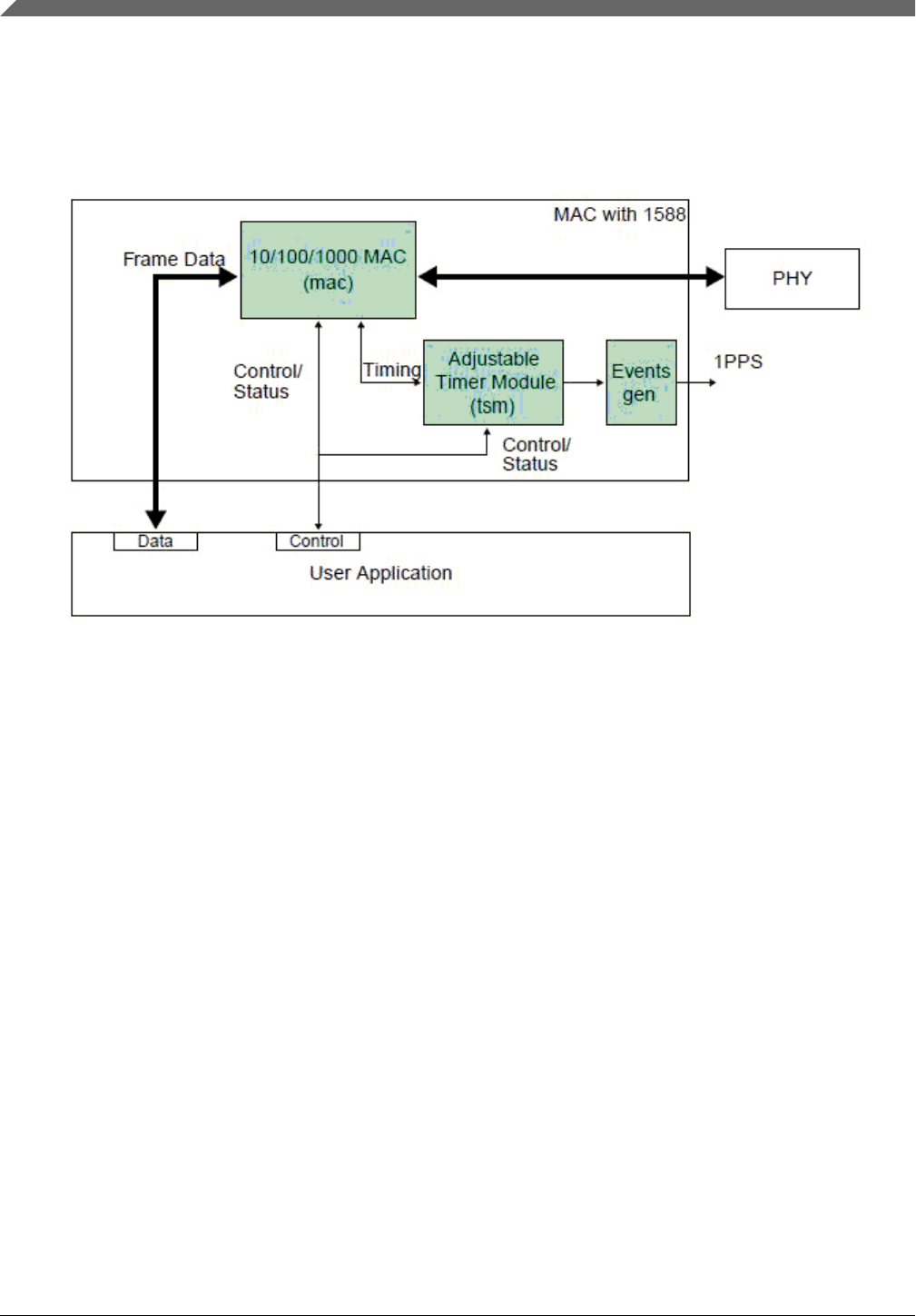
To allow for IEEE 1588 or similar time synchronization protocol implementations, the
ENET MAC is combined with a time-stamping module to support precise time stamping
of incoming and outgoing frames.
Figure 4-1. IEEE 1588 Functions Overview
4.3.1.1 Transmit Timestamping
On transmit, only 1588 event frames need to be time-stamped. The Client application (for
example, the MAC driver) should detect 1588 event frames and set the signal
ff_tx_ts_frm together with the frame.
For every transmitted frame, the MAC returns the captured timestamp on tx_ts (31:0)
with the frame sequence number (tx_ts_id(3:0)) and the transmit status. The transmit
status bit tx_ts_stat (5) indicates that the application had the ff_tx_ts_frm signal asserted
for the frame.
If ff_tx_ts_frm is set to '1', the MAC additionally memorizes the timestamp for the frame
in the register TS_TIMESTAMP. The interrupt bit EIR (TS_AVAIL) is set to indicate
that a new timestamp is available.
Software would implement a handshaking procedure by setting the ff_tx_ts_frm signal
when it transmits the frame it needs a timestamp for and then waits on the EIR
(TS_AVAIL) interrupt bit to know when the timestamp is available. It then can read the
ENET IEEE-1588
i.MX Reference Manual, Rev. L4.9.88_2.0.0-ga, 05/2018
114 NXP Semiconductors

timestamp from the TS_TIMESTAMP register. This is done for all event frames; other
frames do not use the ff_tx_ts_frm indicator and hence do not interfere with the
timestamp capture.
4.3.1.2 Receive Timestamping
When a frame is received, the MAC latches the value of the timer when the frame SFD
field is detected and provides the captured timestamp on ff_rx_ts(31:0). This is done for
all received frames.
The DMA controller has to ensure that it transfers the timestamp provided for the frame
into the corresponding field within the receive descriptor for software access.
4.3.2 Software Operation
The 1588 Driver has the functions listed below:
• Module initialization-Initializes the module with the device-specific structure, and
registers a character driver.
• Interrupt servicing routine-Supports events, such as TS_AVAIL, TS_TIMER. The
driver shares interrupt servicing routine with FEC driver.
4.3.2.1 Source Code Structure
Table below lists the source files available in the drivers/net/ethernet/freescale/ directory.
Table 4-2. ENET 1588 File List
File Description
fec.h Header file defining registers
fec_ptp.c Linux driver for ENET 1588 timer
For more information about the generic Linux driver, see the drivers/net/ethernet/
freescale/fec_ptp.c source file.
4.3.2.2 Menu Configuration Options
By default, ENET 1588 is enabled.
Chapter 4 Connectivity
i.MX Reference Manual, Rev. L4.9.88_2.0.0-ga, 05/2018
NXP Semiconductors 115

4.3.2.3 Programming Interface
The 1588 driver complies with the Linuxptp protocol stack interface.
Stack-specific defines are added to the header file (fec.h).
4.3.3 1588 Stack Support
The 1588 driver supports Linuxptp protocol stack.
4.3.3.1 1588 Stack Introduction
This release supports the following type of the 1588 Stack:
• Linuxptp stack
This software is an implementation of the Precision Time Protocol (PTP) according
to IEEE standard 1588 for Linux OS. The dual design goals are to provide a robust
implementation of the standard and to use the most relevant and modern Application
Programming Interfaces (API) offered by the Linux OS kernel. Supporting legacy
APIs and other platforms is not a goal. The software is copyrighted by the authors
and is licensed under the GNU General Public License.
The software development is hosted at Source Forge: sourceforge.net/projects/linuxptp/
4.3.3.2 Linuxptp Stack Features
Linuxptp support the following features:
• Ordinary/Boundary Clock
• Best master clock algorithm
• Transport over UDP/IPv4, UDP/IPv6, and IEEE 802.3
• Transparent clock (E2E/P2P)
• Slave only
• Supporting IEEE 802.1AS-2011 in the role of end station
ENET IEEE-1588
i.MX Reference Manual, Rev. L4.9.88_2.0.0-ga, 05/2018
116 NXP Semiconductors

4.3.3.3 How to Use the Stacks in Linux OS
In Linux OS, run 1588 stack binary with the following commands.
Linuxptp:
Transport on UDP IPV4 with E2E delay mechanism: ptp4l -A -4 -H -m -i eth0
Transport on UDP IPV4 with P2P delay mechanism: ptp4l -P -A -4 -H -m -i eth0
Transport on UDP IPV6 with E2E delay mechanism: ptp4l -A -6 -H -m -i eth0
Transport on UDP IPV6 with P2P delay mechanism: ptp4l -P -A -6 -H -m -i eth0
Transport on IEEE 802.3 with E2E delay mechanism: ptp4l -A -2 -H -m -i eth0
Transport on IEEE 802.3 with P2P delay mechanism: ptp4l -P -A -2 -H -m -i eth0
4.4 Enhanced Configurable Serial Peripheral Interface
(ECSPI)
4.4.1 Introduction
The ECSPI driver implements a standard Linux driver interface to the ECSPI controllers.
It supports the following features:
• Interrupt-driven transmit/receive of bytes
• Multiple master controller interface
• Multiple slaves select
• Multiclient requests
4.4.1.1 Hardware Operation
ECSPI is used for fast data communication with fewer software interrupts than
conventional serial communications.
Each ECSPI is equipped with a data FIFO and is a master/slave configurable serial
peripheral interface module, allowing the processor to interface with external SPI master
or slave devices.
The primary features of the ECSPI includes:
• Master/slave-configurable
• Four chip select signals to support multiple peripherals
• Up to 32-bit programmable data transfer
• 64 x 32-bit FIFO for both transmit and receive data
• Configurable polarity and phase of the Chip Select (SS) and SPI Clock (SCLK)
Chapter 4 Connectivity
i.MX Reference Manual, Rev. L4.9.88_2.0.0-ga, 05/2018
NXP Semiconductors 117
4.4.2 Software Operation
The following sections describe the ECSPI software operation.
4.4.2.1 SPI Sub-System in Linux OS
The ECSPI driver layer is located between the client layer (SPI-NOR Flash are examples
of clients) and the hardware access layer. The figure below shows the block diagram for
SPI subsystem in Linux OS.
The SPI requests go into I/O queues. Requests for a given SPI device are executed in
FIFO order and they complete asynchronously through completion callbacks. There are
also some simple synchronous wrappers for those calls including the ones for common
transaction types such as writing a command and then reading its response.
SPI-NOR
mtd driver Client #2 driver .... Client #3 driver
SPI Subsystem
ECSPI Hardware
SPI-NOR Flash Client #2 Client #3
....
Figure 4-2. SPI Subsystem
All SPI clients must have a protocol driver associated with them and they all must be
sharing the same controller driver. Only the controller driver can interact with the
underlying SPI hardware module. The figure below shows how the different SPI drivers
are layered in the SPI subsystem.
Enhanced Configurable Serial Peripheral Interface (ECSPI)
i.MX Reference Manual, Rev. L4.9.88_2.0.0-ga, 05/2018
118 NXP Semiconductors
SPI client Driver
SPI Core Driver
ECSPI Controller Driver
ECSPI Controller
SPI Slave
(SPI-NOR Flash)
Client Driver Interface
Controller Driver Interace
FSL ECSPI driver
(spi_imx.c)
SPI Bus Interface
Electrical Interface
SPI slave driver
SPI core driver
ECSPI host
controller driver
SPI slave device
Figure 4-3. Layering of SPI Drivers in SPI Subsystem
4.4.2.2 Software Limitations
The ECSPI driver limitations are as follows:
• Does not currently have SPI slave logic implementation
• Does not support a single client connected to multiple masters
• Does not currently implement the user space interface with the help of the device
node entry but supports sysfs interface
4.4.2.3 Standard Operations
The ECSPI driver is responsible for implementing standard entry points for init, exit, chip
select, and transfer. The driver implements the following functions:
• Init function spi_imx_init() registers the device_driver structure.
• Probe function spi_imx_probe() performs initialization and registration of the SPI
device-specific structure with SPI core driver. The driver probes for memory and
IRQ resources. Configures the IOMUX to enable ECSPI I/O pins, requests for IRQ
and resets the hardware.
• Chip select function spi_imx_chipselect() configures the hardware ECSPI for the
current SPI device. Sets the word size, transfer mode, data rate for this device.
• SPI transfer function spi_imx_transfer() handles data transfers operations.
• SPI setup function spi_imx_setup() initializes the current SPI device.
• SPI driver ISR spi_imx_isr() is called when the data transfer operation is completed
and an interrupt is generated.
Chapter 4 Connectivity
i.MX Reference Manual, Rev. L4.9.88_2.0.0-ga, 05/2018
NXP Semiconductors 119
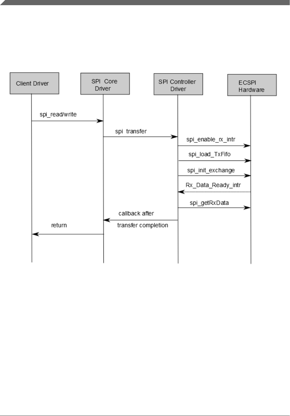
4.4.2.4 ECSPI Synchronous Operation
The figure below shows how the ECSPI provides synchronous read/write operations.
Figure 4-4. ECSPI Synchronous Operation
4.4.2.5 Driver Features
The ECSPI module supports the following features:
• Implements each of the functions required by a ECSPI module to interface to Linux
OS
• Multiple SPI master controllers
• Multiclient synchronous requests
Enhanced Configurable Serial Peripheral Interface (ECSPI)
i.MX Reference Manual, Rev. L4.9.88_2.0.0-ga, 05/2018
120 NXP Semiconductors

4.4.2.6 Source Code Structure
Table below shows the source files available in the devices directory:
drivers/spi/
Table 4-3. CSPI Driver Files
File Description
spi_imx.c SPI Master Controller driver
4.4.2.7 Menu Configuration Options
In menu configuration enable the following module:
• CONFIG_SPI build support for the SPI core. In menuconfig, this option is available
under:
• Device Drivers > SPI Support.
• CONFIG_BITBANG is the Library code that is automatically selected by drivers
that need it. SPI_IMX selects it. In menuconfig, this option is available under:
• Device Drivers > SPI Support > Utilities for Bitbanging SPI masters.
• CONFIG_SPI_IMX implements the SPI master mode for ECSPI. In menuconfig, this
option is available under:
• Device Drivers > SPI Support > Freescale i.MX SPI controllers.
4.4.2.8 Programming Interface
This driver implements all the functions that are required by the SPI core to interface
with the ECSPI hardware.
For more information, see the Linux document generated from build: make htmldocs.
4.4.2.9 Interrupt Requirements
The SPI interface generates interrupts.
ECSPI interrupt requirements are listed in table below.
Table 4-4. ECSPI Interrupt Requirements
Parameter Equation Typical Worst Case
BaudRate/ Transfer Length (BaudRate/(TransferLength)) * (1/Rxtl) 31250 1500000
Chapter 4 Connectivity
i.MX Reference Manual, Rev. L4.9.88_2.0.0-ga, 05/2018
NXP Semiconductors 121

The typical values are based on a baud rate of 1 Mbps with a receiver trigger level (Rxtl)
of 1 and a 32-bit transfer length. The worst-case is based on a baud rate of 12 Mbps (max
supported by the SPI interface) with a 8-bits transfer length.
4.5 Fast Ethernet Controller (FEC)
4.5.1 Introduction
The Fast Ethernet Controller (FEC) driver performs the full set of IEEE 802.3/Ethernet
CSMA/CD media access control and channel interface functions.
The FEC requires an external interface adapter and transceiver function to complete the
interface to the Ethernet media. It supports half or full-duplex operation on 10 Mbps, 100
Mbps, and 1000 Mbps-related Ethernet networks.
The FEC driver supports the following features:
• Full/Half duplex operation
• Link status change detect
• Auto-negotiation (determines the network speed and full or half-duplex operation)
• Transmits features such as automatic retransmission on collision and CRC generation
• Obtaining statistics from the device such as transmit collisions
The network adapter can be accessed through the ifconfig command with interface name
ethx. The driver auto-probes the external adaptor (PHY device).
4.5.1.1 Hardware Operation
The FEC is an Ethernet controller that interfaces the system to the LAN network.
The FEC supports different standard MAC-PHY (physical) interfaces for connection to
an external Ethernet transceiver. The FEC supports the 10/100 Mbps MII, 10/100 Mbps
RMII, and 10/100/1000 Mbps RGMII. In addition, the FEC supports 1000 Mbps RGMII,
which uses 4-bit reduced GMII operating at 125 MHz.
A brief overview of the device functionality is provided here. For details, see the FEC
chapter of the Applications Processor Reference Manual
In MII mode, there are 18 signals defined by the IEEE 802.3 standard and supported by
the EMAC. MII, RMII and RGMII modes uses a subset of the 18 signals. These signals
are listed in table below.
Fast Ethernet Controller (FEC)
i.MX Reference Manual, Rev. L4.9.88_2.0.0-ga, 05/2018
122 NXP Semiconductors

Table 4-5. Pin Usage in MII, RMII and RGMII Modes
Direction EMAC Pin Name RMII Usage RGMII Usage (not supported by i.MX 6SoloLite or
i.MX 6UltraLite)
In/Out FEC_MDIO Management Data Input/
output
Management Data Input/Output
Out FEC_MDC General output Management Data Clock
Out FEC_TXD[0] Data out, bit 0 Data out, bit 0
Out FEC_TXD[1] Data out, bit 1 Data out, bit 1
Out FEC_TXD[2] Not Used Data out, bit 2
Out FEC_TXD[3] Not Used Data out, bit 3
Out FEC_TX_EN Transmit Enable Transmit Enable
Out FEC_TX_ER Not Used Not Used
In FEC_CRS Not Used Not Used
In FEC_COL Not Used Not Used
In FEC_TX_CLK Not Used Synchronous clock reference (REF_CLK, can connect
from PHY)
In FEC_RX_ER Receive Error Not Used
In FEC_RX_CLK Not Used Synchronous clock reference (REF_CLK, can connect
from PHY)
In FEC_RX_DV Receive Data Valid and
generate CRS
RXDV XOR RXERR on the falling edge of
FEC_RX_CLK.
In FEC_RXD[0] Data in, bit 0 Data in, bit 0
In FEC_RXD[1] Data in, bit 1 Data in, bit 1
In FEC_RXD[2] Not Used Data in, bit 2
In FEC_RXD[3] Not Used Data in, bit 3
The MII management interface consists of two pins, FEC_MDIO, and FEC_MDC. The
FEC hardware operation can be divided in the parts listed below. For details, see the
Applications Processor Reference Manuals.
• Transmission-The Ethernet transmitter is designed to work with almost no
intervention from software. Once ECR[ETHER_EN] is asserted and data appears in
the transmit FIFO, the Ethernet MAC is able to transmit onto the network. When the
transmit FIFO fills to the watermark (defined by the TFWR), the MAC transmit logic
asserts FEC_TX_EN and starts transmitting the preamble (PA) sequence, the start
frame delimiter (SFD), and then the frame information from the FIFO. However, the
controller defers the transmission if the network is busy (FEC_CRS asserts).
• Before transmitting, the controller waits for carrier sense to become inactive, then
determines if carrier sense stays inactive for 60 bit times. If the transmission begins
after waiting an additional 36 bit times (96 bit times after carrier sense originally
became inactive), both buffer (TXB) and frame (TXF) interrupts may be generated as
determined by the settings in the EIMR.
Chapter 4 Connectivity
i.MX Reference Manual, Rev. L4.9.88_2.0.0-ga, 05/2018
NXP Semiconductors 123

• Reception-The FEC receiver is designed to work with almost no intervention from
the host and can perform address recognition, CRC checking, short frame checking,
and maximum frame length checking. When the driver enables the FEC receiver by
asserting ECR[ETHER_EN], it immediately starts processing receive frames. When
FEC_RX_DV asserts, the receiver checks for a valid PA/SFD header. If the PA/SFD
is valid, it is stripped and the frame is processed by the receiver. If a valid PA/SFD is
not found, the frame is ignored. In MII mode, the receiver checks for at least one
byte matching the SFD. Zero or more PA bytes may occur, but if a 00 bit sequence is
detected prior to the SFD byte, the frame is ignored.
• After the first six bytes of the frame have been received, the FEC performs address
recognition on the frame. During reception, the Ethernet controller checks for various
error conditions and once the entire frame is written into the FIFO, a 32-bit frame
status word is written into the FIFO. This status word contains the M, BC, MC, LG,
NO, CR, OV, and TR status bits, and the frame length. Receive Buffer (RXB) and
Frame Interrupts (RXF) may be generated if enabled by the EIMR register. When the
receive frame is complete, the FEC sets the L bit in the RxBD, writes the other frame
status bits into the RxBD, and clears the E bit. The Ethernet controller next generates
a maskable interrupt (RXF bit in EIR, maskable by RXF bit in EIMR), indicating that
a frame has been received and is in memory. The Ethernet controller then waits for a
new frame.
• Interrupt management-When an event occurs that sets a bit in the EIR, an interrupt is
generated if the corresponding bit in the interrupt mask register (EIMR) is also set.
The bit in the EIR is cleared if a one is written to that bit position; writing zero has
no effect. This register is cleared upon hardware reset. These interrupts can be
divided into operational interrupts, transceiver/network error interrupts, and internal
error interrupts. Interrupts which may occur in normal operation are GRA, TXF,
TXB, RXF, RXB. Interrupts resulting from errors/problems detected in the network
or transceiver are HBERR, BABR, BABT, LC, and RL. Interrupts resulting from
internal errors are HBERR and UN. Some of the error interrupts are independently
counted in the MIB block counters. Software may choose to mask off these interrupts
as these errors are visible to network management through the MIB counters.
• PHY management-phylib was used to manage all the FEC PHY-related operation
such as PHY discovery, link status, and state machine.MDIO bus will be created in
FEC driver and registered into the system. See Documentation/networking/phy.txt
under the Linux OS source directory for more information.
4.5.2 Software Operation
The FEC driver supports the following functions:
Fast Ethernet Controller (FEC)
i.MX Reference Manual, Rev. L4.9.88_2.0.0-ga, 05/2018
124 NXP Semiconductors

• Module initialization-Initializes the module with the device-specific structure
• Rx/Tx transmition
• Interrupt servicing routine
• PHY management
• FEC management such init/start/stop
• i.MX 6 FEC module use little-endian format
4.5.2.1 Source Code Structure
The table below shows the source files.
They are available at the drivers/net/ethernet/freescale/ directory.
Table 4-6. FEC Driver Files
File Description
fec.h Header file defining registers
fec_main.c Linux driver for Ethernet LAN controller
fec_fixup.c Linux driver for SoC and PHY special implement
For more information about the generic Linux driver, see the drivers/net/ethernet/
freescale/fec_main.c source file.
4.5.2.2 Menu Configuration Options
Configure the kernel to provide for this module:
• CONFIG_FEC is provided for this module. This option is available under:
• Device Drivers > Network device support > Ethernet (10, 100 or 1000 Mbit) >
FEC Ethernet controller.
• To mount NFS-rootfs through FEC, disable the other Network config in the
menuconfig if need.
4.5.2.3 Programming Interface
Table 4-6 lists the source files for the FEC driver.
The following section shows the modifications that were required to the original Ethernet
driver source for porting it to the i.MX device.
Chapter 4 Connectivity
i.MX Reference Manual, Rev. L4.9.88_2.0.0-ga, 05/2018
NXP Semiconductors 125

4.5.2.3.1 Device-Specific Definitions
Device-specific defines are added to the header file (fec.h) and they provide common
board configuration options.
fec.h defines the struct for the register access and the struct for the buffer descriptor. For
example,
/*
* Define the buffer descriptor structure.
*/
struct bufdesc {
unsigned short cbd_datlen; /* Data length */
unsigned short cbd_sc; /* Control and status info */
unsigned long cbd_bufaddr; /* Buffer address */
};
struct bufdesc_ex {
struct bufdesc desc;
unsigned long cbd_esc;
unsigned long cbd_prot;
unsigned long cbd_bdu;
unsigned long ts;
unsigned short res0[4];
};
/*
* Define the register access structure.
*/
#define FEC_IEVENT 0x004 /* Interrupt event reg */
#define FEC_IMASK 0x008 /* Interrupt mask reg */
#define FEC_R_DES_ACTIVE 0x010 /* Receive descriptor reg */
#define FEC_X_DES_ACTIVE 0x014 /* Transmit descriptor reg */
#define FEC_ECNTRL 0x024 /* Ethernet control reg */
#define FEC_MII_DATA 0x040 /* MII manage frame reg */
#define FEC_MII_SPEED 0x044 /* MII speed control reg */
#define FEC_MIB_CTRLSTAT 0x064 /* MIB control/status reg */
#define FEC_R_CNTRL 0x084 /* Receive control reg */
#define FEC_X_CNTRL 0x0c4 /* Transmit Control reg */
#define FEC_ADDR_LOW 0x0e4 /* Low 32bits MAC address */
#define FEC_ADDR_HIGH 0x0e8 /* High 16bits MAC address */
#define FEC_OPD 0x0ec /* Opcode + Pause duration */
#define FEC_HASH_TABLE_HIGH 0x118 /* High 32bits hash table */
#define FEC_HASH_TABLE_LOW 0x11c /* Low 32bits hash table */
#define FEC_GRP_HASH_TABLE_HIGH 0x120 /* High 32bits hash table */
#define FEC_GRP_HASH_TABLE_LOW 0x124 /* Low 32bits hash table */
#define FEC_X_WMRK 0x144 /* FIFO transmit water mark */
#define FEC_R_BOUND 0x14c /* FIFO receive bound reg */
#define FEC_R_FSTART 0x150 /* FIFO receive start reg */
#define FEC_R_DES_START 0x180 /* Receive descriptor ring */
#define FEC_X_DES_START 0x184 /* Transmit descriptor ring */
#define FEC_R_BUFF_SIZE 0x188 /* Maximum receive buff size */
#define FEC_MIIGSK_CFGR 0x300 /* MIIGSK config register */
#define FEC_MIIGSK_ENR 0x308 /* MIIGSK enable register */
4.5.2.3.2 Getting a MAC Address
The MAC address can be set through the kernel command line, kernel device tree DTS
file, OCOTP, or MAC registers set by bootloader, such as U-Boot. The FEC driver uses it
to configure the MAC address for the network device. In general, use kernel command
line in a form of fec.macaddr=0x00,0x04,0x9f,0x01,0x30,0xe0 to set the MAC address.
Fast Ethernet Controller (FEC)
i.MX Reference Manual, Rev. L4.9.88_2.0.0-ga, 05/2018
126 NXP Semiconductors

Due to certain pin conflicts (FEC RMII mode needs to use GPIO_16 or RGMII_TX_CTL
pin as reference clock input/output channel), the one of the both pins cannot connect to
branch lines for other modules use because the branch lines have serious influence on
clock.
4.6 FlexCAN
4.6.1 Introduction
FlexCAN is a communication controller implementing the CAN protocol according to
the CAN 2.0B protocol specification.
The CAN protocol was primarily designed to be used as a vehicle serial data bus meeting
the specific requirements of this field such as real-time processing, reliable operation in
the EMI environment of a vehicle, cost-effectiveness, and required bandwidth. The
standard and extended message frames are supported. The maximum message buffer is
64. The driver is a network device driver of PF_CAN protocol family.
For detailed information, see lwn.net/Articles/253425 or Documentation/networking/
can.txt in Linux source directory.
4.6.1.1 Hardware Operation
For more information on hardware operations, see the Applications Processor Reference
Manual associated with SoC. The FlexCAN on the i.MX 8QuadMax/8QuadXPlus
supports CAN FD protocol.
4.6.2 Software Operation
The CAN driver is a network device driver. For the common information on software
operation, refer to the documents in the kernel source directory Documentation/
networking/can.txt.
The CAN network device driver interface provides a generic interface to setup, configure
and monitor CAN network devices. The user can then configure the CAN device, like
setting the bit-timing parameters, via the netlink interface using the program "ip" from
the "IPROUTE2" utility suite.
Starting and stopping the CAN network device.
Chapter 4 Connectivity
i.MX Reference Manual, Rev. L4.9.88_2.0.0-ga, 05/2018
NXP Semiconductors 127

A CAN network device is started or stopped as usual with the command "ifconfig canX
up/down" or "ip link set canX up/down". Be aware that you *must* define proper bit-
timing parameters for real CAN devices before you can start it to avoid error-prone
default settings:
• ip link set canX up type can bitrate 125000
The iproute2 tool also provides some other configuration capbilities for can bus such as
bit-timing setting. For details, see kernel doc: Documentation/networking/can.txt
4.6.2.1 Source Code Structure
Table below shows the driver source file available in the directory, /linux/drivers/net/can/
Table 4-7. FlexCAN Driver Files
File Description
drivers/net/can/flexcan.c FlexCAN driver
4.6.2.2 Menu Configuration Options
The following kernel configuration options are provided for this module.
• CONFIG_CAN - Build support for PF_CAN protocol family. In menuconfig, this
option is available under
Networking > CAN bus subsystem support.
• CONFIG_CAN_RAW - Build support for Raw CAN protocol. In menuconfig, this
option is available under
Networking > CAN bus subsystem support > Raw CAN Protocol (raw access with
CAN-ID filtering).
• CONFIG_CAN_BCM - Build support for Broadcast Manager CAN protocol. In
menuconfig, this option is available under
Networking > CAN bus subsystem support > Broadcast Manager CAN Protocol
(with content filtering).
• CONFIG_CAN_VCAN - Build support for Virtual Local CAN interface (also in
Ethernet interface). In menuconfig, this option is available under
FlexCAN
i.MX Reference Manual, Rev. L4.9.88_2.0.0-ga, 05/2018
128 NXP Semiconductors

Networking > CAN bus subsystem support > CAN Device Driver > Virtual Local
CAN Interface (vcan).
• CONFIG_CAN_DEBUG_DEVICES - Build support to produce debug messages to
the system log to the driver. In menuconfig, this option is available under
Networking > CAN bus subsystem support > CAN Device Driver > CAN devices
debugging messages.
• CONFIG_CAN_FLEXCAN - Build support for FlexCAN device driver. In
menuconfig, this option is available under
Networking > CAN bus subsystem support > CAN Device Driver > Freescale
FlexCAN.
4.7 Inter-IC (I2C)
4.7.1 Introduction
LPI2C is a bidirectional serial bus that provides a simple, efficient method of data
exchange, minimizing the interconnection between devices.
The LPI2C driver for Linux OS has two parts:
• Bus driver-low level interface that is used to communicate with the LPI2C bus
• Chip driver-interface between other device drivers and the LPI2C bus driver
The I2C bus driver is a low-level interface that is used to interface with the I2C bus. This
driver is invoked by the I2C chip driver and it is not exposed to the user space. The
standard Linux kernel contains a core I2C module that is used by the chip driver to access
the bus driver to transfer data over the I2C bus. This bus driver supports:
• Compatibility with the I2C bus standard
• Bit rates up to 400 Kbps
• Standard I2C master mode
• Power management features by suspending and resuming I2C.
Chapter 4 Connectivity
i.MX Reference Manual, Rev. L4.9.88_2.0.0-ga, 05/2018
NXP Semiconductors 129

4.7.1.1 LPI2C Bus Driver Overview
The LPI2C bus driver is invoked only by the chip driver and is not exposed to the user
space. The standard Linux kernel contains a core I2C module that is used by the chip
driver to access the LPI2C bus driver to transfer data over the LPI2C bus. The chip driver
uses a standard kernel space API that is provided in the Linux kernel to access the core
I2C module. The standard I2C kernel functions are documented in the files available
under Documentation/i2c in the kernel source tree. This bus driver supports the following
features:
• Compatible with the I2C bus standard
• Interrupt-driven, byte-by-byte data transfer
• Standard I2C master mode
4.7.1.2 I2C Device Driver Overview
The I2C device driver implements all the Linux I2C data structures that are required to
communicate with the LPI2C bus driver. It exposes a custom kernel space API to the
other device drivers to transfer data to the device that is connected to the LPI2C bus.
Internally, these API functions use the standard I2C kernel space API to call the I2C core
module. The I2C core module looks up the LPI2C bus driver and calls the appropriate
function in the LPI2C bus driver to transfer data. This driver provides the following
functions to other device drivers:
• Read function to read the device registers
• Write function to write to the device registers
4.7.2 Software Operation
The I2C driver for Linux OS has two parts: an I2C bus driver and an I2C chip driver.
4.7.2.1 I2C Bus Driver Software Operation
The I2C bus driver is described by a structure called i2c_adapter. The most important
field in this structure is struct i2c_algorithm *algo. This field is a pointer to the
i2c_algorithm structure that describes how data is transferred over the I2C bus. The
algorithm structure contains a pointer to a function that is called whenever the I2C chip
driver wants to communicate with an I2C device.
Inter-IC (I2C)
i.MX Reference Manual, Rev. L4.9.88_2.0.0-ga, 05/2018
130 NXP Semiconductors

During startup, the I2C bus adapter is registered with the I2C core when the driver is
loaded. Certain architectures have more than one I2C module. If so, the driver registers
separate i2c_adapter structures for each I2C module with the I2C core. These adapters are
unregistered (removed) when the driver is unloaded.
During normal communication, it times out and returns an error when the transfer has
some error condition, such as NACK is detected. When error condition occurs, I2C driver
should stop current transfer.
4.7.2.2 I2C Device Driver Software Operation
The I2C driver controls an individual I2C device on the I2C bus. A structure, i2c_driver,
describes the I2C chip driver. The fields of interest in this structure are flags and
attach_adapter. The flags field is set to a value I2C_DF_NOTIFY so that the chip driver
can be notified of any new I2C devices, after the driver is loaded. When the I2C bus
driver is loaded, this driver stores the i2c_adapter structure associated with this bus driver
so that it can use the appropriate methods to transfer data.
4.7.2.3 Driver Features
The LPI2C driver supports the following features:
• I2C communication protocol
• I2C master mode of operation
NOTE
The LPI2C driver does not support the slave mode.
4.7.2.4 Source Code Structure
The following file is the source code for LPI2C bus driver:
drivers/i2c/busses/ i2c-lp-imx.c
4.7.2.5 Menu Configuration Options
Configure the kernel option to enable the module by menuconfig:
Device Drivers > I2C support > I2C Hardware Bus support > NXP IMX8 Low Power
I2C interface.
Chapter 4 Connectivity
i.MX Reference Manual, Rev. L4.9.88_2.0.0-ga, 05/2018
NXP Semiconductors 131

4.7.2.6 Programming Interface
The LPI2C device driver can use the standard SMBus interface to read and write the
registers of the device connected to the LPI2C bus. For more information, see include/
linux/i2c.h.
4.8 Media Local Bus
4.8.1 Introduction
MediaLB is an on-PCB or inter-chip communication bus specifically designed to
standardize a common hardware interface and software API library.
This standardization allows an application or multiple applications to access the MOST
Network data or to communicate with other applications with minimum effort. MediaLB
supports all the MOST Network data transport methods: synchronous stream data,
asynchronous packet data, and control message data. MediaLB also supports an
isochronous data transport method. For detailed information about the MediaLB, see the
Media Local Bus Specification.
4.8.1.1 MLB Device Module
The MediaLB module implements the Physical Layer and Link Layer of the MediaLB
specification, interfacing the i.MX to the MediaLB controller.
Media Local Bus
i.MX Reference Manual, Rev. L4.9.88_2.0.0-ga, 05/2018
132 NXP Semiconductors
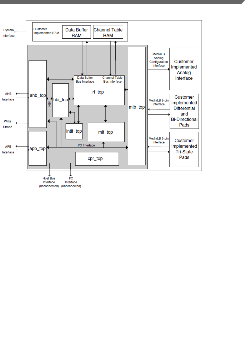
Figure 4-5. MLB Device Top-Level Block Diagram
The MLB implements the 3-pin MediaLB mode and can run at speeds up to 1024Fs. It
does not implement MediaLB controller functionality. All MediaLB devices support a set
of physical channels for sending data over the MediaLB. Each physical channel is 4 bytes
in length (quadlet) and grouped into logical channels with one or more physical channels
allocated to each logical channel. These logical channels can be any combination of
channel type (synchronous, asynchronous, control, or isochronous) and direction
(transmit or receive).
The MLB provides support for up to 64 logical channels and up to 64 physical channels.
Each logical channel is referenced using an unique channel address and represents a
unidirectional data path between a MediaLB device transmitting the data and the
MediaLB device(s) receiving the data.
4.8.1.2 Supported Features
• Synchronous, asynchronous, control, and isochronous channel.
Chapter 4 Connectivity
i.MX Reference Manual, Rev. L4.9.88_2.0.0-ga, 05/2018
NXP Semiconductors 133

• Up to 64 logical channels and 64 physical channels running at a maximum speed of
1024Fs.
• Transmission of commands and data and reception of receive status when
functioning as the transmitting device associated with a logical channel address.
• Reception of commands and data and transmission as receive status responses when
functioning as the receiving device associated with a logical channel address.
• MediaLB lock detection.
• System channel command handling.
• 256Fs, 512Fs and 1024Fs frame rates.
• Asynchronous, control, synchronous, and isochronous channel types.
• The following configurations to MLB device module:
• Frame rate
• Device address
• Channel address
• MLB channel exception get interface. All the channel exceptions are sent and
handled by the application.
4.8.1.3 MLB Driver Overview
The MLB driver is designed as a common Linux OS character driver. It implements one
asynchronous and one control channel device with Ping-Pong buffering operation mode.
The supported frame rates are 256, 512, and 1024Fs. The MLB driver uses common read/
write interfaces to receive/send packets and uses the ioctl interface to configure the MLB
device module.
4.8.1.4 MLB Driver
Functionality of the MLB driver is described in supported features, MLB driver
architecture, and software operation.
4.8.1.5 MLB Driver Architecture
The MLB driver is a common Linux character driver and the architecture is shown in the
figure below.
Media Local Bus
i.MX Reference Manual, Rev. L4.9.88_2.0.0-ga, 05/2018
134 NXP Semiconductors
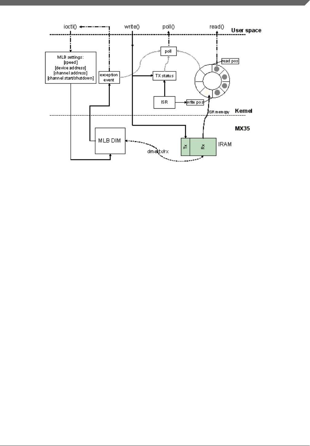
Figure 4-6. MLB Driver Architecture Diagram
The MLB driver creates four minor devices. These four devices support control Tx/Rx
channel, asynchronous Tx/Rx channel, synchronous Tx/Rx channel, and isochronous
Tx/Rx channel. Their device files are /dev/ctrl, /dev/async, /dev/sync, and /dev/isoc. Each
minor device has the same interfaces, and handle both Tx and Rx operation. The
following description is for both control and asynchronous device.
The driver uses IRAM as MLB device module Tx/Rx buffer. All the data transmission
and reception between module and IRAM is handled by the MLB module DMA. The
driver is responsible for configuring the buffer start and end pointer for the MLB module.
For reception, the driver uses a ring buffer to buffer the received packet for read. When a
packet arrives, the MLB module puts the received packet into the IRAM Rx buffer, and
notifies the driver by interrupt. The driver then copy the packet from the IRAM to one
ring buffer node indicated by the write position, and updates the write position with the
next empty node. Finally the packet reader application is notified, and it gets one packet
from the node indicated by the read position of ring buffer. After the read is completed, it
updates the read position with the next available buffer node. There is no received packet
in the ring buffer when the read and write position is the same.
For transmission, the driver writes the packet given by the writer application into the
IRAM Tx buffer, updates the Tx status and sets MLB device module Tx buffer pointer to
start transmission. After transmission completes, the driver is notified by interrupt and
updates the Tx status to accept the next packet from the application.
Chapter 4 Connectivity
i.MX Reference Manual, Rev. L4.9.88_2.0.0-ga, 05/2018
NXP Semiconductors 135

The driver supports NON BLOCK I/O. User applications can poll to check if there are
packets or exception events to read, and also they can check if a packet can be sent or not.
If there are exception events, the application can call ioctl to get the event. The ioctl also
provides the interface to configure the frame rate, device address, and channel address.
4.8.2 Software Operation
The MLB driver provides a common interface to application.
• Packet read/write-BLOCK and NONBLOCK Packet I/O modes are supported. Only
one packet can be read or written at once. The minimum read length must be greater
or equal to the received packet length, meanwhile the write length must be shorter
than 1024 Bytes.
• Polling-The MLB driver provide polling interface which polls for three status,
application can use select to get current I/O status:
• Packet available for read (ready to read)
• Driver is ready to send next packet (ready to write)
• Exception event comes (ready to read)
• ioctl-MLB driver provides the following ioctl:
MLB_SET_FPS
Argument type: unsigned int
Set frame rate, the argument must be 256, 512 or 1024.
MLB_GET_VER
Argument type: unsigned long
Get MLB device module version, which is 0x02000202 by default on the i.MX35.
MLB_SET_DEVADDR
Argument type: unsigned char
Set MLB device address, which is used by the system channel MlbScan command.
MLB_CHAN_SETADDR
Argument type: unsigned int
Set the corresponding channel address [8:1] bits. This ioctl combines both tx and rx
channel address, the argument format is: tx_ca[8:1] << 16 | rx_ca[8:1].
MLB_CHAN_STARTUP
Startup the corresponding type of channel for transmit and reception.
MLB_CHAN_SHUTDOWN
Media Local Bus
i.MX Reference Manual, Rev. L4.9.88_2.0.0-ga, 05/2018
136 NXP Semiconductors

Shutdown the corresponding type of channel.
MLB_CHAN_GETEVENT
Argument type: unsigned long
Get exception event from MLB device module, the event is defined as a set of
enumeration:
MLB_EVT_TX_PROTO_ERR_CUR
MLB_EVT_TX_BRK_DETECT_CUR
MLB_EVT_RX_PROTO_ERR_CUR
MLB_EVT_RX_BRK_DETECT_CUR
4.8.2.1 Driver Files
Table below lists the source file associated with the MLB driver that are found in the
directory drivers/mxc/mlb/.
Table 4-8. MLB Driver Source File List
File Description
mxc_mlb150.c Source file for MLB driver
include/linux/mxc_mlb.h Include file for MLB driver
4.8.2.2 Menu Configuration Options
In menu configuration enable the following module:
Device Drivers > MXC support drivers > MXC Media Local Bus Driver > MLB support.
4.9 PCI Express Root Complex
4.9.1 Introduction
PCI Express hardware module, contained in i.MX SoC, can either be configured to act as
a Root Complex or a PCIe Endpoint.
This document is used to describe the PCI Express Root Complex implementation on
i.MX SoC families.
It also describes the drivers needed to be configured and operated on i.MX PCI Express
device as Root Complex.
Chapter 4 Connectivity
i.MX Reference Manual, Rev. L4.9.88_2.0.0-ga, 05/2018
NXP Semiconductors 137

4.9.1.1 PCIe
PCI Express (PCIe) is Third Generation I/O Interconnect, targeting low cost, high
volume, multiplatform interconnection usages. It has the concepts with earlier PCI and
PCI-X and offers backwards compatibility for existing PCI software with following
differences:
• PCIe is a point-to-point interconnect
• Serial link between devices
• Packet based communication
• Scalable performance via aggregated Lanes from X1 to X16
• Need PCIe switch to have connection between more than two PCIe devices
4.9.1.2 Terminology and Conventions
The following terminologies and conventions are used in this document:
• Bridge
A Function that virtually or actually connects a PCI/PCI-X segment or PCI Express
Port with an internal component interconnect or with another PCI/PCI-X bus
segment or PCI Express Port.
• Downstream
• The relative position of an interconnect/System Element (Port/component) that is
farther from the Root Complex. The Ports on a Switch that are not the Upstream
Port are Downstream Ports. All Ports on a Root Complex are Downstream Ports.
The Downstream component on a Link is the component farther from the Root
Complex.
• A direction of information flow where the information is flowing away from the
Root Complex.
• Endpoint
One of several defined System Elements. A Function that has a Type 00h
Configuration Space header.
• Host
The entity comprising of one (or more) Central Processing Unit(s) (CPU) and
resources, such as Memory (RAM) that can be shared across multiple PCIe nodes
connected through a Root Complex.
• Lane
PCI Express Root Complex
i.MX Reference Manual, Rev. L4.9.88_2.0.0-ga, 05/2018
138 NXP Semiconductors

A set of differential signal pairs, one pair for transmission and one pair for reception.
• Link
The collection of two Ports and their interconnecting Lanes. A Link is a dual simplex
communications path between two components.
• PCIe Fabric
A topology comprised of various PCI Express nodes, also referred as devices. A
device in the fabric can be Root Complex, Endpoint, PCIe-PCI/PCI-X Bridge or a
Switch.
• Port
• Logically, an interface between a component and a PCI Express Link.
• Physically, a group of Transmitters and Receivers located on the same chip that
define a Link.
• Root Complex
RC A defined System Element that includes a Host Bridge, zero or more Root
Complex Integrated Endpoints, zero or more Root Complex Event Collectors, and
one or more Root Ports.
• Root Port
A PCI Express Port on a Root Complex that maps a portion of the Hierarchy through
an associated virtual PCI-PCI Bridge.
• Upstream
• The relative position of an interconnect/System Element (Port/component) that is
closer to the Root Complex. The Port on a Switch that is closest topologically to
the Root Complex is the Upstream Port. The Port on a component that contains
only Endpoint or Bridge Functions is an Upstream Port. The Upstream
component on a Link is the component closer to the Root Complex.
Any element of the fabric which is relatively closer towards RC is treated as 'Upstream'.
All PCIe Endpoint ports (including termination points for bridges) and Switch ports,
which are closer to RC are called Upstream Ports on that device. An Upstream Flow is
the communication moving towards RC.
4.9.1.3 PCIe Topology on i.MX
There is one PCIe port on the i.MX. Currently, only the RC mode is enabled in the Linux
BSP.
The following figure describes the diagram of the PCIe RC port on i.MX.
Chapter 4 Connectivity
i.MX Reference Manual, Rev. L4.9.88_2.0.0-ga, 05/2018
NXP Semiconductors 139
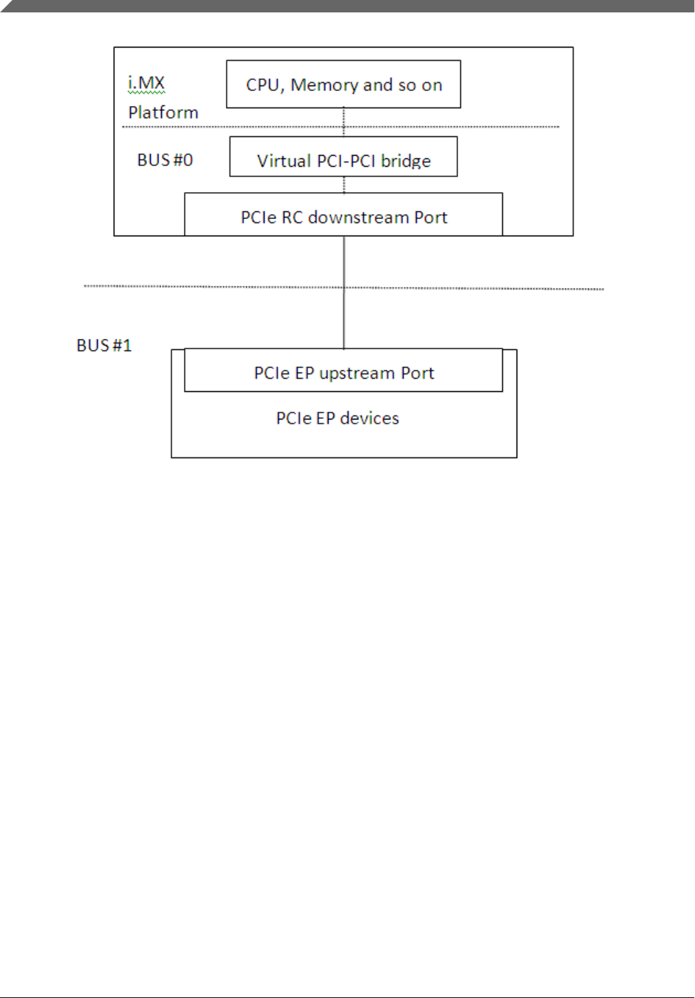
Figure 4-7. diagram of the PCIe RC port on i.MX
PCI Enumeration Mapping
As PCI Express is point to point topology, to maintain compatibility with legacy PCI Bus
- Device notion used for Software Enumeration, we introduce the following concepts
which allow various nodes and their internals to be identified (e.g., PCIe Switches) in
terms of PCI devices/functions:
• Host Bridge: A bridge, integrated into RC to have PCI compatible connection to
Host. The PCI side of this bridge is Bus #0 always. This means, the device on this
bus will be the host itself.
• Virtual PCI-PCI Bridge: Each PCI Express port which is part of RC or a Switch is
treated as a virtual PCI-PCI bridge. This means each port has a primary and
secondary PCI bus and the downstream is mapped into the remote configuration
space.
• Root port associated virtual bridge has Bus #0 on the primary side with secondary
bus on the downstream.
• Each PCIe Switch is viewed as collection of as many virtual PCI-PCI bridges as
number of downstream ports, connected to a virtual PCI bus which is actually
secondary bus of another PCI-PCI bridge forming the upstream port of the switch.
• The upstream port of each EP can either be part of the secondary bus segment of
virtual PCI-PCI Bridge representing downstream port of a switch or of the root port.
PCI Express Root Complex
i.MX Reference Manual, Rev. L4.9.88_2.0.0-ga, 05/2018
140 NXP Semiconductors

4.9.1.4 Features
The following are the various features supported by i.MX as a PCI Express Root
Complex driver.
• Express Base Specification Revision 2.0-compliant.
• Gen2 operation with x1 link supporting 5 GT/s raw transfer rate in single direction.
• Support Legacy Interrupts (INTx) and MSI.
• Max_Payload_Size size (128 bytes).
• It fits into Linux PCI Bus framework to provide PCI compatible software
enumeration support.
• In addition, it provides interface to Endpoint Drivers to access the respective devices
detected downstream.
• The same interface can be used by the PCI Express Port Bus Driver framework in
Linux OS to handle AER, ASP, and so on.
• Interrupt handling facility for EP drivers either as Legacy Interrupts (INTx).
• Access to EP I/O BARs through generic I/O accessories in Linux PCI subsystem.
• Seamless handling of PCIe errors.
4.9.2 Linux OS PCI Subsystem and RC driver
In Linux OS, the PCI implementation can roughly be divided into the following main
components: PCI BIOS architecture-specific Linux OS implementation, Host Controller
(RC) Module, and Core.
• PCI BIOS Architecture-specific Linux OS implementation to kick off PCI bus
initialization. It interfaces with PCI Host Controller code as well as the PCI Core to
perform bus enumeration and allocation of resources such as memory and interrupts.
The successful completion of BIOS execution assures that all the PCI devices in the
system are assigned parts of available PCI resources and their respective drivers
(referred as Slave Drivers). PCI can take control of them using the facilities provided
by PCI Core. It is possible to skip resource allocation (if they were assigned before
Linux OS was booted, for example PC scenario).
• Host Controller (RC) Module handles hardware (SoC + Board) specific initialization
and configuration and it invokes PCI BIOS. It should provide callback functions for
BIOS as well as PCI Core, which will be called during PCI system initialization and
accessing PCI bus for configuration cycles. It provides resources information for
available memory/IO space, INTx interrupt lines, MSI. It should also facilitate IO
Chapter 4 Connectivity
i.MX Reference Manual, Rev. L4.9.88_2.0.0-ga, 05/2018
NXP Semiconductors 141
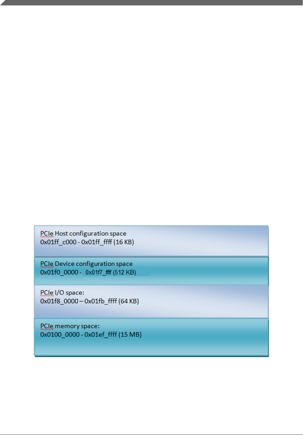
space access (as supported) through in _x_ () out _x_ () You may need to provide
indirect memory access (if supported by h/w) through read _x_ () write _x_ ().
• Core creates and initializes the data structure tree for bus devices as well as bridges
in the system, handles bus/device numberings, creates device entries and proc/sysfs
information, provides services for BIOS and slave drivers and provides hot plug
support (optional/as supported by h/w). It targets (EP) driver interface query and
initializes corresponding devices found during enumeration. It also provides MSI
interrupt handling framework and PCI express port bus support. It provides Hot-Plug
support (if supported), advanced error reporting support, power management event
support, and virtual Channel support to run on PCI express ports (if supported).
4.9.2.1 RC Driver Source Files
The driver files are present at the following path relative to extracted kernel source
directory.
drivers/pci/host/pci-imx6.c
4.9.3 System Resource: Memory Layout
Figure 4-8. Memory Layout (i.MX 6Quad/6DualLite/6Solo)
PCI Express Root Complex
i.MX Reference Manual, Rev. L4.9.88_2.0.0-ga, 05/2018
142 NXP Semiconductors
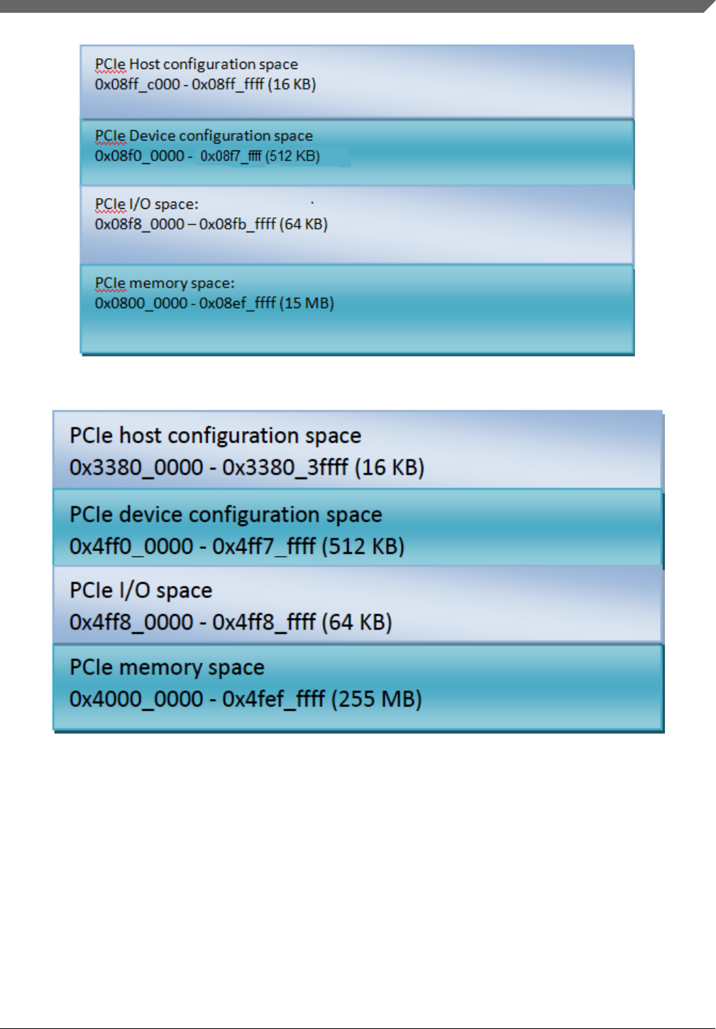
Figure 4-9. Memory Layout (i.MX 6SoloX)
Figure 4-10. Memory Layout (i.MX 7Dual)
• IO and memory spaces are two address spaces used by the devices to communicate
with their device driver running in the Linux kernel on CPU.
• The upper 16 KB PCIe host configuration space.
• This memory segment is used to map the configuration space of PCIe RC. SW
can access PCIe RC core configuration space through the DBI interface.
• PCIe device configuration space.
• Used to map the configuration spaces of PCIe EP devices that are inserted to the
RC downstream port.
Chapter 4 Connectivity
i.MX Reference Manual, Rev. L4.9.88_2.0.0-ga, 05/2018
NXP Semiconductors 143

i.MX 8QuadMax/8QuadXPlus:
i.MX 8QuadMax has both PCIeA and PCIeB, while i.MX 8QuadXPlus has only PCIeB.
• PCIeA
• PCIe host configuration space: 0x5f00_0000 – 0x5f00_ffff (64K bytes)
• PCIe device configuration space: 0x6ff0_0000 – 0x6ff7_ffff (512K bytes)
• PCIe IO space: 0x6ff8_0000 – 0x6ff8_ffff (64K bytes)
• PCIe memory space: 0x6000_0000 – 0x6fef_ffff (255M bytes)
• PCIeB
• PCIe host configuration space: 0x5f01_0000 – 0x5f01_ffff (64K bytes)
• PCIe device configuration space: 0x7ff0_0000 – 0x7ff7_ffff (512K bytes)
• PCIe IO space: 0x7ff8_0000 – 0x7ff8_ffff (64K bytes)
• PCIe memory space: 0x7000_0000 – 0x7fef_ffff (255M bytes)
i.MX 8MQuad:
• PCIe0
• PCIe host configuration space: 0x3380_0000 – 0x33bf_ffff (4Mbytes)
• PCIe device configuration space: 0x1ff0_0000 – 0x1ff7_ffff (512K bytes)
• PCIe IO space: 0x1ff8_0000 – 0x1ff8_ffff (64K bytes)
• PCIe memory space: 0x1800_0000 – 0x1fef_ffff (127M bytes)
• PCIE1
• PCIe host configuration space: 0x33c0_0000 – 0x33ff_ffff (4Mbytes)
• PCIe device configuration space: 0x27f0_0000 – 0x27f7_ffff (512K bytes)
• PCIe IO space: 0x27f8_0000 – 0x27f8_ffff (64K bytes)
• PCIe memory space: 0x2000_0000 – 0x27ef_ffff (127M bytes)
4.9.3.1 System Resource: Interrupt lines
i.MX Root Complex driver uses interrupt line 152 for MSI INT on i.MX 6 platforms, and
154 for MSI INT on i.MX 7Dual platforms.
4.10 USB
USB
i.MX Reference Manual, Rev. L4.9.88_2.0.0-ga, 05/2018
144 NXP Semiconductors

4.10.1 Introduction
The universal serial bus (USB) driver implements a standard Linux driver interface to the
CHIPIDEA USB-HS OTG controller.
The USB provides a universal link that can be used across a wide range of PC-to-
peripheral interconnects. It supports plug-and-play, port expansion, and any new USB
peripheral that uses the same type of port.
The CHIPIDEA USB controller is Enhanced Host Controller Interface (EHCI)-
compliant. This USB driver has the following features:
• High-speed OTG core supported
• High-speed Host Only core (Host1), high-speed, full speed, and low devices are
supported
• High-speed Inter-Chip core (Host2 & Host3)
• High-speed Host Only core (OTG2), high-speed, full speed, and low devices are
supported. A USB2Pci bridge is connected to OTG2 by default. Therefore, users may
not be able to connect other USB devices on this port.
• High-speed Inter-Chip core (Host2)
• Host mode-Supports HID (Human Interface Devices), MSC (Mass Storage Class)
• Peripheral mode-Supports MSC, and CDC (Communication Devices Class) drivers,
which include Ethernet and serial support
• Embedded DMA controller
4.10.1.1 Architectural Overview
The USB host system is composed of a number of hardware and software layers.
The figure below shows a conceptual block diagram of the building block layers in a host
system that support USB 2.0.
Chapter 4 Connectivity
i.MX Reference Manual, Rev. L4.9.88_2.0.0-ga, 05/2018
NXP Semiconductors 145
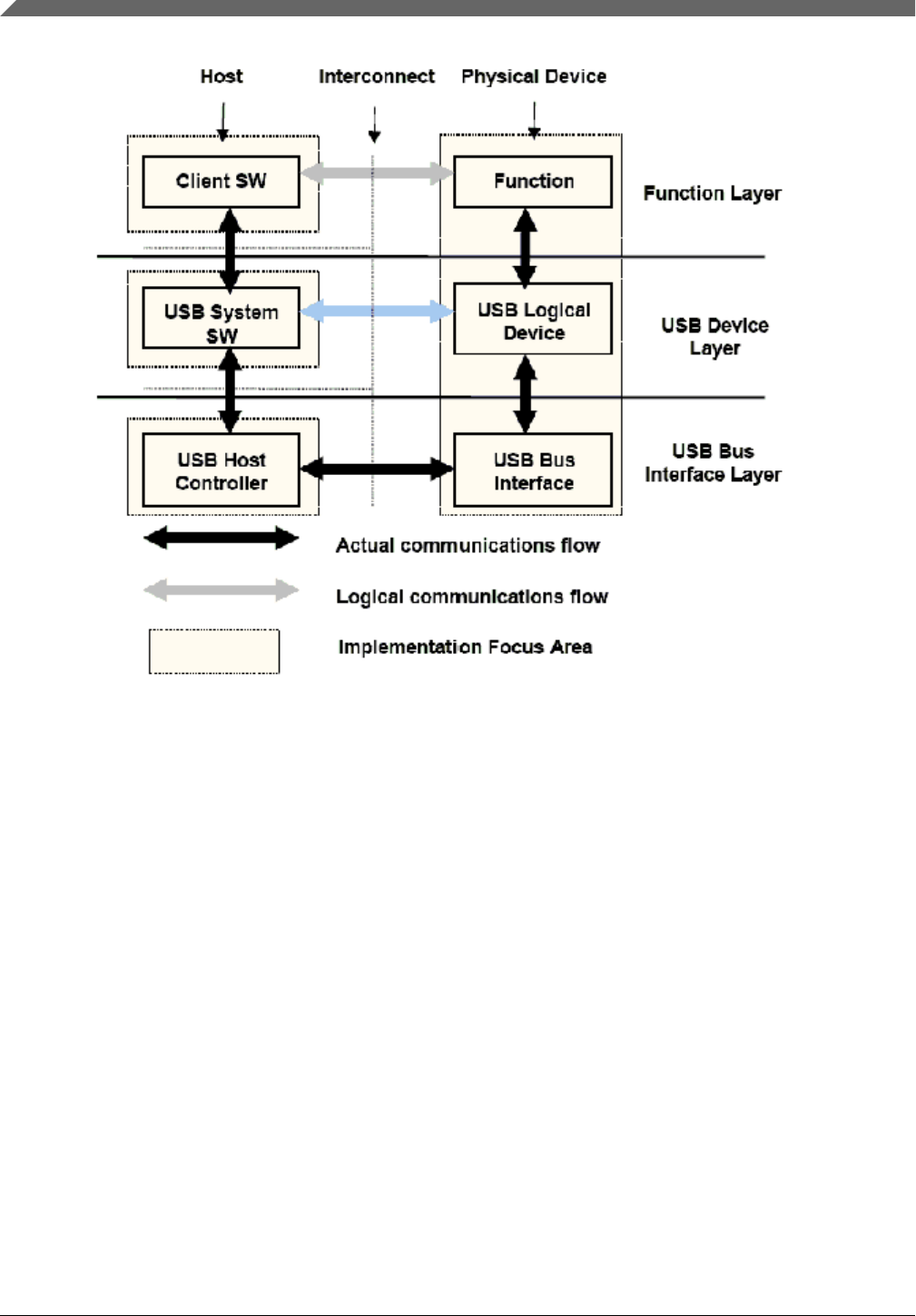
Figure 4-11. USB Block Diagram
4.10.1.2 Hardware Operation
For information on hardware operations, refer to the EHCI spec.ehci-r10.pdf.
The spec is available at Enhanced Host Controller Interface for USB 2.0: Specification
4.10.2 Software Operation
The Linux OS contains a USB driver, which implements the USB protocols. For the USB
host, it only implements the hardware specified initialization functions. For the USB
peripheral, it implements the gadget framework. For OTG, ID dynamic switch host/
device modes are supported. Currently, the runtime suspend for USB is supported, that is
to say when the USB is not in use (both for host and peripheral mode), the USB will enter
low power mode.
USB
i.MX Reference Manual, Rev. L4.9.88_2.0.0-ga, 05/2018
146 NXP Semiconductors

4.10.2.1 Source Code Structure
The table below shows the source files available in the source directory, $KERNEL/
drivers/usb/
Table 4-9. USB Driver Files
File Description
chipidea/core.c Chipidea IP core driver
chipidea/udc.c Chipidea peripheral driver
chipidea/host.c Chipidea host driver
chipidea/otg.c Chipidea OTG driver
chipidea/otg_fsm.c Chipidea OTG HNP and SRP driver
chipidea/ci_hdrc_imx.c i.MX glue layer
chipidea/usbmisc_imx.c i.MX SoC abstract layer
phy/phy-mxs-usb.c i.MX 6 USB physical driver
4.10.2.2 Menu Configuration Options
In menu configuration enable the following module:
Device Drivers --->
[*] USB support --->
<M> EHCI HCD (USB 2.0) support
<M> ChipIdea Highspeed Dual Role Controller
[*] USB Physical Layer drivers --->
<M> Freescale MXS USB PHY support
<M> USB Gadget Support --->
1. CONFIG_USB-Build Support for Host-side USB
2. CONFIG_USB_EHCI_HCD EHCI HCD (USB 2.0) support
Default y
3. CONFIG_USB_CHIPIDEA- ChipIdea high-speed Dual Role Controller
Default y
4. CONFIG_USB_CHIPIDEA_UDC - ChipIdea device controller
Default y
5. CONFIG_USB_CHIPIDEA_HOST - ChipIdea host controller
Default y
Chapter 4 Connectivity
i.MX Reference Manual, Rev. L4.9.88_2.0.0-ga, 05/2018
NXP Semiconductors 147

6. CONFIG_USB_GADGET - USB Gadget Support
Default y
7. CONFIG_USB_MXS_PHY - Freescale MXS USB PHY support
Default y
4.10.2.3 USB Wakeup Usage
The following example is for the OTG port and the first EHCI device.
Controller wakeup setting, after the following settings, the VBUS and ID will be wakeup
source.
echo enabled > /sys/bus/platform/devices/20c9000.usbphy/power/wakeup
echo enabled > /sys/bus/platform/devices/2184000.usb/power/wakeup
echo enabled > /sys/bus/platform/devices/ci_hdrc.0/power/wakeup
EHCI wakeup setting, after the following settings, the host will have wakeup ability, such
as remote wakeup and connect/disconnect wakeup
echo enabled > /sys/bus/usb/devices/usb1/power/wakeup
echo enabled > /sys/bus/usb/devices/1-1/power/wakeup
NOTE
When the OTG mode switches from the host to the device, it
will delete the EHCI wakeup, and the user needs to set it again
before the system suspending.
4.10.2.4 How to Close the USB Child Device Power
The following code string outlines how to close the USB child device power:
echo auto > /sys/bus/usb/devices/1-1/power/control
echo auto > /sys/bus/usb/devices/1-1.1/power/control (If there is a hub at USB device)
4.10.2.5 Changing the Controller Operation Mode
To change the default settings, the use can modify the DTS file as follows:
dr_mode = "host" /* Set controller as gadget-only mode */
dr_mode = "peripheral" /* Set controller as host-only mode */
USB
i.MX Reference Manual, Rev. L4.9.88_2.0.0-ga, 05/2018
148 NXP Semiconductors

dr_mode = "otg" /* Set controller as otg mode */
4.10.2.6 Loadable Module Support
The modprobe utility will automatically load the modules which have dependency among
all modules.
The loading command is as follows:
modprobe phy_mxs_usb
modprobe ci_hdrc_imx
The unloading command is as follows:
modprobe -r ci_hdrc_imx
modprobe -r phy_mxs_usb
4.10.2.7 USB Charger Detection
i.MX SoC has USB charger detection ability, but it has no charging ability. The user can
use the /sys entry to know the USB charger type, charging current, and whether the
charger exists, as shown in the following three lines:
cat /sys/class/power_supply/imx6_usb_charger/type
cat /sys/class/power_supply/imx6_usb_charger/current_max
cat /sys/class/power_supply/imx6_usb_charger/present
Currently, the i.MX 6 Sabre-SD board does not support the USB charger detection
function. i.MX 6 Sabre-Auto and i.MX 6SoloLite EVK support the function.
4.10.3 Embeded Host Certification
4.10.3.1 Adding TPL-Support Property
To pass embeded host USB certification, "tpl-support" should be added in DTS to enable
Targeted Peripheral List (TPL). For example, to enable TPL on the Host port of i.MX
6UltraLite EVK board (imx6ul-14x14-evk.dts):
&usbotg2 {
dr_mode = "host";
disable-over-current;
Chapter 4 Connectivity
i.MX Reference Manual, Rev. L4.9.88_2.0.0-ga, 05/2018
NXP Semiconductors 149

tpl-support;
status = "okay";
};
4.10.3.2 VBUS Control
The VBUS should be kept off until the Linux USB host function is ready. For example,
on the i.MX 6UltraLite EVK board, because the pin is multiplexed with the touch
function, you need to rework the board to make the GPIO (GPIO1_IO02) selected for
VBUScontrol.
Disable the touch function in its DTS file (imx6ul-14x14-evk.dts) as follows:
&tsc {
pinctrl-names = "default";
pinctrl-0 = <&pinctrl_tsc>;
xnur-gpio = <&gpio1 3 0>;
measure_delay_time = <0xffff>;
pre_charge_time = <0xfff>;
status = "disabled";
};
Add VBUS GPIO pinctrl and its regulator node:
pinctrl_usb_otg2: usbotg2grp {
fsl,pins = <
MX6UL_PAD_GPIO1_IO02__GPIO1_IO02 0xb0
>;
};
reg_usb_otg2_vbus: regulator@2 {
compatible = "regulator-fixed";
reg = <2>;
pinctrl-names = "default";
pinctrl-0 = <&pinctrl_usb_otg2>;
regulator-name = "usb_otg2_vbus";
regulator-min-microvolt = <5000000>;
regulator-max-microvolt = <5000000>;
gpio = <&gpio1 2 GPIO_ACTIVE_HIGH>;
enable-active-high;
};
&usbotg2 {
vbus-supply = <®_usb_otg2_vbus>;
dr_mode = "host";
disable-over-current;
tpl-support;
status = "okay";
};
4.11 Low Power Universal Asynchronous Receiver/
Transmitter (LPUART)
Low Power Universal Asynchronous Receiver/Transmitter (LPUART)
i.MX Reference Manual, Rev. L4.9.88_2.0.0-ga, 05/2018
150 NXP Semiconductors

4.11.1 Introduction
The low-level UART driver interfaces the Linux serial driver API to all the UART ports.
It has the following features:
• Interrupt-driven and eDMA-driven transmit/receive of characters
• Standard Linux baud rates up to 4 Mbps
• Transmit and receive characters with 7-bit, 8-bit, 9-bit, or 10-bit character length
• Transmits one or two stop bits
• Supports TIOCMGET IOCTL to read the modem control lines. Only supports the
constants TIOCM_CTS and TIOCM_CAR, plus TIOCM_RI in DTE mode only
• Supports TIOCMSET IOCTL to set the modem control lines. Supports the constants
TIOCM_RTS and TIOCM_DTR only
• Odd and even parity
• XON/XOFF software flow control. Serial communication using software flow
control is reliable when communication speeds are not too high and the probability of
buffer overruns is minimal
• CTS/RTS hardware flow control-both interrupt-driven software-controlled hardware
flow and hardware-driven hardware-controlled flow
• Send and receive break characters through the standard Linux serial API
• Recognizes frame and parity errors
• Ability to ignore characters with break, parity and frame errors
• Get and set UART port information through the TIOCGSSERIAL and
TIOCSSERIAL TTY IOCTL. Some programs like setserial and dip use this feature
to make sure that the baud rate was set properly and to get general information on the
device. The UART type should be set to 52 as defined in the serial_core.h header
file.
• Power management feature by suspending and resuming the UART ports
• Standard TTY layer IOCTL calls
All the UART ports can be accessed from the device files /dev/ttyLP0 to /dev/ttyLP1.
4.11.1.1 Hardware Operation
To determine the number of UART modules available on the device see the Applications
Processor Reference Manual associated with SoC.
Each UART hardware port is capable of standard RS-232 serial communication.
Chapter 4 Connectivity
i.MX Reference Manual, Rev. L4.9.88_2.0.0-ga, 05/2018
NXP Semiconductors 151

Each UART contains a 64-byte transmitter FIFO and a 32-half-word deep receiver FIFO.
Each UART also supports a variety of maskable interrupts when the data level in each
FIFO reaches a programmed threshold level and when there is a change in state in the
modem signals.
4.11.2 Software Operation
The Linux OS contains a core UART driver that manages many of the serial operations
that are common across UART drivers for various platforms.
The low-level UART driver is responsible for supplying information such as the UART
port information and a set of control functions to the core UART driver. These functions
are implemented as a low-level interface between the Linux OS and the UART hardware.
They cannot be called from other drivers or from a user application. The control
functions used to control the hardware are passed to the core driver through a structure
called uart_ops, and the port information is passed through a structure called uart_port.
The low level driver is also responsible for handling the various interrupts for the UART
ports, and providing console support if necessary.
Each UART can be configured to use DMA for the data transfer by enabling the DMA
channel in the DTS file.
The driver requests two DMA channels for the UARTs that need DMA transfer. On a
receive transaction, the driver copies the data from the DMA receive buffer to the TTY
Flip Buffer.
While using DMA to transmit, the driver copies the data from the UART transmit buffer
to the DMA transmit buffer and sends this buffer to the DMA system. For more
information, see the Linux documentation on the serial driver in the kernel source tree.
4.11.2.1 Driver Features
The UART driver supports the following features:
• Baud rates up to 4 Mbps
• Recognizes frame and parity errors only in interrupt-driven mode; does not recognize
these errors in DMA-driven mode
• Sends, receives, and appropriately handles break characters
• Recognizes the modem control signals
• Ignores characters with frame, parity, and break errors if requested to do so
• Implements support for hardware flow control
Low Power Universal Asynchronous Receiver/Transmitter (LPUART)
i.MX Reference Manual, Rev. L4.9.88_2.0.0-ga, 05/2018
152 NXP Semiconductors

• Get and set the UART port information; certain flow control count information is not
available in hardware-driven hardware flow control mode
• Power management
• Interrupt-driven and DMA-driven data transfer
4.11.2.2 Source Code Structure
Table below shows the UART driver source files that are available in the directory:
drivers/tty/serial.
Table 4-10. UART Driver Files
File Description
fsl_lpuart.c Low level driver
4.11.2.3 Configuration
This section discusses configuration options associated with Linux OS, chip
configuration options, and board configuration options.
4.11.2.4 Configuration Options
The UART driver is enabled by default.
Enable the UART driver on Linux® OS menuconfig. This option is located at:
-> Device Drivers
-> Character devices
-> Serial drivers
<*> Freescale LPUART serial port support
[*] Console on Freescale LPUART serial port
4.11.2.5 Source Code Configuration Options
This section details the board configuration options. For the i.MX 8QuadMax boards, the
board-specific configuration options for the driver are set in:
arch/arm/boot/dts/imx*.dts
. For i.MX 8 the board-specific configuration options for the driver are set in:
Chapter 4 Connectivity
i.MX Reference Manual, Rev. L4.9.88_2.0.0-ga, 05/2018
NXP Semiconductors 153

arch/arm64/boot/dts/freescale/fsl-imx*.dts
4.11.2.6 Programming Interface
>The UART driver implements all the methods required by the Linux serial API to
interface with the UART port.
The driver implements and provides a set of control methods to the Linux core UART
driver. For more information about the methods implemented in the driver, see the API
document.
4.11.2.7 Interrupt Requirements
The UART driver interface generates only one interrupt.
The status is used to determine which kinds of interrupt occurs, such as RX or TX.
4.12 Wi-Fi QCA6174
4.12.1 Hardware Operation
The officially supported Wi-Fi chip with our BSP is Murata 1CQ module based on
Qualcomm QCA6174.
The QCA6174 is a single-die wireless local area network (WLAN) and Bluetooth ®
combo solution to support 2 x 2 multi-user multiple input, multiple output (MU-MIMO)
with two spatial streams IEEE802.11 a/b/g/n/ac WLAN standards and Bluetooth 4.2 +
HS, designed to deliver superior integration of WLAN/Bluetooth and low energy
technology.
The i.MX 8QuadMax and i.MX 8QuadXPlus hardware boards use M.2 interface to
connect with the 1CQ Wi-Fi module.
4.12.2 Software Operation
The BSP uses the QCA CLD LEA1.0 Wi-Fi driver, which is released by Qualcomm, and
the firmware and binaries are limited to LA_OPT_BASE_LICENSE and Qualcomm
Atheros License.
Wi-Fi QCA6174
i.MX Reference Manual, Rev. L4.9.88_2.0.0-ga, 05/2018
154 NXP Semiconductors

4.12.2.1 Driver features
The QCA CLD is a CFG80211 driver, which supports both the station and AP mode of
operation.
The driver requires firmware that runs on the chip's network processor. The following
directory designates the firmware location in rootfs: /lib/firmware/.
4.12.2.2 Source Code Structure
The QCA CLD driver source files are available in codeaurora.org: https://
source.codeaurora.org/quic/la/platform/vendor/qcom-opensource/wlan/qcacld-2.0.
4.12.2.3 Menu Configuration Options
The following Linux kernel configuration option is provided for this module:
• CONFIG_MAC80211=y
• COCONFIG_NL80211_TESTMODE=y
• CONFIG_CFG80211_WEXT=y
• CONFIG_HOSTAP=y
• CONFIG_CFG80211_INTERNAL_REGDB=y
4.12.2.4 Device Tree Binding
For device tree, the ATH10K driver requires the following nodes to be defined in the
device tree. For example,
&pcie0{
pinctrl-names = "default";
pinctrl-0 = <&pinctrl_pcie0>;
clkreq-gpio = <&gpio5 20 GPIO_ACTIVE_LOW>;
disable-gpio = <&gpio5 29 GPIO_ACTIVE_LOW>;
reset-gpio = <&gpio5 28 GPIO_ACTIVE_LOW>;
ext_osc = <1>;
hard-wired = <1>;
status = "okay";
};
regulators {
compatible = "simple-bus";
#address-cells = <1>;
#size-cells = <0>;
epdev_on: fixedregulator@100 {
compatible = "regulator-fixed";
regulator-min-microvolt = <3300000>;
regulator-max-microvolt = <3300000>;
regulator-name = "epdev_on";
Chapter 4 Connectivity
i.MX Reference Manual, Rev. L4.9.88_2.0.0-ga, 05/2018
NXP Semiconductors 155

gpio = <&gpio4 9 0>;
enable-active-high;
};
}
4.12.2.5 Configuring WLAN from User Space
4.12.2.5.1 Connecting AP in Station Mode
The following command group is used to connect WLAN to a given SSID.
head -n 4 /etc/wpa_supplicant.conf > /etc/wpa_supplicant.conf.tmp
wpa_passphrase ssid password >> /etc/wpa_supplicant.conf.tmp
mv /etc/wpa_supplicant.conf /etc/wpa_supplicant.conf.bak
mv /etc/wpa_supplicant.conf.tmp /etc/wpa_supplicant.conf
wpa_supplicant -B -i wlp1s0 -c /etc/wpa_supplicant.conf -D nl80211
Here is an example of wpa_supplicant.conf:
ctrl_interface=/var/run/wpa_supplicant
ctrl_interface_group=0
update_config=1
network={
ssid="NETGEAR73"
#psk="freshbutter"
psk=eb0376fc14ee5d1e6ce129ad54da038adab……
}
4.12.2.5.2 Obtaining an IP address
The following command is used to get an IP address for wlp1s0:
udhcpc -i wlp1s0
4.13 USB3
4.13.1 Introduction
For i.MX 8QuadMax and i.MX 8QuadXPlus, there is a super-speed USB IP from
Cadence. The driver code is located at drivers/usb/cdns3.
4.13.2 Supported features
For Host mode:
It uses Linux OS standard XHCI driver, and super-speed is supported well. USB super-
speed disk is tested.
USB3
i.MX Reference Manual, Rev. L4.9.88_2.0.0-ga, 05/2018
156 NXP Semiconductors

For Device mode:
Only single queue is supported. Mass storage, ether, and serial are supported.
Chapter 4 Connectivity
i.MX Reference Manual, Rev. L4.9.88_2.0.0-ga, 05/2018
NXP Semiconductors 157

USB3
i.MX Reference Manual, Rev. L4.9.88_2.0.0-ga, 05/2018
158 NXP Semiconductors

Chapter 5
Graphics
5.1 Graphics Processing Unit (GPU)
5.1.1 Introduction
The Graphics Processing Unit (GPU) is a graphics accelerator targeting embedded 2D/3D
graphics applications.
The 3D graphics processing unit (GPU3D) is an embedded engine that accelerates user
level graphics Application Programming Interface (APIs) such as OpenGL ES 1.1,
OpenGL ES 2.0, and OpenGL ES 3.0 and OpenCL 1.1EP. The 2D graphics processing
unit (GPU2D) is an embedded 2D graphics accelerator targeting graphical user interfaces
(GUI) rendering boost. The VG graphics processing unit (GPUVG) is an embedded
vector graphic accelerator for supporting the OpenVG 1.1 graphics API and feature set.
The GPU driver kernel module source is in the kernel source tree, but the libs are
delivered as binary only.
Graphics Processing Unit Hardware Applicable Platform
3D Vivante dual-
GC7000XSVX
8QuadMax
3D Vivante GC7000Lite 8QuadXPlus/8MQuad
3D Vivante GC2000 6Quad/6Dual
3D Vivante GC2000+ 6QdualPlus/6DualPlus
3D Vivante GC880 6DualLite/6Solo
3D/2D Vivante GC400T 6SoloX
2D Vivante GC320 6Quad/6Dual/6DualLite/6Solo/6SoloLite
Vector Vivante GC355 6Quad/6Dual/6SoloLite
NOTE
• GC400T does not support OpenGL ES 3.0.
i.MX Reference Manual, Rev. L4.9.88_2.0.0-ga, 05/2018
NXP Semiconductors 159

• GC880/GC400T does not support OpenCL 1.1EP. GC2000
and GC2000+ support OpenCL 1.1 EP.
• GC7000XSVX supports OpenCL 1.2 FP, OpenVX 1.0.1,
and Vulkan 1.0.
5.1.1.1 Driver Features
The GPU driver enables this board to provide the following software and hardware
support:
• EGL (EGL is an interface between Khronos rendering APIs such as OpenGL ES or
OpenVG and the underlying native platform window system) 1.5 API defined by
Khronos Group.
• OpenGL ES (OpenGL® ES is a royalty-free, cross-platform API for full-function 2D
and 3D graphics on embedded systems) 1.1 API defined by Khronos Group.
• OpenGL ES 2.0 API defined by Khronos Group.
• OpenGL ES 3.0/3.1/3.2 API defined by Khronos Group.
• OpenVG (OpenVG is a royalty-free, cross-platform API that provides a low-level
hardware acceleration interface for vector graphics libraries such as Flash and SVG)
1.1 API defined by Khronos Group.
• OpenCL (OpenCL is the first open, royalty-free standard for cross-platform, parallel
programming of modern processors.) 1.1 EP API defined by Khronos Group.
• OpenGL 2.1 API defined by Khronos Group.
• Automatic 3D core slowing down, when hot notification from thermal driver is
active, 3D core will run at 1/64 clock.
• OpenCL1.1/1.2FP API defined by Khronos Group.
• OpenVX 1.0.1 API defined by Khronos Group.
• Vulkan 1.0 API defined by Khronos Group.
5.1.1.2 Hardware Operation
For detailed hardware operations, see the GPU chapters in the Applications Processor
Reference Manual specific to SoC.
5.1.2 Software Operation
The GPU driver is divided into two layers. The first layer is running in kernel mode and
acts as the base driver for the whole stack. This layer provides the essential hardware
access, device management, memory management, command queue management,
Graphics Processing Unit (GPU)
i.MX Reference Manual, Rev. L4.9.88_2.0.0-ga, 05/2018
160 NXP Semiconductors

context management and power management. The second layer is running in user mode,
implementing the stack logic and providing the following APIs to the upper layer
applications:
• OpenGL ES 1.1, 2.0, and 3.0 API
• EGL 1.5 API
• OpenGL ES11/20/30/31/32
• OpenCL 1.1/1.2 FP
• OpenVX 1.0.1
• Vulkan 1.0
• OpenGL 4.0
• WebGL 1.0.2
• OpenVG 1.1 API
• OpenCL 1.1 EP API
5.1.2.1 Source Code Structure
Table below lists GPU driver kernel module source structure:
drivers/mxc/gpu-viv
Table 5-1. GPU Driver Files
File Description
Kconfig Kbuild config Kernel configure file and makefile
hal/kernel/arch Hardware-specific driver code for GC2000, GC880, GC400T, and
GC320
hal/kernel/archvg Hardware-specific driver code for GC355
hal/kernel Kernel mode HAL driver
hal/os/linux/kernel OS layer HAL driver
NOTE
If you replace the whole content in this directory, the GPU
kernel driver can be upgraded.
5.1.2.2 Library Structure
Table below lists GPU driver user mode library structure:
<ROOTFS>/usr/lib
Chapter 5 Graphics
i.MX Reference Manual, Rev. L4.9.88_2.0.0-ga, 05/2018
NXP Semiconductors 161

Table 5-2. GPU Library Files
File Description
libCLC.so OpenCL frontend compiler library
libEGL.so** EGL1.4 library
libGAL.so GAL user mode driver
libGLES_CL.so OpenGL ES 1.1 common lite library
(without EGL API, no float point support API)
libGL.so** OpenGL 2.1 common library
libGLES_CM.so OpenGL ES 1.1 common library
(without EGL API, include float point support API)
libGLESv1_CL.so** OpenGL ES 1.1 common lite library
(with EGL API, no float point support API)
libGLESv1_CM.so** OpenGL ES 1.1 common library
(with EGL API, include float point support API)
libGLESv2.so** OpenGL ES 2.0/3.0/3.1/3.2 library
libGLSLC.so OpenGL ES shader language compiler library
libVSC.so OpenGL front-end compiler library
libVivanteOpenCL.so Vivante
libOpenCL.so OpenCL ICD wrapper library
libOpenVG.so* OpenVG 1.1 library
libVDK.so VDK wrapper library.
libVIVANTE.so Vivante user mode driver.
xorg/modules/drivers/vivante_drv.so EXA library for X11 acceleration.
libwayland-viv.so Wayland server-side library for Vivante's EGL driver
libgc_wayland_protocol.so Vivante Wayland Protocol Extension Library
libOpenVX.so* OpenVX 1.0 library
libvulkan..so* Vulkan 1.0 library
**SONAME is used for libEGL.so, libGLESv2.so, libGLESv1_CM.so,
libGLESv1_CL.so, libGL.so.
*For libOpenVG.so, there are two libraries for the OpenVG feature. libOpenVG.3d.so is
the GC7000XSVX/GC2000+/GC2000/GC880/GC400T-based OpenVG library.
libOpenVG.2d.so is the gc355 based OpenVG library.
• For i.MX 6DualPlus/QuadPlus and i.MX 6Dual/Quad, both libOpenVG.3d.so and
libOpenVG.2d.so can be used.
• For i.MX 6DualLite, and i.MX 6SoloX, only libOpenVG.3d.so can be used.
• For i.MX 6SoloLite, only libOpenVG.2d.so can be used.
• If no SOC limitation, for the x11 backend, libOpenVG.3d.so is linked by default.
• If no SOC limitation, for framebuffer, directFB, and Wayland backends, the default
openVG library is linked to libOpenVG.2d.so.
Graphics Processing Unit (GPU)
i.MX Reference Manual, Rev. L4.9.88_2.0.0-ga, 05/2018
162 NXP Semiconductors

This can be done by using the following sequence of commands:
cd <ROOTFS>/usr/lib
sudo ln -s libOpenVG_355.so libOpenVG.so
5.1.2.3 API References
See the following web sites for detailed specifications:
• OpenGL ES 1.1, 2.0, and 3.0 API: www.khronos.org/opengles/
• OpenCL 1.1 EP www.khronos.org/opencl/
• EGL 1.4 API: www.khronos.org/egl/
• OpenVG 1.1 API: www.khronos.org/openvg/
• OpenGL ES API: www.khronos.org/gles/
• OpenCL API: www.khronos.org/opencl/
• OpenVX API: www.khronos.org/openvx/
• Vulkan API: www.khronos.org/vulkan/
• OpenGL API: www.khronos.org/opengl/
• WebGL API: www.khronos.org/webgl/
5.1.2.4 Menu Configuration Options
In menu configuration enable the following module for the GPU driver:
CONFIG_MXC_GPU_VIV is a configuration option for GPU driver. In the menuconfig
this option is available under Device Drivers > MXC support drivers > MXC Vivante
GPU support > MXC Vivante GPU support.
On the screen displayed, select Configure the kernel, select Device Drivers > MXC
support drivers > MXC Vivante GPU support > MXC Vivante GPU support, and then
exit. When the next screen appears, select the following options to enable the GPU
driver:
• Package list > imx-gpu-viv
• This package provides proprietary binary libraries, and test code built from the GPU
for framebuffer
5.2 Wayland
Chapter 5 Graphics
i.MX Reference Manual, Rev. L4.9.88_2.0.0-ga, 05/2018
NXP Semiconductors 163

5.2.1 Introduction
Wayland is a protocol for a compositor to talk to its clients as well as a C library
implementation of that protocol. The compositor can be a standalone display server
running on Linux kernel modesetting and evdev input devices, an X application, or a
Wayland client itself. The clients can be traditional applications, X servers or other
display servers.
Part of the Wayland project is also the Weston reference implementation of a Wayland
compositor. The Weston compositor is a minimal and fast compositor and is suitable for
many embedded and mobile use cases.
This chapter describes how to enable Wayland/Weston support on an i.MX series device.
5.2.1.1 Hardware Operation
i.MX 6SoloLite only supports G2D acceleration, and other SOCs in i.MX series support
EGL3D and G2D acceleration.
5.2.2 Software Operation
This release is based on the Wayland 1.13.0 version and Weston 3.0.0 version.
5.2.2.1 Yocto Build Instructions
The instructions for Yocto Project build are as follows:
1. Prepare a Yocto build directory and follow the setup instructions in the i.MX Yocto
Project User's Guide (IMXLXYOCTOUG) for DISTRO Wayland.
2. Set up Yocto for Wayland in the build directory:
$ MACHINE = <your-machine> DISTRO=fsl-imx-xwayland source fsl-setup-release.sh -b build-
wayland
3. Build an image.
$ bitbake fsl-image-gui
Wayland
i.MX Reference Manual, Rev. L4.9.88_2.0.0-ga, 05/2018
164 NXP Semiconductors

5.2.2.2 Customizing Weston
The NXP-Weston includes two compositors. One is the EGL3D compositor, which is
accelerated by the 3D core. The other is G2D compositor accelerated by the 2D BLT
engines.
Weston options can be updated in the file “/etc/init.d/weston”.
Table 5-3. Common options for Weston
Weston option Description
tty default to current tty.
device "/dev/fb0", default frame buffer , Multi display supported in
G2D compositor.
use-gl EGL accelerated, defaults to be “1”.
use-g2d G2D accelerated, defaults to be “0”.
idle-time Idle time in seconds.
5.2.2.2.1 Multi display supported in Weston
Multi display was supported in G2D compositor only. Add these options to start Weston:
weston --tty=1 --device=/dev/fb0,/dev/fb2 --use-g2d=1 &
5.2.2.2.2 Multi buffer supported in Weston
The Weston server supports both single buffering and multi buffering. In single
buffering, the damage area is rendered to the offscreen surface and blits to front
buffer.The offscreen surface is used to avoid flickering. By default, the Weston server
starts with single buffering.
In multi buffering, instead of rendering to offscreen, the damage area is rendered to back
buffer and does the flip, but the frame rate will be restricted to the display rate. A
maximum of three buffers are supported.
Before starting the Weston server, export FB_MULTI_BUFFER to control the number of
buffers to be used.
Environment variables for single buffering:
export FB_MULTI_BUFFER=1
Environment variables for double buffering:
export FB_MULTI_BUFFER=2
Chapter 5 Graphics
i.MX Reference Manual, Rev. L4.9.88_2.0.0-ga, 05/2018
NXP Semiconductors 165

5.2.3 Running Weston
Perform the following operations to run Weston:
1. Boot the i.MX device.
2. To run clients, the second button in the top bar will run weston-terminal, from which
you can run clients. There are a few demo clients available in the Weston build
directory, but they are all pretty simple and mostly for testing specific features in the
Wayland protocol:
• 'weston-terminal' is a simple terminal emulator, not very compliant, but works
well enough for bash.
• 'weston-flower' draws a flower on the screen, testing the frame protocol.
• 'weston-smoke' tests SHM buffer sharing.
• 'weston-image' loads the image files passed on the command line and shows
them.
5.3 X Windows Acceleration
5.3.1 Introduction
X-Windows System (aka X11 or X) is a portable, client-server based, graphics display
system. X11 is only supported for i.MX 6.
X-Windows system can run with a default frame buffer driver which handles all drawing
operations to the main display. As there is a 2D GPU (graphics processing unit) available,
then some drawing operations can be accelerated. High-level X operations may get
decomposed into low level drawing operations which are accelerated for X-Windows
System.
5.3.1.1 Hardware Operation
X-Windows System acceleration on i.MX with GPU utilizes the Vivante GC320 2D
GPU.
Acceleration is also dependent on the frame buffer memory.
X Windows Acceleration
i.MX Reference Manual, Rev. L4.9.88_2.0.0-ga, 05/2018
166 NXP Semiconductors

5.3.2 Software Operation
X-Windows acceleration is supported for X.org X Server version 1.11.x and later
versions supporting the EXA interface version 2.5.
The following list summarizes the types of operations that are accelerated for X11. All
operations involve frame buffer memory which may be on screen or off screen:
• Solid fill of a rectangle.
• Upload image in system memory into video memory.
• Copy of a rectangle with same pixel format with possible source-target rectangle
overlap.
• Copy of a rectangle supporting most XRender compositing operations with these
options:
• Pixel format conversion.
• Repeating pattern source.
• Porter-Duff blending of source with target.
• Source alpha masking.
The following list includes additional features supported as part of the X-Windows
acceleration:
• Allocation of X pixmaps directly in frame buffer memory.
• EGL swap buffers where the EGL window surface is an X-window.
• X-window can be composited into an X pixmap which can be used directly as any
EGL surface.
5.3.2.1 X-Windows Acceleration Architecture
The following block diagram shows the components that are involved in the acceleration
of X-Windows System:
Chapter 5 Graphics
i.MX Reference Manual, Rev. L4.9.88_2.0.0-ga, 05/2018
NXP Semiconductors 167
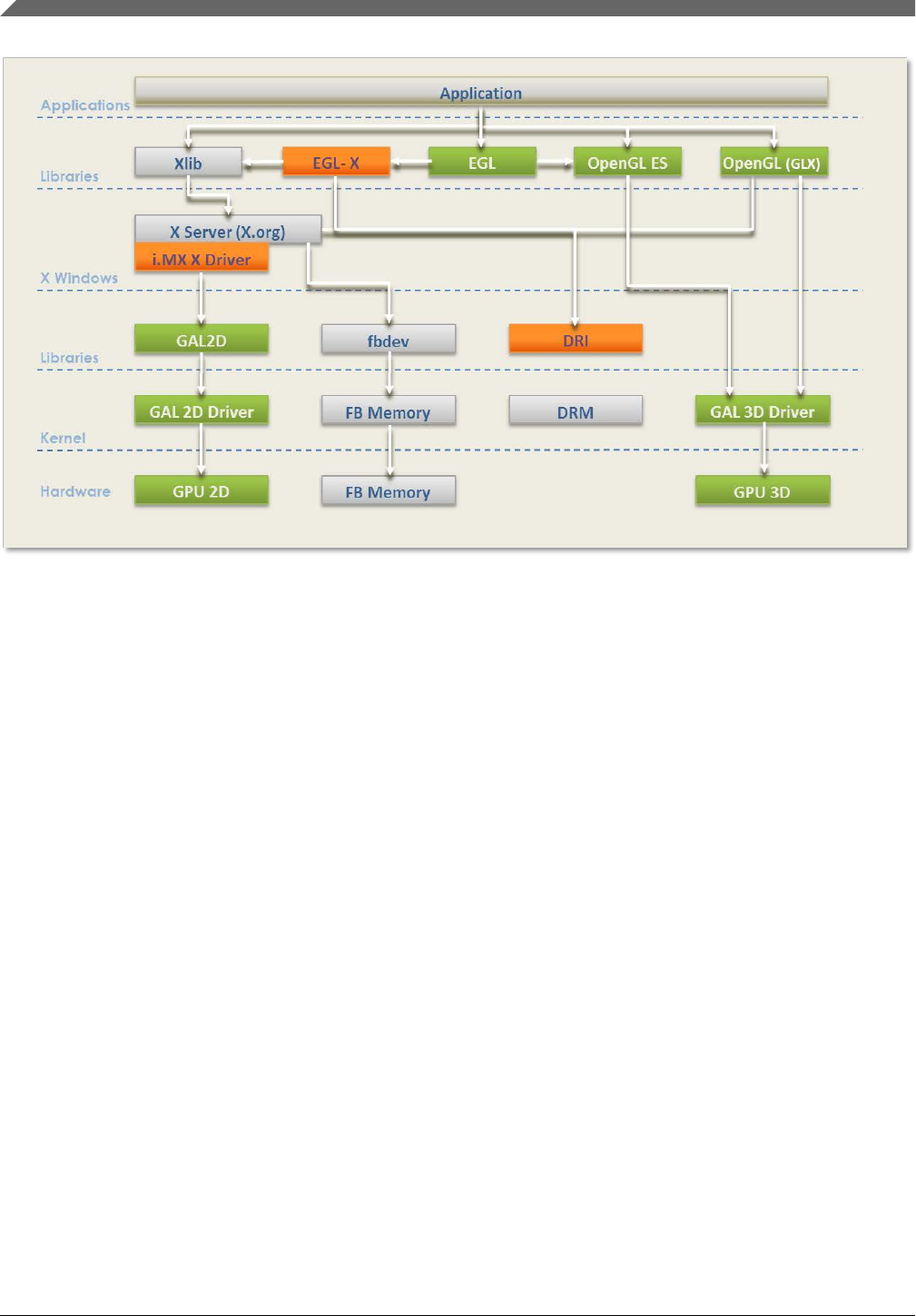
Figure 5-1. X Driver Architecture
The components shown in green are those provided as part of the Vivante 2D/3D GPU
driver support which includes OpenGL/ES and EGL, though some i.MX processors, such
as i.MX 6SoloLite do not contain 3D HW module. The components shown in light gray
are the standard components in the X-Windows System without acceleration. The
components shown in orange are those added to support X-Windows System acceleration
and briefly described here.
The i.MX X Driver library module (vivante-drv.so) is loaded by the X server and
contains the high-level implementation of the X-Windows acceleration interface for i.MX
platforms containing the GC320 2D GPU core. The entire linearly contiguous frame
buffer memory in /dev/fb0 is used for allocating pixmaps for X both on screen and off
screen. The driver supports a custom X extension which allows X clients to query the
GPU address of any X pixmap stored in frame buffer memory.
The libGAL.so library module (libGAL.so) contains the register level programming
interface to the GC320 GPU module. This includes the storing of register programming
commands into packets which can be streamed to the device. The functions in the
libGAL.so library are called by the i.MX X Driver code.
X Windows Acceleration
i.MX Reference Manual, Rev. L4.9.88_2.0.0-ga, 05/2018
168 NXP Semiconductors

The EGL-X library module (libEGL.so) contains the X-Windows implementation of the
low level EGL platform-specific support functions. This allows X-window and X pixmap
objects to be used as EGL window and pixmap surfaces. The EGL-X library uses Xlib
function calls in its implementation along with the i.MX X Driver module's X extension
for querying the GPU address of X pixmaps stored in frame buffer memory.
5.3.2.2 i.MX Driver for X-Windows System
The i.MX X Driver, referred to as vivante-drv.so, implements the EXA interface of the X
server in providing acceleration.
The Vivante X Driver, referred to as vivante-drv.so, implements the EXA interface of the
X server to provide acceleration.
The following list describes details particular to this implementation:
• The implementation builds upon the source from the fbdev frame buffer driver for X
so that it can be the fallback when the acceleration is disabled.
• The implementation is based on X server EXA version 2.5.0.
• The EXA solid fill operation is accelerated, except for source/target drawables
containing less than 300x300 pixels in which case fallback is to software rendering.
• The EXA copy operation is accelerated, except for source/target drawables
containing less than 400x120 pixels in which case fallback is to software rendering.
• EXA putimage (upload into video memory) is accelerated, except for source
drawables containing less than 400x400 pixels in which case fallback is to software
rendering. For EXA solid fill and copy operations, only solid plane masks and only
GXcopy raster-op operations are accelerated.
• For EXA copy operation, the raster-op operations (GXandInverted, GXnor,
GXorReverse, GXorInverted, and GXnand) are not accelerated.
• EXA composite allows for many options and combinations of source/mask/target for
rendering.
• Most of the (commonly used) EXA composite operations are accelerated.
The following types of EXA composite operations are accelerated:
• Composite operations for source/target drawables containing at least 640 pixels. If
less than 640 pixels, the composite path falls to software.
• Simple source composite operations are used when source/target drawables contain
more than 200x200 pixels (operations with mask not supported).
• Constant source (with or without alpha mask) composite with target.
• Repeating pattern source (with or without alpha mask) composite with target.
Chapter 5 Graphics
i.MX Reference Manual, Rev. L4.9.88_2.0.0-ga, 05/2018
NXP Semiconductors 169

• Only these blending functions: SOURCE, OVER, IN, IN-REVERSE, OUT-
REVERSE, and ADD (some of these are needed to support component-alpha
blending which is accelerate).
• In general, the following types of (less commonly used) EXA composite operations
are not accelerated:
• Transformed (that is, scaled, rotated) sources and masks
• Gradient sources
• Alpha masks with repeating patterns
The implementation handles all pixmap allocation for X through the EXA callback
interface. A first attempt is made to allocate the memory where it can be accessed by a
physical GPU address. This attempt can fail if there is insufficient GPU accessible
memory remaining, but it can also fail when the bits per pixel being requested for the
pixmap is less than eight (8). If the attempt to allocate from the GPU accessible memory
fails, then the memory is allocated from the system. If the pixmap memory is allocated
from the system, then this pixmap cannot be involved in a GPU accelerated option. The
number of pitch bytes used to access the pixmap memory may be different depending on
whether it was allocated from GPU accessible memory or from the system. Once the
memory for an X pixmap has been allocated, whether it is from GPU accessible memory
or from the system, the pixmap is locked and can never migrate to the other type of
memory. Pixmap migration from GPU accessible memory to system memory is not
necessary since a system virtual address is always available for GPU accessible memory.
Pixmap migration from system memory to GPU accessible memory is not currently
implemented, but would only help in situations where there was insufficient GPU
accessible memory at initial allocation but more memory becomes available (through de-
allocation) at a later time. The GPU accessible memory pitch (horizontal) alignment for
Vivante 2D GPUs is 8 pixels. Because the memory can be allocated from GPU accessible
memory, these pixels could be used in EGL for OpenGL/ES drawing operations. All of
the memory allocated for /dev/fb0 is made available to an internal linear offscreen
memory manager based on the one used in EXA. The portion of this memory beyond the
screen memory is available for allocation of X pixmap, where this memory area is GPU
accessible. The amount of memory allocated to /dev/fb0 needs to be several MB more
than the amount needed for the screen. The actual amount needed depends on the number
of X-Windows and pixmaps used, the possible usage of X pixmaps as textures, and
whether X-Windows are using the XComposite extension. An X extension, i.e., VIVEXT
shown in Fig. 1, is provided so that X clients can query the physical GPU address
associated with an X pixmap, if that X pixmap was allocated in the GPU accessible
memory.
X Windows Acceleration
i.MX Reference Manual, Rev. L4.9.88_2.0.0-ga, 05/2018
170 NXP Semiconductors

5.3.2.3 i.MX Direct Rendering Infrastructure (DRI) for X-Windows
System
The Direct Rendering Infrastructure, also known as the DRI, is a framework for allowing
direct access to graphics hardware under the X Window System in a safe and efficient
manner. It includes changes to the X server, to several client libraries, and to the kernel
(DRM, Direct Rendering Manager). The most important activity for the DRI is to create
fast OpenGL and OpenGL ES implementations that render to framebuffer memory
directly. Without DRI, the OpenGL driver has to depend on X server for final rendering
(indirect rendering), which degrades the overall performance significantly.
The components of Vivante’s DRI OpenGL implementation include:
• The Direct Rendering Manager (DRM) is a kernel module that provides APIs to
userland to synchronize access to hardware and to manage different classes of video
memory buffers. Vivante’s DRI implementation uses selected DRM APIs for
opening/closing DRI device, and locking/unlocking FB. Most other buffer
management and DMA management functions are handled by Vivante’s specific
kernel module: galcore.ko.
• The EXA driver is a DRI-enabled DDX 2D driver which initializes the DRM when X
server starts. As all X Window pixmap buffers are allocated by the EXA driver from
GPU memory, the GPU can render directly into these buffers if the buffer
information is passed from the X server process to the X client processes (GL or
GLES applications) properly.
• The Vivante-specific X extension “vivext” passes buffer information from X server
to X clients. This Vivante X extension includes the following three interfaces:
• DrawableFlush, which enables X clients to notify X server to flush the GPU
cache for a drawable surface.
• DrawableInfo, which enables X clients to query the drawable information
(position, size, physical address, stride, cliplist, etc.) from the X server.
• PixmapPhysAddr, which enables X clients to query the physical address and
stride of a pixmap buffer from X server.
The integration of GL/GLES application windows with Ubuntu Unity2D desktop is
achieved by following steps:
• GL/GLES applications render a frame into the pixmap buffers that are allocated in
the EXA driver.
• In the SwapBuffers implementation, the driver notifies X server that the pixmap
buffer region is damaged through Xdamage and Xfixes APIs.
• Then the X server will present the latest pixmap buffer to the Unity2D desktop while
maintaining the proper window overlap characteristics relative to the other windows
on the desktop.
Chapter 5 Graphics
i.MX Reference Manual, Rev. L4.9.88_2.0.0-ga, 05/2018
NXP Semiconductors 171

On a compositing X desktop, such as Ubuntu Unity 2D, GLES/GL applications always
render into the full rectangular back buffer of a window. There is no window clipping
required. So the Vivante DRI implementation can take advantage of the GPU’s resolve
function and render into the window back buffer directly.
On a legacy X window desktop, such as Gnome, Xwin, etc., GLES/GL applications have
to render onto the frame buffer surface directly. Thus, the DRI driver uses the
DrawableInfo interface in the VIVEXT extension to obtain the cliplist of the window,
then copies the sub-regions of the render target to the frame buffer according to the
cliplist. This will ensure that the GLES/GL windows overlap with other windows on the
desktop properly. However, the copying of the render target sub-regions to the frame
buffer has to be done by the CPU as the sub-regions’ starting address and alignment may
not meet GPU copy requirements.
The Vivante DRI implementation can detect the type of X window manager (compositing
desktop manager or legacy desktop manager) at run-time, and use appropriate DRI
rendering paths for GLES/GL applications.
5.3.2.4 EGL- X Library
The EGL-X library implements the low level EGL interface when used in X Window
System. The following list describes details particular to this implementation:
• The eglDisplay native display type is “Display*” in X.
• The eglWindowSurfacenative window surface type is “Window” in X.
• The eglPixmapSurface native pixmap surface type is “Pixmap” in X.
When an eglWindowSurface is created, the back buffers used for double-buffering can
have different representations from the window surface (based on the selected
eglConfig). An attempt is made to create each back buffer using the representation which
provides the most efficient blit of the back buffer contents to the window surface when
eglSwapBuffers is called.
The back buffer is allocated by creating an X pixmap of the necessary size. Use the X
extension for the Vivante X Driver module to query the physical frame buffer address for
this X pixmap if it was allocated in the offscreen frame buffer memory.
5.3.2.5 xorg.conf for i.MX
The /etc/X11/xorg.conf file must be properly configured to use the i.MX 6 X Driver.
X Windows Acceleration
i.MX Reference Manual, Rev. L4.9.88_2.0.0-ga, 05/2018
172 NXP Semiconductors

The /etc/X11/xorg.conf file must be properly configured to use the Vivante X Driver.
This configuration appears in a “Device” section of the file which contains some required
entries and some entries that are optional. The following example shows a preferred
configuration for using the Vivante X Driver:
Section "ServerLayout"
Identifier "Default Layout"
Screen "Default Screen"
EndSection
Section "Module"
Load "dbe"
Load "extmod"
Load "freetype"
Load "glx"
Load "dri"
EndSection
Section "InputDevice"
Identifier "Generic Keyboard"
Driver "kbd"
Option "XkbLayout" "us"
Option "XkbModel" "pc105"
Option "XkbRules" "xorg"
EndSection
Section "InputDevice"
Identifier "Configured Mouse"
Driver "mouse"
Option "CorePointer"
EndSection
Section "Device"
Identifier "Your Accelerated Framebuffer Device"
Driver "vivante"
Option "fbdev" "/dev/fb0"
Option "vivante_fbdev" "/dev/fb0"
Option "HWcursor" "false"
EndSection
Section "Monitor"
Identifier "Configured Monitor"
EndSection
Section "Screen"
Identifier "Default Screen"
Monitor "Configured Monitor"
Device "Your Accelerated Framebuffer Device"
DefaultDepth 24
EndSection
Section "DRI"
Mode 0666
EndSection
Mandatory Strings
Some important entries recognized by the Vivante X Driver are described as follows.
Device Identifier and Screen Device String
Chapter 5 Graphics
i.MX Reference Manual, Rev. L4.9.88_2.0.0-ga, 05/2018
NXP Semiconductors 173

The mandatory Identifier entry in the Device section specifies the unique name to
associate with this graphics device.
Section "Device"
Identifier "Your Accelerated Framebuffer Device"
The following entry ties a specific graphics device to a screen. The Device Identifier
string must match the Device string in a Screensection of the xorg.conf file. For example:
Section "Screen"
Identifier "Default Screen"
<other entries>
Device "Your Accelerated Framebuffer Device"
<other entries>
EndSection
Device Driver String
The mandatory Driver entry specifies the name of the loadable Vivante X driver.
Driver "vivante"
Device fbdevPath Strings
The mandatory entries fbdev and vivante_dev specify the path for the frame buffer device
to use.
Section "Device"
Identifier "Your Accelerated Framebuffer Device"
Driver "vivante"
Option "fbdev" "/dev/fb0"
Option "vivante_fbdev" "/dev/fb0"
<other entries>
EndSection
5.3.2.6 Setup X-Windows System Acceleration on Yocto
Prerequisites:
• xserver-xorg-video-imx-viv-(ver).tar.gz, which is Vivante EXA plugin source code
based on GPU driver
• drm-update-arm.patch, which is a patch with adding the ARM lock implementation
for libdrm xf86drm.h. Note that the original xh86drm.h header file from libdrm does
not have lock for supporting ARM architecture. This patch is located in the
community Yocto Project layers Yocto_build/sources/meta-freescale/recipes-
graphics/drm/libdrm/mx6, and shown below: drm-update-arm.patch:
+#elif defined(__arm__)
+ #undef DRM_DEV_MODE
+ #define DRM_DEV_MODE (S_IRUSR|S_IWUSR|S_IRGRP|S_IWGRP|S_IROTH|S_IWOTH)
+
X Windows Acceleration
i.MX Reference Manual, Rev. L4.9.88_2.0.0-ga, 05/2018
174 NXP Semiconductors

+ #define DRM_CAS(lock,old,new,__ret) \
+ do { \
+ __asm__ __volatile__ ( \
+ "1: ldrex %0, [%1]\n" \
+ " teq %0, %2\n" \
+ " strexeq %0, %3, [%1]\n" \
+ : "r" (__ret) \
+ : "r" (lock), "r" (old), "r" (new) \
+ : "cc","memory"); \
+ } while (0)
+
#endif /* architecture */
#endif /* __GNUC__ >= 2 */
Build and install instructions:
• Install the prerequisites modules or patches in the appropriate locations and with
right recipes in Yocto environment.
• Build XServer with correct drm header file (xf86drm.h). The purpose is to create
correct dri module
• Build GPU EXA module with the command ‘bitbake xf86-video-imxfb-vivante’.
vivante_drv.so will be generated with successful build, and then install it together
with xorg and libdri library in target board rootfs in /usr/lib/xorg/modules/
• Install the pre-Yocto-built imx-gpu-viv binary in target board rootfs. For accelerating
X11, the X11 backend is required
• Now ready to run the X11 applications in target board.
NOTE
x11 applications hangs if the ARM core version xf86drm.h is
not used
5.3.2.7 Setup X Window System Acceleration
• Install any packages appropriate for your platform.
• Verify that the device file /dev/galcore is present.
• Verify that the file /etc/X11/xorg.conf contains the correct entries as described in the
previous section.
• Assuming the above steps have been performed, do the following to verify that X
Window System acceleration is indeed operating.
• Examine the log file /var/log/Xorg.0.log and confirm that the following lines are
present.
[ 41.752] (II) Loading /usr/lib/xorg/modules/drivers/vivante_drv.so
[ 41.752] (II) VIVANTE(0): using default device
[ 41.752] (II) VIVANTE(0): Creating default Display subsection in Screen
section "Default Screen" for depth/fbbpp 24/32
[ 41.752] (**) VIVANTE(0): Depth 24, (--) framebufferbpp 32
[ 41.752] (==) VIVANTE(0): RGB weight 888
[ 41.752] (==) VIVANTE(0): Default visual is TrueColor
[ 41.753] (==) VIVANTE(0): Using gamma correction (1.0, 1.0, 1.0)
[ 41.753] (II) VIVANTE(0): hardware: DISP3 BG (video memory: 8100kB)
[ 41.753] (II) VIVANTE(0): checking modes against framebuffer device...
Chapter 5 Graphics
i.MX Reference Manual, Rev. L4.9.88_2.0.0-ga, 05/2018
NXP Semiconductors 175

[ 41.753] (II) VIVANTE(0): checking modes against monitor...
[ 41.753] (--) VIVANTE(0): Virtual size is 1920x1080 (pitch 1920)
[ 41.753] (**) VIVANTE(0): Built-in mode "current": 148.5 MHz, 67.5 kHz,
60.0 Hz
[ 41.753] (II) VIVANTE(0): Modeline "current"x0.0 148.50 1920 2008 2052
2200 1080 1084 1089 1125 +hsync +
vsync -csync (67.5 kHz)
[ 41.753] (==) VIVANTE(0): DPI set to (96, 96)
[ 41.753] (II) Loading sub module "fb"
[ 41.753] (II) LoadModule: "fb"
[ 41.754] (II) Loading /usr/lib/xorg/modules/libfb.so
[ 41.755] (II) Module fb: vendor="X.Org Foundation"
[ 41.755] compiled for 1.10.4, module version = 1.0.0
[ 41.755] ABI class: X.Org ANSI C Emulation, version 0.4
[ 41.755] (II) Loading sub module "exa"
[ 41.755] (II) LoadModule: "exa"
[ 41.756] (II) Loading /usr/lib/xorg/modules/libexa.so
[ 41.756] (II) Module exa: vendor="X.Org Foundation"
[ 41.756] compiled for 1.10.4, module version = 2.5.0
[ 41.756] ABI class: X.Org Video Driver, version 10.0
[ 41.756] (--) Depth 24 pixmap format is 32 bpp
[ 41.797] (II) VIVANTE(0): FB Start = 0x33142000 FB Base = 0x33142000 FB
Offset = (nil)
[ 41.797] (II) VIVANTE(0): test Initializing EXA
[ 41.798] (II) EXA(0): Driver allocated offscreenpixmaps
[ 41.798] (II) EXA(0): Driver registered support for the following
operations:
[ 41.798] (II) Solid
[ 41.798] (II) Copy
[ 41.798] (II) Composite (RENDER acceleration)
[ 41.798] (II) UploadToScreen
[ 42.075] (==) VIVANTE(0): Backing store disabled
[ 42.084] (==) VIVANTE(0): DPMS enabled
5.3.2.8 Troubleshooting
1. Framebuffer devices can be specified by environment variable. This is especially
useful when there are multiple framebuffer devices.
export FB_FRAMEBUFFER_0=/dev/fb2
2. If the above does not resolve the issue:
• If DRM booted up properly, check the /var/log/X11.n log file (n will represent
instance number) for more information.
• If DRM did not boot properly, check your kernel mode driver installation. (See
sections 6.4.2 and 6.4.3 above).
3. Window is created, but nothing is drawn
• If you run an OpenGL application and find a window was created, but nothing
was drawn, try to export the ${__GL_DEV_FB} environment variable:
export __GL_DEV_FB=$FB_FRAMEBUFFER_0.
4. Cannot open Display message
• If you have a message similar to “Cannot open Display,” use the following
command to check whether X is running at :0 or at :1 instance, use:
$ ps –ef|grep X
X Windows Acceleration
i.MX Reference Manual, Rev. L4.9.88_2.0.0-ga, 05/2018
176 NXP Semiconductors

• Then depending on the returned instance number, add the following environment
variable
export DISPLAY=:n
• Then run it again.
5. UART terminal cannot run GPU application with lightdm
• Use ssh terminal instead.
6. EXA build script failure
• Check the log file and make sure your system time is set correctly.
7. Invalid MIT-MAGIC-COOKIE-1 Key error message
• Some GPU applications are not permitted to run using root. Use an alternate
account instead.
8. Segment fault occurs while running GPU application
• Check the attribute for dev/galcore should be updated to 666.
• To update this attribute automatically on system boot,
• Locate and edit file /etc/udev/rules.d/<bsp-specific.rules>.
• Add: “KERNEL==”galcore”,MODE=”0666””
• Lastly, make sure your kernel and GPU drivers are matched.
9. Check whether Compiz is running
• If your host or target has issues after installing the OpenGL Development
Packages in Table 6, check whether compiz is running with the following
command:
$ ps –ef|grep compiz
• If compiz is running, then Ubuntu is using Unity3D by default. To set the default
window manager to Unity2D:
• Locate and edit file /var/lib/AccountsService/users/<username>.
• Change ubuntu to ubunto-2d.
Chapter 5 Graphics
i.MX Reference Manual, Rev. L4.9.88_2.0.0-ga, 05/2018
NXP Semiconductors 177

X Windows Acceleration
i.MX Reference Manual, Rev. L4.9.88_2.0.0-ga, 05/2018
178 NXP Semiconductors

Chapter 6
Video
6.1 Capture
6.1.1 OmniVision Camera
6.1.1.1 OV5640 Using MIPI CSI-2 interface
This is an introduction for ov5640 camera driver which using MIPI CSI-2 interface.
6.1.1.1.1 Hardware Operation
The OV5640 is a small camera sensor and lens module with low power consumption.
The camera driver is located under the Linux V4L2 architecture. and it implements the
V4L2 capture interfaces. Applications cannot use the camera driver directly. Instead, the
applications use the V4L2 capture driver to open and close the camera for preview and
image capture, controlling the camera, getting images from camera, and starting the
camera preview.
The OV5640 uses the serial camera control bus (SCCB) interface to control the sensor
operation. It works as an I2C client, V4L2 driver uses I2C bus to control camera
operation.
OV5640 supports two transfer mode: parallel interface and MIPI interface.
When using MIPI mode, OV5640 connects to i.MX AP chip by MIPI CSI-2 interface.
MIPI receives the sensor data and transfers them to CSI.
See the OV5640 datasheet to get more information on the sensor.
For more information on MIPI CSI-2 and CSI see the Application Processors Reference
Manual associated with the SoC.
i.MX Reference Manual, Rev. L4.9.88_2.0.0-ga, 05/2018
NXP Semiconductors 179

6.1.1.1.2 Software Operation
The camera driver implements the V4L2 capture interface and applications and uses the
V4L2 capture interface to operate the camera.
The supported operations of V4L2 capture are:
• Capture stream mode
The supported picture formats are:
• YUV422P
• UYVY
• YUV420
The supported picture sizes are:
• QVGA
• VGA
• 720P
• 1080P
6.1.1.1.3 Source Code Structure
There are two different software architectures for the OV5640 driver. One is the V4L2
internal interface architecture for i.MX 6Dual/6Quad and i.MX 6Solo/6DualLite IPU
CSI/MIPI CSI. Driver source code is in the directory:
drivers/media/platform/mxc/capture
The other is the V4L2 sub-devices architecture for i.MX 6SoloLite, i.MX 6SoloX, i.MX
7Dual CSI/MIPI CSI. Driver source code is in the directory:
drivers/media/platform/mxc/capture
The table below shows the camera driver source files available in the directory.
Table 6-1. V4L2 Camera Driver Files
File Description
ov5640_mipi.c Camera driver implementation for OV5640 using MIPI CSI-2 interface
ov5640.c Camera driver implementation for OV5640 using parallel interface
6.1.1.1.4 Menu Configuration Options
In menu configuration enable the following module:
Capture
i.MX Reference Manual, Rev. L4.9.88_2.0.0-ga, 05/2018
180 NXP Semiconductors

Device Drivers > Multimedia support (MEDIA_SUPPORT [=y]) > V4L platform devices
(V4L_PLATFORM_DRIVERS [=y]) > MXC Camera/V4L2 PRP Features support >
MXC_CAMERA_OV5640_MIPI
6.1.1.2 OV5642 Using parallel interface
This is an introduction for ov5642 camera driver which using parallel interface.
6.1.1.2.1 Hardware Operation
The OV5642 is a small camera sensor and lens module with low power consumption.
The camera driver is located under the Linux V4L2 architecture. and it implements the
V4L2 capture interfaces. Applications cannot use the camera driver directly. Instead, the
applications use the V4L2 capture driver to open and close the camera for preview and
image capture, controlling the camera, getting images from camera, and starting the
camera preview.
The OV5642 uses the serial camera control bus (SCCB) interface to control the sensor
operation. It works as an I2C client, V4L2 driver uses I2C bus to control camera
operation.
OV5642 supports only parallel interface.
See the OV5642 datasheet to get more information on the sensor.
For more information see the Applications Processor Reference Manual associated with
SoC.
6.1.1.2.2 Software Operation
The camera driver implements the V4L2 capture interface and applications and uses the
V4L2 capture interface to operate the camera.
The supported operations of V4L2 capture are:
• Capture stream mode
• Capture still mode
The supported picture formats are:
• YUV422P
• UYVY
• YUV420
Chapter 6 Video
i.MX Reference Manual, Rev. L4.9.88_2.0.0-ga, 05/2018
NXP Semiconductors 181

The supported picture sizes are:
• QVGA
• VGA
• 720P
• 1080P
• QSXGA
6.1.1.2.3 Source Code Structure
Table below shows the camera driver source files available in the directory.
drivers/media/platform/mxc/capture
Table 6-2. Camera Driver Files
File Description
ov5642.c Camera driver implementation for OV5642 using parallel interface
6.1.1.2.4 Menu Configuration Options
In menu configuration enable the following module:
Device Drivers > Multimedia devices > Video capture adapters > MXC Video For Linux
Camera > MXC Camera/V4L2 PRP Features support > OmniVision ov5642 camera
support.
6.1.2 Camera Serial Interface (CSI)
6.1.2.1 Introduction
The CSI driver enables the i.MX device to directly connect to external CMOS sensors
and CCIR656 video sources. The CSI and sensor drivers are implemented in the Video
for Linux Two (V4L2) driver framework. It consists of the image capture driver and the
video output driver.
6.1.2.1.1 Hardware Operation
The CSI driver configures and operates with the hardware registers for the CSI module. It
provides:
• Configurable interface logic to support most commonly available CMOS sensors.
Capture
i.MX Reference Manual, Rev. L4.9.88_2.0.0-ga, 05/2018
182 NXP Semiconductors

• Full control of 8-bit/pixel, 10-bit/pixel or 16-bit/pixel data format to 32-bit receive
FIFO packing.
• 128x32 FIFO to store received image pixel data.
• Receive FIFO overrun protection mechanism.
• Embedded DMA controllers to transfer data from receive FIFO or statistic FIFO
through AHB bus.
• Support for double buffering two frames in the external memory.
• Single interrupt source to interrupt controller from maskable interrupt sources: Start
of Frame, End of Frame and so on.
• Configurable master clock frequency output to sensor.
For more information, see the CSI chapter in the associated Applications Processor
Reference Manual.
6.1.2.1.2 CSI Software Operation
The CSI driver initializes the CSI interface. Applications use the V4L2 interface to
operate the CSI interface.
6.1.2.1.2.1 Video for Linux 2 (V4L2) APIs
Video for Linux Two (V4L2) is a Linux standard. The API specification is available at
http://v4l2spec.bytesex.org/spec/.
The V4L2 capture device includes two interfaces: the capture interface and the overlay
interface. The capture and overlay interface use the CSI embedded DMA controller to
implement the function. The V4L2 driver implements the standard V4L2 API for capture
and overlay devices. The following is the data flow of capture and overlay.
1. The camera sends the data to the CSI receive FIFO, through the 8-bit/10-bit data
port.
2. The embedded DMA controllers transfer data from the receive FIFO to external
memory through the AHB bus.
3. The data is save to user space memory or output to the frame buffer directly.
6.1.2.1.2.2 V4L2 Capture Device
V4L2 capture support can be selected during kernel configuration. The driver for this
device is in the drivers/media/video/mxc/capture/csi_v4l2_capture.c file.
The memory map stream API is supported. Supported V4L2 IOCTLs include the
following:
VIDIOC_QUERYCAP
VIDIOC_G_FMT
Chapter 6 Video
i.MX Reference Manual, Rev. L4.9.88_2.0.0-ga, 05/2018
NXP Semiconductors 183

VIDIOC_S_FMT
VIDIOC_OVERLAY
VIDIOC_G_FBUF
VIDIOC_S_FBUF
VIDIOC_S_PARM
VIDIOC_G_PARM
VIDIOC_QUERYBUF
VIDIOC_REQBUFS
VIDIOC_DQBUF
VIDIOC_QBUF
VIDIOC_STREAMON
VIDIOC_STREAMOFF
6.1.2.1.2.3 Use of the V4L2 Capture APIs
The following are some sample use cases for the V4L2 capture APIs:
1. Sets the capture pixel format and size using IOCTL VIDIOC_S_FMT.
2. Sets the control information using IOCTL VIDIOC_S_CTRL, for rotation.
3. Requests a buffer using IOCTL VIDIOC_REQBUFS. The common V4L2 driver
creates a chain of buffers (currently the maximum number of frames is 3).
4. Memory maps the buffer to its user space.
5. Executes the IOCTL VIDIOC_DQBUF.
6. Passes the data that requires post-processing to the buffer.
7. Queues the buffer using the IOCTL command VIDIOC_QBUF.
8. Starts the stream by executing IOCTL VIDIOC_STREAMON.
• VIDIOC_STREAMON and VIDIOC_OVERLAY cannot be enabled
simultaneously.
6.1.2.1.3 Source Code Structure
Table below shows the CSI sensor and V4L2 driver source files available in the
following directory:
drivers/media/video/mxc/capture
Table 6-3. V4L2 and SI Driver Files
File Description
fsl_csi.c CSI driver source file
fsl_csi.h CSI driver header file
csi_v4l2_capture.c V4L2 capture device driver source file
mxc_v4l2_capture.h V4L2 capture device driver header file
ov2640.c Camera driver source file
6.1.2.1.4 Menu Configuration Options
In menu configuration enable the following module:
Capture
i.MX Reference Manual, Rev. L4.9.88_2.0.0-ga, 05/2018
184 NXP Semiconductors

• VIDEO_MXC_CSI_CAMERA - Includes support for the CSI Unit and V4L2
capture device. In menuconfig, this option is available under:
Device Drivers > Multimedia devices > Video For Linux > Video Capture Adapters
> MXC Camera/V4L2 PRP Features support
By default, this option is M.
• CONFIG_MXC_CAMERA_OV2640 - Option for the OV2640 sensor driver. In
menuconfig, this option is available under:
Device Drivers > Multimedia devices > Video For Linux > Video Capture Adapters
> MXC Camera/V4L2 PRP Features support
By default, this option is M.
6.1.3 MIPI Camera Serial Interface (MIPI CSI)
6.1.3.1 Introduction
MIPI CSI-2 for i.MX 6 is MIPI-Camera Serial Interface Host Controller. It is a high
performance serial interconnect bus for mobile application which connects camera
sensors to the host system. The CSI-2 Host Controller is a digital core that implements all
protocol functions defined in the MIPI CSI-2 Specification. In doing so, it provides an
interface between the system and the MIPI D-PHY and allows communication with MIPI
CSI-2-compliant Camera Sensor.
The MIPI CSI2 driver is used to manage the MIPI D-PHY and lets it co-work with MIPI
sensor and IPU CSI. MIPI CSI2 driver implements functions as follows:
• MIPI CSI-2 low-level interface for managing the mipi D-PHY register and clock
• MIPI CSI-2 common API for communication between MIPI sensor and MIPI D-
PHY
By calling MIPI common APIs, MIPI sensor can set certain information about sensor
(such as datatype, lanes number, etc.) to MIPI CSI2 driver to configure D-PHY. In order
for the IPU CSI module driver to have the correct configuration, receive appropriate data,
and process it correctly, it is necessary for it to receive information about sensor (such as
datatype, virtual channel, IPU ID, CSI ID, etc.) from the MIPI CSI2 driver.
Chapter 6 Video
i.MX Reference Manual, Rev. L4.9.88_2.0.0-ga, 05/2018
NXP Semiconductors 185

6.1.3.1.1 MIPI CSI2 Driver Overview
MIPI CSI2 driver is invoked only by the MIPI sensor driver and IPU CSI module and is
not exposed to the user space.
MIPI CSI2 driver supports the following features:
• Support 1-4 lanes
• Support IPU(0,1) and CSI(0,1) select
• Support virtual channel select (0-3)
• Support date type includes:
• RGB formats: RGB888, RGB666, RGB565, RGB555, RGB444
• YUV formats: YUV422 8-bit, YUV422 10-bit, YUV420 8-bit, YUV420 10-bit
• RAW data: RAW6, RAW7, RAW8, RAW10, RAW12, RAW14
6.1.3.1.2 Hardware Operation
There are four blocks in the MIPI CSI-2 D-PHY: PHY adaptation layer, packet analyzer,
image date interface, and register bank.
Functions and operations are listed as follows:
• PHY Adaptation Layer is responsible for managing the D-PHY interface including
PHY error handling;
• Packet Analyzer is responsible for data lane merging if required, together with
header decoding, error detection and correction, frame size error detection and CRC
error detection;
• Image Date Interface separates CSI-2 packet header information and reorders data
according to memory storage format. It also generates timing accurate video
synchronization signals. Several error detections are also performed at frame-level
and line-level;
• Register Bank is accessible through a standard AMBA-APB slave interface and
provides access to the CSI-2 Host Controller register for configuration and control.
There is also a fully programmable interrupt generator to inform the system upon
certain events;
6.1.3.2 Software Operation
MIPI CSI2 driver for Linux OS has two parts: MIPI CSI2 driver initialize operation
which initializes mipi_csi2_info struct, and MIPI CSI2 common APIs which exports
APIs for CSI module driver and MIPI sensor driver.
Capture
i.MX Reference Manual, Rev. L4.9.88_2.0.0-ga, 05/2018
186 NXP Semiconductors

6.1.3.2.1 MIPI CSI2 Driver Initialize Operation
MIPI CSI driver first initializes mipi_csi2_info struct, some key information about mipi
sensor will be initialized, such as connected IPU ID, CSI ID, the virtual channel and date
type. Then, the driver initializes D-PHY clock and pixel clock (pixel clock is used for
MIPI D-PHY to transfer data to IPU CSI). After these operations, MIPI CSI csi2 driver
waits for sensor connection.
6.1.3.2.2 MIPI CSI2 Common API Operation
MIPI CSI2 driver exports many APIs to manage MIPI D-PHY.
The following is the introduction for all APIs:
• mipi_csi2_get_info: get the mipi_csi_info
• mipi_csi2_enable: enable MIPI CSI interface
• mipi_csi2_disable: disable MIPI CSI interface
• mipi_csi2_get_status: get MIPI CSI interface disable/enable status
• mipi_csi2_get_bind_ipu: get the IPU ID which MIPI CSI will connect
• mipi_csi2_get_bind_csi: get the CSI ID which MIPI CSI will connect
• mipi_csi2_get_virtual_channel: get the virtual channel number by which MIPI sensor
transfers data to MIPI D-PHY
• mipi_csi2_set_lanes: set the lanes number by which MIPI sensor transfers data to
MIPI D-PHY
• mipi_csi2_set datatype: set the MIPI sensor data type
• mipi_csi2_get_datatype: get the MIPI sensor data type; This function is called by
CSI module to set the CSI register
• mipi_csi2_dphy_status: get the MIPI D-PHY status
• mipi_csi2_get_error1: get the MIPI error1 register information
• mipi_csi2_get_error2: get the MIPI error2 register information
• mipi_csi2_pixelclk_enable: enable the pixel clock
• mipi_csi2_pixelclk_disable: disable the pixel clock
• mipi_csi2_reset: reset the MIPI D-PHY for data receiving and transferring
6.1.3.2.3 Driver Features
MIPI CSI2 driver supports the following features:
• Support 1~4 lanes
• Support IPU(0,1) and CSI(0,1) select
• Support virtual channel select(0~3)
• Support date type includes:
• RGB formats: RGB888, RGB666, RGB565, RGB555, RGB444
Chapter 6 Video
i.MX Reference Manual, Rev. L4.9.88_2.0.0-ga, 05/2018
NXP Semiconductors 187

• YUV formats: YUV422 8bit, YUV422 10bit, YUV420 8bit, YUV420 10bit
• RAW data: RAW6, RAW7, RAW8, RAW10, RAW12, RAW14
6.1.3.2.4 Source Code Structure
Table below shows the MIPI CSI2 driver source files available in the directory.
drivers/mxc/mipi
.
Table 6-4. MIPI CSI2 Driver Files
File Description
mxc_mipi_csi2.c MIPI CSI driver source file
6.1.3.2.5 Menu Configuration Options
In menu configuration enable the following module:
Device Drivers > MXC support drivers > MXC MIPI Support > MIPI CSI2 support.
6.1.3.2.6 Programming Interface
MIPI CSI2 Common APIs can only be called by MIPI sensor driver and IPU CSI module
driver.
Before calling the API, in system initialization stage, use mipi_csi2_platform_data struct
and imx6q_add_mipi_csi2 function to add a MIPI CSI2 driver.
For the MIPI sensor driver, the initialization steps are as follows:
• Get MIPI info by calling mipi_csi2_get_info()
• Enable MIPI CSI interface by calling mipi_csi2_enable()
• Set the lanes by calling mipi_csi2_set_lanes()
• Reset the MIPI D-PHY by calling mipi_csi2_reset()
• Configure MIPI sensor
• Wait for MIPI D-PHY to receive the sensor clock and data until clock and data are
stable by calling mipi_csi2_dphy_status() and mipi_csi2_get_error1()
• When uninstall the sensor driver, disable MIPI CSI interface by calling
mipi_csi2_disable()
For sample code which explains how MIPI sensor uses MIPI APIs, reference
ov5640_mipi driver source code.
For IPU CSI module driver, the call steps are:
Capture
i.MX Reference Manual, Rev. L4.9.88_2.0.0-ga, 05/2018
188 NXP Semiconductors

• get MIPI information by calling mipi_csi2_get_info()
• get IPU id and CSI id to assure configuration of the correct CSI module by calling
mipi_csi2_get_bind_ipu() and mipi_csi2_get_bind_csi()
• get datatype and virtual channel from MIPI CSI driver and configure the CSI module
by calling mipi_csi2_get_datatype() and mipi_csi2_get_virtual_channel()
• perform other configure operation for CSI module and enable CSI
• enable the pixel clock to transfer data from MIPI D-PHY to IPU CSI by calling
mipi_csi2_pixelclk_enable()
• when all tasks are done, disable CSI module first, then disable MIPI pixel clock by
calling mipi_csi2_pixelclk_disable()
For sample code which explains how the CSI module driver uses MIPI APIs, reference
IPU CSI module driver source code.
6.2 Display
6.2.1 Display Processing Unit (DPU)
6.2.1.1 Introduction
The display processing unit (IMXDPU) is designed to support video and graphics
processing functions and to interface with video and still display sensors and displays.
The IMXDPU driver provides internel kernel-level APIs to manipulate logical channels.
A logical channel represents a complete IMXDPU processing flow. For example, a
complete IMXDPU processing flow (logical channel) might consist of reading a YUV
buffer from memory and displaying it to an external interface. The IMXDPU API
consists of a set of common functions for all channels. Its functions are to initialize
channels, set up buffers, enable and disable channels and set up interrupts.
Typical logical channels include:
• CSI direct to memory
• Memory to synchronous frame buffer background
• Memory to synchronous frame buffer foreground
The higher level drivers are responsible for memory allocation and providing user-level
API.
Chapter 6 Video
i.MX Reference Manual, Rev. L4.9.88_2.0.0-ga, 05/2018
NXP Semiconductors 189

6.2.1.2 Source Code Structure
The IMX DPU driver files are in drivers/mxc/imxdpu.
6.2.1.2.1 Menu Configuration Options
The following Linux kernel configuration options are provided for the IMXDPU module.
Device Drivers -> MXC support drivers -> Display Processing Unit Driver Version 0.
6.2.2 Image Processing Unit (IPU)
6.2.2.1 Introduction
The image processing unit (IPU) is designed to support video and graphics processing
functions and to interface with video and still image sensors and displays. The IPU driver
provides a kernel-level API to manipulate logical channels. A logical channel represents
a complete IPU processing flow. For example, a complete IPU processing flow (logical
channel) might consist of reading a YUV buffer from memory, performing post-
processing, and writing an RGB buffer to memory. A logical channel maps one to three
IDMA channels and maps to either zero or one IC tasks. A logical channel can have one
input, one output, and one secondary input IDMA channel. The IPU API consists of a set
of common functions for all channels. Its functions are to initialize channels, set up
buffers, enable and disable channels, link channels for auto frame synchronization, and
set up interrupts.
Typical logical channels include:
• CSI direct to memory
• CSI to viewfinder pre-processing to memory
• Memory to viewfinder pre-processing to memory
• Memory to viewfinder rotation to memory
• Previous field channel of memory to video deinterlacing and viewfinder pre-
processing to memory
• Current field channel of memory to video deinterlacing and viewfinder pre-
processing to memory
• Next field channel of memory to video deinterlacing and viewfinder pre-processing
to memory
• CSI to encoder pre-processing to memory
• Memory to encoder pre-processing to memory
• Memory to encoder rotation to memory
• Memory to post-processing rotation to memory
Display
i.MX Reference Manual, Rev. L4.9.88_2.0.0-ga, 05/2018
190 NXP Semiconductors

• Memory to synchronous frame buffer background
• Memory to synchronous frame buffer foreground
• Memory to synchronous frame buffer DC
• Memory to synchronous frame buffer mask
The IPU API has some additional functions that are not common across all channels, and
are specific to an IPU sub-module. The types of functions for the IPU sub-modules are as
follows:
• Synchronous frame buffer functions
• Panel interface initialization
• Set foreground positions
• Set local/global alpha and color key
• Set gamma
• CSI functions
• Sensor interface initialization
• Set sensor clock
• Set capture size
• Enable or disable prefetching linear frames by using PRE/PRG
• Enable or disable resolving tiled frames by using PRE/PRG
The higher level drivers are responsible for memory allocation, chaining of channels, and
providing user-level API.
Chapter 6 Video
i.MX Reference Manual, Rev. L4.9.88_2.0.0-ga, 05/2018
NXP Semiconductors 191
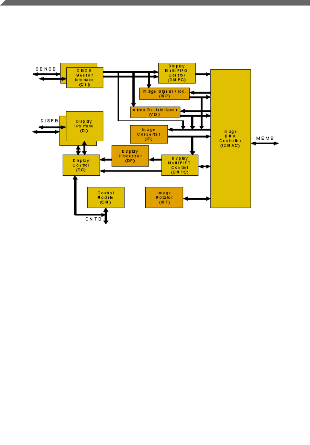
6.2.2.1.1 Hardware Operation
The detailed hardware operation of the IPU is discussed in the Applications Processor
Reference Manual. The following figure shows the IPU hardware modules.
Figure 6-1. IPUv3EX/IPUv3H IPU Module Overview
6.2.2.2 Software Operation
The IPU driver is a self-contained driver module in the Linux kernel.
It consists of a custom kernel-level API for the following blocks:
• Synchronous frame buffer driver
• Display Interface (DI)
• Display Processor (DP)
• Image DMA Controller (IDMAC)
• CMOS Sensor Interface (CSI)
• Image Converter (IC)
• Prefetch/Resolve Engine/Gasket (PRE/PRG)
Figure below shows the interaction between the different graphics/video drivers and the
IPU.
Display
i.MX Reference Manual, Rev. L4.9.88_2.0.0-ga, 05/2018
192 NXP Semiconductors
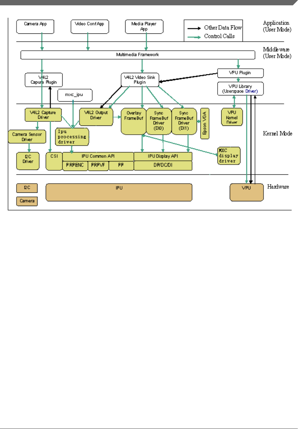
Figure 6-2. Graphics/Video Drivers Software Interaction for IPUv3
The drivers for IPUv1 are named simply ipu. Drivers for IPUv3 contain 3 or v3 in the
name. The IPU drivers are sub-divided as follows:
• Device drivers-include the frame buffer driver for the synchronous frame buffer, the
frame buffer driver for the displays, V4L2 capture drivers for IPU pre-processing, the
V4L2 output driver for IPU post-processing, and the ipu processing driver which
provide system interface to user space or V4L2 drivers. The frame buffer device
drivers are available in drivers/video/mxc. The V4L2 device drivers are available in
drivers/media/platform/mxc.
• The MXC display driver is introduced as a simple framework to manage interaction
between IPU and display device drivers (e.g., LCD, LVDS, HDMI, MIPI, etc.)
• Low-level library routines-interface to the IPU hardware registers. They take input
from the high-level device drivers and communicate with the IPU hardware. The
low-level libraries are available in the directory of the Linux kernel.
Chapter 6 Video
i.MX Reference Manual, Rev. L4.9.88_2.0.0-ga, 05/2018
NXP Semiconductors 193

6.2.2.2.1 IPU Frame Buffer Drivers Overview
The frame buffer device provides an abstraction for the graphics hardware. It represents
the frame buffer video hardware, and allows application software to access the graphics
hardware through a well-defined interface, so that the software is not required to know
anything about the low-level hardware registers.
The driver is enabled by selecting the frame buffer option under the graphics parameters
in the kernel configuration. To supplement the frame buffer driver, the kernel builder
may also include support for fonts and a startup logo. This device depends on the virtual
terminal (VT) console to switch from serial to graphics mode. The device is accessed
through special device nodes, located in the /dev directory, as /dev/fb*. fb0 is generally
the primary frame buffer.
Other than the physical memory allocation and LCD panel configuration, the common
kernel video API is utilized for setting colors, palette registration, image blitting, and
memory mapping. The IPU reads the raw pixel data from the frame buffer memory and
sends it to the panel for display.
6.2.2.2.1.1 IPU Frame Buffer Hardware Operation
The frame buffer interacts with the IPU hardware driver module.
6.2.2.2.1.2 IPU Frame Buffer Software Operation
A frame buffer device is a memory device, such as /dev/mem, and it has features similar
to a memory device. Users can read it, write to it, seek to some location in it, and mmap()
it (the main use). The difference is that the memory that appears in the special file is not
the whole memory, but the frame buffer of some video hardware.
/dev/fb* also interacts with several IOCTLs, which allows users to query and set
information about the hardware. The color map is also handled through IOCTLs. For
more information on what IOCTLs exist and which data structures they use, see include/
uapi/linux/fb.h. The following are a few of the IOCTLs functions:
• Request general information about the hardware, such as name, organization of the
screen memory (planes, packed pixels, and so on), and address and length of the
screen memory.
• Request and change variable information about the hardware, such as visible and
virtual geometry, depth, color map format, timing, and so on. The driver suggests
values to meet the hardware capabilities (the hardware returns EINVAL if that is not
possible) if this information is changed.
• Get and set parts of the color map. Communication is 16 bits-per-pixel (values for
red, green, blue, transparency) to support all existing hardware. The driver does all
Display
i.MX Reference Manual, Rev. L4.9.88_2.0.0-ga, 05/2018
194 NXP Semiconductors

the calculations required to apply the options to the hardware (round to fewer bits,
possibly discard transparency value).
The hardware abstraction makes the implementation of application programs easier and
more portable. The only thing that must be built into the application programs is the
screen organization (bitplanes or chunky pixels, and so on), because it works on the
frame buffer image data directly.
The MXC frame buffer driver (drivers/video/mxc/mxc_ipuv3_fb.c) interacts closely with
the generic Linux frame buffer driver (drivers/video/fbdev/core/fbmem.c).
6.2.2.2.1.3 Synchronous Frame Buffer Driver
The synchronous frame buffer screen driver implements a Linux standard frame buffer
driver API for synchronous LCD panels or those without memory. The synchronous
frame buffer screen driver is the top level kernel video driver that interacts with kernel
and user level applications. This is enabled by selecting the Synchronous Panel Frame
buffer option under the graphics support device drivers in the kernel configuration. To
supplement the frame buffer driver, the kernel builder may also include support for fonts
and a startup logo. This depends on the VT console for switching from serial to graphics
mode.
Except for physical memory allocation and LCD panel configuration, the common kernel
video API is utilized for setting colors, palette registration, image blitting, and memory
mapping. The IPU reads the raw pixel data from the frame buffer memory and sends it to
the panel for display.
The frame buffer driver supports different panels as a kernel configuration option.
Support for new panels can be added by defining new values for a structure of panel
settings.
The frame buffer interacts with the IPU driver using custom APIs that allow:
• Initialization of panel interface settings
• Initialization of IPU channel settings for LCD refresh
• Changing the frame buffer address for double buffering support
The following features are supported:
• Configurable screen resolution
• Configurable RGB 16, 24, or 32 bits per pixel frame buffer
• Configurable panel interface signal timings and polarities
• Palette/color conversion management
• Power management
Chapter 6 Video
i.MX Reference Manual, Rev. L4.9.88_2.0.0-ga, 05/2018
NXP Semiconductors 195

• LCD power off/on
• Enable/disable PRE/PRG features
User applications utilize the generic video API (the standard Linux frame buffer driver
API) to perform functions with the frame buffer. These include the following:
• Obtaining screen information, such as the resolution or scan length
• Allocating user space memory using mmap for performing direct blitting operations
A second frame buffer driver supports a second video/graphics plane.
6.2.2.2.2 IPU Backlight Driver
IPU drivers also control the backlight. The IPU backlight driver implements IPU PWM
backlight control for panels. It exports a sys control file under /sys/class/backlight/pwm-
backlight.0/brightness to user space. The default backlight intensity value is 128.
6.2.2.2.3 IPU Device Driver
IPU (processing) device driver provide image processing features: resizing/rotation/CSC/
combination/deinterlacing based on IC/IRT modules in IPUv3.
The IPU device driver is task based, user just need prepare task setting, queue task, then
block wait task finish. The driver now supports only blocking method, and the non-block
method will be added in the future. The task structures are as follows:
struct ipu_task {
struct ipu_input input;
struct ipu_output output;
bool overlay_en;
struct ipu_overlay overlay;
#define IPU_TASK_PRIORITY_NORMAL 0
#define IPU_TASK_PRIORITY_HIGH 1
u8 priority;
#define IPU_TASK_ID_ANY 0
#define IPU_TASK_ID_VF 1
#define IPU_TASK_ID_PP 2
#define IPU_TASK_ID_MAX 3
u8 task_id;
int timeout;
};
struct ipu_input {
u32 width;
u32 height;
u32 format;
struct ipu_crop crop;
dma_addr_t paddr;
struct ipu_deinterlace deinterlace;
dma_addr_t paddr_n; /*valid when deinterlace enable*/
Display
i.MX Reference Manual, Rev. L4.9.88_2.0.0-ga, 05/2018
196 NXP Semiconductors

};
struct ipu_overlay {
u32 width;
u32 height;
u32 format;
struct ipu_crop crop;
struct ipu_alpha alpha;
struct ipu_colorkey colorkey;
dma_addr_t
paddr;
};
struct ipu_output
{
u32 width;
u32 height;
u32 format;
u8 rotate;
struct ipu_crop crop;
dma_addr_t paddr;
};
To prepare the task, the user just needs to fill task.input, task.overlay (if need combine)
and task.output parameters, and then queue task either by int ipu_queue_task(struct
ipu_task *task); if from the kernel level (V4L2 driver for example), or by
IPU_QUEUE_TASK ioctl under /dev/mxc_ipu if from the application level.
6.2.2.2.4 Source Code Structure
Table 6-5 lists the source files associated with the IPU, Sensor, V4L2, and Panel drivers.
These files are available in the following directories:
drivers/mxc/ipu3
drivers/video/mxc
drivers/video/fbdev/mxc
drivers/video/backlight
Table 6-5. IPU Driver Files
File Description
ipu_common.c IPU common library functions
ipu_ic.c IPU IC base driver
ipu_device.c IPU driver device interface and fops functions
ipu_capture.c IPU CSI capture base driver
ipu_disp.c IPU display functions
ipu_calc_stripes_sizes.c Multistripes method functions for ipu_device.c
pre.c Prefetch/Resolve the engine driver
prg.c Prefetch/Resolve the Gasket driver
Table continues on the next page...
Chapter 6 Video
i.MX Reference Manual, Rev. L4.9.88_2.0.0-ga, 05/2018
NXP Semiconductors 197

Table 6-5. IPU Driver Files (continued)
File Description
mxc_ipuv3_fb.c Driver for synchronous frame buffer
mxc_lcdif.c Display Driver for CLAA-WVGA and SEIKO-WVGA LCD support
mxc_hdmi.c Display Driver for HDMI interface
ldb.c Driver for synchronous frame buffer for on chip LVDS
mxc_dispdrv.c Display Driver framework for synchronous frame buffer
mxc_edid.c Driver for EDID
vdoa.c VDOA post-processing driver, used by ipu_device.c
Table 6-6 lists the global header files associated with the IPU and Panel drivers. These
files are available in the following directories:
drivers/mxc/ipu3/
include/linux/
drivers/media/platform/mxc/
Table 6-6. IPU Global Header Files
File Description
ipu_param_mem.h Helper functions for IPU parameter memory access
ipu_prv.h Header file for Pre-processing drivers
ipu_regs.h IPU register definitions
pre-regs.h Prefetch/Resolve Engine register definitions
prg-regs.h Prefetch/Resolve Gasket register definitions
vdoa.h Header file for VDOA drivers
mxc_dispdrv.h Header file for display driver
mxcfb.h Header file for the synchronous framebuffer driver
ipu.h Header file for IPU basic driver
6.2.2.2.5 Menu Configuration Options
The following Linux kernel configuration options are provided for the IPU module.
In menu configuration enable the following module:
• CONFIG_MXC_IPU_V3 - Includes support for the Image Processing Unit. In
menuconfig, this option is available under:
Device Drivers > MXC support drivers > Image Processing Unit Driver
By default, this option is Y for all architectures.
If ARCH_MXC is true, CONFIG_MXC_IPU_V3 will be set.
Display
i.MX Reference Manual, Rev. L4.9.88_2.0.0-ga, 05/2018
198 NXP Semiconductors

• CONFIG_MXC_IPU_V3_PRG - This enables support for the IPUv3 prefetch gasket
engine to support double buffer handshake control between IPUv3 and prefetch
engine (PRE), snoop the AXI interface for display refresh requests to memory, and
modify the request address to fetch the double buffered row of blocks in OCRAM.
Device Drivers > MXC support drivers > i.MX IPUv3 prefetch gasket engine
This option depends on CONFIG_MXC_IPU_V3 and
CONFIG_MXC_IPU_V3_PRE.
• CONFIG_MXC_IPU_V3_PRE - This enables support for the IPUv3 prefetch engine
to improve the system memory performance. The engine has the capability to resolve
framebuffers in tile pixel format to linear.
Device Drivers > MXC support drivers > i.MX IPUv3 prefetch engine
This option depends on CONFIG_MXC_IPU_V3. Enabling this option selects
CONFIG_MXC_IPU_V3_PRG.
• CONFIG_MXC_CAMERA_OV5640_MIPI - Option for both the OV 5640 mipi
sensor driver and the use case driver. This option is dependent on the
VIDEO_MXC_CAPTURE option. In menuconfig, this option is available under:
Device Drivers > Multimedia support > V4L platform devices > MXC Video For
Linux Video Capture > MXC Camera/V4L2 PRP Features support > OmniVision
5640 Camera support using mipi
• CONFIG_MXC_CAMERA_OV5640 - Option for both the OV5640 sensor driver
and the use case driver. This option is dependent on the VIDEO_MXC_CAPTURE
option. In menuconfig, this option is available under:
Device Drivers > Multimedia platform > V4L platform devices > MXC Video For
Linux Video Capture > MXC Camera/V4L2 PRP Features support > OmniVision
ov5640 camera support
Only one sensor should be installed at a time.
• CONFIG_MXC_IPU_PRP_VF_SDC - Option for the IPU (here the > symbols
illustrates data flow direction between HW blocks):
CSI > IC > MEM MEM > IC (PRP VF) > MEM
Use case driver for dumb sensor or
CSI > IC(PRP VF) > MEM
for smart sensors. In menuconfig, this option is available under:
Chapter 6 Video
i.MX Reference Manual, Rev. L4.9.88_2.0.0-ga, 05/2018
NXP Semiconductors 199

Multimedia devices > Video capture adapters > MXC Video For Linux Camera >
MXC Camera/V4L2 PRP Features support > Pre-Processor VF SDC library
By default, this option is M for all.
• CONFIG_MXC_IPU_PRP_ENC - Option for the IPU:
Use case driver for dumb sensors
CSI > IC > MEM MEM > IC (PRP ENC) > MEM
or for smart sensors
CSI > IC(PRP ENC) > MEM.
In menuconfig, this option is available under:
Device Drivers > Multimedia Devices > Video capture adapters > MXC Video For
Linux Camera > MXC Camera/V4L2 PRP Features support > Pre-processor Encoder
library
By default, this option is set to M for all.
• CONFIG_VIDEO_MXC_CAMERA - This is configuration option for V4L2 capture
Driver. This option is dependent on the following expression:
VIDEO_DEV && MXC_IPU && MXC_IPU_PRP_VF_SDC &&
MXC_IPU_PRP_ENC
In menuconfig, this option is available under:
Device Drivers > Multimedia devices > Video capture adapters > MXC Video For
Linux Camera
By default, this option is M for all.
• CONFIG_VIDEO_MXC_OUTPUT - This is configuration option for V4L2 output
Driver. This option is dependent on VIDEO_DEV && MXC_IPU option. In
menuconfig, this option is available under:
Device Drivers > Multimedia devices > Video capture adapters > MXC Video for
Linux Video Output
By default, this option is Y for all.
• CONFIG_FB - This is the configuration option to include frame buffer support in the
Linux kernel. In menuconfig, this option is available under:
Device Drivers > Graphics support > Support for frame buffer devices
Display
i.MX Reference Manual, Rev. L4.9.88_2.0.0-ga, 05/2018
200 NXP Semiconductors

By default, this option is Y for all architectures.
• CONFIG_FB_MXC - This is the configuration option for the MXC Frame buffer
driver. This option is dependent on the CONFIG_FB option. In menuconfig, this
option is available under:
Device Drivers > Graphics support > MXC Framebuffer support
By default, this option is Y for all architectures.
• CONFIG_FB_MXC_SYNC_PANEL - This is the configuration option that chooses
the synchronous panel framebuffer. This option is dependent on the
CONFIG_FB_MXC option. In menuconfig, this option is available under:
Device Drivers > Graphics support > MXC Framebuffer support > Synchronous
Panel Framebuffer
By default this option is Y for all architectures.
• CONFIG_FB_MXC_LDB - This configuration option selects the LVDS module on
i.MX 6 chip. This option is dependent on CONFIG_FB_MXC_SYNC_PANEL and
CONFIG_MXC_IPUV3 || FB_MXS options. In menuconfig, this option is available
under:
Device Drivers > Graphics support > MXC Framebuffer support > Synchronous
Panel Framebuffer > MXC LDB
• CONFIG_FB_MXC_SII9022 - This configuration option selects the SII9022 HDMI
chip. This option is dependent on CONFIG_FB_MXC_SYNC_PANEL option. In
menuconfig, this option is available under:
Device Drivers > Graphics support > MXC Framebuffer support > Synchronous
Panel Framebuffer > Si Image SII9022 DVI/HDMI Interface Chip
6.2.2.3 Unit Test
NOTE
In order to execute the tests properly, make sure you have the
util-linux package selected and load the following modules:
insmod ipu_prp_enc.ko
insmod ipu_bg_overlay_sdc.ko
insmod ipu_fg_overlay_sdc.ko
insmod ipu_csi_enc.ko
insmod ov5640_camera.ko
insmod mxc_v4l2_capture.ko
Chapter 6 Video
i.MX Reference Manual, Rev. L4.9.88_2.0.0-ga, 05/2018
NXP Semiconductors 201

6.2.2.3.1 Framebuffer Tests
There is a test application named mxc_fb_test.c under the
imx-test-(version)/test/mxc_fb_test
directory.
Execute the fb test as follows:
./mxc_fb_test.out
The result should be Exiting PASS. The test includes fb0(background) and
fb1(foreground) devices open, framebuffer parameters configure, global alpha blending,
FB pan display test, and gamma test.
Redirect an image directly to the framebuffer device as follows:
# cat image.bin > /dev/fb0
6.2.2.3.2 Video4Linux API test
There are test applications named mxc_v4l2_test.c and mxc_v4l2_output.c under the
imx-test-(version)/test/mxc_v4l2_test
directory.
Before running the v4l2 capture test application, you should be able see that the /dev/v4l/
video0 has been created.
Test ID: FSL-UT-V4L2-capture-0010
# mxc_v4l2_capture.out -iw 640 -ih 480 -m 0 -r 0 -c 50 -fr 30 test.yuv
Capture the camera and store the 50 frames of YUV420 (VGA size)to a file called
test.yuv and set the frame rate to 30 fps. Look at mxc_v4l2_capture.out -help to see
usage.
Test ID: FSL-UT-V4L2-overlay-sdc-0010
# mxc_v4l2_overlay.out -iw 640 -ih 480 -it 0 -il 0 -ow 160 -oh 160 -ot 20 -ol 20 -r
0 -t 50 -d 0 -fg -fr 30
Direct preview the camera to SDC foreground, and set frame rate to 30 fps, window
of
interest is 640 X 480 with starting offset(0,0), the preview size is 160 X 160 with
starting offset (20,20). mxc_v4l2_overlay.out -help to see the usage.
Test ID: FSL-UT-V4L2-overlay-sdc-0020
# mxc_v4l2_overlay.out -iw 640 -ih 480 -it 0 -il 0 -ow 160 -oh 160 -ot 20 -ol 20 -r
Display
i.MX Reference Manual, Rev. L4.9.88_2.0.0-ga, 05/2018
202 NXP Semiconductors

4 -t 50 -d 0 -fr 30
Direct preview(90 degree rotation) the camera to SDC background, and set frame rate
to 30 fps.
Test ID: FSL-UT-V4L2-overlay-adc-0010
# mxc_v4l2_overlay.out -iw 640 -ih 480 -it 0 -il 0 -ow 120 -oh 120 -ot 40 -ol 40 -r
0 -t 50 -d 1 -fg -fr 30
Direct preview the camera to foreground, and set frame rate to 30 fps.
Test ID: FSL-UT-V4L2-overlay-adc-0020
# mxc_v4l2_overlay.out -iw 640 -ih 480 -it 0 -il 0 -ow 120 -oh 120 -ot 40 -ol 40 -r
4 -t 50 -d 1 -fg -fr 30
Direct preview(90 degree rotation) the camera to foreground, and set frame rate to
30
fps.
Test ID: FSL-UT-V4L2-output-0010
# mxc_v4l2_output.out -iw 640 -ih 480 -ow 1024 -oh 768 -r 0 -fr 60 test.yuv
Read the YUV420 stream file on test.yuv created by the mxc_v4l2_capture test as run
in test FSL-UT-V4L2-capture-0010. Apply color space conversion and resize, then
display on the framebuffer.
NOTE
The PRP channels require the stride line to be a multiple of 8,
for example with no rotation, the width needs to be 8 bit
aligned; and with 90 degree rotation, the height needs to be 8
bit aligned. Downsizing cannot exceed 8:1. For example, for a
VGA sensor, the smallest downsize is 80 X 60.
6.2.2.3.3 IPU Device Unit test
There is a test application named mxc_ipudev_test.c under the
imx-test-(version)/test/mxc_ipudev_test
directory.
Before running the IPU device test application, you should be able see that the /dev/
mxc_ipu has been created.
Run test like:
./mxc_ipudev_test.out -C config_file raw_data_file
Chapter 6 Video
i.MX Reference Manual, Rev. L4.9.88_2.0.0-ga, 05/2018
NXP Semiconductors 203

./mxc_ipudev_test.out -command_line_options raw_data_file
See imx-test-(version)/test/ipudev_config_file for configure file instruction.
The following is a simple test source code of IPU device overlay which use alpha(global/
local) blending to combine two layers:
NOTE
The overlay width and height must be the same as that of the
output. For example, the input is 240x320, output is 1024x768
when using rotation 90 degree, the overlay must be the same as
output, that is, 1024x768.
static unsigned int fmt_to_bpp(unsigned int pixelformat)
{
unsigned int bpp;
switch (pixelformat) {
case IPU_PIX_FMT_RGB565:
/*interleaved 422*/
case IPU_PIX_FMT_YUYV:
case IPU_PIX_FMT_UYVY:
/*non-interleaved 422*/
case IPU_PIX_FMT_YUV422P:
case IPU_PIX_FMT_YVU422P:
bpp = 16;
break;
case IPU_PIX_FMT_BGR24:
case IPU_PIX_FMT_RGB24:
case IPU_PIX_FMT_YUV444:
bpp = 24;
break;
case IPU_PIX_FMT_BGR32:
case IPU_PIX_FMT_BGRA32:
case IPU_PIX_FMT_RGB32:
case IPU_PIX_FMT_RGBA32:
case IPU_PIX_FMT_ABGR32:
bpp = 32;
break;
/*non-interleaved 420*/
case IPU_PIX_FMT_YUV420P:
case IPU_PIX_FMT_YVU420P:
case IPU_PIX_FMT_YUV420P2:
case IPU_PIX_FMT_NV12:
bpp = 12;
break;
default:
bpp = 8;
break;
}
return bpp;
}
static void dump_ipu_task(struct ipu_task *t)
{
printf("====== ipu task ======\n");
printf("input:\n");
printf("\twidth: %d\n", t->input.width);
printf("\theight: %d\n", t->input.height);
printf("\tcrop.w = %d\n", t->input.crop.w);
printf("\tcrop.h = %d\n", t->input.crop.h);
printf("\tcrop.pos.x = %d\n", t->input.crop.pos.x);
Display
i.MX Reference Manual, Rev. L4.9.88_2.0.0-ga, 05/2018
204 NXP Semiconductors

printf("\tcrop.pos.y = %d\n", t->input.crop.pos.y);
printf("output:\n");
printf("\twidth: %d\n", t->output.width);
printf("\theight: %d\n", t->output.height);
printf("\tcrop.w = %d\n", t->output.crop.w);
printf("\tcrop.h = %d\n", t->output.crop.h);
printf("\tcrop.pos.x = %d\n", t->output.crop.pos.x);
printf("\tcrop.pos.y = %d\n", t->output.crop.pos.y);
if (t->overlay_en) {
printf("overlay:\n");
printf("\twidth: %d\n", t->overlay.width);
printf("\theight: %d\n", t->overlay.height);
printf("\tcrop.w = %d\n", t->overlay.crop.w);
printf("\tcrop.h = %d\n", t->overlay.crop.h);
printf("\tcrop.pos.x = %d\n", t->overlay.crop.pos.x);
printf("\tcrop.pos.y = %d\n", t->overlay.crop.pos.y);
}
}
int main(int argc, char *argv[])
{
int fd, fd_fb, isize, ovsize, alpsize, cnt = 50;
int blank, ret;
FILE * file_in = NULL;
struct ipu_task task;
struct fb_var_screeninfo fb_var;
struct fb_fix_screeninfo fb_fix;
void *inbuf, *ovbuf, *alpbuf, *vdibuf;
fd = open("/dev/mxc_ipu", O_RDWR, 0);
fd_fb = open("/dev/fb1", O_RDWR, 0);
file_in = fopen(argv[argc-1], "rb");
memset(&task, 0, sizeof(task));
/* input setting */
task.input.width = 320;
task.input.height = 240;
task.input.crop.pos.x = 0;
task.input.crop.pos.y = 0;
task.input.crop.w = 0;
task.input.crop.h = 0;
task.input.format = IPU_PIX_FMT_YUV420P;
isize = task.input.paddr =
task.input.width * task.input.height
* fmt_to_bpp(task.input.format)/8;
ioctl(fd, IPU_ALLOC, &task.input.paddr);
inbuf = mmap(0, isize, PROT_READ | PROT_WRITE,
MAP_SHARED, fd, task.input.paddr);
/*overlay setting */
task.overlay_en = 1;
task.overlay.width = 1024;
task.overlay.height = 768;
task.overlay.crop.pos.x = 0;
task.overlay.crop.pos.y = 0;
task.overlay.crop.w = 0;
task.overlay.crop.h = 0;
task.overlay.format = IPU_PIX_FMT_RGB24;
#ifdef GLOBAL_ALP
task.overlay.alpha.mode = IPU_ALPHA_MODE_GLOBAL;
task.overlay.alpha.gvalue = 255;
task.overlay.colorkey.enable = 1;
task.overlay.colorkey.value = 0x555555;
#else
task.overlay.alpha.mode = IPU_ALPHA_MODE_LOCAL;
alpsize = task.overlay.alpha.loc_alp_paddr =
Chapter 6 Video
i.MX Reference Manual, Rev. L4.9.88_2.0.0-ga, 05/2018
NXP Semiconductors 205

task.overlay.width * task.overlay.height;
ioctl(fd, IPU_ALLOC, &task.overlay.alpha.loc_alp_paddr);
alpbuf = mmap(0, alpsize, PROT_READ | PROT_WRITE,
MAP_SHARED, fd, task.overlay.alpha.loc_alp_paddr);
memset(alpbuf, 0x00, alpsize/4);
memset(alpbuf+alpsize/4, 0x55, alpsize/4);
memset(alpbuf+alpsize/2, 0x80, alpsize/4);
memset(alpbuf+alpsize*3/4, 0xff, alpsize/4);
#endif
ovsize = task.overlay.paddr =
task.overlay.width * task.overlay.height
* fmt_to_bpp(task.overlay.format)/8;
ioctl(fd, IPU_ALLOC, &task.overlay.paddr);
ovbuf = mmap(0, ovsize, PROT_READ | PROT_WRITE,
MAP_SHARED, fd, task.overlay.paddr);
#ifdef GLOBAL_ALP
memset(ovbuf, 0x55, ovsize/4);
memset(ovbuf+ovsize/4, 0xff, ovsize/4);
memset(ovbuf+ovsize/2, 0x55, ovsize/4);
memset(ovbuf+ovsize*3/4, 0x00, ovsize/4);
#else
memset(ovbuf, 0x55, ovsize);
#endif
#endif
/* output setting*/
task.output.width = 1024;
task.output.height = 768;
task.output.crop.pos.x = 0;
task.output.crop.pos.y = 0;
task.output.crop.w = 0;
task.output.crop.h = 0;
task.output.format = IPU_PIX_FMT_RGB565;
task.output.rotate = IPU_ROTATE_NONE;
ioctl(fd_fb, FBIOGET_VSCREENINFO, &fb_var);
fb_var.xres = task.output.width;
fb_var.xres_virtual = fb_var.xres;
fb_var.yres = task.output.height;
fb_var.yres_virtual = fb_var.yres * 3;
fb_var.activate |= FB_ACTIVATE_FORCE;
fb_var.nonstd = task.output.format;
fb_var.bits_per_pixel = fmt_to_bpp(task.output.format);
ioctl(fd_fb, FBIOPUT_VSCREENINFO, &fb_var);
ioctl(fd_fb, FBIOGET_VSCREENINFO, &fb_var);
ioctl(fd_fb, FBIOGET_FSCREENINFO, &fb_fix);
task.output.paddr = fb_fix.smem_start;
blank = FB_BLANK_UNBLANK;
ioctl(fd_fb, FBIOBLANK, blank);
task.priority = IPU_TASK_PRIORITY_NORMAL;
task.task_id = IPU_TASK_ID_ANY;
task.timeout = 1000;
again:
ret = ioctl(fd, IPU_CHECK_TASK, &task);
if (ret != IPU_CHECK_OK) {
if (ret > IPU_CHECK_ERR_MIN) {
if (ret == IPU_CHECK_ERR_SPLIT_INPUTW_OVER) {
task.input.crop.w -= 8;
goto again;
}
if (ret == IPU_CHECK_ERR_SPLIT_INPUTH_OVER) {
task.input.crop.h -= 8;
goto again;
}
if (ret == IPU_CHECK_ERR_SPLIT_OUTPUTW_OVER) {
task.output.crop.w -= 8;
Display
i.MX Reference Manual, Rev. L4.9.88_2.0.0-ga, 05/2018
206 NXP Semiconductors

goto again;
}
if (ret == IPU_CHECK_ERR_SPLIT_OUTPUTH_OVER) {
task.output.crop.h -= 8;
goto again;
}
ret = -1;
return ret;
}
}
dump_ipu_task(&task);
while (--cnt > 0) {
fread(inbuf, 1, isize, file_in);
ioctl(fd, IPU_QUEUE_TASK, &task);
}
munmap(ovbuf, ovsize);
ioctl(fd, IPU_FREE, task.input.paddr);
ioctl(fd, IPU_FREE, task.overlay.paddr);
close(fd);
close(fd_fb);
fclose(file_in);
}
6.2.3 LVDS Display Bridge(LDB)
6.2.3.1 Introduction
This section describes the LVDS Display Bridge (LDB) driver which controls the LDB
module to connect with the external display devices with the LVDS interface.
6.2.3.1.1 Hardware Operation
The purpose of the LDB is to support flow of synchronous RGB data from IPU or LCDIF
to external display devices through LVDS interface.
This support covers all aspects of these activities:
1. Connectivity to relevant devices - Displays with LVDS receivers.
2. Arranging data as required by the external display receiver and by LVDS display
standards.
3. Synchronization and control capabilities.
For detailed information about LDB, see the LDB chapter of Applications Processor
Reference Manual for the SoC.
Chapter 6 Video
i.MX Reference Manual, Rev. L4.9.88_2.0.0-ga, 05/2018
NXP Semiconductors 207

6.2.3.2 Software Operation
The LDB driver is functional if the driver is built-in.
When the LDB device is probed properly, the driver configures the LDB reference
resistor mode and the LDB regulator by using platform data information. The LDB driver
probe function tries to match video modes for external display devices to LVDS
interface. The display signal polarities control bits of the LDB are set according to the
matched video modes. LVDS channel mapping mode and bit mapping mode of the LDB
are set according to the LDB device tree node set by the user. The LDB is fully enabled
in probe function if the driver identifies a display device with LVDS interface as the
primary display device.
The steps the driver takes to enable an LVDS channel are:
1. Set ldb_di_clk's parent clk and the parent clk's rate.
2. Set ldb_di_clk's rate.
3. Enable both ldb_di_clk and its parent clk.
4. Set the LDB in a proper mode including display signals' polarities, LVDS channel
mapping mode, bit mapping mode, and reference resistor mode.
5. Enable related LVDS channels.
See drivers/video/mxc/ldb.c for more information.
6.2.3.2.1 Source Code Structure
The source code is available in the following location:
drivers/video/fbdev/mxc/ldb.c
6.2.3.2.2 Menu Configuration Options
The following Linux kernel configuration options are provided for this module.
In menu configuration enable the following module:
Device Drivers -> Graphics support -> MXC Framebufer support ->Synchronous Panel
Framebuffer -> MXC LDB
6.2.4 LVDS
Display
i.MX Reference Manual, Rev. L4.9.88_2.0.0-ga, 05/2018
208 NXP Semiconductors

6.2.4.1 Introduction
The purpose of the LVDS is to support the flow of synchronous RGB data from the
display controller to external display devices through the LVDS interface.
This support covers all aspects of these activities:
1. Connectivity to relevant devices - Displays with LVDS receivers.
2. Arranging data as required by the external display receiver and by LVDS display
standards.
3. Synchronization and control capabilities.
6.2.4.2 Software Operation
The IMX_LVDS driver is functional if the driver is built-in and the device tree status is
set to "okay".
When the IMX_LVDS device driver is probed properly, the driver configures the clocks
for the LVDS. The IMX_LVDS driver probe function sets the default mode to 1080p60.
The LVDS channel mapping mode and bit mapping mode are set to use 30-bit JEIDA
mode.
The driver takes the following steps to enable an LVDS channel:
1. Enable the power to the LVDS.
2. Set ldb_di_clk's parent clk and the parent clk's rate.
3. Set ldb_di_clk's rate.
4. Enable both ldb_di_clk and its parent clk.
5. Set the LVDS in a proper mode including display signals' polarities, channel
mapping mode, and bit mapping mode.
6. Enable related i.MX LVDS channels.
See
drivers/video/fbdev/mxc/imx_lvds.c
for more information.
6.2.4.2.1 Source Code Structure
The source code is available in the following location: drivers/video/fbdev/mxc/
imx_lvds.c
Chapter 6 Video
i.MX Reference Manual, Rev. L4.9.88_2.0.0-ga, 05/2018
NXP Semiconductors 209

6.2.4.2.2 Menu Configuration Options
In menu configuration enable the following module:
Device Drivers -> Graphics support -> MXC Framebufer devices -> i.MX8DV LVDS
Controller
6.2.5 Pixel Pipeline (PxP)
6.2.5.1 Introduction
The Pixel Pipeline (PxP) DMA-ENGINE driver provides a unique API, which are
implemented as a dmaengine client that smooths over the details of different hardware
offload engine implementations. Typically, the users of PxP DMA-ENGINE driver
include EPDC driver, V4L2 Output driver, and the PxP user-space library.
6.2.5.1.1 Hardware Operation
The PxP driver uses PxP registers to interact with the hardware. For detailed hardware
operations, see the Applications Processor Reference Manual document associated with
SoC.
6.2.5.2 Software Operation
There are different versions of PxP IP. To ease the maintenance for the new version of
PxP used on i.MX 7Dual, which has new features mainly for EPDC like hardware
collision detection, E Ink Gen-II waveform algorithm (REAGL/-D) processing in
hardware, and hardware dithering support, there are different drivers (drivers/dma/pxp/
pxp_dma_v3.c). However, each version uses the DMA Engine framework.
6.2.5.2.1 Key Data Structs
The PxP DMA Engine driver implementation depends on the DMA Engine Framework.
There are three important structs in the DMA Engine Framework which are extended by
the PxP driver: struct dma_device, struct dma_chan, struct dma_async_tx_descriptor. The
PxP driver implements several callback functions which are called by the DMA Engine
Framework (or DMA slave) when a DMA slave (client) interacts with the DMA Engine.
The PxP driver implements the following callback functions in struct dma_device:
device_alloc_chan_resources /* allocate resources and descriptors */
Display
i.MX Reference Manual, Rev. L4.9.88_2.0.0-ga, 05/2018
210 NXP Semiconductors

device_free_chan_resources /* release DMA channel's resources */
device_tx_status /* poll for transaction completion */
device_issue_pending /* push pending transactions to hardware */
and,
device_prep_slave_sg /* prepares a slave DMA operation */
device_terminate_all/* manipulate all pending operations on a channel, returns zero or
error code */
The first four functions are used by the DMA Engine Framework, the last two are used
by the DMA slave (DMA client). Notably, device_issue_pending is used to trigger the
start of a PxP operation.
The PxP DMA driver also implements the interface tx_submit in struct
dma_async_tx_descriptor, which is used to prepare the descriptor(s) which will be
executed by the engine. When tasks are received in pxp_tx_submit, they are not
configured and executed immediately. Rather, they are added to a task queue and the
function call is allowed to return immediately.
6.2.5.2.2 Channel Management
Although ePxP does not have multiple channels in hardware, the virtual channels are
supported in the driver; this provides flexibility in the multiple instance/client design. At
any time, a user can call dma_request_channel() to get a free channel, and then configure
this channel with several descriptors (a descriptor is required for each input plane and for
the output plane). When the PxP is no longer being used, the channel should be released
by calling dma_release_channel(). Detailed elements of channel management are
handled by the driver and are transparent to the client.
6.2.5.2.3 Descriptor Management
The DMA Engine processes the task based on the descriptor. One DMA channel is
usually associated with several descriptors. Descriptors are recycled resources, under
control of the offload engine driver, to be reused as operations complete. The extended
TX descriptor packet (pxp_tx_desc), allows the user to pass PxP configuration
information to the driver. This includes everything that the PxP needs to execute a
processing task.
Chapter 6 Video
i.MX Reference Manual, Rev. L4.9.88_2.0.0-ga, 05/2018
NXP Semiconductors 211

6.2.5.2.4 Completion Notification
There are two ways for an application to receive notification that a PxP operation has
completed.
• Call dma_wait_for_async_tx(). This call causes the CPU to spin while it polls for the
completion of the operation.
• Specify a completion callback.
The latter method is recommended. After the PxP operation completes, the PxP output
buffer data can be retrieved.
For general information for DMA Engine Framework, see Documentation/dmaengine.txt
in the Linux kernel source tree.
6.2.5.2.5 Limitations
• The driver currently does not support scatterlist objects in the way they are
traditionally used. Instead of using the scatterlist parameter object to provide a chain
of memory sources and destinations, the driver currently uses it to provide the input
and output buffers (and overlay buffers, if needed) for one transfer.
• The PxP driver may not properly execute a series of transfers that is queued in rapid
sequence. It is recommended to wait for each transfer to complete before submitting
a new one.
6.2.5.2.6 Menu Configuration Options
The following Linux kernel configuration option is provided for this module:
Device Drivers --->
DMA Engine support --->
[*] MXC PxP V2 support
[*] MXC PxP V3 support
[*] MXC PxP Client Device
6.2.5.2.7 Source Code Structure
The PxP driver source code is located in drivers/dma/pxp and include/linux/.
6.2.6 Frame Buffer
Display
i.MX Reference Manual, Rev. L4.9.88_2.0.0-ga, 05/2018
212 NXP Semiconductors

6.2.6.1 Electrophoretic Display Controller (EPDC)
6.2.6.1.1 Introduction
The Electrophoretic Display Controller (EPDC) is a direct-drive active matrix EPD
controller designed to drive E Ink EPD panels supporting a wide variety of TFT
backplanes. The EPDC framebuffer driver acts as a standard Linux frame buffer device
while also supporting a set of custom API extensions, accessible from user space (via
IOCTL) or another kernel module (via direct function call) in order to provide the user
with access to EPD-specific functionality. The EPDC driver is abstracted from any
specific E Ink® panel type, providing flexibility to work with a range of E Ink panel types
and specifications.
The EPDC driver supports the following features:
• Support for EPDC driver as a loadable or built-in module.
• Support for RGB565, RGB24, RGB32 and Y8 frame buffer formats.
• Support for full and partial EPD screen updates.
• Support for up to 256 panel-specific waveform modes.
• Support for automatic optimal waveform selection for a given update.
• Support for synchronization by waiting for a specific update request to complete.
• Support for screen updates from an alternate (overlay) buffer.
• Support for automated collision handling.
• Support for 64 simultaneous update regions.
• Support for pixel inversion in a Y8 frame buffer format.
• Support for 90, 180, and 270 degree HW-accelerated frame buffer rotation.
• Support for panning (y-direction only).
• Support for automated full and partial screen updates through the Linux
fb_deferred_io mechanism.
• Support for three EPDC driver display update schemes: Snapshot, Queue, and Queue
and Merge.
• Support for setting the ambient temperature through either a one-time designated API
call or on a per-update basis.
• Support for user control of the delay between completing all updates and powering
down the EPDC.
6.2.6.1.1.1 Hardware Operation
For detailed hardware operation of the EPDC, see the Applications Processor Reference
Manual associated with the SoC.
Chapter 6 Video
i.MX Reference Manual, Rev. L4.9.88_2.0.0-ga, 05/2018
NXP Semiconductors 213

6.2.6.1.2 Software Operation
The EPDC frame buffer driver is a self-contained driver module in the Linux kernel. It
consists of a standard frame buffer device API coupled with a custom EPD-specific API
extension, accessible through the IOCTL interface. This combined functionality provides
the user with a robust and familiar display interface while offering full control over the
contents and update mode of the E Ink display.
This section covers the software operation of the EPDC driver, both through the standard
frame buffer device architecture, and through the custom E Ink API extensions.
Additionally, panel initialization and framebuffer formats are discussed.
6.2.6.1.2.1 EPDC Frame Buffer Driver Overview
The frame buffer device provides an abstraction for the graphics hardware. It represents
the frame buffer video hardware and allows application software to access the graphics
hardware through a well-defined interface, so that the software is not required to know
anything about the low-level hardware registers. The EPDC driver supports this model
with one key caveat: the contents of the frame buffer are not automatically updated to the
E Ink display. Instead, a custom API function call is required to trigger an update to the E
Ink display. The details of this process are explained in the EPDC Frame Buffer Driver
Extensions.
The frame buffer driver is enabled by selecting the frame buffer option under the graphics
parameters in the kernel configuration. To supplement the frame buffer driver, the kernel
builder may also include support for fonts and a startup logo. The frame buffer device
depends on the virtual terminal (VT) console to switch from serial to graphics mode. The
device is accessed through special device nodes, located in the /dev directory, as /dev/fb*.
fb0 is generally the primary frame buffer.
A frame buffer device is a memory device, such as /dev/mem, and it has features similar
to a memory device. Users can read it, write to it, seek to some location in it, and mmap()
it (the main use). The difference is that the memory that appears in the special file is not
the whole memory, but the frame buffer of some video hardware.
The EPDC frame buffer driver (drivers/video/fbdev/mxc/mxc_epdc_fb.c on i.MX
6SoloLite or i.MX 6DualLite or drivers/video/fbdev/mxc/mxc_epdc_v2_fb.c for
generation-II EPDC on i.MX 7Dual) interacts closely with the generic Linux frame
buffer driver (drivers/video/fbmem.c).
For additional details on the frame buffer device, see documentation in the Linux kernel
found in Documentation/fb/framebuffer.txt.
Display
i.MX Reference Manual, Rev. L4.9.88_2.0.0-ga, 05/2018
214 NXP Semiconductors

6.2.6.1.2.2 EPDC Frame Buffer Driver Extensions
E Ink display technology, in conjunction with the EPDC, has several features that
distinguish it from standard LCD-based frame buffer devices. These differences
introduce the need for API extensions to the frame buffer interface. The EPDC refreshes
the E Ink display asynchronously and supports partial screen updates. Therefore, the
EPDC requires notification from the user when the frame buffer contents have been
modified and which region needs updating. Another unique characteristic of EPDC
updates to the E Ink display is the long screen update latencies (between 300-980 ms),
which introduces the need for a mechanism to allow the user to wait for a given screen
update to complete.
The custom API extensions to the frame buffer device are accessible both from user
space applications and from within kernel space. The standard device IOCTL interface
provides access to the custom API for user space applications. The IOCTL extensions,
along with relevant data structures and definitions, can be found in include/linux/
mxcfb_epdc.h. A full description of these IOCTLs can be found in the Programming
Interface section Programming Interface.
For kernel mode access to the custom API extensions, the IOCTL interface should be
bypassed in favor of direct access to the underlying functions.
6.2.6.1.2.3 EPDC Panel Configuration
The EPDC driver is designed to flexibly support E Ink panels with a variety of panel
resolutions, timing parameters, and waveform modes. The EPDC driver is kept panel-
agnostic through the use of an EPDC panel mode structure, imx_epdc_fb_mode, which
can be found in include/linux/mxcfb_epdc.h.
struct imx_epdc_fb_mode {
struct fb_videomode *vmode;
int vscan_holdoff;
int sdoed_width;
int sdoed_delay;
int sdoez_width;
int sdoez_delay;
int gdclk_hp_offs;
int gdsp_offs;
int gdoe_offs;
int gdclk_offs;
int num_ce;
};
The imx_epdc_fb_mode structure consists of an fb_videomode structure reference and a
set of EPD timing parameters. The fb_videomode structure defines the panel resolution
and the basic timing parameters (pixel clock frequency, hsync and vsync margins) and
the additional timing parameters in imx_epdc_fb_mode define EPD-specific timing
parameters, such as the source and gate driver timings. For details on how to configure E
Ink panel timing parameters, see the EPDC programming model section in the i.MX
Chapter 6 Video
i.MX Reference Manual, Rev. L4.9.88_2.0.0-ga, 05/2018
NXP Semiconductors 215

6SoloLite Applications Processor Reference Manual (IMX6SLRM), i.MX 6DualLite
Applications Processor Reference Manual (IMX6DLRM), or i.MX 7Dual Applications
Processor Reference Manual (IMX7DRM).
In addition to the EPDC panel mode data, functions may be passed to the EPDC driver to
define how to handle the EPDC pins when the EPDC driver is enabled or disabled. These
functions should disable the EPDC pins for purposes of power savings.
6.2.6.1.2.3.1 Boot Command Line Parameters
Additional configuration for the EPDC driver is provided through boot command line
parameters. The format of the command line option is as follows:
epdc video=mxcepdcfb:[panel_name],bpp=16
The EPDC driver parses these options and tries to match panel_name to the name of
video mode specified in the imx_epdc_fb_mode panel mode structure. If no match is
found, then the first panel mode provided in the platform data is used by the EPDC
driver. The bpp setting from this command line sets the initial bits per pixel setting for
the frame buffer. A setting of 32 or 24 selects the RGB888 pixel format, one of 16 selects
RGB565 pixel format, while a setting of 8 selects 8-bit grayscale (Y8) format.
6.2.6.1.2.4 EPDC Waveform Loading
The EPDC driver requires a waveform file for proper operation. This waveform file
contains the waveform information needed to generate the waveforms that drive updates
to the E Ink panel. A pointer to the waveform file data is programmed into the EPDC
before the first update is performed.
There are two options for selecting a waveform file:
1. Select one of the default waveform files included in this BSP release.
2. Use a new waveform file that is specific to the E Ink panel being used.
The waveform file is loaded by the EPDC driver using the Linux firmware APIs.
6.2.6.1.2.4.1 Using a Default Waveform File
The quickest and easiest way to get started using an E Ink panel and the EPDC driver is
to use one of the default waveform files provided in the Linux BSP. This should enable
updates to several different types of E Ink panel without a panel-specific waveform file.
The drawback is that optimal quality should not be expected. Typically, using a non-
panel-specific waveform file for an E Ink panel results in more ghosting artifacts and
overall poorer color quality.
Display
i.MX Reference Manual, Rev. L4.9.88_2.0.0-ga, 05/2018
216 NXP Semiconductors

The following default waveform files included in the BSP reside in /lib/firmware/imx/
epdc:
• epdc_E60_V110.fw - Default waveform for the 6.0 inch V110 E Ink panel.
• epdc_E60_V220.fw - Default waveform for the 6.0 inch V220 E Ink panel (supports
animation mode updates).
• epdc_E97_V110.fw - Default waveform for the 9.7 inch V110 E Ink panel.
• epdc_E060SCM.fw - Default waveform for the 6.0 inch Pearl E Ink panel (supports
animation mode updates).
• epdc_ED060XH2C1.fw - Default waveform for the 6.0 inch E Ink panel (No Reagl/-
D Support by default. For Reagl/-D support, contact NXP support.)
The EPDC driver attempts to load a waveform file with the name
"epdc_[panel_name].fw" under the directory /lib/firmware/imx/epdc in rootfs, where
panel_name refers to the string specified in the fb_videomode name field. This
panel_name information should be provided to the EPDC driver through the kernel
command line parameters described in the preceding chapter. For example, to load the
epdc_E060SCM.fw default firmware file for a Pearl panel, set the EPDC kernel
command line paratmeter to the following:
video=mxcepdcfb:E060SCM,bpp=16
6.2.6.1.2.4.2 Using a Custom Waveform File
To ensure the optimal E Ink display quality, use a waveform file specific to E Ink panel
being used. The raw waveform file type (.wbf) requires conversion to a format that can
be understood and read by the EPDC. This conversion script is not included as part of the
BSP. Therefore, contact NXP to acquire this conversion script.
Once the waveform conversion script has been run on the raw waveform file, the
converted waveform file should be renamed so that the EPDC driver can find it and load
it. The driver is going to search for a waveform file with the name
"epdc_[panel_name].fw" under the directory /lib/firmware/imx/epdc in rootfs, where
panel_name refers to the string specified in the fb_videomode name field. For example, if
the panel is named "E60_ABCD", then the converted waveform file should be named
epdc_E60_ABCD.fw.
NOTE
If the EPDC driver searches for a firmware waveform file that
matches the names of one of the default waveform files (see
preceding chapter), it will choose the default firmware files that
are built into the BSP over any firmware file that has been
added in the firmware search path. Therefore, if you leave the
BSP so that it uses the default firmware files, make sure to use
Chapter 6 Video
i.MX Reference Manual, Rev. L4.9.88_2.0.0-ga, 05/2018
NXP Semiconductors 217

a panel name other than those associated with the default
firmware files, as those default waveform files will be preferred
and selected over a new waveform file placed in the firmware
search path.
6.2.6.1.2.5 EPDC Panel Initialization
The framebuffer driver will not typically (see note below for exceptions) go through any
hardware initialization steps when the framebuffer driver module is loaded. Instead, a
subsequent user mode call must be made to request that the driver initialize itself for a
specific EPD panel. To initialize the EPDC hardware and E Ink panel, an
FBIOPUT_VSCREENINFO ioctl call must be made, with the xres and yres fields of the
fb_var_screeninfo parameter set to match the X and Y resolution of a supported E Ink
panel type. To ensure that the EPDC driver receives the initialization request, the activate
field of the fb_var_screeninfo parameter should be set to FB_ACTIVATE_FORCE.
NOTE
The exception is when the FB Console driver is included in the
kernel. When the EPDC driver registers the framebuffer device,
the FB Console driver will subsequently make an
FBIOPUT_VSCREENINFO ioctl call. This will in turn
initialize the EPDC panel.
6.2.6.1.2.6 Grayscale Framebuffer Selection
The EPDC framebuffer driver supports the use of 8-bit grayscale (Y8) and 8-bit inverted
grayscale (Y8 inverted) pixel formats for the framebuffer (in addition to the more
common RGB565 pixel format). In order to configure the framebuffer format as 8-bit
grayscale, the application would call the FBIOPUT_VSCREENINFO framebuffer ioctl.
This ioctl takes an fb_var_screeninfo pointer as a parameter. This parameter specifies the
attributes of the framebuffer and allows the application to request changes to the
framebuffer format. There are two key members of the fb_var_screeninfo parameter that
must be set in order to request a change to 8-bit grayscale format: bits_per_pixel and
grayscale. bits_per_pixel must be set to 8 and grayscale must be set to one of the 2 valid
grayscale format values: GRAYSCALE_8BIT or GRAYSCALE_8BIT_INVERTED.
The following code snippet demonstrates a request to change the framebuffer to use the
Y8 pixel format:
fb_screen_info screen_info;
screen_info.bits_per_pixel = 8;
screen_info.grayscale = GRAYSCALE_8BIT;
retval = ioctl(fd_fb0, FBIOPUT_VSCREENINFO, &screen_info);
Display
i.MX Reference Manual, Rev. L4.9.88_2.0.0-ga, 05/2018
218 NXP Semiconductors

6.2.6.1.2.7 Enabling an EPDC Splash Screen
By default, the EPDC support in U-Boot is disabled, and therefore splash screen support
is also disabled. To enable splash screen support, edit the configuration file include/
configs/mx6sl_evk.h, include/configs/mx6dl_arm2.h, include/configs/mx6sabresd.h, or
include/configs/mx7dsabresd.h, and enable the following defines:
#define CONFIG_SPLASH_SCREEN
#define CONFIG_MXC_EPDC
Once this change has been made, rebuild the U-Boot image and flash it to your SD card.
Then perform the following steps to flash a waveform file to an SD card where U-Boot
can find it:
1. Identify the EPDC waveform file from the Linux kernel firmware directory that is
the best match for the panel you are using. For the DC2/DC3 boards, that would be
the waveform file epdc_E060SCM.fw.ihex. For the DC4 boards, that would be the
waveform file epdc_ED060XH2C1.fw.ihex.
If only the *.fw" format waveform is obtained, e.g., epdc_E060SCM.fw, then use the
objcopy command as follows on the Linux OS host to do the conversion.
objcopy -I binary -O ihex epdc_E060SCM.fw epdc_E060SCM.fw.ihex
2. Convert the ihex firmware file to a stripped-down binary using the script
ihex2bin.py. Contact Freescale to acquire this script.
python ihex2bin.py -i epdc_E060SCM.fw.ihex -o epdc_E060SCM_splash.bin
3. Write the firmware file to the SD card at the FAT partition.
cp epdc_E060SCM.bin [FAT partition on SD card]
6.2.6.1.2.8 Source Code Structure
Table below lists the source files associated with the EPDC driver. These files are
available in the following directory:
drivers/video/fbdev/mxc/
Table 6-7. EPDC Driver Files
File Description
mxc_epdc_v2_fb.c EPDC V2 frame buffer driver. It is targeted for EPDC on i.MX 7Dual.
epdc_v2_regs.h Register definitions for the EPDC V2 module.
mxc_epdc_fb.c Generation-I EPDC frame buffer driver. It is targeted for EPDC on i.MX 6Sololite or i.MX
6DualLite.
epdc_regs.h Register definitions for the Generation-I EPDC module.
Table below lists the global header files associated with the EPDC driver. These files are
available in the following directory:
Chapter 6 Video
i.MX Reference Manual, Rev. L4.9.88_2.0.0-ga, 05/2018
NXP Semiconductors 219

include/linux
Table 6-8. EPDC Global Header Files
File Description
mxcfb.h Header file for the MXC framebuffer drivers
mxcfb_epdc.h Header file for direct kernel access to the EPDC API extension
6.2.6.1.2.9 Menu Configuration Options
The following Linux kernel configuration options are provided for the EPDC module:
• CONFIG_MXC_EINK_PANEL includes support for the Electrophoretic Display
Controller. In menuconfig, this option is available under:
• Device Drivers > Graphics Support > E Ink Panel Framebuffer
• CONFIG_MXC_EINK_AUTO_UPDATE_MODE enables support for auto-update
mode, which provides automated EPD updates through the deferred I/O framebuffer
driver. This option is dependent on the MXC_EINK_PANEL option. In menuconfig,
this option is available under:
• Device Drivers > Graphics Support > E Ink Auto-update Mode Support
NOTE
This option only enables the use of auto-update mode.
Turning on auto-update mode requires an additional
IOCTL call using the
MXCFB_SET_AUTO_UPDATE_MODE IOCTL.
• CONFIG_FB to include frame buffer support in the Linux kernel. In menuconfig,
this option is available under:
• Device Drivers > Graphics support > Support for frame buffer devices
• By default, this option is Y for all architectures.
• CONFIG_FB_MXC is a configuration option for the MXC Frame buffer driver. This
option is dependent on the CONFIG_FB option. In menuconfig, this option is
available under:
• Device Drivers > Graphics support > MXC Framebuffer support
• By default, this option is Y for all architectures.
• CONFIG_MXC_PXP_V2 enables support for the PxP. The PxP is required by the
EPDC driver for processing (color space conversion, rotation, auto-waveform
selection) framebuffer update regions. This option must be selected for the EPDC
framebuffer driver to operate correctly. In menuconfig, this option is available under:
• Device Drivers > DMA Engine support > MXC PxP support
• CONFIG_MXC_PXP_V3 enables support for new-generation PxP, which is required
by generation-II EPDC driver for processing framebuffer update regions. This option
Display
i.MX Reference Manual, Rev. L4.9.88_2.0.0-ga, 05/2018
220 NXP Semiconductors

must be selected for the EPDC framebuffer driver to operate correctly. In
menuconfig, this option is available under:
• Device Drivers -> DMA Engine support -> MXC PxP V3 support
6.2.6.1.2.10 Programming Interface
6.2.6.1.2.10.1 IOCTLs/Functions
The EPDC Frame Buffer is accessible from user space and from kernel space. A single
set of functions describes the EPDC Frame Buffer driver extension. There are, however,
two modes for accessing these functions. For user space access the IOCTL interface
should be used. For kernel space access the functions should be called directly. For each
function below both the IOCTL code and the corresponding kernel function is listed.
MXCFB_SET_WAVEFORM_MODES / mxc_epdc_fb_set_waveform_modes()
Description:
Defines a mapping for common waveform modes.
Parameters:
mxcfb_waveform_modes *modes
Pointer to a structure containing the waveform mode values for common waveform
modes. These values must be configured in order for automatic waveform mode selection
to function properly.
MXCFB_SET_TEMPERATURE / mxc_epdc_fb_set_temperature
Description:
Set the temperature to be used by the EPDC driver in subsequent panel updates.
Parameters:
int32_t temperature
Temperature value, in degrees Celsius. Note that this temperature setting may be
overridden by setting the temperature value parameter to anything other than
TEMP_USE_AMBIENT when using the MXCFB_SEND_UPDATE ioctl.
MXCFB_SET_AUTO_UPDATE_MODE / mxc_epdc_fb_set_auto_update
Description:
Select between automatic and region update mode.
Parameters:
Chapter 6 Video
i.MX Reference Manual, Rev. L4.9.88_2.0.0-ga, 05/2018
NXP Semiconductors 221

__u32 mode
In region update mode, updates must be submitted via the MXCFB_SEND_UPDATE
IOCTL.
In automatic mode, updates are generated automatically by the driver by detecting pages
in frame buffer memory region that have been modified.
MXCFB_SET_UPDATE_SCHEME / mxc_epdc_fb_set_upd_scheme
Description:
Select a scheme that dictates how the flow of updates within the driver.
Parameters:
__u32 scheme
Select of the following updates schemes:
UPDATE_SCHEME_SNAPSHOT - In the Snapshot update scheme, the contents of the
framebuffer are immediately processed and stored in a driver-internal memory buffer. By
the time the call to MXCFB_SEND_UPDATE has completed, the framebuffer region is
free and can be modified without affecting the integrity of the last update. If the update
frame submission is delayed due to other pending updates, the original buffer contents
will be displayed when the update is finally submitted to the EPDC hardware. If the
update results in a collision, the original update contents will be resubmitted when the
collision has cleared.
UPDATE_SCHEME_QUEUE - The Queue update scheme uses a work queue to
asynchronously handle the processing and submission of all updates. When an update is
submitted via MXCFB_SEND_UPDATE, the update is added to the queue and then
processed in order as EPDC hardware resources become available. As a result, the
framebuffer contents processed and updated are not guaranteed to reflect what was
present in the framebuffer when the update was sent to the driver.
UPDATE_SCHEME_QUEUE_AND_MERGE - The Queue and Merge scheme uses the
queueing concept from the Queue scheme, but adds a merging step. This means that,
before an update is processed in the work queue, it is first compared with other pending
updates. If any update matches the mode and flags of the current update and also overlaps
the update region of the current update, then that update will be merged with the current
update. After attempting to merge all pending updates, the final merged update will be
processed and submitted.
MXCFB_SEND_UPDATE / mxc_epdc_fb_send_update
Description:
Display
i.MX Reference Manual, Rev. L4.9.88_2.0.0-ga, 05/2018
222 NXP Semiconductors

Request a region of the frame buffer be updated to the display.
Parameters:
mxcfb_update_data *upd_data
Pointer to a structure defining the region of the frame buffer, waveform mode, and
collision mode for the current update. This structure also includes a flags field to select
from one of the following update options:
EPDC_FLAG_ENABLE_INVERSION - Enables inversion of all pixels in the update
region.
EPDC_FLAG_FORCE_MONOCHROME - Enables full black/white posterization of all
pixels in the update region.
EPDC_FLAG_USE_ALT_BUFFER - Enables updating from an alternate (non-
framebuffer) memory buffer.
If enabled, the final upd_data parameter includes detailed configuration information for
the alternate memory buffer.
MXCFB_WAIT_FOR_UPDATE_COMPLETE /
mxc_epdc_fb_wait_update_complete
Description:
Block and wait for a previous update request to complete.
Parameters:
mxfb_update_marker_data marker_data
The update_marker value used to identify a particular update (passed as a parameter in
MXCFB_SEND_UPDATE IOCTL call) should be re-used here to wait for the update to
complete. If the update was a collision test update, the collision_test variable will return
the result indicating whether a collision occurred.
MXCFB_SET_PWRDOWN_DELAY / mxc_epdc_fb_set_pwrdown_delay
Description:
Set the delay between the completion of all updates in the driver and when the driver
should power down the EPDC and the E Ink display power supplies.
Parameters:
int32_t delay
Chapter 6 Video
i.MX Reference Manual, Rev. L4.9.88_2.0.0-ga, 05/2018
NXP Semiconductors 223

Input delay value in milliseconds. To disable EPDC power down altogether, use
FB_POWERDOWN_DISABLE (defined below).
MXCFB_GET_PWRDOWN_DELAY / mxc_epdc_fb_get_pwrdown_delay
Description:
Retrieve the driver's current power down delay value.
Parameters:
int32_t delay
Output delay value in milliseconds.
6.2.6.1.2.10.2 Structures and Defines
#define GRAYSCALE_8BIT 0x1
#define GRAYSCALE_8BIT_INVERTED 0x2
#define AUTO_UPDATE_MODE_REGION_MODE 0
#define AUTO_UPDATE_MODE_AUTOMATIC_MODE 1
#define UPDATE_SCHEME_SNAPSHOT 0
#define UPDATE_SCHEME_QUEUE 1
#define UPDATE_SCHEME_QUEUE_AND_MERGE 2
#define UPDATE_MODE_PARTIAL 0x0
#define UPDATE_MODE_FULL 0x1
#define WAVEFORM_MODE_AUTO 257
#define TEMP_USE_AMBIENT 0x1000
#define EPDC_FLAG_ENABLE_INVERSION 0x01
#define EPDC_FLAG_FORCE_MONOCHROME 0x02
#define EPDC_FLAG_USE_ALT_BUFFER 0x100
#define EPDC_FLAG_TEST_COLLISION 0x200
#define FB_POWERDOWN_DISABLE -1
struct mxcfb_rect {
__u32 left; /* Starting X coordinate for update region */
__u32 top; /* Starting Y coordinate for update region */
__u32 width; /* Width of update region */
__u32 height; /* Height of update region */
};
struct mxcfb_waveform_modes {
int mode_init; /* INIT waveform mode */
int mode_du; /* DU waveform mode */
int mode_gc4; /* GC4 waveform mode */
int mode_gc8; /* GC8 waveform mode */
int mode_gc16; /* GC16 waveform mode */
int mode_gc32; /* GC32 waveform mode */
};
struct mxcfb_alt_buffer_data {
__u32 phys_addr; /* physical address of alternate image buffer */
__u32 width; /* width of entire buffer */
__u32 height; /* height of entire buffer */
Display
i.MX Reference Manual, Rev. L4.9.88_2.0.0-ga, 05/2018
224 NXP Semiconductors

struct mxcfb_rect alt_update_region; /* region within buffer to update */
};
struct mxcfb_update_data {
struct mxcfb_rect update_region; /* Rectangular update region bounds */
__u32 waveform_mode; /* Waveform mode for update */
__u32 update_mode; /* Update mode selection (partial/full) */
__u32 update_marker; /* Marker used when waiting for completion */
int temp; /* Temperature in Celsius */
uint flags; /* Select options for the current update */
struct mxcfb_alt_buffer_data alt_buffer_data; /* Alternate buffer data */
};
struct mxcfb_update_marker_data { __u32 update_marker; __u32 collision_test; };
6.2.6.2 ELCDIF Frame Buffer
6.2.6.2.1 Introduction
The ELCDIF frame buffer driver is designed using the Linux kernel frame buffer driver
framework. It implements the platform driver for a frame buffer device. The
implementation uses the fbdev API for generic LCD low-level operations. By means of
this implementation it is possible to realize low level hardware control. Only DOTCLK
mode of the ELCDIF is tested, so theoretically the ELCDIF frame buffer driver can work
with a sync LCD panel driver to support a frame buffer device. The sync LCD driver is
organized in a flexible and extensible manner and is abstracted from any specific sync
LCD panel support. To support another sync LCD panel, the user can write a sync LCD
driver by referring to the existing ones.
6.2.6.2.1.1 Hardware Operation
For detailed hardware operations, see the Applications Processor Reference for the SoC.
6.2.6.2.2 Software Operation
A frame buffer device is a memory device similar to /dev/mem and it has the same
features. It can be read from, written to, or some location in it can be sought and mapped
using mmap(). The difference is that the memory available to the user is not the entire
allocated memory, but only the frame buffer of the video hardware. The device is
accessed through special device nodes, usually located in the /dev directory, /dev/
fb*. /dev/fb* also has several IOCTLs which act on it and through which information
about the hardware can be queried and set. The color map handling operates through
IOCTLs as well. See linux/fb.h for more information on which IOCTLs there are and
which data structures are used.
Chapter 6 Video
i.MX Reference Manual, Rev. L4.9.88_2.0.0-ga, 05/2018
NXP Semiconductors 225

The frame buffer driver implementation for i.MX 6 is abstracted from the actual
hardware. The default panel driver is picked up by video mode defined in platform data
or passed in with 'video=mxc_elcdif_fb:resolution, bpp=bits_per_pixel' kernel bootup
command during probing, where resolution should be in the common frame buffer video
mode pattern and bits_per_pixel should be the frame buffer's color depth.
6.2.6.2.2.1 Menu Configuration Options
The following Linux kernel configurations are provided for this module:
• CONFIG_FB_MXS [=Y|N|M] Configuration option to compile support for the MXC
ELCDIF frame buffer driver into the kernel. This option depends on FB and
(ARCH_MXS || ARCH_MXC).
6.2.6.2.2.2 Source Code Structure
The frame buffer driver source code is in drivers/video/fbdev/mxsfb.c.
6.3 High-Definition Multimedia Interface (HDMI) Overview
6.3.1 Introduction
The HDMI module is supported on some i.MX chips either with on chip solutions or
external solutions. Each SoC HDMI solution is presented in separate chapters.
6.3.2 Software Operation
The HDMI driver is divided into sub-components based on its two primary purposes:
providing video and audio to an HDMI sink device.
The video display driver component and audio driver component require an additional
core driver component to manage common HDMI resources, including the HDMI
registers, clocks, and IRQ.
High-Definition Multimedia Interface (HDMI) Overview
i.MX Reference Manual, Rev. L4.9.88_2.0.0-ga, 05/2018
226 NXP Semiconductors

6.3.2.1 Core
The onchip HDMI i.MX solutions support a core driver that manages resources that must
be shared between the HDMI audio and video drivers. The HDMI audio and video
drivers depend on the HDMI core driver, and the HDMI core driver should always be
loaded and initialized before audio and video. The core driver serves the following
functions:
• Map the HDMI register region and provide APIs for reading and writing to HDMI
registers.
• Perform one-time initialization of key HDMI registers.
• Initialize the HDMI IRQ and provide shared APIs for enabling and disabling the
IRQ.
• Provide a means for sharing information between the audio and video drivers (e.g.,
the HDMI pixel clock).
• Provide a means for synchronization between HDMI video and HDMI audio while
blank/unblank, plug in/plug out events happen. HDMI audio cannot start work while
HDMI cable is in the state of plug out or HDMI is in state of blank. Every time
HDMI audio starts a playback, HDMI audio driver should register its PCM into core
driver and unregister PCM when the playback is finished. Once HDMI video blank
or cable plug out event happens, core driver would pause HDMI audio DMA
controller if its PCM is registered. When HDMI is unblanked or cable plug in event
happens, core driver would firstly check if the cable is in the state of plug in, the
video state is unblank and the PCM is registered. If items listed above are all yes,
core driver would restart HDMI audio DMA.
6.3.2.2 Display Device Registration and Initialization
The following sequence of software activities occurs in the OS boot flow to connect the
HDMI display device to the i.MX Frame Buffer driver through the MXC Display Driver
system:
1. During the HDMI video driver initialization, mxc_dispdrv_register() is called to
register the HDMI module as a display device and to set the mxc_hdmi_disp_init()
function as the display device init callback.
2. When the i.MX Frame Buffer driver is initialized, mxc_dispdrv_init() is called. This
results in an init call to all registered display devices.
3. The mxc_hdmi_disp_init() callback is executed. The HDMI driver receives a structure
from the i.MX Frame Buffer driver containing frame buffer information (fbi). The
HDMI driver registers itself to receive notifications for FB driver events. Finally, the
HDMI driver completes initialization by configuring the HDMI to receive a hotplug
interrupt.
Chapter 6 Video
i.MX Reference Manual, Rev. L4.9.88_2.0.0-ga, 05/2018
NXP Semiconductors 227

NOTE
All display device drivers must be initialized before the i.MX
Frame Buffer driver in order for all display devices to be
registered as MXC Display Driver devices.
6.3.2.3 Hotplug Handling and Video Mode Changes
Once the connection between the i.MX frame buffer driver and the HDMI has been
established through the MXC Display Driver interface, the HDMI video driver waits for a
hotplug interrupt indicating that a valid HDMI sink device is connected and ready to
receive HDMI video data. Subsequent communications between the HDMI and i.MX
Frame Buffer Driver are conducted through the Linux Frame Buffer APIs. The following
list demonstrates the software flow to recognize a HDMI sink device and configure the
ELCDIF FB driver to drive video output:
1. The HDMI video driver receives a hotplug interrupt and reads the EDID from the
HDMI sink device constructing a list of video modes from the retrieved EDID
information. Using either the video mode string from the Linux kernel command line
(for the initial connection) or the most recent video mode (for a later HDMI cable
connection), the HDMI driver selects a video mode from the mode list that is the
closest match.
2. The HDMI video driver calls fb_set_var() to change the video mode in the i.MX
Frame Buffer driver. The i.MX Frame Buffer driver completes its reconfiguration for
the new mode.
3. As a result of calling fb_set_var(), a Frame Buffer notification is sent back to the
HDMI driver indicating that an FB_EVENT_MODE_CHANGE has occurred. The
HDMI driver configures the HDMI hardware for the new video mode.
4. Finally, the HDMI module is enabled to generate output to the HDMI sink device.
The i.MX Frame Buffer Driver will align to the display interface specific to each SoC as
noted for each SoC HDMI chapter.
6.3.2.4 Audio
Since the HDMI Tx audio driver uses the ALSA SoC framework, it is broken into several
files as listed in the source code structure sections of each hdmi chapter. Most of the code
is in the platform DMA driver (sound/soc/imx/imx-hdmi-dma.c) and the CODEC driver
(sound/soc/codecs/mxc_hdmi.c). The machine driver (sound/soc/imx/imx-hdmi.c)
allocates the SoC audio device and links all the SoC components together. The DAI
driver (sound/soc/imx/imx-hdmi-dai.c) is a SoC requirements. It is primarily used to get
the platform data.
High-Definition Multimedia Interface (HDMI) Overview
i.MX Reference Manual, Rev. L4.9.88_2.0.0-ga, 05/2018
228 NXP Semiconductors

The HDMI CODEC driver does most of the initialization of the HDMI audio sampler.
Note that the HDMI Tx block only implements the AHB DMA audio and not the other
audio interfaces (SSI, S/PDIF, etc). The other main function of the HDMI CODEC driver
is to set up a struct of the IEC header information which needs to go into the audio
stream. Since the struct is hooked into the ALSA layer, IEC settings will be accessible in
userspace using the ‘iecset’ utility.
The platform DMA driver handles the HDMI Tx block DMA engine. Note that HDMI
audio uses the HDMI block DMA as well as SDMA. SDMA is used to implement the
multi-buffer mechanism. Since the HDMI Tx block does not automatically merge the
IEC audio header information into the audio stream, the platform DMA driver does the
merging by using hdmi_dma_copy() (for no memory map use) or
hdmi_dma_mmap_copy() (for memory map mode use) function before sending the
buffers out. Note that, due to IEC audio header adding operation, it is possible that the
user space application may not be able to get enough CPU periods to feed the data into
HDMI audio driver in time, especially when system loading is high. In this case, some
spark noise will be heard. In a different audio framework (ALSA LIB, or PULSE
AUDIO), a different log about this noise may be printed. For example, in ALSA LIB,
logs like "underrung!!! at least * ms is lost" are printed.
HDMI audio playback depends on HDMI pixel clock. Therefore, while in the state of
HDMI blank and cable plug out, HDMI audio is either stopped or can't be played. See
detailed information in software_operation_core.
Note that, because HDMI audio driver needs to add the IEC header, the driver needs to
know the amount of data already written into the HDMI audio driver. If application is not
able to decipher the amount of data written, for example DMIX plugin in ALSA LIB, the
HDMI audio driver is not able to work properly. There will be no sound heard.
The HDMI audio supports the features below:
• Playback sample rate
• 32k, 44.1k, 48k, 88.2k, 96k, 176.4k, 192k
• HDMI sink capability
• Playback Channels:
• 2, 4, 6, 8
• HDMI sink capability
• Playback audio formats:
• SNDRV_PCM_FMTBIT_S16_LE
Chapter 6 Video
i.MX Reference Manual, Rev. L4.9.88_2.0.0-ga, 05/2018
NXP Semiconductors 229
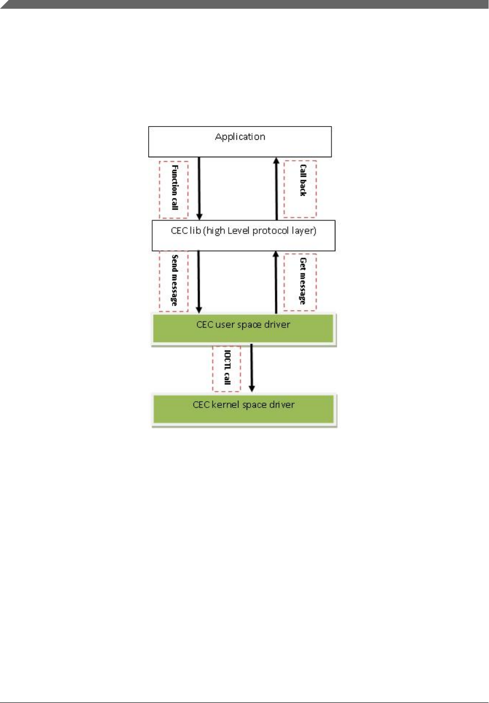
6.3.2.5 CEC
HDMI CEC is a protocol that provides high-level control functions between all of the
various audiovisual products is a user’s environment. The HDMI CEC driver implements
software part of HDMI CEC low Level protocol. It includes getting Logical address,
CEC message sending and receiving, error handle, message re-transmitting, etc.
Figure 6-3. HDMI CEC SW Architecture
6.3.3 i.MX 6 On Chip High-Definition Multimedia Interface (HDMI)
6.3.3.1 Introduction
The High-Definition Multimedia Interface (HDMI) driver supports the on-chip
DesignWare HDMI hardware module on the i.MX 6QuadPlus, 6Quad and 6Dual, which
provides the capability to transfer uncompressed video, audio, and data using a single
cable.
High-Definition Multimedia Interface (HDMI) Overview
i.MX Reference Manual, Rev. L4.9.88_2.0.0-ga, 05/2018
230 NXP Semiconductors

The HDMI driver is divided into four sub-components: A video display device driver that
integrates with the Linux Frame Buffer API, an audio driver that integrates with the
ALSA/SoC sub-system, a CEC driver, and a multifunction device (MFD) driver which
manages the shared software and hardware resources of the HDMI driver.
The HDMI driver supports the following features:
• Integration with the MXC Display Device framework (for managing display device
connections with the IPU(s))
• HDMI video output up to 1080p60 resolution
• Support for reading EDID information from an HDMI sink device
• Hotplug detection
• Support CEC
• Automated clock management to minimize power consumption
• Support for system suspend/resume
• HDMI audio playback (2, 4, 6, or 8 channels, 16-bit, for sample rates 32-KHz to 192-
KHz)
• IEC audio header information exposed through ALSA using ‘iecset’ utility
6.3.3.1.1 Hardware Operation
The HDMI module receives video data from the Image Processing Unit (IPU), audio data
from the external memory interface, and control data from the CPU, as shown in the
figure below.
Output data is transmitted via three Transition-Minimized Differential Signaling (TMDS)
channels to an HDMI sink device external to the SoC. Additionally, the HDMI carries a
VESA Data Display Channel (DDC). The DDC is an I2C interface which allows the
HDMI source to query the HDMI sink for Extended Display Identification Data (EDID).
A CEC channel provides optional high-level control functions between the source and
sink device.
Chapter 6 Video
i.MX Reference Manual, Rev. L4.9.88_2.0.0-ga, 05/2018
NXP Semiconductors 231
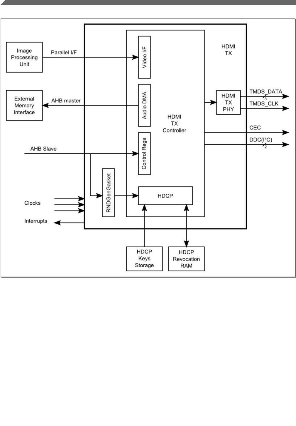
Figure 6-4. HDMI HW Integration
The video input to the HDMI is configurable and may come from either of the two IPU
modules in the i.MX 6 serials and from either of the two Display Interface (DI) ports of
the IPU, DI0 or DI1. This configuration is controlled through the IOMUX module using
the HDMI_MUX_CTRL register field. See the figure below for an illustration of this
interconnection.
High-Definition Multimedia Interface (HDMI) Overview
i.MX Reference Manual, Rev. L4.9.88_2.0.0-ga, 05/2018
232 NXP Semiconductors
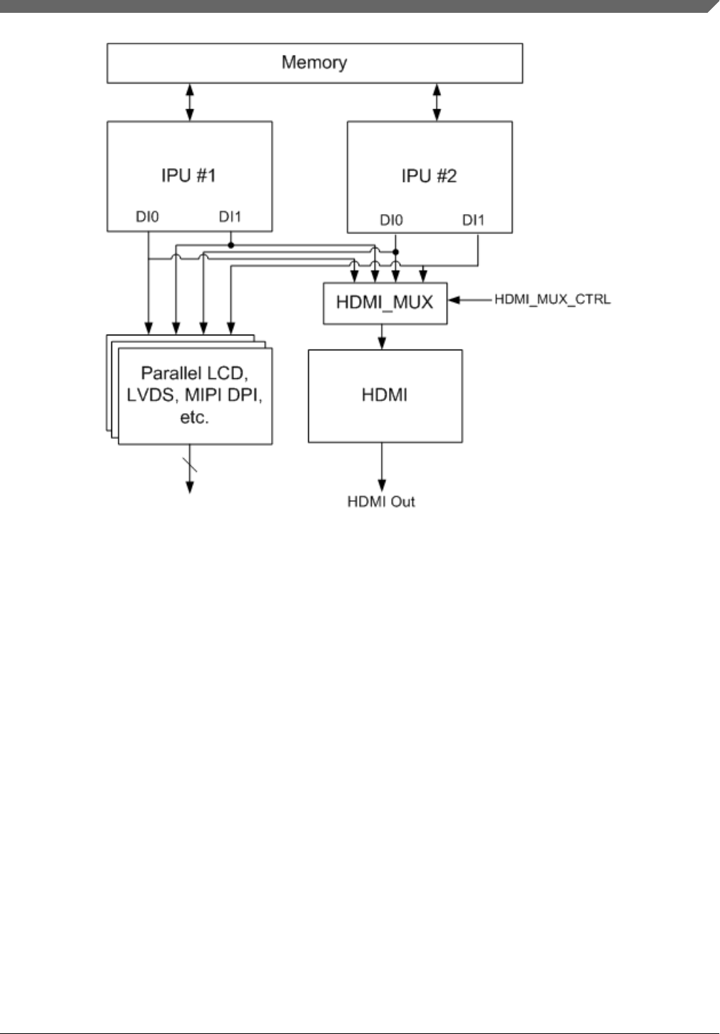
Figure 6-5. IPU-HDMI Hardware Interconnection
6.3.3.2 Software Operation
The HDMI driver is divided into sub-components based on its two primary purposes:
providing video and audio to an HDMI sink device.
The video display driver component and audio driver component require an additional
core driver component to manage common HDMI resources, including the HDMI
registers, clocks, and IRQ.
6.3.3.2.1 Video
The following diagram illustrates both the interconnection between the various HDMI
sub-drivers and the interconnection between the HDMI video driver and the Linux Frame
Buffer subsystem.
Chapter 6 Video
i.MX Reference Manual, Rev. L4.9.88_2.0.0-ga, 05/2018
NXP Semiconductors 233
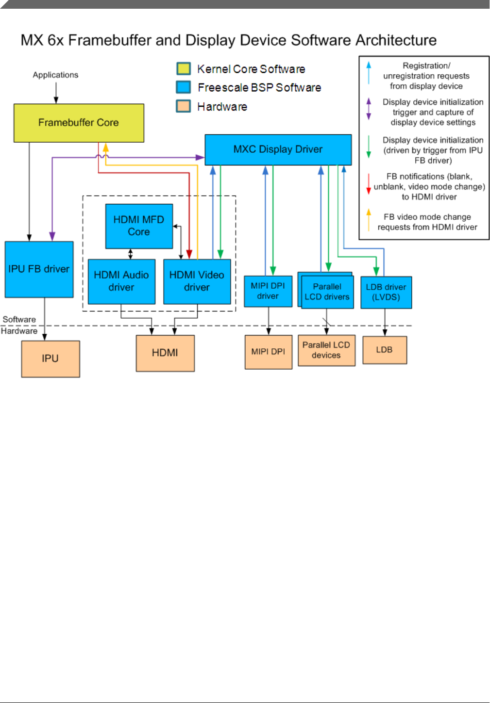
Figure 6-6. HDMI Video SW Architecture
The i.MX 6Dual/6Quad/6Solo/6DualLite/6SoloLite supports many different types of
display output devices (e.g., LVDS, LCD, HDMI and MIPI displays) connected to and
driven by the IPU modules. The MXC Display Driver API provides a system for
registering display devices and configuring how they should be connected to each of the
IPU DIs. The HDMI driver registers itself as a display device using this API in order to
receive the correct video input from the IPU.
6.3.3.2.2 Source Code Structure
The bulk of the source code for the HDMI driver is divided amongst the three software
components that comprise the driver: the HDMI core driver, the HDMI display driver,
and the HDMI audio driver.
Additional platform-specific source code files provide the code for declaring and
registering these HDMI drivers.
The source code for the HDMI core driver is available in the drivers/mfd/ directory.
High-Definition Multimedia Interface (HDMI) Overview
i.MX Reference Manual, Rev. L4.9.88_2.0.0-ga, 05/2018
234 NXP Semiconductors

Table 6-9. HDMI Core Driver File List
File Description
mxc-hdmi-core.c HDMI core driver implemention
A public header for the HDMI core driver is available in the include/linux/mfd/ directory.
Table 6-10. HDMI Core Display Driver Public Header File List
File Description
mxc-hdmi-core.h HDMI core driver header file
The source code for the HDMI display driver is available in the drivers/video/fbdev/mxc
directory.
Table 6-11. HDMI Display Driver File List
File Description
mxc_hdmi.c HDMI display driver implemention
The source code for the HDMI audio driver is available in the sound/soc/ directory.
Although the HDMI is one hardware block, the audio driver is divided into four c files
corresponding to the ALSA SoC layers:
Table 6-12. HDMI Audio Driver File List
File Description
fsl/fsl_hdmi.c HDMI Audio SoC DAI driver implementation
fsl/imx-hdmi-dma.c HDMI Audio SoC platform DMA driver implementation
fsl/imx-hdmi.c HDMI Audio SoC machine driver implementation
The source code for the HDMI CEC driver is available in the drivers/mxc/ directory.
Table 6-13. HDMI CEC Driver File List
File Description
drivers/mxc/hdmi-cec.c HDMI CEC driver implemention
The source code for the HDMI lib is available in the imx-lib/hdmi-cec/ directory.
Table 6-14. HDMI CEC lib File List
File Description
hdmi-cec/mxc_hdmi-cec.c HDMI CEC lib implemention
Table continues on the next page...
Chapter 6 Video
i.MX Reference Manual, Rev. L4.9.88_2.0.0-ga, 05/2018
NXP Semiconductors 235

Table 6-14. HDMI CEC lib File List (continued)
File Description
hdmi-cec/hdmi-cec.h HDMI CEC lib header file
hdmi-cec/android.mk HDMI CEC lib make file
The following platform-level source code files provide structures and functions for
registering the HDMI drivers. These files can be found in the arch/arm/plat-mxc/ directory.
Table 6-15. HDMI Platform File List
File Description
devices/platform-mxc-hdmi-core.c HDMI core driver platform device code
devices/platform-mxc_hdmi.c HDMI display driver platform device code
devices/platform-imx-hdmi-soc.c HDMI audio driver platform device code
devices/platform-imx-hdmi-soc-dai.c HDMI audio driver platform device code
include/mach/mxc_hdmi.h HDMI register defines
6.3.3.2.3 Menu Configuration Options
There are three main Linux kernel configuration options used to select and include HDMI
driver functionality in the Linux OS image.
The CONFIG_FB_MXC_HDMI option provides support for the HDMI video driver, and
can be selected in menuconfig at the following menu location:
Device Drivers > Graphics support > MXC HDMI driver support
HDMI video support is dependent on support for the Synchronous Panel Framebuffer and
also on the inclusion of IPUv3 support.
The CONFIG_SND_SOC_IMX_HDMI option provides support for HDMI audio through
the ALSA/SoC subsystem, and can be found in menuconfig at the following location:
Device Drivers > Sound card support > Advanced Linux Sound Architecture > ALSA for
SoC audio support > SoC Audio support for IMX - HDMI
Selecting either of the previous two configuration options will cause the MXC HDMI
Core configuration option, CONFIG_MFD_MXC_HDMI, to be selected. This option can
also be found in the menuconfig here:
Device Drivers > Multifunction device drivers > MXC HDMI Core
The CONFIG_MXC_HDMI_CEC option provides support for the HDMI CEC driver,
and can be selected in menuconfig at the following menu location:
High-Definition Multimedia Interface (HDMI) Overview
i.MX Reference Manual, Rev. L4.9.88_2.0.0-ga, 05/2018
236 NXP Semiconductors

Device Drivers > MXC support drivers > MXC HDMI CEC (Consumer Electronic
Control) support
6.3.4 External HDMI for i.MX 6 Solo Lite
6.3.4.1 Introduction
The High Definition Multimedia Interface (HDMI) driver supports the external SiI9022
HDMI hardware module, which provides the capability to transfer uncompressed video,
audio, and data using a single cable.
The HDMI driver is divided into two sub-components: a video display device driver that
integrates with the Linux Frame Buffer API and an S/PDIF audio driver that transfers S/
PDIF audio data to SiI9022 HDMI hardware module.
The HDMI driver is only for demo application and supports the following features:
• HDMI video output supports 1080p60 and 720p60 resolutions.
• Support for reading EDID information from an HDMI sink device for video.
• Hotplug detection
• HDMI audio playback (2 channels, 16/24 bit, 44.1 KHz sample rate)
6.3.4.1.1 Hardware Operation
Output data is transmitted via three Transition-Minimized Differential Signaling (TMDS)
channels to an HDMI sink device external to the SoC. Additionally, the HDMI carries a
VESA Data Display Channel (DDC). DDC is an I2C interface which allows the HDMI
source to query the HDMI sink for Extended Display Identification Data (EDID). A CEC
channel provides optional high-level control functions between the source and sink
devices.
Chapter 6 Video
i.MX Reference Manual, Rev. L4.9.88_2.0.0-ga, 05/2018
NXP Semiconductors 237

Figure 6-7. HDMI HW Integration
6.3.4.2 Software Operation
The HDMI driver is divided into sub-components based on its two primary purposes:
providing video and audio to an HDMI sink device.
The audio output depends on video display.
High-Definition Multimedia Interface (HDMI) Overview
i.MX Reference Manual, Rev. L4.9.88_2.0.0-ga, 05/2018
238 NXP Semiconductors

6.3.4.2.1 Source Code Structure
The bulk of the source code for the HDMI driver is divided amongst the two software
components that comprise the driver: the HDMI display driver, and the HDMI audio
driver.
The source code for the HDMI display driver is available in the drivers/video/fbdev/mxc/
directory.
Table 6-16. HDMI Display Driver File List
File Description
mxsfb_sii902x.c HDMI display driver implementation.
The source code for the HDMI audio driver is available in the sound/soc/ directory.
HDMI Audio data source comes from S/PDIF TX.
Table 6-17. HDMI Audio Driver File List
File Description
sound/soc/fsl/imx-spdif.c S/PDIF Audio SoC Machine driver implementation.
sound/soc/fsl/fsl_spdif.c S/PDIF Audio SoC DAI driver implementation.
6.3.4.2.2 Menu Configuration Options
There are two main Linux kernel configuration options used to select and include HDMI
driver functionality in the Linux OS image.
The CONFIG_FB_MXC_SII902X_ELCDIFI option provides support for the Sii902x
HDMI video driver and can be selected in menuconfig at the following menu location:
• Device Drivers > Graphics support > MXC Framebuffer support.
HDMI video support is dependent on MXC ELCDIF Framebuffer.
The CONFIG_SND_MXC_SPDIF option provides support for the HDMI Audio driver
and can be selected in menuconfig at the following menu location:
• Device Drivers > Sound card support > Advanced Linux Sound Architecture >
ALSA for SoC audio support > SoC Audio for Freescale i.MX CPUs > SoC Audio
support for IMX - S/PDIF
6.3.5 External HDMI for i.MX 7ULP EVK
Chapter 6 Video
i.MX Reference Manual, Rev. L4.9.88_2.0.0-ga, 05/2018
NXP Semiconductors 239

6.3.5.1 Introduction
ADD DETAILS HERE _ THIS IS COPIED FROM SoloLite so might not apply to 7ulp
The High Definition Multimedia Interface (HDMI) driver supports the external SiI9022
HDMI hardware module, which provides the capability to transfer uncompressed video,
audio, and data using a single cable.
The HDMI driver is divided into two sub-components: a video display device driver that
integrates with the Linux Frame Buffer API and an S/PDIF audio driver that transfers S/
PDIF audio data to SiI9022 HDMI hardware module.
The HDMI driver is only for demo application and supports the following features:
• HDMI video output supports 1080p60 and 720p60 resolutions.
• Support for reading EDID information from an HDMI sink device for video.
• Hotplug detection
• HDMI audio playback (2 channels, 16/24 bit, 44.1 KHz sample rate)
6.3.5.2 Software Operation
The HDMI driver is divided into sub-components based on its two primary purposes:
providing video and audio to an HDMI sink device.
The audio output depends on video display.
6.3.5.2.1 Source Code Structure
The bulk of the source code for the HDMI driver is divided amongst the two software
components that comprise the driver: the HDMI display driver, and the HDMI audio
driver.
The source code for the HDMI display driver is available in the drivers/video/fbdev/mxc/
directory.
Table 6-18. HDMI Display Driver File List
File Description
mxsfb_sii902x.c HDMI display driver implementation.
The source code for the HDMI audio driver is available in the sound/soc/ directory.
HDMI Audio data source comes from S/PDIF TX.
High-Definition Multimedia Interface (HDMI) Overview
i.MX Reference Manual, Rev. L4.9.88_2.0.0-ga, 05/2018
240 NXP Semiconductors

Table 6-19. HDMI Audio Driver File List
File Description
sound/soc/fsl/imx-spdif.c S/PDIF Audio SoC Machine driver implementation.
sound/soc/fsl/fsl_spdif.c S/PDIF Audio SoC DAI driver implementation.
6.3.5.2.2 Menu Configuration Options
There are two main Linux kernel configuration options used to select and include HDMI
driver functionality in the Linux OS image.
The CONFIG_FB_MXC_SII902X_ELCDIFI option provides support for the Sii902x
HDMI video driver and can be selected in menuconfig at the following menu location:
• Device Drivers > Graphics support > MXC Framebuffer support.
HDMI video support is dependent on MXC ELCDIF Framebuffer.
The CONFIG_SND_MXC_SPDIF option provides support for the HDMI Audio driver
and can be selected in menuconfig at the following menu location:
• Device Drivers > Sound card support > Advanced Linux Sound Architecture >
ALSA for SoC audio support > SoC Audio for Freescale i.MX CPUs > SoC Audio
support for IMX - S/PDIF
6.4 MIPI DSI
6.4.1 MIPI DSI Overview
6.4.1.1 Introduction
The MIPI Display Interface (MIPI DSI) is a driver interface used to communicate with
MIPI device controller on the display panel. MIPI DSI display panel driver provides an
interface to configure the display panel through MIPI DSI.
The MIPI DSI overview can be found here however specifications are only available to
MIPI members .
For i.MX MIPI DSI is supported by a variety of drivers which are described in following
chapters.
Chapter 6 Video
i.MX Reference Manual, Rev. L4.9.88_2.0.0-ga, 05/2018
NXP Semiconductors 241

The MIPI DSI drivers support the following features:
• MIPI DSI communication protocol
• MIPI DSI command mode and video mode
• MIPI DCS command operation
6.4.1.1.1 Hardware Operation
The MIPI DSI module provides a high-speed serial interface between a host processor
and a display module.
It has higher performance, lower power, less EMI, and fewer pins compared with legacy
parallel bus. It is designed to be compatible with the standard MIPI DSI protocol. MIPI
DSI is built on the existing MIPI DPI-2, MIPI DBI-2 and MIPI DCS standards. It sends
pixels or commands to the peripheral and reads back status or pixel information from the
peripheral. MIPI DSI serializes all pixels data, commands and events, and contains two
basic modes: command mode and video mode. It uses command mode to write register
and memory to the display controller while reading display module status information.
On the other hand, it uses video mode to transmit a real-time pixel streams from the host
to peripheral in high-speed mode. It also generates an interrupt when an error occurs.
6.4.1.1.2 Driver Features
The MIPI DSI driver supports the following features:
• MIPI DSI communication protocol
• MIPI DSI command mode and video mode
• MIPI DCS command operation
6.4.1.1.3 MIPI DSI Display Panel Driver Overview
The MIPI DSI display panel driver implements MIPI DSI display panel-related
configuration.
It uses the APIs provided by the MIPI DSI IP driver to read/write the display module
registers. Usually, there is a MIPI DSI slave controller integrated on the display panel.
After power on reset, the MIPI DSI display panel needs to be configured through
standard MIPI DCS command or MIPI DSI Generic command according to the
manufacturer's specification.
6.4.1.2 Software Operation
The MIPI DSI driver has two parts: MIPI DSI IP driver and MIPI DSI display panel
driver.
MIPI DSI
i.MX Reference Manual, Rev. L4.9.88_2.0.0-ga, 05/2018
242 NXP Semiconductors

6.4.1.2.1 MIPI DSI Display Panel Driver Software Operation
The MIPI DSI Display Panel driver enables a particular display panel through MIPI DSI
interface. The driver should provide struct fb_videomode configuration and struct
mipi_lcd_config data: some MIPI DSI parameters for the display panel such as maximum
D-PHY clock, numbers of data lanes and DPI-2 pixel format. Finally, the display driver
needs to setup display panel initialize routine by calling the APIs provided by MIPI DSI
IP drivers.
6.4.1.2.2 Source Code Structure
The MIPI DSI driver source files available in the directory:
drivers/video/mxc.
6.4.2 MIPI DSI for DPU
6.4.2.1 Introduction
The MIPI DSI driver for i.MX with DPU is based on the DPU framebuffer driver. This
driver has two parts:
• MIPI DSI IP driver-low level interface used to communicate with MIPI device
controller on the display panel
• MIPI DSI display panel driver provides an interface to configure the display panel
through MIPI DSI
6.4.2.1.1 MIPI DSI IP Driver Overview
The MIPI DSI IP driver is registered through DPU framebuffer driver interface and it is
not exposed to the user space.
Copied from IPU - update for DPU on i.MX 8
The driver enables the platform-related regulators and clocks. It requests OS-related
system resources and registers framebuffer event notifier for blank/unblank operation.
Next, the driver initializes MIPI D-PHY and configures the MIPI DSI IP according to the
MIPI DSI display panel. MIPI DSI driver supports the following features:
• Compatibility with MIPI Alliance Specification for DSI, Version1.01.00
• Compatibility with MIPI Alliance Specification for D-PHY, Version 1.00.00
• Supports up to 2 D-PHY data lanes
Chapter 6 Video
i.MX Reference Manual, Rev. L4.9.88_2.0.0-ga, 05/2018
NXP Semiconductors 243

• Bidirectional Communication and Escape Mode Support through Data Lane 0
• Programmable display resolutions, from 160x120(QQVGA) to 1024x768(XVGA)
• Video Mode Pixel Formats, 16bpp(565RGB),18bpp(666RGB)packed,
18bpp(666RGB)loosely, 24bpp(888RGB).
• Supports the transmission of all generic commands
• Supports ECC and checksum capabilities
• End-of-Transmission Packet(EoTp) support
• Supports ultra low power mode
6.4.2.2 Software Operation
The MIPI DSI driver for Linux OS has two parts: MIPI DSI IP driver and MIPI DSI
display panel driver.
6.4.2.2.1 MIPI DSI IP Driver Software Operation
COPIED from IPU chapter - please update for MX8 DPU
The MIPI DSI IP driver has a private structure called mipi_dsi_info. The DPU instance to
which the MIPI DSI IP is attached is described in field int dpu_id while the DI instance
inside DPU is described in the field int disp_id.
During startup, the MIPI DSI IP driver is registered with the IPU framebuffer driver
through the field struct mxc_dispdrv_entry when the driver is loaded. It also registers a
framebuffer event notifier with framebuffer core to perform the display panel blank/
unblank operation. The field struct fb_videomode *mode and struct mipi_lcd_config
*lcd_config are received from the display panel callback. The MIPI DSI IP needs this
infomation to configure the MIPI DSI hardware registers.
After initializing the MIPI DSI IP controller and the display module, the MIPI DSI IP
gets the pixel streams from DPU through DPI-2 interface and serializes pixel data and
video event through high-speed data links for display. When there is an framebuffer
blank/unblank event, the registered notifier will be called to enter/leave low power mode.
The MIPI DSI IP driver provides 3 APIs for MIPI DSI display panel driver to configure
display module.
6.4.2.2.2 Source Code Structure
COPIED FROM IPU - update for MX8
Table below shows the MIPI DSI driver source files available in the directory:
drivers/video/mxc.
MIPI DSI
i.MX Reference Manual, Rev. L4.9.88_2.0.0-ga, 05/2018
244 NXP Semiconductors

Table 6-20. MIPI DSI Driver Files
File Description
mipi_dsi.c MIPI DSI IP driver source file
mipi_dsi.h MIPI DSI IP driver header file
mxcfb_hx8369_wvga.c MIPI DSI Display Panel driver source file
6.4.2.2.3 Menu Configuration Options
In menu configuration enable the following module:
Device Drivers > Graphics support > MXC Framebuffer support > Synchronous Panel
Framebuffer > MXC MIPI_DSI
6.4.2.2.4 Programming Interface
The MIPI DSI Display Panel driver can use the API interface to read and write the
registers of the display panel device connected to MIPI DSI link.
COPIED FROM IPU - update for MX8
For more information, see
drivers/video/fbdev/mxc/mipi_dsi.h
.
6.4.3 MIPI DSI for IPU
6.4.3.1 Introduction
The MIPI DSI driver for i.MX6 with IPU is based on the IPU framebuffer driver. This
driver has two parts:
• MIPI DSI IP driver-low level interface used to communicate with MIPI device
controller on the display panel
• MIPI DSI display panel driver provides an interface to configure the display panel
through MIPI DSI
Chapter 6 Video
i.MX Reference Manual, Rev. L4.9.88_2.0.0-ga, 05/2018
NXP Semiconductors 245

6.4.3.1.1 MIPI DSI IP Driver Overview
The MIPI DSI IP driver is registered through IPU framebuffer driver interface and it is
not exposed to the user space.
The driver enables the platform-related regulators and clocks. It requests OS-related
system resources and registers framebuffer event notifier for blank/unblank operation.
Next, the driver initializes MIPI D-PHY and configures the MIPI DSI IP according to the
MIPI DSI display panel. MIPI DSI driver supports the following features:
• Compatibility with MIPI Alliance Specification for DSI, Version1.01.00
• Compatibility with MIPI Alliance Specification for D-PHY, Version 1.00.00
• Supports up to 2 D-PHY data lanes
• Bidirectional Communication and Escape Mode Support through Data Lane 0
• Programmable display resolutions, from 160x120(QQVGA) to 1024x768(XVGA)
• Video Mode Pixel Formats, 16bpp (565 RGB),18bpp (666 RGB) packed, 18 bpp
(666 RGB) loosely, 24bpp (888 RGB).
• Supports the transmission of all generic commands
• Supports ECC and checksum capabilities
• End-of-Transmission Packet(EoTp) support
• Supports ultra low power mode
6.4.3.2 Software Operation
The MIPI DSI driver for Linux OS has two parts: MIPI DSI IP driver and MIPI DSI
display panel driver.
6.4.3.2.1 MIPI DSI IP Driver Software Operation
The MIPI DSI IP driver has a private structure called mipi_dsi_info. The IPU instance to
which the MIPI DSI IP is attached is described in field int ipu_id while the DI instance
inside IPU is described in the field int disp_id.
During startup, the MIPI DSI IP driver is registered with the IPU framebuffer driver
through the field struct mxc_dispdrv_entry when the driver is loaded. It also registers a
framebuffer event notifier with framebuffer core to perform the display panel blank/
unblank operation. The field struct fb_videomode *mode and struct mipi_lcd_config
*lcd_config are received from the display panel callback. The MIPI DSI IP needs this
infomation to configure the MIPI DSI hardware registers.
MIPI DSI
i.MX Reference Manual, Rev. L4.9.88_2.0.0-ga, 05/2018
246 NXP Semiconductors

After initializing the MIPI DSI IP controller and the display module, the MIPI DSI IP
gets the pixel streams from IPU through DPI-2 interface and serializes pixel data and
video event through high-speed data links for display. When there is an framebuffer
blank/unblank event, the registered notifier will be called to enter/leave low power mode.
The MIPI DSI IP driver provides 3 APIs for MIPI DSI display panel driver to configure
display module.
6.4.3.2.2 Source Code Structure
Table below shows the MIPI DSI driver source files available in the directory:
drivers/video/mxc.
Table 6-21. MIPI DSI Driver Files
File Description
mipi_dsi.c MIPI DSI IP driver source file
mipi_dsi.h MIPI DSI IP driver header file
mxcfb_hx8369_wvga.c MIPI DSI Display Panel driver source file
6.4.3.2.3 Menu Configuration Options
In menu configuration enable the following module:
Device Drivers > Graphics support > MXC Framebuffer support > Synchronous Panel
Framebuffer > MXC MIPI_DSI
6.4.3.2.4 Programming Interface
The MIPI DSI Display Panel driver can use the API interface to read and write the
registers of the display panel device connected to MIPI DSI link.
For more information, see drivers/video/fbdev/mxc/mipi_dsi.h.
6.4.4 MIPI DSI LCDIF
6.4.4.1 Introduction
On the i.MX 7Dual platform, the MIPI DSI module comes from Samsung. The MIPI DSI
driver is based on the LCDIF framebuffer driver.
Chapter 6 Video
i.MX Reference Manual, Rev. L4.9.88_2.0.0-ga, 05/2018
NXP Semiconductors 247

This driver has two parts:
• MIPI DSI IP driver-low level interface, used to communicate with the MIPI device
controller on the display panel.
• MIPI DSI display panel driver, provides an interface to configure the display panel
through MIPI DSI.
6.4.4.1.1 MIPI DSI IP Driver Overview
The MIPI DSI IP driver is registered through the LCDIF framebuffer driver interface and
it is not exposed to the user space.
The driver enables the platform-related regulators and clocks. It requests OS-related
system resources and then registers framebuffer event notifier for blank/unblank
operation. Then, the driver initializes MIPI D-PHY and configures the MIPI DSI IP
according to the MIPI DSI display panel. The MIPI DSI driver supports the following
features:
• Compatibility with the MIPI Alliance Specification for DSI, V1.01r11
• Compatibility with the MIPI Alliance Specification for D-PHY, Version 1.00.00
• Supports up to two D-PHY data lanes
• Bidirectional Communication and Escape Mode Support through Data Lane 0
• Maximum resolution ranges up to SXGA+(1400 x 1050 @ 60 Hz, 24 bpp)
• Supports pixel format: 16 bpp, 18 bpp packed, 18 bpp loosely packed (3 byte
format), and 24bpp
• End-of-Transmission Packet (EoTp) support
• Supports ultra low power mode
• Supports PMS control interface for PLL to configure byte clock frequency
• Supports Prescaler to generate escape clock from byte clock
6.4.4.2 Software Operation
The MIPI DSI driver for the Linux OS has two parts: MIPI DSI IP driver and MIPI DSI
display panel driver.
6.4.4.2.1 MIPI DSI IP Driver Software Operation
The MIPI DSI IP driver has a private structure called mipi_dsi_info. During startup, the
MIPI DSI IP driver is registered with the LCDIF framebuffer driver through the field
struct mxc_dispdrv_handle *dispdrv when the driver is loaded. It also registers a
framebuffer event notifier with framebuffer core to perform the display panel blank/
MIPI DSI
i.MX Reference Manual, Rev. L4.9.88_2.0.0-ga, 05/2018
248 NXP Semiconductors

unblank operation. The field struct fb_videomode *mode and struct mipi_lcd_config
*lcd_config are received from the display panel callback. The MIPI DSI IP needs this
information to configure the MIPI DSI hardware registers.
After initializing the MIPI DSI IP controller and the display module, the MIPI DSI IP
gets the pixel streams from LCDIF through DPI-2 interface and serializes pixel data and
video event through high-speed data links for display. When there is a framebuffer blank/
unblank event, the registered notifier is called to enter/leave low power mode. The MIPI
DSI IP driver provides three APIs for MIPI DSI display panel driver to configure the
display module.
6.4.4.2.2 Source Code Structure
The table below shows the MIPI DSI driver source files available in the directory:
drivers/video/mxc
Table 6-22. MIPI DSI Driver Files
File Description
mipi_dsi_samsung.c MIPI DSI IP driver source file
mipi_dsi_samsung.h MIPI DSI IP driver header file
mxcfb_hx8369_wvga.c MIPI DSI Display Panel driver source file
6.4.4.2.3 Menu Configuration Options
In menu configuration enable the following module:
Device Drivers > Graphics support > MXC Framebuffer support > Synchronous Panel
Framebuffer > MXC MIPI_DSI_SAMSUNG
6.4.4.2.4 Programming Interface
The MIPI DSI Display Panel driver can use the API interface to read and write the
registers of the display panel device connected to MIPI DSI link.
For more information, see driver/video/mxc/mipi_dsi_samsung.h.
6.5 Video for Linux 2 (V4L2)
6.5.1 V4L2 Overview
Chapter 6 Video
i.MX Reference Manual, Rev. L4.9.88_2.0.0-ga, 05/2018
NXP Semiconductors 249

6.5.1.1 Introduction
The Video for Linux Two (V4L2) driver is plug-in for the V4L2 framework that enables
support for camera capture.
Some i.MX SoC support V4L2 based on the associated images processing units and
capture hardware. Each chapter will descibe the specific implementation.
For more information on V4L2 go to the API specification for Linux Video for Linux 2
available at Linux Media Subsystem Documentation.
6.5.1.2 V4L2 Capture Device
The V4L2 capture device includes two interfaces:
• Capture interface-uses i.MX processing engine to record the YCrCb video stream
• Overlay interface-uses i.MX processing engine to display the preview video to the
SDC foreground and background panel.
The driver includes two layers. The top layer is the common Video for Linux driver,
which contains chain buffer management, stream API and other ioctl interfaces. The low
level layer is the i.MX SoC implementation for the display engine associated with the
SoC detailed in each V4l2 SoC chapter.
6.5.1.2.1 V4L2 Capture IOCTLs
Currently, the memory map stream API is supported. Supported V4L2 IOCTLs include
the following:
• VIDIOC_QUERYCAP
• VIDIOC_G_FMT
• VIDIOC_S_FMT
• VIDIOC_REQBUFS
• VIDIOC_QUERYBUF
• VIDIOC_QBUF
• VIDIOC_DQBUF
• VIDIOC_STREAMON
• VIDIOC_STREAMOFF
• VIDIOC_OVERLAY
• VIDIOC_G_FBUF
• VIDIOC_S_FBUF
• VIDIOC_G_CTRL
Video for Linux 2 (V4L2)
i.MX Reference Manual, Rev. L4.9.88_2.0.0-ga, 05/2018
250 NXP Semiconductors

• VIDIOC_S_CTRL
• VIDIOC_CROPCAP
• VIDIOC_G_CROP
• VIDIOC_S_CROP
• VIDIOC_S_PARM
• VIDIOC_G_PARM
• VIDIOC_ENUMSTD
• VIDIOC_G_STD
• VIDIOC_S_STD
• VIDIOC_ENUMOUTPUT
• VIDIOC_G_OUTPUT
• VIDIOC_S_OUTPUT
V4L2 control code has been extended to provide support for rotation. The ID is
V4L2_CID_PRIVATE_BASE. Supported values include:
• 0-Normal operation
• 1-Vertical flip
• 2-Horizontal flip
• 3-180° rotation
• 4-90° rotation clockwise
• 5-90° rotation clockwise and vertical flip
• 6-90° rotation clockwise and horizontal flip
• 7-90° rotation counter-clockwise
Figure below shows a block diagram of V4L2 Capture API interaction.
Chapter 6 Video
i.MX Reference Manual, Rev. L4.9.88_2.0.0-ga, 05/2018
NXP Semiconductors 251
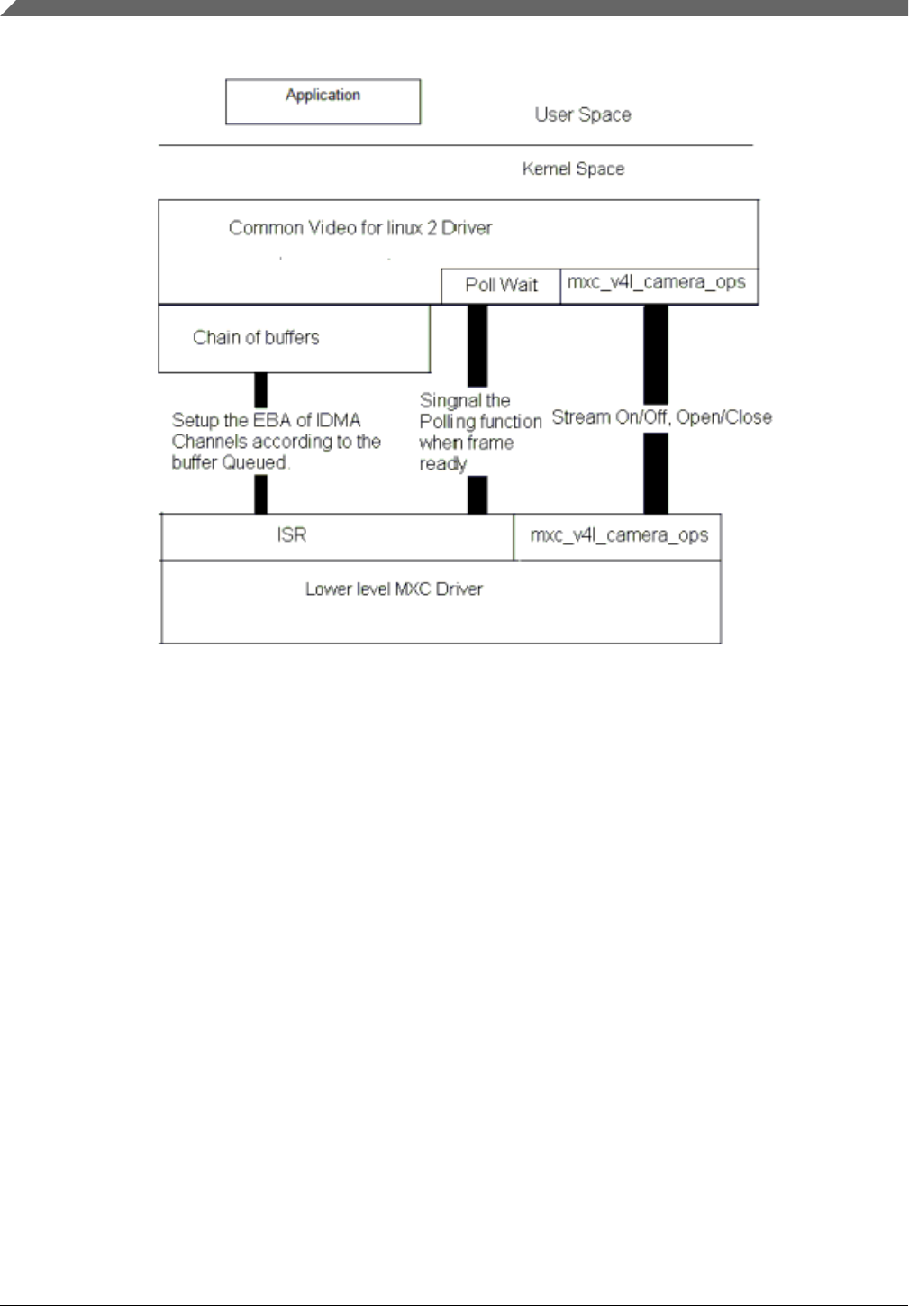
Figure 6-8. Video4Linux2 Capture API Interaction
6.5.1.2.2 Use of the V4L2 Capture APIs
This section describes a sample V4L2 capture process. The application completes the
following steps:
1. Sets the capture pixel format and size by IOCTL VIDIOC_S_FMT.
2. Sets the control information by IOCTL VIDIOC_S_CTRL for rotation usage.
3. Requests a buffer using IOCTL VIDIOC_REQBUFS. The common V4L2 driver
creates a chain of buffers (currently the maximum number of frames is 3).
4. Memory maps the buffer to its user space.
5. Queues buffers using the IOCTL command VIDIOC_QBUF.
6. Starts the stream using the IOCTL VIDIOC_STREAMON. This IOCTL enables the
i.MX Processing Enginee tasks and the IDMA channels. When the processing is
completed for a frame, the driver switches to the buffer that is queued for the next
frame. The driver also signals the semaphore to indicate that a buffer is ready.
7. Takes the buffer from the queue using the IOCTL VIDIOC_DQBUF. This IOCTL
blocks until it has been signaled by the ISR driver.
8. Stores the buffer to a YCrCb file.
Video for Linux 2 (V4L2)
i.MX Reference Manual, Rev. L4.9.88_2.0.0-ga, 05/2018
252 NXP Semiconductors

9. Replaces the buffer in the queue of the V4L2 driver by executing VIDIOC_QBUF
again.
For the V4L2 still image capture process, the application completes the following steps:
1. Sets the capture pixel format and size by executing the IOCTL VIDIOC_S_FMT.
2. Reads one frame still image with YUV422.
FOr the V4L2 overlay support use case, the application completes the following steps:
1. Sets the overlay window by IOCTL VIDIOC_S_FMT.
2. Turns on overlay task by IOCTL VIDIOC_OVERLAY.
3. Turns off overlay task by IOCTL VIDIOC_OVERLAY.
6.5.1.3 V4L2 Output Device
The driver implements the standard V4L2 API for output devices. V4L2 output device
support can be selected during kernel configuration. The driver is available at
drivers/media/platform/mxc/output/mxc_vout.c
.
6.5.1.3.1 V4L2 Output IOCTLs
Currently, the memory map stream API is supported. Supported V4L2 IOCTLs include
the following:
• VIDIOC_QUERYCAP
• VIDIOC_REQBUFS
• VIDIOC_G_FMT
• VIDIOC_S_FMT
• VIDIOC_QUERYBUF
• VIDIOC_QBUF
• VIDIOC_DQBUF
• VIDIOC_STREAMON
• VIDIOC_STREAMOFF
• VIDIOC_G_CTRL
• VIDIOC_S_CTRL
• VIDIOC_CROPCAP
• VIDIOC_G_CROP
• VIDIOC_S_CROP
• VIDIOC_ENUM_FMT
Chapter 6 Video
i.MX Reference Manual, Rev. L4.9.88_2.0.0-ga, 05/2018
NXP Semiconductors 253

The V4L2 control code has been extended to provide support for de-interlace motion. For
this use, the ID is V4L2_CID_MXC_MOTION. Supported values include the following:
• 0-Medium motion
• 1-Low motion
• 2-High motion
6.5.1.3.2 Use of the V4L2 Output APIs
This section describes a sample V4L2 output process that uses the V4L2 output APIs.
The application completes the following steps:
1. Sets the input pixel format and size using IOCTL VIDIOC_S_FMT.
2. Sets the control information using IOCTL VIDIOC_S_CTRL, for rotation, de-
interlace motion(if needed).
3. Sets the output information using IOCTL VIDIOC_S_CROP.
4. Requests a buffer using IOCTL VIDIOC_REQBUFS. The common V4L2 driver
creates a chain of buffers (not allocated yet).
5. Memory maps the buffer to its user space.
6. Executes the IOCTL VIDIOC_QUERYBUF to query buffers.
7. Passes the data that requires post-processing to the buffer.
8. Queues the buffer using the IOCTL command VIDIOC_QBUF.
9. Executes the IOCTL VIDIOC_DQBUF to dequeue buffers.
10. Starts the stream by executing IOCTL VIDIOC_STREAMON.
11. Stop the stream by excuting IOCTL VIDIOC_STREAMOFF.
6.5.2 DPU Video for Linux 2 (V4L2)
6.5.2.1 Introduction
The Video for Linux Two (V4L2) driver on i.MX 8 is plug-in for the V4L2 framework
that enables support for camera capture and display with the Display Processing Unit
(DPU).
The V4L2 camera driver supports only basic capture. The V4l2 capture device takes
incoming video images, either from a camera or a TV decoder, and captures the images
to memory.
The features supported by the V4L2 driver are as follows:
• RGB 24-bit and YUV 4:2:2 interleaved formats for capture interface
• Plug-in of different sensor drivers
Video for Linux 2 (V4L2)
i.MX Reference Manual, Rev. L4.9.88_2.0.0-ga, 05/2018
254 NXP Semiconductors

• Streaming (queued) input buffer
• Programmable input and output pixel format and size
• RGB 16, 24, and 32-bit, YUV 4:2:0, and 4:2:2 interleaved input formats
The driver implements the standard V4L2 API for capture devices. The command
modprobe mxc_v4l2_capture must be run before using these functions.
6.5.2.2 Source Code Structure
6.5.2.2.1 Menu Configuration Options
The kernel configuration options are provided in the DPU chapter here.
Device Drivers -> V4L platform devices > IMXDPU Camera/V4L2 PRP Features support
"Analog Device adv7180 TV Decoder Input support" for TV Decoder support "Maxim
max9286 GMSL Deserializer Input support" for Camera support IMXDPU CSI Encoder
library required for any capture device
6.5.3 IPU Video for Linux Two (V4L2)
6.5.3.1 Introduction
The Video for Linux Two (V4L2) drivers are plug-ins to the V4L2 framework that enable
support for camera and preprocessing functions, as well as video and post-processing
functions.
The V4L2 camera driver implements support for all camera-related functions. The V4l2
capture device takes incoming video images, either from a camera or a stream, and
manipulates them. The output device takes video and manipulates it, then sends it to a
display or similar device.
The features supported by the V4L2 driver interfaced with the i.MX 6 IPU are as follows:
• Direct preview and output to SDC foreground overlay plane (with synchronized to
LCD refresh)
• Direct preview to graphics frame buffer (without synchronized to LCD refresh)
• Color keying or alpha blending of frame buffer and overlay planes
• Streaming (queued) capture from IPU encoding channel
• Direct (raw Bayer) still capture (sensor dependent)
• Programmable pixel format, size, frame rate for preview and capture
• Programmable rotation and flipping using custom API
Chapter 6 Video
i.MX Reference Manual, Rev. L4.9.88_2.0.0-ga, 05/2018
NXP Semiconductors 255

• RGB 16-bit, 24-bit, and 32-bit preview formats
• Raw Bayer (still only, sensor dependent), RGB 16, 24, and 32-bit, YUV 4:2:0 and
4:2:2 planar, YUV 4:2:2 interleaved, and JPEG formats for capture
• Control of sensor properties including exposure, white-balance, brightness, contrast,
and so on
• Plug-in of different sensor drivers
• Link post-processing resize and CSC, rotation, and display IPU channels
• Streaming (queued) input buffer
• Double buffering of overlay and intermediate (rotation) buffers
• Configurable 3+ buffering of input buffers
• Programmable input and output pixel format and size
• Programmable scaling and frame rate
• RGB 16, 24, and 32-bit, YUV 4:2:0 and 4:2:2 planar, and YUV 4:2:2 interleaved
input formats
• TV output
The driver implements the standard V4L2 API for capture, output, and overlay devices.
The command modprobe mxc_v4l2_capture must be run before using these functions.
6.5.3.2 Source Code Structure
The following table lists the source and header files associated with the V4L2 drivers.
These files are available in the following directory:
drivers/media/platform/mxc
Table 6-23. V4L2 Driver Files
File Description
capture/mxc_v4l2_capture.c V4L2 capture device driver
output/mxc_vout.c V4L2 output device driver
capture/mxc_v4l2_capture.h Header file for V4L2 capture device driver
capture/ipu_prp_enc.c Pre-processing encoder driver
capture/ipu_prp_vf_adc.c Pre-processing view finder (asynchronous) driver
capture/ipu_prp_vf_sdc.c Pre-processing view finder (synchronous foreground) driver
capture/ipu_prp_vf_sdc_bg.c Pre-processing view finder (synchronous background) driver
capture/ipu_fg_overlay_sdc.c synchronous forground driver
capture/ipu_bg_overlay_sdc.c synchronous background driver
capture/ipu_still.c Pre-processing still image capture driver
Drivers for specific cameras can be found in divers/media/platform/mxc/capture/.
Drivers for specific output can be found in drivers/media/platform/mxc/output/.
Video for Linux 2 (V4L2)
i.MX Reference Manual, Rev. L4.9.88_2.0.0-ga, 05/2018
256 NXP Semiconductors

6.5.3.2.1 Menu Configuration Options
The kernel configuration options are provided in the IPU chapter.
6.5.4 PXP Video for Linux Two (V4L2)
6.5.4.1 Introduction
The Video for Linux Two (V4L2) drivers are plug-ins to the V4L2 framework that enable
support for camera and preprocessing functions, as well as video and post-processing
functions.
The V4L2 camera driver implements support for all camera-related functions. The V4l2
capture device takes incoming video images, either from a camera or a stream, and
manipulates them. The output device takes video and manipulates it, then sends it to a
display or similar device.
The features supported by the V4L2 driver are as follows:
• Direct preview and output to SDC foreground overlay plane (with synchronized to
LCD refresh)
• Direct preview to graphics frame buffer (without synchronized to LCD refresh)
• Color keying or alpha blending of frame buffer and overlay planes
• Streaming (queued) capture from IPU encoding channel
• Direct (raw Bayer) still capture (sensor dependent)
• Programmable pixel format, size, frame rate for preview and capture
• Programmable rotation and flipping using custom API
• RGB 16-bit, 24-bit, and 32-bit preview formats
• Raw Bayer (still only, sensor dependent), RGB 16, 24, and 32-bit, YUV 4:2:0 and
4:2:2 planar, YUV 4:2:2 interleaved, and JPEG formats for capture
• Control of sensor properties including exposure, white-balance, brightness, contrast,
and so on
• Plug-in of different sensor drivers
• Link post-processing resize and CSC, rotation, and display IPU channels
• Streaming (queued) input buffer
• Double buffering of overlay and intermediate (rotation) buffers
• Configurable 3+ buffering of input buffers
• Programmable input and output pixel format and size
• Programmable scaling and frame rate
Chapter 6 Video
i.MX Reference Manual, Rev. L4.9.88_2.0.0-ga, 05/2018
NXP Semiconductors 257

• RGB 16, 24, and 32-bit, YUV 4:2:0 and 4:2:2 planar, and YUV 4:2:2 interleaved
input formats
• TV output
The driver implements the standard V4L2 API for capture, output, and overlay devices.
The command modprobe mxc_v4l2_capture must be run before using these functions.
6.5.4.2 Source Code Structure
Table below lists the source and header files associated with the V4L2 drivers.
These files are available in the following directory:
rivers/media/platform/mxc
PXP placeholder - Add PXP files
Table 6-24. V4L2 Driver Files
File Description
capture/mxc_v4l2_capture.c V4L2 capture device driver
output/mxc_vout.c V4L2 output device driver
capture/mxc_v4l2_capture.h Header file for V4L2 capture device driver
Drivers for specific cameras can be found in drivers/media/platform/mxc/capture/.
Drivers for specific output can be found in drivers/media/platform/mxc/output/.
6.5.4.2.1 Menu Configuration Options
The kernel configuration options are provided in the PXP chapter.
6.5.5 Video Analog-to-Digital Converter (VADC)
6.5.5.1 Introduction
The video analog-to-digital converter (VADC) consists of an analog video front end
(AFE), and a digital video decoder. The AFE accepts NTSC or PAL input from a device,
such as an analog camera.
The two parts are configured in the VADC driver. The video decoder outputs the
YUV444-formatted data.
Video for Linux 2 (V4L2)
i.MX Reference Manual, Rev. L4.9.88_2.0.0-ga, 05/2018
258 NXP Semiconductors

6.5.5.1.1 Hardware Operation
The Video ADC has the following features:
• Internal voltage and current reference generator
• 10-bit resolution (9.5 bit ENOB at 66.5 Msps)
• 4 analog inputs, with all inputs available for CVBS
• Programmable anti-aliasing filter, gain, and clamp
The video decoder has the following features:
• NTSC/PAL decoder
• Direct data path (no complex resampling)
• Automatic standards detection
• 2D adaptive comb filter
• Datapath/clocking architecture encompasses a time base corrector for VCR signals
• Luma passband is flat to > 6 MHz
6.5.5.2 Software Operation
The VADC driver is located under the Linux V4L2 architecture and it implements the
V4L2 capture interfaces. Applications cannot use the camera driver directly. Instead, the
applications use the V4L2 capture driver to open and close the camera for image capture.
The V4L2 capture supports the following operation:
• Capture stream mode
The following picture format is supported:
• YUV444
The following picture sizes are supported:
• PAL
• NTSC
6.5.5.2.1 Source Code Structure
Table below shows the driver source files available in the directory:
drivers/video/fbdev/mxc
Table 6-25. VADC Driver Files
File Description
mxc_vadc.c VADC driver source code
Chapter 6 Video
i.MX Reference Manual, Rev. L4.9.88_2.0.0-ga, 05/2018
NXP Semiconductors 259

6.5.5.2.2 Menu Configuration Options
In menu configuration enable the following module:
Device Drivers > Multimedia devices > Video capture adapters > MXC Video For Linux
Camera > MXC Camera/V4L2 PRP Features support > MXC VADC support
6.5.5.2.3 DTS Configuration
VADC analog inputs can choose [0-3]. CSI1 or CSI2 can be used to capture the VADC
data. They can be configured in the DTS file.
For example:
vadc_in = <0>; /* VADC input select */
csi_id = <1>; /* CSI select */
The VADC input selected to vin1 and CSI2 is used to capture the VADC data.
6.5.5.3 Unit Test
Before running the unit test, make sure that the following modules are loaded:
• insmod mxc_vadc.ko
• insmod mx6s_capture.ko
Run the unit test:
/unit_tests/mx6s_v4l2_capture.out -d /dev/video<x>
6.6 Video Processing Unit (VPU)
6.6.1 Introduction
The VPU hardware performs all of the codec computation and most of the bitstream
parsing/packeting. Therefore, the software takes advantage of less control and effort to
implement a complex and efficient multimedia codec system.
Video Processing Unit (VPU)
i.MX Reference Manual, Rev. L4.9.88_2.0.0-ga, 05/2018
260 NXP Semiconductors

6.6.2 Software Operation
The VPU software can be divided into two parts: the kernel driver and the user-space
library as well as the application in user space. The kernel driver takes responsibility for
system control and reserving resources (memory/IRQ). It provides an IOCTL interface
for the application layer in user-space as a path to access system resources. The
application in user-space calls related IOCTLs and codec library functions to implement a
complex codec system.
The VPU kernel driver includes the following functions:
• Module initialization which initializes the module with the device-specific structure
• Device initialization which initializes the VPU clock and hardware and request the
IRQ
• Interrupt servicing routine which supports events that one frame has been finished
• File operation routine which provides the following interfaces to user space:
• File open
• File release
• File IOCTL to provide interface for memory allocating and releasing
• Memory map for register and memory accessing in user space
The VPU user space driver has the following functions:
• Codec lib
• Initializes codec system
• Sets codec system configuration
• Controls codec system by command
• Reports codec status and result
• System I/O operation
• Requests and frees memory
• Maps and unmaps memory/register to user space
• Device management
User space application for simple verification:
• Read video raw data
• YUV file dump
• General options to configure the codec behavior
The following figure shows a simple workflow shown in the H.264 example.
Chapter 6 Video
i.MX Reference Manual, Rev. L4.9.88_2.0.0-ga, 05/2018
NXP Semiconductors 261
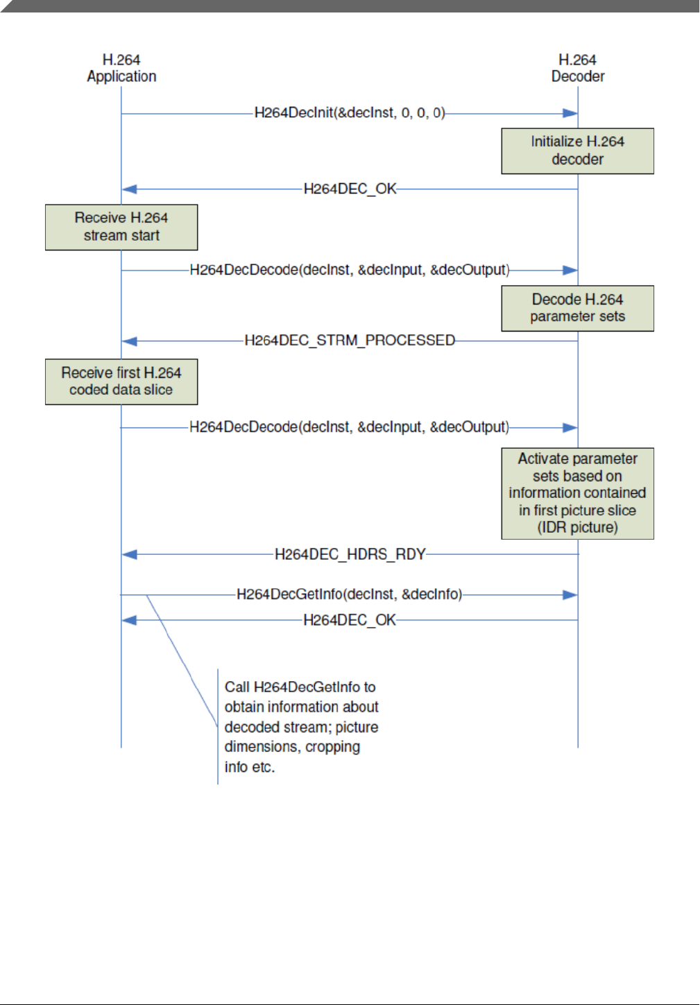
Figure 6-9. Simple Workflow Shown in the H.264 Example
Video Processing Unit (VPU)
i.MX Reference Manual, Rev. L4.9.88_2.0.0-ga, 05/2018
262 NXP Semiconductors
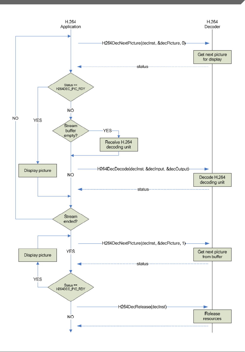
Chapter 6 Video
i.MX Reference Manual, Rev. L4.9.88_2.0.0-ga, 05/2018
NXP Semiconductors 263

6.6.2.1 Menu Configuration Options
In menu configuration enable the following module for the VPU driver:
Device Drivers > MXC support drivers > MXC HANTRO (Video Processing Unit)
support
6.6.2.2 Programming Interface
There is only a user-space programming interface for the VPU module. A user in the
application layer cannot access the kernel driver interface directly. The VPU library
accesses the kernel driver interface for users.
There is one unified interface to wrap all different video formats. The following are the
related APIs:
CODEC_STATE decoder_decode_xxx(CODEC_PROTOTYPE * arg,STREAM_BUFFER * buf, OMX_U32 *
consumed,FRAME * frame);
CODEC_STATE decoder_getinfo_xxx(CODEC_PROTOTYPE * arg,STREAM_INFO * pkg);
CODEC_STATE decoder_setppargs_xxx(CODEC_PROTOTYPE * codec,PP_ARGS * args);
CODEC_STATE decoder_setframebuffer_xxx(CODEC_PROTOTYPE * arg, BUFFER *buff,OMX_U32
available_buffers);
CODEC_STATE decoder_pictureconsumed_xxx(CODEC_PROTOTYPE * arg, BUFFER *buff);
CODEC_STATE decoder_getframe_mpeg4(CODEC_PROTOTYPE * arg, FRAME * frame,OMX_BOOL eos);
FRAME_BUFFER_INFO decoder_getframebufferinfo_xxx(CODEC_PROTOTYPE * arg);
CODEC_STATE decoder_endofstream_xxx(CODEC_PROTOTYPE * arg)
OMX_S32 decoder_scanframe_xxx(CODEC_PROTOTYPE * arg, STREAM_BUFFER * buf,OMX_U32 * first,
OMX_U32 * last);
CODEC_STATE decoder_abort_xxx(CODEC_PROTOTYPE * arg);
CODEC_STATE decoder_abortafter_xxx(CODEC_PROTOTYPE * arg);
CODEC_STATE decoder_setnoreorder_xxx(CODEC_PROTOTYPE * arg, OMX_BOOL no_reorder);
static void decoder_destroy_xxx(CODEC_PROTOTYPE * arg)
6.6.2.3 Unit test
Run unit test to decode video raw data:
>g2dec -P -Ers –ibs –Oout.yuv *.hevc
>g2dec -P -Ers –iivf –Oout.yuv *.vp9
>hx170dec –P –Oout.yuv *.h264
>mx170dec –P –Oout.yuv *.mpeg4
>m2x170dec –P –Oout.yuv *.mpeg2
>vx170dec -P –Oout.yuv *.vc1
>vp8x179dec –P –Oout.yuv *.vp8
>ax170dec –P –Oout.yuv *.avs
Video Processing Unit (VPU)
i.MX Reference Manual, Rev. L4.9.88_2.0.0-ga, 05/2018
264 NXP Semiconductors

Chapter 7
Audio
7.1 Advanced Linux Sound Architecture (ALSA) System on a
Chip (ASoC) Sound
7.1.1 ALSA Sound Driver Introduction
The Advanced Linux Sound Architecture (ALSA), now the most popular architecture in
Linux system, provides audio and MIDI functionality to the Linux operating system.
ALSA has the following significant features:
• Efficient support for all types of audio interfaces, from consumer sound cards to
professional multichannel audio interfaces.
• Fully modularized sound drivers.
• SMP and thread-safe design.
• User space library (alsa-lib) to simplify application programming and provide higher
level functionality.
• Support for the older Open Sound System (OSS) API, providing binary compatibility
for most OSS programs.
ALSA System on Chip (ASoC) layer is designed for SoC audio. The overall project goal
of the ASoC layer provides better ALSA support for embedded system on chip
processors and portable audio CODECs.
The ASoC layer also provides the following features:
• CODEC independence. Allows reuse of CODEC drivers on other platforms and
machines.
• Easy I2S/PCM audio interface setup between CODEC and SoC. Each SoC interface
and CODEC registers its audio interface capabilities with the core.
i.MX Reference Manual, Rev. L4.9.88_2.0.0-ga, 05/2018
NXP Semiconductors 265

• Dynamic Audio Power Management (DAPM). DAPM is an ASoC technology
designed to minimize audio subsystem power consumption no matter what audio-use
case is active. DAPM guarantees the lowest audio power state at all times and is
completely transparent to user space audio components. DAPM is ideal for mobile
devices or devices with complex audio requirements.
• Pop and click reduction. Pops and clicks can be reduced by powering the CODEC
up/down in the correct sequence (including using digital mute). ASoC signals the
CODEC when to change power states.
• Machine-specific controls. Allow machines to add controls to the sound card, for
example, volume control for speaker amp.
Advanced Linux Sound Architecture (ALSA) System on a Chip (ASoC) Sound
i.MX Reference Manual, Rev. L4.9.88_2.0.0-ga, 05/2018
266 NXP Semiconductors
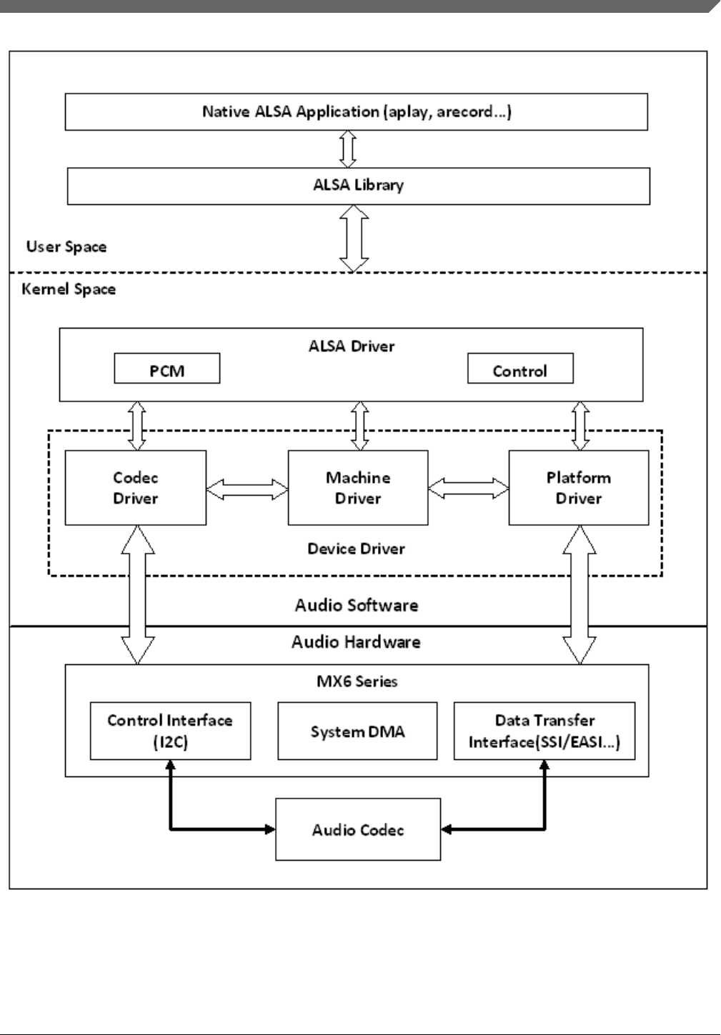
Figure 7-1. ALSA SoC Software Architecture
ASoC basically splits an embedded audio system into 3 components:
Chapter 7 Audio
i.MX Reference Manual, Rev. L4.9.88_2.0.0-ga, 05/2018
NXP Semiconductors 267

• Machine driver-handles any machine-specific controls and audio events, such as
turning on an external amp at the beginning of playback.
• Platform driver-contains the audio DMA engine and audio interface drivers (for
example, I2S, AC97, PCM) for that platform.
• CODEC driver-platform independent and contains audio controls, audio interface
capabilities, the CODEC DAPM definition, and CODEC I/O functions.
More detailed information about ASoC can be found in the Linux kernel documentation
in the Linux OS source tree at linux/Documentation/sound/alsa/soc and at www.alsa-
project.org/main/index.php/ASoC.
7.1.2 SoC Sound Card
Currently, the stereo CODEC (WM8958, WM8960, WM8962, and WM8524), 7.1
CODEC (cs42888), and AM/FM CODEC (si4763) drivers are implemented using ASoC
architecture.
These sound card drivers are built in independently. The stereo sound card supports
stereo playback and capture. The 7.1 sound card supports up to eight channels of audio
playback. While enabling ASRC, 7.1 sound card only supports 2 or 6 channels audio
playback. The AM/FM sound card supports radio PCM capture.
NOTE
The 7.1 CODEC is only supported on the i.MX 6Quad and
i.MX 6Solo SABRE Auto platform.
The AM/FM CODEC is only supported on the i.MX 6Quad and
i.MX 6Solo SABRE Auto platform.
7.1.2.1 Stereo CODEC Features
The stereo CODEC supports the following features:
• Sample rates for playback and capture are 8 KHz, 32 KHz, 44.1 KHz, 48 KHz, and
96 KHz
• Channels:
• Playback: supports two channels.
• Capture: supports two channels.
• Audio formats:
• Playback:
• SNDRV_PCM_FMTBIT_S16_LE
Advanced Linux Sound Architecture (ALSA) System on a Chip (ASoC) Sound
i.MX Reference Manual, Rev. L4.9.88_2.0.0-ga, 05/2018
268 NXP Semiconductors

• SNDRV_PCM_FMTBIT_S20_3LE
• SNDRV_PCM_FMTBIT_S24_LE
• Capture:
• SNDRV_PCM_FMTBIT_S16_LE
• SNDRV_PCM_FMTBIT_S20_3LE
• SNDRV_PCM_FMTBIT_S24_LE
7.1.2.2 7.1 Audio Codec Features
• Sample rates for playback and record:
• 48 KHz, 96 KHz, 192 KHz
• Playback: 5.512 k, 8 k, 11.025 k, 16 k, 22 k, 32 k, 44.1 k, 48 k, 64 k, 88.2 k, 96
k, 176.4 k, 192 k (ASRC enabled)
• Channels:
• Playback: 2, 4, 6, 8 channels
• Playback(ASRC enabled): 2, 6 channels
• Capture: 2, 4 channels
• Audio formats:
• Playback:
• SNDRV_PCM_FMTBIT_S16_LE
• SNDRV_PCM_FMTBIT_S20_3LE
• SNDRV_PCM_FMTBIT_S24_LE
• Playback(ASRC enabled):
• SNDRV_PCM_FMTBIT_S16_LE
• SNDRV_PCM_FMTBIT_S24_LE
• Capture:
• SNDRV_PCM_FMTBIT_S16_LE
• SNDRV_PCM_FMTBIT_S20_3LE
• SNDRV_PCM_FMTBIT_S24_LE
7.1.2.3 AM/FM Codec Features
• Supported sample rate for Capture: 48 KHz
• Supported channels:
• Capture: supports two channels.
• Supported audio formats:
• Capture: SNDRV_PCM_FMTBIT_S16_LE
Chapter 7 Audio
i.MX Reference Manual, Rev. L4.9.88_2.0.0-ga, 05/2018
NXP Semiconductors 269

7.1.2.4 Sound Card Information
The registered sound card information can be listed as follows using the commands aplay
-l and arecord -l. For example, the stereo sound card is registered as card 0.
root@freescale /$ aplay -l
**** List of PLAYBACK Hardware Devices ****
card 0: wm8962audio [wm8962-audio], device 0: HiFi wm8962-0 []
Subdevices: 1/1
Subdevice #0: subdevice #0
7.1.3 Hardware Operation
The following sections describe the hardware operation of the ASoC driver.
7.1.3.1 Stereo Audio CODEC
The stereo audio CODEC is controlled by the I2C interface. The audio data is transferred
from the user data buffer to/from the SSI FIFO through the DMA channel. The DMA
channel is selected according to the audio sample bits. AUDMUX is used to set up the
path between the SSI port and the output port which connects with the CODEC. The
CODEC works in master mode and provides the BCLK and LRCLK. The BCLK and
LRCLK can be configured according to the audio sample rate.
The WM8958, WM8960, and WM8962 ASoC CODEC driver exports the audio record/
playback/mixer APIs according to the ASoC architecture.
The CODEC driver is generic and hardware independent code that configures the
CODEC to provide audio capture and playback. It does not contain code that is specific
to the target platform or machine. The CODEC driver handles:
• CODEC DAI and PCM configuration
• CODEC control I/O-using I2C
• Mixers and audio controls
• CODEC audio operations
• DAC Digital mute control
The WM8958, WM8960, and WM8962 CODEC are registered as an I2C client when the
module initializes. The APIs are exported to the upper layer by the structure
snd_soc_dai_ops .
Headphone insertion/removal can be detected through a GPIO interrupt signal.
SSI dual FIFO features are enabled by default.
Advanced Linux Sound Architecture (ALSA) System on a Chip (ASoC) Sound
i.MX Reference Manual, Rev. L4.9.88_2.0.0-ga, 05/2018
270 NXP Semiconductors

7.1.3.2 7.1 Audio Codec
The 7.1 audio codec includes 8-channel DAC and 4-channel ADC, which are controlled
by the I2C interface. The audio data is transferred from the user data buffer to the ESAI
fifo, through a DMA channel. The DMA channel is selected according to audio sample
bits. The codec works in slave mode as the ESAI provides the BCLK and LRCLK. The
BCLK and LRCLK can be configured according to the audio sample rate. The ESAI
supports up to eight audio output ports. While enabling ASRC, 7.1 audio codec supports
2 or 6 channel playback through ASRC. On the i.MX 6 Sabre ARD board, a CS42888
codec with 4 audio in port is used, each port receive two channels of data in the I2S
format(network mode), providing 8-channel of playback functionality. This codec also
has 2 audio output port connected with ESAI, providing 4-channel of recording
functionality.
The codec driver is generic and hardware independent code that configures the codec to
provide audio capture and playback. It does not contain code that is specific to the target
platform or machine. The codec driver handles:
• Codec DAI and PCM configuration
• Codec control I/O-using I2C
• Mixers and audio controls
• Codec audio operations
• DAI Digital mute control
The CS42888 codec is registered as an I2C client when the module initializes. The APIs
are exported to the upper layer by the structure snd_soc_dai_ops.
7.1.3.3 AM/FM Codec
The AM/FM codec is a virtual codec, it only has a PCM interface connected to the Tuner
device. The audio data is transferred from the user data buffer to or from the SSI FIFO
through the DMA channel. The DMA channel is selected according to the audio sample
bits. AUDMUX is used to set up the path between the SSI port and the output port which
connects with the codec. The codec works in master mode as it provides the BCLK and
LRCLK. The BCLK and LRCLK can be configured according to the audio sample rate.
7.1.4 Software Operation
The following sections describe the software operation of the ASoC driver.
Chapter 7 Audio
i.MX Reference Manual, Rev. L4.9.88_2.0.0-ga, 05/2018
NXP Semiconductors 271

7.1.4.1 ASoC Driver Source Architecture
File imx-pcm-dma.c is shared by the stereo ALSA SoC driver, the 7.1 ALSA SoC driver
and other CODEC driver. This file is responsible for preallocating DMA buffers and
managing DMA channels.
The stereo CODEC is connected to the CPU through the SSI interface. fsl_ssi.c registers
the CPU DAI driver for the stereo ALSA SoC and configures the on-chip SSI interface.
wm8962.c registers the stereo CODEC and hifi DAI drivers. The direct hardware
operations on the stereo codec are in wm8994.c, wm8960.c, and wm8962.c. imx-
wm8958.c, imx-wm8960.c and imx-wm8962.c are the machine layer codes, which create
the driver device and register the stereo sound card.
The multichannel codec is connected to the CPU through the ESAI interface. fsl_esai.c
registers the CPU DAI driver for the stereo ALSA SoC and configures the on-chip ESAI
interface. cs42888.c registers the multichannel CODEC and hifi DAI drivers. The direct
hardware operations on the multichannel CODEC are in cs42888.c. imx-cs42888.c is the
machine layer code which creates the driver device and registers the stereo sound card.
The AM/FM CODEC is connected to the CPU through the SSI interface. fsl_ssi.c
registers the CPU DAI driver for the stereo ALSA SoC and configures the on-chip SSI
interface. si476x.c registers the Tuner CODEC and Tuner DAI drivers. The direct
hardware operations on the CODEC are in si476x.c. imx-si476x.c is the machine layer
code which creates the driver device and registers the sound card.
The following table shows the stereo codec SoC driver source files. These files are under
sound/soc.
Table 7-1. Stereo Codec SoC Driver Files
File Description
fsl/imx-wm8958.c
fsl/imx-wm8960.c
fsl/imx-wm8962.c
Machine layer for stereo CODEC ALSA SoC (CODEC as I2S Master)
fsl/imx-pcm-dma.c Platform layer for stereo CODEC ALSA SoC
fsl/imx-pcm.h Header file for PCM driver and AUDMUX register definitions
fsl/fsl_ssi.c SSI CPU DAI driver for stereo CODEC ALSA SoC
fsl/fsl_ssi.h Header file for SSI CPU DAI driver and SSI register definitions
fsl/fsl_sai.c SAI CPU DAI driver for stereo CODEC ALSA SoC
fsl/fsll_sai.h Header file for SAI CPU DAI driver and SAI register definitions
codecs/wm8994.c
codecs/wm8960.c
CODEC layer for stereo CODEC ALSA SoC
Table continues on the next page...
Advanced Linux Sound Architecture (ALSA) System on a Chip (ASoC) Sound
i.MX Reference Manual, Rev. L4.9.88_2.0.0-ga, 05/2018
272 NXP Semiconductors

Table 7-1. Stereo Codec SoC Driver Files (continued)
File Description
codecs/wm8962.c
codecs/wm8994.h
codecs/wm8960.h
codecs/wm8962.h
Header file for stereo CODEC driver
Table below lists the AM/FM codec SoC driver source files. These files are under sound/
soc.
Table 7-2. AM/FM Codec SoC Driver Source Files
File Description
fsl/imx-si476x.c Machine layer for stereo CODEC ALSA SoC (CODEC as I2S Slave)
fsl/imx-pcm-dma.c Platform layer for stereo CODEC ALSA SoC
fsl/imx-pcm.h Header file for pcm driver and AUDMUX register definitions
fsl/fsl_ssi.c SSI CPU DAI driver for stereo CODEC ALSA SoC
fsl/fsl_ssi.h Header file for SSI CPU DAI driver and SSI register definitions
codecs/si476x.c Codec layer for stereo CODEC ALSA SoC
Table below shows the multiple-channel ADC SoC driver source files. These files are
also under sound/soc.
Table 7-3. CS42888 ASoC Driver Source File
File Description
fsl/imx-cs42888.c Machine layer for multiple-channel CODEC ALSA SoC
fsl/imx-pcm-dma.c Platform layer for multiple-channel CODEC ALSA SoC
fsl/imx-pcm.h Header file for pcm driver
fsl/fsl_esai.c ESAI CPU DAI driver for multiple-channel CODEC ALSA SoC
fsl/fsl_esai.h Header file for ESAI CPU DAI driver
codecs/cs42xx8.c CODEC layer for multiple-channel codec ALSA SoC
codecs/cs42xx8.h Header file for multiple-channel CODEC driver
fsl/fsl_asrc.c CPU DAI driver of ASRC P2P
fsl/fsl_asrc.h Header file for CPU DAI driver of ASRC P2P
fsl/fsl_asrc_pcm.c Platform layer for ASRC P2P
7.1.4.2 Sound Card Registration
The codecs have the same registration sequence:
Chapter 7 Audio
i.MX Reference Manual, Rev. L4.9.88_2.0.0-ga, 05/2018
NXP Semiconductors 273

1. The codec driver registers the codec driver, DAI driver, and their operation
functions.
2. The platform driver registers the PCM driver, CPU DAI driver and their operation
functions, pre allocates buffers for PCM components and sets playback and capture
operations as applicable.
3. The machine layer creates the DAI link between codec and CPU registers the sound
card and PCM devices.
7.1.4.3 Device Open
The ALSA driver performs the following functions:
• Allocates a free substream for the operation to be performed.
• Opens the low level hardware device.
• Assigns the hardware capabilities to ALSA runtime information (the runtime
structure contains all the hardware, DMA, and software capabilities of an opened
substream).
• Configures DMA read or write channel for operation.
• Configures CPU DAI and CODEC DAI interface.
• Configures CODEC hardware.
• Triggers the transfer.
After triggering for the first time, the subsequent DMA read/write operations are
configured by the DMA callback.
7.1.4.4 Devicetree Binding
See the following documents:
• Documentation/devicetree/bindings/sound/fsl,ssi.txt
• Documentation/devicetree/bindings/sound/fsl-sai.txt
• Documentation/devicetree/bindings/sound/fsl,esai.txt
• Documentation/devicetree/bindings/sound/fsl,asrc.txt
• Documentation/devicetree/bindings/sound/wm8962.txt
• Documentation/devicetree/bindings/sound/wm8960.txt
• Documentation/devicetree/bindings/sound/wm8994.txt
• Documentation/devicetree/bindings/sound/cs42xx8.txt
• Documentation/devicetree/bindings/sound/imx-audmux.txt
• Documentation/devicetree/bindings/sound/imx-audio-wm8962.txt
• Documentation/devicetree/bindings/sound/imx-audio-cs42888.txt
• Documentation/devicetree/bindings/sound/imx-audio-si476x.txt
Advanced Linux Sound Architecture (ALSA) System on a Chip (ASoC) Sound
i.MX Reference Manual, Rev. L4.9.88_2.0.0-ga, 05/2018
274 NXP Semiconductors

7.1.4.5 Menu Configuration Options
The following Linux kernel configuration options are provided for this module.
• SoC Audio supports for WM8958, WM8960, and WM8962 CODEC. In menuconfig,
this option is available:
-> Device Drivers
-> Sound card support
-> Advanced Linux Sound Architecture
-> ALSA for SoC audio support
-> SoC Audio for Freescale CPUs
-> SoC Audio support for i.MX boards with wm8962 (or
wm8958, wm8960)
• SoC Audio supports for i.MX cs42888. In menuconfig, this option is available:
-> Device Drivers
-> Sound card support
-> Advanced Linux Sound Architecture
-> ALSA for SoC audio support
-> SoC Audio for Freescale CPUs
-> SoC Audio support for i.MX boards with cs42888
• SoC Audio supports for AM/FM. In menuconfig, this option is available:
-> Device Drivers
-> Sound card support
-> Advanced Linux Sound Architecture
-> ALSA for SoC audio support
-> SoC Audio for Freescale CPUs
-> SoC Audio support for i.MX boards with si476x
7.1.5 Unit Test
This section describes how to use the ALSA driver.
7.1.5.1 Stereo Codec Unit Test
Stereo codec driver supports playback and record features. A default volume can be
adjusted using the alsamixer command.
The playback feature can be tested with the following command:
•aplay [-Dplughw:0,0] audio.wav
Chapter 7 Audio
i.MX Reference Manual, Rev. L4.9.88_2.0.0-ga, 05/2018
NXP Semiconductors 275

The record feature supports the analog microphone and digital microphone. If the analog
microphone is not plugged in, the default is the digital microphone.
For WM8962 codec, the analog microphone is connected to the IN3R port. To enable the
analog microphone, execute the following amixer commands:
•amixer sset 'MIXINR IN3R' on
•amixer sset 'INPGAR IN3R' on
For WM8960 codec, i.MX 7Dual SDB and i.MX 6UltraLite EVK have different analog
microphone hardware connections.
• For i.MX 7Dual SDB, the analog microphone is connected to the LINPUT1 port. To
enable the analog microphone, execute the following amixer commands:
•amixer cset name='Left Input Mixer Boost Switch' on
•amixer cset name='Left Boost Mixer LINPUT1 Switch' on
•amixer cset name='Left Boost Mixer LINPUT2 Switch' off
•amixer cset name='Left Boost Mixer LINPUT3 Switch' off
•amixer cset name='ADC PCM Capture Volume' 195
By default, route the left ADC date to the right ADC channel to support stereo (Left
Data = Left ADC; Right Data = Left ADC):
•amixer cset name='ADC Data Output Select' 1
• For i.MX 6UL EVK, there are two analog microphones, MAIN MIC and HP MIC.
MAIN MIC is connected to the RINPUT1 and RINPUT2 ports to support differential
microphone. HP MIC is connected to the LINPUT1 and LINPUT3 ports. To enable
the analog microphone, execute the following amixer commands:
•amixer cset name='Left Input Mixer Boost Switch' on
•amixer cset name='Left Boost Mixer LINPUT1 Switch' on
•amixer cset name='Left Boost Mixer LINPUT2 Switch' on
•amixer cset name='Left Boost Mixer LINPUT3 Switch' on
•amixer cset name='Right Input Mixer Boost Switch' on
•amixer cset name='Right Boost Mixer RINPUT1 Switch' on
•amixer cset name='Right Boost Mixer RINPUT2 Switch' on
•amixer cset name='Right Boost Mixer RINPUT3 Switch' off
•amixer cset name='ADC PCM Capture Volume' 220
By default, for HP MIC and MAIN MIC, only one channel has voice when recording
stereo WAV (Left Data = Left ADC; Right Data = Right ADC):
•amixer cset name='ADC Data Output Select' 0
When using HP MIC to support stereo, route the left ADC date to the right ADC
channel (Left Data = Left ADC; Right Data = Left ADC):
•amixer cset name='ADC Data Output Select' 1
When using MAIN MIC to support stereo, route the right ADC date to the left ADC
channel (Left Data = Right ADC; Right Data = Right ADC):
Advanced Linux Sound Architecture (ALSA) System on a Chip (ASoC) Sound
i.MX Reference Manual, Rev. L4.9.88_2.0.0-ga, 05/2018
276 NXP Semiconductors

•amixer cset name='ADC Data Output Select' 2
The record feature can be tested by the following command:
•arecord [-Dplughw:0,0] -r 44100 -f S16_LE -c 2 -d 5 record.wav
More usages for aplay/arecord/amixer can be obtained by the following commands:
•aplay --h
•arecord --h
•amixer --h
7.1.5.2 7.1 Audio Codec Unit Test
The 7.1 Audio codec driver supports multichannel playback and record feature. The
codec has a default volume, and you can adjust volume by alsamixer command.
Playback feature can be tested by following command:
• aplay [-Dplughw:0,0] audio.wav
While enabling ASRC, the 7.1 audio codec should use the device 1 for playback. The
codec has a default volume, and you can adjust volume by alsamixer command.
• aplay [-Dplughw:0,1] audio.wav
Record feature supports line in and mic in simultaneously. While on i.MX 6 Sabre ARD
board, LINE-IN (L/R) use AIN1/AIN2, MICS1/MICS2 use AIN3/AIN4. By default, 2-ch
record uses AIN1/AIN2, 4-ch record uses AIN1/AIN2/AIN3/AIN4 together.
Record feature can be tested by following command:
• arecord [-Dplughw:0,0] -r 48000 -f S16_LE -c 2 -d 5 record.wav
Note:The default ALSA config file, asound.conf located under /etc/, only supports stereo
playback and record, which means, to test 4,6,8-ch playback or 4-ch recording, using
aplay audio.wav or arecord -c 4 audio.wav(without -Dplughw), make slight changes to
the configuration file as follows:
• a) make sure playback pcm use dmix_48000 and capture pcm use dsnoop_48000
under pcm.asymed{};
• b) add "channels x" to the end of struct pcm.dmix_48000{} if you want to playback
x-ch wav file(x is greater than 2);
• c) add "channels x" to the end of struct pcm.!dsnoop_48000{} if you want to record
to x-ch wav(x is greater than 2);
If plug plughw is used to make a playback or record, examples as below,
Chapter 7 Audio
i.MX Reference Manual, Rev. L4.9.88_2.0.0-ga, 05/2018
NXP Semiconductors 277

• aplay -Dplughw:0,0 audio.wav or
• arecord -Dplughw:0,0 -c 4 -r 48000 -f S16_LE record.wav
The configuration file asound.conf is not required to change because this file is not used
here.
More usage for aplay/arecord/amixer may be gotten by the following commands.
• aplay --h
• arecord --h
• amixer --h
7.1.5.3 AM/FM Codec Unit Test
This test turns on the AM/FM radio tuner (SI476x). It also sets and gets the current
station.
NOTE
An underrun error may occur sometimes.
This underrun behaviour is normal, since the test connects the AM/FM output to the
audio codec by a simple pipe.
There is no synchronization method between them. Upper layers (such as gstreamer
plugins) should take care of this sync.
Input the following command in command line to start unit test:
• ./mxc_tuner_test.sh
The following infomation is displayed on the console window:
Welcome to radio menu.
1. Turn on the radio
2. Get current frequency
3. Set current frequency
4. Turn off the radio
9. Exit.
• To turn on the radio select option 1
• To get the current frequency select option 2
• To set the desire frecuency select option 3 <enter> set the frequency <9740>
Advanced Linux Sound Architecture (ALSA) System on a Chip (ASoC) Sound
i.MX Reference Manual, Rev. L4.9.88_2.0.0-ga, 05/2018
278 NXP Semiconductors

• To turn off the radio select option 4
• To Exit select option 9
7.2 Asynchronous Sample Rate Converter (ASRC)
7.2.1 Introduction
The Asynchronous Sample Rate Converter (ASRC) converts the sampling rate of a signal
to a signal of different sampling rate. The ASRC supports concurrent sample rate
conversion of up to 10 channels. The sample rate conversion of each channel is
associated to a pair of incoming and outgoing sampling rates. The ASRC supports up to
three sampling rate pairs simultaneously.
7.2.1.1 Hardware Operation
ASRC includes the following features:
• Supports ratio (Fsin/Fsout) range between 1/24 to 8.
• Designed for rate conversion between 44.1 KHz, 32 KHz, 48 KHz, and 96 KHz.
• Other input sampling rates in the range of 8 KHz to 100 KHz are also supported, but
with less performance (see IC spec for more details).
• Other output sampling rates in the range of 30 KHz to 100 KHz are also supported,
but with less performance.
• Automatic accommodation to slow variations in the incoming and outgoing sampling
rates.
• Tolerant to sample clock jitter.
• Designed mainly for real-time streaming audio usage. Can be used for non-realtime
streaming audio usage when the input sampling clocks are not available.
• In any usage case, the output sampling clocks must be activated.
• In case of real-time streaming audio, both input and output clocks need to be
available and activated.
• In case of non-realtime streaming audio, the input sampling rate clocks can be
avoided by setting ideal-ratio values into ASRC interface registers.
The ASRC supports polling, interrupt and DMA modes, but only DMA mode is used in
the platform for better performance. The ASRC supports following DMA channels:
• Peripheral to peripheral, for example: ASRC to ESAI
• Memory to peripheral, for example: memory to ASRC
• Peripheral to memory, for example: ASRC to memory
Chapter 7 Audio
i.MX Reference Manual, Rev. L4.9.88_2.0.0-ga, 05/2018
NXP Semiconductors 279
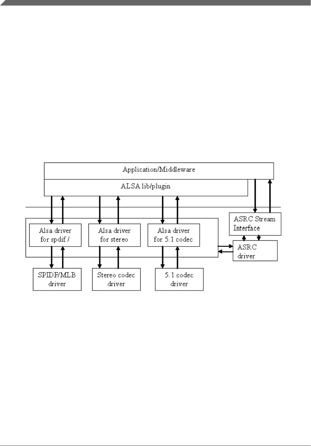
For more information, see the ASRC chapter in the Applications Processor
documentation associated with the SoC.
7.2.2 Software Operation
As an assistant component in the audio system, the ASRC driver implementation depends
on the use cases in the platform.
Currently, ASRC is used in two scenarios.
• Memory > ASRC > Memory, ASRC is controlled by the user application or ALSA
plug-in.
• Memory > ASRC > peripheral, ASRC is controlled directly by other ALSA drivers.
Figure 7-2. Audio Driver Interactions
As illustrated in the figure above, the ASRC stream interface provides the interface for
the user space. The ASRC registers itself under /dev/mxc_asrc and creates proc file /proc/
driver/asrc when the module is inserted. proc is used to track the channel number for each
pair. If all the pairs are not used, users can adjust the channel number through the proc
file. The number of the total channels should be ten, or else the adjusted value cannot be
saved properly.
7.2.2.1 Sequence for Memory to ASRC to Memory
• Open /dev/mxc_asrc device
Asynchronous Sample Rate Converter (ASRC)
i.MX Reference Manual, Rev. L4.9.88_2.0.0-ga, 05/2018
280 NXP Semiconductors

• Request ASRC pair - ASRC_REQ_PAIR
• Configure ASRC pair - ASRC_CONIFG_PAIR
• Start ASRC - ASRC_START_CONV
• Write the raw audio data (to be converted) into the user maintained input buffer. Fill
asrc_convert_buffer struct with input/output buffer length and address. Driver would
copy output data to user maintained output buffer address according to the output
buffer size. Repeat this step until all data is converted. -ASRC_CONVERT
• Stop ASRC conversion - ASRC_STOP_CONV
• Release ASRC pair - ASRC_RELEASE_PAIR
• Close /dev/mxc_asrc device
7.2.2.2 Sequence for Memory to ASRC to Peripheral
Memory to ASRC to peripheral audio path is involved in 7.1 audio codec driver. In 7.1
audio sound card, a new device with the name "cs42888audio [cs42888-audio], device 1:
HiFi-ASRC-FE (*)" is specified for playback and capture with ASRC. The steps below
show the flow of calling ASRC to memory to peripheral:
• The sound device(PCM) has been registered and start to enable the DMA channel in
ALSA driver
• Request ASRC pair - fsl_asrc_request_pair
• Configure ASRC pair - fsl_asrc_config_pair
• Enable the DMA channel from Memory to ASRC and from ASRC to Memory
• Start DMA channel and start ASRC conversion - fsl_asrc_start_pair
• When audio data playback complete, stop DMA channel and ASRC -
fsl_asrc_stop_pair
• Release ASRC pair - fsl_asrc_release_pair
7.2.2.3 Source Code Structure
The table below lists the source files available in the devices directory.
drivers/mxc/asrc
include/linux/
sound/soc/fsl/
sound/soc/codec/
Table 7-4. ASRC Source File List
File Description
fsl_asrc_m2m.c ASRC M2M driver implementation codes
fsl_asrc_m2m_dma.c ALSA platform layer for ASRC M2M
Table continues on the next page...
Chapter 7 Audio
i.MX Reference Manual, Rev. L4.9.88_2.0.0-ga, 05/2018
NXP Semiconductors 281

Table 7-4. ASRC Source File List
(continued)
File Description
imx-cs42888.c Memory to ASRC to ESAI TX implementation in 7.1 audio codec machine driver
imx-pcm-dma.c Memory to ASRC to ESAI TX implementation in 7.1 audio codec platform driver
fsl_esai.c Memory to ASRC to ESAI TX implementation in 7.1 audio codec CPU driver
cs42xx8 Memory to ASRC to ESAI TX implementation in 7.1 audio codec codec driver
fsl_asrc.c ALSA CPU DAI driver of ASRC P2P
fsl_asrc.h Header file for ALSA CPU DAI driver of ASRC P2P
fsl_asrc_dma.c ALSA platform layer for ASRC P2P
fsl_asrc_m2m_dma.c ALSA platform layer for ASRC M2M
7.2.2.4 Menu Configuration Options
The menu configuration options are as follows:
-> Device Drivers
-> Sound card support
-> Advanced Linux Sound Architecture
-> ALSA for SoC audio support
-> SoC Audio for Freescale i.MX CPUs
-> Asynchronous Sample Rate Converter (ASRC) module support
Then the ASRC driver can only be configured with the build-in module.
7.2.2.5 Devicetree Binding
The functions of device tree bindings for ASRC M2M are as follows:
• compatible: Compatible list, must contain "fsl,imx6q-asrc".
• reg: Offset and length of the register set for the device.
• interrupts: Contains the asrc interrupt.
• clocks: Contains an entry for each entry in clock-names.
• clock-names: Must contain "mem", "ipg", "asrck", and "dma". (Generally, "dma" is
used for SPBA clock.)
• dmas: Generic dma devicetree binding as described in Documentation/devicetree/
bindings/dma/dma.txt.
• dma-names: Six dmas have to be defined, "txa", "rxa", "txb", "rxb", "txc", "rxc".
• fsl,clk-map-version: the mapping relationship in different SOC is different. This
version number can be used to indicate clock map information.
• fsl,clk-channel-bits: indicates the channel bit information.
The functions of device tree bindings for ASRC P2P are as follows:
Asynchronous Sample Rate Converter (ASRC)
i.MX Reference Manual, Rev. L4.9.88_2.0.0-ga, 05/2018
282 NXP Semiconductors

• compatible: Compatible list, must contain "fsl,imx6q-asrc-p2p".
• fsl,p2p-rate: A valid sample rate for Back-End (I2S) playback and record.
• fsl,p2p-width: A valid sample width for Back-End (I2S) playback and record.
• fsl,asrc-dma-rx-events: Contains three SDMA event numbers for ASRC Rx.
• fsl,asrc-dma-tx-events: Contains three SDMA event numbers for ASRC Tx.
7.2.2.6 Programming Interface (Exported API and IOCTLs)
The ASRC Exported API allows the ALSA driver to use ASRC services.
The ASRC IOCTLs below are used for user space applications:
ASRC_REQ_PAIR:
Apply a pair from ASRC driver. Once a pair is allocated, ASRC core clock is enabled.
ASRC_CONFIG_PAIR:
Configure ASRC pair allocated. User is responsible for providing parameters defined in
struct asrc_config. Items in asrc_config is listed below:
• pair: ASRC pair allocated by the IOCTL(ASRC_REQ_PAIR).
• channel_num: channel number.
• buffer_num: buffer number need for input and output buffer use.The input/output
buffers are allocated inside ASRC driver. User is responsible for remap it into user
space.
• dma_buffer_size: buffer size for input and output buffers. The buffer size should be
in the unit of page size. Usually, 4k bytes is used.
• input_sample_rate: input sampling rate. Input sample rate should be in 5.512k, 8k,
11.025k, 16k, 22k, 32k, 44.1k, 48k, 64k, 88.2k 96k, 176.4k, 192k.
• output_sample_rate: output sampling rate. Output sampling rate should be in 32k,
44.1k, 48k, 64k, 88.2k, 96k, 176.4k 192k.
• input_word_width: word width of input audio data. The input data word width can be
16 bit or 24 bit.
• output_word_width: word width of output audio data. The output data word width
can be 16 bit or 24 bit.
• inclk: the input clock source can be ESAI RX clock, SSI1 RX clock, SSI2 RX clock,
SPDIF RX clock, MLB_clock, ESAI TX clock, SSI1 TX clock, SSI2 TX clock,
SPDIF TX clock, ASRCLK1 clock, NONE. If using clock except NONE, user
should make sure that the clock is available.
• outclk: the output clock source is the same as the input clock source.
ASRC_CONVERT:
Chapter 7 Audio
i.MX Reference Manual, Rev. L4.9.88_2.0.0-ga, 05/2018
NXP Semiconductors 283

Convert the input data into output data according to the parameters set by
ASRC_CONFIG_PAIR. Driver would copy input_buffer_length bytes data from the
input_buffer_vaddr for convert. After convert, driver fill the output_buffer_length
according to data number generated by ASRC and copy output_buffer_length to
output_buffer_vaddr. However, before calling ASRC_CONVERT, User is responsible
for filling the output_buffer_length according to the ratio of input sample rate and output
sample rate. If the generated buffer size is larger than user filled output_buffer_size,
driver would only copy user filled output_buffer_size to output_buffer_vaddr. If the
generated buffer size is smaller than user filled output_buffer_size(the difference should
be less than 64 bytes.), calling ASRC_CONVERT would fail.
• input_buffer_vaddr: virtual address of input buffer.
• output_buffer_vaddr: virtual address of output buffer.
• input_buffer_length: length of input buffer(bytes).
• output_buffer_length: length of output buffer(bytes).
ASRC_START_CONV:
Start ASRC pair convert.
ASRC_STOP_CONV:
Stop ASRC pair convert.
ASRC_STATUS:
Query ASRC pair status.
7.2.3 Unit Test
This section describes how to use the ASRC driver.
7.2.3.1 Memory-to-ASRC-to-Peripheral
The 7.1 audio codec driver supports calling the ASRC driver for memory > ASRC >
peripheral (ESAI TX). All the input audio files are converted into board-defined
sampling rate, for example, 48 Khz. This use case only supports 2 or 6 channel playback.
To call this use case, follow the steps below:
• Call aplay -l | grep ASRC to get the card number and device number of the playback
PCM. The device name is CS42888_ASRC. For example, the card number is 0 and
the device number is 1.
• Play the audio file with the card0device1 device. For example, aplay -Dplughw:0,1
$AUDIO_FILE.
Asynchronous Sample Rate Converter (ASRC)
i.MX Reference Manual, Rev. L4.9.88_2.0.0-ga, 05/2018
284 NXP Semiconductors

7.2.3.2 Memory-to-ASRC-to-Memory
There is a Memory-to-ASRC-to-Memory test case, mxc_asrc_test.out. It is located at /
unit_tests and can convert WAV to different sample rates, such as:
/unit_tests/mxc_asrc_test.out -to 48000 /unit_tests/audio8k16S.wav audio48k16S.wav
More usages for mxc_asrc_test.out can be obtained by the following command:
/unit_tests/mxc_asrc_test.out -h
The Memory-to-ASRC-to-Memory test case can also be used through a rate converter
alsa lib plugin. To use it, add .asoundrc as follows:
cat > ~/.asoundrc <<-EOF
defaults.pcm.rate_converter "asrcrate"
pcm.dmix_44100 {
type dmix
ipc_key 5678293
ipc_key_add_uid yes
slave{
pcm "hw:0,0"
period_time 10000
format S16_LE
rate 44100
}
}
pcm.asrc {
type plug
route_policy "average"
slave.pcm "dmix_44100"
}
EOF
After adding ~/.asoundrc, use the following command to play back WAV. It converts the
sample rate to 44.1 Kbps automatically:
aplay -D asrc $AUDIO_FILE
or
aplay $AUDIO_FILE
7.3 HDMI Audio
7.3.1 Introduction
HDMI Audio is covered in the HDMI overview chapter in video. See HDMI Audio for
more details.
Chapter 7 Audio
i.MX Reference Manual, Rev. L4.9.88_2.0.0-ga, 05/2018
NXP Semiconductors 285

7.4 The Sony/Philips Digital Interface (S/PDIF)
7.4.1 Introduction
The Sony/Philips Digital Interface (S/PDIF) audio module is a stereo transceiver that
allows the processor to receive and transmit digital audio. The S/PDIF transceiver allows
the handling of both S/PDIF channel status (CS) and User (U) data. The frequency
measurement block allows the S/PDIF RX section to derive the receive clock from the
incoming S/PDIF stream.
7.4.1.1 S/PDIF Overview
Figure below shows the block diagram of the S/PDIF interface.
The Sony/Philips Digital Interface (S/PDIF)
i.MX Reference Manual, Rev. L4.9.88_2.0.0-ga, 05/2018
286 NXP Semiconductors
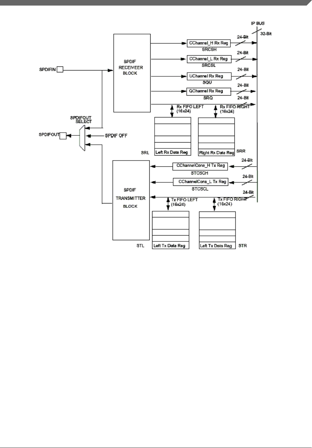
Figure 7-3. S/PDIF Transceiver Data Interface Block Diagram
7.4.1.2 Hardware Overview
The S/PDIF is composed of two parts:
• The S/PDIF receiver extracts the audio data from each S/PDIF frame and places the
data in the S/PDIF Rx left and right FIFOs. The Channel Status and User Bits are
also extracted from each frame and placed in the corresponding registers. The S/
PDIF receiver provides a bypass option for direct transfer of the S/PDIF input signal
to the S/PDIF transmitter.
• For the S/PDIF transmitter, the audio data is provided by the processor through the
SPDIFTxLeft and SPDIFTxRight registers. The Channel Status bits are provided
through the corresponding registers. The S/PDIF transmitter generates a S/PDIF
output bitstream in the biphase mark format (IEC958), which consists of audio data,
channel status and user bits.
Chapter 7 Audio
i.MX Reference Manual, Rev. L4.9.88_2.0.0-ga, 05/2018
NXP Semiconductors 287

In the S/PDIF transmitter, the IEC958 biphase bit stream is generated on both edges of
the S/PDIF Transmit clock. The S/PDIF Transmit clock is generated by the S/PDIF
internal clock dividers and the sources are from outside of the S/PDIF block. The S/PDIF
receiver can recover the S/PDIF Rx clock from the S/PDIF stream. Figure 7-3 shows the
clock structure of the S/PDIF transceiver.
7.4.1.3 Software Overview
The S/PDIF driver is designed under ALSA System on Chip (ASoC) layer. The ASoC
driver for S/PDIF provides one playback device for Tx and one capture device for Rx.
The playback output audio format can be linear PCM data or compressed data with 16-
bit, 20-bit, and 24-bit audio. The allowed sampling bit rates are 44.1, 48 or 32 KHz. The
capture input audio format can be linear PCM data or compressed 24-bit data and the
allowed sampling bit rates are from 16 to 96 KHz. The driver provides the same interface
for PCM and compressed data transmission.
7.4.1.4 The ASoC layer
The ASoC layer divides audio drivers for embedded platforms into separate layers that
can be reused. ASoC divides an audio driver into a codec driver, a machine layer, a DAI
(digital audio interface) layer, and a platform layer. The Linux kernel documentation has
some concise description of these layers in linux/Documentation/sound/alsa/soc. In the
case of the S/PDIF driver, we are able to reuse the platform layer (imx-pcm-dma.c) that is
used by the ssi stereo codec driver and also the generic dummy codec driver useful for
DAI links creation without a real codec.
7.4.2 S/PDIF Tx Driver
The S/PDIF Tx driver supports the following features.
• 32, 44.1 and 48 KHz sample rates.
• Signed 16 and 24-bit little Endian sample format. Due to S/PDIF SDMA feature, the
24-bit output sample file must have 32-bits in each channel per frame. Only the 24
LSBs are valid.
• In the ALSA subsystem, the supported format is defined as S16_LE and S24_LE.
• Stereo playback.
• Information query through iecset or amixer.
The Sony/Philips Digital Interface (S/PDIF)
i.MX Reference Manual, Rev. L4.9.88_2.0.0-ga, 05/2018
288 NXP Semiconductors

• The device ID can be determined by using the 'aplay -l' utility to list out the playback
audio devices.
For example:
root@freescale ~$ aplay -l
**** List of PLAYBACK Hardware Devices ****
card 0: imxspdif [imx-spdif], device 0: S/PDIF PCM snd-soc-dummy-dai-0 []
Subdevices: 1/1
Subdevice #0: subdevice #0
NOTE
The number at the beginning of the IMX_SPDIF line is the
card ID. The string in the square brackets is the card name.
• The ALSA utility provides a common method for user spaces to operate and use
ALSA drivers
#aplay -Dplughw:0,0 audio.wav
NOTE
The -D parameter of aplay indicates the PCM device with
card ID and PCM device ID: hw:[card id],[pcm device id]
The "iecset" utility provides a common method to set or dump the IEC958 status bits.
#iecset -c 0
7.4.2.1 Driver Design
Before S/PDIF playback, the configuration, interrupt, clock and channel registers are
initialized. During S/PDIF playback, the channel status bits are fixed. The DMA and
interrupts are enabled. S/PDIF has 16 TX sample FIFOs on Left and Right channel
respectively. When both FIFOs are empty, an empty interrupt is generated if the empty
interrupt is enabled. If no data are refilled in the 20.8 μs (1/48000), an underrun interrupt
is generated. Overrun is avoided if only 16 sample FIFOs are filled for each channel
every time. If auto re-synchronization is enabled, the hardware checks if the left and right
FIFO are in sync, and if not, it sets the filling pointer of the right FIFO to be equal to the
filling pointer of the left FIFO and an interrupt is generated.
Chapter 7 Audio
i.MX Reference Manual, Rev. L4.9.88_2.0.0-ga, 05/2018
NXP Semiconductors 289

7.4.2.2 Provided User Interface
The S/PDIF transmitter driver provides one ALSA mixer sound control interface to the
user besides the common PCM operations interface. It provides the interface for the user
to write S/PDIF channel status codes into the driver so they can be sent in the S/PDIF
stream. The input parameter of this interface is the IEC958 digital audio structure shown
below, and only status member is used:
struct snd_aes_iec958 {
unsigned char status[24]; /* AES/IEC958 channel status bits */
unsigned char subcode[147]; /* AES/IEC958 subcode bits */
unsigned char pad; /* nothing */
unsigned char dig_subframe[4]; /* AES/IEC958 subframe bits */
};
7.4.3 S/PDIF Rx Driver
The S/PDIF Rx driver supports the following features:
• 16, 32, 44.1, 48, 64 and 96 KHz receiving sample rate
• Signed 24-bit little endian sample format. Due to S/PDIF SDMA feature, each
channel bit length in PCM recorded frame is 32 bits, and only the 24 LSBs are valid
In ALSA subsystem, the supported format is defined as S24_LE.
• Stereo record.
• The device ID can be determined by using the 'arecord -l' to list out record devices.
For example:
root@freescale ~$ arecord -l
**** List of CAPTURE Hardware Devices ****
card 0: cs42888audio [cs42888-audio], device 0: HiFi CS42888-0 []
Subdevices: 1/1
Subdevice #0: subdevice #0
card 1: imxspdif [imx-spdif], device 0: S/PDIF PCM snd-soc-dummy-dai-0 []
Subdevices: 1/1
Subdevice #0: subdevice #0
• The ALSA utility provides a common method for user spaces to operate and use
ALSA drivers.
#arecord -Dplughw:1,0" -c 2 -r 44100 -f S24_LE record.wav
The Sony/Philips Digital Interface (S/PDIF)
i.MX Reference Manual, Rev. L4.9.88_2.0.0-ga, 05/2018
290 NXP Semiconductors

NOTE
The -D parameter of the arecord indicates the PCM device
with card ID and PCM device ID: hw:[card id],[pcm device
id]
The "iecset" utility provides a common method to set or dump the IEC958 status bits.
#iecset -c 1
7.4.3.1 Driver Design
Before the driver can read a data frame from the S/PDIF receiver FIFO, it must wait for
the internal DPLL to be locked. Using the high-speed system clock, the internal DPLL
can extract the bit clock (advanced pulse) from the input bit stream. When this internal
DPLL is locked, the LOCK bit of PhaseConfig Register is set and the driver configures
the interrupt, clock and SDMA channel. After that, the driver can receive audio data,
channel status, user bits and valid bits concurrently.
For channel status reception, a total of 48 channel status bits are received in two registers.
The driver reads them out when a user application makes a request.
For user bits reception, there are two modes for User Channel reception: CD and non-CD.
The mode is determined by the USyncMode (bit 1 of CDText_Control register). User can
call the sound control interface to set the mode (see Table 7-5), but no matter what the
mode is, the driver handles the user bits in the same way. For the S/PDIF Rx, the
hardware block copies the Q bits from the user bits to the QChannel registers and puts the
user bits in UChannel registers. The driver allocates two queue buffers for both U bits
and Q bits. The U bits queue buffer is 96x2 bytes in size, the Q bits queue buffer is 12x2
bytes in size, and queue buffers are filled in the U/Q Full, Err and Sync interrupt
handlers. This means that the user can get the previous ready U/Q bits while S/PDIF
driver is reading new U/Q bits.
For valid bit reception, S/PDIF Rx hardware block triggers an interrupt and set interrupt
status upon reception. A sound control interface is provided for the user to get the status
of this valid bit.
7.4.3.2 Provided User Interface
The S/PDIF Rx driver provides interfaces for user application as shown in table below.
Chapter 7 Audio
i.MX Reference Manual, Rev. L4.9.88_2.0.0-ga, 05/2018
NXP Semiconductors 291

Table 7-5. S/PDIF Rx Driver Interfaces
Interface Type Mode1Parameter Comment
Common PCM PCM - - PCM open/close
prepare/trigger
hw_params/sw_params
Rx Sample
Rate
Sound
Control2r Integer
Range: [16000, 96000]
Get sample rate. It is not accurate due to DPLL
frequency measure module. So the user
application must do a correction to the get
value.
USyncMode Sound
Control
rw Boolean
Value: 0 or 1
Set 1 for CD mode
Set 0 for non-CD mode
Channel Status Sound
Control
r struct snd_aes_iec958
Only status [6] array member is used
-
User bit Sound
Control
r Byte array
96 bytes for U bits
12 bytes for Q bits
-
No good V bit Sound
Control
r Boolean
Value: 0 or 1
An interrupt is associated with the valid flag.
(interrupt 16 - SPDIFValNoGood). This interrupt
is set every time a frame is seen on the SPDIF
interface with the valid bit set to invalid.
1. The mode column shows the interface attribute: r (read) or w (write)
2. The sound control type of interface is called by the snd_ctl_xxx() alsa-lib function
The user application can follow the program flow from Figure 7-4 to use the S/PDIF Rx
driver. First, the application opens the S/PDIF Rx PCM device, waits for the DPLL to
lock the input bit stream, and gets the input sample rate. If the USyncMode needs to be
set, set it before reading the U/Q bits. Next, set the hardware parameters, including
channel number, format and capture sample rate which is obtained from the driver. Then,
call prepare and trigger to startup S/PDIF Rx stream read. Finally, call the read function
to get the data. During the reading process, applications can read the U/Q bits and
channel status from the driver and valid the no good bit.
The Sony/Philips Digital Interface (S/PDIF)
i.MX Reference Manual, Rev. L4.9.88_2.0.0-ga, 05/2018
292 NXP Semiconductors
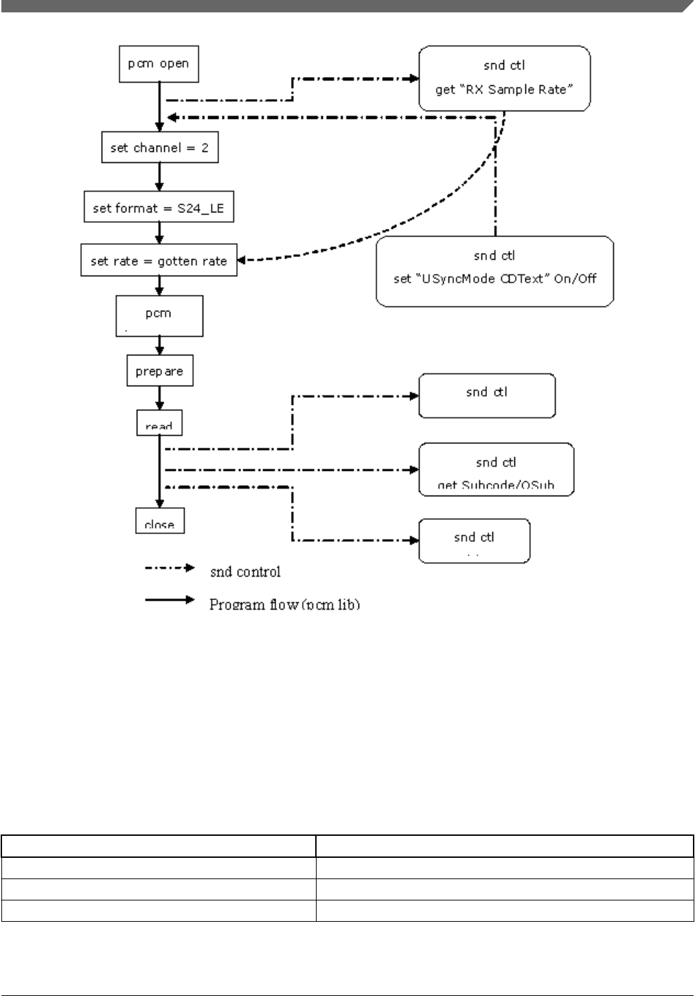
Figure 7-4. S/PDIF Rx Application Program Flow
7.4.4 Source Code Structure
Table below lists the source files for the driver.
These files are under the sound directory.
Table 7-6. S/PDIF Driver Files
File Description
sound/soc/soc-utils.c Dummy ALSA SOC codec driver
sound/soc/fsl/imx-spdif.c S/PDIF ALSA SOC machine layer
sound/soc/fsl/fsl_spdif.c S/PDIF ALSA SOC DAI layer
Table continues on the next page...
Chapter 7 Audio
i.MX Reference Manual, Rev. L4.9.88_2.0.0-ga, 05/2018
NXP Semiconductors 293

Table 7-6. S/PDIF Driver Files (continued)
File Description
sound/soc/fsl/imx-pcm-dma.c ALSA SOC platform layer
sound/soc/fsl/imx-pcm.h ALSA SOC platform layer header
7.4.4.1 Menu Configuration Options
The following Linux kernel configurations are provided for this module:
In menu configuration enable the following module:
• CONFIG_SND_IMX_SPDIF - Configuration option for the S/PDIF driver:
• Device Drivers -> Sound card support -> Advanced Linux Sound Architecture ->
ALSA for SoC audio support -> SoC Audio for Freescale i.MX CPUs -> SoC Audio
support for i.MX boards with S/PDIF
7.4.4.2 Device Tree Bindings
See the following documents:
• Documentation/devicetree/bindings/sound/fsl,spdif.txt
• Documentation/devicetree/bindings/sound/imx-audio-spdif.txt
7.4.4.3 Interrupts and Exceptions
S/PDIF Tx/Rx hardware block has many interrupts to indicate the success, exception and
event.
The driver handles the following interrupts:
• DPLL Lock and Loss Lock-Saves the DPLL lock status; this is used when getting the
Rx sample rate
• U/Q Channel Full and overrun/underrun-Puts the U/Q channel register data into
queue buffer, and update the queue buffer write pointer
• U/Q Channel Sync-Saves the ID of the buffer whose U/Q data is ready for read out
• U/Q Channel Error-Resets the U/Q queue buffer
The Sony/Philips Digital Interface (S/PDIF)
i.MX Reference Manual, Rev. L4.9.88_2.0.0-ga, 05/2018
294 NXP Semiconductors

7.4.5 Unit Test Preparation
In order to prepare to run a unit test, perform the following actions:
• Setup M-Audio Transit USB sound card by installing M-Audio Transit driver on
your PC.
• Install WaveLab tools on your PC.
7.4.5.1 Tx test step
• Plug optical line into [line|optical] port of M-Audio transit.
NOTE
Make sure the [optical out] port of M-Audio transit has no
output (red light off) after plugging the optical line.
• Start up WaveLab, press the record button on the toolbar, set up the record file name,
sample rate, and channel number, and then record.
• Meanwhile, on board use following command to play one wave file:
#aplay -D hw:[card id],[pcm id] audioXXkYYS.wav
• After aplay finishes, stop recording in WaveLab.
• Play the recorded WAV file in wavelab to check.
7.4.5.2 Rx test step
• Plug optical line into [optical port] of M-Audio transit
• Startup WaveLab, open a test WAV file: audioXXkYYS.wav to play in loop
• Meanwhile, on board use the following command to record one WAV file. After
finishing recording, you may playback the record WAV file on other audio card on
the board or PC.
#arecord -D hw:[card id],[pcm id] -c 2 -d 20 -r [sample rate in Hz] -f S24_LE record.wav
NOTE
The sample rate argument in the arecord command must be
consistent with the WAV file playing on WaveLab.
Chapter 7 Audio
i.MX Reference Manual, Rev. L4.9.88_2.0.0-ga, 05/2018
NXP Semiconductors 295

The Sony/Philips Digital Interface (S/PDIF)
i.MX Reference Manual, Rev. L4.9.88_2.0.0-ga, 05/2018
296 NXP Semiconductors

Chapter 8
Security
8.1 Cryptographic Acceleration and Assurance Module
(CAAM)
8.1.1 CAAM Device Driver Overview
This section discusses implementation specifics of the kernel driver components
supporting CAAM (Cryptographic Acceleration and Assurance Module) within the Linux
kernel.
CAAM's base driver packaging can be categorized on two distinct levels:
• Configuration and Job Execution Level
• API Interface Level
Configuration and Job Execution Level consists of:
• A control and configuration module which maps the main register page and writes
global or system required configuration information.
• A module that feeds jobs through job rings, and reports status.
API Interface Level consists of:
• An interface to the Sctterlist Crypto API supporting asynchronous single-pass
authentication-encryption operations, and common blockciphers - caamalg.
• An interface to the Scatterlist Crypto API supporting asynchronous hashes - caamhash.
• An interface to the hwrng API supporting use of the Random Number Generator -
caamrng.
8.1.2 Configuration and Job Execution Level
This section has two parts:
i.MX Reference Manual, Rev. L4.9.88_2.0.0-ga, 05/2018
NXP Semiconductors 297

• Control/Configuration Driver
• Job Ring Driver
8.1.3 Control/Configuration Driver
The control and configuration driver is responsible for initializing and setting up the
master register page, initializing early-on feature initialization, providing limited debug
and monitoring capability, and generally ensuring that all other dependent driver
subsystems can connect to a correctly-configured device.
Step by step, it performs the following actions at startup:
• Allocates a private storage block for this level.
• Maps a virtual address to the full CAAM register page.
• Maps a virtual address for the SNVS register page.
• Maps a virtual (cache coherent) address for Secure Memory.
• Registers the security violation interrupt.
• Selects the correct DMA address size for the platform, and sets DMA address masks
to match.
• Identifies other pertinent interrupt connections.
• Initializes all job ring instances.
• If the system configuration includes a DPAA Queue Interface, that interface has
frame-pop enabled.
NOTE
i.MX 6 configurations do not contain this logic.
• If the instance contains a TRNG, it's oscillator/entropy configuration is set and then
"kickstarted".
• Configuration information is sent to the system console to indicate that the driver is
alive, and what configuration it has assumed.
• If CONFIG_DEBUG_FS is selected in the kernel configuration, then entries are
added to enable debugfs views to useful registers in the performance monitor.
Register views are accessible under the caam/ctl directory at the debugfs root entry.
8.1.4 Job Ring Driver
The Job Ring driver is responsible for providing job execution service to higher-level
drivers. It takes care of overall management of both input and output rings and interrupt
service driving the output ring.
Cryptographic Acceleration and Assurance Module (CAAM)
i.MX Reference Manual, Rev. L4.9.88_2.0.0-ga, 05/2018
298 NXP Semiconductors

One driver call is available for higher layers to use for queueing jobs to a ring for
execution:
int caam_jr_enqueue(struct device *dev, u32 *desc, void (*cbk)(struct device
*dev, u32 *desc, u32 status, void *areq), void *areq);
Arguments:
dev Pointer to the struct device associated with the job ring for use. In the current
configuration, one or more struct device entries exist in the controller's private data block,
one for each ring.
desc Pointer to a CAAM job descriptor to be executed. The driver will map the descriptor
prior to execution, and unmap it upon completion. However, since the driver can't
reasonably know anything about the data referenced by the descriptor, it is the caller's
responsibility to map/flush any of this data prior to submission, and to unmap/invalidate
data after the request completes.
cbk Pointer to a callback function that will be called when the job has completed
processing.
areq Pointer to metadata or context data associated with this request. Often, this can
contain referenced data mapping information that request postprocessing (via the
callback) can use to clean up or release resources once complete.
Callback Function Arguments:
dev Pointer to the struct device associated with the job ring for use.
desc Pointer to the original descriptor submitted for execution.
status Completion status received back from the CAAM DECO that executed the request.
Nonzero only if an error occurred. Strings describing each error are enumerated in
error.c.
areq Metadata/context pointer passed to the original request.
Returns:
• Zero on successful job submission
• -EBUSY if the input ring was full
• -EIO if driver could not map the job descriptor
Chapter 8 Security
i.MX Reference Manual, Rev. L4.9.88_2.0.0-ga, 05/2018
NXP Semiconductors 299

8.1.5 API Interface Level
CAAM module provides a connection through the Scatterlist Crypto API both for
common symmetric blockciphers, and for single-pass authentication-encryption services.
This table lists all installed authentication-encryption algorithms by their common name,
driver name, and purpose. Note that certain platforms, such as i.MX 6, contain a low-
power MDHA accelerator, which cannot support SHA384 or SHA512.
Name Driver Name Purpose
authenc(hmac(md5),cbc(aes)) authenc-hmac-md5-cbc-aes-caam Single-pass authentication/encryption
using MD5 and AES-CBC
authenc(hmac(sha1),cbc(aes)) authenc-hmac-sha1-cbc-aes-caam Single-pass authentication/encryption
using SHA1 and AES-CBC
authenc(hmac(sha224),cbc(aes)) authenc-hmac-sha224-cbc-aes-caam Single-pass authentication/encryption
using SHA224 and AES-CBC
authenc(hmac(sha256),cbc(aes)) authenc-hmac-sha256-cbc-aes-caam Single-pass authentication/
encryptionusing SHA256 and AES-CBC
authenc(hmac(sha384),cbc(aes)) authenc-hmac-sha384-cbc-aes-caam Single-pass authentication/encryption
using SHA384 and AES-CBC
authenc(hmac(sha512),cbc(aes)) authenc-hmac-sha512-cbc-aes-caam Single-pass authentication/encryption
using SHA512 and AES-CBC
authenc(hmac(md5),cbc(des3_ede)) authenc-hmac-md5-cbcdes3_ede-caam Single-pass authentication/encryption
using MD5 and Triple-DES-CBC
authenc(hmac(sha1),cbc(des3_ede)) authenc-hmac-sha1-cbc-des3_ede-
caam
Single-pass authentication/encryption
using SHA1 and Triple-DES-CBC
authenc(hmac(sha224),cbc(des3_ede)) authenc-hmac-sha224-cbc-des3_ede-
caam
Single-pass authentication/encryption
using SHA224 and Triple-DES-CBC
authenc(hmac(sha256),cbc(des3_ede)) authenc-hmac-sha256-cbc-des3_ede-
caam
Single-pass authentication/encryption
using SHA256 and Triple-DES-CBC
authenc(hmac(sha384),cbc(des3_ede)) authenc-hmac-sha384-cbc-des3_ede-
caam
Single-pass authentication/encryption
using SHA384 and Triple-DES-CBC
authenc(hmac(sha512),cbc(des3_ede)) authenc-hmac-sha512-cbc-des3_ede-
caam
Single-pass authentication/encryption
using SHA512 and Triple-DES-CBC
authenc(hmac(md5),cbc(des)) authenc-hmac-md5-cbc-des-caam Single-pass authentication/encryption
using MD5 and Single-DES-CBC
authenc(hmac(sha1),cbc(des)) authenc-hmac-sha1-cbc-des-caam Single-pass authentication/encryption
using SHA1 and Single-DES-CBC
authenc(hmac(sha224),cbc(des)) authenc-hmac-sha224-cbc-des-caam Single-pass authentication/encryption
using SHA224 and Single-DES-CBC
authenc(hmac(sha256),cbc(des)) authenc-hmac-sha256-cbc-des-caam Single-pass authentication/encryption
using SHA256 and Single-DES-CBC
authenc(hmac(sha384),cbc(des)) authenc-hmac-sha384-cbc-des-caam Single-pass authentication/encryption
using SHA384 and Single-DES-CBC
authenc(hmac(sha512),cbc(des)) authenc-hmac-sha512-cbc-des-caam Single-pass authentication/encryption
using SHA512 and Single-DES-CBC
This table lists all installed symmetric key blockcipher algorithms by their common
name, driver name, and purpose.
Cryptographic Acceleration and Assurance Module (CAAM)
i.MX Reference Manual, Rev. L4.9.88_2.0.0-ga, 05/2018
300 NXP Semiconductors

Name Driver Name Purpose
cbc(aes) cbc-aes-caam AES with a CBC mode wrapper
cbc(des3_ede) cbc-3des-caam Triple DES with a CBC mode wrapper
cbc(des) cbc-des-caam Single DES with a CBC mode wrapper
ecb(aes) ecb-aes-caam AES with a ECB mode wrapper
ecb(des3_ede) ecb-3des-caam Triples DES with a ECB mode wrapper
ecb(des) ecb-des-caam Single DES with a ECB mode wrapper
ecb(arc4) ecb-arc4-caam ARC4 with a ECB mode wrapper
ctr(aes) ctr-aes-caam AES with a CTR mode wrapper
Use of these services through the API is exemplified in the common conformance/
performance testing module in the kernel's crypto subsystem, known as tcrypt, visible in
the kernel source tree at crypto/tcrypt.c.
The caamhashmodule provides a connection through the Scatterlist Crypto API both for
common asynchronous hashes.
This table lists all installed asynchronous hashes by their common name, driver name,
and purpose. Note that certain platforms, such as i.MX 6, contain a low-power MDHA
accelerator, which cannot support SHA384 or SHA512.
Name Driver Name Purpose
sha1 sha1-caam SHA1-160 Hash Computation
sha224 sha224-caam SHA224 Hash Computation
sha256 sha256-caam SHA256 Hash Computation
sha384 sha384-caam SHA384 Hash Computation
sha512 sha512-caam SHA512 Hash Computation
md5 md5-caam MD5 Hash Computation
hmac(sha1) hmac-sha1-caam SHA1-160 Hash-based Message
Authentication Code
hmac(sha224) hmac-sha224-caam SHA224 Hash-based Message
Authentication Code
hmac(sha256) hmac-sha256-caam SHA256 Hash-based Message
Authentication Code
hmac(sha384) hmac-sha384-caam SHA384 Hash-based Message
Authentication Code
hmac(sha512) hmac-sha512-caam SHA512 Hash-based Message
Authentication Code
hmac(md5) hmac-md5-caam MD5 Hash-based Message
Authentication Code
Use of these services through the API is exemplified in the common conformance/
performance testing module in the kernel's crypto subsystem, known as tcrypt, visible in
the kernel source tree at crypto/tcrypt.c.
Chapter 8 Security
i.MX Reference Manual, Rev. L4.9.88_2.0.0-ga, 05/2018
NXP Semiconductors 301

The caamrng module installs a mechanism to use CAAM's random number generator to
feed random data into a pair of buffers that can be accessed through /dev/hw_random.
/dev/hw_random is commonly used to feed the kernel's own entropy pool, which can be used
internally, as an entropy source for other random data "devices".
For more information regarding support for this service, see rng-tools available in
sourceforge.net/projects/gkernel/files/rng-tools.
8.1.6 Driver Configuration
Configuration of the driver is controlled by the following kernel confguration parameters
(found under Cryptographic API -> Hardware Crypto Devices):
CRYPTO_DEV_FSL_CAAM
Enables building the base controller driver and the job ring backend.
CRYPTO_DEV_FSL_CAAM_RINGSIZE
Selects the size (e.g., the maximum number of entries) of job rings. This is selectable as a
power of 2 in the range of 2-9, allowing selection of a ring depth ranging from 4 to 512
entries.
The default selection is 9, resulting in a ring depth of 512 job entries.
CRYPTO_DEV_FSL_CAAM_INTC
Enables the use of the hardware's interrupt coalescing feature, which can reduce the
amount of interrupt overhead the system incurs during periods of high utilization.
Leaving this disabled forces a single interrupt for each job completion, simplifying
operation, but increasing overhead.
CRYPTO_DEV_FSL_CAAM_INTC_COUNT_THLD
If coalescing is enabled, selects the number of job completions allowed to queue before
an interrupt is raised. This is selectable within the range of 1 to 255. Selecting 1
effectively defeats the coalescing feature. Any selection of a size greater than the job ring
size forces a situation where the interrupt times out before ever raising an interrupt.
The default selection is 255.
CRYPTO_DEV_FSL_CAAM_INTC_TIME_THLD
Cryptographic Acceleration and Assurance Module (CAAM)
i.MX Reference Manual, Rev. L4.9.88_2.0.0-ga, 05/2018
302 NXP Semiconductors

If coalescing is enabled, selects the count of bus clocks (divided by 64) before a
coalescing timeout where, if the count threshold has not been met, an interrupt is raised at
the end of the time period. The selection range is an integer from 1 to 65535.
The default selection is 2048.
CRYPTO_DEV_FSL_CAAM_CRYPTO_API
Enables Scatterlist Crypto API support for asynchronous blockciphers and for single-pass
autentication-encryption operations through the API using CAAM hardware for
acceleration.
CRYPTO_DEV_FSL_CAAM_AHASH_API
Enables Scatterlist Crypto API support for asynchronous hashing through the API using
CAAM hardware for acceleration.
CRYPTO_DEV_FSL_CAAM_RNG_API
Enables use of the CAAM Random Number generator through the hwrng API. This can
be used to generate random data to feed an entropy pool for the kernels pseudo-random
number generator.
CRYPTO_DEV_FSL_CAAM_RNG_TEST
Enables a captive test to ensure that the CAAM RNG driver is operating and buffering
random data.
8.1.7 Limitations
• Components of the driver do not currently build and run as modules. This may be
rectified in a future version.
• Interdependencies exist between the controller and job ring backends, therefore they
all must run in the same system partition. Future versions of the driver may separate
out the job ring back-end as a standalone module that can run independently (and
support independent API and SM instances) in its own system partition.
• The full CAAM register page is mapped by the controller driver, and derived
pointers to selected subsystems are calculated and passed to higher-layer driver
components. Partition-independent configurations will have to map their own
subsystem pointers instead.
• Upstream variants of this driver support only Power architecture. This ARM
architecture-specific port is not upstreamed at this time, although portions may be
upstreamed at some point.
Chapter 8 Security
i.MX Reference Manual, Rev. L4.9.88_2.0.0-ga, 05/2018
NXP Semiconductors 303

• TRNG kickstart may need to be moved to the bootloader in a future release, so that
the RNG can be used earlier.
• The Job Ring driver has a registration and de-registration functions that are not
currently necessary (and may be rewritten in future editions to provide for shutdown
notifications to higher layers.
• The full CAAM function is exclusive with the Mega/Fast mix off feature in DSM. If
CAAM is enabled, the Mega/Fast mix off feature needs to be disabled, and the user
should "echo enabled > /sys/bus/platform/devices/2100000.aips-bus/2100000.caam/
2101000.jr0/power/wakeup" after the kernel boots up, and then Mega/Fast mix will
keep the power on in DSM.
8.1.8 Limitations in the Existing Implementation Overview
This chapter describes a prototype of a Keystore Management Interface intended to
provide access to CAAM Secure Memory.
Secure memory provides a controlled and access-protected area where critical system
security parameters can be stored and processed in a running system without bus-level
exposure of clear secrets. Secrets can be imported into and exported from secure
memory, but never exported from secure memory in their cleartext form. Instead, secrets
may be exported from secure memory in a covered form, using keys never visible to the
outside.
This driver, with its kernel-level API, exposes a basic interface to allow kernel-level
services access to secure memory functionality. It is split into two pieces:
• Keystore Initialization and Maintenance Interfaces
• Keystore Access Interface
The initialization and maintenance services exist to initialize and define the instance of a
keystore interface. Likewise, the access interface allows kernel-level services to use the
API for management of security parameters.
8.1.9 Initialize Keystore Management Interface
Installs a set of pointers to functions that implement an underlying physical interface to
the keystore subsystem.
In the present release, a default (and hidden) suite of functions implement this interface.
Future implementations of this API may provide for the installation of an alternate
interface. If this occurs, an alternate to this call can be provided.
Cryptographic Acceleration and Assurance Module (CAAM)
i.MX Reference Manual, Rev. L4.9.88_2.0.0-ga, 05/2018
304 NXP Semiconductors

void sm_init_keystore(struct device *dev);
Arguments:
dev points to a struct device established to manage resources for the secure memory
subsystem.
8.1.10 Detect Available Secure Memory Storage Units
Returns the number of available units ("pages") that can be accessed by the local instance
of this driver. Intended for use as a resource probe.
u32 sm_detect_keystore_units(struct device *dev);
Arguments:
dev Points to a struct device established to manage resources for the secure memory
subsystem.
Returns: Number of detected units available for use, 0 through n - 1 may be used with
subsequent calls to all other API functions.
8.1.11 Establish Keystore in Detected Unit
Sets up an allocation table in a detected unit that can be used for the storage of keys (or
other secrets). The unit will be divided into a series of fixed-size slots, each one of which
is marked available in the allocation table. The size of each slot is a build-time selectable
parameter.
No calls to the keystore access interface can occur until sm_establish_keystore() has been
called.
sm_establish_keystore() should follow a call to sm_detect_keystore_units().
int sm_establish_keystore(struct device *dev, u32 unit);
Arguments:
dev Points to a struct device established to manage resources for the secure memory
subsystem.
unit One of the units detected with a call to sm_detect_keystore_units().
Returns:
Chapter 8 Security
i.MX Reference Manual, Rev. L4.9.88_2.0.0-ga, 05/2018
NXP Semiconductors 305

• Zero on successful return
• -EINVAL if the keystore subsystem was not initialized
• -ENOSPC if no memory was available for the allocation table and associated context
data.
8.1.12 Release Keystore
Releases all resources used by this keystore unit. No further calls to the keystore access
interface can be made.
void sm_release_keystore(struct device *dev, u32 unit);
Arguments:
dev Points to a struct device established to manage resources for the secure memory
subsystem.
unit One of the units detected with a call to sm_detect_keystore_units().
8.1.13 Allocate a Slot from the Keystore
Allocate a slot from the keystore for use in all other subsequent operations by the
keystore access interface.
int sm_keystore_slot_alloc(struct device *dev, u32 unit, u32 size, u32*slot);
Arguments:
dev Points to a struct device established to manage resources for the secure memory
subsystem.
unit One of the units detected with a call to sm_detect_keystore_units().
size Desired size of data for storage in the allocated slot.
slot Pointer to the variable to receive the allocated slot number, once known.
Returns:
• Zero for successful completion.
• -EKEYREJECTED if the requested size exceeds the selected slot size.
Cryptographic Acceleration and Assurance Module (CAAM)
i.MX Reference Manual, Rev. L4.9.88_2.0.0-ga, 05/2018
306 NXP Semiconductors

8.1.14 Load Data into a Keystore Slot
Load data into an allocated keystore slot so that other operations (such as encapsulation)
can be carried out upon it.
int sm_keystore_slot_load(struct device *dev, u32 unit, u32 slot, constu8 *key_data, u32
key_length);
Arguments:
dev Points to a struct device established to manage resources for the secure memory
subsystem.
unit One of the units detected with a call to sm_detect_keystore_units().
key_length Length (in bytes) of information to write to the slot.
key_data Pointer to buffer with the data to be loaded. Must be a contiguous buffer.
Returns:
• Zero for successful completion.
• -EFBIG if the requested size exceeds that which the slot can hold.
8.1.15 Demo Image Update
Encapsulate data written into a keystore slot as a Secure Memory Blob.
int sm_keystore_slot_encapsulate(struct device *dev, u32 unit, u32
inslot, u32 outslot, u16 secretlen, u8 *keymod, u16 keymodlen);
Arguments:
dev Points to a struct device established to manage resources for the secure memory
subsystem.
unit One of the units detected with a call to sm_detect_keystore_units().
inslot Slot holding the input secret, loaded into that slot by sm_keystore_slot_load().
Note that the slot containing this secret should be overwritten or deallocated as soon as
practical, since it contains cleartext at this point.
outslot Allocated slot to hold the encapsulated output as a Secure Memory Blob.
secretlen Length of the secret to be encapsulated, not including any blob storage overhead
(blob key, MAC, etc.).
Chapter 8 Security
i.MX Reference Manual, Rev. L4.9.88_2.0.0-ga, 05/2018
NXP Semiconductors 307

keymod Key modifier component to be used for encapsulation. The key modifier allows an
extra secret to be used in the encapsulation process. The same modifier will also be
required for decapsulation.
keymodlen Lenth of key modifier in bytes.
Returns:
• Zero on success
• CAAM job status if a failure occurs
8.1.16 Decapsulate Data in the Keystore
Decapsulate data in the keystore into a Black Key Blob for use in other cryptographic
operations. A Black Key Blob allows a key to be used "covered" in main memory
without exposing it as cleartext.
int sm_keystore_slot_decapsulate(struct device *dev, u32 unit, u32
inslot, u32 outslot, u16 secretlen, u8 *keymod, u16 keymodlen);
Arguments:
dev Points to a struct device established to manage resourcesfor the secure memory
subsystem.
unit One of the units detected with a call to sm_detect_keystore_units().
inslot Slot holding the input data, processed by a prior call to
sm_keystore_slot_encapsulate(), and containing a Secure Memory Blob.
outslot Allocated slot to hold the decapsulated output data in the form of a Black Key
Blob.
secretlen Length of the secret to be decapsulated, without any blob storage overhead.
keymod Key modified component specified at the time of encapsulation.
keymodlen Lenth of key modifier in bytes.
Returns:
• Zero on success
• CAAM job status if a failure occurs
Cryptographic Acceleration and Assurance Module (CAAM)
i.MX Reference Manual, Rev. L4.9.88_2.0.0-ga, 05/2018
308 NXP Semiconductors

8.1.17 Read Data From a Keystore Slot
Extract data from a keystore slot back to a user buffer. Normally to be used after some
other operation (e.g., decapsulation) occurs.
int sm_keystore_slot_read(struct device *dev, u32 unit, u32 slot, u32
key_length, u8 *key_data);
Arguments:
dev Points to a struct device established to manage resources for the secure memory
subsystem.
unit One of the units detected with a call to sm_detect_keystore_units().
slot Allocated slot to read from.
key_length Length (in bytes) of information to read from the slot.
key_data Pointer to buffer to hold the extracted data. Must be a contiguous buffer.
Returns:
• Zero for successful completion.
• -EFBIG if the requested size exceeds that which the slot can hold.
8.1.18 Release a Slot back to the Keystore
Release a keystore slot back to the available pool. Information in the store is wiped clean
before the deallocation occurs.
int sm_keystore_slot_dealloc(struct device *dev, u32 unit, u32 slot);
Arguments:
dev Points to a struct device established to manage resources for the secure memory
subsystem.
unit One of the units detected with a call to sm_detect_keystore_units().
slot Number of the allocated slot to be released back to the store.
Returns:
• Zero for successful completion.
• -EINVAL if an unallocated slot is specified.
Chapter 8 Security
i.MX Reference Manual, Rev. L4.9.88_2.0.0-ga, 05/2018
NXP Semiconductors 309

Configuration of the Secure Memory Driver / Keystore API is dependent on the
following kernel configuration parameters:
CRYPTO_DEV_FSL_CAAM_SM
Turns on the secure memory driver in the kernel build.
CRYPTO_DEV_FSL_CAAM_SM_SLOTSIZE
Configures the size of a secure memory "slot".
Each secure memory unit is block of internal memory, the size of which is
implementation dependent. This block can be subdivided into a number of logical "slots"
of a size which can be selected by this value. The size of these slots needs to be set to a
value that can hold the largest secret size intended, plus the overhead of blob parameters
(blob key and MAC, typically no more than 48 bytes).
The values are selectable as powers of 2, limited to a range of 32 to 512 bytes. The
default value is 7, for a size of 128 bytes.
CRYPTO_DEV_FSL_CAAM_SM_TEST
Enables operation of a captive test / example module that shows how one might use the
API, while verifying its functionality. The test module works along this flow:
• Creates a number of known clear keys (3 sizes).
• Allocated secure memory slots.
• Inserts those keys into secure memory slots and encapsulates.
• Decapsulates those keys into black keys.
• Enrcrypts DES, AES128, and AES256 plaintext with black keys. Since this uses
symmetric ciphers, same-key encryption/decryption results will be equivalent.
• Decrypts enciphered buffers with equivalent clear keys.
• Compares decrypted results with original ciphertext and compares. If they match, the
test reports OK for each key case tested.
Normal output is reported at the console as follows:
platform caam_sm.0: caam_sm_test: 8-byte key test match OK platform
caam_sm.0: caam_sm_test: 16-byte key test match OK platform caam_sm.0:
caam_sm_test: 32-byte key test match OK
• The secure memory driver is not implemented as a kernel module at this point in
time.
• Implementation is presently limited to kernel-mode operations.
Cryptographic Acceleration and Assurance Module (CAAM)
i.MX Reference Manual, Rev. L4.9.88_2.0.0-ga, 05/2018
310 NXP Semiconductors

• One instance is possible at the present time. In the future, when job rings can run
independently in different system partitions, a multiple instance secure memory
driver should be considered.
• All storage requests are limited to the storage size of a single slot (which is of a
build-time configurable length). It may be possible to allow a secret to span multiple
slots so long as those slots can be allocated contiguously.
• Slot size is fixed across all pages/partitions.
• Encapsulation/Decapsulation interfaces could allow for authentication to be
specified; the underlying interface does not request it.
• Encapsulation/Decapsulation interfaces return a job status; this status should be
translated into a meaningful error from errno.h
8.1.19 CAAM/SNVS - Security Violation Handling Interface
Overview
This chapter describes a prototype of a driver component and control interface for SNVS
Security Violations. It provides a means of installing, managing, and executing
application defined handlers meant to process security violation events as a response to
their occurrence in a system.
SNVS allows for the continuous monitoring of a number of possible attack vectors in a
running system. If the occurrence of one of these attach vectors is sensed, (e.g., a Security
Violation has been detected), SNVS can, along with erasing critical security parameters
and transitioning to a failure state. generate an interrupt indicating that the violation has
occurred. This interrupt can dispatch an application-defined routine to take cleanup action
as a consequence of the violation, such that an orderly shutdown of security services
might occur.
Therefore, the purpose of this interface is to allow system-level services to install
handlers for these types of events. This allows the system designer to select how he wants
to respond to specific security violation causes using a simple function call written to his
system-specific requirements.
8.1.20 Operation
For existing platforms, 6 security violation interrupt causes are possible within SNVS. 5
of these violation causes are normally wired for use, and these causes are defined as:
• SECVIO_CAUSE_CAAM_VIOLATION - Violation detected inside CAAM/SNVS
• SECVIO_CAUSE JTAG_ALARM - JTAG activity detected
• SECVIO_CAUSE_WATCHDOG - Watchdog expiration
Chapter 8 Security
i.MX Reference Manual, Rev. L4.9.88_2.0.0-ga, 05/2018
NXP Semiconductors 311

• SECVIO_CAUSE_EXTERNAL_BOOT - External bootload activity
• SECVIO_CAUSE_TAMPER_DETECT - Tamper detection logic triggered
Each of these causes can be associated with an application-defined handler through the
API provided with this driver. If no handler is specified, then a default handler will be
called. This handler does no more than to identify the interrupt cause to the system
console.
8.1.21 Configuration Interface
The following interface can be used to define or remove application-defined violation
handlers from the driver's dispatch table.
8.1.22 Install a Handler
int caam_secvio_install_handler(struct device *dev, enum secvio_cause
cause, void (*handler)(struct device *dev, u32 cause, void *ext), u8
*cause_description, void *ext);
Arguments:
dev Points to SNVS-owning device.
cause Interrupt source cause from the above list of enumerated causes.
handler Application-defined handler, gets called with dev, source cause, and locally-
defined handler argument
cause_description Points to a string to override the default cause name, this can be used as
an alternate for error messages and such. If left NULL, the default description string is
used. ext pointer to any extra data needed by the handler.
Returns:
• Zero on success.
• -EINVAL if an argument was invalid or unusable.
8.1.23 Remove an Installed Driver
int caam_secvio_remove_handler(struct device *dev, enum secvio_cause
cause);
Arguments:
Cryptographic Acceleration and Assurance Module (CAAM)
i.MX Reference Manual, Rev. L4.9.88_2.0.0-ga, 05/2018
312 NXP Semiconductors

dev Points to SNVS-owning device.
cause Interrupt source cause.
Returns:
• Zero on success.
• -EINVAL if an argument was invalid or unusable.
8.1.24 Driver Configuration CAAM/SNVS
CRYPTO_DEV_FSL_CAAM_SECVIO
Enables inclusion of Security Violation driver and configuration interface as part of the
build configuration. The driver is not buildable as a module in its present form.
8.2 Display Content Integrity Checker (DCIC)
8.2.1 Introduction
The goal of the DCIC is to verify that a safety-critical information sent to a display is not
corrupted.
8.2.1.1 Hardware Operation
The DCIC has the following features:
• Pixel clock up to 148.5 MHz
• Configurable polarity of Display Interface control signals
• 24-bit pixel data bus
• Up to 16 rectangular ROIs with a configurable location and size
• Independent CRC32 signature calculation for each ROI
• External controller mismatch indication signal
8.2.2 Software Operation
Chapter 8 Security
i.MX Reference Manual, Rev. L4.9.88_2.0.0-ga, 05/2018
NXP Semiconductors 313

8.2.2.1 Source Code Structure
Table below shows the driver source files available in the directory: drivers/video/fbdev/
mxc/.
Table 8-1. DCIC Driver Files
File Description
mxc_dcic.c DCIC driver source code
8.2.2.2 Menu Configuration Options
In menu configuration enable the following module:
Device Drivers -> Graphics support -> MXC DCIC
8.2.2.3 DTS Configuration
dcic_id = <0>; /* DCIC device index 0-dcic1, i-dcic2 */
dcic_mux = "dcic-lcdif1"; /* DCIC input select */
Table 8-2. DCIC Input Select
Module i.MX 6SoloX i.MX 6Dual/6Quad
DCIC1 dcic_lvds
dcic_lcdif1
dcic-ipu0-di1
dcic-lvds0
dcic-lvds1
dcic-hdmi
DCIC2 dcic_lvds
dcic_lcdif2
dcic-ipu0-di0/dcic-ipu1-di0
dcic-lvds0
dcic-lvds1
dcic-mipi_dpi
8.2.2.4 Programming Interface
8.2.2.5 IOCTLs Functions
The DCIC driver supports the following IOCTLs:
• DCIC_IOC_CONFIG_DCIC: Configures the DCIC input CLK, VSYNC, HSYNC,
and data signal polarity.
Display Content Integrity Checker (DCIC)
i.MX Reference Manual, Rev. L4.9.88_2.0.0-ga, 05/2018
314 NXP Semiconductors

• DCIC_IOC_CONFIG_ROI: Configures the ROI block size and reference signature.
• DCIC_IOC_GET_RESULT: Gets the result of the ROI calculated signature.
8.2.2.6 Structures
struct roi_params {
unsigned int roi_n; /* ROI index */
unsigned int ref_sig; /* Reference CRC32 */
unsigned int start_y; /* start vertical lines of ROI */
unsigned int start_x; /* start horizon lines of ROI */
unsigned int end_y; /* end vertical lines of ROI */
unsigned int end_x; /* end horizon lines of ROI */
char freeze; /* state of ROI */
};
8.2.2.7 DCIC CRC Calculation Functions
There are four functions in this unit test to calculate reference signature:
crc32_calc_18of24bit() /* CRC calculate 18 bit of 24 */
crc32_calc_24bit() /* CRC calculate 24 */
crc32_calc_24of16bit() /* CRC calculate 24 bit of 16 */
crc32_calc_18of16bit() /* CRC calculate 18 bit of 16 */
DCIC calculates CRC according to the display bus width, but the display bus width does
not always align with bytes per pixel (bpp), and the four functions above can cover
different display bus widths and bpps.
8.3 Smart Card Interface - Subscriber Identification Module
(SIM)
8.3.1 Introduction
The Subscriber Identification Module (SIM) is designed to facilitate communication to
SIM cards or Eurochip prepaid phone cards, and compatible with ISO/IEC 7816-3
standards. The SIM module has one port that can be used to interface with various cards.
The interface with the Micro Controller Unit (MCU) is a 32-bit connection as described
in the reference document IP Bus Specification.
8.3.1.1 Modes of Operation
The SIM module I/O interface can be operated in one of the three modes of operation
summarized below.
Chapter 8 Security
i.MX Reference Manual, Rev. L4.9.88_2.0.0-ga, 05/2018
NXP Semiconductors 315

• Two-wire interface: Both the IC pin RX and TX are used to interface to the
SmartCard.
• External one-wire interface: The IC pins RX and TX are tied together externally to
the IC and routed to the SmartCard.
• Internal one-wire interface: The IC pin TX is routed to the SmartCard. The receive
pin RX is connected to the TX pin internally to the IC.
8.3.1.2 External Signal Description
• SIM_CLK: clock that the SIM module provides for the SmartCard. Typical
frequencies are 1 MHz to 5 MHz. This clock is 372 times the data rate that is on pin
SIM_TRXD.
• SIM_RST_B: reset signal from the SIM to the SmartCard.
• SIM_SVEN: SmartCard power supply enable control signal.
• SIM_TRXD: transmitted/received date from SIM module to SmartCard.
• SIM_PD: SmartCard insertion detect.
8.3.2 Source Code Structure
The directory below shows the SIM driver source files.
drivers/mxc/sim/imx_sim.c
8.3.2.1 Menu Configuration Options
Configure the kernel option to enable the module by menuconfig:
Device Drivers > MXC support drivers > MXC SIM Support
8.3.2.2 Software Framework
The following figures show the SIM TX and RX software flows.
Smart Card Interface - Subscriber Identification Module (SIM)
i.MX Reference Manual, Rev. L4.9.88_2.0.0-ga, 05/2018
316 NXP Semiconductors
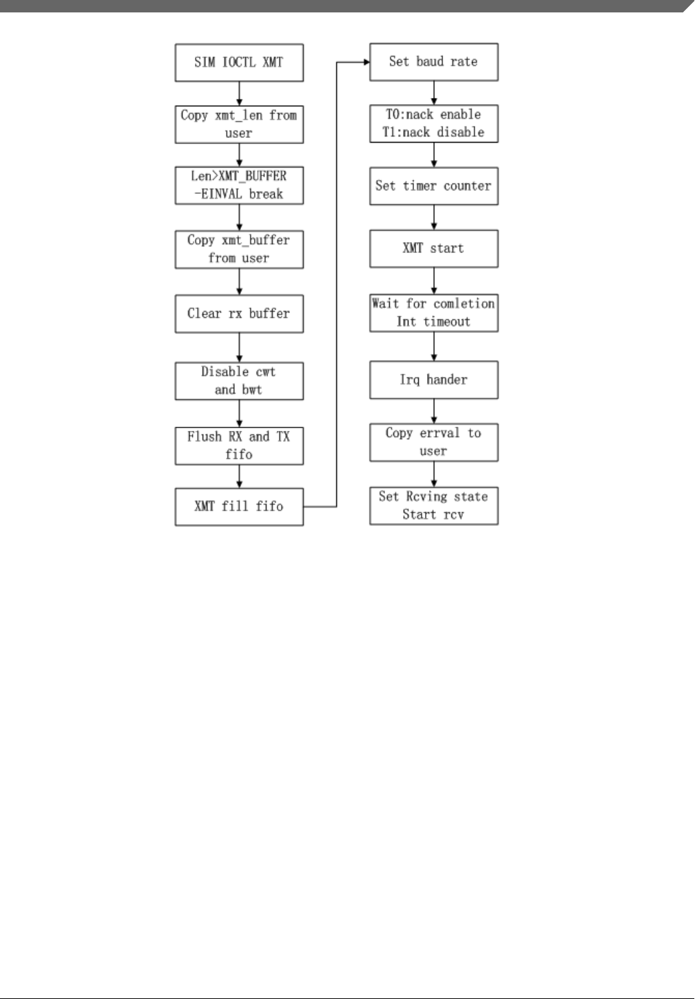
Figure 8-1. SIM transmitting flow
Chapter 8 Security
i.MX Reference Manual, Rev. L4.9.88_2.0.0-ga, 05/2018
NXP Semiconductors 317
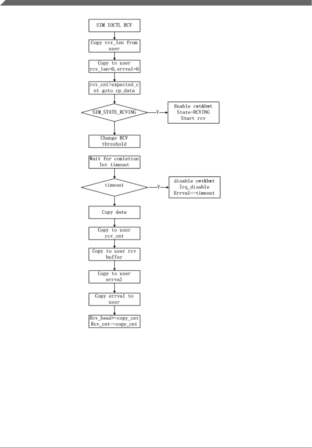
Figure 8-2. SIM receiving flow
8.4 Secure Non-Volatile Storage (SNVS)
Secure Non-Volatile Storage (SNVS)
i.MX Reference Manual, Rev. L4.9.88_2.0.0-ga, 05/2018
318 NXP Semiconductors

8.4.1 Introduction
For more information on Secure Non-Volatile Storage (SNVS), see the i.MX Security
Manual for the associated SoC.
SNVS is a block that interfaces with CAAM and SRTC.
For SNVS services related to CAAM, see Section Driver Configuration CAAM/SNVS.
For SNVS services related to srtc, see Section SRTC Introduction
8.5 SNVS Real Time Clock (SRTC)
8.5.1 Introduction
The Real Time Clock (RTC) module is used to keep the time and date. It provides a
certifiable time to the user and can raise an alarm if tampering with counters is detected.
8.5.1.1 Hardware Operation
The RTC is a fake timer provided by the system controller firmware. It only supports
basic function of read/set time, read/set alarm.
8.5.2 Software Operation
The following sections describe the software operation of the RTC driver.
8.5.2.1 Driver Features
The RTC driver includes the following features:
• Implements the functions required by Linux OS to provide the real time clock and
alarm interrupt
• Alarm wakes up the system from low power modes
Chapter 8 Security
i.MX Reference Manual, Rev. L4.9.88_2.0.0-ga, 05/2018
NXP Semiconductors 319

8.5.2.2 Source Code Structure
The RTC module is implemented in the following directory:
drivers/rtc
Table below shows the RTC module files.
Table 8-3. RTC Driver Files
File Description
rtc-imxdi.c MX6 RTC driver implementation file
rtc-imx8.c MX8 RTC driver implementation file
The source file for the RTC specifies the RTC function implementations.
8.5.2.3 Menu Configuration Options
In menu configuration enable the following module:
Device Drivers > Real Time Clock > Freescale i.MX RTC support
SNVS Real Time Clock (SRTC)
i.MX Reference Manual, Rev. L4.9.88_2.0.0-ga, 05/2018
320 NXP Semiconductors

Chapter 9
Unit Tests
9.1 Advanced Linux Sound Architecture (ALSA) System on a
Chip (ASoC) Sound
9.1.1 Test Name
• mxc_tuner_test.out
9.1.1.1 Location
/unit_tests/ALSA/
9.1.1.2 Functionality
Test audio capabilities using ALSA.
9.1.1.3 Configuration
ALSA is supported on all i.MX for test aplay, arecord and speaker-test. To use this tuner
test it requires tuner hardware available only on the i.MX 6 auto reference boards
9.1.1.4 Use Case and Expected Output
9.2 Asynchronous Sample Rate Converter (ASRC)
i.MX Reference Manual, Rev. L4.9.88_2.0.0-ga, 05/2018
NXP Semiconductors 321

9.2.1 Test Name
• mxc_asrc_test.out
9.2.1.1 Location
/unit_tests/ASRC
9.2.1.2 Functionality
Converts WAV to different sample rates.
9.2.1.3 Configuration
None
9.2.1.4 Use Case and Expected Output
#/unit_tests/ASRC/mxc_asrc_test.out -to 48000 /unit_tests/ASRC/audio8k16S.wav
audio48k16S.wav
---- Running < /unit_tests/ASRC/mxc_asrc_test.out > test ----
Pair A requested
All tests passed with success
More usages for mxc_asrc_test.out can be obtained by the following command:
#/unit_tests/ASRC/mxc_asrc_test.out -h
---- Running < /unit_tests/ASRC/mxc_asrc_test.out > test ----
**************************************************
* Test aplication for ASRC
* Options :
-to <output sample rate> <origin.wav$gt; <converted.wav>
<input clock source> <output clock source>
input clock source types are:
0 -- INCLK_NONE
1 -- INCLK_ESAI_RX
2 -- INCLK_SSI1_RX
3 -- INCLK_SSI2_RX
4 -- INCLK_SPDIF_RX
5 -- INCLK_MLB_CLK
6 -- INCLK_ESAI_TX
7 -- INCLK_SSI1_TX
8 -- INCLK_SSI2_TX
9 -- INCLK_SPDIF_TX
10 -- INCLK_ASRCK1_CLK
default option for output clock source is 0
output clock source types are:
Asynchronous Sample Rate Converter (ASRC)
i.MX Reference Manual, Rev. L4.9.88_2.0.0-ga, 05/2018
322 NXP Semiconductors

0 -- OUTCLK_NONE
1 -- OUTCLK_ESAI_TX
2 -- OUTCLK_SSI1_TX
3 -- OUTCLK_SSI2_TX
4 -- OUTCLK_SPDIF_TX
5 -- OUTCLK_MLB_CLK
6 -- OUTCLK_ESAI_RX
7 -- OUTCLK_SSI1_RX
8 -- OUTCLK_SSI2_RX
9 -- OUTCLK_SPDIF_RX
10 -- OUTCLK_ASRCK1_CLK
default option for output clock source is 10
**************************************************
9.3 Display Content Integrity Checker (DCIC)
9.3.1 Test Name
• mxc_dcic_test.out
9.3.1.1 Location
/unit_tests/DCIC/
9.3.1.2 Functionality
The goal of the DCIC is to verify that a safety-critical information sent to a display is not
corrupted.
9.3.1.3 Configuration
None
9.3.1.4 Use Case and Expected Output
# ./mxc_dcic_test.out -bw 18 -dev 1
Expected output for mxc_dcic_test.out:
Opened fb0
open /dev/dcic1
bpp=16, bus_width=18
Config ROI=1
Chapter 9 Unit Tests
i.MX Reference Manual, Rev. L4.9.88_2.0.0-ga, 05/2018
NXP Semiconductors 323

Config ROI=3
Config ROI=5
ROI=0,crcRS=0x0, crcCS=0x0
ROI=1,crcRS=0x6cd6b18d, crcCS=0x6cd6b18d
ROI=2,crcRS=0x0, crcCS=0x0
ROI=3,crcRS=0xc9da7ae6, crcCS=0xc9da7ae6
ROI=4,crcRS=0x0, crcCS=0x0
ROI=5,crcRS=0xb5ba1453, crcCS=0xb5ba1453
ROI=6,crcRS=0x0, crcCS=0x0
ROI=7,crcRS=0x0, crcCS=0x0
ROI=8,crcRS=0x0, crcCS=0x0
ROI=9,crcRS=0x0, crcCS=0x0
ROI=10,crcRS=0x0, crcCS=0x0
ROI=11,crcRS=0x0, crcCS=0x0
ROI=12,crcRS=0x0, crcCS=0x0
ROI=13,crcRS=0x0, crcCS=0x0
ROI=14,crcRS=0x0, crcCS=0x0
ROI=15,crcRS=0x0, crcCS=0x0
All ROI CRC check success!
9.4 Display
9.4.1 Test Name
• autorun-fb.sh
• mxc_tve_test.sh
• mxc_fb_test.out
• mxc_epdc_fb_test.out
• mxc_epdc_v2_fb_test.out
• mxc_spdc_fb_test.out
• mxc_fb_vsync_test.out
9.4.1.1 Location
/unit_tests/Display/
9.4.1.2 Functionality
The tests under the display directory test some of the display options that are available
with the i.MX family of boards. Some of the devices that can be tested include LVDS,
HDMI and EPDC panels.
Specifically the 'mxc_fb_test.out' tests the following features:
• Basic fb operation
• Set background/foreground to 16 bpp fb
• Global alpha blending
Display
i.MX Reference Manual, Rev. L4.9.88_2.0.0-ga, 05/2018
324 NXP Semiconductors

• Color key test
• Framebuffer Panning
• Gamma test
Aditionally, the EPDC tests 'mxc_epdc_fb_test.out' and 'mxc_epdc_v2_fb_test.out' test
the following features:
• Basic Updates
• Rotation Updates
• Grayscale Framebuffer Updates
• Auto-waveform Selection Updates
• Panning Updates
• Overlay Updates
• Auto-Updates
• Animation Mode Updates
• Fast Updates
• Partial to Full Update Transitions
• Test Pixel Shifting Effect
• Colormap Updates
• Collision Test Mode
• Stress Test
• RGB565, Y8 framebuffer format
• 0, 90, 180, 270 degree framebuffer rotation
• Framebuffer panning
• Use of the alternate framebuffer
• Auto-waveform mode selection
• Automatic update mode
• The force-monochrome update feature and animation mode updates
• Support for using a grayscale colormap
• Snapshot, Queue, and Queue and Merge update schemes
• The EPDC Collision Test mode
9.4.1.3 Configuration
In order to run some tests, changes to the defconfig file for the target board are required.
These changes will add functionality in which the following tests depend upon.
For autorun-fb.sh, 'mxc_fb_test.out' and 'mxc_fb_vsync_test.out' add the following to the
target board defconfig file:
CONFIG_FB=y
CONFIG_FB_MXC=y
CONFIG_FB_MXC_EDID=y
Chapter 9 Unit Tests
i.MX Reference Manual, Rev. L4.9.88_2.0.0-ga, 05/2018
NXP Semiconductors 325

CONFIG_FB_MXC_SYNC_PANEL=y
CONFIG_FB_MXC_LDB=y
CONFIG_FB_MXC_HDMI=y
For 'mxc_epdc_fb_test.out' and 'mxc_epdc_v2_fb_test.out' add the following to the target
board defconfig file:
CONFIG_FB=y
CONFIG_FB_MXC=y
CONFIG_FB_MXC_EINK_PANEL=y
CONFIG_MFD_MAX17135=y
CONFIG_REGULATOR_MAX17135=y
CONFIG_MXC_PXP=y
CONFIG_DMA_ENGINE=y
9.4.1.4 Use Case and Expected Output
# ./autorun-fb.sh
Expected output is:
---- Running < autorun-fb.sh > test ----
Checking for devnode: /dev/fb0
autorun-fb.sh: PASS devnode found: /dev/fb0
FB Blank test
Screen should be off
FB Color test
Setting FB to 16-bpp
Setting FB to 24-bpp
Setting FB to 32-bpp
FB panning test
autorun-fb.sh: Exiting PASS
Exiting PASS.
# ./mxc_tve_test.sh
Expected output is:
---- Running < mxc_tve_test.sh > test ----
Setting TV to NTSC mode
/unit_tests/Display/mxc_tve_test.sh: line 9: echo: write error: Invalid argument
/unit_tests/Display/mxc_tve_test.sh: line 11: /unit_tests/mxc_v4l2_output.out: No such
file or directory
Blank the display
Unblank the display
Setting TV to PAL mode
/unit_tests/Display/mxc_tve_test.sh: line 22: echo: write error: Invalid argument
/unit_tests/Display/mxc_tve_test.sh: line 23: /unit_tests/mxc_v4l2_output.out: No such
file or directory
Blank the display
Unblank the display
# ./mxc_fb_test.out
Display
i.MX Reference Manual, Rev. L4.9.88_2.0.0-ga, 05/2018
326 NXP Semiconductors

Expected Output is shown below. The test should pass without any failure messages, and
the display on panel should be correct. For each test, a sequence of updates should be
reflected on the screen. For almost all tests, the text printed out in the debug console
describes the image that should be observed on the screen. For i.MX6Quad fb0 and fb1
are used for tests, fb0 is background framebuffer, and fb1 is foreground overlay
framebuffer.
Opened fb: /dev/fb0 (DISP4 BG - DI1)
DISP4 BG - DI1: screen info: 1024x768 (virtual: 1024x1536) @ 32-bpp
Opened fb: /dev/fb1 (DISP4 FG)
DISP4 FG: screen info: 240x320 (virtual: 240x960) @ 16-bpp
@DISP4 BG - DI1: Set colorspace to 16-bpp
@DISP4 FG: Set colorspace to 16-bpp
Prepared DISP4 BG - DI1 (black) and DISP4 FG (white). Verify the screen and press any
key to continue!
@DISP4 BG - DI1: Succesfully changed screen to 1024x768 (virtual: 1024x768) @16-bpp
@DISP4 FG: Succesfully changed screen to 240x320 (virtual: 240x320) @16-bpp
Testing global alpha blending...
Fill the FG in black (screen is 240x320 @ 16-bpp)
Fill the BG in white (screen is 1024x768 @ 16-bpp)
Alpha is 0, FG is opaque
Alpha is 255, BG is opaque
Color key enabled
Color key disabled
Global alpha disabled
Pan test start.
@DISP4 FG: Set the colorspace to 16-bpp
Pan test done.
@DISP4 BG - DI1: Set colorspace to 16-bpp
Pan test start.
@DISP4 BG - DI1: Set the colorspace to 16-bpp
Pan test done.
Gamma test start.
Gamma 0.800000
Gamma 1.000000
Gamma 1.500000
Gamma 2.200000
Gamma 2.400000
Gamma test end.
Test bpp start
@DISP4 BG - DI1: Set colorspace to 32-bpp
@DISP4 BG - DI1: Fill the screen in red
@DISP4 BG - DI1: Set colorspace to 24-bpp
@DISP4 BG - DI1: Fill the screen in blue
@DISP4 BG - DI1: Set colorspace to 16-bpp
@DISP4 BG - DI1: Fill the screen in green
Test bpp end
# ./mxc_epdc_fb_test.out [-h] [-a] [-n]
EPDC framebuffer driver test program.
Usage: mxc_epdc_fb_test [-h] [-a] [-p delay] [-u s/q/m] [-n <expression>]
-h Print this message
-a Enabled animation waveforms for fast updates (tests 8-9)
-p Provide a power down delay (in ms) for the EPDC driver
0 - Immediate (default)
-1 - Never
<ms> - After <ms> milliseconds
-u Select an update scheme
s - Snapshot update scheme
q - Queue update scheme
m - Queue and merge update scheme (default)
-n Execute the tests specified in expression
Expression is a set of comma-separated numeric ranges
Chapter 9 Unit Tests
i.MX Reference Manual, Rev. L4.9.88_2.0.0-ga, 05/2018
NXP Semiconductors 327

If not specified, all tests except Stress are run
Example:
./mxc_epdc_fb_test.out -n 1-3,5,7
EPDC tests:
1 - Basic Updates
2 - Rotation Updates
3 - Grayscale Framebuffer Updates
4 - Auto-waveform Selection Updates
5 - Panning Updates
6 - Overlay Updates
7 - Auto-Updates
8 - Animation Mode Updates
9 - Fast Updates
10 - Partial to Full Update Transitions
11 - Test Pixel Shifting Effect
12 - Colormap Updates
13 - Collision Test Mode
14 - Stress Test
15 - Dithering Y8->Y1 Test
16 - Dithering Y8->Y4 Test
17 - Hardware Dithering Test
18 - Advanced Algorithm Test
The full set of tests should pass without any failure messages. For each test, a sequence of
updates should be reflected on the screen. For almost all tests, the text printed out in the
debug console describes the image that should be observed on the screen.
mxc_epdc_v2_fb_test.out: The full set of tests should pass without any failure messages.
For each test, a sequence of updates should be reflected on the screen. For almost all
tests, the text printed out in the debug console describes the image that should be
observed on the screen.
# ./mxc_spdc_fb_test.out
---- Running < ./mxc_spdc_fb_test.out > test ----
Unable to open /dev/fb5
# ./mxc_fb_vsync_test.out
Usage:
/unit_tests/Display# ./mxc_fb_vsync_test.out <fb #> <count>
<fb #> the framebuffer number
<count> the frames to be rendered
Example:
/unit_tests/Display# echo 0 > /sys/class/graphics/fb0/blank
/unit_tests/Display# ./mxc_fb_vsync_test.out 0 100
Expected output is the following when using 100 for the < count > argument
total time for 100 frames = 1655674 us = 60 fps
9.5 Enhanced Configurable Serial Peripheral Interface
(ECSPI)
Enhanced Configurable Serial Peripheral Interface (ECSPI)
i.MX Reference Manual, Rev. L4.9.88_2.0.0-ga, 05/2018
328 NXP Semiconductors

9.5.1 Test Name
• mxc_spi_test1.out
9.5.1.1 Location
/unit_tests/ECSPI/
9.5.1.2 Functionality
This test sends bytes of the last parameter to a specific SPI device. The maximum transfer
bytes are 4096 bytes for bits per word less than 8(including 8), 2048 bytes for bits per
word between 9 and 16, 1024 bytes for bits per word larger than 17(including 17). SPI
writes data received data from the user into Tx FIFO and waits for the data in the Rx
FIFO. Once the data is ready in the Rx FIFO, it is read and sent to user.
9.5.1.3 Configuration
For the i.MX 6QuadPlus/Quad/Dual auto boards this requires the ecspi device tree. This
feature is disabled with default device tree.
9.5.1.4 Use Case and Expected Output
./mxc_spi_test1.out -D 0 -s 1000000 -b 8 E6E0
./mxc_spi_test1.out -D 1 -s 1000000 -b 8 -H -O -C E6E0E6E00001E6E00000
Usage:
./mxc_spi_test1.out [-D spi_no] [-s speed] [-b bits_per_word] [-H] [-O] [-C] $lt;value>
<spi_no> - CSPI Module number in [0, 1, 2]
<speed> - Max transfer speed
<bits_per_word> - bits per word
-H - Phase 1 operation of clock
-O - Active low polarity of clock
-C - Active high for chip select
<value> - Actual values to be sent
9.6 ENET IEEE-1588
Chapter 9 Unit Tests
i.MX Reference Manual, Rev. L4.9.88_2.0.0-ga, 05/2018
NXP Semiconductors 329

9.6.1 Test Name
• autorun-firi.sh
• mxc_irlan_test.sh
9.6.1.1 Location
/unit_tests/ENET/
9.6.1.2 Functionality
The goal of the DCIC is to verify that a safety-critical information sent to a display is not
corrupted.
9.6.1.3 Configuration
None
9.6.1.4 Use Case and Expected Output
# ./autorun-firi.sh
# ./mxc_irlan_test.sh
9.7 ETM
9.7.1 Test Name
• etm
9.7.1.1 Location
/unit_tests/ETM/
ETM
i.MX Reference Manual, Rev. L4.9.88_2.0.0-ga, 05/2018
330 NXP Semiconductors

9.7.1.2 Functionality
Embedded Trace Macrocell, The ETM is an optional debug component that enables
reconstruction of program execution. The ETM is designed as a high-speed, low-power
debug tool that only supports instruction trace. This ensures that area is minimized, and
that gate count is reduced.
9.7.1.3 Configuration
9.7.1.4 Use Case and Expected Output
# ./etm -h
Usage: ./etm [options]
Options:
--etm-3.3 ETM v3.3 trace data
--etm-3.4-alt-branch ETM v3.4 trace data with alternative branch encoding
--pft-1.1 PFT v1.1 trace data
--cycle-accurate Cycle-accurate tracing was enabled (Default 1)
--contextid-bytes Number of Context ID bytes (Default 4)
--formatter Enable Formatter Unpacking
--sourceid-match Enable Source ID from formatter. Also enables formatter
--print-long-waits Highlight long waits
--print-input Print input data
--print-config Print configuration data
--help Print usage information
9.8 Graphics Processing Unit (GPU)
9.8.1 Test Name
• gpu.sh
• gpuinfo.sh
9.8.1.1 Location
/unit_tests/GPU
9.8.1.2 Functionality
GPU function test
• tutorial3: test OpenGL ES 1.1 basic function
Chapter 9 Unit Tests
i.MX Reference Manual, Rev. L4.9.88_2.0.0-ga, 05/2018
NXP Semiconductors 331

• tutorial4_es20: test OpenGL ES 2.0 basic function
• tiger: test OpenVG 1.1 basic function
• tvui: test Raster 2D and LibVivanteDK API
9.8.1.3 Configuration
For gpu.sh and gpuinfo.sh to work add the following line to the target board defconfig
file:
• CONFIG_MXC_GPU_VIV=y
Hardware required: LVDS Display Panel and i.MX SoC with a GPU
9.8.1.4 Use Case and Expected Output
./gpu.sh
- Expected output are frames are drawn properly on screen
• tutorial3: a cube with texture rotating in the middle of the screen
• tutorial4_es20: draws a glass sphere inside a big sphere (enviroment mapping). The
glass sphere shows both reflection and refraction effects.
• tiger: a tiger spinning on the screen.
• tvui: draws several movie clips and a tv control panel.
Example output is:
# ./gpu.sh
---- Running < gpu.sh > test ----
/unit_tests/GPU /unit_tests/GPU
Rendered 100 frames in 624 milliseconds: 160.26 fps
id=43, a,b,g,r=0,8,8,8, d,s=16,0, AA=0,openvgbit=71
frames:100 -- fps:58.997051
press ESC to escape...
./gpu.sh: line 28: cd: /opt/viv_samples/hal/: No such file or directory
/unit_tests/GPU
---- Test < gpu.sh > ended ----
./gpuinfo.sh
- Information about GPU is printed on console.
# ./gpuinfo.sh
---- Running < gpuinfo.sh > test ----
GPU Info
gpu : 0
model : 2000
revision : 5108
product : 0
eco : 0
gpu : 8
model : 320
revision : 5007
Graphics Processing Unit (GPU)
i.MX Reference Manual, Rev. L4.9.88_2.0.0-ga, 05/2018
332 NXP Semiconductors

product : 0
eco : 0
gpu : 9
model : 355
revision : 1215
product : 0
eco : 0
VIDEO MEMORY:
gcvPOOL_SYSTEM:
Free : 134217728 B
Used : 0 B
Total : 134217728 B
gcvPOOL_CONTIGUOUS:
Used : 0 B
gcvPOOL_VIRTUAL:
Used : 0 B
NON PAGED MEMORY:
Used : 0 B
Paged memory Info
lowMem: 0 bytes
highMem: 0 bytes
CMA memory info
cma: 138485760 bytes
>>>>>>>>>>>>>>>>>>>>>>>>>>>>>>>>>>>>>>>>>>>>>>>>>>>>>>>>>
Idle percentage:0.000.000.000.000.000.00%
>>>>>>>>>>>>>>>>>>>>>>>>>>>>>>>>>>>>>>>>>>>>>>>>>>>>>>>>>
---- Test < gpuinfo.sh > ended ----
9.9 High-Definition Multimedia Interface (HDMI) Overview
9.9.1 Test Name
• mxc_cec_test.out
9.9.1.1 Location
/unit_tests/HDMI/
9.9.1.2 Functionality
Verify HDMI CEC function and send poweroff command to HDMI sink.
9.9.1.3 Configuration
For mxc_cec_test.out to work add the following line to the target board defconfig file:
CONFIG_MXC_HDMI_CEC=y
The hardware should support HDMI and TV should support HDMI CEC
Chapter 9 Unit Tests
i.MX Reference Manual, Rev. L4.9.88_2.0.0-ga, 05/2018
NXP Semiconductors 333

9.9.1.4 Use Case and Expected Output
./mxc_cec_test.out
9.10 Inter-IC (I2C)
9.10.1 Test Name
• autorun-mxc_i2c_slave.sh
9.10.1.1 Location
/unit_tests/I2C/
9.10.1.2 Functionality
9.10.1.3 Configuration
None
9.10.1.4 Use Case and Expected Output
9.11 IIM
9.11.1 Test Name
• mxc_iim_test.out
9.11.1.1 Location
/unit_tests/IIM_Driver/
Inter-IC (I2C)
i.MX Reference Manual, Rev. L4.9.88_2.0.0-ga, 05/2018
334 NXP Semiconductors

9.11.1.2 Functionality
This test can read an iim value from a bank or fuse a value to a bank
9.11.1.3 Configuration
None
9.11.1.4 Use Case and Expected Output
For both read and fuse test input values should be in hex format.
Below is the usage for the read case.
./mxc_iim_test read -d <bank_addr>
<bank_addr> - bank address in fuse map file.
read - Indicate that this is a read operation.
Example:
./mxc_iim_test.out read -d 0xc30
Below is the usage for the fuse case.
./mxc_iim_test fuse -d <bank_addr> -v <value>
<bank_addr> - bank address in fuse map file.
<value> - Value to be writen to a bank.
fuse - Indicate that this is a write operation.
Example:
./mxc_iim_test.out fuse 0xc30 -v 0x40
9.12 Keyboard
9.12.1 Test Name
• autorun-keypad.sh
• mxc_keyb_test.sh
9.12.1.1 Location
/unit_tests/Keyboard/
Chapter 9 Unit Tests
i.MX Reference Manual, Rev. L4.9.88_2.0.0-ga, 05/2018
NXP Semiconductors 335

9.12.1.2 Functionality
Tests keyboard input via USB.
9.12.1.3 Configuration
Connect Keyboard to USB OTG port.
9.12.1.4 Use Case and Expected Output
./autorun-keypad.sh
Outputs:
Print "PASS" status
./mxc_keyb_test.sh
Output:
An event will occur when a key is pressed
9.13 Media Local Bus
9.13.1 Test Name
• mxc_mlb150_test
9.13.1.1 Location
/unit_tests/Media_Local_Bus/
9.13.1.2 Functionality
MediaLB is an on-PCB or inter-chip communication bus specifically designed to
standardize a common hardware interface and software API library.
9.13.1.3 Configuration
In menu configuration enable the following module:
Media Local Bus
i.MX Reference Manual, Rev. L4.9.88_2.0.0-ga, 05/2018
336 NXP Semiconductors

Device Drivers > MXC support drivers > MXC Media Local Bus Driver > MLB support
Test only supported on i.MX6SX, i.MX6QP, i.MX6Q, i.MX6DL
9.13.1.4 Use Case and Expected Output
./mxc_mlb150_test [-v] [-h] [-b] [-f fps] [-t casetype] [-q sync quadlets] [-p isoc
packet length]\n"
-v verbose
-h help
-b block io test
-f FPS, 256/512/1024/2048/3072/4096/6144
-t CASE, CASE can be 'sync', 'ctrl', 'async', 'isoc'
-q SYNC QUADLETS, quadlets per frame in sync mode, can be 1, 2, or 3
-p Packet length, package length in isoc mode, can be 188 or 196
9.14 MMC/SD/SDIO Host
9.14.1 Test Name
• autorun-mmc-blockrw.sh
• autorun-mmc-fdisk.sh
• autorun-mmc-fs.sh
• autorun-mmc-mkfs.sh
• autorun-mmc.sh
9.14.1.1 Location
/unit_tests/MMC_SD_SDIO/
9.14.1.2 Functionality
The conjunction of MMC SD SDIO tests exercise the following instructions:
• MMC/SD read write test.
• MMC/SD block read write test.
• MMC/SD fdisk test.
• MMC/SD file system test.
• MMC/SD mkfs test.
Chapter 9 Unit Tests
i.MX Reference Manual, Rev. L4.9.88_2.0.0-ga, 05/2018
NXP Semiconductors 337

9.14.1.3 Configuration
None
9.14.1.4 Use Case and Expected Output
All test return "Pass" if successful.
./autorun-mmc-blockrw.sh
./autorun-mmc-fdisk.sh
./autorun-mmc-fs.sh
./autorun-mmc-mkfs.sh
./autorun-mmc.sh
9.15 MMDC
9.15.1 Test Name
• mmdc2
9.15.1.1 Location
/unit_tests/MMDC/
9.15.1.2 Functionality
MMDC profiling utility.
9.15.1.3 Configuration
The following parameters allow to customize the mmcd2 test:
• export MMDC_SLEEPTIME - define profiling duration (500ms by default)
• export MMDC_LOOPCOUNT - define profiling times (1 by default, -1 means
infinite loop)
• export MMDC_CUST_MADPCR1 - customize madpcr1
MMDC
i.MX Reference Manual, Rev. L4.9.88_2.0.0-ga, 05/2018
338 NXP Semiconductors

9.15.1.4 Use Case and Expected Output
The expected output will print the profiling results
./mmdc2 [ARM:DSP1:DSP2:GPU2D:GPU2D1:GPU2D2:GPU3D:GPU3D2:GPUVG:VPU:M4:PXP:USB:SUM]
9.16 OProfile
9.16.1 Test Name
• autorun-oprofile.sh
9.16.1.1 Location
/unit_tests/OProfile/
9.16.1.2 Functionality
OProfile is a system-wide profiler capable of profiling all running code at low overhead.
OProfile consists of a kernel driver, a daemon for collecting sample data, and several
post-profiling tools for turning data into information.
9.16.1.3 Configuration
None
9.16.1.4 Use Case and Expected Output
./autorun-oprofile.sh
9.17 Owire
Chapter 9 Unit Tests
i.MX Reference Manual, Rev. L4.9.88_2.0.0-ga, 05/2018
NXP Semiconductors 339

9.17.1 Test Name
• autorun-owire.sh
9.17.1.1 Location
/unit_tests/OWire/
9.17.1.2 Functionality
Test EEPROM functionality.
9.17.1.3 Configuration
None
9.17.1.4 Use Case and Expected Output
./autorun-owire.sh
9.18 Power Management
9.18.1 Test Name
• /unit_tests/Power_Management/suspend_random_auto.sh
• /unit_tests/Power_Management/suspend_quick_auto.sh
9.18.1.1 Location
/unit_tests/Power_Management/
9.18.1.2 Functionality
Enables low power mode on and wakes up the different cores on all i.MX boards..
Power Management
i.MX Reference Manual, Rev. L4.9.88_2.0.0-ga, 05/2018
340 NXP Semiconductors

9.18.1.3 Configuration
None
9.19 Remote Processor Messaging
9.19.1 Test Name
• mxc_mcc_tty_test.out
9.19.1.1 Location
/unit_tests/RPMsg/
9.19.1.2 Functionality
Test communication between Cortex-A and Cortex-M cores.
9.19.1.3 Use Case and Expected Output
Run the following command and ensure that the RPMsg TTY receiving program is
running at the backend when starting RPMsg TTY tests.
# ./mxc_dcic_test.out -bw 18 -dev 1
Expected Output:
$ /unit_tests/mxc_mcc_tty_test.out /dev/ttyRPMSG30 115200 R 100 1000 &
Expected output
mxc_mcc_tty_test.out:
$ insmod imx_rpmsg_tty.ko
$ imx_rpmsg_tty rpmsg0: new channel: 0x400 -> 0x1!
$ Install rpmsg tty driver!
$ echo deadbeaf > /dev/ttyRPMSG30
$ imx_rpmsg_tty rpmsg0: msg(<- src 0x1) deadbeaf len 8
9.20 SATA
Chapter 9 Unit Tests
i.MX Reference Manual, Rev. L4.9.88_2.0.0-ga, 05/2018
NXP Semiconductors 341

9.20.1 Test Name
• autorun-ata.sh
9.20.1.1 Location
/unit_tests/SATA/
9.20.1.2 Functionality
This test writes data to the SATA drive connected to the SATA connector on the i.MX
board. The data is then read back and compared to what was written.
9.20.1.3 Configuration
Module required: pata_fsl.ko. Hardware required: SATA drive. Only i.MX 6 Quad and
QuadPlus have SATA support.
9.20.1.4 Use Case and Expected Output
./autorun-ata.sh
Expected output
Test should return "HDD test passes" if successful.
9.21 SIM
9.21.1 Test Name
• mxc_sim_test.out
9.21.1.1 Location
/unit_tests/SIM/
SIM
i.MX Reference Manual, Rev. L4.9.88_2.0.0-ga, 05/2018
342 NXP Semiconductors

9.21.1.2 Functionality
Basic testing of SIM card interface.
9.21.1.3 Configuration
None
9.21.1.4 Use Case and Expected Output
/unit_tests/mxc_sim_test.out
Expected output
atr[0]= 0x3b atr[1]= 0x68 atr[2]= 0x0 atr[3]= 0x0 atr[4]= 0x0 atr[5]= 0x73 atr[6]=
0xc8
atr[7]= 0x40 atr[8]= 0x0 atr[9]= 0x0 atr[10]= 0x90 atr[11]= 0x0
rx[0] = 0x6e rx[1] = 0x0
rx[0] = 0x6d rx[1] = 0x0
rx[0] = 0x6e rx[1] = 0x0
9.22 SNVS Real Time Clock (SRTC)
9.22.1 Test Name
• autorun-rtc.sh
• rtctest.out
• rtcwakeup.out
9.22.1.1 Location
/unit_tests/SRTC/
9.22.1.2 Functionality
These tests check the Real Time Clock (RTC) module which is used to keep the time and
date. It provides a certifiable time to the user and can raise an alarm if tampering with
counters is detected.
Chapter 9 Unit Tests
i.MX Reference Manual, Rev. L4.9.88_2.0.0-ga, 05/2018
NXP Semiconductors 343

9.22.1.3 Configuration
For autorun-rtc.sh, rtctest.out and rtcwakeup.out to work add the following line to the
target board defconfig file:
CONFIG_RTC_DRV_SNVS=y
9.23 Low Power Universal Asynchronous Receiver/
Transmitter (LPUART)
9.23.1 Test Name
• autorun-mxc_uart.sh
• mxc_uart_stress_test.out
• mxc_uart_test.out
• mxc_uart_xmit_test.out
9.23.1.1 Location
/unit_tests/UART/
9.23.1.2 Functionality
These tests excercise the low-level UART driver whihc is responsible for supplying
information such as the UART port information and a set of control functions to the core
UART driver.
9.23.1.3 Configuration
None
9.23.1.4 Use Case and Expected Output
./autorun-mxc_uart.sh
./mxc_uart_stress_test.out /dev/ttymxc#
./mxc_uart_test.out /dev/ttymxc#
./mxc_uart_xmit_test.out /dev/ttymxc#
Low Power Universal Asynchronous Receiver/Transmitter (LPUART)
i.MX Reference Manual, Rev. L4.9.88_2.0.0-ga, 05/2018
344 NXP Semiconductors

9.24 USB
9.24.1 Test Name
• autorun-usb-gadget.sh
• autorun-usb-host.sh
9.24.1.1 Location
/unit_tests/USB/
9.24.1.2 Functionality
This tests excerise the universal serial bus (USB) driver which implements a standard
Linux driver interface to the CHIPIDEA USB-HS OTG controller. The USB provides a
universal link that can be used across a wide range of PC-to-peripheral interconnects. It
supports plug-and-play, port expansion, and any new USB peripheral that uses the same
type of port.
9.24.1.3 Configuration
Modules required:
• /lib/modules/$(kernel_version)/kernel/drivers/usb/gadget/g_ether.ko
• /lib/modules/$(kernel_version)/kernel/drivers/usb/gadget/arcotg_udc.ko
• /lib/modules/$(kernel_version)/kernel/drivers/usb/host/ehci-hcd.ko
9.24.1.4 Use Case and Expected Output
./autorun-usb-gadget.sh
or
./autorun-usb-host.sh
9.25 Video Processing Unit (VPU)
Chapter 9 Unit Tests
i.MX Reference Manual, Rev. L4.9.88_2.0.0-ga, 05/2018
NXP Semiconductors 345

9.25.1 Test Name
• autorun-vpu.sh
• mxc_vpu_test.out
9.25.1.1 Location
/unit_tests/VPU/
9.25.1.2 Functionality
The VPU test exercises the following options on the Video Processing Unit (VPU):
• Decode one stream and display on the LCD.
• Decode a stream and save to a file.
• Decode a stream using a config file.
• Encode a YUV stream and save to a file.
• Encode an image from the camera and decode it to display on the LCD.
• Decode multiple streams with different formats simultaneously.
• Decode and encode simultaneously.
• Output to TV out.
• Test VPU with VDI (HW deinterlace via IPU).
9.25.1.3 Configuration
This tests require libvpu.so under /usr/lib/ and LCD display. This test requires i.MX
6QuadPlus/Quad/Dual SoC.
9.25.1.4 Use Case and Expected Output
./autorun-vpu.sh
Decode one stream and display on the LCD.
To test MPEG-4 decode and display to screen:
./mxc_vpu_test.out -D "-i /usr/vectors/file.m4v -f 0"
To test H.263 decode and display to screen:
./mxc_vpu_test.out -D "-i /usr/vectors/file.263 -f 1"
To test H.264 decode and display to screen:
./mxc_vpu_test.out -D "-i /usr/vectors/file.264 -f 2"
You can get the mp4 test file from the imx-test.git server.
Video Processing Unit (VPU)
i.MX Reference Manual, Rev. L4.9.88_2.0.0-ga, 05/2018
346 NXP Semiconductors

It is located under test/mxc_vpu_test/configs/akiyo.mp4.
Decode a stream and save to a file.
To test MPEG-4 decode and save to file:
./mxc_vpu_test.out -D "-i /usr/vectors/file.m4v -f 0 -o out.yuv"
To test H.263 decode and save to file:
./mxc_vpu_test.out -D "-i /usr/vectors/file.263 -f 1 -o out.yuv"
To test H.264 decode and save to file:
./mxc_vpu_test.out -D "-i /usr/vectors/file.264 -f 2 -o out.yuv"
Decode a stream using a config file.
Change options in config file, e.g, config_dec. Input correct input filename, output
filename, format,
./mxc_vpu_test.out -C config_dec
Encode a YUV stream and save to a file.
To test MPEG-4 encode and save to a file:
./mxc_vpu_test.out -E "-i file.yuv -w 240 -h 320 -f 0 -o file.mpeg4"
To test H.263 encode and save to a file:
./mxc_vpu_test.out -E "-i file.yuv -w 240 -h 320 -f 1 -o file.263"
To test H.264 encode and save to a file:
./mxc_vpu_test.out -E "-i file.yuv -w 240 -h 320 -f 2 -o file.264"
Encode an image from the camera and decode it to display on the LCD.
To encode an MPEG4 image from the camera and display on the LCD: that
./mxc_vpu_test.out -L "-f 0 -w 1280 -h 720"
To encode an H263 image from the camera and display on the LCD:
./mxc_vpu_test.out -L "-f 1 -w 1280 -h 720"
To encode an H264 image from the camera and display on the LCD:
./mxc_vpu_test.out -L "-f 2 -w 1280 -h 720"
Decode multiple streams with different formats simultaneously.
Decoder one H264 and one MPEG4 streams.
./mxc_vpu_test.out -D "-i/vectors/file.264 -f 2" -D "-i ./akiyo.mp4 -f 0 -o akiyo.yuv"
Decode and encode simultaneously.
Encode one MPEG-4 stream and decode one H.264 stream simultaneously.
./mxc_vpu_test.out -E "-w 176 -h 144 -f 0 -o enc.m4v" -D "-i/vectors/file.264 -f
Test VPU with TV out.
Decoder one stream as normal VPU test. For example, H264 video stream:
./mxc_vpu_test.out -D "-i filename -f 2"
Test VPU with VDI (HW deinterlace via IPU).
Select one stream with top and bottom fields are interlaced.
av_stress2_dsmcc4m_1_C1_V11_A6.mp4_track1.h264
To decode the stream and display on LCD:
./mxc_vpu_test.out -D "-i av_stress2_dsmcc4m_1_C1_V11_A6.mp4_track1.h264 -f2"
To decode the stream and display on LCD using high motion stream video De Interlacing
algorithm:
./mxc_vpu_test.out -D "-i av_stress2_dsmcc4m_1_C1_V11_A6.mp4_track1.h264 -v h -f2"
To decode the stream and display on LCD using low motion stream video De Interlacing
algorithm:
./mxc_vpu_test.out -D "-i av_stress2_dsmcc4m_1_C1_V11_A6.mp4_track1.h264 -v l -f2"
To decode the stream and display on LCD having input in NV12 pixel format:
./mxc_vpu_test.out -D "-i av_stress2_dsmcc4m_1_C1_V11_A6.mp4_track1.h264 -v
Chapter 9 Unit Tests
i.MX Reference Manual, Rev. L4.9.88_2.0.0-ga, 05/2018
NXP Semiconductors 347

9.26 Watchdog (WDOG)
9.26.1 Test Name
• autorun-wdog.sh
• wdt_driver_test.out
9.26.1.1 Location
/unit_tests/Watchdog/
9.26.1.2 Functionality
Tests the Watchdog Timer module which protects against system failures by providing an
escape from unexpected hang, infinite loop situations or programming errors.
9.26.1.3 Configuration
None
9.26.1.4 Use Case and Expected Output
Use case
./autorun-wdog.sh
or
./wdt_driver_test.out 1 2 0 &
Expected output
This should generate a reset after 3 seconds (a 1 second time-out and a 2 second sleep).
or
./wdt_driver_test.out 2 1 0
The system should keep running without being reset. This test requires the kernel to be
executed
with the "jtag=on" on some platforms. Press "Ctrl+C" to terminate this test program.
Watchdog (WDOG)
i.MX Reference Manual, Rev. L4.9.88_2.0.0-ga, 05/2018
348 NXP Semiconductors

Chapter 10
Revision History
10.1 Revision History
This table provides the revision history.
Table 10-1. Revision history
Revision number Date Substantive changes
L4.9.51_imx8qxp-alpha 11/2017 Initial release
L4.9.51_imx8qm-beta1 12/2017 Added i.MX 8QuadMax
L4.9.51_imx8mq-beta 12/2017 Added i.MX 8MQuad
L4.9.51_8qm-beta2/8qxp-beta 02/2018 Added i.MX 8QuadMax Beta2 and i.MX
8QuadXPlus Beta
L4.9.51_imx8mq-ga 03/2018 Added i.MX 8MQuad GA
L4.9.88_2.0.0-ga 05/2018 i.MX 7ULP and i.MX 8MQuad GA
release
i.MX Reference Manual, Rev. L4.9.88_2.0.0-ga, 05/2018
NXP Semiconductors 349

Revision History
i.MX Reference Manual, Rev. L4.9.88_2.0.0-ga, 05/2018
350 NXP Semiconductors

Information in this document is provided solely to enable system and software implementers to
use NXP products. There are no express or implied copyright licenses granted hereunder to
design or fabricate any integrated circuits based on the information in this document. NXP
reserves the right to make changes without further notice to any products herein.
NXP makes no warranty, representation, or guarantee regarding the suitability of its products for
any particular purpose, nor does NXP assume any liability arising out of the application or use
of any product or circuit, and specifically disclaims any and all liability, including without
limitation consequential or incidental damages. “Typical” parameters that may be provided in
NXP data sheets and/or specifications can and do vary in different applications, and actual
performance may vary over time. All operating parameters, including “typicals”, must be
validated for each customer application by customerís technical experts. NXP does not convey
any license under its patent rights nor the rights of others. NXP sells products pursuant to
standard terms and conditions of sale, which can be found at the following address:
nxp.com/SalesTermsandConditions.
How to Reach Us:
Home Page:
nxp.com
Web Support:
nxp.com/support
NXP, the NXP logo, Freescale, and the Freescale logo are trademarks of NXP B.V. All other
product or service names are the property of their respective owners.
Arm, the Arm logo, and Cortex are registered trademarks of Arm Limited (or its subsidiaries)
in the EU and/or elsewhere. The Bluetooth word mark and logos are registered trademarks
owned by Bluetooth SIG, Inc. and any use of such marks by NXP is under license. All rights
reserved.
© 2018 NXP B.V.
Document Number: IMXLXRM
Rev. L4.9.88_2.0.0-ga
05/2018
