00Cover Imacs 36 Refguide
imacs-36-refguide imacs-36-refguide
User Manual: imacs-36-refguide
Open the PDF directly: View PDF ![]() .
.
Page Count: 454 [warning: Documents this large are best viewed by clicking the View PDF Link!]
IMACS
Integrated Multiple Access Communications Server
Reference Guide
Publication 000-001949
Revision 3.6.0
October 1997
Premisys Communications
Trademarks:
Premisys is a registered trademark of Premisys Communications, Inc.
ESS is a registered trademark of Lucent Technologies
SLC is a registered trademark of Lucent Technologies
FCC Registration number: 1H5SNG-73866-DD-E (multiplexer)
1H5SNG-73866-DD-E (integral CSU)
B468NR-68618-DM-E (internal modem)
Canadian Certification number: 1932 5217 A
Canadian DOC Load number: 5
Ringer Equivalence number (REN): 0.8B (multiplexer)
0.2A (internal modem)
Approvals:
UL listed to UL# 1459 Second Edition, Number 9K09
CSA listed to C22.2 No. 950-M89
COPYRIGHT © 1992-1997 Premisys Communications, Inc. All rights reserved.
This publication is protected by federal copyright law. No part of this publication may be copied or distributed,
transmitted, transcribed, stored in a retrieval system, or translated into any human or computer language in any
form or by any means, electronic, mechanical, magnetic, manual or otherwise, or disclosed to third parties without
the express written permission of Premisys Communications, 48664 Milmont Drive, Fremont, California, 94538,
(510) 353-7600, FAX (510) 353-7601.
Premisys makes no representation or warranties with respect to the contents hereof and specifically disclaims any
implied warranties of merchantability or fitness for a particular purpose. Further, Premisys Communications
reserves the right to revise this publication and to make changes from time to time in the contents hereof without
obligation of Premisys Communications to notify any person of such revision or changes.
Important Safety Instructions:
1. Read and follow all warning notices and instructions marked on the product or included in this Reference
Guide.
2. This product is intended to be used with a three-wire grounding type plug - a plug which has a grounding pin.
This is a safety feature. Equipment grounding is vital to ensure safe operation. Do not defeat the purpose of the
grounding type plug by modifying the plug or using an adapter.
Prior to installation, use an outlet tester or a voltmeter to check the AC receptacle for the presence of earth
ground. If the receptacle is not properly grounded, the installation must not continue until a qualified electrician
has corrected the problem. If a three-wire grounding type power source is not available, consult a qualified
electrician to determine another method of grounding the equipment.
3. Slots and openings in the cabinet are provided for ventilation. To ensure reliable operation of the product and
to protect it from overheating, these slots and openings must not be blocked or covered.
4. Do not allow anything to rest on the power cord and do not locate the product where persons could step or walk
on the power cord.
5. Do not attempt to service this product yourself, as opening or removing covers may expose you to dangerous
high voltage points or other risks. Refer all servicing to qualified service personnel.
6. Special cables, which may be required by the regulatory inspection authority for the installation site, are the
responsibility of the customer.
7. When installed in the final configuration, the product must comply with the applicable Safety Standards and
regulatory requirements of the country in which it is installed. If necessary, consult with the appropriate
regulatory agencies and inspection authorities to ensure compliance.
8. A rare phenomenon can create a voltage potential between the earth grounds of two or more buildings. If
products installed in separate buildings are interconnected, the voltage potential may cause a hazardous
condition. Consult a qualified electrical consultant to determine whether or not this phenomenon exists and, if
necessary, implement corrective action prior to interconnecting the products.
9. Electrostatic Discharge (ESD) protection must be used when handling circuit card assemblies and all other
electronic parts covered in this manual.
WARNING
This equipment has been tested and found to comply with the limits for a Class "A" Digital Device, pursuant to
part 15 of the FCC Rules. These limits are designed to provide reasonable protection against harmful interference
when the equipment is operated in a commercial environment. This equipment generates, uses, and can radiate
radio frequency energy, and, if not installed and used in accordance with this Reference Guide, may cause harmful
interference to radio communications. Operation of this equipment in a residential area is likely to cause harmful
interference, in which case, the user will be required to correct the interference at his own expense.
The authority to operate this equipment is conditioned by the requirement that no modifications will be made to
the equipment unless the changes or modifications are expressly approved by Premisys Communications.

(10-97) i
Table of Contents
Section 1 - Preface
Introduction.................................................................................................................................................... 1-A-1
How to Use this Reference Guide ................................................................................................................... 1-A-1
T1/E1 Operations............................................................................................................................................ 1-A-2
Page Layout.................................................................................................................................................... 1-A-2
Special Instructions......................................................................................................................................... 1-A-3
Redundant Power Supplies.............................................................................................................................. 1-A-3
Operator Services Requirements..................................................................................................................... 1-A-4
Safety Precautions .......................................................................................................................................... 1-A-4
Grounding................................................................................................................................................... 1-A-4
Power Source.............................................................................................................................................. 1-A-4
Fusing......................................................................................................................................................... 1-A-4
Panel and Cover Removal........................................................................................................................... 1-A-4
Regulatory Compliance Information............................................................................................................... 1-A-5
FCC Part 68 Information............................................................................................................................. 1-A-5
CE Marking ................................................................................................................................................ 1-A-7
Country-Specific Regulatory Compliance Information.................................................................................... 1-A-7
Canada........................................................................................................................................................ 1-A-7
Canadian DOC Information..................................................................................................................... 1-A-7
Japan........................................................................................................................................................... 1-A-8
Class A ITE Notification......................................................................................................................... 1-A-8
Europe ........................................................................................................................................................ 1-A-8
European Telecommunication Approvals................................................................................................ 1-A-8
United Kingdom ......................................................................................................................................... 1-A-8
UK Approval Number............................................................................................................................. 1-A-8
UK Compliance Statements..................................................................................................................... 1-A-8
Germany................................................................................................................................................... 1-A-10
German Approval Number .................................................................................................................... 1-A-10
Safety Warning ..................................................................................................................................... 1-A-10
Customer Service.......................................................................................................................................... 1-A-11
Service...................................................................................................................................................... 1-A-11
Ordering Information................................................................................................................................ 1-A-11
Section 2 - System Information
System Slot Map
Introduction.................................................................................................................................................... 2-A-1
Two-Sided Unit .............................................................................................................................................. 2-A-1
Front-Loading Unit......................................................................................................................................... 2-A-3
Front-Loading Chassis—Power Supplies on Top......................................................................................... 2-A-6
Installation
Introduction.................................................................................................................................................... 2-B-1
Design Plan .................................................................................................................................................... 2-B-1

Table of Contents Reference Guide v3.6
ii (10-97)
Site Selection and Preparation ........................................................................................................................ 2-B-1
Installation Checklist ...................................................................................................................................... 2-B-2
Unpacking and Mounting the Chassis ............................................................................................................. 2-B-5
Two-Sided Chassis...................................................................................................................................... 2-B-5
Front-Loading Chassis (Power Supplies on Side) ........................................................................................ 2-B-6
Front-Loading Chassis (Power Supplies on Top)......................................................................................... 2-B-7
Mounting the Chassis...................................................................................................................................... 2-B-8
Power Supply and Ringing Generator System................................................................................................. 2-B-9
System Power ............................................................................................................................................. 2-B-9
-48VDC Talk Battery.................................................................................................................................. 2-B-9
Ringing Generators..................................................................................................................................... 2-B-9
US/Europe Jumper.................................................................................................................................... 2-B-10
Chassis Grounding........................................................................................................................................ 2-B-11
Grounding Six-Digit Chassis..................................................................................................................... 2-B-12
Front-Loading Chassis: Power Supplies on Side.................................................................................... 2-B-13
Two-Sided Chassis................................................................................................................................ 2-B-13
Front-Loading Chassis: Power Supplies on Top..................................................................................... 2-B-13
Grounding Four-Digit Chassis................................................................................................................... 2-B-14
Installing the AC Power Supply (8901)......................................................................................................... 2-B-14
Installing the DC Power Supply (8902 or 8907)............................................................................................ 2-B-15
External Power Connector ............................................................................................................................ 2-B-16
8916 Chassis Power Connector ................................................................................................................. 2-B-16
891620 Chassis Power Connector ............................................................................................................. 2-B-16
891822/891823 Chassis Power Connector................................................................................................. 2-B-17
891920 Chassis Power Connector ............................................................................................................. 2-B-17
Installing the 115VAC to -48VDC Converter (8903, 8905 and 8908)............................................................ 2-B-18
Installing the Ringing Generator (8904 or 8906)........................................................................................... 2-B-20
To install the 8904 Ringing Generator: ..................................................................................................... 2-B-21
To Install the 8906 Ringing Generator: ..................................................................................................... 2-B-22
Connecting AC Power .................................................................................................................................. 2-B-23
Using Amphenol Connectors ........................................................................................................................ 2-B-23
Basic Operations
Terminal Interface .......................................................................................................................................... 2-C-1
Logging On .................................................................................................................................................... 2-C-1
Registration .................................................................................................................................................... 2-C-3
Main Screens.................................................................................................................................................. 2-C-4
Introduction to Screens ................................................................................................................................... 2-C-5
Status Screen .................................................................................................................................................. 2-C-6
Configuring the Cards..................................................................................................................................... 2-C-7
Alarms............................................................................................................................................................ 2-C-8
Filters ............................................................................................................................................................. 2-C-9
Report....................................................................................................................................................... 2-C-11
Log........................................................................................................................................................... 2-C-11
Ignore ....................................................................................................................................................... 2-C-11
Modifiers...................................................................................................................................................... 2-C-11
ACO............................................................................................................................................................. 2-C-11
Alarm Handling............................................................................................................................................ 2-C-11
Reinitializing the System.............................................................................................................................. 2-C-13
CPU Card ................................................................................................................................................. 2-C-13
Test and Debug Screen ................................................................................................................................. 2-C-14
ZIP............................................................................................................................................................ 2-C-14
DEBUG .................................................................................................................................................... 2-C-15

Reference Guide v3.6Table of Contents
(10-97) iii
REG.......................................................................................................................................................... 2-C-15
BACKUP.................................................................................................................................................. 2-C-17
Backup Procedure ................................................................................................................................. 2-C-18
RESTORE ................................................................................................................................................ 2-C-19
Restore Procedure ................................................................................................................................. 2-C-19
MAIN ....................................................................................................................................................... 2-C-20
System Operations
Introduction.................................................................................................................................................... 2-D-1
Assigning the Timeslot Map ........................................................................................................................... 2-D-1
Assigning Timeslots from a User Card............................................................................................................ 2-D-2
Bus-Connect Model .................................................................................................................................... 2-D-2
E&M Card.................................................................................................................................................. 2-D-3
HSU Card ................................................................................................................................................... 2-D-4
Cross-Connect Model.................................................................................................................................. 2-D-5
Using the Configuration Option...................................................................................................................... 2-D-5
Cross-Connecting WAN Timeslots ................................................................................................................. 2-D-8
Using the Test Option for Voice Cross-Connects .......................................................................................... 2-D-22
Broadcast...................................................................................................................................................... 2-D-26
WAN Link to WAN Link.......................................................................................................................... 2-D-32
Test Access Digroups (TADS)...................................................................................................................... 2-D-33
Monitor Circuit......................................................................................................................................... 2-D-34
Split Circuit .............................................................................................................................................. 2-D-36
Release ..................................................................................................................................................... 2-D-37
Terminate and Leave Access..................................................................................................................... 2-D-38
Signaling and Companding Conversion in Bus-Connect Systems.................................................................. 2-D-40
Checking the Timeslot Map.......................................................................................................................... 2-D-42
Recording the Configuration on Paper .......................................................................................................... 2-D-44
Redundant Operations
Introduction.....................................................................................................................................................2-E-1
Power System..................................................................................................................................................2-E-1
CPU Card ........................................................................................................................................................2-E-2
WAN Card.......................................................................................................................................................2-E-3
Enhanced Bus-Connect WAN Redundancy..................................................................................................2-E-4
Cross-Connect WAN Redundancy ...............................................................................................................2-E-6
ADPCM Card ..................................................................................................................................................2-E-8
Section 3 - CPU Card
Introduction.................................................................................................................................................... 3-A-1
8800 CPU Card........................................................................................................................................... 3-A-1
8801 CPU Card........................................................................................................................................... 3-A-1
8804 CPU Card........................................................................................................................................... 3-A-1
CPU Card Settings.......................................................................................................................................... 3-A-2
Changing Passwords ....................................................................................................................................... 3-A-3
Entering Values in Fields............................................................................................................................ 3-A-3
Printing Alarms Remotely .............................................................................................................................. 3-A-4
TCP/IP Network Management ........................................................................................................................ 3-A-8
Network Statistics......................................................................................................................................... 3-A-12
SLIP ......................................................................................................................................................... 3-A-13

Table of Contents Reference Guide v3.6
iv (10-97)
FDL.......................................................................................................................................................... 3-A-13
IP.............................................................................................................................................................. 3-A-14
ICMP........................................................................................................................................................ 3-A-15
TCP .......................................................................................................................................................... 3-A-16
UDP.......................................................................................................................................................... 3-A-18
TELNET................................................................................................................................................... 3-A-18
SNMP....................................................................................................................................................... 3-A-18
Routing......................................................................................................................................................... 3-A-19
IP NET ..................................................................................................................................................... 3-A-21
SubNetMask ............................................................................................................................................. 3-A-21
Slot/Unit ................................................................................................................................................... 3-A-21
Adding Routes .......................................................................................................................................... 3-A-22
Delete a Route .......................................................................................................................................... 3-A-22
Get Information ........................................................................................................................................ 3-A-22
Section 4 - ADPCM Card
Introduction.................................................................................................................................................... 4-A-1
ADPCM Card Settings.................................................................................................................................... 4-A-1
Section 5 - WAN Card
Introduction.................................................................................................................................................... 5-A-1
811 DSX/CEPT Plug-in Module ................................................................................................................. 5-A-1
812 CSU Plug-in Module............................................................................................................................ 5-A-1
820 HDSL E1 Plug-in Module .................................................................................................................... 5-A-1
8000 Single T1/E1 Link Card ..................................................................................................................... 5-A-1
8010 Dual T1/E1 Link Card........................................................................................................................ 5-A-1
8014 Dual T1/E1 Link Card (with Relays).................................................................................................. 5-A-2
8011 HDSL E1 WAN Card......................................................................................................................... 5-A-2
Configuring the DSX/CEPT Plug-in Module (811) Rev E1+........................................................................... 5-A-3
Configuring the DSX/CEPT Plug-in Module (811) Rev A1-D1 ...................................................................... 5-A-4
Configuring the DSX/CEPT Plug-in Module 811-F ........................................................................................ 5-A-5
Setting Jumpers for Balanced/Unbalanced E1 Operation................................................................................. 5-A-6
Balanced Operation..................................................................................................................................... 5-A-6
Unbalanced Operation................................................................................................................................. 5-A-6
Installing CSU, DSX/CEPT Modules (811, 812, 820)..................................................................................... 5-A-7
WAN Card Settings for CSU/DSX.................................................................................................................. 5-A-7
Cross-Connect (XCON) ............................................................................................................................ 5-A-18
Performance Monitoring ........................................................................................................................... 5-A-19
Far End Statistics...................................................................................................................................... 5-A-21
Test........................................................................................................................................................... 5-A-22
WAN Card Settings for HDSL E1................................................................................................................. 5-A-25
HDSL Performance Monitoring Screen......................................................................................................... 5-A-32

Reference Guide v3.6Table of Contents
(10-97) v
Section 6 - Interface Cards and External Alarm Cards
Interface Cards
Introduction.................................................................................................................................................... 6-A-1
8920 Interface Card .................................................................................................................................... 6-A-1
8921 Interface Card .................................................................................................................................... 6-A-2
Interface Card (8925)...................................................................................................................................... 6-A-3
Interface Card (8926)...................................................................................................................................... 6-A-4
Interface Card (8927)...................................................................................................................................... 6-A-5
Interface Card Ports and Functions ................................................................................................................. 6-A-6
Internal Modem .......................................................................................................................................... 6-A-7
Logging On Remotely................................................................................................................................. 6-A-7
Using the Node Port........................................................................................................................................ 6-A-8
Interface Card Settings.................................................................................................................................... 6-A-9
Signaling Conversion Tables ........................................................................................................................ 6-A-11
Remote Terminal System (RTS)................................................................................................................... 6-A-12
Identification ............................................................................................................................................ 6-A-12
Network Priorities..................................................................................................................................... 6-A-13
Intra-Network Communications................................................................................................................ 6-A-13
Terminal Security ..................................................................................................................................... 6-A-13
Changing the 8927 from Balanced to Unbalanced......................................................................................... 6-A-14
External Alarm Cards
Introduction.................................................................................................................................................... 6-B-1
8401 External Alarm Card .......................................................................................................................... 6-B-1
8402 External Alarm Card .......................................................................................................................... 6-B-1
External Alarm Card Screens (8401 and 8402) ............................................................................................... 6-B-3
8403 External Alarm Card.............................................................................................................................. 6-B-5
Introduction.................................................................................................................................................... 6-B-5
Alarm Sensors ................................................................................................................................................ 6-B-6
Alarm Switches .............................................................................................................................................. 6-B-8
Voice............................................................................................................................................................ 6-B-10
Features........................................................................................................................................................ 6-B-13
Onboard Buzzer........................................................................................................................................ 6-B-13
US/Euro Jumper........................................................................................................................................ 6-B-13
Voltage Control Switches.......................................................................................................................... 6-B-14
Alarm Sensor Jumpers .............................................................................................................................. 6-B-14
Section 7 - Voice Cards
E & M Card
Introduction.................................................................................................................................................... 7-A-1
8118 E&M Card ......................................................................................................................................... 7-A-1
8119 E&M Card ......................................................................................................................................... 7-A-1
UL Statement.......................................................................................................................................... 7-A-1
8104 E&M Card ......................................................................................................................................... 7-A-1
8108 E&M Card ......................................................................................................................................... 7-A-1
UL Statement.......................................................................................................................................... 7-A-1

Table of Contents Reference Guide v3.6
vi (10-97)
8112 E&M Card ......................................................................................................................................... 7-A-2
8113 E&M Card ......................................................................................................................................... 7-A-2
8114 E&M Card ......................................................................................................................................... 7-A-2
8115 E&M Card ......................................................................................................................................... 7-A-2
E&M Card Settings......................................................................................................................................... 7-A-3
Test ................................................................................................................................................................ 7-A-9
FXS Card
Introduction.................................................................................................................................................... 7-B-1
8129 FXS Card ........................................................................................................................................... 7-B-1
UL Statement.......................................................................................................................................... 7-B-1
8122 FXS Card ........................................................................................................................................... 7-B-1
8123 FXS Card ........................................................................................................................................... 7-B-1
8124 FXS Card ........................................................................................................................................... 7-B-1
8125 FXS Card ........................................................................................................................................... 7-B-1
8128 FXS Card ........................................................................................................................................... 7-B-1
FXS Card Settings .......................................................................................................................................... 7-B-2
Test ................................................................................................................................................................ 7-B-8
FXO Card
Introduction.................................................................................................................................................... 7-C-1
8139 FXO Card........................................................................................................................................... 7-C-1
UL Statement.......................................................................................................................................... 7-C-1
8132 FXO Card........................................................................................................................................... 7-C-1
8133 FXO Card........................................................................................................................................... 7-C-1
8134 FXO Card........................................................................................................................................... 7-C-1
8135 FXO Card........................................................................................................................................... 7-C-1
8138 FXO Card........................................................................................................................................... 7-C-1
FXO Card Settings.......................................................................................................................................... 7-C-2
Test ................................................................................................................................................................ 7-C-7
Setting Jumpers on the FXO Card................................................................................................................. 7-C-12
FXS Coin Card
Introduction.................................................................................................................................................... 7-D-1
8149 FXS Coin Card................................................................................................................................... 7-D-1
FXS Coin Card Settings.................................................................................................................................. 7-D-1
External Card Connectors and Pinouts ........................................................................................................ 7-D-1
Card Jumper/Switch Settings ...................................................................................................................... 7-D-1
Installing the FXS Coin Card ...................................................................................................................... 7-D-1
FXS Coin Card User Screens and Settings ...................................................................................................... 7-D-2
Main Screen................................................................................................................................................ 7-D-2
Test Screen ................................................................................................................................................. 7-D-7
FXO Coin Card
Introduction.....................................................................................................................................................7-E-1
8159 FXO Coin Card ...................................................................................................................................7-E-1
FXO Coin Card Settings ..................................................................................................................................7-E-1
External Card Connectors and Pinouts .........................................................................................................7-E-1
Card Jumper/Switch Settings .......................................................................................................................7-E-1
Installing the FXO Coin Card.......................................................................................................................7-E-2

Reference Guide v3.6Table of Contents
(10-97) vii
FXO Coin Card User Screens and Settings.......................................................................................................7-E-3
Main Screen.................................................................................................................................................7-E-3
Test Screen ..................................................................................................................................................7-E-8
Section 8 - Data Cards
High Speed Unit (HSU) Cards
Introduction.................................................................................................................................................... 8-A-1
8202 High-Speed Unit Card........................................................................................................................ 8-A-1
8203 High Speed Unit Card ........................................................................................................................ 8-A-1
8212 High-Speed Unit Card........................................................................................................................ 8-A-1
8214 High-Speed Unit Card V.35 Trunk / User........................................................................................... 8-A-1
8215 High-Speed Unit Card........................................................................................................................ 8-A-1
HSU Card Settings.......................................................................................................................................... 8-A-1
Test .............................................................................................................................................................. 8-A-10
Setting On-board Option Switches................................................................................................................ 8-A-14
Setting Switches on the 8215 HSU Card ................................................................................................... 8-A-14
Using the 1251, 1252 and 1253 Personality Modules .................................................................................... 8-A-15
RS232 Personality Module Description..................................................................................................... 8-A-16
RS232-E Personality Module Description ................................................................................................. 8-A-16
Sub-Rate Unit (SRU) Cards
Introduction.................................................................................................................................................... 8-B-1
8220 Sub-Rate Data Card............................................................................................................................ 8-B-1
SRU Card Settings.......................................................................................................................................... 8-B-1
Examples........................................................................................................................................................ 8-B-9
Test .............................................................................................................................................................. 8-B-12
Office Channel Unit-Data Port (OCU-DP) Cards
Introduction.................................................................................................................................................... 8-C-1
8249 OCU-DP Card.................................................................................................................................... 8-C-1
8247 OCU-DP Card.................................................................................................................................... 8-C-1
845 OCU-DP Child Card ............................................................................................................................ 8-C-1
8248 OCU-DP Card.................................................................................................................................... 8-C-1
OCU-DP Card Settings ................................................................................................................................... 8-C-2
Test ................................................................................................................................................................ 8-C-8
OCU-DP Error Correction and Performance Monitoring............................................................................... 8-C-11
Frame Relay Assembler-Disassembler (FRAD) Card
Introduction.................................................................................................................................................... 8-D-1
8231 FRAD Card........................................................................................................................................ 8-D-1
8231 FRAD Card Main Screen ....................................................................................................................... 8-D-1
8231 FRAD Card Performance Screen............................................................................................................ 8-D-6
DS0 Data Port (DS0-DP)
Introduction.....................................................................................................................................................8-E-1
DS0-DP Card Settings .....................................................................................................................................8-E-1
UL Statement...........................................................................................................................................8-E-1

Table of Contents Reference Guide v3.6
viii (10-97)
Bit-7 Redundant (B7R) Card
Introduction.....................................................................................................................................................8-F-1
8228 Bit-7-Redundant (B7R) Card...............................................................................................................8-F-1
B7R Card Settings ...........................................................................................................................................8-F-2
Basic Rate Interface (BRI) Card
Introduction.................................................................................................................................................... 8-G-1
8260 BRI Card............................................................................................................................................ 8-G-1
8261 BRI Card............................................................................................................................................ 8-G-1
8262 BRI Card............................................................................................................................................ 8-G-1
UL Statement.......................................................................................................................................... 8-G-1
BRI Circuit Applications ................................................................................................................................ 8-G-2
8260 and 8261 BRI Card Settings................................................................................................................... 8-G-3
The Sealing Current Screen ............................................................................................................................ 8-G-9
Conversion ................................................................................................................................................... 8-G-10
Embedded Operations Channel..................................................................................................................... 8-G-13
Remote NTU Configuration.......................................................................................................................... 8-G-13
NTU Test...................................................................................................................................................... 8-G-17
NTU Status................................................................................................................................................... 8-G-19
BRI (8260/8261) Test ................................................................................................................................... 8-G-21
Performance Monitoring (8260/8261)........................................................................................................... 8-G-25
8262 BRI Card Settings ................................................................................................................................ 8-G-28
8262 BRI Card Main Screen Parameter Options........................................................................................ 8-G-28
Conversion ................................................................................................................................................... 8-G-33
Test .............................................................................................................................................................. 8-G-33
Setting Terminal Type Jumpers on the 8261 ................................................................................................. 8-G-37
Setting Sealing Current Jumpers on the 8261................................................................................................ 8-G-38
Setting Jumpers on the 8262 ......................................................................................................................... 8-G-39
Section 9 - Pinouts
Pinouts
Introduction.................................................................................................................................................... 9-A-1
Interface Cards (8920 and 8921)..................................................................................................................... 9-A-1
WAN Link Connector................................................................................................................................. 9-A-4
1183 Adapter (600 Chassis) ........................................................................................................................ 9-A-6
1184 Adapter (800 Chassis) ........................................................................................................................ 9-A-6
RS232 Management Port ............................................................................................................................ 9-A-7
RJ11C Modem Port..................................................................................................................................... 9-A-8
RS485 Node Port ........................................................................................................................................ 9-A-8
RS232 Control Terminal Interface Port....................................................................................................... 9-A-9
Interface Card (8925).................................................................................................................................... 9-A-10
RS232 Control Terminal Interface Port..................................................................................................... 9-A-10
WAN Link Connectors ............................................................................................................................. 9-A-11
Interface Card (8926).................................................................................................................................... 9-A-12
Interface Card (8927).................................................................................................................................... 9-A-13
External Alarm Card (8401 and 8402) .......................................................................................................... 9-A-14
External Alarm Card (8403).......................................................................................................................... 9-A-15
E&M Card (8108)......................................................................................................................................... 9-A-19
E&M Card (8115)......................................................................................................................................... 9-A-21

Reference Guide v3.6Table of Contents
(10-97) ix
E&M Card (8118)......................................................................................................................................... 9-A-22
E&M Card (8119)......................................................................................................................................... 9-A-24
FXS Card (8124 and 8125) ........................................................................................................................... 9-A-26
FXS Card (8128 and 8129) ........................................................................................................................... 9-A-27
FXO Card (8134 and 8135)........................................................................................................................... 9-A-28
FXO Card (8138 and 8139)........................................................................................................................... 9-A-29
FXS Coin Card (8149).................................................................................................................................. 9-A-30
FXO Coin Card (8159) ................................................................................................................................. 9-A-31
HSU Card (8202) RS530............................................................................................................................... 9-A-32
RS530 Channel Connectors....................................................................................................................... 9-A-32
HSU Card (8203).......................................................................................................................................... 9-A-34
DB-25 Channel Connectors....................................................................................................................... 9-A-34
HSU Card (8212) V.35 ................................................................................................................................. 9-A-36
V.35 Channel Connectors ......................................................................................................................... 9-A-36
HSU Card (8214) V.35 ................................................................................................................................. 9-A-38
Homologation Notification ....................................................................................................................... 9-A-38
DB-25/V.35 Channel Connectors.............................................................................................................. 9-A-39
HSU Card (8215) RS530 / V.35.................................................................................................................... 9-A-40
RS530/V.35 Channel Connectors.............................................................................................................. 9-A-40
SRU Card (8220).......................................................................................................................................... 9-A-42
OCU-DP Card (8247) ................................................................................................................................... 9-A-43
OCU-DP Card (8248) ................................................................................................................................... 9-A-44
OCU-DP Card (8249) ................................................................................................................................... 9-A-45
DS0-DP Card (8254)..................................................................................................................................... 9-A-46
FRAD Card (8231) ....................................................................................................................................... 9-A-48
B7R Card (8228) .......................................................................................................................................... 9-A-49
BRI Card (8260, 8261, and 8262) ................................................................................................................. 9-A-50
Section 10 - Additional Information
Error Messages
Glossary

Table of Contents Reference Guide v3.6
x(10-97)

Reference Guide v3.6 Preface
(10-97) Page 1-A-1
Introduction
Premisys Communications' Integrated Multiple Access Communications Server
(IMACS) allows you to take advantage of the sophisticated network services available
from long-distance companies, telephone companies, specialized carriers and PTTs. By
using these new services, you can increase the capabilities of your private network and
simultaneously reduce costs. This Reference Guide will help you put the IMACS to
work in your networking environment.
The IMACS takes the place of many network access devices, including:
• CSUs
• DSUs
• Channel banks
• Drop-and-insert multiplexers
• Digital cross-connect systems
By taking over the functions of all these network access devices, a single IMACS
system allows linking a wide range of voice and data equipment over the network,
among them:
• LAN bridges and routers
• PBXs (analog or digital) and key systems
• Fax machines
• Terminals and computers
• Telephones
• Modems
• Video CODECs
How to Use this Reference Guide
This Reference Guide is arranged to assist the technician in unpacking, assembling,
configuring, and running the integrated access system. The Reference Guide is divided
into Sections. Some Sections are further subdivided into Chapters.
Section 1 contains the Preface (this chapter).
Section 2, System Operations, consists of five chapters: System Slot Map, Installation,
Basic Operations, System Operations, and Redundant Operations. Section 2 answers
most “what-goes-where” questions. Other sections give more detailed descriptions of
the procedures involved in configuring and running the IMACS.
The System Slot Map chapter describes the chassis and details the placement of
individual components.

Reference Guide v3.6 Preface
Page 1-A-2(10-97)
The Installation chapter elaborates upon the previous section and shows various
installation techniques. It also discusses each of the power supplies, converters, and
ringing generators, and provides methods of installing them in the system.
The Basic Operations chapter is an overview that allows users to launch and test the
system and assign values to the alarm warnings. The System Operations chapter
discusses how users define the timeslot map for the individual nodes. The Redundant
Operations chapter deals with power, CPU, WAN, and ADPCM card redundancy
features.
Section 3 contains detailed information on the CPU card.
Section 4 discusses the ADPCM Server Card, which is the only Server card supported
in this release.
Section 5 covers all WAN Cards and their functionalities, including CSU, DSX, HDSL,
and CEPT.
Section 6 discusses the Interface and External Alarm cards.
Section 7 presents the Voice Cards. Currently, these include E&M, FXS, and FXO
cards, as well as FXS and FXO Coin cards.
Section 8 describes the Data Cards. Data cards compatible with this release include the
HSU, SRU, OCU-DP, FRAD, DS0-DP, B7R, and BRI cards.
Section 9 shows Pinouts for all applicable cards. It shows the wiring specifications for
each of the cards.
Section 10 contains a list of error messages and their meanings, as well as a glossary of
frequently encountered terms.
T1/E1 Operations
The IMACS can handle either T1 or E1 operations alone or simultaneously. For
consistency, most of the screenshots in this documentation reflect T1 operation. The
only chapters that specifically address E1 operation are:
Ø System Operations
Ø Basic Operations
Ø Redundant Operations
Ø WAN Card
Page Layout
This Reference Guide was designed to adhere to conventional documentation standards.
The header on each page contains the Revision and Chapter names. The footer of each
page has the version, date of publication, and page number. The page number consists
of the section number, chapter letter, and page.

Reference Guide v3.6 Preface
(10-97) Page 1-A-3
Special Instructions
The following recommendations are to be performed by a qualified service person
ONLY.
1. Never install telephone wiring during a lightning storm.
2. Never install telephone jacks in wet locations unless the jack is specifically
designed for wet locations.
3. Never touch uninsulated telephone wires or terminals unless the telephone
line has been disconnected at the network interface.
4. Use caution when installing or modifying telephone lines.
5. E&M wiring must be confined to inside plant ONLY.
6. Never attempt to remove the power panel without first disconnecting input
power cables.
7. Never attempt to operate this system when the power panel screws are
removed. They provide the safety ground for the system.
This equipment has been tested and found to comply with the limits for a Class A
digital device, pursuant to Part 15 of the FCC Rules. These limits are designed to
provide reasonable protection against harmful interference when the equipment is
operated in a commercial environment. This equipment generates, uses and can radiate
radio frequency energy and, if not installed and used in accordance with the Reference
Guide, may cause harmful interference to radio communications. Operation of this
equipment in a residential area is likely to cause interference, in which case, the user
will be required to correct the interference at his own expense.
Redundant Power Supplies
The following information applies only to systems with redundant power supplies (see
Redundant Operations chapter). The redundant power supply does not share the power
load with other equipment.
1. An equipment grounding conductor that is not smaller in size than the ungrounded
branch-circuit supply conductors, is to be installed as part of the circuit that supplies the
product or system. Bare, covered or insulated grounding conductors are acceptable.
Individually covered or insulated equipment grounding conductors shall have a
continuous outer finish that is either green, or green with one or more yellow stripes.
The equipment grounding conductor is to be connected to ground at the service
equipment.
2. The attachment-plug receptacles in the vicinity of the product or system are all to be
of a grounding type, and the equipment grounding conductors serving these receptacles
are to be connected to earth ground at the service equipment.

Reference Guide v3.6 Preface
Page 1-A-4(10-97)
Operator Services Requirements
This equipment is capable of giving users access to interstate providers of operator
services through the use of equal access codes. Modifications by aggregators to alter
these capabilities may be in violation of the Telephone Operator Consumer Services
Improvement Act of 1990 and Part 68 of the FCC Rules.
Safety Precautions
The equipment is designed and manufactured in compliance with Safety Standard
EN60950. However, the following precautions should be observed to ensure personal
safety during installation or service, and prevent damage to the equipment or equipment
to be connected.
Grounding
The equipment can be grounded through the power cord as well as the terminal marked
.
For detailed information on grounding procedures,
please see the Grounding section in the Installation chapter.
Power Source
AC: 120 Volts @ 2.0 amps / 240 Volts @ 1 amp, 50/60 Hz
DC: +24 Volts @ 3.0 amps / -48 Volts @ 1.5 amps
Additionally, the DC source must provide a means of disconnecting power from the
supply, and the supply voltage must be provided from an isolated source complying
with SELV requirements of EN60950.
Fusing
To avoid fire hazard, use only the fuse with the specified type and rating for the
equipment.
Panel and Cover Removal
Removal of covers and panels should only be attempted by qualified service or
operations persons.
Never attempt to operate the equipment with power panel fasteners removed, or
removal of power panel cover without first disconnecting input power.

Reference Guide v3.6 Preface
(10-97) Page 1-A-5
Regulatory Compliance Information
FCC Part 68 Information
This equipment complies with Part 68 of the FCC rules. On the rear panel of the
equipment is a label that contains, among other information, the FCC registration
number and ringer equivalence number (REN) for this equipment. If requested, this
information must be provided to the telephone company. Tables Preface-1, -2 and -3
show the Ringer-Jack configuration information necessary for FCC registration.
The equipment has FCC Registration Number 1H5SNG-73866-DD-E. This equipment
uses the following USOC jacks: RJ11C, RJ21X, RJ2EX, RJ2FX, RJ2GX and RJ2HX.
The REN is used to determine the quantity of devices which may be connected to the
telephone line. Excessive RENs on the telephone line should not exceed five (5.0). To
be certain of the number of devices that may be connected to the line, as determined by
the total RENs, contact the telephone company to determine the maximum RENs for
the calling area.
If this equipment causes harm to the telephone network, the telephone company will
notify you in advance that temporary discontinuance of service may be required. If
advance notice is not practical, the telephone company will notify you as soon as
possible. Also, you will be advised of your right to file a complaint with the FCC if
you believe it is necessary.
The telephone company may make changes in its facilities, equipment, operations, or
procedures that could affect the operation of the equipment. If this happens, the
telephone company will provide advance notice in order for you to make the necessary
modifications to maintain uninterrupted service.
This equipment cannot be used on telephone company-provided coin service.
Connection to Party Line Service is subject to state tariffs.
This equipment is hearing-aid compatible.
The following information is required for registration with the FCC and is placed on the
rear panel of each unit:
“This device complies with Part 15 of the FCC Rules. Operation is subject to the
following two conditions: (1) This device may not cause harmful interference, and (2)
this device must accept any interference received, including interference that may cause
undesired operation.”
“Complies with Part 68 FCC Rules
FCC Registration Number: 1H5SNG-73866-DD-E
Ringer Equivalence: 0.8 B”

Reference Guide v3.6 Preface
Page 1-A-6(10-97)
Table Preface-1. FCC Registration Information
Reg.
Status MTS/WATS
Interfaces Model # Ringer Equiv.
Number SOC Networ
k USOC Canadian
Jacks
M02LS2 8138 0.4B (ac),
0.0 (dc) ----- RJ11X CA11X
M02GS-2 8138 0.4B (ac),
0.0 (dc) ----- RJ11X CA11X
Reg. 02LS2 8920 0.8B (ac),
0.0 (dc) ----- RJ11X CA11X
Table Preface-2. FCC Registration Information
Reg. Analog PL
Interfaces Model # SOC Network
USOC Canadian
Jacks
Reg. 0L13C 8128 9.0F RJ21X CA21A
Reg. 02LR2 8128 9.0F RJ21X CA21A
Reg. TL11M 8128 9.0F RJ2EX CA2EA
Reg. TL12M 8128 9.0F RJ21FX CA2FA
Reg. TL11E 8108, 8118 9.0F RJ2EX CA2EA
Reg. TL12E 8108, 8118 9.0F RJ2FX CA2FA
Reg. TL31M 8108, 8118 9.0F RJ2GX CA2GA
Reg. TL32M 8108, 8118 9.0F RJ2HX CA2HA
Reg. TL31E 8108, 8118 9.0F RJ2GX CA2GA
Reg. TL32E 8108, 8118 9.0F RJ2HX CA8HA
Table Preface-3. FCC Registration Information
Reg. Digital
Interfaces Model # SOC Network
USOC Canadian
Jacks
Reg. 04DU9-BN 8000, 8010* 6.0Y RJ48 CA81A
Reg. 04DU9-DN 8000, 8010* 6.0Y RJ48 CA81A
Reg. 04DU9-1KN 8000, 8010* 6.0Y RJ48 CA81A
Reg. 04DU9-1SN 8000, 8010* 6.0Y RJ48 CA81A
Reg. 04DU9-1ZN 8000, 8010* 6.0Y RJ48 CA81A
Reg. 04DU9-BN 8000, 8010** 6.0P N/A ---
Reg. 04DU9-DN 8000, 8010** 6.0P N/A ---
Reg. 04DU9-1KN 8000, 8010** 6.0P N/A ---
Reg. 04DU9-1SN 8000, 8010** 6.0P N/A ---
M04DU5-24 8249 6.0F RJ48 CA81A
M04DU5-48 8249 6.0F RJ48 CA81A
M04DU5-56 8249 6.0F RJ48 CA81A
M04DU5-96 8249 6.0F RJ48 CA81A
* with 812 CSU ** with 811 DSX

Reference Guide v3.6 Preface
(10-97) Page 1-A-7
CE Marking
The CE mark is affixed to the equipment that conforms to the following Commission
Directives:
• EMC Directive - 89/336/EEC on the approximation of the laws of the
Member States relating to electromagnetic compatibility.
• Low Voltage Directive - 73/23/EEC on the harmonization of the laws of
the Member States relating to electrical equipment designed for use within
certain voltage limits.
• Telecom Directive - 91/263/EEC on the approximation of the laws of the
Member States concerning telecommunications terminal equipment,
including the mutual recognition of their conformity.
Country-Specific Regulatory Compliance Information
Canada
CANADIAN DOC INFORMATION
NOTICE TO USERS OF THE CANADIAN TELEPHONE NETWORK
The Canadian Department of Communications label identifies certified equipment.
This certification means that the equipment meets certain telecommunications network
protective, operational and safety requirements. The Department does not guarantee
the equipment will operate to the user's satisfaction.
Before installing this equipment, users should ensure that it is permissible to be
connected to the facilities of the local telecommunications company. The equipment
must also be installed using an acceptable method of connection. In some cases, the
company's inside wiring associated with a single line individual service may be
extended by means of a certified connector assembly (telephone extension cord). The
customer should be aware that compliance with the above conditions may not prevent
degradation of service in some situations.
Repairs to certified equipment should be made by an authorized Canadian maintenance
facility designated by the supplier. Any repairs or alterations made by the user to this
equipment, or equipment malfunctions, may give the telecommunications company
cause to request to disconnect the equipment.
Users should ensure for their own protection the electrical ground connection of the
power utility, telephone line and internal metallic water pipe system, if present, are
connected together. This precaution may be particularly important in rural areas.
Caution: Users should not attempt to make such connections themselves, but
should contact the appropriate electrical inspection authority, or electrician, as
appropriate.

Reference Guide v3.6 Preface
Page 1-A-8(10-97)
The Load Number (LN) assigned to each terminal device denotes the percentage of the
total load to be connected to a telephone loop which is used by the device to prevent
overloading. The termination on a loop may consist of any combination of devices
subject only to the requirement that the total of all the Load Numbers of all the devices
does not exceed 100.
Japan
CLASS A ITE NOTIFICATION
Europe
EUROPEAN TELECOMMUNICATION APPROVALS
Under the Telecommunications Terminal Directive the following connections are
approved:
The Dual WAN card (8010), the Single WAN card (8000) and the 120 ohm version of
the DSX/CEPT Module (811) are approved for connection to ONP unstructured 2048
kbiVs digital leased lines with G.703 interfaces, following assessment against CTR12
United Kingdom
UK APPROVAL NUMBER
The BABT approval number is M606037.
The Dual WAN card (8010), the Single WAN card (8000) and the 75 ohm version of
the DSX/CEPT Module (811), connected via the BNC connector panel (1183) are
approved for connection to UK 2048 kbiVs digital leased lines with G.703 (75Ohm)
interfaces.
UK COMPLIANCE STATEMENTS
The E1 Interface is approved in the UK for direct connection to PTO-provided circuits
operating at data rates up to 2.4Mbit/s.
The E1 Interface comprises a combination of single or dual WAN cards, CEPT module
and connector panels as listed in the UK approval documentation.
The approved configuration options are shown below.

Reference Guide v3.6 Preface
(10-97) Page 1-A-9
WAN Card
Single/Dual
800020/801020
CEPT Module
811 Interface Card
89xx Connector Panel
1181/1181UK
1183/1183UK
118320
1184
PTN
I/F
The 89xx Interface Card is also listed in the approval documentation and provides a
direct metallic path between the CEPT module and appropriate Connector Panel.
The power required by the host and the total of all adapter cards installed within the
host environment, together with any auxiliary apparatus, shall not exceed the power
specification of the host apparatus.
The power requirements for this E1 interface are:
8901 PSU
AC Mains: 100 - 240 Vrms, 47 - 63 Hz
DC Output: +5VDC 2A, +12VDC 1.2A, -12VDC 0.2A
8902 PSU
DC Input: 35 - 60 VDC, ± 15%, 120KVA max.
DC Output: +5.6VDC 2.5A, -5.2VDC 1.0A
+12VDC 1.9A, -12VDC 1.0A
It is essential that, when other option cards are introduced which use or generate a
hazardous voltage, the minimum creepages and clearances specified in the table below
are maintained. Suitable user protection to ensure compliance with EN 60950 should
be present on the card. A hazardous voltage is one which exceeds 42.2V peak AC or
60VDC. If you have any doubt, seek advice from a competent installation engineer
before installing other adapters into the host equipment.
The equipment must be installed such that with the exception of the connections to the
host, clearance and creepage distances shown in the table below are maintained
between the card and any other assemblies which use or generate a voltage shown in the
table below. The large distance shown in brackets applies where the local environment
is subject to conductive pollution or dry non-conductive pollution which could become
conductive due to condensation. Failure to maintain these minimum distances would
invalidate the approval.
Clearance (mm) Creepage (mm) Voltage Used or Generated By
Host or Other Cards
2.0 2.4 (3.8) Up to 50Vrms or VDC
2.6 3.0 (4.8) Up to 125Vrms or VDC
4.0 5.0 (8.0) Up to 250Vrms or VDC

Reference Guide v3.6 Preface
Page 1-A-10 (10-97)
4.0 6.4 (10.0) Up to 300Vrms or VDC
For a host or other expansion card
fitted in the host, using or generating
voltages greater than 300V (rms or
DC), advice from a competent
telecommunications safety engineer
must be obtained before installation of
the relevant equipment
Above 300Vrms or VDC
Germany
GERMAN APPROVAL NUMBER
The German approval number is A118 142F.
SAFETY WARNING
SPEZIFISCHE SICHERHEITSMAßNAHMEN
DIE EINRICHTUNG IST GEMÄß DEM SICHERHEITSSTANDARD EN60950
ENTWORFEN UND HERGESTELLT WORDEN. DOCH DIE FOLGENDEN
SICHERHEITSMAßNAMEN SOLLEN EINGEHALTEN WERDEN. UM IHRE
PERSÖNLICHE SICHERHEIT BEI INSTALLATION ODER BEI WARTUNG
SICHERZUSTELLEN UND UM SCHADEN AN DER EINRICHTUNG ODER AN
DER ZUM ANSCHLUß BESTIMMTEN EINRICHTUNG ZU VERMEIDEN.
ERDUNG
Die Einrichtung kann genauso durch das Netzanschlußkabel wie durch das mit
gekennzeichnete Terminal geerdet werden.
STROMVERSORGUNG
Wechselspannung 120/240 Volts 2/1 Amps 50/60 Hertz
Gleichstrom 24/48 Volts 1/1.5 Amps
Die Gleichstromversogung muß zusätzlich den Strom von der Versorgung abstellen
können, und die Versorgungsspannung muß von einer isolierten Quelle gemäß der
SELV-Voraussetzungen von EN60950 versorgt werden.
SCHMELZSICHERUNG
Um Brandgefahr zu vermeiden, dürfen Sie nur die Sicherung von der vorgeschriebenen
Sorte und Nennwerte für die Einrichtung gerbrauchen.
ENTFERNUNG VON PLATTEN UND ABDECKUNGEN
Die Abdeckungen und Platten sollen nur von einem qualifizierten Wartungs- oder
Operationsperson entfernt werden.
Betreiben Sie nie die Einrichtung, wenn die Stromplattenverschlüsse entfernt worden
sind, und entfernen Sie nie die Stromplattenabdeckung, ohne zuerst die
Stromversorgung abzustellen.

Reference Guide v3.6 Preface
(10-97) Page 1-A-11
Customer Service
Service
If you require technical assistance with the installation, operation or maintenance of
products purchased directly from Premisys or you wish to return a product under
Warranty for repair, please call:
Premisys Technical Support at (510) 353-7686.
If you purchased the Premisys product from an authorized dealer, distributor, Value
Added Reseller (VAR) or a third party, please contact that vendor for technical
assistance and warranty support.
Ordering Information
To order equipment, cables or additional copies of this Reference Guide, please call:
Premisys Customer Service at (510) 353-7600.

Reference Guide v3.6 Preface
Page 1-A-12 (10-97)

Reference Guide v3.6 System Slot Map
(10-97) Page 2-A-1
Introduction
The system offers the choice of three chassis and employs four types of cards. This
chapter specifies the slots in which cards of different types may be installed in the three
chassis.
The chassis options are:
1. Front-Loading Chassis - Power Supplies on Side: This chassis provides
full functionality for smaller systems that require few options and small
capacity.
2. Two-Sided Chassis: With front and rear-facing card cages, this chassis
provides maximum system functionality and capacity.
3. Front-Loading Chassis - Power Supplies on Top: This chassis provides the
same functionality and capacity as the two-sided chassis with front facing
card cages.
The following types of cards may be installed in the chassis:
1. Common cards (CPU and Interface cards)
2. User cards (Voice, Data and Alarm cards)
3. WAN cards (single or dual T1/E1,or HDSL)
4. Communications Server cards (ADPCM)
All cards slide into slots in the front of the front-loading systems or the front and back
of the two-sided chassis. Rail guides in the top and bottom of the slots align the cards
with the connectors for easy insertion.
Two-Sided Unit
Figure Slot-1 shows the front of the chassis (often called the Network side) with the slot
numbers labeled. Cards inserted from the Network side have plastic face plates with a
handle in the middle and a retaining screw on the bottom of the cards. Figure Slot-2
shows the back of the chassis (often called the User side) with the slot numbers labeled.
Cards inserted from the User Side have metal face plates with handles at the top and
bottom. Those cards have screws on both the top and bottom of the face plates. Push
the cards firmly into the chassis until the face plate touches the chassis. Screw the face
plates to the chassis so the cards cannot come loose accidentally.
The two-sided chassis has an error-free card placement system. Certain card types are
"keyed" to fit only in their own slots. User cards, for instance, will not seat properly in
the CPU Slots (C-1 and C-2). Table Slot-1 describes card placement and should be used
to determine setup arrangements.
Always put blank face plates over any slots you are not using. Blank face plates help
protect the installed cards from contamination, and are an integral part of the air
circulation system that keeps the system cool. Also, the blank face plates are required
for compliance with UL regulations.
System Slot Map Reference Guide v3.6
Page 2-A-2(10-97)
C1C2P1P2P3W1W2W3W4
F1F2
1
2
3
EUR/US
JP1
Figure Slot-1. Two-Sided Chassis - Front View
R1R2R3R4R5
IFU2U1U3U4U5U6U7U8
AC
R
G
R
+ + +- - - C
O
M
VNVB
VA
Figure Slot-2. Two-Sided Chassis - Rear View

Reference Guide v3.6 System Slot Map
(10-97) Page 2-A-3
Table Slot-1. Card Placement: Two-Sided Chassis
Type of Card # of Cards Slots Used Notes
CPU Cards 1-2 C1-C2 One required in either slot
Server Cards 1-3 P1-P3 ADPCM cards; any slot
WAN Cards 1-4 W1-W4 One required
Interface Card 1IF Required
Alarm Cards 0-8 U1-U8 Internal/External, any user
slot
E&M Cards 0-8 U1-U8 2/4 wire voice, any user slot
FXO Cards 0-8 U1-U8 2 wire voice, any user slot
FXS Cards 0-8 U1-U8 2 wire voice, any user slot
B7R Cards 0-8 U1-U8 FDL Mux, any user slot
BRI Cards 0-8 U1-U8 BRI, any user slot
DS0-DP Cards 0-8 U1-U8 4 wire data, any user slot
FRAD Cards 0-8 U1-U8 Frame Relay, any user slot
HSU Cards 0-8 U1-U8 High speed data, any user slot
OCU-DP Cards 0-8 U1-U8 4 wire data, any user slot
SRU Cards 0-8 U1-U8 Sub-rate data, any user slot
Main Power (AC/DC) 1-2 F1-F2 AC or DC power Supplies
Optional Power 0-2 R1-R5 AC/DC converter
Optional Ringer 0-5 R1-R5 Ringing generator
Front-Loading Unit
Figures Slot-3 and Slot-4 show the front-loading chassis. Designed to maximize the use
of space, the front loading chassis has a common bus that allows all cards to be placed
in similar slots. The combination slots for this unit are P1-P4 (Communications Server
card slots) and W1-W4 (WAN slots). Together, these slots are sometimes referred to as
slots U1-U8 (when used for voice, data or alarm cards).
Cards have either metal face plates or plastic face plates. Push the cards firmly into the
chassis until the face plate touches the chassis. Screw the face plates to the chassis so
the cards cannot come loose accidentally.
As with the two-sided chassis, the user should always put blank face plates over any
slots you are not using. Blank face plates help protect the installed cards from
contamination and are an integral part of the air circulation system that keeps the
system cool. Also, the blank face plates are required for compliance with UL
regulations.
Table Slot-2 describes card placement and should be used to determine setup
arrangements.
System Slot Map Reference Guide v3.6
Page 2-A-4(10-97)
C1C2P1P2P3P4W1W2W3W4IF
S1S2R1
AC
R
G
R
C
O
M
+V-V
Figure Slot-3. Front-Loading Chassis - Power Supplies on Side (older model)
C1C2P1P2P3P4W1W2W3W4IF
F1F2R1
AC
R
G
R
+ + +- - - C
O
M
VNVB
VA
1
2
3
EUR/US
JP1
Figure Slot-4. Front-Loading Chassis - Power Supplies on Side (newer model)

Reference Guide v3.6 System Slot Map
(10-97) Page 2-A-5
Table Slot-2. Card Placement: Front-Loading Chassis - Power Supplies on Side
Type of Card # of Cards Slots Used Notes
CPU Cards 1-2 C1-C2 One required in either slot
Server Cards 1-3 P1-P3 ADPCM Cards
WAN Cards 1-4 W1-W4 One required
Interface Card 1IF Required
Alarm Cards 0-7 P1-4, W1-4 Internal/External, any user
slot
E&M Cards 0-7 P1-4, W1-4 2/4 wire voice, any slot
FXO Cards 0-7 P1-4, W1-4 2 wire voice, any slot
FXS Cards 0-7 P1-4, W1-4 2 wire voice, any slot
B7R Cards 0-7 P1-4, W1-4 FDL Mux, any slot
BRI Cards 0-7 P1-4, W1-4 BRI, any slot
DS0-DP Cards 0-7 P1-4, W1-4 4 wire data, any slot
FRAD Cards 0-7 P1-4, W1-4 Frame Relay, any slot
HSU Cards 0-7 P1-4, W1-4 High speed data, any slot
OCU-DP Cards 0-7 P1-4, W1-4 4 wire data, any slot
SRU Cards 0-7 P1-4, W1-4 Sub-rate data, any slot
Main Power (AC/DC) 1-2 S1-S2 AC or DC power Supplies
Optional Power 0-1 S1-S2 AC/DC converter
Optional Ringer 0-1 R1 Ringing generator
System Slot Map Reference Guide v3.6
Page 2-A-6(10-97)
Front-Loading Chassis—Power Supplies on Top
Figure Slot-5 shows the front-loading chassis with the power supplies on top. This
chassis has three server card slots (P1-3), four WAN card slots (W1-4), and eight user
card slots (U1-8). Slots S1 and S2 can accommodate up to two power supplies, while
slots R1-5 can accommodate up to five power converters or ringing generators. Table
Slot-3 describes card placement and should be used to determine setup.
AC
RGR
VN
VB
+
+
+
-
-
-
COM
VA
R1R2R3R4R5S1S2
C1C2P1P2P3W1W2W3W4IFU1U2U3U4U5U6U7U8
1
2
3
EUR/US
JP1
Figure Slot-5. Front-Loading Chassis - Power Supplies on Top

Reference Guide v3.6 System Slot Map
(10-97) Page 2-A-7
Table Slot-3. Card Placement: Front-Loading Chassis - Power Supplies on Top
Type of Card # of Cards Slots Used Notes
CPU Cards 1-2 C1-C2 One required in either slot
Server Cards 1-3 P1-P3 ADPCM Cards; any slot
WAN Cards 1-4 W1-W4 One required
Interface Card 1IF Required
Alarm Cards 0-8 U1-U8 Internal/External, any user slot
E&M Cards 0-8 U1-U8 2-/4-wire voice, any user slot
FXO Cards 0-8 U1-U8 2-wire voice, any user slot
FXS Cards 0-8 U1-U8 2-wire voice, any user slot
B7R Cards 0-8 U1-U8 FDL Mux, any user slot
BRI Cards 0-8 U1-U8 BRI, any user slot
DS0-DP Cards 0-8 U1-U8 4-wire data, any user slot
FRAD Cards 0-8 U1-U8 FRAD, any user slot
HSU Cards 0-8 U1-U8 High-speed data, any user slot
OCU-DP Cards 0-8 U1-U8 4-wire data, any user slot
SRU Cards 0-8 U1-U8 Sub-rate data, any user slot
Main Power (AC/DC) 1-2 F1-F2 AC or DC power supplies
Optional Power 0-2 R1-R5 AC/DC converter
Optional Ringer 0-5 R1-R5 Ringing generator
System Slot Map Reference Guide v3.6
Page 2-A-8(10-97)
DC Power Supply Fuse
The DC power supply fuse is located on the chassis next to the DC external power
supply connectors on the front or rear panel (depending on chassis model). This fuse is
used to protect any over current on the network voltage (Vn) located on the DC
connector panel. Table Slot-4 lists the part numbers of approved replacement fuses.
Figure Slot-6 shows the location of the fuse replacement cartridge.
Table Slot-4. Replacement Fuses for the DC Power Supply
Manufacturer 250VDC 5A
Bussman GDC
Littlefuse 218005
AC
R
G
R
+
+
+
-
-
-
C
O
M
V
N
V
B
V
A
Replacement Fuse Cartridge
Figure Slot-6. Replacement Fuse Cartridge on Chassis

Reference Guide v3.6 Installation
(10-97) Page 2-B-1
Introduction
The Installation section provides the user with information to unpack and assemble the
Integrated Access Controller. The installation checklist on the next page is provided for
the experienced user as a road map of installation procedures. This chapter will discuss
the unit, power supplies, and different hardware configurations for some of the cards.
The physical installation of the cards that make up the system is discussed in the
Slotmap chapter. Configuration of these cards is presented in later chapters.
Design Plan
The installation should be based upon a thoroughly considered, documented design
plan. Such a plan assures that the necessary components are on hand to implement the
system requirements and that the site can accommodate them.
Site Selection and Preparation
A site survey should be performed to avoid unforeseen problems. A site survey involves
a physical check on key information about a site, including building codes, floor plans,
available power, existing wiring and grounding.
An integrated access device requires a reasonably dust-free operating environment, such
as a computer room or a wiring closet. Do not install the chassis in direct sunlight,
which may increase the unit’s temperature and discolor the chassis. You may mount
the chassis on a wall or in an equipment rack, or place it on a table or other flat surface.
The unit can operate on either AC or DC power when equipped with the proper power
supply. Table Install-2 lists the electrical and environmental requirements.
The mounting brackets (supplied) are required for table top installations to assure
proper airflow in the chassis. The top and bottom of the unit must be clear of any
objects.
When the chassis is installed in a rack, allow a minimum of 2 inches (1.6 cm) space
between the chassis and the equipment above and below the unit for proper ventilation.
Caution: The chassis MUST be installed horizontally for proper ventilation and
cooling effect.
Each customer must provide either space or climate control to assure an ambient
temperature less than approximately 40° C for reliable operations. If heat dissipation is
a problem, increase the space between rack mounted units or install commercially
available “heat baffles” above and below each chassis.
A wide variety of system functions and capacities can be supported by various
combinations of system cards. Table Install-3 lists the specifications for all components
supported by the system in Version 3.6.

Installation Reference Guide v3.6
Page 2-B-2(10-97)
Installation Checklist
Complete and document design plan
Perform site survey and preparation
Unpack and mount chassis
Remove power supply covers (as needed)
Install ground connection
Install AC or DC power supply
Install 115VAC to -48VDC converter (if applicable)
Install ringing generator (if applicable)
Install CPU Card
Configure and install WAN card plug-in modules on WAN card (see Section 5)
Install WAN Card
Install Interface Card
Install all other Cards. Set all jumpers and switches as required before installation. See
Table Install-1 and relevant card chapters in this manual.
Verify voltages (all power supplies in the chassis)
Verify fuse rating
Connect VT-100 to Interface Card with cable (see Basic Operations chapter)
Replace power supply covers
Connect AC power cord or apply DC voltage
Verify that power supplies, CPU, and WAN cards come up with green LEDs on
Register the system (refer to Basic Operations Chapter)
Set Alarm Filters (refer to Basic Operations Chapter)
Test Alarm History (remove card - restore card)
Configure CPU Card (refer to CPU Card Chapter)
Configure WAN Card(s) (refer to WAN Card Chapter)
Configure Interface Card (refer to Interface Card Chapter)
Configure all other Cards (refer to Individual Card Chapters)

Reference Guide v3.6Installation
(10-97) Page 2-B-3
Table Install-1 Module Switches and Jumpers
Card Model Jumpers or Switches Options
WAN: CSU Module 812 JP1-3
WAN: DSX/CEPT Module 811 JP1-4 T1/E1, 75 ohm/120 ohm
WAN: HDSL Plug-in 820
Interface Card 8927 JP2-4 balanced/unbalanced operation
Alarm Card 8401 JP1-4 Active/Passive
Alarm Card 8403 JP1-4 Active/Passive
E&M Card 8108
E&M Card 8115 SW1-4 GND/BAT options
E&M Card 8118 SW1-4 GND/BAT options
E&M Card 8119 SW1-4 GND/BAT options
FXS Card 8124 SW1-4 GND/BAT options
FXS Card 8128
FXO Card 8134 P1-8: JP1,2 MRD option
FXO Card 8135 P1-8: JP1,2 MRD option
FXO Card 8138 P1-8: JP1,2 MRD option
FXO Card 8139 P1-8: JP1, 2 MRD option
FXS Coin Card 8149
FXO Coin Card 8159
HSU Card 8202 P 1, 2 switch RS530/V.35 IF option
HSU Card 8203 JP2
HSU Card 8212
HSU Card 8214 JP1-JP2
HSU Card 8215 P 1-4 switch RS530/V.35 IF option
SRU Card 8220 JP2, JP3, JP9
OCU-DP 8249 JP3-JP4
OCU-DP 8248 JP1-JP7
OCU-DP 8247 JP1-JP7
OCU-DP 8246 JP1
OCU-DP 845
DS0-DP Card 8254 JP1, JP3
FRAD Card 8231 JP1, JP2, JP9
B7R Card 8228
ADPCM Card 8871
BRI-U Card 8260 JP1, JP2, JP9, JP101 -
JP602
BRI-U Card 8261 J101-801 LT/NT option
J102-802 7.5/15 ma sealing current
BRI-ST Card 8262 JP1, JP2, JP5, JP6,
JP101 - JP804
Table Install-2. Electrical and Environmental Requirements
Parameter Requirement
AC Power (110VAC) 90/135VAC 50/60Hz
AC Power (220VAC) 175/264VAC 50/60Hz
DC Power (-48VDC) -35/-60VDC
DC Power (+24VDC) +18/+32VDC
Power consumption 125W (typical)
Temperature (operating) 0° to 50° C, 32° to 122° F
Temperature (storage) -20° to 80° C, -4° to 176° F
Humidity 0% to 95% relative humidity, non-condensing

Installation Reference Guide v3.6
Page 2-B-4(10-97)
Table Install-3. Physical Specifications
Height Width Depth Weight Power
Item Model inches cm inches cm inches cm lb Kg Watt BTU/hr
System Unit 8916 9.0 22.9 17 43.2 9.13 23.2 8.5 3.96 -- --
System Unit 8918 9.0 22.9 17 43.2 15.38 39.0 11.0 5.0 -- --
System Unit 8919 9.0 22.9 17 43.2
AC Power Supply 8901 5.62 14.3 2.13 5.4 8.13 20.6 1.67 .76 -- --
-48VDC Power Supply 8902 5.62 14.3 37.6 8.13 20.6 1.75 .80 -- --
24VDC Power Supply 8907 5.62 14.3 37.6 8.13 20.6 1.75 .80 -- --
AC/DC Converter 8903 5.62 14.3 2.75 7.0 8.13 20.6 2.0 .91 -- --
Power Converter 8905 5.62 14.3 2.75 7.0 8.13 20.6 2.0 .91
Ringing Generator 8906 5.62 14.3 1.38 3.5 6.0 15.2 1.5 .68 -- --
CPU Card 8800 8.0 20.3 .94 2.4 7.5 19.0 .75 .32 1.4 4.78
CPU Card 8801 8.0 20.3 .94 2.4 7.5 19.0 .75 .32 13.41
CPU Card 8804 8.0 20.3 .94 2.4 7.5 19.0 .75 .32 1.4 4.78
WAN Card 8000 8.0 20.3 .94 2.4 7.5 19.0 .75 .32 1.1 3.75
WAN Card 8010 8.0 20.3 .94 2.4 7.5 19.0 .75 .32 1.5 5.12
WAN Card (HDSL) 8011 8.0 20.3 .94 2.4 7.5 19.0 .75 .32
WAN Card 8014 8.0 20.3 .94 2.4 7.5 19.0 .75 .32 26.83
CSU Module 812 3.69 9.37 2.13 5.4 .38 .95 .062 .028 0.25 0.85
DSX/CEPT Module 811 3.63 9.22 2.06 5.2 .50 1.27 .062 .028 0.45 1.54
HDSL Plug-in 820
Interface Card 8920 8.0 20.3 .94 2.4 7.5 19.0 1.0 .45 0.6 2.05
Interface Card 8921 8.0 20.3 .94 2.4 7.5 19.0 1.0 .45
Interface Card 8925 8.0 20.3 .94 2.4 7.5 19.0 1.0 .45 0.15 0.51
Interface Card 8926 8.0 20.3 .94 2.4 7.5 19.0 1.0 .45 0.2 0.68
Interface Card 8927 8.0 20.3 .94 2.4 7.5 19.0 1.0 .45 0.18 0.62
Alarm Card 8401 8.0 20.3 .94 2.4 7.5 19.0 .5 .23 0.4 1.37
E&M Card 8108 8.0 20.3 .94 2.4 7.5 19.0 1.0 .45 3.4 11.61
E&M Card 8115 8.0 20.3 .94 2.4 7.5 19.0 1.0 .45 1.75 5.97
E&M Card 8118 8.0 20.3 .94 2.4 7.5 19.0 1.0 .45 3.4 11.61
E&M Card 8119 8.0 20.3 .94 2.4 7.5 19.0 1.0 .45 3.5 11.94
E&M Card 8115 8.0 20.3 .94 2.4 7.5 19.0
FXO Card 8134 8.0 20.3 .94 2.4 7.5 19.0 1.25 .57 3.5 11.94
FXO Card 8135 8.0 20.3 .94 2.4 7.5 19.0 1.25 .57 3.5 11.94
FXO Card 8138 8.0 20.3 .94 2.4 7.5 19.0 1.25 .57 723.9
FXO Card 8139 8.0 20.3 .94 2.4 7.5 19.0 1.25 .57 723.9
FXS Card 8124 8.0 20.3 .94 2.4 7.5 19.0 1.0 .45 4.85 16.54
FXS Card 8125 8.0 20.3 .94 2.4 7.5 19.0 1.0 .45 4.85 16.54
FXS Card 8128 8.0 20.3 .94 2.4 7.5 19.0 1.0 .45 9.7 33.12
FXS Card 8129 8.0 20.3 .94 2.4 7.5 19.0 1.0 .45 9.7 33.12
FXS Coin Card 8149 8.0 20.3 .94 2.4 7.5 19.0 1.0 .45 9.7 33.12
FXO Coin Card 8159 8.0 20.3 .94 2.4 7.5 19.0 1.0 .45 9.7 33.12
SRU Card 8220 8.0 20.3 .94 2.4 7.5 19.0 .5 .23 4.6 15.7
FRAD Card 8231 8.0 20.3 .94 2.4 7.5 19.0
HSU Card 8202 8.0 20.3 .94 2.4 7.5 19.0 .5 .23 3.4 11.61
HSU Card 8203 8.0 20.3 .94 2.4 7.5 19.0
HSU Card 8212 8.0 20.3 .94 2.4 7.5 19.0 .5 .23 2.5 8.54
HSU Card 8214 8.0 20.3 .94 2.4 7.5 19.0 .5 .23 2.5 8.54
HSU Card 8215 8.0 20.3 .94 2.4 7.5 19.0 .5 .23 3.5 11.94
OCU-DP 8249 8.0 20.3 .94 2.4 7.5 19.0 .5 .23 2.4 8.2
OCU-DP 8248 8.0 20.3 .94 2.4 7.5 19.0 1.0 .45 5.1 17.41
OCU-DP 8247 8.0 20.3 .94 2.4 7.5 19.0 1.0 .45 5.1 17.41
OCU-DP 10-Port 8246 8.0 20.3 .94 2.4 7.5
OCU-DP 845 8.0 20.3 .5 6.25 15.9 .75 .32 5.1 17.41
DS0-DP Card 8254 8.0 20.3 .94 2.4 7.5 19.0 .5 .23 3.1 10.58
ADPCM Card 8871 8.0 20.3
B7R Card 8228 8.0 20.3 .94 2.4 7.5 19.0 .5 .23 4.6 15.7
BRI-U Card 8260 8.0 20.3 .94 2.4 7.5 19.0 1.0 .45 6.3 21.48
BRI-U Card 8261 8.0 20.3 .94 2.4 7.5 19.0
BRI-ST Card 8262 8.0 20.3 .94 2.4 7.5 19.0
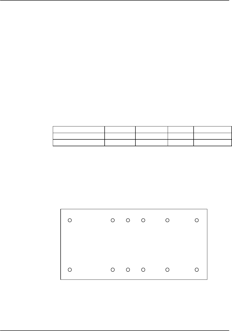
Reference Guide v3.6Installation
(10-97) Page 2-B-5
Unpacking and Mounting the Chassis
When you receive the system, unpack the boxes and check the chassis and cards for
damage. If any part of the unit is damaged, contact the shipping company to file a
claim. The shipping company representative will also tell you how to submit a claim,
where to send the unit, and give you any special instructions you may need.
Pack the unit in the original packing materials and send it by prepaid freight to the
address you received. If the original packing materials are unavailable, pack the unit in
a sturdy box and surround it with shock-absorbing material.
The front and back of the two-sided unit must be accessible for inserting cards. Voice,
data, WAN, and power cables are also attached to connectors at the rear of the chassis.
The front-loading model of the Integrated Access Controller does not need access to the
back side of the unit. Table Install-4 lists the minimum clearances between the
equipment and the nearest object for rack-mounted, wall-mounted or table-top
installations.
Table Install-4. Minimum Rack and Wall-Mount Clearances
Clearance Front Back* Top Bottom
Inches 10 15 2 2
Centimeters 25 38 5 5
* required for the two-sided chassis only
Two-Sided Chassis
The 891822 and 891823 two-sided chassis have twelve holes on each side of the chassis
(see Figure Install-1). These holes facilitate mounting the unit in any standard EIA 19-
or 23-inch rack (48.2 or 58.4 cm). The two holes on the bottom of the unit (t) can be
used for mounting on a table or other flat surface.
Top
B
o
t
t
o
m
B
a
c
k
F
r
o
n
t
t t
Figure Install-1. Mounting Holes (2-Sided Chassis)

Installation Reference Guide v3.6
Page 2-B-6(10-97)
Front-Loading Chassis (Power Supplies on Side)
The 8916 chassis has seven holes on each side of the chassis (as shown in Figure
Install-2). These holes can be used to mount the unit in any standard EIA 19- or 23-
inch rack (48.2 or 58.4 cm). The two holes on the bottom of the unit (t) can be used for
mounting on a table or other flat surface.
T
o
p
Bottom
B
a
c
k
F
r
o
n
t
t
t
Figure Install-2. Mounting Holes (8916 Front-Loading Chassis)
The 891620 chassis has eight holes on each side of the chassis (as shown in Figure
Install-3). These holes can be used to mount the unit in any standard EIA 19- or 23-
inch rack (48.2 or 58.4 cm). The two holes on the bottom of the unit (t) can be used for
mounting on a table or other flat surface.
T
o
p
Bottom
B
a
c
k
F
r
o
n
t
t
t
Figure Install-3. Mounting Holes (891620 Front-Loading Chassis)
Reference Guide v3.6Installation
(10-97) Page 2-B-7
Front-Loading Chassis (Power Supplies on Top)
The 891920 chassis has eight holes on each side of the chassis (as shown in Figure
Install-4). These holes can be used to mount the unit in any standard EIA 19- or 23-
inch rack (48.2 or 58.4 cm). The two holes on the bottom of the unit (t) can be used for
mounting on a table or other flat surface.
Top
Bottom
B
a
c
k
F
r
o
n
t
t
t
Figure Install-4. Mounting Holes (Front-Loading Chassis, Power Supplies on Top)
Installation Reference Guide v3.6
Page 2-B-8(10-97)
Mounting the Chassis
To mount the chassis to the rack, attach the metal brackets (see Figure Install-5) to the
sides of the chassis with the four 10-32x1/4 screws (brackets and all screws provided in
the installation pack). Four 12-24x1/2 screws are needed to attach the chassis to the
rack. The brackets are reversible to allow mounting in 19- or 23-inch racks (48.2 or
58.4 cm). You can attach the brackets using holes at the front of the chassis, back of
the chassis or near the middle. If you mount the brackets in the middle of the chassis,
you can reduce the amount of space required behind it for cables. However, the front
and the back must be accessible to insert and remove cards.
To attach the unit to the wall, use the template of the hole pattern (provided) and copy
to a backboard. The backboard should be 1/2" to 3/4" construction grade plywood.
Attach the unit with the 4-10x5/8 screws provided. The wall mount position must be
with the power supplies closest to the wall.
If you are placing the unit on a tabletop or other hard surface, it is mandatory to assure
clearance for proper airflow in the chassis. Make sure the chassis is accessible from the
front, and has at least 3/4 inches (2 cm) clearance above the chassis. The metal
brackets (see Figure Install-5) should be attached to provide the additional clearance
needed for attaching cables to the user cards for both the two-sided and front-loading
systems. Attach the brackets to the side of the chassis using the two (t) holes. Place the
plastic abrasion-protective inserts ("feet") in the holes provided near the ends of the
bottom of the bracket.
Key:OvalHolesforRack Attachment
Round HolesforRack Attachment
HolesforTabletop Attachment
HolesforPlasticInserts("Feet")
Figure Install-5. Hole Pattern on the Mounting Bracket

Reference Guide v3.6Installation
(10-97) Page 2-B-9
Power Supply and Ringing Generator System
The power supply and ringing generator system can consist of up to two power supplies,
two AC to DC converters and up to four ringing generators. External -48VDC talk
battery and external ringing generators may be used instead of the internal units. Use
the following guidelines to determine your power supply and ringing generator
requirements.
System Power
The system will always require one of the following power supplies:
Ø AC (8901)
Ø -48VDC (8902)
Ø +24VDC (8907)
Even though the 8907 power supply has specifications listed as negative throughout
this manual, it can be used with positive voltage (+24VDC). Because of the
extremely small number of applications that would require it, the conversion
procedure is not covered in this manual. If you are considering using +24VDC,
please call the customer service number listed in the Preface.
For backup, you may add a second power supply (see Preface for specific UL
requirements when adding a redundant power supply). Redundant power supplies are
not load-sharing.
-48VDC Talk Battery
In addition to the power supplies, a -48 VDC talk battery is required whenever there are
analog voice cards present in the system unless all of those are E&M ports and are used
in Transmission Only (TO) mode, or when Type 1 signaling is used.
A -48VDC power source is also required for use with:
Ø External Alarm card
Ø OCU-DP card
Ø BRI card (to provide sealing current)
If the unit is powered by the AC (8901) supply, either the 8903 Internal 115VAC to
-48VDC or 8905 120/240VAC to -48VDC Converter or an external source will be
required for the -48VDC talk battery. The 8903 AC to DC converter is available only
for 115VAC sources. Use 8905 for 220 VAC locations.
Ringing Generators
Ringing generators are required whenever there are FXS cards in the unit or if any FXO
ports are used in Manual Ringdown (MRD) mode. Ringing voltage may be provided
from an external source or by using the 8906 Ringing Generator. The 8906 requires a
-48VDC source in the system.
Customers having the older 8904 Ringing Generator may still use it.

Installation Reference Guide v3.6
Page 2-B-10 (10-97)
Warning: The 8904 must never be used in the same system with an 8906 ringing
generator.
Warning: The 8904 and 8906 ringing generators are incompatible with external
ringing devices.
The 8904 provides ringing voltage of 105VAC (nominal) at 20 Hz for 11
simultaneously ringing voice ports, while the 8906 provides ringing voltage of 100VAC
for the same number of ports. With normal call activity, a single ringing generator
might provide all of the power necessary to run the system. In a group where incoming
calls are at a minimum, 30-50 stations could share the same ringing generator. Small
groups with heavy incoming call volumes might require two or more ringing generators.
This card will not “quit” with a heavy load, it will just have weaker and slower ringing
abilities. That condition should alert you to the need for additional equipment.
The compatibility of power sources and ringing generators that can be used together are
summarized in Table Install-5.
Table Install-5. Power Supply Options Compatibility Table
Power
Sources AC
(8901) -48VDC
(8902) Converter
(8903) Converter
(8905) Ringer
(8906)+24VD
C
(8907)
-48VDC
External Ringer
External Ringer
(8904)
AC (8901) --- yes yes yes yes yes yes yes yes
-48VDC
(8902) yes --- no no yes no yes yes yes
Converter
(8903) yes no --- yes yes no no yes yes
Converter
(8905) yes no yes --- yes no no yes yes
Ringer
(8906)yes yes yes yes --- no yes NO NO
+24VDC
(8907) yes no no no no --- no yes yes
-48VDC
External yes yes no no yes no --- yes yes
Ringer
External yes yes yes yes NO yes yes --- NO
Ringer
(8904) yes yes yes yes NO yes yes NO –
US/Europe Jumper
Prior to inserting any cards and powering up the chassis, jumper JP1 on the 891620,
891822/23, and 891920 chassis must be set to US or European configuration. The
jumper is located on the resource card backplane, and is accessible from the chassis
front. The default setting is US. The resource cards must also have the jumper set
consistent with the chassis. See the Slot Map chapter for more detailed information on
this feature.
1
2
3
E
UR/US
JP1

Reference Guide v3.6Installation
(10-97) Page 2-B-11
Chassis Grounding
! ! ! PLEASE READ—IMPORTANT ! ! !
When using any CPU revision B or C in a six-digit chassis as depicted in
figures Install-6 through Install-9, or in a four-digit chassis as depicted in
figure Install-10 with a voice ringer card installed, the chassis must be
properly grounded to ensure reliable operation.
In order to identify which CPU you have, you must either visually look at the white
sticker that has been placed on the back of the mainboard. It indicates the type and
revision of CPU that is being installed. If you do not have revision B or C CPU’s as
stated above, then please disregard this notice.
To ensure proper operation in a chassis with an external power connector like those
shown below, it is crucial that each chassis is properly grounded. This section details
grounding procedures for each type of chassis. This information presumes that the
operator and/or installer has some knowledge of grounding issues. Please refer to Field
Alert Bulletin 108-000004 for a top level grounding tutorial.
The chassis ground is usually connected to the earth ground directly (using the chassis
ground screw) or via the power cord.
In order to minimize electrical potential between grounds, chassis ground ( ) and
common signal ground (COM) in the terminal power connector should be connected
with a jumper wire or bridge.
Improper grounding may cause a difference in electrical potential between the chassis
and the terminal equipment, which could damage the cards, the terminal equipment, or
both.
IF YOU ARE UNCLEAR ABOUT STANDARD GROUNDING PROCEDURES,
PLEASE CONSULT WITH YOUR NETWORK ADMINISTRATOR.
Ø
×
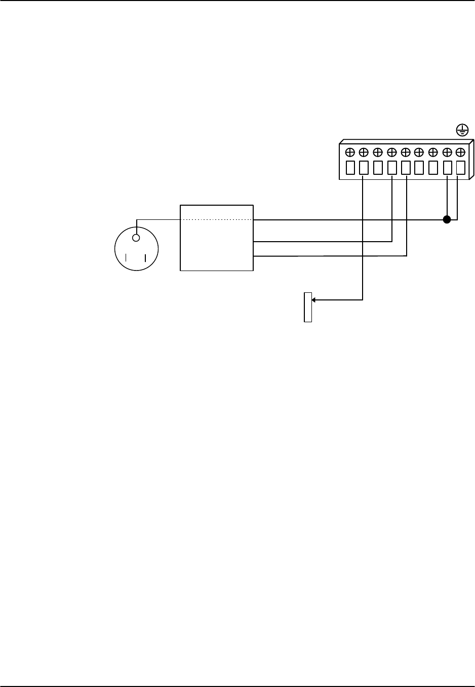
Installation Reference Guide v3.6
Page 2-B-12 (10-97)
Front-Loading Chassis: Power Supplies on Side
Figure Install-6 details the possible ground connections for the external power
connector of the front-loading chassis with power supplies on the side.
R
G
R+ + +- - -
VNVAVB
C
O
M
Optional Telecom Ground
-
+
AC* third wire* ground
-48VDC Return
-48 VDC Supply
AC PLUG
48 VDC PSU
(Note: Optional Telecom Ground Connection:
It may be required when the 48VDC PSU output is
not grounded or when the system is AC powered. It
is only needed for the proper operation of the
Telecom Ground Start and E&M signaling circuits.
For Additional information please refer to Field Alert
Bulletin 108-000001).
POWER CONNECTIONS
Figure Install-6. Ground Connections (Front-Loading Chassis: Power Supplies on Side)
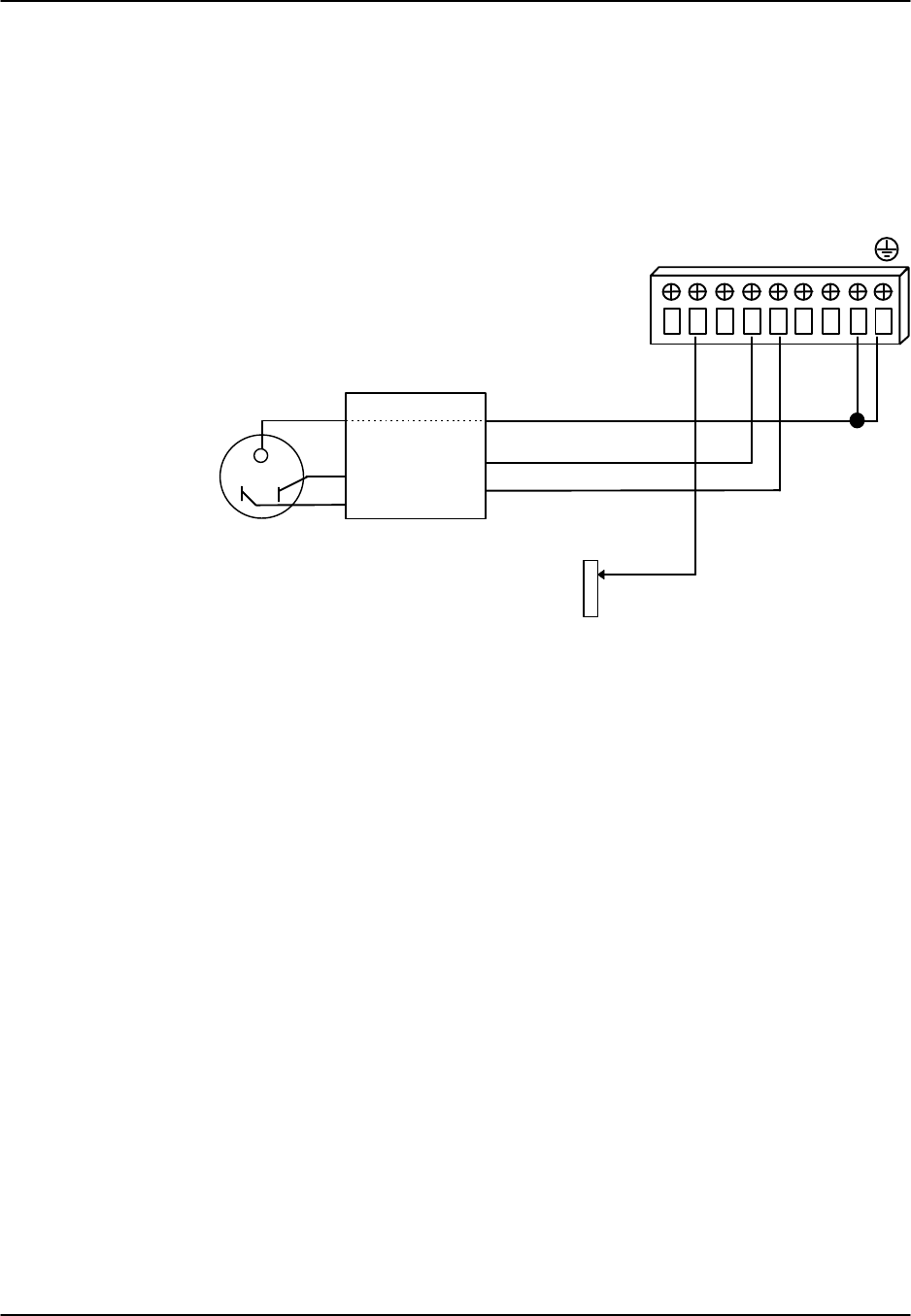
Reference Guide v3.6Installation
(10-97) Page 2-B-13
Two-Sided Chassis
Figure Install-7 details the possible ground connections for the external power
connector of the two-sided chassis.
R
G
R+ + +- - -
VNVAVB
C
O
M
Optional Telecom Ground
AC* third wire* ground
-48VDC Return
-48 VDC Supply
AC PLUG
48 VDC PSU
(Note: on Optional Telecom Ground Connection:
It may be required when the 48VDC PSU output is
not grounded or when the system is AC powered. It
is only needed for the proper operation of the
Telecom Ground Start and E&M signaling circuits.
For Additional information please refer to Field Alert
Bulletin 108-000001).
POWER CONNECTIONS
-
+
Figure Install-7. Ground Connections (Two-Sided Chassis)
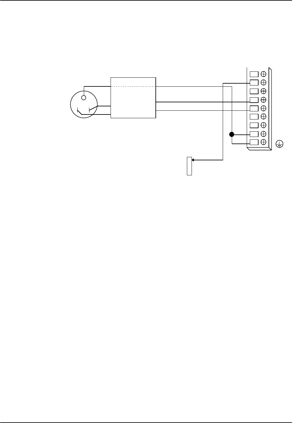
Installation Reference Guide v3.6
Page 2-B-14 (10-97)
Front-Loading Chassis: Power Supplies on Top
Figure Install-8 details the possible ground connections for the external power
connector of the front-loading chassis with power supplies on the top.
RGR
+
+
+
-
-
-
COM
VN
VA
VB
Optional Telecom Ground
AC* third wire* ground
-48VDC Return
-48 VDC Supply
AC PLUG
48 VDC PSU
(Note: on Optional Telecom Ground Connection:
It may be required when the 48VDC PSU output is
not grounded or when the system is AC powered. It
is only needed for the proper operation of the
Telecom Ground Start and E&M signaling circuits.
For Additional information please refer to Field Alert
Bulletin 108-000001).
-
+
POWER CONNECTIONS
Figure Install-8. Ground Connections (Front-Loading Chassis: Power Supplies on
Top)
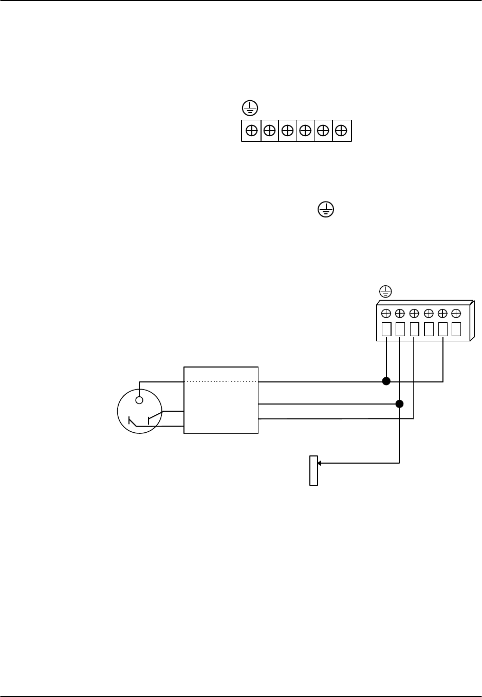
Reference Guide v3.6Installation
(10-97) Page 2-B-15
Grounding Four-Digit Chassis
The front-loading chassis (revision C1 or greater) has a terminal block connector near
the AC power connection and main power fuse, as shown in Figure Install-9.
R
G
R
C
O
M
+V-V
Figure Install-9. Chassis External Power Connector (rev. C1+)
As with the six-digit chassis, this chassis must be properly grounded for reliable
operations and safety. This is accomplished by strapping the common ground
connector (COM) to the earth ground connector ( ), as shown in Figure Install-10
below.
R
G
R
+-
VV
C
O
M
Optional Telecom Ground
AC* third wire* ground
-48VDC Return
-48 VDC Supply
AC PLUG
48 VDC PSU
(Note: on Optional Telecom Ground Connection:
It may be required when the 48VDC PSU output is
not grounded or when the system is AC powered. It
is only needed for the proper operation of the
Telecom Ground Start and E&M signaling circuits.
For Additional information please refer to Field Alert
Bulletin 108-000001).
POWER CONNECTIONS
-
+
Figure Install-10. Chassis Ground Connections (Front-Loading Chassis: Power
Supplies on Side).

Installation Reference Guide v3.6
Page 2-B-16 (10-97)
Installing the AC Power Supply (8901)
To install the AC Power Supply proceed with the following steps. Table Install-6 lists
the power supply specifications.
1. Remove the panel covering the front power slots. You may insert or
remove the power supply module while power is on or off.
2. Hold the power supply by its metal handle and align the printed circuit
board (PCB) edges with the rail guides of either power supply slot (F1 or
F2 for two-sided systems, S1 or S2 for front loading systems). Push the
module in until it is firmly seated in the backplane connector and replace
the panel that covers the front power supply slots.
Table Install-6. AC Power Supply Specifications
Parameter Rating
Output Power Continuous 50W
Output Power Peak (60 sec) 70W (10% duty cycle)
Input Current (maximum) 1.7A at 120VAC 60Hz full rated output load
Source Input Current (maximum) 3A
Inrush Surge Current max 3.7A peak at 240VAC cold start
Input Frequency 47-63Hz
Efficiency min 65%
Approvals UL, FCC, CSA
Installing the DC Power Supply (8902 or 8907)
Table Install-7 lists specifications for the 8902 (-48VDC) and 8907 (+24VDC) power
supplies.
Table Install-7. DC Power Supply Specifications
Parameter 8902 Rating 8907 Rating
Output Power 50W continuous 50W continuous
Input Power -35 to -60VDC +18 to +32VDC
Source Input Current (Max) 3A 5A
Approvals UL, FCC, CSA UL, FCC, CSA
Perform the following steps to install:
1. Remove the panel covering the front power slots. You may insert or
remove the power supply module while power is on or off.
2. Hold the power supply by its metal handle and align the PCB edges with
the rail guides of either power supply slot (F1 or F2 for two-sided systems,
S1 or S2 for front loading systems). Push the module in until it is firmly
seated in the backplane connector, and replace the panel that covers the
front power supply slots.

Reference Guide v3.6Installation
(10-97) Page 2-B-17
External Power Connector
8916 Chassis Power Connector
A terminal block connector is attached to the 8916 chassis near the AC power
connection and main power fuse. Figure Install-11 shows the connector.
R
G
R
C
O
M
+V-V
Figure Install-11. 8916 External Power Connector (rev. C1+)
Six Phillips-head screws are attached to the terminal block on the chassis. The two end
screws anchor the connector to the chassis, and the one on the left acts as the chassis
ground. The other screws are used to connect power wires from other sources. The
"+V" screw is used for power return. The "RGR" screw is used for an external ringer.
Wiring should be done according to a wiring plan that takes into account the size of the
wire, type of insulation, length of the wire and environmental conditions of the
installation site. All wires should be secured according to local requirements. A 14
gauge ground wire less than 20 feet in length is recommended. The Common and
Ground terminals may need to be strapped together.
All connections should be made using insulated ring terminals like the one shown in
Figure Install-12.
Size 6
.300 inch
(3.4 cm)
Figure Install-12. Ring Terminal (insulated) Specifications
891620 Chassis Power Connector
The power connector blocks are the same for all chassis with six-digit product numbers.
Diagrams of these chassis that display the placement of the power connector block can
be found in the Slot Map chapter.
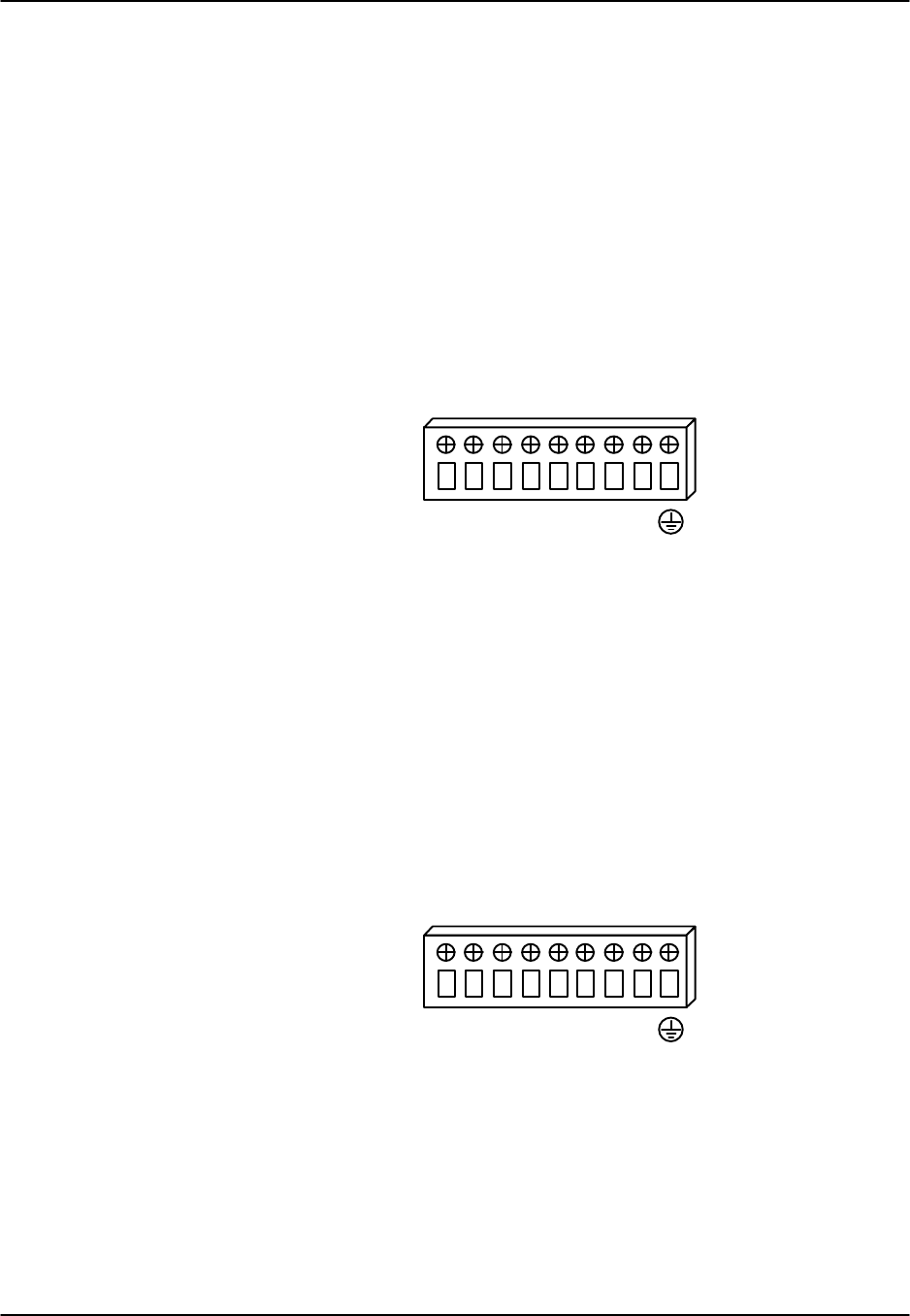
Installation Reference Guide v3.6
Page 2-B-18 (10-97)
Grounds and power feeds are connected to the power connector block by inserting and
fastening the wires in the proper slot. The screw adjacent to each slot can be loosened
or tightened to secure the connection. For safety reasons, no more than one-eighth of
an inch (0.125") of the connecting wire should be exposed. No uninsulated wire
should be visible from the power connector block.
Figure Install-13 shows the power connector block for the 891620. This block provides
for dual power connections at VA and VB where redundant power feeds are required.
Connection VA feeds power supply slot F1. Connection VB feeds power supply slot F2.
In addition, VN can be connected to a -48v source for powering voice cards and circuits.
The COM (common) is used for signal reference. RGR (ringer) connection is used
when an external ringer is connected to the chassis. Ringer bias is selected by the
connection to VN+ or VN-.
Note: If -48vdc is applied to VA or VB DO NOT connect external power to VN
R
G
R
+ + +- - -
VNVAVB
C
O
M
Figure Install-13. 891620 Terminal Power Connector
891822/891823 Chassis Power Connector
Figure Install-14 shows the power connector block for the 891822 and 891823. This
block provides for dual power connections at VA and VB where redundant power feeds
are required. Connection VA feeds power supply slot F1. Connection VB feeds slot F2.
In addition, VN can be connected to a -48v source for powering voice cards and circuits.
The COM (common) is used for signal reference. RGR (ringer) connection is used
when an external ringer is connected to the chassis. Ringer bias is selected by the
connection to VN+ or VN-.
Note: If -48vdc is applied to VA or VB DO NOT connect external power to VN
R
G
R
+ + +- - -
VNVAVB
C
O
M
Figure Install-14. 891822/891823 Terminal Power Connector
891920 Chassis Power Connector
Figure Install-15 shows the power connector block for the 891920. This block provides
for dual power connections at VA and VB where redundant power feeds are required.
Connection VA feeds power supply slot F1. Connection VB feeds power supply slot F2.

Reference Guide v3.6Installation
(10-97) Page 2-B-19
In addition, VN can be connected to a -48v source for powering voice cards and circuits.
The COM (common) is used for signal reference. RGR (ringer) connection is used
when an external ringer is connected to the chassis. Ringer bias is selected by the
connection to VN+ or VN-.
Note: If -48vdc is applied to VA or VB DO NOT connect external power to VN
RGR
+
+
+
-
-
-
COM
VN
VA
VB
Figure Install-15. 891920 Terminal Power Connector
Installing the 115VAC to -48VDC Converter (8903, 8905 and
8908)
Do not install the 8903 if the unit is connected to an external -48VDC power source.
1. For the two-sided chassis, remove the panel covering the rear power slots.
Install the module in any of the five rear slots while power is on or off.
For the front-loading chassis, remove the panel covering the front power
slots. Install the module in slot S1 or S2 while power is on or off.
2. Hold the converter by the metal handle and align the PCB edges with the
slot rail guides in the power supply cage. Gently push the module in until
it is firmly seated in the backplane connector.
3. When the power supply is installed and the power is on, the green LED on
the front panel of the converter should be on. If the LED goes off,
something is wrong. Check that the supply is properly seated in the
connector and replace the panel that covers the power slots.
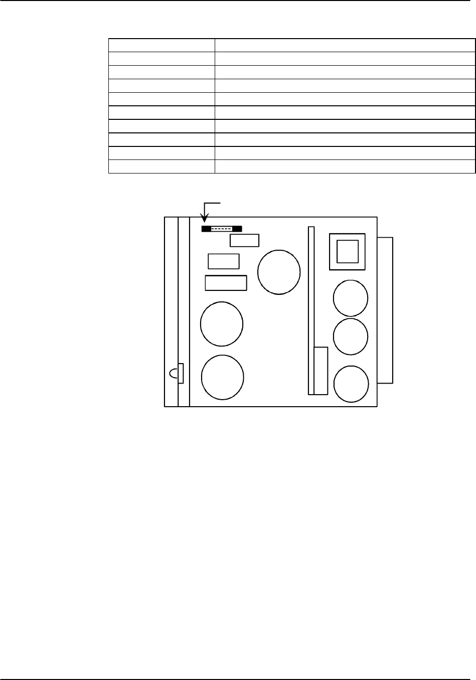
Installation Reference Guide v3.6
Page 2-B-20 (10-97)
Table Install-8. AC to DC Converter Specifications
Parameter Rating
Output Power 75 Watt Max
Output Voltage -48VDC
Output Current 1.5A DC
Hold Up Time 20 mSec minimum at full load and 117VAC input
Input Voltage 90-135VAC
Frequency 110VAC=60Hz
Efficiency 0.83
Heat Dissipation 55 BTU per hour
Approvals UL, FCC, CSA
Fuse - 1.5 A 250V
Handle
Power
Bus
Edge
Connector
Figure Install-16. AC-to-DC Converter Layout

Reference Guide v3.6Installation
(10-97) Page 2-B-21
Installing the Ringing Generator (8904 or 8906)
The 8904 provides ringing voltage of 105VAC (nominal) at 20 Hz for 11
simultaneously ringing voice ports, while the 8906 provides ringing voltage of 100VAC
(nominal) for the same number of ports.
If more than one ringing generator is required in the same chassis, they must have the
same part number. The 8904 and 8906 Ringing Generators cannot be mixed in a
single chassis. Note: Ringing Generator 8904 is a discontinued product. If you are in
need of Technical Assistance, please contact Product Support at (510) 353-7686.
Ensure that the system has a -48VDC power source before installing either of the
modules. You may install up to four (4) ringing generators on the two-sided chassis
depending upon availability of slots. The front-loading system with the power supplies
on the side can have only one ringing generator.
The outputs of all ringing generators are linked together by OR circuits on the ringing
bus. In cases where more than one generator is installed, one must be jumpered as
MASTER and the others must be jumpered as SLAVE. The master ringing generator
will synchronize the ringing signals on the ringing bus. (For more information on
configuring the MASTER/SLAVE jumpers, please see the diagrams of the 8904 and
8906 later in this chapter.)
Table Install-9 lists the specifications for the 8904 and the 8906.
Table Install-9. Ringing Generator Specifications
Parameter 8904 Rating 8906 Rating
Input Power 44-56VDC 45-56VDC
Input Current 70mA no load, 350mA
full load 250mA RMS
Efficiency 0.6 0.6
Heat Dissipation 25 BTU per hour 12 BTU per hour
Output Power 10W 30W@56V
25W @48V
22.5W@45V
Output Voltage 105VAC 100VAC
Output Current 100mA 250mA
Output Frequency 20Hz 20Hz
Distortion <3% <3%
Approvals UL, CSA UL (pending)
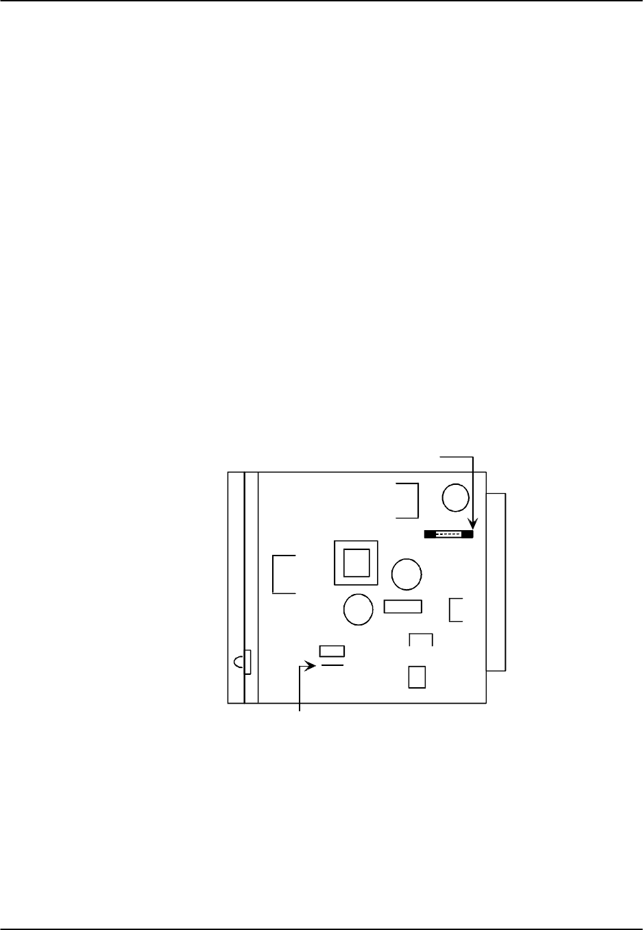
Installation Reference Guide v3.6
Page 2-B-22 (10-97)
To install the 8904 Ringing Generator:
1. Be sure that power is off before inserting or removing the 8904
ringing generator.
2. For the two-sided chassis, remove the panel covering the rear power slots.
You may install the module in any of the five rear slots. For the front-
loading chassis, remove the panel covering the front power slots. Install
the module in slot R1 only.
3. Make sure that jumper W201 is installed if this is the only 8904 ringing
generator in the unit, or if it is the MASTER ringing generator (see Figure
Install-17).
4. Remove jumper W201 if this is a SLAVE ringing generator. Remove the
jumper by cutting it with wire cutters.
5. Hold the ringing generator by the metal handle and align the PCB edges
with the slot rail guides in the power supply backplane. Gently push the
module in until it is firmly seated in the backplane connector.
6. When the supply is installed and power is on, the LED on the rear panel of
the ringing generator should flicker at a rate of 20 times per second. If
this LED is not flickering, something is wrong. Check that the
Master/Slave settings are correct and that the module is firmly seated in
the connector.
5. Replace the panel that covers the rear power slots.
Master/Slave Jumper
W201
Fuse - 1.0A 250V
Power
Bus
Edge
Connector
(remove if using as slave)
Figure Install-17. 8904 Ringing Generator Layout
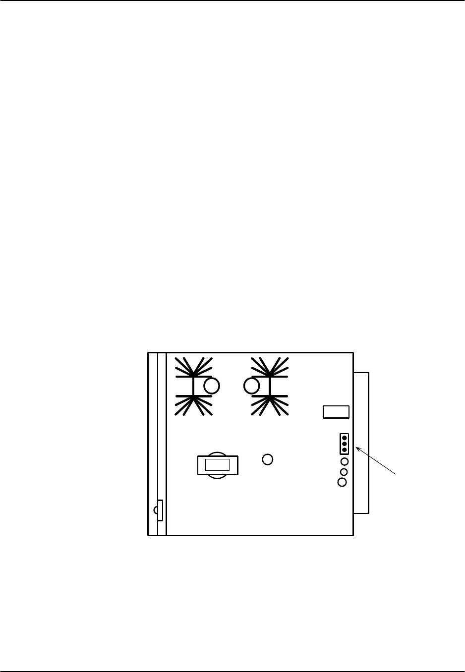
Reference Guide v3.6Installation
(10-97) Page 2-B-23
To Install the 8906 Ringing Generator:
1. You must make sure that power is off before inserting or removing the
ringing generator.
2. For the two-sided chassis, remove the panel covering the rear power slots.
You may insert or remove the module in any of the five rear slots. For the
front-loading chassis with power supplies on the top, remove the panel
covering the front power slots, and insert or remove the module in any of
the five slots. For the front-loading chassis with power supplies on the
side, you may insert or remove the module in slot R1 only.
3. The JP1 jumper is factory-preset to the MASTER configuration (see
Figure Install-18). You do not need to change this jumper if this is the
MASTER ringing generator, or the only ringing generator in the system.
If this is a SLAVE ringing generator, move the jumper on JP1 from the
lower pins (MASTER) to the upper pins (SLAVE).
4. Hold the ringing generator by the metal handle and align the PCB edges
with the slot rail guides in the power supply backplane. Gently push the
module in until it is firmly seated in the backplane connector.
5. When the supply is installed and power is on, the LED on the rear panel of
the ringing generator should flicker at a rate of 20 times per second. A
problem is indicated if this LED is not flickering,. Check that the
Master/Slave settings are correct and that the module is firmly seated in
the connector.
6. Replace the panel cover.
Power
Bus
Edge
Connector
Slave
Master
JP1
Master/Slave
Jumper
Figure Install-18. 8906 Ringing Generator Layout
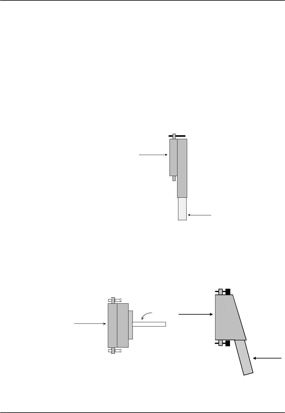
Installation Reference Guide v3.6
Page 2-B-24 (10-97)
Connecting AC Power
Attach the AC power source to the system at the AC power socket. This socket
accommodates the standard 3-prong molded power cord supplied with the system.
Secure the power cord to the rack or cabinet for strain relief and route it down to the
bottom of the chassis.
Using Amphenol Connectors
Many of the cables used to connect cards in the Integrated Access Controller to wiring
devices use Amphenol connectors at either one or both ends of the cable. The
traditional Amphenol connector placed the connector at a right angle to the cable itself,
(see Figure Install-19) thus preventing the screw at the bottom of the connector from
being properly attached without removing the hood. This type of cable connector is not
recommended for use with this system.
Amphenol
Cable
Figure Install-19. Undesirable Amphenol Connectors
Newly designed cables mount the Amphenol connector at a 25° angle to the cable and
use screws that can be twisted by fingertips to attach the connector from both the top
and the bottom. Other types of cables mount the connector at a 90° angle (see Figure
Install-20). It is suggested that cables of this design be used with the cards in your
system.
Amphenol
Cable
Amphenol
Amphenol
Cable
Figure Install-20. Preferred Amphenol Connectors

Reference Guide v3.6 Basic Operations
(10-97) Page 2-C-1
Terminal Interface
The system is controlled through a serial interface to a VT-100 terminal or a PC
running a terminal emulation program. Connect the terminal or selected PC COM port
to the Interface card TERM jack. Set the terminal’s communications parameters as
follows:
9.6 kbps; 8 data bits; no parity; 1 stop bit.
Logging On
When both the system and your terminal are on, the log-on screen shown in Figure
Basic-1 will normally appear. If the screen stays blank after 30 seconds, press the
<Enter> key to display the screen. If the screen remains blank, check your terminal
settings and connections. (For remote log-on procedures, see the Interface Card
chapter.)
When the system is started for the first time after initial installation, you will see the
Registration screen. See the Registration section later in this chapter for instructions.
If new system firmware or a different type of CPU has been installed, you will be asked
to “Zip” the system. For instructions check “Reinitializing the System” later in this
chapter.
Node_1 | | 12-
31
IMACS
Integrated Multiple Access Communications Server
Copyright (C) Premisys Communications Inc 1991-1996
Password:
Node: Node_1
Version: 3.6x
Figure Basic-1. The Log-On Screen

Basic Operations Reference Guide v3.6
Page 2-C-2(10-97)
The initial Log-On passwords correspond to one of four access level names. For
example, the manager access level has the preset password Manager. Passwords are
case-sensitive. See Table Basic-1 for a listing of all passwords and access levels. For
procedures used to change passwords, see the CPU Card chapter later in this guide.
Table Basic-1. Access Levels
Access
Level Initial
Password Description
Superuser ********* Special access for maintenance and diagnostics, to be
used as directed by a certified technician.
Manager Manager Full access to all configuration options, diagnostic
features and password management.
Operator Operator Read/write access to configuration and diagnostic
features.
Viewer Viewer Read-only access to configuration and diagnostic
features.
If you are configuring the system for the first time, log in as “Manager.” If you are
maintaining the system after its initial configuration, the password has probably
changed from "Manager;" consult your network administrator for the current password.
Type the password and press the <Enter> key to display the main screen for your
system.

Reference Guide v3.6 Basic Operations
(10-97) Page 2-C-3
Registration
When the system is started for the first time, the registration screen will appear.
Answer the questions shown at the bottom of the screen, and the system will
automatically respond with the correct application parameters and prompts.
The registration procedure consists of the three steps shown below.
1. Enter the vendor code. If no other vendor code is specified, enter the
vendor code 101.
2. Select the type of chassis used (either front-loading with power supplies
on the side, front-loading with power supplies on top, or the two-sided
chassis).
3. Confirm the proposed changes by selecting (Y for yes or N for no). Figure
Basic-2 shows the completed Registration screen.
Node_1 | Welcome to Registration | 12-31-99 14:33
Vendor Code: 101
1. Front - Loading Only / Power Supplies on side
2. Front - Loading Only / Power Supplies on top
3. Front & Rear Loading Only / Power Supplies on side
Select one: 3
Is the Information on this screen correct (Y/N)?
Figure Basic-2. Screen Layout

Basic Operations Reference Guide v3.6
Page 2-C-4(10-97)
Main Screens
After login you will see one of the two following screens: Figure Basic-3 shows the
main screen for a front-and-rear loading Integrated Access Controller; Figure Basic-4
shows the main screen for a front-loading only system. Depending on the number of
cards installed in your system, your screen may show more or fewer cards than seen in
these figures. For consistency and simplicity hereafter, this manual shows only screens
for the front-and-rear loading Integrated Access Controller.
Node_1 | | 12-31-99
14:33
Slot Installed Status Slot Installed Status
C1 CPU XCON IF INTF+modem
C2 CPU XCON RDNT U1 ALR
P1 ADPCM-64 U2 E&M 4Wx8-6
P2 ADPCM-64 U3 FXS 2Wx8-9
P3 ADPCM-64 U4 FXO 2Wx8-9
W1 CSU+CSU U5 HSU 366x2
W2 CSU+CSU U6 OCU-DPx5
W3 CEPT+CEPT U7 FRAD-18
W4 CEPT+CEPT U8 SRU-232x10
F1 PS1 RI RINGER
F2 PS2
Alarms | Config| Del | accepT | Xcon | sYs | Logout | sEr | Oos | cpusWtch
Figure Basic-3. Main Screen for Front-and-Rear Loading System

Reference Guide v3.6 Basic Operations
(10-97) Page 2-C-5
Node_1 | | 12-31-99 14:33
Slot Installed Status
C1 CPU XCON
C2 CPU XCON RDNT
P1/U1 HSU-366x2
P2/U2 ADPCM-64
P3/U3 ALR
P4/U4 SRU-232x10
W1/U5 CSU+CSU
W2/U6 B7R-8
W3/U7 OCU-DPx2
W4/U8 BRI U-IFx8
IF INTF+modem
S1
S2
S3
RI RINGER
Alarms | Config| Del | accepT | Xcon | sYs | Logout | sEr | Oos | cpusWtch
Figure Basic-4. Main Screen for Front-Loading Only System

Basic Operations Reference Guide v3.6
Page 2-C-6(10-97)
Introduction to Screens
After you have determined configuration requirements, you can log on and set the cards
to implement a custom network design. For each card, the system presents a screen that
shows the options and allows you to set them.
All screens have the same general layout, as shown in Figure Basic-5.
Node_1 | IF INTF+modem 8923 Rev A2-0 Ser 01103 | 12-31-99 14:33
1 OOS U3
PRIMARY CLK int
EXT RATE n/a
EXT FORMAT n/a
EXT FRAME n/a
SECONDARY CLK int
EXT RATE n/a
EXT FORMAT n/a
EXT FRAME n/a
CURRENT CLK int
int ext
Save | Undo | Refresh | Time | ACO | proFiles | taBs | Ports | Main
Figure Basic-5. Screen Layout
• The dark line at the top of the card is the Header Information Line. This line lists
the node identity (“Node_1” in the figure above), card identity, time, and date.
• The small dark area in the upper right, immediately below the header, displays
alarm summary information. In this example, the alarm reveals an Out of Service
(OOS) card in slot U-3. If no alarms are active, nothing will be displayed in this
location.
• The area just below the node ID is the Parameter Settings section of the screen.
This section displays current or default settings from the range of user options
available on each card.
• The Status and Data Entry Change Line is located near the bottom of the card on
the left-hand side. This line allows the user to select the options for each
parameter.
• The dark line at the bottom of the screen displays the Menu of Actions. Each
action contains one capitalized letter. Press the capitalized letter of an action on
the keyboard to perform the described action.

Reference Guide v3.6 Basic Operations
(10-97) Page 2-C-7
It is very important that you record the configuration information for each card as you
determine its settings. You, or someone servicing the system at a later date, will need
this information to aid in troubleshooting. A simple way to record your configuration is
to photocopy the setting tables in the card sections of this guide and write the
information for your configuration in the column labeled Initial Setting. Store these
pages in a safe place, where they can be available to anyone servicing the system.
Status Screen
A quick way to check activity of the ports of all system cards is to use the Status screen.
Figure Basic-6 shows the Status screen. The lowercase letters that follow card entries
show the status of each port on the cards. The possible values are "s" (Standby), "a"
(Active), "t" (Test), "l" (Loopback) and "r" (Redundant).
Node_1 | | 12-31-99
14:33
Slot Installed Status Slot Installed Status
C1 CPU XCON IF INTF+modem
C2 CPU XCON RDNT U1 ALR ssss
P1 ISDN-PRI ssssssss U2 E&M 4Wx8-6 ssssssss
P2 ADPCM-64 ssssssss U3 FXS 2Wx8-9 ssssssss
P3 INV MUX ssss U4 FXO 2Wx8-9 ssssssss
W1 CSU+CSU ss U5 HSU 366x2 ss
W2 CSU+CSU rr U6 OCU-DPx5 sssss
W3 CEPT+CEPT ss U7 FRAD-18 ssssssss
W4 CEPT+CEPT rr U8 SRU-232x10 ssssssssss
F1 PS1 RI RINGER
F2 PS2
Alarms | Config | Del | accepT | Xcon | sYs | Logout | Oos| cpusWtch
Figure Basic-6. The Status Screen
Pressing the “s” key again will return the screen without status settings. If the system is
restarted by log-off/log-on activity or loss of power, the screen will also return to its
normal condition.

Basic Operations Reference Guide v3.6
Page 2-C-8(10-97)
Configuring the Cards
The main screen lists all the installed cards next to their slot numbers. To access the
screen for each card, move the cursor using the arrow keys to highlight the card and
press the <Enter> key.
Use the arrow keys and the <Enter> key to move around on the screens. When
changing card parameters, some settings require you to enter values, while others allow
you to select from a list of possible options. When a list of possible options is
available, use the right and left arrow keys to move through the options. Use the
<Enter> key to select the setting under the cursor. Use the right and left arrow keys to
select the option you want or type over the old value using the keyboard. Press the
<Enter> key to select the option or enter the value. After all choices are made, save
your changes by pressing “s.”
To access the menu of actions at the bottom of the screen, make sure no option is
selected and then press the capitalized letter that represents the action you want.
Menu of Actions
Table Basic-2 show the Menu of Actions for the Main Screen.
Table Basic-2. Main Screen Menu of Actions
Action Function
Alarms Brings up the Alarm screen. Refer to "Alarms" later in this chapter.
Config Sets up the system using a standard configuration. Refer to "Using the
Configuration Option" later in the System Operations Chapter.
Del Removes an OOS card from system memory.
accepTRemoves card settings. Used when replacing a card in one slot with a
different kind of card (see below).
Xcon Brings up the cross-connect screens. See System Operations chapter.
sYsBrings up the system screen. Provides for high-level system testing
and maintenance.
Logout Logs the user off the system.
sEr (serialization) Identify the card in a given slot
Oos Set the card out of service
cpusWtch Switches from the active CPU to the redundant CPU card. See
Redundancy chapter.
Configure each card to match the system settings previously determined. On the main
screen, select each card in turn and change the options for that card as appropriate.
Select the Save action after making all the changes for a card; then return to the main
screen to configure the next card. Once configured, card settings (by slot) are
permanently stored in the NVRAM on the Interface Card. Similar cards may be
replaced without having to reconfigure the new card. If you replace the card with a
different type of card, the system will ask if you want to lose the current card settings.
Press “t” (accepT) to allow this transaction.

Reference Guide v3.6 Basic Operations
(10-97) Page 2-C-9
Alarms
Alarms warn you of problems and alert you to possible hardware or facility failures.
The Alarm sub-screens are accessed from the main screen by pressing the "A" key. The
Alarm screen displays the currently active alarms, if any, and provides access to the
Alarm Filters screen and the Alarm History screen. Figure Basic-7 shows the Alarm
screen with one active alarm.
Node_1 | | 12-31-99 14:33
Active Alarms: 1 Page 1 of 1
00023 W1-1 CSU+CSU C CGA_RED 12-31-99 12:41:21
Refresh | pgUp | pgDn | History | Filters | Main
Figure Basic-7. The Alarm Screen
The first entry shows the Alarm Number (a sequential number from one to 65,535) used
to identify the alarm for tracking and maintenance (in this case, #00023). The second
entry shows the location of the problem by card slot number (in this case, w1-1). The
third column shows the type of card affected (in this case, a WAN card with two CSU
modules). The fourth entry shows the alarm modifier (in this case, C [critical]). See a
later section in this chapter for more information about alarm modifiers. The fifth entry
shows the type of alarm generated (in this case, CGA_RED). The sixth entry shows the
date of the alarm and the last entry shows the time the alarm was logged (in this case,
12-31-99 at 12:41:21).

Basic Operations Reference Guide v3.6
Page 2-C-10 (10-97)
Filters
You can set filters for each alarm so that the alarm reports occurrences in a number of
different ways. Figure Basic-8 shows the Alarm Filters screen accessed by pressing "F"
on the main Alarm screen.
Node_1 | | 12-31-99 14:33
OOS Out of Service report crit aco-on
NOS No Signal report major aco-off
LOS Loss of Sync report minor aco-off
YEL Yellow Alarm report info aco-off
AIS Alarm Info Signal report crit aco-off
CGA_RED Carrier Group–Red report crit aco-off
CGA_YEL Carrier Group–Yellow report crit aco-off
EER Excessive Error Rate report crit aco-off
SENSOR Alarm card sensor report crit aco-off
DCHAN D-chan out of service report crit aco-off
SWITCH Switch to redundant card report crit aco-off
UCA User card/port alarm report crit aco-off
RESET System reset report crit aco-off
ACO Alarm Cut-Off report crit n/a
SYNC Clock Sync Alarm report crit aco-off
EER-3 Error rate above 10e-3 report crit aco-off
PLC_OOF DS3 PCLP Out of Framing report crit aco-off
PLC_LOF DS3 PCLP Losst of Frame report crit aco-off
PLC_YEL DS3 PCLP Yellow Alarm report crit aco-off
Save | Undo | Refresh | Main
Figure Basic-8. The Alarm Filters Screen
The first column shows the alarm abbreviation that is shown on the screen when an
alarm is generated. The second column shows the alarm title. The third column
contains the filters ignore, report and log. The fourth column contains the filter
modifiers info, minor, major and critical. The last column sets the ACO alarm aco-
off and aco-on. All of these options are explained later in this chapter.
The filter in the third column will take precedence over its modifier. If, for instance,
you have an alarm filter set to ignore, the setting of the modifier as info, minor, major
or critical will be ignored as well. Table Basic-3 identifies the alarms and their
meanings.
Alarm filters should be set prior to activation of card ports!

Reference Guide v3.6 Basic Operations
(10-97) Page 2-C-11
Table Basic-3. Alarm Filters
Filter Alarm Meaning
OOS Out of Service The card, power supply or ringing generator is faulty or has been
removed from the unit.
NOS No Signal Incoming WAN signal is lost.
LOS Loss of Synchronization Frame Alignment is lost.
YEL Yellow Alarm The system has received a Yellow Alarm signal from a remote device.
Usually received when the device loses WAN signal or
synchronization.
AIS Alarm Information Signal The system has received a Blue Alarm signal from a remote device.
Usually received when the remote or intermediate device has a major
failure.
CGA_RED Carrier Group Alarm - Red The local incoming WAN signal has a serious problem and trunk
conditioning is started. After receiving a RED alarm (NOS or LOS) for
2-3 seconds, the system initiates the appropriate trunk conditioning
sequence (see voice cards for information about the TC_CGA setting)
and sends a Yellow Alarm to the remote device. If the system is in
drop/insert mode, it also sends an AIS signal to the downstream
equipment.
CGA_YEL Carrier Group Alarm - Yellow The system has initiated trunk conditioning in response to a Yellow
Alarm from a remote device. After 2-3 seconds, the system initiates
the appropriate trunk conditioning sequence (see voice cards for
information about the TC_CGA setting)
EER Excessive Error Rate The error rate measured by the system has exceeded the threshold set
on the WAN card.
SENSOR Alarm Card Sensor The Alarm Card sensor has received an alarm indication from an
attached device.
DCHAN D-chan out of service If the network side D channel looses contact with the user side, an
alarm message will be generated. The alarm message will show the
slot # and D channel # where the problem exists.
SWITCH Switch to redundant card The primary card has failed and the system has switched to the
redundant card. See the Redundant Operations Chapter.
UCA User card/port alarm One or more active ports on a user card are not working properly.
Voice ports will show an alarm for excessive signaling transitions and
data ports will show an alarm for exceeding the data error threshold.
RESET System reset The system has been reset by either loss of power or by system
software upgrade.
ACO Alarm Cut-Off The ACO option forces you to manually clear certain alarms. Without
this option, self-correcting alarms might not be noticed. When the
ACO option is set to either Report or Log and the modifier is set to
Major, alarms will report normally but will also generate an ACO
alarm. If the modifier is set to Minor, it will not generate the ACO
alarm. If the filter is set to Ignore, no alarms will be generated.
SYNC Clock Sync Alarm The SYNC alarm is generated when either the primary or secondary
external clock source is lost. This alarm is in addition to the condition
that lost the clock source (CGA-RED or OOS).
EER-3 Excessive Error Rate (10e-3) While using transcoder operations for E1 that involve downstream
tributaries, setting EER-3 to "report" will cause an alarm to appear on
the local system when E1 transmission errors exceed 10e-3 (1 in 1000).
The local EER-3 alarm will identify the effected WAN link (i.e., W1-1)
and take it out of service. Simultaneously, the downstream tributary
will receive an AIS alarm to warn them of the condition.
PLC_OOF DS3 PLCP Out of Framing Physical Layer Convergence protocol is Out of Framing
PLC_LOF DS3 PLCP Loss of Frame Physical Layer Convergence protocol has lost framing

Basic Operations Reference Guide v3.6
Page 2-C-12 (10-97)
PLC_YEL DS3 PLCL Yellow Alarm Physical Layer Convergence protocol is reporting a yellow alarm
Report
Setting the filter for the various alarms to report causes the alarm indication to be sent
to a remote device (see the Interface Card chapter), displays the alarm report on the
screen, and logs the alarm in the Alarm History.
Log
Setting the filter for the alarms to log, displays the alarm report on the screen and logs
the alarm in the Alarm History (see later in this chapter).
Ignore
Setting the filter for the alarms to ignore, will cause the alarm indication to be ignored
by the system.
Modifiers
Each alarm may also be designated as info, minor, major and critical. The filter
modifier shows on both the active alarm and alarm history screens.
When used in conjunction with the External Alarm card, the occurrence of any alarm
designated as critical will trigger a form-C contact on the External Alarm card which,
in turn, can serve to activate an external device such as a bell or light. Similarly, the
occurrence of any alarm designated as major would trigger a different contact and
therefore activate a different external indicator. (See External Alarm Card chapter.)
ACO
ACO (Alarm Cut Off) is an additional security feature used by the system to alert the
operator of alarms that clear themselves while the unit is unattended. If ACO is set to
report or log, any alarm set to report or log with a major modifier will cause an
additional alarm message to appear on the screen. This message, known as the ACO
alarm message, must be manually cleared by the operator. Used with the node port of
the Interface card (see Interface card chapter), ACO can also trigger some external
alarm device such as a bell or light that must also be manually cleared by the operator.
ACO alarms must be cleared from the Interface card screen.
Alarm Handling
The report alarm function attempts to send alarm information to a remote printer,
Network Management System or other logging device, in addition to logging the alarm
in the Alarm History log. These features use the built-in serial port and modem on the
Interface card. You need to change settings on the Printout Alarms screen or IP screen
on the Interface card to activate these special functions. (See Interface Card for more
information.)
Alarms set to either log or report record occurrences automatically to the Alarm
History log. You can access the Alarm History log from the Main Alarm screen by
pressing the "H" key from the Main Alarm Screen.

Reference Guide v3.6 Basic Operations
(10-97) Page 2-C-13
Figure Basic-9 shows the Alarm History Screen. While the history screen is displayed,
you can update the list with any new alarms that occur by selecting Refresh from the
bottom menu of actions. You can delete all entries in the log by selecting Clear from
the menu of actions on the history screen by pressing the “c” key.
All alarms (except those set to ignore) appear in the Alarms field (in the upper right
corner of the screen), regardless of their setting on the filters screen. The display in the
alarms field is the abbreviated version of the alarm name and slot number. For
example, OOS U3 indicates that the card in user slot three is out of service.
Node_1 | | 12-31-99 14:33
History Alarms: 4 Page 1 of 1
00012 W1-1 CSU+CSU C CGA_RED 12-31 12:22:00 12-31 12:23:00
00011 W1-1 CSU+CSU M NOS 12-30 08:02:09 12-30 09:30:00
00010 W1-1 CSU+CSU I YEL 12-30 10:45:00 12-30 11:15:55
00009 C1 CPU XCON m RESET 12-28 16:35:17 12-28 22:02:00
Refresh | Clear | pgUp | pgDn | Main
Figure Basic-9. The Alarm History Screen

Basic Operations Reference Guide v3.6
Page 2-C-14 (10-97)
Reinitializing the System
Information about cards inserted, card settings, WAN connections, passwords and other
data is stored on the nonvolatile RAM (NVRAM) on the Interface Card. When most
card types are removed and replaced, the NVRAM remembers the card settings and if
the same kind of card is inserted in the slot, there will be no need to reprogram the
settings. If, on the other hand, a card is replaced with a different type of card, then the
system will offer the operator the option of deleting the old card, so that the new
parameters can be established (see Accept function in “Configuring the Cards,” earlier
in this chapter).
CPU Card
One exception to the rule in the previous paragraph is changing the CPU card type
between standard bus-connect, enhanced bus-connect or cross-connect. When a CPU
card is removed and replaced by a like CPU card, the system will reevaluate the
NVRAM and assign the old system parameters to the new CPU card (including
passwords).
If the CPU card is replaced with one of the other types of CPU card, or in some cases
with the same type of CPU card that is equipped with a different version of firmware,
the new CPU card will want to “cold-start” the system (overwrite NVRAM information
on the Interface card). The screen shown as Figure Basic-10 will be shown.
*** NVRAM on INTF Card is not available, Software revision has been changed ***
Press ‘Z’ to zip the System
Zip | zAp | Debug | Reg | Main
Figure Basic-10. Cold Start NVRAM Screen
If the new CPU card was inserted in error, the process can be stopped by removing the
wrong CPU card and replacing it with the correct type of card.

Reference Guide v3.6 Basic Operations
(10-97) Page 2-C-15
Warning: Pressing the Z command from the Menu of Actions will start the ZIP process.
"Zipping " the system deletes all of the information stored on NVRAM on the Interface
Card and resets the system. All cards must then be completely reconfigured.
When the Z key is pressed, the system will display the main log-in screen and ask for
password authorization from either Manager or Operator access levels. After the
correct password, the system will ask the question, "OK to Zip the system (y/n)"? If Y
is pressed, the system will test and reinitialize itself. All NVRAM information will be
erased from the Interface card and a new log-in screen will appear.
Test and Debug Screen
Advanced configuration and diagnostics are available through the use of the sYs
(System) command from the Menu of Actions of the Main Screen. Pressing Y brings
up the Test and Debug screen shown in Figure Basic-11.
Test and Debug
Zip | Debug | Reg | Backup | rEstore | Main
Figure Basic-11. Test and Debug Screen
ZIP
Caution: The Z (Zip) command allows the user with Operator (and higher) password
authority to reset the entire system. Since the settings for all cards in the system will be
reset to their original factory settings, "zipping" the system should be thoroughly
considered prior to implementation. The Zip screen is shown as Figure Basic-12.

Basic Operations Reference Guide v3.6
Page 2-C-16 (10-97)
Test and Debug
Zip will reboot the system. Ok to Zip (y/n)?
Zip | Debug | Reg | Backup | rEstore | Main
Figure Basic-12. Zip Screen
DEBUG
The D (Debug) command is only available to factory software engineers with a
password authorization higher than "Superuser." It gives access to the system software
coding.
REG
The R (Registration) command allows the user with Operator (and higher) password
authority to change the registration of the system. The user must have the information
shown below to properly reregister the system. There should be no reason for this
command to be used during normal operation of the system.
The registration procedure consists of the three steps shown below. Answer the
questions at the bottom of the screen and the system will automatically respond with the
correct application parameters and prompts.
1. Enter the vendor code. If no other vendor code is specified, enter the
vendor code 101.
2. Select the type of chassis used (either front-loading with power supplies
on the side, front-loading with power supplies on top, or the two-sided
chassis).
Confirm the proposed changes by selecting y for yes or n for no). Figure Basic-13
shows the completed Registration screen.

Reference Guide v3.6 Basic Operations
(10-97) Page 2-C-17
Node_1 | Welcome to Registration | 12-31-99 14:33
Vendor Code: xxx
1. Front - Loading Only / Power Supplies on side
2. Front - Loading Only / Power Supplies on top
3. Front & Rear Loading Only / Power Supplies on side
Select one: 3
Is the Information on this screen correct (Y/N)?
Figure Basic-13. Registration Screen

Basic Operations Reference Guide v3.6
Page 2-C-18 (10-97)
BACKUP
The Backup command backs up system information to a text file in the PC that is
running the terminal emulation program. The Backup command allows backup of
information on a system-wide or card-by-card basis. It also backs up Alarm Filters,
Alarm History, Installation Table and Cross Connect information. It is best to back up
information after any significant changes in system configuration and at intervals that
assure that alarm history and other operating information will be maintained
dependably. Figure Basic-14 shows the Backup Screen. The Backup procedure is
detailed below.
Node_1 | NVRAM Backup | 12-31-99 14:33
C1 backup Install Table backup
C2 backup Cross Connect backup
P1 backup Alarm Filters backup
P2 backup Alarms History backup
P3 backup
P4 backup
W1 backup
W2 backup
W3 backup
W4 backup
IF backup
U1 backup
U2 backup
U3 backup
U4 backup
U5 backup
U6 backup
U7 backup
U8 backup
Go | Copy | Main
Figure Basic-14 Backup
The Backup procedure creates a text file in which the parameters for the chosen cards
are encoded. This information can then be used by the Restore command (see below)
to restore the parameters to certain cards, or to the whole unit.
Because the Backup command creates a simple text file, the actual commands for the
Backup procedure will vary depending on the computer system and terminal software
you are using to interface with the unit. The following procedure is specific to
Windows 95 using Microsoft Terminal software, but can be easily modified to adapt to
other systems and software.

Reference Guide v3.6 Basic Operations
(10-97) Page 2-C-19
BACKUP PROCEDURE
1. From the Main Screen, type Y (for sYs)
2. Type B (for Backup). The screen in Figure Basic-14 lists all slots and
categories with the default option backup. If you wish to do a full
backup, proceed to Step 3.
If you do not want to backup a certain slot, use the arrow keys to highlight
it, and press <Enter>. The choices no and backup appear at the bottom of
the screen. Use the left arrow key to highlight no, and press <Enter>. The
slots or categories deselected will show no after the slot or category and
will not be backed up. If you wish to deselect a number of entries in
sequence, press C (for Copy) to change the next slot or category to match
the slot or category you have just deselected.
3. In the Microsoft Terminal menu bar, select the Transfers pull-down
menu.
4. From the Transfers pull-down menu, select Receive Text File.
5. In the "Receive Text File" field, select the name of the file and its
directory location. When you select OK a bar will appear at the bottom of
the screen, with two buttons, Stop and Pause, as well as the number of
bytes and the name of the file being received.
6. Type G (for Go). The screen will fill with scrolling text. When the text
stops scrolling, you will see the message "BACKUP COMPLETE, hit 'm'
to go back to menu."
7. At this point, turn the transfer function off by selecting the Stop button at
the bottom of the screen. The text file containing all the parameters for
the selected cards and categories has now been saved.
8. Type M to return to the NVRAM Backup screen. This will allow you to
double-check that your backup selections were correct. Type M again to
return to the Test and Debug screen.

Basic Operations Reference Guide v3.6
Page 2-C-20 (10-97)
RESTORE
The Restore command restores all selected card and system information from a file
created by the Backup procedure.
The Restore procedure is detailed below. This procedure is specific to the use of
Microsoft Terminal in Windows 95, but can be easily modified for other systems and
software.
RESTORE PROCEDURE
1. From the Main Screen, type Y (for sYs)
2. Type E (for rEstore). In the screen shown in Figure Basic-15, the default
for all slots and categories is restore. To do a full restore, proceed to Step
3.
If you do not want to restore a certain slot, use the arrow keys to highlight
it, and press <Enter>. The choices no and backup appear at the bottom of
the screen. Use the left arrow key to highlight no, and press <Enter>. The
slots or categories deselected will show no after the slot or category and
will not be restored. To deselect a number of entries in sequence, press C
(for Copy) to change the next slot or category to match the entry you have
just deselected.
3. Type G (for Go). You will see the message
"Restore is active. Press <ESC> twice to end".
4. In the Microsoft Terminal menu bar, select the Transfers pull-down
menu.
5. From the Transfers pull-down menu, select Send Text File.
6. At the bottom of the screen, you will see the progress of the file as it is
received by the unit. (On some systems, you will not see any progress
indicator.) When the restoration is complete, you will see the message
"Restore COMPLETED, press <ESC> twice to end." At this point, all
parameters for the selected cards and categories have been restored.
7. Pressing <ESC> twice will bring up the message "Resetting..." and then
show the following prompt: "Restore is done, do you wish to restart now
(y/n)?" Selecting Y will cause the unit to reinitialize itself using the
restored parameters. You will be required to log in again.

Reference Guide v3.6 Basic Operations
(10-97) Page 2-C-21
Node_1 NVRAM Restore 12-31-99 14:33
C1 restor
eInstall Table restore
C2 restor
eCross Connect restore
P1 restor
eAlarm Filters restore
P2 restor
e
P3 restor
e
P4 restor
e
W1 restor
e
W2 restor
e
W3 restor
e
W4 restor
e
IF restor
e
U1 restor
e
U2 restor
e
U3 restor
e
U4 restor
e
U5 restor
e
U6 restor
e
U7 restor
e
U8 restor
e
Go Copy Main
Figure Basic-15. Restore Screen
Note: The “Alarm History” field does not display on the Restore Screen because alarm
history can only hold 32k of memory. This history information can be saved to a
separate storage device (i.e. Personal Computer) indifferently for future reference and
use.
MAIN
The "M" (Main) command returns the user to the main system screen.

Reference Guide v3.6 System Operations
(10-97) Page 2-D-1
Introduction
The primary purpose of your equipment is to maximize the use of incoming and
outgoing T1/E1 lines by assigning specific channels (DS0s) to perform voice, data and
cross-connect functions. These system operations are described in detail in this chapter.
Assigning the Timeslot Map
The system operations described in this chapter use two types of CPU, bus-connect
(Models 8800 and 8804) and cross-connect (Model 8801). For the purposes of this
chapter, the operation of the Model 8804 CPU is identical to that of the Model 8800
CPU. As a result, the 8804 CPU is not explicitly covered in this chapter. Differences
between it and the 8800 are discussed in the CPU card section.
The cross-connect CPU differs in application from the bus-connect models because of
the DS0 cross-connect module that allows you to select and assign independent
connections of one DS0 to another. In this chapter we will refer to these connections as
"pass-through" circuits because they link a DS0 from one T1/E1 link to another through
the system. Using the cross-connect CPU also allows the user to have up to eight
separate T1/E1 links on four WAN cards in any cross-connect combination possible.
The next six sections describe ways to administer the network and assemble bandwidth
portions to meet these needs. Where applicable, each section first addresses bus-
connect systems with Model 8800 CPUs and then cross-connect systems with Model
8801 CPUs.
Ø The first section deals with assigning incoming and outgoing user card ports to
T1/E1 channels (timeslot).
Ø The second section describes a time-saving tool known as the "Configuration"
option that automatically assigns sequential WAN timeslot to ports on analog voice
cards and allows WANs to be assigned without any cards.
Ø The third section concerns cross-connecting WAN timeslot to other WAN timeslot
in both bus-connect and cross-connect systems.
Ø The fourth section addresses a special application that is supported in cross-connect
systems only: the ability to broadcast a data signal over multiple WAN aggregates.
Ø The fifth section describes signaling status, signaling conversion and companding
conversion in bus-connect systems.
Ø The sixth section shows you how to view the timeslot map after the assignments
and cross-connects are made.
In this manual, we define "assigning timeslots" as the process of connecting user card
ports to WAN timeslots, and "cross-connecting timeslots" as the process of connecting
WAN timeslots to other WAN timeslots.

System Operations Reference Guide v3.6
Page 2-D-2(10-97)
Assigning Timeslots from a User Card
The timeslot map specifies the connections between all incoming and outgoing lines
connected to the system. It allows you to split the bandwidth of T1/E1 lines into
amounts appropriate for normal voice and data communications. A timeslot map
comprises all the connections you define for all the cards in the system.
Bus-Connect Model
A system equipped with a Model 8800 bus-connect CPU can access only two T1/E1
links and has two modes accessed from the WAN card screen: Drop-and-Insert (d-i)
and Terminal (term). Note: When voice is going through the d-i, signaling must be
turned on for voice to work correctly. Drop-and-Insert mode allows you to route part of
the bandwidth of one of the T1/E1 lines to user cards while the unit automatically
routes the rest to the other WAN link. In Terminal mode you can route the bandwidth
of both T1/E1 links to user cards only. A description of the process follows.
Timeslot assignment will be as unique as each customer's needs. A system using an
E&M card and HSU card in T1 operation is used as an example here to illustrate the
timeslot assignment process. Many different arrangements of timeslot assignments are
possible with these two cards. Figure System-1 illustrates of one of those ways. In
Drop-and-Insert mode, you can define a route on the timeslot map that assigns WAN
port 1-1 timeslots (TS) 1-8 to ports 1-8 on the E&M card and TS#9-16 to the first port
on the HSU card which is programmed to operate as an 8xDS0 super-rate data port.
The remaining 8 timeslots will automatically be cross-connected to the corresponding
timeslots on WAN port 1-2. The E&M card illustrates the case in which each port on
the card can be assigned to only a single WAN timeslot (see Figure System-2). The
HSU card illustrates the case in which one port may be assigned to multiple WAN
timeslots using a table (see Figure System-3). All other available cards are assigned to
timeslots in a similar manner, and specific instructions are included in each card
chapter.
1
2
3
4
5
6
7
8
WAN 1-1
TS# 1-8
TS# 9-16
TS# 17-24
WAN 1-2
TS# 17-24
E&M
Card
HSU
Card
1
2
Figure System-1. A Drop-and-Insert Mode for T1 Operations

Reference Guide v3.6System Operations
(10-97) Page 2-D-3
E&M Card
You can define a timeslot map from any user card (data or voice) for connections
involving that user card, or from a WAN card for connections involving only WAN
cards. For example, Figure System-2 shows the E&M card screen for the above
example, from which you can define a timeslot map as follows:
1. From the Main Screen, select the E&M card.
2. Select the WAN port to which you want to assign the E&M port. In our
example, this would be WAN w1-1.
3. Select TS for each port and a number for the corresponding timeslot on the
WAN port will appear at the bottom of the screen. You can change the
number by using the up and down arrow keys and the <Enter> key.
4. Change the STATE for each port you intend to use from stdby to actv.
5. Select Save from the menu of actions at the bottom of the screen to save
your changes.
Node_1 | U1 E&M 4Wx8ER 8119 Rev A2-0 Ser 00101 | 12-31-99
14:33
12345678
STATE actv actv actv actv actv actv actv actv
WAN w1-1 w1-1 w1-1 w1-1 w1-1 w1-1 w1-1 w1-1
TS 01 02 03 04 05 06 07 08
MODE e&m e&m e&m e&m e&m e&m e&m e&m
R2 TYPE n/a n/a n/a n/a n/a n/a n/a n/a
Rx TLP 0.0 0.0 0.0 0.0 0.0 0.0 0.0 0.0
Tx TLP 0.0 0.0 0.0 0.0 0.0 0.0 0.0 0.0
CODING u-law u-law u-law u-law u-law u-law u-law u-law
TC CGA idle idle idle idle idle idle idle idle
LB off off off off off off off off
PATTRN none none none none none none none none
HYBRID n/a n/a n/a n/a n/a n/a n/a n/a
SIG CONV off off off off off off off off
RATE 64k 64k 64k 64k 64k 64k 64k 64k
ADPCM n/a n/a n/a n/a n/a n/a n/a n/a
08
Save | Undo | Refresh | Copy | Test | Main
Figure System-2. E&M Card with Timeslot Selection Displayed
DACOM Timeslot Renumbering
The E&M Card timeslot selection screen shown above can be modified for DACOM
format. The timeslot data will be translated into DACOM format using a new assigned
vendor code. This will allow the renumbering of timeslots so they will be displayed into
Korean format.
If Vendor Code indicates DACOM, then renumbered timeslots will be displayed using
the Korean format. Timeslots 1 through 15 will be unchanged. Timeslots 17 through 31
will be renumbered as 16 through 30, and timeslot 16 will be renumbered as 31.

System Operations Reference Guide v3.6
Page 2-D-4(10-97)
Note: ONLY use this option to reassign the timeslots on the E&M Card to DACOM.
Otherwise, DO NOT change your vendor code.
HSU Card
Figure System-3 shows the HSU card screen for the example in Figure System-1, from
which you can define a timeslot map as follows:
1. From the Main Screen, select the HSU card.
2. Select the WAN port to which you want to assign the HSU port. In our
example, this would be WAN w1-1.
3. Select the TS table and all 24 timeslots will appear at the bottom of the
screen. Place an “X” under all appropriate timeslots using the space
bar to either select or delete timeslot assignment, and then press the
<Enter> key. In the example, the HSU port is assigned eight timeslots
(numbers 9-16).
4. Change the STATE for each port you intend to use from stdby to actv.
5. Select Save from the menu of actions at the bottom of the screen to save
your changes.
Node_1 | U2 HSU-530x2 8202 Rev C0-0 Ser 00054 | 12-31-99
14:33
1 2
STATE stdby stdby
WAN/SRV w1-1 w1-1
MODE dce dce
TS table table
RATE 64K 64K
Tx CLOCK int int
CLOCK PLRTY norm norm
DATA PLRTY norm norm
CTS perm perm
CTS DELAY 0 0
LOCAL LB off off
LB GEN MODE dds dds
LB GEN off off
LB DET w/to w/to
ISDN CONN no no
1 1 1 1 1 1 1 1 1 1 2 2 2 2 2
1 2 3 4 5 6 7 8 9 0 1 2 3 4 5 6 7 8 9 0 1 2 3 4
x x x x x x
Save | Undo | Refresh | Copy | Test | Dial | Perf | Main
Figure System-3. HSU Card Screen with the Timeslot Selection Displayed

Reference Guide v3.6System Operations
(10-97) Page 2-D-5
DACOM Timeslot Renumbering
The HSU Card timeslot selection screen shown above can be modified for DACOM
format. The timeslot data will be translated into DACOM format using a new assigned
vendor code. This will allow the renumbering of timeslots so they will be displayed into
Korean format.
If Vendor Code indicates DACOM, then renumbered timeslots will be displayed using
the Korean format. Timeslots 1 through 15 will be unchanged. Timeslots 17 through 31
will be renumbered as 16 through 30, and timeslot 16 will be renumbered as 31.
Note: ONLY use this option to reassign the timeslots on the HSU Card to DACOM.
Otherwise, DO NOT change your vendor code.
Cross-Connect Model
The difference between bus-connect and cross-connect model 8801 is that the cross-
connect model allows you to access two T1/E1 links for each of four WAN cards for a
total of eight T1/E1 links. Since there is no d-i or term mode setting, all WAN card
connections to other WAN cards are accomplished through the cross-connect option on
the main screen and must be individually specified (see later section in this chapter).
User cards on systems equipped with the cross-connect CPU are assigned to WAN
timeslots in exactly the same manner as bus-connect versions.
Using the Configuration Option
Both bus-connect and cross-connect systems support the ability to automatically assign
timeslots to E&M, FXS and FXO cards using the configuration option from the main
screen. Figure System-4 shows a picture of the timeslot assignments for four E&M
cards using E1 operations. The configure option automatically assigns the 8 ports from
E&M card #1 to timeslots 1-8, seven ports from E&M card #2 to timeslots 9-15, and the
8 ports from E&M card #3 to timeslots 17-24, timeslots 25-31 are assigned to E&M
card #4, ports 1-7. The configuration option only works with WAN ports 1-1 and 1-2.
With a T1 WAN port, the configuration option would automatically assign the eight
ports from the first E&M card to timeslots 1-8, the eight ports from the second E&M
card to timeslots 9-16 and the eight ports from the third E&M card to timeslots 17-24.
1
2
3
4
5
6
7
8
WAN 1-1 = E1
TS# 1-8
TS# 9-15
TS# 17-24
E&M
Card
1
2
3
4
5
6
7
8
E&M
Card
1
2
3
4
5
6
7
8
E&M
Card
TS# 25-31
1
2
3
4
5
6
7
8
E&M
Card
#1 #2 #3
#4

System Operations Reference Guide v3.6
Page 2-D-6(10-97)
Figure System-4. Timeslot Map Using Configuration Option in E1 Operation
In order to use the Configuration Option, the following constraints apply:
Ø You must be configuring 3 vacant adjacent user slots for T1 operation or 4 vacant
adjacent user slots for E1 operation. Cards must be sequentially in order (i.e. U1,
U2, U3).
Ø You need to set the MODE on the WAN port to term.
Ø The 3 or 4 cards you intend to configure must be the same type (see below).
The following steps and series of figures demonstrate the Configuration Option in E1
operation:
1. Place the cursor on the first of the 4 slots you intend to install. In Figure
System-5, slots U5-U8 will be assigned to the 30 user timeslots on the E1
WAN port. Press c to initiate the configuration option.
2. Select the type of card (E&M-600Ω, E&M (extended range), FXS-900Ω, FXS-
600Ω, FXO-900Ω or FXO-600Ω as shown in Figure System-5.
3. Select the WAN port to which you wish to assign the voice cards (W1-1 or
W1-2) as shown in Figure System-6.
4. The system automatically builds the necessary timeslot structure, but since
the user slots are vacant, the system will register Out Of Service alarms for
each of the 4 cards, as shown in Figure System-7. Inserting the four E&M
cards will turn off the alarm condition.
5. Figure System-8 shows the WAN Xconnect screen with the correctly
assigned timeslots.

Reference Guide v3.6System Operations
(10-97) Page 2-D-7
Node_1 | | 12-31-99
14:33
Slot Installed Status Slot Installed Status
C1 CPU XCON IF INTF+modem
C2 U1 ALR
P1 ADPCM-64 U2 E&M 4Wx8-6
P2 ADPCM-64 U3 FXS 2Wx8-9
P3 ADPCM-64 U4 FXS 2Wx8-9
W1 CEPT+CEPT U5
W2 CEPT+CEPT U6
W3 CSU+CSU U7
W4 CSU+CSU U8
F1 PS1 R1 RINGER
F2 PS2
e&m-6 e&mer fxs-9 fxs-6 fxo-9 fxo-6
Alarms | Config | Del | accepT | Xcon | sYs| Logout | cpuSwtch
Figure System-5. Configuration Screen (select operation)
Node_1 | | 12-31-99
14:33
Slot Installed Status Slot Installed Status
C1 CPU XCON IF INTF+modem
C2 U1 ALR
P1 ADPCM-64 U2 E&M 4Wx8-6
P2 ADPCM-64 U3 FXS 2Wx8-9
P3 ADPCM-64 U4 FXS 2Wx8-9
W1 CEPT+CEPT U5
W2 CEPT+CEPT U6
W3 CSU+CSU U7
W4 CSU+CSU U8
F1 PS1 R1 RINGER
F2 PS2
w1-1 wan1-2
Alarms | Config | Del | accepT | Xcon | sYs| Logout | cpuSwtch
Figure System-6. Configuration Screen (select WAN card)

System Operations Reference Guide v3.6
Page 2-D-8(10-97)
Node_1 | | 12-31-99
14:33
Slot Installed Status Slot Installed Status OOS U8
C1 CPU XCON IF INTF+modem OOS U7
C2 U1 ALR OOS U6
P1 ADPCM-64 U2 E&M 4Wx8-6 OOS U5
P2 ADPCM-64 U3 FXS 2Wx8-9
P3 ADPCM-64 U4 FXS 2Wx8-9
W1 CEPT+CEPT U5 E&M 4Wx8-6 OOS
W2 CEPT+CEPT U6 E&M 4Wx8-6 OOS
W3 CSU+CSU U7 E&M 4Wx8-6 OOS
W4 CSU+CSU U8 E&M 4Wx8-6 OOS
F1 PS1 R1 RINGER
F2 PS2
Alarms | Config | Del | accepT | Xcon | sYs| Logout | cpuSwtch
Figure System-7. Configuration Screen (with Alarms noted)
Node_1 | W1 CEPT+CEPT 8010 Rev A6-2 Ser 00101 | 12-31-99
14:33
TS XCON TS CIRCUIT_ID TS XCON TS CIRCUIT_ID OOS U8
0 frame align 64k 16 cas 64k OOS U7
1 U5-1 A-01 user_circuit 17 U7-1 A-17 user_circuit OOS U6
2 U5-2 A-02 user_circuit 18 U7-2 A-18 user_circuit OOS U5
3 U5-3 A-03 user_circuit 19 U7-3 A-19 user_circuit
4 U5-4 A-04 user_circuit 20 U7-4 A-20 user_circuit
5 U5-5 A-05 user_circuit 21 U7-5 A-21 user_circuit
6 U5-6 A-06 user_circuit 22 U7-6 A-22 user_circuit
7 U5-7 A-07 user_circuit 23 U7-7 A-23 user_circuit
8 U5-8 A-08 user_circuit 24 U7-8 A-24 user_circuit
9 U6-1 A-09 user_circuit 25 U8-1 A-25 user_circuit
10 U6-2 A-10 user_circuit 26 U8-2 A-26 user_circuit
11 U6-3 A-11 user_circuit 27 U8-3 A-27 user_circuit
12 U6-4 A-12 user_circuit 28 U8-4 A-28 user_circuit
13 U6-5 A-13 user_circuit 29 U8-5 A-29 user_circuit
14 U6-6 A-14 user_circuit 30 U8-6 A-30 user_circuit
15 U6-7 A-15 user_circuit 31 U8-7 A-31 user_circuit
Refresh | Test | Main
Figure System-8. WAN Card Timeslot Screen

Reference Guide v3.6System Operations
(10-97) Page 2-D-9
Cross-Connecting WAN Timeslots
After assigning user cards to timeslots, the remaining WAN bandwidth may be assigned
to pass-through connections between T1/E1 links.
Bus-Connect Model
In bus-connect mode, the choice of Mode from the WAN card will automatically
determine how WAN timeslot cross-connects are made. Whatever mode is selected
will apply to both T1 and E1 links. In the d-i mode, all timeslots on one T1/E1 link
that are not assigned to user ports will be cross-connected to the other link on a one-to-
one basis. In the term mode, no cross-connect circuits are possible. Note that if a
Model 8804 CPU is used, then a Dual WAN card in slot W3 can only be used in term
mode. W3 Does Not support voice cards 8212, 8220 and 8221.
If the Dual WAN card in slot W1 is optioned with one T1 port (DSX or CSU) and one
E1 port (CEPT), and if that card is set to operate in d-i mode, then the cross-connect
map used by the system for unassigned ports will be as shown in Table System-1.
Table System-1. T1 to E1 Cross-Connect Map in d-i Mode
T1 DS0 E1 DS0 T1 DS0 E1 DS0
1 1 13 17
2 2 14 18
3 3 15 19
4 5 16 21
5 6 17 22
6 7 18 23
7 9 19 25
8 10 20 26
9 11 21 27
10 13 22 29
11 14 23 30
12 15 24 31
Cross-Connect Model
Cross-connecting WAN timeslots with the cross-connect model is performed from the
Main screen. To access this function, select "X" from the Menu of Actions on the Main
screen. Choosing "Add" from the Menu of Actions provides the fields used to program
all of the "pass through" circuits in your network. Figure System-9 shows the "Add"
fields. Table System-2 lists the circuit parameters along with the possible and default
values.

System Operations Reference Guide v3.6
Page 2-D-10 (10-97)
Node_1 | C1 CPU XCON 8801 Rev C01-0 Ser 00101 | 12-31-99 14:33
page: 1 of 1
CIRCUIT ID W/U TS/BW TEST W/U TS/BW TEST TYPE TC CNV
new_circuit w1-1 00x64 off w1-1 00x64 off d n/a n/a
Save
Figure System-9. The CPU Cross-Connect Screen

Reference Guide v3.6System Operations
(10-97) Page 2-D-11
Table System-2. Cross-Connect Card Setting Options and Defaults
Parameter User Options Default
CIRCUIT ID Any combination of letters or numbers up to 14 characters
including spaces new_circuit
W/U w1-1 w1-2 w2-1 w2-2 w3-1 w3-2 w4-1 w4-2 w1-1
TS/BW table 00
TEST off all0 all1 m_oos 1:1 1:7 lpbk 300Hz 1kHz
3kHz off
W/U w1-1 w1-2 w2-1 w2-2 w3-1 w3-2 w4-1 w4-2 w1-1
TS/BW table 00
TEST off all0 all1 m_oos 1:1 1:7 lpbk 300Hz 1kHz
3kHz off
TYPE v v&s d d
TC
v n/a no
v&s e&m fxsl fxsg fxsd plar dpo fxol fxog fxod
dpt user* mrd e&m
d n/a n/a
CNV
pcm
conv none A-mu mu-A none
sig
conv none ANSI-CCITT CCITT-ANSI ABCD-ABAB
ABCD-AB01 none
*selection of user will require user bit pattern information to be entered
Circuit Identification
A "circuit" is defined as a group of one or more DS0s that are cross-connected from one
WAN link to another. Each circuit can carry voice or data traffic, and each is given its
own name to facilitate cross-connect management within the system. The "CIRCUIT
ID" field allows the user to define and name individual pass-through circuits. The
default value is "new circuit" and can be changed to show any pertinent title for the
pass-through connection, although each circuit ID must be unique. The title can
contain up to fourteen letters or numbers, of upper and lower case, including spaces and
underscore (_), dash (-). In Figure System-10, the circuit is identified as SF01-NY01.
Warning: When cross-connecting multiple independent data DS0s (not a superrate
circuit) between WAN aggregates in a cross-connect system, you must program each
data DS0 cross-connect independently of the others. Note: Crossconnecting multiple
DS0s in v mode maintains DS0 integrity. Attempting to save time by cross-connecting
those independent data DS0s as one superrate circuit could cause data errors. This
limitation does not apply to voice DS0s.

System Operations Reference Guide v3.6
Page 2-D-12 (10-97)
Node_1 | C1 CPU XCON 8801 Rev C01-0 Ser 00101 | 12-31-99 14:33
page: 1 of 1
CIRCUIT ID W/U TS/BW TEST W/U TS/BW TEST TYPE TC CNV
new_circuit w1-1 00x64 off w1-1 00x64 off d n/a n/a
SF01-NY01
Save
Figure System-10. New Circuit Selection
W/U (WAN Unit)
The first WAN Unit column is the T1/E1 link from which the pass-through connection
begins. (Since these circuits are bi-directional, the concept of beginning or ending is
used for illustrative purposes only.) The options are all of the WAN cards and ports,
and the identification uses the same convention (w1-1, w1-2, etc.) seen earlier. If a
WAN card is not present in the W/U selected, an error message is generated. The
example shown in Figure System-11, shows the selection of WAN 1-1.

Reference Guide v3.6System Operations
(10-97) Page 2-D-13
Node_1 | C1 CPU XCON 8801 Rev C01-0 Ser 00101 | 12-31-99 14:33
page: 1 of 1
CIRCUIT ID W/U TS/BW TEST W/U TS/BW TEST TYPE TC CNV
new_circuit w1-1 00x64 off w1-1 00x64 off d n/a n/a
SF01-NY01
Save
Figure System-11. The WAN Unit Options
TS/BW
The first Timeslot/Band Width column shows the different timeslots from WAN 1-1
that will be assigned to this pass-through connection. Figure System-12 shows the
selection of timeslots 8-12 from WAN 1-1 assigned to the start of the connection. Any
number of timeslots from 1-24 would be acceptable for T1 operations and from 1-15
and 17-31 for E1 operations. The bandwidth is automatically assigned. Selection is
made using the space bar and the arrow keys. The arrow key moves from slot to slot
and the space bar toggles between selecting and deselecting the timeslot.

System Operations Reference Guide v3.6
Page 2-D-14 (10-97)
Node_1 | C1 CPU XCON 8801 Rev C01-0 Ser 00101 | 12-31-99 14:33
page: 1 of 1
CIRCUIT ID W/U TS/BW TEST W/U TS/BW TEST TYPE TC CNV
SF01-NY01 w1-1 00x64 off w1-1 00x64 off d n/a n/a
1 1 1 1 1 1 1 1 1 1 2 2 2 2 2
1 2 3 4 5 6 7 8 9 0 1 2 3 4 5 6 7 8 9 0 1 2 3 4
x x x x x
Save
Figure System-12. The Timeslot/Bandwidth Options
Test (for Data Circuits)
The first Test column allows the user to select the test pattern to be applied to this
circuit in the direction of the first WAN link specified. Figure System-13 shows the
options which are selected by highlighting the choice and pressing the return key. The
choices are off (no testing), all 0 (all zeros), all 1 (all ones), m_oos (Multiplexer Out Of
Synchronization), 1:1 ("one to one" pattern where a 1 is followed by one zero), 1:7
("one to seven" pattern where a 1 is followed by seven zeros), lpbk (loopback), 300 Hz
(steady 300 cycle tone), 1kHz (steady 1000 cycle tone), and 3kHz (steady 3000 cycle
tone). When the circuit is saved, the system will send the selected pattern toward the
first end of the circuit on each DS0 to facilitate testing. When circuit testing is finished,
"Test" should be returned to the "off" position. The loopback (lpbk) option places the
circuit in loopback in the direction of the first WAN link specified.
If you are dealing with a voice cross-connect circuit (with or without signaling), test
capabilities are accessed from the WAN cross-connect screen. This feature is
discussed at the end of this section.

Reference Guide v3.6System Operations
(10-97) Page 2-D-15
Node_1 | C1 CPU XCON 8801 Rev C01-0 Ser 00101 | 12-31-99 14:33
page: 1 of 1
CIRCUIT ID W/U TS/BW TEST W/U TS/BW TEST TYPE TC CNV
SF01-NY01 w1-1 05x64 off w1-1 00x64 off d n/a n/a
off all 0 all 1 moos 1:1 1:7 lpbk 300Hz 1kHz 3kHz
Save
Figure System-13. The Test Options
W/U (WAN Unit)
The second WAN Unit column is the T1/E1 link in which the pass-through connection
ends. The options are all of the WAN cards and ports. If a WAN card is not present in
the W/U selected, an error message is generated. The example shown in Figure
System-14, shows the selection of WAN 3-2.
TS/BW
The second Timeslot/Band Width column shows the different timeslots from WAN 3-2
that will be assigned to this pass-through connection. Figure System-14 shows the
selection of 5 timeslots from WAN 3-2 assigned to the end of the connection. Any
number of timeslots from 1-24 would be accepted for T1 operations and from 1-15 and
17-31 for E1 operations. The bandwidth is automatically assigned. Selection is made
using the space bar and the arrow keys. The arrow key moves from slot to slot and the
space bar toggles between selecting and deselecting the timeslot. The number of DS0s
assigned to this half of the cross-connect circuit must equal the number assigned to the
other. If not, the system will reject the connections and generate an error message.

System Operations Reference Guide v3.6
Page 2-D-16 (10-97)
Test (for Data Circuits)
The second Test column allows the user to select the test pattern to be applied to this
circuit in the direction of the second WAN link specified. Figure System-14 shows the
option set at off. Like the previous Test column, the choices are: off (no testing), all 0
(all zeros), all 1 (all ones), m_oos (Multiplexer Out Of Synchronization), 1:1 ("one to
one" pattern where a 1 is followed by one zero, and then another one), 1:7 ("one to
seven" pattern where a zero is followed by a 1 and 7 zeros, and then another one), lpbk
(loopback), 300 Hz (steady 300 Hz tone), 1kHz (steady 1000 Hz tone), and 3kHz
(steady 3000 Hz tone). When the circuit is saved, the system will send the selected
pattern toward the second end of the circuit on each DS0 to facilitate testing. When
circuit testing is finished, "Test" should be returned to the "off" position. The
Loopback (lpbk) option places the circuit in loopback in the direction of the first WAN
link specified.
If you are dealing with a voice cross-connect circuit (with or without signaling), test
capabilities are accessed from the WAN cross-connect screen. This feature is
discussed at the end of this section.
Type
The Type column selects the mode of operation for the pass-through circuit. Figure
System-14 shows the selection of Type. The choices are v (voice) requiring no trunk
conditioning; v&s (voice with signaling) which will preserve A/B (robbed bit) signaling
on the selected timeslots and provide trunk conditioning; and d (data) which also
supports trunk conditioning.
Node_1 | C1 CPU XCON 8801 Rev C01-0 Ser 00101 | 12-31-99 14:33
page: 1 of 1
CIRCUIT ID W/U TS/BW TEST W/U TS/BW TEST TYPE TC CNV
SF01-NY01 w1-1 05x64 off w3-2 05x64 off dn/a n/a
v v&s d
Save
Figure System-14. The Type Options

Reference Guide v3.6System Operations
(10-97) Page 2-D-17
TC
The operator may define the pattern to be transmitted on a cross-connected circuit
should one of the two WAN links that define that circuit fail. This is known as Trunk
Conditioning and the selections available are based upon the selection in the Type
column.
For d (data), no choice is available and the system automatically shows n/a (not
applicable). An example of this is shown above as Figure System-14.
For v&s (voice with signaling) the choices shown in Figure System-15 are user (a user
defined bit pattern, as shown in Figure System-16, that is requested when user is
selected), e&m, fxsl (foreign exchange station-loop start), fxsg (foreign exchange
station-ground start), fxsd (foreign exchange station-defined network), plar (private
line-automatic ringdown), dpo (dial pulse-originating), fxol (foreign exchange office-
loop start), fxog (foreign exchange office-ground start), fxod (foreign exchange office-
defined network), dpt (dial pulse-terminating), and mrd (manual ringdown).
Node_1 | C1 CPU XCON 8801 Rev C01-0 Ser 00101 | 12-31-99 14:33
page: 1 of 1
CIRCUIT ID W/U TS/BW TEST W/U TS/BW TEST TYPE TC CNV
SF01-NY01 w1-1 05x64 off w3-2 05x64 off v&s e&m no
TC CGA e&m idle e&m idle
e&m fxsl fxsg fxsd plar dpo fxol fxog fxod dpt user
mrd
Save
Figure System-15. The User Option Screen

System Operations Reference Guide v3.6
Page 2-D-18 (10-97)
Node_1 | C1 CPU XCON 8801 Rev C01-0 Ser 00101 | 12-31-99 14:33
page: 1 of 1
CIRCUIT ID W/U TS/BW TEST W/U TS/BW TEST TYPE TC CNV
SF01-NY01 w1-1 05x64 off w3-2 05x64 off v&s e&m no
TC CGA user 0x00 user 0x00
Enter 2 hex digits: 0x00
Save
Figure System-16. The User Bit Pattern Selection Screen
For v (voice options) , no choice is available and the system automatically shows n/a
(not applicable). An example of this is shown as Figure System-17.
Node_1 | C1 CPU XCON 8801 Rev C01-0 Ser 00101 | 12-31-99 14:33
page: 1 of 1
CIRCUIT ID W/U TS/BW TEST W/U TS/BW TEST TYPE TC CNV
SF01-NY01 w1-1 05x64 off w3-2 05x64 off v&s e&m no
Save
Figure System-17. The Voice Options Screen

Reference Guide v3.6System Operations
(10-97) Page 2-D-19
CNV
The Conversion (CNV) parameter allows the user to request that PCM companding and
signaling conversion be performed on this cross-connect circuit. Since these
conversions only apply to voice circuits, if the TYPE selected is data (d), then the only
acceptable value here is n/a. Similarly, if the TYPE selected is voice without signaling
(v), the system will only allow you to request PCM companding conversion. If the
TYPE is voice with signaling (v&s), then you can select any combination of
companding and/or signaling conversion.
If the TYPE is v or v&s, the system will first ask you to "Select PCM CONV:" for
defining the type of companding conversion you require. (See Figure System-18.) The
options are no companding conversion (none), convert the incoming A-law signal to
mu-law (A-mu) and convert the incoming mu-law signal to A-law (mu-A).
If the TYPE is v&s, the system will prompt you to "Select SIG CONV:" for selecting
the type of signaling conversion needed. (See Figure System-19.) The first option is
default signaling conversion (none) where a bit pattern of "0000" will automatically be
converted to "0001" in the T1 to CEPT direction.
The second option (ANSI-CCITT) will convert the incoming ANSI signaling to CCITT
signaling. The third option (CCITT-ANSI) convert the incoming CCITT signaling to
ANSI signaling. These two options are complementary (i.e. if either one is selected in
one direction, the other is automatically selected for the reverse direction). When
convert is selected then the TC field is used to select what type of conversion is used
from the TABS field on the interface card.
The fourth option (ABCD-ABAB) will convert the incoming CEPT signaling to T1
signaling for an ESF or D4 cross-connect. The fifth option (ABCD-AB01) will convert
the incoming T1 signaling to CEPT signaling for a ESF or D4 cross-connect. These
two options are complementary (i.e. if either one is selected in one direction, the other
is automatically selected for the reverse direction).
Because of space limitations in the CNV column on the screen, the system will display
a summary notation of the choices just made. The possible values are no (no
conversion), sig (signaling is converted, but not the PCM), pcm (PCM is converted, but
not the signaling) and p&s (both signaling and PCM are converted). Figure System-20
illustrates those options.

System Operations Reference Guide v3.6
Page 2-D-20 (10-97)
Node_1 | C1 CPU XCON 8801 Rev C01-0 Ser 00101 | 12-31-99 14:33
page: 1 of 1
CIRCUIT ID W/U TS/BW TEST W/U TS/BW TEST TYPE TC CNV
SF01-NY01 w1-1 05x64 off w3-2 05x64 off v&s e&m pcm
Select PCM CONV: none A-mu mu-A
Save
Figure System-18. Selecting PCM Conversion
Node_1 | C1 CPU XCON 8801 Rev C01-0 Ser 00101 | 12-31-99 14:33
page: 1 of 1
CIRCUIT ID W/U TS/BW TEST W/U TS/BW TEST TYPE TC CNV
SF01-NY01 w1-1 05x64 off w3-2 05x64 off v&s e&m pcm
Select SIG CONV: none ANSI-CCITT CCITT-ANSI ABCD-ABAB ABCD-AB01
Save
Figure System-19. Selecting Signaling Conversion

Reference Guide v3.6System Operations
(10-97) Page 2-D-21
Node_1 | C1 CPU XCON 8801 Rev C01-0 Ser 00101 | 12-31-99 14:33
page: 1 of 1
CIRCUIT ID W/U TS/BW TEST W/U TS/BW TEST TYPE TC CNV
SF01-NY01 w1-1 05*64 off w3-2 05*64 off v n/a no
SF01-PHX11 w1-1 01*64 off w2-1 01*64 off v&s e&m sig
SEA4AX w2-1 01*64 off w3-1 01*64 off v&s e&m pcm
Test w2-2 01*64 off w3-2 01*64 off v&s e&m p&s
Add | uPdate | dElete | pgUp | pgDn | View all | Tads | Main
Figure System-20. Completed Circuits
Menu of Actions
Table System-3 shows the Menu of Actions for the Completed Circuits screen.
Table System-3. Menu of Actions
Action Function
Add Add allows you to program additional pass-through cross-connects in
the system. If mistakes are made during the add process, pressing the
up arrow or down arrow key will terminate this operation.
uPdate The uPdate action is initiated by pressing the "p" key. With this
command, you can change any of the parameters of a pass-through
connection. As shown in Figure System-22. Use the arrow keys to
highlight the area to be changed and close the transaction using the "S"
(Save) command.
dElete The dElete action is initiated by pressing the "e" key. Use this
command to delete existing pass-through connections. As shown in
Figure System-21, the system will prompt you to delete the circuit, and
the "y" key must be pressed to complete the transaction.
pgUpThe pgUp (page up) action is initiated by pressing the "u" key. Since
the system can handle many different cross-connect circuits, you may
exceed a single screen. New pages will be added automatically to
accommodate additional circuits. The page count feature at the top of
the screen shows you the current page and the total amount of cross-
connect pages. Use this command to scroll up through the pages of
cross-connect information.

System Operations Reference Guide v3.6
Page 2-D-22 (10-97)
pgDnThe pgDn (page down) action is initiated by pressing the "d" key. This
action is similar to the pageUp command. Use this command to scroll
down through the pages of cross-connect information.
View all The View all action is initiated by pressing the "v" key. This action is
used to access the Broadcast screen discussed in a later section.
Tads The Test Access Digroups (TADs) function is a remote test access for
data cross connects that pass through the system according to
publication TR-TSY-000343, Issue #1, June 1986. A test center can
access the Integrated Access Controller and assign a non-intrusive
testing circuit between the unit and the test center via another WAN
link. See the TADs section later in this chapter.
Main Pressing "m" (Main) will return the user to the main cross-connect
screen.
Node_1 | C1 CPU XCON 8801 Rev C01-0 Ser 00101 | 12-31-99 14:33
page: 1 of 1
CIRCUIT ID W/U TS/BW TEST W/U TS/BW TEST TYPE TC CNV
SF01-NY01 w1-1 05*64 off w3-2 05*64 off v n/a no
Delete Selected Circuit (y/n)?
Add | uPdate | dElete | pgUp | pgDn | View all | Tads | Main
Figure System-21. The Delete Cross-Connect Screen

Reference Guide v3.6System Operations
(10-97) Page 2-D-23
Node_1 | W1 CSU+CSU 8010 Rev A6-2 Ser 00101 | 12-31-99
14:33
TS XCON TS CIRCUIT_ID TS XCON TS CIRCUIT_ID
1 13
2 14
3 15
4 16
5 17
6 18
7 19
8 w3-2 1 SF01-NY01 20
9 w3-2 2 SF01-NY01 21
10 w3-2 3 SF01-NY01 22
11 w3-2 4 SF01-NY01 23
12 w3-2 5 SF01-NY01 24
Refresh | Test | Main
Figure System-22. The Updated WAN Card Screen
Using the Test Option for Voice Cross-Connects
Voice and data circuits differ in the way in which the test function is accessed. While
the user can set up test patterns on data circuits on the cross-connect screen from the
main screen, users testing voice circuits must use a subscreen of the WAN Xconnect
card screen. Figure System-23 shows the error message that appears when the user
attempts to access testing of voice circuits from the CPU Xconnect screen.

System Operations Reference Guide v3.6
Page 2-D-24 (10-97)
Node_1 | C1 CPU XCON 8801 Rev C01-0 Ser 00101 | 12-31-99 14:33
page: 1 of 1
CIRCUIT ID W/U TS/BW TEST W/U TS/BW TEST TYPE TC CNV
SF01-HSTN4C w3-1 02*64 off w2-2 02*64 off v&s e&m p&s
MIFL42A-SF01 w2-1 01*64 off w3-1 01*64 off d n/a n/a
NY66-WDC18a w2-1 01*64 off w2-2 01*64 off v&s e&m p&s
SF01-HSTN4C w3-1 02*64 off w2-2 02*64 off v&s e&m p&s
Channel test is available from WAN XCON screen. Press any key to continue . . .
Save
Figure System-23. Message on CPU Xconnect Screen
Figure System-24 shows the WAN Xconnect screen for the voice circuit used in this
example. Place the cursor over the selected circuit and press the "t" key to bring up the
Test Screen shown in Figure System-25. This screen splits the circuit into two parts
with your location as the midpoint. The first column of test parameters will apply to
that portion of the circuit on WAN 2-1, timeslot 13. The second column of test
parameters will apply to that portion of the circuit on WAN 2-2, timeslot 13.
Table System-4 lists the test parameters along with the possible and default values.

Reference Guide v3.6System Operations
(10-97) Page 2-D-25
Node_1 | W1 CSU+CSU 8010 Rev A6-2 Ser 00101 | 12-31-99 14:33
TS XCON TS CIRCUIT_ID TS XCON TS CIRCUIT_ID
1 u2-1 A-01 user_circuit 13 w2-2 13 NY66-WDC18a
2 u2-2 A-02 user_circuit 14
3 u2-3 A-03 user_circuit 15
4 u2-4 A-04 user_circuit 16
5 u2-5 A-05 user_circuit 17
6 18
7 19 w3-1 5 MIFL42A-SF01
8 20
9 21
10 u2-6 A-06 user_circuit 22
11 u2-7 A-07 user_circuit 23
12 u2-8 A-08 user_circuit 24
Refresh | Test | Main
Figure System-24. Highlighted Circuit on WAN Xconnect Screen
Node_1 | | 12-31-99 14:33
w2-1 ts13 w2-2 ts13
TX ABCD mon mon
PATTERN off off
MON Tx ABCD 0000 0101
MON Rx ABCD 1111 1111
CONVERSION p&s p&s
TYPE v&s v&s
WAN STATE stdby stdby
mon set
Refresh | Test | Main
Figure System-25. Test Screen and ABCD Bit Set Option
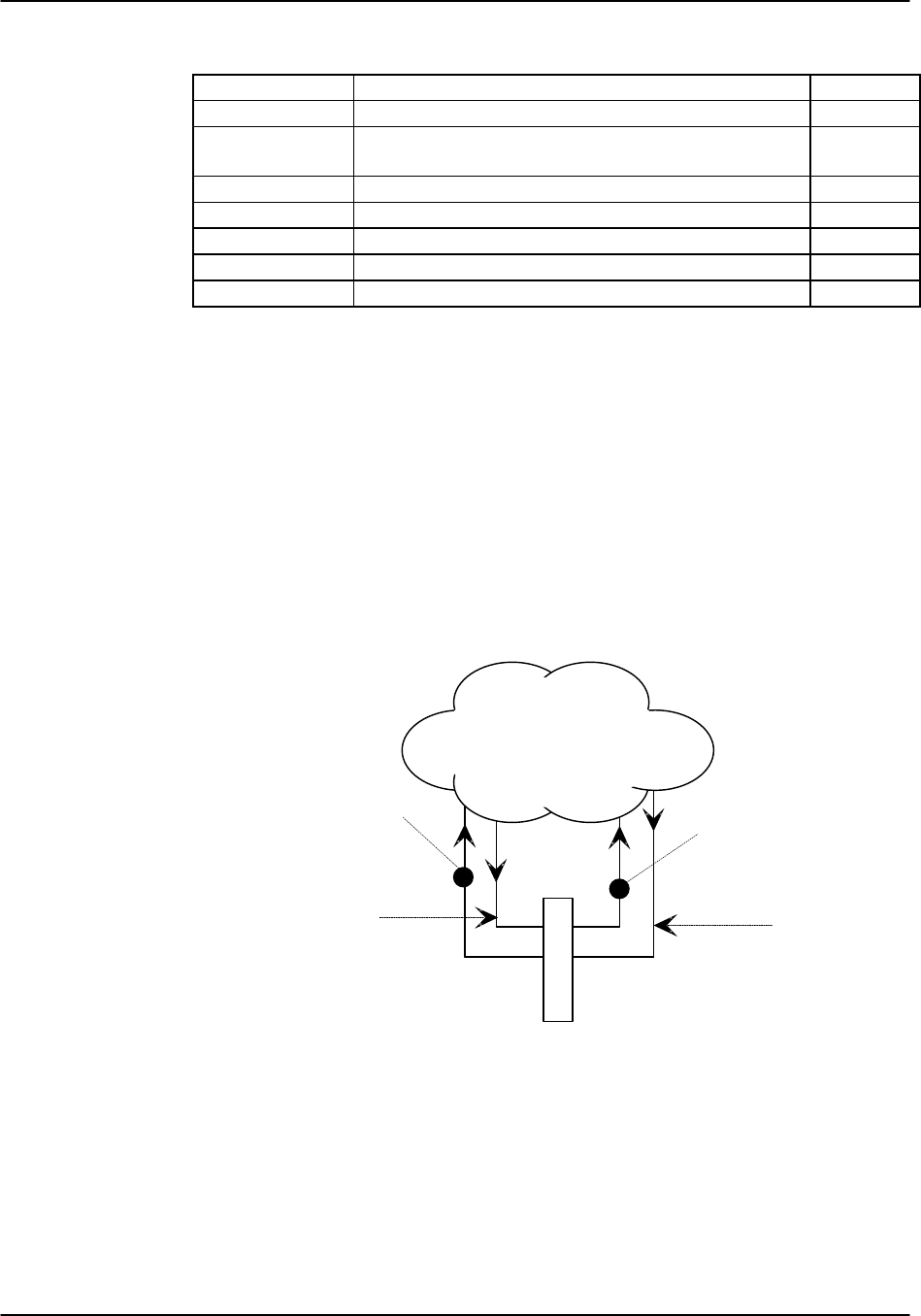
System Operations Reference Guide v3.6
Page 2-D-26 (10-97)
Table System-4. WAN Cross-Connect Test Screen Options
Parameter User Options Default
Tx ABCD mon set mon
PATTERN off all 0 all 1 m_oos 1:1 1:7 lpbk
300Hz 1kHz 3kHz off
MON Tx ABCD information only - no user options
MON Rx ABCD information only - no user option
CONVERSION information only - no user option
TYPE information only - no user option
WAN STATE information only - no user option
Tx ABCD
The Transmit ABCD bit parameter allows the user to observe the bit pattern being sent
on the transmit side of the line (mon) or to set a different pattern for testing that portion
of the circuit (set). Choosing set brings up a small four character window at the bottom
of the screen and allows the user to type in a new pattern of ones and zeros. Figure
System-26 shows a diagram of the process. When Tx ABCD for WAN 2-1 is set to
mon, the WAN 2-1 column reflects the ABCD bits being sent out on WAN 2-1. This
pattern should be identical to the Rx ABCD on WAN 2-2 (unless the conversion table is
used). When Tx ABCD for WAN 2-1 is set to set, the user supplies a bit pattern of four
1s and 0s for the new ABCD bits. The Rx ABCD stream from WAN 2-2 is broken at
circle #1, and the new pattern is inserted into the Tx ABCD stream. The same applies
for mon and set for WAN 2-2. The bit stream will be broken at circle #2.
WAN XCONN
Rx ABCD
1 2
Network
WAN 2-2
Rx ABCD
WAN 2-1
Tx ABCD
WAN 2-2
Tx ABCD
WAN 2-1
Figure System-26. Voice Test Diagram

Reference Guide v3.6System Operations
(10-97) Page 2-D-27
PATTERN
The Pattern parameter allows the user to choose a test pattern to be transmitted as PCM
data on the selected side of the circuit. The options are off, all 0 (zeros), all 1 (ones),
m_oos (multiplexer out of synchronization), 1:1 (a one followed by a zero and then
another one), 1:7 (a zero followed by a one and seven zeros, then another one), lpbk
(loopback), 300 Hz (300 Hz tone), 1kHz (1000 Hz tone) and 3kHz (3000 Hz tone).
Since the Tx ABCD only changes signaling bits, this option allows the user to choose
the test pattern. A different pattern can be sent on either side of the circuit.
MON Tx ABCD
The Monitor Transmit ABCD bit information field shows the bit pattern being
transmitted on the outbound circuit. It can be changed by using the set command. This
parameter is for information only.
MON Rx ABCD
The Monitor Receive ABCD bit information field allows the bit pattern being received
on the inbound circuit. This parameter is for information only, it is not changeable by
the user.
CONVERSION
The Conversion information field shows the user the conversion setting selected from
the cross-connect screen. The possible values are no (no conversion), sig (signaling is
converted, but not the PCM), pcm (PCM is converted, but not the signaling) and p&s
(both signaling and PCM are converted). This parameter is for information only, it is
not changeable by the user on this screen.
WAN STATE
The WAN State information field shows the current status of the port. The possible
values are stdby, actv, test (the operator is actively controlling the circuit), OOS (the
WAN port is Out of Service) and CGA (the WAN port assigned has a CGA alarm).
This parameter is for information only, it is not changeable by the user on this screen.
Broadcast
One of the special features of WAN timeslot assignment in cross-connect systems is the
ability to copy a data signal and send it to multiple locations without disturbing the
original circuit. This feature is called Broadcast (meaning multi-cast, not to be
confused with broadcast quality video).
An example of this feature would be a major company that transmits data lecture from
the corporate headquarters in Denver to the sales office in San Francisco. Sales offices
in Salt Lake City, Houston and Phoenix would like to be in the data lecture as well.
The master circuit (Denver to San Francisco) is a two-way circuit (i.e., both ends can
send and receive data). The other ends of the broadcast circuits (the sales offices in Salt
Lake City, Houston and Phoenix) can only receive the output of the Denver end of the
master circuit (i.e., they will not be able to take part in the discussion in “real time”).

System Operations Reference Guide v3.6
Page 2-D-28 (10-97)
The following series of figures shows how the process works.
Figure System-27 shows the main cross-connect screen. In this example, T1 circuits
connected at the Denver office go to San Francisco (w1-1), Houston (w1-2), Salt Lake
City (w2-1) and Phoenix (w2-2). This screen only shows the cross-connects made from
WAN cards to WAN cards, not User cards to WAN cards.
DENVER01 | C1 CPU XCON 8801 Rev C01-0 Ser 00101 | 12-31-99
14:33
page: 1 of 1
CIRCUIT ID W/U TS/B
WTEST W/U TS/BW TEST TYPE TC CNV
SF-SLC w1-1 01*6
4off w2-
101*64 off v n/a no
HST-PHX w1-2 01*6
4off w2-
201*64 off v n/a no
Add | uPdate | dElete | pgUp | pgDn | View all | Tads | Main
Figure System-27. Main Cross-Connect Screen
Broadcast circuits can be initiated, updated or deleted only from the broadcast screen.
To access the Broadcast option, press the "V" (View all) selection from the menu of
options and the All Circuits screen (Figure System-28) is displayed. In addition to the
WAN to WAN cross-connects, this screen also shows User card to WAN card timeslot
assignments for all WAN cards.
Because this screen shows all WAN timeslots that are either assigned to user cards or
cross-connected to other timeslots, it could be quite full.

Reference Guide v3.6System Operations
(10-97) Page 2-D-29
DENVER01 | C1 CPU XCON 8801 Rev C01-0 Ser 00101 | 12-31-99
14:33
page: 1 of 1
CIRCUIT ID W/U TS/B
WTES
TW/U TS/BW TEST TYPE TC CNV
user_circui
tw4-1 06*5
6off w1-
106*56 off d n/a n/a
user_circui
tw4-2 06*5
6off w2-
206*56 off d n/a n/a
SF-SLC w1-1 01*6
4off w2-
101*64 off v n/a no
HST-PHX w1-2 01*6
4off w2-
201*64 off v n/a no
Bcast | uPdate | dElete | pgUp | pgDn | Main
Figure System-28. All Circuits Screen
In addition to the two WAN to WAN cross-connects shown in Figure System-28, an
HSU circuit from slot u4-1 to the San Francisco T1 circuit on WAN 1-1 and an HSU
circuit from slot u4-2 to Phoenix on WAN 2-2 are shown in Figure System-29.
To select the broadcast option, place the cursor over the User card circuit that will be
copied (in this case, it will be the Denver end of the Denver to San Francisco link on
WAN 1-1) and press the "b" (Broadcast) key from the menu of options. The screen
shown in Figure System-29 will show the dynamics of the first copy of that circuit.
Pressing the "Enter" key allows users to access and modify connection options.

System Operations Reference Guide v3.6
Page 2-D-30 (10-97)
DENVER01 | C1 CPU XCON 8801 Rev C01-0 Ser 00101 | 12-31-99
14:33
page: 1 of 1
CIRCUIT ID W/U TS/BW TEST W/U TS/BW TEST TYPE TC CNV
user_circui
tw4-1 06*56 off w1-1 06*56 off d n/a n/a
user_circui
tw4-2 06*56 off w2-2 06*56 off d n/a n/a
SF-SLC w1-1 01*64 off w2-1 01*64 off v n/a no
HST-PHX w1-2 01*64 off w2-2 01*64 off v n/a no
user_circui
tw4-1 06*56 off w1-1 00*56 off b/d n/a no
Lecture
Save
Figure System-29. Add Broadcast Screen
In this example, the broadcast circuit is labeled "Lecture" for easier identification later
when the circuit will be disconnected.
Figure System-30 shows the selection of a second destination for the broadcast circuit.
In this example, that destination is Salt Lake City, which is accessed through WAN w2-
1. The timeslot selection is shown in Figure System-31. Selecting "S" (Save) from the
Menu of Actions will save the parameters of the new circuit. Figure System-32 shows
the new circuit. Note that the circuit type is "b/d" (broadcast/data).
Similar actions will duplicate this circuit for the other destinations. Figure System-33
shows the completed circuits.
To disconnect the circuits when the program is finished, highlight the circuit to be
disconnected with the cursor and press the "e" key and the screen shown in Figure
System-34 will appear. Selecting "y" will permanently delete the copied circuit while
leaving the original circuit intact.

Reference Guide v3.6System Operations
(10-97) Page 2-D-31
DENVER01 | C1 CPU XCON 8801 Rev C01-0 Ser 00101 | 12-31-99
14:33
page: 1 of 1
CIRCUIT ID W/U TS/BW TEST W/U TS/BW TEST TYPE TC CNV
user_circuit w4-1 06*56 off w1-1 06*56 off d n/a n/a
user_circuit w4-2 06*56 off w2-2 06*56 off d n/a n/a
SF-SLC w1-1 01*64 off w2-1 01*64 off v n/a no
HST-PHX w1-2 01*64 off w2-2 01*64 off v n/a no
Lecture w4-1 06*56 off w1-1 06*56 off b/d n/a no
w1-1 w1-2 w2-1 w2-2 w3-1 w3-2 w4-1 w4-2
Save
Figure System-30. "To" Destination Selection
DENVER01 | C1 CPU XCON 8801 Rev C01-0 Ser 00101 | 12-31-99
14:33
page: 1 of 1
CIRCUIT ID W/U TS/BW TEST W/U TS/BW TEST TYP
ETC CNV
user_circuit w4-1 06*56 off w1-1 06*56 off d n/a n/a
user_circuit w4-2 06*56 off w2-2 06*56 off d n/a n/a
SF-SLC w1-1 01*64 off w2-1 01*64 off v n/a no
HST-PHX w1-2 01*64 off w2-2 01*64 off v n/a no
Lecture w4-1 06x56 off w2-1 01x64 off b/d n/a no
1 1 1 1 1 1 1 1 1 1 2 2 2 2 2
1 2 3 4 5 6 7 8 9 0 1 2 3 4 5 6 7 8 9 0 1 2 3 4
x x x x x x
Save
Figure System-31. Timeslot Selection

System Operations Reference Guide v3.6
Page 2-D-32 (10-97)
DENVER01 | C1 CPU XCON 8801 Rev C01-0 Ser 00101 | 12-31-99 14:33
page: 1 of 1
CIRCUIT ID W/U TS/BW TEST W/U TS/BW TEST TYPE TC CNV
user_circuit w4-1 06*56 off w1-1 06*56 off d n/a n/a
user_circuit w4-2 06*56 off w2-2 06*56 off d n/a n/a
SF-SLC w1-1 01*64 off w2-1 01*64 off v n/a no
HST-PHX w1-2 01*64 off w2-2 01*64 off v n/a no
Lecture w4-1 06*56 off w2-1 06*56 off b/d n/a no
Bcast | uPdate | dElete | pgUp | pgDn | Main
Figure System-32. Completed Broadcast Circuit
DENVER01 | C1 CPU XCON 8801 Rev C01-0 Ser 00101 | 12-31-99 14:33
page: 1 of 1
CIRCUIT ID W/U TS/BW TEST W/U TS/BW TEST TYPE TC CNV
user_circuit w4-1 06*56 off w1-1 06*56 off d n/a n/a
user_circuit w4-2 06*56 off w2-2 06*56 off d n/a n/a
SF-SLC w1-1 01*64 off w2-1 01*64 off v n/a no
HST-PHX w1-2 01*64 off w2-2 01*64 off v n/a no
Lecture w4-1 06*56 off w2-1 06*56 off b/d n/a no
Lecture w4-1 06*56 off w1-2 06*56 off b/d n/a no
Lecture w4-1 06*56 off w2-2 06*56 off b/d n/a no
Bcast | uPdate | dElete | pgUp | pgDn | Main
Figure System-33. Three Broadcast Circuits

Reference Guide v3.6System Operations
(10-97) Page 2-D-33
DENVER01 | C1 CPU XCON 8801 Rev C01-0 Ser 00101 | 12-31-99 14:33
page: 1 of 1
CIRCUIT ID W/U TS/BW TEST W/U TS/BW TEST TYPE TC CNV
user_circuit w4-1 06*56 off w1-1 06*56 off d n/a n/a
user_circuit w4-2 06*56 off w2-2 06*56 off d n/a n/a
SF-SLC w1-1 01*64 off w2-1 01*64 off v n/a no
HST-PHX w1-2 01*64 off w2-2 01*64 off v n/a no
Lecture w4-1 06*56 off w2-1 06*56 off b/d n/a no
Lecture w4-1 06*56 off w1-2 06*56 off b/d n/a no
Lecture w4-1 06*56 off w2-2 06*56 off b/d n/a no
Delete Selected Circuit (y/n)?
Bcast | uPdate | dElete | pgUp | pgDn | Main
Figure System-34. Delete Broadcast Circuit
WAN Link to WAN Link
Circuits from a WAN link to a WAN link can also be duplicated from the broadcast
screen. The same procedure is used to establish multiple connections for WAN to
WAN circuits.
Back in Figure System-30, highlighting the WAN link circuit on slot w1-1 will allow
you to cross-connect duplicate information to any other WAN link needed.

System Operations Reference Guide v3.6
Page 2-D-34 (10-97)
Menu of Actions
Table System-5 shows the Menu of Actions for the Broadcast screen.
Table System-5. Menu of Actions
Action Function
Bcast Bcast allows you to program additional broadcast cross-connects in the
system. If mistakes are made during the add process, pressing the up
arrow or down arrow key will terminate this operation.
uPdate The uPdate action is initiated by pressing the "p" key. With this
command, you can change any of the parameters of a broadcast
connection. Use the arrow keys to highlight the area to be changed
and close the transaction using the "s" (Save) command.
dElete The dElete action is initiated by pressing the "e" key. Use this
command to delete existing broadcast connections. As shown in
Figure System-34 earlier, the system will prompt you to delete the
circuit, and the "y" key must be pressed to complete the transaction.
pgUpThe pgUp (Page Up) action is initiated by pressing the "u" key. Since
the system can handle many different circuits, you may fill the screen
allotment for data. New pages will be added automatically to
accommodate additional circuits. The page count feature at the top of
the screen shows you the current page and the total amount of pages of
information. Use this command to scroll up through the pages of
cross-connect information.
pgDnThe pgDn (Page Down) action is initiated by pressing the "d" key.
This action is similar to the pgUp command. Use this command to
scroll down through the pages of cross-connect information.
Main Pressing "m" (Main) will return you to the cross-connect screen.
Test Access Digroups (TADS)
The Test Access Digroups (TADS) is a remote test access for data cross connects that
pass through the system according to publication TR-TSY-000343, Issue #1, June 1986.
A test center can access the system and assign a non-intrusive testing circuit between
the unit and the test center via another WAN link. For the purposes of this discussion
on Test Access Digroups, the figures show a 64kbps data circuit between Fremont, CA.
and Jacksonville, FL. Figure System-35 shows the cross-connect screen with the data
circuits connected.

Reference Guide v3.6System Operations
(10-97) Page 2-D-35
Node_1 | C1 10161 CPU XCON COM 407535038 Ser 00101 | 12-31-99
14:33
page: 1 of 1
CIRCUIT ID FACILITY TEST EQUIPMENT TEST TYPE TC CNV
Jacksonville w1-1 01*64 off w1-2 01*64 off d moos n/a
moNitor | spLit | Release | Tla | pgUp | pgDn | Main
Figure System-35. The TADS Screen
In Figure System-35, the data circuit called "Jacksonville" is connected on a single time
slot between WAN1-1 and W1-2.
Monitor Circuit
With the monitor circuit, the data test center (by remote access) creates a "hitless"
monitor connection (i.e., one that can be created, maintained and dropped without
affecting the information on the circuit being tested) between the data test center and
the Node_1 Device.
Highlighting the desired circuit and pressing the "N" key, brings up the add monitor
circuit screen shown in Figure System-36.

System Operations Reference Guide v3.6
Page 2-D-36 (10-97)
Node_1 | C1 10161 CPU XCON COM 407535038 Ser 00101 | 12-31-99
14:33
page: 1 of 1
CIRCUIT ID FACILITY TEST EQUIPMENT TEST TYPE TC CNV
Jacksonville w1-1 01*64 off w1-2 01*64 off d moos n/a
new_circuit w1-1 00*64 off w1-1 00*64 off m/d moos n/a
moNitor | spLit | Release | Tla | pgUp | pgDn | Main
Figure System-36. The Add Monitor Circuit Screen
Cross connect information is added in a similar fashion to the Add Broadcast screen
mentioned in the last section. Figure System-37 shows the completed monitor circuit.
Node_1 | C1 10161 CPU XCON COM 407535038 Ser 00101 | 12-31-99 14:33
page: 1 of 1
CIRCUIT ID FACILITY TEST EQUIPMENT TEST TYPE TC CNV
Jacksonvill
ew1-1 01*64 mon w1-2 01*64 off d moos n/a
monitor ckt w1-1 01*64 off w2-1 01*64 off m/d moos n/a
monitor ckt w1-2 01*64 off w2-1 01*64 off m/d moos n/a
moNitor | spLit | Release | Tla | pgUp | pgDn | Main
Figure System-37. Completed Monitor Circuit
Reference Guide v3.6System Operations
(10-97) Page 2-D-37
Figure System-38 shows a diagram of how the Monitor circuit splits the original cross
connect circuit for testing.
Notice how the test circuit uses two 64kbps WAN timeslots, one for the transmit side
and one for the receive side of the line.
Fremont DTE
Jacksonville DCE
Data Test Center Equip
W1-2 #1
W1-1 #1(T)
W1-2 #1
W1-1 #1(R)
W2-1 #1
W2-1 #2
Figure System-38. Monitor Circuit Diagram
Split Circuit
Pressing the "L" command from the Menu of Actions allows you to split the circuit
through the data test center equipment. New circuit information is added in the same
way as with the monitor circuit.
With the Split Circuit, the data test center splits the circuit and connects it to their
equipment. Unlike the Monitor test circuit, the Split test circuit is intrussive and all
transmit and receive data must pass through the equipment at the data test center.
Figure System-39 shows the TADS screen with a split circuit completed. It uses two
64kbps timeslots (like the Monitor circuit). Figure System-40 shows a diagram of the
split test circuit.
System Operations Reference Guide v3.6
Page 2-D-38 (10-97)
Node_1 | C1 10161 CPU XCON COM 407535038 Ser 00101 | 12-31-99
14:33
page: 1 of 1
CIRCUIT ID FACILITY TEST EQUIPMENT TEST TYPE TC CNV
Jacksonvill
ew1-1 01*64 spl w1-2 01*64 off d moos n/a
split ckt w1-1 01*64 off w2-1 01*64 off s/d moos n/a
split ckt w1-2 01*64 off w2-1 01*64 off s/d moos n/a
moNitor | spLit | Release | Tla | pgUp | pgDn | Main
Figure System-39. TADS Screen with Split Circuits
Fremont DTE
Jacksonville DCE
Data Test Center Equip
W1-2 #1
W1-1 #1(T)
W1-2 #1
W1-1 #1(R)
W2-1 #1
W2-1 #2
Figure System-40. Split Circuit Diagram

Reference Guide v3.6System Operations
(10-97) Page 2-D-39
Release
Pressing the "R" command from the Menu of Actions allows you to release the circuit
from the data test center equipment. The system will verify the action desired with a
yes/no question.
With the Release Circuit, the Data Test Center removes the connection between the
circuit being tested and restores the circuit to its preaccessed state.
Figure System-41 show the TADS screen with the release verification.
Node_1 | C1 10161 CPU XCON COM 407535038 Ser 00101 | 12-31-99
14:33
page: 1 of 1
CIRCUIT ID FACILITY TEST EQUIPMENT TEST TYPE TC CNV
Jacksonvill
ew1-1 01*64 spl w1-2 01*64 off d moos n/a
split ckt w1-1 01*64 off w2-1 01*64 off s/d moos n/a
split ckt w1-2 01*64 off w2-1 01*64 off s/d moos n/a
Restore Selected Circuit (y/n)?
moNitor | spLit | Release | Tla | pgUp | pgDn | Main
Figure System-41. TADS Restore Circuit Screen
Terminate and Leave Access
The Terminate and Leave Access (TLA) circuit gives the data test center the capability
to terminate one or both directions of transmission on a circuit by inserting an
unassigned channel code (01111111) in the outgoing transmission path(s). The TLA
feature is useful in circuit provisioning to turn circuits up and down remotely, and in
testing multipoint circuits to isolate and remove noisy bridge legs from service.
Figure System-42 shows the TLA screen with the choice of Monitor (mon) or
Unassigned Channel Code (uca) to be applied to the highlighted circuit. (If TLA had
been applied to a Split circuit, the choices would have been spl or uca.)

System Operations Reference Guide v3.6
Page 2-D-40 (10-97)
Node_1 | C1 10161 CPU XCON COM 407535038 Ser 00101 | 12-31-99
14:33
page: 1 of 1
CIRCUIT ID FACILITY TEST EQUIPMENT TEST TYPE TC CNV
Jacksonville w1-1 01*64 mon w1-2 01*64 off d moos n/a
monitor ckt w1-1 01*64 off w2-1 01*64 off m/d moos n/a
monitor ckt w1-2 01*64 off w2-1 01*64 off m/d moos n/a
Jacksonville w1-1 01*64 mon w1-2 01*64 off d moos n/a
mon uac
moNitor | spLit | Release | Tla | pgUp | pgDn | Main
Figure System-42. TLA Circuit State Screen
Menu of Actions
Table System-6 shows the Menu of Actions for the TADS screen.
Table System-6. Menu of Actions
Action Funtion
moNitor The Monitor command allows the user to create a monitor circuit at the
WAN interface. See section above.
spLit The Monitor command allows the user to create a split circuit at the
WAN interface. See section above.
Release The Release command allows the user to release and restore a split
circuit or a monitor circuit. See section above.
Tla The Terminate and Leave Access (TLA) command is the capability to
terminate one or both directions of transmission on a circuit. See
section above.
pgUpThe pgUp) action is initiated by pressing the "u" key. Since the system
can handle many different TADS circuits, you may fill the screen
allotment for data. New pages will be added automatically to
accommodate additional circuits. Use this command to scroll up
through the pages of TADS information.
pgDnThe pgDn (Page Down) action is initiated by pressing the "d" key. This
action is similar to the pgUp command. Use this command to scroll
down through the pages of cross-connect information.
Main Pressing "m" (Main) will return you to the cross-connect screen.

Reference Guide v3.6System Operations
(10-97) Page 2-D-41
Signaling and Companding Conversion in Bus-Connect
Systems
User card ports may or may not have a signaling mode applied to them when assigned
to a timeslot. Typically, analog voice cards (i.e., E&M, FXO, FXS) will have their
analog signaling information converted to digital signaling bits which are then inserted
into the digital bitstream. Data card circuits (i.e., HSU, SRU, etc.), on the other hand,
do not require the system to perform any signaling processing or conversion.
Unlike DS0s terminating on voice or data cards in the system that will have controlled
signaling parameters, circuits that "pass through" your system must have signaling
assigned to them by the user. This ensures that the WAN cards either maintain existing
signaling patterns as in T1-T1 circuits or change and convert them for circuits going
from a T1 to an E1 environment.
In Figure System-43, timeslots 1-8 and 13-18 are connected to user cards and therefore
will have signaling automatically turned off or on by the system depending on the type
of user ports that are assigned to them. Of the pass-through connections on the other
timeslots, you can either select signaling or no signaling depending the type of
equipment or channel facility on which it is ultimately terminated. For voice circuits,
you would probably want to enable signaling, and for data equipment, you would
probably want to disable signaling (the default). Further, this screen allows you to
request that signaling conversion and/or companding conversion be performed on pass-
through circuits.
Node_1 | W1 CSU+CSU 8010 Rev A6-2 Ser 00101 | 12-31-99 14:33
TS XCONNECT BW
CNV TS XCONNECT BW CNV
1 u2-1 voice 64k sig 13 u5-1 data 06x56k
2 u2-2 voice 64k sig 14 u5-1 data 06x56k
3 u2-3 voice 64k sig 15 u5-1 data 06x56k
4 u2-4 voice 64k sig 16 u5-1 data 06x56k
5 u2-5 voice 64k sig 17 u5-1 data 06x56k
6 u2-6 voice 64k sig 18 u5-1 data 06x56k
7 u2-7 voice 64k sig 19 w1-2 ts-19 64k no
8 u2-8 voice 64k sig 20 w1-2 ts-20 64k no
9 u1-2 ts-9 64k no 21 w1-2 ts-21 64k no
10 u1-2 ts-10 64k no 22 w1-2 ts-22 64k no
11 u1-2 ts-11 64k no 23 w1-2 ts-23 64k no
12 u1-2 ts-12 64k no 24 w1-2 ts-24 64k no
Save | Undo | Refresh | sIgnaling | Main
Figure System-43. WAN Cross-Connect Screen

System Operations Reference Guide v3.6
Page 2-D-42 (10-97)
To change the signaling and/or companding options of a voice circuit on a WAN card
using the drop-and-insert mode, place the cursor over the timeslot you wish to change
and select I (sIgnaling) from the Menu of Actions. Table System-7 shows the matrix of
choices for the handling of signaling, signaling conversion and companding conversion.
Table System-7. Signaling and Companding Options
Select
Signaling Select PCM CONV Select SIG CONV Select SIG
TYPE
none (no choice)
yes none, A-mu, mu-A ANSI-CCITT, CCITT-ANSI,
ABCD-ABAB, ABCD-AB01 e&m, fxs,
plar, fxo
no none, A-mu, mu-A (no choice) (no choice)
The first option is Select Signaling. The choices are either yes or no, depending upon
the type of circuit passed through the system (voice or data). Whichever choice is
made, the system will then prompt you to select PCM companding conversion. The
choices for Select PCM CONV are none, A-mu (A-Law to Mu-Law, E1 to T1
conversion) and mu-A (Mu-Law to A-Law, T1 to E1 conversion).
On a normal data service, you would probably choose no and none. A voice circuit on
a T1-T1 "pass through" might require signaling enabled but not converted, so the
choices would be yes (to pass voice signaling through), and none (the PCM does not
have to be converted), and none (the signaling does not have to be converted).
If, for instance, you have an international voice circuit passed through your system to a
North American T1 circuit, you would probably need to have both signaling and PCM
conversion converted. Choosing yes for Select Signaling will bring up your Select
PCM CONV options, followed by a prompt to select the signaling conversion for this
circuit.
The first option is default signaling conversion (none) where a bit pattern of "0000" will
automatically be converted to "0001" in the T1 to CEPT direction.
The second option (ANSI-CCITT) will convert the incoming ANSI signaling to CCITT
signaling. The third option (CCITT-ANSI) converts the incoming CCITT signaling to
ANSI signaling. These two options are complementary (i.e. if either one is selected in
one direction, the other is automatically selected for the reverse direction).
The fourth option (ABCD-ABAB) will convert the incoming CEPT signaling to T1
signaling for an ESF or D4 cross-connect. The fifth option (ABCD-AB01) will convert
the incoming T1 signaling to CEPT signaling for a ESF or D4 cross-connect. These
two options are complementary (i.e. if either one is selected in one direction, the other
is automatically selected for the reverse direction).
If signaling conversion is enabled for that circuit, you will then be asked to Select SIG
TYPE. The choices are e&m, fxs, plar and fxo. After this final choice, the screen
updates the signaling and conversion information on that circuit.

Reference Guide v3.6System Operations
(10-97) Page 2-D-43
Figure System-44 shows the WAN card cross-connect screen for a bus-connect system.
Timeslots 19-24 show all of the possible choices for pass through circuits. The values
are no (signaling is not passed through and neither PCM nor SIG are converted), pcm
(signaling is not passed through, PCM is converted, SIG is not converted), sig-no
(signaling is passed through and there is no PCM or SIG conversion), sig-sig (signaling
is passed through, PCM is not converted, SIG is converted), sig-pcm (signaling is
passed through, PCM is converted, SIG is not converted) and sig-p&s (signaling is
passed through, both PCM and SIG are converted).
Node_1 | W1 CSU+CSU 8010 Rev A6-2 Ser 00101 | 12-31-99 14:33
TS XCONNECT BW
CNV TS XCONNECT BW CNV
1 u2-1 voice 64k sig 13 u5-1 data 06x56k
2 u2-2 voice 64k sig 14 u5-1 data 06x56k
3 u2-3 voice 64k sig 15 u5-1 data 06x56k
4 u2-4 voice 64k sig 16 u5-1 data 06x56k
5 u2-5 voice 64k sig 17 u5-1 data 06x56k
6 u2-6 voice 64k sig 18 u5-1 data 06x56k
7 u2-7 voice 64k sig 19 w1-2 ts-19 64k no
8 u2-8 voice 64k sig 20 w1-2 ts-20 64k pcm
9 u1-2 ts-9 64k no 21 w1-2 ts-21 64k no
10 u1-2 ts-10 64k no 22 w1-2 ts-22 64k sig
11 u1-2 ts-11 64k no 23 w1-2 ts-23 64k pcm
12 u1-2 ts-12 64k no 24 w1-2 ts-24 64k p&s
Save | Undo | Refresh | sIgnaling | Main
Figure System-44. Signaling and Companding Options
Checking the Timeslot Map
Once the timeslots are selected and assigned, the list of all DS0 connections (the
timeslot map) can be viewed through the WAN card Xconnect screen for both bus-
connect and cross-connect systems. (In the bus-connect version, changes of signaling
status [trunk conditioning] can also be done from this screen [see previous section]).
You can see the results of your assignment selections by checking the timeslot map as
follows:
1. From the Main Screen, select the WAN card in slot W-1.
2. Type <x> to bring up the timeslot screen (see Figure System-45).
3. Selecting <m> for Main will return you to the WAN card screen.
4. Selecting <m> for Main again will return you to the Main screen.

System Operations Reference Guide v3.6
Page 2-D-44 (10-97)
Node_1 | W1 CSU+CSU 8010 Rev A6-2 Ser 00101 | 12-31-99
14:33
TS XCON TS CIRCUIT ID TS XCON TS CIRCUIT ID
1 u2-1 D-01
user_circuit 13
2 u2-1 D-02
user_circuit 14
3 u2-1 D-03
user_circuit 15
4 u2-1 D-04
user_circuit 16
5 u2-1 D-05
user_circuit 17
6 u2-1 D-06
user_circuit 18
7 u2-1 D-07
user_circuit 19 u2-1 A-01 user_circuit
8 20 u2-1 A-02 user_circuit
9 21 u2-1 A-03 user_circuit
10 22 u2-1 A-04 user_circuit
11 23 u2-1 A-05 user_circuit
12 24 u2-1 A-06 user_circuit
Save | Undo | Refresh | Main
Figure System-45. Timeslot Screen in T1 Operation
Figure System-46 shows the same example displayed on a bus-connect system using E1
connections in d-i mode. (Timeslot #16 will not be available for assignment on
either the HSU table or the voice card timeslots.) Like T1 operation in d-i mode,
unspecified timeslots are automatically assigned to corresponding slots on the other
WAN port on the same card.
DACOM Timeslot Renumbering
The WAN Card timeslot selection screen shown above can be modified for DACOM
format. The timeslot data will be translated into DACOM format using a new assigned
vendor code. This will allow the renumbering of timeslots so they will be displayed into
Korean format.
If Vendor Code indicates DACOM, then renumbered timeslots will be displayed using
the Korean format. Timeslots 1 through 15 will be unchanged. Timeslots 17 through 31
will be renumbered as 16 through 30, and timeslot 16 will be renumbered as 31.
Note: ONLY use this option to reassign the timeslots on the WAN Card to DACOM.
Otherwise, DO NOT change your vendor code.

Reference Guide v3.6System Operations
(10-97) Page 2-D-45
Node_1 | W1 CEPT+CEPT 8010 Rev A6-2 Ser 00101 | 12-31-99
14:33
TS XCON TS CIRCUIT_ID TS XCON TS CIRCUIT_ID
0 frame align 64k 16 cas 64k
1 U5-1 A-01 user_circuit 17 U7-1 A-17 user_circuit
2 U5-2 A-02 user_circuit 18 U7-2 A-18 user_circuit
3 U5-3 A-03 user_circuit 19 U7-3 A-19 user_circuit
4 U5-4 A-04 user_circuit 20 U7-4 A-20 user_circuit
5 U5-5 A-05 user_circuit 21 U7-5 A-21 user_circuit
6 U5-6 A-06 user_circuit 22 U7-6 A-22 user_circuit
7 U5-7 A-07 user_circuit 23 U7-7 A-23 user_circuit
8 U5-8 A-08 user_circuit 24 U7-8 A-24 user_circuit
9 U6-1 A-09 user_circuit 25 U8-1 A-25 user_circuit
10 U6-2 A-10 user_circuit 26 U8-2 A-26 user_circuit
11 U6-3 A-11 user_circuit 27 U8-3 A-27 user_circuit
12 U6-4 A-12 user_circuit 28 U8-4 A-28 user_circuit
13 U6-5 A-13 user_circuit 29 U8-5 A-29 user_circuit
14 U6-6 A-14 user_circuit 30 U8-6 A-30 user_circuit
15 U6-7 A-15 user_circuit 31 U8-7 A-31 user_circuit
Refresh | Test | Main
Figure System-46. Timeslot Screen in E1 Operation
Recording the Configuration on Paper
After you set up your initial system configuration and define your timeslot map, take
the time to record this information on paper. Recording the initial configuration in a
logical manner will pay for itself if you have a problem later.
Record the information in any way that makes sense to you and your colleagues.
Whatever your approach, it is suggested that you also note the initial settings for each
card in copies of the T1 or E1 operation tables provided as Tables System-8 and -9.
Store all the initial configuration information in a safe place where anyone needing to
service the system can easily find it.

System Operations Reference Guide v3.6
Page 2-D-46 (10-97)
Table System-8. Timeslot Recording Form (T1 Operation)
WAN Port # _______ - _______
TS Number Card Type Port Number
1
2
3
4
5
6
7
8
9
10
11
12
13
14
15
16
17
18
19
20
21
22
23
24

Reference Guide v3.6System Operations
(10-97) Page 2-D-47
Table System-9. Timeslot Recording Form (E1 Operation)
WAN Port # _______ - _______
TS Number Card Type Port Number
0
1
2
3
4
5
6
7
8
9
10
11
12
13
14
15
16
17
18
19
20
21
22
23
24
25
26
27
28
29
30
31

Reference Guide v3.6 Redundant Operations
(10-97) Page 2-E-1
Introduction
The system can be configured with redundant features that will switch operations from
failed critical components to "backup" replacements with the minimum loss of service
possible in the event of equipment failure.
The four areas of redundant operations are the power system (load share), the CPU
card, the WAN card and the ADPCM network.
Power System
Each of the power supply components is designed to switch to alternative units (if
available) in the event the primary unit fails. Additionally, the defective unit will
create a system alarm upon failure to alert the operator of the condition so that suitable
diagnostic and repair work may be initiated. The units covered by these redundancy
parameters are:
• 8901 AC Power Supply
• 8902 DC Power Supply
• 8906 Ringing Generator (Master only, see below)
• 8907 DC Power Supply
Upon failure, the LED on the 8903 or 8905 AC to DC Power Converter will be turned
off but will not generate a system alarm (unless the system is equipped with the 8902
External Alarm card).
If the "Master" 8906 Ringing Generator fails, an alarm will be generated and the LED
will turn off. If a "slave" Ringing Generator fails, the LED will turn off but no alarm
will be generated by the system.
Figure RDNT-1 shows the main screen of a cross-connect system in which Power
Supply #1 (PS1) has failed. The Power Supply failure is noted in the alarm message in
the top right hand corner of the screen.

Redundant Operations Reference Guide v3.6
Page 2-E-2(10-97)
Node_1 | | 12-31-99 14:33
Slot Installed Status Slot Installed Status PS1
OOS
C1 CPU XCON IF INTF+modem
C2 CPU XCON RDNT U1 ALR
P1 ADPCM-64 U2 E&M 4Wx8-6
P2 ADPCM-64 U3 FXS 2Wx8-9
P3 ADPCM-64 U4 FXO 2Wx8-9
W1 CSU+CSU U5 HSU 366x2
W2 CSU+CSU U6 OCU-DPx5
W3 CEPT+CEPT U7 FRAD-18
W4 CEPT+CEPT U8 SRU-232x10
F1 PS1 OOS RI RINGER
F2 PS2
Alarms | Config | Del | accepT | Xcon | sYs | Logout | Oos | cpusWtch
Figure RDNT-1. Redundant Power Systems (Two-Sided Chassis)
CPU Card
CPU Card redundancy is valuable to the user because of the criticality of the CPU card
to the operation of the entire system. CPU redundancy is supported in both cross-
connect and enhanced bus-connect units using two 8801 or 8804 models respectively.
A CPU card installed in slot C2 will become the redundant mate of the one in slot C1, if
they are both of the same type.
Switching from one CPU card to the other is triggered by any one of the following
conditions:
• A software command issued by the operator
• Removal of the active CPU card
• Failure or malfunction of the active CPU card
During a CPU redundancy switch over, disruptions to voice and data traffic are
momentary and traffic will recover automatically.
Figure RDNT-2 shows the Main screen of a cross-connect system. The CPU in slot C1
is active and the CPU in slot C2 is the redundant mate. When the command
"cpusWtch" is selected from the Menu of Actions, the system will prompt the user with
the yes/no question.
Figure RDNT-3 shows the same screen after the switch. The CPU card in slot C1 now
shows redundant and the CPU in slot C2 now shows as the active mate. Note: This
switch is intrusive and will cause an outage.

Reference Guide v3.6Redundant Operations
(10-97) Page 2-E-3
Node_1 | | 12-31-99 14:33
Slot Installed Status
C1 CPU RCON
C2 CPU RCON RDNT
P1/U1 E&M 4Wx8-6
P2/U2 FXS 2Wx8-9
P3/U3 FXO 2Wx8-9
P4/U4 HSU 366x2
W1/U5 CSU+CSU
W2/U6 CSU+CSU
W3/U7 CEPT+CEPT
W4/U8 CEPT+CEPT
IF INTF+modem
S1 PS1
S2 PS2
RI RINGER
OK to switch to redundant CPU (y/n)?
Alarms | Config | Del | accepT | Xcon | sYs | Logout | Oos | cpusWtch
Figure RDNT-2. Redundant CPU Cards (Front-Loading Chassis)
Node_1 | | 12-31-99 14:33
Slot Installed Status
C1 CPU RCON RDNT
C2 CPU RCON
P1/U1 E&M 4Wx8-6
P2/U2 FXS 2Wx8-9
P3/U3 FXO 2Wx8-9
P4/U4 HSU 366x2
W1/U5 CSU+CSU
W2/U6 CSU+CSU
W3/U7 CEPT+CEPT
W4/U8 CEPT+CEPT
IF INTF+modem
S1 PS1
S2 PS2
RI RINGER
Alarms | Config | Del | accepT | Xcon | sYs | Logout | Oos | cpusWtch
Figure RDNT-3. CPU Switchover (Front-Loading Chassis)
WAN Card
T1 and E1 WAN redundancy is supported in enhanced bus-connect systems (Model
8804 CPU) and in cross-connect systems (Model 8801 CPU). It is not supported in the
standard bus-connect systems (Model 8800 CPU).

Redundant Operations Reference Guide v3.6
Page 2-E-4(10-97)
In both cases, the user may define in software, one or more events that can trigger a
WAN redundancy switchover from among the following options:
• A software command issued by the operator
• The removal of the active WAN port or card
• The failure or malfunction (OOS) of the active WAN port or card
• CGA alarm declaration on the active WAN port or card
During a WAN redundancy switchover, disruptions to voice and data traffic are
momentary and traffic will recover automatically.
Enhanced Bus-Connect WAN Redundancy
In enhanced bus-connect systems, a single or dual WAN card that is installed in slot W2
automatically becomes the redundant mate of the WAN card in slot W1. Similarly, a
WAN card in slot W4 automatically becomes the redundant mate of the WAN card in
slot W3. This is known as 1x1 redundancy and a "Y-adapter" (Model 1239) is required
to bring the outputs of each pair of WAN ports onto the same facility. The "master"
WAN card and its redundant mate must be equipped with the same mix of DSX, CSU
or CEPT modules and those must be placed in the same positions on both cards. If an
incompatible WAN card is installed in a redundant slot, then the system will "reject"
that card. If a Dual WAN is used in "terminate" mode, only the failed WAN port will
switch to its redundant mate. If the Dual WAN card is programmed for "drop and
insert" mode, both ports will switch even if only one has failed.
Figure RDNT-4 shows the Main screen (status screen selected) of the enhanced bus-
connect system. In this example, the two ports on WAN-1 are paired with the two ports
on WAN-2, while the two ports on WAN-3 are paired with the two ports on WAN-4.
Figure RDNT-5 shows the main WAN card screen for the card in slot W3 with port 1
selected. The software command "sWitch" is selected from the choices in the Menu of
Actions and the system delivers the prompt shown in the same figure. Pressing "y" will
complete the transaction and the traffic on WAN port 3-1 will be switched to WAN port
4-1. The main screen (Figure RDNT-6) now shows WAN port 4-1 as the active port
and WAN port 3-1 as the redundant port.
Note: There are no internal test functions available for WAN #3 or #4.

Reference Guide v3.6Redundant Operations
(10-97) Page 2-E-5
Node_1 | | 12-31-99
14:33
Slot Installed Status Slot Installed Status
C1 CPU RCON IF INTF+modem
C2 U1 ALR s s s s
P1 U2 E&M 4Wx8-6 s s s s s s s
s
P2 U3 FXS 2Wx8-9 s s s s s s s
s
P3 U4 FXO 2Wx8-9 s s s s s s s
s
W1 CSU+CSU a a U5 HSU 366x2 s s
W2 CSU+CSU r r U6 HSU 366x2 s s
W3 CEPT+CEPT a a U7 HSU 366x2 s s
W4 CEPT+CEPT r r U8 OCU-DPx5 s s s s s
F1 PS1 RI RINGER
F2 PS2
Alarms | Config | Del | accepT | Xcon | sYs | Logout | Oos | cpusWtch
Figure RDNT-4. RCON WAN Cards (Two-Sided Chassis)
Node_1 | | 12-31-99
14:33
CSU CSU
STATE actv STATE actv
MODE term MODE term
FORMAT esf FORMAT esf
LINE CODE b8zs LINE CODE b8zs
PULSE n/a PULSE n/a
LINE LEN 0 LINE LEN 0
SLIP LIM 126 SLIP LIM 126
AIS none AIS none
LINE LB off LINE LB off
LOCAL LB off LOCAL LB off
CH LB off CH LB off
LB ADDR 01 LB ADDR 01
LB DET w/to LB DET w/to
ESF/NMS RP at&t ESF/NMS RP at&t
EER THRHD 10e-4 EER THRHD 10e-4
RDNT RULES none RDNT RULES none
OK to switch to the redundant WAN (y/n)?
Save | Undo | Refresh | Xcon | Perf | Test | sWitch | Main
Figure RDNT-5. RCON WAN Card Switchover

Redundant Operations Reference Guide v3.6
Page 2-E-6(10-97)
Node_1 | | 12-31-99
14:33
Slot Installed Status Slot Installed Status
C1 CPU RCON IF INTF+modem
C2 U1 ALR s s s s
P1 U2 E&M 4Wx8-6 s s s s s s s
s
P2 U3 FXS 2Wx8-9 s s s s s s s
s
P3 U4 FXO 2Wx8-9 s s s s s s s
s
W1 CSU+CSU r a U5 HSU 366x2 s s
W2 CSU+CSU a r U6 HSU 366x2 s s
W3 CEPT+CEPT r r U7 HSU 366x2 s s
W4 CEPT+CEPT a a U8 OCU-DPx5 s s s s s
F1 PS1 RI RINGER
F2 PS2
Alarms | Config | Del | accepT | Xcon | sYs | Logout | Oos | cpusWtch
Figure RDNT-6. RCON WAN Cards (Two-Sided Chassis)
Cross-Connect WAN Redundancy
In cross-connect systems, WAN redundancy requires the installation of a Dual WAN
card with Relays (Model 8014) in slot W4. That WAN card with Relays acts as the
redundant card for the WAN cards installed in slots W1 through W3 provided it is
equipped with matching DSX, CSU or CEPT plug-in modules and that the plug-in
modules are installed in the correct positions. This is known as 1xN redundancy and,
following a redundancy switchover, the relay module on the 8014 switches the output
of the redundant WAN card to the correct pins on the WAN connector of the Interface
card. Note that if a Model 8014 Dual WAN card with Relays is installed in slots W1,
W2 or W3, then it will function as a standard Dual WAN card. Also, if the plug-ins of
a Model 8014 installed in slot W4 do not match those of a WAN card in slot W1,
W2 or W3, then it cannot act as that card's redundant mate. Even though the
system will not reject the card, it will simply not switch even if the active WAN card
fails. Finally, if a standard WAN card is installed in slot W4, then WAN redundancy
cannot be supported by the system. In cross-connect systems redundancy
switchovers occur on a WAN card (not port) basis and the whole card must match
the redundant card in slot W4 for the switchover to occur. Note: In the 8014 there
must never be a physical T-1 connection to WAN 4 that is being used as a Redundant
WAN.
Figure RDNT-7 shows the main screen (status screen selected) of a cross-connect
system. In this example the two CSU ports in WANs 1, 2 and 3 are backed-up by the
two ports in W4.

Reference Guide v3.6Redundant Operations
(10-97) Page 2-E-7
Node_1 | | 12-31-99 14:33
Slot Installed Status
C1 CPU XCON
P1/U1 E&M 4Wx8-6 s s s s s s s s
P2/U2 FXS 2Wx8-9 s s s s s s s s
P3/U3 FXO 2Wx8-9 s s s s s s s s
P4/U4 HSU 366x2 s s
W1/U5 CSU+CSU a a
W2/U6 CSU+CSU a a
W3/U7 CSU+CSU a a
W4/U8 CSU+CSU r r
IF INTF+modem
S1 PS1
S2 PS2
RI RINGER
Alarms | Config | Del | accepT | Xcon | sYs | Logout | Oos | cpusWtch
Figure RDNT-7. XCON WAN Cards (Front-Loading Chassis)
Figure RDNT-8 shows the main WAN card screen for the card in slot W1 with port 1-1
selected. The software command "sWitch" is selected from the choices in the Menu of
Actions and the system delivers the prompt shown. Pressing "y" will complete the
transaction and the traffic on the card in slot W1 will be switched to the 8014 card in
slot W4. The main screen (Figure RDNT-9) now shows both ports on the card in slot
W4 as active port and the ports on the card in slot W1 as redundant.
Node_1 | | 12-31-99 14:33
CSU CSU
STATE actv STATE actv
MODE xcon MODE term
FORMAT esf FORMAT esf
LINE CODE b8zs LINE CODE b8zs
PULSE n/a PULSE n/a
LINE LEN 0 LINE LEN 0
SLIP LIM 126 SLIP LIM 126
AIS none AIS none
LINE LB off LINE LB off
LOCAL LB off LOCAL LB off
CH LB off CH LB off
LB ADDR 01 LB ADDR 01
LB DET w/to LB DET w/to
ESF/NMS RP at&t ESF/NMS RP at&t
EER THRHD 10e-4 EER THRHD 10e-4
RDNT RULES n/a RDNT RULES none
OK to switch to the redundant WAN (y/n)?
Save | Undo | Refresh | Xcon | Perf | Test | sWitch | Main
Figure RDNT-8. Switchover in Cross-Connect System

Redundant Operations Reference Guide v3.6
Page 2-E-8(10-97)
Node_1 | | 12-31-99 14:33
Slot Installed Status
C1 CPU XCON
P1/U1 E&M 4Wx8-6 s s s s s s s s
P2/U2 FXS 2Wx8-9 s s s s s s s s
P3/U3 FXO 2Wx8-9 s s s s s s s s
P4/U4 HSU 366x2 s s
W1/U5 CSU+CSU r r
W2/U6 CSU+CSU a a
W3/U7 CSU+CSU a a
W4/U8 CSU+CSU a a
IF INTF+modem
S1 PS1
S2 PS2
RI RINGER
Alarms | Config | Del | accepT | Xcon | sYs | Logout | Oos | cpusWtch
Figure RDNT-9. XCON WAN Cards (Front-Loading Chassis)
ADPCM Card
This system can employ ADPCM cards that use voice compression technology to
effectively increase the digital voice transmission capabilities of voice cards (E&M,
FXS or FXO) or WAN links. See the ADPCM chapter in the Server Cards section for
complete technical details about the ADPCM card.
Each system allows one, two, or three ADPCM cards located in slots P1 through P3,
depending on slot availability. In systems with two or three ADPCM cards, any one of
the cards can be selected as the redundant backup. No restrictions exist about slot
order.
Figure RDNT-10 shows a console with three ADPCM cards. The ADPCM card in slot
P1 is highlighted. Pressing the "Enter" key will bring up the ADPCM main screen
shown as Figure RDNT-11.

Reference Guide v3.6Redundant Operations
(10-97) Page 2-E-9
Node_1 | | 12-31-99 14:33
Slot Installed Status Slot Installed Status
C1 IF INTF+modem
C2 U1 ALR s s s s
P1 ADPCM-64 s s s s s s s s U2 E&M 4Wx8-6 s s s s s s s s
P2 ADPCM-64 s s s s s s s s U3 FXS 2Wx8-9 s s s s s s s s
P3 ADPCM-64 s s s s s s s s U4 FXO 2Wx8-9 s s s s s s s s
W1 CSU+CSU s s U5 HSU 366x2 s s
W2 CSU+CSU s s U6 OCU-DPx5 s s s s s
W3 CEPT+CEPT s s U7 FRAD-18 s s s s s s s s
W4 CEPT+CEPT s s U8 SRU-232x10 s s s s s s s s s s
F1 PS1 RI RINGER
F2
Alarms | Config | Del | accepT | Xcon | sYs | Logout | Oos | cpusWtch
Figure RDNT-10. Selecting the Redundant ADPCM Card
Node_1 | | 12-31-99 14:33
12345678
STATE stdby stdby stdby stdby stdby stdby stdby stdby
USER n/a n/a n/a n/a n/a n/a n/a n/a
WAN w1-1 w1-1 w1-1 w1-1 w1-1 w1-1 w1-1 w1-1
TS 01 01 01 01 01 01 01 01
ADPCM WAN w1-1 w1-1 w1-1 w1-1 w1-1 w1-1 w1-1 w1-1
ADPCM TS 01 01 01 01 01 01 01 01
TYPE v v v v v v v v
RATE 32k 32k 32k 32k 32k 32k 32k 32k
SIG MODE e&m e&m e&m e&m e&m e&m e&m e&m
CODING u-law u-law u-law u-law u-law u-law u-law u-law
TC CGA idle idle idle idle idle idle idle idle
stdby actv rdnt
Save | Undo | Refresh | pg_Left | pg_riGht | Main
Figure RDNT-11. The ADPCM Card Main Screen
Highlighting the STATE parameter and pressing the "Enter" key shows a new option
"rdnt." Selecting "rdnt" as the STATE for any of the ADPCM ports and saving the
changes will cause the entire card to become the redundant ADPCM card for the
system. The main screen will change and look like the one shown in Figure RDNT-12.

Redundant Operations Reference Guide v3.6
Page 2-E-10 (10-97)
Node_1 | | 12-31-99 14:33
1 2 3 4 5 6 7 8
STATE rdnt rdnt rdnt rdnt rdnt rdnt rdnt rdnt
USER n/a n/a n/a n/a n/a n/a n/a n/a
WAN w1-1 w1-1 w1-1 w1-1 w1-1 w1-1 w1-1 w1-1
TS 01 01 01 01 01 01 01 01
ADPCM WAN w1-1 w1-1 w1-1 w1-1 w1-1 w1-1 w1-1 w1-1
ADPCM TS 01 01 01 01 01 01 01 01
TYPE v v v v v v v v
RATE 32k 32k 32k 32k 32k 32k 32k 32k
SIG MODE e&m e&m e&m e&m e&m e&m e&m e&m
CODING u-law u-law u-law u-law u-law u-law u-law u-law
TC CGA idle idle idle idle idle idle idle idle
Save | Undo | Refresh | pg_Left | pg_riGht | Main
Figure RDNT-12. The ADPCM Card Main Screen
Should either card in slots P2 or P3 fail for any reason, the entire voice compression
network will switch to the redundant card in slot P1. When the Out of Service
condition is repaired, the card in the slot that previously failed will become the
redundant card for the system.
The system does not have to have any of the ADPCM cards redundant. All three slots
(P1-P3) can be used for traffic on ADPCM voice networks.

Reference Guide v3.6 CPU Card
(10-97) Page 3-A-1
Introduction
This section discusses the installation and operation of the CPU card. It describes the
three types of CPU Cards and includes the following main topics:
Ø CPU Card Settings
Ø Printing Alarms Remotely
Ø TCP/IP Network Management
Ø Network Statistics
Ø Routing
The CPU Card controls all operations of the system. One CPU Card is required for all
installations. Two Models 8801 or 8804 CPUs can be used for CPU redundancy.
8800 CPU Card
The 8800 is the base model CPU Card. It supports up to two T1 or E1 WAN ports (on
one WAN Card). The 8800 requires that you install the WAN Card in slot W1 and that
all channels be assigned to time slots on links W1-1 and W1-2. A system that uses an
8800 CPU card is said to operate in "standard bus-connect" mode. The 8800 CPU does
not support redundant operations.
8801 CPU Card
The 8801 CPU card supports complex applications requiring more than two WAN ports
and the ability to cross-connect DS0s between WANs. The 8801 supports up to four
WAN Cards for a total of eight T1 or E1 WAN ports and has a built-in cross-connect
module. A system that uses an 8801 CPU card is said to operate in "cross-connect"
mode. Two Model 8801 CPUs can be installed in slots C1 and C2 to achieve CPU
redundancy. The 8801 also supports 1xN WAN redundancy. (See the Redundant
Systems chapter.)
8804 CPU Card
The 8804 CPU supports two T1 or E1 WAN links in slot W1-1 and W 1-2 with a
redundant card (similarly configured) in slot W2. It supports another two T1 or E1
WAN links in slot W3-1 and W3-2 with a redundant card (similarly configured) in slot
W4. If the T1/E1 link in w1-1 fails for any reason, the system will automatically switch
to the similarly configured card in slot w2-1 (W1-2 would switch to W2-2 in the same
way).
Slot W3 can support either a Single or a Dual T1/E1 WAN card. If the T1/E1 link in
w3-1 fails for any reason, the system will automatically switch to the similarly
configured card in slot w4-1 (w3-2 would switch to w4-2 in the same way).

CPU Card Reference Guide v3.6
Page 3-A-2(10-97)
Note that WAN ports in slot W3 can operate only in "terminate" mode and can
only support 8202, 8213 or 8215 HSU card ports and OCU-DP ports from an 8247
5 or 10-port OCU-DP card. No other voice or data ports can be assigned to the
WAN card in slot W3 in this mode.
A system that uses an 8804 CPU is said to operate in "enhanced bus-connect" mode.
Two Model 8804 CPUs can be installed in slots C1 and C2 to achieve CPU redundancy.
The 8804 also supports 1x1 WAN redundancy. (See the Redundant Systems chapter.)
CPU Card Settings
Figure CPU-1 shows the main CPU card screen. Fill in the fields on the screen to
configure the CPU for your site and system. Use the commands at the bottom of the
screen to perform various system functions. Table CPU-1 lists the commands.
Node_1 | C1 CPU XCON 8801 Rev C3-0 Ser 00202 | 12-31-99
14:33
NODE ID Node_1
SUPERUSER **************
MANAGER Manager
OPERATOR Operator
VIEWER Viewer
SYS CONT System Contact
SYS LOC System Location
SYS PH# 5106231574
ALRM SEQ all
ACO cur
C1 Active Host 3.60 Voice 3.60
Save | Undo | Refresh | Prt | tcp/Ip | Main
Figure CPU-1. CPU Card Screen
The CPU screen has ten setting fields: Node ID, four passwords, System Contact
Person, System Location, System Phone Number, Alarm Sequence and Alarm Cutoff.
The Node ID must be unique within each user’s network for each unit. The
“Superuser” password level is reserved for use by factory personnel only.
The other three levels are referred to as "manager," "operator" and "viewer"
respectively. The user sets these values on the CPU card screen, shown in Figure CPU-
1. Each password can be up to 14 characters long (alphabetic and numeric only). Note
that passwords are case-sensitive. For more information about passwords, and changing
the settings on this card, refer to “Logging On” in the Basic Operations chapter.

Reference Guide v3.6 CPU Card
(10-97) Page 3-A-3
The System Contact Person is the name of the person to contact.
The System Location is where the system resides.
The System Phone Number is the phone number used by a remote user to engage the
system in a VT-100 session (using either ISDN D channel dialing or the Remote
Integrated Terminal System described in the Interface chapter). Up to ten numeric
characters can be placed in this field.
The Alarm Sequence establishes how the sequence number for alarms is generated. If
this parameter is set to all, any alarm generated by the system will be assigned a
sequence number. If this parameter is set to report , only those alarms set to report will
be assigned a sequence number. See the Basic Operations chapter for additional
information on setting alarm reporting characteristics.
The Alarm Cut Off (ACO) option reports a status to the user based on the setting latch
(condition held) or cur (current condition).
The CPU screen also displays the status of each CPU (Active or Redundant), the type of
CPU installed and the version of the voice and host software.
Changing Passwords
Depending on the security procedures for your network, you may need to change
passwords frequently. The best passwords are at least 6 and no more than 12 characters
long, are not found in a dictionary, and contain both letters and numbers. Because the
system is case-sensitive, you can capitalize some of the letters in the passwords to give
you more possible combinations. Perform the following steps to change the system
passwords:
1. Log on to the system at the Manager access level and select the CPU card
from the main screen.
2. Highlight the password you want to change and press the <Enter> key.
3. Type the new password (up to 14 characters, alphanumeric, case sensitive
(no spaces allowed)) over the old password and press the <Enter> key.
4. Make sure the password appears as you want it (passwords are case-
sensitive) and save your changes.
Entering Values in Fields
To change the value in a field:
1. Use the arrow keys to scroll to the field.
2. Press the <Enter> key to open the entry area at the bottom of the screen.
3. If the system offers a set of choices, use the arrow keys to scroll to your
choice and press <Enter> again.
If data entry is required, type in the data and press <Enter>.
4. When desired entries have been made press s (Save) to save the entries.

CPU Card Reference Guide v3.6
Page 3-A-4(10-97)
Menu of Actions
Table CPU-1 shows the Menu of Actions for the CPU Card.
Table CPU-1. CPU Card Screen Menu of Actions
Action Function
Save Saves changes to settings.
Undo Returns all settings to the last saved state.
Refresh Updates certain time-related information fields that are not
automatically updated (i.e. performance and test data).
Prt Initiates alarm printing to remote device. Refer to “Printing Alarms
Remotely” in this section.
tcp/IpSets up communications with a Network Management System via
SNMP or TELNET. Refer to “TCP/IP Network Management” in this
section.
Main Returns to the main terminal screen. If changes are made to settings
and not saved, you will be prompted to save or lose changes.
Printing Alarms Remotely
Often integrated access controllers are placed in unsupervised locations (equipment
closets, etc.). With no one present to detect alarms that might occur, the system
administrators have no way of knowing that the unit is not operating properly.
The basic solution to the Network Management problem is the Print Alarm feature.
Each system can be programmed to call a predetermined telephone number at specific
intervals and report the presence of selected system alarms. Alarms are chosen to print
remotely by selecting the Report option in the alarm filters (see Basic Operations
chapter).
The user can employ either an external modem (with faster transmission rates) or the
internal modem (2.4kbps) on many of the Interface cards to send system alarms to a
remote logging device such as a printer or personal computer. If using the internal
modem, the user should connect the remote device to a V.22 bis 2.4kbps asynchronous
modem set to auto-answer, eight data bits, one stop bit, and no parity. When the
modem connected to the remote logging device answers, the system sends the alarm
messages as a string of ASCII characters formatted with carriage returns and line feeds
and hangs up the call. More information on this process can be found later in this
chapter.
The network administrator can also call the phone number associated with the system
modem and initiate a two-way, interactive VT-100 session with the system to determine
the nature of the problem and dispatch technicians if necessary.
Another Network Management solution is the TCP/IP feature discussed later in this
chapter. If the TCP/IP network management system is active, the Print Alarm
feature will not operate.
Using the TCP/IP feature automatically converts alarm messages into SNMP traps for
forwarding to downstream NMS equipment.

Reference Guide v3.6 CPU Card
(10-97) Page 3-A-5
Figure CPU-2 shows the Print Alarm screen. Table CPU-2 lists the settings controlled
on the screen along with their possible and default values.
Node_1 | C1 CPU XCON 8801 Rev C3-0 Ser 00202 | 12-31-99 14:33
1
PRT ALARMS off
PRT PHONE#
PRT RETRY 1
PRT ATTEMPTS 1
PRT MAJOR&CRIT 1
PRT MINOR&INFO 1
ELEMENT 1 number
ELEMENT 2 alarm
ELEMENT 3 model
ELEMENT 4 address
ELEMENT 5 time
ELEMENT 6 severity
Save | Undo | Refresh | Main
Figure CPU-2. Print Alarm Screen
Table CPU-2. Print Alarm Options and Defaults
Parameter User Options Notes Default
PRT ALARMS off direct modem 1off
PRT PHONE# telephone number (up to 14 numbers)
PRT RETRY 1-60 1
PRT ATTEMPTS 1-99 1
PRT MAJOR&CRIT 1-500 1
PRT MINOR&INFO 1-32000 1
ELEMENT 1 alarm model address time
severity number empty 2number
ELEMENT 2 alarm model address time
severity number empty 2alarm
ELEMENT 3 alarm model address time
severity number empty 2model
ELEMENT 4 alarm model address time
severity number empty 2address
ELEMENT 5 alarm model address time
severity number empty 2time
ELEMENT 6 alarm model address time
severity number empty 2severity
NOTES
1. The Print Alarms option must be off if TCP/IP is on.
2. The choice of “empty” will eliminate that element from the NMS report.

CPU Card Reference Guide v3.6
Page 3-A-6(10-97)
PRT ALARMS
The Print Alarms option sets parameters for alarm output to a remote device. The
system uses the modem on the Interface card to call a remote device or Network
Management System. The system sends the alarm information for all alarm filters set
to Report (see “Alarms” in the Basic Operations chapter). Set the Printout Alarms
setting to off to disable all external alarm-generated messages. The direct setting sends
all alarms reported since the last report cycle to a local device through the DB-9
computer port. The modem setting sends all alarms reported since the last report cycle
to a remote device through the modem port.
The remote device may be any asynchronous ASCII device which can accept lines of
text up to 80 characters long. It must support XON/XOFF flow control and be capable
of attaching to an asynchronous dial-up modem. Figure CPU-3 shows an OOS alarm
reported to a remote device.
The device’s modem must be compatible with CCITT Rec. V.22 bis and support
connections at 2.4kbps. Set the modem for auto answer mode. Both the device and
modem should be set for 8 data bits, 1 stop bit, and no parity.
PRT PHONE#
The Print Phone Number is the number the modem dials when sending alarms to the
remote device. The number may be up to 14 digits long.
PRT RETRY
The Print Retry field determines the number of time the system will wait between
attempts to redial the remote device. The retry interval can be from 1-60 minutes.
PRT ATTEMPTS
1. The Print Attempts is the maximum number of times the system attempts
to contact the remote device before giving up. The number of attempts
can range from 1-99.
PRT MAJOR
The Print Major field is the maximum number of time the system will wait from the
occurrence of a major alarm until it places a call to the remote device to report it. The
interval-cycle can be from 1-500 seconds. All alarm reports designated as "Major"
(see “Alarms” in the Basic Operations chapter) will be reported at that time. For
example, if the user specifies an interval-cycle of 300 seconds (5 minutes), every major
alarm that occurs during a 5 minute period will be reported at the end of that cycle.
The Print Major interval-cycle starts from the most recent of:
1. The end of the last Major cycle (if no alarms occur).
2. When parameters are saved using the Save command from the Menu of
Actions.
3. 40 seconds after the last alarm message is reported.

Reference Guide v3.6 CPU Card
(10-97) Page 3-A-7
PRT MINOR
The Print Minor field is the maximum number of time the system will wait from the
occurrence of a minor alarm until it places a call to the remote device to report it. The
interval-cycle can be from 1-32,000 seconds. All alarm reports designated as "Minor"
(see “Alarms” in the Basic Operations chapter) will be reported at that time. For
example, if the user specifies an interval-cycle of 3,600 seconds (60 minutes), every
minor alarm that occurs during a 60 minute period will be reported at the end of that
cycle.
The Print Minor interval-cycle starts from the most recent of:
1. The end of the last Minor cycle (if no alarms occur).
2. When parameters are saved using the Save command from the Menu of
Actions.
3. 40 seconds after the last alarm message is reported.
When the specified interval-cycle for major or minor alarms is reached, the system will
send a list of the accumulated alarms sorted by the elements below. To avoid
congestion, alarm reporting is limited at the remote device or Network Management
System to the first 40 lines of non-reported alarms. The system will then wait 40
seconds and send the next 40 lines, and continue sending in that way (i.e. 40 lines, wait
40 seconds) until finished with the entire list of non-reported alarms. Forty seconds
after the last alarm message is reported, the new interval-cycle starts.
ELEMENT 1-6
The elements of the alarm configuration (see the Basic Operations Chapter), alarm,
model, address, time, severity, number, or empty can be arranged in any order that is
most helpful for the user. For instance, the user might want the order of the alarm
configuration to be severity, time, model, address, alarm, and number, while another
might want the sequence to be model, time, alarm, address, severity, and number.
Elements 1-6 can order these variables in any way needed.
NO=Node_1
AK=7
NU=00038
AL=OOS
ML=8840
UN=P2
ON=07-20-95 14:44:12
OF=07-20-95 16:12:16
SV=C
END
Figure CPU-3. Remote Printout of Alarms
For example, Figure CPU-3 shows the Node Name, "Node_1," Acknowledgment
Number 7, Alarm Number 38, Alarm type is Out of Service, Model 8840, Address
Number P2, Time on 7/20/95 at 14:44:12, Time off 7/20/95 at 16:12:16, and Severity is
Critical.

CPU Card Reference Guide v3.6
Page 3-A-8(10-97)
Menu of Actions
Table CPU-3 shows the Menu of Actions for the Print Alarms Screen.
Table CPU-3. Print Alarms Screen Menu of Actions
Action Function
Save Saves changes to settings.
Undo Returns all settings to the last saved state.
Refresh Used on Testing and Monitoring screens to update statistics and on
other screens to redraw the screen.
Main Returns to the CPU card main screen. If changes are made to settings
and not saved, you will be prompted to save or lose changes.
TCP/IP Network Management
This section presents another type of Network Management System supported by this
unit for diagnosing and reporting trouble at unsupervised locations. SNMP alarm traps
and TELNET configuration can transmit over this path. Both formats can use the 4kbps
FDL (Facility Data Link) on a T1 link using ESF format, the SA4 on an E1 link, a full
DS0 on a T1/E1 link, or the computer port of the Interface card using SLIP protocol.
If you do not understand the NMS concepts of IP addressing, SNMP, SLIP,
TELNET and Ping, please consult with your network administrator before
attempting to install or repair components presented in this section.
If the FDL is used to transmit and receive information, a Lucent Technologies DACSII
(6.1 or higher) or DACSII ISx (3.0 or higher) is used to convert the FDL/IP information
to a full DS0. (On a point-to-point circuit, a DACSII is not needed.)
If you have a small number of remote units to supervise, one of the Network
Management System options is to use a B7R (Bit-7 Redundant) card at the NMS site.
One through eight remote units send alarm information on the FDL/SA4 of a DS1 to
either a DACSII on eight individual DS0s and multiplex the contents into a single
38.4kbps asynch circuit using SLIP protocol for use by a communication server or
terminal server for routing to a Local Area Network. (See B7R card chapter.)
Using IP addresses, the network management center can communicate directly with the
affected unit, diagnose the problem, and dispatch a technician if necessary.
Figure CPU-4 shows how a typical system might be set up to make use of this feature.
This figure shows eight integrated access controllers (from different geographic
locations) reporting alarms through the TCP/IP interface to workstations at the network
site using the procedure mentioned above.
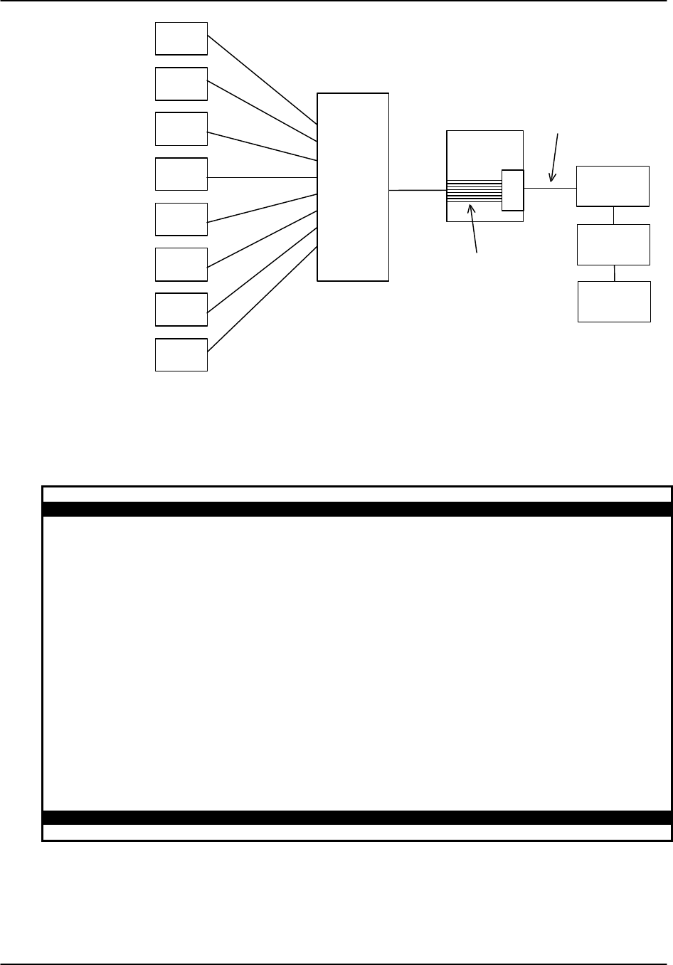
Reference Guide v3.6 CPU Card
(10-97) Page 3-A-9
Terminal Server
4Kbps TCP/IP
Single 38.4Kbps
Asynch SLIP Circuit
System #1
FDL Circuits
System #2
System #3
System #4
System #5
System #6
System #7
System #8
DACSII
T1/E1
LAN
Workstations
B
7
R
Up to 8 DS0s
Concentrator
Unit
Figure CPU-4. Typical TCP/IP Network Management System
Figure CPU-5 shows the TCP/IP screen. Table CPU-4 shows the TCP/IP screen
parameters and options.
Node_1 | C1 CPU XCON 8801 | Rev A2-0 Ser 01103 | 12-31-99 14:33
1
HOST IP STATUS stdby
HOST IP ADDR 0.0.0.0
HOST NETMASK 0.0.0.0
DEFAULT IP PORT n/a
DEFAULT IP SLOT n/a
DEFAULT IP UNIT n/a
RPT1 IP ADDR 0.0.0.0
RPT1 COMMUN STR
RPT2 IP ADDR 0.0.0.0
RPT2 COMMUN STR
RPT3 IP ADDR 0.0.0.0
RPT3 COMMUN STR
Ping | Netstat | rOute | Save | Undo | Refresh | Main
Figure CPU-5. TCP/IP Screen

CPU Card Reference Guide v3.6
Page 3-A-10 (10-97)
Table CPU-4. TCP/IP Screen Parameters and Options
PARAMETER User Options Notes Default
HOST IP STATUS stdby actv stdby
HOST IP ADDR IP address 0.0.0.0
HOST NETMASK IP address 0.0.0.0
DEFAULT IP PORT off local wan serv 1off
DEFAULT IP SLOT n/a 1n/a
DEFAULT IP UNIT n/a 1n/a
RPT1 IP ADDR IP address 0.0.0.0
RPT1 COMMUN STR blank
RPT2 IP ADDR IP address 0.0.0.0
RPT2 COMMUN STR blank
RPT3 IP ADDR IP address 0.0.0.0
RPT3 COMMUN STR blank
NOTES
1. The user options depend upon the selection in the Default IP Port selection. All user
options are explained below.
HOST IP STATUS
The Host IP Status is the IP address status for this specific integrated access controller.
HOST IP ADDR
The Host IP Address is the IP address for this specific integrated access controller. If
the B7R is used for this NMS, the Port IP address must be the same as the one entered
in the ADDR field of that card.
HOST NETMASK
The Host Netmask is used to indicate how much of the IP address is used for host
addressing and how much is used for network addressing. If the B7R card is used for
this NMS, this address must be the same as the one entered in the NETMSK field of
that card.
DEFAULT IP PORT
The Default IP Port setting tells the CPU card where IP packets will be sent or received.
The options are off (to disable Network Management System), local (information will
be sent over the DB-9 computer serial port to NMS equipment), wan (information will
be sent over the WAN FDL or a DS0 [chosen on the WAN card main screen with
ESF/NMS RPT option]), or serv (information sent over WAN DS0s through the
Ethernet connection to the NMS equipment).
If this parameter is set to local, wan or serv the Print Alarms feature (mentioned in the
previous section) must be set to off. If local is chosen for this setting, the internal
modem will not operate.

Reference Guide v3.6 CPU Card
(10-97) Page 3-A-11
DEFAULT IP SLOT
The Default IP Slot options are determined by the choice of Default IP Port. If off or
local is selected for that parameter, this option will show n/a. If wan is selected, the
options for this parameter will show W1-W4 (the WAN card slot that transmits and
receives NMS information). If serv is selected, the options for this parameter are P1-P3
(the Server card slot that transmits and receives NMS information).
DEFAULT IP UNIT
The Default IP Unit options are determined by the choice of Default IP Port. If off or
local is selected for that parameter, this option will show n/a. If wan or serv is selected
above, the options for this parameter will be 1-2 (corresponding with the WAN or
Server port).
RPT1 IP ADDR
The RPT1 IP Address is the IP address of the first Network Management System host
running a SNMP trap server.
RPT1 COMMUN STR
The RPT1 Community String holds the community string for the first NMS host
running a SNMP trap server. The community string provides additional security by
rejecting messages that do not contain the correct string. There must be some entry in
this field to enable RPT1.
RPT2 IP ADDR
The RPT2 IP Address is the IP address of the second Network Management System
host running an SNMP trap server.
RPT2 COMMUN STR
The RPT2 Community String holds the community string for the first NMS host
running an SNMP trap server. The community string provides additional security by
rejecting messages that do not contain the correct string. There must be some entry in
this field to enable RPT2.
RPT3 IP ADDR
The RPT3 IP Address is the IP address of the third Network Management System host
running an SNMP trap server.

CPU Card Reference Guide v3.6
Page 3-A-12 (10-97)
RPT3 COMMUN STR
The RPT3 Community String holds the community string for the first NMS host
running an SNMP trap server. The community string provides additional security by
rejecting messages that do not contain the correct string. There must be some entry in
this field to enable RPT3.
Menu of Actions
Table CPU-5 shows the Menu of Actions for the TCP/IP screen.
Table CPU-5. TCP/IP Screen Menu of Actions
Action Function
Ping Test to see if the connected device responds to an echo request message.
After entering the IP address of the host device, the status line will
display, "Testing . . ." The next message will tell if the host is alive or
down.
Netstat Displays the Network Statistics. See below.
rOute Shows the Routing screen. See Routing section below.
Save Saves changes to settings.
Undo Returns all settings to the last saved state.
Refresh Used on Testing and Monitoring screens to update statistics and on
other screens to redraw the screen.
Main Returns to the CPU card main screen. If changes are made to settings
and not saved, you will be prompted to save or lose changes.
Network Statistics
The Network Statistics screens provide maintenance and diagnostic information for the
different protocols supported by this equipment. Statistics begin to accumulate when
the TCP/IP Port is changed from off to local or wan and will continue to store
information until it is turned off. Figure CPU-6 shows the first of four network
statistics screens. Figures CPU-7 through -9 show the other three screens.

Reference Guide v3.6 CPU Card
(10-97) Page 3-A-13
Node_1 | C1 CPU XCON 8801 Rev C3-0 Ser 00202 | 12-31-99 14:33
NETSTAT Page 1 of 4
SLIP
MTU Size 240
Bytes Received 0
Packets Received 0
Packets Discarded 0
Packets Dropped - Buffer 0
Buffer Overflow 0
Packets Sent Out 0
Bytes Sent Out 0
FDL
MTU Size 240
Frames Received 0
Frames Aborted on Receive 0
Frames To Transmit from Above 0
Frames Transmitted 0
Frames Aborted on Transmit 0
pgUp | pgDn | Refresh | Main
Figure CPU-6. TCP/IP Network Statistics Screen
SLIP
The MTU (Maximum Transmission Unit) Size field shows the largest number of user-
data (e.g., the largest size of an packet) that can be sent in a single frame. The MTU for
this system is 210 with overhead = 240.
The Bytes Received field shows the number of bytes received by the local system from
the network host.
The Packets Received field shows the number of packets (unit of bytes, roughly similar
to an IP datagram) received by the local system from the network host.
The Packets Discarded field shows the number of packets sent by the network host that
were discarded by the local system. Packets are discarded because they either exceed
the MTU or are not complete.
The Packets Dropped - buffer field shows the number of incoming packets that were
dropped because there was not enough free memory to buffer them.
The Buffer Overflow field shows the occurrences of buffer overflow at the local system.
The Packets Sent Out field shows the number of packets transmitted by the local system
to the network host.
The Bytes Sent Out field shows the number of bytes transmitted to the network host by
the local system.

CPU Card Reference Guide v3.6
Page 3-A-14 (10-97)
FDL
The MTU (Maximum Transmission Unit) Size field shows the largest number of bytes
that can be sent in a single frame. The default MTU is 210 with overhead = 240.
The Frames Received field shows the number of frames received by the local system
from the network host.
The Frames Aborted on Receive field shows the number of frames that were aborted
when received by the local system from the network host. Frames are aborted because
they either exceed the MTU or are not complete.
The Frames to Transmit from Above field shows the number of frames that were sent
by the local system to the TCP layer of the network host.
The Frames Transmitted field shows the number of frames sent from the local system to
the network host.
The Frames Aborted on Transmit field shows the number of frames aborted when
transmitted by the local system to the network host. Frames are aborted because they
either exceed the MTU or are not complete.
Node_1 | C1 CPU XCON 8801 Rev C3-0 Ser 00202 | 12-31-99 14:33
NETSTAT Page 2 of 4
IP
Default TTL 255
Datagrams Received 0
Datagrams Discarded 0
Datagrams Delivered Above 0
Datagrams From Above 0
Datagrams Sent 0
TX Wait for RAM 0
TX Aborted - mailbox short 0
ICMP
Messages Received 0
Messages Discarded 0
Messages Sent 0
Echo Requests Received 0
Echo Replies Sent 0
Echo Requests Sent 0
Echo Replies Received 0
Dest Unreachable Sent 0
pgUp | pgDn | Refresh | Main
Figure CPU-7. TCP/IP Network Statistics Screen
IP
The Default TTL field shows the Time To Live for information packets from
transmission to delivery. The TTL for this system is 255 seconds.
The Datagrams Received field shows the number of IP datagrams (packets) received by
the local system from the network host.

Reference Guide v3.6 CPU Card
(10-97) Page 3-A-15
The Datagrams Discarded - checksum field shows the number of datagrams that were
discarded by the local system.
The Datagrams Discarded - protocol field shows the number of IP datagrams that were
discarded by the local system because the protocol used is not supported. The
supported transmit protocols are IP, ICMP, TCP and UDP. The supported receive
protocols are IP and TCP.
The Datagrams Delivered Above field shows the number of datagrams sent to the TCP
layer of the network host to the local system.
The Datagrams From Above field shows the number of information or traps sent by the
local system to the UDP or TCP layer of the network host.
The Datagrams Sent field shows the total number of datagrams sent by the local system
to the network host.
The TX Waits for RAM field shows the total number of datagrams sent by the local
system which were delayed by lack of free RAM memory.
The TX Aborted - mailbox short field shows the total number of datagrams aborted by
the local system because of a mail subsystem overflow.
ICMP
The Messages Received field shows the number of ICMP messages received by the
local system from the network host.
The Messages Discarded field shows the number of ICMP messages by the network
host that were discarded (for any reason) by the local system.
The Messages Sent field shows the number of ICMP messages sent by the local system
to the network host.
The Echo Requests Received field shows the number of "ping" message requests
received by local system by the network host. This figure is part of the total messages
received.
The Echo Replies Sent field shows the number of "ping" message requests transmitted
to the network host. This figure is part of the total messages sent.
The Echo Requests Sent field shows the number of "ping" requests sent to the network
host by the local system. This figure is part of the total messages sent.
The Echo Replies Received field shows the number of "ping" message replies received
by the local system. This figure is part of the total messages received.
The Destination Unreachable Sent field shows the number of ICMP messages that were
discarded upon receipt by the network host because they were improperly addressed.

CPU Card Reference Guide v3.6
Page 3-A-16 (10-97)
Node_1 | C1 CPU XCON 8801 Rev C3-0 Ser 00202 | 12-31-99 14:33
NETSTAT Page 3 of 4
TCP State = LISTEN
Packets Received 0
Packets Discarded - Checksum 0
Packets Discarded - Port 0
Packets Discarded - Window 0
Bytes Delivered Above 0
Bytes From Above 0
Packets Sent 0
ACKs Received 0
Packets Sent - reset 0
Packets Sent - ACK 0
Packets Retransmitted 0
RTT Increased 0
RTT Decreased 0
Connections Opened 0
Connections Closed 0
Connections Aborted 0
Packets Tx Aborted - RAM 0
pgUp | pgDn | Refresh | Main
Figure CPU-8. TCP/IP Network Statistics Screen
TCP
Transmission Control Protocol is a transport layer, connection-oriented, end-to-end
protocol. It provides reliable, sequenced, and unduplicated delivery of bytes to a
remote or local user. TCP provides reliable byte stream communication between pairs
of processes in hosts attached to interconnect networks.
The Packets Received field shows the number of TCP packets received by the local
system from the network host.
The Packets Discarded - Checksum field shows the number of TCP packets that were
discarded by the local system because the checksum failed.
The Packets Discarded - Port field shows the number of TCP packets that were
discarded by the local system because the port assignment was incorrect.
The Packets Discarded - Window field shows the number of TCP packets that were
discarded by the local system because the window data was incorrect.
The Bytes Delivered Above field shows the number of information or traps sent from
TCP layer of the network host to the local system.
The Bytes From Above field shows the number of information or traps sent to the TCP
layer of the network host from the local system.
The Packets Sent field shows the total number of TCP packets that were transmitted to
the network host by the local system.

Reference Guide v3.6 CPU Card
(10-97) Page 3-A-17
The ACKs Received field shows the total number of acknowledgments that were
received by the local system from the network host.
The Packets Sent - reset field shows the total number of TCP packets that were
transmitted by the network host to the local system.
The Packets Sent - ACK field shows the total number of TCP acknowledgment packets
that were transmitted by the network host to the local system.
The Packets Retransmitted field shows the total number of TCP packets that were
retransmitted by the local system to the network host.
The RTT Increased field shows the number of times the retransmission time-out was
increased because the system was busy.
The RTT Decreased field shows the number of times the retransmission time-out was
decreased because the system was not busy.
The Connections Opened field shows the total number of connections that were opened
by the local system to the network host.
The Connections Closed field shows the total number of connections that were closed
by the local system to the network host.
The Connections Aborted field shows the number of times the connection was aborted
because either the number of consecutive retransmission’s was equal to 10 or
retransmission time-out was equal to 15 minutes.
The Packets TX Aborted - RAM field shows the total number of packets sent by the
local system which were aborted because of the lack of free RAM memory.
Node_1 | C1 CPU XCON 8801 Rev C3-0 Ser 00202 | 12-31-99 14:33
NETSTAT Page 4 of 4
UDP
Packets From Above 0
Packets Sent 0
TELNET
Bytes Received 0
Bytes Received as Commands 0
Bytes Delivered Above 0
Bytes Replied as Commands 0
Bytes From Above 0
Bytes Sent 0
Sessions Opened 0
Sessions Closed 0
TX Wait for Buffer 0
SNMP
PDUs Sent 0
Traps Sent 0
pgUp | pgDn | Refresh | Main
Figure CPU-9. TCP/IP Network Statistics Screen

CPU Card Reference Guide v3.6
Page 3-A-18 (10-97)
UDP
User Datagram Protocol is a transport layer, connectionless mode protocol, providing a
datagram mode of communication for delivery of packets to a remote or local user.
The Packets From Above field shows the number of UDP packets sent by the local
system to the network host.
The Packets Sent field shows the number of UDP packets transmitted from the local
system to the network host.
TELNET
The Bytes Received field shows the total number of bytes that were received by the
local system from the network host.
The Bytes Received as Commands field shows the total number of bytes that were
received as commands by the local network from the network host.
The Bytes Delivered Above field shows the total number of bytes that were transmitted
by the network host to the local system.
The Bytes Replied as Commands field shows the total number of bytes that were
transmitted as commands by the local system to the network host.
The Bytes From Above field shows the total number of bytes that were received by the
network host from the local system.
The Bytes Sent field shows the total number of bytes that were transmitted by the local
system to the network host.
The Sessions Opened field shows the total number of sessions that were opened by the
local system with the network host.
The Sessions Closed field shows the total number of sessions that were closed by the
local system with the network host.
The TX Wait for Buffer field shows the total number of transmissions that were delayed
by the local system for free memory in the buffer.
SNMP
The PDUs Sent field shows the number of Protocol Data Units sent from the local
system. A Protocol Data Unit is a data object exchanged by protocol machines, usually
containing both protocol control information and user data.
The Traps Sent field shows the total number of SNMP traps that were transmitted by
the local system to the network host.

Reference Guide v3.6 CPU Card
(10-97) Page 3-A-19
Menu of Actions
Table CPU-6 shows the Menu of Actions for the Network Statistics screen.
Table CPU-6. Network Statistics Screen Menu of Actions
Action Function
pgUpScrolls forward through network statistics one page at a time.
pgDnScrolls backward through network statistics one page at a time.
Refresh Since the system does not update statistics automatically, the Refresh
command must be used to update information in statistics fields.
Main Returns to the CPU card IP screen. If changes are made to settings and
not saved, you will be prompted to save or lose changes.
Routing
The system supports multi-point routing of Internet Protocol (IP) packets to either a
local Network Management System over the computer port or to a remote NMS over
the B7R card, timeslot #24 or the Facilities Data Link (FDL) of a T1 link. (For E1 links,
the information is sent on the B7R card, timeslot #31 or the SA4.)
If you want to use an entire timeslot (either 24 or 31) for remote NMS routing, no
action needs to be taken. If a B7R card is used or you want to use the FDL or SA4, an
additional selection must be made on the WAN card. For T1 links the selection is made
on the ESF/NMS RP parameter and on E1 links it is made on the COM/NMS RP
parameter. (See the WAN card and B7R card chapters for further information.)
All packets arriving on any of the optional paths or the local port will be treated by the
IP stack as follows:
• If the packet's destination address matches that system's address, the packet is
processed locally.
• If the address is not the same, the unit will search the routing table to find a remote
address that matches the destination of the packet.
• If a match is not found for the packet, it is routed to the interface specified in the
DEF DEST field. If the default destination matches the interface the packet arrived
from, the packet is dropped.
All IP addresses between the Remote Start and Remote End addresses must go to the
same WAN link. If you are unclear about IP Addresses, please consult with your
Network Administrator.
Figure CPU-10 shows a typical routing application. Even though 24 integrated access
controllers are used in this example, the number of remote units is virtually unlimited
except for bandwidth and link-down considerations.
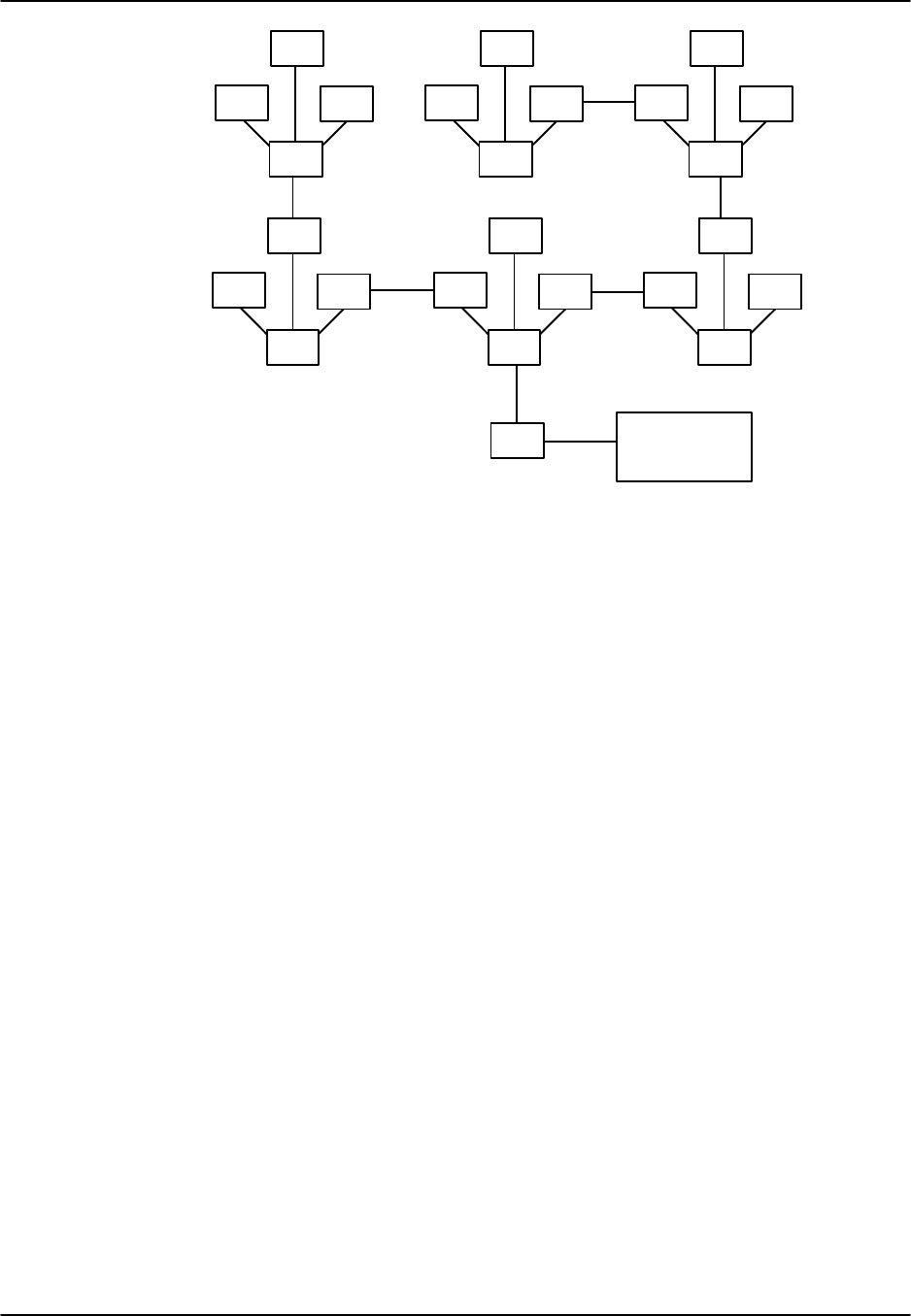
CPU Card Reference Guide v3.6
Page 3-A-20 (10-97)
S2
S4
S3
S1
S6
S8
S7
S5
S10
S9
S11
S12
S14
S13
S15
S16
S18
S17
S19
S20
S22
S21
S23
S24
Comm Serv
S25
Figure CPU-10. Routing Feature Diagram
In the diagram above, 24 integrated access controllers will transmit alarm information
to an IP routing Controller (System 25) by the optional paths of separate WAN links.
The network administrator assigns IP addresses for each system on the TCP/IP screen of
each unit's interface card (PORT IP ADDR). System 20 is connected by any of the
optional paths to System 25 which supports NMS equipment (the communications
server) by either a local SLIP connection directly from the CPU card or any of the
optional paths of a WAN link. In this example, all alarms received by any of the 24
Controllers will be forwarded to Controller 25 on a single WAN link.
Each of the 24 reporting units use System 25's IP address as the RPT1 IP ADDR on the
TCP/IP screen of its interface card. First routing is initiated by the off/on command for
each sub-unit. The IP address for REM STRT is the lowest IP address of the sub-units
controlled by that port. The IP address for REM END is the highest IP address of the
sub-units controlled by that port. The local port is included to be able to transmit the IP
packets generated by the routing unit to the same destination. In most cases, the DEF
DEST of all units controlled by this router will be the same place (either the local port
or optional WAN paths to a distant location).
The column headings are associated with the incoming WAN link associated with the
IP location of the remote systems. For example, if you expect incoming information
from system #1 on WAN 1-1, you would assign the IP address for system #1 between
the REM STRT and REM END for WAN 1-1.
Figure CPU-11 shows the Routing screen and Table CPU-6 lists the options for that
screen.

Reference Guide v3.6 CPU Card
(10-97) Page 3-A-21
Node_1 | C1 CPU XCON 8802 Rev C3-0 Ser 00672 | 12-31-99 14:33
page: 1 of 1 IP STATIC ROUTING
IP Net SubNetMask SLOT/UNIT
Save | Refresh | Add | dEl | Get | pgUp | pgDn | Main |
Figure CPU-11. Routing Screen
Table CPU-6. Settings for Routing Parameters
Parameter User Options Default
IP NET a valid SubNet or Gateway address ip
SUBNETMASK a valid Netmask IP address ip
SLOT/UNIT wan: W1-1 through W2-4
serv: P1-P3
user: not supported
local: COMP
w1-1
IP NET
The IP Net field shows a valid SubNet or Gateway address of a device located on this
system unit.
SubNetMask
The Remote Netmask field shows the Netmask of a device located remotely from this
system. Any valid Netmask is acceptable. The remote netmask information is the same
as that placed on the remote unit's TCP/IP screen.
Slot/Unit
The Default Destination specifies where to route packets received from a remote device
and the routing device to downstream NMS equipment (either the optional paths of a
WAN link or the local SLIP port).

CPU Card Reference Guide v3.6
Page 3-A-22 (10-97)
Menu of Actions
Table CPU-7. Routing Screen Menu of Actions
Action Function
Save Saves changes to settings.
Refresh Used on Testing and Monitoring screens to update statistics and on
other screens to redraw the screen.
Add Open the data entry screen to add a route
dEl Delete a route
Get Get information on routing destinations
PgUpGo to a previous page of routing paths
PgDnGo to the next page of routing paths
Main Returns to the CPU card main screen. If changes are made to settings
and not saved, you will be prompted to save or lose changes.
Adding Routes
In the Routing Screen, type a (Add) to present a data entry screen. A data line appears
near the bottom of the screen for the four address parameters of Table CPU-6. Use the
right/left arrow keys to scroll to the desired field. Press <Enter> to present the
corresponding data entry field (Figure CPU-11). Type in the correct address
parameters, up to three digits (0-255) in each segment of the address, using the right
arrow key to move to the next segment. Press <Enter> again to move the entered
address into the data line. Use the left/right arrow keys to move on to the next address
to be entered and repeat the process. The Slot/Unit field offers the entry categories
shown in Figure CPU-12. Scroll to the desired category and press<Enter> to present
one of the choices shown in Table CPU-6. Scroll to the desired value and press
<Enter>. When valid address and destination parameters have been added, type s to
save the address. The system will not save an invalid address. To exit the Add screen
without saving press the up or down arrow key.
Delete a Route
In the Routing Screen, scroll to the route to be deleted. With the route highlighted,
press e to delete.
Get Information
To obtain addressing information, press g for Get. The system displays the destination
variables wan, serv, user, and local across the bottom of the screen. Use the left/right
arrow keys to scroll to the desired destination and press <Enter> to select. The choices
available under each of these options are then displayed. Now highlight the desired
option and press <Enter> again to initiate the search. The system responds:
Sending RIP Request. Please wait ...
Press any key to cancel
After the system sends RIP request, the IP Static Routing screen will return, displaying
valid IP Net (address), SubNetMask, and Slot/Unit information.

Reference Guide v3.6 CPU Card
(10-97) Page 3-A-23
Node_1 | C1 CPU XCON 8802 Rev C3-0 Ser 00672 | 12-31-99 14:33
page: 1 of 1 IP STATIC ROUTING
IP Net SubNetMask SLOT/UNIT
0.0.0.0 0.0.0.0 w1-1
Save
Figure CPU-12. Routing Address Entry
Node_1 | C1 CPU XCON 8802 Rev C3-0 Ser 00672 | 12-31-99 14:33
page: 1 of 1 IP STATIC ROUTING
IP Net SubNetMask SLOT/UNIT
0.0.0.0 0.0.0.0 w1-1
wan serv user local
Save
Figure CPU-13. Slot/Unit Options

CPU Card Reference Guide v3.6
Page 3-A-24 (10-97)
Table CPU-8. Slot Unit Options
Slot/Unit Options Description Default
WAN w1-1 through w4-2 w1-1
SERV P1 through P3 P1
USER not supported
LOCAL

Reference Guide v3.6 ADPCM Card
(10-97) Page 4-A-1
Introduction
The 8871 ADPCM card is a plug-in resource card for the system. The card has 32 pairs
of voice compression engines that accept input directly from voice, SRU or BRI cards
in the same system unit or voice traffic on WAN links through the system. ADPCM
cards require a matching card at the other end to decompress the voice channels to
normal 64K operation. Except for SRU which uses h link to extract data from timeslot.
Each pair of compression engines utilize one 64Kbps DS0 for two compressed
channels. In Figure ADPCM-1 the eight numbers at the top of the screen represent the
first four pairs of compression engines. Each engine can compress 64Kbps voice traffic
to either 24Kbps, 32Kbps or 40Kbps (depending upon compression quality needed).
The rate of any DS0 is 64Kbps, so the sum of the compression rates for engine #1 and
#2 must equal that figure. If, for instance, you assign a 32Kbps circuit to engine #1,
engine #2 can only accept a 32Kbps circuit. A 40Kbps circuit can only be paired with a
24Kbps circuit and vice-versa.
The compression engines work in pairs. Engine numbers 1 and 2, 3 and 4, 5 and 6, 7
and 8, are paired. Each member of the pair must have the same ADPCM WAN and
ADPCM TS. Additionally, both members of the compression engine pair must be active
before either port will operate.
The ADPCM card can compress low speed asynchronous data transmission (19.2Kbps
or less) from an SRU port that will occupy a 24Kbps engine. Each data circuit must be
paired with a 40Kbps voice channel. It can also compress B channel voice traffic from
the BRI card without restriction of compression rates.
Each unit can have up to three ADPCM cards installed (two normal ADPCM cards and
one redundant card). See the Redundant Operations chapter for further information
about redundant ADPCM cards.
The ADPCM card supports Transition Signaling as defined by ANSI T1.302-1989 with
the exception of the Alarm bits. ANSI T1.302 specifies signaling at the 32Kbps
compression rate. The ADPCM card uses this scheme for 24Kbps and 40Kbps although
it is not included in the standard. Table ADPCM-1 summarizes the signals supported by
each transcoder data rate. User channel configuration must adhere to these
specifications.
Table ADPCM-1. Signal Compression Rates
Transcoder
Rate Voice
Quality
(MOS)*
Modem Data DTMF FAX
24Kbps 3.6-3.8 Range no under study no
32Kbps 4.0-4.3 Range up to 4.8 Kbps
V.32 9.6 Kbps
OK Group II
40Kbps 4.0-4.3 Range up to 12 Kbps
V.32 14.4 (tbd)
OK Group III
* MOS - Mean Opinion Score based upon subjective evaluation

ADPCM Card Reference Guide v3.6
Page 4-A-2(10-97)
ADPCM Card Settings
Figure ADPCM-1 shows the ADPCM screen. Table ADPCM-2 lists the settings
controlled on this screen along with their possible and default values.
Node_1 | P1 ADPCM-64x1 8871 Rev D0-0 Ser 00259 | 12-31-99 14:33
Version #:0.1 1 2 3 4 5 6 7 8
STATE stdby stdby stdby stdby stdby stdby stdby stdby
USER n/a n/a n/a n/a n/a n/a n/a n/a
WAN/SERV none none none none none none none none
TS n/a n/a n/a n/a n/a n/a n/a n/a
ADPCM W/S none none none none none none none none
ADPCM TS n/a n/a n/a n/a n/a n/a n/a n/a
TYPE v&s v&s v&s v&s v&s v&s v&s v&s
RATE 24K 24K 24K 24K 24K 24K 24K 24K
SIG MODE e&m e&m e&m e&m e&m e&m e&m e&m
CODING u-law u-law u-law u-law u-law u-law u-law u-law
TC CGA idle idle idle idle idle idle idle idle
Save | Save | Undo | Refresh | < | > | sWitch | Main
Figure ADPCM-1. The ADPCM Card Screen
Table ADPCM-2. ADPCM Card Setting Options and Defaults
Parameter User Options Default
STATE stdby actv rdnt stdby
USER n/a uX-1 through uX-8 n/a
WAN/SERV none w1-1 through w4-2 MORE
BACK P1 P2 P3 w1-1
TS n/a 01-24 01-31 01
ADPCM W/S w1-1 w1-2 w2-1 w2-2 w3-1 w3-2 w4-1 w4-2 w1-1
ADPCM TS n/a 01-24 01-31 01
TYPE v&s v trnsp v&s
RATE 24K 32K 40K 24K
SIG MODE n/a e&m fxs plar fxo e&m
CODING u-law a-inv u-law
TC CGA idle busy idle
STATE
The State setting determines whether the port is active or inactive. When assigning
ADPCM engine pairs for WAN traffic, set the State setting to stdby (standby) for ports
you are not using or have not yet configured. Set it to actv (active) for ports that are
ready for use.

Reference Guide v3.6 ADPCM Card
(10-97) Page 4-A-3
Setting the State to rdnt (redundant) for any port on an unused card will cause that card
to act as the redundant back-up for all of the other ADPCM cards in that unit. Once a
card is designated as a redundant ADPCM card the only way it can be used for regular
ADPCM traffic is to change the state of the selected port back to either actv or stdby .
When assigning ADPCM engine pairs from user cards, changing the port from stdby to
actv and saving the selection information on the user card screen will cause the system
to automatically assign an ADPCM engine.
When the engine is assigned from a user card, no changes can be made from the
ADPCM card screen to any of the fields.
USER
The User setting identifies the User card and port connected to this engine. This is the
place where the ADPCM card will expect incoming (not compressed) voice, sub-rate
data or B channel traffic. If assigned from a voice card, SRU or BRI card port, this
selection will show the user slot and port number (i.e. u5-2 for the card in slot U5, port
#2). If you are assigning a WAN timeslot, this setting will show n/a.
WAN/SERV
The WAN/SERV setting identifies the incoming WAN or server link connected to this
engine. This is the place where the ADPCM card will expect incoming (not
compressed) voice. This option shows the choices: none, w1-1through w4-2 and MORE
on the first line of choices. If you select MORE it offers the choices of P1, P2, or P3.
Choose none if you are assigning from a voice card or SRU card port; choose from w1-
1 - w2-4 if assigning from a WAN card, and P1-P3, if assigning from a server card.
TS
The Timeslot parameter selects the specific timeslot on the WAN link chosen in the
previous setting that the ADPCM card can expect incoming voice traffic. The options
are determined by the equipment on the WAN link selected in the previous setting. If
WAN 1-1 is equipped with either a CSU or DSX module, the options are 1-24. If a
CEPT module is installed on that link, the options are 1-15 and 17-31 . If you are
assigning from a voice card, SRU card or BRI card port, this setting will show n/a.
ADPCM W/S
The ADPCM W/S setting identifies the outgoing WAN link to which the engine is
connected. This option shows the choices: none, w1-1through w4-2. If you are
assigning either from a voice card, SRU or BRI card port or voice traffic from a WAN
timeslot, this setting will show w1-1 through w4-2. This is the WAN link to which the
ADPCM card will route outgoing (compressed) traffic.
ADPCM TS
The ADPCM Timeslot parameter selects the specific timeslot on the WAN link chosen
in the previous setting that the ADPCM card will send outgoing compressed traffic. The
options are determined by the equipment on the WAN link selected in the previous
setting. If WAN 1-1 is equipped with either a CSU or DSX module, the options are 1-
24. If a CEPT module is installed on that link, the options are 1-15 and 17-31 .

ADPCM Card Reference Guide v3.6
Page 4-A-4(10-97)
TYPE
The Type parameter identifies the voice and signaling requirements for the incoming
circuit. The options are v (voice), v&s voice and (signaling) and trnsp (transparent).
The v setting is used when the input to the ADPCM channel is a 64Kbps channel and
inband signaling is not required. The v&s setting is used when the input to the ADPCM
channel is a 64Kbps voice channel and the ADPCM card must provide inband
signaling.
The trnsp setting allows the user to map the output of SRU ports to the ADPCM
channel. Sub-Rate Data will be clocked into the ADPCM channel at an input rate equal
to 24Kbps and then passed transparently (non-compressed) through the ADPCM card to
the appropriate WAN timeslot. This could be useful when the user has an odd number
of voice channels and wants to utilize the empty engine pair of the last ADPCM
channel.
B channel traffic from the BRI card also uses the trnsp Type setting but is not restricted
in its compression rates.
If the engine is assigned from a voice card, this selection will show v&s. If assigned by
an SRU or BRI card, it will show trnsp . It cannot be changed from this screen.
RATE
The Rate parameter identifies the compression requirements for the incoming circuit.
The options are 24K, 32K and 40K (the pair of engines must be equal to 64Kbps).
If this engine is assigned from a user card port, the selection will show the value that
was chosen on that port. It cannot be changed from this screen.
SIG MODE
The Signal Mode parameter identifies the type of signaling required for the incoming
circuit. If v&s was chosen in the Type setting, the options are e&m, fxs, plar and fxo. If
v or trnsp were chosen in the Type setting, the only option is n/a.
If this engine is assigned from a user card, the selections are uX-1 through uX-8. The
default is n/a.
CODING
The Coding parameter identifies the PCM format required for the incoming circuit. The
choices are u-law or a-inv .
If this engine is assigned from a voice or BRI card, this selection will show the value
that was selected for that port. If this engine is assigned from an SRU card, this
selection will show u-law . It cannot be changed from this screen.

Reference Guide v3.6 ADPCM Card
(10-97) Page 4-A-5
TC CGA
The Trunk Conditioning CGA parameter identifies the type of trunk conditioning
required for the incoming circuit. If v&s were chosen in the Type setting, the options
are idle or busy. If trnsp or v was chosen in the Type setting, the only option is n/a.
If this engine is assigned from a voice card, this selection will show the value that was
selected on the voice card port. If assigned from an SRU or BRI card port, the field will
show n/a. It cannot be changed from this screen.
Menu of Actions
Table ADPCM-3 shows the Menu of Actions for the ADPCM Card.
Table ADPCM-3. The ADPCM Card Screen Menu of Actions
Action Function
Save Saves changes to settings.
Undo Returns all settings to the last saved state.
Refresh Updates certain time-related information fields that are not
automatically updated (i.e. performance and test data).
<Scroll to the left
>Scroll to the right
sWitch Switches an active ADPCM card to its redundant mate.
Main Returns to the main screen. If changes are made to settings and not
saved, you will be prompted to save or lose changes.

ADPCM Card Reference Guide v3.6
Page 4-A-6(10-97)

Reference Guide v3.6 WAN Card
(10-97) Page 5-A-1
Introduction
This section discusses the WAN cards and the plug-in modules that define their
communications functions. It covers physical configuration of the plug-in modules and
their installation as well as the software configuration, monitoring and testing of the
cards after installation.
WAN cards manage the flow of data through your network. They are also the point of
T1/E1 termination and generate or receive clocking. Both CSU and DSX modules are
used to connect to T1 facilities operating at 1.544 Mbps. The CEPT module is used
internationally for connection to a 2.048 Mbps E1 facility.
WAN cards equipped with CSU or DSX modules will also act as the "near end"
termination point for Subscriber Loop Carrier (SLC96) facilities as outlined in
publication TR-TSY-000008, Issue 2, August 1987.
Additional information about WAN card functions is included in the Installation
chapter, System Operations chapter and Redundancy chapter.
811 DSX/CEPT Plug-in Module
The DSX/CEPT plug-in module supports either DSX or CEPT modes. It is mounted on
the WAN Card. DSX is a T1 operation and CEPT is an E1 operation. Jumper settings
on the module specify DSX or CEPT operation. Information about installing the
module and changing jumper settings is included in this chapter.
812 CSU Plug-in Module
The CSU plug-in module is required for Channel Service Unit (CSU) operation in a T1
environment. Like the 811, it is mounted on the WAN Card.
820 HDSL E1 Plug-in Module
The HDSL E1(High-bit-rate Digital Subscriber Line) module is a plug-in for the 8011
HDSL E1 WAN card. It provides transport for E1 rate (2.048 mbps) data over copper
cable without mid-span repeaters or conditioning.
8000 Single T1/E1 Link Card
The single T1/E1 Link Card is the basic WAN Card. It has a single port for DSX/CEPT
or CSU operation.
8010 Dual T1/E1 Link Card
The dual T1/E1 Link Card has two ports for either DSX/CEPT or CSU operation or a
combination of the two. The Dual T1/E1 Link Card will work with only one plug-in
module as long as the WAN port without the plug-in module remains in the standby
state. However, a CGA_RED alarm will be generated for that port.

WAN Card Reference Guide v3.6
Page 5-A-2(10-97)
8014 Dual T1/E1 Link Card (with Relays)
In Cross-Connect systems, the dual T1/E1 Link Card (with relays), when placed in slot
W-4, acts as a redundant card for up to three standard WAN Cards located in slots W-1,
W-2 and W-3. This is known as 1xN redundancy. The relay module on this card will
switch its output to the correct pins on the WAN connector on the Interface Card. If
placed in any other slot, it will behave like an ordinary WAN card.
Note: If the plug-ins of the Model 8014 installed in slot w4 do not match those of a
WAN card in slot w1, w2 or w3, then it cannot act as that card’s redundant mate.
8011 HDSL E1 WAN Card
The 8011 HDSL E1 WAN Card is a dual-port card that provides HDSL services by
incorporating the 820 HDSL E1 plug-in module.
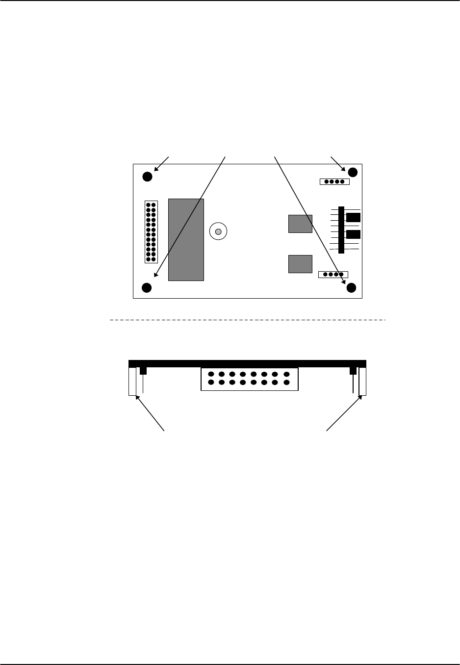
Reference Guide v3.6WAN Card
(10-97) Page 5-A-3
811 WAN Module
When installing the 811 CSU/DSX module on the 8000 WAN or 8010 WAN, there are
situations in which the plastic standoffs do not allow the module to seat correctly on the
WAN board (see Figure WAN-1).
TOP VIEW
HOLES for Plastic Standoffs
Side View
Remove all plastic standoffs
Figure WAN-1. Removal of Plastic Standoffs - 811 WAN Module
When assembling and installing the module on the WAN card, it is our advice that the
plastic standoffs be removed to eliminate the possibility of errors on the associated
T1 or E1 lines. For this reason, the plastic standoffs are no longer being supplied by
the manufacturer for new WAN modules.
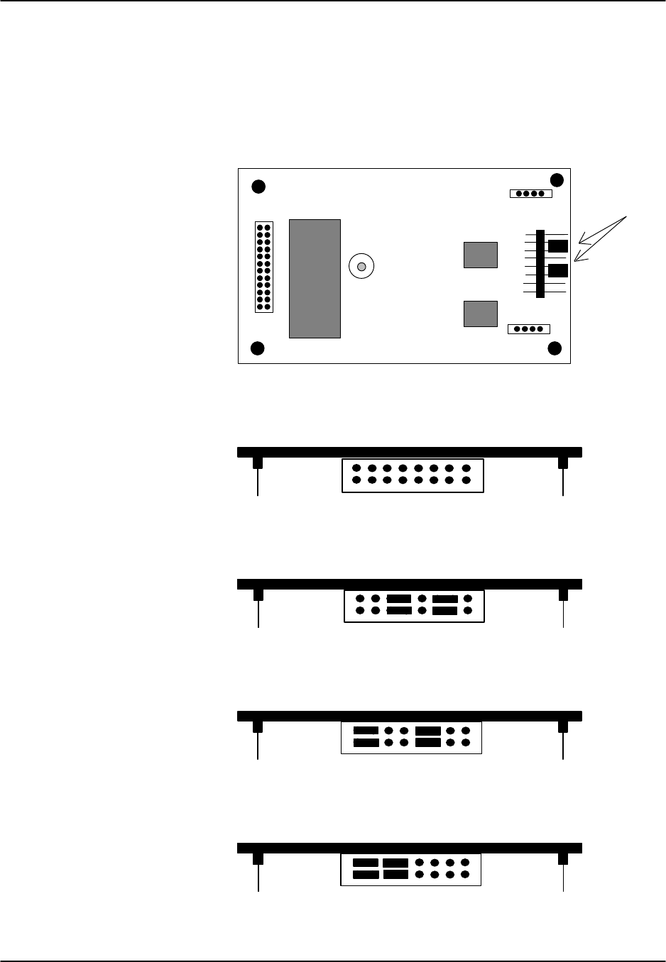
WAN Card Reference Guide v3.6
Page 5-A-4(10-97)
Configuring the DSX/CEPT Plug-in Module (811) Rev E1+
The Model 811 DSX/CEPT Revision E1+ plug-in module (see Figure WAN-2 and
WAN-3) provides jumper settings for impedance compensation. The 811 offers either
T1 or E1 (75Ω or 120Ω operation). To configure the 811, change the jumper positions
on the pins according to Figures WAN-4 through WAN-6. The unit is shipped as
shown in Figure WAN-4.
Jumpers
Figure WAN-2. 811 DSX/CEPT Module (Top View)
Figure WAN-3. 811 DSX/CEPT Module (End View)
Figure WAN-4. Jumper Settings for T1 Operation
Figure WAN-5. Jumper Settings for E1 (75Ω75Ω)
Figure WAN-6. Jumper Settings for E1 (120Ω120Ω)
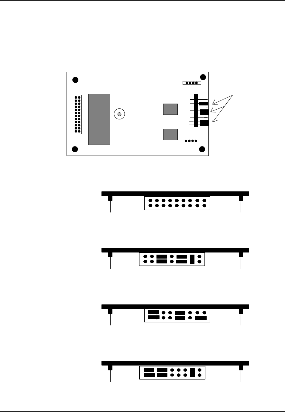
Reference Guide v3.6WAN Card
(10-97) Page 5-A-5
Configuring the DSX/CEPT Plug-in Module (811) Rev A1-D1
The Model 811 DSX/CEPT Revision A1-D1 plug-in module (see Figure WAN-7 and
WAN-8) provides jumper settings for impedance compensation. The 811 offers either
T1 or E1 (75Ω or 120Ω operation). To configure the 811, change the jumper positions
on the pins according to Figures WAN-9 through WAN-11. The unit is shipped as
shown in Figure WAN-9.
Jumpers
Figure WAN-7. 811 DSX/CEPT Module (Top View)
Figure WAN-8. 811 DSX/CEPT Module (End View)
Figure WAN-9. Jumper Settings for T1 Operation
Figure WAN-10. Jumper Settings for E1 (75Ω75Ω)
Figure WAN-11. Jumper Settings for E1 (120Ω120Ω)

WAN Card Reference Guide v3.6
Page 5-A-6(10-97)
Configuring the DSX/CEPT Plug-in Module 811-F
Jumpers
set to
E1-75
811-F
Figure WAN-12. 811 DSX/CEPT Module (Top View)
The DSX/CEPT 811-F module is shown above in Figure WAN-12. This module may
be optioned for T1, E1/120 Ohms or E1/75 Ohms. The specific jumper option
configuration is shown on the card itself. The jumpers shown on this graphic are set to
E1/75 Ohms.
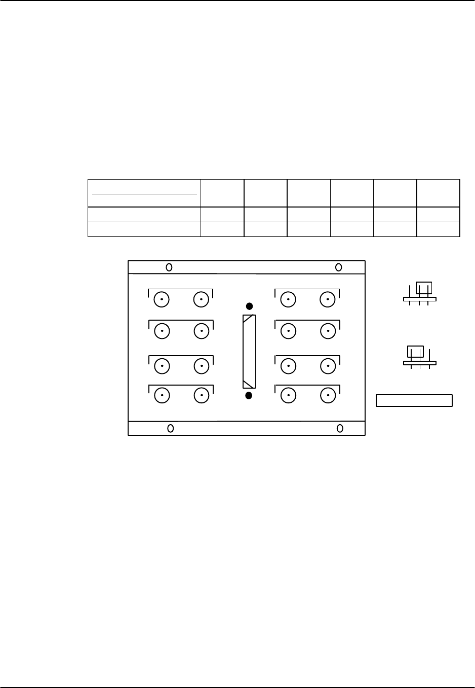
Reference Guide v3.6WAN Card
(10-97) Page 5-A-7
Setting Jumpers for Balanced/Unbalanced E1 Operation
E1 links can be set either to be balanced or unbalanced by setting jumpers on the
DSX/CEPT Plug-in Module (811) or the 1183 external distribution panel, or both. (See
Table WAN-1 for information on which revisions of the DSX/CEPT Plug-in Module
have jumpers.) The 1183 and 118320 connector block mounts in place of the cover on
the 8916 and 891620 front-loading chassis (see Figure WAN-13) and connects to the
Interface Card via a 50-pin cable. Each BNC connector has its own jumper. The 1184
connector block mounts on the 8918xx chassis.
Table WAN-1.
Selectability of Bal/Unbal jumpers on the DSX/CEPT module (by revision)
Revision ØØ
ÚÚ DSX/CEPT Module ABC D EF
811 Yes Yes n/a Yes No No
81120 No No n/a n/a n/a n/a
10193
UNBAL BAL
RX
Options on the Rear
UNBAL BAL
RX
Rx TX
Rx TX
Rx TX
Rx TX
Rx
TX
Rx
TX
Rx
TX
Rx
TX
Figure WAN-13. 1183 E1 Interface Adapter
Balanced Operation
For balanced E1 operation, the jumpers on both the 1183 panel and each DSX/CEPT
Plug-in Module should be set to "balanced" prior to installation.
Unbalanced Operation
For unbalanced E1 operation, the jumpers should be set to "unbalanced" in one location
only, and set to "balanced" in all other cases. When multiple cards with jumpers are
installed, the unbalanced jumper should be set on the card nearest the E1 line.
When the 1183 or 1184 panel is present, it is considered nearest to the E1 line, and the
corresponding jumper on the rear of the panel would be set to "unbalanced" while all
other module jumpers would be set to "balanced."
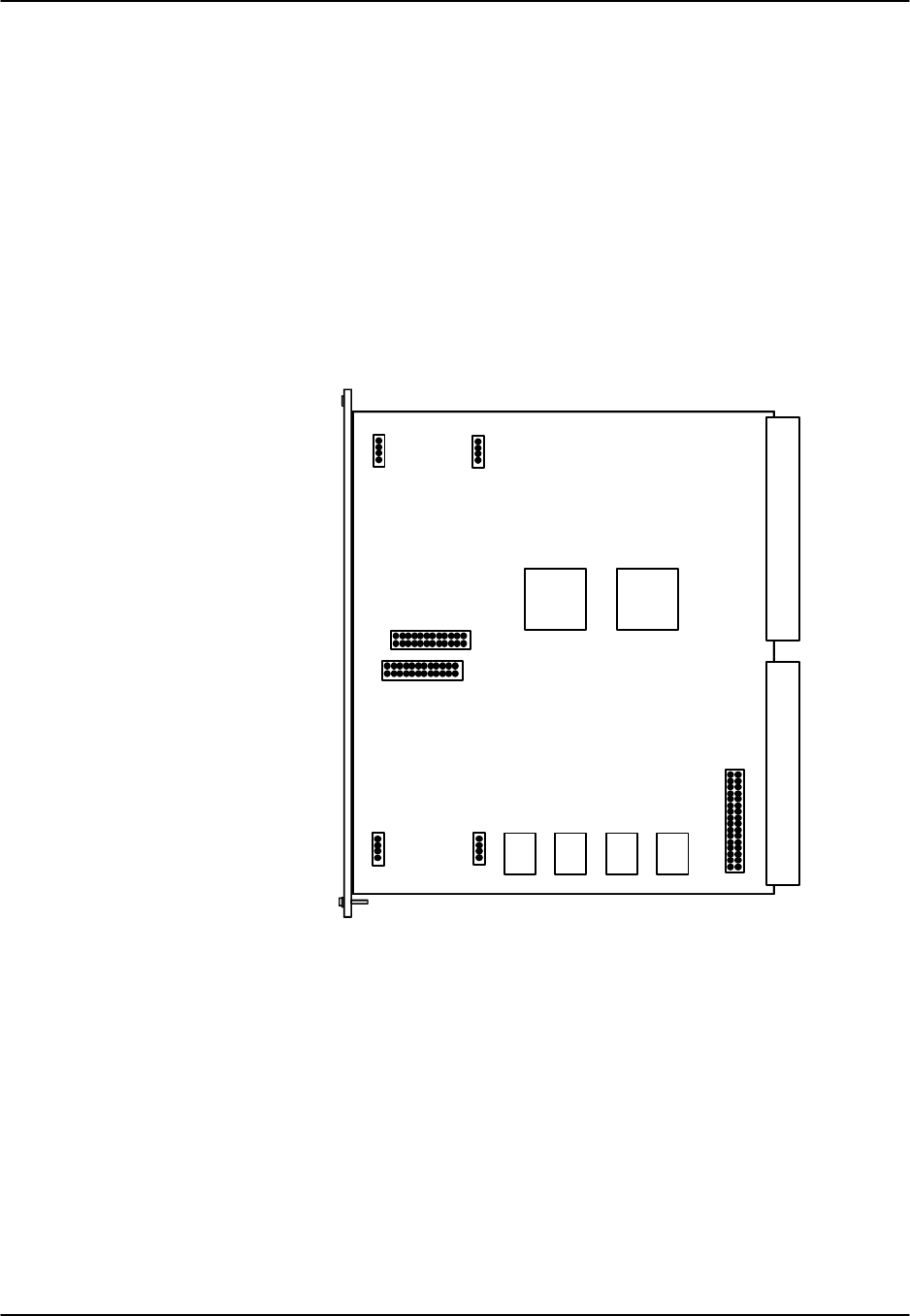
WAN Card Reference Guide v3.6
Page 5-A-8(10-97)
Installing CSU, DSX/CEPT Modules (811, 812, 820)
Plug-in modules used to activate WAN cards must be installed prior to insertion of the
WAN card into the unit. Figure WAN-13 shows a diagram of the WAN card and the
correct placement of these modules. If, for example, your system had a T1 link (DSX)
and an E1 link (CEPT), you would receive two DSX/CEPT modules. Using Figure
WAN-14 as a guide, place the DSX module in the slot reserved for WAN 1-1 (reference
only, not shown this way on actual card). Insert the pins for TX in JP #10, while
simultaneously inserting the pins for RX in JP #9 and the 24-pin end connector pins in
JP #6. After changing the jumpers to convert the DSX module to CEPT, place the
CEPT module in the slot reserved for WAN 1-2. Insert the TX pins into JP #15, the RX
pins into JP #14, and the 24-pin end connector pins into JP #13.
The CSU module connectors are inserted in the same manner.
Retaining
Power
Bus
Edge
Connector
XILINX
XILINX
JP6
JP10
JP9
JP13
JP14
JP15
(WAN 1-1)
(WAN 1-2)
Figure WAN-14. Inserting DSX/CEPT/CSU Modules
WAN Card Settings for CSU/DSX
Since both CSU and DSX configurations are T1 operations, Figure WAN-15 shows the
WAN card screen for CSU/DSX operation. Table WAN-2 lists the CSU/DSX settings
controlled on the screen along with their possible and default values. For information
about cross-connects and the timeslot map used to connect your WAN to voice and data
ports or equipment, see the System Operations chapter.

Reference Guide v3.6WAN Card
(10-97) Page 5-A-9
In addition to the Local and Line Loopbacks described below, a Single or Dual Link
card that is equipped with a CSU plug-in module will recognize and respond to
industry-standard T1 loop-up and loop-down codes that are generated from the network
or from a remote device. It will ignore those codes if the Single or Dual Link card is
equipped with a DSX plug-in module.
Node_1 | W1 CSU+DSX 8010 Rev A6-2 Ser 00101 | 12-31-99
14:33
CSU DSX
STATE stdby STATE stdby
MODE xcon MODE xcon
FORMAT esf FORMAT esf
LINE CODE b8zs LINE CODE b8zs
PULSE n/a PULSE n/a
LINE LEN 0 LINE LEN 133
SLIP LIM 126 SLIP LIM 126
AIS/ALM none AIS/ALM none
LINE LB off LINE LB off
LOCAL LB off LOCAL LB off
CH LB off CH LB off
LB ADDR 01 LB ADDR 01
LB GEN off LB GEN off
LB DET w/to LB DET w/to
ESF/NMS RP at&t ESF/NMS RP at&t
EER THRHD 10e-4 EER THRHD 10e-4
RDNT RULES n/a RDNT RULES n/a
GROUP none GROUP none
Save | Undo | Refresh | Xcon | Perf | Farstat | Test | sWitch | Main
Figure WAN-15. Typical WAN Card Main Screen for T1 CSU or DSX

WAN Card Reference Guide v3.6
Page 5-A-10 (10-97)
Table WAN-2. Parameter Options and Defaults for CSU/DSX Operations
Parameter User Options Notes Default
STATE stdby act stdby
MODE term d-i xcon 1xcon
FORMAT d4 esf slc96 slcd4 esf
LINE CODE ami b8zs 2b8zs
PULSE n/a trnsp Z15s n/a
LINE LEN 0 7.5 15.0 3 0
SLIP LIM 126 138 126
AIS/ALM none tcodr 4none
LINE LB off on off
LOCAL LB off on off
CH LB off clr off
LB ADDR 01-24 01
LB GEN off llb plb nlb off
LB DET w/to on off w/to
ESF/NMS RP none at&t ansi c-fdl c-b7r efdl 5at&t
EER THRHD 10e-4 thru 10e-9 none 10e-4
RDNT RULES n/a none OOS CGA 6n/a
GROUP none 1 2 3 4 7none
NOTES
1. Valid options for Bus Connect systems are term and d-i. The only valid
option for Cross-Connect systems is xcon.
2. These options are valid only if you have a CSU and the Line Code is ami.
If you have a CSU and the Line Code is b8zs, then this setting will default
to n/a. If you have a DSX module, then this setting will always default to
n/a.
3. These options are valid only if you have a CSU. If you have a DSX
module, then the possible options are 0 (default), 133, 266, 399, 533, 655,
and csu.
4. The settings for AIS/ALM vary greatly by the settings of other parameters.
A complete matrix of AIS/ALM settings is shown as Table WAN-4 later
in this chapter.
5. If the format is d4 or slc96, the only option to appear will be none.
6. If there is no redundant WAN card in the appropriate slot the only option
that will appear is n/a.
7. Selection of GROUP is a two-step process. After identifying the group
number (1-4), the user must select the secondary group (A, B or C). A
which point TC ODR will then become available.

Reference Guide v3.6WAN Card
(10-97) Page 5-A-11
WAN Card Parameters
The following paragraphs describe the parameters for the DSU/DSX WAN cards shown
in Figure WAN-15 and Table WAN-2.
STATE
In standby state, the WAN port is electrically disconnected from the external network.
Set the State setting to standby (stdby) when setting up your WAN links, then change it
to active (actv) when starting normal operations.
MODE
In bus-connect systems, WAN cards have two possible modes of operation, Terminal
and Drop-and-Insert. Terminal (term) mode is for channel bank applications. All
timeslots must connect to a port on a user card or remain unconnected. Drop-and-Insert
(d-i) mode automatically connects all timeslots on WAN link #1 to the corresponding
timeslots on WAN link #2 of the same card. You can assign any or all of the timeslots
to voice and data ports by overriding the automatic setup. See the Systems Operations
chapter for more information about using these two modes, and about timeslot maps in
general. In cross-connect systems, the Mode automatically defaults to (xcon).
FORMAT
The Format setting specifies the framing to be used on the WAN link so that it matches
the framing used by your T1 carrier. Set the Format parameter based on the type of
framing your T1 carrier requires. If you are using an external Channel Service Unit
(CSU), the framing format must match that of the CSU. The options are d4 (normal
superframe), esf (extended superframe) and slc96 (subscriber loop carrier).
Table WAN-3 (on the next page) lists the DS0 time slots and the corresponding SLC
assignments (taken from TR-TSY-000008).
LINE CODE
The Line Code setting matches the coding used by your T1 interface to that used by
your T1 carrier or CSU. Set the Line Code setting based on the type of encoding your
T1 carrier uses. If you are using an external CSU, the line coding must match that of
the CSU. The options are ami and b8zs.
PULSE
For CSU modules configured for ami mode only, the user must also specify if the
system should ensure pulse density (also known as ones density) or if that responsibility
belongs to the attached customer equipment. In z15s mode, the system will monitor the
outbound data stream and will place a “1” in the 16th bit position whenever it detects
fifteen consecutive zeros. Obviously, this can lead to data corruption. In Transparent
mode (trnsp), the system will pass all incoming data transparently (the DTE must
provide 1s density). If the Line Code parameter for the CSU is b8zs, then Pulse will
default to trnsp. If the WAN link is equipped with a DSX plug-in, then this option will
automatically default to n/a.

WAN Card Reference Guide v3.6
Page 5-A-12 (10-97)
Table WAN-3. DS0-SLC Conversion Table
DS0 Time Slot SLC Channel Number
Shelf A Shelf B Shelf C* Shelf D*
1 1 25 49 73
2 13 37 61 85
3 2 26 50 74
4 14 38 62 86
5 3 27 51 75
6 15 39 63 87
7 4 28 52 76
8 16 40 64 88
9 5 29 53 77
10 17 41 65 89
11 6 30 54 78
12 18 42 66 90
13 7 31 55 79
14 19 43 67 91
15 8 32 56 80
16 20 44 68 92
17 9 33 57 81
18 21 45 69 93
19 10 34 58 82
20 22 46 70 94
21 11 35 59 83
22 23 47 71 95
23 12 36 60 84
24 24 48 72 96
* Shelf C and D not supported in this release
LINE LEN
Use the Line Length setting to adjust the T1 signal strength to the distance that it must
travel before it encounters the next T1 device or repeater. For the DSX module, the
options are 133, 266, 399, 533, 655 feet or csu which is used to connect to the
equipment side of a co-located external CSU. In addition, there is an option called 0
that allows the DSX module to talk to the network side of a co-located external CSU
over a short-distance four-wire cable. For a CSU module, the three options are 0, 7.5
and 15.0 which define the amount of attenuation (in dB) that will be applied to the T1
signal before it is transmitted. Provisioning the circuit for 0 will result in the strongest
possible signal whereas a setting of 15.0 will generate the weakest possible signal.
SLIP LIM
Slip Limit defines how many bits of wander the T1 aggregate card will tolerate before
forcing a frame slip. The options are 126 and 138 bits which correspond to all old and
more recent versions of the relevant specification.

Reference Guide v3.6WAN Card
(10-97) Page 5-A-13
AIS/ALM
The AIS/ALM setting, allows the user to specify the type of “keep-alive” signal known
as AIS/ALM (Alarm Indication Signal/Alarm) that the system will generate on one
T1/E1 should the other fail. The AIS/ALM setting is dependent upon the format
selected for this WAN unit. Table WAN-4 shows AIS/ALM settings for Bus Connect
and Cross-Connect systems using the different FORMAT settings.
Table WAN-4. AIS/ALM Settings
System Format AIS/ALM
D4 none
Bus Connect/RB Connect ESF none, frm, unfrm
SLC-96 note, orb13, orb16
D4 none, tcodr
Cross-Connect ESF none, frm, unfrm
SLC-96 note, orb13, orb16
In Bus Connect and Redundant Bus Connect systems, the only option available for D4
framing is none (no AIS signal is to be generated). The options for ESF framing are
none, frm for a framed alarm signal and unfrm for an unframed alarm signal. The
options for SLC-96 framing are note (network office terminating equipment), orb16
(Office Repeater Bay - 16 frames) and orb13 (Office Repeater Bay - 13 frames).
In Cross-Connect systems, the options available for D4 framing are none (no AIS signal
is to be generated) and tcodr (transcoder operations). Selection of tcodr can only be
assigned after selection of the Group option. The options for ESF framing are none,
frm for a framed alarm signal and unfrm for an unframed alarm signal. The options
for SLC-96 framing are note (network office terminating equipment), orb16 (Office
Repeater Bay - 16 frames) and orb13 (Office Repeater Bay - 13 frames).
LINE LB
The Line Loopback setting controls looping of the full T1/E1 line back to the network,
as shown in Figure WAN-16. The options are off and on. When on, this setting allows
end-to-end testing of the line.
LOCAL LB
The Local Loopback setting controls looping of the full T1/E1 line back to the PCM
bus, as shown in Figure WAN-16. The options are off and on. When on, this setting
allows testing of local equipment.
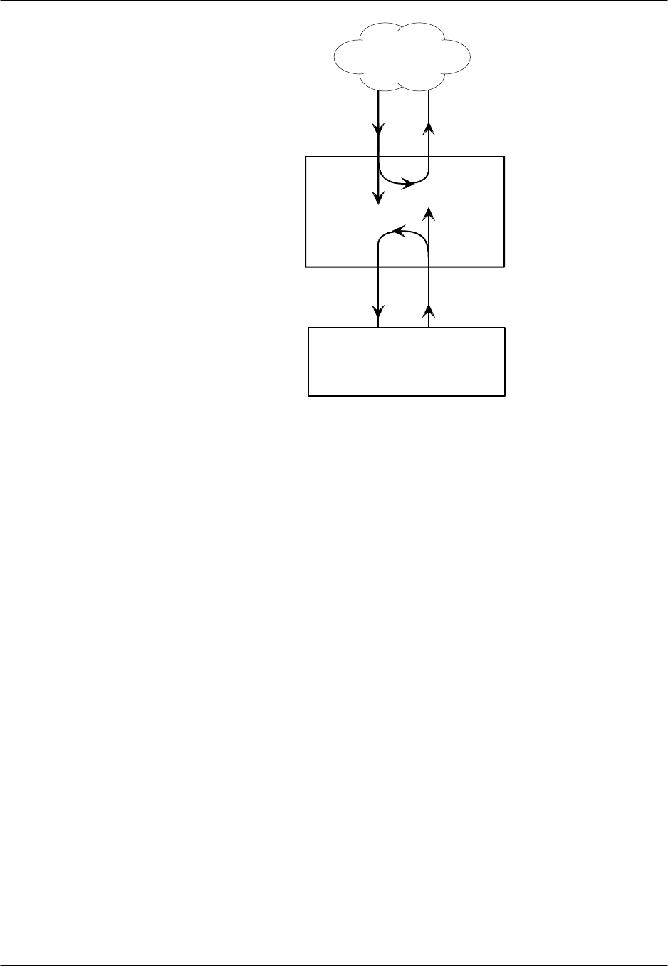
WAN Card Reference Guide v3.6
Page 5-A-14 (10-97)
T1/E1
WAN Card
Local Loopback
Line Loopback
Network
PCM bus
Figure WAN-16. WAN Card Line and Local Loopbacks
CH LB
The Channel Loopback setting allows you to select the type of local loopback for
individual DS0 channels or the WAN aggregate. A channel loopback loops a single
DS0 channel back towards the PCM bus (see Figure WAN-17) and cannot be used to
loop multiple DS0s or a portion of a DS0. Refer to user cards for other loopback
options which may allow you to loop part of a channel or multiple channels.
The loopback can be off or clear (clr). “Clear” means that the entire 64kbps clear
channel will be looped back, but without the Robbed Bit Signaling (RBS), if any, that is
embedded in this channel.
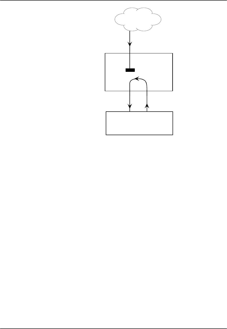
Reference Guide v3.6WAN Card
(10-97) Page 5-A-15
T1/E1
WAN Card
Network
PCM bus
Figure WAN-17. WAN Card Channel Loopback
LB ADDR
The Loopback Address setting, in conjunction with the Channel Loopback setting,
specifies which channel is to be looped back. Only one channel may be looped back at
any one time for each T1 link. The valid selections for T1 lines are 1-24.
LB GEN
The Loopback Generate setting generates in-band diagnostic codes that are sent to the
remote equipment These codes are ANSI T1.403 compatible with DS1 networks and
allow you to command a latching loopback at remote DS1 equipment. The options are
off, llb (Local Loopback), plb (payload Loopback [when the entire signal, excluding
the framing bit, is looped back]) and nlb (Network Loopback).
LB DET
This option allows the card to detect DS1 channel loopbacks. When set to off, no T1
loopbacks can be detected. When set to on, T1 loopbacks will be detected and
maintained until a loop down is detected. The with/time-out (w/to) is the same as on
except that if no loop down is detected after 10 minutes, the loopback will self-
terminate.

WAN Card Reference Guide v3.6
Page 5-A-16 (10-97)
ESF/NMS RP
This setting specifies the format in which performance statistics for the T1 link will be
gathered and stored in the system. In ESF mode, these performance statistics are
accessible to the carrier over the Facilities Data Link (FDL) as well as to you through
the user interface. The options are none, at&t, ansi, both, c-fdl and c-b7r. The at&t
option means that the statistics are gathered in accordance with AT&T Publication
54016 whereas the ansi option means that the ANSI T1.403 specification will be used.
You can also specify that the information should be stored in both AT&T and ANSI
modes simultaneously by selecting both. Performance statistics are also available for
D4 formatted T1 lines. See the section on T1 Performance Monitoring in this chapter
for more detailed information on this topic.
The choice of c-fdl disables telco-side capability to access performance monitoring
information. The c-fdl option sends and receives network management information
over the facility data link. The c-b7r option sends and receives the same information
over timeslot #24 on the WAN link highlighted.
EER THRHD
The Excessive Error Rate Threshold selects the error rate at which an alarm is declared.
This setting interacts with the EER setting in the Alarm Filters of your system. (See
Basic Operations chapter.) The options are 10e-4 through 10e-9 or none.
RDNT RULES
The selection of Redundancy Rules will define the method of determining what event
will trigger a WAN port to switch to its redundant mate. The options are none, OOS or
CGA. See the Redundancy Chapter for more information about redundant WAN
operations. If there is no redundant WAN card in the appropriate slot or there is an
ISDN or ADPCM card in the system, the only option that will appear is n/a.
GROUP
The Group setting identifies a method of link-fail alarm propagation from upstream
trunks to downstream tributaries when the system is configured for transcoder.
Selection of group is a two-step process. After identifying the group number (1-4), the
user must select the secondary group (A [child group], B [child group] or C [parent
group]).
Figure WAN-18 shows two Integrated Access Controllers with "parent-child"
groupings. Child groups are designated as "A" and "B." Parent groups are designated
"C." At this time TCODR may be turned on if alarms are to be propagated to distant
end.

Reference Guide v3.6WAN Card
(10-97) Page 5-A-17
WAN2-1
(C) (C1)
Controller #1 Controller #2
W1-1 (A)
W1-2 (B)
W3-1 (A1)
W3-2 (B1)
Device #1 Device #2
Trunk
Tributary Tributary
Figure WAN-18. Using WAN Groups
For the purposes of this discussion, the WAN links between the Device and the
Integrated Access Controller (A, B, A1, and B1) will be called “tributaries” and the
WAN link between the two Controller Units (C and C1) will be referred to as a “trunk.”
In the normal condition (no WAN groups selected), a failure on any of the tributaries
supplying Device #1 would be reported at Integrated Access Controller #1 and Device
#1 only. A failure of the trunk (C to C1) would be reported at Controller #1 and #2
only.
When Groups are created at both systems, a trunk failure (C to C1) will inform all of
the associated tributaries (A and B, A1 and B1) of that condition.
When Groups are used in conjunction with the Network Management option
(mentioned earlier) and the AIS/ALM is set to tcodr, a failure of any of the tributaries
will propagate the failure through the trunk to the associated tributary at the other end
(A to A1 or B to B1).
The following notification procedure is followed:
1. A Loss of Signal, Loss of Frame, Error Rate Exceeded or AIS failure of
the transmit leg of W1-1(A) between Device #1 and Integrated Access
Controller #1 occurs.
2. Controller #1 detects the failure on the receive leg and declares an alarm
for W1-1(A).
3. Controller #1 sets the A Bit (Yellow Alarm) in the transmit leg of W1-
1(A). Device #1 detects this condition and knows not to use W1-1(A).
4. Controller #1(C) sends an alarm message to Controller #2 (C1) that W1-
1(A) is either CGA_RED or AIS.
5. Controller #2 sets the transmit leg of W3-1(A1) into AIS (CGA_RED).
Device #2 detects this condition and knows not to use W3-1(A1).
When the original failure is corrected, the alarm is also cleared for downstream
tributaries.

WAN Card Reference Guide v3.6
Page 5-A-18 (10-97)
Menu of Actions
Table WAN-5 shows the Menu of Actions for the CSU/DSX main WAN card screen.
Table WAN-5. WAN Card Screen Menu of Actions
Action Function
Save Saves changes to settings
Undo Returns all settings to the last saved state.
Refresh Updates certain time-related information fields that are not
automatically updated (i.e. performance and test data).
Xcon Shows the cross-connect map for each WAN port. See the System
Operations section for a detailed description of cross-connect features.
Perf Brings up the performance monitoring screen for the near end system.
See the Performance Monitoring section below.
Farstat Opens performance monitoring screen for Far-end Statistics
Test Initiates and monitors testing of all WAN card ports. Refer to Test
section below.
SWitch Allows the user to switch wan port operations to the redundant mate.
See the Redundant Operations section.
pArs Not supported in this release. Reserved for future use.
Main Returns to the main terminal screen. If changes are made to settings
and not saved, you will be prompted to save or lose changes.

Reference Guide v3.6WAN Card
(10-97) Page 5-A-19
Cross-Connect (XCON)
The Cross-Connect (Xcon) command in the Main WAN screen allows you to view the
Cross-Connections that have been set up in the system. Highlight one of the WANs on
the card and type x (Xcon) to select Cross-Connect. Either an E1 screen (Figure WAN-
19) or a T1 screen (Figure WAN-20) will appear, depending upon the WAN
highlighted. This is a display-only screen. Timeslot and cross-connect configuration
are discussed in the System Operations chapter of this manual.
Node_1 | W2 CSU+CEPT 8010 Rev A6-2 Ser 11132 | 12-31-99
14:33
TS XCON TS CIRCUIT_ID TS XCON TS CIRCUIT_ID
0 frame align 64k 16 cas 64k
1 u5-1 A-01 user_circuit 17 u7-1 A-17 user_circuit
2 u5-2 A-02 user_circuit 18 u7-2 A-18 user_circuit
3 u5-3 A-03 user_circuit 19 u7-3 A-19 user_circuit
4 u5-4 A-04 user_circuit 20 u7-4 A-20 user_circuit
5 u5-5 A-05 user_circuit 21 u7-5 A-21 user_circuit
6 u5-6 A-06 user_circuit 22 u7-6 A-22 user_circuit
7 u5-7 A-07 user_circuit 23 u7-7 A-23 user_circuit
8 u5-8 A-08 user_circuit 24 u7-8 A-24 user_circuit
9 u6-1 A-09 user_circuit 25 u8-1 A-25 user_circuit
10 u6-2 A-10 user_circuit 26 u8-2 A-26 user_circuit
11 u6-3 A-11 user_circuit 27 u8-3 A-27 user_circuit
12 u6-4 A-12 user_circuit 28 u8-4 A-28 user_circuit
13 u6-5 A-13 user_circuit 29 u8-5 A-29 user_circuit
14 u6-6 A-14 user_circuit 30 u8-6 A-30 user_circuit
15 u6-7 A-15 user_circuit 31 u8-7 A=31 user_circuit
Refresh | Test | Main
Figure WAN-19. E1 Cross-Connect Display

WAN Card Reference Guide v3.6
Page 5-A-20 (10-97)
Node_1 | W2 CSU+CEPT 8010 Rev A6-2 Ser 11132 | 12-31-99
14:33
TS XCON TS CIRCUIT_ID TS XCON TS CIRCUIT_ID
1 13
2 14
3 15
4 16
5 17
6 18
7 19
8 20
9 21
10 22
11 23
12 24
Refresh | Test | Main
Figure WAN-20. T1 Cross-Connect Display
Performance Monitoring
Performance monitoring is supported on all WAN aggregates. The performance
monitoring screen is accessed by typing the p (Perf) command from the WAN card
main screen Menu of Actions. Performance statistics are accumulated for 15 minute
increments that include the current period and the previous 96 periods that are accessed
by the pgUp and pgDn commands from the Menu of Actions.
In the T1 environment, an error is defined as any CRC6, Controlled Slip or Out of
Frame error for "esf" format and any Bipolar Violation (BPV), Controlled Slip or Out of
Frame error for the "d4" format. In the E1 environment, an error is defined as any
CRC4, Controlled Slip or Out of Frame error.
Figure WAN-21 shows the T1 performance monitoring screen (the E1 screen is similar
except for the Menu of Actions). The performance statistics are gathered and displayed
in fifteen-minute intervals. Periods when no seconds have accumulated are represented
by lines in each of the columns. Table WAN-8 identifies the error conditions.
Two sets of registers accumulate performance data for T1 WAN links. The user
registers and the network registers are driven by the same errored events. However,
they can be cleared at separate times. The user may view both the user and network
registers but may only clear the user registers. The network has access to only the
network registers and can clear only network registers. E1 WAN links have only one
set of registers.
Table WAN-9 shows the Menu of Actions for the Performance Monitoring Screen.

Reference Guide v3.6WAN Card
(10-97) Page 5-A-21
Node_1 | W1 CSU+DSX 8010 Rev A6-2 Ser 00101 | 12-31-99
14:33
Unit 1 PERFORMANCE USER REGISTERS Sec. 167 of 900
ES UAS SES BES LOFC SLIP DM STATUS
CUR 0 0 0 0 0 0 0 . . T . . .
01 0 0 0 0 0 0 0 . . T . . .
02 0 0 0 0 0 0 0 . . T . . .
03 0 0 0 0 0 0 0 . . T . . .
04 0 0 0 0 0 0 0 . . T . . .
05 0 0 0 0 0 0 0 . . T . . .
06 0 0 0 0 0 0 0 . . T . . .
07 0 0 0 0 0 0 0 . . T . . .
08 0 0 0 0 0 0 0 . . T . . .
09 0 0 0 0 0 0 0 . . T . . .
10 0 0 0 0 0 0 0 . . T . . .
11 0 0 0 0 0 0 0 . . T . . .
12 0 0 0 0 0 0 0 . . T . . .
TOTAL 0 0 0 0 0 0 0 . . T . . .
STATUS: Y=YEL N=NOS T=Test L=LOS O=OOS B=BPV E=ERR
Refresh | pgUp | pgDn | uSerregs | Networkregs | Clearregs | Main
Figure WAN-21. Performance Monitoring Screen

WAN Card Reference Guide v3.6
Page 5-A-22 (10-97)
Table WAN-8. Performance Monitoring Displays
Parameter Display
ES Errored Seconds (ES) registers the number of seconds with one or more CRC6
(ESF), BPV (D4) or CRC4 (E1) errors, OR one or more OOFs, OR one or more
Controlled Slips.
UAS Unavailable Seconds (UAS) shows the number of seconds during which service is
unavailable. An unavailable signal state is declared after ten consecutive
Severely Errored Seconds (SESs) are logged. An unavailable state is cleared after
ten consecutive non-Severely Errored Seconds are logged. Unavailable Seconds
are also accumulated if the card has an out-of-service (OOS) condition.
SES A Severely Errored Second (SES) is any second with 320 or more CRC6 (ESF),
BPV (D4) or CRC4 (E1) errors, OR one or more OOF errors.
BES A Bursty Errored Second (BES) is any second with more than one and less than
320 CRC6 (ESF), BPV (D4) or CRC4 (E1) errors.
LOFC The Loss of Frame Count (LOFC) is the accumulation of Loss Of Frame (LOF)
conditions. LOF is declared after 2.5 seconds of continuous Loss Of
Synchronization (LOS) or Out-Of-Frame (OOF) condition. LOF is cleared after
no more than fifteen consecutive seconds without an LOS or OOF condition.
SLIP A Slipped Second contains one or more Controlled Slips. A Controlled Slip is the
deletion or replication of a DS1/E1 frame by the receiving equipment.
DM A Degraded Minute (DM) is any minute during the reporting period that contains
more than 10-6 errors as described in CCITT G.821. The count for this field is 1-
15 rather than 1-900 for the other fields.
STATUS Status displays error codes for conditions that occur during a fifteen minute
interval. Identifying codes are displayed at the bottom of the screen. Values are Y
(Yellow Alarm received), N (No Signal), T (Test Mode - line loop, local loop,
payload loop or standby), L (Loss of Synchronization - 2 out of 4 frame bits in
error), O (Out of Service), B (Bipolar Violation) and E (Excessive Error Rate).
Menu of Actions
Table WAN-9. Performance Monitoring Screen Menu of Actions
Action Function
Refresh Because statistics are not calculated in real time, the Refresh command must be
used to update the screen with new inforamtion.
pgUpPages through the performance statistics for the current 15 minute period
and periods 96-1.
pgDnPages through the performance statistics for the current 15 minute period
and periods 1-96.
uSerregs Allows the user to view the User Registers. Not shown for CEPT operation
because it is the only set of registers for that mode.
Networkregs Allows the user to view the Network Registers. When a user is viewing the
network registers, the Clear Registers option disappears. (This action is not
available in D4 mode or CEPT operation.)
Clearregs Clears the User Registers. Network statistics remain the same.
Main Returns to the main WAN card screen.

Reference Guide v3.6WAN Card
(10-97) Page 5-A-23
Far End Statistics
The Far End Statistics (Farstat) screen (Figure WAN-22) reports the same impairlments
as the Performance Monitoring screen. The same statistics are collected in the same
manner for the far end system for both T1 and E1 systems. Since there are no registers
for this option at the near end, the register commands are not available in the Menu of
Actions.
Node_1 | W1 H_E1+H_E1 8011 Rev A1-0 Ser 00101 | 12-31-99 14:33
Unit 1 AT&T FAREND STATISTICS NETWORK REGISTERS Sec. 240 of 900
ES UAS SES BES LOFC SLIP
CUR000000
01 ***** ***** ***** ***** ***** *****
02 ***** ***** ***** ***** ***** *****
03 ***** ***** ***** ***** ***** *****
04 ***** ***** ***** ***** ***** *****
05 ***** ***** ***** ***** ***** *****
06 ***** ***** ***** ***** ***** *****
07 ***** ***** ***** ***** ***** *****
08 ***** ***** ***** ***** ***** *****
09 ***** ***** ***** ***** ***** *****
10 ***** ***** ***** ***** ***** *****
11 ***** ***** ***** ***** ***** *****
12 ***** ***** ***** ***** ***** *****
TOTAL 0 0 0 0 0 0
Retrieving message. Please wait...
Refresh | Clear | pgUp | pgDn | Main
Figure WAN-22. Far-End Statistics

WAN Card Reference Guide v3.6
Page 5-A-24 (10-97)
Test
Selecting "Test" from the WAN Screen Menu of Options brings up the screen shown in
Figure WAN-23. From this screen, users are allowed to create test situations between
WAN cards or between a single WAN card and data test equipment at a remote site.
Table WAN-10 lists the user options and display field definitions on this screen.
Defaults are shown in bold type. Table WAN-11 shows the Menu of Actions for the
Test Screen.
In a system using an enhanced bus-connect 8804 CPU card, the test feature cannot
be accessed by cards in WAN slot #3 or #4.
Node_1 | W1 CEPT+CEPT 8010 Rev A6-2 Ser 00101 | 12-31-99
14:33
CSU CSU
BERT off off
SYNC no no
BE 0 0
ES 0 0
SES 0 0
CSES 0 0
OSS 0 0
BER 0.0e+1 0.0e+1
ELAP 0 0
LB STATE none none
Save | Undo | Refresh | InsertErr | Clear | Main
Figure WAN-23. The WAN Card Test Screen

Reference Guide v3.6WAN Card
(10-97) Page 5-A-25
Table WAN-10. Test Screen Options
Parameter User Options Default
BERT off mark space 1:1 1:7 3:24
qrss lp-up lp-dn off
SYNC yes no no
BE see description below
ES see description below
SES see description below
CSES see description below
OSS see description below
BER see description below
ELAP see description below
LB STATE pl-lb l-lb none.
BERT
Bit Error Rate Tester (BERT) sends a data pattern and measures the bit error rate (BER)
on the selected WAN port. The patterns that can be selected are off, mark (all ones),
space (all zeros), 1:1 (one-zero-one-zero), 1:7 (zero-one-6 zeros), 3:24 (3 ones-24
zeros), qrss (quasi-random pseudo signal), lp-up (which sends a T1 loop-up code to the
remote end) and lp-dn (which sends a loop-down code to the remote end). Loop-up (lp-
up) and loop down (lp-dn) codes are not supported for CEPT WANs.
SYNC
Synchronization (SYNC) displays yes if the integrated BERT has achieved
synchronization either with itself via a remote loopback or with the remote test
equipment, no if it has not.
BE
Bit Error (BE) displays the total number of bit errors logged.
ES
Errored Seconds (ES) displays the total number of seconds in which errors were
detected.
SES
Severely Errored Seconds (SES) shows the total number of seconds in which the bit
error rate exceeded one bit per thousand (1 x 10⁻³).

WAN Card Reference Guide v3.6
Page 5-A-26 (10-97)
CSES
Consecutive Severely Errored Seconds (CSES) is triggered by the occurrence of ten
consecutive Severely Errored Seconds. Once triggered, the CSES field will increment
(by one) for each elapsed second until the system logs ten consecutive non-Severely
Errored Seconds.
OSS
Out of Synchronization Seconds (OSS) shows the number of seconds that the BRI
BERT has been out of synchronization.
BER
Bit Error Rate (BER) shows the rate at which errors are being logged. BER equals the
number of bit errors (BE) divided by the total number of bits transmitted during the test.
ELAP
Elapsed time (ELAP) is the total number of seconds elapsed during the test.
LB STATE
The Loopback State indicates that a loopback from a remote device is both present and
operational. The field will show pl-lb (payload loop-back) when the entire signal,
excluding the framing bit, is looped back. The field will show l-lb (line loop-back)
when the entire signal is looped back. It will show none if the WAN port is not in
loopback.
Menu of Actions
Table WAN-11. Test Screen Menu of Actions
Action Function
Save Saves changes to settings.
Undo Returns all settings to the last saved state.
Refresh Updates certain time-related information fields that are not automatically updated (i.e.
performance and test data).
InsertErr Allows the user to manually insert a single error into the clear data signal.
Clear Clears the testing screen and resets all counters to zero.
Main Returns to the WAN card main screen. If changes are made to settings and not saved,
you will be prompted to save or lose changes.

Reference Guide v3.6WAN Card
(10-97) Page 5-A-27
WAN Card Settings for HDSL E1
Figure WAN-24 shows the WAN card screen for HDSL E1 operation. Table WAN-12
lists the HDSL E1 settings controlled on the screen along with their possible and default
values. For information about cross-connects and the timeslot map used to connect
your WAN to voice and data ports or equipment, see the System Operations chapter.
Node_1 | W1 H_E1+H_E1 8011 Rev A1-0 Ser 00101 | 12-31-99 14:33
H_E1 H_E1
STATE stdby STATE stdby
MODE xcon MODE xcon
FRAME crc FRAME crc
TS16 cas TS16 cas
EVEN BIT norm EVEN BIT norm
AIS/ALM none AIS/ALM none
LINE LB off LINE LB off
LOCAL LB off LOCAL LB off
CH LB off CH LB off
LB ADDR 01 LB ADDR 01
LB GEN off LB GEN off
COM/NMS RP none COM/NMS RP none
EER THRHD 10-e-4 EER THRHD 10-e-4
RDNT RULES none RDNT RULES none
GROUP none GROUP none
Save | Undo | Refresh | Xcon | Perf | Farstat | Test | sWitch | Hdsl | Main
Figure WAN-24. The WAN Card Screen for HDSL_E1 Operations

WAN Card Reference Guide v3.6
Page 5-A-28 (10-97)
Table WAN-12. Parameter Options for CEPT Operations
Parameter User Options Default
STATE stdby actv stdby
MODE term d-i xcon xcon
FRAME crc d-frm crc
TS16 cas ccs nos nos
EVEN BIT norm inv norm
AIS/ALM none tcodr none
LINE LB off on off
LOCAL LB off on off
CH LB off clr off
LB ADDR 00-31 00-31
LB GEN off llb plb nlb off
COM/NMS none c-sa4 c-br7 none
EER THRHD 10e-4 - 10e-9 10e-4
RDNT RULES none OOS CGA none
GROUP none 1 2 3 4 none
STATE
Leave the card in standby (stdby) when setting up your WAN links; then change it to
active (actv) when starting normal operations.
MODE
In bus-connect systems, WAN cards have Terminal (term) and Drop-and-Insert (d-i)
modes of operation. In Terminal mode, used for channel bank applications, all
timeslots must connect to a port on a user card or remain unconnected. Drop-and-
Insertmode automatically connects all timeslots on WAN link #1 to the corresponding
timeslots on WAN link #2 of the same card. You can assign any or all of the timeslots
to voice and data ports by overriding the automatic setup. See the Systems Operations
chapter for more information about using these two modes, and about timeslot maps in
general. In cross-connect systems, Mode automatically defaults to xcon, the only
available option.
FRAME
Selects frame types: Cyclic Redundancy Check, 4th level (crc) or Dual Frame (d-frm).
TS16
Selects signaling usage of slot 16: Channel Associated Signaling (cas), Common
Channel Signaling (ccs) or No Signaling (nos). In the CAS and CCS, timeslot 16 is
used to carry signaling information for all channels on the E1. If nos is selected, then
timeslot 16 becomes available for user data.

Reference Guide v3.6WAN Card
(10-97) Page 5-A-29
EVEN BIT
Setting the Even Bit parameter for inv causes the system to invert every even bit in
every DS0 timeslot, insuring ones-density. This option should be used only if the entire
E1 stream is composed of PCM voice.
AIS/ALM
Specifies the type of “keep-alive” signal known as AIS/ALM (Alarm Indication
Signal/Alarm) that the system will generate on one E1 should the other fail. AIS/ALM
will show none until the GROUP is selected
LINE LB
Controls looping the full E1 line back to the network. On enables, off disables end-to-
end testing of the line.
LOCAL LB
Controls looping the full E1 line back to the PCM bus. The options are off and on. On
allows testing of local equipment; off disables testing. The system generates a “Keep
Alive - Type 1” pattern on the E1 line.
CH LB
Enables individual DS0 channel loopback toward the PCM bus (see Figure WAN-16
earlier in this chapter). A channel loopback loops a single DS0 channel and cannot be
used to loop multiple DS0s or a portion of a DS0. Refer to user cards for other
loopback options which may allow you to loop part of a channel or multiple channels.
Clr enables, off disables loopback.
LB ADDR
The Loopback Address specifies which channel is to be looped back in the Channel
Loopback. Valid selections for E1 lines are 0-31. Do not loop timeslot 16 unless the
E1 interface is in no signaling (nos) mode.
LB GEN
LB GEN generates in-band diagnostic codes that are sent to the remote equipment
These codes are compatible with DDS networks and allow you to command a latching
loopback at remote DDS equipment. The options are off, llb (Local Loopback), plb
(payload Loopback) and nlb (Network Loopback).
COM/NMS
Communications/Network Management System Report tells the system where to send
TCP/IP packets from the NMS configuration selected on the Interface card. The
options are none (no NMS), c-sa4 (use SA4 channel for NMS information) and c-b7r
(send NMS information to a B7R card on timeslot 31).

WAN Card Reference Guide v3.6
Page 5-A-30 (10-97)
EER THRHD
Excessive Error Rate Threshold selects the error rate at which an alarm is declared.
This setting interacts with the EER setting in the Alarm Filters of your system. (See
Basic Operations chapter.) The options are 10e-4 through 10e-9 or none.
RDNT RULES
Redundancy Rules define the method of determining what event will trigger a WAN
port to switch to its redundant mate. The options are none, OOS or CGA. See the
Redundancy Chapter for more information about redundant WAN operations. If there
is no redundant WAN card in the appropriate slot, or there is an ISDN or ADPCM card
in the system, the only option that will appear is none.
GROUP
Group identifies a path of link-fail alarm propagation from upstream trunks to
downstream tributaries. Selection of group is a two-step process. After identifying the
group number (1-4), the user must select the secondary group (A [child group], B [child
group] or C [parent group]). The group setting is normally used for transcoder
applications.
Menu of Actions
Table WAN-13 shows the Menu of Actions for the E1 HDSL WAN Card. Relevant
actions are described below.
Table WAN-13. WAN Card Screen Menu of Actions
Action Function
Save Saves changes to settings.
Undo Returns all settings to the last saved state.
Refresh Updates certain time-related information fields that are not automatically
updated (i.e. performance and test data).
Xcon Shows the cross-connect map for each WAN port. See the System
Operations section for a detailed description of cross-connect features.
Perf Brings up the performance monitoring screen. See the Performance
Monitoring section of this chapter.
Farstat Opens performance monitoring screen for Far-end Statistics
Test Initiates and monitors testing of all WAN card ports. Refer to Test
section below.
sWitch Allows the user to switch wan port operations to the redundant mate. See
the Redundant Operations section.
Hdsl Sets HDSL options
Main Returns to the main terminal screen. If changes are made to settings and
not saved, you will be prompted to save or lose changes.

Reference Guide v3.6WAN Card
(10-97) Page 5-A-31
Cross-Connect (XCON)
The Cross-Connect (Xcon) command in the E1 HDSL WAN Main WAN screen allows
you to view the Cross-Connections that have been set up in the system. Functionality
and screens are the same as those for the WAN cards (CEPT) discussed earlier in this
chapter.
Performance Monitoring
Performance monitoring for the HDSL E1 WAN card is essentially the same as for the
T1 WAN, except that only a single set of registers is used. Therefore only the
Clearregs command appears in the menu of actions, as shown in Figure WAN-25.
Node_1 | W1 CSU+DSX 8010 Rev A6-2 Ser 00101 | 12-31-99
14:33
Unit 1 PERFORMANCE USER REGISTERS Sec. 167 of 900
ES UAS SES BES LOFC SLIP DM STATUS
CUR 0 0 0 0 0 0 0 . . T . . .
01 0 0 0 0 0 0 0 . . T . . .
02 0 0 0 0 0 0 0 . . T . . .
03 0 0 0 0 0 0 0 . . T . . .
04 0 0 0 0 0 0 0 . . T . . .
05 0 0 0 0 0 0 0 . . T . . .
06 0 0 0 0 0 0 0 . . T . . .
07 0 0 0 0 0 0 0 . . T . . .
08 0 0 0 0 0 0 0 . . T . . .
09 0 0 0 0 0 0 0 . . T . . .
10 0 0 0 0 0 0 0 . . T . . .
11 0 0 0 0 0 0 0 . . T . . .
12 0 0 0 0 0 0 0 . . T . . .
TOTAL 0 0 0 0 0 0 0 . . T . . .
STATUS: Y=YEL N=NOS T=Test L=LOS O=OOS B=BPV E=ERR
Refresh | pgUp | pgDn | uSerregs | Networkregs | Clearregs | Main
Figure WAN-25. HDSL_E1 Performance Monitoring Screen

WAN Card Reference Guide v3.6
Page 5-A-32 (10-97)
HDSL Screen
Figure WAN-26 displays the HDSL Screen for the 8011 Dual HDSL E1 WAN card.
Table WAN-14 lists the actions on the bottom line of this screen, and Table WAN-15
shows the screen options and defaults.
Node_1 | W1 H_E1+H_E1 8011 Rev A0-0 Ser 00101 | 12-31-99 14:33
1 2
TRAIN MODE ltu ntu
ES THRSHLD 0 0
SES THRSHLD 0 0
UAS THRSHLD 0 0
LOOP off off
LOSS LP1 0 0
LOSS LP2 0 0
QLTY LP 1 loss loss
QLTY LP 2 10 10
LB STATUS none none
Save | Undo | Refresh | Perf | Main
Figure WAN-26. HDSL Screen
Table WAN-15. HDSL Screen Options and Defaults
Parameter User Options
TRAIN MODE This parameter determines the master/slave relationship between the
units. The setting for the central office local unit is ltu (default). Remote units
should be set to ntu.
LOOP This parameter sets loopbacks on the remote unit. Selecting r-loc will cause the
remote link to loop back to the PCM buses of the remote unit. Selecting r-net will
cause the remote link to loop back to the network. The default is off.
LOSS LP 1 Displays the loss in loop 1 within ±2 dB. (display only)
LOSS LP 2 Displays the loss in loop 2 within ±2 dB. (display only)
QLTY LP 1 This parameter indicates the measure of signal quality correlated to noise margin
in loop 1. Possible readouts are loss (no sync), or a number from 1 to 10, where
10 is the best signal. (display only)
QLTY LP 2 This parameter indicates the measure of signal quality correlated to noise margin
in loop 2. Possible readouts are loss (no sync), or a number from 1 to 10, where
10 is the best signal. (display only)
LB STATUS No user input - display only.

Reference Guide v3.6WAN Card
(10-97) Page 5-A-33
Menu of Actions
Table WAN-14. HDSL Screen Actions
Action
Function
Save Saves changes to settings.
Undo Returns all settings to the last saved state.
Refresh Redraws the screen.
Perf Brings up the HDSL Performance Monitoring screen
Main Returns to the 8011 Dual HDSL E1 WAN card screen.

WAN Card Reference Guide v3.6
Page 5-A-34 (10-97)
HDSL Performance Monitoring Screen
Figure WAN-27 shows the HDSL Performance Monitoring Screen for the 8011 Dual
HDSL E1 WAN card. The screen displays statistics for either Unit 1 (HDSL module 1)
or Unit 2 (HDSL module 2), depending on which unit you choose in the HDSL Screen.
Node_1 | W1 H_E1+H_E1 8011 Rev A0-0 Ser 00000 | 12-31-99 14:33
Unit 1 HDSL PERFORMANCE (15 Min Interval) *Local*
ES SES UAS ES SES UAS STATUS
CUR 0 0 0 0 0 0 . . T . . .
01 0 0 0 0 0 0 . . T . . .
02 0 0 0 0 0 0 . . T . . .
03 0 0 0 0 0 0 . . T . . .
04 0 0 0 0 0 0 . . T . . .
05 0 0 0 0 0 0 . . T . . .
06 0 0 0 0 0 0 . . T . . .
07 0 0 0 0 0 0 . . T . . .
08 0 0 0 0 0 0 . . T . . .
09 0 0 0 0 0 0 . . T . . .
10 0 0 0 0 0 0 . . T . . .
11 0 0 0 0 0 0 . . T . . .
12 0 0 0 0 0 0 . . T . . .
TOTAL 0 0 0 0 0 0 . . T . . .
STATUS: L=LOS R=REVERSED T=TEST
Refresh | Clearregs | 24 HR | 15 mIn | rEmote | Local | pgUp | pgDn | Main
Figure WAN-27. Typical HDSL Performance Monitoring Screen
(local 15-minute interval)
The above screen shows the number of error conditions detected in loops 1 and 2 (local
or remote), in either 15-minute or 24-hour increments. This allows for four different
possible displays:
• 15-minute intervals, Local Loop (default)
• 15-minute intervals, Remote Loop
• 24-hour intervals, Local Loop
• 24-hour intervals, Remote Loop
You can alternate between screens by selecting from the actions at the bottom of the
screen. When 15-minute intervals are active, pressing “h” (24 Hr) switches to 24-hour
intervals (see Figure WAN-25). Pressing “i” (15 mIn) in the 24-hour interval mode
switches to 15-minute intervals. Similarly, pressing “e” (rEmote) from the Local screen
switches to the Remote screen, and pressing “l” (Local) from the Remote screen
switches to the Local screen.

Reference Guide v3.6WAN Card
(10-97) Page 5-A-35
The only difference between the 15-minute and 24-hour interval screens is the historical
time periods shown on the left side of the screen. In 24-hour intervals, seven historical
time periods appear, corresponding to the activity over the past seven twenty-four hour
monitoring periods, providing one week of historical monitoring data. (Note that these
will be blank if monitoring has just started.)
In 15-minute intervals, 12 historical time periods are shown on the left side of the
screen. By selecting 'D' (pgDn) from the Menu of Actions, the user can view historical
time periods 13 through 24. Pressing 'D' again will display historical time periods 25
through 32. These periods correspond to the activity over the past thirty-two 15-minute
monitoring periods, thus providing eight hours of historical data.
Table WAN-16 lists the actions available from these screens. The display parameters
are described in Table WAN-17.
Menu of Actions
Table WAN-16. HDSL Performance Monitoring Screen Actions
Action
Function
Refresh Redraws the screen and updates information.
Clearregs Clears the user registers and starts over.
24 HrSwitches to 24 hour interval monitoring
15 mInSwitches to 15 minute interval monitoring
rEmote Switches to remote loop monitoring
Local Switches to local loop monitoring
pgUpScrolls up through historical intervals (n/a for 24 hour intervals)
pgDnScrolls down through historical intervals
Main Returns to the 8011 Dual HDSL card screen.
Table WAN-17. HDSL Performance Display Parameters
Parameter Display
ES Errored Seconds (ES) registers the number of seconds with one or more CRC6
(ESF), BPV (D4) or CRC4 (E1) errors, OR one or more OOFs, OR one or more
Controlled Slips.
SES A Severely Errored Second (SES) is any second with 320 or more CRC6 (ESF),
BPV (D4) or CRC4 (E1) errors, OR one or more OOF errors.
UAS Unavailable Seconds (UAS) shows the number of seconds during which service is
unavailable. An unavailable signal state is declared after ten consecutive
Severely Errored Seconds (SESs) are logged. An unavailable state is cleared after
ten consecutive non-Severely Errored Seconds are logged. Unavailable Seconds
are also accumulated if the card has an out-of-service (OOS) condition.
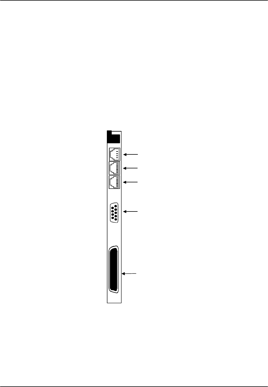
Reference Guide v3.6 Interface Card
(10-97) Page 6-A-1
Introduction
The interface card provides all communications connections to the system. This section
discusses general Interface Card information, as well as specific settings for the
Interface Card.
All Interface cards must be installed in the IF slot on all chassis.
8920 Interface Card
The 8920 Interface Card has communications, control and network interface ports (see
Figure Interface-1). It features an internal modem that facilitates remote
communication with the system unit. The 8920 has a DB9 (DTE-male) serial port for
network management and two RJ48 jacks that connect to the node port for alarm
notification and VT-100 control terminal port. Additionally, an RJ11 jack is available
for the modem port. The 8920 supports eight T1 or E1 WAN links.
RS232 Control Terminal
Interface Port
RS232 (Male) Management Port
RS485 Node Port
RJ11 Modem Port
WAN Link Connector
Figure Interface-1. 8920 Interface Card Front Panels
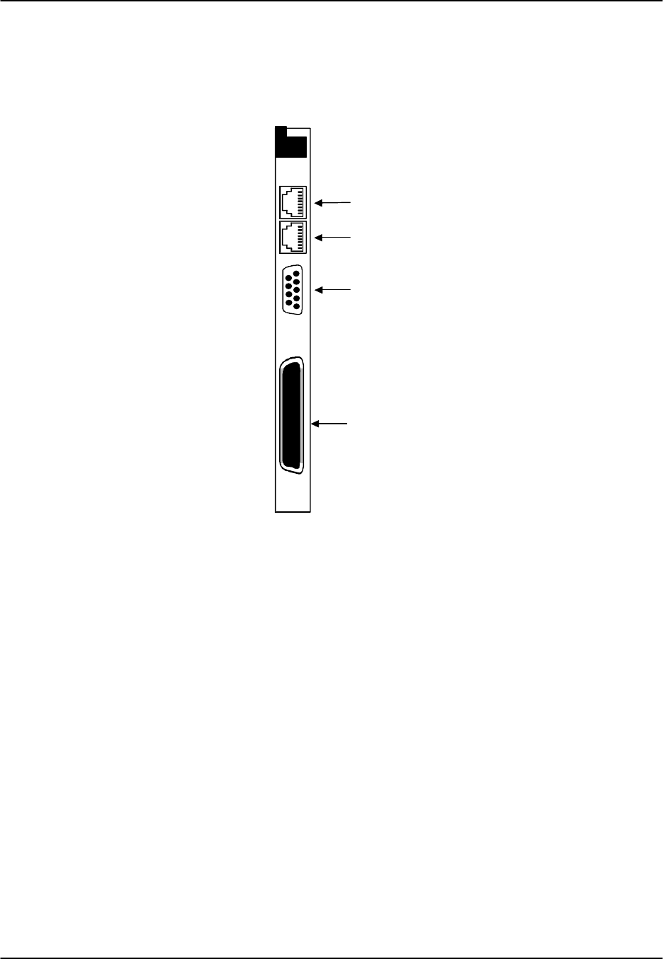
Interface Card Reference Guide v3.6
Page 6-A-2(10-97)
8921 Interface Card
The 8921 Interface Card is similar to the 8920 except there is no modem for remote
access or alarm printing (see Figure Interface-2). All other fittings and functions are the
same.
RS232 Control Terminal
Interface Port
RS232 (Male) Management Port
RS485 Node Port
WAN Link Connector
Figure Interface-2. 8921 Interface Card Front Panels
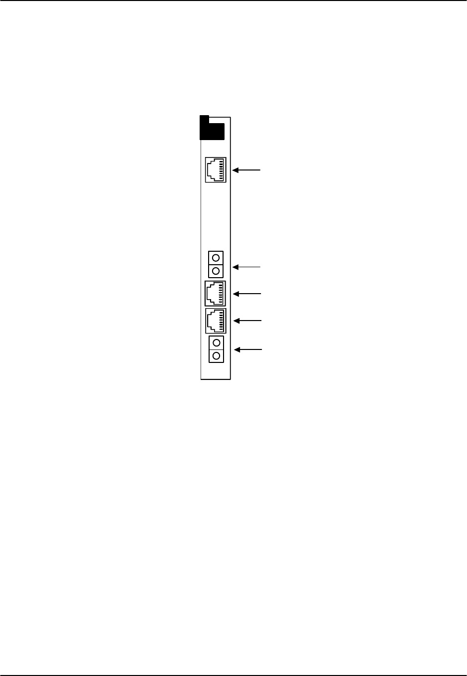
Reference Guide v3.6Interface Card
(10-97) Page 6-A-3
Interface Card (8925)
The 8925 Interface Card uses RJ48 jacks to terminate two (2) T1’s and Bantam
connectors to terminate two T1 WAN links and an RS232 control terminal interface
port or balanced 120 ohm E1. The computer port, modem port and node port are not
available on this interface card. The interface card connectors are arranged as shown in
Figure Interface-3.
RS232 Control Terminal
T1 WAN Connector (WAN 1-2)
Interface Port
WAN 1-2 Bantam Jack
WAN 1-1 Bantam Jack
T1 WAN Connector (WAN 1-1)
TX
RX
TX
RX
Figure Interface-3. 8925 Interface Card Ports
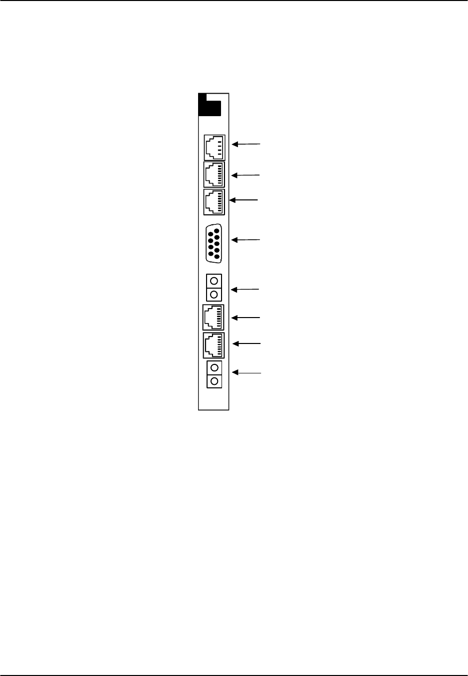
Interface Card Reference Guide v3.6
Page 6-A-4(10-97)
Interface Card (8926)
The 8926 Interface card is similar to the 8925 Interface card with the addition of the
computer port, node port and modem port. The interface card connectors are arranged
as shown in Figure Interface-4.
RS232 Control Terminal
T1 WAN Connector (WAN 1-2)
Interface Port
WAN 1-2 Bantam Jack
WAN 1-1 Bantam Jack
T1 WAN Connector (WAN 1-1)
TX
RX
TX
RX
RS232 (Male) Management Port
RS485 Nodal Port
RJ11 Modem Port
Figure Interface-4. 8926 Interface Card Port

Reference Guide v3.6Interface Card
(10-97) Page 6-A-5
Interface Card (8927)
The 8927 Interface Card uses BNC connectors to terminate two E1 WAN links, a DB9
computer port, an RJ48 control terminal interface port and an RJ48 node port. The
interface card connectors are arranged as shown in Figure Interface-5.
RS232 Control Terminal
E1 WAN Connector (WAN 1-2)
Interface Port
E1 WAN Connector (WAN 1-1)
TX
RX
TX
RX
RS485 Nodal Port
RS232 Computer Port
Figure Interface-5. 8927 Interface Card Port
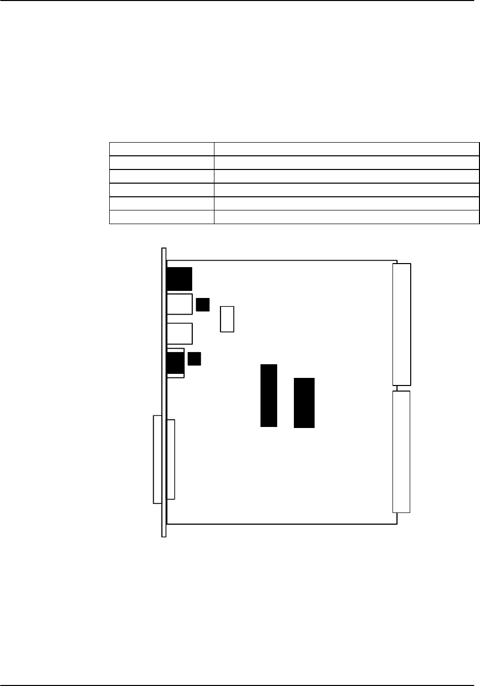
Interface Card Reference Guide v3.6
Page 6-A-6(10-97)
Interface Card Ports and Functions
The Interface card controls many critical functions in the system. It provides interfaces
to external control devices, terminates all T1 and E1 WAN links, and holds the
nonvolatile RAM and the internal modem. Table Interface-1 lists the interface ports
and functions. Figure Interface-6 shows the component layout and labels the ports. See
the Pinouts chapter for electrical specifications and pin assignments.
Table Interface-1. Interface Ports and Functions
Interface Ports Function
Modem Connects the internal modem to a phone line.
Node Provides contacts to report ACO alarms.
Control Terminal Connects the system to a VT-100 compatible terminal.
Computer Connects a local device for printing alarms; or to NMS..
T1/E1 WAN link Connects the system to T1 and E1 lines.
Modem Line
(no modem on 8921)
Nodal Port
VT-100 Control Terminal
DB-9 Serial Port
Amphenol Connector
for WAN Connections
Power
Bus
Edge
Connectors
Figure Interface-6. Component Layout for the 8920 and 8921 Interface Card

Reference Guide v3.6Interface Card
(10-97) Page 6-A-7
Internal Modem
The internal modem is an asynchronous CCITT V.22 bis modem. It allows remote
access to the terminal interface and automatic logging of alarm messages to a remote
device. Table Interface-2 lists the parameters and rating specifications of the internal
modem.
Table Interface-2. Modem Specifications
Parameter Rating
Compatibility CCITT V.22 bis
Modulation 16 point QAM
Line Interface 2-wire balanced 600 ohms
Approval FCC Part 68
Equalization receive automatic adaptive
transmit fixed compromise
Receiver Sensitivity ON to OFF threshold -45 dBm
OFF to ON threshold -48 dBm
Dialing Mode DTMF Tone
Speed Supported 2400 bps asynchronous
Code Set 8-bit characters plus one stop bit with no parity
Ringer Equivalence 0.2 A
Transmit Level -9.5 dBm
Logging On Remotely
Normally a local network operator uses a VT-100 terminal to directly access the
terminal interface. But where central control or service access is required, the internal
modem provides an access method to the terminal interface from a remote location. .
The modem automatically answers any incoming calls. The modem communicates at
2.4kbps using 8 data bits, one stop bit and no parity
To initiate a call, the remote operator dials in using a VT-100 compatible terminal. The
remote operator can press the <Enter> key to display the log-on screen. After entering
a valid password, the remote operator has complete access to the terminal interface as
described in the Basic Operations chapter.
To disconnect, the remote operator logs off and hangs up the line. The modem
automatically resets and waits for another call.
If an operator is logged on to the system with a local terminal when a modem call is
received, he will automatically be logged off the system and will not be able to restore
local access until the modem connection is broken.

Interface Card Reference Guide v3.6
Page 6-A-8(10-97)
Using the Node Port
The node port allows the system to report ACO (Alarm Cutoff) alarms to an external
system to alert the operator to critical situations. Using the ACO function, (see Basic
Operations chapter), keeps the alarm active until manually cleared from the terminal.
The node port uses an RJ48 connector. Pins 3, 4 and 5 form an RS485 compatible c-
contact closure that can be used to report ACO alarms to an external system. Pins 1, 2,
6 and 7 are reserved for future use. Pin 8 is a ground.
Connecting the ACO alarm interface to an external alarm device (such as a buzzer or
light) alerts you to problems with the system. Figure Interface-7 shows a possible
configuration connecting a unit to a generic external alarm system. The nominal input
is 5V and the short-circuit current is 250mA. See the Pinouts chapter for pin
assignments.
The alarm interface is activated by the ACO setting discussed in the Basic Operations
chapter. This will activate the device when a designated alarm occurs. The Basic
Operations chapter fully discusses conditions and settings necessary to enable this
feature.
Interface Card
Nodal Port
Designation
Pin #
Amp
Amp
Common
External Alarm
System
+N
1
2
3
4
5
6
7
8
-N
ANO
ANC
ACOM
+F
-F
GND
ANO = Open to ACOM on Alarm
ANC = Closed to ACOM on Alarm
Figure Interface-7. Node Port ACO Alarm Interface

Reference Guide v3.6Interface Card
(10-97) Page 6-A-9
Interface Card Settings
Figure Interface-8 shows the interface card Main screen. Table Interface-3 lists the
settings controlled on the screen along with their possible and default values.
Node_1 | IF INTF+modem 8920 Rev A2-0 Ser 01103 | 12-31-99 16:46
1
PRIMARY CLK int
SECONDARY CLK w1-1
EXTERNAL CLK rcv
CURRENT CLK int
Save | Undo | Refresh | Time | ACO | proFiles | taBs | Ports | Main
Figure Interface-8. Interface Card Main Screen
Table Interface-3. Main Screen Options and Defaults
Parameter User Options Default
PRIMARY CLK int w1-1 through w4-2 ext (not used) int
SECONDARY CLK int w1-1 through w4-2 ext (not used) w1-1
EXTERNAL CLK rcv gen rcv
CURRENT CLK unchangeable int
PRIMARY CLK
The Primary Clock provides all internal timing for the system. Two clock sources are
possible: a network source or the internal crystal oscillator.
A network clock source provides the best Primary Clock source. If you use a network
clock source, you must specify the WAN link to which the clock source is connected;
for example, w1-1. A WAN clock source will be either 1.544 or 2.048 Mbps depending
on whether you are using a T1 or E1 line and must be accurate to ±50 parts per million
(or ±50 x 10-6).

Interface Card Reference Guide v3.6
Page 6-A-10 (10-97)
Alternatively, the system can generate a clock from its own crystal. If you select int,
the crystal provides the clock source for this unit. The stability of this Stratum 4 clock
is ±25 parts per million (or ±25 x 10-6). If you use the system internal crystal as a clock
source, all other devices attached to the network should derive their clocking from the
internal clock as well. The Primary Clock can be set to external (ext), but this feature
is not supported in this release.
SECONDARY CLK
Should the Primary Clock signal fail, the system automatically reverts to the defined
Secondary Clock source. This source may also be a WAN link or the internal crystal.
Although a secondary clock source is not required, good network design dictates that
you have a backup if one is available. This clock cannot be external. Selection of ext
will generate an error message.
EXTERNAL CLK
Reserved for future use.
CURRENT CLK
The current clock shows the clock now in operation. This field is not accessible by the
user.
Menu of Actions
Table Interface-4 shows the Menu of Actions for the Interface Card.
Table Interface-4. Interface Card Screen Menu of Actions
Action Function
Save Saves changes to settings.
Undo Returns all settings to the last saved state.
Refresh Used on Testing and Monitoring screens to update statistics and on
other screens to redraw the screen.
Time Sets the system time and date. Use the up and down arrows to make
changes.
ACO ACO alarm. See the Alarm section of the Basic Operations chapter.
proFiles Profiles function unoperable with this release.
taBs Conversion tables for ABCD bits from ANSI to CCITT for voice
circuits. See “Conversion Tables” later in this chapter.
Ports Allows users to update and set the protocol, rate, communication
configuration, and handshake of the communications ports on the
interface card.
Main Returns to the Main screen. If changes are made to settings and not
saved, you will be prompted to save or lose changes.

Reference Guide v3.6Interface Card
(10-97) Page 6-A-11
Signaling Conversion Tables
The Signaling Conversion Tables are especially useful when cross-connecting a T1
(ANSI) voice circuit to E1 (CCITT). Changing the ABCD signaling bits to facilitate
proper signaling between the two carrier types may be necessary for proper system
operation.
All types of voice circuits (E&M, FXS, FXO and PLAR) can access the ABCD
Signaling Bit Conversion Tables for changes to their respective patterns.
The user can accept the default bit pattern changes or manually override those settings
and choose a different bit pattern and insert it into the table. Figure Interface-9 shows
the Conversion Tables accessed by pressing the "B" (taBs). Each voice circuit type is
represented by two columns corresponding to CCITT to ANSI (C->A) and ANSI to
CCITT (A->C) conversion of ABCD bits.
Node_1 b | IF INTF+modem 8920 Rev A2-0 Ser 01103 | 12-31-99 16:46
E&M FXS FXO PLAR
ABCD C->A A->C C->A A->C C->A A->C C->A A->C
0000 0000 1101 0101 0101 0101 0101 1111 0101
0001 0000 1101 0101 0101 0101 0101 1111 0101
0010 0000 1101 0101 1101 0101 1101 1111 1101
0011 0000 1101 0101 1101 0101 1101 1111 1101
0100 0000 1101 0101 1101 0101 1101 1111 1101
0101 1111 1101 0000 1101 1111 1101 0000 1101
0110 0000 1101 0101 1101 0101 1101 1111 1101
0111 0000 1101 0101 1101 0101 1101 1111 1101
1000 0000 1101 0101 1101 0101 1101 1111 1101
1001 0000 1101 0101 0101 0101 1101 1111 1101
1010 0000 1101 0101 0101 0101 1101 1111 1101
1011 0000 1101 0101 1101 0101 1101 1111 1101
1100 0000 1101 0101 1101 0101 1101 1111 1101
1101 0000 0101 0101 0101 0101 1101 1111 1101
1110 0000 1101 0101 1101 0101 1101 1111 1101
1111 0000 0101 0101 0101 0101 1101 1111 1101
Save | Undo | Refresh | Default | Main
Figure Interface-9. Conversion Tables Screen
For instance, an E&M circuit in the "0101" state will send "0101" from the CCITT end
of the circuit and the ANSI end would receive "1111" Conversely, the same state
would be sent as "1111" from the ANSI end and received at the CCITT end as "0101."
Either receive bit pattern can be manually overridden by the user.
The E&M portion of the conversion table is also used for DN, PLAR-D3, DPO and
DPT. The FXS portion of the conversion table is used for FXS from FXO. The FXO
portion of the conversion table is used for FXO to FXS. The PLAR portion of the
conversion table is also used for PLAR-D4 to PLAR and MRD.

Interface Card Reference Guide v3.6
Page 6-A-12 (10-97)
Menu of Actions
Table Interface-5 shows the Menu of Actions for the Conversion Tables screen.
Table Interface-5. Conversion Tables Screen Menu of Actions
Action Function
Save Saves changes to settings.
Undo Returns all settings to the last saved state.
Refresh Used on Testing and Monitoring screens to update statistics and on other
screens to redraw the screen.
Default Returns columns to default settings, one column at a time. The user must
save changes after using this command.
Main Returns to the Interface card main screen. If changes are made to
settings and not saved, you will be prompted to save or lose changes.
Remote Terminal System (RTS)
The Remote Terminal System (RTS) is a special application for users using microwave
transmission. Using communication software, a user can log into any number of
different systems from a single control station (PC, MAC, Sun, or HP Workstation) to
download alarm information, change card settings, and perform maintenance.
Systems are connected from the Interface card’s COM port to a wireless control
network through the RS232 input on one of the four service channels on the wireless
network. The Control Station (PC) is connected to pin #2 out and #3 in. Each of the
integrated access controllers is connected to RS232 pin #2 in and pin #3 out.
The actual number of the systems that can be connected together is determined by the
amount of different numbers that can fit in the “SYS PH#” field in the CPU sub menu.
The CPU sub menu is accessed by selecting a CPU through the user interface and
pressing the <ENTER> key.
Identification
Each system has a unique identification number on the integrated access controller
network (phone number). The unique identification number is used to determine which
Controller can be accessed remotely on a serial line. The identification number for
each console needs to be entered in the “SYS PH#” field in the CPU sub menu. No two
systems can have the same number in the “SYS PH#” on the same network. If that field
is the same on more than one integrated access controller, race conditions will occur.
Therefore each console on a single network must have an individual number in the
“SYS PH#” field.
The identification numbers for the integrated access controllers cannot be entered
through a control station. This safeguard is provided to ensure a reliable connection
between a control station and an integrated access controller. Attempts to change an
identification number of a system remotely will be denied.
Reference Guide v3.6Interface Card
(10-97) Page 6-A-13
Network Priorities
All integrated access controllers on the wireless network have equal priorities. Because
of this equality, no Controller can interrupt a remote session between another Controller
and a control station. This is why the control station always initiates all communication
on the RTS network.
Intra-Network Communications
Integrated access controllers cannot communicate with each other. Communication on
the network is only between the control station and a single Controller. Since the
communications on the network of integrated access controllers is always initiated by
the control station, the Controller systems cannot communicate with each other.
Figure Interface-10 shows a diagram of three RTS units.
System
PC #34 #35 #36
System System
Figure Interface-10. Typical RTS Configuration
The PC associated with integrated access controller #34 can engage any of the two
other units by using "AT" commands from the communications software used. If a
local VT-100 is active at any of the remote locations, the user will be logged off and the
master PC will control the system unit. When the master PC logs off, the local user
will be able log into the unit again. Connections at all units are done through the DB9
computer port.
Terminal Security
No user may log into any integrated access controller on the network without knowing
the individual password of each system.
Table Interface-6 lists the "AT" commands and the associated function. All "AT"
commands are followed by pressing the <Enter> key.
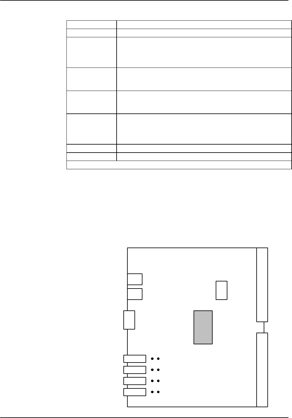
Interface Card Reference Guide v3.6
Page 6-A-14 (10-97)
Table Interface-6. "AT" Commands Used by RTS
AT Command Function
ATDTxxx Establish a user interface connection.
ATDTxxxR Establish an alarm reporting connection. (Connection only lasts
for the length of time necessary to upload and display all alarms
that are being reported by the system that have not yet been
displayed.)
ATDTxxxC Establish a current alarm reporting connection. (Connection only
lasts for the length of time necessary to upload and display all
active alarms that are being reported by the system.)
ATDTxxxH Establish a historical alarm reporting connection. (Connection
only lasts for the length of time necessary to upload and display
the alarm history reported by the system.)
ATDTxxxCH Establish a current and historical alarm reporting connection.
(Connection only lasts for the length of time necessary to upload
and display the current alarms and alarm history reported by the
system.)
+++ Disconnects a remote session.
"L" (letter L) Disconnects a remote session.
xxx indicates the phone number on the CPU card of the desired system unit.
Changing the 8927 from Balanced to Unbalanced
The jumpers on the 8927 dual E1 Interface card change the operation of the E1 link
from balanced to unbalanced. Figure Interface-11 shows the card layout with the
position of jumper JP2, JP3, JP5, and JP4. The card is shipped with the jumpers open
(the balanced position). To change the E1 link for WAN 1-1 to unbalanced, close
jumpers JP2 and JP3. To change the E1 link for WAN 1-2 to unbalanced, close
jumpers JP5 and JP4.
Node Port
VT-100 Port
DB9 Serial
WAN1-2
WAN1-1
T
T
R
R
JP4
JP5
JP3
JP2

Reference Guide v3.6Interface Card
(10-97) Page 6-A-15
Figure Interface-11. Jumpers on the 8927 Card

Reference Guide v3.6 External Alarm Cards
(10-97) Page 6-B-1
Introduction
The External Alarm card performs two alarm-notification functions. The "Switch/Act
On" (outbound) function allows the system to report internal alarms to external devices
such as buzzers, bells or lights. The "Sensor/Trig On" (inbound) function allows
externally generated alarms to be reported to the system through sensors that are located
on the card.
This chapter discusses the three External Alarm cards available for use with the
integrated access system: the 8401, 8402, and 8403. Only one External Alarm card may
reside in the integrated access system at a time. The 8401 and 8402 offer 4 and 3
inbound and outbound alarm circuits, respectively, and have a similar architecture.
They will be discussed together at the start of the chapter. The 8403, which offers
additional capabilities (28 inbound and 14 outbound), is discussed at the end of the
chapter.
8401 External Alarm Card
The 8401 External Alarm card supports four (4) outbound switches and four (4)
inbound sensors. The outbound switches are used to report internal alarms to external
devices by triggering form-C contact closures (120VAC - 0.5A), and the inbound
sensors are used to bring foreign alarm indications into the system. External alarms that
are reported by a sensor are listed in the alarm history file.
8402 External Alarm Card
The 8402 External Alarm card supports three (3) outbound switches and three (3)
inbound sensors. This card is similar to the 8401 except the fourth alarm port can only
be used as an outbound alarm to show that the system’s power unit has failed. This
card would be especially helpful when used in locations where loss of power to any of
the units would be a critical problem.
A -48VDC power source is required with this card. It may be provided by the 8905
Converter or from an external source.

External Alarm Cards Reference Guide v3.6
Page 6-B-2(10-97)
IMPORTANT NOTE
To enable the reporting of alarms originating from sensors the SENSOR variable in the
Alarm Filters menu must be set to report (see “Filters” in Chapter 2C, “Basic
Operations”). From the system Main Menu, select Alarms, and choose Filters to
display a menu of alarm filters shown below. Use the arrow keys to highlight the first
column of the SENSOR line. Press <Enter> to display the options ignore, log, and
report. The option chosen here will act as the highest level option for all alarm card
sensors. If this variable is set to ignore, any alarm conditions from the alarm sensors
will be ignored, even if individual sensors are set to report at the alarm card.
Likewise, if this variable is set to log, all of the sensors on the alarm card that are set to
anything but ignore will be logged, but not reported. For this reason, it is crucial that
the SENSOR Alarm Filter be set to report.
Node_1 | | 12-31-99 14:33
1 2 3
OOS
Out of Service
log
major
aco-off
NOS
No Signal
log
minor
aco-off
LOS
Loss of Sync
log
minor
aco-off
YEL
Yellow Alarm
log
minor
aco-off
AIS
Alarm Info Signal
log
minor
aco-off
CGA_RED
Carrier Group
–
Red
log
major
aco-off
CGA_YEL
Carrier Group
–
Yellow
log
major
aco-off
EER
Excessive Error Rate
ignore
minor
aco-off
SENSOR
Alarm card sensor
report
minor
aco-on
DCHAN
D-chan out of service
ignore
minor
aco-off
SWITCH
Switch to redundant card
report
major
aco-off
UCA
User card/port alarm
ignore
minor
aco-off
RESET
System reset
report
major
aco-off
ACO
Alarm Cut-Off
log
minor
n/a
SYNC
Clock Sync Alarm
ignore
minor
aco-off
EER-3
Error rate above 10e-3
ignore
minor
aco-off
PLC_OOF
DS3 PLCP Out of Framing
ignore
minor
aco-off
PLC_LOF
DS3 PLCP Loss of Frame
ignore
minor
aco-off
PLC_YEL
DS3 PLCL Yellow Alarm
ignore
minor
aco-off
Save | Undo | Refresh | Main

Reference Guide v3.6External Alarm Cards
(10-97) Page 6-B-3
External Alarm Card Screens (8401 and 8402)
Figure Alarm-1 shows the External Alarm Card screen for the 8401; the 8402, with only
3 ports would have only 3 columns of options. Table Alarm-1 shows the settings and
options.
Node_1 | U1 ALR 8401 Rev B0-0 Ser 00101 | 12-31-99 14:33
1 2 3 4
SWITCH stdby stdby stdby stdby
ACT ON minor minor minor minor
SENSOR stdby stdby stdby stdby
TRIG ON close close close close
Major = 0 Minor = 0
Save | Undo | Refresh | Main
Figure Alarm-1. External Alarm Card Screen
Table Alarm-1. External Alarm Card Setting Options and Defaults
Parameter User Options Default
SWITCH stdby actv stdby
ACT ON minor major any minor
SENSOR stdby actv stdby
TRIG ON close open close
SWITCH
The Switch setting indicates if the outbound alarm switch is on (actv) or off (stdby).
ACT ON
The Act On parameter defines the type of system alarm that will cause the switch to
trigger. You can program each alarm switch to trigger on minor (info and minor)
alarms, major (major and critical) alarms or any alarm message. See the Alarms
section of the Basic Operations chapter for more information on how you define an
alarm as major or minor.
SENSOR
The Sensor setting indicates if the inbound alarm sensor is on (actv) or off (stdby).

External Alarm Cards Reference Guide v3.6
Page 6-B-4(10-97)
TRIG ON
The Trigger On parameter defines if the sensor should report an external alarm upon
sensing the opening (open) or the closure (close) of the C-form contact to which it is
connected.
Major=
The Major= accumulation register shows the current number of reported alarms that are
designated either Major or Critical.
Minor=
The Minor= accumulation register shows the current number of reported alarms that are
designated either Minor or Informational.
Menu of Actions
Table Alarm-2 shows the Menu of Actions for the External Alarm Card.
Table Alarm-2. Alarm Card Screen Menu of Actions
Action Function
Save Saves changes to settings.
Undo Returns all settings to the last saved state.
Refresh Updates certain time-related information fields that are not
automatically updated (i.e. performance and test data).
Main Returns to the main terminal screen. If changes are made to settings
and not saved, you will be prompted to save or lose changes.

Reference Guide v3.6External Alarm Cards
(10-97) Page 6-B-5
8403 External Alarm Card
Introduction
The 8403 External Alarm Card supports 28 sensor inputs and 14 external device ports.
Of the 14 external device controls, 8 are Form C contacts (normally open or closed
based on user configuration), 4 are Form A contacts (normally open), and 2 are Form B
contacts (normally closed).
In addition, the card provides an FXS type telephone interface (RJ-11 jack, loop start
only, no ringer interface) and an on-board piezoelectric buzzer with either internally
generated and customer-selected alarm sounds or sounds transmitted by the network.
In the on-hook condition, ring signaling turns on the buzzer with either a locally stored
ringback pattern or a network-provided signal. In the off-hook conditions, voice output
of the transcoder is routed to the transformer. In an alarm condition, if the sound option
is enabled, a 3,000 Hz signal is routed to the buzzer.
All sensor inputs are current loop type (4-20 ma current detection). All sensors can be
either active (surge protection only) or optically isolated passive current detectors.
Active sensors can be powered by either the network battery (-48 VDC) or by the main
power supply (+12VDC).
The 8403 External Alarm Card is shown in Figure Alarm-3, emphasizing the positions
of switches and jumpers used to configure the card. All switches and jumpers should be
set prior to installation.

External Alarm Cards Reference Guide v3.6
Page 6-B-6(10-97)
Alarm Sensors
Figure Alarm-2 shows page 1 of 3 Alarm Sensors Card screens. Table Alarm-3 lists the
settings controlled on the screen along with the possible and default values.
Node_1 | U1 ALR 8403 Rev B0-0 Ser 00101 | 12-31-99
14:33
page: 1 of 3 ALARM SENSORS
# SENSOR NAME TRIG ON STATUS ALARM TYPE BUZZER
1 close log major on
2 close log major on
3 close log major on
4 close log major on
5 close log major on
6 close log major on
7 close log major on
8 close log major on
9 close log major on
10 close log major on
Refresh | dEfault | pgUp | pgDn | sWitches | Voice |
Main
Figure Alarm-2. External Alarm Card (8403) Sensors Screen
Table Alarm-3. External Alarm Card (8403) Sensors Screen Options and Defaults
Parameter User Options Default
#[Alarm Sensor number 1-28] fixed
SENSOR NAME [user-input sensor name] blank
TRIG ON close open close
STATUS ignore log report ignore
ALARM TYPE info minor major crit minor
BUZZER off on off
SENSOR NAME
A user input field of up to six (6) characters to identify the specific alarm. (Note: The
sensor name is a local identifier, and is not transmitted with alarm conditions.)
TRIG ON
The Trigger On parameter defines if the sensor should report an external alarm upon
sensing the opening (open) or the closure (close) of the contact to which it is connected.
The default value is close.

Reference Guide v3.6External Alarm Cards
(10-97) Page 6-B-7
STATUS
This value indicates what action should be taken in the event of an alarm for each
individual sensor. This variable may be set to log the alarm in the alarm register, or to
report the alarm. (Reported alarms are also logged.) The default value is ignore.
ALARM TYPE
This user-definable parameter indicates the severity of the incoming alarm. The
options are info, minor, major, and crit. The default value is minor.
BUZZER
This variable indicates whether the onboard buzzer should be activated when the sensor
indicates an alarm. The default value is off.
Menu of Actions
Table Alarm-4. External Alarm Card (8403) Sensors Screen Menu of Actions
Action Function
Refresh Redraws the screen.
dEfault Returns all settings to the default state.
pgUpUse to return to previous page.
pgDnUse to go to next page
sWitches Changes to the Switches screen.
Voice Changes to the Voice screen.
Main Returns to the main sensor screen. If changes are made to settings
and not saved, you will be prompted to save or lose changes.

External Alarm Cards Reference Guide v3.6
Page 6-B-8(10-97)
Alarm Switches
Figure Alarm-3 shows the first of two pages of the Alarm Switches screen. Table
Alarm-5 lists the settings controlled on the screen along with the possible and default
values.
Node_1 | U1 ALR 8403 Rev B0-0 Ser 00101 | 12-31-99 14:33
page: 1 of 2 ALARM SWITCHES
# SWITCH NAME SW. CTRL ACT ON SENSOR # STATUS
1 act_on major n/a off
2 act_on major n/a off
3 act_on major n/a off
4 act_on major n/a off
5 act_on major n/a off
6 act_on major n/a off
7 act_on major n/a off
Refresh | dEfault | pgUp | pgDn | Main
Figure Alarm-3. External Alarm Card (8403) Switches Screen
Table Alarm-5. External Alarm Card (8403) Switch Screen Options and Defaults
Parameter User Options Default
#[Alarm Switch number 1-14] fixed
SWITCH NAME [user-input switch name] blank
SW. CTRL off on act_on act_on
ACT ON info minor major crit sensor major
SENSOR # n/a 1-28 Note
1n/a
STATUS off on displayed
Notes: 1. Sensor numbers are assignable if the ACT ON parameter is
set to sensor numbered 1 -28, the default is 1.
SWITCH NAME
A user-input field up to six (6) characters to identify the specific switch. (Note: The
switch name is a local identifier, and is not transmitted with alarm conditions.)

Reference Guide v3.6External Alarm Cards
(10-97) Page 6-B-9
SW. CTRL
This variable indicates the initial state of the switch. The possibilities are off (which
unconditionally turns the switch off), on (which unconditionally turns the switch on) or
act_on (which relies on the state of the switch). The default value is off.
As noted above, 12 of the switches are Form C (which may be either open or closed),
one is Form A (always open), and one is Form B (always closed).
In the event of system power failure, switch #1 can be used as a fail-safe switch to
activate a device that notifies the user. In order for this to occur, a jumper must be set
on jumper pair JP63. located towards the center of the card. The contact for switch #1
will close if the system loses power, establishing a circuit that can be used to power an
external warning device. The current source must be provided by the external device.
ACT ON
This parameter defines the condition that will cause the switch to trigger. The user can
program each alarm switch to trigger on info, minor, major, or crit alarms.
Alternatively, the switch trigger can also be assigned to a particular sensor. When
sensor is selected, SENSOR # allows the user to indicate the number of the sensor that
will trigger the alarm. The default value is major.
SENSOR #
When the ACT ON field is set to sensor, the user can input a value from 1 to 28,
indicating the number of the sensor that will trigger the switch. The default value is
n/a.
STATUS
This is a display-only field. The user cannot access it.
Menu of Actions
Table Alarm-6. External Alarm Card (8403) Switches Screen Menu of Actions
Action Function
Refresh Updates certain time-related information fields that are not
automatically updated.
dEfault Returns all settings to the default state.
pgUpReturns user to previous page.
pgDnAdvances user to next page.
Main Returns to the main sensor screen.

External Alarm Cards Reference Guide v3.6
Page 6-B-10 (10-97)
Voice
An RJ11 FXS voice port is situated on the front of the card between the two Amphenol
connectors. The initial voice screen is shown in Figure Alarm-4. The options and
defaults are shown in Table Alarm-7.
Node_1 | U1 ALR 8403 Rev A0-0 Ser 0101 | 12-31-99 14:33
1
STATE actv
WAN/SRV w1-1
TS 20
MODE plar
TYPE d3-m1
Rx TLP -5.0
Tx TLP 2.0
CODING u-law
RINGBK off
Save | Undo | Refresh | Main
Figure Alarm-4. External Alarm Card (8403) Voice Screen
Table Alarm-7. External Alarm Card (8403) Voice Screen Options and Defaults
Parameter User Options Default
STATE stdby actv stdby
WAN/SRV none w1-1 through w4-2 none
TS 1-24 (1-31) n/a
MODE fxs plar fxs
TYPE loop d3-m1 d4-m1 d3-m2 d4-m2 d3-m3
d4-m3 loop
RX TLP -10.0 to +2.0 -5.0
TX TLP -10.0 to +5.0 2.0
CODING u-law a-inv a-law u-law
RINGBK off on off
STATE
The State setting determines whether the port is active or inactive. An inactive port
does not occupy a time slot on a WAN link. Set the State setting to stdby (standby) for
ports you are not using or have not yet configured. Set it to actv (active) for ports that
are ready for use. The default value is stdby.

Reference Guide v3.6External Alarm Cards
(10-97) Page 6-B-11
WAN
The WAN setting identifies the WAN link assigned to this port. It is not necessary for
all ports on the same card to be assigned to the same WAN link, or to contiguous time
slots on a WAN link. The default value is none.
TS
The TS setting identifies the time slot on the WAN link to which this port is assigned.
Values range from 1-24 for T1 links and 1-31 for E1 links. Time slot 16 is not
available on E1 links that are programmed for cas or ccs signaling. For a display of the
available time slots, refer to your cross-connect map for the WAN link; see the System
Operations chapter for information about viewing cross-connect maps. The default
value is n/a.
MODE
The Mode setting should be determined by the type of equipment to which you are
connecting the port. All options use two-wire balanced connections. The fxs (Foreign
Exchange Station) option allows you to connect a telephone to the system.
The plar (private line automatic ringdown) option provides point-to-point unswitched
connections between two telephone sets. This configuration is usually not attached to
an exchange or switch; rather, it provides a “hot line” between two locations.
TYPE
The Type setting matches the signaling behavior of the FXS equipment and the remote
switch. The loop (Loop Start) option, which is used with POTS stations and simple
PBX trunks, is only available when the MODE setting is fxs. If the MODE setting is
plar, then the TYPE options are d3-m1, d4-m1, d3-m2, d4-m2, d3-m3, and d4-m3.
Caution: Before activating this port, verify the behavior expected by both the station
equipment and the remote central office equipment and ensure that you have the system
properly configured.
Rx TLP
The Receive Transmission Level Point setting controls the amount of gain or
attenuation added to signals after they are decoded to analog signals. To increase the
signal level, set the Rx TLP setting to a positive number (i.e., the larger the number, the
more gain is added). To decrease the signal level, set the Rx TLP setting to a negative
number (i.e., the more negative the number, the more the signal level is decreased). For
example, an incoming signal at -5 dBm can be increased to -3 dBm by setting Rx TLP
to +2 dB. Acceptable values range from -10.0 dB to +2.0 dB. The default value is -
5.0.

External Alarm Cards Reference Guide v3.6
Page 6-B-12 (10-97)
Tx TLP
The Transmit Transmission Level Point setting controls the amount of gain or
attenuation added to signals after they are received from the local analog port and
before they are encoded to digital PCM signals. To increase the signal level, set the Tx
TLP setting to a negative number (i.e., the more negative the number, the more gain is
added). To decrease the signal level, set the Tx TLP setting to a positive number (i.e.,
the more positive the number, the more the signal level is decreased). For example, an
incoming signal at -5 dBm can be increased to -2 dBm by setting Tx TLP to -3 dB.
Acceptable values range from -10.0 dB to +5.0 dB. The default value is +2.0.
CODING
The Coding setting sets the PCM companding method used for a port. In general, in the
T1/North American environment use µ-law coding. In the E1/International
environment, use a-inv (inverted A-law) or a-law coding; a-inv provides greater 1s
density than a-law. The coding default is determined by the type of card in the WAN
port you select. The default value is u-law (Note: On the system screens, "u" is used in
place of "µ" because of ASCII character limitations, but should be read as "mu-law.").
RINGBK
The ringback setting specifies whether a ringback tone is generated by the system and
sent towards the network. This option should be turned on when the network does not
provide an audible ringing tone to the calling party. The default value is off.
Menu of Actions
Table Alarm-8. External Alarm Card (8403) Voice Screen Menu of Actions
Action Function
Save Saves changes to settings.
Undo Returns all settings to the last saved state.
Refresh Updates certain time-related information fields that are not
automatically updated on the screen.
Main Returns to the main terminal screen. If changes are made to settings
and not saved, you will be prompted to save or lose changes.
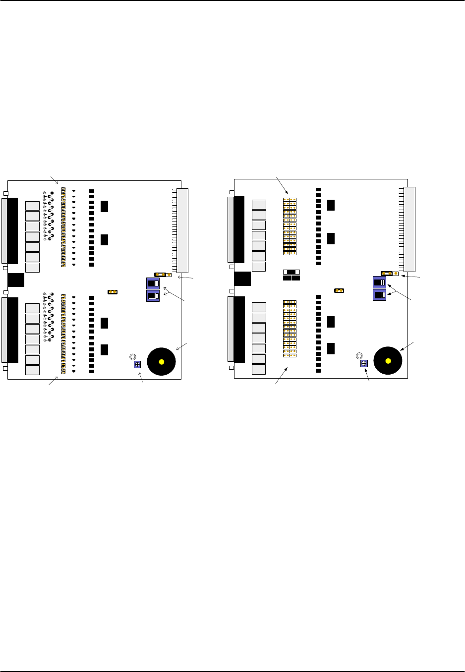
Reference Guide v3.6External Alarm Cards
(10-97) Page 6-B-13
Features
Diagrams of the 8403 External Alarm Card are shown in Figure Alarm-5. Earlier
versions of the card have the alarm sensor jumpers set at angles, as shown in the
diagram on the left, while later versions have the alarm sensor jumpers grouped in
pairs, as shown in the diagram on the right. Otherwise, the two cards are functionally
equivalent.
The features identified in the drawings are discussed in detail below.
Earlier Version Later Version
S
Y
SB
A
T
U
S
E
U
R
Onboard
Buzzer
Buzzer
Volume
Control
US/Euro
Jumper
S1
S2
Voltage
Control
Switches
AlarmSensor
Jumpersfor
ConnectorJ4
AlarmSensor
Jumpersfor
ConnectorJ3
J4
J3
RJ-11
J
P
6
3
SYS
BAT
US EUR
Onboard
Buzzer
Buzzer
Volume
Control
US/Euro
Jumper
S1
S2
Voltage
Control
Switches
Alarm Sensor
Jumpers for
Connector J4
Alarm Sensor
Jumpers for
Connector J3
J4
J3
RJ-11
JP63
JP1
JP2
1 2 6 73SI 4 5 8 9 10 1112 13 14 1516 17 1819 22 23 25 26 272820S I 21 24
JP3
JP4
PASV
ACTV
Figure Alarm-5. External Alarm Card (8403).
Onboard Buzzer
The 8403 alarm card contains an onboard buzzer for audible alarms. The buzzer can be
set to activate when a particular sensor signals an alarm condition. The buzzer volume
is set by a control dial marked "VOL," which can be adjusted using a small screwdriver.
US/Euro Jumper
The card may be set either to US or European configuration by moving a jumper
located on J64. Setting the jumper on the left two pins establishes US configuration.
On the right two pins, the jumper is configured for European voltage. This property
should match the configuration of your particular chassis, or the card will not operate
properly. The factory default is US position.
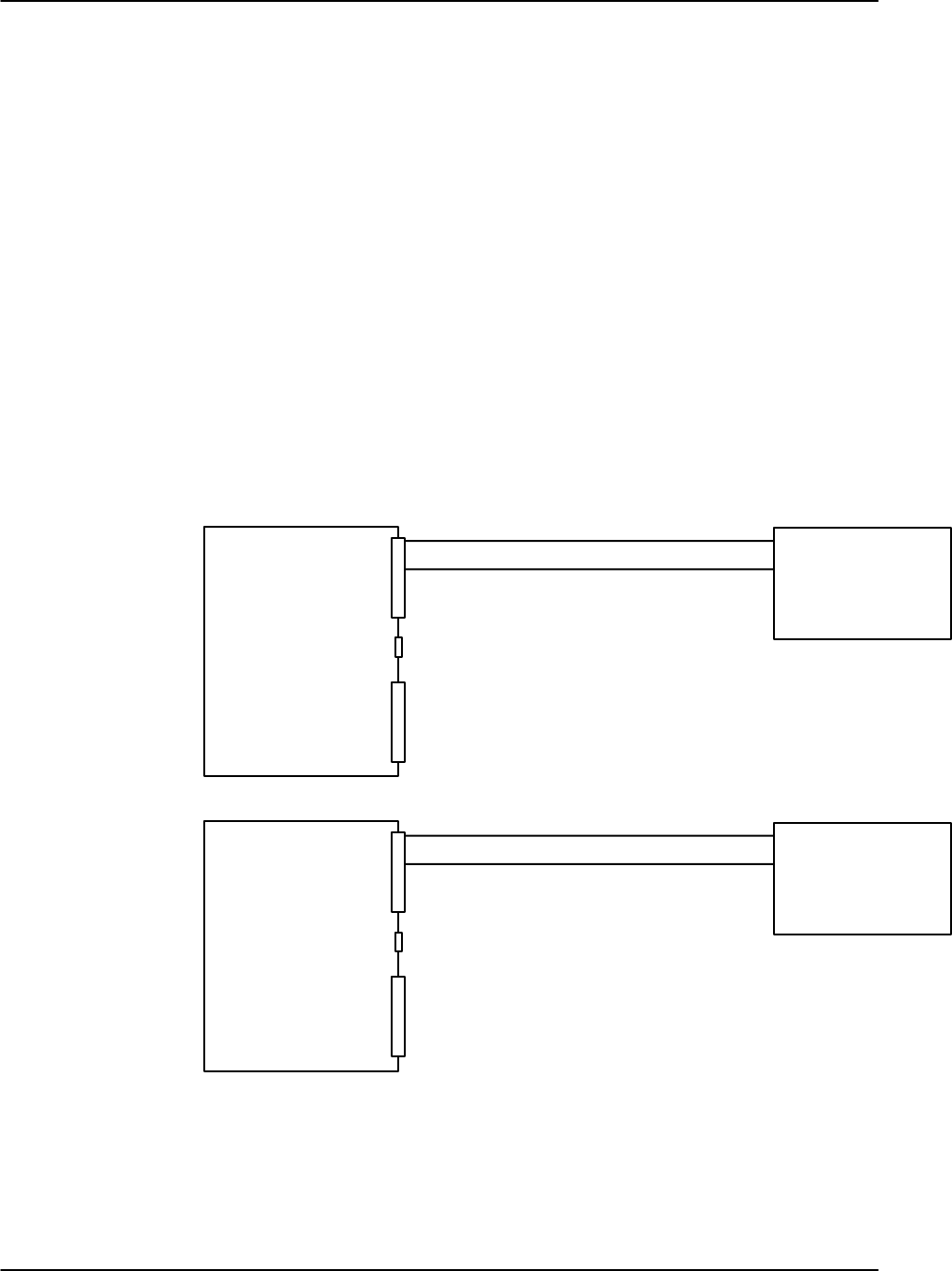
External Alarm Cards Reference Guide v3.6
Page 6-B-14 (10-97)
Voltage Control Switches
Switches S1 and S2 are used to control the voltage supplied to each group of active
sensors. When either of these switches are set to "SYS," the board supplies ±12vDC
system power to the sensor group specific to that Amphenol connector. When either of
the switches are set to "BAT," the board supplies telco power to the sensors in that
group.
The switches can be set individually (meaning one can be set to "SYS" and the other to
"BAT") but doing so will affect all 14 sensors in the respective group.
Switch S1 controls the sensors on the J3 (lower) connector, while Switch S2 controls
the sensors on the J4 (upper) connector.
The factory default for these switches is SYS.
Alarm Sensor Jumpers
Each sensor relates to a pair of jumpers on the board, which controls whether the sensor
is powered from the card (active mode) or from an external device (passive mode).
Passive mode provides 2500V isolation. Figure Alarm-6 displays these options.
Alarm
CardActiveMode
Current
SourceExternal
Device
Alarm
CardPassiveMode
External
Device
Current
Source
Figure Alarm-6. Active Mode vs. Passive Mode.
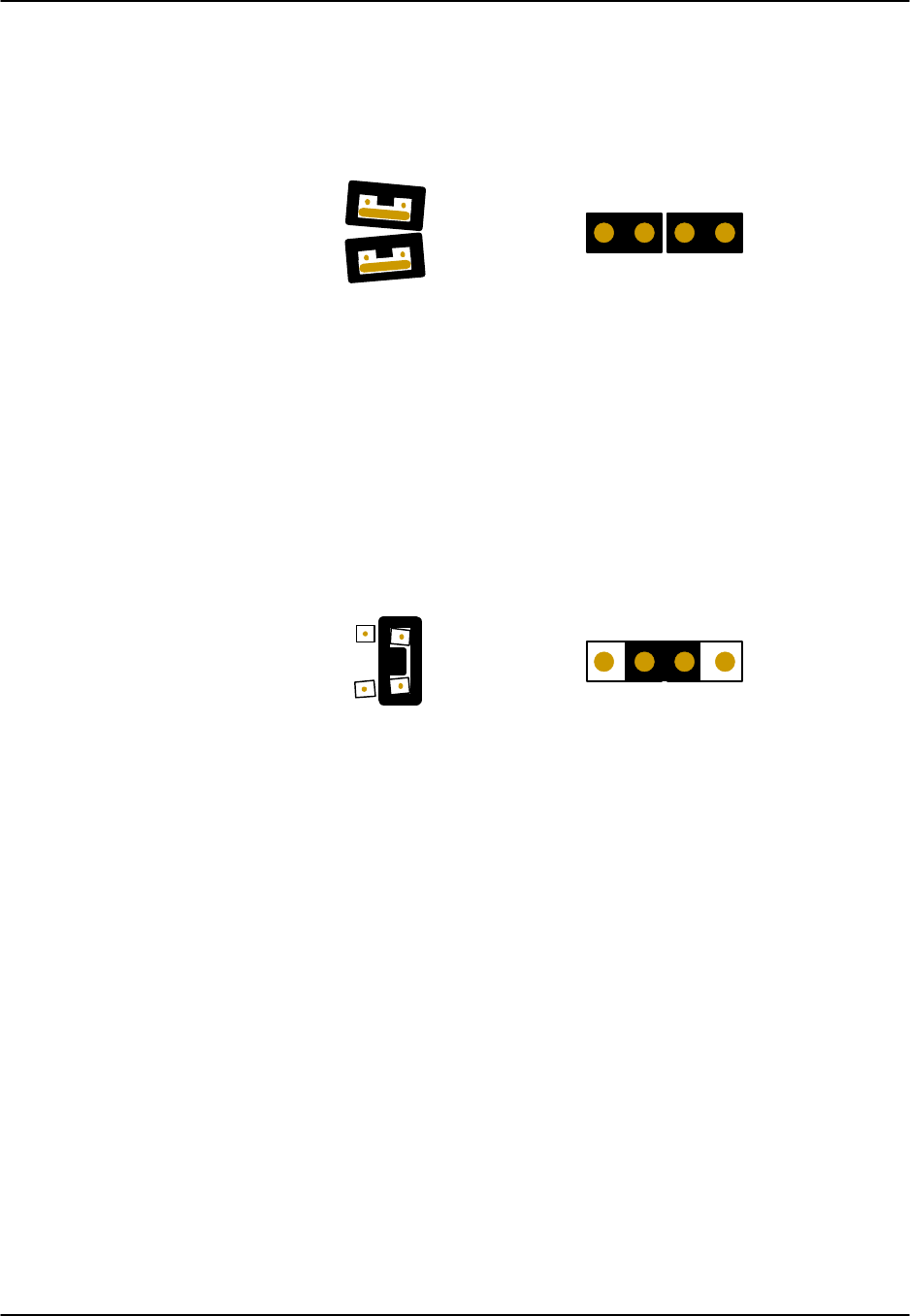
Reference Guide v3.6External Alarm Cards
(10-97) Page 6-B-15
The jumper pairs are set at a slight angle (see Figure Alarm-7). The jumpers are
separated into two groups of 28 jumpers each. The upper group is associated with the
sensors on the upper Amphenol connector (J4), while the lower group is associated with
the sensors on the lower Amphenol connector (J3).
Earlier Version Later Version
Figure Alarm-7. Jumper Pair (Active Mode).
Note: All jumper pairs are set by factory default to active mode.
The default setting, as shown above, is active mode, in which the sensors are powered
by the card. This setting provides surge protection for the sensors.
To set the jumper pair to passive mode, users must remove both jumpers and then insert
a single jumper across the pair, as shown in Figure Alarm-8. The other jumper should
be stowed on one of the unused pins. (The pairs are set at an angle so that the extra
jumper will not fit across the outside pins.) This provides full isolation (to 2500V) for
the sensor.
Earlier Version Later Version
Figure Alarm-8. Jumper Pair (Passive Mode).

External Alarm Cards Reference Guide v3.6
Page 6-B-16 (10-97)

Reference Guide v3.6 E&M Card
(10-97) Page 7-A-1
Introduction
E&M cards manage the flow of voice traffic over the network. The E&M card
translates an analog signal to a digital bitstream at the local system and digital to analog
at the remote system. E&M signaling types I, II, IV and V are supported. Each card
controls four or eight units or channels. Normal E&M, Transmission Only and E&MR2
modes are supported. E&M cards can use voice-compression features of the ADPCM
server card.
8118 E&M Card
The 8118 is a 4-wire 600 Ω E&M/TO card with eight ports. This card has the same
extended range feature as the 8115. All normal E&M features are supported by this
card.
8119 E&M Card
The 8119 is a 4-wire 600 Ω E&M/TO card with eight ports. This card has an extended
TX TLP range (-17.5 to +14.5dB) to support dedicated 4-wire modem applications (this
is especially important for data transmission speeds of 19.2kbps or higher). This card
supports all normal E&M features.
UL Statement
OPERATION OF THIS INTERFACE IS LIMITED TO
INTRA-BUILDING CONNECTIONS ONLY
In addition to the cards shown above, whose operation will be discussed in this chapter,
the following discontinued models are supported by v3.6 software:
8104 E&M Card
The 8104 is a 2-wire E&M car with four ports and 600Ω impedance.
8108 E&M Card
The 8108 is a 2-wire E&M card with eight ports and 600Ω impedance.
UL Statement
OPERATION OF THIS INTERFACE IS LIMITED TO
INTRA-BUILDING CONNECTIONS ONLY

E&M Card Reference Guide v3.6
Page 7-A-2(10-97)
8112 E&M Card
The 8112 is a 4-wire E&M card with two ports and 600Ω impedance.
8113 E&M Card
The 8113 is a 4-wire E&M card with two ports and 600Ω.
8114 E&M Card
The 8114 is a 4-wire E&M card with four ports and 600Ω impedance.
8115 E&M Card
The 8115 is a 4-wire E&M card with four ports and 600Ω.
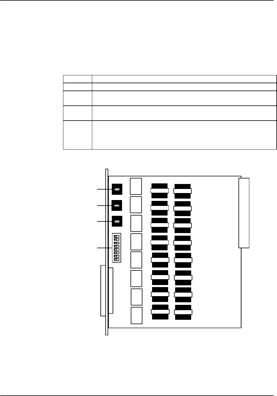
Reference Guide v3.6E&M Card
(10-97) Page 7-A-3
E&M Card Settings
E&M voice cards require hardware and software setup. Each E&M card has four
switches (see Figure E&M-1), labeled S1 through S4, that control the type of E&M
signaling the card uses. All ports on a card must use the same type of signaling. Table
E&M-1 defines the switches.
Table E&M-1. E&M Card Switch Definitions
Switch Definition
S1 Source of the Earth lead; can be either internal (INT) or external (EXT).
S2 Type of internal source for the Earth lead; can be either battery (-48VDC)
or ground (GND).
S3 Type of internal source for the Magnetic lead; can be either battery
(-48VDC) or ground (GND).
S4 Normal state of the Earth lead; can either be grounded (ON) or open
(OFF). Each card port number is designated on the 8 place rocker switch.
All eight switches must be set to the same position (i.e., all ON or all
OFF).
Power
Bus
Edge
Connector
Switch #1
Switch #2
Switch #3
Switch #4
Figure E&M-1. Positions of the four E&M Card Switches
Table E&M-2 lists the switch settings based on the E&M type and the signaling
direction.

E&M Card Reference Guide v3.6
Page 7-A-4(10-97)
Table E&M-2. E&M Card Switch Settings
E&M Type Direction S1 S2 S3 S4 (all switches)
INormal E&M* INT GND GND OFF
Trunk** INT BAT BAT ON
II Normal E&M* EXT BAT GND OFF
Trunk** EXT GND BAT OFF
IV Normal E&M* EXT GND BAT OFF
Trunk** EXT GND BAT OFF
VNormal E&M* INT GND BAT OFF
Trunk** INT GND BAT OFF
Factory Settings (default) INT GND GND OFF
*Indicates the port is attached to a device that generates signaling, such as a PBX.
**Indicates the port is attached to a device that does not generate signaling, such as a
channel bank. In this case, the system emulates a PBX and generates signaling. Also
called Reverse E&M or Pulse Link Repeater (PLR) orientation.
The eight units or channels that each E&M card can control are listed on the screen in
columns, as shown in Figure E&M-2. Table E&M-3 lists the setting on the E&M voice
card screen along with the possible and default values.
Node_1 | U1 E&M 4Wx8ER 8119 Rev A2-0 Ser 00101 | 12-31-99 14:33
1 2 3 4 5 6 7 8
STATE stdby stdby stdby stdby stdby stdby stdby stdby
WAN w1-1 w1-1 w1-1 w1-1 w1-1 w1-1 w1-1 w1-1
TS 01 01 01 01 01 01 01 01
MODE e&m e&m e&m e&m e&m e&m e&m e&m
R2 TYPE n/a n/a n/a n/a n/a n/a n/a n/a
Rx TLP 0.0 0.0 0.0 0.0 0.0 0.0 0.0 0.0
Tx TLP 0.0 0.0 0.0 0.0 0.0 0.0 0.0 0.0
CODING u-law u-law u-law u-law u-law u-law u-law u-law
TC CGA idle idle idle idle idle idle idle idle
LB off off off off off off off off
PATTRN none none none none none none none none
HYBRID n/a n/a n/a n/a n/a n/a n/a n/a
SIG CONV off off off off off off off off
RATE 64k 64k 64k 64k 64k 64k 64k 64k
ADPCM n/a n/a n/a n/a n/a n/a n/a n/a
Save | Undo | Refresh | Copy | Test | Main
Figure E&M-2. E&M Card Screen

Reference Guide v3.6E&M Card
(10-97) Page 7-A-5
Table E&M-3. E&M Card Setting Options and Defaults
Parameter User Options Notes Default
STATE stdby act stdby
WAN w1-1 w1-2 w2-1 w2-2 w3-1
w3-2 w4-1 w4-2 w1-1
TS 01-24 01-31 1 01
MODE e&m to e&mR2 R2mod e&m
R2 TYPE n/a 2n/a
RX TLP -16.3 dB to +7.5 dB 0
TX TLP -16.3 dB to +7.5 dB 3 0
CODING u-law a-inv a-law 4u-law
TC CGA idle busy idle
LB off dgtl anlg off
PATTERN none D-mW quiet none
HYBRID n/a set1 to set8 user 5n/a
SIG CONV off on off
RATE 64K 24K,1 32K,1 40K,1 24K,2
32K,2 40K,2 64K
ADPCM n/a P1 P2 P3 6n/a
NOTES
1. Time slot 16 is not available if the port is assigned to an E1 WAN link
whose TS 16 is programmed for cas or ccs.
2. The default is sl-1 if the mode selected is e&mR2 or R2mod.
3. Extended settings for 8119 card are -17.5 to +14.5dB.
4. The default is a-inv for E1 and µµ-law for T1.
5. Only the 8108 E&M card (which provides a two-wire interface) supports
the HYBRID parameter.
6. Choosing a RATE other than 64K allows the user to select an ADPCM
slot.
STATE
The State setting determines whether the port is active or inactive. An inactive port
does not occupy a time slot on a WAN link. Set the state setting to standby (stdby) for
ports you are not using or have not yet configured. Set it to active (actv) for ports that
are ready for use.
WAN
The WAN setting identifies the WAN link assigned to this port. It is not necessary for
all ports on the same card to be assigned to the same WAN link, or to contiguous time
slots on a WAN link.

E&M Card Reference Guide v3.6
Page 7-A-6(10-97)
TS
The TS setting identifies the time slot on the WAN link to which this port is assigned.
Values range from 1-24 for T1 links and 1-31 for E1 links. Time slot 16 is not
available for E1 links that are programmed for cas or ccs signaling. For a display of the
available time slots, refer to your cross-connect map for the WAN link selected. (See
the System Operations chapter for information about viewing cross-connect maps.)
MODE
The Mode setting specifies if the port uses E&M (e&m) signaling or if it operates in
Transmission Only (to) mode. Use to mode if connecting to four-wire dedicated-line
modems that do not require E&M signaling. The signaling type for all eight ports on an
E&M card is selected by setting hardware switches S1 through S4 as described earlier
in this chapter. Select e&m if you want standard Type I, II IV or V signaling. Select
e&mR2 for symmetrical R2 signaling from either the digital or analog side. R2mod
provides modified R2 signaling for Motorola paging terminal equipment.
R2 TYPE
The R2 Type setting is reserved for future use. The value of n/a is unchangeable by the
user. Signaling type for all eight E&M ports on a card is selected by setting hardware
switches S1-S4 as described earlier. If the Mode selected for the port is e&mR2, then
the R2 Type will automatically default to sl-1.
Rx TLP
The Receive Transmission Level Point setting controls the amount of gain or
attenuation added to signals after they are decoded to analog signals. To increase the
signal level, set the Rx TLP setting to a positive number (i.e., the larger the number, the
more gain is added). To decrease the signal level, set the Rx TLP setting to a negative
number (i.e., the more negative the number, the more the signal level is decreased). For
example, an incoming signal at -5 dBm can be increased to -2 dBm by setting Rx TLP
to +3 dB. Acceptable values range from -16.3 dB to +7.5 dB.
Tx TLP
The Transmit Transmission Level Point setting controls the amount of gain or
attenuation added to signals after they are received from the local analog port and
before they are encoded to digital PCM signals. To increase the signal level, set the Tx
TLP setting to a negative number (i.e., the more negative the number, the more gain is
added). To decrease the signal level, set the Tx TLP setting to a positive number (i.e.,
the more positive the number, the more the signal level is decreased). For example, an
incoming signal at -5 dBm can be increased to -2 dBm by setting Tx TLP to -3 dB.
Acceptable values for the extended range 8119 E&M Card comprise -17.5 dB to +14.5
dB. Acceptable values for normal range E&M Cards comprise -16.5 dB to +7.3 dB.
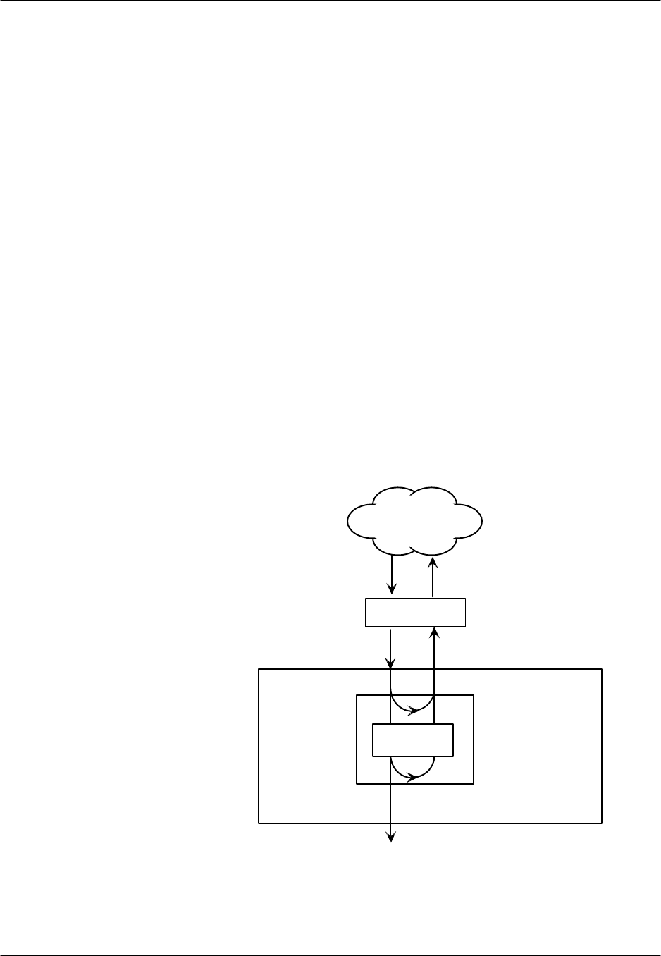
Reference Guide v3.6E&M Card
(10-97) Page 7-A-7
CODING
The Coding setting sets the PCM companding method used for a port. In general, in the
T1/North American environment use µµ-law coding. In the E1/International
environment use a-law or a-inv (inverted A-law) coding; a-inv provides greater 1s
density than a-law. The coding default is determined by the type of card in the WAN
port you select.
TC CGA
The Trunk Conditioning during Carrier Group Alarm setting defines whether the E&M
port should be placed in idle or busy mode upon declaration of a Carrier Group Alarm
(CGA) on the WAN link to which the port is assigned. The TC CGA setting has no
effect on Transmission Only (to) circuits.
In most cases, you should set this parameter to busy. If a call is in progress when the
CGA alarm is received, the system will hold the call for two seconds, drop it and then
busy out the port to the attached PBX for the duration of the alarm. Once the alarm
clears, the system will automatically place the port back in idle mode thereby making it
available to the attached PBX.
LB
The LB setting sets the loopback for this circuit to off, digital (dgtl), or analog (anlg).
Figure E&M-3 illustrates the loopback options.
CODEC
Digital Loopback
Analog Loopback
PCM bus
T1/E1
DSO
E&M
Voice Card
Digital to Analog
Converter
Network
Figure E&M-3. E&M Card Loopbacks

E&M Card Reference Guide v3.6
Page 7-A-8(10-97)
PATTRN
The Pattern setting sets the outgoing test pattern, generated by the system, that is sent to
the selected port. A different pattern can be set for each port. The none option disables
sending a test pattern. The D-mW (Digital milliwatt) option sends a 1 kHz tone at 0.0
dBm. The setting of the Rx TLP setting affects the D-mW signal level. The quiet
option places a 600Ω termination on the line so that no analog signal is sent.
HYBRID
Available for the two-wire 8108 E&M card only, the Hybrid option assigns a three byte
pattern to define the adjustment for return loss (similar to Build Out Capacitors). The
default, set1, balances to the ideal termination of 900Ω @ 2.15mF. The other settings
are reserved for future use.
SIG CONV
The Signaling Conversion parameter allows the user to change the ABCD signaling bits
from CCITT (E1) to ANSI (T1) standards. This conversion is completed regardless of
the type of WAN aggregate (CSU/DSX or CEPT) to which it is attached.
The options are off (which means that ANSI signaling is used) and on (which converts
transmit signaling from ANSI to CCITT format according to the Interface Card
Conversion Table for E&M signaling, and also converts receive signaling from CCITT
to ANSI).
RATE
The Rate parameter allows the user to utilize the voice compression capabilities of the
ADPCM server card. If that card is not present in the system, changes cannot be made
to this setting. The 64K option (default) does not use ADPCM resources (it is the
normal operation rate for voice circuits).
ADPCM voice channels are assigned in pairs by designating two voice ports (E&M,
FXO or FXS) to the same WAN link and timeslot and selecting rate settings for the pair
that add up to 64kbps (i.e. [24K,1+40K,2],[ 32K,1+32K,2] and [40K,1+24K,2]). The
numeral 1 after the rate setting assigns that portion of the voice port pair to the odd side
of the ADPCM pair. The numeral 2 after the rate setting assigns that portion of the
voice port pair to the even side of the ADPCM pair.
For more information about voice port assignments to the ADPCM card, please consult
the ADPCM section of the manual.
ADPCM
The ADPCM parameter lets the user choose which ADPCM card to which this E&M
port is assigned. The default setting is n/a and only changes when a Rate smaller than
64k is selected (see above). The user is then allowed to select which ADPCM card to
use for the port (assignment is made by chassis slot number). The options are P1, P2
and P3.

Reference Guide v3.6E&M Card
(10-97) Page 7-A-9
Menu of Actions
Table E&M-4 shows the Menu of Actions for the E&M Card.
Table E&M-4. E&M Card Screen Menu of Actions
Action Function
Save Saves changes to settings.
Undo Returns all settings to the last saved state.
Refresh Updates certain time-related information fields that are not
automatically updated (i.e. performance and test data).
Copy Copies the contents of the current column to the next column. Useful if
you change a lot of entries in one column and want to repeat those
changes in subsequent columns.
Test Initiates and monitors testing of all E&M card ports. Refer to Test
section below.
Main Returns to the main terminal screen. If changes are made to settings
and not saved, you will be prompted to save or lose changes.
Test
The Test option facilitates testing and maintenance by allowing the user to monitor and
set the status of the analog interface leads as well as monitoring and setting the value of
the A, B, C and D signaling bits of all E&M circuits on that card. In cross-connect
systems only, the test option can also apply test patterns and tones towards the user and
network sides of the system.
The Test screen also shows the signaling type assigned to this card via the switch
settings described earlier.
Figure E&M-4 shows the E&M Card Test parameters and Table E&M-5 shows the
settings for each.

E&M Card Reference Guide v3.6
Page 7-A-10 (10-97)
Node_1 | U1 E&M 4Wx8ER 8119 Rev A2-0 Ser 00101 | 12-31-99 14:33
SIG MON = OFF 1 2 3 4 5 6 7 8
TEST n/a n/a n/a n/a n/a n/a n/a n/a
Tx ABCD mon mon mon mon mon mon mon mon
Rx ABCD mon mon mon mon mon mon mon mon
E-lead mon mon mon mon mon mon mon mon
TO USER n/a n/a n/a n/a n/a n/a n/a n/a
TO NTWK n/a n/a n/a n/a n/a n/a n/a n/a
Tx ABCD n/a n/a n/a n/a n/a n/a n/a n/a
Rx ABCD n/a n/a n/a n/a n/a n/a n/a n/a
E-lead off off off off off off off off
M-lead off off off off off off off off
MODE e&m e&m e&m e&m e&m e&m e&m e&m
STATUS W stb W stb W stb W stb W stb W stb W stb W stb
E&M Signaling Type: I-t
Save | Undo | Refresh | Main | siG mon
Figure E&M-4. E&M Card Test Screen
Table E&M-5. E&M Card Test Screen Options
Parameter User Options Default
SIG MON off on off
TEST off on off
TX ABCD mon set mon
RX ABCD mon set mon
E-LEAD mon set mon
TO USER PCM 300Hz 1kHz 3kHz quiet PCM
TO NTWK PCM 300Hz 1kHz 3kHz quiet PCM
TX ABCD Information only - no user input n/a
RX ABCD Information only - no user input n/a
E-LEAD Information only - no user input n/a
M-LEAD Information only - no user input n/a
MODE Information only - no user input n/a
STATUS Information only - no user input n/a
SIG MON
The Signaling Monitor feature works with the user card alarm system (see Basic
Operations section) to detect excessive signaling bit transitions. The system will
generate alarms if the number of transitions of any signaling bit in transmit or receive
direction for an active port exceeds 255 in any four-second interval. The options are off
and on. They are toggled using the “G” command in the Menu of Actions.

Reference Guide v3.6E&M Card
(10-97) Page 7-A-11
TEST
The Test parameter shows if the port is in test mode or not. Inactive ports and ports
that are assigned to inactive WANs will show a test status of n/a. The test status
options for active ports are off and on.
Tx ABCD
The Transmit ABCD setting allows the user to either monitor the status of the ABCD
signaling bits being transmitted towards the network or set a specific ABCD pattern for
testing the transmit side of the circuit. The options for this field are mon (monitor) or
set. Choosing set will bring up a four digit field for you to input the ABCD pattern you
want to transmit. Any four digit combination of ones and zeros is acceptable for this
setting.
Rx ABCD
The Receive ABCD setting allows the user to either monitor the status of the ABCD
signaling bits being received from the network or set a specific ABCD pattern for
testing the receive side of the circuit.
The options for this field are mon (monitor) or set. Choosing set will bring up a four
digit field for you to input the ABCD pattern you want to receive. Any four digit
combination of ones and zeros is acceptable for this setting. The Rx ABCD bits cannot
be set in bus-connect systems and the only option is mon (monitor).
E-lead
The E-lead setting allows the user to either monitor or set the E lead. The options for
this field are mon (monitor) or set. Choosing set will bring up the options off (which
drops the E lead) and on (which raises the E lead).
TO USER
In cross-connect systems only, the To User parameter allows you to break the circuit
and send a test tone on the user side of the system. The options for this field are PCM,
300Hz, 1 kHz, 3 kHz and quiet. Selecting PCM means that you do not want to inject
a tone toward the user and that the PCM signal received from the network should
continue to be sent to the user port in the normal manner.
This parameter is not supported in bus-connect systems and will always appear as n/a.
TO NTWK
In cross-connect systems only, the To Network parameter allows you to break the
circuit and send a test tone on the network side of the system. The options for this field
are PCM, 300Hz, 1 kHz, 3 kHz and quiet. Selecting PCM means that you do not
want to inject a tone toward the network and that the PCM signal received from the user
port should continue to be sent to the network in the normal manner.

E&M Card Reference Guide v3.6
Page 7-A-12 (10-97)
This parameter is not supported in bus-connect systems and will always appear as n/a.
Tx ABCD
The Transmit ABCD information field shows the current values of the ABCD bits that
are being transmitted to the network. If TX ABCD in the top half of the screen is
changed via the set function mentioned above, and the settings are saved by the Save
command in the Menu of Actions, the new bit pattern chosen will be reflected here.
Rx ABCD
The Receive ABCD information field shows the current values of the ABCD signaling
bits that are received from the network. If RX ABCD in the top half of the screen is
changed via the set function mentioned above, and the settings are saved by the Save
command in the Menu of Actions, the new bit pattern chosen will be reflected here.
E-Lead
The E-lead information field shows the current status of the E-lead of this port. The
settings are either on or off.
M-Lead
The M-lead information field shows the current status of the M-lead of this port. The
settings are either on or off.
MODE
The Mode informational field shows the current mode of the port that was selected on
the main E&M card screen. Valid settings are e&m, to, e&mR2 and R2mod.
STATUS
The Status information field shows the current status of the port. Table E&M-6 lists and
describes all of the possible conditions that are reported in this field.

Reference Guide v3.6E&M Card
(10-97) Page 7-A-13
Table E&M-6. Status Information Field Settings
Setting Meaning
stdby The E&M port is in standby.
W stb The WAN that the E&M port is assigned to is in standby.
W tst The WAN that the E&M port is assigned to is in test.
W OOS The WAN that the E&M port is assigned to is Out Of Service.
noWAN No WAN card configured in the slot to which the E&M port is assigned.
OOS The E&M card is Out of Service.
Call Call set-up is in progress.
Busy A call is in progress.
idle The E&M circuit is not being used and is available.
TC The E&M circuit is undergoing Trunk Conditioning because of a CGA
alarm on the WAN to which it is assigned.
test The operator is actively controlling the circuit by setting values for Tx
ABCD, Rx ABCD or E-lead.
maint The E&M port is undergoing maintenance.
E&M Signaling Type
The E&M signaling type that was set by the switch configuration mentioned earlier is
displayed in this field. The user can check the switch settings without having to remove
the card. The E&M Signaling types are I, II, IV and V, followed by a “-t” if the card is
set to provide trunk signaling.
Menu of Actions
Table E&M-7 shows the Menu of Actions for the E&M card test screen.
Table E&M-7. E&M Card Test Screen Menu of Actions
Action Function
Save Saves changes to settings.
Undo Returns all settings to the last saved state.
Refresh Updates certain time-related information fields that are not
automatically updated (i.e. performance and test data).
Main Returns to the E&M card main screen. If changes are made to settings
and not saved, you will be prompted to save or lose changes.
siG mon Works with the user card alarm system (see Basic Operations section)
to detect excessive signaling bit transitions. The options are off and
on. They are toggled using the “G” command in the Menu of Actions.

E&M Card Reference Guide v3.6
Page 7-A-14 (10-97)

Reference Guide v3.6 FXS Card
(10-97) Page 7-B-1
Introduction
Foreign Exchange Station Cards manage the flow of FXS voice traffic over the
network. The FXS card translates an analog signal to a digital bitstream at the local
system and digital to analog at the remote system.
All cards have a two-wire interface that supports Foreign Exchange Station, Private
Line Automatic Ringdown, Foreign Exchange Software Defined Network, Dial Pulse
Originating and Wink operations. FXS cards can use the voice-compression features of
the ADPCM server card.
FXS Cards also support digital to analog conversion as outlined in TR-TSY-000008 for
circuits using Subscriber Loop Carriers (SLC96) facilities.
8129 FXS Card
The 8129 FXS Card has eight ports and provides 600Ω terminating impedance. All
FXS features are supported by this card.
UL Statement
OPERATION OF THIS INTERFACE IS LIMITED TO
INTRA-BUILDING CONNECTIONS ONLY
In addition to the card shown above, whose operation will be discussed in this chapter,
the following discontinued models are supported by v3.6 software:
8122 FXS Card
8122 FXS Card has two ports and provides 900Ω terminating impedance.
8123 FXS Card
8123 FXS Card has two ports and provides 600Ω terminating impedance.
8124 FXS Card
8124 FXS Card has four ports and provides 900Ω terminating impedance.
8125 FXS Card
8125 FXS Card has four ports and provides 600Ω terminating impedance.
8128 FXS Card
8128 FXS Card has eight ports and provides 900Ω terminating impedance.

FXS Card Reference Guide v3.6
Page 7-B-2(10-97)
FXS Card Settings
FXS card setting options are displayed in columns on the FXS card screen, as shown in
Figure FXS-1. Table FXS-1 lists the settings controlled on the screen along with the
possible and default values. The settings are similar to those for other voice cards.
Node_1 | U1 FXS 2Wx8-9 8129 Rev A8-0 Ser 00101 | 12-31-99
14:33
1 2 3 4 5 6 7 8
STATE stdby stdby stdby stdby stdby stdby stdby stdby
WAN w1-1 w1-1 w1-1 w1-1 w1-1 w1-1 w1-1 w1-1
TS 01 01 01 01 01 01 01 01
MODE fxs fxs fxs fxs fxs fxs fxs fxs
TYPE loop loop loop loop loop loop loop loop
Rx TLP 0.0 0.0 0.0 0.0 0.0 0.0 0.0 0.0
Tx TLP 0.0 0.0 0.0 0.0 0.0 0.0 0.0 0.0
CODING u-law u-law u-law u-law u-law u-law u-law u-law
TC CGA idle idle idle idle idle idle idle idle
LB off off off off off off off off
PATTRN none none none none none none none none
HYBRID set1 set1 set1 set1 set1 set1 set1 set1
RINGBK off off off off off off off off
SIG CONV off off off off off off off off
RATE 64k 64k 64k 64k 64k 64k 64k 64k
ADPCM n/a n/a n/a n/a n/a n/a n/a n/a
Save | Undo | Refresh | Copy | Test | Main
Figure FXS-1. FXS Card Screen

Reference Guide v3.6FXS Card
(10-97) Page 7-B-3
Table FXS-1. FXS Card Setting Options and Defaults
PARAMETER USER OPTIONS NOTES DEFAULT
STATE stdby act stdby
WAN w1-1 w1-2 w2-1 w2-2 w3-1
w3-2 w4-1 w4-2 w1-1
TS 01-24 01-31 1 01
MODE fxs fxsdn wink plar dpo slc96 2fxs
TYPE loop lp-fd gs gs-i gs-a ls-R2 loop
RX TLP -10.0 dB to +2.0 dB 0.0
TX TLP -10.0 dB to +5.0 dB 0.0
CODING u-law a-inv a-law 3u-law
TC CGA idle busy idle
LB off dgtl anlg off
PATTERN none D-mW quiet none
HYBRID set1 to set8 user set1
RINGBK off on off
SIG CONV off on off
RATE 64k 24k,1 32k,1 40k,1 24k,2
32k,2 40k,2 64k
ADPCM n/a P1 P2 P3 4n/a
NOTES
1. Time slot 16 is not available if the port is assigned to an E1 WAN link
whose TS 16 is programmed for cas or ccs.
2. These options are only valid if the Mode selected is fxs or wink. If the
Mode is fxsdn, then the Type options are the same as above with the
addition of fgd and boa. If the Mode is plar, then the Type options are d3
or d4. If the Mode is dpo, then the Type setting will automatically default
to dpo.
3. The default is a-inv for E1 and µµ-law for T1. These values will change
depending upon the WAN link selected.
4. Choosing RATE other than 64k allows the user to select an ADPCM slot.
STATE
The State setting determines whether the port is active or inactive. An inactive port
does not occupy a time slot on a WAN link. Set the State setting to standby (stdby) for
ports you are not using or have not yet configured. Set it to active (actv) for ports that
are ready for use.
WAN
The WAN setting identifies the WAN link assigned to this port. It is not necessary for
all ports on the same card to be assigned to the same WAN link, or to contiguous time
slots on a WAN link.

FXS Card Reference Guide v3.6
Page 7-B-4(10-97)
TS
The TS setting identifies the time slot on the WAN link to which this port is assigned.
Values range from 1-24 for T1 links and 1-31 for E1 links. Time slot 16 is not
available on E1 links that are programmed for cas or ccs signaling. For a display of the
available time slots, refer to your cross-connect map for the WAN link; see the
Operations chapter for information about viewing cross-connect maps.
MODE
The Mode setting should be determined by the type of equipment to which you are
connecting the port. All options use two-wire balanced connections. The fxs (Foreign
Exchange Station) option allows you to connect the system to a 2 way (both inbound
and outbound calls) PBX trunk or a key system trunk. The system requires a ringing
generator for this option. The fxsdn (Foreign Exchange Software Defined Network)
option provides access to new services offered by advanced networks from many major
carriers. The system requires a ringing generator for this option. The wink option uses
the same type of signaling as fxsdn and provides a 150MS delay, then a 200MS "wink"
back to the central office when the FXS card sees an off-hook condition from the
central office. The system requires a ringing generator for this option.
The plar (private line automatic ringdown) option provides point-to-point unswitched
connections between two telephone sets. This configuration is usually not attached to
an exchange or switch; rather it provides a “hot line” between two locations. The unit
requires a ringing generator for this option.
The dpo (Dial Pulse Originating) option allows the unit to attach to out-going one-way
trunks from a PBX, key system, or a telephone set. This option is very similar to the
fxs option; however, the system does not require a ringing generator.
The slc96 (Subscriber Loop Carrier 96) option allows the unit to attach to out-going
one-way trunks from a PBX, CENTREX, key system, or a telephone set to a SLC96
channel. The slc96 mode must be active on the WAN card selected.
TYPE
The Type setting matches the signaling behavior of the FXS equipment and the remote
switch. Use the loop (Loop Start) option with POTS stations and simple PBX trunks.
Use the lp-fd (Loop Start - Forward Disconnect) option with automated answering
equipment. Use the gs (Ground Start) option with two-way PBX trunks because it helps
to prevent glaring or call collisions. Use the gs-i (Ground Start Immediate) option for
equipment requiring fast-response time to the station or PBX. Use the gs-a (Ground
Start Automatic) option for equipment requiring fast-response time to the central office.
The selection you choose must match the behavior of both the station equipment and
the remote central office or PBX equipment.
If you selected the fxsdn mode, the choice of fgd is offered to make the circuit
compatible with Feature Group "D" high-speed modem services that require special
software. An additional choice of boa (bill on answer) sends a signal back to the office
when the customer answers the phone to start billing for the call.

Reference Guide v3.6FXS Card
(10-97) Page 7-B-5
If you selected the plar option for the Mode of this port, then the two options that are
supported under Type are d3 and d4 which meet the pre-1988 and post-1988
specifications for PLAR circuits. If you selected dpo as the Mode, the Type will
automatically default to dpo.
If slc96 is selected for Mode, the two options supported are sp (single party) and uvg
(universal voice grade).
Caution: Before activating this port, verify the behavior expected by both the station
equipment and the remote central office equipment and ensure that you have the system
properly configured.
Rx TLP
The Receive Transmission Level Point setting controls the amount of gain or
attenuation added to signals after they are decoded to analog signals. To increase the
signal level, set the Rx TLP setting to a positive number (i.e., the larger the number, the
more gain is added). To decrease the signal level, set the Rx TLP setting to a negative
number (i.e., the more negative the number, the more the signal level is decreased). For
example, an incoming signal at -5 dBm can be increased to -3 dBm by setting Rx TLP
to +2 dB. Acceptable values range from -10.0 dB to +2.0 dB.
Tx TLP
The Transmit Transmission Level Point setting controls the amount of gain or
attenuation added to signals after they are received from the local analog port and
before they are encoded to digital PCM signals. To increase the signal level, set the Tx
TLP setting to a negative number (i.e., the more negative the number, the more gain is
added). To decrease the signal level, set the Tx TLP setting to a positive number (i.e.,
the more positive the number, the more the signal level is decreased). For example, an
incoming signal at -5 dBm can be increased to -2 dBm by setting Tx TLP to -3 dB.
Acceptable values range from -10.0 dB to +5.0 dB.
CODING
The Coding setting sets the PCM companding method used for a port. In general, in the
T1/North American environment use µµ-law coding. In the E1/International
environment use a-law or a-inv (inverted A-law) coding; a-inv provides greater 1s
density than a-law. The coding default is determined by the type of card in the WAN
port you select.
TC CGA
The Trunk Conditioning during Carrier Group Alarm setting defines whether the FXS
port should be placed in idle or busy mode upon declaration of a Carrier Group Alarm
(CGA) on the WAN link to which the port is assigned. In most cases, you should set
this parameter to busy. If a call is in progress when the CGA alarm is received, the
system will hold the call for two seconds, drop it and then busy out the port to the
attached PBX for the duration of the alarm. Once the alarm clears, the system will
automatically place the port back in idle mode thereby making it available to the
attached PBX.
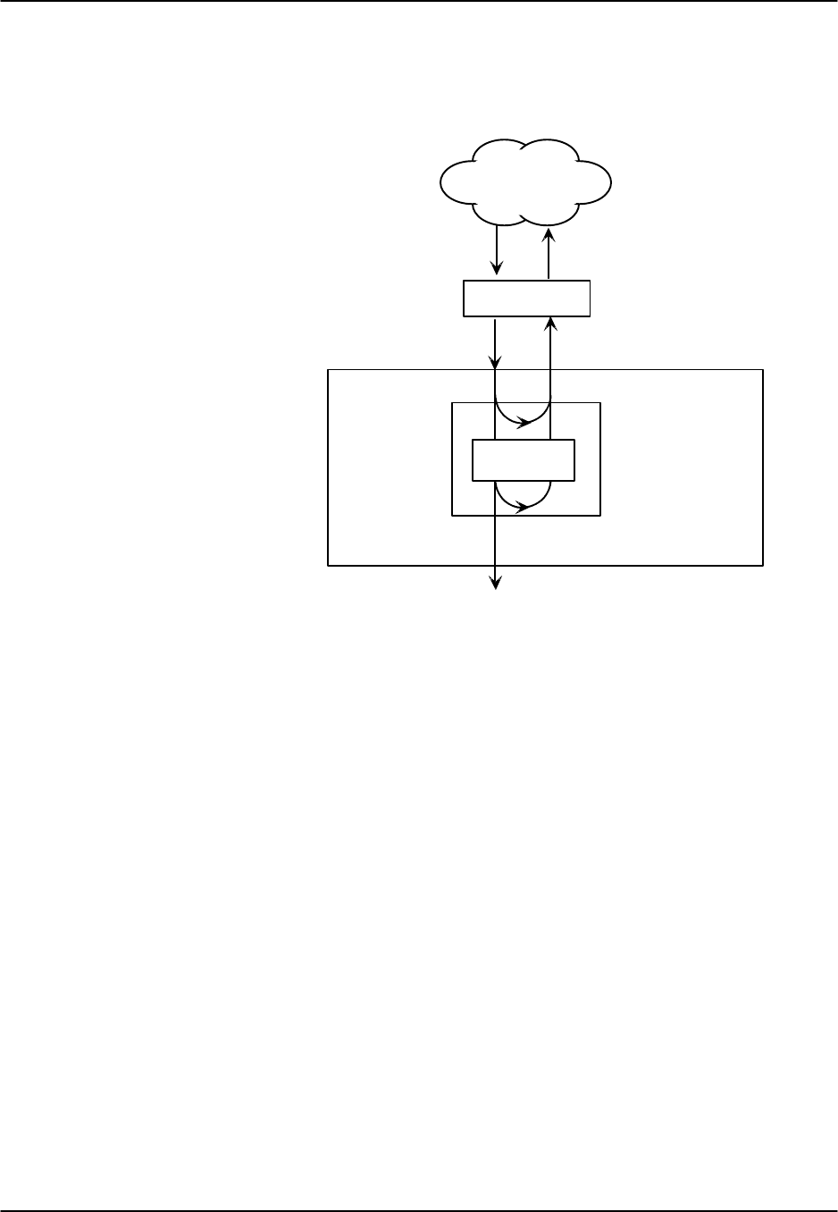
FXS Card Reference Guide v3.6
Page 7-B-6(10-97)
LB
The Loopback setting sets the loopback for this circuit to off, digital (dgtl), or analog
(anlg). Figure FXS-2 illustrates the loopback options.
CODEC
Digital Loopback
Analog Loopback
PCM bus
T1/E1
DSO
FXS
Voice Card
Digital to Analog
Converter
Network
Figure FXS-2. FXS Card Loopbacks
PATTR
The Pattern setting sets the outgoing test pattern for this analog port. The pattern,
generated by the system, is sent to the selected port. A different pattern can be set for
each port. The none option disables sending a test pattern. The D-mW (Digital
milliwatt) option sends a 1 kHz tone at 0.0 dBm. The setting of the Rx TLP setting
affects the D-mW signal level. The quiet option places a 900Ω termination on the line
so that no analog signal is sent.
HYBRID
The Hybrid option assigns a three byte pattern to define the adjustment for return loss
(similar to Build Out Capacitors). The default, set1, balances to the ideal termination
of 900Ω @ 2.15mF in the case of the 8124 and 8128 cards 600Ω @ 2.15mF in the case
of the 8125 and 8129 cards. The other settings are reserved for future use.
RINGBK
The ringback setting specifies whether a ringback tone is generated by the system and
sent towards the network. The options are off and on. This option should be turned on
when the network service does not provide an audible ringing tone to the calling party.

Reference Guide v3.6FXS Card
(10-97) Page 7-B-7
SIG CONV
The Signaling Conversion parameter allows the user to change the ABCD signaling bits
from CCITT (E1) to ANSI (T1) standards. This conversion is completed regardless of
the type of WAN aggregate (CSU/DSX or CEPT) to which it is attached.
The options are off (which means that ANSI signaling is used) and on (which converts
transmit signaling from ANSI to CCITT format according to the Interface Card
Conversion Table for FXS signaling, and also converts receive signaling from CCITT
to ANSI).
RATE
The Rate parameter allows the user to utilize the voice compression capabilities of the
ADPCM server card. If that card is not present in the system, changes cannot be made
to this setting. The 64k option (default) does not use ADPCM resources (it is the
normal operation rate for voice circuits).
ADPCM voice channels are assigned in pairs by designating two voice ports (E&M,
FXO or FXS) to the same WAN link and timeslot and selecting rate settings for the pair
that add up to 64kbps (i.e. [24k,1+40k,2],[ 32k,1+32k,2] and [40k,1+24k,2]). The
numeral 1 after the rate setting assigns that portion of the voice port pair to the odd side
of the ADPCM pair. The numeral 2 after the rate setting assigns that portion of the
voice port pair to the even side of the ADPCM pair.
For more information about voice port assignments to the ADPCM card, please consult
the ADPCM section of the manual.
ADPCM
The ADPCM parameter lets the user choose which ADPCM card to place this E&M
port. The default setting is n/a and only changes when a Rate smaller than 64k is
selected (see above). The user is then allowed to select which ADPCM card to use for
the port (assignment is made by chassis slot number). The options are P1, P2 and P3.

FXS Card Reference Guide v3.6
Page 7-B-8(10-97)
Menu of Actions
Table FXS-2 shows the Menu of Actions for the FXS Card.
Table FXS-2. FXS Card Screen Menu of Actions
Action Function
Save Saves changes to settings.
Undo Returns all settings to the last saved state.
Refresh Updates certain time-related information fields that are not automatically
updated (i.e. performance and test data).
Copy Copies the contents of the current column to the next column. Useful if
you change a lot of entries in one column and want to repeat those
changes in subsequent columns.
Test Initiates and monitors testing of all FXS card ports. Refer to Test section
below.
Main Returns to the main terminal screen. If changes are made to settings and
not saved, you will be prompted to save or lose changes.
Test
The Test option facilitates testing and maintenance by allowing the user to monitor and
set the status of the analog interface leads as well as monitoring and setting the value of
the A, B, C and D signaling bits of all FXS circuits on that card. In cross-connect
systems only, the test option also allows the user to apply test patterns and tones
towards the user and network sides of the system.
Figure FXS-3 shows the FXS Card Test parameters and Table FXS-3 shows the settings
for each.

Reference Guide v3.6FXS Card
(10-97) Page 7-B-9
Node_1 | U1 FXS 2Wx8-9 8129 Rev A8-0 Ser 00101 | 12-31-99
14:33
SIG MON = OFF
1 2 3 4 5 6 7 8
TEST n/a n/a n/a n/a n/a n/a n/a n/a
Tx ABCD mon mon mon mon mon mon mon mon
Rx ABCD mon mon mon mon mon mon mon mon
T-R-CNTL mon mon mon mon mon mon mon mon
TO USER n/a n/a n/a n/a n/a n/a n/a n/a
TO NTWK n/a n/a n/a n/a n/a n/a n/a n/a
Tx ABCD n/a n/a n/a n/a n/a n/a n/a n/a
Rx ABCD n/a n/a n/a n/a n/a n/a n/a n/a
T-R-CNTL RbTo RbTo RbTo RbTo RbTo RbTo RbTo RbTo
T-R-STAT off off off off off off off off
MODE fxs fxs fxs fxs fxs fxs fxs fxs
TYPE loop loop loop loop loop loop loop loop
STATUS W stb W stb W stb W stb W stb W stb W stb W stb
Save | Undo | Refresh | Main | siG Mon
Figure FXS-3. FXS Card Test Screen
Table FXS-3. FXS Card Test Parameters
Parameter User Options Default
SIG MON off on off
TEST off on off
Tx ABCD mon set mon
Rx ABCD mon set mon
T-R-CNTL mon set mon
TO USER PCM 300Hz 1kHz 3kHz quiet PCM
TO NTWK PCM 300Hz 1kHz 3kHz quiet PCM
Tx ABCD Information only - no user input n/a
Rx ABCD Information only - no user input n/a
T-R-CNTL Information only - no user input RbTo
T-R-STAT Information only - no user input off
MODE Information only - no user input fxs
TYPE Information only - no user input loop
STATUS Information only - no user input W stb
SIG MON
The Signaling Monitor feature works with the user card alarm system (see Basic
Operations section) to detect excessive signaling bit transitions. The system will
generate alarms if the number of transitions of any signaling bit in transmit or receive
direction for an active port exceeds 255 in any four second interval. The options are off
and on, and they are toggled using the G command in the Menu of Actions.

FXS Card Reference Guide v3.6
Page 7-B-10 (10-97)
TEST
The Test parameter shows if the port is in test mode or not. Inactive ports and ports
that are assigned to inactive WANs will show a test status of n/a. The test status
options for active ports are off and on.
Tx ABCD
The Transmit ABCD setting allows the user to either monitor the status of the ABCD
signaling bits being transmitted towards the network or set a specific ABCD pattern for
testing the transmit side of the circuit. The options for this field are mon (monitor) or
set. Choosing set will bring up a four digit field to input the ABCD pattern you want to
transmit. Any four digit combination of ones and zeros is acceptable for this setting.
Rx ABCD
The Receive ABCD setting allows the user to either monitor the status of the ABCD
signaling bits being received from the network or set a specific ABCD pattern for
testing the receive side of the circuit. The options for this field are mon (monitor) or
set. Choosing set will bring up a four digit field for you to input the ABCD pattern you
want to receive. Any four digit combination of ones and zeros is acceptable for this
setting. The Rx ABCD bits cannot be set in bus-connect systems and the only option is
mon (monitor).
T-R-CNTL
The Tip and Ring Control setting allows the user to either monitor (mon) or set (set) the
state of the Tip and Ring leads of an FXS port. Choosing set will bring up the
following options (b=battery, o=open, g=ground):
RbTo -48V is applied to the Ring lead and the Tip lead is open
TbRo -48V is applied to the Tip lead and the Ring lead is open
RbTg -48V is applied to the Ring lead and the Tip lead is grounded
TbRg -48V is applied to the Tip lead and the Ring lead is grounded
TO USER
In cross-connect systems only, the To User parameter allows you to break the circuit
and send a test tone on the user side of the system. The options for this field are PCM,
300Hz, 1kHz, 3kHz and quiet. Selecting PCM means that you do not want to inject a
tone toward the user and that the PCM signal received from the network should
continue to be sent to the user port in the normal manner.
This parameter is not supported in bus-connect systems and will always appear as n/a.

Reference Guide v3.6FXS Card
(10-97) Page 7-B-11
TO NTWK
In cross-connect systems only, the To Network parameter allows you to break the
circuit and send a test tone on the network side of the system. The options for this field
are PCM, 300Hz, 1kHz, 3kHz and quiet. Selecting PCM means that you do not want
to inject a tone toward the network and that the PCM signal received from the user port
should continue to be sent to the network in the normal manner.
This parameter is not supported in bus-connect systems and will always appear as n/a.
Tx ABCD
The Transmit ABCD informational field shows the current values of the ABCD bits that
are being transmitted to the network. If TX ABCD in the top half of the screen is
changed via the set function mentioned above, and the settings are saved by the Save
command in the Menu of Actions, the new bit pattern chosen will be reflected here.
Rx ABCD
The Receive ABCD informational field shows the current values of the ABCD
signaling bits that are received from the network. If RX ABCD in the top half of the
screen is changed via the set function mentioned above, and the settings are saved by
the Save command in the Menu of Actions, the new bit pattern chosen will be reflected
here.
T-R-CNTL
The Tip and Ring Control informational field shows the current status of the Tip and
Ring leads of the FXS port from the perspective of the system. The possible values are
(b=battery, o=open, g=ground):
RbTo -48V is applied to the Ring lead and the Tip lead is open
TbRo -48V is applied to the Tip lead and the Ring lead is open
RbTg -48V is applied to the Ring lead and the Tip lead is grounded
TbRg -48V is applied to the Tip lead and the Ring lead is grounded
ring ringing voltage is applied between Tip and Ring
T-R-STAT
The Tip and Ring Status informational field describes what the attached device is doing
with the Tip and Ring leads of the FXS port. The possible values are:
loop attached device is connecting Tip and Ring together
rgnd the Ring lead is grounded by the attached device
open the Ring lead is not connected to either the Tip lead or to ground

FXS Card Reference Guide v3.6
Page 7-B-12 (10-97)
MODE
The Mode informational field shows the current mode of the port that was selected on
the main FXS card Screen. Valid settings are fxs, fxsdn, wink, plar, dpo or slc96.
TYPE
The Type informational field shows the current status of the signal field selected on the
main FXS card screen for this port. Valid settings for fxs and wink modes are loop start
(loop), loop start - forward disconnect (lp-fd), ground start (gs), ground start immediate
(gs-i) and ground start automatic (gs-a). Valid settings for fxsdn modes are loop start
(loop), loop start - forward disconnect (lp-fd), ground start (gs), ground start immediate
(gs-i), ground start automatic (gs-a) and fgd (Feature Group "D"). Valid settings for the
plar mode are (d3) and (d4). The only valid setting for the dpo mode is dial pulse
originating (dpo).
STATUS
The Status informational field shows the current status of the port. Table FXS-4 lists
and describes all of the possible conditions that are reported in this field.
Table FXS-4. Status Information Field Settings
Setting Meaning
stdby The FXS port is in standby.
W stb The WAN that the FXS port is assigned to is in standby.
W tst The WAN that the FXS port is assigned to is in test.
W OOS The WAN that the FXS port is assigned to is Out Of Service.
noWAN There is no WAN card configured in the slot to which the FXS port is
assigned.
call Call set-up is in progress.
busy A call is in progress.
idle The FXS circuit is not being used and is available.
TC The FXS circuit is undergoing Trunk Conditioning because of a CGA
alarm on the WAN to which it is assigned.
test The operator is actively controlling the circuit by setting values for Tx
ABCD or Rx ABCD.
maint The FXS port is in maintenance condition.

Reference Guide v3.6FXS Card
(10-97) Page 7-B-13
Menu of Actions
Table FXS-5 shows the Menu of Actions for the FXS Card Test Screen.
Table FXS-5. FXS Card Test Screen Menu of Actions
Action Function
Save Saves changes to settings.
Undo Returns all settings to the last saved state.
Refresh Updates certain time-related information fields that are not automatically
updated (i.e. performance and test data).
Main Returns to the FXS card main screen. If changes are made to settings
and not saved, you will be prompted to save or lose changes.
siG mon The signal monitor is used with the user card alarm system to notify the
user of excessive transitions of signaling bits.

FXS Card Reference Guide v3.6
Page 7-B-14 (10-97)

Reference Guide v3.6 FXO Card
(10-97) Page 7-C-1
Introduction
Foreign Exchange Office Cards manage the flow of FXO voice traffic over the network.
The FXO card translates an analog signal to a digital bitstream at the local system and
digital to analog at the remote system. All FXO cards have a two-wire interface and
support Foreign Exchange Office functions, Manual Ringdown, Foreign Exchange
Defined Network and Dial Pulse Terminating operations. FXO cards can use the voice-
compression features of the ADPCM server card.
8139 FXO Card
The 8139 FXO Card is an eight port card with 600Ω terminating impedance. All FXO
features are supported by this card.
UL Statement
OPERATION OF THIS INTERFACE IS LIMITED TO
INTRA-BUILDING CONNECTIONS ONLY
In addition to the card shown above, whose operation will be discussed in this chapter,
the following discontinued models are supported by v3.6 software:
8132 FXO Card
The 8132 FXO Card is a two port card with 900Ω terminating impedance.
8133 FXO Card
The 8133 FXO Card is a two port card with 600Ω terminating impedance.
8134 FXO Card
The 8134 FXO Card is a four port card with 900Ω terminating impedance.
8135 FXO Card
The 8135 FXO Card is a four port card with 600Ω terminating impedance.
8138 FXO Card
The 8138 FXO Card is a four port card with 900Ω terminating impedance.

FXO Card Reference Guide v3.6
Page 7-C-2(10-97)
FXO Card Settings
FXO card setting options are displayed in columns on the FXO card screen, as shown in
Figure FXO-1. Table FXO-1 lists the settings controlled on the screen along with the
possible and default values. The settings are similar to those for other voice cards.
Node_1 | U1 FXO 2Wx8-9 8139 Rev C2-0 Ser 00101 | 12-31-99 14:33
1 2 3 4 5 6 7 8
STATE stdby stdby stdby stdby stdby stdby stdby stdby
WAN w1-1 w1-1 w1-1 w1-1 w1-1 w1-1 w1-1 w1-1
TS 01 01 01 01 01 01 01 01
MODE fxo fxo fxo fxo fxo fxo fxo fxo
SIGNAL loop loop loop loop loop loop loop loop
Rx TLP 0.0 0.0 0.0 0.0 0.0 0.0 0.0 0.0
Tx TLP 0.0 0.0 0.0 0.0 0.0 0.0 0.0 0.0
CODING u-law u-law u-law u-law u-law u-law u-law u-law
TC CGA idle idle idle idle idle idle idle idle
LB off off off off off off off off
PATTRN none none none none none none none none
HYBRID set1 set1 set1 set1 set1 set1 set1 set1
WK DLY 00000000
WINK 0 0 0 0 0 0 0 0
SIG CONV off off off off off off off off
RATE 64k 64k 64k 64k 64k 64k 64k 64k
ADPCM n/a n/a n/a n/a n/a n/a n/a n/a
Save || Undo || Refresh || Copy || Test || Main
Figure FXO-1. FXO Card Screen
Table FXO-1. FXO Card Setting Options and Defaults
Parameter User Options Notes Default
STATE stdby act stdby
WAN w1-1 w1-2 w2-1 w2-2 w3-1
w3-2 w4-1 w4-2 w1-1
TS 01-24 01-31 1 01
MODE fxo fxodn dpt mrd fxo
SIGNAL loop gs lp-fd R2 gs-a lp-em 2loop
RX TLP -10.0 dB to +2.0 dB 0.0
TX TLP -10.0 dB to +5.0 dB 0.0
CODING u-law a-law a-inv 3u-law
TC CGA idle busy idle
LB off dgtl anlg off
PATTERN none D-mW quiet none
HYBRID set1 to set8 user set1
WK DLY 00-99 4 0
WINK 00-199 4 0
SIG CONV off on off
RATE 64k 24k,1 32k,1 40k,1 24k,2
32k,2 40k,2 64k

Reference Guide v3.6FXO Card
(10-97) Page 7-C-3
ADPCM n/a P1 P2 P3 5n/a
NOTES
1. Time slot 16 is not available if the port is assigned to an E1 WAN link whose TS 16
is programmed for cas or ccs.
2. These options are only valid if the Mode selected is fxo, or fxodn. If the mode is
dpt, then the Type options are dpt (default), R2 or i-R2. If the Mode is mrd, then
the Type setting will automatically default to mrd.
3. The default is a-inv for E1 and m-law for T1. These values will change depending
upon the WAN link selected.
4. These settings should be used with fxodn and dpt modes only.
5. Choosing a RATE other than 64k allows the user to select an ADPCM slot.
STATE
The State setting determines whether the port is active or inactive. An inactive port
does not occupy a time slot on a WAN link. Set the State setting to standby (stdby) for
ports you are not using or have not yet configured. Set it to active (actv) for ports that
are ready for use.
WAN
The WAN setting identifies the WAN link assigned to this port. It is not necessary for
all ports on the same card to be assigned to the same WAN link, or to contiguous time
slots on a WAN link.
TS
The TS setting identifies the time slot on the WAN link to which this port is assigned.
Values range from 1-24 for T1 links and 1-31 for E1 links. Time slot 16 is not
available on E1 links that are programmed for cas or ccs signaling. For a display of the
available time slots, refer to your cross-connect map for the WAN link. See the System
Operations chapter for information about defining cross-connect maps.
MODE
The Mode setting should be determined by the type of equipment to which you connect
the port. All options use two-wire balanced connections. The fxo (Foreign Exchange
Office) option allows you to connect the system to a 2 way PBX trunk (both inbound
and outbound calls) or a key system trunk. The fxodn (Foreign Exchange Office -
Defined Network) option provides access to new services offered by advanced networks
from many major carriers. The dpt (Dial Pulse Terminating) option allows the unit to
attach to incoming one-way trunks from a PBX, key system, or a telephone set. This
option is similar to the fxo option.

FXO Card Reference Guide v3.6
Page 7-C-4(10-97)
The mrd (manual ringdown) option provides point-to-point unswitched connections
between two telephone sets. This configuration is usually not attached to an exchange
or switch; rather it provides a “hot line” between two locations. The system requires
hardware changes and a ringing generator for this option (see instructions later in this
chapter).
SIGNAL
The Signal setting matches the signaling behavior of the FXO equipment and the
remote switch. Use the loop (Loop Start) option with telephone sets and simple PBX
trunks. Use the gs (Ground Start) option with two-way PBX trunks because it helps to
prevent glaring or call collisions. Use the lp-fd (Loop Start - Forward Disconnect)
option with automated answering equipment. The R2 option is provided for a CCITT
R2 interface. The selection you choose must match the behavior of the station
equipment and the remote central office or PBX equipment.
If you selected the dpt option for the Mode of any port, then the three options that are
supported under Type are dpt for standard Dial Pulse Termination signaling used in
North America, R2 for CCITT signaling used internationally and i-R2 (immediate R2)
which provides immediate seizure acknowledgment to the network. If you selected
mrd as the Mode, then Type will automatically default to mrd.
Caution: Before activating a port, verify the behavior expected by both the station
equipment and the remote central office equipment and ensure that you have the system
properly configured.
Rx TLP
The Receive Transmission Level Point setting controls the amount of gain or
attenuation added to signals after they are decoded to analog signals. To increase the
signal level, set the Rx TLP setting to a positive number (i.e., the larger the number, the
more gain is added). To decrease the signal level, set the Rx TLP setting to a negative
number (i.e., the more negative the number, the more the signal level is decreased). For
example, an incoming signal at -5 dBm can be increased to -3 dBm by setting Rx TLP
to +2 dB. Acceptable values range from -10.0 dB to +2.0 dB.
Tx TLP
The Transmit Transmission Level Point setting controls the amount of gain or
attenuation added to signals after they are received from the local analog port and
before they are encoded to digital PCM signals. To increase the signal level, set the Tx
TLP setting to a negative number (i.e., the more negative the number, the more gain is
added). To decrease the signal level, set the Tx TLP setting to a positive number (i.e.,
the more positive the number, the more the signal level is decreased). For example, an
incoming signal at -5 dBm can be increased to -2 dBm by setting Tx TLP to -3 dB.
Acceptable values range from -10.0 dB to +5.0 dB.
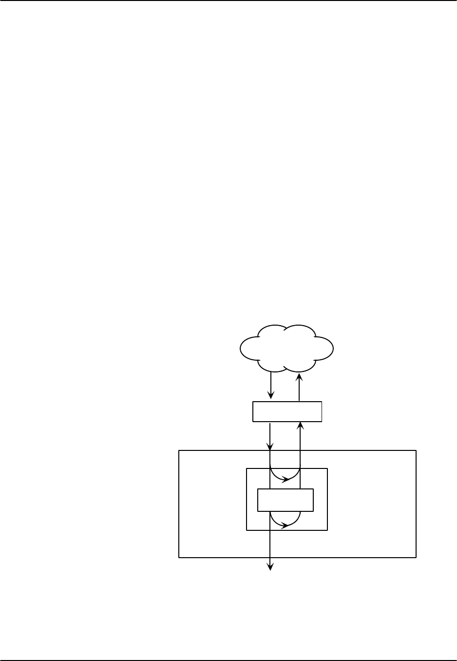
Reference Guide v3.6FXO Card
(10-97) Page 7-C-5
CODING
The Coding setting sets the PCM companding method used for a port. In general, in the
T1/North American environment use m-law coding. In the E1/International
environment use a-law or a-inv (inverted A-law) coding;
a-inv provides greater 1s density than a-law. The coding default is determined by the
type of card in the WAN port you select.
TC CGA
The Trunk Conditioning during Carrier Group Alarm setting defines whether the FXO
port should be placed in idle or busy mode upon declaration of a Carrier Group Alarm
(CGA) on the WAN link to which the port is assigned. In most cases, you should set
this parameter to busy. If a call is in progress when the CGA alarm is received, the
system will hold the call for two seconds, drop it and then busy out the port to the
attached PBX for the duration of the alarm. Once the alarm clears, the system will
automatically place the port back in idle mode thereby making it available to the
attached PBX.
LB
The Loopback setting sets the loopback for this circuit to off, digital (dgtl), or analog
(anlg). Figure FXO-2 illustrates the loopback options.
CODEC
Digital Loopback
Analog Loopback
PCM bus
T1/E1
DSO
FXO
Voice Card
Digital to Analog
Converter
Network
Figure FXO-2. FXO Card Loopbacks

FXO Card Reference Guide v3.6
Page 7-C-6(10-97)
PATTRN
The Pattern setting sets the outgoing test pattern for this analog port. The pattern,
generated by the system, is sent only to the currently selected port. The none option
disables sending a test pattern. The D-mW (Digital milliwatt) option sends a 1 kHz
tone at 0.0 dBm. The Rx TLP setting affects the D-mW signal level. The quiet option
places a 900Ω termination on the line so that no analog signal is sent.
HYBRID
The Hybrid option assigns a three byte pattern to define the adjustment for return loss
(similar to Build Out Capacitors). The default, set1, balances to the ideal termination
of 900Ω & 2.15mF, in the case of the 8134 and 8138 cards and to 600Ω @ 2.15mF, in
the case of the 8135 and 8139 cards. The other settings are reserved for future use.
WK DLY
The Wink Delay setting allows the user to set the wink delay time. The options are
units of 100 milliseconds. Settings are 1-99 (100 milliseconds to 9.9 seconds). The
Wink Delay and Wink options are applicable to CCITT systems for determining the
delay of the R2 state machine. They should only be used with modes fxodn and dpt
(R2 and i-R2).
WINK
The Wink setting allows the user to set the wink duration time. The options are units of
100 milliseconds. Settings are 1-99 (100 milliseconds to 9.9 seconds). This option is
only applicable with modes fxodn and dpt (R2 and i-R2).
SIG CONV
The Signaling Conversion parameter allows the user to change the ABCD signaling bits
from CCITT (E1) to ANSI (T1) standards. This conversion is completed regardless of
the type of WAN aggregate (CSU/DSX or CEPT) to which it is attached. The options
are off (which means that ANSI signaling is used) and on (which converts transmit
signaling from ANSI to CCITT format according to the Interface Card Conversion
Table for FXO signaling, and also converts receive signaling from CCITT to ANSI).
RATE
The Rate parameter allows the user to utilize the voice compression capabilities of the
ADPCM server card. If that card is not present in the system, changes cannot be made
to this setting. The 64k option (default) does not use ADPCM resources (it is the
normal operation rate for voice circuits).

Reference Guide v3.6FXO Card
(10-97) Page 7-C-7
ADPCM voice channels are assigned in pairs by designating two voice ports (E&M,
FXO or FXS) to the same WAN link and timeslot and selecting rate settings for the pair
that add up to 64kbps (i.e. [24k,1+40k,2],[ 32k,1+32k,2] and [40k,1+24k,2]). The
numeral 1 after the rate setting assigns that portion of the voice port pair to the odd side
of the ADPCM pair. The numeral 2 after the rate setting assigns that portion of the
voice port pair to the even side of the ADPCM pair.
For more information about voice port assignments to the ADPCM card, please consult
the ADPCM section of the manual.
ADPCM
The ADPCM parameter lets the user choose the ADPCM card on which to place this
FXO port. The default setting is n/a and only changes when a Rate smaller than 64k is
selected (see above). The user is then allowed to select which ADPCM card to use for
the port (assignment is made by chassis slot number). The options are P1, P2 and P3.
Menu of Actions
Table FXO-2 shows the Menu of Actions for the FXO Card.
Table FXO-2. FXO Card Screen Menu of Actions
Action Function
Save Saves changes to settings.
Undo Returns all settings to the last saved state.
Refresh Updates certain time-related information fields that are not
automatically updated (i.e. performance and test data).
Copy Copies the contents of the current column to the next column. Useful if
you change a lot of entries in one column and want to repeat those
changes in subsequent columns.
Test Initiates and monitors testing of all FXO card ports. Refer to Test
section below.
Main Returns to the main terminal screen. If changes are made to settings
and not saved, you will be prompted to save or lose changes.
Test
The Test option facilitates testing and maintenance by allowing the user to monitor and
set the status of the analog interface leads as well as monitoring and setting the value of
the A, B, C and D signaling bits of all FXO circuits on that card. In cross-connect
systems only, the test option also allows the user to apply test patterns and tones
towards the user and network sides of the system.
Figure FXO-3 shows the FXO Card Test parameters and Table FXO-3 shows the
settings for each.

FXO Card Reference Guide v3.6
Page 7-C-8(10-97)
Node_1 | U1 FXO 2Wx8-9 8139 Rev C2-0 Ser 00101 | 12-31-99 14:33
SIG MON = OFF
1 2 3 4 5 6 7 8
TEST n/a n/a n/a n/a n/a n/a n/a n/a
Tx ABCD mon mon mon mon mon mon mon mon
Rx ABCD mon mon mon mon mon mon mon mon
T-R-CNTL mon mon mon mon mon mon mon mon
TO USER n/a n/a n/a n/a n/a n/a n/a n/a
TO NTWK n/a n/a n/a n/a n/a n/a n/a n/a
Tx ABCD n/a n/a n/a n/a n/a n/a n/a n/a
Rx ABCD n/a n/a n/a n/a n/a n/a n/a n/a
T-R-CNTL n/a n/a n/a n/a n/a n/a n/a n/a
T-R-STAT n/a n/a n/a n/a n/a n/a n/a n/a
MODE fxo fxo fxo fxo fxo fxo fxo fxo
TYPE loop loop loop loop loop loop loop loop
STATUS W stb W stb W stb W stb W stb W stb W stb W stb
Save | Undo | Refresh | Main | siG mon
Figure FXO-3. FXO Card Test Screen
Table FXO-3. FXO Card Test Screen Parameters
Parameter User Options Default
SIG MON off on off
TEST off on off
TX ABCD mon set mon
RX ABCD mon set mon
T-R-CNTL mon set mon
TO USER PCM 300Hz 1kHz 3kHz quiet PCM
TO NTWK PCM 300Hz 1kHz 3kHz quiet PCM
TX ABCD Information only - no user input n/a
RX ABCD Information only - no user input n/a
T-R-CNTL Information only - no user input n/a
T-R-STAT Information only - no user input n/a
MODE Information only - no user input n/a
TYPE Information only - no user input n/a
STATUS Information only - no user input n/a
SIG MON
The Signaling Monitor feature works with the user card alarm system (see Basic
Operations section) to detect excessive signaling bit transitions. The system will
generate alarms if the number of transitions of any signaling bit in transmit or receive
direction for an active port exceeds 255 in any four second interval. The options are off
and on, and they are toggled using the G command in the Menu of Actions.

Reference Guide v3.6FXO Card
(10-97) Page 7-C-9
TEST
The Test Parameter shows if the port is in the test mode or not. Inactive ports and ports
that are assigned to inactive WANs will show a test status of n/a. The test status
options for active ports are off and on.
Tx ABCD
The Transmit ABCD setting allows the user to either monitor the status of the ABCD
signaling bits being transmitted towards the network or set a specific ABCD pattern for
testing the transmit side of the circuit. The options for this field are mon (monitor) or
set. Choosing set will bring up a four digit field for you to input the ABCD pattern you
want to transmit. Any four digit combination of ones and zeros is acceptable for this
setting.
Rx ABCD
The Receive ABCD setting allows the user to either monitor the status of the ABCD
signaling bits being received from the network or set a specific ABCD pattern for
testing the receive side of the circuit. The options for this field are mon (monitor) or
set. Choosing set will bring up a four digit field for you to input the ABCD pattern you
want to receive. Any four digit combination of ones and zeros is acceptable for this
setting. The Rx ABCD bits cannot be set in bus-connect systems and the only option is
mon (monitor).
T-R-CNTL
The Tip and Ring Control setting allows the user to either monitor (mon) or set (set) the
state of the Tip and Ring leads of an FXO port. Choosing set will bring up the
following options:
loop the Tip and Ring leads are tied together
open the Ring lead is not connected to either the Tip or to ground
TO USER
In cross-connect systems only, the To User parameter allows you to break the circuit
and send a test tone toward the user side of the system. The options for this field are
PCM, 300Hz, 1 kHz, 3 kHz and quiet. Selecting PCM means that you do not want to
inject a tone toward the user and that the PCM signal received from the network should
continue to be sent to the user port in the normal manner.
This parameter is not supported in bus-connect systems and will always appear as n/a.

FXO Card Reference Guide v3.6
Page 7-C-10 (10-97)
TO NTWK
In cross-connect systems only, the To Network parameter allows you to break the
circuit and send a test tone toward the network side of the system. The options for this
field are PCM, 300Hz, 1 kHz, 3 kHz and quiet. Selecting PCM means that you do
not want to inject a tone toward the network and that the PCM signal received from the
user port should continue to be sent to the network in the normal manner.
This parameter is not supported in bus-connect systems and will always appear as n/a.
Tx ABCD
The Transmit ABCD information field shows the current values of the ABCD bits that
are being transmitted to the network. If TX ABCD in the top half of the screen is
changed via the set function mentioned above, and the settings are saved by the Save
command in the Menu of Actions, the new bit pattern chosen will be reflected here.
Rx ABCD
The Receive ABCD information field shows the current values of the ABCD signaling
bits that are received from the network. If RX ABCD in the top half of the screen is
changed via the set function mentioned above, and the settings are saved by the Save
command in the Menu of Actions, the new bit pattern chosen will be reflected here.
T-R-CNTL
The Tip and Ring Control information field shows the current status of the Tip and
Ring leads of the FXO port from the perspective of the system. The possible values
are:
loop the Tip and Ring leads are tied together
open the Ring lead is not connected to either the Tip or to ground
rgnd the Ring lead is grounded
lpgnd the Tip and Ring leads are tied together and the Tip is grounded
ring ringing voltage is being applied between the Tip and Ring
T-R-STAT
The Tip and Ring Status information field describes what the attached device is doing
with the Tip and Ring leads of the FXO port. The possible values are:
ring attached device is applying ringing voltage between Tip and Ring
TbRg attached device is applying -48V battery to the Tip lead and is
grounding the Ring lead
ToRo attached device is leaving both the Tip and Ring leads open
TgRo attached device is grounding the Tip lead and leaving the Ring lead
open
RbTg attached device is applying -48V battery to the Ring lead and is
grounding the Tip lead

Reference Guide v3.6FXO Card
(10-97) Page 7-C-11
RbTo attached device is applying -48V battery to the Ring lead and is
leaving the Tip lead open
TgR* attached device is grounding the Tip lead and the state of the Ring
lead is unknown
ToR* attached device is leaving the Tip lead open and the state of the Ring
lead is unknown
RoT* attached device is leaving the Ring lead open and the state of the Tip
lead is unknown
n/a information is not available
MODE
The Mode information field shows the current mode of the port that was selected on the
main FXO card Screen. Valid settings are fxo, fxodn, dpt or mrd.
TYPE
The Type information field shows the current status of the signal field selected on the
main FXO card screen for this port. Valid settings for both fxo and fxodn modes are
loop (loop), ground start (gs), loop start-forward disconnect (lp-fd) and R2 (R2). Valid
settings for the dpt mode are dial pulse terminating (dpt), R2 (R2) and immediate R2
(i-R2). The only valid setting for the mrd mode is manual ringdown (mrd).
STATUS
The Status information field shows the current status of the port. Table FXO-4 lists and
describes all of the possible conditions that are reported in this field.
Table FXO-4. Status Information Field Settings
Setting Meaning
stdby The FXO port is in standby.
W stb The WAN that the FXO port is assigned to is in standby.
W tst The WAN that the FXO port is assigned to is in test.
W OOS The WAN that the FXO port is assigned to is Out Of Service.
noWAN There is no WAN card configured in the slot to which the FXO port is
assigned.
call Call set-up is in progress.
busy A call is in progress.
idle The FXO circuit is not being used and is available.
TC The FXO circuit is undergoing Trunk Conditioning because of a CGA
alarm on the WAN to which it is assigned.
test The operator is actively controlling the circuit by setting values for Tx
ABCD or Rx ABCD.
maint The FXO port is in maintenance condition.

FXO Card Reference Guide v3.6
Page 7-C-12 (10-97)
Menu of Actions
Table FXO-5 shows the Menu of Actions for the FXO Card Test Screen.
Table FXO-5. FXO Card Test Screen Menu of Actions
Action Function
Save Saves changes to settings.
Undo Returns all settings to the last saved state.
Refresh Updates certain time-related information fields that are not automatically
updated (i.e. performance and test data).
Main Returns to the FXO card main screen. If changes are made to settings
and not saved, you will be prompted to save or lose changes.
siG mon The signal monitor is used with the user card alarm system to notify the
user of excessive transitions of signaling bits.
Setting Jumpers on the FXO Card
Setting or resetting jumpers is necessary for conversion of individual ports on the FXO
card to mrd (Manual Ringdown) mode. To make this conversion, remove the FXO
card from its slot and connect shorting jumpers (ordered separately) vertically from #1
to #2 on both sets of pins next to the front edge of the card as shown in Figure FXO-4.
The numbers (#1 and #2) are not stenciled on the card, but they are shown here to
clarify the procedure.
Ports can be set individually for the mrd feature, but once set, remain in the mrd mode
until the jumpers are removed. This information is repeated in the Installation chapter.
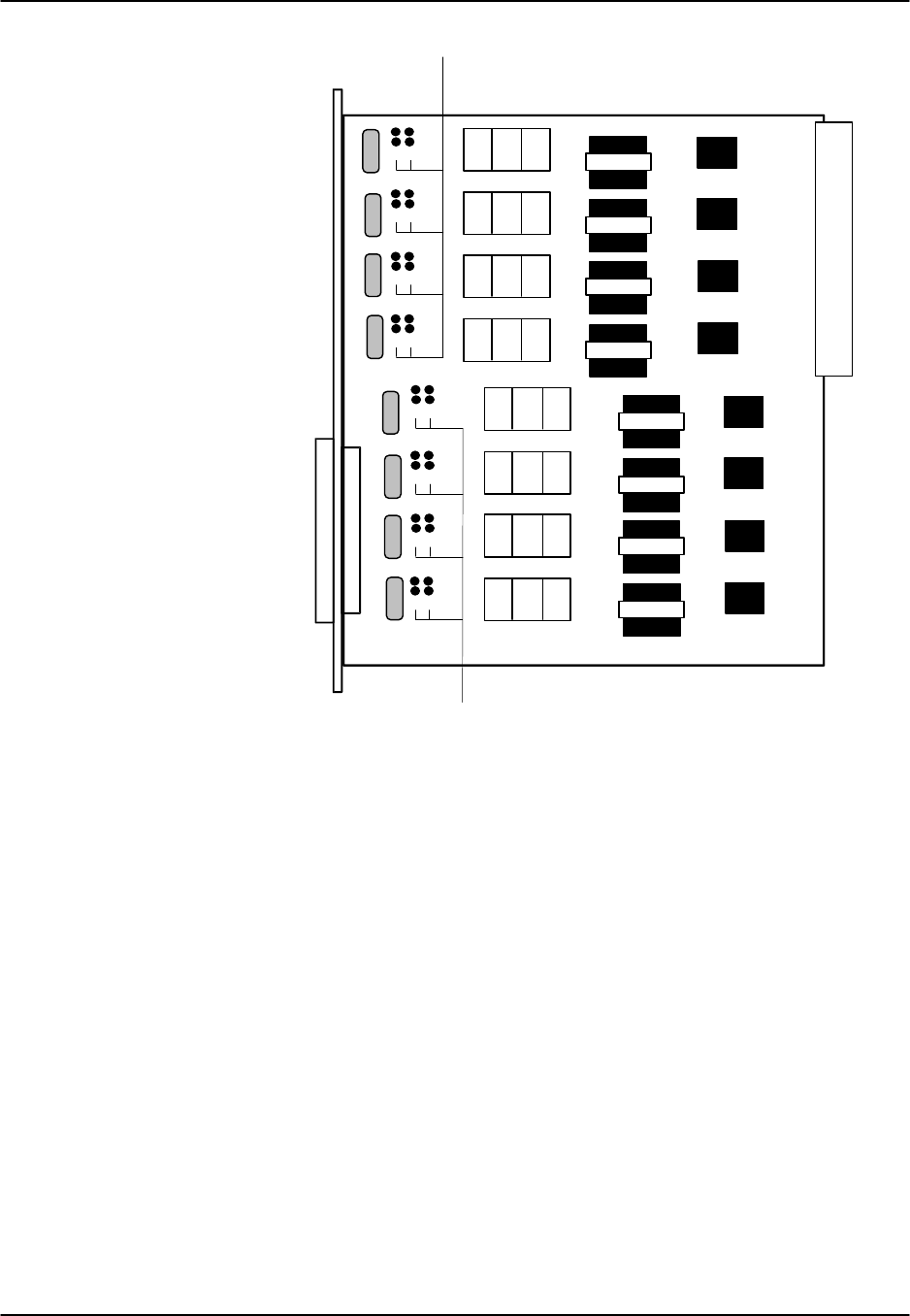
Reference Guide v3.6FXO Card
(10-97) Page 7-C-13
Power
Bus
Edge
Connector
Port #8
∧
Port #7
∧
Port #6
∧
Port #5
∧
Port #4
∧
Port #3
∧
Port #2
∧
Port #1
∧
Jumpers to Reset
1
1
2
2
1
1
2
2
1
1
2
2
1
1
2
2
Jumpers to Reset
1
1
2
2
1
1
2
2
1
1
2
2
1
1
2
2
Figure FXO-4. Jumpers for mrd Mode

FXO Card Reference Guide v3.6
Page 7-C-14 (10-97)

Reference Guide v3.6 FXS Coin Card
(10-97) Page 7-D-1
Introduction
This chapter provides connector pinout, configuration, and troubleshooting information
for the Foreign Exchange - Station (FXSC) Coin Voice Cards.
These cards manage the flow of FXS voice traffic over the network. Each card encodes
analog (voice, VF) signals to a digital bitstream at the local system for transmission
over a T1 or E1 network. It also decodes the digital signals to analog at the remote
system.
Each FXS coin card has two-wires interfaces that support FXS, Private Line Automatic
Ringdown (PLAR), Foreign Exchange Station-Defined Network (FXSDN), Dial-Pulse
Originating (DPO), and Wink-start operations. The FXS cards also can use the voice-
compression features of an ADPCM card.
8149 FXS Coin Card
The 8149 FXS Coin Card has six ports and two wires, providing a 600-ohm terminating
impedance. The card consists of backplane interface circuitry, serial EEPROM for card
identification and adjustment parameters storage, metering pulse interface extension
between Coin Box Office (CO) and coin phone on the side of the coin phone, and six
voice line interface circuits. Each line interface circuit consists of a codec, a hybrid
circuit.
FXS Coin Card Settings
External Card Connectors and Pinouts
Refer to the Pinout Chapter in this manual.
Card Jumper/Switch Settings
The FXS Coin Card does not have any jumpers or switches on its motherboard.
Installing the FXS Coin Card
Install the FXS Coin Card in any user card slot. These slots are U1 to U8 on the two-
sided chassis and front-loading chassis with power supplies on top, or P1 to P4 and W1
to W4 on the front-loading chassis with power supplies on the side.

FXS Coin Card Reference Guide v3.6
Page 7-D-2(10-97)
FXS Coin Card User Screens and Settings
Main Screen
You must configure the FXS Coin Card for operation after installing it into the system
chassis. This is done from the FXS Coin Card Main Screen (see Figure FXSC-1). To
go to that screen, highlight the desired card in the System Main Screen and press
<Enter>. This screen shows one configuration column for each port on the card.
Node_1 | U2 FXSC 6-600 Rev D1-0 Ser 00061 | 12-31-99 14:33
1 2 3 4 5 6 7 8
STATE stdby stdby stdby stdby stdby stdby stdby stdby
WAN w1-1 w1-1 w1-1 w1-1 w1-1 w1-1 w1-1 w1-1
TS 01 01 01 01 01 01 01 01
MODE fxsc fxsc fxsc fxsc fxsc fxsc fxsc fxsc
TYPE hf-a1 hf-a1 hf-a1 hf-a1 hf-a1 hf-a1 hf-a1 hf-a1
Rx TLP 0.0 0.0 0.0 0.0 0.0 0.0 0.0 0.0
Tx TLP 0.0 0.0 0.0 0.0 0.0 0.0 0.0 0.0
CODING u-laq u-law u-law u-law u-law u-law u-law u-law
TC CGA idle idle idle idle idle idle idle idle
LB off off off off off off off off
PATTRN none none none none none none none none
HYBRID set1 set1 set1 set1 set1 set1 set1 set1
RINGBK off off off off off off off off
SIG CONV off off off off off off off off
RATE 64k 64k 64k 64k 64k 64k 64k 64k
ADPCM n/a n/a n/a n/a n/a n/a n/a n/a
Save | Undo | Refresh | Copy | Test | Main
Figure FXSC-1. Typical FXS Coin Card Main Screen
The bottom highlighted line of this screen shows various actions that you can perform
from the screen. You perform the desired action by pressing the associated capital letter
key. Table FXSC-1 summarizes these actions. For example, after you configure the
FXS coin card ports, press “s” to save your settings.

Reference Guide v3.6FXS Coin Card
(10-97) Page 7-D-3
Menu of Actions
Table FXSC-1. Main Screen Actions
Action Function
Save Saves changes to settings.
Undo Returns all settings to the last saved state.
Refresh Updates certain time-related information fields that are not
automatically updated (i.e., test status).
Copy Copies the contents of the current column to the next column. Useful if
you change a lot of entries in one column and want to repeat those
changes in subsequent columns.
Test Initiates and monitors testing of all FXS coin card ports. Refer to the
Test section of this chapter.
Main Returns to the Systems Main Screen. If changes are made to settings
and not saved, you will be prompted to either save or lose your changes.
Table FXSC-2 summarizes the configuration settings for the FXS coin card, along with
the available and factory-default option settings. The parameters and settings are also
described in the following paragraphs.
Table FXSC-2. Main Screen Option Settings and Defaults
Parameter User Options Notes Default
STATE stdby actv stby
WAN w1-1 w1-2 w2-1 w2-2 w3-1 w3-3 w4-1 w4-2 1w1-1
TS 01-24 01-31 2 01
MODE fxsc fxsc
TYPE hf-a1 hf-a2 hf-cb rb-a1 rb-a2 rb-cb hf-a1
RX TLP -10.0 dB to +2.0 dB 0.0
TX TLP -10.0 dB to +5.0 dB 0.0
CODING u-law a-law a-inv 3u-law
TC CGA idle busy idle
LB off dgtl anlg off
PATTERN none D-mW quiet none
HYBRID set1 to set8 user 4set1
RINGBK off on off
RATE 64K, 24K,1 32K,1 40K,1 24K,2 32K,2 40K,2 564K
ADPCM n/a P1 P2 P3 n/a
NOTES
1. Choosing wan allows you to choose a WAN port (w1-1 through w4-2).
2. Time slot 16 is not available if the port is assigned to an E1 WAN link whose time
slot 16 is programmed for CAS or CCS.

FXS Coin Card Reference Guide v3.6
Page 7-D-4(10-97)
3. The default is a-inv for E1 and u-law for T1. These values will change depending
upon the WAN link selected.
4. The default (set1) is the only active option. It balances to the ideal termination of
600 ohms + 2.15 uF. The other settings are reserved for future use.
5. Choosing a Rate other than 64K allows you to select an ADPCM.
STATE
The State setting determines whether the port is active or inactive. An inactive port
does not occupy a time slot on a WAN link. Set the State setting to stdby (standby) for
ports that are not to be used or that have not yet been configured. Set it to actv (active)
for ports that are ready for use.
WAN
The WAN setting identifies the WAN link assigned to this port. If you choose wan, you
also must select the desired port (w1-1 through w4-2) of a WAN card for transmission
over a T1 or E1 link. This can be an ATM or FRS card, which resides in chassis slot
P1, P2, or P3. You must then choose a logical port on that card. The user option is not
used.
It is not necessary to assign all ports of the same FXS coin card to the same WAN link,
or to contiguous time slots on a WAN link.
TS
The TS setting identifies the time slot on the WAN link to which this port is assigned.
Values range from 1 to 24 for T1 links and 1 to 31 for E1 links. Time slot 16 is not
available on E1 links that are programmed for cas or ccs signaling. For a display of the
available time slots, refer to the cross-connect map for the WAN link; see the
Operations chapter for information about viewing cross-connect maps.
MODE
The Mode setting should be determined by the type of equipment to which the user is
connecting the port. All options use two-wire balanced connections. The fxsc (Foreign
Exchange Station-Coin) option allows users to connect the system to a two-way (both
inbound and outbound calls) PBX trunk or a key system trunk.
TYPE
The Type setting matches the signaling behavior of the FXSC equipment and the
remote switch. These settings are hf-a1 (high frequency - 12kHz), hf-a2 (high
frequency - 16kHz), hf-cb (high frequency-clear back), rb-a1 (reverse battery-answer
1), rb-a2 (reverse battery-answer 2), and rb-cb (reverse battery-clear back).

Reference Guide v3.6FXS Coin Card
(10-97) Page 7-D-5
Rx TLP
The Receive Transmission Level Point (TLP) setting controls the amount of gain or loss
added to the incoming signal after it is decoded to analog. To increase the signal level,
set the Rx TLP setting to a positive value (i.e., the larger the number, the more gain is
added). To decrease the signal level, set the Rx TLP setting to a negative value (i.e., the
more negative the number, the more the signal level is decreased). For example, an
incoming signal at -5 dBm can be increased to -3 dBm by setting Rx TLP to +2 dB.
The Rx TLP range is -10.0 dB to +2.0 dB.
Tx TLP
The Transmit TLP setting controls the amount of gain or loss added to a voice signal
from the CPE before it is encoded to digital PCM. To increase the signal level, set the
Tx TLP setting to a negative value (i.e., the more negative the number, the more gain is
added). To decrease the signal level, set the Tx TLP setting to a positive value (i.e., the
more positive the number, the more the signal level is decreased). For example, an
incoming signal at -5 dBm can be increased to -2 dBm by setting the Tx TLP to -3 dB.
The Tx TLP range is -10.0 dB to +5.0 dB.
CODING
The Coding setting sets the PCM companding method used for a port. Generally, the
North American T1 environment uses m-law coding, and the International E1
environment uses a-law or a-inv (inverted A-law) coding. The a-inv setting provides a
higher ones density than a-law. The default coding setting is determined by the type of
associated WAN card.
TC CGA
The Trunk Conditioning during Carrier Group Alarm setting defines whether the FXS
port should be forced idle or busy upon declaration of a Carrier Group Alarm (CGA) on
the WAN link to which the port is assigned. In most cases, you should set this
parameter to busy. If a call is in progress when the CGA alarm is received, the system
will hold the call for two seconds, drop it, and then busy out the port to the attached
PBX for the duration of the alarm. Once the alarm clears, the system will automatically
place the port back in the idle mode, making it available to the PBX.
LB
The Loopback field lets you loop the port back toward the network and far end. The
dgtl (digital) loopback sends the incoming digital DS0 signal back to the far end
without decoding it. The anlg (analog) loopback sends the decoded analog signal back
to the far end after decoding and then re-encoding it. Figure FXSC-2 shows the
loopback options, which allow you to test and troubleshoot the FXS card. To disable a
loopback, set this field to off.
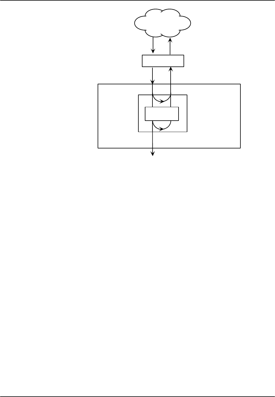
FXS Coin Card Reference Guide v3.6
Page 7-D-6(10-97)
CODEC
Digital Loopback
Analog Loopback
PCM bus
T1/E1
DSO
Digital to Analog
Converter
Network
Figure FXSC-2. FXS Coin Card Loopbacks
PATTRN
The Pattern field selects an outgoing test pattern for the current card port. The test
pattern is generated by the system and sent to the selected port. You can select a
different pattern for each port. The none option disables the test pattern. The D-mW
(Digital milliwatt) option sends a 1 kHz tone at 0.0 dBm. The setting of the Rx TLP
setting affects the D-mW signal level. The quiet option places a 600-ohm termination
on the line so that no analog signal is sent (idle mode).
HYBRID
The Hybrid option assigns a three byte pattern to define the adjustment for return loss
(similar to Build Out Capacitors). The default, set1, balances to the ideal termination of
600 ohms + 2.15 uF. The other settings are reserved for future use.
RINGBK
The ringback setting specifies whether a ringback tone is generated by the system and
sent towards the network. Turn this option off when the network service does not
provide an audible ringing tone to the calling party.
RATE
The Rate parameter allows you to use the voice compression capabilities of an ADPCM
card. If that card is not present in the system, the Rate stays at 64k and cannot be
changed. The 64k option is the normal encoding/decoding rate for voice circuits.

Reference Guide v3.6FXS Coin Card
(10-97) Page 7-D-7
ADPCM voice channels are assigned in pairs by designating two voice ports (E&M,
FXO, or FXS) to the same WAN link and timeslot, and selecting rate settings for the
pair that add up to 64 kbps. The following combinations are possible:
24K,1+40K,2 (24 kb coding on one side of the time slot and 40 kb coding on the other
side of the same time slot)
32K,1+32K,2 (32 kb encoding on each side of a time slot)
40K,1+24K,2 (40 kb coding on one side of the time slot and 24 kb coding on the other
side)
Number 1 after the rate setting assigns that portion of the voice port pair to the odd side
of the ADPCM pair. Number 2 after the rate setting assigns that portion of the voice
port pair to the even side of the ADPCM pair.
For more information about voice port assignments to an ADPCM card, please consult
Chapter 7A of this guide.
The number 1 after the rate setting assigns that portion of the voice port pair to the odd
side of the ADPCM pair. The number 2 after the rate setting assigns that portion of the
voice port pair to the even side of the ADPCM pair.
For more information about voice port assignments to the ADPCM card, please consult
the ADPCM section of the manual.
ADPCM
The ADPCM parameter lets the user choose which ADPCM card to place this E&M
port. The default setting is n/a and only changes when a Rate smaller than 64k is
selected (see above). The user is then allowed to select which ADPCM card to use for
the port (this assignment is made by chassis slot number). The options are slots P1, P2,
and P3.
Test Screen
The Test option facilitates testing and maintenance by allowing you to monitor and set
the status of the analog interface leads, and to monitor or set the value of the A, B, C,
and D signaling bits of all FXS circuits on that card. In cross-connect systems, the test
option also allows you to apply test patterns and tones towards the user and network
sides of the system.
Figure FXSC-3 shows the FXS Coin Card Test Screen parameters, Table FXSC-3 lists
some actions you can perform from this screen, and Table FXSC-4 shows the settings
for each parameter.

FXS Coin Card Reference Guide v3.6
Page 7-D-8(10-97)
Node_1 | U2 FXSC 6-600 Rev D1-0 Ser 00061 | 12-31-99 14:33
SIG MON=OFF
1 2 3 4 5 6 7 8
TEST off off off off off off off off
Tx ABCD mon mon mon mon mon mon mon mon
Rx ABCD mon mon mon mon mon mon mon mon
T-R-CNTL mon mon mon mon mon mon mon mon
TO USER n/a n/a n/a n/a n/a n/a n/a n/a
TO NTWK n/a n/a n/a n/a n/a n/a n/a n/a
Tx ABCD n/a n/a n/a n/a n/a n/a n/a n/a
Rx ABCD n/a n/a n/a n/a n/a n/a n/a n/a
T-R-CNTL RbTo RbTo RbTo RbTo RbTo RbTo RbTo RbTo
T-R-STAT off off off off off off off off
MODE fxsc fxsc fxsc fxsc fxsc fxsc fxsc fxsc
TYPE hf-a1 hf-a1 hf-a1 hf-a1 hf-a1 hf-a1 hf-a1 hf-a1
STATUS noWAN noWAN noWAN noWAN noWAN noWAN noWAN noWAN
Save | Undo | Refresh | Main | siG mon
Figure FXSC-3 Typical FXS Coin Card Test Screen

Reference Guide v3.6FXS Coin Card
(10-97) Page 7-D-9
Menu of Actions
Table FXSC-3. Test Screen Actions
Action Function
Save Saves changes to settings.
Undo Returns all settings to the last saved state.
Refresh Updates certain time-related information fields that are not automatically
updated (i.e. performance and test data).
Main Returns to the FXS Coin Card Main Screen. If changes are made to
settings and not saved, you will be prompted to save or lose changes.
siG mon Used with the user card alarm system to notify you of excessive transitions
of signaling bits.
Table FXSC-4. Test Screen Option Settings and Defaults
Parameter User Options Default
SIG MON off on off
TEST off on off
TX ABCD mon mon
RX ABCD mon mon
T-R-CNTL mon mon
TO USER n/a n/a
TO NTWK n/a n/a
TX ABCD Status information only; not editable n/a
RX ABCD Status information only; not editable n/a
T-R-CNTL Status information only; not editable n/a
T-R-STAT Status information only; not editable n/a
MODE Status information only; not editable n/a
TYPE Status information only; not editable n/a
STATUS Status information only; not editable n/a

FXS Coin Card Reference Guide v3.6
Page 7-D-10 (10-97)
SIG MON
The Signaling Monitor feature works with the user card alarm system (see Chapter 3-A)
to detect excessive signaling bit transitions. The system will generate alarms if the
number of transitions of any signaling bit in transmit or receive direction for an active
port exceeds 255 in any four second interval. The options are off and on, and they are
toggled by pressing “g” (siGmon command) in the Test Screen.
TEST
The Test parameter shows if the port is in test mode or not. Inactive ports and ports that
are assigned to inactive WANs will show a test status of n/a. The test status options for
active ports are off and on.
Tx ABCD
The Transmit ABCD setting allows you to either monitor the status of the ABCD
signaling bits being transmitted towards the network or set a specific ABCD pattern for
testing the transmit side of the circuit. The option for this field is mon (monitor).
Rx ABCD
The Receive ABCD setting allows the user to either monitor the status of the ABCD
signaling bits being received from the network or set a specific ABCD pattern for
testing the receive side of the circuit. The option for this field is mon (monitor).
T-R-CNTL
The Tip and Ring Control setting allows you to mon (monitor) the state of the Tip and
Ring leads of an FXS port:
RbTo (-48V is applied to the Ring lead and the Tip lead is open)
TbRo (-48V is applied to the Tip lead and the Ring lead is open)
RbTg (-48V is applied to the Ring lead and the Tip lead is grounded)
TbRg (-48V is applied to the Tip lead and the Ring lead is grounded)
TO USER
In cross-connect systems only, the To User parameter allows you to break the circuit
and send a test tone on the user side of the system. The options for this field are PCM,
300Hz, 1kHz, 3kHz, and quiet. Choose PCM if you do not want to inject a tone
toward the CPE. In this case, the PCM signal received from the network is still sent to
the CPE in the normal manner.

Reference Guide v3.6FXS Coin Card
(10-97) Page 7-D-11
TO NTWK
In cross-connect systems only, the To Network parameter allows you to break the
circuit and send a test tone on the network side of the system. The options for this field
are PCM, 300Hz, 1kHz, 3kHz, and quiet. Choose PCM if you do not want to inject a
tone toward the network. In this case, the PCM signal received from the CPE is still
sent to the network in the normal manner.
Tx ABCD
The Transmit ABCD informational field shows the current values of the ABCD bits that
are being transmitted to the network. If TX ABCD in the top half of the screen is
changed via the set function mentioned above, and the settings are saved by the Save
command in the Menu of Actions, the new bit pattern chosen will be reflected here.
Rx ABCD
The Receive ABCD informational field shows the current values of the ABCD
signaling bits that are received from the network. If RX ABCD in the top half of the
screen is changed via the set function mentioned above, and the settings are saved by
the Save command in the Menu of Actions, the new bit pattern chosen will be reflected
here.
T-R-CNTL
The Tip and Ring Control informational field shows the current status of the Tip and
Ring leads of the FXS port from the perspective of the system. The possible values are
as follows
(b = battery, o = open, g = ground):
RbTo (-48V is applied to the Ring lead and the Tip lead is open)
TbRo (-48V is applied to the Tip lead and the Ring lead is open)
RbTg (-48V is applied to the Ring lead and the Tip lead is grounded)
TbRg (-48V is applied to the Tip lead and the Ring lead is grounded)
ring (the ringing voltage is applied between Tip and Ring)
T-R-STAT
The Tip and Ring Status informational field describes what the attached device is doing
with the Tip and Ring leads of the FXS port. The possible values are:
loop (attached device is connecting Tip and Ring together)
rgnd (the Ring lead is grounded by the attached device)
open (Ring lead is not connected to either the Tip lead or to ground)

FXS Coin Card Reference Guide v3.6
Page 7-D-12 (10-97)
MODE
The Mode informational field shows the current mode of the port that was selected on
the main FXS coin card Screen. Valid settings are fxsc.
TYPE
The Type setting matches the signaling behavior of the FXSC equipment and the
remote switch. These settings are hf-a1 (high frequency - 12kHz), hf-a2 (high
frequency - 16kHz), hf-cb (high frequency-clear back), rb-a1 (reverse battery-answer
1), rb-a2 (reverse battery-answer 2), and rb-cb (reverse battery-clear back).
STATUS
The Status field shows the current status of the port. Table FXSC-5 lists and describes
all of the possible conditions reported by this field.
Table FXSC-5. Status Information Field Settings
Setting Meaning
STDBY The FXS port is in standby.
W STB WAN card to which the FXS port is assigned is in standby.
W TST WAN card to which the FXS port is assigned is under test.
W OOS WAN card to which the FXS port is assigned is out of service.
NOWAN There is no WAN card configured in the slot to which the FXS port is
assigned.
CALL Call set-up is in progress.
BUSY Call is in progress.
IDLE No call is in progress (port is available for a call).
TC The port is in Trunk Conditioning because a CGA alarm occurred on the
associated WAN port.
TEST A test is in progress on the port (i.e., you are actively controlling the circuit
by setting values for Tx ABCD or Rx ABCD).
MAINT The port is in a maintenance condition.

Reference Guide v3.6 FXO Coin Card
(10-97) Page 7-E-1
Introduction
The Foreign Exchange Office Coin Card manages the flow of FXOC voice traffic over
the network. The FXOC card translates an analog signal to a digital bitstream at the
local system and digital to analog at the remote system. All FXOC cards have a two-
wire interface and support Foreign Exchange Office functions, Manual Ringdown,
Foreign Exchange Defined Network and Dial Pulse Terminating operations. FXOC
cards can use the voice-compression features of the ADPCM resource card.
8159 FXO Coin Card
The 8159 FXO Coin Card has eight ports and two wires, providing a 600-ohm
terminating impedance. The card consists of backplane interface circuitry, serial
EEPROM for card identification and adjustment parameters storage, metering pulse
interface extension between Coin Box Office (CO) and coin phone on the CO side, and
eight voice line interface circuits. Each line interface circuit consists of a codec, a
hybrid circuit (2 to 4 wire converter), line feed circuitry and relays to control modes of
operation.
FXO Coin Card Settings
External Card Connectors and Pinouts
Refer to the Pinout Chapter in this manual.
Card Jumper/Switch Settings
Setting or resetting jumpers is necessary for conversion of individual ports on the
FXOC card to mrd (Manual Ringdown) mode. To make this conversion, remove the
FXOC card from its slot and connect shorting jumpers (ordered separately) vertically
from #1 to #2 on both sets of pins next to the front edge of the card as shown in Figure
FXOC-1. The numbers (#1 and #2) are not stenciled on the card, but they are
shown here to clarify the procedure.
Ports can be set individually for the mrd feature, but once set, remain in the mrd mode
until the jumpers are removed. This information is repeated in the Installation chapter.

FXO Coin Card Reference Guide v3.6
Page 7-E-2(10-97)
Power
Bus
Edge
Connector
Port #8
∧
Port #7
∧
Port #6
∧
Port #5
∧
Port #4
∧
Port #3
∧
Port #2
∧
Port #1
∧
Jumpers to Reset
1
1
2
2
1
1
2
2
1
1
2
2
1
1
2
2
Jumpers to Reset
1
1
2
2
1
1
2
2
1
1
2
2
1
1
2
2
Figure FXOC-1. Jumpers for mrd Mode
Installing the FXO Coin Card
Install the FXO Coin Card in any user card slot. These slots are U1 to U8 on the two-
sided chassis and front-loading chassis with power supplies on top, or P1 to P4 and W1
to W4 on the front-loading chassis with power supplies on the side.

Reference Guide v3.6FXO Coin Card
(10-97) Page 7-E-3
FXO Coin Card User Screens and Settings
Main Screen
FXOCoin Card setting options are displayed in columns on the FXO Coin Card screen,
as shown in Figure FXOC-2. Table FXOC-1 lists the settings controlled on the screen
along with the possible and default values. The settings are similar to those for other
voice cards.
Node_1 | U1 FXOC 8-600 Rev A2-0 Ser 00003 | 12-31-99 14:33
1 2 3 4 5 6 7 8
STATE stdby stdby stdby stdby stdby stdby stdby stdby
WAN w1-1 w1-1 w1-1 w1-1 w1-1 w1-1 w1-1 w1-1
TS 01 01 01 01 01 01 01 01
MODE fxoc fxoc fxoc fxoc fxoc fxoc fxoc fxoc
SIGNAL hf-a1 hf-a1 hf-a1 hf-a1 hf-a1 hf-a1 hf-a1 hf-a1
Rx TLP 0.0 0.0 0.0 0.0 0.0 0.0 0.0 0.0
Tx TLP 0.0 0.0 0.0 0.0 0.0 0.0 0.0 0.0
CODING n/a n/a n/a n/a n/a n/a n/a n/a
TC CGA idle idle idle idle idle idle idle idle
LB off off off off off off off off
PATTRN none none none none none none none none
HYBRID set1 set1 set1 set1 set1 set1 set1 set1
RATE 64k 64k 64k 64k 64k 64k 64k 64k
ADPCM n/a n/a n/a n/a n/a n/a n/a n/a
Save | Undo | Refresh | Copy | Test | Main
Figure FXOC-2. Typical FXO Coin Card Main Screen
The bottom highlighted line of this screen shows various actions that you can perform
from the screen. You perform the desired action by pressing the associated capital letter
key. Table FXOC-1 summarizes these actions. For example, after you configure the
FXO coin card ports, press “s” to save your settings.

FXO Coin Card Reference Guide v3.6
Page 7-E-4(10-97)
Menu of Actions
Table FXOC-1. Typical FXO Coin Card Main Screen Actions
Action Function
Save Saves changes to settings.
Undo Returns all settings to the last saved state.
Refresh Updates certain time-related information fields that are not
automatically updated (i.e., test status).
Copy Copies the contents of the current column to the next column. Useful if
you change a lot of entries in one column and want to repeat those
changes in subsequent columns.
Test Initiates and monitors testing of all FXO coin card ports. Refer to the
Test section of this chapter.
Main Returns to the System Main Screen. If changes are made to settings and
not saved, you will be prompted to save or lose changes.
Table FXOC-2 summarizes the configuration settings for the FXO coin card, along with
the available and factory-default option settings. The parameters and settings are also
described in the following paragraphs.
Table FXOC-2. Typical FXO Coin Card Main Screen Option Settings and Defaults
Parameter User Options Notes Default
STATE
stdbyactv
stdby
WAN
w1-1w1-2w2-1w2-2w3-1w3-2w41w4-2
1
w1-1
TS
01-2401-31
2
01
MODE
fxoc
fxoc
SIGNAL
hf-a1hf-a2hf-cbrb-a1rb-a2rb-cb
3
hf-a1
RX TLP
-10.0dBto+2.0dB
0.0
TX TLP
-10.0dBto+5.0dB
0.0
CODING
u-lawa-inva-law
4
u-law
TC CGA
idlebusy
idle
LB
offdgtlanlg
off
PATTRN
noneD-mWquiet
none
HYBRID
set1toset8user
5
set1
RATE
6
64K
ADPCM
n/aP1P2P3
n/a
NOTES
1. Choosing wan allows you to choose a WAN port (w1-1 through w4-2). The user
option is not used.
2. Time slot 16 is not available if the port is assigned to an E1 WAN link whose TS
16 is programmed for cas or ccs.
3. The default is hf-a1.
4. The default is a-inv for E1 and m-law for T1. These values will change depending
upon the WAN link selected.

Reference Guide v3.6FXO Coin Card
(10-97) Page 7-E-5
5. The default, set1, is the only active option. It balances to the ideal termination of
600 ohms +2.15uF. The other settings are reserved for future use.
6. Choosing a Rate other than 64K allows you to select an ADPCM slot.
STATE
The State setting determines whether the port is active or inactive. An inactive port
does not occupy a time slot on a WAN link. Set the State setting to stdby (standby) for
ports you are not using or have not yet configured. Set it to actv (active) for ports that
are ready for use.
WAN
The WAN setting identifies the WAN link assigned to this port. It is not necessary for
all ports on the same card to be assigned to the same WAN link, or to contiguous time
slots on a WAN link.
TS
The TS setting identifies the time slot on the WAN link to which this port is assigned.
Values range from 1-24 for T1 links and 1-31 for E1 links. Time slot 16 is not available
on E1 links that are programmed for cas or ccs signaling. For a display of the available
time slots, refer to your cross-connect map for the WAN link.
MODE
The Mode setting should be determined by the type of equipment to which you connect
the port. All options use two-wire balanced connections. The fxoc (Foreign Exchange
Office Coin) option allows you to connect the system to a 2 way PBX trunk (both
inbound and outbound calls) or a key system trunk. The fxodn (Foreign Exchange
Office - Defined Network) option provides access to new services offered by advanced
networks from many major carriers. The dpt (Dial Pulse Terminating) option allows
the unit to attach to incoming one-way trunks from a PBX, key system, or a telephone
set. This option is similar to the fxoc option.
The mrd (manual ringdown) option provides point-to-point unswitched connections
between two telephone sets. This configuration is usually not attached to an exchange
or switch; rather it provides a “hot line” between two locations. The system requires
hardware changes and a ringing generator for this option (see instructions later in this
chapter).
SIGNAL
The Signal setting matches the signaling behavior of the FXOC equipment and the
remote switch. These settings are hf-a1(high frequency - 12kHz), hf-a2 (high frequency
- 16kHz), hf-cb (high frequency-clear back), rb-a1 (reverse battery-answer 1), rb-a2
(reverse battery-answer 2), and rb-cb (reverse battery-clear back).

FXO Coin Card Reference Guide v3.6
Page 7-E-6(10-97)
Rx TLP
The Receive Transmission Level Point setting controls the amount of gain or
attenuation added to signals after they are decoded to analog signals. To increase the
signal level, set the Rx TLP setting to a positive number (i.e., the larger the number, the
more gain is added). To decrease the signal level, set the Rx TLP setting to a negative
number (i.e., the more negative the number, the more the signal level is decreased). For
example, an incoming signal at -5 dBm can be increased to -3 dBm by setting Rx TLP
to +2 dB. Acceptable values range from -10.0 dB to +2.0 dB.
Tx TLP
The Transmit Transmission Level Point setting controls the amount of gain or
attenuation added to signals after they are received from the local analog port and
before they are encoded to digital PCM signals. To increase the signal level, set the Tx
TLP setting to a negative number (i.e., the more negative the number, the more gain is
added). To decrease the signal level, set the Tx TLP setting to a positive number (i.e.,
the more positive the number, the more the signal level is decreased). For example, an
incoming signal at -5 dBm can be increased to -2 dBm by setting Tx TLP to -3 dB.
Acceptable values range from -10.0 dB to +5.0 dB.
CODING
The Coding setting sets the PCM companding method used for a port. Generally, the
North American T1 environment uses m-law coding. The International E1 environment
uses a-law or a-inv (inverted A-law) coding, and a-inv provides a higher ones density
than a-law. The coding default is determined by the type of card in the WAN port you
select.
TC CGA
The Trunk Conditioning during Carrier Group Alarm setting defines whether the FXOC
port should be placed in idle or busy mode upon declaration of a Carrier Group Alarm
(CGA) on the WAN link to which the port is assigned. In most cases, you should set
this parameter to busy. If a call is in progress when the CGA alarm is received, the
system will hold the call for two seconds, drop it and then busy out the port to the
attached PBX for the duration of the alarm. Once the alarm clears, the system will
automatically place the port back in idle mode thereby making it available to the
attached PBX.
LB
The Loopback setting sets the loopback for this circuit to off, dgtl (digital), or anlg
(analog). Figure FXOC-3 illustrates the loopback options.
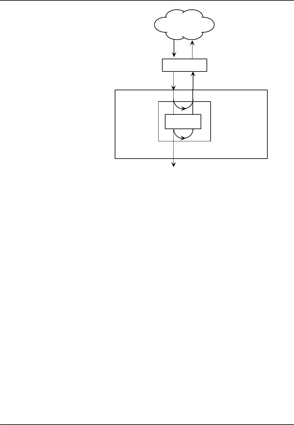
Reference Guide v3.6FXO Coin Card
(10-97) Page 7-E-7
CODEC
Digital Loopback
Analog Loopback
PCM bus
T1/E1
DSO
FXO
Voice Card
Digital to Analog
Converter
Network
Figure FXOC-3. FXO Coin Card Loopbacks
PATTRN
The Pattern setting sets the outgoing test pattern for this analog port. The pattern,
generated by the system, is sent only to the currently selected port. The none option
disables sending a test pattern. The D-mW (Digital milliwatt) option sends a 1 kHz
tone at 0.0 dBm. The Rx TLP setting affects the D-mW signal level. The quiet option
places a 900Ω termination on the line so that no analog signal is sent.
HYBRID
The Hybrid option assigns a three byte pattern to define the adjustment for return loss
(similar to Build Out Capacitors). The default, set1, balances to the ideal termination
of 900Ω @ 2.15mF, in the case of the 8134 and 8138 cards and to 600Ω @ 2.15mF, in
the case of the 8135 and 8139 cards. The other settings are reserved for future use.
RATE
The Rate parameter allows you to utilize the voice compression capabilities of the
ADPCM resource card. If that card is not present in the system, changes cannot be
made to this setting. The 64K option (default) does not use ADPCM resources (it is the
normal operation rate for voice circuits).
ADPCM voice channels are assigned in pairs by designating two voice ports (E&M,
FXOC or FXS) to the same WAN link and timeslot and selecting rate settings for the
pair that add up to 64Kbps (i.e., [24K,1+40K,2],[ 32K,1+32K,2] and [40K,1+24K,2]).
The numeral 1 after the rate setting assigns that portion of the voice port pair to the odd
side of the ADPCM pair. The numeral 2 after the rate setting assigns that portion of the
voice port pair to the even side of the ADPCM pair.

FXO Coin Card Reference Guide v3.6
Page 7-E-8(10-97)
For more information about voice port assignments to the ADPCM card, please consult
the ADPCM section of the manual.
ADPCM
The ADPCM parameter lets you choose the ADPCM card on which to place this FXO
port. The default setting is n/a and only changes when a Rate smaller than 64k is
selected (see above). You can then select which ADPCM card to use for the port
(assignment is made by chassis slot number). The options are P1, P2, and P3.
Test Screen
The Test option facilitates testing and maintenance by allowing the user to monitor and
set the status of the analog interface leads as well as monitoring and setting the value of
the A, B, C and D signaling bits of all FXOC circuits on that card. In cross-connect
systems only, the test option also allows the user to apply test patterns and tones
towards the user and network sides of the system.
Figure FXOC-4 shows the FXO Coin Card Test parameters and Table FXOC-4 shows
the settings for each.
Node_1 | U5 FXOC 8-600 Rev D6-0 Ser 05027 | 12-31-99 14:33
SIG MON=OFF 1 2 3 4 5 6 7 8
TEST on on on on on on on on
Tx ABCD mon mon mon mon mon mon mon mon
Rx ABCD mon mon mon mon mon mon mon mon
T-R-CNTL mon mon mon mon mon mon mon mon
TO USER PCM PCM PCM PCM PCM PCM PCM PCM
TO NTWK PCM PCM PCM PCM PCM PCM PCM PCM
Tx ABCD n/a n/a n/a n/a n/a n/a n/a n/a
Rx ABCD n/a n/a n/a n/a n/a n/a n/a n/a
T-R-CNTL open open open open open open open open
T-R-STAT n/a n/a n/a n/a n/a n/a n/a n/a
MODE fxoc fxoc fxoc fxoc fxoc fxoc fxoc fxoc
TYPE hf-a1 hf-a1 hf-a1 hf-a1 hf-a1 hf-a1 hf-a1 hf-a1
STATUS noWan noWan noWan noWan noWan noWan noWan noWan
Save | Undo | Refresh | Main | siG mon
Figure FXOC-4. Typical FXO Coin Card Test Screen

Reference Guide v3.6FXO Coin Card
(10-97) Page 7-E-9
Menu of Actions
Table FXOC-3. Test Screen Actions
Action Function
Save Saves changes to settings.
Undo Returns all settings to the last saved state.
Refresh Updates certain time-related information fields that are not automatically
updated (i.e. performance and test data).
Main Returns to the main terminal screen. If changes are made to settings and
not saved, you will be prompted to save or lose changes.
siG mon The signal monitor is used with the user card alarm system to notify the
user of excessive transitions of signaling bits.
Table FXOC-4. Test Screen Option Settings and Defaults
Parameter User Options Default
SIG MON off on off
TEST off on off
TX ABCD mon set mon
RX ABCD mon set mon
T-R-CNTL mon set mon
TO USER PCM 300Hz 1kHz 3kHz quiet PCM
TO NTWK PCM 300Hz 1kHz 3kHz quiet PCM
TX ABCD Status information only; not editable n/a
RX ABCD Status information only; not editable n/a
T-R-CNTL Status information only; not editable n/a
T-R-STAT Status information only; not editable n/a
MODE Status information only; not editable n/a
TYPE Status information only; not editable n/a
STATUS Status information only; not editable n/a
SIG MON
The Signaling Monitor feature works with the user card alarm system (see Basic
Operations section) to detect excessive signaling bit transitions. The system will
generate alarms if the number of transitions of any signaling bit in transmit or receive
direction for an active port exceeds 255 in any four second interval. The options are off
and on, and they are toggled using the G command in the Menu of Actions.
TEST
The Test Parameter shows if the port is in the test mode or not. Inactive ports and ports
that are assigned to inactive WANs will show a test status of n/a. The test status
options for active ports are off and on.

FXO Coin Card Reference Guide v3.6
Page 7-E-10 (10-97)
Tx ABCD
The Transmit ABCD setting allows you to either monitor the status of the ABCD
signaling bits being transmitted towards the network or set a specific ABCD pattern for
testing the transmit side of the circuit. The option for this field is mon (monitor).
Rx ABCD
The Receive ABCD setting allows you to either monitor the status of the ABCD
signaling bits being received from the network or set a specific ABCD pattern for
testing the receive side of the circuit. The option for this field is mon (monitor). The
Rx ABCD bits cannot be set in bus-connect systems and the only option is mon
(monitor).
T-R-CNTL
The Tip and Ring Control setting allows you to only monitor mon the state of the Tip
and Ring leads of an FXO port.
TO USER
In cross-connect systems only, the To User parameter allows you to break the circuit
and send a test tone toward the user side of the system. The options for this field are
PCM, 300Hz, 1 kHz, 3 kHz and quiet. Selecting PCM means that you do not want to
inject a tone toward the user and that the PCM signal received from the network should
continue to be sent to the user port in the normal manner.
This parameter is not supported in bus-connect systems and will always appear as n/a.
TO NTWK
In cross-connect systems only, the To Network parameter allows you to break the
circuit and send a test tone toward the network side of the system. The options for this
field are PCM, 300Hz, 1 kHz, 3 kHz and quiet. Selecting PCM means that you do
not want to inject a tone toward the network and that the PCM signal received from the
user port should continue to be sent to the network in the normal manner.
This parameter is not supported in bus-connect systems and will always appear as n/a.
Tx ABCD
The Transmit ABCD setting allows you to either monitor the status of the ABCD
signaling bits being transmitted towards the network or set a specific ABCD pattern for
testing the transmit side of the circuit. The options for this field are mon (monitor) or
set. Choosing set will bring up a four digit field for you to input the ABCD pattern you
want to transmit. Any four digit combination of ones and zeros is acceptable for this
setting.

Reference Guide v3.6FXO Coin Card
(10-97) Page 7-E-11
Rx ABCD
The Receive ABCD setting allows you to either monitor the status of the ABCD
signaling bits being received from the network or set a specific ABCD pattern for
testing the receive side of the circuit. The options for this field are mon (monitor) or
set. Choosing set will bring up a four-digit field for you to input the ABCD pattern you
want to receive. Any four digit combination of ones and zeros is acceptable for this
setting.
T-R-CNTL
The Tip and Ring Control information field shows the current status of the Tip and
Ring leads of the FXOC port from the perspective of the system. The possible values
are:
loop the Tip and Ring leads are tied together
open the Ring lead is not connected to either the Tip or to ground
rgnd the Ring lead is grounded
lpgnd the Tip and Ring leads are tied together and the Tip is grounded
ring ringing voltage is being applied between the Tip and Ring
T-R-STAT
The Tip and Ring Status information field describes what the attached device is doing
with the Tip and Ring leads of the FXO port. The possible values are:
ring (attached device is applying ringing voltage between Tip and Ring)
TbRg (attached device is applying -48V battery to Tip and grounding Ring)
ToRo (attached device is leaving both the Tip and Ring leads open)
TgRo (attached device is grounding the Tip lead and is leaving the Ring lead open)
RbTg (attached device is applying -48V battery to Ring and grounding Tip)
RbTo (attached device is applying -48V battery to Ring and leaving Tip open)
TgR* (attached device is grounding Tip, and the Ring lead state is unknown)
ToR* (attached device is leaving Tip open, and the Ring lead state is unknown)
RoT* (attached device is leaving Ring open, and the Tip lead state is unknown)
n/a (information is not available)
MODE
The Mode information field shows the current mode of the port that was selected on the
main FXOC card Screen. Valid settings are fxoc.

FXO Coin Card Reference Guide v3.6
Page 7-E-12 (10-97)
TYPE
The Type information field shows the current status of the signal field selected on the
main FXOC card screen for this port. Valid settings for both fxo and fxodn modes are
loop (loop), gs (ground start), lp-fd (loop start-forward disconnect) and R2 (R2). Valid
settings for the dpt mode are dpt (dial pulse terminating), R2 (R2) and (i-R2)
immediate R2). The only valid setting for the mrd mode is mrd (manual ringdown).
STATUS
The Status information field shows the current status of the port. Table FXOC-5 lists
and describes all of the possible conditions that are reported in this field.
Table FXOC-5. Status Information Field Settings
Setting Meaning
STDBY The FXOC port is in standby.
W STB The WAN that the FXOC port is assigned to is in standby.
W TST The WAN that the FXOC port is assigned to is in test.
W OOS The WAN that the FXOC port is assigned to is Out Of Service.
NOWAN There is no WAN card configured in the slot to which the FXOC port is
assigned.
CALL Call set-up is in progress.
BUSY A call is in progress.
IDLE The FXOC circuit is not being used and is available.
TC The FXOC circuit is undergoing Trunk Conditioning because of a CGA
alarm on the WAN to which it is assigned.
TEST The operator is actively controlling the circuit by setting values for Tx
ABCD or Rx ABCD.
MAINT The FXOC port is in maintenance condition.

Reference Guide v3.6 HSU Card
(10-97) Page 8-A-1
Introduction
HSU cards allow you to connect high speed data terminal equipment (DTE) and data
communications equipment (DCE) to WAN links, server cards (ADPCM) or another
HSU card.
8202 High-Speed Unit Card
The 8202 HSU Card supports two RS530/RS449 data ports. It can also support V.35
and RS232 data through the use of the appropriate Personality Module (See the end of
this chapter for instructions on the personality modules).
8203 High Speed Unit Card
The 8203 HSU Card supports two ANSI/EIA/TIA-530 ports. Each of the two ports can
be configured to operate as DCE or DTE at data rates from 56 Kbps to 2.048 Mbps.
8212 High-Speed Unit Card
The 8212 HSU Card supports two V.35 data ports.
8214 High-Speed Unit Card V.35 Trunk / User
The 8214 HSU Card supports two V.35 data ports. Each of the two ports can be
configured to operate as DCE or DTE at data rates from 56 Kbps to 2.048 Mbps in
56Kbps or 64 Kbps steps.
8215 High-Speed Unit Card
The 8215 HSU Card supports four RS530 or V.35 data ports. The selection of RS530
or V.35 is made on a port-by-port basis using on-board switches (see Installation
chapter). It can also support RS232 data at 56kbps through the use of the 1252 and
1253 Personality Modules and 1240 cable adapter (See the end of this chapter for
instructions on using the personality modules).
Caution: When using modes without B8ZS and Pulse set to transparent, HSU card
ports assigned to multirate circuits greater than or equal to 4x64kbps must have
DTE connected to the port prior to activation. Failure to attach DTE will cause a
false carrier alarm. Using Alternate Channel AMI will avoid this problem.
HSU Card Settings
Figure HSU-1 shows the high-speed data unit (HSU) screen. Table HSU-1 lists the
settings controlled on this screen along with their possible and default values.

HSU Card Reference Guide v3.6
Page 8-A-2(10-97)
Node_1 | U2 HSU-530x2 8202 Rev C0-0 Ser 00054 | 12-31-99
14:33
1 2
STATE stdby stdby
WAN/SRV w1-1 w1-1
MODE dce dce
TS table table
RATE 64K 64K
Tx CLOCK int int
CLOCK PLRTY norm norm
DATA PLRTY norm norm
CTS perm perm
CTS DELAY 0 0
LOCAL LB off off
LB GEN MODE dds dds
LB GEN off off
LB DET w/to w/to
ISDN CONN no no
Save | Undo | Refresh | Copy | Test | Dial | Perf | Main
Figure HSU-1. HSU Card Screen

Reference Guide v3.6HSU Card
(10-97) Page 8-A-3
Node_1 | W1/U5 HSU-dte 8203 Rev D6-0 Ser 05027 | 12-31-99
14:33
1 2
STATE stdby stdby
WAN/SRV w1-1 w1-1
MODE dce dce
TS table table
RATE 64K 64K
Tx CLOCK int int
CLOCK PLRTY norm norm
DATA PLRTY norm norm
CTS perm perm
CTS DELAY 0 0
LOCAL LB off off
LB GEN MODE dds dds
LB GEN off off
LB DET w/to w/to
ISDN CONN no no
Save | Undo | Refresh | Copy | Test | Dial | Perf | Main
Figure HSU-2. HSU Card Screen (dte)

HSU Card Reference Guide v3.6
Page 8-A-4(10-97)
Node_1 | W1/U5 HSU-trunk 8214 Rev D6-0 Ser 05027 | 12-31-99
14:33
1 2
STATE stdby stdby
WAN/SRV w1-1 w1-1
MODE dce dce
TS table table
RATE 64K 64K
Tx CLOCK int int
CLOCK PLRTY norm norm
DATA PLRTY norm norm
CTS perm perm
CTS DELAY 0 0
LOCAL LB off off
LB GEN MODE dds dds
LB GEN off off
LB DET w/to w/to
ISDN CONN no no
Save | Undo | Refresh | Copy | Test | Dial | Perf | Main
Figure HSU-3. HSU Card Screen (trunk)
Table HSU-1. HSU Card Setting Options and Defaults
Parameter User Options Notes Default
STATE stdby actv stdby
WAN/SRV wan serv user 1w1-1
MODE dce dte dce
TS table 2table
RATE 64k 56k 56k
TX CLOCK int ext int
CLOCK PLRTY norm inv norm
DATA PLRTY norm inv norm
CTS perm rlocal ignor local perm
CTS DELAY 0 30 60 100 0
LOCAL LB off dte net off
LB GEN MODE dds v.54 ft1 dds
LB GEN off ocu csu dsu ds0 3off
LB DET w/to on off wto
ISDN CONN no 4 no
NOTES
1. The WAN/SERVER parameter has three choices: wan, serv and user. In
wan mode, the options are w1-1 through w4-2.

Reference Guide v3.6HSU Card
(10-97) Page 8-A-5
2. If the WAN selected above has a CSU or DSX module connected, the
values range from 1-24. If a CEPT module is installed the values are 1-31.
3. These options are only valid if the Loopback Generation Mode selected is
dds. If the Loopback Generation Mode is v.54 or ft1, then the LB GEN
options are off and on.
4. This is an information-only field, there are no user selections.
STATE
The State setting determines whether the port is active or inactive. An inactive port
does not occupy time slots on a WAN link. Set the State setting to standby (stdby) for
ports you are not using or have not yet configured. Set it to active (actv) for ports that
are ready for use. The control leads assume the status shown in Table HSU-2 for the
different states.
Table HSU-2. HSU Card State Status
Control Leads Active WAN Link Down Standby
RLSD High or follows remote RTS Low Low
DSR High High Low
CTS Definable Definable High
WAN/SRV
The WAN/SERVER setting identifies the card to which the output of this port is
directed. If wan is chosen, the data from this port will be directed to a WAN port (the
options are w1-1 through w4-2).
MODE
This parameter allows you to identify how the HSU port appears to the device on the
other end of the circuit. The dce option causes the port to be recognized as a DCE (data
circuit-terminating equipment) device. The dte option causes the port to be recognized
as a DTE (data terminal equipment) device.
Note that the choices appearing for some of the parameters that follow will depend on
whether you choose dce or dte as the Mode. Those parameters and their available
settings are described below.
TS
The TS (time slot) setting identifies the time slots on the WAN link when wan is
selected in the previous setting. Unlike the other user cards, the HSU card can use
many time slots on a single WAN port to create a super-rate circuit for an individual
HSU port. One or all DS0s on a single T1/E1 link can be assembled for use by the HSU
port according to the speed requirements of the DTE.
Values range from 1-24 for T1 links and 1-31 for E1 links. Time slot 16 is not
available for E1 links that are programmed for cas or ccs signaling. Figure HSU-4
shows the display when table is selected. Using the space bar to select and deselect the
time slot, this example shows time slots 11-16 on WAN 1-1 assigned to this port. Time
slot assignments do not need to be contiguous.

HSU Card Reference Guide v3.6
Page 8-A-6(10-97)
Node_1 | U2 HSU-530x2 8202 Rev C0-0 Ser 00054 | 12-31-99
14:33
1 2
STATE stdby stdby
WAN/SRV w1-1 w1-1
MODE dce dce
TS table table
RATE 64K 64K
Tx CLOCK int int
CLOCK PLRTY norm norm
DATA PLRTY norm norm
CTS perm perm
CTS DELAY 0 0
LOCAL LB off off
LB GEN MODE dds dds
LB GEN off off
LB DET w/to w/to
ISDN CONN no no
1 1 1 1 1 1 1 1 1 1 2 2 2 2 2
1 2 3 4 5 6 7 8 9 0 1 2 3 4 5 6 7 8 9 0 1 2 3 4
x x x x x x
Save | Undo | Refresh | Copy | Test | Dial | Perf | Main
Figure HSU-4. HSU Table Option
RATE
The Rate setting allows you to select the bandwidth for all time slots assigned to this
port. Choices are 56k or 64k. This choice, multiplied by the number of time slots
assigned to the port define the port speed.
Tx CLOCK
The Transmit Clock setting identifies the clock source for the transmit data (SD)
stream. The internal (int) option requires the DTE to synchronize its transmitted data
with the clock on the SCT leads. The external (ext) option requires the DTE to
synchronize the transmitted data with the clock on the SCTE leads.
Use the external option with a long V.35 cable to make sure the data and clock are in
phase when they arrive at the system. The DTE must loop back the clock on the SCT
leads to the SCTE leads. If the external option is selected and the system does not
detect a clock on the SCTE leads, then the HSU automatically generates a clock
internally. If this clock is not synchronized with the data, then the CLK PLRTY can be
changed to attempt to synchronize.

Reference Guide v3.6HSU Card
(10-97) Page 8-A-7
CLOCK PLRTY
The Clock Polarity setting provides another way to compensate for long V.35 cables in
those cases where the DTE equipment does not provide SCTE. When using inverted
(inv) mode, the relationship between clock and data is altered to compensate for the
long cable distance that the signals must travel. The other option, normal (norm),
means that the relationship between clock and data is left unchanged. If you use
inverted (inv) Clock Polarity, set the Transmit Clock (Tx CLK) to (int).
DATA PLRTY
The Data Polarity option allows you to invert all bits in the transmitted data stream.
The default, normal (norm), means that the data is left untouched while inverted (inv)
means that all bits will be inverted. This can be helpful in ensuring ones density on T1
links when the data is known to contain long strings of zeros. By inverting those zeros,
you reduce the likelihood that the composite T1 stream will not meet the ones density
requirement. Both systems must have this parameter set to the same option.
CTS
The Clear To Send setting controls when a CTS signal is sent. Some DTE equipment
must receive a CTS signal before transmitting data. Change the CTS setting to
permanent (perm) to make the CTS signal always High or on. The remote-local
(rlocal) option allows RTS to control both the CTS of the local equipment and RLSD
of the remote DTE equipment.
Set the CTS setting to ignore (ignor) to make the CTS signal always Low or off. The
CTS signal is always High (enabled) when the port is in standby state, regardless of the
CTS setting. Set the CTS setting to local (locl) to make the CTS signal follow the RTS
signal from the local DTE.
CTS DELAY
The Clear To Send Delay setting delays the changes in the CTS signal in local mode.
Enter the value that you need in milliseconds. The options are 0, 30, 60, and 100 ms.
If you do not know what value you need, start with 0 ms and increase the value if you
experience problems. The CTS setting must be set to local before the CTS Delay setting
has any effect.
LB
The dte option loops back data to the local DTE device. It tests the local cabling and
most of the circuitry in the HSU card (see Figure HSU-5).
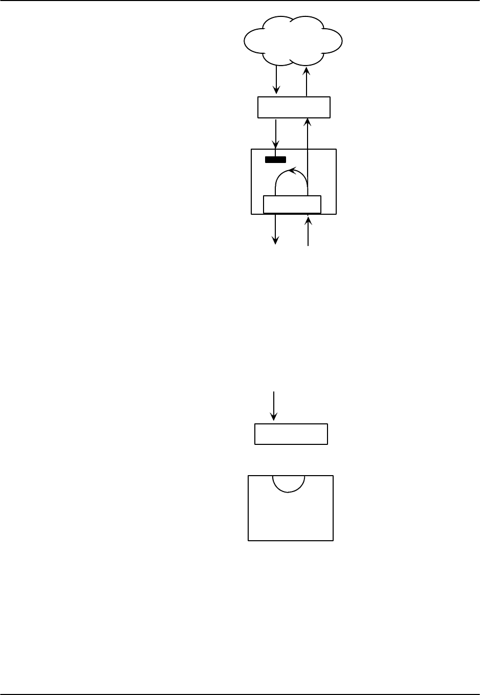
HSU Card Reference Guide v3.6
Page 8-A-8(10-97)
PCM bus
T1/E1
DSO
Network
HSU Port
Figure HSU-5. Data Card DTE Loopback
The network (net) option loops back data toward the remote device. It tests some of the
HSU card circuitry, the system common equipment, the WAN link card, the remote
equipment, and the WAN line between the two sites (see Figure HSU-6). This option
also drops the DSR control signal output on the HSU port.
PCM bus
T1/E1
DSO
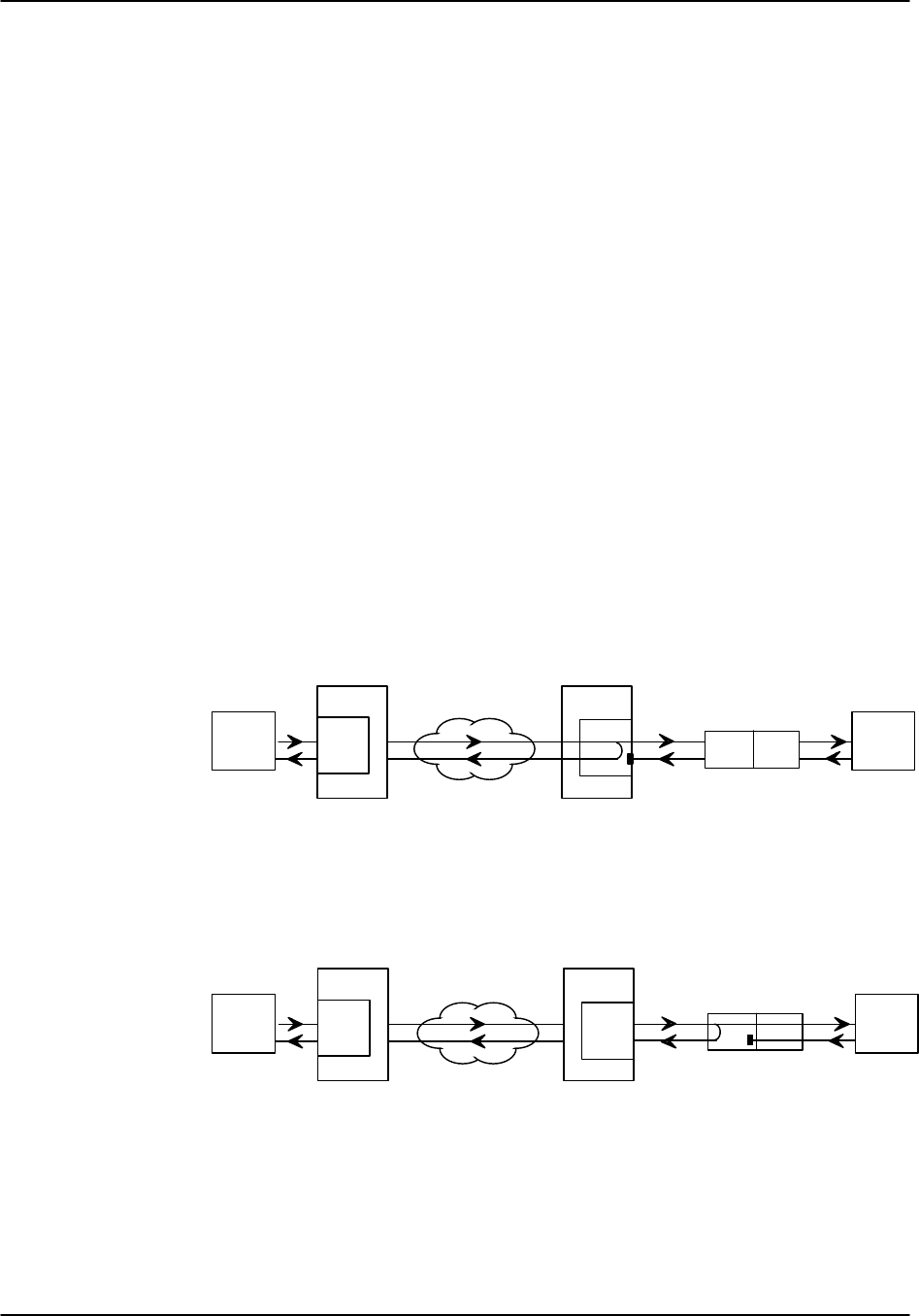
Reference Guide v3.6HSU Card
(10-97) Page 8-A-9
LB GEN MODE
The Loopback Generation Mode setting defines the type of in-band loop-up and loop-
down codes that will be sent to the remote equipment. Three industry-standard codes
are supported: dds, which will send a DDS-compatible latching loopback code in each
of the DS0s that make up the circuit; v.54, which is compatible with CCITT V.54
standard and ft1, which is compatible with ANSI Fractional T1 standard. The final
option, perf (performance monitoring), activates an 8kbps performance monitoring
channel (isolated from the total bandwidth of the circuit) that collects end-to-end
performance statistics from a local HSU card to a remote HSU card. (See Performance
Monitoring section later in this chapter.)
LB GEN
If you selected v.54, ft1 or perf in the previous setting, the Loopback Generation
setting allows you to send a loop-up command (on) or a loop-down command (off). If
you selected dds as the Loopback Generation Mode, then this setting allows you to
define the type of DDS loopback that you wish to generate. The four options are ocu
(Office Channel Unit), dsu (Data Service Unit), csu (Channel Service Unit) and ds0 (a
full 64kbps loopback). Figures HSU-7, -8, and -9 illustrate where the loopbacks will
take place. You can also turn all DDS remote loopbacks off.
Loop-up or loop-down commands cannot be implemented for two ports on the same
card simultaneously. The user must finish all loopback operations on one port before
attempting to perform any loopback operations on another port.
Local Site Remote Site
Remote System
OCU-DP
Card
Local
DTE
Remote
DTE
Local System
HSU
Card CSU DSU
Carrier's
DDS Network
Figure HSU-7. A Remote OCU or DS0 Loopback Commanded by the System
CSU DSU
Local Site Remote Site
Local
DTE
Local System
HSU
Card
Remote
DTE
Carrier's
DDS Network
Remote System
OCU-DP
Card
Figure HSU-8. A Remote CSU Loopback Commanded by the System

HSU Card Reference Guide v3.6
Page 8-A-10 (10-97)
CSU DSU
Local Site Remote Site
Local
DTE
Local System
HSU
Card
Remote
DTE
Carrier's
DDS Network
Remote System
OCU-DP
Card
Figure HSU-9. A Remote DSU Loopback Commanded by the System
LB DET
Depending on the selection you made for Loopback Generation Mode above, the HSU
port will respond to any of the loopback codes generated by a remote system. The
Loopback Detection setting does not affect local loopback commands from the local
control terminal.
The off option causes the system to ignore remote loopback commands. The on option
causes the system to monitor ports for loopback commands from the remote equipment,
but only in the format selected in LB GEN MODE. If the system detects a loopback
code, it loops the data back until the remote equipment releases the loopback. The with
time-out (w/to) option is the same as the on option, except that after ten minutes the
system automatically releases loopbacks initiated by the remote equipment.
EER
The Excessive Error Rate parameter is only available on the 8213 HSU card. This
option selects the error rate at which an alarm is declared. If the number of errors
exceeds the value set by this option an "E" will be placed in the Status Column of the
Performance Monitoring screen. The options are 10e-4 through 10e-9 or none.

Reference Guide v3.6HSU Card
(10-97) Page 8-A-11
Menu of Actions
Table HSU-3 shows the Menu of Actions for the HSU Card.
Table HSU-3. HSU Card Screen Menu of Actions
Action Function
Save Saves changes to settings.
Undo Returns all settings to the last saved state.
Refresh Updates certain time-related information fields that are not automatically
updated (i.e. performance and test data).
Copy Copies the contents of the current column to the next column. Useful if
you change a lot of entries in one column and want to repeat those
changes in subsequent columns.
Test Initiates and monitors testing of all HSU card ports. Refer to Test section
below.
Dial Enables the user to identify the HSU port by telephone number,
download and modify call profiles from the Interface card, dial and
broadcast ISDN calls.
Perf Not supported.
Main Returns to the main terminal screen. If changes are made to settings and
not saved, you will be prompted to save or lose changes.
Test
Selection of "Test" from the Menu of Options will bring up the screen shown in Figure
HSU-10. From this screen, users are allowed to create test situations between HSU
Cards or between a single HSU Card and data test equipment at a remote site. Table
HSU-4 lists the settings controlled on this screen along with their possible and default
values.

HSU Card Reference Guide v3.6
Page 8-A-12 (10-97)
Node_1 | U2 HSU-530x2 8202 Rev C0-0 Ser 00054 | 12-31-99 14:33
1 2
BERT n/a n/a
CTS norm norm
RLSD norm norm
DSR norm norm
SYNC no no
BE ***** *****
ES ***** *****
SES ***** *****
CSES ***** *****
OSS ***** *****
BER ***** *****
ELAP ***** *****
RTS ***** *****
DTR ***** *****
LB ST ***** *****
Save | Undo | Refresh | InsertErr | Clear | Main
Figure HSU-10. HSU Card Test Screen
Table HSU-4. HSU Card Test Screen Setting Options and Defaults
Parameter User Options Default
BERT off mark space 1:1 1:7 511 qrss 2047
ds0 ff 7e 32 40 ocu-a csu-a dsu-a
csu1a csu2a
off
CTS norm off on norm
RLSD norm off on norm
DSR norm off on norm
SYNC information only - no user options
BE information only - no user options
ES information only - no user options
SES information only - no user options
CSES information only - no user options
OSS information only - no user options
BER information only - no user options
ELAP information only - no user options
RTS information only - no user options
DTR information only - no user options
LB ST information only - no user options
BERT
Bit Error Rate Tester (BERT) sends a data pattern and measures the bit error rate (BER)
on the selected HSU port. The patterns that can be selected are off, mark (1111), space
(0000), 1:1 (1010), 1:7 (0100-0000), 511 (511 test pattern), qrss (quasi-random pseudo
signal) and 2047 (2047 test pattern).

Reference Guide v3.6HSU Card
(10-97) Page 8-A-13
On the model 8215 HSU only, selection of BERT pattern ds0 will display another set of
BERT patterns. Additional nonlatching loopback patterns are ff (1111-0000), 7e (0111-
1110), 32 (0011-0010), 40 (0100-0000), ocu-a (ocu-alternating byte), csu-a (csu-
alternating byte), dsu-a (dsu-alternating byte), csu1a (csu - one repeater - alternating
byte) and csu2a (csu - two repeaters - alternating byte). The results of the alternating
patterns (ocu-a, csu-a, dsu-a, csu1a and csu2a) will display on the test screen.
CTS
The Clear To Send (CTS) option allows you to define whether the CTS control lead
should be held high (on) or low (off). Selecting either on or off will override the
selection made in the HSU Card screen. The third option is normal (norm) which
means that CTS will operate in the mode selected in the HSU Card screen.
RLSD
The Receive Level Signal Detect (RLSD) option allows you to define whether the
RLSD control lead is held high (on) or low (off). The third option is normal (norm)
which means that RLSD will behave as described in Table HSU-2.
DSR
The Data Set Ready (DSR) option allows you to define whether the DSR control lead
should be held high (on) or low (off). The third option is normal (norm) which means
that DSR will behave as described in Table HSU-2.
SYNC
The Synchronization (SYNC) field tells you if the integrated BERT has achieved
synchronization either with itself via a remote loopback or with the remote test
equipment. This is an information-only field, there are no user-selectable parameters.
BE
The Bit Error field shows the total number of bit errors logged. This is an information-
only field, there are no user-selectable parameters.
ES
The Errored Seconds field shows the total number of seconds in which any errors were
detected. This is an information-only field, there are no user-selectable parameters.
SES
The Severely Errored Seconds (SES) field shows the total number of seconds in which
the bit error rate exceeded one bit per thousand (1 x 10⁻³). Since this is an information-
only field, there are no user-selectable parameters.

HSU Card Reference Guide v3.6
Page 8-A-14 (10-97)
CSES
The Consecutive Severely Errored Seconds (CSES) field is triggered by the occurrence
of ten consecutive Severely Errored Seconds. Once triggered, the CSES field will
increment (by one) for each elapsed second until the system logs ten consecutive non-
Severely Errored Seconds. This it an information-only field there ore no user-selectable
parameters.
OSS
The Out of Synchronization Seconds field shows the number of seconds that the HSU
BERT has been out of synchronization. This is an information-only field, there are no
user-selectable parameters.
BER
The Bit Error Rate (BER) field shows the rate at which errors are being logged. The
system calculates BER by dividing the number of bit errors (BE) by the total number of
bits transmitted during the test. This is an information-only field, there are no user-
selectable parameters.
ELAP
The Elapsed time setting shows the running tally of the total number of seconds during
the test. This is an information-only field, there are no user-selectable parameters for
this option.
RTS
The Request To Send (RTS) field shows the current status of the RTS control lead. The
two values that can be displayed are "on" and "off." This is an information-only field,
there are no user-selectable parameters for this option.
DTR
The Data Terminal Ready (DTR) field shows the current status of the DTR control lead.
The two values that can be displayed are "on" and "off." This is an information-only
field, there are no user-selectable parameters for this option.
The DTR field will always show "on" for the 8212 HSU card (Revision A and earlier)
but it will toggle between "off" and "on" all other HSU cards.
LB ST
The Loopback State field indicates, whether there are any remotely-initiated loopbacks
currently active on the HSU port. This field will display both latching and non-latching
loopbacks that are initiated from a remote device via in band loop-up codes. In
addition to "none," the six messages that can be displayed in that field are "l-ocu," "l-
dsu" and "l-csu" for latching loopbacks, and "ocu," "dsu" and "csu" for non-latching
loopbacks. This is an information-only field, there are no user-selectable parameters
for this option.

Reference Guide v3.6HSU Card
(10-97) Page 8-A-15
Menu of Actions
Table HSU-5 shows the Menu of Actions for the Test Screen of the HSU Card.
Table HSU-5. Test Screen Menu of Actions
Action Function
Save Saves changes to settings.
Undo Returns all settings to the last saved state.
Refresh Updates certain time-related information fields that are not
automatically updated (i.e. performance and test data).
InsertErr Allows the user to manually insert a single error into the clear data
signal.
Clear Clears the testing screen and resets all counters to zero.
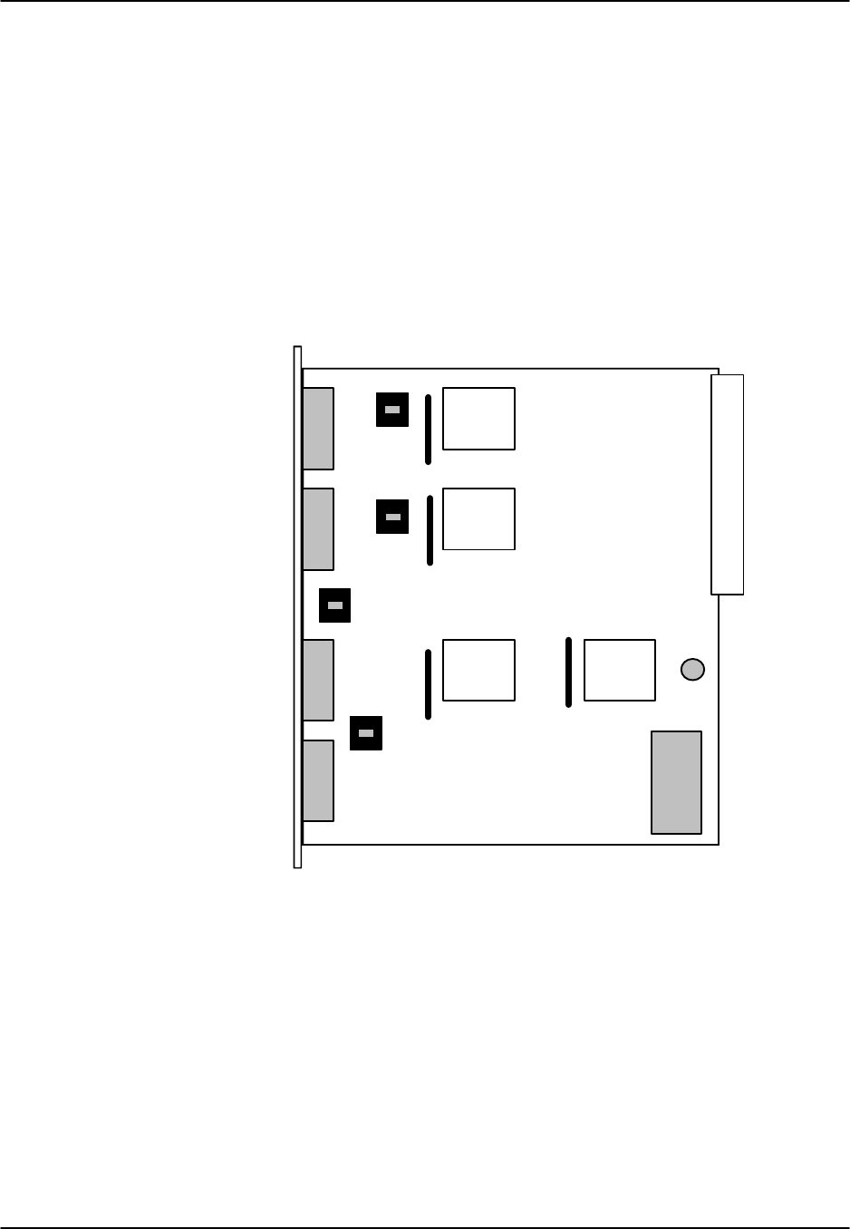
HSU Card Reference Guide v3.6
Page 8-A-16 (10-97)
Setting On-board Option Switches
Setting Switches on the 8215 HSU Card
Setting or resetting switches is necessary for conversion of the operation of all four
ports on the 8215 HSU card from RS-530 to V.35. To make this conversion, remove
the HSU card from its slot and toggle the slide switches between RS530 and V.35 as
shown in Figure HSU-11.
Ports can be set individually for either RS530 or V.35 operation features, but once set,
remain in that mode until the slide switches are reset. This information is repeated in
the Installation chapter.
Power
Bus
Edge
Connector
Xilinx
Xilinx
Xilinx
Xilinx
RS-530
V.35
RS-530
V.35
RS-530
V.35
RS-530
V.35
Figure HSU-11. Switches for Conversion from RS530 to V.35
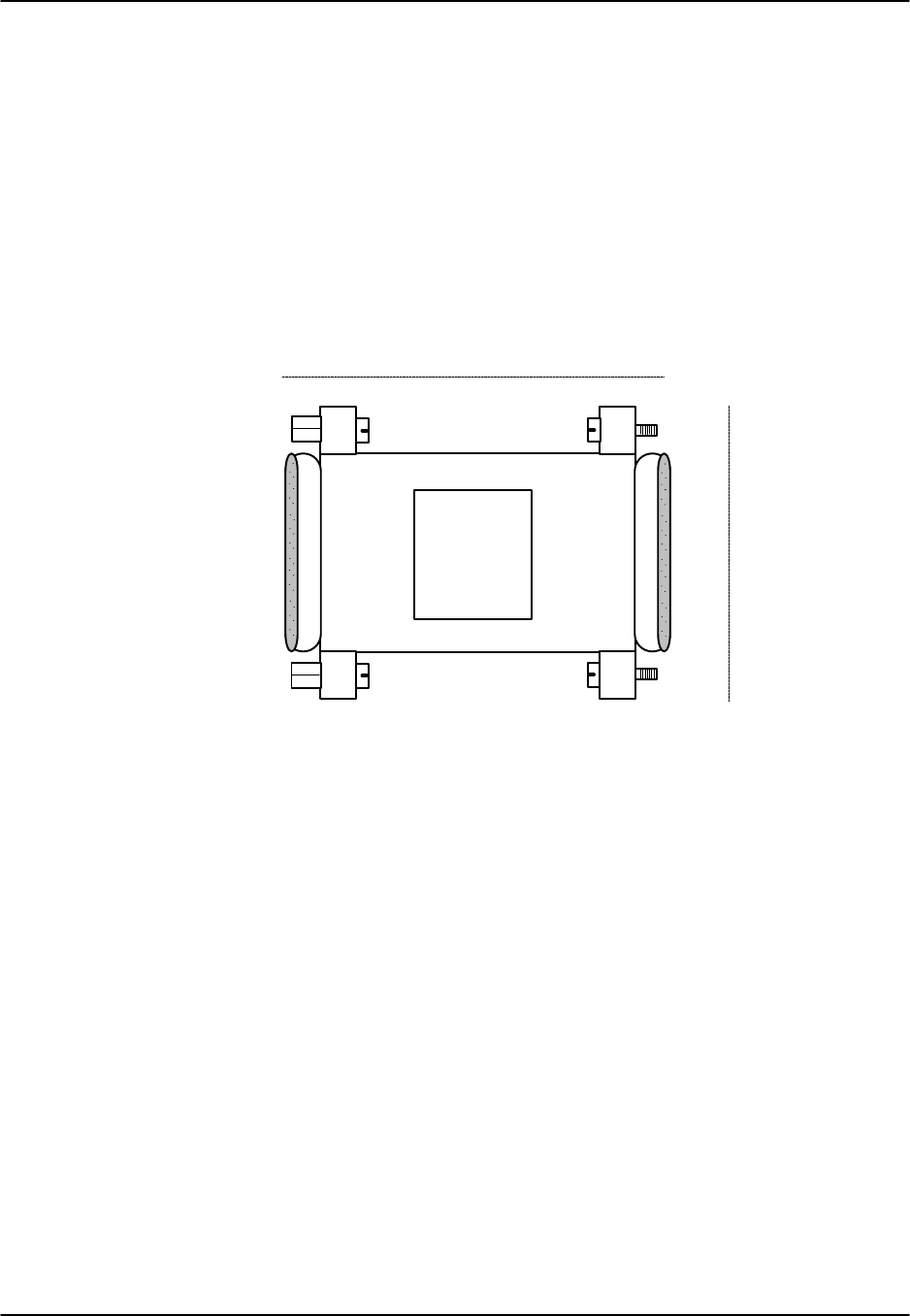
Reference Guide v3.6HSU Card
(10-97) Page 8-A-17
Using the 1251, 1252 and 1253 Personality Modules
When using the 8202, and 8215 HSU cards, you may wish to connect the RS530 output
to V.35 (for the 8202) or RS232 equipment (for the 8202, and 8215). The 1251 (V.35),
1252 (RS232) and 1253 (RS232-E) Personality Modules were developed to assist in this
process. Shaped like a "gender changer," these modules plug into the female DB-25
port connector on the HSU card and then attach via a male cable connector to the other
equipment. For RS232 operation, the recommended length of cables should be less
than 25' and the speed no greater than 56kbps.
Figure HSU-12 shows a drawing with the dimensions (in inches) of a Personality
Module.
1251 2.125"
2.50"
Figure HSU-12. The RS530 to V.35 Personality Module
The 8215 HSU cards have internal switch settings (see Figure HSU-11) for changing
signals from RS530 to V.35.
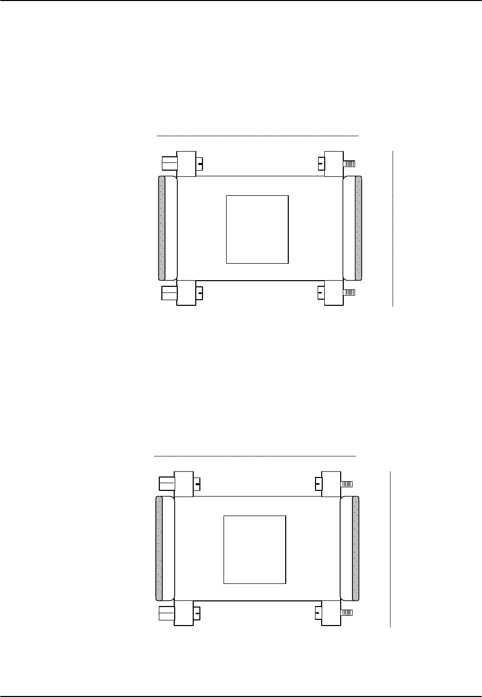
HSU Card Reference Guide v3.6
Page 8-A-18 (10-97)
RS232 Personality Module Description
Signals can be converted from RS530 to RS232 with the use of the 1252 Personality
Module. Since the 8215 HSU card is equipped with DB-26 connectors, a special cable
must be used to connect to the 1252 module (with DB-25 connectors).
Figure HSU-13 shows a drawing with the dimensions (in inches) of a Personality
Module.
1252
2.125"
2.50"
Figure HSU-13. The RS530 to RS232 Personality Module
RS232-E Personality Module Description
The RS232-E Personality Module similarly converts RS530-A (balanced signal) to
RS232-E (unbalanced signal) format which allows the HSU cards to interoperate with
equipment employing an interface conforming to the ANSI/EIA/TIA-232-E electrical
characteristics. Figure HSU-14 shows this module.
1253
2.125"
2.50"
Figure HSU-14. RS530-A to RS232-E Personality Module

Reference Guide v3.6 SRU Card
(10-97) Page 8-B-1
Introduction
8220 Sub-Rate Data Card
Each 8220 Sub-Rate Data card allows you to connect up to 10 low and medium speed
(300bps-38.4Kbps) data equipment to the system. Since an SRU port does not require a
complete 64Kbps time slot, the Sub-Rate card allows you to multiplex a number of
devices into a single, subdivided time slot on a WAN card. SRU card ports can also be
multiplexed with voice traffic on an ADPCM engine.
Each port can receive timing from either the DTE device or the system clock. If the
DTE supplies the transmit clocking, it must be synchronized with the system clocking
source.
SRU Card Settings
Figure SRU-1 shows the sub-rate data unit (SRU) screen. The ten ports correspond to
the ten RJ-48C connectors on the back of the card. Table SRU-1 lists the settings
controlled on this screen along with their possible and default values. Note: BCON
Systems will not allow same timeslot on two different WANS to reside on same SRU
Card, XCON will allow this.
Node_1 | U1 SRU-232x10 8220 RevAB-0 SER 00101 | 12-31-99 14:33
1 2 3 4 5 6 7 8 9 10
STATE stdby stdby stdby stdby stdby stdby stdby stdby stdby stdby
WAN 01 01 01 01 01 01 01 01 01 01
TS n/a n/a n/a n/a n/a n/a n/a n/a n/a n/a
FRAME a a a a a a a a a a
RATE 0.3 0.3 0.3 0.3 0.3 0.3 0.3 0.3 0.3 0.3
SR TS 01 01 01 01 01 01 01 01 01 01
INTF 01 01 01 01 01 01 01 01 01 01
COM CF 8,1,N 8,1,N 8,1,N 8,1,N 8,1,N 8,1,N 8,1,N 8,1,N 8,1,N 8,1,N
CTS perm perm perm perm perm perm perm perm perm perm
TX CLK n/a n/a n/a n/a n/a n/a n/a n/a n/a n/a
LB off off off off off off off off off off
LB GEN off off off off off off off off off off
LB DET w/to w/to w/to w/to w/to w/to w/to w/to w/to w/to
DL OPT off off off off off off off off off off
ADPCM n/a n/a n/a n/a n/a n/a n/a n/a n/a n/a
MAJ EC off off off off off off off off off off
Save | Undo | Refresh | Copy | Test | Main
Figure SRU-1. SRU Card Default Screen

SRU Card Reference Guide v3.6
Page 8-B-2(10-97)
Table SRU-1. SRU Card Setting Options and Defaults
Parameter User Options Notes Default
STATE stdby act stdby
WAN w1-1 through w4-2 w1-1
TS 01-24 01-31 1 01
FRAME a b-5 b-10 b-20 x.50 adpcm hlink nlink a
RATE 0.3 1.2 2.4 4.8 9.6 14.4 19.2 28.8
38.4 20.3
SR TS n/a 1 1-5 1-10 1-20 1
INTF asyn sync v.14 asyn
8 7 6 5 8
COM CF 1 2 3 1
none odd even space mark none
CTS perm l0 l30 l60 l100 rl0 rl3 rl6 rl10
off perm
TX CLK n/a int ext n/a
LB off dte net off
LB GEN n/a off ocu csu dsu off
LB DET n/a w/to on off w/to
DL OPT off on off
ADPCM n/a P1 P2 P3 n/a
MAJ EC off on none 10e-3 10e-4 10e-5
10e-6 10e-7 4off
NOTES
1. Time slot 16 is not available if the port is assigned to an E1 WAN link whose TS 16
is programmed for cas or ccs.
2. Speeds of .3, 1.2 and 14.4 are not supported for synchronous channels (except 14.4
sync with Frame of adpcm, hlink or nlink).
3. Communication Configuration is a three step process. This field will show n/a when
sync is chosen for the INTF option.
4. Majority Error Correction is a two step process. The user will see only choices off
and on. When on is chosen the other alternatives will appear.
STATE
The State setting determines whether the port is active or inactive. Set the State setting
to standby (stdby) for ports you are not using or have not yet configured. Set it to
active (actv) for ports that are ready for use. The control leads assume the status shown
in Table SRU-2 for the different states.

Reference Guide v3.6SRU Card
(10-97) Page 8-B-3
Table SRU-2. SRU Card State Status
Control Leads Active WAN Link Down Standby
RLSD High or follows remote RTS Low Low
CTS definable definable Low
WAN
The WAN setting identifies the WAN link assigned to this port. It is not necessary for
ports on the same card to be assigned to the same WAN link, or to contiguous time slots
on a WAN link.
TS
The Time Slot setting identifies the time slot on the WAN link to which this port is
connected. Values range from 01-24 for T1 links and 01-31 (excluding #16 in cas or
ccs mode) for E1 links. The Sub-Rate card can further subdivide the WAN time slot
into smaller segments for transmission of low speed data. Each WAN time slot can be
further divided into a maximum of 20 2.4Kbps time slots (see Figure SRU-2).
FRAME
The Frame setting allows you to define the sub-rate format that the port will use and to
set the usable space allotted to each WAN time slot. The choices are DSO-A (a) that
allows one sub-rate time slot, DSO-B with a limit of five sub-rate time slots (b-5),
DSO-B with a limit of ten sub-rate time slots (b-10) and DSO-B with a limit of twenty
sub-rate time slots (b-20). Figure SRU-2 shows the DS0-A and DS0-B framing sub-rate
time slot interaction. In b-20 frame, two or more SRU cards can be configured to
occupy the same WAN time slot.
Additional choices include x.50 (an ITU standard), adpcm (used to multiplex sub-rate
data on an ADPCM card) and hlink (a proprietary format used when far end of the
circuit has an ADPCM card while the near end does not). The adpcm frame uses a
24Kbps portion of the ADPCM engine. (See the ADPCM chapter for information on
using the ADPCM engines.)
RATE
The Rate setting allows you to select the rate in thousands of bits per second (kbps) for
transmission of data. The selection will change depending upon the framing mode and
interface selected.
In no case can the maximum total bandwidth of any SRU card exceed 115.2Kbps.
The maximum bandwidth of the SRU card depends upon the mode of operations for
each port. The maximum bandwidth for the sync Interface setting is 115.2Kbps and the
host will not allow more than this to be assigned.
The maximum bandwidth for async and v.14 is harder to compute because the
computation depends upon the amount of data being sent.

SRU Card Reference Guide v3.6
Page 8-B-4(10-97)
At a minimum, async ports have a multiplication factor of 1.2 times a sync port and
v.14 has a multiplication factor of 1.6 times that of a sync port. Using the Delay
Optimization feature will also degrade the maximum bandwidth by a factor of 1.5 times
the maximum bandwidth figure.
These computation factors suggest a maximum of 96Kbps (96Kbps x 1.2 = 115.2Kbps)
for async ports and 72Kbps (72Kbps x 1.6 = 115.2Kbps) for v.14 ports be used.
However, due to the nature of async and v.14 data transmission, we do not enforce
these limits because the user will not be transmitting data at the full rate. The Delay
Optimization feature will also degrade the maximum bandwidth by a factor of 1.5 times
the total bandwidth. BERT adds another 2x multiplication factor to the data rates
shown above.
TS #1 TS #2 TS #3 TS #4
WAN CARD #1 PORT #1 (w1-1)
SRU TS
1 1 2 3 4 5 1-201-10
Framing a b-5 b-10 b-20
Maximum Speed
per SR TS (Kbps)
* Speeds greater than 9.6Kbps will occupy contiguous SRU Time Slots in 9.6Kbps
increments (i.e. a 19.2Kbps circuit would take SRU time slots #1 and #2)
38.4 38.4* 4.8 2.4
Figure SRU-2. Time Slot Integration
SR TS
The Sub-Rate Time Slot (SR TS) indicates the sub-rate position within the DS0 time
slot that the port will occupy (see Figure SRU-2). If a framing is selected, only one
sub-rate time slot is supported and the SR TS setting will default to 1. If b-5 framing is
selected, then the sub-rate time slots available are 1-5. If b-10 framing is selected, then
the sub-rate time slots available are 1-10. If b-20 framing is selected, then the sub-rate
time slots available are 1-20. Portions of sub-rate time slots can be assigned to any
SRU port from any SRU card within the system (see Example later in this chapter). If
adpcm or hlink are chosen for the frame parameter, this field will show n/a.
In b-5 framing, if circuits with speeds greater than 9.6Kbps are assigned to the sub-rate
time slot, adjacent sub-rate time slots must be available to accommodate their size. A
19.2Kbps circuit would occupy two contiguous sub-rate time slots (leaving space for up
to three 9.6Kbps circuits) and a 38.4Kbps circuit would occupy four contiguous sub-rate
time slots (leaving space for one 9.6Kbps circuit).
The SR TS number selected will be the first segment occupied by this circuit. If a
28.8Kbps circuit occupies three segments of the b-5 frame, selecting SR TS #1 will
assign it to segments 1, 2 and 3. Segments 4 and 5 may be assigned either
independently to 9.6 (or less)Kbps circuits in SR TS #4 and #5 or combined for a
19.2Kbps circuit assigned to SR TS #4.

Reference Guide v3.6SRU Card
(10-97) Page 8-B-5
If a circuit exceeds the slots necessary to accommodate it, such as a 38.4Kbps circuit to
SR TS #3 in b-5 framing, the message, "Invalid SR TS," will be displayed. If a circuit
requires more space than the SR TS has available, such as having a 38.4Kbps circuit in
SR TS #1 and then attempting to assign a 19.2Kbps circuit to SR TS #4, the message
"SR TS overlapping," will be displayed.
The number of sub-rate timeslots available for x.50 will depend upon the Rate selected.
If the 2.4 Rate is selected, the number available will be 20. If the 4.8 Rate is selected,
the number available will be 10. If the 9.6 Rate is selected, the number available will
be 5. When multiplexing different rate circuits on the same timeslot, the following
formula is necessary to compute the position in the sub-rate timeslot: a 9.6 circuit will
occupy slots n, n+5, n+10 and n+15; a 4.8 circuit will occupy slots n and n+10; a 2.4
circuit will occupy slots n (where n = the timeslot selected).
INTF
The Interface setting allows you to choose the protocol necessary for the terminal
associated with this port. The choices are Asynchronous (asyn), Synchronous (sync)
and v.14 (v.14). If Synchronous transmission is selected, the choices for STOP, DATA
and PAR will show as not applicable (n/a).
Both asyn and v.14 options provide asynchronous to synchronous conversion. The v.14
option is an industry standard which will allow the SRU card to interoperate with many
DSUs. The asyn option is a streamlined proprietary algorithm which will increase the
performance of the SRU card.
COM CF
The Communication Configuration setting is a three step process that allows the user to
choose the Data bits, Stop bits and Parity settings. The Data setting allows you to
change the bits-per-byte number depending upon the type of terminal associated with
this particular port. The options are 8, 7, 6, 5.
The second option allows you to select the number of Stop bits that check data
sampling for the terminal associated with this port. The choices are 1 and 2.
The third choice is the Parity setting that changes the data parity for the terminal
associated with this particular port. The options are none, odd, even, space and mark.
CTS
The Clear To Send setting allows you to define how the port should respond to receipt
of Request to Send (RTS) from the attached equipment. This setting also allows you to
change the delay time (in milliseconds) from when the SRU receives the RTS until it
issues the CTS. The local option allows RTS to control CTS. The remote-local options
allows RTS to control both the CTS of the local equipment and RLSD of the remote
equipment. The options are permanent (perm), local - immediate (l0), local -30 mS
(l30), local -60 mS (l60), local -100 mS (l100), remote/local - immediate (rl0),
remote/local - 30 mS (rl3), remote/local - 60 mS (rl6), remote/local - 100 mS (rl10)
and off.
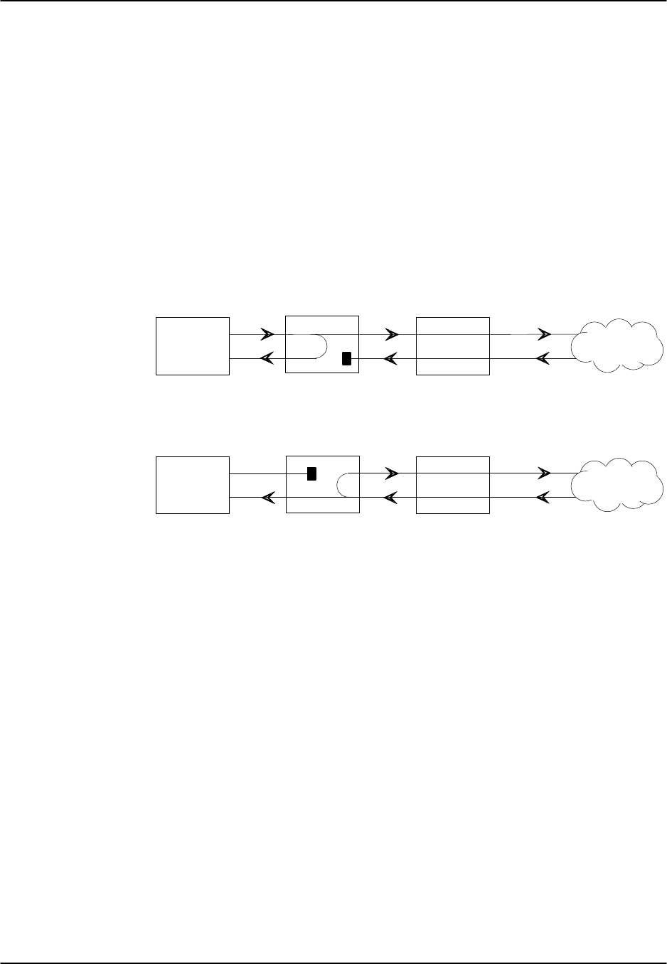
SRU Card Reference Guide v3.6
Page 8-B-6(10-97)
TX CLK
The Transmit Clock setting allows the user to select the clocking source for this port.
The options are n/a, if async INTF is chosen and internal (int), if sync INTF is chosen.
The int setting uses the system for the clock source and the ext setting allows the DTE
to generate the transmit clocking information.
LB
The Loopback setting allows you to activate local loopbacks on the SRU. The settings
are off, toward the DTE (dte) and toward the network (net). Figure SRU-3 shows a
diagram of the two loopback conditions.
SRU WAN Link
DTE
net Loopback Option
Network
SRU WAN Link
DTE
dte Loopback Option
Network
Figure SRU-3. SRU Card Loopbacks
LB GEN
The Loopback Generate setting generates in-band diagnostic codes that are sent to the
remote equipment These codes are compatible with DDS networks and allow you to
command a latching loopback at remote DDS equipment. You can start loopbacks at
the remote ocu (Office Channel Unit), the dsu (Data Service Unit) or the csu (Channel
Service Unit). Figures 8B-4, 8B-5 and 8B-6 show the loopback locations. You can
also turn all of the loopbacks off. This field will show n/a if adpcm or hlink are
chosen for the FRAME parameter.
Loop-up or loop-down commands cannot be implemented for two ports on the same
card simultaneously. The user must finish all loopback operations on one port before
attempting to perform any loopback operations on another port.
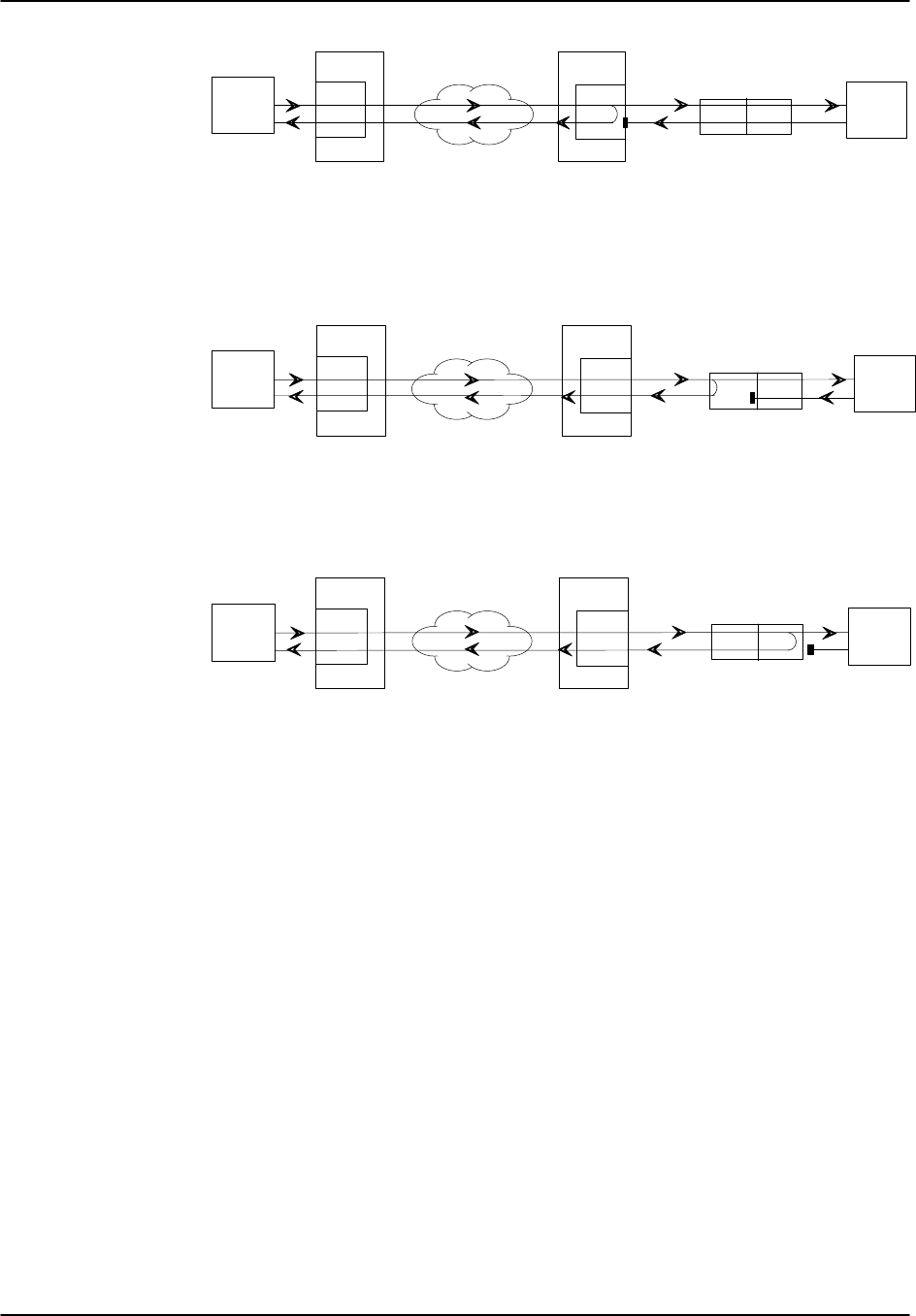
Reference Guide v3.6SRU Card
(10-97) Page 8-B-7
Carrier's
DDS Network
CSU DSU
Local Site Remote Site
Local System
SRU
Card
Remote System
OCU-DP
Card
Remote
DTE
Local
DTE
Figure SRU-4. A Remote SRU Loopback Commanded by the System
Carrier's
DDS Network
CSU DSU
Local Site Remote Site
Local System
SRU
Card
Remote System
OCU-DP
Card
Remote
DTE
Local
DTE
Figure SRU-5. A Remote CSU Loopback Commanded by the System
Carrier's
DDS Network
CSU DSU
Local Site Remote Site
Local System
SRU
Card
Remote System
OCU-DP
Card
Remote
DTE
Local
DTE
Figure SRU-6. A Remote DSU Loopback Commanded by the System
LB DET
The Loopback Detection setting determines how the SRU Card will respond to latching
and non-latching loopback commands from remote equipment. The SRU reacts only to
the in-band DDS format loopback commands for OCU Loop, CSU Loop, and DSU
Loop. The Loopback Detection setting does not affect local loopback commands from
the local control terminal.
The (on) option causes the SRU Card to monitor ports for DDS format loopback
commands from the remote equipment. If the SRU Card detects a loopback command,
it loops the data back until the remote equipment sends a stop loopback command. The
with time-out (w/to) option is the same as the on option, except that after ten minutes
the SRU Card automatically releases loopbacks commanded by the remote equipment.
The off option causes the SRU Card to ignore all remote loopback commands. This
field will show n/a if adpcm or hlink are chosen for the FRAME parameter.

SRU Card Reference Guide v3.6
Page 8-B-8(10-97)
DL OPT
Delay Optimization decreases the end-to-end delay time for applications that require
lower delay time. The options are off and on.
The cost for using Delay Optimization is a decrease in total bandwidth for the card by a
factor of 1.5. For example, a user that has 10 ports using the sync Interface will have
115.2Kbps maximum bandwidth available. If delay optimization is used on all 10
ports, the maximum bandwidth available will be 76.8Kbps.
ADPCM
If adpcm is chosen for the FRAME parameter, this field will allow the user to select the
ADPCM card to direct this traffic. The options are P1, P2 or P3. These are the
communications server card slot designations that are stamped on the chassis. If any
other option is selected this field will show n/a.
MAJ EC
The Majority Vote Error Correction parameter is available for ports using DSOA
framing and having speeds of 9.6Kbps and lower. Option selection is done in a two
step operation. The initial options are off and on. If the on option is chosen, a new set
of options will appear at the bottom of the screen.
The new options are used to select the error threshold, above which the card will
generate an alarm. The choices are none, 10e-3, 10e-4, 10e-5, 10e-6 and 10e-7. While
the majority vote algorithm is capable of correcting error rates in excess of 10e-3, the
Excessive Error Rate alarm is designed to give system administrators advanced notice
of problems before users detect them. Table SRU-3 shows the bit error rates for
Majority Vote error correction.
Table SRU-3. Bit Error Rates for Majority Vote Error Correction
Threshold EER Set EER Reset Period
none none none none
10e-3 64 or more errors 63 or fewer errors 1 second
10e-4 64 or more errors
or any of the above 63 or fewer errors 10 seconds
10e-5 38 or more errors
or any of the above 37 or fewer errors 60 seconds
10e-6 3 or more errors
or any of the above 2 or fewer errors 60 seconds
10e-7 17 or more errors
or any of the above 16 or fewer errors three 15 minute
time intervals

Reference Guide v3.6SRU Card
(10-97) Page 8-B-9
Menu of Actions
Table SRU-4 shows the Menu of Actions for the SRU Card.
Table SRU-4. The SRU Card Screen Menu of Actions
Action Function
Save Saves changes to settings.
Undo Returns all settings to the last saved state.
Refresh Updates certain time-related information fields that are not
automatically updated (i.e. performance and test data).
Copy Copies the contents of the current column to the next column. Useful if
you change a lot of entries in one column and want to repeat those
changes in subsequent columns.
Test Initiates and monitors testing of all SRU card ports. Refer to Test
section below.
Main Returns to the main terminal screen. If changes are made to settings
and not saved, you will be prompted to save or lose changes.
Examples
Figure SRU-7 shows some of the ways SRU cards can be used to network low-speed
data using the DS0-A and DS0-B framing. In this diagram, five SRU Cards are
connected to eight WAN time slots, on one WAN port, on one WAN card (many
combinations of cards/ports/time slots are possible). Each SRU card is separated to
show the ten ports on each card. Each port is assigned to a low-speed data device and
the transmission speed of that device is shown in the center of the SRU port. The
diagram sometimes shows only one connection to eliminate unnecessary lines in the
diagram. Each port is a direct connection and will not support interchange of data
transmission between ports.
The first time a WAN card/port/time slot is used, the framing selected on the SRU port
will segregate that WAN time slot into SRU time slots. Once selected, those SRU TSs
will apply to all ports assigned to that WAN time slot.
Once the framing is selected for the WAN card/port/time slot, low-speed data devices
can be arranged and selected on the SRU card settings to maximize the system
capabilities.
In this example, the first port on SRU #1 assigned a framing to WAN 1-1, TS 1, and
selected a 38.4Kbps device for its use. The second port has b-5 framing to WAN 1-1,
TS 2. Of the five SRU time slots on that WAN time slot, the first three are used to
support a 28.8Kbps device (three 9.6Kbps contiguous SRU time slots). The 9.6Kbps
device on SRU #1 port #3 occupies the fourth SRU time slot and another 9.6Kbps from
SRU #3, port #10, is placed in the fifth slot.
WAN 1-1, TS 3 was segregated into ten SRU time slots by the selection of b-10
framing that supports either .3, 1.2, 2.4 or 4.8Kbps transmission. Six 4.8Kbps ports are
assigned to the first six SRU time slots. The diagram shows only one connection to
eliminate unnecessary lines in the diagram. The six ports are six direct connections
and will not support interchange of data transmission. The other four SRU time slots
are used by ports 1-4 on SRU #4. Again, the single line does not imply interexchange.

SRU Card Reference Guide v3.6
Page 8-B-10 (10-97)
WAN 1-1, TS 4 has b-20 framing and will support up to twenty .3, 1.2 or 2.4Kbps
circuits from two (or more) SRU cards. In this example, SRU #1, port #10 is assigned
to SRU TS #1, SRU #2, ports 1-10 are assigned to SRU TS 2-11. The nine SRU time
slots left are used by SRU #3, ports 1-9. As mentioned earlier, SRU #3, port #10 is a
9.6Kbps circuit assigned to WAN 1-1, TS 2, SRU time slot #5. WAN 1-1, TS 5, has a
framing. Only one device can transmit data in this SRU time slot. In this example, a
2.4Kbps circuit was assigned to SRU #4, port #5.
WAN 1-1, TS 6 has b-5 framing, so five SRU time slots are available. The first two
9.6Kbps slots are used by a 19.2Kbps circuit on SRU #4, port #6, while the other three
are used by 9.6Kbps circuits on SRU #4, ports 7-9.
WAN 1-1, TS 7 has the same characteristics as TS 6, except that the first SRU time slot
is used by a 9.6Kbps circuit on SRU #4, port #10, SRU time slots 2-4 are assigned to
the single 28.8 port on SRU #5. WAN 1-1, TS 8 was designated as b-10 framing and
the first eight SRU time slots are associated with the 2.4 and 4.8Kbps circuits on SRU
#5, ports 3-10.
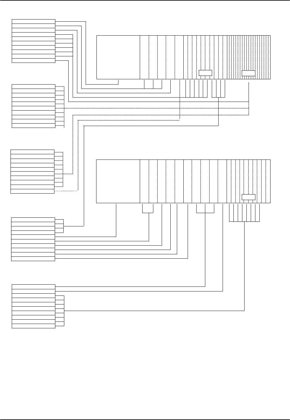
Reference Guide v3.6SRU Card
(10-97) Page 8-B-11
TS #1
TS #2
TS #3
TS #4
WAN CARD #1 PORT #1
SRU TS
1
1
2
3
4
5
TS #5
TS #6
TS #7
TS #8
WAN CARD #1 PORT #1
1
1
2
3
4
5
1
2
3
4
5
SRU #1
SRU TS
28.8
38.4
9.6
4.8
4.8
4.8
4.8
4.8
4.8
2.4
SRU #2
2.4
2.4
2.4
2.4
2.4
2.4
2.4
2.4
2.4
2.4
SRU #3
2.4
2.4
2.4
2.4
2.4
2.4
2.4
2.4
2.4
9.6
SRU #4
4.8
4.8
2.4
2.4
2.4
19.2
9.6
9.6
9.6
9.6
SRU #5
9.6
28.8
4.8
4.8
2.4
4.8
4.8
2.4
4.8
4.8
1-10
1-20
1-10
Port #
1
2
3
4
5
6
7
8
9
10
Port #
1
2
3
4
5
6
7
8
9
10
Port #
1
2
3
4
5
6
7
8
9
10
Port #
1
2
3
4
5
6
7
8
9
10
Port #
1
2
3
4
5
6
7
8
9
10
Figure SRU-7. SRU-WAN Timeslot Assignments

SRU Card Reference Guide v3.6
Page 8-B-12 (10-97)
Test
Selection of "Test" from the Menu of Options will bring up the screen shown in Figure
SRU-8. From this screen, users are allowed to create test situations between SRU Cards
or between a single SRU Card and data test equipment at a remote site. Table SRU-5
lists the settings controlled on this screen along with their possible and default values.
Node_1 | U1 SRU-232x10 8220 Rev B-0 SER 00101 | 12-31-99 14:33
1 2 3 4 5 6 7 8 9 10
BERT n/a n/a n/a n/a n/a n/a n/a n/a n/a n/a
DIR net net net net net net net net net net
CTS norm norn norm norn norm norn norm norn norm norn
RLSD norm norn norm norn norm norn norm norn norm norn
SYNC no no no no no no no no no no
BE ***** ***** ***** ***** ***** ***** ***** ***** ***** *****
ES ***** ***** ***** ***** ***** ***** ***** ***** ***** *****
SES ***** ***** ***** ***** ***** ***** ***** ***** ***** *****
CSES ***** ***** ***** ***** ***** ***** ***** ***** ***** *****
OSS ***** ***** ***** ***** ***** ***** ***** ***** ***** *****
BER ***** ***** ***** ***** ***** ***** ***** ***** ***** *****
ELAP ***** ***** ***** ***** ***** ***** ***** ***** ***** *****
RTS ***** ***** ***** ***** ***** ***** ***** ***** ***** *****
SR OSS ***** ***** ***** ***** ***** ***** ***** ***** ***** *****
LB ST ***** ***** ***** ***** ***** ***** ***** ***** ***** *****
EER ***** ***** ***** ***** ***** ***** ***** ***** ***** *****
Save | Undo | Refresh | InsertErr | Clear | Main
Figure SRU-8. SRU Card Test Screen
Table SRU-5. SRU Card Test Screen Setting Options and Defaults
Parameter User Options Default
BERT n/a off mark space 1:1 1:7 511 2047 n/a
DIR net user net
CTS norm off on norm
RLSD norm off on norm
SYNC information only – no user options
BE information only – no user options
ES information only – no user options
SES information only – no user options
CSES information only – no user options
OSS information only – no user options
BER information only – no user options
ELAP information only – no user options
RTS information only – no user options
SR OSS information only – no user options

Reference Guide v3.6SRU Card
(10-97) Page 8-B-13
LB ST information only – no user options
EER information only – no user options
BERT
Bit Error Rate Tester (BERT) sends a data pattern and measures the bit error rate (BER)
on the selected SRU port. The patterns that can be selected are off, mark (all ones),
space (all zeros), 1:1 (one-zero-one-zero), 1:7 (one-7 zeros-one-7 zeros), 511 (511 test
pattern) and 2047 (2047 test pattern).
DIR
The Direction (DIR) setting allows you to specify where the BERT test signal should be
directed. The first option is net (network) which means that the test signal will be
transmitted through the system toward the Wide Area Network (WAN). The user
option means that the signal will be directed toward the attached DTE device over the
RS232 interface.
CTS
The Clear To Send (CTS) option allows you to define whether the CTS control lead
should be held high (on) or low (off). Selecting either on or off will override the
selection made in the SRU Card screen. The third option is normal (norm) which
means that CTS will behave as described in Table SRU-2.
RLSD
The Receive Level Signal Detect (RLSD) option allows you to define whether the
RLSD control lead should be held high (on) or low (off). The third option is normal
(norm) which means that RLSD will behave as described in Table SRU-2.
SYNC
The Synchronization (SYNC) field tells you if the integrated BERT has achieved
synchronization either with itself via a remote loopback or with the remote test
equipment. Since this is an information-only field, there are no user-selectable
parameters.
BE
The Bit Error field shows the total number of bit errors logged. Since this is an
information-only field, there are no user-selectable parameters.
ES
The Errored Seconds field shows the total number of seconds in which any errors were
detected. Since this is an information-only field, there are no user-selectable
parameters.

SRU Card Reference Guide v3.6
Page 8-B-14 (10-97)
SES
The Severely Errored Seconds (SES) field shows the total number of seconds in which
the bit error rate exceeded one bit per thousand (1 x 10⁻³). Since this is an information-
only field, there are no user-selectable parameters.
CSES
The Consecutive Severely Errored Seconds (CSES) field is triggered by the occurrence
of ten consecutive Severely Errored Seconds. Once triggered, the CSES field will
increment (by one) for each elapsed second until the system logs ten consecutive non-
Severely Errored Seconds. Since this it an information-only field there are no user-
selectable parameters.
OSS
The Out of Synchronization Seconds field shows the number of seconds that the SRU
BERT has been out of synchronization. Since this is an information-only field, there
are no user-selectable parameters.
BER
The Bit Error Rate (BER) field shows the rate at which errors are being logged. The
system calculates BER by dividing the number of bit errors (BE) by the total number of
bits transmitted during the test. Since this is an information-only field, there are no
user-selectable parameters.
ELAP
The Elapsed time setting shows the running tally of the total number of seconds during
the test. Since this is an information-only field, there are no user-selectable parameters
for this option.
RTS
The Request To Send (RTS) field shows the current status of the RTS control lead. The
two values that can be displayed are "on" and "off." Since this is an information-only
field, there are no user-selectable parameters for this option.
SR OSS
The Subrate Out of Synchronization Seconds (SR OSS) field shows how many seconds
in which there was a Subrate framing loss. Since this is an information-only field, there
are no user-selectable parameters for this option.

Reference Guide v3.6SRU Card
(10-97) Page 8-B-15
LB ST
The Loopback State (LB ST) field indicates whether there are any remotely-initiated
loopbacks currently active on the SRU port. This field will display both latching and
non-latching loopbacks that are initiated from a remote device via in-band loop-up
codes. In addition to "none," the six possible messages that can be displayed in that
field are "l-ocu," "l-dsu" and "l-csu" for latching loopbacks, and "ocu," "dsu" and "csu"
for non-latching loopbacks. Since this is an information-only field, there are no user-
selectable parameters for this option.
EER
The Excessive Error field will display the computed the DS0 error rate for each port
where that option was selected. The Majority Error Rate will be computed based on the
integration period for the selected threshold. For example, if the 10e-4 threshold was
selected, the integration would be ten seconds.
Menu of Actions
Table SRU-6 shows the Menu of Actions for the Test Screen of the SRU Card.
Table SRU-6. Test Screen Menu of Actions
Action Function
Save Saves changes to settings.
Undo Returns all settings to the last saved state.
Refresh Updates certain time-related information fields that are not
automatically updated (i.e. performance and test data).
InsertErr Allows the user to manually insert a single error into the clear data
signal.
Clear Clears the testing screen and resets all counters to zero.
Main Returns to the SRU card main screen. If changes are made to settings
and not saved, you will be prompted to save or lose changes.

SRU Card Reference Guide v3.6
Page 8-B-16 (10-97)

Reference Guide v3.6 OCU-DP Cards
(10-97) Page 8-C-1
Introduction
The OCU-DP (Office Channel Unit–Data Port) is used to interface directly to Data
Service Units (DSUs)/Channel Service Units (CSUs) supporting data traffic up to and
including 64kbps. A four-wire circuit can connect the OCU-DP card to a DSU/CSU
that can be located up to four miles away. In Switched 56kbps mode, users access the
network on an as-needed basis by dial-up commands. The system must be equipped to
provide -48VDC power to fully support the functionality of the OCU-DP card.
8249 OCU-DP Card
The 8249 OCU-DP card supports two ports, each of which may be connected to a
DSU/CSU operating at 64kbps, 56kbps, Switched 56kbps, 19.2kbps, 9.6kbps, 4.8kbps
or 2.4kbps. Secondary channel operation is supported from 2.4 to 56kbps.
8247 OCU-DP Card
The 8247 OCU-DP card supports ten ports, five of which require installation of the 845
child card to become operational. The 8247 supports all the features and functions of
the 8249 two-port OCU-DP card with the following exceptions:
• BCH Error correction is not supported
• Performance monitoring is not supported
• Operation in CSU mode is not supported
845 OCU-DP Child Card
The 845 OCU-DP Child Card is a piggy-back addition to the 8247 OCU-DP card that
activates the additional five data ports on the 8247.
8248 OCU-DP Card
The 8248 OCU-DP card is an older version of the 8247 OCU-DP that supports five
ports with the installation of the 845 child card.

OCU-DP Card Reference Guide v3.6
Page 8-C-2(10-97)
OCU-DP Card Settings
Figure OCU-1 shows the OCU-DP screen. Table OCU-1 lists the settings controlled on
this screen along with their possible and default values.
Node_1 | U1 OCU-DPx2 8249 Rev AC-0 Ser 00101 | 12-31-99
14:33
1 2
STATE stdby stdby
WAN/SRV w1-1 P1-C3
TS 01 n/a
FRAME a a
RATE 2.4 64k
SR TS 01 01
MODE ocu ocu
ERR COR off n/a
SECOND off n/a
USER LB d d
LB off off
LB GEN off off
LB DET w/to w/to
Save | Undo | Refresh | Perf | Test | Main
Figure OCU-1. The Main Card Screen
Table OCU-1. Setting Options and Defaults
Parameter User Options Notes Default
STATE stdby act stdby
WAN w1-1 w1-2 w2-1 w2-2 w3-1 w3-2
w4-1 w4-2 w1-1
TS 01-24 01-31 01
FRAME a b-5 b-10 b-20 a
RATE 2.4 4.8 9.6 19.2 56k 64k sw56k 2.4
SR TS 01 01-05 01-10 01-20 01
MODE ocu csu ocu
ERR COR off maj-v bch 1off
SECOND off on off
USER LB d o d
LB off dte net-d net-a off
LB GEN off ocu-n cha-n cha-u off
LB DET w/to on off w/to

Reference Guide v3.6OCU-DP Card
(10-97) Page 8-C-3
NOTES
1. The maj-v option is supported on all cards if the Rate is 2.4, 4.8 or 9.6. The bch
option is supported only if the Rate is 19.2 , 56k or 64k in systems using the 8800
and 8804 CPU Cards or the Rate is 19.2 with systems using the 8801 CPU Card.
Error Correction is not supported if the Rate is sw56k. BCH Error Correction is not
supported on the 5-port and 10-port OCU-DP card.
STATE
The State setting determines whether the port is active or inactive. An inactive port
does not occupy a time slot on a WAN link. Set the state setting to standby (stdby) for
ports you are not using or have not yet configured. Set it to active (actv) for ports that
are ready for use.
WAN
The WAN setting identifies the WAN link assigned to this port. It is not necessary for
all ports on the same card to be assigned to the same WAN link, or to be assigned to
contiguous time slots on a WAN link.
TS
The TS setting identifies the time slot on the WAN link to which this port is connected.
Values range from 01 to 24 for T1 links and 01 to 31 (excluding TS 16 in cas or ccs
mode) for E1 links. For a display of the available time slots, refer to your cross-connect
map for the WAN link; see the Operations chapter for information about viewing cross-
connect maps.
FRAME
The Frame setting allows you to set up the framing of the DS0 to which the OCU-DP
port is connected. The choices, as diagrammed in Figure OCU-2, are DSO-A (a), DSO-
B with a limit of five ports (b-5), DSO-B with a limit of ten ports (b-10), DSO-B with a
limit of twenty ports (b-20).
RATE
The Rate setting identifies the highest data transmission rate for the OCU-DP port.
Values are 2.4, 4.8, 9.6, 19.2, 56k, 64k and sw56k (switched 56kbps). See Figure
OCU-2.

OCU-DP Card Reference Guide v3.6
Page 8-C-4(10-97)
SR TS
The Sub-Rate Time Slot (SR TS) indicates the sub-rate position within the DS0 time
slot that the port will occupy (see Figure OCU-2). If a framing is selected, only one
sub-rate time slot is supported and the SR TS setting will default to 1. If b-5 framing is
selected, then the sub-rate time slots available are 1-5. If b-10 framing is selected, then
the sub-rate time slots available are 1-10. If b-20 framing is selected, then the sub-rate
time slots available are 1-20.
In b-5 framing, if circuits with speeds greater than 9.6kbps are assigned to the sub-rate
time slot, adjacent sub-rate time slots must be available to accommodate their size. A
19.2kbps circuit would occupy two contiguous sub-rate time slots (leaving space for up
to three 9.6kbps circuits from other OCU-DP cards and ports).
The SR TS number selected will be the first segment occupied by this circuit. If a
19.2kbps circuit occupies two segments of the b-5 frame, selecting SR TS #1 will
assign it to segments 1 and 2. Segments 3, 4 and 5 may be assigned either
independently to 9.6kbps (or less) circuits from other OCU-DP cards.
If a circuit is assigned that exceeds the slots necessary to accommodate it, such as a
19.2kbps circuit to SR TS #5 in b-5 framing, the message, "Invalid SR TS," will be
displayed. If a circuit requires more space than the SR TS has available, such as a
having a 19.2kbps circuit assigned to SR TS #1, a 19.2kbps circuit assigned to SR TS
#3 and then attempting to assign a 19.2kbps circuit to SR TS #4, the message "SR TS
overlapping," will be displayed.
a
b-5
b-10
b-20
56k
19.2k*
4.8k
2.4k
Framing
Maximum
TS #1
TS #2
TS #3
TS #4
WAN #1, Port #1 (w1-1)
Speed
* A 19.2 kbps circuit will occupy two contiguous 9.6 kbps subrate time slots
Figure OCU-2. Frames, Rates and Time Slots
MODE
The Mode setting options are ocu and csu. You should select ocu (which is by far the
more common) whenever the OCU-DP port is attached to a CSU/DSU over a 4-wire
circuit. In that mode, the OCU-DP port will generate the necessary sealing current and
the CSU/DSU will terminate it. The csu mode should not be used unless you have two
back-to-back OCU-DP ports. In that case, to achieve proper orientation and sealing
current, one of two OCU-DP ports should be configured for ocu mode and the other for
csu mode. The csu mode is not supported on the 5-port and 10-port OCU-DP card.

Reference Guide v3.6OCU-DP Card
(10-97) Page 8-C-5
ERR COR
The Error Correction setting provides for different methods of error correction
depending upon the Rate selected. The default ERR COR setting is off. When sub-rate
speeds of 9.6k or less are chosen in the Rate setting, the Error Correction setting of
maj-v (majority vote) is available. Using the majority vote option allows the system to
do error-polling and decision-making based upon the repeated bit pattern.
The bch error correction is available for rates of 19.2, 56k and 64k on the 8800 and
8804 CPU Cards or a 19.2 rate on the 8801 CPU Card. Using bch with either 56k or
64k requires an additional WAN timeslot to carry the error correction information. The
WAN timeslot selected must be larger than the one chosen in the TS option (e.g., if
timeslot #17 is chosen for TS, the timeslot used for error correction must be #18-24 for
T1 systems and #18-31 for E1 systems).
Error Correction is not supported on the 5-port and 10-port OCU-DP card.
SECOND
Secondary channel allows the CSU/DSU to establish a separate lower speed data circuit
with the OCU-DP port. When synchronized, this special circuit can be used for testing
and maintenance of the main circuit or for the transmission of other low-speed data.
The settings are on and off.
The secondary channel is transported in the 8th bit position of the DS0 to which the
OCU-DP is assigned. The following chart shows the secondary channel rate associated
with the various primary port rates supported on the OCU-DP card. For a further
description of the secondary channel function refer to Pub 62310 and TA TSY 000077
and TA TSY 000083.
Primary Port Rate Secondary Port Rate
56kbps 2666 bps
19.2kbps 1,066 bps
9.6kbps 533 bps
4.8kbps 266 bps
2.4kbps 133 bps
USER LB
The User Loopback (USER LB) is a specialized code conversion function that is only
relevant in Taiwan and some other countries in the Far East. The two options are d and
o, neither of which has any effect in North America.
LB
The OCU-DP card supports three Loopback options that act on the card itself. The dte
option loops the 4-wire analog interface of the OCU-DP port towards the attached
CSU/DSU. It is used to test the local cabling and the analog drivers in the OCU-DP
card (see Figure OCU-3).

OCU-DP Card Reference Guide v3.6
Page 8-C-6(10-97)
The network A (net-a) option loops the 4-wire OCU-DP interface towards the network.
It is used to test all of the OCU-DP card circuitry, the system common equipment, the
WAN link card, the remote equipment, and the WAN line between the two sites (see
Figure OCU-4).
The network D (net-d) option puts a loopback towards the network at the point where
the OCU-DP card interfaces with the system bus. It serves to separate the OCU-DP
card circuitry from the system common equipment, the WAN link card, the remote
equipment, and the WAN line between the two sites (see Figure OCU-5).
System Unit
with OCU-DP Card
Local Site Remote Site
CSU/DSU OCU
Remote
DTE
Local
DTE
CSU/DSU
Carrier's
DDS Network
Figure OCU-3. OCU Local Loopback (dte option)
Carrier's
DDS Network
Remote Site
CSU/DSU OCU CSU/DSU
System Unit
Local Site
with OCU-DP Card
Remote
DTE
Local
DTE
Figure OCU-4. OCU Local Loopback (net-a option)
Carrier's
DDS Network
Remote Site
CSU/DSU OCU CSU/DSU
System Unit
Local Site
with OCU-DP Card
Remote
DTE
Local
DTE
Figure OCU-5. OCU Local Loopback (net-d option)
LB GEN
The Loopback Generate settings initiate various in-band diagnostic codes sent to the
remote equipment. These codes are compatible with DDS networks and allow you to
command a latching loopback at remote DDS equipment. The ds0-n loopback loops
the analog interface of the remote OCU-DP device back towards the network for
circuits using the 64k Rate. The ocu-n loopback loops the analog interface of the
remote OCU-DP device back towards the network for circuits using the 56k or less
Rates. The csu-n loopback loops the 4-wire interface of the remote CSU/DSU device
back towards the network. A 48V converter is required for this loopback.
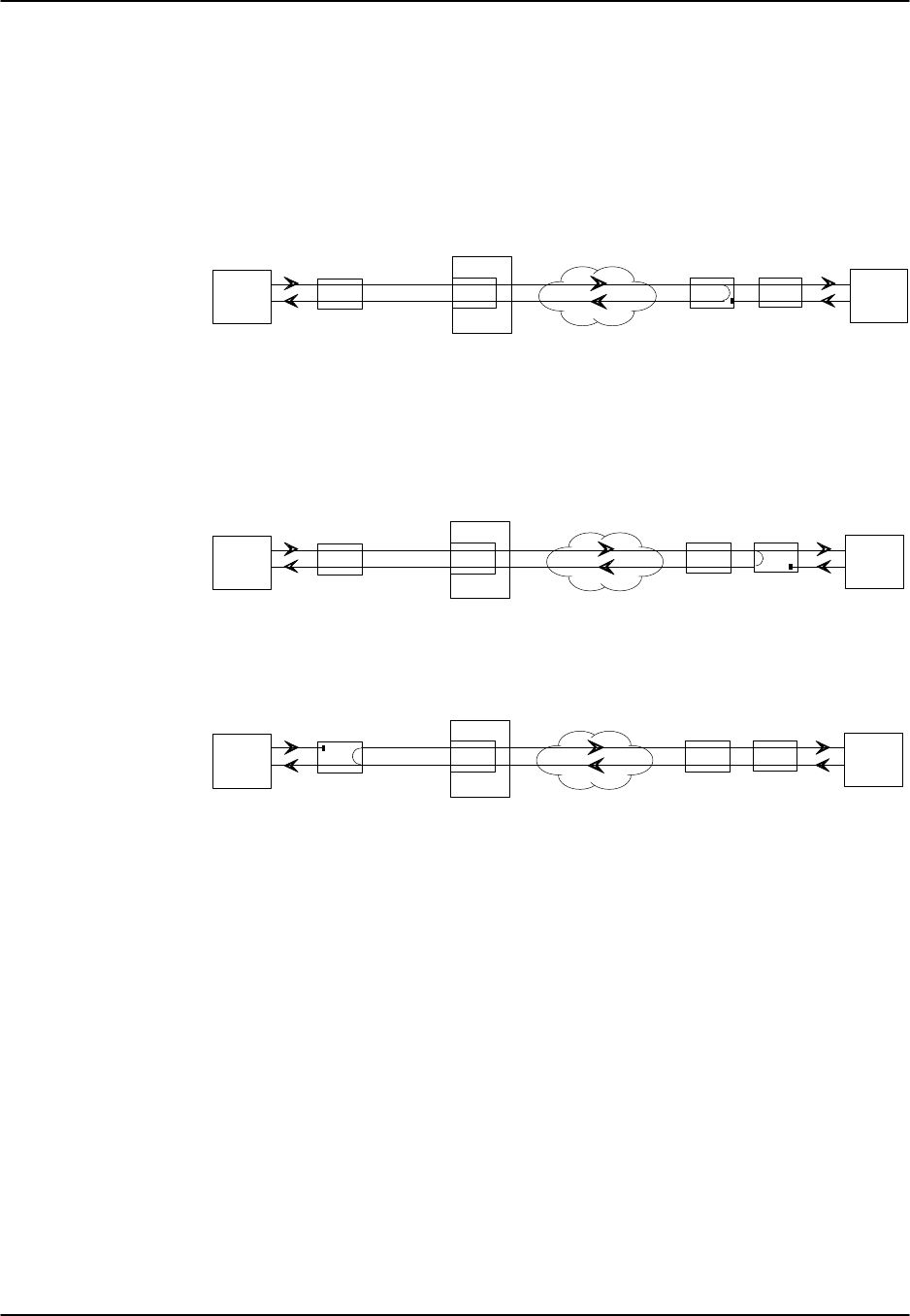
Reference Guide v3.6OCU-DP Card
(10-97) Page 8-C-7
The csu-u loopback loops the 4-wire interface of the local CSU/DSU device towards
the network. Figures OCU-6, -7, and -8 show the loopback locations. You can also
turn all remote loopbacks off.
Loop-up or loop-down commands cannot be implemented for two ports on the same
card simultaneously. The user must finish all loopback operations on one port before
attempting to perform any loopback operations on another port.
Carrier's
DDS Network
Remote Site
CSU/DSU OCU CSU/DSU
System Unit
Local Site
with OCU-DP Card
Local
DTE
Remote
DTE
Figure OCU-6. OCU Remote Loopback (ds0-n and ocu-n options)
Carrier's
DDS Network
Remote Site
CSU/DSU OCU CSU/DSU
System Unit
Local Site
with OCU-DP Card
Local
DTE
Remote
DTE
Figure OCU-7. OCU Remote Loopback (csu-n option)
Carrier's
DDS Network
Remote Site
CSU/DSU OCU CSU/DSU
System Unit
Local Site
with OCU-DP Card
Local
DTE
Remote
DTE
Figure OCU-8. OCU Remote Loopback (csu-u option)
LB DET
The Loopback Detection setting determines how the system responds to latching and
non-latching loopback commands from remote equipment. The OCU-DP reacts only to
the in-band DDS format loopback commands for Channel Loop, OCU Loop, and DSU
Loop. The Loopback Detection setting does not affect local loopback commands from
the local control terminal. The settings are off, on and w/to (on with time out).
The off option causes the system to ignore all remote loopback commands. The on
option causes the system to monitor for DDS format loopback commands from the
remote equipment. If the system detects a loopback command, it loops the data back
until the remote equipment sends a stop loopback command. The with time-out (w/to)
option is the same as the on option, except that after ten minutes the system
automatically releases loopbacks commanded by the remote equipment.
When using the OCU-DP port for a clear-channel, 64kbps circuit in DS0A mode, you
should set the loopback detection to off to prevent unintentional loopback activation.

OCU-DP Card Reference Guide v3.6
Page 8-C-8(10-97)
Menu of Actions
Table OCU-2 shows the Menu of Actions for the OCU-DP Card.
Table OCU-2. The OCU-DP Card Screen Menu of Actions
Action Function
Save Saves changes to settings.
Undo Returns all settings to the last saved state.
Refresh Updates certain time-related information fields that are not
automatically updated (i.e. performance and test data).
Perf Brings up the performance monitoring screen. See below.
Test Initiates and monitors testing of all OCU-DP card ports. Refer to Test
section below.
Main Returns to the main terminal screen. If changes are made to settings
and not saved, you will be prompted to save or lose changes.
Test
Selection of "Test" from the Menu of Options will bring up the screen shown in Figure
OCU-9. From this screen, users are allowed to create test situations between OCU-DP
cards or between a single OCU-DP card and data test equipment at a remote site. Table
OCU-3 lists the settings controlled on this screen along with their possible and default
values.
Node_1 | U1 OCU-DPx2 8249 Rev AC-0 Ser 00101 | 12-31-99
14:33
1 2
BERT n/a n/a
DIR net net
DATA pri pri
SYNC no no
BE ***** *****
ES ***** *****
SES ***** *****
CSES ***** *****
OSS ***** *****
BER ***** *****
ELAP ***** *****
LB ST ***** *****
4W DDS ***** *****
Save | Undo | Refresh | insertErr | Clear | Main
Figure OCU-9. The OCU-DP Test Card Screen

Reference Guide v3.6OCU-DP Card
(10-97) Page 8-C-9
Table OCU-3. Setting Options and Defaults
Parameter User Options Notes Default
BERT off mark space 1:1 1:7 511
2047 qrss off
DIR net user net
DATA pri sec pri
SYNC information only—no user options
BE information only—no user options
ES information only—no user options
SES information only—no user options
CSES information only—no user options
OSS information only—no user options
BER information only—no user options
ELAP information only—no user options
LB ST information only—no user options
4W DDS information only—no user options
BERT
Bit Error Rate Tester (BERT) sends a data pattern and measures the bit error rate (BER)
on the selected OCU-DP port. The patterns that can be selected are off, mark (all
ones), space (all zeros), 1:1 (1010), 1:7 (0100-0000), 511 (511 test pattern), 2047 (2047
test pattern) and qrss (quasi-random pseudo signal).
DIR
The Direction (DIR) setting allows you to specify where the BERT test signal should be
directed. The first option is net (network) which means that the test signal will be
transmitted through the system toward the Wide Area Network (WAN). The user
option means that the signal will be directed toward the attached CSU/DSU device over
the 4-wire interface.
DATA
The DATA setting specifies whether the BERT test signal should be connected to the
Primary (pri) or the Secondary (sec) channel of the OCU-DP port. If there is no
Secondary channel associated with the OCU-DP port, then the only option available is
pri.
SYNC
The Synchronization (SYNC) field tells you if the integrated BERT has achieved
synchronization either with itself via a remote loopback or with the remote test
equipment. Since this is an information-only field, there are no user-selectable
parameters.

OCU-DP Card Reference Guide v3.6
Page 8-C-10 (10-97)
BE
The Bit Error field shows the total number of bit errors logged. Since this is an
information-only field, there are no user-selectable parameters.
ES
The Errored Seconds field shows the total number of seconds in which any errors were
detected. Since this is an information-only field, there are no user-selectable
parameters.
SES
The Severely Errored Seconds (SES) field shows the total number of seconds in which
the bit error rate exceeded one bit per thousand (1 x 10⁻³). Since this is an information-
only field, there are no user-selectable parameters.
CSES
The Consecutive Severely Errored Seconds (CSES) field is triggered by the occurrence
of ten consecutive Severely Errored Seconds. Once triggered, the CSES field will
increment (by one) for each elapsed second until the system logs ten consecutive non-
Severely Errored Seconds. Since this it an information-only field there ore no user-
selectable parameters.
OSS
The Out of Synchronization Seconds field shows the number of seconds that the OCU-
DP BERT has been out of synchronization. Since this is an information-only field,
there are no user-selectable parameters.
BER
The Bit Error Rate (BER) field shows the rate at which errors are being logged. The
system calculates BER by dividing the number of bit errors (BE) by the total number of
bits transmitted during the test. Since this is an information-only field, there are no
user-selectable parameters.
ELAP
The Elapsed time setting shows the running tally of the total number of seconds during
the test. Since this is an information-only field, there are no user-selectable parameters
for this option.
4W DDS
The 4-wire DDS setting shows if the 4-wire interface is both present and operational.
The field will show norm if the interface is connected or nos for No Signal.

Reference Guide v3.6OCU-DP Card
(10-97) Page 8-C-11
Menu of Actions
Table OCU-4 shows the Menu of Actions for the Test Screen of the OCU Card.
Table OCU-4. Test Screen Menu of Actions
Action Function
Save Saves changes to settings.
Undo Returns all settings to the last saved state.
Refresh Since the informational fields on this screen are not updated in “real
time,” the Refresh command is used to obtain the latest statistics.
InsertErr Allows you to manually insert a single error into a clear data signal.
Test Clears the test screen.
Main Returns to the OCU-DP card main screen. If changes are made to
settings and not saved, you will be prompted to save or lose changes.
OCU-DP Error Correction and Performance Monitoring
If "majority vote" or "BCH" error correction is enabled on the two-port OCU-DP card,
then the system will support performance monitoring of the data traffic. The
performance monitoring screen is accessed by selecting one of the two ports from the
OCU-DP card main screen and typing "p." Error correction and performance
monitoring are not supported on the 5-port and 10-port OCU-DP card.
If the BCH method of error correction is selected, then the OCU-DP card will monitor
the data traffic coming in from the T1 network and use the BCH polynomial values that
accompany the data to log the number of errors and to attempt to correct such errors.
Any data errors that are observed are considered "input" data errors and contribute to
the input error statistics such as Input Errored Seconds (IES), Input Severely Errored
Seconds (ISES) and Input Consecutive Severely Errored Seconds (ICSES). Depending
upon the severity of the input errors, the BCH algorithm may be able to correct the data
prior to transmitting it over the four-wire DDS circuit. If an error is so severe that it
cannot be corrected, then it will also be logged as an "output" data error and will
increment the Output Errored Seconds (OES), Output Severely Errored Seconds (OSES)
and Output Consecutive Severely Errored Seconds (OCSES) counters.
If the majority vote method of error correction is selected, then the OCU-DP card will
monitor the data traffic coming in from the T1 network and use the majority vote
algorithm to determine if any data errors have occurred. Any data errors that are
observed are considered "input" data errors and contribute to the input error statistics
such as Input Errored Seconds (IES), Input Severely Errored Seconds (ISES) and Input
Consecutive Severely Errored Seconds (ICSES). Since the majority vote algorithm
assumes that it can correct any data input errors, the "output" data error category has no
meaning in this context. Consequently, the Output Errored Seconds (OES), Output
Severely Errored Seconds (OSES) and Output Consecutive Severely Errored Seconds
(OCSES) fields do not apply to the majority vote mode.
Figure OCU-10 shows the OCU-DP performance monitoring screen. Performance
statistics covering the previous twenty-four hours are available and are totaled-up at the
bottom of the screen.

OCU-DP Card Reference Guide v3.6
Page 8-C-12 (10-97)
Node_1 | U1 OCU-DPx2 8249 Rev AC-0 Ser 00101 | 12-31-99
14:33
UNIT 1 PERFORMANCE
IES ISES ICSES OES OSES OCSES
CUR 0 0 0 0 0 0
01 0 0 0 0 0 0
02 0 0 0 0 0 0
03 0 0 0 0 0 0
04 0 0 0 0 0 0
05 0 0 0 0 0 0
06 0 0 0 0 0 0
07 0 0 0 0 0 0
08 0 0 0 0 0 0
09 0 0 0 0 0 0
10 0 0 0 0 0 0
11 0 0 0 0 0 0
12 0 0 0 0 0 0
TOTAL 0 0 0 0 0 0
Refresh | Clear | pgUp | pgDn | Main
Figure OCU-10. Performance Monitoring Screen
IES
The Input Errored Seconds (IES) field shows the total number of seconds in which any
input errors were detected. Since this is an information-only field, there are no user-
selectable parameters.
ISES
The Input Severely Errored Seconds (ISES) field shows the total number of seconds in
which the input bit error rate exceeded one bit per thousand (1 x 10⁻³). Since this is an
information-only field, there are no user-selectable parameters.
ICSES
The Input Consecutive Severely Errored Seconds (ICSES) field is triggered by the
occurrence of ten consecutive Input Severely Errored Seconds. Once triggered, the
ICSES field will increment by one for each elapsed second until the system logs ten
consecutive seconds that are not severely errored. Since this is an information-only
field, there are no user-selectable parameters.

Reference Guide v3.6OCU-DP Card
(10-97) Page 8-C-13
OES
The Output Errored Seconds (OES) field shows the total number of seconds in which
any output errors were detected. This field only applies if the error correction method
selected is BCH. Since this is an information-only field, there are no user-selectable
parameters.
OSES
The Output Severely Errored Seconds (OSES) field shows the total number of seconds
in which the output bit error rate exceeded one bit per thousand (1 x 10⁻³). This field
only applies if the error correction method selected is BCH. Since this is an
information-only field, there are no user-selectable parameters.
OCSES
The Output Consecutive Severely Errored Seconds (OCSES) field is triggered by the
occurrence of ten consecutive Output Severely Errored Seconds. Once triggered, the
OCSES field will increment by one for each elapsed second until the system logs ten
consecutive that are not severely errored. This field only applies if the error correction
method selected is BCH. Since this is an information-only field, there are no user-
selectable parameters.
Menu of Actions
Table OCU-5 shows the Menu of Actions for the Performance Monitoring Screen of the
OCU Card.
Table OCU-5. Performance Monitoring Screen Menu of Actions
Action Function
Refresh Updates certain time-related information fields that are not
automatically updated (i.e. performance and test data).
Clear Clears the test screen.
pgUpScrolls through data screens from the oldest to the newest.
pgDnScrolls through data screens from the newest to the oldest.
Main Returns to the OCU-DP card main screen.

OCU-DP Card Reference Guide v3.6
Page 8-C-14 (10-97)

Reference Guide v3.6 FRAD Card
(10-97) Page 8-D-1
Introduction
8231 FRAD Card
The 8231 FRAD (Frame Relay Assembler Disassembler) card is a plug-in user card for
the system. It provides users access to the Frame Relay network of carriers through the
use of ten on-board RS232 ports on the front panel of the card. Additionally, DS0-B
traffic can be routed through the FRAD card across the backplane via WAN cross-
connect and low speed data cards.
8231 FRAD Card Main Screen
Figure FRAD-1 shows the 8231 FRAD main screen. Table FRAD-1 lists the settings
controlled on this screen along with their possible and default values.
Node_1 | U1 FRAD2-10 8231 Rev A2-0 Ser 01103 | 12-31-99 14:33
Version #:2.0 1 2 3 4 5 6 7 8 9 10
STATE actv stdby actv actv actv stdby stdby stdby stdby stdby
PRT TYP frad frad frad frad frad frad frad frad frad frad
SRC none none rs232 rs232 rs232 none none none none none
TS 02 n/a n/a n/a n/a n/a n/a n/a n/a n/a
RATE 64k n/a 19.2 9.6 14.4 n/a n/a n/a n/a n/a
DLCI n/a 16 16 16 16 16 16 16 16 16
SUB AD no no no no no no no no no no
LMI none n/a n/a n/a n/a n/a n/a n/a n/a n/a
DTE PRM n/a n/a n/a n/a n/a n/a n/a n/a n/a n/a
DES PRT 1 1 1 1 1 1 1 1 1 1
FORMAT hdlc hdlc hdlc hdlc hdlc hdlc hdlc hdlc hdlc hdlc
COM CTF n/a n/a n/a n/a n/a n/a n/a n/a n/a n/a
FLW CTL n/a n/a n/a n/a n/a n/a n/a n/a n/a n/a
CTS n/a n/a n/a n/a n/a n/a n/a n/a n/a n/a
TX CLK int int int int int int int int int int
LB off off off off off off off off off off
FRM LEN n/a n/a n/a n/a n/a n/a n/a n/a n/a n/a
Save | Undo | Refresh | Perf | Test | Main
Figure FRAD-1. 8231 FRAD Card Main Screen

FRAD Card Reference Guide v3.6
Page 8-D-2(10-97)
Table FRAD-1. 8231 Main Screen Options and Defaults
Parameter User Options Default
STATE stdby actv stdby
PRT TYP frad conc
SRC wan serv rs232
wan: none w1-1 through w4-2
serv: P1 P2 P3
rs232: 2.4 4.8 9.6 14.4 19.2 28.8 38.4
w1-1
TS n/a table
table: 1-24 (T1)
table
RATE 56k 64k 56k
DLCI Enter number <1 - 1024> 1-1024
SUB ADR n/a n/a
LMI n/a n/a
DTE PRM n/a n/a
DES PRT 1 - 10 1-10
FORMAT hdlc hdlc
COM CF n/a n/a
CTS n/a n/a
TX CLK int ext int
LB off dte net off
FRM LEN 32 64 128 256 n/a n/a
STATE
The State setting determines whether the port is active or inactive. An inactive port
does not occupy time slots on a WAN link. Set the State setting to standby (stdby ) for a
port you are not using or have not yet configured. Set it to active (actv ) for a port that
is ready for use.
PRT TYPE
The Port Type identifies the type of interface expected for this port. The selections are
frad and conc. If frad is selected, the rs232 or serv is the usual input source. If conc is
selected then wan is the usual input source.
SRC
The Source parameter allows the user to select the type and source of data input to that
port. The options are wan, serv and rs232 . If rs232 is selected, the card will expect
direct transmission of data through the corresponding RS232 input port (i.e. the eight
numbers at the top of the screen are also associated with the eight user ports on the back
of the card).
The User card is set up as four groups of two ports each (1-2, 3-4, 5-6, 7-8 and 9-10).
These ports are considered pairs so that if rs232 is selected for port #1, port #2 will also
require RS232 input.

Reference Guide v3.6FRAD Card
(10-97) Page 8-D-3
TS
The Timeslot (TS) setting identifies the time slot on the WAN link to which the Frame
Relay port is connected. Highlight the table option and press the "Enter" key. At the
bottom of the screen, the system will display the time slots that can be assigned to the
WAN link selected in the previous selection (i.e. if w1-1 is chosen and the SRC option
is either CSU or DSX, 24 timeslots will show available for assignment, if w1-1 is
CEPT, 30 timeslots will show available for assignment). Only one timeslot can be
selected for each Frame Relay port.
RATE
The Rate parameter is user selectable depending upon the SRC and the Format settings.
If frad and rs232 is selected, the options (in Kbps) are 2.4 to 38.4. Since these ports are
considered pairs, if rs232 is selected above for port #3, port #4 will also have choices
for 2.4 to 38.4Kbps rates.
If conc is selected the rate parameter selection options will be 56k and 64k
DLCI
The Data Link Connection Identifier (DLCI) identifies the frame's logical connection
within the Frame Relay port. This number is assigned by the carrier. The options are 16
through 991.
SUB AD
n/a - not available - no user input
LMI
The Local Management Interface options are n/a when the Port Type is set to frad and
none when Port Type is conc.
DTE PRM
n/a - not available - no user input
DES PRT
The Destination Port options are n/a if frad port type is selected and 1-10 if conc
(concentrator) is selected.
FORMAT
The Format parameter is currently set to hdlc.
COM CTF
n/a - not available - no user input.
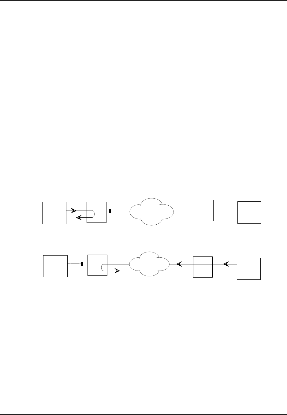
FRAD Card Reference Guide v3.6
Page 8-D-4(10-97)
CTS
n/a - not available - no user input
TX CLK
The Transmit Clock (TX CLK) setting is only available to users who selected rs232 in
the SRC setting. The options are int (internal) and ext (external). If any other SRC
setting was selected, this setting will show as n/a. (A special cable, available from your
vendor, is necessary to enable the external clock.)
LB
The Loopback (LB) setting allows you to activate a number of different loopback
options for RS232 (Figure FRAD-2). The off option is the default setting. The dte
(DTE) loops data from the local DTE back to itself through the local FRAD card. The
net (network) option loops data back toward the distant DTE through the local FRAD
card.
FRM LEN
The Frame Length is the amount of data being transmitted over the data lines.
Local
DTE
FRAD card
Remote
DTE
DTE Loopback
Network
Frame Relay
Network Loopback
Local
DTE
FRAD card
Remote
DTE
Network
Frame Relay
Figure FRAD-2. FRAD Loopback Options

Reference Guide v3.6FRAD Card
(10-97) Page 8-D-5
Menu of Actions
Table FRAD-2 shows the Menu of Actions for the 8231 main screen.
Table FRAD-2. 8231 Card Main Screen Menu of Actions
Action Function
Save Saves changes to settings.
Undo Returns all settings to the last saved state.
Refresh Updates certain time-related information fields that are not
automatically updated (i.e. performance and test data).
Perf Allows the user to access the screen that contains performance statistics
of the Frame Relay port. Refer to Performance section below.
Test Allows the user to access the screen that initiates and measures testing
statistics for highlighted user. Then refer to test section below.
Main Returns to the main screen. If changes are made to settings and not
saved, you will be prompted to save or lose changes.

FRAD Card Reference Guide v3.6
Page 8-D-6(10-97)
8231 FRAD Card Performance Screen
The 8231 Frame Relay card records performance statistics for the Frame Relay port.
Measurements taken during the current hour and each of the previous 24 hours are
displayed. A second counter at the top of the screen shows elapsed time from the last
expired hour or in the current hour. Performance statistics are not updated in real time.
Use the "R" (Refresh) command from the Menu of Actions at the bottom of the screen
to update columns. The total for the entire 24 hour period (not including the current
hour figure) is shown at the bottom of the column. Figure FRAD-3 shows the
performance monitoring screen for the main Frame Relay card screen.
Node_1 | U1 FRAD2-10 8231 Rev A2-0 Ser 01103 | 12-31-99
14:33
Port 01 PERFORMANCE SEC. 00000 of 900
FRAME Rx FRAME Tx OCTETS Rx OCTETS Tx DRPRx DRPTx STATUS
CUR 0 0 0 0 0 0 .LS
01 0 0 0 0 0 0 .LS
02 0 0 0 0 0 0 .LS
03 0 0 0 0 0 0 .LS
04 0 0 0 0 0 0 .LS
05 0 0 0 0 0 0 .LS
06 0 0 0 0 0 0 .LS
07 0 0 0 0 0 0 .LS
08 0 0 0 0 0 0 .LS
09 0 0 0 0 0 0 .LS
10 0 0 0 0 0 0 .LS
11 0 0 0 0 0 0 .LS
12 0 0 0 0 0 0 .LS
TOTAL 0 0 0 0 0 0 .LS
STATUS: T=DTE Down L=LOOPBACK S=STANDBY
pgUp | pgDn | Refresh | Main
Figure FRAD-3. The 8231 Port Performance Monitoring Screen
BLOCK Rx
The Block Receive column shows a total of Blocks received during that particular one
hour period.
BLOCK Tx
The Block Transmit column shows a total of Blocks transmitted during that particular
one hour period.
OCTETS Rx
The Octets Receive column shows a total of bytes received during that particular one
hour period.

Reference Guide v3.6FRAD Card
(10-97) Page 8-D-7
OCTETS Tx
The Octets Transmit column shows a total of bytes received during that particular one
hour period.
DRPRX
The Dropped (frame) Received column tabulates the total number of frames dropped
before being received during the 15 minute period.
DRPTX
The Dropped (frame) Transmitted column tabulates the total number of frames dropped
before being transmitted during the 15 minute period.
STATUS
The Status column shows an alphabetic character to describe the condition that caused
the error in the last two columns. Conditions displayed are T (DTE port down), L
(Loopback) and S (Standby).
Menu of Actions
Table FRAD-3 shows the Menu of Actions for the Main Performance Monitoring
screen.
Table FRAD-3. Main Performance Monitoring Screen Menu of Actions
Action Function
pgUpView the first 12 hour period (current + 1-12).
pgDnView the second 12 hour period (current + 13-24).
Refresh Update performance and test data that are not automatically updated
Main Return to the user port configuration screen.

FRAD Card Reference Guide v3.6
Page 8-D-8(10-97)

Reference Guide v3.6 DS0-DP Card
(10-97) Page 8-E-1
Introduction
The 8254 DS0 Data Port/G.703 Contradirectional/Codirectional Data Unit (DS0-
DP/G.703) is a plug-in user card for the system. The DS0-DP/G.703 provides a 64kbps
interface to a DS0 of a T1/E1 network. Since the byte alignment of the 64kbps data
stream to the DS0 is essential, the interface provides a 64kbps bit clock and a 8KHz
byte clock in the DS0-DP mode, and a composite clock/data signal in the G.703 mode.
DS0-DP Card Settings
Figure DS0-1 shows the DS0-DP screen. Table DS0-1 lists the settings controlled on
this screen along with their possible and default values.
Node_1 | U1 DS0DPx4 8254 Rev A01-0 Ser 01103 | 12-31-99
14:33
1 2 3 4
STATE stdby stdby stdby stdby
WAN w1-1 w1-1 w1-1 w1-1
TS 01 01 01 01
MODE ds0dp ds0dp ds0dp ds0dp
CLK int int int int
LB off off off off
LBGEN off off off off
LB DET off off off off
Save | Undo | Refresh | Copy | Main
Figure DS0-1. The DS0-DP Card Screen
UL Statement
OPERATION OF THIS INTERFACE IS LIMITED TO
INTRA-BUILDING CONNECTIONS ONLY

DS0-DP Card Reference Guide v3.6
Page 8-E-2(10-97)
Table DS0-1. DS0-DP Card Setting Options and Defaults
Parameter User Options Default
STATE stdby actv stdby
WAN w1-1 w1-2 w2-1 w2-2 w3-1 w3-2 w4-1
w4-2 w1-1
TS 1-24 1-31 01
MODE ds0dp contr codir ds0dp
CLK int ext int
LB off dte net off
LB GEN off ocu csu dsu ds0 off
LB DET off enab w/to off
STATE
The State setting determines whether the port is active or inactive. An inactive port
does not occupy a time slot on a WAN link. Set the state setting to standby (stdby) for
ports you are not using or have not yet configured. Set it to active (actv) for ports that
are ready for use.
WAN
The WAN setting identifies the WAN link assigned to this port. It is not necessary for
all ports on the same card to be assigned to the same WAN link, or to contiguous time
slots on a WAN link.
TS
The TS setting identifies the time slot on the WAN link to which this port is assigned.
Values range from 1-24 for T1 links and 1-31 (excluding time slot 16 in cas or ccs
mode) for E1 links. For a display of the available time slots, refer to your cross-connect
map for the WAN link; see the Operations chapter for information about viewing cross-
connect maps.
MODE
This option displays the selection of modes. In ds0dp mode, the port will provide a
common bit and byte clock to be used by the attached DTE device for both receive and
transmit. When one port is set to ds0dp all other ports will default to the DS0-DP mode
as well. Similarly, when one port is changed to one of the G.703 modes (Codirectional
or Contradirectional), any port set for the DS0-DP mode will default to the
Contradirectional mode. The contr selection configures the port for the
Contradirectional mode. In this mode, the card supplies both the transmit and receive
clocks to the DTE. The codir selection configures the port for the Codirectional mode.
In this mode, the clocks and data make up a composite signal. The clocks must be
derived from the data.

Reference Guide v3.6DS0-DP Card
(10-97) Page 8-E-3
CLK
This option allows the selection of the desired clocking mode when in the DS0-DP
mode. When set to int, the card generates the bit and byte clocks to the DTE. When set
to ext, the card receives the bit and byte clocks from the attached device. All ports must
have the same clock setting, therefore, when one port is changed, all ports are changed.
When a G.703 mode is selected, this option defaults to n/a.
LB
This option allows the user to set local loopbacks. The off option is for no loopbacks.
The dte selection loops data towards the DTE. The net option loops data towards the
network.
LB GEN
This option allows the user to set local loopbacks. The off option is for no loopbacks.
The other options (ocu, dsu, csu, ds0) force the card to send the appropriate DDS
latching loopback code towards the remote end. This option will only function in the
DS0-DP mode.
LB DET
This option allows the card to detect DDS latching loopbacks. When set to off, no
loopbacks can be detected. When set to enab, loopbacks will be detected. When a
loopback is detected, it will be maintained until a loop down is detected. w/to is the
same as enab except that if no loop down is detected after 10 minutes, the loopback
will self-terminate. This option only functions in the DS0-DP mode.
Menu of Actions
Table DS0-2 shows the Menu of Actions for the DS0-DP Card.
Table DS0-2. The DS0-DP Card Screen Menu of Actions
Action Function
Save Saves changes to settings.
Undo Returns all settings to the last saved state.
Refresh Updates certain time-related information fields that are not automatically
updated (i.e. performance and test data).
Copy Copies the contents of the current column to the next column. Useful if
you change a lot of entries in one column and want to repeat those
changes in subsequent columns.
Main Returns to the main terminal screen. If changes are made to settings and
not saved, you will be prompted to save or lose changes.

DS0-DP Card Reference Guide v3.6
Page 8-E-4(10-97)
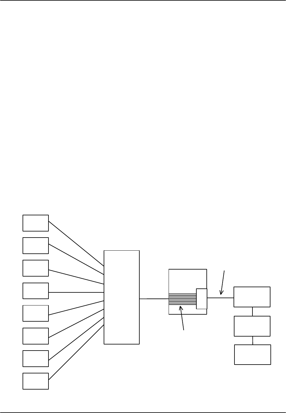
Reference Guide v3.6 B7R Card
(10-97) Page 8-F-1
Introduction
The B7R Data card enables the system to accept network management information
from each of eight separate DS0s and multiplex them into a single 38.4kbps
asynchronous bitstream running the Serial Line Interface Protocol (SLIP). (See the
Network Management section of the CPU card chapter.)
8228 Bit-7-Redundant (B7R) Card
The 8228 B7R Card will multiplex up to eight B7R formatted data channels from eight
different DS0s. This card has a separate maintenance and testing channel (port #9) and
a single aggregate channel (port #10) to redirect information from the DS0s to the
single RS232 connector on the back of the card.
Figure B7R-1 shows the part the B7R card plays in the Network Management System.
SNMP alarm traps and TELNET configuration run over this path. Both formats can use
the 4kbps FDL (Facility Data Link) on a T1 link using ESF format, a full DS0 on a T1
link or the computer port of the Interface card using SLIP protocol.
If the FDL is used to transmit and receive information, a DACSII (6.1 or higher) must
be used to convert the FDL/IP information to a full DS0. (On point-to-point circuits, a
DACSII is not needed.) A B7R card is used at the NMS site to multiplex the contents
of eight DS0 circuits into a single 38.4kbps asynchronous circuit using SLIP protocol
for use by a communication server or terminal server for routing to a Local Area
Network.
Terminal Server
4Kbps TCP/IP
Single 38.4Kbps
Asynch SLIP Circuit
System #1
FDL Circuits
System #2
System #3
System #4
System #5
System #6
System #7
System #8
DACSII
T1/E1
LAN
Workstations
B
7
R
Up to 8 DS0s
Concentrator
Unit
Figure B7R-1. A Typical NMS Application

B7R Card Reference Guide v3.6
Page 8-F-2(10-97)
B7R Card Settings
Figure B7R-2 shows the B7R card screen. Table B7R-1 lists the settings controlled on
this screen along with their possible and default values.
Node_1 | U1 B7R-8 8228 Rev A0-0 Ser 00101 | 12-31-99 14:33
1 2 3 4 5 6 7 8 9 10
STATE stdby stdby stdby stdby stdby stdby stdby stdby stdby stdby
WAN w1-1 w1-1 w1-1 w1-1 w1-1 w1-1 w1-1 w1-1 w1-1 w1-1
TS 01 01 01 01 01 01 01 01 01 01
RATE fdl fdl fdl fdl fdl fdl fdl fdl fdl fdl
COM CF n/a n/a n/a n/a n/a n/a n/a n/a n/a n/a
CTS n/a n/a n/a n/a n/a n/a n/a n/a n/a n/a
ADDR Ip Ip Ip Ip Ip Ip Ip Ip Ip Ip
NETMSK Ip Ip Ip Ip Ip Ip Ip Ip Ip Ip
Save | Undo | Refresh | Copy | Main
Figure B7R-2. SRU Card Default Screen
Table B7R-1. B7R Card Setting Options and Defaults
Parameter User Options Notes Default
STATE stdby actv stdby
WAN w1-1 w1-2 w2-1 w2-2 w3-1 w3-
2 w4-1 w4-2 w1-1
TS 01-24 01-31 01
FORMAT b7r b4r 9.6 19.2 28.2 38.4 1b7r
8 7 6 5 8
COM CF 1 2 2 1
none odd even space mark none
CTS off on off
ADDR ip 30.0.0.0
NETMSK ip 40.0.0.0
NOTES
1. Rate settings are only available for port #10.
2. Com CF is a three step process that is only available for port #9 and #10.

Reference Guide v3.6B7R Card
(10-97) Page 8-F-3
3. The IP address of ports #1-8 must match the IP address assigned to the remote
system on that DS0. Port #9 does not require an IP address because it is a debug
port.
4. Ports #1-8 share the same subnetwork mask, and the subnet address for ports #1-8
must be different from the one used for port #10.
STATE
The State setting determines whether the port is active or inactive. Set the State setting
to standby (stdby) for ports you are not using or have not yet configured. Set it to
active (actv) for ports that are ready for use. Port #9 is used for debug purposes and is
normally in the stdby position.
WAN
The WAN setting identifies the WAN link that carries the data for this B7R port (either
from the DACS or directly from the WAN link). The choices for this setting are w1-1
through w4-2. Ports #9 and #10 do not require input from WAN links, therefore this
field shows n/a for these ports.
TS
The TS (timeslot) setting identifies the timeslot on the WAN link carrying data for the
B7R port (either from the DACS or directly from the WAN link). Acceptable values
for this field are 01-24 for a T1 link or 01-15 and 17-31 for an E1 link.
Generally, timeslots are assigned sequentially. For example, card #1 would be assigned
to ports 1-8, card #2 to ports 9-16 and card #3 would be assigned to ports 17-24, but
this is not required.
RATE
The Rate setting allows you to select the rate in thousands of bits per second (kbps) for
transmission of data. The rate of ports #1-8 are preset to 4kbps. The rate of port #9 is
preset to 9.6kbps. The options for port #10 are 9.6, 19.2, 28.8 and 38.4. Since the
combined output of ports #1-8 are 32kbps, port #10 should be set to 38.4 to
accommodate a full system.
COM CF
The Communication Configuration setting is not applicable for ports #1-8 and the n/a
value cannot be changed. Ports #9-10 can be changed in a three step procedure that
selects the data bits, parity and stop bits. The default values are 8, N, 1.

B7R Card Reference Guide v3.6
Page 8-F-4(10-97)
CTS
The Clear To Send setting selects an option that will allow hardware handshaking with
the terminal server and the B7R card when enabled for port #10. Since it is not
applicable for ports #1-8, the n/a value cannot be changed. Ports #9-10 can be
changed. The values for this setting are off and on.
All cabling must be terminated before activating the CTS feature.
ADDR
The Address setting defines the IP address for each Integrated Access Controller
associated with the first eight ports and port #10. Port #9 does not require an IP address
and cannot be changed from the n/a setting. This address must be the same as the
address used in the PORT IP ADDR field on the Interface card of the system with
which it is associated for ports #1-8. The IP address for port #10 is a unique address for
each B7R card and must be on a different network than ports #1-8. This allows the user
to "ping" each B7R card itself for system diagnostics.
NETMSK
The Network Mask setting defines the single subnet mask address for each system
associated with the first eight ports and a different subnet mask for port #10. A change
of subnet mask for any of the first eight ports will change all of the ports. Port #9 does
not require a subnet mask and cannot be changed from the n/a setting. This address
must be the same as the address used in the NETMASK field on the Interface card of
the system with which it is associated for ports #1-8.
Menu of Actions
Table B7R-2 shows the Menu of Actions for the B7R card.
Table B7R-2. The B7R Card Screen Menu of Actions
Action Function
Save Saves changes to settings.
Undo Returns all settings to the last saved state.
Refresh Updates certain time-related information fields that are not
automatically updated (i.e. performance and test data).
Copy Copies the contents of the current column to the next column. Useful
if you change a lot of entries in one column and want to repeat those
changes in subsequent columns.
Main Returns to the main terminal screen. If changes are made to settings
and not saved, you will be prompted to save or lose changes.

Reference Guide v3.6 BRI Card
(10-97) Page 8-G-1
Introduction
The Basic Rate Interface (BRI) user card offers non-switched connectivity to sites
located up to 18,000 feet from the system location. Factors such as wire gauge, bridge
tap and loading patterns are described in ANSI T1.601-1992 specifications. The 8260
and 8261 BRI cards are equipped with eight (8) “U” interfaces, each of which can carry
one BRI, 2B+D channel, providing either two 64Kbps or one 128Kbps bearer channels
per interface.
The 8262 four-wire BRI card supports the “S” and “T” interfaces. The connection
distances for this card are largely dependent on the number of devices connected to the
card.
8260 BRI Card
The 8260 BRI Card has software selectable mode operations of LT and NT. The 8260
supports up to eight leased or BRI terminal extension (brite) applications. The 8260
does not support sealing current and does not provide any DC termination.
8261 BRI Card
The 8261 BRI Card has all of the functionality of the 8260. Switching between the LT
and NT modes requires both making a menu selection and changing jumper connections
on the card (see Figure BRI-14). The 8261 supports sealing current of 7.5mA or
15.0mA for a number of different times and duration.
To activate sealing current, set the jumpers on the card to the desired position (see
Figure BRI-15 for jumper locations) also set SEAL CURR to on (see Figure BRI-2).
The Sealing Current screen (see Figure BRI-3) provides for setting the start time,
duration, and repeat interval.
This card is shipped with jumpers attached that make the automatic default for the card
LT and 15mA sealing current. (Sealing current is not applicable in NT mode.)
The 8260 and 8261 are very similar in operation and will be discussed together at the
start of the chapter. The 8262 BRI Card is sufficiently different that its screen and
operation information is included separately.
8262 BRI Card
The 8262 BRI Card is designed to support “S/T” 4-wire interface applications. It also
supports both internal and external phantom power arrangements. Jumpers are
available to select termination’s on the receive and transmit sides individually.
UL Statement
OPERATION OF THIS INTERFACE IS LIMITED TO
INTER-BUILDING CONNECTIONS LESS THAN 1,000 METERS
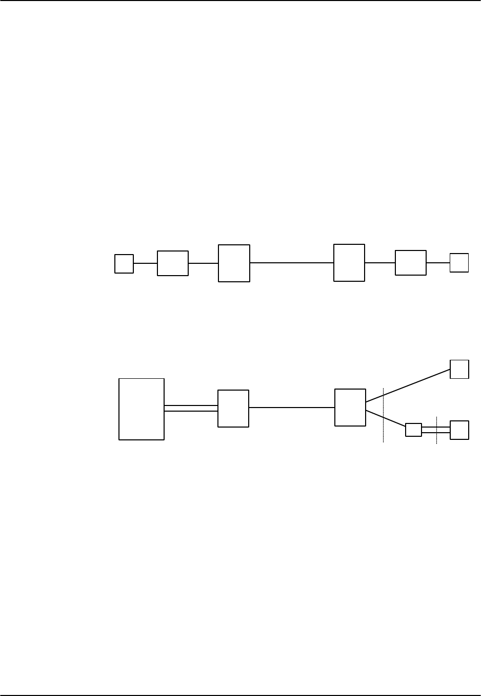
BRI Card Reference Guide v3.6
Page 8-G-2(10-97)
BRI Circuit Applications
Figure BRI-1 shows the difference between the two circuit types, Leased line (lease)
and BRI Terminal Extension (brite). The leased circuit can be any standard 2B1Q (U
interface) NTU device that supports "nailed-up" (1 or 2 B channels) connections with
no D channel signaling. The brite mode supports switched connectivity to ISDN
capable switches and D channel signaling on either a full DS0 or multiplexed 4:1 on a
single DS0.
For both examples, B channels carrying voice traffic on the BRI card can be
compressed through the ADPCM card to extend the user's resources (see Conversion
section). The only limitation on BRI traffic is that NTUs or NT1s must be located less
than 18,000 feet from the system unit.
T1/E1
System Unit DTE
System Unit
NTU
DTE
T1/E1
System Unit
NT1
BRI Eq
BRI Terminal Extension
System Unit
ISDN Switch
Near End
Near End
Far End
Far End
Leased Line
2B1Q NTU
2B1Q
BRI
Lines
4-wire
BRI Eq
2-wire
"U" "S/T"
Figure BRI-1. Typical BRI System Application

Reference Guide v3.6BRI Card
(10-97) Page 8-G-3
8260 and 8261 BRI Card Settings
Figure BRI-2 shows the BRI main screen and Table BRI-1 lists the settings controlled
on the screen along with their possible and default values.
Node_1 | U1 BRI Ux8sc 8261 Rev D2-0 Ser 01103 | 12-31-99
14:33
Version: #1.5
1 2 3 4 5 6 7 8
STATE stdby stdby stdby stdby stdby stdby stdby stdby
TERMINAL lt lt lt lt lt lt lt lt
TYPE lease lease lease lease lease lease lease lease
B MODE none none none none none none none none
B1 WAN/SRV w1-1 w1-1 w1-1 w1-1 w1-1 w1-1 w1-1 w1-1
B1 TS n/a n/a n/a n/a n/a n/a n/a n/a
B2 WAN/SRV w1-1 w1-1 w1-1 w1-1 w1-1 w1-1 w1-1 w1-1
B2TS n/a n/a n/a n/a n/a n/a n/a n/a
D WAN w1-1 w1-1 w1-1 w1-1 w1-1 w1-1 w1-1 w1-1
D TS n/a n/a n/a n/a n/a n/a n/a n/a
D SUBCHAN off off off off off off off off
LOCAL LB off off off off off off off off
LB CHAN B1 B1 B1 B1 B1 B1 B1 B1
LBGEN MD ddsT ddsT ddsT ddsT ddsT ddsT ddsT ddsT
LB GEN off off off off off off off off
SEAL CURR off off off off off off off off
TR COND off off off off off off off off
Save | Undo | Refresh | Copy | conVert | Eoc | Ntu | Test | Perf | Main
Figure BRI-2. The BRI Main Screen

BRI Card Reference Guide v3.6
Page 8-G-4(10-97)
Table BRI-1. BRI Card Parameter Options and Defaults (8260/8261)
Parameter User Options Notes Default
STATE stdby actv stdby
TERMINAL lt nt lt
TYPE lease brite lease
B MODE none B1 B2 B1+B2 128K none
B1 WAN/SERV w1-1 w1-2 w2-1 w2-2 w3-1 w3-2 w4-
1 w4-2 3w1-1
B1 TS n/a 01-24 01-31 01
B2 WAN/SERV w1-1 w1-2 w2-1 w2-2 w3-1 w3-2 w4-
1 w4-2 3w1-1
B2 TS n/a 01-24 01-31 01
D WAN w1-1 w1-2 w2-1 w2-2 w3-1 w3-2 w4-
1 w4-2 1w1-1
D TS n/a 01-24 01-31 1 01
D SUBCHAN off 1 2 3 4 1off
LOCAL LB off ta net off
LB CHAN B1 B2 B1+B2 B1
LBGEN MD ddsT ddsN v54T v54N ft1T ft1N eoc ddsT
LB GEN off B1ocu B1csu B1ds0 B1dsu B2ocu
B2csu B2ds0 B2dsu 2off
SEAL CURR n/a off on n/a
TR CONDoff on off
NOTES
1. D Channels will only show if brite is selected for Type.
2. These choices are only available for LBGEN Modes of ddsT and ddsN.
See LB GEN paragraph below.
3. SRV functions will be activated in a future release.
STATE
The State setting determines whether the port is active or inactive. An inactive port
does not occupy a time slot on a WAN link. Set the State option to standby (stdby) for
ports you are not using or have not yet configured. Set it to active (actv) for ports that
are ready for use.
TERMINATION
The 8260 and 8261 Terminal setting shows if the port is acting as a line termination
(lt) or a network termination (nt). Generally, the line termination resides at the local
central office, while the network termination is located at the customer location.
Changing the termination from nt (the default) to lt on the 8261 BRI card requires
changing jumper settings on the card itself. Instructions for this conversion are
included at the end of this chapter.

Reference Guide v3.6BRI Card
(10-97) Page 8-G-5
TYPE
The Type setting determines the type of BRI connection for this port. The options
available are lease (a permanent circuit), brite (BRI Terminal Emulation), iw
(interworking) and ntu_l (Network Terminating Unit - Lease, 8260 and 8261 only).
If ntu_l is selected, the user is required to select either 64 (which corresponds to the
Adtran NTU) or 2560 (which corresponds to the 2560/2561 NTUs). If the wrong type
of NTU is selected, the user will not be able to perform remote configuration of the
NTU.
B MODE
The B Channel Mode option determines the B channel usage for this port. Setting the
port to none tells the system that the equipment associated with this port does not
require a B channel and access to both B WANs is disabled. Setting the highlighted
port to B1 tells the system that only one B channel is required for the BRI equipment.
Selecting B1 enables the B1 WAN and B1 TS and disables the B2 WAN and B2 TS.
Setting the port to B2 tells the system that only one B channel is required for the BRI
equipment. Selecting B2 enables the B2 WAN and B2 TS and disables the B1 WAN
and B1 TS.
Setting the port to B1+B2 tells the system that two B channels are required for the BRI
equipment. Selecting B1+B2 enables both the B1/B2 WANs and TSs. Any WAN and
any timeslot can be assigned to either B channel.
Setting the port to 128K tells the system that a 128Kbps "pipe" is required for the DTE
equipment. Selecting 128K enables both the B1/B2 WANs and TSs. Both B channels
must be assigned to the same WAN.
B1 WAN/SERV
The WAN setting identifies the WAN link for the first B channel assigned to this port.
It is not necessary for all 8 ports on the same card to be assigned to the same WAN link,
or to contiguous time slots on a WAN link. The serv port is set from conVert screen.
B1 TS
The TS setting identifies the time slot on the WAN link for the first B channel assigned
to this port. Values range from 1-24 for T1 links and 1-31 for E1 links. Time slot 16 is
not available on E1 links that are programmed for cas or ccs signaling. For a display of
the available time slots, refer to your cross-connect map for the WAN link. See the
Operations chapter for information about viewing cross-connect maps.
B2 WAN/SERV
The WAN setting identifies the WAN link for the second B channel assigned to this
port. If 128K is selected for the B Mode, the second B channel must be assigned to the
same WAN link as the first B channel.

BRI Card Reference Guide v3.6
Page 8-G-6(10-97)
B2 TS
The TS setting identifies the time slot on the WAN link for the second B channel
assigned to this port. Values range from 1-24 for T1 links and 1-31 for E1 links. Time
slot 16 is not available on E1 links that are programmed for cas or ccs signaling.
D WAN
The D WAN setting identifies the WAN link for the D channel assigned to this port for
brite circuits. It is not necessary for all ports on the same card to be assigned to the
same WAN link, or to contiguous time slots on a WAN link.
D TS
The TS setting identifies the time slot on the WAN link for the D channel assigned to
this port for brite circuits. Values range from 1-24 for T1 links and 1-31 for E1 links.
Time slot 16 is not available on E1 links that are programmed for cas or ccs signaling.
D SUBCHAN
The D Subchannel option allows the user to use a full DS0 for the D channel or split the
DS0 into four 16Kbps sections to allow D channels to be combined into a single
64Kbps DS0. D subchannels must be used on the same BRI card only.
LOCAL LB
The Local Loopback setting controls the direction of the local loopback. The settings
are off (for no loopback), ta (for a loopback toward the terminal adapter) and net (for a
loopback toward the network).
LB CHAN
The Loopback Channel setting places the local loopback on either the first B channel
(B1), the second B channel (B2) or both B channels (B1+B2).
LBGEN MD
The Loopback Generation Mode specifies the type of loopback to be placed on the
circuit. The BRI card only generates loopback codes, it does not detect loopback codes.
The options are ddsT (a DDS loopback on the terminal side of the line), ddsN (a DDS
loopback on the network side of the line), v54T (V.54 loopback toward the terminal),
v54N (V.54 loopback toward network), ft1T (a fractional T1 loopback toward the
terminal), ft1N (fractional T1 loopback toward the network) and eoc (Embedded
Operations Channel loopback towards the U interface).

Reference Guide v3.6BRI Card
(10-97) Page 8-G-7
LB GEN
The Loopback Generation option specifies different loopback codes depending on the
selection of loopback generation mode above. The options for ddsT and ddsN are off
(no loopback), B1ocu (an OCU loopback on the first B channel), B1csu (a CSU
loopback on the first B channel), B1ds0 (a full DS0 loopback on the first B channel),
B1dsu (a DSU loopback on the first B channel), B2ocu (an OCU loopback on the
second B channel), B2csu (a CSU loopback on the second B channel), B2ds0 (a full
DS0 loopback on the second B channel) and B2dsu (a DSU loopback on the second B
channel).
The options for v.54T, v,54N, ft1T and ft1N are off (no loopback), B1 (v.54 or Ft1
loopback on the first B channel), B2 (v.54 or Ft1 loopback on the second B channel)
and B1+B2 (v.54 or Ft1 loopback on both B channels).
The options for eoc are off (no loopback), B1 (eoc loopback on the first B channel), B2
(eoc loopback on the second B channel), B1+B2 (eoc loopback on the both B channels)
and 2B+D (eoc loopback on the both B channels and the D channel).
If the loopback is directed toward the terminal, the loopback pattern selected will not
start until the U-ST parameter on the test screen shows the status of "actv." (See the
test section below for further information about the U-ST parameter.)
SEAL CURR
Sealing current (on the 8261 card only) is used to inhibit corrosion on wire splices in
outside plant. The Sealing Current option on the BRI card allows the user to select
sealing current on a port-by-port basis.
Jumpers on the card allow the user to choose between a 15mA (the default) or
7.5mA current (provided by the -48VDC power converter). The jumper settings
are shown at the end of this chapter.
The setting for this parameter is n/a for the 8260 card. The settings are no and yes for
the 8261 card. Choosing yes for this setting will automatically bring up the screen of
Figure BRI-3. Table BRI-3 shows the parameter settings and defaults for this screen.
RCVE
The settings are noTst (no code violation test) and cdVol (code violation test). If cdVol
is set and a code violation is detected, the card sends an interrupt toward the network
line.
TR COND
The Trunk condition (TR COND) setting allows the BRI card to pass trunk conditions
from the network to the U/ST interface when set to on. Setting the TR COND state to
off prevents the condition to be passed through the card.

BRI Card Reference Guide v3.6
Page 8-G-8(10-97)
Menu of Actions
Table BRI-2. BRI Card Main Screen Menu of Actions
Action
Function
Save
Saves changes to settings.
Undo
Returns all settings to the last saved state.
Refresh Updates certain time-related information fields that are not automatically
updated (i.e. performance and test data).
Copy Copies the contents of the current column (except timeslot) to the next
column. Useful if a user changes a lot of entries in one column and
wants to repeat those changes in subsequent columns.
conVert The Conversion feature allows the B channels to be used with ADPCM
compression features. See the Conversion section.
Eoc
Embedded Operations Channel (not yet supported)
Ntu
Network Terminating Unit programming. (not applicable to 8262).
Test
Initiates and monitors testing of all BRI card ports. See Test section.
Perf Shows the performance statistics for the port highlighted. See the
Performance Monitoring section. Not implemented in S/T card.
Main Returns to the main terminal screen. If changes are made to settings and
not saved, users will be prompted to save or lose changes.

Reference Guide v3.6BRI Card
(10-97) Page 8-G-9
The Sealing Current Screen
This screen applies to the 8261 only, and only in LT mode. Move the cursor to the
SEAL CURR selection for the desired channel and press <Enter> to bring up the screen
of Figure BRI-3.
Node_1 | U1 BRI Ux8sc 8261 Rev D2-0 Ser 01103 | 12-31-99
14:33
1
START (h) 0
DURATION (m) 0
REPEAT 0
REP.EVRY (h) 0
Save | Undo | Refresh | Main
Figure BRI-3. The Sealing Current Screen
Table BRI-3. Sealing Current Options
Parameter User Options Default
START (H) 0-24 0
DURATION (M) 1-60 1
REPEAT no yes no
REP EVRY (H) 0 1-24 0
START (h)
The Start parameter allows the user to set the time (in hours) that the sealing current is
to be applied to the selected port. The values are 0 (zero) through 24. Selection of zero
will start the sealing current as soon as the changes are saved. Selection of any other
number between 1 and 24 turns on the sealing current on that many hours from
now.(e.g. selection of six [6] turns on the current six hours from now).

BRI Card Reference Guide v3.6
Page 8-G-10 (10-97)
DURATION (m)
The Duration parameter allows the user to set the duration of time (in minutes) the
sealing current is to be applied to the port selected. The values are 1-60.
REPEAT
The Repeat parameter allows the user to repeat the application of sealing current to the
line of the port selected. The values are yes and no.
REP. EVRY (h)
The Repeat Every parameter allows the user to set the time (in hours) that the sealing
current is to be repeated on the port selected. The values are 1-24. Selection of any
number between 1 and 24 repeats the sealing current on that interval (e.g. selection of
one [1] repeats the current every hour).
Menu of Actions
Table BRI-4 shows the Menu of Actions for the Sealing Current Screen.
Table BRI-4. Sealing Current Screen Menu of Actions
Action Function
Save Save changes to settings.
Undo Return all settings to the last saved state.
Refresh Update time-related information fields that are not automatically updated
Main Return to the main terminal screen. If changes are made to settings and
not saved, you will be prompted to save or lose changes.
Conversion
The conversion feature allows the user to compress B channel voice traffic to be used
with the ADPCM card. Figure BRI-4 shows the Conversion screen and Table BRI-5
shows the options and default settings.
It is not necessary to assign both B channels of a B1+B2 circuit to ADPCM engines.
Furthermore, B channels can share an ADPCM timeslot with any other type of
service.

Reference Guide v3.6BRI Card
(10-97) Page 8-G-11
Node_1 | U1 BRI Ux8sc 8261 Rev D2-0 Ser 01103 | 12-31-99
14:33
Version: #1.8
1 2 3 4 5 6 7 8
B1 CNV off off off off off off off off
B1 RATE n/a n/a n/a n/a n/a n/a n/a n/a
B1 ADPCM n/a n/a n/a n/a n/a n/a n/a n/a
B2 CNV off off off off off off off off
B2 RATE n/a n/a n/a n/a n/a n/a n/a n/a
B2 ADPCM n/a n/a n/a n/a n/a n/a n/a n/a
Save | Undo | Refresh | Main
Figure BRI-4. Conversion Screen
Table BRI-5. Conversion Screen Options and Defaults
Parameter User Options Default
B1 CNV off ad-u ad-A off
B1 RATE n/a 24K,1 32K,1 40K,1 24K,2 32K,2 40K,2 n/a
B1 ADPCM n/a P1 P2 P3 n/a
B2 CNV off ad-u ad-A off
B2 RATE n/a 24K,1 32K,1 40K,1 24K,2 32K,2 40K,2 n/a
B2 ADPCM n/a P1 P2 P3 n/a
B1 CNV
The B Channel #1 Conversion parameter allows the user to choose Pulse Code
Modulation (PCM) coding for B channel #1 voice traffic. The values are off, ad-u and
ad-A. Use ad-u when converting from T1 carriers and use ad-A for E1 carriers (this
signal is A-inv not A-law).
B1 RATE
The B Channel #1 Rate parameter allows the user to choose both the speed of the B
Channel traffic and the position on the ADPCM time slot.
There must be two ADPCM engines assigned to each WAN timeslot and the rate
combination of both engines must equal 64Kbps.

BRI Card Reference Guide v3.6
Page 8-G-12 (10-97)
The values are n/a, 24K,1 (64Kbps to 24Kbps on the first ADPCM engine), 32K,1
(64Kbps to 32Kbps on the first ADPCM engine), 40K,1 (64Kbps to 40Kbps on the first
ADPCM engine), 24K,2 (64Kbps to 24Kbps on the second ADPCM engine), 32K,2
(64Kbps to 32Kbps on the second ADPCM engine), 40K,2 (64Kbps to 40Kbps on the
second ADPCM engine).
B1 ADPCM
The B Channel #1 ADPCM parameter allows you to choose the ADPCM card to which
you would like to assign this B channel. The options are n/a, P1 (the ADPCM card in
slot P1), P2 (the ADPCM card in slot P2) and P3 (the ADPCM card in slot P3).
B2 CNV
The B Channel #2 Conversion parameter allows the user to choose Pulse Code
Modulation (PCM) coding for B channel #2 voice traffic. The values are off, ad-u and
ad-A. Use ad-u when converting from T1 carriers and use ad-A for E1 carriers (this
signal is A-inv not A-law).
B2 RATE
The B Channel #2 Rate parameter allows the user to choose both the speed of the B
Channel traffic and the position on the ADPCM time slot.
There are two ADPCM engines assigned to each WAN timeslot and the rate
combination of both engines must equal 64Kbps.
The values are n/a, 24K,1 (64Kbps to 24Kbps on the first ADPCM engine), 32K,1
(64Kbps to 32Kbps on the first ADPCM engine), 40K,1 (64Kbps to 40Kbps on the first
ADPCM engine), 24K,2 (64Kbps to 24Kbps on the second ADPCM engine), 32K,2
(64Kbps to 32Kbps on the second ADPCM engine), 40K,2 (64Kbps to 40Kbps on the
second ADPCM engine).
B2 ADPCM
The B Channel #2 ADPCM parameter allows you to choose the ADPCM card to which
you would like to assign this B channel. The options are n/a, P1 (the ADPCM card in
slot P1), P2 (the ADPCM card in slot P2) and P3 (the ADPCM card in slot P3).

Reference Guide v3.6BRI Card
(10-97) Page 8-G-13
Menu of Actions
Table BRI-6 shows the Menu of Actions for the BRI Conversion Screen.
Table BRI-6. Menu of Actions
Action Function
Save Saves changes to settings.
Undo Returns all settings to the last saved state.
Refresh Redraws the screen.
Main Returns to the BRI card main screen. If changes are made to settings and
not saved, you will be prompted to save or lose changes.
Embedded Operations Channel
Not currently supported
Remote NTU Configuration
The Ntu option on the BRI Main screen allows the user to configure up to 8 remote
NTUs per card. This option is currently available only for 8260/8261 BRI cards with
1.8 firmware). Typing n (Ntu) on the 8260/8261 Main Screen brings up the NTU
screen of Figure BRI-5.
DEV TYPE: NTU560 | SW VER: 5.2 | 12-31-99 14:33
1
DTE INTF TYPE v.36
DTE SYNC/ASYN sync
DTE DATA RATE 64k
CLOCK MODE int
DCD OPTIONS on
DCD OFF DELAY n/a
DSR OPTIONS on
CTS OPTIONS on
CTS ON DELAY n/a
ASYN BAUDRATE offset
RI INDICATION off
RL LINE ena
LL LINE ena
NTU CONSOLE ena
Save | Undo | Refresh | Load | Write | Test | stAtus | Main
Figure BRI-5. Remote NTU Configuration Screen

BRI Card Reference Guide v3.6
Page 8-G-14 (10-97)
NTU Configuration Parameters and Options
Use the arrow keys to scroll through the options of Figure BRI-5. Table BRI-7 shows
the parameters and options available. Defaults are identified in parameter lists by bold
type.
Table BRI-7. Remote NTU Configuration Screen Options and Defaults
Parameter User Options Default
DTE INTF TYPE Display only. v.36; for the 2561, it is v.24. display only
DTE SYNC/ASYN sync asy8 asy9 asy10 asy11 sync
DTE DATA RATE sync: 1.2k 2.4k 4.8k 9.6k 14.4k 19.2k
28.8k 32k 38.4k 48k 56k 64k 72k
128k
asyx: <1.2k 1.2k 2.4k 4.8k 9.6k 14.4k
19.2k 28.8k 38.4k
CLOCK MODE Display only. display only
DCD OPTIONS off on r_rts on
DCD OFF DELAY n/a 5-80 bits n/a
DSR OPTIONS off on on
CTS OPTIONS off on l_rts on
CTS ON DELAY n/a 0-60 bits 10-250 msec n/a
ASYN BAUDRATE offset exact offset
RI INDICATION off on off
RL LINE dis dis
LL LINE dis ena ena
NTU CONSOLE dis ena ena
DTE INTF TYPE
Display only. The DTE Interface Type identifies the interface on the rear panel of the
NTU. This parameter is detected automatically. For the 2560, it is v.36; for the 2561, it
is v.24.
DTE SYNC/ASYN
Selects Synchronous (sync) or asynchronous (asy) transmission mode (Sync is the
default). Asynchronous transmission has options for four character lengths: asy8
(8-bit), asy9 (9-bit), asy10 (10-bit), or asy11 (11-bit).
DTE DATA RATE
sync: 1.2k 2.4k 4.8k 9.6k 14.4k 19.2k 28.8k 32k 38.4k 48k 56k 64k 72k
128k
asyx: <1.2k 1.2k 2.4k 4.8k 9.6k 14.4k 19.2k 28.8k 38.4k

Reference Guide v3.6BRI Card
(10-97) Page 8-G-15
CLOCK MODE
Display only. CLOCK MODE is detected based on the Primary Clock setting on the
Interface Card.
DCD OPTIONS
The Data Carrier Detect option can be off, on (default), or r_rts (Remote Ready To
Send). r_rts option requires setting of the DCD OFF DELAY option.
DCD OFF DELAY
n/a if the DCD OPTIONS selection is on or off.
If r_rts is selected, the options are 5, 10, 15, 20, 25, 30, 35, 40, 45, 50, 55, 60, 65, 70,
75, or 80 bits.
DSR OPTIONS
off or on.
CTS OPTIONS
The Clear To Send option can be off, on (default), or l_rts (Local Ready To Send).
l_rts option requires setting of the CTS ON DELAY option.
CTS ON DELAY
n/a if the CTS OPTIONS selection is on or off.
If l_rts is selected, the CTS ON DELAY is measured either in bits or milliseconds. The
options are 0, 10, 20, 30, 40, 50, or 60 bits, or 10, 20, 30, 40, 50, 100, or 250 msecs.
ASYN BAUDRATE
The asynchronous baud rate can either be set as offset (default) or exact.
RI INDICATION
The ring indicator setting may be turned on or off (default)
RL LINE
The remote (network) loop line indicator is always disabled. This is the loop between
the BRI card and the NTU (see Figure BRI-6). May be overridden locally by means
of a switch on the front panel of the NTU.
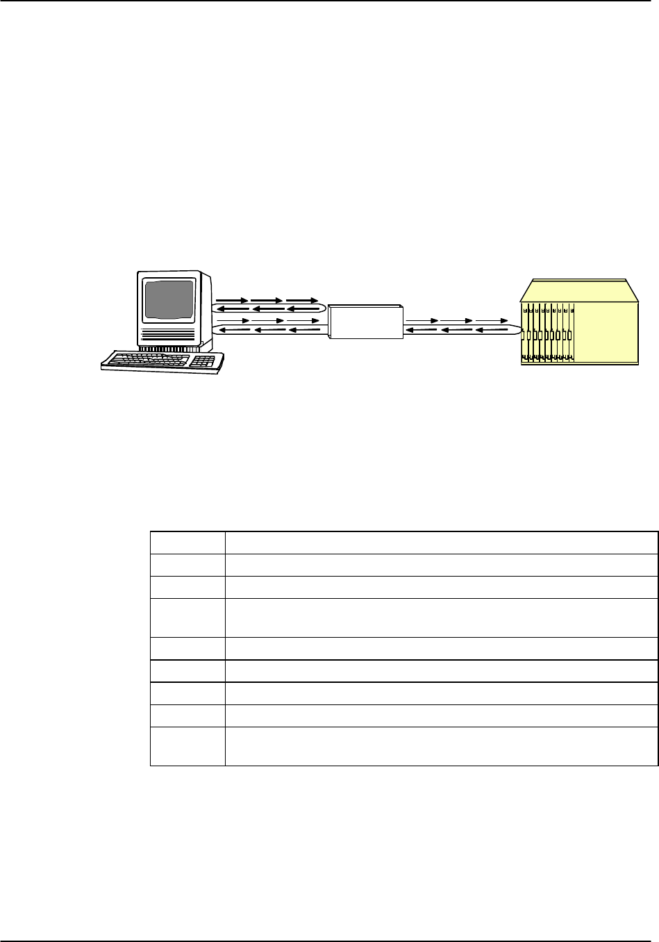
BRI Card Reference Guide v3.6
Page 8-G-16 (10-97)
LL LINE
Sets up loopback testing permission between the NTU and the Data Terminal
Equipment (DTE) (see Figure BRI-6). The setting may be ena (enable) (default) or dis
(disable). This parameter can be overridden locally by means of a switch on the
front panel of the NTU.
NTU CONSOLE
When this option is enabled (ena) (default), the NTU may be programmed locally by a
line from the rear connector port to a DTE. When disabled, the NTU must be
programmed remotely (e.g., through the BRI card).
L o cal L o o p
Remote (Network) L o o p
NTU
DTEChassis w/BRI Card
Figure BRI-6. Local and Remote NTU Loopback Testing.
Menu of Actions
Table BRI-8. Remote NTU Configuration Screen Menu of Actions.
Action Function
Save Saves changes to settings.
Undo Returns all settings to the last saved state.
Refresh Data is not automatically updated on screen. Pressing the "R" key will
show updated statistics.
Load Loads currently saved parameters from the NTU.
Write Saves configuration information to the NTU.
Test Brings up the Test Screen (see below).
stAtus Brings up the Status Screen (see below).
Main Returns to the BRI card main screen. If changes are made to settings and
not saved, users will be prompted to save or lose changes.

Reference Guide v3.6BRI Card
(10-97) Page 8-G-17
NTU Test
Figure BRI-7 shows the NTU Test screen, while Table BRI-9 shows the parameter
options.
DEV TYPE: NTU560 | SW VER: 5.2 | 12-31-99 14:33
1
TEST off
TIMER on
STATUS off
ERROR n/a
TOTAL n/a
Save | Undo | Refresh | Main
Figure BRI-7. NTU Test Screen
Table BRI-9. NTU Test Screen Options and Defaults
Parameter User Options Notes Default
TEST off net off
TIMER off on on
STATUS off loc net loc_net 1off
ERROR n/a 2n/a
TOTAL n/a 2n/a
NOTES
1 The loc and loc_net options are included to support manual loopback override at
the NTU site.
2 These parameters are not supported in this release.
TEST
Choosing net allows the user to start a loopback test in the network loop (between the
BRI card and NTU). The default is off.

BRI Card Reference Guide v3.6
Page 8-G-18 (10-97)
TIMER
This indicates whether the loopback test is set to time out, or whether it is ongoing.
The options are off and on (default). This is a read-only parameter; it is not user-
selectable.
STATUS
This parameter indicates the direction of the loopback testing. The options are off
(default), loc (local loop), net (network loop), and loc_net (local and network loops).
The loc and loc_net parameters are included in the event that the local loopback testing
is activated manually by selecting a switch on the front panel of the NTU. This is a
read-only parameter; it is not user-selectable.
ERROR
This parameter is not supported in this release.
TOTAL
This parameter is not supported in this release.
Menu of Actions
Table BRI-10. NTU Test Screen Menu of Actions.
Action Function
Save Saves changes to settings.
Undo Returns all settings to the last saved state.
Refresh Test data is not automatically updated on screen. Pressing the "R" key
will show updated statistics.
Main Returns to the remote NTU configuration screen. If changes are made to
settings and not saved, users will be prompted to save or lose changes.

Reference Guide v3.6BRI Card
(10-97) Page 8-G-19
NTU Status
Figure BRI-8 shows the NTU Status screen, while Table BRI-11 identifies the status
displays.
DEV TYPE: NTU560 | SW VER: 5.2 | 12-31-99 14:33
1
ALARM none
CTS on
DSR on
DCD on
RTS off
DTR off
RX FIFO ERR no
TX FIFO ERR no
HW CODE 1
LINE TR st5411
ASIC REV 3
EPLD REV 2
Refresh | Main
Figure BRI-8. NTU Status Screen

BRI Card Reference Guide v3.6
Page 8-G-20 (10-97)
Table BRI-11. NTU Status Screen Displays
Parameter Display
ALARM none U L R M
Displays active alarms, including: none, U (U interface is down), L (NTU has lost
sync and is not yet configured), R (NTU has been reset and is not yet configured),
and M (NTU is in the Master mode).
CTS CTS Status: off on
DSR DSR Status: off on
DCD DCD Status: off on
RTS RTS Status: off on
DTR DTR Status: off on
RX FIFO ERR Indicates a FIFO buffering error on the receive end; reports yes or no.
TX FIFO ERR Indicates a FIFO buffering error on the transmit end; reports yes or no.
HW CODE 0-255
LINE TR Line transceiver type: tp3410 or st5411
ASIC REV 0-255
EPLD REV 0-255
Menu of Actions
Table BRI-12. NTU Status Screen Menu of Actions.
Action Function
Refresh Data is not automatically updated on screen. Pressing the "R" key will
show updated statistics.
Main Returns to the remote NTU configuration screen. If changes are made to
settings and not saved, users will be prompted to save or lose changes.

Reference Guide v3.6BRI Card
(10-97) Page 8-G-21
BRI (8260/8261) Test
Selection of "Test" from the Menu of Options will bring up the screen shown in Figure
BRI-9. From this screen, users are allowed to create test situations between BRI Cards
or between a single BRI Card and data test equipment at a remote site. Table BRI-15
lists the settings controlled on this screen along with their possible and default values.
Node_1 | U1 BRI Ux8sc 8260 Rev B1-0 Ser 01103 | 12-31-99
14:33
1 2 3 4 5 6 7 8
BERT n/a n/a n/a n/a n/a n/a n/a n/a
DIR ta ta ta ta ta ta ta ta
CHAN B1 B1 B1 B1 B1 B1 B1 B1
SYNC no no no no no no no no
BE ***** ***** ***** ***** ***** ***** ***** *****
ES ***** ***** ***** ***** ***** ***** ***** *****
SES ***** ***** ***** ***** ***** ***** ***** *****
CSES ***** ***** ***** ***** ***** ***** ***** *****
OSS ***** ***** ***** ***** ***** ***** ***** *****
BER ***** ***** ***** ***** ***** ***** ***** *****
ELAP ***** ***** ***** ***** ***** ***** ***** *****
U-ST ***** ***** ***** ***** ***** ***** ***** *****
LB ST ***** ***** ***** ***** ***** ***** ***** *****
SEAL ***** ***** ***** ***** ***** ***** ***** *****
Save | Undo | Refresh | InsertErr | Clear | Main
Figure BRI-9. BRI Card Test Screen (8260 and 8261)

BRI Card Reference Guide v3.6
Page 8-G-22 (10-97)
Table BRI-15. 8260/8261 Test Screen Options and Defaults
Parameter User Options Default
BERT off mark space 1:1 1:7
p_1 p_0 p_1:1 p_1:7 off
DIR ta net ta
CHAN B1 B2 128K D B1
SYNC see description below no
BE see description below
ES see description below
SES see description below
CSES see description below
OSS see description below
BER see description below
ELAP see description below
U-ST stdby, init , actv, fail, deact, nos, los,
b1eoc, b2eoc, 2beoc, bdeoc.actv
LB ST off, ta, or net. off
SEAL Indicates if the sealing current is
selected or not (8261 BRI Card only).

Reference Guide v3.6BRI Card
(10-97) Page 8-G-23
BERT
Bit Error Rate Tester (BERT) sends a data pattern and measures the bit error rate (BER)
on the selected BRI port. Depending upon whether the test is on B channels or D
channels, the patterns can be sent as either raw data or as HDLC packets containing the
patterns. BERT can only be sent on one port at a time.
For a B channel test, the patterns that can be selected are off, mark (1111), space
(0000), 1:1 (1010), 1:7 (0100-0000), p_1 (packet, 1111), p_0 (packet, 0000), p_1:1
(packet, 1010) and p_1:7 (packet, 0100-0000).
If the D channel is selected, the patterns that can be selected are off, p_1 (packet,
1111), p_0 (packet, 0000), p_1:1 (packet, 1010) and p_1:7 (packet, 0100-0000).
DIR
Selects the direction of the test. The options are ta, toward the Terminal Adapter
(customer site) or net, toward the Network (carrier).
CHAN
Selects the side of the line on which the BER pattern will be sent. The options are B1
(BERT on B channel #1), B2 (BER is on B channel #2), 128K (BERT is on the 128K
pipe) and D (BERT is on the D channel).
SYNC
Synchronization (SYNC) displays yes if the integrated BERT has achieved
synchronization either with itself via a remote loopback or with the remote test
equipment, no if it has not.
BE
Bit Error (BE) displays the total number of bit errors logged.
ES
Errored Seconds (ES) displays the total number of seconds in which errors were
detected.
SES
Severely Errored Seconds (SES) shows the total number of seconds in which the bit
error rate exceeded one bit per thousand (1 x 10⁻³).

BRI Card Reference Guide v3.6
Page 8-G-24 (10-97)
CSES
Consecutive Severely Errored Seconds (CSES) is triggered by the occurrence of ten
consecutive Severely Errored Seconds. Once triggered, the CSES field will increment
(by one) for each elapsed second until the system logs ten consecutive non-Severely
Errored Seconds.
OSS
Out of Synchronization Seconds (OSS) shows the number of seconds that the BRI
BERT has been out of synchronization.
BER
Bit Error Rate (BER) shows the rate at which errors are being logged. BER equals the
number of bit errors (BE) divided by the total number of bits transmitted during the test.
ELAP
Elapsed time (ELAP) is the total number of seconds elapsed during the test.
U-ST
Displays the status of the U interface ports. Possible U interface states include stdby,
init (initializing), actv, fail (failed to activate), deact (deactivated), nos (no signal), los
(loss of signal), b1eoc (eoc loopback on B1), b2eoc (eoc loopback on B2), 2beoc (eoc
loopback on both B channels), bdeoc (eoc loopback on both B and D channels).
If the LB GEN option (on the previous screen) is set to ta, the U-ST field must show
"actv" before any loopbacks selected become operational.
LB ST
Loopback State (LB STATE) indicates the local loopback selected on the main screen
for this port. Possible states are: off, ta, or net.
SEAL
Indicates if the sealing current is selected or not (8261 BRI Card only).

Reference Guide v3.6BRI Card
(10-97) Page 8-G-25
Menu of Actions
Table BRI-16 shows the Menu of Actions for the BRI test screen.
Table BRI-16. Test Screen Menu of Actions
Action Function
Save Saves changes to settings.
Undo Returns all settings to the last saved state.
Refresh Test data is not automatically updated in "real time." Pressing the
"R" key will show updated statistics.
InsertErr Allows the user to manually insert a single error into the clear data
signal.
Clear Clears the testing screen and resets all counters to zero.
Main Returns to the BRI card main screen. If changes are made to settings
and not saved, you will be prompted to save or lose changes.
Performance Monitoring (8260/8261)
The 8260 and 8261 BRI cards support proprietary performance monitoring, which
continuously measures operation performance of the connection from the Integrated
Access Controller to the NTU. Each one hour segment is divided into 3600 seconds
and statistics are kept for the current hour and the past 24 one hour periods.
To get statistics for a particular port, highlight the port on the BRI card main screen and
press the P (Performance Monitoring) key. The screen shown as Figure BRI-10
appears. Table BRI-17 defines the parameters displayed.
While viewing the performance monitoring screen, the user must press the R (refresh)
command from the menu of actions to obtain updated statistics.

BRI Card Reference Guide v3.6
Page 8-G-26 (10-97)
Node_1 | U1 BRI Ux8sc 8260 Rev D2-0 Ser 01103 | 12-31-99
14:33
Unit 1 PERFORMANCE
ES UAS NOS LOS DM NEBE FEBE STATUS
CUR 0 0 0 0 0 0 0 . . . . . .
010 0 0 0 0 0 0 0 . . . . . .
020 0 0 0 0 0 0 0 . . . . . .
030 0 0 0 0 0 0 0 . . . . . .
040 0 0 0 0 0 0 0 . . . . . .
050 0 0 0 0 0 0 0 . . . . . .
060 0 0 0 0 0 0 0 . . . . . .
070 0 0 0 0 0 0 0 . . . . . .
080 0 0 0 0 0 0 0 . . . . . .
090 0 0 0 0 0 0 0 . . . . . .
100 0 0 0 0 0 0 0 . . . . . .
110 0 0 0 0 0 0 0 . . . . . .
120 0 0 0 0 0 0 0 . . . . . .
TOTAL 0 0 0 0 0 0 0 . . . . . .
STATUS: T=Test; L=LOS; N=NOS; P=PS1; p=PS2; t=NTM; S=STDBY/SWITCH
Save | Undo | Refresh | insertErr | Clear | Main
Figure BRI-10. BRI Card Performance Monitoring Screen
Table BRI-17. Performance Monitoring Displays
Parameter User Options Default
ES see description below display only
UAS see description below display only
NOS see description below display only
LOS see description below display only
DM see description below display only
NEBE see description below display only
FEBE see description below display only
STATUS L (loss of synchronization), N (no signal), S (standby), T
(test), P (power failure of primary source for NT), p (power
failure of secondary source for NT) and t (network terminal
test mode).
see status options
ES
Errored Seconds registers the number of seconds for which the BRI card detected a
Near End Block Error (NEBE) or a Far End Block Error (FEBE) greater than zero (0)

Reference Guide v3.6BRI Card
(10-97) Page 8-G-27
UAS
Unavailable Seconds shows the number of seconds for which the U-Interface is not
available (not active).
NOS
No Signal Seconds column shows the number of seconds for which the BRI card
detected a NOS line condition (applicable for LT Terminal Type only). For NT
Terminal Type, no signal seconds are reported in the Unavailable Seconds column.
LOS
Loss of Synchronization Seconds shows the number of seconds for which the BRI card
detected a LOS line condition (applicable for LT Terminal Type only). For NT
Terminal Type, the loss of synchronization seconds are included in the Unavailable
Seconds column.
DM
The Degraded Minutes register shows the number of minutes for which the BRI card
detected ES, UAS, NOS or LOS greater than zero (0).
NEBE
Near End Block Error shows transmission errors detected by the near end equipment.
FEBE
Far End Block Error shows transmission errors detected by the far end equipment.
STATUS
Status displays error codes for line conditions that occur during the one hour intervals.
Identifying codes are displayed at the bottom of the screen. The values are L (loss of
synchronization), N (no signal), S (standby), T (test), P (power failure of primary
source for NT), p (power failure of secondary source for NT) and t (network terminal
test mode).
The last three codes (P, p and t) are not available for network terminal applications.

BRI Card Reference Guide v3.6
Page 8-G-28 (10-97)
Menu of Actions
Table BRI-18 shows the Menu of Actions for the BRI Performance Monitoring screen.
Table BRI-18. Performance Monitoring Screen Menu of Actions
Action Function
Refresh Since the BRI card does not show accumulated performance statistics in
"real time" (i.e. second by second), the Refresh command must be used
to show changes from the last recorded number.
Clear Clears the testing screen and resets all counters to zero.
pgUpAllows the user to see the first 12 hour period (current + 1-12).
pgDnAllows the user to see the second 12 hour period (current + 13-24).
Main Returns to the main screen.
8262 BRI Card Settings
Figure BRI-11 shows the 8262 BRI main screen.
Node_1 | U1 BRI-STx8 8262 Rev E2-0 Ser 00047 | 12-31-99 14:33
Version: #1.8
1 2 3 4 5 6 7 8
STATE stdby stdby stdby stdby stdby stdby stdby stdby
TERMINAL nt-pp nt-pp nt-pp nt-pp nt-pp nt-pp nt-pp nt-pp
TYPE lease lease lease lease lease lease lease lease
B MODE none none none none none none none none
B1 WAN/SRV none none none none none none none none
B1 TS n/a n/a n/a n/a n/a n/a n/a n/a
B2 WAN/SRV none none none none none none none none
B2 TS n/a n/a n/a n/a n/a n/a n/a n/a
D WAN none none none none none none none none
D TS n/a n/a n/a n/a n/a n/a n/a n/a
D SUBCHAN n/a n/a n/a n/a n/a n/a n/a n/a
LOCAL LB off off off off off off off off
LB CHAN B1 B1 B1 B1 B1 B1 B1 B1
LBGEN MD ddsT ddsT ddsT ddsT ddsT ddsT ddsT ddsT
LB GEN off off off off off off off off
RCVE noTst noTst noTst noTst noTst noTst noTst noTst
TR COND off off off off off off off off
Save | Undo | Refresh | Copy | conVert | Eoc | Ntu | Test | Perf | Main
Figure BRI-11. BRI Main Screen (8262)
8262 BRI Card Main Screen Parameter Options
Table BRI-19 lists the parameters controlled on the screen along with their possible
settings. Default values in the option lists are identified in bold type.

Reference Guide v3.6BRI Card
(10-97) Page 8-G-29
Table BRI-19. 8262 BRI Card Parameter Options and Defaults
Parameter User Options Default
STATE stdby actv stdby
TERMINAL nt-pp nt-sb nt-eb te nt-pp
TYPE lease brite iw lease
B MODE none B1 B2 B1+B2 128K none
B1 WAN/SRV none w1-1 w1-2 w2-1 w2-2 w3-1 w3-2
w4-1 w4-2
P1 P2 P3
none
B1 TS n/a 01-24 01-31 n/a
B2 WAN/SRV none w1-1 w1-2 w2-1 w2-2 w3-1 w3-2
w4-1 w4-2
P1 P2 P3
none
B2 TS n/a 01-24 01-31 n/a
D WAN none w1-1 w1-2 w2-1 w2-2 w3-1 w3-2
w4-1 w4-2
P1 P2 P3
none
D TS n/a 01-24 01-31 n/a
D SUBCHAN n/a off 1 2 3 4 n/a
LOCAL LB off ta net off
LB CHAN B1 B2 B1+B2 B1
LBGEN MD ddsT ddsN v54T v54N ft1T ft1N ddsT
LB GEN off B1ocu B1csu B1ds0 B1dsu B2ocu B2csu
B2ds0 B2dsu off
RCVE noTst cdVol noTst
TR COND n/a off on off
NOTES
1. SRV functions (P1, P2 and P3) may be activated from the conVert screen when an
ADPCM server is installed.
2. D-Channels will only show if brite is selected for Type.
3. These choices are only available for LB GEN Modes of ddsT and ddsN. See LB
GEN paragraph below.

BRI Card Reference Guide v3.6
Page 8-G-30 (10-97)
STATE
Set the State option to stdby (standby) for ports that are not in use or not yet
configured; set it to actv (active) for ports that are ready for use. The default is stdby.
TERMINAL
The 8262 Terminal setting allows the port to be set as an nt-pp (network termination
point-to-point), nt-sb (network termination short-bus), nt-eb (network termination
extended-bus) or te (terminal equipment) device. The default for the 8262 is nt-pp.
TYPE
The Type setting determines the type of BRI connection for this port. The options
available are lease (a permanent circuit), brite (BRI Terminal Emulation), iw
(interworking) and ntu_l (Network Terminating Unit - Lease, 8260 and 8261 only).
B MODE
Determines the B channel usage for this port. none disables access to both B WANs.
Setting the highlighted port to B1 assigns only one B channel. Selecting B1 enables the
B1 WAN and B1 TS and disables the B2 WAN and B2 TS. Setting the port to B2
enables the B2 WAN and B2 TS and disables the B1 WAN and B1 TS.
Selecting B1+B2 enables both the B1/B2 WANs and TSs. Any WAN and any timeslot
can be assigned to either B channel.
Setting the port to 128K tells the system that a 128kbps "pipe" is required for the DTE
equipment. Selecting 128K enables both the B1/B2 WANs and TSs. Both B channels
must be assigned to the same WAN.
B1 WAN/SRV
The WAN setting identifies the WAN link for the first B channel assigned to this port.
It is not necessary for all 8 ports on the same card to be assigned to the same WAN link,
or to contiguous time slots on a WAN link. The serv port is set from conVert screen.
B1 TS
The TS setting identifies the time slot on the WAN link for the first B channel assigned
to this port. Values range from 1-24 for T1 links and 1-31 for E1 links. Time slot 16 is
not available on E1 links that are programmed for cas or ccs signaling. Use the up and
down arrow keys to scroll through the time slots. For a display of the available time
slots, refer to the cross-connect map for the WAN link. See the Operations chapter for
information about viewing cross-connect maps. There is no assignment to a server.

Reference Guide v3.6BRI Card
(10-97) Page 8-G-31
B2 WAN/SRV
The WAN setting identifies the WAN link for the second B channel assigned to this
port. If 128K is selected for the B Mode, the second B channel must be assigned to the
same WAN link as the first B channel. The serv port is set from conVert screen.
B2 TS
The TS setting identifies the time slot on the WAN link for the second B channel
assigned to this port. Values range from 1-24 for T1 links and 1-31 for E1 links. Time
slot 16 is not available on E1 links that are programmed for cas or ccs signaling. The
up and down arrow keys are used to scroll through the time slots. There is no
assignment to a server.
D WAN
The D WAN setting identifies the WAN link for the D channel assigned to this port for
brite circuits. It is not necessary for all ports on the same card to be assigned to the
same WAN link, or to contiguous time slots on a WAN link.
D TS
The TS setting identifies the time slot on the WAN link for the D channel assigned to
this port for brite circuits. Values range from 1-24 for T1 links and 1-31 for E1 links.
Time slot 16 is not available on E1 links that are programmed for cas or ccs signaling.
D SUBCHAN
The D Subchannel option allows users to employ a full DS0 for the D channel or split
the DS0 into four 16kbps sections to allow D channels to be combined into a single
64kbps DS0. D subchannels must be used on the same BRI card only.
LOCAL LB
The Local Loopback setting controls the direction of the local loopback. The settings
are off (no loopback), ta (loopback toward the terminal adapter) and net (loopback
toward the network).
LB CHAN
The Loopback Channel setting places the local loopback on either B1 (the first B
channel), B2 (the second B channel) or B1+B2 (both B channels).

BRI Card Reference Guide v3.6
Page 8-G-32 (10-97)
LBGEN MD
The Loopback Generation Mode specifies the type of loopback to be placed on the
circuit. The BRI card only generates loopback codes, it does not detect loopback codes.
The options are ddsT (DDS loopback on the terminal side of the line), ddsN (a DDS
loopback on the network side of the line), v54T (V.54 loopback toward the terminal),
v54N (V.54 loopback toward network), ft1T (fractional T1 loopback toward the
terminal), ft1N (fractional T1 loopback toward the network).
LB GEN
The Loopback Generation option specifies different loopback codes depending on the
selection of loopback generation mode above. The options for ddsT and ddsN are off
(no loopback), B1ocu (an OCU loopback on the first B channel), B1csu (a CSU
loopback on the first B channel), B1ds0 (a full DS0 loopback on the first B channel),
B1dsu (a DSU loopback on the first B channel), B2ocu (an OCU loopback on the
second B channel), B2csu (a CSU loopback on the second B channel), B2ds0 (a full
DS0 loopback on the second B channel) and B2dsu (a DSU loopback on the second B
channel).
The options for v.54T, v.54N, ft1T and ft1N are off (no loopback), B1 (v.54 or Ft1
loopback on the first B channel), B2 (v.54 or Ft1 loopback on the second B channel)
and B1+B2 (v.54 or Ft1 loopback on the both B channels).
If the loopback is directed toward the terminal, the loopback pattern selected will not
start until the U-ST parameter on the test screen shows the status of actv. (See the Test
section for further information about the U-ST parameter).
RCVE
The settings are noTst (no code violation test) and cdVol (code violation test). If cdVol
is set and a code violation is detected, the card sends an interrupt toward the network
line.
TR COND
The Trunk condition (TR COND) setting allows the BRI card to pass trunk conditions
from the network to the U/ST interface when set to on. Setting the TR COND state to
off prevents passing the condition through the card.

Reference Guide v3.6BRI Card
(10-97) Page 8-G-33
Menu of Actions
Table BRI-20. BRI Card Main Screen Menu of Actions
Action
Function
Save
Saves changes to settings.
Undo
Returns all settings to the last saved state.
Refresh Updates certain time-related information fields that are not
automatically updated (i.e. performance and test data).
Copy Copies the contents of the current column (except timeslot) to the next
column. Useful if a user changes a lot of entries in one column and
wants to repeat those changes in subsequent columns.
conVert The Conversion feature allows the B channels to be used with ADPCM
compression features. See the Conversion section.
Eoc
Embedded Operations Channel (not yet supported)
Ntu
Network Terminating Unit programming. (not applicable to 8262).
Test
Initiates and monitors testing of all BRI card ports. See Test section.
Perf Shows the performance statistics for the port highlighted. See the
Performance Monitoring section. Not implemented in S/T card.
Main Returns to the main terminal screen. If changes are made to settings
and not saved, users will be prompted to save or lose changes.
Conversion
The conversion feature (conVert) for the 8262 is the same as for the 8260/8261 and will
not be repeated here.
Test
Selecting Test from the Main Screen Menu of Actions for the 8262 brings up the screen
shown in Figure BRI-12. The test screen lets users create test situations between BRI
Cards or between a single BRI Card and data test equipment at a remote site. Table
8G-21 lists the options and displayed values on this screen. Values of parameters to be
entered (if any) are listed at the top of the User option cell for the field, with the default
shown in bold type.

BRI Card Reference Guide v3.6
Page 8-G-34 (10-97)
Node_1 | U1 BRI-STx8 8262 Rev E2-0 Ser 00047 | 12-31-99 14:33
Version: #1.5
1 2 3 4 5 6 7 8
BERT off off off off off off off off
DIR ta ta ta ta ta ta ta ta
CHAN B1 B1 B1 B1 B1 B1 B1 B1
SYNC no no no no no no no no
BE 0 ***** ***** ***** ***** ***** ***** *****
ES 0 ***** ***** ***** ***** ***** ***** *****
SES 0 ***** ***** ***** ***** ***** ***** *****
CSES 0 ***** ***** ***** ***** ***** ***** *****
OSS 0 ***** ***** ***** ***** ***** ***** *****
BER 0e-0 ***** ***** ***** ***** ***** ***** *****
ELAP 0 ***** ***** ***** ***** ***** ***** *****
L1-ST actv ***** ***** ***** ***** ***** ***** *****
LB ST off ***** ***** ***** ***** ***** ***** *****
Save | Undo | Refresh | InsertErr | Clear | Main
Figure BRI-12. BRI 8262 Test Screen
Table BRI-21. 8262 Test Screen Options and Defaults
Parameter User Options Default
BERT off mark space 1:1 1:7 p_1 p_0
p_1:1 p_1:7 off
DIR ta net ta
CHAN B1 B2 128K D B1
SYNC yes no no
BE see description below
ES see description below
CSES see description below
OSS see description below
BER see description below
ELAP see description below
L1-ST actv, fail, or init actv
LB ST off, ta, or net off
BERT
Bit Error Rate Tester (BERT) sends a data pattern and measures the bit error rate (BER)
on the selected BRI port. Depending upon whether the test is on B channels or D
channels, the patterns can be sent as either raw data or as HDLC packets containing the
patterns. BERT can only be sent on one port at a time.

Reference Guide v3.6BRI Card
(10-97) Page 8-G-35
For a B channel test, the patterns that can be selected are off, mark (1111), space
(0000), 1:1 (1010), 1:7 (0100-0000), p_1 (packet, 1111), p_0 (packet, 0000), p_1:1
(packet, 1010) and p_1:7 (packet, 0100-0000).
If the D channel is selected, the patterns that can be selected are off, p_1 (packet,
1111), p_0 (packet, 0000), p_1:1 (packet, 1010) and p_1:7 (packet, 0100-0000).
DIR
Selects the direction of the test. The options are ta, toward the Terminal Adapter
(customer site) or net, toward the Network (carrier).
CHAN
Selects the side of the line on which the BER pattern will be sent. The options are B1
(BERT on B channel #1), B2 (BER is on B channel #2), 128K (BERT is on the 128K
pipe) and D (BERT is on the D channel).
SYNC
Synchronization (SYNC) displays yes if the integrated BERT has achieved
synchronization either with itself via a remote loopback or with the remote test
equipment, no if it has not.
BE
Bit Error (BE) displays the total number of bit errors logged.
ES
Errored Seconds (ES) displays the total number of seconds in which errors were
detected.
SES
Severely Errored Seconds (SES) shows the total number of seconds in which the bit
error rate exceeded one bit per thousand (1 x 10⁻³).
CSES
Consecutive Severely Errored Seconds (CSES) is triggered by the occurrence of ten
consecutive Severely Errored Seconds. Once triggered, the CSES field will increment
(by one) for each elapsed second until the system logs ten consecutive non-Severely
Errored Seconds.

BRI Card Reference Guide v3.6
Page 8-G-36 (10-97)
OSS
Out of Synchronization Seconds (OSS) shows the number of seconds that the BRI
BERT has been out of synchronization.
BER
Bit Error Rate (BER) shows the rate at which errors are being logged. BER equals the
number of bit errors (BE) divided by the total number of bits transmitted during the test.
ELAP
Elapsed time (ELAP) is the total number of seconds elapsed during the test.
L1-ST
L1-ST (L1-STATE) displays the condition for the selected port. Possible states are:
actv, fail, or init.
LB ST
Loopback State (LB STATE) indicates the local loopback selected on the main screen
for this port. Possible states are: off, ta, or net.
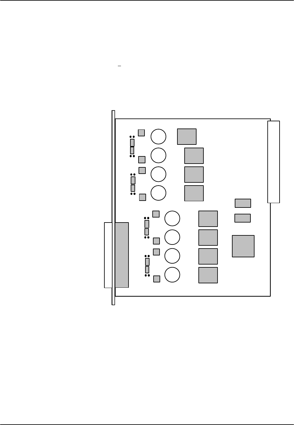
Reference Guide v3.6BRI Card
(10-97) Page 8-G-37
Setting Terminal Type Jumpers on the 8261
Setting or resetting jumpers is necessary for conversion of individual ports on the 8261
from Network Terminal (nt) to Line Terminal (lt). Cards are shipped with Network
Terminal as the default (jumpers closed). To make the conversion, remove the BRI
card from its slot and remove shorting jumpers across the jumpers labeled J101-J801
(the first digit [e.g. 101] is the port number indicator) on both sets of pins next to the
front edge of the card as shown in Figure BRI-13.
Ports can be set individually for the lt feature, but once set, remain in the lt mode until
the jumpers are reattached.
Power
Bus
Edge
Connector
Amphenol
J801
Connector
J701
J601
J501
J401
J301
J201
J101
Figure BRI-13. LT-NT Jumper Locations on the 8261 BRI Card

BRI Card Reference Guide v3.6
Page 8-G-38 (10-97)
Setting Sealing Current Jumpers on the 8261
Setting or resetting jumpers is necessary for conversion of individual ports on the 8261
from 15mA to 7.5mA of sealing current. Cards are shipped with 15mA as the default
(jumpers closed). To make the conversion, remove the BRI card from its slot and
remove shorting jumpers across the pins labeled J102-J802 (the first digit [e.g. 102] is
the port number indicator) on both sets of pins next to the front edge of the card as
shown in Figure BRI-14.
Ports can be set individually for 7.5mA but, once set, remain in that setting until the
jumpers are reattached.
Power
Bus
Edge
Connector
Amphenol
Connector
J802
J702
J602
J502
J402
J302
J202
J102
Figure BRI-14. Sealing Current Jumper Locations on the 8261 BRI Card
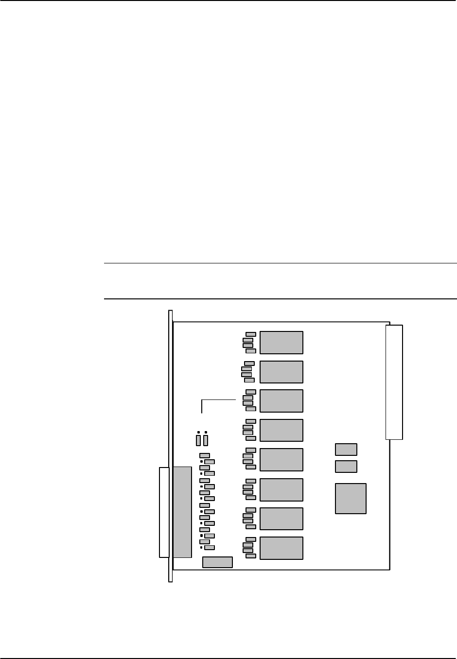
Reference Guide v3.6BRI Card
(10-97) Page 8-G-39
Setting Jumpers on the 8262
As shown in Figure BRI-15, there are 4 jumper options, JPx01, JPx02, JPx03 and
JPx04, for each of the eight (8) BRI ports. (The “x” indicates the numbers 1 through 8.)
Jumpers JPx02, when installed, applies the XMT 100 Ohm termination. Jumpers
JPx03, are installed as the default to apply the RCV 100 Ohm termination. The actual
network design determines the setting of these termination’s.
Jumpers JPx01 and JPx04 are installed (ON) to provide either internal (INT) or
external (EXT) -48v power to the phantom leads based upon the setting of JP5 and JP6
(see markings on the 8262 board). When the JPx01 and JPx04 jumpers are ON, they
provide power out on the cable pair. When OFF, there is no power out on the cable
pair.
The jumper defaults are as follows:
Phantom Power - ON/OFF (Jx01 and Jx04) are default = ON
Phantom Power Source - Int/Ext (JP5 & JP6) are default = External
100 Ohm Term - Xmt OUT, Rcv IN
If external power is used, jumpers JP5 and JP6 must be set to EXTERNAL mode.
Failure to do so could damage or destroy the card or system.
Power
Bus
Edge
Connector
Amphenol
Connector
JP701
JP704
JP102
JP103
JP5/6
Figure BRI-15. Jumper Locations on the 8262 BRI Card

BRI Card Reference Guide v3.6
Page 8-G-40 (10-97)
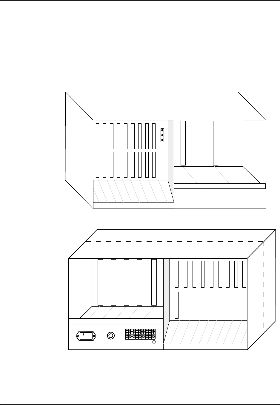
Reference Guide v3.6 Pinouts
(10-97) Page 9-A-1
Introduction
This chapter describes the pinouts of the card connectors used to attach circuits and
devices to the integrated access system complex. The front view of the two-sided
chassis is shown in Figure Pinouts-1. The two-sided unit was designed so that all
cabling would be done at the back of the chassis shown in Figure Pinouts-2. All front-
loading chassis were designed so that all cabling would be done at the front of the
chassis, as seen in Figure Pinouts-3 through Figure Pinouts-5. The number and type of
connectors needed will vary with the card installed. Each card that requires cabling is
shown in this chapter, the connector is described, and the pinouts labeled.
C1C2P1P2P3W1W2W3W4
F1F2
1
2
3
EUR/US
JP1
Figure Pinouts-1. 891822/891823 Two-Side Chassis, Front View
R1R2R3R4R5
IFU2U1U3U4U5U6U7U8
AC
R
G
R
+ + +- - - C
O
M
VNVB
VA
Figure Pinouts-2. 891822/891823 Two-Sided Chassis, Back View
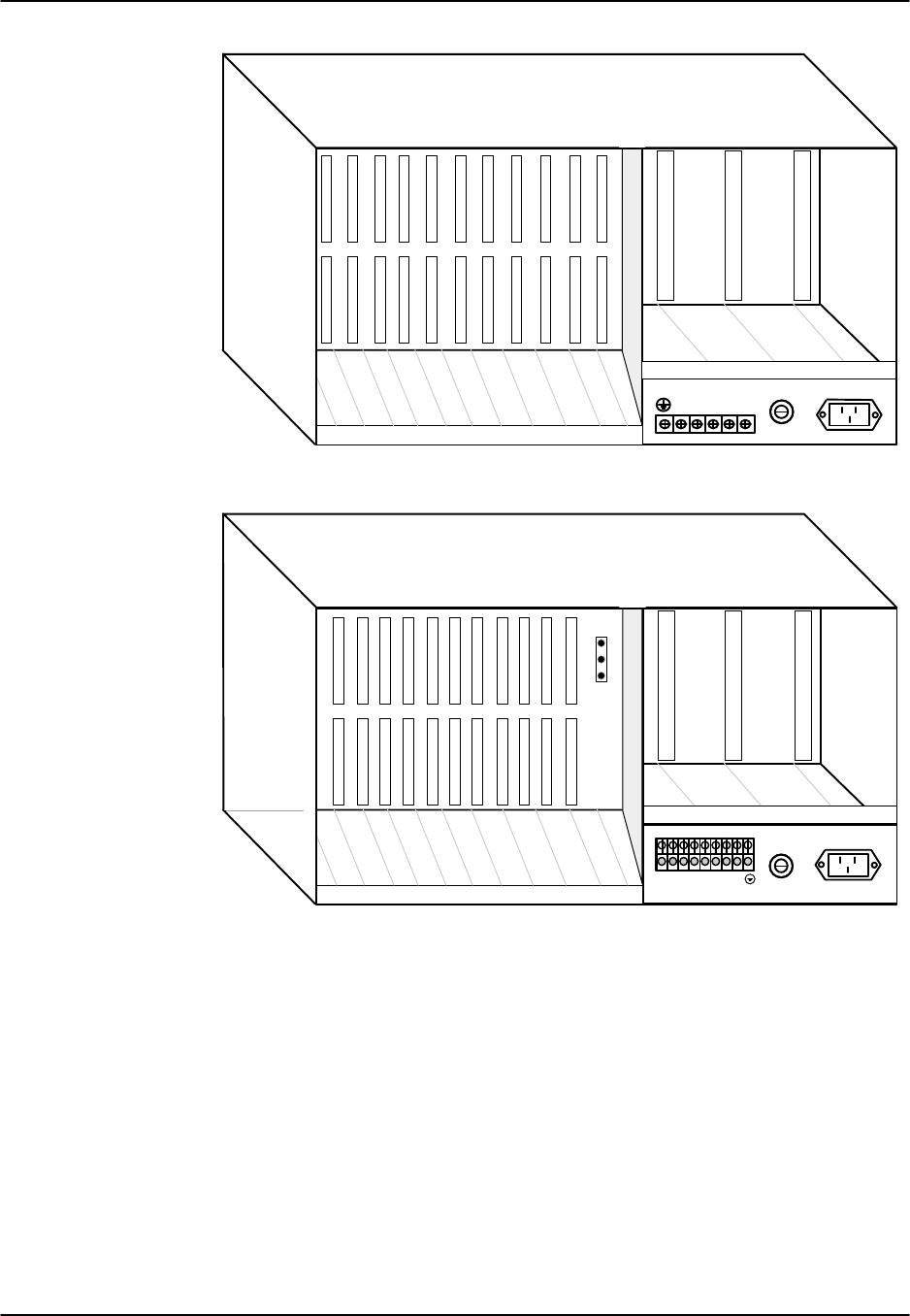
Pinouts Reference Guide v3.6
Page 9-A-2(10-97)
C1C2P1P2P3P4W1W2W3W4IF
S1S2R1
AC
R
G
R
C
O
M
+V-V
Figure Pinouts-3. 8916 Front-Loading Chassis.
C1C2P1P2P3P4W1W2W3W4IF
F1F2R1
AC
R
G
R
+ + +- - - C
O
M
VNVB
VA
1
2
3
EUR/US
JP1
Figure Pinouts-4. 891620 Front-Loading Chassis.
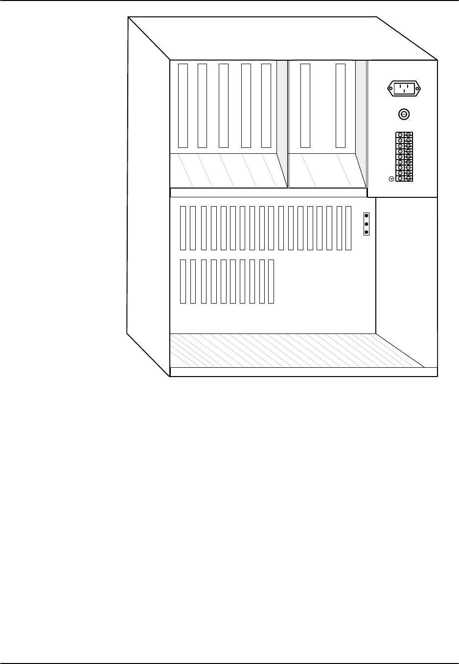
Reference Guide v3.6 Pinouts
(10-97) Page 9-A-3
AC
RGR
VN
VB
+
+
+
-
-
-
COM
VA
R1R2R3R4R5S1S2
C1C2P1P2P3W1W2W3W4IFU1U2U3U4U5U6U7U8
1
2
3
EUR/US
JP1
Figure Pinouts-5. 891920 Front-Loading Chassis.

Pinouts Reference Guide v3.6
Page 9-A-4(10-97)
Interface Cards (8920 and 8921)
The 8920 and 8921 Interface Cards must be installed in slot IF on all units. The
interface card connectors are arranged as shown in Figure Pinouts-6. The 8920 has a
DB9 (DTE Male) serial port. The 8921 is similar to the 8920 in all aspects except there
is not modem jack.
RS232 Control Terminal
Interface Port
RS232 (Male) Management Port
RS485 Node Port
RJ11 Modem Port
WAN Link Connector
Figure Pinouts-6. Interface Card Connectors (8920 and 8921)
This section describes the interface card connectors from the bottom to the top of the
card.
WAN Link Connector
The WAN link connector allows you to connect the WAN card ports to incoming and
outgoing T1/E1 lines. It has the following characteristics:
Connector: 50-pin RJ27X
Gender: Female
Figure Pinouts-7 shows the pinouts for this connector, while Table Pinouts-1 lists the
pin assignments. Electrical signals comply with T1/E1 specifications.

Reference Guide v3.6 Pinouts
(10-97) Page 9-A-5
Pin 50
Pin 26
Pin 25
Pin 1
Figure Pinouts-7. WAN Link Connector
Table Pinouts-1. WAN Link Pin Assignments
WAN Link Designation Pin # Function
WAN 1-1 TI 47 Rx from Network
WAN 1-1 RI 22 Rx from Network
WAN 1-1 T48 Tx to Network
WAN 1-1 R23 Tx to Network
WAN 1-2 TI 44 Rx from Network
WAN 1-2 RI 19 Rx from Network
WAN 1-2 T45 Tx to Network
WAN 1-2 R20 Tx to Network
WAN 2-1 TI 41 Rx from Network
WAN 2-1 RI 16 Rx from Network
WAN 2-1 T42 Tx to Network
WAN 2-1 R17 Tx to Network
WAN 2-2 TI 38 Rx from Network
WAN 2-2 RI 13 Rx from Network
WAN 2-2 T39 Tx to Network
WAN 2-2 R14 Tx to Network
WAN 3-1 TI 35 Rx from Network
WAN 3-1 RI 10 Rx from Network
WAN 3-1 T36 Tx to Network
WAN 3-1 R11 Tx to Network
WAN 3-2 TI 32 Rx from Network
WAN 3-2 RI 7 Rx from Network
WAN 3-2 T33 Tx to Network
WAN 3-2 R8Tx to Network
WAN 4-1 TI 29 Rx from Network
WAN 4-1 RI 4 Rx from Network
WAN 4-1 T30 Tx to Network
WAN 4-1 R5Tx to Network
WAN 4-2 TI 26 Rx from Network
WAN 4-2 RI 1 Rx from Network
WAN 4-2 T27 Tx to Network
WAN 4-2 R2Tx to Network
All other pins are unconnected.
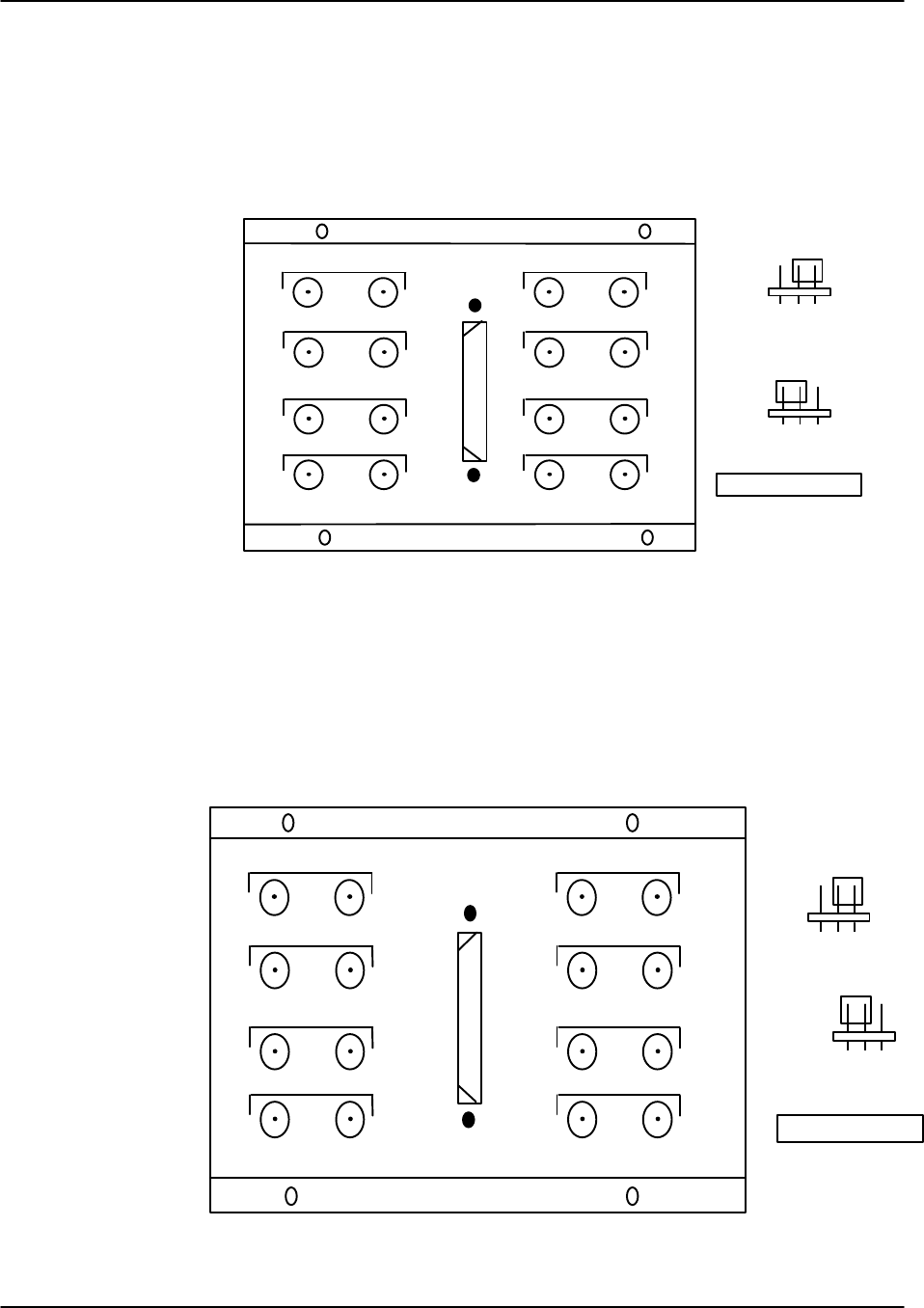
Pinouts Reference Guide v3.6
Page 9-A-6(10-97)
1183 Adapter (600 Chassis)
The 1183 Adapter may be used to provide convenient coaxial cable connections for 8
E1 lines. The 1183 Adapter interfaces with the WAN Link Connector. It is shown in
Figure Pinouts-8. Jumpers should be set for balanced or unbalanced operation prior to
installation. For a discussion of balanced/unbalanced jumper settings please see the
WAN section of this manual.
10193
BAL UNBAL
RX
Options on the Rear
UNBAL BAL
RX
Rx TX
Rx TX
Rx TX
Rx TX
Rx
TX
Rx
TX
Rx
TX
Rx
TX
Figure Pinouts-8. 1183 E1 Interface Adapter
1184 Adapter (800 Chassis)
The 1184 Adapter may be used to provide convenient coaxial cable connections for 8
E1 lines. The 1184 Adapter interfaces with the WAN Link Connector. It is shown in
Figure Pinouts-9. Jumpers should be set for balanced or unbalanced operation prior to
installation. For a discussion of balanced/unbalanced jumper settings please see the
WAN section of this manual.
BAL UNBAL
RX
Options on the Rear
UNBAL BAL
RX
Rx TX
Rx TX
Rx TX
Rx TX
Rx
TX
Rx
TX
Rx
TX
Rx
TX
Figure Pinouts-9. 1184 E1 Interface Adapter
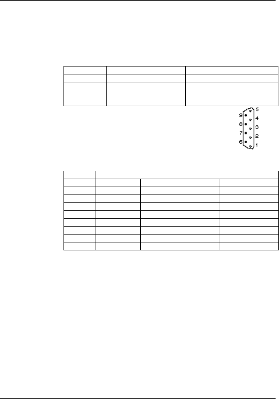
Reference Guide v3.6 Pinouts
(10-97) Page 9-A-7
RS232 Management Port
The RS232 computer port is used for direct reporting of alarms to an outside device and
connecting to the network management system has the characteristics shown in Table
Pinouts-2
Table Pinouts-2. RS232 Management Port Characteristics
Connector: 9-pin D-connector 9-pin D-connector
Gender: male Male
Standard: EIA 574 EIA 574
Electrical: RS232 DTE RS232 DTE
Card 8920 8921
The pinouts for the computer port connector are shown at right,
while Table Pinouts-3 lists the pin assignments. In the table,
“Input” means that data is flowing from the computer to the
system.
Table Pinouts-3. Management Port Pin Assignments (DB-9)
Pin # Pin Name Pin Function DTE Direction
1RLSD Receive Line Signal Detect IN
2RxD Receive Data IN
3TxD Transmit Data OUT
4DTR Data Terminal Ready OUT
5S Gnd Signal Ground N/A
6DSR Data Set Ready IN
7RTS Request to Send OUT
8CTS Clear to Send IN
9 RI Ring Indicator IN
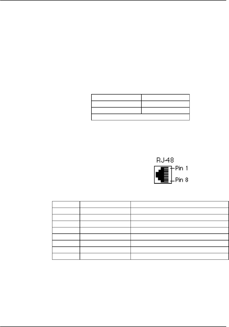
Pinouts Reference Guide v3.6
Page 9-A-8(10-97)
RJ11C Modem Port
The modem port is used to connect the Interface card's internal dial modem to a
standard telephone line. This port may be used either to log into the unit from a remote
VT100 terminal or to send system alarms to a remote device. The modem port presents
an RJ11C female connector. Table Pinouts-5 lists the pin assignments. The modem
port has the following characteristics:
Connector: RJ11C receptacle
Gender: Female
Standard: RJ11C
Electrical: 600 ohm, 2-wire
Table Pinouts-5. Modem Port Pin Assignments
Pin # Function
3Tip
4Ring
Pins 1, 2, 5, and 6 are unconnected.
RS485 Node Port
The RS485 node port has the following characteristics:
Connector: RJ48 receptacle
Gender: Female
Electrical: RS485
Table Pinouts-6 lists the pin assignments.
Table Pinouts-6. Node Port Pin Assignments
Pin # Designation Function
1+n Internodal Communications
2-n Internodal Communications
3ANO Alarm on Open Condition
4ANC Alarm on Closed Condition
5ACOM Alarm Common Lead (Source)
6+F Frame Synchronization
7-f Frame Synchronization
8GND Chassis Ground
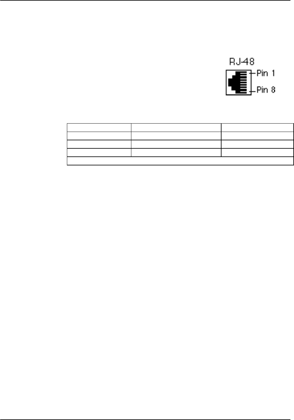
Reference Guide v3.6 Pinouts
(10-97) Page 9-A-9
RS232 Control Terminal Interface Port
The RS232 control terminal interface port allows you to connect the system to a VT100
compatible terminal, with which you can send commands to the system. The control
terminal interface port characteristics are shown below:
Connector: RJ48 receptacle
Gender: Female
Standard: EIA 561
Electrical: RS232 DCE
Table Pinouts-7 lists the pin assignments.
Table Pinouts-7. Control Terminal Interface Port Pin Assignment
Pin # Function Direction
4Signal Ground N/A
5Receive Data Output
6Transmit Data Input
All other pins are unconnected.
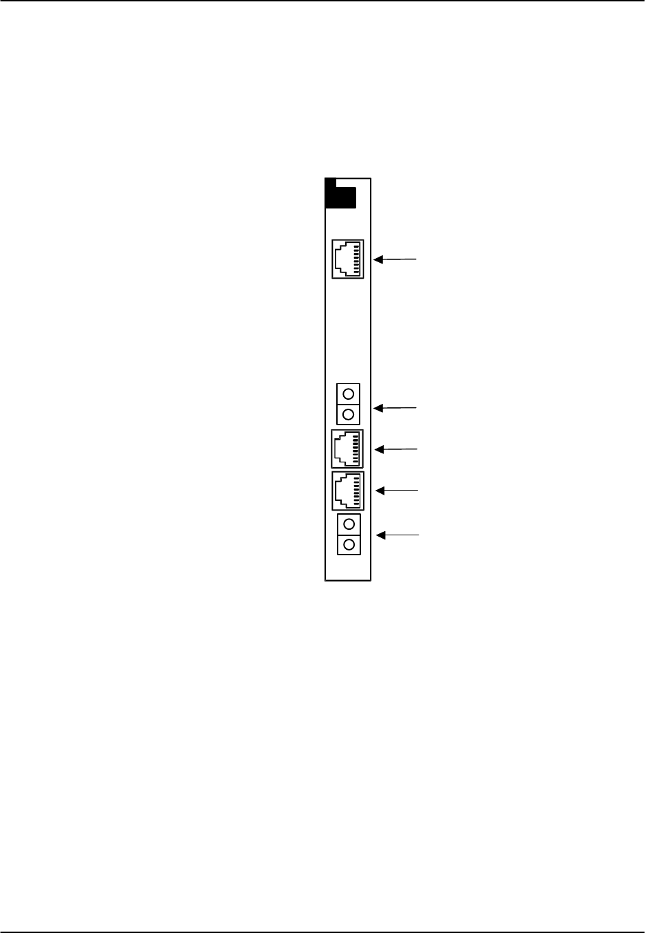
Pinouts Reference Guide v3.6
Page 9-A-10 (10-97)
Interface Card (8925)
The 8925 Interface Card uses RJ48 jacks to terminate two T1 and four Bantam jacks to
monitor WAN links and an RS232 control terminal interface port. The computer port,
modem port and node port are not available on this interface card. Like the 8920, this
card must be installed in slot IF on all units. The interface card connectors are arranged
as shown in Figure Pinouts-10. The pinouts for the RJ48 connectors for T1 links are
shown in Table Pinouts-8.
RS232 Control Terminal
T1 WAN Connector (WAN 1-2)
Interface Port
WAN 1-2 Bantam Jack
WAN 1-1 Bantam Jack
T1 WAN Connector (WAN 1-1)
TX
RX
TX
RX
Figure Pinouts-10. 8925 Interface Card Ports
RS232 Control Terminal Interface Port
The RS232 control terminal interface port allows you to connect the system to a VT100
compatible terminal, which you can use to send commands to the system. The port uses
a standard RJ48 jack as described for the 8920.

Reference Guide v3.6 Pinouts
(10-97) Page 9-A-11
WAN Link Connectors
The WAN connectors allows you to connect the system to two WAN links The
terminals are standard RJ48 or Bantam jacks. Table Pinouts-8 lists the pin assignments
for each RJ48 and Bantam jack with which it is associated.
Table Pinouts-8. WAN Link and Monitoring Pin Assignments
WAN Link Designation Function RJ-48 Pin Bantam Pin
WAN 1-1 TI Rx from Network 2RX 1
WAN 1-1 RI Rx from Network 1RX 2
WAN 1-1 TTx to Network 5TX 1
WAN 1-1 RTx to Network 4TX 2
WAN 1-2 TI Rx from Network 2RX 1
WAN 1-2 RI Rx from Network 1RX 2
WAN 1-2 TTx to Network 5TX 1
WAN 1-2 RTx to Network 4TX 2
All other pins are unconnected.
Pinouts Reference Guide v3.6
Page 9-A-12 (10-97)
Interface Card (8926)
The 8926 Interface card is similar to the 8925 Interface card with the addition of the
computer port, node port and modem port. Like the 8920, this card must be installed in
slot IF on all units. The interface card connectors are arranged as shown in Figure
Pinouts-11. The pinouts for the RJ48 connectors for T1 links are the same as those
shown for the 8925 Interface card (see Table Pinouts-9). The pinouts for the DB9,
RJ48 and RJ11 connectors are the same as those shown for the 8920 Interface card.
RS232 Control Terminal
T1 WAN Connector (WAN 1-2)
Interface Port
WAN 1-2 Bantam Jack
WAN 1-1 Bantam Jack
T1 WAN Connector (WAN 1-1)
TX
RX
TX
RX
RS232 (Male) Management Port
RS485 Nodal Port
RJ11 Modem Port
Figure Pinouts-11. 8926 Interface Card Port
Reference Guide v3.6 Pinouts
(10-97) Page 9-A-13
Interface Card (8927)
The 8927 Interface Card uses BNC connectors to terminate two E1 WAN links, a DB9
management port, an RJ48 control terminal interface port and an RJ48 node port. Like
the 8920 and 8925, it must be installed in slot IF on all units. The interface card
connectors are arranged as shown in Figure Pinouts-12. The pinouts for the DB9 and
RJ48 connectors are the same as those shown for the 8920 Interface card.
RS232 Control Terminal
E1 WAN Connector (WAN 1-2)
Interface Port
E1 WAN Connector (WAN 1-1)
TX
RX
TX
RX
RS485 Nodal Port
RS232 (Male) Management Port
Figure Pinouts-12. 8927 Interface Card Port

Pinouts Reference Guide v3.6
Page 9-A-14 (10-97)
External Alarm Card (8401 and 8402)
External Alarm cards can be installed in any user card slot, U1-U-8 on the 8918 two-
sided chassis or 8919 front-loading chassis, and P1-P4 or W1-W4 on the 8916 front-
loading chassis. These cards enable the integrated access system to respond to four
external alarms (three alarms for the 8402) for control of environmental and security
conditions, and four internal alarms (three alarms for the 8402) to outside alarm
indicators (for example, a critical alarm lights a red light).
Each inbound alarm sensor has the capability of responding to one external condition.
The alarms appear on the screen in the alarm section, showing the alarm as a SENSOR
alarm and includes the slot number and sensor number of the condition (i.e., SENSOR
U7-4).
The inbound alarm sensors may be optioned to accept either 12 or 48v. Both JP1 and
JP2 jumpers should be set to the proper inbound voltage. The inbound sensors are
isolated from ground.
Each outbound "floating" relay (normally open contacts and normally closed contacts)
responds to system alarm categories (major [major and critical] and minor [minor and
informational]) and activates an external device. There are two relays for each of the
four Alarm Card ports. The relays are dual-pole, double-throw.
The External Alarm Card has an RJ27X (female) 50-pin Amphenol connector located
on the faceplate of the card. Figure Pinouts-13 shows the pinouts for the connector and
Table Pinouts-9 shows the pin assignments for both inbound sensor alarms and
outbound internal alarm indicators.
Pin 50
Pin 26
Pin 25
Pin 1
Figure Pinouts-13. External Alarm Card Connector Pinouts
Table Pinouts-9. External Alarm Card Pin Assignments
Inward Alarms Outward Alarms
Sensor Designation Pin Relay Source Norm Close Norm Open
1R1 1R1(A) 7 6 8
T1 26 R1(B) 32 31 33
2R2 2R2(A) 11 10 12
T2 27 R2(B) 36 35 37
3R3 3R3(A) 15 14 16
T3 28 R3(B) 40 39 41
4R4 4R4(A) 19 18 20
T4 29 R4(B) 44 43 45
Reference Guide v3.6 Pinouts
(10-97) Page 9-A-15
External Alarm Card (8403)
The 8403 External Alarm Card has two Amphenol connectors, J3 (lower) and J4
(upper), located on the card front to interface the sensors and switches (see Figure
Pinouts-14). The pin positions are displayed in Figure Pinouts-15. Pin assignments for
sensors are documented in Table Pinouts-10, while the pin assignments for switches are
displayed in Table Pinouts-11.
J4
J3
R
J
1
1
Figure Pinouts-14. External Alarm Card (8403) Connectors.
Pin 50
Pin 26
Pin 25
Pin 1
Figure Pinouts-15. External Alarm Card (8403) J3/J4 Pinouts

Pinouts Reference Guide v3.6
Page 9-A-16 (10-97)
Table Pinouts-10. External Alarm Card (8403) Sensor Pin Assignments
Sensor Desig.
J3
Connector
Pin # Sensor Desig.
J4
Connector
Pin #
1sense - 12 15 sense - 12
sense + 37 sense + 37
2sense - 13 16 sense - 13
sense + 38 sense + 38
3sense - 14 17 sense - 14
sense + 39 sense + 39
4sense - 15 18 sense - 15
sense + 40 sense + 40
5sense - 16 19 sense - 16
sense + 41 sense + 41
6sense - 17 20 sense - 17
sense + 42 sense + 42
7sense - 18 21 sense - 18
sense + 43 sense + 43
8sense - 19 22 sense - 19
sense + 44 sense + 44
9sense - 20 23 sense - 20
sense + 45 sense + 45
10 sense - 21 24 sense - 21
sense + 46 sense + 46
11 sense - 22 25 sense - 22
sense + 47 sense + 47
12 sense - 23 26 sense - 23
sense + 48 sense + 48
13 sense - 24 27 sense - 24
sense + 49 sense + 49
14 sense - 25 28 sense - 25
sense + 50 sense + 50
Reference Guide v3.6 Pinouts
(10-97) Page 9-A-17
Table Pinouts-11. External Alarm Card (8403) Switch Pin Assignments
Switch #
Contact
Type
Form Desig.
J3
Connector
Pin # Switch #
Contact
Type
Form Desig.
J4
Connector
Pin #
1COpen 28COpen 27
Close 1Close 26
Comm 3Comm 28
2COpen 27 9COpen 2
Close 26 Close 1
Comm 28 Comm 3
3AOpen --- 10 BOpen 4
Close 4Close ---
Comm 29 Comm 29
4COpen 611 COpen 6
Close 5Close 5
Comm 7Comm 7
5COpen 31 12 COpen 31
Close 30 Close 30
Comm 32 Comm 32
6COpen 913 COpen 9
Close 8Close 8
Comm 10 Comm 10
7COpen 34 14 COpen 34
Close 33 Close 33
Comm 35 Comm 35
The jumper pairs that correspond to each sensor are numbered accordingly. For
example, the jumper pairs for sensor #12 are those in row SI12 of the lower jumper
group (columns JP1 and JP2). The jumper pairs that correspond to sensor #25 are those
in row SI25 of the upper jumper group (columns JP3 and JP4).
The outside pin of each jumper pair carries voltage, while the inside pins are passive, as
shown in Figure Pinouts-15. The outside (left) pins for the jumper pairs in columns JP1
and JP3 carry positive (+) voltage, while the outside (right) pins for the jumper pairs in
columns JP2 and JP4 carry negative (-) voltage.
1516 17 1819 2223 25 26 272820SI 21 24
JP3
JP4
PASV
ACTV
Positive (+)
VoltageNegative (-)
Voltage
Figure Pinouts-16. Jumper Pair Assignments.

Pinouts Reference Guide v3.6
Page 9-A-18 (10-97)
Between the Amphenol connectors is a standard RJ11 connector to interface the voice
port. The pin positions for this connector are shown in Figure Pinouts-17, while its pin
assignments are shown in Table Pinouts-12. The RJ11 port, which may be used to send
system alarms to a remote device, has the following characteristics:
Connector: RJ11 receptacle
Gender: Female
Standard: RJ11
Electrical: 600Ω 2-wire
Pin 1
Pin 8
Pin 1
Pin 6
Figure Pinouts-17. RJ11 Port
Table Pinouts-12. RJ11 Port Pin Assignments
Pin # Function
3Ring
4Tip
All other pins are unconnected.

Reference Guide v3.6 Pinouts
(10-97) Page 9-A-19
E&M Card (8108)
The 2-wire, eight-port 8108 E&M Card can be installed in any user card slot, U1-U-8
on the 8918 two-sided chassis or 8919 front-loading chassis, and P1-P4 or W1-W4 on
the 8916 front-loading chassis. This card allows you to connect the integrated access
system to 2-wire analog voice equipment with E&M signaling.
The 8108 E&M Card has an RJ27X (female) 50-pin Amphenol connector located on the
faceplate of the card. Figure Pinouts-18 shows the pinouts for this connector, while
Table Pinouts-13 lists the pin assignments.
Pin 50
Pin 26
Pin 25
Pin 1
Figure Pinouts-18. 8108 E&M Card Connector

Pinouts Reference Guide v3.6
Page 9-A-20 (10-97)
Table Pinouts-13. 8108 E&M Card Connector Pin Assignments
Port # Designation Pin #
1T26
1R1
1E28
1M3
2T29
2R4
2E31
2M6
3T32
3R7
3E34
3M9
4T35
4R10
4E37
4M12
5T38
5R13
5E40
5M15
6T41
6R16
6E43
6M18
7T44
7R19
7E46
7M21
8T47
8R22
8E49
8M24
All channels SG 25
All channels SB 50
All other pins are unconnected.

Reference Guide v3.6 Pinouts
(10-97) Page 9-A-21
E&M Card (8115)
The 4-wire, four-port 8115 E&M Card can be installed in any user card slot, U1-U-8 on
the 8918 two-sided chassis or 8919 front-loading chassis, and P1-P4 or W1-W4 on the
8916 front-loading chassis. This card allows you to connect the integrated access
system to 4-wire analog voice equipment with E&M signaling.
The 8115 E&M Card has an RJ27X (female) 50-pin Amphenol connector located on the
faceplate of the card. Figure Pinouts-19 shows the pinouts for this connector, while
Table Pinouts-14 lists the pin assignments.
Pin 50
Pin 26
Pin 25
Pin 1
Figure Pinouts-19. 8115 E&M Card Connector
Table Pinouts-14. 8115 E&M Card Connector Pin Assignments
Port # Designation Pin #
1T26
1R1
1T1 27
1R1 2
1E28
1M3
2T29
2R4
2T1 30
2R1 5
2E31
2M6
3T32
3R7
3T1 33
3R1 8
3E34
3M9
4T35
4R10
4T1 36
4R1 11
4E37
4M12
All channels SG 25
All channels SB 50
All other pins are unconnected.

Pinouts Reference Guide v3.6
Page 9-A-22 (10-97)
E&M Card (8118)
The 4-wire, eight-port 8118 E&M card can be installed in any user card slot, U1-U-8 on
the 8918 two-sided chassis or 8918 front-loading chassis, and P1-P4 or W1-W4 on the
8916 front-loading chassis. This card allows you to connect the system to four-wire
analog voice equipment with E&M signaling.
The 8118 E&M card has an RJ27X (female) 50-pin Amphenol connector located on the
faceplate of the card. Figure Pinouts-20 shows the pinouts for this connector, while
Table Pinouts-15 lists the pin assignments.
Pin 50
Pin 26
Pin 25
Pin 1
Figure Pinouts-20. 8118 Card Connector
Table Pinouts-15. 8118 Pin Assignments
Port # Designation Pin #
1T26
1R1
1T1 27
1R1 2
1E28
1M3
2T29
2R4
2T1 30
2R1 5
2E31
2M6
3T32
3R7
3T1 33
3R1 8
3E34
3M9
4T35
4R10
4T1 36
4R1 11
4E37
4M12

Reference Guide v3.6 Pinouts
(10-97) Page 9-A-23
Table Pinouts-15. 8118 Pin Assignments (cont.)
5T38
5R13
5T1 39
5R1 14
5E40
5M15
6T41
6R16
6T1 42
6R1 17
6E43
6M18
7T44
7R19
7T1 45
7R1 20
7E46
7M21
8T47
8R22
8T1 48
8R1 23
8E49
8M24
All channels SG 25
All channels SB 50

Pinouts Reference Guide v3.6
Page 9-A-24 (10-97)
E&M Card (8119)
The 4-wire, eight-port 8119 E&M card can be installed in any user card slot, U1-U-8 on
the 8918 two-sided chassis or 8919 front-loading chassis, and P1-P4 or W1-W4 on the
8916 front-loading chassis. This card allows you to connect the system to four-wire
analog voice equipment with E&M signaling.
The 8119 E&M card has an RJ27X (female) 50-pin Amphenol connector located on the
faceplate of the card. Figure Pinouts-21 shows the pinouts for this connector, while
Table Pinouts-16 lists the pin assignments.
Pin 50
Pin 26
Pin 25
Pin 1
Figure Pinouts-21. 8119 E&M Card Connector
Table Pinouts-16. 8119 Pin Assignments
Port # Designation Pin #
1T26
1R1
1T1 27
1R1 2
1E28
1M3
2T29
2R4
2T1 30
2R1 5
2E31
2M6
3T32
3R7
3T1 33
3R1 8
3E34
3M9
4T35
4R10
4T1 36
4R1 11
4E37
4M12

Reference Guide v3.6 Pinouts
(10-97) Page 9-A-25
Table Pinouts-16. 8119 Pin Assignments (cont.)
5T38
5R13
5T1 39
5R1 14
5E40
5M15
6T41
6R16
6T1 42
6R1 17
6E43
6M18
7T44
7R19
7T1 45
7R1 20
7E46
7M21
8T47
8R22
8T1 48
8R1 23
8E49
8M24
All channels SG 25
All channels SB 50
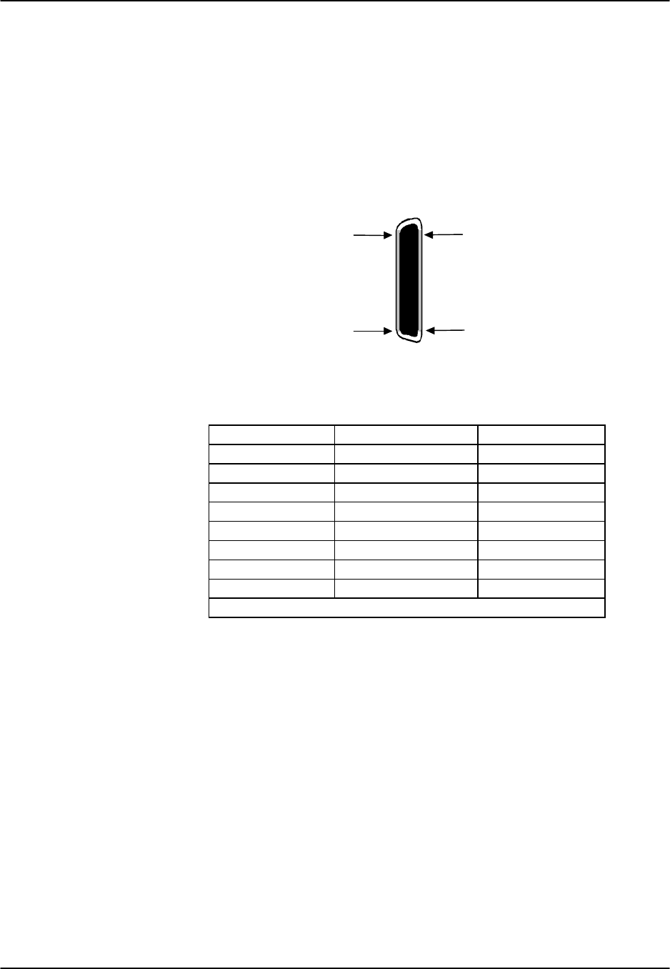
Pinouts Reference Guide v3.6
Page 9-A-26 (10-97)
FXS Card (8124 and 8125)
The 2-wire, four-port 8124 and 8125 FXS cards can be installed in any user card slot,
U1-U-8 on the 8918 two-sided chassis or 8919 front-loading chassis, and P1-P4 or W1-
W4 on the 8916 front-loading chassis. These cards allow you to connect the integrated
access system to 2-wire analog voice equipment.
The 8124 and 8125 FXS cards have an RJ27X (female) 50-pin Amphenol connector
located on the faceplate of the card. Figure Pinouts-22 shows the pinouts for this
connector, while Table Pinouts-17 lists the pin assignments.
Pin 50
Pin 26
Pin 25
Pin 1
Figure Pinouts-22. 8124 and 8125 FXS Card Connector
Table Pinouts-17. 8124 and 8125 FXS Card Pin Assignments
Port # Designation Pin #
1T1 26
1R1 1
2T2 29
2R2 4
3T3 32
3R3 7
4T4 35
4R4 10
All other pins are unconnected.

Reference Guide v3.6 Pinouts
(10-97) Page 9-A-27
FXS Card (8128 and 8129)
The 2-wire, eight-port 8128 and 8129 FXS cards can be installed in any user card slot,
U1-U-8 on the 8918 two-sided chassis or 8919 front-loading chassis, and P1-P4 or W1-
W4 on the 8916 front-loading chassis. These cards allow you to connect the integrated
access system to 2-wire analog voice equipment.
The 8128 and 8129 FXS cards have an RJ27X (female) 50-pin Amphenol connector
located on the faceplate of the card. Figure Pinouts-23 shows the pinouts for this
connector, while Table Pinouts-18 lists the pin assignments.
Pin 50
Pin 26
Pin 25
Pin 1
Figure Pinouts-23. 8128 and 8129 FXS Card Connector
Table Pinouts-18. 8128 and 8129 FXS Card Pin Assignments
Port # Designation Pin #
1T1 26
1R1 1
2T2 29
2R2 4
3T3 32
3R3 7
4T4 35
4R4 10
5T5 38
5R5 13
6T6 41
6R6 16
7T7 44
7R7 19
8T8 47
8R8 22
All other pins are unconnected.

Pinouts Reference Guide v3.6
Page 9-A-28 (10-97)
FXO Card (8134 and 8135)
The 2-wire, four-port 8134 and 8135 FXO cards can be installed in any user card slot,
U1-U-8 on the 8918 two-sided chassis or 8919 front-loading chassis, and P1-P4 or W1-
W4 on the 8916 front-loading chassis. These cards allow you to connect the integrated
access system to 2-wire analog voice equipment.
The 8134 and 8135 FXO cards have an RJ27X (female) 50-pin Amphenol connector
located on the faceplate of the card. Figure Pinouts-24 shows the pinouts for this
connector, while Table Pinouts-19 lists the pin assignments.
Pin 50
Pin 26
Pin 25
Pin 1
Figure Pinouts-24. 8134 and 8135 FXO Card Connectors
Table Pinouts-19. 8134 and 8135 FXO Card Pin Assignments
Port # Designation Pin #
1T1 26
1R1 1
2T2 29
2R2 4
3T3 32
3R3 7
4T4 35
4R4 10
All other pins are unconnected.

Reference Guide v3.6 Pinouts
(10-97) Page 9-A-29
FXO Card (8138 and 8139)
The 2-wire, eight-port 8138 and 8139 FXO cards can be installed in any user card slot,
U1-U-8 on the 8918 two-sided chassis or 8919 front-loading chassis, and P1-P4 or W1-
W4 on the 8916 front-loading chassis. These cards allow you to connect the integrated
access system to 2-wire analog voice equipment.
The 8138 and 8139 FXO cards have an RJ27X (female) 50-pin Amphenol connector
located on the faceplate of the card. Figure Pinouts-25 shows the pinouts for this
connector, while Table Pinouts-20 lists the pin assignments.
Pin 50
Pin 26
Pin 25
Pin 1
Figure Pinouts-25. 8138 and 8139 FXO Card Connector
Table Pinouts-20. 8138 and 8139 FXO Card Pin Assignments
Port # Designation Pin #
1T1 26
1R1 1
2T2 29
2R2 4
3T3 32
3R3 7
4T4 35
4R4 10
5T5 38
5R5 13
6T6 41
6R6 16
7T7 44
7R7 19
8T8 47
8R8 22
All other pins are unconnected.
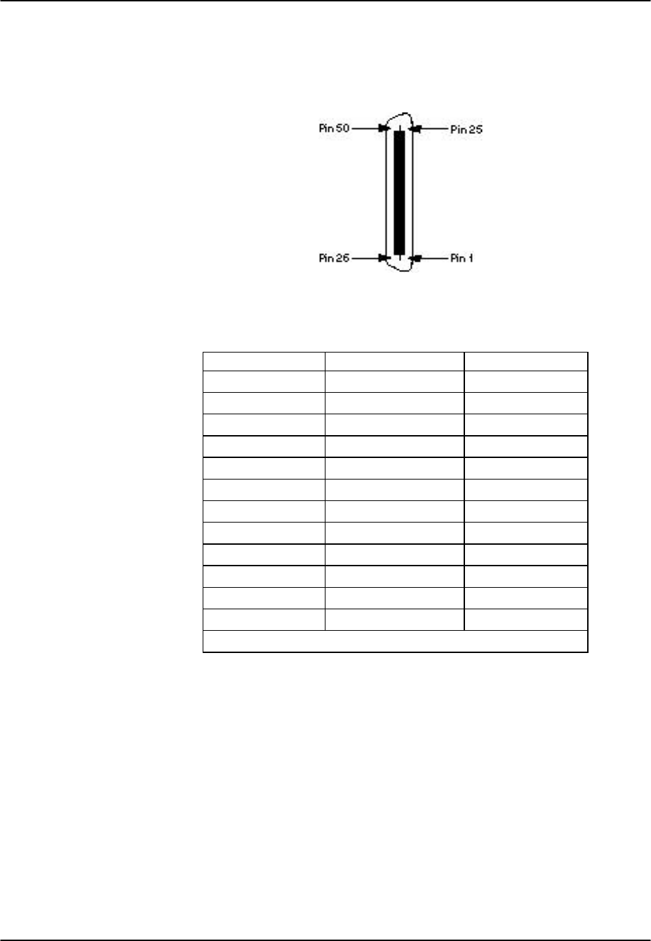
Pinouts Reference Guide v3.6
Page 9-A-30 (10-97)
FXS Coin Card (8149)
The FXS Coin Card has a 50-pin Amphenol jack located on its faceplate. Figure
Pinouts-26 shows this jack, and Table Pinout-21 list the signal pinouts.
Figure Pinouts-26. FXS Coin Card Jack
Table Pinouts-21. FXS Coin Card Jack Pinouts
Port Designation Pin
1T1 26
1R1 1
2T2 29
2R2 4
3T3 32
3R3 7
4T4 35
4R4 10
5R5 13
5T5 38
6R6 16
6T6 41
All other pins are unconnected.
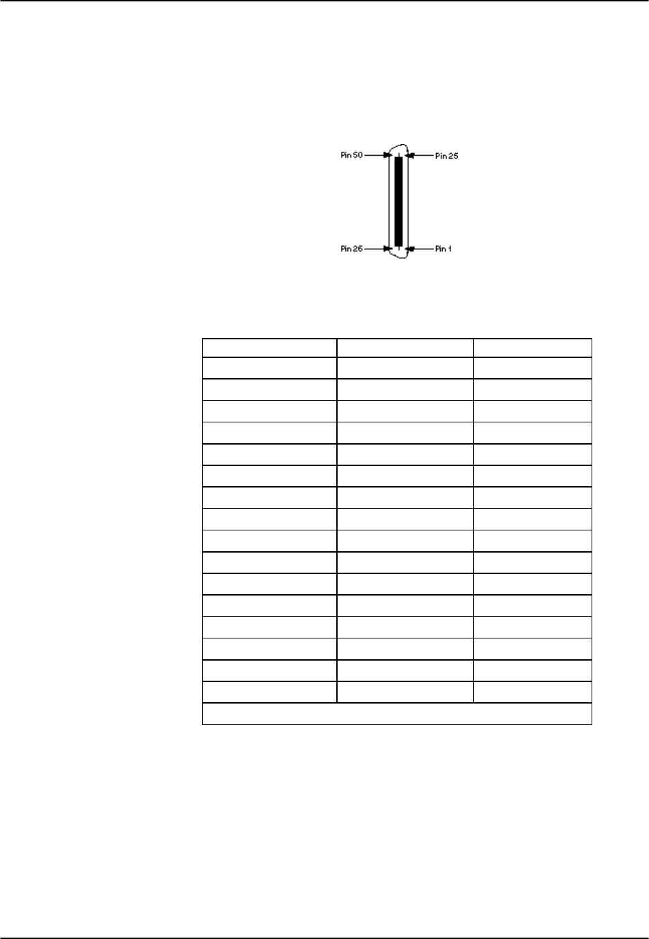
Reference Guide v3.6 Pinouts
(10-97) Page 9-A-31
FXO Coin Card (8159)
The FXO Coin Card has a 50-pin Amphenol jack on its faceplate. Figure Pinouts-27
shows this jack, and Table Pinouts-22 lists the signal pinouts.
Figure Pinouts-27. FXO Coin Card Jack
Table Pinouts-22. FXO Coin Card Jack Pinouts
Port # Designation Pin #
1T1 26
1R1 1
2T2 29
2R2 4
3T3 32
3R3 7
4T4 35
4R4 10
5T5 38
5R5 13
6T6 41
6R6 16
7T7 44
7R7 19
8T8 47
8R8 22
All other pins are unconnected.
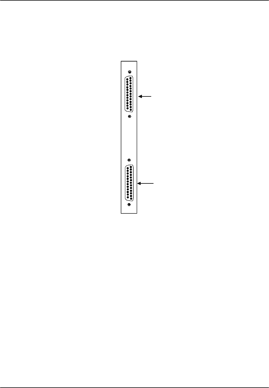
Pinouts Reference Guide v3.6
Page 9-A-32 (10-97)
HSU Card (8202) RS530
The 8202 HSU Card may be installed in any user card slot, U1-U-8 on the 8918 two-
sided chassis or 8919 front-loading chassis, and P1-P4 or W1-W4 on the 8916 front-
loading chassis. Each card has two DB-25 connectors. Figure Pinouts-28 shows the
card.
Port #1 Connector
Port #2 Connector
Figure Pinouts-28. 8202 HSU Card Connectors
RS530 Channel Connectors
The RS530 connectors on the 8202 HSU card allow you to connect the system to
external data devices. The connectors have the following characteristics:
Connector: 25-pin D-connectors
Gender: Female
Standards: 8202—Proprietary pinout
Electrical: 8202—RS530
Figure Pinouts-29 shows the connector Pinouts and Table Pinouts-23 lists the pin
assignments.

Reference Guide v3.6 Pinouts
(10-97) Page 9-A-33
Pin 25
Pin 14
Pin 13
Pin 1
DB-25
Figure Pinouts-29. Channels 1 and 2 Connectors on 8202 HSU Card
Table Pinouts-23. 8202 HSU Card Channel Connectors Pin Assignments
Pin # Function Direction
1Cable Shield --
2Send Data A Input
3Receive Data A Output
4RTS A Input
5CTS A Output
6DCE Ready Output
7Signal Common --
8RR/RLSD A Output
9Receive Timing B Output
10 RR/RLSD B Output
11 Terminal Timing B Input
12 Send Timing B Output
13 CTS B Output
14 Send Data B Input
15 Send Timing A Output
16 Receive Data B Output
17 Receive Timing A Output
18 Local Loopback Input
19 RTS B Input
20 DTE Ready Input
21 Remote Loopback Input
22 Incoming Call Output
23 Receive Common --
24 Terminal Timing A Input
25 Test Mode Output
All other pins are unconnected.
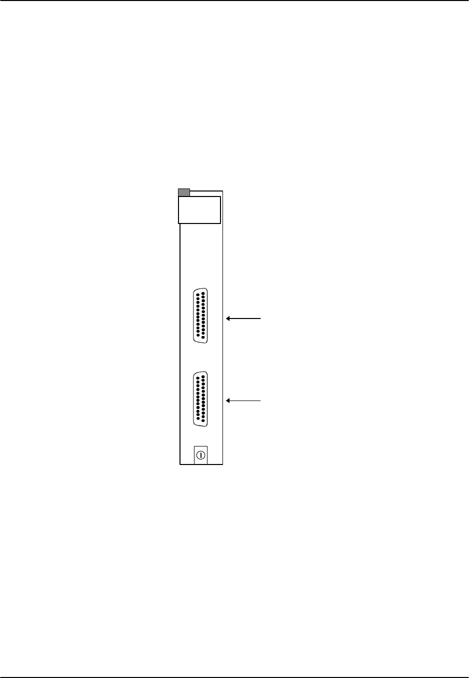
Pinouts Reference Guide v3.6
Page 9-A-34 (10-97)
HSU Card (8203)
The 8203 High-Speed data Unit (HSU) card allows users to connect high-speed data
terminal equipment (DTE) and data communications equipment (DCE) to WAN links
or other HSU cards.
The 8203 HSU Card has two ports supporting ANSI/EIA/TIA-530 or two X.21 data
ports (see Figure Pinouts-30). Each of the two ports can be configured to operate as a
DCE port or a DTE port, with data speeds ranging from 56/64 Kb/s to 1.544/2.048
Mb/s.
The card may be installed in any user card slot, U1-U-8 on the 8918 two-sided chassis
or 8919 front-loading chassis, and P1-P4 or W1-W4 on the 8916 front-loading chassis.
HSU-dte
P
1
P
2
Port #1 Connectors
Port #2 Connectors
Figure Pinouts-30. 8203 HSU Card Connectors
DB-25 Channel Connectors
The DB-25 connectors on the 8203 HSU card allow you to connect the system to
external data devices. The connectors have the following characteristics:
Connector: 25-pin D-connectors
Gender: Female
Standards: 8203—Proprietary pinout
Electrical: 8203—X.21
Figure Pinouts-31 shows the connector Pinouts and Table Pinouts-24 lists the pin
assignments.

Reference Guide v3.6 Pinouts
(10-97) Page 9-A-35
Pin 25
Pin 14
Pin 13
Pin 1
DB-25
Figure Pinouts-31. Connectors on an 8203 HSU Card
Table Pinouts-24. 8203 HSU Card Pin Assignments
Pin # Function Direction
1Cable Shield --
2RD A Output
3TD A Input
4RTS A Output
7Signal Common (Ground) --
8Control RLSD A Output
10 Control RLSD B Output
11 Timing Clock B Input
14 RD B Output
16 TD B Input
19 RTS B Input
24 Timing Clock A Input
All unlisted pins are unconnected.
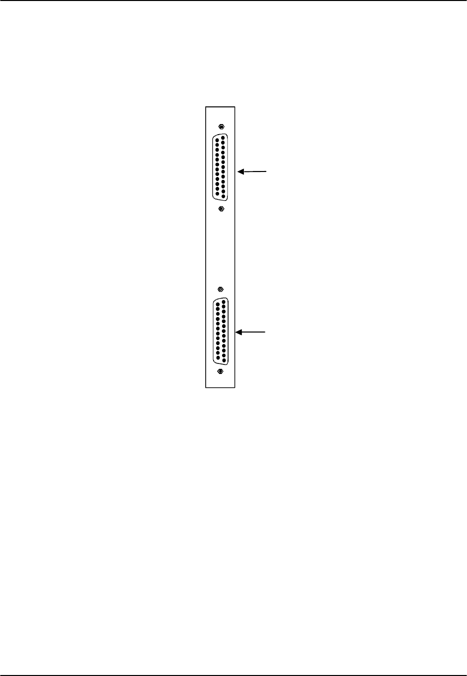
Pinouts Reference Guide v3.6
Page 9-A-36 (10-97)
HSU Card (8212) V.35
The 8212 HSU Card may be installed in any user card slot, U1-U-8 on the 8918 two-
sided chassis or 8919 front-loading chassis, and P1-P4 or W1-W4 on the 8916 front-
loading chassis. Each card has two DB-25 connectors. Figure Pinouts-32 shows the
card.
Port #1 Connector
Port #2 Connector
Figure Pinouts-32. 8212 HSU Card Connectors
V.35 Channel Connectors
The V.35 connectors on the 8212 HSU Card allow you to connect the system to
external data devices. The connectors have the following characteristics:
Connector: 25-pin D-connectors
Gender: Female
Standards: 8212—Proprietary pinout
Electrical: 8212—V.35 DCE
Figure Pinouts-33 shows the connector pinouts and Table Pinouts-25 lists the pin
assignments.

Reference Guide v3.6 Pinouts
(10-97) Page 9-A-37
Pin 25
Pin 14
Pin 13
Pin 1
DB-25
Figure Pinouts-33. Connectors on an 8212 HSU Card
Table Pinouts-25. 8212 HSU Card Pin Assignments
Pin # Function Direction
1Cable Shield ---
4RTS Input
5CTS Output
6DSR Output
7Signal Ground ---
8RLSD Output
9SD B Input
10 SD A Input
11 SCTE B Input
12 SCTE A Input
13 RD B Output
14 RD A Output
17 SCR B Output
18 SCR A Output
24 SCT B Output
25 SCT A Output
All other pins are unconnected.
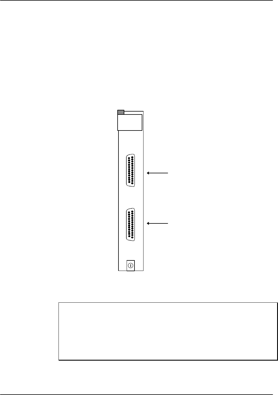
Pinouts Reference Guide v3.6
Page 9-A-38 (10-97)
HSU Card (8214) V.35
The 8214 High-Speed data Unit (HSU) card allows users to connect high-speed data
terminal equipment (DTE) and data communications equipment (DCE) to WAN links
or other HSU cards.
The 8214 HSU Card supports two V.35 data ports. Each of the two ports can be
configured to operate as a DCE port or a DTE port, with data speeds ranging from
56/64 Kb/s to 1.544/2.048 Mb/s.
The card may be installed in any user card slot, U1-U-8 on the 8918 two-sided chassis
or 8919 front-loading chassis, and P1-P4 or W1-W4 on the 8916 front-loading chassis.
Figure Pinouts-34 shows the card.
P
1
P
2
HSU-trunk
Port #1 Connector
Port #2 Connector
Figure Pinouts-34. 8214 HSU Card Connectors
Homologation Notification
The equipment was tested against NET2 for connection to V.35 interfaces to Digital
Data Networks. Testing was carried out using a Premisys 1260M cable for DTE
connections.
If any other cable is used, its capacitance must not exceed 2060 picofarads (pF).

Reference Guide v3.6 Pinouts
(10-97) Page 9-A-39
DB-25/V.35 Channel Connectors
The DB-25/V.35 connectors on the 8214 HSU card allow you to connect the system to
external data devices or trunks. The connectors have the following characteristics:
Connector: 25-pin D-connectors
Gender: Female
Standards: 8214—Proprietary pinout
Electrical: 8214—V.35
Figure Pinouts-35 shows the connector Pinouts and Table Pinouts-26 lists the pin
assignments.
Pin 25
Pin 14
Pin 13
Pin 1
DB-25
Figure Pinouts-35. Connectors on an 8214 HSU Card
Table Pinouts-26 8214 HSU Card Pin Assignments
Pin # Function Direction
1Cable Shield ---
4RTS Input
5CTS Output
6DSR Output
7Signal Ground ---
8RLSD Output
9TD B Input
10 TD A Input
11 TT B Input
12 TT A Input
13 RD B Output
14 RD A Output
15 RC A Input
16 RC B Input
17 RT B Output
18 RT A Output
19 TM Output
20 DTR Output
21 RLB Input
22 LLB Input
24 ST B Output
25 ST A Output
All other pins are unconnected.
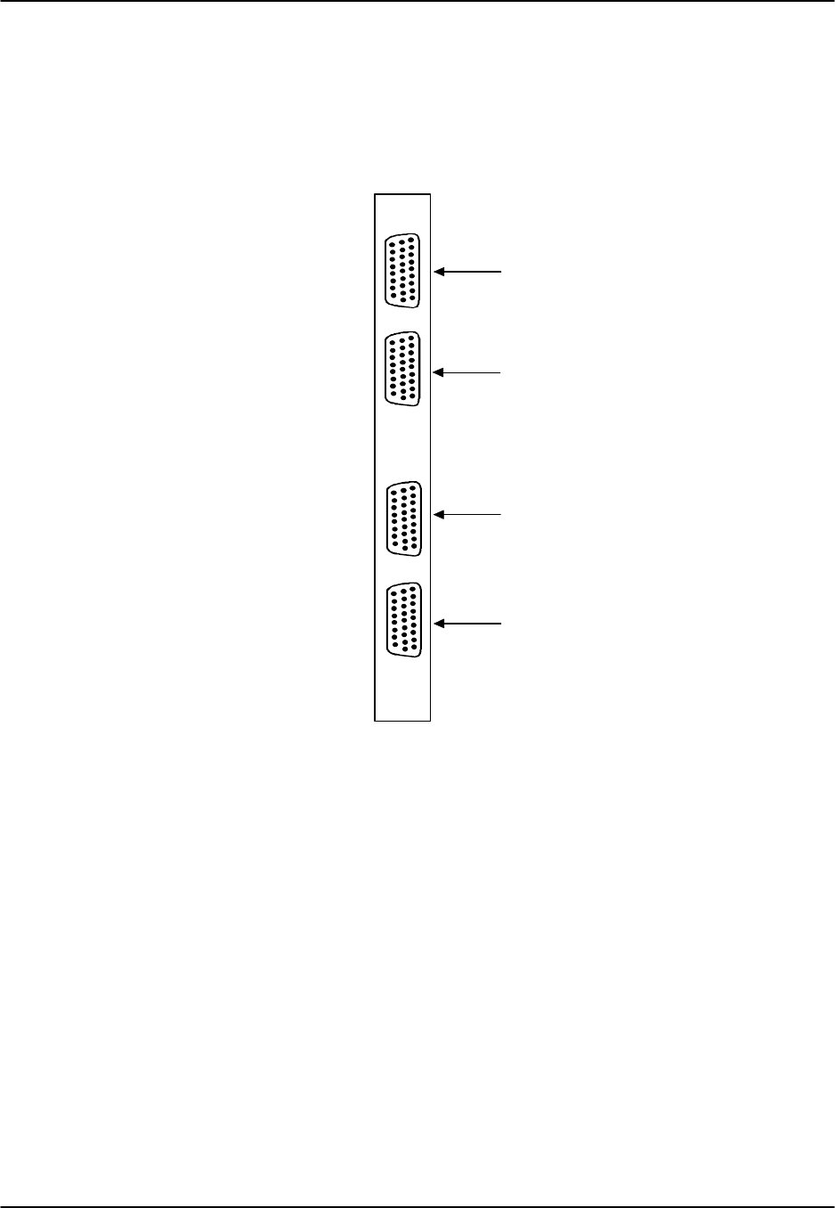
Pinouts Reference Guide v3.6
Page 9-A-40 (10-97)
HSU Card (8215) RS530 / V.35
The 8215 HSU card may be installed in any user card slot, U1-U-8 on the 8918 two-
sided chassis or 8919 front-loading chassis, and P1-P4 or W1-W4 on the 8916 front-
loading chassis. Each card has four DB-26 connectors. Figure Pinouts-36 shows the
card.
Port #1
Port #2
Port #3
Port #4
Figure Pinouts-36. 8215 HSU Card Connectors
RS530/V.35 Channel Connectors
The RS530/V.35 connectors on the 8215 HSU card allow you to connect the system to
external data devices. The connectors have the following characteristics:
Connector: 26-pin D-connectors
Gender: Female
Standards: 8215—Proprietary pinout
Electrical: 8215—RS530 or V.35 (switch selectable)
Figure Pinouts-37 shows the connector Pinouts and Table Pinouts-27 lists the pin
assignments.

Reference Guide v3.6 Pinouts
(10-97) Page 9-A-41
Pin 26
Pin 19
Pin 9
Pin 1
DB-26
Figure Pinouts-37. Connectors on 8215 HSU Card
Table Pinouts-27. 8215 HSU Card Pin Assignments
Pin # Function Direction
1Cable Shield --
2Send Data A Input
3Receive Data A Output
4RTS A Input
5CTS A Output
6DCE Ready Output
7Signal Common --
8RR/RLSD A Output
9Receive Timing B Output
10 RR/RLSD B Output
11 Terminal Timing B Input
12 Send Timing B Output
13 CTS B Output
14 Send Data B Input
15 Send Timing A Output
16 Receive Data B Output
17 Receive Timing A Output
18 Local Loopback Input
19 RTS B Input
20 DTE Ready Input
21 Remote Loopback Input
22 Incoming Call Output
23 Ext Rcv Clock Input
24 Terminal Timing A Input
25 Test Mode Output
26 Ext Rcv Clock Input
All other pins are unconnected.
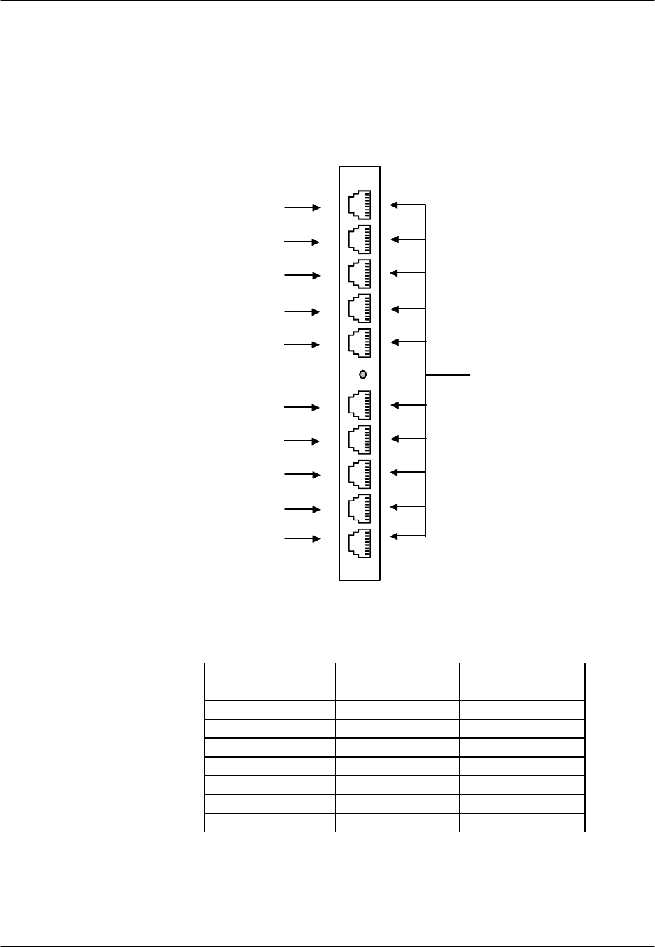
Pinouts Reference Guide v3.6
Page 9-A-42 (10-97)
SRU Card (8220)
The SRU card may be installed in any user card slot, U1-U-8 on the 8918 two-sided
chassis or 8919 front-loading chassis, and P1-P4 or W1-W4 on the 8916 front-loading
chassis. Each card has ten standard RJ48C connectors that correspond with the ten sub-
rate time slots assignable from each card. Figure Pinouts-38 shows the card and Table
Pinouts-28 shows the pinouts for the RJ48C connections on the SRU Card.
RJ-48C
SRU TS
#1
#2
#3
#4
#5
#6
#7
#8
#9
#10
Figure Pinouts-38. SRU Card Connectors
Table Pinouts-28. SRU Connector Pin Assignments
Male RJ-48 Pin # Signal Name Direction
1RCLK output
2RLSD output
3TCLK output
4GND -
5RD output
6TD input
7CTS output
8RTS input
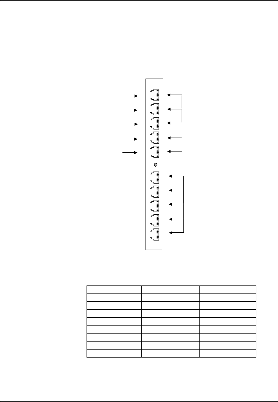
Reference Guide v3.6 Pinouts
(10-97) Page 9-A-43
OCU-DP Card (8247)
The 8247 OCU-DP card may be installed in any user card slot, U1-U-8 on the 8918
two-sided chassis or 8919 front-loading chassis, and P1-P4 or W1-W4 on the 8916
front-loading chassis. The card has ten standard RJ48C connectors, five of which are
assignable from the card. The other five connectors on the 8247 OCU-DP card are
activated with the 845 Child Card. Figure Pinouts-39 shows the card and Table Pinouts-
29 shows the pin assignments for the RJ48C connections on the OCU-DP Card.
RJ-48C
OCU-DP
#1
#2
#3
#4
#5
Activated
Child
with 845
Figure Pinouts-39. 8247 OCU-DP Card Connectors
Table Pinouts-29. 8247 OCU-DP Card Pin Assignments
Male RJ-48 Pin # Signal Name Direction
1R1 input
2T1 input
3-- --
4-- --
5-- --
6-- --
7Toutput
8Routput

Pinouts Reference Guide v3.6
Page 9-A-44 (10-97)
OCU-DP Card (8248)
The 8248 OCU-DP card may be installed in any user card slot, U1-U-8 on the 8918
two-sided chassis or 8919 front-loading chassis, and P1-P4 or W1-W4 on the 8916
front-loading chassis. The card has ten standard RJ48C connectors, five of which are
assignable from the card. The other five connectors on the 8248 OCU-DP card are
activated with the 845 Child Card. Figure Pinouts-40 shows the card and Table Pinouts-
30 shows the pin assignments for the RJ48C connections on the OCU-DP Card.
RJ-48C
OCU-DP
#1
#2
#3
#4
#5
Activated
Child
with 845
Figure Pinouts-40. 8248 OCU-DP Card Connectors
Table Pinouts-30. 8248 OCU-DP Card Pin Assignments
Male RJ-48 Pin # Signal Name Direction
1R1 input
2T1 input
3-- --
4-- --
5-- --
6-- --
7Toutput
8Routput
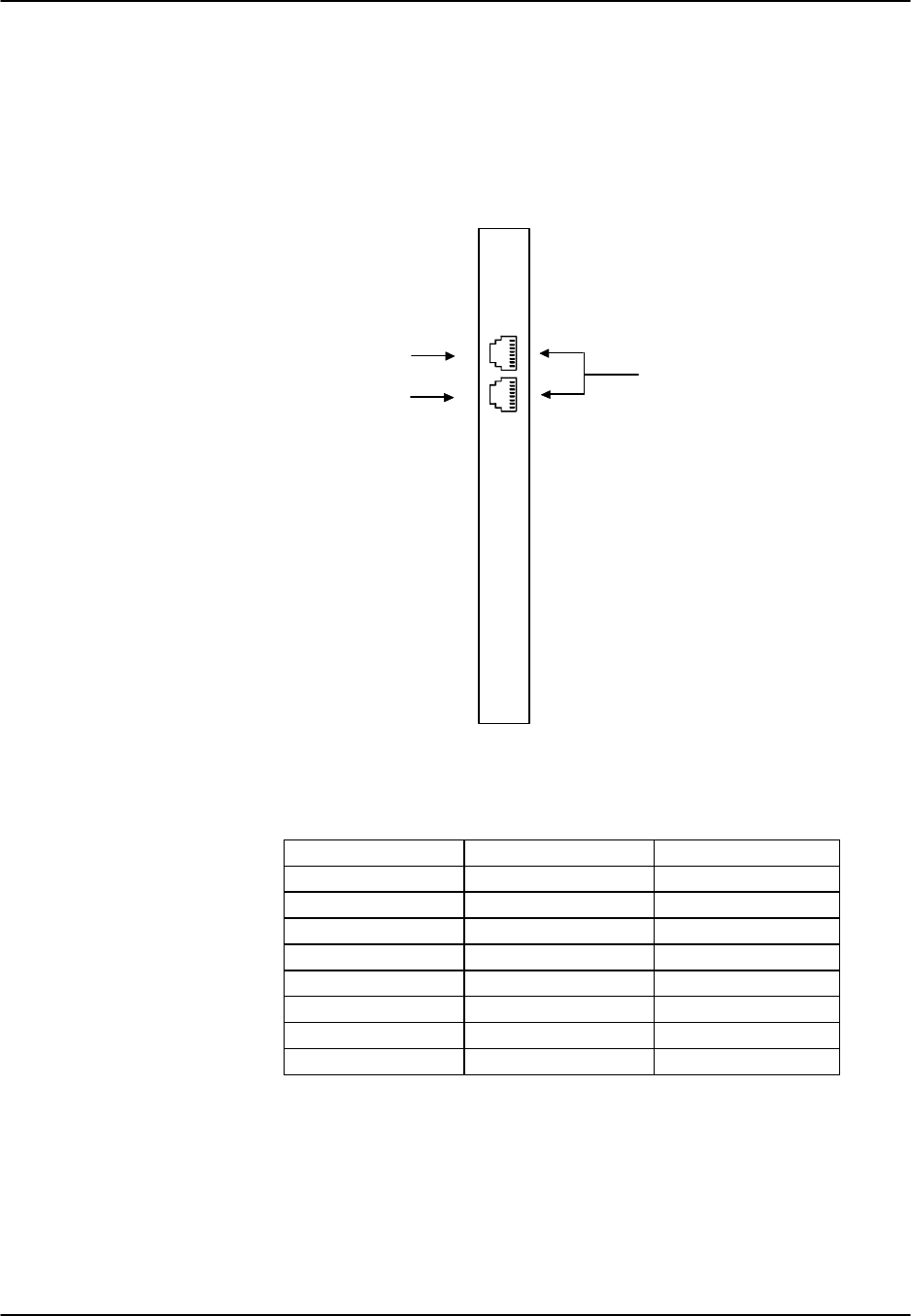
Reference Guide v3.6 Pinouts
(10-97) Page 9-A-45
OCU-DP Card (8249)
The OCU-DP card may be installed in any user card slot, U1-U-8 on the 8918 two-sided
chassis or 8919 front-loading chassis, and P1-P4 or W1-W4 on the 8916 front-loading
chassis. Each card has two standard RJ48C connectors that correspond with the two
OCU-DP Ports assignable from each card. Figure Pinouts-41 shows the card and Table
Pinouts-31 shows the pin assignments for the RJ48C connections on the OCU-DP Card.
RJ-48C
OCU-DP
#1
#2
Port
Figure Pinouts-41. 8249 OCU-DP Card Connectors
Table Pinouts-31. 8249 OCU-DP Card Pin Assignments
Male RJ-48 Pin # Signal Name Direction
1R1 input
2T1 input
3-- --
4-- --
5-- --
6-- --
7Toutput
8Routput
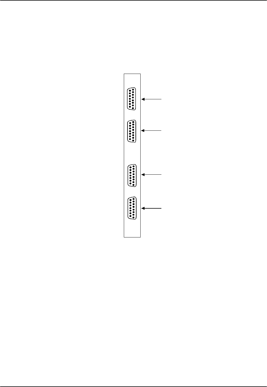
Pinouts Reference Guide v3.6
Page 9-A-46 (10-97)
DS0-DP Card (8254)
The DS0-DP card may be installed in any user card slot, U1-U-8 on the 8918 two-sided
chassis or 8919 front-loading chassis, and P1-P4 or W1-W4 on the 8916 front-loading
chassis. Each card has four standard (female) DB-15 connectors that are labeled to
correspond with the four DS0-DP Ports assignable from each card. Figure Pinouts-42
shows the card and Table Pinouts-32 shows the pin assignments for the DB-15(F)
connections on the DS0-DP Card.
Port #1
Port #2
Port #3
Port #4
Figure Pinouts-42. DS0-DP Card Connectors

Reference Guide v3.6 Pinouts
(10-97) Page 9-A-47
Table Pinouts-32. DS0-DP Card Pin Assignments
DB-15(F) Pin Signal Name Direction Modes Used In
1GND --- all
2N/A --- n/a
3CR CK A output contra-directional
4CX CK A output contra-directional
5DTAR A output all
6DTAX A input all
7BYTECLK A both DS0-DP
8BITCLK A both DS0-DP
9N/A --- n/a
10 CR CK A output contra-directional
11 CX CK A output contra-directional
12 DTAR A output all
13 DTAX A input all
14 BYTECLK A both DS0-DP
15 BITCLK A both DS0-DP
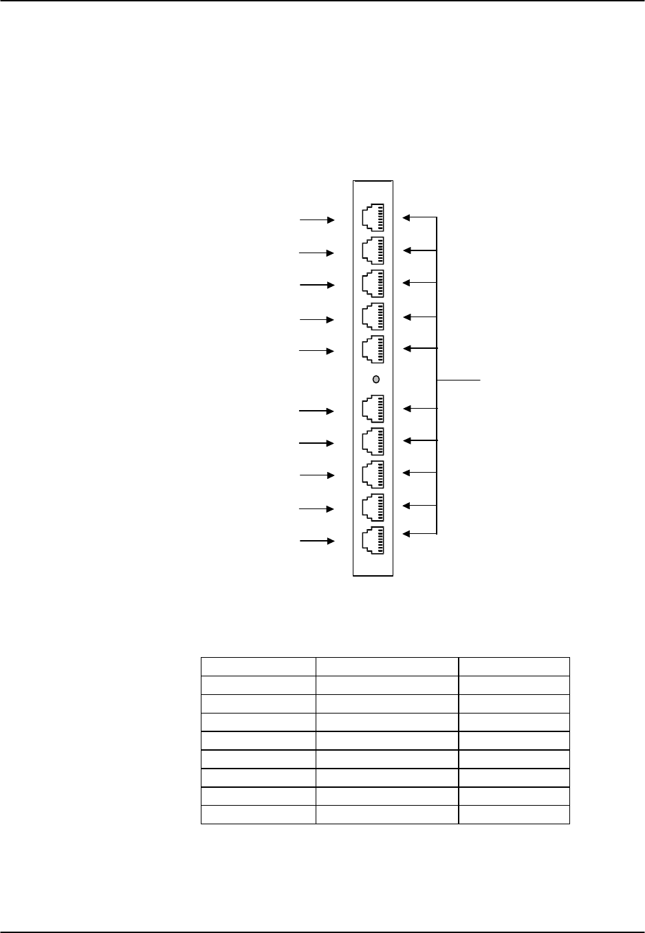
Pinouts Reference Guide v3.6
Page 9-A-48 (10-97)
FRAD Card (8231)
The 8231 FRAD card may be installed in any user card slot, U1-U-8 on the 8918 two-
sided chassis or 8919 front-loading chassis, and P1-P4 or W1-W4 on the 8916 front-
loading chassis. Each card has ten standard RJ48C connectors that correspond with the
ten user ports assignable from each card. Figure Pinouts-43 shows the card and Table
Pinouts-33 shows the pin assignments for the RJ48C connections on the 8231 FRAD
Card.
Top Handle
RJ-48C
FRAD User
#1
#2
#3
#4
#5
#6
#7
#8
Bottom Handle
#9
#10
Figure Pinouts-43. FRAD Card Connectors
Table Pinouts-33. FRAD Card Pin Assignments
Male RJ-48 Pin Signal Name Direction
1RCLK output
2RLSD output
3TCLK output
4GND -
5RD output
6TD input
7CTS output
8RTS input
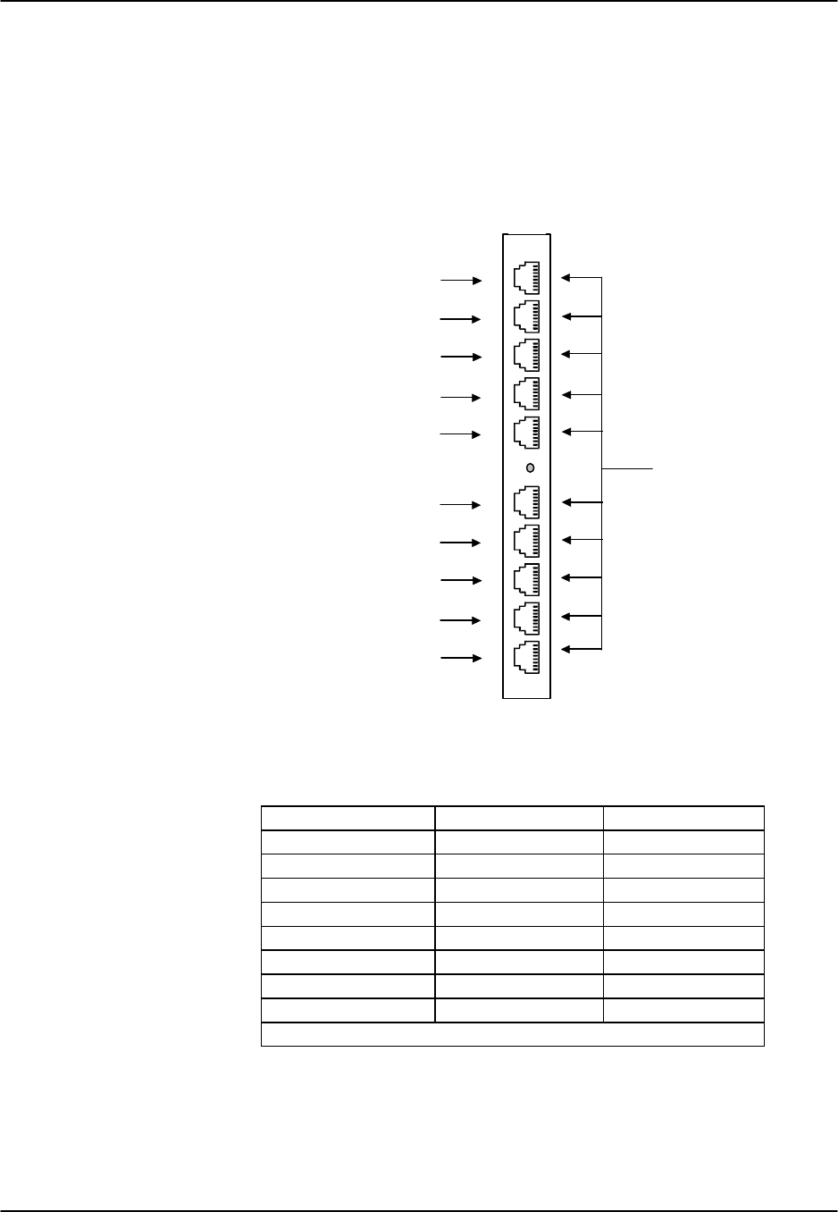
Reference Guide v3.6 Pinouts
(10-97) Page 9-A-49
B7R Card (8228)
The B7R card may be installed in any user card slot, U1-U-8 on the 8918 two-sided
chassis or 8919 front-loading chassis, and P1-P4 or W1-W4 on the 8916 front-loading
chassis. Each card has ten standard RJ48C connectors (8 of which are unused). The
two usable port connectors are for the Aggregate Port and the Debug Port. Figure
Pinouts-44 shows the card and Table Pinouts-34 shows the pin assignments for the
RJ48C connections on the B7R Card.
Top Handle
RJ-48C
B7R User
Bottom Handle
Unused
Unused
Unused
Unused
Unused
Unused
Unused
Unused
Debug Port #9
Aggregate Port
Figure Pinouts-44. B7R Card Connectors
Table Pinouts-34. B7R Card Pin Assignments
Male RJ-48 Pin # Signal Name Direction
1* RCLK output
2RLSD output
3* TCLK output
4GND -
5RD output
6TD input
7CTS output
8RTS input
* Clocking unnecessary for Asynch Transmission

Pinouts Reference Guide v3.6
Page 9-A-50 (10-97)
BRI Card (8260, 8261, and 8262)
The eight-port BRI cards may be installed in any user card slot, U1-U-8 on the 8918
two-sided chassis or 8919 front-loading chassis, and P1-P4 or W1-W4 on the 8916
front-loading chassis. These cards allow you to connect the integrated access system to
leased BRI services from service providers.
The BRI card has an RJ27X (female) 50-pin Amphenol connector located on the
faceplate of the card. Figure Pinouts-45 shows the pinouts for this connector. Table
Pinouts-35 lists the pin assignments for the 8260 and 8261, while Table Pinouts-36 lists
the pin assignments for the 8262.
Pin 50
Pin 26
Pin 25
Pin 1
Figure Pinouts-45. BRI Card Connector
Table Pinouts-35. BRI Card Pin Assignments (8260 / 8261)
Port # Designation Pin #
1T1 26
1R1 1
2T2 29
2R2 4
3T3 32
3R3 7
4T4 35
4R4 10
5T5 38
5R5 13
6T6 41
6R6 16
7T7 44
7R7 19
8T8 47
8R8 22
All other pins are unconnected.

Reference Guide v3.6 Pinouts
(10-97) Page 9-A-51
Table Pinouts-36 BRI Card Pin Assignments (8262)
Port
Designation
Pin #
1
Xmt
–
T0
26
1
Xmt
–
R0
1
1
Rcv
–
T0
27
1
Rcv
–
R0
2
2
Xmt
–
T1
29
2
Xmt
–
R1
4
2
Rcv
–
T1
30
2
Rcv
–
R1
5
3
Xmt
–
T2
32
3
Xmt
–
R2
7
3
Rcv
–
T2
33
3
Rcv
–
R2
8
4
Xmt
–
T3
35
4
Xmt
–
R3
10
4
Rcv
–
T3
36
4
Rcv
–
R3
11
5
Xmt
–
T4
38
5
Xmt
–
R4
13
5
Rcv
–
T4
39
5
Rcv
–
R4
14
6
Xmt
–
T5
41
6
Xmt
–
R5
16
6
Rcv
–
T5
42
6
Rcv
–
R5
17
7
Xmt
–
T6
44
7
Xmt
–
R6
19
7
Rcv
–
T6
45
7
Rcv
–
R6
20
8
Xmt
–
T7
47
8
Xmt
–
R7
22
8
Rcv
–
T7
48
8
Rcv
–
R7
23
External Power
+48v
50
External Power
-48v
25
If external power is used, jumpers JP5 and JP6 must be set to EXTERNAL mode.
Failure to do so could damage or destroy the card or integrated access system.

Pinouts Reference Guide v3.6
Page 9-A-52 (10-97)
