Instructions
User Manual:
Open the PDF directly: View PDF ![]() .
.
Page Count: 4

ELEC6233'Digital'System'Synthesis' 1' Courswork'2'FPGA'embedded'system'synthesis'
'
'
ELEC6233 Digital System Synthesis
FPGA implementation of a complex number multiplier
Introduction
This'exercise'is'done'individually'and'the'assessment'is:'
•'''By'formal'report'describing'the'final'design,'its'development,'implementation'and'
testing.'
•'''By'a'laboratory'demonstration'of'the'final'design'on'an'Altera'FPGA'development'system'
Specification
The'objective'of'this'exercise'is'to'design,'in'combinational'logic,'a'multiplier'of'two'
complex'numbers:'
''
p=
α
q
''''''''''''''''''''(1)'
'
Where'
α
=Re
α
+jIm
α
'with'the'real'and'imaginary'part'represented'as'signed'8-bit'2’s'
complement'numbers'in'the'range'-1..+1-2-8'and'
q=Re q+jIm q
'with'the'real'and'
imaginary'part'represented'as'signed'8-bit'2’s'complement'integers'in'the'range'-128..127.'''
The'output'from'the'multiplier'
p=Re p+jIm p
'is'required'to'preserve'only'the'8-bit'
integer'part'of'the'calculation.''
Such'calculations'are'frequently'required'in'systems'which'implement'Fourier'transform'
algorithms'and'are'used'in'many'digital'signal-processing'applications.''
Implementation and lab demo
Your'multiplier'must'be'implemented'as'combinational'logic'but'a'simple'sequential'logic'
controller'is'also'required'to'read'the'operands'from'the'switches'on'the'FPGA'
development'kit'and'to'display'the'result'on'the'LEDs.'The'8-bit'operands'must'be'read'
from'the'switches'SW0-SW7'on'the'FPGA'development'system'and'the'resulting'product'
displayed'on'the'LEDS'LED0-LED7.''Switch'SW8'provides'handshaking'functionality'as'
described'in'the'pseudocode'below.''Switch'SW9'should'act'as'an'active'low'reset'of'your'
controller.''
Pseudocode of the lab demo sequence
1. Wait for
Re
α
by polling switch SW8. Wait while SW8=0. When SW8 becomes 1
(SW8=1) read
Re
α
from SW0-SW7.'
2. Wait for switch SW8 to become 0'
3. Wait for
Im
α
as specified in step 1.'
4. Wait for SW8 to become 0'
5. Repeat steps 1-4 to read
Re q
and
Im q
'
6. Display the real part of the result
Re p
on LED0-LED7.'
7. Wait until SW8 becomes 1'
8. Display the imaginary part of the result
Im p
on LED0-LED7.'
9. Wait until SW8 becomes 0'
10. Go to step 1.'
ELEC6233'Digital'System'Synthesis' 2' Courswork'2'FPGA'embedded'system'synthesis'
'
'
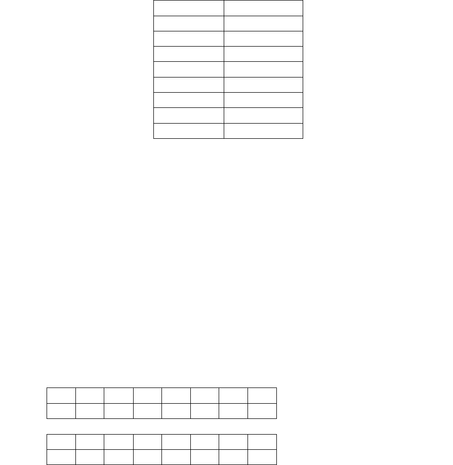
Data formats
The'real'and'imaginary'part'of'operand'
q
'are'8-bit'2’s'complement'signed'integers,'i.e.'
their'values'are'in'the'range'-128..+127.'
The'real'and'imaginary'part'of'operand'
α
'are'2’s'complement'signed'fixed-point'fractions'
in'the'range'-1'..'+1'–'2^(-8),'i.e.'they'are'2’s'complement'fractional'numbers'with'the'radix'
point'positioned'after'the'most'significant'bit.''Therefore'the'weights'of'the'individual'bits'
are:'
'
Bit'position'
Weight'
7 '
-2^0'
6'
2^(-1)'
5'
2^(-2)'
4'
2^(-3)'
3'
2^(-4)'
2'
2^(-5)'
1'
2^(-6)'
0'(LSB)'
2(-7)'
'
When'such'whole'integers'and'fractions'are'multiplied,'a'double-length'16-bit'product'is'
obtained'which'is'a'2’s'complement'number'with'the'radix'point'positioned'after'the'9-th'
bit.'Note'however'that'the'output'of'the'entire'calculation'must'be'an'8-bit'2’s'complement'
whole'number.'
Binary multiplication examples
Binary'multiplication'of'2’s'complement'8-bit'numbers'yields'a'16-bit'result.''As'one'of'the'
numbers'is'represented'in'the'range'-1..+1-2-7'and'the'other'in'the'range'-128..127,'it'is'
important'to'determine'correctly'which'8-bits'of'the'16-bit'result'represent'the'integer'part'
which'should'be'used'for'further'calculations.''The'following'examples'illustrate'which'
result'bits'represent'the'integer'part.'
'
Example(1.(Multiply(0.75(x(6.(
In'2’s'complement'8-bit'binary'representation'these'two'operands'are:'
'
weights:'
-20'
2-1'
2-2'
2-3'
2-4'
2-5'
2-6'
2-7'
0.75'=''
0.'
1'
1'
0'
0'
0'
0'
0'
'
weights:'
-27'
26'
25'
24'
23'
22'
21'
20'
6'=''
0'
0'
0'
0'
0'
1'
1'
0.'
'
'
'
'
'
ELEC6233'Digital'System'Synthesis' 3' Courswork'2'FPGA'embedded'system'synthesis'
'
'
'
The'16-bit'result'is:'
''
-28'
27'
26'
25'
24'
23'
22'
21'
20'
2-1'
2-2'
2-3'
2-4'
2-5'
2-6'
2-7'
0'
0'
0'
0'
0'
0'
1'
0'
0.'
1'
0'
0'
0'
0'
0'
0'
'
which'represents'the'value'of'4.5.''The'shaded'area'shows'which'bits'need'to'be'extracted'
when'the'representation'is'truncated'to'8'bits.'Note'that'the'fraction'part'is'discarded'
entirely,'so'the'8-bit'result'is'now'4.'Also'note'that'when'the'leading'bit'is'discarded,'the'
weight'of'the'new'leading'bit'must'now'change'from'27'to'-27.'Why?''The'importance'of'the'
correct'interpretation'of'the'leading'bit’s'weight'is'evident'in'the'following'example,'where'
the'result'is'negative.''
Example(2.(Multiply(-0.25(x(20.(
The'two'operands'in'signed'binary'are:'
'
weights:'
-20'
2-1'
2-2'
2-3'
2-4'
2-5'
2-6'
2-7'
-0.25'=''
1.'
1'
1'
0'
0'
0'
0'
0'
'
weights:'
-27'
26'
25'
24'
23'
22'
21'
20'
20'=''
0'
0'
0'
1'
0'
1'
0'
0.'
'
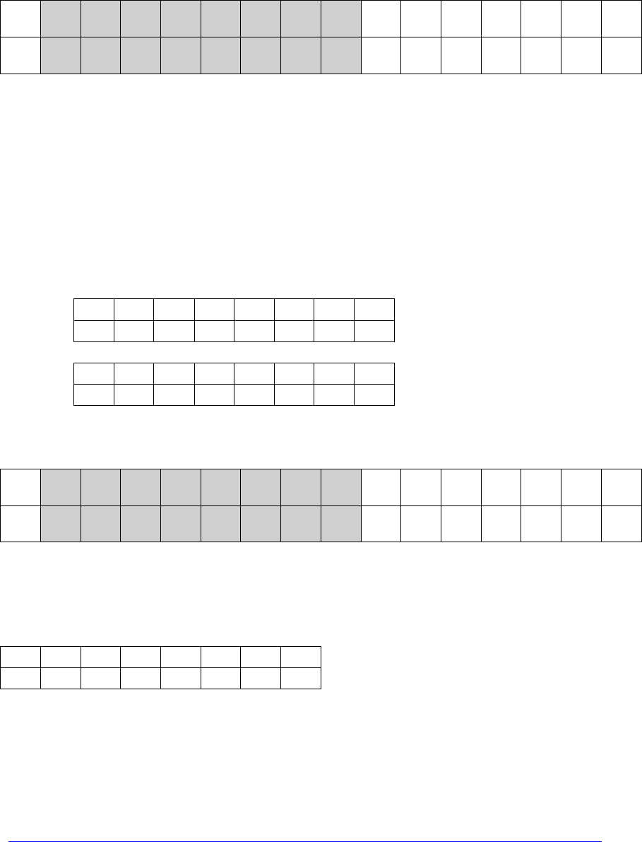
The'16-bit'result'is:'
''
-28'
27'
26'
25'
24'
23'
22'
21'
20'
2-1'
2-2'
2-3'
2-4'
2-5'
2-6'
2-7'
1'
1'
1'
1'
1'
1'
0'
1'
1.'
0'
0'
0'
0'
0'
0'
0'
'
which'is''-5'in'decimal'representation.'Again,'the'shaded'area'shows'which'8'bits'to'extract'
when'the'result'is'truncated'from'16'to'8'bits'for'further'calculations.'The'truncated'8-bit'
result'has'the'weight'of'-27'on'the'most'significant'bit'so'that'it'still'correctly'represents'-5:'
'
-27'
26'
25'
24'
23'
22'
21'
20'
1'
1'
1'
1'
1'
0'
1'
1.'
'
If'you'would'like'to'experiment'more'with'binary'multiplication'of'signed'numbers,'run'
some'SystemVerilog'simulations'of'your'multiplier'in'Modelsim,'which'is'what'you'should'
do'anyway'to'test'your'multiplier'module'before'synthesis.'If'you'would'like'to'practice'
signed'binary'multiplication'by'hand,'I'recommend'you'use'Booth’s'algorithm'(and'rather'
fewer'than'8-bits!):'
https://secure.ecs.soton.ac.uk/notes/elec6234/1617/11embeddedmultiplication2.pdf'
ELEC6233'Digital'System'Synthesis' 4' Courswork'2'FPGA'embedded'system'synthesis'
'
'
The'original'paper'where'Andrew'Booth'published'his'algorithm'back'in'1951'can'be'found'
here:'http://qjmam.oxfordjournals.org/content/4/2/236.short'
Design strategy
Develop'SystemVerilog'code'and'a'testbench'to'simulate'your'design'in'Modelsim.'
Synthesise'the'design'in'Altera'Quartus'and'carefully'analyse'the'synthesis'warnings,'
statistics'and'RTL'diagrams.''Correct'any'errors'and'when'you'are'satisfied'that'the'results'
of'the'calculations'are'right,''synthesise'the'whole'design'again'and'carefully'analyse'the'
warnings,'statistics'and'RTL'diagrams.''If'you'have'not'yet'taken'out'an'FGPA'development'
system'on'loan'for'another'assignment,'you'will'be'able'to'loan'one'until'Week'12.'In'Week'
11'or'12'(after'the'Easter'Break)'you'will'be'asked'to'demonstrate'your'design'in'the'
Electronics'Laboratory.'
Formal report
Submit'an'electronic'copy'of'your'report'through'the'electronic'handin'system,'and'a'
printed'copy'to'the'ECS'front'office'by'the'deadline'specified'on'the'ELEC6233'notes'
website.'''The'report'should'not'exceed'1500'words'in'length.'It'must'contain'a'full'
discussion'of'your'design,'including'the'final'circuit'diagrams,'sample'data,'simulation'and'
synthesis'result.''Source'files'must'be'packaged'in'a'zip'file'and'submitted'electronically'as'a'
separate'file'at'the'same'time.'In'this'exercise,'20%'of'the'marks'are'allocated'to'the'report,'
its'style'and'organisation,'with'the'remaining'80%'for'the'technical'content.'As'always,'
bonus'marks'are'awarded'for'implementation'of'novel'concepts.'
'
tjk,'23'Mar’17'
