IRLML6402 Datasheet. Www.s Manuals.com. Irf
User Manual: Marking of electronic components, SMD Codes E*, E****. Datasheets BAT54, IRLML6402, IRLML6402PbF, NUP4103FC.
Open the PDF directly: View PDF ![]() .
.
Page Count: 9
Parameter Typ. Max. Units
RθJA Maximum Junction-to-Ambient75 100 °C/W
IRLML6402
HEXFET® Power MOSFET
These P-Channel MOSFETs from International Rectifier utilize
advanced processing techniques to achieve extremely low on-
resistance per silicon area. This benefit, combined with the fast
switching speed and ruggedized device design that HEXFET®
power MOSFETs are well known for, provides the designer with
an extremely efficient and reliable device for use in battery and
load management.
A thermally enhanced large pad leadframe has been incorporated
into the standard SOT-23 package to produce a HEXFET Power
MOSFET with the industry's smallest footprint. This package,
dubbed the Micro3™, is ideal for applications where printed
circuit board space is at a premium. The low profile (<1.1mm)
of the Micro3 allows it to fit easily into extremely thin application
environments such as portable electronics and PCMCIA cards.
The thermal resistance and power dissipation are the best
available.
Thermal Resistance
VDSS = -20V
RDS(on) = 0.065Ω
lUltra Low On-Resistance
lP-Channel MOSFET
l SOT-23 Footprint
lLow Profile (<1.1mm)
lAvailable in Tape and Reel
lFast Switching
Description
12/14/11
www.irf.com 1
Parameter Max. Units
VDS Drain- Source Voltage -20 V
ID @ TA = 25°C Continuous Drain Current, VGS @ -4.5V -3.7
ID @ TA= 70°C Continuous Drain Current, VGS @ -4.5V -2.2 A
IDM Pulsed Drain Current -22
PD @TA = 25°C Power Dissipation 1.3
PD @TA = 70°C Power Dissipation 0.8
Linear Derating Factor 0.01 W/°C
EAS Single Pulse Avalanche Energy11 mJ
VGS Gate-to-Source Voltage ± 12 V
TJ, TSTG Junction and Storage Temperature Range -55 to + 150 °C
Absolute Maximum Ratings
W
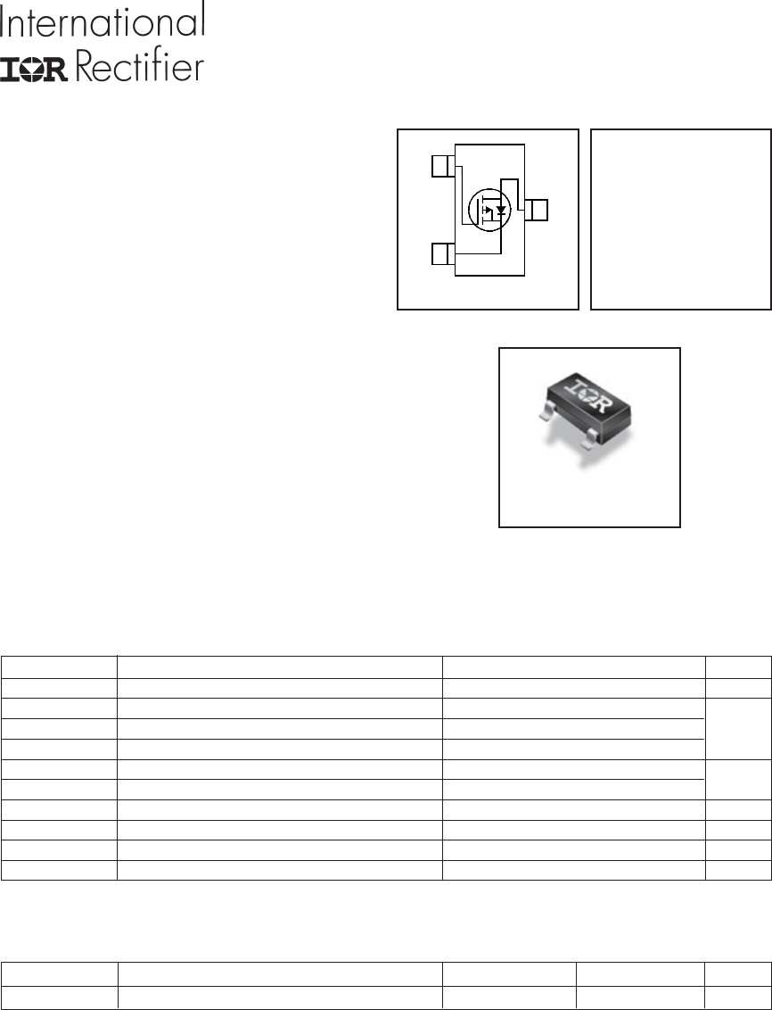
Micro3™
S
G1
2
D3
PD - 93755D
IRLML6402
2www.irf.com
Parameter Min. Typ. Max. Units Conditions
ISContinuous Source Current MOSFET symbol
(Body Diode) ––– ––– showing the
ISM Pulsed Source Current integral reverse
(Body Diode) ––– ––– p-n junction diode.
VSD Diode Forward Voltage ––– ––– -1.2 V TJ = 25°C, IS = -1.0A, VGS = 0V
trr Reverse Recovery Time ––– 29 43 ns TJ = 25°C, IF = -1.0A
Qrr Reverse RecoveryCharge ––– 11 17 nC di/dt = -100A/μs
Repetitive rating; pulse width limited by
max. junction temperature.
Notes:
Pulse width ≤ 400μs; duty cycle ≤ 2%.
Source-Drain Ratings and Characteristics
-1.3
-22
A
S
D
G
** For recommended footprint and soldering techniques refer to application note #AN-994.
Surface mounted on 1" square single layer 1oz. copper FR4 board,
steady state.
Starting TJ = 25°C, L = 1.65mH
RG = 25Ω, IAS = -3.7A.
Parameter Min. Typ. Max. Units Conditions
V(BR)DSS Drain-to-Source Breakdown Voltage -20 ––– ––– V VGS = 0V, ID = -250μA
ΔV(BR)DSS/ΔTJBreakdown Voltage Temp. Coefficient ––– -0.009 ––– V/°C Reference to 25°C, ID = -1mA
––– 0.050 0.065 VGS = -4.5V, ID = -3.7A
––– 0.080 0.135 VGS = -2.5V, ID = -3.1A
VGS(th) Gate Threshold Voltage -0.40 -0.55 -1.2 V VDS = VGS, ID = -250μA
gfs Forward Transconductance 6.0 ––– ––– S VDS = -10V, ID = -3.7A
––– ––– -1.0 VDS = -20V, VGS = 0V
––– ––– -25 VDS = -20V, VGS = 0V, TJ = 70°C
Gate-to-Source Forward Leakage ––– ––– -100 VGS = -12V
Gate-to-Source Reverse Leakage ––– ––– 100 VGS = 12V
QgTotal Gate Charge ––– 8.0 12 ID = -3.7A
Qgs Gate-to-Source Charge ––– 1.2 1.8 nC VDS = -10V
Qgd Gate-to-Drain ("Miller") Charge ––– 2.8 4.2 VGS = -5.0V
td(on) Turn-On Delay Time ––– 350 ––– VDD = -10V
trRise Time ––– 48 ––– ID = -3.7A
td(off) Turn-Off Delay Time ––– 588 ––– RG = 89Ω
tfFall Time ––– 381 ––– RD = 2.7Ω
Ciss Input Capacitance ––– 633 ––– VGS = 0V
Coss Output Capacitance ––– 145 ––– pF VDS = -10V
Crss Reverse Transfer Capacitance ––– 110 ––– ƒ = 1.0MHz
Electrical Characteristics @ TJ = 25°C (unless otherwise specified)
IGSS
µA
Ω
RDS(on) Static Drain-to-Source On-Resistance
IDSS Drain-to-Source Leakage Current
nA
ns
IRLML6402
www.irf.com 3
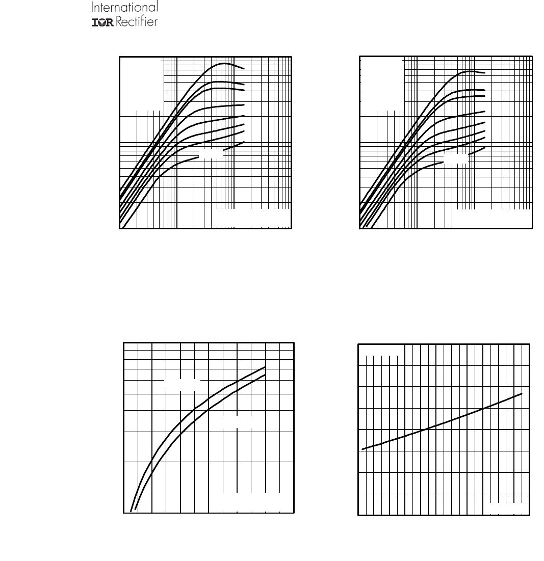
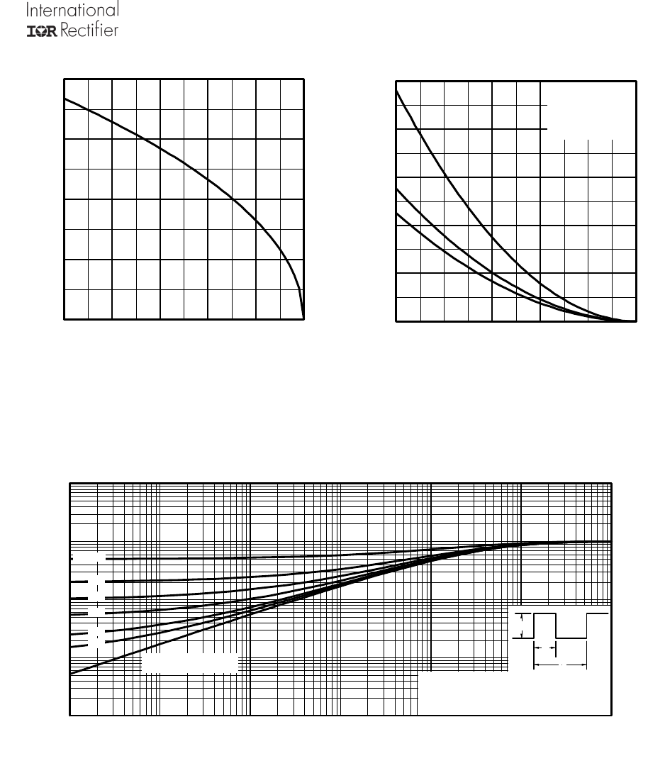
Fig 4. Normalized On-Resistance
Vs. Temperature
Fig 2. Typical Output CharacteristicsFig 1. Typical Output Characteristics
Fig 3. Typical Transfer Characteristics
1
10
100
0.1 1 10 100
20μs PULSE WIDTH
T = 25 C
J°
TOP
BOTTOM
VGS
-7.00V
-5.00V
-4.50V
-3.50V
-3.00V
-2.70V
-2.50V
-2.25V
-V , Drain-to-Source Voltage (V)
-I , Drain-to-Source Current (A)
DS
D
-2.25V
1
10
100
0.1 1 10 100
20μs PULSE WIDTH
T = 150 C
J°
TOP
BOTTOM
VGS
-7.00V
-5.00V
-4.50V
-3.50V
-3.00V
-2.70V
-2.50V
-2.25V
-V , Drain-to-Source Voltage (V)
-I , Drain-to-Source Current (A)
DS
D
-2.25V
10
100
2.0 3.0 4.0 5.0 6.0 7.0 8.0
V = -15V
20μs PULSE WIDTH
DS
-V , Gate-to-Source Voltage (V)
-I , Drain-to-Source Current (A)
GS
D
T = 25 C
J°
T = 150 C
J°
-60 -40 -20 020 40 60 80 100 120 140 160
0.0
0.5
1.0
1.5
2.0
T , Junction Temperature ( C)
R , Drain-to-Source On Resistance
(Normalized)
J
DS(on)
°
V =
I =
GS
D
-4.5V
-3.7A
IRLML6402
4www.irf.com
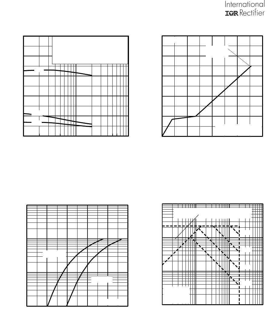
Fig 8. Maximum Safe Operating Area
Fig 6. Typical Gate Charge Vs.
Gate-to-Source Voltage
Fig 5. Typical Capacitance Vs.
Drain-to-Source Voltage
Fig 7. Typical Source-Drain Diode
Forward Voltage
0.1
1
10
100
0.1 1 10 100
OPERATION IN THIS AREA LIMITED
BY RDS(on)
Single Pulse
T
T
= 150 C
= 25 C
°
°
J
C
-V , Drain-to-Source Voltage (V)
-I , Drain Current (A)I , Drain Current (A)
DS
D
10us
100us
1ms
10ms
110 100
VDS, Drain-to-Source Voltage (V)
0
200
400
600
800
1000
C, Capacitance(pF)
Coss
Crss
Ciss
VGS
= 0V, f = 1 MHZ
Ciss
= C
gs
+ C
gd, C
ds
SHORTED
Crss
= C
gd
Coss
= C
ds
+ C
gd
036912
0
2
4
6
8
10
Q , Total Gate Charge (nC)
-V , Gate-to-Source Voltage (V)
G
GS
FOR TEST CIRCUIT
SEE FIGURE
I =
D
13
-3.7A
V =-10V
DS
0.1
1
10
100
0.2 0.4 0.6 0.8 1.0 1.2
-V ,Source-to-Drain Voltage (V)
-I , Reverse Drain Current (A)
SD
SD
V = 0 V
GS
T = 25 C
J°
T = 150 C
J°
IRLML6402
www.irf.com 5
Fig 11. Maximum Effective Transient Thermal Impedance, Junction-to-Ambient
Fig 9. Maximum Drain Current Vs.
Case Temperature
Fig 10. Maximum Avalanche Energy
Vs. Drain Current
25 50 75 100 125 150
0.0
1.0
2.0
3.0
4.0
T , Case Temperature ( C)
-I , Drain Current (A)
°
C
D
25 50 75 100 125 150
0
5
10
15
20
25
Starting T , Junction Temperature ( C)
E , Single Pulse Avalanche Energy (mJ)
J
AS
°
ID
TOP
BOTTOM
-1.7A
-3.0A
-3.7A
0.1
1
10
100
1000
0.00001 0.0001 0.001 0.01 0.1 1 10
Notes:
1. Duty factor D = t / t
2. Peak T = P x Z + T
1 2
JDM thJA A
P
t
t
DM
1
2
t , Rectangular Pulse Duration (sec)
Thermal Response (Z )
1
thJA
0.01
0.02
0.05
0.10
0.20
D = 0.50
SINGLE PULSE
(THERMAL RESPONSE)
IRLML6402
6www.irf.com
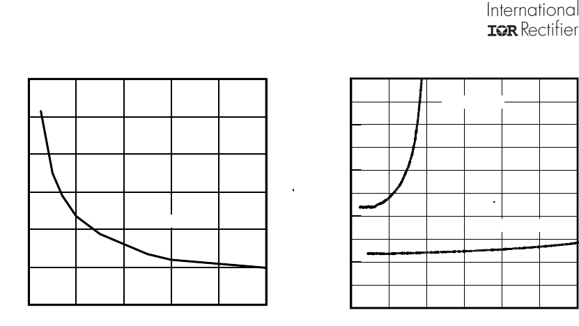
Fig 13. Typical On-Resistance Vs.
Drain Current
Fig 12. Typical On-Resistance Vs.
Gate Voltage
2.0 3.0 4.0 5.0 6.0 7.0
-VGS, Gate -to -Source Voltage ( V )
0.02
0.04
0.06
0.08
0.10
0.12
0.14
RDS(on) , Drain-to -Source Voltage ( Ω )
Id = -3.7A
0 5 10 15 20 25 30
-ID , Drain Current ( A )
0.00
0.04
0.08
0.12
0.16
0.20
RDS ( on ) , Drain-to-Source On Resistance ( Ω )
VGS = -4.5V
VGS = -2.5V
IRLML6402
www.irf.com 7
Micro3 / SOT-23 Package Marking
A YW LC
PART NUMBER
Y = YEAR
W = WEEK
LOT
CODE
HALOGEN FREE
INDICATOR
PART NUMBER CODE REFERENCE:
A = IRLML2402
B =IRLML2803
C = IRLML2402
D = IRLML5103
E = IRLML6402
F = IRLML6401
G = IRLML2502
H = IRLML5203
Note: A line above the work week
(as shown here) indicates Lead-free
Micro3 (SOT-23 / TO-236AB) Part Marking Information
Note: For the most current drawing please refer to IR website at http://www.irf.com/package
A2001 A27
W = (1-26) IF PRECEDED BY LAST DIGIT OF CALENDAR YEAR
W = (27-52) IF PRECEDED BY A LETTER
Y
82008
32003
12001
YEAR
2002 2
52005
2004 4
2007
2006
7
6
2010 0
2009 9
YEAR Y
C03
WOR K
WE E K
01
02
A
W
B
04 D
24
26
25
X
Z
Y
WOR K
WE E K W
K
H
G
F
E
D
C
B
2006
2003
2002
2005
2004
2008
2007
2010
2009 J
Y51
29
28
30
C
B
D
50 X
52 Z
0.972
1.900
Recommended Footprint
0.802
0.950 2.742
Micro3 (SOT-23) (Lead-Free) Package Outline
Dimensions are shown in millimeters (inches)
e
E1
E
D
A
B
0.15 [0.006]
e1
12
3
MCBA
5
6
6
5
3X L
c
b
A1 3X
A
A2
ABC
M
0.20 [0.008]
0.10 [0.004] C
C
L2
H4L1
7
0.89 1.12
SYMBOL MAXMIN
A1
b
0.01 0.10
c
0.30 0.50
D
0.08 0.20
E
2.80 3.04
E1
2.10 2.64
e
1.20 1.40
A
0.95 BSC
L 0.40 0.60
08
MILLIMETERS
A2 0.88 1.02
e1 1.90 BSC
REF0.54L1
BSC0.25L2 BSC
REF
INCHES
80
0.0004
MIN MAX
DIMENSIONS
NOTES:
1. DIMENSIONING & TOLERANCING PER ANSI Y14.5M-1994
2. DIMENSIONS ARE SHOW N IN MILLIMETERS [INCHES].
3. CONTROLLING DIMENSION: MILLIMETER.
4. DATUM PLANE H IS LOCATED AT THE MOLD PARTING LINE.
5. DATUM A AND B TO BE DETERMINED AT DATUM PLANE H.
6. DIMENSIONS D AND E1 ARE MEASURED AT DATUM PLANE H. DIMENSIONS DOES
NOT INCLUDE MOLD PROTRUSIONS OR INTERLEAD FLASH. MOLD PROTRUSIONS
OR INTERLEAD FLASH SHALL NOT EXCEED 0.25 MM [0.010 INCH] PER SIDE.
7. DIMENSION L IS THE LEAD LENGTH FOR SOLDERING TO A SUBSTRATE.
8. OUTLINE CONFORMS TO JEDEC OUTLINE TO-236 AB.
IRLML6402
8www.irf.com
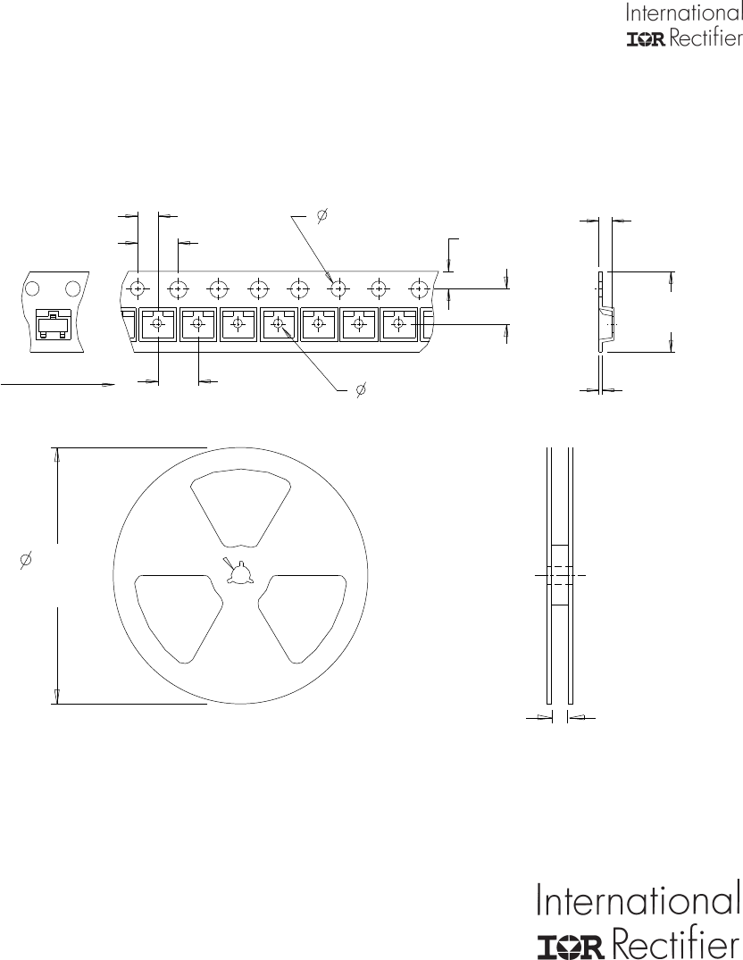
Micro3™(SOT-23/TO-263AB) Tape & Reel Information
Dimensions are shown in millimeters (inches)
2.05 ( .080 )
1.95 ( .077 )
TR
FEED DIRECTION
4.1 ( .161 )
3.9 ( .154 )
1.6 ( .062 )
1.5 ( .060 ) 1.85 ( .072 )
1.65 ( .065 )
3.55 ( .139 )
3.45 ( .136 )
1.1 ( .043 )
0.9 ( .036 )
4.1 ( .161 )
3.9 ( .154 ) 0.35 ( .013 )
0.25 ( .010 )
8.3 ( .326 )
7.9 ( .312 )
1.32 ( .051 )
1.12 ( .045 )
9.90 ( .390 )
8.40 ( .331 )
178.00
( 7.008 )
MAX.
NOTES:
1. CONTROLLING DIMENSION : MILLIMETER.
2. OUTLINE CONFORMS TO EIA-481 & EIA-541.
Data and specifications subject to change without notice.
IR WORLD HEADQUARTERS: 101N.Sepulveda Blvd, El Segundo, California 90245, USA Tel: (310) 252-7105
TAC Fax: (310) 252-7903
Visit us at www.irf.com for sales contact information. 12/2011