KB9012 Datasheet. Www.s Manuals.com. R0.9 Ene
User Manual: Datasheets KB9012BF, KB9012QF.
Open the PDF directly: View PDF ![]() .
.
Page Count: 257 [warning: Documents this large are best viewed by clicking the View PDF Link!]
- Content ii
- 1. General Description 0
- 2. Pin Assignment and Description 8
- 3. Pin Descriptions 15
- 3.1 Hardware Trap 15
- 3.2 Pin Descriptions by Functions 16
- 3.2.1 Low Pin Count I/F Descriptions. 16
- 3.2.2 PS/2 I/F Descriptions 16
- 3.2.3 Internal Keyboard Encoder (IKB) Descriptions 16
- 3.2.4 SMBus Descriptions 16
- 3.2.5 FAN Descriptions 17
- 3.2.6 Pulse Width Modulation (PWM) Descriptions 17
- 3.2.7 Analog-to-Digital Converter Descriptions 17
- 3.2.8 Digital-to-Analog Converter Descriptions 17
- 3.2.9 8051 External I/F Descriptions 17
- 3.2.10 External Clock Descriptions 18
- 3.2.11 Miscellaneous Signals Descriptions 18
- 3.2.12 Voltage Comparator Pins Descriptions 18
- 3.2.13 Power Pins Descriptions 18
- 3.2.14 51ON Power Pins Descriptions 19
- 4. Module Descriptions 20
- 4.1 Chip Architecture 20
- 4.2 GPIO 25
- 4.3 Keyboard and Mouse Control Interface (KBC) 49
- 4.4 ENE Serial Bus Controller (ESB) 54
- 4.5 Internal KeyBoard (IKB) Encoder 61
- 4.6 PECI 72
- 4.7 OWM 78
- 4.8 Pulse Width Modulation (PWM) 83
- 4.9 Fan Controller 90
- 4.10 General Purpose Timer (GPT) 100
- 4.11 SDI Host/Device Interface Controller 104
- 4.12 Watchdog Timer (WDT) 112
- 4.13 Low Pin Count Interface (LPC) 119
- 4.14 X-Bus Interface (XBI) 132
- 4.15 Consumer IR Controller (CIR) 138
- 4.16 General Waveform Generator (GWG) 150
- 4.17 PS/2 Interface (PS/2) 153
- 4.18 Embedded Controller (EC) 157
- 4.18.1 EC Function Description 157
- 4.18.2 EC Command Program Sequence 158
- 4.18.3 EC SCI Generation 159
- 4.18.4 EC/KBC Clock Configuration 160
- 4.18.5.1 A/D Converter Control 161
- 4.18.5.2 A/D Panel Drive Mode 162
- 4.18.6 D/A Converter Control 163
- 4.18.7 Power Management Control 164
- 4.18.8 EC Registers Description (0xFF00~0xFF2F) 165
- 4.19 General Purpose Wake-up Controller (GPWU) 177
- 4.20 System Management Bus Controller (SMBus) 188
- 4.21 8051 Microprocessor 201
- Application Appendix : 218
- 5. Electrical Characteristics 227
- 6. Package Information 238
- 1. General Description
- 2. Pin Assignment and Description
- 3. Pin Descriptions
- 3.1 Hardware Trap
- 3.2 Pin Descriptions by Functions
- 3.2.1 Low Pin Count I/F Descriptions.
- 3.2.2 PS/2 I/F Descriptions
- 3.2.3 Internal Keyboard Encoder (IKB) Descriptions
- 3.2.4 SMBus Descriptions
- 3.2.5 FAN Descriptions
- 3.2.6 Pulse Width Modulation (PWM) Descriptions
- 3.2.7 Analog-to-Digital Converter Descriptions
- 3.2.8 Digital-to-Analog Converter Descriptions
- 3.2.9 8051 External I/F Descriptions
- 3.2.10 External Clock Descriptions
- 3.2.11 Miscellaneous Signals Descriptions
- 3.2.12 Voltage Comparator Pins Descriptions
- 3.2.13 Power Pins Descriptions
- 3.2.14 51ON Power Pins Descriptions
- 4. Module Descriptions
- 4.1 Chip Architecture
- 4.2 GPIO
- 4.3 Keyboard and Mouse Control Interface (KBC)
- 4.4 ENE Serial Bus Controller (ESB)
- 4.5 Internal KeyBoard (IKB) Encoder
- 4.6 PECI
- 4.7 OWM
- 4.8 Pulse Width Modulation (PWM)
- 4.9 Fan Controller
- 4.10 General Purpose Timer (GPT)
- 4.11 SDI Host/Device Interface Controller
- 4.12 Watchdog Timer (WDT)
- 4.13 Low Pin Count Interface (LPC)
- 4.14 X-Bus Interface (XBI)
- 4.15 Consumer IR Controller (CIR)
- 4.16 General Waveform Generator (GWG)
- 4.17 PS/2 Interface (PS/2)
- 4.18 Embedded Controller (EC)
- 4.19 General Purpose Wake-up Controller (GPWU)
- 4.20 System Management Bus Controller (SMBus)
- 4.21 8051 Microprocessor
- Application Appendix :
- 5. Electrical Characteristics
- 6. Package Information

KB9012
Keyboard Controller
Data Sheet
Revision 0.9
June 2010
Headquarters
4F-1, No.9, Prosperity Rd.,
Science-based Industrial Park,
Hsinchu City, Taiwan, R.O.C
TEL: 886-3-6662888
FAX: 886-3-6662999
http://www.ene.com.tw
Copyright© 2011, ENE Technology Inc. All rights reserved.
ENE RESERVES THE RIGHT TO AMEND THIS DOCUMENT WITHOUT NOTICE AT ANY TIME. ENE
ASSUMES NO RESPONSIBILITY FOR ANY ERRORS APPEAR IN THE DOCUMENT, AND ENE DISCLAIMS
ANY EXPRESS OR IMPLIED WARRANTY, RELATING TO SALE AND/OR USE OF ENE PRODUCTS
INCLUDING LIABILITY OR WARRANTIES RELATING TO FITNESS FOR A PARTICULAR PURPOSE, OR
INFRINGEMENT OF ANY PATENTS, COPYRIGHTS OR OTHER INTELLECTUAL PROPERTY RIGHTS.
Taipei Office
4F, No.88, Bauchiau Rd.
Shindian City, Taipei,
Taiwan, R.O.C.
TEL: 886-2-89111525
FAX: 886-2-89111523

Copyright© 2011, ENE Technology Inc.
ii
KB9012 Keyboard Controller Datasheet
CONFIDENTIAL
ENE Technology Inc.
Confidential Document
Restricted Circulation
- This document is issued for only. Please do not transfer it to other companies.
- This document is the property of ENE Technology Corp. It should be returned once unused.
- Please do not make any copy of this document and deliver to others.
THIS DOCUMENT CONTAINS CONFIDEMTIAL
INFORMATION OF ENE PRODUCTS. ANY
UNAUTHORIZED USE OR DISCLOSURE COULD
IMPACT ENE’S COMPETITIVE ADVANTAGE.
This document issued to:
Recipient
Company
Serial Number

Copyright© 2011, ENE Technology Inc.
i
KB9012 Keyboard Controller Datasheet
CONFIDENTIAL
Revision
Revision
Description
Date
0.1
1. Draft with only pin-assignment and IO cells
2010/5
0.2
1. Re-organize contents,
2. Update IO cell name / structure
3. Update Memory Map
4. Reserved all electronic character for design characteristic only
2010/6
0.3
1. Update IO cell drive
2010/6
0.4
1. Update Block Diagram with GWG
2. Correct IO cells typo, remove BQCZT04HIV
3. Update power-fail flag in application appendix
4. Update Register files as following :
5. Update IKB HW command brief
6. Update Open-Drain PWM register
7. Modify SHDI registers for fixed clock source, SHI modes
8. Update WDT registers breathe LED flexible configuration
9. Update LPC MEM cycle map to XRAM illustration
10. Update XBI for e-flash operation and remove SHC description
11. Update GWG register as new-added functions
12. Update EC section registers for VC/PLC/ADC
13. Update SMB, extend previously banked-REGs, slave address
14. Update power-latch&voltage comparator in application appendix
2010/10
0.5
1. Update STOP mode power consumption
2. Add KBC POR and ECRST# timing
2010/10
0.6
1. Update KB9012 A1 P/N
2010/12
0.7
1. Fix register typo, TCON W0C
2. Update PCON2 description
3. Update GPIO_MISC for SHDI pin-out enable for each ports
4. Fix WDTCFG description of WDT disable password
5. Update SHDI clock setting
6. Update XBIMISC IC trimming status
2011/01
0.8
1. Update PS/2 Timing
2. Remove external SPI flashing timing
3. Update BQCZT04IV cell character
4. Update ESD information
5. Update thermal information
6. Update 9012A2 into P/N list and VC related setting. Please refer
ECN for details.
2011/03
0.9
1. Update 9012A3 into P/N list and related changes. Please refer
ECN for details.
2. Remove 4.13.3 & 4.13.4 LPC/FWH Memory decode range ;
remove Bank0 0xFE90[3], 0xFE94[7:0], 0xFE95[2],[7]
Bank1 0xFE92[5:0], 0xFE93[5:0]
3. Refine WDT breath LED similar to non-embedded-flash product
4. Refine ECMISC, IOSCCR for power consumption control
5. Refine function select control of tables
SDI host two ports select is by GPIO_MISC[2:1]
GPIO5D/5E (Crystal) is by CLK32CR[5:4]
VCouts are by GPIOFSx
Vcins are by VCCR[1:0]
6. Revise application appendix to correspond latest setting
2011/06
1.0
1. Refine hardware trap section, recover FDA trap in A3 version
2011/06

Copyright© 2011, ENE Technology Inc.
ii
KB9012 Keyboard Controller Datasheet
CONFIDENTIAL
CONTENT
CONTENT ................................................................................................................... II
1. GENERAL DESCRIPTION..................................................................................... 0
1.1 OVERVIEW ........................................................................................................... 0
1.2 FEATURES ........................................................................................................... 1
1.3 COMPARISON (KB930 VS. KB9012) .................................................................... 6
1.4 BLOCK DIAGRAM ................................................................................................. 7
2. PIN ASSIGNMENT AND DESCRIPTION .............................................................. 8
2.1 KB9012 128-PIN LQFP DIAGRAM TOP VIEW ....................................................... 8
2.2 KB9012 128 LFBGA BALL MAP ........................................................................ 9
2.3 KB9012 PIN ASSIGNMENT SIDE A ..................................................................... 10
2.4 KB9012 PIN ASSIGNMENT SIDE B ......................................................................11
2.5 KB9012 PIN ASSIGNMENT SIDE C ..................................................................... 12
2.6 KB9012 PIN ASSIGNMENT SIDE D ..................................................................... 13
2.7 I/O CELL DESCRIPTIONS .................................................................................... 14
2.7.1 I/O Buffer Table ....................................................................................... 14
2.7.2 I/O Buffer Characteristic Table.............................................................. 14
3. PIN DESCRIPTIONS ............................................................................................ 15
3.1 HARDWARE TRAP .............................................................................................. 15
3.2 PIN DESCRIPTIONS BY FUNCTIONS ..................................................................... 16
3.2.1 Low Pin Count I/F Descriptions. ........................................................... 16
3.2.2 PS/2 I/F Descriptions .............................................................................. 16
3.2.3 Internal Keyboard Encoder (IKB) Descriptions .................................. 16
3.2.4 SMBus Descriptions ............................................................................... 16
3.2.5 FAN Descriptions .................................................................................... 17
3.2.6 Pulse Width Modulation (PWM) Descriptions ..................................... 17
3.2.7 Analog-to-Digital Converter Descriptions ........................................... 17
3.2.8 Digital-to-Analog Converter Descriptions ........................................... 17
3.2.9 8051 External I/F Descriptions .............................................................. 17
3.2.10 External Clock Descriptions ............................................................... 18
3.2.11 Miscellaneous Signals Descriptions .................................................. 18
3.2.12 Voltage Comparator Pins Descriptions ............................................. 18
3.2.13 Power Pins Descriptions ..................................................................... 18
3.2.14 51ON Power Pins Descriptions .......................................................... 19

Copyright© 2011, ENE Technology Inc.
iii
KB9012 Keyboard Controller Datasheet
CONFIDENTIAL
4. MODULE DESCRIPTIONS .................................................................................. 20
4.1 CHIP ARCHITECTURE ......................................................................................... 20
4.1.1 Power Planes........................................................................................... 20
4.1.2 Clock Domains ........................................................................................ 21
4.1.3 PCICLK and CLKRUN#........................................................................... 23
4.1.4 Internal Memory Map.............................................................................. 24
4.2 GPIO ................................................................................................................ 25
4.2.1 GPIO Function Description ................................................................... 25
4.2.2 GPIO Structures ...................................................................................... 29
4.2.3 GPIO Attribution Table ........................................................................... 30
4.2.4 GPIO Registers Descriptions (0xFC00~0xFC7F) ................................ 33
4.2.5 GPIO Programming Sample .................................................................. 48
4.3 KEYBOARD AND MOUSE CONTROL INTERFACE (KBC) ........................................ 49
4.3.1 KBC I/F Function Description ............................................................... 49
4.3.2 KBC Registers Description (0xFC80~0xFC8F) ................................... 50
4.4 ENE SERIAL BUS CONTROLLER (ESB).............................................................. 54
4.4.1 ESB Function Description ..................................................................... 54
4.4.2 ESB Registers Description (0xFC90~0xFC9F) ................................... 55
4.4.3 ESB Programming Sample .................................................................... 60
4.5 INTERNAL KEYBOARD (IKB) ENCODER .............................................................. 61
4.5.1 IKB Function Description ...................................................................... 61
4.5.2 IKB Registers Description (0xFCA0~0xFCAF).................................... 63
4.5.3 IKB Matrix Value Mapping Table ........................................................... 69
4.6 PECI ................................................................................................................. 72
4.6.1 PECI Functional Description ................................................................. 72
4.6.2 PECI Timing Setting ............................................................................... 73
4.6.3 PECI Register Description (0xFCD0~0xFCDF) ................................... 74
4.7 OWM ................................................................................................................ 78
4.7.1 OWM Functional Description ................................................................ 78
4.7.2 OWM Timing Setting Illustration .......................................................... 79
4.7.3 OWM Register Description (0xFCF0~0xFCFF) ................................... 80
4.8 PULSE WIDTH MODULATION (PWM) .................................................................. 83
4.8.1 PWM Function Description.................................................................... 83
4.8.2 PWM Duty Cycle Setting Illustration .................................................... 84
4.8.3 PWM Registers Description (0xFE00~0xFE1F) .................................. 87
4.9 FAN CONTROLLER ............................................................................................. 90

Copyright© 2011, ENE Technology Inc.
iv
KB9012 Keyboard Controller Datasheet
CONFIDENTIAL
4.9.1 Fan Function Description ...................................................................... 90
4.9.1.1 Fan Tachometer Monitor & Auto-FAN mode .................................... 91
4.9.1.2 FANPWM Setting & Fixed-FAN Mode ................................................ 92
4.9.2 Fan Registers Description (0xFE20~0xFE4F) ..................................... 93
4.9.3 Fan Programming Sample ..................................................................... 99
4.10 GENERAL PURPOSE TIMER (GPT) ................................................................. 100
4.10.1 GPT Function Description ................................................................. 100
4.10.2 GPT Registers Description (0xFE50~0xFE6F) ................................ 101
4.10.3 GPT Programming Sample ................................................................ 103
4.11 SDI HOST/DEVICE INTERFACE CONTROLLER .................................................. 104
4.11.1 SDI Host/Device Interface Description............................................. 104
4.11.2 SDI Host Interface Register Description (0xFE70~0xFE7F) .......... 106
4.11.3 SDI Device Interface Register Description (0xFE70~0xFE7F) ...... 108
4.11.4 SDI Programming Sample .................................................................. 111
4.12 WATCHDOG TIMER (WDT) ............................................................................. 112
4.12.1 WDT Function Description ................................................................ 112
4.12.2 Setting for WDT Breathing LED ........................................................ 113
4.12.3 WDT Registers Description (0xFE80~0xFE8F) ............................... 114
4.12.4 WDT Programming Sample ............................................................... 118
4.13 LOW PIN COUNT INTERFACE (LPC) ................................................................ 119
4.13.1 LPC Function Description ................................................................. 119
4.13.2 LPC I/O Decode Range ...................................................................... 119
4.13.3 Index-I/O Port ...................................................................................... 120
4.13.4 LPC to MEM cycle XRAM ................................................................... 121
4.13.5 Extended I/O Port (Debug Port, Port80) .......................................... 123
4.13.6 LPC Registers Description (0xFE90~0xFE9F for bank selection) 124
4.14 X-BUS INTERFACE (XBI) ................................................................................ 132
4.14.1 XBI Function Description .................................................................. 132
4.14.2 XBI Registers Description (0xFEA0~0xFEBF) ................................ 133
4.15 CONSUMER IR CONTROLLER (CIR) ................................................................ 138
4.15.1 CIR Function Description .................................................................. 138
4.15.2 CIR Block Diagram ............................................................................. 140
4.15.3 CIR Remote Protocol.......................................................................... 141
4.15.3.1 Philips RC5 Protocol ........................................................................................ 141
4.15.3.2 Philips RC6 Protocol ........................................................................................ 142
4.15.3.3 NEC Protocol .................................................................................................... 142
4.15.4 CIR Automatic Carrier Frequency Detection and Modulation ...... 143

Copyright© 2011, ENE Technology Inc.
v
KB9012 Keyboard Controller Datasheet
CONFIDENTIAL
4.15.5 CIR Registers Description (0xFEC0~0xFECF) ................................ 145
4.15.6 CIR Programming Sample ................................................................. 149
4.16 GENERAL WAVEFORM GENERATOR (GWG) ................................................... 150
4.16.1 GWG Function Description ............................................................... 150
4.16.2 GWG Register Description (0xFED0~0xFEDF) ............................... 151
4.17 PS/2 INTERFACE (PS/2) ................................................................................ 153
4.17.1 PS/2 Interface Function Description ................................................ 153
4.17.2 PS/2 Interface Registers Description (0xFEE0~0xFEFF) .............. 153
4.18 EMBEDDED CONTROLLER (EC) ...................................................................... 157
4.18.1 EC Function Description ................................................................... 157
4.18.2 EC Command Program Sequence.................................................... 158
4.18.3 EC SCI Generation .............................................................................. 159
4.18.4 EC/KBC Clock Configuration ............................................................ 160
4.18.5.1 A/D Converter Control..................................................................... 161
4.18.5.2 A/D Panel Drive Mode ..................................................................... 162
4.18.6 D/A Converter Control........................................................................ 163
4.18.7 Power Management Control.............................................................. 164
4.18.8 EC Registers Description (0xFF00~0xFF2F) ................................... 165
4.19 GENERAL PURPOSE WAKE-UP CONTROLLER (GPWU) ................................... 177
4.19.1 GPWU Function Description ............................................................. 177
4.19.2 GPWU Registers Description (0xFF30~0xFF7F) ............................ 178
4.19.3 GPWU Programming Sample ............................................................ 187
4.20 SYSTEM MANAGEMENT BUS CONTROLLER (SMBUS) ..................................... 188
4.20.1 SMBus Function Description ............................................................ 188
4.20.2 SMBus Controller 0 Register Description (0xFF90~0xFFBF) ....... 192
4.20.3 SMBus Controller 1 Register Description (0xFFD0~0xFFFF) ....... 196
4.21 8051 MICROPROCESSOR ............................................................................... 201
4.21.1 8051 Microprocessor Function Description ................................... 201
4.21.2 8051 Microprocessor Instruction ..................................................... 202
4.21.3 8051 Interrupt Controller ................................................................... 207
4.21.4 Interrupt Enable/Flag Table ............................................................... 208
4.21.5 8051 Special Function Register (SFR) ............................................. 210
4.21.6 8051 Microprocessor Register Description .................................... 211
APPLICATION APPENDIX : .................................................................................. 218
A.1 ENE DEBUG INTERFACE, EDI .......................................................................... 218
A.1.1 Enable EDI ............................................................................................. 219

Copyright© 2011, ENE Technology Inc.
vi
KB9012 Keyboard Controller Datasheet
CONFIDENTIAL
A.1.2 EDI Instructions .................................................................................... 219
A.1.3 Read Command .................................................................................... 220
A.1.4 Write Command .................................................................................... 220
A.1.5 Disable EDI Command......................................................................... 221
A.2 POWER-LATCH ................................................................................................ 222
A.3 VOLTAGE COMPARATOR .................................................................................. 223
A.4 POWER FAIL FLAG BRIEF DESCRIPTION ........................................................... 225
A.5 EMBEDDED FLASH BRIEF DESCRIPTION ........................................................... 226
5. ELECTRICAL CHARACTERISTICS ................................................................. 227
5.1 ABSOLUTE MAXIMUM RATING ........................................................................... 227
5.2 DC ELECTRICAL CHARACTERISTICS ................................................................. 227
BQCZ16HIV ..................................................................................................... 227
BQC04HIV ....................................................................................................... 227
BQCW16HIV .................................................................................................... 228
BQC04HI .......................................................................................................... 228
BQC08HIV ....................................................................................................... 228
BQC04HIVPECI ............................................................................................... 229
BQCZT04IV (XCLKI, XCLKO, ADC/DAC) ..................................................... 230
5.3 A/D & D/A CHARACTERISTICS ......................................................................... 231
5.4 RECOMMEND OPERATION CONDITION ............................................................... 232
5.5 OPERATING CURRENT ...................................................................................... 232
5.6 PACKAGE THERMAL INFORMATION ................................................................... 232
5.7 AC ELECTRICAL CHARACTERISTICS ................................................................. 233
5.7.1 KBC POR and ECRST# ........................................................................ 233
5.7.2 LPC interface Timing ............................................................................ 234
5.7.3 PS/2 interface Timing ........................................................................... 236
5.7.4 SMBus interface Timing....................................................................... 237
6. PACKAGE INFORMATION ................................................................................ 238
6.1 LQFP 128-PIN OUTLINE DIAGRAM .................................................................. 238
6.1.1 Top View ................................................................................................. 238
6.1.2 Side View ............................................................................................... 239
6.1.3 Lead View............................................................................................... 240
6.1.4 LQFP Outline Dimensions ................................................................... 241
6.2 LFBGA 128-PIN OUTLINE DIAGRAM ............................................................... 242
6.2.1 Top View ................................................................................................. 242
6.2.2 Side View ............................................................................................... 243

Copyright© 2011, ENE Technology Inc.
vii
KB9012 Keyboard Controller Datasheet
CONFIDENTIAL
6.2.3 Bottom View .......................................................................................... 244
6.2.4 LFBGA Outline Dimensions ................................................................ 245
6.3 PART NUMBER DESCRIPTION............................................................................ 246
1. General Description
1.1 Overview
The ENE KB9012 is a customized IC based on KB9010 for specific application of minimizing
power-consumption. Several pins are provided for external power-latch to save power-consumption.
IO characteristic and cells are also improved.
The ENE KB901x series is embedded controller (EC) with embedded-Flash for notebook
platforms. In KB9012, the e-Flash is 128KB. The embedded controller contains industrial standard
8051 microprocessor and provides function of i8042 keyboard controller basically. KB9012 is
embedded LPC interface used to communicate with Host. The embedded controller also features
rich interfaces for general applications, such as PS/2 interface, Keyboard matrix encoder, PWM
controller, A/D converter, D/A converter, Fan controller, SMBus controller, GPIO controller, PECI
controller, one wire master, SPI controller, and extended interface (ENE Serial Bus) for more
applications, like capacitive touch button application and GPIO extender.
Compared with last generation of KB3926 series, KB9012 added PECI/OWM, another 2 SMBus,
another 2 Fan tachometers, enhanced SPI host/slave controller, internal oscillator for newest
application. KB9012 also improves structure of other modules including 8051, XBI, LPC, IKB, FAN,
WDT, GPIO, ESB, EDI. For detail improvement, please refer the related section.

Copyright© 2011, ENE Technology Inc.
1
KB9012 Keyboard Controller Datasheet
CONFIDENTIAL
1.2 Features
LPC Low Pin Count Interface
- SIRQ supporting IRQ1, IRQ12, SCI or SMI# interrupt and one programmable
IRQ provided.
- I/O Address Decoding:
Legacy KBC I/O port 60h/64h
Programmable EC I/O port, 62h/66h(recommend)
I/O port 68h/6Ch (sideband)
2 Programmable 4-byte Index-I/O ports to access internal EC registers.
- Memory Decoding:
Firmware Hub decode
LPC memory decode
- Compatible with LPC specification v1.1
- Support LPC interface re-direction to IKB for debugging
X-bus Bus Interface (XBI) : Flash Interface
- Embedded 128KB flash support
- The 64KB code memory can be mapped into system memory by one 16KB and
one 48KB programmable pages independently.
- Enhanced pre-fetch mechanism.
8051 Microprocessor
- Compatible with industrial 8051 instructions with 3 cycles.
- 8051 runs at 8/16/22 MHz, programmable.
- 256 bytes internal RAM. (special design) and 4KB tight-coupled SRAM
- 24 extended interrupt sources.
- Two 16-bit timers.
- Supports idle and stop mode.
- Enhanced embedded debug interface.
- Support Tx/Rx and support re-direction to IKB for debugging

Copyright© 2011, ENE Technology Inc.
2
KB9012 Keyboard Controller Datasheet
CONFIDENTIAL
8042 Keyboard Controller
- 8 standard 8042 commands processed by hardware.
- Each hardware command can be optionally processed by firmware.
- Pointing device multiplex mode support.
- Fast GA20 and KB reset support.
PS/2 Controller
- Support at most 3 external PS/2 devices.
- External PS/2 device operation in firmware mode.
Internal Keyboard Matrix (IKB)
- 18x8 keyboard scan matrix.
- Support W2K Internet and multimedia keys.
- Support hotkey events defined.
- Ghost key cancellation mechanism provided.
- Enhanced de-bounce feature added
Embedded Controller (EC)
- ACPI Spec 2.0 compliant.
- 5 standard EC commands supported directly by hardware.
- Each hardware command can be processed by firmware optionally.
- Programmable EC I/O ports, 62h/66h by default.
SMBus Host Controller
- 4 SMBus Interfaces with 2 SMBus Controllers
- SMBus Spec 2.0 compliant.
- Byte mode support.
- Slave function support.
Digital-to-Analog Converter (DAC)
- 4 DAC channels with 8-bit resolution.
- All pins of DAC can be alternatively configured as GPIO.

Copyright© 2011, ENE Technology Inc.
3
KB9012 Keyboard Controller Datasheet
CONFIDENTIAL
Analog-to-Digital Converter (ADC)
- 8 ADC channels with 10-bit resolution.
- All pins of ADC can be alternatively configured as GPIO.
Pulse Width Modulator (PWM)
- 6 PWM channels are provided. (8-bit *2, 14-bit *2 and FANPWM(12-bit) *2)
- Clock source selectable:.
1MHz/64KHz/4KHz/256Hz (for 8-bit PWM)
Peripheral clock or 1MHz (for 14-bit PWM)
Peripheral clock (for FANPWM)
- Duty cycle programmable and cycle time up to 1 sec(for 8-bit PWM)
WatchDog Timer (WDT)
- 32.768KHz input clock.
- 10-bit counter with 32ms unit for watchdog reset.
- Three watchdog reset mechanism.
Reset 8051
Reset whole chip, except GPIO.
Reset whole chip including GPIO.
- WDT breathing LED
Real Time Clock
- 32.768KHz input clock.
- 24-bit timer support.
General Purpose Timer (GPT)
- Two 16-bit and two 8-bit general purpose timer with 32.768KHz clock source.
General Purpose Wakeup (GPWU)
- Those I/O with GPI (general purpose input) configuration can generate
interrupts or wakeup events, including pins named in GPXIOAxx.

Copyright© 2011, ENE Technology Inc.
4
KB9012 Keyboard Controller Datasheet
CONFIDENTIAL
General Purpose Input/Output (GPIO)
- All general purpose I/O can be programmed as input or output.
- All output pins can be configured to be tri-state optionally.
- All input pins are equipped with pull-up, high/low active and edge/level trigger
selection.
- All pins of DAC can be configured as GPIO.
- All pins of ADC can be configured as GPIO.
- A specific pair of GPIO pins with signal pass-through feature.
- GPIO50 for external lock signal set by firmware, un-locked by PCIRST# falling
FAN Controller
- Two fan controllers with tachometer inputs.
- Automatic fan control support.
- 12-bit FANPWM support.
Consumer IR (CIR)
- Several protocols decoded/encoded by hardware.
- Interrupt for CIR application.
- Support wide/narrow band receiver.
- Transmit/Receive simultaneously.
- Remote power-on support.
ENE Serial Bus Interface (ESB)
- A proprietary and flexible interface for extension with ENE KBC.
- Firmware accesses ESB devices via internal memory address directly.
- Interrupt capability.
ENE Debug Interface (EDI)
- Flexible debug interface with IKB pins.
- Keil-C development tool compatible
- EDI detect frequency support 1M~8M
SPI Device Interface (SHDI)
- A enhanced SPI host/device controller is embedded in the KBC.
- Flexible design for SPI applications.
One Wire Master (OWM)
- Embedded One Wire controller used to control one wire devices.

Copyright© 2011, ENE Technology Inc.
5
KB9012 Keyboard Controller Datasheet
CONFIDENTIAL
PECI Interface
- Support Intel PECI.
- Support wide speed range from 2Kbps to 2Mbps.
Power Management
- Sleep mode: 8051 program counter (PC) stops and enters idle mode.
- Deep sleep mode: All clocks stop except external 32.768KHz OSC. 8051 enters
stop mode.
- 51ON power management function
MISC
- Support General Waveform Generator to easily and accurately generate
us-scale to ms-scale specific waveform.
- Support two voltage comparators. Two voltage input sources to compare with
internal DAC voltage value, and response the comparison result on two digital
outputs, used to detect abnormal situation (like over temperature and etc.).
Package
- 128-pin LQFP package, Lead Free (RoHS).
Copyright© 2011, ENE Technology Inc.
6
KB9012 Keyboard Controller Datasheet
CONFIDENTIAL
1.3 Comparison (KB930 vs. KB9012)
KB930A
KB9012
Microprocessor
8051 (256byte IRAM)
8051 (256byte IRAM)
Built-in SRAM
4KB
4KB
LPC
2 index-I/O sets
2 index-I/O sets
Flash
None
Embedded flash 128KB
Real Time Clock
support
Support
ADC
Six 10-bit ADC channels
Eight 10-bit ADC channels
DAC
Four 8-bit DAC channels
Four 8-bit DAC channels
WDT
32ms timer unit with 10bits control
32ms timer unit with 10bits control
OWM
Support
Support
PWM
6 sets
PWM0/1 – 8 bit
PWM2/3 – 14 bit
FANPWM0/1 – 12 bit
6 sets
PWM0/1 – 8 bit
PWM2/3 – 14 bit
FANPWM0/1 – 12 bit
External PS/2 I/F
3
3
GPIO
Programmable Bi-direction I/O
GPIO pass through : 1 pair
Max 100 pins I/O
Programmable Bi-direction I/O
GPIO pass through : 1 pair
Max 106 pins I/O
All GPIO are bi-directional
All GPIO are wake-up enable
IKB Matrix
18x8
18x8
FAN controller
2 (Enhanced precision and 2
additional Tachometer Monitors)
2 (Enhanced precision and 2
additional Tachometer Monitors)
GPT
4
4
SMBus
4 Interfaces with 2 controllers
Byte mode support
4 (F/W updated)
Byte mode support
CIR
Hardware encode/decode
IRQ and I/O port support
Carrier frequency calculation
TX with carrier modulation
Learning mode support
TX/RX simultaneously
Hardware encode/decode
IRQ and I/O port support
Carrier frequency calculation
TX with carrier modulation
Learning mode support
TX/RX simultaneously
PECI
Support PECI 3.0
Support PECI 3.0
EDI
Support
Support
ESB
Support
Support
SDI/SHDI
SDI Host/Slave support
SDI Host/Slave support
MISC
Voltage Comparator
Voltage Comparator (Different pin-out
compared with KB930)
General Waveform Generator
51ON Power Management
Package
128 LQFP
128 LQFP
Dimension
14mmx14mm
14mmx14mm
Copyright© 2011, ENE Technology Inc.
7
KB9012 Keyboard Controller Datasheet
CONFIDENTIAL
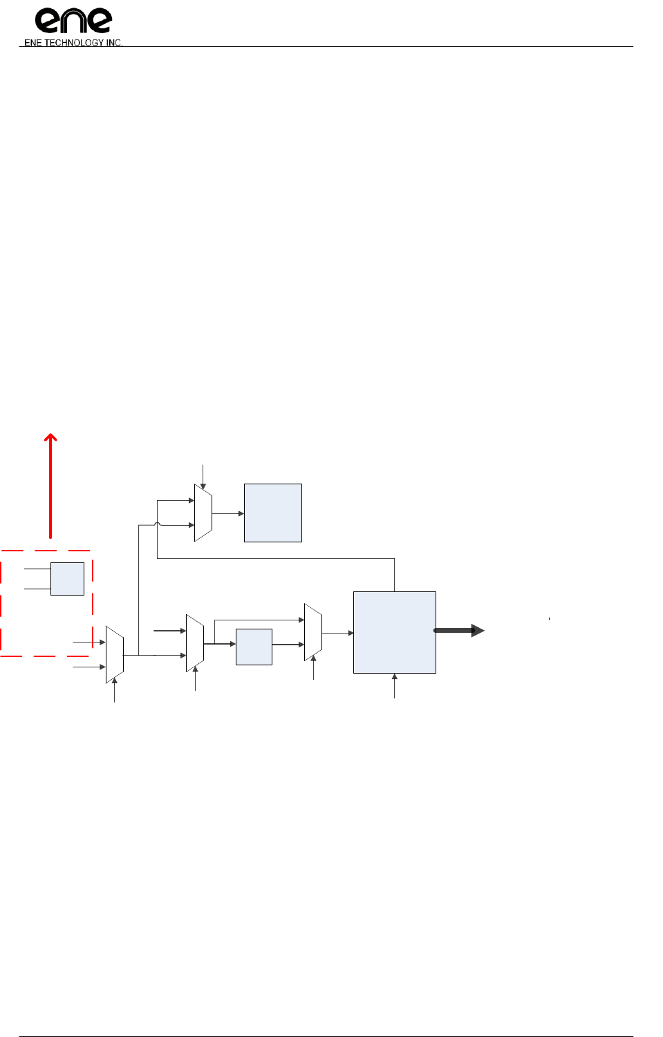
1.4 Block Diagram
LPC I/F
8051
build-in with
2 16-bit timers
1 UART
24 extended interrupt channels
ENE Host BUS
XBI/XIO
ENE
2nd
BUS
4KB
SRAM
GPT
x 4
GPIO
x 106
EC
hardware
command
x 5
KBC
hardware
command
x 8
FAN
X 2
WDT
IKB
18 x 8
hardware
command
x 10
PS2
x 3
LPC/FWH
MEM cycles
EC
Port 80
Index
IO Cycles
KBC
IO Cycles
code
Fetching
Bus
Data
Bus
EC Index mode can accessing
full register space by this path
clock
control
DAC
x 4
16.384 Mhz
32.768 Khz
PMU
ADC
X 8
CIR
SPI I/F
ESB
PECI
OWM
SHDI
PWM
X 6
SMBx2
4 ports
PCI clock
32.768 Mhz
GWG
EDI
Copyright© 2011, ENE Technology Inc.
8
KB9012 Keyboard Controller Datasheet
CONFIDENTIAL
2. Pin Assignment and Description
2.1 KB9012 128-pin LQFP Diagram Top View
2
1
4
3
6
5
8
7
10
9
60
59
58
57
56
55
54
53
52
51
50
49
48
47
46
45
44
43
42
41
40
39
38
37
36
35
34
33
KSI1
KSI0
KSO15
KSO14
KSO13
KSO12
KSO11
KSO10
KSO9
KSO8
KSO7
KSO6
KSO5
KSO4
KSO3
KSO2
KSO1
KSO0
CLKRUN#
ECRST#
GPIO1A
GND
GPIO19
VCC
11
12
13
14
15
16
17
18
19
20
21
22
23
24
25
26
27
28
105
106
107
108
109
110
111
112
113
114
115
116
117
118
119
120
121
122
123
124
125
126
127
128
29
30
31
32
64
63
62
61
KSI5
KSI4
KSI3
KSI2
101
102
103
104
97
98
99
100
KB9012
128-LQFP
96
95
94
93
92
91
90
89
81
88
87
86
83
82
85
84
75
80
77
76
79
78
69
74
71
70
73
72
65
67
66
68
KSI6
KSI7
AD0
AD1
GA20
KBRST#
SERIRQ
LFRAME#
LAD3
GPIO04
GPIO0A
LAD0
GPIO08
VCC
GPIO07
LAD1
PCIRST#
LAD2
PCICLK
GND
GPIO0D
GPIO0C
GPIO0B
SCI#
PWM0
VCC
PWM1
GND
PWM2
FANPWM0
FANPWM1
FANFB0
FANFB1
GPIO16
GPIO18
GPIO17 AD2
AD3
AVCC
DA0
DA3
DA2
DA1
AGND
AD4
AD5
SCL1
SDA1
KSO17
KSO16
SCL0
SDA0
PSDAT1
PSCLK1
PSDAT2
PSCLK2
PSDAT3
PSCLK3
GPIO50
GPIO52
GPIO53
GPIO54
GPIO55
GND
GPIO56
VCC
GPXIOA00
GPXIOA01
GPXIOA02
GPXIOA03
GPXIOA04
GPXIOA05
GPXIOA06
GPXIOA07
GPXIOA08
GPXIOA09
GPXIOA10
GPXIOA11
GPXIOD00
GPXIOD01
GPXIOD02
GPXIOD03
GPXIOD04
GPXIOD05
GPXIOD06
GPXIOD07
GND_0
VCC_0
GPIO5B
GPIO5C
GPIO57
V18R
VCC
GPIO58
GPIO5A
GPIO59
AD6
AD7
GPIO5D
GPIO5E

Copyright© 2011, ENE Technology Inc.
9
KB9012 Keyboard Controller Datasheet
CONFIDENTIAL
2.2 KB9012 128 LFBGA Ball Map
A1 A11A10A9A8A7A6A5A4A3A2 A12 A13
B1 B11B10B9B8B7B6B5B4B3B2 B12 B13
C1 C2 C12 C13
D1 D10D9D8D7D6D5D4D2 D12 D13
E1 E10E9E8E7E6E5E4E2 E12 E13
F1 F10F9F5F4F2 F12 F13
G1 G10G9G5G4G2 G12 G13
H1 H10H9H5H4H2 H12 H13
J1 J10J9J8J7J6J5J4J2 J12 J13
K1 K10K9K8K7K6K5K4K2 K12 K13
L1 L2 L12 L13
M1 M11M10
M9M8M7M6M5M4M3M2 M12 M13
N1 N11N10N9N8N7N6N5N4N3N2 N12 N13
GPXIOA01 GPIO55 GPIO54 GPIO52 PSCLK3 SDA1 SDA0 SCL0 DA1 DA2 AGND AD3 AD1
GPXIOA00 GPIO56 GPIO53 GPIO50 PSDAT3 GPIO40(AD6) GPIO41(AD7) SCL1 DA3 DA0 AVCC AD2 AD0
GPXIOA02 GPXIOD00
GPXIOA04 GPXIOA05
GPXIOA08 GPXIOA06
GPXIOA11 GPXIOA10
GPXIOD02 GND
GPXIOD04GPXIOD07(PECI)
XCLKI (MOSI)
XCLKO (MISO)
V18R KBRST#
KSI5 KSI6
KSI3 KSI4
KSI1 KSI2
VCC ECRST#
KSO1 KSO0
KSO2 KSO3
KSO9 KSO8
KSO11 KSO10
GPIO1A GPIO08
VCC GPIO19
GPIO18 GND
GPXIOA03 PSDAT2 PSCLK1 AD5 KSO17 KSI0 KSI7
GPXIOA07 PSCLK2 PSDAT1 AD4 KSO16 KSO15 KSO14
GPXIOA09 GPXIOD01
GPXIOD05 GPXIOD03
GPXIOD06 GPIO57
KSO13 KSO12
KSO6 KSO7
KSO5 KSO4
VCC GPIO04 VCC VCC GND GND GND
LFRAME# LAD1 GPIO0A VCC GPIO11 GPIO17 GPIO16
LAD2 PCIRST# CLKRUN# GPIO0C PWM1 PWM0 FANPWM0 FANFB0
LAD0 PCICLK SCI# GPIO0B GPIO0D GPIO07 FANPWM1 FANFB1
(SPICLK) GA20 SERIRQ
GPIO59 (SPICS#) LAD3

Copyright© 2011, ENE Technology Inc.
10
KB9012 Keyboard Controller Datasheet
CONFIDENTIAL
2.3 KB9012 Pin Assignment Side A
KB9012
Pin No.
KB9012
BGA
Name
GPIO
Alt
Output
Alt.
Input
Default
ECRST#
L/H
IO CELL
1
M2
GA20
GPIO00
GA20
GPIO00
HiZ / HiZ
BQC04HIV
2
L2
KBRST#
GPIO01
KBRST#
GPIO01
HiZ / HiZ
BQC04HIV
3
M3
SERIRQ
HiZ / HiZ
BQCZ16HIV
4
K4
LFRAME#
HiZ / HiZ
BQCZ16HIV
5
N3
LAD3
HiZ / HiZ
BQCZ16HIV
6
J5
GPIO04
GPIO04
GPIO04
HiZ / HiZ
BQC04HIV
7
M4
LAD2
HiZ / HiZ
BQCZ16HIV
8
K5
LAD1
HiZ / HiZ
BQCZ16HIV
9
--
VCC
VCC
10
N4
LAD0
HiZ / HiZ
BQCZ16HIV
11
--
GND
GND
12
N5
PCICLK
HiZ / HiZ
BQCZ16HIV
13
M5
PCIRST#
GPIO05
PCIRST#
GPIO05
IE / IE
BQCZ16HIV
14
N9
GPIO07
GPIO07
i_clk_8051
GPIO07
HiZ / HiZ
BQC04HIV
15
L13
GPIO08
GPIO08
i_clk_peri
GPIO08
HiZ / HiZ
BQC04HIV
16
K6
GPIO0A
GPIO0A
OWM
RLC_RX2
OWM
GPIO0A
HiZ / HiZ
BQC04HIV
17
N7
GPIO0B
GPIO0B
ESB_CLK
GPIO0B
HiZ / HiZ
BQCW16HIV
18
M7
GPIO0C
GPIO0C
ESB_DAT
ESB_DAT
GPIO0C
HiZ / HiZ
BQC08HIV
19
N8
GPIO0D
GPIO0D
RLC_TX2
GPIO0D
HiZ / HiZ
BQC04HIV
20
N6
SCI#
GPIO0E
SCI#
GPIO0E
HiZ / HiZ
BQC04HIV
21
M9
PWM0
GPIO0F
PWM0
GPIO0F
HiZ / HiZ
BQCZ16HIV
22
K7/J7
VCC
VCC
VCC
23
M8
PWM1
GPIO10
PWM1
GPIO10
HiZ / HiZ
BQC04HIV
24
J8/J9/J10
GND
GND
GND
25
K8
GPIO11
GPIO11
PWM2
GPIO11
HiZ / HiZ
BQC04HIV
26
M10
FANPWM0
GPIO12
FANPWM0
GPIO12
HiZ / HiZ
BQC04HIV
27
N10
FANPWM1
GPIO13
FANPWM1
GPIO13
HiZ / HiZ
BQC04HIV
28
M11
FANFB0
GPIO14
FANFB0
GPIO14
HiZ / HiZ
BQC04HIV
29
N11
FANFB1
GPIO15
FANFB1
GPIO15
HiZ / HiZ
BQC04HIV
30
K10
GPIO16
GPIO16
E51TXD
GPIO16
HiZ / HiZ
BQC04HIV
31
K9
GPIO17
GPIO17
E51CLK
E51RXD
GPIO17
HiZ / HiZ
BQC04HIV
32
N12
GPIO18
GPIO18
POWER_FAIL1
GPIO18
HiZ / HiZ
BQC04HIV

Copyright© 2011, ENE Technology Inc.
11
KB9012 Keyboard Controller Datasheet
CONFIDENTIAL
2.4 KB9012 Pin Assignment Side B
KB9012
Pin No.
KB9012
BGA
Name
GPIO
Alt
Output
Alt.
Input
Default
ECRST#
L/H
IO CELL
33
--
VCC
VCC
34
M13
GPIO19
GPIO19
PWM3
GPIO19
HiZ / HiZ
BQCZ16HIV
35
--
GND
GND
36
L12
GPIO1A
GPIO1A
NUMLED#
GPIO1A
HiZ / HiZ
BQC20HIV
37
K13
ECRST#
IE / IE
BQC04HIV
38
M6
CLKRUN#
GPIO1D
CLKRUN#
CLKRUN#
GPIO1D
HiZ / HiZ
BQCZ16HIV
39
J13
KSO0
GPIO20
KSO0
TP_TEST
GPIO20
IE(PU)/IE(PU)
BQC04HIV
40
J12
KSO1
GPIO21
KSO1
TP_PLL
GPIO21
IE(PU)/IE(PU)
BQC04HIV
41
H12
KSO2
GPIO22
KSO2
TP_TMUX
GPIO22
IE(PU)/IE(PU)
BQC04HIV
42
H13
KSO3
GPIO23
KSO3
TP_PLL_LOCK
GPIO23
IE(PU)/IE(PU)
BQC04HIV
43
H10
KSO4
GPIO24
KSO4
GPIO24
HiZ / HiZ
BQC04HIV
44
H9
KSO5
GPIO25
KSO5
PCICLK
(LPC)
GPIO25
HiZ / HiZ
BQCZ16HIV
45
G9
KSO6
GPIO26
KSO6
PCIRST#
(LPC)
GPIO26
HiZ / HiZ
BQC04HIV
46
G10
KSO7
GPIO27
KSO7
SERIRQ(LPC)
SERIRQ(LPC)
GPIO27
HiZ / HiZ
BQC04HIV
47
G13
KSO8
GPIO28
KSO8
LFRAME#
(LPC)
GPIO28
HiZ / HiZ
BQC04HIV
48
G12
KSO9
GPIO29
KSO9
GPIO29
HiZ / HiZ
BQC04HIV
49
F13
KSO10
GPIO2A
KSO10
GPIO2A
HiZ / HiZ
BQC04HIV
50
F12
KSO11
GPIO2B
KSO11
LAD3(LPC)
LAD3(LPC)
GPIO2B
HiZ / HiZ
BQC04HIV
51
F10
KSO12
GPIO2C
KSO12
LAD2(LPC)
LAD2(LPC)
GPIO2C
HiZ / HiZ
BQC04HIV
52
F9
KSO13
GPIO2D
KSO13
LAD1(LPC)
LAD1(LPC)
GPIO2D
HiZ / HiZ
BQC04HIV
53
E10
KSO14
GPIO2E
KSO14
LAD0(LPC)
LAD0(LPC)
GPIO2E
HiZ / HiZ
BQC04HIV
54
E9
KSO15
GPIO2F
KSO15
(E51_RXD)
GPIO2F
HiZ / HiZ
BQC04HIV
55
D9
KSI0
GPIO30
(E51_TXD)
KSI0
GPIO30
IE(PU)/IE(PU)
BQC04HIV
56
E12
KSI1
GPIO31
KSI1
GPIO31
IE(PU)/IE(PU)
BQC04HIV
57
E13
KSI2
GPIO32
KSI2
GPIO32
IE(PU)/IE(PU)
BQC04HIV
58
D12
KSI3
GPIO33
KSI3
GPIO33
IE(PU)/IE(PU)
BQC04HIV
59
D13
KSI4
GPIO34
KSI4/EDI_CS
GPIO34
IE(PU)/IE(PU)
BQC04HIV
60
C12
KSI5
GPIO35
KSI5/EDI_CLK
GPIO35
IE(PU)/IE(PU)
BQC04HIV
61
C13
KSI6
GPIO36
KSI6/EDI_DIN
GPIO36
IE(PU)/IE(PU)
BQC04HIV
62
D10
KSI7
GPIO37
EDI_DO
KSI7
GPIO37
IE(PU)/IE(PU)
BQC04HIV
63
B13
AD0
GPIO38
AD0
GPIO38
HiZ / HiZ
BQCZT04IV
64
A13
AD1
GPIO39
AD1
GPIO39
HiZ / HiZ
BQCZT04IV

Copyright© 2011, ENE Technology Inc.
12
KB9012 Keyboard Controller Datasheet
CONFIDENTIAL
2.5 KB9012 Pin Assignment Side C
KB9012
Pin No.
KB9012
BGA
Name
GPIO
Alt
Output
Alt.
Input
Default
ECRST#
L/H
IO CELL
65
B12
AD2
GPIO3A
AD2
GPIO3A
HiZ / HiZ
BQCZT04IV
66
A12
AD3
GPIO3B
AD3
GPIO3B
HiZ / HiZ
BQCZT04IV
67
B11
AVCC
AVCC
68
B10
DA0
GPIO3C
DA0
GPIO3C
HiZ / HiZ
BQCZT04IV
69
A11
AGND
AGND
70
A9
DA1
GPIO3D
DA1
GPIO3D
HiZ / HiZ
BQCZT04IV
71
A10
DA2
GPIO3E
DA2
GPIO3E
HiZ / HiZ
BQCZT04IV
72
B9
DA3
GPIO3F
DA3
GPIO3F
HiZ / HiZ
BQCZT04IV
73
B6
AD6
GPIO40
CIR_RX
/ AD6
GPIO40
HiZ / HiZ
BQCZT04IV
74
B7
AD7
GPIO41
CIR_RLC_TX
AD7
GPIO41
HiZ / HiZ
BQCZT04IV
75
E7
AD4
GPIO42
AD4
GPIO42
HiZ / HiZ
BQCZT04IV
76
D7
AD5
GPIO43
AD5
GPIO43
HiZ / HiZ
BQCZT04IV
77
A8
SCL0
GPIO44
SCL0
GPIO44
HiZ / HiZ
BQC04HI
78
A7
SDA0
GPIO45
SDA0
GPIO45
HiZ / HiZ
BQC04HI
79
B8
SCL1
GPIO46
SCL1
GPIO46
HiZ / HiZ
BQC04HI
80
A6
SDA1
GPIO47
SDA1
GPIO47
HiZ / HiZ
BQC04HI
81
E8
KSO16
GPIO48
KSO16
GPIO48
HiZ / HiZ
BQC04HIV
82
D8
KSO17
GPIO49
KSO17
GPIO49
HiZ / HiZ
BQC04HIV
83
D6
PSCLK1
GPIO4A
PSCLK1 / SCL2
GPIO4A
HiZ / HiZ
BQC04HI
84
E6
PSDAT1
GPIO4B
PSDAT1 / SDA2
GPIO4B
HiZ / HiZ
BQC04HI
85
E5
PSCLK2
GPIO4C
PSCLK2
/ SCL3
GPIO4C
HiZ / HiZ
BQCZ16HIV
86
D5
PSDAT2
GPIO4D
PSDAT2
/ SDA3
GPIO4D
HiZ / HiZ
BQC20HIV
87
A5
PSCLK3
GPIO4E
PSCLK3
GPIO4E
HiZ / HiZ
BQC04HI
88
B5
PSDAT3
GPIO4F
PSDAT3
GPIO4F
HiZ / HiZ
BQC04HI
89
B4
GPIO50
GPIO50
GPIO50
HiZ / HiZ
BQC04HI
90
A4
GPIO52
GPIO52
E51CS#
GPIO52
HiZ / HiZ
BQC20HIV
91
B3
GPIO53
GPIO53
CAPSLED#
E51TMR1
GPIO53
HiZ / HiZ
BQC20HIV
92
A3
GPIO54
GPIO54
WDT_LED#
E51TMR0
GPIO54
HiZ / HiZ
BQC20HIV
93
A2
GPIO55
GPIO55
SCROLED#
E51INT0
GPIO55
HiZ / HiZ
BQC20HIV
94
--
GND
GND
95
B2
GPIO56
GPIO56
E51INT1
GPIO56
HiZ / HiZ
BQC04HIV
96
--
VCC
VCC

Copyright© 2011, ENE Technology Inc.
13
KB9012 Keyboard Controller Datasheet
CONFIDENTIAL
2.6 KB9012 Pin Assignment Side D
KB9012
Pin No.
KB9012
BGA
Name
GPIO
Alt
Output
Alt.
Input
Default
ECRST#
L/H
IO CELL
97
B1
GPXIOA00
GPXIOA00
SHICS#
SDICS#
HiZ / HiZ
BQC04HIV
98
A1
GPXIOA01
GPXIOA01
SHICLK
SDICLK
HiZ / HiZ
BQC04HIV
99
C1
GPXIOA02
GPXIOA02
SHIDO
SDIDI
HiZ / HiZ
BQC04HIV
100
D4
GPXIOA03
GPXIOA03
POWER_FAIL0
FANFB2
HiZ / HiZ
BQC04HIV
101
D1
GPXIOA04
GPXIOA04
FANFB3
HiZ / HiZ
BQC04HIV
102
D2
GPXIOA05
GPXIOA05
VCIN1
HiZ / HiZ
BQC04HIV
103
E2
GPXIOA06
GPXIOA06
VCOUT1
HiZ / HiZ
BQC04HIV
104
E4
GPXIOA07
GPXIOA07
VCOUT0
HiZ / HiZ
BQC04HIV
105
E1
GPXIOA08
GPXIOA08
HiZ / HiZ
BQCZ16HIV
106
F4
GPXIOA09
GPXIOA09
HiZ / HiZ
BQCZ16HIV
107
F2
GPXIOA10
GPXIOA10
HiZ / HiZ
BQCZ16HIV
108
F1
GPXIOA11
GPXIOA11
GWG
HiZ / HiZ
BQCZ16HIV
109
C2
GPXIOD00
GPXIOD00
SDIDO
SHIDI /
VCIN0
HiZ / HiZ
BQC04HIV
110
F5
GPXIOD01
GPXIOD01
AC_IN
HiZ / HiZ
BQC04HIV
111
J6
VCC_0
HiZ / HiZ
VCC_0
112
G1
GPXIOD02
GPXIOD02
ALW_PWR_EN
HiZ / HiZ
BQC04HIV
113
G2
GND_0
HiZ / HiZ
GND_0
114
G5
GPXIOD03
GPXIOD03
ON/OFFBTN#
HiZ / HiZ
BQC04HIV
115
H1
GPXIOD04
GPXIOD04
HiZ / HiZ
BQC04HIV
116
G4
GPXIOD05
GPXIOD05
HiZ / HiZ
BQC04HIV
117
H4
GPXIOD06
GPXIOD06
HiZ / HiZ
BQC04HIV
118
H2
GPXIOD07
GPXIOD07
PECI
PECI
HiZ / HiZ
BQC04HIVPECI
119
K2
GPIO5B
GPIO5B
(MISO)
GPIO5B
HiZ / HiZ
BQCZ16HIV
120
J2
GPIO5C
GPIO5C
(MOSI)
GPIO5C
HiZ / HiZ
BQCZ16HIV
121
H5
GPIO57
GPIO57
XCLK32K
GPIO57
HiZ / HiZ
BQC04HIV
122
J1
GPIO5D
GPIO5D
(XCLKI)
GPIO5D
HiZ / HiZ
BQCZT04IV
123
K1
GPIO5E
GPIO5E
(XCLKO)
GPIO5E
HiZ / HiZ
BQCZT04IV
124
L1
V18R
125
J4
VCC
VCC
126
M1
GPIO58
GPIO58
(SPICLK)
GPIO58
HiZ / HiZ
BQCW16HIV
127
N1
GPIO59
GPIO59
GPIO59
IE / IE
BQC04HIV
128
N2
GPIO5A
GPIO5A
(SPICS#)
GPIO5A
HiZ / HiZ
BQCZ16HIV
* Please note, crystal pad signal frequency should be lower than 1MHz.
Copyright© 2011, ENE Technology Inc.
14
KB9012 Keyboard Controller Datasheet
CONFIDENTIAL
2.7 I/O Cell Descriptions
2.7.1 I/O Buffer Table
Cell
Description
Application
BQCZ16HIV
Schmitt trigger, 16mA Output / Sink Current, Input / Output / Pull Up
Enable(40KΩ), 5 V Tolerance.
GPIO, LPC
I/F
BQC04HIV
Schmitt trigger, 4mA Output / Sink Current, Input / Output / Pull Up
Enable(40KΩ), 5 V Tolerance
GPIO
BQCW16HIV
Schmitt trigger, 16mA Output / Sink Current, 5 V Tolerance, Input / Output / Pull
Up Enable
ESB_CLK/
SPI_CLK
BQC04HI
Schmitt trigger, 4mA Output / Sink Current, 5 V Tolerance, Input / Output
Enable
GPIO
BQC08HIV
Schmitt trigger, 8mA Output / Sink Current, 5V Tolerance, Input / Output / Pull
Up Enable
ESB_DAT
BQC04HIVPECI
Mixed Mode IO, PECI enable, with GPIO
GPIO: Schmitt trigger, 4mA Output / Sink Current,
PECI: 0.9V~1.2V
PECI, GPIO
BQCZT04IV
***
Mixed Mode IO, AE enable, with GPIO
GPIO: Schmitt trigger, 4mA Output / Sink Current, Input / Output / Pull Up
Enable
ADC/DAC,
XCLKI,
XCLKO
* 5V Tolerance, only if pull-high disable and output disable.
** Please note, the total current in each side on VCC or VSS of chip can not exceed over 48mA.
*** Please note, As BQCZT04IV with shared crystal pad, signal frequency should be lower than 1MHz.
2.7.2 I/O Buffer Characteristic Table
Cell
Output
Input
Analog
Signal
Pull-High
Enable(40k)
5V
Tolerance
Current
(mA)
Application
BQCZ16HIV
ˇ
ˇ
ˇ
ˇ
8~16
GPIO, LPC
I/F
BQC04HIV
ˇ
ˇ
ˇ
ˇ
2~4
GPIO
BQCW16HIV
ˇ
ˇ
ˇ
ˇ
8~16
ESB_CLK/
SPI_CLK
BQC04HI
ˇ
ˇ
ˇ
2~4
GPIO
BQC08HIV
ˇ
ˇ
ˇ
ˇ
4~8
ESB_DAT
BQC04HIVPECI
ˇ
ˇ
ˇ
ˇ
2~4
PECI, GPIO
BQCZT04IV
ˇ
ˇ
ˇ
ˇ
2~4
ADC/DAC,
XCLKI,
XCLKO
Copyright© 2011, ENE Technology Inc.
15
KB9012 Keyboard Controller Datasheet
CONFIDENTIAL
3. Pin Descriptions
3.1 Hardware Trap
Hardware trap pins are used to latch external signal at rising edge of ECRST#. The hardware
trap pins are for some special purpose which should be defined while boot-up. The following table
gives the collection of hardware trap pins. Please note, all the following hardware trap pins are
pull-high internally after reset.
Trap Name
Pin No.
Description
TP_TEST
(GPIO20,KSO0)
39
While this trap is asserted to be low, the internal DPLL circuit uses other clock source
for reference, instead of 32KHz oscillator.
Low: test clock mode enable
High: normal mode using 32KHz oscillator.
TP_PLL
(GPIO21,KSO1)
40
While this trap is asserted to be low, some DPLL related signals can be output for
test.
Low: DPLL test mode enable.
High: DPLL test mode disable
TP_TMUX
(GPIO22,KSO2)
41
TestMux Mode Trap
Low: Test mode
High: Normal operation
TP_PLL_Lock
(GPIO23,KSO3)
42
This trap is used for eFlash & EDI operation, , the 8051 will be held at reset state
LOW: Test Mode
HIGH: Normal operation
* Please note while TP_TMUX and TP_PLL_Lock keep low at the same time, a mechanism called FlashDirectAccess will
enable. That is, users can flush and program a SPI flash via specific IKB pins with external tool.
FlashDirectAccess:
The KBC provides a new interface to program SPI flash via IKB interface. With this feature, users can easily utilize 4 pins
from keyboard matrix (IKB) without disassembly whole machine. These 4 pins are connected directly to external SPI-Flash
interface. The following table shows the mapped pins while entering FlashDirectAccess mode.
EDI : For detail ENE Debug Interface, please refer the EDI section for enabling, instruction, and application.
Pin No.
Normal Mode
FlashDirectAccess Mode
59
KSI4 (I)
(Input) EDI_CS, Transfer signal from terminal into KBC and though SPICS# to SPI_Flash
60
KSI5 (I)
(Input) EDI_CLK, Transfer signal from terminal into KBC and though SPICLK to SPI_Flash
61
KSI6 (I)
(Input) EDI_DIN, Transfer signal from terminal into KBC and though MOSI to SPI_Flash
62
KSI7 (I)
(Output) EDI_DO, Transfer signal from terminal into KBC and though MISO to SPI_Flash
ENE
KBC
Terminal SPI-Flash
P128, SPICS#
P120, MOSI
P119, MISO
P126, SPICLK
P59, KSI4
P60, KSI5
P61, KSI6
P62, KSI7
EDI_CS
EDI_CLK
EDI_DIN
EDI_DO

Copyright© 2011, ENE Technology Inc.
16
KB9012 Keyboard Controller Datasheet
CONFIDENTIAL
3.2 Pin Descriptions by Functions
3.2.1 Low Pin Count I/F Descriptions.
Pin Name
Pin No.
Direction
Description
LAD[3:0]
5, 7,8,10
I/O
LPC address bus.
LFARAME#
4
I
LPC frame control signal.
PCIRST#
13
I
LPC module reset by this signal.
PCICLK
12
I
33MHz PCI clock input.
SERIRQ
3
I/O
Serial IRQ
CLKRUN#
38
I/OD
Clock run control
3.2.2 PS/2 I/F Descriptions
Pin Name
Pin No.
Direction
Description
PSCLK1
83
I/OD
PS/2 port 1 clock
Muxed with SMBus port 2 clock
PSDAT1
84
I/OD
PS/2 port 1 data
Muxed with SMBus port 2 data
PSCLK2
85
I/OD
PS/2 port 2 clock
Muxed with SMBus port 3 clock
PSDAT2
86
I/OD
PS/2 port 2 data
Muxed with SMBus port 3 data
PSCLK3
87
I/OD
PS/2 port 3 clock
PSDAT3
88
I/OD
PS/2 port 3 data
3.2.3 Internal Keyboard Encoder (IKB) Descriptions
Pin Name
Pin No.
Direction
Description
KSO[17:0]
82,81,54-39
O
Keyboard Scan Out
KSI[7:0]
62-55
I
Keyboard Scan In
3.2.4 SMBus Descriptions
Pin Name
Pin No.
Direction
Description
SCL0
77
I/OD
SMBus clock (interface 0)
SDA0
78
I/OD
SMBus data (interface 0)
SCL1
79
I/OD
SMBus clock (interface 1)
SDA1
80
I/OD
SMBus data (interface 1)
SCL2
83
I/OD
SMBus clock (interface 2)
Muxed with PS/2 port 1 clock
SDA2
84
I/OD
SMBus data (interface 2)
Muxed with PS/2 port 1 data
SCL3
85
I/OD
SMBus clock (interface 3)
Muxed with PS/2 port 2 clock
SDA3
86
I/OD
SMBus data (interface 3)
Muxed with PS/2 port 2 data
Copyright© 2011, ENE Technology Inc.
17
KB9012 Keyboard Controller Datasheet
CONFIDENTIAL
3.2.5 FAN Descriptions
Pin Name
Pin No.
Direction
Description
FANPWM0
26
O
FANPWM0 output
FANPWM1
27
O
FANPWM1 output
FANFB0
28
I
FAN0 tachometer input
FANFB1
29
I
FAN1 tachometer input
FANFB2
100
I
FAN2 tachometer input
FANFB3
101
I
FAN3 tachometer input
3.2.6 Pulse Width Modulation (PWM) Descriptions
Pin Name
Pin No.
Direction
Description
PWM0
21
O
PWM pulse output
PWM1
23
O
PWM pulse output
PWM2
25
O
PWM pulse output
PWM3
34
O
PWM pulse output
3.2.7 Analog-to-Digital Converter Descriptions
Pin Name
Pin No.
Direction
Description
AD[3:0]
66-63
I
10bit A/D converter input
AD[5:4]
76,75
I
10bit A/D converter input
AD6
73
I
10bit A/D converter input
AD7
74
I
10bit A/D converter input
3.2.8 Digital-to-Analog Converter Descriptions
Pin Name
Pin No.
Direction
Description
DA[3:0]
72-70,68
O
8bit D/A converter output
3.2.9 8051 External I/F Descriptions
Pin Name
Pin No.
Direction
Description
E51TXD
30
O
8051 serial port, transmit port.
E51RXD
31
I
8051 serial port, receive port.
E51CLK
31
O
For different serial scheme, E51CLK will shift out clock.
E51CS#
90
O
E51TMR0
92
I
E51INT0
93
I
E51TMR1
91
I
E51INT1
95
I
Copyright© 2011, ENE Technology Inc.
18
KB9012 Keyboard Controller Datasheet
CONFIDENTIAL
3.2.10 External Clock Descriptions
(These pins are reserved for external CLK design structure, also could be set as GPIO function)
Pin Name
Pin No.
Direction
Description
XCLKI
122
I
32.768KHz input
XCLKO
123
O
32.768KHz output
3.2.11 Miscellaneous Signals Descriptions
Pin Name
Pin No.
Direction
Description
GA20
1
O
KBC will gate A20 address line
KBRST#
2
O
KBRST# is used to generate system reset.
SCI#
20
O
SCI# asserts to the system for requesting service while
related events occur.
ECRST#
37
I
While ECRST# asserted, the KBC will reset globally.
OWM
16
I/O
One Wire Master input and output signal
PECI
118
I/O
PECI input and output signal
GWG
108
O
General Waveform Generator for 3D application
POWER_FAIL0
100
O
Used to indicate the power fail under Power Fail Voltage.
POWER_FAIL1
32
O
Used to indicate the power fail under Power Fail Voltage.
3.2.12 Voltage Comparator Pins Descriptions
Pin Name
Pin No.
Direction
Description
VCIN0
109
I
Voltage comparator input port0
VCOUT0
104
O
Voltage comparator output port0
VCIN1
102
I
Voltage comparator input port1
VCOUT1
103
O
Voltage comparator output port1
3.2.13 Power Pins Descriptions
Pin Name
Pin No.
Direction
Description
VCC
9,22,33,96,111,125
Power supply for digital plane.
GND
11,24,35,94,113
Power ground for digital plane.
AVCC
67
Power supply for analog plane.
AGND
69
Power ground for analog plane.
V18R
124
Connected to external Capacitor for internal 1.8V
VCC_0
111
Power supply for 51ON power management
GND_0
113
Power ground for 51ON power management

Copyright© 2011, ENE Technology Inc.
19
KB9012 Keyboard Controller Datasheet
CONFIDENTIAL
3.2.14 51ON Power Pins Descriptions
(The 51ON power management are with different power domain from main IC power)
Pin Name
Pin No.
Direction
Description
GPXIOD01
110
I/O
AC_IN
GPXIOD02
112
I/O
ALW_PWR_EN
GPXIOD03
114
I/O
ON/OFFBTN#

Copyright© 2011, ENE Technology Inc.
20
KB9012 Keyboard Controller Datasheet
CONFIDENTIAL
4. Module Descriptions
4.1 Chip Architecture
4.1.1 Power Planes
Power planes are ±10% tolerance for recommend operation condition, The KBC provides
V1.8 power plane for different generation.
Power Plane
Description
Power
Ground
Digital Plane
This power provides power for all digital logic no matter what
power mode is.
VCC
GND
Analog Plane
This power provides power for all analog logic, such as A/D
and D/A converter.
AVCC
AGND
Digital V1.8
The system inputs 3.3V power and the internal regulator
outputs 1.8V voltage. The 1.8V output should connect a
capacitor for stable purpose.
V1.8
GND
Power Latch
Plane
This power provides power for the power-latch circuit. It could
help to provide power saving management.
VCC_0
GND_0
Copyright© 2011, ENE Technology Inc.
21
KB9012 Keyboard Controller Datasheet
CONFIDENTIAL
4.1.2 Clock Domains
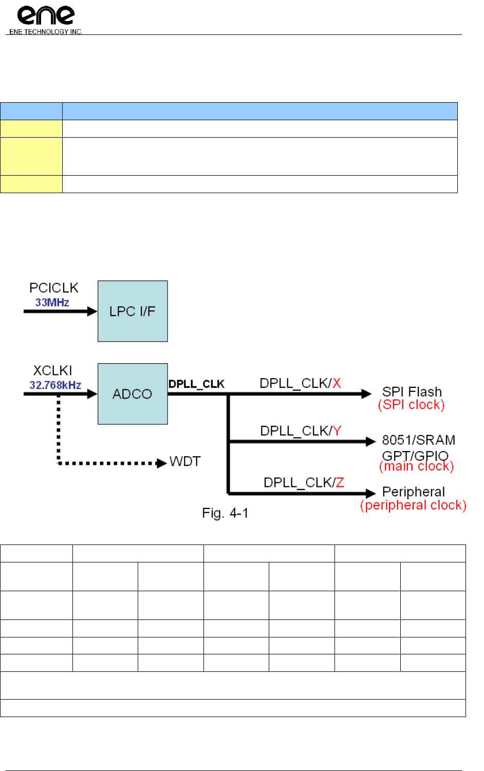
Three clock sources, PCICLK, DPLL_CLK and XCLKI will be discussed in this section. A
summary is list in the following table.
Clock
Description
PCICLK
PCI clock 33MHz for LPC I/F.
DPLL_CLK
Main clock for 8051/peripheral. DPLL clock can be generated with or without XCLK for
reference. DPLL clock can be divided for different applications. Fig. 4-1 gives an example for
illustration.
XCLKI
External 32.768KHz for reference.
The following figure shows more detail about the operation in the KBC. The external
32.768KHz is provided for two purposes. One is to provide an accurate reference for internal DPLL
module, and the other one is to provide another clock source for watchdog timer.
The possible (X,Y,Z) combination with exact clock value is summarized as the following table.
SPI Clock (X)
Main Clock (Y)
Peripheral Clock (Z)
CLKCFG[6]=0
(default)
CLKCFG[6]=1
CLKCFG[6]=0
(default)
CLKCFG[6]=1
CLKCFG[6]=0
(default)
CLKCFG[6]=1
CLKCFG[3:2]=0
(default)
16*
66
8*
8
4*
4
CLKCFG[3:2]=1
32
66
16
16
8
8
CLKCFG[3:2]=2
32
66
22
22
11
11
CLKCFG[3:2]=3
32
66
32
32
16
16
* While power on default, no matter what value CLKCFG[3:2], CLKCFG[6] are, the dividend (X,Y,Z) is always (4,
8, 16). The PCI clock is 66MHz, X= 66/4 = 16MHz, Y= 66/8 = 8Mhz , Z= 66/16 = 4MHz
Be noted that, these clock frequency is only valid after KBC correctly referring clock.
Copyright© 2011, ENE Technology Inc.
22
KB9012 Keyboard Controller Datasheet
CONFIDENTIAL
Note: Internal OSC of KB9012 application
Since KB9012 also provide internal OSC, the clock source selection is similar
to KBx930. Developer could choose clock source from internal-OSC, external
crystal, or host LPCLCK depending on different application and system status. As
following is simplified clocking distribution tree for setting.
Please note that, KB9012 also support external clock source without crystal
device. For correctly configuration, please contact your sales or technical
representative for the application note: Using External OSC Clock Source for ENE Keyboard
Controller.
PCICLK
0xFF1F[5]
PLLCFG2
0
1
External Source
0xFE8A[0]
Internal OSC
0xFE8A[1]
0xFE8A[2]
CLK32CR
0
1
10-bit
Divider
DPLL
& Clock
Generator
0xFF1F[4]
PLLCFG2
0
1
WDT
0
1
0xFE80[7]
WDTCFG
{XBI, SPI Flash
8051, SRAM, GPT, GPIO
Peripheral
0xFF0D[5]
CLKCFG
Enable
0xFE8A[5:4]
CLK32CR Pin 122 , Pin 123
00 : GPIO5D, GPIO5E
01 : GPIO5D, XCLKO as external clock input
10 : XLCKI, GPIO5E, where XLCKI is external clock input
11 : XLCKI, XCLKO, as crystal pads to external crystal
KBC
Pin 122
Pin 123
32k Source Pad Configuration
Copyright© 2011, ENE Technology Inc.
23
KB9012 Keyboard Controller Datasheet
CONFIDENTIAL
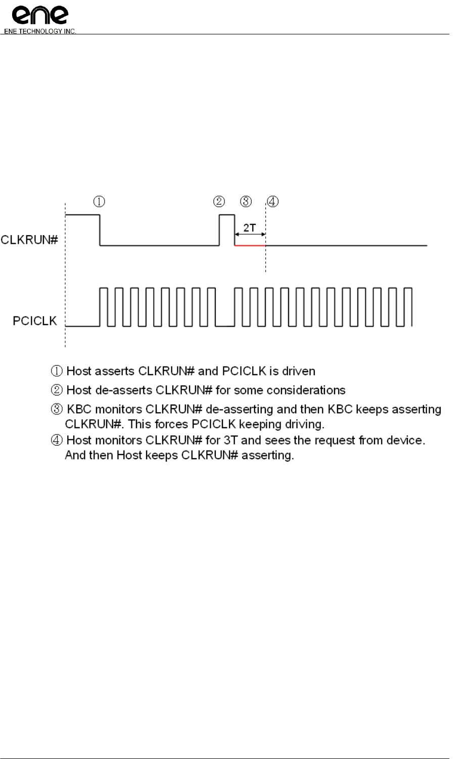
4.1.3 PCICLK and CLKRUN#
While system power-on, the host starts to drive CLKRUN# low for a while to inform the slaves
that a 33MHz PCICLK will be given. At this moment, CLKRUN# of KBC is in input mode. If the host
tries to stop the PCICLK for some purpose, the CLKRUN# will be de-asserted. In KB9012 design,
the KBC responses CLKRUN# signal according to LPC_CDCSR configuration. Please refer section
4.13.7 LPC Registers Description for KB9012 application. For more detail please refer to PCI Mobile
Design Guide version 1.1.

Copyright© 2011, ENE Technology Inc.
24
KB9012 Keyboard Controller Datasheet
CONFIDENTIAL
4.1.4 Internal Memory Map
No
Module
Descriptions
Address Range
Size (Byte)
1
Flash
Space mapped to system BIOS
0x0000~0xEBFF
59K
2
XRAM
Embedded SRAM
0xEC00~0xFBFF
4K
3
GPIO
General purpose I/O
0xFC00~0xFC7F
128
1K
4
KBC
Keyboard controller
0xFC80~0xFC8F
16
5
ESB
ENE serial bus controller
0xFC90~0xFC9F
16
6
IKB
Internal keyboard matrix
0xFCA0~0xFCAF
16
7
(ESB)
(Available for ESB)
0xFCB0~0xFCBF
16
8
(ESB)
(Available for ESB)
0xFCC0~0xFCCF
16
9
PECI
PECI controller
0xFCD0~0xFCDF
16
10
RSV
Reserved
0xFCE0~0xFCEF
16
11
OWM
One Wire Master
0xFCF0~0xFCFF
16
12
(ESB)
(Available for ESB)
0xFD00~0xFDFF
256
13
PWM
Pulse width modulation
0xFE00~0xFE1F
32
14
FAN
Fan controller
0xFE20~0xFE4F
48
15
GPT
General purpose timer
0xFE50~0xFE6F
32
16
SDIH/
SDID
SPI host interface/
SPI device interface
0xFE70~0xFE7F
16
17
WDT
Watchdog timer
0xFE80~0xFE8F
16
18
LPC
Low pin count interface
0xFE90~0xFE9F
16
19
XBI
X-bus interface
0xFEA0~0xFEBF
32
20
CIR
Consumer IR controller
0xFEC0~0xFECF
16
21
GWG
General Waveform Generation
0xFED0~0xFEDF
16
22
PS2
PS/2 interface
0xFEE0~0xFEFF
32
23
EC
Embedded controller
0xFF00~0xFF2F
48
24
GPWU
General purpose wakeup event
0xFF30~0xFF7F
80
25
RSV
Reserved
0xFF80~0xFF8F
16
26
SMBus
SMBus controller 0
0xFF90~0xFFBF
48
27
RSV
Reserved
0xFFC0~0xFFCF
16
28
SMBus
SMBus controller 1
0xFFD0~0xFFFF
48

Copyright© 2011, ENE Technology Inc.
25
KB9012 Keyboard Controller Datasheet
CONFIDENTIAL
4.2 GPIO
GPIOFSx is only for Output Function Selection, not for Input Function.
Example1 – GPIO14 is used as FANFB1, then
GPIO(GPIOFS10) 0xFC02 b‘4 must be 0,
GPIO(GPIOIE10) 0xFC62 b‘4 must be 1.
Example2 – PS/2 clock/data lines and SMBus clock/data are bi-directional.
They must be programmed as Output Function Selection = 1 and Input Enable = 1.
For other specific GPIO initialization, please refer the SW programming guide.
4.2.1 GPIO Function Description
The GPIO module is flexible for different applications. Each GPIO pin can be configured
as alternative input or alternative output mode. The alternative function can be selected by register
setting. A summary table is given as below for more detail.
GPIO
Alt. Output
Alt. Input
Default Alt. Output
Alt. Selection Reg.
GPIO00
GA20
GPIO00
GPIOFS00.[0]
GPIO01
KBRST#
GPIO01
GPIOFS00.[1]
GPIO02*
GPIO02
GPIOFS00.[2]
GPIO03*
GPIO03
GPIOFS00.[3]
GPIO04
GPIO04
GPIOFS00.[4]
GPIO05
PCIRST#
GPIO05
GPIOFS00.[5]
GPIO06*
GPIO06
GPIOFS00.[6]
GPIO07
i_clk_8051
GPIO07
GPIOFS00.[7]
GPIO08
i_clk_peri
GPIO08
GPIOFS08.[0]
GPIO09*
GPIO09
GPIOFS08.[1]
GPIO0A
OWM
RLC_RX2
/ OWM
GPIO0A
GPIOFS08.[2]
OWMCFG[7]
GPIO0B
ESB_CLK
GPIO0B
GPIOFS08.[3]
GPIO0C
ESB_DAT
ESB_DAT
GPIO0C
GPIOFS08.[4]
GPIO0D
RLC_TX2
GPIO0D
GPIOFS08.[5]
GPIO0E
SCI#
GPIO0E
GPIOFS08.[6]
GPIO0F
PWM0
GPIO0F
GPIOFS08.[7]
GPIO10
PWM1
GPIO10
GPIOFS10.[0]
GPIO11
PWM2
GPIO11
GPIOFS10.[1]
GPIO12
FANPWM0
GPIO12
GPIOFS10.[2]
GPIO13
FANPWM1
GPIO13
GPIOFS10.[3]
GPIO14
FANFB0
GPIO14
GPIOFS10.[4]
GPIO15
FANFB1
GPIO15
GPIOFS10.[5]
GPIO16
E51TXD
GPIO16
GPIOFS10.[6]
GPIO17
E51CLK
E51RXD
GPIO17
GPIOFS10.[7]
GPIO18
POWER_FAIL1
GPIO18
GPIOFS18.[0]
GPIO19
PWM3
GPIO19
GPIOFS18.[1]
GPIO1A
NUMLED#
GPIO1A
GPIOFS18.[2]
GPIO1B*
GPIO1B
GPIOFS18.[3]
GPIO1C*
GPIO1C
GPIOFS18.[4]

Copyright© 2011, ENE Technology Inc.
26
KB9012 Keyboard Controller Datasheet
CONFIDENTIAL
GPIO
Alt. Output
Alt. Input
Default Alt. Output
Alt. Selection Reg.
GPIO1D
CLKRUN#
CLKRUN#
GPIO1D
GPIOFS18.[5]
GPIO1E*
GPIO1E
GPIOFS18.[6]
GPIO1F*
GPIO1F
GPIOFS18.[7]
GPIO20
KSO00
TP_TEST
GPIO20
GPIOFS20.[0]
GPIO21
KSO01
TP_PLL
GPIO21
GPIOFS20.[1]
GPIO22
KSO02
TP_TMUX
GPIO22
GPIOFS20.[2]
GPIO23
KSO03
TP_PLL_Lock
GPIO23
GPIOFS20.[3]
GPIO24
KSO04
GPIO24
GPIOFS20.[4]
GPIO25
KSO05
PCICLK (LPC)
GPIO25
GPIOFS20.[5]
GPIO_MISC2[7]
GPIO26
KSO06
PCIRST# (LPC)
GPIO26
GPIOFS20.[6]
GPIO_MISC2[7]
GPIO27
KSO07
SERIRQ (LPC)
SERIRQ (LPC)
GPIO27
GPIOFS20.[7]
GPIO_MISC2[7]
GPIO28
KSO08
LFRAME# (LPC)
GPIO28
GPIOFS28.[0]
GPIO_MISC2[7]
GPIO29
KSO09
GPIO29
GPIOFS28.[1]
GPIO2A
KSO10
GPIO2A
GPIOFS28.[2]
GPIO2B
KSO11
LAD0 (LPC)
LAD0 (LPC)
GPIO2B
GPIOFS28.[3]
GPIO_MISC2[7]
GPIO2C
KSO12
LAD1 (LPC)
LAD1 (LPC)
GPIO2C
GPIOFS28.[4]
GPIO_MISC2[7]
GPIO2D
KSO13
LAD2 (LPC)
LAD2 (LPC)
GPIO2D
GPIOFS28.[5]
GPIO_MISC2[7]
GPIO2E
KSO14
LAD3 (LPC)
LAD3 (LPC)
GPIO2E
GPIOFS28.[6]
GPIO_MISC2[7]
GPIO2F
KSO15
(E51_RXD)
GPIO2F
GPIOFS28.[7]
GPIO_MISC2[2]
GPIO30
(E51_TXD)
KSI0
GPIO30
GPIOFS30.[0]
GPIO_MISC2[2]
GPIO31
KSI1
GPIO31
GPIOFS30.[1]
GPIO32
KSI2
GPIO32
GPIOFS30.[2]
GPIO33
KSI3
GPIO33
GPIOFS30.[3]
GPIO34
KSI4
/ EDI_CS
GPIO34
GPIOFS30.[4]
GPIO35
KSI5
/ EDI_CLK
GPIO35
GPIOFS30.[5]
GPIO36
KSI6
/ EDI_DIN
GPIO36
GPIOFS30.[6]
GPIO37
EDI_DO
KSI7
GPIO37
GPIOFS30.[7]
GPIO38
AD0
GPIO38
GPIOFS38.[0]
GPIO39
AD1
GPIO39
GPIOFS38.[1]
GPIO3A
AD2
GPIO3A
GPIOFS38.[2]
GPIO3B
AD3
GPIO3B
GPIOFS38.[3]
GPIO3C
DA0
GPIO3C
GPIOFS38.[4] ★

Copyright© 2011, ENE Technology Inc.
27
KB9012 Keyboard Controller Datasheet
CONFIDENTIAL
GPIO
Alt. Output
Alt. Input
Default Alt. Output
Alt. Selection Reg.
GPIO3D
DA1
GPIO3D
GPIOFS38.[5] ★
GPIO3E
DA2
GPIO3E
GPIOFS38.[6] ★
GPIO3F
DA3
GPIO3F
GPIOFS38.[7] ★
GPIO40
AD6
CIR_RX
GPIO40
GPIOFS40.[0]
GPIO41
CIR_RLC_TX
AD7
GPIO41
GPIOFS40.[1]
GPIO42
AD4
GPIO42
GPIOFS40.[2]
GPIO43
AD5
GPIO43
GPIOFS40.[3]
GPIO44
SCL0
GPIO44
GPIOFS40.[4]
GPIO45
SDA0
GPIO45
GPIOFS40.[5]
GPIO46
SCL1
GPIO46
GPIOFS40.[6]
GPIO47
SDA1
GPIO47
GPIOFS40.[7]
GPIO48
KSO16
GPIO48
GPIOFS48.[0]
GPIO49
KSO17
GPIO49
GPIOFS48.[1]
GPIO4A
PSCLK1 / SCL2
GPIO4A
GPIOFS48.[2]
GPIO_MISC2[4]
GPIO4B
PSDAT1
/ SDA2
GPIO4B
GPIOFS48.[3]
GPIO_MISC2[4]
GPIO4C
PSCLK2
/ SCL3
GPIO4C
GPIOFS48.[4]
GPIO_MISC2[5]
GPIO4D
PSDAT2
/ SDA3
GPIO4D
GPIOFS48.[5]
GPIO_MISC2[5]
GPIO4E
PSCLK3
GPIO4E
GPIOFS48.[6]
GPIO4F
PSDAT3
GPIO4F
GPIOFS48.[7]
GPIO50
GPIO50
GPIOFS50.[0]
GPIO51*
GPIO51
GPIOFS50.[1]
GPIO52
E51CS#
GPIO52
GPIOFS50.[2]
GPIO53
CAPSLED#
E51TMR1
GPIO53
GPIOFS50.[3]
GPIO54
WDT_LED#
E51TMR0
GPIO54
GPIOFS50.[4]
GPIO55
SCORLED#
E51INT0
GPIO55
GPIOFS50.[5]
GPIO56
E51INT1
GPIO56
GPIOFS50.[6]
GPIO57
XCLK32K
GPIO57
GPIOFS50.[7]
GPIO58
(SPICLK)
GPIO58
GPIO_MISC.[1]
GPIO59
TEST_CLK
GPIO59
GPIOFS58.[1]
GPIO5A
(SPICS#)
GPIO5A
GPIO_MISC.[1]
GPIO5B
(MISO)
GPIO5B
GPIO_MISC.[1]
GPIO5C
(MOSI)
GPIO5C
GPIO_MISC.[1]
GPIO5D
(XCLKI)
GPIO5D
CLK32CR[5:4]
GPIO5E
(XCLKO)
GPIO5E
CLK32CR[5:4]
GPXIOA00
SHICS#
SDICS#
GPXIOA00
GPIO_MISC.[2]
GPXIOA01
SHICLK
SDICLK
GPXIOA01
GPIO_MISC.[2]
GPXIOA02
SHIDO
SDIDI
GPXIOA02
GPIO_MISC.[2]
GPXIOA03
POWER_FAIL0
FANFB2
GPXIOA03
GPXAFS00[3]
FANTMCFG0[0]

Copyright© 2011, ENE Technology Inc.
28
KB9012 Keyboard Controller Datasheet
CONFIDENTIAL
GPIO
Alt. Output
Alt. Input
Default Alt. Output
Alt. Selection Reg.
GPXIOA04
FANFB3
GPXIOA04
GPXAFS00[4]
FANTMCFG1[0]
GPXIOA05
VCIN1
GPXIOA05
VCCR[1]
GPXIOA06
VCOUT1
GPXIOA06
GPXAFS00[6]
GPXIOA07
VCOUT0
GPXIOA07
GPXAFS00[7]
GPXIOA08
GPXIOA08
GPXAFS08[0]
GPXIOA09
GPXIOA09
GPXAFS08[1]
GPXIOA10
GPXIOA10
GPXAFS08[2]
GPXIOA11
GWG
GPXIOA11
GPXAFS08[3]
GPXIOD00
SDIDO
SHIDI / VCIN0
GPXIOD00
GPIO_MISC.[2]
VCCR[0]
GPXIOD01
AC_IN
GPXIOD01
GPXDFS00[1]
GPXIOD02
ALW_PWR_EN
GPXIOD02
GPXDFS00[2]
GPXIOD03
ON/OFFBTN#
GPXIOD03
GPXDFS00[3]
GPXIOD04
GPXIOD04
GPXDFS00[4]
GPXIOD05
GPXIOD05
GPXDFS00[5]
GPXIOD06
GPXIOD06
GPXDFS00[6]
GPXIOD07
PECI
PECI
GPXIOD07
GPXDFS00[7]
* In KB9012, these GPIO pins no more exist. The corresponding register bits do not work.
** Please Note in KB9012, the GPXIOAx / GPXIODx could be configured PU / OD pin by pin.
*** Please note, crystal pad signal frequency should be lower than 1MHz.
★ If DAC function selected, please do not set this register bit.
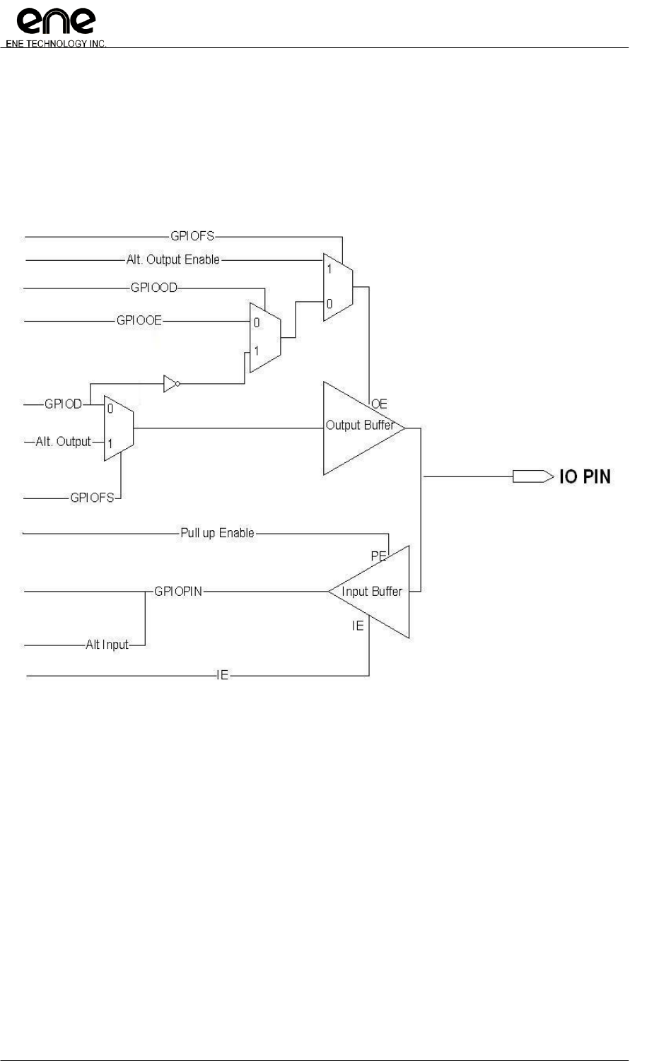
Copyright© 2011, ENE Technology Inc.
29
KB9012 Keyboard Controller Datasheet
CONFIDENTIAL
4.2.2 GPIO Structures
In this section, the GPIO structure is illustrated as following diagram. The upper part is
alternative output circuit and the lower part is alternative input circuit. In the figure, GPIOFS is used
to enable alternative output. GPIOOD is for open-drain setting with output function. GPIOOE is the
switch for data output. As shown in the figure, the alternative input embedded with pull-high and
interrupt feature.

Copyright© 2011, ENE Technology Inc.
30
KB9012 Keyboard Controller Datasheet
CONFIDENTIAL
4.2.3 GPIO Attribution Table
GPIO
Alt.
Output
Alt.
Input
Default
Alt. Output
Alt. Selection
Reg.
Input
Enable
Output
Enable
Pull Up
(40KΩ)
Open
Drain
Output
Current
GPIO00
GA20
GPIO00
GPIOFS00.[0]
V
V
V
V
2-4mA
GPIO01
KBRST#
GPIO01
GPIOFS00.[1]
V
V
V
V
2-4mA
GPIO02*
GPIO02
GPIOFS00.[2]
GPIO03*
GPIO03
GPIOFS00.[3]
GPIO04
GPIO04
GPIOFS00.[4]
V
V
V
V
2-4mA
GPIO05
PCIRST#
GPIO05
GPIOFS00.[5]
V
V
V
V
8-16mA
GPIO06*
GPIO06
GPIOFS00.[6]
GPIO07
i_clk_805)
GPIO07
GPIOFS00.[7]
V
V
V
V
2-4mA
GPIO08
i_clk_peri
GPIO08
GPIOFS08.[0]
V
V
V
V
2-4mA
GPIO09*
GPIO09
GPIOFS08.[1]
GPIO0A
OWM
RLC_RX2
OWM
GPIO0A
GPIOFS08.[2]
OWMCFG[7]
V
V
V
V
2-4mA
GPIO0B
ESB_CLK
GPIO0B
GPIOFS08.[3]
V
V
V
V
8-16mA
GPIO0C
ESB_DAT
ESB_DAT
GPIO0C
GPIOFS08.[4]
V
V
V
V
4~8mA
GPIO0D
RLC_TX2
GPIO0D
GPIOFS08.[5]
V
V
V
V
2-4mA
GPIO0E
SCI#
GPIO0E
GPIOFS08.[6]
V
V
V
V
2-4mA
GPIO0F
PWM0
GPIO0F
GPIOFS08.[7]
V
V
V
V
8-16mA
GPIO10
PWM1
GPIO10
GPIOFS10.[0]
V
V
V
V
2-4mA
GPIO11
PWM2
GPIO11
GPIOFS10.[1]
V
V
V
V
2-4mA
GPIO12
FANPWM0
GPIO12
GPIOFS10.[2]
V
V
V
V
2-4mA
GPIO13
FANPWM1
GPIO13
GPIOFS10.[3]
V
V
V
V
2-4mA
GPIO14
FANFB0
GPIO14
GPIOFS10.[4]
V
V
V
V
2-4mA
GPIO15
FANFB1
GPIO15
GPIOFS10.[5]
V
V
V
V
2-4mA
GPIO16
E51TXD
GPIO16
GPIOFS10.[6]
V
V
V
V
2-4mA
GPIO17
E51CLK
E51RXD
GPIO17
GPIOFS10.[7]
V
V
V
V
2-4mA
GPIO18
POWER_FAIL1
GPIO18
GPIOFS18.[0]
V
V
V
V
2-4mA
GPIO19
PWM3
GPIO19
GPIOFS18.[1]
V
V
V
V
8-16mA
GPIO1A
NUMLED#
GPIO1A
GPIOFS18.[2]
V
V
V
V
16-20mA
GPIO1B*
GPIO1B
GPIOFS18.[3]
GPIO1C*
GPIO1C
GPIOFS18.[4]
GPIO1D
CLKRUN#
CLKRUN#
GPIO1D
GPIOFS18.[5]
V
V
V
V
8-16mA
GPIO1E*
GPIO1E
GPIOFS18.[6]
GPIO1F*
GPIO1F
GPIOFS18.[7]
GPIO20
KSO00
TP_TEST
GPIO20
GPIOFS20.[0]
V
V
V
V
2-4mA
GPIO21
KSO01
TP_PLL
GPIO21
GPIOFS20.[1]
V
V
V
V
2-4mA
GPIO22
KSO02
TP_TMUX
GPIO22
GPIOFS20.[2]
V
V
V
V
2-4mA
GPIO23
KSO03
TP_PLL_Lock
GPIO23
GPIOFS20.[3]
V
V
V
V
2-4mA
GPIO24
KSO04
GPIO24
GPIOFS20.[4]
V
V
V
V
2-4mA
GPIO25
KSO05
PCICLK(LPC)
GPIO25
GPIOFS20.[5]
GPIO_MISC2[7]
V
V
V
V
8-16mA
GPIO26
KSO06
PCIRST#(LPC)
GPIO26
GPIOFS20.[6]
GPIO_MISC2[7]
V
V
V
V
2-4mA
GPIO27
KSO07 /
SERIRQ(LPC)
SERIRQ(LPC)
GPIO27
GPIOFS20.[7]
GPIO_MISC2[7]
V
V
V
V
2-4mA
GPIO28
KSO08
LFRAME#(LPC)
GPIO28
GPIOFS28.[0]
GPIO_MISC2[7]
V
V
V
V
2-4mA
GPIO29
KSO09
GPIO29
GPIOFS28.[1]
V
V
V
V
2~4mA
GPIO2A
KSO10
GPIO2A
GPIOFS28.[2]
V
V
V
V
2~4mA

Copyright© 2011, ENE Technology Inc.
31
KB9012 Keyboard Controller Datasheet
CONFIDENTIAL
GPIO2B
KSO11 /
LAD0(LPC)
LAD0(LPC)
GPIO2B
GPIOFS28.[3]
GPIO_MISC2[7]
V
V
V
V
2-4mA
GPIO2C
KSO12 /
LAD1(LPC)
LAD1(LPC)
GPIO2C
GPIOFS28.[4]
GPIO_MISC2[7]
V
V
V
V
2-4mA
GPIO2D
KSO13 /
LAD2(LPC)
LAD2(LPC)
GPIO2D
GPIOFS28.[5]
GPIO_MISC2[7]
V
V
V
V
2-4mA
GPIO2E
KSO14 /
LAD3(LPC)
LAD3(LPC)
GPIO2E
GPIOFS28.[6]
GPIO_MISC2[7]
V
V
V
V
2-4mA
GPIO2F
KSO15
(E51_RXD)
GPIO2F
GPIOFS28.[7]
GPIO_MISC2[2]
V
V
V
V
2-4mA
GPIO30
(E51_TXD)
KSI0
GPIO30
GPIOFS30.[0]
GPIO_MISC2[2]
V
V
V
V
2-4mA
GPIO31
KSI1
GPIO31
GPIOFS30.[1]
V
V
V
V
2-4mA
GPIO32
KSI2
GPIO32
GPIOFS30.[2]
V
V
V
V
2-4mA
GPIO33
KSI3
GPIO33
GPIOFS30.[3]
V
V
V
V
2-4mA
GPIO34
KSI4 /
EDI_CS
GPIO34
GPIOFS30.[4]
V
V
V
V
2-4mA
GPIO35
KSI5 /
EDI_CLK
GPIO35
GPIOFS30.[5]
V
V
V
V
2-4mA
GPIO36
KSI6 /
EDI_DIN
GPIO36
GPIOFS30.[6]
V
V
V
V
2-4mA
GPIO37
EDI_DO
KSI7
GPIO37
GPIOFS30.[7]
V
V
V
V
2-4mA
GPIO38
AD0
GPIO38
GPIOFS38.[0]
V
V
V
V
2-4mA
GPIO39
AD1
GPIO39
GPIOFS38.[1]
V
V
V
V
2-4mA
GPIO3A
AD2
GPIO3A
GPIOFS38.[2]
V
V
V
V
2-4mA
GPIO3B
AD3
GPIO3B
GPIOFS38.[3]
V
V
V
V
2-4mA
GPIO3C
DA0
GPIO3C
GPIOFS38.[4]
V
V
V
V
2-4mA
GPIO3D
DA1
GPIO3D
GPIOFS38.[5]
V
V
V
V
2-4mA
GPIO3E
DA2
GPIO3E
GPIOFS38.[6]
V
V
V
V
2-4mA
GPIO3F
DA3
GPIO3F
GPIOFS38.[7]
V
V
V
V
2-4mA
GPIO40
AD6
CIR_RX
GPIO40
GPIOFS40.[0]
V
V
V
V
2-4mA
GPIO41
CIR_RLC_TX
AD7
GPIO41
GPIOFS40.[1]
V
V
V
V
2-4mA
GPIO42
AD4
GPIO42
GPIOFS40.[2]
V
V
V
V
2-4mA
GPIO43
AD5
GPIO43
GPIOFS40.[3]
V
V
V
V
2-4mA
GPIO44
SCL0
GPIO44
GPIOFS40.[4]
V
V
V
2-4mA
GPIO45
SDA0
GPIO45
GPIOFS40.[5]
V
V
V
2-4mA
GPIO46
SCL1
GPIO46
GPIOFS40.[6]
V
V
V
2-4mA
GPIO47
SDA1
GPIO47
GPIOFS40.[7]
V
V
V
2-4mA
GPIO48
KSO16 /
GPIO48
GPIOFS48.[0]
V
V
V
V
2-4mA
GPIO49
KSO17
GPIO49
GPIOFS48.[1]
V
V
V
V
2-4mA
GPIO4A
PSCLK1
/ SCL2
GPIO4A
GPIOFS48.[2]
GPIO_MISC2[4]
V
V
V
2-4mA
GPIO4B
PSDAT1
/ SDA2
GPIO4B
GPIOFS48.[3]
GPIO_MISC2[4]
V
V
V
2-4mA
GPIO4C
PSCLK2
/ SCL3
GPIO4C
GPIOFS48.[4]
GPIO_MISC2[5]
V
V
V
V
8-16mA
GPIO4D
PSDAT2
/ SDA3
GPIO4D
GPIOFS48.[5]
GPIO_MISC2[5]
V
V
V
V
16-20mA
GPIO4E
PSCLK3
GPIO4E
GPIOFS48.[6]
V
V
V
2-4mA
GPIO4F
PSDAT3
GPIO4F
GPIOFS48.[7]
V
V
V
2-4mA
GPIO50
GPIO50
GPIOFS50.[0]
V
V
V
2-4mA
GPIO51*
GPIO51
GPIOFS50.[1]
GPIO52
E51CS#
GPIO52
GPIOFS50.[2]
V
V
V
V
16-20mA
GPIO53
CAPSLED#
E51TMR1
GPIO53
GPIOFS50.[3]
V
V
V
V
16-20mA

Copyright© 2011, ENE Technology Inc.
32
KB9012 Keyboard Controller Datasheet
CONFIDENTIAL
GPIO54
WDT_LED#
E51TMR0
GPIO54
GPIOFS50.[4]
V
V
V
V
16-20mA
GPIO55
SCORLED#
E51INT0
GPIO55
GPIOFS50.[5]
V
V
V
V
16-20mA
GPIO56
E51INT1
GPIO56
GPIOFS50.[6]
V
V
V
V
2-4mA
GPIO57
XCLK32K
GPIO57
GPIOFS50.[7]
V
V
V
V
2-4mA
GPIO58
(SPICLK)
GPIO59
GPIO_MISC[1]
V
V
V
V
8~16mA
GPIO59
TEST_CLK
GPIO59
GPIOFS58.[1]
V
V
V
V
2-4mA
GPIO5A
(SPICS#)
GPIO5A
GPIO_MISC[1]
V
V
V
V
8~16mA
GPIO5B
(MISO)
GPIO5B
GPIO_MISC[1]
V
V
V
V
8~16mA
GPIO5C
(MOSI)
GPIO5C
GPIO_MISC[1]
V
V
V
V
8~16mA
GPIO5D
(XCLKI)
GPIO5D
CLK32CR[5:4]
V
V
V
V
2-4mA
GPIO5E
(XCLIO)
GPIO5E
CLK32CR[5:4]
V
V
V
V
2-4mA
GPXIOA00
SHICS#
SDICS#
GPXIOA00
GPIO_MISC.[2]
V
V
V
V
2-4mA
GPXIOA01
SHICLK
SDICLK
GPXIOA01
GPIO_MISC.[2]
V
V
V
V
2-4mA
GPXIOA02
SHIDO
SDIDI
GPXIOA02
GPIO_MISC.[2]
V
V
V
V
2-4mA
GPXIOA03
POWER_FAIL0
FANFB2
GPXIOA03
GPXAFS00[3]
FANTMCFG0[0]
V
V
V
V
2-4mA
GPXIOA04
FANFB3
GPXIOA04
GPXAFS00[4]
FANTMCFG1[0]
V
V
V
V
2-4mA
GPXIOA05
VCIN1
GPXIOA05
VCCR[1]
V
V
V
V
2-4mA
GPXIOA06
VCOUT1
GPXIOA06
GPXAFS00[6]
V
V
V
V
2-4mA
GPXIOA07
VCOUT0
GPXIOA07
GPXAFS00[7]
V
V
V
V
2-4mA
GPXIOA08
GPXIOA08
GPXAFS08[0]
V
V
V
V
8-16mA
GPXIOA09
GPXIOA09
GPXAFS08[1]
V
V
V
V
8-16mA
GPXIOA10
GPXIOA10
GPXAFS08[2]
V
V
V
V
8-16mA
GPXIOA11
GPXIOA11
GPXAFS08[3]
V
V
V
V
8-16mA
GPXIOD00
SDIDO
SHIDI
/ VCIN0
GPXIOD00
GPIO_MISC.[2]
VCCR[0]
V
V
V
V
2-4mA
GPXIOD01
AC_IN
GPXIOD01
GPXDFS00[1]
V
V
V
V
2-4mA
GPXIOD02
ALW_PWR_EN
GPXIOD02
GPXDFS00[2]
V
V
V
V
2-4mA
GPXIOD03
ON/OFFBTN#
GPXIOD03
GPXDFS00[3]
V
V
V
V
2-4mA
GPXIOD04
GPXIOD04
GPXDFS00[4]
V
V
V
V
2-4mA
GPXIOD05
GPXIOD05
GPXDFS00[5]
V
V
V
V
2-4mA
GPXIOD06
GPXIOD06
GPXDFS00[6]
V
V
V
V
2-4mA
GPXIOD07
PECI
PECI
GPXIOD07
GPXDFS00[7]
V
V
V
V
2-4mA
* Denotes that these pins do not exist in KB9012
** Please Note in KB9012, the GPXIOAx / GPXIODx could be configured PU / OD pin by pin.
*** Please note, crystal pad signal frequency should be lower than 1MHz.

Copyright© 2011, ENE Technology Inc.
33
KB9012 Keyboard Controller Datasheet
CONFIDENTIAL
4.2.4 GPIO Registers Descriptions (0xFC00~0xFC7F)
In KB9012, new GPIOs are added. Related control registers are added for
ADC/DAC/CLK/GPXIOA/GPXIOD related GPIOs.
Function Selection Register
Offset
Name
Type.
Description
Default
Bank
0x00
GPIOFS00
R/W
GPIO00~GPIO07 Function Selection
bit[0]~bit[7] stand for GPIO00~GPIO07 separately
0: General purpose output function selected
1: Alternative output function selected.
Note: No GPIO02/03/06 in KB9012 IC.
0x00
0xFC
0x01
GPIOFS08
R/W
GPIO08~GPIO0F Function Selection
bit[0]~bit[7] stand for GPIO08~GPIO0F separately
0: General purpose output function selected
1: Alternative output function selected.
Note: No GPIO09 in KB9012 IC.
0x00
0xFC
0x02
GPIOFS10
R/W
GPIO10~GPIO17 Function Selection
bit[0]~bit[7] stand for GPIO10~GPIO17 separately
0: General purpose output function selected
1: Alternative output function selected.
0x00
0xFC
0x03
GPIOFS18
R/W
GPIO18~GPIO1F Function Selection
bit[0]~bit[7] stand for GPIO18~GPIO1F separately
0: General purpose output function selected
1: Alternative output function selected.
Note: No GPIO1B/1C/1E/1F in KB9012 IC.
0x00
0xFC
0x04
GPIOFS20
R/W
GPIO20~GPIO27 Function Selection
bit[0]~bit[7] stand for GPIO20~GPIO27 separately
0: General purpose output function selected
1: Alternative output function selected.
0x00
0xFC
0x05
GPIOFS28
R/W
GPIO28~GPIO2F Function Selection
bit[0]~bit[7] stand for GPIO28~GPIO2F separately
0: General purpose output function selected
1: Alternative output function selected.
0x00
0xFC
0x06
GPIOFS30
R/W
GPIO30~GPIO37 Function Selection
bit[0]~bit[7] stand for GPIO30~GPIO37 separately
0: General purpose output function selected
1: Alternative output function selected.
0x00
0xFC
0x07
GPIOFS38
R/W
GPIO38~GPIO3F Function Selection
bit[0]~bit[7] stand for GPIO38~GPIO3F separately
0: General purpose output function selected
1: Alternative output function selected.
0x00
0xFC
0x08
GPIOFS40
R/W
GPIO40~GPIO47 Function Selection
bit[0]~bit[7] stand for GPIO40~GPIO47 separately
0: General purpose output function selected
1: Alternative output function selected.
0x00
0xFC
0x09
GPIOFS48
R/W
GPIO48~GPIO4F Function Selection
bit[0]~bit[7] stand for GPIO48~GPIO4F separately
0: General purpose output function selected
1: Alternative output function selected.
0x00
0xFC

Copyright© 2011, ENE Technology Inc.
34
KB9012 Keyboard Controller Datasheet
CONFIDENTIAL
Function Selection Register
Offset
Name
Type.
Description
Default
Bank
0x0A
GPIOFS50
R/W
GPIO50~GPIO57 Function Selection
bit[0]~bit[7] stand for GPIO50~GPIO57 separately
0: General purpose output function selected
1: Alternative output function selected.
Note: No GPIO51 in KB9012 IC.
0x00
0xFC
0x0B
GPIOFS58
R/W
GPIO58~GPIO5F Function Selection
bit[0]~bit[7] stand for GPIO58~GPIO5F separately
0: General purpose output function selected
1: Alternative output function selected.
Note: No GPIO5F in KB9012 IC.
0x00
0xFC
0x0C
GPXAFS00
R/W
GPXIOA00~GPXIOA07 Function Selection
bit[0]~bit[7] stand for GPXIOA00~GPXIOA07 separately
0: General purpose output function selected
1: Alternative output function selected.
0xC0
0xFC
0x0D
GPXAFS08
R/W
GPXIOA08~GPXIOA15 Function Selection
bit[0]~bit[7] stand for GPXIOA08~GPXIOA15 separately
0: General purpose output function selected
1: Alternative output function selected.
Note: No GPXIOA12/13/14/15 in KB9012 IC.
0x00
0xFC
0x0E
Reserved
RSV
Reserved
RSV
0xFC
0x0F
GPXDFS00
R/W
GPXIOD00~GPXIOD07 Function Selection
bit[0]~bit[7] stand for GPXIOD00~GPXIOD07 separately
0: General purpose output function selected
1: Alternative output function selected.
0x00
0xFC

Copyright© 2011, ENE Technology Inc.
35
KB9012 Keyboard Controller Datasheet
CONFIDENTIAL
Output Enable Register
Offset
Name
Type.
Description
Default
Bank
0x10
GPIOOE00
R/W
GPIO00~GPIO07 Output Enable
bit[0]~bit[7] stand for GPIO00~GPIO07 separately
0: Output Disable
1: Output Enable
Note: No GPIO02/03/06 in KB9012 IC.
0x00
0xFC
0x11
GPIOOE08
R/W
GPIO08~GPIO0F Output Enable
bit[0]~bit[7] stand for GPIO08~GPIO0F separately
0: Output Disable
1: Output Enable
Note: No GPIO09 in KB9012 IC.
0x00
0xFC
0x12
GPIOOE10
R/W
GPIO10~GPIO17 Output Enable
bit[0]~bit[7] stand for GPIO10~GPIO17 separately
0: Output Disable
1: Output Enable
0x00
0xFC
0x13
GPIOOE18
R/W
GPIO18~GPIO1F Output Enable
bit[0]~bit[7] stand for GPIO18~GPIO1F separately
0: Output Disable
1: Output Enable
Note: No GPIO1B/1C/1E/1F in KB9012 IC.
0x00
0xFC
0x14
GPIOOE20
R/W
GPIO20~GPIO27 Output Enable
bit[0]~bit[7] stand for GPIO20~GPIO27 separately
0: Output Disable
1: Output Enable
0x00
0xFC
0x15
GPIOOE28
R/W
GPIO28~GPIO2F Output Enable
bit[0]~bit[7] stand for GPIO28~GPIO2F separately
0: Output Disable
1: Output Enable
0x00
0xFC
0x16
GPIOOE30
R/W
GPIO30~GPIO37 Output Enable
bit[0]~bit[7] stand for GPIO30~GPIO37 separately
0: Output Disable
1: Output Enable
0x00
0xFC
0x17
GPIOOE38
R/W
GPIO38~GPIO3F Output Enable
bit[0]~bit[7] stand for GPIO3C~GPIO3F separately
0: Output Disable
1: Output Enable
0x00
0xFC
0x18
GPIOOE40
R/W
GPIO40~47 Output Enable
bit[0]~bit[7] stand for GPIO40~GPIO47 separately
0: Output Disable
1: Output Enable
0x00
0xFC
0x19
GPIOOE48
R/W
GPIO48~GPIO4F Output Enable
bit[0]~bit[7] stand for GPIO48~GPIO4F separately
0: Output Disable
1: Output Enable
0x00
0xFC
0x1A
GPIOOE50
R/W
GPIO50~GPIO57 Output Enable
bit[0]~bit[7] stand for GPIO50~GPIO57 separately
0: Output Disable
1: Output Enable
Note: No GPIO51 in KB9012 IC.
0x00
0xFC
0x1B
GPIOOE58
R/W
GPIO58~GPIO5F Output Enable
bit[0]~bit[7] stand for GPIO58~GPIO59 separately
0: Output Disable
1: Output Enable
Note: No GPIO5F in KB9012 IC.
0x00
0xFC

Copyright© 2011, ENE Technology Inc.
36
KB9012 Keyboard Controller Datasheet
CONFIDENTIAL
Output Enable Register
Offset
Name
Type.
Description
Default
Bank
0x1C
GPXAOE00
R/W
GPXIOA00~GPXIOA07 Output Enable
bit[0]~bit[7] stand for GPXIOA00~GPXIOA07 separately
0: Output Disable
1: Output Enable
0x00
0xFC
0x1D
GPXAOE08
R/W
GPXIOA08~GPXIOA15 Output Enable
bit[0]~bit[7] stand for GPXIOA08~GPXIOA15 separately
0: Output Disable
1: Output Enable
Note: No GPXIOA12/13/14/15 in KB9012 IC.
0x00
0xFC
0x1E
RSV
RSV
Reserved
RSV
0xFC
0x1F
GPXDOE00
R/W
GPXIOD00~GPXIOD07 Output Enable
bit[0]~bit[7] stand for GPXIOD00~GPXIOD07 separately
0: Output Disable
1: Output Enable
0x00
0xFC

Copyright© 2011, ENE Technology Inc.
37
KB9012 Keyboard Controller Datasheet
CONFIDENTIAL
Output Data Port Register
Offset
Name
Type.
Description
Default
Bank
0x20
GPIOD00
R/W
GPIO00~GPIO07 Output Data Port for output function.
Bit[0]~bit[7] stand for GPIO00~GPIO07 separately
Note: No GPIO02/03/06 in KB9012 IC.
0x00
0xFC
0x21
GPIOD08
R/W
GPIO08~GPIO0F Output Data Port for output function.
Bit[0]~bit[7] stand for GPIO08~GPIO0F separately
Note: No GPIO09 in KB9012 IC.
0x00
0xFC
0x22
GPIOD10
R/W
GPIO10~GPIO17 Output Data Port for output function.
Bit[0]~bit[7] stand for GPIO10~GPIO17 separately
0x00
0xFC
0x23
GPIOD18
R/W
GPIO18~GPIO1F Output Data Port for output function.
Bit[0]~bit[7] stand for GPIO18~GPIO1F separately
Note: No GPIO1B/1C/1E/1F in KB9012 IC.
0x00
0xFC
0x24
GPIOD20
R/W
GPIO20~GPIO27 Output Data Port for output function.
Bit[0]~bit[7] stand for GPIO20~GPIO27 separately
0x00
0xFC
0x25
GPIOD28
R/W
GPIO28~GPIO2F Output Data Port for output function.
Bit[0]~bit[7] stand for GPIO28~GPIO2F separately
0x00
0xFC
0x26
GPIOD30
R/W
GPIO30~GPIO37 Output Data Port for output function.
Bit[0]~bit[7] stand for GPIO30~GPIO37 separately
0x00
0xFC
0x27
GPIOD38
R/W
GPIO38~GPIO3F Output Data Port for output function.
Bit[0]~bit[7] stand for GPIO38~GPIO3F separately
0x00
0xFC
0x28
GPIOD40
R/W
GPIO40~47 Output Data Port for output function.
Bit[0]~bit[7] stand for GPIO40~GPIO47 separately
0x00
0xFC
0x29
GPIOD48
R/W
GPIO48~GPIO4F Output Data Port for output function.
Bit[0]~bit[7] stand for GPIO48~GPIO4F separately
0x00
0xFC
0x2A
GPIOD50
R/W
GPIO50~GPIO57 Output Data Port for output function.
Bit[0]~bit[7] stand for GPIO50~GPIO57 separately
Note: No GPIO51 in KB9012 IC.
0x00
0xFC
0x2B
GPIOD58
R/W
GPIO58~GPIO5F Output Data Port for output function.
Bit[0]~bit[7] stand for GPIO58~GPIO5F separately
Note: No GPIO5F in KB9012 IC.
0x00
0xFC
0x2C
GPXAD00
R/W
GPXIOA00~GPXIOA07 Output Data Port for output function.
Bit[0]~bit[7] stand for GPXIOA00~GPXIOA07 separately
0x00
0xFC
0x2D
GPXAD08
R/W
GPXIOA08~GPXIOA15 Output Data Port for output function.
Bit[0]~bit[7] stand for GPXIOA08~GPXIOA15 separately
Note: No GPXIOA12/13/14/15 in KB9012 IC.
0x00
0xFC
0x2E
RSV
RSV
Reserved
RSV
0xFC
0x2F
GPXDD00
R/W
GPXIOD00~GPXIOD07 Output Data Port for output function.
Bit[0]~bit[7] stand for GPXIOD00~GPXIOD07 separately
0x00
0xFC

Copyright© 2011, ENE Technology Inc.
38
KB9012 Keyboard Controller Datasheet
CONFIDENTIAL
Input Data Port Register
Offset
Name
Type.
Description
Default
Bank
0x30
GPIOIN00
R
GPIO00~GPIO07 Input Data Port for input function.
Bit[0]~bit[7] stand for GPIO00~GPIO07 separately
Note: No GPIO02/03/06 in KB9012 IC.
0xFF
0xFC
0x31
GPIOIN08
R
GPIO08~GPIO0F Input Data Port for input function.
Bit[0]~bit[7] stand for GPIO08~GPIO0F separately
Note: No GPIO09 in KB9012 IC.
0xFF
0xFC
0x32
GPIOIN10
R
GPIO10~GPIO17 Input Data Port for input function.
Bit[0]~bit[7] stand for GPIO10~GPIO17 separately
0xFF
0xFC
0x33
GPIOIN18
R
GPIO18~GPIO1F Input Data Port for input function.
Bit[0]~bit[7] stand for GPIO18~GPIO1F separately
Note: No GPIO1B/1C/1E/1F in KB9012 IC.
0xFF
0xFC
0x34
GPIOIN20
R
GPIO20~GPIO27 Input Data Port for input function.
Bit[0]~bit[7] stand for GPIO20~GPIO27 separately
0xFF
0xFC
0x35
GPIOIN28
R
GPIO28~GPIO2F Input Data Port for input function.
Bit[0]~bit[7] stand for GPIO28~GPIO2F separately
0xFF
0xFC
0x36
GPIOIN30
R
GPIO30~GPIO37 Input Data Port for input function.
Bit[0]~bit[7] stand for GPIO30~GPIO37 separately
0xFF
0xFC
0x37
GPIOIN38
R
GPIO38~GPIO3F Input Data Port for input function.
Bit[0]~bit[7] stand for GPIO38~GPIO3F separately
0xFF
0xFC
0x38
GPIOIN40
R
GPIO40~GPIO47 Input Data Port for input function.
Bit[0]~bit[7] stand for GPIO40~GPIO47 separately
0xFF
0xFC
0x39
GPIOIN48
R
GPIO48~GPIO4F Input Data Port for input function.
Bit[0]~bit[7] stand for GPIO48~GPIO4F separately
0xFF
0xFC
0x3A
GPIOIN50
R
GPIO50~GPIO57 Input Data Port for input function.
Bit[0]~bit[7] stand for GPIO50~GPIO57 separately
Note: No GPIO51 in KB9012 IC.
0xFF
0xFC
0x3B
GPIOIN58
R
GPIO58~GPIO5F Input Data Port for input function.
Bit[0]~bit[7] stand for GPIO58~GPIO5F separately
Note: No GPIO5F in KB9012 IC.
0xFF
0xFC
0x3C
GPXAIN00
R
GPXIOA00~GPXIOA07 Input Data Port for input function.
Bit[0]~bit[7] stand for GPXIOA00~GPXIOA07 separately
0xFF
0xFC
0x3D
GPXAIN08
R
GPXIOA08~GPXIOA15 Input Data Port for input function.
Bit[0]~bit[7] stand for GPXIOA08~GPXIOA15 separately
Note: No GPXIOA12/13/14/15 in KB9012 IC.
0xFF
0xFC
0x3E
RSV
RSV
Reserved
RSV
0xFC
0x3F
GPXDIN00
R
GPXIOD00~GPXIOD07 Input Data Port for input function.
Bit[0]~bit[7] stand for GPXIOD00~GPXIOD07 separately
0xFF
0xFC

Copyright© 2011, ENE Technology Inc.
39
KB9012 Keyboard Controller Datasheet
CONFIDENTIAL
Pull-up Enable Register
Offset
Name
Type.
Description
Default
Bank
0x40
GPIOPU00
R/W
GPIO00~GPIO07 Internal Pull-Up Resistor Enable for input
function
bit[0]~bit[7] stand for GPIO00~GPIO07 separately
0: Pull-Up resistor disable
1: Pull-Up resistor enable
Note: No GPIO02/03/06 in KB9012 IC.
0x00
0xFC
0x41
GPIOPU08
R/W
GPIO08~GPIO0F Internal Pull-Up Resistor Enable for input
function
bit[0]~bit[7] stand for GPIO08~GPIO0F separately
0: Pull-Up resistor disable
1: Pull-Up resistor enable
Note: No GPIO09 in KB9012 IC.
0x00
0xFC
0x42
GPIOPU10
R/W
GPIO10~GPIO17 Internal Pull-Up Resistor Enable for input
function
bit[0]~bit[7] stand for GPIO10~GPIO17 separately
0: Pull-Up resistor disable
1: Pull-Up resistor enable
0x00
0xFC
0x43
GPIOPU18
R/W
GPIO18~GPIO1F Internal Pull-Up Resistor Enable for input
function
bit[0]~ bit[7] stand for GPIO18~GPIO1F separately
0: Pull-Up resistor disable
1: Pull-Up resistor enable
Note: No GPIO1B/1C/1E/1F in KB9012 IC.
0x00
0xFC
0x44
GPIOPU20
R/W
GPIO20~GPIO27 Internal Pull-Up Resistor Enable for input
function
bit[0]~bit[7] stand for GPIO20~GPIO27 separately
0: Pull-Up resistor disable
1: Pull-Up resistor enable
0x0F
0xFC
0x45
GPIOPU28
R/W
GPIO28~GPIO2F Internal Pull-Up Resistor Enable for input
function
bit[0]~bit[7] stand for GPIO28~GPIO2F separately
0: Pull-Up resistor disable
1: Pull-Up resistor enable
0x00
0xFC
0x46
GPIOPU30
R/W
GPIO30~GPIO37 Internal Pull-Up Resistor Enable for input
function
bit[0]~bit[7] stand for GPIO30~GPIO37 separately
0: Pull-Up resistor disable
1: Pull-Up resistor enable
0xFF
0xFC
0x47
GPIOPU38
R/W
GPIO38~GPIO3F Internal Pull-Up Resistor Enable for input
function
bit[0]~bit[7] stand for GPIO38~GPIO3F separately
0: Pull-Up resistor disable
1: Pull-Up resistor enable
0x00
0xFC
0x48
GPIOPU40
R/W
GPIO40~47 Internal Pull-Up Resistor Enable for input function
bit[0]~bit[7] stand for GPIO40~GPIO47 separately
0: Pull-Up resistor disable
1: Pull-Up resistor enable
Note: No Pull-UP Resistor in GPIO44/45/46/47 in KB9012 IC.
0x00
0xFC
0x49
GPIOPU48
R/W
GPIO48~GPIO4F Internal Pull-Up Resistor Enable for input
function
bit[0]~bit[7] stand for GPIO48~GPIO4F separately
0: Pull-Up resistor disable
1: Pull-Up resistor enable
Note: No Pull-UP Resistor in GPIO4A/4B/4E/4F in KB9012 IC.
0x00
0xFC

Copyright© 2011, ENE Technology Inc.
40
KB9012 Keyboard Controller Datasheet
CONFIDENTIAL
Pull-up Enable Register
Offset
Name
Type.
Description
Default
Bank
0x4A
GPIOPU50
R/W
GPIO50~GPIO57 Internal Pull-Up Resistor Enable for input
function
bit[0]~bit[7] stand for GPIO50~57 separately
0: Pull-Up resistor disable
1: Pull-Up resistor enable
Note: No GPIO51 in KB9012 IC.
Note: No Pull-UP Resistor in GPIO50 in KB9012 IC.
0x00
0xFC
0x4B
GPIOPU58
R/W
GPIO58~GPIO5F Internal Pull-Up Resistor Enable for input
function
bit[0]~bit[7] stand for GPIO58~GPIO5F separately
0: Pull-Up resistor disable
1: Pull-Up resistor enable
Note: No GPIO5F in KB9012 IC.
0x00
0xFC
0x4C
GPXAPU00
R/W
GPXIOA00~GPXIOA07 Internal Pull-Up Resistor Enable for
input function
bit[0]~bit[7] stand for GPXIOA00~GPXIOA07 separately
0: Pull-Up resistor disable
1: Pull-Up resistor enable
0x00
0xFC
0x4D
GPXAPU08
R/W
GPXIOA08~GPXIOA15 Internal Pull-Up Resistor Enable for
input function
bit[0]~bit[7] stand for GPXIOA08~GPXIOA15 separately
0: Pull-Up resistor disable
1: Pull-Up resistor enable
Note: No GPXIOA12/13/14/15 in KB9012 IC.
0x00
0xFC
0x4E
RSV
RSV
Reserved
RSV
0xFC
0x4F
GPXDPU00
R/W
GPXIOD00~GPXIOA07 Internal Pull-Up Resistor Enable for
input function
bit[0]~bit[7] stand for GPXIOD00~GPXIOA07 separately
0: Pull-Up resistor disable
1: Pull-Up resistor enable
0x00
0xFC

Copyright© 2011, ENE Technology Inc.
41
KB9012 Keyboard Controller Datasheet
CONFIDENTIAL
Open Drain Enable Register
Offset
Name
Type.
Description
Default
Bank
0x50
GPIOOD00
R/W0C
GPIO00~GPIO07 Open Drain Enable for output function
bit[0]~bit[7] stand for GPIO00~GPIO07 separately
0: Open drain disable
1: Open drain enable.
Note: No GPIO02/03/06 in KB9012 IC.
0x00
0xFC
0x51
GPIOOD08
R/W0C
GPIO08~GPIO0F Open Drain Enable for output function
bit[0]~bit[7] stand for GPIO08~GPIO0F separately
0: Open drain disable
1: Open drain enable.
Note: No GPIO09 in KB9012 IC.
0x00
0xFC
0x52
GPIOOD10
R/W0C
GPIO10~GPIO17 Open Drain Enable for output function
bit[0]~bit[7] stand for GPIO10~GPIO17 separately
0: Open drain disable
1: Open drain enable.
0x00
0xFC
0x53
GPIOOD18
R/W0C
GPIO18~GPIO1F Open Drain Enable for output function
bit[0]~bit[7] stand for GPIO18~GPIO1F separately
0: Open drain disable
1: Open drain enable.
Note: No GPIO1B/1C/1E/1F in KB9012 IC.
0x00
0xFC
0x54
GPIOOD20
R/W0C
GPIO20~GPIO27 Open Drain Enable for output function
bit[0]~bit[7] stand for GPIO20~GPIO27 separately
0: Open drain disable
1: Open drain enable.
0x00
0xFC
0x55
GPIOOD28
R/W0C
GPIO28~GPIO2F Open Drain Enable for output function
bit[0]~bit[7] stand for GPIO28~GPIO2F separately
0: Open drain disable
1: Open drain enable.
0x00
0xFC
0x56
GPIOOD30
R/W0C
GPIO30~GPIO37 Open Drain Enable for output function
bit[0]~bit[7] stand for GPIO30~GPIO37 separately
0: Open drain disable
1: Open drain enable.
0x00
0xFC
0x57
GPIOOD38
R/W0C
GPIO38~GPIO3F Open Drain Enable for output function
bit[0]~bit[7] stand for GPIO38~GPIO3F separately
0: Open drain disable
1: Open drain enable.
0x00
0xFC
0x58
GPIOOD40
R/W0C
GPIO40~47 Open Drain Enable for output function
bit[0]~bit[7] stand for GPIO40~GPIO47 separately
0: Open drain disable
1: Open drain enable.
0x00
0xFC
0x59
GPIOOD48
R/W0C
GPIO48~GPIO4F Open Drain Enable for output function
bit[0]~bit[7] stand for GPIO48~GPIO4F separately
0: Open drain disable
1: Open drain enable.
0x00
0xFC
0x5A
GPIOOD50
R/W0C
GPIO50~GPIO57 Open Drain Enable for output function
bit[0]~bit[7] stand for GPIO50~GPIO57 separately
0: Open drain disable
1: Open drain enable.
Note: No GPIO51 in KB9012 IC.
0x00
0xFC
0x5B
GPIOOD58
R/W0C
GPIO58~GPIO5F Open Drain Enable for output function
bit[0]~bit[7] stand for GPIO58~GPIO5F separately
0: Open drain disable
1: Open drain enable.
Note: No GPIO5F in KB9012 IC.
0x00
0xFC

Copyright© 2011, ENE Technology Inc.
42
KB9012 Keyboard Controller Datasheet
CONFIDENTIAL
Open Drain Enable Register
Offset
Name
Type.
Description
Default
Bank
0x5C
GPXAOD00
R/W
GPXIOA00~GPXIOA07 Open Drain Enable for output
function
bit[0]~bit[7] stand for GPXIOA00~GPXIOA07 separately
0: Open drain disable
1: Open drain enable.
0x00
0xFC
0x5D
GPXAOD08
R/W
GPXIOA08~GPXIOA15 Open Drain Enable for output
function
bit[0]~bit[7] stand for GPXIOA08~GPXIOA15 separately
0: Open drain disable
1: Open drain enable.
Note: No GPXIOA12/13/14/15 in KB9012 IC.
0x00
0xFC
0x5E
RSV
RSV
Reserved
RSV
0xFC
0x5F
GPXDOD00
R/W
GPXIOD00~GPXIOD07 Open Drain Enable for output
function
bit[0]~bit[7] stand for GPXIOD00~GPXIOD07 separately
0: Open drain disable
1: Open drain enable.
0x00
0xFC

Copyright© 2011, ENE Technology Inc.
43
KB9012 Keyboard Controller Datasheet
CONFIDENTIAL
Input Enable Register
Offset
Name
Type.
Description
Default
Bank
0x60
GPIOIE00
R/W
GPIO00~GPIO07 Input Enable for input function
bit[0]~bit[7] stand for GPIO00~GPIO07 separately
0: GPIO input mode disable
1: GPIO input mode enable.
Note: No GPIO02/03/06 in KB9012 IC.
0x20
0xFC
0x61
GPIOIE08
R/W
GPIO08~GPIOF Input Enable for input function
bit[0]~bit[7] stand for GPIO08~GPIO0F separately
0: GPIO input mode disable
1: GPIO input mode enable.
Note: No GPIO09 in KB9012 IC.
0x00
0xFC
0x62
GPIOIE10
R/W
GPIO10~GPIO17 Input Enable for input function
bit[0]~bit[7] stand for GPIO10~GPIO17 separately
0: GPIO input mode disable
1: GPIO input mode enable.
0x00
0xFC
0x63
GPIOIE18
R/W
GPIO18~GPIO1F Input Enable for input function
bit[0]~bit[7] stand for GPIO18~GPIO1F separately
0: GPIO input mode disable
1: GPIO input mode enable.
Note: No GPIO1B/1C/1E/1F in KB9012 IC.
0x00
0xFC
0x64
GPIOIE20
R/W
GPIO20~GPIO27 Input Enable for input function
bit[0]~bit[7] stand for GPIO20~GPIO27 separately
0: GPIO input mode disable
1: GPIO input mode enable.
0x0F
0xFC
0x65
GPIOIE28
R/W
GPIO28~GPIO2F Input Enable for input function
bit[0]~bit[7] stand for GPIO28~GPIO2F separately
0: GPIO input mode disable
1: GPIO input mode enable.
0x00
0xFC
0x66
GPIOIE30
R/W
GPIO30~GPIO37 Input Enable for input function
bit[0]~bit[7] stand for GPIO30~GPIO37 separately
0: GPIO input mode disable
1: GPIO input mode enable.
0xFF
0xFC
0x67
GPIOIE38
R/W
GPIO38~GPIO3F Input Enable for input function
bit[0]~bit[7] stand for GPIO38~GPIO3F separately
0: GPIO input mode disable
1: GPIO input mode enable.
0x00
0xFC
0x68
GPIOIE40
R/W
GPIO40~GPIO47 Input Enable for input function
bit[0]~bit[7] stand for GPIO40~GPIO47 separately
0: GPIO input mode disable
1: GPIO input mode enable.
0x00
0xFC
0x69
GPIOIE48
R/W
GPIO48~GPIO4F Input Enable for input function
bit[0]~bit[7] stand for GPIO48~GPIO4F separately
0: GPIO input mode disable
1: GPIO input mode enable.
0x00
0xFC
0x6A
GPIOIE50
R/W
GPIO50~GPIO57 Input Enable for input function
bit[0]~bit[7] stand for GPIO50~GPIO57 separately
0: GPIO input mode disable
1: GPIO input mode enable.
Note: No GPIO51 in KB9012 IC.
0x00
0xFC
0x6B
GPIOIE58
R/W
GPIO58~GPIO5F Input Enable for input function
bit[0]~bit[7] stand for GPIO58~GPIO5F separately
0: GPIO input mode disable
1: GPIO input mode enable.
Note: No GPIO5F in KB9012 IC.
0x02
0xFC

Copyright© 2011, ENE Technology Inc.
44
KB9012 Keyboard Controller Datasheet
CONFIDENTIAL
Input Enable Register
Offset
Name
Type.
Description
Default
Bank
0x6C
GPXAIE00
R/W
GPXIOA00~GPXIOA07 Input Enable for input function
bit[0]~bit[7] stand for GPXIOA00~GPXIOA07 separately
0: GPIO input mode disable
1: GPIO input mode enable.
0x00
0xFC
0x6D
GPXAIE08
R/W
GPXIOA08~GPXIOA15 Input Enable for input function
bit[0]~bit[7] stand for GPXIOA08~GPXIOA15separately
0: GPIO input mode disable
1: GPIO input mode enable.
Note: No GPXIOA12/13/14/15 in KB9012 IC.
0x00
0xFC
0x6E
RSV
RSV
Reserved
RSV
0xFC
0x6F
GPXDIE00
R/W
GPXIOD00~GPXIOD07 Input Enable for input function
bit[0]~bit[7] stand for GPXIOD00~GPXIOD07 separately
0: GPIO input mode disable
1: GPIO input mode enable.
0x00
0xFC

Copyright© 2011, ENE Technology Inc.
45
KB9012 Keyboard Controller Datasheet
CONFIDENTIAL
GPIO_MISC Control Register
Offset
Name
Bit
Type
Description
Default
Bank
0x70
GPIO_MISC
7
R/W
ESB_DAT(GPIO0C) output current selection
0: 4mA
1: 8mA
0x60
0xFC
6
R/W
SPICLK(GPIO58) output current selection
0: 8mA
1: 16mA
5
R/W
ESB_CLK(GPIO0B) output current selection
0: 8mA
1: 16mA
4
R/W
RSV
3
R/W
GPIO17 / GPIO18 are featured with signal bypass function.
Signal input via GPIO17 can be directly passed through
GPIO18.
0: Pass through function disable
1: Pass through function enable
2
R/W
SHDI pin-out enable (GPXA00/01/02, GPXD00)
0: disable
1: enable
Also refer to SHICFG
1
R/W
SHDI pin-out enable (GPIO58/5A/5B/5C)
0: disable
1: enable
Also refer to SHICFG
0
R/W
Beep glue logic switch.
GPIO12 can be output a specific function as following formula.
GPIO12 = PWM2 ⊕GPIO16(input) ⊕GPIO17(input)
0: Beep glue logic function disable
1: Beep glue logic function enable

Copyright© 2011, ENE Technology Inc.
46
KB9012 Keyboard Controller Datasheet
CONFIDENTIAL
GPIO_MISC 2 Control Register
Offset
Name
Bit
Type
Description
Default
Bank
0x71
GPIO_MISC2
7
R/W
LPC bus redirection enable, will redirect LPC bus to relative
KSO pins:
0: Disable
1: Enable
PCICLK to GPIO25(KSO5)
PCIRST# to GPIO26(KSO6)
SERIRQ to GPIO27(KSO7)
LFRAME# to GPIO28(KSO8)
LAD3 to GPIO2B(KSO11)
LAD2 to GPIO2C(KSO12)
LAD1 to GPIO2D(KSO13)
LAD0 to GPIO2E(KSO14)
0x00
0xFC
6
R/W
Select GPIO25(KSO5) output current 4mA/16mA
=0, Select Output Current 4mA for GPIO25(KSO5)
=1, Select Output Current 16mA for GPIO25(KSO5)
5
R/W
Enable SMBus port 3 (SCL3/SDA3)
0:Disable
1:Enable
4
R/W
Enable SMBus port 2 (SCL2/SDA2)
0:Disable
1:Enable
3
RSV
Reserved
2
R/W
Enable E51 Tx/Rx to IKB interface for debugging
E51_TXD : Pin 30, GPIO16 -> Pin 55, GPIO30
E51_RXD : Pin 31, GPIo17 -> Pin 54, GPIO2F
1~0
RSV
Reserved
GPIO Test Mux Register
Offset
Name
Bit
Type
Description
Default
Bank
0x72
Reserved
7~0
RSV
Reserved
0x00
0xFC
GPX MISC Control Register
Offset
Name
Bit
Type
Description
Default
Bank
0x73
GPX_MISC
7~3
RSV
Reserved
0x00
0xFC
2
R/W
GPIO18 output power fail flag enable
0: Disable
1: Enable
1
R/W
GPXIOA03 output power fail flag enable
0: Disable
1: Enable
0
RSV
Reserved

Copyright© 2011, ENE Technology Inc.
47
KB9012 Keyboard Controller Datasheet
CONFIDENTIAL
GPIO LED Control
Offset
Name
Bit
Type
Description
Default
Bank
0x74
GPIO_LED
7~6
RSV
Reserved
0x00
0xFC
5
R/W
Enable high drive IO cell for the specific GPIO,
GPIO55 (SCORLED#) enable
0: Disable (16mA)
1: Enable (20mA)
4
R/W
Enable high drive IO cell for the specific GPIO,
GPIO54 (WDT_LED#) enable
0: Disable (16mA)
1: Enable (20mA)
3
R/W
Enable high drive IO cell for the specific GPIO,
GPIO53 (CAPSLED#) enable
0: Disable (16mA)
1: Enable (20mA)
2
R/W
Enable high drive IO cell for the specific GPIO,
GPIO52 enable
0: Disable (16mA)
1: Enable (20mA)
1
R/W
Enable high drive IO cell for the specific GPIO,
GPIO4D enable
0: Disable (16mA)
1: Enable (20mA)
0
R/W
Enable high drive IO cell for the specific GPIO,
GPIO1A (NUMLED#) enable
0: Disable (16mA)
1: Enable (20mA)
GPIO Flash Direct Access Configuration
Offset
Name
Bit
Type
Description
Default
Bank
0x75
GPIO_FDA
7~2
RSV
Reserved
0x00
0xFC
1~0
R/W
Configuration for FDA Mode
00: Disable
01: Reserved
10: Reserved
11: Reserved

Copyright© 2011, ENE Technology Inc.
48
KB9012 Keyboard Controller Datasheet
CONFIDENTIAL
4.2.5 GPIO Programming Sample
In this section gives some programming sample to control GPIO module. Please note,
ENE does not guarantee these codes in every field application. The following table describes
scenario of GPIO filed application.
Example
PIN
Function
GPIO00 (GA20)
Output
GPIO01 (KBRST#)
Output
GPIO02 (GPIO) *
Input
GPIO03 (GPIO) *
Input
GPIO04 (GPIO)
Output
GPIO05 (PCIRST#)
Input
GPIO06 (GPIO) *
Input
GPIO07 (GPIO)
Output
Programming model
1. Set function selection register.
GPIOFS00 (0xFC00) = 0x23 (0b 0010 0011)
2. Set related pins to be output enable.
GPIOOE00 (0xFC10) = 0x93 (0b 1001 0011)
3. Set related pins to be input enable.
GPIOIE00 (0xFC60) = 0x6C (0b 0110 1100)
* GPIO02/03/06 do not exist in KB9012 chip

Copyright© 2011, ENE Technology Inc.
49
KB9012 Keyboard Controller Datasheet
CONFIDENTIAL
4.3 Keyboard and Mouse Control Interface (KBC)
4.3.1 KBC I/F Function Description
The KBC is compatible with i8042 and responsible for keyboard/mouse accessing via
legacy 60h/64h ports. The port 60h is the data port and port 64h is the command port. The legacy
IRQ1 for keyboard devices and IRQ12 for mouse devices can be generated. The KBC interface
provides fast GA20 control for legacy application.
KBC data register can be accessed by host or KBC firmware. Writing this register will setup a
OBF (Output Buffer Full) flag, which can be clear by firmware. While the host issues I/O write to
60h/64h port, an IBF (Input Buffer Full) flag will assert. The interrupts can be programmed to issue
while the flag of IBF/OBF asserting.
The following table gives a summary about port 60h/64h accessing.
Port
Access
Type
Register
Flag
Comment
60h
I/O Write
Data
KBCDAT (0xFC85)
IBF
Write data to keyboard/mouse
64h
I/O Write
Command
KBCCMD (0xFC84)
IBF
Write command to keyboard/mouse
60h
I/O Read
Data
KBCDAT (0xFC85)
OBF
Read data from keyboard/mouse
64h
I/O Read
Status
KBCSTS (0xFC86)
Read status from keyboard/mouse
KBC data register, KBCDAT, keeps data from host or data written by KBC firmware.
Bit
7
6
5
4
3
2
1
0
Name
Keyboard/Mouse Data Register
KBC command register, KBCCMD, is used to keep the command from host. This register is
read only.
Bit
7
6
5
4
3
2
1
0
Name
Keyboard/Mouse Command Register
KBC status register, KBCSTS, keeps the status as the following table. For more detail please
refer to the section, KBC Registers Description.
Bit
7
6
5
4
3
2
1
0
Name
Parity Error
Time Out
Aux. Data Flag
Un-inhibited
Address (A2)
System Flag
IBF
OBF

Copyright© 2011, ENE Technology Inc.
50
KB9012 Keyboard Controller Datasheet
CONFIDENTIAL
4.3.2 KBC Registers Description (0xFC80~0xFC8F)
KBC Command Byte Register (KBC command 20h/60h)
Offset
Name
Bit
Type
Description
Default
Bank
0x80
KBCCB
7
R/W
PS/2 hardware mode enable
0: Disable
1: Enable
If the host issues command 20h via port 64h, and the KBC
returns data via port 60h. This bit will always be read as zero.
0x40
0xFC
6
R/W
Scan code set2 conversion enable (PS/2 scan code set2
converts to set 1)
0: Disable
1: Enable
5
R/W
Disable Auxiliary device
0: Enable
1: Disable
4
R/W
Disable Keyboard device
0: Enable
1: Disable
3
R/W
Inhibit Override
0: Disable
1: Enable
2
R/W
System Flag (warm boot flag)
0: cold boot
1: warm boot
1
R/W
IRQ12 Enable
While KBCSTS[5]=1(Auxiliary Data Flag) and KBCSTS[0]=1
(OBF), then IRQ12 will issue.
0: Disable
1: Enable
0
R/W
IRQ1 Enable
While KBCSTS[5]=0 (Auxiliary Data Flag) and KBCSTS[0]=1
(OBF), then IRQ1 will issue.
0: Disable
1: Enable

Copyright© 2011, ENE Technology Inc.
51
KB9012 Keyboard Controller Datasheet
CONFIDENTIAL
KBC Configuration
Offset
Name
Bit
Type
Description
Default
Bank
0x81
KBCCFG
7
R/W
Keyboard lock enable
0: Disable
1: Enable
0x00
0xFC
6
R/W
Fast gate A20 control
0: Disable gate A20 control
1: Enable gate A20 control
5
R/W
KBC hardware command sets (90h~93h, D4h) enable.
0: Disable
1: Enable
4
R/W
KBC hardware command sets (60h, A7h~ABh, Adh~Aeh)
enable.
0: Disable
1: Enable
3
R/W
Keyboard lock flag status
0: keyboard not lock or not inhibit
1: keyboard lock or inhibit
2
R/W
KBC hardware command sets (A4h, A6h) enable.
0: Disable
1: Enable
1
R/W
IBF (KBCSTS[1]) interrupt enable. (IBF from 0 to 1)
0: Disable
1: Enable
0
R/W
OBF (KBCSTS[0]) interrupt enable (OBF from 1 to 0)
0: Disable
1: Enable
KBC Interrupt Pending Flag
Offset
Name
Bit
Type
Description
Default
Bank
0x82
KBCIF
7-3
RSV
Reserved
0x00
0xFC
2
R/W1C
Status of KBC command handled by firmware
While receiving KBC commands which need firmware to
handle, the hardware will set this bit. Then the firmware will deal
with all the following command until this bit is clear by firmware.
1
R/W1C
IBF interrupt pending flag
0: no IBF interrupt occurs
1: IBF interrupt occurs
0
R/W1C
OBF interrupt pending flag
0: no OBF interrupt occurs
1: OBF interrupt occurs
Copyright© 2011, ENE Technology Inc.
52
KB9012 Keyboard Controller Datasheet
CONFIDENTIAL
KBC Hardware Command Enable
Offset
Name
Bit
Type
Description
Default
Bank
0x83
KBCHWEN
7
R/W
KBC hardware command set (FEh) enable
0: Disable
1: Enable
0x00
0xFC
6
R/W
KBC hardware command set (E0h) enable
0: Disable
1: Enable
5
R/W
KBC hardware command set (D3h) enable
0: Disable
1: Enable
4
R/W
KBC hardware command set (D2h) enable
0: Disable
1: Enable
3
R/W
KBC hardware command set (D1h) enable
0: Disable
1: Enable
2
R/W
KBC hardware command set (D0h) enable
0: Disable
1: Enable
1
R/W
KBC hardware command set (C0h) enable
0: Disable
1: Enable
0
R/W
KBC hardware command set (20h) enable
0: Disable
1: Enable
KBC Command Buffer
Offset
Name
Bit
Type
Description
Default
Bank
0x84
KBCCMD
7-0
RO
Command written to port 64h will be stored in this register
0x00
0xFC
KBC Data Input/Output Buffer
Offset
Name
Bit
Type
Description
Default
Bank
0x85
KBCDAT
7-0
R/W
Data written to this register to make OBF set (OBF=1).
The host read this register via port 60h.
0x00
0xFC
Copyright© 2011, ENE Technology Inc.
53
KB9012 Keyboard Controller Datasheet
CONFIDENTIAL
KBC Host Status
Offset
Name
Bit
Type
Description
Default
Bank
0x86
KBCSTS
7
R/W
Parity error
0: No parity error occurs in PS/2 protocol
1: Parity error occurs in PS/2 protocol.
0x00
0xFC
6
R/W
Timeout
0: No timeout occurs in PS/2 protocol
1: Timeout occurs in PS/2 protocol.
5
R/W
Auxiliary data flag
4
RO
Uninhibited
0: keyboard inhibited
1: keyboard not inhibited
3
RO
Address (A2)
0: output buffer data from 60h
1: output buffer data from 64h
2
RO
System flag
1
R/W1C
IBF
0
R/W1C
OBF
RSV
Offset
Name
Bit
Type
Description
Default
Bank
0x87~
0x89
RSV
7-0
RSV
Reserved
0x00
0xFC
KBC Write Data
Offset
Name
Bit
Type
Description
Default
Bank
0x8A
KBCDATR
7-0
RO
Read back port of KBCDAT, [0xFC85]
0x00
0xFC
RSV
Offset
Name
Bit
Type
Description
Default
Bank
0x8B~
0x8F
RSV
7~0
RSV
Reserved
0x00
0xFC
Copyright© 2011, ENE Technology Inc.
54
KB9012 Keyboard Controller Datasheet
CONFIDENTIAL
4.4 ENE Serial Bus Controller (ESB)
4.4.1 ESB Function Description
To extend the usage of the current design, an ENE Serial Bus interface is introduced. An
external ESB device can be controlled by firmware transparently. As the following table, 3 memory
address ranges are reserved for ESB devices.
ESBED field
Memory Range
Bit 2
0xFCC0~0xFCCF
Bit 1
0xFCB0~0xFCBF
Bit 0
0xFD00~0xFDFF
In the ESB architecture, external ESB devices are supported. And each device can be
configured with interrupt capability. A figure gives the topology of ENE Serial Bus as following.

Copyright© 2011, ENE Technology Inc.
55
KB9012 Keyboard Controller Datasheet
CONFIDENTIAL
4.4.2 ESB Registers Description (0xFC90~0xFC9F)
ESB Configuration
Offset
Name
Bit
Type
Description
Default
Bank
0x90
ESBCFG
7
R/W
Loop back test enable
0: Disable
1: Enable
0x00
0xFC
6-5
R/W
ESB clock divide factor selection.
00: 2Mhz
01: 4Mhz
10: 8Mhz
11: 16Mhz
4
R/W
External device access mode.
0: Access external device via 4 predefined memory ranges.
(automatic mode)
1: Access external devices via ESBCA, ESBCD and ESBRD
registers. (byte mode)
3
R/W
ESB clock output enable
0: Disable
1: Enable
2
R/W
ESB interrupt enable
0: Disable
1: Enable
1
R/W
ESB host queries device interrupt status automatically. (when
ESBCFG[3]=1)
0: Disable
1: Enable
0
R/W
ESB function enable
0: Disable
1: Enable

Copyright© 2011, ENE Technology Inc.
56
KB9012 Keyboard Controller Datasheet
CONFIDENTIAL
ESB Command and Status
Offset
Name
Bit
Type
Description
Default
Bank
0x91
ESBCS
7
RSV
Reserved
0x00
0xFC
6
R/W1C
Device resume signal flag
0: no event
1: event occurs.
5
R/W1C
ESB bus timeout status
0: no timeout event
1: bus timeout
4
R/W1C
Device data received status.
0: no data received
1: data received.
3
R
ESB host busy flag.
0: not busy
1: host busy
2
W
Start to send command, command byte in ESBCD, 0xFC94
Write ―0‖ will not work.
1: send command
1-0
R/W
ESB access command type (while ESBCFG[3]=1)
00: interrupt query
01: read
10: write
11: Reserved
Copyright© 2011, ENE Technology Inc.
57
KB9012 Keyboard Controller Datasheet
CONFIDENTIAL
ESB Interrupt Enable of External Device
Offset
Name
Bit
Type
Description
Default
Bank
0x92
ESBINTE
7
RSV
Reserved
0x00
0xFC
6
R/W
Device resume signal interrupt enable
0: Disable
1: Enable
5
R/W
Bus timeout interrupt enable
0: Disable
1: Enable
4
R/W
Device data received interrupt enable
0: Disable
1: Enable
3
R/W
Interrupt enable (IRQ3) of external ESB device.
0: Disable
1: Enable
2
R/W
Interrupt enable (IRQ2) of external ESB device.
0: Disable
1: Enable
1
R/W
Interrupt enable (IRQ1) of external ESB device.
0: Disable
1: Enable
0
R/W
Interrupt enable (IRQ0) of external ESB device.
0: Disable
1: Enable
ESB Command Address
Offset
Name
Bit
Type
Description
Default
Bank
0x93
ESBCA
7-0
R/W
External ESB device address to be accessed. (when
ESBCFG[4]=1)
The address is predefined according to different device.
0x00
0xFC
ESB Command Data
Offset
Name
Bit
Type
Description
Default
Bank
0x94
ESBCD
7-0
R/W
Write data port to external ESB device (when ESBCFG[4]=1)
0x00
0xFC
ESB Received Data
Offset
Name
Bit
Type
Description
Default
Bank
0x95
ESBRD
7-0
R/W
Read data port to external ESB device (when ESBCFG[4]=1)
If loop back test enabled (when ESBCFG[7]=1), the register will
be writable, otherwise, read-only.
0x00
0xFC
Copyright© 2011, ENE Technology Inc.
58
KB9012 Keyboard Controller Datasheet
CONFIDENTIAL
ESB Enable for External Device
Offset
Name
Bit
Type
Description
Default
Bank
0x96
ESBED
7-5
RSV
Reserved
0x00
0xFC
4
R/W
Low clock mode enable (clock source 32KHz)
For performance and power saving consideration, while low
clock mode enabled, please set the query function off.
0: Disable
1: Enable
3
RSV
Reserved
2
R/W
Enable external ESB device decoding address
0xFCC0~0xFCCF
0: Disable
1: Enable
1
R/W
Enable external ESB device decoding address
0xFCB0~0xFCBF
0: Disable
1: Enable
0
R/W
Enable external ESB device decoding address
0xFD00~0xFDFF.
0: Disable
1: Enable
ESB Interrupt Event Pending Flag for External Chip
Offset
Name
Bit
Type
Description
Default
Bank
0x97
ESBINT
7
R/W1C
Interrupt event pending flag of IRQ7 (cascade mode only)
0: no event
1: event occurs
0x00
0xFC
6
R/W1C
Interrupt event pending flag of IRQ6 (cascade mode only)
0: no event
1: event occurs
5
R/W1C
I Interrupt event pending flag of IRQ5 (cascade mode only)
0: no event
1: event occurs
4
R/W1C
Interrupt event pending flag of IRQ4 (cascade mode only)
0: no event
1: event occurs
3
R/W1C
Interrupt event pending flag of IRQ3
0: no event
1: event occurs
2
R/W1C
Interrupt event pending flag of IRQ2
0: no event
1: event occurs
1
R/W1C
Interrupt event pending flag of IRQ1
0: no event
1: event occurs
0
R/W1C
Interrupt event pending flag of IRQ0
0: no event
1: event occurs

Copyright© 2011, ENE Technology Inc.
59
KB9012 Keyboard Controller Datasheet
CONFIDENTIAL
ESB Cascade Mode Configuration
Offset
Name
Bit
Type
Description
Default
Bank
0x98
ESBCAS
7
R/W
Interrupt enable of IRQ7 for external chip
0: disable
1: enable
0x00
0xFC
6
R/W
Interrupt enable of IRQ6 for external chip
0: disable
1: enable
5
R/W
Interrupt enable of IRQ5 for external chip
0: disable
1: enable
4
R/W
Interrupt enable of IRQ4 for external chip
0: disable
1: enable
3-1
RSV
Reserved
0
R/W
Cascade mode enable
0: disable
1: enable

Copyright© 2011, ENE Technology Inc.
60
KB9012 Keyboard Controller Datasheet
CONFIDENTIAL
4.4.3 ESB Programming Sample
In this section gives some programming sample to control ESB module. Please note, ENE
does not guarantee these codes in every field application. The following table describes scenario of
ESB filed application.
Example
A device connecting to ESB master.
Programming model
GPIOFS08[4:3] (0xFC01[4:3])= 11b ; ESB function selection pin
GPIOIE08[4] (0xFC61[4]) = 1b ; Set ESB_DAT pin IE
ESBCFG (0xFC90) = 0x69 ; ESB clock = Main CLOCK 32MHz
; ESB enable & automatic mode enable
ESBED (0xFC96) = 0x02 ; Enable ESB range 0xFCC0~0xFCCF
Now F/W can access ESB device via 0xFCC0~0xFCCF

Copyright© 2011, ENE Technology Inc.
61
KB9012 Keyboard Controller Datasheet
CONFIDENTIAL
4.5 Internal KeyBoard (IKB) Encoder
4.5.1 IKB Function Description
The KBC supports internal keyboard encoder (IKB) in the notebook system. Here is the
feature highlight of IKB module.
- Support 18x8 matrix.
- Keyboard scan output (KSO) 18 lines.
- Keyboard scan input (KSI) 8 lines
- KSO/KSI can be programmed to be GPIO
- KSO/KSI internal programmable pull-high feature supported.
- KSO/KSI can be used for redirection for LPC, 8051 Tx/Rx, EDI debug application
- Support half-HW mode & FW mode de-bounce setting

Copyright© 2011, ENE Technology Inc.
62
KB9012 Keyboard Controller Datasheet
CONFIDENTIAL
Table for IKB Hardware Command Brief:
Command
Description
*ED
Set LED.
Modify the status of LED by the following argument byte.
Normal sequence: ED FA WW FA (WW is setting to IKBLED[2:0])
Bits 7~3
Must be Zero
Bit 2
Caps Lock LED
Bit 1
Num Lock LED
Bit 0
Scroll Lock LED
WW define as above
EE
ECHO.
Send EE back to the host after receiving this command.
Normal sequence: EE EE
*F0
Access Scan Code Set. Host uses the 1st argument to specify the R/W operation.
If 1st argument equals 0x00, it‘s a read operation.
If 1st argument not equals 0x00, it‘s a write operation and KBC ignores the
argument. (Supports Set 2 scan code)
Normal sequence:
F0 FA 00 FA 02, (read scan code set as 2 )
F0 FA 02 FA (use set 2 scan code)
F2
Get Device ID. Normal sequence: F2 FA AB 41
*F3
Set Typematic Rate.
Normal sequence: F3 FA WW FA (WW is setting to IKBTYPEC)
F4
Enable.
Start scanning the key matrix and sending the scan code to the host
KBC is in disable mode after hardware rest. System BIOS should configure all
options of KBC and enable it.
Normal sequence: F4 FA
F5
Disable.
When disabled, KBC can‘t TX key to PS2.
And KBC will keep the key until Enable or Reset or Default occurs.
F6
Set Default.
Restore the default setting of typematic rate and LED status,
Normal sequence: F6 FA
FE
Resend.
Re-transmit the last byte.
Normal sequence: FE WW (WW is the last byte of KBC sent to PS2 to be resent)
FF
Reset.
Generate soft-reset to reset PS2 interface,
It will clear all internal flags of scan controller.
The scan, kgen, TX/RX state machine will go to idle and clear all buffers.
* When these commands waiting RX argument, KBC can TX key to PS2.

Copyright© 2011, ENE Technology Inc.
63
KB9012 Keyboard Controller Datasheet
CONFIDENTIAL
4.5.2 IKB Registers Description (0xFCA0~0xFCAF)
IKB Configuration
Offset
Name
Bit
Type
Description
Default
Bank
0xA0
IKBCFG
7
R/W
IKB scan controller test mode enable.
0: Disable
1: Enable
0x00
0xFC
6
R/W
IKB PS/2 wait time setting. The IKB makes sure PS/2 bus idle
for specific time and then transmit the scan codes.
0: 8 μs
1: 64μs
5
RW
IKB De-bounce function control for half-HW mode
0: Disable
1: Enable
4
WO
Force controller to scan key matrix. Write ―1‖ to start.
3
RSV
Reserved
2
R/W
IKB scan repeat enable.
Set this bit force the IKB controller to scan every 30ms.
0: Disable
1: Enable
1
R/W
Standard KB command hardware mode enable.
Once the IKB received standard KB command, the hardware
will handle it.
0: Disable
1: Enable
0
R/W
IKB scan controller enable.
0: Disable
1: Enable
Copyright© 2011, ENE Technology Inc.
64
KB9012 Keyboard Controller Datasheet
CONFIDENTIAL
IKB LED Control
Offset
Name
Bit
Type
Description
Default
Bank
0xA1
IKBLED
7
R/W
NumLock key
0: Fn-Lock
1: NumLock =Fn-Lock
0x00
0xFC
6
R/W
Flag of Fn-Shift (in hardware mode)
0: Fn-Shift not pressed
1: Fn-Shift pressed
5
R/W
Flag of Fn-Lock (in hardware mode)
0: Fn-Lock not pressed
1: Fn-Lock pressed
4
R/W
LED output polarity, CapLock/NumLock/ScrLock output
0: positive logic
1: negative logic
3
RSV
Reserved
2
R/W
CapLock LED driving
H/W auto set or clear it, polarity depend on IKBLED[4]
1
R/W
NumLock LED driving
H/W auto set or clear it, polarity depend on IKBLED[4]
0
R/W
ScrLock LED driving
H/W auto set or clear it, polarity depend on IKBLED[4]
IKB Typematic Control
Offset
Name
Bit
Type
Description
Default
Bank
0xA2
IKBTYPEC
7
RSV
Reserved
0x00
0xFC
6-5
R/W
1st key repeat delay time selection.
00b: 250ms
01b: 500ms
10b: 750ms
11b: 1 sec
4-0
R/W
Typematic repeat characters per second.
1Fh: 2 char/sec 10h: 10 char/sec
1Bh: 3 char/sec 0Dh: 12 char/sec
18h: 4 char/sec 0Bh: 15 char/sec
17h: 5 char/sec 08h: 16 char/sec
15h: 6 char/sec 05h: 20 char/sec
13h: 8 char/sec 00h: 30 char/sec

Copyright© 2011, ENE Technology Inc.
65
KB9012 Keyboard Controller Datasheet
CONFIDENTIAL
IKB Interrupt Enable
Offset
Name
Bit
Type
Description
Default
Bank
0xA3
IKBIE
7
R/W
Enable F/W mode IKB de-bounce control for wait time cycle
0: disable
1: enable
0x00
0xFC
6
R/W
Wait time cycle timing unit selection
(Only valid when IKBIE[7]=1, also refer IKBSFC[7:4] for details)
1: 1m sec pulse
0: 4m sec pulse
5
R/W
Interrupt enable. While the following commands handled by
hardware occur.
KB reset / KB disable / KB Enable / Non-standard hardware
mode command
0: Disable
1: Enable
4
R/W
IKB RX finished interrupt enable.
0: Disable
1: Enable
3
R/W
IKB TX finished interrupt enable.
0: Disable
1: Enable
2
R/W
IKB typmatic repeat timeout interrupt enable.
0: Disable
1: Enable
1
R/W
IKB scan code finished interrupt enable. (IKBHCFG[0]=0)
IKB break key (hotkey) interrupt enable. (IKBHCFG[0]=1)
0: Disable
1: Enable
0
R/W
IKB make key interrupt enable. (IKBHCFG[0]=0)
IKB make key (hotkey) interrupt enable. (IKBHCFG[0]=1)
0: Disable
1: Enable
Copyright© 2011, ENE Technology Inc.
66
KB9012 Keyboard Controller Datasheet
CONFIDENTIAL
IKB Interrupt Pending Flag
Offset
Name
Bit
Type
Description
Default
Bank
0xA4
IKBPF
7
WO
Force the IKB controller enter idle mode.
Write ―1‖ to enter idle mode.
0x00
0xFC
6
R/W1C
IKBSADR (0xFCA9) valid flag.
0: no more valid IKBSADR
1: IKBSADR valid
5
R/W1C
Interrupt flag. While the following commands handled by
hardware occur.
KB reset / KB disable / KB enable
0: event is not active
1: event is active
4
R/W1C
IKB RX finished and non-standard hardware mode command
occurring interrupt flag.
0: event is not active
1: event is active
3
R/W1C
IKB TX finished interrupt flag.
0: event is not active
1: event is active
2
R/W1C
IKB typematic repeat timeout interrupt flag
0: event is not active
1: event is active
1
R/W1C
IKB scan code finished interrupt flag. (IKBHCFG[0]=0)
IKB break key (hotkey) interrupt flag. (IKBHCFG[0]=1)
0: event is not active
1: event is active
0
R/W1C
IKB make key interrupt flag. (IKBHCFG[0]=0)
IKB make key (hotkey) interrupt flag. (IKBHCFG[0]=1)
0: Disable
1: Enable
IKB PS/2 TX Data Byte
Offset
Name
Bit
Type
Description
Default
Bank
0xA5
IKBTXDAT
7-0
R/W
The IKB port to transmit data to PS/2 controller
Writing to this port, the data will be delivered to PS/2 controller.
After transmission completes and a TX finished interrupt
issues.
0x00
0xFC
IKB PS/2 RX Data Byte
Offset
Name
Bit
Type
Description
Default
Bank
0xA6
IKBRXDAT
7-0
R/W
The IKB port to receive data from PS/2 controller.
After receiving data from PS/2 controller, a RX finished interrupt
issues.
0x00
0xFC

Copyright© 2011, ENE Technology Inc.
67
KB9012 Keyboard Controller Datasheet
CONFIDENTIAL
IKB Hardware Mode Configuration
Offset
Name
Bit
Type
Description
Default
Bank
0xA7
IKBHCFG
7-3
RSV
Reserved
0x00
0xFC
2
R/W
IKB hotkey flag while hardware mode enable (IKBCFG[0]=1)
0: event is not active
1: event is active
1
R/W
IKB hotkey finish indicator
While KBC recognizes a hotkey, the KBC setup the hotkey flag
(IKBCFG[2]) to invoke firmware to handle. Firmware will write
―1‖ to this bit after completing the hotkey event.
0
R/W
IKB hardware mode enable
0: Disable
1: Enable
IKB Scan Inputs
Offset
Name
Bit
Type
Description
Default
Bank
0xA8
IKBKSI
7-0
RO
IKB scan input buffer
0x00
0xFC
IKB Scan Address
Offset
Name
Bit
Type
Description
Default
Bank
0xA9
IKBSADR
7-0
RO
IKB scan address of current key
0x00
0xFC
IKB Scan Timing Control
Offset
Name
Bit
Type
Description
Default
Bank
0xAA
IKBSDB
7-4
R/W
KSO release (floating) time
Time = (value + 1) * 8μs
0xF7
0xFC
3-0
R/W
KSO drive low time
Time = (value + 1) * 8μs
IKB Make Key (hardware mode)
Offset
Name
Bit
Type
Description
Default
Bank
0xAB
IKBMK
7-0
RO
The scan controller places make key in this register.
If hotkey occurs, the register contains the matrix value.
0x00
0xFC
IKB Break Key (hardware mode)
Offset
Name
Bit
Type
Description
Default
Bank
0xAC
IKBBK
7-0
RO
The scan controller places break key in this register.
If hotkey occurs, the register contains the matrix value.
0x00
0xFC

Copyright© 2011, ENE Technology Inc.
68
KB9012 Keyboard Controller Datasheet
CONFIDENTIAL
IKB Scan All key de-bounce control
Offset
Name
Bit
Type
Description
Default
Bank
0xAD
IKBSADB
7
RSV
Reserved
0x55
0xFC
6~4
R/W
De-bounce times for valid break key
000: 1 times
¦
111: 8 times
3
RSV
Reserved
2~0
R/W
De-bounce times for valid make key
000: 1 times
¦
111: 8 times
IKB Scan Function Control
Offset
Name
Bit
Type
Description
Default
Bank
0xAE
IKBSFC
7-4
R/W
The scan function will wait ―X‖ time after then scan all keys
again.
“X‖ range 0~15m sec
0000 0m sec
¦
1111 15m sec
(F/W mode de-bounce, also refer IKBIE for wait time timing
base setting which could be 1ms base / 4ms base)
0x00
0xFC
3-0
RSV
Reserved
IKB Key Generation Flag
Offset
Name
Bit
Type
Description
Default
Bank
0xAF
IKBKGENFG
7-6
RO
IKB PS2 KB Reset, Disable and Enable hardware command
interrupt pending flag status
00: No interrupt event
01: Reset command interrupt
10: Disable command interrupt
11: Enable command interrupt
0x00
0xFC
5~3
RSV
Reserved
2
RO
Idle mode status
1
R/W1C
Ghost key identification flag (IKBHCFG[0]=1)
0: No ghost key
1: Ghost key found
0
R/W1C
IKB make key scan flag. If this bit is set to ―1‖, all the make
keys will be ignored.
0: not over 5 make key occur at a time
1: over 5 make key occur at a time

Copyright© 2011, ENE Technology Inc.
69
KB9012 Keyboard Controller Datasheet
CONFIDENTIAL
4.5.3 IKB Matrix Value Mapping Table
In this section, the following tables show the mapping information between matrix value
and PS/2 set1 scan code. The first one is the standard keys mapping, and the second one is for
multimedia keys mapping.
Standard Keys
Matrix
Value
(set 2)
Description
Scan Code
(set 1)
Matrix
Value
(set 2)
Description
Scan Code
(set 1)
00h
Error(overrun)
FFh
40h
Reserved
6Bh
01h
F9
43h
41h
< ,
33h
02h
F7
41h
42h
K
25h
03h
F5
3Fh
43h
I
17h
04h
F3
3Dh
44h
O
18h
05h
F1
3Bh
45h
) 0
0Bh
06h
F2
3Ch
46h
( 9
0Ah
07h
F12
58h
47h
Reserved
60h
08h
Reserved
64h
48h
Reserved
6Ch
09h
F10
44h
49h
> .
34h
0Ah
F8
42h
4Ah
? /
35h
0Bh
F6
40h
4Bh
L
26h
0Ch
F4
3Eh
4Ch
: ;
27h
0Dh
Tab
0Fh
4Dh
P
19h
0Eh
~
29h
4Eh
_ -
0Ch
0Fh
Reserved
59h
4Fh
Reserved
61h
10h
Reserved
65h
50h
Reserved
6Dh
11h
Left Alt
38h
51h
Reserved
73h
12h
Left Shift
2Ah
52h
― ‗
28h
13h
Reserved
70h
53h
Reserved
74h
14h
Left Ctrl
1Dh
54h
{ [
1Ah
15h
Q
10h
55h
+ =
0Dh
16h
! 1
02h
56h
Reserved
62h
17h
Reserved
5Ah
57h
Reserved
6Eh
18h
Reserved
66h
58h
Caps Lock
3Ah
19h
Reserved
71h
59h
Right Shift
36h
1Ah
Z
2Ch
5Ah
Return
1Ch
1Bh
S
1Fh
5Bh
} ]
1Bh
1Ch
A
1Eh
5Ch
Reserved
75h
1Dh
W
11h
5Dh
|\(US only) ~#(102-key)
2Bh
1Eh
@ 2
03h
5Eh
Reserved
63h
1Fh
Reserved
5Bh
5Fh
Reserved
76h
20h
Reserved
67h
60h
Fn (PTL)
55h
21h
C
2Eh
61h
|\(102-key)
56h

Copyright© 2011, ENE Technology Inc.
70
KB9012 Keyboard Controller Datasheet
CONFIDENTIAL
Matrix
Value
(set 2)
Description
Scan Code
(set 1)
Matrix
Value
(set 2)
Description
Scan Code
(set 1)
22h
X
2Dh
62h
Reserved
77h
23h
D
20h
63h
Reserved
78h
24h
E
12h
64h
Reserved
79h
25h
$ 4
5Ch
65h
Reserved
7Ah
26h
# 3
04h
66h
Backspace
0Eh
27h
Reserved
05h
67h
Reserved
7Bh
28h
Reserved
68h
68h
Reserved
7Ch
29h
Space
39h
69h
1 End
4Fh
2Ah
V
2Fh
6Ah
Reserved
7Dh
2Bh
F
21h
6Bh
4 Left Arrow
4Bh
2Ch
T
14h
6Ch
7 Home
47h
2Dh
R
13h
6Dh
Reserved
7Eh
2Eh
% 5
06h
6Eh
Reserved
7Fh
2Fh
Reserved
5Dh
6Fh
Reserved
6Fh
30h
Reserved
69h
70h
0 Ins
52h
31h
N
31h
71h
. Del
53h
32h
B
30h
72h
2 Down Arrow
50h
33h
H
23h
73h
5
4Ch
34h
G
22h
74h
6 Right Arrow
4Dh
35h
Y
15h
75h
8 Up Arrow
48h
36h
^ 6
07h
76h
ESC
01h
37h
Reserved
5Eh
77h
Num Lock
45h
38h
Reserved
6Ah
78h
F11
57h
39h
Reserved
72h
79h
+
4Eh
3Ah
M
32h
7Ah
3 PgDn
51h
3Bh
J
24h
7Bh
-
4Ah
3Ch
U
16h
7Ch
*
37h
3Dh
& 7
08h
7Dh
9 PgUp
49h
3Eh
* 8
09h
7Eh
Scroll Lock
46h
3Fh
Reserved
5Fh
7Fh
Sys Req (84-key)
54h

Copyright© 2011, ENE Technology Inc.
71
KB9012 Keyboard Controller Datasheet
CONFIDENTIAL
Multimedia Keys
Matrix
Value
(set 2)
Description
Scan Code
(set 1)
Matrix
Value
(set 2)
Description
Scan Code
(set 1)
00h – 7Fh
Standard Keys
See table
above
9Ah
ACPI Sleep
E0 5F
80h
Left Shift
2Ah
9Bh
ACPI Wake
E0 63
81h
Left Ctrl
1Dh
9Ch
Left Window
E0 5B
82h
Left Alt
38h
9Dh
Right Window
E0 5C
83h
F7
41h
9Eh
Windows App
E0 5D
84h
SysReq
54h
9Fh
Break
1D E0 46
85h
Right Shift
36h
A0h
Volume Up
E0h 30h
86h
Right Ctrl
E0h 1Dh
A1h
Volume Down
E0h 2Eh
87h
Right Alt
E0h 38h
A2h
Next
E0h 19h
88h
Print Screen
E0h 2Ah E0h
37h
A3h
Previous
E0h 10h
89h
Pause
E1h 1Dh 45h
A4h
Stop
E0h 24h
8Ah
Insert
E0h 52h
A5h
Play/Pause
E0h 22h
8Bh
Home
E0h 47h
A6h
Mute
E0h 20h
8Ch
Page Up
E0h 49h
A7h
Media Select
E0h 6Dh
8Dh
Delete
E0h 53h
A8h
Email Reader
E0h 6Ch
8Eh
End
E0h 4Fh
A9h
Calculator
E0h 21h
8Fh
Page Down
E0h 51h
AAh
My Computer
E0h 6Bh
90h
Up Arrow
E0h 48h
ABh
WWW Search
E0h 65h
91h
Left Arrow
E0h 41h
ACh
WWW Home
E0h 32h
92h
Down Arrow
E0h 50h
ADh
WWW Back
E0h 6Ah
93h
Right Arrow
E0h 4Dh
AEh
WWW Forward
E0h 69h
94h
/
E0h 35h
AFh
WWW Stop
E0h 68h
95h
Enter
E0h 1Ch
B0h
WWW Refresh
E0h 67h
96h
Fn Shift
No scan
code
B1h
WWW Favor
E0h 66h
97h
Fn Lock
No scan
code
B2h
OADG
45h/46h
98h
Num/Fn Lock
45h
B3h
Empty Key
No scan
code
99h
ACPI Power
E0h 5Eh
B4h – FFh
Hot Key
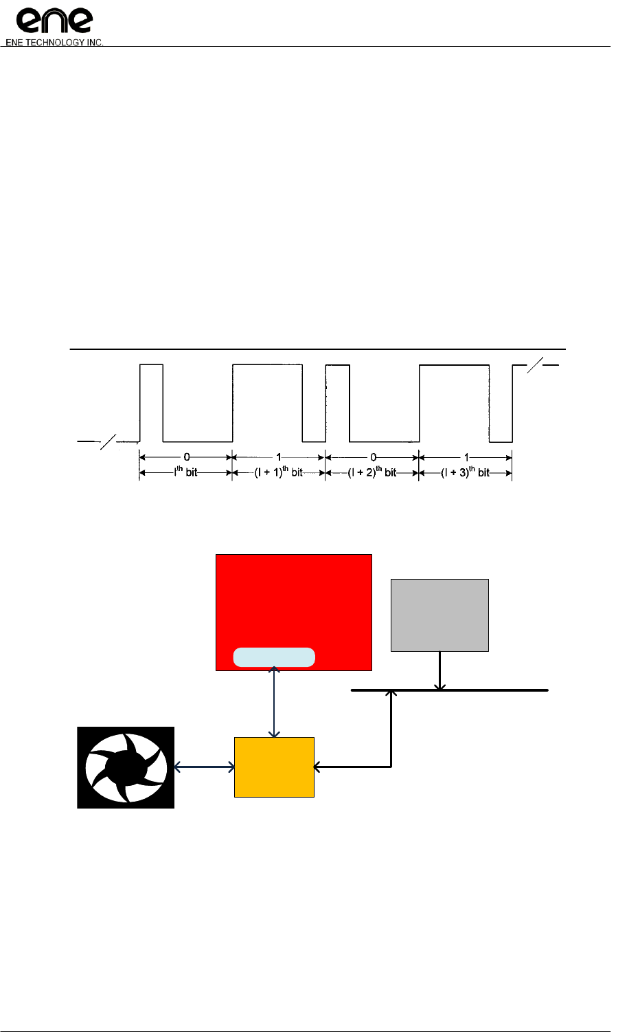
Copyright© 2011, ENE Technology Inc.
72
KB9012 Keyboard Controller Datasheet
CONFIDENTIAL
4.6 PECI
4.6.1 PECI Functional Description
The Platform Environment Control Interface (PECI) is a one-wire bus interface that provides
a communication channel between Intel processor and chipset components to external monitoring
devices. PECI could be used for real time control and implement Intel‘s latest platform control
methodology.
The PECI is a subset of SST(Simple Serial Transport) application. The PECI specification
provides information for electrical requirements, platform topologies, power management handling,
bus device enumeration, commands and addressing for Intel based system.
Compared with ENE KB930, KB9012 is added with AWFCS application for PECI 3.0 implement
for latest Intel feature.
Figure 4.6.1 Example stream of 4 bits: “0101”
(Logic bit ‘0’ encodes as 1000 pulse; Logic bit ‘1’ encodes as 1110 pulse)
EC / SIO
Intel
Processor
PECI
PECI
Intel
Chipset
SMBUS
Conceptual Block Diagram
Not Intended to depict actual implementation
Figure 4.6.2 Conceptual Block Diagram for PECI application

Copyright© 2011, ENE Technology Inc.
73
KB9012 Keyboard Controller Datasheet
CONFIDENTIAL
4.6.2 PECI Timing Setting
Terminology
Description
Formula
Source Clock
Select the source in PECICFG[7] for 32Mhz
or 4Mhz
0: 32M
1: 4M
Quarter bit timing
1/4 bit timing could be selected in
PECICTL[7:5]
Quarter bit timing is
N * (Source Clock)
N is:
4 for PECICTL[7:5] = b000
|
|
11 for PECICTL[7:5] = b111
TBIT
Bit clock rate, which logic bit ‗0‘ encodes as
1000 pulse; Logic bit ‗1‘ encodes as 1110
pulse
TBIT = Quarter bit timing * 4
Frequency setting table:
PECICFG[7] value
Source Frequency
Source Period
0
32M
31.3 ns
1
4M
250 ns
32Mhz 31.3 ns
PECICTL[7:5]
factor
Quarter bit timing (ns)
= source period * factor
TBIT (ns)=
Quarter bit timing * 4
Bus
Frequency
000
4
125
500
2M
001
5
156.25
625
1.6M
010
6
187.5
750
1.3M
011
7
218.75
875
1.1M
100
8
250
1000
1M
101
9
281.25
1125
889K
110
10
312.5
1250
800K
111
11
343.75
1375
727K
4Mhz 250 ns (0.25us)
PECICTL[7:5]
factor
Quarter bit timing (us)
= source period * factor
TBIT (us)=
Quarter bit timing * 4
Bus
Frequency
000
4
1.00
4.00
250K
001
5
1.25
5.00
200K
010
6
1.50
6.00
167K
011
7
1.75
7.00
143K
100
8
2.00
8.00
125K
101
9
2.25
9.00
111K
110
10
2.50
10.00
100K
111
11
2.75
11.00
90K

Copyright© 2011, ENE Technology Inc.
74
KB9012 Keyboard Controller Datasheet
CONFIDENTIAL
4.6.3 PECI Register Description (0xFCD0~0xFCDF)
PECI function configuration
Offset
Name
Bit
Type
Description
Default
Bank
0xD0
PECICFG
7
R/W
PECI operation frequency setting
0: 2Mhz ~ 16Khz
1: 250Khz ~ 2Khz
0x00
0xFC
6
R/W
PECI output enable selection
0: normal mode
1: PECI output enable always high
5
R/W
PECI output data selection
0: normal mode
1: PECI output data always high for debugging
4
R/W
Slow clock at idle state disable (for low power)
0: enable
1: disable
3
R/W
PECI Interrupt Enable (total enable)
2
R/W
Increase cycle of quarter bit timing, then quarter bit timing will
be increased to 1T
0: disable
1: enable
1
R/W
PECI data input de-bounce enable
0: disable, monitor data 1/2bit timing point.
1: enable, monitor data from 1/2bit to 3/4bit timing.
0
R/W
PECI function enable, state machine will come back to idle
state, when this bit is disabled.
0: enable
1: disable
Copyright© 2011, ENE Technology Inc.
75
KB9012 Keyboard Controller Datasheet
CONFIDENTIAL
PECI function control
Offset
Name
Bit
Type
Description
Default
Bank
0xD1
PECICTL
7~5
R/W
Quarter bit timing setting factor, timing unit is based on PECI
source clock (PECICFG[7])
and it could form PECI bus frequency = 4 * quarter bit timing
000: Quarter bit timing = 4 * T
001: (4+1) = 5T
|
|
111: (4+7) = 11T
0x00
0xFC
4
R/W
AW(Assured Write) FCS function enable for PECI 3.0
0: disable
1: enable
3
R/W
Restrict read FIFO data status path only for E51
0: disable (All path can read FIFO data)
1: enable (only 8051)
2
WO
FIFO reset
Write 1 to clear all FIFO pointers and data.
1
WO
Issue abort command
This bit will be auto clear when abort behavior finish.
The originator can't abort message when receives data state.
0
WO
Issue package to client
This bit will be auto clear when package transfer finish.
PECI status observation
Offset
Name
Bit
Type
Description
Default
Bank
0xD2
PECIST
7
RO
The counter value of quarter bit timing for debugging
The overall counter is 9 bit length.
PECIST[7] : PECIQTB[7:0] = overall 9 bit counter value
0x01
0xFC
6
RSV
Reserved
5
RO
TX active flag for transmitter state
4
RO
RX active flag for receiver state
3
RO
PECI bus line status for debugging
2
RO
Bus busy
1
RO
FIFO full flag for write/read state
0
RO
FIFO empty flag for write/read state
Copyright© 2011, ENE Technology Inc.
76
KB9012 Keyboard Controller Datasheet
CONFIDENTIAL
PECI interrupt enable control
Offset
Name
Bit
Type
Description
Default
Bank
0xD3
PECIINTE
7~5
RSV
Reserved
0x00
0xFC
4
R/W
Interrupt Enable of Command complete
3
R/W
Interrupt Enable of Client Abort
2
R/W
Interrupt Enable of FCS fault
1
R/W
Interrupt Enable of FIFO half
0
R/W
Interrupt Enable of FIFO error
PECI interrupt status (event pending flag)
Offset
Name
Bit
Type
Description
Default
Bank
0xD4
PECIINT
7~5
RSV
Reserved
0x00
0xFC
4
R/W1C
Interrupt Status of Command Complete
The protocol status is finish, so state machine come back idle
state then this bit will be set.
3
R/W1C
Interrupt Status of Client Abort
The client reply to FCS is a one's complement. That means
client will abort this message.
2
R/W1C
Interrupt Status of FCS fault
The client reply to FCS is not correct.
If FCS value is wrong then this bit will be set.
1
R/W1C
Interrupt Status of FIFO half
If FIFO half, this bit will be set.
That means FW must be write/read register PECIWD/PECIRD.
0
R/W1C
Interrupt Status of FIFO error
If full flag is set and write data to PECIWD, it will be set;
If empty flag is set and read data from PECIRD, it will be set.
PECI target address
Offset
Name
Bit
Type
Description
Default
Bank
0xD5
PECIADR
7~0
R/W
This is the address of the PECI device targeted to receive a
message.
0x00
0xFC
PECI write length byte
Offset
Name
Bit
Type
Description
Default
Bank
0xD6
PECIWLB
7~0
R/W
The Write Length byte in the PECI header is used to convey the
number of bytes the originator will send to the target device.
The length byte includes command and data byte.
0x00
0xFC
PECI read length byte
Offset
Name
Bit
Type
Description
Default
Bank
0xD7
PECIRLB
7~0
R/W
The Read Length byte is used by the target to determine the
number of data bytes it must supply to the originator before
Returning the FCS over that data.
0x00
0xFC
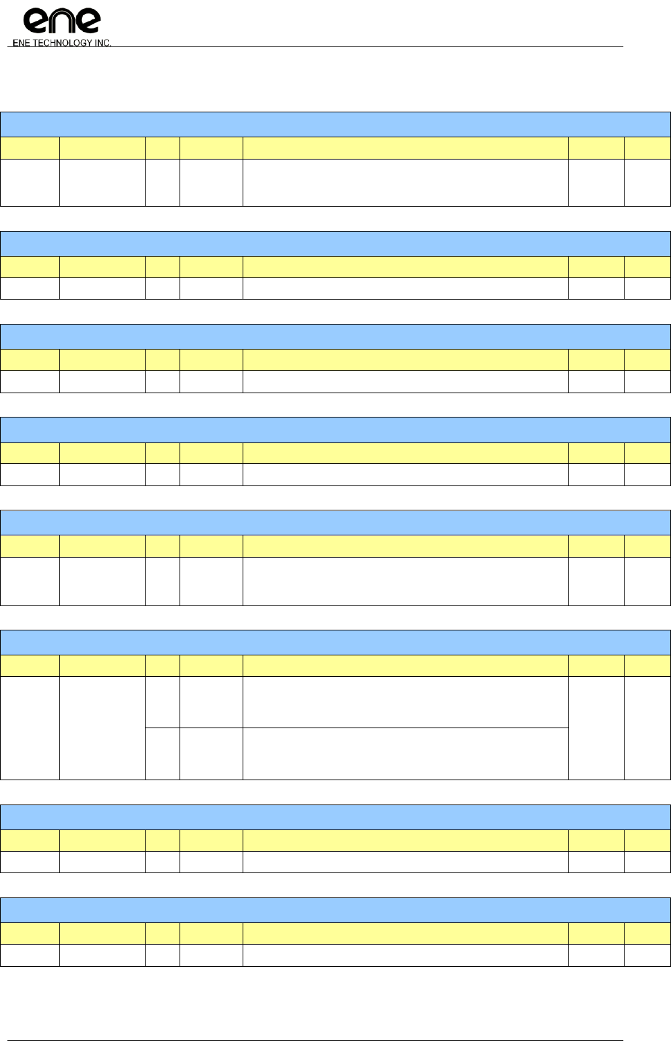
Copyright© 2011, ENE Technology Inc.
77
KB9012 Keyboard Controller Datasheet
CONFIDENTIAL
PECI write data byte
Offset
Name
Bit
Type
Description
Default
Bank
0xD8
PECIWD
7~0
R/W
PECI Write data. This includes both commands and data. All
commands require at least one Command byte with the
exception of Ping().
0x00
0xFC
PECI read data byte
Offset
Name
Bit
Type
Description
Default
Bank
0xD9
PECIRD
7~0
RO
PECI Received (Read) data from client devices.
0x00
0xFC
PECI Client Read FCS value
Offset
Name
Bit
Type
Description
Default
Bank
0xDA
PECICRFCS
7~0
RO
Read FCS value from client
0x00
0xFC
PECI generated FCS value
Offset
Name
Bit
Type
Description
Default
Bank
0xDB
PECIOFCS
7~0
RO
The FCS value generated from originator
0x00
0xFC
PECI tbit counter value observation
Offset
Name
Bit
Type
Description
Default
Bank
0xDC
PECIQTB
7~0
RO
The counter value of quarter bit timing for debugging
The overall counter is 9 bit length.
PECIST[7] : PECIQTB[7:0] = overall 9 bit counter value
0x00
0xFC
PECI FIFO write/read pointer observation
Offset
Name
Bit
Type
Description
Default
Bank
0xDD
PECIPOIN
7~4
RO
FIFO Read Pointer
FIFO read pointer points to the location in the FIFO to read from
next
0x00
0xFC
3~0
RO
FIFO Write Pointer
FIFO write pointer points to the location in the FIFO to write to
next
PECI AW FCS Value
Offset
Name
Bit
Type
Description
Default
Bank
0xDE
PECIAWFCS
7~0
RO
AW FCS value from originator
0x00
0xFC
PECI Client Write FCS Value
Offset
Name
Bit
Type
Description
Default
Bank
0xDF
PECICWFCS
7~0
RO
Write FCS value from client
0x00
0xFC

Copyright© 2011, ENE Technology Inc.
78
KB9012 Keyboard Controller Datasheet
CONFIDENTIAL
4.7 OWM
4.7.1 OWM Functional Description
OWM is called One Wire Bus Master Interface (GPIO0A) which could be used as simple host
interface, OWM device ID identification, and device power. OWM interface is featured as 1)
Bi-directional; 2) single-master/multi-slave; 3) half-duplex. OWM is physically implemented with
single open-drain master connected to one or more open-drain slave devices. Pull-up resistor is
commonly used to pull the bus to 3 or 5 V.
The OWM supports:
1. Dallas One Wire Bus Master and TI HDQ protocol.
2. Interrupt enable for Reset/Break, Read and Write command.
3. Separate 8-bit read and write buffers.
4. Configurable timing registers can be setting by F/W.
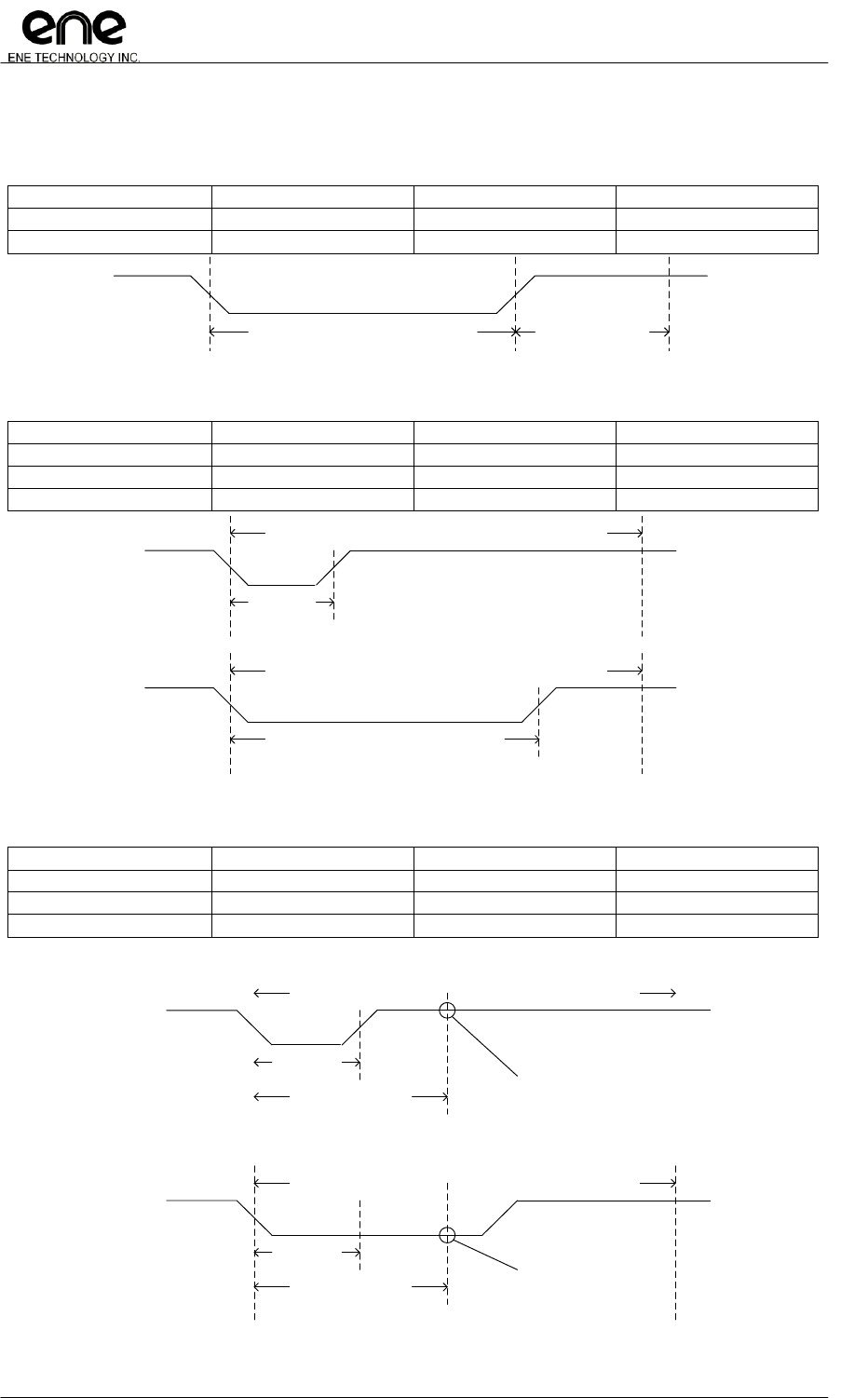
Copyright© 2011, ENE Technology Inc.
79
KB9012 Keyboard Controller Datasheet
CONFIDENTIAL
4.7.2 OWM Timing Setting Illustration
Reset / Break Timing
Register Name
Time Base
Default Value
Default Timing
OWMRSTL, 0xFCF5
8 us
0x40
512 us
OWMRSTH, 0xFCF6
8 us
0x40
512 us
Reset Time Low
(OWMRSTL)
Reset Time High
(OWMRSTH)
Write Timing
Register Name
Time Base
Default Value
Default Timing
OWMWT, 0xFCF7
2 us
0x2D
90 us
OWMW1L, 0xFCF8
1 us
0x0A
10 us
OWMW0L, 0xFCF9
1 us
0x50
80 us
Write1 time
(OWMW1L)
Write Slot Timing (data = 1)
(OWMWT)
Write0 time
(OWMW0L)
Write Slot Timing (data = 0)
(OWMWT)
Read Timing
Register Name
Time Base
Default Value
Default Timing
OWMRT, 0xFCFA
2 us
0x2D
90 us
OWMRL, 0xFCFB
1 us
0x03
3 us
OWMRS, 0xFCFC
1 us
0x14
20 us
Note : OWMRL is for Dallas only
Dallas : Pull
Low time
(OWMRL)
Sample Data time
(OWMRS) Read Data 1
Dallas : Pull
Low time
(OWMRL)
Read Slot Timing (data = 0)
(OWMRT)
Sample Data time
(OWMRS) Read Data 0

Copyright© 2011, ENE Technology Inc.
80
KB9012 Keyboard Controller Datasheet
CONFIDENTIAL
4.7.3 OWM Register Description (0xFCF0~0xFCFF)
OWM bus master configuration
Offset
Name
Bit
Type
Description
Default
Bank
0xF0
OWMCFG
7
R/W
EN : One Wire Bus Master Interface Enable
0: Disable One Wire Bus Master Interface
1: Enable One Wire Bus Master Interface
0x00
0xFC
6
R/W
TI/Dallas Mode Select
1: TI mode
0: Dallas mode
5~4
RSV
Reserved
3
R/W
ETMOI: Enable Timeout Interrupt.
Interrupt occurs if timeout interrupt flag is set
0: Disable
1: Enable
2
R/W
EWRI: Enable Write Command Complete Interrupt.
Interrupt occurs if write command complete flag is set
0: Disable
1: Enable
1
R/W
ERDI: Enable Read Command Complete Interrupt.
Interrupt occurs if read command complete flag is set
0: Disable
1: Enable
0
R/W
ERSTI: Enable Reset/Break Completely Interrupt.
Interrupt occurs if reset/break complete flag is set
0: Disable
1: Enable
Copyright© 2011, ENE Technology Inc.
81
KB9012 Keyboard Controller Datasheet
CONFIDENTIAL
OWM bus master status
Offset
Name
Bit
Type
Description
Default
Bank
0xF1
OWMSR
7
RO
BSY : One Wire Host Busy Status
0: Idle
1: Busy
0x00
0xFC
6~5
RO
Reserved
4
RO
PDR: Presence Detect Result. (for Dallas Only)
The detect result status of the presence detect when
reset/break complete interrupt occurs.
0: Not Exist
1: Exist
3
R/W1C
TMO: Timeout flag of read/write command for slave response.
0: No timeout event
1: Timeout event
2
R/W1C
WRC: Status flag of write command for operation completion
0: Write command not complete
1: Write command complete
1
R/W1C
RDC : Status flag of read command for operation completion
0: Read command not complete
1: Read command complete
0
R/W1C
RSTC: Status flag of reset/break for operation completion
0: Reset/Break command not complete
1: Reset/Break command complete
(Set when the reset high time reached after reset low time )
OWM bus master command
Offset
Name
Bit
Type
Description
Default
Bank
0xF2
OWMCMD
7~2
RSV
Reserved
0x03
0xFC
1~0
R/W
One Wire Interface Command
00: Reset /Break
01: Read
10: Write
11: No operation
OWM bus master write data buffer (transmit)
Offset
Name
Bit
Type
Description
Default
Bank
0xF3
OWMWB
7~0
R/W
The transmit data buffer send to a slave device
0x00
0xFC
OWM bus master read data buffer (receive)
Offset
Name
Bit
Type
Description
Default
Bank
0xF4
OWMRB
7~0
RO
The receive data buffer got from a slave device
0x00
0xFC
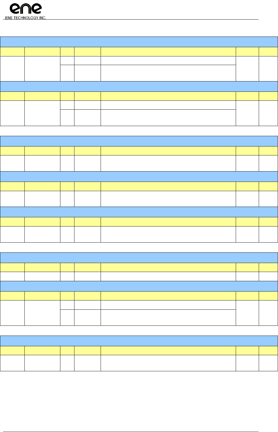
Copyright© 2011, ENE Technology Inc.
82
KB9012 Keyboard Controller Datasheet
CONFIDENTIAL
OWM reset/break low timing
Offset
Name
Bit
Type
Description
Default
Bank
0xF5
OWMRSTL
7
RSV
Reserved
0x40
0xFC
6~0
R/W
The Reset Time Low interval,,
Clock time base = 8us
OWM reset/break high timing
Offset
Name
Bit
Type
Description
Default
Bank
0xF6
OWMRSTH
7
RSV
Reserved
0x40
0xFC
6~0
R/W
The Reset Time High interval
Clock time base = 8us
OWM write slot timing
Offset
Name
Bit
Type
Description
Default
Bank
0xF7
OWMWT
7~0
R/W
Write 1-bit Data time interval
Clock time base = 2us
0x2D
0xFC
OWM write 1 low timing
Offset
Name
Bit
Type
Description
Default
Bank
0xF8
OWMW1L
7~0
R/W
Write 1 time interval
Clock time base = 1us
0x0A
0xFC
OWM write 0 low timing
Offset
Name
Bit
Type
Description
Default
Bank
0xF9
OWMW0L
7~0
R/w
Write 0 time interval
Clock time base = 1us
0x50
0xFC
OWM read slot timing
Offset
Name
Bit
Type
Description
Default
Bank
0xFA
OWMRT
7
R/W
Host Read 1-bit Data time, clock time base = 2us .
0x2D
0xFC
OWM read low timing
Offset
Name
Bit
Type
Description
Default
Bank
0xFB
OWMRL
7~4
RSV
Reserved
0x03
0xFC
3~0
R/W
For Dallas only, Host to pull low time
Clock time base = 1us
OWM read sample timing
Offset
Name
Bit
Type
Description
Default
Bank
0xFC
OWMRS
7~0
R/W
The time interval for Host to check read data 0 or 1,
Clock time base = 1us.
0x14
0xFC

Copyright© 2011, ENE Technology Inc.
83
KB9012 Keyboard Controller Datasheet
CONFIDENTIAL
4.8 Pulse Width Modulation (PWM)
4.8.1 PWM Function Description
The PWM supports 6 PWM channels:
1. two 8-bits PWM @ PWM0 (16mA) / PWM1(4mA)
2. two 14-bits PWM with pre-scaler @ PWM2(4mA) / PWM3(16mA)
3. two 12-bits PWM @ FANPWM0(4mA) / FANPWM1(4mA)
(Refer FAN section)
Pulse width modulation (PWM) is a powerful technique for controlling analog circuits with a
processor‘s digital outputs. PWM is employed in a wide variety of applications, ranging from
measurement and communications to power control and conversion. The duty cycle of PWM is
illustrated as the following figure.
10% 50% 100%
PWM Duty-Cycle range from 0%~100%
(10% per scale in the illustrration)
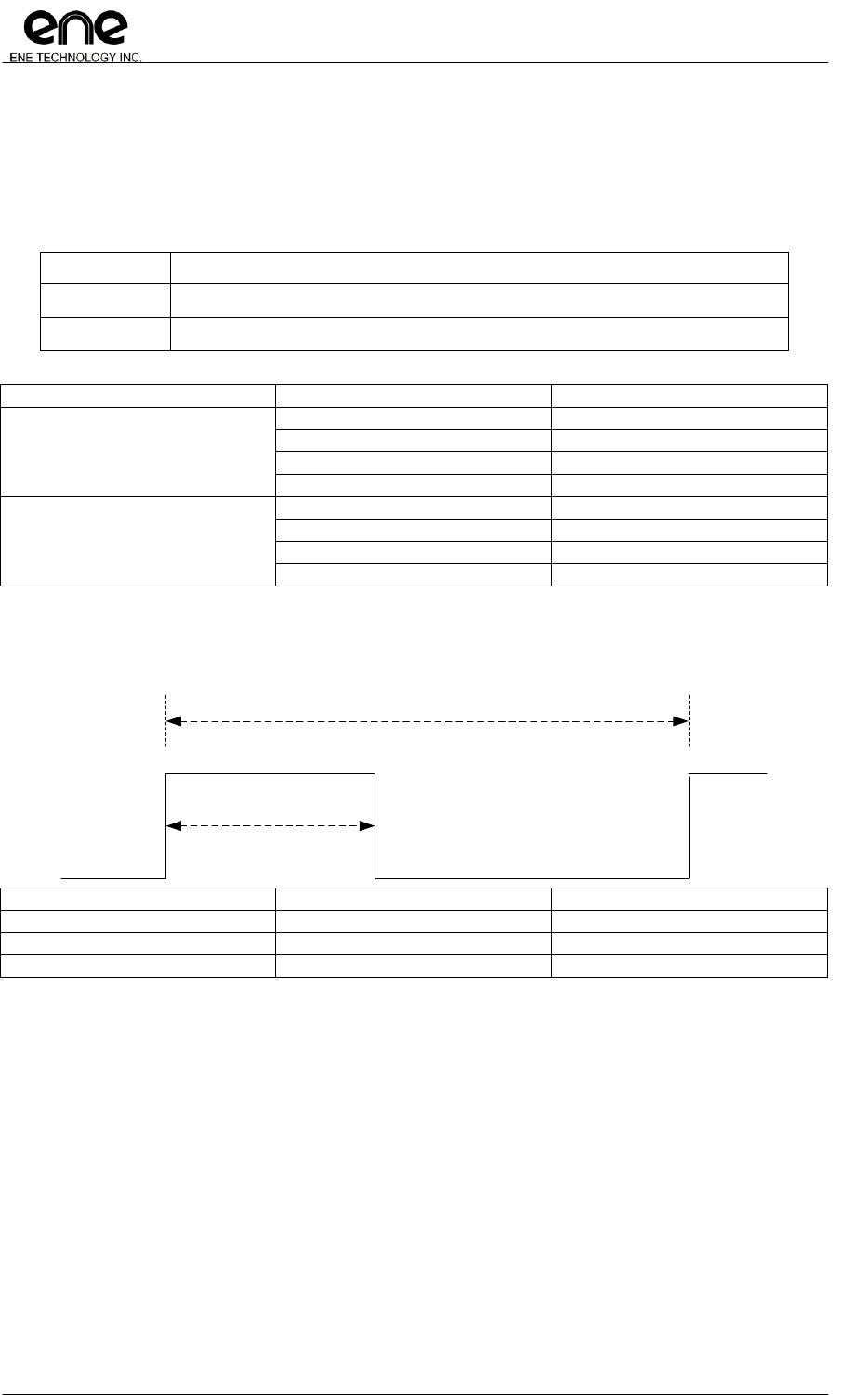
Copyright© 2011, ENE Technology Inc.
84
KB9012 Keyboard Controller Datasheet
CONFIDENTIAL
4.8.2 PWM Duty Cycle Setting Illustration
The following table summarizes the relationship about the applications with the definition in
the PWM registers description. The setting of PWM0/1(8 bits) and PWM2/3(14 bits) is different.
PWM0/1 (8 bits):
Definition
Formula
Duty Cycle
(PWM High Period Length+1)/(PWM Cycle Period Length+1) *100%
Cycle Length
( PWM Cycle Length Register +1) * (PWM clock source)
PWM Channel
Term
Register Field
PWM0
PWM High Period Length
PWMHIGH0 ( 0xFE01 )
PWM Cycle Length
PWMCYC0 ( 0xFE02 )
PWM clock source
PWMCFG[3:2] ( 0xFE00[3:2])
PWM enable
PWMCFG[0] ( 0xFE00[0])
PWM1
PWM High Period Length
PWMHIGH1 ( 0xFE03 )
PWM Cycle Length
PWMCYC1 ( 0xFE04 )
PWM clock source
PWMCFG[7:6] ( 0xFE00[7:7])
PWM enable
PWMCFG[4] ( 0xFE00[4])
Example:
Set PWM0 with period = 100ms ( 10Hz ), with duty cycle = 40% ( 40ms )
100 ms
40 ms
Term
Register Field
Designed Value
PWM clock source
PWMCFG[3:2] ( 0xFE00[3:2])
4 ms
PWM Cycle Length
PWMCYC0 ( 0xFE02 )
4 * (X+1) = 100ms , X = 24
PWM High Period Length
PWMHIGH0 ( 0xFE01 )
(X+1) / (24+1) = 40%, X = 9
Programming Model:
1. GPIOFS08[7] (0xFC01[7]) = 1b // Set GPIO function
2. PWMCFG[3:0] (0xFE00[3:0]) = 1101b // Set 4ms and enable PWM0
3. PWMCYC0 (0xFE02) = 0x18 // Set PWM period 100ms
4. PWMHIGH0 (0xFE01) = 0x09 // Set duty cycle 40%

Copyright© 2011, ENE Technology Inc.
85
KB9012 Keyboard Controller Datasheet
CONFIDENTIAL
PWM2/3 (14 bits):
Definition
Formula
Duty Cycle
(PWM High Period Length+1)/(PWM Cycle Period Length+1) *100%
Cycle Length
( PWMCYC + 1 ) * 2 * ( 1 + Prescaler )/(Peripheral clock or fixed 1 MHz)
PWM Channel
Term
Register Field
PWM2
PWM High Period Length
PWMHIGH2H ( 0xFE08[5:0])
PWMHIGH2L ( 0xFE09)
PWM Cycle Length
PWMCYC2H ( 0xFE0A [5:0])
PWMCYC2L ( 0xFE0B )
PWM clock source
PWMCFG2 ( 0xFE06[6])
PWM prescaler
PWMCFG2[5:0] ( 0xFE06[5:0])
PWM enable
PWMCFG2[7] ( 0xFE06[7])
PWM3
PWM High Period Length
PWMHIGH3H ( 0xFE0C[5:0])
PWMHIGH3L ( 0xFE0D)
PWM Cycle Length
PWMCYC3H ( 0xFE0E [5:0])
PWMCYC3L ( 0xFE0F )
PWM clock source
PWMCFG3 ( 0xFE07[6])
PWM prescaler
PWMCFG3[5:0] ( 0xFE07[5:0])
PWM enable
PWMCFG3[7] ( 0xFE07[7])
Example:
Set PWM2 with 800hz pulse with peripheral clock @ 11Mhz
Term
Register Field
Designed Value
PWM prescaler
PWMCFG2[5:0] ( 0xFE06[5:0])
0
PWM Cycle Length
PWMCYC2H ( 0xFE0A [5:0])
(X+1)*2*(1+0) / 11M = 1/800
X = 6874 , 0x1ADB
PWMCYC2L ( 0xFE0B )
PWM clock source
PWMCFG2 ( 0xFE06[6])
0b for peripheral @ 11MHz
Note: Peripheral clock could be programmed by clock setting
Programming Model:
1. GPIOFS10[1] (0xFC01[7]) = 1b // Set GPIO function
2. PWMCFG2 (0xFE00) = 0x80 // Set peripheral clock, prescaler, enable PWM0
3. PWMCYC2H ( 0xFE0A ) = 0x1A // Set PWM frequency 800hz
4. PWMCYC2L ( 0xFE0B ) =0xDB // Set PWM frequency 800hz

Copyright© 2011, ENE Technology Inc.
86
KB9012 Keyboard Controller Datasheet
CONFIDENTIAL
Special Cases:
When the related PWM setting meet some special condition, the PWM would response with specific
behavior as the following table.
Condition
PWM Output
high period length> cycle length
Always ―1‖ (High)
high period length = 0x00
and cycle length = 0x00
Always ―1‖ (High)
high period length = 0x00
and cycle length = 0xFF
A Short Pulse
high period length = 0xFF
and cycle length = 0x00
Always ―1‖ (High)
Switch to GPIO mode and output low
Always ―0‖ (Low)
Copyright© 2011, ENE Technology Inc.
87
KB9012 Keyboard Controller Datasheet
CONFIDENTIAL
4.8.3 PWM Registers Description (0xFE00~0xFE1F)
PWM Configuration
Offset
Name
Bit
Type
Description
Default
Bank
0x00
PWMCFG
7-6
R/W
PWM1 clock source selection
0: 0.976μs (1μs)
1: 62.5μs (64μs)
2: 250μs (256μs)
3: 3.99ms (4ms)
0x00
0xFE
5
RSV
Reserved
4
R/W
PWM1 Enable
0: Disable
1: Enable
3-2
R/W
PWM0 clock source selection
0: 0.976μs (1μs)
1: 62.5μs (64μs)
2: 250μs (256μs)
3: 3.99ms (4ms)
1
RSV
Reserved
0
R/W
PWM0 Enable
0: Disable
1: Enable
PWM0 High Period Length
Offset
Name
Bit
Type
Description
Default
Bank
0x01
PWMHIGH0
7-0
R/W
High Period Length of PWM0.
This should be smaller than Cycle Length.
0x00
0xFE
PWM0 Cycle Length
Offset
Name
Bit
Type
Description
Default
Bank
0x02
PWMCYC0
7-0
R/W
Cycle Length of PWM0.
0x00
0xFE
PWM1 High Period Length
Offset
Name
Bit
Type
Description
Default
Bank
0x03
PWMHIGH1
7-0
R/W
High Period Length of PWM1.
This should be smaller than Cycle Length.
0x00
0xFE
PWM1 Cycle Length
Offset
Name
Bit
Type
Description
Default
Bank
0x04
PWMCYC1
7-0
R/W
Cycle Length of PWM1
0x00
0xFE
Copyright© 2011, ENE Technology Inc.
88
KB9012 Keyboard Controller Datasheet
CONFIDENTIAL
PWM Open Drain Configuration
Offset
Name
Bit
Type
Description
Default
Bank
0x05
PWMOD
7-4
RSV
RSV
0x00
0xFE
3
R/W
PWM3 Open Drain Enable
0: Disable, Push-Pull PWM
1: Enable, Open Drain PWM
2
R/W
PWM2 Open Drain Enable
0: Disable, Push-Pull PWM
1: Enable, Open Drain PWM
1
R/W
PWM1 Open Drain Enable
0: Disable, Push-Pull PWM
1: Enable, Open Drain PWM
0
R/W
PWM0 Open Drain Enable
0: Disable, Push-Pull PWM
1: Enable, Open Drain PWM
PWM2 Configuration
Offset
Name
Bit
Type
Description
Default
Bank
0x06
PWMCFG2
7
R/W
PWM2 Enable
0: Disable
1: Enable
0x00
0xFE
6
R/W
PWM2 pre-scaler clock selection
0: peripheral clock
1: 1MHz clock (fixed)
5-0
R/W
The 6-bit pre-scaler of PWM2
The pre-scalar value = register value + 1
PWM3 Configuration
Offset
Name
Bit
Type
Description
Default
Bank
0x07
PWMCFG3
7
R/W
PWM3 Enable
0: Disable
1: Enable
0x00
0xFE
6
R/W
PWM3 pre-scaler clock selection
0: peripheral clock
1: 1MHz clock (fixed)
5-0
R/W
The 6-bit pre-scaler of PWM3
The pre-scaler value = register value + 1
PWM2 High Period Length (14-bit)
Offset
Name
Bit
Type
Description
Default
Bank
0x08
PWMHIGH2H
5-0
R/W
Higher 6 bits (of 14-bit)
0x00
0xFE
0x09
PWMHIGH2L
7-0
R/W
Lower 8 bits (of 14-bit)
0x00
0xFE
PWM2 Cycle Length (14-bit)
Offset
Name
Bit
Type
Description
Default
Bank
0x0A
PWMCYC2H
5-0
R/W
Higher 6 bits (of 14-bit)
0x00
0xFE
0x0B
PWMCYC2L
7-0
R/W
Lower 8 bits (of 14-bit)
0x00
0xFE

Copyright© 2011, ENE Technology Inc.
89
KB9012 Keyboard Controller Datasheet
CONFIDENTIAL
PWM3 High Period Length (14-bit)
Offset
Name
Bit
Type
Description
Default
Bank
0x0C
PWMHIGH3H
5-0
R/W
Higher 6 bits (of 14-bit)
0x00
0xFE
0x0D
PWMHIGH3L
7-0
R/W
Lower 8 bits (of 14-bit)
0x00
0xFE
PWM3 Cycle Length (14-bit)
Offset
Name
Bit
Type
Description
Default
Bank
0x0E
PWMCYC3H
5-0
R/W
Higher 6 bits (of 14-bit)
0x00
0xFE
0x0F
PWMCYC3L
7-0
R/W
Lower 8 bits (of 14-bit)
0x00
0xFE

Copyright© 2011, ENE Technology Inc.
90
KB9012 Keyboard Controller Datasheet
CONFIDENTIAL
4.9 Fan Controller
4.9.1 Fan Function Description
The KBC provides 2 interfaces with speed monitor for fan control. There are two clock sources
for fan controller, one is based on peripheral clock and the other is set as 4 choices from
62.5us~7.8125us. The fan controller can be configured to control PWM known as FANPWM.
FANPWM could operate as automatic-FAN mode or Fixed-FAN mode.
The KBC uses the pin FANPWM0/1 to drive external fan device, and the fan device feedback
the speed via the pin FANFB0/1. The fan controller keeps the speed in the monitor register.
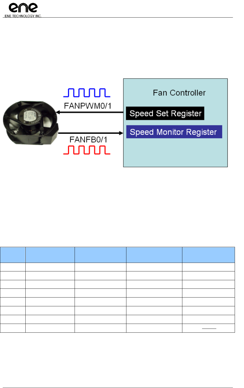
Copyright© 2011, ENE Technology Inc.
91
KB9012 Keyboard Controller Datasheet
CONFIDENTIAL
4.9.1.1 Fan Tachometer Monitor & Auto-FAN mode
When used as automatic mode, it will compare the speed and check if the current speed is
higher or slower than the expected one. If slower, the controller will increase the frequency to drive
FANPWM0/1 automatically, otherwise decrease the frequency. The expected speed can be
programmable by F/W.
Here is table for programmers use automatic FAN mode. In this table, information is illustrated
with 62.5us clock resolution. The Set Counter is the required values filled in FANSETH0/1 and
FANSETL0/1.
RPM = 60,000,000 / {FANSET * (FANPWM Period) } or
Set Counter = 60,000,000 / { RPM * (FANPWM Period) } or
Set Counter = (us per round) / (FANPWM Period)
Auto-FAN mode clock could be set in FANCFG0/1[7] , FANSTS0/1[6:5] to select 1) peripheral clock,
2) 62.5us d, 3) 31.25us, 4) 15.625us, 5) 7.8125us
RPM
RPS
us per round =
(1/RPS) * 10^6
Set Counter
( 62.5 us )
Set Counter
(7.8125 us)
8000
133
7500
120
960
6000
100
10000
160
1280
5000
83.33
12000
192
1536
4000
66.667
15000
240
1920
3000
50
20000
320
2560
2000
33.333
30000
480
3840
1000
16.667
60000
960
7680
500
8.3
120000
1920
15360
Note: RPM = Rounds per minute, RPS = Rounds per second

Copyright© 2011, ENE Technology Inc.
92
KB9012 Keyboard Controller Datasheet
CONFIDENTIAL
4.9.1.2 FANPWM Setting & Fixed-FAN Mode
The fan controller can be used to control 12-bit PWM channel called FANPWM. While
Fixed-FAN mode enable and PWM function applied, the fan controller will refer to the peripheral
clock, and the PWM high period and cycle time can be determined as the following formula
(Behavior is similar to general ENE-KBC PWM channels without pre-scaler referring peripheral
clock):
PWM Cycle Length = (PWM cycle register + 1 ) * peripheral clock resolution
PWM High Period = (PWM high period register + 1 ) * peripheral clock
Duty Cycle = (PWM high period register +1) / (PWM cycle register +1)
The high pulse width of PWM can be set in FANPWMH0/1 and FANPWML0/1, fill in the
high-byte first and then low-byte in order.
.

Copyright© 2011, ENE Technology Inc.
93
KB9012 Keyboard Controller Datasheet
CONFIDENTIAL
4.9.2 Fan Registers Description (0xFE20~0xFE4F)
Fan0 Configuration
Offset
Name
Bit
Type
Description
Default
Bank
0x20
FANCFG0
7
R/W
FAN0 monitor clock selection.
0: peripheral clock
1: the base clock will be based on FANSTS0[6:5](0xFE21)
0x00
0xFE
6
R/W
FAN0 speed monitor counter edge trigger selection.
0: count pulse event on rising edge.
1: count pulse event on rising and falling edge.
5
R/W
FANPWM0 cycle width enable
0: Disable
1: Enable
4
R/W
FANPWM0 enable.
0: Disable
1: Enable
3
R/W
FAN0 speed monitor interrupt enable
0: Disable
1: Enable
2
R/W
FAN0 speed monitor timeout error interrupt enable
0: Disable
1: Enable
1
R/W
Auto-fan mode enable (FANCFG0[0] for FANFB0 ,
FANCFG0[4] for FANPWM0 should also be enabled)
0: Disable
1: Enable
0
R/W
FAN0 tachometer monitor enable.
0: Disable
1: Enable
Copyright© 2011, ENE Technology Inc.
94
KB9012 Keyboard Controller Datasheet
CONFIDENTIAL
Fan0 Control and Status Register
Offset
Name
Bit
Type
Description
Default
Bank
0x21
FANSTS0
7
R/W
FAN0 auto-load FANCPWM function enable
0: Disable
1: Enable
0x00
0xFE
6-5
R/W
Clock resolution selection when not referring peripheral clock.
( FANCFG0[7](0xFE20) = 1 )
00: 62.5us (default)
01: 31.25us
10: 15.625us
11: 7.8125us
4
R/W
FAN0 digital noise filter enable.
0: Disable
1: Enable
3-2
RSV
Reserved
1
R/W1C
Flag of FAN0 speed monitor timeout error
0: no timeout error
1: timeout error event
0
R/W1C
Flag of FAN0 speed monitor update event.
0: no update event.
1: update event
Fan0 Speed Monitor Counter Value (12-bit)
Offset
Name
Bit
Type
Description
Default
Bank
0x22
FANMONH0
3-0
RO
High 4 bits of FAN0 speed monitor counter value
0x0F
0xFE
0x23
FANMONL0
7-0
RO
Low 8 bits of FAN0 speed monitor counter value
0xFF
0xFE
Fan0 Speed Set Counter Value (12-bit)
Offset
Name
Bit
Type
Description
Default
Bank
0x24
FANSETH0
3-0
R/W
High 4 bits of target FAN0 speed counter value.
0x00
0xFE
0x25
FANSETL0
7-0
R/W
Low 8 bits of target FAN0 speed counter value.
0x00
0xFE
Notice: These two registers are used in auto-fan mode and are set as target fan speed counter value
FANPWM0 High Pulse Width Bits (12-bit) (Fixed-FAN mode, FANCFG0[1]=0)
Offset
Name
Bit
Type
Description
Default
Bank
0x26
FANPWMH0
3-0
R/W
High 4 bits of FANPWM0 high pulse width.
0x00
0xFE
0x27
FANPWML0
7-0
R/W
Low 8 bits of FANPWM0 high pulse width.
0x00
0xFE
Notice: These two registers are used in fixed-fan mode and are set as target FANPWM high width to change effective fan speed
Current FANPWM0 High Pulse Width Bits (12-bit)
Offset
Name
Bit
Type
Description
Default
Bank
0x28
FANCPWMH0
3-0
RO
High 4 bits of current FANPWM0 high pulse width.
0x00
0xFE
0x29
FANCPWML0
7-0
RO
Low 8 bits of current FANPWM0 high pulse width.
0x00
0xFE
Copyright© 2011, ENE Technology Inc.
95
KB9012 Keyboard Controller Datasheet
CONFIDENTIAL
FANPWM0 Cycle Length (12-bit) (Fixed-FAN mode, FANCFG0[5]=1)
Offset
Name
Bit
Type
Description
Default
Bank
0x2A
FANPWMCH0
3-0
R/W
High 4 bits of Cycle length of FANPWM0
0x00
0xFE
0x2B
FANPWMCL0
7-0
R/W
Low 8 bits of Cycle length of FANPWM0
0x00
0xFE
Notice: These two registers are used in fixed-fan mode and are set as target FANPWM cycle length
FANPWM0 Auto-Load High Pulse Width Bits
Offset
Name
Bit
Type
Description
Default
Bank
0x2C
FANUPWM0
7-4
RSV
Reserved
0x0F
0xFE
3-0
R/W
If auto-load feature enabled (FANSTS0[7]=1), this register
value will be auto-loaded into FANCPWMH0 registers and
FANCPWML0 will be forced to be zero to handle monitor
timeout.
FAN tachometer monitor controller configuration for FANFB2
Offset
Name
Bit
Type
Description
Default
Bank
0x2D
FANTMCFG0
7-6
RSV
Reserved
0x00
0xFE
5-4
R/W
Clock resolution selection ( FANTMCFG0[1](0xFE2D[1]) = 0 )
00: 62.5us (default)
01: 31.25us
10: 15.625us
11: 7.8125us
3
R/W1C
Flag bit for Fan tachometer monitor timeout error event.
0: no timeout error
1: timeout error event
2
R/W
FAN digital filter enable for Fan tachometer monitor
0: Disable
1: Enable
1
R/W
Test mode enable for Fan tachometer monitor
0: the monitor base clock will be based on FANTMCFG0[5:4]
1: the monitor base clock will be peripheral clock.
0
R/W
FAN tachometer monitor enable for FANFB2
0: Disable
1: Enable
FAN tachometer monitor speed monitor counter value for FANFB2
Offset
Name
Bit
Type
Description
Default
Bank
0x2E
FANTMMONH0
3-0
RO
High 4 bits of FANFB2 speed monitor counter value
0x0F
0xFE
0x2F
FANTMMONL0
7-0
RO
Low 8 bits of FANFB2 speed monitors counter value.
0xFF
0xFE

Copyright© 2011, ENE Technology Inc.
96
KB9012 Keyboard Controller Datasheet
CONFIDENTIAL
Fan1 Configuration
Offset
Name
Bit
Type
Description
Default
Bank
0x30
FANCFG1
7
R/W
FAN1 monitor clock selection.
0: peripheral clock
1: the monitor base clock will based on FANSTS1[6:5](0xFE31)
0x00
0xFE
6
R/W
FAN1 speed monitor counter edge trigger selection.
0: count pulse event on rising edge.
1: count pulse event on rising and falling edge.
5
R/W
FANPWM1 cycle width enable
0: Disable
1: Enable
4
R/W
FANPWM1 enable.
0: Disable
1: Enable
3
R/W
FAN1 speed monitor interrupt enable
0: Disable
1: Enable
2
R/W
FAN1 speed monitor timeout error interrupt enable
0: Disable
1: Enable
1
R/W
Auto-fan mode enable (FANCFG1[0] for FANFB1 ,
FANCFG1[4] for FANPWM1 should also be enabled)
0: Disable
1: Enable
0
R/W
FAN1 tachometer monitor enable.
0: Disable
1: Enable
Copyright© 2011, ENE Technology Inc.
97
KB9012 Keyboard Controller Datasheet
CONFIDENTIAL
Fan1 Control and Status Register
Offset
Name
Bit
Type
Description
Default
Bank
0x31
FANSTS1
7
R/W
FAN1 auto-load FANCPWM function enable
0: Disable
1: Enable
0x00
0xFE
6-5
R/W
Clock resolution selection when not referring peripheral clock.
( FANCFG1[7](0xFE30) = 1 )
00: 62.5us (default)
01: 31.25us
10: 15.625us
11: 7.8125us
4
R/W
FAN1 digital noise filter enable.
0: Disable
1: Enable
3-2
R/W
Reserved
1
R/W
Flag of FAN1 speed monitor timeout error
0: no timeout error
1: timeout error event
0
R/W
Flag of FAN1 speed monitor update event.
0: no update event.
1: update event
Fan1 Speed Monitor Counter Value (12-bit)
Offset
Name
Bit
Type
Description
Default
Bank
0x32
FANMONH1
3-0
RO
High 4 bits of FAN1 speed monitor counter value
0x0F
0xFE
0x33
FANMONL1
7-0
RO
Low 8 bits of FAN1 speed monitor counter value
0xFF
0xFE
Fan1 Speed Set Counter Value (12-bit)
Offset
Name
Bit
Type
Description
Default
Bank
0x34
FANSETH1
3-0
R/W
High 4 bits of target FAN1 speed counter value.
0x00
0xFE
0x35
FANSETL1
7-0
R/W
Low 8 bits of target FAN1 speed counter value.
0x00
0xFE
Notice: These two registers are used in auto-fan mode and are set as target fan speed counter value
FANPWM1 High Pulse Width Bits (12-bit) (Fixed-FAN mode, FANCFG1[1]=0)
Offset
Name
Bit
Type
Description
Default
Bank
0x36
FANPWMH1
3-0
R/W
High 4 bits of FANPWM1 high pulse width.
0x00
0xFE
0x37
FANPWML1
7-0
R/W
Low 8 bits of FANPWM1 high pulse width.
0x00
0xFE
Notice: These two registers are used in fixed-fan mode and are set as target FANPWM high width to change effective fan speed
Current FANPWM1 High Pulse Width Bits (12-bit)
Offset
Name
Bit
Type
Description
Default
Bank
0x38
FANCPWMH1
3-0
RO
High 4 bits of current FANPWM1 high pulse width.
0x00
0xFE
0x39
FANCPWML1
7-0
RO
Low 8 bits of current FANPWM1 high pulse width.
0x00
0xFE

Copyright© 2011, ENE Technology Inc.
98
KB9012 Keyboard Controller Datasheet
CONFIDENTIAL
FANPWM1 Cycle Length (12-bit) (Fixed-FAN mode, FANCFG1[5]=1)
Offset
Name
Bit
Type
Description
Default
Bank
0x3A
FANPWMCH1
3-0
R/W
High 4 bits of Cycle length of FANPWM1
0x00
0xFE
0x3B
FANPWMCL1
7-0
R/W
Low 8 bits of Cycle length of FANPWM1
0x00
0xFE
Notice: These two registers are used in fixed-fan mode and are set as target FANPWM cycle length
FANPWM1 Update High Pulse Width Bits
Offset
Name
Bit
Type
Description
Default
Bank
0x3C
FANUPWM1
7-4
RSV
Reserved
0x0F
0xFE
3-0
R/W
If auto-load feature enabled (FANSTS1[7]=1), this register
value will be auto-loaded into FANCPWMH1 registers and
FANCPWML1 will be forced to be zero to handle monitor
timeout.
FAN tachometer monitor controller configuration for FANFB3
Offset
Name
Bit
Type
Description
Default
Bank
0x3D
FANTMCFG1
7-6
RSV
Reserved
0x00
0xFE
5-4
R/W
Clock resolution selection ( FANTMCFG1[1](0xFE3D[1]) = 0 )
00: 62.5us (default)
01: 31.25us
10: 15.625us
11: 7.8125us
3
R/W1C
Flag bit for Fan tachometer monitor timeout error event.
0: no timeout error
1: timeout error event
2
R/W
FAN digital filter enable for Fan tachometer monitor
0: Disable
1: Enable
1
R/W
Test mode enable for Fan tachometer monitor
1: the monitor base clock will be peripheral clock.
0: the monitor base clock will be based on FANTMCFG1[5:4]
0
R/W
FAN tachometer monitor enable for FANFB3
0: Disable
1: Enable
FAN tachometer monitor speed monitor counter value for FANFB3
Offset
Name
Bit
Type
Description
Default
Bank
0x3E
FANTMMONH1
3-0
RO
High 4 bits of FANFB3 speed monitor counter value
0x0F
0xFE
0x3F
FANTMMONL1
7-0
RO
Low 8 bits of FANFB3 speed monitors counter value.
0xFF
0xFE

Copyright© 2011, ENE Technology Inc.
99
KB9012 Keyboard Controller Datasheet
CONFIDENTIAL
4.9.3 Fan Programming Sample
In this section gives some programming sample to control FAN module. Please note, ENE
does not guarantee these codes in every field application. The following table describes scenario of
FAN filed application.
Example
FAN0 @ 4000 rpm with automatic PWM control
FAN1 @ some rpm with fixed PWM control
Programming model
For FAN0:
1. Set related GPIO function select register to enable alternative output.
GPIOFS10[2] (0xFC02[2]) = 1b
2. Set related GPIO input enable.
GPIOIE10[4] (0xFC62[4]) = 1b
3. Set FAN0 Auto-FAN mode and refer default 62.5us clock
FANCFG0 (0xFE20) = 0x93
4. Set FAN0 target speed value (Refer the table 4.9.1.1 for calculation)
FANMONH0 (0xFE24) = 0x00
FANMONL0 (0xFE25) = 0xF0
For FAN1:
1. Set related GPIO function select register to enable alternative output.
GPIOFS10[3] (0xFC02[3]) = 1b
2. Set FAN1 Fixed-FAN mode and enable FANPWM1
FANCFG1 (0xFE30) = 0x90
3. set FAN1 speed monitor counter value
FANPWMH1 (0xFE36) = 0x03
FANPWML2 (0xFE37) = 0xE8

Copyright© 2011, ENE Technology Inc.
100
KB9012 Keyboard Controller Datasheet
CONFIDENTIAL
4.10 General Purpose Timer (GPT)
4.10.1 GPT Function Description
The KBC provides 4 GPTs (General Purpose Timers), two 16-bit timers and two 8-bit timers.
These 4 GPTs operate based on 32.768 khz and all timers have the interrupt capability. The GPT is
simply a free run counter. While the timer meets the specific value in counter register, for instance,
0xFE53 and 0xFE55, an interrupt issues (if interrupt enabled) and the counter reset to be zero.
- GPT0 and GPT1 are 8-bit timers.
- GPT2 and GPT3 are 16-bit timers.
Since 32.768 khz = 30 us period. For the designed target timer period T us, the required value
need to be filled in counter register = (T in us) / 30.
Eg: A 200Hz timer is with timer period of 5ms. The required value is 5000 / 30 = 166 = 0xA6

Copyright© 2011, ENE Technology Inc.
101
KB9012 Keyboard Controller Datasheet
CONFIDENTIAL
4.10.2 GPT Registers Description (0xFE50~0xFE6F)
GPT Configuration
Offset
Name
Bit
Type
Description
Default
Bank
0x50
GPTCFG
7-5
RSV
Reserved
0x00
0xFE
4
R/W
GPT test mode enable.
In test mode, the GPT runs with main clock.
0: Disable
1: Enable
3
R/W
GPT3 counting and interrupt enable.
0: Disable
1: Enable
2
R/W
GPT2 counting and interrupt enable.
0: Disable
1: Enable
1
R/W
GPT1 counting and interrupt enable.
0: Disable
1: Enable
0
R/W
GPT0 counting and interrupt enable.
0: Disable
1: Enable
GPT Pending Flag
Offset
Name
Bit
Type
Description
Default
Bank
0x51
GPTPF
7
WO
Writing ―1‖ to this bit forces GPT3 restart.
0x00
0xFE
6
WO
Writing ―1‖ to this bit forces GPT2 restart.
5
WO
Writing ―1‖ to this bit forces GPT1 restart.
4
WO
Writing ―1‖ to this bit forces GPT0 restart.
3
R/W1C
Interrupt pending flag of GPT3.
2
R/W1C
Interrupt pending flag of GPT2.
1
R/W1C
Interrupt pending flag of GPT1.
0
R/W1C
Interrupt pending flag of GPT0.
GPT0 Counter Value
Offset
Name
Bit
Type
Description
Default
Bank
0x53
GPT0
7-0
R/W
Once GPT0 counter meets this value, an interrupt issues.
GPT0 restart to count from zero.
0x00
0xFE
RSV
Offset
Name
Bit
Type
Description
Default
Bank
0x54
RSV
7-0
RSV
Reserved
0x00
0xFE
GPT1 Counter Value
Offset
Name
Bit
Type
Description
Default
Bank
0x55
GPT1
7-0
R/W
Once GPT1 counter meets this value, an interrupt issues.
GPT1 restart to count from zero.
0x00
0xFE

Copyright© 2011, ENE Technology Inc.
102
KB9012 Keyboard Controller Datasheet
CONFIDENTIAL
GPT2 Counter Value (16-bit)
Offset
Name
Bit
Type
Description
Default
Bank
0x56
GPT2H
7-0
R/W
High byte of GPT2 counter value
Once GPT2 counter meets this 16-bit value, an interrupt issues.
GPT2 restart to count from zero.
0x00
0xFE
0x57
GPT2L
7-0
R/W
Low byte of GPT2 counter value
Once GPT2 counter meets this 16-bit value, an interrupt issues.
GPT2 restart to count from zero.
0x00
0xFE
GPT3 Counter Value (16-bit)
Offset
Name
Bit
Type
Description
Default
Bank
0x58
GPT3H
7-0
R/W
High byte of GPT3 counter value.
Once GPT3 counter meets this 16-bit value, an interrupt issues.
GPT3 restart to count from zero.
0x00
0xFE
0x59
GPT3L
7-0
R/W
Low byte of GPT3 counter value.
Once GPT2 counter meets this 16-bit value, an interrupt issues.
GPT3 restart to count from zero.
0x00
0xFE

Copyright© 2011, ENE Technology Inc.
103
KB9012 Keyboard Controller Datasheet
CONFIDENTIAL
4.10.3 GPT Programming Sample
In this section gives some programming sample to control GPT module. Please note,
ENE does not guarantee these codes in every field application. The following table describes
scenario of GPT filed application.
Example
Programming GPT0 to issue an interrupt every 5ms
Programming model
1. Set GPT configuration register, enable GPT0 interrupt.
GPTCFG[0] (0xFE50[0]) = 1b
2. Fill the GPT counter value.
GPT0 (0xFE53) = 0xA6 ; 5000/30 = 0xA6
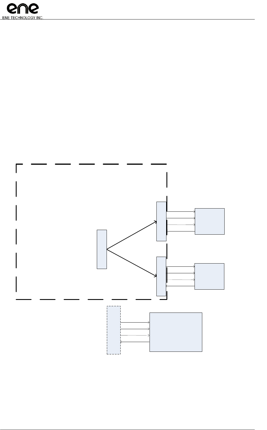
Copyright© 2011, ENE Technology Inc.
104
KB9012 Keyboard Controller Datasheet
CONFIDENTIAL
4.11 SDI Host/Device Interface Controller
The SDI host/device controller can be programmed to a SPI Host or a SPI Device. The
Default is the SPI Host. The SPI Host and Device use the same IO pins.
4.11.1 SDI Host/Device Interface Description
The Serial Peripheral Interface Bus or SPI (often pronounced ―spy‖) bus is a synchronous serial
data link standard designed by Motorola that operates in full duplex mode. Devices communicate in
master/slave mode where the master device initiates the data frame.
The SDI host mode could support the SPI mode 0/1. Mode 2/3 are added and is configurable
by SHICFG[5:4] now.
SDI device mode could support the SPI mode 0. SDI device is recommended to operate at
Command Mode.
SPI
Device
P128, SPICS#
P120, (MOSI)
P119, (MISO)
P126, SPICLK
ENE-KBC
SDI Device
Mode
P97, SDICS#
P99, SDIDI
P109, SDIDO
P98, SDICLK
SPI
Device
P97, SHICS#
P99, SHIDO
P109, SHIDI
P98, SHICLK
ENE Flash I/F
ENE SDI I/F
ENE E-Flash
KBC Series
(Controlled by XBI in non-E-Flash KBC)
(Controlled by SDI in non-E-Flash KBC)
……From other IC SPI host signaling
Selected by SHICFG[6]
…From ENE SDI
host/device Controller
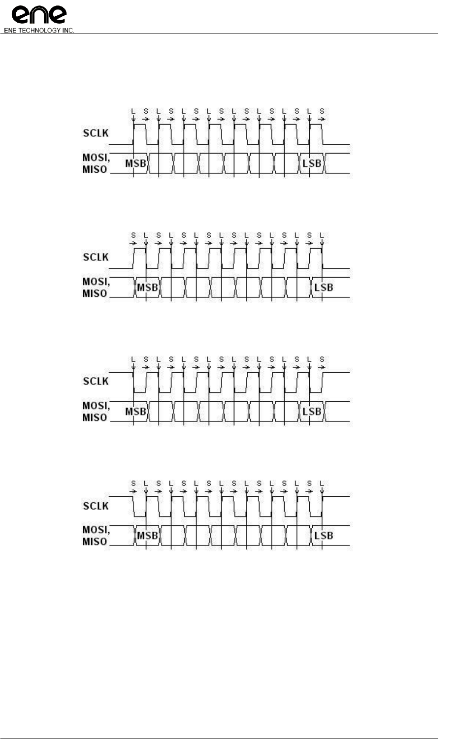
Copyright© 2011, ENE Technology Inc.
105
KB9012 Keyboard Controller Datasheet
CONFIDENTIAL
Illustration of General SPI modes :
Mode 0
Mode 1
Mode 2
Mode 3

Copyright© 2011, ENE Technology Inc.
106
KB9012 Keyboard Controller Datasheet
CONFIDENTIAL
4.11.2 SDI Host Interface Register Description (0xFE70~0xFE7F)
SDI host interface configuration
Offset
Name
Bit
Type
Description
Default
Bank
0x70
SHICFG
7
RSV
Reserved
0x00
0xFE
6
R/W
Select SDI host/device Pins
0 : Select pins from Pin 97/98/99/109
1 : Select pins form Pin 119/120/126/128
Please refer section 4.11.1 illustration
Also Refer GPIO_MISC[2:1]
5-4
R/W
SDI host signal timing relation and SPI mode
00:Mode 0,
Clock default low, Data drive @ falling, latch
@ rising
01: Mode 1,
Clock default low, Data drive @ rising, latch
@ falling
10: Mode 2,
Clock default high, Data drive @ rising, latch
@ falling
11: Mode 3,
Clock default high, Data drive @ falling, latch
@ rising
Please refer section 4.11.1 illustration
3-1
R/W
SPI clock divide
000 : SPI clock run 16 Mhz
001 : SPI clock run 8 Mhz
010 : SPI clock run 4 Mhz
011 : SPI clock run 2 Mhz
100, 101, 111 : SPI clock run 1 Mhz
0
R/W
SDI host controller enable
0: Disable
1: Enable
SDI host control register
Offset
Name
Bit
Type
Description
Default
Bank
0x71
SHICTR
7
RO
SDI host Idle flag. If this bit set, the SDI host is in an idle state.
0: busy
1: idle
0x00
0xFE
6-1
RSV
Reserved
0
R/W
SDI host SHICS# Pin Control
0 : Set SHICS# High
1 : Set SHICS# Low
SDI host interface transmit data port
Offset
Name
Bit
Type
Description
Default
Bank
0x72
SHITBUF
7-0
R/W
While SHICFG[7]=1 (SDI host not busy), writing to this register
will force data output to SHIDO in continuously serial 8 bits.
MSB first.
0x00
0xFE

Copyright© 2011, ENE Technology Inc.
107
KB9012 Keyboard Controller Datasheet
CONFIDENTIAL
SDI host interface receive data port
Offset
Name
Bit
Type
Description
Default
Bank
0x73
SHIRBUF
7-0
RO
SDI host reading port.
0x00
0xFE
Copyright© 2011, ENE Technology Inc.
108
KB9012 Keyboard Controller Datasheet
CONFIDENTIAL
4.11.3 SDI Device Interface Register Description (0xFE70~0xFE7F)
SDI device interface configuration
Offset
Name
Bit
Type
Description
Default
Bank
0x78
SDICFG
7
RO
SDICS# status
0x44
0xFE
6~4
RSV
Reserved
3
R/W
SDI command mode
0: Disable. (Normal mode)
1: Enable. (Command mode)
(When enable this mode, SDICFG[2:1] would not take effect)
(Configurable command : Read TX buffer in register SDICMD)
2
R/W
Enable SDI device TX.
0: Disable
1: Enable
1
R/W
Enable SDI device RX.
0: Disable
1: Enable
0
R/W
SDI device controller enable
0: Disable
1: Enable
SDI device interface interrupt configuration
Offset
Name
Bit
Type
Description
Default
Bank
0x79
SDIINT
7
RSV
Reserved
0x00
0xFE
6
R/W1C
(Normal mode only) Transmit buffer empty pending flag
5
R/W1C
(Normal mode only) Receive buffer full pending flag
4
R/W1C
SDICS# rising edge pending flag
3
RSV
Reserved
2
R/W
(Normal mode only) Transmit buffer empty interrupt enable bit
When Tx buffer counter from 1 to 0, interrupt would occur.
0: Disable
1: Enable
1
R/W
(Normal mode only) Receive buffer full interrupt enable bit
When Rx buffer counter from 3 to 4, interrupt would occur.
0: Disable
1: Enable
0
R/W
SDICS# rising edge interrupt enable bit
0: Disable
1: Enable
Copyright© 2011, ENE Technology Inc.
109
KB9012 Keyboard Controller Datasheet
CONFIDENTIAL
SDI device interface transmit status
Offset
Name
Bit
Type
Description
Default
Bank
0x7A
SDITSTS
7
RSV
Reserved
0x00
0xFE
6~4
RO
Transmit buffer counter
In normal mode:
The number how many data in Tx Buffer not transmitted.
In command mode:
The number of transmitted byte data in single transition.
3
RSV
Reserved
2
R/W1C
(Normal mode only) Transmit buffer underflow flag
1
RO
(Normal mode only) Transmit buffer full flag
0
R
(Normal mode only) Transmit buffer empty flag
W
Write 1 to clear Tx buffer
Normal mode:
FIFO's write point and read point are both reset to point to
position "0".
Command mode:
Only FIFO's write point is reset to point to position "0".
SDI device interface receive status
Offset
Name
Bit
Type
Description
Default
Bank
0x7B
SDIRSTS
7
RSV
Reserved
0x00
0xFE
6~4
RO
Receive Buffer count
Normal mode :
The number how many data in Rx Buffer not read.
Command mode:
The number of received byte data in single transition.
3
RSV
Reserved
2
R/W1C
(Normal mode only) Receive buffer overflow flag
1
RO
(Normal mode only) Receive buffer full flag
0
R
(Normal mode only) Receive buffer empty flag
W
Write 1 to clear Rx buffer
Normal mode:
FIFO's write point and read point are both reset to point to
position "0".
Command mode:
Only FIFO's read point is reset to point to position "0".
SDI device interface transmit data port (4 bytes buffer)
Offset
Name
Bit
Type
Description
Default
Bank
0x7C
SDITBUF
7~0
WO
SDI Device Interface Transmitted Data Port
Normal mode:
Before write operation to external SPI host.
TX flags should be confirmed.
If TX buffer is full, SDI device would preserve the previous data
If TX buffer is empty, SDI device always transmit data = 0x00.
0x00
0xFE
Copyright© 2011, ENE Technology Inc.
110
KB9012 Keyboard Controller Datasheet
CONFIDENTIAL
SDI device interface receive data port (4 bytes buffer)
Offset
Name
Bit
Type
Description
Default
Bank
0x7D
SDIRBUF
7
RO
SDI Device Interface Received Data Port
Normal mode:
Before read operation from external SPI host.
RX flags should be confirmed.
If RX buffer is full, SDI device would preserve the previous data
If RX buffer is empty, SDI device always read data = 0x00.
Command mode:
In single transaction, SDI device will only receive 4 bytes data.
If over 4 bytes data are read, SDI will skip the latest data and
preserve the previous data.
RX buffer can be read according the Rx buffer's read point.
0x00
0xFE
Command : Read TX buffer
Offset
Name
Bit
Type
Description
Default
Bank
0x7E
SDICMD
7~0
R/W
(Command mode only)
Configurable command : Read TX buffer
0x5A
0xFE
SDI TX/RX buffer write point and read point
Offset
Name
Bit
Type
Description
Default
Bank
0x7F
SDIPT
7~6
RO
Tx buffer write point
0x00
0xFE
5~4
RO
Tx buffer read point
3~2
RO
Rx buffer write point
1~0
RO
Rx buffer read point
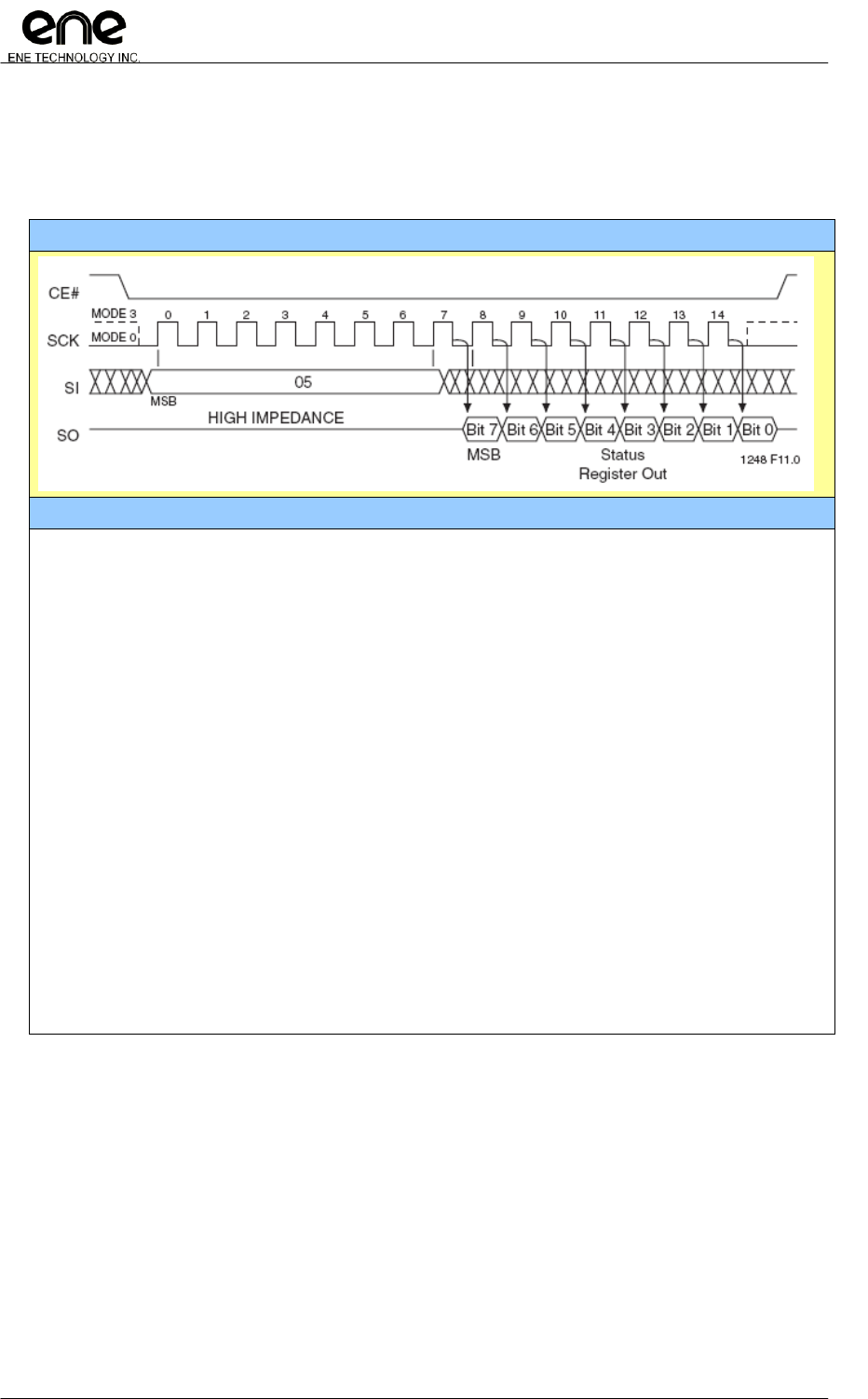
Copyright© 2011, ENE Technology Inc.
111
KB9012 Keyboard Controller Datasheet
CONFIDENTIAL
4.11.4 SDI Programming Sample
In this section gives some programming sample to control SDI module. Please note,
ENE does not guarantee these codes in every field application. The following table describes
scenario of SDI host filed application.
Example : Send CMD and data to device Atmel_25010
Programming model
GPIO_MISC[2] (0xFC70[2]) = 1b; //Enable SDI interface,
GPXDIE00[0] (0xFC6F[0]) = 1b; //Enable SDI host data input
SHICFG (0xFE70) = 0x01; //Enable SDI host module mode 0, clock = Peripheral clock/2
SHICFG |= 0x10; //Set SDICS# low
SHITBUF = 0x06; //Transfer CMD WREN(0x06) to device
while((SDI_Non_IDLE)==0); //Wait bus idle
SHICFG &= ~0x10; //Set SDICS# H
SHICFG |= 0x10; // Set SDICS# Low
SHITBUF = 0x05; // Transfer CMD RDSR to device
while((SDI_Non_IDLE)==0); //Wait bus idle
SHITBUF = 0x00; // Write Dummy
while((SDI_Non_IDLE)==0);
temp = SHIRBUF;
SHICFG = 0x00; //disable SDICS# and SDI data port
if(temp = 0x02) //WREN success to device

Copyright© 2011, ENE Technology Inc.
112
KB9012 Keyboard Controller Datasheet
CONFIDENTIAL
4.12 Watchdog Timer (WDT)
4.12.1 WDT Function Description
A Watchdog Timer (WDT) is a hardware timing device that triggers a system reset while
the system encounters any unrecoverable situation. The WDT utilizes 32.768 khz for operation. The
WDT triggers the system WDT reset in three ways.
- Reset the 8051 microprocessor only.
- Reset the whole logic, except GPIO modules.
- Reset the whole logic, including GPIO modules.
Here gives the highlight of WDT register field features & setting:
- 20 bit Watchdog (10bit programmable register field with 31.25ms resolution)
- Interrupt support
- WDT LED breathing support
- 24 bit timer (TMR) support
- System 32khz clock source setting
Timing Example:
With a 32.768 khz WDT clock source, the timing period is about 30.5 us.
In KB9012 :
The maximum WDT reset timer is 20bit (220 x 30.5us = 32 seconds)
(Higher 10 bit register field available, 32ms), for real application recommended N≧3.
The maximum WDT interrupt time is half the WDT timer, (16 seconds)
The maximum TMR timer is 24 bit (224 x 30.5us = 512 seconds, about 8 minute)

Copyright© 2011, ENE Technology Inc.
113
KB9012 Keyboard Controller Datasheet
CONFIDENTIAL
4.12.2 Setting for WDT Breathing LED
ENE KBC GPIO54
WDT_LED#
VLED
In KB9010 series, GPIO54(WDT_LED#) support a breathing LED functionality. The
configuration is recommended as the above illustration: Connected via LED to high voltage power
supply. The breathing characteristic could be programmed as the following illustration: Please be
noted that output PWM higher duty cycle means less lighting and vice versa.
Max Lighting
(duty cycle=0%)
Min Lighting
(duty cycle=100%)
DEC Lighting
(0%->100%)
INC Lighting
(From 100%->0%)
………Periodically
Configuration:
1. Max lighting period would keep (M * 32 ms), in BRTMR_BD[7:4],
Timing unit can be set in BRTMR_CFG[5:4], (32/64/128/256 ms)
2. DEC lighting period would gradually increase the PWM duty cycle, thus the
breathing LED would be less bright. The scale is divided into 64 scales as
default. The scale-up floor can be set in BRTMR_CFG[3:0], as numbered
30h~3Fh. Every (Y * 2 ms) would increase 1 scale PWM duty(thus less lighting)
until the min lighting period. In other words, with larger Y, DEC would be slower.
With smaller Y, DEC would be faster. Y can be set in the register
BRTMR_ID[3:0].
3. Min lighting period would keep (N * 32 ms), in BRTMR_BD[3:0],
Timing unit can be set in BRTMR_CFG[5:4], (32/64/128/256 ms)
4. INC lighting period would gradually decrease the PWM duty cycle, thus the
breathing LED would be brighter. The scale is divided into 64 scales as default.
The start scale-down can be set in BRTMR_CFG[3:0], as numbered 30h~3Fh.
Every (X * 2 ms) would decrease 1 scale until the next max lighting period. In
other words, with larger Y, INC would be slower. With smaller Y, INC would be
faster. X can be set in the register BRTMR_ID[7:4],

Copyright© 2011, ENE Technology Inc.
114
KB9012 Keyboard Controller Datasheet
CONFIDENTIAL
4.12.3 WDT Registers Description (0xFE80~0xFE8F)
WDT Configuration
Offset
Name
Bit
Type
Description
Default
Bank
0x80
WDTCFG
7
R/W
WDT clock source selection
0: DPLL 32.768KHz source
1: Internal OSC or External Crystal 32.768KHz source
0x00
0xFE
6~3
R/W
WDT disable password
Writing 1001b to this field will force WDT disable
2
R/W
WDT test mode enable
0: normal mode (depend on WDTCFG[7], 0xFE80[7])
1: test mode, clock driven by internal 32MHz
1
R/W
WDT interrupt enable (WDT reset warning)
0: Disable
1: Enable
0
R/W
WDT reset enable.
Once WDT resets, two WDT pending flags are clear.
0: Disable
1: Enable
WDT Pending Flag
Offset
Name
Bit
Type
Description
Default
Bank
0x81
WDTPF
7-5
RSV
Reserved
0x00
0xFE
1
R/W1C
WDT interrupt flag
Once the timer counts to half of WDT (0xFE82), an interrupt
occurs. If the timer counts to WDT(0xFE82), a WDT reset
occurs.
0: no event
1: event occurs
0
R/W1C
WDT reset flag
Once the timer counts to WDT (0xFE82), a WDT reset occurs
and this flag is set.
0: no event
1: event occurs
WDT High 8-bit Counter Value (for WDT reset system of 10 bits counter)
Offset
Name
Bit
Type
Description
Default
Bank
0x82
WDT
7-0
R/W
The high 8-bits of WDT counter value.
The WDT timer unit is 30.5us * 210 = 32ms. The overall high 10
bits counter is combined from WDT:LEDCFG[7:6]
Please note, fill the overall value at least greater than or equal 3
(>=3) for hardware limitation.
0x00
0xFE

Copyright© 2011, ENE Technology Inc.
115
KB9012 Keyboard Controller Datasheet
CONFIDENTIAL
WDT Breathing LED Configuration
Offset
Name
Bit
Type
Description
Default
Bank
0x83
LEDCFG
7~6
R/W
The following 2 bits after WDT counter value.
The WDT timer unit is 30.5us * 210 = 32ms. The overall high 10
bits counter is combined from WDT:LEDCFG[7:6]
Please note, fill the overall value at least greater than or equal 3
(>=3) for hardware limitation.
0x00
0xFE
5
RSV
Reserved
4
R/W
Breathing LED Open-Drain function enable
0: Disable
1: Enable
3
R/W
Breathing LED function enable
0: Disable
1: Enable
2-0
RSV
Reserved
WDT TMR (24-bit Timer) Configuration
Offset
Name
Bit
Type
Description
Default
Bank
0x84
TMR_CFG
7
R/W
TMR enable
0: Disable/reset TMR
1: Enable TMR
0x00
0xFE
6~3
RSV
Reserved
2
RO
TMR interrupt pending flag overflow.
While TMR interrupt flag (TMR_CFG[1]) is set and an interrupt
event occurs again. This bit will be set and can be clear via
writing TMR_CFG[7] with ―0‖.
0: no event
1: event occurs
1
R/W1C
TMR interrupt flag.
When TMR counter[23:16] is equal to TMR_MATCH register.
This bit will be set.
0: no event
1: event occurs
0
R/W
TMR counter start control.
0: stop counting
1: start counting
WDT TMR (24-bit Timer) Counter Match Value
Offset
Name
Bit
Type
Description
Default
Bank
0x85
TMR_MATCH
7-0
R/W
The highest 8bit counter match value register
Assumed clock source 32.768KHz, the TMR time unit is 216 x
30.5us = 2 second in this register.
When timer counter[23:16] is reached this value, timer emits
interrupt and TMR_CFG[1] is set to 1 .
0x00
0xFE
Copyright© 2011, ENE Technology Inc.
116
KB9012 Keyboard Controller Datasheet
CONFIDENTIAL
WDT TMR (24-bit Timer) Counter Value 1
Offset
Name
Bit
Type
Description
Default
Bank
0x86
TMR_V1
7-0
RO
Value for TMR counter[23:16]
0x00
0xFE
WDT TMR (24-bit Timer) Counter Value 2
Offset
Name
Bit
Type
Description
Default
Bank
0x87
TMR_V2
7-0
RO
Value for TMR counter[15:8]
0x00
0xFE
Breathing LED Timer for Bright (max lighting) & Dark (min lighting)
Offset
Name
Bit
Type
Description
Default
Bank
0x88
BRTMR_BD
7-4
R/W
Timer values for the max lighting period
M * {Setting of BRTMR_CFG[5:4]}…default 32 ms
0x00
0xFE
3-0
R/W
Timer values for the min lighting period
N * {Setting of BRTMR_CFG[5:4]}…default 32 ms
Breathing LED Timer for INC lighting & DEC lighting
Offset
Name
Bit
Type
Description
Default
Bank
0x89
BRTMR_ID
7-4
R/W
Timer values for the DEC lighting period
X * 2 ms
(DEC starts from the setting value of BRTMR_CFG[3:0], until 0)
0x00
0xFE
3-0
R/W
Timer values for the INC lighting period
Y * 2 ms
(INC ends at the setting value of BRTMR_CFG[3:0], from 0)
Clock 32khz Control Register
Offset
Name
Bit
Type
Description
Default
Bank
0x8A
CLK32CR
7~6
RSV
Reserved
0x00
0xFE
5~4
RSV
Function selection for XCLKI & XCLKO pad (Pin 122 GPIO5D,
Pin 123 GPIO5E)
Pin 122 , Pin 123
00 : GPIO5D, GPIO5E
01 : GPIO5D, XCLKO as external clock input
10 : XLCKI, GPIO5E, where XLCKI is external clock input
11 : XLCKI, XCLKO, as crystal pads to external crystal
3
R/W
PS2, GPT, FAN, FANMON, PWM clock source selection
0: Clock source from KBC DPLL divider
1: Clock source from external 32khz crystal
2
R/W
Crystal 32khz clock selection
0: Clock source from external clock or external crystal
1: Clock source from internal osc
Note : For proper changes of clock source during operation, be
sure to program CLK32CR[0], or CLK32CR[1] to enable the
related source before applying changes.
1
R/W
Internal osc enable
0: Disable
1: Enable
0
R/W
External crystal / clock enable
0: Disable
1: Enable

Copyright© 2011, ENE Technology Inc.
117
KB9012 Keyboard Controller Datasheet
CONFIDENTIAL
Internal OSC Control Register
Offset
Name
Bit
Type
Description
Default
Bank
0x8B
IOSCCR
7
RSV
Reserved
0x00
0xFE
6
R/W
OSC OP Enable, OSC OP is used to trade-off the precision and
power consumption, the approximate trade-off is as followed:
0: Disable, 10uA leakage with 32Khz±20%
1: Enable, 28uA leakage with 32Khz±10%
5-0
RSV
Reserved
Breathing LED Timer Configuration Register
Offset
Name
Bit
Type
Description
Default
Bank
0x8C
BRTMR_CFG
7~6
RSV
Reserved
0x0F
0xFE
5~4
R/W
Timing Unit for the max lighting & min lighting period
00: 32ms
01: 64ms
10: 128ms
11: 256ms
3~0
R/W
Start value & end value for DEC lighting & INC lighting period
0000: The reference values as 30h
0001: The reference values as 31h
...
…
…
1111: The reference values as 3Fh

Copyright© 2011, ENE Technology Inc.
118
KB9012 Keyboard Controller Datasheet
CONFIDENTIAL
4.12.4 WDT Programming Sample
In this section gives some programming sample to control WDT module. Please note, ENE
does not guarantee these codes in every field application. The following table describes scenario of
WDT filed application.
Example
Set WDT=512ms to reset system, and an interrupt occurs while
WDT=256ms (half of WDT)
Programming model
WDT (0xFE82) = 0x10 ; set WDT=512ms
WDTCFG (0xFE80) = 0x03 ; enable interrupt and WDT reset

Copyright© 2011, ENE Technology Inc.
119
KB9012 Keyboard Controller Datasheet
CONFIDENTIAL
4.13 Low Pin Count Interface (LPC)
4.13.1 LPC Function Description
The Low Pin Count (LPC) is an interface for modern ISA-free system. The KBC
connects to the system via LPC interface. The following LPC cycle types are supported.
Type
Address
Data
LPC I/O Read
16-bit
8-bit
LPC I/O Write
16-bit
8-bit
LPC Memory Read
32-bit
8-bit
LPC Memory Write
32-bit
8-bit
FWH Read
28-bit
8-bit
FWH Write
28-bit
8-bit
4.13.2 LPC I/O Decode Range
Item
Port
Comment
Keyboard Controller
60h/64h
Embedded Controller
62h/66h (default)
Programmable
Legacy I/O
68h/6Ch, 2Eh/2Fh
EC Index-I/O
FF29h~FF2Bh/FF2Dh~FF2Fh(default)
2 Sets, Programmable.
Debug Port
80h
Only write cycle support interrupt

Copyright© 2011, ENE Technology Inc.
120
KB9012 Keyboard Controller Datasheet
CONFIDENTIAL
4.13.3 Index-I/O Port
The KBC provides a method to communicate with the host via legacy I/O port. The host
can access the XRAM space inside the KBC. The I/O port is called Index-I/O. Two Index-I/Os are
supported and programmable. The registers, LPCIBAH and LPCIBAL (0xFE92 and 0xFE93), are
used to specify the desired I/O port base. To enable the 2nd Index-I/O, the LPCSCFG[5], (0xFE90[5])
should be set.
With only 1 index-I/O, the base address is 4 bytes alignment. If the LPCSCFG[5] set, the
index-I/O base address will be 8 bytes align for the 1st & 2nd Index-I/O reserved.
For example, while the base address is 0xFF2C (LPCIBAH=0xFF, LPCIBAL=0x2C) and
LPCSCFG[5] set, the 1st index-I/O address will be 0xFF29 (io_base +1).
The following table collects the port definition for the host. The base address of Index-I/O
is assumed to be io_base.
1st Index-I/O
2nd Index-I/O (LPCSCFG[5]=1)
XRAM address (high)
io_base+1
XRAM address (high)
io_base+5
XRAM address (low)
io_base+2
XRAM address (low)
io_base+6
XRAM data (high)
io_base+3
XRAM data (high)
io_base+7
Here is an example how to use an Index-I/O.
EC F/W
Host software
1. EC F/W setups the base address, for instance,
0x380. That is, LPCIBAH=0x03 and
LPCIBAL=0x80.
2. If the 2nd Index-I/O is needed, turn on the enable
bit. That is, LPCSCFG[5]=1 (0xFE90[5]=1).
1. Host setups the desired XRAM address:
Port 0x381 = high byte of XRAM address
Port 0x382 = low byte of XRAM address
2. And then the host can access the content/data
via Port 0x383.
3. If the 2nd Index-I/O required.
Port 0x385 = high byte of XRAM address
Port 0x386 = low byte of XRAM address
Port 0x387 = content/data of XRAM address

Copyright© 2011, ENE Technology Inc.
121
KB9012 Keyboard Controller Datasheet
CONFIDENTIAL
4.13.4 LPC to MEM cycle XRAM
In KB9012, the KBC 4K SRAM could be mapped for LPC memory decoding. The related
register fields are as followed. Also refer the next page for the simplified illustration of the LPC to
XRAM.
Register Name
Description
LPCFPCFG ( 0xFE91[1] )
Enable bit
LPCXRAMHA ( 0xFE9E )
LPCXRAMLA ( 0xFE9F )
Highest two bytes of the full decoding address
LPCXRAMCFG ( 0xFE97[0] )
XRAM slot & corresponded LPC address selection
LPCXRAMBL ( 0xFE9D )
Select the 256 bytes block window within the selected XRAM slot
& corresponded LPC address
Please be noted that, LPCFPCFG, LPCXRAMHA, LPCXRAMLA, LPCXRAMCFG, LPCXRAMBL
should be programmed when LPCSCFG[7:6]=2‘b01 to select LPC register bank 1 field
LPC full 32bits address
MSB
LSB
8 bits
8 bits
8 bits
8 bits
LPCXRAMHA
( 0xFE9E )
LPCXRAMLA
( 0xFE9F )
LPCXRAMBL ( 0xFE9D ) are the 256 bytes
enable separately registers by each enable bit
When LPCXRAMCFG ( 0xFE97[0] ) = 1
The XRAM 0xF400~0xFBFF would map LPC
address lower 2 bytes as 0x0800~0x0FFF
LPCXRAMBL ( 0xFE9D )
Bit
LPC to XRAM Decode Range
0
0800~08FF
1
0900~09FF
2
0A00~0AFF
3
0B00~0BFF
4
0C00~0CFF
5
0D00~0DFF
6
0E00~0EFF
7
0F00~0FFF
When LPCXRAMCFG ( 0xFE97[0] ) = 0
The XRAM 0xEC00~0xF3FF would map LPC
address lower 2 bytes as 0x0000~0x07FF
LPCXRAMBL ( 0xFE9D )
Bit
LPC to XRAM Decode Range
0
0800~08FF
1
0900~09FF
2
0A00~0AFF
3
0B00~0BFF
4
0C00~0CFF
5
0D00~0DFF
6
0E00~0EFF
7
0F00~0FFF

Copyright© 2011, ENE Technology Inc.
122
KB9012 Keyboard Controller Datasheet
CONFIDENTIAL
Flash, Space mapped to
system BIOS
0x0000~0xEBFF
59KB
LPCXRAMCFG
0xFE97[0] = 0
0xEC00~0xF3FF
XRAM, Embedded SRAM
0xEC00~0xFBFF
4KB
All other Registers
(KBC, EC, and etc.)
0xFC00~0xFFFF
1KB LPCXRAMCFG
0xFE97[0] = 1
0xF400~0xFBFF
LPC Decoding Address 32 bits
The XXYY highest two bytes base
are set in LPCXRAMHA, LPCXRAMLA
0xFFFF FFFF
0xXXYY 1000
LPCXRAMCFG
0xFE97[0] = 1
0x0800~0x0FFF
LPCXRAMCFG
0xFE97[0] = 0
0x0000~0x07FF
0xXXYY 0000
0x0000 0000 LPCXRAMBL[0]
LPCXRAMBL[1]
LPCXRAMBL[2]
LPCXRAMBL[3]
LPCXRAMBL[4]
LPCXRAMBL[5]
LPCXRAMBL[6]
LPCXRAMBL[7]
LPCXRAMBL[0]
LPCXRAMBL[1]
LPCXRAMBL[2]
LPCXRAMBL[3]
LPCXRAMBL[4]
LPCXRAMBL[5]
LPCXRAMBL[6]
LPCXRAMBL[7]
256bytes block select seperatedly
LPCXRAM to select the map
LPCFPCFG 0xFE91[1] as the enable bit

Copyright© 2011, ENE Technology Inc.
123
KB9012 Keyboard Controller Datasheet
CONFIDENTIAL
4.13.5 Extended I/O Port (Debug Port, Port80)
Developers may use legacy I/O port, 0x80 for debug. The KBC provides a debug
interface for this application, called extended I/O port (debug port). The port address can be
programmable in the KBC. The host software can use this interface not only for debug but also for
special communication with the EC F/W. This interface provides interrupt capability as well. That is,
while host accesses this I/O port, an interrupt to 8051 occurs. There is one thing should be reminded.
The interrupt feature is only for I/O-write to this port, not for I/O-read. Please note, the interrupt
capability is controlled in the register ECCFG[2] (0xFF04[2]).

Copyright© 2011, ENE Technology Inc.
124
KB9012 Keyboard Controller Datasheet
CONFIDENTIAL
4.13.6 LPC Registers Description (0xFE90~0xFE9F for bank selection)
LPC SIRQ Configuration for Quiet Mode
Offset
Name
Bit
Type
Description
Default
Bank
0x90
LPCSCFG
7-6
R/W
LPC Register Bank Switch
Registers, 0xFE91~0xFE9F, are mapping to 2 banks.
00: Bank 0
01: Bank 1
10: Reserved
11: Reserved
0x20
0xFE
5
R/W
Enable 2nd index-I/O mode
4
R/W
Switch of CIR/User-defined IRQ
Switch between CIR and User defined SIRQ, and the SIRQ
channel is defined in LPCTCFG[3:0]
0: User defined SIRQ
1: CIR SIRQ (Any one from CIRPF [3:0],FEC2h )
3
RSV
Reserved
2
R/W
LPC I/O 2Eh/2Fh decode enable.
If enabled, 0xFE9A/0xFE9B are configured to take in charge of
LPC I/O 2Eh/2Fh.
0: Disable
1: Enable
1
Ro
LPC SIRQ mode
0: Continuous mode
1: Quiet mode
0
WO
Force LPC SIRQ cycle start.
Writing ―1‖ to this bit forces SIRQ signal low for a pulse.
Copyright© 2011, ENE Technology Inc.
125
KB9012 Keyboard Controller Datasheet
CONFIDENTIAL
4.13.6.1 LPC Registers Bank0 Descriptions (LPCSCFG[7:6]=2'b00, 15 bytes)
LPC SIRQ Configuration
Offset
Name
Bit
Type
Description
Default
Bank
0x91
LPCSIRQ
7
R/W
Ignore A22 of FWH cycle.
0: Disable
1: Enable
0x00
0xFE
6
R/W
SCI SIRQ enable
0: Disable
1: Enable
5
R/W
IRQ12 SIRQ enable
0: Disable
1: Enable
4
R/W
IRQ1 SIRQ enable
0: Disable
1: Enable
3-0
R/W
SCI SIRQ channel.
0x00: no SIRQ
0x01: IRQ1
0x02: SMI#
0x03: IRQ3
0x04: IRQ4
….
0x0F: IRQ15
LPC Index-I/O Base Address (16-bit)
Offset
Name
Bit
Type
Description
Default
Bank
0x92
LPCIBAH
7-0
R/W
High byte of LPC index-I/O address
0xFF
0xFE
0x93
LPCIBAL
7-0
R/W
Low byte of LPC index-I/O address (8-byte alignment required)
0x28
0xFE
LPC Firmware Hub Configuration
Offset
Name
Bit
Type
Description
Default
Bank
0x94
Reserved
7-0
RSV
Reserved
0x00
0xFE
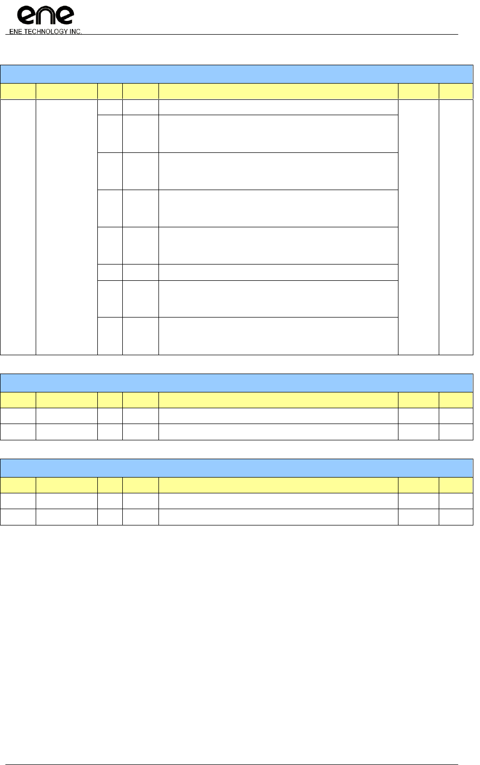
Copyright© 2011, ENE Technology Inc.
126
KB9012 Keyboard Controller Datasheet
CONFIDENTIAL
LPC Configuration
Offset
Name
Bit
Type
Description
Default
Bank
0x95
LPCCFG
7
RSV
Reserved
0x80
0xFE
6
R/W
Index-I/O port enable
0: Disable
1: Enable
5
R/W
KBC 60h/64h I/O port enable
0: Disable
1: Enable
4
R/W
Debug port (port 80) enable
0: Disable
1: Enable
3
R/W
EC I/O port enable (default port 62h/66h)
0: Disable
1: Enable
2
RSV
Reserved
1
R/W
SIRQ always in continuous mode enable
0: Disable
1: Enable
0
R/W
LPC CLKRUN# enable
0: Disable
1: Enable
LPC Extended (Debug) I/O Base Address (16-bit)
Offset
Name
Bit
Type
Description
Default
Bank
0x96
LPCXBAH
7-0
R/W
High byte of Extended I/O (debug port)
0x00
0xFE
0x97
LPCXBAL
7-0
R/W
Low byte of Extended I/O (debug port)
0x80
0xFE
LPC EC I/O Base Address (16-bit)
Offset
Name
Bit
Type
Description
Default
Bank
0x98
LPCEBAH
7-0
R/W
High byte of EC I/O
0x00
0xFE
0x99
LPCEBAL
7-0
R/W
Low byte of EC I/O
0x62
0xFE
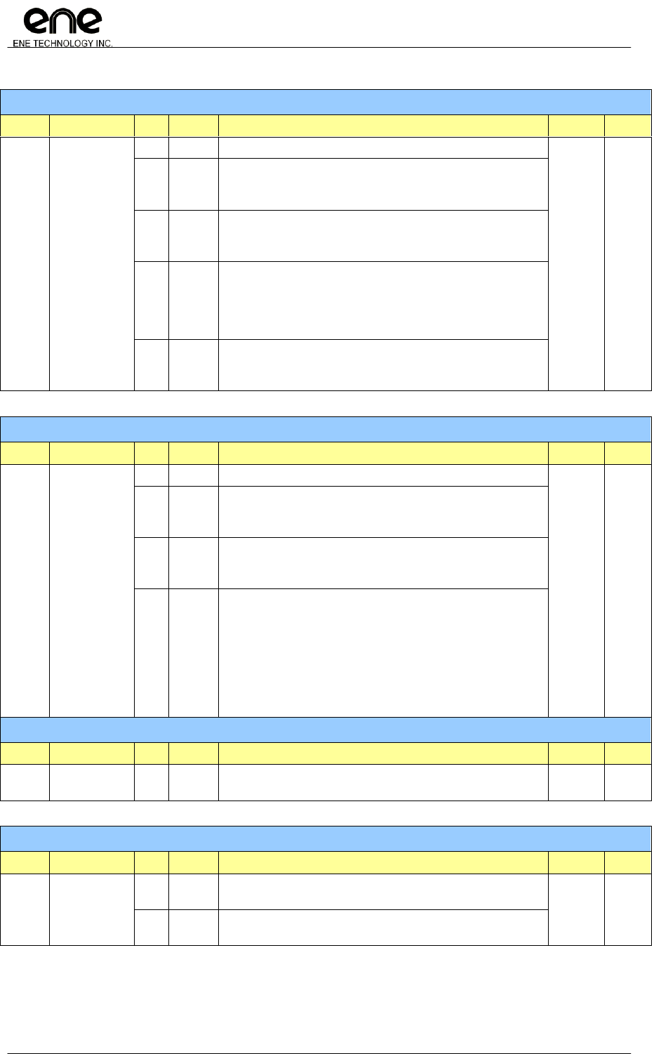
Copyright© 2011, ENE Technology Inc.
127
KB9012 Keyboard Controller Datasheet
CONFIDENTIAL
LPC I/O 0x2E/0x2F Configuration and Status (LPCSCFG[2]=1)
Offset
Name
Bit
Type
Description
Default
Bank
0x9A
LPC2ECFG
7-4
RSV
Reserved
0x00
0xFE
3
RO
The previous access type of 2Eh/2Fh
0: Read
1: Write
2
R/W1C
Interrupt flag of accessing 2Fh I/O.
0: no event
1: event occurs
1
R/W
2Fh I/O interrupt enable
If this bit set, while host accesses 2Fh I/O, an interrupt will
issue.
0: Disable
1: Enable
0
R/W
Decode 2Eh/2Fh I/O enable.
0: Disable
1: Enable
LPC USER SIRQ Configuration (LPCSCFG[2]=0)
Offset
Name
Bit
Type
Description
Default
Bank
0x9B
LPCTCFG
7-6
RSV
Reserved
0x00
0xFE
5
R/W
User defined SIRQ Setting.
0: Low
1: High
4
R/W
User defined SIRQ channel enable
0: Disable
1: Enable
3~0
R/W
User defined SIRQ channel number
0x00: no SIRQ
0x01: IRQ1
0x02: SMI#
0x03: IRQ3
0x04: IRQ4
….
0x0F: IRQ15
LPC I/O 2E Read Port Register (LPCSCFG[2]=1)
Offset
Name
Bit
Type
Description
Default
Bank
0x9B
LPCTCFG
7-0
RO
Host writes data to I/O port 0x2E,
EC F/W could read data from this register.
0x00
0xFE
LPC Read/Write Data of I/O 0x2F (LPCSCFG[2]=1)
Offset
Name
Bit
Type
Description
Default
Bank
0x9C
LPC2FDAT
7-0
R
Host writes data to I/O port 0x2F,
EC F/W could read data from this register.
0x00
0xFE
7-0
W
If host issue any read access to I/O port 0x2F,
the host will get the data which kept in this register
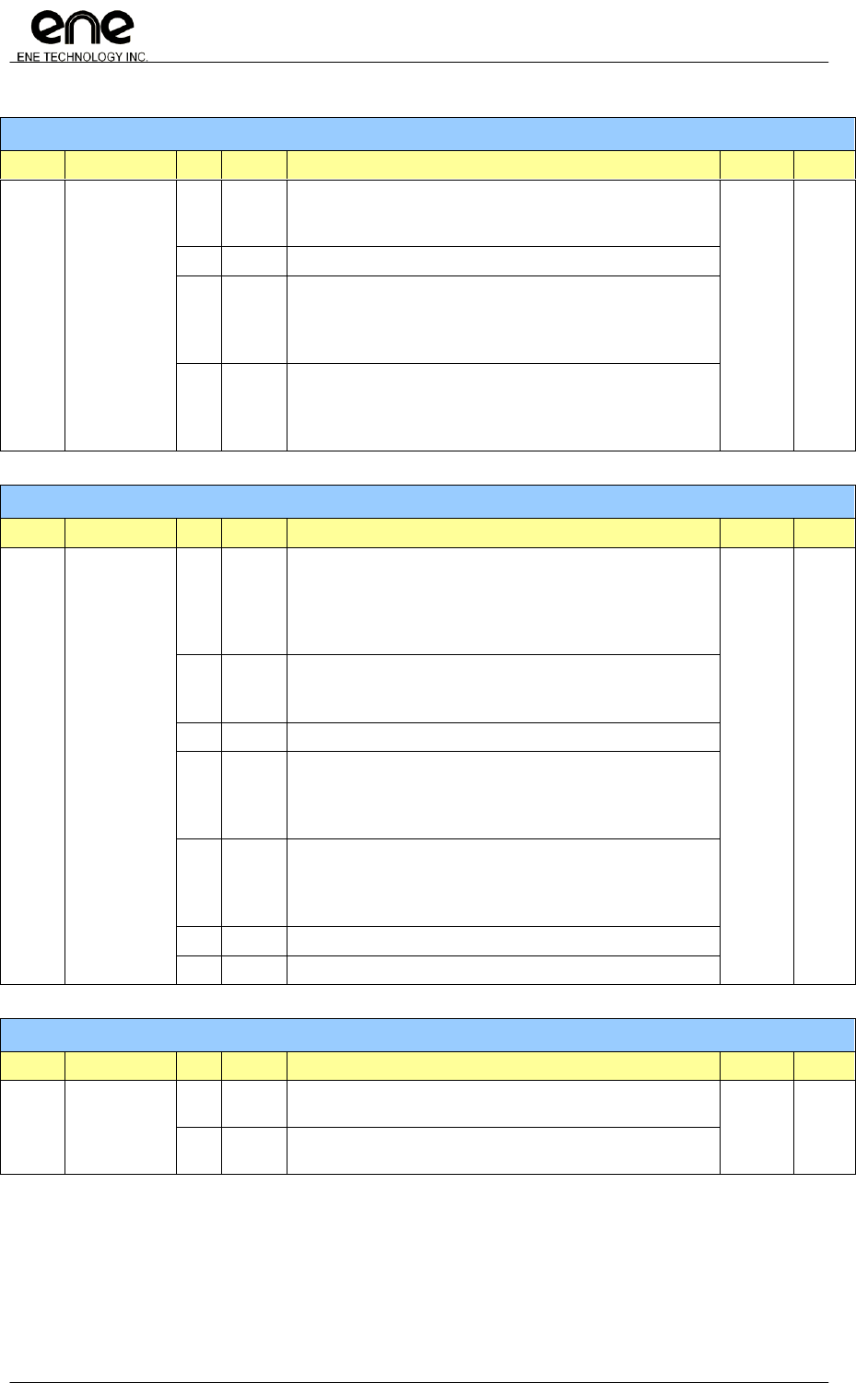
Copyright© 2011, ENE Technology Inc.
128
KB9012 Keyboard Controller Datasheet
CONFIDENTIAL
LPC I/O 0x68/0x6C Configuration
Offset
Name
Bit
Type
Description
Default
Bank
0x9D
LPC68CFG
7
R/W
LPC decode I/O port 68h/6Ch enable
0: Disable
1: Enable
0x00
0xFE
6-2
RSV
Reserved
1
R/W
IBF interrupt enable
Interrupt issues while IBF rising (LPC write I/O 68h/6Ch)
0: Disable
1: Enable
0
R/W
OBF interrupt enable
Interrupt issues while OBF falling (LPC read I/O 68h)
0: Disable
1: Enable
LPC I/O 0x68/0x6C Configuration and Status Register
Offset
Name
Bit
Type
Description
Default
Bank
0x9E
LPC68CSR
7
R/W1C
I/O 68h/6Ch busy flag.
EC F/W can write ―1‖ to clear this flag.
A write cycle to port 6Ch with data 0xFF also clear this flag
0: not busy
1: busy
0x00
0xFE
6
RO
Indicator of write port.
0: write 68h occurs
1: write 6Ch occurs.
5-4
RSV
Reserved
3
R/W1C
IBF interrupt flag
Interrupt flag while IBF rising (LPC write I/O 68h/6Ch)
0: no event
1: event occurs
2
R/W1C
OBF interrupt flag
Interrupt flag while OBF falling (LPC read I/O 68h)
0: no event
1: event occurs
1
R/W1C
IBF of port 68h/6Ch
0
R/W1C
OBF of port 68h/6Ch
LPC I/O 0x68/0x6C Data Register
Offset
Name
Bit
Type
Description
Default
Bank
0x9F
LPC68DAT
7-0
R
Host writes data to I/O port 0x68/0x6C,
EC F/W could read data from this register.
0x00
0xFE
7-0
W
If host issue any read access to I/O port 0x68/0x6C,
the host will get the data which kept in this register
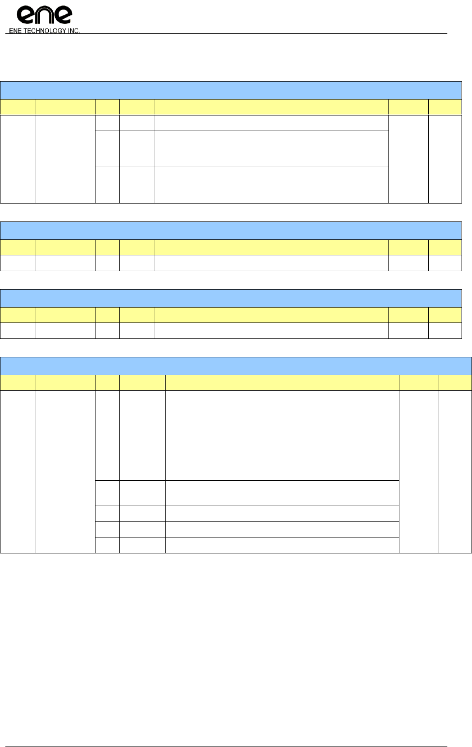
Copyright© 2011, ENE Technology Inc.
129
KB9012 Keyboard Controller Datasheet
CONFIDENTIAL
4.13.6.2 LPC Registers Bank1 Descriptions (LPCSCFG[7:6]=2'b01, 15 bytes)
LPC MEM/FWH Configuration register
Offset
Name
Bit
Type
Description
Default
Bank
0x91
LPCFPCFG
7~2
RSV
Reserved
0x00
0xFE
1
R/W
LPC to XRAM enable bit
0: Disable
1: Enable
0
R/W
Protection enable
0: Disable
1: Enable
LPC MEM/FWH protection segment
Offset
Name
Bit
Type
Description
Default
Bank
0x92
Reserved
7-0
RSV
Reserved
0x00
0xFE
LPC MEM/FWH block number
Offset
Name
Bit
Type
Description
Default
Bank
0x93
Reserved
7-0
RSV
Reserved
0x00
0xFE
LPC misc register set 0
Offset
Name
Bit
Type
Description
Default
Bank
0x94
LPCMISC0
7
R/W
Embedded-Flash and external SPI-Flash., write 1 to enable
After enable the lock function, this bit could only be clear by
PCIRST# falling
1. Erase/Program Embedded-Flash is locked, F/W mode is also
in-active.
2. The related GPIO50 alt. function select, output enable,
output data, pull-up enable, open drain would be locked.
3. GPIO_MISC[1] is locked to prevent SDI host access via
SPI-flash port
0x00
0xFE
6
R/W1C
SIRQ start frame detection flag
Set 1 by hardware, and clear by firmware
5
RO
Latched status of SERIRQ (pin3)
4
RO
Latched status of LFRAME# (pin 4)
3~0
RO
Latched status of LAD[3:0] ports
Copyright© 2011, ENE Technology Inc.
130
KB9012 Keyboard Controller Datasheet
CONFIDENTIAL
LPC control and status register for clock detection function
Offset
Name
Bit
Type
Description
Default
Bank
0x95
LPC_CDCSR
7~5
RSV
Reserved
0x00
0xFE
4
R/W1C
Clock detection pending flag
When clock stopping detected, this bit will be high and clock
monitoring will be stopped. Clearing the pending flag will cause
detection start again.
0:Clock alive detected, and clock source is still in monitoring
1:Clock stop detected
3
RSV
Reserved
2
R/W
CLKRUN# Pull Down Enable
The signal of CLKRUN# will be pulled down by satisfying all
following conditions:
1. The port of CLKRUN# is at Pull Up state.
2. PCI Clock stopping detected.
3. There are latched SIRQ request to be emitted.
0:Disable
1:Enable
1
R/W
Clock source select for detection
0: Select PCI clock signal for detection.
1: Select clock path of 32K OSC to detect.
0
R/W
Clock detection enable
0:Disable
1:Enable
LPC raw counter value output for clock detection function
Offset
Name
Bit
Type
Description
Default
Bank
0x96
LPC_CDCV
7-0
RO
Referenced output of counter value for debugging purpose
0x00
0xFE
LPCXRAMCFG
Offset
Name
Bit
Type
Description
Default
Bank
0x97
LPCXRAMCFG
7-1
RSV
Reserved
0x00
0xFE
0
R/W
LPC to XRAM 2K range select
0: 0xEC00~0xF3FF to 0x0000~0x07FF
1: 0xF400~0xFBFF to 0x0800~0x0FFF
0xFE
LPC transaction debug output register 0
Offset
Name
Bit
Type
Description
Default
Bank
0x98
LPCTDR0
7
RO
Transaction data valid indication
0x00
0xFE
6
RSV
Reserved
5~4
RO
Transaction Toggle bits
It will be accumulated after a valid transaction done
3~0
RSV
Reserved
RSV
Offset
Name
Bit
Type
Description
Default
Bank
0x99~9C
RSV
7-0
RSV
Reserved
0x00
0xFE

Copyright© 2011, ENE Technology Inc.
131
KB9012 Keyboard Controller Datasheet
CONFIDENTIAL
LPC to XRAM Select Block Register (Depend on LPCXRAMCFG for different range)
Select LPC to XRAM block according to the corresponded XRAM range. Each block can be enabled separately
(When LPCXRAMCFG[0]=0)
Offset
Name
Bit
Type
Description
Default
Bank
0x9D
LPCXRAMBL
7
R/W
0700~07FF
0x00
0xFE
6
R/W
0600~06FF
5
R/W
0500~05FF
4
R/W
0400~04FF
3
R/W
0300~03FF
2
R/W
0200~02FF
1
R/W
0100~01FF
0
R/W
0000~00FF
Select LPC to XRAM block according to the corresponded XRAM range. Each block can be enabled separately
(When LPCXRAMCFG[0]=1)
Offset
Name
Bit
Type
Description
Default
Bank
0x9D
LPCXRAMBL
7
R/W
0F00~0FFF
0x00
0xFE
6
R/W
0E00~0EFF
5
R/W
0D00~0DFF
4
R/W
0C00~0CFF
3
R/W
0B00~0BFF
2
R/W
0A00~0AFF
1
R/W
0900~09FF
0
R/W
0800~08FF
LPC to XRAM High Address Register
Offset
Name
Bit
Type
Description
Default
Bank
0x9E
LPCXRAMHA
7-0
R/W
LPC to XRAM high address
0x00
0xFE
LPC to XRAM Low Address Register
Offset
Name
Bit
Type
Description
Default
Bank
0x9F
LPCXRAMLA
7-0
R/W
LPC to XRAM low address
0x00
0xFE
Copyright© 2011, ENE Technology Inc.
132
KB9012 Keyboard Controller Datasheet
CONFIDENTIAL
4.14 X-Bus Interface (XBI)
4.14.1 XBI Function Description
The KBC implements a XBI module to handle the related request from 8051/LPC to internal
flash device. Since in 901x KBC series, embedded flash is designed. The XBI serves as interface
between 8051/LPC to e-flash rather than external SPI-Flash(which is via external SPI interface)
The following figure is operation illustration.
XBI
Arbiter
SPI \ Embedded
Flash
8051 / LPC
Request
ISP
Here gives the feature of XBI module.
- Two 8051 code segments, one for 16K and the other for 48K.
- XBI arbiter to handle the transaction of 8051 and LPC request.
- Embedded flash burst write support
Copyright© 2011, ENE Technology Inc.
133
KB9012 Keyboard Controller Datasheet
CONFIDENTIAL
4.14.2 XBI Registers Description (0xFEA0~0xFEBF)
8051 Address Segment 0 Mapping Configuration (0x0000~0x3FFF)
Offset
Name
Bit
Type
Description
Default
Bank
0xA0
XBISEG0
7
R/W
8051 code segment SEG0 remapping enable.
0: Disable
1: Enable
0x00
0xFE
6
RSV
Reserved
5-0
R/W
SEG0 XBI Address
SEG0 XBI Address = XBISEG0[5:0]*16K + 8051 Address[13:0]
8051 Address Segment 3 Mapping Configuration
Offset
Name
Bit
Type
Description
Default
Bank
0xA1
XBISEG3
7
R/W
8051 code segment SEG3 remapping enable.
0: Disable
1: Enable
0x00
0xFE
6
RSV
Reserved
5-0
R/W
When 8051 Address is C000h~FFFFh,
Set for the SEG3 XBI Address
SEG3 XBI Address = XBISEG3[5:0]*16K + 8051 Address[13:0]
(XBI addressing range is 1M, where XBI addressing > Flash
physical addressing. The address will round robin)
SPI host controller configuration
Offset
Name
Bit
Type
Description
Default
Bank
0xA2
SHCCFG
7~0
RSV
Reserved
0x00
0xFE
LPC Read Buffer Configuration
Offset
Name
Bit
Type
Description
Default
Bank
0xA3
XBI_LPBCFG
7-4
RSV
Reserved
0x0F
0xFE
3~0
R/W
Code-Memory Region Selection
Should enable XRAM as code-Memory by XBICS[3] ( 0xFEA6 )
at first, and 8051 can fetch code from XRAM region for
following setting
0000: 0xEC00~0xECFF
0001: 0xEC00~0xEDFF
0010: 0xEC00~0xEEFF
0011: 0xEC00~0xEFFF
...
1111: 0xEC00~0xFBFF
XBI XIO Enable
Offset
Name
Bit
Type
Description
Default
Bank
0xA4
RSV
7-0
RSV
Reserved
0x00
0xFE

Copyright© 2011, ENE Technology Inc.
134
KB9012 Keyboard Controller Datasheet
CONFIDENTIAL
XBI Configuration
Offset
Name
Bit
Type
Description
Default
Bank
0xA5
XBICFG
7
RSV
Reserved
0x07
0xFE
6
R/W
8051 instruction fetch (sustaining access)
0: Disable
1: Enable
5
RSV
Reserved
4
RO
Enable WR# to Flash
Enable FW mode
3
R/W
Enable extend SELMEM# and SELE51# 1 clock for RD# and
WR# setup and hold time
2~0
R/W
RD# and WR# command clock count
XBI E51CS# Configuration
Offset
Name
Bit
Type
Description
Default
Bank
0xA6
XBICS
7-6
RSV
Reserved
0x00
0xFE
5
R/W
XBI arbitration priority.
0: Disable
1: Enable
4
R/W
Reset code segment enable.
Once the 8051 reset, the code segment SEG0 or SEG1 can be
reset if the corresponding code segment enabled.
(XBISEG0[7]/XBISEG1[7])
0: Disable
1: Enable
3
R/W
Enable XRAM for 8051 to fetch code
The targeted XRAM region is selected by XBILPBCFG[3:0]
(0xFEA3).
0: Disable
1: Enable
Note, users should move codes from Flash to XRAM, jump to
XRAM and then enable this bit.
2
R/W
Reset XBI arbiter while in idle/stop mode.
0: Disable
1: Enable
1
R/W
EHB fast accessing enable.
Enable this bit gets better performance in EHB.
0: Disable
1: Enable
0
RSV
Reserved
XBI Write Enable
Offset
Name
Bit
Type
Description
Default
Bank
0xA7
XBIWE
7-0
R/W
XBI write command.
00h: exit SRAM test mode
A4h: Enable flash write cycle
C5h: enter SRAM test mode
0x00
0xFE
Copyright© 2011, ENE Technology Inc.
135
KB9012 Keyboard Controller Datasheet
CONFIDENTIAL
XBI Embedded Flash Address (22-bit) = [SPIA2(6bit) : SPIA1(8bit) : SPIA0(8bit)]
Offset
Name
Bit
Type
Description
Default
Bank
0xA8
EFA0
7-0
R/W
Embedded Address lower 8-bits (A7:A0)
0x00
0xFE
0xA9
EFA1
7-0
R/W
Embedded Address middle 8-bits (A15:A8)
0x00
0xFE
0xAA
EFA2
5-0
R/W
Embedded Address upper 6-bits (A21:A16)
0x00
0xFE
XBI Embedded Flash Output/Input Data Port
Offset
Name
Bit
Type
Description
Default
Bank
0xAB
EFDAT
7-0
R/W
Input (read) / Output (write) data port of Embedded flash
interface.
0x00
0xFE
XBI Embedded Flash Command Port
Offset
Name
Bit
Type
Description
Default
Bank
0xAC
EFCMD
7-0
R/W
Commands support for embedded flash. Writing this register
will force the protocol start. Please note, the address phases
must be prior to command phase.
Embedded flash command support:
02h Page latch
03h Read
20h Erase selected page
70h Program selected page
80h Clear HVPL data
90h Read Trim data from special rows
0x00
0xFE
XBI Embedded Flash Configuration/Status Register
Offset
Name
Bit
Type
Description
Default
Bank
0xAD
EFCFG
7~4
RSV
Reserved
0x00
0xFE
3
R/W
Write enable of EFCMD register,0xFEAC.
0: Disable
1: Enable
2
RSV
Reserved
1
RO
Embedded flash controller accessing in busy status.
0: not busy
1: busy
0
RSV
Reserved
XBI Embedded Flash Output Data for Read compare
Offset
Name
Bit
Type
Description
Default
Bank
0xAE
EFDATR
7-0
RO
Output data to embedded flash interface.
0x00
0xFE
XBI Embedded Flash Burst Write
Offset
Name
Bit
Type
Description
Default
Bank
0xAF
EMFBURW
7-1
RSV
Reserved
0x00
0xFE
0
R/W
Abort Burst Write (Page Latch)
0: Disable
1: Enable
Copyright© 2011, ENE Technology Inc.
136
KB9012 Keyboard Controller Datasheet
CONFIDENTIAL
Reserved
Offset
Name
Bit
Type
Description
Default
Bank
0xB0~
0xB3
RSV
7~0
RSV
Reserved
0x00
0xFE
XBI Embedded Flash signals 1 in FW mode
Offset
Name
Bit
Type
Description
Default
Bank
0xB4
XBIEFSIG1
7
R/W
When F/W mode enable, the control bit of stand-by power
0: Disable
1: Enable
0x00
0xFE
6
R/W
When F/W mode enable, the control bit of VPOS/VNEG
discharge
0: Disable
1: Enable
5~4
R/W
When F/W mode enable,
Erase/Program sequence control
3
R/W
When F/W mode enable,
Auxiliary memory address select
2
R/W
When F/W mode enable,
Page buffer write enable
0: Disable
1: Enable
1
R/W
When F/W mode enable,
CLK enable for address/mode/ sequence control
0: Disable
1: Enable
0
R/W
When F/W mode enable,
Address CLK input
XBI Embedded Flash signals 2 in FW mode
Offset
Name
Bit
Type
Description
Default
Bank
0xB5
XBIEFSIG2
7
R/W
PCLK source selection
0: PCLK from OSC output (CLKOUT)
1: PCLK form 32M fix clock
0x00
0xFE
6
R/W
Pump source selection
0: Pump from flash output
1: Pump from Pe of embedded flash controller
5~4
R/W
When F/W mode enable,
Data ouitput bit number control
3~0
R/W
When F/W mode enable,
Operational mode inputs
XBI Pump IP trimming bits
Offset
Name
Bit
Type
Description
Default
Bank
0xB6
XBIPUMP
7~4
R/W
PDAC[3:0]
For independent control of VPOS pump level output DAC
0xD5
0xFE
3~0
R/W
NDAC[3:0]
For independent control of VNEG pump level output DAC
Copyright© 2011, ENE Technology Inc.
137
KB9012 Keyboard Controller Datasheet
CONFIDENTIAL
XBI Flash IP trimming bits
Offset
Name
Bit
Type
Description
Default
Bank
0xB7
XBIFM
7~4
R/W
ITIM[3:0]
Trim DAC for trimming SA timing current of Vref
0x14
0xFE
3~0
R/W
BDAC[3:0]
For flash test
XBI VR IP trimming bits
Offset
Name
Bit
Type
Description
Default
Bank
0xB8
XBIVR
7~4
R/W
TCTRIM[3:0]
Trimming bits for temperature coefficient of Vref
0x33
0xFE
3~0
R/W
ABSTRIM[3:0]
Trimming bits for absolute value of Vref
XBI MISC Reg
Offset
Name
Bit
Type
Description
Default
Bank
0xB9
XBIMISC
7~6
RO
IC Trimming Status
0x00
0xFE
5
R/W
Reserved
4~0
R/W
S[4:0]
TRIM bits for frequenct.

Copyright© 2011, ENE Technology Inc.
138
KB9012 Keyboard Controller Datasheet
CONFIDENTIAL
4.15 Consumer IR Controller (CIR)
4.15.1 CIR Function Description
The KBC embeds with a native hardware Consumer IR controller, which connects to system
via LPC interface. Popular protocols are supported, such as RC-5/RC-6/NEC/RLC. The CIR
controller handles the protocol of RC-5/RC-6/NEC/RLC for receiving, and only RLC for transmit. IRQ
and I/O port are implemented. An extended function is implemented to support learning application.
The basic features are list as the following table. The CIR functionality of KB9012 is compatible to
KBx926/KBx390 series.
9012
RX carrier demodulation
V
TX carrier modulation
V
RX protocol support
RC5/RC6/NEC/RLC
TX protocol support
RLC
RX carrier frequency measurement
V
A SIRQ channel can be assigned for CIR application. The related programming registers are
summarized as following table.
Register
Description
LPCSCFG[4] (0xFE90[4])
SIRQ selection for LPCTCFG[3:0] (0xFE9B[3:0])
0: User defined IRQ
1: CIR IRQ enable
LPCTCFG[3:0] (0xFE9B[3:0])
SIRQ channel number.
0x00: IRQ0
0x01: IRQ1
…
0x0F: IRQ15
Here is the features highlight.
- Native hardware protocol decoder, such as RC5/RC6/NEC and RLC.
- I/O and IRQ resource for CIR controller.
- Support 2 sets of RX/TX in one chip, and RX/TX works simultaneously.
- RX carrier demodulation/ TX carrier modulation support.
- Wide range of carrier frequency support, 15K~1MHz. (The carrier frequency is 30K~60KHz in
normal application)
- More flexible in carrier sample frequency, 1μs.~128μs (The sample frequencies are 25, 50 and
100μs for normal application).
- Remote controller learning support.
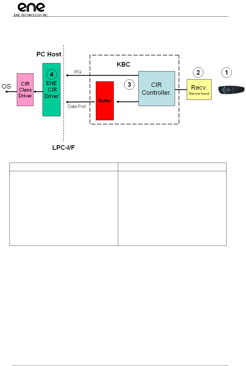
Copyright© 2011, ENE Technology Inc.
139
KB9012 Keyboard Controller Datasheet
CONFIDENTIAL
The following figure shows an example how a CIR controller works with narrow band receiver.
Here gives the guidance for programming CIR.
For Receive
For Transmit
1. Select protocol via setting CIRCFG2 (0xFEC1)
2. According to the selected protocol, setup
CIRHIGH/CIRBIT/CIRSTART/CIRSTART2, i.e.,
0xFEC3~0xFEC6
3. Enable protocol and other configuration setting
via CIRCFG (0xFEC0)
4. EC F/W waits for data-in by pooling or interrupt.
1. Select RLC protocol and enable via setting
CIRCFG (0xFEC0)
2. Writing to CIRRLC_OUT0, 0xFEC9, will start to
transmit.
3. If CIRRLC_OUT0 (0xFEC9) and CIRRLC_OUT1
(0xFECA) are written at the same time, it start to
transmit CIRRLC_OUT0 and then
CIRRLC_OUT1.
4. If only CIRRLC_OUT0 (0xFEC9) is written, the
hardware will transmit CIRRLC_OUT0 first and
then CIRRLC_OUT1.
5. Each byte transmit completion, an interrupt will
occur.
Copyright© 2011, ENE Technology Inc.
140
KB9012 Keyboard Controller Datasheet
CONFIDENTIAL
4.15.2 CIR Block Diagram
The CIR controller supports two RX ports (GPIO40/GPIO0A) and two TX ports
(GPIO41/GPIO0D). A register bit, CIRCFG2[5] (0xFEC1[5]), is used to determine RX source. For
example, if CIRCFG2[5]=0, GPIO40 is the RX source, otherwise GPIO0A. The TX port is selected
according to the GPIO function selection register. The following table gives an example of RX/TX
combination.
GPIOFS08[5]=0b, GPIOFS[1]=1b
GPIOFS08[5]=1b, GPIOFS[1]=0b
CIRCFG2[5]=0b
(RX,TX)=(GPIO40, GPIO41)
(RX,TX)=(GPIO40, GPIO0D)
CIRCFG2[5]=1b
(RX,TX)=(GPIO0A, GPIO41)
(RX,TX)=(GPIO0A, GPIO0D)
The CIR controller could detect the carrier frequency and demodulate the carrier. This
provides a learning feature for CIR application. The frequency detection range is from 15.75KHz to
1MHz. After demodulation, the CIR controller handles remote signals with hardware decoder which
supports RC5/RC6/NEC/RLC protocols. If transmit function needed, the CIR controller could
modulate the carrier and send it out via GPIO41/GPIO0D. The output carrier frequency range is the
same as input (15.75KHz~1MHz). The RX and TX can work simultaneously in the current design.
The following diagram gives more detail about CIR controller.

Copyright© 2011, ENE Technology Inc.
141
KB9012 Keyboard Controller Datasheet
CONFIDENTIAL
4.15.3 CIR Remote Protocol
In this section, brief introduction of protocols supported in the CIR is given. Four
protocols are supported, Philips RC5/RC6, NEC and Run-Length-Code. Only features and protocol
definition listed. For more detail please refer to the related specifications.
4.15.3.1 Philips RC5 Protocol
Here highlights the features of Philips RC5 protocol.
- Manufacturer Philips.
- Carrier frequency 36KHz.
- Bi-phase coding.
- 5 bits address / 6 bits command lengths
RC5 Protocol
Bit1
Bit2
Bit3
Bit4
Bit5
Bit6
Bit7
Bit8
Bit9
Bit10
Bit11
Bit12
Bit13
Bit14
S1
S2
T
Address
Command
S1/S2: start bits, always ―1‖
T: toggle bit, This bit is inverted every time a key is released and pressed again.
Address: IR device address, MSB first.
Command: IR command, MSB first.

Copyright© 2011, ENE Technology Inc.
142
KB9012 Keyboard Controller Datasheet
CONFIDENTIAL
4.15.3.2 Philips RC6 Protocol
Here highlights the features of Philips RC6 protocol.
- Manufacturer Philips.
- Carrier frequency 36KHz.
- Bi-phase coding.
- 5 bits address
- Variable command lengths based on the operation mode.
RC6 Protocol
LS
SB
MB2
MB1
MB0
T
A
7
A
6
A
5
A
4
A
3
A
2
A
1
A
0
C
7
C
6
C
5
C
4
C
3
C
2
C
1
C
0
Header
Control
Information
SF
Header Phase (ENE CIR)
Data Phase (ENE CIR)
LS: Leader symbol
SB: Start bit, always ―1‖
MB2-MB0: Mode bits, operation mode selection.
T: Trailer bit, this bit can be served as a toggle bit.
A7-A0: Address
C7-C0: Command
SF: Signal free time, 2.666ms.
4.15.3.3 NEC Protocol
Here highlights the features of NEC protocol.
- Manufacturer NEC.
- Carrier frequency 38KHz.
- Pulse distance modulation.
- 8 bit address / 8 bit command length
- Address/Command transmitted twice.
- Total transmit time is constant.
NCE Protocol
AGC burst
space
Address
~Address
Command
~Command
9ms
4.5ms
8bit
8bit
8bit
8bit
AGC burst: set gain of IR remote controller, 9ms long
Space: follow by AGC burst, 4.5ms.
Address: 8-bit address, LSB first.
~Address: inverted 8-bit address, LSB first.
Command: 8-bit command, LSB first.
~Command: inverted 8-bit command, LSB first
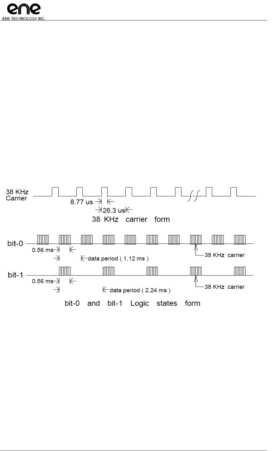
Copyright© 2011, ENE Technology Inc.
143
KB9012 Keyboard Controller Datasheet
CONFIDENTIAL
4.15.4 CIR Automatic Carrier Frequency Detection and Modulation
To support learning feature, wide-band transmitter and receiver will be used in a system.
The KBC introduces a new mechanism to provide carrier frequency information of wide-band
receiver to the host.
The CIR controller needs to be programmed with two parameters for the detection.
Register CIRCAR_PULS is used to determine these two parameters. CIRCAR_PULS[7:4] keeps
the discard number of carrier pulse and CIRCAR_PULS[3:0] keeps the average number to detect.
The CIRCAR_PULS[7:4] tells the controller to discard the specific number of carrier pulse from the
beginning. The controller then gets the average number of carriers pulse as sample data and
analyzes. The detection of carrier period is kept in CIRCAR_PRD[6:0], and the valid flag is kept in
CIRCAR_PRD[7]. Please note, the detection range is from 15.75KHz~1MHz. (The general
application is from 30K~60KHz).
Here gives an example as the above waveform. Bit stream with 38KHz carrier is shown as bit-0.
Each bit is 0.56ms in length and 38KHz carrier period is 26.3μs, that is, there will be about 21
carrier pulses in a bit. If CIRCAR_PULS[7:4]=5 and CIRCAR_PULS[3:0]=10, once the detection
enabled, the CIR controller will get 6th carrier pulse as the first one and analyze the sequential 10
pluses. The detection result can be obtained via register CIRCAR_PRD.
Copyright© 2011, ENE Technology Inc.
144
KB9012 Keyboard Controller Datasheet
CONFIDENTIAL
The related registers for automatic carrier frequency detection are listed as following.
Register
Address
Description
CIRCFG2[5:4]
0xFEC1[5:4]
Bit5=1, select wide-band as bit-decoder input.
Bit4=1, enable wide-band frequency detection
CIRCAR_PULS
0xFECB
CIRCAR_PULS[7:4] = discard number of carrier pulse
CIRCAR_PULS[3:0] = average number of carrier pulse
CIRCAR_PRD
0xFECC
Detection of wide-band carrier period
CIRCAR_HPRD
0xFECD
Detection of wide-band carrier period, pulse width high.
The KBC provides the modulation ability for RLC transmit. The carrier frequency of
modulation can be programmable. Before the carrier modulation, the programmer should notice the
modulation polarity. That is, if the data bus (TX) is kept low in idle state, only data in high state will be
modulated and the bit, CIRMOD_PRD[7], should be ―1‖.
The related registers for RLC modulation is summarized as below.
Register
Address
Description
CIRCFG[7]
0xFEC0
RLC output modulation enable.
CIRMOD_PRD
0xFECE
CIRMOD_PRD[7] = modulation polarity selection
CIRMOD_PRD[6:0] = modulation carrier period
CIRMOD_HPRD
0xFECF
CIRMOD_HPRD[6:0] = modulation carrier period, pulse width
high.

Copyright© 2011, ENE Technology Inc.
145
KB9012 Keyboard Controller Datasheet
CONFIDENTIAL
4.15.5 CIR Registers Description (0xFEC0~0xFECF)
CIR Configuration
Offset
Name
Bit
Type
Description
Default
Bank
0xC0
CIRCFG
7
R/W
Output carrier modulator for RLC (TX)
0: Disable
1: Enable
0x00
0xFE
6
R/W
Output polarity reversed for RLC. (TX)
0: Disable
1: Enable
5
R/W
Interrupt while transmit completes with RLC protocol. (TX)
0: Disable
1: Enable
4
R/W
Output enable for RLC protocol. (TX)
Once the data filled into CIRRLC_OUT1 (0xFECA), the
controller starts the transmit with RLC protocol
0: Disable
1: Enable
3
R/W
Input carrier demodulator. (RX)
0: Disable
1: Enable
2
R/W
Input polarity reversed. (RX)
0: Disable
1: Enable
1
R/W
Interrupt enable. (RX)
Two conditions issue interrupt.
1. After decode a byte in RX
2. Once receive the ―Repeat‖ in NEC protocol
0: Disable
1: Enable
0
R/W
Protocol decode enable. (RX)
The protocol type is determined by CIRCFG2[3:0] (0xFEC1)
0: Disable
1: Enable,

Copyright© 2011, ENE Technology Inc.
146
KB9012 Keyboard Controller Datasheet
CONFIDENTIAL
CIR Configuration 2
Offset
Name
Bit
Type
Description
Default
Bank
0xC1
CIRCFG2
7
R/W
Fast sample (data phase, not leader phase) enable for input
signal. If this bit set, the sample period changes.
For RC5/RC6, period changes from 30μs to 16μs
For NEC, period changes from 64μs to 30μs
0: Disable
1: Enable
0x00
0xFE
6
R/W
Fast sample (leader phase) enable for input signal.
If this bit set, the sample period changes.
For RC6, period changes from 64μs to 30μs
0: Disable
1: Enable
5
R/W
Input selection for protocol decoder (bit-decoder)
0: from GPIO40
1: from GPIO0A
4
R/W
Frequency detection enable.
0: Disable
1: Enable
3-0
R/W
CIR Protocol selection. (valid while CIRCFG[0]=1)
000: RLC
001: RC5
010: RC6
011: NEC
others: reserved.
CIR Pending Flag and Status
Offset
Name
Bit
Type
Description
Default
Bank
0xC2
CIRPF
7
RO
Hardware RX idle state.
0: not idle state
1: idle state
0x00
0xFE
6
RO
Hardware TX (RLC) idle state.
0: not idle state
1: idle state
5-4
RSV
Reserved
3
R/W1C
Pending flag of RLC transmit complete
0: no event
1: event occurs
2
R/W1C
Pending flag of RLC receive counter overflow
0: no event
1: event occurs
1
R/W1C
Pending flag of NEC repeat protocol
0: no event
1: event occurs
0
R/W1C
Pending flag of data-in
This bit is set while data received and stored in CIRDAT_IN.
0: no event
1: event occurs

Copyright© 2011, ENE Technology Inc.
147
KB9012 Keyboard Controller Datasheet
CONFIDENTIAL
Value for High Pulse Width
Offset
Name
Bit
Type
Description
Default
Bank
0xC3
CIRHIGH
5-0
R/W
This register determines the high pulse width of a ―logic bit‖.
High pulse width = Decoder sample period * CIRHIGH
0x00
0xFE
Value for Bit Width(RC5/RC6) / Logic Bit-One (NEC)
Offset
Name
Bit
Type
Description
Default
Bank
0xC4
CIRBIT
6-0
R/W
This register determines the bit width of a ―logic bit‖. (RC5/RC6)
Bit width = Decoder sample period * CIRBIT
This register determines the ―logic bit-one‖. (NEC)
Logic bit-one = Decoder sample period * CIRBIT
0x00
0xFE
Value for Leader Pulse Width (RC6/NEC) for Normal Packet
Offset
Name
Bit
Type
Description
Default
Bank
0xC5
CIRSTART
6-0
R/W
This register determines the leader pulse width for normal
packet (RC6/ENC)
Leader pulse width = Decoder sample period * CIRSTART
0x00
0xFE
Value for Tailer Bit Width (RC6) / Leader Width of Repeat Packet (NEC)
Offset
Name
Bit
Type
Description
Default
Bank
0xC6
CIRSTART2
6-0
R/W
This register determines the bit width of trailer (RC6)
trailer bit width = Decoder sample period * CIRSTART2
This register determines the leader width of repeat packet (NEC)
Leader width(repeat) = Decoder sample period * CIRSTART2
0x00
0xFE
CIR Decode Data Byte
Offset
Name
Bit
Type
Description
Default
Bank
0xC7
CIRDAT_IN
7-0
RO
Received data to decode.
0x00
0xFE
CIR Counter Value for RLC Sample Period
Offset
Name
Bit
Type
Description
Default
Bank
0xC8
CIRRLC_CFG
7
R/W
Counter overflow control bit.
0: if overflow, the counter will stop.
1: if overflow, an interrupt issues and the counter keeps
counting.
0x00
0xFE
6-0
R/W
CIR RLC sample period, The unit is 1μs.
Please note CIRRLC_CFG[6:0] can not be zero.
CIR RLC Output 1st Byte
Offset
Name
Bit
Type
Description
Default
Bank
0xC9
CIRRLC_OUT0
7-0
R/W
Output (TX) 1st byte for RLC protocol.
0x00
0xFE
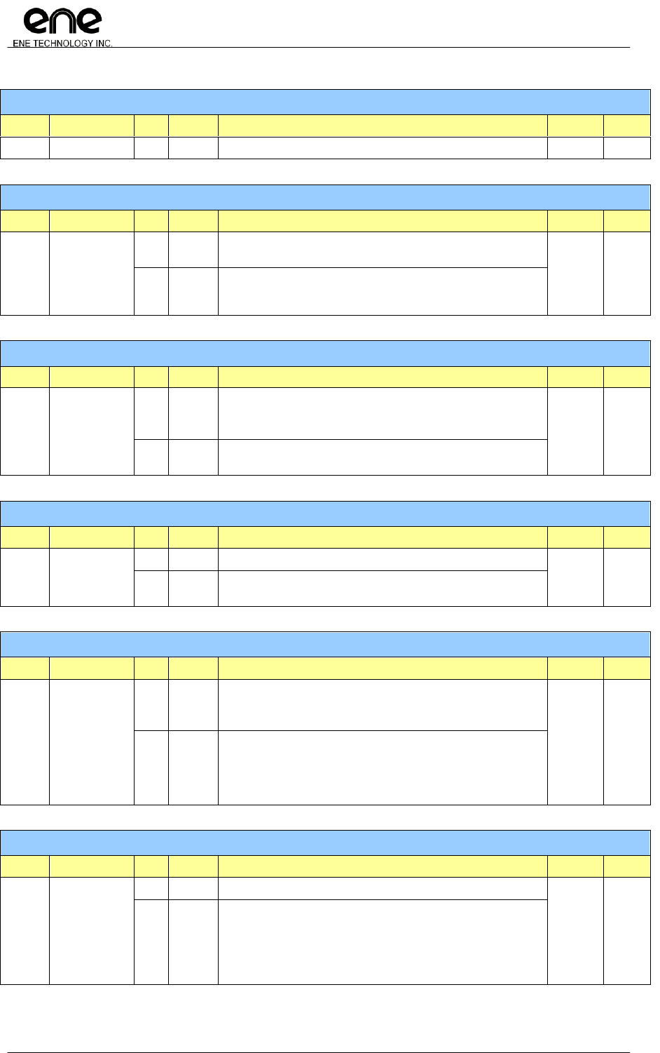
Copyright© 2011, ENE Technology Inc.
148
KB9012 Keyboard Controller Datasheet
CONFIDENTIAL
CIR RLC Output 2nd Byte
Offset
Name
Bit
Type
Description
Default
Bank
0xCA
CIRRLC_OUT1
7-0
R/W
Output (TX) 2nd byte for RLC protocol.
0x00
0xFE
CIR Carrier Discard/Average Pulse Number Setting for Automatic Carrier Detection.
Offset
Name
Bit
Type
Description
Default
Bank
0xCB
CIRCAR_PULS
7-4
R/W
Discard carrier pulse number
F/W should specify the number of pulse to discard
0x44
0xFE
3-0
R/W
Average carrier pulse number
F/W should specify the average number to calculate the carrier
period.
CIR Detected Carrier Period
Offset
Name
Bit
Type
Description
Default
Bank
0xCC
CIRCAR_PRD
7
RO
Detected carrier period valid.
0: carrier detection not completed.
1: carrier detection completed.
0x00
0xFE
6-0
RO
Detected carrier period.
Detected carrier period = CIRCAR_PRD[6:0] x 500ns
CIR Detected Pulse Width High of Carrier
Offset
Name
Bit
Type
Description
Default
Bank
0xCD
CIRCAR_HPRD
7
RSV
Reserved
0x00
0xFE
6-0
R/W
Detected pulse width high of carrier
Pulse width high = CIRCAR_HPRD[6:0] x 500ns
CIR Modulation Carrier Period (RLC only)
Offset
Name
Bit
Type
Description
Default
Bank
0xCE
CIRMOD_PRD
7
R/W
Carrier modulation selection.
0: If TX idle state is high ,only low signal in TX will be modulated
1: If TX idle state is low, only high signal in TX will be modulated
0x00
0xFE
6-0
R/W
Modulation carrier period.
This register determines the modulation carrier period. The unit
is 500ns. The value can be chosen from 0x02 to 0x7F, i.e., the
period is from 15.87KHz~1MHz.
The period = CIRMOD_PRD[6:0] x 500 ns.
CIR Pulse Width High of Modulation Carrier (RLC only)
Offset
Name
Bit
Type
Description
Default
Bank
0xCF
CIRMOD_HPRD
7
R/W
Reserved
0x00
0xFE
6-0
R/W
Pulse width high of modulation carrier.
This register determines the pulse width high of modulation
carrier. The unit is 500ns. The value can be chosen from 0x01
to 0x7E. Please note, the pulse width high can not be larger
than the carrier period.
The pulse width high = CIRMOD_HPRD[6:0] x 500 ns.

Copyright© 2011, ENE Technology Inc.
149
KB9012 Keyboard Controller Datasheet
CONFIDENTIAL
4.15.6 CIR Programming Sample
In this section gives some programming sample to control CIR module. Please note, ENE does
not guarantee these codes in every field application. The following table describes scenario of CIR
filed application.
Example
A RC6 receiver which filters out carrier is connected to CIR RX pin.
Programming model
GPIOIE40[0] (0xFC68[0]) = 1; //Enable CIR Rx input
CIRCFG (0xFEC0) = 0x07; //Enable Rx interrupt and protocol
CIRCFG2 (0xFEC1) = 0x02; //Select RC-6 protocol
CIRHIGH (0xFEC3) = 0x0B; //High width = 32*11 = 352 us
CIRBIT (0xFEC4) = 0x22; //Bit width = 32*34 = 1088 us
CIRSTART (0xFEC5) = 0x3B; //Leader width = 64*59 = 3776 us
CIRSTART2 (0xFEC6) = 0x4A; //Trailer width = 32*74 = 2368 us
When CIRPF[0] (0xFEC2[0]) = 1, Read CIRDAT_IN (0xFEC7) to get data.
Copyright© 2011, ENE Technology Inc.
150
KB9012 Keyboard Controller Datasheet
CONFIDENTIAL
4.16 General Waveform Generator (GWG)
4.16.1 GWG Function Description
General waveform generator is used to output specific pre-defined pulse (two phase available)
with single trigger or continuous trigger. User can generate the arbitrary pulse width with
concatenate method by the co-operation of interrupt mode using dynamic adjusting of pulse
registers. The programmable characteristic is as followed:
Phase 0
Phase 1
Register Name
Description
GWGCFG[3] (0xFED0)
Output drive level when idle state
0: for low level when idle state
1: for high level when idle state
GWGCFG[2] (0xFED0)
Output drive enable when idle state
GWGCFG[1] (0xFED0)
Continuously pulses train enable bit
GWGCFG[0] (0xFED0)
GWG enable bit
GWGCP (0xFED3)
Timing base setting for phase 0/1 pulse timing.
Time base = (GWGCP+1) * 2 us
GWGPR0[7] (0xFED4)
Phase 0 signal level,
0: for low level
1: for high level
GWGPR0[6:0] (0xFED4)
Phase 0 signal lasting period
The time base is from GWGCP
GWGPR1[7] (0xFED5)
Phase 1 signal level,
0: for low level
1: for high level
GWGPR1[6:0] (0xFED5)
Phase 1 signal lasting period
The time base is from GWGCP
Timing Example:
GWGCP is to set the phase 0/1 timing base. Eg: GWGCP = 0xFF, the timing base would be
256*2 = 512 us. And if set the GWGPR0 = 0xFF, the phase 0 of pulse will be high level and
sustain 512 us * 127 = 65024 us which is about 65ms length.
Copyright© 2011, ENE Technology Inc.
151
KB9012 Keyboard Controller Datasheet
CONFIDENTIAL
4.16.2 GWG Register Description (0xFED0~0xFEDF)
Configuration of GWG
Offset
Name
Bit
Type
Description
Default
Bank
0xD0
GWGCFG
7~6
RSV
Reserved
0x00
0xFE
5
R/W
Test mode enable
4
R/W
Interrupt enable
3
R/W
Output level when idle state
0: for low level when idle state
1: for high level when idle state
2
R/W
Output enable when idle state
0: disable
1: output the signal level according to GWGCFG[3] (0xFED0)
1
R/W
Continuously pulses train enable
0
R/W
GWG function enable
Event Pending Flag
Offset
Name
Bit
Type
Description
Default
Bank
0xD1
GWGPF
7~5
RSV
Reserved
0x00
0xFE
4
R/W1C
Start bit of GWG
Write 1 to this bit would start the waveform output
3~2
RSV
Reserved
1
R/W
Event pending flag for the phase 1 waveform finished
0
R/W
Event pending flag for the phase 0 waveform finished
Event Interrupt Enable Registers
Offset
Name
Bit
Type
Description
Default
Bank
0xD2
GWGIE
7~2
RSV
Reserved
0x00
0xFE
1
R/W
Interrupt enable for the event pending flag for the phase 1
0
R/W
Interrupt enable for the event pending flag for the phase 0
Copyright© 2011, ENE Technology Inc.
152
KB9012 Keyboard Controller Datasheet
CONFIDENTIAL
Clock Period Register
Offset
Name
Bit
Type
Description
Default
Bank
0xD3
GWGCP
7~0
R/W
Timing base setting for phase 0/1 pulse timing
Time base = (N+1) * 2 us
0x00
0xFE
Pulse Setting Register 0
Offset
Name
Bit
Type
Description
Default
Bank
0xD4
GWGPR0
7
R/W
Output Level setting for phase 0
0: for low level
1: for high level
0x00
0xFE
6~0
R/W
Counter Value for phase 0 pulse sustain time
Timing unit is based on GWGCP
Pulse Setting Register 1
Offset
Name
Bit
Type
Description
Default
Bank
0xD5
GWGPR1
7
R/W
Output Level setting for phase 1
0: for low level
1: for high level
0x00
0xFE
6~0
R/W
Counter value for phase 1 pulse sustain time
Timing unit is based on GWGCP

Copyright© 2011, ENE Technology Inc.
153
KB9012 Keyboard Controller Datasheet
CONFIDENTIAL
4.17 PS/2 Interface (PS/2)
4.17.1 PS/2 Interface Function Description
The PS/2 protocol is a two-wire bi-direction interface in the industrial standard. This
supports many PS/2 human interface devices, such as keyboard, mouse or touchpad device. Here
gives the highlights of PS/2 features in the KBC.
- 3 external PS/2 channels supported.
- 1 internal PS/2 channel for IKB.
- Each PS/2 channel is with interrupt capability.
- Each PS/2 channel can be enabled/disabled individually.
- Both hardware and flexible firmware mode support for PS/2 protocol.
- Each PS/2 channel can be programmed to be GPIO function.
4.17.2 PS/2 Interface Registers Description (0xFEE0~0xFEFF)
PS/2 Configuration
Offset
Name
Bit
Type
Description
Default
Bank
0xE0
PS2CFG
7
R/W
PS/2 port3 (TX/RX) enable. If disable, PS3CLK will be low.
0: Disable
1: Enable
0x00
0xFE
6
R/W
PS/2 port2 (TX/RX) enable. If disable, PS2CLK will be low.
0: Disable
1: Enable
5
R/W
PS/2 port1 (TX/RX) enable. If disable, PS1CLK will be low.
0: Disable
1: Enable
4
R/W
PS/2 port0 IKB(TX/RX) enable. If disable, IKB clock will be low.
0: Disable
1: Enable
3
R/W
PS/2 parity error interrupt
0: Disable
1: Enable
2
R/W
PS/2 TX timeout interrupt.
TX timeout condition:
(a)ps2clk keeps high over 210μs~240μs during TX.
(b)Host requests bus and waits over 120ms~150ms
0: Disable
1: Enable
1
R/W
PS/2 transmit-one-byte interrupt
0: Disable
1: Enable
0
R/W
PS/2 receive-one-byte interrupt
0: Disable
1: Enable
Copyright© 2011, ENE Technology Inc.
154
KB9012 Keyboard Controller Datasheet
CONFIDENTIAL
PS/2 Interrupt Pending Flag
Offset
Name
Bit
Type
Description
Default
Bank
0xE1
PS2PF
7
RO
Flag of PS/2 port3 received one byte.
0: no event
1: event occurs
0x00
0xFE
6
RO
Flag of PS/2 port2 received one byte.
0: no event
1: event occurs
5
RO
Flag of PS/2 port1 received one byte.
0: no event
1: event occurs
4
RO
Flag of PS/2 port0 (IKB) received one byte.
0: no event
1: event occurs
3
R/W1C
Interrupt flag of PS/2 parity error
0: no event
1: event occurs
2
R/W1C
Interrupt flag of PS/2 TX timeout.
0: no event
1: event occurs
1
R/W1C
Interrupt flag of PS/2 transmit-one-byte
0: no event
1: event occurs
0
R/W1C
Interrupt flag of PS/2 receive-one-byte
0: no event
1: event occurs
PS/2 Transmitter/Receiver Control
Offset
Name
Bit
Type
Description
Default
Bank
0xE2
PS2CTRL
7
R/W
Data port PS2DATA (0xFEE3) connects to PS/2 port3
0: Disconnect
1: Connect
0x00
0xFE
6
R/W
Data port PS2DATA (0xFEE3) connects to PS/2 port2
0: Disconnect
1: Connect
5
R/W
Data port PS2DATA (0xFEE3) connects to PS/2 port1
0: Disconnect
1: Connect
4
R/W
Data port PS2DATA (0xFEE3) connects to PS/2 port0
0: Disconnect
1: Connect
3
WO
Write ―1‖ to force PS/2 TX reset.
2
WO
Write ―1‖ to force PS/2 RX reset.
1
RO
PS/2 RX timeout flag.
The flag may implies the followings.
(a) ps2clk keeps high over 210μs~240μs during RX
(b) host issues reset command and the device does not
response.
(c) General PS/2 packet timeout defined in the protocol.
0
RSV
Reserved
Copyright© 2011, ENE Technology Inc.
155
KB9012 Keyboard Controller Datasheet
CONFIDENTIAL
PS/2 Data Port
Offset
Name
Bit
Type
Description
Default
Bank
0xE3
PS2DATA
7-0
R/W
EC F/W gets/writes data from/to host via this register.
0x00
0xFE
PS/2 Configuration 2
Offset
Name
Bit
Type
Description
Default
Bank
0xE4
PS2CFG2
7
R/W
PS/2 port3 hardware mode enable.
0: Disable
1: Enable
0x00
0xFE
6
R/W
PS/2 port2 hardware mode enable.
0: Disable
1: Enable
5
R/W
PS/2 port1 hardware mode enable.
0: Disable
1: Enable
4
R/W
PS/2 port0 (IKB) hardware mode enable.
0: Disable
1: Enable
3
R/W
PS/2 hardware mode enable.
0: Disable
1: Enable
2
R/W
PS/2 host request timeout control. (in PS/2 hardware mode
only)
0: Host request timeout 120ms~150ms
1: Host request timeout 15ms~16ms
1
RSV
Reserved.
0
R/W
PS/2 clock/data input debounce control
0: 1μs
1: 2μs
PS/2 Pin Input Status
Offset
Name
Bit
Type
Description
Default
Bank
0xE5
PS2PINS
7
RO
PS/2 port3 clock pin status
0x00
0xFE
6
RO
PS/2 port2 clock pin status
5
RO
PS/2 port1 clock pin status
4
RO
PS/2 port0 (IKB) clock pin status
3
RO
PS/2 port3 data pin status
2
RO
PS/2 port2 data pin status
1
RO
PS/2 port1 data pin status
0
RO
PS/2 port0 (IKB) data pin status

Copyright© 2011, ENE Technology Inc.
156
KB9012 Keyboard Controller Datasheet
CONFIDENTIAL
PS/2 Pin Output
Offset
Name
Bit
Type
Description
Default
Bank
0xE6
PS2PINO
7
RO
PS/2 port3 clock pin status
0x00
0xFE
6
RO
PS/2 port2 clock pin status
5
RO
PS/2 port1 clock pin status
4
RO
PS/2 port0 (IKB) clock pin status
3
RO
PS/2 port3 data pin status
2
RO
PS/2 port2 data pin status
1
RO
PS/2 port1 data pin status
0
RO
Command control TX state

Copyright© 2011, ENE Technology Inc.
157
KB9012 Keyboard Controller Datasheet
CONFIDENTIAL
4.18 Embedded Controller (EC)
4.18.1 EC Function Description
The ACPI specification defined for the embedded controller (EC) interface requires
either three separate host interfaces (KBC, SCI, SMI) or two interfaces (KBC, and shared SCI/SMI).
The ENE KBC supports KBC and SCI interface, and SMI interface can be shared with SCI or use a
dedicated GPIO. The embedded controller also provides some features which are collected as
following:
- Handles EC standard commands from host, firmware mode support.
- Handles EC extended commands from host, only firmware mode support.
- SCI generation capability.
- Extended I/O write interface, i.e., debug port (port 80) support.
- KBC/EC clock configuration.
- A/D and D/A control.
- Power management control.
- Miscellaneous control.
The host queries (read) EC status and issues (write) EC command via port 66h. The EC data
port is 62h. The status of EC is defined as the below table:
Status Bit
Name
Description
7
RSV
Reserved
6
RSV
Reserved
5
SCI
SCI event flag. Please note, this bit will not be set if standard EC commands
(80h~84h) issued by host.
0: No SCI event occurs
1: SCI event occurs
4
Burst Enable
The burst enable flag
0: Disable
1: Enable
3
Command/Data Flag
0: Previous access port is data port. (EC_DAT)
1: Previous access port is command/status port. (EC_CMD/EC_STS)
2
RSV
Reserved
1
IBF
Input Buffer Full flag of EC
0
OBF
Output Buffer Full flag of EC
The EC commands are defined as following, for more detail please refer to ACPI, Advanced
Configuration Power Interface Specification. 2.0
Value
Command
Description
80h
EC Read
Read EC space registers
81h
EC Write
Write EC space registers
82h
EC Burst Enable
Enable EC operation in burst mode
83h
EC Burst Disable
Disable EC operation in burst mode
84h
EC Query
Query SCI events
Others
Firmware Command
Extended commands and handled with F/W mode.

Copyright© 2011, ENE Technology Inc.
158
KB9012 Keyboard Controller Datasheet
CONFIDENTIAL
4.18.2 EC Command Program Sequence
The following table summarizes the standard EC commands programming flow. Port
66h is the EC command and status port and port 62h is the EC data port.
Command Byte
Command
Program Sequence
80h
EC Read
1. Host writes command byte 80h (EC_Read) to port 66h.
2. EC will issue SCI to host while IBF=0
3. Host writes address to port 62h.
4. EC will issue SCI to host while OBF=1
5. Host reads data via port 62h.
81h
EC Write
1. Host writes command byte 81h (EC_Write) to port 66h.
2. EC will issue SCI to host while IBF=0
3. Host writes address to port 62h.
4. EC will issue SCI to host while IBF=0
5. Host writes data to port 62h.
6. EC will issue SCI to host while IBF=0
82h
Burst Enable
1. Host writes command byte 82h (Burst_Enable) to port 66h.
2. EC will issue SCI to host while OBF=1.
3. Host reads via port62h. If 90h obtained, it‘s Burst Ack.
83h
Burst Disable
1. Host writes command byte 83h (Burst_Disable) to port 66h.
2. EC will issue SCI to host while IBF=0
84h
Query EC
1. Host writes command byte 84h (Query_EC) to port 66h.
2. EC will issue SCI to host while OBF=1.
3. Host reads data via port 62h. The data obtained is SCI_ID number.

Copyright© 2011, ENE Technology Inc.
159
KB9012 Keyboard Controller Datasheet
CONFIDENTIAL
4.18.3 EC SCI Generation
The EC can generate SCI with independent enable control and status flag. Plenty of
hardware SCI events are predefined, and a firmware SCI event gives more flexible use for different
applications. There is a F/W SCI command port located at SCID (0xFF0B). As the F/W writes any
non-zero value to this port, and corresponding enable bit (SCIE0[6]) is set. A hardware SCI signal
will issue to host in sequence. Then the host uses standard EC_Query (84h) command to get the
SCI ID which is written by F/W before. The below table summarizes the information about SCI
events, SCI IDs and the priorities.
SCI ID
Event
Switch
Applications
Priority
00h
Nothing
N/A
0(Highest)
01h-07h
RSV
N/A
Reserved
1
08h
WDT
SCIE0[0]
Watchdog
2
09h
LPC_IO2F /
OWM
SCIE0[1]
LPC I/O 0x2F R/W accessing interrupt
/ OWM
3
0Ah
PS2
SCIE0[2]
PS/2 event
4
0Bh
KBC
SCIE0[3]
IBF rising (LPC write I/O 60h/64h)
OBF falling (LPC read I/O 60h)
5
0Ch
IKB
SCIE0[4]
IKB
6
0Dh
LPC_IO686C
SCIE0[5]
IBF rising (LPC write I/O 68h/6Ch)
OBF falling (LPC read I/O 68h)
7
0Eh
LPC_IO6266
SCIE0[6]
IBF rising (LPC write I/O 62h/66h)
OBF falling (LPC read I/O 62h)
8
FW_SCIID
FW_SCI
SCIE0[7]
EC F/W SCI event
9
10h
FAN0
SCIE1[0]
FAN0 monitor event (update/overflow)
10
11h
FAN1
SCIE1[1]
FAN1 monitor event (update/overflow)
11
12h
SMBus
SCIE1[2]
SMBus events
12
13h
CIR
SCIE1[3]
CIR events
13
14h
GPT0
SCIE1[4]
GPT0 event
14
15h
GPT1
SCIE1[5]
GPT1 event
15
16h
GPT2
SCIE1[6]
GPT2 event
16
17h
GPT3 / SDI
SCIE1[7]
GPT3 event /SDI
17
18h
EXTWIO / PECI
SCIE3[0]
Write extended I/O (LPC I/O port 80)
18
19h
GPIO00~GPIO0F
SCIE3[1]
GPIO00~GPIO0F
19
1Ah
GPIO10~GPIO1F
SCIE3[2]
GPIO10~GPIO1F
20
1Bh
GPIO20~GPIO2F
SCIE3[3]
GPIO20~GPIO2F
21
1Ch
GPIO30~GPIO3F
SCIE3[4]
GPIO30~GPIO3F
22
1Dh
GPIO40~GPIO4F
SCIE3[5]
GPIO40~GPIO4F / GPXIOA00~GPXIOA11
23
1Eh
GPIO50~GPIO5F
SCIE3[6]
GPIO50~GPIO59 / GPXIOD00~GPXIOD07
24
1Fh
ADC
SCIE3[7]
ADC update
25(Lowest)

Copyright© 2011, ENE Technology Inc.
160
KB9012 Keyboard Controller Datasheet
CONFIDENTIAL
The SCI pulse width is programmable for different applications. Two unit basis, 16μs and 64
μs can be chosen. To change the SCI pulse width, register PXCFG[2] (0xFF14) is to select the
timing base unit and SCICFG[3:0] (0xFF03) is to decide another coefficient. The SCI pulse is
decided by the following equation. Please refer to registers description for details.
SCI Pulse Width = SCICFG[3:0] * Unit ( 16μs or 64 μs)
4.18.4 EC/KBC Clock Configuration
he EC provides programmable interface to adjust the microprocessor and peripheral
frequency. The programming interface is located at register CLKCFG/CLKCFG2 (0xFF0D/0xFF1E)
and PLLCFG/PLLCFG2 (0xFF0F/0xFF1F). The figure 4-1 (in section Clock Domain) illustrates the
clock scheme applied in the KBC.

Copyright© 2011, ENE Technology Inc.
161
KB9012 Keyboard Controller Datasheet
CONFIDENTIAL
4.18.5.1 A/D Converter Control
The control interface of A/D is in the EC space. Details SPEC of the A/D converters
could be found in the electronics characteristic chapter.
The following table summarizes the related registers of these 8 A/D converters.
Name
Address
Description
ADDAEN[3:0]
0xFF15
ADC port enable bits of ADC3~ADC0
Bit3: ADC3
Bit2: ADC2
Bit1: ADC1
Bit0: ADC0
If ADC selected, please do not set related IE register.
ADCTRL[7:4]
0xFF18
ADC port enable bits of ADC7~ADC4
Bit7: ADC7
Bit6: ADC5
Bit5: ADC4
Bit4: ADC4
ADCTRL[3:1]
0xFF18
ADC channels selection to be converted and put in ADCDAT and ECIF[7:6]
ADCDAT
0xFF19
This stands for higher bit9~bit2 of 10bit A/D result.
ECIF[7:6]
0xFF1A
This stands for lower bit1~bit0 of 10bit A/D result.
The following gives the programming sample to control ADC.
Example
Using ADC0 to get input analog signal
Programming model
1. Clear IE of the related pin
GPIOIE38[0] (0xFC67[0]) = 0b
2. Enable ADC function
ADDAEN[0] (0xFF15[0]) = 1b
3. Enable ADC control
ADCTRL (0xFF18) = 0x01
Waiting ADC interrupt.
4. Read ADCDAT (0xFF19) and ECIF (0xFF1A)
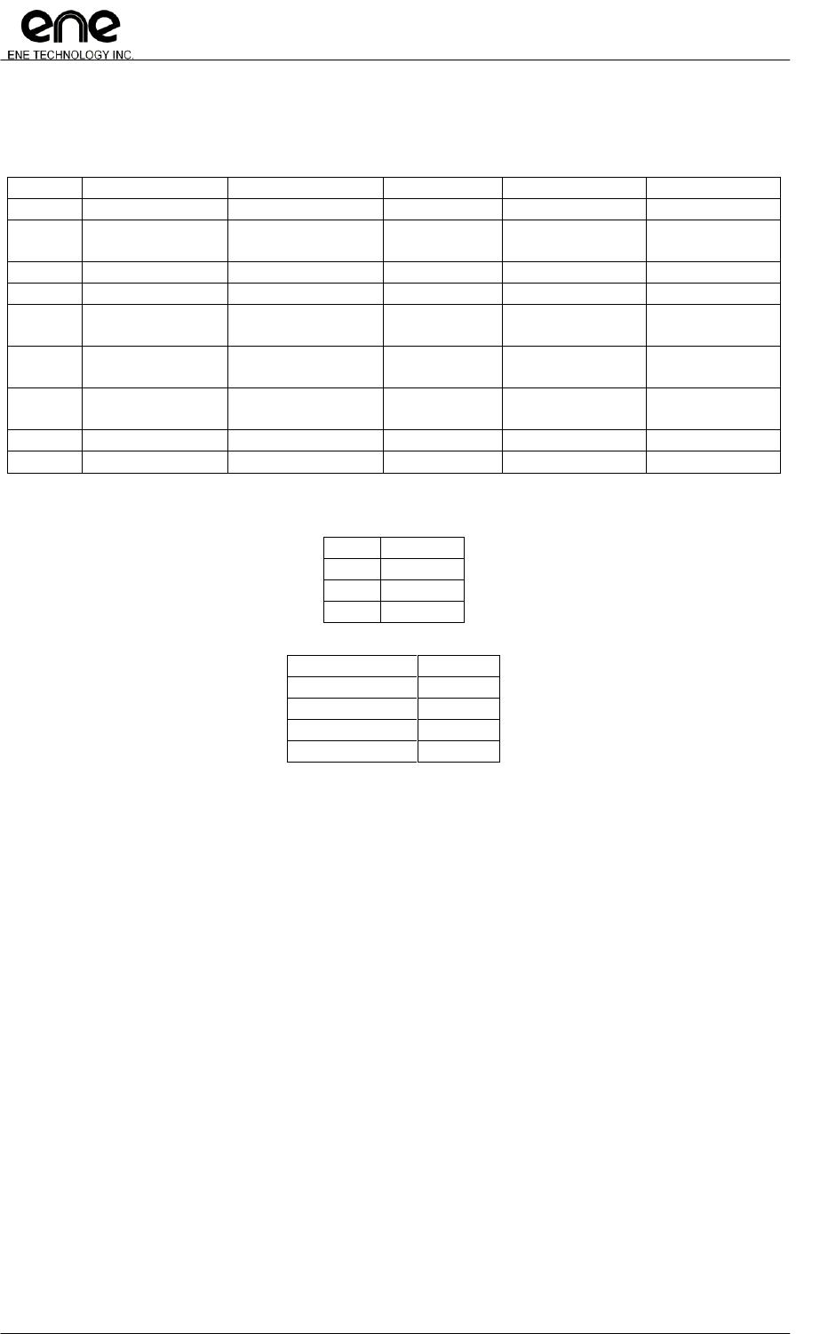
Copyright© 2011, ENE Technology Inc.
162
KB9012 Keyboard Controller Datasheet
CONFIDENTIAL
4.18.5.2 A/D Panel Drive Mode
Table for Panel Drive Mode :
PDM
Input Channel
X Driver
Y Driver
Measurement
Description
0
ADC 0~6
OFF
OFF
ADC
Normal ADC
1
0 (X+)
OFF
1 (Y+), VCC
3 (Y-), GND
Y Position
4-Wire
2
0 (X+)
2 (X-) , GND
1 (Y+), VCC
Z1 Position
4-Wire
3
3 (Y-)
2 (X-), GND
1 (Y+), VCC
Z2 Position
4-Wire
4
1 (Y+)
0 (X+) , VCC
2 (X-) , GND
OFF
X Position
4-Wire
5
4 (WIPER)
0 (UL) , VCC
2 (LL), GND
1 (UR), VCC
3 (LR), GND
Y Position
5-Wire
6
4 (WIPER)
0 (UL), VCC
2 (LL), VCC
1 (UR), GND
3 (LR), GND
X Position
5-Wire
7
0 (X+)
0 (X+), PU
3 (Y-), GND
PENIRQ
4-Wire
8
4 (WIPER)
4 (WIPER), PU
3 (Y-), GND
PENIRQ
5-Wire
4-Wire Touch, Note:
X+
ADC0
Y+
ADC1
X-
ADC2
Y-
ADC3
5-Wire Touch, Note:
Upper Left
ADC0
Upper Right
ADC1
Lower Left
ADC2
Lower Right
ADC3
WIPER
ADC4
Copyright© 2011, ENE Technology Inc.
163
KB9012 Keyboard Controller Datasheet
CONFIDENTIAL
4.18.6 D/A Converter Control
The control interface of D/A is in the EC space. Details SPEC of the D/A converters could
be found in the electronics characteristic chapter.
The following table summarizes the related registers of these 4 D/A converters.
Name
Address
Description
ADDAEN[7:4]
0xFF15
DAC port Enable bits of DAC3~DAC0
Bit7: DAC3
Bit6: DAC2
Bit5: DAC1
Bit4: DAC0
If DAC selected, please do not set related GPIO function selection register.
DAC0
0xFF10
DAC0 Output Value
DAC1
0xFF11
DAC1 Output Value
DAC2
0xFF12
DAC2 Output Value
DAC3
0xFF13
DAC3 Output Value
The following gives the programming sample to control a DAC.
Example
Using DAC2
Programming model
1. Clear the alternative function selection of the related pin
GPIOFS38[6] (0xFC07[6]) = 0b ;
2. Enable DAC function
ADDAEN[6] (0xFF15[6]) = 1b
3. Fill the value to be converted.
DAC2 (0xFF12) = specific value to convert
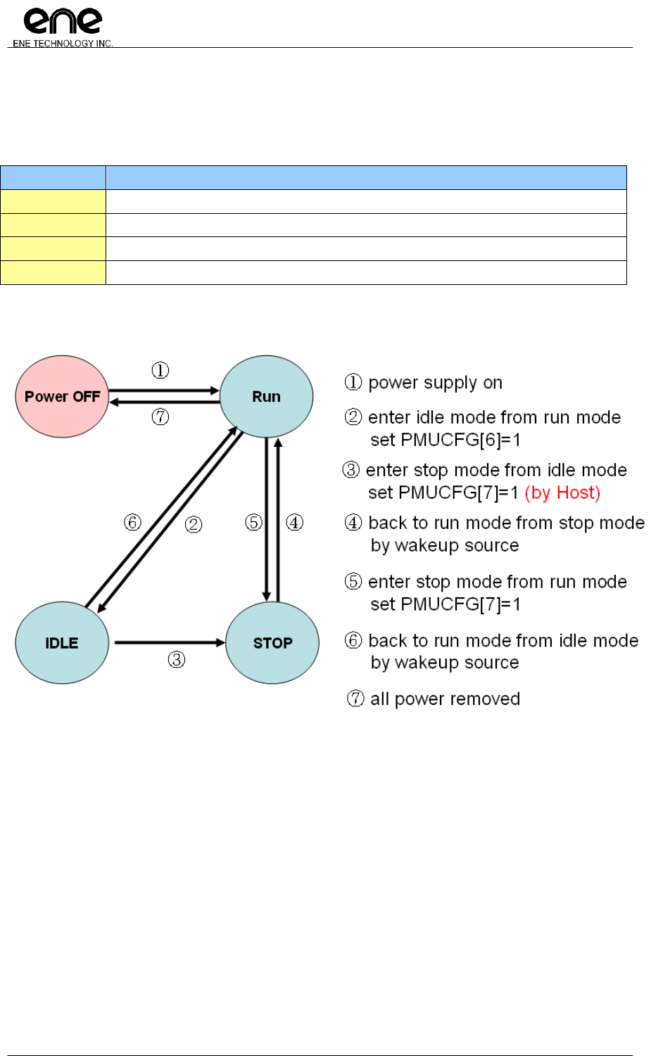
Copyright© 2011, ENE Technology Inc.
164
KB9012 Keyboard Controller Datasheet
CONFIDENTIAL
4.18.7 Power Management Control
Two power modes are defined, one is STOP mode and the other is IDLE mode. The
register PMUCFG (0xFF0C) is used to configure the power management. The following table gives
more detail about the definition for these two power modes.
Mode
Description
STOP
All clock sources stop, except external PCI clock and 32.768KHz.
IDLE
Only clock of 8051 microprocessor stops.
RUN
System operations in normal mode.
OFF
All power supply removed, including AC and battery
The diagram below shows the relationship between each power mode.
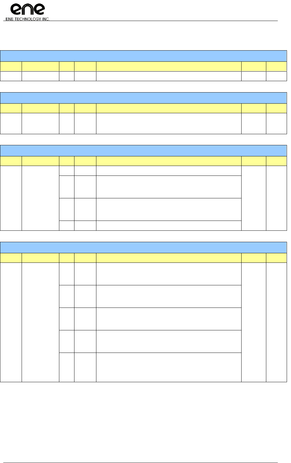
Copyright© 2011, ENE Technology Inc.
165
KB9012 Keyboard Controller Datasheet
CONFIDENTIAL
4.18.8 EC Registers Description (0xFF00~0xFF2F)
EC Hardware Revision ID
Offset
Name
Bit
Type
Description
Default
Bank
0x00
ECHV
7-0
RO
EC Hardware version
0xA3
0xFF
EC Firmware Revision ID
Offset
Name
Bit
Type
Description
Default
Bank
0x01
ECFV
7-0
R/W
EC firmware version
This register will be a data port, ADC_test_data[7:0] in ADC
test mode (ADCTRL[1]=1).
0x00
0xFF
EC High Address
Offset
Name
Bit
Type
Description
Default
Bank
0x02
ECHA
7-6
RSV
Reserved
0x0F
0xFF
5
R/W
Write protection of PXCFG[1], PXCFG[4].
0: writable.
1: write protection.
4
R/W
Index-I/O mode access control.
0: access range 0xF400~0xFFFF
1: access range 0xF400~0xF403 and 0xFC00~0xFFFF
3-0
RSV
Reserved
EC SCI Configuration
Offset
Name
Bit
Type
Description
Default
Bank
0x03
SCICFG
7
R/W
Standard EC commands generate SCI.
0: Disable
1: Enable
0x90
0xFF
6
R/W
SCIID port enable. (F/W SCI write port enable)
0: Disable
1: Enable
5
R/W
SCI polarity
0: Low active (default)
1: High active
4
R/W
SCIE0/SCIE1/SCIE2 (0xFF05~0xFF07) enable.
0: Disable
1: Enable
3-0
R/W
SCI pulse width. (max. 1ms)
SCI pulse width = SCICFG[3:0] * (time unit)
where time unit is determined by PXCFG[2], 64μs or 16μs
If SCICFG[3:0]=0, SCI pulse width = width of system clock.

Copyright© 2011, ENE Technology Inc.
166
KB9012 Keyboard Controller Datasheet
CONFIDENTIAL
EC Configuration
Offset
Name
Bit
Type
Description
Default
Bank
0x04
ECCFG
7
R/W
EPB fast access enable. To enhance EPB performance.
0: Disable
1: Enable
0x00
0xFF
6
R/W
Test mode selection
0: Normal mode
1: Test mode.
5~3
RSV
Reserved
2
R/W
Extended I/O (debug I/O, port 80) interrupt enable. Only
available while write cycle to port 80 from the host.
0: Disable
1: Enable
1
R/W
Reserved
0
R/W
OBF interrupt enable.
EC data port interrupt enable.
CPU reads data from EC data port.
0: Disable
1: Enable
EC SCI Interrupt Enable (SCIE0,SCIE1,SCIE3)
Offset
Name
Bit
Type
Description
Default
Bank
0x05
SCIE0
7-0
R/W
SCI Event0 enable
0: Disable
1: Enable
0x00
0xFF
0x06
SCIE1
7-0
R/W
SCI Event1 enable
0: Disable
1: Enable
0x00
0xFF
0x07
SCIE3
7-0
R/W
SCI Event3 enable
0: Disable
1: Enable
0x00
0xFF
EC SCI Flag (SCIF0,SCIF1,SCIF3)
Offset
Name
Bit
Type
Description
Default
Bank
0x08
ECIF0
7-0
R/W1C
SCI Event0 flag
0: no event
1: event occurs
0x00
0xFF
0x09
ECIF1
7-0
R/W1C
SCI Event1 flag
0: no event
1: event occurs
0x00
0xFF
0x0A
ECIF3
7-0
R/W1C
SCI Event3 flag
0: no event
1: event occurs
0x00
0xFF
EC SCI ID Write Port (to Generate SCI Event)
Offset
Name
Bit
Type
Description
Default
Bank
0x0B
SCID
7-0
R/W
Firmware SCI write port
0x00
0xFF

Copyright© 2011, ENE Technology Inc.
167
KB9012 Keyboard Controller Datasheet
CONFIDENTIAL
EC PMU Control/Configuration
Offset
Name
Bit
Type
Description
Default
Bank
0x0C
PMUCFG
7
WO
Write ―1‖ to enter STOP mode.
0x2F
0xFF
6
WO
Write ―1‖ to enter Idle mode.
5
R/W
LPC cycle wakeup system from STOP mode.
0: Disable
1: Enable
4
R/W
Reset 8051 while in STOP mode.
0: Disable
1: Enable
3
R/W
SCI wakeup system
0: Disable
1: Enable
2
R/W
WDT wakeup system from STOP mode.
0: Disable
1: Enable
1
R/W
GPWU wakeup system from STOP mode.
0: Disable
1: Enable
0
R/W
Interrupt wakeup system from Idle mode.
0: Disable
1: Enable
Copyright© 2011, ENE Technology Inc.
168
KB9012 Keyboard Controller Datasheet
CONFIDENTIAL
EC Clock Configuration
Offset
Name
Bit
Type
Description
Default
Bank
0x0D
CLKCFG
7
R/W
Flash clock from external clock (GPIO59).
0: Disable
1: Enable
0x00
0xFF
6
R/W
Flash clock control.
0: Half speed. (DPLL_CLK/2)
1: Full speed (DPLL_CLK)
please note, while CLKCFG[6]=0 and CLKCFG[3:2]=0
( power-on default ), the SPI flash clock is always 16MHz.
5
R/W
Enable DPLL to generate 32.768 MHz
0: Disable
1: Enable
4
R/W
DPLL enters low power state while in STOP mode.
0: Disable
1: Enable
3-2
R/W
8051/Peripheral clock selection.
11b: 32 MHz / 16 MHz
10b: 22 MHz / 11 MHz
01b: 16 MHz / 8 MHz
00b: 8 MHz / 4 MHz (default)
1
R/W
Peripheral slow down to 1MHz automatically.
If no host access, the peripheral clock will slow down to 1MHz
automatically.
0: Disable
1: Enable
0
R/W
Clock slow down to 2MHz / 1MHz (8051 / Peripheral) in Idle
mode. If this bit set, the clock of flash will be stopped in idle
mode.
0: Disable
1: Enable
EC Extended I/O (Debug Port) Write Data
Offset
Name
Bit
Type
Description
Default
Bank
0x0E
EXTIOW
7-0
R/W
If the host write data to extended I/O (debug port, port80), an
interrupt occurs, and then the firmware read it back via this
register.
0x00
0xFF
EC PLL Configuration
Offset
Name
Bit
Type
Description
Default
Bank
0x0F
PLLCFG
7-0
R/W
DPLL initial value. (low 8-bit)
After reset, the DPLL will output frequency about 32MHz with
default value 0xD0.
DPLL initial value is 10-bit, the higher two bits are located at
0xFF1F, PLLCFG2[7:6].
0x51
0xFF
Copyright© 2011, ENE Technology Inc.
169
KB9012 Keyboard Controller Datasheet
CONFIDENTIAL
EC DAC0 Output Value (ECMISC[1:0]=00b) / Extended Command (ECMISC[1:0]=11b)
Offset
Name
Bit
Type
Description
Default
Bank
0x10
DAC0
7-0
R/W
The digital data to be converted in DAC0.
0x00
0xFF
0x10
EXTCMD
7-0
R/W
8051 extended command port.
Once the command is filled, two events may occur.
- if non-zero command written, 8051 interrupt issues.
- If zero command written, SCI event issues.
Please note, EXTARG0/EXTARG1/EXTARG2 must be ready
before filling this register.
0x00
0xFF
EC DAC1 Output Value (ECMISC[1:0]=00b)/ Extended Command Argument 0(ECMISC[1:0]=11b)
Offset
Name
Bit
Type
Description
Default
Bank
0x11
DAC1
7-0
R/W
The digital data to be converted in DAC1.
0x00
0xFF
0x11
EXTARG0
7-0
R/W
Extended command argument0
0x00
0xFF
EC DAC2 Output Value (ECMISC[1:0]=00b)/ Extended Command Argument 1(ECMISC[1:0]=11b)
Offset
Name
Bit
Type
Description
Default
Bank
0x12
DAC2
7-0
R/W
The digital data to be converted in DAC2.
0x00
0xFF
0x12
EXTARG1
7-0
R/W
Extended command argument1
0x00
0xFF
EC DAC3 Output Value (ECMISC[1:0]=00b)/ Extended Command Argument 2(ECMISC[1:0]=11b)
Offset
Name
Bit
Type
Description
Default
Bank
0x13
DAC3
7-0
R/W
The digital data to be converted in DAC3.
0x00
0xFF
0x13
EXTARG2
7-0
R/W
Extended command argument2
0x00
0xFF
EC 8051 On-Chip Control
Offset
Name
Bit
Type
Description
Default
Bank
0x14
PXCFG
7-5
RSV
Reserved
0x00
0xFF
4
R/W
Setting for WDT timeout reset of GPIO
This field is only valid when PXCFG[1]=‘0‘
To write this bit, set the field on ECHA[5]=‘0‘
0: GPIO module when WDT timeout reset will not be reset.
1: GPIO module when WDT timeout reset will be reset.
3
RSV
Reserved
2
R/W
SCI pulse width time unit.
0: 64μs
1: 16μs
1
R/W
WDT timeout reset selection
0: reset whole KBC, selectable GPIO module.
1: reset 8051 only
To write this bit, set the field on ECHA[5]=‘0‘
0
R/W
8051 program counter control
0: program counter starts to execute.
1: 8051 reset and PC=0
PC will keep 0 (reset vector) until this bit is written to ―0‖

Copyright© 2011, ENE Technology Inc.
170
KB9012 Keyboard Controller Datasheet
CONFIDENTIAL
EC ADC/DAC Function Switch
Offset
Name
Bit
Type
Description
Default
Bank
0x15
ADDAEN
7-4
R/W
DAC3~DAC0 Function Enable
Bit7~Bit4 represents DAC3~DAC0 respectively
0: DAC Disable
1: DAC Enable
If DAC enable, please do not set related GPIO function
selection register.
0x00
0xFF
3-0
R/W
ADC3~ADC0 Function Enable
Bit3~Bit0 represents ADC3~ADC0 respectively
0: ADC Disable
1: ADC Enable.
If ADC enable, please do not set related GPIO bit with
input enable (IE).
EC PLL Frequency Register (High Byte)
Offset
Name
Bit
Type
Description
Default
Bank
0x16
PLLFRH
7-0
R/W
DPLL frequency = 32.768KHz(external) * PLLFR
PLLFR[11:0] =( PLLFRH[7:0] : PLLFRL[7:4] )
To generate 32.768MHz, PLLFR = 1000 (decimal) = 0x3E8
i.e., PLLFRH=0x3E
0x3E
0xFF
EC PLL Frequency Register (Low Byte)
Offset
Name
Bit
Type
Description
Default
Bank
0x17
PLLFRL
7-4
R/W
DPLL frequency = 32.768KHz * PLLFR
PLLFR[11:0] =( PLLFRH[7:0] : PLLFRL[7:4] )
To generate 32.768MHz, PLLFR = 1000 (decimal) = 0x3E8
i.e., PLLFRL[7:4]=0x8
0x83
0xFF
3
R/W
DPLL lock value presented in CHIPID (0xFF1E~0xFF1F).
(Only valid if ECSTS[2]=0)
0: Disable
1: Enable.
2
R/W
DPLL test mode enable
0: Disable
1: Enable.
1-0
RSV
Reserved

Copyright© 2011, ENE Technology Inc.
171
KB9012 Keyboard Controller Datasheet
CONFIDENTIAL
EC ADC Control Register
Offset
Name
Bit
Type
Description
Default
Bank
0x18
ADCTRL
7~4
R/W
ADC7~ADC4 Function Enable
Bit7~Bit4 represents ADC7~ADC4 respectively
0: ADC Disable
1: ADC Enable.
If ADC enable, please do not set related GPIO bit with
input enable (IE).
0x00
0xFF
3-1
R/W
Convert ADC channel selection.
000: ADC0
001: ADC1
010: ADC2
011: ADC3
100: ADC4
101: ADC5
110: ADC6
111: ADC7
0
R/W
ADC convert start and force interrupt after converting.
0: ADC stops converting, interrupt disable
1: ADC starts converting, interrupt enable
EC ADC Data Output Port
Offset
Name
Bit
Type
Description
Default
Bank
0x19
ADCDAT
7-0
RO
Converted data by ADC. ADC output[9:2]=ADCDAT[7:0]
0x00
0xFF
EC Interrupt Pending Flag
Offset
Name
Bit
Type
Description
Default
Bank
0x1A
ECIF
7-6
RO
Converted data by ADC. ADC output[1:0]=ECIF[7:6]
0x00
0xFF
5-3
RSV
Reserved
2
R/W1C
EC firmware mode flag.
If EC command handled by F/W, this flag will be set
1
R/W1C
EC IBF interrupt pending flag
0: no event
1: event occurs
0
R/W1C
EC OBF interrupt pending flag
0: no event
1: event occurs
EC Data Port
Offset
Name
Bit
Type
Description
Default
Bank
0x1B
ECDAT
7-0
R/W
EC data port.
If ECDAT written, ECSTS[0] (OBF) becomes ―1‖.
0x00
0xFF
EC Command Port
Offset
Name
Bit
Type
Description
Default
Bank
0x1C
ECCMD
7-0
RO
This register keeps EC command issued by the host.
0x00
0xFF
Copyright© 2011, ENE Technology Inc.
172
KB9012 Keyboard Controller Datasheet
CONFIDENTIAL
EC Control and Status Port
Offset
Name
Bit
Type
Description
Default
Bank
0x1D
ECSTS
7
R/W
Reserved
0x00
0xFF
6
R/W
Reserved
5
RO
SCI pending flag
0: no event
1: event occurs
4
R/W
Burst enable status.
0: EC burst mode disable
1: EC burst mode enable.
3
R/W
EC I/O write port indicator
0: host writes for data (writes I/O port 62h)
1: host writes for command (writes I/O port 66h)
2
R/W
Register 0xFF1E and 0xFF1F function select.
0: CHIPID display selected
or show DPLL lock value based on 0xFF17[3]
1: CLKCFG2/PLLCFG2 function selected
1
R/W1C
IBF (Input Buffer Full)
0: buffer not full
1: buffer full
0
R/W1C
OBF (Output Buffer Full)
0: buffer not full
1: buffer full
EC Clock Configuration 2
Offset
Name
Bit
Type
Description
Default
Bank
0x1E
CHIPID_H
7-0
R/W
CHIPID high byte. (ECSTS[2]=0)
0x90
0xFF
0x1E
DPLL_FREQH
7-6
RSV
Reserved
0x00
0xFF
5-0
RO
ECSTS[2] = 0, and PLLFRL[3]=1,
DPLL setting frequency value [9:4]
0x1E
CLKCFG2
7-0
R/W
Divider of (DPLL Freq)/2 to generate 1μs (ECSTS[2]=1)
Eg: DPLL outputs 64MHz (by default), to generate 1μs, the
divider should be 32. That is the CLKCFG2 will be 0x1F.
0x1F
0xFF

Copyright© 2011, ENE Technology Inc.
173
KB9012 Keyboard Controller Datasheet
CONFIDENTIAL
EC PLL Configuration 2
Offset
Name
Bit
Type
Description
Default
Bank
0x1F
CHIPID_L
7-0
R/W
CHIPID low byte. (ECSTS[2]=0)
0x12
0xFF
0x1F
DPLL_FREQL
7-4
RO
ECSTS[2] = 0, and PLLFRL[3]=1,
DPLL setting frequency value [3:0]
0x00
0xFF
3-0
RO
ECSTS[2] = 0, and PLLFRL[3]=1,
DPLL setting phase [3:0]
0x1F
PLLCFG2
7-6
R/W
High 2 bits of DPLL initial value. (ECSTS[2]=1)
DPLL initial value is 10-bit, the low 8 bits are located at 0xFF0F,
PLLCFG[7:0].
0x21
0xFF
5
R/W
DPLL reference selection.
0: Reference PCI clock
1: Reference 32.768KHz source. (default)
4
R/W
DPLL source clock divider.
0: Disable. (default)
1: Enable.
If PLLCFG2[5]=1, then this bit should be ―0‖.
If PLLCFG2[5]=0, this bit should be ―1‖.
3-0
R/W
DPLL low speed state setting in Idle mode.
The default value is 0001b, the DPLL will provide 2MHz (8051)/
1MHz (Peripheral) clock.
EC MISC Configuration
Offset
Name
Bit
Type
Description
Default
Bank
0x20
ECMISC
7
RO
8051 state.
0: Idle state
1: Normal state
0x80
0xFF
6
RSV
Reserved
5
R/W
POFR standby enable
Trade-off for leakage current and POFR, about 3uA
4
R/W
LDO standby enable
Trade-off for leakage current and LDO, about 26uA
3
RSV
Reserved
2
R/W
8051 extended command (ExtCMD, 0xFF10) interrupt enable.
0: Disable
1: Enable
1
R/W
Register function select of 0x1410~0x1413 for LPC index-I/O
0: DAC
1: LPC index-I/O Extended command related registers
0
R/W
Register function select of 0x1410~0x1413 for 8051.
0: DAC
1: 8051 Extended command related registers
EC Extended I/O (Debug I/O) Data Port by Host
Offset
Name
Bit
Type
Description
Default
Bank
0x21
EXTIOR
7-0
R/W
The host reads extended I/O port and gets data from this
register. No interrupt occurs.
0x00
0xFF
Copyright© 2011, ENE Technology Inc.
174
KB9012 Keyboard Controller Datasheet
CONFIDENTIAL
Embedded Debug Interface Feature Register
Offset
Name
Bit
Type
Description
Default
Bank
0x22
EDIF
7
R/W
EDI feature enable
0: disable
1: enable
0x00
0xFF
6-0
RSV
Reserved
Embedded Debug Interface Active Status Register
Offset
Name
Bit
Type
Description
Default
Bank
0x23
EDIAS
7
R/W
EDI active status
0: not active
1: active
0x00
0xFF
6-0
RSV
Reserved
Embedded Debug Version ID
Offset
Name
Bit
Type
Description
Default
Bank
0x24
EDIID
7-0
RO
EDI version
0x04
0xFF
ADC Pending Flag Register
Offset
Name
Bit
Type
Description
Default
Bank
0x25
ADCPF
7~3
RSV
Reserved
0x00
0xFF
2
RO
ADC PENIRQ in-line status
1
R/W1C
ADC PENIRQ pending flag
0
R/W1C
Converting ADC channel pending flag
ADC Interrupt Enable
Offset
Name
Bit
Type
Description
Default
Bank
0x26
ADCIE
7~2
RSV
Reserved
0x00
0xFF
1
R/W
ADC PENIRQ interrupt enable
0
R/W
Converting ADC interrupt enable

Copyright© 2011, ENE Technology Inc.
175
KB9012 Keyboard Controller Datasheet
CONFIDENTIAL
Voltage comparator control and status register
Offset
Name
Bit
Type
Description
Default
Bank
0x27
VCCR
7~6
RSV
Reserved
0x03
0xFF
5
R/W
VC1 output active polarity,
0: active low (Default)
1: active high
4
R/W
VC0 output active polarity,
0: active low (Default)
1: active high
3~2
R/W
Voltage comparator de-bounce De-bounce setting
00: No De-bounce
01: continually trigger 2 times
10: continually trigger 4 times
11: continually trigger 6 times
1
R/W
Voltage comparator pair 1 enable
0
R/W
Voltage comparator pair 0 enable
Power fail control and status register
Offset
Name
Bit
Type
Description
Default
Bank
0x28
PFCSR
7
R/W1C
Power Fail status flag
This bit is set by hardware if voltage of power is under Power
Fail Voltage and write 1 clear by firmware or system reset
occur
0x00
0xFF
6
RSV
Reserved
5~4
R/W
Power fail De-bounce setting
00: No De-bounce
01: continually trigger twice
10: continually trigger 4 times
11: continually trigger 6 times
3~1
RSV
Reserved
0
R/W
Power fail status enable
GPXIOA03 or GPIO18 will output low to indicate the system
power is under Power Fail Voltage. The output pin select is
controlled by GPX_MISC[2:1].
0: Disable
1: Enable
Note: GPXIOA03 / GPIO18 will return to previous state if
PFCSR[7] is written 1 clear.
Voltage Comparator Control and Status Register
Offset
Name
Bit
Type
Description
Default
Bank
0x29
VCSR
7
RO
Voltage Comparator 1 output status
0x0C
0xFF
6
RO
Voltage Comparator 0 output status
5-4
RSV
Reserved
3
R/W
VC1 output open-drain enable
2
R/W
VC0 output open-drain enable
1~0
RSV
Reserved
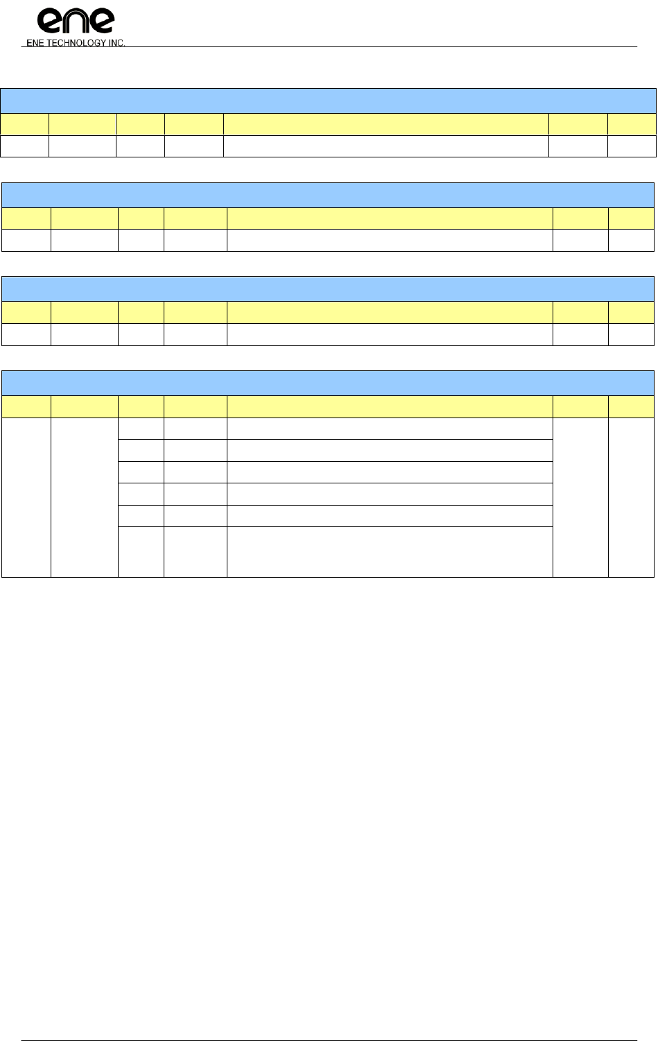
Copyright© 2011, ENE Technology Inc.
176
KB9012 Keyboard Controller Datasheet
CONFIDENTIAL
Crystal 32k control register
Offset
Name
Bit
Type
Description
Default
Bank
0x2A
RSV
7~0
RSV
Reserved
0x00
0xFF
Voltage Comparator 0 DAC compare value
Offset
Name
Bit
Type
Description
Default
Bank
0x2B
VCDAC0
7~0
R/W
The DAC value compared with VC0
0x5D
0xFF
Voltage Comparator 1 DAC compare value
Offset
Name
Bit
Type
Description
Default
Bank
0x2C
VCDAC1
7~0
R/W
The DAC value compared with VC1
0x5D
0xFF
Power-Latch / Voltage Comparator register (Power Supply from VCC_0)
Offset
Name
Bit
Type
Description
Default
Bank
0x2D
PA0_REG
7~5
RSV
Reserved
0x08
0xFF
4
R/W
Voltage Comparator 1 output into power-latch enable
3
R/W
Voltage Comparator 0 output into power-latch enable
2
R/W0C
Voltage Comparator 1 output into power-latch pending flag
1
R/W0C
Voltage Comparator 0 output into power-latch pending flag
0
RSV
Valid bit for PA0_REG
Whenever POR reset, PA0_REG[0] will reset to 0.
Value of ‗1‘ to present PA0_REG is valid for power-latch.

Copyright© 2011, ENE Technology Inc.
177
KB9012 Keyboard Controller Datasheet
CONFIDENTIAL
4.19 General Purpose Wake-up Controller (GPWU)
4.19.1 GPWU Function Description
The GPIO module provides flexible methods to wakeup the KBC or to generate interrupt. Once
the input function is determined, plenty of features for wakeup can be setup. Here is the table to
summarize all the features.
Compared with KBx926 series, KB9012 enable all GPXIOAx pins as external wake-up source.
For detail register description, please refer the following section.
Wakeup Enable
0: Disable
1: Enable
Polarity
0:↓/ L
1:↑/ H
Edge/Level
0: Edge
1: Level
Toggle
0: Disable
1: Enable
Description
0
X
X
X
No wakeup events occur
1
X
X
1
Signal toggle trigger
1
0
0
0
Falling edge trigger
1
0
1
0
Low level trigger
1
1
0
0
Rising edge trigger
1
1
1
0
High level trigger

Copyright© 2011, ENE Technology Inc.
178
KB9012 Keyboard Controller Datasheet
CONFIDENTIAL
4.19.2 GPWU Registers Description (0xFF30~0xFF7F)
GPIO Wakeup Event Enable
Offset
Name
Bit
Type
Description
Default
Bank
0x30
GPWUEN00
7-0
R/W
GPIO00~GPIO07 Wakeup Event Switch
bit[0]~bit[7] stand for GPIO00~GPIO07 separately
0: Wakeup event disable
1: Wakeup event enable
Note: NO GPIO02/03/06 in KB9012 IC
0x00
0xFF
0x31
GPWUEN08
7-0
R/W
GPIO08~GPIO0F Wakeup Event Switch
bit[0]~bit[7] stand for GPIO08~GPIO0F separately
0: Wakeup event disable
1: Wakeup event enable
Note: NO GPIO09 in KB9012 IC
0x00
0xFF
0x32
GPWUEN10
7-0
R/W
GPIO10~GPIO17 Wakeup Event Switch
bit[0]~bit[7] stand for GPIO10~GPIO17 separately
0: Wakeup event disable
1: Wakeup event enable
0x00
0xFF
0x33
GPWUEN18
7-0
R/W
GPIO18~GPIO1F Wakeup Event Switch
bit[0]~bit[7] stand for GPIO18~GPIO1F separately
0: Wakeup event disable
1: Wakeup event enable
Note: NO GPIO1B/1C/1E/1F in KB9012 IC
0x00
0xFF
0x34
GPWUEN20
7-0
R/W
GPIO20~GPIO27 Wakeup Event Switch
bit[0]~bit[7] stand for GPIO20~GPIO27 separately
0: Wakeup event disable
1: Wakeup event enable
0x00
0xFF
0x35
GPWUEN28
7-0
R/W
GPIO28~GPIO2F Wakeup Event Switch
bit[0]~bit[7] stand for GPIO28~GPIO2F separately
0: Wakeup event disable
1: Wakeup event enable
0x00
0xFF
0x36
GPWUEN30
7-0
R/W
GPIO30~GPIO37 Wakeup Event Switch
bit[0]~bit[7] stand for GPIO30~GPIO37 separately
0: Wakeup event disable
1: Wakeup event enable
0x00
0xFF
0x37
GPWUEN38
7-0
R/W
GPIO38~GPIO3F Wakeup Event Switch
bit[0]~bit[7] stand for GPIO38~GPIO3F separately
0: Wakeup event disable
1: Wakeup event enable
0x00
0xFF
0x38
GPWUEN40
7-0
R/W
GPIO40~GPIO47 Wakeup Event Switch
bit[0]~bit[7] stand for GPIO40~GPIO47 separately
0: Wakeup event disable
1: Wakeup event enable
0x00
0xFF
0x39
GPWUEN48
7-0
R/W
GPIO48~GPIO4F Wakeup Event Switch
bit[0]~bit[7] stand for GPIO48~GPIO4F separately
0: Wakeup event disable
1: Wakeup event enable
0x00
0xFF
0x3A
GPWUEN50
7-0
R/W
GPIO50~GPIO57 Wakeup Event Switch
bit[0]~bit[7] stand for GPIO50~GPIO57 separately
0: Wakeup event disable
1: Wakeup event enable
Note: NO GPIO51 in KB9012 IC
0x00
0xFF

Copyright© 2011, ENE Technology Inc.
179
KB9012 Keyboard Controller Datasheet
CONFIDENTIAL
GPIO Wakeup Event Enable
Offset
Name
Bit
Type
Description
Default
Bank
0x3B
GPWUEN58
7-0
R/W
GPIO58~GPIO5F Wakeup Event Switch
bit[0]~bit[1] stand for GPIO58~GPIO5F separately
0: Wakeup event disable
1: Wakeup event enable
Note: NO GPIO5F in KB9012 IC
0x00
0xFF
0x3C
GXDWUEN00
7-0
R/W
GPXIOD00~GPXIOD07 Wakeup Event Switch
bit[0]~bit[7] stand for GPXIOD00~GPXIOD07 separately
0: Wakeup event disable
1: Wakeup event enable
0x00
0xFF
0x3D
GXAWUEN00
7-0
R/W
GPXIOA00~GPXIOA07 Wakeup Event Switch
bit[0]~bit[7] stand for GPXIOA00~GPXIOA07 separately
0: Wakeup event disable
1: Wakeup event enable
0x00
0xFF
0x3E
GXAWUEN08
7-0
R/W
GPXIOA08~GPXIOA15 Wakeup Event Switch
bit[0]~bit[7] stand for GPXIOA08~GPXIOA15 separately
0: Wakeup event disable
1: Wakeup event enable
Note: NO GPXIOA12/13/14/15 in KB9012 IC
0x00
0xFF

Copyright© 2011, ENE Technology Inc.
180
KB9012 Keyboard Controller Datasheet
CONFIDENTIAL
GPIO Wakeup Event Pending Flag
Offset
Name
Bit
Type
Description
Default
Bank
0x40
GPWUPF00
7-0
R/W1C
GPIO00~GPIO07 Wakeup Event Pending Flag
bit[0]~bit[7] stand for GPIO00~GPIO07 separately
0: No wakeup event
1: Wakeup event pending
Note: NO GPIO02/03/06 in KB9012 IC
0x00
0xFF
0x41
GPWUPF08
7-0
R/W1C
GPIO08~GPIO0F Wakeup Event Pending Flag
bit[0]~bit[7] stand for GPIO08~GPIO0F separately
0: No wakeup event
1: Wakeup event pending
Note: NO GPIO09 in KB9012IC
0x00
0xFF
0x42
GPWUPF10
7-0
R/W1C
GPIO10~GPIO17 Wakeup Event Pending Flag
bit[0]~bit[7] stand for GPIO10~GPIO17 separately
0: No wakeup event
1: Wakeup event pending
0x00
0xFF
0x43
GPWUPF18
7-0
R/W1C
GPIO18~GPIO1F Wakeup Event Pending Flag
bit[0]~bit[7] stand for GPIO18~GPIO1F separately
0: No wakeup event
1: Wakeup event pending
Note: NO GPIO1B/1C/1E/1F in KB9012IC
0x00
0xFF
0x44
GPWUPF20
7-0
R/W1C
GPIO20~GPIO27 Wakeup Event Pending Flag
bit[0]~bit[7] stand for GPIO20~GPIO27 separately
0: No wakeup event
1: Wakeup event pending
0x00
0xFF
0x45
GPWUPF28
7-0
R/W1C
GPIO28~GPIO2F Wakeup Event Pending Flag
bit[0]~bit[7] stand for GPIO28~GPIO2F separately
0: No wakeup event
1: Wakeup event pending
0x00
0xFF
0x46
GPWUPF30
7-0
R/W1C
GPIO30~GPIO37 Wakeup Event Pending Flag
bit[0]~bit[7] stand for GPIO30~GPIO37 separately
0: No wakeup event
1: Wakeup event pending
0x00
0xFF
0x47
GPWUPF38
7-0
R/W1C
GPIO38~GPIO3F Wakeup Event Pending Flag
bit[0]~bit[7] stand for GPIO38~GPIO3Fseparately
0: No wakeup event
1: Wakeup event pending
0x00
0xFF
0x48
GPWUPF40
7-0
R/W1C
GPIO40~GPIO47 Wakeup Event Pending Flag
bit[0]~bit[7] stand for GPIO40~GPIO47 separately
0: No wakeup event
1: Wakeup event pending
0x00
0xFF
0x49
GPWUPF48
7-0
R/W1C
GPIO48~GPIO4F Wakeup Event Pending Flag
bit[0]~bit[7] stand for GPIO48~GPIO4F separately
0: No wakeup event
1: Wakeup event pending
0x00
0xFF
0x4A
GPWUPf50
7-0
R/W1C
GPIO50~GPIO57 Wakeup Event Pending Flag
bit[0]~bit[7] stand for GPIO50~GPIO57 separately
0: No wakeup event
1: Wakeup event pending
Note: NO GPIO51 in KB9012 IC
0x00
0xFF
0x4B
GPWUPF58
7-0
R/W1C
GPIO58~GPIO5F Wakeup Event Pending Flag
bit[0]~bit[7] stand for GPIO58~GPIO5F separately
0: No wakeup event
1: Wakeup event pending
Note: NO GPIO5F in KB9012 IC
0x00
0xFF

Copyright© 2011, ENE Technology Inc.
181
KB9012 Keyboard Controller Datasheet
CONFIDENTIAL
GPIO Wakeup Event Pending Flag
Offset
Name
Bit
Type
Description
Default
Bank
0x4C
GXDWUPF00
7-0
R/W1C
GPXIOD00~GPXIOD07 Wakeup Event Pending Flag
bit[0]~bit[7] stand for GPXIOD00~GPXIOD07 separately
0: No wakeup event
1: Wakeup event pending
0x00
0xFF
0x4D
GXAWUPF00
7-0
R/W
GPXIOA00~GPXIOA07 Wakeup Event Pending Flag
bit[0]~bit[7] stand for GPXIOA00~GPXIOA07 separately
0: No wakeup event
1: Wakeup event pending
0x00
0xFF
0x4E
GXAWUPF08
7-0
R/W
GPXIOA08~GPXIOA15 Wakeup Event Pending Flag
bit[0]~bit[7] stand for GPXIOA08~GPXIOA15 separately
0: No wakeup event
1: Wakeup event pending
Note: NO GPXIOA12/13/14/15 in KB9012 IC
0x00
0xFF

Copyright© 2011, ENE Technology Inc.
182
KB9012 Keyboard Controller Datasheet
CONFIDENTIAL
GPIO Wakeup Polarity Selection
Offset
Name
Bit
Type
Description
Default
Bank
0x50
GPWUPS00
7-0
R/W
GPIO00~GPIO07 Wakeup Polarity Selection
bit[0]~bit[7] stand for GPIO00~GPIO07 separately
0: Low active (level trigger) / Falling (edge trigger)
1: High active (high trigger) / Rising (edge trigger)
Note: NO GPIO02/03/06 in KB9012 IC
0x00
0xFF
0x51
GPWUPS08
7-0
R/W
GPIO08~GPIO0F Wakeup Polarity Selection
bit[0]~bit[7] stand for GPIO08~GPIO0F separately
0: Low active (level trigger) / Falling (edge trigger)
1: High active (high trigger) / Rising (edge trigger)
Note: NO GPIO09 in KB9012 IC
0x00
0xFF
0x52
GPWUPS10
7-0
R/W
GPIO10~GPIO17 Wakeup Polarity Selection
bit[0]~bit[7] stand for GPIO10~GPIO17 separately
0: Low active (level trigger) / Falling (edge trigger)
1: High active (high trigger) / Rising (edge trigger)
0x00
0xFF
0x53
GPWUPS18
7-0
R/W
GPIO18~GPIO1F Wakeup Polarity Selection
bit[0]~bit[7] stand for GPIO18~GPIO1F separately
0: Low active (level trigger) / Falling (edge trigger)
1: High active (high trigger) / Rising (edge trigger)
Note: NO GPIO1B/1C/1E/1F in KB9012 IC
0x00
0xFF
0x54
GPWUPS20
7-0
R/W
GPIO20~GPIO27 Wakeup Polarity Selection
bit[0]~bit[7] stand for GPIO20~GPIO27 separately
0: Low active (level trigger) / Falling (edge trigger)
1: High active (high trigger) / Rising (edge trigger)
0x00
0xFF
0x55
GPWUPS28
7-0
R/W
GPIO28~GPIO2F Wakeup Polarity Selection
bit[0]~bit[7] stand for GPIO28~GPIO2F separately
0: Low active (level trigger) / Falling (edge trigger)
1: High active (high trigger) / Rising (edge trigger)
0x00
0xFF
0x56
GPWUPS30
7-0
R/W
GPIO30~GPIO37 Wakeup Polarity Selection
bit[0]~bit[7] stand for GPIO30~GPIO37 separately
0: Low active (level trigger) / Falling (edge trigger)
1: High active (high trigger) / Rising (edge trigger)
0x00
0xFF
0x57
GPWUPS38
7-0
R/W
GPIO38~GPIO3F Wakeup Polarity Selection
bit[0]~bit[7] stand for GPIO38~GPIO3F separately
0: Low active (level trigger) / Falling (edge trigger)
1: High active (high trigger) / Rising (edge trigger)
0x00
0xFF
0x58
GPWUPS40
7-0
R/W
GPIO40~GPIO47 Wakeup Polarity Selection
bit[0]~bit[7] stand for GPIO40~GPIO47 separately
0: Low active (level trigger) / Falling (edge trigger)
1: High active (high trigger) / Rising (edge trigger)
0x00
0xFF
0x59
GPWUPS48
7-0
R/W
GPIO48~GPIO4F Wakeup Polarity Selection
bit[0]~bit[7] stand for GPIO48~GPIO4F separately
0: Low active (level trigger) / Falling (edge trigger)
1: High active (high trigger) / Rising (edge trigger)
0x00
0xFF
0x5A
GPWUPS50
7-0
R/W
GPIO50~GPIO57 Wakeup Polarity Selection
bit[0]~bit[7] stand for GPIO50~GPIO57 separately
0: Low active (level trigger) / Falling (edge trigger)
1: High active (high trigger) / Rising (edge trigger)
Note: NO GPIO51 in KB9012 IC
0x00
0xFF
0x5B
GPWUPS58
7-0
R/W
GPIO58~GPIO5F Wakeup Polarity Selection
bit[0]~bit[7] stand for GPIO58~GPIO5F separately
0: Low active (level trigger) / Falling (edge trigger)
1: High active (high trigger) / Rising (edge trigger)
Note: NO GPIO5F in KB9012 IC
0x00
0xFF

Copyright© 2011, ENE Technology Inc.
183
KB9012 Keyboard Controller Datasheet
CONFIDENTIAL
GPIO Wakeup Polarity Selection
Offset
Name
Bit
Type
Description
Default
Bank
0x5C
GXDWUPS00
7-0
R/W
GPXIOD00~GPXIOD07 Wakeup Polarity Selection
bit[0]~bit[7] stand for GPXIOD00~GPXIOD07 separately
0: Low active (level trigger) / Falling (edge trigger)
1: High active (high trigger) / Rising (edge trigger)
0x00
0xFF
0x5D
GXAWUPS00
7-0
R/W
GPXIOA00~GPXIOA07 Wakeup Polarity Selection
bit[0]~bit[7] stand for GPXIOA00~GPXIOA07 separately
0: Low active (level trigger) / Falling (edge trigger)
1: High active (high trigger) / Rising (edge trigger)
0x00
0xFF
0x5E
GXAWUPS08
7-0
R/W
GPXIOA08~GPXIOA15 Wakeup Polarity Selection
bit[0]~bit[7] stand for GPXIOA08~GPXIOA15 separately
0: Low active (level trigger) / Falling (edge trigger)
1: High active (high trigger) / Rising (edge trigger)
Note: NO GPXIOA12/13/14/15 in KB9012 IC
0x00
0xFF

Copyright© 2011, ENE Technology Inc.
184
KB9012 Keyboard Controller Datasheet
CONFIDENTIAL
GPIO Wakeup Level/Edge Trigger Selection
Offset
Name
Bit
Type
Description
Default
Bank
0x60
GPWUEL00
7-0
R/W
GPIO00~GPIO07 Wakeup Level/Edge Selection
bit[0]~bit[7] stand for GPIO00~GPIO07 separately
0: Edge trigger
1: Level trigger
Note: NO GPIO02/03/06 in KB9012 IC
0x00
0xFF
0x61
GPWUEL08
7-0
R/W
GPIO08~GPIO0F Wakeup Level/Edge Selection
bit[0]~bit[7] stand for GPIO08~GPIO0F separately
0: Edge trigger
1: Level trigger
Note: NO GPIO09 in KB9012 IC
0x00
0xFF
0x62
GPWUEL10
7-0
R/W
GPIO10~GPIO17 Wakeup Level/Edge Selection
bit[0]~bit[7] stand for GPIO10~GPIO17 separately
0: Edge trigger
1: Level trigger
0x00
0xFF
0x63
GPWUEL18
7-0
R/W
GPIO18~GPIO1F Wakeup Level/Edge Selection
bit[0]~bit[7] stand for GPIO18~GPIO1F separately
0: Edge trigger
1: Level trigger
Note: NO GPIO1B/1C/1E/1F in KB9012 IC
0x00
0xFF
0x64
GPWUEL20
7-0
R/W
GPIO20~GPIO27 Wakeup Level/Edge Selection
bit[0]~bit[7] stand for GPIO20~GPIO27 separately
0: Edge trigger
1: Level trigger
0x00
0xFF
0x65
GPWUEL28
7-0
R/W
GPIO28~GPIO2F Wakeup Level/Edge Selection
bit[0]~bit[7] stand for GPIO28~GPIO2F separately
0: Edge trigger
1: Level trigger
0x00
0xFF
0x66
GPWUEL30
7-0
R/W
GPIO30~GPIO37 Wakeup Level/Edge Selection
bit[0]~bit[7] stand for GPIO30~GPIO37 separately
0: Edge trigger
1: Level trigger
0x00
0xFF
0x67
GPWUEL38
7-0
R/W
GPIO38~GPIO3F Wakeup Level/Edge Selection
bit[0]~bit[7] stand for GPIO38~GPIO3F separately
0: Edge trigger
1: Level trigger
0x00
0xFF
0x68
GPWUEL40
7-0
R/W
GPIO40~GPIO47 Wakeup Level/Edge Selection
bit[0]~bit[7] stand for GPIO40~GPIO47 separately
0: Edge trigger
1: Level trigger
0x00
0xFF
0x69
GPWUEL48
7-0
R/W
GPIO48~GPIO4F Wakeup Level/Edge Selection
bit[0]~bit[7] stand for GPIO48~GPIO4F separately
0: Edge trigger
1: Level trigger
0x00
0xFF
0x6A
GPWUEL50
7-0
R/W
GPIO50~GPIO57 Wakeup Level/Edge Selection
bit[0]~bit[7] stand for GPIO50~GPIO57 separately
0: Edge trigger
1: Level trigger
Note: NO GPIO51 in KB9012 IC
0x00
0xFF
0x6B
GPWUEL58
7-0
R/W
GPIO58~GPIO5F Wakeup Level/Edge Selection
bit[0]~bit[7] stand for GPIO58~GPIO5F separately
0: Edge trigger
1: Level trigger
Note: NO GPIO5F in KB9012 IC
0x00
0xFF

Copyright© 2011, ENE Technology Inc.
185
KB9012 Keyboard Controller Datasheet
CONFIDENTIAL
GPIO Wakeup Level/Edge Trigger Selection
Offset
Name
Bit
Type
Description
Default
Bank
0x6C
GXDWUEL00
7-0
R/W
GPXIOD00~GPXIOD07 Wakeup Level/Edge Selection
bit[0]~bit[7] stand for GPXIOD00~GPXIOD07 separately
0: Edge trigger
1: Level trigger
0x00
0xFF
0x6D
GXAWUEL00
7-0
R/W
GPXIOA00~GPXIOA07 Wakeup Polarity Selection
bit[0]~bit[7] stand for GPXIOA00~GPXIOA07 separately
0: Edge trigger
1: Level trigger
0x00
0xFF
0x6E
GXAWUEL08
7-0
R/W
GPXIOA08~GPXIOA15 Wakeup Polarity Selection
bit[0]~bit[7] stand for GPXIOA08~GPXIOA15 separately
0: Edge trigger
1: Level trigger
Note: NO GPXIOA12/13/14/15 in KB9012 IC
0x00
0xFF

Copyright© 2011, ENE Technology Inc.
186
KB9012 Keyboard Controller Datasheet
CONFIDENTIAL
GPIO Wakeup Input Change (Toggle) Trigger Selection
Note:This setting will ignore the corresponding bit of GPWUELxx.
Offset
Name
Bit
Type
Description
Default
Bank
0x70
GPWUCHG00
7-0
R/W
GPIO00~GPIO07 Wakeup Input Change (Toggle) Trigger
bit[0]~bit[7] stand for GPIO00~GPIO07 separately
0: Toggle trigger disable
1: Toggle trigger enable
Note: NO GPIO02/03/06 in KB9012 IC
0x00
0xFF
0x71
GPWUCHG08
7-0
R/W
GPIO08~GPIO0F Wakeup Input Change (Toggle) Trigger
bit[0]~bit[7] stand for GPIO08~GPIO0F separately
0: Toggle trigger disable
1: Toggle trigger enable
Note: NO GPIO09 in KB9012 IC
0x00
0xFF
0x72
GPWUCHG10
7-0
R/W
GPIO10~GPIO17 Wakeup Input Change (Toggle) Trigger
bit[0]~bit[7] stand for GPIO10~GPIO17 separately
0: Toggle trigger disable
1: Toggle trigger enable
0x00
0xFF
0x73
GPWUCHG18
7-0
R/W
GPIO18~GPIO1F Wakeup Input Change (Toggle) Trigger
bit[0]~bit[7] stand for GPIO18~GPIO1F separately
0: Toggle trigger disable
1: Toggle trigger enable
Note: NO GPIO1B/1C/1E/1F in KB9012 IC
0x00
0xFF
0x74
GPWUCHG20
7-0
R/W
GPIO20~GPIO27 Wakeup Input Change (Toggle) Trigger
bit[0]~bit[7] stand for GPIO20~GPIO27 separately
0: Toggle trigger disable
1: Toggle trigger enable
0x00
0xFF
0x75
GPWUCHG28
7-0
R/W
GPIO28~GPIO2F Wakeup Input Change (Toggle) Trigger
bit[0]~bit[7] stand for GPIO28~GPIO2F separately
0: Toggle trigger disable
1: Toggle trigger enable
0x00
0xFF
0x76
GPWUCHG30
7-0
R/W
GPIO30~GPIO37 Wakeup Input Change (Toggle) Trigger
bit[0]~bit[7] stand for GPIO30~GPIO37 separately
0: Toggle trigger disable
1: Toggle trigger enable
0x00
0xFF
0x77
GPWUCHG38
7-0
R/W
GPIO38~GPIO3F Wakeup Input Change (Toggle) Trigger
bit[0]~bit[7] stand for GPIO38~GPIO3F separately
0: Toggle trigger disable
1: Toggle trigger enable
0x00
0xFF
0x78
GPWUCHG40
7-0
R/W
GPIO40~GPIO47 Wakeup Input Change (Toggle) Trigger
bit[0]~bit[7] stand for GPIO40~GPIO47 separately
0: Toggle trigger disable
1: Toggle trigger enable
0x00
0xFF
0x79
GPWUCHG48
7-0
R/W
GPIO48~GPIO4F Wakeup Input Change (Toggle) Trigger
bit[0]~bit[7] stand for GPIO48~GPIO4F separately
0: Toggle trigger disable
1: Toggle trigger enable
0x00
0xFF
0x7A
GPWUCHG50
7-0
R/W
GPIO50~GPIO57 Wakeup Input Change (Toggle) Trigger
bit[0]~bit[7] stand for GPIO50~GPIO57 separately
0: Toggle trigger disable
1: Toggle trigger enable
Note: NO GPIO51 in KB9012 IC
0x00
0xFF
0x7B
GPWUCHG58
7-0
R/W
GPIO58~GPIO5F Wakeup Input Change (Toggle) Trigger
bit[0]~bit[7] stand for GPIO58~GPIO5F separately
0: Toggle trigger disable
1: Toggle trigger enable
Note: NO GPIO5F in KB9012 IC
0x00
0xFF
Copyright© 2011, ENE Technology Inc.
187
KB9012 Keyboard Controller Datasheet
CONFIDENTIAL
GPIO Wakeup Input Change (Toggle) Trigger Selection
Note:This setting will ignore the corresponding bit of GPWUELxx.
Offset
Name
Bit
Type
Description
Default
Bank
0x7C
GXDWUCHG00
7-0
R/W
GPXIOD00~GPXIOD07 Wakeup Input Change (Toggle) Trigger
bit[0]~bit[7] stand for GPXIOD00~GPXIOD07 separately
0: Toggle trigger disable
1: Toggle trigger enable
0x00
0xFF
0x7D
GXAWUCHG00
7-0
R/W
GPXIOA00~GPXIOA07 Wakeup Input Change (Toggle) Trigger
bit[0]~bit[7] stand for GPXIOA00~GPXIOA07 separately
0: Toggle trigger disable
1: Toggle trigger enable
0x00
0xFF
0x7E
GXAWUCHG08
7-0
R/W
GPXIOA08~GPXIOA15 Wakeup Input Change (Toggle) Trigger
bit[0]~bit[7] stand for GPXIOA08~GPXIOA15 separately
0: Toggle trigger disable
1: Toggle trigger enable
Note: NO GPXIOA12/13/14/15 in KB9012 IC
0x00
0xFF
4.19.3 GPWU Programming Sample
In this section gives some programming sample to control GPWU module. Please note,
ENE does not guarantee these codes in every field application. The following table describes
scenario of GPWU filed application.
Example
PIN
Function
GPIO02
Low level trigger
GPIO03
Rising edge trigger
GPIO05
Falling edge trigger
GPIO06
Edge change trigger
Programming model
1. Set related wakeup enable register.
GPWUEN00 (0xFF30) = 0x6C
2. Set related wakeup polarity register
GPWUPS00 (0xFF50) = 0x08
3. Set related wakeup edge/level trigger register
GPWUEL00 (0xFC60) = 0x04
4. Set related wakeup input change register
GPWUCHG00 (0xFF70) = 0x40

Copyright© 2011, ENE Technology Inc.
188
KB9012 Keyboard Controller Datasheet
CONFIDENTIAL
4.20 System Management Bus Controller (SMBus)
4.20.1 SMBus Function Description
The SMBus is a two wire interface design based on I2C bus. The SMBus controller in the KBC
supports SMBus 2.0 and supports both master and slave mode with 4 interfaces. The SMBus
controller 0 is responsible for SMBus 0/1 : SCL0/SDA0, SCL1/SDA1. The SMBus controller 1 is
responsible for SMBus 2/3 : SCL2/SDA2, SCL3/SDA3. Please be noted that the slave address
register is different compared with KBx926 series.
The SMBus controller supports 12 command protocols as following table. For more detail
about each command protocol, please refer to the System Management Bus Specification 2.0.
Command Byte
Command
Command Byte
Command
02h
Quick Write
08h
Write Word
03h
Quick Read
09h
Read Word
04h
Send Byte
0Ah
Write Block
05h
Receive Byte
0Bh
Read Block
06h
Write Byte
0Ch
Word Process
07h
Read Byte
0Dh
Block Process

Copyright© 2011, ENE Technology Inc.
189
KB9012 Keyboard Controller Datasheet
CONFIDENTIAL
The SMBus introduces new mechanism to communicate with I2C devices, called Byte
mode. If the SMBus operates in this mode, only 3 protocols are supported, 05h (Receive Byte), 0Ah
(Write Block) and 0Bh (Read Block). Here gives the brief programming guide of how to use Byte
mode as following table and timing illustration.
05h, Receive Byte
0Ah, Write Block
0Bh, Read Block
1. Set the address in SMBADR
(0xFF9A).
2. Set the ACK or NACK bit in
SMBPF (0xFF96[6]).
3. Set the protocol in SMBPRTCL
(0xFF98).
4. Once one byte data received, the
interrupt pending flag will be set
(0xFF96[5]). And the F/W could
obtain the data via pooling or
interrupt method.
5. If more than one byte received,
the F/W must set the ACK or
NACK response in advance. (the
same as step 2), then continue to
the step 4 until all bytes complete.
1. Set the address in SMBADR
(0xFF9A).
2. Set the data array in SMBDAT
(0xFF9C).
3. Set the count number in
SMBCNT (0xFFBC).
4. Set the protocol in SMBPRTCL
(0xFF98).
1. Set the address in SMBADR
(0xFF9A).
2. Set the count number in
SMBCNT (0xFFBC).
3. Set the protocol in SMBPRTCL
(0xFF98).
05h, Receive Byte Receive 1 byte
Interrupt Protocol complete
Interrupt
0Ah, Write Block Protocol complete
Interrupt
0Bh, Read Block Protocol complete
Interrupt

Copyright© 2011, ENE Technology Inc.
190
KB9012 Keyboard Controller Datasheet
CONFIDENTIAL
Examples :
A. Write 12 bytes data into SMBus device (address = 0x16)
1. Set SMBADR (0xFF9A) = 0x16. //bit0 = 0 -> write
2. Write 8 bytes data into SMBDAT (0xFF9C~0xFFA3) //the length of data array = 8
3. Set SMBCNT (0xFFBC) = 0x0C. //12 bytes data
4. Set SMBPRTCL (0xFF98) = 0x0A. //start protocol, 0Ah write block.
5. Wait the interrupt of SMBus. //8 bytes data transferred
//completely.
6. Write other 4 bytes data into SMBDAT (0xFF9C~0xFF9F).
7. Clear the bit5 of SMBSTS(0xFF99) to notify the block protocol going.
8. Wait the interrupt of SMBus. //protocol completed.
B. Read 12 bytes data from SMBus device (address = 0x16)
1. Set SMBADR (0xFF9A) = 0x17. //bit0 = 1 -> read
2. Set SMBCNT (0xFFBC) = 0x0C. //12 bytes data
3. Set SMBPRTCL (0xFF98) = 0x0B. //start protocol, 0Bh read block
4. Wait the interrupt of SMBus. //8 bytes data transferred
//completely
5. Read 8 bytes data from SMBDAT (0xFF9C~0xFFA3)
6. Clear the bit5 of SMBSTS(0xFF99) to notify the block protocol going.
7. Wait the interrupt of SMBus. //completely
8. Read other 4 bytes data from SMBDAT (0xFF9C~0xFF9F)
C. Read n (>1) bytes data from SMBus device (address = 0x16)
1. Set SMBADR (0xFF9A) = 0x17. //bit0 = 1 -> read
2. Set SMBPF (0xFF96.6) = 0. //ACK
3. Set SMBPRTCL (0xFF98) = 0x05. //start protocol, 05h receive byte
4. Wait the interrupt of SMBus. //Received one byte
5. Read 1 byte data from SMBDAT (0xFF9C).
6. This protocol is completed (Is it the last 1 byte data to be read)?
Yes -> Set SMBPF (0xFF96.6) = 1 (NACK) and clear SMBPF (0xFF96.5). Go to step7.
No -> Clear SMBPF (0xFF96.5). Go to step4.
7. Wait the interrupt of SMBus. //protocol completed.
8. Read the last byte data from SMBDAT (0xFF9C).

Copyright© 2011, ENE Technology Inc.
191
KB9012 Keyboard Controller Datasheet
CONFIDENTIAL
The SMBus controller works as a host (master). The controller can be programmed to
enable slave mode. In slave mode, the controllers will response to its slave address which is
programmable. A slave device could communicate with the SMBus host controller via SMBus Alert
or Host Notify protocols. The SMBus Alert protocol can be implemented via optional SMBAlert#
signal or periodical ARA (Alert Response Address) command. As to Host Notify protocol, The
controller provides registers for F/W to achieve different applications. The following gives the brief
summary between Host Notify protocol and SMBus register interface.
1bit
7bit
1bit
1bit
7bit
1bit
8bit
1bit
8bit
1bit
1bit
S
SMB Host Addr.
Wr
A
Device Addr.
A
Data Low Byte
A
Data High Byte
A
P
SMB Host Addr : stored in SMBAADR, 0xFFBD.
Device Addr : stored in SMBAADR, 0xFFBD.
Data Low Byte: stored in SMBADAT0, 0xFFBE.
Data High Byte: stored in SMBADAT1, 0xFFBF.
S: Start bit P: Stop bit
Slave (SMBus device) to Master
Master (SMBus host) to Slave
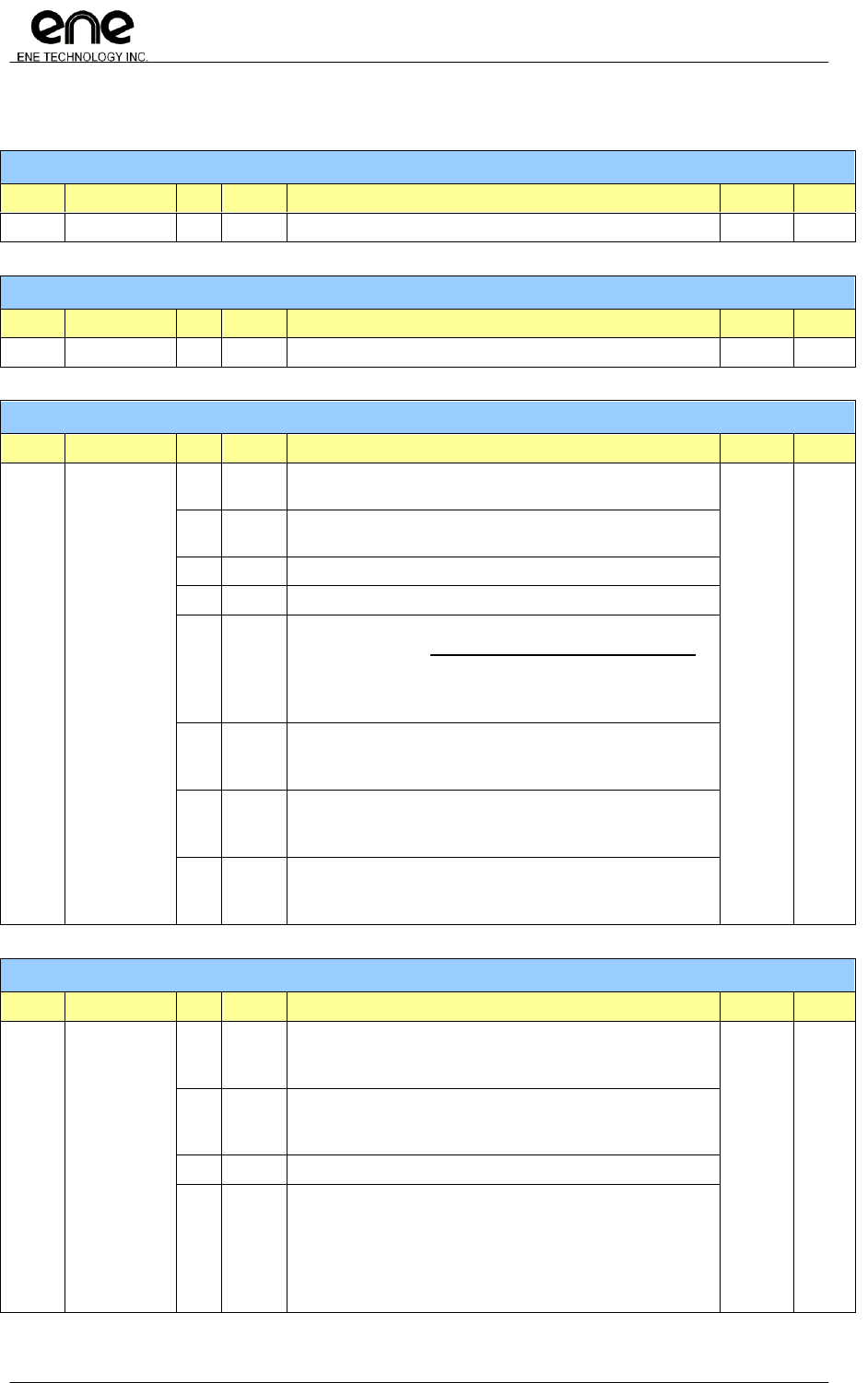
Copyright© 2011, ENE Technology Inc.
192
KB9012 Keyboard Controller Datasheet
CONFIDENTIAL
4.20.2 SMBus Controller 0 Register Description (0xFF90~0xFFBF)
SMBus Slave Address
Offset
Name
Bit
Type
Description
Default
Bank
0x90
SMB0RSA
7-0
RO
SMBus slave address (7-bits long), bit0 ignores.
0x00
0xFF
SMBus CRC Value
Offset
Name
Bit
Type
Description
Default
Bank
0x92
SMB0TCRC
7-0
RO
CRC value transmits to SMBus.
0x00
0xFF
SMBus Pin Control
Offset
Name
Bit
Type
Description
Default
Bank
0x93
SMB0PIN
7
R/W
SMBus data line forced to low.
Write ―0‖ to force SDA0 or SDA1 low.
0x00
0xFF
6
R/W
SMBus clock line forced to low.
Write ―0‖ to force SCL0 or SCL1 low.
5
RO
Status of SDA0 or SDA1 or SDA0 wired SDA1..
4
RO
Status of SCL0 or SCL1 or SCL0 wired SCL1.
3
R/W
Byte mode function enable
3 protocols support, Write Block/Read Block/Receive Byte.
Protocols are defined via register SMB0PRTCL[6:0]
0: Disable
1: Enable
2
R/W
SCL/SDA input debounce enable.
0: Disable
1: Enable
1
R/W
SCL1/SDA1 pin connected to SMBus controller.
0: Disable
1: Enable
0
R/W
SCL0/SDA0 pin connected to SMBus controller.
0: Disable
1: Enable
SMBus Configuration
Offset
Name
Bit
Type
Description
Default
Bank
0x94
SMB0CFG
7
R/W
SMBus master disable
0: Enable master function.
1: Disable master function
0x06
0xFF
6
R/W
SMBus host alarm protocol disable (0xFFBD~0xFFBF disable)
0: Enable slave function.
1: Disable slave function
5
RSV
Reserved
4-0
R/W
SMBus clock period
If SMB0CFG[4:0]>0 and SMB0PIN[2]=1, the period is
SMBus 0/1 clock period = (SMB0CFG[4:0]+1) * 4μs
If SMB0CFG[4:0]>0 and SMB0PIN[2]=0, the period is
SMBus 0/1 clock period = SMB0CFG[4:0] * 4μs
Please do not set these bits to ―0‖.
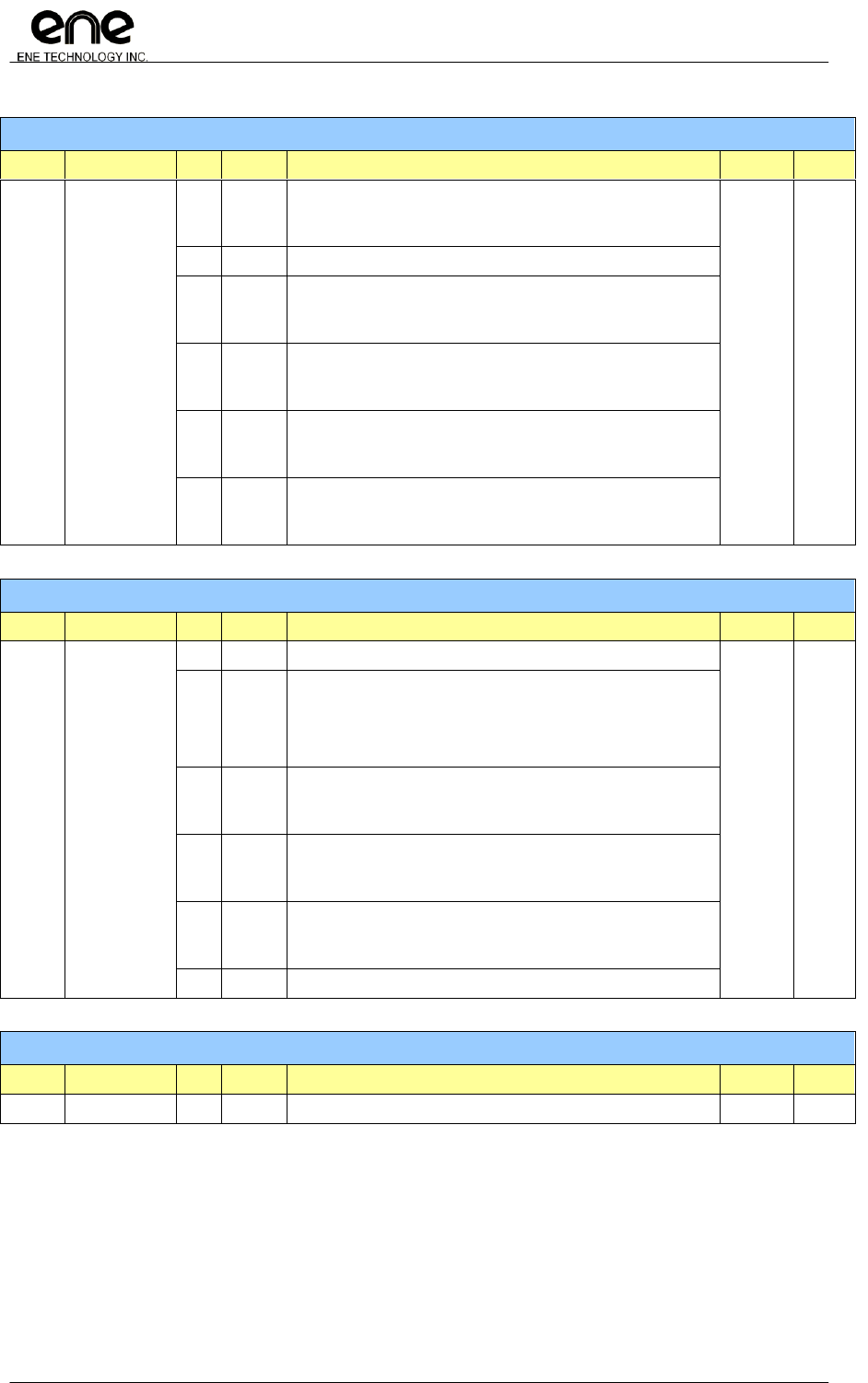
Copyright© 2011, ENE Technology Inc.
193
KB9012 Keyboard Controller Datasheet
CONFIDENTIAL
SMBus Interrupt Enable
Offset
Name
Bit
Type
Description
Default
Bank
0x95
SMB0EN
7
RO
SMBus host controller status
0: not busy
1: busy
0x00
0xFF
6-4
RSV
Reserved
3
R/W
SMBus slave protocol selection.
0: word read/write
1: byte read/write
2
R/W
SMBus slave mode enable.
0: Disable
1: Enable
1
R/W
SMBus alert (host notify protocol) interrupt
0: Disable
1: Enable
0
R/W
SMBus protocol completion interrupt
0: Disable
1: Enable
SMBus Interrupt Pending Flag
Offset
Name
Bit
Type
Description
Default
Bank
0x96
SMB0PF
7
RSV
Reserved
0x00
0xFF
6
R/W
ACK bit of Receive Byte (Byte Mode) protocol
0: ACK, the Receive Byte protocol keeps going
1: NACK, once the F/W ready to obtain the last Receive Byte,
F/W set this bit in advance. After this last byte transferred, the
controller issues NACK to device and the protocol stop.
5
R/W1C
Read data interrupt flag of Receive Byte (Byte Mode) protocol
0: no event
1: event occurs
4
RO
Read protocol interrupt flag of SMBus slave
0: no event
1: event occurs
3
R/W1C
Interrupt flag of SMBus slave
0: no event
1: event occurs
2-0
RSV
Reserved
SMBus Received CRC Value
Offset
Name
Bit
Type
Description
Default
Bank
0x97
SMB0RCRC
7-0
RO
The CRC value received from SMBus slave device.
0x00
0xFF

Copyright© 2011, ENE Technology Inc.
194
KB9012 Keyboard Controller Datasheet
CONFIDENTIAL
SMBus Protocol
Offset
Name
Bit
Type
Description
Default
Bank
0x98
SMB0PRTCL
7
R/W
SMBus transaction with PEC (Packet Error Check)
0: Disable
1: Enable.
0x00
0xFF
6-0
R/W
Command protocol.
02h: Quick Write
03h: Quick Read
04h: Send Byte
05h: Receive Byte / Receive Byte (Byte Mode)
06h: Write Byte
07h: Read Byte
08h: Write Word
09h: Read Word
0Ah: Write Block / Write Block (Byte Mode)
0Bh: Read Block / Read Block (Byte Mode)
0Ch: Word Process
0Dh: Block Process
others: Reserved
SMBus Status
Offset
Name
Bit
Type
Description
Default
Bank
0x99
SMB0STS
7
R/W
SMBus command done flag
0: no event (Write 0 to clear)
1: event occurs
0x00
0xFF
6
R/W
SMBus alarm (host notify protocol) interrupt flag
0: no event (Write 0 to clear)
1: event occurs
5
R/W
SMBus block data array protocol control. F/W could control the
protocol progress via this bit.
0: Block Data Array protocol keeps going.
1: Block Data Array protocol stops
4-0
R/W
Error code.
00h: no error
07h: unknown address failure.
10h: device address no ACK
12h: command no ACK
13h: device data no ACK
17h: device access deny
18h: SMBus timeout
19h: unsupported protocol
1Ah: SMBus busy
1Fh: PEC (Packet Error Check) error
others: Reserved
SMBus Address Port
Offset
Name
Bit
Type
Description
Default
Bank
0x9A
SMB0ADR
7-0
R/W
SMBus address (7-bits long), bit0 ignored.
0x00
0xFF
0x9A
SMB0ADR
(SMB0PIN[3]=1)
7-1
R/W
SMBus address (7-bits long).
0x00
0xFF
0
R/W
Data direction bit
0: Write
1: Read
Copyright© 2011, ENE Technology Inc.
195
KB9012 Keyboard Controller Datasheet
CONFIDENTIAL
SMBus Command Port
Offset
Name
Bit
Type
Description
Default
Bank
0x9B
SMB0CMD
7-0
R/W
SMBus command port
0x00
0xFF
SMBus Data Array (8 Bytes)
Offset
Name
Bit
Type
Description
Default
Bank
0x9C
SMB0DAT0
7-0
R/W
Data port for Send/Receive/Read Byte/Write Byte protocol
0x00
0xFF
0x9D
SMB0DAT1
7-0
R/W
Data port for Read Word/Write Word protocol, 2nd byte data
0x00
0xFF
0x9E
SMB0DAT2
7-0
R/W
Data port for Block protocol
0x00
0xFF
0x9F
SMB0DAT3
7-0
R/W
Data port for Block protocol
0x00
0xFF
0xA0
SMB0DAT4
7-0
R/W
Data port for Block protocol
0x00
0xFF
0xA1
SMB0DAT5
7-0
R/W
Data port for Block protocol
0x00
0xFF
0xA2
SMB0DAT6
7-0
R/W
Data port for Block protocol
0x00
0xFF
0xA3
SMB0DAT7
7-0
R/W
Data port for Block protocol
0x00
0xFF
SMBus Slave Address
Offset
Name
Bit
Type
Description
Default
Bank
0xA4~
0xBB
RSV
7-0
RSV
Reserved
0x00
0xFF
SMBus Block Count
Offset
Name
Bit
Type
Description
Default
Bank
0xBC
SMB0CNT
7-5
RSV
Reserved
0x00
0xFF
4~0
R/W
SMBus block count.
―0x00‖, for 32-byte length in a block transfer.
SMBus Alarm (Host Notify Protocol) Address / SMBus Slave Received Command Code
Offset
Name
Bit
Type
Description
Default
Bank
0xBD
SMB0AADR
7-0
R/W
This register is alarm address or SMBus Slave Command Code
for Response Slave Address.
0x00
0xFF
SMBus Alarm Data
Offset
Name
Bit
Type
Description
Default
Bank
0xBE
SMB0DAT0
7-0
R/W
Alarm data (low byte)
0x00
0xFF
0xBF
SMB0DAT1
7-0
R/W
Alarm data (high byte)
0x00
0xFF

Copyright© 2011, ENE Technology Inc.
196
KB9012 Keyboard Controller Datasheet
CONFIDENTIAL
4.20.3 SMBus Controller 1 Register Description (0xFFD0~0xFFFF)
SMBus Slave Address
Offset
Name
Bit
Type
Description
Default
Bank
0xD0
SMB1RSA
7-0
RO
SMBus slave address (7-bits long), bit0 ignores.
0x00
0xFF
SMBus CRC Value
Offset
Name
Bit
Type
Description
Default
Bank
0xD2
SMB1TCRC
7-0
RO
CRC value transmits to SMBus.
0x00
0xFF
SMBus Pin Control
Offset
Name
Bit
Type
Description
Default
Bank
0xD3
SMB1PIN
7
R/W
SMBus data line forced to low.
Write ―0‖ to force SDA2 or SDA3 low.
0x00
0xFF
6
R/W
SMBus clock line forced to low.
Write ―0‖ to force SCL2 or SCL3 low.
5
RO
Status of SDA2 or SDA3 or SDA2 wired SDA3..
4
RO
Status of SCL2 or SCL3 or SCL2 wired SCL3
3
R/W
Byte mode function enable
3 protocols support, Write Block/Read Block/Receive Byte.
Protocols are defined via register SMB1PRTCL[6:0]
0: Disable
1: Enable
2
R/W
SCL/SDA input debounce enable.
0: Disable
1: Enable
1
R/W
SCL3/SDA3 pin connected to SMBus controller.
0: Disable
1: Enable
0
R/W
SCL2/SDA2 pin connected to SMBus controller.
0: Disable
1: Enable
SMBus Configuration
Offset
Name
Bit
Type
Description
Default
Bank
0xD4
SMB1CFG
7
R/W
SMBus master disable
0: Enable master function.
1: Disable master function
0x06
0xFF
6
R/W
SMBus host alarm protocol disable (0xFFFD~0xFFFF disable)
0: Enable slave function.
1: Disable slave function
5
RSV
Reserved
4-0
R/W
SMBus clock period
If SMB1CFG[4:0]>0 and SMB1PIN[2]=1, the period is
SMBus clock period = (SMB1CFG[4:0]+1) * 4μs
If SMB1CFG[4:0]>0 and SMB1PIN[2]=0, the period is
SMBus clock period = SMB1CFG[4:0] * 4μs
Please do not set these bits to ―0‖.

Copyright© 2011, ENE Technology Inc.
197
KB9012 Keyboard Controller Datasheet
CONFIDENTIAL
SMBus Interrupt Enable
Offset
Name
Bit
Type
Description
Default
Bank
0xD5
SMB1EN
7
RO
SMBus host controller status
0: not busy
1: busy
0x00
0xFF
6-4
RSV
Reserved
3
R/W
SMBus slave protocol selection.
0: word read/write
1: byte read/write
2
R/W
SMBus slave mode enable.
0: Disable
1: Enable
1
R/W
SMBus alert (host notify protocol) interrupt
0: Disable
1: Enable
0
R/W
SMBus protocol completion interrupt
0: Disable
1: Enable
SMBus Interrupt Pending Flag
Offset
Name
Bit
Type
Description
Default
Bank
0xD6
SMB1PF
7
RSV
Reserved
0x00
0xFF
6
R/W
ACK bit of Receive Byte (Byte Mode) protocol
0: ACK, the Receive Byte protocol keeps going
1: NACK, once the F/W ready to obtain the last Receive Byte,
F/W set this bit in advance. After this last byte transferred, the
controller issues NACK to device and the protocol stop.
5
R/W1C
Read data interrupt flag of Receive Byte (Byte Mode) protocol
0: no event
1: event occurs
4
RO
Read protocol interrupt flag of SMBus slave
0: no event
1: event occurs
3
R/W1C
Interrupt flag of SMBus slave
0: no event
1: event occurs
2-0
RSV
Reserved
SMBus Received CRC Value
Offset
Name
Bit
Type
Description
Default
Bank
0xD7
SMB1RCRC
7-0
RO
The CRC value received from SMBus slave device.
0x00
0xFF

Copyright© 2011, ENE Technology Inc.
198
KB9012 Keyboard Controller Datasheet
CONFIDENTIAL
SMBus Protocol
Offset
Name
Bit
Type
Description
Default
Bank
0xD8
SMB1PRTCL
7
R/W
SMBus transaction with PEC (Packet Error Check)
0: Disable
1: Enable.
0x00
0xFF
6-0
R/W
Command protocol.
02h: Quick Write
03h: Quick Read
04h: Send Byte
05h: Receive Byte / Receive Byte (Byte Mode)
06h: Write Byte
07h: Read Byte
08h: Write Word
09h: Read Word
0Ah: Write Block / Write Block (Byte Mode)
0Bh: Read Block / Read Block (Byte Mode)
0Ch: Word Process
0Dh: Block Process
others: Reserved
SMBus Status
Offset
Name
Bit
Type
Description
Default
Bank
0xD9
SMB1STS
7
R/W
SMBus command done flag
0: no event (Write 0 to clear)
1: event occurs
0x00
0xFF
6
R/W
SMBus alarm (host notify protocol) interrupt flag
0: no event (Write 0 to clear)
1: event occurs
5
R/W
SMBus block data array protocol control. F/W could control the
protocol progress via this bit.
0: Block Data Array protocol keeps going.
1: Block Data Array protocol stops
4-0
R/W
Error code.
00h: no error
07h: unknown address failure.
10h: device address no ACK
12h: command no ACK
13h: device data no ACK
17h: device access deny
18h: SMBus timeout
19h: unsupported protocol
1Ah: SMBus busy
1Fh: PEC (Packet Error Check) error
others: Reserved
SMBus Address Port
Offset
Name
Bit
Type
Description
Default
Bank
0xDA
SMB1ADR
7-0
R/W
SMBus address (7-bits long), bit0 ignored.
0x00
0xFF
0xDA
SMB1ADR
(SMB1PIN[3]=1)
7-1
R/W
SMBus address (7-bits long).
0x00
0xFF
0
R/W
Data direction bit
0: Write
1: Read

Copyright© 2011, ENE Technology Inc.
199
KB9012 Keyboard Controller Datasheet
CONFIDENTIAL
SMBus Command Port
Offset
Name
Bit
Type
Description
Default
Bank
0xDB
SMB1CMD
7-0
R/W
SMBus command port
0x00
0xFF
SMBus Data Array (8 Bytes)
Offset
Name
Bit
Type
Description
Default
Bank
0xDC
SMB1DAT0
7-0
R/W
Data port for Send/Receive/Read Byte/Write Byte protocol
0x00
0xFF
0xDD
SMB1DAT1
7-0
R/W
Data port for Read Word/Write Word protocol, 2nd byte data
0x00
0xFF
0xDE
SMB1DAT2
7-0
R/W
Data port for Block protocol
0x00
0xFF
0xDF
SMB1DAT3
7-0
R/W
Data port for Block protocol
0x00
0xFF
0xE0
SMB1DAT4
7-0
R/W
Data port for Block protocol
0x00
0xFF
0xE1
SMB1DAT5
7-0
R/W
Data port for Block protocol
0x00
0xFF
0xE2
SMB1DAT6
7-0
R/W
Data port for Block protocol
0x00
0xFF
0xE3
SMB1DAT7
7-0
R/W
Data port for Block protocol
0x00
0xFF
SMBus Slave Address
Offset
Name
Bit
Type
Description
Default
Bank
0xE4~
0xFB
RSV
7-0
RSV
Reserved
0x00
0xFF
SMBus Block Count
Offset
Name
Bit
Type
Description
Default
Bank
0xFC
SMB1CNT
7-5
RSV
Reserved
0x00
0xFF
4~0
R/W
SMBus block count.
―0x00‖, for 32-byte length in a block transfer.
SMBus Alarm (Host Notify Protocol) Address / SMBus Slave Received Command Code
Offset
Name
Bit
Type
Description
Default
Bank
0xFD
SMB1AADR
7-0
R/W
This register is alarm address or SMBus Slave Command Code
for Response Slave Address.
0x00
0xFF
SMBus Alarm Data
Offset
Name
Bit
Type
Description
Default
Bank
0xFE
SMB1DAT0
7-0
R/W
Alarm data (low byte)
0x00
0xFF
0xFF
SMB1DAT1
7-0
R/W
Alarm data (high byte)
0x00
0xFF

Copyright© 2011, ENE Technology Inc.
200
KB9012 Keyboard Controller Datasheet
CONFIDENTIAL
SMBus Programming Sample
In this section gives some programming sample to control SMBus module. Please note,
ENE does not guarantee these codes in every field application. The following table describes
scenario of SMBus filed application.
Example
Reading status of a battery (address 0x0A)
Programming model
SMB0ADR (0xFF9A) = 0x0A ; battery address
SMB0CMD (0xFF9B) = 0x12
SMB0PTCL (0xFF98) = 0x07
Wait SMB0STS (0xFF99[7]) = 1b ; command complete
Check if SMB0STS[4:0] = 0000b ; no error
Read SMB0DAT (0xFF9C) ; the current status

Copyright© 2011, ENE Technology Inc.
201
KB9012 Keyboard Controller Datasheet
CONFIDENTIAL
4.21 8051 Microprocessor
4.21.1 8051 Microprocessor Function Description
The Microprocessor inside KBC is an industrial compatible i8051. The 8051 is featured
with 128bytes Special Function Register (SFR), Serial port, 2 16-bit Timers and 3 I/O ports with
interrupt capability. The 8051 operates based on external crystal and runs at 8MHz by default. The
following figure gives an illustration of the 8051 architecture. Except the standard 128bytes SFR,
8051 in KBx930 series is designed with overall 256 bytes internal memory

Copyright© 2011, ENE Technology Inc.
202
KB9012 Keyboard Controller Datasheet
CONFIDENTIAL
4.21.2 8051 Microprocessor Instruction
The instruction of 8051 microprocessor is fully compatible with industrial i8051. The
instruction sets are as following table. The OpCode is in Hexadecimal and (b) means Binary. B
stands for byte number of instruction. C stands for number of cycle needed.
Arithmetic
Mnemonic
OP code
Byte
Cycle
Description
ADD A, #data
24
2
2
Add immediate data to Accumulator
ADD A, direct
25
2
2
Add direct byte to Accumulator
ADD A, @ RN
26~27
1
2
Add indirect RAM to Accumulator (@R0~R1, OP 0x26~0x27)
ADD A, RN
28~2F
1
2
Add register to Accumulator (R0~R7, OP 0x28~0x2F)
ADDC A, #data
34
2
2
Add immediate data to Accumulator with Carry
ADDC A, direct
35
2
2
Add direct byte to Accumulator with Carry
ADDC A, @ RN
36~37
1
2
Add indirect RAM to Accumulator with Carry (@R0~R1, OP 0x26~0x27)
ADDC A, RN
38~3F
1
2
Add register to Accumulator with Carry (R0~R7, OP 0x38~0x3F)
SUBB A, #data
94
2
2
Subtract immediate data from ACC with Borrow
SUBB A, direct
95
2
2
Subtract direct byte from ACC with Borrow
SUBB A, @ RN
96~97
1
2
Subtract indirect RAM from ACC with Borrow (R0~R1, OP 0x96~0x97)
SUBB A, RN
98~9F
1
2
Subtract register from Accumulator with Borrow (R0~R7, OP 0x98~0x9F)
INC A
04
1
2
Increment Accumulator
INC direct
05
2
2
Increment direct byte
INC @ RN
06~07
1
2
Increment indirect RAM (R0~R1, OP 0x06~0x07)
INC RN
08~0F
1
2
Increment Register (R0~R7, OP 0x08~0x0F)
DEC A
14
1
2
Decrement Accumulator
DEC direct
15
2
2
Decrement direct byte
DEC @ RN
16~17
1
2
Decrement indirect RAM (R0~R1, OP 0x16~0x17)
DEC RN
18~1F
1
2
Decrement Register (R0~R7, OP 0x18~0x1F)
INC DPTR
A3
1
2
Increment Data Pointer
MUL AB
A4
1
2
Multiply A & B
DIV AB
84
1
2
Divide A by B
DA A
D4
1
2
Decimal Adjust Accumulator

Copyright© 2011, ENE Technology Inc.
203
KB9012 Keyboard Controller Datasheet
CONFIDENTIAL
Logic & Byte Operation
Mnemonic
OP code
Byte
Cycle
Description
ANL direct, A
52
2
2
AND Accumulator to direct byte
ANL direct, #data
53
3
2
AND immediate data to direct byte
ANL A, #data
54
2
2
AND immediate data to Accumulator
ANL A, direct
55
2
2
AND direct byte to Accumulator
ANL A, @ RN
56~57
1
2
AND indirect RAM to Accumulator (R0~R1, OP 0x56~0x57)
ANL A, RN
58~58
1
2
AND Register to Accumulator (R0~R7, OP 0x58~0x5F)
ORL direct, A
42
2
2
OR Accumulator to direct byte
ORL direct, #data
43
3
2
OR immediate data to direct byte
ORL A, #data
44
2
2
OR immediate data to Accumulator
ORL A, direct
45
2
2
OR direct byte to Accumulator
ORL A, @ RN
46~47
1
2
OR indirect RAM to Accumulator (R0~R1, OP 0x46~0x47)
ORL A, RN
48~4F
1
2
OR Register to Accumulator (R0~R7, OP 0x48~0x4F)
XRL direct, A
62
2
2
XOR Accumulator to direct byte
XRL direct, #data
63
3
2
XOR immediate data to direct byte
XRL A, #data
64
2
2
XOR immediate data to Accumulator
XRL A, direct
65
2
2
XOR direct byte to Accumulator
XRL A, @ RN
66~67
1
2
XOR indirect RAM to Accumulator (R0~R1, OP 0x66~0x67)
XRL A, RN
68~6F
1
2
XOR Register to Accumulator (R0~R7, OP 0x68~0x6F)
CLR A
E4
1
2
Clear Accumulator
CPL A
F4
1
2
Complement Accumulator
RL A
2 3
1
2
Left rotate Accumulator
RLC A
3 3
1
2
Left rotate Accumulator through Carry
RR A
0 3
1
2
Right rotate Accumulator
RRC A
1 3
1
2
Right rotate Accumulator through Carry
SWAP A
C 4
1
2
Swap Accumulator Nibbles

Copyright© 2011, ENE Technology Inc.
204
KB9012 Keyboard Controller Datasheet
CONFIDENTIAL
Data Movement
Mnemonic
OP code
Byte
Cycle
Description
MOV A, RN
E8~EF
1
2
Move Register to Accumulator (R0~R7, OP 0xE8~0xEF)
MOV A, direct
E5
2
2
Move direct byte to Accumulator
MOV A, @ RN
E6~E7
1
2
Move indirect RAM to Accumulator (R0~R1, OP 0xE6~0xE7)
MOV A, #data
74
2
2
Move immediate data to Accumulator
MOV RN, A
F8~FF
1
2
Move Accumulator to Register (R0~R7, OP 0xF8~0xFF)
MOV RN, direct
A8~AF
2
2
Move direct byte to Register (R0~R7, OP 0xA8~0xAF)
MOV RN, #data
78~7F
2
2
Move immediate data to Register (R0~R7, OP 0x78~0x7F)
MOV direct, A
F5
2
2
Move Accumulator to direct byte
MOV direct, @ RN
86~87
2
2
Move indirect RAM to direct byte (R0~R1, OP 0x86~0x87)
MOV direct, RN
88~8F
2
2
Move Register to direct byte (R0~R7, OP 0x88~0x8F)
MOV direct, #data
75
3
2
Move immediate data to direct byte
MOV direct, direct
85
3
2
Move direct byte to direct byte
MOV @ RN, direct
A6~A7
2
2
Move direct byte to indirect RAM (R0~R1, OP 0xA6~0xA7)
MOV @ RN, A
F6~F7
1
2
Move Accumulator to indirect RAM (R0~R1, OP 0xF6~0xF7)
MOV @ RN, #data
76~77
2
2
Move immediate to indirect RAM (R0~R1, OP 0x76~0x77)
MOV DPTR,#data16
90
3
2
Load Data Pointer with a 16bit constant
MOVC A,@ A+PC
83
1
>33
Move Code byte relative to PC to Accumulator
MOVC A,@ A+DPTR
93
1
>33
Move Code byte relative to DPTR to Accumulator
MOVX A, @ DPTR
E0
1
>=5
Move External RAM to Accumulator
MOVX A, @ RN
E2~E3
1
>=5
Move External RAM to Accumulator (R0~R1, OP 0xE2~0xE3)
MOVX @ DPTR, A
F0
1
>=4
Move Accumulator to External RAM
MOVX @ RN, A
F2~F3
1
>=4
Move Accumulator to External RAM (R0~R1, OP 0xF2~0xF3)
POP direct
D0
2
2
POP direct byte from Stack
PUSH direct
C0
2
2
Push direct byte to Stack
XCH A, direct
C 5
2
2
Exchange direct byte with Accumulator
XCH A, @ RN
C6~C7
1
2
Exchange indirect RAM with Accumulator (R0~R1, OP 0xC6~0xC7)
XCH A, RN
C8~CF
1
2
Exchange Register with Accumulator (R0~R7, OP 0xC8~0xCF)
XCHD A, @ RN
D6~D7
1
2
Exchange low order nibble of indirect RAM with Accumulator
(R0~R1, OP 0xD6~0xD7)
Copyright© 2011, ENE Technology Inc.
205
KB9012 Keyboard Controller Datasheet
CONFIDENTIAL
Bit Operation
Mnemonic
OP code
Byte
Cycle
Description
SETB bit
D2
2
2
Set direct bit
SETB C
D3
1
2
Set Carry
CLR bit
C2
2
2
Clear direct bit
CLR C
C3
1
2
Clear Carry
CPL bit
B2
2
2
Complement direct bit
CPL C
B3
1
2
Complement Carry
ANL C, bit
82
2
2
AND direct bit to Carry
ANL C, /bit
B0
2
2
AND complement of direct bit to Carry
ORL C, bit
72
2
2
OR direct bit to Carry
ORL C, /bit
A0
2
2
OR complement of direct bit to Carry
MOV C, bit
92
2
2
Move direct bit to Carry
MOV bit, C
A2
2
2
Move Carry to direct bit
JC relative
4 0
2
2
Jump if Carry is set
JNC relative
5 0
2
2
Jump if Carry is NOT set
JB bit, relative
2 0
3
2
Jump if direct bit is set
JBC bit, relative
1 0
3
2
Jump if direct bit is set & clear bit
JNB bit, relative
3 0
3
2
Jump if direct bit is NOT set
Program Branching
Mnemonic
OP code
Byte
Cycle
Description
ACALL address11
bbb1 0001
2
3
Absolute sub-routine call
AJMP address11
bbb0 0001
2
2
Absolute jump
LCALL address16
12
3
3
Long sub-routine call
LJMP address16
02
3
2
Long jump
SJMP relative
80
2
2
Short jump (relative address)
JMP @ A+DPTR
73
1
2
Jump indirect relative to the DPTR
JNZ relative
70
2
2
Jump if Accumulator is NOT zero
JZ relative
60
2
2
Jump if Accumulator is zero
CJNE A, #data, relative
B4
3
2
Compare immediate to Accumulator and Jump if NOT equal
CJNE A, direct, relative
B5
3
2
Compare direct byte to Accumulator and Jump if NOT equal
CJNE @ RN, #data, relative
B6~B7
3
2
Compare immediate to indirect and Jump if NOT equal
(R0~R1, OP 0xB6~0xB7)
CJNE RN, #data, relative
B8~BF
3
2
Compare immediate to Register and Jump if NOT equal
(R0~R7, OP 0xB8~0xBF)
DJNZ direct, relative
D5
3
2
Decrement direct byte and Jump if NOT zero
DJNZ RN, relative
D8~DF
2
2
Decrement register and Jump if NOT zero (R0~R7, OP 0xD8~0xDF)
RET
22
1
3
Return from sub-routine
RETI
32
1
3
Return form interrupt

Copyright© 2011, ENE Technology Inc.
206
KB9012 Keyboard Controller Datasheet
CONFIDENTIAL
Special Instruction
Mnemonic
OP code
Byte
Cycle
Description
NOP
00
1
2
No Operation

Copyright© 2011, ENE Technology Inc.
207
KB9012 Keyboard Controller Datasheet
CONFIDENTIAL
4.21.3 8051 Interrupt Controller
In order to support more application, the 8051 in KBC extends interrupt channel to 24 for
internal peripherals, that is, I/O port P0, P1 and P3 are with interrupt capability. The interrupt priority
for each channel is fixed and no nested interrupt is supported. Here is the table to summarize the
implementation of the interrupt controller.
Int. Source
Vector Address
Applications
Priority
IE0
0x0003
8051 external interrupt 0
0(Highest)
TF0
0x000B
8051 Timer 0
1
IE1
0x0013
8051 external interrupt 1
2
TF1
0x001B
8051 Timer 1
3
RI & TI
0x0023
8051 Serial port TX/RX interrupt
4
P0I[0]
0x0043
Watchdog / General Waveform Generator
5
P0I[1]
0x004B
LPC I/O 0x2F R/W accessing interrupt / OWM
6
P0I[2]
0x0053
PS/2 event
7
P0I[3]
0x005B
KBC
8
P0I[4]
0x0063
IKB
9
P0I[5]
0x006B
68h/6Ch ports
10
P0I[6]
0x0073
EC
11
P0I[7]
0x007B
ESB events
12
P1I[0]
0x0083
FAN0 monitor event (update/overflow)
13
P1I[1]
0x008B
FAN1 monitor event (update/overflow)
14
P1I[2]
0x0093
SMBus events
15
P1I[3]
0x009B
CIR events
16
P1I[4]
0x00A3
GPT0 event
17
P1I[5]
0x00AB
GPT1 event
18
P1I[6]
0x00B3
GPT2 event
19
P1I[7]
0x00BB
GPT3 event / SDI
20
P3I[0]
0x00C3
Write extended I/O (LPC I/O port 80) / PECI
21
P3I[1]
0x00CB
GPIO00~GPIO0F
22
P3I[2]
0x00D3
GPIO10~GPIO1F
23
P3I[3]
0x00DB
GPIO20~GPIO2F
24
P3I[4]
0x00E3
GPIO30~GPIO3F
25
P3I[5]
0x00EB
GPIO40~GPIO4F / GPXIOA00~GPXIOA11
26
P3I[6]
0x00F3
GPIO50~GPIO59 / GPXIOD00~GPXIOD07
27
P3I[7]
0x00FB
ADC update
28(Lowest)

Copyright© 2011, ENE Technology Inc.
208
KB9012 Keyboard Controller Datasheet
CONFIDENTIAL
4.21.4 Interrupt Enable/Flag Table
Application
Interrupt Enable
Pending Flag
address
bit
behavior
address
bit
type
8051 external interrupt0
(GPIO1A)
A8h
(IE)
0
2
88h
(TCON)
1
2
8051 Timer0
A8h
(IE)
1
2
88h
(TCON)
5
2
8051 external interrupt0
(GPIO1B)
A8h
(IE)
2
2
88h
(TCON)
3
2
8051 Timer1
A8h
(IE)
3
2
88h
(TCON)
7
2
8051 Serial Port
A8h
(IE)
4
2
98h
(SCON)
1~0
1
WDT
FE80h
(WDTCFG)
1
1
FE81h
(WDTPF)
1
1
FE81h
(WDTPF)
0
1
RTC
FE84h
(TMR_CFG)
7,0
1
FE84h
(TMR_CFG)
1
1
LPC I/O R/W 0x2F
FF20h
(ECMISC)
2
1
-
-
-
FF9Ah
(LPC2ECFG)
1
1
FE9Ah
(LPC2ECFG)
2
1
PS/2
FEE0h
(PS2CFG)
3~0
2
FEE1h
(PS2PF)
3~0
2
KBC
FC81h
(KBCCFG)
1,0
1
FC82h
(KBCIF)
1,0
2
IKB
FCA3h
(IKBIE)
5~0
1
FCA4h
(IKBPF)
5~0
2
LPC 68h/6Ch
IBF_Rising
OBF_Falling
FE9Dh
(LPC68CFG)
1,0
1
FE9Eh
(LPC68CSR)
1,0
1
FE9Eh
(LPC68CSR)
3,2
2
EC host interrupt
FF04h
(ECCFG,IBF)
1
4
FF1Ah
(ECIF,IBF)
1
1
FF04h
(ECCFG,OBF)
0
2
FF1Ah
(ECIF,OBF)
0
2
behavior
1. IE bit = 1, interrupt asserts when trigger event occurs
2. IE bit = 1, interrupt asserts when trigger event occurs
but if PF not clear, interrupt will continue asserting
3. IE = 1, interrupt asserts when trigger event occurs
or IE bit is from low to high(0 -> 1) when Pending Flag(PF) is = 1
4. No matter IE bit = 1 or 0, interrupt asserts when trigger event occurs
type
1. When trigger event occurs, PF will be set to 1.
PF cleared to 0 by W1C/W0C
2. IE bit = 1, when event occurs, PF will be set to 1.
PF is cleared to 0 by W1C/W0C

Copyright© 2011, ENE Technology Inc.
209
KB9012 Keyboard Controller Datasheet
CONFIDENTIAL
4.21.4 Interrupt Enable/Flag Table (Continued)
Application
Interrupt Enable
Pending Flag
address
bit
behavior
address
bit
type
ESB
FC90h
(ESBCFG)
2
3
-
-
-
FC92h
(ESBINTE)
6~4
3
FC91h
(ESBCS)
6~4
1
FC92h
(ESBINTE)
3~0
3
FC97h
(ESBINT)
7~0
1
FC98h
(ESBCAS)
7~4
3
FC97h
(ESBINT)
1
FAN
FE20h
(FANCFG0)
3,2
3
FE21h
(FANSTS0)
1,0
1
FE30h
(FANCFG1)
3,2
3
FE31h
(FANSTS1)
1,0
1
SMBus
FF95h
(SMBEB)
0
1
FF99h
(SMBSTS)
7,5
1
FF96h
(SMBPF)
5
1
FF95h
(SMBEB)
1
1
FF99h
(SMBSTS,alarm)
6
1
FF95h
(SMBEB)
2
1
FF96h
(SMBPF,Slave)
3
1
CIR TX
FEC0h
(CIRCFG, TX)
5
1
FEC2h
(CIRPF, TX)
3
1
CIR RX
FEC0h
(CIRCFG, RX)
1
1
FEC2h
(CIRPF)
2~0
1
GPT0~GPT3
FE50h
(GPTCFG)
3~0
1
FE51h
(GPTPF)
3~0
2
Write Extended I/O
FE95h
(LPCCFG)
4
1
-
-
-
GPWU
FF3xh
(GPWUENxx)
7~0
3
FF4xh
(GPWUPFxx)
7~0
1
ADC
FF18h
(ADCTRL)
0
1
-
-
-
behavior
Interrupt Behavior => (Interrupt Occurs)
(1) IE bit = 1, interrupt asserts when trigger event occurs
(2) IE bit = 1, interrupt asserts when trigger event occurs
but if PF not clear, interrupt will continue asserting
(3) IE = 1, interrupt asserts when trigger event occurs
or IE bit is from low to high(0 -> 1) when Pending Flag(PF) is = 1
(4) No matter IE bit = 1 or 0, interrupt asserts when trigger event occurs
type
Pending Flag(PF) =>
6. When trigger event occurs, PF will be set to 1.
PF cleared to 0 by WC1/WC0
(2) IE bit = 1, when event occurs, PF will be set to 1.
PF is cleared to 0 by WC1/WC0

Copyright© 2011, ENE Technology Inc.
210
KB9012 Keyboard Controller Datasheet
CONFIDENTIAL
4.21.5 8051 Special Function Register (SFR)
The Special Function Registers are located in the internal RAM of 8051 microprocessor. The
internal address is from 0x80 to 0xFF, sized with 128 bytes. All the SFRs are compatible with the
standard ones. Some SFRs are redesigned with new features for flexible application. The following
table gives a brief summary.
P3IE, P1IE, P0IE are read/write registers used as Interrupt Enable (IE) to their corresponding
interrupt inputs. These three registers are original 8051 port registers with 8-bits. For the embedded
8051 inside KB910, the 3 ports are used for interrupt input (always rise pulses) extensions. The
overall interrupt events are 24.
P3IF, P1IF, P0IF are Interrupt Flag(IF) corresponding to the 24 interrupt inputs. The IFs are set
by external interrupt event (always a rising pulse, one clock width), and are cleared by software
(execute IRET instruction for active interrupt). The original alternate 8051 port 3 functions are not
related with P3IE and P3IF.
For more detail, please refer to the section of register description.
80
P0IE
SP
DPL
DPH
PCON2
PCON
87
88
TCON
TMOD
TL0
TL1
TH0
TH1
8F
90
P1IE
97
98
SCON
SBUF
SCON2
SCON3
SCON4
9F
A0
P2
A7
A8
IE
AF
B0
P3IE
B7
B8
IP
BF
C0
C7
C8
CF
D0
PSW
D7
D8
P0IF
DF
E0
ACC
E7
E8
P1IF
EF
F0
B
F7
F8
P3IF
FF
★
1. The blue parts are changed from standard features and the green ones are the new design for special features. And
all the others are the standard features of conventional 8051.
2. The registers listed in the column with ★mark are all bit addressable.
Copyright© 2011, ENE Technology Inc.
211
KB9012 Keyboard Controller Datasheet
CONFIDENTIAL
4.21.6 8051 Microprocessor Register Description
The SFR registers are located at internal RAM 0x80 ~ 0xFF.
P0 Interrupt Enable Register
Address
Name
Bit
Type
Description
Default
0x80
P0IE
7-0
R/W
P0 interrupt enable. Bit0~7 for P0[0]~P0[7] respectively.
0: Disable
1: Enable
0x00
Stack Pointer
Address
Name
Bit
Type
Description
Default
0x81
SP
7-0
R/W
8051 stack pointer register
0x07
Data Pointer Low Byte
Address
Name
Bit
Type
Description
Default
0x82
DPL
7-0
R/W
Low byte of DPTR
0x00
Data Pointer High Byte
Address
Name
Bit
Type
Description
Default
0x83
DPH
7-0
R/W
High byte of DPTR
0x00
Interrupt Vector High Address
Address
Name
Bit
Type
Description
Default
0x85
IVHA
7-3
R/W
Interrupt Vector High Address Setting:
Interrupt Vector = { IVHA, 3‘b0 } + Original_Vector_Address
0x00
2-0
RSV
Reserved
Processor Control Register 2
Address
Name
Bit
Type
Description
Default
0x86
PCON2
7
R/W
Reserved but this bit should be ―0‖.
0x20
6
R/W
Timer0/Timer1 test mode enable.
0: Disable
1: Enable
5
R/W
Reserved
4
R/W
KBC modules write control.
Once this bit set, 8051 could issue write access to external
modules.
0: Disable
1: Enable
3
R/WC0
Same interrupt source pending flag.
If the 8051 is handling some interrupt event, at the same time,
the same source asserting the interrupt again, this flag will be
set. If this flag set, the 8051 will re-enter ISR again once
executing IRET. Writing ―0‖ to clear this flag.
2
RSV
Reserved
1
R/W
E51 Timer select 1us
0
RSV
Reserved
Copyright© 2011, ENE Technology Inc.
212
KB9012 Keyboard Controller Datasheet
CONFIDENTIAL
Processor Control Register
Address
Name
Bit
Type
Description
Default
0x87
PCON
7
RSV
Reserved
0x00
6
R/W
Enable ―detection of 8051 whether in idle loop‖
5
R/W
Interrupt vector offset address1
0: Interrupt vector address offset adding 0x0
1: Interrupt vector address offset adding 0x8000
4
R/W
Interrupt vector offset address2
0: Interrupt vector address offset adding 0x0
1: Interrupt vector address offset adding 0x4000
Please note, if PCON[5]=1 and PCON[4]=1 then the result of
interrupt vector address will be added 0xC000.
3
R/W
General purpose flag 1
0: no event
1: event occurs
2
R/W
General purpose flag 2
0: no event
1: event occurs
1
WO
Stop mode enable.
All clock stop except the external 32.768K OSC and PCICLK.
1: Enable (write ―0‖ no work)
0
WO
Idle mode enable.
The clock of 8051 stops.
1: Enable (write ―0‖ no work)
Timer/Counter Control Register
Address
Name
Bit
Type
Description
Default
0x88
TCON
7
R/W0C
TF1, Timer1 overflow flag
0: no event
1: event occurs
0x00
6
R/W
TR1, Timer1 start control.
0: stop to count
1: start to count
5
R/W0C
TF0, Timer0 overflow flag
0: no event
1: event occurs
4
R/W
TR0, Timer0 start control.
0: stop to count
1: start to count
3
R/W0C
IE1, External interrupt 1 flag
0: no event
1: event occurs
2
R/W
IT1, External interrupt 1 trigger selection
0: low level trigger
1: falling edge trigger
1
R/W0C
IE0, External interrupt 0 flag
0: no event
1: event occurs
0
R/W
IT0, External interrupt 0 trigger selection
0: low level trigger
1: falling edge trigger
Copyright© 2011, ENE Technology Inc.
213
KB9012 Keyboard Controller Datasheet
CONFIDENTIAL
Timer Mode Register
Address
Name
Bit
Type
Description
Default
0x89
TMOD
7
R/W
GATE1, this bit is the gate control of TR1 and INT1
0: Disable
1: Enable
0x00
6
R/W
CT1, Timer1 timer/counter selection
0: Timer
1: Counter
5-4
R/W
TM1, Timer1 mode selection
0: 13-bit timer
1: 16-bit timer
2: 8-bit auto reload timer
3: Timer 1 stops.
3
R/W
GATE0, this bit is the gate control of TR0 and INT0
0: Disable
1: Enable
2
R/W
CT0, Timer0 timer/counter selection
0: Timer
1: Counter
1-0
R/W
TM0, Timer0 mode selection
0: 13-bit timer
1: 16-bit timer
2: 8-bit auto reload timer
3: TL0 and TH0 are two 8-bit timers.
Timer 0 Low Byte
Address
Name
Bit
Type
Description
Default
0x8A
TL0
7-0
R/W
Low byte of timer 0
0x00
Timer 1 Low Byte
Address
Name
Bit
Type
Description
Default
0x8B
TL1
7-0
R/W
Low byte of timer 1.
0x00
Timer 0 High Byte
Address
Name
Bit
Type
Description
Default
0x8C
TH0
7-0
R/W
High byte of timer 0
0x00
Timer 1 High Byte
Address
Name
Bit
Type
Description
Default
0x8D
TH1
7-0
R/W
High byte of timer 1
0x00

Copyright© 2011, ENE Technology Inc.
214
KB9012 Keyboard Controller Datasheet
CONFIDENTIAL
Port1 Interrupt Enable Register
Address
Name
Bit
Type
Description
Default
0x90
P1IE
7-0
R/W
Port 1 interrupt enable. Bit0~7 for P1[0]~P1[7] respectively
0: Disable
1: Enable
0x00
Serial Port Control Register
Address
Name
Bit
Type
Description
Default
0x98
SCON
7-6
R/W
SM1,SM0, serial port mode
00: 8-bit shift register, E51RX will be shift clock of E51CLK.
01: 8-bit serial port (variable)
10: 9-bit serial port (variable)
11: 9-bit serial port (variable)
0x50
5
RSV
Reserved
4
R/W
REN, serial port receive function enable.
0: Disable
1: Enable
3
R/W
TB8, The 9th bit of transmit data in mode2 and mode3.
2
R/W
RB8, The 9th bit of receive data
1
R/W0C
TI, TX interrupt flag
0: no event
1: event occurs
0
R/W0C
RI, RX interrupt flag
0: no event
1: event occurs
Serial Port Data Buffer Register
Address
Name
Bit
Type
Description
Default
0x99
SBUF
7-0
R/W
Serial port data buffer
0x00
Serial Port Control Register 2
Address
Name
Bit
Type
Description
Default
0x9A
SCON2
7-0
R/W
High byte of 16-bit counter for baud rate
0x00
Serial Port Control Register 3
Address
Name
Bit
Type
Description
Default
0x9B
SCON3
7-0
R/W
Low byte of 16-bit counter for baud rate
0x00
Copyright© 2011, ENE Technology Inc.
215
KB9012 Keyboard Controller Datasheet
CONFIDENTIAL
Serial Port Control Register 4
Address
Name
Bit
Type
Description
Default
0x9C
SCON4
7-2
RSV
Reserved
0x00
1~0
R/W
Serial Port mode 0 baud- rate setting
(E51 clock set in CLKCFG, 0xFF0D )
00: E51 clock divide 2
01: E51 clock divide 4
10: E51 clock divide 8
11: E51 clock divide 16
Port 2 Register
Address
Name
Bit
Type
Description
Default
0xA0
P2
7-0
R/W
Port 2 register
0x00
Interrupt Enable Register
Address
Name
Bit
Type
Description
Default
0xA8
IE
7
R/W
EA, all interrupts enable.
0: Disable
1: Enable
0x00
6
R/W
EP, Change P0IF, P1IF, P3IF Interrupt event trigger flag to
Interrupt event pending flag
0: Disable
1: Enable
5
RSV
Reserved
4
R/W
ES, serial port interrupt enable
0: Disable
1: Enable
3
R/W
ET1, timer1 overflow interrupt enable
0: Disable
1: Enable
2
R/W
EX1, external interrupt 1 enable.
0: Disable
1: Enable
1
R/W
ET0, timer0 overflow interrupt enable
0: Disable
1: Enable
0
R/W
EX0, external interrupt 0 enable.
0: Disable
1: Enable
Interrupt Enable Register
Address
Name
Bit
Type
Description
Default
0xB0
P3IE
7-0
R/W
Port 3 interrupt enable. Bit0~7 for P3[0]~P3[7] respectively
0: Disable
1: Enable
0x00
Copyright© 2011, ENE Technology Inc.
216
KB9012 Keyboard Controller Datasheet
CONFIDENTIAL
Interrupt Priority Register
Address
Name
Bit
Type
Description
Default
0xB8
IP
7-5
RSV
Reserved
0x00
4
R/W
Serial port interrupt priority
0: Low
1: High
3
R/W
Timer1 interrupt priority
0: Low
1: High
2
R/W
External interrupt 1 priority
0: Low
1: High
1
R/W
Timer 0 interrupt priority
0: Low
1: High
0
R/W
External interrupt 0 priority
0: Low
1: High
Processor Status Word Register
Address
Name
Bit
Type
Description
Default
0xD0
PSW
7
R/W
CY, carry flag
0x00
6
R/W
AC, auxiliary carry flag.
5
R/W
F0, for user general purpose.
4
R/W
RS1, register bank selector 1.
3
R/W
RS0, register bank selector 0.
2
R/W
OV, overflow flag
1
R/W
F1, flag 1 for user general purpose
0
R/W
P, parity flag
Port0 Interrupt Flag Register
Address
Name
Bit
Type
Description
Default
0xD8
P0IF
7-0
R/W
Port 0 interrupt flag.
0x00
Accumulator, ACC
Address
Name
Bit
Type
Description
Default
0xE0
ACC
7-0
R/W
Accumulator
0x00
Port1 Interrupt Flag Register
Address
Name
Bit
Type
Description
Default
0xE8
P1IF
7-0
R/W
Port 1 interrupt flag.
0x00

Copyright© 2011, ENE Technology Inc.
217
KB9012 Keyboard Controller Datasheet
CONFIDENTIAL
B Register
Address
Name
Bit
Type
Description
Default
0xF0
B
7-0
R/W
B register, for MUL and DIV instructions.
0x00
Port3 Interrupt Flag Register
Address
Name
Bit
Type
Description
Default
0xF8
P3IF
7-0
R/W
Port 3 interrupt flag.
0x00
Copyright© 2011, ENE Technology Inc.
218
KB9012 Keyboard Controller Datasheet
CONFIDENTIAL
Application Appendix :
A.1 ENE debug Interface, EDI
EDI_CS
EDI_CLK
EDI_DIN
EDI_DO
74
The above picture shows: EDI provide a SPI I/F as a debug interface.
The interface pin number in KB9012 is as following :
KB9012
Pin No.
KB9012
BGA
Name
GPIO
Alt
Output
Alt.
Input
Default
ECRST#
L/H
IO CELL
59
KSI4
GPIO34
KSI4/EDI_CS
GPIO34
IE(PU)/IE(PU)
BQC04HIV
60
KSI5
GPIO35
KSI5/EDI_CLK
GPIO35
IE(PU)/IE(PU)
BQC04HIV
61
KSI6
GPIO36
KSI6/EDI_DIN
GPIO36
IE(PU)/IE(PU)
BQC04HIV
62
KSI7
GPIO37
EDI_DO
KSI7
GPIO37
IE(PU)/IE(PU)
BQC04HIV
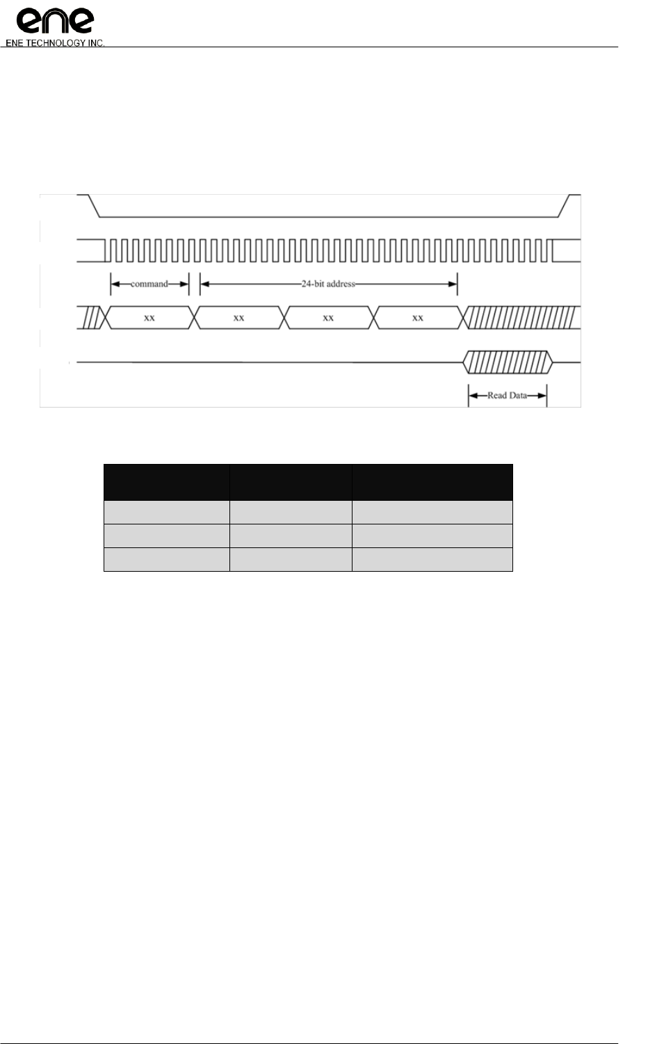
Copyright© 2011, ENE Technology Inc.
219
KB9012 Keyboard Controller Datasheet
CONFIDENTIAL
A.1.1 Enable EDI
To enable EDI, it is by detecting any SPI command with EDI_CLK frequency between 1MHz to
8MHz. After enabling EDI, the transaction frequency could be up to 16MHz.
EDI_CS
EDI_CLK
EDI_DIN
EDI_DO
A.1.2 EDI Instructions
Command Name
Command Code
Address Byte Count
Read
30h
3
Write
40h
3
Disable EDI
F3h
0
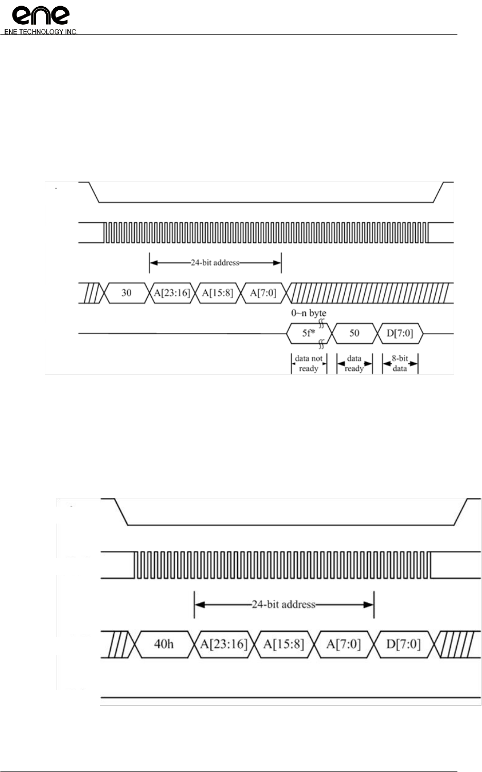
Copyright© 2011, ENE Technology Inc.
220
KB9012 Keyboard Controller Datasheet
CONFIDENTIAL
A.1.3 Read Command
Read command is by issuing command code 30h, which is followed by 3-bytes of the target
address. While fetching data, 5Fh is shown on EDI_DO to indicate BUSY. This could be lasting for n
bytes length. After fetching data, 50h is shown on EDI_DO to indicate the data is ready to be read,
and the next 1 byte is the valid read data.
EDI_CS
EDI_CLK
EDI_DIN
EDI_DO
A.1.4 Write Command
Write command is by issuing command code 40h, which is followed by 3-bytes of the target
address. The 64k address boundary should be kept. Write command on EDI v2.0 (KB9010) only
support EHB memory space (0h~FFFFh), in other words A[23:16] should be 0h). For details
memory space mapping, please refer Part B.
EDI_CS
EDI_CLK
EDI_DIN
EDI_DO
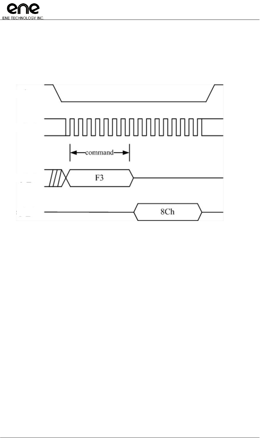
Copyright© 2011, ENE Technology Inc.
221
KB9012 Keyboard Controller Datasheet
CONFIDENTIAL
A.1.5 Disable EDI Command
Disable EDI command is by issuing command code F3h. On EDI_DO pin, 8Ch would be
shown to indicate the EDI is disabled.
EDI_CS
EDI_CLK
EDI_DIN
EDI_DO
Copyright© 2011, ENE Technology Inc.
222
KB9012 Keyboard Controller Datasheet
CONFIDENTIAL
A.2 Power-Latch
In KB9012, a separated power plane VCC_0 is implemented for basic power detection and
management. VCC_0 power plane is with GPXIOD01 / GPXIOD02 / GPXIOD03 pins. They serve as
power latch logic as following:
Pin Name
Pin No.
Direction
Description
GPXIOD01
110
I/O
AC_IN
GPXIOD02
112
I/O
ALW_PWR_EN
GPXIOD03
114
I/O
ON/OFFBTN#
VCC_0
111
Power supply for 51ON power-latch.
GND_0
113
Power ground for 51ON power-latch.
AC_IN
Input State
ON/OFFBTN#
Input State
ALW_PWR_EN
Output State
High voltage Level
X
High voltage Level
X
Low voltage Level
High voltage Level
Low voltage Level
High voltage Level
Low voltage Level
Note: The Power-Latch / Voltage Comparator Register is designed with power-supply of VCC_0.
It could be used to keep Voltage Comparator within VCC_0 power plane which provide firmware
management flexibility. Please refer the later section for other voltage comparator information.
Copyright© 2011, ENE Technology Inc.
223
KB9012 Keyboard Controller Datasheet
CONFIDENTIAL
A.3 Voltage Comparator
In KB9012, a voltage comparator is implemented for comparison of external input and
programmed voltage. The comparison valued is based on DAC behavior. In KB9012A2 later version,
The VC is default enabled; special function hardware trap is also designed to disable VC1.
Pin Name
Pin No.
Direction
Description
VCIN0
109
I
Pin-out is also GPXIOD00
VCOUT0
104
O
Pin-out is also GPXIOA07
VCIN1
102
I
Pin-out is also GPXIOA05
VCOUT1
103
O
Pin-out is also GPXIOA06
Voltage Comparator Control and Status Register
Offset
Name
Bit
Type
Description
Default
Bank
0x29
VCSR
7
RO
Voltage Comparator 1 output status
0x0C
0xFF
6
RO
Voltage Comparator 0 output status
5-4
RSV
Reserved
3
R/W
VC1 output open-drain enable
2
R/W
VC0 output open-drain enable
1~0
RSV
Reserved
Crystal 32k control register
Offset
Name
Bit
Type
Description
Default
Bank
0x2A
RSV
7~0
RSV
Reserved
0x00
0xFF
Voltage Comparator 0 DAC compare value
Offset
Name
Bit
Type
Description
Default
Bank
0x2B
VCDAC0
7~0
R/W
The DAC value compared with VC0
0x5D
0xFF
Voltage Comparator 1 DAC compare value
Offset
Name
Bit
Type
Description
Default
Bank
0x2C
VCDAC1
7~0
R/W
The DAC value compared with VC1
0x5D
0xFF
Power-Latch / Voltage Comparator register (Power Supply from VCC_0)
Offset
Name
Bit
Type
Description
Default
Bank
0x2D
PA0_REG
7~5
RSV
Reserved
0x08
0xFF
4
R/W
Voltage Comparator 1 output into power-latch enable
3
R/W
Voltage Comparator 0 output into power-latch enable
2
R/W0C
Voltage Comparator 1 output into power-latch pending flag
1
R/W0C
Voltage Comparator 0 output into power-latch pending flag
0
RSV
Valid bit for PA0_REG
Whenever POR reset, PA0_REG[0] will reset to 0.
Value of ‗1‘ to present PA0_REG is valid for power-latch.

Copyright© 2011, ENE Technology Inc.
224
KB9012 Keyboard Controller Datasheet
CONFIDENTIAL
Voltage comparator control and status register
Offset
Name
Bit
Type
Description
Default
Bank
0x27
VCCR
7~6
RSV
Reserved
0x03
0xFF
5
R/W
VC1 output active polarity,
0: active low (Default)
1: active high
4
R/W
VC0 output active polarity,
0: active low (Default)
1: active high
3~2
R/W
Voltage comparator de-bounce De-bounce setting
00: No De-bounce
01: continually trigger 2 times
10: continually trigger 4 times
11: continually trigger 6 times
1
R/W
Voltage comparator pair 1 enable
0
R/W
Voltage comparator pair 0 enable
The Comparison behavior is as followed:
VCIN input voltage is compared with the programmed value of VCDAC.
Once the VCIN voltage > VCDAC, the VCOUT will drive the active status of VCCR.
The driving status will response on VCSR which is by system power plane; and PA0_REG which
is by VCC_0 power plane.
For example:
If VCIN0 input is 3.3 voltage and VCDAC0 is configured as 2.7V. VCCR is also as default active
low. Now, VCIN0>VCDAC0, VCOUT will drive low.
Copyright© 2011, ENE Technology Inc.
225
KB9012 Keyboard Controller Datasheet
CONFIDENTIAL
A.4 Power Fail Flag Brief Description
In KB9012, GPIO18 and GPXIOA03 could be used to signal the power status of ENE-KBC.
Once the VCC is lower than specific value, GPIO18 and GPXIOA03 would drive low to indicate the
system low situation. The specific value is characterized as Power Fail Voltage.
GPX_MISC bits could be programmed separately to choose which pin is used for signaling.
PFCSR could be used for fail detection de-bounce control, status flag, and functionality enable bit.
Pin Name
Pin No.
Direction
Description
POWER_FAIL0
100
O
Used to indicate the power fail under Power Fail Voltage.
POWER_FAIL1
32
O
Used to indicate the power fail under Power Fail Voltage.
GPX MISC Control Register
Offset
Name
Bit
Type
Description
Default
Bank
0x73
GPX_MISC
7~3
RSV
Reserved
0x00
0xFC
2
R/W
GPIO18 output power fail flag enable
0: Disable
1: Enable
1
R/W
GPXIOA03 output power fail flag enable
0: Disable
1: Enable
0
RSV
Reserved
Power fail control and status register
Offset
Name
Bit
Type
Description
Default
Bank
0x28
PFCSR
7
R/W1C
Power Fail status flag
This bit is set by hardware if voltage of power is under Power
Fail Voltage and write 1 clear by firmware or system reset
occur
0x00
0xFF
6
RSV
Reserved
5~4
R/W
Power fail De-bounce setting
00: No De-bounce
01: continually trigger twice
10: continually trigger 4 times
11: continually trigger 6 times
3~1
RSV
Reserved
0
R/W
Power fail status enable
GPXIOA03 or GPIO18 will output low to indicate the system
power is under Power Fail Voltage. The output pin select is
controlled by GPX_MISC[2:1].
0: Disable
1: Enable
Note: GPXIOA03 / GPIO18 will return to previous state if
PFCSR[7] is written 1 clear.

Copyright© 2011, ENE Technology Inc.
226
KB9012 Keyboard Controller Datasheet
CONFIDENTIAL
A.5 Embedded Flash Brief Description
KB901x series is designed with embedded flash. The flash control registers are in KB901x XBI
section, 0xFEA0~0xFEBF. In KB9012, the embedded-flash is 128Kbyte. The physical structure
divides the 128Kbyte into pages. Each page is 128Byte size. A buffer HVPL is used to manage
physical operation into/from flash. (Physical write into flash cost more operation time.)
General commands are as followed and also described in 0xFEA0~0xFEBF registers.
Command
ID
Name
Description
0x02
Page Latch
Latch the data into page buffer
0x03
Read
0x20
Erase selected page
Erase the page (128B size) based
on the A8~A21
0x70
Program selected page
Write the data of page buffer into
flash cell
0x80
Clear HVPL data
Clear the data of page buffer
Embedded-Flash could be accessed via EDI, LPC index-I/O, and other flexible programming
management. For further information, please refer ENE flash related application note.

Copyright© 2011, ENE Technology Inc.
227
KB9012 Keyboard Controller Datasheet
CONFIDENTIAL
5. Electrical Characteristics
5.1 Absolute Maximum Rating
Symbol
Parameter
Condition
Rating
Unit
VCC
Power Source Voltage
All voltages are referred to GND.
-0.3 ~ 3.6
V
Vi
Input Voltage
-0.3 ~ 3.6
V
Vo
Output Voltage
-0.3 ~ 3.6
V
TSTG
Storage Temperature
-65 ~ 150
℃
ESD
Human Body Mode (HBM)
4K
V
Machine Mode (MM)
200
5.2 DC Electrical Characteristics
BQCZ16HIV
Parameter
Symbol
Min
Typ.
Max
Unit
Condition
Input Low Threshold
Vt-
1.23
V
Input High Threshold
Vt+
1.90
V
Hysteresis
VTH
0.67
V
Output Low Voltage
VOL
0.4
V
16mA Sink
Output High Voltage
VOH
2.8
V
16mA Source
Input Leakage Current
IIL
0.02
μA
No pull-up
Input Pull-Up Resistance
RPU
40K
Ω
VI=0V
Input Capacitance
CPU
5.5
pF
Output Capacitance
COUT
5.5
pF
Bi-directional Capacitance
CBID
5.5
pF
BQC04HIV
Parameter
Symbol
Min
Typ.
Max
Unit
Condition
Input Low Threshold
Vt-
1.23
V
Input High Threshold
Vt+
1.90
V
Hysteresis
VTH
0.67
V
Output Low Voltage
VOL
0.4
V
4mA Sink
Output High Voltage
VOH
2.8
V
4mA Source
Input Leakage Current
IIL
0.02
μA
No pull-up
Input Pull-Up Resistance
RPU
40K
Ω
VI=0V
Input Capacitance
CPU
5.5
pF
Output Capacitance
COUT
5.5
pF
Bi-directional Capacitance
CBID
5.5
pF

Copyright© 2011, ENE Technology Inc.
228
KB9012 Keyboard Controller Datasheet
CONFIDENTIAL
BQCW16HIV
Parameter
Symbol
Min
Typ.
Max
Unit
Condition
Input Low Threshold
Vt-
1.23
V
Input High Threshold
Vt+
1.90
V
Hysteresis
VTH
0.67
V
Output Low Voltage
VOL
0.4
V
16mA Sink
Output High Voltage
VOH
2.8
V
16mA Source
Input Leakage Current
IIL
0.02
μA
No pull-up
Input Pull-Up Resistance
RPU
40K
Ω
VI=0V
Input Capacitance
CPU
5.5
pF
Output Capacitance
COUT
5.5
pF
Bi-directional Capacitance
CBID
5.5
pF
BQC04HI
(No Pull-Up resistance function)
Parameter
Symbol
Min
Typ.
Max
Unit
Condition
Input Low Threshold
Vt-
1.23
V
Input High Threshold
Vt+
1.90
V
Hysteresis
VTH
0.67
V
Output Low Voltage
VOL
0.4
V
4mA Sink
Output High Voltage
VOH
2.8
V
4mA Source
Input Leakage Current
IIL
0.02
μA
No pull-up
Input Pull-Up Resistance*
RPU
--
Ω
Input Capacitance
CPU
5.5
pF
Output Capacitance
COUT
5.5
pF
Bi-directional Capacitance
CBID
5.5
pF
BQC08HIV
Parameter
Symbol
Min
Typ.
Max
Unit
Condition
Input Low Threshold
Vt-
1.23
V
Input High Threshold
Vt+
1.90
V
Hysteresis
VTH
0.67
V
Output Low Voltage
VOL
0.4
V
8mA Sink
Output High Voltage
VOH
2.8
V
8mA Source
Input Leakage Current
IIL
0.02
μA
No pull-up
Input Pull-Up Resistance
RPU
40K
Ω
Input Capacitance
CPU
5.5
pF
Output Capacitance
COUT
5.5
pF
Bi-directional Capacitance
CBID
5.5
pF

Copyright© 2011, ENE Technology Inc.
229
KB9012 Keyboard Controller Datasheet
CONFIDENTIAL
BQC04HIVPECI
Parameter
Symbol
Min
Typ.
Max
Unit
Condition
Input Low Threshold
Vt-
1.23
V
Input High Threshold
Vt+
1.90
V
Hysteresis
VTH
0.67
V
Input Low Threshold
Vt-
0.37
V
PECI Enable
Input High Threshold
Vt+
0.68
V
PECI Enable
Hysteresis
VTH
0.31
V
PECI Enable
Output Low Voltage
VOL
0.4
V
4mA Sink
Output High Voltage
VOH
2.8
V
4mA Source
Input Leakage Current
IIL
0.02
μA
No pull-up
Input Pull-Up Resistance
RPU
40K
Ω
Input Capacitance
CPU
5.5
pF
Output Capacitance
COUT
5.5
pF
Bi-directional Capacitance
CBID
5.5
pF

Copyright© 2011, ENE Technology Inc.
230
KB9012 Keyboard Controller Datasheet
CONFIDENTIAL
BQCZT04IV (XCLKI, XCLKO, ADC/DAC)
Parameter
Symbol
Min
Typ.
Max
Unit
Condition
Input Low Threshold
Vt-
1.18
V
Input High Threshold
Vt+
1.97
V
Hysteresis
VTH
0.79
V
Output Low Voltage
VOL
0.4
V
Output High Voltage
VOH
2.8
V
Input Leakage Current
IIL
0.02
μA
Input Pull-Up Resistance
RPU
40K
Ω
Input Capacitance
CPU
5.5
pF
Output Capacitance
COUT
5.5
pF
Bi-directional Capacitance
CBID
5.5
pF

Copyright© 2011, ENE Technology Inc.
231
KB9012 Keyboard Controller Datasheet
CONFIDENTIAL
5.3 A/D & D/A Characteristics
ADC characteristics
Parameter
Limits
Unit
Min
Typ
Max
Resolution
10
Bit
Integral Non-linearity Error (INL)
±4
LSB
Differential Non-linearity Error (DNL)
±4
LSB
Offset Error
±4
LSB
Gain Error
±4
LSB
A/D Input Voltage Range
0.1Vcca
0.9Vcca
V
A/D Input Leakage Current
<0.5
uA
A/D Input Resistance
10
MΩ
A/D Input Capacitance
2
pF
A/D Clock Frequency
1
MHz
Voltage Conversion Time
256
uS
DAC characteristics
Parameter
Limits
Unit
Min
Typ
Max
Resolution
8
Bit
Integral Non-linearity Error (INL)
±2
LSB
Differential Non-linearity Error (DNL)
±1
LSB
Offset Error
±1
LSB
Gain Error
±2
LSB
D/A Output Voltage Range
0
Vcca
V
D/A Output Setting Time
1.12
uS
D/A Output Resistance
3.5
kΩ
D/A Output Capacitance
1
pF

Copyright© 2011, ENE Technology Inc.
232
KB9012 Keyboard Controller Datasheet
CONFIDENTIAL
5.4 Recommend Operation Condition
Symbol
Parameter
Limits
Unit
Min
Typ
Max
Vcc
Power Source Voltage
3.0
3.3
3.6
V
GND
Ground Voltage
-0.3
0
0.3
V
VCCA
Analog Reference Voltage
(for A/D and D/A)
3.0
3.3
3.6
V
AGND
Analog Ground Voltage
-0.3
0
0.3
V
Top
Operating Temperature
0
25
70
℃
VFAIL
Power Fail Voltage
2.9
V
* Design SPEC and Characteristic only
5.5 Operating Current
Symbol
Parameter
Limits
Unit
Typ
ICC
Typical current
consumption in operating
state under Windows
environment. All clock
domains are running, and
no keyboard/mouse
activities.
20
mA
ISTOP
Typical current
consumption in STOP
mode when PLL in low
power state, WDT disable,
functional modules OFF
90
uA
5.6 Package Thermal Information
Thermal resistance (degrees C/W). ThetaJA、ThetaJC values for KB9012
ThetaJA @ 0 m/s
ThetaJC
128-Pin LQFP
52.3
21.9
128-Pin LFBGA
50.9
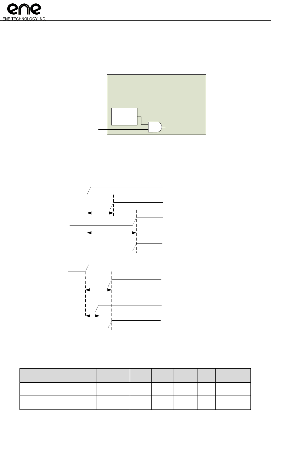
Copyright© 2011, ENE Technology Inc.
233
KB9012 Keyboard Controller Datasheet
CONFIDENTIAL
5.7 AC Electrical Characteristics
5.7.1 KBC POR and ECRST#
ECRST# is external input pin for power-on reset and HW reset. However, ENE-KBC is also
implemented with internal POR. Simplified power-on logic is as illustrated:
ENE KBC
Internal
POR
ECRST# KBC Chip
RESET
There is one constrain for the ECRST# signals.
For power-on reset, the internal POR circuit is designed with TPOR to boot-up. The ECRST#
should be implemented with external delay circuit of TECRST# for system application. The
delay timing TECRST# is only meaningful when it is larger than TPOR.
Vcc
TPOR
POR Ready
(Internal)
TECRST#
ECRST#
KBC Chip Reset
(Internal)
Design of TECRST# longer than TPOR
Vcc
TPOR
POR Ready
(Internal)
TECRST#
ECRST#
KBC Chip Reset
(Internal)
Design of TECRST# smaller than TPOR
For general application, ENE recommends to used internal POR for power-on reset; design to
place a pull-high resistor on ECRST# to guarantee reset event would not be triggered unexpectedly.
Please also note that, IC reset signal is sensitive to environment, the signal should be kept clean.
Parameter
Symbol
Min.
Typ.
Max.
Unit
Condition
Internal POR timing
TPOR
--
30
--
ms
Application depending
design of external delay
TECRST#
--
--
--
us
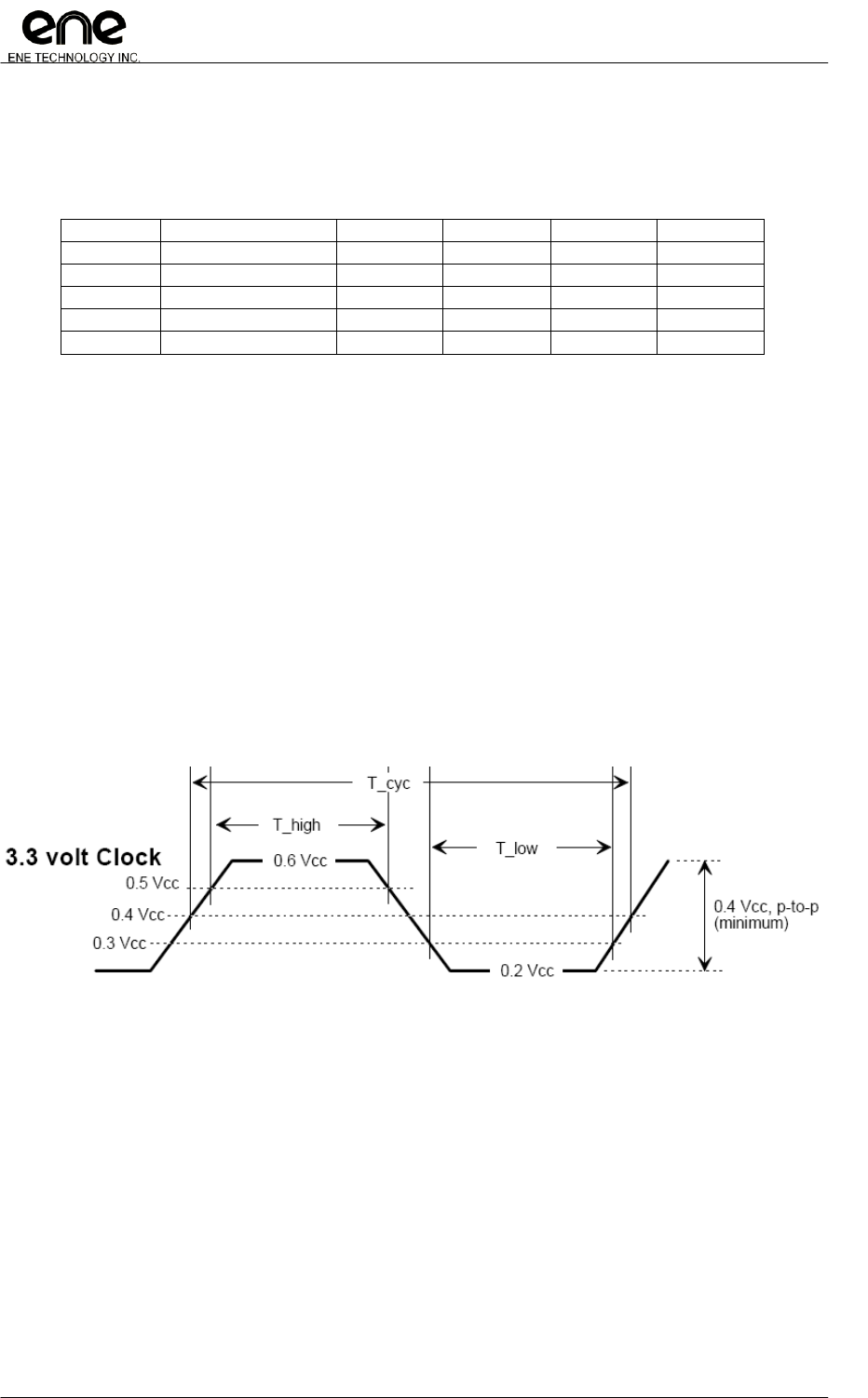
Copyright© 2011, ENE Technology Inc.
234
KB9012 Keyboard Controller Datasheet
CONFIDENTIAL
5.7.2 LPC interface Timing
Note: All AC characteristics of the LPC interface meet the PCI Local Bus SPEC for 3.3V DC signaling.
Clock & Reset:
Symbol
Parameter
Min
Max
Units
Notes
Tcyc
CLK Cycle Time
30
33
ns
1,4
Thigh
CLK High Time
11
ns
Tlow
CLK Low Time
11
ns
CLK Slew Rate
1
4
V/ns
2
Reset Slew Rate
50
mV/ns
3
1. In general, all PCI components must work within clock frequency constrain. The clock frequency
may be changed at any time during the operation of the system so long as the clock edges
remain "clean" (monotonic) and the minimum cycle and high and low times are not violated.
The clock may only be stopped in a low state.
2. Rise and fall times are specified in terms of the edge rate measured in V/ns. This slew rate must
be met across the minimum peak-to-peak portion of the clock waveform as shown below.
3. The minimum RST# slew rate applies only to the rising (de-assertion) edge of the reset signal
and ensures that system noise cannot render an otherwise monotonic signal to appear to
bounce in the switching range.
4. Device operational parameters at frequencies under 16 MHz may be guaranteed by design
rather than by testing.

Copyright© 2011, ENE Technology Inc.
235
KB9012 Keyboard Controller Datasheet
CONFIDENTIAL
Timing Parameters
Symbol
Parameter
Min
Max
Units
Notes
Tval
CLK to Signal Valid Delay
2
11
ns
Ton
Float to Active Delay
2
ns
1
Toff
Active to Float Delay
28
ns
1
Tsu
Input Setup Time to CLK
7
ns
2,3
Th
Input Hold Time from CLK
0
ns
3
1. For purposes of Active/Float timing measurements, the Hi-Z or ―off‖ state is defined to be when
the total current delivered through the component pin is less than or equal to the leakage
current specification.
2. Setup time applies only when the device is not driving the pin. Devices cannot drive and receive
signals at the same time.
3. Refer the timing measurement conditions as below
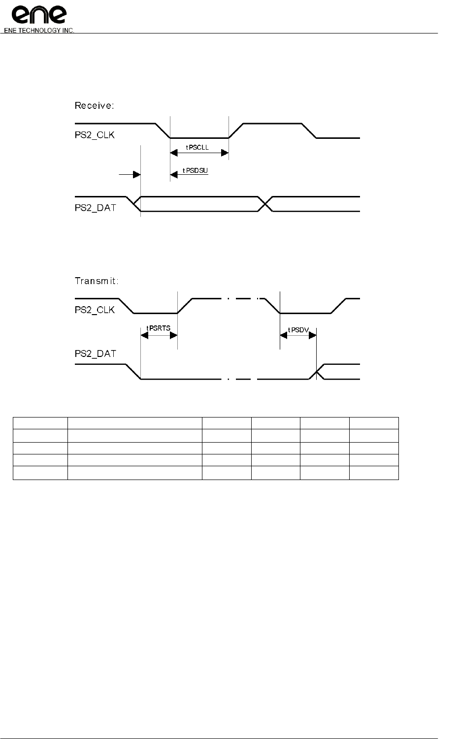
Copyright© 2011, ENE Technology Inc.
236
KB9012 Keyboard Controller Datasheet
CONFIDENTIAL
5.7.3 PS/2 interface Timing
Timing Parameters
Symbol
Parameter
Min
Max
Units
Notes
TPSRTS
Request to send state time
110
μs
TPSCLL
Clock low time
125
ns
1, 2
TPSDSU
Data input setup time
1
ns
2
TPSDV
Data output data valid time
5
μs
1. Simulated under 8051=8Mhz
2. For characteristic only.
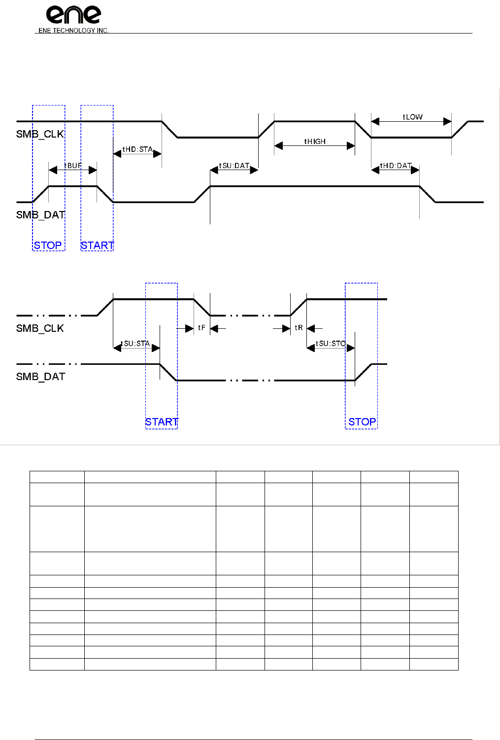
Copyright© 2011, ENE Technology Inc.
237
KB9012 Keyboard Controller Datasheet
CONFIDENTIAL
5.7.4 SMBus interface Timing
Timing Parameters
Symbol
Parameter
Min
Typ.
Max
Units
Notes
Tbuf
Bus free time between Stop
and Start Condition
4.7
μs
Thd:sta
Hold time after (repeated)
star condition. After this
period, the first clock is
generated.
4.0
μs
Tsu:sta
Repeated start condition
setup time
4.7
μs
Tsu:sto
Stop condition setup time
4.0
μs
Thd:dat
Data hold time
300
ns
Tsu:dat
Data setup time
250
ns
Ttimeout
Detect clock low timeout
25
35
ms
Tlow
Clock low period
4.7
μs
2
Thigh
Clock high period
4.0
50
μs
2
Tf
Data fall time
300
ns
Tr
Data rise time
1000
ns
1. For characteristic only
2. SMBUS frequency dependant
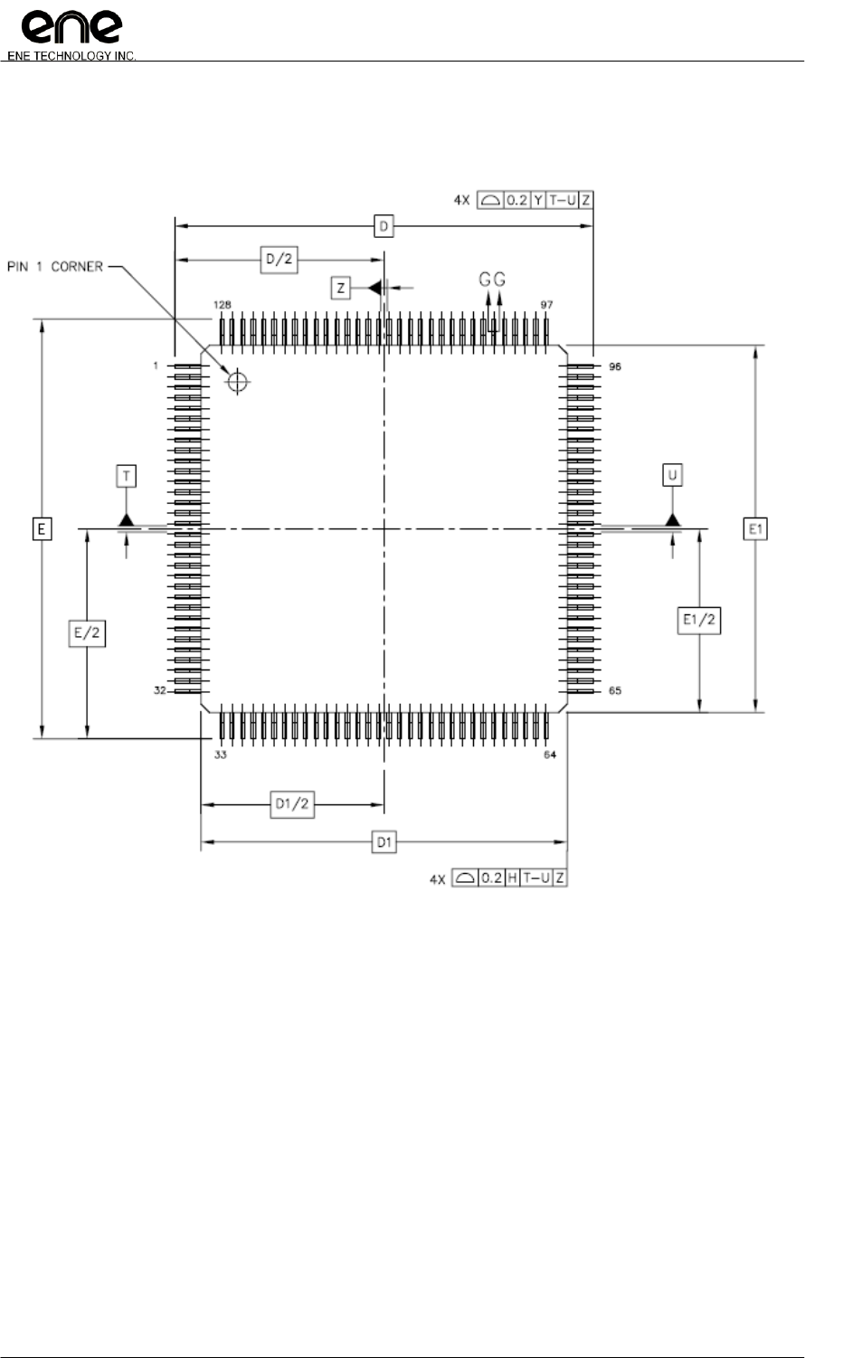
Copyright© 2011, ENE Technology Inc.
238
KB9012 Keyboard Controller Datasheet
CONFIDENTIAL
6. Package Information
6.1 LQFP 128-Pin Outline Diagram
6.1.1 Top View

Copyright© 2011, ENE Technology Inc.
239
KB9012 Keyboard Controller Datasheet
CONFIDENTIAL
6.1.2 Side View
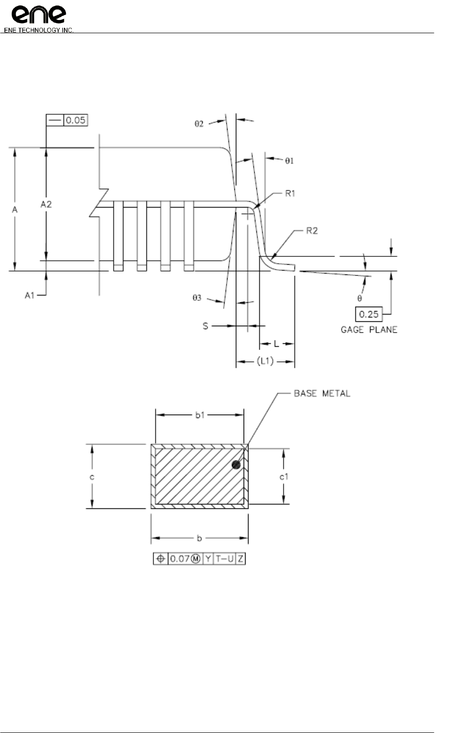
Copyright© 2011, ENE Technology Inc.
240
KB9012 Keyboard Controller Datasheet
CONFIDENTIAL
6.1.3 Lead View

Copyright© 2011, ENE Technology Inc.
241
KB9012 Keyboard Controller Datasheet
CONFIDENTIAL
6.1.4 LQFP Outline Dimensions
DIM
Min.
Typ.
Max.
DIM
Min.
Typ.
Max.
A
———
1.6
E1
14 BSC
A1
0.05
0.15
L
0.45
0.6
0.75
A2
1.35
1.4
1.45
L1
1 REF
b
0.13
0.16
0.23
R1
0.08
———
b1
0.13
0.19
R2
0.08
0.2
c
0.09
0.2
S
0.2
———
c1
0.09
0.16
θ
0°
3.5°
7°
D
16 BSC
θ1
0°
———
D1
14 BSC
θ2
11°
12°
13°
e
0.4 BSC
θ3
11°
12°
13°
E
16 BSC
Unit
mm
Package
14x14x1.4
Pitch POD
0.4
Footprint
2mm
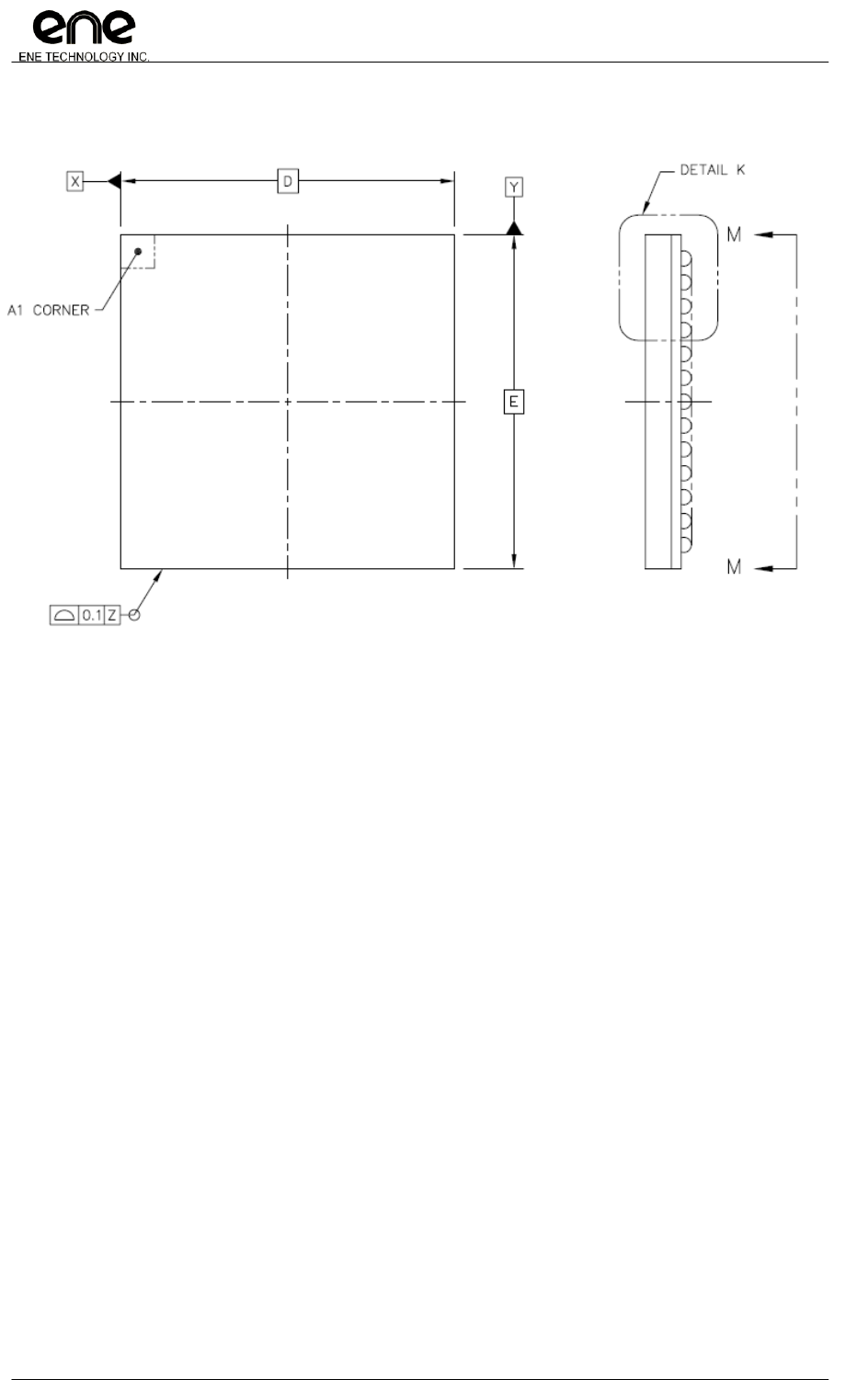
Copyright© 2011, ENE Technology Inc.
242
KB9012 Keyboard Controller Datasheet
CONFIDENTIAL
6.2 LFBGA 128-Pin Outline Diagram
6.2.1 Top View
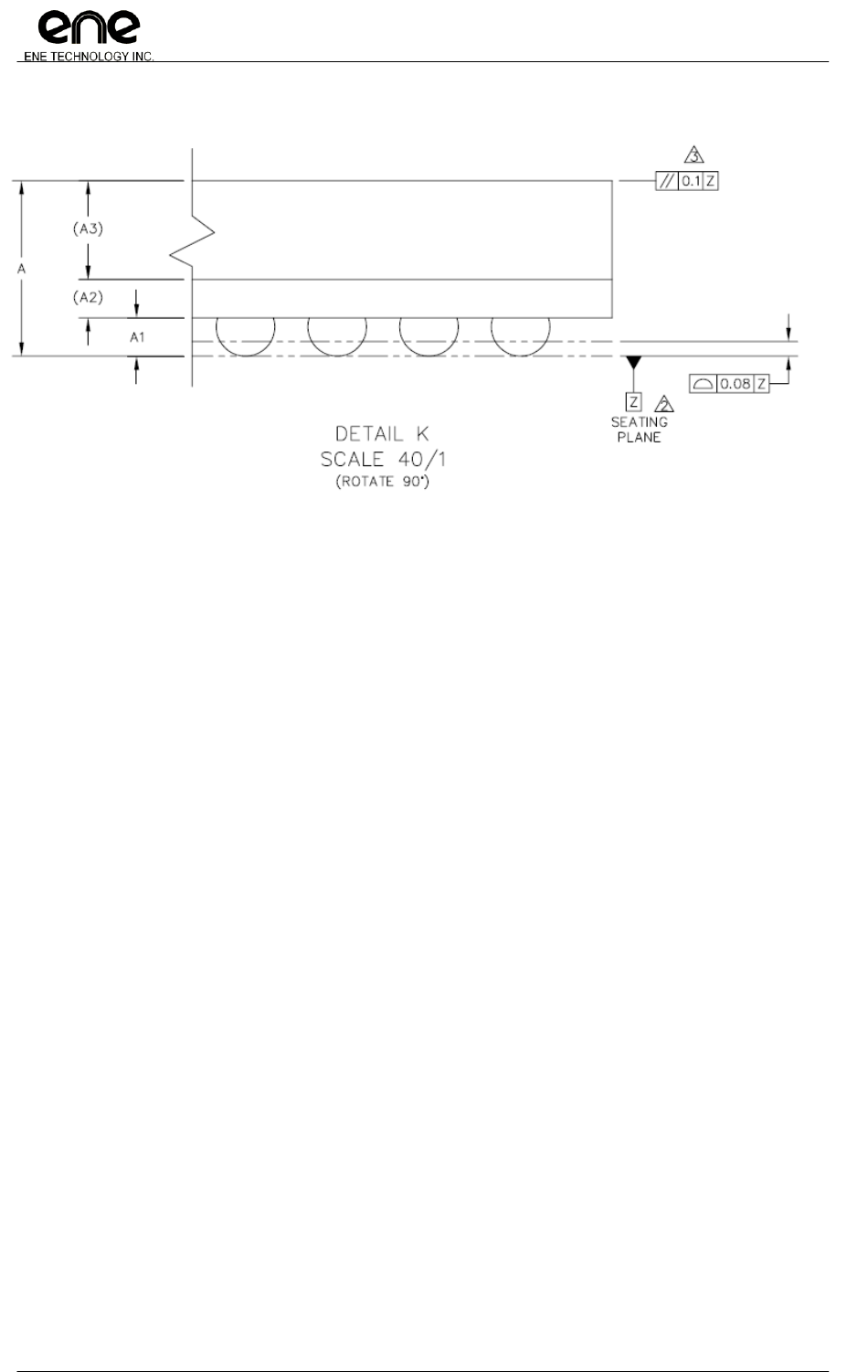
Copyright© 2011, ENE Technology Inc.
243
KB9012 Keyboard Controller Datasheet
CONFIDENTIAL
6.2.2 Side View
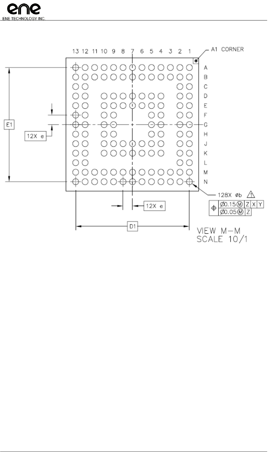
Copyright© 2011, ENE Technology Inc.
244
KB9012 Keyboard Controller Datasheet
CONFIDENTIAL
6.2.3 Bottom View

Copyright© 2011, ENE Technology Inc.
245
KB9012 Keyboard Controller Datasheet
CONFIDENTIAL
6.2.4 LFBGA Outline Dimensions
DIM
Min.
Nor.
Max.
A
———
1.3
A1
0.16
0.26
A2
0.21
A3
0.7
b
0.27
0.37
D
7
E
7
e
0.5
D1
6
E1
6
Unit
mm
Package
7mm * 7 mm

Copyright© 2011, ENE Technology Inc.
246
KB9012 Keyboard Controller Datasheet
CONFIDENTIAL
6.3 Part Number Description
Part Number
Package Size
Lead Free Process
Status
KB9012QF A3
14mm * 14mm
128 pins LQFP
Lead Free
Available
KB9012BF A3
7mm * 7mm
128 balls LFBGA
Lead Free
Available
KB9012QF A2
14mm * 14mm 128
pins LQFP
Lead Free
EOL
KB9012BF A2
7mm * 7mm
128 balls LFBGA
Lead Free
EOL