Lab Instructions
User Manual:
Open the PDF directly: View PDF ![]() .
.
Page Count: 9

Environment Setup
bash
cp -rp /mnt/hld_fpga-sysc $HOME
export HLD_ROOT=$HOME/hld_fpga-sysc/
export SC_DIR=/opt/systemc/2.3.1
export GTEST_DIR=/opt/googletest/googletest
export PYTHONPATH=.:$HLD_ROOT/scripts/systemc-gen
WIKI
• firefox https://github.com/intel/rapid-design-methods-for-developing-hardware-
accelerators/wiki
• or firefox $HLD_ROOT/docs/wiki/index.html
VCS and Quartus setup:
source /mnt/harpv2/env.sh
Install AAL SDK (if not done previously):
cp /mnt/harpv2/SR-5.0.3-Release.tar.gz $HOME
tar xzvf SR-5.0.3-Release.tar.gz
cd SR-5.0.3-Release/Base/SW
tar xzvf aalsdk-5.0.3.BSD-License.tar.gz
cd aalsdk-5.0.3
./configure --prefix=$HOME/SR-5.0.3-Release/Base/SW/install
make; make install
cd ../install
export AALSDK=`pwd`
Install MPF (memory layer building block required to use virtual addressing in HW):
cp /mnt/harpv2/harpv2_mpf.tar.gz $HOME;
cd $HOME; tar xzvf $HOME/harpv2_mpf.tar.gz
cd harpv2_mpf/BBB_cci_mpf/sw; make prefix=$AALSDK
export CCI_MPF_SW_ROOT=`pwd`
Compile FPGA APP SW (common SW driver for HLD apps)
cd $HLD_ROOT/fpga_sw/5.0.3/AcclAppVtp/
make prefix=$AALSDK
Lab Overview
The lab goes over implementing a Floyd's Cycle Detection Algorithm on Xeon/FPGA
(based on SR-5.0.3 SDK)
Input: SW implementation of the algorithm
Output:

− Generated RTL for FPGA
− Refactored SW that offloads the computation to FPGA
− SW-ASE simulation running
Please have the wiki handy (firefox https://github.com/intel/rapid-design-methods-for-
developing-hardware-accelerators/wiki)
Every lab has a solution under labN-solution folder. Each lab is independent.
Algorithm
1. Let us take 2 pointers namely slow Pointer and fast Pointer to traverse a Singly
Linked List at different speeds. A slow Pointer (Also called Tortoise) moves one
step forward while fast Pointer (Also called Hare) moves 2 steps forward
Start Tortoise and Hare at the first node of the List.
2. If Hare reaches end of the List, return as there is no loop in the list.
3. Else move Hare one step forward.
4. If Hare reaches end of the List, return as there is no loop in the list.
5. Else move Hare and Tortoise one step forward.
6. If Hare and Tortoise pointing to same Node return, we found loop in the List.
7. Else start with STEP-2.
cycle_detection.c
int cycle_detect(listnode_t *head) {
listnode_t *fast, *slow;
slow = head;
fast = head;
while(!(slow == NULL || fast == NULL)) {
fast = fast->next;
if(!fast)
return 0;
if(fast == slow)
return 1;
fast = fast->next;
slow = slow->next;
}
return 0;

Lab1: Partition SW following SW/HW Interface
The original SW resides in file $HLD_ROOT/labs/linkedlist-lab/cycle_detect.c. You can
compile it using “make” command. The original code has to be refactored to conform to
the SW/HW interface specified by IFpgaApp C++ interface
($HLD_ROOT/common/fpga_app_if.h).
We provide the FpgaSWAlloc class ($HLD_ROOT/common/fpga_app_sw.h) that
implements alloc(), join() and free() methods for simulation in software, so only
compute() method has to be implemented.
We will create a Config struct for this application with address offsets to the header of the
list and the result. The Config object is passed to compute() method. This is the only way
to pass initial data from SW to future HW. The rest of communications between SW and
HW will be carried out over shared memory. Thus, Config often has pointers to shared
memory to let HW know where to read/write data to/from.
Go to $HLD_ROOT/labs/linkedlist-lab/lab1.
Config structure is defined in Config.h. The SW code is refactored to use the IFpgaApp
interface in cycle_detection_sw.cpp. The code that emulates HW and implements
compute() method is located in cycle_detection_hw_emul.h. cycle_detect() function from
the original SW is the one we offload in this lab.
LAB INSTRUCTIONS:
- Implement compute() function by processing the config and redirecting a call to
the cycle_detect() function you moved from original SW
- Hint1: Look at the Config struct methods and ones that return pointers for the
linked list header and the result
- When done, run “make” and then “cycle_detection_hw_emul” to simulate
refactored SW
Note: The refactored SW code ( cycle_detection_sw.cpp ) will be the driver reused across
different execution models including the physical platform. The ifdefs include different
implementation of AcclApp class depending on the model.
class IFpgaApp {
virtual void *alloc( unsigned long long size_in_bytes) = 0;
virtual void compute( const void * config_ptr, const unsigned int config_size) = 0;
virtual void join() = 0;
virtual void free() = 0;
};
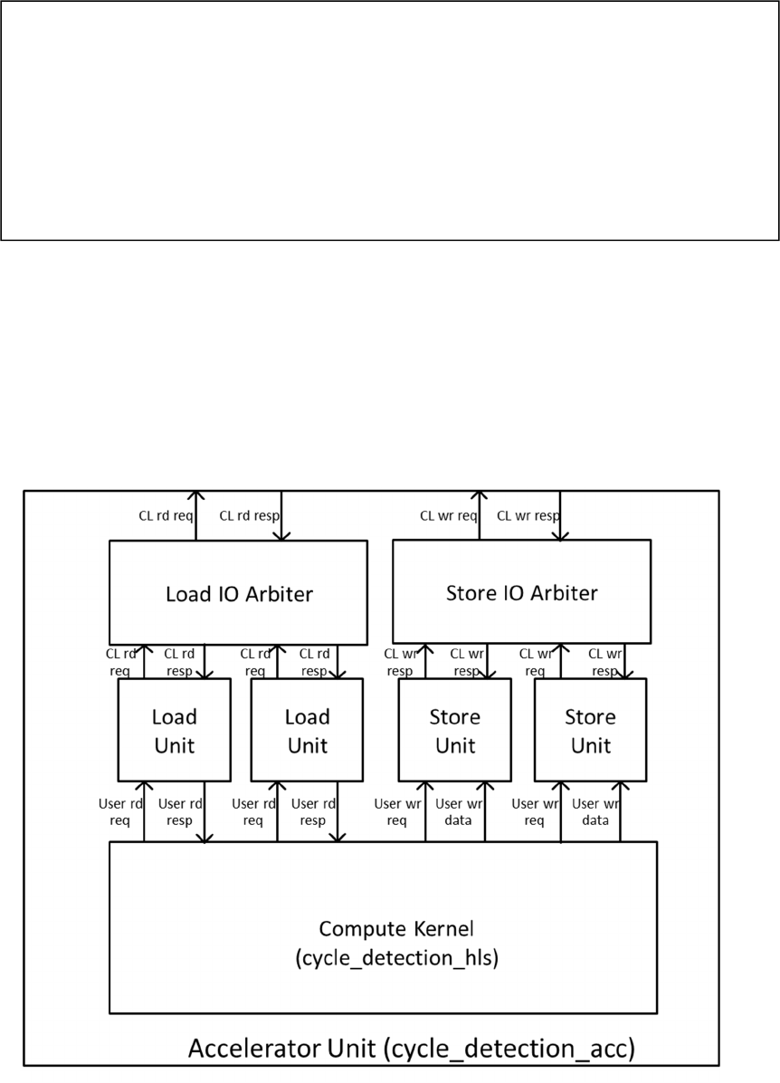
Lab2: Python DSL and SystemC Accelerator Code Generation
Most of the accelerator SystemC code and testbench is automatically generated. The user
needs to specify memory ports needed for computation and their types. The compute
kernel module (cycle_detection_hls) will be generated with ports corresponding to
memory port selection. The complete accelerator unit (cycle_detection_acc) will be
generated with the load/store units corresponding on the selected memory port types as
shown in the figure.
#ifdef SC_KERNEL
#include "cycle_detection_hls_tb.h"
#elif SC_ACC
#include "cycle_detection_acc_tb.h"
#elif FPGA_ACC
#include "AcclApp.h"
#else
#include "cycle_detection_hw_emul.h"
#endif

The way memory port specification is captured is by the means of Python DSL that we
provide. The DSL captures the following about a design:
− dut name (the generated files will have the dut name as a base name)
− user types that will be used as a payload for the memory ports
− memory inputs and outputs, their types and parameters for load store units
− extra config fields (by default for every memory port config will have the base
address of the corresponding data in memory)
− SystemC thread specification, memory port mapping to threads and module hierarchy
Go to lab2.
Open dut_params.py to see dut name and user types specified in Python DSL.
LAB INSTRUCTIONS:
− In dut_params.py file, specify two user memory ports: read port for type Node (name
it “inp”), write port for type CycleInfoExist (name it “out”).
− Hint1: Follow Python Interface Spec API from the wiki using TypedRead and
TypedWrite types correspondingly. Make sure you read about max_burst_count and
buf_size_in_cl parameters. You will need to pick them at this point but will be able to
change them later.
− Generate all SystemC collaterals following the CHEATSHEET
− make MODE=kernel (simulation should hang as there’s no functionality yet)
Note: there are multiple simulation collaterals were generated. We provide testbenches to
simulation at kernel level (cycle_detection_hls), accelerator level (cycle_detection_acc).
Different modes of simulation are activated by the MODE parameter used with Makefile.
Lab3: Complete Cycle Detect Functionality in SystemC
Go to lab 3. In generated files, e.g. cycle_detection_hls.h, you will see cog-related
comments. They allow regenerating files (already with user modifications) when changes
in dut_params are required. Those comments can also be deleted if -d flag is used with
the cog scripts. Open cycle_detection_hls.h:
− detection() function is the CTHREAD SystemC process that implements the cycle
detection algorithm
− Note special structure of any CTHREAD process: while(1) loop with main
functionality, reset section before the while(1) loop and wait() statements
− See how the memory port bundles (inpReqOut, inpRespIn) and (outReqOut,
outDataOut) are used to get the next Node in the linked list and to write
CycleExistInfo respectively
LAB INSTRUCTIONS:
− Complete the code where requests to memory are done to get the next Node in the
linked list to update slow and fast offsets
− Hint1: see how the fast_offset gets updated in the same function
− When done, make using: “make MODE=kernel” and then run the test:
“./cycle_detection_kernel”

Lab 4: Measuring Memory BW
The cycle_detection_acc module is fully defined by the generated file
cycle_detection_acc.h. The testbench harness to test this block is instantiated in
cycle_detection_acc_tb.h. To compile this testbench, do:
− make MODE=acc
See achievable memory BW by running it: ./cycle_detection_acc
LAB INSTRUCTIONS:
− In cycle_detection_acc_tb.h change the frequency of design to 200Mhz and observe
changes in the memory BW report
− In cycle_detection_acc_tb.h change memory latency to 500ns and observe changes in
the memory BW report
− Recompile for every change “make MODE=acc” and rerun
Note: In this simulation, we use a mock memory model that is simply models latency and
bandwidth of memory. Mock memory is useful to give quick feedback on design issues
like we’ve seen in cycle detection algorithm -> cannot utilize memory bandwidth
To help saturate memory BW often multi-threading or multiple AUs are required
− For cases when increasing AU frequency does not help utilizing BW – multi-
threading inside one AU will help
− For cases when memory BW scales proportionally to the AU frequency – multiple
AUs will help (we provide a multi_au_template to facilitate multiple AU integration)
Lab 5: HLS Flow and generated RTL integration
We synthesize the cycle_detection_acc module with HLS. We use C-to-Silicon Compiler
from Cadence®. The script for the synthesis tool is provided in lab5/ctos directory. The
synthesis process takes some time for the first time as it characterizes all components by
running gate-level synthesis for them. The characterization will be cached for the next
run in rc_work directory.
The generated RTL is located under lab5/afu directory.

In order for the automatic flow to integrate generated RTL extra information is needed
about the design that is captured in hld_defines.v file that is also located under afu
directory.
− HLD_ACC_CLK will determine the frequency of the accelerator
− HLD_AFU_ID* is needed for SW to locate the accelerator service on FPGA
− HLD_APP_CONFIG_WIDTH is the SW config size in bits
− HLD_AFU_MODULE_NAME is the name of the top verilog module in generated
RTL
See User Guide, section CCIP integration for more details
Next, we will run RTL + SW simulation using the ASE environment.
LAB INSTRUCTIONS:
ASE with verilog simulation runs in a separate shell. In the new shell, source VCS and
Quartus setup script, set up HLD_ROOT and AALSDK variables according to the setup
instructions (see first section of this document)
Launching ASE RTL simulation:
− Go to SR-5.0.3-Release/Base/SW/aalsdk-5.0.3/ase
− Use scripts/generate_ase_environment.py to create vlog_files.list (use location to
lab5/afu for RTL source):
./scripts/generate_ase_environment.py $HLD_ROOT/labs/linkedlist-
lab/lab5/afu/ -t VCS
− Replace the vlog_files.list with the following (edit harpX-user to your home
directory!!)
`define HLD_MEM_RD_PORTS 1
`define HLD_MEM_WR_PORTS 1
// in Mhz //CLK_400=3'b000, CLK_200=3'b001, CLK_100=3'b010
`define HLD_ACC_CLK CLK_200
// ---- REGENERATE THE IDS BELOW FOR YOUR AFU -----
//xxd -l 8 -p /dev/random
`define HLD_AFU_ID_H 64'h30b1cf9b9bee84e7
`define HLD_AFU_ID_L 64'hfd2e242e7efcb9d8
//in bits
`define HLD_APP_CONFIG_WIDTH 128
`define HLD_AFU_MODULE_NAME cycledetection_acc_rtl
//dependent on the number of ACC buffers
`define HLD_REQ_ASYNC_FIFO_LOG2DEPTH 4
//
`define HLD_RESP_ASYNC_FIFO_LOG2DEPTH 4
-F /home/harpX-user/harpv2_mpf/BBB_cci_mpf/hw/sim/cci_mpf_sim_addenda.txt
-F /home/harpX-user/hld_fpga-sysc/rtl/5.0.3/ase_rtl_common_files.txt
+incdir+/home/harpX-user/hld_fpga-sysc/labs/linkedlist-lab/lab5/afu
/home/harpX-user/hld_fpga-sysc/linkedlist-lab/lab5/afu/cycledetection_acc_rtl.v
− You also need to edit Makefile to add MPF_PLATFORM define
SNPS_VLOGAN_OPT+= +define+MPF_PLATFORM_BDX
− Run: make;make sim
Running SW for FPGA:
− Export the ASE_WORKDIR in the original shell according to instructions on the
screen after you ran “make sim”
− In lab5: make MODE=fpga prefix=$AALSDK
− ./cycle_detection_fpga
The simulation should run producing output in both shell windows.
Lab 6: Performance Simulation
The performance simulator is built on top of ASE environment. We provide a script to
patch the default ASE code (you may want to create a backup copy of original ASE). The
patched ASE will run in the performance mode by default. You can enable functional
mode only (original ASE mode) by setting ASE_PERF flag to 0 in Makefile.
LAB INSTRUCTIONS:
In ASE shell:
pushd $HLD_ROOT/ase_perf
./patch-ase.csh $HOME/SR-5.0.3-Release/Base/SW/aalsdk-5.0.3/ase
popd
Recompile and launch ASE
− make;make sim
Running SW for FPGA:
− In lab5: make MODE=fpga
− ./cycle_detection_fpga
After the test is finished, the timing report is printed in the ASE shell (you may Ctrl-C the
ASE shell in case it is run in the mode to run multiple tests) as below.

================== Stats of QA_FPGA_CACHE =================
Cache Size = 1024
Associativity = 1
Line Size = 1
Replacement Policy = 2
Word Size = 1
*mTotalWordUsed = 35 Words
*mTotalWordReadFromLLM = 55 Words
Word Waste Ratio = 0.363636
Base Address = 0
Total MSHR Hit Count = 0
Total Cache Access = 1375
Total Cache Miss = 59
Miss Rate = 0.0429091
Total Cache Pipeline Hazards = 27
Total Read Miss = 38
Total Write Miss = 21
Total Eviction = 18
================== CCI-P Stats =================
Total Data Accessed = 88000 Bytes
Min Latency of VL0 Access = 12500 ps
Max Latency of VL0 Access = 505 ns
Avg Latency of VL0 Access = 33811 ps
Total Requests at CCI-P = 1375
Total Bandwidth at CCI-P interface = 0.35329 GB/sec
Total Read Bandwidth at CCI-P interface = 0.345581 GB/sec
Total Write Bandwidth at CCI-P interface = 0.00770813 GB/sec
Total VL0 Bandwidth = 0.35329 GB/sec
Total VH0 Bandwidth = -0 GB/sec
Total VH1 Bandwidth = -0 GB/sec
================== Stat of DRAM =================
Avg Latency of a DRAM Request = 85 ns
Total DRAM Requests = 23
ase_top_ccip_emulator_i_qa_fpga_mem_subsystem.mDRAM : Total DRAM Request = 23
ase_top_ccip_emulator_i_qa_fpga_mem_subsystem.mDRAM : DRAM BandWidth =
0.0463082 GB/sec
