Leddarvu And Configurator User Guide
User Manual:
Open the PDF directly: View PDF ![]() .
.
Page Count: 117 [warning: Documents this large are best viewed by clicking the View PDF Link!]
- 1. Introduction
- 1.1. Description
- 1.2. SPI Carrier Board
- 1.3. USB, CAN and SERIAL Carrier Board
- 1.4. Working Diagram
- 1.4.1. SPI Carrier Board
- 1.4.2. USB, CAN and SERIAL Board
- 2. Underlying Principles
- 3. Getting Started
- 3.1. Optional power supply
- 3.2. Optional SPI cable
- 3.3. Setup
- 3.4. Connecting to the LeddarVu Module
- 4. Measurements and Settings
- 4.1. Distance Measurement
- 4.2. Data Description
- 4.3. Acquisition Settings
- 4.4. Measurement Rate
- 4.5. CPU Load
- 5. Communication Interfaces
- 5.1. SPI Interface
- 5.1.1. SPI Basics
- 5.1.2. SPI Protocol
- 5.1.3. Memory Map
- Configuration data
- Device information and constants
- Detection list
- Transaction configuration
- 5.1.4. SPI Operation
- SPI port configuration
- Speed and timing
- Access
- Modification
- 5.2. I2C Interface
- 5.3. USB Interface
- 5.4. Serial Link Interface
- 5.5. CAN Bus Interface
- 6. Leddar™ Configurator
- 6.1. Introduction to Configurator Software
- 6.2. Connection Window
- 6.3. Leddar™ Configurator Main Window
- 6.3.1. Toolbar
- 6.3.2. Fit to Window
- 6.3.3. Force Equal Horizontal and Vertical Scales
- 6.3.4. Zoom in
- 6.3.5. Zoom out
- 6.3.6. Scale
- 6.3.7. Panning and Zooming
- 6.3.8. Changing the LeddarVu Module Origin
- 6.3.9. Changing the LeddarVu Module Orientation
- 6.4. Settings
- 6.4.1. Module Name
- 6.4.2. Acquisition Settings
- 6.4.3. Serial Port
- 6.4.4. CAN Port
- 6.5. Saving and Loading a Configuration
- 6.6. Configuring Detection Records
- 6.7. Using Detection Records
- 6.8. Data Logging
- 6.9. Device State
- General
- Device Information
- Carrier
- 6.10. Preferences
- 6.11. Raw Detections
- 7. Specifications
- 7.1. General
- 7.2. Mechanical
- 7.3. Electrical
- 7.4. Optical
- 7.5. Performance
- 7.6. Regulatory Compliancy
- 7.7. Dimensions
- 7.7.1. 100 Module
- 7.7.2. 48 Module
- 7.7.3. 20 Module
- 8. Help
- Index

LeddarTech Inc.
2740 Einstein Street
Quebec, Quebec G1P 4S4
CANADA
www.leddartech.com
Leddar Vu8
User Guide

Copyright © 2017 LeddarTech Inc. All rights reserved.
The Company shall not be liable for any errors contained herein or for any damages arising out
of or related to this document or the information contained therein, even if the Company has
been advised of the possibility of such damages.
The information contained herein is the property of LeddarTech Inc., and shall not be
reproduced in whole or in part without prior written approval of LeddarTech Inc.
LeddarTech Inc. assumes no responsibility for any errors or omissions in this document.
Leddar is a trademark of LeddarTech Inc. All other trademarks are the property of their
respective owners.
Leddar™ Configurator software: this software is based in part on the work of the Independent
JPEG Group.

3
Table of Contents
Introduction ..................................................................... 6
1.1. Description ....................................................................................... 6
1.2. SPI Carrier Board ............................................................................. 8
1.3. USB, CAN and SERIAL Carrier Board .................................................... 9
1.4. Working Diagram ............................................................................ 14
1.4.1. SPI Carrier Board .................................................................................... 15
1.4.2. USB, CAN and SERIAL Board .................................................................... 16
Underlying Principles ...................................................... 17
Getting Started ............................................................... 18
3.1. Optional power supply ..................................................................... 18
3.2. Optional SPI cable ........................................................................... 19
3.3. Setup ............................................................................................ 19
3.4. Connecting to the LeddarVu Module ................................................... 22
Measurements and Settings ............................................ 25
4.1. Distance Measurement ..................................................................... 25
4.2. Data Description ............................................................................. 26
4.3. Acquisition Settings ......................................................................... 28
4.4. Measurement Rate .......................................................................... 34
4.5. CPU Load ....................................................................................... 35
Communication Interfaces .............................................. 37
5.1. SPI Interface .................................................................................. 37
5.1.1. SPI Basics .............................................................................................. 37
5.1.2. SPI Protocol ........................................................................................... 38
5.1.3. Memory Map .......................................................................................... 41
5.1.4. SPI Operation ......................................................................................... 47
5.2. I2C Interface .................................................................................. 48
5.3. USB Interface ................................................................................. 48

4 P/N 54A0028-2 012017 © 2017 LeddarTech Inc. Printed in Canada. All rights reserved.
5.4. Serial Link Interface ........................................................................ 48
5.5. CAN Bus Interface ........................................................................... 62
Leddar™ Configurator ..................................................... 72
6.1. Introduction to Configurator Software ................................................ 72
6.2. Connection Window ......................................................................... 73
6.3. Leddar™ Configurator Main Window .................................................. 74
6.3.1. Toolbar .................................................................................................. 74
6.3.2. Fit to Window ......................................................................................... 74
6.3.3. Force Equal Horizontal and Vertical Scales .................................................. 75
6.3.4. Zoom in ................................................................................................. 75
6.3.5. Zoom out ............................................................................................... 75
6.3.6. Scale ..................................................................................................... 75
6.3.7. Panning and Zooming .............................................................................. 75
6.3.8. Changing the LeddarVu Module Origin ....................................................... 78
6.3.9. Changing the LeddarVu Module Orientation ................................................ 79
6.4. Settings ......................................................................................... 80
6.4.1. Module Name ......................................................................................... 81
6.4.2. Acquisition Settings ................................................................................. 82
6.4.3. Serial Port .............................................................................................. 83
6.4.4. CAN Port ................................................................................................ 84
6.5. Saving and Loading a Configuration ................................................... 86
6.6. Configuring Detection Records .......................................................... 86
6.7. Using Detection Records .................................................................. 89
6.8. Data Logging .................................................................................. 90
6.9. Device State ................................................................................... 93
6.10. Preferences .................................................................................... 95
6.11. Raw Detections ............................................................................... 97
Specifications ............................................................... 101
7.1. General ........................................................................................ 101
7.2. Mechanical ................................................................................... 101
7.3. Electrical ...................................................................................... 102
7.4. Optical ......................................................................................... 102
7.5. Performance ................................................................................. 103
7.6. Regulatory Compliancy .................................................................. 110
7.7. Dimensions .................................................................................. 110
7.7.1. 100° Module ......................................................................................... 111
7.7.2. 48° Module .......................................................................................... 112
7.7.3. 20° Module .......................................................................................... 113


6
Introduction
The LeddarVu module enables developers and integrators to make the most of
Leddar™ technology through integration in detection and ranging systems. The
purpose of the LeddarVu module is to easily and rapidly be integrated in various
applications.
The module can be configured to be used in very simple applications or to perform
more complex tasks depending on the hardware and software settings.
1.1. Description
The LeddarVu module contains the following:
Source
Receiver
The module comes in two configurations: SPI or USB, CAN and SERIAL. Depending
on your configuration, they offer the following features:
Horizontal FoV: 20°, 48°, 100°
Vertical FoV: 0.3°, 3°
8 detection segments
Real-time data acquisition and display (through SPI)
SPI (Serial Peripheral Interface) for the direct link with the receiver (SPI carrier
board)
I2C interface to read the optional temperature sensor on the source module (SPI
carrier board)
Serial link interface: TTL, RS-232, RS-422, and RS-485 (USB, CAN and SERIAL
carrier board)
USB interface (USB, CAN and SERIAL carrier board)
CAN bus interface for acquisition (USB, CAN and SERIAL carrier board)
7
Figure 1: General elements of the LeddarVu module
Receiver assembly
The receiver assembly contains the photodetector array (8 elements), the circuit
receiver, and an M7 Atmel processor (MCU).
The module generates a full waveform per segment at its measurement rate.
Emitter assembly
The emitter assembly includes the emitter (LED, VSCEL, or laser), the emitter driver
circuit, and the temperature sensor.
Light source pulsing is controlled by the receiver assembly since the receiver data
acquisition must be synchronized with the light source pulses. The temperature
sensor, located near the light source, is used to implement temperature
compensation on the ranging results.
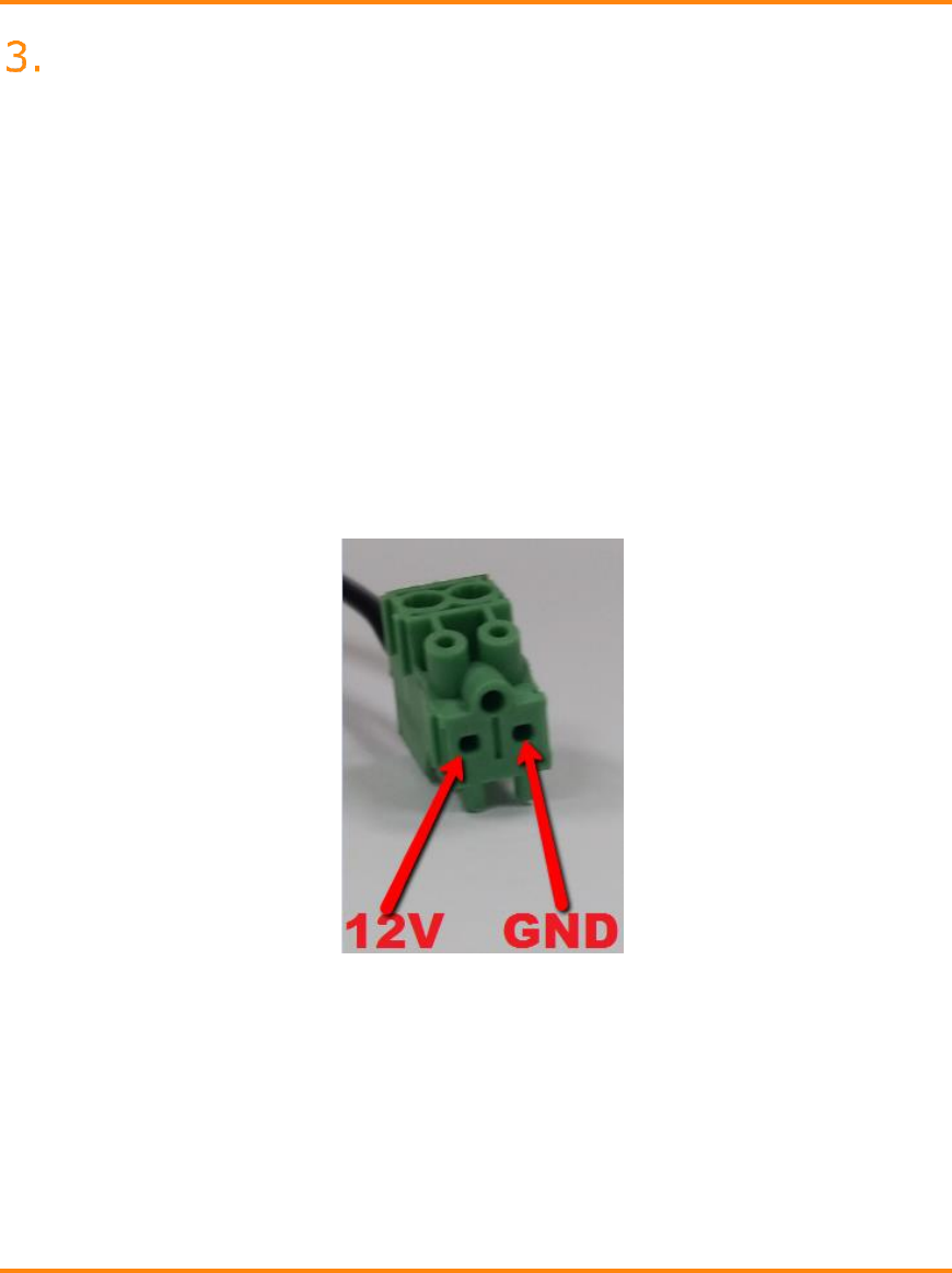
Power connection
The power connection is a 2-pin connector that provides the module with a 12 V
power source.
8 P/N 54A0028-2 012017© 2017 LeddarTech Inc. Printed in Canada. All rights reserved.
1.2. SPI Carrier Board
The following presents the description of the SPI board.
Figure 2: Board of the SPI LeddarVu module
*Power outputs can supply up to 15 mA
9
1.3. USB, CAN and SERIAL Carrier Board
The following presents the description of the USB, CAN and SERIAL board.
Figure 3: Board of the USB, CAN and SERIAL LeddarVu module
*Power outputs can supply up to 15 mA

10 P/N 54A0028-2 012017© 2017 LeddarTech Inc. Printed in Canada. All rights reserved.
DIP Switches
The DIP switches are used for the configuration of the serial port number 1. This
port is configurable to these EIA electrical interfaces for the following standard serial
communication ports:
RS-232
RS-485 two-wire configuration
RS-422/RS-485 four-wire configuration
Table 1: Communication port configuration (for 6 positions DIP switch)
NOTE: On all port configurations, the module is still a half-duplex slave.
Interface
DIP switches position
1
2
3
4
5
6
RS-232
OFF
OFF
ON
OFF
OFF
X
RS-485
two-wire
configuration
ON
ON
OFF
ON
ON
X
RS-422
RS-485
four-wire
configuration
ON
OFF
ON
OFF
OFF
X

11
Table 2: Communication port configuration (for 8-position DIP switch)
NOTES:
DIP switch position 6 on ‘ON’ position enables a 121Ω termination resistor to
RS-485 two-wire configuration only (must be kept on ‘OFF’ position in any
other configuration)
DIP switch position 8 on ‘ON’ position enables a 121Ω termination resistor to
CAN port
Configurable serial link 1
Depending on the DIP switch positions, the configurable serial link pin functionalities
differ (refer to Table 3).
Interface
DIP switch position
1
2
3
4
5
6
7
8
RS-232
OFF
ON
OFF
OFF
OFF
X
X
X
RS-485
two-wire
configuration
ON
OFF
ON
ON
ON
X
X
X
RS-422
RS-485
four-wire
configuration
ON
ON
OFF
OFF
OFF
X
X
X

12 P/N 54A0028-2 012017© 2017 LeddarTech Inc. Printed in Canada. All rights reserved.
Table 3: Communication link configuration
Pin
position
Interface
RS-232
RS-485 two-wire
configuration
RS-422
RS-485 four-wire
configuration
1
GND
GND
GND
3
RTS
D -
Dout -
5
NC
NC
NC
7
RX
D -
Din +
9
TX
D +
Dout +
11
CTS
D -
Din -
NOTE: If a two-wire or four-wire differential port configuration is selected, in
function of your network configuration, you should put bias resistors on
transmitter or receiver lines to maintain the proper idle voltage and force
the line to the idle condition.
Push buttons
The S1 push button is used for a hard reset purpose; a short press resets the
module.
The S3 push button is used for special purposes (refer to Table 4).

13
Table 4: S3 push button functionalities
Description
Action
Long press during
module operation (longer
than 10 seconds)
Resets the carrier board configuration to the default values:
CAN port configuration
1Mbsp, standard frame format
Base Rx: 0x740
Base Tx: 0x750
No delay
Distance in cm and a max. of 96 echoes
Serial link configuration
115,200 bps, 8 bits, no parity, no flow control, 1 stop
bit
Distance in cm and a max. of 40 echoes
Modbus address: 1
Press the S3 button for
more than 2 seconds
during startup (or after a
hard reset)
Put the USB, CAN and SERIAL carrier board in bootloader
mode. This feature is used to upgrade the USB, CAN and
SERIAL carrier board firmware.
Use the LeddarTech software tool to upgrade firmware.
14 P/N 54A0028-2 012017© 2017 LeddarTech Inc. Printed in Canada. All rights reserved.
1.4. Working Diagram
The working diagram explains how the module works in the standard and optional
configurations.
Figure 4: LeddarVu module working diagram
15
1.4.1. SPI Carrier Board
The SPI carrier board includes the following elements:
SPI and control interface
The SPI serial port functionalities are available via pins 3, 5, 7, and 9. The port has
a standard signal level of 0 V through 3.3 V.
Table 5: SPI pin definition
Pin
Function
3
CLK (input)
5
MISO (output)
7
MOSI (input)
9
CS (input)
I2C interface
The integrated circuit (I2C) protocol is intended to allow multiple slave digital
circuits to communicate with one or more master circuit. As for the SPI, it is only
intended for short distance communications. The port has a standard signal level of
0 V through 3.3 V.
Power supply
The power source includes the source, the auxiliary DC output connection, the +12
V connection, the +5 V analog supply, and the +3.3 V supply.
Reference pulse
The reference pulse interacts with the receiver interface to set the reference
segment.

16 P/N 54A0028-2 012017© 2017 LeddarTech Inc. Printed in Canada. All rights reserved.
1.4.2. USB, CAN and SERIAL Board
The optional carrier board includes the standard elements and the following ones:
Serial ports (TTL, RS-232, RS-422, and RS-485)
The TTL port is used for the short range transmission of data. The port has a
standard signal level of 0 V through 3.3 V.
The RS-232 is used for the transmission of data. It defines the signals connection
between the data terminal equipment (such as a computer) and the data circuit-
terminating equipment (such as a modem).
The RS-422 (ANSI/TIA/EIA-422-B), a four-wire configuration, specifies the electrical
characteristics of the digital signaling circuit. It can transmit data at rates as high as
10 Mbit/s or may be sent on cables as long as 1500 meters. Some systems directly
interconnect and may be used to extend the range of an RS-232 connection.
The RS-485 (ANSI/TIA/IEA-485) is a two-wire or four-wire differential serial
communication port. It is often used in electrically noisy environments.
Microcontroller MCU
The source and control assembly is equipped with an MCU on the carrier board. It is
provided to transmit data from the receiver module through the communication
ports.
USB interface
The USB interface is a compatible 2.0, full-speed 12-MBit/s port. This interface
emulates a VCP (virtual COM port) used as a serial port.
Application and reset switch
The reset switch restarts the module. This can be used as an alternative to cycling
the power.
Serial link configuration DIP switches
The source and control assembly is equipped with ten DIP switches. Five of them are
used to configure serial link 1 (see Figure 2 and Figure 3).
CAN bus interface
The CAN bus is implemented via a differential pair. The ISO 11898 standard
describes the CAN technology. The interface has a level of 3.3 V.
17
Underlying Principles
Created by LeddarTech, LEDDAR™ (light-emitting diode detection and ranging) is a
unique sensing technology based on light (infrared spectrum) and the time-of-flight
of light principle. The light source illuminates the area of interest (pulsed typically at
10 kHz for the Leddar Vu8 20° module) and the multichannel module receiver
collects the backscatter of the emitted light and measures the time taken for the
emitted light to return back to the module. An 8- or 16-channel photodetector array
is used and provides multiple detection and ranging segments. Full-waveform
analysis enables detection and distance measurement of multiple objects in each
segment, provided that foreground objects do not fully obscure objects behind
them. Oversampling and accumulation techniques are used to provide extended
resolution and range.
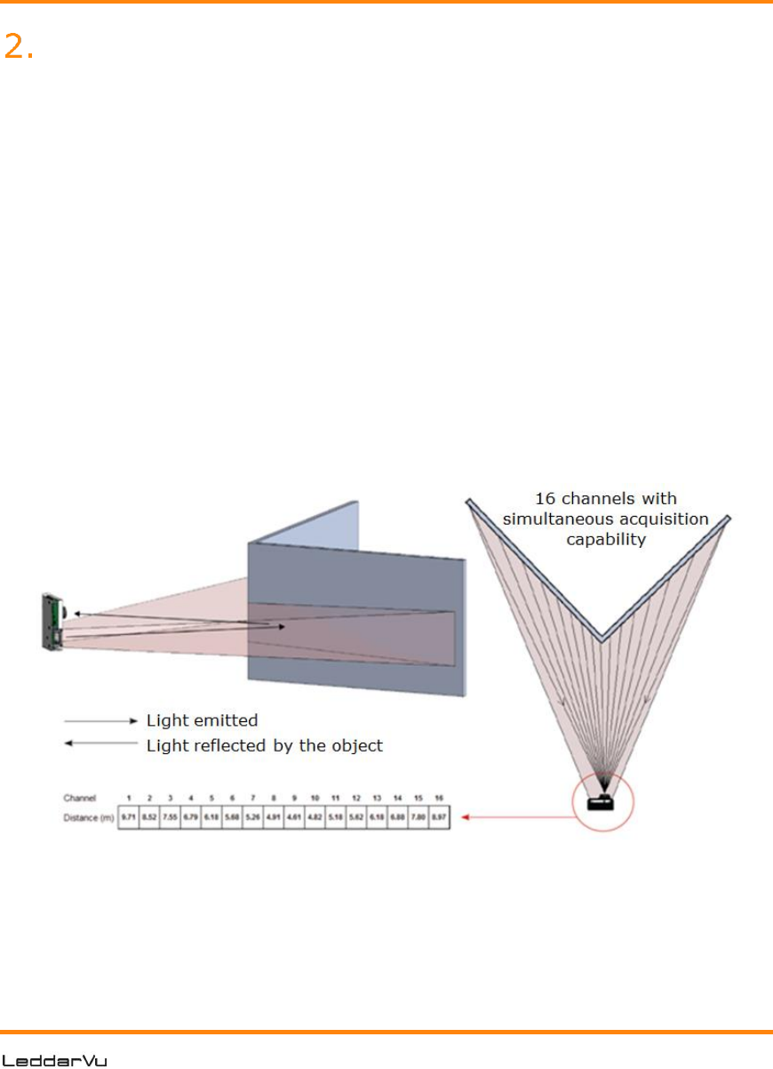
Figure 5 illustrates the illumination area and detection segments. In this cases, the
16 segments provide a profile of the object in the beam. In other installations, the
channels can be used to locate and track one or multiple objects in the beam.
Figure 5: Illumination area and detection zone
The core of Leddar™ sensing is the pulsing of diffused light, collection of reflected
light (including oversampling and accumulation), and full-waveform analysis. The
light source type, the number of light sources, the illumination and reception beam,
and the number of photodetectors can all be tailored to fit specific application
requirements such as detection range, beam, and spatial resolution.
18 P/N 54A0028-2 012017© 2017 LeddarTech Inc. Printed in Canada. All rights reserved.
Getting Started
This chapter presents the steps to install Leddar™ Configurator and start using the
LeddarVu.
3.1. Optional power supply
The power supply included with the Starter Kit version of the Leddar Vu8 has a
pluggable terminal block that connects to the 12V header connector of the LeddarVu
sensor. Location of the 12V header pin can be found on Figure 2 (LeddarVu SPI) or
Figure 3 (LeddarVu USB, UART, CAN Bus).
Figure 6: Optional Power Supply Terminal Block

19
3.2. Optional SPI cable
The table below shows the pinout of the optional SPI cable sold by LeddarTech.
Refer to Figure 2 for connection information.
Table 6: Optional SPI Cable Pinout
Wire Color
Function
Black
Ground
Blue
Reset_N
Orange
SCLK
Green
MISO
Yellow
MOSI
Brown
CS#
3.3. Setup
This section presents the Leddar™ Configurator installation and the procedure to set
up the LeddarVu module. All software operations are described in chapter 6.
To install Leddar™ Configurator:
Download the LeddarInstaller.exe file from our Web site at
http://support.leddartech.com/login.
If you are a new user, fill the form and click Submit.
If you are a registered user, login by entering your e-mail address and
password, and click Log In.
In the Download section, click a product and then click
LeddarInstaller.exe. Double-click the file to start the installation.
1. On the computer desktop, double-click the Leddar™ Configurator
icon.
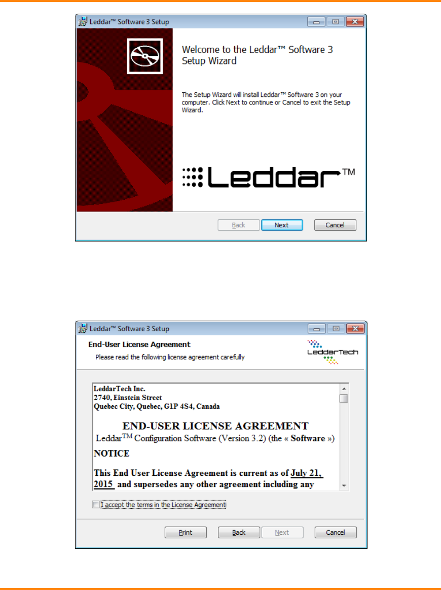
2. In the Welcome to the Leddar™ Software 3 Setup Wizard dialog
box, click Next.
20 P/N 54A0028-2 012017© 2017 LeddarTech Inc. Printed in Canada. All rights reserved.
Figure 7: Welcome to the Leddar™ Software 3 Setup Wizard dialog box
3. In the End-User License Agreement dialog box, read the terms of the
agreement, select the I accept the terms in the License Agreement
check box, and click Next.
Figure 8: End-User License Agreement dialog box
21
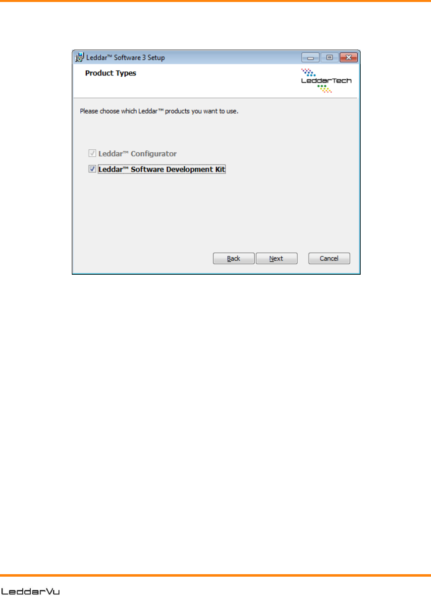
4. In the Product Types dialog box, the Leddar™ Software
Development Kit check box is selected by default.
Figure 9: Product Types dialog box
5. Click Next.
6. In the Destination Folder dialog box, click Next to select the default
destination folder.
OR
Click the Change button to choose a destination folder.
7. In the Ready to Install Leddar™ Software 3 dialog box, click the
Install button.
8. In the Completed the Leddar™ Software 3 Setup Wizard dialog
box, click Finish.
Leddar™ Configurator creates an icon on the computer desktop.
22 P/N 54A0028-2 012017© 2017 LeddarTech Inc. Printed in Canada. All rights reserved.
3.4. Connecting to the LeddarVu Module
The first time the module is connected to a computer, a few seconds are required for
Windows™ to detect it and complete the installation.
Once the installation is completed, you can connect to the LeddarVu module to
create your configuration.
To connect to the module:
1. Connect the power cable to the module and to a power source.
2. Connect the USB cable to the module and to the computer.
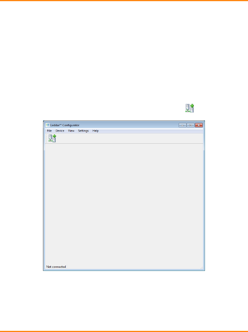
3. On the computer desktop, double-click the Leddar™ Configurator icon.
4. In Leddar™ Configurator, click the connect button ( ).
Figure 10: Connecting to a module
23
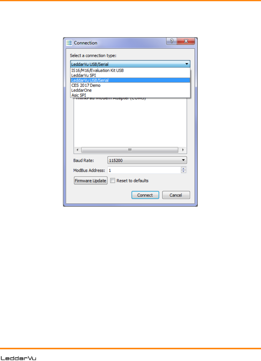
5. In the Connection dialog box, in the Select a connection type list,
select either LeddarVu SPI for a standard board or LeddarVu Serial
for an USB, CAN and SERIAL.
Figure 11: Connection dialog box
6. In the Available ports list, select the product and click the Connect
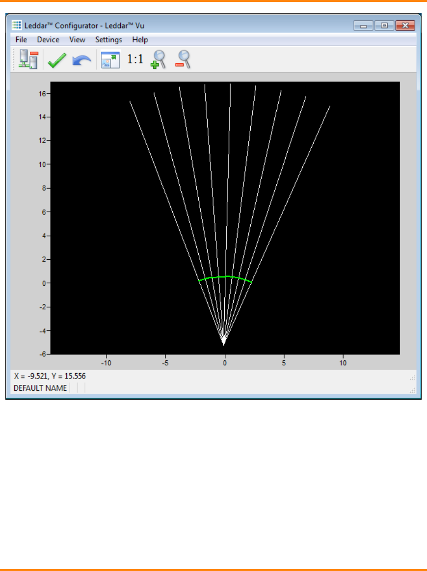
button.
The main window displays the detections (green lines) in the segments (white lines).
25
Measurements and Settings
This chapter presents measurements, settings, and zone definition for the LeddarVu
module.
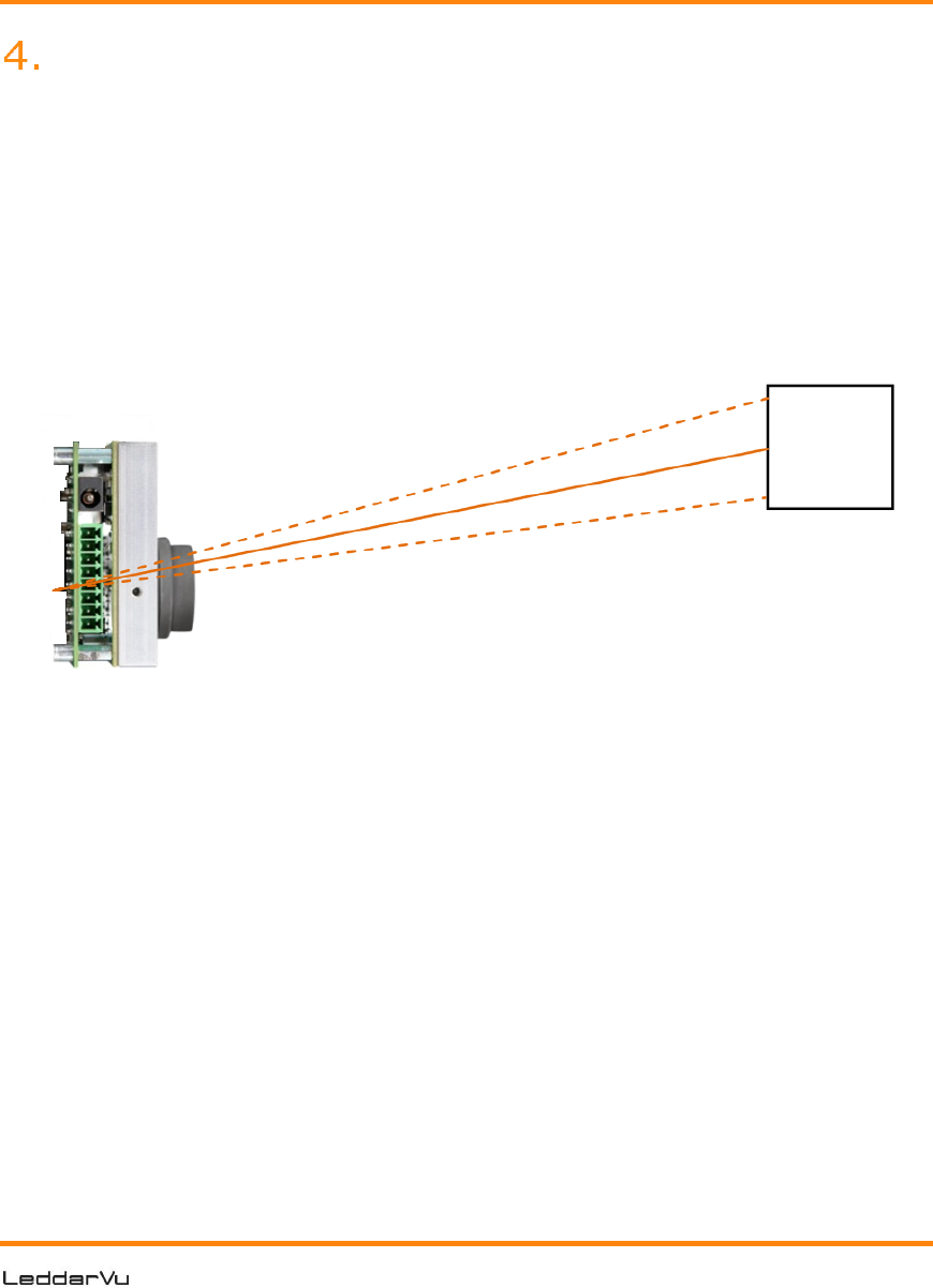
4.1. Distance Measurement
Distance is measured from the base of the standoffs for the LeddarVu module.
Figure 13: Distance measurement
The dashed lines illustrate 1 of the 8 segments and the solid line indicates the
distance measured by the module in that segment.

26 P/N 54A0028-2 012017© 2017 LeddarTech Inc. Printed in Canada. All rights reserved.
4.2. Data Description
Data displayed in the Raw Detections dialog box allow the user to precisely define
the desired detection parameters (View menu> Raw Detections).
Figure 14: Raw Detections dialog box
An object crossing the beam of the module is detected and measured. It is qualified
by its distance, segment position, and amplitude. The quantity of light reflected back
to the module by the object generates the amplitude. The bigger the reflection, the
higher the amplitude will be.
Table 7: Raw detection table description
Field
Description
Segment (Seg)
Beam segment in which the object is detected.
Distance
Position of the detected object.
Amplitude
Quantity of light reflected by the object and measured by the
module.
Flags
8-bit status (bit field). See Table 8.

27
The Flag parameter provides the status information that indicates the measurement
type.
Table 8: Flag value description
Bit
position
Bit = 0
Bit = 1
0
Invalid measurement
Valid measurement
1
Normal measurement
Measurement is the result of demerge
processing
2
Reserved
Reserved
3
Normal measurement
Received signal is above the
saturation level.
Measurements are valid (VALID is set)
but have a lower accuracy and
precision.
Consider decreasing the light source
intensity.
4
Reserved
Reserved
5
Reserved
Reserved
6
Reserved
Reserved
7
Reserved
Reserved
8
Reserved
Reserved
9
Reserved
Reserved
The Flag field provisions for 8 bits encoded as a bit field. Three bits are currently
used. The following table presents the implemented decimal values of the status bit
field.
Table 9: Status value description
Status value
(decimal)
Status value (binary)
Description
1
00000001
Normal measurement
(valid)
9
00001001
Saturated signal (valid)
28 P/N 54A0028-2 012017© 2017 LeddarTech Inc. Printed in Canada. All rights reserved.
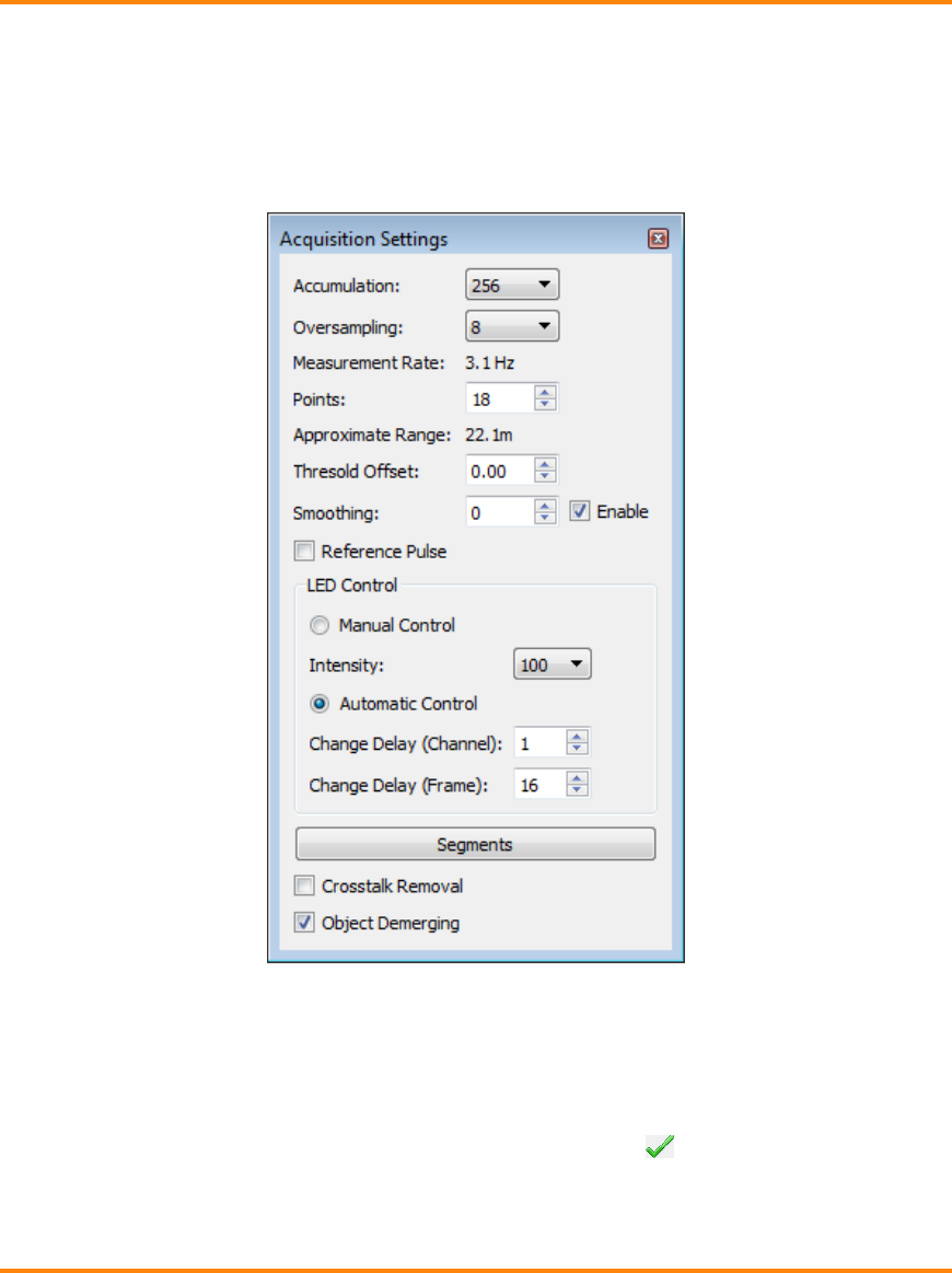
4.3. Acquisition Settings
Acquisition settings allow you to define parameters to use for detection.
To open the Acquisition Settings dialog box, on the Device menu, point to
Configuration and click Acquisition.
Figure 15: Acquisition Settings dialog box
The numbers on a grey background are modified only by using the arrows, while the
ones on a white background can additionally be modified manually by the numeric
keypad of your keyboard.
To apply new acquisition settings, click the apply button ( ).

29
Table 10: Acquisition setting description
Parameter
Description
Effect
Accumulation
Number of
accumulations
Higher values enhance the range, and reduce the measurement rate and
noise.
Oversampling
Number of oversampling
cycles
Higher values enhance the accuracy/precision/resolution and reduce the
measurement rate.
Points
Number of base sample
points
Determines the maximum detection range.
Threshold
Offset
Modification to the
amplitude threshold
Higher values decrease the sensitivity and reduce the range.
Smoothing
Object smoothing
algorithm
Smooths the LeddarVu module measurements.
The behavior of the smoothing algorithm can be adjusted by a value
ranging from -16 to 16. Higher values enhance the module precision, but
reduce the module reactivity.
The smoothing algorithm can be deactivated by clearing the Enable check
box.
The measurement smoothing algorithm is advised for application that need
to measure slowly moving objects with a high precision.
The application requiring to quickly track moving objects, the smoothing
should be configured with a value lower than 0 or simply deactivated.
Light Source
Control
Light source power
control options
Selects between manual and automatic power control. In automatic, light
source power is adjusted according to incoming detection amplitudes. The
current LED power level is visible in the Device State window (View
menu, State command).
Change Delay
(Channel and
Frame)
Minimum delay between
power changes
Smaller numbers speed up the response time of the light source power
adjustment.
Object
demerging
Discrimination of objects
close to each other
Eases the discrimination of multiple objects in the same segment.
Object demerging is only available for measurement rates under 5.0 Hz.
The number of merged pulses that can be processed in each frame is also
limited. A status field is available in the device state window (LeddarTM
Configurator) indicating if the sensor processes all merged pulses.
The measurement of demerged objects tends to be less precise than for
usual detections
Crosstalk
Removal
Inter-segment
interference noise
removal
Crosstalk is a phenomenon inherent to all multiple segments time-of-flight
sensors. It causes a degradation of the distance measurement accuracy of
an object when one or more objects with significantly higher reflectivity
are detected in other segments at a similar distance.
This option enables an algorithm to compensate the degradation due to
crosstalk.
This algorithm increases the computational load of the LeddarVu module
microcontroller. It is recommended to disable the crosstalk removal if the
module is configured to run at rates higher than 50 Hz.

30 P/N 54A0028-2 012017© 2017 LeddarTech Inc. Printed in Canada. All rights reserved.
Accumulation
When you increase the accumulation value, you reduce the noise as well as the measurement
rate. Depending on your application, a reduction of the noise might be more important than a
high measurement rate.
Oversampling
When you increase the accumulation value, you increase the resolution (accuracy) but you
reduce the measurement rate. Depending on your application, a higher resolution might
be more important than a high measurement rate.
Points
Determines the maximum detection range. It also has an impact on the processing load
since it impacts the number of sample points to process for each segment.
Threshold offset
The threshold offset is a value that modifies the detection amplitude threshold.
A default detection threshold table was determined to provide robust detection and
minimize false detections caused by noise in the input signal.
Figure 16 presents the threshold table for a light source intensity of 16. This table is
effective when the threshold offset value is 0.
Figure 16: Detection threshold example

31
The multiple lines on each graph present the thresholds for numbers of
accumulations of 1 (top curve), 2, 4, 8, 16, 32, 64, 128, and 256 (bottom curve).
Accumulations of 512 and 1024 are also available, although not shown (provide the
lowest thresholds).
The threshold offset parameter has the effect of offsetting each value in the
threshold table by the selected value. This provides a means of reducing the
sensitivity (positive value) or increasing the sensitivity (negative value) of the
module. Increasing the value of the threshold offset allows ignoring (will not result
in a measurement) signals with amplitude higher than the default threshold.
Decreasing the value of the threshold offset allows measurements of amplitude
signals lower than the default threshold.
NOTE: The default setting (0) is selected to ensure a very low occurrence of false
measurements.
False measurements are likely to occur when reducing the threshold offset (negative
values). These false measurements are very random in occurrence while true
measurements will be repeatable. For this reason, it may be useful in some
applications to use a higher sensitivity and filter out the false measurements at the
application level. For example, this can be useful in applications that require long
detection ranges or detection of small or low reflectivity targets.
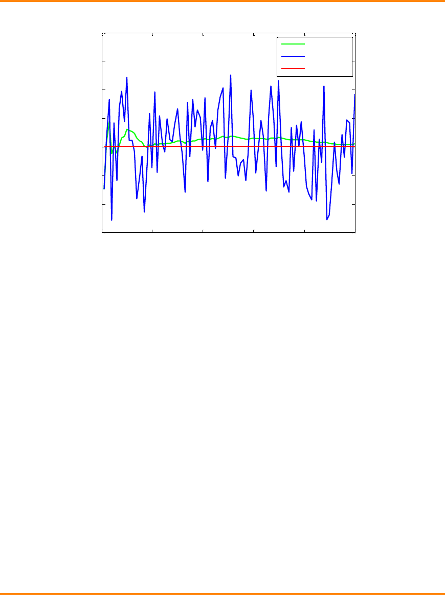
Smoothing
The smoothing algorithm increases the precision of the measurement at the cost of
the LeddarVu module reactivity. The algorithm works by averaging consecutive
measurements over a given time history. The history length of the filter is defined
as a function of the measurement noise level. It also changes according to the
oversampling and accumulation settings. The history length of the averaging filter
can also be adjusted by a parameter ranging from -16 to 16. Higher values increase
the module precision, but reduce the module reactivity. An example of the behavior
of the measurement smoothing algorithm is depicted in Figure 17.
32 P/N 54A0028-2 012017© 2017 LeddarTech Inc. Printed in Canada. All rights reserved.
Figure 17: Measurement smoothing example
The red line represents the true target distance; the blue curve corresponds to the
target distance measured by the module without smoothing, while the green curve
is the smoothed measurements. One could notice the measurement precision
(standard deviation) is dramatically improved by the smoothing algorithm.
NOTE: The smoothing algorithm is recommended for applications that need highly
precise measurements of slowly moving objects. For application that tracks
quickly moving objects, it is advised to decrease the value of the smoothing
parameter or to disable the smoothing algorithm.
Light Source Control
There is a total of 5 light source power levels. Their approximate relative power is
evenly distributed between 0 through 100%.
The change delay defines the number of measurements required before allowing the
LeddarVu module to increase or decrease by one the light source power level. For
example, with the same change delay, the maximum rate of change (per second) of
the light source power will two times higher at 12.5 Hz than at 6.25 Hz.
NOTE: Since the change delay parameter is a number of measurements, the delay
will vary if the measurement rate is changed (through modification of the
accumulation and oversampling parameters).
020 40 60 80 100
14.98
14.99
15
15.01
15.02
15.03
15.04
15.05
Sample
Distance (m)
Estimated
Measured
True

33
Keeping the module in automatic light source power mode (default setting) ensures
it adapts to varying environments. Close range objects may reflect so much light
they can saturate the module, reducing the quality of the measurements. This mode
will adapt the light output within the change delay setting to reach the optimal
amplitude. On the other hand, low amplitudes provide lower accuracy and precision.
The automatic light source power mode will select a light source intensity that
provides the highest intensity that avoids the saturation condition.
NOTE: When a strongly reflective or near object is present in the field of view while
monitoring farther distances, the automatic adjustment will reduce the
effective range of the module (reduce light source intensity) and may
prevent detection of long range or low reflectivity objects. For these
applications, manual mode with light source power set to 100% may be a
better setting.

34 P/N 54A0028-2 012017© 2017 LeddarTech Inc. Printed in Canada. All rights reserved.
4.4. Measurement Rate
The LeddarVu module acquires a base input waveform for each segment at a rate
between 10 kHz and 40 kHz, depending on the sensor field of view (see Table 11).
Multiple acquisitions are used to perform accumulations and oversampling, and
generate a final waveform that is then processed to detect the presence of objects
and measure their position.
Table 11: Base Acquisition Rate Based on the Field of View
Leddar Vu8 FOV
Base Acquisition Rate
20°
10 kHz
48°
20 kHz
100°
40 kHz
Therefore, the final measurement rate is:
Measurement rate = base rate/number of segments
enabled/accumulations/oversampling
For example, Leddar Vu8 20° with 256 accumulations and an oversampling value of
8:
Measurement rate = 10000 / 256 / 8 / 8= 0.61 Hz
Table 12 presents the measurement rate for typical values of accumulations and
oversampling.

35
Table 12: Measurement rate for Leddar Vu8 100°
Accumulation
Oversampling
Measurement Rate (Hz)
LeddarVu
20°
LeddarVu
48°
LeddarVu
100°
1024
8
0.15
0.3
0.61
512
8
0.3
0.6
1.22
256
8
0.6
1.2
2.4
128
8
1.22
2.4
4.8
64
8
2.4
4.8
9.7
32
8
4.8
9.7
19.5
1024
4
0.3
0.6
1.2
512
4
0.6
1.2
2.4
256
4
1.2
2.4
4.8
128
4
2.4
4.8
9.7
64
4
4.8
9.7
19.5
32
4
9.7
19.5
39.0
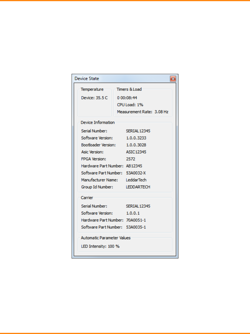
4.5. CPU Load
The measurement rate varies with the accumulations and oversampling settings.
The higher the rate, the higher the processing load is on the source and control
assembly microcontroller. The Point parameter, in the Acquisition Settings dialog
box, (Device menu, Configuration> Acquisition) also has an impact on the
processing load since it impacts the number of sample points to process for each
segment.
Given the high flexibility of parameter settings, it is possible to create a processing
load that exceeds the capacity of the microcontroller. When the microcontroller load
is exceeded, the theoretical measurement rate will not be obtained.
36 P/N 54A0028-2 012017© 2017 LeddarTech Inc. Printed in Canada. All rights reserved.
The load (CPU Load) is displayed in the Device State window (View menu>
State). It is recommended to verify the load when modifying the accumulations,
oversampling, and point count parameters. The measurement rate will be lower
than the calculated rate and the measurement period may be irregular when the
load nears or reaches 100%.
Figure 18: Device State window
37
Communication Interfaces
The interfaces and links are optional and are implemented depending on your
configuration.
5.1. SPI Interface
The SPI interface on the SPI board is a direct link to the receiver module.
The SPI interface available with the USB, CAN and SERIAL board is a port connected
to MCU but not implemented for the moment.
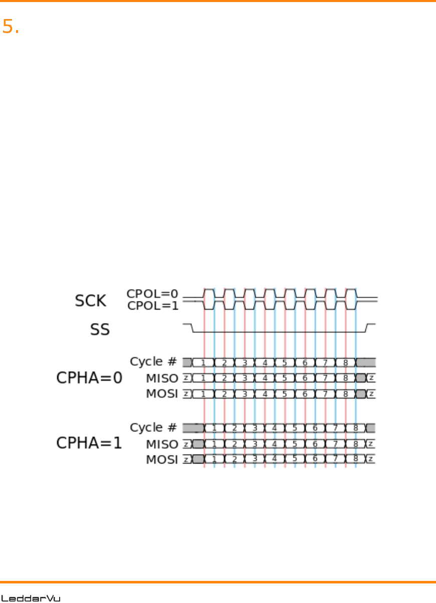
5.1.1. SPI Basics
The SPI interface uses the configuration mode 0; where, data is captured on the
rising edge of the clock signal and outputted on the falling.
Figure 19: Standard SPI timing diagram
The Table 13 presents the basic clock signal modes.

38 P/N 54A0028-2 012017© 2017 LeddarTech Inc. Printed in Canada. All rights reserved.
Table 13: Basic modes
Mode
Clock Polarity
CPOL
Clock Phase
CPHA
0
0
0
1
0
1
2
1
0
3
1
1
5.1.2. SPI Protocol
The universal SPI protocol uses a combination of standard commands for FLASH and
SRAM memories.
Each SPI packet contains a header, a payload, and a cyclic redundancy check (CRC).
The first byte of the header corresponds to an instruction opcode. It is followed by a
24-bit address and the 16-bit size of the payload. The payload contains a number of
user-data bytes. The last 16 bits of the packet is the CRC16 (IBM) of both header
and payload. The table below summarizes the structure of an SPI packet. It is noted
that address and the CRC are packed with the most significant byte first while the
first byte of data corresponds to the least significant byte.
Table 14: Byte offsets
Field
Opcode
Address
Size
Data
CRC16
Byte
offset
1
2
3
4
5
6
7
…
7 + n
8 + n
9 + n
The supported opcodes are presented in Table 15.

39
Table 15: SPI opcode commands
Mnemonic
Opcode
Operation
Description
READ
0x0B
Read data
The read command returns data from
memory starting at the selected
address. It needs a delay between the
group containing the opcode, address,
and size data, and the return data
stream to let the receiver module to
decode the request and get the ready
data to the clock.
WRITE
0x02
Write data
The write command writes data to
memory starting at the selected
address and is limited to a page of 1 to
512 bytes.
CE
0xC7
Reset
configuration
The reset command resets the module
to the default configuration. The
process is started on deassert of nCS
and the write-enable flag in the status
register must be asserted.
RDSR
0x05
Read status
register
The read status command returns a
byte of the status register and bit-field
flags (refer to Table 16).
WREN
0x06
Write enabled
The write enabled command disables
the write protection in order to modify
any parameters.
WRDIS
0x04
Write disabled
The write disabled command enables
the write protection to lock the module
from any parameter changes.
SOFTRST
0x99
Software reset
The software reset command resets
the receiver module.
40 P/N 54A0028-2 012017© 2017 LeddarTech Inc. Printed in Canada. All rights reserved.
The status register and bit flags are presented in Table 16.
Table 16: Status register
Bit
Name
Access
Description
7:2
Reserved
R/W
Future use
1
Write enable
latch
R
0 = Write disabled
1 = Write enabled
0
Module
ready
R
0 = Module ready
1 = Module busy (programming, erasing)
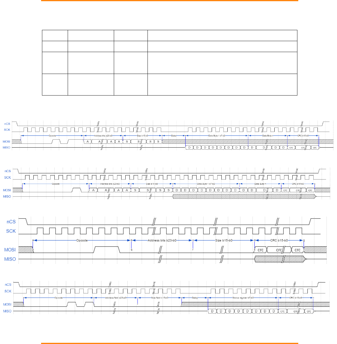
Data chronograms are represented in Figure 20 and Figure 21, and opcode and
register chronograms are presented in Figure 22 and Figure 23.
Figure 20: Read data chronogram
Figure 21: Write data chronogram
Figure 22: Single opcode chronogram (write enabled example)
Figure 23: Read status register chronogram

41
5.1.3. Memory Map
The memory map is divided in four memory banks. This section presents the
description of the four memory banks in a table format.
Table 17: Memory banks
Bank
Number
Start Base
Address
Bank
Size (KB)
Access
Description
0
0x00000000
1024
R/W
Configuration data
5
0x00400000
128
Read only
Device information and
constants
13
0x00500000
1024
Read only
Detection list
19
0x00FFFB00
1
R/W
Transaction configuration
Configuration data
Table 18: Configuration data bank
Offset
length
Type
Description
0
32
char
Module name as an ASCII string
32
1
uint8_t
Accumulation exponent: Ie. 3 = 23=8
33
1
uint8_t
Oversampling exponent: Ie 3 = 23=8
34
1
uint8_t
Base point sample
35
4
uint32_t
Bit field of segment enabled
39
4
uint32_t
Acquisition rate of the reference pulse
43
4
float
Yaw angle of the module
47
4
float
Pitch angle of the module
51
4
float
Roll angle of the module
55
4
float
X-axis position of the module
59
4
float
Y-axis position of the module
63
4
float
Z-axis position of the module
67
1
int8_t
Precision (smoothing): Stabilizes the
module measurements. The behavior
of the smoothing algorithm can be
adjusted by a value ranging from –16

42 P/N 54A0028-2 012017© 2017 LeddarTech Inc. Printed in Canada. All rights reserved.
through 16.
68
1
uint8_t
Precision enabled
69
1
uint8_t
Saturation compensation enabled
70
1
uint8_t
Overshoot management enabled
71
4
int32_t
Sensitivity (detection threshold)
setting expressed in a raw amplitude
scale.
75
1
uint8_t
Light source power (0 to 100)
76
1
uint8_t
Auto light source power enabled
77
2
uint16_t
Auto frame average: Changes the
delay in the number of measurements.
This is the responsivity of the auto
light source power according to the
number of frames.
79
1
uint8_t
Auto detections average: Number of
detections for saturation acceptance
(the number of detections can be
saturated to avoid decreasing the light
source power when using the
automatic mode). This is the
responsivity of the auto light source
power according to the number of
detections.
80
1
uint8_t
Object demerging enabled
81
1
uint8_t
Static noise removal enabled
Device information and constants
Table 19: Device information and constants bank
Offset
length
Type
Description
0
32
char
Module part number as an ASCII string
32
32
char
Software part number as an ASCII string
64
32
char
Module serial number as an ASCII string
96
32
char
Manufacturer name as an ASCII string
128
32
char
Group identification number as an ASCII

43
string
160
32
char
Build date as an ASCII string
192
32
char
Firmware version as an ASCII string
224
32
char
Bootloader version as an ASCII string
256
32
char
ASIC version as an ASCII string (optionally
filled in function of the module)
288
32
char
FPGA version as an ASCII string
320
2
uint16_t
Module type
0x00000000: Invalid Device
0x00000007: M16 Evaluation Kit
0x00000008: IS16
0x00000009: M16
0x0000000A: Leddar One
0x0000000D: Leddar Vu8
322
4
uint32_t
Internal Use
326
1
uint8_t
Accumulation exponent min.
327
1
uint8_t
Accumulation exponent max.
328
1
uint8_t
Oversampling exponent min.
329
1
uint8_t
Oversampling exponent max.
330
1
uint8_t
Base point sample min.
331
1
uint8_t
Base point sample max.
332
2
uint16_t
Number of vertical segments
334
2
uint16_t
Number of horizontal segments
336
2
uint16_t
Number of reference segments
338
4
uint32_t
Base point sample distance
342
4
uint32_t
Reference segment mask: bit-field mask
indicates the position of the reference
segments.
346
2
uint16_t
Number of sample max.
348
1
uint8_t
Internal Use

44 P/N 54A0028-2 012017© 2017 LeddarTech Inc. Printed in Canada. All rights reserved.
349
4
uint32_t
Clock frequency
353
1
uint8_t
Maximum number of detections per segment
354
4
uint32_t
Distance scale
358
1
uint8_t
Raw amplitude scale bit, to which 0xd must
be added (amplitude scale given in bitshift).
ie raw amplitude << (scale bit + 0x0d)
359
4
uint32_t
Raw amplitude scale, to which the value
8192 must be added.
363
2
int16_t
Precision min.
365
2
int16_t
Precision max.
367
4
int32_t
Sensitivity min.
371
4
int32_t
Sensitivity max.
375
1
uint8_t
Current light source power count (max 16)
376
2
uint16_t
Auto frame average min.
378
2
uint16_t
Auto frame average max.
380
1
uint8_t
Auto light source power percent min.
381
1
uint8_t
Auto light source power percent max.
382
1
uint8_t
Auto detections average min.
383
1
uint8_t
Auto detections average max.
384
1
uint8_t
Static noise calibration source:
0 = By end-user
1 = By factory
385
4
uint32_t
CPU load scale
389
4
uint32_t
Temperature scale

45
Detection list
Table 20: Detection list bank
Offset
length
Type
Description
0
4
uint32_t
Timestamp: in ms since the power up
4
2
uint16_t
Number of detection (N)
6
2
uint16_t
Current percentage of light source
power
8
4
uint32_t
Acquisition options
12
N *
detection
structure
size
Array of
detection
structure
Start of detection list array
Refer to Table 21 for details.
Table 21: Detection structure size
Offset
length
Type
Description
0
4
uint32_t
Distance expressed in distance scale
To convert to meters, the distance
must be divided by the distance scale.
4
4
uint32_t
Amplitude expressed in raw amplitude
scale
To convert the amplitude to count, it
must be divided by the amplitude
scale.
Amplitude = Contents of this
register/(Amplitude Scale Register +
8192)
8
2
uint16_t
Segment number
10
2
uint16_t
Bit-field detection flags:
Bit 0: Detection is valid (will
always be set)
Bit 1: Detection was the result of
object demerging
Bit 2: Reserved
Bit 3: Detection is saturated

46 P/N 54A0028-2 012017© 2017 LeddarTech Inc. Printed in Canada. All rights reserved.
Transaction configuration
Table 22: Transaction configuration bank
Offset
length
Type
Description
0
1
uint8_t
Secure-transaction enabled flags:
1 = Enables the CRC calculation and validation on any
transaction. This flag is enabled by default.
0 = No CRC validation. The CRC field is still required in
SPI protocol but can be set to any value.
1
1
uint8_t
Transaction modes:
0 = Free run. The READY pin is asserted on each ready
detection frame. The host must be able to read data on
time.
1 = Blocking read. On the READY pin assertion, host
must read all data from traces or detections bank (data
transaction control source configuration) to continue
acquisition.
2 = Partial blocking read. On the READY pin assertion,
host can read all data from traces of the detection bank
and the acquisition is still running. Possible loss of
detection frames if the host reading data is very long.
2
2
uint16_t
CRC of the last transaction
4
2
uint16_t
Bit-field information of last transactions:
All bits to 0: No transaction error
Bit-0: Access right violation
Bit-1: Invalid address
Bit-2: Command not found
Bit-3: Write disabled
Bit-4: CRC failed
Bit-5: Command execution error
Bit-6: Invalid packet
6
1
uint8_t
Data transaction control source:
0 = On trace
1 = On detections
This register determines which data type will control the

47
READY pin and manage the transaction mode.
5.1.4. SPI Operation
The SPI operation includes four parameters: SPI port configuration, speed and
timing, access, and modification.
SPI port configuration
The SPI port must be configured in the 0 mode (refer to section 5.1.1 on page 37)
to communicate with the receiver module. To prevent the receiver module to go into
the bootloader mode, the port must never have all SPI input pins (nCS, MOSI and
CLK) set to the low level for more than 100 milliseconds at power up or when
performing a hard reset.
Speed and timing
For the read operation, a delay is needed between the header (group containing the
opcode, address, and size data), and the return data stream to let the receiver
module to decode the request and get the ready data to the clock. This delay can be
set to 1 millisecond. During this delay, the SPI clock must be halted and the nCS
must be staying asserted (see Figure 20 on page 40).
The SPI clock frequency can be in the range between 500 kHz and 25 MHz.
Access
In order to access a parameter, you need to add a parameter offset to the
associated bank start base address. Use the parameter length to get or set the
whole parameter field.
Modification
To modify a parameter:
1. Disable the write protection of the module by sending the write enabled
command.
2. Poll the status register to get the ready state and write enabled flag
asserted.
3. Send the new parameter value.
4. Poll the status register to get the ready state.

48 P/N 54A0028-2 012017© 2017 LeddarTech Inc. Printed in Canada. All rights reserved.
5. Send the write disabled command (write protection) to prevent any
unwanted parameter change.
NOTE: To prevent any data corruption or loss after modifying a parameter or a
firmware update, the module must be in the ready state before shutting it
down or doing a hard reset.
5.2. I2C Interface
The I2C interface on the SPI board is a direct link to the receiver and source
modules. For the moment, only the temperature sensor is accessible. Refer to the
LM75BIMM-3/NOPB temperature sensor datasheet from Texas Instrument.
The I2C interface available with the enhance board is a port connected to MCU but
not implemented for the moment.
5.3. USB Interface
The USB interface available with the USB, CAN and SERIAL board is a VCP (virtual
COM port) serial emulation port. This port is used as a serial link with the Modbus
protocol (refer to section 5.4 Serial Link Interface). This interface can also be used
to update the USB, CAN and SERIAL board firmware in the bootloader mode.
5.4. Serial Link Interface
The serial links can be of the following electric signals: TTL, RS-232, RS-422, and
RS-485.
The serial link ports use the Modbus protocol using the RTU transmission mode only.
This section describes the commands that are implemented.
For more information on the Modbus protocol, please visit
www.modbus.org.
Read input register (function code 0x4)
The following table presents the registers for the read input commands
Table 23: Read input register messages
Address
Description
1
Detection status for polling mode:

49
0 = Detections not ready
1 = Detections ready: this status flag is reset to 0
after reading this register
2
Number of segments (N)
11
Number of detections
12
Current percentage of light source power
13
Bit field of acquisition status: Reserved
14
Low 16 bits of timestamp (number of milliseconds
since the module was started)
15
High 16 bits of timestamp
16 to
16 + N-1
Distance of first detection for each segment, zero if no
detection in a segment. The distance unit is defined by the
serial port parameters.
16 + N to
16 + (2*N) - 1
Amplitude of first detection for each segment times 64
(that is, amplitude = this register/64), zero if no
detection in a segment
16 + (2*N) to
16 + (3*N) - 1
Flag of the first detection for each segment:
Bit 0: Detection is valid (will always be set)
Bit 1: Detection was the result of object demerging
Bit 2: Reserved
Bit 3: Detection is saturated
16 + (3*N) to
16 + (4*N) - 1
Distance of the second detection for each segment
16 + (4*N) to
16 + (5*N) - 1
Amplitude of the second detection for each segment
16 + (5*N) to
16 + (6*N) - 1
Flag of the second detection for each segment
16 + (6*N) to
16 + (7*N) - 1
Distance of the third detection
16 + (7*N) to
16 + (8*N) - 1
Amplitude of the third detection
16 + (8*N) to
16 + (9*N) - 1
Flag of the third detection

50 P/N 54A0028-2 012017© 2017 LeddarTech Inc. Printed in Canada. All rights reserved.
16 + (9*N) to
16 + (10*N) - 1
Distance of the fourth detection
16 + (10*N) to
16 + (11*N) - 1
Amplitude of the fourth detection
16 + (11*N) to
16 + (12*N) - 1
Flag of the fourth detection
16 + (12*N) to
16 + (13*N) - 1
Distance of fifth detection
16 + (13*N) to
16 + (14*N) - 1
Amplitude of fifth detection
16 + (14*N) to
16 + (15*N) - 1
Flag of the fifth detection
16 + (15*N) to
16 + (16*N) - 1
Distance of the sixth detection
16 + (16*N) to
16 + (17*N) - 1
Amplitude of the sixth detection
16 + (17*N) to
16 + (18*N) - 1
Flag of the sixth detection
NOTE: As per the Modbus protocol, register values are returned in big-endian
format.
Read holding register (function code 0x3), write register (function
code 0x6), write multiple register (function code 0x10), and
read/write multiple register (function code 0x17)
The following table presents the registers for these commands (see section 4.3 for a
more detailed description of parameters).
Table 24: Read holding register message definition
Address
Description
0
Exponent for the number of accumulations (that is, if the
content of this register is n, 2n accumulations are performed)
1
Exponent for the number of oversamplings (that is, if the
content of this register is n, 2n oversamplings are performed)
2
Number of base samples
3
Reserved
4
Detection threshold as a fixed-point value with a 6-bit

51
fractional part (i.e. threshold value is this register divided by
64).
5
Light source power in percentage of the maximum. A value
above 100 is an error. If a value is specified that is not one of
the pre-defined values, the closest pre-defined value will be
used. The register can be read back to know the actual value
set.
6
Bit field of acquisition options:
Bit-0: Automatic light source power enabled
Bit-1: Demerge object enabled
Bit-2: Static noise removal enabled
Bit-3: Precision enabled
Bit-4: Saturation compensation enabled
Bit-5: Overshoot management enabled
7
Auto light source power change delay in number of
measurements
8
Reserved
9
Number of echoes for saturation acceptance: The number of
echoes can be saturated to avoid decreasing the light source
power in automatic mode.
10
Operation mode
Write mode:
0: Stop (stop acquisition)
1: Continuous
2: Single (acquisition of a single detection frame)
Read mode:
10: Stopped (sensor is stopped)
11: Continuous acquisition mode
12: Single frame busy (acquisition in progress)
13: Sensor is busy
11
Smoothing: Stabilizes the module measurements. The
behavior of the smoothing algorithm can be adjusted by a

52 P/N 54A0028-2 012017© 2017 LeddarTech Inc. Printed in Canada. All rights reserved.
value ranging from –16 through 16.
12
Low 16 bits of segment enabled: Bit-field of enabled segment
13
High 16 bits of segment enabled
NOTE: As per the Modbus protocol, register values are returned in big-endian
format.
A request for a register that does not exist will return error code 2. Trying to set a
register to an invalid value will return error code 3. If an error occurs while trying to
execute the function, error code 4 will be returned.
Report server ID (function code 0x11)
This function returns information on the LeddarVu module in the following format:
Table 25: Report server ID messages
Offset
Length
Description
0
1
Number of bytes of information (excluding this one).
Currently 0x99 since the size of information returned is
fixed.
1
32
Serial number as an ASCII string
33
1
Run status 0: OFF, 0xFF: ON. Should always return 0 FF,
otherwise the module is defective.
34
32
The device name as an ASCII string
66
32
The hardware part number as an ASCII string
98
32
The software part number as an ASCII string
130
8
The full firmware version as 4 16-bit values
138
48
The full bootloader version as 4 16-bit values
146
2
The FPGA-build version
148
4
Internal Use
152
2
Module identification code (9 for the module)
Get detections (function code 0x41)
This function returns the detections/measurements in the following format:

53
The first byte is the number of detections in the message. Because of the limitation
on a Modbus message length, a maximum of 40 detections will be returned.
NOTE: This maximum can be configured to a lower value using the Leddar™
Configurator software (serial port configuration) or the Write Register
command described below.
Following the first byte, each detection has six bytes (refer to Table 26)
Table 26: Get detection messages (detection fields)
Offset
Length
Description
0
2
The distance (little-endian). Distance unit is defined by serial port
parameters
2
2
The amplitude times 64 [that is, amplitude = this field/64 (little-endian)]
4
1
3 bits are flags describing the measurement (all others are reserved):
Bit 0: Detection is valid (will always be set)
Bit 1: Detection was the result of object demerging
Bit 2: Reserved
Bit 3: Detection is saturated
5
1
Segment number
Trailing all the detections have 3 more fields (refer to Table 27).
Table 27: Get detection messages (trailing fields)
Offset
Length
Description
0
4
Timestamp of the acquisition (little-endian). The timestamp is expressed
as the number of milliseconds since the device was started.
4
1
Current light source power as a percentage of maximum.
5
2
Bit-field acquisition. Reserved
Read module data (function code 0x42)
Table 28 and Table 29 present the request and answer codes for reading data.
Table 28: Requests
Offset
Length
Description
0
4
Base address: 0x00000000 to 0x00FFFFFF

54 P/N 54A0028-2 012017© 2017 LeddarTech Inc. Printed in Canada. All rights reserved.
4
1
Number of bytes to read: 1 through 247
Table 29: Answers
Offset
Length
Description
0
4
Base address: 0x00000000 to
0x00FFFFFF
4
1
Number of bytes read: 1 through 247
5
Nb * 1 byte
Data
Write module data (function code 0x43)
Table 30 and Table 31 present the request and answer codes for writing data.
Table 30: Requests
Offset
Length
Description
0
4
Base address: 0x00000000 to 0x00FFFFFF
4
1
Number of bytes written: 1 through 247
5
Nb * 1 byte
Data
Table 31: Answers
Offset
Length
Description
0
4
Base address: 0x00000000 to 0x00FFFFFF
4
1
Number of bytes written: 1 through 247
Send opcode command (function code 0x44)
Table 32 and Table 33 present the request and answer codes for sending the
opcode.
Table 32: Requests
Offset
Length
Description
0
1
Opcode, supported opcodes:

55
Read status = 0x05
Write enabled = 0x06
Write disabled = 0x04
Reset configuration = 0x C7
Soft reset = 0x99
1
1
Argument: optional value (must be set to
0x00)
Table 33: Answers
Offset
Length
Description
0
1
Opcode
1
1
Return value: optional return value (read
status opcode = Status value)
Get serial port settings (function code 0x45, 0x00)
Table 34, Table 35 and Table 36 present the requests and answers of the get serial
port settings.
Table 34: Requests
Offset
Length
Description
0
1
Sub-function code: 0x00
Table 35: Answers header field
Offset
Length
Description
0
1
Sub-function code: 0x00
1
1
Number of serial port
2
1
Current logical serial port number (current logical serial
number connected to the host used for this transaction)

56 P/N 54A0028-2 012017© 2017 LeddarTech Inc. Printed in Canada. All rights reserved.
Table 36: Answers serial port settings field
Offset
Length
Description
0
1
Logical serial port number
1
4
Baud rate, supported rates:
9,600
19,200
38,400
57,600
115,200
5
1
Date size: 8 = 8-bit size
6
1
Parity:
0 = None
1 = Odd
2 = Even
7
1
Stop bit:
1 = 1 stop bit
2 = 2 stop bits
8
1
Flow control: 0 = None
9
1
Modbus address: 1 through 247
10
1
Max. echoes per transactions. Used for the Get Detection
command (function code 0x41), max. of 40 echoes.
11
2
Distance resolution:
1 = m
10 = dm
100 = cm
1,000 = mm
NOTE: This answer table is repeated by the number of available serial port.
Set serial port settings (function code 0x45, 0x01)
Table 37, Table 38 and Table 39 present the requests and answers for the set serial
port settings.

57
Table 37: Requests header field
Offset
Length
Description
0
1
Sub-function code: 0x01
Table 38: Requests serial port setting field
Offset
Length
Description
0
1
Settings of corresponding logical serial port number to set.
1
4
Baud rate, supported rates:
9,600
19,200
38,400
57,600
115,200
5
1
Date size: 8 = 8-bit size
6
1
Parity:
0 = None
1 = Odd
2 = Even
7
1
Stop bit:
1 = 1 stop bit
2 = 2 stop bits
8
1
Flow control: 0 = None
9
1
Modbus address: 1 through 247
10
1
Max. echoes per transactions. Used for the Get Detection
command (function code 0x41), max. of 40 echoes.
11
2
Distance resolution:
1 = m
10 = dm
100 = cm
1,000 = mm
NOTE: This request table can be repeated by the number of available serial ports
(by using the corresponding logical port number).

58 P/N 54A0028-2 012017© 2017 LeddarTech Inc. Printed in Canada. All rights reserved.
Table 39: Answers
Offset
Length
Description
0
1
Sub-function code: 0x01
Get carrier firmware information (function code 0x45, 0x02)
Table 40 and Table 41 present the registers for the firmware information commands.
Table 40: Requests
Offset
Length
Description
0
1
Sub-function code: 0x02
Table 41: Answers
Offset
Length
Description
0
1
Sub-function code: 0x02
1
32
Firmware part number ASCII string
33
8
Firmware version in four units for format A,
B, C, and D.
Get carrier device information (function code 0x45, 0x03)
Table 42 and Table 43 present the registers for the carrier device information
commands.
Table 42: Requests
Offset
Length
Description
0
1
Sub-function code: 0x03

59
Table 43: Answers
Offset
Length
Description
0
1
Sub-function code: 0x03
1
32
Hardware part number ASCII string
33
32
Hardware serial number ASCII string
65
4
Option bits. For Leddar use
Get CAN port settings (function code 0x45, 0x04)
Table 44, Table 45 and Table 46 present the requests and answers of the get CAN
port settings.
Table 44: Requests
Offset
Length
Description
0
1
Sub-function code: 0x04
Table 45: Answers header field
Offset
Length
Description
0
1
Sub-function code: 0x04
1
1
Number of CAN port

60 P/N 54A0028-2 012017© 2017 LeddarTech Inc. Printed in Canada. All rights reserved.
Table 46: Answers CAN port settings field
Offset
Length
Description
0
1
Logical CAN port number settings
1
4
Baud rate, supported rates:
10,000
20,000
50,000
100,000
125,000
250,000
500,000
1,000,000
5
1
Frame format:
0 = Standard 11 bits
1 = Extended 29 bits
6
4
Tx base ID
10
4
Rx base ID
14
1
Maximum number of detections
(measurements) returned per CAN detection
message transaction: 1 through 96
15
2
Distance resolution:
1 = m
10 = dm
100 = cm
1,000 = mm
17
2
Inter-message delay 0 through 65535
milliseconds
19
2
Inter-cycle delay 0 through 65535
milliseconds
NOTE: This answer table is repeated by the number of available CAN port.

61
Set CAN port settings (function code 0x45, 0x05)
Table 47 and Table 48 present the requests and answers for the CAN port
commands.
Table 47: Requests header field
Offset
Length
Description
0
1
Sub-function code: 0x05
Table 48: Requests CAN port settings field
Offset
Length
Description
0
1
Settings of corresponding logical CAN port number to set
1
4
Baud rate, supported rates:
10,000
20,000
50,000
100,000
125,000
250,000
500,000
1,000,000
5
1
Frame format:
0 = Standard 11 bits
1 = Extended 29 bits
6
4
Tx base ID
10
4
Rx base ID
14
1
Maximum number of detections (measurements) returned
per CAN detection message transaction: 1 through 96
15
2
Distance resolution:
1 = m
10 = dm
100 = cm
1,000 = mm
17
2
Inter-message delay 0 through 65535 milliseconds
19
2
Inter-cycle delay 0 through 65535 milliseconds
NOTE: This request table can be repeated by the number of available CAN port (by
using the corresponding logical port number).

62 P/N 54A0028-2 012017© 2017 LeddarTech Inc. Printed in Canada. All rights reserved.
Table 49: Answers
Offset
Length
Description
0
1
Sub-function code: 0x05
5.5. CAN Bus Interface
The CAN bus interface uses two default message IDs that can be modified by the
user: 1856 (0x740) and 1872 (0x750).
Four message IDs are available:
Table 50: CAN message IDs
Message ID
Direction
Data Type
0x740
Rx
Request from a host
0x750
Tx
Answer to a host request
0x751
Tx
Number of detection messages
0x752 and over
Tx
Detection messages
1856 (0x740) (Rx base ID)
These are 8-byte length messages for command requests that the module monitors:
the first byte (Byte 0) describes the main function and the rest of the message bytes
are used as arguments. Undescribed bytes are reserved and must be set to 0.
The module answer messages are described in section 1872 (0x750) (Tx base ID).

63
Table 51: CAN bus request message
Function Request
(Byte 0)
Function Request
Description
Function Arguments
(Byte 1)
1
Stop sending detections
continuously
2
Send detection once
Bit field of operation mode
Bit-0:
0 = Return detection in single
message mode
1 = Return detection in
multiple message mode
3
Start sending detections
continuously (that is, the
module will send a new set
of detections each time they
are ready without waiting
for a request).
Bit field of operation mode
Bit-0:
0 = Return detection in single
message mode
1 = Return detection in
multiple message mode
4
Get input data (read only)
See Table 52
5
Get holding data
See Table 53
6
Set holding data
See Table 54
7
Set base address
See Table 55
8
Read module data
See Table 56
9
Write module data
See Table 57
10
Send module opcode
command
See Table 58

64 P/N 54A0028-2 012017© 2017 LeddarTech Inc. Printed in Canada. All rights reserved.
Table 52: CAN bus request message (Get input data)
Input Data Type
(Byte 1)
Input Data Description
0
Number of segments
1
Device identification and option
2 and 3
Firmware version
4 and 5
Bootloader version
6
FPGA version
7 through 12
Serial number
13 through 18
Device name
19 through 24
Hardware part number
25 through 30
Software part number
Table 53: CAN bus request message (Get holding data)
Holding Data Type
(Byte 1)
Holding Data Description
0
Acquisition configuration
1
Smoothing and detection threshold
2
Light source power management
3
Distance resolution and acquisition options
4
CAN port configuration 1
5
CAN port configuration 2
6
CAN port configuration 3
7
Reserved
8
Segment enabled

65
Table 54: CAN bus request message (Set holding data)
Holding
Data Type
(Byte 1)
Holding Data
Description
Argument
Argument Description
0
Acquisition
configuration
Byte 2
Exponent for the number of accumulation
(that is, if the content of this register is n, 2n
accumulations are performed).
Byte 3
Exponent for the number of oversampling
(that is, if the content of this register is n, 2n
oversamplings are performed).
Byte 4
Number of base samples
1
Smoothing
and detection
threshold
Byte 2
Smoothing: Stabilizes the module
measurements. The behavior of the
smoothing algorithm can be adjusted by a
value ranging from -16 to 16.
Bytes 4
through 7
Detection threshold as a fixed-point value with
a 6-bit fractional part (that is, threshold value
is this register divided by 64).
2
Light source
power
management
Byte 2
Light source power in percentage of the
maximum. A value above 100 is an error. If a
value is specified that is not one of the
predefined values, the closest predefined
value will be used. The register can be read
back to know the actual value. Note that this
value is ignored if the automatic light source
intensity parameter is enabled.
Byte 3
Number of echoes for saturation acceptance:
the number of echoes can be saturated to
avoid decreasing the light source power when
using the automatic mode.
Bytes 4 and 5
Auto light source power changes the delay in
number of measurements
3
Distance
resolution and
acquisition
options
Bytes 2 and 3
Distance units:
1 = m
10 = dm
100 = cm
1,000 = mm

66 P/N 54A0028-2 012017© 2017 LeddarTech Inc. Printed in Canada. All rights reserved.
Bytes 4 and 5
Bit field of acquisition options:
Bit-0: Automatic light source power enabled
Bit-1: Demerge object enabled
Bit-2: Static noise removal enabled
Bit-3: Precision enabled
Bit-4: Saturation compensation enabled
Bit-5: Overshoot management enabled
4
CAN port
configuration 1
Byte 2
Baud rate (kbps):
0 = 1000
1 = 500
2 = 250
3 = 125
4 = 100
5 = 50
6 = 20
7 = 10
Byte 3
Frame format:
0 = Standard 11 bits
1 = Extended 29 bits
Bytes 4
through 7
Tx base ID
5
CAN port
configuration 2
Bytes 4
through 7
Rx base ID
6
CAN port
configuration 3
Byte 3
Maximum number of detections
(measurements) returned per CAN detection
message transaction: 1 through 96
Bytes 4 and 5
Inter-message delay 0 through 65535
milliseconds
Bytes 6 and 7
Inter-cycle delay 0 through 65535 milliseconds
7
Reserved
-
-
8
Segment
enabled
Bytes 4
through 7
Bit-field of the enabled segments

67
Table 55: CAN bus request message (Set base address)
Data
Description
Argument
Argument Description
Base address
Bytes 4
through 7
Base address to access (from 0x00000000 to 0x00FFFFFF)
Table 56: CAN bus request message (Read module data)
Data
Description
Argument
Argument Description
Read module
data
Byte 1
Data length (1, 2, or 4)
Bytes 2 and 3
Offset from 0x0000 to 0xFFFF (final address to access is the
result of the base address plus this offset).
Table 57: CAN bus request message (Write module data)
Data
Description
Argument
Argument Description
Write module
data
Byte 1
Data length (1, 2, or 4)
Bytes 2 and 3
Offset from 0x0000 to 0xFFFF (final address to access is the result of
the base address plus this offset).
Bytes 4
through 7
Data to write
Table 58: CAN bus request message (Send module opcode command)
Data
Description
Argument
Argument Description
Send module
opcode
command
Byte 2
Opcode
Byte 3
Optional argument (must be set to 0x00)

68 P/N 54A0028-2 012017© 2017 LeddarTech Inc. Printed in Canada. All rights reserved.
1872 (0x750) (Tx base ID)
These are 8-byte answer messages to the host command requests.
Table 59: CAN bus answer message
Answer
Data
(Byte 0)
Answer Data
Description
Additional Answer Data
(Byte 1 to Byte 7)
1
Answer to stop
continuously sending
detection requests.
Success: Return echo from the command request.
Fail: All bytes, from 2 through 7, are set to 0xFF.
2
Answer to send once a
detection request.
Success: Return echo from the command request.
Fail: All bytes, from 2 through 7, are set to 0xFF.
3
Answer to continuously
sending a detection
request.
Success: Return echo from the command request.
Fail: All bytes, from 2 through 7, are set to 0xFF.
4
Answer to the Get input
data request.
Success: See format in Table 60
Fail: All bytes, from 2 through 7, are set to 0xFF.
5
Answer to the Get
holding data request.
Success: See format in Table 54
Fail: All bytes, from 2 through 7, are set to 0xFF.
6
Answer to the Set
holding data request.
Success: Return echo of the command request.
Fail: All bytes, from 2 through 7, are set to 0xFF.
7
Answer to the Set base
address request.
Success: Return echo of the command request.
Fail: All bytes, from 2 through 7, are set to 0xFF.
8
Answer to the Read
module data request.
Success: See Table 61
Fail: All bytes, from 2 through 7, are set to 0xFF.
9
Answer to the Write
module data request.
Success: return echo of the command request.
Fail: All bytes, from 2 through 7, are set to 0xFF.
10
Answer to the Send
module opcode request.
Success: See Table 62
Fail: All bytes, from 2 through 7, are set to 0xFF.

69
Table 60: CAN bus answer message (Get input data)
Input Data
Type
(Byte 1)
Input Data
Description
Argument
Arguments Description
0
Number of segments
Bytes 2 and 3
Number of segments
1
Device identification
and options
Bytes 2 and 3
Device identification code (8 for
IS16)
Bytes 4 through 7
Device option flags (LeddarTech
internal use)
2
Firmware version in
format A, B, C, D.
Bytes 2 and 3
The firmware build version (A)
Bytes 4 and 5
The firmware build version (B)
Bytes 6 and 7
The firmware build version (C)
3
Firmware version in
format A, B, C, D.
Bytes 2 and 3
The firmware build version (D)
4
Bootloader version
in format A, B, C, D.
Bytes 2 and 3
The bootloader build version (A)
Bytes 4 and 5
The bootloader build version (B)
Bytes 6 and 7
The bootloader build version (C)
5
Bootloader version
in format A, B, C, D.
Bytes 2 and 3
The bootloader build version (D)
6
FPGA version
Bytes 2 and 3
The FPGA version
Byte 6
Run status 0: OFF, 0xFF: ON. Should
always return 0xFF, otherwise the
module is defective.
7 through 12
Serial number
Bytes 2 through 7
Serial number as an ASCII string
(max. 32 bytes)
13 through 18
Device name
Bytes 2 through 7
The device name as an ASCII string
(max. 32 bytes)
19 through 24
Hardware part
number
Bytes 2 through 7
The hardware part number as an
ASCII string (max. 32 bytes)
25 through 30
Software part
number
Bytes 2 through 7
The software part number as an
ASCII string (max. 32 bytes)

70 P/N 54A0028-2 012017© 2017 LeddarTech Inc. Printed in Canada. All rights reserved.
Table 61: CAN bus answer message (Read module data)
Data Description
Argument
Argument Description
Read module opcode
command
Byte 1
Data length (1, 2, or 4)
Byte 2
Offset
Byte 3
Byte 4
Data to read
Byte 5
Byte 6
Byte 7
Table 62: CAN bus answer message (Send module opcode request)
Data Description
Argument
Argument Description
Send module opcode
command
Byte 2
Opcode
Byte 3
Optional argument
Byte 4
Optional return value
1873 (0x751) (Tx base ID + 1)
These are 8-byte messages that indicates the number of detections that will be sent.
Table 63: CAN bus number of detection messages
Data
Data Return Description
Byte 0
Number of detections
Byte 1
Current light source power as a percentage of the maximum
Byte 2
Status of the bit field acquisition: Reserved
Byte 3
Bytes 4 through 7
Timestamp of the acquisition. The timestamp is expressed as the
number of milliseconds since the module was started.

71
1874 (0x752) (Tx base ID + 2)
These are the detection messages with flag information, which contains one
detection presented in the following format:
Data bytes 0 and 1 contain the distance in units defined by the distance-units
holding data.
Data bytes 2 and 3 contain the amplitude. This value must be divided by 64 to
get the amplitude (that is, 6 bits for fractional part).
Data bytes 4 and 5 contain the flag information as described in the table below.
Bytes 6 and 7 contain the segment number.
Table 64: Flag information about measurements
Data
Description
Bit 0
The detection is valid (always set).
Bit 1
The detection is the result of object demerging.
Bit 2
Reserved
Bit 3
The detection is saturated.
Bits 4 through 15
Reserved
Detection messages can be sent in two modes: as a single-message ID or a
multiple-message ID.
For the single-message ID mode, all detection messages are sequentially sent on
the same message ID; that is, 1874 (0x752).
For the multiple-message ID mode, detections are send on a message IDs ranging
from 1874 through the number of detections (1874 + number of detections). The
range of message IDs can be limited by the maximum number of detections to
output to the CAN port (defined in CAN configuration 3 holding data for a maximum
configurable of 96 detections).
The following are examples of message IDs for the 1874 base (with a 19-detection
frame):
From 1874 through 1893.
From 1874 through 1890, for a module setup with a maximum of 16 number of
detections.
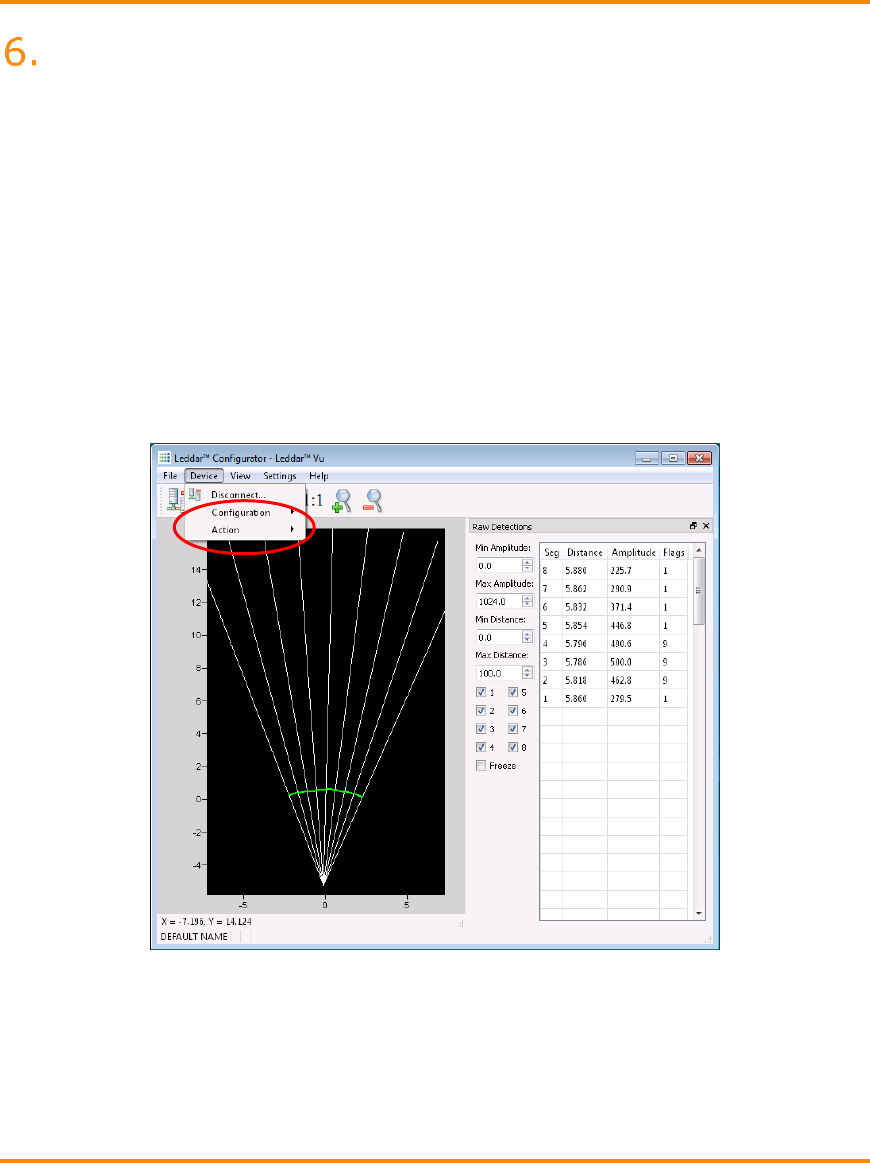
72 P/N 54A0028-2 012017© 2017 LeddarTech Inc. Printed in Canada. All rights reserved.
Leddar™ Configurator
Leddar™ Configurator provides configuration parameters and operation
functionalities for LeddarTech products.
6.1. Introduction to Configurator Software
The Configurator interface can be resized manually or set to full screen view.
All dialog boxes that do not include a selection of action buttons at the bottom, such
as Connect, OK, Cancel, etc. are dockable at the top, the bottom, or on the right
side of the main window.
Figure 24: Raw Detections dialog box docked on the side of the main
window
When a dialog box or a window is already open a check mark appears next to the
command on the menu.
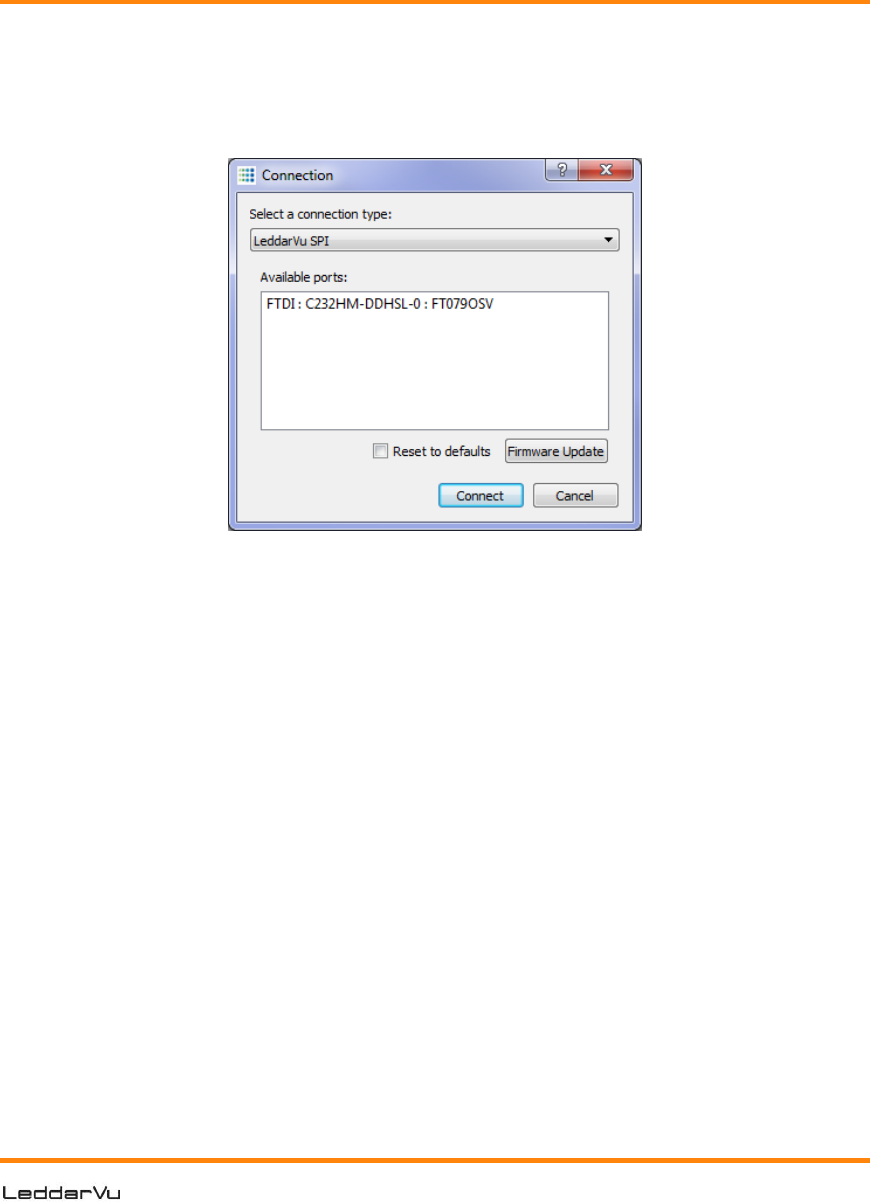
73
6.2. Connection Window
The following is a description of the information shown in the Connection dialog
box.
Figure 25: Connection dialog box
Select a connection Type
The connection type you are using.
Available ports list
The list of available ports displays the modules currently detected.
NOTE: The next descriptions apply to IS16/M16/Evaluation Kit USB.
Name
The device name can be modified (see section “6.4.1 Module Name” on page 81).
Serial Number
The serial number of the device as assigned by LeddarTech.
Type
The product name.
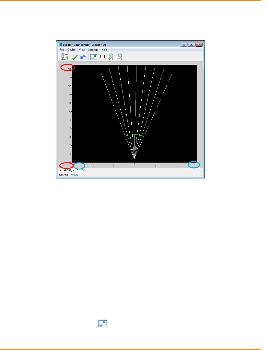
74 P/N 54A0028-2 012017© 2017 LeddarTech Inc. Printed in Canada. All rights reserved.
6.3. Leddar™ Configurator Main Window
After connecting to the device, the main window opens.
Figure 26: Leddar™ Configurator main window
The measurements are plotted in a symbolic graph containing the 16 segments
(white lines) originating from the LeddarVu module. Detections are drawn as arcs in
their corresponding segments. Only valid measurements are displayed. A more
detailed description of the measurements can be obtained in the Raw Detections
dialog box (see section “6.11 Raw Detections” on page 97).
The X and Y numbers displayed at the bottom are the mouse cursor position
coordinates.
6.3.1. Toolbar
The toolbar includes several buttons for adjusting the view of the main window
display.
6.3.2. Fit to Window
Click the fit-to-window button ( ) to adjust the LeddarVu module view to the main
window.
Vertical scale
setting areas
Horizontal scale
setting areas

75
6.3.3. Force Equal Horizontal and Vertical Scales
When the equal scaling button ( ) is selected (button highlighted), the original
ratio of the display is kept or restored. The horizontal and vertical scales will be set
to the same values and the beam will be displayed in accordance with the beam
properties (for example, the display will show a 48° beam for a 48° LeddarVu
module).
Click the button again to change the vertical and horizontal scales independently.
NOTE: When in equal scaling mode, you cannot zoom the display horizontally or
vertically, that is, holding the <Control> or <Shift> key down while zooming
in or out will have no effect. The scales cannot then be modified by entering
values in the fields shown in Figure 26 above.
6.3.4. Zoom in
Click the zoom in button ( ) to zoom in vertically and horizontally around the
center of the display.
6.3.5. Zoom out
Click the zoom out button ( ) to zoom out vertically and horizontally around the
center of the display.
6.3.6. Scale
The window opens with the default scale setting. The horizontal and vertical scales
can be changed manually by entering new values in the fields accessible by clicking
the areas shown in Figure 26.
To apply the changes, click anywhere in the main window.
6.3.7. Panning and Zooming
The display in the main window can be panned and zoomed in different ways.
Panning and zooming is done relative to the mouse cursor position.
You can move up, down, and sideways by clicking and dragging the display.
To zoom the display in and out, use the mouse wheel alone. This has the same
effect as clicking the zoom in ( ) or zoom out ( ) button respectively (see sections
6.3.4 and 6.3.5).
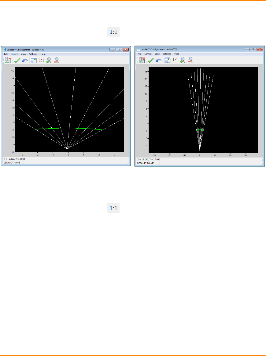
76 P/N 54A0028-2 012017© 2017 LeddarTech Inc. Printed in Canada. All rights reserved.
To zoom the display horizontally, hold down the <Control> key of the computer
keyboard while using the mouse wheel.
NOTE: The equal scaling button ( ) must be not selected (not highlighted).
Figure 27: Zooming in (left) and out (right) horizontally
To zoom the display vertically, hold the <Shift> key down while using the mouse
wheel.
NOTE: The equal scaling button ( ) must be not selected (not highlighted).
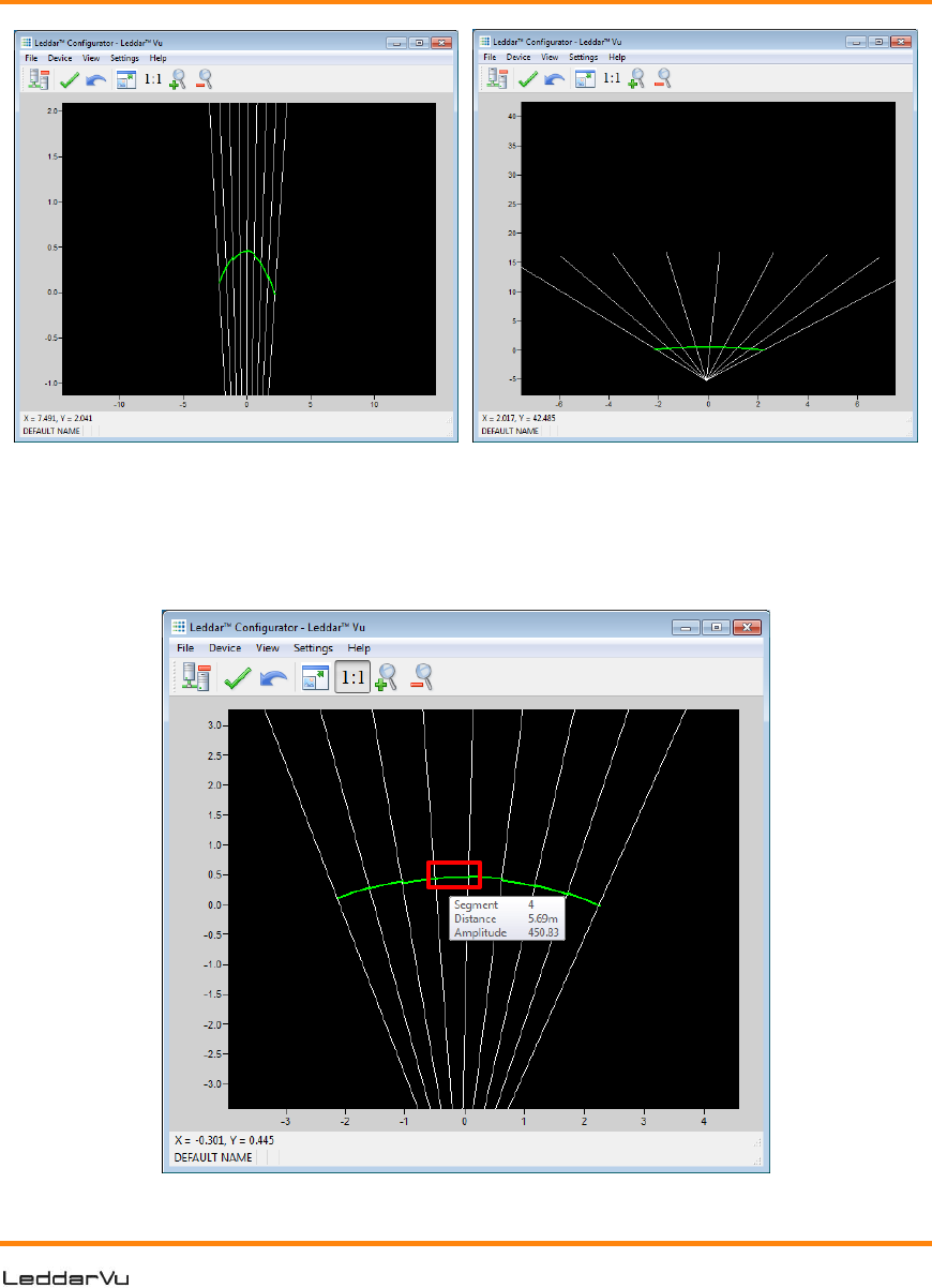
77
Figure 28: Zooming in (left) and out (right) vertically
The measurements of a detection point appear as a pop-up when you point to it with
the mouse cursor for a more accurate assessment of the detection. Detection points
are shown in the form of green lines (arcs) in the main window for visibility reasons.
Figure 29: Detection point coordinates
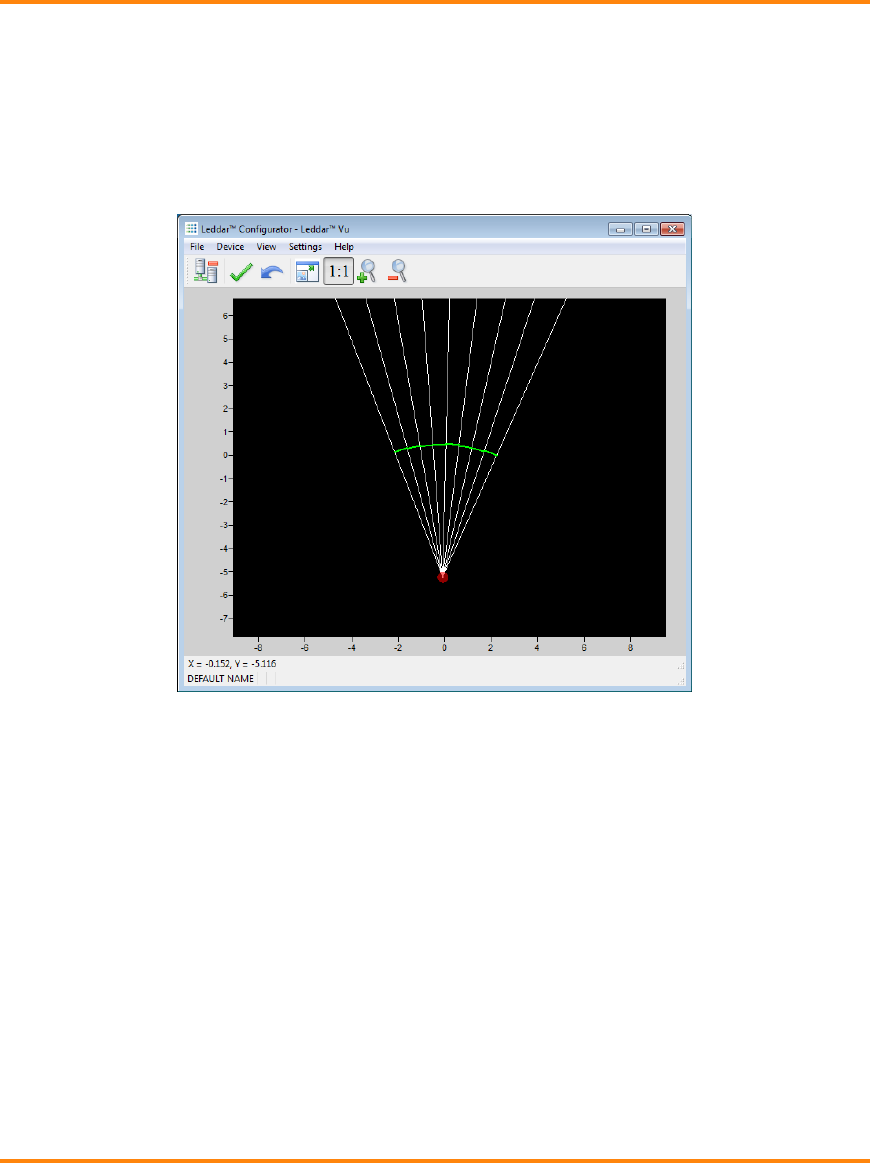
78 P/N 54A0028-2 012017© 2017 LeddarTech Inc. Printed in Canada. All rights reserved.
6.3.8. Changing the LeddarVu Module Origin
The module origin can be modified by clicking the module origin at the bottom of the
segments.
To do so, use the mouse cursor to point to the bottom of the segments (a red dot
appears); click and drag it in the desired position.
Figure 30: Dot indicator to modify the module origin
If you click and drag the module origin, its position is displayed in the status bar as
shown in Figure 31.
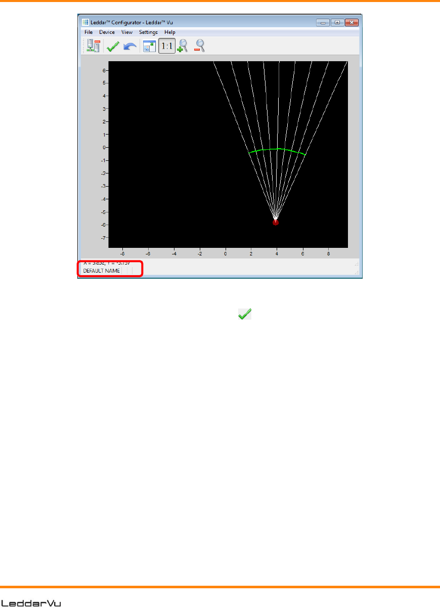
79
Figure 31: Module position changed
To apply the changes, click the apply button ( ).
The origin is saved in the module and it can also be modified by editing the
parameters in the module position settings window.
6.3.9. Changing the LeddarVu Module Orientation
The module origin may be rotated to match its physical position. If you do so, the
main window display can better match the physical installation of the module. For
example, if the module is installed above the ground, the origin can be set to reflect
its position.
Use the mouse cursor to point to the top of the segments (the top turns red); click
and drag it in the desired position.
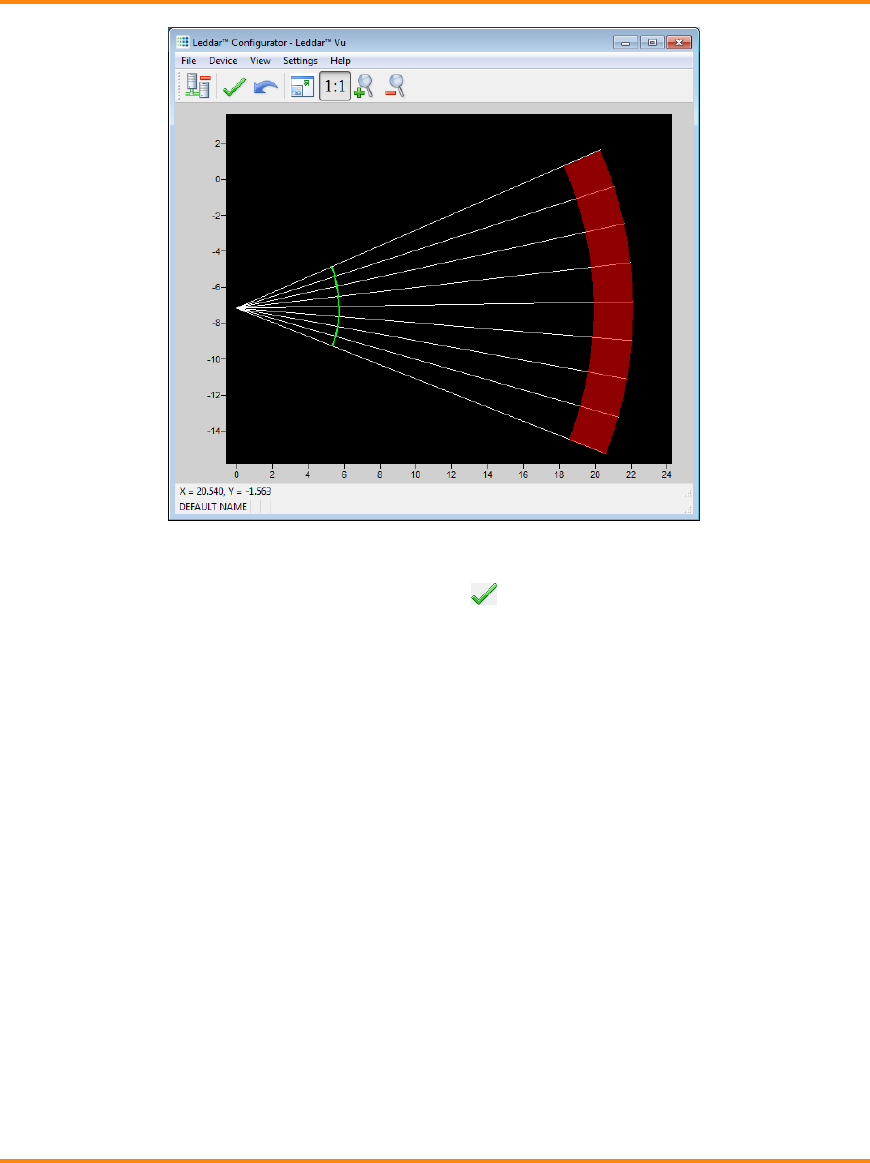
80 P/N 54A0028-2 012017© 2017 LeddarTech Inc. Printed in Canada. All rights reserved.
Figure 32: Red bar to rotate the module position
To apply the changes, click the apply button ( ).
The module orientation is saved in the module and can also be modified by editing
the parameters in the module position settings window.
6.4. Settings
The LeddarVu module stores a number of settings. Once saved in the module, these
parameters are effective at each power up. The Leddar™ Configurator software
loads these parameters upon each connection.
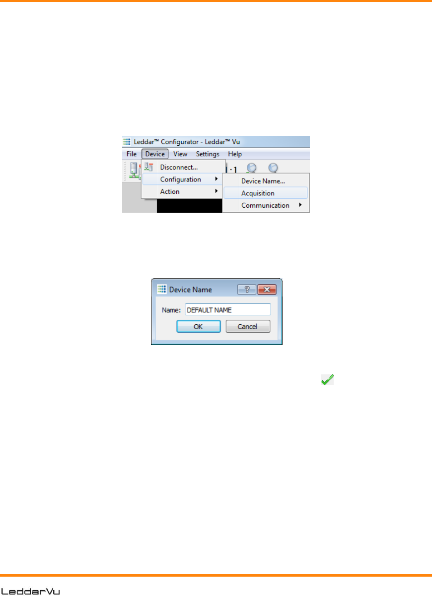
81
6.4.1. Module Name
When you connect to a LeddarVu module for the first time, it has a default name.
You can change that name at any time.
To change the module name:
1. Connect to a module.
2. On the Device menu, point to Configuration and click Device Name.
Figure 33: Device menu and the Configuration menu items
3. In the Device Name dialog box, in the Name field, type the new name
of the module and click OK.
Figure 34: Device Name dialog box
4. To apply the change, click the apply button ( ) in the Leddar™
Configurator main window.
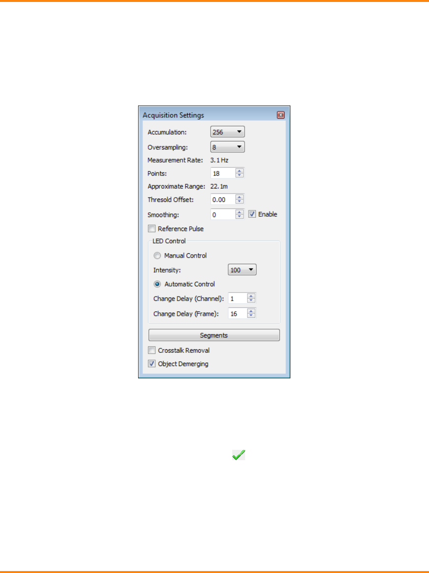
82 P/N 54A0028-2 012017© 2017 LeddarTech Inc. Printed in Canada. All rights reserved.
6.4.2. Acquisition Settings
The acquisition settings allow you to define parameters to use for detection and
distance measurement.
To open the Acquisition Settings dialog box, on the Device menu, point to
Configuration and click Acquisition.
Figure 35: Acquisition Settings dialog box
The numbers on a grey background are modified only by using the arrows, while the
ones on a white background can additionally be modified manually by using the
numeric keypad of your keyboard.
To apply the changes, click the apply button ( ) in the main window.
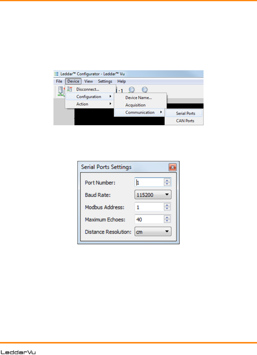
83
6.4.3. Serial Port
The serial port settings of the USB, CAN and SERIAL board are configurable.
To configure the serial port:
1. On the Device menu, point to Configuration, point to
Communication, and click Serial Ports.
Figure 36: Device menu
2. In the Serial Port Setting dialog box, use the arrows or type
numbers to modify the values.
Figure 37: Serial Port Settings dialog box
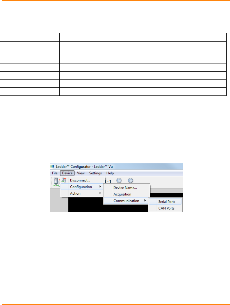
84 P/N 54A0028-2 012017© 2017 LeddarTech Inc. Printed in Canada. All rights reserved.
Table 65 describes the serial port settings.
Table 65: Serial port setting description
Parameter
Value
Port number
Select 1 for the configurable serial link number 1.
Select 2 for the TTL serial link number 2.
Select 3 for the USB VCP serial link.
Baud rate
9600, 19200, 38400, 57600, 115200 bps
Address
1 to 247
Detections
0 to 40
Distance resolution
Millimeters (mm), centimeters (cm), decimeters (dm), meters (m)
6.4.4. CAN Port
The CAN port settings of the USB, CAN and SERIAL board are configurable.
To configure the CAN port:
3. On the Device menu, point to Configuration, point to
Communication, and click CAN Ports.
Figure 38: Device menu
4. In the Serial Port Setting dialog box, use the arrows or type
numbers to modify the values.
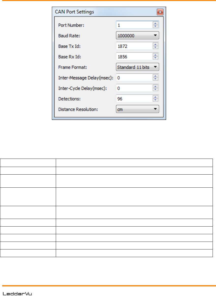
85
Figure 39: CAN Port Settings dialog box
Table 68 describes the CAN port settings.
Table 66: CAN port setting description
Parameter
Value
Port number
Select 1 for CAN communication
Baud rate
10000, 20000, 50000, 100000, 125000, 250000, 500000,
1000000 bps
Base Tx ID
The base CAN arbitration ID used for data messages coming from
the USB, CAN and SERIAL to host (see the protocol
documentation).
Base Rx ID
The base CAN arbitration ID used for data messages sent to the
USB, CAN and SERIAL board (see the protocol documentation).
Frame format
Standard, Extended
Inter-message delay
0 to 65535 milliseconds
Inter-cycle delay
0 to 65535 milliseconds
Detections
1 to 96
Distance resolution
Millimeters (mm), centimeters (cm), decimeters (dm), meters (m)
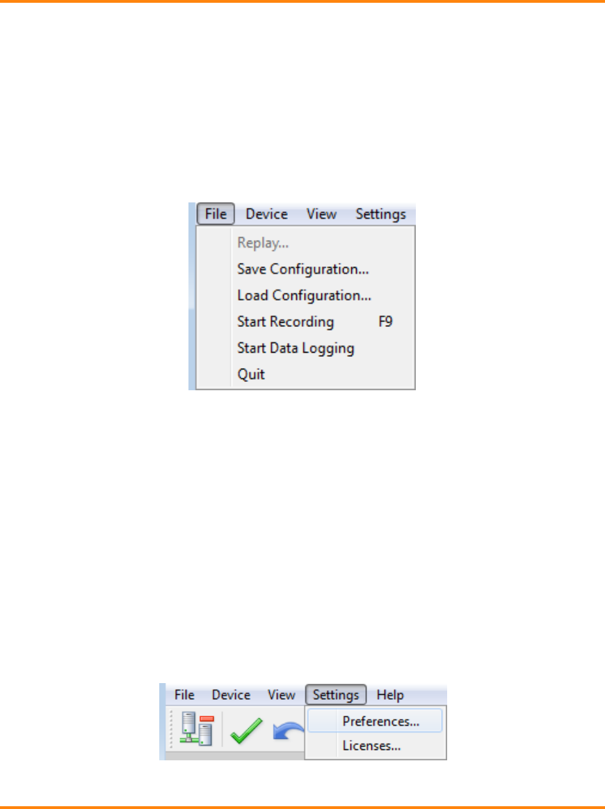
86 P/N 54A0028-2 012017© 2017 LeddarTech Inc. Printed in Canada. All rights reserved.
6.5. Saving and Loading a Configuration
The software configuration for a device can be saved to a file. This enables you to
backup settings and restore them in case of system failure or in case you want to
revert to earlier settings. You can also get the configuration that was stored with a
record file.
To save a configuration:
On the File menu, click Save Configuration.
Figure 40: File menu
To load a configuration:
On the File menu, click Load Configuration.
6.6. Configuring Detection Records
Detection records provide a playback of detections recorded by a device. This visual
information can be useful for verification, troubleshooting, or training purposes.
Detection records allow for a full data playback stored in a *.ltl file that can later be
reloaded and replayed.
To configure the detection record:
1. In Leddar™ Configurator, on the Settings menu, click Preferences.
Figure 41: Settings menu
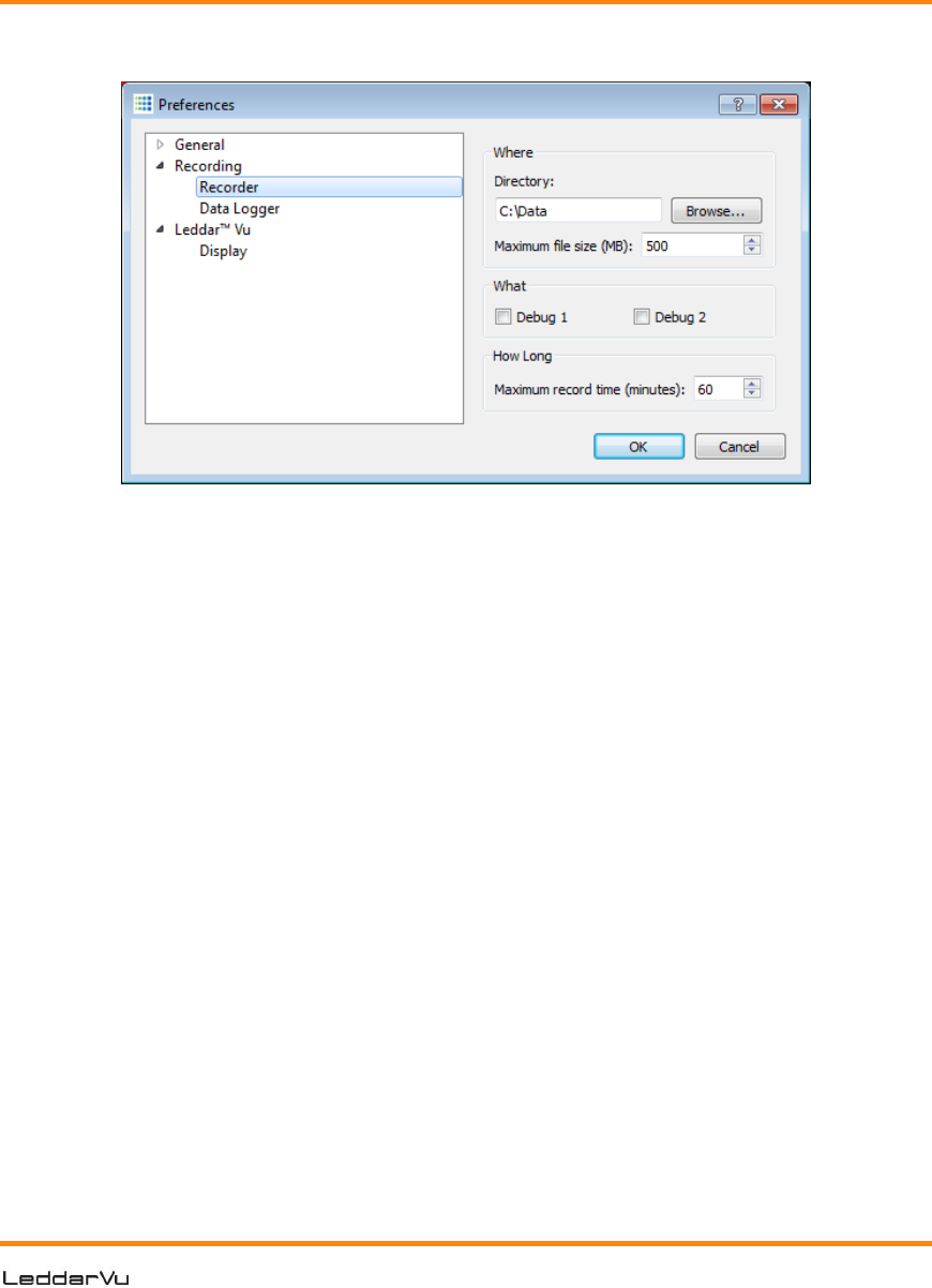
87
2. In the Preferences dialog box, click Recording and click Recorder.
Figure 42: Preferences dialog box
3. Under Directory, click the Browse button to select the path where you
want to save the detection record file.
4. In the Maximum file size box, set the maximum file size by using the
arrows or by entering the value manually.
5. Under What, select one of the Debug check boxes.
6. Under How Long, next to Maximum record time, determine the
length of time for recording by using the arrows or by entering the value
manually.
At the end of that period, recording will stop even if the file size has not
reached its maximum.
7. Click OK to save the settings.
A complete description of the elements found in the Preferences for recording
dialog box follows after the next two procedures.
To start a recording:
On the File menu, click Start Recording.
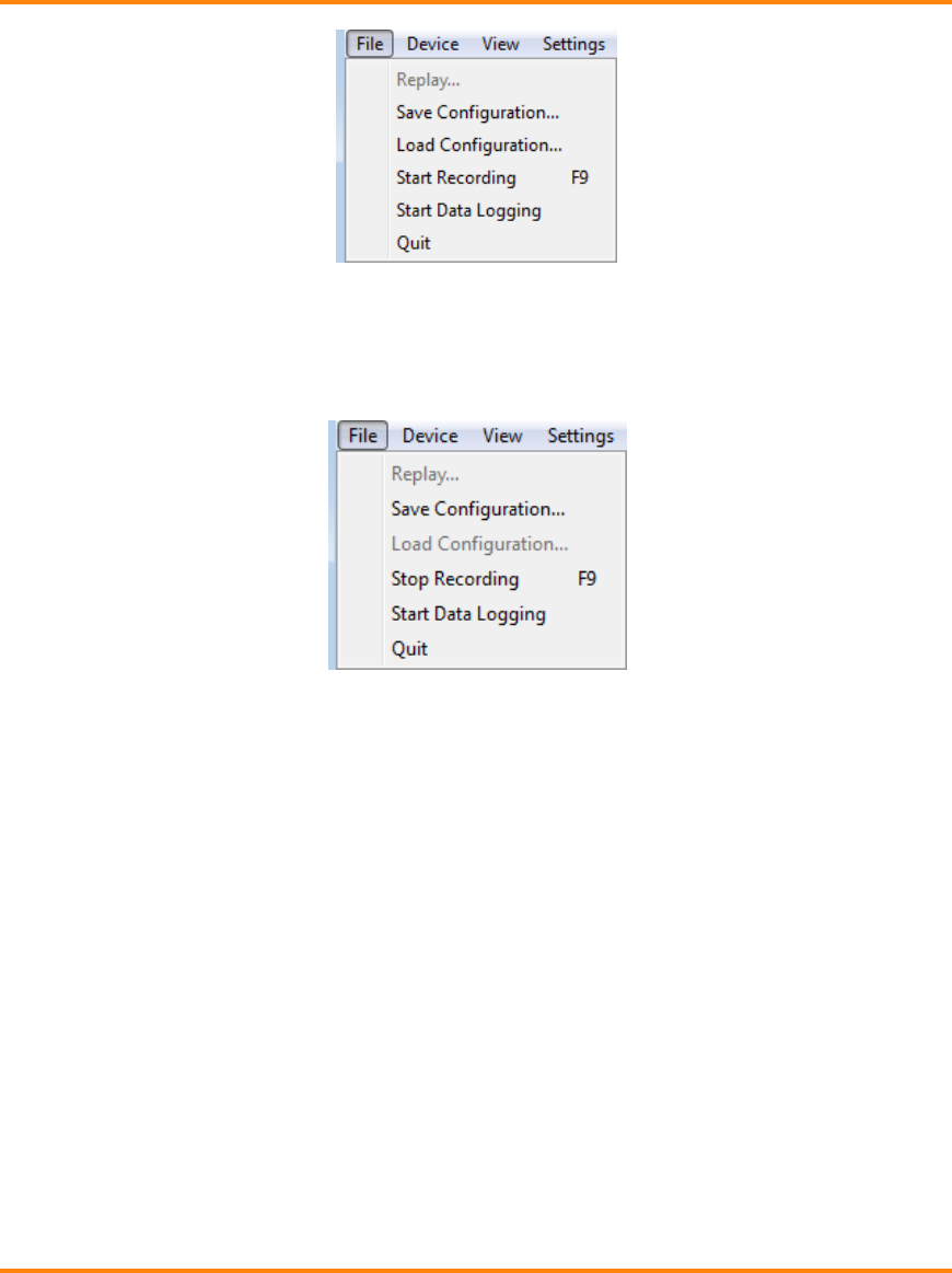
88 P/N 54A0028-2 012017© 2017 LeddarTech Inc. Printed in Canada. All rights reserved.
Figure 43: File menu
To stop a recording manually:
On the File menu, click Stop Recording.
Figure 44: File menu to stop a recording
The following is a description of the elements available in the Preferences for
recording dialog box.
Record directory
The record directory is the folder in which all record files will be saved. These files
are in a proprietary format, with the extension *.ltl, and can only be opened and
viewed with the Leddar™ Configurator software.
Maximum file size
Record files can be quite large. Set the maximum file size as needed. The recording
stops for the current file once it reaches the maximum file size and automatically
switches the recording to another file. This is to keep record files of manageable
sizes.
Debug
These check boxes are reserved for the use of LeddarTech technicians.
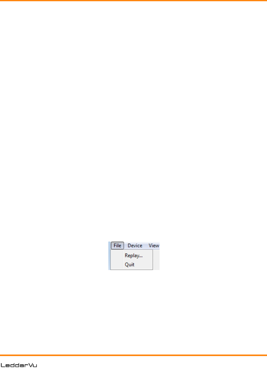
89
Maximum record time
The value entered as the Maximum record time determines the length of the time
for recording. At the end of that period, recording will stop even if the file size has
not reached its maximum.
6.7. Using Detection Records
Once you have completed a recording, you can review it and extract part of the
recording.
The Record Replay dialog box offers the same functions as a regular video player:
there is a stop button, a play button, and frame-by-frame forward and backward
buttons.
The Position slider lets you move directly to a desired position.
The Playback Speed slider lets you adjust the speed of the recording playback;
faster is to the left.
The Start, End, and Extract buttons allow you to select a portion of the recording
and extract it for further reference or analysis.
To play a record:
1. If you are connected to a device, disconnect from the device.
OR
Open another Leddar™ Configurator main window.
NOTE: The record files can also be opened by double-clicking them.
2. On the File menu, click Replay.
Figure 45: File menu to open a recording
3. In the Record Replay dialog box, click the browse button to select a
file.
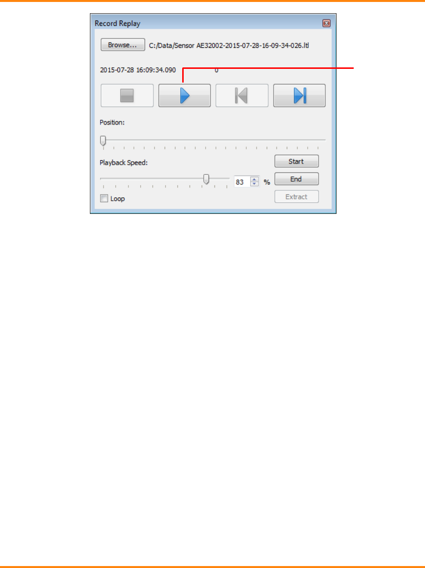
90 P/N 54A0028-2 012017© 2017 LeddarTech Inc. Printed in Canada. All rights reserved.
Figure 46: Record Replay dialog box
4. Click the play button to start the playback.
To extract a record file segment:
1. Set the Position slider to the position where you want the file segment
to start and click the Start button.
2. Set the Position slider to the position where you want the file segment
to stop and click the End button.
OR
Play the record and stop it at a position of interest and then click the
Start button; restart playing the record and stop it again at a position of
interest and click the Stop button.
3. Click the Extract button to extract and save that file segment.
6.8. Data Logging
The data logging function is used to output the data to a .txt file. This file can be imported
in a software application, such as Microsoft Excel, for offline analysis.
The duration of the record is indicated in the status bar.
Each line of the generated text file contains the information related to a single
detection.
Play
button
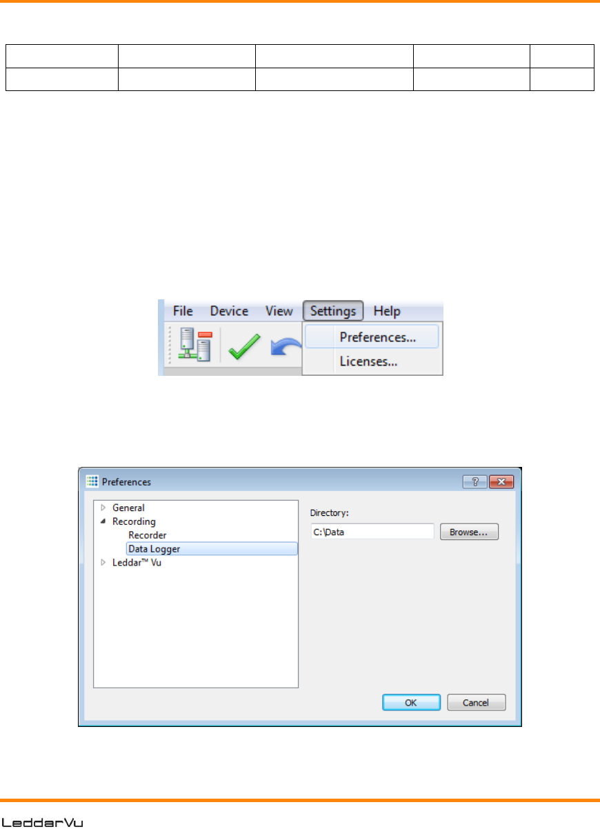
91
Table 67: Field description of the log text file
Time (msec)
Segment [0 15]
Amplitude [0 512]
Distance (m)
Status
12735204
7
0.9
33.61
1
The time of the detection is 12735204 milliseconds from the time the LeddarVu
module was started.
The location of the detection is segment 7 (the 8th segment).
The amplitude of the detection is 0.09, which is very low (small, far, or dark
object).
The distance of the detection is 33.61 meters.
The status indicates a normal measurement.
To use the data logging function:
1. In Leddar™ Configurator, on the Settings menu, click Preferences.
Figure 47: Settings menu
2. In the Preferences dialog box, click Recording and click Data
Logger.
Figure 48: Preferences dialog box for logging data
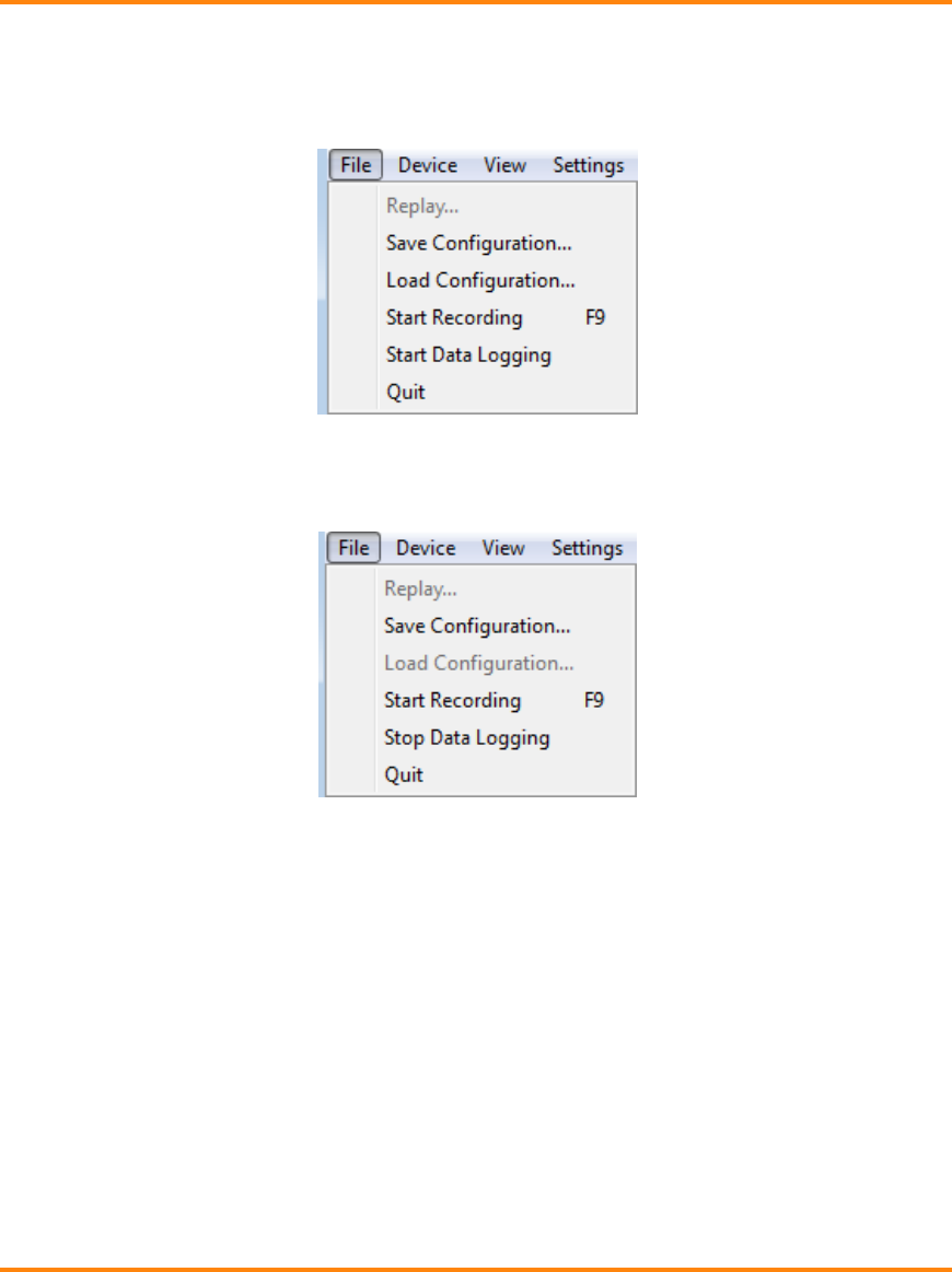
92 P/N 54A0028-2 012017© 2017 LeddarTech Inc. Printed in Canada. All rights reserved.
3. Under Directory, click the browse button to select the path where you
want to save the log and click OK.
4. On the File menu, click Start Data Logging.
Figure 49: File menu
5. To stop recording, on the File menu, click Stop Data Logging.
Figure 50: File menu to stop data recording
A .txt file is saved in the selected directory.
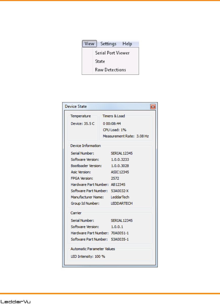
93
6.9. Device State
Information about a device is accessible when connecting to a device in the
Connection window or by clicking the State command on the View menu.
Figure 51: View menu
The Device State window opens.
Figure 52: Device State window

94 P/N 54A0028-2 012017© 2017 LeddarTech Inc. Printed in Canada. All rights reserved.
General
Timers & Load
This feature gives information in days, hours, minutes, and seconds about two types
of activities of a device. The first line indicates the time elapsed since the last device
reset, the second since the last power cut or outage.
Measurement Rate
This parameter indicates the rate at which the module measures the speed and
dimension of static or moving surfaces.
Automatic Parameter Values
This parameter indicates the intensity of the light source.
Device Information
Serial Number
This parameter indicates the serial number of the device as assigned by LeddarTech.
Software Version
This parameter indicates the software version, which is specific to the processor of
your unit.
Bootloader Version
This parameter indicates the bootloader (booting instructions) version, which is
specific to the processor of your unit.
Asic Version
This parameter indicates the version of the application-specific integrated circuit;
the microchip designed for this special application. This field is optional in function of
the receiver module type.
FPGA Version
This parameter indicates the field-programmable gate array circuit used in the
device.
Hardware Part Number
This parameter indicates the hardware part number of the device as assigned by
LeddarTech.

95
Software Part Number
This parameter indicates the software part number of the device as assigned by
LeddarTech.
Manufacturer Name
This parameter indicates the name assigned to LeddarTech.
Group Id Number
This parameter indicates the end-user group unique identifier used for licencing
purposes
Carrier
Serial Number
This parameter indicates the serial number of the USB, CAN and SERIAL carrier
board as assigned by LeddarTech.
Software Version
This parameter indicates the software version, which is specific to USB, CAN and
SERIAL carrier board of your unit.
Hardware Part Number
This parameter indicates the hardware part number of the USB, CAN and SERIAL
carrier board as assigned by LeddarTech.
Software Part Number
This parameter indicates the software part number of the USB, CAN and SERIAL
carrier board as assigned by LeddarTech.
6.10. Preferences
Preferences are used to change various settings related to the display of Leddar™
Configurator.
The Preferences dialog box is opened by clicking the Preferences command on
the Settings menu.
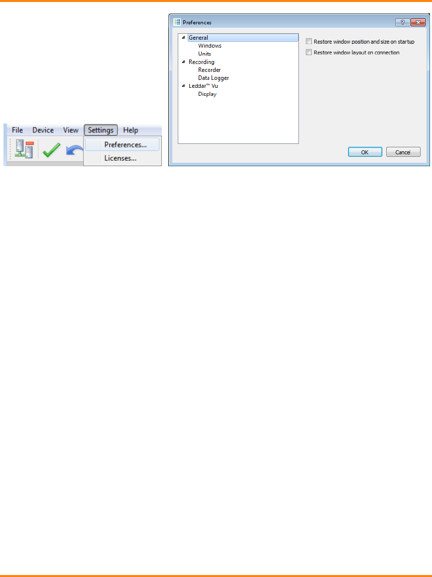
96 P/N 54A0028-2 012017© 2017 LeddarTech Inc. Printed in Canada. All rights reserved.
Figure 53: Settings Menu and Preferences Dialog Box
Windows
The two options allow the user to select how the content of the main window will be
displayed in Leddar™ Configurator. Choices are:
The Restore window position and size on startup feature starts Leddar™
Configurator at the same place on the computer desktop and at the same size it
was when it was closed.
The Restore window layout on connection feature connects to the Evaluation
Kit at the same size it was and with all docked dialog boxes or windows that
were displayed when it was closed.
Distance
The unit that is applied to distances displayed in Leddar™ Configurator.
Temperature
The unit used when displaying the temperature.
Recording
The Recorder parameter lets you choose how data files are recorded.
The Data Logger parameter lets you select a directory to store logs.
Display
The Detection Arc Thickness parameter allows a user to modify the pixel width of
the displayed green detections arcs in the main window.
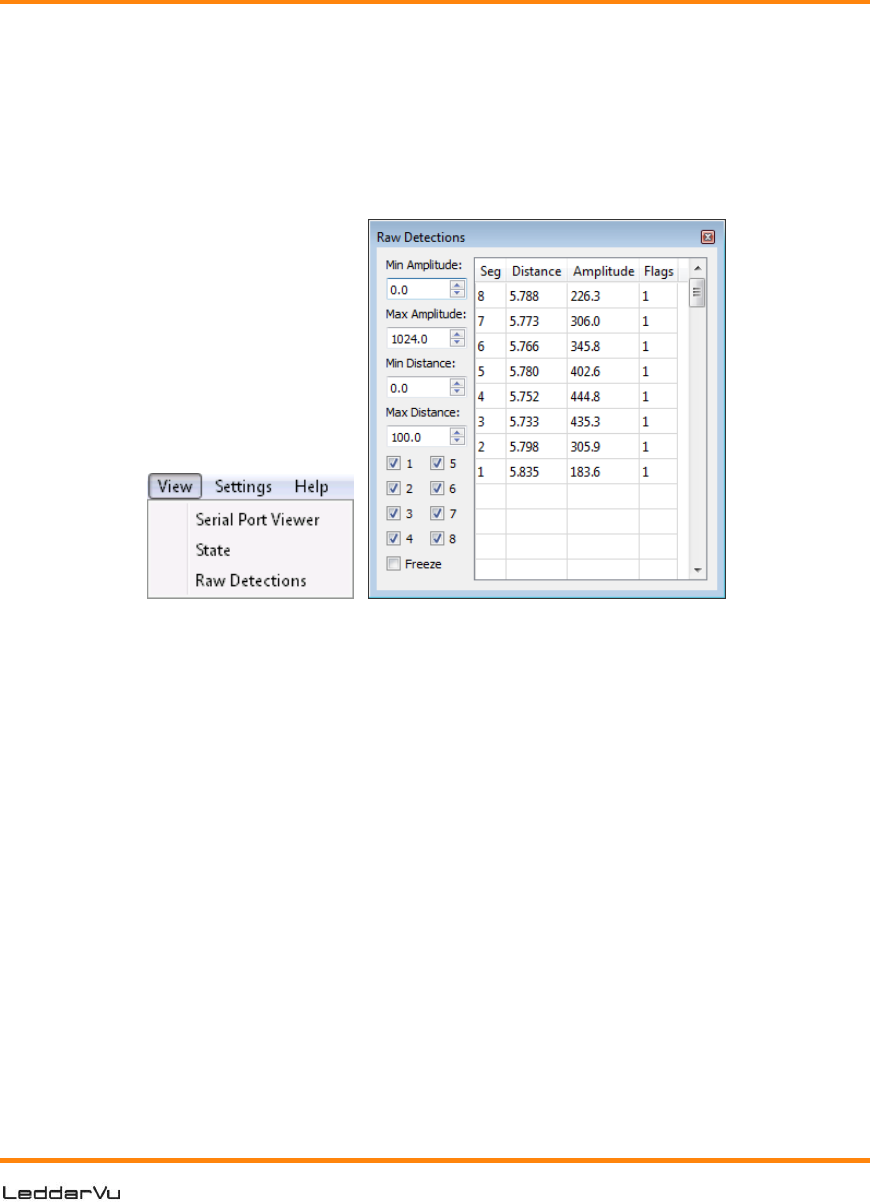
97
6.11. Raw Detections
The Raw Detections dialog box allows you to view detection values in many ways.
It provides filters to isolate segments and detection parameters..
To open the Raw Detections dialog box, on the View menu, click Raw
Detections.
Figure 54: View menu and Raw Detections dialog box
Figure 55 presents an example of raw detections. When there is no detection in
some segments, only the segments where a detection occurred appear in the list.
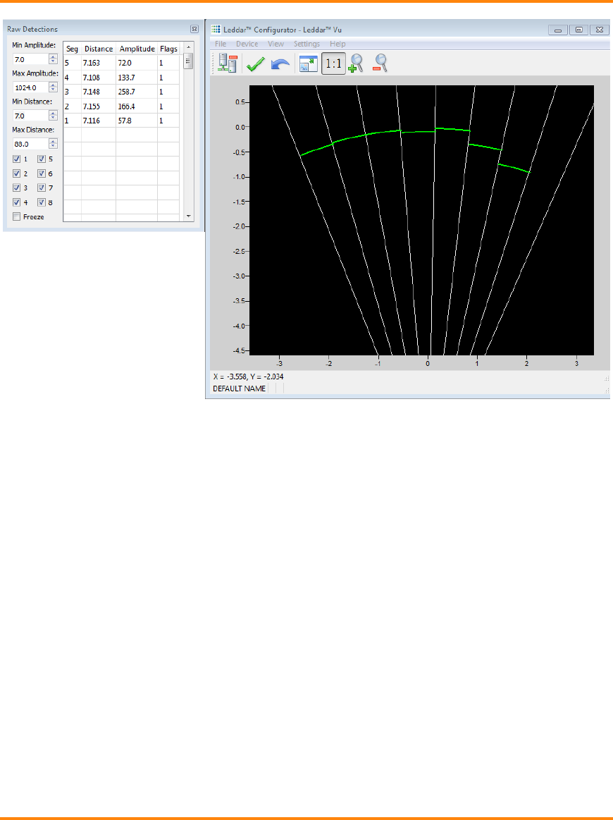
98 P/N 54A0028-2 012017© 2017 LeddarTech Inc. Printed in Canada. All rights reserved.
Figure 55: Example of detection filters
The following is a description of the parameters available in the Raw Detections
dialog box.
Min and Max Amplitude
The value entered in the Min Amplitude box shows only detections of amplitude
higher or equal to that value. For example, if the minimum amplitude is set to 5,
only the detections of amplitude 5 and more will be displayed.
The value entered in the Max Amplitude box will show only detections of amplitude
lower or equal to that value. For example, if the maximum amplitude is set to 8,
only the detections of amplitude 8 and lower will be displayed.
Setting a value in both fields will result in a range of amplitude to display.
Min and Max Distance
The value entered in the Min Distance box will show only detections at a distance
greater or equal to that value. For example, if the minimum distance is set to 10,
only the detections at a distance of 10 and more will be displayed.

99
The value entered in the Max Amplitude box will show only detections at a
distance smaller or equal to that value. For example, if the minimum distance is set
to 20, only the detections at a distance of 20 and less will be displayed.
Setting a value in both fields will result in a range of distance to display.
Boxes 1 to 8
Check boxes 1 to 8 allow you to select which segments to display.
Freeze
When selected, the Freeze parameter freezes the values displayed in the Raw
Detections dialog box. To return to the live display, clear the check box.
Seg
The Seg column lists the segment for which there is a detection according to the
filters used. The segment numbers are read from left to right starting at 1.
Distance and Amplitude
The Distance column displays the distance of the detection and the Amplitude
column displays its amplitude.

100 P/N 54A0028-2 012017© 2017 LeddarTech Inc. Printed in Canada. All rights reserved.
Flag
The Flag column displays a number that represents a detection type.
Table 68: Flag value description
Bit position
Bit 0
Bit 1
0
Invalid measurement
Valid measurement
1
Reserved
Reserved
2
Reserved
Reserved
3
Normal measurement
Received signal is above the saturation level.
Measurements are valid (VALID is set) but
have a lower accuracy and precision.
Consider decreasing the light source intensity.
4
Reserved
Reserved
5
Reserved
Reserved
6
Reserved
Reserved
7
Reserved
Reserved
The Flag parameter provisions for 8 bits encoded as a bit field. Three bits are
currently used. The following table presents the implemented decimal values of the
status bit field.
Table 69: Status value description
Status value
(decimal)
Status value
(binary)
Description
1
00000001
Normal measurement (valid)
9
00001001
Saturated signal (valid)
101
Specifications
This chapter presents the LeddarVu module.
7.1. General
Table 70: General specifications
Light Source pulse rate
51.2 kHz
Photodetector array size
1 x 8
Photodetector acquisition rate
100 MHz
Measurement rate
See Table 12 on page 35.
USB (optional)
2.0, 12 Mbits/s
CAN (optional)
10 to 1000 kbit/s, optional 120- termination
Serial links (optional)
TTL, RS-232, RS-422, and RS-485. 2-wire,
4-wire, 9600 to 115200 BPS
Operating temperature
-40°C to +85°C
7.2. Mechanical
Table 71: Mechanical specifications
Assembly height
43.3 mm
Assembly width
35.2 mm
See section 7.6 for dimensions including optics.

102 P/N 54A0028-2 012017© 2017 LeddarTech Inc. Printed in Canada. All rights reserved.
7.3. Electrical
Table 72: Electrical specifications
Voltage
12 VDC
Power consumption (total)
2.2 W
Power output maximum current
15 mA
7.4. Optical
Table 73: Optical specifications
Wavelength
905 nm (infrared)
Laser risk group
IEC 60825-1:2014 (Third Edition); Class I laser
product (certification pending)
Beam width and height
See
Table 74.
Table 74: Beam width and height
Beam Option
Beam Width*
Beam Height*
20° x 0.3°
16.4°
0.173°
20° x 3°
16.3°
3.12°
48° x 0.3°
56.3°
0.149°
48° x 3°
57.1°
3.06°
100° x 0.3°
88.8°
0.168°
100° x 3°
58.0°
3.10°
* These parameters present the sensitivity of the module across the beam width
(segment amplitude efficiency) and height (amplitude vs. tilt). See Figure 56.
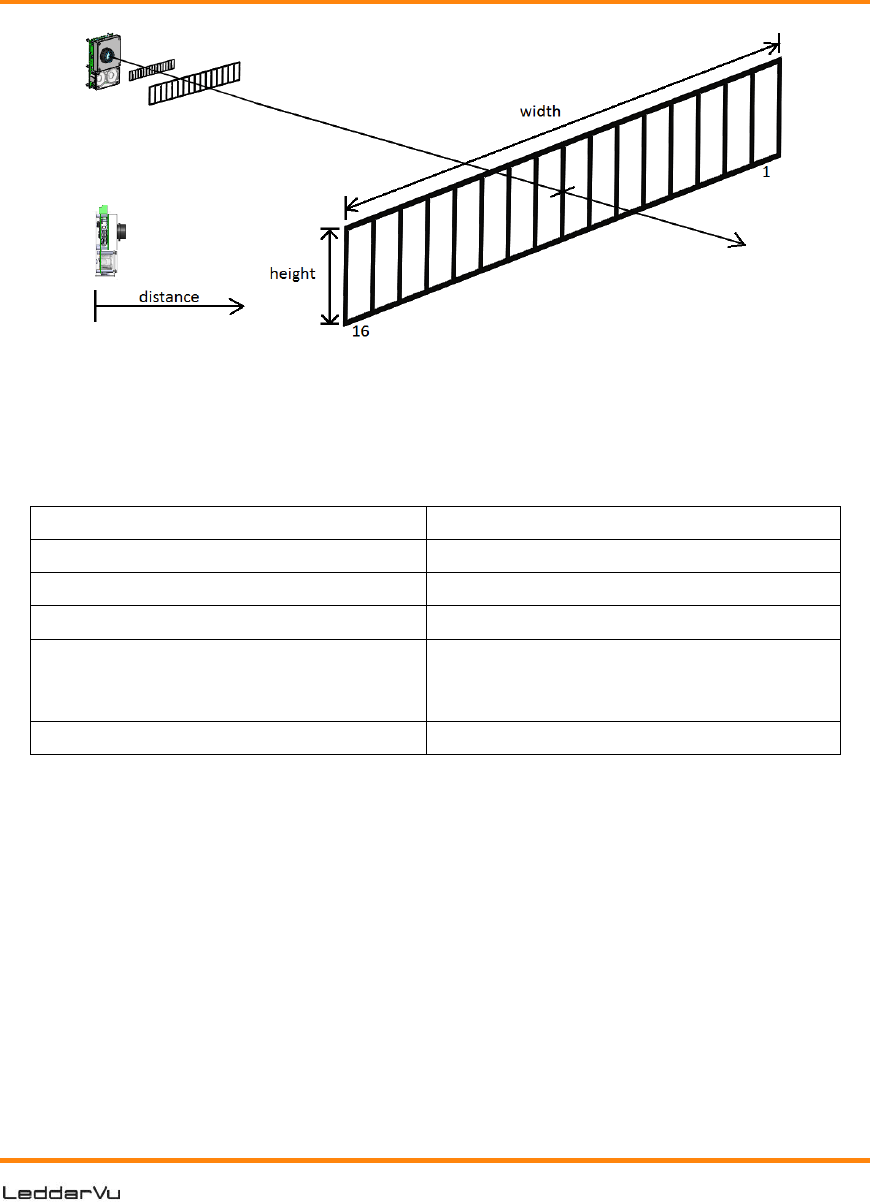
103
Figure 56: Beam pattern width (left) and height (right)
7.5. Performance
Table 75: Module performances
Performance Metrics
Values
Measurement accuracy
±5 cm
Measurement precision
6 mm (amplitude >15)
Resolution
1 cm
Range (maximum light source
intensity)
Varies with beam optics and target
properties (see amplitude vs range
figures below)
Data refresh rate
Up to 100 Hz (standard board)
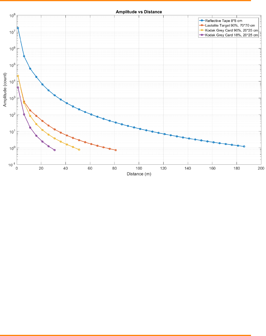
104 P/N 54A0028-2 012017© 2017 LeddarTech Inc. Printed in Canada. All rights reserved.
Figure 57: 20° x 0.3° (maximum intensity, 256 accumulations, and 8
oversamplings)
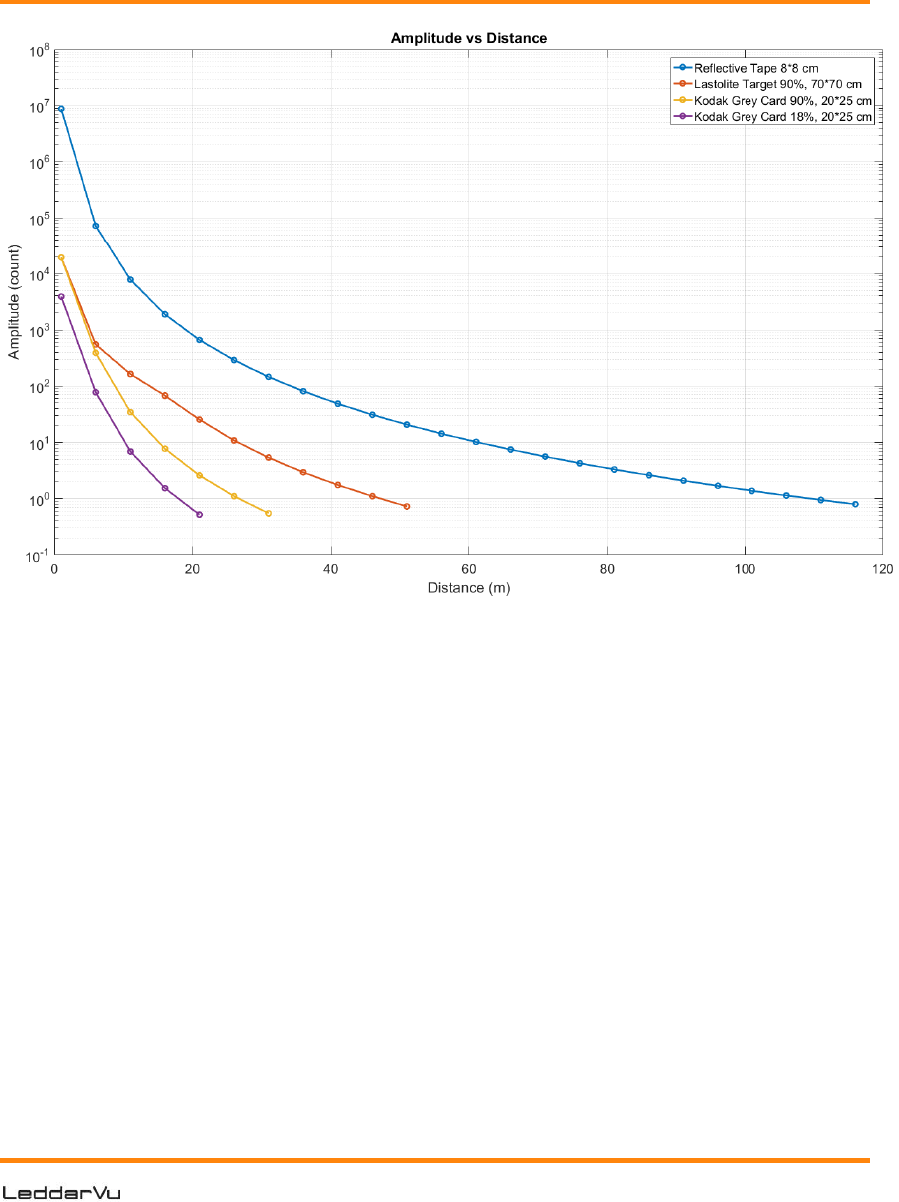
105
Figure 58: 20° x 3° (maximum intensity, 256 accumulations, and 8
oversamplings)
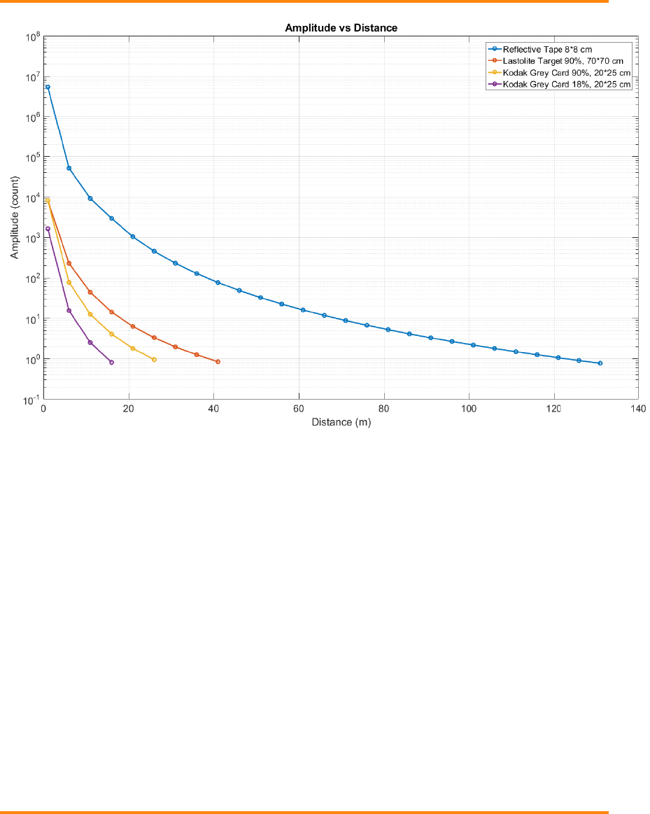
106 P/N 54A0028-2 012017© 2017 LeddarTech Inc. Printed in Canada. All rights reserved.
Figure 59: 48° x 0.3° (maximum intensity, 256 accumulations, and 8
oversamplings)
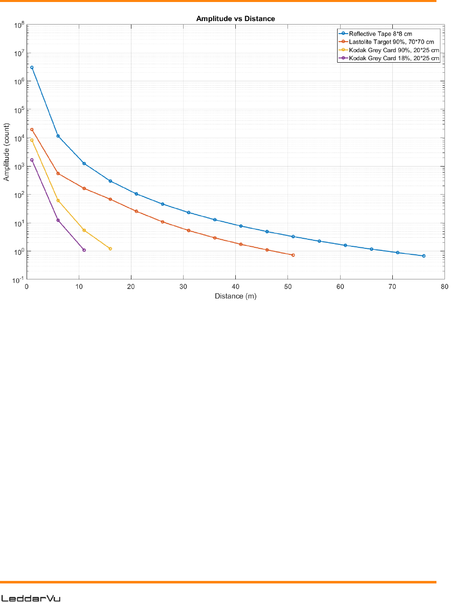
107
Figure 60: 48° x 3° (maximum intensity, 256 accumulations, and 8
oversamplings)
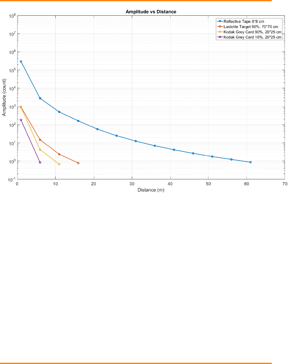
108 P/N 54A0028-2 012017© 2017 LeddarTech Inc. Printed in Canada. All rights reserved.
Figure 61: 100° x 0.3° (maximum intensity, 256 accumulations, and 8
oversamplings)
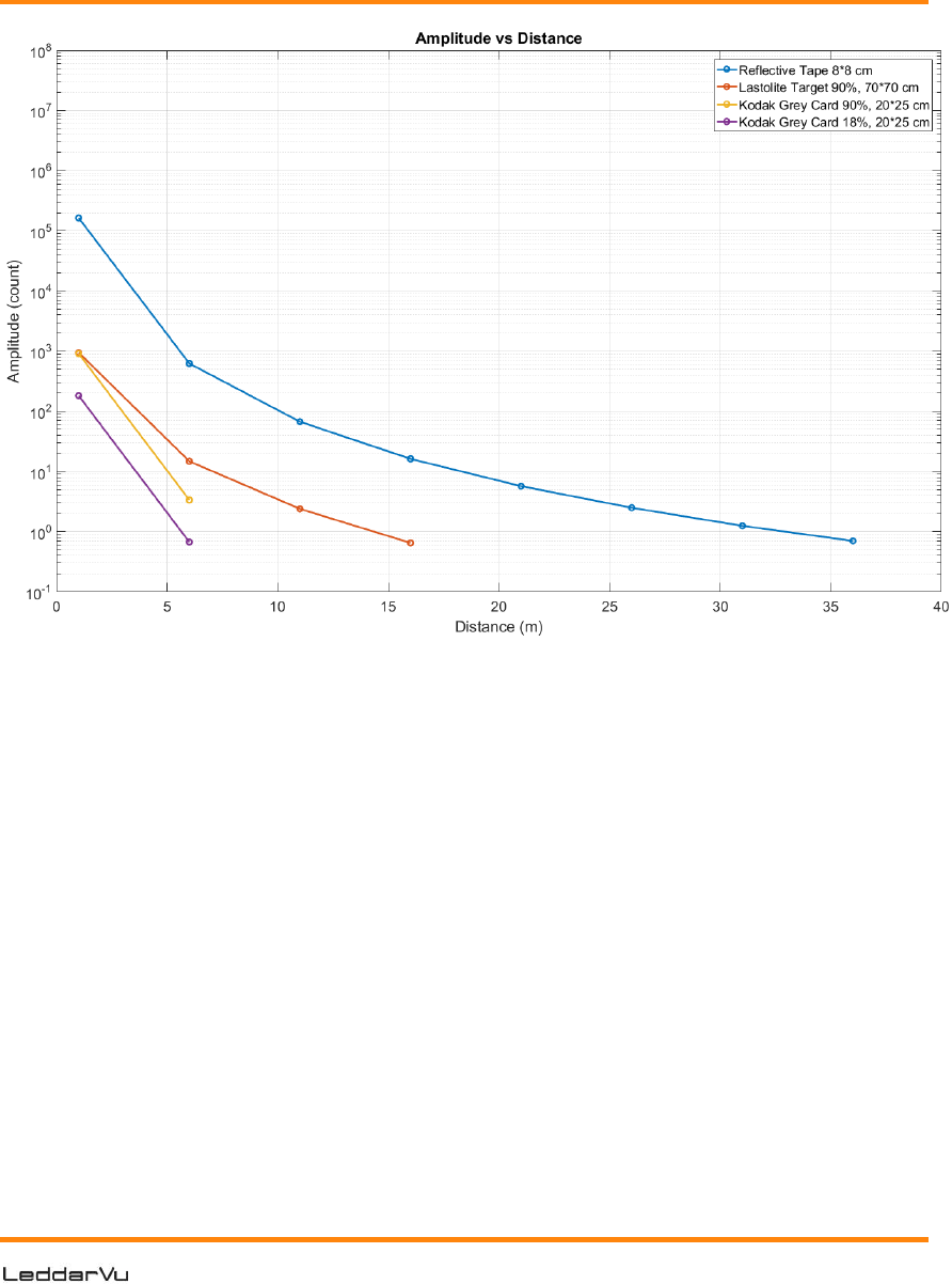
109
Figure 62: 100° x 3° (maximum intensity, 256 accumulations, and 8
oversamplings)

110 P/N 54A0028-2 012017© 2017 LeddarTech Inc. Printed in Canada. All rights reserved.
7.6. Regulatory Compliancy
The module complies with FDA performance standards for laser products except for
deviations pursuant to Laser Notice No. 50, dated June 24, 2007.
NOTE: Testing results are valid for a cable length shorter than 3 meters.
Table 76: Regulatory compliance
Test Name Standard
Test Specification
Performance
Criterion
Result
Radiated emissions
FCC part 15 (2013) subpart B
Class A
30MHz-1GHz
N/A
Pass
Radiated emissions
CISPR11 (2009) A1 (2010)
Group 1 - class A
30MHz-1GHz
N/A
Pass
Radiated emissions
ICES-003 (2012)
Class A
30MHz-1GHz
N/A
Pass
Electrostatic discharge immunity
IEC61000-4-2 (2008)
Contact: ±4 kV
Air: ±8 kV
C
Pass
Radiated electromagnetic field immunity
IEC61000-4-3 (2006)
A1 (2007) A2 (2010)
80 MHz-1000M Hz: 10 V/m
1.4 GHz – 2 GHz: 3 V/m
2 GHz - 2.7 GHz: 1 V/m
C
Pass
7.7. Dimensions
This section presents the LeddarVu module dimensions.
111
7.7.1. 100° Module
Figure 63: 100° module dimensions
112 P/N 54A0028-2 012017© 2017 LeddarTech Inc. Printed in Canada. All rights reserved.
7.7.2. 48° Module
Figure 64: 48° module dimensions
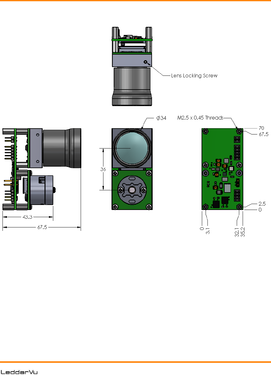
113
7.7.3. 20° Module
Figure 65: 20° module dimensions

114 P/N 54A0028-2 012017© 2017 LeddarTech Inc. Printed in Canada. All rights reserved.
Help
For technical inquiries, please contact LeddarTech technical support by registering
online at www.leddartech.com/support to easily:
Follow up on your requests
Find quick answers to questions
Get valuable updates
Or by contacting us at:
+ 1 418 653 9000
+ 1 855 865 9900
8:30 a.m. - 5:00 p.m. Eastern Standard Time
To facilitate the support, please have in hand all relevant information such as part
numbers, serial numbers, etc.
E-mail
support@leddartech.com
Company address
LeddarTech Inc.
2740 Einstein Street
Quebec, QC G1P 4S4
Canada
www.leddartech.com

115
Index
A
Accumulation ................................ 29, 30
Accuracy .......................................... 103
Amplitude, raw detection ...................... 98
Asic version ........................................ 94
Atmel processor ................................... 7
Automatic parameter values ................. 94
C
CAN bus ..................................... 16, 101
CAN port settings, Get ......................... 59
CAN port settings, Set .......................... 61
Carrier device information, Get ............. 58
Carrier firmware information, Get .......... 58
Circuit receiver ..................................... 7
Connection type .................................. 73
Control interface ................................. 15
Controller, pulsing ................................ 7
Crosstalk removal ................................ 29
D
Data Logger ........................................ 96
Data recording .................................... 86
Debug ................................................ 88
Detection
Filters, raw detection ........................ 97
Using records ................................... 86
Detection arc thickness ........................ 96
Detections, Get ................................... 52
Device
Automatic parameter values .............. 94
Group ID number ............................. 95
Hardware part number ...................... 94
Manufacturer’s name ........................ 95
Name .............................................. 73
Power outage ................................... 94
Serial number ............................ 73, 94
Software part number ....................... 95
Type ............................................... 73
USB, CAN and SERIAL carrier board
hardware part number ................... 95
USB, CAN and SERIAL carrier board
serial number ............................... 95
USB, CAN and SERIAL carrier board
software part number .................... 95
USB, CAN and SERIAL carrier board
version, software .......................... 95
Version, Asic.................................... 94
Version, bootloader .......................... 94
Version, FPGA .................................. 94
Version, software ............................. 94
DIP switches ................................. 10, 16
Distance ............................................. 96
raw detection .................................. 98
unit ................................................ 96
E
Emitter assembly .................................. 7
F
File size
Records .......................................... 87
Records, maximum .......................... 88
Flag, raw detection ............................ 100
FPGA version ...................................... 94
Freeze, raw detection .......................... 99
H
Holding register, Read ......................... 50
I
I2C .................................................... 15
ID number, group ............................... 95
Input register, Read ............................ 48
Intensity, Light Source ......................... 32
Interface
Control ........................................... 15
I2C ................................................. 15

116 P/N 54A0028-2 012017© 2017 LeddarTech Inc. Printed in Canada. All rights reserved.
USB ................................................ 16
L
Laser .................................................. 7
LED .................................................... 7
Light Source
Control ............................................ 29
Intensity ................................... 29, 32
Pulse rate ...................................... 101
M
Main window ....................................... 23
Manufacturer’s name ........................... 95
MCU processor ..................................... 7
MCU, microcontroller ........................... 16
Measurement rate ........................... 7, 94
Modbus protocol .................................. 48
Module data
Read ............................................... 53
Write .............................................. 54
Module list .......................................... 73
O
Opcode command, Send ....................... 54
Oversampling................................ 29, 30
P
Part number
Hardware ........................................ 94
Hardware, USB, CAN and SERIAL carrier
board ........................................... 95
Software ......................................... 95
Software, USB, CAN and SERIAL carrier
board ........................................... 95
Photodetector ............................... 7, 101
Points .......................................... 29, 30
Ports
RS-232 ........................................... 16
RS-422 ........................................... 16
RS-485 ........................................... 16
TTL ................................................. 16
Power ................................................ 15
Power outage ...................................... 94
Precision .......................................... 103
Preferences
Data Logger ..................................... 96
Display, window ............................... 96
Distance unit ................................... 96
Modifying ........................................ 95
Recorder ......................................... 96
Temperature unit ............................. 96
Protocol, Modbus ................................. 48
Push buttons ...................................... 12
R
Range .............................................. 103
Raw detection
Amplitude ....................................... 98
Distance ......................................... 98
Flag .............................................. 100
Freeze ............................................ 99
Segment ......................................... 99
Receiver ............................................... 7
Receiver assembly ................................. 7
Recorder ............................................ 96
Recording ........................................... 96
Recording detections ........................... 89
Records
Detection (video) ............................. 86
Directory ......................................... 88
File size .................................... 87, 88
Recording .................................. 86, 89
Time length, maximum ..................... 89
Reference pulse .................................. 15
Register
Multiple, Read .................................. 50
Multiple, Write ................................. 50
Write .............................................. 50
Report server ID ................................. 52
Reset ................................................. 16
Resolution ........................................ 103
RS-232 port ....................................... 16
RS-422 port ....................................... 16
RS-485 port ....................................... 16
S
Segment, raw detection ....................... 99
Serial number ............................... 73, 94
Serial number, USB, CAN and SERIAL
carrier ............................................ 95
Serial port settings, Get ....................... 55
Serial port settings, Set ....................... 56
Settings
Accumulation ................................... 29

117
Light Source Intensity ....................... 29
Oversampling .................................. 29
Points ............................................. 29
Smoothing ....................................... 29
Threshold offset ............................... 29
Smoothing .................................... 29, 31
Software
Part number .................................... 95
Part number, USB, CAN and SERIAL
carrier board ................................ 95
Source assembly .................................. 7
SPI .................................................... 15
Switch, reset ...................................... 16
T
Temperature ....................................... 96
Operating ...................................... 101
Temperature sensor .............................. 7
Threshold offset ............................ 29, 30
Timers & Load ..................................... 94
TTL port ............................................. 16
U
Units
Distance ......................................... 96
Temperature ................................... 96
USB interface...................................... 16
USB port .......................................... 101
USB, CAN and SERIAL carrier board
Hardware part number ...................... 95
serial number .................................. 95
Software part number ....................... 95
Software version .............................. 95
V
Version
Asic ................................................ 94
Bootloader ...................................... 94
FPGA .............................................. 94
Software, USB, CAN and SERIAL carrier
board .......................................... 95
VersionSsoftware ................................ 94
Voltage ............................................ 102
VSCEL ................................................. 7
W
Wavelength ...................................... 102
Window .............................................. 96
