LG 42SL80 Training Manual. Www.s Manuals.com. Manual
User Manual: LCD TV LG 42SL80 - Service manuals and Schematics. Free.
Open the PDF directly: View PDF ![]() .
.
Page Count: 93
- 42SL80 Thin Training Manual 05/04/2010
- OUTLINE
- 42SL80 PRODUCT INFORMATION SECTION
- DISASSEMBLY and TROUBLESHOOTING SECTION
- POWER SUPPLY SECTION
- Power Supply (Master Power Switch Type 1) Location
- Power Supply (SMPS) Board Layout
- Power Supply Start Up Sequence
- Power Supply Controls from Micro Processor
- Power Supply (SMPS) Board Operational Troubleshooting
- TEST 1 Power Supply Board Low Voltage Test
- TEST 2 Power Supply Board Backlight Test
- Power Supply Connector P201 Voltage and Diode Check
- Power Supply P204 to Inverter A CN1 Voltage and Diode Check
- Power Supply P205 to Inverter B CN201 Voltage and Diode Check
- Power Supply Connector SK100 and P101 Voltage and Diode Check
- INVERTER A and B SECTION
- EEFL Compared to CCFL (This set uses EEFL Bulbs)
- EEFL Compared to CCFL Electrodes
- General Backlight Information
- Inverter A (Shield Removed) Layout
- Inverter B (Shield Removed) Layout
- Inverter Layouts and Component Voltages
- Ballast Transformer Waveforms
- Ballast Transformer Noise Suppression Pads
- RF Prevention and Heat Transfer Materials “Chocolate”.
- Ballast Control Signals from Main Board P400 (Through SMPS)
- Power Supply Backlight Drive Signal Effects
- Inverter A Connector CN1 and CN2 Voltage and Diode Check
- Inverter A Connector CN3 Voltage and Diode Check
- Inverter B Connector CN201 Voltage and Diode Check
- Inverter B Connector CN203 Voltage and Diode Check
- T-CON (TFT DRIVE) SECTION
- T-CON (TFT Drive) Board Components Identified
- T-CON (TFT Drive) Board Checks
- T-CON (TFT Drive) Panel Voltage Development Checks
- T-CON Board Connector CN1 to Main Board Voltage and Diode Check
- T-CON Board Connector CN2 to the Main Board (Voltage and Diode Check)
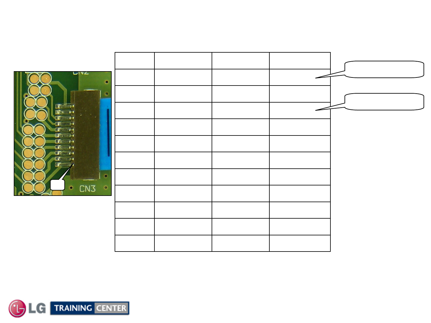
- T-CON Board Connector CN3 to Inverter A (Voltage and Diode Check)
- MAIN BOARD SECTION
- Additional Main Board Information
- Main Board Layout
- Main Board (Front View) Component Identification
- Main Board (Front Side) Component Voltages
- Main Board (Back View) Component Locations
- Main Board (Back Side) Component Voltages
- Main Board X600 and X800 Check
- Main Board Tuner with Shield Off (Pin ID)
- Main Board Tuner Video and SIF Output Check
- Main Board Tuner Clock and Data Lines
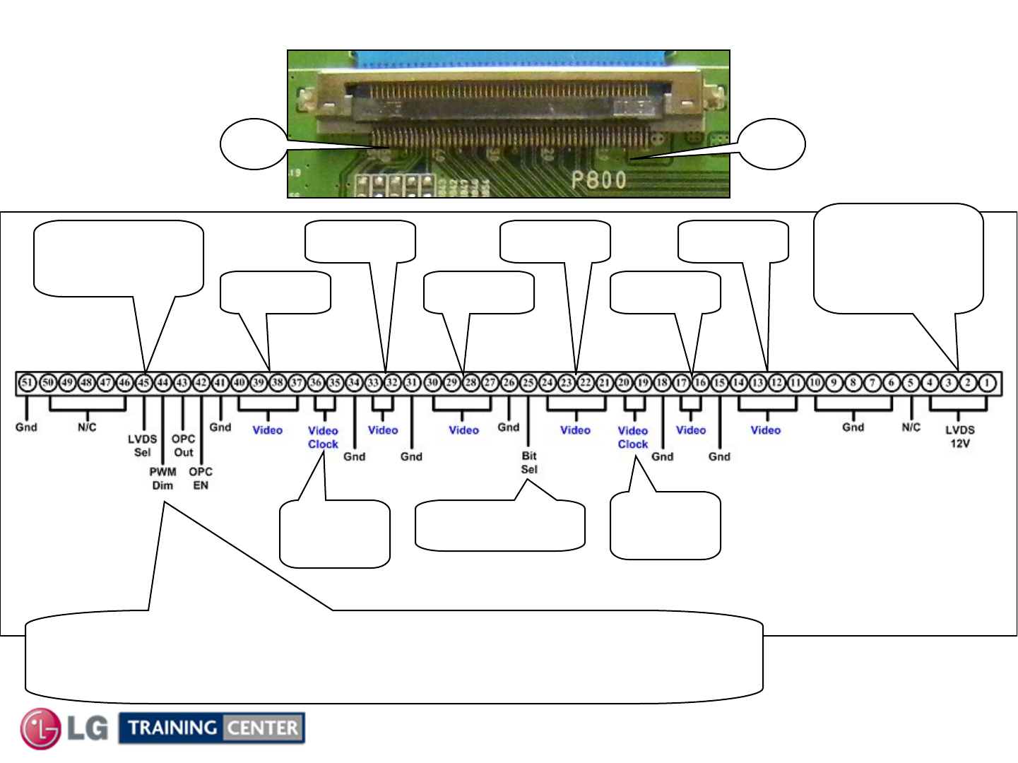
- Main Board LVDS P800 Video Output Check
- Main Board Connector P400 to Power Supply Voltage and Diode Check
- Main Board LVDS Connector P800 Pin Identification
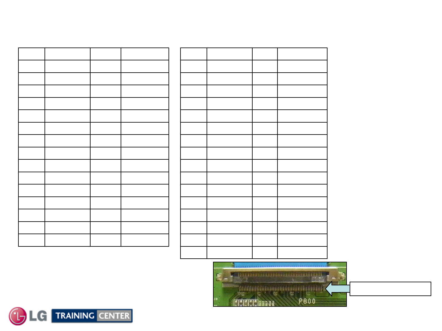
- Main Board Connector P800 to T-CON Voltage and Diode Check
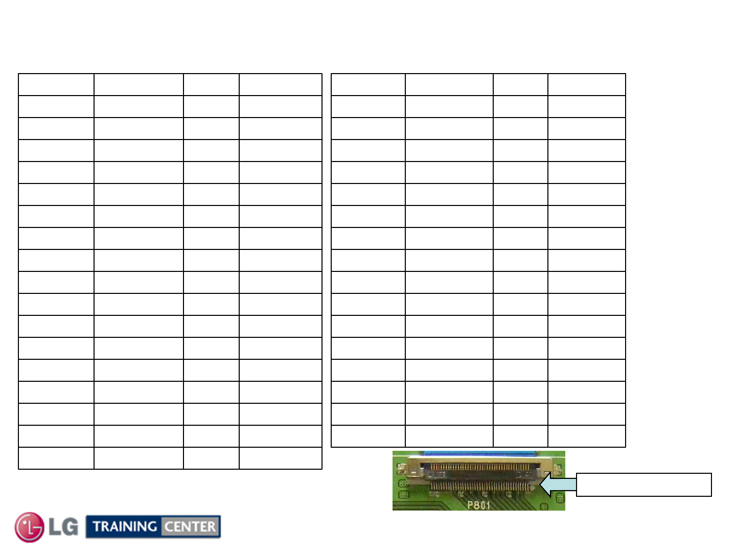
- Main Board Connector P801 to the T-CON Board Voltage and Diode Check
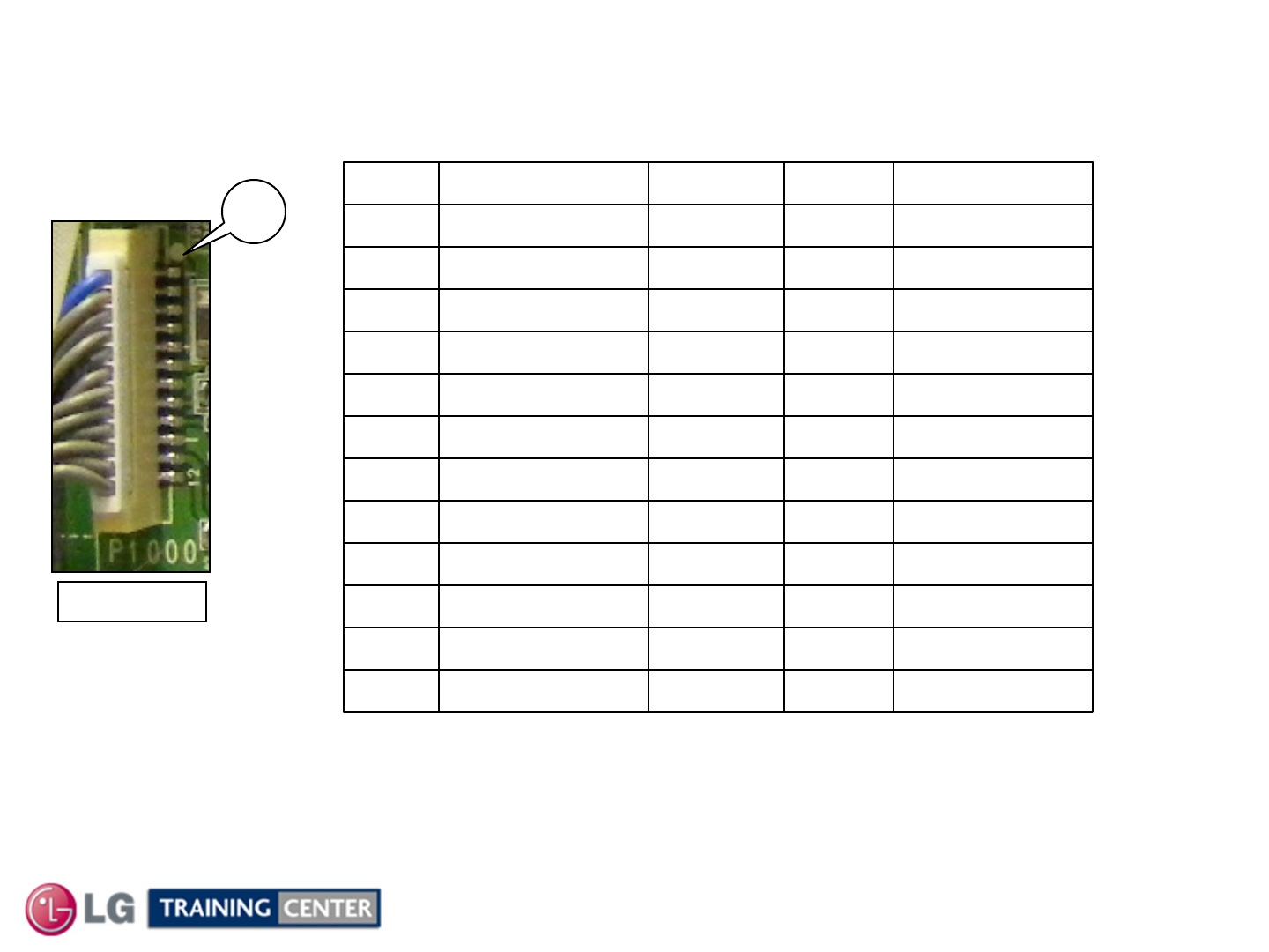
- Main Board Connector P1000 to (Ft. IR/LED Control) Voltage and Diode Check
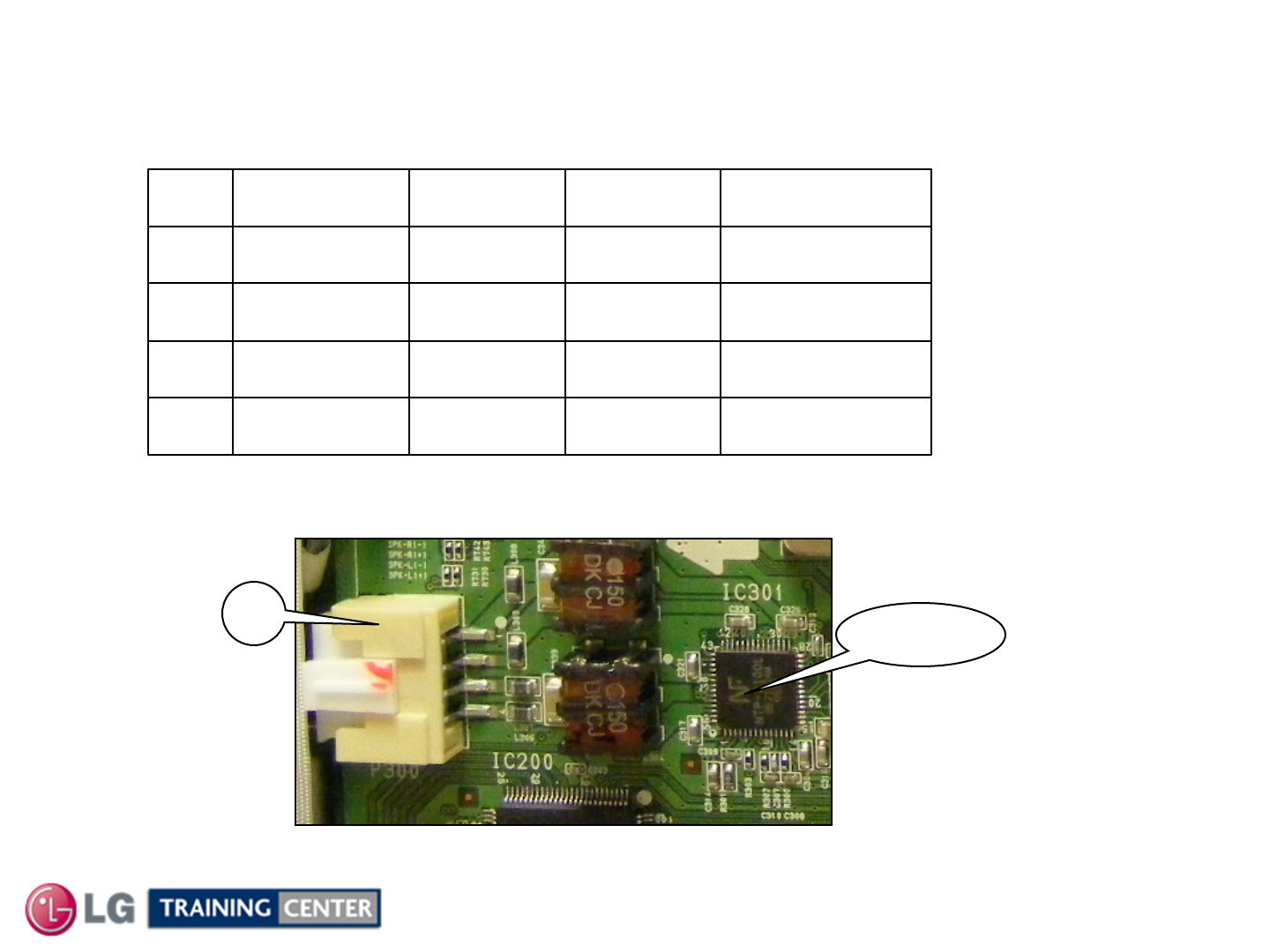
- Main Board Connector P300 to Speakers Voltage and Diode Check
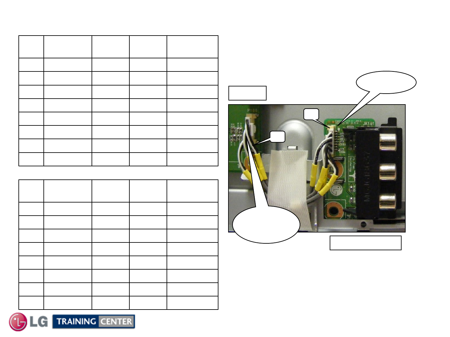
- Side A/V Board Connector P100 to Main P101 Voltage and Diode Check
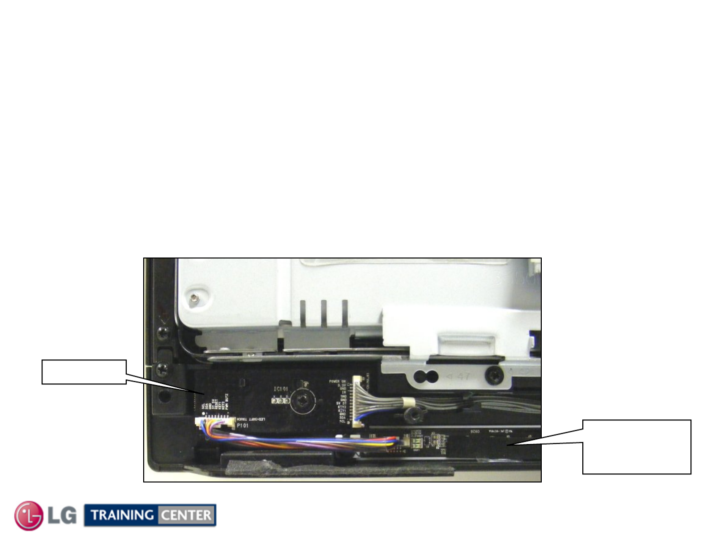
- FRONT IR SECTION
- SOFT TOUCH KEY BOARD SECTION
- INVISIBLE SPEAKER SYSTEM SECTION
- INTERCONNECT DIAGRAM (11 X 17 Foldout) SECTION
- 42SL80 Conclusion Page

42SL80
42SL80
Original February 11, 2010
Updated May 04, 2010
1080P
Direct View LCD

LCD DV 42SL80
2February 2010
OUTLINE
OUTLINE
• Two Inverter Boards
• Main Board
•T-CON Board
Circuit Board Operation, Troubleshooting of :
• Switch mode Power Supply
Section 1
Section 2
Contact Information, Preliminary Matters, Specifications,
LCD Overview, General Troubleshooting Steps,
Signal Distribution, Disassembly Instructions and Voltages
• Ft Control Board
P-DIM (Digital Dimming) Routed from the Main
board to the T-CON to the Ballast.
42SL80

LCD DV 42SL80
3February 2010
42SL80 LCD Direct View Display
Section 1
This Section will cover Contact Information and remind the Technician of Important Safety Precautions for
the Customers Safety as well as the Technician and the Equipment.
Basic Troubleshooting Techniques which can save time and money sometimes can be overlooked. These
techniques will also be presented.
This Section will get the Technician familiar with the Disassembly, Identification and Layout of the LCD
Display Panel.
At the end of this Section the Technician should be able to Identify the Circuit Boards and have the ability
and knowledge necessary to safely remove and replace any Circuit Board or Assembly.
Overview of Topics to be Discussed
Overview of Topics to be Discussed

LCD DV 42SL80
4February 2010
IMPORTANT SAFETY NOTICE
IMPORTANT SAFETY NOTICE
The information in this training manual is intended for use by persons possessing an adequate background in
electrical equipment, electronic devices, and mechanical systems. In any attempt to repair a major Product,
personal injury and property damage can result. The manufacturer or seller maintains no liability for the
interpretation of this information, nor can it assume any liability in conjunction with its use. When servicing this
product, under no circumstances should the original design be modified or altered without permission from LG
Electronics. Unauthorized modifications will not only void the warranty, but may lead to property damage or
user injury. If wires, screws, clips, straps, nuts, or washers used to complete a ground path are removed for
service, they must be returned to their original positions and properly fastened.
CAUTION
CAUTION
To avoid personal injury, disconnect the power before servicing this product. If electrical power is required for
diagnosis or test purposes, disconnect the power immediately after performing the necessary checks. Also be
aware that many household products present a weight hazard. At least two people should be involved in the
installation or servicing of such devices. Failure to consider the weight of an product could result in physical
injury.
Preliminary Matters (The Fine Print)
Preliminary Matters (The Fine Print)

LCD DV 42SL80
5February 2010
Today’s sophisticated electronics are electrostatic discharge (ESD) sensitive. ESD can weaken or damage
the electronics in a manner that renders them inoperative or reduces the time until their next failure.
Connect an ESD wrist strap to a ground connection point or unpainted metal in the product. Alternatively,
you can touch your finger repeatedly to a ground connection point or unpainted metal in the product. Before
removing a replacement part from its package, touch the anti-static bag to a ground connection point or
unpainted metal in the product. Handle the electronic control assembly by its edges only. When
repackaging a failed electronic control assembly in an anti-static bag, observe these same precautions.
Regulatory Information
Regulatory Information
This equipment has been tested and found to comply with the limits for a Class B digital device, pursuant to
Part 15 of the FCC Rules. These limits are designed to provide reasonable protection against harmful
interference when the equipment is operated in a residential installation. This equipment generates, uses,
and can radiate radio frequency energy, and, if not installed and used in accordance with the instruction
manual, may cause harmful interference to radio communications. However, there is no guarantee that
interference will not occur in a particular installation. If this equipment does cause harmful interference to
radio or television reception, which can be determined by turning the equipment off and on, the user is
encouraged to try to correct the interference by one or more of the following measures: Reorient or relocate
the receiving antenna; Increase the separation between the equipment and the receiver; Connect the
equipment to an outlet on a different circuit than that to which the receiver is connected; or consult the
dealer or an experienced radio/TV technician for help.
ESD Notice
ESD Notice
(Electrostatic Static Discharge)
(Electrostatic Static Discharge)

LCD DV 42SL80
7February 2010
Safety and Handling Regulations
1. Approximately 20 minute pre-run time is required before making any picture performance
adjustments from the Menu.
2. Refer to the Voltage/Current silk screening on the Switch Mode Power Supply.
3. C-MOS circuits are sensitive to static electricity.
Use caution when dealing with these IC and circuits.
4. Exercise care when making voltage and waveform checks to prevent costly short circuits
from damaging the unit.
5. Be cautious of lost screws and other metal objects to prevent a possible short in the
circuitry.
1. Check the appearance of the Replacement Panel and Circuit Boards for both physical
damage and part number accuracy.
2. Check the model label. Verify model names and board model matches.
3. Check details of defective condition and history. Example: Oscillator failure dead set, etc…
Checking Points to be Considered
LCD Direct View Overview
LCD Direct View Overview

LCD DV 42SL80
8February 2010
Basic Troubleshooting Steps
Basic Troubleshooting Steps
Define, Localize, Isolate and Correct
•Define Look at the symptom carefully and determine what circuits could be causing
the failure. Use your senses Sight, Smell, Touch and Hearing. Look for burned parts and
check for possible overheated components. Capacitors will sometimes leak dielectric material
and give off a distinct odor. Frequency of power supplies will change with the load, or listen for
relay closing etc. Observation of the front Power LED may give some clues.
•Localize After carefully checking the symptom and determining the circuits to be
checked and after giving a thorough examination using your senses the first check should
always be the DC Supply Voltages to those circuits under test. Always confirm the supplies
are not only the proper level but be sure they are noise free. If the supplies are missing check
the resistance for possible short circuits.
•Isolate To further isolate the failure, check for the proper waveforms with the
Oscilloscope to make a final determination of the failure. Look for correct Amplitude Phasing
and Timing of the signals also check for the proper Duty Cycle of the signals. Sometimes
“glitches” or “road bumps” will be an indication of an imminent failure.
•Correct The final step is to correct the problem. Be careful of ESD and make sure to
check the DC Supplies for proper levels. Make all necessary adjustments and lastly always
perform a Safety AC Leakage Test before returning the product back to the Customer.
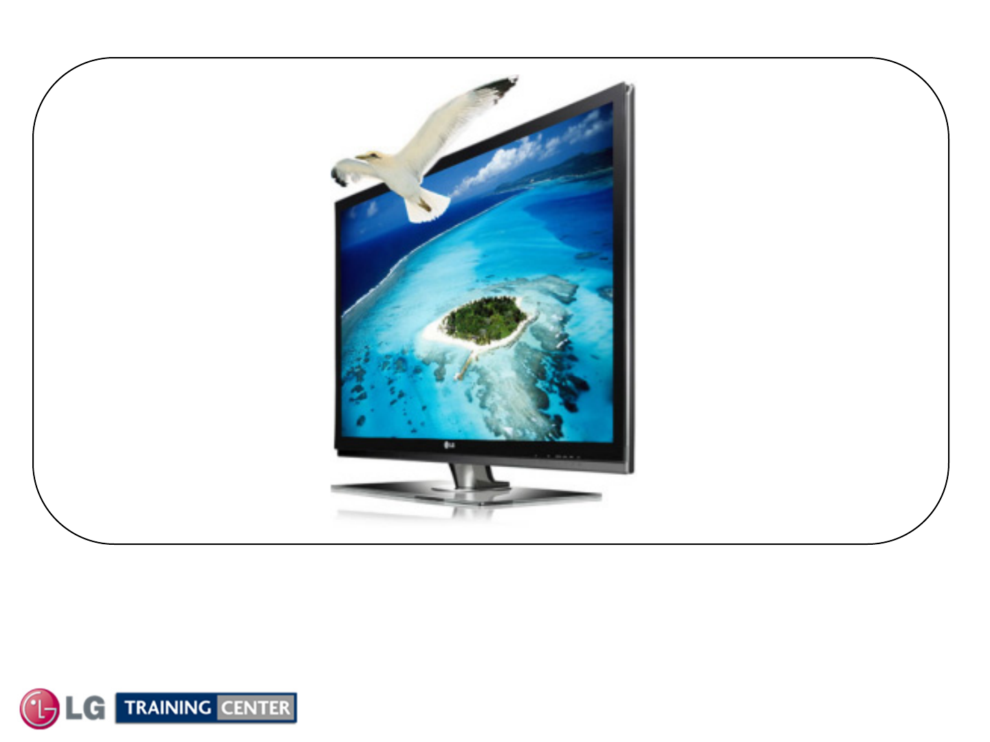
LCD DV 42SL80
9February 2010
This section of the manual will discuss the specifications of the
42SL80
LCD Direct View Display
42SL80 PRODUCT INFORMATION SECTION
42SL80 PRODUCT INFORMATION SECTION

LCD DV 42SL80
10 February 2010
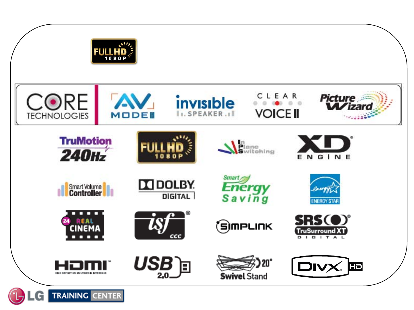
42SL80 Basic Specifications
42SL80 Basic Specifications
• TruMotion 240Hz
• Intelligent Sensor Mode
• Full HD 1080p HD Resolution
• 150,000:1 Dynamic Contrast Ratio (Brightness 500 cd/m2)
• 2.2ms Response Time (Gray To Gray)
• 500 cd/m2 Brightness
•Wide Color Gamut
• Super IPS Panel
• Wide Viewing Angle (178º / 178º)
•XD Engine®
• 24p Real Cinema
• ISFccc® Ready
• Picture Wizard
• AV Mode II (Cinema, Sports, Game)
• 60,000 Hour Panel Life (typical)
• NTSC/ATSC Tuners with Clear QAM
• 2 HD Component Video Inputs
• 2 Composite inputs
• 1 Digital Audio Out
• USB 2.0 (JPEG, MP3, MP4, Divx)
• PC Connectivity (D-Sub 15pin)
LCD DV 42SL80
11 February 2010
Basic Specifications (LOGO Familiarization)
Basic Specifications (LOGO Familiarization)
Full HD 1080p Resolution
Displays HDTV programs in full 1920 x 1080p
resolution for a more detailed picture.

LCD DV 42SL80
12 February 2010
TOP PORTION BOTTOM PORTION
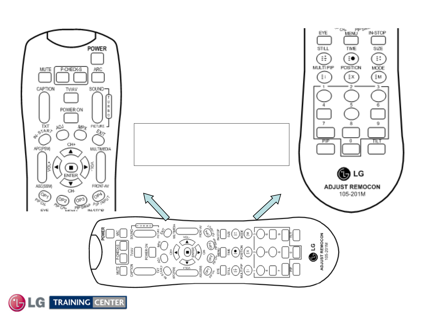
Remote Control Familiarization
Remote Control Familiarization
p/n MKJ61841701
LCD DV 42SL80
13 February 2010
Accessing the Service Menu
Accessing the Service Menu
To access the Service Menu.
1) You must have the Service
Remote. p/n 105-201M
2) Press “In-Start”
3) A Password screen appears.
Note: A Password is required
to enter the Service Menu.
Enter; 0000
LCD DV 42SL80
14 February 2010
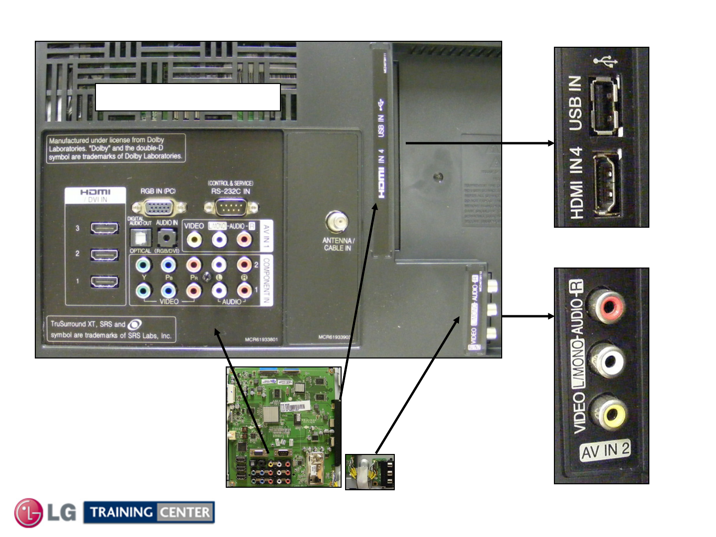
Side Input Jacks
Rear and Side Input Jacks
Rear and Side Input Jacks
Main Board
Orientation
Rear Input Jacks
Side AV
Side A/V Input
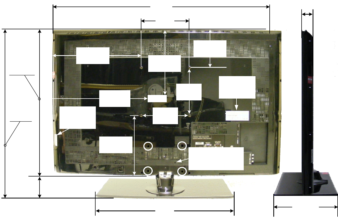
42LS80 Dimensions
7-7/8"
200mm
24.1/2”
622.3
39.3/8"
1000mm
Remove 4 screws to
remove stand for
wall mount
15.¾“
400mm
21.7/8"
500mm
27.1/8"
688.34mm
Center
7-7/8"
200mm
6.11/16"
170mm
10.1/16"
255mm
2-5/8"
66.04mm
Weight without Stand: 41.2 lb
Weight with Stand: 52.2 lb
1.13/16"
4.572mm
11.5/16"
287.02mm
19.11/16"
500.06mm
12.1/4”
31.15mm
15
42SL80 Product Dimensions
42SL80 Product Dimensions
There must be at least 4 inches of Clearance on all sides
Wattage
Average 210W
Stand By 0.36W
Model No.
Serial No.
Label
Model No.
Serial No.
Label
7-7/8"
200mm
LCD DV 42SL80
16 February 2010
This section of the manual will discuss Disassembly, Layout and Circuit
Board Identification, of the 42SL80 LCD Direct View Television.
Upon completion of this section the Technician will have a better
understanding of the disassembly procedures, the layout of the
printed circuit boards and be able to identify each board.
DISASSEMBLY and TROUBLESHOOTING SECTION
DISASSEMBLY and TROUBLESHOOTING SECTION
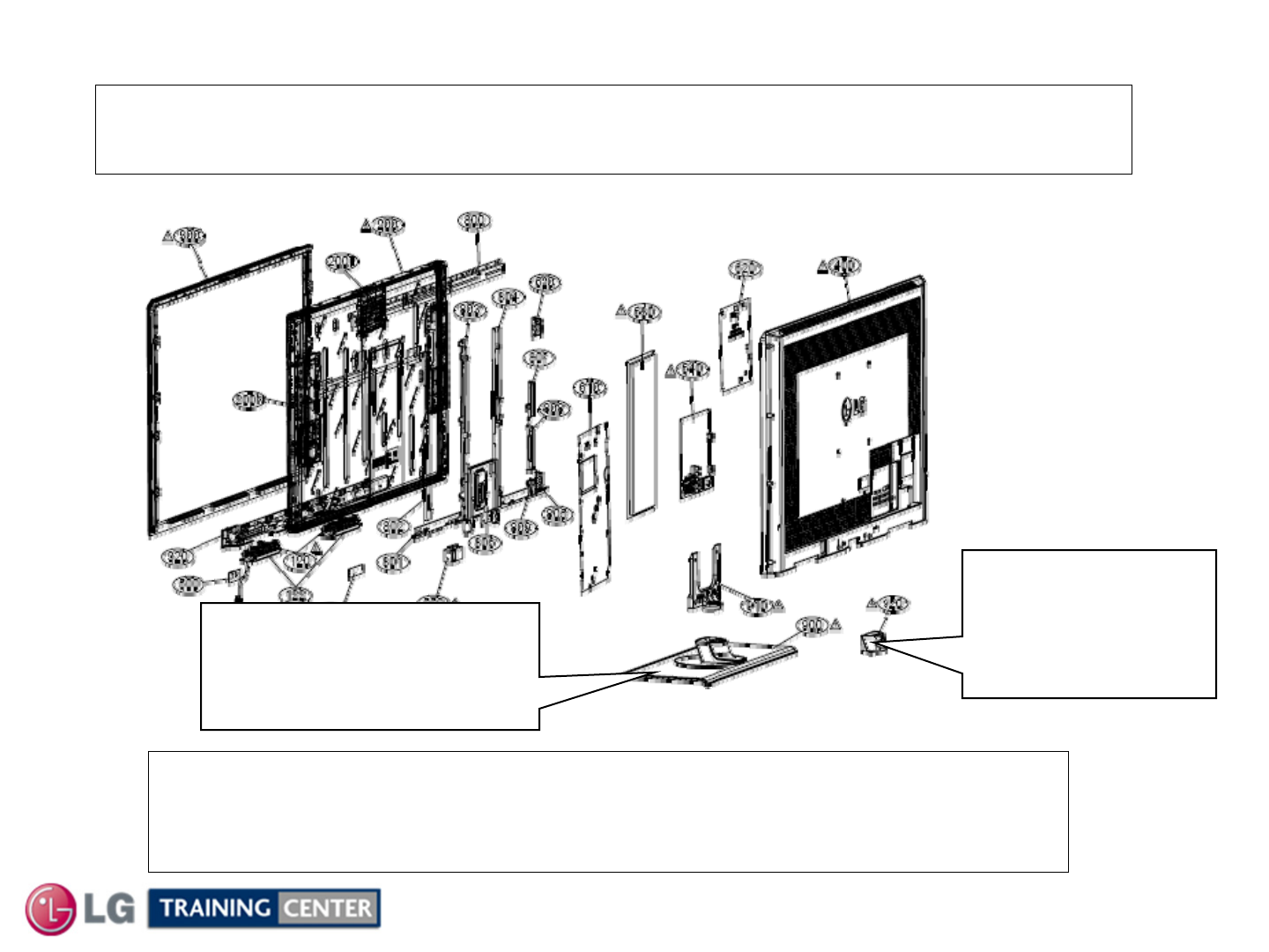
The Stand must be
assembled when TV first
received out of the box.
Decorative Cap
(If Installed)
Must be removed
To take back off.
LCD DV 42SL80
17 February 2010
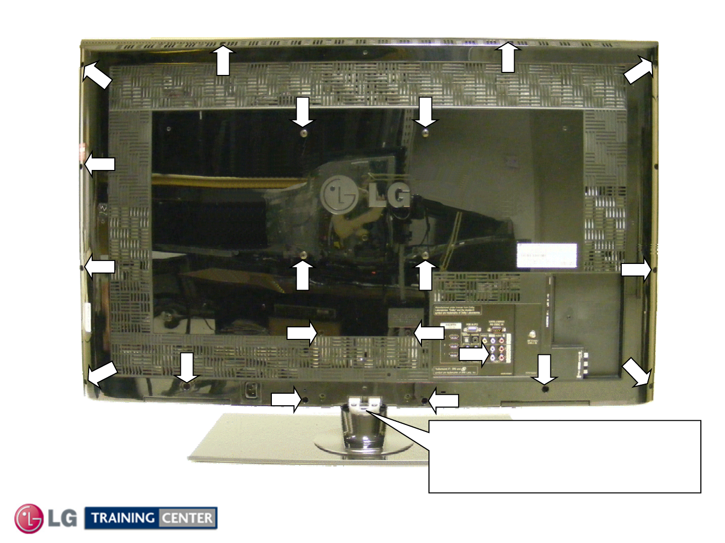
Removing the Back Cover
Removing the Back Cover
The Stand does not need to be removed
Remove the 19 screws indicated.
Pay attention to the size and type of screw
as there are many different types.
Putting in the improper screw when
reassembling may Cause damage.
The top two stand screws
Need to be removed, but
Not the bottom two screws.
Warning: The stand base is
“Glass” be careful, it will break.
If the customer has installed the
decorative Plastic Cap, it must be
removed before the back will come off.
LCD DV 42SL80
18 February 2010
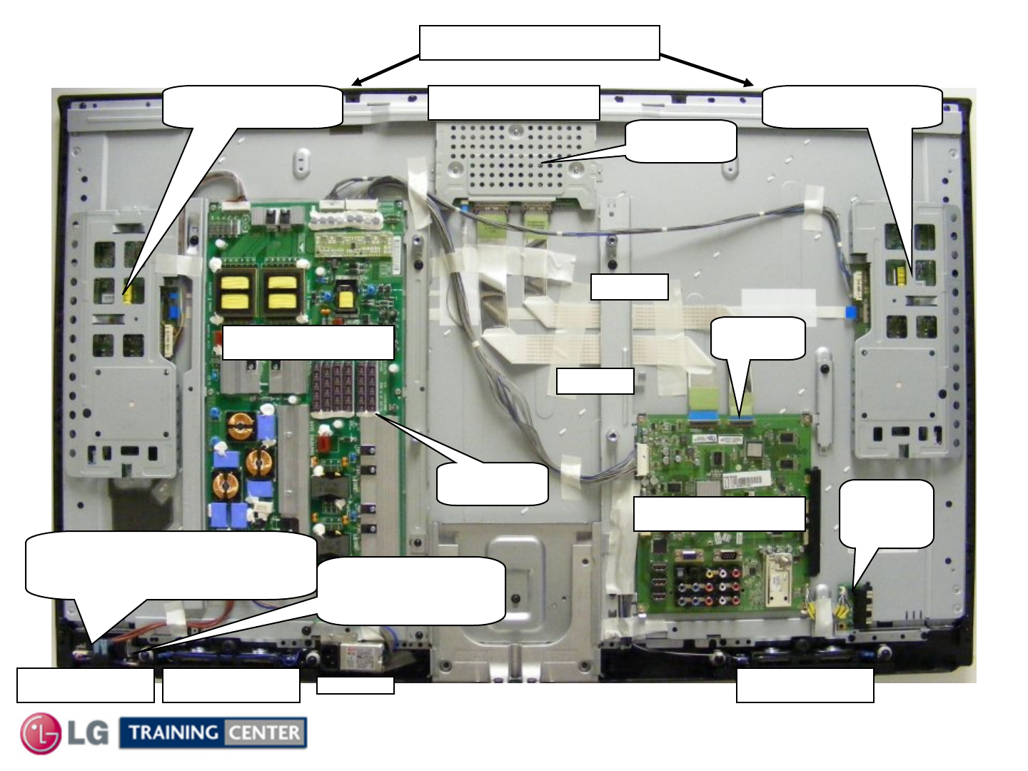
Circuit Board Layout
Circuit Board Layout
T-CON
MAIN
SMPS
INVERTER A
FRONT CONTROL (IR)
p/n EBR63322103 KEY BOARD
p/n EBR63609903
LVDS
LVDS
p/n EAT60667401 INVERTER B
SIDE
A/V
Invisible Speakers
EAB60866701
AC Input
p/n EAY58470001
p/n EBR63774601
Invisible Speakers
EAB60866701
Main
Power Switch
Inverters p/n EAY60750201
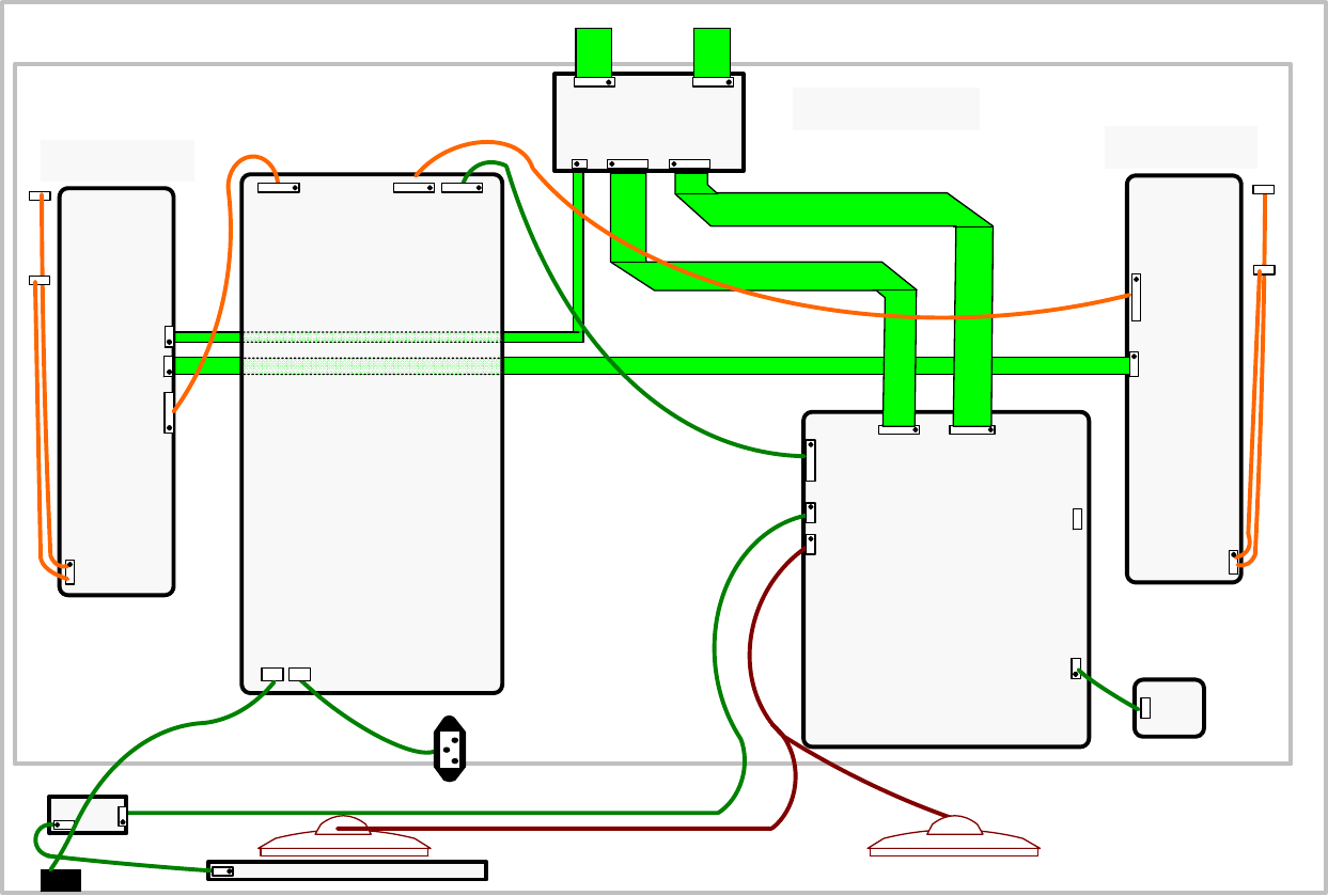
42LS80 Connector Identification Diagram
42LS80 Connector Identification Diagram
19
T-CON
POWER
SUPPLY
MAIN
BOARD
P204 P205
SK100
P101
CN1
CN2
CN1
CN5 CN4
P800 P801
P400
Speakers (Front Left)
Speakers (Front Right)
AC In
Main Power
Switch
P803
N/C
TFT Panel
INVERTER
P201
Front Keys
CN3
CN2CN3
P1000
P300
CN201
CN203
INVERTER
CN5
P101
P100 J2
P100
P101
A/V IN
Front “Soft Switch” Keys
FRONT IR
SC1
Black
CN205
LN
L
MC1
Black
LCD DV 42SL80
20 February 2010
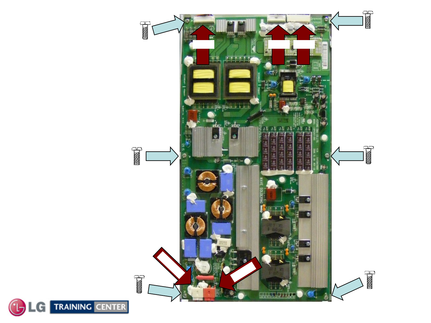
Power Supply Board Removal
Power Supply Board Removal
Disconnect P201, P205,
P204, P101 and AC In
SK100.
Remove the 6 screws
indicated by the arrows.
SK100
P101
To Main Power Switch SK100 AC In
Caution: Be careful when
touching the back side of
the Power Supply as
some capacitors can still
hold a charge.
P201P205P204 P201 to Main
P205 to Inverter B
P204 to Inverter A
LCD DV 42SL80
21 February 2010
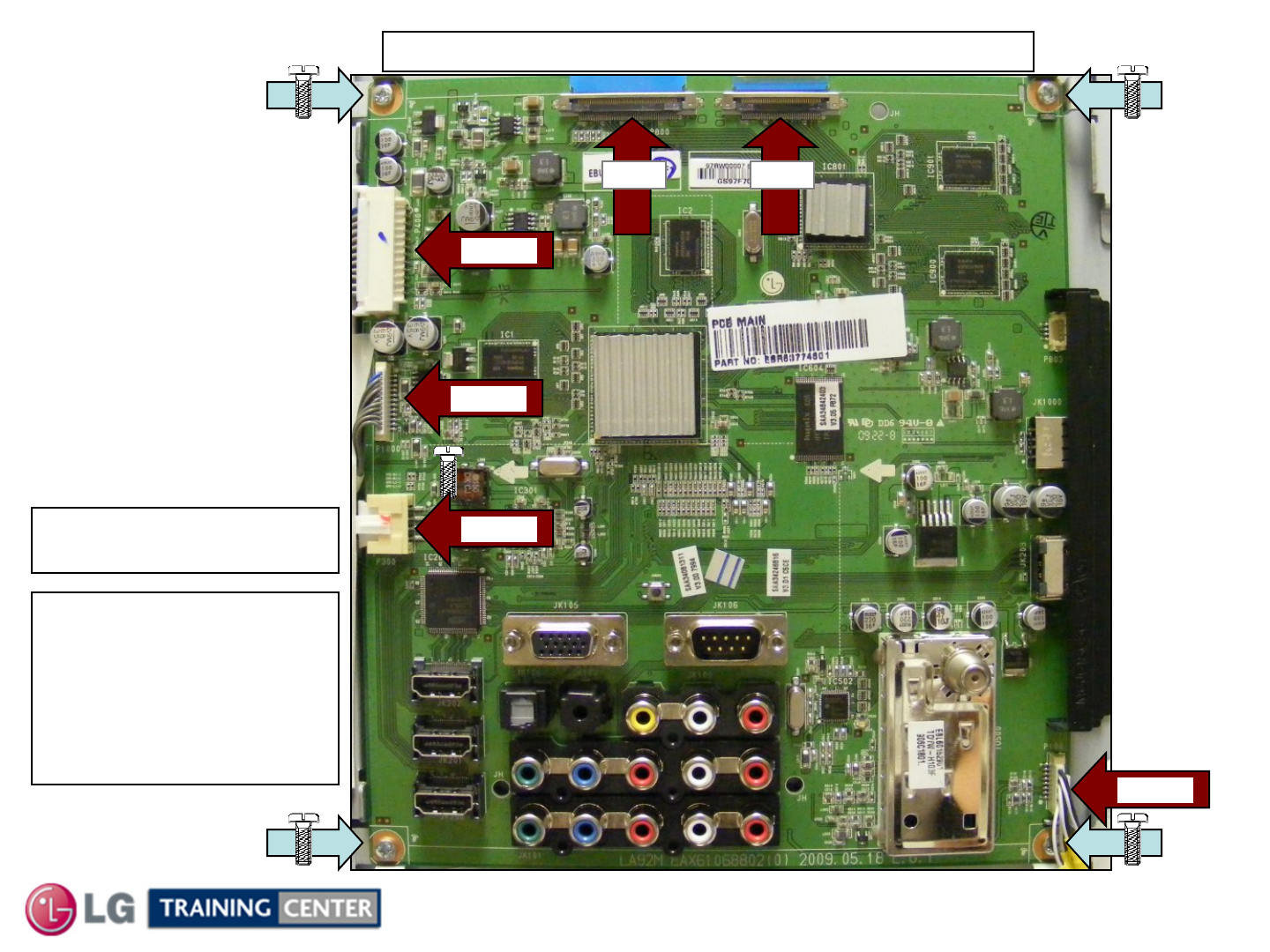
Main Board Removal
Main Board Removal
Disconnect
P100, P300,
P400, P800,
P801
Remove the 4
screws
indicated by
the arrows.
To A/V
Board
P801
P100
P800
P400
P1000
P300
Remove any tape holding
down any cables.
NOTE: Be sure to check on
top and behind the
Micro/Video Processor IC.
Look for Chocolate
(Heat Transfer Material).
Be sure to transfer to new
Board if present.
Flip the locking tabs upward, pull the LVDS ribbon up and out
To
SMPS
To
SPKs

LCD DV 42SL80
22 February 2010
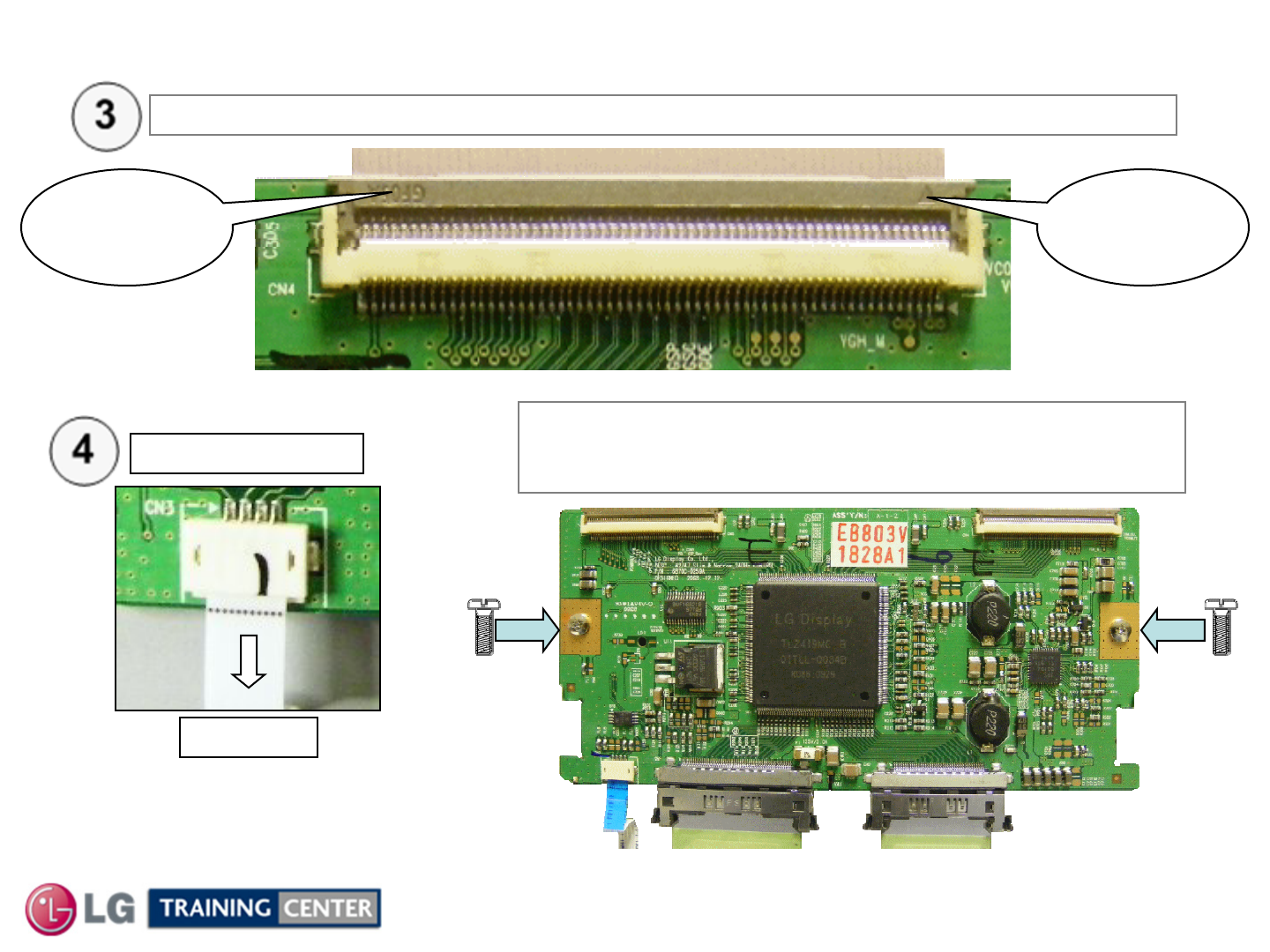
Removing the T
Removing the T-
-CON Board (1 of 2)
CON Board (1 of 2)
Press
In Press
In
Remove the LVDS Connectors CN1 and CN2
Remove the 3 Screws in the T-CON shield.
There is a small
lip at the top of the
shield, pull straight
out slightly to
remove.
Be careful with the tabs.
They are fragile and will break.
Rock the connector side ways while
pulling the cable out.
LCD DV 42SL80
23 February 2010
Removing the T
Removing the T-
-CON Board (2 of 2)
CON Board (2 of 2)
Flip the Locking Mechanism upward on CN4 and CN5 to release the LVDS cables to the Panel.
T-CON SERVICE POSITION
Remember, these two screws have to be replaced in the board
if the TV is to be run with the T-CON shield removed.
Flip
Downward
Flip
Downward
Pull Out
Pull out (CN3)
LCD DV 42SL80
24 February 2010
Inverter A Removal
Inverter A Removal
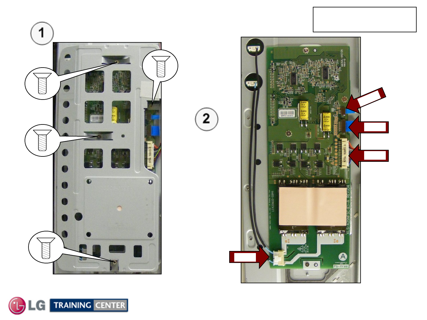
Remove 4 screws.
Be careful not to drop these screws. p/n EAY60750201
Includes both Inverters
To T-CON
To SMPS
To Inverter B
CN1
CN3
CN2
CN5
Disconnect
CN1, CN2,
CN3 and
CN5
To
Backlights
LCD DV 42SL80
25 February 2010
Inverter B Removal
Inverter B Removal
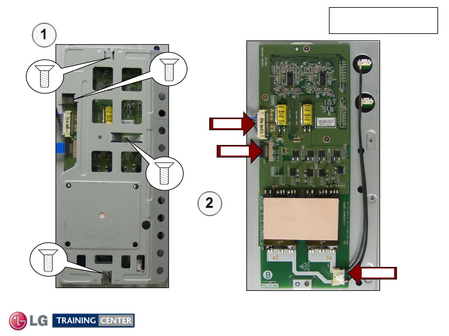
Remove 4 screws.
To
Backlights
To SMPS
To Inverter A
CN205
Disconnect
CN201,
CN203 and
CN205
CN203
CN201
Be careful not to drop these screws. p/n EAY60750201
Includes both Inverters
LCD DV 42SL80
26 February 2010
POWER SUPPLY SECTION
POWER SUPPLY SECTION
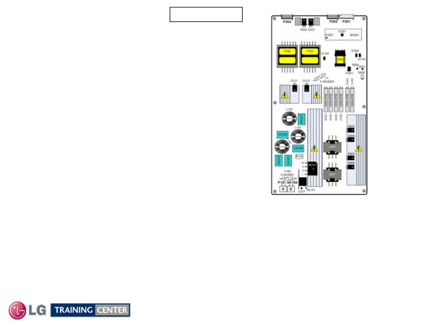
This set utilizes a Switch Mode Power Supply.
Input Voltages: AC
Stand-By Output Voltages:
•+5V (Stand By 5V) to the Main.
Run Output Voltages:
•+5V (Stand By 5V) to the Main
•12V to the Main
(Video Processing, Tuner B+
and T-CON B+)
•24V to the Main
(Audio B+)
•24V to both Inverters
Run Input Commands from Main:
•PWR-ON (Relay On Command)
Brings the SMPS out of Stand-By
•INV-ON (In and Out to the Ballast)
This line also called “I-C”
Turns on the Backlights
p/n EAY58470001
LCD DV 42SL80
27 February 2010
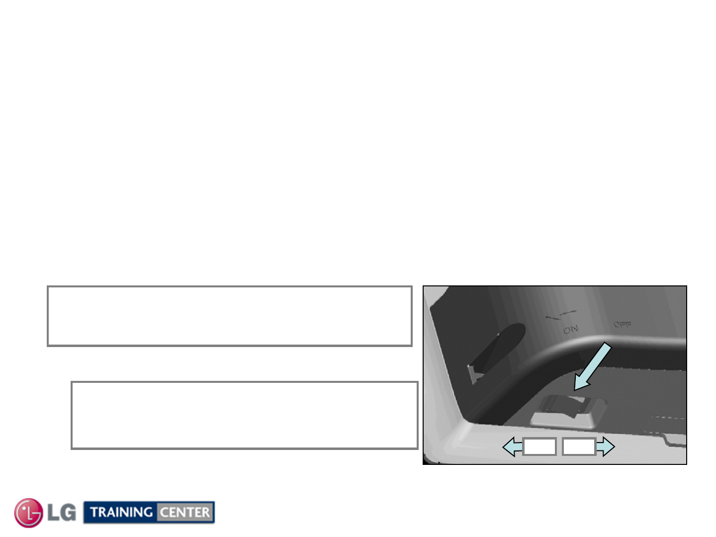
There are three types of Main Power switch used in LG televisions.
Type 1: Shuts off AC to the Power Supply.
Type 2: Opens ground to the front IR board. (Stand-By 5V Remains, the Main board stays alive).
This prevents any activity of the IR or the Key Board. When the Switch is opened, a line called Power Key pulls up high
when ground opens. When the switch is closed, this same line called Power Key feeds back to the Microprocessor and the
Micro. Turns on the Power.
Type 3: Opens ground to the front IR board. (Stand-By 5V turns off, the Main board is dead).
This prevents any activity of the IR or the Key Board. When the Switch is opened, a line called Power Key pulls up high
when ground opens. This line feeds back to the Main board and from there it routes to the Power Supply. The high tells the
Controller chip to turn off STBY-5V. When the switch is closed, this same line called Power Key now goes high and feeds
back to the Power Supply and tells the controller chip to turn STBY-5V on.
Power Supply (Main Power Switch Type 1) Location
Power Supply (Main Power Switch Type 1) Location
MAIN POWER SWITCH LOCATION
Type 1
(Bottom Left Side viewed from rear) On Off
If the TV won’t come on, be sure to check the Main
Power Switch before assuming a failure has occurred.
This switch breaks AC to the SMPS.
LCD DV 42SL80
28 February 2010
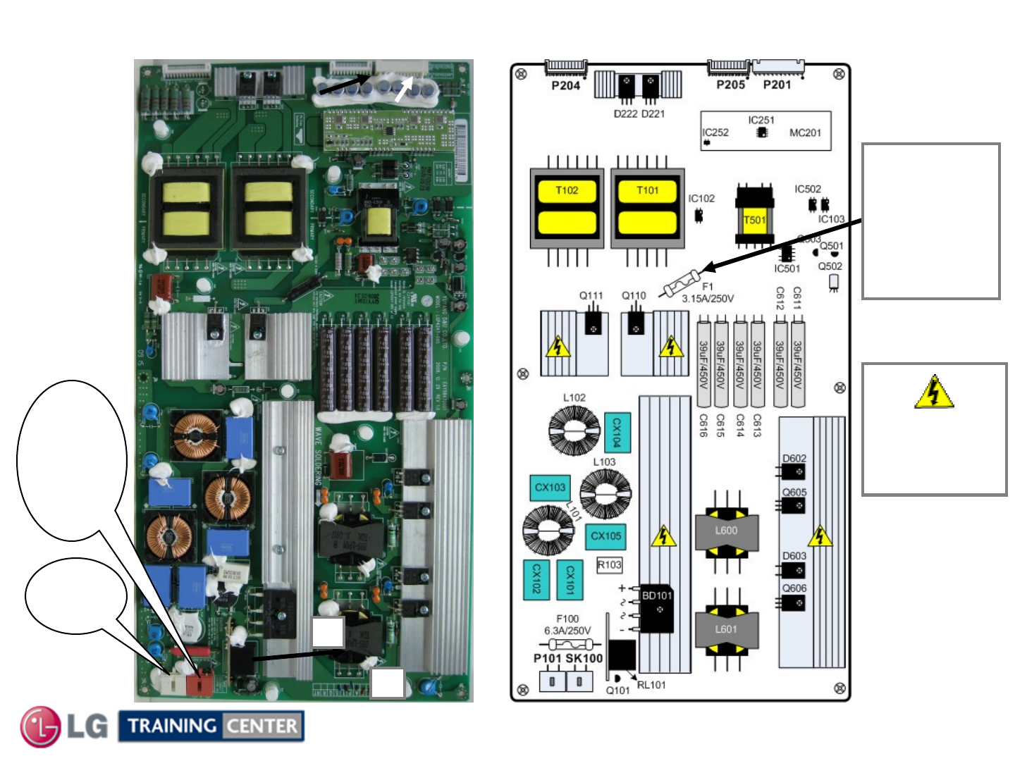
Power Supply (SMPS) Board Layout
Power Supply (SMPS) Board Layout
Hot Ground
Shock
Hazard
F1
3.15A/250V
STBY 170V
Run 388.5V
From Hot
Gnd
L
N
SK100
AC IN
P101
To
Main
Power
Switch
Inverter B
POWER SUPPLY (SMPS)
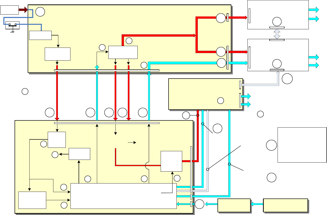
42SL80 Power Supply Start Up Sequence
42SL80 Power Supply Start Up Sequence
29
Inverter A
Inverter On
Starts the Inverters
24V B+ for the Inverters
Stand
By 5V
Remote or Power Button Key
MAIN BOARD
5V Q408
Switch
RL_ON
12V Video
Processing
Inv
On
Stand
By 5V Reg
1
2 6 66 8
6
3
5
6
6
6
Primary side fuse:
Stand-By 170V
Run 388.5V (Hot Gnd)
4
24V
Audio
12V 24V
8
Reg
For
Micro
12V
7
At point TV is in
Stand-By state.
Energy Star compliant.
Less than 1 Watt
4
Other Circuits
5V General
And 5V
PWM-DIM
Digital
Dimming
Manipulates
Backlights
Tuner B+
10
Cust Menu for
Backlight
and
Picture Content
Manipulate P-DIM
Relay On
3
8
No AC
Det in
this
model
LVDS
Video
12V
AC In
Ft IRKey
24V
INV
On
LVDS Panel Control
Inv On/Off
Microprocessor IC600
Also Video Processor
(RL_ON)
To Panel
3.3V, 26V, -5V, 16V
Video
9
10
Tru-Motion
LVDS Video
IC406
3.3V
IC603
Q408
PWM-DIM
CN4
CN1
P201
CN3
Main
Power
Switch
Bridge
P203
To Panel
Backlights
Power On
Power
On
6
3.3V, 26V, -5V, 16V
P205 CN101
624V CN3
CN203
INV OnSync
10
10
P400
Soft Touch Key
12V/24V
Regulators
P1000
LVDS
12V
Switch
Inverter On
7
P800
P801
8
7
Video
On LVDS cables
12V LVDS
T-CON Board
9
Voltages developed by U5
On T-CON
8
CN4
CN5
Reset
Generator
+5V General
PWM 2
PWM-DIM is not used
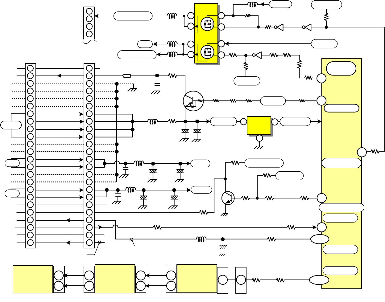
47LH85 P400 on Main Board to SMPS P201 Turn On Circuit
47LH85 P400 on Main Board to SMPS P201 Turn On Circuit
INV ON/OFF
PWR ON
100Ω
R414
C421
15pF
P400
11.9V
Gnd
Gnd
Gnd
Gnd
0V
0V
4.9V
1.6V
PWR On
P201
ERROR
PWR
A.DIM
I-C
P-DIM
n/c
SMPS
AB12
IC600
Mstar
PWM2
PWM3
n/c
Gnd
Gnd
Gnd
Gnd
A-DIM (Analog Dimming) Fixed Value.
H5 R775
100
GPIO137
5.2V
MAIN PWB
5.14V
Gnd
Gnd
12V
2
1
4
3
6
5
8
7
10
9
11
12
14
13
16
15
18
17
20
19
22
21
23
24
2
1
4
3
6
5
8
7
10
9
11
12
14
13
16
15
18
17
20
19
22
21
23
24
24.7V
24V
Gnd
Gnd
Gnd
Gnd
Gnd
Gnd
n/c n/c
n/c n/c
E5 GPIO 134
L405
L407
+24V
C425
C427
68uF
C430
0.1uF
L402
+12V
C405
0.1uF
Q400
R425R421
R787
100Ω
G5
R422
10KΩ
Q401
R430 0Ω
R418
3.3KΩ
GPIO 136
R774
100Ω
+5V General
RL_ON
Inverter On/Off
3
1
2
6
5
8
7
Q408
+5V
L417
L418
12V_TCON
L419
Q406
0.2V
6V
0.6V
4
Q405
Q407
Panel Control
L411
R783
10KΩ
0V
0.6V
+12V
R454 47KΩ
R455 47KΩ
AA13
C407
C412
100uF
5V_ST
L403
Relay On
A-DIM
P-DIM
C409
1uF
24.7V
4.3V
20K
30
E8 GPIO 97
R713
100ΩError Out
5.2V
R427 4.7KΩ
R426
10KΩ
+3.3V ST
R437 10KΩ
R434
0Ω
R442 0Ω
R450
560Ω
P800
2
1
4
3
To
T-CON
F6
Power
On/Off
GPIO 185
Video
Processor
n/c
R726
1.2K
PWM 3
R725
1.2K
R843
0Ω
T-CON 44
P800
8
CN1
2
CN3
3
2
CN2
3
INVERTER A
C408
47uF
R412
0Ω
R420
0Ω
C400
22uF
0Ω
R431
0Ω
R792
100Ω
5V_ST
R449 10KΩ
IC406
32
1
+3.3V_ST
+3.3V_ST
Micro B+
Multiple Pins
Panel Power
5.14V
5.14V
5.14V
11.9V
n/c
T-CON (UC1)
Processes P-DIM
Inverter A
Processes P-DIM
INVERTER B Scan 2
Scan 1
9
11
CN3
Duty 2
Duty 1
1
3
Inverter B
Processes P-DIM
CN203

LCD DV 42SL80
31 February 2010
Power Supply (SMPS) Board Operational Troubleshooting
Power Supply (SMPS) Board Operational Troubleshooting
Power Supply Troubleshooting
AC voltage is supplied to the Power Supply at Connector SC100. This set does not use AC Detect.
The AC input generates a Hot Ground primary power supply that runs in two states, Stand-By (170) and
Run (388.5V) measured at Fuse F1 from Hot Ground. This primary voltage develops all other voltages
that are output from the SMPS. During Stand-By, the 5 Volt Standby (5V_ST) should be present at
connector P201, Pins 7,8,9 or 10. If Missing remove AC Power and unplug Connector P201, apply AC
Power and recheck for presence of 5V_ST (5.1V to 4.7V). Loss of 5V_ST would be a SMPS Failure. If
5V_ST returns, it would be an indication of a failure on the Main Board or possibly the Front Board (IR)
assembly. Suspect a possible short circuit loading the supply. Remember to observe the Front Power
Indicating LED this may save some time. A lit LED indicates the Stand-By 5V voltage is present
and the Microprocessor is communicating with the front LED driver IC!
The Main Board sends two commands to the Power Supply Board one being PWR_ON and the other is
INV ON. These two signals are used to control the SMPS turn on sequence. First the command PWR_ON
(Pin 2) also known as POWER ON, activates the Inverter voltages 24V and the 24V and 12V lines to the
Main board. The 2nd command is INV ON (I_C) (P201 pin 20). It is the Lamp Lighting Command Signal.
If either command (PWR-ON or INV-ON) is missing it will result in a no picture symptom and the backlights
will not turn on.
These voltages can not be easily checked using the normal “Stand-Alone” Power Supply check.
This Power Supply utilizes many different voltage sensing circuits that will prevent the usual procedure.
The Stand-By 5V to the Main Board MUST BE LOADED for the SMPS to stay on.
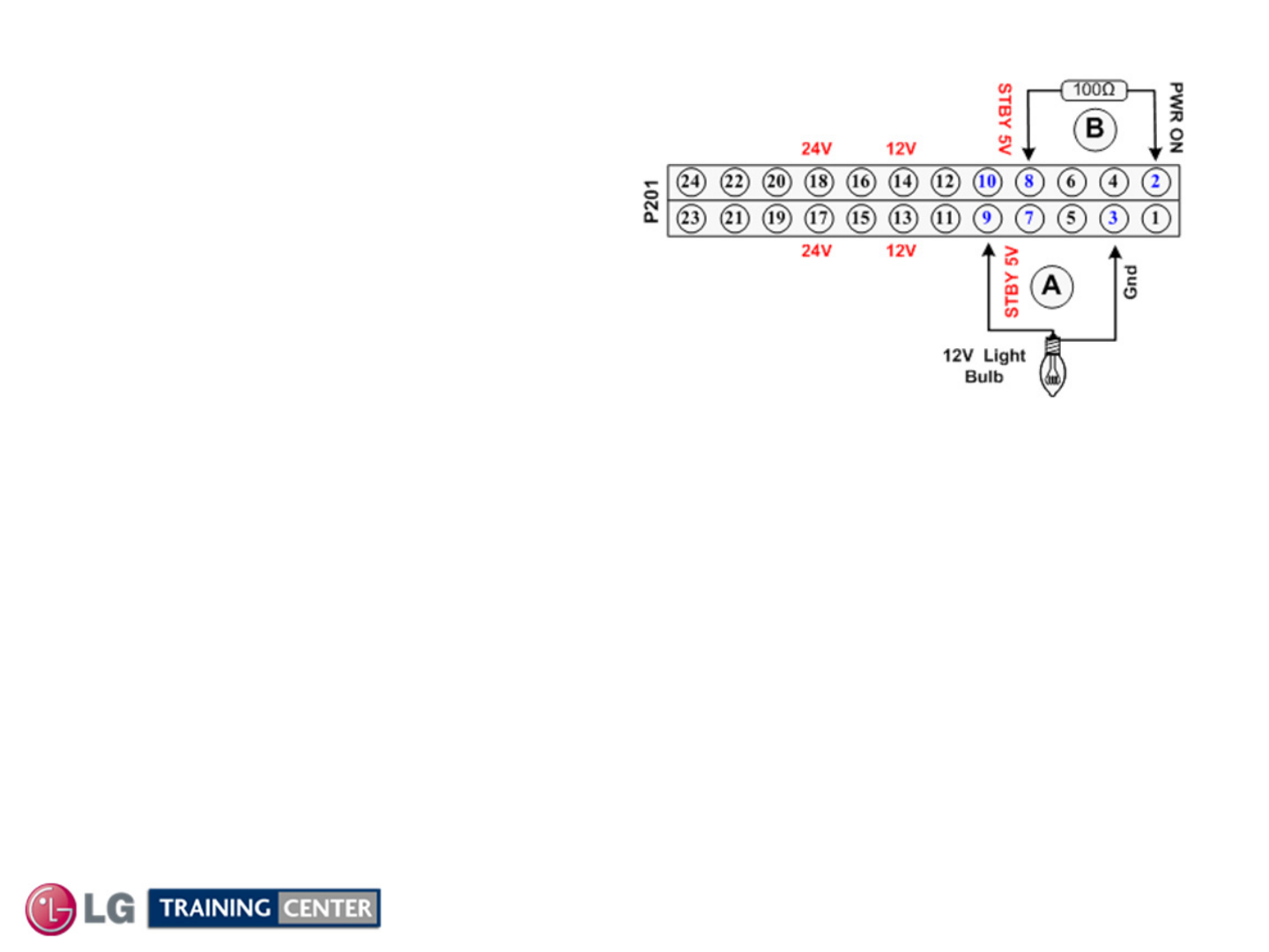
You can not just jump the PWR_ON command from 5V_ST like it was done before. Using a simple 12V
flashlight bulb from 5V_ST to Gnd. Will supply a sufficient load to run the SMPS stand alone.
LCD DV 42SL80
32 February 2010
AC Should not be applied at any time while
adding the light bulb, resistors or while
unplugging connectors as damage to the
circuit Board may occur.
•The SMPS “MUST” be producing STBY 5V on either pin 7, 8, 9 or 10 (5V).
If 5V Standby is not being generated, the SMPS is defective and must be replaced.
There is no need to continue with the next test.
•Unplug P400 on the Main Board. Use Main Board P400 Side to insert the
light bulb and resistors.
TEST 1: LOW VOLTAGE TEST:
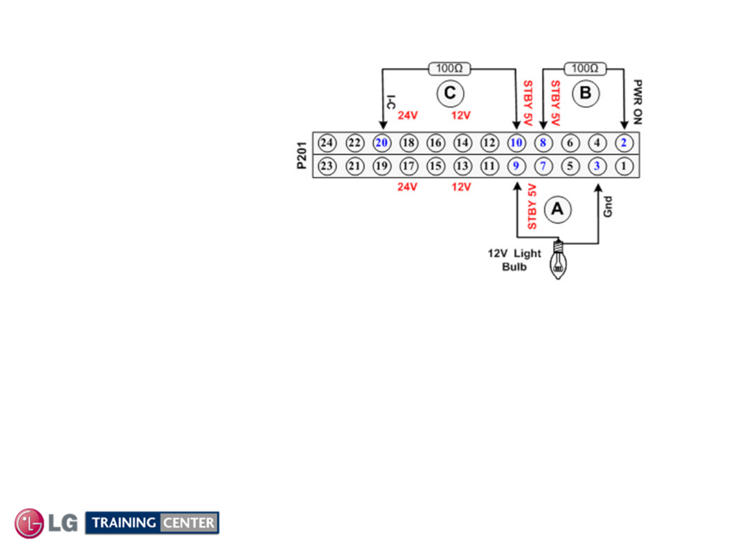
Step (A) Add a 12V Light Bulb (10W) between 5V_ST and Gnd. This Supplies a load on the 5V_ST line that will
allow the supply to be powered up one section at a time.
Step (B) Add a 100Ω¼ watt resistor from 5V_ST to PWR ON and the 12V and 24V Run Lines will become active.
Connector P201 Check pins 13 and 14 for 13.3V. Check pins 17 and 18 for 26.2V.
Connector P205 Check pins 1 through 5 for 26.2V.
Connector P204 Check pins 1 through 5 for 26.2V.
Remove AC power.
TEST 1 Power Supply Board Low Voltage Test
TEST 1 Power Supply Board Low Voltage Test
LCD DV 42SL80
33 February 2010
TEST 2: BACKLIGHT TEST:
Leave the Light Bulb and the resistor that was
added in the previous steps A and B connected.
Step (C)
Pull the Connector CN3 from the T-CON board.
Add a 100Ω¼ watt resistor from 5V Standby to I-C (Inverter On) pin 20.
Add AC Power, the Backlights should turn on.
Note: If they do not, confirm that the I-C line (Inverter On voltage) is sent out pin 12 of both P203 and P205 going to
each Inverter. If 24V and I-C are present on both Inverters, see the Inverter Section of this book.
Remove AC power and return all connectors to the correct location.
Note: Using the test above, Inverter B can not be run Stand-Alone. Inverter A can be run by removing Inverter B
CN201. But the Right side of the screen (as viewed from the front) will be brighter and the Backlights will blink.
If CN203 is removed, then Inverter A will not run.
If 24V and I-C are present on both Inverters, see the Inverter Section of this book.
TEST 2 Power Supply Board Backlight Test
TEST 2 Power Supply Board Backlight Test
LCD DV 42SL80
34 February 2010
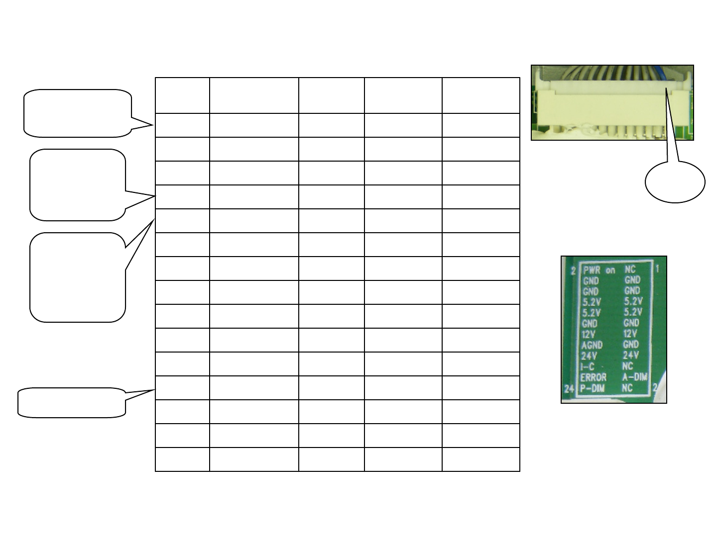
Power Supply Connector P201 Voltage and Diode Check
Power Supply Connector P201 Voltage and Diode Check
Diode Check taken with meter in Diode Mode with all Connectors Removed
GndGndGndGnd15
0.72V11.9V0V12V13-14
1.6V4.9V0VPWR on2
Open4.3V0VI-C20
Open0V0VErr Out22
Openn/cn/c
2P-DIM24
Openncncnc1
GndGndGndGnd3-6
Open5.14V5.14V*5.2V7-10
GndGndGndGnd11-12
GndGndGndAGND16
0.42V24.7V0V24V17-18
ncncncnc19
Open1.67V0V
1A-DIM21
ncncncnc23
Diode
Check
Run STBYLabelPin
P201 "SMPS" to P400 "Main Board"
2 P-DIM Pin 24
is not used.
I-C
Same as
Inverter
Control
On/Off
* Stand By 5V
P201
P201 Label
Pin 1
1 A-DIM
Pin 21
Fixed Voltage
LCD DV 42SL80
35 February 2010
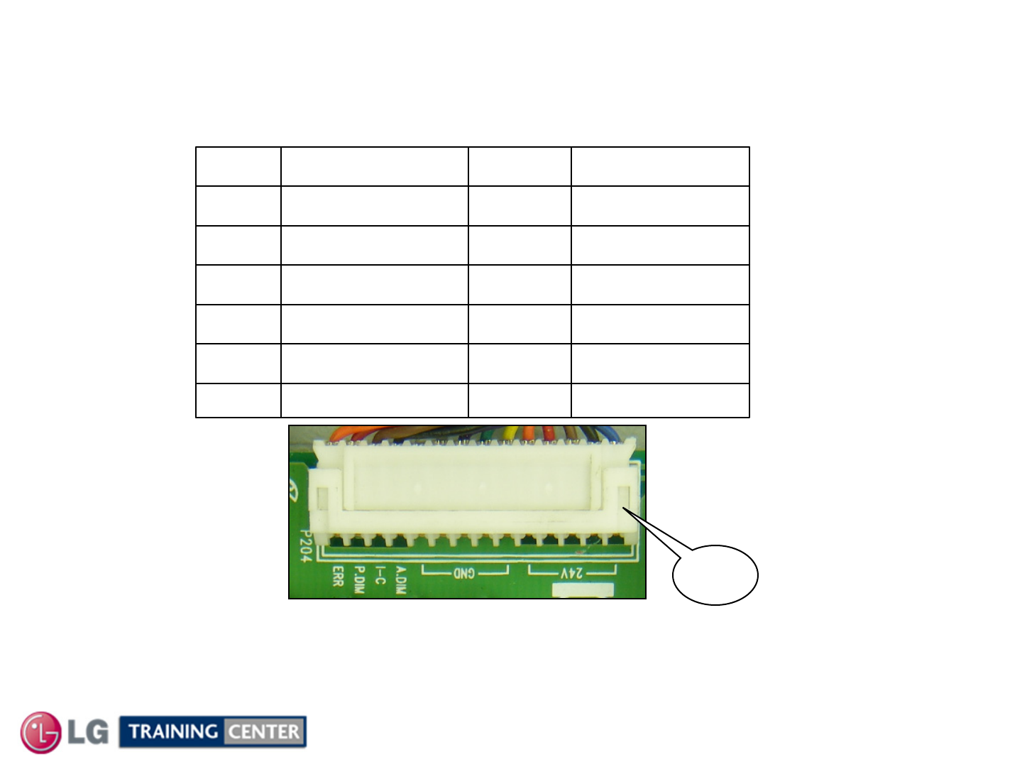
Power Supply P204 to Inverter A CN1 Voltage and Diode Check
Power Supply P204 to Inverter A CN1 Voltage and Diode Check
Diode Check taken with meter in Diode Mode with all Connectors Removed
Open0VError14
Open3.40VPWM-DIM13
Open4.3VI-C (INV On/Off)12
Open1.6VA-DIM11
GndGndGnd6-10
0.42V24.7V24V1-5
Diode CheckRun LabelPin
P204 "SMPS" to CN1 “Inverter A"
Pin 1
There are no Stand-By voltages.
LCD DV 42SL80
36 February 2010
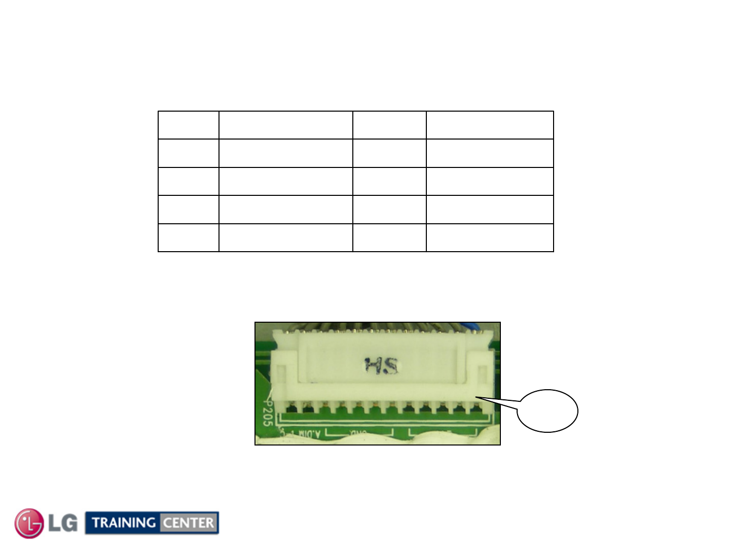
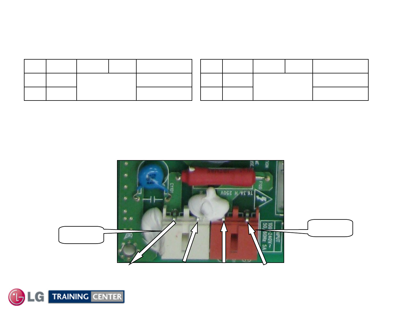
Power Supply P205 to Inverter B CN201 Voltage and Diode Check
Power Supply P205 to Inverter B CN201 Voltage and Diode Check
Diode Check taken with meter in Diode Mode with all Connectors Removed
Open3.45VI-C (INV On/Off)12
Open1.6VA-DIM11
GndGndGnd6-10
0.42V24.7V24V1-5
Diode CheckRun LabelPin
P205 "SMPS" to CN201 “Inverter B"
There are no Stand-By voltages.
Pin 1
LCD DV 42SL80
37 February 2010
Power Supply Connector SK100 and P101 Voltage and Diode Check
Power Supply Connector SK100 and P101 Voltage and Diode Check
Diode Check taken with meter in Diode Mode with all Connectors Removed
AC Voltage Readings Across Pins 1 and 2
for STBY and RUN.
OLN2
OL
120Vac
L1
Diode CheckRun STBYLabelPin
AC Voltage Readings for either pin 1 or pin
2 in STBY and RUN with one lead on
Neutral of SK101.
OLn/a2
OL
120Vac
n/a1
Diode CheckRun STBYLabelPin
SK100 "SMPS" to AC IN P101 "SMPS" to MAIN POWER SWITCH
SK101
P100
Bottom Left of SMPS
LiveNeutral
With the Main Power Switch Closed (On) AC flows.
When Open (Off) AC open and does not flow.
AC In
To Main
Power Switch
From Main
Power Switch

LCD DV 42SL80
38 February 2010
Inverter A and B Boards
Each Inverter receives it B+ from the Switch Mode Power Supply. Inverter A
CN1 Pins 1~5 and Inverter B CN201 Pins 1~5. 24V is delivered when the
“Power On” command arrives at the SMPS.
The Backlights are turned on when the “Inverter On” command arrives. INV-
ON is sent from the Main board through the SMPS to Inverter A CN1 Pin 12.
Then Inverter A sends the On/Off (Inverter On/Off) command to Inverter B via
CN3 to CN203 pin 7.
The Backlights are manipulated by the control signal
“P-DIM (Digital Dimming)” coming from the T-CON board via CN2 pins 2 and 3
to Inverter A CN3. Then the controller chip on Inverter A sends Duty 1 and
Duty 2 to Inverter B on CN205 pins 1 and 3.
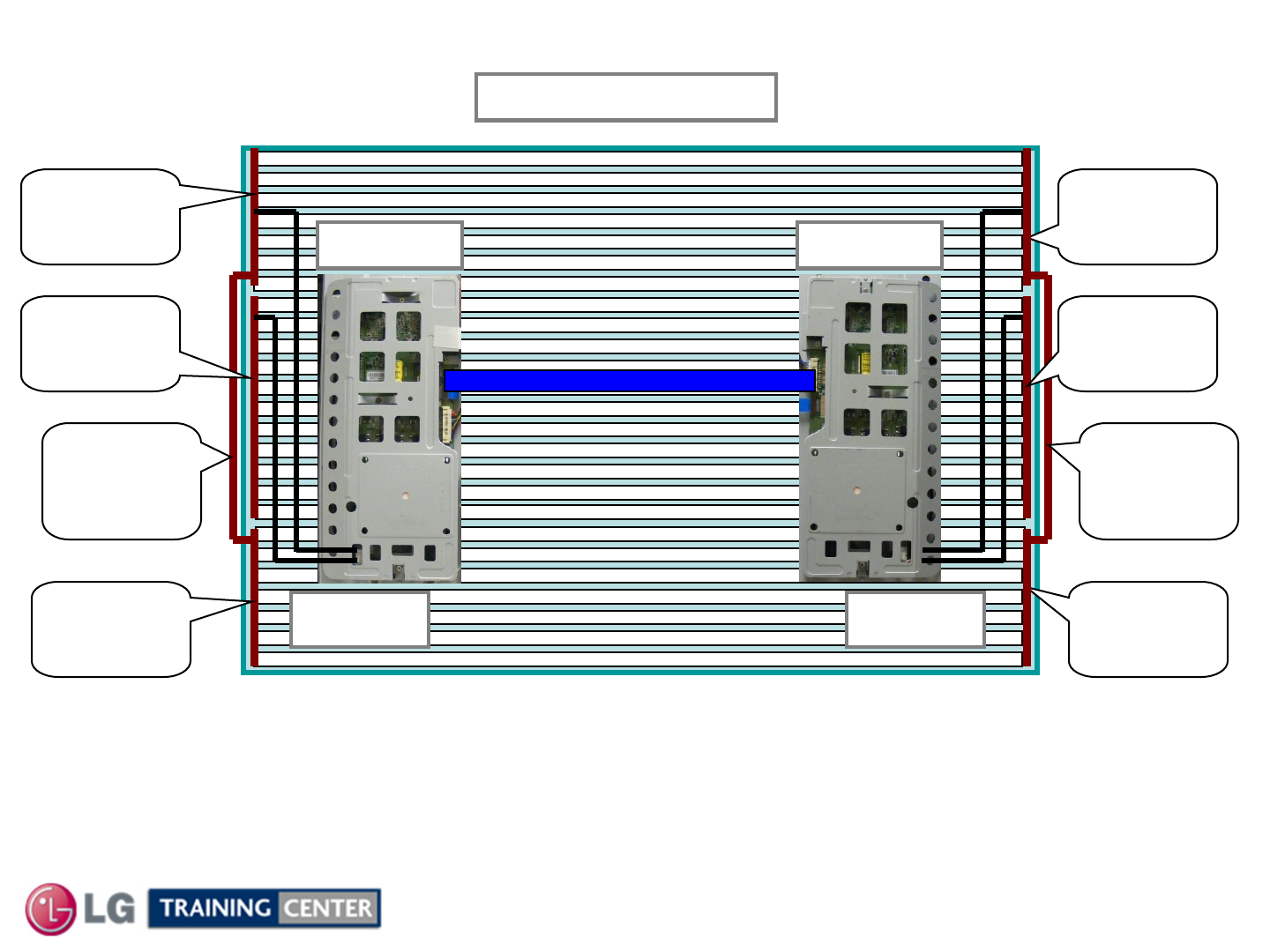
The output of 1.2Kv is sent to three sections of the backlight behind the LCD
panel. These three sections are broken up as follows: The Top and Bottom
sections are tied together, each containing 6 bulbs (total 12). The Center
section has 13 bulbs. All total 25 bulbs.
INVERTER A and B SECTION
INVERTER A and B SECTION

LCD DV 42SL80
39 February 2010
Complicated and more
expensive structure
Simple structure
Lamp manufacturing process
Lamp assembly structure
Low Cost
Large number of Lamp
Drive by single inverter
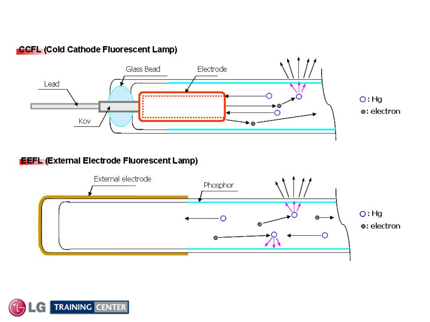
EEFL Compared to CCFL (This set uses EEFL Bulbs)
EEFL Compared to CCFL (This set uses EEFL Bulbs)
V
Starting
Voltage
Operating
Voltage I
V
Starting
Voltage
and
Operating
Voltage
I
CCFL (Cold Cathode Fluorescent Lamp) EEFL (External Electrode Fluorescent Lamp)
Simple structure, Low price
Center 13 Bulbs
Bottom 6 Bulbs
Top 6 Bulbs
Inverter
1Inverter
2
A
Transformer
for every bulb.
More Consistent Operating VoltageWide Range for Operating Voltage
Complex structure, High price
LCD DV 42SL80
40 February 2010
Key: Long Life Time
•For CCFL, Hg gas is consumed mainly near the internal electrode
•For EEFL, longer life time is expected because there is no internal electrode consuming Hg gas
EEFL Compared to CCFL Electrodes
EEFL Compared to CCFL Electrodes
LCD DV 42SL80
41 February 2010
General Backlight Information
General Backlight Information
Number of lamps “25”
EEFL (External Electrode Fluorescent Lamp)
LOW COST Large number of lamps driven by a single inverter
Inverter A
Connection
board to
6 Bulbs
Connection
board to
6 Bulbs
To Backlights
Over 1.2KV
25 Bulbs
Inverter B
Connection
board to
13 Bulbs
Ties Top
board with
bottom
board
Connection
board to
6 Bulbs
Connection
board to
6 Bulbs
Connection
board to
13 Bulbs
Ties Top
board with
bottom
board
To Backlights
Over 1.2KV
LCD DV 42SL80
42 February 2010
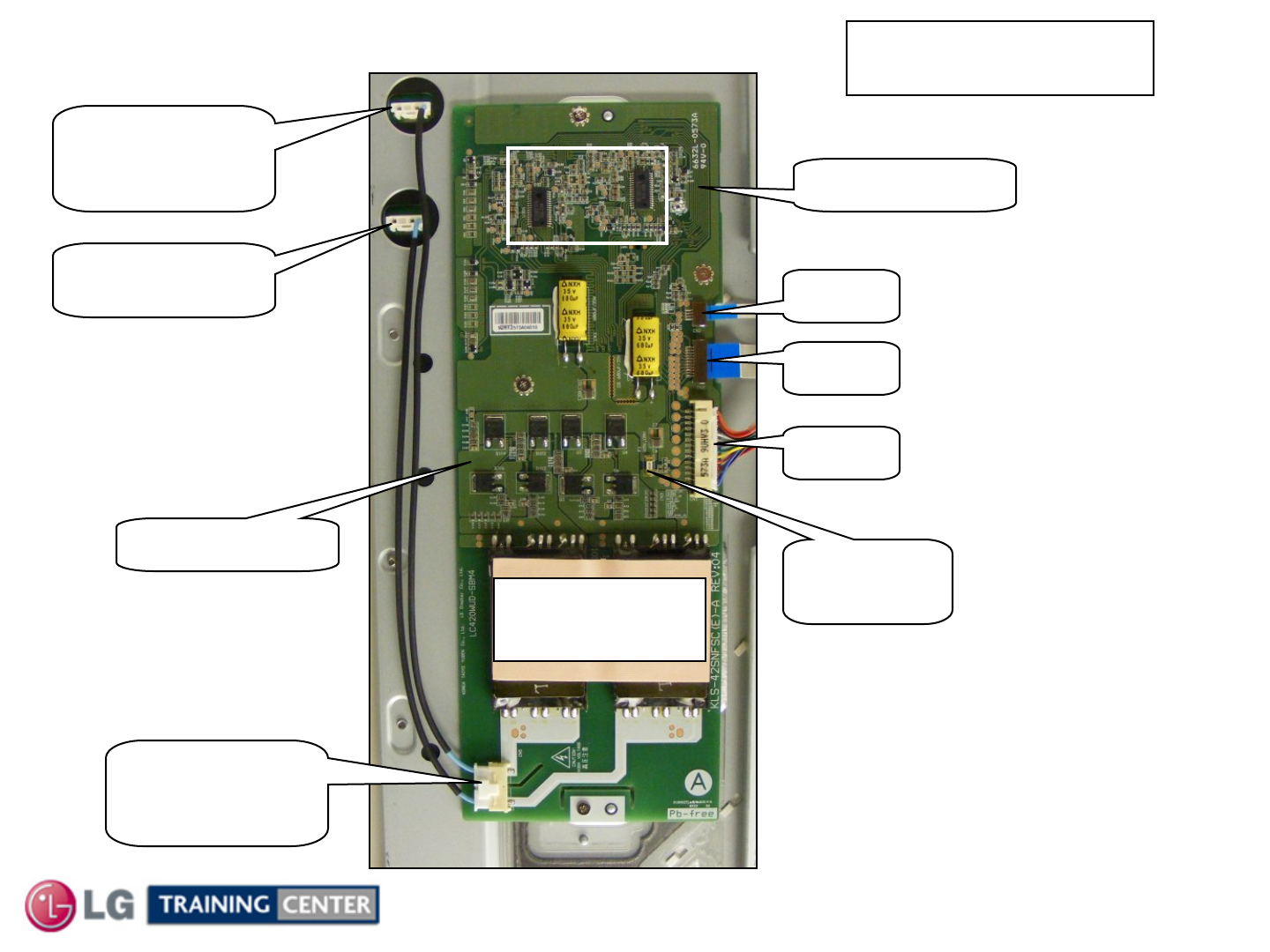
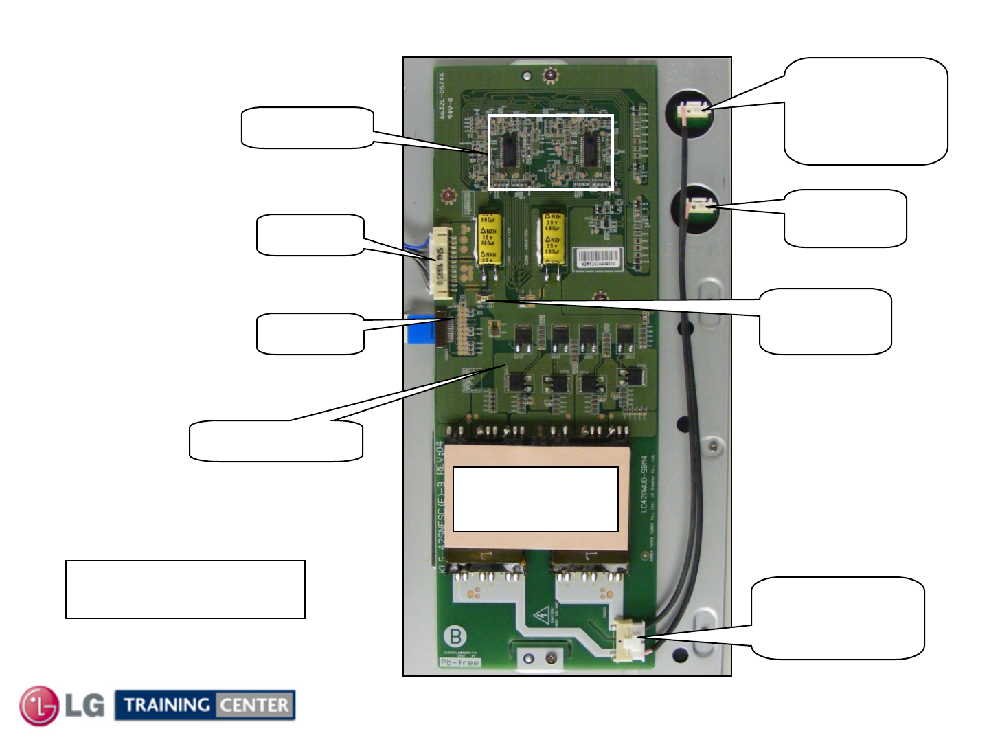
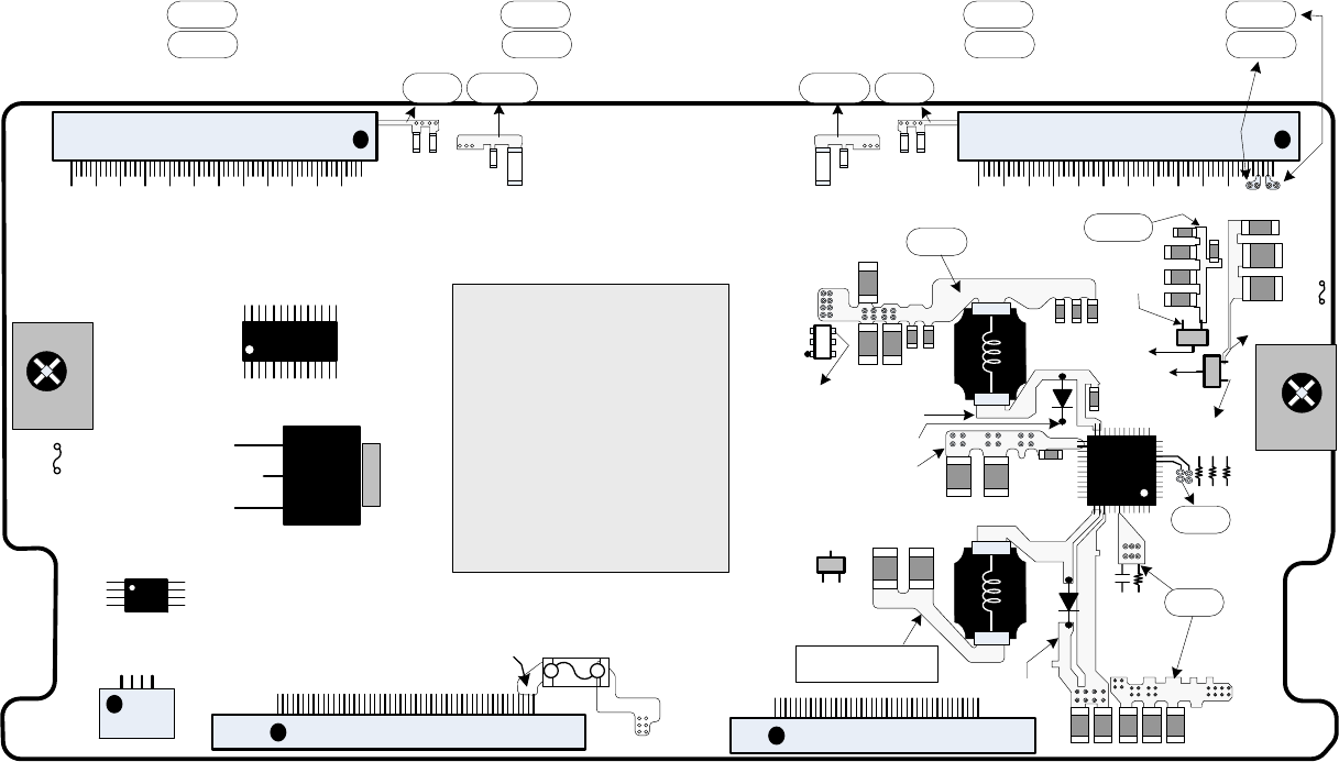
Inverter A (Shield Removed) Layout
Inverter A (Shield Removed) Layout
Ballast
Transformers
p/n EAY60750201
Includes both Inverters
CN5
To Backlights
Left Side
CN1
CN2
F1
12A/65V
To CN3 of T-CON
To P204 of SMPS
CN3 To CN203 of Inverter B
To Top 6 bulbs
and Bottom
6 bulbs
Center 13
bulbs
Driver FETs
Driver ICs
LCD DV 42SL80
43 February 2010
Inverter B (Shield Removed) Layout
Inverter B (Shield Removed) Layout
Ballast
Transformers
p/n EAY60750201
Includes both Inverters CN205
To Backlights
Right Side
CN203 F201
12A/65V
To P205 of SMPS CN201
To CN3 of Inverter A
To Top 6
bulbs and
Bottom
6 bulbs
To Center
13 bulbs
Driver FETs
Driver ICs
44
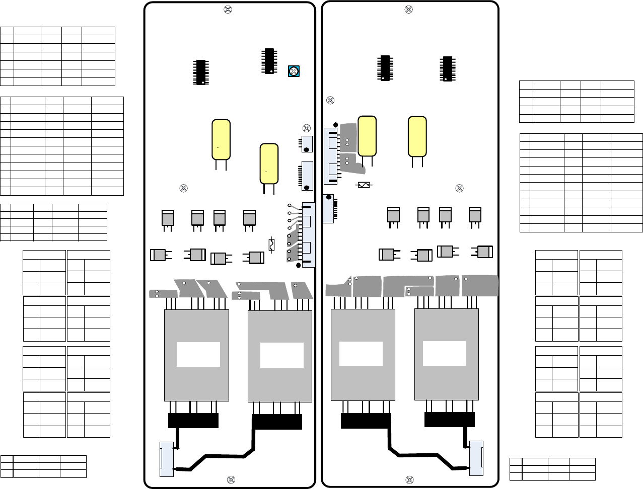
42SL80 Inverter A & B Layout and Component Volatages
42SL80 Inverter A & B Layout and Component Volatages
Pin Label STBY Run Diode Check
4 GND GND GND GND
3 SCAN 2 0V 0.67V-2.4V OPEN
2 SCAN 1 0V 0.67V-2.4V OPEN
1 NC 0V 3.3V OPEN
CN2 Connector "Inverter A" to CN3 "T-CON"
Pin Label Run AC Resistance
1TO MC1
2 TO BLACK
72 Ohms
72 Ohms
1.2Kv
1.2Kv
CN201 Connector "Inverter B" to P205 "SMPS"
Pin Label STBY Run Resistance
12 n/c n/c 4.3V OPEN
11 Vbr-A 0V 1.6V OPEN
6-10 GND GND GND GND
1-5 OPEN
VIN 0V 24.7V
CN203 Connector "Inverter A" to CN3 "Inverter B"
Pin Label STBY Run Resistance
1 DUTY_S1 0V 0.71V-2.4V OPEN
2GND GNDGND GND
3 DUTY_S2 0V 0.71V-2.4V OPEN
4 FB_S1 0V 0.96V 2.9V
5 ON/OFF 0V 4.3V OPEN
6 STB 0V 3.2V OPEN
7 VREF 0V 1.0V OPEN
8 FB_M1 0V 1.0V 2.9V
9 SRT 0V 1.4V OPEN
10 SS 0V 2.9V OPEN
11 CT_SYNC_IN 0V 1.5V 1.7V
CN1 Connector "Inverter A" to P204 "SMPS"
Pin Label STBY Run Resistance
14 STATUS 0V 0V OPEN
13 NC 0V 0V OPEN
12 ON/OFF 0V 4.3V OPEN
11 Vbr-A 0V 1.6V OPEN
6-10 GND GND GND GND
1-5 VIN 0V 24.7V OPEN
CN3 Connector "Inverter A" to CN203 "Inverter B"
Pin Label STBY Run Resistance
11 DUTY_M1 0V 0.71V-2.4V OPEN
10 GND GND GND GND
9 DUTY_M2 0V 0.71V-2.4V OPEN
8 FB_S1 0V 0.96V 2.9V
7 ON/OFF 0V 4.3V OPEN
6 STB 0V 3.2V OPEN
5 VREF 0V 1.0V OPEN
4 FB_M1 0V 1.0V 2.9V
3 SRT 0V 1.4V OPEN
2 SS 0V 2.9V OPEN
1CT_SYNC_IN 0V 1.5V 1.7V
CN205 Connector "Inverter B" TO "LCD Panel"
Pin Label Run AC Resistance
1TO SC1
2 TO BLACK
72 Ohms
72 Ohms
1.2Kv
1.2Kv
21.7V
24.6V
24.8V
Q104/Q102
0.6V
21.6V
Gnd
Q106/Q103
G
D
S
Q3/Q6
0.73V
20.4V
GND
G24.1V
D 24.6V
S20.3V
Q2/Q4
G
D
S
G
D
S
G
G
G
G
GG
G
G
DD
DDDD
S
S
SS
S
S
S
D
Inverter B
CN201
CN203
T201 T301
35V
680
uF
F1
65V/ 12A
Q302
Q304Q204
Q202
CN205
Q203
U201 & U301 are DC-AC
Inverter Control ICs
U201 U301
C208C243
35V
680
uF
D
Q206 Q208 Q303
S
- + - +
Inverter A
T1
T101
35V
680
uF
35V
680
uF
F1
65V/ 12A
Q104 Q102 Q2 Q4
CN5
Q103 Q3 Q6
CN1
CN3
CN2
Q106
U101 & U1 are DC-AC
Inverter Control ICs
U1
U101
C43
C8
S
D
Do Not
Adjust
G
G
G
GG G
G
G
DD
D
D
D
D
S
SSS
S
S
S
D
- +
- +
CN5 Connector "Inverter A" TO MC1 and Black "LCD Panel"
27.0V
24.6V
23.1V
Q104/Q102
0.28V
23V
Gnd
Q106/Q103
G
D
S
Q3/Q6
0.3V
23.0V
GND
G26.9V
D 24.6V
S23.1V
Q2/Q4
G
D
S
G
D
S
Backlights
at 100%
Backlights
at 100%
Backlights
at 0%
21.7V
24.6V
24.8V
Q302/Q304
0.6V
21.6V
Gnd
Q306/Q303
G
D
S
Q203/Q206
0.73V
20.4V
GND
G24.1V
D 24.6V
S20.3V
Q202/Q204
G
D
S
G
D
S
27.0V
24.6V
23.1V
Q302/Q304
0.28V
23V
Gnd
Q306/Q303
G
D
S
Q203/Q206
0.3V
23.0V
GND
G26.9V
D 24.6V
S23.1V
Q202/Q204
G
D
S
G
D
S
Backlights
at 100%
Backlights
at 100%
Backlights
at 0%
LCD DV 42SL80
45 February 2010
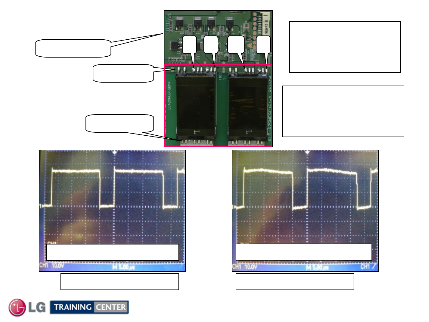
Ballast Transformer Waveforms
Ballast Transformer Waveforms
All Transformers Pin 1
30V p/p 48kHz (5uSec)
29.2V p/p 48kHz (5uSec)
Both Inverters have
2 Drive Transformers.
They have the same
configuration.
Warning, secondary
is over 1.2Kv
Do Not Measure without
proper equipment.
All Transformers Pin 6
Primary
6 1 6 1
FET Drivers
Secondary
LCD DV 42SL80
46 February 2010
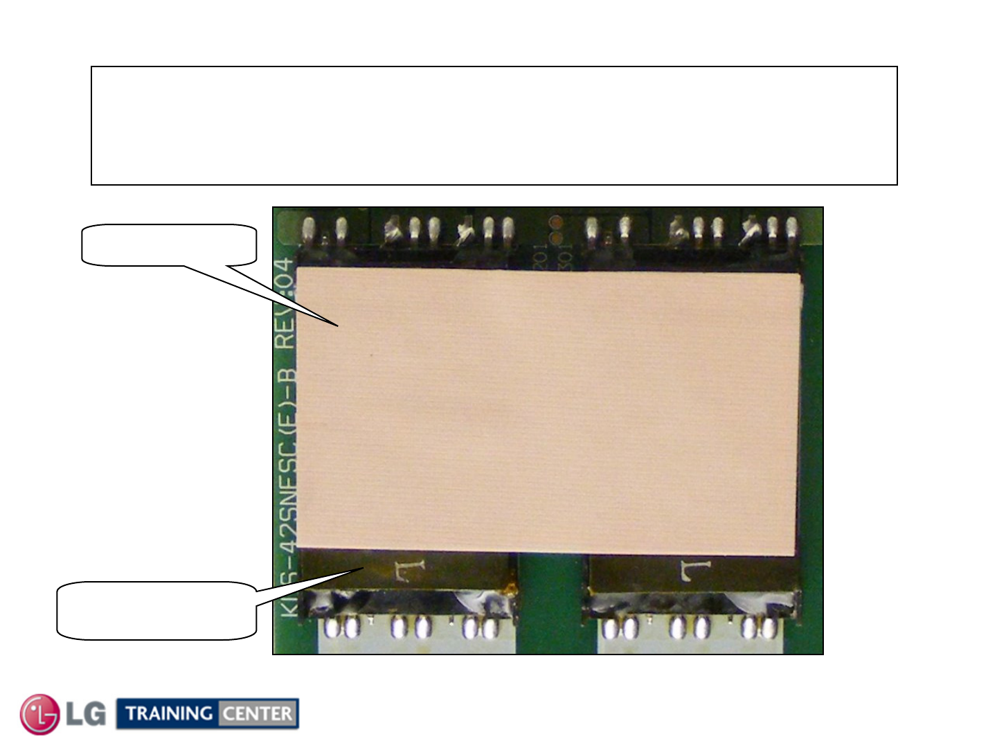
Ballast Transformer Noise Suppression Pads
Ballast Transformer Noise Suppression Pads
Both Inverters have 2 Drive Transformers.
There is a rubber pad that covers both drive transformers on both A and B
Inverters. These pads reduce the vibration noise being generated from
these transformers, be sure to replace these.
Padding
Drive
Transformers
LCD DV 42SL80
47 February 2010
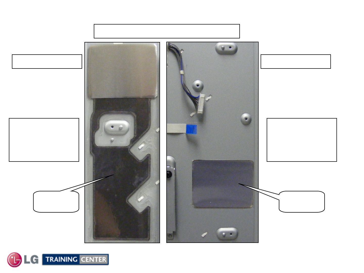
RF Prevention Shields behind the Inverters
RF Prevention Shields behind the Inverters
Behind the Inverters are shields
Shield
Inverters A side Inverters B side
Shield
The Shield on
Inverters B side
is adhered to
the panel.
The Shield on
Inverters A side
is adhered to
the panel.
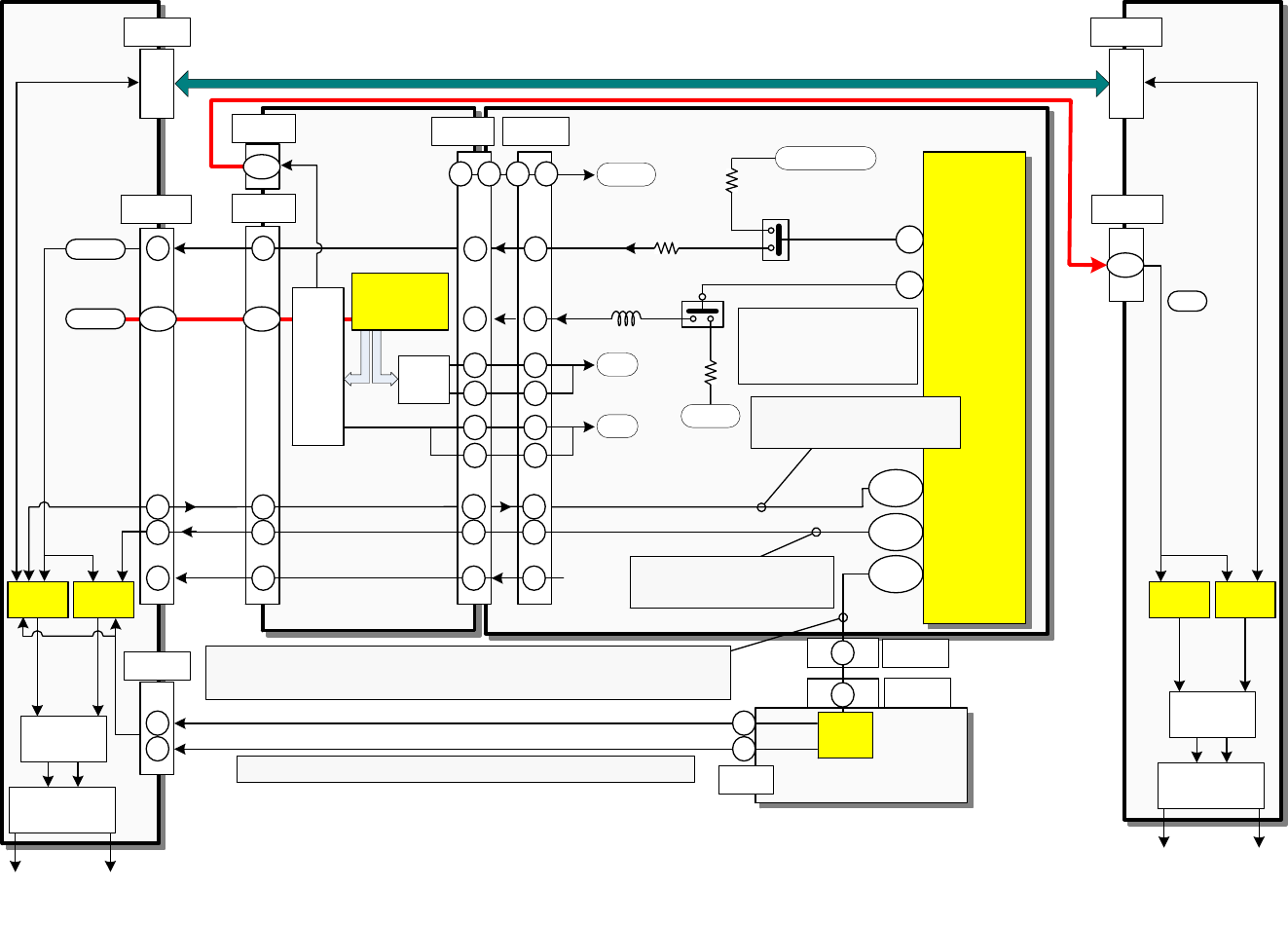
42LS80 Inverters Turn On Circuit P400 on Main Board To Power Supply P201
42LS80 Inverters Turn On Circuit P400 on Main Board To Power Supply P201
48
IC600
Mstar
INV On/Off
4.82V
20
P700
POWER
SUPPLY
PWR
2.86V
2
13
14
17
CN1
12
INV On/Off
ERR 0V
22
14
ERR
P201
P204
MAIN PWB
20
22
12
14
G5
Relay On
Q401
Inverter On
5V_ST
Q400 E5
5V General
Stby 5V
7 8 9 10
12V
24V
14
17
18
13
21~5
24V
Reg
24V
12V
Reg
PWM-DIM
VBR-B
PWM-2
PWM-DIM (PWM Dimming) Manipulates the Backlight Brightness via Customer’s
OSD, via the video processor IC400 and by the Intelligent Sensor. Darker Picture,
Darker Backlights to facilitate improved Contrast Ratio. 0.7V ~ 2.4V Range
T-CON PWB
44
8
P800
CN1
2
CN3
CN2
2
VBR-A
PWM-0
21
11 21
11
A-DIM (Analog Dimming)
Fixed Voltage 1.6V
GPIO97
E8
ERROR 4th time this line
goes high, power shuts off.
GPIO131
GPIO136
Hi if Lamps do not light
A-DIM
4.3V
24.7V
0V
1.6V 1.67V
LVDS
Cable
Ballast
Driver 1 Ballast
Driver 2
Fixed
13 P-DIM not
used
13 n/c
33
Scan 1
Scan 2
AB12
1~5
24V
18
SMPS
Controler
2424
SCAN 1 and SCAN 2 are manipulated by PWM-DIM (PWM Dimming)
AB13
CN3 11 Pins Carrying On/Off, Duty, Sync and
Drive signals. Receiving Error feedback.
CN201
INVERTER
B
1.2kV
Out
Ballast
Driver 1
Ballast
Driver 2
48K
Drive
signals
1~5
24V
CN203
11 Pins Receiving On/Off, Duty, Sync and
Drive signals. Sending Error feedback.
P205
1~5
24.7V
Output
FETs
Output
Transformers
1.2kV
Out
48K
Drive
signals
Output
FETs
Output
Transformers
For Circuit Details, see
P400 ON MAIN PWB TO
SMPS P201 TURN ON
CIRCUIT
VIN
VIN
On/Off
INVERTER
A
n/c
UC1
LCD DV 42SL80
49 February 2010
Power Supply Backlight Drive Signal Effects
Power Supply Backlight Drive Signal Effects
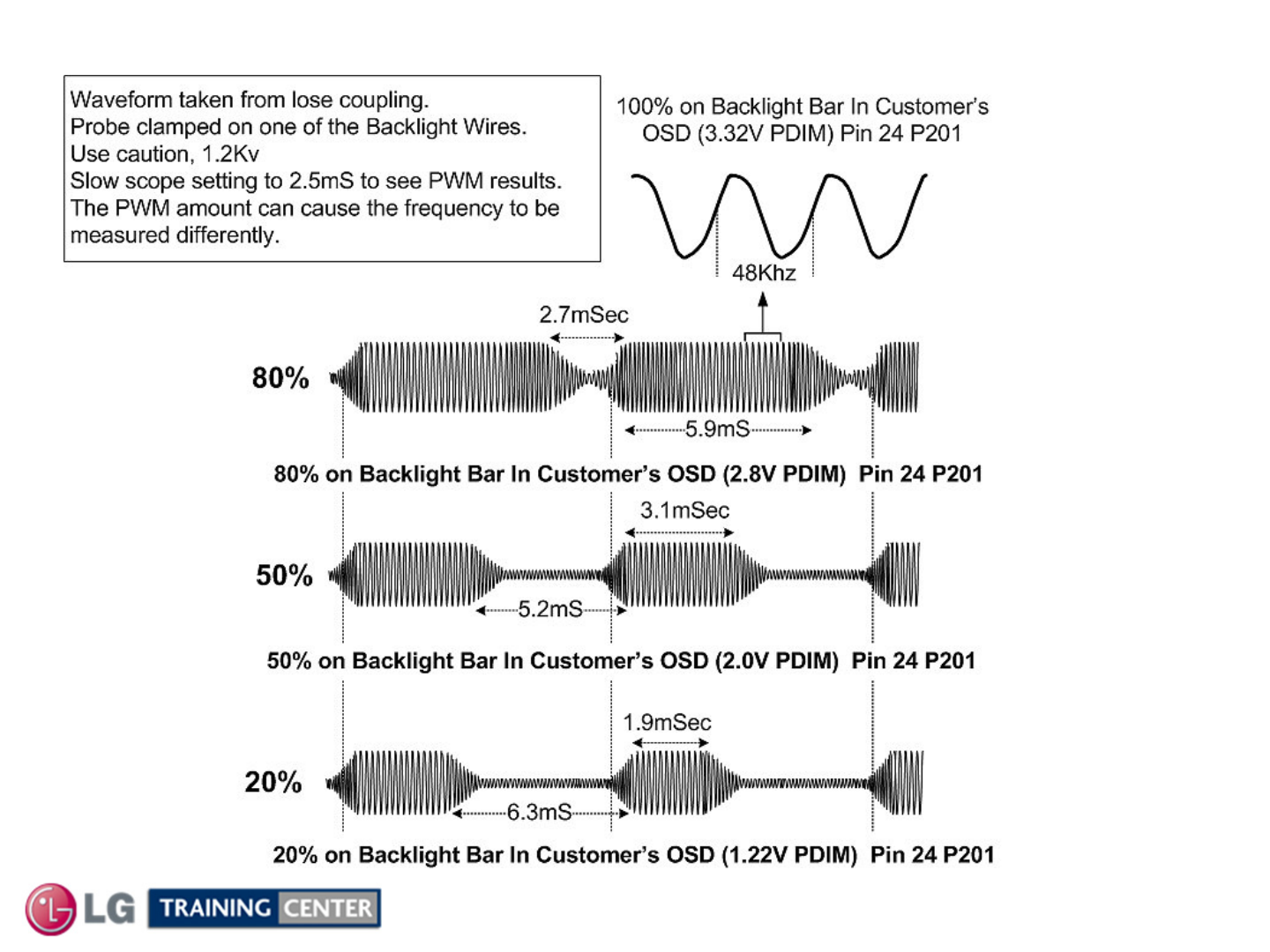
PWM-DIM
manipulates
the Burst
Triangle
Oscillator in
the ballast
drive IC.
A-DIM also
manipulates
the Burst
Triangle
Oscillator
But it is not
used.
Note:
Backlights will
attempt to fire 4
times. During these
attempts, the Error
line will change
from 5V to 0V.
0V when lamp tries
to fire or is lit.
5V when the lamps
are not lit.
After 4 attempts, if
the Error Out line
returns to 5V, this
tells the Micro to
turn the set off.
LCD DV 42SL80
50 February 2010
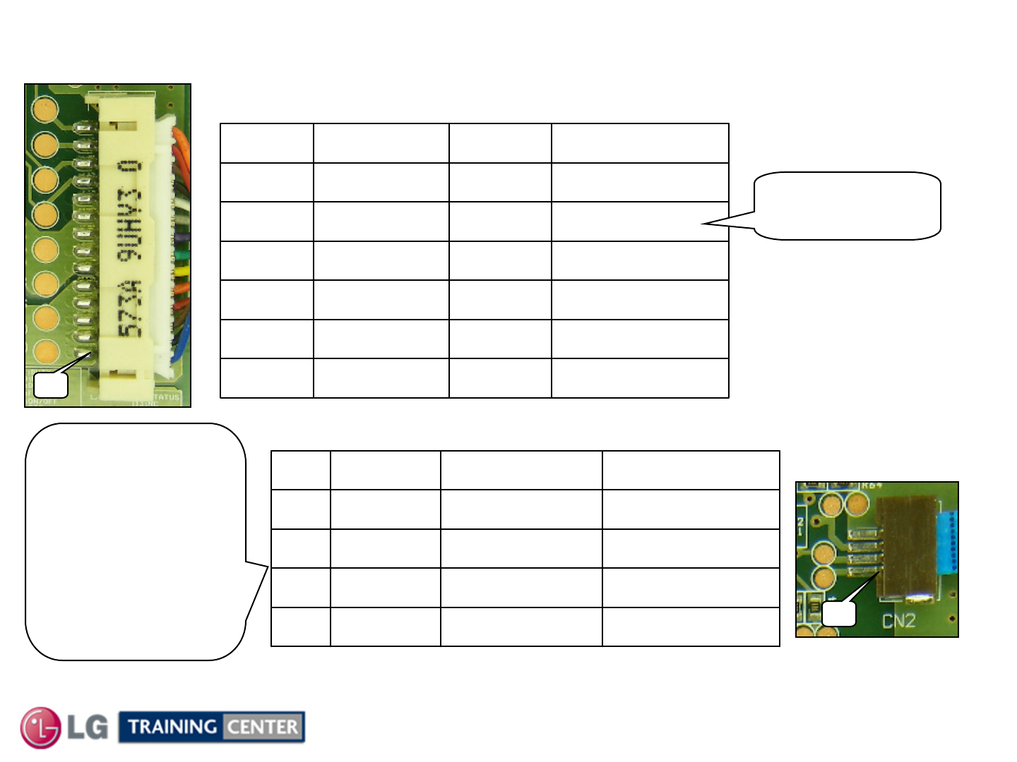
Inverter A Connector CN1 and CN2 Voltage and Diode Check
Inverter A Connector CN1 and CN2 Voltage and Diode Check
Diode Check taken with meter in Diode Mode with all Connectors Removed
Open24.7VVIN1-5
Open1.6VVRB-A11
Open4.3VOn/Off12
Open0Vn/c13
Open0VStatus14
GndGndGnd6-10
Diode CheckRun LabelPin
CN1 “Inverter A" to P203 "SMPS"
There are no Stand-By voltages.
Open3.3Vn/c4
Open*0.67V~2.4VScan 23
Open*0.67V~2.4VScan 12
GndGndGnd1
Diode CheckRun LabelPin
CN2 “Inverter A" to CN3 “T-CON"
Pins 2/3
(Digital Dimming)
Can vary according to
the brightness level of
the video signal and the
OSD Backlight setting.
0.67V 0% to 2.4V
100%. Output from the
Video Processing chip
IC100 (Mstar) through
T-CON.
Pin 13 PDIM
(Digital Dimming)
This pin is not used.
CN1
CN2
1
1
LCD DV 42SL80
51 February 2010
Inverter A Connector CN3 Voltage and Diode Check
Inverter A Connector CN3 Voltage and Diode Check
Diode Check taken with meter in Diode Mode with all Connectors Removed
Open2.9VSS2
Open1.4VSRT3
2.9V1.0VOn/Off4
Open1.0VVREF5
Open3.2VSTB6
1.7V1.5VCT-SYNC-IN1
2.9V0.96VFB_S18
Open*0.71V~2.4VDUTY_M29
GndGndGnd10
Open*0.71V~2.4VDUTY_M111
Open4.3ON/OFF7
Diode CheckRun LabelPin
CN3 “Inverter A" to P203 “Inverter B"
There are no Stand-By voltages.
Varies with PDIM
CN3
Varies with PDIM
1
LCD DV 42SL80
52 February 2010
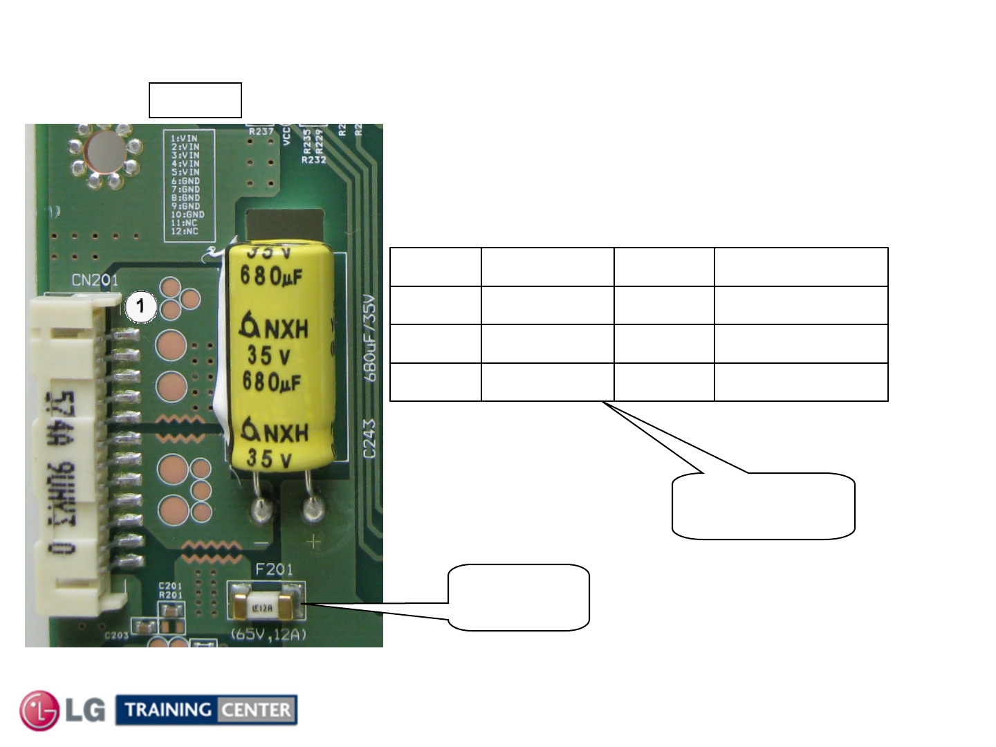
Open24.7VVIN1-5
GndGndGnd6-10
Open1.6VN/C11-12
Diode CheckRun LabelPin
CN201 “Inverter B" to P205 "SMPS"
Inverter B Connector CN201 Voltage and Diode Check
Inverter B Connector CN201 Voltage and Diode Check
Diode Check taken with meter in Diode Mode with all Connectors Removed
There are no Stand-By voltages.
Pin 11 and 12
are not used.
CN201
F201
24.7V Fuse
LCD DV 42SL80
53 February 2010
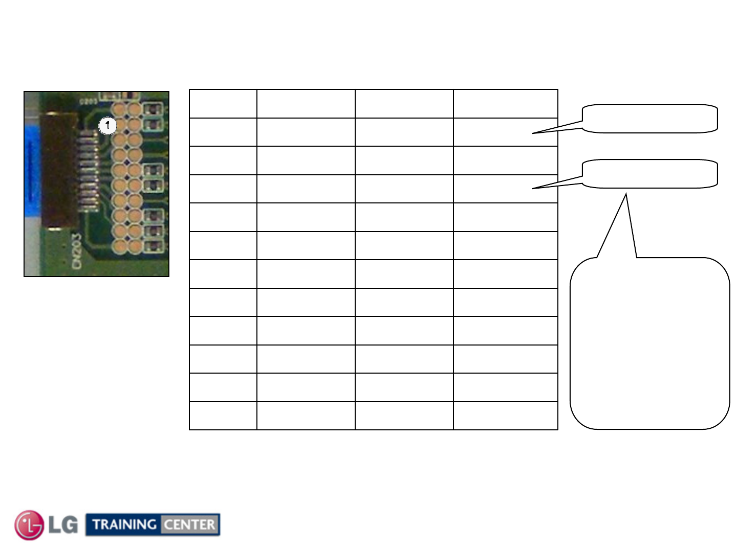
Inverter B Connector CN203 Voltage and Diode Check
Inverter B Connector CN203 Voltage and Diode Check
Diode Check taken with meter in Diode Mode with all Connectors Removed
Open2.9VSS10
Open1.4VSRT9
2.9V1.0VFB_M18
Open1.0VVREF7
Open3.2VSTB6
Open1.5VCT-SYNC-IN11
2.9V0.96VFB_S14
Open*0.71V~2.4VDUTY_S23
GndGndGnd2
Open*0.71V~2.4VDUTY_S11
Open4.3ON/OFF5
Diode CheckRun LabelPin
CN203 “Inverter B" to CN3 “Inverter A"
There are no Stand-By voltages.
Varies with PDIM
CN203
Varies with PDIM
Pins 1/3 Duty
(Digital Dimming)
Can vary according to
the brightness level of
the video signal and the
OSD Backlight setting.
0.67V 0% to 2.4V
100%. Output from the
Video Processing chip
IC100 (Mstar) through
T-CON.

LCD DV 42SL80
54 February 2010
LCD Controller Board
The T-CON IC UC1 receives from the Main Boards LVDS Video Signals at CN1 and CN2.
This is a Dual 12 Bit (24 pin) LVDS Video Signal which it processes into TFT Drive Signals
which are delivered through connectors CN4 and CN5 to the LCD TFT Panel.
T-CON B+: 12V is supplied to the T-Con Board on connector CN1 from the Main Board
P800 easily measured at fuse F1, (3A and 125V).
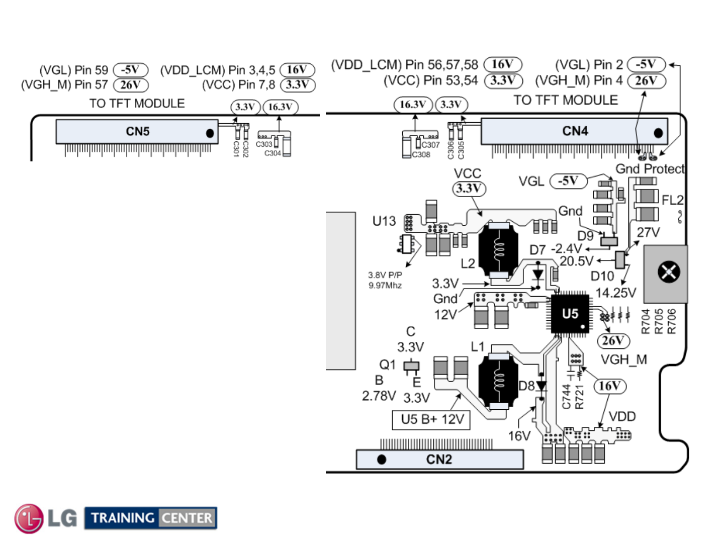
There is a DC to DC converter (U5) that creates;
(16V Measured at VDD). (26V Measured at pin 8 of U5).
(3.3V Measured at VCC). (-5V Measured at D9 top right leg).
These Voltages can also be measured at the ribbon connectors delivering signals to the
TFT panel
(CN4 26V pin 4, -5V pin 2, 3.3V pins 53, 54 and 16V pins 56, 57 and 58).
(CN5 26V pin 57, -5V pin 59, 3.3V pins 7, 8 and 16V pins 3,4 and 5).
See the 11X17 Foldout (Interconnect Diagram) for more details.
In the set the T-CON also receives the P-DIM voltage from the Main board on CN1 pin 8.
Then the Controller UC1 outputs P-DIM control signals now called Scan 1 and Scan 2 on
the CN3 connector, pins 2 and 3 to Inverter A CN2.
T
T-
-CON (TFT DRIVE) SECTION
CON (TFT DRIVE) SECTION
T-CON (TFT Drive) with (Shield Removed) Components Identified
T-CON (TFT Drive) with (Shield Removed) Components Identified
Warning:
T-Con PWB under shield. Be sure to reinsert screws before operating set with shield removed.
p/n EAT60667401
55
1) 6.9V
2) 13.7V
3) 15.7V
4) 13.7V
5) 13.0V
6) 12.0V
7) 10.9V
8) Gnd
9) 16.0V
10) 10.1V
11) 8.2V
12) 7.7V
13) 3.3V
14) 3.3V
15) 3.3V
16) Gnd
17) Gnd
18) Gnd
19) 5.8V
20) 5.0V
21) 3.9V
22) 2.9V
23) 6.0V
24) Gnd
25) 2.2V
26) 0.3V
27) 2.2V
28) 6.9V
TO TFT MODULE
UC1
FL3
1) Gnd
2) 1.8V
3) 3.3V
TO TFT MODULE
T-CON BOARD
(TFT Driver)
Gnd Protect
U11
Q1
U12
U10
(VGL) Pin 2
(VGH_M) Pin 4
(VDD_LCM) Pin 56,57,58
(VCC) Pin 53,54 26V
16V -5V
3.3V
26V 16V-5V 3.3V
B
2.78V
U13
D8
L1
FL2
Gnd Protect
L2
D9
D10
U5
E
3.3V
C
3.3V
20.5V
14.25V
-2.4V
R704
R705
R706
3.3V
26V
27V
C744
R721
U5
Gnd
-5V
VCC
(CN1) Pin 48-51
F1 (12V)
125V / 3A
CN1 CN2
U5 B+ 12V
16V
VGH_M
16V
VGL
12V
3.3V
1
2
3
2
CN4
CN3
C308
C307
C306
C305
16.3V 3.3V
C304
C303
C302
C301
16.3V3.3V
CN5
(VDD_LCM) Pin 3,4,5
(VCC) Pin 7,8
(VGL) Pin 59
(VGH_M) Pin 57
Gnd
D7
3.8V P/P
9.97Mhz
VDD
1~4) Gnd
5) 0V
6) 3.3V
7) 3.3V
8) 3.3V
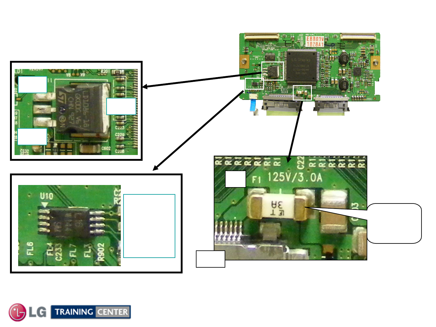
LCD DV 42SL80
56 February 2010
T
T-
-CON (TFT Drive) Board Checks
CON (TFT Drive) Board Checks
T-CON Board (Locations)
1.8V
3.3V
Gnd
U11
Check the Regulator for
Correct Voltage
Check Fuse F1 for 12V
Voltage supplied from CN1
Pins 48, 49, 50, and 51.
F1
CN1
Check
Fuse
F1 (12V)
1~4) Gnd
5) 0V
6) 3.3V
7) 3.3V
8) 3.3V
U10
LCD DV 42SL80
57 February 2010
T
T-
-CON (TFT Drive) Panel Voltage Development Checks
CON (TFT Drive) Panel Voltage Development Checks
The development for the
voltages on the CN4 and CN5
connectors are shown here.
This is an excerpt from the
Interconnect diagram.
Panel voltages are outlined
in the rounded cornered
boxes.
LCD DV 42SL80
58 February 2010
T
T-
-CON Board Connector CN1 to Main Board Voltage and Diode Check
CON Board Connector CN1 to Main Board Voltage and Diode Check
Diode Check taken with meter in Diode
Mode with all Connectors Removed
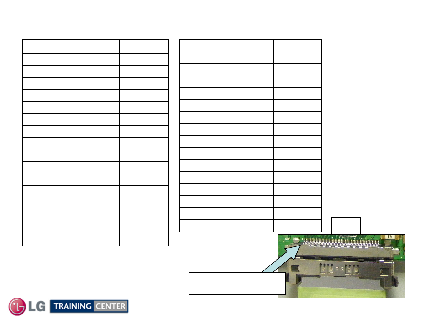
CN1 CONNECTOR "T-CON Board“ to P800 "Main"
*Pin 8 PWM-DIM 3.15V (Max 100%) to 0.6V (Min 0%)
Customer’s Menu Backlight setting.
1.1V1.3VURSA_A+2
24
1.1V1.3VURSA_A-2
25
Open0V
N/C
27
1.1V1.3VURSA_B+0
28
1.1V1.3VURSA_B-0
29
1.1V1.3VURSA_B+1
30
1.1V1.3VURSA_B-1
31
1.1V1.3VURSA_B+2
32
1.1V1.3VURSA_B-2
33
1.1V1.2VURSA_BCK+
35
1.1V1.1VURSA_BCK-
36
1.1V1.3VURSA_B+3
38
1.1V1.3VURSA_B-3
39
1.1V1.3VURSA_B+4
40
1.1V1.3VURSA_B-4
41
3.18V12.06V12V T-CON48-51
Diode CheckRunLabelPin
Open0V
N/C
7
1.3V*2.7V
PWM-DIM
8
Open0V
N/C
9
1.75V0.6VOPC_EN
10
Open0V
N/C
11
1.1V1.3VURSA_A+0
12
1.1V1.3VURSA_A-0
13
1.1V1.3VURSA_A+1
14
1.1V1.3VURSA_A-1
15
1.1V1.2VURSA_A+2
16
1.1V1.1VURSA_A-2
17
1.1V1.1VURSA_ACK+
19
1.1V1.2VURSA_ACK-
20
1.1V1.3VURSA_A+3
22
1.1V1.3VURSA_A-3
23
Diode CheckRunLabelPin
See arrow on the T-CON
board CN1 indicating pin 1
Pins 2, 3, 4, 5, 6 and 47
are all no connection.
Pins 1, 18, 21, 26, 34, 37,
42, 43, 44, 45 and 46 are
all ground.
CN1
Text in Blue are
LVDS video
signals.
LCD DV 42SL80
59 February 2010
T
T-
-CON Board Connector CN2 to the Main Board (Voltage and Diode Ch
CON Board Connector CN2 to the Main Board (Voltage and Diode Check)
eck)
Diode Mode values taken with all Connectors Removed
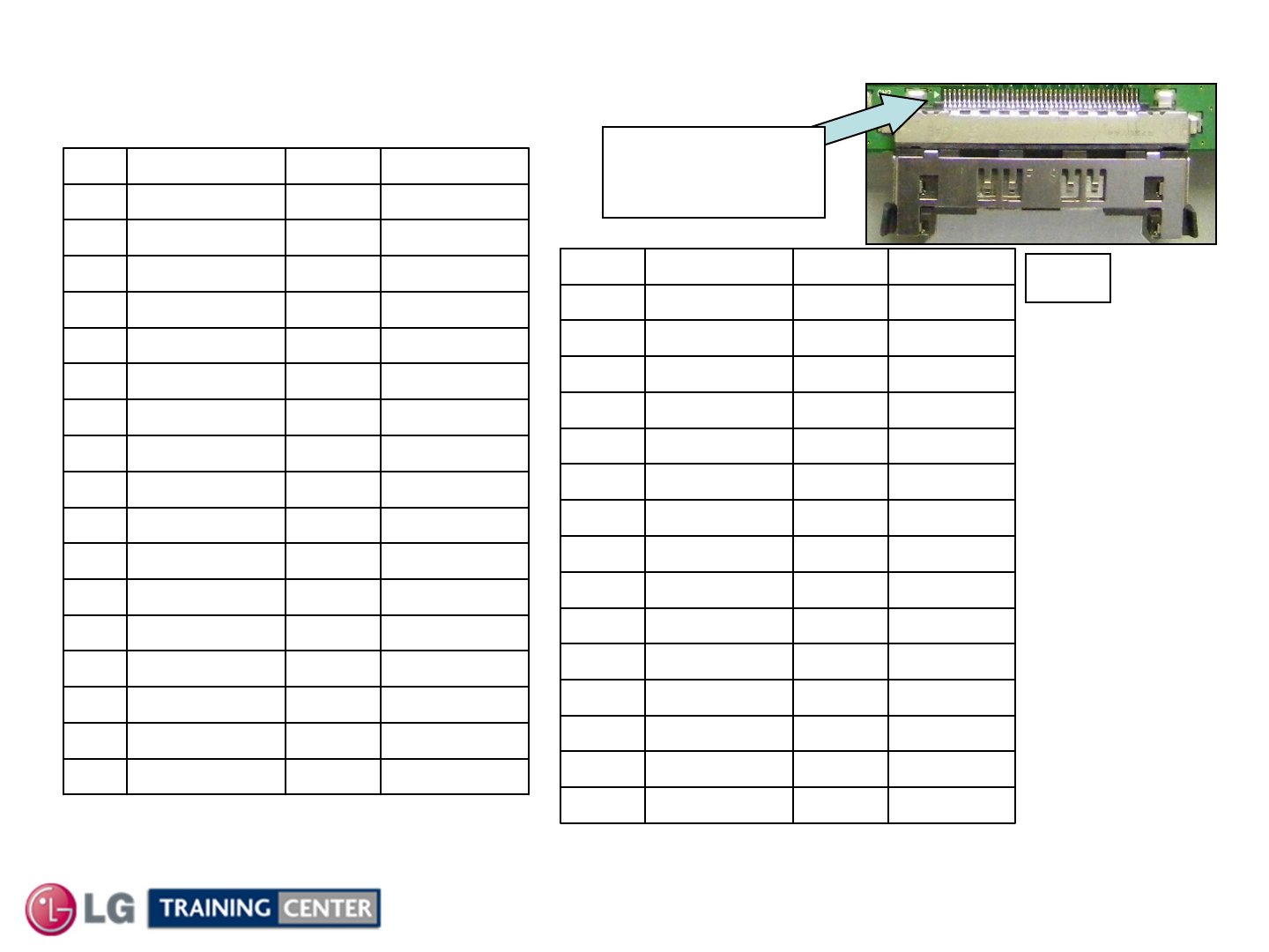
CN2 “T-CON“ to P801 CONNECTOR "Main"
Open1.3VURSA-C+320
Open1.2VURSA-C-321
Open1.13VURSA-C+422
Open1.18VURSA-C-423
GndGndGnd24
GndGndGnd25
Diode TestRunLabelPin
GndGndGnd19
Open1.23VURSA-CCK-18
Open1.23VURSA-CCK+17
GndGndGnd16
Open1.2VURSA-C-215
Open1.3VURSA-C+214
Open1.2VURSA-C-113
Open1.3VURSA-C+112
Open1.2VURSA-C-O11
Open1.28VURSA-C+010
n/cn/cn/c1-9
Diode TestRunLabelPin
GndGndGnd40-41
Open1.15VURSA-D-439
Open1.4VURSA-D+438
Open1.25VURSA-D-337
Open1.3VURSA-D+336
GndGndGnd35
Open1.29VURSA-DCK-34
Open1.23VURSA-DCK+33
GndGndGnd32
Open1.2VURSA-D-231
Open1.3VURSA-D+230
Open1.3VURSA-D-129
Open1.29VURSA-D+128
Open1.25VURSA-D-027
Open1.29VURSA-D+026
See arrow on the
T-CON board CN1
indicating pin 1
CN2
Text in Blue are
LVDS video
signals.
LCD DV 42SL80
60 February 2010
T
T-
-CON Board Connector CN3 to Inverter A (Voltage and Diode Check)
CON Board Connector CN3 to Inverter A (Voltage and Diode Check)
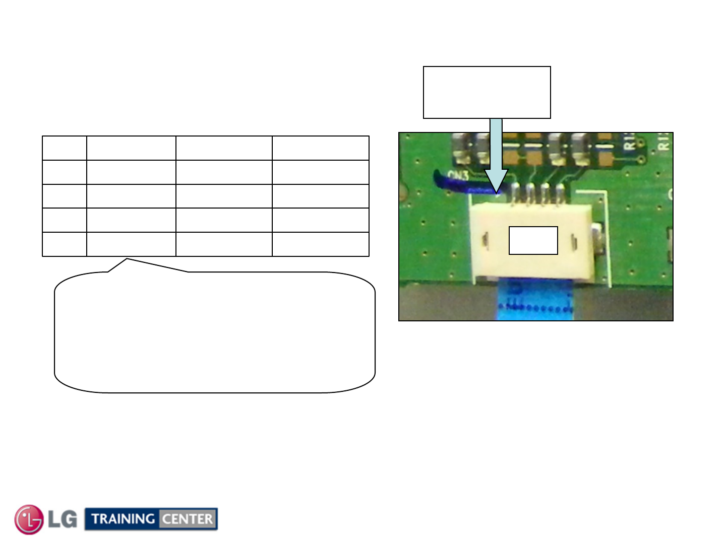
Diode Mode values taken with
all Connectors Removed
CN3 “T-CON“ to CN2 “Inverter A"
Open0.67V~2.4VSCAN 23
Diode TestRunLabelPin
GndGndGnd4
Open0.67V~2.4VSCAN 12
n/cn/cn/c1
See arrow on the
T-CON board CN3
indicating pin 1
CN3
Pins 2 SCAN 1 and 3 SCAN 2 (Digital Dimming)
Can vary according to the brightness level of the
video signal and the OSD Backlight setting.
0.67V 0% to 2.4V 100%.
P-DIM Output from the Video Processing chip IC100
(Mstar) and input on CN1 pin 8 T-CON.

LCD DV 42SL80
61 February 2010
MAIN BOARD SECTION
MAIN BOARD SECTION
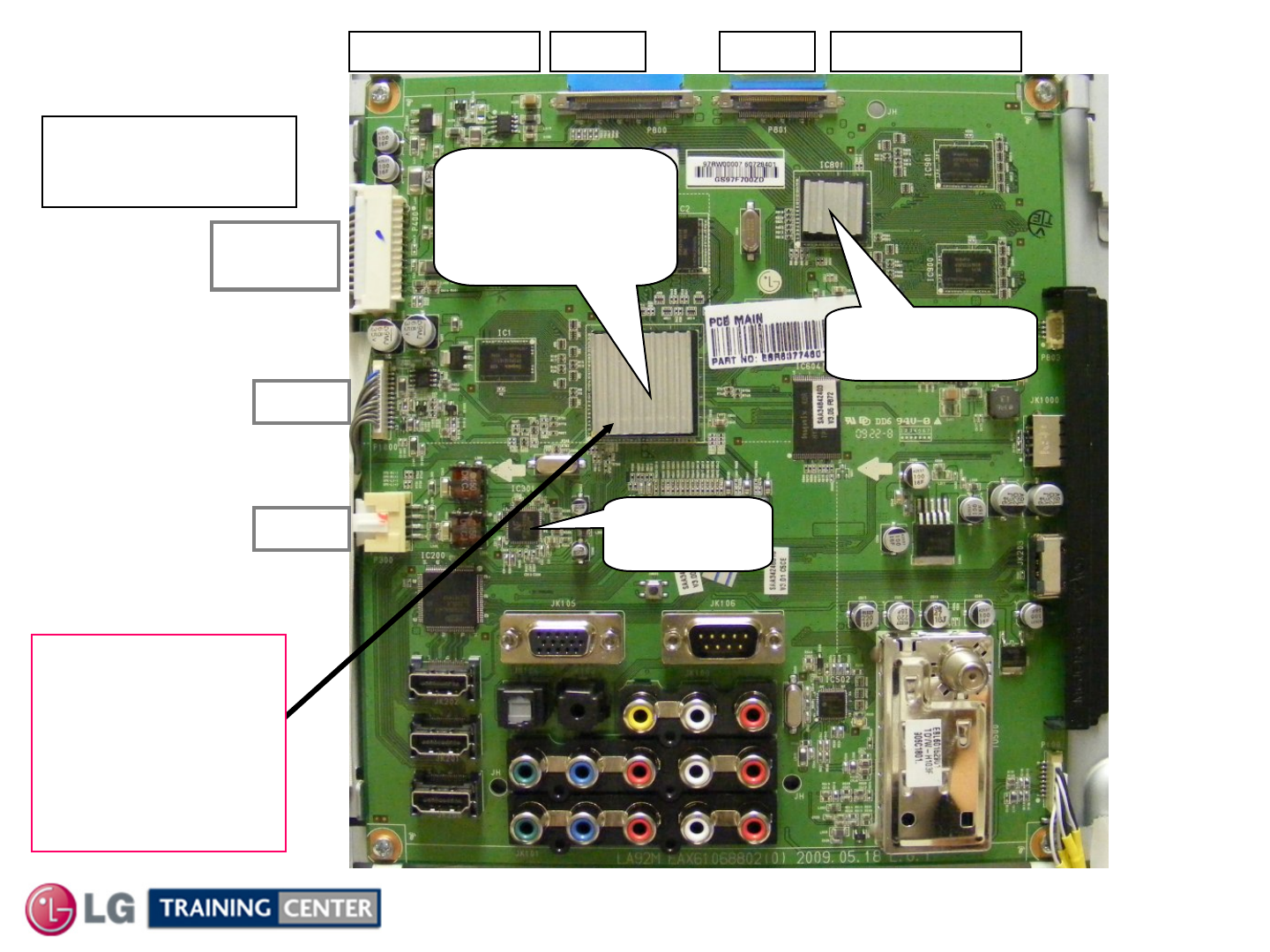
The Main board receives its operational B+ from the Power Supply via P400.
There are two LVDS cable feeds that go to the T-CON (TFT Driver) section. These carry the Dual 12
bit LVDS Video signals and the TruMotion 60Hz Dual 12 bit LVDS. These signals have already been
prepared for the T-CON board. The Main board also includes the Tuner, Audio and Audio/Video
inputs and selection circuits.
STAND-BY
•STBY 5V pins 7~10
The Main board also develops several B+ sources on the board.
LVDS
•LVDS 12V AUDIO
•3.3V
•1.8V_AMP
Mstar IC600 Video and Micro Processors
•1.2V
IC3502 Tru-Motion IC.
•1.26V_MEMC, 1.8V_MEMC,
1.8V_DDR, and 3.3V
RUN
•12V pins 13 and 14
•24V pins 17 and 18.
TUNER and VSB CIRCUIT
•9V
•5V TU
•3.3V_DVDD_PVSB
•1.2V_DVDD_PVSB
•3.3V_DVDD_PVSB
STAND-BY VOLTAGES
•3.3V_ST
GENERAL
•5V_General
•5V_EXT
Input Voltages from SMPS.
Digital Video Demodulator/Decoder
Progressive Vestal Side Band
(Dif + / Dif -)
IF_P / IF_N
Tuner Developed from 9V above
Motion
Estimation
Motion
Compensation
Amplifier (Audio)
Voltage_Stand By
Stand By
Double Data Rate-Synchronous RAM Memory
For Audio Amplification
(Converted to 24V_Amp)
For Tuner Voltage (Dropped to 5V)
and output (Switched) for T-CON
For all other regulators except 12V/24V
and output to Ft. IR
For Microprocessor and output to Ft. IR
For Video Processing / DDRs
For Tuner Demodulator Low Voltage
Development
For Tuner B+ Developed from 12V Input
Not generated, but switched from the
12V arriving from the SMPS.

LCD DV 42SL80
62 February 2010
Additional Main Board Information
Additional Main Board Information
Input Signal Processing
IC600 is the main Microprocessor and the main Signal Processor.
The Main board is responsible for :
• ATSC, NTSC, and QAM reception and processing
• RS 232 service only Port (software upgrades and home theater environment).
•Wired Remote Port
• (2) Component Input Y, Pr, Pb and Audio L R
• (3) HDMI Inputs (back) (1) HDMI (Side Input)
• RGB PC and (PC Audio)
• USB (software upgrades using flash drive). USB located on the Side.
• AV Composite (1 Rear and 1 Side Input)
• SIF and SAP Output Signals
• Dual 12 Bit (24 pin) LVDS to the T-CON Board via P800 and P801.
• Including 12V T-CON.
• Audio output signals to the Speakers P300.
• Digital Audio Output Coaxial and Optical Always active, (Note: HDMI converts to Stereo)
• ON OFF Controls to the SMPS turning on low voltage generation and Backlights.
• Backlight intensity control signal (Digital Dimming) P-DIM sent to the T-CON board.
LCD DV 42SL80
63 February 2010
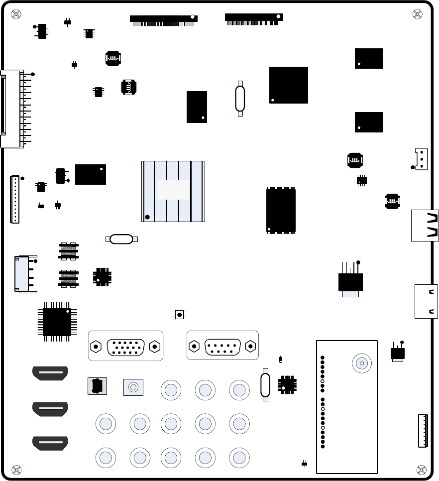
Main Board Layout
Main Board Layout
VIDEO PROCESSOR
IC600 RUNS HOT,
THIS IS NORMAL.
P700 To
SMPS
P1000
To Front IR
Board
Assembly
T-CON Board
To Speakers
Look carefully on top
and behind the Video
Processor IC for
Chocolate
(Heat Transfer)
material.
Be sure to transfer to
new Board if replaced.
P300
IC600
Microprocessor
and
Video Processor
IC801
Tru-Motion
P800 P801T-CON Board
IC1200
Audio Amp
DDR
DDR
64
P800
IC801
Tru-
Motion
P801
IC801 Operates at
high temperature
X800
25Mhz
Q408
2
3
1
IC300
E
C
B
Q1000
IC604
IC901
IC900
IC1
X600
12Mhz
IC600
Micro/Video
Processor
Mstar
IC404
IC504SW600
IC1200
L304
P1000
Q500
TU500 Tuner
TDVW-H103F
X500
25Mhz
P803
N/A
IC502
12V LVDS
Pins 1~4
P300
42LS80
MAIN BOARD
42SL80
Main Board
(Front Side)
Component
Layout
42SL80
Main Board
(Front Side)
Component
Layout
P100
L305
E
C
B
IC301
P400
IC2
IC500
D500
IC406
NAND
FLASH
IC400
IC605
IC602
A1
C
A2D1003
R-
R+
L-
L+
E
C
B
Q406
IC600
Mstar
DDR
DDR
Y
PC
Audio
PC RS232
HDMI 1
HDMI 2
HDMI 3
Pr Pb
YPrPb Audio
LR
Video LR
L406
L412
L422
L424
(1)
(19) Analog Video
(4) Tuner 5V_TU
(8) Data
(9) Clock
(12) Dig DIF+
(13) Dig DIF-
(16) SIF
HDMI
4
USB
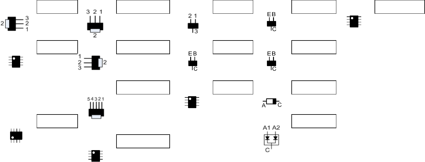
42SL80 Main (Front Side) Component Voltages
IC300 +1.8V AMP IC406 +3.3V_ST IC605 Reset Gen Q500 Tuner Video IC403 +1.6V_MEMC
Pin Regulator Pin Regulator Pin for Power_Det Pin Buffer Pin Regulator
[1] Gnd [1] 0V [1] Gnd B 1.7V [1] 0V
[2] 1.8V [2] 3.3V [2] 3.5V C 0V [2] 0.8V
[3] 3.3V [3] 5.0V [3] 3.3V E 2.3V [3] 1.2V
[4] 1.2V
IC400 +1.8V_DDR IC500 9V Reg Q406 5V Switch Q1000 Moving LED [5] 1.8V
Pin Regulator Pin to IC501 Tuner 5V Pin Control Pin Inverter [6] 5.0V
[1] n/c [1] 12V B 0.6V B 0V [7] 1.2V
[2] 3.2V [2] Gnd C 0V C 3.3V [8] 5.0V
[3] 3.2V [3] 8.9V E Gnd E Gnd
[4] n/c
[5] n/c IC504 +3.3V_PVSB Q408 +5V/12VLVDS D500 Speed Up Reset
[6] 1.8V Pin Regulator Pin Switch Pin IC502
[7] 0.8V [1] 4.94V [1] 5.1V C 3.4V
[8] Gnd [2] 4.94V [2] 0.29V A 3.38V
[3] Gnd [3] 11.9V
IC404 +1.8V_MEMC [4] 3.4V [4] 5.99V D1003 Moving LED
Pin Regulator [5] 1.25V [5] 11.98V Pin Routing
[1] 0.8V [6] 11.98V A1 0V
[2] Gnd IC602 HDCP [7] 5.06V C 0.1V
[3] 4.92V Pin EEPROM [8] 5.06V A2 0V
[4] 6.5V [1] Gnd
[5] 4.8V [2] Gnd
[6] 1.8V [3] 5.0V
[7] 1.8V [4] Gnd
[8] 4.8V [5] 3.3V
[6] 3.3V
[7] 5.0V
[8] 5.0V
65
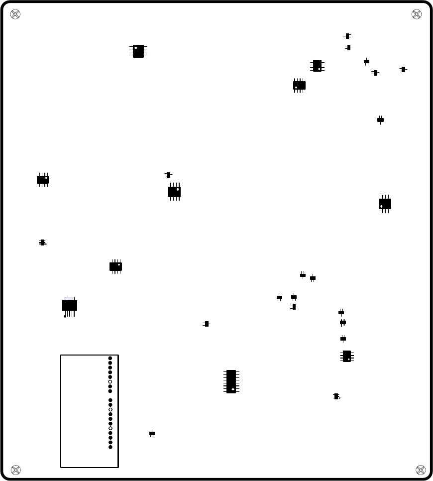
42SL80
Main Board
(Back Side)
Component Layout
42SL80
Main Board
(Back Side)
Component Layout
66
TUNER TU500
TDVW-H103F
IC100
C
A2A1
E
C
B
EC
B
42SL80 MAIN BOARD
(Back View)
1
IC501
IC503
IC102
IC504
IC1000
IC601
E
C
B
Q600
IC800
IC606
IC401
IC402
E
CB
Q407
Q405
EC
B
Q605
EC
B
Q400
E
C
B
Q604
E
C
B
Q401
2
3
1
IC603
E
C
BQ603
EC
B
Q602
D600
E
C
BQ300
C
A2A1
D200
Q200
C
A2A1 D129
IC101
Q101
(1)
(19) Analog Video
(4) Tuner 5V_TU
(8) Data
(9) Clock
(12) Dig DIF+
(13) Dig DIF-
(16) SIF E
C
BQ501
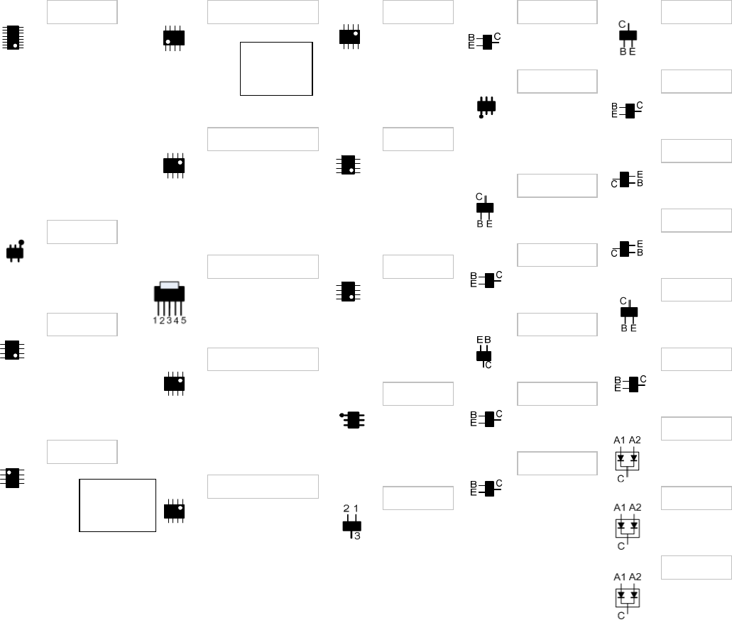
42SL80 Main (Back Side) Component Voltages
IC100 RS232 IC402 +3.3V_MEMC IC601 Serial Flash Q101 IR RS232 Q501 Tuner SIF
Pin Rx/Tx Pin Regulator Pin for Boot Pin Buffer Pin Buffer
[1] 3.3V [1] [1] 0.04V B 0.634V B 2.4V
[2] 5.56V [2] Gnd [2] 3.2V C 0V C 0V
[3] 0.02V [3] 4.98V [3] 2.5V E 0V E 3.0V
[4] 0.03V [4] 7.6V [4] 0V
[5] 5.5V [5] 4.9V [5] 0V Q200 HDMI CEC Q600 Write Protect
[6] 5.5V [6] 3.3V [6] 0V Pin Pin for IC601
[7] 5.5V [7] 3.3V [7] 3.2V [1] 3.2V B 0V
[8] 0V [8] 0V [8] 3.2V [2] 3.2V C 2.5V
[9] 3.29V [3] 0V E Gnd
[10] 3.24V IC405 +5V EXT IC606 Micro IC600 [4] 0V
[11] n/c Pin Regulator Pin EEPROM [5] 0V Q602 S5/S6 Reset
[12] 3.31V [1] 0.8V [1] Gnd [6] 3.16V Pin Switch for Mstar
[13] 0V [2] Gnd [2] Gnd B 0V
[14] 5.5V [3] 12V [3] Gnd Q300 Audio Mute C 3.28V
[15] Gnd [4] 9.6V [4] Gnd Pin Switch E 0V
[16] 3.29V [5] 5V [5] 3.24V B 0.62V
[6] 4.97V [6] 3.24V C 0.01V Q603 Power_On_
IC101 SPIF Optical [7] 4.97V [7] 0V E Gnd Pin Delay Switch
Pin Audio [8] 1.9V [8] 3.24V B 0V
[1] 0.03V Q400 PWR On/Off C 0.04V
[2] 0V IC501 +5V_TU IC800 SPI Flash IC801 Pin Switch E Gnd
[3] 0V Pin for Tuner Pin Memory B 2.9V
[4] 0V [1] 8.92V [1] 0V C 5V Q604 Power_Det
[5] 0V [2] 1.88V [2] 0.8V E 5V Pin Switch
[3] 5.04V [3] 3.2V B 0V
IC102 RGB [4] 0V [4] 0V Q401 INV_ON C 3.3V
Pin EEPROM [5] Gnd [5] 0V Pin Inverter E Gnd
[1] Gnd [6] 0.09V B 0.05V
[2] Gnd IC503 +1.2V_PVSB [7] 3.2V C 4.35V Q605 Power_Det
[3] Gnd Pin Regulator [8] 3.2V E Gnd Pin +12V Side
[4] Gnd [1] 0V B 0.65V
[5] 3.3V [2] 3.3V IC1000 USB +5V Q405 12V LVDS C 0.0V
[6] 3.3V [3] 3.4V Pin Switch Pin Switch Control E Gnd
[7] 3.18V [4] 0V [1] 4.95V B 0.05V
[8] 0V [5] 0V [2] Gnd C 0.65V D129 5V Routing
[6] 1.2V [3] 3.21V E Gnd Pin for IC1200
IC401 +1.26V_VDDC [7] 0.8V [4] 4.95V A1 0.03V
Pin Regulator [8] 0V [5] 0V Q407 12V LVDS C 4.5V
[1] [6] 4.95V Pin Source A2 5.1V
[2] Gnd IC504 +1.26V_PVSB B 0.65V
[3] 5.0V Pin Regulator IC603 Reset Gen C 0.0V D200 Shunt for
[4] 6.0V [1] 0.8V Pin for IC600 E Gnd Pin Q200
[5] 4.9V [2] 0V [1] 0V A1 0V
[6] 0V [3] 11.8V [2] 0V C 3.1V
[7] 0V [4] 9.6V [3] 3.3V A2 3.2V
[8] 3.2V [5] 5.0V
[6] 5.0V D600 Audio Mute
[7] 5.0V Pin Routing
[8] 0.9V A1 0.01V
C 2.7V
A2 3.29V
WARNING
Measure Pin 1
with O-scope
ONLY
WARNING
Measure Pin 1
with O-scope
ONLY
67
LCD DV 42SL80
68 February 2010
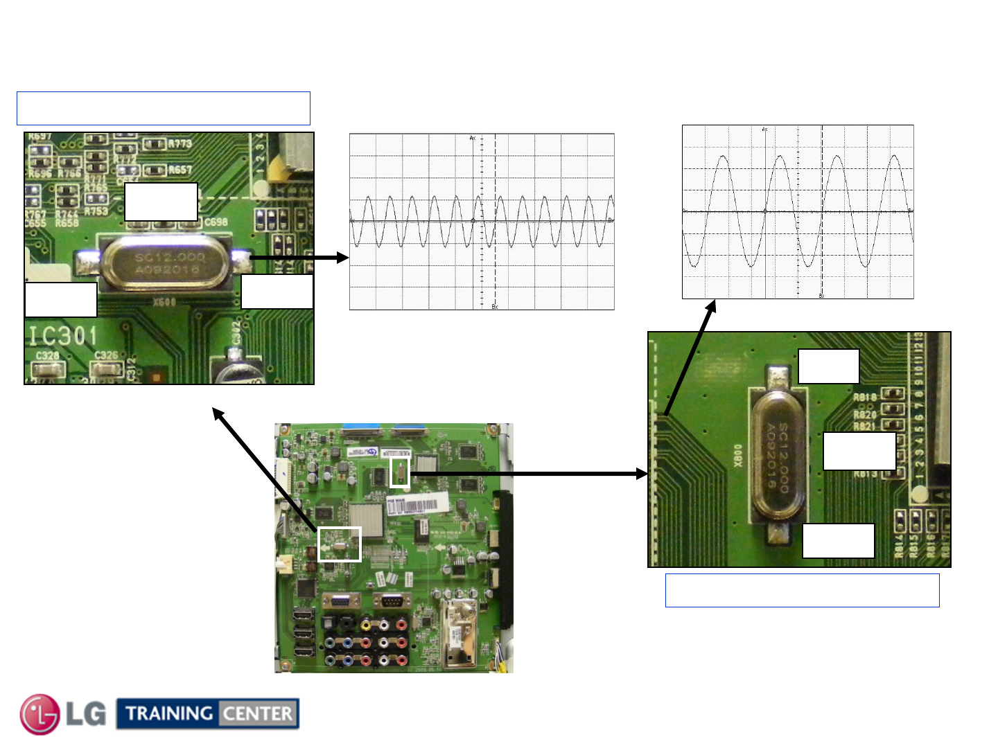
Main Board X600 and X800 Check
Main Board X600 and X800 Check
X800
Location
X600
Location
2.28Vp/p
12Mhz
Set on or off
IC600 Microprocessor Crystal
MAIN Board
2.8Vp/p
12Mhz
X800
Crystal for TruMotion IC801
Only when set is on
X600
1.62V
1.58V
1.6V
1.58V
LCD DV 42SL80
69 February 2010
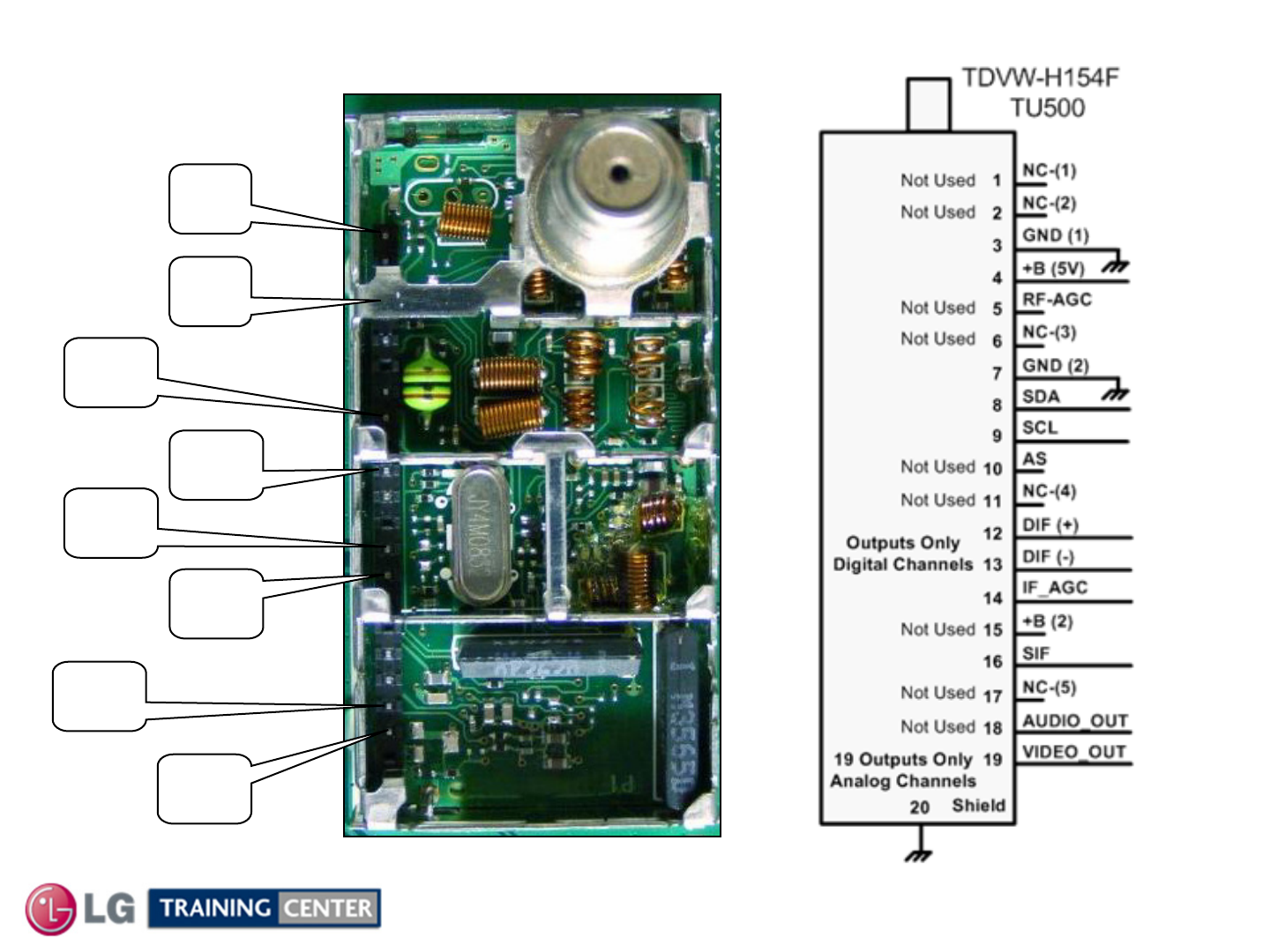
Main Board Tuner with Shield Off (Pin ID)
Main Board Tuner with Shield Off (Pin ID)
1
19
18
4
13
12
9
8
LCD DV 42SL80
70 February 2010
MAIN Board
Tuner Location
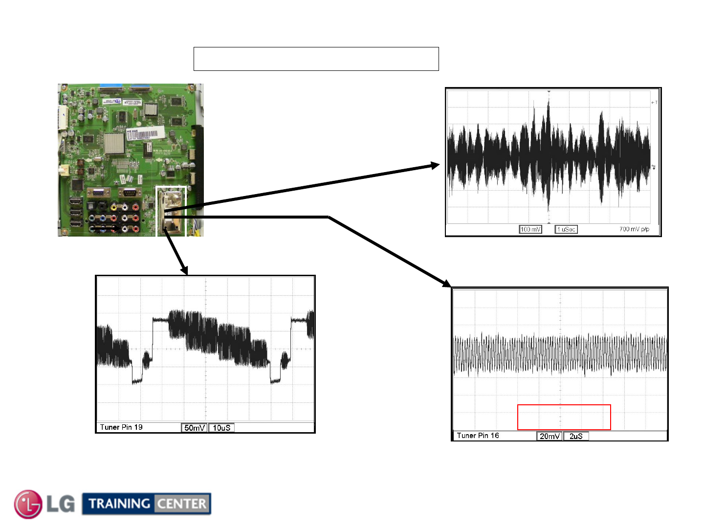
Main Board Tuner Video and SIF Output Check
Main Board Tuner Video and SIF Output Check
450mVp/p
Pin 16 “SIF” Signal
USING COLOR BAR SIGNAL INPUT Pin 12 and Pin 13
“Dig IF” Signal
Note: “Dig IF” Signal only
when receiving a Digital
Channel.
700mVp/p
Pin 1
Pin 19
“Video”
Signal
2.24Vp/p
Note: “Video Out” Signal only when
receiving an analog Channel.
LCD DV 42SL80
71 February 2010
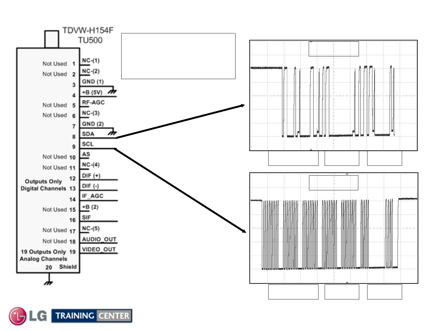
Main Board Tuner Clock and Data Lines
Main Board Tuner Clock and Data Lines
Pin 8 SDA
100uS1V per/div 5V p/p
Pin 9 SCL
100uS1V per/div 5V p/p
Note:
SCL and SDA only active
during an actual
Channel Change.
LCD DV 42SL80
72 February 2010
MAIN Board
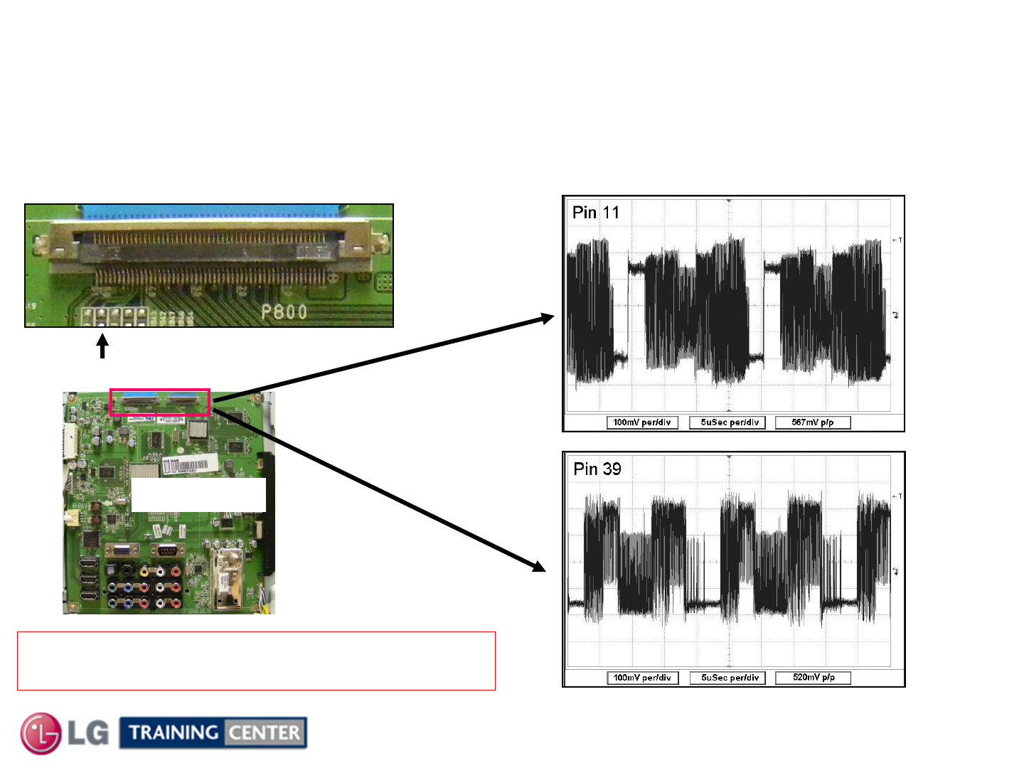
Main Board LVDS P800 Video Output Check
Main Board LVDS P800 Video Output Check
P800
Location
To confirm that the Main Board is outputting Picture Content signals, check P800 (LVDS) cable for
output. Check pins 11-14,16-17, 19-24, 27-30, 32-33 and 35-40. Pins 35-36 carry the clock for TA
and 19-20 carry the clock for TB. These signals vary from each other, but looking for signals like
the ones shown below on any of these pins will confirm the output of video content. This signal is
using standard SMTE Color Bar output from a generator as the input source.
Pin 1
Pin 39
This is just a sample of two pins on the LVDS.
There are 20 pins on P801 carrying video.
2uS
500nS
2uS
500nS
Pin 51
Pin 1, 2, 3, 4 (LVDS 12V)
P800
Pin 11
LCD DV 42SL80
73 February 2010
Main Board Connector P400 to Power Supply Voltage and Diode Chec
Main Board Connector P400 to Power Supply Voltage and Diode Check
k
Diode Check taken with meter in Diode Mode with all Connectors Removed
1(A-DIM) Pin 21 Fixed and not used 2 PDIM Pin 24 is open on the Main Board
P400 1
ncncncnc23
GndGndGndGnd11-12
GndGndGndGnd3-6
ncncncnc1
Open0V0V
2PDIM24
Open0V0VERROR22
Open1.8V0V
1A-DIM21
Open4.3V0VINV.ON20
ncncncnc19
Open24.7V0V24V17-18
GndGndGndGnd15-16
2.1V11.9V0V12V13-14
1.1V5.14V5.14V5.2V7-10
2.7V4.9V0VPWR on2
Diode
Check
Run STBYLabelPin
P400 “Main” to P201 “SMPS”
Stand By
5V
LCD DV 42SL80
74 February 2010
Main Board LVDS Connector P800 Pin Identification
Main Board LVDS Connector P800 Pin Identification
12V for
T-CON
Board
Pin 44 PDIM (Digital Dimming) Can vary according to the brightness level
of the video signal and the OSD Backlight setting. 0.6V 0% to 3.3V 100%.
Output from the Video Processing chip IC100 (Mstar).
Video
Video
Video
10bit TA or
10bit TB
Resolution
Video
51 1
P800
Video
Video
TA
Clock
TB
Clock
LCD DV 42SL80
75 February 2010
Main Board Connector P800 to T
Main Board Connector P800 to T-
-CON Voltage and Diode Check
CON Voltage and Diode Check
Diode Check taken with meter in Diode Mode with all Connectors Removed
P800 "Main" CONNECTOR to CN1 "T-CON Board“
*Pin 44 PWM-DIM 3.2V (Max 100%) to
0.6V (Min 0%) Customer’s Menu Backlight setting.
The T-CON then routes P-DIM to the Ballast.
Pins 6,7,8,9,10, 15, 18, 26,
31, 34, and 51 are all
ground.
1.1V1.3VURSA_A-2
27
N/CN/CN/C
25
1.1V1.3VURSA_B+0
24
1.1V1.3VURSA_B-0
23
1.1V1.3VURSA_B+1
22
1.1V1.3VURSA_B-1
21
1.1V1.3VURSA_B+2
20
1.1V1.3VURSA_B-2
19
1.1V1.2VURSA_BCK+
17
1.1V1.1VURSA_BCK-
16
1.1V1.3VURSA_B+3
14
1.1V1.3VURSA_B-3
13
1.1V1.3VURSA_B+4
12
1.1V1.3VURSA_B-4
11
3.18V12.06V12V T-CON
1~4
Diode CheckRunLabelPin
N/CN/C
N/C
45
1.3V*3.2V
PWM-DIM
44
N/CN/CN/C
43
1.75V0.6VOPC_EN
42
N/CN/CN/C
41
1.1V1.3VURSA_A+0
40
1.1V1.3VURSA_A-0
39
1.1V1.3VURSA_A+1
38
1.1V1.3VURSA_A-1
37
1.1V1.2VURSA_A+2
36
1.1V1.1VURSA_A-2
35
1.1V1.1VURSA_ACK+
33
1.1V1.2VURSA_ACK-
32
1.1V1.3VURSA_A+3
30
1.1V1.3VURSA_A-3
29
1.1V1.3VURSA_A+2
28
Diode CheckRunLabelPin
Pins 5, 41, 43, 46, 47, 48,
49 and 50 are all no
connection.
(Pin 1) is on the right
Text in Blue are
LVDS video
signals.
LCD DV 42SL80
76 February 2010
Main Board Connector P801 to the T
Main Board Connector P801 to the T-
-CON Board Voltage and Diode Check
CON Board Voltage and Diode Check
Diode Mode values taken with all Connectors Removed
P801 CONNECTOR "Main" to CN2 “T-CON"
GndGndGnd18
GndGndGnd17
Open1.29VURSA-D+016
Open1.25VURSA-D-015
Open1.29VURSA-D+114
Open1.3VURSA-D-113
Open1.3VURSA-D+212
Open1.2VURSA-D-211
GndGndGnd10
Open1.23VURSA-DCK+9
Open1.29VURSA-DCK-8
GndGndGnd7
Open1.3VURSA-D+36
Open1.25VURSA-D-35
Open1.4VURSA-D+44
Open1.15VURSA-D-43
GndGndGnd1-2
Diode TestRunLabelPin
n/cn/cn/c34-41
n/cn/cn/c33
Open1.28VURSA-C+032
Open1.2VURSA-C-O31
Open1.3VURSA-C+130
Open1.2VURSA-C-129
Open1.3VURSA-C+228
Open1.2VURSA-C-227
GndGndGnd26
Open1.23VURSA-CCK+25
Open1.23VURSA-CCK-24
GndGndGnd23
Open1.3VURSA-C+322
Open1.2VURSA-C-321
Open1.13VURSA-C+420
Open1.18VURSA-C-419
Diode TestRunLabelPin
(Pin 1) is on the right
Text in Blue
are LVDS
video
signals.
LCD DV 42SL80
77 February 2010
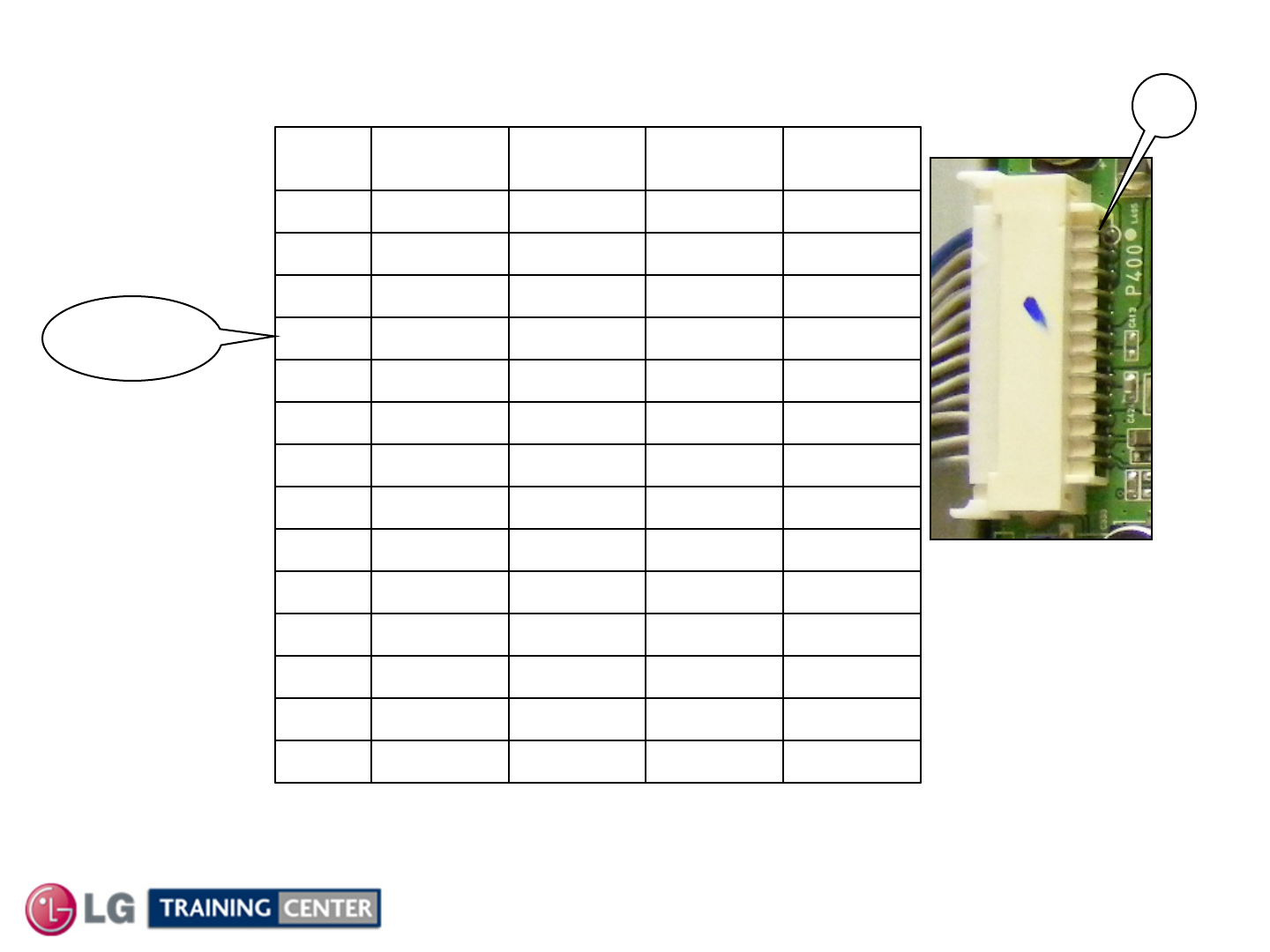
Main Board Connector P1000 to (Ft. IR/LED Control) Voltage and
Main Board Connector P1000 to (Ft. IR/LED Control) Voltage and Diode Check
Diode Check
Diode Check taken with meter in Diode Mode with all Connectors Removed
P1000 CONNECTOR "MAIN Board" to P100 "Front IR / LED Board Assy"
Open3.29V0VPWR_ON12
0.67V3.31V3.31V3.3V_ST11
GndGndGndGnd10
Open4.18V4.18VIR9
GndGndGndWarm_ST8
GndGndGndGnd7
1.1V5.1V5.1V5V ST6
1.3V3.26V3.26VKey25
1.0V3.26V3.26VKey14
GndGndGndGnd3
1.6V3.2V0VSDA2
1.6V3.2V0VSCL1
Diode CheckRun STBYLabelPin
1
P1000
LCD DV 42SL80
78 February 2010
Main Board Connector P300 to Speakers Voltage and Diode Check
Main Board Connector P300 to Speakers Voltage and Diode Check
Diode Check taken with meter in Diode Mode with all Connectors Removed
SPK-L(+)
SPK-L(-)
SPK-R(+)
SPK-R(-)
LABEL
2.63V12.0V0V4
2.63V12.0V0V3
2.63V12.0V0V2
2.63V12.0V0V1
Diode CheckRunSBYPin
P300 CONNECTOR "Main" to "Speakers"
Use speaker out to test for defective Audio Amp IC301
1IC301
LCD DV 42SL80
79 February 2010
Side A/V Board Connector P100 to Main P101 Voltage and Diode Che
Side A/V Board Connector P100 to Main P101 Voltage and Diode Check
ck
Diode Check taken with meter in Diode Mode
with all Connectors Removed
P101 Connector “Side A/V IN Board" to P100 "Main"
Main
P101
P100
GndGndGndGnd8
Open0V0VAV_R_IN7
GndGndGndGnd6
Open0V0VAV_L_IN5
GndGndGndGnd4
Open0V0VAV_DET3
Open0V0VCVBS_IN2
GndGndGndGnd1
Diode
Check
RunSTBYLabelPin
Side AV Board
1
1
GndGndGndGnd1
0.07V0V0VCVBS_IN2
Open0V0VAV_DET3
GndGndGndGnd4
Open0V0VAV_L_IN5
GndGndGndGnd6
Open0V0VAV_R_IN7
GndGndGndGnd8
Diode
Check
RunSTBYLabelPin
P100 Connector “Main" to P100 " Side A/V IN Board"
Main
LCD DV 42SL80
80 February 2010
FRONT IR SECTION
FRONT IR SECTION
The Front IR board contains the Infrared receiver and the Intelligent Sensor.
This board receives its B+ (STBY5V) from the Main Board. It also has connections to the side Key
board. The 3.3V pull up for the Soft Touch Keys is routed from the Main board through the Front IR
board to the Soft Touch Key board.
The Front Power LEDs are now on the Soft Touch Key Board section and pulsate incrementally as the
set turns on and decrease as the set turns off. This is accomplished using an LED driver IC which
communicates with the Main board via Clock and Data lines.
There are several Zener diodes on the board as well and since it receives STAND-BY 5V (STBY 5V) it
could make the Power Supply or the Main board appear to be defective if a short was introduced to the
stand by line.
IR Board
Soft Touch
Key and LED
Board
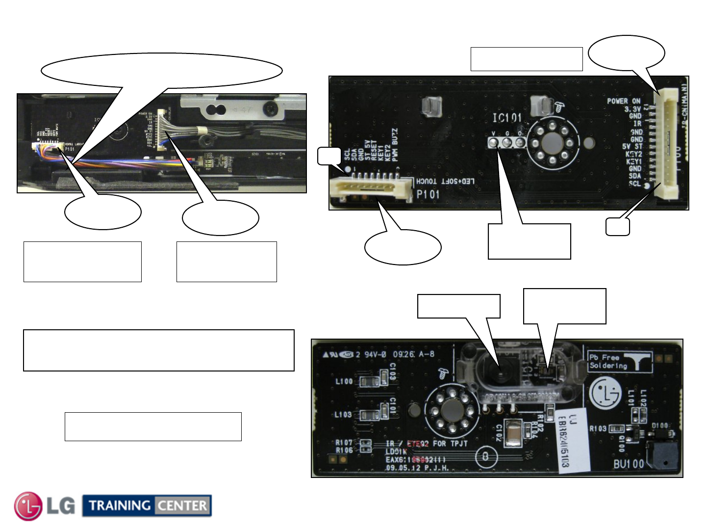
LCD DV 42SL80
81 February 2010
Front Board Assembly (IR and Power LED) Layout (Front and Back V
Front Board Assembly (IR and Power LED) Layout (Front and Back View)
iew)
To Main Board
To Main
Board
To Soft Touch
Key Board
Note: STBY5V is routed to this board.
Be aware of a possibility for a short.
P100
Main Power SW Removed
IR Sensor Intelligent
Sensor
IC101
IR Sensor
P100
1
1
P101
P101
p/n: EBR63322103
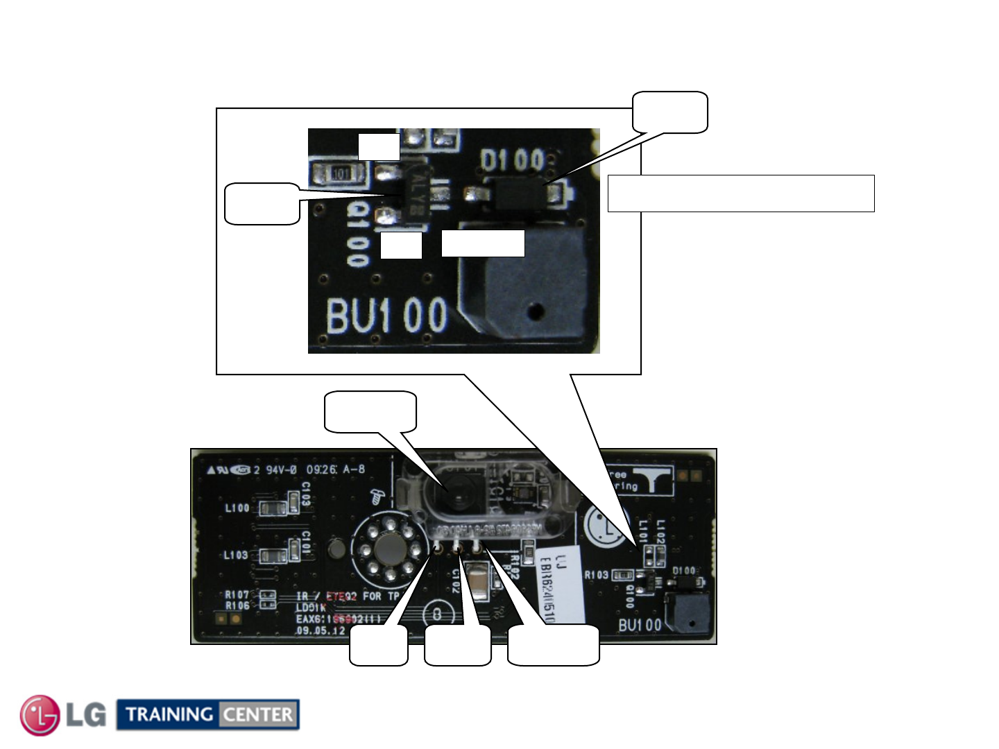
LCD DV 42SL80
82 February 2010
Front Board Assembly Component Check
Front Board Assembly Component Check
D100 5.14V both sides
0V 5.14V
Q100
0V
D100
5V 4.18VGnd
IC101
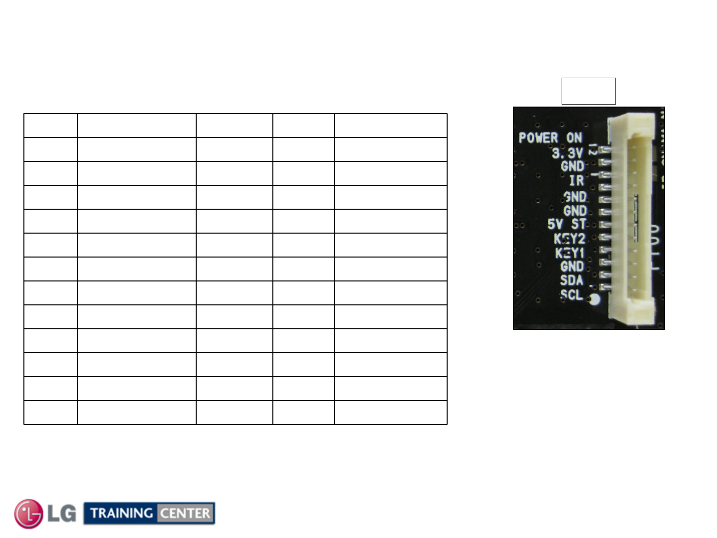
LCD DV 42SL80
83 February 2010
Front Connector P100 to Main Voltage and Diode Check
Front Connector P100 to Main Voltage and Diode Check
Diode Check taken with meter in Diode Mode with all
Connectors Removed
P100 Connector “IR Board“
to "MAIN Board" P1000 P100
Open3.2V0VSCL1
Open3.2V0VSDA2
GndGndGndGnd3
Open3.26V3.26VKey14
Open3.26V3.26VKey25
2.6V5.1V5.1V5V ST6
GndGndGndGnd7
GndGndGndGnd8
2.6V4.18V4.18VIR9
GndGndGndGnd10
Open3.31V3.31V3.3V_ST11
Open3.29V0VPOWER_ON12
Diode CheckRun STBYLabelPin
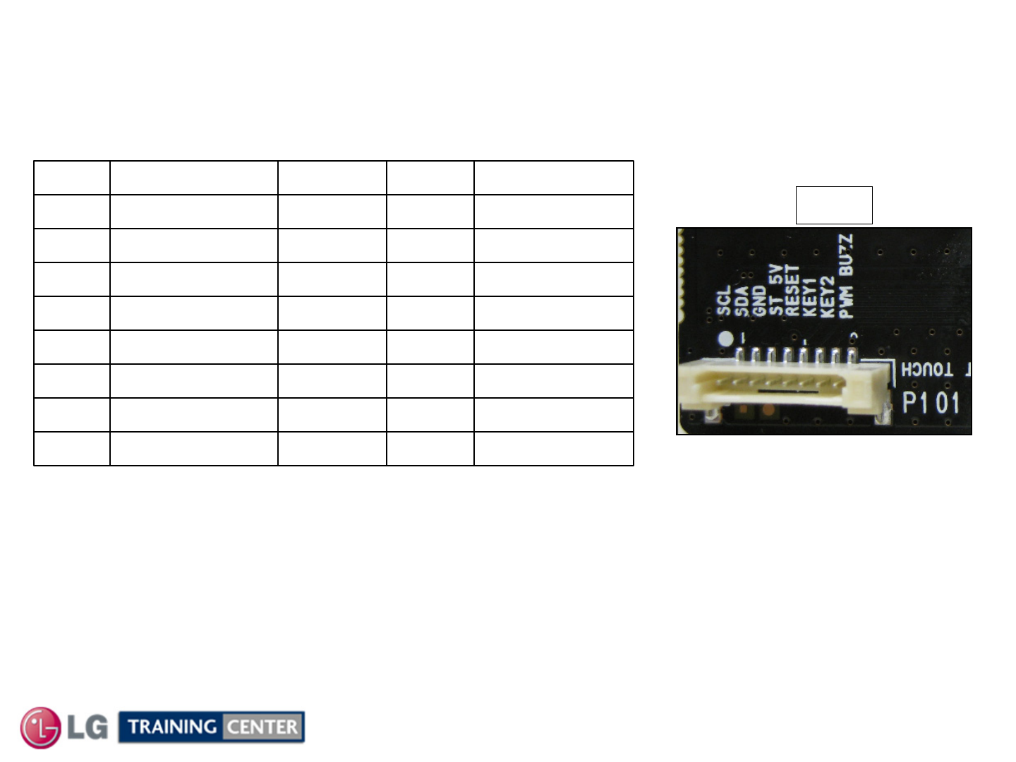
LCD DV 42SL80
84 February 2010
Front Connector P101 to Soft Key Board Voltage and Diode Check
Front Connector P101 to Soft Key Board Voltage and Diode Check
Diode Check taken with meter in Diode Mode with all
Connectors Removed
P101 Connector “IR Board“ to
“Soft Touch Key Board" J2
P101
0.8V0V0VPWM BUZZ8
Open3.26V3.26VKey27
Open3.26V3.26VKey16
Open0V0VReset5
Open5.1V5.1V5V ST4
GndGndGndGnd3
Open3.31V3.31VSDA2
Open3.29V0VSCL1
Diode CheckRun STBYLabelPin
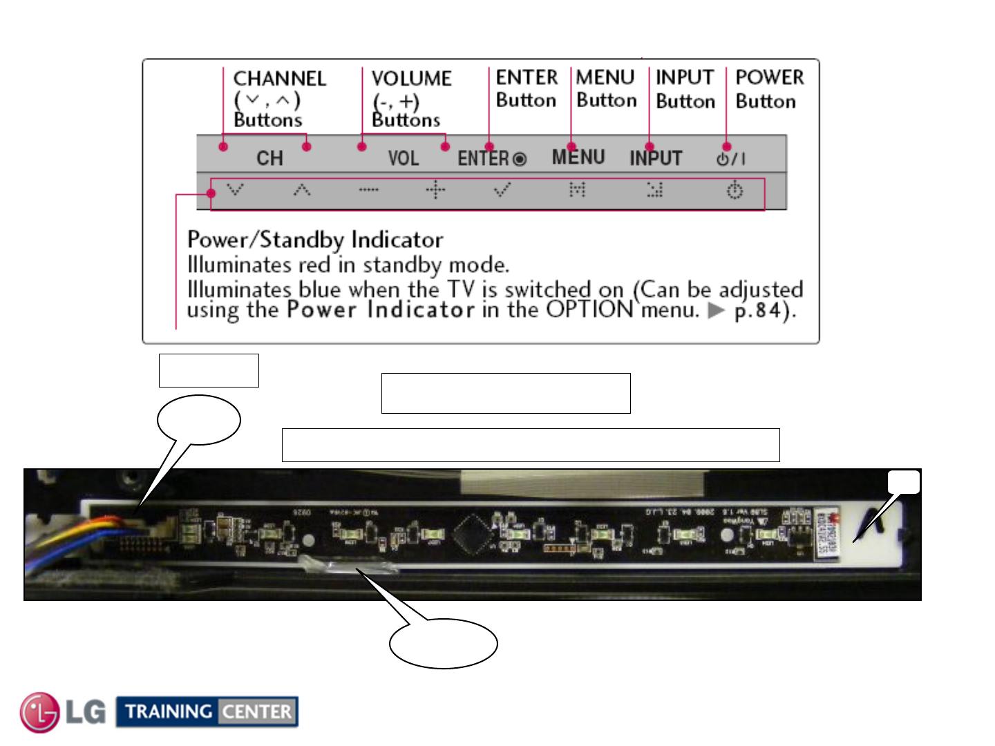
LCD DV 42SL80
85 February 2010
SOFT TOUCH KEY BOARD SECTION
SOFT TOUCH KEY BOARD SECTION
To Ft. IR
J2
1
Glue
Note: The Soft Touch Key Board is Glued into place.
p/n: EBR63609903
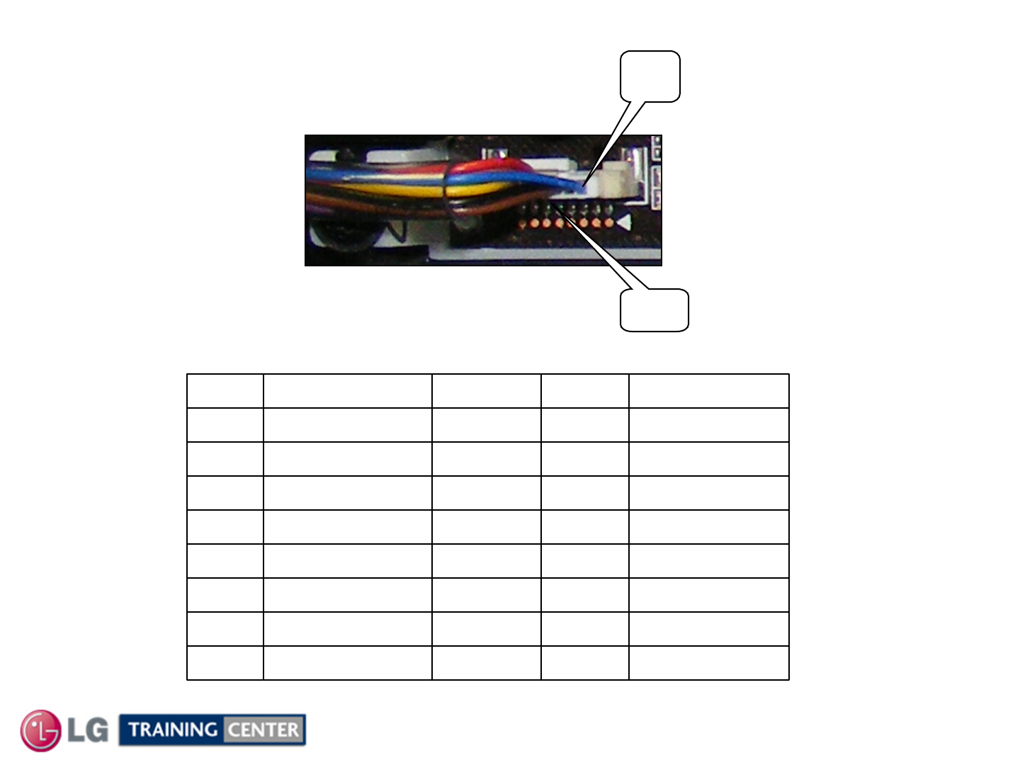
LCD DV 42SL80
86 February 2010
Soft Touch Key Assembly J2 Information
Soft Touch Key Assembly J2 Information
1
J2
P101 Connector “IR Board“ to
“Soft Touch Key Board" J2
1.3V0V0VPWM BUZZ8
1.5V3.26V3.26VKey27
1.5V3.26V3.26VKey16
Open0V0VReset5
1.6V5.1V5.1V5V ST4
GndGndGndGnd3
1.5V3.31V3.31VSDA2
1.5V3.29V0VSCL1
Diode CheckRun STBYLabelPin
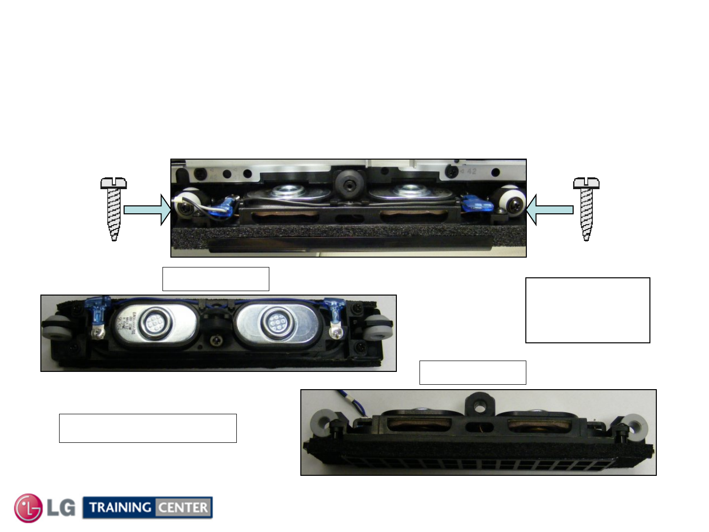
LCD DV 42SL80
87 February 2010
INVISIBLE SPEAKER SYSTEM SECTION
INVISIBLE SPEAKER SYSTEM SECTION
The 42SL80 contains the Invisible Speaker system.
The Full Range Speakers point downward, so there are no front viewable
speaker grills or air ports.
Invisible Speaker System Overview (Full Range Speakers)
Invisible Speaker System Overview (Full Range Speakers)
Reading
across speaker
wires, 8.2 ohm.
p/n: EAB60866701
Top View
Side View

LCD DV 42SL80
88 February 2010
INTERCONNECT DIAGRAM (11 X 17 Foldout) SECTION
INTERCONNECT DIAGRAM (11 X 17 Foldout) SECTION
This section shows the Interconnect Diagram called the 11X17
This section shows the Interconnect Diagram called the 11X17
foldout that
foldout that’
’s available in the Paper and Adobe version of the
s available in the Paper and Adobe version of the
Training Manual.
Training Manual.
Use the Adobe version to zoom in for easier reading.
Use the Adobe version to zoom in for easier reading.
When Printing the Interconnect diagram, print from the Adobe
When Printing the Interconnect diagram, print from the Adobe
version and print onto 11X17 size paper for best results.
version and print onto 11X17 size paper for best results.
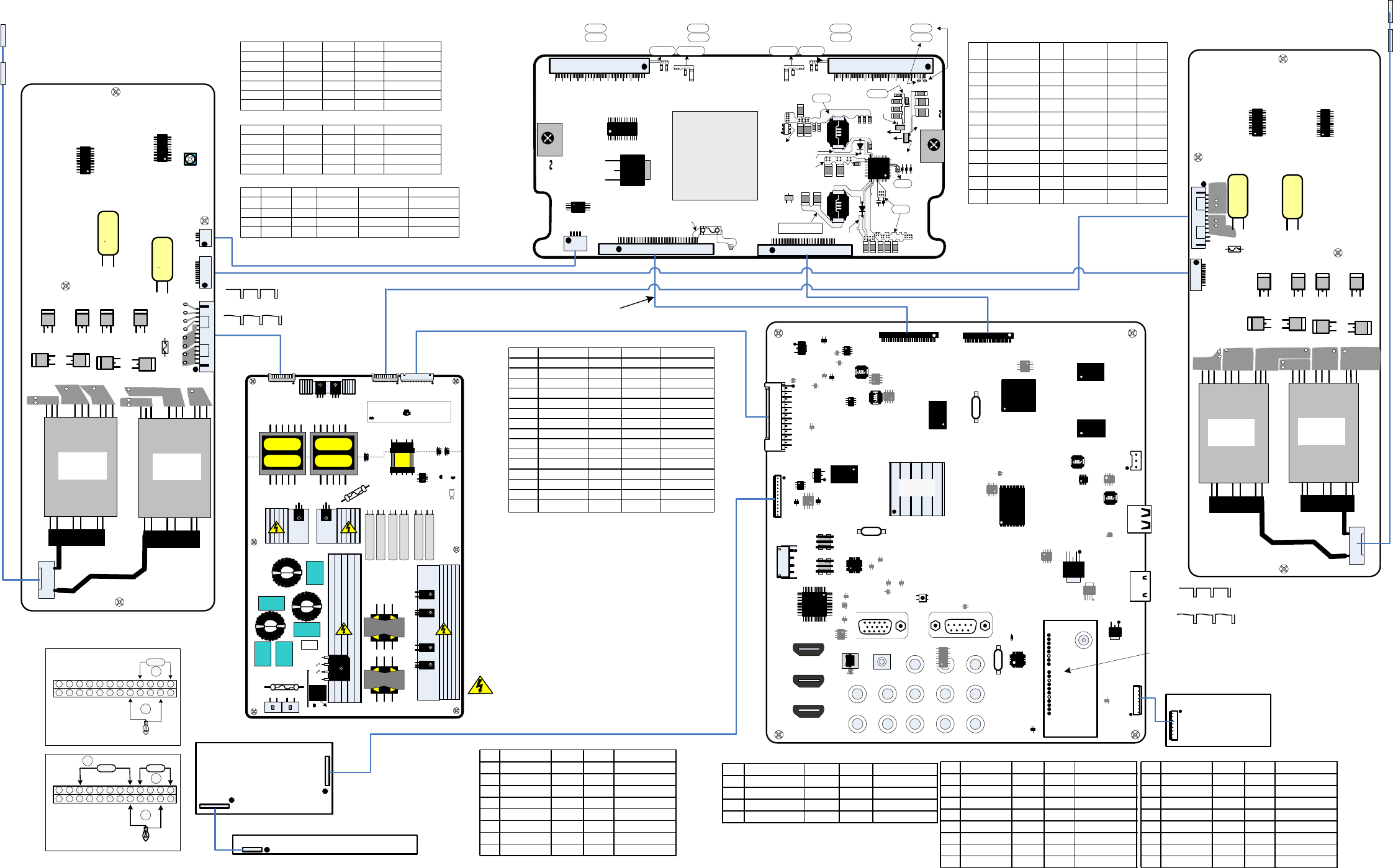
42SL80 INTERCONNECT DIAGRAM
Power Supply
Front IR
IR Receiver
Intelligent Sensor
SMPS TEST 1: To Force Power Supply On.
Disconnect P800 on Main board.
Load the 5V line using a 12V light bulb.
Jump pins 7,8,9 or 10 (5V) to pin 2 using a 100
resistor. (Test Voltage Outputs 12V, 24V to Main
and 24V to both Inverters).
SMPS TEST 2: Jump pins 7,8,9 or 10 (5V) to pin 20
(INV-ON). The Backlights should turn on.
LVDS
*PWM-DIM (P-DIM) is open on the Main board, n/c.
*A-DIM is fixed and does not move.
12V to T-CON
Pin 48~51.
Intelligent Sensor
Intelligent Sensor
TO TFT MODULE
UC1
FL3
1) Gnd
2) 1.8V
3) 3.3V
TO TFT MODULE
T-CON BOARD
(TFT Driver)
Gnd Protect
U11
Q1
U12
U10
(VGL) Pin 2
(VGH_M) Pin 4
(VDD_LCM) Pin 56,57,58
(VCC) Pin 53,54 26V
16V -5V
3.3V
26V
16V-5V 3.3V
B
2.78V
U13
D8
L1
FL2 Gnd
Protect
L2
D9
D10
U5
E
3.3V
C 3.3V
20.5V
14.25V
-2.4V
R704
R705
R706
3.3V
26V
27V
C744
R721
U5
Gnd
-5V
VCC
(CN1) Pin 48-51 F1 (12V)
125V / 3A
CN1 CN2
U5 B+ 12V
16V
VGH_M
16V
VGL
12V
3.3V
1
2
3
2
CN4
CN3
C308
C307
C306
C305
16.3V 3.3V
C304
C303
C302
C301
16.3V3.3V
CN5
(VDD_LCM) Pin 3,4,5
(VCC) Pin 7,8
(VGL) Pin 59
(VGH_M) Pin 57
Gnd
D7
3.8V P/P
9.97Mhz
VDD
1~4) Gnd
5) 0V
6) 3.3V
7) 3.3V
8) 3.3V
1) 6.9V
2) 13.7V
3) 15.7V
4) 13.7V
5) 13.0V
6) 12.0V
7) 10.9V
8) Gnd
9) 16.0V
10) 10.1V
11) 8.2V
12) 7.7V
13) 3.3V
14) 3.3V
15) 3.3V
16) Gnd
17) Gnd
18) Gnd
19) 5.8V
20) 5.0V
21) 3.9V
22) 2.9V
23) 6.0V
24) Gnd
25) 2.2V
26) 0.3V
27) 2.2V
28) 6.9V
U12
P204
IC251
IC252 MC201
P101 SK100
D221D222
T101T102 IC102 IC502
IC103
IC501
T501
F1
3.15A/250V
L600
L601
BD101 Q606
D603
Q605
D602
39uF/450V C616
C615
C614
C613
C612
C611
Q502
Q503Q501
Q111 Q110
P201P205
Q101
F100
6.3A/250V
+
-
CX102
CX101
CX105
CX103
CX104
L102
L103
L101
R103
RL101
39uF/450V
39uF/450V
39uF/450V
39uF/450V
39uF/450V
(1)
(19) Analog Video
(4) Tuner 5V_TU
(8) Data
(9) Clock
(12) Dig DIF+
(13) Dig DIF-
(16) SIF
DDR
DDR
P800
IC801
Tru-
Motion
P801
IC801 Operates at
high temperature
X800
25Mhz
Q408
2
3
1
IC300
E
C
B
Q1000
IC604
IC901
IC900
IC1
X600
12Mhz Micro/Video
Processor
Mstar
IC404
IC504
SW600
IC1200
L304
P1000
Q500
TU500 Tuner
TDVW-H103F
X500
25Mhz
P803
N/A
IC502
12V LVDS
Pins 1~4
P300
MAIN BOARD
P100
L305
E
C
B
IC301
P400
IC2
IC500
D500
IC406
NAND
FLASH
IC400
IC605
IC602
D1003
R-
R+
L-
L+
E
C
B
Q406
IC600
Mstar
DDR
DDR
Y
PC
Audio
PC RS232
HDMI 1
HDMI 2
HDMI 3
HDMI
4
USB
Pr Pb
YPrPb Audio
LR
Video LR
L406
L412
L422
L424
E
CB
E
CB
E
CB
E
CB
IC100
E
CB
IC501
IC503
IC102
IC405
IC1000
IC601
Q600
IC800
IC606
IC401
IC402
E
C
B
Q407
Q405
Q605
Q400 E
C
B
Q604
E
C
BQ401
2
3
1
IC603
E
C
B
Q603
Q602
D600
E
C
B
Q300
D200
Q200
D129
IC101
Q101
E
CB
Grayed Out Components are on the Back Side
E
C
B
Q501
P100
Front “Soft Switch” Keys
P101
J2
To
Backlights
1.2K
To
Backlights
1.2K
Side A/V
P101
P201 "SMPS" to P400 "Main"
Pin Label STBY Run Diode Check
1
2PWR-ON0V4.9V 1.6V
3-6
7-10 5.2V 5.14V
11-12
13-14
Gnd Gnd Gnd Gnd
15 Gnd Gnd Gnd Gnd
17-18
19
21 *A-DIM 0V 1.6V
22
N/C N/C N/C Open
N/C N/C N/C Open
Gnd Gnd GndGnd
5.14V Open
12V 0V 11.9V 0.27V
24V 0V 24.7V 0.42V
Open
ERR OUT 0V 0V Open
*P-DIM
16 A-Gnd Gnd Gnd Gnd
20 I-C 0V 4.3V Open
23 N/C N/C N/C Open
24 N/C N/C Open
Stand-by 5V
Pin Label STBY Run Diode
Check
11 DUTY_M1 0V 0.71V-2.4V OPEN
10 GND GND GND GND
9 DUTY_M2 0V 0.71V-2.4V OPEN
8 FB_S1 0V 0.96V 2.9V
7 ON/OFF 0V 4.3V OPEN
6 STB 0V 3.2V OPEN
5 VREF 0V 1.0V OPEN
4 FB_M1 0V 1.0V 2.9V
3 SRT 0V 1.4V OPEN
2 SS 0V 2.9V OPEN
1CT_SYNC_IN0V 1.5V 1.7V
CN3 "Inverter A" To CN203 "Inverter B"
Diode
Check
OPEN
GND
OPEN
2.9V
OPEN
OPEN
OPEN
2.9V
OPEN
OPEN
1.7V
"A" "B"
P201
B
100
PWR ON
317511 915 1319 1721
428 612 1016 1420 1822
23
24
STBY 5V
24V 12V
A
Gnd
STBY 5V
24V 12V
12V Light Bulb
SMPS TEST 1
P201
B
100
317511 915 1319 1721
428 612 1016 1420 1822
23
24
STBY 5V
24V 12V
A
Gnd
STBY 5V
12V Light Bulb
24V 12V
100
INV-ON
C
SMPS TEST 2
P1000 “Main” to P100 “Front IR”
Pin Label STBY Run
1 SCL 0V 3.2V 1.6V
2 SDA 0V 3.2V 1.6V
3 Gnd Gnd Gnd Gnd
4 Key1 3.26V 3.26V 1.0V
5 Key2 3.26V 3.26V 1.3V
6 5V_ST 5.1V 5.1V 1.1V
7 Gnd Gnd Gnd Gnd
8 Warm_ST Gnd Gnd Gnd
Diode Check
Remote Diode Check
9IR4.18V Open
10 Gnd Gnd Gnd
11 3.3V_ST 3.31V 0.67V
12 PWR_ON 0V Open
Pin Label STBY Run
4.18V
Gnd
3.31V
3.29V
P1000 “Main” to P100 “Front IR”
F1
STBY 170V
RUN 188.5V
Inverter A
T1
T101
35V
680
uF
35V
680
uF
F1
65V/ 12A
Q104 Q102 Q2 Q4
CN5
Q103 Q3 Q6
CN1
CN3
CN2
Q106
U101 & U1 are DC-AC Inverter
Control ICs
U1
U101
C43
C8
Do Not
Adjust
+-
+-
Inverter B
CN201
CN203
T201 T301
35V
680uF
F1
65V/ 12A
Q302Q304Q204Q202
CN205
Q306
Q206
Q203 Q303
U201 & U301 are DC-AC
Inverter Control ICs
U201 U301
C208C243
35V
680uF
+-+
-
24V
See second page of Interconnect
Diagram for Main board DC Voltages
See pages 3/4 of Interconnect
Diagram for LVDS Waveforms
1616
1616
Pin 1 T201/T301
29.2V p/p 48kHz
Pin 6 T201/T301
30V p/p 48kHz
Pin 1 T101/T1
29.2V p/p 48kHz
Pin 6 T101/T1
30V p/p 48kHz
CN2 "Inverter A" to CN3 "T-CON"
Diode Check
4
Run STBYLabel
Pin
Gnd
Scan 2
Gnd Gnd Gnd
Open
3
2
1
Scan 1
n/c
Open
0.67V-2.4V
0.67V-2.4V
Openn/c n/c
0V
0V
Diode Check
Gnd
0.98V
0.98V
0.98V
T-CON Side
C
A2 A1
C
A2 A1
C
A2 A1
A1
C
A2
(19)
Indicates Hot
Ground
P100 “Main” to P101 “Side A/V”
Pin Label STBY Run
8 Gnd Gnd Gnd
7
CVBS_IN 0V
6Gnd
Open
5
AV_DET
Gnd
4
AV_L_IN Open
3Gnd
2
AV_R_IN Open
1Gnd
Diode Check
0V
Gnd
0V
Gnd
0V
Gnd Gnd
Gnd
0V
0V
Gnd
0V
Gnd
0V
Gnd
Gnd
0.07V
P101 “Side A/V” to P100 “Main”
Pin Label STBY Run
8
7
6
5
4
3
2
1Diode Check
Gnd Gnd Gnd
CVBS_IN 0V Open
Gnd
Open
AV_DET
Gnd
AV_L_IN Open
Gnd Gnd
AV_R_IN Open
Gnd
0V
Gnd
0V
Gnd
0V
Gnd Gnd
Gnd
0V
0V
Gnd
0V
Gnd
0V
Gnd
MC1
Black
To Top 6 and Bottom 6 bulbs
To Center 13 bulbs
SC1
Black
PANEL BACKLIGHT CONNECTIONS
To Top 6 and Bottom 6 bulbs
To Center 13 bulbs
PANEL BACKLIGHT CONNECTIONS
P204 "SMPS" to CN1 "Inverter A"
Pin Label STBY Run Diode Check
1,2,3,4,5 24V 0V 24.7V 0.42V
6,7,8,9,10 Gnd Gnd Gnd Gnd
11 A-DIM 1.7V Open
12 *I-C 4.3V
13 *PWM-DIM N/C
14 ERROR 0V
0V
0V
0V
0V
Open
Open
Open
*I-C is Inverter On
*P-DIM is not used on this pin.
P205 "SMPS" to CN501 "Inverter B"
12
11
6
1
Diode CheckRun STBYLabel
12
11
1,2,3,4,5
6,7,8,9,10
24V
Gnd
A-DIM
*I-C
0V 24.7V 0.42V
Gnd Gnd Gnd
1.7V Open
4.3V
0V
0V Open
Pin
To
Spks
D
GS
D
GS
D
GS
D
GS
D
G
S
G
S
D
D
G
S
G
S
D
D
GS
D
GS
D
GS
D
GS
D
G
S
G
S
D
D
G
S
G
S
D
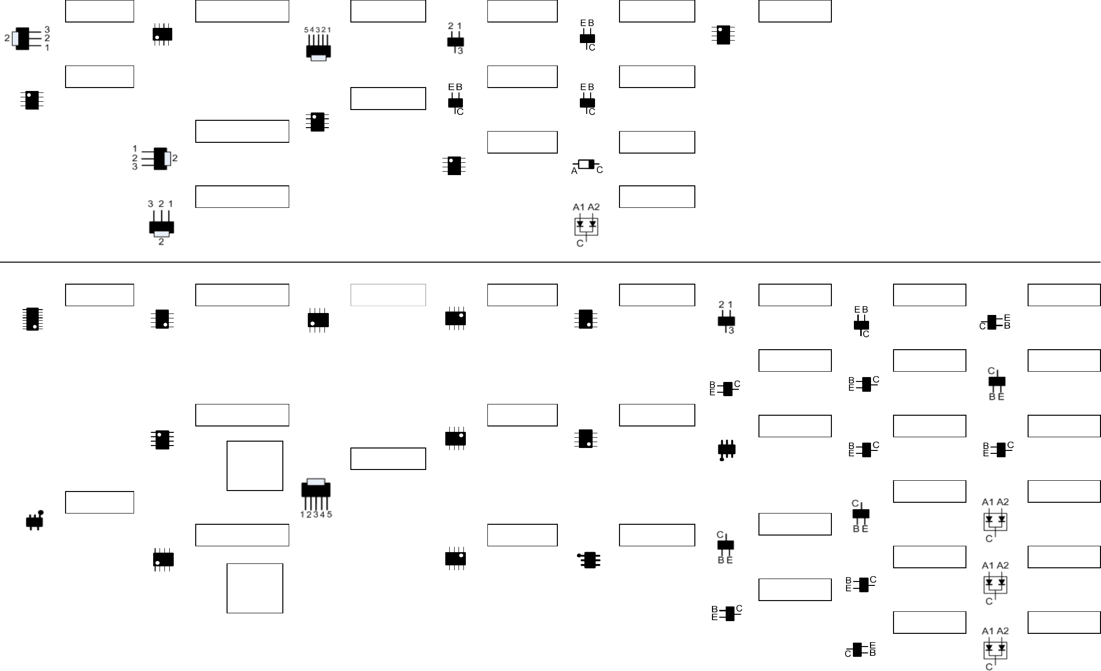
42SL80 MAIN (FRONT SIDE) SIMICONDUCTORS
IC300 +1.8V AMP IC404 +1.8V_MEMC IC504 +3.3V_PVSB IC605 Reset Gen Q500 Tuner Video IC403 +1.6V_MEMC
Pin Regulator Pin Regulator Pin Regulator Pin for Power_Det Pin Buffer Pin Regulator
[1] Gnd [1] 0.8V [1] 4.94V [1] Gnd B 1.7V [1] 0V
[2] 1.8V [2] Gnd [2] 4.94V [2] 3.5V C 0V [2] 0.8V
[3] 3.3V [3] 4.92V [3] Gnd [3] 3.3V E 2.3V [3] 1.2V
[4] 6.5V [4] 3.4V [4] 1.2V
IC400 +1.8V_DDR [5] 4.8V [5] 1.25V Q406 5V Switch Q1000 Moving LED [5] 1.8V
Pin Regulator [6] 1.8V Pin Control Pin Inverter [6] 5.0V
[1] n/c [7] 1.8V IC602 HDCP B 0.6V B 0V [7] 1.2V
[2] 3.2V [8] 4.8V Pin EEPROM C 0V C 3.3V [8] 5.0V
[3] 3.2V [1] Gnd E Gnd E Gnd
[4] n/c IC406 +3.3V_ST [2] Gnd
[5] n/c Pin Regulator [3] 5.0V Q408 +5V/12VLVDS D500 Speed Up Reset
[6] 1.8V [1] 0V [4] Gnd Pin Switch Pin IC502
[7] 0.8V [2] 3.3V [5] 3.3V [1] 5.1V C 3.4V
[8] Gnd [3] 5.0V [6] 3.3V [2] 0.29V A 3.38V
[7] 5.0V [3] 11.9V
IC500 9V Reg [8] 5.0V [4] 5.99V D1003 Moving LED
Pin to IC501 Tuner 5V [5] 11.98V Pin Routing
[1] 12V [6] 11.98V A1 0V
[2] Gnd [7] 5.06V C 0.1V
[3] 8.9V [8] 5.06V A2 0V
42SL80 MAIN (BACK SIDE) SIMICONDUCTOR
S
IC100 RS232 IC102 RGB IC405 +5V EXT IC503 +1.2V_PVSB IC606 Micro IC600 IC603 Reset Gen Q401 INV_ON Q603 Power_On_
Pin Rx/Tx Pin EEPROM Pin Regulator Pin Regulator Pin EEPROM Pin for IC600 Pin Inverter Pin Delay Switch
[1] 3.3V [1] Gnd [1] 0.8V [1] 0V [1] Gnd [1] 0V B 0.05V B 0V
[2] 5.56V [2] Gnd [2] Gnd [2] 3.3V [2] Gnd [2] 0V C 4.35V C 0.04V
[3] 0.02V [3] Gnd [3] 12V [3] 3.4V [3] Gnd [3] 3.3V E Gnd E Gnd
[4] 0.03V [4] Gnd [4] 9.6V [4] 0V [4] Gnd
[5] 5.5V [5] 3.3V [5] 5V [5] 0V [5] 3.24V Q101 IR RS232 Q405 12V LVDS Q604 Power_Det
[6] 5.5V [6] 3.3V [6] 4.97V [6] 1.2V [6] 3.24V Pin Buffer Pin Switch Control Pin Switch
[7] 5.5V [7] 3.18V [7] 4.97V [7] 0.8V [7] 0V B 0.634V B 0.05V B 0V
[8] 0V [8] 0V [8] 1.9V [8] 0V [8] 3.24V C 0V C 0.65V C 3.3V
[9] 3.29V E 0V E Gnd E Gnd
[10] 3.24V IC401 +1.26V_VDDC IC504 +1.26V_PVSB IC800 SPI Flash IC801
[11] n/c Pin Regulator Pin Regulator Pin Memory Q200 HDMI CEC Q407 12V LVDS Q605 Power_Det
[12] 3.31V [1] 8.0V Oscilloscope ONL
Y
[1] 0.8V [1] 0V Pin Pin Source Pin +12V Side
[13] 0V [2] Gnd [2] 0V [2] 0.8V [1] 3.2V B 0.65V B 0.65V
[14] 5.5V [3] 5.0V IC501 +5V_TU [3] 11.8V [3] 3.2V [2] 3.2V C 0.0V C 0.0V
[15] Gnd [4] 6.0V Pin for Tuner [4] 9.6V [4] 0V [3] 0V E Gnd E Gnd
[16] 3.29V [5] 4.9V [1] 8.92V [5] 5.0V [5] 0V [4] 0V
[6] 0V [2] 1.88V [6] 5.0V [6] 0.09V [5] 0V Q501 Tuner SIF D129 5V Routing
IC101 SPIF Optical [7] 0V [3] 5.04V [7] 5.0V [7] 3.2V [6] 3.16V Pin Buffer Pin for IC1200
Pin Audio [8] 3.2V [4] 0V [8] 0.9V [8] 3.2V B 2.4V A1 0.03V
[1] 0.03V [5] Gnd Q300 Audio Mute C 0V C 4.5V
[2] 0V IC402 +3.3V_MEMC IC601 Serial Flash IC1000 USB +5V Pin Switch E 3.0V A2 5.1V
[3] 0V Pin Regulator Pin for Boot Pin Switch B 0.62V
[4] 0V [1] 8.0V Oscilloscope ONL
Y
[1] 0.04V [1] 4.95V C 0.01V Q600 Write Protect D200 Shunt for
[5] 0V [2] Gnd [2] 3.2V [2] Gnd E Gnd Pin for IC601 Pin Q200
[3] 4.98V [3] 2.5V [3] 3.21V B 0V A1 0V
[4] 7.6V [4] 0V [4] 4.95V Q400 PWR On/Off C 2.5V C 3.1V
[5] 4.9V [5] 0V [5] 0V Pin Switch E Gnd A2 3.2V
[6] 3.3V [6] 0V [6] 4.95V B 2.9V
[7] 3.3V [7] 3.2V C 5V Q602 S5/S6 Reset D600 Audio Mute
[8] 0V [8] 3.2V E 5V Pin Switch for Mstar Pin Routing
B 0V A1 0.01V
C 3.28V C 2.7V
E 0V A2 3.29V
WARNING
Measure Pin
1 with O-
scope ONLY
WARNING
Measure Pin
1 with O-
scope ONLY
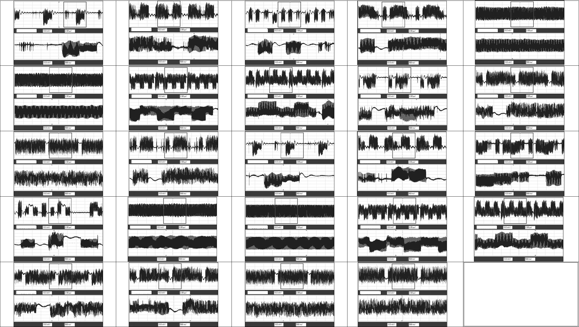
42SL80 LVDS P800 WAVEFORMS
42SL80 P800 LVDS CABLE WAVEFORMS:
Waveforms taken using SMTP Color Bar input.
All readings give the Scale 10mV and Time Base
related to scope settings.
Top waveform in each image gives a slower rate,
2us per division. Outlined area is shown in the
bottom waveform at 500ns per division time
base.
Pin 11 Pin 12 Pin 16
Pin 24
Pin 35
Pin 38Pin 37
Pin 30
Pin 23
Pin 20
Pin 13 Pin 14
Pin 17 Pin 21
Pin 27 Pin 28
Pin 36
Pin 32
Pin 39 Pin 40
Pin 19 Pin 22
Pin 29
Pin 33
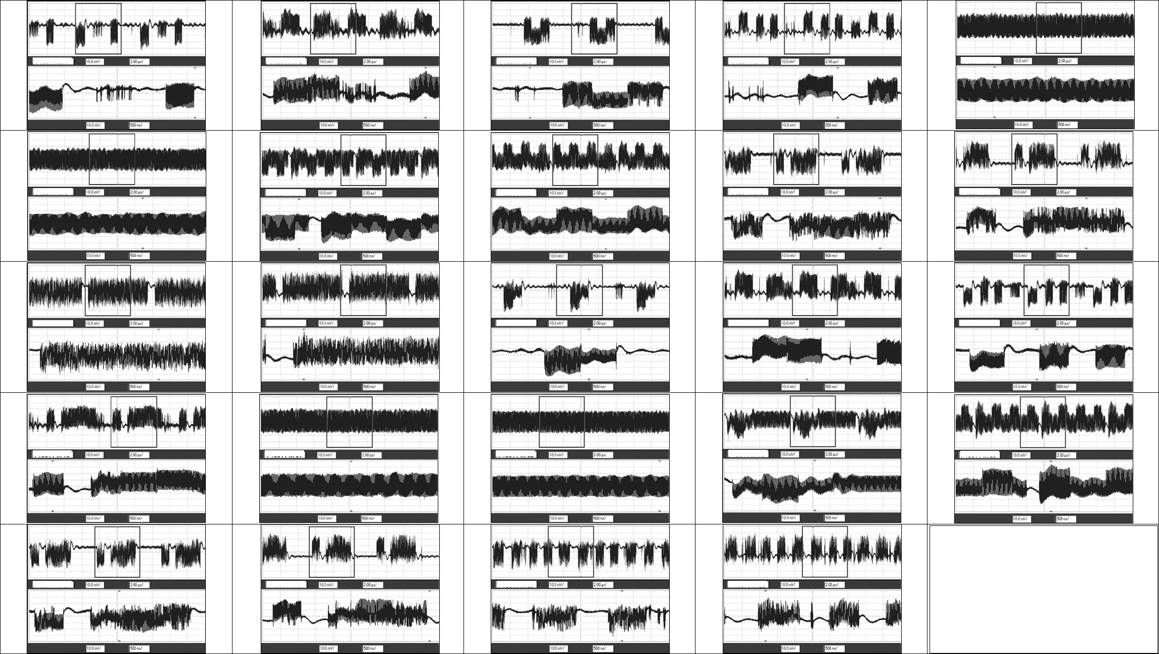
42SL80 LVDS P801 WAVEFORMS
42SL80 P801 LVDS CABLE WAVEFORMS:
Waveforms taken using SMTP Color Bar input.
All readings give the Scale 10mV and Time Base
related to scope settings.
Top waveform in each image gives a slower rate,
2us per division. Outlined area is shown in the
bottom waveform at 500ns per division time
base.
Pin 3
Pin 12
Pin 15
Pin 22
Pin 29 Pin 30
Pin 27
Pin 16
Pin 8
Pin 4 Pin 5 Pin 6
Pin 11
Pin 9 Pin 13 Pin 14
Pin 19 Pin 20 Pin 21
Pin 28
Pin 24 Pin 25
Pin 31 Pin 32

42SL80
42SL80
Direct View LCD
This concludes the 42SL80
training session.
