LMV331 Datasheet. Www.s Manuals.com. 20150113 Utc
User Manual: Marking of electronic components, SMD Codes V3, V3**, V3-, V3-***, V30, V3064, V31, V32, V331G, V3=***, V3W, V3p, V3t. Datasheets BFG67, DZ23B43-V, DZ23B47-V, DZ23B51-V, DZ23C3V3-V, LMV331G-AE5-R, LMV331G-AL5-R, NCV3064DR2G, RT9167A-2HGB, RT9167A-2HPB, TC74A3-3.3VCT, TZT3V3CW, TZT43CW, TZT47CW, TZT51CW.
Open the PDF directly: View PDF ![]() .
.
Page Count: 7
UNISONIC TECHNOLOGIES CO., LTD
LMV331 LINEAR INTEGRATED CIRCUIT
www.unisonic.com.tw 1 of 6
Copyright © 2015 Unisonic Technologies Co., Ltd QW-R104-006.C
SINGLE GENERAL PURPOSE,
LOW VOLTAGE, SMALL PACK
COMPARATORS
DESCRIPTION
The UTC LMV331 is the single version, which is available in
space saving SOT23-5 packages. The UTC LMV331 is the most
cost-effective solution where space, low voltage, low power and
price are the primary specification in circuit design for portable
consumer products. The UTC LMV331 have bipolar input and
output stages for improved noise performance.
FEATURES
* Low operating voltage 2.7-5V.
* Industrial temperature range (−40˚C~+85˚C)
* Low supply current 60µA
* Input common mode voltage range includes ground
* Low output saturation voltage 0.2V
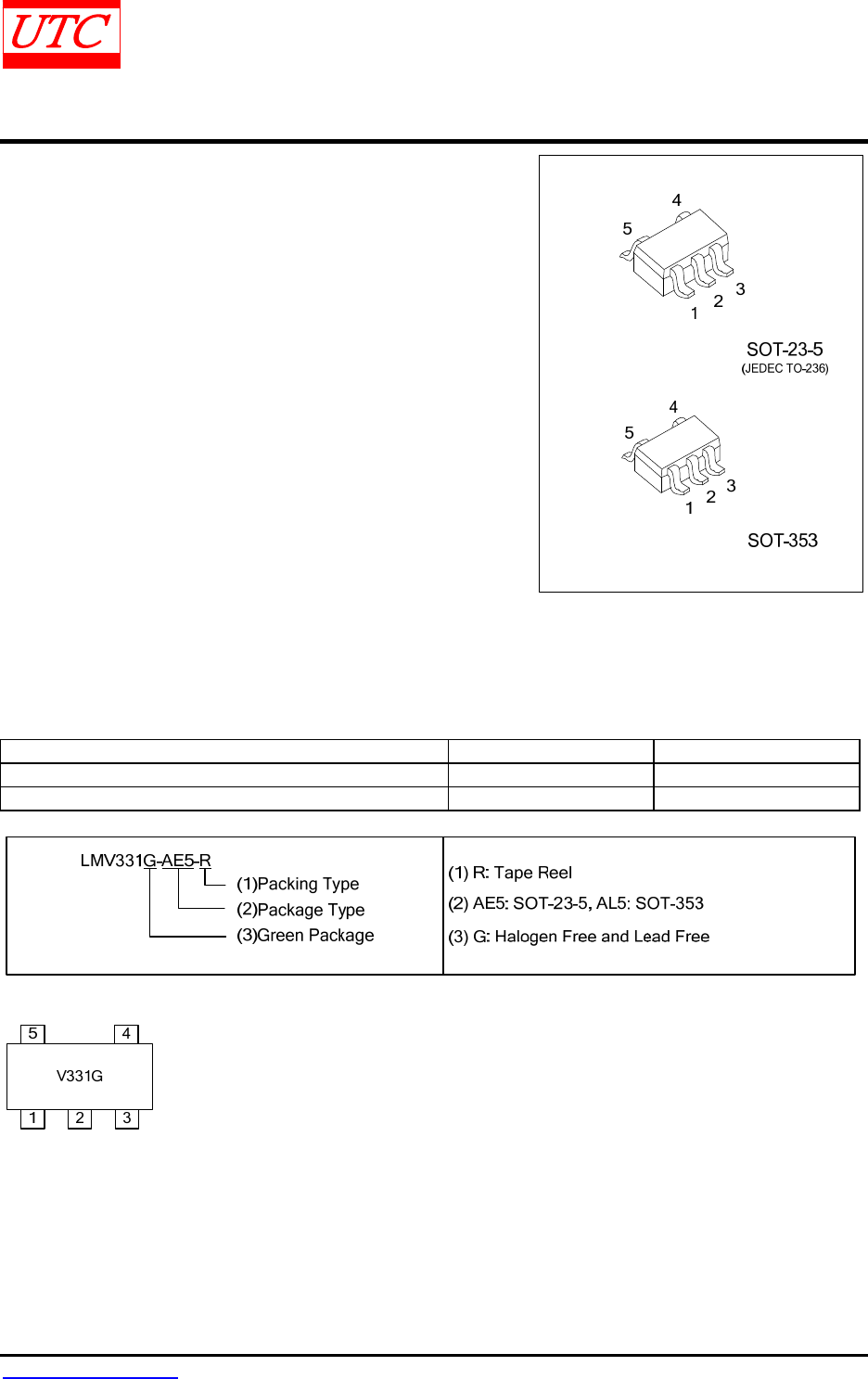
ORDERING INFORMATION
Ordering Number Package Packing
LMV331G-AE5-R SOT-23-5 Tape Reel
LMV331G-AL5-R SOT-353 Tape Reel
MARKING
LMV331 LINEAR INTEGRATED CIRCUIT
UNISONIC TECHNOLOGIES CO., LTD 2 of 6
www.unisonic.com.tw QW-R104-006.C
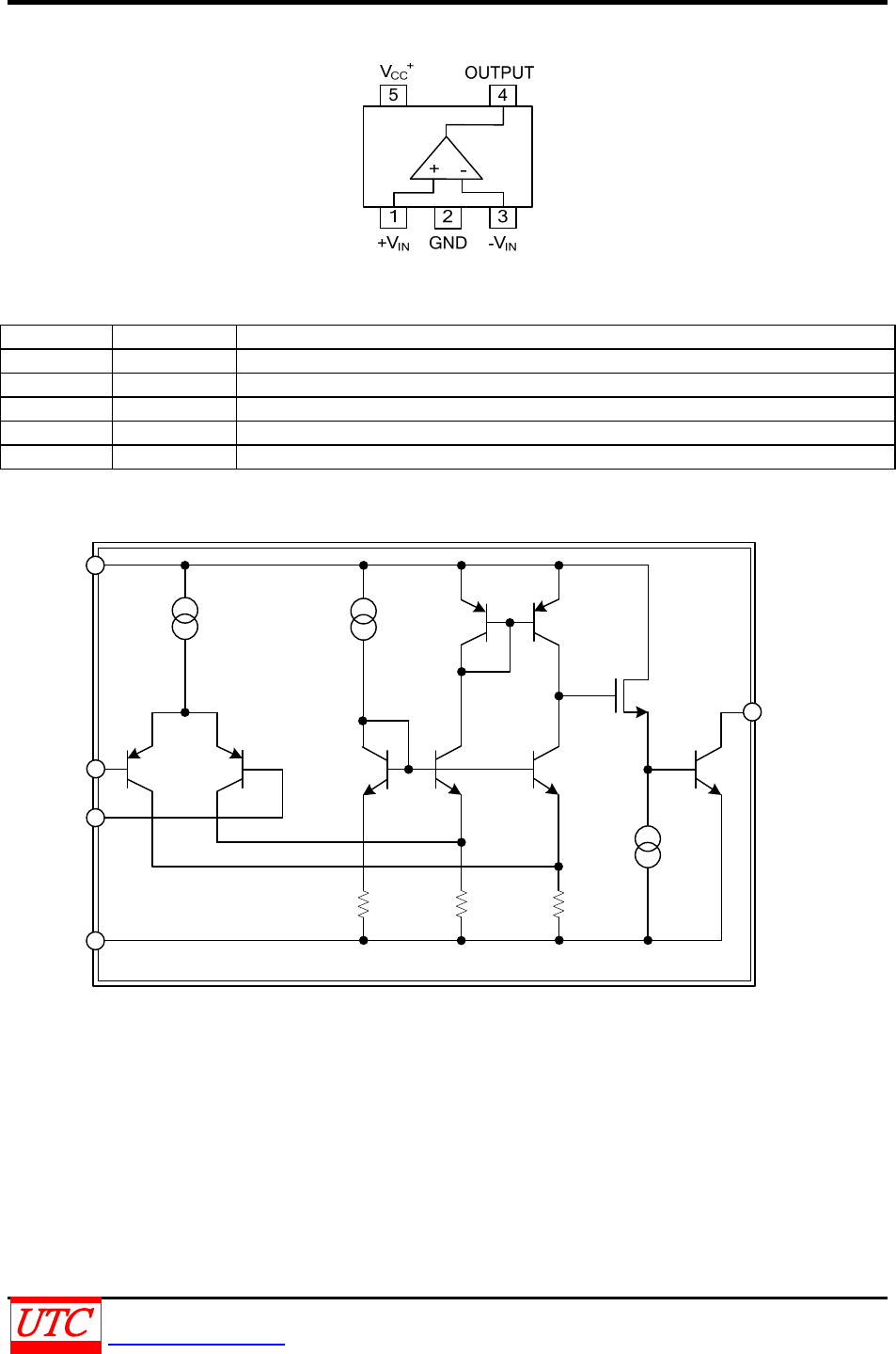
PIN CONFIGURATION
PIN DESCRIPTION
PIN NO. PIN NAME DESCRIPTION
1 +VIN Non-inverting input
2 GND Ground
3 +VIN inverting input
4 OUTPUT Output
5 VCC+ Power supply
BLOCK DIAGRAM
VCC
+
-VIN
OUTPUT
Q8
M1
R2 R1
R3
Q3
Q4
Q5
Q7
Q6
Q2Q1
GND
+VIN
LMV331 LINEAR INTEGRATED CIRCUIT
UNISONIC TECHNOLOGIES CO., LTD 3 of 6
www.unisonic.com.tw QW-R104-006.C
ABSOLUTE MAXIMUM RATING
PARAMETER SYMBOL RATINGS UNIT
Supply Voltage VCC 2.7~5.5 V
Differential Input Voltage VIN
(
DIFF
)
±VCC V
Voltage on Any Pin (Referred to GND pin) 5.5 V
Soldering Information Infrared or Convection (20 sec) 235 °C
Junction Temperature (Note 1) TJ 150 °C
Operating Temperature TOPR -40~+85 °C
Storage Temperature TSTG -65~+150 °C
Note: Absolute maximum ratings are those values beyond which the device could be permanently damaged.
Absolute maximum ratings are stress ratings only and functional device operation is not implied.
THERMAL CHARACTERISTICS (Note1)
PARAMETER SYMBOL RATINGS UNIT
Junction to Ambient SOT-23-5 θJA 265 °C/W
SOT-353 350 °C/W
2.7V DC ELECTRICAL CHARACTERISTICS
(All limits guaranteed for TJ=25˚C, V+=2.7V, V−=0V, unless otherwise specified. Boldface limits apply at the
temperature extremes.)
PARAMETER SYMBOL TEST CONDITIONS MIN
TYP
(Note 2)
MAX
(Note 3) UNIT
Input Offset Voltage VOS 1.7 7 mV
Input Offset Voltage Average Drift TCVOS 5 µV/˚C
Input Bias Current IB 10 250 nA
Input Offset Current IOS 5 50 nA
Input Voltage Range VCM -0.1 V
2.0 V
Saturation Voltage VSAT I
sink≤1mA 200 mV
Output Sink Current IO V
O≤1.5V 5 23 mA
Supply Current IS 40 100 µA
Output Leakage Current 0.003 1 µA
2.7V AC ELECTRICAL CHARACTERISTICS (TJ=25˚C, V+=2.7V, RL=5.1kΩ, V−=0V.)
PARAMETER SYMBOL TEST CONDITIONS MIN
TYP
(Note 2) MAX UNIT
Propagation Delay (High to Low) tPHL Input Overdrive=10mV 1000 ns
Input Overdrive=100mV 350 ns
Propagation Delay (Low to High) tPLH Input Overdrive=10mV 500 ns
Input Overdrive=100mV 400 ns
LMV331 LINEAR INTEGRATED CIRCUIT
UNISONIC TECHNOLOGIES CO., LTD 4 of 6
www.unisonic.com.tw QW-R104-006.C
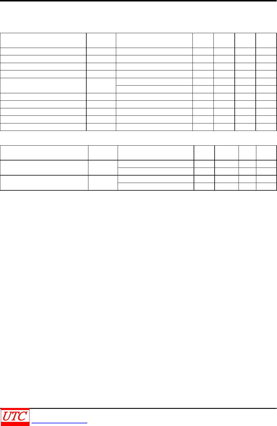
5V DC ELECTRICAL CHARACTERISTICS
(All limits guaranteed for TJ=25˚C, V+=5V, V−=0V, Unless otherwise specified. Boldface limits apply at the
temperature extremes.)
PARAMETER SYMBOL TEST CONDITIONS MIN
TYP
(Note 2)
MAX
(Note 3) UNIT
Input Offset Voltage VOS 1.7 7 mV
Input Offset Voltage Average Drift TCVOS 5 µV/˚C
Input Bias Current IB 25 250 nA
Input Offset Current IOS 2 50 nA
Input Voltage Range VCM -0.1 V
4.2 V
Voltage Gain AV 20 50 V/mV
Saturation Voltage VSAT I
sink≤4mA 200 400 mV
Output Sink Current IO V
O≤1.5V 10 84 mA
Supply Current IS 60 120 µA
Output Leakage Current 0.003 1 µA
5V AC ELECTRICAL CHARACTERISTICS (TJ=25˚C, V+=5V, RL=5.1kΩ, V−=0V.)
PARAMETER SYMBOL TEST CONDITIONS MIN TYP
(Note 2) MAX UNIT
Propagation Delay (High to Low) tPHL Input Overdrive=10mV 600 ns
Input Overdrive=100mV 200 ns
Propagation Delay (Low to High) tPLH Input Overdrive=10mV 450 ns
Input Overdrive=100mV 300 ns
Notes: 1. The maximum power dissipation is a function of TJ(max), θJA, and TA. The maximum allowable power
dissipation at any ambient temperature is PD=(TJ(max)-TA)/θJA. All numbers apply for packages soldered
directly into a PC board.
2. Typical Values represent the most likely parametric norm.
3. All limits are guaranteed by testing or statistical analysis.
LMV331 LINEAR INTEGRATED CIRCUIT
UNISONIC TECHNOLOGIES CO., LTD 5 of 6
www.unisonic.com.tw QW-R104-006.C
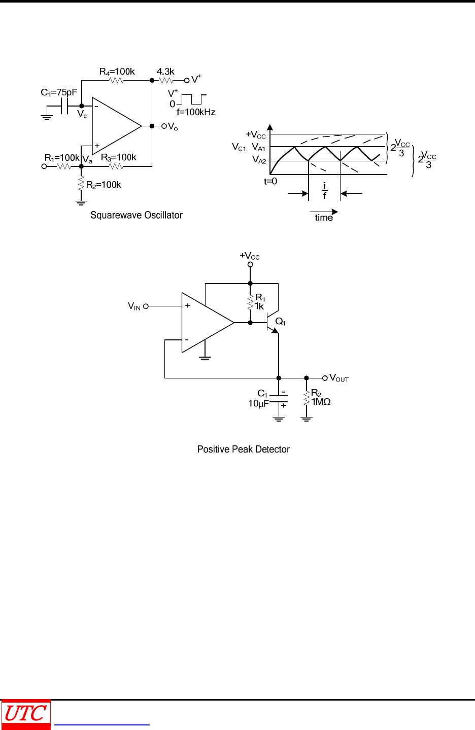
TYPICAL APPLICATION CIRCUIT

LMV331 LINEAR INTEGRATED CIRCUIT
UNISONIC TECHNOLOGIES CO., LTD 6 of 6
www.unisonic.com.tw QW-R104-006.C
UTC assumes no responsibility for equipment failures that result from using products at values that
exceed, even momentarily, rated values (such as maximum ratings, operating condition ranges, or
other parameters) listed in products specifications of any and all UTC products described or contained
herein. UTC products are not designed for use in life support appliances, devices or systems where
malfunction of these products can be reasonably expected to result in personal injury. Reproduction in
whole or in part is prohibited without the prior written consent of the copyright owner. The information
presented in this document does not form part of any quotation or contract, is believed to be accurate
and reliable and may be changed without notice.