LPC H2129 HEADER BOARD FOR LPC2129 ARM MICROCONTROLLER
User Manual: olimex -
Open the PDF directly: View PDF ![]() .
.
Page Count: 3
LPC-H2129 HEADER BOARD FOR
LPC2129 ARM7TDMI-S MICROCONTROLLER
Features:
• MCU: LPC2129 16/32 bit ARM7TDMI-S™
with 256K Bytes Program Flash, 16K Bytes
RAM, RTC, 4x 10 bit ADC 2.44 uS, 2x
UART, 2x CAN, I2C, SPI, 2x 32bit
TIMERS, 7x CCR, 6x PWM, WDT, 5V
tolerant I/O, up to 60MHz operation
• standard JTAG connector with ARM 2x10
pin layout for programming/debugging with
ARM-JTAG
• two on board voltage regulators 1.8V and
3.3V with up to 800mA current
• single power supply: +5VDC required
• power supply status LED
• power supply filtering capacitor
• RESET circuit with external control of
Philips ISP utility via RS232
• RESET button
• DBG jumper for JTAG enable
• BSL jumper for Bootloader enable
• JRST jumper for enable/disable external
RESET control by RS232
• 10 Mhz crystal
• extension headers for all uC ports
• PCB: FR-4, 1.5 mm (0,062"), green
soldermask, white silkscreen component
print
• Dimensions: 76x55 mm (3.0x2.2")
• space between the pin rows: 48.26 mm
(1.9")
Supported devices:
Philips Semiconductors Inc. LPC2129 16/32 bit
ARM7TDMI-S™
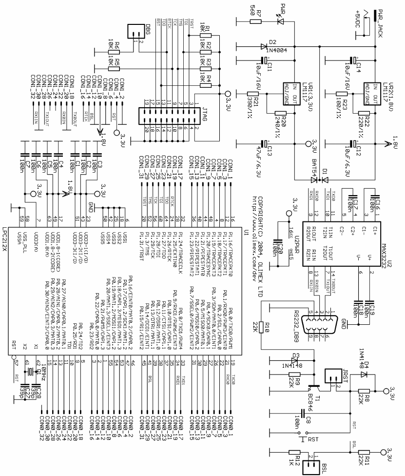
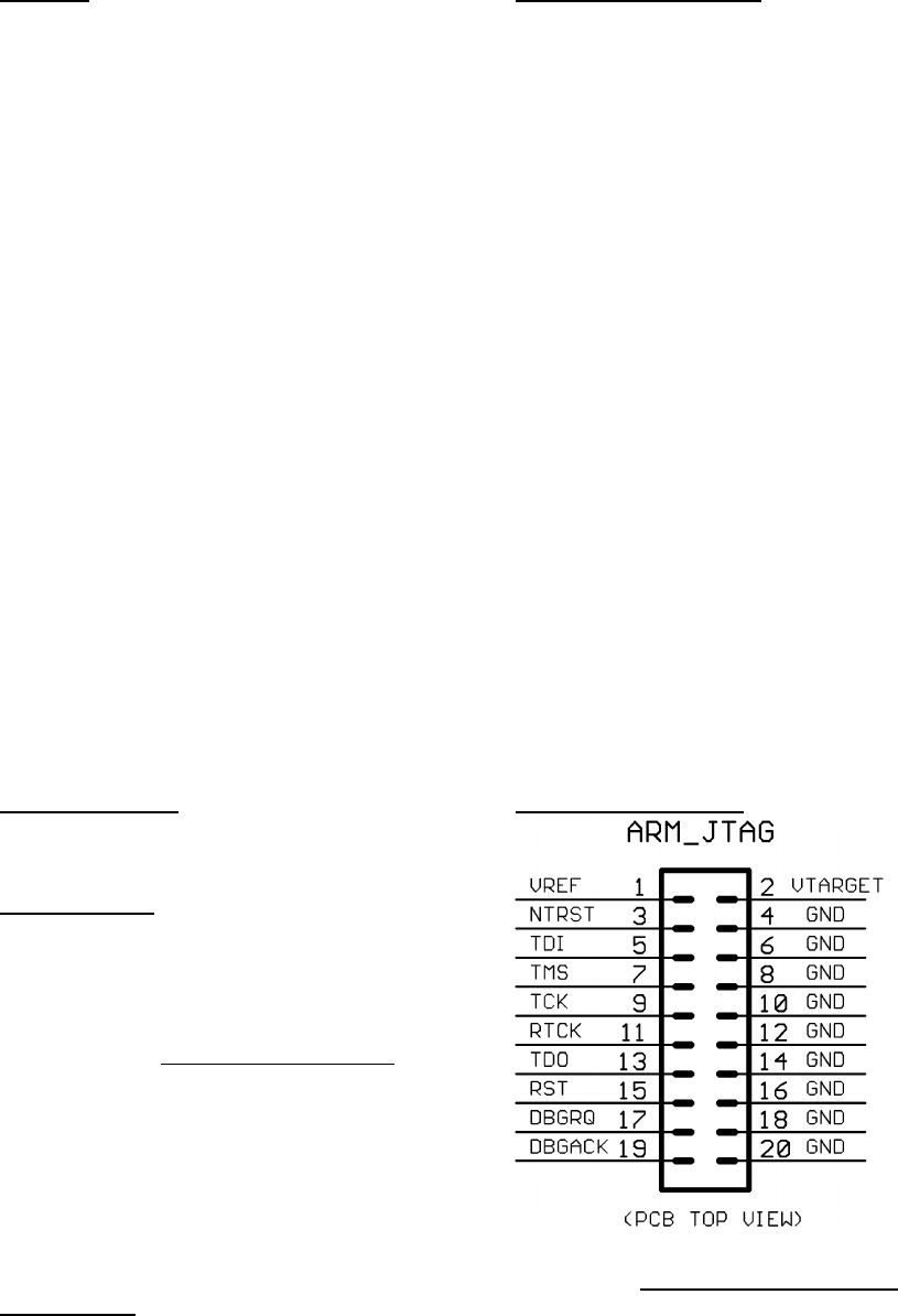
JTAG interface:
The JTAG connector is 2x10 pin with 0,1" step
and ARM recommended JTAG layout. PIN.1 is
marked with square pad on bottom and arrow on
top.
Note: to enable JTAG interface DBG jumper
should be shorted at the time of POWER UP.
Important: when JTAG is enabled P1.16-P1.31
ports take their JTAG alternative function no
matter of PINSEL1 register value, so during
debugging with JTAG these ports are not
available for the user program.
JTAG signals description:
PIN.1 (VTREF) Target voltage sense. Used to
indicate the target’s operating voltage to the
debug tool.
PIN.2 (VTARGET) Target voltage. May be
used to supply power to the debug tool.
PIN.3 (nTRST) JTAG TAP reset, this signal
should be pulled up to Vcc in target board.
PIN4,6, 8, 10,12,14,16,18,20 Ground. The Gnd-
Signal-Gnd-Signal strategy implemented on the
20-way connection scheme improves noise
immunity on the target connect cable.
PIN.5 (TDI) JTAG serial data in, should be
pulled up to Vcc on target board.
PIN.7 (TMS) JTAG TAP Mode Select, should
be pulled up to Vcc on target board.
PIN.9 (TCK) JTAG clock.
PIN.11 (RTCK) JTAG re-timed clock.
Implemented on certain ASIC ARM
implementations the host ASIC may need to
synchronize external inputs (such as JTAG
inputs) with its own internal clock.
PIN.13 (TDO) JTAG serial data out.
PIN.15 (nSRST) Target system reset.
PIN.17 (DBGRQ) Asynchronous debug request.
DBGRQ allows an external signal to force the
ARM core into debug mode, should be pull
down to GND.
PIN.19 (DBGACK) Debug acknowledge signal.
The ARM core acknowledges debug-mode in
response to a DBGRQ input.
JTAG connector layout:
Copyright(c) 2004, OLIMEX Ltd., All rights reserved.
Development boards for ARM, AVR, MSP430 and PIC microcontrollers http://www.olimex.com/dev
Power supply:
Power supply is made with two LDO adjustable
voltage regulators LM1117. Input voltage should
be in range 5-9VDC. Watch out the polarity as
schematic have no input protection diode and
reversing the input power supply will be fatal for
LPC2124 microcontroller
RS232 interface:
LPC2129 have two RS232 channels. They both
are connected via MAX3232 IC and are
available for use with RS232 levels. Channel 0
with TXD0 and RXD0 is used by the Bootloader
program to program LPC2124 Flash memory
without external programmer. Channel 1 is
general purpose RS232 channel and may be used
by user program. Channel 0 signals are available
on SUB_D 9 pin connector.
RESET:
Reset circuit is made by simple external RC
group. There is possibility to apply RESET
externally via RS232 DTR signal (when JRST is
shorted this feature is enabled) or by the small
RESET pushbutton on the board.
Oscillator:
According to LPC2129 datasheets internal PLL
will work with external crystal in range 10-
25Mhz, however our test with 14.7456 Mhz
crystal show that JTAG communication doesn’t
work properly on devices with above 10Mhz
external crystal, so despite 14.7456Mhz crystal
allows very convenient communication values
we had to install 10Mhz crystal for this device.
This makes programming with Philips ISP utility
above 38400 bps impossible, but JTAG debugger
works without problems, switching crystal to
14.7456Mhz makes ISP programming possible at
higher speeds like 115Kbps but JTAG debugger
works unreliable.
Bootloader:
The Bootloader program is enabled when BSL
jumper is shorted at time of power up. In this
case Bootloader takes the program control and
user may download Flash memory with Philips
ISP programming utility. Note that if you want to
run code in Flash memory BSL jumper should be
open at time of power up, otherwise Bootloader
will stay in control and will not allow program in
Flash to run. The newer versions of Philips ISP
utility use DTR signal as RESET control, if you
want to use this feature jumper JRST should be
shorted otherwise leave it open. (we recommend
you when you use bootloader with Philips ISP
utility to close both BSL and JRST jumpers, and
when you run your code to leave these jumpers
open). ISP utility allows many programming
speeds to be choosen but with the 10Mhz crystal
it works only up to 38400 bps.
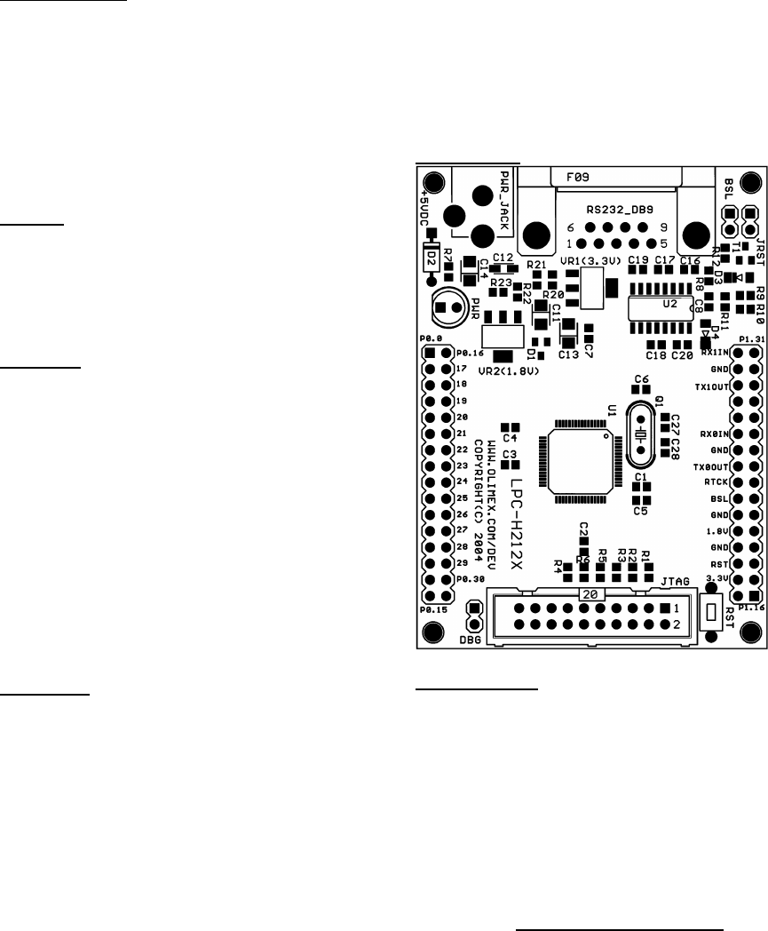
Board layout:
Ordering codes:
LPC-H2129 - assembled and tested with
LPC2129 microcontroller
Copyright(c) 2004, OLIMEX Ltd., All rights reserved.
Development boards for ARM, AVR, MSP430 and PIC microcontrollers http://www.olimex.com/dev