LT6106 Datasheet. Www.s Manuals.com. Linear
User Manual: Marking of electronic components, SMD Codes LT, LT-***, LTADY, LTAFT, LTAGN, LTAGP, LTB2, LTB3, LTCWK, LTCWY, LTCXB, LTDDQ, LTDWF, LTDWH, LTDWK, LTDWM, LTG6, LTH2, LTH7, LTJ, LTKX, LTP, LTPG, LTRD, LTUK, LTYD, LTYN. Datasheets 1SMB18AT3, LT1713CMS8, LT1713IMS8, LT1716, LT1933ES6, LT1933HS6, LT1933IS6, LT1937ES5, LT3465, LT3465A, LT6106, LT6202CS5, LT6203CMS8, LT6203IMS8, LTC1986ES6, LTC3401, LTC4054ES5-4.2, LTC4054XES5-4.2, LTC4151, LTC4151-1, LTC6246, LTC6247, P6SMB33A, PZU6.8B2A, RT9819A-36PV, SMBJ18A, TP
Open the PDF directly: View PDF ![]() .
.
Page Count: 13
LT6106
1
6106fa
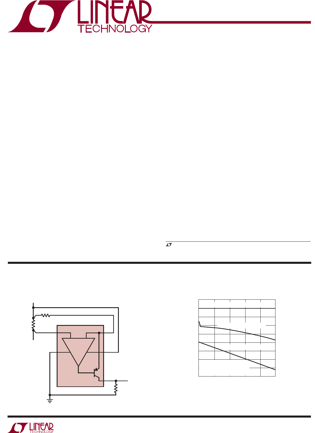
TYPICAL APPLICATION
FEATURES
APPLICATIONS
DESCRIPTION
36V Low Cost High Side
Current Sense in a SOT-23
The LT
®
6106 is a versatile high side current sense ampli-
fi er. Design fl exibility is provided by the excellent device
characteristics: 250μV maximum offset and 40nA maxi-
mum input bias current. Gain for each device is set by two
resistors and allows for accuracy better than 1%.
The LT6106 monitors current via the voltage across an
external sense resistor (shunt resistor). Internal circuitry
converts input voltage to output current, allowing for a
small sense signal on a high common mode voltage to
be translated into a ground referenced signal. The low DC
offset allows for monitoring very small sense voltages. As
a result, a small valued shunt resistor can be used, which
minimizes the power loss in the shunt.
The wide 2.7V to 44V input voltage range, high accuracy
and wide operating temperature range make the LT6106
ideal for automotive, industrial and power management
applications. The very low power supply current of the
LT6106 also makes it suitable for low power and battery
operated applications.
■ Gain Confi gurable with Two Resistors
■ Low Offset Voltage: 250μV Maximum
■ Output Current: 1mA Maximum
■ Supply Range: 2.7V to 36V, 44V Absolute Maximum
■ Low Input Bias Current: 40nA Maximum
■ PSRR: 106dB Minimum
■ Low Supply Current: 65μA Typical, V+ = 12V
■ Operating Temperature Range: –40°C to 125°C
■ Low Profi le (1mm) ThinSOT
TM
Package
■ Current Shunt Measurement
■ Battery Monitoring
■ Power Management
■ Motor Control
■ Lamp Monitoring
■ Overcurrent and Fault Detection
LT6106
1k
VOUT
200mV/A
6106 TA01a
100Ω
3V TO 36V
LOAD
0.02Ω
–
+
V+
V–
OUT
–IN+IN
3V to 36V, 5A Current Sense with AV = 10
, LT, LTC and LTM are registered trademarks of Linear Technology Corporation.
ThinSOT is a trademark of Linear Technology Corporation. All other trademarks are the
property of their respective owners.
Measurement Accuracy vs Load Current
LOAD CURRENT (A)
0
–1.2
ACCURACY (% OF FULL SCALE)
–1.0
–0.6
–0.4
–0.2
245
0.6
6106 TA01b
–0.8
13
0
0.2
0.4 LIMIT OVER TEMPERATURE
LIMIT OVER TEMPERATURE
TYPICAL PART AT TA = 25°C
5A FULL SCALE
RSENSE = 0.02Ω
AV = 10
RIN = 100Ω
ROUT = 1k
V+ = 3V
LT6106
2
6106fa
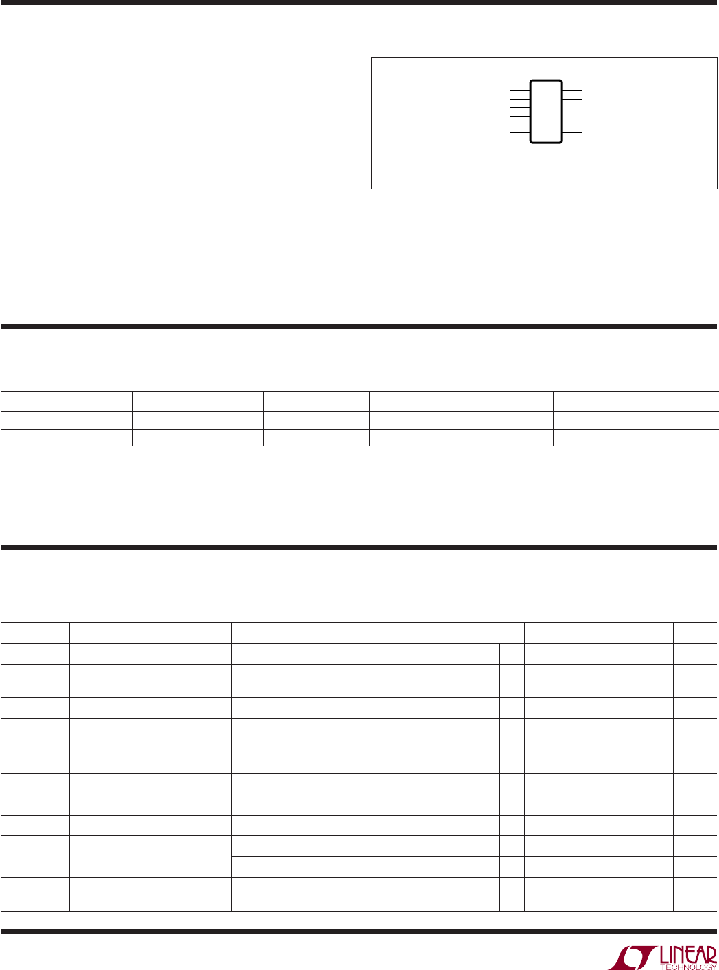
PIN CONFIGURATIONABSOLUTE MAXIMUM RATINGS
Supply Voltage (V+ to V–)..........................................44V
Input Voltage (+IN to V–) ............................................ V+
(–IN to V–) ............................................ V+
Input Current ........................................................–10mA
Output Short-Circuit Duration .......................... Indefi nite
Operating Temperature Range (Note 4)
LT6106C ............................................... –40°C to 85°C
LT6106H ............................................ –40°C to 125°C
Specifi ed Temperature Range (Note 4)
LT6106C ................................................... 0°C to 70°C
LT6106H ............................................ –40°C to 125°C
Storage Temperature Range ................... –65°C to 150°C
Lead Temperature (Soldering, 10 sec) .................. 300°C
(Note 1)
OUT 1
V– 2
TOP VIEW
S5 PACKAGE
5-LEAD PLASTIC TSOT-23
–IN 3
5 V+
4 +IN
TJMAX = 150°C, θJA = 250°C/W
ORDER INFORMATION
ELECTRICAL CHARACTERISTICS
SYMBOL PARAMETER CONDITIONS MIN TYP MAX UNITS
V+Supply Voltage Range ●2.7 36 V
VOS Input Offset Voltage VSENSE = 5mV
●
150 250
350
μV
μV
ΔVOS/ΔT Input Offset Voltage Drift VSENSE = 5mV ●1μV/°C
IBInput Bias Current (+IN) V+ = 12V, 36V
●
40
65
nA
nA
IOS Input Offset Current V+ = 12V, 36V 1 nA
IOUT Maximum Output Current (Note 2) ●1mA
PSRR Power Supply Rejection Ratio V+ = 2.7V to 36V, VSENSE = 5mV ●106 dB
VSENSE(MAX) Input Sense Voltage Full Scale RIN = 500Ω (Notes 2, 7) ●0.5 V
AV Error Gain Error (Note 3) VSENSE = 500mV, RIN = 500Ω, ROUT = 10k, V+ = 12.5V ●–0.65 –0.25 0 %
VSENSE = 500mV, RIN = 500Ω, ROUT = 10k, V+ = 36V ●–0.45 –0.14 0.1 %
VOUT(HIGH) Output Swing High
(Referred to V+)
VSENSE = 120mV
●
1.2
1.4
V
V
The ● denotes the specifi cations which apply over the full specifi ed
operating temperature range, otherwise specifi cations are at TA = 25°C. V+ = 12V, V+ = VSENSE+, RIN = 100Ω, ROUT = 10k, Gain = 100
unless otherwise noted. (Note 6)
Lead Free Finish
TAPE AND REEL (MINI) TAPE AND REEL PART MARKING* PACKAGE DESCRIPTION TEMPERATURE RANGE
LT6106CS5#TRMPBF LT6106CS5#TRPBF LTCWK 5-Lead Plastic TSOT-23 0°C to 70°C
LT6106HS5#TRMPBF LT6106HS5#TRPBF LTCWK 5-Lead Plastic TSOT-23 –40°C to 125°C
TRM = 500 pieces. *Temperature grades are identifi ed by a label on the shipping container.
Consult LTC Marketing for parts specifi ed with wider operating temperature ranges.
Consult LTC Marketing for information on lead based fi nish parts.
For more information on lead free part marking, go to: http://www.linear.com/leadfree/
For more information on tape and reel specifi cations, go to: http://www.linear.com/tapeandreel/
LT6106
3
6106fa
Note 1: Stresses beyond those listed under Absolute Maximum Ratings
may cause permanent damage to the device. Exposure to any Absolute
Maximum Rating condition for extended periods may affect device
reliability and lifetime. In addition to the Absolute Maximum Ratings, the
output current of the LT6106 must be limited to insure that the power
dissipation in the LT6106 does not allow the die temperature to exceed
150°C. See the applications information section “Power Dissipation
Considerations” for further information.
Note 2: Guaranteed by the gain error test.
Note 3: Gain error refers to the contribution of the LT6106 internal circuitry
and does not include errors in the external gain setting resistors.
Note 4: The LT6106C is guaranteed functional over the operating
temperature range of –40°C to 85°C. The LT6106C is designed,
ELECTRICAL CHARACTERISTICS
The ● denotes the specifi cations which apply over the full specifi ed
operating temperature range, otherwise specifi cations are at TA = 25°C. V+ = 12V, V+ = VSENSE+, RIN = 100Ω, ROUT = 10k, Gain = 100
unless otherwise noted.
SYMBOL PARAMETER CONDITIONS MIN TYP MAX UNITS
Minimum Output Voltage
(Note 5)
VSENSE = 0mV, RIN = 100Ω, ROUT = 10k
●
12 45
65
mV
mV
VSENSE = 0mV, RIN = 500Ω, ROUT = 10k, V+ = 12V, 36V
●
716
22
mV
mV
BW Signal Bandwidth (–3dB) IOUT = 1mA, RIN = 100Ω, ROUT = 5k 200 kHz
trInput Step Response (to 50% of
Output Step)
ΔVSENSE = 100mV Step, RIN = 100Ω, ROUT = 5k,
Rising Edge
3.5 μs
ISSupply Current V+ = 2.7V, IOUT = 0μA, (VSENSE = –5mV)
●
60 85
115
μA
V+ = 12V, IOUT = 0μA, (VSENSE = –5mV)
●
65 95
120
μA
V+ = 36V, IOUT = 0μA, (VSENSE = –5mV)
●
70 100
130
μA
characterized and expected to meet specifi ed performance from –40°C to
85°C but is not tested or QA sampled at these temperatures. The LT6106H
is guaranteed to meet specifi ed performance from –40°C to 125°C.
Note 5: The LT6106 output is an open collector current source. The
minimum output voltage scales directly with the ratio ROUT/10k.
Note 6: VSENSE+ is the voltage at the high side of the sense resistor,
RSENSE. See Figure 1.
Note 7: VSENSE (MAX) is the maximum sense voltage for which the Electrical
Characteristics will apply. Higher voltages can affect performance but will
not damage the part provided that the output current of the LT6106 does
not exceed the allowable power dissipation as described in Note 1.
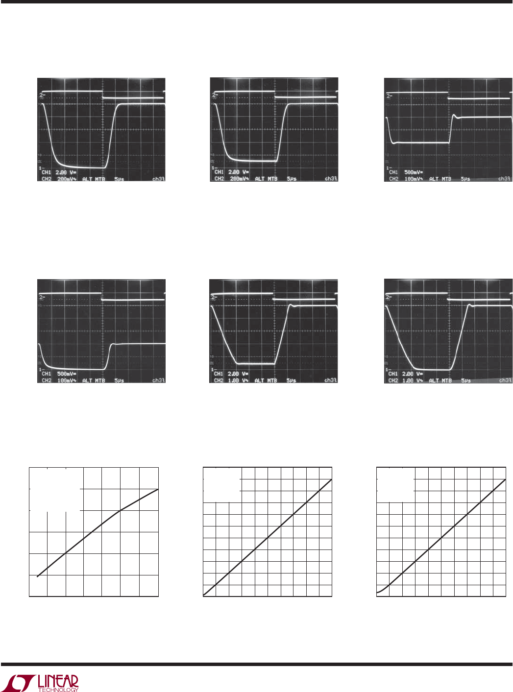
TYPICAL PERFORMANCE CHARACTERISTICS
Input Offset Voltage vs
Temperature
TEMPERATURE (°C)
–55
INPUT OFFSET VOLTAGE (μV)
0
200
125
6106 G03
–200
–400 –25 5 35 65 95
400
–100
100
–300
300
VSENSE = 5mV
V+ = 12V
RIN = 100Ω
ROUT = 10k
AV = 100
TYPICAL UNITS
INPUT OFFSET VOLTAGE (μV)
–200
PERCENT OF UNITS (%)
10
12
16
120
6106 G23
4
8
14
6
2
0–120 –40 0 40 200
V+ = 12V
VSENSE = 5mV
RIN = 100Ω
ROUT = 10k
1068 UNITS
VOS Distribution
SUPPLY VOLTAGE (V)
0
CHANGE IN INPUT OFFSET VOLTAGE (μV)
10
40
50
40
6106 G02
0
–10
–70 10 20 30
515 25 35
–30
70
60
30
20
–20
–40
–50
–60
VSENSE = 5mV
RIN = 100Ω
ROUT = 10k
TYPICAL UNITS
Input Offset Voltage vs
Supply Voltage
LT6106
4
6106fa
TYPICAL PERFORMANCE CHARACTERISTICS
Gain vs Frequency
Step Response 0mV to 10mV
(RIN = 100Ω)
Step Response 10mV to 20mV
(RIN = 100Ω)
Gain vs Frequency
Input Bias Current vs Supply
Voltage
Power Supply Rejection Ratio
vs Frequency
TEMPERATURE (°C)
–45
GAIN ERROR (%)
–0.30
–0.20
–0.10
0
35
6106 G04
–0.40
–0.50
–0.35
–0.25
–0.15
–0.05
–0.45
–0.55
–0.60 –25 –5 15 55 75 95 115 130
VOUT = 1V
IOUT = 1mA
ROUT = 1k
TYPICAL UNIT
V+ = 36V
V+ = 12V
V+ = 5V
V+ = 2.7V
SUPPLY VOLTAGE (V)
0
INPUT BIAS CURRENT (nA)
16
18
20
40
6106 G05
14
12
15
17
19
13
11
10 105 2015 30 35 45
25 50
TA = –40°C
TA = 25°C
TA = 70°C
TA = 125°C
VSENSE = 5mV
RIN = 100Ω
FREQUENCY (Hz)
20
POWER SUPPLY REJECTION RATIO (dB)
40
60
80
100
100 10k 100k 1M
6106 G06
0
1k
120
10
30
50
70
90
110
VOUT = 2.5V
VOUT = 5V
VOUT = 10V
V+ = 12.5V
AV = 20
RIN = 500Ω
ROUT = 10k
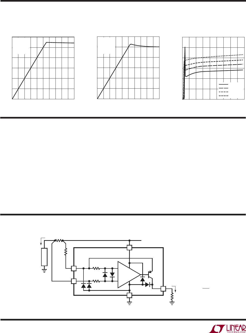
Power Supply Rejection Ratio
vs Frequency
FREQUENCY (Hz)
20
POWER SUPPLY REJECTION RATIO (dB)
40
60
80
100
100 10k 100k 1M
6106 G08
0
1k
120
10
30
50
70
90
110
VOUT = 0.5V
VOUT = 1V
VOUT = 2V
V+ = 12.5V
AV = 20
RIN = 100Ω
ROUT = 2k
FREQUENCY (Hz)
10
GAIN (dB)
40
45
5
0
35
20
30
25
15
1k 100k 1M 10M
6106 G09
–30
–25
–20
–15
–10
–5
10k
V+ = 12.5V
AV = 100
RIN = 100Ω
ROUT = 10k
VOUT = 10V
VOUT = 2.5V
VSENSE
20mV/DIV
VOUT
500mV/DIV
0V
5μs/DIVAV = 100
VOUT = 0V TO 1V
ROUT = 10k
V+ = 12V
6106 G1
VSENSE
20mV/DIV
VOUT
500mV/DIV
0V
5μs/DIVAV = 100
VOUT = 1V TO 2V
ROUT = 10k
V+ = 12V
6106 G1
FREQUENCY (Hz)
10
GAIN (dB)
40
45
5
0
35
20
30
25
15
1k 100k 1M 10M
6106 G14
–30
–25
–20
–15
–10
–5
10k
V+ = 12.5V
AV = 20
RIN = 500Ω
ROUT = 10k
VOUT = 10V
VOUT = 2.5V
Gain Error vs Temperature
Gain Error Distribution
GAIN ERROR (%)
–0.60
0
PERCENT OF UNITS (%)
4
2
8
6
10
24
20
–0.48 –0.36
22
18
16
14
12
–0.24 –0.12
0
6106 G24
V+ = 12.5V
VSENSE = 500mV
RIN = 500Ω
ROUT = 10k
11,072 UNITS
TA = 25°C
LT6106
5
6106fa
Output Voltage Swing vs
Temperature
Step Response 0mV to 100mV
(RIN = 100Ω)
TYPICAL PERFORMANCE CHARACTERISTICS
Step Response 0mV to 50mV
(RIN = 500Ω)
Step Response 50mV to 500mV
(RIN = 500Ω)
Output Voltage vs Input Sense
Voltage (0mV ≤ VSENSE ≤ 10mV)
Step Response 10mV to 100mV
(RIN = 100Ω)
Step Response 50mV to 100mV
(RIN = 500Ω)
TEMPERATURE (°C)
–50
OUTPUT VOLTAGE (V)
11.00
11.05
11.10
25 75
6106 G07
10.95
10.90
–25 0 50 100 125
10.85
10.80
V+ = 12V
AV = 100
RIN = 100Ω
ROUT = 10k
VSENSE = 120mV
VSENSE
200mV/DIV
VOUT
2V/DIV
0V
5μs/DIVAV = 100
VOUT = 0V TO 10V
ROUT = 10k
V+ = 12V
6106 G1
VSENSE
200mV/DIV
VOUT
2V/DIV
0V
5μs/DIVAV = 100
VOUT = 1V TO 10V
ROUT = 10k
V+ = 12V
6106 G1
VSENSE
100mV/DIV
VOUT
500mV/DIV
0V
5μs/DIVAV = 20
VOUT = 1V TO 2V
ROUT = 10k
V+ = 12V
6106 G1
5
VSENSE
100mV/DIV
VOUT
500mV/DIV
0V
5μs/DIVAV = 20
VOUT = 0V TO 1V
ROUT = 10k
V+ = 12V
6106 G1
6
VSENSE
1V/DIV
VOUT
2V/DIV
0V
5μs/DIVAV = 20
VOUT = 1V TO 10V
ROUT = 10k
V+ = 12V
6106 G1
7
Step Response 0mV to 500mV
(RIN = 500Ω)
VSENSE
1V/DIV
VOUT
2V/DIV
0V
5μs/DIVAV = 20
VOUT = 0V TO 10V
ROUT = 10k
V+ = 12V
6106 G1
8
VSENSE (mV)
0
VOUT (mV)
600
800
1100
1000
89
6106 G19
400
200
500
700
900
300
100
0246
135710
V+ = 12V
AV = 100
RIN = 100Ω
ROUT = 10k
Output Voltage vs Input Sense
Voltage (0mV ≤ VSENSE ≤ 10mV)
VSENSE (mV)
0
VOUT (mV)
120
160
220
200
89
6106 G20
80
40
100
140
180
60
20
0246
135710
V+ = 12V
AV = 20
RIN = 500Ω
ROUT = 10k
LT6106
6
6106fa
BLOCK DIAGRAM
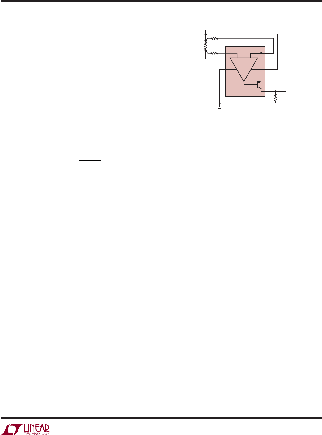
PIN FUNCTIONS
OUT (Pin 1):
Current Output. OUT will source a current
that is proportional to the sense voltage into an external
resistor.
V– (Pin 2):
Normally Connected to Ground.
–IN (Pin 3):
The internal sense amplifi er will drive –IN to
the same potential as +IN. A resistor (RIN) tied from V+
to –IN
sets the output current IOUT
= VSENSE/RIN. VSENSE
is the voltage developed across RSENSE.
+IN (Pin 4):
Must be tied to the system load end of the
sense resistor, either directly or through a resistor.
V+ (Pin 5):
Positive Supply Pin. The V+ pin should be con-
nected directly to either side of the sense resistor, RSENSE.
Supply current is drawn through this pin. The circuit may
be confi gured so that the LT6106 supply current is or is
not monitored along with the system load current. To
monitor only the system load current, connect
V+
to the
more positive side of the sense resistor. To monitor the
total current, including that of the LT6106, connect
V+
to
the more negative side of the sense resistor.
–
+
V+
V–OUT
6106 F01
VBATTERY
IOUT
VSENSE
RSENSE
ILOAD
ROUT
–
+
L
O
A
D
VOUT = VSENSE • ROUT
RIN
14k
14k
–IN
+IN
5
2
1
3
4
RIN
Figure 1. LT6106 Block Diagram and Typical Connection
TYPICAL PERFORMANCE CHARACTERISTICS
VSENSE (mV)
0
VOUT (V)
4
8
12
2
6
10
40 80 120 160
6106 G21
200200 60 100 140 180
V+ = 12V
AV = 100
RIN = 100Ω
ROUT = 10k
VSENSE (mV)
0
VOUT (V)
4
8
12
2
6
10
200 400 600 800
6106 G22
10001000 300 500 700 900
V+ = 12V
AV = 20
RIN = 500Ω
ROUT = 10k
Supply Current vs Supply Voltage
SUPPLY VOLTAGE (V)
0
0
SUPPLY CURRENT (μA)
20
60
80
100
10 20 25 45
6106 G01
40
515 30 35 40
120
TA = –40°C
TA = 25°C
TA = 70°C
TA = 125°C
Output Voltage vs Input Sense
Voltage (0mV ≤ VSENSE ≤ 1V)
Output Voltage vs Input Sense
Voltage (0mV ≤ VSENSE ≤ 200mV)
LT6106
7
6106fa
APPLICATIONS INFORMATION
Introduction
The LT6106 high side current sense amplifi er (Figure 1) pro-
vides accurate monitoring of current through a user-selected
sense resistor. The sense voltage is amplifi ed by a user-
selected gain and level shifted from the positive power sup-
ply to a ground-referred output. The output signal is analog
and may be used as is, or processed with an output fi lter.
Theory of Operation
An internal sense amplifi er loop forces –IN to have the
same potential as +IN. Connecting an external resistor,
RIN, between –IN and V+ forces a potential across RIN
that is the same as the sense voltage across RSENSE. A
corresponding current, VSENSE/RIN, will fl ow through RIN.
The high impedance inputs of the sense amplifi er will not
conduct this current, so it will fl ow through an internal
PNP to the output pin as IOUT
.
The output current can be transformed into a voltage by
adding a resistor from OUT to V–. The output voltage is
then VO = V–
+ IOUT • ROUT
.
Table 1. Useful Gain Confi gurations
GAIN RIN ROUT VSENSE at VOUT = 5V IOUT at VOUT = 5V
20 499Ω 10k 250mV 500μA
50 200Ω 10k 100mV 500μA
100 100Ω 10k 50mV 500μA
GAIN RIN ROUT VSENSE at VOUT = 2.5V IOUT at VOUT = 2.5V
20 249Ω 5k 125mV 500μA
50 100Ω 5k 50mV 500μA
100 50Ω 5k 25mV 500μA
Selection of External Current Sense Resistor
The external sense resistor, RSENSE, has a signifi cant ef-
fect on the function of a current sensing system and must
be chosen with care.
First, the power dissipation in the resistor should be con-
sidered. The system load current will cause both heat and
voltage loss in RSENSE. As a result, the sense resistor
should be as small as possible while still providing the
input dynamic range required by the measurement. Note
that input dynamic range is the difference between the
maximum input signal and the minimum accurately mea-
sured signal, and is limited primarily by input DC offset of
the internal amplifi er of the LT6106. In addition, RSENSE
must be small enough that VSENSE does not exceed the
maximum input voltage specifi ed by the LT6106, even un-
der peak load conditions. As an example, an application
may require that the maximum sense voltage be 100mV.
If this application is expected to draw 2A at peak load,
RSENSE should be no more than 50mΩ.
Once the maximum RSENSE value is determined, the mini-
mum sense resistor value will be set by the resolution or
dynamic range required. The minimum signal that can be
accurately represented by this sense amplifi er is limited by
the input offset. As an example, the LT6106 has a typical
input offset of 150μV. If the minimum current is 20mA, a
sense resistor of 7.5mΩ will set VSENSE to 150μV. This is
the same value as the input offset. A larger sense resis-
tor will reduce the error due to offset by increasing the
sense voltage for a given load current. Choosing a 50mΩ
RSENSE will maximize the dynamic range and provide a
system that has 100mV across the sense resistor at peak
load (2A), while input offset causes an error equivalent to
only 3mA of load current. Peak dissipation is 200mW. If a
5mΩ sense resistor is employed, then the effective current
error is 30mA, while the peak sense voltage is reduced to
10mV at 2A, dissipating only 20mW.
The low offset and corresponding large dynamic range of
the LT6106 make it more fl exible than other solutions in
this respect. The 150μV typical offset gives 60dB of dy-
namic range for a sense voltage that is limited to 150mV
maximum, and over 70dB of dynamic range if the rated
input maximum of 0.5V is allowed.
Sense Resistor Connection
Kelvin connection of the –IN and +IN inputs to the sense
resistor should be used in all but the lowest power appli-
cations. Solder connections and PC board interconnec-
tions that carry high current can cause signifi cant error
in measurement due to their relatively large resistances.
One 10mm × 10mm square trace of one-ounce copper is
approximately 0.5mΩ. A 1mV error can be caused by as
little as 2A fl owing through this small interconnect. This
will cause a 1% error in a 100mV signal. A 10A load cur-
rent in the same interconnect will cause a 5% error for the
same 100mV signal. By isolating the sense traces from the
high current paths, this error can be reduced by orders of
LT6106
8
6106fa
APPLICATIONS INFORMATION
magnitude. A sense resistor with integrated Kelvin sense
terminals will give the best results. Figure 2 illustrates the
recommended method.
This approach can be helpful in cases where occasional
bursts of high currents can be ignored.
Care should be taken when designing the board layout for
RIN, especially for small RIN values. All trace and inter-
connect resistances will increase the effective RIN value,
causing a gain error.
Selection of External Output Resistor, ROUT
The output resistor, ROUT
, determines how the output cur-
rent is converted to voltage. VOUT is simply IOUT • ROUT
.
In choosing an output resistor, the maximum output volt-
age must fi rst be considered. If the following circuit is a
buffer or ADC with limited input range, then ROUT must be
chosen so that IOUT(MAX) • ROUT is less than the allowed
maximum input range of this circuit.
In addition, the output impedance is determined by ROUT
. If
the circuit to be driven has high enough input impedance,
then almost any useful output impedance will be accept-
able. However, if the driven circuit has relatively low input
impedance, or draws spikes of current such as an ADC
might do, then a lower ROUT value may be required in order
to preserve the accuracy of the output. As an example, if
the input impedance of the driven circuit is 100 times ROUT
,
then the accuracy of VOUT will be reduced by 1% since:
VIRR
RR
OUT OUT
OUT IN DRIVEN
OUT IN DRIVEN
=+
=
••()
()
IIR IR
OUT OUT OUT OUT
•• .••
100
101 099=
Error Sources
The current sense system uses an amplifi er and resistors
to apply gain and level shift the result. The output is then
dependent on the characteristics of the amplifi er, such as
gain and input offset, as well as resistor matching.
Ideally, the circuit output is:
VV R
RVRI
OUT SENSE OUT
IN SENSE SENSE SENSE
==•; •
In this case, the only error is due to resistor mismatch,
which provides an error in gain only. However, offset volt-
age and bias current cause additional errors.
Figure 3. Shunt Diode Limits Maximum Input Voltage to Allow
Better Low Input Resolution Without Overranging
Figure 2. Kelvin Input Connection Preserves Accuracy with
Large Load Currents
Selection of External Input Resistor, RIN
RIN should be chosen to allow the required resolution
while limiting the output current to 1mA. In addition, the
maximum value for RIN is 500Ω. By setting RIN such that
the largest expected sense voltage gives IOUT = 1mA, then
the maximum output dynamic range is available. Output
dynamic range is limited by both the maximum allowed
output current and the maximum allowed output voltage,
as well as the minimum practical output signal. If less
dynamic range is required, then RIN can be increased
accordingly, reducing the maximum output current and
power dissipation. If low sense currents must be resolved
accurately in a system that has a very wide dynamic range,
a smaller RIN than the maximum current spec allows may
be used if the maximum current is limited in another way,
such as with a Schottky diode across RSENSE (Figure 3).
This will reduce the high current measurement accuracy
by limiting the result, while increasing the low current
measurement resolution.
LT6106
ROUT
VOUT
6106 F02
RIN
V+
LOAD
RSENSE
–
+
V+
V–
OUT
–IN+IN
V+
LOAD
DSENSE
6106 F03
RSENSE
LT6106
9
6106fa
APPLICATIONS INFORMATION
Output Error Due to the Amplifi er DC Offset
Voltage, VOS
EV
R
R
OUT VOS OS OUT
IN
() •=
The DC offset voltage of the amplifi er adds directly to the
value of the sense voltage, VSENSE. This is the dominant
error of the system and it limits the low end of the dynamic
range. The paragraph “Selection of External Current Sense
Resistor” provides details.
Output Error Due to the Bias Currents, IB+ and IB–
The bias current IB+ fl ows into the positive input of the
internal op amp. IB– fl ows into the negative input.
EOUT(IBIAS) =ROUT IB
+•RSENSE
RIN
–I
B–
⎛
⎝
⎜
⎞
⎠
⎟
Assuming IB+ ≅ IB– = IBIAS, and RSENSE << RIN then:
E
OUT(IBIAS)
≅ –ROUT • IBIAS
It is convenient to refer the error to the input:
E
IN(IBIAS)
≅ –RIN • IBIAS
For instance if IBIAS is 60nA and RIN is 1k, the input referred
error is 60μV. Note that in applications where RSENSE ≅
RIN, IB+ causes a voltage offset in RSENSE that cancels the
error due to IB– and EOUT(IBIAS)
≅ 0mV. In most applica-
tions, RSENSE << RIN, the bias current error can be similarly
reduced if an external resistor RIN+ = (RIN – RSENSE) is
connected as shown in Figure 4. Under both conditions:
E
IN(IBIAS)
= ±RIN • IOS; where IOS
= IB+ – IB–
If the offset current, IOS, of the LT6106 amplifi er is 6nA,
the 60μV error above is reduced to 6μV.
Adding RIN+
as described will maximize the dynamic
range of the circuit. For less sensitive designs, RIN+ is
not necessary.
Output Error Due to Gain Error
The LT6106 exhibits a typical gain error of –0.25% at 1mA
output current. The primary source of gain error is due to
the fi nite gain to the PNP output transistor, which results in
a small percentage of the current in RIN not appearing in the
output load ROUT
.
Minimum Output Voltage
The curves of the Output Voltage vs Input Sense Voltage
show the behavior of the LT6106 with low input sense volt-
ages. When VSENSE = 0V, the output voltage will always
be slightly positive, the result of input offset voltages and
of a small amount of quiescent current (0.7μA to 1.2μA)
fl owing through the output device. The minimum output
voltage in the Electrical Characteristics table include both
these effects.
Power Dissipation Considerations
The power dissipated by the LT6106 will cause a small
increase in the die temperature. This rise in junction tem-
perature can be calculated if the output current and the
supply current are known.
The power dissipated in the LT6106 due to the output
signal is:
P
OUT = (VIN– – VOUT) • IOUT
Since VIN– ≅ V+, POUT ≅ (V+ – VOUT) • IOUT
The power dissipated due to the quiescent supply current is:
P
Q = IS • (V+ – V–)
The total power dissipated is the output dissipation plus
the quiescent dissipation:
P
TOTAL = POUT + PQ
The junction temperature is given by:
T
J = TA + θJA • PTOTAL
At the maximum operating supply voltage of 36V and the
maximum guaranteed output current of 1mA, the total
Figure 4. Second Input R Minimizes Error Due to Input Bias Current
LT6106
ROUT
VOUT
6106 F04
RIN–
RIN+
V+
LOAD
RSENSE
–
+
V+
V–
OUT
RIN+ = RIN– – RSENSE
–IN+IN
LT6106
10
6106fa
APPLICATIONS INFORMATION
power dissipation is 41mW. This amount of power dis-
sipation will result in a 10°C rise in junction temperature
above the ambient temperature.
It is important to note that the LT6106 has been designed
to provide at least 1mA to the output when required, and
can deliver more depending on the conditions. Care must
be taken to limit the maximum output current by proper
choice of sense resistor and RIN– and, if input fault con-
ditions exist, external clamps.
Output Filtering
The output voltage, VOUT
, is simply IOUT • ZOUT
. This makes
fi ltering straightforward. Any circuit may be used which
generates the required ZOUT to get the desired fi lter re-
sponse. For example, a capacitor in parallel with ROUT
will give a lowpass response. This will reduce unwanted
noise from the output, and may also be useful as a charge
reservoir to keep the output steady while driving a switch-
ing circuit such as a MUX or ADC. This output capacitor
in parallel with an output resistor will create a pole in the
output response at:
fRC
dB OUT OUT
–•• •
3
1
2
=π
Useful Equations
Input Voltage: VSENSE =IR
Voltage
SENSE SENSE
•
GGain: VOUT
V
R
R
SENSE
OUT
IN
=
Current Gain: I
Transcond
OUT
I
R
R
SENSE
SENSE
IN
=
uuctance: I
Transimpedance: V
OUT
O
VR
SENSE IN
=1
UUT
IRR
R
SENSE SENSE OUT
IN
=•
Power Supply Connection
For normal operation, the V+ pin should be connected to
either side of the sense resistor. Either connection will
meet the constraint that +IN ≤ V+ and –IN ≤ V+. During
normal operation, VSENSE should not exceed 500mV (see
VSENSE(MAX) under Electrical Characteristics). This ad-
ditional constraint can be stated as V+ – (+IN) ≤ 500mV.
Referring to Figure 5, feedback will force the voltages
at the inputs –IN and +IN to be equal to (VS – VSENSE).
Connecting V+ to the load side of the shunt results in equal
voltages at +IN, –IN and V+. Connecting V+ to the supply
end of the shunt results in the voltages at +IN and –IN to
be VSENSE below V+.
If the V+ pin is connected to the supply side of the shunt
resistor the supply current drawn by the LT6106 is not
included in the monitored current. If the V+ pin is con-
nected to the load side of the shunt resistor (Figure 5),
the supply current drawn by the LT6106 is included in
the monitored current. It should be noted that in either
confi guration, the output current of the LT6106 will not
be monitored since it is drawn through the RIN resistor
connected to the positive side of the shunt. Contract the
factory for operation of the LT6106 with a V+ outside of
the recommended operating range.
Figure 5. LT6106 Supply Current Monitored with the Load
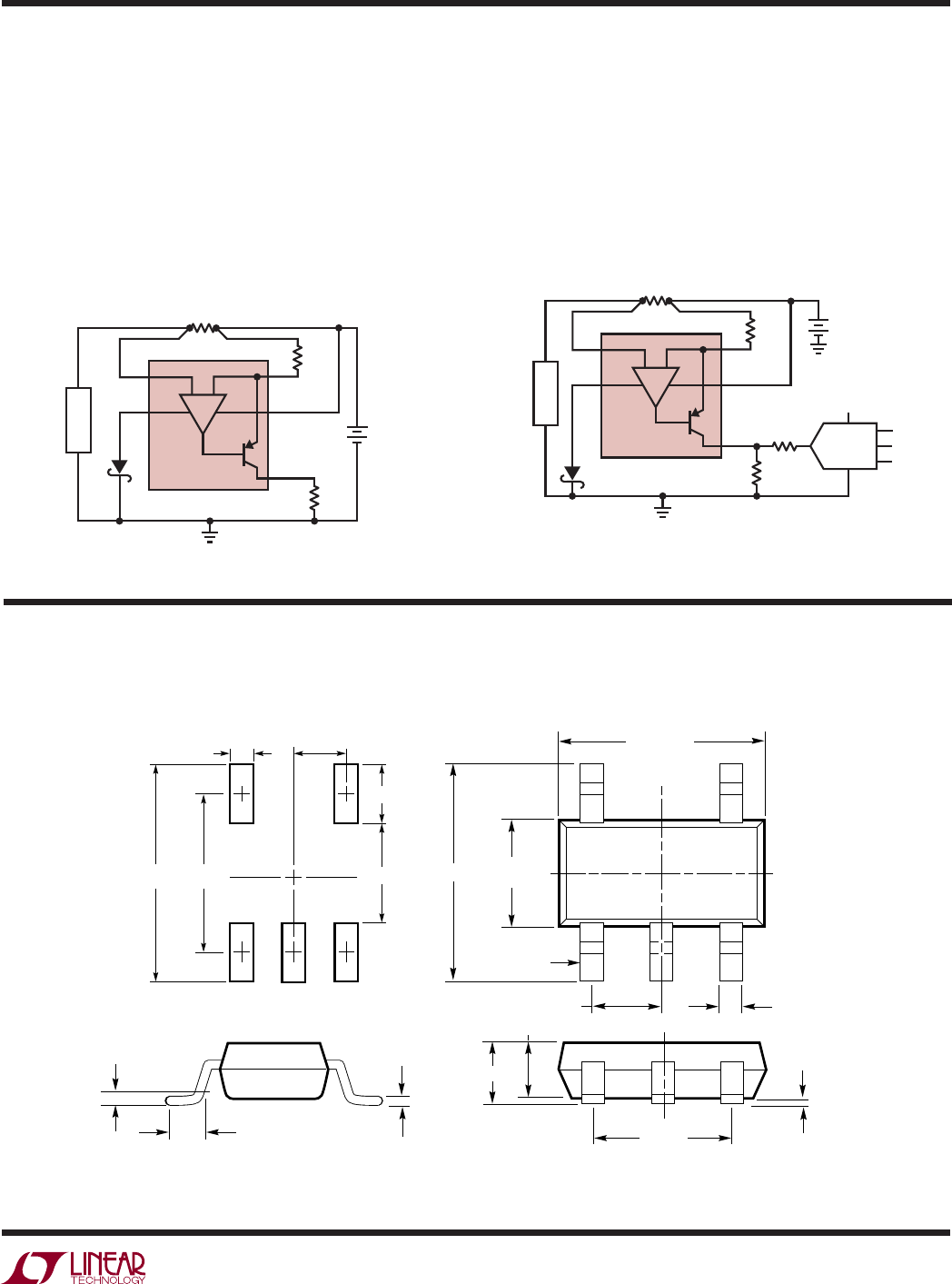
Reverse Supply Protection
Some applications may be tested with reverse-polarity
supplies due to an expectation of the type of fault during
operation. The LT6106 is not protected internally from ex-
ternal reversal of supply polarity. To prevent damage that
may occur during this condition, a Schottky diode should
be added in series with V– (Figure 6). This will limit the
reverse current through the LT6106. Note that this diode
will limit the low voltage performance of the LT6106 by
effectively reducing the supply voltage to the part by VD.
LT6106
ROUT
VOUT
6106 F05
RIN
VS
LOAD
RSENSE
–
+
V+
V–
OUT
–IN+IN
LT6106
11
6106fa
Information furnished by Linear Technology Corporation is believed to be accurate and reliable.
However, no responsibility is assumed for its use. Linear Technology Corporation makes no representa-
tion that the interconnection of its circuits as described herein will not infringe on existing patent rights.
PACKAGE DESCRIPTION
APPLICATIONS INFORMATION
In addition, if the output of the LT6106 is wired to a de-
vice that will effectively short it to high voltage (such as
through an ESD protection clamp) during a reverse sup-
ply condition, the LT6106’s output should be connected
through a resistor or Schottky diode (Figure 7).
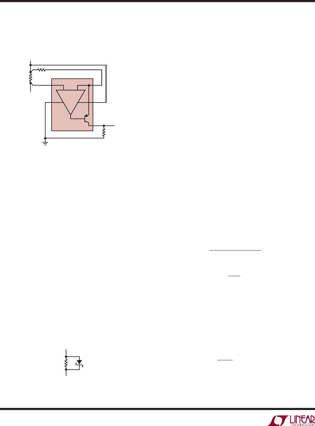
Demo Board
Demo board DC1240 is available for evaluation of the
LT6106.
Response Time
The photos in the Typical Performance Characteristics show
the response of the LT6106 to a variety of input conditions
and values of RIN. The photos show that if the output cur-
rent is very low or zero and an input transient occurs, there
will be an increased delay before the output voltage begins
changing while internal nodes are being charged.
Figure 6. Schottky Diode Prevents Damage During Supply Reversal
Figure 7. Additional Resistor R3 Protects Output
During Supply Reversal
S5 Package
5-Lead Plastic TSOT-23
(Reference LTC DWG # 05-08-1635)
1.50 – 1.75
(NOTE 4)
2.80 BSC
0.30 – 0.45 TYP
5 PLCS (NOTE 3)
DATUM ‘A’
0.09 – 0.20
(NOTE 3) S5 TSOT-23 0302 REV B
PIN ONE
2.90 BSC
(NOTE 4)
0.95 BSC
1.90 BSC
0.80 – 0.90
1.00 MAX
0.01 – 0.10
0.20 BSC
0.30 – 0.50 REF
NOTE:
1. DIMENSIONS ARE IN MILLIMETERS
2. DRAWING NOT TO SCALE
3. DIMENSIONS ARE INCLUSIVE OF PLATING
4. DIMENSIONS ARE EXCLUSIVE OF MOLD FLASH AND METAL BURR
5. MOLD FLASH SHALL NOT EXCEED 0.254mm
6. JEDEC PACKAGE REFERENCE IS MO-193
3.85 MAX
0.62
MAX
0.95
REF
RECOMMENDED SOLDER PAD LAYOUT
PER IPC CALCULATOR
1.4 MIN
2.62 REF
1.22 REF
6106 F06
LT6106
R2
4.99k
D1
VBATT
RSENSE
L
O
A
D
V+
V–
OUT
–IN+IN
–+
R1
100Ω
6106 F07
LT 6 1 0 6
R2
4.99k
D1
VBATT
R3
1k
RSENSE
L
O
A
D
V+
V–
OUT
–IN+IN
ADC
R1
100Ω
–+
LT6106
12
6106fa
Linear Technology Corporation
1630 McCarthy Blvd., Milpitas, CA 95035-7417
(408) 432-1900 ● FAX: (408) 434-0507 ● www.linear.com
© LINEAR TECHNOLOGY CORPORATION 2007
LT 0807 REV A • PRINTED IN USA
RELATED PARTS
PART NUMBER DESCRIPTION COMMENTS
LT1787 Precision Bidirectional, High Side Current Sense Amplifi er 75μV VOS, 60V, 60μA Operation
LT6100 Gain-Selectable High Side Current Sense Amplifi er 4.1V to 48V, Pin-Selectable Gain: 10, 12.5, 20, 25, 40, 50V/V
LT C
®
6101/LTC6101HV High Voltage, High Side, Precision Current Sense Amplifi ers 4V to 60V/5V to 100V, Gain Confi gurable, SOT-23
LTC6103 Dual High Side, Precision Current Sense Amplifi er 4V to 60V, Gain Confi gurable 8-Pin MSOP
LTC6104 Bidirectional High Side, Precision Current Sense Amplifi er 4V to 60V, Gain Confi gurable 8-Pin MSOP
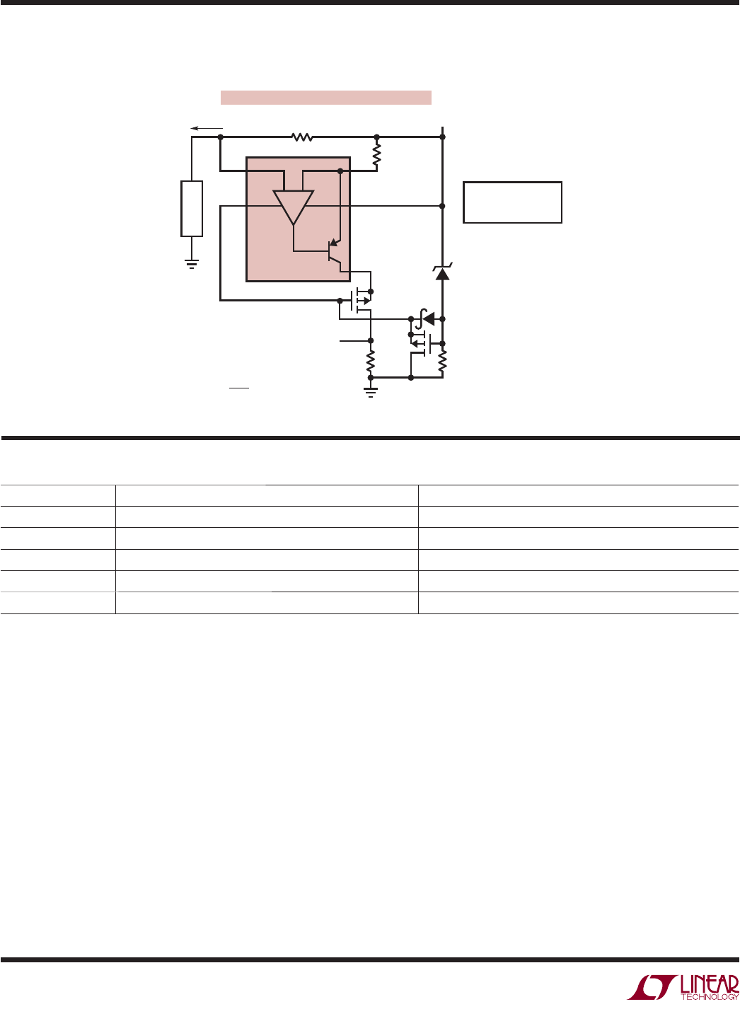
TYPICAL APPLICATION
Simple 400V Current Monitor
6106 TA02
LT6106
RIN
100Ω
VOUT
ROUT
4.99k
L
O
A
D
–+
VOUT = • VSENSE = 49.9 VSENSE
ROUT
RIN
M1 AND M2 ARE FQD3P50
M1
2M
12V
CMPZ12L
M2
400V
BAT46
VSENSE
RSENSE
ISENSE
+–
DANGER! Lethal Potentials Present — Use Caution
DANGER!!
HIGH VOLTAGE!!
V+
V–
OUT
–IN+IN