LTC6246, LTC6247, LTC6248 Datasheet. Www.s Manuals.com. Linear
User Manual: Marking of electronic components, SMD Codes 62, 62*, 620-015, 620-018, 620-025, 620-027, 620-0285, 620-030, 620-033, 620-035, 620-050, 620-0ER, 620-115, 620-118, 620-125, 620-127, 620-1285, 620-130, 620-133, 620-135, 620-150, 620-1ER, 6202, 6202I, 6203, 6203I, 6204, 6204I, 624, 6248, 625, 62883BHRTZ, 62883HRTZ, 62883IRTZ, 62883CHRTZ, 62883CIRTZ , 62A, 62Y. Datasheets 1.5SMC62AT3, BZV49-C62, FMMT624, FMMT625, ISL62883BHRTZ, ISL62883CHRTZ, ISL62883CIRTZ, ISL62883HRTZ, ISL62883IRTZ, LT6202CS8, LT6202IS8, LT620
Open the PDF directly: View PDF ![]() .
.
Page Count: 25
LTC6246/LTC6247/LTC6248
1
624678fa
Typical applicaTion
DescripTion
180MHz, 1mA Power
Efficient Rail-to-Rail
I/O Op Amps
The LTC
®
6246/LTC6247/LTC6248 are single/dual/quad low
power, high speed unity gain stable rail-to-rail input/output
operational amplifiers. On only 1mA of supply current they
feature an impressive 180MHz gain-bandwidth product,
90V/µs slew rate and a low 4.2nV/√Hz of input-referred
noise. The combination of high bandwidth, high slew rate,
low power consumption and low broadband noise makes
these amplifiers unique among rail-to-rail input/output op
amps with similar supply currents. They are ideal for lower
supply voltage high speed signal conditioning systems.
The LTC6246 family maintains high efficiency performance
from supply voltage levels of 2.5V to 5.25V and is fully
specified at supplies of 2.7V and 5.0V.
For applications that require power-down, the LTC6246
and the LTC6247 in MS10 offer a shutdown pin which
disables the amplifier and reduces current consumption
to 42µA.
The LTC6246 family can be used as a plug-in replacement
for many commercially available op amps to reduce power
or to improve input/output range and performance.
L, LT, LTC, LTM, Linear Technology and the Linear logo are registered trademarks of Linear
Technology Corporation. All other trademarks are the property of their respective owners.
FeaTures
applicaTions
n Gain Bandwidth Product: 180MHz
n –3dB Frequency (AV = 1): 120MHz
n Low Quiescent Current: 1mA Max
n High Slew Rate: 90V/µs
n Input Common Mode Range Includes Both Rails
n Output Swings Rail-to-Rail
n Low Broadband Voltage Noise: 4.2nV/√Hz
n Power-Down Mode: 42μA
n Fast Output Recovery
n Supply Voltage Range: 2.5V to 5.25V
n Input Offset Voltage: 0.5mV Max
n Input Bias Current: 100nA
n Large Output Current: 50mA
n CMRR: 110dB
n Open Loop Gain: 45V/mV
n Operating Temperature Range: –40°C to 125°C
n Single in 6-Pin TSOT-23
n Dual in MS8, 2mm × 2mm Thin DFN,TS0T-23, MS10
n Quad in MS16
n Low Voltage, High Frequency Signal Processing
n Driving A/D Converters
n Rail-to-Rail Buffer Amplifiers
n Active Filters
n Video Amplifiers
n Fast Current Sensing Amplifiers
n Battery Powered Equipment
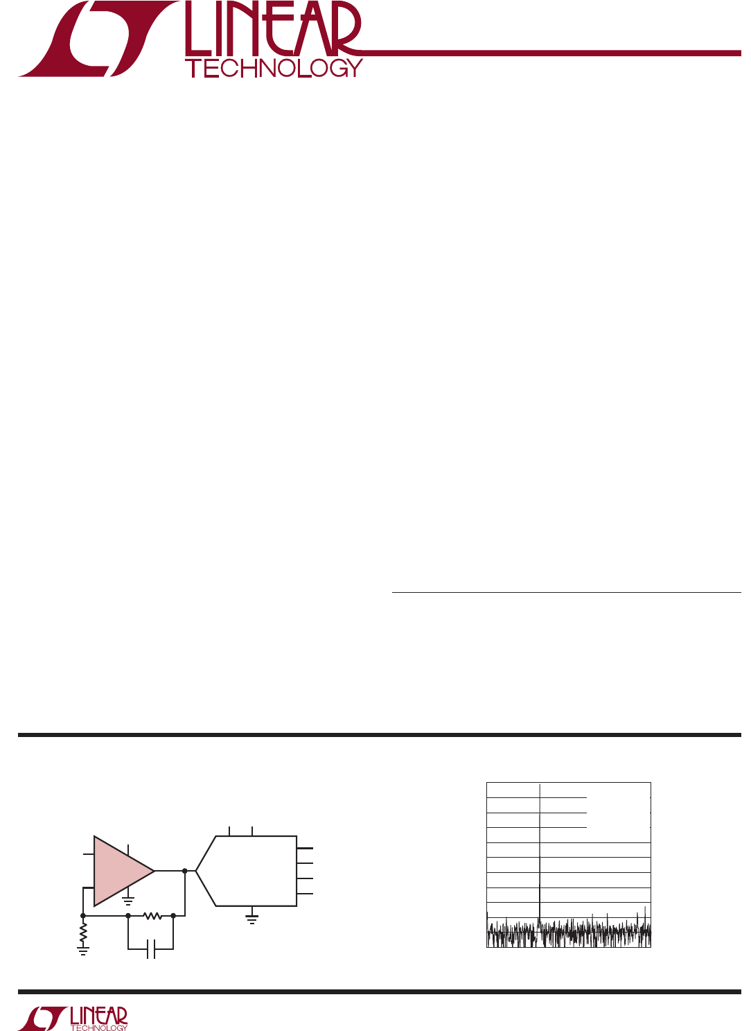
LTC6246
+
–
624678 TA01a
LTC2366
VREF
GND
VDD
3.3V 2.5V
CS
SDO
SCK
OVDD
3.3V
VIN
AIN
499Ω
1%
499Ω
1%
10pF
FREQUENCY (kHz)
0
MAGNITUDE (dB)
0
–10
–30
–50
–70
–20
–40
–60
–80
–90
–100
–110 400 800200 600
624678 TA01b
1000
fIN = 350.195kHz
fSAMP = 2.2Msps
SFDR = 82dB
SNR = 70dB
1024 POINT FFT
Low Noise Low Distortion Gain = 2 ADC Driver
350kHz FFT Driving ADC
LTC6246/LTC6247/LTC6248
2
624678fa
absoluTe MaxiMuM raTings
pin conFiguraTion
orDer inForMaTion
LEAD FREE FINISH TAPE AND REEL PART MARKING* PACKAGE DESCRIPTION SPECIFIED TEMPERATURE RANGE
LTC6246CS6#TRMPBF LTC6246CS6#TRPBF LTDWF 6-Lead Plastic TSOT-23 0°C to 70°C
LTC6246IS6#TRMPBF LTC6246IS6#TRPBF LTDWF 6-Lead Plastic TSOT-23 –40°C to 85°C
LTC6246HS6#TRMPBF LTC6246HS6#TRPBF LTDWF 6-Lead Plastic TSOT-23 –40°C to 125°C
LTC6247CKC#TRMPBF LTC6247CKC#TRPBF DWJT 8-Lead (2mm × 2mm) UTDFN 0°C to 70°C
LTC6247IKC#TRMPBF LTC6247IKC#TRPBF DWJT 8-Lead (2mm × 2mm) UTDFN –40°C to 85°C
LTC6247CMS8#PBF LTC6247CMS8#TRPBF LTDWH 8-Lead Plastic MSOP 0°C to 70°C
LTC6247IMS8#PBF LTC6247IMS8#TRPBF LTDWH 8-Lead Plastic MSOP –40°C to 85°C
LTC6247CTS8#TRMPBF LTC6247CTS8#TRPBF LTDWK 8-Lead Plastic TSOT-23 0°C to 70°C
LTC6247ITS8#TRMPBF LTC6247ITS8#TRPBF LTDWK 8-Lead Plastic TSOT-23 –40°C to 85°C
LTC6247HTS8#TRMPBF LTC6247HTS8#TRPBF LTDWK 8-Lead Plastic TSOT-23 –40°C to 125°C
Total Supply Voltage (V+ to V–) ................................5.5V
Input Current (+IN, –IN, SHDN) (Note 2) ..............±10mA
Output Current (Note 3) .....................................±100mA
Operating Temperature Range (Note 4) . –40°C to 125°C
Specified Temperature Range (Note 5) .. –40°C to 125°C
Storage Temperature Range .................. –65°C to 150°C
Junction Temperature ........................................... 150°C
Lead Temperature (Soldering, 10 sec)
(MSOP, TSOT Packages Only) ...............................300°C
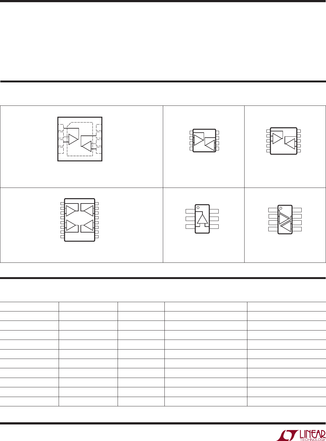
TOP VIEW
9
KC PACKAGE
8-LEAD PLASTIC UTDFN (2mm s 2mm)
5
6
7
8
4
3
2
1OUT A
–IN A
+IN A
V–
V+
OUT B
–IN B
+IN B
+
–
+
–
TJMAX = 125°C, θJA = 102°C/W (NOTE 9)
EXPOSED PAD (PIN 9) IS V–, MUST BE SOLDERED TO PCB
1
2
3
4
OUT A
–IN A
+IN A
V–
8
7
6
5
V+
OUT B
–IN B
+IN B
TOP VIEW
MS8 PACKAGE
8-LEAD PLASTIC MSOP
+
–
+
–
TJMAX = 150°C, θJA = 163°C/W (NOTE 9)
1
2
3
4
5
OUT A
–IN A
+IN A
V–
SHDNA
10
9
8
7
6
V+
OUT B
–IN B
+IN B
SHDNB
TOP VIEW
MS PACKAGE
10-LEAD PLASTIC MSOP
+
–
+
–
TJMAX = 150°C, θJA = 160°C/W (NOTE 9)
1
2
3
4
5
6
7
8
OUT A
–IN A
+IN A
V+
+IN B
–IN B
OUT B
16
15
14
13
12
11
10
9
OUT D
–IN D
+IN D
V–
+IN C
–IN C
OUT C
TOP VIEW
MS PACKAGE
16-LEAD PLASTIC MSOP
+
–
+
–
+
–
+
–
TJMAX = 150°C, θJA = 125°C/W (NOTE 9)
OUT 1
V– 2
+IN 3
6 V+
5SHDN
4 –IN
TOP VIEW
S6 PACKAGE
6-LEAD PLASTIC TSOT-23
+–
TJMAX = 150°C, θJA = 192°C/W (NOTE 9)
OUT A 1
–IN A 2
+IN A 3
V– 4
8 V+
7 OUT B
6 –IN B
5 +IN B
TOP VIEW
TS8 PACKAGE
8-LEAD PLASTIC TSOT-23
+
–
+
–
TJMAX = 150°C, θJA = 195°C/W (NOTE 9)
(Note 1)
LTC6246/LTC6247/LTC6248
3
624678fa
(VS = 5V) The l denotes the specifications which apply across the
specified temperature range, otherwise specifications are at TA = 25°C. For each amplifier VS = 5V, 0V; VSHDN = 2V; VCM = VOUT = 2.5V,
unless otherwise noted.
orDer inForMaTion
LEAD FREE FINISH TAPE AND REEL PART MARKING* PACKAGE DESCRIPTION SPECIFIED TEMPERATURE RANGE
LTC6247CMS#PBF LTC6247CMS#TRPBF LTDWM 10-Lead Plastic MSOP 0°C to 70°C
LTC6247IMS#PBF LTC6247IMS#TRPBF LTDWM 10-Lead Plastic MSOP –40°C to 85°C
LTC6248CMS#PBF LTC6248CMS#TRPBF 6248 16-Lead Plastic MSOP 0°C to 70°C
LTC6248IMS#PBF LTC6248IMS#TRPBF 6248 16-Lead Plastic MSOP –40°C to 85°C
LTC6248HMS#PBF LTC6248HMS#TRPBF 6248 16-Lead Plastic MSOP –40°C to 125°C
TRM = 500 pieces. *Temperature grades are identified by a label on the shipping container.
Consult LTC Marketing for parts specified with wider operating temperature ranges.
Consult LTC Marketing for information on lead based finish parts.
For more information on lead free part marking, go to: http://www.linear.com/leadfree/
For more information on tape and reel specifications, go to: http://www.linear.com/tapeandreel/
elecTrical characTerisTics
SYMBOL PARAMETER CONDITIONS MIN TYP MAX UNITS
VOS Input Offset Voltage VCM = Half Supply
l
–500
–1000
50 500
1000
µV
µV
VCM = V+ – 0.5V, NPN Mode
l
–2.5
–3
0.1 2.5
3
mV
mV
∆VOS Input Offset Voltage Match
(Channel-to-Channel) (Note 8)
VCM = Half Supply
l
–600
–1000
50 600
1000
µV
µV
VCM = V+ – 0.5V, NPN Mode
l
–3.5
–4
0.1 3.5
4
mV
mV
VOS TCInput Offset Voltage Drift l–2 µV/°C
IBInput Bias Current (Note 7) VCM = Half Supply
l
–350
–550
–30 350
550
nA
nA
VCM = V+ – 0.5V, NPN Mode
l
100
0
400 1000
1500
nA
nA
IOS Input Offset Current VCM = Half Supply
l
–250
–400
–10 250
400
nA
nA
VCM = V+ – 0.5V, NPN Mode
l
–250
–400
–10 250
400
nA
nA
enInput Noise Voltage Density f = 100kHz 4.2 nV/√Hz
Input 1/f Noise Voltage f = 0.1Hz to 10Hz 1.6 µVP-P
inInput Noise Current Density f = 100kHz 2.0 pA/√Hz
CIN Input Capacitance Differential Mode
Common Mode
2
0.8
pF
pF
RIN Input Resistance Differential Mode
Common Mode
32
14
kΩ
MΩ
AVOL Large Signal Voltage Gain RL = 1k to Half Supply (Note 10)
l
30
14
45 V/mV
V/mV
RL = 100Ω to Half Supply (Note 10)
l
5
2.5
15 V/mV
V/mV
CMRR Common Mode Rejection Ratio VCM = 0V to 3.5V
l
78
76
110 dB
dB

LTC6246/LTC6247/LTC6248
4
624678fa
elecTrical characTerisTics
SYMBOL PARAMETER CONDITIONS MIN TYP MAX UNITS
ICMR Input Common Mode Range l0 VSV
PSRR Power Supply Rejection Ratio VS = 2.5V to 5.25V
VCM = 1V
l
69
65
73 dB
dB
Supply Voltage Range (Note 6) l2.5 5.25 V
VOL Output Swing Low (VOUT – V–) No Load
l
25 40
55
mV
mV
ISINK = 5mA
l
70 110
160
mV
mV
ISINK = 25mA
l
160 250
450
mV
mV
VOH Output Swing High (V+ – VOUT) No Load
l
70 100
150
mV
mV
ISOURCE = 5mA
l
130 175
225
mV
mV
ISOURCE = 25mA
l
300 500
750
mV
mV
ISC Output Short-Circuit Current Sourcing
l
–80 –35
–30
mA
mA
Sinking
l
60
40
100 mA
mA
ISSupply Current per Amplifier VCM = Half Supply
l
0.95 1
1.4
mA
mA
VCM = V+ – 0.5V
l
1.25 1.4
1.8
mA
mA
ISD Disable Supply Current per Amplifier VSHDN = 0.8V
l
42 75
200
µA
µA
ISHDNL SHDN Pin Current Low VSHDN = 0.8V
l
–3
–4
–1.6 0
0
µA
µA
ISHDNH SHDN Pin Current High VSHDN = 2V
l
–300
–350
35 300
350
nA
nA
VLSHDN Pin Input Voltage Low l0.8 V
VHSHDN Pin Input Voltage High l2 V
IOSD Output Leakage Current Magnitude in
Shutdown
VSHDN = 0.8V, Output Shorted to Either
Supply
100 nA
tON Turn-On Time VSHDN = 0.8V to 2V 5 µs
tOFF Turn-Off Time VSHDN = 2V to 0.8V 2 µs
BW –3dB Closed Loop Bandwidth AV = 1, RL = 1k to Half Supply 120 MHz
GBW Gain-Bandwidth Product f = 2MHz, RL = 1k to Half Supply
l
100
70
180 MHz
MHz
tS, 0.1% Settling Time to 0.1% AV = –1, VO = 2V Step RL = 1k 74 ns
tS, 0.01% Settling Time to 0.01% AV = –1, VO = 2V Step RL = 1k 202 ns
SR Slew Rate AV = –3.33, 4.6V Step (Note 11)
l
60
50
90 V/µs
V/µs
FPBW Full Power Bandwidth VOUT = 4VP-P (Note 13) 4 MHz
(VS = 5V) The l denotes the specifications which apply across the
specified temperature range, otherwise specifications are at TA = 25°C. For each amplifier VS = 5V, 0V; VSHDN = 2V; VCM = VOUT = 2.5V,
unless otherwise noted.
LTC6246/LTC6247/LTC6248
5
624678fa
SYMBOL PARAMETER CONDITIONS MIN TYP MAX UNITS
HD2/HD3 Harmonic Distortion
RL = 1k to Half Supply
fC = 100kHz, VO = 2VP-P
fC = 1MHz, VO = 2VP-P
fC = 2MHz, VO = 2VP-P
110/90
88/80
78/62
dBc
dBc
dBc
RL = 100Ω to Half Supply fC = 100kHz, VO = 2VP-P
fC = 1MHz, VO = 2VP-P
fC = 2MHz, VO = 2VP-P
90/79
66/60
59/51
∆GDifferential Gain (Note 14) AV = 1, RL = 1k, VS = ±2.5V 0.2 %
∆θ Differential Phase (Note 14) AV = 1, RL = 1k, VS = ±2.5V 0.08 Deg
Crosstalk AV = –1, RL = 1k to Half Supply,
VOUT = 2VP-P, f = 1MHz
–90 dB
elecTrical characTerisTics
(VS = 5V) The l denotes the specifications which apply across the
specified temperature range, otherwise specifications are at TA = 25°C. For each amplifier VS = 5V, 0V; VSHDN = 2V; VCM = VOUT = 2.5V,
unless otherwise noted.
elecTrical characTerisTics
(VS = 2.7V) The l denotes the specifications which apply across the
specified temperature range, otherwise specifications are at TA = 25°C. For each amplifier VS = 2.7V, 0V; VSHDN = 2V; VCM = VOUT =
1.35V, unless otherwise noted.
SYMBOL PARAMETER CONDITIONS MIN TYP MAX UNITS
VOS Input Offset Voltage VCM = Half Supply
l
–100
–300
500 1000
1400
µV
µV
VCM = V+ – 0.5V, NPN Mode
l
–1.75
–2.25
0.75 3.25
3.75
mV
mV
∆VOS Input Offset Voltage Match
(Channel-to-Channel) (Note 8)
VCM = Half Supply
l
–700
–1000
–20 700
1000
µV
µV
VCM = V+ – 0.5V, NPN Mode
l
–3.5
–4
0.1 3.5
4
mV
mV
VOS TCInput Offset Voltage Drift l2 µV/°C
IBInput Bias Current (Note 7) VCM = Half Supply
l
–450
–600
–100 450
600
nA
nA
VCM = V+ – 0.5V, NPN Mode
l
50
0
350 1000
1500
nA
nA
IOS Input Offset Current VCM = Half Supply
l
–250
–350
–10 250
350
nA
nA
VCM = V+ – 0.5V, NPN Mode
l
–250
–350
–10 250
350
nA
nA
enInput Noise Voltage Density f = 100kHz 4.6 nV/√Hz
Input 1/f Noise Voltage f = 0.1Hz to 10Hz 1.7 µVP-P
inInput Noise Current Density f = 100kHz 1.8 pA/√Hz
CIN Input Capacitance Differential Mode
Common Mode
2
0.8
pF
pF
RIN Input Resistance Differential Mode
Common Mode
32
12
kΩ
MΩ
AVOL Large Signal Voltage Gain RL = 1k to Half Supply
(Note 12)
l
15
7.5
25 V/mV
V/mV
RL = 100Ω to Half Supply
(Note 12)
l
2
1.3
7.5 V/mV
V/mV
LTC6246/LTC6247/LTC6248
6
624678fa
elecTrical characTerisTics
(VS = 2.7V) The l denotes the specifications which apply across the
specified temperature range, otherwise specifications are at TA = 25°C. For each amplifier VS = 2.7V, 0V; VSHDN = 2V; VCM = VOUT =
1.35V, unless otherwise noted.
SYMBOL PARAMETER CONDITIONS MIN TYP MAX UNITS
CMRR Common Mode Rejection Ratio VCM = 0V to 1.2V
l
80
78
100 dB
dB
ICMR Input Common Mode Range l0 VSV
PSRR Power Supply Rejection Ratio VS = 2.5V to 5.25V
VCM = 1V
l
69
65
73 dB
dB
Supply Voltage Range (Note 6) l2.5 5.25 V
VOL Output Swing Low (VOUT – V–) No Load
l
20 40
55
mV
mV
ISINK = 5mA
l
80 125
160
mV
mV
ISINK = 10mA
l
110 175
225
mV
mV
VOH Output Swing High (V+ – VOUT) No Load
l
60 85
100
mV
mV
ISOURCE = 5mA
l
135 190
225
mV
mV
ISOURCE = 10mA
l
180 275
400
mV
mV
ISC Short Circuit Current Sourcing
l
–35 –20
–15
mA
mA
Sinking
l
25
20
50 mA
mA
ISSupply Current per Amplifier VCM = Half Supply
l
0.89 1
1.3
mA
mA
VCM = V+ – 0.5V
l
1 1.3
1.7
mA
mA
ISD Disable Supply Current per Amplifier VSHDN = 0.8V
l
22 50
90
µA
µA
ISHDNLSHDN Pin Current Low VSHDN = 0.8V
l
–1
–1.5
–0.5 0
0
µA
µA
ISHDNHSHDN Pin Current High VSHDN = 2V
l
–300
–350
45 300
350
nA
nA
VLSHDN Pin Input Voltage l0.8 V
VHSHDN Pin Input Voltage l2.0 V
IOSD Output Leakage Current Magnitude in Shutdown VSHDN = 0.8V, Output Shorted to Either
Supply
100 nA
tON Turn-On Time VSHDN = 0.8V to 2V 5 µs
tOFF Turn-Off Time VSHDN = 2V to 0.8V 2 µs
BW –3dB Closed Loop Bandwidth AV = 1, RL = 1k to Half Supply 100 MHz
GBW Gain-Bandwidth Product f = 2MHz, RL = 1k to Half Supply
l
80
50
150 MHz
tS, 0.1 Settling Time to 0.1% AV = –1, VO = 2V Step RL = 1k 119 ns
tS, 0.01 Settling Time to 0.01% AV = –1, VO = 2V Step RL = 1k 170 ns
SR Slew Rate AV = –1, 2V Step 55 V/µs
LTC6246/LTC6247/LTC6248
7
624678fa
elecTrical characTerisTics
Note 1: Stresses beyond those listed under Absolute Maximum Ratings
may cause permanent damage to the device. Exposure to any Absolute
Maximum Rating condition for extended periods may affect device
reliability and lifetime.
Note 2: The inputs are protected by back-to-back diodes. If any of
the input or shutdown pins goes 300mV beyond either supply or the
differential input voltage exceeds 1.4V the input current should be limited
to less than 10mA. This parameter is guaranteed to meet specified
performance through design and/or characterization. It is not production
tested.
Note 3: A heat sink may be required to keep the junction temperature
below the absolute maximum rating when the output current is high.
Note 4: The LTC6246C/LTC6247C/LTC6248C and LTC6246I/LTC6247I/
LTC6248I are guaranteed functional over the temperature range of –40°C
to 85°C. The LTC6246H/LTC6247H/LTC6248H are guaranteed functional
over the temperature range of –40°C to 125°C.
Note 5: The LTC6246C/LTC6247C/LTC6248C are guaranteed to meet
specified performance from 0°C to 70°C. The LTC6246C/LTC6247C/
LTC6248C are designed, characterized and expected to meet specified
performance from –40°C to 85°C but are not tested or QA sampled at
these temperatures. The LTC6246I/LTC6247I/LTC6248I are guaranteed
to meet specified performance from –40°C to 85°C. The LTC6246H/
LTC6247H/LTC6248H are guaranteed to meet specified performance from
–40°C to 125°C.
Note 6: Minimum supply voltage is guaranteed by power supply rejection
ratio test.
Note 7: The input bias current is the average of the average of the currents
through the positive and negative input pins.
Note 8: Matching parameters are the difference between amplifiers A and
D and between B and C on the LTC6248; between the two amplifiers on the
LTC6247.
Note 9: Thermal resistance varies with the amount of PC board metal
connected to the package. The specified values are with short traces
connected to the leads with minimal metal area.
Note 10: The output voltage is varied from 0.5V to 4.5V during
measurement.
Note 11: Middle 80% of the output waveform is observed. RL = 1k at half
supply.
Note 12: The output voltage is varied from 0.5V to 2.2V during
measurement.
Note 13: FPBW is determined from distortion performance in a gain of +2
configuration with HD2, HD3 < –40dBc as the criteria for a valid output.
Note 14: Differential gain and phase are measured using a Tektronix
TSG120YC/NTSC signal generator and a Tektronix 1780R video
measurement set.
VOS Distribution, VCM = VS/2
(MS, PNP Stage)
VOS Distribution, VCM = VS/2
(TSOT-23, PNP Stage)
VOS Distribution, VCM = V+ – 0.5V
(MS, NPN Stage)
Typical perForMance characTerisTics
(VS = 2.7V) The l denotes the specifications which apply across the
specified temperature range, otherwise specifications are at TA = 25°C. For each amplifier VS = 2.7V, 0V; VSHDN = 2V; VCM = VOUT =
1.35V, unless otherwise noted.
SYMBOL PARAMETER CONDITIONS MIN TYP MAX UNITS
FPBW Full Power Bandwidth VOUT = 2VP-P (Note 13) 3.3 MHz
Crosstalk AV = –1, RL = 1k to Half Supply,
VOUT = 2VP-P, f = 1MHz
–90 dB
INPUT OFFSET VOLTAGE (µV)
PERCENT OF UNITS (%)
22
20
16
12
8
2
18
14
10
6
4
0–50–150 150
624678 G01
350250–250–375 50
VS = 5V, 0V
VCM = 2.5V
INPUT OFFSET VOLTAGE (µV)
PERCENT OF UNITS (%)
25
15
5
20
10
0–125 –25–75
624678 G02
75 12525 175–175
VS = 5V, 0V
VCM = 2.5V
INPUT OFFSET VOLTAGE (µV)
PERCENT OF UNITS (%)
16
12
8
2
14
10
6
4
0–1200 400–400
624678 G03
1200 2000–2000
VS = 5V, 0V
VCM = 4.5V
LTC6246/LTC6247/LTC6248
8
624678fa
Typical perForMance characTerisTics
Offset Voltage vs Output Current Warm-Up Drift vs Time
Input Bias Current
vs Common Mode Voltage
Offset Voltage
vs Input Common Mode Voltage
VOS vs Temperature
(MS10, PNP Stage)
VOS Distribution, VCM = V+ – 0.5V
(TSOT-23, NPN Stage)
VOS vs Temperature
(MS10, NPN Stage)
VOS vs Temperature
(MS10, PNP Stage)
VOS vs Temperature
(MS10, NPN Stage)
INPUT COMMON MODE VOLTAGE (V)
0
OFFSET VOLTAGE (µV)
500
400
100
200
–300
300
0
–100
–200
–400
–500 1.5 3.51 2.5 4.5
624678 G09
530.5 2 4
–55°C
VS = 5V, 0V
125°C
25°C
OUTPUT CURRENT (mA)
–100
VOS (mV)
2.0
1.5
0.5
–1.0
1.0
0
–0.5
–1.5
–2.0 –75 25–25 75
624678 G10
1000–50 50
25°C
125°C
–55°C
VS = ±2.5V
TIME AFTER POWER-UP (s)
0
CHANGE IN OFFSET VOLTAGE (µV)
5
0
–10
–25
–5
–15
–20
–30
–35 20 10060 140
624678 G11
1608040 120
VS = ±2.5V
TA = 25°C
COMMON MODE VOLTAGE (V)
0
INPUT BIAS CURRENT (nA)
800
600
200
–200
–600
–1200
400
0
–400
–800
–1000
–1400
–1600 1.5 3.51 2.5 4.5
624678 G12
530.5 2 4
25°C
125°C
–55°C
VS = 5V, 0V
INPUT OFFSET VOLTAGE (µV)
PERCENT OF UNITS (%)
18
12
14
10
4
16
8
6
2
0–1200
624678 G04
400 1200–400 2000–2000
VS = 5V, 0V
VCM = 4.5V
TEMPERATURE (°C)
VOLTAGE OFFSET (µV)
500
200
300
100
–200
400
0
–100
–300
–400 –15–35
624678 G05
5 25 65 85 105 125–55
VS = 5V, 0V
VCM = 2.5V
6 DEVICES
45
TEMPERATURE (°C)
VOLTAGE OFFSET (µV)
2500
1000
1500
500
–1000
2000
0
–500
–1500
–2000
–2500 –15–35
624678 G06
5 25 65 85 105 125–55
VS = 5V, 0V
VCM = 4.5V
6 DEVICES
45
TEMPERATURE (°C)
VOLTAGE OFFSET (µV)
1200
1000
800
600
400
200
0–15–35
624678 G07
5 25 65 85 105 125–55
VS = 2.7V, 0V
VCM = 1.35V
6 DEVICES
45
TEMPERATURE (°C)
VOLTAGE OFFSET (µV)
2500
2000
1500
1000
500
0
–1500
–1000
–500
–2000 –15–35
624678 G08
5 25 65 85 105 125–55
VS = 2.7V, 0V
VCM = 2.2V
6 DEVICES
45
LTC6246/LTC6247/LTC6248
9
624678fa
Typical perForMance characTerisTics
Supply Current Per Amplifier
vs SHDN Pin Voltage
SHDN Pin Current
vs SHDN Pin Voltage
Input Noise Voltage and Noise
Current vs Frequency
Input Bias Current vs Temperature
Supply Current
vs Supply Voltage (Per Amplifier)
0.1Hz to 10Hz Voltage Noise
TIME (1s/DIV)
0
VOLTAGE NOISE (500nV/DIV)
1.5 VS = ±2.5V
1.0
0.5
0
0.5
–1.0
–1.5 1 73 9
624678 G14
104 5 62 8
TOTAL SUPPLY VOLTAGE (V)
0
SUPPLY CURRENT (mA)
1.20
1.00
0.80
0.60
0.40
0.20
01 3
624678 G16
TA = 125°C
TA = 25°C
TA = –55°C
4 52
TEMPERATURE (°C)
–55
INPUT BIAS CURRENT (nA)
700
600
300
–100
400
500
0
200
100
–200 355–25 95
624678 G13
12565
VS = 5V, 0V
VCM = 4.5V
VCM = 2.5V
FREQUENCY (Hz)
1
VOLTAGE NOISE (nV/√Hz)
CURRENT NOISE (pA/√Hz)
1000
en, VCM = 4.5V
en, VCM = 2.5V
in, VCM = 2.5V
in, VCM = 4.5V
100
10
1.0
0.1 10 1k 10M
624678 G15
10k 100k 1M100
SHDN PIN VOLTAGE (V)
0
SUPPLY CURRENT (mA)
1.25
1.00
0.75
0.50
0.25
02.521.510.5 3.5
624678 G17
5
125°C
VS = 5V, 0V
25°C
–55°C
4 4.53
SHDN PIN VOLTAGE (V)
0
SHDN PIN CURRENT (µA)
0.25
0
–0.25
–0.50
–0.75
–1.00
–1.25
–1.50
–1.75
–2.00
–2.25
–2.50 2.521.510.5 3.5
624678 G18
5
125°C
VS = 5V, 0V
SHUTDOWN CURRENT
25°C
–55°C
4 4.53
Output Saturation Voltage
vs Load Current (Output High)
Minimum Supply Voltage,
VCM = VS/2 (PNP Operation)
Minimum Supply Voltage,
VCM = V+ – 0.5V (NPN Operation)
TOTAL SUPPLY VOLTAGE (V)
2
OFFSET VOLTAGE (mV)
12
10
8
6
4
2
0
–2 2.5 3.5
624678 G19
5.5
125°C
25°C
–55°C
4 4.5 53
TOTAL SUPPLY VOLTAGE (V)
2
OFFSET VOLTAGE (mV)
5
4
3
2
1
0
–1 2.5 3.5
624678 G20
5.5
125°C
25°C –55°C
4 4.5 53
VCM = VCC – 0.5V
LOAD CURRENT (mA)
OUTPUT HIGH SATURATION VOLTAGE (V)
624678 G21
10
1
0.1
0.01
0.01 10 10010.1
VS = ±2.5V
TA = –55°C
TA = 125°C
TA = 25°C
LTC6246/LTC6247/LTC6248
10
624678fa
Typical perForMance characTerisTics
Open Loop Gain and Phase
vs Frequency
Gain vs Frequency (AV = 1) Gain vs Frequency (AV = 2)
Gain Bandwidth and Phase
Margin vs Supply Voltage
Gain Bandwidth and Phase
Margin vs Temperature
Open Loop Gain
Output Short-Circuit Current
vs Power Supply Voltage Open Loop Gain
Output Saturation Voltage
vs Load Current (Output Low)
LOAD CURRENT (mA)
OUTPUT LOW SATURATION VOLTAGE (V)
624678 G22
10
1
0.1
0.01
0.01 10 10010.1
VS = ±2.5V
TA = –55°C
TA = 125°C
TA = 25°C
OUTPUT VOLTAGE (V)
0
INPUT VOLTAGE (µV)
500
400
300
200
100
0
–100
–200
–300
–400
–500 2.5 3.5
624678 G24
5
RL = 1k TO MID SUPPLY
RL = 1k TO GROUND
RL = 100 TO MID SUPPLY
RL = 100 TO GROUND
TA = 25°C
VS = 5V, 0V
4 4.521.510.5 3
OUTPUT VOLTAGE (V)
0
INPUT VOLTAGE (µV)
1000
900
500
600
700
800
400
300
200
100
0
–100
–200
–300 2.5
624678 G25
2.7
RL = 1k TO MID SUPPLY
RL = 1k TO GROUND
RL = 100 TO MID SUPPLY
RL = 100 TO GROUND
TA = 25°C
VS = 2.7V, 0V
21.510.5
POWER SUPPLY VOLTAGE (±V)
1.25
OUTPUT SHORT-CIRCUIT CURRENT (mA)
120
100
80
60
40
20
0
–20
–40
–60
–80
–100 1.651.45 2.05
624678 G23
2.65
TA = 125°C
TA = 125°C
SINK
SOURCE
TA = 25°C
TA = 25°C
TA = –55°C
TA = –55°C
2.25 2.451.85
FREQUENCY (MHz)
GAIN (dB)
624678 G26
6
0
–18
–12
–6
–24
0.01 10 10010.1
VS = ±2.5V
TA = 25°C
RL = 1k
FREQUENCY (MHz)
GAIN (dB)
624678 G27
12
0
6
–12
–6
–18
0.01 10 10010.1
VS = ±2.5V
TA = 25°C
RF = RG = 1k
RL = 1k
FREQUENCY (Hz)
GAIN (dB)
PHASE (DEG)
624678 G28
80
10
20
30
40
50
60
70
–10
0
–20
150
0
50
100
–50
–100
100k 100M 300M10M1M
TA = 25°C
RL = 1k
VS = ±2.5V
PHASE
GAIN VS = ±1.35V
VS = ±2.5V
VS = ±1.35V
TOTAL SUPPLY VOLTAGE (V)
2.5
GAIN BANDWIDTH (MHz)
PHASE MARGIN (DEG)
200
180
160
140
120
100
70
60
50
3 3.5 4.5
PHASE MARGIN
GAIN BANDWIDTH PRODUCT
624678 G29
TA = 25°C
RL = 1k
54
TEMPERATURE (°C)
–55
GAIN BANDWIDTH (MHz)
PHASE MARGIN (DEG)
300
250
200
150
100
60
70
50
40
–35 –15 4525
PHASE MARGIN
GAIN BANDWIDTH PRODUCT
624678 G30
125
TA = 25°C
RL = 1k
65 85 1055
VS = ±2.5V
VS = ±1.35V
VS = ±2.5V
VS = ±1.35V
LTC6246/LTC6247/LTC6248
11
624678fa
Typical perForMance characTerisTics
Power Supply Rejection Ratio
vs Frequency
Series Output Resistor
vs Capacitive Load (AV = 1)
Series Output Resistor
vs Capacitive Load (AV = 2)
Output Impedance vs Frequency
Common Mode Rejection Ratio
vs Frequency
Slew Rate vs Temperature
FREQUENCY (Hz)
OUTPUT IMPEDANCE (Ω)
624678 G31
1000
10
100
1
0.1
0.01
0.001
100k 100M 1G10M1M
VS = ±2.5V
AV = 10
AV = 1
AV = 2
FREQUENCY (Hz)
COMMON MODE REJECTION RATIO (dB)
624678 G31
110
90
80
70
60
50
40
30
100
20
10
0
–1010 100 1k 10k 100k 100M 1G10M1M
TA = 25°C
VS = ±2.5V
FREQUENCY (Hz)
10
POWER SUPPLY REJECTION RATIO (dB)
50
40
30
20
10
70
80
60
0
–10 100 1k 100k
NEGATIVE SUPPLY
POSITIVE SUPPLY
624678 G33
VS = ±2.5V
TA = 25°C
100M10M1M10k
TEMPERATURE (°C)
–55
SLEW RATE (V/µs)
140
FALLING, VS = ±2.5V
RISING, VS = ±2.5V
FALLING, VS = ±1.35V
RISING, VS = ±1.35V
120
100
80
60
40 –35 45255–15 85
624678 G34
125
AV = –1, RL = 1k, VOUT = 4VP-P (±2.5V),
2VP-P (±1.35V) SLEW RATE MEASURED
AT MIDDLE 2/3 OF OUTPUT
10565
Distortion vs Frequency
(AV = 1, 5V)
Distortion vs Frequency
(AV = 2, 5V)
Distortion vs Frequency
(AV = 1, 2.7V)
FREQUENCY (MHz)
0.01
DISTORTION (dBc)
–40
–50
–60
–70
–80
–90
–100
–110
–120 0.1 101
624678 G37
VS = ±2.5V
VOUT = 2VP-P
AV = 1
RL = 100Ω, 2ND
RL = 1kΩ, 3RD
RL = 1kΩ, 2ND
RL = 100Ω, 3RD
FREQUENCY (MHz)
0.01
DISTORTION (dBc)
–40
–50
–60
–70
–80
–90
–100
–110
–120 0.1 101
624678 G38
VS = ±1.35V
VOUT = 1VP-P
AV = 1
RL = 100Ω, 2ND
RL = 1kΩ, 3RD
RL = 1kΩ, 2ND
RL = 100Ω, 3RD
FREQUENCY (MHz)
0.01
DISTORTION (dBc)
–40
–50
–60
–70
–80
–90
–100
–110
–120 0.1 101
624678 G39
VS = ±2.5V
VOUT = 2VP-P
AV = 2
RL = 100Ω, 2ND
RL = 1kΩ, 3RD
RL = 1kΩ, 2ND
RL = 100Ω, 3RD
CAPACITIVE LOAD (pF)
10
OVERSHOOT (%)
80
70
60
50
40
30
20
10
0100 100001000
624678 G35
VS = ±2.5V
VOUT = 100mVP-P
AV = 1
RS = 20Ω
RS = 49.9Ω
RS = 10Ω
+
–
RS
CL
VOUT
VIN
AV = 1
CAPACITIVE LOAD (pF)
10
OVERSHOOT (%)
80
70
60
50
40
30
20
10
0100 100001000
624678 G36
VS = ±2.5V
VOUT = 200mVP-P
RF = RG = 500Ω,
AV = 2
RS = 20Ω
RS = 49.9Ω
RS
500Ω
500Ω
CL
VOUT
VIN AV = 2
RS = 10Ω
+
–
LTC6246/LTC6247/LTC6248
12
624678fa
Typical perForMance characTerisTics
Large Signal Response
Small Signal Response Output Overdriven Recovery
Settling Time vs Output Step
(Noninverting)
Settling Time vs Output Step
(Inverting) SHDN Pin Response Time
Distortion vs Frequency
AV = 2, 2.7V)
Maximum Undistorted Output
Signal vs Frequency
OUTPUT STEP (V)
–4
SETTLING TIME (ns)
200
180
160
140
40
60
80
100
120
20
0–3 –1
624678 G42
4
1mV 1mV
10mV 10mV
0 1 32–2
VS = ±2.5V
AV = 1
TA = 25°C
1k
VOUT
VIN
+
–
OUTPUT STEP (V)
–4
SETTLING TIME (ns)
200
180
160
140
40
60
80
100
120
20
0–3 –1
624678 G43
4
10mV
0 1 32–2
1k
1k
1k
VOUT
VIN
VS = ±2.5V
AV = –1
TA = 25°C
1mV
10mV
1mV
+
–
VOUT
1.6V/DIV
AV = 1
VS= ±2.5V
RL = 1k
VIN = 1.6V
VSHDN
2.5V/DIV
0V
0V
624678 G44
10µs/DIV
1V/DIV
0V
AV = 1
VS= ±2.5V
RL = 1k
624678 G45
200ns/DIV
25mV/DIV
0V
AV = 1
VS= ±2.5V
RL = 1k
624678 G46
50ns/DIV
VOUT
2V/DIV
AV = ±2
VS= ±2.5V
RL = 1k
VIN = 3VP-P
VIN
1V/DIV
0V
0V
624678 G47
100ns/DIV
FREQUENCY (MHz)
0.01
DISTORTION (dBc)
–40
–50
–60
–70
–80
–90
–100
–110
–120 0.1 101
624678 G40
VS = ±1.35V
VOUT = 1VP-P
AV = 2
RL = 100Ω, 2ND
RL = 1kΩ, 3RD
RL = 1kΩ, 2ND
RL = 100Ω, 3RD
FREQUENCY (MHz)
0.01
OUTPUT VOLTAGE SWING (VP-P)
5
4
3
2
1
00.1 101
624678 G41
VS = ±2.5V
TA = 25°C
RL = 1kΩ
HD2, HD3 < –40dBc
AV = 2
AV = –1
LTC6246/LTC6247/LTC6248
13
624678fa
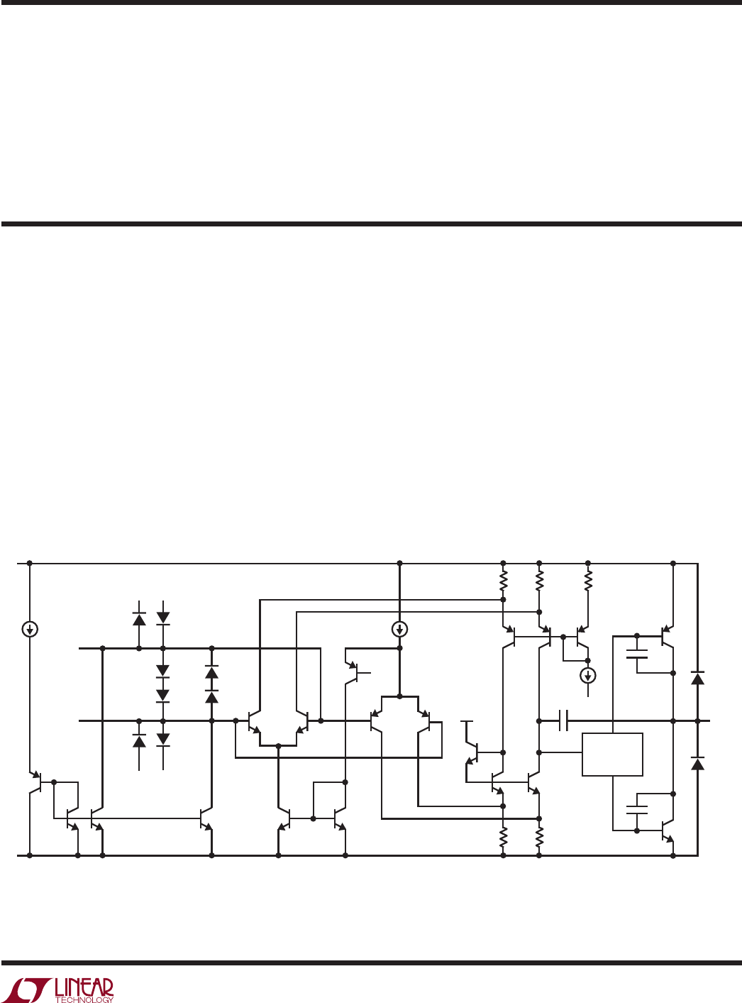
applicaTions inForMaTion
Circuit Description
The LTC6246/LTC6247/LTC6248 have an input and output
signal range that extends from the negative power supply
to the positive power supply. Figure 1 depicts a simplified
schematic of the amplifier. The input stage is comprised
of two differential amplifiers, a PNP stage, Q1/Q2, and an
NPN stage, Q3/Q4 that are active over different common
mode input voltages. The PNP stage is active between
the negative supply to nominally 1.2V below the positive
supply. As the input voltage approaches the positive sup-
ply, the transistor Q5 will steer the tail current, I1, to the
current mirror, Q6/Q7, activating the NPN differential pair
and the PNP pair becomes inactive for the remaining input
common mode range. Also, at the input stage, devices Q17
to Q19 act to cancel the bias current of the PNP input pair.
When Q1/Q2 are active, the current in Q16 is controlled to
be the same as the current in Q1 and Q2. Thus, the base
current of Q16 is nominally equal to the base current of
the input devices. The base current of Q16 is then mirrored
by devices Q17 to Q19 to cancel the base current of the
input devices Q1/Q2. A pair of complementary common
emitter stages, Q14/Q15, enable the output to swing from
rail-to-rail.
Figure 1. LTC6246/LTC6247/LTC6248 Simplified Schematic Diagram
–IN: Inverting Input of Amplifier. Valid input range from V–
to V+.
+IN: Non-Inverting Input of Amplifier. Valid input range
from V– to V+.
V+ : Positive Supply Voltage. Allowed applied voltage
ranges from 2.5V to 5.25V when V– = 0V.
V– : Negative Supply Voltage. Typically 0V. This can be made
a negative voltage as long as 2.5V ≤ (V+ – V–) ≤ 5.25V.
SHDN: Active Low Shutdown. Threshold is typically 1.1V
referenced to V–. Floating this pin will turn the part on.
OUT: Amplifier Output. Swings rail-to-rail and can typically
source/sink over 50mA of current at a total supply of 5V.
pin FuncTions
624678 F01
Q15
ESDD5
Q14
C2
C1
BUFFER
AND
OUTPUT BIAS
R5R4
Q13
Q12
I3
V–
+
CC
Q8
R3
Q11
Q9
Q10
R2R1
Q2Q1Q3Q4
I1
+
I2
+
VBIAS
Q5
Q6Q19 Q7
D8
D7
Q18
Q17
D6
D5
ESDD2
V–
ESDD1
V+
ESDD4
V–
ESDD3
V+
Q16
V–
V+
+IN
–IN
ESDD6
OUT

LTC6246/LTC6247/LTC6248
14
624678fa
applicaTions inForMaTion
Input Offset Voltage
The offset voltage will change depending upon which
input stage is active. The PNP input stage is active from
the negative supply rail to approximately 1.2V below the
positive supply rail, then the NPN input stage is activated
for the remaining input range up to the positive supply rail
with the PNP stage inactive. The offset voltage magnitude
for the PNP input stage is trimmed to less than 500µV with
5V total supply at room temperature, and is typically less
than 150μV. The offset voltage for the NPN input stage
is typically less than 1.7mV with 5V total supply at room
temperature.
Input Bias Current
The LTC6246 family uses a bias current cancellation cir-
cuit to compensate for the base current of the PNP input
pair. When the input common mode voltage is less than
200mV, the bias cancellation circuit is no longer effective
and the input bias current magnitude can reach a value
above 1µA. For common mode voltages ranging from
0.2V above the negative supply to 1.2V below the positive
supply, the low input bias current of the LTC6246 family
allows the amplifiers to be used in applications with high
source resistances where errors due to voltage drops
must be minimized.
Output
The LTC6246 family has excellent output drive capability.
The amplifiers can typically deliver over 50mA of output
drive current at a total supply of 5V. The maximum out-
put current is a function of the total supply voltage. As
the supply voltage to the amplifier decreases, the output
current capability also decreases. Attention must be paid
to keep the junction temperature of the IC below 150°C
(refer to the Power Dissipation Section) when the output
is in continuous short circuit. The output of the amplifier
has reverse-biased diodes connected to each supply. If
the output is forced beyond either supply, extremely high
current will flow through these diodes which can result
in damage to the device. Forcing the output to even 1V
beyond either supply could result in several hundred mil-
liamps of current through either diode.
Input Protection
The input stages are protected against a large differential
input voltage of 1.4V or higher by 2 pairs of back-to-back
diodes to prevent the emitter-base breakdown of the input
transistors. In addition, the input and shutdown pins have
reverse biased diodes connected to the supplies. The cur-
rent in these diodes must be limited to less than 10mA.
The amplifiers should not be used as comparators or in
other open loop applications.
ESD
The LTC6246 family has reverse-biased ESD protection
diodes on all inputs and outputs as shown in Figure 1.
There is an additional clamp between the positive and nega-
tive supplies that further protects the device during ESD
strikes. Hot plugging of the device into a powered socket
must be avoided since this can trigger the clamp resulting
in larger currents flowing between the supply pins.
Capacitive Loads
The LTC6246/LTC6247/LTC6248 are optimized for high
bandwidth and low power applications. Consequently they
have not been designed to directly drive large capacitive
loads. Increased capacitance at the output creates an ad-
ditional pole in the open loop frequency response, wors-
ening the phase margin. When driving capacitive loads, a
resistor of 10Ω to 100Ω should be connected between the
amplifier output and the capacitive load to avoid ringing
or oscillation. The feedback should be taken directly from
the amplifier output. Higher voltage gain configurations
tend to have better capacitive drive capability than lower
gain configurations due to lower closed loop bandwidth
and hence higher phase margin. The graphs titled Series
Output Resistor vs Capacitive Load demonstrate the tran-
sient response of the amplifier when driving capacitive
loads with various series resistors.
LTC6246/LTC6247/LTC6248
15
624678fa
applicaTions inForMaTion
Figure 2. 5pF Feedback Cancels Parasitic Pole
Feedback Components
When feedback resistors are used to set up gain, care
must be taken to ensure that the pole formed by the
feedback resistors and the parasitic capacitance at the
inverting input does not degrade stability. For example if
the amplifier is set up in a gain of +2 configuration with
gain and feedback resistors of 5k, a parasitic capacitance
of 5pF (device + PC board) at the amplifier’s inverting
input will cause the part to oscillate, due to a pole formed
at 12.7MHz. An additional capacitor of 5pF across the
feedback resistor as shown in Figure 2 will eliminate any
ringing or oscillation. In general, if the resistive feedback
network results in a pole whose frequency lies within the
closed loop bandwidth of the amplifier, a capacitor can be
added in parallel with the feedback resistor to introduce
a zero whose frequency is close to the frequency of the
pole, improving stability.
624678 F02
CPAR
5k
–
+
VOUT
VIN
5k
5pF
Power Dissipation
The LTC6246 and LTC6247 contain one and two amplifiers
respectively. Hence the maximum on-chip power dis-
sipation for them will be less than the maximum on-chip
power dissipation for the LTC6248, which contains four
amplifiers.
The LTC6248 is housed in a small 16-lead MS package and
typically has a thermal resistance (θJA) of 125°C/ W. It is
necessary to ensure that the die’s junction temperature
does not exceed 150°C. The junction temperature, TJ, is
calculated from the ambient temperature, TA, power dis-
sipation, PD, and thermal resistance, θJA:
TJ = TA + (PD • θJA)
The power dissipation in the IC is a function of the supply
voltage, output voltage and load resistance. For a given
supply voltage with output connected to ground or supply,
the worst-case power dissipation PD(MAX) occurs when
the supply current is maximum and the output voltage at
half of either supply voltage for a given load resistance.
PD(MAX) is approximately (since IS actually changes with
output load current) given by:
P
D(MAX) =(VS•IS(MAX))+VS
2
2
/ RL
Example: For an LTC6248 in a 16-lead MS package operating
on ±2.5V supplies and driving a 100Ω load to ground, the
worst-case power dissipation is approximately given by
PD(MAX)/Amp = (5 • 1.3mA) + (1.25)2/100 = 22mW
If all four amplifiers are loaded simultaneously then the
total power dissipation is 88mW.
At the Absolute Maximum ambient operating temperature,
the junction temperature under these conditions will be:
TJ = TA + PD • 125°C/W
= 125 + (0.088W • 125°C/W) = 136°C
which is less than the absolute maximum junction tem-
perature for the LTC6248 (150°C).
Refer to the Pin Configuration section for thermal resis-
tances of various packages.
Shutdown
The LTC6246 and LTC6247MS have SHDN pins that can
shut down the amplifier to 42µA typical supply current.
The SHDN pin needs to be taken below 0.8V above the
negative supply for the amplifier to shut down. When left
floating, the SHDN pin is internally pulled up to the positive
supply and the amplifier remains on.
LTC6246/LTC6247/LTC6248
16
624678fa
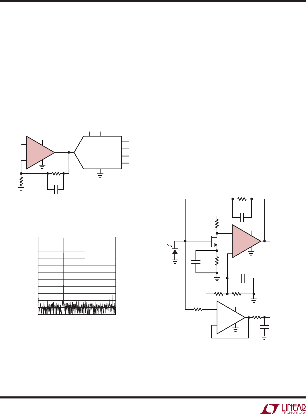
Figure 3. Single Supply 12-Bit ADC Driver
Typical applicaTions
12-Bit ADC Driver
Figure 3 shows the LTC6246 driving an LTC2366 12-bit A/D
converter. The low wideband noise of the LTC6246 main-
tains a 70dB SNR even without the use of an intermediate
antialiasing RC filter. On a single 3.3V supply with a 2.5V
reference, a full –1dBFS output can be obtained without
the amplifier transitioning between input regions, thus
minimizing crossover distortion. Figure 4 shows an FFT
obtained with a sampling rate of 2.2Msps and a 350kHz
input waveform. Spurious free dynamic range is a quite
handsome 82dB.
LTC6246
+
–
624678 F03
LTC2366
VREF
GND
VDD
3.3V 2.5V
CS
SDO
SCK
OVDD
3.3V
VIN
AIN
499Ω
1%
499Ω
1%
10pF
Figure 4. 350kHz FFT Showing 82dB SFDR
FREQUENCY (kHz)
0
MAGNITUDE (dB)
0
–10
–30
–50
–70
–20
–40
–60
–80
–90
–100
–110 400 800200 600
624678 F04
1000
fIN = 350.195kHz
fSAMP = 2.2Msps
SFDR = 82dB
SNR = 70dB
1024 POINT FFT
C3
0.1µF
LTC6246
–
+
624678 F05
3V
LT6003
–
+3V
3V
3V
VOUT = VR + IPD • 1M
–3dB BW = 700kHz
ICC = 2.2mA
OUTPUT NOISE = 160µVRMS MEASURED ON A 1MHz BW
VOUT IS REFERRED TO VR
AT ZERO PHOTOCURRENT, VOUT = VR
VR
R1
1M, 1%
R3
1k
R2
1k
C2
6.8nF
FILM
OR NPO
Q1
NXP
BF862
PD1
OSRAM
SFH213
IPD
R5
20k
R4
10k
R6
10M
C1
0.1pF
R7
1k
C4
1µF
Low Noise Low Power DC-Accurate Single Supply
Photodiode Amplifier
Figure 5 shows the LTC6246 applied as a low power high
performance transimpedance amplifier for a photodiode.
A low noise JFET Q1 acts as a current buffer, with R2 and
R3 imposing a low frequency gain of approximately 1.
Transimpedance gain is set by feedback resistor R1 to
1MΩ. R4 and R5 set the LTC6246 inputs at 1V below
the 3V rail, with C3 reducing their noise contribution.
By feedback this 1V also appears across R2, setting the
JFET quiescent current at 1mA completely independent
of its pinchoff voltage and IDSS characteristics. It does
this by placing the JFETs 1mA VGS at the gate referenced
to the source, which is sitting 1V above ground. For this
JFET, that will typically be about 500mV, and this voltage
is imposed as a reverse voltage on the photodiode PD1.
At zero IPD photocurrent, the output sits at the same volt-
age and rises as photocurrent increases. As mentioned
before, R2 and R3 set the JFET gain to 1 at low frequency.
Figure 5. Low Noise Low Power DC Accurate
Single Supply Photodiode Amplifier
LTC6246/LTC6247/LTC6248
17
624678fa
This is not the lowest noise configuration for a transistor, as
downstream noise sources appear at the input completely
unattenuated. At low frequency, this is not a concern for a
transimpedance amplifier because the noise gain is 1 and
the output noise is dominated by the 130nV/√Hz of the 1MΩ
R1. However, at increasing frequencies the capacitance
of the photodiode comes into play and the circuit noise
gain rises as the 1MΩ feedback looks back into lower and
lower impedance. But capacitor C2 comes to the rescue.
In addition to the obvious quenching of noise source R3,
capacitor C2 increases the JFET gain to about 30 at high
frequency effectively attenuating the downstream noise
contributions of R2 and the op amp input noise. Thus the
circuit achieves low input voltage noise at high frequency
where it is most needed. Amplifier LT6003 is used to
buffer the output voltage of the photodiode and R7 and
C4 are used to filter out the voltage noise of the LT6003.
Bandwidth to 700kHz was achieved with this circuit, with
integrated output noise being 160µVRMS up to 1MHz. Total
supply current was a very low 2.2mA.
Typical applicaTions
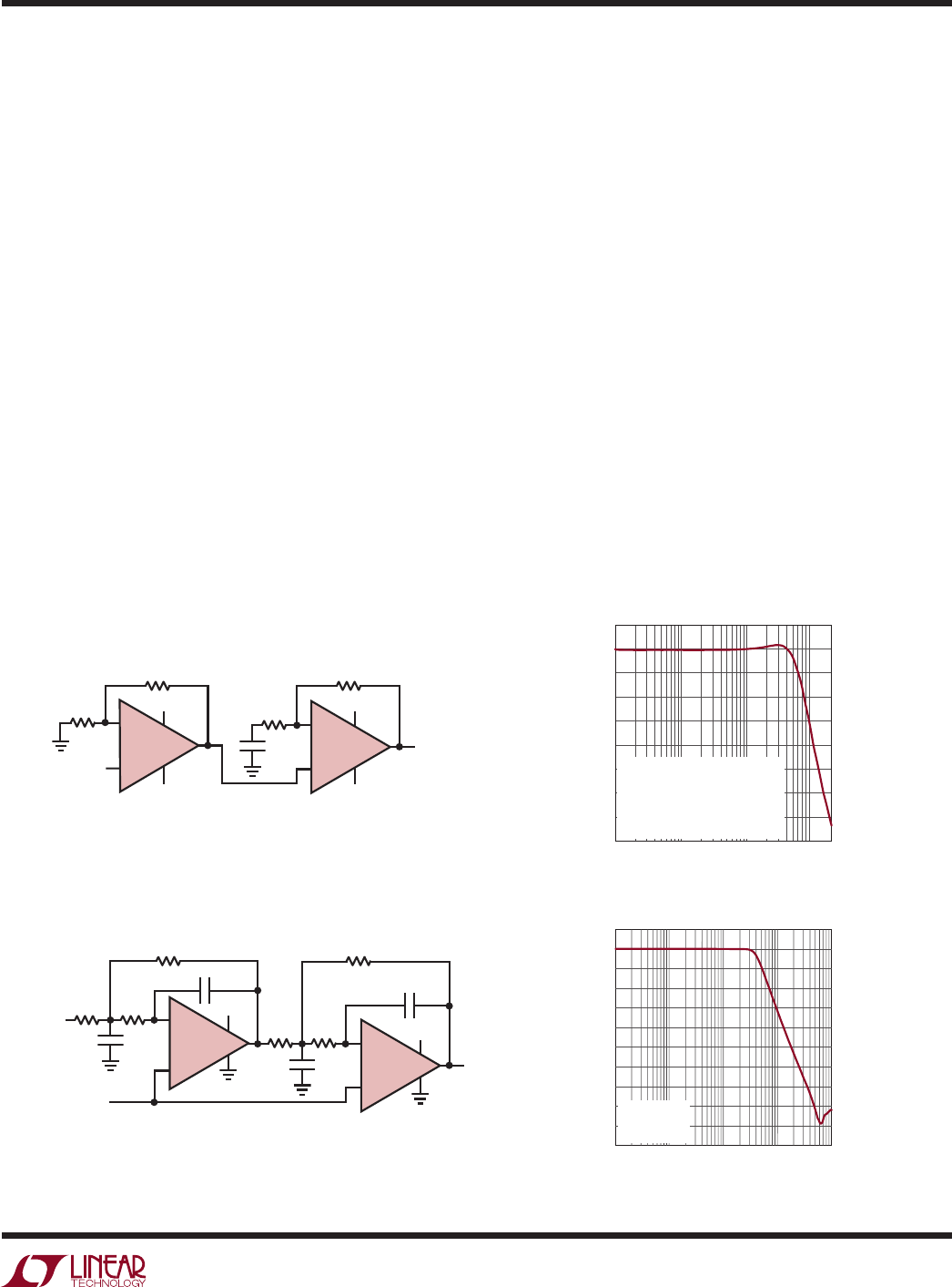
60dB 5.5MHz Gain Block
Figure 6 shows the LTC6247 configured as a low power
high gain high bandwidth block. Two amplifiers each
configured with a gain of 31V/V, are cascaded in series. A
660nF capacitor is used to limit the DC gain of the block
to around 30dB to minimize output offset voltage. Figure 7
shows the frequency response of the block. Mid-band
voltage gain is approximately 60dB with a –3dB frequency
of 5.5MHz, thus resulting in a gain-bandwidth product of
5.5GHz with only 1.9mA of quiescent supply current.
Single 2.7V Supply 4MHz 4th Order Butterworth Filter
Benefitting from low voltage operation and rail-to-rail
output, a low power filter that is suitable for antialiasing
can be built as shown in Figure 8. On a 2.7V supply the
filter has a passband of approximately 4MHz with 2VP-P
input signal and a stopband attenuation that is greater than
–75dB at 43MHz as shown in Figure 9. The resistor and
capacitor values can be scaled to reduce noise at the cost
of large signal power consumption and distortion.
624678 F06
–
+
1k 2.5V
–2.5V
2.5V
–2.5V
VIN
1/2LTC6247
50Ω
1.5k
–
+
1/2LTC6247
660nF VOUT
30k
Figure 6. 60dB 5.5MHz Gain Block
FREQUENCY (kHz)
10k
GAIN (dB)
65
60
50
40
30
55
45
35
25
20 1M100k 10M
624678 F07
VS = ±2.5V
VIN = 4.5mVP-P
RL = 1kΩ
DC GAIN = 30dB
(DUE TO 660nF DC BLOCKING CAP)
OUTPUT OFFSET = 4mV
Figure 7
Figure 8. Single 2.7V Supply 4MHz
4th Order Butterworth Filter
624678 F08
56pF
–
+
VIN 1.1k 2.3k
1/2LTC6247
12pF
2.7k 2.7V
1.2V
910Ω
910Ω
–
+
1/2LTC6247
120pF
2.7V
VOUT
5.6pF
1.1k
FREQUENCY (kHz)
10k
GAIN (dB)
10
–10
–30
–50
–70
–20
–40
–60
–80
–90
0
–100 100k 10M1M
624678 F09
100M
VS = 2.7V, 0V
VIN = 2VP-P
RL = 1kΩ to 0V
Figure 9
LTC6246/LTC6247/LTC6248
18
624678fa
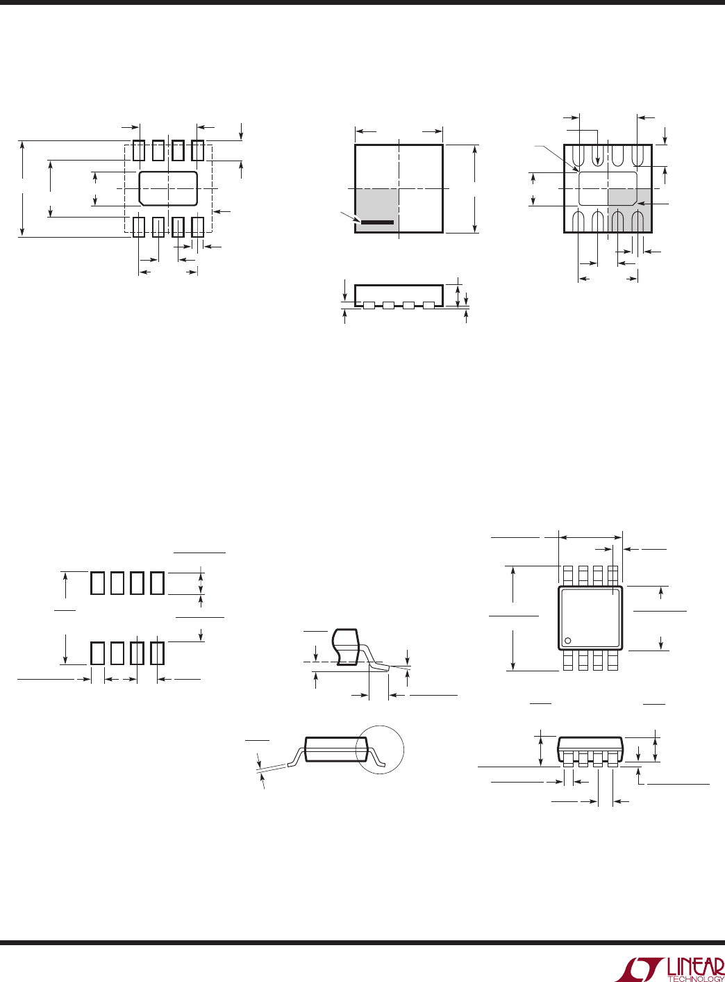
package DescripTion
KC Package
8-Lead Plastic UTDFN (2mm × 2mm)
(Reference LTC DWG # 05-08-1749 Rev Ø)
2.00 p0.10
2.00 p0.10
NOTE:
1. DRAWING IS NOT A JEDEC PACKAGE OUTLINE
2. DRAWING NOT TO SCALE
3. ALL DIMENSIONS ARE IN MILLIMETERS
4. DIMENSIONS OF EXPOSED PAD ON BOTTOM OF PACKAGE DO NOT INCLUDE
MOLD FLASH. MOLD FLASH, IF PRESENT, SHALL NOT EXCEED 0.15mm ON ANY SIDE
5. EXPOSED PAD SHALL BE SOLDER PLATED
6. SHADED AREA IS ONLY A REFERENCE FOR PIN 1 LOCATION ON THE
TOP AND BOTTOM OF PACKAGE
0.40 p 0.10
BOTTOM VIEW—EXPOSED PAD
0.64 p 0.10
0.55 p0.05
R = 0.115
TYP
R = 0.05
TYP
1.35 REF
1.37 p 0.10
1
4
85
PIN 1 BAR
TOP MARK
(SEE NOTE 6)
0.125 REF
0.00 – 0.05
(KC8) UTDFN 0107 REVØ
0.23 p 0.05
0.45 BSC
0.25 p 0.05
1.35 REF
RECOMMENDED SOLDER PAD PITCH AND DIMENSIONS
APPLY SOLDER MASK TO AREAS THAT ARE NOT SOLDERED
0.64 p0.05
1.37 p0.05
1.15 p0.05
0.70 p0.05
2.55 p0.05
PACKAGE
OUTLINE
0.45 BSC
PIN 1 NOTCH
R = 0.20 OR
0.25 s 45o
CHAMFER
MS8 Package
8-Lead Plastic MSOP
(Reference LTC DWG # 05-08-1660 Rev F)
MSOP (MS8) 0307 REV F
0.53 p 0.152
(.021 p .006)
SEATING
PLANE
NOTE:
1. DIMENSIONS IN MILLIMETER/(INCH)
2. DRAWING NOT TO SCALE
3. DIMENSION DOES NOT INCLUDE MOLD FLASH, PROTRUSIONS OR GATE BURRS.
MOLD FLASH, PROTRUSIONS OR GATE BURRS SHALL NOT EXCEED 0.152mm (.006") PER SIDE
4. DIMENSION DOES NOT INCLUDE INTERLEAD FLASH OR PROTRUSIONS.
INTERLEAD FLASH OR PROTRUSIONS SHALL NOT EXCEED 0.152mm (.006") PER SIDE
5. LEAD COPLANARITY (BOTTOM OF LEADS AFTER FORMING) SHALL BE 0.102mm (.004") MAX
0.18
(.007)
0.254
(.010)
1.10
(.043)
MAX
0.22 – 0.38
(.009 – .015)
TYP
0.1016 p 0.0508
(.004 p .002)
0.86
(.034)
REF
0.65
(.0256)
BSC
0o – 6o TYP
DETAIL “A”
DETAIL “A”
GAUGE PLANE
1 2 34
4.90 p 0.152
(.193 p .006)
8765
3.00 p 0.102
(.118 p .004)
(NOTE 3)
3.00 p 0.102
(.118 p .004)
(NOTE 4)
0.52
(.0205)
REF
5.23
(.206)
MIN
3.20 – 3.45
(.126 – .136)
0.889 p 0.127
(.035 p .005)
RECOMMENDED SOLDER PAD LAYOUT
0.42 p 0.038
(.0165 p .0015)
TYP
0.65
(.0256)
BSC
LTC6246/LTC6247/LTC6248
19
624678fa
package DescripTion
MS Package
10-Lead Plastic MSOP
(Reference LTC DWG # 05-08-1661 Rev E)
MSOP (MS) 0307 REV E
0.53 ± 0.152
(.021 ± .006)
SEATING
PLANE
0.18
(.007)
1.10
(.043)
MAX
0.17 – 0.27
(.007 – .011)
TYP
0.86
(.034)
REF
0.50
(.0197)
BSC
1 2 34 5
4.90 ± 0.152
(.193 ± .006)
0.497 ± 0.076
(.0196 ± .003)
REF
8910 76
3.00 ± 0.102
(.118 ± .004)
(NOTE 3)
3.00 ± 0.102
(.118 ± .004)
(NOTE 4)
NOTE:
1. DIMENSIONS IN MILLIMETER/(INCH)
2. DRAWING NOT TO SCALE
3. DIMENSION DOES NOT INCLUDE MOLD FLASH, PROTRUSIONS OR GATE BURRS.
MOLD FLASH, PROTRUSIONS OR GATE BURRS SHALL NOT EXCEED 0.152mm (.006") PER SIDE
4. DIMENSION DOES NOT INCLUDE INTERLEAD FLASH OR PROTRUSIONS.
INTERLEAD FLASH OR PROTRUSIONS SHALL NOT EXCEED 0.152mm (.006") PER SIDE
5. LEAD COPLANARITY (BOTTOM OF LEADS AFTER FORMING) SHALL BE 0.102mm (.004") MAX
0.254
(.010) 0° – 6° TYP
DETAIL “A”
DETAIL “A”
GAUGE PLANE
5.23
(.206)
MIN
3.20 – 3.45
(.126 – .136)
0.889 ± 0.127
(.035 ± .005)
RECOMMENDED SOLDER PAD LAYOUT
0.305 ± 0.038
(.0120 ± .0015)
TYP
0.50
(.0197)
BSC
0.1016 ± 0.0508
(.004 ± .002)
LTC6246/LTC6247/LTC6248
20
624678fa
package DescripTion
MS Package
16-Lead Plastic MSOP
(Reference LTC DWG # 05-08-1669 Rev Ø)
MSOP (MS16) 1107 REV Ø
0.53 p 0.152
(.021 p .006)
SEATING
PLANE
0.18
(.007)
1.10
(.043)
MAX
0.17 –0.27
(.007 – .011)
TYP
0.86
(.034)
REF
0.50
(.0197)
BSC
16151413121110
12345678
9
NOTE:
1. DIMENSIONS IN MILLIMETER/(INCH)
2. DRAWING NOT TO SCALE
3. DIMENSION DOES NOT INCLUDE MOLD FLASH, PROTRUSIONS OR GATE BURRS.
MOLD FLASH, PROTRUSIONS OR GATE BURRS SHALL NOT EXCEED 0.152mm (.006") PER SIDE
4. DIMENSION DOES NOT INCLUDE INTERLEAD FLASH OR PROTRUSIONS.
INTERLEAD FLASH OR PROTRUSIONS SHALL NOT EXCEED 0.152mm (.006") PER SIDE
5. LEAD COPLANARITY (BOTTOM OF LEADS AFTER FORMING) SHALL BE 0.102mm (.004") MAX
0.254
(.010) 0o – 6o TYP
DETAIL “A”
DETAIL “A”
GAUGE PLANE
5.23
(.206)
MIN
3.20 – 3.45
(.126 – .136)
0.889 p 0.127
(.035 p .005)
RECOMMENDED SOLDER PAD LAYOUT
0.305 p 0.038
(.0120 p .0015)
TYP
0.50
(.0197)
BSC
4.039 p 0.102
(.159 p .004)
(NOTE 3)
0.1016 p 0.0508
(.004 p .002)
3.00 p 0.102
(.118 p .004)
(NOTE 4)
0.280 p 0.076
(.011 p .003)
REF
4.90 p 0.152
(.193 p .006)
LTC6246/LTC6247/LTC6248
21
624678fa
S6 Package
6-Lead Plastic TSOT-23
(Reference LTC DWG # 05-08-1636)
package DescripTion
1.50 – 1.75
(NOTE 4)
2.80 BSC
0.30 – 0.45
6 PLCS (NOTE 3)
DATUM ‘A’
0.09 – 0.20
(NOTE 3) S6 TSOT-23 0302 REV B
2.90 BSC
(NOTE 4)
0.95 BSC
1.90 BSC
0.80 – 0.90
1.00 MAX 0.01 – 0.10
0.20 BSC
0.30 – 0.50 REF
PIN ONE ID
NOTE:
1. DIMENSIONS ARE IN MILLIMETERS
2. DRAWING NOT TO SCALE
3. DIMENSIONS ARE INCLUSIVE OF PLATING
4. DIMENSIONS ARE EXCLUSIVE OF MOLD FLASH AND METAL BURR
5. MOLD FLASH SHALL NOT EXCEED 0.254mm
6. JEDEC PACKAGE REFERENCE IS MO-193
3.85 MAX
0.62
MAX
0.95
REF
RECOMMENDED SOLDER PAD LAYOUT
PER IPC CALCULATOR
1.4 MIN
2.62 REF
1.22 REF
LTC6246/LTC6247/LTC6248
22
624678fa
package DescripTion
TS8 Package
8-Lead Plastic TSOT-23
(Reference LTC DWG # 05-08-1637)
1.50 – 1.75
(NOTE 4)
2.80 BSC
0.22 – 0.36
8 PLCS (NOTE 3)
DATUM ‘A’
0.09 – 0.20
(NOTE 3) TS8 TSOT-23 0802
2.90 BSC
(NOTE 4)
0.65 BSC
1.95 BSC
0.80 – 0.90
1.00 MAX 0.01 – 0.10
0.20 BSC
0.30 – 0.50 REF
PIN ONE ID
NOTE:
1. DIMENSIONS ARE IN MILLIMETERS
2. DRAWING NOT TO SCALE
3. DIMENSIONS ARE INCLUSIVE OF PLATING
4. DIMENSIONS ARE EXCLUSIVE OF MOLD FLASH AND METAL BURR
5. MOLD FLASH SHALL NOT EXCEED 0.254mm
6. JEDEC PACKAGE REFERENCE IS MO-193
3.85 MAX
0.52
MAX
0.65
REF
RECOMMENDED SOLDER PAD LAYOUT
PER IPC CALCULATOR
1.4 MIN
2.62 REF
1.22 REF
LTC6246/LTC6247/LTC6248
23
624678fa
Information furnished by Linear Technology Corporation is believed to be accurate and reliable.
However, no responsibility is assumed for its use. Linear Technology Corporation makes no representa-
tion that the interconnection of its circuits as described herein will not infringe on existing patent rights.
revision hisTory
REV DATE DESCRIPTION PAGE NUMBER
A 2/10 Changes to Graph G15 9
LTC6246/LTC6247/LTC6248
24
624678fa
Linear Technology Corporation
1630 McCarthy Blvd., Milpitas, CA 95035-7417
(408) 432-1900 ● FAX: (408) 434-0507 ● www.linear.com
LINEAR TECHNOLOGY CORPORATION 2009
LT 0210 REV A • PRINTED IN USA
Typical applicaTion
PART NUMBER DESCRIPTION COMMENTS
Operational Amplifiers
LT1818/LT1819 Single/Dual Wide Bandwidth, High Slew Rate Low Noise and
Distortion Op Amps
400MHz, 9mA, 6nV/√Hz, 2500V/µs, 1.5mV –85dBc at 5MHz
LT1806/LT1807 Single/Dual Low Noise Rail-to-Rail Input and Output Op Amps 325MHz, 13mA, 3.5nV/√Hz, 140V/µs, 550µV, 85mA Output Drive
LT6230/LT6231/
LT6232
Single/Dual/Quad Low Noise Rail-to-Rail Output Op Amps 215MHz, 3.5mA, 1.1nV/√Hz, 70V/µs, 350µV
LT6200/LT6201 Single/Dual Ultralow Noise Rail-to-Rail Input/Output Op Amps 165MHz, 20mA, 0.95nV/√Hz, 44V/µs, 1mV
LT6202/LT6203/
LT6204
Single/Dual/Quad Ultralow Noise Rail-to-Rail Op Amp 100MHz, 3mA, 1.9nV/√Hz, 25V/µs, 0.5mV
LT1468 16-Bit Accurate Precision High Speed Op Amp 90MHz, 3.9mA, 5nV/√Hz, 22V/µs, 175µV,
–96.5dB THD at 10VP-P, 100kHz
LT1803/LT1804/
LT1805
Single/Dual/Quad Low Power High Speed Rail-to-Rail Input
and Output Op Amps
85MHz, 3mA, 21nV√Hz, 100V/µs, 2mV
LT1801/LT1802 Dual/Quad Low Power High Speed Rail-to-Rail Input and
Output Op Amps
80MHz, 2mA, 8.5nV√Hz, 25V/µs, 350µV
LT6552 Single Supply Rail-to-Rail Output Video Difference Amplifier 75MHz (–3dB), 13.5mA, 55.5nV/√Hz, 350V/µs, 20mV
LT1028 Ultralow Noise, Precision High Speed Op Amps 75MHz, 9.5mA, 0.85nV/√Hz, 11V/µs, 40µV
LT6233/LT6234/
LT6235
Single/Dual/Quad Low Noise Rail-to-Rail Output Op Amps 60MHz, 1.2mA, 1.2nV/√Hz, 15V/µs, 0.5mV
LT6220/LT6221/
LT6222
Single/Dual/Quad Low Power High Speed Rail-to-Rail Input
and Output Op Amps
60MHz, 1mA, 10nV/√Hz, 20V/µs, 350µV
LT6244 Dual High Speed CMOS Op Amp 50MHz, 7.4mA, 8nV/√Hz, 35V/µs, 100µV, Input Bias Current = 1pA
LT1632/LT1633 Dual/Quad Rail-to-Rail Input and Output Precision Op Amps 45MHz, 4.3mA, 12nV/√Hz, 45V/µs, 1.35mV
LT1630/LT1631 Dual/Quad Rail-to-Rail Input and Output Op Amps 30MHz, 3.5mA, 6nV/√Hz, 10V/µs, 525µV
LT1358/LT1359 Dual/Quad Low Power High Speed Op Amps 25MHz, 2.5mA, 8nV/√Hz, 600V/µs, 800µV, Drives All Capacitive Loads
ADC’s
LTC2366 3Msps, 12-Bit ADC Serial I/O 72dB SNR, 7.8mW No Data Latency TSOT-23 Package
LTC2365 1Msps, 12-Bit ADC Serial I/O 73dB SNR, 7.8mW No Data Latency TSOT-23 Package
LTC1417 Low Power 14-Bit 400ksps ADC Parallel I/O Single 5V or ±5V Supplies, 0V to 4.096V or ±2.048V Input Range
LTC1274 Low Power 12-Bit 400ksps ADC Parallel I/O 10mW Single 5V or ±5V Supplies, 0V to 4.096V or ±2.048V Input Range
relaTeD parTs
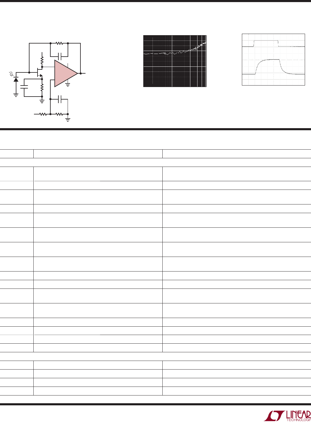
LTC6246
+
–
624678 TA02a
VOUT ≈ 0.5V + IPD • 1M
3V
R1
1M, 1%
3V
3V
R2
1k
IPD
C3
0.1µF
C1
0.1pF
R5
20k
R4
10k
R3
1k
–3dB BW = 700kHz
ICC = 2.2mA
OUTPUT NOISE = 153µVRMS
MEASURED ON A 1MHz BW
C2
6.8nF
FILM
OR NPO
PD1
OSRAM
SFH213
Q1
NXP
BF862
20nV/√Hz/DIV
200
0
624678 TA02b
100kHz 1MHz
10kHz
0V
5V/DIV
LED DRIVER
VOLTAGE
624678 TA02c
500ns/DIV
500mV/DIV
OUTPUT
WAVEFORM
700kHz, 1MΩ Single Supply Photodiode Amplifier Output Noise Spectrum Transient Response