MAX5025 MAX5028 Datasheet. Www.s Manuals.com. R2 Maxim
User Manual: Marking of electronic components, SMD Codes AA, AA**, AA***, AA-, AA-**, AA-***, AA=***, AAA, AAA***, AAC, AAD, AAE, AAE**, AAF, AAFI, AAG, AAH**, AAHC, AAHO, AAI**, AAIK, AAJ**, AAJ***, AAJF*, AAJI, AAJJ, AAL***, AAM***, AAN***, AANC, AAP, AAQ, AAR, AAS, AASQ, AASR, AAT***, AATJ, AATK, AATL, AATM, AAU, AAU**, AAW, AAX, Aa. Datasheets 2N7002T, 2SD1757K, 74AHC1G00GW, AME8804AEEY, BCW60A, BCX51, BD48E23G, BD48K23G, BL3406B-1.0V, BL9641, LR9641, MAX1736EUT41-T, MAX1736EUT42-T, MAX2644, MAX4335EXT-T, MAX4336EXT
Open the PDF directly: View PDF ![]() .
.
Page Count: 14
General Description
The MAX5025–MAX5028 constant-frequency, pulse-
width modulating (PWM), low-noise boost converters
are intended for low-voltage systems that often need a
locally generated high voltage. These devices are
capable of generating low-noise, high output voltages
required for varactor diode biasing in TV tuners, set-top
boxes, and PCI cable modems. The MAX5025–
MAX5028 operate from as low as 3V and switch at
500kHz.
The constant-frequency, current-mode PWM architec-
ture provides for low output noise that is easy to filter. A
40V lateral DMOS device is used as the internal power
switch, making the devices ideal for boost converters
up to 36V. The MAX5025/MAX5026 adjustable versions
require the use of external feedback resistors to set the
output voltage. The MAX5027/MAX5028 offer a fixed
30V output. These devices are available in a small, 6-
pin SOT23 package.
Applications
TV Tuner Power Supply
Low-Noise Varactor Diode Biasing
Set-Top Box Tuner Power Supply
PCI Cable Modem
Voice-Over-Cable
LCD Power Supply
Avalanche Photodiode Biasing
Features
♦Input Voltage Range:
3V to 11V (MAX5026/MAX5028)
4.5V to 11V (MAX5025/MAX5027)
♦Wide Output Voltage Range: VCC to 36V
♦Output Power: 120mW (max)
♦User-Adjustable Output Voltage with
MAX5025/MAX5026 Using External Feedback
Resistors
♦Fixed 30V Output Voltage: MAX5027/MAX5028
♦Internal 1.3Ω (typ), 40V Switch
♦Constant PWM Frequency Provides Easy Filtering
in Low-Noise Applications
♦500kHz (typ) Switching Frequency
♦1μA (max) Shutdown Current
♦Small, 6-Pin SOT23 Package
MAX5025–MAX5028
500kHz, 36V Output, SOT23,
PWM Step-Up DC-DC Converters
________________________________________________________________
Maxim Integrated Products
1
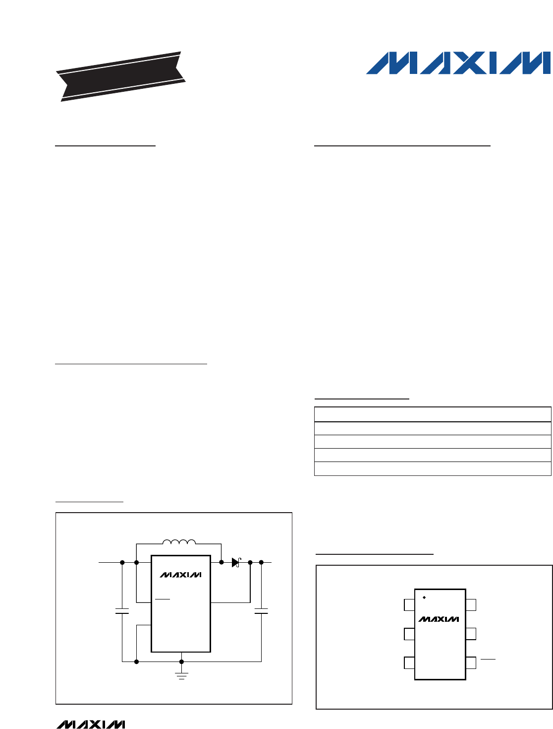
GND
FB
16LX
5V
CC
PGND
MAX5025–
MAX5028
SOT23-6
TOP VIEW
2
34
SHDN
Pin Configuration
VOUT
30V
C1 C2
L1
VCC = 4.5V TO 11V
(MAX5027)
VCC = 3V TO 11V
(MAX5028) D1
VCC
GND
FB
PGND
LX
MAX5027
MAX5028
SHDN
Typical Operating Circuit
19-2239; Rev 2; 3/09
EVALUATION KIT
AVAILABLE
Ordering Information
PA RT TEMP RANGE PIN- PACK AGE
MAX5025EUT-T -40°C to +85°C 6 SOT23-6
MAX5026EUT-T -40°C to +85°C 6 SOT23-6
MAX5027EUT-T -40°C to +85°C 6 SOT23-6
MAX5028EUT-T -40°C to +85°C 6 SOT23-6
For pricing, delivery, and ordering information, please contact Maxim Direct at 1-888-629-4642,
or visit Maxim’s website at www.maxim-ic.com.
Selector Guide appears at end of data sheet.

MAX5025–MAX5028
500kHz, 36V Output, SOT23,
Step-Up DC-DC Converters
2 _______________________________________________________________________________________
ABSOLUTE MAXIMUM RATINGS
ELECTRICAL CHARACTERISTICS
(VCC = 5V, SHDN = VCC, TA= -40°C to +85°C, unless otherwise noted. Typical values are at TA= +25°C.) (Note 1)
Stresses beyond those listed under “Absolute Maximum Ratings” may cause permanent damage to the device. These are stress ratings only, and functional
operation of the device at these or any other conditions beyond those indicated in the operational sections of the specifications is not implied. Exposure to
absolute maximum rating conditions for extended periods may affect device reliability.
VCC to GND............................................................-0.3V to +12V
PGND to GND .......................................................-0.1V to +0.1V
FB to GND (MAX5025/MAX5026)...............-0.3V to (VCC + 0.3V)
FB to GND (MAX5027/MAX5028)...........................-0.3V to +40V
SHDN to GND.............................................-0.3V to (VCC + 0.3V)
LX to GND ..............................................................-0.3V to +45V
Peak LX Current ................................................................600mA
Operating Temperature Range ...........................-40°C to +85°C
Continuous Power Dissipation (TA= +70°C)
6-Pin SOT23 (derate 8.7mW/°C above +70°C)..........695.7mW
Junction Temperature......................................................+150°C
Storage Temperature Range .............................-65°C to +165°C
Lead Temperature (soldering 10s) ..................................+300°C
PARAMETER
SYMBOL
CONDITIONS
MIN TYP MAX
UNITS
SUPPLY VOLTAGE
MAX5026/MAX5028 3.0 11
Input Voltage Range VCC MAX5025/MAX5027 4.5 11 V
Undervoltage Lockout
VUVLO
Rise/fall, hysteresis = 3mV
2.25 2.65 2.95
V
Supply Current ICC MAX5025/MAX5026, FB = 1.4V
MAX5027/MAX5028, FB = 35V
350 1000
µA
Shutdown Current ISHDN SHDN = GND
0.01
1µA
BOOST CONVERTER
MAX5025/MAX5027
345 500 1000
Switching Frequency fSW MAX5026/MAX5028, VCC = 3.3V
410 500
670 kHz
MAX5025/MAX5027,
ILOAD = 2mA, VCC = 4.5V to 11V,
VOUT = 30V
0.25
Line Regulation
MAX5026/MAX5028,
ILOAD = 0.5mA, VCC = 3V to 11V,
VOUT = 30V
0.25
%/V
MAX5025/MAX5027,
VCC = 5V, ILOAD = 0 to 4mA,
VOUT = 30V
2.0
Load Regulation
MAX5026/MAX5028,
VCC = 3.3V, ILOAD = 0 to 1mA,
VOUT = 30V
1.0
%
Thermal Shutdown
140
°C
Thermal Shutdown Hysteresis 2°C
MAX5025–MAX5028
ELECTRICAL CHARACTERISTICS (continued)
(VCC = 5V, SHDN = VCC, TA= -40°C to +85°C, unless otherwise noted. Typical values are at TA= +25°C.) (Note 1)
PARAMETER SYMBOL CONDITIONS MIN TYP MAX UNITS
MAX5025, VCC = 4.5V to 11V 1.19 1.25 1.31
MAX5027, VCC = 4.5V to 11V 28.5 30.0 31.5
MAX5026, VCC = 3.3V to 11V 1.212 1.25 1.288
FB Set Point VFB
MAX5028, VCC = 3.3V to 11V 29.0 30 31
V
MAX5025/MAX5026, FB = 1V 110 310 nA
FB Input Bias Current IFB MAX5027/MAX5028, FB = 30V 100 170 µA
Output Voltage
Adjustment Range MAX5025/MAX5026 VCC + 1 36 V
LX OUTPUT
MAX5026/MAX5028,
VCC = 3V 2.0 4.0
VCC = 5V 1.3 3.0
LX On-Resistance RON ILX = 40mA
VCC = 11V 1.0 2.5
Ω
Switch Current Limit ILIM Note 2 260 mA
MAX5025/MAX5026,
VFB = 1.4V
LX Leakage Current VLX = 40V
MAX5027/MAX5028,
VFB = 35V
0.01 10 µA
LOGIC INPUT: SHDN
Input Low Level VIL 0.8 V
Input High Level VIH 2.4 V
Input Bias Current -1 1 µA
Note 1: All devices are 100% production tested at TA= +25°C. All temperature limits are guaranteed by design.
Note 2: Switch current-limit accuracy is typically ±20% and is a function of the input voltage. ILIM = (VIN/5) (260mA).
500kHz, 36V Output, SOT23,
Step-Up DC-DC Converters
_______________________________________________________________________________________ 3
MAX5025–MAX5028
500kHz, 36V Output, SOT23,
Step-Up DC-DC Converters
4 _______________________________________________________________________________________
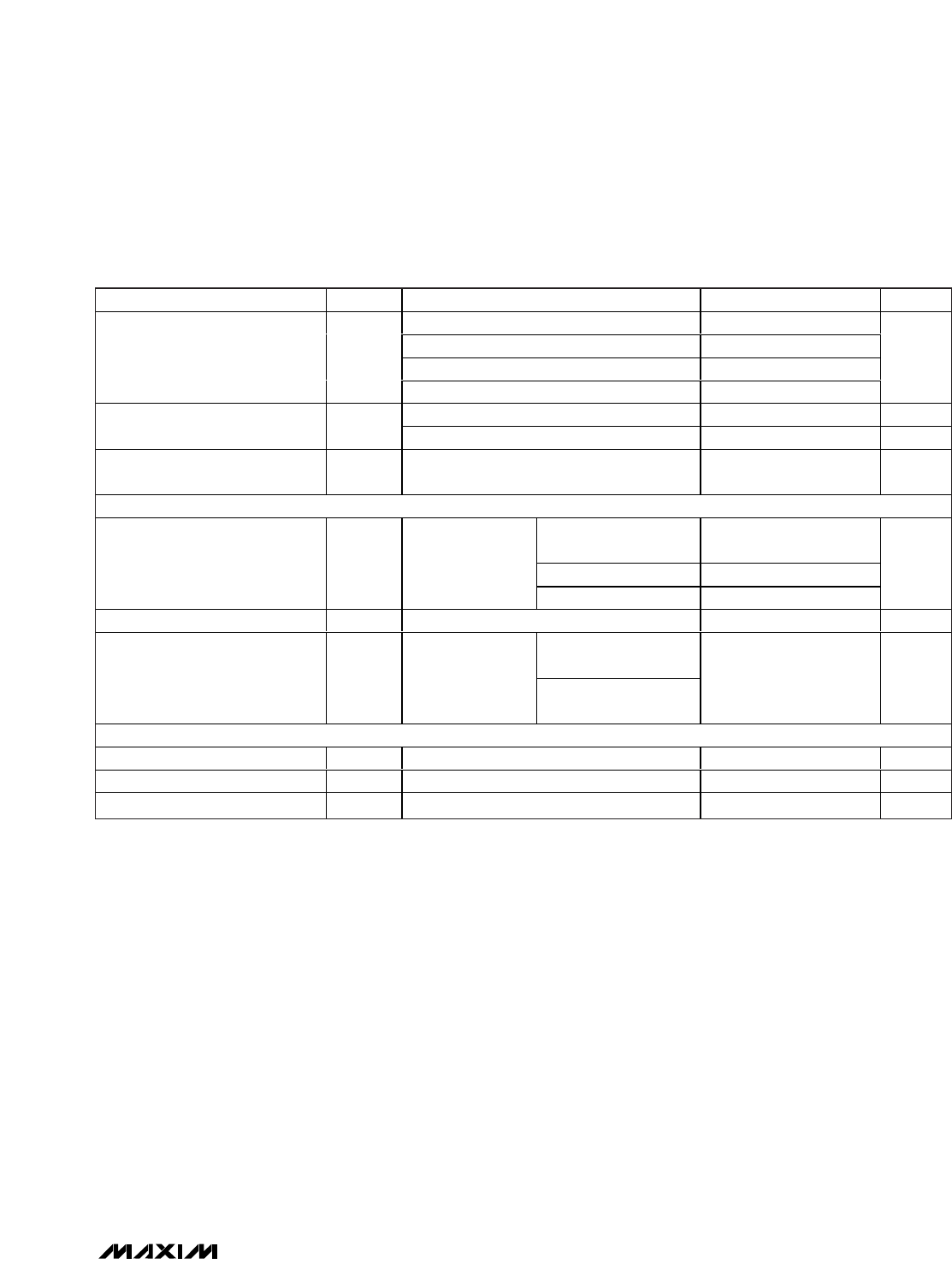
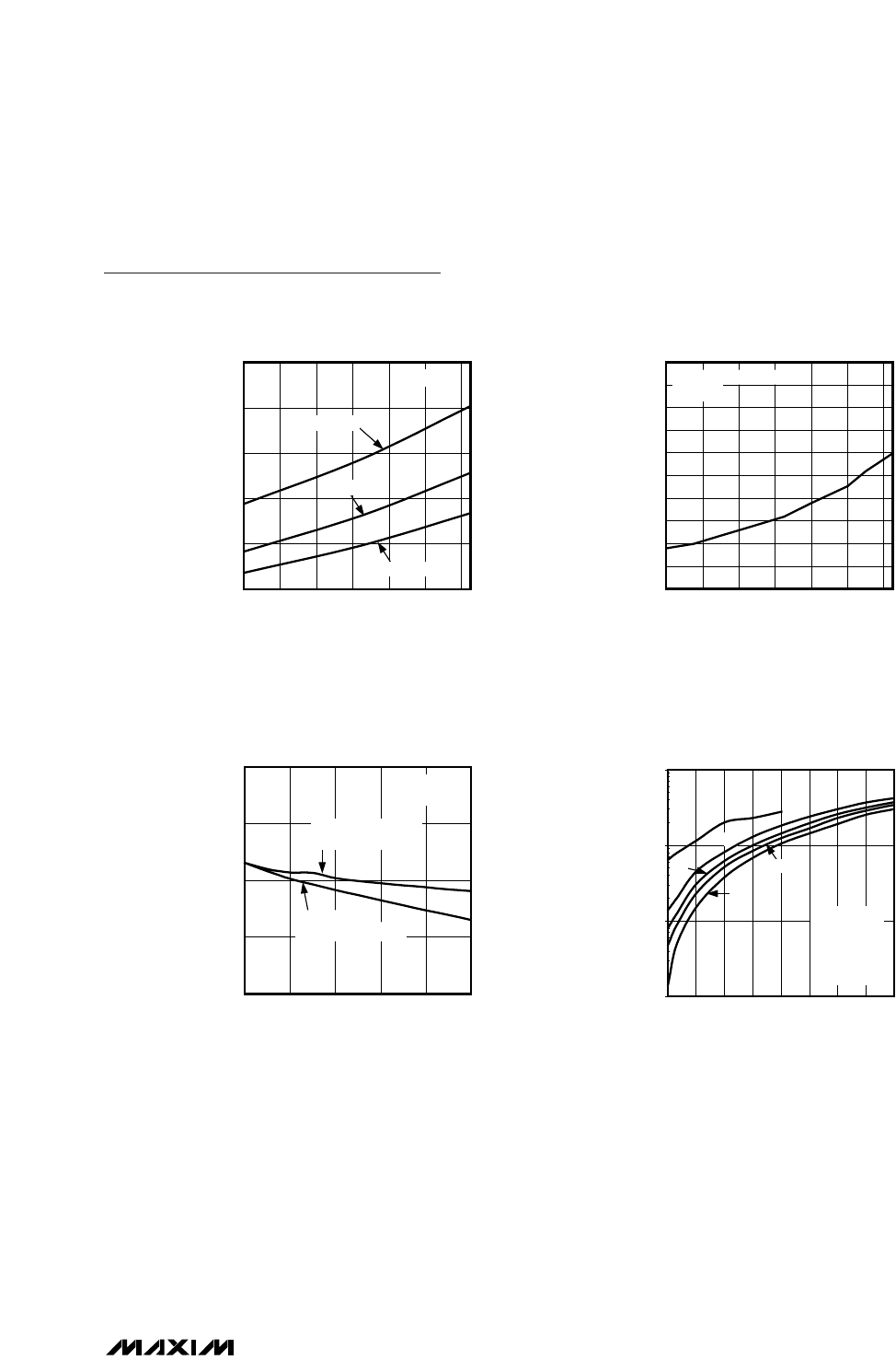
0
20
10
40
30
50
60
80
70
90
0246810
MAX5025-28 toc01
LOAD CURRENT (mA)
EFFICIENCY (%)
EFFICIENCY vs. LOAD CURRENT
(VOUT = 12V)
MAX5026
VCC = 5V,
VOUT = 12V
CIRCUIT OF FIGURE 2.
R1 = 147kΩ, R2 = 16.2kΩ
0
20
10
50
40
30
80
70
60
90
04268
MAX5025-28 toc02
LOAD CURRENT (mA)
EFFICIENCY (%)
EFFICIENCY vs. LOAD CURRENT
(VOUT = 15V)
MAX5026
VCC = 5V,
VOUT = 12V
CIRCUIT OF FIGURE 2.
R1 = 147kΩ, R2 = 13kΩ
0
20
10
30
60
70
50
40
80
012345
MAX5025-28 toc03
LOAD CURRENT (mA)
EFFICIENCY (%)
EFFICIENCY vs. LOAD CURRENT
(VOUT = 24V)
MAX5026
VCC = 5V,
VOUT = 24V
CIRCUIT OF FIGURE 2.
R1 = 147kΩ, R2 = 8.07kΩ
0
10
30
20
50
60
40
70
01234
MAX5025-28 toc04
LOAD CURRENT (mA)
EFFICIENCY (%)
EFFICIENCY vs. LOAD CURRENT
(VOUT = 30V)
MAX5026
VCC = 5V,
VOUT = 30V
CIRCUIT OF FIGURE 2.
R1 = 147kΩ, R2 = 6.34kΩ
0
0.5
1.0
1.5
2.0
2.5
3.0
3.5
4.0
01234
MAX5025-28 toc05
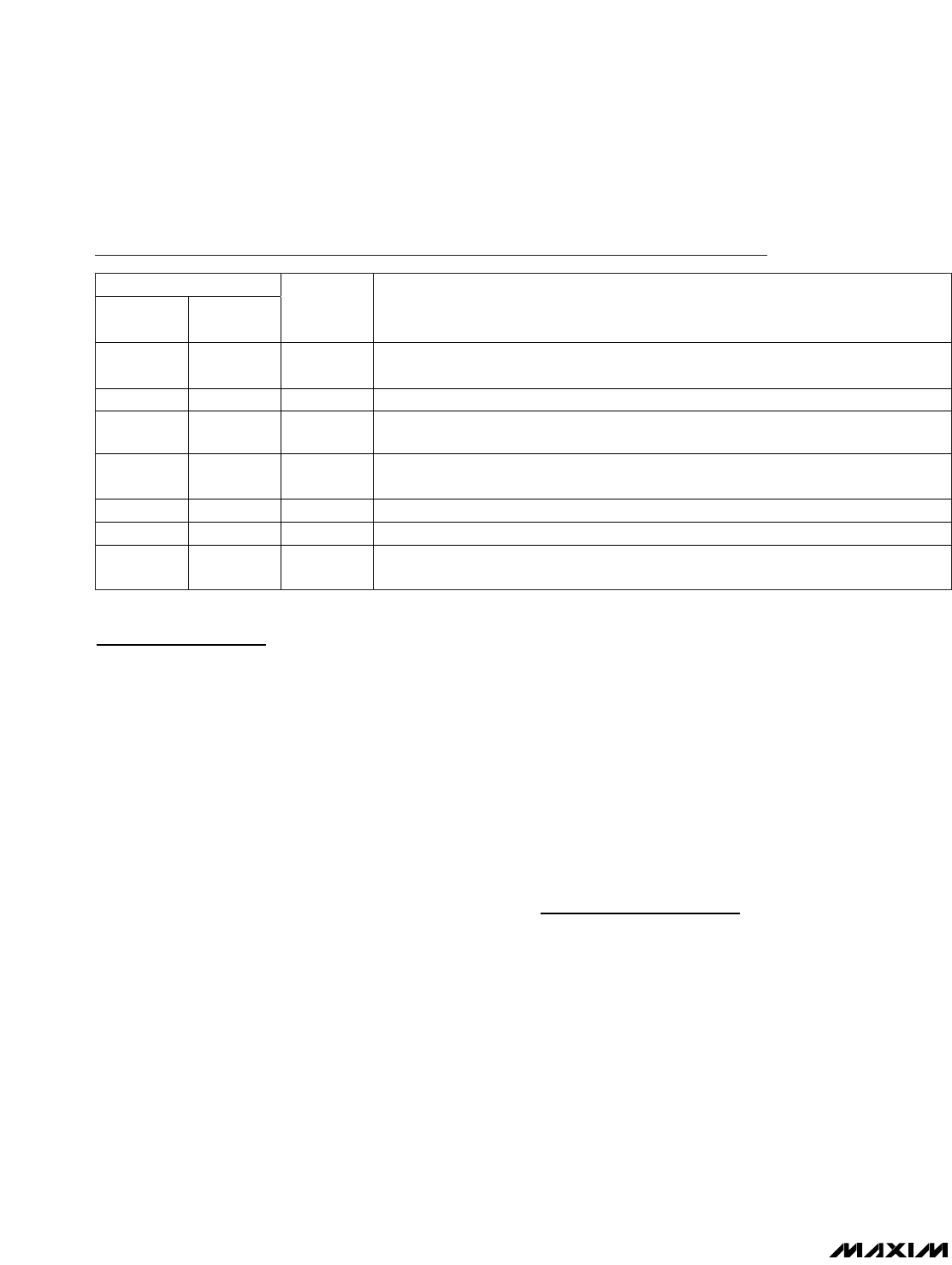
LOAD CURRENT (mA)
STARTUP VOLTAGE (V)
MAX5026 MINIMUM STARTUP VOLTAGE
vs. LOAD CURRENT
0
150
100
50
200
250
300
350
400
450
500
036912
MAX5025-28 toc06
SUPPLY VOLTAGE (V)
SUPPLY CURRENT (μA)
MAX5026/MAX5028
SUPPLY CURRENT vs. SUPPLY VOLTAGE
CURRENT INTO VCC PIN
DEVICE NOT SWITCHING
0
2
4
6
8
10
12
14
16
357911
MAX5025-28 toc07
SUPPLY VOLTAGE (V)
NO LOAD SUPPLY CURRENT (mA)
MAX5026
NO LOAD SUPPLY CURRENT
vs. SUPPLY VOLTAGE
CIRCUIT OF FIGURE 2
VOUT = 30V
150
350
250
550
450
750
650
850
-40 0 20-20 40 60 80
SUPPLY CURRENT vs. TEMPERATURE
MAX5025-28 toc08
TEMPERATURE (°C)
SUPPLY CURRENT (μA)
CURRENT INTO VCC PIN
VCC = 11V
VCC = 9V
VCC = 7V
VCC = 5V
VCC = 3V
200
300
250
450
400
350
600
550
500
650
-40 0 20-20 40 60 80
MAX5025-28 toc09
TEMPERATURE (°C)
SWITCHING FREQUENCY (kHz)
MAX5026
SWITCHING FREQUENCY vs. TEMPERATURE
VCC = 5V
VOUT = 30V
CIRCUIT OF FIGURE 2.
Typical Operating Characteristics
(VCC = 5V, VOUT = 30V, TA= +25°C, unless otherwise noted.)

MAX5025–MAX5028
Typical Operating Characteristics (continued)
(VCC = 5V, VOUT = 30V, TA= +25°C, unless otherwise noted.)
500kHz, 36V Output, SOT23,
Step-Up DC-DC Converters
_______________________________________________________________________________________
5
EXITING SHUTDOWN
MAX5025-28 toc10
5V
OUTPUT
VOLTAGE
20V/div
INDUCTOR
CURRENT
50mA/div
SHUTDOWN
VOLTAGE
5V/div
30V
5V
2ms/div
MAX5026, VCC = 5V, VOUT = 30V, ILOAD = 1mA.
CIRCUIT OF FIGURE 3
ENTERING SHUTDOWN
MAX5025-28 toc11
30V
OUTPUT
VOLTAGE
20V/div
SHUTDOWN
VOLTAGE
5V/div
5V
5V
0V
100ms/div
MAX5026, VCC = 5V, VOUT = 30V, ILOAD = 1mA.
CIRCUIT OF FIGURE 3
MAX5025-28 toc12
LX PIN
20V/div
VOUT
2mV/div
AC-COUPLED
IL
100mA/div
0V
0mA
1μs/div
MAX5026, VCC = 5V, VOUT = 30V, ILOAD = 0.1mA.
CIRCUIT OF FIGURE 2
LIGHT-LOAD SWITCHING WAVEFORM
WITHOUT RC FILTER
MAX5025-28 toc13
LX PIN
20V/div
VOUT
1mV/div
AC-COUPLED
IL
100mA/div
0V
0mA
1μs/div
MAX5026, VCC = 5V, VOUT = 30V, ILOAD = 0.1mA.
CIRCUIT OF FIGURE 3
LIGHT-LOAD SWITCHING WAVEFORM
WITH RC FILTER
MAX5025-28 toc14
LX PIN
20V/div
VOUT
5mV/div
AC-COUPLED
IL
200mA/div
0V
0mA
1μs/div
MAX5026, VCC = 5V, VOUT = 30V, ILOAD = 2mA.
CIRCUIT OF FIGURE 2
MEDIUM-LOAD SWITCHING WAVEFORM
WITHOUT RC FILTER
MAX5025-28 toc15
LX PIN
20V/div
VOUT
1mV/div
AC-COUPLED
IL
200mA/div
0V
0mA
1μs/div
MAX5026, VCC = 5V, VOUT = 30V, ILOAD = 2mA.
CIRCUIT OF FIGURE 3
MEDIUM-LOAD SWITCHING WAVEFORM
WITH RC FILTER
MAX5025–MAX5028
500kHz, 36V Output, SOT23,
Step-Up DC-DC Converters
6 _______________________________________________________________________________________
Typical Operating Characteristics (continued)
(VCC = 5V, VOUT = 30V, TA= +25°C, unless otherwise noted.)
MAX5025-28 toc17
LX PIN
20V/div
VOUT
1mV/div
AC-COUPLED
IL
200mA/div
0V
0mA
1μs/div
MAX5026, VCC = 5V, VOUT = 30V, ILOAD = 4mA.
CIRCUIT OF FIGURE 3
HEAVY-LOAD SWITCHING WAVEFORM
WITH RC FILTER
LOAD TRANSIENT RESPONSE
MAX5025-28 toc18
OUTPUT
VOLTAGE
200mV/div
AC-COUPLED
LOAD
CURRENT
10mA/div
0mV
0mA
1ms/div
MAX5026, VCC = 5V, VOUT = 30V, ILOAD = 0 TO 4mA.
CIRCUIT OF FIGURE 2
LINE TRANSIENT RESPONSE
MAX5025-28 toc19
OUTPUT
VOLTAGE
1mV/div
AC-COUPLED
INPUT
VOLTAGE
100mV/div
AC-COUPLED
0mV
0mV
2ms/div
MAX5026, VCC = 5V TO 5.2V, VOUT = 30V, ILOAD = 1mA.
CIRCUIT OF FIGURE 2
MAX5025-28 toc20
1.230
1.235
1.245
1.240
1.260
1.265
1.255
1.250
1.270
FB PIN VOLTAGE (V)
-40 0 20-20 40 60 80
TEMPERATURE (°C)
MAX5026
FB PIN VOLTAGE vs. TEMPERATURE
VCC = 11V
VCC = 5V
VCC = 3V
29.0
29.4
29.2
29.8
29.6
30.2
30.0
30.4
-40 0 20-20 40 60 80
MAX5025-28 toc21
TEMPERATURE (°C)
FB PIN VOLTAGE (V)
MAX5028
FB PIN VOLTAGE vs. TEMPERATURE
VCC = 11V
VCC = 5V
VCC = 3V
MAX5025-28 toc16
LX PIN
20V/div
VOUT
5mV/div
AC-COUPLED
IL
200mA/div
0V
0mA
1μs/div
MAX5026, VCC = 5V, VOUT = 30V, ILOAD = 4mA.
CIRCUIT OF FIGURE 2
HEAVY-LOAD SWITCHING WAVEFORM
WITHOUT RC FILTER
MAX5025–MAX5028
500kHz, 36V Output, SOT23,
Step-Up DC-DC Converters
_______________________________________________________________________________________
7
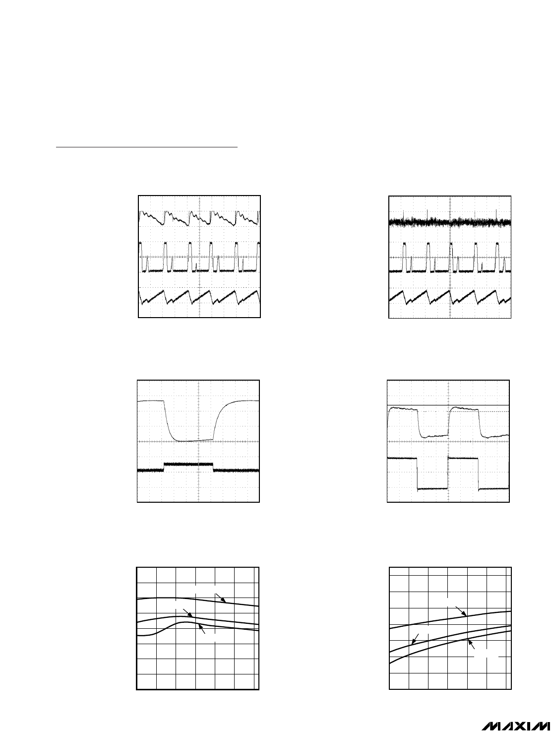
0
0.015
0.010
0.005
0.025
0.020
0.045
0.040
0.035
0.030
0.050
-40 -20 0 20 40 60 80
MAX5025-28 toc23
TEMPERATURE (°C)
LX LEAKAGE CURRENT (μA)
LX LEAKAGE CURRENT vs. TEMPERATURE
CURRENT INTO LX PIN
VLX = 40V
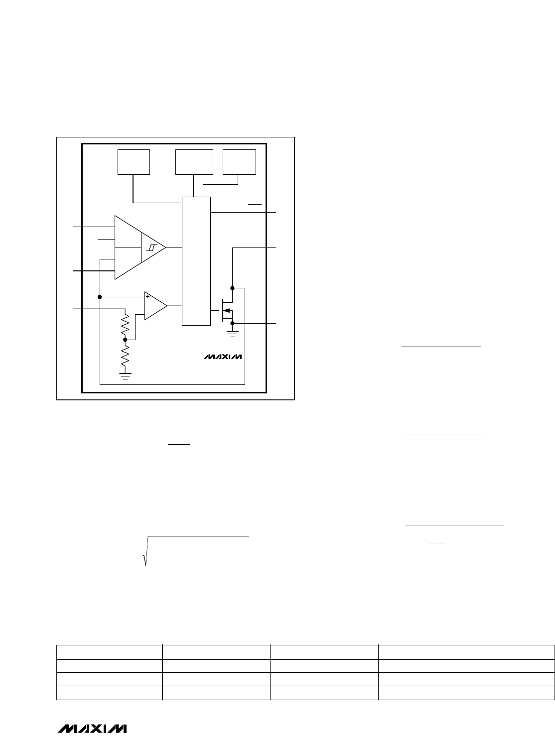
32
31
30
29
28
021 345
LOAD REGULATION
MAX5025-28 toc24
LOAD CURRENT (mA)
OUTPUT VOLTAGE (V)
MAX5026
VCC = 5V
WITH RC FILTER
(CIRCUIT OF FIGURE 3)
WITHOUT RC FILTER
(CIRCUIT OF FIGURE 2)
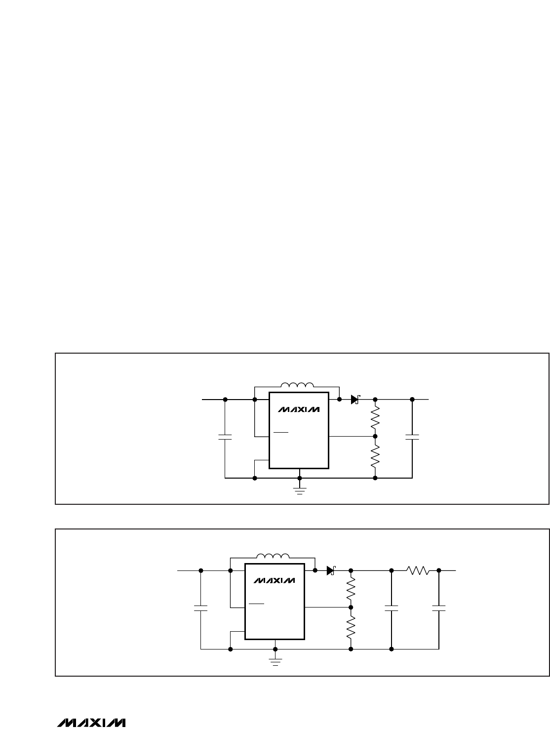
MAX5025-28 toc25
INPUT VOLTAGE (V)
MAXIMUM LOAD CURRENT (mA)
MAX5026
MAXIMUM LOAD CURRENT
vs. INPUT VOLTAGE
975
1
10
100
0.1
311
A: VOUT = 12V
B: VOUT = 24V
C: VOUT = 30V
D: VOUT = 32V
E: VOUT = 36V
A
B
E
CD
Typical Operating Characteristics (continued)
(VCC = 5V, VOUT = 30V, TA= +25°C, unless otherwise noted.)
0.5
1.0
2.0
1.5
2.5
3.0
-40 0-20 20 40 60 80
MAX5025-28 toc22
TEMPERATURE (°C)
RON (Ω)
SWITCH ON-RESISTANCE
vs. TEMPERATURE
VCC = 3V
VCC = 5V
VCC = 11V
MAX5026
MAX5025–MAX5028
500kHz, 36V Output, SOT23,
Step-Up DC-DC Converters
8 _______________________________________________________________________________________
Pin Description
PIN
MAX5025/
MAX5026
MAX5027/
MAX5028
NAME FUNCTION
1 1 PGND Power Ground. Connect directly to local ground plane. Use a star ground configuration
for low noise.
2 2 GND Ground. Connect directly to local ground plane.
3—FB
Feedback Pin. Reference voltage is approximately 1.25V. Connect resistive-divider tap
here. Minimize trace area at FB. See Setting the Output Voltage section.
—3FB
Feedback Pin. Connect VOUT to FB for +30V. Internal resistors divide down the output
voltage.
44SHDN Shutdown Pin. Connect to VCC to enable device. Connect to GND to shut down.
55V
CC Input Supply Voltage. Bypass with a 4.7µF ceramic capacitor.
66LX
Drain of Internal 40V N-Channel DMOS. Connect inductor/diode to LX. Minimize trace
area at this pin to keep EMI down.
Detailed Description
The MAX5025–MAX5028 current-mode PWM con-
trollers operate in a wide range of DC-DC conversion
applications including boost, flyback, and isolated out-
put configurations. These converters provide low-
noise, high output voltages making them ideal for var-
actor diode tuning applications as well as TFT LCD
bias. Other features include shutdown, fixed 500kHz
PWM oscillator, and a wide input range: 3V to 11V for
MAX5026/MAX5028 and 4.5V to 11V for MAX5025/
MAX5027.
The MAX5025–MAX5028 operate in discontinuous
mode in order to reduce the switching noise at the out-
put. Other continuous mode boost converters generate
a large voltage spike at the output when the LX switch
turns on because there is a conduction path between
the output, diode, and switch to ground during the time
needed for the diode to turn off.
To reduce the output noise even further, the LX switch
turns off by taking 40ns typically to transition from “ON”
to “OFF.” As a consequence, the positive slew rate of
the LX node is reduced and the current from the induc-
tor does not “force” the output voltage as hard as
would be the case if the LX switch were to turn off more
quickly.
PWM Controller
The heart of the MAX5025–MAX5028 current-mode
PWM controllers is a BiCMOS multi-input comparator
that simultaneously processes the output-error signal
and switch current signal. The main PWM comparator
is direct summing, lacking a traditional error amplifier
and its associated phase shift. The direct summing
configuration approaches ideal cycle-by-cycle control
over the output voltage since there is no conventional
error amp in the feedback path.
The device operates in PWM mode using a fixed-fre-
quency, current-mode operation. The current-mode
feedback loop regulates peak inductor current as a
function of the output error signal.
SHDN
Input
The SHDN pin provides shutdown control. Connect
SHDN to VCC for normal operation. To disable the
device, connect SHDN to GND.
Design Procedure
The MAX5025–MAX5028 can operate in a number of
DC-DC converter configurations including step-up, sin-
gle-ended primary inductance converter (SEPIC), and
flyback. The following design discussions are limited to
step-up, with a complete circuit shown in the
Application Circuits
section.
Setting the Output Voltage
The output voltage of the MAX5027/MAX5028 is fixed
at 30V. The output voltage of the MAX5025/MAX5026 is
set by two external resistors (R1 and R2, Figure 2 and
Figure 3). First select the value of R2 in the 5kΩto
50kΩrange. R1 is then given by:
MAX5025–MAX5028
500kHz, 36V Output, SOT23,
Step-Up DC-DC Converters
_______________________________________________________________________________________ 9
where VREF is 1.25V
Determining Peak Inductor Current
If the boost converter remains in the discontinuous
mode of operation, then the approximate peak inductor
current, ILPEAK, is represented by the formula below:
where TSis the period, VOUT is the output voltage, VIN
is the input voltage, IOUT is the output current, and ηis
the efficiency of the boost converter.
Determining the Inductor Value
47µH is the recommended inductor value when the out-
put voltage is 30V and the input voltage is 5V. In gener-
al, the inductor should have a current rating greater
than the current-limit value. For example, the inductor’s
current rating should be greater than 150mA to support
a 4mA output current. Equivalent series resistance
(ESR) should be below 1Ωfor reasonable efficiency.
Due to the MAX5025–MAX5028’s high switching fre-
quency, inductors with a ferrite core or equivalent are
recommended. Powdered iron cores are not recom-
mended due to their high losses at frequencies over
500kHz. Table 1 shows a list of vendors and 47µH
inductor parts.
For 4mA output current and output voltages other than
30V, the inductor can be simply scaled in value
according to the following formula:
Use the following formula to calculate the upper bound
of the inductor value at different output voltages and
output currents. This is the maximum inductance value
for discontinuous mode operation.
Calculate the lower bound, LLOWER, for the acceptable
inductance value using the following formula, which will
allow the maximum output current to be delivered with-
out reaching the peak current limit:
Notice that the switch current limit, (VIN/5)(260mA), is a
function of the input voltage, VIN. The current rating of
the inductor should be greater than the switch current
limit.
LTV VI
VmA
LOWER S OUT IN OUT
IN
=−
()
()
⎛
⎝
⎜⎞
⎠
⎟
2
5260
2
η
LVV VT
IV
UPPER
OUT IN S
OUT OUT
IN
=−
()
2
2
2
η
LHV V
V
OUT IN
=
()
−
()
()
47
25
μ
ITV VI
L
LPEAK S OUT IN OUT
=−
()
2
η
RR
V
V
OUT
REF
12 1=⎛
⎝
⎜
⎞
⎠
⎟
-
CONTROL
LOGIC
MAIN PWM
COMPARATOR
CURRENT-
LIMIT
COMPARATOR
FB
REF
-A
+A
+C
-C
MAX5025
MAX5026
THERMAL
SHUTDOWN
OSCILLATORULVO
PGND
3
GND
2
VCC
5
SHDN 4
1
6LX
N
Table 1. Inductor Vendors
VENDOR PHONE FAX PART NUMBER OF 47µH INDUCTOR
Coilcraft 847-639-6400 847-639-1469 DT1608C-473
Sumida 847-545-6700 847-545-6720 CDRH4D28-470
Toko 847-297-0070 847-699-7864 A915BY-470M
Figure 1. Functional Diagram

MAX5025–MAX5028
500kHz, 36V Output, SOT23,
Step-Up DC-DC Converters
10 ______________________________________________________________________________________
For a design in which VIN = 5V, VOUT = 30V, IOUT =
4mA, η= 0.5, and TS= 2µs,
LUPPER = 87µH
and
LLOWER = 12µH.
For a worst-case scenario in which VIN = 4.75V, VOUT
= 29V, IOUT = 4.4mA, η= 0.5, and TS= 1.25µs,
LUPPER = 46µH
and
LLOWER = 9µH.
The choice of 47µH as the recommended inductance
value is reasonable given the worst-case scenario
above. In general, the higher the inductance, the lower
the switching noise. Load regulation is also better with
higher inductance.
Diode Selection
The MAX5025–MAX5028’s high switching frequency
demands a high-speed rectifier. Schottky diodes are
recommended for most applications because of their
fast recovery time and low forward-voltage drop.
Ensure that the diode’s peak current rating is greater
than or equal to the peak inductor current. Also, the
diode reverse breakdown voltage must be greater than
VOUT. Table 2 lists diode vendors.
Capacitor Selection
Output Filter Capacitor
The output filter capacitor should be 1µF or greater. To
achieve low output ripple, a capacitor with low ESR, low
ESL, and high capacitance value should be selected.
For very low output ripple applications, the output of the
boost converter can be followed by an RC filter to fur-
ther reduce the ripple. Figure 3 shows a 100Ω, 1µF fil-
ter used to reduce the switching output ripple to
1mVp-p.
X7R ceramic capacitors are better for this boost appli-
cation because of their low ESR and tighter tolerance
over temperature than the Y5V ceramic capacitors.
Table 3 below lists manufacturers of recommended
capacitors.
Input Capacitor
Bypass VCC with a 4.7µF ceramic capacitor as close to
the IC as is practical.
Applications Information
Layout Considerations
The MAX5025–MAX5028 switch at high speed, man-
dating careful attention to layout for optimum perfor-
mance. Protect sensitive analog grounds by using a
star ground configuration. Minimize ground noise by
connecting GND, PGND, the input bypass-capacitor
ground lead, and the output-filter ground lead to a sin-
gle point (star ground configuration). Also, minimize
Table 2. Schottky Diode Vendors
VENDOR PHONE FAX PART NUMBERS
Comchip 510-657-8671 510-657-8921 CDBS1045
Panasonic 408-942-2912 408-946-9063 MA2Z785
ST-Microelectronics 602-485-6100 602-486-6102 TMMBAT48
Vishay-Telefunken 402-563-6866 402-563-6296 BAS382
Zetex 631-360-2222 631-360-8222 ZHCS500
Table 3. Capacitor Table
COMPANY PHONE FAX PART NUMBERS
GRM42-2X7R105K050AD (1µF capacitor)
Murata 814-237-1431 814-238-0490 GRM32-1210R71C475R (4.7µF capacitor)
UMK325BJ105KH (1µF capacitor)
Taiyo Yuden 408-573-4150 408-573-4159 EMK316BJ475ML (4.7µF capacitor)
C3225X7R1H155K (1.5µF capacitor)
TDK 847-803-6100 847-803-6296 C3225X7R1H105K (1µF capacitor)
MAX5025–MAX5028
500kHz, 36V Output, SOT23,
Step-Up DC-DC Converters
______________________________________________________________________________________ 11
trace lengths to reduce stray capacitance, trace resis-
tance, and radiated noise. The trace between the out-
put voltage-divider (MAX5025/MAX5026) and the FB
pin must be kept short, as well as the trace between
GND and PGND.
Inductor Layout
The shielded drum type inductors have a small air gap
around the top and bottom periphery. The incident fring-
ing magnetic field from this air gap to the copper plane
on the PC board tends to reduce efficiency. This is a
result of the induced eddy currents on the copper plane.
To minimize this effect, avoid laying out any copper
planes under the mounting area of these inductors.
30V Boost Application Circuit
Figures 2 and 3 show the MAX5025/MAX5026 operat-
ing in a 30V boost application. Figure 3 has an RC filter
to reduce noise at the output. These circuits provide
output currents greater than 4mA with an input voltage
of 5V or greater. They are designed by following the
Design Procedure
section. Operating characteristics of
these circuits are shown in the
Typical Operating
Characteristics
section.
VCC
VOUT
+30V
GND
FB
PGND
C1
4.7μF
C2
1μF
LX
L1
47μH
MAX5025
MAX5026
C2
1μF
VCC = 4.5V TO 11V
(MAX5025)
VCC = 3V TO 11V
(MAX5026)
D1
R1
147kΩ
R2
6.34kΩ
TOKO 47μH INDUCTOR
A915BY-470M ZETEX SCHOTTKY DIODE
ZHCS500
SHDN
Figure 2. Adjustable 30V Output Circuit
VCC
VOUT
+30V
GND
FB
PGND
C1
4.7μF
C2
1μF
LX
L1
47μH
MAX5025
MAX5026
C3
1μF
VCC = 4.5V TO 11V
(MAX5025)
VCC = 3V TO 11V
(MAX5026)
D1
R1
147kΩ
R3
100Ω
R2
6.34kΩ
TOKO 47μH INDUCTOR
A915BY-470M ZETEX SCHOTTKY DIODE
ZHCS500
SHDN
Figure 3. Adjustable 30V Output Circuit with RC Filter
MAX5025–MAX5028
500kHz, 36V Output, SOT23,
Step-Up DC-DC Converters
12 ______________________________________________________________________________________
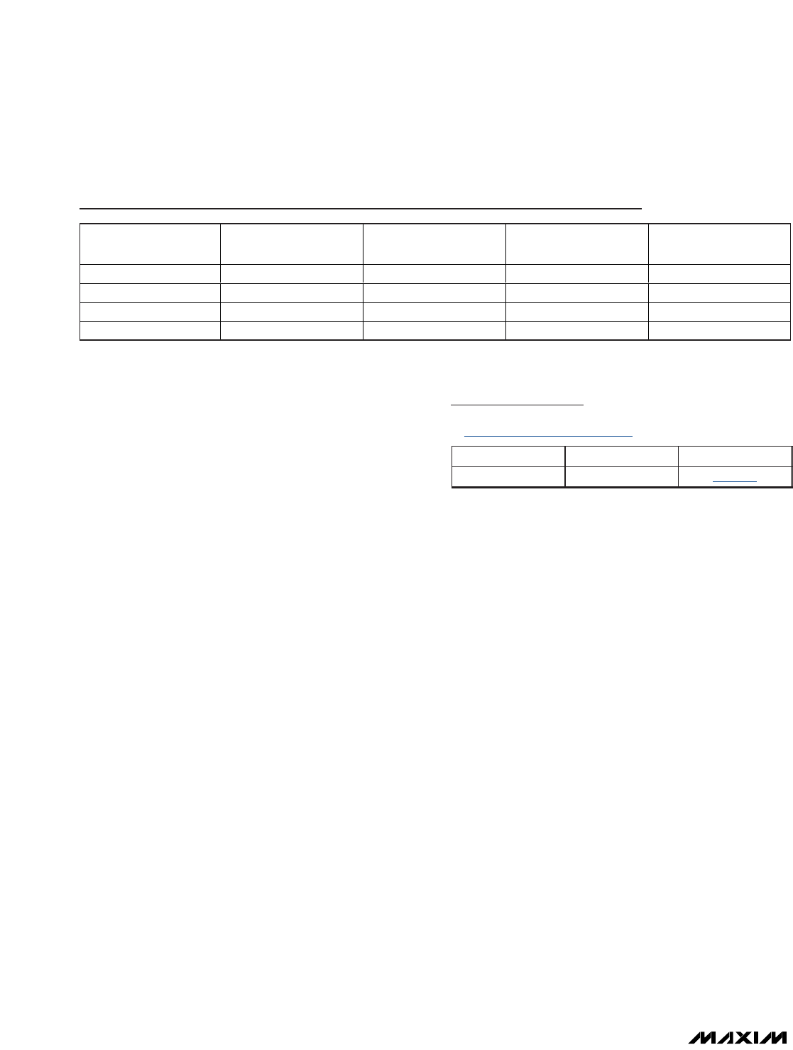
Selector Guide
PART OUTPUT FREQUENCY
TOLERANCE
FB SET POINT
TOLERANCE INPUT VOLTAGE
MAX5025 Adjustable -31% to +100% ±5% 4.5V to 11V
MAX5026 Adjustable -18% to +34% ±3% 3V to 11V
MAX5027 Fixed 30V -31% to +100% ±5% 4.5V to 11V
MAX5028 Fixed 30V -18% to +34% ±3% 3V to 11V
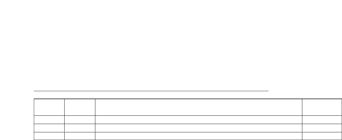
Package Information
For the latest package outline information and land patterns, go
to www.maxim-ic.com/packages.
PACKAGE TYPE PACKAGE CODE DOCUMENT NO.
6 SOT23 S8-2 21-0058
____________________Chip Information
TRANSISTOR COUNT: 365
PROCESS: BiCMOS
Maxim cannot assume responsibility for use of any circuitry other than circuitry entirely embodied in a Maxim product. No circuit patent licenses are
implied. Maxim reserves the right to change the circuitry and specifications without notice at any time.
Maxim Integrated Products, 120 San Gabriel Drive, Sunnyvale, CA 94086 408-737-7600 ____________________
13
© 2009 Maxim Integrated Products Maxim is a registered trademark of Maxim Integrated Products, Inc.
MAX5025–MAX5028
500kHz, 36V Output, SOT23,
Step-Up DC-DC Converters
Revision History
REVISION
NUMBER
REVISION
DATE DESCRIPTION PAGES
CHANGED
0 10/01 Initial release —
1 12/01 Released the MAX5027 1
2 3/09 Revised the Absolute Maximum Ratings section. 2