MMBT3906 PNP Switching Transistor Nxp
User Manual: Marking of electronic components, SMD Codes 7B, 7B-, 7BW, 7Bp, 7Bt. Datasheets MMBT3906, SMZ2515.
Open the PDF directly: View PDF ![]() .
.
Page Count: 8
DATA SHEET
Product data sheet
Supersedes data of 2000 Apr 11 2003 Mar 18
DISCRETE SEMICONDUCTORS
MMBT3906
PNP switching transistor
db
ook, halfpage
M3D088
2003 Mar 18 2
NXP Semiconductors Product data sheet
PNP switching transistor MMBT3906
FEATURES
•Collector current capability IC = −200 mA
•Collector-emitter voltage VCEO = −40 V.
APPLICATIONS
•General switching and amplification.
DESCRIPTION
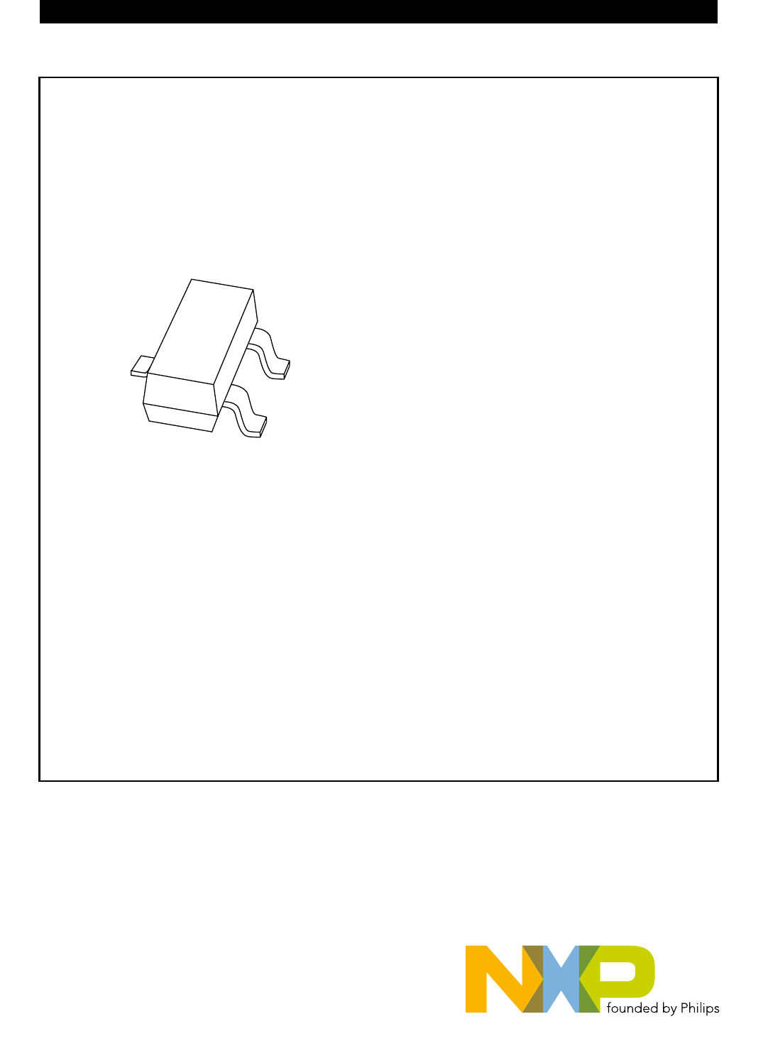
PNP switching transistor in a SOT23 plastic package.
NPN complement: MMBT3904.
MARKING
Note
1. ∗ = p: Made in Hong Kong.
∗ = t: Made in Malaysia.
∗ = W: Made in China.
TYPE NUMBER MARKING CODE(1)
MMBT3906 7B∗
PINNING
PIN DESCRIPTION
1base
2emitter
3collector
handbook, halfpage
21
3
MAM256
Top view
2
3
1
Fig.1 Simplified outline (SOT23) and symbol.
QUICK REFERENCE DATA
SYMBOL PARAMETER MAX. UNIT
VCEO collector-emitter voltage −40 V
ICcollector current (DC) −200 mA
LIMITING VALUES
In accordance with the Absolute Maximum Rating System (IEC 60134).
Note
1. Transistor mounted on an FR4 printed-circuit board.
SYMBOL PARAMETER CONDITIONS MIN. MAX. UNIT
VCBO collector-base voltage open emitter − −40 V
VCEO collector-emitter voltage open base − −40 V
VEBO emitter-base voltage open collector − −6 V
ICcollector current (DC) − −200 mA
ICM peak collector current − −200 mA
IBM peak base current − −100 mA
Ptot total power dissipation Tamb ≤ 25 °C; note 1 −250 mW
Tstg storage temperature −65 +150 °C
Tjjunction temperature −150 °C
Tamb operating ambient temperature −65 +150 °C
2003 Mar 18 3
NXP Semiconductors Product data sheet
PNP switching transistor MMBT3906
THERMAL CHARACTERISTICS
Note
1. Transistor mounted on an FR4 printed-circuit board.
CHARACTERISTICS
Tamb = 25 °C unless otherwise specified.
SYMBOL PARAMETER CONDITIONS VALUE UNIT
Rth j-a thermal resistance from junction to ambient note 1 500 K/W
SYMBOL PARAMETER CONDITIONS MIN. MAX. UNIT
ICBO collector cut-off current IE = 0; VCB = −30 V − −50 nA
IEBO emitter cut-off current IC = 0; VEB = −6 V − −50 nA
hFE DC current gain VCE = −1 V; see Fig.2
IC = −0.1 mA 60 −
IC = −1 mA 80 −
IC = −10 mA 100 300
IC = −50 mA 60 −
IC = −100 mA 30 −
VCEsat collector-emitter saturation
voltage
IC = −10 mA; IB = −1 mA − −250 mV
IC = −50 mA; IB = −5 mA − −400 mV
VBEsat base-emitter saturation voltage IC = −10 mA; IB = −1 mA − −850 mV
IC = −50 mA; IB = −5 mA − −950 mV
Cccollector capacitance IE = ie = 0; VCB = −5 V; f = 1 MHz −4.5 pF
Ceemitter capacitance IC = ic = 0; VEB = −500 mV;
f = 1 MHz
−10 pF
fTtransition frequency IC = −10 mA; VCE = −20 V;
f = 100 MHz
250 −MHz
Fnoise figure IC = −100 µA; VCE = −5 V;
RS = 1 kΩ; f = 10 Hz to 15.7 kHz
−4dB
Switching times (between 10% and 90% levels); see Fig.7
tddelay time ICon = −10 mA; IBon = −1 mA;
IBoff = 1 mA
−35 ns
trrise time −35 ns
tsstorage time −225 ns
tffall time −75 ns
2003 Mar 18 4
NXP Semiconductors Product data sheet
PNP switching transistor MMBT3906
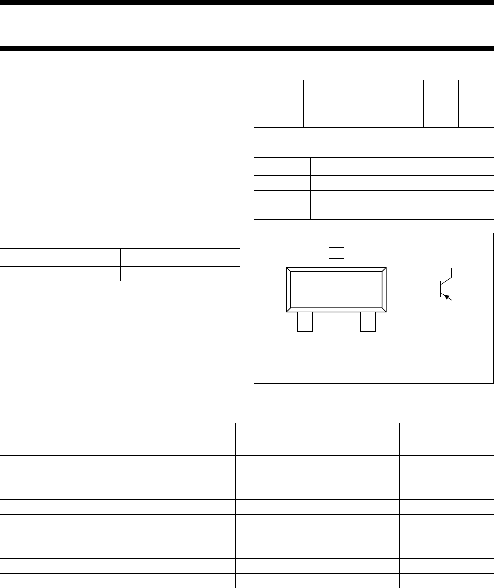
handbook, halfpage
0
400
600
200
MHC459
−10−1−1−10 IC (mA)
hFE
−102−103
(1)
(3)
(2)
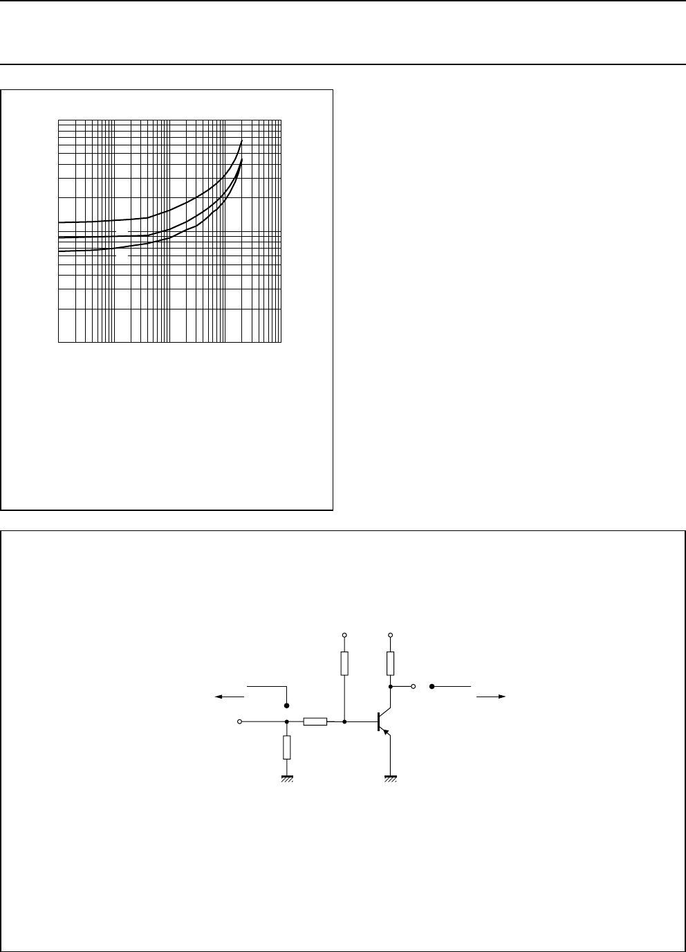
Fig.2 DC current gain; typical values.
VCE = −1 V.
(1) Tamb = 150 °C.
(2) Tamb = 25 °C.
(3) Tamb = −55 °C.
handbook, halfpage
0−10
−250
0
−50
−100
−150
−200
−2VCE (V)
IC
(mA)
−4−6−8
MHC460
(1)
(2)(3)
(9)
(7)
(10)
(8)
(6)
(5)
(4)
Fig.3 Collector current as a function of
collector-emitter voltage.
(1) IB = −1.5 mA.
(2) IB = −1.35 mA.
(3) IB = −1.2 mA.
(4) IB = −1.05 mA.
(5) IB = −0.9 mA.
(6) IB = −0.75 mA.
(7) IB = −0.6 mA.
(8) IB = −0.45 mA.
(9) IB = −0.3 mA.
(10) IB = −0.15 mA.
Tamb = 25 °C.
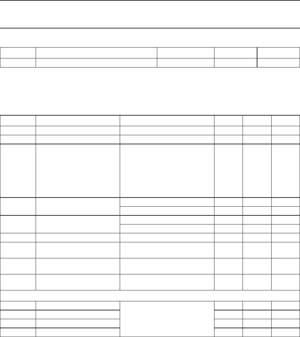
handbook, halfpage
−200
−1200
−400
−600
−800
−1000
MHC461
−1−10−1IC (mA)
VBE
(mV)
−10 −102−103
(3)
(2)
(1)
Fig.4 Base-emitter voltage as a function of
collector current.
VCE = −1 V.
(1) Tamb = −55 °C.
(2) Tamb = 25 °C.
(3) Tamb = 150 °C.
handbook, halfpage
−200
−1200
−400
−600
−800
−1000
MHC462
−1−10−1IC (mA)
VBEsat
(mV)
−10 −102−103
(1)
(3)
(2)
Fig.5 Base-emitter saturation voltage as a
function of collector current.
IC/IB = 10.
(1) Tamb = −55 °C.
(2) Tamb = 25 °C.
(3) Tamb = 150 °C.
2003 Mar 18 5
NXP Semiconductors Product data sheet
PNP switching transistor MMBT3906
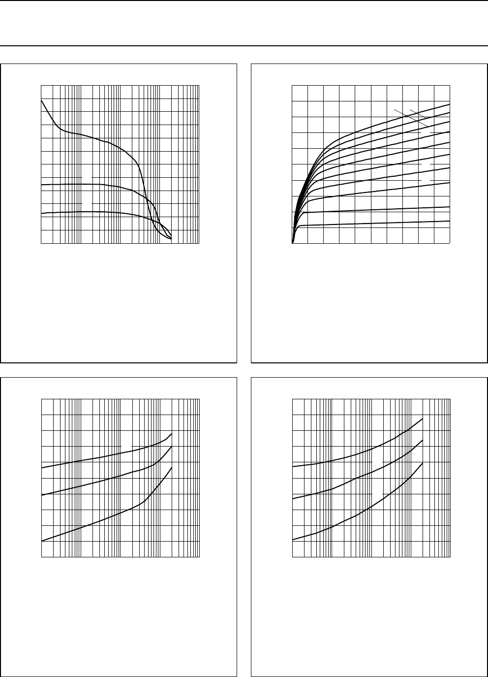
handbook, halfpage
−103
−102
−10
MHC463
−10−1−1−10 IC (mA)
VCEsat
(mV)
−102−103
(1)
(2)
(3)
Fig.6 Collector-emitter saturation voltage as a
function of collector current.
IC/IB = 10.
(1) Tamb = 25 °C.
(2) Tamb = 150 °C.
(3) Tamb = −55 °C.
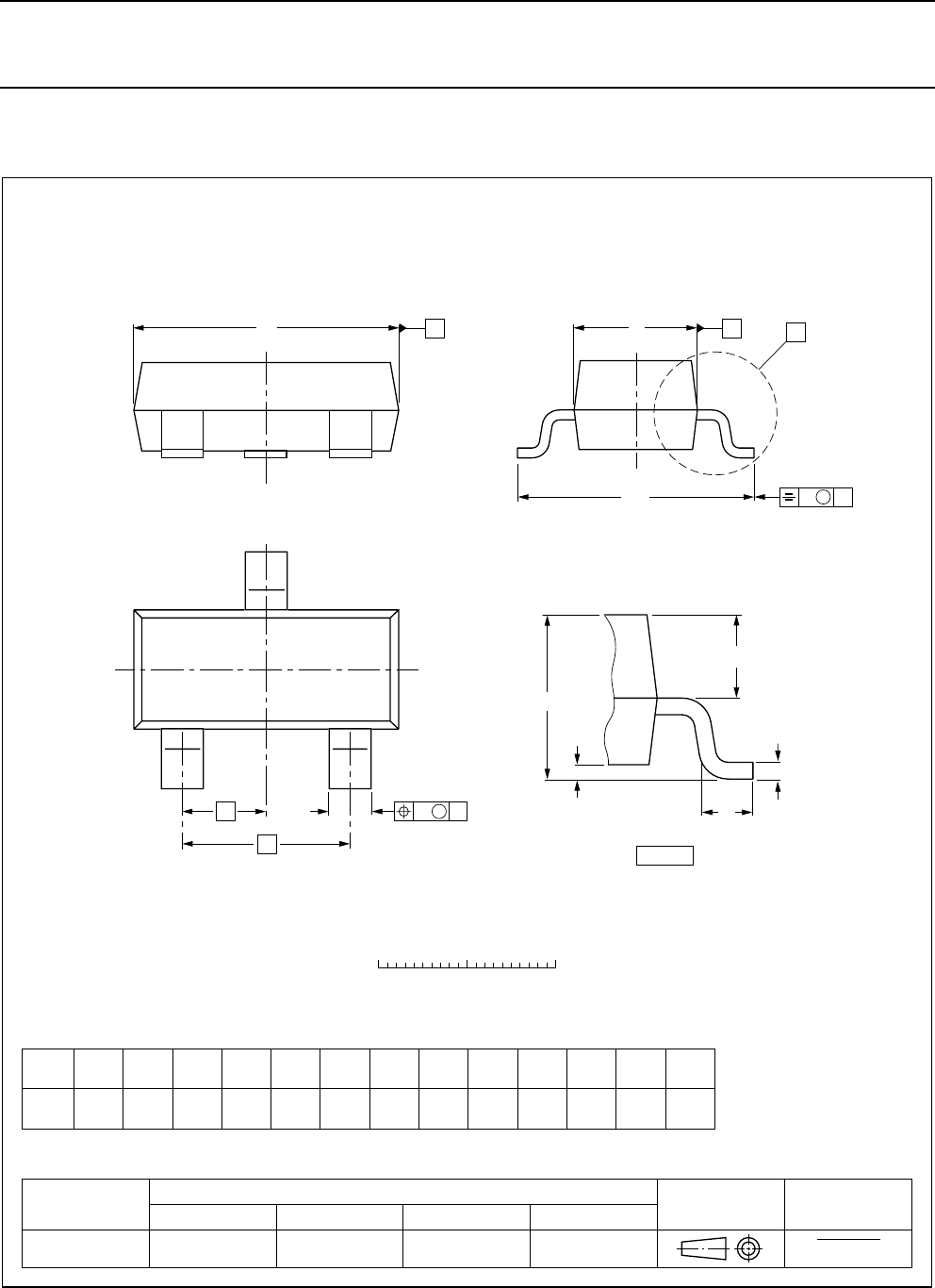
handbook, full pagewidth
RC
R2
R1
DUT
MGD624
Vo
RB
(probe)
450 Ω
(probe)
450 Ω
oscilloscope oscilloscope
V
BB
Vi
V
CC
Fig.7 Test circuit for switching times.
Vi = 5 V; T = 500 µs; tp = 10 µs; tr = tf ≤ 3 ns.
R1 = 56 Ω; R2 = 2.5 kΩ; RB = 3.9 kΩ; RC = 270 Ω.
VBB = 1.9 V; VCC = −3 V.
Oscilloscope: input impedance Zi = 50 Ω.
2003 Mar 18 6
NXP Semiconductors Product data sheet
PNP switching transistor MMBT3906
PACKAGE OUTLINE
UNIT A1
max. bpcDE e1HELpQwv
REFERENCES
OUTLINE
VERSION EUROPEAN
PROJECTION ISSUE DATE
97-02-28
99-09-13
IEC JEDEC EIAJ
mm 0.1 0.48
0.38 0.15
0.09 3.0
2.8 1.4
1.2 0.95
e
1.9 2.5
2.1 0.55
0.45 0.1
0.2
DIMENSIONS (mm are the original dimensions)
0.45
0.15
SOT23 TO-236AB
bp
D
e1
e
A
A1
Lp
Q
detail X
HE
E
wM
vMA
B
AB
0 1 2 mm
scale
A
1.1
0.9
c
X
12
3
Plastic surface mounted package; 3 leads SOT2
3

2003 Mar 18 7
NXP Semiconductors Product data sheet
PNP switching transistor MMBT3906
DATA SHEET STATUS
Notes
1. Please consult the most recently issued document before initiating or completing a design.
2. The product status of device(s) described in this document may have changed since this document was published
and may differ in case of multiple devices. The latest product status information is available on the Internet at
URL http://www.nxp.com.
DOCUMENT
STATUS(1) PRODUCT
STATUS(2) DEFINITION
Objective data sheet Development This document contains data from the objective specification for product
development.
Preliminary data sheet Qualification This document contains data from the preliminary specification.
Product data sheet Production This document contains the product specification.
DISCLAIMERS
General ⎯ Information in this document is believed to be
accurate and reliable. However, NXP Semiconductors
does not give any representations or warranties,
expressed or implied, as to the accuracy or completeness
of such information and shall have no liability for the
consequences of use of such information.
Right to make changes ⎯ NXP Semiconductors
reserves the right to make changes to information
published in this document, including without limitation
specifications and product descriptions, at any time and
without notice. This document supersedes and replaces all
information supplied prior to the publication hereof.
Suitability for use ⎯ NXP Semiconductors products are
not designed, authorized or warranted to be suitable for
use in medical, military, aircraft, space or life support
equipment, nor in applications where failure or malfunction
of an NXP Semiconductors product can reasonably be
expected to result in personal injury, death or severe
property or environmental damage. NXP Semiconductors
accepts no liability for inclusion and/or use of NXP
Semiconductors products in such equipment or
applications and therefore such inclusion and/or use is at
the customer’s own risk.
Applications ⎯ Applications that are described herein for
any of these products are for illustrative purposes only.
NXP Semiconductors makes no representation or
warranty that such applications will be suitable for the
specified use without further testing or modification.
Limiting values ⎯ Stress above one or more limiting
values (as defined in the Absolute Maximum Ratings
System of IEC 60134) may cause permanent damage to
the device. Limiting values are stress ratings only and
operation of the device at these or any other conditions
above those given in the Characteristics sections of this
document is not implied. Exposure to limiting values for
extended periods may affect device reliability.
Terms and conditions of sale ⎯ NXP Semiconductors
products are sold subject to the general terms and
conditions of commercial sale, as published at
http://www.nxp.com/profile/terms, including those
pertaining to warranty, intellectual property rights
infringement and limitation of liability, unless explicitly
otherwise agreed to in writing by NXP Semiconductors. In
case of any inconsistency or conflict between information
in this document and such terms and conditions, the latter
will prevail.
No offer to sell or license ⎯ Nothing in this document
may be interpreted or construed as an offer to sell products
that is open for acceptance or the grant, conveyance or
implication of any license under any copyrights, patents or
other industrial or intellectual property rights.
Export control ⎯ This document as well as the item(s)
described herein may be subject to export control
regulations. Export might require a prior authorization from
national authorities.
Quick reference data ⎯ The Quick reference data is an
extract of the product data given in the Limiting values and
Characteristics sections of this document, and as such is
not complete, exhaustive or legally binding.

NXP Semiconductors
Contact information
For additional information please visit: http://www.nxp.com
For sales offices addresses send e-mail to: salesaddresses@nxp.com
© NXP B.V. 2009
All rights are reserved. Reproduction in whole or in part is prohibited without the prior written consent of the copyright owner.
The information presented in this document does not form part of any quotation or contract, is believed to be accurate and reliable and may be changed
without notice. No liability will be accepted by the publisher for any consequence of its use. Publication thereof does not convey nor imply any license
under patent- or other industrial or intellectual property rights.
Customer notification
This data sheet was changed to reflect the new company name NXP Semiconductors. No changes were
made to the content, except for the legal definitions and disclaimers.
Printed in The Netherlands 613514/02/pp8 Date of release: 2003 Mar 18 Document order number: 9397 750 10243
