MT501 Datasheet. Www.s Manuals.com. Mos Tech
User Manual: Marking of electronic components, SMD Codes 2A, 2A*, 2A***, 2A18, 2A20, 2A25, 2A30, 2A35, 2A4, 2A40, 2A45, 2A50, 2A55, 2A60, 2A7, 2AG, 2AL. Datasheets FAN5350UCX, FMMT3906, KST3906, MMBT3906, MMBT3906G-AE3, MMBT3906G-AL3, MMBT3906G-AN3, MMBT3906L-AE3, MMBT3906L-AL3, MMBT3906L-AN3, MT501, PZM2.4NBA, PZM2.7NB2A, Si2302ADS.
Open the PDF directly: View PDF ![]() .
.
Page Count: 13
LOW POWER LIGHTING LED DRIVER DATA SHEET MT501
15 ~ 60mA Single/Dual channel LED Driver
Features
- The most easy used linear constant current LED driver
- 15mA~ 60mA, 1 to 2 channel constant current
regulator
- No external current setting resistor is needed
- 1.5V ~ 12V wide supply voltage range supports self
power structure in lighting application
- Very low dropout voltage
IPN ≦ 40mA → VPN ≒ 0.4V
IPN > 40mA → VPN ≒ 0.6V
- PWM dimming by VDD pin
- 2uS/2uS current rising/falling time
- -40℃ ~ 120℃ junction operating temperature
- Cascade-able for higher voltage applications*
( type 1Axx only)
- Current leak/no leak design for lighting/display
Application
- Low chip to chip current skew
IPN ≦ 40mA → chip current skew < ±5%
IPN > 40mA → chip current skew < ±6%
- Less than 1%/V load (or line) regulation
- Minimized footprint
- Green package
* Patent pending
Product Description
MT501 is a simple general purpose current regulation
component that can be easily used in various LED lighting
applications. With the excellent load/line regulation and
minimized chip current skew, MT501 keep LED’s current
very stable even when power or load fluctuate in a wide
range and make light intensity very uniform in large area of
LED light source.
Except power supply function, the VDD pin of MT501 is
output enable (OE) also, and can be used in digital PWM
controlled circuit to achieve more precise current adjusting
in gray level applications.
The minimized power supply voltage let MT501 be used
as a current regulative diode (CRD) when VDD and VP pin
are tight together. This application makes MT501 very easy
to be used. Just like a diode, when this diode is inserted in
LED series, the current in circuit is regulated.
In high supply voltage and low LED load voltage
applications, two or more single channel MT501 (A type)
can be connected in series to share redundant high voltage.
With the unique share voltage technology of MOS-TECH
Semiconductor, the extra redundant voltage can be shared
by each MT501 by a reasonable mechanism. This special
capability let MT501 very suit for the usage of wide range
power supply that many liner type LED drivers cannot work.
Applications
Type A – For lighting application
- General LED lighting
- LCD back lighting
- LED torch / flashlight
- RGB lighting
Type B – For display application (No current leak)
- RGB display pixel driver
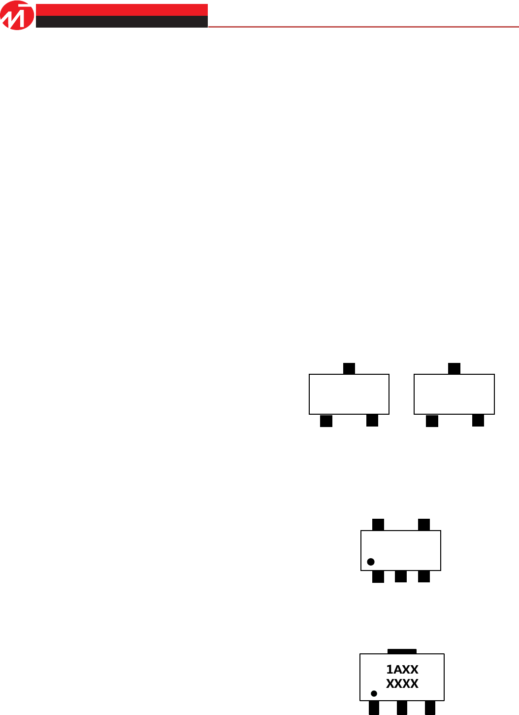
Package Type
- SOT 23-3 (single channel, type A/B)
- SOT23-5 (dual channel, type A) – two independent
driver in single package.
- SOT89-3 (single channel, type A, package option)
VN
VP
1 A X X
VN
VP
1 B X X
VDD
VDD
VN
VP1
2 A X X
VDD1 VDD2
VP2
VN
VP VDD
MOS-TECH Semiconductor Co.,LTD
Terminal Description
Pin Name
Function
VDD
Power supply
VP
Current in
VN
Current out
Ordering Information
Part Number: MT501
Example: “1A25” is single channel cascade-able MT501, current 25mA.
“1B25” is single channel NU501, current 25mA
“2A20” is dual channel NU501, current 20mA.
PS: Before you issue your P.O., please contact your agent or
MOS-TECH Semiconductor to make sure the channel and center current
that is available.
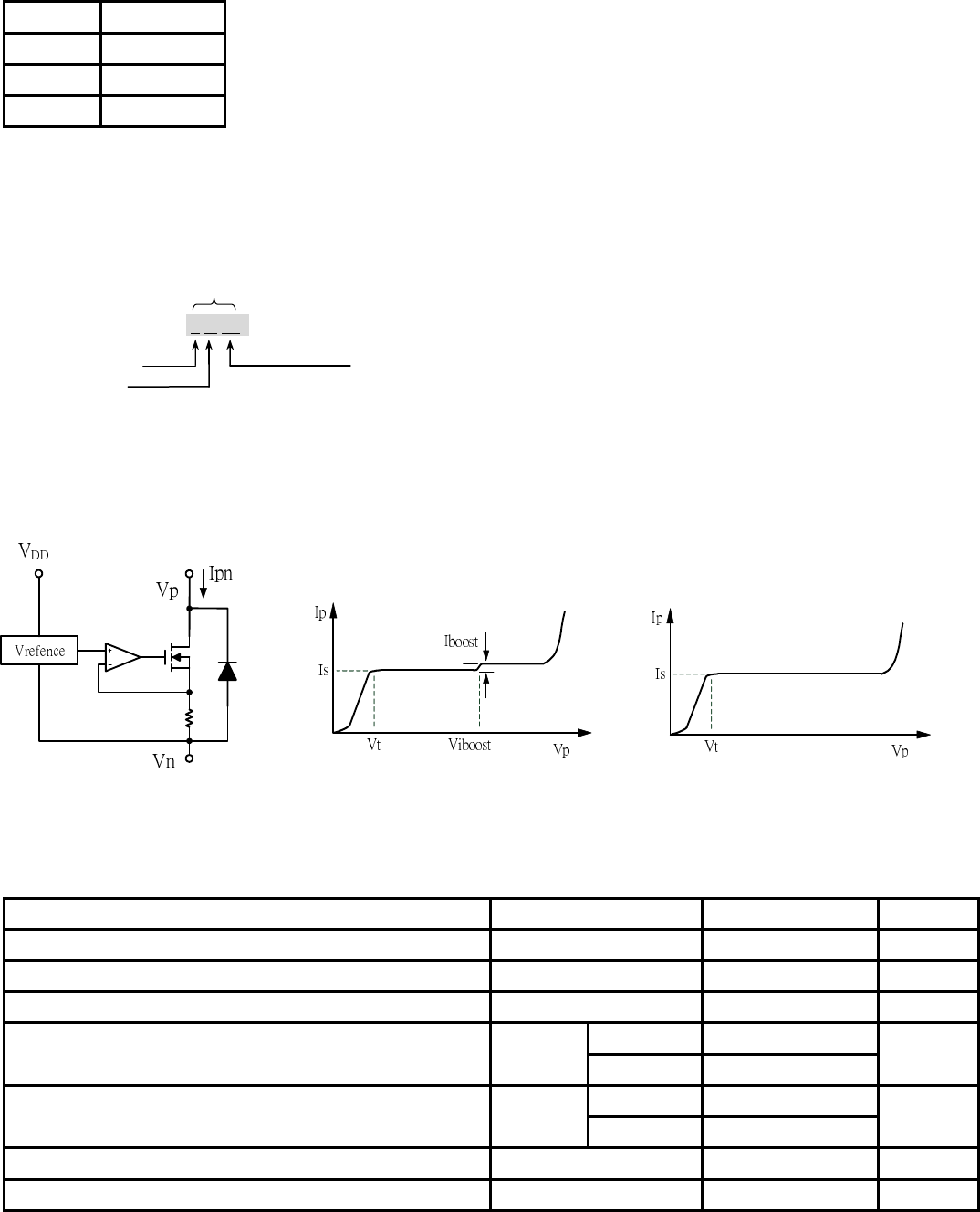
Block Diagram per channel and Ideal IV characteristic
Maximum Ratings (T = 25°C)
Characteristic
Symbol
Rating
Unit
Supply voltage
VDD
0 ~ 16
V
Output voltage
VP
-0.2 ~ 17
V
Output current
IPN
IS** +10%
mA
Power Dissipation (Ta=25°C)
PD
SOT 23
0.25
W
SOT 89
0.7
Thermal Resistance (On PCB, Ta=25°C)
RTH(j-a)
SOT 23
300
°C /W
SOT 89
180
Operating temperature
TOPR
-40~+85
°C
Storage temperature
TSTG
-55~+150
°C
x A xx
Channels
Product type
Output current (mA)
Top marking
Type A – IV curve Type B – IV curve
Electrical Characteristics and Recommended Operating Conditions
** IS is output saturation current.
Switching Characteristics (T = 25°
°°
°C)
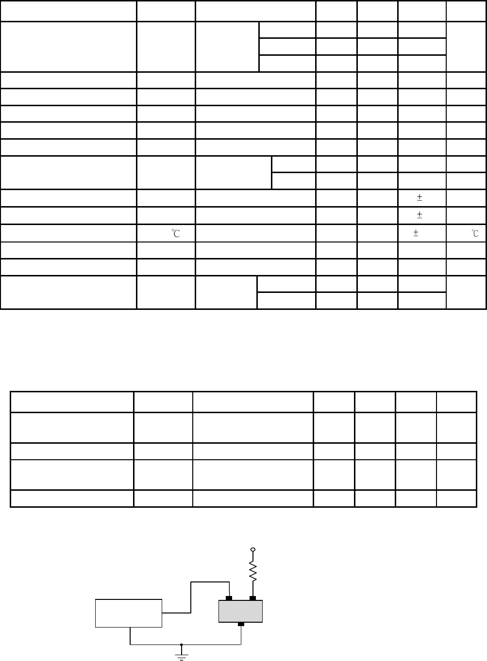
Test Circuit
Characteristic Symbol Condition Min. Typ. Max. Unit
Supply voltage VDD
Room Temp.
VPN >= 1V
IS <= 25mA 1.5 - 12
V IS <= 40mA 2 - 12
IS > 40mA 2.5 - 12
Supply current IDD - 100 150 250 uA
Minimum dropout voltage VPNmin VDD >=3.8V 0.4 - 0.6 V
Maximum output voltage VPNmax IPN = IS - - 0.25 / IPN V
Output breakdown voltage VPNBD IPN = 0, VDD = 0V - - 17 V
Output current IS Spec. 15 - 60 mA
Leakage ILeakage
0V < VDD < 0.4V,
VP = 10V
Type A 1 - 5 uA
Type B 0 - 0.5 uA
Line regulation %/VDD 12V > VDD
> 1.6V - - 1 %/V
Load regulation %/VP 8V > VP > 1.6V - - 1 %/V
Thermal regulation %/10 VDD = VP = 2V - - 0.5 %/10
Threshold voltage (Type A only) Viboost IP = IS*1.1 11 12 13 V
Current boost (Type A only) Iboost VP = Viboost 7 10 13 % * IS
Chip current skew ISkew VDD = VP = 2V IPN <= 40mA - - 5 %
IPN > 40mA - - 6
Characteristic Symbol Condition Min. Typ. Max. Unit
Propagation Delay Time
VDD from “L” to “H” tpLH VP=1V, VDD = 0V → 3V - 1 - uS
Output current rising time tRise VP=1V, VDD = 0V → 3V - 1.5 5 uS
Propagation Delay Time
VDD from “H” to “L” tpHL VP=1V, VDD = 3V → 0V - 1 - uS
Output current falling time tFall VP=1V, VDD = 3V → 0V - 1.5 5 uS
VDD
Function
generator
+V
VP
VN
RLoad
MT501
0.00
10.00
20.00
30.00
40.00
50.00
60.00
70.00
0.1
0.5
1
1.8
2.6
3.4
4.2
5
5.8
6.6
7.4
8.2
9
9.8
10.6
11.4
12.2
13
13.8
14.6
15.4
16.2
17
Timing Waveform
I/V curve
V
DD
V
N
V
P
V
P
V
N
VDD
tpHL
50%
90%
90%
50% 10%
VDD
VP
50% 50%
tpLH
tRise tFall
10%
V
DD
V
N
V
P
V
P
V
N
VDD
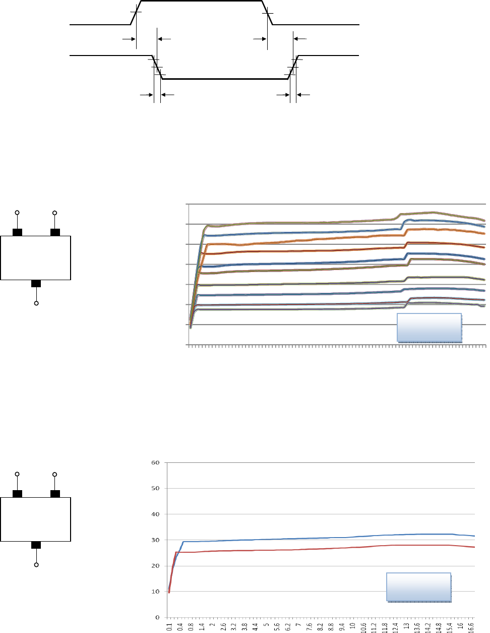
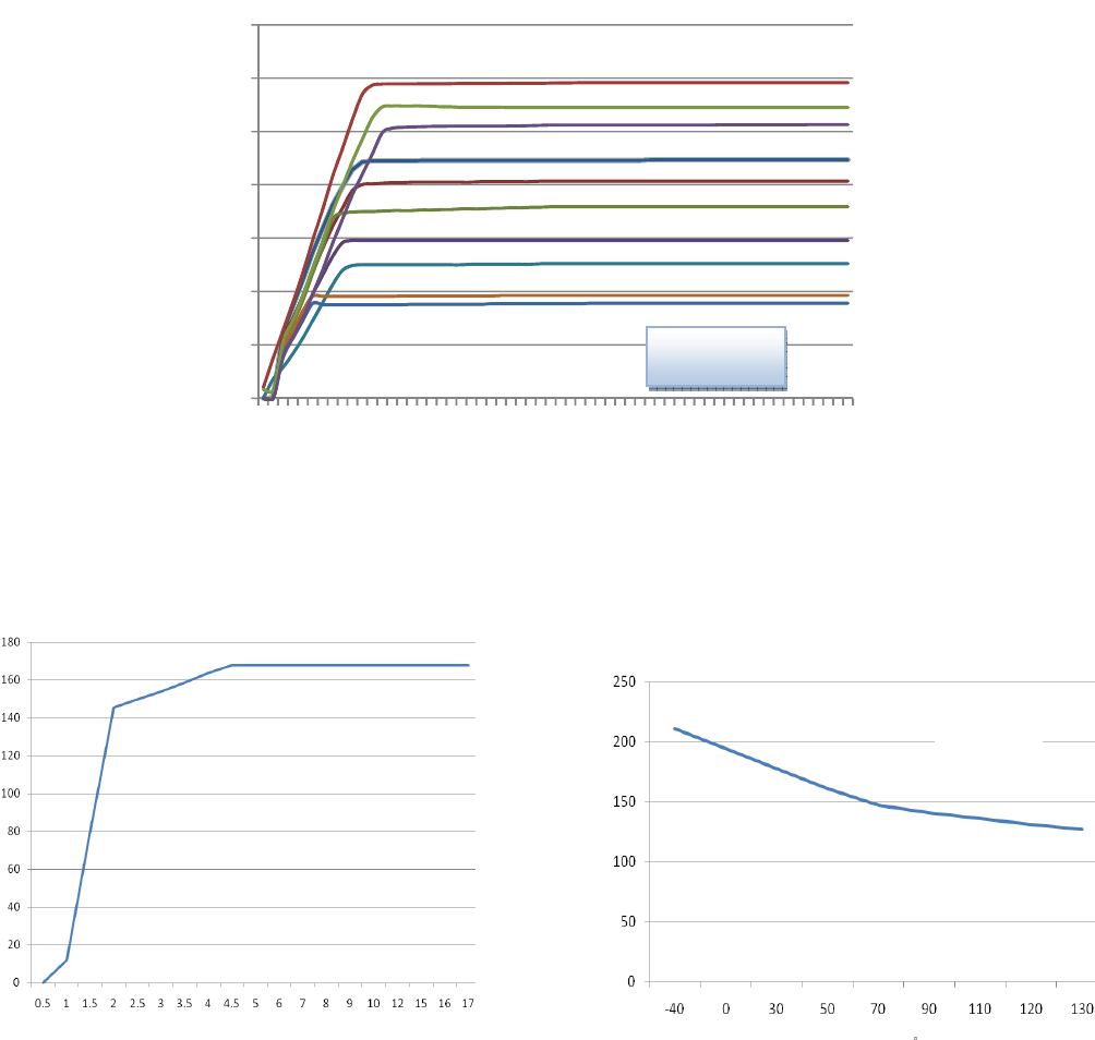
Load regulation characteristic (B type)
Output voltage VPN (V)
Output current IPN (mA)
1B25
1B30
VDD = 3.8V
Load regulation characteristic (A type)
Output voltage VPN (V)
Output current IPN (mA)
VDD = 3.8V
1A18
1A20
1A25
1A30 1A35
1A40
1A55
1A45
1A50
1A60
MT501
MT501
0.0
10.0
20.0
30.0
40.0
50.0
60.0
70.0
0.9
1.4
1.9
2.4
2.9
3.5
4.4
5.2
6.2
7.2
8.2
9.2
Supply voltage VDD (V)
IDD (uA)
I
DD
Vs. V
DD
Characteristic (Room Temp)
Temperature ( C)
IDD (uA)
IDD Vs. Temperature Characteristic
VDD= 5V
V
PN
= 2V
Supply voltage VDD (V)
Output current IPN (mA)
Line regulation characteristic
1A18
1A20
1A25
1A30
1A35
1A45
1A40
VPN = 1V
1A50
1A55
1A60
Application design consideration
MT501 is a linear constant current driver. While this device is designed in lighting system, the heat generation should be
considered. Generally, the higher current designed in system, the higher power will suffer by this
power consuming by MT501 and to increase the whole system efficiency, the drop voltage across
minimized. The following design note can reduce the heat generation from
output constant current and the needed supply voltage (normal operation condition).
1. Drop the power supply voltage as low as possible in the normal operation condition.
2. Get the LEDs in current loop as many as possible in the normal operation condition.
3. Get a voltage sharing resistor in series in current loop .
4. If system power is greater that 24V, it suggests to connect a small SMD type capacitor (0.1uF~10uF) between VDD and
VN pin. That will greatly improve the stability of system.
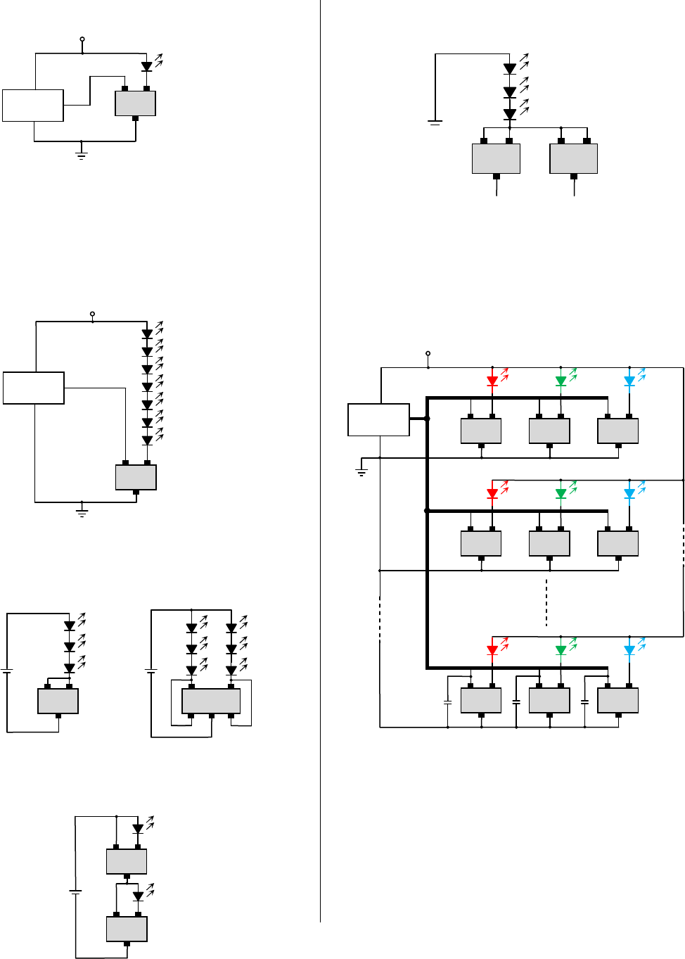
Application Circuits
5V PWM indicator application
24V PWM lighting with dimming application
With the special designed character of leak, the A type
NU501 can be used in dimming application even when
system power is higher than the maximum VP voltage.
12V lighting application
High voltage drop application
Parallel application
RGB display pixel application
1AXX
V
DD
V
P
V
N
8V ~ 24V
1AXX
VP
V
DD
VN
PWM
generator
+24
V
1A20
V
DD VP
VN
PWM
generator
+5V
1B20
V
DD VP
V
N
V
DD
V
P
VN
12V
V
DD
V
P
VN
PWM
generator
+5V
RGB PWM signal
1B20
V
DD VP
VN
1B20
V
DD VP
VN
1B20
V
DD VP
VN
1B20
VDD VP
VN
1B20
VDD VP
VN
1B20
VDD VP
VN
1B20
VDD VP
VN
1B20
VDD VP
VN
1B20
VDD VP
VN
PWM R
PWM R
PWM R
PWM G
PWM
G
PWM
G
PWM B
PWM
B
PWM
B
VDD1 VDD2
VDD VP
V
N
12V
V
P1 VN
12V
V
P
2
MT501
MT501
MT501 MT501 MT501 MT501 MT501
MT501 MT501 MT501
MT501 MT501 MT501
MT501 MT501
MT501
MT501
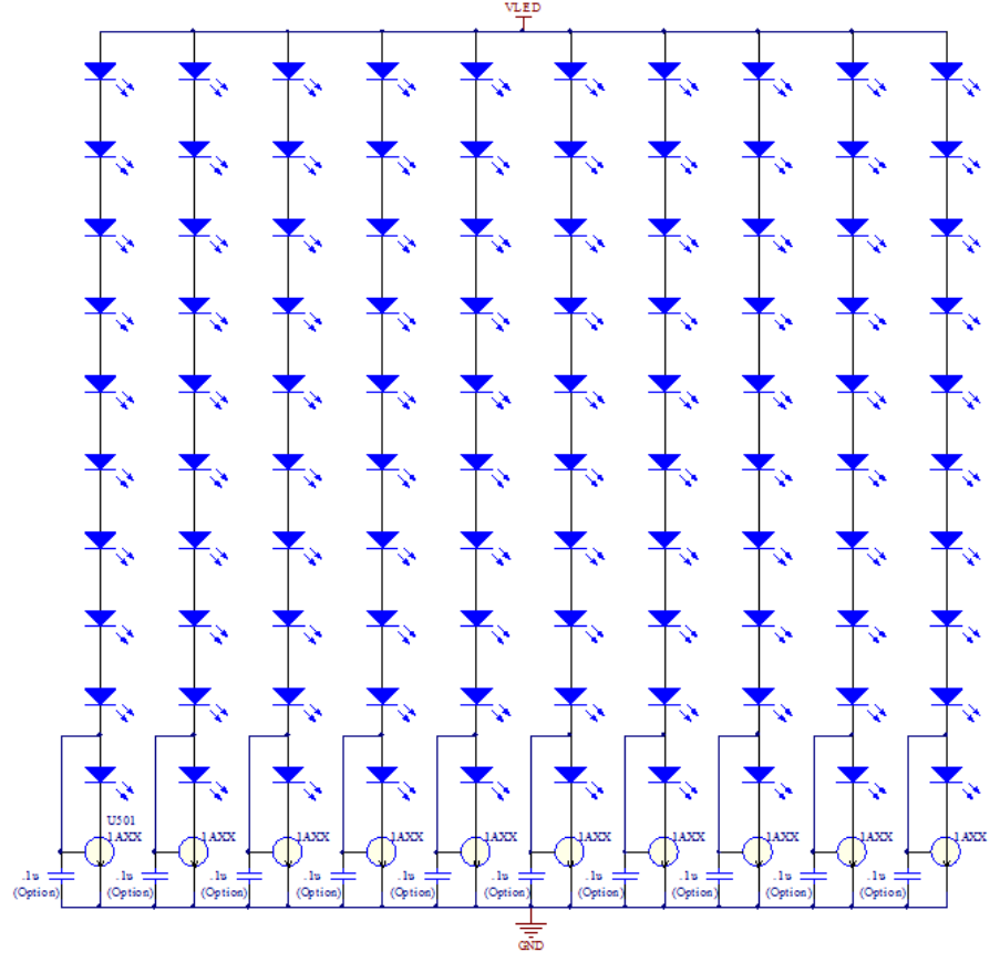
36V light tube application
LED Vf = 3.3V ~ 3.5V
VLED = 35.5V ~ 40V
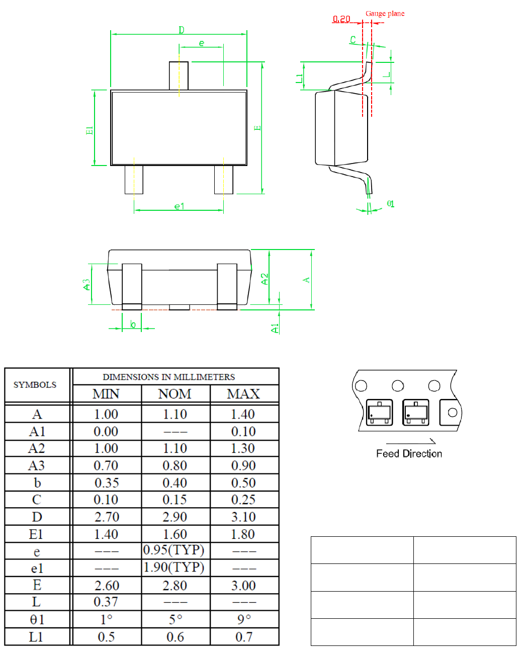
Package Dimensions
SOT23-3
Taping Specification
PACKAGE Q’TY/REEL
SOT23-3 3,000 ea
SOT23-5 3,000 ea
SOP89 1,000 ea
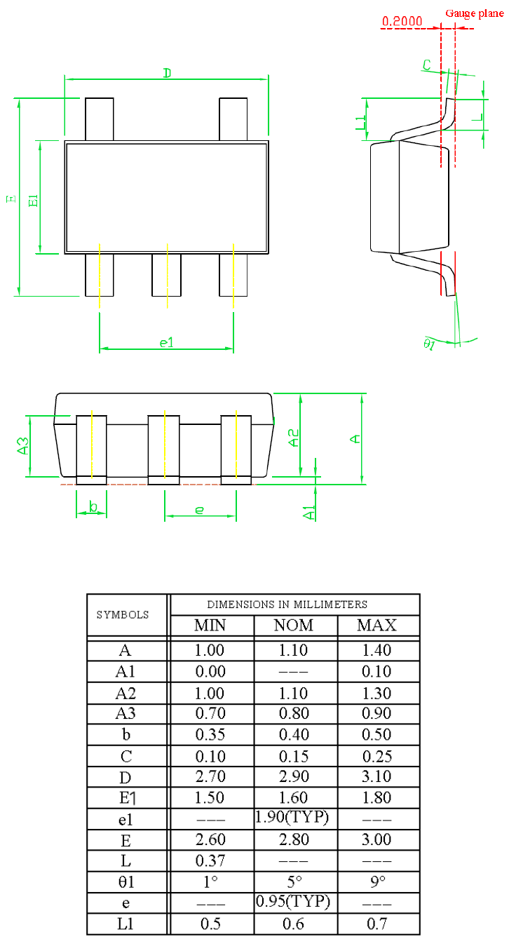
SOT23-5
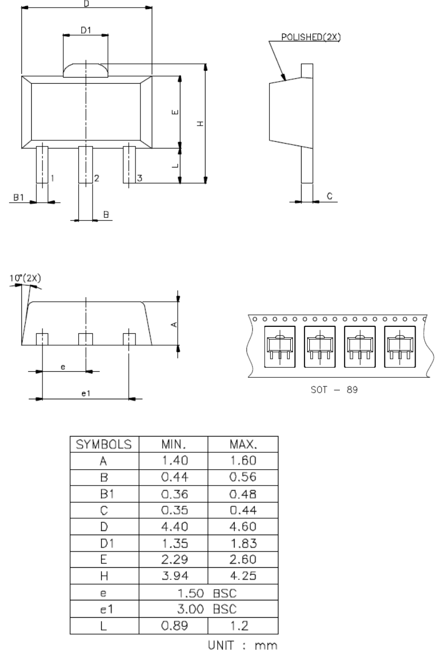
SOT89

1. This document is provided for reference purposes only so that Mos-tech customers may select the appropriate
Mos-tech products for their use. Mos-tech neither makes warranties or representations with respect to the
accuracy or completeness of the information contained in this document nor grants any license to any
intellectual property rights or any other rights of Mos-tech or any third party with respect to the information in
this document.
2. Mos-tech shall have no liability for damages or infringement of any intellectual property or other rights arising
out of the use of any information in this document, including, but not limited to, product data, diagrams, charts,
programs, algorithms, and application circuit examples.
3. You should not use the products or the technology described in this document for the purpose of military
applications such as the development of weapons of mass destruction or for the purpose of any other military
use. When exporting the products or technology described herein, you should follow the applicable export
control laws and regulations, and procedures required by such laws and regulations.
4. All information included in this document such as product data, diagrams, charts, programs, algorithms, and
application circuit examples, is current as of the date this document is issued. Such information, however, is
subject to change without any prior notice. Before purchasing or using any Mos-tech products listed in this
document, please confirm the latest product information with a Mos-tech sales office. Also, please pay regular
and careful attention to additional and different information to be disclosed by Mos-tech such as that disclosed
through our website. (http://www.mtsemi.com )
5. Mos-tech has used reasonable care in compiling the information included in this document, but Mos-tech
assumes no liability whatsoever for any damages incurred as a result of errors or omissions in the information
included in this document.
6. When using or otherwise relying on the information in this document, you should evaluate the information in
light of the total system before deciding about the applicability of such information to the intended application.
Mos-tech makes no representations, warranties or guaranties regarding the suitability of its products for any
particular application and specifically disclaims any liability arising out of the application and use of the
information in this document or Mos-tech products.
7. With the exception of products specified by Mos-tech as suitable for automobile applications, Mos-tech
products are not designed, manufactured or tested for applications or otherwise in systems the failure or
malfunction of which may cause a direct threat to human life or create a risk of human injury or which require
especially high quality and reliability such as safety systems, or equipment or systems for transportation and
traffic, healthcare, combustion control, aerospace and aeronautics, nuclear power, or undersea communication
transmission. If you are considering the use of our products for such purposes, please contact a Mos-tech
sales office beforehand. Mos-tech shall have no liability for damages arising out of the uses set forth above.
8. Notwithstanding the preceding paragraph, you should not use Mos-tech products for the purposes listed below:
(1) artificial life support devices or systems
(2) surgical implantations
(3) healthcare intervention (e.g., excision, administration of medication, etc.)
(4) any other purposes that pose a direct threat to human life
Mos-tech shall have no liability for damages arising out of the uses set forth in the above and purchasers who
elect to use Mos-tech products in any of the foregoing applications shall indemnify and hold harmless Mos-tech
Technology Corp., its affiliated companies and their officers, directors, and employees against any and all
damages arising out of such applications.
9. You should use the products described herein within the range specified by Mos-tech, especially with respect
to the maximum rating, operating supply voltage range, movement power voltage range, heat radiation
characteristics, installation and other product characteristics. Mos-tech shall have no liability for malfunctions or
damages arising out of the use of Mos-tech products beyond such specified ranges.
10. Although Mos-tech endeavors to improve the quality and reliability of its products, IC products have specific
characteristics such as the occurrence of failure at a certain rate and malfunctions under certain use
conditions. Please be sure to implement safety measures to guard against the possibility of physical injury, and
injury or damage caused by fire in the event of the failure of a Mos-tech product, such as safety design for
hardware and software including but not limited to redundancy, fire control and malfunction prevention,
appropriate treatment for aging degradation or any other applicable measures. Among others, since the
evaluation of microcomputer software alone is very difficult, please evaluate the safety of the final products or
system manufactured by you.
11. In case Mos-tech products listed in this document are detached from the products to which the Mos-tech
products are attached or affixed, the risk of accident such as swallowing by infants and small children is very
high. You should implement safety measures so that Mos-tech products may not be easily detached from your
products. Mos-techshall have no liability for damages arising out of such detachment.
12. This document may not be reproduced or duplicated, in any form, in whole or in part, without prior written
approval from Mos-tech.
13. Please contact a Mos-tech sales office if you have any questions regarding the information contained in this
document, Mos-tech semiconductor products, or if you have any other inquiries.
Notes regarding these materials
MOS-TECH Semiconductor Co.,LTD
©2010 MOS-TECH Semiconductor Corporation www.mtsemi.com
1. ᴀ䌘᭭ᰃЎњ䅽⫼᠋ḍ⫼䗨䗝ᢽড়䗖ⱘᴀ݀ৌѻકⱘখ㗗䌘᭭ˈᇍѢᴀ䌘᭭Ё᠔䆄䕑ⱘᡔᴃֵᙃˈᑊ䴲ᛣ
ੇⴔᇍᴀ݀ৌ㗙ϝ㗙ⱘⶹ䆚ѻᴗঞ݊Ҫᴗ߽خߎֱ䆕ᇍᅲᮑᴗ䖯㸠ⱘᡓ䇎DŽ
2. ᇍѢՓ⫼ᴀ䌘᭭᠔䆄䕑ⱘѻક᭄ǃǃ㸼ǃᑣǃㅫ⊩ঞ݊Ҫᑨ⫼⬉䏃՟㗠ᓩ䍋ⱘᤳᆇ㗙ᇍϝ㗙ⱘ
ⶹ䆚ѻᴗঞ݊Ҫᴗ߽䗴៤։⢃ˈᴀ݀ৌϡᡓᢙӏԩ䋷ӏDŽ
3. ϡ㛑ᇚᴀ䌘᭭᠔䆄䕑ⱘѻકᡔᴃ⫼Ѣ㾘⸈ണᗻ℺఼ⱘᓔথㄝⳂⱘǃݯџⳂⱘ݊Ҫⱘݯ䳔⫼䗨ᮍ䴶DŽ
ˈߎষᯊᖙ乏䙉ᅜ中国ⱘlj∛ঞ䌌ᯧ⊩NJঞ݊ҪߎষⱘⳌ݇⊩Ҹᑊሹ㸠䖭ѯ⊩ҸЁ㾘ᅮⱘᖙ㽕
㓁DŽ
4. ᴀ䌘᭭᠔䆄䕑ⱘѻક᭄ǃǃ㸼ǃᑣǃㅫ⊩ҹঞ݊Ҫᑨ⫼⬉䏃՟ㄝ᠔ֵ᳝ᙃഛЎᴀ䌘᭭থ㸠ᯊⱘݙᆍˈ
ᴀ݀ৌ᳝ৃ㛑خџܜ䗮ⶹⱘᚙމϟˈᇍᴀ䌘᭭᠔䆄䕑ⱘѻક㗙ѻક㾘Ḑ䖯㸠ᬍDŽ᠔ҹ䌁фՓ⫼
ᴀ݀ৌⱘञᇐԧѻકПࠡˈ䇋џܜᴀ݀ৌⱘ㧹Ϯにষ⹂䅸᳔ᮄⱘֵᙃᑊ㒣ᐌ⬭ᛣᴀ݀ৌ䗮䖛݀ৌЏ义
(http://www.mtsemi.com)ㄝ݀ᓔⱘ᳔ᮄֵᙃDŽ
5. ᇍѢᴀ䌘᭭Ё᠔䆄䕑ⱘֵᙃˈࠊᯊ៥Ӏሑֱ䆕ߎ⠜ᯊⱘ㊒⹂ᗻˈԚϡᡓᢙᴀ䌘᭭ⱘভ䗄ϡᔧ㗠㟈Փ乒
ᅶ䙁ফᤳ༅ㄝⱘӏԩⳌ݇䋷ӏDŽ
6. Փ⫼ᴀ䌘᭭᠔䆄䕑ⱘѻક᭄ǃǃ㸼ㄝ᠔⼎ⱘᡔᴃݙᆍǃᑣǃㅫ⊩ঞ݊Ҫᑨ⫼⬉䏃՟ᯊˈϡҙ㽕ᇍ᠔
Փ⫼ⱘᡔᴃֵᙃ䖯㸠ऩ⣀䆘Ӌˈ䖬㽕ᇍᭈϾ㋏㒳䖯㸠ܙߚⱘ䆘ӋDŽ䇋乒ᅶ㞾㸠䋳䋷ˈ䖯㸠ᰃ৺䗖⫼ⱘ߸ᮁDŽ
ᴀ݀ৌᇍѢᰃ৺䗖⫼ϡ䋳ӏԩ䋷ӏDŽ
7. ᴀ䌘᭭Ё᠔䆄䕑ⱘѻકᑊ䴲䩜ᇍϛϔߎ⦄ᬙ䱰ᰃ䫭䇃䖤㸠ህӮ࿕㚕ࠄҎⱘ⫳ੑ㒭Ҏԧᏺᴹॅᆇⱘᴎ఼ǃ
㋏㒳བ⾡ᅝܼ㺙㕂㗙䖤䕧Ѹ䗮⫼ⱘǃए⭫ǃ➗⚻ࠊǃ㟾఼ẄǃḌ㛑ǃ⍋ᑩЁ㒻⫼ⱘᴎ఼㋏㒳ㄝ
㗠䆒䅵ࠊ䗴ⱘ⡍߿ᰃᇍѢક䋼ৃ䴴ᗻ㽕∖ᵕ催ⱘᴎ఼㋏㒳ㄝ˄ᇚᴀ݀ৌᣛᅮ⫼Ѣ≑䔺ᮍ䴶ⱘѻક⫼
Ѣ≑䔺ᯊ䰸˅DŽབᵰ㽕⫼ѢϞ䗄ⱘⳂⱘˈ䇋ࡵᖙџܜᴀ݀ৌⱘ㧹Ϯにষ䆶DŽˈᇍѢ⫼ѢϞ䗄Ⳃⱘ
㗠䗴៤ⱘᤳ༅ㄝˈᴀ݀ৌὖϡ䋳䋷DŽ
8. 䰸Ϟ䗄乍ݙᆍˈϡ㛑ᇚᴀ䌘᭭Ё䆄䕑ⱘѻક⫼Ѣҹϟ⫼䗨DŽབᵰ⫼Ѣҹϟ⫼䗨㗠䗴៤ⱘᤳ༅ˈᴀ݀ৌ
ὖϡ䋳䋷DŽ
1˅⫳ੑ㓈ᣕ㺙㕂DŽ
2˅ỡඟѢҎԧՓ⫼ⱘ㺙㕂DŽ
3˅⫼Ѣ⊏⭫˄ߛ䰸ᙷ䚼ǃ㒭㥃ㄝ˅ⱘ㺙㕂DŽ
4˅݊ҪⳈᕅડࠄҎⱘ⫳ੑⱘ㺙㕂DŽ
9. Փ⫼ᴀ䌘᭭᠔䆄䕑ⱘѻકᯊˈᇍѢ᳔乱ᅮؐǃᎹ⬉⑤⬉य़ⱘ㣗ೈǃᬒ⛁⡍ᗻǃᅝ㺙ᴵӊঞ݊Ҫᴵӊ䇋
ᴀ݀ৌ㾘ᅮⱘֱ䆕㣗ೈݙՓ⫼DŽབᵰ䍙ߎњᴀ݀ৌ㾘ᅮⱘֱ䆕㣗ೈՓ⫼ᯊˈᇍѢ⬅ℸ㗠䗴៤ⱘᬙ䱰ߎ⦄
ⱘџᬙˈᴀ݀ৌᇚϡᡓᢙӏԩ䋷ӏDŽ
10.ᴀ݀ৌϔⳈ㟈Ѣᦤ催ѻકⱘ䋼䞣ৃ䴴ᗻˈԚϔ㠀ᴹ䇈ˈञᇐԧѻકᘏӮҹϔᅮⱘὖ⥛থ⫳ᬙ䱰ǃ㗙⬅
ѢՓ⫼ᴵӊϡৠ㗠ߎ⦄䫭䇃䖤㸠ㄝDŽЎњ䙓ܡᴀ݀ৌⱘѻકথ⫳ᬙ䱰㗙䫭䇃䖤㸠㗠ᇐ㟈Ҏ䑿џᬙ☿♒
䗴៤⼒Ӯᗻⱘᤳ༅ˈᏠᳯᅶ᠋㛑㞾㸠䋳䋷䖯㸠ݫԭ䆒䅵ǃ䞛পᓊ⚻ᇍㄪঞ䖯㸠䰆ℶ䫭䇃䖤㸠ㄝⱘᅝܼ䆒䅵
˄ࣙᣀ⹀ӊ䕃ӊϸᮍ䴶ⱘ䆒䅵˅ҹঞ㗕࣪໘⧚ㄝˈ䖭ᰃЎᴎ఼㋏㒳ⱘߎॖֱ䆕DŽ⡍߿ᰃऩ⠛ᴎⱘ䕃ӊˈ
⬅Ѣऩ⣀䖯㸠偠䆕ᕜೄ䲒ˈ᠔ҹ㽕∖乒ᅶࠊ䗴ⱘ᳔㒜ⱘᴎ఼ঞ㋏㒳Ϟ䖯㸠ᅝܼẔ偠ᎹDŽ
11. བᵰᡞᴀ䌘᭭᠔䆄䕑ⱘѻકҢ݊䕑ԧ䆒Ϟौϟˈ᳝ৃ㛑䗴៤၈ܓ䇃৲ⱘॅ䰽DŽ乒ᅶᇚᴀ݀ৌѻકᅝ㺙ࠄ
乒ᅶⱘ䆒Ϟᯊˈ䇋乒ᅶ㞾㸠䋳䋷ᇚᴀ݀ৌѻક䆒㕂Ўϡᆍᯧ࠹㨑ⱘᅝܼ䆒䅵DŽབᵰҢ乒ᅶⱘ䆒Ϟ࠹㨑㗠
䗴៤џᬙᯊˈᴀ݀ৌᇚϡᡓᢙӏԩ䋷ӏDŽ
12.ᕫࠄᴀ݀ৌⱘџܜк䴶䅸ৃᯊˈϡৃᇚᴀ䌘᭭ⱘϔ䚼ߚ㗙ܼ䚼䕀䕑㗙ࠊDŽ
13.བᵰ䳔㽕њ㾷݇Ѣᴀ䌘᭭ⱘ䆺㒚ݙᆍˈ㗙᳝݊Ҫ݇ᖗⱘ䯂乬ˈ䇋ᴀ݀ৌⱘ㧹Ϯにষ䆶DŽ
݇Ѣ߽⫼ᴀ䌘᭭ᯊⱘ⊼ᛣџ乍
⊼ᛣ
ᴀ᭛াᰃখ㗗䆥᭛ˈࠡ义᠔䕑㣅᭛⠜“Cautions”᳝ℷᓣᬜDŽ
©2010 MOS-TECH Semiconductor Corporation www.mtsemi.com
MOS-TECH Semiconductor Co.,LTD
1. MOS-TECH Semiconductor Corp. puts the maximum effort into making semiconductor products better
and more reliable, but there is always the possibility that trouble may occur with them. Trouble with
semiconductors may lead to personal injury, fire or property damage.
Remember to give due consideration to safety when making your circuit designs, with appropriate
measures such as (i) placement of substitutive, auxiliary circuits, (ii) use of nonflammable material or
(iii) prevention against any malfunction or mishap.
Keep safety first in your circuit designs!