MT6217 Datasheet. Www.s Manuals.com. R1.01 Mediatek
User Manual: Datasheets MT6217.
Open the PDF directly: View PDF ![]() .
.
Page Count: 350 [warning: Documents this large are best viewed by clicking the View PDF Link!]

MT6217 GSM/GPRS
Baseband Processor Data Sheet
Revision 1.01
Apr. 18, 2005

MT6217 GSM/GPRS Baseband Processor Data Sheet Revision 1.01
2/349 MediaTek Inc. Confidential
Revision History
Revision Date Comments
1.00 Sep. 01, 2004 First Release
1.01 Apr. 18, 2005 1) Corrected interrupt source naming in MCU Subsystem > Interrupt Controller > Table 12.
GPI-FIQ -> MFIQ, GPI -> MIRQ
2) Corrected GPIO_MODE6 register description from nIRQ -> MIRQ and nFIQ -> MFIQ
3) Corrected LCD_SDAT0 and LCD_SDAT1 register address
4) Updated EMI_GEN register
5) Updated GPIO16, GPIO17, GPIO18 PU/PD control, and added GPIO40 in product
description
6) Updated GPIO_MODE2 register
7) Added NLD15~NLD8 digital pin characteristics
8) Updated driving strength in digital pin characteristics

MT6217 GSM/GPRS Baseband Processor Data Sheet Revision 1.01
3/349 MediaTek Inc. Confidential
TABLE OF CONTENTS
Revision History ......................................................................................................................................2
1. System Overview............................................................................................................................... 2
1.1 Features ........................................................................................................................................................................................... 2
1.2 General Description ...................................................................................................................................................................... 2
2 Product Description..........................................................................................................................2
2.1 Pin Outs........................................................................................................................................................................................... 2
2.2 Pin Description .............................................................................................................................................................................. 2
2.3 Power Description .........................................................................................................................................................................2
3 Micro-Controller Unit Subsystem................................................................................................... 2
3.1 Processor Core ............................................................................................................................................................................... 2
3.2 Memory Management .................................................................................................................................................................. 2
3.3 Bus System.....................................................................................................................................................................................2
3.4 Direct Memory Access.................................................................................................................................................................2
3.5 Interrupt Controller.......................................................................................................................................................................2
3.6 Internal Memory Controller ........................................................................................................................................................2
3.7 External Memory Interface..........................................................................................................................................................2
4 Microcontroller Peripherals ............................................................................................................ 2
4.1 Pulse-Width Modulation Outputs ............................................................................................................................................... 2
4.2 Alerter ............................................................................................................................................................................................. 2
4.3 SIM Interface ................................................................................................................................................................................. 2
4.4 Keypad Scanner.............................................................................................................................................................................2
4.5 General Purpose Inputs/Outputs ................................................................................................................................................. 2
4.6 General Purpose Timer.................................................................................................................................................................2
4.7 UART .............................................................................................................................................................................................. 2
4.8 IrDA Framer................................................................................................................................................................................... 2
4.9 Real Time Clock ............................................................................................................................................................................2
4.10 Auxiliary ADC Unit ...................................................................................................................................................................... 2
5 Microcontroller Coprocessors .........................................................................................................2
5.1 GPRS Cipher Unit .........................................................................................................................................................................2
5.2 Divider ............................................................................................................................................................................................ 2
5.3 CSD Accelerator............................................................................................................................................................................2
5.4 FCS Codec......................................................................................................................................................................................2
6 Multi-Media Subsystem...................................................................................................................2
6.1 LCD Interface ................................................................................................................................................................................ 2
6.2 JPEG Decoder................................................................................................................................................................................ 2
6.3 Image Resizer................................................................................................................................................................................ 2
6.4 NAND FLASH interface ............................................................................................................................................................. 2
6.5 USB Device Controller ................................................................................................................................................................ 2
6.6 Memory Stick and SD Memory Card Controller.....................................................................................................................2
7 Audio Front-end................................................................................................................................ 2
7.1 General Description ...................................................................................................................................................................... 2
7.2 Register Definitions...................................................................................................................................................................... 2
7.3 Programming Guide...................................................................................................................................................................... 2
8 Radio Interface Control ...................................................................................................................2
8.1 Base-band Serial Interface........................................................................................................................................................... 2
8.2 Base-band Parallel Interface........................................................................................................................................................2

MT6217 GSM/GPRS Baseband Processor Data Sheet Revision 1.01
4/349 MediaTek Inc. Confidential
8.3 Automatic Power Control (APC) Unit ...................................................................................................................................... 2
8.4 Automatic Frequency Control (AFC) Unit ............................................................................................................................... 2
9 Baseband Front End......................................................................................................................... 2
9.1 Baseband Serial Ports ................................................................................................................................................................... 2
9.2 Downlink Path (RX Path) ............................................................................................................................................................ 2
9.3 Uplink Path (TX Path).................................................................................................................................................................. 2
10 Timing Generator.............................................................................................................................2
10.1 TDMA timer................................................................................................................................................................................... 2
10.2 Slow Clocking Unit ...................................................................................................................................................................... 2
11 Power, Clocks and Reset...................................................................................................................2
11.1 Baseband to PMIC Serial Interface............................................................................................................................................2
11.2 Clocks.............................................................................................................................................................................................. 2
11.3 Reset Management........................................................................................................................................................................2
11.4 Software Power Down Control................................................................................................................................................... 2
12 Analog Front-end & Analog Blocks ................................................................................................ 2
12.1 General Description ...................................................................................................................................................................... 2
12.2 MCU Register Definitions........................................................................................................................................................... 2
12.3 Programming Guide...................................................................................................................................................................... 2
13 Digital Pin Electrical Characteristics.............................................................................................. 2

MT6217 GSM/GPRS Baseband Processor Data Sheet Revision 1.01
5/349 MediaTek Inc. Confidential
Preface
Acronym for Register Type
R/W Capable of both read and write access
RO Read only
RC Read only. After reading the register bank, each bit which is HIGH(1) will be cleared to LOW(0 )
automatically.
WO Write only
W1S Write only. When writing data bits to register bank, each bit which is HIGH(1) will cause the
corresponding bit to be set to 1. Data bits which are LOW(0) has no effect on the corresponding bit.
W1C Write only. When writing data bits to register bank, each bit which is HIGH(1) will cause the
corresponding bit to be cleared to 0. Data bits which are LOW(0) has no effect on the corresponding bit.

MT6217 GSM/GPRS Baseband Processor Data Sheet Revision 1.01
6/349 MediaTek Inc. Confidential
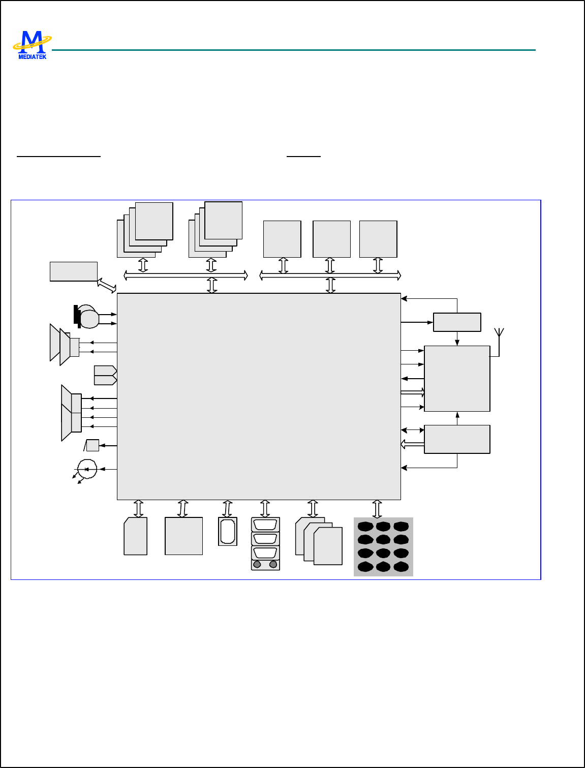
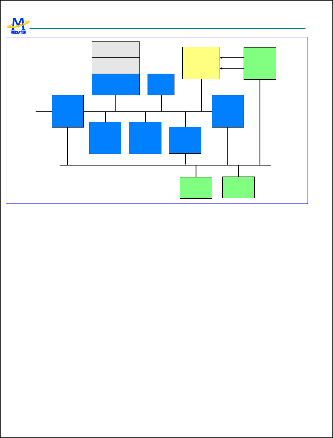
1. System Overview
The MT6217 is a highly integrated single chip solution for
GSM/GPRS phone. Based on 32-bit ARM7EJ -STM RISC
processor, MT6217 features not only high performance
GPRS Class 12 MODEM but is also designed with support
for the wireless multi-media applications, such as
advanced display engine, hardware JPEG decoder,
synthesis audio with 64-tone polyphony, digital audio
playback, Java acceleration, MMS and etc. Additionally,
MT6217 provides varieties of advanced interfaces for
functionality extensions, like 8-port external memory
interface, 3-port 8/16-bit parallel interface, NAND Flash,
IrDA, USB and MMC/SD/MS/MS Pro. The typical
application can be shown as Figure 1.
External Memory Interface
Providing the greatest capacity for expansion, the MT6217
supports up to 8 state-of-the-art devices with SRAM-like
interface, including burst/page mode Flash, page mode
SRAM, Pseudo SRAM, Color/Parallel LCD, and
multi-media companion chip, like Camera and Melody
chips. Regarding the consideration of power consumption
and low noise, this interface is designed for flexible I/O
voltage and allows for lowering supply voltage down to
1.8V. In addition, the driving strength is configurable that
makes the signal integrity problem easy. Retention
technology is also specifically used on data bus to prevent
the bus from being floating during turn over.
Multi-media Subsystem
In order to provide more flexibility and bandwidth for
multi-media products, an additional 8/16 bit parallel
interface is incorporated. This interface is designed
specially for support with Camera companion chip as well
as LCD panel. Moreover, it can connect NAND flash
device to provide a solution for multi-media data storage.
For running multi-media application faster, MT6217
integrates also several hardware-based engines. With
hardware based JPEG decoder, the MT6217 easily handles
real-time playback of compressed image. With hardware
based Resizer and advanced display engine, it can display
and combine arbitrary size of images with up to 4 blending
layers.
User Interface
For user interactions, the MT6217 brings together all
necessary peripheral blocks for multi-media GSM/GPRS
phone. It comprises the Keypad Scanner with capability of
multiple key pressing, SIM Controller, Alerter, Real Time
Clock, PWM, Serial LCD Controller and General Purpose
Programmable I/Os. For connectivity and data storage, the
MT6217 consists of UART, IrDA, USB 1.1 Slave and
MMC/SD/MS/MS Pro. Besides, for large amount of data
transfer, high performance DMA (Direct Memory Access)
and hardware flow control are implemented, that greatly
enhances the performance and saves precious processing
power.
Audio Interface
With highly integrated mixed-signal Audio Front-End, the
MT6217 completes an architecture that allows for easy
audio interfacing with direct connection to the audio
transducers. Not only D/A and A/D Converters for Voice
Band, but also the high resolution Stereo D/A Converters
for Audio band are integrated. In addition, the MT6217
provides also Stereo Input and Analog Mixer. All of them
enable the MT6217 based terminal a rich platform for
multi-media applications.
Radio Interface
Providing a well-organized radio interface with flexibility
for efficient customization, the MT6217 integrates
mixed-signal Baseband Front-End. It carries out gain and
offset calibration mechanisms and filters with
programmable coefficients for comprehensive
compatibility control on RF modules. The approach is also
combining a high resolution D/A Converter for controlling
VCXO or crystal instead of TCVCXO to reduce the
overall system cost. On the other hand, with 14-bit high
resolution A/D Converter for RF downlink path, MT6217
achieves great quality of MODEM performance. Besides,
to remove the necessary of external current-driving
component, the driving strength of some BPI outputs is
designed to be configurable.
Debug Function
MT6217 GSM/GPRS Baseband Processor Data Sheet Revision 1.01
7/349 MediaTek Inc. Confidential
The JTAG interface enables in-circuit debugging of
software program with the ARM7EJ -S core. With this
standardized debugger interface, the MT6217 provides
developers with a wide set of options for choosing ARM
development kits from supports of thirty parties.
Power Management
The MT6217 offers various low-power features helping
reduce system power consumption including Pause Mode
of 32KHz clocking at Standby State, Power Down Mode
for individual peripherals and Processor Sleep Mode.
Fabricated in low-power CMOS process, together with the
low-power features, the overall system can achieve ultra
low power consumption.
Package
The MT6217 device is offered in a 13mm×13mm, 282-ball,
0.65 mm pitch, TFBGA package.
RF
Module
MT6217
Speech/Audio
Output
Speech/Audio
Input
Keypad
External Memory
Interface
Melody
LCD
TCVCXO
AFC
APC
TX I/Q
RX I/Q
BPI
BSI
Alerter
SIM
Supply Voltages
JTAG
UART
IrDA
Power
Management
Circuitry
Serial
LCD
SYSCLK
Serial
LCD
MMC/SD/MS/
MSPro
USB
B2PSI
AuxAD
C
1 2 3
4 5 6
7 8 9
*0 #
Camera
HiFi Stero
Output
FM Stereo
Radio Input
Debugger
PWM
NAND
Flash LCD
8/16-bit Parallel
Interface
Flash
SRAM
PSRAM
Figure 1 Typical application of MT6217

MT6217 GSM/GPRS Baseband Processor Data Sheet Revision 1.01
8/349 MediaTek Inc. Confidential
1.1 Features
n General
l Integrated voice-band, audio-band and base-band analog front ends
l TFBGA 13mm×13mm, 282-ball, 0.65 mm pitch package
n MCU Subsystem
l ARM7EJ -S 32-bit RISC processor
l Java hardware acceleration for faster Java-based games and other applets
l Operating frequency: 26/52 MHz
l 13 DMA channels
l 128K Bytes zero-wait-state on-chip SRAM
l On -chip boot ROM for Factory Flash Programming
l Watchdog timer for system crash recovery
l 2 sets of General Purpose Timer
l Circuit Switch Data and Division coprocessors
n External Memory Interface
l Support up to 8 external devices
l Support 8-bit or 16-bit memory components with size up to 64M Bytes each
l Support Flash and SRAM with Page Mode or Burst Mode
l Support Pseudo SRAM
l Industrial standard Parallel LCD Interface
l Built-in hardware acceleration function for color LCD panels
l Support multi-media companion chips with 8/16 bits data width
l Flexible I/O voltage of 1.8V ~ 3V for memory interface
l Configurable driving strength for memory interface
n Multi-media Subsystem
l Dedicated 8/16-bit Parallel Interface, support up to 3 external devices
l High speed hardware JPEG decoder, support both baseline sequential and progressive JPEG files
l High quality hardware Resizer capable of tailoring JPEG image to arbitrary size
l Support simultaneously equipping up to 2 parallel LCD and 1 serial LCD panels
l Support LCD panel maximum resolution up to 800x600 at 16bpp

MT6217 GSM/GPRS Baseband Processor Data Sheet Revision 1.01
9/349 MediaTek Inc. Confidential
l Capable of combining display memories with up to 4 blending layers
l NAND Flash Interface for mass storages
l Full-speed USB 1.1 Device
l Multi Media Card/Secure Digital Memory Card/Memory Stick/Memory Stick Pro controller
n Audio and Modem CODEC
l Wavetable synthesis with up to 64 notes
l Advanced wavetable synthesizer capable of generating simulated stereo
l Wavetable including GM full set of 128 instruments and 47 sets of percussion
l PCM Playback and Record
l Dial tone generation
l Voice Memo
l Noise Reduction
l Echo Suppression
l Advanced Sidetone Oscillation Reduction
l Digital sidetone generator with programmable gain
l Two programmable acoustic compensation filters
l GSM/GPRS quad vocoders for adaptive multirate (AMR), enhanced full rate (EFR), full rate (FR) and half rate (HR)
l GSM channel coding, equalization and A5/1 and A5/2 ciphering
l GPRS GEA and GEA2 ciphering
l Programmable GSM/GPRS Modem
l Packet Switched Data with CS1/CS2/CS3/CS4 coding schemes
l GSM Circuit Switch Data
l GPRS Class 12
n User Interfaces
l 6-row × 7-column keypad controller with hardware scanner
l Support multiple key press for gaming
l SIM Card Controller with hardware flow control
l 3 UARTs with hardware flow control and speed up to 921600 bps
l IrDA modulator/demodulator with hardware framer
l Real Time Clock (RTC) operating with a separate power supply
l Serial LCD Interface with 7 bytes TX FIFO

MT6217 GSM/GPRS Baseband Processor Data Sheet Revision 1.01
10/349 MediaTek Inc. Confidential
l General Purpose I/Os (GPIOs)
l 2 Sets of Pulse Width Modulation (PWM) Output
l Alerter Output with Enhanced PWM or PDM
l Six external interrupt lines
n Audio Interface and Audio Front End
l Two microphone inputs sharing one low noise amplifier with programmable gain
l Two Voice power amplifiers with programmable gain
l 2nd order Sigma-Delta A/D Converter for voice uplink path
l D/A Converter for voice downlink path
l High resolution D/A Converters for Stereo Audio playback
l Stereo analog input for stereo audio source
l Analog Multiplexer for Stereo Audio
l Stereo to Mono Conversion
l Support half-duplex hands-free operation
l Complying with GSM 03.50
n Radio Interface and Baseband Front End
l GMSK modulator with analog I and Q channel outputs
l 10 -bit D/A Converter for uplink baseband I and Q signals
l 14-bit high resolution A/D Converter for downlink baseband I and Q signals
l Calibration mechanism of offset and gain mismatch for baseband A/D Converter and D/A Converter
l 10 -bit D/A Converter for Automatic Power Control
l 13 -bit high resolution D/A Converter for Automatic Frequency Control
l Programmable Radio RX filter
l 2 Channels Baseband Serial Interface (BSI) with 3-wire control
l 10 -Pin Baseband Parallel Interface (BPI) with programmable driving strength
l Multi-band support
n Power Management
l Power Down Mode for analog and digital circuits
l Processor Sleep Mode
l Pause Mode of 32KHz clocking at Standby State
l 7-channel Auxiliary 10-bit A/D Converter for charger and battery monitoring

MT6217 GSM/GPRS Baseband Processor Data Sheet Revision 1.01
11/349 MediaTek Inc. Confidential
n Test and Debug
l Built-in digital and analog loop back modes for both Audio and Baseband Front-End
l DAI port complying with GSM Rec.11.10
l JTAG port for debugging embedded MCU

MT6217 GSM/GPRS Baseband Processor Data Sheet Revision 1.01
12/349 MediaTek Inc. Confidential
1.2 General Description
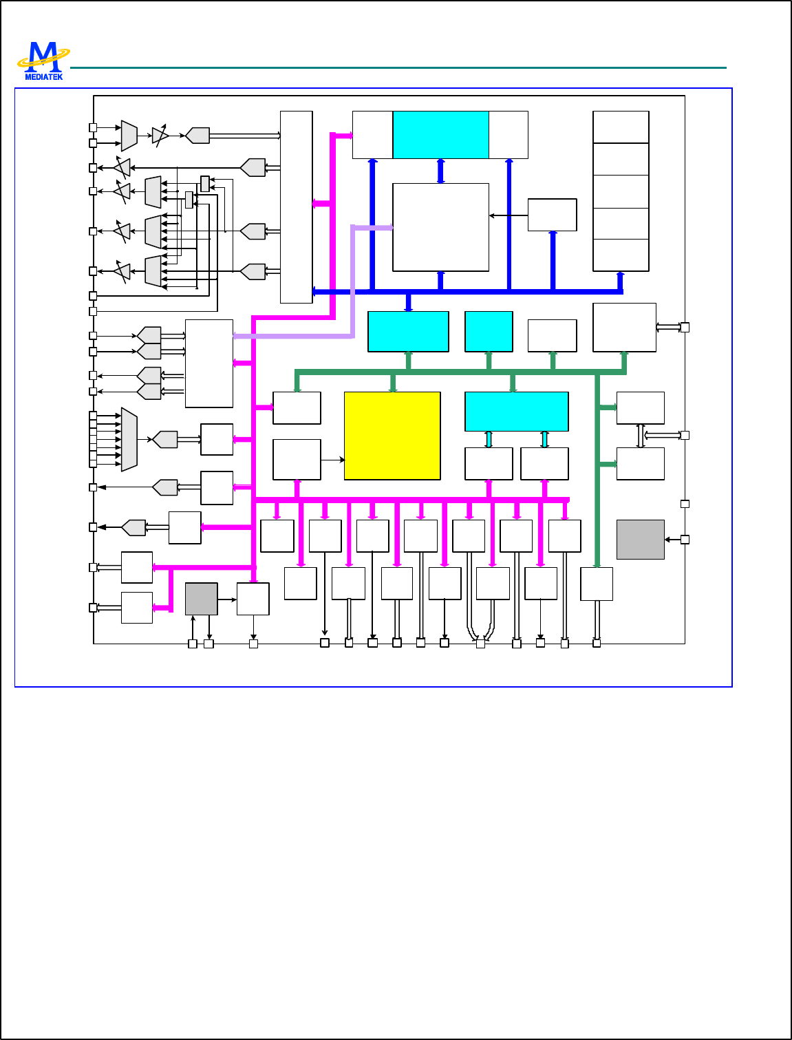
Figure 2 details the block diagram of MT6217. Based on dual-processor architecture, the major processor of MT6217 is
ARM7EJ -S, which mainly runs high-level GSM /GPRS protocol software as well as multi-media applications. With the
other one is a digital signal processor corresponding for handling the low-level MODEM as well as advanced audio
functions. Except for some mixed-signal circuitries, the other building blocks in MT6217 are connected to either the
microcontroller or the digital signal processor. Specifically, MT6217 consists of the following subsystems:
l Microcontroller Unit (MCU) Subsystem, including an ARM7EJ -S RISC processor and its accompanying memory
management and interrupt handling logics.
l Digital Signal Processor (DSP) Subsystem, including a DSP and its accompanying memory, memory controller,
and interrupt controller.
l MCU/DSP Interface, where the MCU and the DSP exchange hardware and software information.
l Microcontroller Peripherals, which includes all user interface modules and RF control interface modules.
l Microcontroller Coprocessors, which intends to run computing-intensive processes in place of Microcontroller.
l DSP Peripherals, which are hardware accelerators for GSM/GPRS channel codec.
l Multi-media Subsystem, which integrate several advanced accelerators to support multi-media applications.
l Voice Front End, the data path of conveying analog speech from and to digital speech.
l Audio Front End, also the data path of conveying stereo audio from stereo audio source
l Baseband Front End, the data path of conveying digital signal form and to analog signal of RF modules.
l Timing Generator, generating the control signals related to the TDMA frame timing.
l Power, Reset and Clock subsystem, managing the power, reset and clock distribution inside MT6217.
Details of the individual subsystems and blocks are described in following Chapters.
MT6217 GSM/GPRS Baseband Processor Data Sheet Revision 1.01
13/349 MediaTek Inc. Confidential
BSI
ARM7EJ-S
DSP
Interrupt
Controller
MCU/DSP
Interface
Memory
Patch
Unit
Trap
Unit
DSP
Coprocessor
Boot
ROM
On-Chip
SRAM
DMA
Controller
External
Memory
Interface
Interrupt
Controller
TDMA
Timer
DAC APC
DAC AFC
SIM GPIO
Keypad
Scanner
BPI
WDT
ADC Aux
ADC
Clock
Generator
MMC
SD/MS
MS Pro
Audio
Path
Baseband
Path
ADC
USBAlerter
MT6217
DSP
Coprocessor
DSP
Coprocessor
Serial RF
Control
Parallel RF
Control
APC
ADC
DAC
DAC
ADC
DAC
DAC
DAC
+
+
Bridge
DSP
Coprocessor
NAND Flash
Controller
DSP
Coprocessor
Aux
ADC
AFC
TX_Q
TX_I
RX_I
RX_Q
VOICE_0
VOICE_1
AUDIO_L
AUDIO_R
MIC_0
MIC_1
STEREO_L
STEREO_R
System
Clock
13/26MHz
32KHz
Crystal
JTAG
Flash
SRAM
LCD
Melody
Wake Up User InterfaceReset
GPT
LCD
Controller
Image
Resizer
JPEG
Decoder
NAND
Flash
LCD
Camera
B2PSI IrDA
PWM Serial
LCD
RTC
UART
32K
OSC
ConnectivitySerial Port
Figure 2 MT6217 block diagram.

MT6217 GSM/GPRS Baseband Processor Data Sheet Revision 1.01
14/349 MediaTek Inc. Confidential
2 Product Description
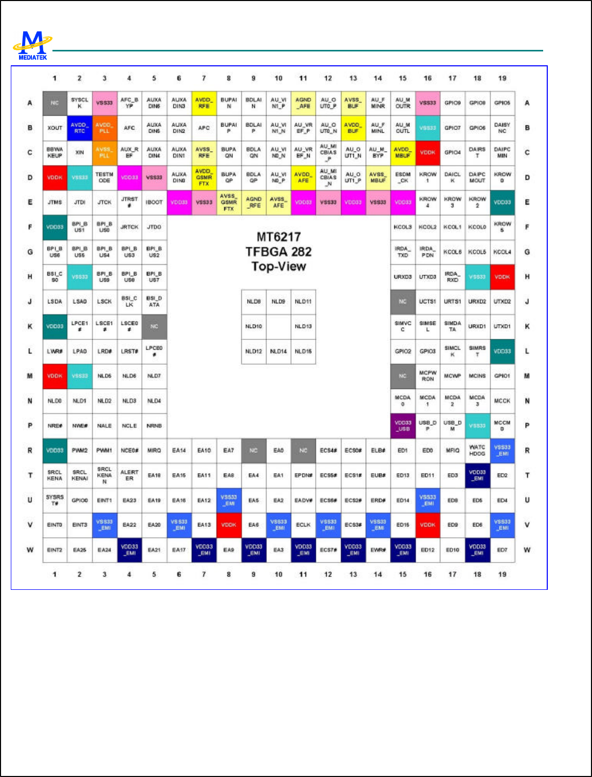
2.1 Pin Outs
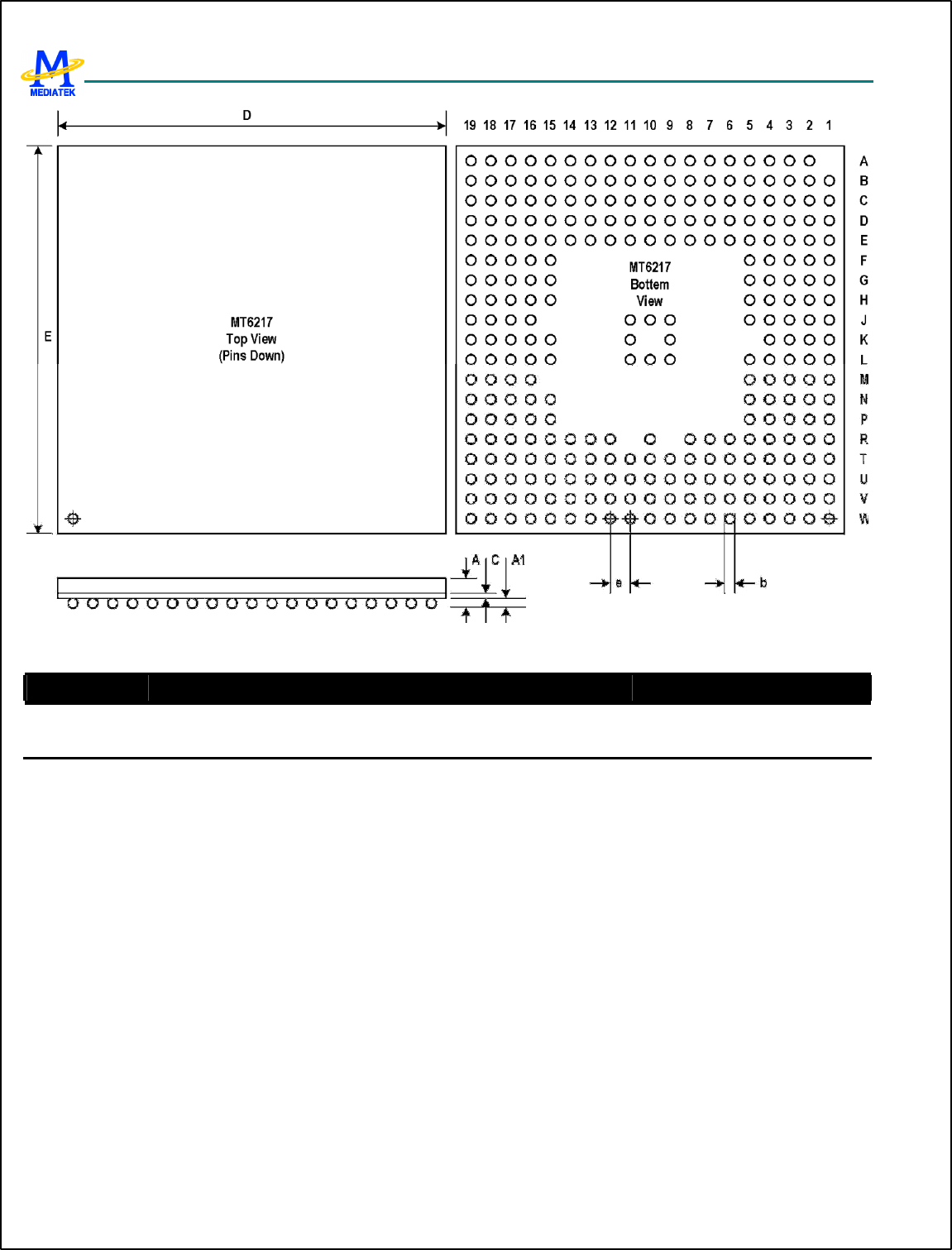
One type of package for this product, TFBGA 13mm*13mm, 282-ball, 0.65 mm pitch Package, is offered.
Pin outs and the top view are illustrated in Figure 3 for this package. Outline and dimension of package is illustrated in
Figure 4, while the definition of package is shown in Table 1.
MT6217 GSM/GPRS Baseband Processor Data Sheet Revision 1.01
15/349 MediaTek Inc. Confidential
Figure 3 Top View of MT6217 TFBGA 13mm*13mm, 282-ball, 0.65 mm pitch Package
MT6217 GSM/GPRS Baseband Processor Data Sheet Revision 1.01
16/349 MediaTek Inc. Confidential
Figure 4 Outlines and Dimension of TFBGA 13mm*13mm, 282-ball, 0.65 mm pitch Package
Body Size Ball Count Ball Pitch Ball Dia. Package Thk. Stand Off Substrate Thk.
D E N e b A (Max.) A1 C
13 13 282 0.65 0.3 1.4 0.3 0.36
Table 1 Definition of TFBGA 13mm*13mm, 282-ball, 0.65 mm pitch Package (Unit: mm)
MT6217 GSM/GPRS Baseband Processor Data Sheet Revision 1.01
17/349 MediaTek Inc. Confidential
2.2 Pin Description
Ball
13X13 Name Dir Description Mode0 Mode1 Mode2 Mode3 Pull Reset
JTAG Port
E4 JTRST# I JTAG test port reset input PD Input
E3 JTCK I JTAG test port clock input PU Input
E2 JTDI I JTAG test port data input PU Input
E1 JTMS I JTAG test port mode switch PU Input
F5 JTDO O JTAG test port data output 0
F4 JRTCK O JTAG test port returned clock output 0
RF Parallel Control Unit
F3 BPI_BUS0 O RF hard-wire control bus 0 0
F2 BPI_BUS1 O RF hard-wire control bus 1 0
G5 BPI_BUS2 O RF hard-wire control bus 2 0
G4 BPI_BUS3 O RF hard-wire control bus 3 0
G3 BPI_BUS4 O RF hard-wire control bus 4 0
G2 BPI_BUS5 O RF hard-wire control bus 5 0
G1 BPI_BUS6 IO RF hard-wire control bus 6 GPIO10 BPI_BU
S6 PD Input
H5 BPI_BUS7 IO RF hard-wire control bus 7 GPIO11 BPI_BU
S7 6.5MHz 26MHz PD Input
H4 BPI_BUS8 IO RF hard-wire control bus 8 GPIO12 BPI_BU
S8
13MHz 26MHz PD Input
H3 BPI_BUS9 IO RF hard-wire control bus 9 GPIO13 BPI_BU
S9
BSI_CS
1
PD Input
RF Serial Control Unit
H1 BSI_CS0 O RF 3-wire interface chip select 0 0
J5 BSI_DATA O RF 3-wire interface data output 0
J4 BSI_CLK O RF 3-wire interface clock output 0
PWM Interface
R3 PWM1 IO Pulse width modulated signal 1 GPIO2
1
PWM1 DSP_G
PO0
TBTX
FS
PD Input
R2 PWM2 IO Pulse width modulated signal 2 GPIO2
2
PWM2 DSP_G
PO1
TBRX
EN
PD Input
T4 ALERTER IO Pulse width modulated signal for buzzer GPIO2
3
ALERT
ER
DSP_G
PO2
BTRX
FS
PD Input
Serial LCD/PM IC Interface
J3 LSCK IO Serial display interface data output GPIO16 LSCK TBTXE
N PU Input
J2 LSA0 IO Serial display interface address output GPIO17 LSA0 TDTIR
Q
PU Input
J1 LSDA IO Serial display interface clock output GPIO18 LSDA TCTIR
Q2 PU Input
K4 LSCE0# IO Serial display interface chip select 0
output GPIO19 LSCE0# DSP_TI
D0 TCTIR
Q1 PU Input
K3 LSCE1# IO Serial display interface chip select 1 GPIO20 LSCE1# LPCE2# TEVTV PU Input
MT6217 GSM/GPRS Baseband Processor Data Sheet Revision 1.01
18/349 MediaTek Inc. Confidential
output AL
Parallel LCD/Nand-Flash Interface
K2 LPCE1# IO Parallel display interface chip select 1
output GPIO24 LPCE1# NCE1# MCU_
TD0 PU
L5 LPCE0# O Parallel display interface chip select 0
output
L4 LRST# O Parallel display interface Reset Signal
L3 LRD# O Parallel display interface Read Strobe
L2 LPA0 O Parallel display interface address output
L1 LWR# O Parallel display interface Write Strobe
L11 NLD15 IO Parallel LCD/NAND-Flash Data 15 PD
L10 NLD14 IO Parallel LCD/NAND-Flash Data 14 PD
K11 NLD13 IO Parallel LCD/NAND-Flash Data 13 PD
L9 NLD12 IO Parallel LCD/NAND-Flash Data 12 PD
J11 NLD11 IO Parallel LCD/NAND-Flash Data 11 PD
K9 NLD10 IO Parallel LCD/NAND-Flash Data 10 PD
J10 NLD9 IO Parallel LCD/NAND-Flash Data 9 PD
J9 NLD8 IO Parallel LCD/NAND-Flash Data 8 PD
M5 NLD7 IO Parallel LCD/NAND-Flash Data 7 PD
M4 NLD6 IO Parallel LCD/NAND-Flash Data 6 PD
M3 NLD5 IO Parallel LCD/NAND-Flash Data 5 PD
N5 NLD4 IO Parallel LCD/NAND-Flash Data 4 PD
N4 NLD3 IO Parallel LCD/NAND-Flash Data 3 PD
N3 NLD2 IO Parallel LCD/NAND-Flash Data 2 PD
N2 NLD1 IO Parallel LCD/NAND-Flash Data 1 PD
N1 NLD0 IO Parallel LCD/NAND-Flash Data 0 PD
P5 NRNB IO NAND-Flash Read/Busy Flag GPIO25 NRNB DSP_TI
D1 MCU_T
ID1 PU
P4 NCLE IO NAND-Flash Command Latch Signal GPIO26 NCLE DSP_TI
D2 MCU_
TID2 PD
P3 NALE IO NAND-Flash Address Latch Signal GPIO27 NALE DSP_TI
D3
MCU_
TID3 PD
P2 NWE# IO NAND-Flash Write Strobe GPIO28 NWE# DSP_TI
D4
MCU_
DID PU
P1 NRE# IO NAND-Flash Read Strobe GPIO29 NRE# DSP_TI
D5 MCU_
DFS PU
R4 NCE0# IO NAND-Flash Chip select output GPIO30 NCE0# DSP_TI
D6 MCU_
DCK PU
SIM Card Interface
L18 SIMRST O SIM card reset output 0
L17 SIMCLK O SIM card clock output 0
K15 SIMVCC O SIM card supply power control 0
K16 SIMSEL IO SIM card supply power select GPIO32 SIMSE
L
PD 0
K17 SIMDATA IO SIM card data input/output 0
Dedicated GPIO Interface
U2 GPIO0 IO General purpose input/output 0 GPIO0 DSP_GP
O3
PD Input

MT6217 GSM/GPRS Baseband Processor Data Sheet Revision 1.01
19/349 MediaTek Inc. Confidential
M19 GPIO1 IO General purpose input/output 1 GPIO1 DICK PD Input
L15 GPIO2 IO General purpose input/output 2 GPIO2 DID PD Input
L16 GPIO3 IO General purpose input/output 3 GPIO3 DIMS PD Input
C17 GPIO4 IO General purpose input/output 4 GPIO4 DSP_CK
L
DSPLC
K
TRASD
4 PD Input
A19 GPIO5 IO General purpose input/output 5 GPIO5 AHB_C
LK
DSPLD3 TRASD
3 PD Input
B18 GPIO6 IO General purpose input/output 6 GPIO6 ARM_C
LK DSPLD2 TRASD
2 PD Input
B17 GPIO7 IO General purpose input/output 7 GPIO7 SLOW_
CK DSPLD1 TRASD
1 PD Input
A18 GPIO8 IO General purpose input/output 19 GPIO8 F32K_C
K DSPLD0 TRASD
0 PD Input
A17 GPIO9 IO General purpose input/output 21 GPIO9 TRARS
YN C PD Input
Miscellaneous
U1 SYSRST# I System reset input active low Input
R18 WATCHD
OG# O Watchdog reset output 1
T3 SRCLKEN
AN O External TCXO enable output active low GPO1 SRCLK
ENAN 0
T1 SRCLKEN
A O External TCXO enable output active
high GPO0 SRCLK
ENA 1
T2 SRCLKEN
AI IO External TCXO enable input GPIO31 SRCLK
ENAI PD
D3 TESTMOD
E I Test Mode control input PD
D15 ESDM_CK O Internal monitor clock output N.C.
E5 IBOOT I Boot Device Configuration Input Input
Keypad Interface
G17 KCOL6 I Keypad column 6 PU Input
G18 KCOL5 I Keypad column 5 PU Input
G19 KCOL4 I Keypad column 4 PU Input
F15 KCOL3 I Keypad column 3 PU Input
F16 KCOL2 I Keypad column 2 PU Input
F17 KCOL1 I Keypad column 1 PU Input
F18 KCOL0 I Keypad column 0 PU Input
F19 KROW5 O Keypad row 5 0
E16 KROW4 O Keypad row 4 0
E17 KROW3 O Keypad row 3 0
E18 KROW2 O Keypad row 2 0
D16 KROW1 O Keypad row 1 0
D19 KROW0 O Keypad row 0 0
External Interrupt Interface
V1 EINT0 I External interrupt 0 PU Input
U3 EINT1 I External interrupt 1 PU Input
W1 EINT2 I External interrupt 2 PU Input

MT6217 GSM/GPRS Baseband Processor Data Sheet Revision 1.01
20/349 MediaTek Inc. Confidential
V2 EINT3 I External interrupt 3 PU Input
R5 MIRQ IO Interrupt to MCU GPIO41 MIRQ 13MHz 6.5MHz PU Input
R17 MFIQ IO Interrupt to MCU GPIO42 MFIQ PU Input
External Memory Interface
R16 ED0 IO External memory data bus 0 PU/
PD
Input
R15 ED1 IO External memory data bus 1 PU/
PD
Input
T19 ED2 IO External memory data bus 2 PU/
PD
Input
T17 ED3 IO External memory data bus 3 PU/
PD
Input
U19 ED4 IO External memory data bus 4 PU/
PD
Input
U18 ED5 IO External memory data bus 5 PU/
PD
Input
V18 ED6 IO External memory data bus 6 PU/
PD
Input
W19 ED7 IO External memory data bus 7 PU/
PD
Input
U17 ED8 IO External memory data bus 8 PU/
PD
Input
V17 ED9 IO External memory data bus 9 PU/
PD
Input
W17 ED10 IO External memory data bus 10 PU/
PD
Input
T16 ED11 IO External memory data bus 11 PU/
PD
Input
W16 ED12 IO External memory data bus 12 PU/
PD
Input
T15 ED13 IO External memory data bus 13 PU/
PD
Input
U15 ED14 IO External memory data bus 14 PU/
PD
Input
V15 ED15 IO External memory data bus 15 PU/
PD
Input
U14 ERD# O External memory read strobe 1
W14 EWR# O External memory write strobe 1
R13 ECS0# O External memory chip select 0 1
T13 ECS1# O External memory chip select 1 1
U13 ECS2# O External memory chip select 2 1
V13 ECS3# O External memory chip select 3 1
R12 ECS4# O External memory chip select 4 1
T12 ECS5# O External memory chip select 5 1
U12 ECS6# O External memory chip select 6 1
W12 ECS7# IO External memory chip select 7 GPIO40 ECS7# PU 1
R14 ELB# O External memory lower byte strobe 1
T14 EUB# O External memory upper byte strobe 1

MT6217 GSM/GPRS Baseband Processor Data Sheet Revision 1.01
21/349 MediaTek Inc. Confidential
T11 EPDN# O Power Down Control Signal for PSRAM GPO2 EPDN# 0
U11 EADV# O Address valid for burst mode flash
memory 1
V11 ECLK O Clock for flash memory 0
R10 EA0 O External memory address bus 0 0
T10 EA1 O External memory address bus 1 0
U10 EA2 O External memory address bus 2 0
W10 EA3 O External memory address bus 3 0
T9 EA4 O External memory address bus 4 0
U9 EA5 O External memory address bus 5 0
V9 EA6 O External memory address bus 6 0
R8 EA7 O External memory address bus 7 0
T8 EA8 O External memory address bus 8 0
W8 EA9 O External memory address bus 9 0
R7 EA10 O External memory address bus 10 0
T7 EA11 O External memory address bus 11 0
U7 EA12 O External memory address bus 12 0
V7 EA13 O External memory address bus 13 0
R6 EA14 O External memory address bus 14 0
T6 EA15 O External memory address bus 15 0
U6 EA16 O External memory address bus 16 0
W6 EA17 O External memory address bus 17 0
T5 EA18 O External memory address bus 18 0
U5 EA19 O External memory address bus 19 0
V5 EA20 O External memory address bus 20 0
W5 EA21 O External memory address bus 21 0
V4 EA22 O External memory address bus 22 0
U4 EA23 O External memory address bus 23 0
W3 EA24 O External memory address bus 24 0
W2 EA25 O External memory address bus 25 0
USB Interface
P16 USB_DP IO USB D+ Input/Output
P17 USB_DM IO USB D- Input/Output
Memory Card Interface
P19 MCCM0 IO SD Command/MS Bus State Output PU/
PD
N15 MCDA0 IO SD Serial Data IO 0/MS Serial Data IO PU/
PD
N16 MCDA1 IO SD Serial Data IO 1 PU/
PD
N17 MCDA2 IO SD Serial Data IO 2 PU/
PD
N18 MCDA3 IO SD Serial Data IO 3 PU/
PD
N19 MCCK O SD Serial Clock/MS Serial Clock Output
M16 MCPWRO O SD Power On Control Output

MT6217 GSM/GPRS Baseband Processor Data Sheet Revision 1.01
22/349 MediaTek Inc. Confidential
N
M17 MCWP I SD Write Protect Input GPIO15 MCWP PU
M18 MCINS I SD Card Detect Input GPIO14 MCINS PU
UART Interface
K18 URXD1 I UART 1 receive data PU Input
K19 UTXD1 O UART 1 transmit data 1
J16 UCTS1 I UART 1 clear to send PU Input
J17 URTS1 O UART 1 request to send 1
J18 URXD2 IO UART 2 receive data GPIO35 URXD2 UCTS3 PU Input
J19 UTXD2 IO UART 2 transmit data GPIO36 UTXD2 URTS3 PU Input
H15 URXD3 IO UART 3 receive data GPIO33 URXD3 PU Input
H16 UTXD3 IO UART 3 transmit data GPIO34 UTXD3 PU Input
H17 IRDA_RXD IO IrDA receive data GPIO37 IRDA_R
XD UCTS2 PU Input
G15 IRDA_TXD IO IrDA transmit data GPIO38 IRDA_T
XD
URTS2 PU Input
G16 IRDA_PDN IO IrDA Power Down Control GPIO39 IRDA_P
DN
PU Input
Digital Audio Interface
D17 DAICLK IO DAI clock output GPIO43 DAICLK TDMA_
CK TRACL
K PU Input
D18 DAIPCM O
UT
IO DAI pcm data out GPIO44 DAIPC
MOUT
TDMA_
D1
TRASY
NC
PD Input
C19 DAIPCMIN IO DAI pcm data input GPIO45 DAIPC
MIN
TDMA_
D2
TRASD
7
PU Input
C18 DAIRST IO DAI reset signal input GPIO47 DAIRST TDMA_
FS TRASD
6 PU Input
B19 DAISYNC IO DAI frame synchronization signal output GPIO46 DAISYN
C BFEPRB
O TRASD
5 PU Input
Analog Interface
B15 AU_MOUL Audio analog output left channel
A15 AU_MOUR Audio analog output right channel
C14 AU_M_BY
P Audio DAC bypass pin
B14 AU_FMIN
L FM radio analog input left channel
A14 AU_FMIN
R FM radio analog input right channel
D13 AU_OUT1_
P Earphone 1 amplifier output (+)
C13 AU_OUT1_
N Earphone 1 amplifier output (-)
B12 AU_OUT0_
N Earphone 0 amplifier output (-)
A12 AU_OUT0_
P Earphone 0 amplifier output (+)
C12 AU_MICBI
AS_P Microphone bias supply (+)
D12 AU_MICBI Microphone bias supply (-)

MT6217 GSM/GPRS Baseband Processor Data Sheet Revision 1.01
23/349 MediaTek Inc. Confidential
AS_N
C11 AU_VREF_
N Audio reference voltage (-)
B11 AU_VREF_
P
Audio reference voltage (+)
D10 AU_VIN0_
P
Microphone 0 amplifier input (+)
C10 AU_VIN0_
N Microphone 0 amplifier input (-)
B10 AU_VIN1_
N Microphone 1 amplifier input (-)
A10 AU_VIN1_
P Microphone 1 amplifier input (+)
D9 BDLAQP Quadrature input (Q+) baseband codec
downlink
C9 BDLAQN Quadrature input (Q -) baseband codec
downlink
A9 BDLAIN In-phase input (I+) baseband codec
downlink
B9 BDLAIP In-phase input (I-) baseband codec
downlink
B8 BUPAIP In-phase output (I+) baseband codec
uplink
A8 BUPAIN In-phase output (I-) baseband codec
uplink
C8 BUPAQN Quadrature output (Q+) baseband codec
uplink
D8 BUPAQP Quadrature output (Q-) baseband codec
uplink
B7 APC Automatic power control DAC output
D6 AUXADIN
0
Auxiliary ADC input 0
C6 AUXADIN
1
Auxiliary ADC input 1
B6 AUXADIN
2 Auxiliary ADC input 2
A6 AUXADIN
3 Auxiliary ADC input 3
C5 AUXADIN
4 Auxiliary ADC input 4
B5 AUXADIN
5 Auxiliary ADC input 5
A5 AUXADIN
6
Auxiliary ADC input 6
C4 AUX_REF Auxiliary ADC reference voltage input
B4 AFC Automatic frequency control DAC
output
A4 AFC_BYP Automatic frequency control DAC
bypass capacitance
VCXO Interface
A2 SYSCLK 13MHz or 26MHz system clock input

MT6217 GSM/GPRS Baseband Processor Data Sheet Revision 1.01
24/349 MediaTek Inc. Confidential
RTC Interface
C2 XIN 32.768 KHz crystal input
B1 XOUT 32.768 KHz crystal output
C1 BBWAKEU
P O Baseband power on/off control 1
Supply Voltages
D1 VDDK Supply voltage of internal logic
M1 VDDK Supply voltage of internal logic
V8 VDDK Supply voltage of internal logic
V16 VDDK Supply voltage of internal logic
H19 VDDK Supply voltage of internal logic
C16 VDDK Supply voltage of internal logic
W4 VDD33_E
MI
Supply voltage of memory interface
driver
W7 VDD33_E
MI
Supply voltage of memory interface
driver
W9 VDD33_E
MI
Supply voltage of memory interface
driver
W11 VDD33_E
MI
Supply voltage of memory interface
driver
W13 VDD33_E
MI
Supply voltage of memory interface
driver
W15 VDD33_E
MI
Supply voltage of memory interface
driver
W18 VDD33_E
MI
Supply voltage of memory interface
driver
T18 VDD33_E
MI
Supply voltage of memory interface
driver
V3 VSS33_EM
I
Ground of memory interface driver
V6 VSS33_EM
I
Ground of memory interface driver
U8 VSS33_EM
I
Ground of memory interface driver
V10 VSS33_EM
I
Ground of memory interface driver
V12 VSS33_EM
I
Ground of memory interface driver
V14 VSS33_EM
I
Ground of memory interface driver
U16 VSS33_EM
I
Ground of memory interface driver
V19 VSS33_EM
I
Ground of memory interface driver
R19 VSS33_EM
I
Ground of memory interface driver
P15 VDD33_US
B
Supply voltage of drivers for USB

MT6217 GSM/GPRS Baseband Processor Data Sheet Revision 1.01
25/349 MediaTek Inc. Confidential
D4 VDD33 Supply voltage of drivers except
memory interface and USB
F1 VDD33 Supply voltage of drivers except
memory interface and USB
K1 VDD33 Supply voltage of drivers except
memory interface and USB
R1 VDD33 Supply voltage of drivers except
memory interface and USB
L19 VDD33 Supply voltage of drivers except
memory interface and USB
E19 VDD33 Supply voltage of drivers except
memory interface and USB
E15 VDD33 Supply voltage of drivers except
memory interface and USB
E13 VDD33 Supply voltage of drivers except
memory interface and USB
E11 VDD33 Supply voltage of drivers except
memory interface and USB
E6 VDD33 Supply voltage of drivers except
memory interface and USB
A3 VSS33 Ground of drivers except memory
interface
D2 VSS33 Ground of drivers except memory
interface
D5 VSS33 Ground of drivers except memory
interface
H2 VSS33 Ground of drivers except memory
interface
M2 VSS33 Ground of drivers except memory
interface
P18 VSS33 Ground of drivers except memory
interface
H18 VSS33 Ground of drivers except memory
interface
A16 VSS33 Ground of drivers except memory
interface
B16 VSS33 Ground of drivers except memory
interface
E14 VSS33 Ground of drivers except memory
interface
E12 VSS33 Ground of drivers except memory
interface
E7 VSS33 Ground of drivers except memory
interface
B3 AVDD_PL
L
Supply voltage for PLL
C3 AVSS_PLL Ground for PLL supply
B2 AVDD_RT
C
Supply voltage for Real Time Clock
Analog Supplies
C15 AVDD_MB
UF Supply Voltage for Audio band section

MT6217 GSM/GPRS Baseband Processor Data Sheet Revision 1.01
26/349 MediaTek Inc. Confidential
D14 AVSS_MB
UF
GND for Audio band section
B13 AVDD_BU
F
Supply voltage for voice band transmit
section
A13 AVSS_BUF GND for voice band transmit section
D11 AVDD_AF
E
Supply voltage for voice band receive
section
A11 AGND_AF
E
GND reference voltage for voice band
section
E10 AVSS_AFE GND for voice band receive section
E9 AGND_RF
E
GND reference voltage for baseband
section, APC, AFC and AUXADC
E8 AVSS_GS
MRFTX
GND for baseband transmit section
D7 AVDD_GS
MRFTX
Supply voltage for baseband transmit
section
C7 AVSS_RFE GND for baseband receive section, APC,
AFC and AUXADC
A7 AVDD_RF
E Supply voltage for baseband receive
section, APC, AFC and AUXADC
Table 2 Pin Descriptions (Bolded types are functions at reset)

MT6217 GSM/GPRS Baseband Processor Data Sheet Revision 1.01
27/349 MediaTek Inc. Confidential
2.3 Power Description
Ball
13X13 Name IO Suppl y IO GND Core Supply Core GND Remark
B17 GPIO7 VDDK VSSK
A18 GPIO8 VDDK VSSK
A17 GPIO9
VDD33 VSS33
VDDK VSSK
B16 VSS33
A16 VSS33
C16 VDDK Typ. 1.8V
E15 VDD33 Typ. 2.8V
D15 ESDM_CK VDD33 VSS33 VDDK VSSK
E14 VSS33
E13 VDD33 Typ. 2.8V
E12 VSS33
E11 VDD33 Typ. 2.8V
E7 VSS33
J9 NLD8
J10 NLD9
K9 NLD10
J11 NLD11
VDD33 VSS33 VDDK VSSK
E6 VDD33 Typ. 2.8V
L9 NLD12
K11 NLD13
L10 NLD14
L11 NLD15
VDD33 VSS33 VDDK VSSK
D5 VSS33
D4 VDD33 Typ. 2.8V
A3 VSS33
B3 AVDD_PLL Typ. 2.8V
A2 SYSCLK AVDD_PLL AVSS_PLL AVDD_PLL AVSS_PLL
C3 AVSS_PLL
B2 AVDD_RTC Typ. 1.5V
B1 XOUT AVDD_RTC VSS33 AVDD_RTC VSS33
C2 XIN AVDD_RTC VSS33 AVDD_RTC VSS33
C1 BBWAKEUP AVDD_RTC VSS33 AVDD_RTC VSS33
D2 VSS33
D3 TESTMODE VDD33 VSS33 VDDK VSSK
D1 VDDK Typ. 1.8V

MT6217 GSM/GPRS Baseband Processor Data Sheet Revision 1.01
28/349 MediaTek Inc. Confidential
E5 IBOOT VDDK VSSK
E4 JTRST# VDDK VSSK
E3 JTCK VDDK VSSK
E2 JTDI VDDK VSSK
E1 JTMS VDDK VSSK
F5 JTDO VDDK VSSK
F4 JRTCK VDDK VSSK
F3 BPI_BUS0 VDDK VSSK
F2 BPI_BUS1
VDD33 VSS33
VDDK VSSK
F1 VDD33 Typ. 2.8V
G5 BPI_BUS2 VDDK VSSK
G4 BPI_BUS3 VDDK VSSK
G3 BPI_BUS4 VDDK VSSK
G2 BPI_BUS5 VDDK VSSK
G1 BPI_BUS6 VDDK VSSK
H5 BPI_BUS7 VDDK VSSK
H4 BPI_BUS8
VDD33 VSS33
VDDK VSSK
H2 VSS33
H3 BPI_BUS9 VDDK VSSK
H1 BSI_CS0 VDDK VSSK
J5 BSI_DATA VDDK VSSK
J4 BSI_CLK VDDK VSSK
J3 LSCK VDDK VSSK
J2 LSA0 VDDK VSSK
J1 LSDA VDDK VSSK
K4 LSCE0# VDDK VSSK
K3 LSCE1#
VDD33 VSS33
VDDK VSSK
K1 VDD33
K2 LPCE1# VDDK VSSK
L5 LPCE0# VDDK VSSK
L4 LRST# VDDK VSSK
L3 LRD# VDDK VSSK
L2 LPA0 VDDK VSSK
L1 LWR# VDDK VSSK
M5 NLD7 VDDK VSSK
M4 NLD6 VDDK VSSK
M3 NLD5
VDD33 VSS33
VDDK VSSK
M2 VSS33
M1 VDDK Typ. 1.8V

MT6217 GSM/GPRS Baseband Processor Data Sheet Revision 1.01
29/349 MediaTek Inc. Confidential
N5 NLD4 VDDK VSSK
N4 NLD3 VDDK VSSK
N3 NLD2 VDDK VSSK
N2 NLD1 VDDK VSSK
N1 NLD0 VDDK VSSK
P5 NRNB VDDK VSSK
P4 NCLE VDDK VSSK
P3 NALE VDDK VSSK
P2 NEW# VDDK VSSK
P1 NRE# VDDK VSSK
R4 NCE#
VDD33 VSS33
VDDK VSSK
R1 VDD33 Typ. 2.8V
R3 PWM1 VDDK VSSK
R2 PWM2 VDDK VSSK
T4 ALERTER VDDK VSSK
T1 SRCLKENA VDDK VSSK
T3 SRCLKENAN VDDK VSSK
T2 SRCLKENAI VDDK VSSK
U1 SYSRST# VDDK VSSK
U2 GPIO0 VDDK VSSK
V1 EINT0 VDDK VSSK
U3 EINT1 VDDK VSSK
W1 EINT2 VDDK VSSK
V2 EINT3
VDD33 VSS33
VDDK VSSK
V3 VSS33_EMI
W2 EA25 VDDK VSSK
W3 EA24 VDDK VSSK
U4 EA23 VDDK VSSK
V4 EA22
VDD33_EMI
VSS33_EMI
VDDK VSSK
W4 VDD33_EMI Typ. 1.8~2.8V
R5 MIRQ VDDK VSSK
W5 EA21 VDDK VSSK
V5 EA20 VDDK VSSK
U5 EA19 VDDK VSSK
T6 EA18
VDD33_EMI
VSS33_EMI
VDDK VSSK
V6 VSS33_EMI
W6 EA17 VDDK VSSK
U6 EA16 VDDK VSSK
T6 EA15
VDD33_EMI
VSS33_EMI
VDDK VSSK

MT6217 GSM/GPRS Baseband Processor Data Sheet Revision 1.01
30/349 MediaTek Inc. Confidential
R6 EA14 VDDK VSSK
W7 VDD33_EMI Typ. 1.8~2.8V
V7 EA13 VDDK VSSK
U7 EA12 VDDK VSSK
T7 EA11 VDDK VSSK
R7 EA10
VDD33_EMI VSS33_EMI
VDDK VSSK
V8 VDDK Typ. 1.8V
U8 VSS33_EMI
W8 EA9 VDDK VSSK
T8 EA8 VDDK VSSK
R8 EA7 VDDK VSSK
V9 EA6
VDD33_EMI
VSS33_EMI
VDDK VSSK
W9 VDD33_EMI Typ. 1.8~2.8V
U9 EA5 VDDK VSSK
T9 EA4 VDDK VSSK
W10 EA3
VDD33_EMI
VSS33_EMI
VDDK VSSK
V10 VSS33_EMI
U10 EA2 VDDK VSSK
T10 EA1 VDDK VSSK
R10 EA0
VDD33_EMI VSS33_EMI
VDDK VSSK
W11 VDD33_EMI Typ. 1.8~2.8V
U11 EADV# VDDK VSSK
V11 ECLK VDDK VSSK
T11 EPDN#
VDD33_EMI VSS33_EMI
VDDK VSSK
V12 VSS33_EMI
W12 ECS7# VDDK VSSK
U12 ECS6# VDDK VSSK
T12 ECS5# VDDK VSSK
R12 ECS4#
VDD33_EMI VSS33_EMI
VDDK VSSK
W13 VDD33_EMI Typ. 1.8~2.8V
V13 ECS3# VDDK VSSK
U13 ECS2# VDDK VSSK
T13 ECS1# VDDK VSSK
R13 ECS0#
VDD33_EMI
VSS33_EMI
VDDK VSSK
V14 VSS33_EMI
W14 EWR# VDDK VSSK
U14 ERD# VDDK VSSK
T14 EUB# VDDK VSSK
R14 ELB#
VDD33_EMI
VSS33_EMI
VDDK VSSK

MT6217 GSM/GPRS Baseband Processor Data Sheet Revision 1.01
31/349 MediaTek Inc. Confidential
W15 VDD33_EMI Typ. 1.8~2.8V
V15 ED15 VDDK VSSK
U15 ED14 VDDK VSSK
T15 ED13 VDDK VSSK
W16 ED12
VDD33_EMI VSS33_EMI
VDDK VSSK
V16 VDDK
U16 VSS33_EMI
T16 ED11 VDDK VSSK
W17 ED10 VDDK VSSK
V17 ED9
VDD33_EMI VSS33_EMI
VDDK VSSK
W18 VDD33_EMI Typ. 1.8~2.8V
U17 ED8 VDDK VSSK
W19 ED7 VDDK VSSK
V18 ED6
VDD33_EMI VSS33_EMI
VDDK VSSK
V19 VSS33_EMI
U18 ED5 VDDK VSSK
U19 ED4 VDDK VSSK
T17 ED3
VDD33_EMI VSS33_EMI
VDDK VSSK
T18 VDD33_EMI Typ. 1.8~2.8V
T19 ED2 VDDK VSSK
R15 ED1 VDDK VSSK
R16 ED0 VDDK VSSK
R17 MFIQ VDDK VSSK
R18 WATCHDOG
VDD33_EMI
VSS33_EMI
VDDK VSSK
R19 VSS33_EMI
P15 VDD33_USB Typ. 3.3V
P16 USB_DP VDDK VSSK
P17 USB_DM
VDD33_USB VSS33_USB
VDDK VSSK
P18 VSS33
P19 MCCM0 VDDK VSSK
N15 MCDA0 VDDK VSSK
N16 MCDA1 VDDK VSSK
N17 MCDA2 VDDK VSSK
N18 MCDA3 VDDK VSSK
N19 MCCK VDDK VSSK
M16 MCPWRON VDDK VSSK
M17 MCWP VDDK VSSK
M18 MCINS VDDK VSSK
M19 GPIO1
VDD33
VSS33
VDDK VSSK

MT6217 GSM/GPRS Baseband Processor Data Sheet Revision 1.01
32/349 MediaTek Inc. Confidential
L15 GPIO2 VDDK VSSK
L16 GPIO3 VDDK VSSK
L19 VDD33 Typ. 2.8V
L18 SIMRST VDDK VSSK
L17 SIMCLK VDDK VSSK
K15 SIMVCC VDDK VSSK
K16 SIMSEL VDDK VSSK
K17 SIMDATA VDDK VSSK
K18 URXD1 VDDK VSSK
K19 UTXD1 VDDK VSSK
J16 UCTS1 VDDK VSSK
J17 URTS1 VDDK VSSK
J18 URXD2 VDDK VSSK
J19 UTXD2 VDDK VSSK
H15 URXD3 VDDK VSSK
H16 UTXD3
VDD33
VSS33
VDDK VSSK
H19 VDDK VDDK VSSK Typ. 1.8V
H18 VSS33 VDDK VSSK
H17 IRDA_PDN VDDK VSSK
G15 IRDA_TXD VDDK VSSK
G16 IRDA_RXD VDDK VSSK
G17 KCOL6 VDDK VSSK
G18 KCOL5 VDDK VSSK
G19 KCOL4 VDDK VSSK
F15 KCOL3 VDDK VSSK
F16 KCOL2 VDDK VSSK
F17 KCOL1 VDDK VSSK
F18 KCOL0 VDDK VSSK
F19 KROW5 VDDK VSSK
E16 KROW4 VDDK VSSK
E17 KROW3 VDDK VSSK
E18 KROW2
VDD33
VSS33
VDDK VSSK
E19 VDD33 Typ. 2.8V
D16 KROW1 VDDK VSSK
D19 KROW0 VDDK VSSK
D17 DAICLK VDDK VSSK
D18 DAIPCMOUT VDDK VSSK
C19 DAIPCMIN VDDK VSSK
C18 DAIRST
VDD33 VSS33
VDDK VSSK

MT6217 GSM/GPRS Baseband Processor Data Sheet Revision 1.01
33/349 MediaTek Inc. Confidential
B19 DAISYNC VDDK VSSK
C17 GPIO4 VDDK VSSK
A19 GPIO5 VDDK VSSK
A18 GPIO6 VDDK VSSK
C15 AVDD_MBUF Typ. 2.8V
B15 AU_MOUTL
A15 AU_MOUTR
D14 AVSS_MBUF
C14 AU_M_BYP
B14 AU_FMINL
A14 AU_FMINR
D13 AU_OUT1_P
C13 AU_OUT1_N
B12 AU_OUT0_N
B13 AVDD_BUF Typ. 2.8V
A12 AU_OUT0_P
A13 AVSS_BUF
C12 AU_MICBIAS_P
D12 AU_MICBIAS_N
D11 AVDD_AFE Typ. 2.8V
C11 AU_VREF_N
B11 AU_VREF_P
A11 AGND_AFE
D10 AU_VIN0_P
C10 AU_VIN0_N
B10 AU_VIN1_N
A10 AU_VIN1_P
E10 AVSS_AFE
D9 BDLAQP
C9 BDLAQN
E9 AGND_RFE
A9 BDLAIN
B9 BDLAIP
E8 AVSS_GSMRFTX
B8 BUPAIP
A8 BUPAIN
D7 AVDD_GSMRFTX Typ. 2.8V
C8 BUPAQN
D8 BUPAQP

MT6217 GSM/GPRS Baseband Processor Data Sheet Revision 1.01
34/349 MediaTek Inc. Confidential
C7 AVSS_RFE
B7 APC
A7 AVDD_RFE Typ. 2.8V
D6 AUXADIN0
C6 AUXADIN1
B6 AUXADIN2
A6 AUXADIN3
C5 AUXADIN4
B5 AUXADIN5
A5 AUXADIN6
C4 AUX_REF
B4 AFC
A4 AFC_BYP
Table 3 Power Descriptions

MT6217 GSM/GPRS Baseband Processor Data Sheet Revision 1.01
35/349 MediaTek Inc. Confidential
3 Micro-Controller Unit Subsystem
Figure 5 illustrates the block diagram of the Micro-Controller Unit Subsystem in MT 6217. A 32-bit RISC processor,
ARM7EJ -S, plays the role of the major bus master controlling the whole subsystem. Essentially, it communicates with all
the other on-chip modules by way of system buses: AHB Bus and APB Bus.
All bus transactions originate from bus masters, while slaves can only respond requests from bus masters. Prior to a data
transfer can be established, bus master must ask for bus ownership. This is accomplished by request-grant handshaking
protocol between masters and arbiters.
Two levels of bus hierarchy are designed to provide alternatives for different performance requirements, i.e. AHB Bus and
APB Bus for system back bone and peripheral buses, respectively. To have high performance and proper effic iency, the
AHB Bus provides 32-bit data path with multiplex scheme for bus interconnections.
For APB Bus, it supports 16-bit addressing and both 16-bit and 32-bit data paths. Since it is designated to reduce interface
complexity for lower data transfer rate, it is isolated from high bandwidth AHB Bus by APB Bridge. APB Bus is also
optimized for minimal power consumption by employing gated-clock scheme.
Whenever the target slave locates on AHB Bus, the transaction is conducted directly on AHB Bus. However, if the target
slave is a peripheral, the transaction should be further forwarded to APB Bus by APB Bridge.
Only memory addressing method is used in MT6217 based system. All components are mapped onto MCU 32-bit address
space. A Memory Management Unit is employed to have a central decode scheme. It generates certain selection signals for
each memory-addressed modules on AHB Bus.
In order to off-load the processor core, a DMA Controller is designated to act as a master and share the bus resources on
AHB Bus to do fast data movement between modules. This controller comprises thirteen DMA channels.
The Interrupt Controller provides a software interface to manipulate interrupt events. It can handle up to 32 interrupt
sources asserted at the same time. In general, it generates 2 levels of interrupt requests, FIQ and IRQ, to the processor.
A 256K Byte SRAM is provided for acting as system memory for high-speed data access. For factory programming
purpose, a Boot ROM module is used. These two modules use the same Internal Memory Controller to connect to AHB
Bus.
External Memory Interface supports both 8-bit and 16-bit devices. Since AHB Bus is 32-bit wide, all the data transfer will
be converted into several 8-bit or 16-bit cycles depending on the data width of target device. Note that, this interface is
specific to both synchronous and asynchronous components, like Flash, SRAM and parallel LCD. This interface supports
also page and burst mode type of Flash.
MT6217 GSM/GPRS Baseband Processor Data Sheet Revision 1.01
36/349 MediaTek Inc. Confidential
MCU-DSP
Interface
ARM7EJ-S
External
Memory
Interface
System RAM
DMA
Controller
APB
Bridge
System ROM
Peripheral
Peripheral
Interrupt
Controller
Internal Memory
Controller Arbiter
AHB Bus
APB Bus
Ext
Bus
USB
Figure 5 Block Diagram of the Micro-Controller Unit Subsystem in MT 6217
3.1 Processor Core
3.1.1 General Description
The Micro -Controller Unit Subsystem in MT6217 is built up with a 32-bit RISC core, ARM7EJ-S that is based on Von
Neumann architecture with a single 32-bit data bus carrying both instructions and data. The memory interface of
ARM7EJ -S is totally compliant to AMBA based bus system. Basically, it can be connected to AHB Bus directly.
3.2 Memory Management
3.2.1 General Description
The processor core of MT6217, ARM7EJ -S, supports only memory addressing method for instruction fetch and data access.
It manages a 32-bit address space that has addressing capability up to 4GB. System RAM, System ROM, Registers, MCU
Peripherals and external components are all mapped onto such 32-bit address space, as depicted in Figure 6.
MT6217 GSM/GPRS Baseband Processor Data Sheet Revision 1.01
37/349 MediaTek Inc. Confidential
MCU 32-bit
Addressing
Space
EA[25:0]
Addressing
Space
APB Peripherals
MCU-DSP Interface
Reserved
8FFF_FFFFh
|
8000_0000h
7FFF_FFFFh
|
7000_0000h
6FFF_FFFFh
|
5000_0000h
4FFF_FFFFh
|
4000_0000h
3FFF_FFFFh
|
0000_0000h External Memroy
Internal Memory
7800_0000h
7000_0000h USB
Virtual FIFO
9FFF_FFFh
|
9000_0000h
9800_0000h
9000_0000h LCD
Reserved
Figure 6 The Memory Layout of MT6217
The address space is organized as basis of blocks with size of 256M By tes for each. Memory blocks MB0-MB9 are
determined and currently dedicated to specific functions, as shown in Table 4, while the others are reserved for future usage.
Essentially, the block number is uniquely selected by address line A31-A28 of internal system bus.
Memory
Block
Block Address
A31-A28 Address Range Description
00000000h-07FFFFFFh Boot Code, EXT SRAM or EXT Flash/MISC
MB0 0h 08000000h-0FFFFFFFh EXT SRAM or EXT Flash/MISC
10000000h-17FFFFFFh EXT SRAM or EXT Flash/MISC
MB1 1h 18000000h-1FFFFFFFh EXT SRAM or EXT Flash/MISC
20000000h-27FFFFFFh EXT SRAM or EXT Flash/MISC
MB2 2h 28000000h-2FFFFFFFh EXT SRAM or EXT Flash/MISC
30000000h-37FFFFFFh EXT SRAM or EXT Flash/MISC
MB3 3h 38000000h-3FFFFFFFh EXT SRAM or EXT Flash/MISC

MT6217 GSM/GPRS Baseband Processor Data Sheet Revision 1.01
38/349 MediaTek Inc. Confidential
40000000h-47FFFFFFh System RAM
MB4 4h 48000000h-4FFFFFFFh System ROM
MB5 5h 50000000h-5FFFFFFFh
MB6 6h 60000000h-6FFFFFFFh MCU-DSP Interface
70000000h-77FFFFFFh USB
MB7 7h 78000000h-7FFFFFFFh Virtual FIFO
MB8 8h 80000000h-8FFFFFFFh APB Slaves
90000000h-97FFFFFFh LCD
MB9 9h
Table 4 Definitions of Memory Blocks in MT6217
3.2.1.1 External Access
To have external access, the MT6217 outputs 26 bits (A25-A0) of address lines along with 8 selection signals that
correspond to associated memory blocks. That is, MT6217 can support at most 8 MCU addressable external components.
The data width of internal system bus is fixed as 32-bit wide, while the data width of the external components can be either
8 or 16 bit.
Since devices are usually available with variety operating grades, adaptive configurations for different applications are
needed. MT6217 provides software programmable registers to configure to adapt operating conditions in terms of different
wait-states.
3.2.1.2 Memory Re-mapping Mechanism
To permit system being configured with more flexible, a memory re-mapping mechanism is provided. It allows software
program to swap BANK0 (ECS0#) and BANK1 (ECS1#) dynamically. Whenever the bit valu e of RM0 in register
EMI_REMAP is changed, these two banks will be swapped accordingly. Besides, it also permits system being boot in
different sequence as detailed in 3.2.1.3 Boot Sequence.
3.2.1.3 Boot Sequence
Since the ARM7EJ -S core always starts to fetch instructions from the lowest memory address at 00000000h (MB0) after
system being reset. It is designed to have a dynamic mapping architecture capable of associating Boot Code, external Flash
or external SRAM with memory block MB0.
By default, the Boot Code is mapped onto MB0 while the state of IBOOT is “0”. But, this configuration can be changed by
altering the state of IBOOT before system reset or programming bit value of RM1 in register EMI_REMAP directly.
MT6217 system provides two kinds of boot up scheme:
l Start up system of running codes from Boot Code for factory programming
l Start up system of running codes from external FLASH or ROM device for normal operation
MT6217 GSM/GPRS Baseband Processor Data Sheet Revision 1.01
39/349 MediaTek Inc. Confidential
3.2.1.3.1 Boot Code
The Boot Code is placed together with Memory Re -Mapping Mechanism in External Memory Controller and comprises
just two words of instructions as shown below. It is quite obvious that there is a jump instruction that leads the processor to
run the code started at address of 48000000h wh ere the System ROM is placed.
ADDRESS BINARY CODE ASSEMBLY
00000000h E51FF004h LDR PC, 0x4
00000004h 48000000h (DATA)
3.2.1.3.2 Factory Programming
The configuration for factory programming is shown in Figure 7. Usually the Factory Programming Host connects with
MT6217 by way of UART interface. To have it works properly, the system should boot up from Boot Code. That is the
IBOOT should be tied to GND. The down load speed can be up to 921K bps while MCU is running at 26MHz.
After system being reset, the Boot Code will guide the processor to run the Factory Programming software placed in
System ROM. Then, MT6217 will start and continue to poll the UART1 port until valid information is detected. The first
information received on the UART1 will be used to configure the chip for factory programming. The Flash down loader
program is then transferred into System RAM or external SRAM.
Further information will be detailed in MT6217 Software Programming Specification.
MT6217 Factory
Programming
Host
FLASH
UART
External
Memory
Interface
IBOOT
Figure 7 System configuration required for factory programming
3.2.1.4 Little Endian Mode
The MT6217 system always treats 32-bit words of memory in Little Endian format. In Little Endian mode, the lowest
numbered byte in a word is stored in the least significant byte, and the highest numbered byte in the most significant
position. Byte 0 of the memory system is therefore connected to data lines 7 through 0.
3.3 Bus System
3.3.1 General Description
Two levels of bus hierarchy are employed in constructing the Micro-Controller Unit Subsystem of MT 6217. As depicted in
Figure 5, AHB Bus and APB Bus serve for system backbone and peripheral buses, while an APB bridge connects these two
buses. Both AHB and APB Buses operate at the same clock rate as processor core.

MT6217 GSM/GPRS Baseband Processor Data Sheet Revision 1.01
40/349 MediaTek Inc. Confidential
The APB Bridge is the only bus master resided on the APB bus. All APB slaves are mapped onto memory block MB8 in
MCU 32-bit addressing space. A central address decoder is implemented inside the bridge to generate those select signals
for individual peripheral. In addition, since the base address of each APB slave has been associated with select signals, the
address bus on APB will contains only the value of offset address.
The maximum address space that can be allocated to a single APB slave is 64KB, i.e. 16-bit address lines. The width of
data bus is mainly constrained to 16-bit to minimize the design complexity and power consumption while some of them
uses 32-bit data bus to accommodate more bandwidth. In the case where an APB slave needs large amount of transfers, the
device driver can also request a DMA resource or channel to conduct a burst of data transfer. The base address and data
width of each peripheral are listed in Table 5.
Base Address Description Data Width Software Base ID
8000_0000h Configuration Registers
(Clock, Power Down, Version and Reset) 16 CONFG Base
8001_0000h External Memory Interface 16 EMI Base
8002_0000h Interrupt Controller 32 CIRQ Base
8003_0000h DMA Controller 32 DMA Base
8004_0000h Reset Generation Unit 16 RGU Base
8005_0000h Reserved
8006_0000h GPRS Cipher Unit 32 GCU Base
8007_0000h Software Debug 16 SWDBG Base
8008_0000h MCU Tracer 32 TRC Base
8009_0000h NAND Flash Interface 32 NFI base
8010_0000h General Purpose Timer 16 GPT Base
8011_0000h Keypad Scanner 16 KP Base
8012_0000h General Purpose Inputs/Outputs 16 GPIO Base
8013_0000h UART 1 16 UART1 Base
8014_0000h SIM Interface 16 SIM Base
8015_0000h Pulse-Width Modulation Outputs 16 PWM Base
8016_0000h Alerter Interface 16 ALTER Base
8017_0000h Reserved
8018_0000h UART 2 16 UART2 Base
8019_0000h Reserved
801a_0000h IrDA 16 IRDA Base
801b_0000h UART 3 16 UART3 Ba se
801c_0000h Base-Band to PMIC Serial Interface 16 B2PSI Base
8020_0000h TDMA Timer 16 TDMA Base
8021_0000h Real Time Clock 16 RTC Base
8022_0000h Base-Band Serial Interface 32 BSI Base
8023_0000h Base-Band Parallel Interface 16 BPI Base
8024_0000h Automatic Frequency Control Unit 16 AFC Base
MT6217 GSM/GPRS Baseband Processor Data Sheet Revision 1.01
41/349 MediaTek Inc. Confidential
8025_0000h Automatic Power Control Unit 32 APC Base
8026_0000h Frame Check Sequence 16 FCS Base
8027_0000h Auxiliary ADC Unit 16 AUXADC Base
8028_0000h Divider/Modulus Coprocessor 32 DIVIDER Base
8029_0000h CSD Format Conversion Coprocessor 32 CSD_ACC Base
802a_0000h MS/SD Controller 32 MSDC Base
8030_0000h MCU-DSP Shared Register 16 SHARE Base
8031_0000h DSP Patch Unit 16 PATCH Base
8040_0000h Audio Front End 16 AFE Base
8041_0000h Base-Band Front End 16 BFE Base
8050_0000h Analog Chip Interface Controller 16 MIXED Base
8060_0000h JPEG Decoder 32 JPEG Base
8061_0000h Resizer 32 RESZ Base
Table 5 Register Base Addresses for MCU Peripherals
REGISTER ADDRESS REGISTER NAME SYNONYM
CONFG + 0000h Hardware Version Register HW_VER
CONFG + 0004h Firmware Version Register FW_VER
CONFG + 0008h Hardware Code Register HW_CODE
CONFG + 0404h APB Bus Control Register APB_CON
Table 6 APB Bridge Register Map
3.3.2 Register Definitions
CONFG+0000h
Hardware Version Register HW_VERSION
Bit 15 14 13 12 11 10 9 8 7 6 5 4 3 2 1 0
Name
EXTP MAJREV MINREV HFIX
Type RO RO RO RO
Reset
8 A 0 0
This register is useful for software program to determine the hardware version of the chip. It will have a new value
whenever each metal fix or major step is performed. All these values are incremented by a step of 1.
HFIX Iteration to fix a hardware bug, in case of some layer mask fixed
MINREV Minor Revision of the chip, in case of all layer masks changed
MAJREV Major Revision of the chip
EXTP This field shows the existence of Hardware Code Register that presents the Hardware ID while the value is other
than zero.
CONFG+0004h
Firmware Version Register FW_VERSION
Bit 15 14 13 12 11 10 9 8 7 6 5 4 3 2 1 0
Name
EXTP MAJREV MINREV FFIX
MT6217 GSM/GPRS Baseband Processor Data Sheet Revision 1.01
42/349 MediaTek Inc. Confidential
Type RO RO RO RO
Reset
8 A 0 0
This register is useful for software program to determine the Firmware ROM version that is included in this chip. All these
values are incremented by a step of 1.
FFIX Iteration to fix a firmware bug
MINREV Minor Revision of the firmware
MAJREV Major Revision of the firmware
EXTP This field shows the existence of Hardware Code Register that presents the Hardware ID when the value is other
than zero.
CONFG+0008h
Hardware Code Register HW_CODE
Bit 15 14 13 12 11 10 9 8 7 6 5 4 3 2 1 0
Name
CODE3 CODE2 CODE1 CODE0
Type RO RO RO RO
Reset
6 2 1 7
This register presents the Hardware ID.
CODE This version of chip is coded as 6217h.
CONFG+0404h
APB Bus Control Register APB_CON
Bit 15 14 13 12 11 10 9 8 7 6 5 4 3 2 1 0
Name
APBW
6 APBW
4 APBW
3 APBW
2 APBW
1 APBW
0 APBR
6 APBR
4 APBR
3 APBR
2 APBR
1 APBR
0
Type R/W R/W R/W R/W R/W R/W R/W R/W R/W R/W R/W R/W
Reset
0 0 0 0 0 0 1 1 1 1 1 1
This register is used to control the timing of Read Cycle and Write Cycle on APB Bus. Note that APB Bridge 5 is different
from other bridges. The access time is varied, and access is not completed until acknowledge signal from APB slave is
asserted.
APBR0-APBR6 Read Access Time on APB Bus
0 1-Cycle Access
1 2-Cycle Access
APBW0-APBW6 Write Access Time on APB Bus
0 1-Cycle Access
1 2-Cycle Access
CONFG+0500h
AHB Bus Control Register AHB_CON
Bit 15 14 13 12 11 10 9 8 7 6 5 4 3 2 1 0
Name
EMI
Type R/W
Reset
0
EMI Control the AHB-EMI interface
0 latch mode. In order to meet bus timing constraints, Additional stage of registers are inserted between AHB
and EMI. While running at 52MHz, AHB-EMI interface must be set as latch mode..
1 direct couple mode. AHB and EMI are directly coupled. While running
MT6217 GSM/GPRS Baseband Processor Data Sheet Revision 1.01
43/349 MediaTek Inc. Confidential
at 26MHz, AHB-EMI interface must be set as direct couple mode for better
bus efficiency.
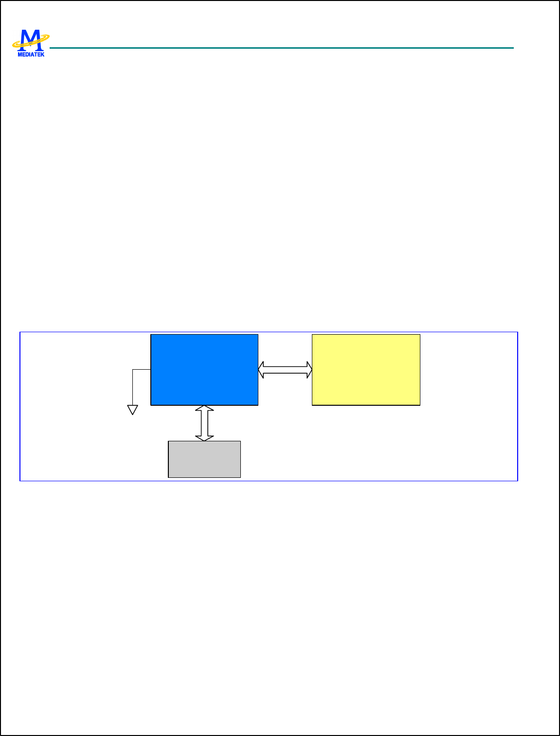
3.4 Direct Memory Access
3.4.1 General Description
A generic DMA Controller is placed on Layer 2 AHB Bus to support fast data transfers, and also to off-load the processor.
With this controller, specific devices on AHB or APB buses can benefit greatly from quickly completing data movement
from or to memory module, i.e. Internal System RAM or External SRAM. Such Generic DMA Controller can also be used
to connect any two devices other than memory module as long as they can be addressed in memory space.
Figure 8 Variety Data Paths of DMA Transfers
Thirteen channels of data transfer are supported at one time. Each channel has a similar set of registers to be configured to
different scheme as desired. If more than thirteen devices are requesting the DMA resources at the same time, software
based arbitration should be employed. Once the service candidate is decided, the responsible device driver should configure
the Generic DMA Controller properly in order to conduct DMA transfers. Both Interrupt and Polling based schemes in
handling the completion event are supported. The block diagram of such generic DMA Controller is illustrated in Figure 9.
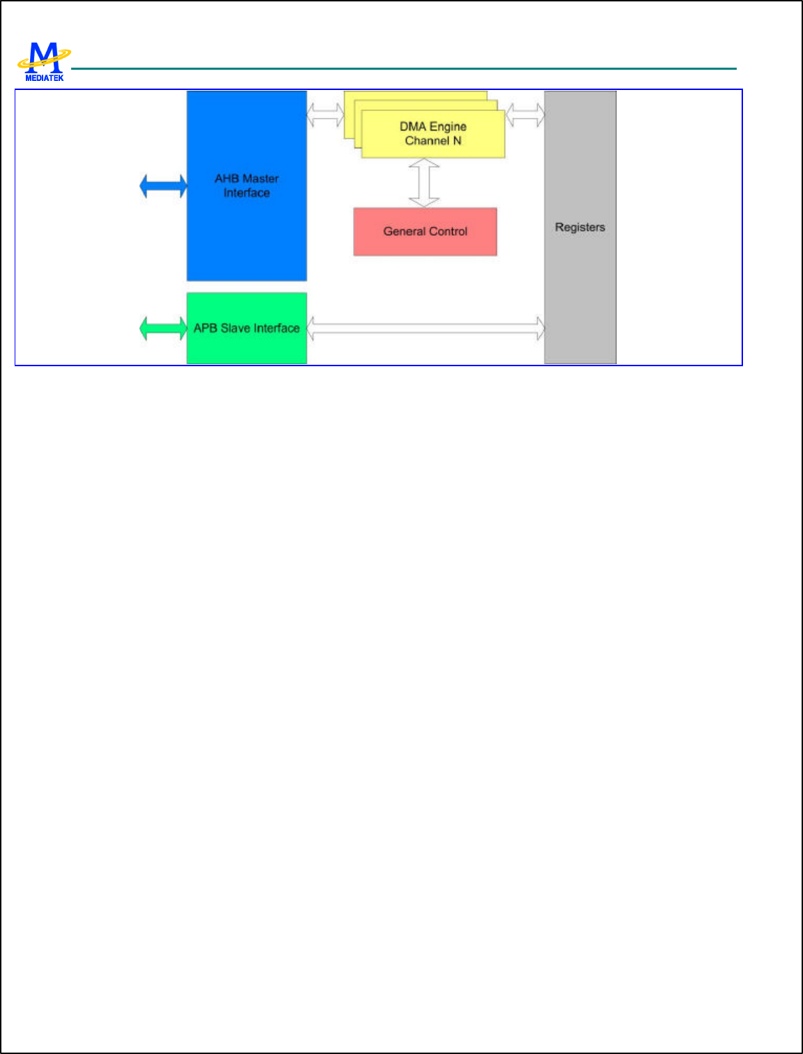
MT6217 GSM/GPRS Baseband Processor Data Sheet Revision 1.01
44/349 MediaTek Inc. Confidential
Figure 9 Block Diagram of Direct memory Access Module
3.4.1.1 Full-Size & Half-Size DMA Channels
There are two types of DMA channels in the DMA controller. The first one is called full-size DMA channel, and the second
one is called half-size DMA channel. Channel 1 to 3 are full-size DMA channels, and channel 4 to 9 are half-size ones. The
difference between the two types of DMA channels is that both source and destination address are programmable in
full-size DMA channels, but only one side of address can be programmed in half-size DMA channel. This can be source or
destination address. The addresses of the other sides are preset. Which preset address is used depends on the setting of MAS
in DMA Channel Control Register. See the section of Register Definition for the detail.
3.4.1.2 Ring Buffer & Double Buffer Memory Data Movement
DMA channel 1-9 support ring-buffer and double -buffer memory data movement. This can be achieved by programming
DMA_WPPT and DMA_WPTO, as well as set WPEN in DMA_CON register enable. Figure 10 illustrates how this
function works. Once transfer counter reaches the value of WPPT, next address will jump to WPTO address after
completing data transfer of WPPT. Note that there is only one side can be configured as ring-buffer or two-buffer memory,
and this is controlled by WPSD in DMA_CON register.
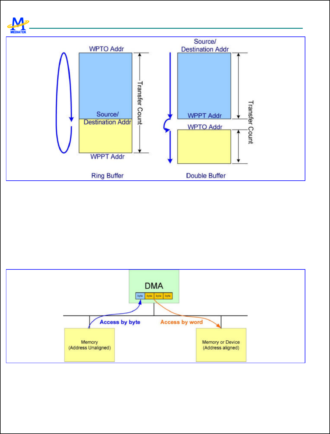
MT6217 GSM/GPRS Baseband Processor Data Sheet Revision 1.01
45/349 MediaTek Inc. Confidential
Figure 10 Ring Buffer and double Buffer Memory Data Movement
3.4.1.3 Unaligned Word Access
The address of word access on AHB bus must be aligned to word boundary, or the 2 LSB will be truncated to 00b. If
programmers don’t notice that, it may cause incorrect data fetch. For the case of moving data from unaligned addresses to
aligned addresses, it’s usually done by splitting the word into four bytes, and moves it by byte. This cause four read and
four write transfers on bus. To improve bus efficiency, unaligned-word access is provided in DMA 4-9.
While this function is enable. DMAs move data from unaligned address to aligned address by executing four continuous
byte-read access and one word-write access, and vice versa. This reduces three transfers on bus.
Figure 11 unaligned word accesses
3.4.1.4 Virtual FIFO DMA
Virtual FIFO DMA is used to ease UART control. The difference between the Virtual FIFO DMAs and the ordinary DMAs
is additional FIFO controller is designed in DMA. The read and write pointer are kept in Virtual FIFO DMA. Once READ
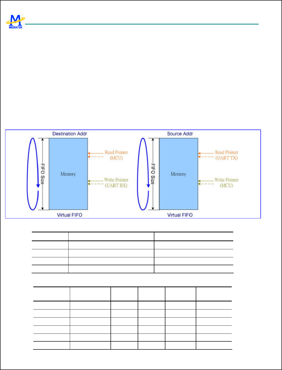
MT6217 GSM/GPRS Baseband Processor Data Sheet Revision 1.01
46/349 MediaTek Inc. Confidential
to this FIFO occurs, the read pointer will points to the address of the next data. On the contrary, the write pointer move to
the next address while Write to this FIFO occurs. If FIFO is empty, a FIFO read will not be allowed. In the same way, data
won’t be written into FIFO if FIFO is full. For the reason of the requirement of UART flow control, an alert length shall be
programmed. Once the FIFO Space is less than this value. An alert signal will issue to enable UART flow control. What
kinds of flow control will be taken is depend on the setting in UART.
Each Virtual FIFO DMA can be programmed as RX or TX FIFO. This depends on the setting of DIR in DMA_CON
register. If DIR is “0”(READ), it means TX FIFO. On the contrary, if DIR is “1”(WRITE), the Virtual FIFO DMA is
specified as a RX FIFO.
Virtual FIFO DMA provides an interrupt to MCU. This interrupt is to inform MCU that there are data in the FIFO, and the
amount of data is over or under the value defined in DMA_COUNT register. With this, MCU doesn’t need to poll DMA to
know when it needs to remove the data from FIFO or put data into FIFO.
Note that Virtual FIFO DMAs can’t be used as generic DMAs, i.e. DMA1-9.
Figure 12 Virtual FIFO DMA
DMA number Address of Virtual FIFO Access Port Associated UART
DMA10 7800_0000h UART1 RX / ALL UART TX
DMA11 7800_0100h UART2 RX / ALL UART TX
DMA12 7800_0200h UART3 RX / ALL UART TX
DMA13 7800_0300h ALL UART TX
Table 7 Virtual FIFO Access Port
DMA number Type Ring Buffer Two Buffer Burst Mode Unaligned Word
Access
DMA1 Full Size ? ? ?
DMA2 Full Size ? ? ?
DMA3 Full Size ? ? ?
DMA4 Half Size ? ? ? ?
DMA5 Half Size ? ? ? ?
DMA6 Half Size ? ? ? ?

MT6217 GSM/GPRS Baseband Processor Data Sheet Revision 1.01
47/349 MediaTek Inc. Confidential
DMA7 Half Size ? ? ? ?
DMA8 Half Size ? ? ? ?
DMA9 Half Size ? ? ? ?
DMA10 Virtual FIFO ?
DMA11 Virtual FIFO ?
DMA12 Virtual FIFO ?
DMA13 Virtual FIFO ?
Table 8 Function list of DMA channels
REGISTER ADDRESS REGISTER NAME SYNONYM
DMA + 0000h DMA Global Status Register DMA_GLBSTA
DMA + 0100h DMA Channel 1 Source Address Register DMA1_SRC
DMA + 0104h DMA Channel 1 Destination Address Register DMA1_DST
DMA + 0108h DMA Channel 1 Wrap Point Address Register DMA1_WPPT
DMA + 010Ch DMA Channel 1 Wrap To Address Register DMA1_WPTO
DMA + 0110h DMA Channel 1 Transfer Count Register DMA1_COUNT
DMA + 0114h DMA Channel 1 Control Register DMA1_CON
DMA + 0118h DMA Channel 1 Start Register DMA1_START
DMA + 011Ch DMA Channel 1 Interrupt Status Register DMA1_INTSTA
DMA + 0120h DMA Channel 1 Interrupt Acknowledge Register DMA1_ACKINT
DMA + 0124h DMA Channel 1 Remaining Length of Current Transfer DMA1_RLCT
DMA + 0128h DMA Channel 1 Bandwidth Limiter Register DMA1_LIMITER
DMA + 0200h DMA Channel 2 Source Address Register DMA2_SRC
DMA + 0204h DMA Channel 2 Destination Address Register DMA2_DST
DMA + 0208h DMA Channel 2 Wrap Point Address Register DMA2_WPPT
DMA + 020Ch DMA Channel 2 Wrap To Address Register DMA2_WPTO
DMA + 0210h DMA Channel 2 Transfer Count Register DMA2_COUNT
DMA + 0214h DMA Channel 2 Control Register DMA2_CON
DMA + 0218h DMA Channel 2 Start Register DMA2_START
DMA + 021Ch DMA Channel 2 Interrupt Status Register DMA2_INTSTA
DMA + 0220h DMA Channel 2 Interrupt Acknowledge Register DMA2_ACKINT
DMA + 0224h DMA Channel 2 Remaining Length of Current Transfer DMA2_RLCT
DMA + 0228h DMA Channel 2 Bandwidth Limiter Register DMA2_LIMITER
DMA + 0300h DMA Channel 3 Source Address Register DMA3_SRC
DMA + 0304h DMA Channel 3 Destination Address Register DMA3_DST
DMA + 0308h DMA Channel 3 Wrap Point Address Register DMA3_WPPT
DMA + 030Ch DMA Channel 3 Wrap To Address Register DMA3_WPTO
DMA + 0310h DMA Channel 3 Transfer Count Register DMA3_COUNT
DMA + 0314h DMA Channel 3 Control Register DMA3_CON

MT6217 GSM/GPRS Baseband Processor Data Sheet Revision 1.01
48/349 MediaTek Inc. Confidential
DMA + 0318h DMA Channel 3 Start Register DMA3_START
DMA + 031Ch DMA Channel 3 Interrupt Status Register DMA3_INTSTA
DMA + 0320h DMA Channel 3 Interrupt Acknowledge Register DMA3_ACKINT
DMA + 0324h DMA Channel 3 Remaining Length of Current Transfer DMA3_RLCT
DMA + 0328h DMA Channel 3 Bandwidth Limiter Register DMA3_LIMITER
DMA + 0408h DMA Channel 4 Wrap Point Address Register DMA4_WPPT
DMA + 040Ch DMA Channel 4 Wrap To Address Register DMA4_WPTO
DMA + 0410h DMA Channel 4 Transfer Count Register DMA4_COUNT
DMA + 0414h DMA Channel 4 Control Register DMA4_CON
DMA + 0418h DMA Channel 4 Start Register DMA4_START
DMA + 041Ch DMA Channel 4 Interrupt Status Register DMA4_INTSTA
DMA + 0420h DMA Channel 4 Interrupt Acknowledge Register DMA4_ACKINT
DMA + 0424h DMA Channel 4 Remaining Length of Current Transfer DMA4_RLCT
DMA + 0428h DMA Channel 4 Bandwidth Limiter Register DMA4_LIMITER
DMA + 042Ch DMA Channel 4 Programmable Address Register DMA4_PGMADDR
DMA + 0508h DMA Channel 5 Wrap Point Address Register DMA5_WPPT
DMA + 050Ch DMA Channel 5 Wrap To Address Register DMA5_WPTO
DMA + 0510h DMA Channel 5 Transfer Count Register DMA5_COUNT
DMA + 0514h DMA Channel 5 Control Register DMA5_CON
DMA + 0518h DMA Channel 5 Start Register DMA5_START
DMA + 051Ch DMA Channel 5 Interrupt Status Register DMA5_INTSTA
DMA + 0520h DMA Channel 5 Interrupt Acknowledge Register DMA5_ACKINT
DMA + 0524h DMA Channel 5 Remaining Length of Current Transfer DMA5_RLCT
DMA + 0528h DMA Channel 5 Bandwidth Limiter Register DMA5_LIMITER
DMA + 052Ch DMA Channel 5 Programmable Address Register DMA5_PGMADDR
DMA + 0608h DMA Channel 6 Wrap Point Address Register DMA6_WPPT
DMA + 060Ch DMA Channel 6 Wrap To Address Register DMA6_WPTO
DMA + 0610h DMA Channel 6 Transfer Count Register DMA6_COUNT
DMA + 0614h DMA Channel 6 Control Register DMA6_CON
DMA + 0618h DMA Channel 6 Start Register DMA6_START
DMA + 061Ch DMA Channel 6 Interrupt Status Register DMA6_INTSTA
DMA + 0620h DMA Channel 6 Interrupt Acknowledge Register DMA6_ACKINT
DMA + 0624h DMA Channel 6 Remaining Length of Current Transfer DMA6_RLCT
DMA + 0628h DMA Channel 6 Bandwidth Limiter Register DMA6_LIMITER
DMA + 062Ch DMA Channel 6 Programmable Address Register DMA6_PGMADDR
DMA + 0708h DMA Channel 7 Wrap Point Address Register DMA7_WPPT
DMA + 070Ch DMA Channel 7 Wrap To Address Register DMA7_WPTO
DMA + 0710h DMA Channel 7 Transfer Count Register DMA7_COUNT
DMA + 0714h DMA Channel 7 Control Register DMA7_CON

MT6217 GSM/GPRS Baseband Processor Data Sheet Revision 1.01
49/349 MediaTek Inc. Confidential
DMA + 0718h DMA Channel 7 Start Register DMA7_START
DMA + 071Ch DMA Channel 7 Interrupt Status Register DMA7_INTSTA
DMA + 0720h DMA Channel 7 Interrupt Acknowledge Register DMA7_ACKINT
DMA + 0724h DMA Channel 7 Remaining Length of Current Transfer DMA7_RLCT
DMA + 0728h DMA Channel 7 Bandwidth Limiter Register DMA7_LIMITER
DMA + 072Ch DMA Channel 7 Programmable Address Register DMA7_PGMADDR
DMA + 0808h DMA Channel 8 Wrap Point Address Register DMA8_WPPT
DMA + 080Ch DMA Channel 8 Wrap To Address Register DMA8_WPTO
DMA + 0810h DMA Channel 8 Transfer Count Register DMA8_COUNT
DMA + 0814h DMA Channel 8 Control Register DMA8_CON
DMA + 0818h DMA Channel 8 Start Register DMA8_START
DMA + 081Ch DMA Channel 8 Interrupt Status Register DMA8_INTSTA
DMA + 0820h DMA Channel 8 Interrupt Acknowledge Register DMA8_ACKINT
DMA + 0824h DMA Channel 8 Remaining Length of Current Transfer DMA8_RLCT
DMA + 0828h DMA Channel 8 Bandwidth Limiter Register DMA8_LIMITER
DMA + 082Ch DMA Channel 8 Programmable Address Register DMA8_PGMADDR
DMA + 0908h DMA Channel 9 Wrap Point Address Register DMA9_WPPT
DMA + 090Ch DMA Channel 9 Wrap To Address Register DMA9_WPTO
DMA + 0910h DMA Channel 9 Transfer Count Register DMA9_COUNT
DMA + 0914h DMA Channel 9 Control Register DMA9_CON
DMA + 0918h DMA Channel 9 Start Register DMA9_START
DMA + 091Ch DMA Channel 9 Interrupt Status Register DMA9_INTSTA
DMA + 0920h DMA Channel 9 Interrupt Acknowledge Register DMA9_ACKINT
DMA + 0924h DMA Channel 9 Remaining Length of Current Transfer DMA9_RLCT
DMA + 0928h DMA Channel 9 Bandwidth Limiter Register DMA9_LIMITER
DMA + 092Ch DMA Channel 9 Programmable Address Register DMA9_PGMADDR
DMA + 0A10h DMA Channel 10 Transfer Count Register DMA10_COUNT
DMA + 0A14h DMA Channel 10 Control Register DMA10_CON
DMA + 0A18h DMA Channel 10 Start Register DMA10_START
DMA + 0A1Ch DMA Channel 10 Interrupt Status Register DMA10_INTSTA
DMA + 0A20h DMA Channel 10 Interrupt Acknowledge Register DMA10_ACKINT
DMA + 0A28h DMA Channel 10 Bandwidth Limiter Register DMA10_LIMITER
DMA + 0A2Ch DMA Channel 10 Programmable Address Register DMA10_PGMADDR
DMA + 0A30h DMA Channel 10 Write Pointer DMA10_WRPTR
DMA + 0A34h DMA Channel 10 Read Pointer DMA10_RDPTR
DMA + 0A38h DMA Channel 10 FIFO Count DMA10_FFCNT
DMA + 0A3Ch DMA Channel 10 FIFO Status DMA10_FFSTA
DMA + 0A40h DMA Channel 10 Alert Length DMA10_ALTLEN
DMA + 0A44h DMA Channel 10 FIFO Size DMA10_FFSIZE

MT6217 GSM/GPRS Baseband Processor Data Sheet Revision 1.01
50/349 MediaTek Inc. Confidential
DMA + 0B10h DMA Channel 11 Transfer Count Register DMA11_COUNT
DMA + 0B14h DMA Channel 11 Control Register DMA11_CON
DMA + 0B18h DMA Channel 11 Start Register DMA11_START
DMA + 0B1Ch DMA Channel 11 Interrupt Status Register DMA11_INTSTA
DMA + 0B20h DMA Channel 11 Interrupt Acknowledge Register DMA11_ACKINT
DMA + 0B28h DMA Channel 11 Bandwidth Limiter Register DMA11_LIMITER
DMA + 0B2Ch DMA Channel 11 Programmable Address Register DMA11_PGMADDR
DMA + 0B30h DMA Channel 11 Write Pointer DMA11_WRPTR
DMA + 0B34h DMA Channel 11 Read Pointer DMA11_RDPTR
DMA + 0B38h DMA Channel 11 FIFO Count DMA11_FFCNT
DMA + 0B3Ch DMA Channel 11 FIFO Status DMA11_FFSTA
DMA + 0B40h DMA Channel 11 Alert Length DMA11_ALTLEN
DMA + 0B44h DMA Channel 11 FIFO Size DMA11_FFSIZE
DMA + 0C10h DMA Channel 12 Transfer Count Register DMA12_COUNT
DMA + 0C14h DMA Channel 12 Control Register DMA12_CON
DMA + 0C18h DMA Channel 12 Start Register DMA12_START
DMA + 0C1Ch DMA Channel 12 Interrupt Status Register DMA12_INTSTA
DMA + 0C20h DMA Channel 12 Interrupt Acknowledge Register DMA12_ACKINT
DMA + 0C28h DMA Channel 12 Bandwidth Limiter Register DMA12_LIMITER
DMA + 0C2Ch DMA Channel 12 Programmable Address Register DMA12_PGMADDR
DMA + 0C30h DMA Channel 12 Write Pointer DMA12_WRPTR
DMA + 0C34h DMA Channel 12 Read Pointer DMA12_RDPTR
DMA + 0C38h DMA Channel 12 FIFO Count DMA12_FFCNT
DMA + 0C3Ch DMA Channel 12 FIFO Status DMA12_FFSTA
DMA + 0C40h DMA Channel 12 Alert Length DMA12_ALTLEN
DMA + 0C44h DMA Channel 12 FIFO Size DMA12_FFSIZE
DMA + 0D10h DMA Channel 13 Transfer Count Register DMA13_COUNT
DMA + 0D14h DMA Channel 13 Control Register DMA13_ CON
DMA + 0D18h DMA Channel 13 Start Register DMA13_START
DMA + 0D1Ch DMA Channel 13 Interrupt Status Register DMA13_INTSTA
DMA + 0D20h DMA Channel 13 Interrupt Acknowledge Register DMA13_ACKINT
DMA + 0D28h DMA Channel 13 Bandwidth Limiter Register DMA13_LIMITER
DMA + 0D2Ch DMA Channel 13 Programmable Address Register DMA13_PGMADDR
DMA + 0D30h DMA Channel 13 Write Pointer DMA13_WRPTR
DMA + 0D34h DMA Channel 13 Read Pointer DMA13_RDPTR
DMA + 0D38h DMA Channel 13 FIFO Count DMA13_FFCNT
DMA + 0D3Ch DMA Channel 13 FIFO Status DMA13_FFSTA
DMA + 0D40h DMA Channel 13 Alert Length DMA13_ALTLEN
DMA + 0D44h DMA Channel 13 FIFO Size DMA13_FFSIZE
MT6217 GSM/GPRS Baseband Processor Data Sheet Revision 1.01
51/349 MediaTek Inc. Confidential
Table 9 DMA Controller Register Map
3.4.2 Register Definitions
Registers programming tips,
l Start registers shall be cleared, when associated channels are being programmed.
l PGMADDR, i.e. programmable address, only exists in half-size DMA channels. If DIR in Control Register is high,
PGMADDR represents Destination Address. On the contrary, it represents Source Address.
l Functions of ring-buffer & double-buffer memory data movement can be activated in either source side or
destination side by programming DMA_WPPT & and DMA_WPTO, as well as setting WPEN in DMA_CON
register high. WPSD in DMA_CON register determines the activated side.
DMA+0000h DMA Global Status Register DMA_GLBSTA
Bit 31 30 29 28 27 26 25 24 23 22 21 20 19 18 17 16
Name
IT13 RUN1
3 IT12 RUN1
2 IT11 RUN1
1 IT10 RUN1
0 IT9 RUN9
Type RO RO RO RO RO RO RO RO RO RO
Reset
0 0 0 0 0 0 0 0 0 0
Bit 15 14 13 12 11 10 9 8 7 6 5 4 3 2 1 0
Name
IT8 RUN8 IT7 RUN7 IT6 RUN6 IT5 RUN5 IT4 RUN4 IT3 RUN3 IT2 RUN2 IT1 RUN1
Type RO RO RO RO RO RO RO RO RO RO RO RO RO RO RO RO
Reset
0 0 0 0 0 0 0 0 0 0 0 0 0 0 0 0
This register helps software program being well aware of the global status of DMA channels.
RUNN DMA channel n status
0 Channel n is stopped or has completed the transfer already.
1 Channel n is currently running.
ITN Interrupt status for channel n
0 No interrupt is generated.
1 An interrupt is pending and waiting for service.
DMA+0n00h DMA Channel n Source Address Register DMAn_SRC
Bit 31 30 29 28 27 26 25 24 23 22 21 20 19 18 17 16
Name
SRC[31:16]
Type R/W
Reset
0
Bit 15 14 13 12 11 10 9 8 7 6 5 4 3 2 1 0
Name
SRC[15:0]
Type R/W
Reset
0
The above registers are to prompt the base or current address that a DMA channel is dealing with currently. In regard to a
write to this register, it specifies the base address of transfer source for a DMA channel. Before being able to program these
registers, the software program should be sure of that STR in DMAn_START is set to ‘0’, that is the DMA channel is
stopped and disabled completely. Other wise, the DMA channel may run out of order. In regard to a read to this set, it shows
the value exactly the same as the one being written while SINC in DMAn_CON is set to “0”. With SINC being set to “1”, it
MT6217 GSM/GPRS Baseband Processor Data Sheet Revision 1.01
52/349 MediaTek Inc. Confidential
appears the current source address that the data being getting from. It allows software program being well tracking the
progress of DMA transfer.
Note that n is from 1 to 3.
SRC SRC[31:0] specifies the base or current address of transfer source for a DMA channel, i.e. channel 1, 2 or 3
WRITE base address of transfer source
READ base address of transfer source if SINC in DMAn_CON is “0”
current address of transfer source if SINC in DMAn_CON is “1”
DMA+0n04h DMA Channel n Destination Address Register DMAn_DST
Bit 31 30 29 28 27 26 25 24 23 22 21 20 19 18 17 16
Name
DST[31:16]
Type R/W
Reset
0
Bit 15 14 13 12 11 10 9 8 7 6 5 4 3 2 1 0
Name
DST[15:0]
Type R/W
Reset
0
The above registers are to index the base or current address that a DMA channel is dealing with currently. In regard to a
write to this set, it specifies the base address of the transfer destination for a DMA channel. Before being able to program
these register, the software should be sure of that STR in DMAn_START is set to ‘0’, that is the DMA channel is stopped
and disabled completely. Other wise, the DMA channel may run out of order. In regard to a read to this set, it shows the
value exactly the same as the one being written while DINC in DMAn_CON is set to “0”. With DINC being set to “1”, it
appears the current destination address that the data being sending to. It allows software program being well tracking the
progress of DMA transfer.
Note that n is from 1 to 3.
DST DST[31:0] specifies the base or current address of transfer destination for a DMA channel, i.e. channel 1, 2 or 3.
WRITE base address of transfer destination
READ base address of transfer destination if DINC in DMAn_CON is “0”
current address of transfer destination if DINC in DMAn_CON is “1”
DMA+0n08h DMA Channel n Wrap Point Count Register DMAn_WPPT
Bit 31 30 29 28 27 26 25 24 23 22 21 20 19 18 17 16
Name
Type
Reset
Bit 15 14 13 12 11 10 9 8 7 6 5 4 3 2 1 0
Name
WPPT[15:0]
Type R/W
Reset
0
The above registers are to specify the transfer count before the jump point. This can be used to support ring buffer or double
buffer style memory accesses. To enable this function, two control bit, WPEN and WPSD, in DMA control register should
be programmed. See following register description for the detail. While transfer counter in DMA engine matches this
address, an address jump will occurs, and the next address will be the address specified in DMAn_WPTO. Before being
able to program these register, the software should be sure of that STR in DMAn_START is set to ‘0’, that is the DMA
MT6217 GSM/GPRS Baseband Processor Data Sheet Revision 1.01
53/349 MediaTek Inc. Confidential
channel is stopped and disabled completely. Other wise, the DMA channel may run out of order. To enable this function,
WPEN in DMA_CON should be set.
Note that n is from 1 to 9.
WPPT WPPT[15:0] specifies the amount of the transfer count from start to jumping point for a DMA channel, i.e.
channel 1 – 9.
WRITE the address of the jump point.
READ the same as what you fill in.
DMA+0n0Ch DMA Channel n Wrap To Address Register DMAn_WPTO
Bit 31 30 29 28 27 26 25 24 23 22 21 20 19 18 17 16
Name
WPTO[31:16]
Type R/W
Reset
0
Bit 15 14 13 12 11 10 9 8 7 6 5 4 3 2 1 0
Name
WPTO[15:0]
Type R/W
Reset
0
The above registers are to specify the address of the jump destination of a given DMA transfer to support ring buffer or
double buffer style memory accesses. To enable this function, two control bit, WPEN and WPSD, in DMA control register
should be programmed. See following register description for the detail. Before being able to program these register, the
software should be sure of that STR in DMAn_START is set to ‘0’, that is the DMA channel is stopped and disabled
completely. Other wise, the DMA channel may run out of order. To enable this function, WPEN in DMA_CON should be
set.
Note that n is from 1 to 9.
WPTO WPTO[31:0] specifies the address of the jump point for a DMA channel, i.e. channel 1 – 11.
WRITE the address of the jump destination.
READ the same as what you fill in.
DMA+0n10h DMA Channel n Transfer Count Register DMAn_COUNT
Bit 31 30 29 28 27 26 25 24 23 22 21 20 19 18 17 16
Name
Type
Reset
Bit 15 14 13 12 11 10 9 8 7 6 5 4 3 2 1 0
Name
LEN
Type R/W
Reset
0
This register specifies the amount of total transfer count that the DMA channel is required to perform. Upon completion, the
DMA channel generates an interrupt request to the processor while ITEN in DMAn_CON is set as ‘1’. Note that the total
size of data being transferred by a DMA channel is determined by LEN together with the SIZE in DMAn_CON, i.e. LEN x
SIZE.
For virtual FIFO DMA, this register is used to configure the RX threshold and TX threshold. Interrupt is triggered while
FIFO count >= RX threshold in RX path or FIFO count =< TX threshold in TX path. Note that ITEN bit in DMA_CON
register shall be set, or no interrupt will issue.
MT6217 GSM/GPRS Baseband Processor Data Sheet Revision 1.01
54/349 MediaTek Inc. Confidential
Note that n is from 1 to 13.
LEN The amount of total transfer count
DMA+0n14h DMA Channel n Control Register DMAn_CON
Bit 31 30 29 28 27 26 25 24 23 22 21 20 19 18 17 16
Name
MAS DIR WPEN
WPSD
Type R/W R/W R/W R/W
Reset
0 0 0 0
Bit 15 14 13 12 11 10 9 8 7 6 5 4 3 2 1 0
Name
ITEN BURST B2W DRQ DINC SINC SIZE
Type R/W R/W R/W R/W R/W R/W R/W
Reset
0 0 0 0 0 0 0
This register appeals all the available control schemes for a DMA channel that is ready for software programmer to
configure with. Note that all these fields cannot be changed while DMA transfer is in progress or unexpected situation may
occur.
Note that n is from 1 to 13.
SIZE Data size within the confine of a bus cycle per transfer
These bits confines the size to the specified value for individual bus cycle that data is moving between source and
destination. The size is in terms of byte and has maximum value of 4 bytes. It is mainly decided by the data width
of a DMA master.
00 Byte transfer/1 byte
01 Half-word transfer/2 bytes
10 Word transfer/4 bytes
11 Reserved
SINC Appearance control for the source address registers DMAn_MSBSRC and DMAn_LSBSRC
0 The base address of the source
1 The current address of the source that the DMA channel is currently dealing with.
DINC Appearance control for the destination address registers DMAn_MSBDST and DMAn_LSBDST
0 The base address of the destination
1 The current address of the destination that the DMA channel is currently dealing with
DREQ Throttle and handshake control for DMA transfer
0 No throttle control during DMA transfer or transfers occurred only between memories
1 Hardware handshake management
The DMA master is able to throttle down the transfer rate by way of request-grant handshake.
B2W Word to Byte or Byte to Word transfer for the applications of transferring non-word-aligned-address data to
word-aligned-address data. Note that BURST shall be set to 4-beat burst while enabling this function, and the
SIZE shall be set to Byte.
NO effect on channel 1 – 3 & 10 - 13.
0 Disable
1 Enable
BURST Transfer Type. Burst-type transfers have better bus efficiency. Massy data movement is recommended to use this
kind of transfer. But note that burst-type transfer won’t stop until all of the beats are completed or transfer length is
reached. FIFO threshold of peripherals shall be configured carefully while you use it to move data from/to this
peripheral.

MT6217 GSM/GPRS Baseband Processor Data Sheet Revision 1.01
55/349 MediaTek Inc. Confidential
What transfer type can be used is restricted by the SIZE. If SIZE is 00b, i.e. byte transfer, all of the four transfer
types can be used. If SIZE is 01b, i.e. half-word transfer, 16-beat incrementing burst can’t be used. If SIZE is 10b,
i.e. word transfer, only single and 4-beat incrementing burst can be used.
NO effect on channel 10 - 13.
000 Single
001 Reserved
010 4-beat incrementing burst
011 Reserved
100 8-beat incrementing burst
101 Reserved
110 16-beat incrementing burst
111 Reserved
ITEN DMA transfer completion interrupt enable.
0 Disable
1 Enable
WPSD The side using wrap-addressing function. Only one sid e of a DMA channel can activate wrap-addressing function
at a time.
NO effect on channel 10 - 13.
0 wrap-addressing on source
1 wrap-addressing on destination
WPEN Wrap addressing for ring buffer. The next address of DMA jumps to WRAP TO address while current address
matches WRAP POINT address.
NO effect on channel 10 - 13.
0 Disable
1 Enable
DIR the directions of DMA transfer for half -size DMA channels, i.e. channel 4 – 11. The direction is from the
viewpoint of DMA masters. WRITE means that reads from master and then writes to the address specified in
DMA_PGMADDR. Vice versa.
NO effect on channel 1 - 3.
0 Read
1 Write
MAS Master selection. Specifying which master occupies this DMA channel. Once assigned to certain master,
corresponding DREQ and DACK will be connected. In regard to half-size DMA channels, i.e. channel 4 – 11, a
preset address will be assigned as well.
0000 SIM
0001 MSDC
0010 IrDA TX
0011 IrDA RX
0100 USB1 Write
0101 USB1 Read
0110 USB2 Write
0111 USB2 Read
1000 UART1 TX
1001 UART1 RX
MT6217 GSM/GPRS Baseband Processor Data Sheet Revision 1.01
56/349 MediaTek Inc. Confidential
1010 UART2 TX
1011 UART2 RX
1100 UART3 TX
1101 UART3 RX
1110 DDMA
1111 NFI (full-size DMA only)
DMA+0n18h DMA Channel n Start Register DMAn_START
Bit 31 30 29 28 27 26 25 24 23 22 21 20 19 18 17 16
Name
Type
Reset
Bit 15 14 13 12 11 10 9 8 7 6 5 4 3 2 1 0
Name
STR
Type R/W
Reset
0
This register controls the activity of a DMA channel. Note that prior to set STR to “1”, all the configurations should be
done by giving proper value to the registers including DMAn_SRC, DMAn_DST, DMAn_PGMADDR, DMAn_COUNT
and DMAn_CON. Note also that once the STR is set to “1”, the hardware will not clear it automatically no matter the DMA
channel accomplishes the DMA transfer or not. Put another way, the value of STR keeps as “1” in spite of the completion
of DMA transfer. Therefore, the software program should be sure to clear STR to “0” before being able to re-start another
DMA transfer.
Note that n is from 1 to 13.
STR Start control for a DMA channel
0 The DMA channel is stopped
1 The DMA channel is started and running
DMA+0n1Ch DMA Channel n Interrupt Status Register DMAn_INTSTA
Bit 31 30 29 28 27 26 25 24 23 22 21 20 19 18 17 16
Name
Type
Reset
Bit 15 14 13 12 11 10 9 8 7 6 5 4 3 2 1 0
Name
INT
Type RO
Reset
0
This register shows the interrupt status of a DMA channel. In fact the value is exa ctly the same as in DMA_GLBSTA.
Note that n is from 1 to 13.
INT Interrupt Status for DMA Channel
0 No interrupt request is generated.
1 One interrupt request is pending and waiting for service
DMA+0n20h DMA Channel n Interrupt Acknowledge Register DMAn_ACKINT
Bit 31 30 29 28 27 26 25 24 23 22 21 20 19 18 17 16
Name
Type
MT6217 GSM/GPRS Baseband Processor Data Sheet Revision 1.01
57/349 MediaTek Inc. Confidential
Reset
Bit 15 14 13 12 11 10 9 8 7 6 5 4 3 2 1 0
Name
ACK
Type WO
Reset
0
This register is used to acknowledge the current interrupt request associated with the completion event of a DMA channel
by software program. Note that this is a write-only register, any read to it will return a value of “0”.
Note that n is from 1 to 1 3.
ACK Interrupt acknowledge for the DMA channel
0 No effect
1 Interrupt request is acknowledged and should be relinquished.
DMA+0n24h DMA Channel n Remaining Length of Current Transfer DMAn_RLCT
Bit 31 30 29 28 27 26 25 24 23 22 21 20 19 18 17 16
Name
Type
Reset
Bit 15 14 13 12 11 10 9 8 7 6 5 4 3 2 1 0
Name
RLCT
Type RO
Reset
0
This register is to reflect the left amount of the transfer.
Note that n is from 1 to 9
DMA+0n28h DMA Bandwidth limiter Register DMAn_LIMITER
Bit 31 30 29 28 27 26 25 24 23 22 21 20 19 18 17 16
Name
Type
Reset
Bit 15 14 13 12 11 10 9 8 7 6 5 4 3 2 1 0
Name
LIMITER
Type R/W
Reset
0
This register is to suppress the Bus utilization of the DMA channel. The value is from 0 to 255. 0 means no limitation, and
255 means totally banned. The value between 0 and 255 means certain DMA can has permission to use AHB every (4 X n)
AHB clock cycles.
Note that it’s not recommended to limit the Bus utilization of the DMA channels because this will increase the latency of
response to the masters, and the transfer rate will decrease as well. Before using it, programmer must make sure that
masters have some protective mechanism to avoid going into wrong state.
Note that n is from 1 to 13.
LIMITER from 0 to 255. 0 means no limitation, 255 means totally banned, and others means Bus access permission
every (4 X n) AHB clock.
MT6217 GSM/GPRS Baseband Processor Data Sheet Revision 1.01
58/349 MediaTek Inc. Confidential
DMA+0n2Ch DMA Channel n Programmable Address Register DMAn_PGMADD
R
Bit 31 30 29 28 27 26 25 24 23 22 21 20 19 18 17 16
Name
PGMADDR[31:16]
Type R/W
Reset
0
Bit 15 14 13 12 11 10 9 8 7 6 5 4 3 2 1 0
Name
PGMADDR[15:0]
Type R/W
Reset
0
The above registers are to specify the address for a half-size DMA channel. This address represents source address if DIR in
DMA_CON is set to 0, and on the contrary it represents destination address. Before being able to program these register,
the software should be sure of that STR in DMAn_START is set to ‘0’, that is the DMA channel is stopped and disabled
completely. Other wise, the DMA channel may run out of order. To enable this function, a control bit in DMA control
register should
Note that n is from 4 to 11.
PGMADDR PGMADDR[31:0] specifies the address for a half-size DMA channel, i.e. channel 4 – 11.
WRITE the address of the jump destination.
READ base address of transfer destination if SINC/DINC in DMAn_CON is “0”
current address of transfer destination if SINC/DINC in DMAn_CON is “1”
DMA+0n30h DMA Channel n Virtual FIFO Write Pointer Register DMAn_WRPTR
Bit 31 30 29 28 27 26 25 24 23 22 21 20 19 18 17 16
Name
WRPTR[31:16]
Type RO
Bit 15 14 13 12 11 10 9 8 7 6 5 4 3 2 1 0
Name
WRPTR[15:0]
Type RO
Note that n is from 10 to 13.
WRPTR Virtual FIFO Write Pointer.
DMA+0n34h DMA Channel n Virtual FIFO Read Pointer Register DMAn_RDPTR
Bit 31 30 29 28 27 26 25 24 23 22 21 20 19 18 17 16
Name
RDPTR[31:16]
Type RO
Bit 15 14 13 12 11 10 9 8 7 6 5 4 3 2 1 0
Name
RDPTR[15:0]
Type RO
Note that n is from 10 to 13.
RDPTR Virtual FIFO Read Pointer.
DMA+0n38h DMA Channel n Virtual FIFO Data Count Register DMAn_FFCNT
Bit 31 30 29 28 27 26 25 24 23 22 21 20 19 18 17 16
Name
Type
MT6217 GSM/GPRS Baseband Processor Data Sheet Revision 1.01
59/349 MediaTek Inc. Confidential
Bit 15 14 13 12 11 10 9 8 7 6 5 4 3 2 1 0
Name
FFCNT
Type RO
Note that n is from 10 to 13.
FFCNT To display the number of data stored in FIFO. 0 means FIFO empty, and FIFO is full if FFCNT is equal to
FFSIZE.
DMA+0n3Ch DMA Channel n Virtual FIFO Status Register DMAn_FFSTA
Bit 31 30 29 28 27 26 25 24 23 22 21 20 19 18 17 16
Name
Type
Reset
Bit 15 14 13 12 11 10 9 8 7 6 5 4 3 2 1 0
Name
ALT EMPT
Y FULL
Type RO RO RO
Reset
0 1 0
Note that n is from 10 to 13.
FULL To indicate FIFO is full.
0 Not Full
1 Full
EMPTY To indicate FIFO is empty.
0 Not Empty
1 Empty
ALT To indicate FIFO Count is larger than ALTLEN. DMA will issue alert signal to UART to enable UART flow
control.
0 Not reach alert region
1 Reach alert region.
DMA+0n40h DMA Channel n Virtual FIFO Alert Length Register DMAn_ALTLEN
Bit 31 30 29 28 27 26 25 24 23 22 21 20 19 18 17 16
Name
Type
Reset
Bit 15 14 13 12 11 10 9 8 7 6 5 4 3 2 1 0
Name
ALTLEN
Type R/W
Reset
0
Note that n is from 10 to 13.
ALTLEN specifies the Alert Length of Virtual FIFO DMA. Once remaining FIFO space is less than ALTLEN, an alert
signal will issued to UART to enable flow control. Normally, ALTLEN shall be larger than 16 for UART
application.
DMA+0n44h DMA Channel n Virtual FIFO Size Register DMAn_FFSIZE
Bit 31 30 29 28 27 26 25 24 23 22 21 20 19 18 17 16
Name
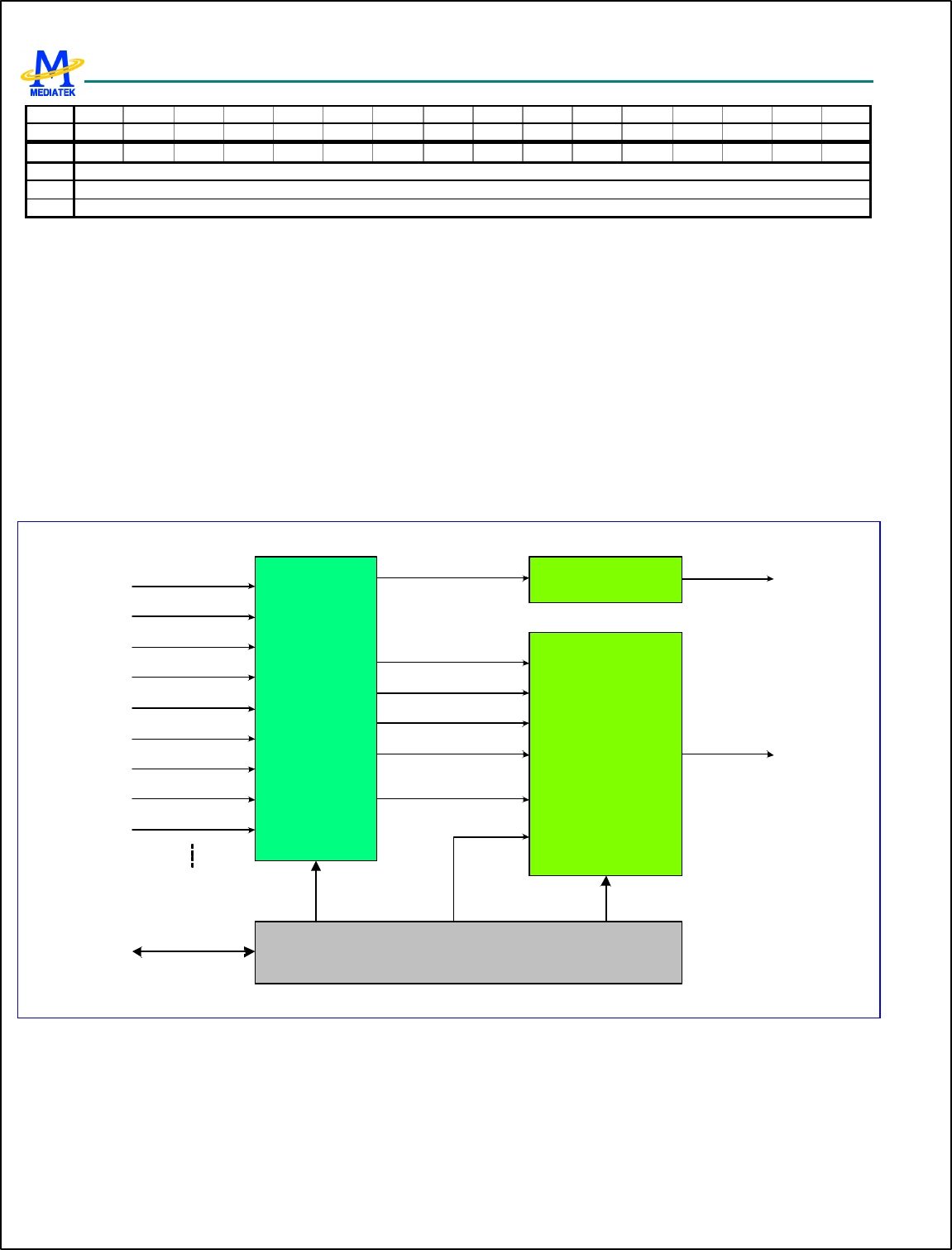
MT6217 GSM/GPRS Baseband Processor Data Sheet Revision 1.01
60/349 MediaTek Inc. Confidential
Type
Reset
Bit 15 14 13 12 11 10 9 8 7 6 5 4 3 2 1 0
Name
FFSIZE
Type R/W
Reset
0
Note that n is from 10 to 13.
FFSIZE specifies the FIFO Size of Virtual FIFO DMA.
3.5 Interrupt Controller
3.5.1 General Description
Figure 13 outlines the major functionality of the MCU Interrupt Controller. The interrupt controller processes all interrupt
sources coming from external lines and internal MCU peripherals. Since ARM7EJ-S core supports two levels of interrupt
latency, this controller will generate two request signals: FIQ for fast, low latency interrupt request and IRQ for more
general interrupts with lower priority.
Interrupt
Input
Multiplex
IRQ
Controller
IRQn
IRQ0
IRQ1
IRQ2
IRQ31
KP
TDMA
GPT
SIM
UART1
DSP2MCU
RTC
UART2
EINT FIQ
IRQ
FIQ
Controller
Registers
SoftIRQ
APB Bus
Figure 13 Block Diagram of the Interrupt Controller
One and only one of the interrupt sources can be assigned to FIQ Controller and have the highest priority in requesting
timing critical service. All the others should share the same IRQ signal by connecting them to IRQ Controller. The IRQ
Controller manages up 32 interrupt lines of IRQ0 to IRQ31 with fixed priority in descending order.

MT6217 GSM/GPRS Baseband Processor Data Sheet Revision 1.01
61/349 MediaTek Inc. Confidential
The Interrupt Controller provides a simple software interface by mean of regis ters to manipulate the interrupt request shared
system. IRQ Selection Registers and FIQ Selection Register determine the source priority and connecting relation among
sources and interrupt lines. IRQ Source Status Register allows software program to identify the source of interrupt that
generates the interrupt request. IRQ Mask Register provides software to mask out undesired sources some time. End of
Interrupt Register permits software program to indicate the controller that a certain interrupt service routine has been
finished.
Binary coded version of IRQ Source Status Register is also made available for software program to helpfully identify the
interrupt source. Note that while taking this advantage, it should also take the binary coded version of End of Interrupt
Register coincidently.
The essential Interrupt Table of ARM7EJ -S core is shown as Table 10.
Address Description
00000000h System Reset
00000018h IRQ
0000001Ch FIQ
Table 10 Interrupt Table of ARM7EJ -S
3.5.1.1 External Interrupt
This interrupt controller also integrates an External Interrupt Controller that can support up to 4 interrupt requests coming
from external sources, the EINT0–3 as shown in Figure 14, and 4 WakeUp interrupt requests, i.e. EINT4-7, coming from
peripherals used to inform system to resume system clock.
The four external interrupts can be used for different kind of applications, mainly for event detections: detection of hand
free connection, detection of hood opening, detection of battery charger connection.
Since the external event may be unstable in a certain period, de -bounce mechanism is introduced to ensure the functionality.
The circuitry is mainly used to verify that if the input signal remains stable for a programmable number of periods of the
clock. When this condition is satisfied, for the appearance or the disappearance of the input, the output of the de-bounce
logic will change to the desired state. Note that, because it uses the 32KHz slow clock for doing de-bounce process, the
parameters takes effect no sooner than 1 32KHz clock cycle, ~31.25us, after software program sets them. For example of
changing the polarity of an external interrupt, a 31.25us guard time shall be applied between the two events of changing the
polarity value in EINT_CON register and End-of-Interrupt. Or an abnormal external interrupt could be triggered.
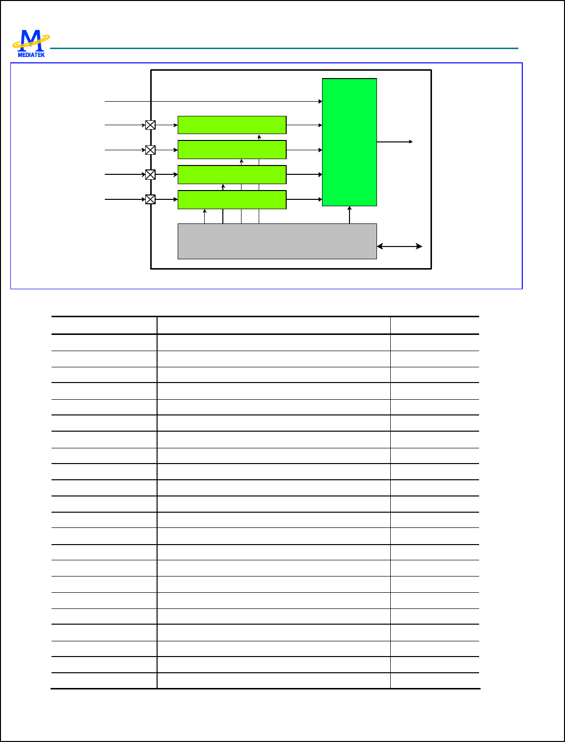
MT6217 GSM/GPRS Baseband Processor Data Sheet Revision 1.01
62/349 MediaTek Inc. Confidential
Debounce Logic
Debounce Logic
Debounce Logic
Registers
Interrupt
Control
Logic
EINT_IRQ
EINT3
EINT1
EINT2
APB Bus
MT6217
Debounce Logic
EINT0
EINT4-7
Figure 14 Block diagram of External Interrupt Controller
REGISTER ADDRESS REGISTER NAME SYNONYM
CIRQ + 0000h IRQ Selection 0 Register IRQ_SEL0
CIRQ + 0004h IRQ Selection 1 Register IRQ_SEL1
CIRQ + 0008h IRQ Selection 2 Register IRQ_SEL2
CIRQ + 000Ch IRQ Selection 3 Register IRQ_SEL3
CIRQ + 0010h IRQ Selection 4 Register IRQ_SEL4
CIRQ + 0014h IRQ Selection 5 Register IRQ_SEL5
CIRQ + 0018h FIQ Selection Register FIQ_SEL
CIRQ + 001Ch IRQ Mask Register IRQ_MASK
CIRQ + 0020h IRQ Mask Disable Register IRQ_MASK_DIS
CIRQ + 0024h IRQ Mask Enable Register IRQ_MASK_EN
CIRQ + 0028h IRQ Status Register IRQ_STA
CIRQ + 002Ch IRQ End of Interrupt Register IRQ_EOI
CIRQ + 0030h IRQ Sensitive Register IRQ_SENS
CIRQ + 0034h IRQ Software Interrupt Register IRQ_SOFT
CIRQ + 0038h FIQ Control Register FIQ_CON
CIRQ + 003Ch FIQ End of Interrupt Register FIQ_EOI
CIRQ + 0040h Binary Coded Value of IRQ_STATUS IRQ_STA2
CIRQ + 0044h Binary Coded Value of IRQ_EOI IRQ_EOI2
CIRQ + 0100h EINT Status Register EINT_STA
CIRQ + 0104h EINT Mask Register EINT_MASK
CIRQ + 0108h EINT Mask Disable Register EINT_MASK_DIS
CIRQ + 010Ch EINT Mask Enable Register EINT_MASK_EN
MT6217 GSM/GPRS Baseband Processor Data Sheet Revision 1.01
63/349 MediaTek Inc. Confidential
CIRQ + 0110h EINT Interrupt Acknowledge Register EINT_INTACK
CIRQ + 0114h EINT Sensitive Register EINT_SENS
CIRQ + 0120h EINT0 De-bounce Control Register EINT0_CON
CIRQ + 0130h EINT1 De-bounce Control Register EINT1_CON
CIRQ + 0140h EINT2 De-bounce Control Register EINT2_CON
CIRQ + 0150h EINT3 De-bounce Control Register EINT3_CON
CIRQ + 0160h EINT4 De-bounce Control Register EINT4_CON
CIRQ + 0170h EINT5 De-bounce Control Register EINT5_CON
CIRQ + 0180h EINT6 De-bounce Control Register EINT6_CON
CIRQ + 0190h EINT7 De-bounce Control Register EINT7_CON
Table 11 Interrupt Controller Register Map
3.5.2 Register Definitions
CIRQ+0000h IRQ Selection 0 Register IRQ_SEL0
Bit 31 30 29 28 27 26 25 24 23 22 21 20 19 18 17 16
Name
IRQ5 IRQ4 IRQ3
Type R/W R/W R/W
Reset
5 4 3
Bit 15 14 13 12 11 10 9 8 7 6 5 4 3 2 1 0
Name
IRQ2 IRQ1 IRQ0
Type R/W R/W R/W
Reset
2 1 0
CIRQ+0004h IRQ Selection 1 Register IRQ_SEL1
Bit 31 30 29 28 27 26 25 24 23 22 21 20 19 18 17 16
Name
IRQB IRQA IRQ9
Type R/W R/W R/W
Reset
B A 9
Bit 15 14 13 12 11 10 9 8 7 6 5 4 3 2 1 0
Name
IRQ8 IRQ7 IRQ6
Type R/W R/W R/W
Reset
8 7 6
CIRQ+0008h IRQ Selection 2 Register IRQ_SEL2
Bit 31 30 29 28 27 26 25 24 23 22 21 20 19 18 17 16
Name
IRQ11 IRQ10 IRQF
Type R/W R/W R/W
Reset
11 10 F
Bit 15 14 13 12 11 10 9 8 7 6 5 4 3 2 1 0
Name
IRQE IRQD IRQC
Type R/W R/W R/W
Reset
E D C
CIRQ+000Ch IRQ Selection 3 Register IRQ_SEL3
Bit 31 30 29 28 27 26 25 24 23 22 21 20 19 18 17 16
MT6217 GSM/GPRS Baseband Processor Data Sheet Revision 1.01
64/349 MediaTek Inc. Confidential
Name
IRQ17 IRQ16 IRQ15
Type R/W R/W R/W
Reset
17 16 15
Bit 15 14 13 12 11 10 9 8 7 6 5 4 3 2 1 0
Name
IRQ14 IRQ13 IRQ12
Type R/W R/W R/W
Reset
14 13 12
CIRQ+0010h IRQ Selection 4 Register IRQ_SEL4
Bit 31 30 29 28 27 26 25 24 23 22 21 20 19 18 17 16
Name
IRQ1D IRQ1C IRQ1B
Type R/W R/W R/W
Reset
1D 1C 1B
Bit 15 14 13 12 11 10 9 8 7 6 5 4 3 2 1 0
Name
IRQ1A IRQ19 IRQ18
Type R/W R/W R/W
Reset
1A 19 18
CIRQ+0014h IRQ Selection 5 Register IRQ_SEL5
Bit 31 30 29 28 27 26 25 24 23 22 21 20 19 18 17 16
Name
Type
Reset
Bit 15 14 13 12 11 10 9 8 7 6 5 4 3 2 1 0
Name
IRQ1F IRQ1E
Type R/W R/W
Reset
1F 1E
CIRQ+0018h FIQ Selection Register FIQ_SEL
Bit 31 30 29 28 27 26 25 24 23 22 21 20 19 18 17 16
Name
Type
Reset
Bit 15 14 13 12 11 10 9 8 7 6 5 4 3 2 1 0
Name
FIQ
Type R/W
Reset
0
The IRQ/FIQ Selection Registers provide system designers with a flexible routing scheme to make various mappings of
priority among interrupt sources possible. It allows the interrupt sources being mapped onto interrupt requests of either FIQ
or IRQ. Where only one interrupt source can be assigned to FIQ, the other ones should share IRQ by mapping them onto
IRQ0 to IRQ1F connected to IRQ controller. The priority of IRQ0-IRQ1F is fixed, i.e. IRQ0 > IRQ1 > IRQ2 > … > IRQ1E
> IRQ1F. During the software configuration process, the Interrupt Source Code of desired interrupt source should be
written into source field of the corresponding IRQ_SEL0-IRQ_SEL4/FIQ_SEL. 5-bit Interrupt Source Codes for all
interrupt sources are fixed and defined in Table 12.
Interrupt Source Interrupt Source Code
MFIQ 00000
TDMA_CTIRQ1 00001
TDMA_CTIRQ2 00010

MT6217 GSM/GPRS Baseband Processor Data Sheet Revision 1.01
65/349 MediaTek Inc. Confidential
DSP2CPU 00011
SIM 00100
DMA 00101
TDMA 00110
UART1 00111
KeyPad 01000
UART2 01001
GPTimer 01010
EINT 01011
USB 01100
MSDC 01101
RTC 01110
IrDA 01111
LCD 10000
UART3 10001
MIRQ 10010
WDT 10011
JPEG 10100
Resizer 10101
NFI 10110
B2PSI 10111
Reserved 11000
Reserved 11001
Reserved 11010
Reserved 11011
Reserved 11100
Reserved 11101
Reserved 11110
Reserved 11111
Table 12 Interrupt Source Code for Interrupt Sources
FIQ, IRQ0-1F The 5-bit content of this field would be the Interrupt Source Code shown in Table 12 indicating that the
certain interrupt source uses the associated interrupt line to generate interrupt requests.
CIRQ+001Ch IRQ Mask Register IRQ_MASK
Bit 31 30 29 28 27 26 25 24 23 22 21 20 19 18 17 16
Name
IRQ1F
IRQ1E
IRQ1D
IRQ1C
IRQ1B
IRQ1A
IRQ19 IRQ18
IRQ17
IRQ16
IRQ15
IRQ14 IRQ13
IRQ12
IRQ11
IRQ10
Type R/W R/W R/W R/W R/W R/W R/W R/W R/W R/W R/W R/W R/W R/W R/W R/W
Reset
1 1 1 1 1 1 1 1 1 1 1 1 1 1 1 1
Bit 15 14 13 12 11 10 9 8 7 6 5 4 3 2 1 0
Name
IRQF IRQE IRQD IRQC IRQB IRQA IRQ9 IRQ8 IRQ7 IRQ6 IRQ5 IRQ4 IRQ3 IRQ2 IRQ1 IRQ0
Type R/W R/W R/W R/W R/W R/W R/W R/W R/W R/W R/W R/W R/W R/W R/W R/W
Reset
1 1 1 1 1 1 1 1 1 1 1 1 1 1 1 1
MT6217 GSM/GPRS Baseband Processor Data Sheet Revision 1.01
66/349 MediaTek Inc. Confidential
This register contains ma sk bit for each interrupt line in IRQ Controller. It allows each interrupt source of IRQ0 to IRQ1F
to be disabled or masked out separately under software control. After System Reset, all bit values will be set to ‘1’ to
indicate that interrupt requests are prohibited.
IRQ0-1F Mask Control for the Associated Interrupt Source in IRQ Controller
0 Interrupt is enabled
1 Interrupt is disabled
CIRQ+0020h IRQ Mask Clear Register IRQ_MASK_CL
R
Bit 31 30 29 28 27 26 25 24 23 22 21 20 19 18 17 16
Name
IRQ1F
IRQ1E
IRQ1D
IRQ1C
IRQ1B
IRQ1A
IRQ19 IRQ18
IRQ17
IRQ16
IRQ15
IRQ14 IRQ13
IRQ12
IRQ11
IRQ10
Type W1C W1C W1C W1C W1C W1C W1C W1C W1C W1C W1C W1C W1C W1C W1C W1C
Bit 15 14 13 12 11 10 9 8 7 6 5 4 3 2 1 0
Name
IRQF IRQE IRQD IRQC IRQB IRQA IRQ9 IRQ8 IRQ7 IRQ6 IRQ5 IRQ4 IRQ3 IRQ2 IRQ1 IRQ0
Type W1C W1C W1C W1C W1C W1C W1C W1C W1C W1C W1C W1C W1C W1C W1C W1C
This register is used to clear bits in the IRQ Mask Register. When writing to this register, each data bit which is high will
cause the corresponding bit in the IRQ Mask Register to be cleared. Data bits which are low have no effect on the
corresponding bits in the IRQ Mask Register
IRQ0-1F Clear corresponding bits in IRQ Mask Register.
0 no effect
1 Disable corresponding MASK bit
CIRQ+0024h IRQ Mask SET Register IRQ_MASK_SET
Bit 31 30 29 28 27 26 25 24 23 22 21 20 19 18 17 16
Name
IRQ1F
IRQ1E
IRQ1D
IRQ1C
IRQ1B
IRQ1A
IRQ19 IRQ18
IRQ17
IRQ16
IRQ15
IRQ14 IRQ13
IRQ12
IRQ11
IRQ10
Type W1S W1S W1S W1S W1S W1S W1S W1S W1S W1S W1S W1S W1S W1S W1S W1S
Bit 15 14 13 12 11 10 9 8 7 6 5 4 3 2 1 0
Name
IRQF IRQE IRQD IRQC IRQB IRQA IRQ9 IRQ8 IRQ7 IRQ6 IRQ5 IRQ4 IRQ3 IRQ2 IRQ1 IRQ0
Type W1S W1S W1S W1S W1S W1S W1S W1S W1S W1S W1S W1S W1S W1S W1S W1S
This register is used to set bits in the IRQ Mask Register. When writing to this register, each data bit which is high will
cause the corresponding bit in the IRQ Mask Register to be set. Data bits which are low have no effect on the corresponding
bits in the IRQ Mask Register
IRQ0-1F Set corresponding bits in IRQ Mask Register.
0 no effect
1 Enable corresponding MASK bit
CIRQ+0028h IRQ Source Status Register IRQ_STA
Bit 31 30 29 28 27 26 25 24 23 22 21 20 19 18 17 16
Name
IRQ1F
IRQ1E
IRQ1D
IRQ1C
IRQ1B
IRQ1A
IRQ19 IRQ18
IRQ17
IRQ16
IRQ15
IRQ14 IRQ13
IRQ12
IRQ11
IRQ10
Type RC RC RC RC RC RC RC RC RC RC RC RC RC RC RC RC
Reset
0 0 0 0 0 0 0 0 0 0 0 0 0 0 0 0
Bit 15 14 13 12 11 10 9 8 7 6 5 4 3 2 1 0
Name
IRQF IRQE IRQD IRQC IRQB IRQA IRQ9 IRQ8 IRQ7 IRQ6 IRQ5 IRQ4 IRQ3 IRQ2 IRQ1 IRQ0
Type RC RC RC RC RC RC RC RC RC RC RC RC RC RC RC RC
Reset
0 0 0 0 0 0 0 0 0 0 0 0 0 0 0 0
MT6217 GSM/GPRS Baseband Processor Data Sheet Revision 1.01
67/349 MediaTek Inc. Confidential
This Register allows software to poll which interrupt line generates the IRQ interrupt request. A bit set to ‘1’ indicates a
corresponding active interrupt line. Only one flag is active at a time. The IRQ_STA is type of READ-ONLY, write access
will have no effect to the content.
IRQ0-1F Interrupt Indication for the Associated Interrupt Source
0 The associated interrupt source is non-active
1 The associated interrupt source is asserted
CIRQ+002Ch IRQ End of Interrupt Register IRQ_EOI
Bit 31 30 29 28 27 26 25 24 23 22 21 20 19 18 17 16
Name
IRQ1F
IRQ1E
IRQ1D
IRQ1C
IRQ1B
IRQ1A
IRQ19 IRQ18
IRQ17
IRQ16
IRQ15
IRQ14 IRQ13
IRQ12
IRQ11
IRQ10
Type WO WO WO WO WO WO WO WO WO WO WO WO WO WO WO WO
Reset
0 0 0 0 0 0 0 0 0 0 0 0 0 0 0 0
Bit 15 14 13 12 11 10 9 8 7 6 5 4 3 2 1 0
Name
IRQF IRQE IRQD IRQC IRQB IRQA IRQ9 IRQ8 IRQ7 IRQ6 IRQ5 IRQ4 IRQ3 IRQ2 IRQ1 IRQ0
Type WO WO WO WO WO WO WO WO WO WO WO WO WO WO WO WO
Reset
0 0 0 0 0 0 0 0 0 0 0 0 0 0 0 0
This register provides a mean for software to relinquish and refresh the Interrupt Controller. Writing a ‘1’ to the specific bit
position will result in an End of Interrupt Command internally to the corresponding interrupt line.
IRQ0-1F End of Interrupt Command for the Associated Interrupt Line
0 No service is currently in progress or pending
1 Interrupt request is in-service
CIRQ+0030h IRQ Sensitive Register IRQ_SENS
Bit 31 30 29 28 27 26 25 24 23 22 21 20 19 18 17 16
Name
IRQ1F
IRQ1E
IRQ1D
IRQ1C
IRQ1B
IRQ1A
IRQ19 IRQ18
IRQ17
IRQ16
IRQ15
IRQ14 IRQ13
IRQ12
IRQ11
IRQ10
Type R/W R/W R/W R/W R/W R/W R/W R/W R/W R/W R/W R/W R/W R/W R/W R/W
Reset
0 0 0 0 0 0 0 0 0 0 0 0 0 0 0 0
Bit 15 14 13 12 11 10 9 8 7 6 5 4 3 2 1 0
Name
IRQF IRQE IRQD IRQC IRQB IRQA IRQ9 IRQ8 IRQ7 IRQ6 IRQ5 IRQ4 IRQ3 IRQ2 IRQ1 IRQ0
Type R/W R/W R/W R/W R/W R/W R/W R/W R/W R/W R/W R/W R/W R/W R/W R/W
Reset
0 0 0 0 0 0 0 0 0 0 0 0 0 0 0 0
All interrupt lines of IRQ Controller, IRQ0-IRQ1F can be programmed as either edge or level sensitive. By default, all the
interrupt lines are edge sensitive and should be active LOW. For edge sensitive interrupt line, while being activated, the
output of edge-detection circuitry will remain HIGH until after the MCU acknowledges the interrupt by issuing End of
Interrupt command and then being able to enable further interrupts to occur. For level sensitive interrupt lines, the interrupt
source should be cleared before EOI command of writing IRQ_EOI in preventing another interrupt to occur.
IRQ0-1F Sensitive Type of the Associated Interrupt Source
0 Edge sensitivity with active LOW
1 Level sensitivity with active LOW
CIRQ+0034h IRQ Software Interrupt Register IRQ_SOFT
Bit 31 30 29 28 27 26 25 24 23 22 21 20 19 18 17 16
Name
IRQ1F
IRQ1E
IRQ1D
IRQ1C
IRQ1B
IRQ1A
IRQ19 IRQ18
IRQ17
IRQ16
IRQ15
IRQ14 IRQ13
IRQ12
IRQ11
IRQ10
Type R/W R/W R/W R/W R/W R/W R/W R/W R/W R/W R/W R/W R/W R/W R/W R/W
Reset
0 0 0 0 0 0 0 0 0 0 0 0 0 0 0 0
Bit 15 14 13 12 11 10 9 8 7 6 5 4 3 2 1 0
Name
IRQF IRQE IRQD IRQC IRQB IRQA IRQ9 IRQ8 IRQ7 IRQ6 IRQ5 IRQ4 IRQ3 IRQ2 IRQ1 IRQ0
MT6217 GSM/GPRS Baseband Processor Data Sheet Revision 1.01
68/349 MediaTek Inc. Confidential
Type R/W R/W R/W R/W R/W R/W R/W R/W R/W R/W R/W R/W R/W R/W R/W R/W
Reset
0 0 0 0 0 0 0 0 0 0 0 0 0 0 0 0
Setting “1” to the specific bit position generates a software interrupt for corresponding Interrupt Line before mask. This
register is used for debug purpose.
IRQ0-IRQ1F Software Interrupt
CIRQ+0038h FIQ Control Register FIQ_CON
Bit 31 30 29 28 27 26 25 24 23 22 21 20 19 18 17 16
Name
Type
Reset
Bit 15 14 13 12 11 10 9 8 7 6 5 4 3 2 1 0
Name
SENS MASK
Type R/W R/W
Reset
0 1
This register provides a mean for software program to control the FIQ Controller.
MASK Mask Control for the FIQ Interrupt Source
0 Interrupt is enabled
1 Interrupt is disabled
SENS Sensitive Type of the FIQ Interrupt Source
0 Edge sensitivity with active LOW
1 Level sensitivity with active LOW
CIRQ+003Ch FIQ End of Interrupt Register FIQ_EOI
Bit 31 30 29 28 27 26 25 24 23 22 21 20 19 18 17 16
Name
Type
Reset
Bit 15 14 13 12 11 10 9 8 7 6 5 4 3 2 1 0
Name
EOI
Type WO
Reset
0
This register provides a mean for software to relinquish and refresh the FIQ Controller. Writing a ‘1’ to the specific bit
position will result in an End of Interrupt Command internally to the corresponding interrupt line.
EOI End of Interrupt Command
CIRQ+0040h Binary Coded Value of IRQ_STATUS IRQ_STA2
Bit 31 30 29 28 27 26 25 24 23 22 21 20 19 18 17 16
Name
Type
Reset
Bit 15 14 13 12 11 10 9 8 7 6 5 4 3 2 1 0
Name
STS
Type RC
Reset
0
This Register is a binary coded version of IRQ_STA. It is used for software program to poll which interrupt line generates
the IRQ interrupt request in mu ch more easy way. Any read to it makes the same result of as reading IRQ_STA. The
MT6217 GSM/GPRS Baseband Processor Data Sheet Revision 1.01
69/349 MediaTek Inc. Confidential
IRQ_STA2 is also type of READ-ONLY, write access takes no effect to the content. Note that, IRQ_STA2 should be
coupled with IRQ_EOI2 while using it.
STS Binary Coded Value of IRQ_STA
CIRQ+0044h Binary Coded Value of IRQ_EOI IRQ_EOI2
Bit 31 30 29 28 27 26 25 24 23 22 21 20 19 18 17 16
Name
Type
Reset
Bit 15 14 13 12 11 10 9 8 7 6 5 4 3 2 1 0
Name
EOI
Type WO
Reset
0
This register is a binary coded version of IRQ_EOI. It provides a more easy way for software program to relinquish and
refresh the Interrupt Controller. Writing a specific code will result an End of Interrupt Command internally to the
corresponding interrupt line. Note that, IRQ_EOI2 should be coupled with IRQ_STA2 while using it.
EOI Binary Coded Value of IRQ_EOI
CIRQ+0100h EINT Interrupt Status Register EINT_STA
Bit 31 30 29 28 27 26 25 24 23 22 21 20 19 18 17 16
Name
Type
Reset
Bit 15 14 13 12 11 10 9 8 7 6 5 4 3 2 1 0
Name
EINT7
EINT6
EINT5
EINT4 EINT3
EINT2
EINT1
EINT0
Type RO RO RO RO RO RO RO RO
Reset
0 0 0 0 0 0 0 0
This register keeps up with current status that which EINT Source generates the interrupt request. If EINT sources are set to
edge sensitivity, EINT_IRQ will be de-asserted while this register is read.
EINT0-EINT7 Interrupt Status
0 No Interrupt Request is generated
1 Interrupt Request is pending
CIRQ+0104h EINT Interrupt Mask Register EINT_MASK
Bit 31 30 29 28 27 26 25 24 23 22 21 20 19 18 17 16
Name
Type
Reset
Bit 15 14 13 12 11 10 9 8 7 6 5 4 3 2 1 0
Name
EINT7
EINT6
EINT5
EINT4 EINT3
EINT2
EINT1
EINT0
Type R/W R/W R/W R/W R/W R/W R/W R/W
Reset
1 1 1 1 1 1 1 1
This register controls that if EINT Source is allowed to generate interrupt request. Setting a “1” to the specific bit
position prohibits the External Interrupt Line to active accordingly.
EINT0-EINT7 Interrupt Mask
0 Interrupt Request is enabled
MT6217 GSM/GPRS Baseband Processor Data Sheet Revision 1.01
70/349 MediaTek Inc. Confidential
1 Interrupt Request is disabled
CIRQ+0108h EINT Interrupt Mask Clear Register EINT_MASK_CL
R
Bit 31 30 29 28 27 26 25 24 23 22 21 20 19 18 17 16
Name
Type
Bit 15 14 13 12 11 10 9 8 7 6 5 4 3 2 1 0
Name
EINT7
EINT6
EINT5
EINT4 EINT3
EINT2
EINT1
EINT0
Type W1C W1C W1C W1C W1C W1C W1C W1C
This register is used to individually clear mask bit. Only the bits set to 1 are in effect, and these mask bits will set to 0. Else
mask bits keep original value.
EINT0-EINT7 Disable Mask for the Associated External Interrupt Source
0 no effect
1 Dis able corresponding MASK bit
CIRQ+010Ch EINT Interrupt Mask Set Register EINT_MASK_SE
T
Bit 31 30 29 28 27 26 25 24 23 22 21 20 19 18 17 16
Name
Type
Bit 15 14 13 12 11 10 9 8 7 6 5 4 3 2 1 0
Name
EINT7
EINT6
EINT5
EINT4 EINT3
EINT2
EINT1
EINT0
Type W1S W1S W1S W1S W1S W1S W1S W1S
This register is used to individually set mask bit. Only the bits set to 1 are in effect, and these mask bits will set to 1. Else
mask bits keep original value.
EINT0-EINT7 Disable Mask for the Associated External Interrupt Source
0 no effect
1 Enable corresponding MASK bit
CIRQ+0110h EINT Interrupt Acknowledge Register EINT_INTACK
Bit 31 30 29 28 27 26 25 24 23 22 21 20 19 18 17 16
Name
Type
Reset
Bit 15 14 13 12 11 10 9 8 7 6 5 4 3 2 1 0
Name
EINT7
EINT6
EINT5
EINT4 EINT3
EINT2
EINT1
EINT0
Type WO WO WO WO WO WO WO WO
Reset
0 0 0 0 0 0 0 0
Writing “1” to the specific bit position means to acknowledge the interrupt request correspondingly to the External Interrupt
Line source.
EINT0-EINT7 Interrupt Acknowledge
0 No effect
1 Interrupt Request is acknowledged
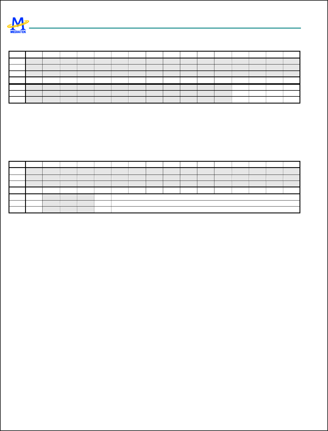
MT6217 GSM/GPRS Baseband Processor Data Sheet Revision 1.01
71/349 MediaTek Inc. Confidential
CIRQ+0114h EINT Sensitive Register EINT_SENS
Bit 31 30 29 28 27 26 25 24 23 22 21 20 19 18 17 16
Name
Type
Reset
Bit 15 14 13 12 11 10 9 8 7 6 5 4 3 2 1 0
Name
EINT3
EINT2
EINT1
EINT0
Type R/W R/W R/W R/W
Reset
1 1 1 1
Sensitive type of external interrupt source. Only EINT0 – 3 need to be specified. EINT4 – 7 are always edge sensitive.
EINT0-3 Sensitive Type of the Associated External Interrupt Source
0 Edge sensitivity at falling edge
1 Level sensitivity with active LOW
CIRQ+01m0h EINTn De-bounce Control Register EINTn_CON
Bit 31 30 29 28 27 26 25 24 23 22 21 20 19 18 17 16
Name
Type
Reset
Bit 15 14 13 12 11 10 9 8 7 6 5 4 3 2 1 0
Name
EN POL CNT
Type R/W R/W R/W
Reset
0 0 0
These registers control the de-bounce logic for external interrupt sources in order to minimize the possibility of false
activations. EINT4 – 7 have no de-bounce mechanism. Therefore only bit POL is used.
Note that n is from 0 to 7, and m is n plus 2.
CNT De -bounce Duration in terms of numbers of 32KHz clock cycles
POL Activation Type of the EINT Source
0 Negative polarity
1 Positive polarity
EN De -bounce Control Circuit
0 Disable
1 Enable
3.6 Internal Memory Controller
3.6.1 System RAM
MT6217 provides four 64K Byte size of on-chip memory modules acting as System RAM for data access with zero latency.
Such module is composed of four high speed synchronous SRAMs with AHB Slave Interface connected to system
backbone AHB Bus, as shown in Figure 15. The synchronous SRAM operates at the same clock as AHB Bus and is
organized as 32-bit wide with 4 byte-write signals capable for byte operations.
MT6217 GSM/GPRS Baseband Processor Data Sheet Revision 1.01
72/349 MediaTek Inc. Confidential
3.6.2 System ROM
The System ROM is primarily used to store software program for Factory Programming. However, due to it’s advantageous
zero latency performance, some of timing critical codes are also placed in this area. This module is composed of high-speed
diffusion ROM with AHB Slave Interface connected to system backbone AHB Bus, as shown in Figure 15. It operates at
the same clock as AHB Bus and is organized as 32-bit wide.
Figure 15 Block Diagram of Internal Memory Controller
3.6.3 Register Definitions
ROM+0000h System Memory Configuration Register SYSRAM_CNF
Bit 31 30 29 28 27 26 25 24 23 22 21 20 19 18 17 16
Name
SYSRAM_KEY
Type W
Reset
6217
Bit 15 14 13 12 11 10 9 8 7 6 5 4 3 2 1 0
Name
EN3 ID3 EN2 ID2 EN1 ID1 EN0 ID0
Type W - W W - W W - W W - W
Reset
1 0 1 1 1 0 1 0 1 0 0 1 1 0 0 0
SYSRAM KEY System RAM Key
3.7 External Memory Interface
3.7.1 General Description
MT6217 incorporates a powerful and flexible memory controller, External Memory Interface, to connect with a variety of
memory components. This controller provides generic access schemes to asynchronous/synchronous type of memory
MT6217 GSM/GPRS Baseband Processor Data Sheet Revision 1.01
73/349 MediaTek Inc. Confidential
devices, such as Flash Memory and SRAM. It can simultaneously support up to 8 memory banks BANK0-BANK7 with
maximum size of 64MB each.
Since most of the target asynchronous components have similar AC requirements, it is desirable to have a generic
configuration scheme to interface them. Such that, software program can treat different components by simply specifying
certain predefined parameters. All those parameters are based on cycle time of system clock. The interface definition based
on such asynchronous/synchronous scheme is listed in Table 13. Note that, this interface always operates data in Little
Endian format for all type of accesses.
Page/Burst mode Flash is supported for those applications required to run EIP (execution in place).
Signal Name Type Description
EA[25:0] O Address Bus
ED[15:0] I/O Data Bus
EWR# O Write Enable Strobe
ERD# O Re ad Enable Strobe
ELB# O Lower Byte Strobe
EUB# O Upper Byte Strobe
ECS# [7:0] O BANK0~BANK7 Selection Signal
EPDN O Pseudo SRAM Power Down Control Signal
ECLK O Burst Mode Flash Clock Signal
EADV# O Burst Mode Flash Address Latch Signal
Table 13 External Memory Interface of MT6217 for Asynchronous/Synchronous Type Components
This controller can also handle parallel type of LCD. By connecting with them, 8080 type of control method is supported.
The interface definition is detailed in Table 14.
Bus Type ECS7# EA25 ERD# EWR# ED[15:0]
8080 series CS# A0 RD# WR# D[15:0]
Table 14 Configuration for LCD Parallel Interface
REGISTER ADDRESS REGISTER NAME SYNONYM
EMI + 0000h EMI Control Register for BANK0 EMI_CONA
EMI + 0008h EMI Control Register for BANK1 EMI_CONB
EMI + 0010h EMI Control Register for BANK2 EMI_CONC
EMI + 0018h EMI Control Register for BANK3 EMI_COND
EMI + 0020h EMI Control Register for BANK4 EMI_CONE
EMI + 0028h EMI Control Register for BANK5 EMI_CONF
EMI + 0030h EMI Control Register for BANK6 EMI_CONG
EMI + 0038h EMI Control Register for BANK7 EMI_CONH
EMI + 0040h EMI Remap Control Register EMI_REMAP
EMI + 0044h EMI General Control Register EMI_GEN
EMI + 0050h Code Cache and Code Prefetch Control Register PREFETCH_CON
MT6217 GSM/GPRS Baseband Processor Data Sheet Revision 1.01
74/349 MediaTek Inc. Confidential
EMI + 0060h EMI Patch Enable Register EMI_PATCHEN
EMI + 0064h EMI Patch 0 Address Register EMI_PADDR0
EMI + 006Ch EMI Patch 0 Instruction Register EMI_PDATA0
EMI + 0074h EMI Patch 1 Address Register EMI_PADDR1
EMI + 007Ch EMI Patch 1 Instruction Register EMI_PDATA1
Table 15 External Memory Interface Register Map
3.7.2 Register Definitions
EMI+0000h EMI Control Register for BANK0 EMI_CONA
Bit 31 30 29 28 27 26 25 24 23 22 21 20 19 18 17 16
Name
C2WS C2WH C2RS ADV PRLT BMOD
E PMO
DE
Type R/W R/W R/W R/W R/W R/W R/W
Reset
0 0 0 1 0 0 0
Bit 15 14 13 12 11 10 9 8 7 6 5 4 3 2 1 0
Name
DW RBLN WST PSIZE RLT
Type R/W R/W R/W R/W R/W
Reset
0 1 0 0 7
EMI+0008h EMI Control Register for BANK1 EMI_CONB
Bit 31 30 29 28 27 26 25 24 23 22 21 20 19 18 17 16
Name
C2WS C2WH C2RS ADV PRLT BMOD
E PMO
DE
Type R/W R/W R/W R/W R/W R/W R/W
Reset
0 0 0 1 0 0 0
Bit 15 14 13 12 11 10 9 8 7 6 5 4 3 2 1 0
Name
DW RBLN WST PSIZE RLT
Type R/W R/W R/W R/W R/W
Reset
0 1 0 0 7
EMI+0010h EMI Control Register for BANK2 EMI_CONC
Bit 31 30 29 28 27 26 25 24 23 22 21 20 19 18 17 16
Name
C2WS C2WH C2RS ADV PRLT BMOD
E PMO
DE
Type R/W R/W R/W R/W R/W R/W R/W
Reset
0 0 0 1 0 0 0
Bit 15 14 13 12 11 10 9 8 7 6 5 4 3 2 1 0
Name
DW RBLN WST PSIZE RLT
Type R/W R/W R/W R/W R/W
Reset
0 1 0 0 7
EMI+0018h EMI Control Register for BANK3 EMI_COND
Bit 31 30 29 28 27 26 25 24 23 22 21 20 19 18 17 16
Name
C2WS C2WH C2RS ADV PRLT BMOD
E PMO
DE
Type R/W R/W R/W R/W R/W R/W R/W
MT6217 GSM/GPRS Baseband Processor Data Sheet Revision 1.01
75/349 MediaTek Inc. Confidential
Reset
0 0 0 1 0 0 0
Bit 15 14 13 12 11 10 9 8 7 6 5 4 3 2 1 0
Name
DW RBLN WST PSIZE RLT
Type R/W R/W R/W R/W R/W
Reset
0 1 0 0 7
EMI+0020h EMI Control Register for BANK4 EMI_CONE
Bit 31 30 29 28 27 26 25 24 23 22 21 20 19 18 17 16
Name
C2WS C2WH C2RS ADV PRLT BMOD
E PMO
DE
Type R/W R/W R/W R/W R/W R/W R/W
Reset
0 0 0 1 0 0 0
Bit 15 14 13 12 11 10 9 8 7 6 5 4 3 2 1 0
Name
DW RBLN WST PSIZE RLT
Type R/W R/W R/W R/W R/W
Reset
0 1 0 0 7
EMI+0028h EMI Control Register for BANK5 EMI_CONF
Bit 31 30 29 28 27 26 25 24 23 22 21 20 19 18 17 16
Name
C2WS C2WH C2RS ADV PRLT BMOD
E PMO
DE
Type R/W R/W R/W R/W R/W R/W R/W
Reset
0 0 0 1 0 0 0
Bit 15 14 13 12 11 10 9 8 7 6 5 4 3 2 1 0
Name
DW RBLN WST PSIZE RLT
Type R/W R/W R/W R/W R/W
Reset
0 1 0 0 7
EMI+0030h EMI Control Register for BANK6 EMI_CONG
Bit 31 30 29 28 27 26 25 24 23 22 21 20 19 18 17 16
Name
C2WS C2WH C2RS ADV PRLT BMOD
E PMO
DE
Type R/W R/W R/W R/W R/W R/W R/W
Reset
0 0 0 1 0 0 0
Bit 15 14 13 12 11 10 9 8 7 6 5 4 3 2 1 0
Name
DW RBLN WST PSIZE RLT
Type R/W R/W R/W R/W R/W
Reset
0 1 0 0 7
EMI+0038h EMI Control Register for BANK7 EMI_CONH
Bit 31 30 29 28 27 26 25 24 23 22 21 20 19 18 17 16
Name
C2WS C2WH C2RS ADV PRLT BMOD
E PMO
DE
Type R/W R/W R/W R/W R/W R/W R/W
Reset
0 0 0 1 0 0 0
Bit 15 14 13 12 11 10 9 8 7 6 5 4 3 2 1 0
Name
DW RBLN WST PSIZE RLT
Type R/W R/W R/W R/W R/W
Reset
0 1 0 0 7
For each bank (BANK0-BANK7), there is a dedicate control register in connection with the associated bank controller.
These registers have the timing parameters that help the controller to convey memory access into proper timing waveform.
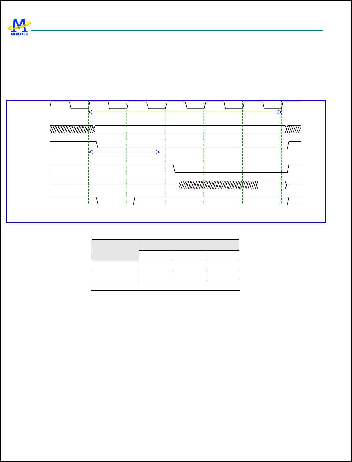
MT6217 GSM/GPRS Baseband Processor Data Sheet Revision 1.01
76/349 MediaTek Inc. Confidential
Note that, Except for parameter DW that is in unit of bit, all the other parameters specified explicitly are based on bus clock
speed in terms of cycle count.
RLT Read Latency Time
Specifying the parameter RLT turns effectively to insert wait-states in bus transfer to requesting agent. Such
parameter should be chosen carefully to meet the common parameter tACC (access time) for device in read
operation. Example is shown below.
ECLK
RLT+1
EA
ECSn#
C2RS
ERD#
ED
EADV
RLT=4, C2RS=2
Figure 16 Read Wait State Timing Diagram
Read Latency Time
Access Time 13MHz 26MHz 52MHz
60ns 0 1 3
90ns 1 2 4
120ns 1 3 5
Table 16 Reference value of Read Latency Time for variant memory devices
PMODE Page Mode Control
If target device supports page mode operations, the Page Mode Control can be enabled. Read in Page Mode is
determined by set of parameters: PRLT and PSIZE.
0 disable page mode operation
1 enable page mode operation
BMODE Burst Mode Control
If target device supports burst mode operations, the Burst Mode Control can be enabled. Read in Burst Mode is
determined by set of parameters: PRLT and PSIZE.
0 disable burst mode operation
1 enable burst mode operation
PRLT Read Latency Within the Same Page or in Burst Mode Operation
Since page/burst mode operation only help to eliminate read latency in subsequent burst within the same page, it
doesn’t matter with the initial latency at all. Thus, it should still adopt RLT parameter for initial read or burst read
between different pages though PMODE or BMODE is set “1”.
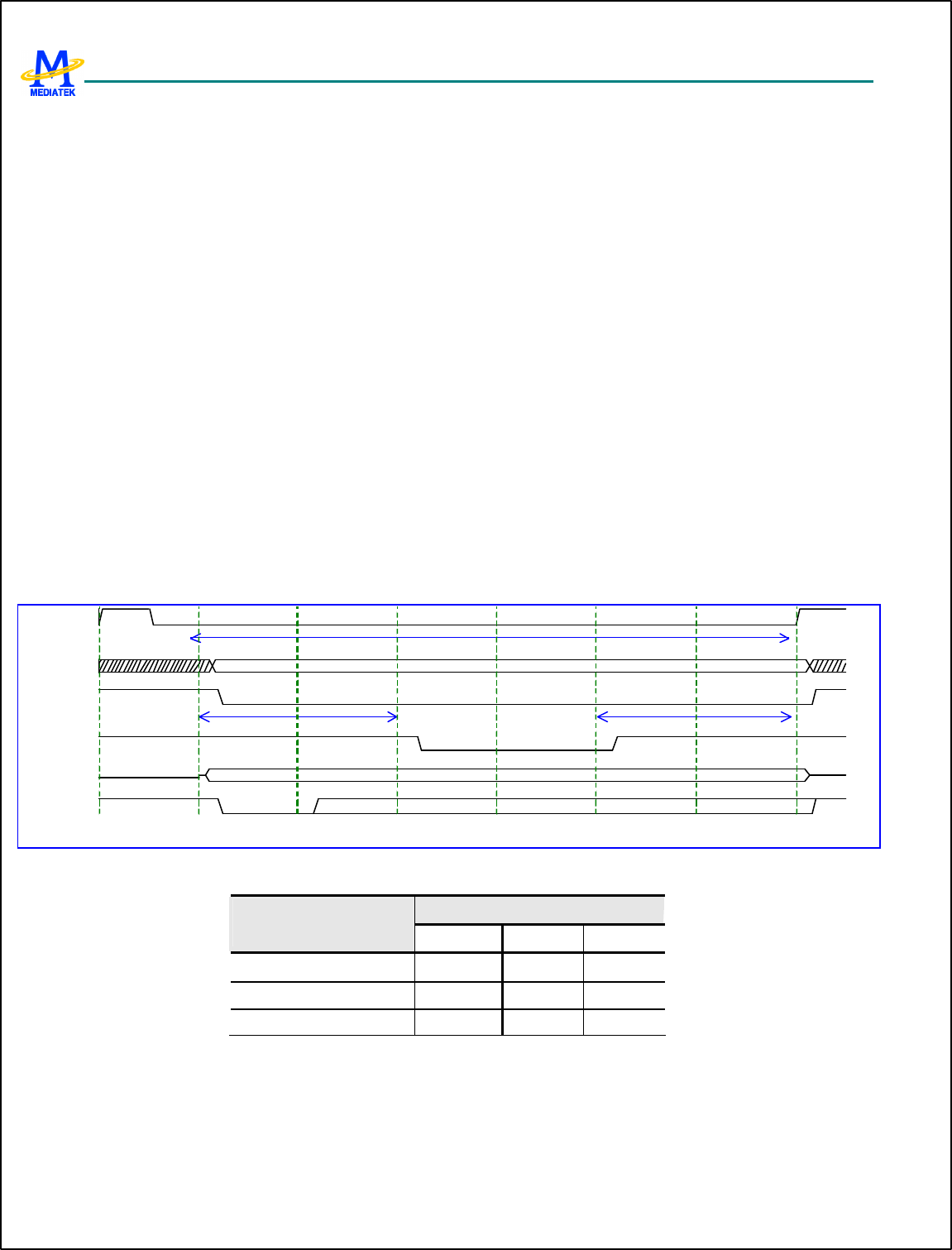
MT6217 GSM/GPRS Baseband Processor Data Sheet Revision 1.01
77/349 MediaTek Inc. Confidential
000 zero wait state
001 one wait state
010 two wait state
011 three wait state
100 four wait state
101 five wait state
110 six wait state
111 seven wait state
PSIZE Page/Burst Size for Page/Burst Mode Operation
These bit positions describe the page/burst size that the Page/Burst Mode enabled device will behave.
000 8 byte, EA[22:3] remains the same
001 16 byte, EA[22:4] remains the same
010 32 byte, EA[22:5] remains the same
011 64 byte, EA[22:6] remains the same
100~110 reserved for future use
111 continuous sequential burst
WST Write Wait State
Specifying the parameters to extend adequate setup and hold time for target component in write operation. Those
parameters also effectively insert wait-states in bus transfer to requesting agent. Example is shown in Figure 17
and Table 17.
WST+C2WH+2
EA
ECSn#
C2WS
C2WH+1
EWR#
ED
EADV
WST=3, C2WS=2, C2WH=1
Figure 17 Write Wait State Timing Diagram
Write Wait State
Write Pulse Width
(Write Data Setup Time) 13MHz 26MHz 52MHz
30ns 0 0 1
60ns 0 1 3
90ns 1 2 4
Table 17 Reference value of Write Wait State for variant memory devices
RBLN Read Byte Lane Enable
0 all byte lanes held high during system reads
1 all byte lanes held low during system reads
DW Data Width
MT6217 GSM/GPRS Baseband Processor Data Sheet Revision 1.01
78/349 MediaTek Inc. Confidential
Since the data width of internal system bus is fixed as 32-bit wide, any access to external components might be
converted into more than one cycles, depending on transfer size and the parameter DW for the specific component.
In general, this bit position of certain component is cleared to ‘0’ upon system reset and is programmed during the
system initialization process prior to begin access to it. Note that, dynamic changing this parameter will cause
unexpected result.
0 16-bit device
1 8-bit device
EMI+0040h EMI Re-map Control Register EMI_REMAP
Bit 15 14 13 12 11 10 9 8 7 6 5 4 3 2 1 0
Name
RM1 RM0
Type R/W R/W
Reset
BOOT
0
This register accomplishes the Memory Re -mapping Mechanism. Basically, it provides the kernel software program or
system designer a capability of changing memory configuration dynamically. Three kinds of configuration are permitted.
RM[1:0] Re-mapping control for Boot Code, BANK0 and BANK1, refer to Table 18.
RM[1:0] Address 00000000h – 07ffffffh Address 08000000h – 08ffffffh
00 Boot Code BANK1
01 BANK1 BANK0
10 BANK0 BANK1
11 BANK1 BANK0
Table 18 Memory Map Configuration
EMI+0044h EMI General Control Register EMI_GEN
Bit 31 30 29 28 27 26 25 24 23 22 21 20 19 18 17 16
Name
CLKS
R CLKE
2 CLKE
4 CLKE
8 CSSR CSE2 CS E4 CSE8 EASR EAE2 EAE4 EAE8 EDSR EDE2 EDE4 RWE8
Type R/W R/W R/W R/W R/W R/W R/W R/W R/W R/W R/W R/W R/W R/W R/W R/W
Reset
1 1 0 0 1 1 0 0 1 1 0 0 1 1 0 0
Bit 15 14 13 12 11 10 9 8 7 6 5 4 3 2 1 0
Name
PRCE
N PRCCNT BANK
BURS
T EDA FLUS
H PDNE CKE CKDLY
Type R/W R/W R/W R/W R/W R/W R/W R/W R/W
Reset
0 0 1 1 1 1 0 0 0
This register is general control that can alter the behavior of all bank controllers according to specific features below.
CLKSR Slew Rate Control for Pin ECLK
CLKE2 Driving Strength Control for Pin ECLK (+2mA)
CLKE4 Driving Strength Control for Pin ECLK (+4mA)
CLKE8 Driving Strength Control for Pin ECLK (+8mA)
CSSR Slew Rate Control for Pin EADV# and ECS#,
CSE2 Driving Strength Control for Pin EADV# and ECS# (+2mA)
CSE4 Driving Strength Control for Pin EADV# and ECS# (+4mA)
CSE8 Driving Strength Control for Pin EADV# and ECS# (+8mA)

MT6217 GSM/GPRS Baseband Processor Data Sheet Revision 1.01
79/349 MediaTek Inc. Confidential
EASR Slew Rate Control for Pin EA[25:0]
EAE2 Driving Strength Control for Pin EA[25:0] (+2mA)
EAE4 Driving Strength Control for Pin EA[25:0] (+4mA)
EAE8 Driving Strength Control for Pin EA [25:0] (+8mA)
EDSR Slew Rate Control for Pin ED[15:0], EUB#, ELB#, ERD# and EWR#
EDE2 Driving Strength Control for Pin ED[15:0] , EUB#, ELB#, ERD# and EWR# (+2mA)
EDE4 Driving Strength Control for Pin ED[15:0] , EUB#, ELB#, ERD# and EWR# (+4mA)
EDE8 Driving Strength Control for Pin ED[15:0] , EUB#, ELB#, ERD# and EWR# (+8mA)
PRCEN Pseudo SRAM Write Protection Control
0 Disable
1 Enable
PRCCNT Pseudo SRAM Dummy Cycle Insertion Count
BANK Inter-Bank Turnaround Cycle Insertion
0 Disable
1 Enable
BURST Burst Access Dummy Cycle Insertion
0 Disable
1 Enable
EDA ED[15:0] Activity
0 Drive ED Bus only on write access
1 Always drive ED Bus except for read access
FLUSH Instruction Cache Write Flush Control
PDNE Pseudo SRAM Power Down Mode Control
CKE Burst Mode Flash Clock Enable Control
CKDLY Burst Mode Flash Clock Delay Control
EMI+0050h Code Cache and Code Prefetch Control Register PREFETCH_CO
N
Bit 31 30 29 28 27 26 25 24 23 22 21 20 19 18 17 16
Name
DB7 DB6 DB5 DB4 DB3 DB2 DB1 DB0 DWRP
8 DPRE
F DCAC
H
Type R/W R/W R/W R/W R/W R/W R/W R/W R/W RW R/W
Reset
0 0 0 0 0 0 0 0 0 0 0
Bit 15 14 13 12 11 10 9 8 7 6 5 4 3 2 1 0
Name
IB7 IB6 IB5 IB4 IB3 IB2 IB1 IB0 IWRP
8 IPREF ICAC
H
Type R/W R/W R/W R/W R/W R/W R/W R/W R/W RW R/W
Reset
0 0 0 0 0 0 0 0 0 0 0
This register is used to control the functions of Code/Data Cache and Code/Data Prefetch. The Code/Data Cache is a low
latency memory that can store up to 16 most recently used instruction codes/data. While an instruction/data fetch hits the
one in the code/data cache, not only the access time could be minimized, but also the singling to off chip ROM or Flash
could be relieved. In addition, it can also store up to 16 prefetched instruction codes/data while Code/Data Prefetch function
is enabled. The Code/Data Prefetch is a sophisticated controller that can predict and fetch the instruction codes/data in
advance based on previous code/data fetching sequence. As the Code/Data Prefetch always performs the fetch staffs during
the period that the EMI interface is in IDLE state. The bandwidth to off chip memory could be fully utilized. On the other
MT6217 GSM/GPRS Baseband Processor Data Sheet Revision 1.01
80/349 MediaTek Inc. Confidential
hand, if the instruction/data fetch hits the one of prefetched codes/data, the access time could be minimized and then
enhance the overall system performance.
xWRP8 Prefetch Size
0 8 bytes
1 16 bytes
xBn Prefetchable/Cacheable Area
There bit positions determine the prefetchable and cacheable region in which the instruction/data could be cached
or prefetched.
xPREF Prefetch Enable
xCACH Cache Enable
EMI+0060h EMI Patch Enable Register EMI_PATCHEN
Bit 15 14 13 12 11 10 9 8 7 6 5 4 3 2 1 0
Name
EN1 EN0
Type R/W R/W
Reset
0 0
ENn Patch Enable
EMI+0064h EMI Patch Address 0 Register EMI_PADD0
Bit 31 30 29 28 27 26 25 24 23 22 21 20 19 18 17 16
Name
PADD0
Type R/W
Bit 15 14 13 12 11 10 9 8 7 6 5 4 3 2 1 0
Name
PADD0
Type R/W
PADD0 Patch 0 Address
EMI+006Ch EMI Patch Instruction 0 Register EMI_PDAT0
Bit 31 30 29 28 27 26 25 24 23 22 21 20 19 18 17 16
Name
PDAT0
Type R/W
Bit 15 14 13 12 11 10 9 8 7 6 5 4 3 2 1 0
Name
PDAT0
Type R/W
PDAT0 Patch 0 Instruction
EMI+0074h EMI Patch Address 1 Register EMI_PADD1
Bit 31 30 29 28 27 26 25 24 23 22 21 20 19 18 17 16
Name
PADD1
Type R/W
Bit 15 14 13 12 11 10 9 8 7 6 5 4 3 2 1 0
Name
PADD1
Type R/W
PADD1 Patch 1 Address
EMI+007Ch EMI Patch Instruction 1 Register EMI_PDAT1
Bit 31 30 29 28 27 26 25 24 23 22 21 20 19 18 17 16

MT6217 GSM/GPRS Baseband Processor Data Sheet Revision 1.01
81/349 MediaTek Inc. Confidential
Name
PDAT1
Type R/W
Bit 15 14 13 12 11 10 9 8 7 6 5 4 3 2 1 0
Name
PDAT1
Type R/W
PDAT1 Patch 1 Instruction

MT6217 GSM/GPRS Baseband Processor Data Sheet Revision 1.01
82/349 MediaTek Inc. Confidential
4 Microcontroller Peripherals
Microcontroller (MCU) Peripherals are devices that are under direct control of the Microcontroller. Most of them are
attached to the Advanced Peripheral Bus (APB) of the MCU subsystem, thus shall serve as APB slaves. Each MCU
peripheral has to be accessed as a memory-mapped I/O device, i.e., the MCU or the DMA bus master read or write specific
peripheral by issuing memory-addressed transactions.
Following is the list of MCU peripherals:
l Pulse-Width Modulation Outputs
l Alerter
l SIM Interface
l Keypad Scanner
l LCD Interface
l General Purpose Inputs/Outputs
l Watchdog Timer
l Real Time Clock
l UART
l IrDA Framer
l MMC/SD/MS/MS Pro
l Baseband Serial Interface (BSI)
l Baseband Parallel Interface (BPI)
l Automatic Power Control (APC) Unit
l Automatic Frequency Control (AFC) Unit
l Auxiliary ADC unit
l General-Purpose Timers
l TDMA Timer
l MCU Coprocessors
l JPEG Decoder
l Imagine Resizer
l NAND Flash Controller
Most of the above items will be mentioned in this chapter, while the others will be covered in other chapters according to
their particular category of function.
MT6217 GSM/GPRS Baseband Processor Data Sheet Revision 1.01
83/349 MediaTek Inc. Confidential
4.1 Pulse-Width Modulation Outputs
4.1.1 General Description
Two generic pulse-width modulators are implemented to generate pulse sequences with programmable frequency and duty
cycle for LCD backlight or charging purpose. The duration of the PWM output signal is Low as long as the internal counter
value is greater than or equals to the threshold value and the waveform is shown in Figure 18.
Internal counter
Threshold
PWM Signal
Figure 18 PWM waveform
The frequency and volume of PWM output signal are determined by these registers: PWM_COUNT, PWM_THRES,
PWM_CON. POWERDOWN (pdn_pwm) signal is applied to power-down the PWM module. When PWM is deactivated
(POWERDOWN=1), the output will in low state.
The output PWM frequency is determined
by: 032000,1CLKSEL when 13000000CLK
)1_(2)1_(====
+××+ whenCLKSELCLK
COUNTPWMCONPWM
CLK
The output PWM duty cycle is determined by: 1_
_
+COUNTPWM
THRESPWM
Care should be taken that PWM_THRES should be less than the PWM_COUNT. If this condition is not satisfied, the
output pulse of the PWM will be always in High state.
4.1.2 Register Definitions
PWM+0000h PWM1 Control register PWM1_CON
Bit 15 14 13 12 11 10 9 8 7 6 5 4 3 2 1 0
Name
CLKSE
L CLK [1:0]
Type R/W R/W
Reset
0 0
CLK Select PWM1 clock prescaler scale
00 CLK Hz
01 CLK/2 Hz
10 CLK/4 Hz
11 CLK/8 Hz
Note: When PWM1 module is disabled, its output should be keep in LOW state.
CLKSEL Select PWM1 clock
0 CLK=13M Hz
MT6217 GSM/GPRS Baseband Processor Data Sheet Revision 1.01
84/349 MediaTek Inc. Confidential
1 CLK=32K Hz
PWM+0004h PWM1 max counter value register PWM1_COUNT
Bit 15 14 13 12 11 10 9 8 7 6 5 4 3 2 1 0
Name
PWM1_COUNT [12:0]
Type R/W
Reset
1FFFh
PWM1_COUNT PWM1 max counter value. It will be the initial value for the internal counter. If PWM1_COUNT is
written when the internal counter is counting backwards, no matter which mode it is, there is no effect
until the internal counter counts down to zero, i.e. a complete period.
PWM+0008h PWM1 Threshold Value register PWM1_THRES
Bit 15 14 13 12 11 10 9 8 7 6 5 4 3 2 1 0
Name
PWM1_THRES [12:0]
Type R/W
Reset
0
PWM1_THRES Threshold value. When the internal counter value is greater than or equals to PWM1_THRES, the PWM1
output signal will be “0”; when the internal counter is less than PWM1_THRES, the PWM1 output signal
will be “1”.
PWM+000Ch PWM2 Control register PWM2_CON
Bit 15 14 13 12 11 10 9 8 7 6 5 4 3 2 1 0
Name
CLKSE
L CLK [1:0]
Type R/W R/W
Reset
0 0
CLK Select PWM2 clock prescaler scale
00 CLK Hz
02 CLK/2 Hz
10 CLK/4 Hz
11 CLK/8 Hz
Note: When PWM2 module is disabled, its output should be keep in LOW state.
CLKSEL Select PWM2 clock
0 CLK=13M Hz
1 CLK=32K Hz
PWM+0010h PWM2 max counter value register PWM2_COUNT
Bit 15 14 13 12 11 10 9 8 7 6 5 4 3 2 1 0
Name
PWM2_COUNT [12:0]
Type R/W
Reset
1FFFh
PWM2_COUNT PWM2 max counter value. It will be the initial value for the internal counter. If PWM2_COUNT is
written when the internal counter is counting backwards, no matter which mode it is, there is no effect
until the internal counter counts down to zero, i.e. a complete period.
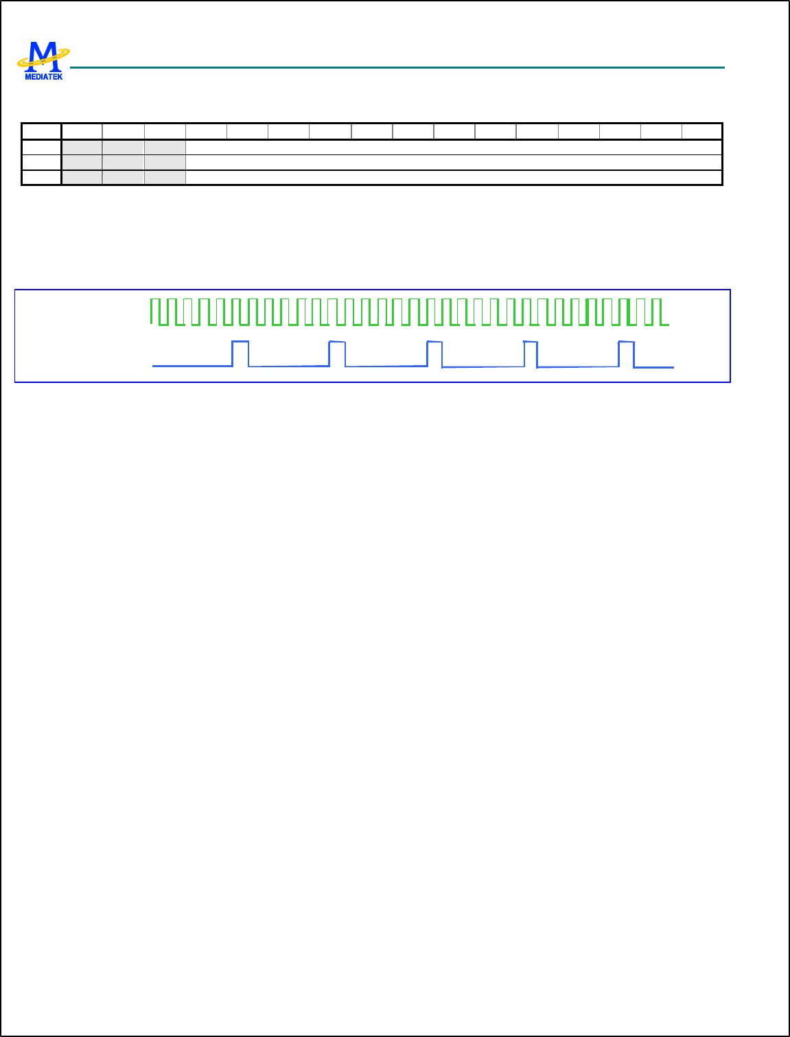
MT6217 GSM/GPRS Baseband Processor Data Sheet Revision 1.01
85/349 MediaTek Inc. Confidential
PWM+0014h PWM2 Threshold Value register PWM2_THRES
Bit 15 14 13 12 11 10 9 8 7 6 5 4 3 2 1 0
Name
PWM2_THRES [12:0]
Type R/W
Reset
0
PWM2_THRES Threshold value. When the internal counter value is greater than or equals to PWM2_THRES, the PWM1
output signal will be “0”; when the internal counter is less than PWM2_THRES, the PWM2 output signal
will be “1”.
Figure 19 shows the PWM waveform with register value present.
PWM_COUNT = 5
PWM_THRES = 1
PWM_CON = 0b
13MHz
Figure 19 PWM waveform with register value present
4.2 Alerter
4.2.1 General Description
The output of Alerter has two sources: one is the enhanced pwm output signal, which is implemented embedded in Alerter
module; the other is PDM signal from DSP domain directly. The enhanced pwm with three operation modes is implemented
to generate a signal with programmable frequency and tone volume. The frequency and volume are determined by four
registers: ALERTER_CNT1, ALERTER_THRES, ALERTER_CNT2 and ALERTER_CON. ALERTER_CNT1 and
ALERTER_CNT2 are the initial counting values of internal counter1 and internal counter2 respectively. POWERDOWN
signal is applied to power-down the Alerter module. When Alerter is deactivated (POWERDOWN=1), the output will be in
low state.
With ALERTER_CON, the output source can be chosen from enhanced pwm or PDM. The waveform of the alerter from
enhanced pwm source in different modes can be shown in Figure 20. In mode 1, the polarity of alerter output signal
according to the relationship between internal counter1 and the programmed threshold will be inverted each time internal
counter2 reaches zero. In mode2, each time the internal counter2 count backwards to zero the alerter output signal is normal
pwm signal (i.e. signal is low as long as the internal counter1 value is greater than or equals to ALERTER_THRES, and it is
high when the internal counter1 is less than ALERTER_THRES) or low state by turns. In mode3, the value of internal
counter2 has no effect on output signal, i.e. the alerter output signal is low as long as the internal counter1 value is above
the programmed threshold and is high the internal counter1 is less than ALERTER_THRES when no matter what value the
internal counter2 is.
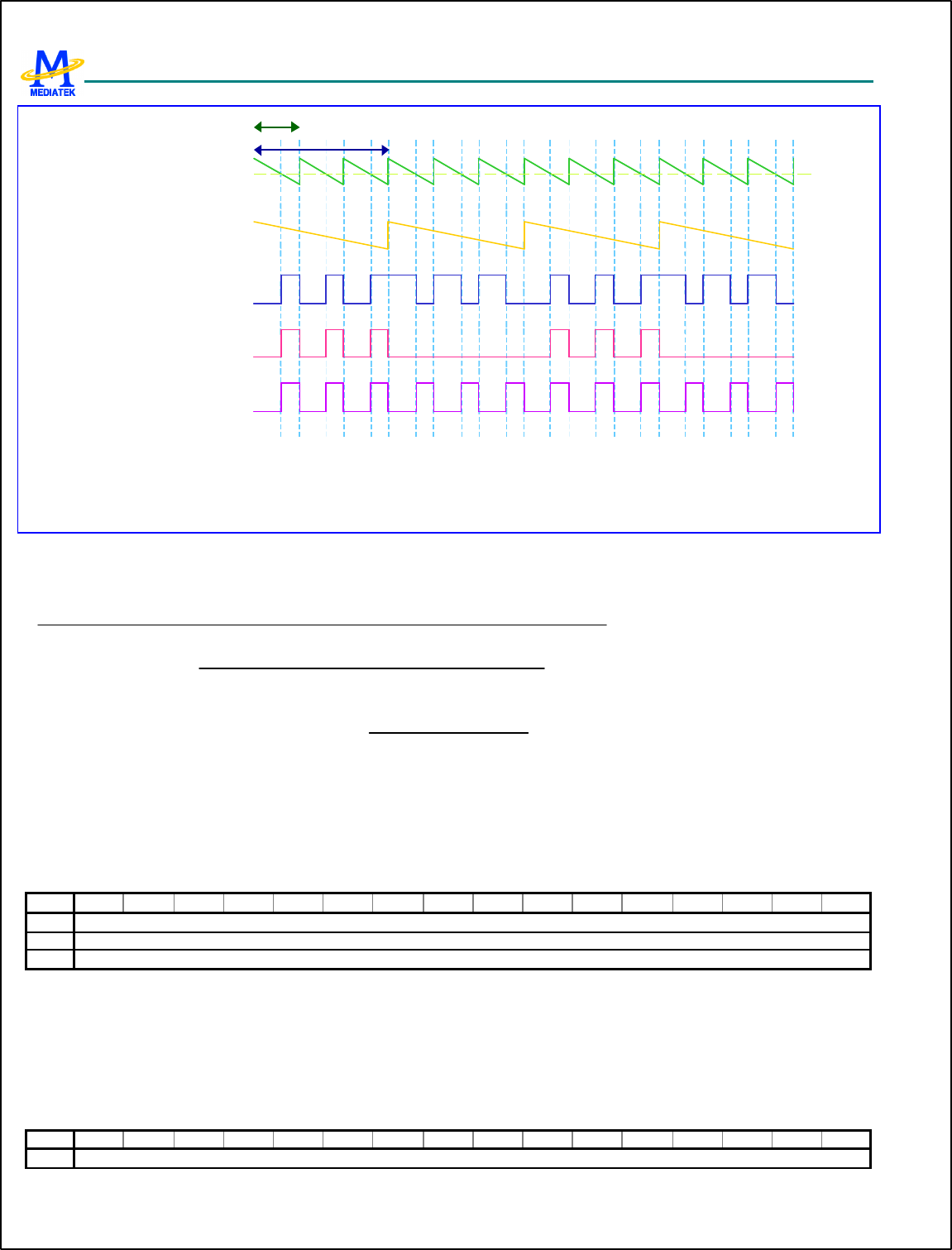
MT6217 GSM/GPRS Baseband Processor Data Sheet Revision 1.01
86/349 MediaTek Inc. Confidential
ALERTER_THRES
enhance pwmout (mode 1)
enhance pwmout (mode 2)
enhanced pwmout (mode 3)
T2
Internal counter1
T1 = ALERTER_CNT1 *1/13MHz *( ALERTER_CON[1:0]+1)
T2 = T1 *( ALERTER_CNT2+1)
T1
Internal counter2
Figure 20 Alerter waveform
The output signal frequency is determined by:
3 modeor
])0:1[_()11_(
13000000
2 mode and 1 modeor
)12_()11_()1]0:1[_(2
13000000
×+
+×+×+×
f
CONALERTERCNTALERTER
f
CNTALERTERCNTALERTERCONALERTER
The volume of the output signal is determined by: 11_
_
+CNTALERTER
THRESALERTER
4.2.2 Register Definitions
ALTER+0000h Alerter counter1 value register ALERTER_CNT
1
Bit 15 14 13 12 11 10 9 8 7 6 5 4 3 2 1 0
Name
ALERTER_CNT1 [15:0]
Type R/W
Reset
FFFFh
ALERTER_CNT1 Alerter max counter’s value. ALERTER_CNT1 is the initial value of internal counter1. If
ALERTER_CNT1 is written when the internal counter1 is counting backwards, no matter which mode it is,
there is no effect until the internal counter1 counts down to zero, i.e. a complete period.
ALTER+0004h Alerter threshold value register ALERTER_THR
ES
Bit 15 14 13 12 11 10 9 8 7 6 5 4 3 2 1 0
Name
ALERTER_THRES [15:0]
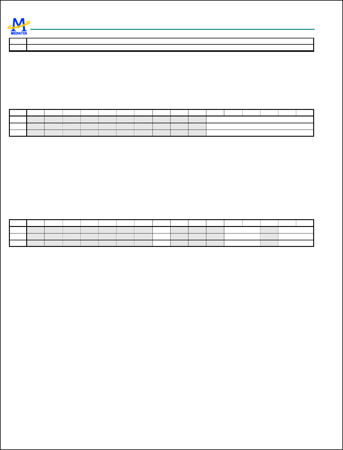
MT6217 GSM/GPRS Baseband Processor Data Sheet Revision 1.01
87/349 MediaTek Inc. Confidential
Type R/W
Reset
0
ALERTER_THRES Threshold value. When the internal counter1 value is greater than or equals to ALERTER_THRES,
the Alerter output signal will be low state; when the counter1 is less than ALERTER_THRES, the Alerter
output signal will be high state.
ALTER+0008h Alerter counter2 value register ALERTER_CNT
2
Bit 15 14 13 12 11 10 9 8 7 6 5 4 3 2 1 0
Name
ALERTER_CNT2 [ 5:0]
Type R/W
Reset
111111b
AlERTER_CNT2 ALERTER_CNT2 is the initial value for internal counter2. The internal counter2 decreases by one
everytime the internal counter1 count down to be zero. The polarity of alerter output signal which depends on the
relationship between the internal counter1 and ALERTER_THRES will be inverted anytime when the internal
counter2 counts down to zero. E.g. in the beginning, the output signal is low when the internal counter1 isn’t less
ALERTER_THRES and is high when the internal counter1 is less than ALERTER_THRES. But after the internal
counter2 counts down to zero, the output signal will be high when the internal counter1 isn’t less than
ALERTER_THRES and will be low when the internal counter1 is less than ALERTER_THRES.
ALTER+000Ch Alerter control register ALERTER_CON
Bit 15 14 13 12 11 10 9 8 7 6 5 4 3 2 1 0
Name
TYPE MODE CLK [1:0]
Type R/W R/W R/W
Reset
0 0 0
CLK Select PWM Waveform clock
00 13M Hz
01 13/2M Hz
10 13/4M Hz
11 13/8M Hz
MODE Select Alerter mode
00 Mode 1 selected
01 Mode 2 selected
10 Mode 3 selected
TYPE Select the ALERTER output source from PWM or PDM
0 Output generated from PWM path
1 Output generated from PDM path
Note: When alerter module is power down, its output should be kept in low state.
Figure 21 shows the Alerter waveform with register value present.
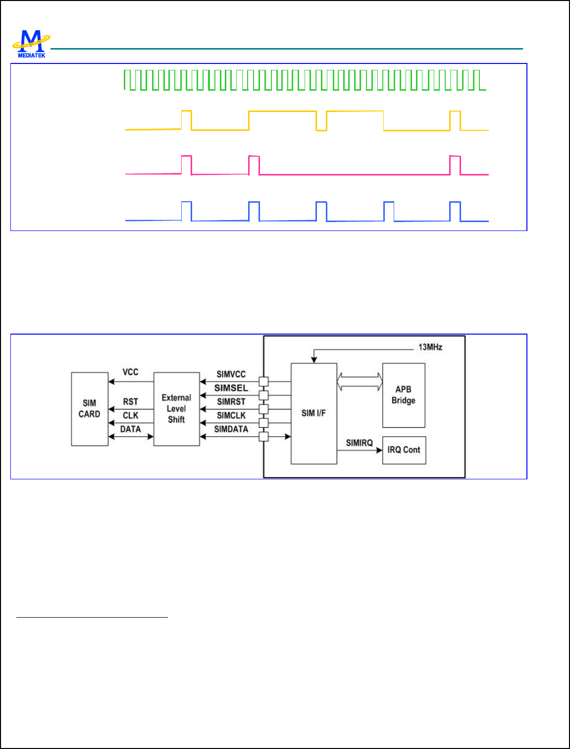
MT6217 GSM/GPRS Baseband Processor Data Sheet Revision 1.01
88/349 MediaTek Inc. Confidential
ALERTER_CNT1 =5
ALERTER_CNT2 =1
ALERTER_THRESH = 1
ALERTER_CON = 01000b
ALERTER_CNT1 =5
ALERTER_CNT2 =1
ALERTER_THRESH = 1
ALERTER_CON = 00100b
ALERTER_CNT1 =5
ALERTER_CNT2 =1
ALERTER_THRESH = 1
ALERTER_CON =00000b
13MHz
Figure 21 Alerter output signal from enhanced pwm with register value present
4.3 SIM Interface
The MT6217 contains a dedicated smart card interface to allow the MCU access to the SIM card. It can operate via 5
terminals, using SIMVCC, SIMSEL, SIMRST, SIMCLK and SIMDATA.
Figure 22 SIM Interface Block Diagram
The SIMVCC is used to control the external voltage supply to the SIM card and SIMSEL determines the regulated smart
card supply voltage. SIMRST is used as the SIM card reset signal. Besides, SIMDATA and SIMCLK are used for data
exchange purpose.
Basically, the SIM interface acts as a half duplex asynchronous communication port and its data format is composed of ten
consecutive bits: a start bit in state Low, eight information bits, and a tenth bit used for parity checking. The data format can
be divided into two modes as follows:
Direct Mode (ODD=SDIR=SINV=0)
SB D0 D1 D2 D3 D4 D5 D6 D7 PB
SB: Start Bit (in state Low)
Dx: Data Byte (LSB is first and logic level ONE is High)
PB: Even Parity Check Bit
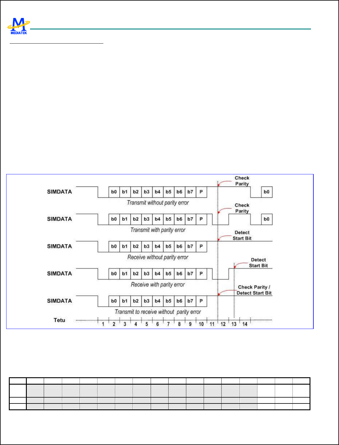
MT6217 GSM/GPRS Baseband Processor Data Sheet Revision 1.01
89/349 MediaTek Inc. Confidential
Indirect Mode (ODD=SDIR=SINV=1)
SB N7 N6 N5 N4 N3 N2 N1 N0 PB
SB: Start Bit (in state Low)
Nx: Data Byte (MSB is first and logic level ONE is Low)
PB: Odd Parity Check Bit
If the receiver gets a wrong parity bit, it will respond by pulling the SIMDATA Low to inform the transmitter and the
transmitter will retransmit the character.
When the receiver is a SIM Card, the error response starts 0.5 bits after the PB and it may last for 1~2 bit periods.
When the receiver is the SIM interface, the error response starts 0.5 bits after the PB and lasts for 1.5 bit period.
When the SIM interface is the transmitter, it will take totally 14 bits guard period whether the error response appears. If the
receiver shows the error response, the SIM interface will retransmit the previous character again else it will transmit the
next character.
Figure 23 SIM Interface Timing Diagram
4.3.1 Register Definitions
SIM+0000h SIM module control register SIM_CON
Bit 15 14 13 12 11 10 9 8 7 6 5 4 3 2 1 0
Name
WRST
CSTO
P SIMO
N
Type W R/W R/W
Reset
0 0 0

MT6217 GSM/GPRS Baseband Processor Data Sheet Revision 1.01
90/349 MediaTek Inc. Confidential
SIMON SIM card power-up/power-down control
0 Initiate the card deactivation sequence
1 Initiate the card activation sequence
CSTOP Enable clock stop mode. Together with CPOL in SIM_CNF register, it determines the polarity of the SIMCLK in
this mode.
0 Enable the SIMCLK output.
1 Disable the SIMCLK output
WRST SIM card warm reset control
SIM+0004h SIM module configuration register SIM_CNF
Bit 15 14 13 12 11 10 9 8 7 6 5 4 3 2 1 0
Name
HFEN T0EN T1EN TOUT SIMS
EL ODD SDIR SINV CPOL TXAC
K RXAC
K
Type R/W R/W R/W R/W R/W R/W R/W R/W R/W R/W R/W
Reset
0 0 0 0 0 0 0 0 0 0 0
RXACK SIM card reception error handshake control
0 Disable character receipt handshaking
1 Enable character receipt handshaking
TXACK SIM card transmission error handshake control
0 Disable character transmission handshaking
1 Enable character transmission handshaking
CPOL SIMCLK polarity control in clock stop mo de
0 Make SIMCLK stop in LOW level
1 Make SIMCLK stop in HIGH level
SINV Data Inverter.
0 Not invert the transmitted and received data
1 Invert the transmitted and received data
SDIR Data Transfer Direction
0 LSB is transmitted and received first
1 MSB is transmitted and received first
ODD Select odd or even parity
0 Even parity
1 Odd parity
SIMSEL SIM card supply voltage select
0 SIMSEL pin is set to LOW level
1 SIMSEL pin is set to HIGH level
TOUT SIM work waiting time counter control
0 Disable Time-Out counter
1 Enable Time-Out counter
T1EN T=1 protocol controller control
0 Disable T=1 protocol controller
1 Enable T=1 protocol controller
T0EN T=0 protocol controller control
0 Disable T=0 protocol controller
1 Enable T=0 protocol controller
MT6217 GSM/GPRS Baseband Processor Data Sheet Revision 1.01
91/349 MediaTek Inc. Confidential
HFEN Hardware flow control
0 Disable hardware flow control
1 Enable hardware flow control
SIM +0008h SIM Baud Rate Register SIM_BRR
Bit 15 14 13 12 11 10 9 8 7 6 5 4 3 2 1 0
Name
ETU[8:0] SIMCLK[1:0]
Type R/W R/W
Reset
372d 01
SIMCLK Set SIMCLK frequency
00 13/2 MHz
01 13/4 MHz
10 13/8 MHz
11 13/12 MHz
ETU Determines the duration of elementary time unit in unit of SIMCLK
SIM +0010h SIM interrupt enable register SIM_IRQEN
Bit 15 14 13 12 11 10 9 8 7 6 5 4 3 2 1 0
Name
EDCE
RR T1EN
D RXER
R T0EN
D SIMO
FF ATRER
R TXER
R TOU
T OVRU
N RXTID
E TXTID
E
Type R/W R/W R/W R/W R/W R/W R/W R/W R/W R/W R/W
Reset
0 0 0 0 0 0 0 0 0 0 0
For all these bits
0 Interrupt is disabled
1 Interrupt is enabled
SIM +0014h SIM module status register SIM_STA
Bit 15 14 13 12 11 10 9 8 7 6 5 4 3 2 1 0
Name
EDCE
RR T1EN
D RXER
R T0EN
D SIMO
FF ATRER
R TXER
R TOU
T OVRU
N RXTID
E TXTID
E
Type R/C R/C R/C R/C R/C R/C R/C R/C R/C R R
Reset
— — — — — — — — — — —
TXTIDE Transmit FIFO tide mark reached interrupt occurred
RXTIDE Receive FIFO tide mark reached interrupt occurred
OVRUN Transmit/Receive FIFO overrun interrupt occurred
TOUT Between character timeout interrupt occurred
TXERR Character transmission error interrupt occurred
ATRERR ATR start time-out interrupt occurred
SIMOFF Card deactivation complete interrupt occurred
T0END Data Transfer handled by T=0 Controller completed interrupt occurred
RXERR Character reception error interrupt occurred
T1END Data Transfer handled by T=1 Controller completed interrupt occurred
EDCERR T=1 Controller CRC error occurred
SIM +0020h SIM retry limit register SIM_RETRY
Bit 15 14 13 12 11 10 9 8 7 6 5 4 3 2 1 0
MT6217 GSM/GPRS Baseband Processor Data Sheet Revision 1.01
92/349 MediaTek Inc. Confidential
Name
TXRETRY RXRETRY
Type R/W R/W
Reset
3h 3h
RXRETRY Specify the max. numbers of receive retries that are allowed when parity error has occurred.
TXRETRY Specify the max. numbers of transmit retries that are allowed when parity error has occurred.
SIM +0024h SIM FIFO tide mark register SIM_TIDE
Bit 15 14 13 12 11 10 9 8 7 6 5 4 3 2 1 0
Name
TXTIDE[3:0] RXTIDE[3:0]
Type R/W R/W
Reset
0h 0h
RXTIDE Trigger point for RXTIDE interrupt
TXTIDE Trigger point for TXTIDE interrupt
SIM +0030h Data register used as Tx/Rx Data Register SIM_DATA
Bit 15 14 13 12 11 10 9 8 7 6 5 4 3 2 1 0
Name
DATA[7:0]
Type R/W
Reset
—
DATA Eight data digits. These correspond to the character being read or written
SIM +0034h SIM FIFO count register SIM_COUNT
Bit 15 14 13 12 11 10 9 8 7 6 5 4 3 2 1 0
Name
COUNT[4:0]
Type R/W
Reset
0h
COUNT The number of characters in the SIM FIFO when read, and flushes when written.
SIM +0040h SIM activation time register SIM_ATIME
Bit 15 14 13 12 11 10 9 8 7 6 5 4 3 2 1 0
Name
ATIME[15:0]
Type R/W
Reset
AFC7h
ATIME The register defines the duration, in SIM clock cycles, of the time taken for each of the three stages of the card
activation process
SIM +0044h SIM deactivation time register SIM_DTIME
Bit 15 14 13 12 11 10 9 8 7 6 5 4 3 2 1 0
Name
DTIME[11:0]
Type R/W
Reset
3E7h
DTIME The register defines the duration, in 13MHz clock cycles, of the time taken for each of the three stages of the
card deactivation sequence
SIM +0048h Character to character waiting time register SIM_WTIME
Bit 15 14 13 12 11 10 9 8 7 6 5 4 3 2 1 0
MT6217 GSM/GPRS Baseband Processor Data Sheet Revision 1.01
93/349 MediaTek Inc. Confidential
Name
WTIME[15:0]
Type R/W
Reset
983h
WTIME Maximum interval between the leading edge of two consecutive characters in 4 ETU unit
SIM +004Ch Block to block guard time register SIM_GTIME
Bit 15 14 13 12 11 10 9 8 7 6 5 4 3 2 1 0
Name
GTIME
Type R/W
Reset
10d
GTIME Minimum interval between the leading edge of two consecutive characters sent in opposite directions in ETU unit
SIM +0060h SIM command header register: INS SIM_INS
Bit 15 14 13 12 11 10 9 8 7 6 5 4 3 2 1 0
Name
INSD SIMINS[7:0]
Type R/W R/W
Reset
0h 0h
SIMINS This field should be identical to the INS instruction code. When writing to this register, the T=0 controller will be
activated and data transfer will be initiated.
INSD [Description for this register field]
0 T=0 controller receives data from the SIM card
1 T=0 controller sends data to the SIM card
SIM +0064h SIM command header register: P3 SIM_P3(ICC_LE
N)
Bit 15 14 13 12 11 10 9 8 7 6 5 4 3 2 1 0
Name
SIMP3[8:0]
Type R/W
Reset
0h
SIMP3 This field should be identical to the P3 instruction code. It should be written prior to the SIM_INS register. While
the data transfer is going on, this field shows the no. of the remaining data to be sent or to be received
SIM +0068h SIM procedure byte register: SW1 SIM_SW1(ICC_L
EN)
Bit 15 14 13 12 11 10 9 8 7 6 5 4 3 2 1 0
Name
SIMSW1[7:0]
Type R
Reset
0h
SIMSW1 This field holds the last received procedure byte for debug purpose. When the T0END interrupt occurred, it
keeps the SW1 procedure byte.
SIM +006Ch SIM procedure byte register: SW2 SIM_SW2(ICC_E
DC)
Bit 15 14 13 12 11 10 9 8 7 6 5 4 3 2 1 0
Name
SIMSW2[7:0]
Type R

MT6217 GSM/GPRS Baseband Processor Data Sheet Revision 1.01
94/349 MediaTek Inc. Confidential
Reset
0h
SIMSW2 This field holds the SW2 procedure byte
4.3.2 SIM Card Insertion and Removal
The detection of physical connection to the SIM card and card removal is done by the external interrupt controller or by
GPIO.
4.3.3 Card Activation and Deactivation
The card activation and deactivation sequence both are controlled by H/W. The MCU initiates the activation sequence by
writing a “1” to bit 0 of the SIM_CON register, and then the interface performs the following activation sequence:
l Assert SIMRST LOW
l Set SIMVCC at HIGH level and SIMDATA in reception mode
l Enable SIMCLK clock
l De -assert SIMRST HIGH (required if it belongs to active low reset SIM card)
The final step in a typical card session is contact deactivation in order that the card is not electrically damaged. The
deactivation sequence is initiated by writing a “0” to bit 0 of the SIM_CON register, and then the interface performs the
following deactivation sequence:
l Assert SIMRST LOW
l Set SCIMCLK at LOW level
l Set SIMDATA at LOW level
l Set SIMVCC at LOW level
4.3.4 Answer to Reset Sequence
After card activation, a reset operation results in an answer from the card consisting of the initial character TS, followed by
at most 32 characters. The initial character TS provides a bit synchronization sequence and defines the conventions to
interpret data bytes in all subsequent characters.
On reception of the first character, TS, MCU should read this character, establish the respective required convention and
reprogram the related registers. These processes should be completed prior to the completion of reception of the next
character. And then, the remainder of the ATR sequence is received, read via the SIM_DATA in the selected convention and
interpreted by the S/W.
The timing requirement and procedures for ATR sequence are handled by H/W and shall meet the requirement of ISO
7816-3 as shown in Figure 24.
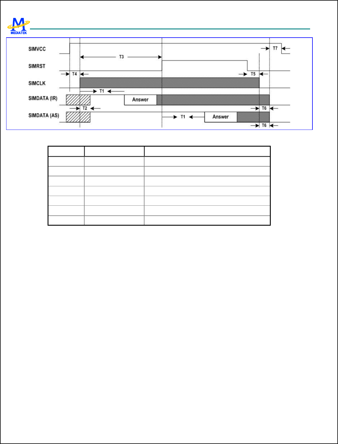
MT6217 GSM/GPRS Baseband Processor Data Sheet Revision 1.01
95/349 MediaTek Inc. Confidential
Figure 24 Answer to Reset Sequence
Time Value Comment
T1 > 400 SIMCLK SIMCLK start to ATR appear
T2 < 200 SIMCLK SIMCLK start to SIMDATA in reception mode
T3 > 40000 SIMCLK SIMCLK start to SIMRST High
T4 — SIMVCC High to SIMCLK start
T5 — SIMRST Low to SIMCLK stop
T6 — SIMCLK stop to SIMDATA Low
T7 — SIMDATA Low to SIMVCC Low
Table 19 Answer to Reset Sequence Time-Out Condition
4.3.5 SIM Data Transfer
Two transfer modes are provided, either in software controlled byte by byte fashion or in a block fashion using T=0
controller and DMA controller. In both modes, the time -out counter could be enabled to monitor the elapsed time between
two consecutive bytes.
4.3.5.1 Byte Transfer Mode
This mode is used during ATR and PPS procedure. In this mode, the SIM interface only ensures error free character
transmission and reception.
Receiving Character
Upon detection of the start-bit sent by SIM card, the interface transforms into reception mode and the following bits are
shifted into an internal register. If no parity error is detected or character-receive handshaking is disabled, the
received-character is written into the SIM FIFO and the SIM_CNT register is increased by one. Otherwise, the SIMDATA
line is held low at 0.5 etu after detecting the parity error for 1.5 etus, and the character is re-received. If a character fails to
be received correctly for the RXRETRY times, the receive-handshaking is aborted and the last-received character is written
into the SIM FIFO, the SIM_CNT is increased by one and the RXERR interrupt is generated
When the number of characters held in the receive FIFO exceeds the level defined in the SIM_TIDE
register, a RXTIDE interrupt is generated. The number of characters held in the SIM FIFO can be

MT6217 GSM/GPRS Baseband Processor Data Sheet Revision 1.01
96/349 MediaTek Inc. Confidential
determined by reading the SIM_CNT register and writing to this register will flush the SIM FIFO.
Sending Character
Characters that are to be sent to the card are first written into the SIM FIFO and then automatically transmitted to the card
at timed intervals. If character-transmit handshaking is enabled, the SIMDATA line is sampled at 1 etu after the parity bit. If
the card indicates that it did not receive the character correctly, the character is retransmitted a maximum of TXRETRY
times before a TXERR interrupt is generated and the transmission is aborted. Otherwise, the succeeding byte in the SIM
FIFO is transmitted.
If a character fails to be transmitted and a TXERR interrupt is generated, the interface needs to be reset by flushing the SIM
FIFO before any subsequent transmit or receive operation.
When the number of characters held in the SIM FIFO falls below the level defined in the SIM_TIDE register, a TXTIDE
interrupt is generated. The number of characters held in the SIM FIFO can be determined by reading the SIM_CNT register
and writing to this register will flush the SIM FIFO.
4.3.5.2 Block Transfer Mode
Basically, the SIM interfa ce is designed to work in conjunction with the T=0 protocol controller and the DMA controller
during non-ATR and non-PPS phase, though it is still possible for software to service the data transfer manually like in byte
transfer mode if necessary and thus the T=0 protocol should be controlled by software.
The T=0 controller is accessed via four registers representing the instruction header bytes INS and P3, and the procedure
bytes SW1 and SW2. These registers are:
SIM_INS, SIM_P3
SIM_SW1, SIM_SW2
During characters transfer, SIM_P3 holds the number of characters to be sent or to be received and SIM_SW1 holds the last
received procedure byte including NULL, ACK, NACK and SW1 for debug purpose.
Data Receive Instruction
Data Receive Instructions receive data from the SIM card. It is instantiated as the following procedure.
1. Enable the T=0 protocol controller by setting the T0EN bit to 1 in SIM_CNF register
2. Program the SIM_TIDE register to 0x0000 (TXTIDE = 0, RXTIDE = 0)
3. Program the SIM_IRQEN to 0x019C (Enable RXERR, TXERR, T0END, TOUT and OVRUN interrupts)
4. Write CLA, INS, P1, P2 and P3 into SIM FIFO
5. Program the DMA controller :
DMAn_MSBSRC and DMAn_LSBSRC : address of SIM_DATA register
DMAn_MSBDST and DMAn_LSBDST : memory address reserved to store the received characters
DMAn_COUNT : identical to P3 or 256 (if P3 == 0)
DMAn_CON : 0x0078
6. Write P3 into SIM_P3 register and then INS into SIM_INS register (Data Transfer is initiated
now)
7. Enable the Time-out counter by setting the TOUT bit to 1 in SIM_CNF register
8. Start the DMA controller by writing 0x8000 into the DMAn_START register to
Upon completion of the Data Receive Instruction, T0END interrupt will be generated and then the Time-out counter should
be disabled by setting the TOUT bit back to 0 in SIM_CNF register.

MT6217 GSM/GPRS Baseband Processor Data Sheet Revision 1.01
97/349 MediaTek Inc. Confidential
If error occurs during data transfer (RXERR, TXERR, OVRUN or TOUT interrupt is generated), the SIM card should be
deactivated first and then activated prior subsequent operations.
Data Send Instruction
Data Send Instructions send data to the SIM card. It is instantiated as the following procedure.
1. Enable the T=0 protocol controller by setting the T0EN bit to 1 in SIM_CNF register
2. Program the SIM_TIDE register to 0x0100 (TXTIDE = 1, RXTIDE = 0)
3. Program the SIM_IRQEN to 0x019C (Enable RXERR, TXERR, T0END, TOUT and OVRUN interrupts)
4. Write CLA, INS, P1, P2 and P3 into SIM FIFO
5. Program the DMA controller :
DMAn_MSBSRC and DMAn_LSBSRC : memory address reserved to store the transmitted characters
DMAn_MSBDST and DMAn_LSBDST : address of SIM_DATA register
DMAn_COUNT : identical to P3
DMAn_CON : 0x0074
6. Write P3 into SIM_P3 register and then (0x0100 | INS) into SIM_INS register (Data Transfer
is initiated now)
7. Enable the Time-out counter by setting the TOUT bit to 1 in SIM_CNF register
8. Start the DMA controller by writing 0x8000 into the DMAn_START register
Upon completion of the Data Send Instruction, T0END interrupt will be generated and then the Time -out counter should be
disabled by setting the TOUT bit back to 0 in SIM_CNF register.
If error occurs during data transfer (RXERR, TXERR, OVRUN or TOUT interrupt is generated), the SIM card should be
deactivated first and then activated prior subsequent operations.
4.4 Keypad Scanner
4.4.1 General Description
The keypad can be divided into two parts: one is the keypad interface including 7 columns and 6 rows; the other is the key
detection block which provides key pressed, key released and de-bounce mechanism. Each time key pressed or key released,
i.e. something different in the 7 x 6 matrix, the key detection block will sense it, and it will start to recognize if it’s a key
pressed or key released event. Whenever the key status changes and is stable, a KEYPAD IRQ will be issued. The MCU
can then read the key(s) pressed directly in KP_HI_KEY, KP_MID_KEY and KP_LOW_KEY registers. To ensure that the
key pressed information won’t be missed, the status register in keypad won’t be read clear by APB bus read command. The
status register only changes by the key-pressed detection FSM. This keypad can detect one or two key-pressed
simultaneously with any combination. Figure 25 shows one key pressed condition. Figure 26(a) and Figure 26(b) indicate
two keys pressed cases. Since the key press detection depends on the high or low level of the external keypad interface, if
keys are pressed at the same time and these exists one key is on the same column and the same row with the other keys,
there will get a redundant key; e.g. there are three keys, key1 = (x1, y1), key2 = (x2, y2), key3 = (x1, y2), key4 = (x2, y1)
will be detected, but key4 is a redundant one. Hence, the keypad can detect one or two keys pressed simultaneously at any
combination. Due to the keypad interface, more than two keys pressed simultaneously with some specific pattern will get
the wrong information. Without the specific pattern, the keypad-scanning block can detect 11 keys at the same time and it ’s
shown as Figure 27.
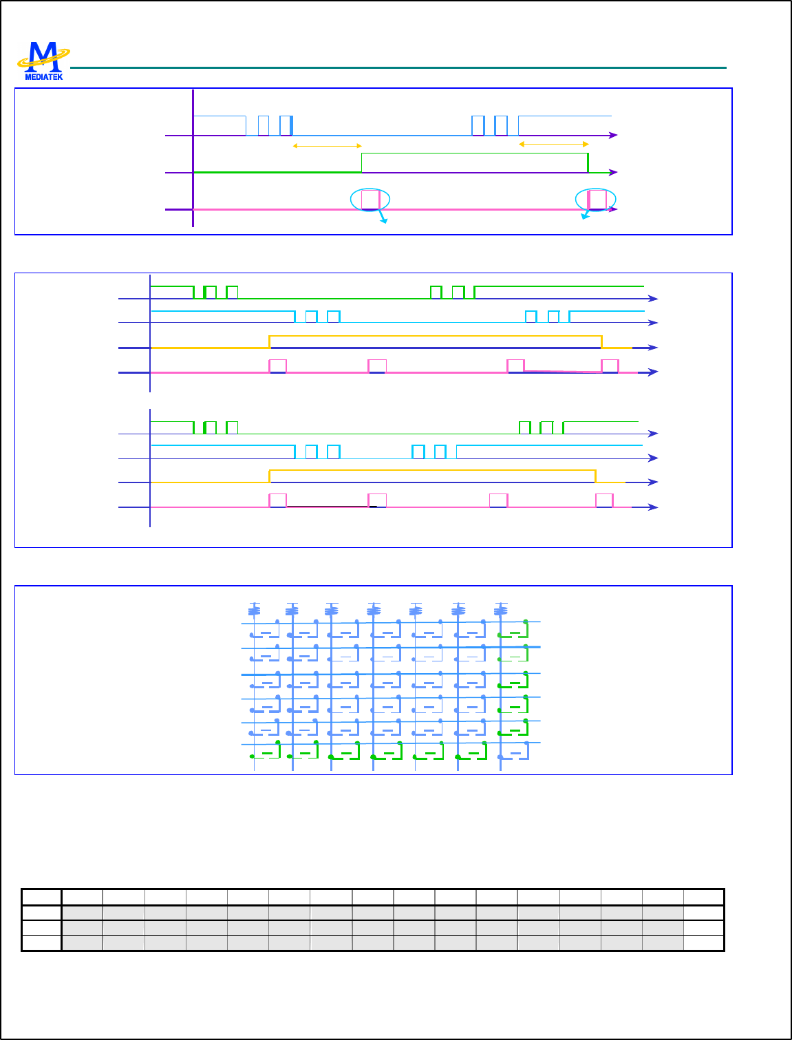
MT6217 GSM/GPRS Baseband Processor Data Sheet Revision 1.01
98/349 MediaTek Inc. Confidential
Key -pressed Status
De-bounce time De-bounce time
Key Pressed
KP_IRQ
KEY_PRESS_IRQ KEY_RELEASE_IRQ
Figure 25 One key pressed with de-bounce mechanism denoted
Key1 pressed
Key2 pressed
Status
IRQ
Key1 pressed Key2 pressed Key1 released Key2 released
Key1 pressed
Key2 pressed
Status
IRQ
Key1 pressed Key2 pressed Key2 released Key1 released
(a)
(b)
Key1 pressed
Key2 pressed
Status
IRQ
Key1 pressed Key2 pressed Key1 released Key2 released
Key1 pressed
Key2 pressed
Status
IRQ
Key1 pressed Key2 pressed Key2 released Key1 released
(a)
(b)
Figure 26 (a) Two keys pressed, case 1 (b) Two keys pressed, case 2
COL4 COL3 COL2 COL1 COL0
1
1
1
1
1
1
1
1
1
1
1
1
1
1
1
1
1
1
1
1
0
0
0
0
0
1
1
1
1
1
COL5
0 0 0 0 10
ROW0
ROW1
ROW2
ROW3
ROW4
ROW5 1
1
1
1
1
COL6
0
Figure 27 10 keys are detected at the same time
4.4.2 Register Definitions
KP +0000h Keypad status KP_STA
Bit 15 14 13 12 11 10 9 8 7 6 5 4 3 2 1 0
Name
STA
Type RO
Reset
0
STA This register indicates the keypad status, and it won’t be cleared by read.
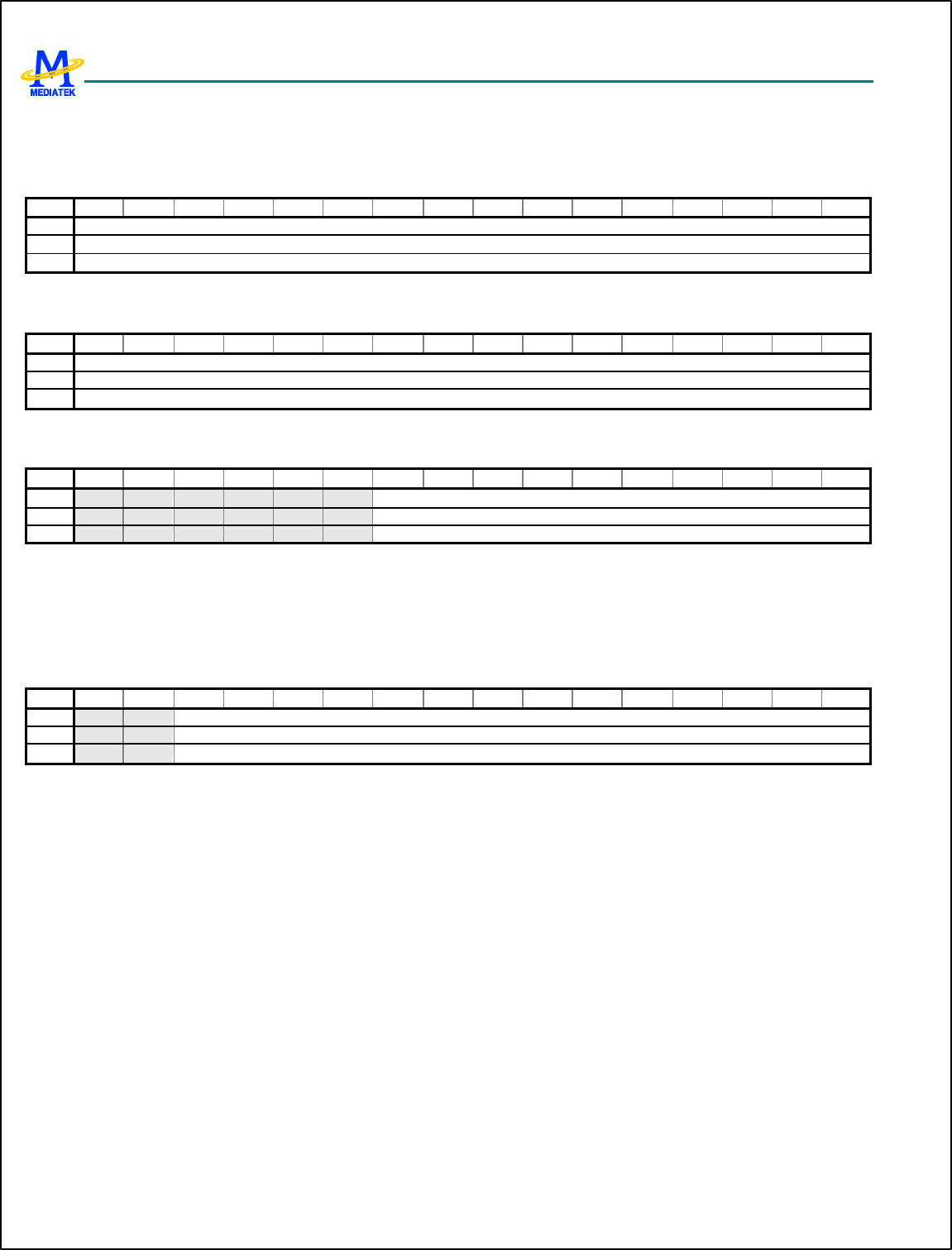
MT6217 GSM/GPRS Baseband Processor Data Sheet Revision 1.01
99/349 MediaTek Inc. Confidential
0 No key pressed
1 Key pressed
KP +0004h Keypad scanning output, the lower 16 keys
KP_LOW_KEY
Bit 15 14 13 12 11 10 9 8 7 6 5 4 3 2 1 0
Name
KEYS [15:0]
Type RO
Reset
FFFFh
KP +0008h Keypad scanning output, the medium 16 keys KP_MID_KEY
Bit 15 14 13 12 11 10 9 8 7 6 5 4 3 2 1 0
Name
KEYS [31:16]
Type RO
Reset
FFFFh
KP+000Ch Keypad scanning output, the higher 4 keys KP_HIGH_KEY
Bit 15 14 13 12 11 10 9 8 7 6 5 4 3 2 1 0
Name
KEYS[41:32]
Type RO
Reset
3FFh
These two registers list the status of 42 keys on the keypad. When the MCU receives the KEYPAD IRQ, both two registers
must be read. If any key is pressed, the relative bit will be set to 0.
KEYS Status list of the 42 keys.
KP +00010h De-bounce period setting KP_DEBOUNCE
Bit 15 14 13 12 11 10 9 8 7 6 5 4 3 2 1 0
Name
DEBOUNCE [13:0]
Type R/W
Reset
400h
This register defines the waiting period before key press or release events are considering stale.
DEBOUNCE De-bounce time = KP_DEBOUNCE/32 ms .
4.5 General Purpose Inputs/Outputs
MT-6217 offers 48 general-purpose I/O pins and 3 general-purpose output pins. By setting the control registers, MCU
software can control the direction, the output value and read the input values on these pins. Besides, these GPIOs and GPOs
are multiplexed with other functionalities to reduce the pin count.
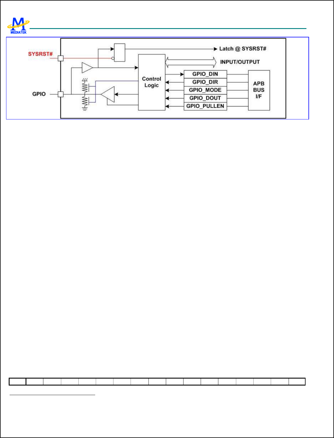
MT6217 GSM/GPRS Baseband Processor Data Sheet Revision 1.01
100/349 MediaTek Inc. Confidential
Figure 28 GPIO Block Diagram
GPIOs at RESET
At hardware reset (SYSRST#), GPIOs are all configured as inputs and the following alternative uses of GPIO pins are
made:
l GPIO[41] is used as the JMODE input for JTAG mode selection
l GPIO[42] is used as the MSIZE input for boot rom size indication 1
These GPIOs are used to latch the inputs at reset to memorize the wanted configuration to make sure that the system restarts
or boots in the right mode.
Multiplexing of Signals on GPIO
The GPIO pins can be multiplexed with other signals.
l DAICLK, DAIPCMIN, DAIPCMOUT, DAIRST: digital audio interface for FTA
l BPI_BUS4, BPI_BUS5, BPI_BUS6, BPI_BUS7: radio hard-wire control
l BSI_CS1: additional chip select signal for radio 3-wire interface
l LCD_CS0#, LCD_CS1#, LCD_DATA, LCD_CLK, LCD_A0: serial display interface
l PWM1, PWM2: pulse width modulation signal
l UDSR1, UDTR1: hardware flow control signals for UART1
l URXD2, UTXD2, UCTS2, URTS2: data and flow control signals for UART2
Multiplexed of Signals on GPO
l SRCLKENA, SRCLKENAN: power on signal of the external VCXO LDO
4.5.1 Register Definitions
GPIO+0000h GPIO direction control register 1 GPIO_DIR1
Bit 15 14 13 12 11 10 9 8 7 6 5 4 3 2 1 0
1 For detailed BOOT and MSIZE configuration, please see in Micro-Controller Unit System section
MT6217 GSM/GPRS Baseband Processor Data Sheet Revision 1.01
101/349 MediaTek Inc. Confidential
Name
GPIO1
5 GPIO1
4 GPIO1
3 GPIO1
2 GPIO1
1 GPIO1
0 GPIO9
GPIO8
GPIO7
GPIO6
GPIO5
GPIO4
GPIO3
GPIO2
GPIO1
GPIO
0
Type R/W R/W R/W R/W R/W R/W R/W R/W R/W R/W R/W R/W R/W R/W R/W R/W
Reset
0 0 0 0 0 0 0 0 0 0 0 0 0 0 0 0
GPIO +0010h GPIO direction control register 2 GPIO_DIR2
Bit 15 14 13 12 11 10 9 8 7 6 5 4 3 2 1 0
Name
GPIO3
1 GPIO3
0 GPIO2
9 GPIO2
8 GPIO2
7 GPIO2
6 GPIO2
5 GPIO2
4 GPIO2
3 GPIO2
2 GPIO2
1 PGIO2
0 GPIO1
9 GPIO1
8 GPIO1
7 GPIO
16
Type R/W R/W R/W R/W R/W R/W R/W R/W R/W R/W R/W R/W R/W R/W R/W R/W
Reset
0 0 0 0 0 0 0 0 0 0 0 0 0 0 0 0
GPIO+0020h GPIO direction control register 1 GPIO_DIR3
Bit 15 14 13 12 11 10 9 8 7 6 5 4 3 2 1 0
Name
GPIO4
7 GPIO4
6 GPIO4
5 GPIO4
4 GPIO4
3 GPIO4
2 GPIO4
1 GPIO4
0 GPIO3
9 GPIO3
8 GPIO3
7 GPIO3
6 GPIO3
5 GPIO3
4 GPIO3
3 GPIO
32
Type R/W R/W R/W R/W R/W R/W R/W R/W R/W R/W R/W R/W R/W R/W R/W R/W
Reset
0 0 0 0 0 0 0 0 0 0 0 0 0 0 0 0
GPIOn GPIO direction control
0 GPIOs are configured as input
1 GPIOs are configured as output
GPIO +0030h GPIO pull-up/pull-down enable register 1 GPIO_PULLEN1
Bit 15 14 13 12 11 10 9 8 7 6 5 4 3 2 1 0
Name
GPIO1
5 GPIO1
4 GPIO1
3 GPIO1
2 GPIO1
1 GPIO1
0 GPIO9
GPIO8
GPIO7
GPIO6
GPIO5
GPIO4
GPIO3
GPIO2
GPIO1
GPIO
0
Type R/W R/W R/W R/W R/W R/W R/W R/W R/W R/W R/W R/W R/W R/W R/W R/W
Reset
1 1 1 1 1 1 1 1 1 1 1 1 1 1 1 1
GPIO +0040h GPIO pull-up/pull-down enable register 2 GPIO_PULLEN2
Bit 15 14 13 12 11 10 9 8 7 6 5 4 3 2 1 0
Name
GPIO3
1 GPIO3
0 GPIO2
9 GPIO2
8 GPIO2
7 GPIO2
6 GPIO2
5 GPIO2
4 GPIO2
3 GPIO2
2 GPIO2
1 PGIO2
0 GPIO1
9 GPIO1
8 GPIO1
7 GPIO
16
Type R/W R/W R/W R/W R/W R/W R/W R/W R/W R/W R/W R/W R/W R/W R/W R/W
Reset
1 1 1 1 1 1 1 1 1 1 1 1 1 1 1 1
GPIO+0050h GPIO pull-up/pull-down enable register 3 GPIO_PULLEN3
Bit 15 14 13 12 11 10 9 8 7 6 5 4 3 2 1 0
Name
GPIO4
7 GPIO4
6 GPIO4
5 GPIO4
4 GPIO4
3 GPIO4
2 GPIO4
1 GPIO4
0 GPIO3
9 GPIO3
8 GPIO3
7 GPIO3
6 GPIO3
5 GPIO3
4 GPIO3
3 GPIO
32
Type R/W R/W R/W R/W R/W R/W R/W R/W R/W R/W R/W R/W R/W R/W R/W R/W
Reset
1 1 1 1 1 1 1 1 1 1 1 1 1 1 1 1
GPIOn GPIO direction control
0 GPIOs are configured as input
1 GPIOs are configured as output
GPIO +0060h GPIO data input inversion register 1 GPIO_DINV1
Bit 15 14 13 12 11 10 9 8 7 6 5 4 3 2 1 0
MT6217 GSM/GPRS Baseband Processor Data Sheet Revision 1.01
102/349 MediaTek Inc. Confidential
Name
INV15
INV14
INV13 INV12
INV11
INV10
INV9 INV8 INV7 INV6 INV5 INV4 INV3 INV2 INV1 INV0
Type R/W R/W R/W R/W R/W R/W R/W R/W R/W R/W R/W R/W R/W R/W R/W R/W
Reset
0 0 0 0 0 0 0 0 0 0 0 0 0 0 0 0
GPIO +0070h GPIO data input inversion register 2 GPIO_DINV2
Bit 15 14 13 12 11 10 9 8 7 6 5 4 3 2 1 0
Name
INV31
INV30
INV29 INV28
INV27
INV26
INV25
INV24 INV23
INV22
INV21 INV20
INV19 IVN18
INV17
INV16
Type R/W R/W R/W R/W R/W R/W R/W R/W R/W R/W R/W R/W R/W R/W R/W R/W
Reset
0 0 0 0 0 0 0 0 0 0 0 0 0 0 0 0
GPIO +0080h GPIO data input inversion register 3 GPIO_DINV3
Bit 15 14 13 12 11 10 9 8 7 6 5 4 3 2 1 0
Name
INV47
INV46
INV45 INV44
INV43
INV42
INV41
INV40 INV39
INV38
INV37 INV36
INV35 INV34
INV33
INV32
Type R/W R/W R/W R/W R/W R/W R/W R/W R/W R/W R/W R/W R/W R/W R/W R/W
Reset
0 0 0 0 0 0 0 0 0 0 0 0 0 0 0 0
GPIO +0090h GPIO data output register 3 GPIO_DOUT1
Bit 15 14 13 12 11 10 9 8 7 6 5 4 3 2 1 0
Name
GPIO1
5 GPIO1
4 GPIO1
3 GPIO1
2 GPIO1
1 GPIO1
0 GPIO9
GPIO8
GPIO7
GPIO6
GPIO5
GPIO4 GPIO3
GPIO2
GPIO1
GPIO
0
Type R/W R/W R/W R/W R/W R/W R/W R/W R/W R/W R/W R/W R/W R/W R/W R/W
Reset
0 0 0 0 0 0 0 0 0 0 0 0 0 0 0 0
GPIO +00A0h GPIO data output register 2 GPIO_DOUT2
Bit 15 14 13 12 11 10 9 8 7 6 5 4 3 2 1 0
Name
GPIO3
1 GPIO3
0 GPIO2
9 GPIO2
8 GPIO2
7 GPIO2
6 GPIO2
5 GPIO2
4 GPIO2
3 GPIO2
2 GPIO2
1 PGIO2
0 GPIO1
9 GPIO1
8 GPIO1
7 GPIO
16
Type R/W R/W R/W R/W R/W R/W R/W R/W R/W R/W R/W R/W R/W R/W R/W R/W
Reset
0 0 0 0 0 0 0 0 0 0 0 0 0 0 0 0
GPIO +00B0h GPIO data output register 2 GPIO_DOUT3
Bit 15 14 13 12 11 10 9 8 7 6 5 4 3 2 1 0
Name
GPIO4
7 GPIO4
6 GPIO4
5 GPIO4
4 GPIO4
3 GPIO4
2 GPIO4
1 GPIO4
0 GPIO3
9 GPIO3
8 GPIO3
7 GPIO3
6 GPIO3
5 GPIO3
4 GPIO3
3 GPIO
32
Type R/W R/W R/W R/W R/W R/W R/W R/W R/W R/W R/W R/W R/W R/W R/W R/W
Reset
0 0 0 0 0 0 0 0 0 0 0 0 0 0 0 0
GPIO +00C0h GPIO data Input register 1 GPIO_DIN1
Bit 15 14 13 12 11 10 9 8 7 6 5 4 3 2 1 0
Name
GPIO1
5 GPIO1
4 GPIO1
3 GPIO1
2 GPIO1
1 GPIO1
0 GPIO9
GPIO8
GPIO7
GPIO6
GPIO5
GPIO4 GPIO3
GPIO2
GPIO1
GPIO
0
Type R R R R R R R R R R R R R R R R
Reset
X X X X X X X X X X X X X X X X
GPIO +00D0h GPIO data Input register 2 GPIO_DIN2
Bit 15 14 13 12 11 10 9 8 7 6 5 4 3 2 1 0
Name
GPIO3
1 GPIO3
0 GPIO2
9 GPIO2
8 GPIO2
7 GPIO2
6 GPIO2
5 GPIO2
4 GPIO2
3 GPIO2
2 GPIO2
1 PGIO2
0 GPIO1
9 GPIO1
8 GPIO1
7 GPIO
16
Type R R R R R R R R R R R R R R R R
MT6217 GSM/GPRS Baseband Processor Data Sheet Revision 1.01
103/349 MediaTek Inc. Confidential
Reset
X X X X X X X X X X X X X X X X
GPIO +00E0h GPIO data Input register 3 GPIO_DIN3
Bit 15 14 13 12 11 10 9 8 7 6 5 4 3 2 1 0
Name
GPIO4
7 GPIO4
6 GPIO4
5 GPIO4
4 GPIO4
3 GPIO4
2 GPIO4
1 GPIO4
0 GPIO3
9 GPIO3
8 GPIO3
7 GPIO3
6 GPIO3
5 GPIO3
4 GPIO3
3 GPIO
32
Type R R R R R R R R R R R R R R R R
Reset
X X X X X X X X X X X X X X X X
GPIO +00F0h GPO data output register GPO_DOUT
Bit 15 14 13 12 11 10 9 8 7 6 5 4 3 2 1 0
Name
GPO2
GPO1
GPO0
Type R/W R/W R/W
Reset
0 0 0
GPIO +0100h GPIO mode control register 1 GPIO_MODE1
Bit 15 14 13 12 11 10 9 8 7 6 5 4 3 2 1 0
Name
GPIO7_M GPIO6_M GPIO5_M GPIO4_M GPIO3_M GPIO2_M GPIO1_M GPIO0_M
Type R/W R/W R/W R/W R/W R/W R/W R/W
Reset
00 00 00 00 00 00 00 00
GPIO0_M GPIO mode selection
00 Configured as GPIO function
01 Reserved
10 DSP General Purpose Output 3
11 Reserved
GPIO1_M GPIO mode selection
00 Configured as GPIO function
01 DICK
10 Reserved
11 Reserved
GPIO2_M GPIO mode selection
00 Configured as GPIO function
01 DID
10 Reserved
11 Reserved
GPIO3_M GPIO mode selection
00 Configured as GPIO function
01 DIMS
10 Reserved
11 Reserved
GPIO4_M GPO mode selection
00 Configured as GPIO function
01 DSP Clock
10 DSP LPT Clock
11 MCU Tracer Data 4

MT6217 GSM/GPRS Baseband Processor Data Sheet Revision 1.01
104/349 MediaTek Inc. Confidential
GPIO5_M GPIO mode selection
00 Configured as GPIO function
01 AHB Clock
10 DSP LPT Data 3
11 MCU Tracer Data 3
GPIO6_M GPIO mode selection
00 Configured as GPIO function
01 MCU Clock
10 DSP LPT Data 2
11 MCU Tracer Data 2
GPIO7_M GPIO mode selection
00 Configured as GPIO function
01 Slow Clock
10 DSP LPT Data 1
11 MCU Tracer Data 1
GPIO +0110h GPIO mode control register 2 GPIO_MODE2
Bit 15 14 13 12 11 10 9 8 7 6 5 4 3 2 1 0
Name
GPIO15_M GPIO14_M GPIO13_M GPIO12_M GPIO11_M GPIO10_M GPIO9_M GPIO8_M
Type R/W R/W R/W R/W R/W R/W R/W R/W
Reset
00 00 00 00 00 00 00 00
GPIO8_M GPIO mode selection
00 Configured as GPIO function
01 32KHz
10 DSP LPT Data 0
11 MCU Tracer Data 0
GPIO9_M GPIO mode selection
00 Configured as GPIO function
01 Reserved
10 Reserved
11 MCU Tracer Re-Synchronization Signal
GPIO10_M GPIO mode selection
00 Configured as GPIO function
01 BPI_BUS6
10 Reserved
11 Reserved
GPIO11_M GPIO mode selection
00 Configured as GPIO function
01 BPI_BUS7
10 Reserved
11 Reserved
GPIO12_M GPIO mode selection
00 Configured as GPIO function
01 BPI_BUS8

MT6217 GSM/GPRS Baseband Processor Data Sheet Revision 1.01
105/349 MediaTek Inc. Confidential
10 13MHz Clock
11 6.5MHz Clock
GPIO13_M GPIO mode selection
00 Configured as GPIO function
01 BPI_BUS9
10 BSI_CS1
11 Reserved
GPIO14_M GPIO mode selection
00 Configured as GPIO function
01 MS/SD/MMC Card Insertion Signal
10 Reserved
11 Reserved
GPIO15_M GPIO mode selection
00 Configured as GPIO function
01 MS/SD/MMC Write Protection Signal
10 Reserved
11 Reserved
GPIO +0120h GPIO mode control register 3 GPIO_MODE3
Bit 15 14 13 12 11 10 9 8 7 6 5 4 3 2 1 0
Name
GPIO23_M GPIO22_M GPIO21_M GPIO20_M GPIO19_M GPIO18_M GPIO17_M GPIO16_M
Type R/W R/W R/W R/W R/W R/W R/W R/W
Reset
00 00 00 00 00 00 00 00
GPIO16_M GPIO mode selection
00 Configured as GPIO function
01 Serial LCD Interface/PM IC Interface Clock Signal
10 Reserved
11 TDMA Timer Uplink Frame Enable Signal
GPIO17_M GPIO mode selection
00 Configured as GPIO function
01 Serial LCD Interface Address/Data Signal
10 Reserved
11 TDMA Timer DIRQ Signal
GPIO18_M GPIO mode selection
00 Configured as GPIO function
01 Serial LCD Interface Data/PM IC Interface Data Signal
10 Reserved
11 TDMA Timer CTIRQ2 Signal
GPIO19_M GPIO mode selection
00 Configured as GPIO function
01 Serial LCD Interface/PM IC Interface Chip Select Signal 0
10 DSP Task ID 0
11 TDMA Timer CTIRQ1 Signal
GPIO20_M GPIO mode selection

MT6217 GSM/GPRS Baseband Processor Data Sheet Revision 1.01
106/349 MediaTek Inc. Confidential
00 Configured as GPIO function
01 Serial LCD Interface Chip Select Signal 1
10 Parallel LCD Interface Chip Select Signal 2
11 TDMA Timer Event Validate Signal
GPIO21_M GPIO mode selection
00 Configured as GPIO function
01 PWM1
10 DSP General Purpose Output 1
11 TDMA Timer Uplink Frame Sync Signal
GPIO22_M GPIO mode selection
00 Configured as GPIO function
01 PWM2
10 DSP General Purpose Output 1
11 TDMA Timer Downlink Frame Enable Signal
GPIO23_M GPIO mode selection
00 Configured as GPIO function
01 Alerter
10 DSP General Purpose Output 2
11 TDMA Timer Downlink Frame Sync Signal
GPIO +0130h GPIO mode control register 4 GPIO_MODE4
Bit 15 14 13 12 11 10 9 8 7 6 5 4 3 2 1 0
Name
GPIO31_M GPIO30_M GPIO29_M GPIO28_M GPIO27_M GPIO26_M GPIO25_M GPIO24_M
Type R/W R/W R/W R/W R/W R/W R/W R/W
Reset
00 00 00 00 00 00 00 00
GPIO24_M GPIO mode selection
00 Configured as GPIO function
01 Parallel LCD Interface Chip Select Signal 1
10 Nandflash Interface Chip Select Signal 1
11 MCU Bus Master ID 0
GPIO25_M GPIO mode selection
00 Configured as GPIO function
01 Nandflash Interface Ready/Busy Signal
10 DSP Task ID 1
11 MCU Bus Master ID 1
GPIO26_M GPIO mode selection
00 Configured as GPIO function
01 Nandflash Interface Command Latch Signal
10 DSP Task ID 2
11 MCU Bus Master ID 2
GPIO27_M GPIO mode selection
00 Configured as GPIO function
01 Nandflash Interface Address Latch Signal
10 DSP Task ID 3

MT6217 GSM/GPRS Baseband Processor Data Sheet Revision 1.01
107/349 MediaTek Inc. Confidential
11 MCU Bus Master ID 3
GPIO28_M GPIO mode selection
00 Configured as GPIO function
01 Nandflash Interface Write Strobe Signal
10 DSP Task ID 4
11 MCU Task ID Serial Data Output
GPIO29_M GPIO mode selection
00 Configured as GPIO function
01 Nandflash Interface Read Strobe Signal
10 DSP Task ID 5
11 MCU Task ID Frame Sync Signal
GPIO30_M GPIO mode selection
00 Configured as GPIO function
01 Nandflash Interface Chip Select Signal 0
10 DSP Task ID 6
11 MCU Task ID Clock Signal
GPIO31_M GPIO mode selection
00 Configured as GPIO function
01 VCXO Enable Signal Input
10 Reserved
11 Reserved
GPIO +0140h GPIO mode control register 5 GPIO_MODE5
Bit 15 14 13 12 11 10 9 8 7 6 5 4 3 2 1 0
Name
GPIO39_M GPIO38_M GPIO37_M GPIO36_M GPIO35_M GPIO34_M GPIO33_M GPIO32_M
Type R/W R/W R/W R/W R/W R/W R/W R/W
Reset
00 00 00 00 00 00 00 00
GPIO32_M GPIO mode selection
00 Configured as GPIO function
01 SIM Interface Voltage Select Signal
10 Reserved
11 Reserved
GPIO33_M GPIO mode selection
00 Configured as GPIO function
01 UART3 RXD Signal
10 Reserved
11 Reserved
GPIO34_M GPIO mode selection
00 Configured as GPIO function
01 UART3 TXD Signal
10 Reserved
11 Reserved
GPIO35_M GPIO mode selection
00 Configured as GPIO function

MT6217 GSM/GPRS Baseband Processor Data Sheet Revision 1.01
108/349 MediaTek Inc. Confidential
01 UART2 RXD Signal
10 UART3 CTS Signal
11 Reserved
GPIO36_M GPIO mode selection
00 Configured as GPIO function
01 UART2 TXD Signal
10 UART3 RTS Signal
11 Reserved
GPIO37_M GPIO mode selection
00 Configured as GPIO function
01 IrDA RXD Signal
10 UART2 CTS Signal
11 Reserved
GPIO38_M GPIO mode selection
00 Configured as GPIO function
01 IrDA TXD Signal
10 UART2 RTS Signal
11 Reserved
GPIO39_M GPIO mode selection
00 Configured as GPIO function
01 IrDA Power Down Control Signal
10 Reserved
11 Reserved
GPIO +0150h GPIO mode control register 6 GPIO_MODE6
Bit 15 14 13 12 11 10 9 8 7 6 5 4 3 2 1 0
Name
GPIO47_M GPIO46_M GPIO45_M GPIO44_M GPIO43_M GPIO42_M GPIO41_M GPIO40_M
Type R/W R/W R/W R/W R/W R/W R/W R/W
Reset
00 00 00 00 00 00 00 00
GPIO40_M GPIO mode selection
00 Configured as GPIO function
01 External Memory Interface Chip Select Signal 7
10 Reserved
11 Reserved
GPIO41_M GPIO mode selection
00 Configured as GPIO function
01 MIRQ Signal
10 6.5 MHz Clock Signal
11 13MHz Clock Signal
GPIO42_M GPIO mode selection
00 Configured as GPIO function
01 MFIQ signal
10 Reserved
11 Reserved

MT6217 GSM/GPRS Baseband Processor Data Sheet Revision 1.01
109/349 MediaTek Inc. Confidential
GPIO43_M GPIO mode selection
00 Configured as GPIO function
01 Digital Audio Interface Clock Output
10 TDMA Timer Debug Interface Clock Output
11 MCU Tracer Interface Clock Signal Output
GPIO44_M GPIO mode selection
00 Configured as GPIO function
01 Digital Audio Interface PCM Data Output
10 TDMA Timer Debug Interface Data Output 1
11 MCU Tracer Interface Synchronization Signal Output
GPIO45_M GPIO mode selection
00 Configured as GPIO function
01 Digital Audio Interface PCM Data Input
10 TDMA Timer Debug Interface Data Output 0
11 MCU Tracer Interface Data Output 7
GPIO46_M GPIO mode selection
00 Configured as GPIO function
01 Digital Audio Interface Synchronization Signal Output
10 BFE Debug Signal Output
11 MCU Tracer Interface Data Output 5
GPIO47_M GPIO mode selection
00 Configured as GPIO function
01 Digital Audio Interface Reset Signal Input
10 TDMA Timer Debug Interface Frame Sync Signal
11 MCU Tracer Interface Data Output 6
GPIO +0160h GPO mode control register 1 GPO_MODE1
Bit 15 14 13 12 11 10 9 8 7 6 5 4 3 2 1 0
Name
GPO2_M GPO1_M GPO0_M
Type R/W R/W R/W
Reset
01 01 01
GPO0_M GPO mode selection
00 Configured as GPO function
01 VCXO Enable Signal Output Active High
10 Reserved
11 Reserved
GPO1_M GPO mode selection
00 Configured as GPO function
01 VCXO Enable Signal Output Active Low
10 Reserved
11 Reserved
GPO2_M GPO mode selection
00 Configured as GPO function
01 External Memory Interface Power Down Control for Pseudo SRAM
MT6217 GSM/GPRS Baseband Processor Data Sheet Revision 1.01
110/349 MediaTek Inc. Confidential
10 Reserved
11 Reserved
4.6 General Purpose Timer
4.6.1 General Description
Three general-purpose timers, that are 16 bit long and runs independently with the same clock source are provided. Each
timer can operate in two modes: one-shot mode and auto-repeat mode. In one-shot mode, when the timer counts down and
reaches zero, it is halted. In auto-repeat mode, as the timer reaches zero, it will simply reset and continue counting
backward until the disable signal is set to be one. If the initial counting value (i.e. GPTIMER1_DAT for GPT1 or
GPTIMER_DAT2 for GPT2) is written when the timer is running, no matter which mode it is , there is no effect until the
next time the timer is restarted. Hence, be sure to set the destined values for GPTIMER_DAT and the
GPTIMER_PRESCALER registers before enable the gptimer.
4.6.2 Register Definitions
GPT +0000h GPT1 Control register GPTIMER1_CON
Bit 15 14 13 12 11 10 9 8 7 6 5 4 3 2 1 0
Name
EN MODE
Type R/W R/W
Reset
0 0
MODE This register controls GPT1 to count repeatedly or just one-shot
0 One-shot mode is selected
1 Auto-repeat mode is selected
EN This register controls GPT1 starts to count or disables it
0 GPT1 is disabled
1 GPT1 is enabled
GPT +0004h GPT1 Time-Out Interval register GPTIMER1_DAT
Bit 15 14 13 12 11 10 9 8 7 6 5 4 3 2 1 0
Name
CNT [15:0]
Type R/W
Reset
FFFFh
CNT [15:0] Initial counting value. GPT1 will count down from GPTIMER1_DAT. When GPT1 counts down to zero,
interrupt of GPT1 will be generated.
GPT +0008h GPT2 Control register GPTIMER2_CON
Bit 15 14 13 12 11 10 9 8 7 6 5 4 3 2 1 0
Name
EN MODE
Type R/W R/W
Reset
0 0
MODE This register controls GPT2 to count repeatedly or just one-shot
0 One-shot mode is selected
1 Auto-repeat mode is selected
MT6217 GSM/GPRS Baseband Processor Data Sheet Revision 1.01
111/349 MediaTek Inc. Confidential
EN This register controls GPT2 starts to count or disables it
0 GPT2 is disabled
1 GPT2 is enabled
GPT +000Ch GPT2 Time-Out Interval register GPTIMER2_DAT
Bit 15 14 13 12 11 10 9 8 7 6 5 4 3 2 1 0
Name
CNT [15:0]
Type R/W
Reset
FFFFh
CNT [15:0] Initial counting value. GPT2 will count down from GPTIMER2_DAT. When GPT2 counts down to zero,
interrupt of GPT2 will be generated.
GPT +0010h GPT Status register GPTIMER_STA
Bit 15 14 13 12 11 10 9 8 7 6 5 4 3 2 1 0
Name
GPT2 GPT1
Type RC RC
Reset
0 0
This register is for illustrating of the gptimer time out status. Each flag is set when the corresponding counter countdown
finished, and can be cleared when the CPU reads the status register.
GPT +0014h GPT1 Prescaler register GPTIMER1_PRES
CALER
Bit 15 14 13 12 11 10 9 8 7 6 5 4 3 2 1 0
Name
PRESCALER [2:0]
Type R/W
Reset
100b
PRESCALER This register controls the gptimer1 counting clock
000 16K Hz
001 8K Hz
010 4K Hz
011 2K Hz
100 1K Hz
101 500Hz
110 250Hz
111 125Hz
GPT +0018h GPT2 Prescaler register GPTIMER2_PRES
CALER
Bit 15 14 13 12 11 10 9 8 7 6 5 4 3 2 1 0
Name
PRESCALER [2:0]
Type R/W
Reset
100b
PRESCALER This register controls the gptimer2 counting clock
000 16K Hz
001 8K Hz
MT6217 GSM/GPRS Baseband Processor Data Sheet Revision 1.01
112/349 MediaTek Inc. Confidential
010 4K Hz
011 2K Hz
100 1K Hz
101 500Hz
110 250Hz
111 125Hz
GPT+001Ch GPT3 Control register GPTIMER3_CON
Bit 15 14 13 12 11 10 9 8 7 6 5 4 3 2 1 0
Name
EN
Type R/W
Reset
0
EN This register controls GPT 3 starts to count or disables it
0 GPT3 is disabled
1 GPT3 is enabled
GPT+0020h GPT3Time-Out Interval register GPTIMER_DAT3
Bit 15 14 13 12 11 10 9 8 7 6 5 4 3 2 1 0
Name
CNT[15:0]
Type RO
Reset
0
CNT [15:0] GPT3 is a free run timer if EN = 1. Software will read this register to count the time interval needed.
GPT+0024h GPT3 Prescaler register GPTIMER3_PRES
CALER
Bit 15 14 13 12 11 10 9 8 7 6 5 4 3 2 1 0
Name
PRESCALER [2:0]
Type R/W
Reset
100b
PRESCALER This register controls the gptimer3 counting clock
000 16K Hz
001 8K Hz
010 4K Hz
011 2K Hz
100 1K Hz
101 500Hz
110 250Hz
112 125Hz
4.7 UART
4.7.1 General Description
The MT6217 houses three UARTs. The UARTs provide full duplex serial communication channels between the MT6217
and external devices.
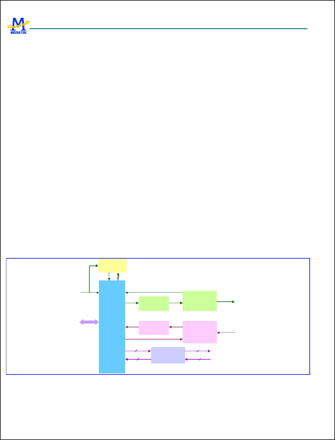
MT6217 GSM/GPRS Baseband Processor Data Sheet Revision 1.01
113/349 MediaTek Inc. Confidential
The UART has M16C450 and M16550A modes of operation, which are compatible with a range of standard software
drivers. The extensions have been designed to be broadly software compatible with 16550A variants, but there are some
areas where there is no consensus.
In common with the M16550A, the UART supports word lengths from five to eight bits, an optional parity bit and one or
two stop bits, and is fully programmable by an 8-bit CPU interface. A 16-bit programmable baud rate generator and an 8-bit
scratch register are included, together with separate transmit and receive FIFOs. Eight modem control lines and a diagnostic
loop-back mode are provided. The UART also includes two DMA handshake lines, which are used to indicate when the
FIFOs are ready to transfer data to the CPU. Interrupts can be generated from any of 10 sources.
Note: The UART has been designed so that all internal operations are synchronized by the CLK signal. This results in
minor timing differences between the UART and the industry standard 16550A device, which mean that the core is not
clock for clock identical to the original device.
After a hardware reset, the UART is in M16C450 mode. It can then have its FIFOs enabled and enter M16550A mode. The
UART then adds further functionality beyond M16550A mode. Each of the extended functions can be selected individually
under software control.
The UART provides more powerful enhancements than the industry-standard 16550:
l Hardware flow control. This is a very useful feature when the ISR latency is hard to predict and control in the
embedded applications. It relieves the MCU from having to fetch the received data within a fixed amount of time.
l Output of an IR-compatible electrical pulse with a width 3/16 of that of a regular bit period.
Note: In order to enable any of the enhancements, the Enhanced Mode bit, EFR[4], has to be set. If EFR[4] is not set, it is
not possible to write to IER[7:5], FCR[5:4], ISR[5:4] and MCR[7:6]. This is to ensure that the UART is backward
compatible for software that has been written for 16C450 and 16550A devices.
Figure 29 shows the block diagram of the 6217 UART device.
APB
BUS
I/F
Baud Rate
Generator
TX FIFO TX Machine
RX FIFO
Modem
Control
RX Machine
Modem Outputs
Modem Inputs
APB Bus
clock
divisor
uart_tx_data
uart_rx_data
baud
Figure 29 Block Diagram of UART
4.7.2 Register Definitions
n = 1, 2, 3; for uart1, uart2 and uart3 respectively.

MT6217 GSM/GPRS Baseband Processor Data Sheet Revision 1.01
114/349 MediaTek Inc. Confidential
UARTn+0000h RX Buffer Register UART_RBR
Bit 15 14 13 12 11 10 9 8 7 6 5 4 3 2 1 0
Name
RBR[7:0]
Type R
RBR RX Buffer Register. This is a read-only register. The received data can be read by accessing this register.
Modified when LCR[7] = 0.
UARTn+0000h TX Holding Register UART_THR
Bit 15 14 13 12 11 10 9 8 7 6 5 4 3 2 1 0
Name
THR[7:0]
Type W
THR TX Holding Register. This is a write-only register. The data to be transmitted is written to this register, and then
sent to PC via serial communication.
Modified when LCR[7] = 0.
UARTn+0004h Interrupt Enable Register UART_IER
Bit 15 14 13 12 11 10 9 8 7 6 5 4 3 2 1 0
Name
CTSI RTSI XOFFI
X EDSSI
ELSI ETBEI
ERBFI
Type R/W
Reset
0
IER By storing a ‘1’ to a specific bit position, the interrupt associated with that bit is enabled. Otherwise, the interrupt
is disabled.
IER[3:0] are modified when LCR[7] = 0.
IER[7:4] are modified when LCR[7] = 0 & EFR[4] = 1.
CTSI Masks an interrupt that is generated when a rising edge is detected on the CTS modem control line.
Note: This interrupt is only enabled when hardware flow control is enabled
0 Un-mask an interrupt that is generated when a rising edge is detected on the CTS modem control line.
1 Mask an interrupt that is generated when a rising edge is detected on the CTS modem control line.
RTSI Masks an interrupt that is generated when a rising edge is detected on the RTS modem control line.
Note: This interrupt is only enabled when hardware flow control is enabled
0 Un-mask an interrupt that is generated when a rising edge is detected on the RTS modem control line
1 Mask an interrupt that is generated when a rising edge is detected on the RTS modem control line.
XOFFI Masks an interrupt that is generated when an XOFF character is received.
Note: This interrupt is only enabled when software flow control is enabled
0 Un-mask an interrupt that is generated when an XOFF character is received.
1 Mask an interrupt that is generated when an XOFF character is received.
EDSSI When set ("1"), an interrupt is generated if DDCD, TERI, DDSR or DCTS (MSR[4:1]) becomes set.
0 No interrupt is generated if DDCD, TERI, DDSR or DCTS (MSR[4:1]) becomes set.
1 An interrupt is generated if DDCD, TERI, DDSR or DCTS (MSR[4:1]) becomes set.
ELSI When set ("1"), an interrupt is generated if BI, FE, PE or OE (LSR[4:1]) becomes set.
0 No interrupt is generated if BI, FE, PE or OE (LSR[4:1]) becomes set.
1 An interrupt is generated if BI, FE, PE or OE (LSR[4:1]) becomes set.
ETBEI When set ("1"), an interrupt is generated if the TX Holding Register is empty or the contents of the TX FIFO
have been reduced to its Trigger Level.
MT6217 GSM/GPRS Baseband Processor Data Sheet Revision 1.01
115/349 MediaTek Inc. Confidential
0 No interrupt is generated if the TX Holding Register is empty or the contents of the TX FIFO have been
reduced to its Trigger Level
1 An interrupt is generated if the TX Holding Register is empty or the contents of the TX FIFO have been
reduced to its Trigger Level
ERBFI When set ("1"), an interrupt is generated if the RX Buffer contains data.
0 No interrupt is generated if the RX Buffer contains data.
1 An interrupt is generated if the RX Buffer contains data.
UARTn+0008h Interrupt Identification Register UART_IIR
Bit 15 14 13 12 11 10 9 8 7 6 5 4 3 2 1 0
Name
FIFOE ID4 ID3 ID2 ID1 ID0 NINT
Type R
Reset
0 0 0 0 0 0 0 1
IIR Identify if there are pending interrupts; ID4 and ID3 will present only when EFR[4] = 1.
The following table gives the IIR[5:0] codes associated with the possible interrupts:
IIR[5:0]
Priority Level
Interrupt Source
00 0001 - No interrupt pending
000110 1 Line Status Interrupt BI, FE, PE or OE set in LSR
000100 2 RX Data Received RX Data received or RX Trigger Level reached.
001100 2 RX Data Timeout Timeout on character in RX FIFO.
000010 3 TX Holding Register Empty TX Holding Register empty or TX FIFO Trigger Level reached.
000000 4 Modem Status change DDCD, TERI, DDSR or DCTS set in MSR
010000 5 Software Flow Control XOFF Character received
100000 6 Hardware Flow Control CTS or RTS Rising Edge
Table 20 The IIR[5:0] codes associated with the possible interrupts
Line Status Interrupt: A RX Line Status Interrupt (IIR[5:0] == 000110b) is generated if ELSI (IER[2]) is set and any of BI,
FE, PE or OE (LSR[4:1]) becomes set. It ’s cleared by reading the Line Status Register.
RX Data Received Interrupt: A RX Received interrupt (IER[5:0] == 000100b) is generated if EFRBI (IER[0]) is set and
either RX Data is placed in the RX Buffer Register or the RX Trigger Level is reached. It ’s cleared by reading the RX
Buffer Register or the RX FIFO (if enabled).
RX Data Timeout Interrupt:
When virtual FIFO mode is disabled, RX Data Timeout Interrupt is generated if all the following apply:
1. There is at least one character in the FIFO
2. The most recent character was received longer than four character periods ago. (inclusive of all start, parity and stop
bits)
3. The most recent CPU read of the FIFO was longer than four character periods ago.
The timeout timer is restarted on receipt of a new bye from the RX Shift Register, or on a CPU read from the RX FIFO.
The RX Data Timeout Interrupt is enabled by setting EFRBI (IER[0]) to “1”, and it’s cleared by reading RX FIFO.
When virtual FIFO mode is enabled, RX Data Timeout Interrupt is generated if all the following apply:

MT6217 GSM/GPRS Baseband Processor Data Sheet Revision 1.01
116/349 MediaTek Inc. Confidential
1. There is no character in the FIFO
2. The most recent character was received longer than four character periods ago. (inclusive of all start, parity and stop
bits)
3. The most recent CPU read of the FIFO was longer than four character periods ago.
The timeout timer is restarted on receipt of a new byte from the RX Shift Register.
The RX Holding Register Empty Interrupt: A TX Holding Register Empty Interrupt (IIR[5:0] = 000010b) is generated if
ETRBI (IER[1]) is set and either the TX Holding Register or, if FIFOs are enabled, the TX FIFO becomes empty. It ’s
cleared by writing to the TX Holding Register or TX FIFO if FIFO enabled.
Modem Status Change Interrupt: A Modem Status Change Interrupt (IIR[5:0] = 000000b) is generated if EDSSI (IER[3]) is
set and either DDCD, TERI, DDSR or DCTS (MSR[3:0]) becomes set. It’s cleared by reading the Modem Status Register.
Software Flow Control Interrupt: A Software Flow Control Interrupt (IIR[5:0] = 010000b) is generated if Software Flow
Control is enabled and XOFFI (IER[5]) becomes set, indicating that an XOFF character has been received. It’s cleared by
reading the Interrupt Identification Register.
Hardware Flow Control Interrupt: A Hardware Flow Control Interrupt (IER[5:0] = 100000b) is generated if Hardware Flow
Control is enabled and either RTSI (IER[6]) or CTSI (IER[7]) becomes set indicating that a rising edge has been detected
on either the RTS/CTS Modem Control line. It ’s cleared by reading the Interrupt Identification Register.
UARTn+0008h FIFO Control Register UART_FCR
Bit 15 14 13 12 11 10 9 8 7 6 5 4 3 2 1 0
Name
RFTL1 RFTL0 TFTL1
TFTL0
DMA1 CLRT CLRR FIFOE
Type W
FCR FCR is used to control the trigger levels of the FIFOs, or flush the FIFOs.
FCR[7:6] is modified when LCR != BFh
FCR[5:4] is modified when LCR != BFh & EFR[4] = 1
FCR[4:0] is modified when LCR != BFh
FCR[7:6] RX FIFO trigger threshold
0 1
0 6
1 12
2 22
FCR[5:4] TX FIFO trigger threshold
0 1
1 4
2 8
3 14
DMA1 This bit determines the DMA mode, which the TXRDY and RXRDY pins support. TXRDY and RXRDY act to
support single-byte transfers between the UART and memory (DMA mode 0) or multiple byte transfers (DMA
mode1). Note that this bit has no effect unless the FIFOE bit is set as well
0 The device operates in DMA Mode 0.
1 The device operates in DMA Mode 1.

MT6217 GSM/GPRS Baseband Processor Data Sheet Revision 1.01
117/349 MediaTek Inc. Confidential
TXRDY – mode0: Goes active (low) when the TX FIFO or the TX Holding Register is empty. Becomes inactive
when a byte is written to the Transmit channel.
TXRDY – mode1: Goes active (low) when there are no characters in the TX FIFO. Becomes inactive when the TX
FIFO is full.
RXRDY – mode0: Becomes active (low) when there is at least one character in the RX FIFO or the RX Buffer
Register is full. It becomes inactive when there are no more characters in the RX FIFO or RX Buffer register.
RXRDY – mode1: Becomes active (low) when the RX FIFO Trigger Level reached or an RX FIFO Character
Timeout occurs. It goes inactive when the RX FIFO is empty.
CLRT Clear Transmit FIFO. This bit is self-clearing.
0 Leave TX FIFO intact.
1 Clear all the bytes in the TX FIFO.
CLRR Clear Receive FIFO. This bit is self-clearing.
0 Leave RX FIFO intact.
1 Clear all the bytes in the RX FIFO.
FIFOE FIFO Enabled. This bit must be a 1 for any of the other bits in the registers to have any effect.
0 Disable both the RX and TX FIFOs.
1 Enable both the RX and TX FIFOs.
UARTn+000Ch
Line Control Register UART_LCR
Bit 15 14 13 12 11 10 9 8 7 6 5 4 3 2 1 0
Name
DLAB SB SP EPS PEN STB WLS1
WLS0
Type R/W
Reset
0 0 0 0 0 0 0 0
LCR Line Control Register. Determine characteristics of serial communication signals
Modified when LCR[7] = 0.
DLAB Divisor Latch Access Bit.
0 The RX and TX Registers are read/written at Address 0 and the IER register is read/written at Address 4.
1 The Divisor Latch LS is read/written at Address 0 and the Divisor Latch MS is read/written at Address 4.
SB Set Break
0 No effect
1 SOUT signal is forced into the “0” state.
SP Stick Parity
0 No effect.
1 The Parity bit is forced into a defined state, dependent upon state of EPS and PEN:
If EPS = "1" & PEN = "1", the Parity bit is set and checked = "0".
If EPS = "0" & PEN = "1", the Parity bit is set and checked = "1".
EPS Even Parity Select
0 When EPS=”0”, an odd number of ones is sent and checked.
1 When EPS=”1”, an even number of ones is sent and checked.
PEN Parity Enable
0 The Parity is neither transmitted nor checked
1 The Parity is transmitted and checked.
STB Number of Stop Bits
0 One STOP bit is always added.

MT6217 GSM/GPRS Baseband Processor Data Sheet Revision 1.01
118/349 MediaTek Inc. Confidential
1 Two STOP bits are added after each character is sent; unless the character length is 5 when 1 STOP bit is
added.
WLS1, 0 Word Length Select.
0 5 bits.
1 6 bits
2 7 bits
3 8 bits
UARTn+0010h Modem Control Register UART_MCR
Bit 15 14 13 12 11 10 9 8 7 6 5 4 3 2 1 0
Name
XOFF
STAT
US
IR
ENAB
LE X LOOP
OUT2 OUT1 RTS DTR
Type R/W
Reset
0 0 0 0 0 0 0 0
MCR Modem Control Register. Control interface signals of the UART.
MCR[4:0] are modified when LCR[7] = 0,
MCR[7:6] are modified when LCR[7] = 0 & EFR[4] = 1.
XOFF Status This is a read-only bit.
0 When an XON character is received.
1 When an XOFF character is received.
IR Enable Enable IrDA modulation/demodulation.
0 Disable IrDA modulation/demodulation.
1 Enable IrDA modulation/demodulation.
LOOP Loop-back control bit
0 No loop-back is enabled
1 Loop-back mode is enabled
OUT2 Control the state of the output NOUT2, even in loop mode.
0 NOUT2=”1”.
1 NOUT2=”0”.
OUT1 Control the state of the output NOUT1, even in loop mode.
0 NOUT1=”1”.
1 NOUT1=”0”.
RTS Control the state of the output NRTS, even in loop mode.
0 NRTS=”1”.
1 NRTS=”0”.
DTR Control the state of the output NDTR, even in loop mode.
0 NDTR=”1”.
1 NDTR=”0”.
UARTn+0014h Line Status Register UART_LSR
Bit 15 14 13 12 11 10 9 8 7 6 5 4 3 2 1 0
Name
FIFOE
RR TEMT THRE BI FE PE OE DR
Type R/W
Reset
0 1 1 0 0 0 0 0

MT6217 GSM/GPRS Baseband Processor Data Sheet Revision 1.01
119/349 MediaTek Inc. Confidential
LSR Line Status Register.
Modified when LCR[7] = 0.
FIFOERR RX FIFO Error Indicator.
0 No PE, FE, BI set in the RX FIFO.
1 Set to 1 when there is at least one PE, FE or BI in the RX FIFO.
TEMT TX Holding Register (or TX FIFO) and the TX Shift Register are empty.
0 Empty conditions below are not met.
1 If FIFOs are enabled, the bit is set whenever the TX FIFO and the TX Shift Register are empty. If FIFOs are
disabled, the bit is set whenever TX Holding Register and TX Shift Register are empty.
THRE Indicate if there is room for TX Holding Register or TX FIFO is reduced to its Trigger Level.
0 When at least one byte is written to the TX FIFO or the TX Shift Register.
1 Set whenever the contents of the TX FIFO are reduced to its Trigger Level (FIFOs are enabled), or whenever
TX Holding Register is empty and ready to accept new data (FIFOs are disabled.)
BI Break Interrupt.
0 Reset by the CPU reading this register
1 If the FIFOs are disabled, this bit is set whenever the SIN is held in the 0 state for more than one transmission
time (START bit + DATA bits + PARITY + STOP bits).
If the FIFOs are enabled, this error is associated with a corresponding character in the FIFO and is flagged
when this byte is at the top of the FIFO. When a break occurs, only one zero character is loaded into the FIFO:
the next character transfer is enabled when SIN goes into the marking state and receives the next valid start bit.
FE Framing Error.
0 Reset by the CPU reading this register
1
If the FIFOs are disabled, this bit is set if the received data did not have a valid STOP bit. If the FIFOs are
enabled, the state of this bit is revealed when the byte it refers to is the next to be read.
PE Parity Error
0 Reset by the CPU reading this register
1
If the FIFOs are disabled, this bit is set if the received data did not have a valid parity bit. If the FIFOs are
enabled, the state of this bit is revealed when the byte it refers to is the next to be read.
OE Overrun Error
0 Reset by the CPU reading this register
1 If the FIFOs are disabled, this bit is set if the RX Buffer was not read by the CPU before new data from the
RX Shift Register overwrote the previous contents.
If the FIFOs are enabled, an overrun error occurs when the RX FIFO is full and the RX Shift Register becomes
full. OE is set as soon as this happens. The character in the Shift Register is then overwritten, but it is not
transferred to the FIFO.
DR Data Ready.
0 Cleared by the CPU reading the RX Buffer or by reading all the FIFO bytes.
1 Set by the RX Buffer becoming full or by a byte being transferred into the FIFO.
UARTn+0018h Modem Status Register UART_MSR
Bit 15 14 13 12 11 10 9 8 7 6 5 4 3 2 1 0
Name
DCD RI DSR CTS DDCD TERI DDSR
DCTS
Type R/W R/W R/W R/W R/W R/W R/W R/W
Reset
Input Input Input Input 0 0 0 0

MT6217 GSM/GPRS Baseband Processor Data Sheet Revision 1.01
120/349 MediaTek Inc. Confidential
Note: After reset, D4-D7 are inputs. A modem status interrupt can be cleared by writing ‘0’ or set by writing ‘1’ to this
register. D0-D3 can be written to.
Modified when LCR[7] = 0.
MSR Modem Status Register
DCD Data Carry Detect.
When Loop = "0", this is the complement of the NDCD input signal.
When Loop = "1", this is equal to the OUT2 bit in the Modem Control Register.
RI Ring Indicator.
When Loop = "0", this is the complement of the NRI input signal.
When Loop = "1", this is equal to the OUT1 bit in the Modem Control Register.
DSR Data Set Ready
When Loop = "0", this is the complement of the NDSR input signal.
When Loop = "1", this is equal to the DTR bit in the Modem Control Register.
CTS Clear To Send.
When Loop = "0", this is the complement of the NCTS input signal.
When Loop = "1", this is equal to the RTS bit in the Modem Control Register.
DDCD Delta Data Carry Detect.
0 The state of DCD has not changed since the Modem Status Register was last read
1 Set if the state of DCD has changed since the Modem Status Register was last read.
TERI Trailing Edge Ring Indicator
0 The NRI input does not change since this register was last read.
1 Set if the NRI input changes from “0” to “1” since this register was last read.
DDSR Delta Data Set Ready
0 Cleared if the state of DSR has not changed since this register was last read.
1 Set if the state of DSR has changed since this register was last read.
DCTS Delta Clear To Send
0 Cleared if the state of CTS has not changed since this register was last read.
1 Set if the state of CTS has changed since this register was last read.
UARTn+001Ch
Scratch Register UART_SCR
Bit 15 14 13 12 11 10 9 8 7 6 5 4 3 2 1 0
Name
SCR[7:0]
Type R/W
A general purpose read/write register. After reset, its value is un-defined.
Modified when LCR[7] = 0.
UARTn+0000h Divisor Latch (LS) UART_DLL
Bit 15 14 13 12 11 10 9 8 7 6 5 4 3 2 1 0
Name
DLL[7:0]
Type R/W
MT6217 GSM/GPRS Baseband Processor Data Sheet Revision 1.01
121/349 MediaTek Inc. Confidential
Reset
1
UARTn+0004h Divisor Latch (MS) UART_DLM
Bit 15 14 13 12 11 10 9 8 7 6 5 4 3 2 1 0
Name
DLL[7:0]
Type R/W
Reset
0
Note: DLL & DLM can only be updated if DLAB is set (“1”). Note too that division by 1 generates a BAUD signal that is
constantly high.
Modified when LCR[7] = 1.
The table below shows the divisor needed to generate a given baud rate from CLK inputs of 13, 26MHz and 52MHz. The
effective clock enable generated is 16 x the required baud rate.
BAUD 13MHz 26MHz 52MHz
110 7386 14773 29545
300 2708 5417 10833
1200 677 1354 2708
2400 338 677 1354
4800 169 339 677
9600 85 169 339
19200 42 85 169
38400 21 42 85
57600 14 28 56
115200 6 14 28
Table 2 Divisor needed to generate a given baud rate
UARTn+0008h Enhanced Feature Register UART_EFR
Bit 15 14 13 12 11 10 9 8 7 6 5 4 3 2 1 0
Name
AUTO
CTS AUTO
RTS D5 ENAB
LE -E SW FLOW CONT[3:0]
Type R/W R/W R/W R/W R/W
Reset
0 0 0 0 0
*NOTE: Only when LCR=BF’h
Auto CTS Enables hardware transmission flow control
0 Disabled.
1 Enabled.
Auto RTS Enables hardware reception flow control
0 Disabled.
1 Enabled.
Enable-E Enable enhancement features.
0 Disabled.
1 Enabled.
CONT[3:0] Software flow control bits.
MT6217 GSM/GPRS Baseband Processor Data Sheet Revision 1.01
122/349 MediaTek Inc. Confidential
00xx No TX Flow Control
10xx Transmit XON1/XOFF1 as flow control bytes
01xx Transmit XON2/XOFF2 as flow control bytes
11xx Transmit XON1 & XON2 and XOFF1 & XOFF2 as flow control words
xx00 No RX Flow Control
xx10 Receive XON1/XOFF1 as flow control bytes
xx01 Receive XON2/XOFF2 as flow control bytes
xx11 Receive XON1 & XON2 and XOFF1 & XOFF2 as flow control words
UARTn+0010h XON1 UART_XON1
Bit 15 14 13 12 11 10 9 8 7 6 5 4 3 2 1 0
Name
XON1[7:0]
Type R/W
Reset
0
UARTn+0014h XON2 UART_XON2
Bit 15 14 13 12 11 10 9 8 7 6 5 4 3 2 1 0
Name
XON2[7:0]
Type R/W
Reset
0
UARTn+0018h XOFF1 UART_XOFF1
Bit 15 14 13 12 11 10 9 8 7 6 5 4 3 2 1 0
Name
XOFF1[7:0]
Type R/W
Reset
0
UARTn+001Ch
XOFF2 UART_XOFF2
Bit 15 14 13 12 11 10 9 8 7 6 5 4 3 2 1 0
Name
XOFF2[7:0]
Type R/W
Reset
0
*Note: XON1, XON2, XOFF1, XOFF2 are valid only when LCR=BFh.
UARTn+0020h AUTOBAUD_EN AUTOBAUD_EN
Bit 15 14 13 12 11 10 9 8 7 6 5 4 3 2 1 0
Name
AUTO
_EN
Type R/W
Reset
0
AUTOBAUD_EN Auto-baud enable signal
0 Auto-baud function disable
1 Auto-baud function enable
UARTn+0024h HIGH SPEED UART HIGHSPEED
Bit 15 14 13 12 11 10 9 8 7 6 5 4 3 2 1 0
MT6217 GSM/GPRS Baseband Processor Data Sheet Revision 1.01
123/349 MediaTek Inc. Confidential
Name
SPEED [1:0]
Type R/W
Reset
0
SPEED UART sample counter base
0 bases on 16*baud_pulse, baud_rate = system clock frequency/16/{DLH, DLL}
1 bases on 8*baud_pulse, baud_rate = system clock frequency/8/{DLH, DLL}
2 bases on 4*baud_pulse, baud_rate = system clock frequency/4/{DLH, DLL}
3 bases on sampe_count * baud_pulse, baud_rate = system clock frequency / sampe_count
The table below shows the divisor needed to generate a given baud rate from CLK inputs of 13MHz bases on different
HIGHSPEED value.
BAUD HIGHSPEED = 0 HIGHSPEED = 1 HIGHSPEED = 2
110 7386 14773 29545
300 2708 7386 14773
1200 677 2708 7386
2400 338 677 2708
4800 169 338 677
9600 85 169 338
19200 42 85 169
38400 21 42 85
57600 14 21 42
115200 7 14 21
230400 * 7 14
460800 * * 7
921600 * * *
Table 21 Divisor needed to generate a given baud rate from 13MHz based on different HIGHSPEED value
The table below shows the divisor needed to generate a given baud rate from CLK inputs of 26MHz bases on different
HIGHSPEED value.
BAUD HIGHSPEED =
HIGHSPEED =
HIGHSPEED =
110 14773 29545 59091
300 5417 14773 29545
1200 1354 5417 14773
2400 677 1354 5417
4800 339 677 1354
9600 169 339 667
19200 85 169 339
38400 42 85 169
57600 28 42 85
MT6217 GSM/GPRS Baseband Processor Data Sheet Revision 1.01
124/349 MediaTek Inc. Confidential
115200
14
28
42
230400
7 14 28
460800
* 7 14
921600
* * 7
Table 22 Divisor needed to generate a given baud rate from 26MHz based on different HIGHSPEED value
The table below shows the divisor needed to generate a given baud rate from CLK inputs of 52MHz bases on different
HIGHSPEED value.
BAUD
HIGHSPEED =
HIGHSPEED =
HIGHSPEED =
110 29545 59091 118182
300 10833 29545 59091
1200 2708 10833 29545
2400 1354 2708 10833
4800 677 1354 2708
9600 339 677 1354
19200 169 339 677
38400 85 169 339
57600 56 85 169
115200
28 56 85
230400
14 28 56
460800
7 14 28
921600
* 7 14
Table 4 Divisor needed to generate a given baud rate from 52MHz based on different HIGHSPEED value
UARTn+0028h SAMPLE_COUNT SAMPLE_COUN
T
Bit 15 14 13 12 11 10 9 8 7 6 5 4 3 2 1 0
Name
SAMPLECOUNT [7:0]
Type R/W
Reset
0
When HIGHSPEED=3, the sample_count is the threshold value for UART sample counter
(sample_num).
UARTn+002Ch
SAMPLE_POINT SAMPLE_POINT
Bit 15 14 13 12 11 10 9 8 7 6 5 4 3 2 1 0
Name
SAMPLEPOINT [7:0]
Type R/W
Reset
ffh
When HIGHSPEED=3, UART gets the input data when sample_count=sample_num.
MT6217 GSM/GPRS Baseband Processor Data Sheet Revision 1.01
125/349 MediaTek Inc. Confidential
e.g . system clock = 13MHz, 921600 = 13000000 / 14
sample_count = 14 and sample point = 7 (sample the central point to decrease the inaccuracy)
UARTn+0030h AUTOBAUD_REG AUTOBAUD_RE
G
Bit 15 14 13 12 11 10 9 8 7 6 5 4 3 2 1 0
Name
BAUD_STAT[3:0] BAUDRATE[3:0]
Type R R
Reset
0 0
BAUD_RATE Autobaud baud rate
0 115200
1 57600
2 38400
3 19200
4 9600
5 4800
6 2400
7 1200
8 300
9 110
BAUDSTAT Autobaud format
0 Autobaud is detecting
1 AT_7N1
2 AT_7O1
3 AT_7E1
4 AT_8N1
5 AT_8O1
6 AT_8E1
7 at_7N1
8 at_7E1
9 at_7O1
10 at_8N1
11 at_8E1
12 at_8O1
13 Autobaud detection fails
UARTn+0038h AUTOBAUDSAMPLE AUTOBAUDSAM
PLE
Bit 15 14 13 12 11 10 9 8 7 6 5 4 3 2 1 0
Name
AUTOBAUDSAMPLE
Type R/W R/W R/W R/W R/W R/W R/W
Reset
dh
Since the system clock may changes, autobaud sample duration should changes as system clock
MT6217 GSM/GPRS Baseband Processor Data Sheet Revision 1.01
126/349 MediaTek Inc. Confidential
changes. When system clock = 13MHz, autobaudsample = 6; when system clock = 26MHz,
autobaudsample = 13.
UARTn+003Ch
Guard time added register GUARD
Bit 15 14 13 12 11 10 9 8 7 6 5 4 3 2 1 0
Name
GUARD_
EN GUARD_CNT[3:0]
Type R/W R/W R/W R/W R/W
Reset
0 0 0 0 0
GUARD_CNT Guard interval count value. Guard interval = (1/(system clock / 16 / div )) * GUARD_CNT.
GUARD_EN Guard interval add enable signal
0 No guard interval added
1 Add guard interval after stop bit
UARTn+0040h Escape character register ESCAPE_DAT
Bit 15 14 13 12 11 10 9 8 7 6 5 4 3 2 1 0
Name
ESCAPE_DAT[7:0]
Type R/W
Reset
FFh
ESCAPE_DAT Escape character added before software flow control data and escape character, i.e. if tx data is xon (31h),
with esc_en =1, uart will transmit data as esc + CEh (~xon).
UARTn+0044h Escape enable register ESCAPE_EN
Bit 15 14 13 12 11 10 9 8 7 6 5 4 3 2 1 0
Name
ESC_E
N
Type R/W
Reset
0
ESC_EN Add escape character in transmitter and remove escape character in receiver by UART.
0 Don’t deal with the escape character
1 Add escape character in transmitter and remove escape character in receiver
UARTn+0048h Sleep enable register SLEEP_EN
Bit 15 14 13 12 11 10 9 8 7 6 5 4 3 2 1 0
Name
SELL
P_EN
Type R/W
Reset
0
SLEEP_EN For sleep mode issue
0 Don’t deal with sleep mode indicate signal
1 To activate hardware flow control or software control according to software initial setting when chip enter
sleep mode. Releasing hardware flow when chip wakes up; but for software control, uart will send xon when
wakes up and FIFO doesn’t reach threshold level.
UARTn+004Ch
Virtual FIFO enable register VFIFO_EN
Bit 15 14 13 12 11 10 9 8 7 6 5 4 3 2 1 0
MT6217 GSM/GPRS Baseband Processor Data Sheet Revision 1.01
127/349 MediaTek Inc. Confidential
Name
VFIFO
_EN
Type R/W
Reset
0
VFIFO_EN Virtual FIFO mechanism enable signal
0 Disable VFIFO mode
1 Enable VFIFO mode. When virtual mode is enabled, the flow control will base on DMA threshold, and will
generate timeout interrupt for DMA.
4.8 IrDA Framer
4.8.1 General Description
IrDA framer, which is depicted as Figure 30, is implemented to reduce the CPU loading for IrDA transmission. IrDA
framer functional block can be divided into two parts: one is the transmitting part; the other is the receiving part. In the
transmitter, it will perform BOFs addition, byte stuffing, the addition of 16-bits FCS and EOF appendence. In the receiving
part, it will execute BOFs removing, ESC character remove, CRC checking and EOF detection. Besides, the framer will
perform 3/16 modulator and demodulator to connect to the IR transceiver. The transmitter and receiver all need DMA
channel.
IrDA_TX
IrDA_RX
IrDA_TX_FIFO
IrDA_RX_FIFO
IrDA_TX_FIFO_CTRL
IrDA_RX_FIFO_CTRL
3/16 mod
3/16 demod
Figure 30 IrDA framer functional block
4.8.2 Register Definitions
IRDA+0000h TX BUF and RX BUF BUF
Bit 15 14 13 12 11 10 9 8 7 6 5 4 3 2 1 0
Name
BUF[7:0]
Type R/W
Reset
0
BUF IrDA Framer transmit or receive data
IRDA+0004h TX BUF and RX BUF clear signal BUF_CLEAR
Bit 15 14 13 12 11 10 9 8 7 6 5 4 3 2 1 0
Name
CLEAR
Type R/W
MT6217 GSM/GPRS Baseband Processor Data Sheet Revision 1.01
128/349 MediaTek Inc. Confidential
Reset
0
CLEAR When CLEAR=1, the FIFO will be cleared
IRDA+0008h Maximum Turn Around Time MAX_T
Bit 15 14 13 12 11 10 9 8 7 6 5 4 3 2 1 0
Name
MAX_T [13:0]
Type R/W
Reset
3E80h
MAX_T Maximum turn around time is the maximum time that a station can hold the P/F bit. This parameter along with the
baud rate parameter dictates the maximum number of bytes that a station can transmit before giving the line to
another station by transmitting a frame with the P/F bit. This parameter is used by one station to indicate the
maximum time the other station can send before it must turn the link around. 500ms is the only valid value when
the baud ra te is less than 115200kbps. The default value is 500ms.
IRDA+000Ch Minimum Turn Around Time MIN_T
Bit 15 14 13 12 11 10 9 8 7 6 5 4 3 2 1 0
Name
MIN_T [15:0]
Type R/W
Reset
FDE8h
MIN_T Minimum turn around time, the default value is 10ms. The minimum turn around time parameter deals with the
time needed for a receiver to recover following saturation by transmission from the same device. This parameter
corresponds to the required time delay between the last byte of the last frame sent by a station and the point at
which it is ready to receive the first byte of a frame from another station, i.e. it is the latency for transmits
complete to ready for receiving.
IRDA+0010h Number of additional BOFs prefixed to the beginning
of a frame BOFS
Bit 15 14 13 12 11 10 9 8 7 6 5 4 3 2 1 0
Name
TYPE BOFS [6:0]
Type R/W R/W
Reset
0 1011b
BOFs Additional BOFs number; the additional BOFs parameter indicates the number of additional flags needed at the
beginning of every frame. The main purpose of the addition of additional BOFs is to provide a delay at the
beginning of each frame for device with long interrupt latency.
TYPE Additional BOFs type
1 BOF = C0h
0 BOF = FFh
IRDA+0014h Baud rate divisor DIV
Bit 15 14 13 12 11 10 9 8 7 6 5 4 3 2 1 0
Name
DIV[15:0]
Type R/W
Reset
55h
DIV Transmit or receive rate divider. Rate = System clock frequency / DIV/ 16; the default value = ‘h55 when in
contention mode.
MT6217 GSM/GPRS Baseband Processor Data Sheet Revision 1.01
129/349 MediaTek Inc. Confidential
IRDA+0018h Transmit frame size TX_FRAME_SIZ
E
Bit 15 14 13 12 11 10 9 8 7 6 5 4 3 2 1 0
Name
TX_FRAME_SIZE[11:0]
Type R/W
Reset
40h
TX_FRAME_SIZE Transmit frame size; the default value = 64 when in contention mode.
IRDA+001Ch Receiving frame1 size RX_FRAME1_SI
ZE
Bit 15 14 13 12 11 10 9 8 7 6 5 4 3 2 1 0
Name
RX_FRAME1_SIZE[11:0]
Type R
Reset
0
RX_FRAME1_SIZE The actual number of receiving frame 1 size.
IRDA+0020h Transmit abort indication ABORT
Bit 15 14 13 12 11 10 9 8 7 6 5 4 3 2 1 0
Name
ABOR
T
Type R/W
Reset
0
ABORT When set 1, the framer will transmit abort sequence and closes the frame without an FCS field or an ending flag.
IRDA+0024h IrDA framer transmit enable signal TX_EN
Bit 15 14 13 12 11 10 9 8 7 6 5 4 3 2 1 0
Name
TX_ON
E
TXINVE
RT MODE
TX_E
N
Type R/W R/W R/W R/W
Reset
0 0 0 0
TX_EN Transmit enable
MODE Modulation type selection
0 3/16 modulation
1 1.61us
TXINVERT Invert transmit signal
0 transmit signal isn’t inverted.
1 inverts transmit signal.
TX_ONE: Control the tranmit enable signal is one hot or not
0 tx_en won’t be de-asserted until software programs.
1 tx_en will be de-asserted (i.e. transmit disable) automatically after one frame has been send.
IRDA+0028h IrDA framer receive enable signal RX_EN
Bit 15 14 13 12 11 10 9 8 7 6 5 4 3 2 1 0
Name
RX_ON
E
RXINVE
RT
RX_E
N
Type R/W R/W R/W
MT6217 GSM/GPRS Baseband Processor Data Sheet Revision 1.01
130/349 MediaTek Inc. Confidential
Reset
0 0 0
RX_EN Receive enable
RXINVERT Invert receive signal
0 receive signal isn’t inverted
1 inverts receive signal
RX_ONE Disable receive when get one frame
0 rx_en won’t be de-asserted until software programs.
1 rx_en will be de-asserted (i.e. transmit disable) automatically after one frame has been send.
IRDA+002Ch FIFO trigger level indication TRIGGER
Bit 15 14 13 12 11 10 9 8 7 6 5 4 3 2 1 0
Name
RX_TRIG[ TX_TRIG
Type R/W R/W
Reset
0 0
TX_TRIG The tx FIFO interrupt trigger threshold
00 0 byte
01 1 byte
02 2 byte
RX_TRIG The rx FIFO interrupt trigger threshold
00 1 byte
01 2 byte
02 3 byte
IRDA+0030h IRQ enable signal IRQ_ENABLE
Bit 15 14 13 12 11 10 9 8 7 6 5 4 3 2 1 0
Name
2NDR
X_CO
MP
RXRES
TART
THRES
HTIME
OUT
FIFOTI
MEOU
T
TXABO
RT
RXABO
RT
MAXTI
MEOU
T
MINTI
MEOU
T
RXCO
MPLET
E
TXCO
MPLET
E
STATU
S RXTRI
G TXTRI
G
Type R/W R/W R/W R/W R/W R/W R/W R/W R/W R/W R/W R/W
Reset
0 0 0 0 0 0 0 0 0 0 0 0
IRQ_ENABLE Interrupt enable signal
0 disable
1 enable
TXTRIG Transmit data reaches the threshold level
0 No interrupt is generated
1 Interrupt is generated when transmit FIFO size reaches threshold
RXTRIG Receive data reaches the threshold level
0 No interrupt is generated
1 Interrupt is generated when receive FIFO size reaches threshold
STATUS Any status lists as following has happened
(overrun, size_error)
0 No interrupt is generated
1 Interrupt is generated when one of the statuses occurred
TXCOMPLETE Transmit one frame completely
0 No interrupt is generated

MT6217 GSM/GPRS Baseband Processor Data Sheet Revision 1.01
131/349 MediaTek Inc. Confidential
1 Interrupt is generated when transmitting one frame completely
RXCOMPLETE Receive one frame completely
0 No interrupt is generated
1 Interrupt is generated when receiving one frame completely
MINTIMEOUT Minimum time timeout
0 No interrupt is generated
1 Interrupt is generated when minimum timer is timed out
MAXTIMEOUT Maximum time timeout
0 No interrupt is generated
1 Interrupt is generated when maximum timer is timed out
RXABORT Receiving aborting frame
0 No interrupt is generated
1 Interrupt is generated when receiving aborting frame
TXABORT Transmitting aborting frame
0 No interrupt is generated
1 Interrupt is generated when transmitting aborting frame
FIFOTIMEOUT FIFO timeout
0 No interrupt is generated
1 Interrupt is generated when FIFO timeout
THRESHTIMEOUT Threshold time timeout
0 No interrupt is generated
1 Interrupt is generated when threshold timer is timed out
RXRESTART Receiving a new frame before one frame is received completely
0 No interrupt is generated
1 Interrupt is generated when receiving a new frame before one frame is received completely
2NDRX_COMP Receiving second frame and get P/F bit
0 No interrupt is generated
1 Interrupt is generated when receiving second frame and get P/F bit completely
IRDA+0034h Interrupt Status IRQ_STA
Bit 15 14 13 12 11 10 9 8 7 6 5 4 3 2 1 0
Name
2NDR
X_CO
MP
RXRES
TART
THRES
HTIME
OUT
FIFOTI
MEOU
T
TXABO
RT
RXABO
RT
MAXTI
MEOU
T
MINTI
MEOU
T
RXCO
MPLET
E
TXCO
MPLET
E
STATU
S RXFIF
O TXFIF
O
Type RC RC RC RC RC RC RC RC RC RC RC RC RC
Reset
0 0 0 0 0 0 0 0 0 0 0 0 0
TXFIFO Transmit FIFO reaches threshold
RXFIFO Receive FIFO reaches threshold
ERROR generated when one of the statuses occurred
(data_error, PF_detect, fifo_hold1, fifo_empty, crc_fail, frame_error, overrun, size_error)
TXCOMPLETE Transmitting one frame completely
RXCOMPLETE Receiving one frame completely
MINTIMEOUT Minimum turn around time timeout
MAXTIMEOUT Maximum turn around time timeout
RXABORT Receiving aborting frame
MT6217 GSM/GPRS Baseband Processor Data Sheet Revision 1.01
132/349 MediaTek Inc. Confidential
TXABORT Transmitting aborting frame
FIFOTIMEOUT FIFO is timeout
THRESHTIMEOUT Threshold time timeout
RXRESTART Receiving a new frame before one frame is received completely
2NDRX_COMP Receiving second frame and get P/F bit completely
IRDA+0038h STATUS register STATUS
Bit 15 14 13 12 11 10 9 8 7 6 5 4 3 2 1 0
Name
FIFOHO
LD1
FIFO
EMPTY OVER
RUN RXSIZ
E
Type R/W R/W R/W R/W
Reset
0 0 0 0
RXSIZE Receive frame size error
OVERRUN Frame over run
FIFOEMPTY FIFO empty
FIFOHOLD1 FIFO holds one
IRDA+003Ch Transceiver power on/off control
TRANSCEIVER_
PDN
Bit 15 14 13 12 11 10 9 8 7 6 5 4 3 2 1 0
Name
TRANS_
PDN
Type R/W
Reset
1
Transceiver_PDN Power on/off control for external IrDA transceiver
IRDA+0040h Maximum number of receiving frame size RX_FRAME_MA
X
Bit 15 14 13 12 11 10 9 8 7 6 5 4 3 2 1 0
Name
MAX_RX_FRAME_SIZE_
Type R/W
Reset
0
RX_FRAME_MAX Receive frame max size, when actual receiving frame size is larger than rx_frame_max, RXSIZE is
asserted.
IRDA+0044h Threshold Time THRESH_T
Bit 15 14 13 12 11 10 9 8 7 6 5 4 3 2 1 0
Name
DISCONNECT_TIME[15:0 ]
Type R/W
Reset
bb8h
THRESHOLD TIME Threshold time; it ’s used to control the time a station will wait without receiving valid frame before
it disconnects the link. Associated with this is the time a station will wait without receiving valid frames before it
will send a status indication to the service user layer.
MT6217 GSM/GPRS Baseband Processor Data Sheet Revision 1.01
133/349 MediaTek Inc. Confidential
IRDA+0048h Counter enable signal COUNT_ENABL
E
Bit 15 14 13 12 11 10 9 8 7 6 5 4 3 2 1 0
Name
THRESH
_EN
MIN_E
N MAX_E
N
Type R/W R/W R/W
Reset
0 0 0
COUNT_ENABLE Counter enable signals
IRDA+004Ch Indication of system clock rate CLOCK_RATE
Bit 15 14 13 12 11 10 9 8 7 6 5 4 3 2 1 0
Name
CLOCK_RAT
E
Type R/W
Reset
0
CLOCK_RATE Indication of the system clock rate
0 26MHz
1 52MHz
2 13MHz
IRDA+0050h System Clock Rate Fix RATE_FIX
Bit 15 14 13 12 11 10 9 8 7 6 5 4 3 2 1 0
Name
RATE
_FIX
Type R/W
Reset
0
RATE_FIX Fix irda framer sample base clock rate as 13MHz
0 clock rate base on clock_rate selection
1 13MHz
IRDA+0054h RX Frame1 Status FRAME1_STAT
US
Bit 15 14 13 12 11 10 9 8 7 6 5 4 3 2 1 0
Name
UNKNOW
_ERROR
PF_DETE
CT
CRC_FAI
L
FRAME_
ERROR
Type R/W R/W R/W R/W
Reset
0 0 0 0
FRAME_ERROR Framing error, i.e. stop bit = 0
0 No framing error
1 Framing error occurred
CRC_FAIL CRC check fail
0 CRC check successfully
1 CRC check fail
PF_DETECT P/F bit detect
0 No a P/F bit frame
1 Detect P/F bit in this frame
MT6217 GSM/GPRS Baseband Processor Data Sheet Revision 1.01
134/349 MediaTek Inc. Confidential
UNKNOWN_ERROR Receiving error data i.e. escape character is followed by a character that it’s not a esc, bof, eof
character.
0 Data receiving correctly e
1 Unknown error occurred
IRDA+0058h RX Frame2 Status FRAME2_STAT
US
Bit 15 14 13 12 11 10 9 8 7 6 5 4 3 2 1 0
Name
UNKNOW
_ERROR
PF_DETE
CT
CRC_FAI
L
FRAME_
ERROR
Type R/W R/W R/W R/W
Reset
0 0 0 0
FRAME_ERROR Framing error, i.e. stop bit = 0
0 No framing error
1 Framing error occurred
CRC_FAIL CRC check fail
0 CRC check successfully
1 CRC check fail
PF_DETECT P/F bit detect
0 No a P/F bit frame
1 Detect P/F bit in this frame
UNKNOWN_ERROR Receiving error data i.e. escape character is followed by a character that it’s not a esc, bof, eof
character.
0 Data receiving correctly
1 Unknown error occurred
IRDA+005Ch Receiving frame2 size RX_FRAME2_SI
ZE
Bit 15 14 13 12 11 10 9 8 7 6 5 4 3 2 1 0
Name
RX_FRAME2_SIZE[11:0]
Type R
Reset
0
RX_FRAME2_SIZE The actual number of receiving frame 2 size.
4.9 Real Time Clock
4.9.1 General Description
The Real Time Clock (RTC) module provides time and data information. It works on the 32.768KHz oscillator with
independent power supply. When the MS is powered off, a dedicated regulator is used to supply the RTC block. If the main
battery is not present, the backup supply such as a small mercury cell battery or a large capacitor is used. In addition to
provide timing data, alarm interrupt is generated and it can be used to power up the base-band core through the
BBWAKEUP pin. Also, regulator interrupts corresponding to the seconds; minutes, hours and days can be generated
whenever the time counter value reaches a maximum. The year span is supported up to 2127. The ma ximum day of month
values are stored in the RTC block, which depend on the leap year condition.

MT6217 GSM/GPRS Baseband Processor Data Sheet Revision 1.01
135/349 MediaTek Inc. Confidential
4.9.2 Register Definitions
RTC+0000h Baseband power up RTC_BBPU
Bit 15 14 13 12 11 10 9 8 7 6 5 4 3 2 1 0
Name
KEY_BBPU AUTO
BBPU
WRITE_E
N
PWRE
N
Type W R/W R/W R/W R/W
KEY_BBPU Bus write acceptable only when KEY_BBPU = 0x43
AUTO If BBWAKEUP will be low state when SYSRST# high to low
0 BBWAKEUP won’t be low state when SYSRST# high to low automatically
1 BBWAKEUP will be low state when SYSRST# high to low automatically
BBPU Controls the power of PMIC, when powerkey1=A357h & powerkey2=67D2h it will be the value programmed by
software or it will be low if above situation is not true.
0 Power down
1 Power on
WRITE_EN When WRITE_EN is written as 0 by software program, the rtc write interface will be disabled until another
system power on.
PWREN
0 RTC alarm has no action on power switch
1 When RTC alarm occurs, BBPU will be assigned as 1, then system power on by rtc alarm wakeup.
RTC+0004h RTC IRQ status RTC_IRQ_STA
Bit 15 14 13 12 11 10 9 8 7 6 5 4 3 2 1 0
Name
TCST
A ALST
A
Type R/C R/C
ALSTA This register indicates IRQ occurred due to alarm condition met
0 IRQ occurred for alarm condition met
1 No IRQ occurred for alarm condition met
TCSTA This register indicates IRQ occurred due to tick condition met
0 IRQ occurred for tick condition met
1 No IRQ occurred for tick condition met
RTC+0008h RTC IRQ enable RTC_IRQ_EN
Bit 15 14 13 12 11 10 9 8 7 6 5 4 3 2 1 0
Name
ONESH
OT
TC_E
N AL_E
N
Type R/W R/W R/W
ONESHOT Controls automatic reset of AL_EN & TC_EN
AL_EN This register indicates the control bit for IRQ generation due to alarm condition met
0 Disable IRQ generation due to alarm condition met
1 Enable the alarm time match interrupt. Clear it when ONESHOT is high upon generation of the corresponding
IRQ
TC_EN This register indicates the control bit for IRQ generation due to tick condition met
0 Disable IRQ generation due to tick condition met

MT6217 GSM/GPRS Baseband Processor Data Sheet Revision 1.01
136/349 MediaTek Inc. Confidential
1 Enable the tick time match interrupt. Clear it when ONESHOT is high upon generation of the corresponding
IRQ
RTC+000Ch Counter increment IRQ enable RTC_CII_EN
Bit 15 14 13 12 11 10 9 8 7 6 5 4 3 2 1 0
Name
1/8SEC
CII
1/4SEC
CII
1/2SEC
CII
YEACI
I MTHC
II DOW
CII DOMC
II HOUC
II MINCII
SECC
II
Type R/W R/W R/W R/W R/W R/W R/W R/W R/W R/W
This register activates or de-activates the IRQ generation when the TC counter reaches its maximum value.
SECCII Set this bit to 1 to activate the IRQ at each second update
MINCII Set the bit to 1 to activate the IRQ at each minute update
HOUCII Set the bit to 1 to activate the IRQ at each hour update
DOMCII Set the bit to 1 to activate the IRQ at each day of month update
DOWCII Set the bit to 1 to activate the IRQ at each day of week update
MTHCII Set the bit to 1 to activate the IRQ at each month update
YEACII Set the bit to 1 to activate the IRQ at each year update
1/2SECCII Set the bit to 1 to activate the IRQ at each one-half update
1/4SECCII Set the bit to 1 to activate the IRQ at each one-fourth update
1/8SECCII Set the bit to 1 to activate the IRQ at each one-eighth update
RTC+0010h RTC alarm mask RTC_AL_MASK
Bit 15 14 13 12 11 10 9 8 7 6 5 4 3 2 1 0
Name
YEA_M
SK
MTH_M
SK
DOW_M
SK
DOM_M
SK
HOU_M
SK
MIN_MS
K
SEC_M
SK
Type R/W R/W R/W R/W R/W R/W R/W
The alarm condition for alarm IRQ generation is according to each bit in this register is masked or not.
SEC_MSK
0 Condition (RTC_TC_SEC = RTC_AL_SEC) is checked to generate the alarm signal
1 Condition (RTC_TC_SEC = RTC_AL_SEC) is masked, i.e. the value of RTC_TC_SEC won’t affect the alarm
IRQ generation
MIN_MSK
0 Condition (RTC_TC_MIN = RTC_AL_MIN) is checked to generate the alarm signal
1 Condition (RTC_TC_MIN = RTC_AL_MIN) is masked, i.e. the value of RTC_TC_MIN won’t affect the
alarm IRQ generation
HOU_MSK
0 Condition (RTC_TC_HOU = RTC_AL_HOU) is checked to generate the alarm signal
1 Condition (RTC_TC_HOU = RTC_AL_HOU) is masked, i.e. the value of RTC_TC_HOU won’t affect the
alarm IRQ generation
DOM_MSK
0 Condition (RTC_TC_DOM = RTC_AL_DOM) is checked to generate the alarm signal
1 Condition (RTC_TC_DOM = RTC_AL_DOM) is masked, i.e. the value of RTC_TC_DOM won’t affect the
alarm IRQ generation
DOW_MSK
0 Condition (RTC_TC_DOW = RTC_AL_DOW) is checked to generate the alarm signal
MT6217 GSM/GPRS Baseband Processor Data Sheet Revision 1.01
137/349 MediaTek Inc. Confidential
1 Condition (RTC_TC_DOW = RTC_AL_DOW) is masked, i.e. the value of RTC_TC_DOW won’t affect the
alarm IRQ generation
MTH_MSK
0 Condition (RTC_TC_MTH = RT C_AL_MTH) is checked to generate the alarm signal
1 Condition (RTC_TC_MTH = RTC_AL_MTH) is masked, i.e. the value of RTC_TC_MTH won’t affect the
alarm IRQ generation
YEA_MSK
0 Condition (RTC_TC_YEA = RTC_AL_YEA) is checked to generate the alarm signal
1 Condition (RTC_TC_YEA = RTC_AL_YEA) is masked, i.e. the value of RTC_TC_YEA won’t affect the
alarm IRQ generation
RTC+0014h RTC seconds time counter register RTC_TC_SEC
Bit 15 14 13 12 11 10 9 8 7 6 5 4 3 2 1 0
Name
TC_SECOND
Type R/W
TC_SECOND The time counter second initial value. The range of its value is: 0-59.
RTC+0018h RTC minutes time counter register RTC_TC_MIN
Bit 15 14 13 12 11 10 9 8 7 6 5 4 3 2 1 0
Name
TC_MINUTE
Type R/W
TC_MINUTE The time counter minute initial value. The range of its value is: 0-59.
RTC+001Ch RTC hours time counter register RTC_TC_HOU
Bit 15 14 13 12 11 10 9 8 7 6 5 4 3 2 1 0
Name
TC_HOUR
Type R/W
TC_HOUR The time counter hour initial value. The range of its value is: 0-23.
RTC+0x0020 RTC day of month time counter register RTC_TC_DOM
Bit 15 14 13 12 11 10 9 8 7 6 5 4 3 2 1 0
Name
TC_DOM
Type R/W
TC_DOM The time counter day of month initial value. The day of month maximum value depends on the leap year
condition, i.e. 2 LSB of year time counter are zeros.
RTC+0x0024 RTC day of week time counter register RTC_TC_DOW
Bit 15 14 13 12 11 10 9 8 7 6 5 4 3 2 1 0
Name
TC_DOW
Type R/W
TC_DOW The time counter day of week initial value. The range of its value is: 1-7.
RTC+0x0028 RTC month time counter register RTC_TC_MTH
Bit 15 14 13 12 11 10 9 8 7 6 5 4 3 2 1 0
Name
TC_MONTH
MT6217 GSM/GPRS Baseband Processor Data Sheet Revision 1.01
138/349 MediaTek Inc. Confidential
Type R/W
TC_MONTH The time counter month initial value. The range of its value is: 1-12.
RTC+0x002C RTC year time counter register RTC_TC_YEA
Bit 15 14 13 12 11 10 9 8 7 6 5 4 3 2 1 0
Name
AL_SEC OND
Type R/W
TC_YEAR The time counter year initial value. The range of its value is: 0-127. (2000-2127)
RTC+0x0030 RTC second alarm setting register RTC_AL_SEC
Bit 15 14 13 12 11 10 9 8 7 6 5 4 3 2 1 0
Name
AL_SECOND
Type R/W
AL_SECOND The second value of the alarm counter setting. The range of its value is: 0-59.
RTC+0x0034 RTC minute alarm setting register RTC_AL_MIN
Bit 15 14 13 12 11 10 9 8 7 6 5 4 3 2 1 0
Name
AL_MINUTE
Type R/W
AL_MINUTE The minute value of the alarm counter setting. The range of its value is: 0-59.
RTC+0x0038 RTC hour alarm setting register RTC_AL_HOU
Bit 15 14 13 12 11 10 9 8 7 6 5 4 3 2 1 0
Name
AL_HOUR
Typ e R/W
AL_HOUR The hour value of the alarm counter setting. The range of its value is: 0-23.
RTC+0x003C RTC day of month alarm setting register RTC_AL_DOM
Bit 15 14 13 12 11 10 9 8 7 6 5 4 3 2 1 0
Name
AL_DOM
Type R/W
AL_DOM The day of month value of the alarm counter setting. The day of month maximum value depends on the leap
year condition, i.e. 2 LSB of year time counter are zeros.
RTC+0x0040 RTC day of week alarm setting register RTC_AL_DOW
Bit 15 14 13 12 11 10 9 8 7 6 5 4 3 2 1 0
Name
AL_DOW
Type R/W
AL_DOW The day of week value of the alarm counter setting. The range of its value is: 1-7.
RTC+0x0044 RTC month alarm setting register RTC_AL_MTH
Bit 15 14 13 12 11 10 9 8 7 6 5 4 3 2 1 0
Name
AL_MONTH
Type R/W
AL_MONTH The month value of the alarm counter setting. The range of its value is: 1-12.
MT6217 GSM/GPRS Baseband Processor Data Sheet Revision 1.01
139/349 MediaTek Inc. Confidential
RTC+0x0048 RTC year alarm setting register RTC_AL_YEA
Bit 15 14 13 12 11 10 9 8 7 6 5 4 3 2 1 0
Name
AL_YEAR
Type R/W
AL_YEAR The year value of the alarm counter setting. The range of its value is: 0-127. (2000 -2127)
RTC+0x004C XOSC bias current control register RTC_XOSCCALI
Bit 15 14 13 12 11 10 9 8 7 6 5 4 3 2 1 0
Name
XOSCCALI
Type W
XOSCCALI This register controls the XOSC32 bias current. Before the first program by software, the XOSCCALI
value is 11111b.
RTC+0050h RTC_POWERKEY1 register RTC_POWERKE
Y1
Bit 15 14 13 12 11 10 9 8 7 6 5 4 3 2 1 0
Name
RTC_POWERKEY1
Type R/W
RTC+0054h RTC_POWERKEY2 register RTC_POWERKE
Y2
Bit 15 14 13 12 11 10 9 8 7 6 5 4 3 2 1 0
Name
RTC_POWERKEY2
Type R/W
These register sets are used to determine that if the real time clock has been programmed by software; i.e. the time value in
real time clock is correct. When the real time clock first power on, the register contents are all in a mass, therefore the time
values shown are incorrect. Software needs to know if the real time clock has been programmed. Hence, these two registers
are defined for first power-on issue. After software programs the correct value, these two register sets don’t need to be
updated. In addition to program the correct time value, when contents of these register sets are wrong, the interrupt won’t
be generated; therefore, the real time clock won’t generate the interrupts before software programs it. Unwanted interrupt
due to wrong time value won’t occur. The destined values of these two register sets are:
RTC_POWERKEY1 A357h
RTC_POWERKEY2 67D2h
RTC+0058h PDN1 RTC_PDN1
Bit 15 14 13 12 11 10 9 8 7 6 5 4 3 2 1 0
Name
RTC_PDN1[7:0]
Type R/W
RTC_PDN1[3:1] is for reset de-bounce mechanism.
0 2ms
1 8ms
2 32ms
3 128ms

MT6217 GSM/GPRS Baseband Processor Data Sheet Revision 1.01
140/349 MediaTek Inc. Confidential
4 256ms
5 512ms
6 1024ms
7 2048ms
RTC_PDN1[7:4] & RTC_PDN1[0] is the spare register for software to keep some power on and power off state
information.
RTC+005Ch PDN2 RTC_PDN2
Bit 15 14 13 12 11 10 9 8 7 6 5 4 3 2 1 0
Name
RTC_PDN2[7:0]
Type R/W
RTC_PDN2 The spare register for software to keep some power on and power off state information.
4.10 Auxiliary ADC Unit
The auxiliary ADC unit is used to monitor the status of battery and charger, identify the plugged peripheral, and perform
temperature measurement. There provides 7 input channels for diversified application in this unit.
There provides 2 modes of operation: immediate mode and timer-triggered mode. The mode of each channel can be
individually selected through register AUXADC_CON0. For example, if the flag SYN0 in the register AUXADC_CON0 is
set, the channel 0 will be set in timer-triggered mode. Otherwise, it’s in immediate mode.
In immediate mode, the A/D converter will sample the value once only when the flag in the register AUXADC_CON1 has
been set. For example, if the flag IMM0 in the register AUXADC_CON1 is set, the A/D converter will sample the data for
channel 0. The IMM flags should be cleared and set again to initialize another sampling.
The value sampled for the channel 0 will be stored in register AUXADC_DAT0, the value for the channel 1 will be stored
in register AUXADC_DAT1, and vice versa.
If the AUTOSET flag in the register AUXADC_CON3 is set, the auto-sample function is enabled. The A/D converter will
sample the data for the channel in which the corresponding data register has been read. For example, in case the SYN1 flag
is not set, the AUTOSET flag is set, when the data register AUXADC_DAT0 has been read, the A/D converter will sample
the next value for the channel 1 immediately.
If multiple channels are selected at the same time, the task will be performed sequentially on every selected channel. For
example, if we set AUXADC_CON1 to be 0x7f, that is, all 7 channels are selected, the state machine in the unit will start
sampling from channel 6 to channel 0, and save the values of each input channel in the respective registers. The same
process also applies in the timer-triggered mode.
In timer-triggered mode, the A/D converter will sample the value for the channels in which the corresponding SYN flags
are set when the TDMA timer counts to the value specified in the register TDMA_AUXEV1, which is placed in the TDMA
timer. For example, if we set AUXADC_CON0 to be 0x7f, all 7 channels are selected to be in timer-triggered mode. The
state machine will make sampling for all 7 channels sequentially and save the values in registers from AUXADC_DAT0 to
AUXADC_DAT6, as it does in immediate mode.
There provides a dedicated timer-triggered scheme for channel 0. The scheme is enabled by setting the SYN7 flag in the
register AUXADC_CON2. The timing offset for this event is stored in the register TDMA_AUXEV0 in the TDMA timer.
MT6217 GSM/GPRS Baseband Processor Data Sheet Revision 1.01
141/349 MediaTek Inc. Confidential
The sampled data triggered by this specific event is stored in the register AUXADC_DAT7. It’s used to separate the results
of two individual software routines that perform action on the auxiliary ADC unit.
The AUTOCLRn in the register AUXADC_CON3 is set when it’s intended to sample only once after setting
timer-triggered mode. If AUTOCLR1 flag has been set, after the data for the channels in timer-triggered mode has been
stored, the SYNn flags in the register AUXADC_CON0 will be cleared. Instead, if AUTOCLR0 flag has been set, after the
data for the channel 0 has been stored in the register AUXADC_DAT7, the SYN7 flag in the register AUXADC_CON2 will
be cleared.
The usage of the immediate mode and timer-triggered mode are mutual exclusive in terms of individual channel.
The PUWAIT_EN bit in the registers AUXADC_CON3 is used to power up the analog port in advance. That ensures that
the power has ramped up to the stable state before A/D converter starts the conversion. The analog part will be
automatically powered down after the conversion is completed.
4.10.1 Register Definitions
AUXADC+0000
h Auxiliary ADC control register 0 AUXADC_CON0
Bit 15 14 13 12 11 10 9 8 7 6 5 4 3 2 1 0
Name
SYN6 SYN5 SYN4 SYN3 SYN2 SYN1 SYN0
Type R/W R/W R/W R/W R/W R/W R/W
Reset
0 0 0 0 0 0 0
SYNn Those 7 bits define whether the corresponding channel is to be sampled or not in timer-triggered mode. It’s
associated with timing offset register TDMA_AUXEV1 . It’s supported to set multiple flags. The flags can be
automatically clearly after those channel have been sampled if AUTOCLR1 in the register AUXADC_CON3 is
set.
0 The channel is not selected.
1 The channel is selected.
AUXADC+0004
h Auxiliary ADC control register 1 AUXADC_CON1
Bit 15 14 13 12 11 10 9 8 7 6 5 4 3 2 1 0
Name
IMM6 IMM5 IMM4 IMM3 IMM2 IMM1 IMM0
Type R/W R/W R/W R/W R/W R/W R/W
Reset
0 0 0 0 0 0 0
IMMn Those 7 bits are set individually to sample the data for the corresponding channel. It’s supported to set multiple
flags.
0 The channel is not selected.
1 The channel is selected.
AUXADC+0008
h Auxiliary ADC control register 2 AUXADC_CON2
Bit 15 14 13 12 11 10 9 8 7 6 5 4 3 2 1 0
Name
SYN7
Type R/W
Reset
0

MT6217 GSM/GPRS Baseband Processor Data Sheet Revision 1.01
142/349 MediaTek Inc. Confidential
SYN7 This bit is used only for channel 0 and to be associated with timing offset register TDMA_AUXEV0 in the TDMA
timer in timer-triggered mode. The flag can be automatically clearly after channel 0 have been sampled if
AUTOCLR0 in the register AUXADC_CON3 is set.
0 The channel is not selected.
1 The channel is selected.
AUXADC+000
Ch Auxiliary ADC control register 3 AUXADC_CON3
Bit 15 14 13 12 11 10 9 8 7 6 5 4 3 2 1 0
Name
AUTO
SET PUWA
IT_EN
AUTO
CLR1 AUTO
CLR0 STA
Type R/W R/W R/W R/W RO
Reset
0 0 0 0 0
AUTOSET The field defines the auto-sample mode of the module. In auto-sample mode, each channel with its sample
register being read can start sampling immediately without configuring the control register AUXADC_CON1
again.
PUWAIT_EN The field enables the power warm-up period to ensure power stability before the SAR process take place.
It ’s recommended to activate.
0 The mode is not enabled.
1 The mode is enabled.
AUTOCLR1 The field defines the auto-clear mode of the module for event 1. In auto-clear mode, each timer-triggered
channel get the samples of the specified channels once after the SYNn bit in the register AUXADC_CON0 have
been set. The SYNn bits will be automatically be cleared and the channel will not being enabled again by the timer
event except the SYNn flags are set again.
0 The automatic clear mode is not enabled.
1 The automatic clear mode is enabled.
AUTOCLR0 The field defines the auto-clear mode of the module for event 0. In auto-clear mode, the timer-triggered
channel 0 get the sample once after the SYN7 bit in the register AUXADC_CON2 have been set. The SYN7 bit
will be automatically cleared and the channel will not be enabled again by the timer event 0 except the SYN7 flag
is set again.
0 The automatic clear mode is not enabled.
1 The automatic clear mode is enabled.
STA The field defines the state of the module.
0 This module is idle.
1 This module is operating.
AUXADC+0010
h Auxiliary ADC channel 0 register AUXADC_DAT0
Bit 15 14 13 12 11 10 9 8 7 6 5 4 3 2 1 0
Name
DAT
Type RO
Reset
0
The register stores the sampled data for the channel 0. There are 8 registers of the same type for the corresponding channel.
The overall register definition is listed in Table 23.

MT6217 GSM/GPRS Baseband Processor Data Sheet Revision 1.01
143/349 MediaTek Inc. Confidential
Register Address Register Function Acronym
AUXADC+0010h Auxiliary ADC channel 0 data register AUXADC_DAT0
AUXADC+0014h Auxiliary ADC channel 1 data register AUXADC_DAT1
AUXADC+0018h Auxiliary ADC channel 2 data register AUXADC_DAT2
AUXADC+001Ch Auxiliary ADC channel 3 data register AUXADC_DAT3
AUXADC+0020h Auxiliary ADC channel 4 data register AUXADC_DAT4
AUXADC+0024h Auxiliary ADC channel 5 data register AUXADC_DAT5
AUXADC+0028h Auxiliary ADC channel 6 data register AUXADC_DAT6
AUXADC+002Ch Auxiliary ADC channel 0 data register for TDMA event 0 AUXADC_DAT7
Table 23 Auxiliary ADC data register list
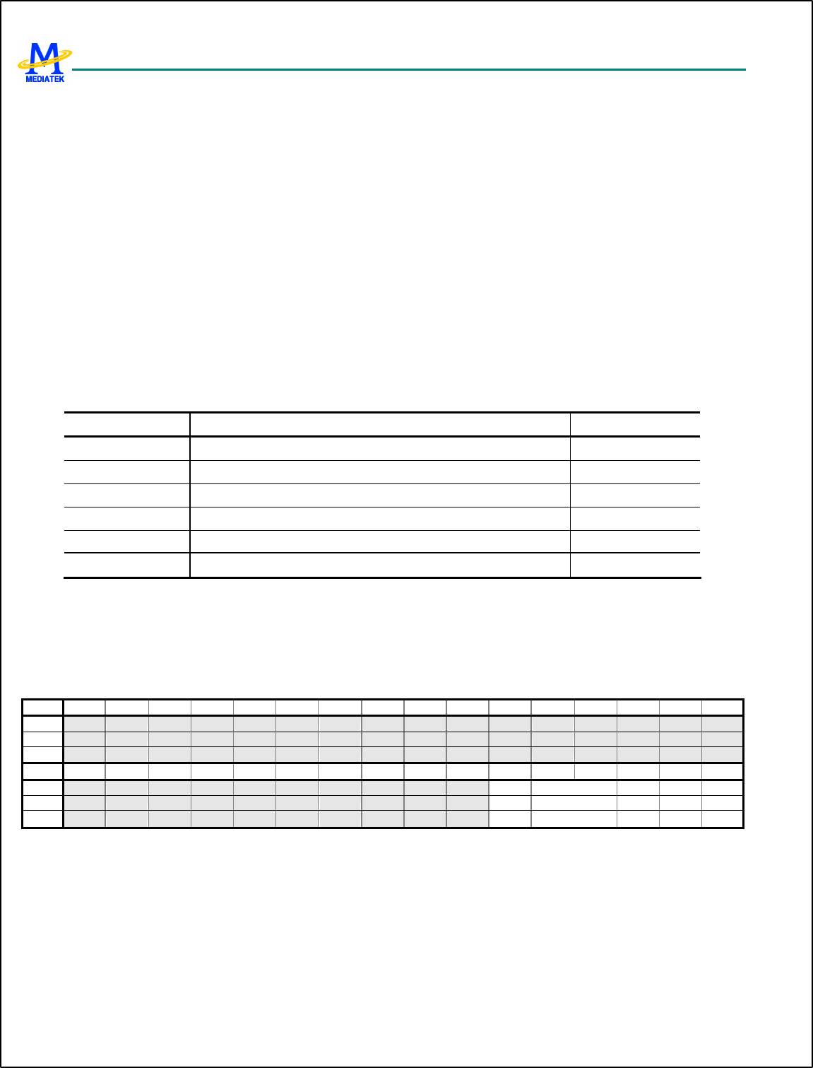
MT6217 GSM/GPRS Baseband Processor Data Sheet Revision 1.01
144/349 MediaTek Inc. Confidential
5 Microcontroller Coprocessors
Microcontroller Coprocessors are designed to run computing-intensive processes in place of Microcontroller (MCU). Those
coprocessors intend to offer a solution special for timing critical GSM/GPRS Modem processes that require fast response
and massive data movement. Controls to the coprocessors are all through memory access by way of APB Bus.
5.1 GPRS Cipher Unit
5.1.1 General Description
The unit implements the GPRS encryption/decryption scheme that accelerates the computation of encryption and
decryption GPRS pattern. The block accelerates the computation of the key stream. However the bit-wise
encryption/decryption of the data is still done by the MCU.
Both GEA and GEA2 are supported.
Register Address Register Function Acronym
GCU+0000h GPRS Encryption Algorithm Control Register GCU_CON
GCU+0004h GPRS Encryption Algorithm Status Register GCU_SAT
GCU+0008h GPRS Secret Key Kc 0 Register GCU_SKEY0
GCU+000Ch GPRS Secret Key Kc 1 Register GCU_SKEY1
GCU+0010h GPRS Message Key Register GCU_MKEY
GCU+0014h GPRS Ciphered Data Register GCU_CDATA
Table 24 GCU Registers
5.1.2 Register Definitions
GCU+0000h GPRS Encryption Algorithm Control Register GCU_CON
Bit 31 30 29 28 27 26 25 24 23 22 21 20 19 18 17 16
Name
Type
Reset
Bit 15 14 13 12 11 10 9 8 7 6 5 4 3 2 1 0
Name
RBO KS SINIT DIR GEA2
Type R/W R/W WO R/W R/W
Reset
0 10 0 0 0
This register controls the key generation function of the GPRS Encryption Algorithm.
GEA2 Choose the encryption/decryption scheme. 1 = GEA2, while 0 = GEA.
DIR The DIRECTION input of the GPRS Encryption Algorithm.
SINIT Start initialization. The MCU writes 1 to start initialization. The bit is always read at 0.
KS Control the read access. 00 = byte access, 01 = half word (16 bits) access, 10 = word access, 11 reserved. Default
value is 10.
MT6217 GSM/GPRS Baseband Processor Data Sheet Revision 1.01
145/349 MediaTek Inc. Confidential
RBO Reversal Byte Order bit. If the bit was set to 1, the byte order of GCU_SKEY0, GCU_SKEY1, GCU_MKEY in
write operation and GCU_SKEY0, GCU_SKEY1, GCU_MKEY, GCU_CDATA in read operation would be the
reverse of baseband processor, and if the bit was 0, the behavior would be the same as baseband processor.
Byte-order of GCU_CON and GCU_SAT is not affected. The default value is 0 which is different from that in
MT6217.
GCU+0004h GPRS Encryption Algorithm Status Register GCU_SAT
Bit 31 30 29 28 27 26 25 24 23 22 21 20 19 18 17 16
Name
Type
Reset
Bit 15 14 13 12 11 10 9 8 7 6 5 4 3 2 1 0
Name
STAT KEY_
COM INIT
Type RO RO RO
Reset
110 0 0
This register shows the status of the GPRS Encryption unit.
INIT Initialization flag. 1 = the GCU is currently performing the initialization phase.
KEY_COM Key-stream computation. 1 = the GCU is computing new key stream, while 0 = a new key is available or the
GCU is in initialization phase.
STAT The state of GCU core. For debug purpose.
GCU+0008h GPRS Secret Key Kc 0 Register GCU_SKEY0
Bit 31 30 29 28 27 26 25 24 23 22 21 20 19 18 17 16
Name
KC[31:16]
Typ e R/W
Reset
0
Bit 15 14 13 12 11 10 9 8 7 6 5 4 3 2 1 0
Name
KC[15:0]
Type R/W
Reset
0
GCU+000Ch GPRS Secret Key Kc 1 Register GCU_SKEY1
Bit 31 30 29 28 27 26 25 24 23 22 21 20 19 18 17 16
Name
KC[63:48]
Type R/W
Reset
0
Bit 15 14 13 12 11 10 9 8 7 6 5 4 3 2 1 0
Name
KC[47:32]
Type R/W
Reset
0
This set of registers shall be programmed with the GPRS Encryption Algorithm secret key.
GCU+0010h GPRS Message Key Register GCU_MKEY
Bit 31 30 29 28 27 26 25 24 23 22 21 20 19 18 17 16
Name
MKEY[31:16]
Type R/W
Reset
0
Bit 15 14 13 12 11 10 9 8 7 6 5 4 3 2 1 0
MT6217 GSM/GPRS Baseband Processor Data Sheet Revision 1.01
146/349 MediaTek Inc. Confidential
Name
MKEY[15:0]
Type R/W
Reset
0
This register shall be programmed with the “message key” for the GPRS Encryption Algorithm.
GCU+0014h GPRS Ciphered DATA Register GCU_CDATA
Bit 31 30 29 28 27 26 25 24 23 22 21 20 19 18 17 16
Name
CDATA[31:16]
Type RO
Bit 15 14 13 12 11 10 9 8 7 6 5 4 3 2 1 0
Name
CDATA[15:0]
Type RO
The register contains the key stream. GCU will continue to generate next word of key while current word of key is
removed.
5.2 Divider
To ease the processing load of MCU, a divider is employed here. The divider can operate signed and unsigned 32bit/32bit
division, as well as modulus. The processing time of the divider is from 1 clock cycle to 33 clock cycles, which depends
upon the magnitude of the value of the dividend. The detailed processing time is listed below in Table 7. From the table we
can see that there are two kind of processing time (except for when the dividend is zero) in an item. Which kind depends on
whether there is the need for restoration at the last step of the division operation.
After the divider is started by setting START to “1” in Divider Control Register, DIV_RDY will go low, and it will be
asserted after the division process is finished. MCU could detect this status bit by polling it to know the correct access
timing. In order to simplify polling, only the value of register DIV_RDY will appear while Divider Control Register is read.
Hence, MCU does not need to mask other bits to extract the value of DIV_RDY.
In GSM/GPRS system, many divisions are executed with some constant divisors. Therefore, some often-used constants are
stored in the divider to speed up the process. By controlling control bits IS_CNST and CNST_IDX in Divider Control
register, one can start a division without giving a divisor. This could save the time for writing divisor in and the instruction
fetch time , and thus make the process more efficient.
Signed Division Unsigned Division
Dividend Clock Cycles Dividend Clock Cycles
0000_0000h 1 0000_0000h 1
0000_00ffh – (-0000_0100h),
excluding 0x0000_0000
8 or 9 0000_0001h - 0000_00ffh 8 or 9
0000_ffffh – (-0001_0000h)
16 or 17 0000_0100h - 0000_ffffh 16 or 17
00ff_ffffh – (-0100_0000h)
24 or 25 0001_0000h - 00ff_ffffh 24 or 25
7fff_ffffh – (-8000_0000h)
32 or 33 0100_0000h - ffff_ffffh 32 or 33
Table 25 Processing time in different value of dividend.
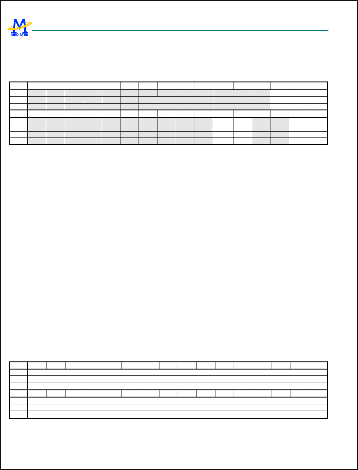
MT6217 GSM/GPRS Baseband Processor Data Sheet Revision 1.01
147/349 MediaTek Inc. Confidential
5.2.1 Register Definitions
DIVIDER+0000
h Divider Control Register DIV_CON
Bit 31 30 29 28 27 26 25 24 23 22 21 20 19 18 17 16
Name
CNST_IDX
Type WO
Reset
0
Bit 15 14 13 12 11 10 9 8 7 6 5 4 3 2 1 0
Name
IN_CN
ST SIGN DIV_R
DY STAR
T
Type WO WO RO WO
Reset
0 1 1 0
START To start division. It will return to 0 after division has started.
DIV_RDY Current status of divider. Note that when DIV_ CON register is read, only the value of DIV_RDY will appear.
That means program does not need to mask other part of the register to extract the information of DIV_RDY.
0 division is in progress.
1 division is finished.
SIGN To indicate signed or unsigned division.
0 Unsigned division.
1 Signed division.
IS_CNST To indicate if internal constant value should be used as a divis or. If IS_CNST is enabled, User does not need
to write the value of the divisor, and divider will automatically use the internal constant value instead. What
value divider will use depends on the value of CNST_IDX.
0 Normal division. Divisor is written in via APB
1 Using internal constant divisor instead.
CNST_IDX Index of constant divisor.
0 divisor = 13
1 divisor = 26
2 divisor = 51
3 divisor = 52
4 divisor = 102
5 divisor = 104
DIVIDER
+0004h Divider Dividend register DIV_DIVIDEND
Bit 31 30 29 28 27 26 25 24 23 22 21 20 19 18 17 16
Name
DIVIDEND[31:16]
Type WO
Reset
0
Bit 15 14 13 12 11 10 9 8 7 6 5 4 3 2 1 0
Name
DIVIDEND[15:0]
Type WO
Reset
0
Dividend.
MT6217 GSM/GPRS Baseband Processor Data Sheet Revision 1.01
148/349 MediaTek Inc. Confidential
DIVIDER
+0008h Divider Divisor register DIV_DIVISOR
Bit 31 30 29 28 27 26 25 24 23 22 21 20 19 18 17 16
Name
DIVISOR[31:16]
Type WO
Reset
0
Bit 15 14 13 12 11 10 9 8 7 6 5 4 3 2 1 0
Name
DIVISOR[15:0]
Type WO
Reset
0
Divisor.
DIVIDER
+000Ch Divider Quotient register DIV_QUOTIENT
Bit 31 30 29 28 27 26 25 24 23 22 21 20 19 18 17 16
Name
QUOTIENT[31:16]
Type RO
Reset
0
Bit 15 14 13 12 11 10 9 8 7 6 5 4 3 2 1 0
Name
QUOTIENT[15:0]
Type RO
Reset
0
Quotient.
DIVIDER
+0010h Divider Remainder register DIV_REMAINDE
R
Bit 31 30 29 28 27 26 25 24 23 22 21 20 19 18 17 16
Name
REMAINDER[31:16]
Type RO
Reset
0
Bit 15 14 13 12 11 10 9 8 7 6 5 4 3 2 1 0
Name
REMAINDER[15:0]
Type RO
Reset
0
Remainder.
5.3 CSD Accelerator
5.3.1 General Description
This unit performs the data format conversion of RA0 RA1 and FAX in CSD service. CSD service comprises two major
functions, data flow throttling and data format conversion. The data format conversion is a bit -wise operation and takes a
number of instructions to complete a conversion. Therefore it’s not efficient to do by MCU self. A coprocessor, CSD
accelerator, is designed here to reduce the computing power need by performing this function.
What CSD accelerator do is just help to convert data format, and the function of data flow throttling is still implemented by
MCU. Basically, CSD accelerator performs three types of data format conversion, RA0, RA1 and FAX.
MT6217 GSM/GPRS Baseband Processor Data Sheet Revision 1.01
149/349 MediaTek Inc. Confidential
For RA0 conversion, only uplink RA0 data format conversion is provided here. That’s because there are too many
judgments on downlink path conversion, and this will greatly increase area cost. Uplink RA0 conversion is to insert one
start bit and one stop bit before and after a byte respectively during 16 bytes. Figure 31 illustrates the detailed conversion
table.
RA0 converter can only process RA0 data state by state. Before filling in new data, software must make sure the converted
data of certain state is withdrawn, or the converted data will be replaced by the new data. For example, if 32-bit data in
written, and then state pointer goes from state 0 to state 1, and word ready of state 0 is asserted. Before writing next 32-bit
data, the word of state 0 should be withdrawn first, or the data will lose.
RA0 records the number of written bytes, state pointer, and ready state word. The information can help software to do flow
control. See Register Definition for the detail.
Data bits Stop bitStart bit
State 0
State 1
State 2
State 3
State 4
Figure 31 data format conversion of RA0
For RA1 conversion, both directions, downlink and uplink, are supported. The data formats vary in different data rate. The
detailed conversion table is shown in Figure 32 and Figure 33. The yellow part is the payload data, and the blue part is
status bit.
MT6217 GSM/GPRS Baseband Processor Data Sheet Revision 1.01
150/349 MediaTek Inc. Confidential
D1 D2 D3 D4 D5 D6 S1
D7 D8 D9 D10 D11 D12 X
D13 D14 D15 D16 D17 D18 S3
D19 D20 D21 D22 D23 D24 S4
E4 E5 E6 E7 D25 D26 D27
D28 D29 D30 S6 D31 D32 D33
D34 D35 D36 XD37 D38 D39
D40 D41 D42 S8 D43 D44 D45
D46 D47 D48 S9
Bit 0
Bit 59
Bit 6
Figure 32 data format conversion for 6k/12k RA1
Figure 33 data format conversion for 3.6k RA1
For FAX, two types of bit -reversal functions are provided. One is bit-wise reversal, and the other is byte-wise reversal,
which are illustrated in Figure 34 and Figure 35 respectively.
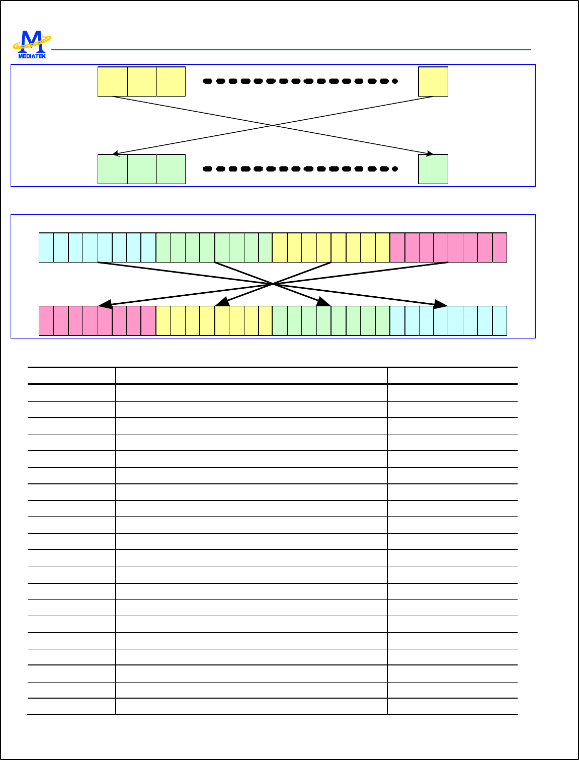
MT6217 GSM/GPRS Baseband Processor Data Sheet Revision 1.01
151/349 MediaTek Inc. Confidential
b31 b30 b29 b0
b0 b1 b2 b31
Figure 34 Type 1 bit reverse
b31 b0b7b15b23
b0b7 b15 b8 b23 b16 b31 b24
Figure 35 Type 2 bit reverse
Register Address Register Function Acronym
CSD + 0000h CSD RA0 Control Register CSD_RA0_CON
CSD + 0004h CSD RA0 Status Register CSD_RA0_STA
CSD + 0008h CSD RA0 Input Data Register CSD_RA0_DI
CSD + 000Ch CSD RA0 Output Data Register CSD_RA0_DO
CSD + 0100h CSD RA1 6K/12K Uplink Input Data Register 0 CSD_RA1_6_12K_ULDI0
CSD + 0104h CSD RA1 6K/12K Uplink Input Data Register 1 CSD_RA1_6_12K_ULDI1
CSD + 0108h CSD RA1 6K/12K Uplink Status Data Register CSD_RA1_6_12K_ULSTUS
CSD + 010Ch CSD RA1 6K/12K Uplink Output Data Register 0 CSD_RA1_6_12K_ULDO0
CSD + 0110h CSD RA1 6K/12K Uplink Output Data Register 1 CSD_RA1_6_12K_ULDO1
CSD + 0200h CSD RA1 6K/12K Downlink Input Data Register 0 CSD_RA1_6_12K_DLDI0
CSD + 0204h CSD RA1 6K/12K Downlink Input Data Register 1 CSD_RA1_6_12K_DLDI1
CSD + 0208h CSD RA1 6K/12K Downlink Output Data Register 0 CSD_RA1_6_12K_DLDO0
CSD + 020Ch CSD RA1 6K/12K Downlink Output Data Register 1 CSD_RA1_6_12K_DLDO1
CSD + 0210h CSD RA1 6K/12K Downlink Status Data Register CSD_RA1_6_12K_DLSTUS
CSD + 0300h CSD RA13.6K Uplink Input Data Register 0 CSD_RA1_3P6K_ULDI0
CSD + 0304h CSD RA13.6K Uplink Status Data Register CSD_RA1_3P6K_ULSTUS
CSD + 0308h CSD RA13.6K Uplink Output Data Register 0 CSD_RA1_3P6K_ULDO0
CSD + 030Ch CSD RA13.6K Uplink Output Data Register 1 CSD_RA1_3P6K_ULDO1
CSD + 0400h CSD RA1 3.6K Downlink Input Data Register 0 CSD_RA1_3P6K_DLDI0
CSD + 0404h CSD RA1 3.6K Downlink Input Data Register 1 CSD_RA1_3P6K_DLDI1
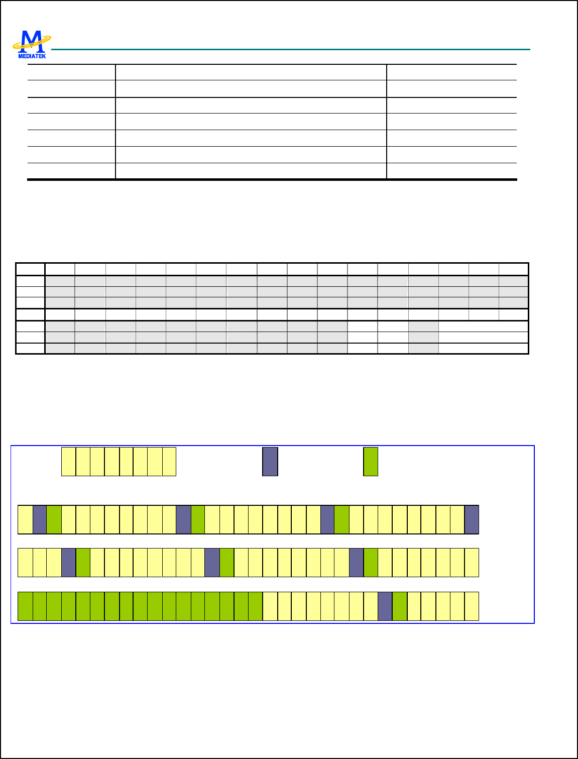
MT6217 GSM/GPRS Baseband Processor Data Sheet Revision 1.01
152/349 MediaTek Inc. Confidential
CSD + 0408h CSD RA1 3.6K Downlink Output Data Register 0 CSD_RA1_3P6K_DLDO0
CSD + 040Ch CSD RA1 3.6K Downlink Status Data Register CSD_RA1_3P6K_DLSTUS
CSD + 0500h CSD FAX Bit Reverse Type 1 Input Data Register CSD_FAX_BR1_DI
CSD + 0504h CSD FAX Bit Reverse Type 1 Output Data Register CSD_FAX_BR1_DO
CSD + 0510h CSD FAX Bit Reverse Type 2 Input Data Register CSD_FAX_BR2_DI
CSD + 0514h CSD FAX Bit Reverse Type 2 Output Data Register CSD_FAX_BR2_DO
Table 26 CSD Accelerater Registers
5.3.2 Register Definitions
CSD+0000h CSD RA0 Control Register CSD_RA0_CON
Bit 31 30 29 28 27 26 25 24 23 22 21 20 19 18 17 16
Name
Type
Reset
Bit 15 14 13 12 11 10 9 8 7 6 5 4 3 2 1 0
Name
RST BTS0 VLD_BYTE
Type WO WO R/W
Reset
0 0 100
VLD_BYTE Specify how many valid bytes of current input data. It must be specified before filling data in.
BTS0 Back to state 0. Force RA0 converter go back to state 0. Incomplete word will be padded by STOP bit. For
instance, back-to-state0 command is issued after 8 byte data are filled in. Then these bit after the 8
th byte will be
padded with stop bits, and RDYWD2 is asserted. After removing state word 2, the state pointer goes back to state
0. Note that new data filling should take place after removing state word 2, or the state pointer may be out of order.
Data bits Stop bitStart bit
State 0
State 1
State 2
Figure 36 Example of Back to state 0
RST Reset RA0 converter. In case, erroneously operation makes data disordered. This bit can restore all state to original
state.
MT6217 GSM/GPRS Baseband Processor Data Sheet Revision 1.01
153/349 MediaTek Inc. Confidential
CSD+0004h CSD RA0 Status Register CSD_RA0_STA
Bit 31 30 29 28 27 26 25 24 23 22 21 20 19 18 17 16
Name
Type
Reset
Bit 15 14 13 12 11 10 9 8 7 6 5 4 3 2 1 0
Name
BYTECNT CRTSTA RDYWD
Type R/W R/W RC
Reset
0 0 0
RDYWD0~4 Ready word. To indicate which state word is ready for withdrawal. Data should be withdrawn before next
data filling into CSD_RA0_DI, if there are any bits asserted.
0 Not ready
1 Ready
CRTSTA current state. State0 ~ state4. To indicate which state word software is filling in.
BYTECNT The total number of bytes software filling in.
CSD+0008h CSD RA0 Input Data Register CSD_RA0_DI
Bit 31 30 29 28 27 26 25 24 23 22 21 20 19 18 17 16
Name
DIN
Type R/W
Reset
0
Bit 15 14 13 12 11 10 9 8 7 6 5 4 3 2 1 0
Name
DIN
Type R/W
Reset
0
DIN The RA0 convert input data. Ready word indicator shall be check before filling in data. If there are any words
ready, withdraw them first, or the ready data in RA0 converter will be replaced.
CSD+000Ch CSD RA0 Output Data Register CSD_RA0_DO
Bit 31 30 29 28 27 26 25 24 23 22 21 20 19 18 17 16
Name
DOUT
Type R/W
Reset
0
Bit 15 14 13 12 11 10 9 8 7 6 5 4 3 2 1 0
Name
DOUT
Type R/W
Reset
0
DOUT RA0 converted data. The return data is corresponding to the ready word indicator defined in CSD_RA0_STA
register. The five bit of RDYWD map to state0 ~ state 4 accordingly. When CSD_RA0_DO is read, the asserted
state word will be returned. If there are two state words asserted at the same time, the lower one will be returned.
CSD+0100h CSD RA1 6K/12K Uplink Input Data Register 0 CSD_RA1_6_12
K_ULDI0
Bit 31 30 29 28 27 26 25 24 23 22 21 20 19 18 17 16
Name
DIN
Type R/W
Reset
0
Bit 15 14 13 12 11 10 9 8 7 6 5 4 3 2 1 0
MT6217 GSM/GPRS Baseband Processor Data Sheet Revision 1.01
154/349 MediaTek Inc. Confidential
Name
DIN
Type R/W
Reset
0
DIN The D1 to D32 of RA1 uplink data.
CSD+0104h CSD RA1 6K/12K Uplink Input Data Register 1 CSD_RA1_6_12
K_ULDI1
Bit 31 30 29 28 27 26 25 24 23 22 21 20 19 18 17 16
Name
Type
Reset
Bit 15 14 13 12 11 10 9 8 7 6 5 4 3 2 1 0
Name
DIN
Type R/W
Reset
0
DIN The D33 to D48 of RA1 uplink data.
CSD+0108h CSD RA1 6K/12K Uplink Status Data Register CSD_RA1_6_12
K_ULSTUS
Bit 31 30 29 28 27 26 25 24 23 22 21 20 19 18 17 16
Name
Type
Reset
Bit 15 14 13 12 11 10 9 8 7 6 5 4 3 2 1 0
Name
E7 E6 E5 E4 X SB SA
Type R/W R/W R/W R/W R/W R/W R/W
Reset
0 0 0 0 0 0 0
SA Represents S1, S3, S6, and S8 of status bits.
SB Represents S4 and S9 of status bits.
X Represents X of status bits.
E4 Represents E4 of status bits.
E5 Represents E5 of status bits.
E6 Represents E6 of status bits.
E7 Represents E7 of status bits.
CSD+010Ch CSD RA1 6K/12K Uplink Output Data Register 0 CSD_RA1_6_12
K_ULDO0
Bit 31 30 29 28 27 26 25 24 23 22 21 20 19 18 17 16
Name
DOUT
Type R/W
Reset
0
Bit 15 14 13 12 11 10 9 8 7 6 5 4 3 2 1 0
Name
DOU
Type R/W
Reset
0
DOUT The bit 0 to bit 31 of RA1 6K/12K uplink frame.
MT6217 GSM/GPRS Baseband Processor Data Sheet Revision 1.01
155/349 MediaTek Inc. Confidential
CSD+0110h CSD RA1 6K/12K Uplink Output Data Register 1 CSD_RA1_6_12
K_ULDO1
Bit 31 30 29 28 27 26 25 24 23 22 21 20 19 18 17 16
Name
DOUT
Type R/W
Reset
0
Bit 15 14 13 12 11 10 9 8 7 6 5 4 3 2 1 0
Name
DOUT
Type R/W
Reset
0
DOUT The bit32 to bit 59 of RA1 6K/12K uplink frame.
CSD+0200h CSD RA1 6K/12K Downlink Input Data Register 0 CSD_RA1_6_12
K_DLDI0
Bit 31 30 29 28 27 26 25 24 23 22 21 20 19 18 17 16
Name
DIN
Type R/W
Reset
0
Bit 15 14 13 12 11 10 9 8 7 6 5 4 3 2 1 0
Name
DIN
Type R/W
Reset
0
DIN The bit 0 to bit 31 of RA1 6K/12K downlink frame.
CSD+0204h CSD RA1 6K/12K Downlink Input Data Register 1 CSD_RA1_6_12
K_DLDI1
Bit 31 30 29 28 27 26 25 24 23 22 21 20 19 18 17 16
Name
DIN
Type R/W
Reset
0
Bit 15 14 13 12 11 10 9 8 7 6 5 4 3 2 1 0
Name
DIN
Type R/W
Reset
0
DIN The bit32 to bit 59 of RA1 6K/12K downlink frame.
CSD+0208h CSD RA1 6K/12K Downlink Output Data Register 0 CSD_RA1_6_12
K_DLDO0
Bit 31 30 29 28 27 26 25 24 23 22 21 20 19 18 17 16
Name
DOUT
Type R/W
Reset
0
Bit 15 14 13 12 11 10 9 8 7 6 5 4 3 2 1 0
Name
DOUT
Type R/W
Reset
0
DOUT The D1 to D32 of RA1 downlink data.
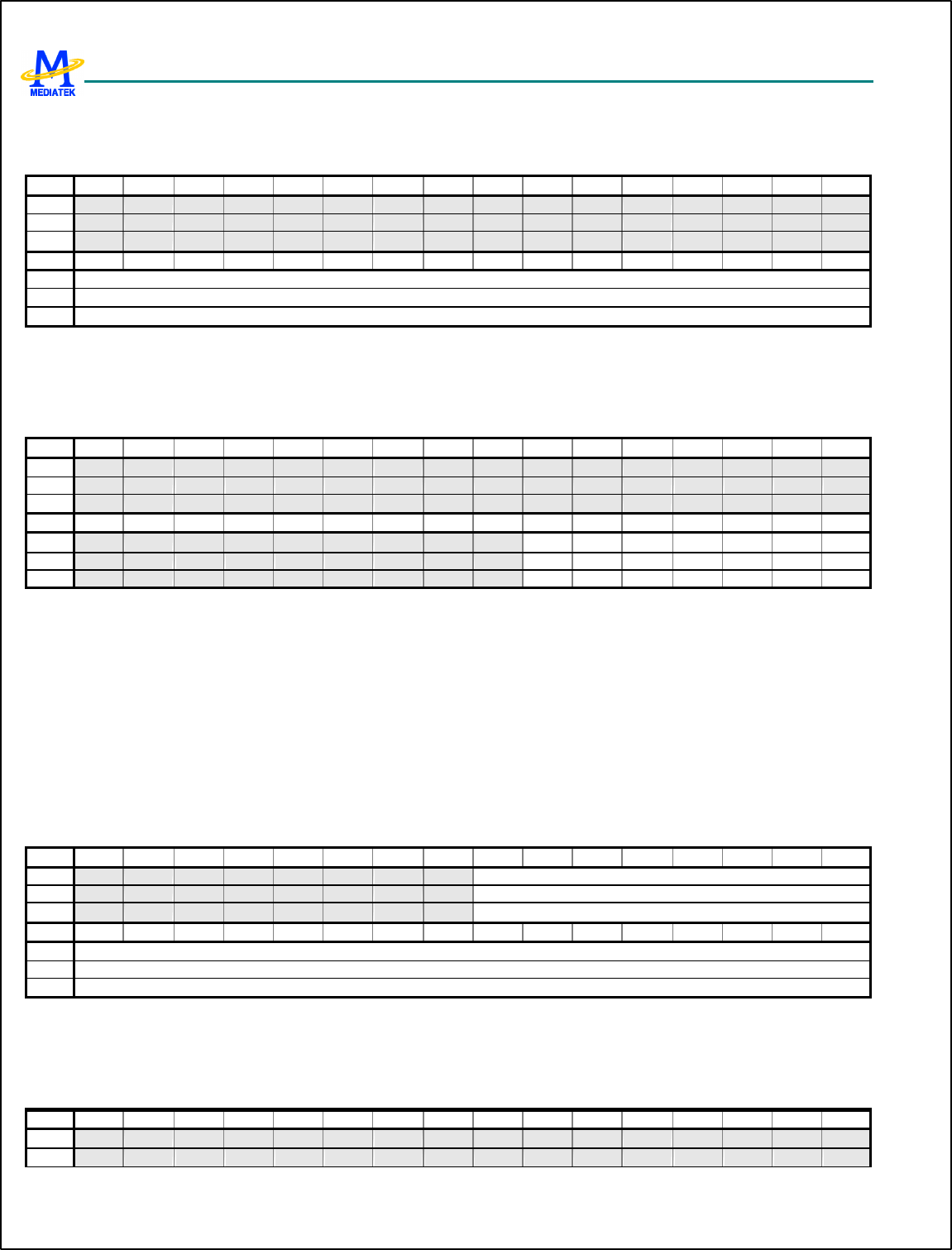
MT6217 GSM/GPRS Baseband Processor Data Sheet Revision 1.01
156/349 MediaTek Inc. Confidential
CSD+020Ch CSD RA1 6K/12K Downlink Output Data Register 1 CSD_RA1_6_12
K_DLDO1
Bit 31 30 29 28 27 26 25 24 23 22 21 20 19 18 17 16
Name
Type
Reset
Bit 15 14 13 12 11 10 9 8 7 6 5 4 3 2 1 0
Name
DOUT
Type R/W
Reset
0
DOUT The D33 to D48 of RA1 downlink data.
CSD+0210h CSD RA1 6K/12K Downlink Status Data Register CSD_RA1_6_12
K_DLSTUS
Bit 31 30 29 28 27 26 25 24 23 22 21 20 19 18 17 16
Name
Type
Reset
Bit 15 14 13 12 11 10 9 8 7 6 5 4 3 2 1 0
Name
E7 E6 E5 E4 X SB SA
Type R/W R/W R/W R/W R/W R/W R/W
Reset
0 0 0 0 0 0 0
SA The result of majority votes of S1, S3, S6 and S8. SA is “0” if equal vote.
SB The result of majority votes of S4 and S9. SB is “0” if equal vote.
X The result of majority votes of two X bits in downlink frame. X is “0” if equal vote.
E4 Represents E4 of status bits.
E5 Represents E5 of status bits.
E6 Represents E6 of status bits.
E7 Represents E7 of status bits.
CSD+0300h CSD RA1 3.6K Uplink Input Data Register 0
CSD_RA1_3P6K
_ULDI0
Bit 31 30 29 28 27 26 25 24 23 22 21 20 19 18 17 16
Name
DIN
Type R/W
Reset
0
Bit 15 14 13 12 11 10 9 8 7 6 5 4 3 2 1 0
Name
DIN
Type R/W
Reset
0
DIN The D1 to D24 of RA1 3.6K uplink data.
CSD+0304h CSD RA1 3.6K Uplink Status Data Register
CSD_RA1_3P6K
_ULSTUS
Bit 31 30 29 28 27 26 25 24 23 22 21 20 19 18 17 16
Name
Type
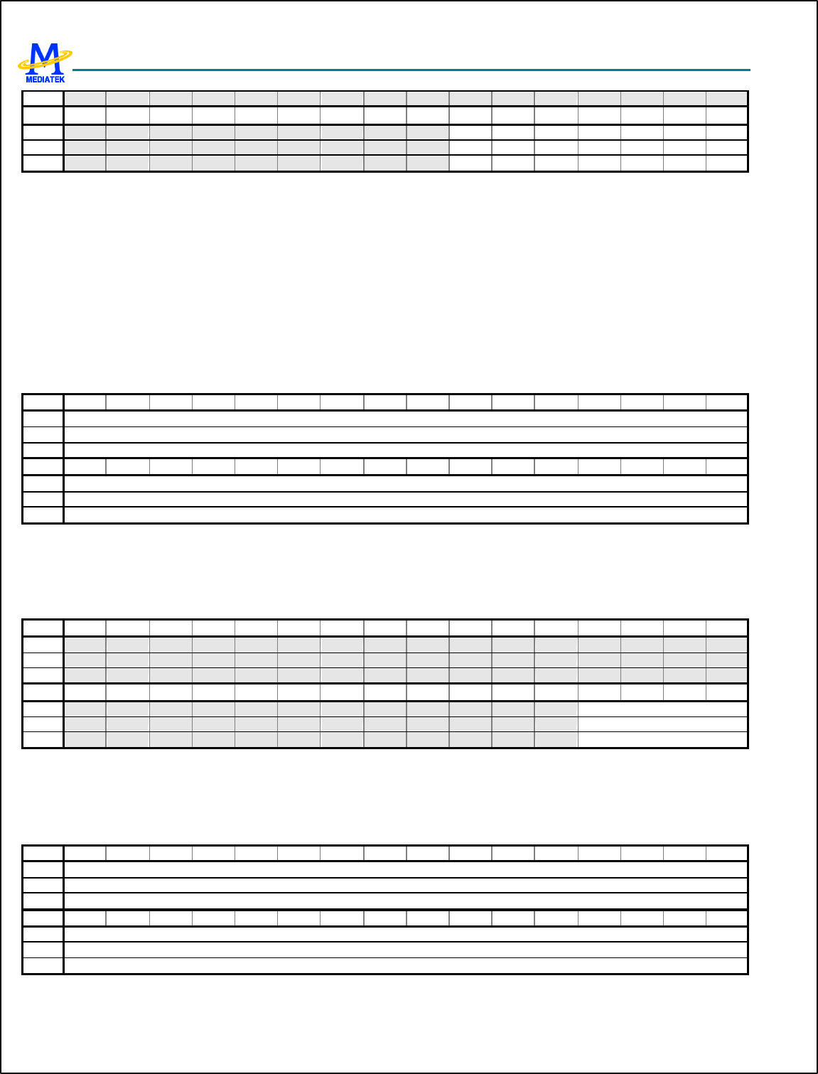
MT6217 GSM/GPRS Baseband Processor Data Sheet Revision 1.01
157/349 MediaTek Inc. Confidential
Reset
Bit 15 14 13 12 11 10 9 8 7 6 5 4 3 2 1 0
Name
E7 E6 E5 E4 X SB SA
Type R/W R/W R/W R/W R/W R/W R/W
Reset
0 0 0 0 0 0 0
SA Represents S1, S3, S6, and S8 of status bits.
SB Represents S4 and S9 of status bits.
X Represents X of status bits.
E4 Represents E4 of status bits.
E5 Represents E5 of status bits.
E6 Represents E6 of status bits.
E7 Represents E7 of status bits.
CSD+0308h CSD RA1 3.6K Uplink Output Data Register 0
CSD_RA1_3P6K
_ULDO0
Bit 31 30 29 28 27 26 25 24 23 22 21 20 19 18 17 16
Name
DOUT
Type R/W
Reset
0
Bit 15 14 13 12 11 10 9 8 7 6 5 4 3 2 1 0
Name
DOUT
Type R/W
Reset
0
DOUT The bit 0 to bit 31 of RA1 3.6K uplink frame
CSD+030Ch CSD RA1 3.6K Uplink Output Data Register 1
CSD_RA1_3P6K
_ULDO1
Bit 31 30 29 28 27 26 25 24 23 22 21 20 19 18 17 16
Name
Type
Reset
Bit 15 14 13 12 11 10 9 8 7 6 5 4 3 2 1 0
Name
DOUT
Type R/W
Reset
0
DOUT The bit 32 to bit 35 of RA1 3.6K uplink frame
CSD+0400h CSD RA1 3.6K Downlink Input Data Register 0
CSD_RA1_3P6K
_DLDI0
Bit 31 30 29 28 27 26 25 24 23 22 21 20 19 18 17 16
Name
DIN
Type R/W
Reset
0
Bit 15 14 13 12 11 10 9 8 7 6 5 4 3 2 1 0
Name
DIN
Type R/W
Reset
0
DIN The bit 0 to bit 31 of RA1 3.6K downlink frame
MTK Confidential Release for SIMCOM
MTK Confidential Release for SIMCOM
MT6217 GSM/GPRS Baseband Processor Data Sheet Revision 1.01
158/349 MediaTek Inc. Confidential
CSD+0404h CSD RA1 3.6K Downlink Input Data Register 1
CSD_RA1_3P6K
_DLDI1
Bit 31 30 29 28 27 26 25 24 23 22 21 20 19 18 17 16
Name
Type
Reset
Bit 15 14 13 12 11 10 9 8 7 6 5 4 3 2 1 0
Name
DIN
Type R/W
Reset
0
DIN The bit 32 to bit 35 of RA1 3.6K downlink frame
CSD+0408h CSD RA1 3.6K Downlink Output Data Register 0
CSD_RA1_3P6K
_DLDO0
Bit 31 30 29 28 27 26 25 24 23 22 21 20 19 18 17 16
Name
DOUT
Type R/W
Reset
0
Bit 15 14 13 12 11 10 9 8 7 6 5 4 3 2 1 0
Name
DOUT
Type R/W
Reset
0
DIN The D1 to D24 of RA1 3.6K downlink data.
CSD+040Ch CSD RA1 3.6K Downlink Status Data Register
CSD_RA1_3P6K
_DLSTUS
Bit 31 30 29 28 27 26 25 24 23 22 21 20 19 18 17 16
Name
Type
Reset
Bit 15 14 13 12 11 10 9 8 7 6 5 4 3 2 1 0
Name
E7 E6 E5 E4 X SB SA
Type R/W R/W R/W R/W R/W R/W R/W
Reset
0 0 0 0 0 0 0
SA The result of majority votes of S1, S3, S6 and S8. SA is “0” if equal vote.
SB The result of majority votes of S4 and S9. SB is “0” if equal vote.
X The result of majority votes of two X bits in downlink frame. X is “0” if equal vote.
E4 Represents E4 of status bits.
E5 Represents E5 of status bits.
E6 Represents E6 of status bits.
E7 Represents E7 of status bits.
CSD+0500h CSD FAX Bit Reverse Type 1 Input Data Register CSD_FAX_
BR1_
DI
Bit 31 30 29 28 27 26 25 24 23 22 21 20 19 18 17 16
Name
DIN
Type R/W
MT6217 GSM/GPRS Baseband Processor Data Sheet Revision 1.01
159/349 MediaTek Inc. Confidential
Reset
0
Bit 15 14 13 12 11 10 9 8 7 6 5 4 3 2 1 0
Name
DIN
Type R/W
Reset
0
DIN 32 -bit input data for type 1 bit reverse of FAX data. The action of Type 1 bit reverse is to reverse this word by
word.
CSD+0504h CSD FAX Bit Reverse Type 1 Output Data Register
CSD_FAX_BR1_
DO
Bit 31 30 29 28 27 26 25 24 23 22 21 20 19 18 17 16
Name
DOUT
Type R/W
Reset
0
Bit 15 14 13 12 11 10 9 8 7 6 5 4 3 2 1 0
Name
DOUT
Type R/W
Reset
0
DOUT 32 -bit result data for type 1 bit reverse of FAX data.
CSD+0510h CSD FAX Bit Reverse Type 2 Input Data Register
CSD_FAX_BR2_
DI
Bit 31 30 29 28 27 26 25 24 23 22 21 20 19 18 17 16
Name
DIN
Type R/W
Reset
0
Bit 15 14 13 12 11 10 9 8 7 6 5 4 3 2 1 0
Name
DIN
Type R/W
Reset
0
DIN 32 -bit input data for type 2 bit reverse of FAX data. The action of Type 1 bit reverse is to reverse this word by
byte.
CSD+0514h CSD FAX Bit Reverse Type 2 Output Data Register
CSD_FAX_BR2_
DO
Bit 31 30 29 28 27 26 25 24 23 22 21 20 19 18 17 16
Name
DOUT
Type R/W
Reset
0
Bit 15 14 13 12 11 10 9 8 7 6 5 4 3 2 1 0
Name
DOUT
Type R/W
Reset
0
DOUT 32 -bit result data for type 2 bit reverse of FAX data.

MT6217 GSM/GPRS Baseband Processor Data Sheet Revision 1.01
160/349 MediaTek Inc. Confidential
5.4 FCS Codec
5.4.1 General Description
FCS (Frame Check Sequence) is used to detect errors of the following information bits:
l RLP-frame of CSD services in GSM. The frame length is fixed as 240 or 576 bits including the 24-bit FCS field.
l LLC-frame of GPRS service. The frame length is determined by the information field, and length of the FCS field
is 24-bit.
Generation of the frame check sequence is very similar to the CRC coding in baseband signal
processing. ETSI GSM specifications 04.22 and 04.64 both define the coding rule. The coding rules
are:
1. The CRC shall be ones complement of the modulo-2 sum of:
l the remainder of xkž(x23+x22+x21+…+x2+x+1) modulo-2 divided by the generator polynomial, where k is the
number of bits of the dividend. (i.e. fill the shift registers with all ones initially before feeding data)
l the remainder of the modulo-2 division by the generator polynomial of the product of x24 by the dividend, which
are the information bits.
2. The CRC-24 generator polynomial is:
G(x)=x24+x23+x21+x20+x19+x17+x16+x15+x13+x8+x7+x5+x4+x2+1
3. The 24-bit CRC are appended to the data bits in the MSB-first manner.
4. Decoding is identical to encoding except that data fed into the syndrome circuit is 24-bit longer than the
information bits at encoding. The dividend is also multiplied by x
24. If no error occurs, the remainder should satisfy
R(x)=x22+x21+x19+x18+x16+x15+x11 +x8+x5+x4 (0x6d8930)
And the parity output word will be 0x9276cf.
In contrast to conventional CRC, this special coding scheme makes the encoder wholly identical to
the decoder and simplifies the hardware design.
5.4.2 Register Definitions
FCS+0000h FCS input data register FCS_DATA
Bit 15 14 13 12 11 10 9 8 7 6 5 4 3 2 1 0
Name
D15 D14 D13 D12 D11 D10 D9 D8 D7 D6 D5 D4 D3 D2 D1 D0
Type WO WO WO WO WO WO WO WO WO WO WO WO WO WO WO WO
THE data bits input. First write of this register is the starting point of the encode or decode process.
DX X=0…15. The input format is D15·xn+ D14·x n-1+ D13·xn-2+ … + Dk·xk+ …, thus D15 is the first bit being pushed
into the shift register. If the last data word is less than 16 bits, the rest bits are neglected.
FCS+0004h Input data length indication register FCS_DLEN
Bit 15 14 13 12 11 10 9 8 7 6 5 4 3 2 1 0
MT6217 GSM/GPRS Baseband Processor Data Sheet Revision 1.01
161/349 MediaTek Inc. Confidential
Name
LEN
Type WO
THE MCU specifies the total data length in bits to be encoded or decoded.
LEN The data length. A number of multiple -of-8 is required (Number_of_Bytes x 8)
FCS+0x0008h FCS parity output register 1, MSB part FCS_PAR1
Bit 15 14 13 12 11 10 9 8 7 6 5 4 3 2 1 0
Name
P15 P14 P13 P12 P11 P10 P9 P8 P7 P6 P5 P4 P3 P2 P1 P0
Type RC RC RC RC RC RC RC RC RC RC RC RC RC RC RC RC
Reset
0 0 0 0 0 0 0 0 0 0 0 0 0 0 0 0
FCS+000Ch FCS parity output register 2, LSB part FCS_PAR2
Bit 15 14 13 12 11 10 9 8 7 6 5 4 3 2 1 0
Name
P23 P22 P21 P20 P19 P18 P17 P16
Type RC RC RC RC RC RC RC RC
Reset
0 0 0 0 0 0 0 0
PARITY bits output. For FCS_PAR2, bit 8 to bit15 will be filled by zeros when reading.
PX X=0…23. The output format is P23·D 23+ P22·D 22+ P21·D 21+ … + Pk·D k+ …+P1·D 1+P0, thus P23 is the
earliest bit being popped out from the shift register and first appended to the information bits. In other words,
{FCS_PAR2[7:0], FCS_PAR1[15:8], FCS_PAR1[7:0] } is t he order of appending parity to data.
FCS+0010h FCS codec status register FCS_STAT
Bit 15 14 13 12 11 10 9 8 7 6 5 4 3 2 1 0
Name
BUSY FER RDY
Type RC RC RC
Reset
0 0 0
BUSY Since the codec works in serial manner and the data word is input in parallel manner, BUSY = 1 indicates that
current data word is being processed and write to FCS_DATA is invalid. BUSY = 0 allows write of FCS_DATA
during encode or decode process.
FER Frame error indication, only for decode mode. FER = 0 means no error occurs and FER = 1 means the parity
check is failed. Write of FCS_RST.RST or first write of FCS_DATA will reset this bit to 0.
RDY When RDY = 1, the encode or decode process has been finished. For encode, the parity data in FCS_PAR1 and
FCS_PAR2 are correctly available. For decode, FCS_STAT.FER indication is valid. Write of FCS_RST.RST
or first write of FCS_DATA will reset this bit to 0.
FCS+0014h FCS codec reset register FCS_RST
Bit 15 14 13 12 11 10 9 8 7 6 5 4 3 2 1 0
Name
EN_D
E PAR BIT RST
Type WO WO WO WO
RST RST = 0 resets the CRC coprocessor. Before setup of FCS codec, the MCU needs to set RST = 0 to flush the shift
register content before encode or decode.
BIT BIT = 0 means not to invert the bit order in a byte of data words when the codec is running. BIT = 1 means the bit
order in a byte written in FCS_DATA should be reversed.

MT6217 GSM/GPRS Baseband Processor Data Sheet Revision 1.01
162/349 MediaTek Inc. Confidential
PAR PAR = 0 means not to invert the bit order in a byte of parity words when the codec is running, include reading of
FCS_PAR1 and FCS_PAR2. PAR = 1 means bit order of parity words should be reversed, in decoding or
encoding.
EN_DE EN_DE = 0 means encode; EN_DE = 1 means decode

MT6217 GSM/GPRS Baseband Processor Data Sheet Revision 1.01
163/349 MediaTek Inc. Confidential
6 Multi-Media Subsystem
MT6217 is specially designed to support multi-media terminals. It integrates several hardware based accelerators, like
advanced LCD display controller, hardware JPEG decoder and hardware Image Resizer. Besides, MT6217 also
incorporates NAND Flash, USB 1.1 Device and SD/MMC/MS/MS Pro Controllers for massive data transfers and storages.
This chapter describes those functional blocks in detail.
6.1 LCD Interface
MT6217 contains a versatile LCD controller which is optimized for multimedia applications. This controller supports many
types of LCD modules and contains a rich feature set to enhance the functionality. These features are:
l Up to 320 x 240 resolution
l Supports 8-bpp (RGB332), 12-bpp (RGB444), 16-bpp (RGB565), 18-bit (RGB666) and 24-bit (RGB888) color
depths
l 4 Layers Overlay with individual vertical and horizontal size, vertical and horizontal offset, source key, opacity and
display rotation control(90°,180°, 270°, mirror and mirror then 90°, 180° and 270°)
l 2 Color Look-Up Tables
For parallel LCD modules, this special LCD controller can reuse external memory interface or use dedicated 8/16-bit
parallel interface to access them and 8080 type interface is supported. It can transfer the display data from the internal
SRAM or external SRAM/Flash Memory to the off-chip LCD modules.
For serial LCD modules, this interface performs parallel to serial conversion and both 8- and 9- bit serial interface is
supported. The 8-bit serial interface uses four pins – LSCE#, LSDA, LSCK and LSA0 – to enter commands and data.
Meanwhile, the 9-bit serial interface uses three pins – LSCE#, LSDA and LSCK – for the same purpose. Data read is not
available with the serial interface and data entered must be 8 bits.
MT6217 GSM/GPRS Baseband Processor Data Sheet Revision 1.01
164/349 MediaTek Inc. Confidential
Figure 37 LCD Interface Block Diagram
Figure 38 shows the timing diagram of this serial interface. When the block is idle, LSCK is forced LOW and LSCE# is
forced HIGH. Once the data register contains data and the interface is enabled, LSCE# is pulled LOW and remain LOW for
the duration of the transmission.
8-bit Serial Interface
LSCK(SPH=SPO=0)
LSDA D7 D6 D5 D4 D3 D2 D1 D0
LSCE#
LSA0
9-bit Serial Interface
LSCK(SPH=SPO=0)
LSDA A0 D7 D6 D5 D4 D3 D2 D1 D0
LSCE#
LSA0
Figure 38 LCD Interface Transfer Timing Diagram
6.1.1 Register Definitions
LCD +0000h LCD Interface Status Register LCD_STA
Bit 15 14 13 12 11 10 9 8 7 6 5 4 3 2 1 0
MT6217 GSM/GPRS Baseband Processor Data Sheet Revision 1.01
165/349 MediaTek Inc. Confidential
Name
RUN
Type R
Reset
0
RUN LCD Interface Running Status
DATA_PEND Data Pending Indicator in Hardware Trigger Mode
CMD_PEND Command Pending Indicator in Hardware Triggered Refresh Mode
LCD +0004h LCD Interface Interrupt Enable Register LCD_INTEN
Bit 15 14 13 12 11 10 9 8 7 6 5 4 3 2 1 0
Name
CPL
Type R/W
Reset
0
CPL LCD Frame Transfer Complete Interrupt Control
DATA_CPL Data Transfer Complete in Hardware Triggered Refresh Mode Interrupt Control
CMD_CPL Command Transfer Complete in Hardware Trigger Refresh Mode Interrupt Control
LCD +0008h LCD Interface Interrupt Status Register LCD_INTSTA
Bit 15 14 13 12 11 10 9 8 7 6 5 4 3 2 1 0
Name
CPL
Type R
Reset
0
CPL LCD Frame Transfer Complete Interrupt
DATA_CPL Data Transfer Complete in Hardware Triggered Refresh Mode Interrupt
CMD_CPL Command Transfer Complete in Hardware Triggered Refresh Mode Interrupt
LCD +000Ch LCD Interface Frame Transfer Register LCD_START
Bit 15 14 13 12 11 10 9 8 7 6 5 4 3 2 1 0
Name
STAR
T
Type R/W
Reset
0
START Start Control of LCD Frame Transfer
LCD +0010h LCD Parallel/Serial Interface Reset Register LCD_RSTB
Bit 15 14 13 12 11 10 9 8 7 6 5 4 3 2 1 0
Name
RSTB
Type R/W
Reset
1
RSTB Parallel/Serial LCD Module Reset Control
LCD +0014h LCD Serial Interface Configuration Register LCD _SCNF
Bit 15 14 13 12 11 10 9 8 7 6 5 4 3 2 1 0
Name
26M 13M CSP1 CSP0 8/9 DIV SPH SPO
Type R/W R/W R/W R/W R/W R/W R/W R/W
SPO Clock Polarity Control
SPH Clock Phase Control
MT6217 GSM/GPRS Baseband Processor Data Sheet Revision 1.01
166/349 MediaTek Inc. Confidential
DIV Serial Clock Divide Select Bits
8/9 8-bit or 9-bit Interface Selection
CSP0 Serial Interface Chip Select 0 Polarity Control
CSP1 Serial Interface Chip Select 1 Polarity Control
LCD +0018h LCD Parallel Interface Configuration Register 0 LCD_PCNF0
Bit 31 30 29 28 27 26 25 24 23 22 21 20 19 18 17 16
Name
C2WS C2WH C2RS
Type R/W R/W R/W
Bit 15 14 13 12 11 10 9 8 7 6 5 4 3 2 1 0
Name
26M 13M DW WST RLT
Type R/W R/W R/W R/W R/W
RLT Read Latency Time
WST Write Wait State Time
C2RS Chip Select (LPCE#) to Read Strobe (LRD#) Setup Time
C2WH Chip Select (LPCE#) to Write Strobe (LWR#) Hold Time
C2WS Chip Select (LPCE#) to Write Strobe (LWR#) Setup Time
LCD +001Ch LCD Parallel Interface Configuration Register 1 LCD_PCNF1
Bit 31 30 29 28 27 26 25 24 23 22 21 20 19 18 17 16
Name
C2WS C2WH C2RS
Type R/W R/W R/W
Bit 15 14 13 12 11 10 9 8 7 6 5 4 3 2 1 0
Name
26M 13M DW WST RLT
Type R/W R/W R/W R/W R/W
RLT Read Latency Time
WST Write Wait State Time
C2RS Chip Select (LPCE#) to Read Strobe (LRD#) Setup Time
C2WH Chip Select (LPCE#) to Write Strobe (LWR#) Hold Time
C2WS Chip Select (LPCE#) to Write Strobe (LWR#) Setup Time
LCD +0020h LCD Parallel Interface Configuration Register 2 LCD_PCNF2
Bit 31 30 29 28 27 26 25 24 23 22 21 20 19 18 17 16
Name
C2WS C2WH C2RS
Type R/W R/W R/W
Bit 15 14 13 12 11 10 9 8 7 6 5 4 3 2 1 0
Name
26M 13M DW WST RLT
Type R/W R/W R/W R/W R/W
RLT Read Latency Time
WST Write Wait State Time
C2RS Chip Select (LPCE#) to Read Strobe (LRD#) Setup Time
C2WH Chip Select (LPCE#) to Write Strobe (LWR#) Hold Time
C2WS Chip Select (LPCE#) to Write Strobe (LWR#) Setup Time
MT6217 GSM/GPRS Baseband Processor Data Sheet Revision 1.01
167/349 MediaTek Inc. Confidential
LCD
+4000/4100h LCD Parallel Interface Data Register 0 LCD_PDAT0
Bit 15 14 13 12 11 10 9 8 7 6 5 4 3 2 1 0
Name
DATA
Type R/W
DATA Writing to LCD+0800 will drive LPA0 low while sending this data out in parallel BANK0, otherwise will drive
LPA0 high
LCD
+5000/5100h LCD Parallel Interface Data Register 1 LCD_PDAT1
Bit 15 14 13 12 11 10 9 8 7 6 5 4 3 2 1 0
Name
DATA
Type R/W
DATA Writing to LCD+0808 will drive LPA0 low while sending this data out in parallel BANK1, otherwise will drive
LPA0 high
LCD
+6000/6100h LCD Parallel Interface Data Register 2 LCD_PDAT2
Bit 15 14 13 12 11 10 9 8 7 6 5 4 3 2 1 0
Name
DATA
Type R/W
DATA Writing to LCD+0810 will drive LPA0 low while sending this data out in parallel BANK2, otherwise will drive
LPA0 high
LCD
+9000/9100h LCD Serial Interface Data Register 0 LCD_SDAT0
Bit 15 14 13 12 11 10 9 8 7 6 5 4 3 2 1 0
Name
DATA
Type W
DATA Writing to LCD+0A00 will drive LSA0 low while sending this data out in serial BANK0, otherwise will drive
LSA0 high
LCD
+8000/8100h LCD Serial Interface Data Register 1 LCD_SDAT1
Bit 15 14 13 12 11 10 9 8 7 6 5 4 3 2 1 0
Name
DATA
Type W
DATA Writing to LCD+0A08 will drive LSA0 low while sending this data out in serial BANK1, otherwise will drive
LSA0 high
LCD +0040h Main Window Size Register LCD_MWINSIZE
Bit 31 30 29 28 27 26 25 24 23 22 21 20 19 18 17 16
Name
ROW
Type R/W
MT6217 GSM/GPRS Baseband Processor Data Sheet Revision 1.01
168/349 MediaTek Inc. Confidential
Bit 15 14 13 12 11 10 9 8 7 6 5 4 3 2 1 0
Name
COLUMN
Type R/W
COLUMN Virtual Image Window Column Size
ROW Virtual Image Window Row Size
LCD +0050h Region of Interest Window Control Register LCD_WROICON
Bit
31
30
29
28
27
26
25
24
23
22
21
20
19
18
17
16
Name
EN0
EN1
EN2
EN3
PERIOD
Type R/W R/W R/W R/W R/W
Bit
15
14
13
12
11
10
9
8
7
6
5
4
3
2
1
0
Name
ENC W2M DISC
ON COMMAND FORMAT
Type R/W R/W R/W R/W R/W
FORMAT LCD Module Data Format
0000000 8bit 1cycle/1pixel RGB3.3.2 RRRGGGBB
0000001 1cycle/1pixel RGB3.3.2 BBGGGRRR
0001000 3cycle/2pixel RGB4.4.4 RRRRGGGG
BBBBRRRR
GGGGBBBB
0001011 3cycle/2pixel RGB4.4.4 GGGGRRRR
RRRRBBBB
BBBBGGGG
0010000 2cycle/1pixel RGB5.6.5 RRRRRGGG
GGGBBBBB
0010011 2cycle/1pixel RGB5.6.5 GGGRRRRR
BBBBBGGG
0011000 3cycle/1pixel RGB6.6.6 RRRRRRXX
GGGGGGXX
BBBBBBXX
0011100 3cycle/1pixel RGB6.6.6 XXRRRRRR
XXGGGGGG
XXBBBBBB
0100000 3cycle/1pixel RGB8.8.8 RRRRRRRR
GGGGGGGG
BBBBBBBB
1000000 16bit 1cycle/2pixel RGB3.3.2 RRRGGGBBRRRGGGBB
1000010 1cycle/2pixel RGB3.3.2 RRRGGGBBRRRGGGBB
1000001 1cycle/2pixel RGB3.3.2 BBGGGRRRBBGGGRRR
1000011 1cycle/2pixel RGB3.3.2 BBGGGRRRBBGGGRRR
1001100 1cycle/1pixel RGB4.4.4 XXXXRRRRGGGGBBBB
1001101 1cycle/1pixel RGB4.4.4 XXXXBBBBGGGGRRRR
1001000 1cycle/1pixel RGB4.4.4 RRRRGGGGBBBBXXXX
1001001 1cycle/1pixel RGB4.4.4 BBBBGGGGRRRRXXXX
MT6217 GSM/GPRS Baseband Processor Data Sheet Revision 1.01
169/349 MediaTek Inc. Confidential
1010000 1cycle/1pixel RGB5.6.5 RRRRRGGGGGGBBBBB
1010001 1cycle/1pixel RGB5.6.5 BBBBBGGGGGGRRRRR
1011100 3cycle/2pixel RGB6.6.6 XXXXRRRRRRGGGGGG
XXXXBBBBBBRRRRRR
XXXXGGGGGGBBBBBB
1011111 3cycle/2pixel RGB6.6.6 XXXXGGGGGGRRRRRR
XXXXRRRRRRBBBBBB
XXXXBBBBBBGGGGGG
1011000 3cycle/2pixel RGB6.6.6 RRRRRRGGGGGGXXXX
BBBBBBRRRRRRXXXX
GGGGGGBBBBBBXXXX
1011011 3cycle/2pixel RGB6.6.6 GGGGGGRRRRRRXXXX
RRRRRRBBBBBBXXXX
BBBBBBGGGGGGXXXX
1100000 3cycle/2pixel RGB8.8.8 RRRRRRRRGGGGGGGG
BBBBBBBBRRRRRRRR
GGGGGGGGBBBBBBBB
1100011 3cycle/2pixel RGB8.8.8 GGGGGGGGRRRRRRRR
RRRRRRRRBBBBBBBB
BBBBBBBBRRRRRRRR
COMMAND Number of Commands to be sent to LCD module
DISCON Block Write Enable Control. By setting both DISCON and W2M to 1, this LCD accelerator will update the
ROI window within the MAIN Window
W2M Enable Data Address Increasing After Each Data Transfer
ENC Command Transfer Enable Control
PERIOD Waiting Period Between Two Consecutive Data Transfers
ENn Layer Window Enable Control
LCD +0054h Region of Interest Window Offset Register LCD_WROIOFS
Bit 31 30 29 28 27 26 25 24 23 22 21 20 19 18 17 16
Name
Y-OFFSET
Type R/W
Bit 15 14 13 12 11 10 9 8 7 6 5 4 3 2 1 0
Name
X-OFFSET
Type R/W
X-OFFSET ROI Window Column Offset
Y-OFFSET ROI Window Row Offset
LCD +0058h Region of Interest Window Command Start Address
Register
LCD_WROICAD
D
Bit 31 30 29 28 27 26 25 24 23 22 21 20 19 18 17 16
Name
AD DR
Type R/W
Bit 15 14 13 12 11 10 9 8 7 6 5 4 3 2 1 0
MT6217 GSM/GPRS Baseband Processor Data Sheet Revision 1.01
170/349 MediaTek Inc. Confidential
Name
ADDR
Type R/W
ADDR ROI Window Command Address
LCD +005Ch Region of Interest Window Data Start Address Register
LCD_WROIDAD
D
Bit 31 30 29 28 27 26 25 24 23 22 21 20 19 18 17 16
Name
ADDR
Type R/W
Bit 15 14 13 12 11 10 9 8 7 6 5 4 3 2 1 0
Name
ADDR
Type R/W
ADDR ROI Window Data Address
LCD +0060h Region of Interest Window Size Register LCD_WROISIZE
Bit 31 30 29 28 27 26 25 24 23 22 21 20 19 18 17 16
Name
ROW
Type R/W
Bit 15 14 13 12 11 10 9 8 7 6 5 4 3 2 1 0
Name
COLUMN
Type R/W
COLUMN ROI Window Column Size
ROW ROI Window Row Size
LCD +0070h Layer 0 Window Control Register LCD_L0WINCO
N
Bit 31 30 29 28 27 26 25 24 23 22 21 20 19 18 17 16
Name
SRCKEY
Type R/W
Bit 15 14 13 12 11 10 9 8 7 6 5 4 3 2 1 0
Name
SRC KEYE
N ROTATE PLAE
N PLA0/
1 OPAE
N OPA SWP
Type R/W R/W R/W R/W R/W R/W R/W R/W
SWP Swap high byte and low byte of pixel data
OPA Opacity Value Setting
OPAEN Opacity Enable Control
PLA0/1 Color Palette Selection
PLAEN Color Palette Enable Control
ROTATE Rotation Configuration
000 0 degree rotation
001 90 degree rotation anti-counterclockwise
010 180 degree rotation anti-counterclockwise
011 270 degree rotation anti-counterclockwise
100 Horizontal flip
101 Horizontal flip then 90 degree rotation anti-counterclockwise
110 Horizontal flip then 180 degree rotation anti-counterclockwise
MT6217 GSM/GPRS Baseband Processor Data Sheet Revision 1.01
171/349 MediaTek Inc. Confidential
111 Horizontal flip then 270 degree rotation anti-counterclockwise
KEYEN Source Key Enable Control
SRC Disable auto-increment of the source pixel address
SRCKEY Source Key Value
LCD +0074h Layer 0 Window Display Offset Register LCD_L0WINOFS
Bit 31 30 29 28 27 26 25 24 23 22 21 20 19 18 17 16
Name
Y-OFFSET
Type R/W
Bit 15 14 13 12 11 10 9 8 7 6 5 4 3 2 1 0
Name
X-OFFSET
Type R/W
Y-OFFSET Layer 0 Window Row Offset
X-OFFSET Layer 0 Window Column Offset
+0078h Layer 0 Window Display Start Address Register LCD_L0WINADD
Bit 31 30 29 28 27 26 25 24 23 22 21 20 19 18 17 16
Name
ADDR
Type R/W
Bit 15 14 13 12 11 10 9 8 7 6 5 4 3 2 1 0
Name
ADDR
Type R/W
ADDR Layer 0 Window Data Address
LCD +007Ch Layer 0 Window Size LCD_L0WINSIZ
E
Bit 31 30 29 28 27 26 25 24 23 22 21 20 19 18 17 16
Name
ROW
Type R/W
Bit 15 14 13 12 11 10 9 8 7 6 5 4 3 2 1 0
Name
COLUMN
Type R/W
ROW Layer 0 Window Row Size
COLUMN Layer 0 Window Column Size
LCD +0080h Layer 1 Window Control Register LCD_L1WINCO
N
Bit 31 30 29 28 27 26 25 24 23 22 21 20 19 18 17 16
Name
SRCKEY
Type R/W
Bit 15 14 13 12 11 10 9 8 7 6 5 4 3 2 1 0
Name
SRC KEYE
N ROTATE PLAE
N PLA0/
1 OPAE
N OPA SWP
Type R/W R/W R/W R/W R/W R/W R/W R/W
SWP Swap high byte and low byte of pixel data
OPA Opacity Value Setting
OPAEN Enable Opacity Control
MT6217 GSM/GPRS Baseband Processor Data Sheet Revision 1.01
172/349 MediaTek Inc. Confidential
PLA0/1 Color Palette Selection
PLAEN Color Palette Enable Control
ROTATE Rotation Configuration
000 0 degree rotation
001 90 degree rotation
010 180 degree rotation
011 270 degree rotation
100 Vertical flip
101 Reserved
110 Horizontal flip
111 Reserved
KEYEN Source Key Enable Control
SRC Disable auto-increment of the source pixel address
SRCKEY Source-Key
LCD +0084h Layer 1 Window Display Offset Register LCD_L1WINOFS
Bit 31 30 29 28 27 26 25 24 23 22 21 20 19 18 17 16
Name
Y-OFFSET
Type R/W
Bit 15 14 13 12 11 10 9 8 7 6 5 4 3 2 1 0
Name
X-OFFSET
Type R/W
X-OFFSET Layer 1 Window Row Offset
Y-OFFSET Layer 1 Window Column Offset
LCD +0088h Layer 1 Window Display Start Address Register LCD_L1WINADD
Bit 31 30 29 28 27 26 25 24 23 22 21 20 19 18 17 16
Name
ADDR
Type R/W
Bit 15 14 13 12 11 10 9 8 7 6 5 4 3 2 1 0
Name
ADDR
Type R/W
ADDR La yer 1 Window Data Address
LCD +008Ch Layer 1 Window Size LCD_L1WINSIZ
E
Bit 31 30 29 28 27 26 25 24 23 22 21 20 19 18 17 16
Name
ROW
Type R/W
Bit 15 14 13 12 11 10 9 8 7 6 5 4 3 2 1 0
Name
COLUMN
Type R/W
COLUMN Layer 1 Window Column Size
ROW Layer 1 Window Row Size
MT6217 GSM/GPRS Baseband Processor Data Sheet Revision 1.01
173/349 MediaTek Inc. Confidential
LCD +0090h Layer 2 Window Control Register LCD_L2WINCO
N
Bit 31 30 29 28 27 26 25 24 23 22 21 20 19 18 17 16
Name
SRCKEY
Type R/W
Bit 15 14 13 12 11 10 9 8 7 6 5 4 3 2 1 0
Name
SRC KEYE
N ROTATE PLAE
N PLA0/
1 OPAE
N OPA SWP
Type R/W R/W R/W R/W R/W R/W R/W R/W
SWP Swap high byte and low byte of pixel data
OPA Opacity Value Setting
OPAEN Enable Opacity Control
PLA0/1 Color Palette Selection
PLAEN Color Palette Enable Control
ROTATE Rotation Configuration
000 0 degree rotation
001 90 degree rotation
010 180 degree rotation
011 270 degree rotation
100 Vertical flip
101 Reserved
110 Horizontal flip
111 Reserved
KEYEN Source Key Enable Control
SRC Disable auto-increment of the source pixel address
SRCKEY Source-Key
LCD +0094h Layer 2 Window Display Offset Register LCD_L2WINOFS
Bit 31 30 29 28 27 26 25 24 23 22 21 20 19 18 17 16
Name
Y-OFFSET
Type R/W
Bit 15 14 13 12 11 10 9 8 7 6 5 4 3 2 1 0
Name
X-OFFSET
Type R/W
X-OFFSET Layer 2 Window Column Offset
Y-OFFSET Layer 2 Window Row Offset
LCD +0098h Layer 2 Window Display Start Address Register LCD_L2WINADD
Bit 31 30 29 28 27 26 25 24 23 22 21 20 19 18 17 16
Name
ADDR
Type R/W
Bit 15 14 13 12 11 10 9 8 7 6 5 4 3 2 1 0
Name
ADDR
Type R/W
ADDR Layer 2 Window Data Address
MT6217 GSM/GPRS Baseband Processor Data Sheet Revision 1.01
174/349 MediaTek Inc. Confidential
LCD +009Ch Layer 2 Window Size LCD_L2WINSIZ
E
Bit 31 30 29 28 27 26 25 24 23 22 21 20 19 18 17 16
Name
ROW
Type R/W
Bit 15 14 13 12 11 10 9 8 7 6 5 4 3 2 1 0
Name
COLUMN
Type R/W
COLUMN Layer 2 Window Column Size
ROW Layer 2 Window Row Size
LCD +00A0h Layer 3 Window Control Register LCD_L3WINCO
N
Bit 31 30 29 28 27 26 25 24 23 22 21 20 19 18 17 16
Name
SRCKEY
Type R/W
Bit 15 14 13 12 11 10 9 8 7 6 5 4 3 2 1 0
Name
SRC KEYE
N ROTATE PLAE
N PLA0/
1 OPAE
N OPA SWP
Type R/W R/W R/W R/W R/W R/W R/W R/W
SWP Swap high byte and low byte of pixel data
OPA Opacity Value Setting
OPAEN Enable Opacity Control
PLA0/1 Color Palette Selection
PLAEN Color Palette Enable Control
ROTATE Rotation Configuration
000 0 degree rotation
001 90 degree rotation
010 180 degree rotation
011 270 degree rotation
100 Vertical flip
101 Reserved
110 Horizontal flip
111 Reserved
KEYEN Source Key Enable Control
SRC Disable auto-increment of the source pixel address
SRCKEY Source-Key
LCD +00A4h Layer 3 Window Display Offset Register LCD_L3WINOFS
Bit 31 30 29 28 27 26 25 24 23 22 21 20 19 18 17 16
Name
Y-OFFSET
Type R/W
Bit 15 14 13 12 11 10 9 8 7 6 5 4 3 2 1 0
Name
X-OFFSET
Type R/W
X-OFFSET Layer 3 Window Column Offset
MT6217 GSM/GPRS Baseband Processor Data Sheet Revision 1.01
175/349 MediaTek Inc. Confidential
Y-OFFSET Layer 3 Window Row Offset
LCD +00A8h Layer 3 Window Display Start Address Register LCD_L3WINADD
Bit 31 30 29 28 27 26 25 24 23 22 21 20 19 18 17 16
Name
ADDR
Type R/W
Bit 15 14 13 12 11 10 9 8 7 6 5 4 3 2 1 0
Name
ADDR
Type R/W
ADDR Layer 3 Window Data Address
LCD +00ACh Layer 3 Window Size LCD_L3WINSIZ
E
Bit 31 30 29 28 27 26 25 24 23 22 21 20 19 18 17 16
Name
ROW
Type R/W
Bit 15 14 13 12 11 10 9 8 7 6 5 4 3 2 1 0
Name
COLUMN
Type R/W
COLUMN Layer 3 Window Column Size
ROW Layer 3 Window Row Size
LCD
+C200h~C3FCh LCD Interface Color Palette LUT 0 Registers LCD_PAL0
Bit 31 30 29 28 27 26 25 24 23 22 21 20 19 18 17 16
Name
LUT0
Type R/W
Bit 15 14 13 12 11 10 9 8 7 6 5 4 3 2 1 0
Name
LUT0
Type R/W
LUT0 These Bits Set LUT0 Data in RGB565 Format
LCD
+C400h~C5FCh LCD Interface Color Palette LUT 1 Registers LCD_PAL1
Bit 31 30 29 28 27 26 25 24 23 22 21 20 19 18 17 16
Name
LUT1
Type R/W
Bit 15 14 13 12 11 10 9 8 7 6 5 4 3 2 1 0
Name
LUT1
Type R/W
LUT1 These Bits Set LUT1 Data in RGB565 Format
LCD +C600h~C63C LCD Interface Command/Parameter Registers LCD_COMD
Bit 31 30 29 28 27 26 25 24 23 22 21 20 19 18 17 16
Name
C0 COMM
Type R/W R/W
Bit 15 14 13 12 11 10 9 8 7 6 5 4 3 2 1 0
Name
C0 COMM
MT6217 GSM/GPRS Baseband Processor Data Sheet Revision 1.01
176/349 MediaTek Inc. Confidential
Type R/W R/W
COMM Command Data and Parameter Data for LCD Module
C0 Write to ROI Command Address if C0 = 1, otherwise write to ROI Data Address
6.2 JPEG Decoder
6.2.1 Overview
To boost JPEG image processing performance, a hardware block is preferred to aid software and deal with JPEG file as
much as possible. As a result, JPEG Decoder is designed to decode all baseline and progressive JPEG images with all YUV
sampling frequencies combinations. To gain the speed performance with our best, JPEG decoder will handle all portions of
JPEG files except the 17-byte SOF marker. The software program only needs to program related control registers based on
the SOF marker and wait for an interrupt coming from hardware. Take into consideration the limited size of memories,
hardware also supports multiple runs of JPEG progressive images and breakpoints insertion in huge JPEG files. Multiple
runs can reduce memory usage largely by 1/N where N is the number of runs. Breakpoints insertion allows software to load
partial JPEG file from external flash to internal memory if the JPEG file is too large to sit in internally in one time.
6.2.2 Register Definitions
JPEG+0000h JPEG Decoder Control Register JPEG_FILE_ADDR
Bit 31 30 29 28 27 26 25 24 23 22 21 20 19 18 17 16
Name
FILE_ADDR[31:16]
Type R/W R/W R/W R/W R/W R/W R/W R/W R/W R/W R/W R/W R/W R/W R/W R/W
Bit 15 14 13 12 11 10 9 8 7 6 5 4 3 2 1 0
Name
FILE_ADDR[15:0]
Type R/W R/W R/W R/W R/W R/W R/W R/W R/W R/W R/W R/W R/W R/W R/W R/W
The JPEG file starting address must be a multiple of 4. Not affected by global reset and jpeg decoder abort.
FILE_ADDR Starting physical address of input JPEG file in SRAM
JPEG+0004h JPEG Decoder Control Register TBLS_START_ADD
R
Bit 31 30 29 28 27 26 25 24 23 22 21 20 19 18 17 16
Name
START_ADDR[31:16]
Type R/W R/W R/W R/W R/W R/W R/W R/W R/W R/W R/W R/W R/W R/W R/W R/W
Bit 15 14 13 12 11 10 9 8 7 6 5 4 3 2 1 0
Name
START_ADDR[15:11]
Type R/W R/W R/W R/W R/W
The table starting address must be a multiple of 2K. Not affected by global reset and jpeg decoder abort. Need
reprogramming for multiple runs of progressive images.
START_ADDR The starting address of the memory space for 4 quantization tables and 8 Huffman tables. The memory
space must be 2K Bytes at least.
JPEG+0008h JPEG Decoder Control Register SAMP_FACTOR
Bit 31 30 29 28 27 26 25 24 23 22 21 20 19 18 17 16
MT6217 GSM/GPRS Baseband Processor Data Sheet Revision 1.01
177/349 MediaTek Inc. Confidential
Name
Type
Bit 15 14 13 12 11 10 9 8 7 6 5 4 3 2 1 0
Name
H_SAMP_0[1
:0] V_SAMP_0[1
:0] H_SAMP_1[1
:0] V_SAMP_1[1
:0] H_SAMP_2[1
:0] V_SAMP_2[1
:0]
Type R/W R/W R/W R/W R/W R/W
This register contains the sampling factor of YUV components. Not affected by global reset and jpeg decoder abort.
H_SAMP_0 Horizontal sampling factor of the 1st component, Y.
00 SF is 1
01 SF is 2
10 Invalid
11 SF is 4
V_SAMP_0 Vertical sampling factor of the 1st component, Y.
00 SF is 1
01 SF is 2
10 Invalid
11 SF is 4
H_SAMP_1 Horizontal sampling factor of the 2nd component, U.
00 SF is 1
01 SF is 2
10 Invalid
12 SF is 4
V_SAMP_1 Vertical sampling factor of the 2nd component, U.
00 SF is 1
01 SF is 2
10 Invalid
11 SF is 4
H_SAMP_2 Horizontal sampling factor of the 3rd component, V.
00 SF is 1
01 SF is 2
10 Invalid
13 SF is 4
V_SAMP_2 Vertical sampling factor of the 3
rd component, V.
00 SF is 1
01 SF is 2
10 Invalid
11 SF is 4
JPEG+000Ch JPEG Decoder Control Register COMP_ID
Bit 31 30 29 28 27 26 25 24 23 22 21 20 19 18 17 16
Name
COMP0_ID[7:0] COMP1_ID[7:0]
Type R/W R/W
Bit 15 14 13 12 11 10 9 8 7 6 5 4 3 2 1 0
Name
COMP2_ID[7:0]
Type R/W
MT6217 GSM/GPRS Baseband Processor Data Sheet Revision 1.01
178/349 MediaTek Inc. Confidential
This register contains the IDs of YUV components. Not affected by global reset and jpeg decoder abort.
COMP0_ID The 1st component (Y) ID extracted from SOF marker.
COMP1_ID The 2nd component (U) ID extracted from SOF marker.
COMP2_ID The 3rd component (V) ID extracted from SOF marker.
JPEG+0010h JPEG Decoder Control Register TOTAL_MCU_NUM
Bit 31 30 29 28 27 26 25 24 23 22 21 20 19 18 17 16
Name
TOTAL_MCU_NUM[31:16]
Type R/W
Bit 15 14 13 12 11 10 9 8 7 6 5 4 3 2 1 0
Name
TOTAL_MCU_NUM[15:0]
Type R/W
This register contains the total MCU number in interleaved scan. Note that if the MCU number is N, program (N-1) into
this register. Not affected by global reset and jpeg decoder abort.
JPEG+0014h JPEG Decoder Control Register
INTLV_MCU_NUM_
PER_MCU_ROW
Bit 31 30 29 28 27 26 25 24 23 22 21 20 19 18 17 16
Name
Type
Bit 15 14 13 12 11 10 9 8 7 6 5 4 3 2 1 0
Name
INTLV_MCU_NUM_PER_MCU_ROW[9:0]
Type R/W
This register contains the MCU number per row in interleaved scan. Not affected by global reset and jpeg decoder abort.
JPEG+0018h JPEG Decoder Control Register
COMP0_NONINTLV
_DU_NUM_PER_MC
U_ROW
Bit 31 30 29 28 27 26 25 24 23 22 21 20 19 18 17 16
Name
Type
Bit 15 14 13 12 11 10 9 8 7 6 5 4 3 2 1 0
Name
DUMMY_DU COMP0_NONINTLV_MCU_NUM_PER_MCU_ROW[9:0]
Type R/W R/W
This register contains the MCU number per row in non-interleaved scan of the 1st component (Y). Not affected by global
reset and jpeg decoder abort. Note that COMP0_NONINTLV_MCU_NUM_PER_MCU_ROW includes the number of
DUMMY_DU if any.
DUMMY_DU Dummy data unit number in non-interleaved scan of the 1
st component
00 no dummy data unit
01 one dummy data unit
10 two dummy data units
11 three dummy data units
COMP0_NONINTLV_MCU_NUM_PER_MCU_ROW The MCU number per row in non-interleaved scan of the 1st
component (Y).
MT6217 GSM/GPRS Baseband Processor Data Sheet Revision 1.01
179/349 MediaTek Inc. Confidential
In progressive image, dummy data unit columns are inevitable if more than 8 redundant pixel columns are transmitted to fill
up the last MCU in a MCU row. For example, in 422 format, a MCU is composed of 16 x 16 pixels. If a given image size is
355 x 400, for JPEG encoder to compress, the image will grow to 368 x 400 first such that both width and height are
multiples of 16. It can be seen that to be dividable by 16, there are 13 redundant Y-component pixels in horizontal (width)
direction. These 13 Y-component pixels will be compressed by encoders in interleaved scans because a complete MCU will
need 16 x 16 pixels. It is different though in non-interleaved scans because in non-interleaved scans a complete MCU only
needs 8 x 8 Y-component pixels. Therefore among the 13 redundant pixels the first 5 will still be compressed as interleaved
scans while the last 8 will be dropped. In this case, software must program the DUMMY_DU field to 1 so the hardware will
know one 8 x 8 data unit should be skipped at the last of a MCU row in non-interleaved scan.
JPEG+001Ch JPEG Decoder Control Register
COMP1_NONINTLV
_DU_NUM_PER_MC
U_ROW
Bit 31 30 29 28 27 26 25 24 23 22 21 20 19 18 17 16
Name
Type
Bit 15 14 13 12 11 10 9 8 7 6 5 4 3 2 1 0
Name
DUMMY_DU COMP1_NONINTLV_MCU_NUM_PER_MCU_ROW[9:0]
Type R/W R/W
This register contains the MCU number per row in non-interleaved scan of the 2nd component (Y). Not affected by global
reset and jpeg decoder abort. Note that COMP1_NONINTLV_MCU_NUM_PER_MCU_ROW includes the number of
DUMMY_DU if any.
DUMMY_DU Dummy data unit number in non-interleaved scan of the 2nd component
00 no dummy data unit
01 one dummy data unit
10 two dummy data units
11 three dummy data units
COMP1_NONINTLV_MCU_NUM_PER_MCU_ROW The MCU number per row in non-interleaved scan of the 2nd
component (U).
JPEG+0020h JPEG Decoder Control Register
COMP2_NONINTLV
_DU_NUM_PER_MC
U_ROW
Bit 31 30 29 28 27 26 25 24 23 22 21 20 19 18 17 16
Name
Type
Bit 15 14 13 12 11 10 9 8 7 6 5 4 3 2 1 0
Name
DUMMY_DU COMP2_NONINTLV_MCU_NUM_PER_MCU_ROW[9:0]
Type R/W R/W
This register contains the MCU number per row in non-interleaved scan of the 3rd component (V). Not affected by global
reset and jpeg decoder abort. Note that COMP2_NONINTLV_MCU_NUM_PER_MCU_ROW includes the number of
DUMMY_DU if any.
DUMMY_DU Dummy data unit number in non-interleaved scan of the 3rd component
00 no dummy data unit
MT6217 GSM/GPRS Baseband Processor Data Sheet Revision 1.01
180/349 MediaTek Inc. Confidential
01 one dummy data unit
10 two dummy data units
11 three dummy data units
COMP2_NONINTLV_MCU_NUM_PER_MCU_ROW The MCU number per row in non-interleaved scan of the 3rd
component (V).
JPEG+0024h JPEG Decoder Control Register COMP0_DATA_UNI
T_NUM
Bit 31 30 29 28 27 26 25 24 23 22 21 20 19 18 17 16
Name
COMP0_DATA_UNIT_NUM[31:16]
Type R/W
Bit 15 14 13 12 11 10 9 8 7 6 5 4 3 2 1 0
Name
COMP0_DATA_UNIT_NUM[15:0]
Type R/W
This register contains the 8x8 data unit number of the 1st component in non-interleaved scans. Note that if the data unit
number is N, program (N-1) into this register. Not affected by global reset and jpeg decoder abort.
JPEG+0028h JPEG Decoder Control Register COMP1_DATA_UNI
T_NUM
Bit 31 30 29 28 27 26 25 24 23 22 21 20 19 18 17 16
Name
COMP1_DATA_UNIT_NUM[31:16]
Type R/W
Bit 15 14 13 12 11 10 9 8 7 6 5 4 3 2 1 0
Name
COMP1_DATA_UNIT_NUM[15:0]
Type R/W
This register contains the 8x8 data unit number of the 2nd component in non-interleaved frame. Note that if the data unit
number is N, program (N -1) into this register. Not affected by global reset and jpeg decoder abort.
JPEG+002Ch JPEG Decoder Control Register COMP2_DATA_UNI
T_NUM
Bit 31 30 29 28 27 26 25 24 23 22 21 20 19 18 17 16
Name
COMP2_DATA_UNIT_NUM[31:16]
Type R/W
Bit 15 14 13 12 11 10 9 8 7 6 5 4 3 2 1 0
Name
COMP2_DATA_UNIT_NUM[15:0]
Type R/W
This register contains the 8x8 data unit number of the 3rd component in non-interleaved frame. Note that if the data unit
number is N, program (N -1) into this register. Not affected by global reset and jpeg decoder abort.
JPEG+0030h JPEG Decoder Control Register
COMP0_PROGR_C
OEFF_START_ADD
R
Bit 31 30 29 28 27 26 25 24 23 22 21 20 19 18 17 16
Name
COMP0_PROGR_COEFF_START_ADDR[31:16]
Type R/W
MT6217 GSM/GPRS Baseband Processor Data Sheet Revision 1.01
181/349 MediaTek Inc. Confidential
Bit 15 14 13 12 11 10 9 8 7 6 5 4 3 2 1 0
Name
COMP0_PROGR_COEFF_START_ADDR[15:0]
Type R/W
This register contains the starting address of the memory space storing the intermediate progressive coefficients of the 1st
component. This value must be a multiple of 4. Not affected by global reset and jpeg decoder abort.
JPEG+0034h JPEG Decoder Control Register
COMP1_PROGR_C
OEFF_START_ADD
R
Bit 31 30 29 28 27 26 25 24 23 22 21 20 19 18 17 16
Name
COMP1_PROGR_COEFF_START_ADDR[31:16]
Type R/W
Bit 15 14 13 12 11 10 9 8 7 6 5 4 3 2 1 0
Name
COMP1_PROGR_COEFF_START_ADDR[15:0]
Type R/W
This register contains the starting address of the memory space storing the intermediate progressive coefficients of the 2nd
component. This value must be a multiple of 4. Not affected by global reset and jpeg decoder abort.
JPEG+0038h JPEG Decoder Control Register
COMP2_PROGR_C
OEFF_START_ADD
R
Bit 31 30 29 28 27 26 25 24 23 22 21 20 19 18 17 16
Name
COMP2_PROGR_COEFF_START_ADDR[31:16]
Type R/W
Bit 15 14 13 12 11 10 9 8 7 6 5 4 3 2 1 0
Name
COMP2_PROGR_COEFF_START_ADDR[15:0]
Type R/W
This register contains the starting address of the memory space storing the intermediate progressive coefficients of the 3rd
component. This value must be a multiple of 4. Not affected by global reset and jpeg decoder abort.
JPEG+003Ch JPEG Decoder Control Register JPEG_CTRL
Bit 31 30 29 28 27 26 25 24 23 22 21 20 19 18 17 16
Name
JPEG
_MOD
E DU9[2:0] DU8[2:0] DU7[2:0] DU6[2:0] DU5[2:0]
Type R/W R/W R/W R/W R/W R/W
Bit 15 14 13 12 11 10 9 8 7 6 5 4 3 2 1 0
Name
DU4[2:0] DU3[2:0] DU2[2:0] DU1[2:0] DU0[2:0]
Type R/W R/W R/W R/W R/W
This register contains 2 information: the operating mode of JPEG decoder and the order of 3 components in a MCU.
Affected by global reset and jpeg decoder abort. Need reprogramming for multiple runs of progressive images.
JPEG_MODE The operating mode of JPEG decoder.
0 Baseline mode
1 Progressive mode
DU9 The 10th data unit component category in a MCU

MT6217 GSM/GPRS Baseband Processor Data Sheet Revision 1.01
182/349 MediaTek Inc. Confidential
100 The 10th data unit is the 1st component (Y)
101 The 10th data unit is the 2nd component (U)
11 0 The 10th data unit is the 3rd component (V)
111 Not used in current frame
000-011 Invalid
DU8 The 9th data unit component category in a MCU
100 The 9th data unit is the 1st component (Y)
101 The 9th data unit is the 2nd component (U)
11 0 The 9th data unit is the 3rd component (V)
111 Not used in current frame
000-011 Invalid
DU7 The 8th data unit component category in a MCU
100 The 8th data unit is the 1st component (Y)
101 The 8th data unit is the 2nd component (U)
11 0 The 8th data unit is the 3rd component (V)
111 Not used in current frame
000-011 Invalid
DU6 The 7th data unit component category in a MCU
100 The 7th data unit is the 1st component (Y)
101 The 7th data unit is the 2nd component (U)
110 The 7th data unit is the 3rd component (V)
111 Not used in current frame
000-011 Invalid
DU5 The 6th data unit component category in a MCU
100 The 6th data unit is the 1st component (Y)
101 The 6th data unit is the 2nd component (U)
11 0 The 6th data unit is the 3rd component (V)
111 Not used in current frame
000-011 Invalid
DU4 The 5th data unit component category in a MCU
100 The 5th data unit is the 1st component (Y)
101 The 5th data unit is the 2nd component (U)
11 0 The 5th data unit is the 3rd component (V)
111 Not used in current frame
000-011 Invalid
DU3 The 4th data unit component category in a MCU
100 The 4th data unit is the 1st component (Y)
101 The 4th data unit is the 2nd component (U)
11 0 The 4th data unit is the 3rd component (V)
111 Not used in current frame
000-011 Invalid
DU2 The 3rd data unit component category in a MCU
100 The 3rd data unit is the 1st component (Y)
101 The 3rd data unit is the 2nd component (U)
MT6217 GSM/GPRS Baseband Processor Data Sheet Revision 1.01
183/349 MediaTek Inc. Confidential
11 0 The 3rd data unit is the 3rd component (V)
111 Not used in current frame
000-011 Invalid
DU1 The 2nd data unit component category in a MCU
100 The 2nd data unit is the 1st component (Y)
101 The 2nd data unit is the 2nd component (U)
11 0 The 2nd data unit is the 3rd component (V)
111 Not used in current frame
000-011 Invalid
DU0 The 1st data unit component category in a MCU
100 The 1st data unit is the 1st component (Y)
101 The 1st data unit is the 2nd component (U)
11 0 The 1st data unit is the 3rd component (V)
111 Not used in current frame
000-011 Invalid
JPEG+0040h JPEG Decoder Control Register JPEG_DEC_TRIG
Bit 31 30 29 28 27 26 25 24 23 22 21 20 19 18 17 16
Name
Type W
Bit 15 14 13 12 11 10 9 8 7 6 5 4 3 2 1 0
Name
Type W
JPEG_DEC_TRIG will trigger JPEG decoding operation no matter what value is programmed.
JPEG+0044h JPEG Decoder Control Register JPEG_DEC_ABOR
T
Bit 31 30 29 28 27 26 25 24 23 22 21 20 19 18 17 16
Name
Type W
Bit 15 14 13 12 11 10 9 8 7 6 5 4 3 2 1 0
Name
Type W
JPEG_DEC_ABORT will abort JPEG decoding operation and reset JPEG decoder hardware no matter what value is
programmed.
JPEG+0048h JPEG Decoder Control Register JPEG_FILE_BRP
Bit 31 30 29 28 27 26 25 24 23 22 21 20 19 18 17 16
Name
JPEG_FILE_BRP[31:16]
Type R/W
Bit 15 14 13 12 11 10 9 8 7 6 5 4 3 2 1 0
Name
JPEG_FILE_BRP[15:0]
Type R/W
JPEG_DEC_BRP stands for a 32-bit byte breakpoint address that hardware will stall once the breakpoint address is
encountered. This control register provides a solution for software to swap internal memory content with external memory
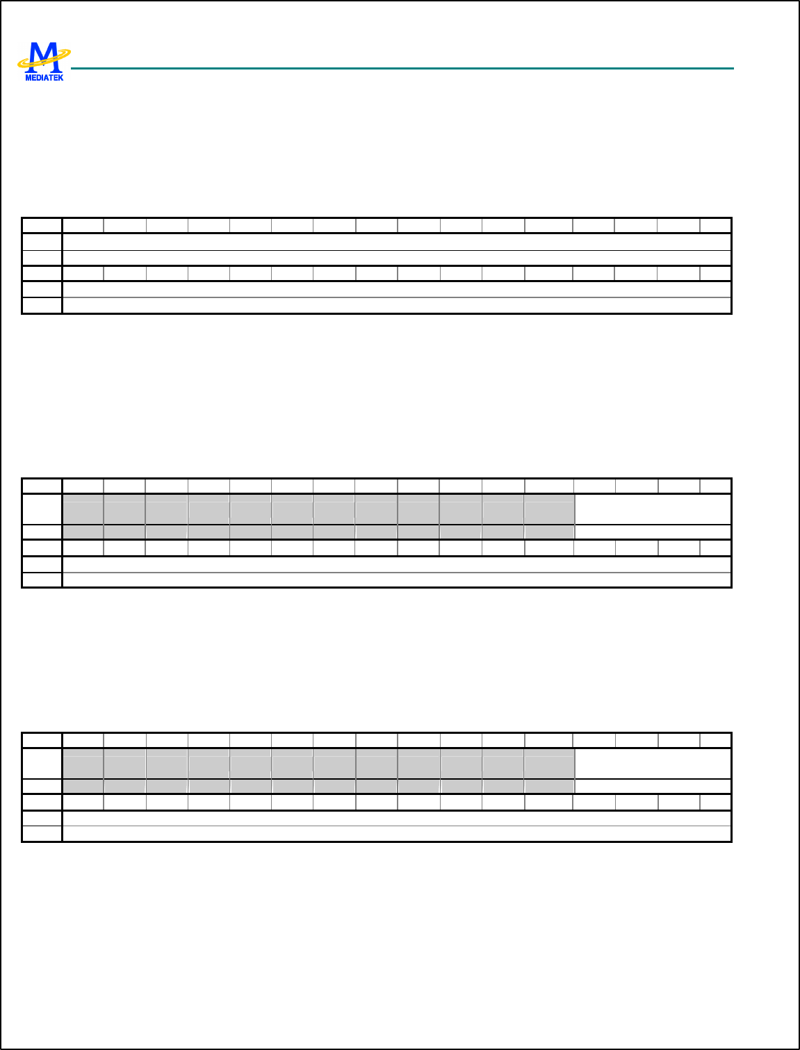
MT6217 GSM/GPRS Baseband Processor Data Sheet Revision 1.01
184/349 MediaTek Inc. Confidential
in case that JPEG source file is too big for internal memory to store at one time. A breakpoint interrupt will fire when
hardware DMA address hits the breakpoint address. Note that the breakpoint address must be a multiple of 4. Not affected
by global reset and jpeg decoder abort.
JPEG+004Ch JPEG Decoder Control Register JPEG_FILE_TOTA
L_SIZE
Bit 31 30 29 28 27 26 25 24 23 22 21 20 19 18 17 16
Name
JPEG_FILE_TOTAL_SIZE[31:16]
Type R/W
Bit 15 14 13 12 11 10 9 8 7 6 5 4 3 2 1 0
Name
JPEG_FILE_TOTAL_SIZE[15:0]
Type R/W
JPEG_FILE_TOTAL_SIZE represents the JPEG source file size in bytes. Hardware will fire a file overflow interrupt and
stall if the DMA address equals to this address. Note that the breakpoint address must be a multiple of 4. If the file size is
not able to be divided by 4, increment the size value until it is. Not affected by global reset and jpeg decoder abort. Not
affected by global reset and jpeg decoder abort.
JPEG+0050h JPEG Decoder Control Register INTLV_FIRST_MC
U_INDEX
Bit 31 30 29 28 27 26 25 24 23 22 21 20 19 18 17 16
Name
INTLV_FIRST_MCU_IND
EX [19:16]
Type R/W
Bit 15 14 13 12 11 10 9 8 7 6 5 4 3 2 1 0
Name
INTLV_FIRST_MCU_INDEX[15:0]
Type R/W
This control register specifies the first MCU index that hardware will process in the interleaved scans of the current image.
The JPEG decoder is able to skip certain MCUs by defining the first and last MCU index. If an image is expected to show
in a whole, program this register to 0. Not affected by global reset and jpeg decoder abort.
JPEG+0054h JPEG Decoder Control Register INTLV_LAST_MCU
_INDEX
Bit 31 30 29 28 27 26 25 24 23 22 21 20 19 18 17 16
Name
INTLV_LAST_MCU_INDE
X[19:16]
Type R/W
Bit 15 14 13 12 11 10 9 8 7 6 5 4 3 2 1 0
Name
INTLV_LAST_MCU_INDEX[15:0]
Type R/W
This control register specifies the last MCU index that hardware will process in the interleaved scans of the current image.
The JPEG decoder is able to skip certain MCUs by defining the first and last MCU index. If an image is expected to show
in a whole, be sure this register value is more than the total MCU number.(make it 0xfffff if possible in this case). Not
affected by global reset and jpeg decoder abort.
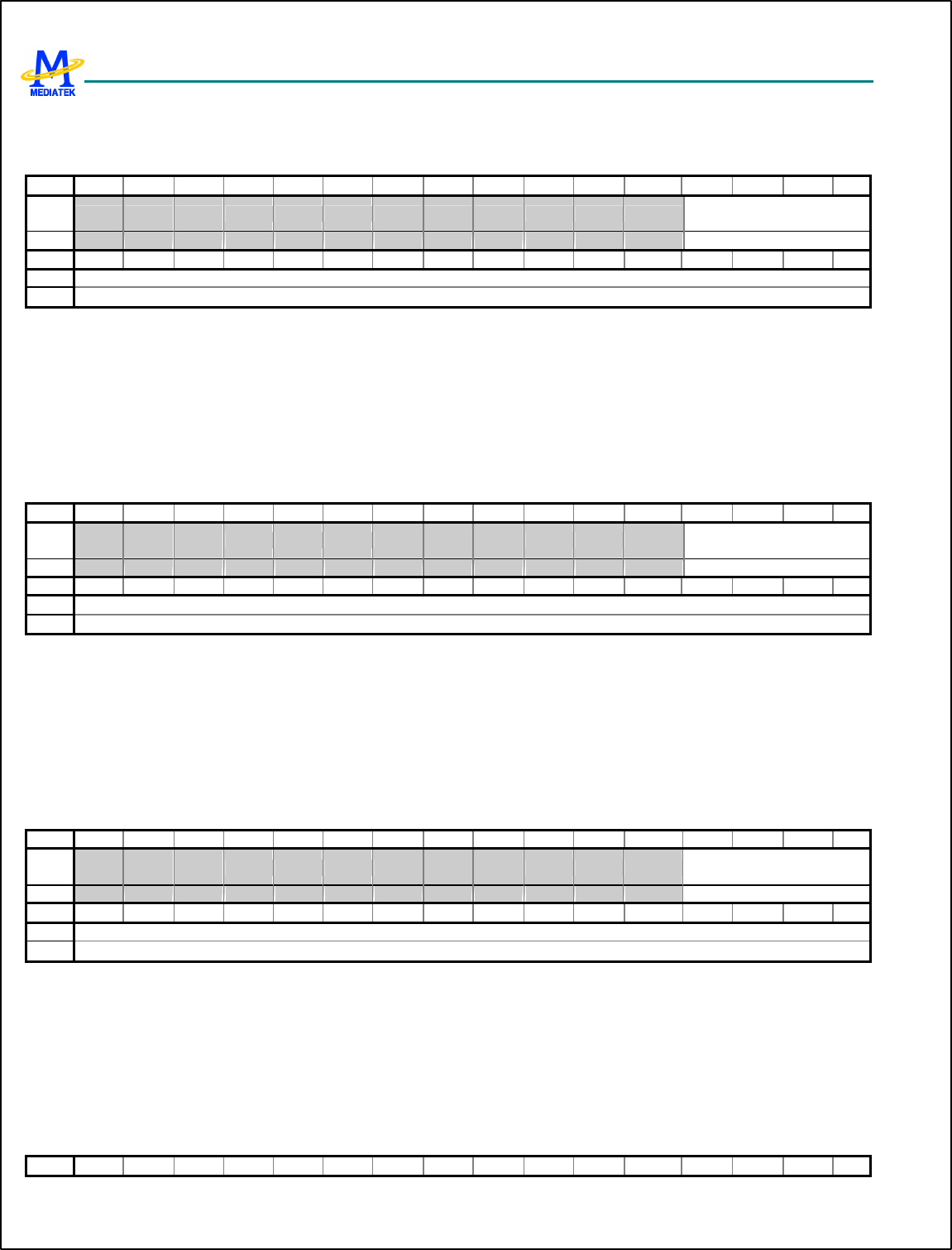
MT6217 GSM/GPRS Baseband Processor Data Sheet Revision 1.01
185/349 MediaTek Inc. Confidential
JPEG+0058h JPEG Decoder Control Register COMP0_FIRST_MC
U_INDEX
Bit 31 30 29 28 27 26 25 24 23 22 21 20 19 18 17 16
Name
COMP0_FIRST_MCU_IN
DEX[19:16]
Type R/W
Bit 15 14 13 12 11 10 9 8 7 6 5 4 3 2 1 0
Name
COMP0_FIRST_MCU_INDEX[15:0]
Type R/W
Only effective in progressive images. This control register specifies the first MCU index that hardware will process in the
non-interleaved scans containing Y component of the current image. The JPEG decoder is able to skip certain MCUs by
defining the first and last MCU index. If an image is expected to show in a whole, program this register to 0. Not affected
by global reset and jpeg decoder abort.
JPEG+005Ch JPEG Decoder Control Register COMP0_LAST_MC
U_INDEX
Bit 31 30 29 28 27 26 25 24 23 22 21 20 19 18 17 16
Name
COMP0_LAST_MCU_IND
EX [19:16]
Type R/W
Bit 15 14 13 12 11 10 9 8 7 6 5 4 3 2 1 0
Name
COMP0_LAST_MCU_INDEX[15:0]
Type R/W
Only effective in progressive images. This control register specifies the last MCU index that hardware will process in the
non-interleaved scans containing Y component of the current image. The JPEG decoder is able to skip certain MCUs by
defining the first and last MCU index. If an image is expected to show in a whole, be sure this register value is more than
the total MCU number.(make it 0xfffff if possible in this case). Not affected by global reset and jpeg decoder abort.
JPEG+0060h JPEG Decoder Control Register COMP1_FIRST_MC
U_INDEX
Bit 31 30 29 28 27 26 25 24 23 22 21 20 19 18 17 16
Name
COMP1_FIRST_MCU_IND
EX [19:16]
Type R/W
Bit 15 14 13 12 11 10 9 8 7 6 5 4 3 2 1 0
Name
COMP1_FIRST_MCU_INDEX[15:0]
Type R/W
Only effective in progressive images. This control register specifies the first MCU index that hardware will process in the
non-interleaved scans containing U component of the current image. The JPEG decoder is able to skip certain MCUs by
defining the first and last MCU index. If an image is expected to show in a whole, program this register to 0. Not affected
by global reset and jpeg decoder abort.
JPEG+0064h JPEG Decoder Control Register COMP1_LAST_MC
U_INDEX
Bit 31 30 29 28 27 26 25 24 23 22 21 20 19 18 17 16
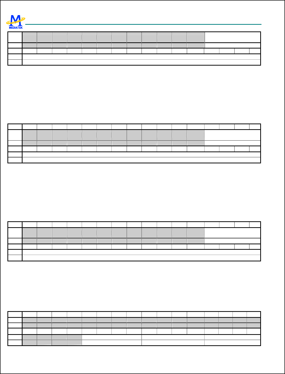
MT6217 GSM/GPRS Baseband Processor Data Sheet Revision 1.01
186/349 MediaTek Inc. Confidential
Name
COMP1_LAST_MCU_IND
EX [19:16]
Type R/W
Bit 15 14 13 12 11 10 9 8 7 6 5 4 3 2 1 0
Name
COMP1_LAST_MCU_INDEX[15:0]
Type R/W
Only effective in progressive images. This control register specifies the last MCU index that hardware will process in the
non-interleaved scans containing U component of the current image. The JPEG decoder is able to skip certain MCUs by
defining the first and last MCU index. If an image is expected to show in a whole, be sure this register value is more than
the total MCU number.(make it 0xfffff if possible in this case). Not affected by global reset and jpeg decoder abort.
JPEG+0068h JPEG Decoder Control Register COMP2_FIRST_MC
U_INDEX
Bit 31 30 29 28 27 26 25 24 23 22 21 20 19 18 17 16
Name
COMP2_FIRST_MCU_IND
EX [19:16]
Type R/W
Bit 15 14 13 12 11 10 9 8 7 6 5 4 3 2 1 0
Name
COMP2_FIRST_MCU_INDEX[15:0]
Type R/W
Only effective in progressive images. This control register specifies the first MCU index that hardware will process in the
non-interleaved scans containing V component of the current image. The JPEG decoder is able to skip certain MCUs by
defining the first and last MCU index. If an image is expected to show in a whole, program this register to 0. Not affected
by global reset and jpeg decoder abort.
JPEG+006Ch JPEG Decoder Control Register COMP2_LAST_MC
U_INDEX
Bit 31 30 29 28 27 26 25 24 23 22 21 20 19 18 17 16
Name
COMP2_LAST_MCU_IND
EX [19:16]
Type R/W
Bit 15 14 13 12 11 10 9 8 7 6 5 4 3 2 1 0
Name
COMP2_LAST_MCU_INDEX[15:0]
Type R/W
Only effective in progressive images. This control register specifies the last MCU index that hardware will process in the
non-interleaved scans containing V component of the current image. The JPEG decoder is able to skip certain MCUs by
defining the first and last MCU index. If an image is expected to show in a whole, be sure this register value is more than
the total MCU number.(make it 0xfffff if possible in this case). Not affected by global reset and jpeg decoder abort.
JPEG+0070h JPEG Decoder Control Register QT_ID
Bit 31 30 29 28 27 26 25 24 23 22 21 20 19 18 17 16
Name
Type
Bit 15 14 13 12 11 10 9 8 7 6 5 4 3 2 1 0
Name
COMP0_QT_ID[3:0] COMP1_QT_ID[3:0] COMP2_QT_ID[3:0]
Type R/W R/W R/W
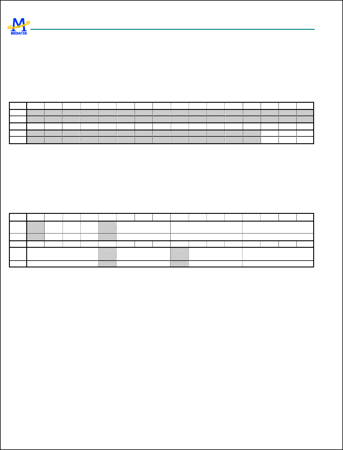
MT6217 GSM/GPRS Baseband Processor Data Sheet Revision 1.01
187/349 MediaTek Inc. Confidential
This register contains the quantization table IDs for YUV components. Not affected by global reset and jpeg decoder abort.
COMP0_QT_ID Quantization table ID of Y component directly extracted from SOF marker
COMP1_QT_ID Quantization table ID of U component directly extracted from SOF marker
COMP2_QT_ID Quantization table ID of V component directly extracted from SOF marker
JPEG+0074h JPEG Decoder Control Register JPEG_DEC_INTER
RUPT_STATUS
Bit 31 30 29 28 27 26 25 24 23 22 21 20 19 18 17 16
Name
Type
Bit 15 14 13 12 11 10 9 8 7 6 5 4 3 2 1 0
Name
INT2 INT1 INT0
Type R R R
The register reflects the interrupt status
INT2 Set to 1 by file overflow interrupt
INT1 Set to 1 by breakpoint interrupt
INT0 Set to 1 by end of file interrupt
JPEG+0078h JPEG Decoder Control Register JPEG_DEC_STAT
US
Bit 31 30 29 28 27 26 25 24 23 22 21 20 19 18 17 16
Name
FOS BRPS EOFS JPEG_DEC_STATE HUFF_DEC_STATE MARKER_PARSER_STAT
E
Type R R R R R R
Bit 15 14 13 12 11 10 9 8 7 6 5 4 3 2 1 0
Name
SOS_PARSER_STATE DHT_PARSER_STA
TE DQT_PARSER_STA
TE DATA_UNIT_STATE
Type R R R R
6.3 Image Resizer
6.3.1 General Description
The block provides capability for image resizing. It receives image data from a block-based image source such as JPEG
decoder in format of YUV color space, and then performs image resizing. The illustrative diagram is shown in Figure 39.
The capability of resizing in the block is divided into two portions, coarse pass and fine pass. The first pass is coarse
resizing pass and it could be able to have image shrink as 1, 1/4, 1/16, or 1/64 small as original size. The second pass is fine
resizing pass and it could be able to have image shrink and enlarge in fractional ratio. As shown in Figure 39 fine resizing
pass is composed of horizontal and vertical resizing. Through combination of the two passes, an image can scale up or
down in any ratio under some constraints. Furthermore, to enhance throughput there are bypass path for horizontal and
vertical resizing when no resizing is needed. The constraint for coarse shrinking is that the size of image after coarse
shrinking has the limit of maximum value 2047x2047. The assumption should be guaranteed by MMI. Thus maximum of
the size of source image is 16376x16376. Furthermore, the size of final target image also has the limit of maximum value
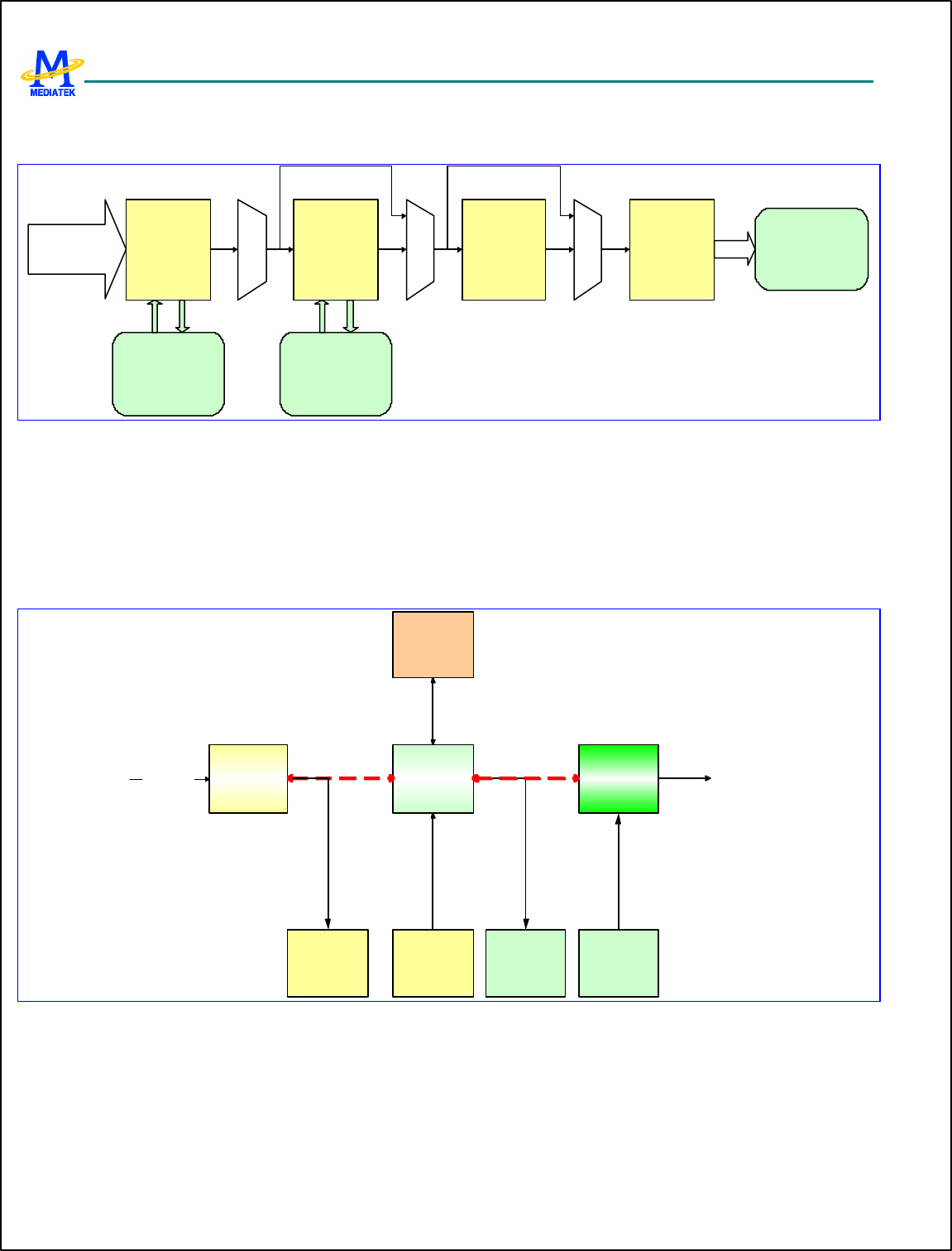
MT6217 GSM/GPRS Baseband Processor Data Sheet Revision 1.01
188/349 MediaTek Inc. Confidential
2047x2047. However, coarse shrinking is only supported for block-based image source. Therefore maximum of the size of
a pixel-based source image is only 2047x2047.
VERTICAL
RESIZER
Working Memory
HORIZONTAL
RESIZER
Line Buffer
COARSE
RESIZER YUV2RGB Target MemoryFrom JPEG Decoder
Figure 39 Overview of Image Resizer
The block diagram for block-based image sources is shown in Figure 40. Here the block “CS” stands for block based CS
(Coarse Shrinking). Block based CS is dedicated for JPEG decoder and it ’s 8x8 block-based process. Other blocks in the
diagram are scan-line based process. The major application is CS, then HR and then VR. The possible applications include
CS only, HR+VR only. The red dot lines in Figure 40 indicate hardware handshaking between two blocks.
The base address of Image Resizer is 0x8061_0000.
Coarse Shrinking
(CS)
Image Sources
Memory Interface
(MIF)
Horizontal Resize
(HR)
Vertical Resize
(VR)
Memory Interface
(MIF)
Software
Command
Memory Interface
(MIF)
Memory Interface
(MIF)
Figure 40 Block Diagram of Image Resizer for JPEG decoder
6.3.2 Requirements
There are two memory blocks needed in the block. One is line buffer, and the other is working memory. Line buffer is used
to store color components from image sources after coarse scaling. Working memory is for fine scaling. However, for
pixel-based image sources only working memory is needed.

MT6217 GSM/GPRS Baseband Processor Data Sheet Revision 1.01
189/349 MediaTek Inc. Confidential
6.3.2.1 Memory Requirements
First consider block-based image sources. Let’s denote sampling factor for Y-component as (HY, V
Y), U-component as (HU,
VU) and V-component as (HV, VV). Hmax=max(HY, HU, HV). Vmax=max(V
Y, V
U, VV). Then the memory requirement for line
buffer is (the width of source image size after coarse shrinking)*(V
Y *8+ VU*8+ V
V*8) bytes. For the case of which image
source is JPEG decoder, it is 2047x(4x8+4x8+2x8)=163760B as (HY, HU, HV)=(1,1,1), (V
Y, VU, VV)=(4,4,2) and the width
of source image size after coarse shrinking is 2047. If dual line buffer is desired, it becomes about 327.5KB. In addition,
the ratio of size of line buffer for YUV components must be equal to the ratio of (VY, VU, VV). For example, assume
(VY, V
U, VV)=(4,2,2) and line buffer size of Y component is 32 lines. Then line buffer size of U component must be 16 lines
and so does the line buffer size of V components. The memory requirement for working memory is (the width of target
image size)* (line size of working memory)*3 bytes. Of course, more memory is allowable.
Then consider pixel-based image sources. Only working memory is needed. The memory requirement for working memory
is (the width of target image size)* (line size of working memory)*3. Of course, more memory is allowable.
6.3.2.2 Image Requirements
First consider block-based image sources. The image data from image sources are inputted in unit of color component such
as Y- or U- or V-components. Every color component is composed of 8x8 pixels with 8-bit color depth per pixel. Therefore
the width of an image source must be multiples of 8*(maximum horizontal sampling factor). Similarly the height of an
image source also must be multiples of 8*(maximum vertical sampling factor). The maximum size of target image after
coarse shrinking is 2047x2047.
Then consider pixel-based image sources. The width and height of source image must be less than 2047 and so does that of
target image.
6.3.3 Coarse Shrinking
Coarse resizing could be able to have image shrink as 1, 1/4, 1/16, or 1/64 large as original size. It ’s dedicated for JPEG
decoder. Therefore all processes are based on blocks composed of 8x8 pixels. There are flow control between coarse
shrinking and JPEG decoder. When line buffer is not enough for coarse shrinking, coarse shrinking will halt image data
input from JPEG decoder until line buffer is enough. Remember coarse shrinking is only for block-based image sources.
6.3.4 Fine Resizing
Fine resizing is composed of horizontal resizing and vertical resizing. It has fractional resizing capability. The image input
to fine resizing has size limit of maximum 2047x2047, so does the output of fine resizing. For the sake of cost and speed,
the algorithm used in fine resizing is bilinear algorithm. In horizontal resizing working memory enough to fill in two
scan-lines is needed. Of course dual buffer or more can be used. For pixel-based image, horizontal or vertical resizing can
be trigged if necessarily or disabled if unnecessarily. However, if horizontal/vertical resizing is unnecessary and trigged,
then horizontal/vertical resizing must be reset after resizing finishes.
6.3.5 Throughput
For block-based image sources, the process time for one pixel is about 3 cycles. Therefore if 15 frames per second are
desired and Image Resizer is running at 52 MHz then the maxi mum pixel number per frame is about 1.15M. That is about
1075x1075.
MT6217 GSM/GPRS Baseband Processor Data Sheet Revision 1.01
190/349 MediaTek Inc. Confidential
For pixel-based image sources, the process time for one pixel is about 2.25 cycles. Therefore if 15 frames per second are
desired and Image Resizer is running at 52 MHz then the maximum pixel number per frame is about 1.5M. That is about
1241x1241.
Since memory bandwidth requirements are different for scale up and down, it may be able to enhance throughput by adjust
the register setting of RESZ_CFG.BWA0/BWB0. When scale up, memory bandwidth requirements for read is higher than
memory bandwidth requirements for write. However, when scale down, memory bandwidth requirements for write is
higher than memory bandwidth requirements for read. Therefore when horizontally scale up throughput can be enhance by
setting RESZ_CFG.B0 with higher value than RESZ_CFG.A0. Similarly when horizontally scale down throughput can be
enhance by setting RESZ_CFG.A0 with higher value than RESZ_CFG.B0. Therefore when vertically scale up throughput
can be enhance by setting RESZ_CFG.B1 with higher value than RESZ_CFG.A1. Similarly when vertically scale down
throughput can be enhance by setting RESZ_CFG.A1 with higher value than RESZ_CFG.B1.
6.3.6 YUV2RGB
Format translation from YUV domain to RGB domain is provided after vertical resizing. The sources of YUV2RGB are
image data on the fly after vertical resizing. RGB is in format of 5-6-5. RGB output from YUV2RGB is in format of 5-6-5.
That is, one pixel occupies two bytes.
MSB LSB Memory Address
pixel 1 R (5bits) G (6 bits) B (5 bits) 0
pixel 2 R (5bits) G (6 bits) B (5 bits) 2
pixel 3 R (5bits) G (6 bits) B (5 bits) 4
Line 1 pixel 4 R (5bits) G (6 bits) B (5 bits) 6
pixel W R (5bits) G (6 bits) B (5 bits) 2x(W-1)
pixel 1 R (5bits) G (6 bits) B (5 bits) 2W
pixel 2 R (5bits) G (6 bits) B (5 bits) 2W+2
pixel 3 R (5bits) G (6 bits) B (5 bits) 2W+4
Line 2 pixel 4 R (5bits) G (6 bits) B (5 bits) 2W+6
pixel W R (5bits) G (6 bits) B (5 bits) 2x(2W-1)
Figure 41 RGB Format
6.3.7 Register Definitions
REGISTER ADDRESS REGISTER NAME SYNONYM
RESZ+ 0000h Image Resizer Configuration Register RESZ_CFG
RESZ + 0004h Image Resizer Control Register RESZ_CON
RESZ + 0008h Image Resizer Status Register RESZ_STA

MT6217 GSM/GPRS Baseband Processor Data Sheet Revision 1.01
191/349 MediaTek Inc. Confidential
RESZ + 000Ch Image Resizer Interrupt Register RESZ_INT
RESZ + 0010h Image Resizer Source Image Size Register 1 RESZ_SRCSZ1
RESZ + 0014h Image Resizer Target Image Size Register 1 RESZ_TARSZ1
RESZ + 0018h Image Resizer Horizontal Ratio Register 1 RESZ_HRATIO1
RESZ + 001Ch Image Resizer Vertical Ratio Register 1 RESZ_VRATIO1
RESZ + 0020h Image Resizer Horizontal Residual Register 1 RESZ_HRES1
RESZ + 0024h Image Resizer Vertical Residual Register 1 RESZ_VRES1
RESZ + 0030h Image Resizer Block Coarse Shrinking Configuration Register RESZ_BLKCSCFG
RESZ + 0034h Image Resizer Y-Component Line Buffer Memory Base Address RESZ_YLMBASE
RESZ + 0038h Image Resizer U-Component Line Buffer Memory Base Address RESZ_ULMBASE
RESZ + 003Ch Image Resizer V-Component Line Buffer Memory Base Address RESZ_VLMBASE
RESZ + 0040h Image Resizer Fine Resizing Configuration Register RESZ_FRCFG
RESZ + 0050h Image Resizer Y Line Buffer Size Register RESZ_YLBSIZE
RESZ + 005Ch Image Resizer Pixel-Based Resizing Working Memory Base Address RESZ_PRWMBASE
RESZ + 0080h Image Resizer YUV2RGB Configuration Register RESZ_YUV2RGB
RESZ + 0084h Image Resizer Target Memory Base Address Register RESZ_TMBASE
RESZ + 00B0h Image Resizer Information Register 0 RESZ_INFO0
RESZ + 00B4h Image Resizer Information Register 1 RESZ_INFO1
RESZ + 00B8h Image Resizer Information Register 2 RESZ_INFO2
RESZ + 00BCh Image Resizer Information Register 3 RESZ_INFO3
RESZ + 00C0h Image Resizer Information Register 4 RESZ_INFO4
RESZ + 00C4h Image Resizer Information Register 5 RESZ_INFO5
RESZ+0000h Image Resizer Configuration Register RESZ_CFG
Bit 31 30 29 28 27 26 25 24 23 22 21 20 19 18 17 16
Name
BWB1 BWA1 BWB0 BWA0
Type R/W R/W R/W R/W
Reset
0000 0000 0000 0000
Bit 15 14 13 12 11 10 9 8 7 6 5 4 3 2 1 0
Name
Type
Reset
The register is for global configuration of Image Resizer.
BWA0 Bandwidth selection for port A of memory interface 0. In block-based mode, that is memory interface between
BLKCS and BLKHR. In pixel-based mode, that’s is memory interface between PELHR and PELVR. Each
memory interface has one write port (port A) and one read port (port B). The arbitration between port A and port B
of memory interface 0 is based on the setting of the register fields BWA0 and BWB0. The arbitration schem is fair
between port A and port B. However, if the register field BWA0 is set larger value than the register field BWB0
then port A can get more bandwidth than port B.
0 If memory access of port A and port B take place simultaneously, then grant will be given to port B whenever
port A gets grant once.

MT6217 GSM/GPRS Baseband Processor Data Sheet Revision 1.01
192/349 MediaTek Inc. Confidential
1 If memory access of port A and port B take place simultaneously, then grant will be given to port B whenever
port A gets grant twice.
2 If memory access of port A and port B take place simultaneously, then grant will be given to port B whenever
port A gets grant three times.
…
BWB0 Bandwidth selection for port b of memory interface 0. In block-based mode, that is memory interface between
BLKCS and BLKHR. In pixel-based mode, that’s is memory interface between PELHR and PELVR. Each
memory interface has one write port (port A) and one read port (port B). The arbitration between port A and port B
of memory interface 0 is based on the setting of the register fields BWA0 and BWB0. The arbitration schem is fair
between port A and port B. However, if the register field BWB0 is set larger value than the register field BWA0
then port B can get more bandwidth than port A.
0 If memory access of port A and port B take place simultaneously, then grant will be given to port A whenever
port B gets grant once.
1 If memory access of port A and port B take place simultaneously, then grant will be given to port A whenever
port B gets grant twice.
2 If memory access of port A and port B take place simultaneously, then grant will be given to port A whenever
port B gets grant three times.
…
BWA1 Bandwidth selection for port A of memory interface 1. In block-based mode, that is memory interface between
BLKHR and BLKVR. In pixel-based mode, that’s is memory interface between PELHR and PELVR. Each
memory interface has one write port (port A) and one read port (port B). The arbitration between port A and port B
of memory interface 1 is based on the setting of the register fields BWA1 and BWB1. The arbitration schem is fair
between port A and port B. However, if the register field BWA1 is set larger value than the register field BWB1
then port A can get more bandwidth than port B.
0 If memory access of port A and port B take place simu ltaneously, then grant will be given to port B whenever
port A gets grant once.
1 If memory access of port A and port B take place simultaneously, then grant will be given to port B whenever
port A gets grant twice.
2 If memory access of port A and port B take place simultaneously, then grant will be given to port B whenever
port A gets grant three times.
…
BWB1 Bandwidth selection for port b of memory interface 1. In block-based mode, that is memory interface between
BLKHR and BLKVR. In pixel-based mode, that’s is memory interface between PELHR and PELVR. Each
memory interface has one write port (port A) and one read port (port B). The arbitration between port A and port B
of memory interface 1 is based on the setting of the register fields BWA1 and BWB1. The arbitration schem is fair
between port A and port B. However, if the register field BWB1 is set larger value than the register field BWA1
then port B can get more bandwidth than port A.
0 If memory access of port A and port B take place simultaneously, then grant will be given to port A whenever
port B gets grant once.
1 If memory access of port A and port B take place simultaneously, then grant will be given to port A whenever
port B gets grant twice.
2 If memory access of port A and port B take place simultaneously, then grant will be given to port A whenever
port B gets grant three times.
…

MT6217 GSM/GPRS Baseband Processor Data Sheet Revision 1.01
193/349 MediaTek Inc. Confidential
RESZ+0004h Image Resizer Control Register RESZ_CON
Bit 31 30 29 28 27 26 25 24 23 22 21 20 19 18 17 16
Name
YUV2
RGBR
ST
PELV
RRST PELH
RRST BLKC
SRST
Type R/W R/W R/W R/W
Reset
0 0 0 0
Bit 15 14 13 12 11 10 9 8 7 6 5 4 3 2 1 0
Name
YUVS
2RGB
ENA
PELV
RENA
PELH
RENA
BLKC
SENA
Type R/W R/W R/W R/W
Reset
0 0 0 0
The register is for global control of Image Resizer. Furthermore, software reset will NOT reset all register setting.
Remember trigger Image Resizer first before trigger image sources to Image Resizer.
BLKCSENA Writing ‘1’ to the register bit will cause Block Coarse Shrinking proceed to work. Block Coarse Shrinking
is designed to cooperate width JPEG decoder. It works on the fly. Bu it needs to be restarted every time
before working.
PELHRENA Writing ‘1’ to the register bit will cause pixel-based fine horizontal resizing proceed to work. However, if
horizontal resizing is not necessary, donot write ‘1’ to the register bit.
PELVRENA Writing ‘1’ to the register bit will cause pixel-based fine vertical resizing proceed to work. However, if
vertical resizing is not necessary, donot write ‘1’ to the register bit.
YUV2RGBENA Writing ‘1’ to the register bit will cause YUV2RGB proceed to work.
BLKCSRST Writing ‘1’ to the register bit will force Block Coarse Shrinking to stop immediately and have Block
Coarse Shrinking keep in reset state. In order to have Block Coarse Shrinking go to normal state, writing
‘0’ to the register bit.
PELHRRST Writing ‘1’ to the register will cause pixel-based fine horizontal resizing to stop immediately and have
pixel-based fine horizontal resizing keep in reset state. In order to have pixel-based fine horizontal
resizing go to normal state, writing ‘0’ to the register bit.
PELVRRST Writing ‘1’ to the register will pixel-based fine vertical resizing to stop immediately and have pixel-based
fine vertical resizing keep in reset state. In order to have pixel-based fine vertical resizing go to normal
state, writing ‘0’ to the register bit.
YUV2RGBRST Writing ‘1’ to the register will force YUV2RGB to stop immediately and have YUV2RGB keep in reset
state. In order to have YUV2RGB go to normal state, writing ‘0’ to the register bit.
RESZ+0008h Image Resizer Status Register RESZ_STA
Bit 31 30 29 28 27 26 25 24 23 22 21 20 19 18 17 16
Name
Type
Reset
Bit 15 14 13 12 11 10 9 8 7 6 5 4 3 2 1 0
Name
BLKIN
TRAB
SY
Y2RB
USY
PELV
RBUS
Y
PELH
RBUS
Y
BLKC
SBUS
Y
Type RO RO RO RO RO
Reset
0 0 0 0 0
The register indicates global status of Image Resizer.
MT6217 GSM/GPRS Baseband Processor Data Sheet Revision 1.01
194/349 MediaTek Inc. Confidential
BLKCSBUSY Block-based CS (Corase Shrinking) Busy Status
PELHRBUSY Pixel-based HR (Horizontal Resizing) Busy Status
PELVRBUSY Pixel-based VR (Vertical Resizing) Busy Status
Y2RBUSY YUV2RGB Busy Status
BLKINTRABSY Block-based CS (Corase Shrinking) Intra-Block Busy Status
RESZ+000Ch Image Resizer Interrupt Register RESZ_INT
Bit 31 30 29 28 27 26 25 24 23 22 21 20 19 18 17 16
Name
Type
Reset
Bit 15 14 13 12 11 10 9 8 7 6 5 4 3 2 1 0
Name
Y2RIN
T PELV
RINT PELH
RINT BLKC
SINT
Type RC RC RC RC
Reset
0 0 0 0
The register shows up the interrupt status of resizer.
BLKCSINT Interrupt for BLKCS (Block-based Coarse Shrink). No matter the register bit RESZ_BLKCSCFG.INTEN is
enabled or not, the register bit will be active whenever BLKCS completes. It could be as software interrupt by
polling the register bit. Clear it by reading the register.
PELHRINT Interrupt for PELHR (Pixel-based Horizontal Resizing). No matter the register bit RESZ_FRCFG.HRINTEN
is enabled or not, the register bit will be active whenever PELHR completes. It could be as software interrupt
by polling the register bit. Clear it by reading the register.
PELVRINT Interrupt for PELVR (Pixel -based Vertical Resizing). No matter the register bit RESZ_FRCFG.VRINTEN is
enabled or not, the register bit will be active whenever PELVR completes. It could be as software interrupt by
polling the register bit. Clear it by reading the register.
Y2RINT Interrupt for YUV2RGB (YUV to RGB). No matter the register bit RESZ_YUV2RGB.INTEN is enabled or
not, the register bit will be active whenever interrupt for completeness of YUV2RGB translation of an image
is active. It could be as software interrupt by polling the register bit. Clear it by reading the register.
RESZ+0010h Image Resizer Source Image Size Register 1 RESZ_SRCSZ1
Bit 31 30 29 28 27 26 25 24 23 22 21 20 19 18 17 16
Name
HS
Type R/W
Bit 15 14 13 12 11 10 9 8 7 6 5 4 3 2 1 0
Name
WS
Type R/W
The register specifies the size of source image after coarse shrink process. The allowable maximum size is 2047x2047.
Note that for the width of source image must be multiples of 8xHmax and the height of source image must be multiples of
8xVmax when Block Coarse Shrinking is involved.
WS The register field specifies the width of source image after coarse shrink process.
1 The width of source image after coarse shrink process is 1.
2 The width of source image is 2.
…
HS The register field specifies the height of source image after coarse shrink process.
1 The height of source image after coarse shrink process is 1.
MT6217 GSM/GPRS Baseband Processor Data Sheet Revision 1.01
195/349 MediaTek Inc. Confidential
2 The height of source image after coarse shrink process is 2.
…
RESZ+0014h Image Resizer Target Image Size Register 1 RESZ_TARSZ1
Bit 31 30 29 28 27 26 25 24 23 22 21 20 19 18 17 16
Name
HT
Type R/W
Bit 15 14 13 12 11 10 9 8 7 6 5 4 3 2 1 0
Name
WT
Type R/W
The register specifies the size of target image. The allowable maximum size is 2047x2047.
WT The register field specifies the width of target image.
1 The width of target image is 1.
2 The width of target image is 2.
…
HT The register field specifies the height of target image.
1 The height of target image is 1.
2 The height of target image is 2.
…
RESZ+0018h Image Resizer Horizontal Ratio Register RESZ_HRATIO1
Bit 31 30 29 28 27 26 25 24 23 22 21 20 19 18 17 16
Name
RATIO [31:16]
Type R/W
Bit 15 14 13 12 11 10 9 8 7 6 5 4 3 2 1 0
Name
RATIO [15:0]
Type R/W
The register specifies horizontal resizing ratio. It is obtained by RESZ_SRCSZ.WS * 221 / RESZ_TARSZ.WT.
RESZ+001Ch Image Resizer Vertical Ratio Register 1 RESZ_VRATIO1
Bit 31 30 29 28 27 26 25 24 23 22 21 20 19 18 17 16
Name
RATIO [31:16]
Type R/W
Bit 15 14 13 12 11 10 9 8 7 6 5 4 3 2 1 0
Name
RATIO [15:0]
Type R/W
The register specifies vertical resizing ratio. It is obtained by RESZ_SRCSZ.HS * 2
21 / RESZ_TARSZ.HT.
RESZ+0020h Image Resizer Horizontal Residual Register 1 RESZ_HRES1
Bit 31 30 29 28 27 26 25 24 23 22 21 20 19 18 17 16
Name
Type
Bit 15 14 13 12 11 10 9 8 7 6 5 4 3 2 1 0
Name
RESIDUAL
Type R/W
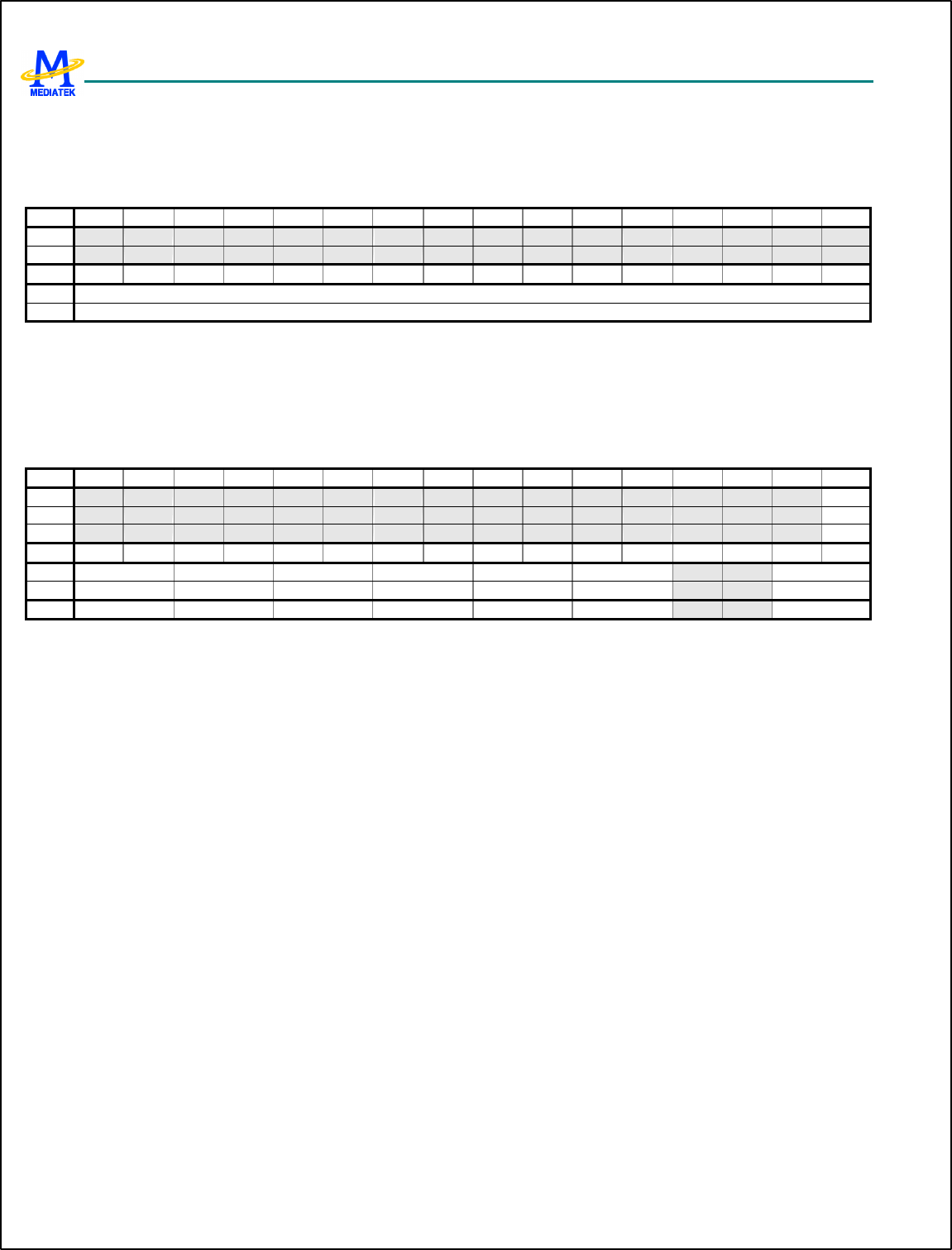
MT6217 GSM/GPRS Baseband Processor Data Sheet Revision 1.01
196/349 MediaTek Inc. Confidential
The register specifies horizontal residual. It is obtained by RESZ_SRCSZ.WS % RESZ_TARSZ.WT The allowable
maximum value is 2046.
RESZ+0024h Image Resizer Vertical Residual Register 1 RESZ_VRES1
Bit 31 30 29 28 27 26 25 24 23 22 21 20 19 18 17 16
Name
Type
Bit 15 14 13 12 11 10 9 8 7 6 5 4 3 2 1 0
Name
RESIDUAL
Type R/W
The register specifies vertical residual. It is obtained by RESZ_SRCSZ.HS % RESZ_TARSZ.HT. The allowable maximum
value is 2046.
RESZ+0030h Image Resizer Block Coarse Shrinking
Configuration Register RESZ_BLKCSCFG
Bit 31 30 29 28 27 26 25 24 23 22 21 20 19 18 17 16
Name
INTEN
Type R/W
Reset
0
Bit 15 14 13 12 11 10 9 8 7 6 5 4 3 2 1 0
Name
VV HV VU HU VY HY CSF
Type R/W R/W R/W R/W R/W R/W R/W
Reset
00 00 00 00 00 00 00
The register is for various configuration of Block Coarse Shrinking in Image Resizer. Block Coarse Shrinking is dedicated
for JPEG decoder. Therefore all processes are based on blocks composed of 8x8 pixels. Note that all parameters must be
set before writing ‘1’ to the register bit RESZ_CON.BLKCSENA.
CSF It stands for Coarse Shrink Factor. The value specifies the scale factor in coarse shrink pass.
00 Image size does not change after coarse shrink pass.
01 Image size becomes 1/4 of original size after coarse shrink pass.
10 Image size becomes 1/16 of original size after coarse shrink pass.
11 Image size becomes 1/64 of original size after coarse shrink pass.
HY Horizontal sampling factor for Y-component
00 Horizontal sampling factor for Y-component is 1.
01 Horizontal sampling factor for Y-component is 2.
10 Horizontal sampling factor for Y-component is 4.
11 No Y-component.
VY Vertical sampling factor for Y-component
00 Vertical sampling factor for Y-component is 1.
01 Vertical sampling factor for Y-component is 2.
10 Vertical sampling factor for Y-component is 4.
11 No Y-component.
HU Horizontal sampling factor for U-component
00 Horizontal sampling factor for U-component is 1.
01 Horizontal sampling factor for U-component is 2.
10 Horizontal sampling factor for U-component is 4.
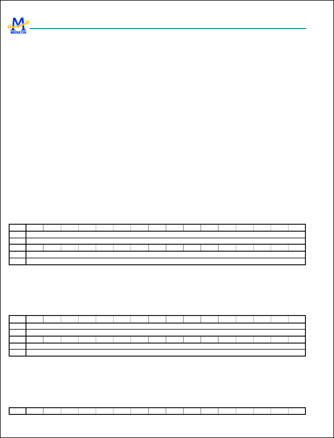
MT6217 GSM/GPRS Baseband Processor Data Sheet Revision 1.01
197/349 MediaTek Inc. Confidential
11 No U-component.
VU Vertical sampling factor for U-component
00 Vertical sampling factor for U-component is 1.
01 Vertical sampling factor for U-component is 2.
10 Vertical sampling factor for U-component is 4.
11 No U-component.
HV Horizontal samp ling factor for V-component
00 Horizontal sampling factor for V-component is 1.
01 Horizontal sampling factor for V-component is 2.
10 Horizontal sampling factor for V-component is 4.
11 No V-component.
VV Vertical sampling factor for V-component
00 Vertical sampling factor for V-component is 1.
01 Vertical sampling factor for V-component is 2.
10 Vertical sampling factor for V-component is 4.
11 No V-component.
INTEN Interrupt Enable. When interrupt for BLKCS is enabled, interrupt will arise whenever BLKCS finishes.
0 Interrupt for BLKCS is disabled.
1 Interrupt for BLKCS is enabled.
RESZ+0034h Image Resizer Y-Component Line Buffer Memory
Base Address Register RESZ_YLMBASE
Bit 31 30 29 28 27 26 25 24 23 22 21 20 19 18 17 16
Name
YLMBASE [31:16]
Type R/W
Bit 15 14 13 12 11 10 9 8 7 6 5 4 3 2 1 0
Name
YLMBASE [15:0]
Type R/W
The register specifies the base address of line buffer for Y-component. It could be byte-aligned. It’s only usefull in
block-based mode.
RESZ+0038h Image Resizer U-Component Line Buffer
Memory Base Address Register RESZ_ULMBASE
Bit 31 30 29 28 27 26 25 24 23 22 21 20 19 18 17 16
Name
ULMBASE [31:16]
Type R/W
Bit 15 14 13 12 11 10 9 8 7 6 5 4 3 2 1 0
Name
ULMBASE [15:0]
Type R/W
The register specifies the base address of line buffer for U-component. It could be byte -aligned. It ’s only usefull in
block-based mode.
RESZ+003Ch Image Resizer V-Component Line Buffer Memory
Base Address Register RESZ_VLMBASE
Bit 31 30 29 28 27 26 25 24 23 22 21 20 19 18 17 16
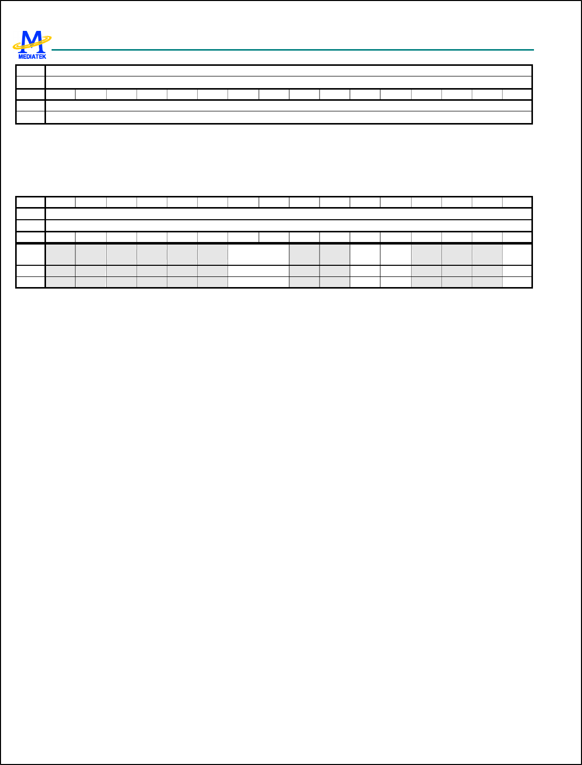
MT6217 GSM/GPRS Baseband Processor Data Sheet Revision 1.01
198/349 MediaTek Inc. Confidential
Name
VLMBASE [31:16]
Type R/W
Bit 15 14 13 12 11 10 9 8 7 6 5 4 3 2 1 0
Name
VLMBASE [15:0]
Type R/W
The register specifies the base address of line buffer for V-component. It could be byte -aligned. It’s only usefull in
block-based mode.
RESZ+0040h Image Resizer Fine Resizing Configuration Register
RESZ_FRCFG
Bit 31 30 29 28 27 26 25 24 23 22 21 20 19 18 17 16
Name
WMSZ
Type R/W
Bit 15 14 13 12 11 10 9 8 7 6 5 4 3 2 1 0
Name
PCSF1 VRINT
EN HRINT
EN VRSS
Type R/W R/W R/W R/W
Reset
00 0 0 0
The register specifies various setting of control for fine resizing, including of horizontal and vertical resizing. Note that all
parameters must be set before horizontal and vertical resizing proceeds.
VRSS The register bit specifies whether subsampling for vertical resizing is enabled. For throughput issue, vertical
resizing may be simplified by subsampling lines vertically. The register bit is only valid in pixel-based mode.
0 Subsampling for vertical resizing is disabled.
1 Subsampling for vertical resizing is enabled.
HRINTEN HR (Horizontal Resizing) Interrupt Enable. When interrupt for HR is enabled, interrupt will arise whenever HR
finishes.
0 Interrupt for HR is disabled.
1 Interrupt for HR is enabled.
VRINTEN VR (Vertical Resizing) Interrupt Enable. When interrupt for VR is enabled, interrupt will arise whenever VR
finishes.
0 Interrupt for VR is disabled.
1 Interrupt for VR is enabled.
PCSF1 Coarse Shrinking Factor 1 for pixel-based resizing. Only horizontal coarse shrinking is supported for
pixel-based resizing.
00 No coarse shrinking.
01 Image width becomes 1/2 of original size after coarse shrink pass.
10 Image width becomes 1/4 of original size after coarse shrink pass.
11 Image width becomes 1/8 of original size after coarse shrink pass.
SEQ The register bit is used to force block-based horizontal resizing and vertical resizing to execute sequentially. When
the bit is set to ‘1’, even though dual buffer for working memory is used block-based horizontal resizing will not
process next image data until block-based vertical resizing finishes current image data. The register bit is only
valid in block-based mode.
0 block-based horizontal resizing and vertical resizing can execute parallel.
1 block-based horizontal resizing and vertical resizing will execute sequentially.
WMSZ It stands for Working Memory SiZe. The register specifies how many lines after horizontal resizing can be filled
into working memory. If dual line buffer is used, horizontal resizing and vertical resizing can execute parallel. Its
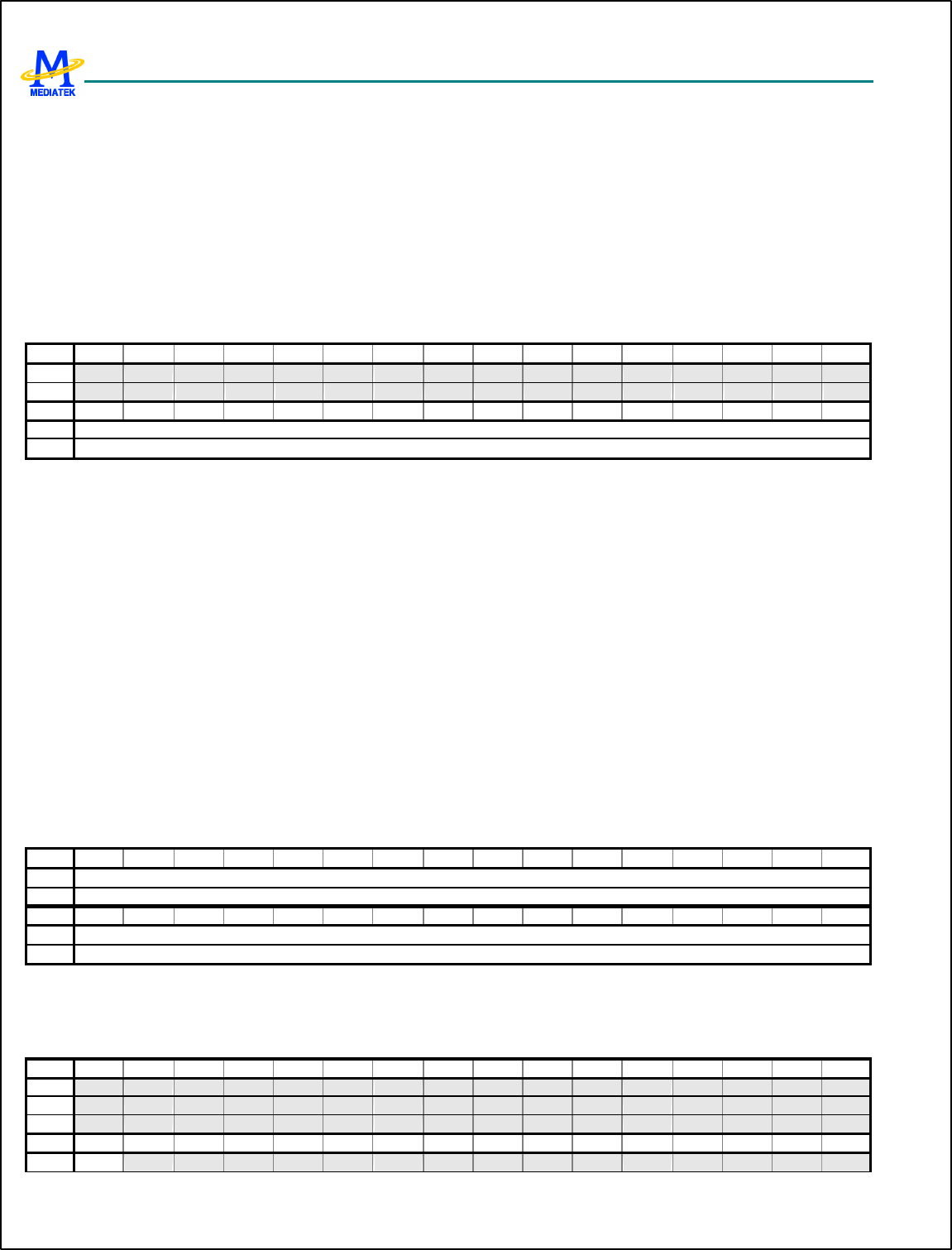
MT6217 GSM/GPRS Baseband Processor Data Sheet Revision 1.01
199/349 MediaTek Inc. Confidential
allowable maximum value is 2046 in block-based mode, however 16 in pixel-based mode. In pixel-based
mode, if the register field is set with a value more than 16 then horizontal resizing will be disabled.
Furthermore, its minimum value is 4.
1 Working memory for each color component in block-based mode is 1.
2 Working memory for each color component in block-based mode is 2.
3 Working memory for each color component in block-based mode is 3.
4 Working memory for each color component in block-based mode is 4.
…
RESZ+0050h Image Resizer Y Line Buffer Size Register RESZ_YLBSIZE
Bit 31 30 29 28 27 26 25 24 23 22 21 20 19 18 17 16
Name
Type
Bit 15 14 13 12 11 10 9 8 7 6 5 4 3 2 1 0
Name
YLBZE
Type R/W
The register specifies line buffer size for image data after coarse shrinking. It’s only useful in block-based mode.
YLBSZ It stands for Y-component Line Buffer SiZe. The register field specifies how many lines of Y-component can be
filled into line buffer. Line buffer size for U- and V-component can be determined according to sampling factor.
For example, if (VY, V
U, VV)=(4,4,2) and line buffer size for Y-component is 32 lines then line buffer size for
U-component is also 32 lines and V-component 16 lines. If line buffer has capacity for whole image after block
coarse shrinking, then block coarse shrinking can be used as applications of scale down by 2, or 4, or 8. If dual line
buffer is used, block coarse shrinking and horizontal resizing can execute parallel. The allowable maximum value
is 2047.
1 Line buffer size for Y-component is 1 lines.
2 Line buffer size for Y-component is 2 lines.
3 Line buffer size for Y-component is 3 lines.
…
RESZ+005Ch Image Resizer Pixel-Based Resizing Working
Memory Base Address Register RESZ_PRWMBASE
Bit 31 30 29 28 27 26 25 24 23 22 21 20 19 18 17 16
Name
PRWMBASE [31:16]
Type R/W
Bit 15 14 13 12 11 10 9 8 7 6 5 4 3 2 1 0
Name
PRWMBASE [15:0]
Type R/W
The register specifies the base address of working memory in pixel-based resizing mode. It must be byte-aligned.
RESZ+0080h Image Resizer YUV2RGB Configuration Register RESZ_YUV2RGB
Bit 31 30 29 28 27 26 25 24 23 22 21 20 19 18 17 16
Name
Type
Reset
Bit 15 14 13 12 11 10 9 8 7 6 5 4 3 2 1 0
Name
INTEN
MT6217 GSM/GPRS Baseband Processor Data Sheet Revision 1.01
200/349 MediaTek Inc. Confidential
Type R/W
Reset
0
The register specifies various setting of control for YUV2RGB. Note that ALL parameters must be set before writing ‘1’
to the register bit RESZ_CONN.YUV2RGBENA.
INTEN Interrupt Enable. When interrupt for YUV2RGB is enabled, interrupt will arise whenever YUV2RGB finishes.
0 Interrupt for YUV2RGB is disabled.
1 Interrupt for YUV2RGB is enabled.
RESZ+0084h Image Resizer Target Memory Base Address
Register RESZ_TMBASE
Bit 31 30 29 28 27 26 25 24 23 22 21 20 19 18 17 16
Name
TMBASE [31:16]
Type R/W
Bit 15 14 13 12 11 10 9 8 7 6 5 4 3 2 1 0
Name
TMBASE [15:1]
Type R/W
The register specifies the base address of target memory. Target memory is memory space for destination of YUV2RGB. It’
must be half-word (2 bytes) aligned.
RESZ+00B0h Image Resizer Information Register 0 RESZ_INFO0
Bit 31 30 29 28 27 26 25 24 23 22 21 20 19 18 17 16
Name
INFO[31:16]
Type RO
Bit 15 14 13 12 11 10 9 8 7 6 5 4 3 2 1 0
Name
INFO[15:0]
Type RO
The register shows progress of BLKCS. But they are not real processed width/height. Sampling factors must be taken into
consideration. For example, if (VY, V
U, VV)=(2,4,4) then real processed width/height are two times of the register.
INFO[31:16] BLKCS y
INFO[15:00] BLKCS x
RESZ+00B4 Image Resizer Information Register 1 RESZ_INFO1
Bit 31 30 29 28 27 26 25 24 23 22 21 20 19 18 17 16
Name
INFO[31:16]
Type RO
Bit 15 14 13 12 11 10 9 8 7 6 5 4 3 2 1 0
Name
INFO[15:0]
Type RO
The register shows progress of BLK2PEL.
INFO[31:16] BLK2PEL y
INFO[15:00] BLK2PEL x
RESZ+00B8 Image Resizer Information Register 2 RESZ_INFO2
Bit 31 30 29 28 27 26 25 24 23 22 21 20 19 18 17 16
MT6217 GSM/GPRS Baseband Processor Data Sheet Revision 1.01
201/349 MediaTek Inc. Confidential
Name
INFO[31:16]
Type RO
Bit 15 14 13 12 11 10 9 8 7 6 5 4 3 2 1 0
Name
INFO[15:0]
Type RO
The register shows progress of pixels received fro m BLKCS in fine resizing stage.
INFO[31:16] Indicate the account of vertical lines received from BLKCS in fine resizing stage.
INFO[15:00] Indicate the account of horizontal pixels received from BLKCS in fine resizing stage. Note that it will
become zero when resizing completes.
RESZ+00BC Image Resizer Information Register 3 RESZ_INFO3
Bit 31 30 29 28 27 26 25 24 23 22 21 20 19 18 17 16
Name
INFO[31:16]
Type RO
Bit 15 14 13 12 11 10 9 8 7 6 5 4 3 2 1 0
Name
INFO[15:0]
Type RO
The register shows progress of horizontal resizing in fine resizing stage.
INFO[31:16] Indicate the account of horizontal resizing in fine resizing stage in horizontal direction.
INFO[15:00] Indicate the account of horizontal resizing in fine resizing stage in vertical direction.
RESZ+00C0 Image Resizer Information Register 4 RESZ_INFO4
Bit 31 30 29 28 27 26 25 24 23 22 21 20 19 18 17 16
Name
INFO[31:16]
Type RO
Bit 15 14 13 12 11 10 9 8 7 6 5 4 3 2 1 0
Name
INFO[15:0]
Type RO
The register shows progress of vertical resizing in fine resizing stage.
INFO[31:16] Indicate the account of vertical resizing in fine resizing stage in horizontal direction.
INFO[15:00] Indicate the account of vertical resizing in fine resizing stage in vertical direction.
RESZ+00C5 Image Resizer Information Register 5 RESZ_INFO5
Bit 31 30 29 28 27 26 25 24 23 22 21 20 19 18 17 16
Name
INFO[31:16]
Type RO
Bit 15 14 13 12 11 10 9 8 7 6 5 4 3 2 1 0
Name
INFO[15:0]
Type RO
The register shows progress of YUV-to-RGB
INFO[31:16] Indicate YUV-to-RGB in horizontal direction.
INFO[15:00] Indicate YUV-to-RGB in vertical direction.

MT6217 GSM/GPRS Baseband Processor Data Sheet Revision 1.01
202/349 MediaTek Inc. Confidential
6.3.8 Application Notes
l Determine line buffer size by taking into consideration of CSF and sampling factor. For example, if CSF=3 and
(Vy, Vu, Vv)=(4,x,x) then minimum of line buffer could be 4 instead of 32.
l Working memory. Maximum value is 16 and minimum 4. Remember that each pixel occupies 3 bytes. Thus
minimum requirement for working memory in pixel-based resizing is (pixel number in a line)x3x4 bytes.
l Configuration procedure for block-based image sources
RESZ_BLKCSCFG = select CSF,sampling factor, interrupt enable;
RESZ_YLBBASE = memory base for Y-component;
RESZ_ULBBASE = memory base for U-component;
RESZ_VLBBASE = memory base for V-component;
RESZ_YLBSIZE = line buffer size for Y-component;
RESZ_TMBASE = target memory base address;
RESZ_SRCSZ = source image size;
RESZ_TARSZ = target image size;
RESZ_HRATIO = horizontal ratio;
RESZ_VRATIO = vertical ratio;
RESZ_HRES = horizontal residual;
RESZ_VRES = vertical residual;
RESZ_FRCFG = working memory size,interrupt enable;
RESZ_PRWMBASE = working memory base;
RESZ_CON = 0xf;
6.4 NAND FLASH interface
6.4.1 General description
MT6217 provides NAND flash interface.
The NAND FLASH interface support features as follows:
l ECC (Hamming code) acceleration capable of one-bit error correction or two bits error detection.
l Programmable ECC block size. Support 1, 2 or 4 ECC block within a page.
l Word/byte access through APB bus.
l Direct Memory Access for massive data transfer.
l Latch sensitive interrupt to indicate ready state for read, program, erase operation and error report.
l Programmable wait states, command/address setup and hold time, read enable hold time, and write enable recovery
time.
l Support page size : 512(528) bytes and 2048(2112) bytes.
l Support 2 chip select for NAND flash parts.
l Support 8/16 bits I/O interface.
MT6217 GSM/GPRS Baseband Processor Data Sheet Revision 1.01
203/349 MediaTek Inc. Confidential
The NFI core can automatically generate ECC parity bits when programming or reading the device. If the user approves the
way it stores the parity bits in the spare area for each page, the AUTOECC mode can be used. Otherwise, the user can
prepare the data (may contains operating system information or ECC parity bits) for the spare area with another
arrangement. In the former case, the core can check the parity bits when reading from the device. The ECC module features
the hamming code, which is capable of correcting one bit error or detecting two bits error within one ECC block.
6.4.2 Register definition
NFI+0000h NAND flash access control register NFI_ACCCON
Bit 15 14 13 12 11 10 9 8 7 6 5 4 3 2 1 0
Name
C2R W2R WH WST RLT
Type R/W R/W R/W R/W R/W
Reset 0 0 0 0 0
This is the timing access control register for the NAND FLASH interface. In order to accommodate operations for different
system clock frequency ranges from 13MHz to 52MHz, wait states and setup/hold time margin can be configured in this
register.
C2R The field signifies the minimum required time from NCEB low to NREB low.
W2R The field signifies the minimum required time from NWEB high to NREB low. It’s in unit of 2T. So the actual
time ranges from 2T to 8T in step of 2T.
WH Write-enable hold -time.
The field specifies the hold time of NALE, NCLE, NCEB signals relative to the rising edge of NWEB. This field
is associated with WST to expand the write cycle time, and is associated with RLT to expand the read cycle time.
RLT Read Latency Time
The field specifies how many wait states to be inserted to meet the requirement of the read access time for the
device.
00 No wait state.
01 1T wait state.
10 2T wait state.
11 3T wait state.
WST Write Wait State
The field specifies the wait states to be inserted to meet the requirement of the pulse width of the NWEB signal.
00 No wait state.
01 1T wait state.
10 2T wait state.
11 3T wait state.
NFI +0004h NFI page format control register NFI_PAGEFMT
Bit 15 14 13 12 11 10 9 8 7 6 5 4 3 2 1 0
Name
B16E
N ECCBLKSIZE ADRM
ODE PSIZE
Type R/W R/W R/W R/W
Reset 0 0 0 0
This register manages the page format of the device. It includes the bus width selection, the page size, the associated
address format, and the ECC block size.
MT6217 GSM/GPRS Baseband Processor Data Sheet Revision 1.01
204/349 MediaTek Inc. Confidential
B16EN 16 bits I/O bus interface enable.
ECCBLKSIZE ECC block size.
This field signifies the size of one ECC block. The hardware -fuelled ECC generation provides 2 or 4 blocks within
a single page.
0 ECC block size: 128 bytes. Used for devices with page size equal to 512 bytes.
1 ECC block size: 256 bytes. Used for devices with page size equal to 512 bytes.
2 ECC block size: 512 bytes. Used for devices with page size equal to 512 or 2048 bytes.
3 ECC block size: 1048 bytes. Used for devices with page size equal to 2048 bytes.
4~ Reserved.
ADRMODE Address mode. This field specifies the input address format.
0 Normal input address mode, in which the half page identifier is not specified in the address assignment but in
the command set. As in Table 27, A7 to A0 identifies the byte address within half a page, A12 to A9 specifies
the page address within a block, and other bits specify the block address. The mode is used mostly for the
device with 512 bytes page size.
1 Large size input address mode, in which all address information is specified in the address assignment rather
than in the command set. As in Table 7, A11 to A0 identifies the byte address within a page (column address).
The mode is used for the device with 2048 bytes page size.
NLD7 NLD6 NLD5 NLD4 NLD3 NLD2 NLD1 NLD0
First cycle A7 A6 A5 A4 A3 A2 A1 A0
Second cycle A16 A15 A14 A13 A12 A11 A10 A9
Table 27 Address assignment of the first type (ADRMODE = 0, cycles after second one are omitted)
NLD7 NLD6 NLD5 NLD4 NLD3 NLD2 NLD1 NLD0
First cycle A7 A6 A5 A4 A3 A2 A1 A0
Second cycle 0 0 0 0 0 0 A9 A8
Table 28 Address assignment of the second type (ADRMODE = 1, cycles after second one are omitted)
PSIZE Page Size.
The field specifies the size of one page for the device. Two most widely used page size are supported.
0 The page size is 528 bytes (including 512 bytes data area and 16 bytes spare area).
1 The page size is 2112 bytes (including 2048 bytes data area and 64 bytes spare area).
2~ Reserved.
NFI +0008h Operation control register NFI_OPCON
Bit 15 14 13 12 11 10 9 8 7 6 5 4 3 2 1 0
Name
NOB SRD EWR ERD BWR BRD
Type W/R WO WO WO R/W R/W
Reset 0 0 0 0 0 0
This register controls the burst mode and the single of the data access. In burst mode, the core supposes there are one or
more than one page of data to be accessed. On the contrary, in single mode, the core supposes there are only less than 4
bytes of data to be accessed.
BRD Burst read mode. Setting this field to be logic-1 enables the data read operation. The NFI core will issue read
cycles to retrieve data from the device when the data FIFO is not full or the device is not in the busy state. The NFI
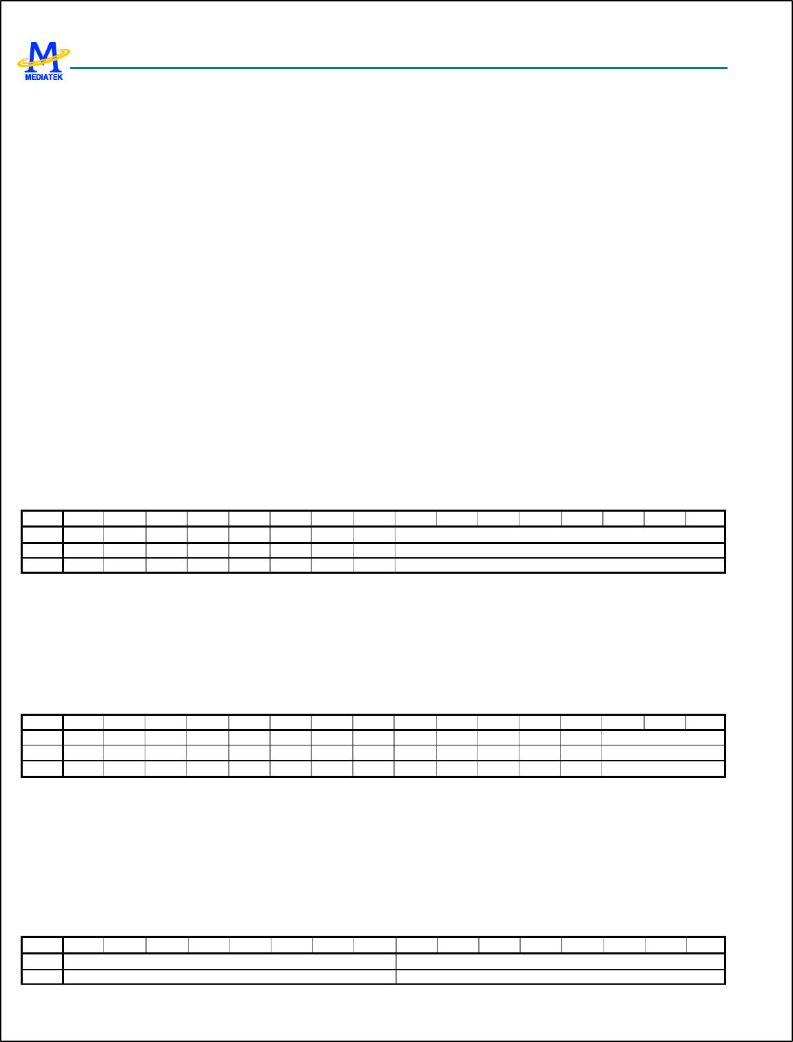
MT6217 GSM/GPRS Baseband Processor Data Sheet Revision 1.01
205/349 MediaTek Inc. Confidential
core supports consecutive page reading. A page address counter is built in. If the reading reaches to the end of the
page, the device will enter the busy state to prepare data of the next page, and the NFI core will automatically
pause reading and remain inactive until the device returns to the ready state. The page address counter will restart
to count from 0 after the device returns to the ready state and start retrieving data again.
BWR Burst write mode. Setting to be logic-1 enables the data burst write operation for DMA operation. Actually the NFI
core will issue write cycles once if the data FIFO is not empty even without setting this flag. But if DMA is to be
utilized, the bit should be enabled. If DMA is not to be utilized, the bit didn’t have to be enabled.
ERD ECC read mode. Setting to be logic-1 initializes the ECC checking and correcting for the current page. The ECC
checking is only valid when a full ECC block has been read.
EWR Setting to be logic -1 initializes the ECC parity generation for the current page. The ECC code generation is only
valid when a full ECC block has been programmed.
SRD Setting to be logic -1 initializes the one-shot data read operation. It’s mainly used for read ID and read status
command, which requires no more than 4 read cycles to retrieve data from the device.
NOB The field signifies the number of bytes to be retrieved from the devic e in single mode, and the number of bytes per
AHB transaction in both single and burst mode.
0 Read 4 bytes from the device.
1 Read 1 byte from the device.
2 Read 2 bytes from the device.
3 Read 3 bytes from the device.
NFI +000Ch Command register NFI_CMD
Bit 15 14 13 12 11 10 9 8 7 6 5 4 3 2 1 0
Name
CMD
Type R/W
Reset 45
This is the command input register. The user should write this register to issue a command. Please refer to device datasheet
for the command set. The core can issue some associated commands automatically. Please check out register NFI_CON for
those commands.
CMD Command word.
NFI +0010h Address length register NFI_ADDNOB
Bit 15 14 13 12 11 10 9 8 7 6 5 4 3 2 1 0
Name
ADDR_NOB
Type R/W
Reset 0
This register signifies the number of bytes corresponding to current command. The valid number of bytes ranges from 1 to
5. The address format depends on what device to be used and what commands to be applied. The NFI core is made
transparent to those different situations except that the user has to define the number of bytes.
The user should write the target address to the address register NFI_ADDRL before programming this register.
ADDR_NOB Nu mber of bytes for the address
NFI +0014h Least significant address register NFI_ADDRL
Bit 31 30 29 28 27 26 25 24 23 22 21 20 19 18 17 16
Name
ADDR3 ADDR2
Type R/W R/W
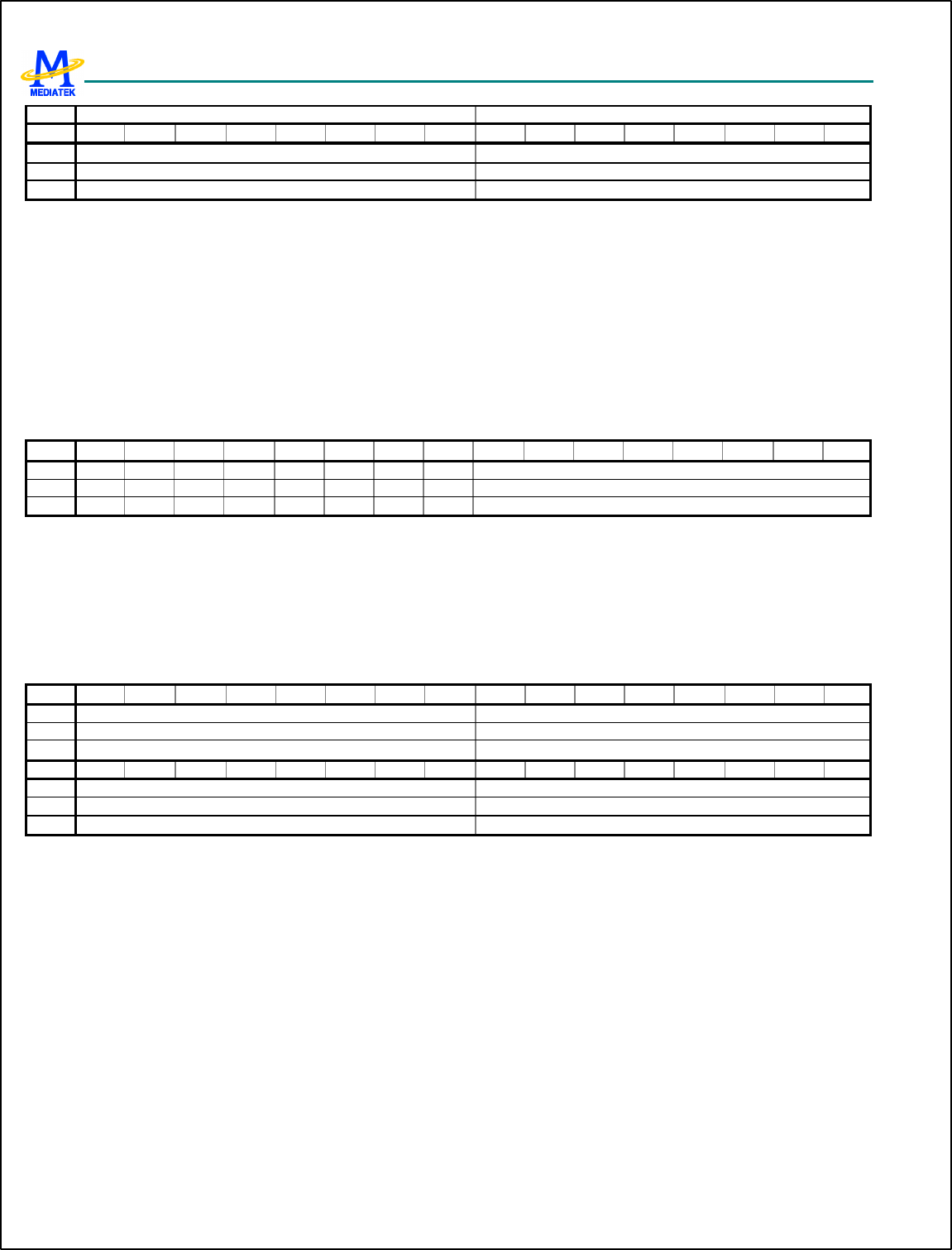
MT6217 GSM/GPRS Baseband Processor Data Sheet Revision 1.01
206/349 MediaTek Inc. Confidential
Reset 0 0
Bit 15 14 13 12 11 10 9 8 7 6 5 4 3 2 1 0
Name
ADDR1 ADDR0
Type R/W R/W
Reset 0 0
This defines the least significant 4 bytes of the address field to be applied to the device. Since the device bus width is 1 byte,
the NFI core arranges the order of address data to be least significant byte first. The user should put the first address byte in
the field ADDR0, the second byte in the field ADDR1, and so on.
ADDR3 The fourth address byte.
ADDR2 The third address byte.
ADDR1 The second address byte.
ADDR0 The first address byte.
NFI +0018h Most significant address register NFI_ADDRM
Bit 15 14 13 12 11 10 9 8 7 6 5 4 3 2 1 0
Name
ADDR4
Type R/W
Reset 0
This register defines the most significant byte of the address field to be applied to the device. The NFI core support s
address size up to 5 bytes. Programming this register implicitly indicates that the number of address field is 5. In this case,
the NFI core will automatically set the ADDR_NOB to 5.
ADDR4 The fifth address byte.
NFI +001Ch Write data buffer NFI_DATAW
Bit 31 30 29 28 27 26 25 24 23 22 21 20 19 18 17 16
Name
DW3 DW2
Type R/W R/W
Reset 0 0
Bit 15 14 13 12 11 10 9 8 7 6 5 4 3 2 1 0
Name
DW1 DW0
Type R/W R/W
Reset 0 0
This is the write port of the data FIFO. It supports word access. The least significant byte DW0 is to be programmed to the
device first, then DW1, and so on.
If the data to be programmed is not word aligned, byte write access will be needed. Instead, the user should use another
register NFI_DATAWB for byte programming. Writing a word to NFI_DATAW is equivalent to writing four bytes DW0,
DW1, DW2, DW3 in order to NFI_DATAWB. Be reminded that the word alignment is from the perspective of the user.
The device bus is byte-wide. According to the flash’s nature, the page address will wrap around once it reaches the end of
the page.
DW3 Write data byte 3.
DW2 Write data byte 2.
DW1 Write data byte 1.
DW0 Write data byte 0.
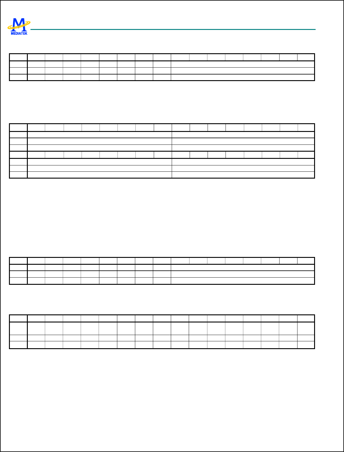
MT6217 GSM/GPRS Baseband Processor Data Sheet Revision 1.01
207/349 MediaTek Inc. Confidential
NFI +0020h Write data buffer for byte access NFI_DATAWB
Bit 15 14 13 12 11 10 9 8 7 6 5 4 3 2 1 0
Name
DW0
Type R/W
Reset 0
This is the write port for the data FIFO for byte access.
DW0 Write data byte.
NFI +0024h Read data buffer NFI_DATAR
Bit 31 30 29 28 27 26 25 24 23 22 21 20 19 18 17 16
Name
DR3 DR2
Type RO RO
Reset 0 0
Bit 15 14 13 12 11 10 9 8 7 6 5 4 3 2 1 0
Name
DR1 DR0
Type RO RO
Reset 0 0
This is the read port of the data FIFO. It supports word access. The least significant byte DR0 is the first byte read from the
device, then DR1, and so on.
DR3 Read data byte 3.
DR2 Read data byte 2.
DR1 Read data byte 1.
DR0 Read data byte 0.
NFI +0028h Read data buffer for byte access NFI_DATARB
Bit 15 14 13 12 11 10 9 8 7 6 5 4 3 2 1 0
Name
DR0
Type RO
Reset 0
This is the read port of the data FIFO for byte access.
NFI +002Ch NFI status NFI_PSTA
Bit 15 14 13 12 11 10 9 8 7 6 5 4 3 2 1 0
Name
BUSY DATA
W DATA
R ADDR CMD
Type RO R/W R/W R/W R/W
Reset 0* 0 0 0 0
This register signifies the NFI core control status including command mode, address mode, data program and read mode.
The user should poll this register for the end of those operations.
*The value of BUSY bit depends on the GPIO configuration. If GPIO is configured for NAND flash application, the reset
value should be 0, which represents that NAND flash is in idle status. When the NAND flash is busy, the value will be 1.
BUSY Latched NRB signal for the NAND flash.
DATAW The NFI core is in data write mode.
DATAR The NFI core is in data read mode.

MT6217 GSM/GPRS Baseband Processor Data Sheet Revision 1.01
208/349 MediaTek Inc. Confidential
ADDR The NFI core is in address mode.
CMD The NFI core is in command mode.
NFI +0030h FIFO control NFI_FIFOCON
Bit 15 14 13 12 11 10 9 8 7 6 5 4 3 2 1 0
Name
RESE
T FLUS
H WR_F
ULL WR_E
MPTY RD_F
ULL RD_E
MPTY
Type WO WO RO RO RO RO
Reset 0 0 0 1 0 1
The register signifies the status of the data FIFO.
RESET Reset the stats machine and data FIFO.
FLUSH Flush the data FIFO.
WR_FULL Data FIFO full in burst write mode.
WR_EMPTY Data FIFO empty in burst write mode.
RD_FULL Data FIFO full in burst read mode.
RD_EMPTY Data FIFO empty in burst read mode.
NFI +0034h NFI control NFI_CON
Bit 15 14 13 12 11 10 9 8 7 6 5 4 3 2 1 0
Name
BYTE
_RW MULTI
PAGE
_CON
READ
_CON
PROG
RAM_
CON
ERAS
E_CO
N
SW_P
ROGS
PARE
_EN
MULTI
_PAG
E_RD
_EN
AUTO
ECC_
ENC_
EN
AUTO
ECC_
DEC_
EN
DMA_
WR_E
N
DMA_
RD_E
N
Type R/W R/W R/W R/W R/W R/W R/W R/W R/W R/W R/W
Reset 0 0 0 0 0 0 0 0 0 0 0
The register controls the DMA and ECC functions. For all field, Setting to be logic -1 signifies enabled, while 0 signifies
disabled.
BYTE_RW Enable APB byte access.
MULTIPAGE_CON This bit signifies that the first-cycle command for read operation (00h) can be automatically
performed to read the next page automatically. Automatic ECC decoding flag AUTOECC_DEC_EN should also
be enabled for multiple page access.
READ_CON This bit signifies that the second-cycle command for read operation (30h) can be automatically performed.
This conforms to the command set for the device with more then 1Gb capacity.
PROGRAM_CON This bit signifies that the second-cycle command for page program operation (10h) can be
automatically performed after the data for the entire page (including the spare area) has been written. It should be
associated with automatic ECC encoding mode enabled.
ERASE_CON The bit signifies that the second-cycle command for block erase operation (D0h) can be automatically
performed after the block address is latched.
SW_PROGSPARE_EN If enabled, the NFI core allows the user to program or read the spare area. Otherwise, the
spare area can be programmed or read by the core.
MULTI_PAGE_RD_EN Multiple page burst read enable. If enabled, the burst read operation could continue through
multiple pages within a block. It’s also possible and more efficient to associate with DMA scheme to read a sector
of data contained within the same block.

MT6217 GSM/GPRS Baseband Processor Data Sheet Revision 1.01
209/349 MediaTek Inc. Confidential
AUTOECC_ENC_EN Automatic ECC encoding enable. If enabled, the ECC parity is written automatically to the spare
are a right after the end of the data area. If SW_PROGSPARE_EN is set, however, the mode can’t be enabled
since the core can’t access the spare area.
AUTOECC_DEC_EN Automatic ECC decoding enabled, the error checking and correcting are performed automatically
on the data read from the memory and vice versa. If enabled, when the page address reaches the end of the data
read of one page, additional read cycles will be issued to retrieve the ECC parity-check bits from the spare area to
perform checking and correcting.
DMA_WR_EN This field is used to control the activity of DMA write transfer.
DMA_RD_EN This field is used to control the activity of DMA read transfer.
NFI +0038h Interrupt status register NFI_INTR
Bit 15 14 13 12 11 10 9 8 7 6 5 4 3 2 1 0
Name
BUSY
_RET
URN
ERR_
COR3 ERR_
COR2
ERR_
COR1
ERR_
COR0
ERR_
DET3 ERR_
DET2 ERR_
DET1 ERR_
DET0
ERAS
E_CO
MPLE
TE
RESE
T_CO
MPLE
TE
WR_C
OMPL
ETE
RD
_COM
PLET
E
Type RC RC RC RC RC RC RC RC RC RC RC RC RC
Reset 0 0 0 0 0 0 0 0 0 0 0 0 0
The register indicates the status of all the interrupt sources. Read this register will clear all interrupts.
BUSY_RETURN Indicates that the device state returns from busy by inspecting the R/B# pin.
ERR_COR3 Indicates that the single bit error in ECC block 3 needs to be corrected.
ERR_COR2 Indicates that the single bit error in ECC block 2 needs to be corrected.
ERR_COR1 Indicates that the single bit error in ECC block 1 needs to be corrected.
ERR_COR0 Indicates that the single bit error in ECC block 0 needs to be corrected.
ERR_DET3 Indicates an uncorrectable error in ECC block 3.
ERR_DET2 Indicates an uncorrectable error in ECC block 2.
ERR_DET1 Indicates an uncorrectable error in ECC block 1.
ERR_DET0 Indicates an uncorrectable error in ECC block 0.
ERASE_COMPLETE Indicates that the erase operation is completed.
RESET_COMPLETE Indicates that the reset operation is completed.
WR_COMPLETE Indicates that the write operation is completed.
RD_COMPLETE Indicates that the single page read operation is completed.
NFI +003Ch Interrupt enable register NFI_INTR_EN
Bit 15 14 13 12 11 10 9 8 7 6 5 4 3 2 1 0
Name
ERR_
COR3
_EN
ERR_
COR2
_EN
ERR_
COR1
_EN ERR_
DET3
_EN
ERR_
DET2
_EN
ERR_
DET1
_EN
BUSY
_RET
URN_
EN
ERR_
COR_
EN
ERR_
DET_
EN
ERAS
E_CO
MPLE
TE_E
N
RESE
T_CO
MPLE
TE_E
N
WR_C
OMPL
ETE_
EN
RD_
COM
PLET
E_EN
Type R/W R/W R/W R/W R/W R/W R/W R/W R/W R/W R/W R/W R/W
Reset 0 0 0 0 0 0 0 0 0 0 0 0 0
This register controls the activity for the interrupt sources.
ERR_COR1_EN The error correction interrupt enable for the 2nd ECC block.
ERR_COR2_EN The error correction interrupt enable for the 3rd ECC block.
ERR_COR3_EN The error correction interrupt enable for the 4th ECC block.
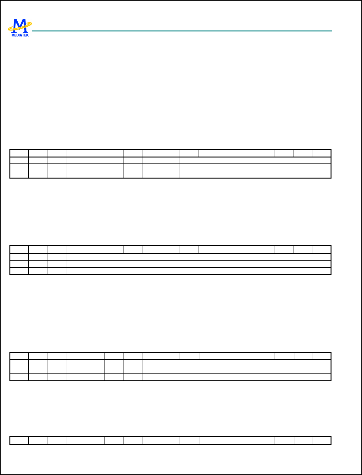
MT6217 GSM/GPRS Baseband Processor Data Sheet Revision 1.01
210/349 MediaTek Inc. Confidential
ERR_DET1_EN The error detection interrupt enable for the 2nd ECC block.
ERR_DET2_EN The error detection interrupt enable for the 3rd ECC block.
ERR_DET3_EN The error detection interrupt enable for the 4th ECC block.
BUSY_RETURN_EN The busy return interrupt enable.
ERR_COR_EN The error correction interrupt enable for the 1st ECC block.
ERR_DET_EN The error detection interrupt enable for the 1st ECC block.
ERASE_COMPLETE_EN The erase completion interrupt enable.
RESET_COMPLETE_EN The reset completion interrupt enable.
WR_COMPLETE_EN The single page write completion interrupt enable.
RD_COMPLETE_EN The single page read completion interrupt enable.
NFI+0040h NAND flash page counter NFI_PAGECNTR
Bit 15 14 13 12 11 10 9 8 7 6 5 4 3 2 1 0
Name
CNTR
Type R/W
Reset 0
The register represents the number of pages that the NFI has read since the issuing of the read command. For some devices,
the data can be read consecutively through different pages without the need to issue another read command. The user can
monitor this register to know current page count, particularly when read DMA is enabled.
CNTR The page counter.
NFI+0044h NAND flash page address counter NFI_ADDRCNTR
Bit 15 14 13 12 11 10 9 8 7 6 5 4 3 2 1 0
Name
CNTR
Type R/W
Reset 0
The register represents the current read/write address with respect to initial address input. It counts in unit of byte. In page
read and page program operation, the address should be the same as that in the state machine in the target device.
The address supports up to 4096 bytes.
CNTR The address count.
NFI +0050h ECC block 0 parity error detect syndrome address NFI_
SYM0_ADDR
Bit 15 14 13 12 11 10 9 8 7 6 5 4 3 2 1 0
Name
SYM
Type RO
Reset 0
This register identifies the address within ECC block 0 that a single bit error has been detected.
SYM The byte address of the error-correctable bit.
NFI +0054h ECC block 1 parity error detect syndrome address NFI_SYM1_ADD
R
Bit 15 14 13 12 11 10 9 8 7 6 5 4 3 2 1 0
MT6217 GSM/GPRS Baseband Processor Data Sheet Revision 1.01
211/349 MediaTek Inc. Confidential
Name
SYM
Type RO
Reset 0
This register identifies the address within ECC block 1 that a single bit error has been detected.
SYM The byte address of the error-correctable bit.
NFI +0058h ECC block 2 parity error detect syndrome address NFI_SYM2_ADD
R
Bit 15 14 13 12 11 10 9 8 7 6 5 4 3 2 1 0
Name
SYM
Type RO
Reset 0
This register identifies the address within ECC block 2 that a single bit error has been detected.
SYM The byte address of the error-correctable bit.
NFI +005Ch ECC block 3 parity error detect syndrome address NFI_SYM3_ADD
R
Bit 15 14 13 12 11 10 9 8 7 6 5 4 3 2 1 0
Name
SYM
Type RO
Reset 0
This register identifies the address within ECC block 3 that a single bit error has been detected.
SYM The byte address of the error-correctable bit.
NFI +0060h ECC block 0 parity error detect syndrome word NFI_SYM0_DAT
Bit 31 30 29 28 27 26 25 24 23 22 21 20 19 18 17 16
Name
ED3 ED2
Type RO RO
Reset 0 0
Bit 15 14 13 12 11 10 9 8 7 6 5 4 3 2 1 0
Name
ED1 ED0
Type RO RO
Reset 0 0
This register signifies the syndrome word for the corrected ECC block 0. To correct the error, the user should first read
NFI_ SYM0_ADDR for the address of the correctable word, and then read NFI_SYM0_DAT, directly XOR the syndrome
word with the data word to obtain the correct word.
NFI +0064h ECC block 1 parity error detect syndrome word NFI_SYM1_DAT
Bit 31 30 29 28 27 26 25 24 23 22 21 20 19 18 17 16
Name
ED3 ED2
Type RO RO
Reset 0 0
Bit 15 14 13 12 11 10 9 8 7 6 5 4 3 2 1 0
Name
ED1 ED0
Type RO RO
Reset 0 0
MT6217 GSM/GPRS Baseband Processor Data Sheet Revision 1.01
212/349 MediaTek Inc. Confidential
This register signifies the syndrome word for the corrected ECC block 0. To correct the error, the user should first read
NFI_ SYM1_ADDR for the address of the correctable word, and then read NFI_SYM1_DAT, directly XOR the syndrome
word with the data word to obtain the correct word.
NFI +0068h ECC block 2 parity error detect syndrome word NFI_SYM2_DAT
Bit 31 30 29 28 27 26 25 24 23 22 21 20 19 18 17 16
Name
ED3 ED2
Type RO RO
Reset 0 0
Bit 15 14 13 12 11 10 9 8 7 6 5 4 3 2 1 0
Name
ED1 ED0
Type RO RO
Reset 0 0
This register signifies the syndrome word for the corrected ECC block 0. To correct the error, the user should first read
NFI_ SYM2_ADDR for the address of the correctable word, and then read NFI_SYM2_DAT, directly XOR the syndrome
word with the data word to obtain the correct word.
NFI +006Ch ECC block 3 parity error detect syndrome word NFI_SYM3_DAT
Bit 31 30 29 28 27 26 25 24 23 22 21 20 19 18 17 16
Name
ED3 ED2
Type RO RO
Reset 0 0
Bit 15 14 13 12 11 10 9 8 7 6 5 4 3 2 1 0
Name
ED1 ED0
Type RO RO
Reset 0 0
This register signifies the syndrome word for the corrected ECC block 0. To correct the error, the user should first read
NFI_ SYM3_ADDR for the address of the correctable word, and then read NFI_SYM3_DAT, directly XOR the syndrome
word with the data word to obtain the correct word.\
NFI +0070h NFI ECC error detect indication register NFI_ERRDET
Bit 15 14 13 12 11 10 9 8 7 6 5 4 3 2 1 0
Name
EBLK
3 EBLK
2 EBLK
1 EBLK
0
Type RO RO RO RO
Reset
0 0 0 0
This register identifies the block in which an uncorrectable error has been detected.
NFI +0080h NFI ECC parity word 0 NFI_PAR0
Bit 15 14 13 12 11 10 9 8 7 6 5 4 3 2 1 0
Name
PAR
Type RO
Reset 0
This register signifies the ECC parity for the ECC block 0. It’s calculated by the NFI core and can be read by the user. It’s
generated when writing or reading a page.
MT6217 GSM/GPRS Baseband Processor Data Sheet Revision 1.01
213/349 MediaTek Inc. Confidential
Register Address Register Function Acronym
NFI +0080h NFI ECC parity word 0 NFI_PAR0
NFI +0084h NFI ECC parity word 1 NFI_PAR1
NFI +0088h NFI ECC parity word 2 NFI_PAR2
NFI +008Ch NFI ECC parity word 3 NFI_PAR3
NFI +0090h NFI ECC parity word 4 NFI_PAR4
NFI +0094h NFI ECC parity word 5 NFI_PAR5
NFI +0098h NFI ECC parity word 6 NFI_PAR6
NFI +009Ch NFI ECC parity word 7 NFI_PAR7
Table 29 NFI parity bits register table
NFI+0100h NFI device select register NFI_CSEL
Bit 15 14 13 12 11 10 9 8 7 6 5 4 3 2 1 0
Name
CSEL
Type R/W
Reset
0
The register is used to select the target device. It decides which CEB pin to be functional.
CSEL Chip select. The value defaults to 0.
0 Device 1 is selected.
1 Device 2 is selected.
6.4.3 Device programming sequence
This section lists the program sequences to successfully use any compliant devices.
For block erase
1. Enable erase complete interrupt (NFI_INTR_EN = 8h).
2. Write command (NFI_CMD = 60h).
3. Write block address (NFI_ADDR).
4. Set the number of address bytes (NFI_ADDRNOB).
5. Check program status (NFI_PSTA) to see whether the operation has been completed. Omitted if ERASE_CON has
been set.
6. Write command (NFI_ CMD = D0h). Omitted if ERASE_CON has been set.
7. Check the erase complete interrupt.
For status read
1. Write command (NFI_CMD = 70h).
2. Set single word read for 1 byte (NFI_OPCON = 1100h).
3. Check program status (NFI_PSTA) to see whether the operation has been completed.

MT6217 GSM/GPRS Baseband Processor Data Sheet Revision 1.01
214/349 MediaTek Inc. Confidential
4. Read single byte (NFI_DATAR).
For page program
1. Enable write complete interrupt (NFI_INTR_EN = 2h).
2. Set DMA mode, and hardware ECC mode (NFI_CON = Ah).
3. Write command (NFI_CMD = 80h).
4. Write page address (NFI_ADDR).
5. Set the number of address bytes (NFI_ADDRNOB).
6. Set burst write (NFI_OPCON = 2h).
7. In DMA mode, the signal DMA_REQ controls the access. The user can also check the status of the FIFO
(NFI_FIFOCON) and write a pre -specified number of data whenever the FIFO is not full and until the end of page is
reached.
8. Check program status (NFI_PSTA) to see whether all operation has been completed.
9. Set ECC parities write. Omitted if hardware ECC mode has been set.
10. Check program status (NFI_PSTA) to see whether the above operation has been completed.
11. Write command (NFI_CMD = 10h). Omitted if PROGRAM_CON has been set.
12. Check the program complete interrupt.
For page read
1. Enable busy ready, read complete, ECC correct indicator, and ECC error indicator interrupt. (NFI_INTR_EN = 41h).
2. Set DMA mode, and hardware ECC mode. (NFI_CON = 5h).
3. Write command (NFI_CMD = 00h).
4. Write page address (NFI_ADDR).
5. Set the number of address bytes (NFI_ADDRNOB).
6. Check busy ready interrupt.
7. Set burst read (NFI_OPCON = 1h).
8. In DMA mode, the signal DMA_REQ controls the access. The user can also check the status of the FIFO
(NFI_FIFOCON) and read a pre-specified number of data whenever the FIFO is not empty and until the end of page is
reached.
9. Set ECC parities check. Omitted if hardware ECC mode has been set.
10. Check program status (NFI_PSTA) or check ECC correct and error interrupt.
11. Read the ECC correction or error information.
6.4.4 Device timing control
This section illustrates the timing diagram.
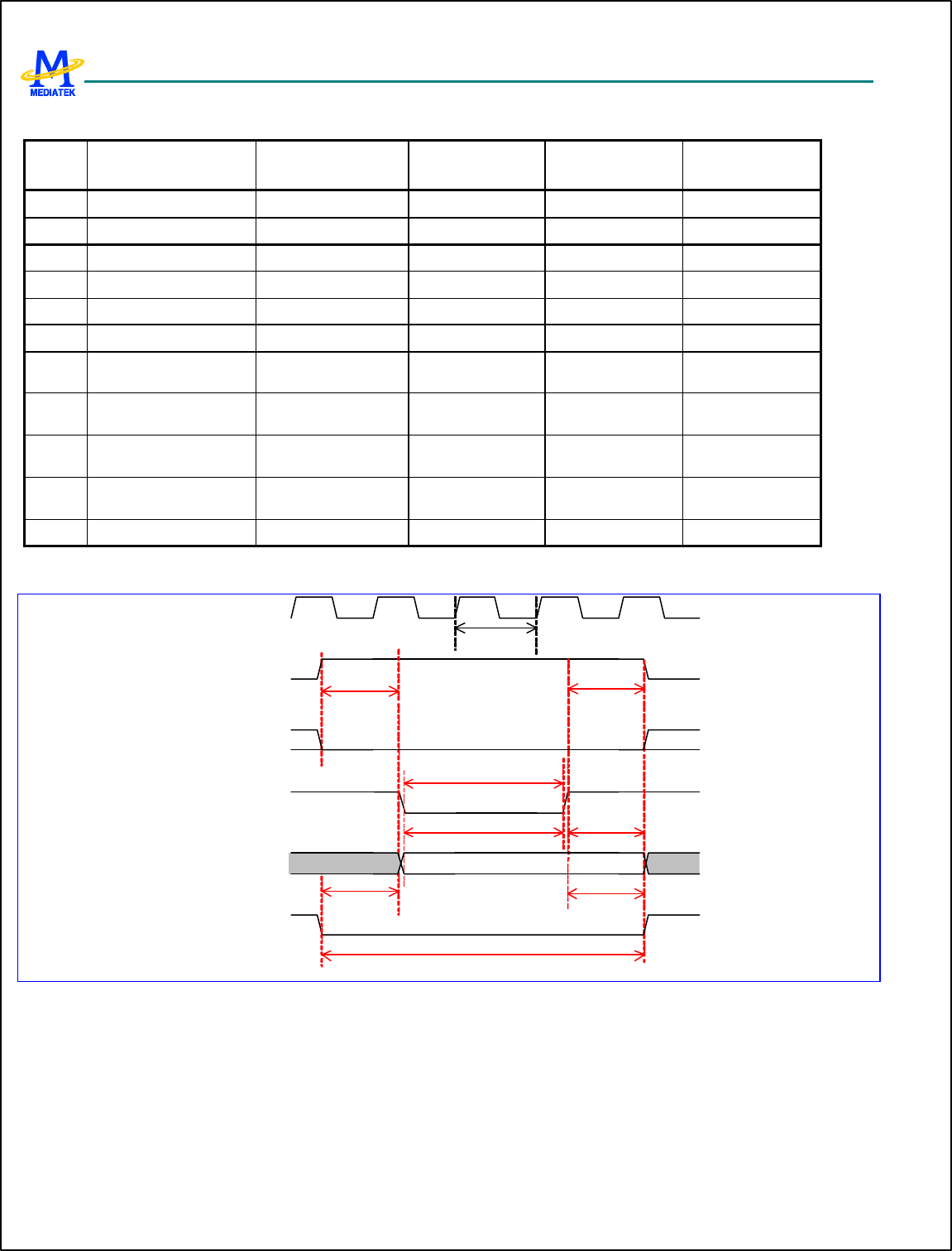
MT6217 GSM/GPRS Baseband Processor Data Sheet Revision 1.01
215/349 MediaTek Inc. Confidential
The ideal timing for write access is listed as listed in Table 30.
Parame
ter Description Timing specification Timing at 13MHz
(WST, WH) = (0,0)
Timing at 26MHz
(WST, WH) = (0,0)
Timing at 52MHz
(WST, WH) = (1,0)
TWC1 Write cycle time 3T + WST + WH 230.8ns 105.4ns 76.9ns
TWC2 Write cycle time 2T + WST + WH 153.9ns 76.9ns 57.7ns
TDS Write data setup time 1T + WST 76.9ns 38.5ns 38.5ns
TDH Write data hold time 1T + WH 76.9ns 38.5ns 19.2ns
TWP Write enable time 1T + WST 76.9ns 38.5ns 38.5ns
TWH Write high time 1T + WH 76.9ns 38.5ns 19.2ns
TCLS Command latch enable
setup time 1T 76.9ns 38.5ns 19.2ns
TCLH Command latch enable
hold time 1T + WH 76.9ns 38.5ns 19.2ns
TALS Address latch enable
setup time 1T 76.9ns 38.5ns 19.2ns
TALH Address latch enable
hold time
1T + WH 76.9ns 38.5ns 19.23ns
FWC Write data rate 1 / T
WC2 6.5Mbytes/s 13Mbytes/s 17.3Mbytes/s
Table 30 Write access timing
WST
tCLS, tALS tCLH, tALH
tWP
tDH
HCLK
NCLE
NWEB
NLD
NCEB
tCES tCEH
tDS
NALE
command
tWC1
Figure 42 Command input cycle (1 wait state).
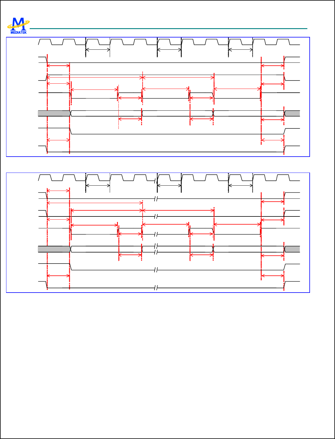
MT6217 GSM/GPRS Baseband Processor Data Sheet Revision 1.01
216/349 MediaTek Inc. Confidential
WST
tALS tALH
tWP
tDH
HCLK
NALE
NWEB
NLD
tWH
OE
(internal)
NCEB tCES tCEH
NCLE
tCLS tCLH
tDH
tWH
tDH
tWP tWP
WST WST
A0 A1 A2
tWC2
tWC1
Figure 43 Address input cycle (1 wait state)
WST
tALS tALH
tWP
tDH
HCLK
NALE
NWEB
NLD
tWH
OE
(internal)
NCEB tCES tCEH
NCLE tCLS
tCLH
tDH
tWH
tDH
tWP tWP
WST WST
D0 D526 D527
tWC2
tWC1
tWC2
Figure 44 Consecutive data write cycles (1 wait state, 0 hold time extension)
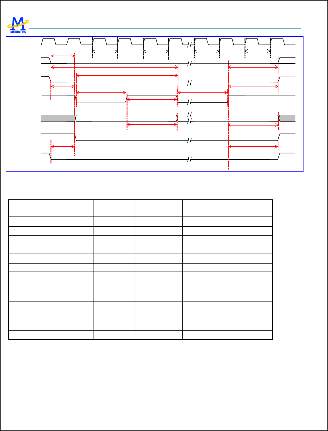
MT6217 GSM/GPRS Baseband Processor Data Sheet Revision 1.01
217/349 MediaTek Inc. Confidential
WST
tALS tALH
tWP
HCLK
NALE
NWEB
NLD
tWH
WHWH
OE
(internal)
NCEB tCES tCEH
tDH
tDH
NCLE tCLS
D0 D527
WST
tWP
tCLH
tWC2
tWC1
Figure 45 Consecutive data write cycles (1 wait state, 1 hold time extension)
The ideal timing for read access is as listed in Table 7.
Parame
ter Description Timing
specification Timing at 13MHz
(RLT, WH) = (0,0)
Timing at 26MHz
(RLT, WH) = (1,0)
Timing at 52MHz
(RLT, WH) = (2,0)
TRC1 Read cycle time 3T + RLT + WH 230.8ns 153.8ns 96.2ns
TRC2 Read cycle time 2T + RLT + WH 153.9ns 115.4ns 76.9ns
TDS Read data setup time 1T + RLT 76.9ns 76.9ns 57.7ns
TDH Read data hold time 1T + WH 76.9ns 38.5ns 19.2ns
TRP Read enable time 1T + RLT 76.9ns 76.9ns 57.7ns
TRH Read high time 1T + WH 76.9ns 38.5ns 19.2ns
TCLS Command latch enable
setup time
1T 76.9ns 38.5ns 19.2ns
TCLH Command latch enable
hold time
1T + WH 76.9ns 38.5ns 19.2ns
TALS Address latch enable
setup time
1T 76.9ns 38.5ns 19.2ns
TALH Address latch enable hold
time 1T + WH 76.9ns 38.5ns 19.2ns
FRC Write data rate 1 / TRC2 6.5Mbytes/s 8.7Mbytes/s 13Mbytes/s
Table 31 Read access timing
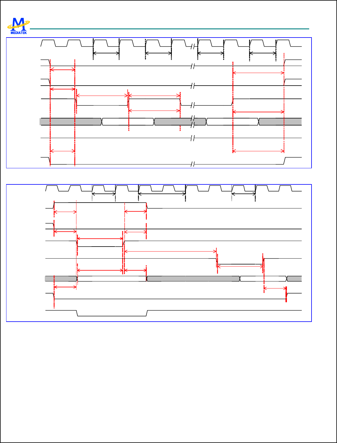
MT6217 GSM/GPRS Baseband Processor Data Sheet Revision 1.01
218/349 MediaTek Inc. Confidential
WST
tALS
tCLH
, tALH
tWP
HCLK
NALE
NREB
NLD
tWH
WHWH
OE
(internal)
NCEB tCES tCEH
tDH
tDH
NCLE
tCLS
D0 D527
WST
Figure 46 Serial read cycle (1 wait state, 1 hold time extension)
WST
tCLS tCLH
tWP
tDH
HCLK
NCLE
NWEB
NLD
NCEB
tCES tCEH
tDS
NALE
70h
tALS tALH
NREB
Status
tWHR
tRP
WST
OE
(internal)
W2R
Figure 47 Status read cycle (1 wait state)
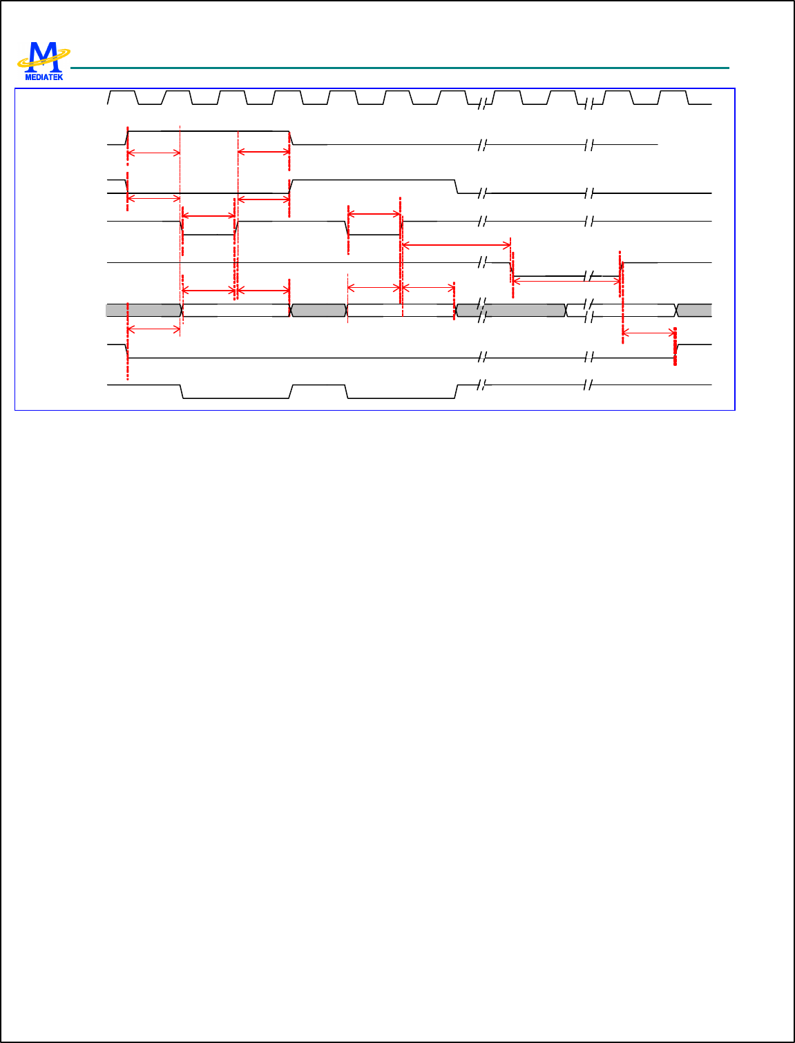
MT6217 GSM/GPRS Baseband Processor Data Sheet Revision 1.01
219/349 MediaTek Inc. Confidential
tCLS tCLH
tWP
tDH
HCLK
NCLE
NWEB
NLD
NCEB
tCES tCEH
tDS
NALE
90h
tALS tALH
NREB
01h, 06h
tWHR
tRP
OE
(internal)
tWP
00h
tDH
tDS
Figure 48 ID and manufacturer read (0 wait state)
6.5 USB Device Controller
6.5.1 General Description
This chip provides a USB function interface that is in compliance with Universal Serial Bus Specification Rev 1.1. The
USB device controller supports only full-speed (12Mbps) operation. The cellular phone can make use of this widely
available USB interfaces to transmit/receive data with USB hosts, typically PC/laptop.
There provides 5 endpoints in the USB device controller besides the mandatory control endpoint, where among them, 3
endpoints are for IN transactions and 2 endpoints are for OUT transactions. Word, half-word, and byte access are allowed
for loading and unloading the FIFO. 4 DMA channels are equipped with the controller to accelerate the data transfer. The
features of the endpoints are as follows:
1. Endpoint 0: The control endpoint feature 16 bytes FIFO and accommodates maximum packet size of up to 16 bytes.
DMA transfer is not supported.
2. IN endpoint 1: It features 64 bytes FIFO and accommodates maximum packet size of up to 64 bytes. DMA transfer is
supported.
3. IN endpoint 2: It features 64 bytes FIFO and accommodates maximum packet size of up to 64 bytes. DMA transfer is
supported.
4. IN endpoint 3: It features 16-byte FIFO and accommodates maximum packet size of 16 bytes. DMA transfer is not
supported.
5. OUT endpoint 1: It features 64 bytes FIFO and accommodates maximum packet size of 64 bytes. DMA transfer is
supported.
6. OUT endpoint 2: It features 64 bytes FIFO and accommodates maximum packet size of 64 bytes. DMA transfer is
supported.
MT6217 GSM/GPRS Baseband Processor Data Sheet Revision 1.01
220/349 MediaTek Inc. Confidential
For each endpoint except the endpoint 0, if the packet size is small than half the size of the FIFO, at most 2 packets can be
buffered.
This unit is highly software configurable. All endpoints except the control endpoint can be configured to be a bulk, interrupt
or isochro nous endpoints. Composite device is also supported. The IN endpoint 1 and the OUT endpoint 1 shares the same
endpoint number but they can be use sep arately. So is the situation as the IN endpoint 2 and the OUT endpoint 2.
The USB device uses cable-powered feature for the transceiver but only drains little current. An external resistor (nominally
1.5Kohm) is required to be placed across Vbus and D+ signal. Two additional external serial resistors might be needed to
place on the output of D+ and D- signals to make the output impedance equivalent to 28~44Ohm.
6.5.2 Register Definitions
70000000h USB function address register USB_FADDR
Bit 7 6 5 4 3 2 1 0
Name
UPD FADDR
Type RO R/W
Reset
0 0
This is an 8-bit register that should be written with the function’s 7-bit address (received through a SET_ADDRESS
description). It is then used for decoding the function address in subsequent token packets.
UPD Set when FADDR is written. It’s cleared when the new address takes effect (at the end of the current transfer).
FADDR The function address of the device.
70000001h USB power control register USB POWER
Bit 7 6 5 4 3 2 1 0
Name
ISO_UP SWRSTENA
B RESET RESUME SUSPMODE SUSPENAB
Type R/W R/W RO R/W RO R/W
Reset
0 0 0 0 0 0
ISO_UP When set by the MCU, the core will wait for an SOF token from the time INPKTRDY is set before sending
the packet.
SWRSTENAB Set by the MCU to enable the mode in which the device can only be reset by the software after detecting
reset signals on the bus. In case the software is delayed by other high-priority process and can’t make it to
read the command from the buffer before the hardware reset the device after detecting the reset signal on the
bus, the command will be lost. That’s why the software-reset mode is effective. When the flag is enabled, the
hardware state machine can’t reset by itself, but rather can be reset by the software. In that sense, the software
and the hardware can keep synchronous on detecting the reset signal.
RESET The read-only bit is set when Reset signaling is present on the bus.
RESUME Set by the MCU to generate Resume signaling when the function is in suspend mode. The MCU should clear
this bit after 10 ms (a maximum of 15 ms) to end Resume signaling.
SUSPMODE Set by the USB core when Suspend mode is entered. Cleared when the CPU reads the interrupt register,
or sets the Resume bit of this register.
SUSPENAB Set by the MCU to enable device into Suspend mode when Suspend signaling is received on the bus.
70000002h USB IN endpoints interrupt register USB_INTRIN
Bit 7 6 5 4 3 2 1 0
MT6217 GSM/GPRS Baseband Processor Data Sheet Revision 1.01
221/349 MediaTek Inc. Confidential
Name
EP3 EP2 EP1 EP0
Type RC RC RC RC
Reset
0 0 0 0
This is a read-only register that indicates which of the interrupts for IN endpoints 0 to 3 are currently active. All active
interrupts will be cleared when this register is read.
EP3 IN endpoint #3 interrupt.
EP2 IN endpoint #2 interrupt.
EP1 IN endpoint #1 interrupt.
EP0 IN endpoint #0 interrupt.
70000004h USB OUT endpoints interrupt register USB_INTROUT
Bit 7 6 5 4 3 2 1 0
Name
EP2 EP1
Type RC RC
Reset
0 0
This is a read-only register that indicates which of the interrupts for OUT endpoints 1 and 2 are currently active. All active
interrupts will be cleared when this register is read.
EP2 OUT endpoint #2 interrupt.
EP1 OUT endpoint #1 interrupt.
70000006h USB general interrupt register USB_INTRUSB
Bit 7 6 5 4 3 2 1 0
Name
SOF RESET RESUME SUSP
Type RC RC RC RC
Reset
0 0 0 0
This is a read-only register that indicates which USB interrupts are currently active. All active interrupts will be cleared
when this register is read.
SOF Set at the start of each frame.
RESET Set when Reset signaling is detected on the bus.
RESUME Set when Resume signaling is detected on the bus while the USB core is in suspend mode.
SUSP Set when Suspend signaling is detected on the bus.
70000007h USB IN endpoints interrupt enable register USB_INTRINE
Bit 7 6 5 4 3 2 1 0
Name
EP3 EP2 EP1 EP0
Type R/W R/W R/W R/W
Reset
1 1 1 1
This register provides interrupt enable bits for the interrupts in USB_INTRIN. On reset, the bits corresponding to endpoint
0 and all IN endpoints are set to 1.
EP3 IN endpoint 3 interrupt enable.
EP2 IN endpoint 2 interrupt enable.
EP1 IN endpoint 1 interrupt enable.
EP0 IN endpoint 0 interrupt enable.
MT6217 GSM/GPRS Baseband Processor Data Sheet Revision 1.01
222/349 MediaTek Inc. Confidential
70000009h USB OUT endpoints interrupt enable register USB_INTROUTE
Bit 7 6 5 4 3 2 1 0
Name
EP2 EP1
Type R/W R/W
Reset
1 1
This register provides interrupt enable bits for the interrupts in USB_INTROU T. On reset, the bits corresponding to all
OUT endpoints are set to 1.
EP2 OUT endpoint 2 interrupt enable.
EP1 OUT endpoint 1 interrupt enable.
7000000Bh USB general interrupt enable register USB_INTRUSBE
Bit 7 6 5 4 3 2 1 0
Name
SOF RESET RESUME SUSP
Type R/W R/W R/W R/W
Reset
0 1 1 0
This register provides interrupt enable bits for each of the interrupts for USB_INTRUSB.
SOF SOF interrupt enable
RESET Reset interrupt enable
RESUME Resume interrupt enable
SUSP Suspend interrupt enable
7000000Ch USB frame count #1 register USB_FRAME1
Bit 7 6 5 4 3 2 1 0
Name
NUML
Type RO
Reset
0
The register holds the lower 8 bits of the last received frame number.
NUML The lower 8 bits of the frame number.
7000000Dh USB frame count #2 register USB_FRAME2
Bit 7 6 5 4 3 2 1 0
Name
NUMH
Type RO
Reset
0
The register holds the upper 3 bits of the last received frame number.
NUMH The upper 3 bits of the frame number.
7000000Eh USB endpoint register index USB_INDEX
Bit 7 6 5 4 3 2 1 0
Name
INDEX
Type R/W
Reset
0
MT6217 GSM/GPRS Baseband Processor Data Sheet Revision 1.01
223/349 MediaTek Inc. Confidential
The register determines which endpoint control/status registers are to be accessed at addresses USB+10h to USB+17h.
Each IN endpoint and each OUT endpoint have their own set of control/status registers. Only one set of IN control/status
and one set of OUT control/status registers appear in the memory map at any one time. Before accessing an endpoint’s
control/status registers, the endpoint number should be written to the USB_INDEX register to ensure that the correct
control/status registers appear in the memory map.
INDEX The index of the endpoint.
7000000Fh USB reset control USB_RSTCTRL
Bit 7 6 5 4 3 2 1 0
Name
SWRST RSTCNTR
Type R/W R/W
Reset
0 0
The register is used to control the reset process when the device detects the reset command issued from the host.
SWRST If the flag SWRSTENAB in the register USB_POWER is set to be 1, the software enable mode is enabled,
and the device can be reset by writing this flag to be 1.
RSTCNTR The field signifies the duration for the reset operation to take place after detecting reset signal on the bus. It’s
only enabled when software reset is not enabled. If the value is equal to zero, the duration is 2.5us. Otherwise,
the duration is equal to this value multiplied by 341 and then added by 2.5 in unit of us. The range
consequently starts from 2.5us to 5122.5 us.
70000011h USB control/status register for endpoint 0 USB_EP0_CSR
Bit 7 6 5 4 3 2 1 0
Name
SSETUPEND SOUTPKTRD
Y SENDSTALL
SETUPEND DATAEND SENTSTALL INPKTRDY
OUTPKTRDY
Type R/WS R/WS R/WS RO R/WS R/WC R/WS RO
Reset
0 0 0 0 0 0 0 0
The register is used for all control/status of endpoint 0. The register is active when USB_INDEX register is set to 0.
SSETUPEND The MCU writes a 1 to this bit to clear the SETUPEND bit. It’s cleared automatically. Only active
when a transaction has been started.
SOUTPKTRDY The MCU writes a 1 to this bit to clear the OUTPKTRDY bit. It’s cleared automatically. Only
active when an OUT transaction has been started.
SENDSTALL The MCU writes a 1 to this bit to terminate the current transaction. The STALL handshake will be
transmitted and then this bit will be cleared automatically.
SETUPEND This bit will be set when a control transaction ends before the DATAEND bit has been set. An
interrupt will be generated and FIFO flushed at this time. The bit is cleared by the MCU writing a 1 to the
SSETUPEND bit.
DATAEND The MCU sets this bit:
1. When setting INPKTRDY for the last data packet.
2. When clearing OUTPKTRDY after unloading the last data packet.
3. When setting INPKTRDY for a zero length data packet.
It’s cleared automatically
SENTSTALL This bit is set when a STALL handshake is transmitted. The MCU should clear this bit by writing a
0.
MT6217 GSM/GPRS Baseband Processor Data Sheet Revision 1.01
224/349 MediaTek Inc. Confidential
INPKTRDY The MCU sets this bit after loading a data packet into the FIFO. It is cleared automatically when the data
packet has been transmitted. An interrupt is generated when this bit is set.
OUTPKTRDY This bit is set when a data packet has been received. An interrupt is generated when this bit is set.
The MCU clears this bit by setting the SOUTPKTRDY bit.
70000016h USB byte count register USB_EP0_COU
NT
Bit 7 6 5 4 3 2 1 0
Name
COUNT
Type RO
Reset
0
The register indicates the number of received data bytes in the endpoint 0. The value returned is valid while OUTPKTRDY
bit of USB_EP0_CSR register is set. The register is active when USB_INDEX register is set to 0.
COUNT The number of received data bytes in the endpoint 0.
70000010h USB maximum packet size register for IN endpoint 1~3 USB_EP_INMAX
P
Bit 7 6 5 4 3 2 1 0
Name
MAXP
Type R/W
Reset
0
The register holds the maximum packet size for transactions through the currently selected IN endpoint – in units of 8 bytes.
In setting the value, the programmer should note the constraints placed by the USB Specification on packet size for bulk
interrupt, and isochronous transactions in full-speed operations. There is an INMAXP register for each IN endpoint except
endpoint 0. The registers are active when USB_INDEX register is set to 1, 2, and 3, respectively.
The value written to this register should match the wMaxPacketSize field of the standard endpoint descriptor for the
associated endpoint. A mismatch could cause unexpected results. If a value greater than the configured IN FIFO size for the
endpoint is written to the register, the value will be automatically changed to the IN FIFO size. If the value written to the
register is less than, or equal to, half the IN FIFO size, two IN packets can be buffered. The configured IN FIFO size for the
endpoint 1, 2, and 3, are 64 bytes, 64 bytes, and 16 bytes, respectively.
The register is reset to 0. If the register is changed after packets have been sent from the endpoint, the endpoint IN FIFO
should be completely flushed after writing the new value to the register.
MAXP The maximum packet size in units of 8 bytes.
70000011h USB control/status register #1 for IN endpoint 1~3 USB_EP_INCSR
1
Bit 7 6 5 4 3 2 1 0
Name
CLRDATATO
G SENTSTALL SENDSTALL FLUSHFIFO UNDERRUN FIFONOTEM
PTY INPKTRDY
Type WO R/WC R/W WO R/WC RO R/WS
Reset
0 0 0 0 0 0 0
The register provides control and status bits for IN transactions through the currently selected endpoint. There is an
INCSR1 register for each IN endpoint except endpoint 0. The registers are active when USB_INDEX register is set to 1, 2,
and 3, respectively.
MT6217 GSM/GPRS Baseband Processor Data Sheet Revision 1.01
225/349 MediaTek Inc. Confidential
CLRDATATOG The MCU writes a 1 to this bit to reset the endpoint IN data toggle to 0.
SENTSTALL The bit is set when a STALL handshake is transmitted. The FIFO is flushed and the INPKTRDY bit
is cleared. The MCU should clear this bit by writing a 0 to this bit.
SENDSTALL The MCU writes a 1 to this bit to issue a STALL handshake to an IN token. The MCU clears this bit
to terminate the stall condition.
FLUSHFIFO The MCU writes a 1 to this bit to flush the next packet to be transmitted from the endpoint IN FIFO.
The FIFO pointer is reset and the INPKTRDY bit is cleared. If the FIFO contains two packets,
FLUSHFIFO will need to be set twice to completely clear the FIFO.
UNDERRUN In isochronous mode, this bit is set when a zero length data packet is sent after receiving an IN
token with the INPKTRDY bit not set. In Bulk/Interrupt mode, this bit is set when a NAK is returned in
response to an IN token. The MCU should clear this bit by writing a 0 to this bit.
FIFONOTEMPTY This bit is set when there is at least 1 packet in the IN FIFO.
INPKTRDY The MCU sets this bit after loading a data packet into the FIFO. Only active when an IN transaction has
been started. It is cleared automatically when a data packet has been transmitted. An interrupt is generated
(if enabled) when the bit is cleared.
70000012h USB control/status register #2 for IN endpoint 1~3 USB_EP_INCSR
2
Bit 7 6 5 4 3 2 1 0
Name
AUTOSET ISO MODE DMAENAB RFCDATATO
G
Type R/W R/W R/W R/W R/W
Reset
0 0 0 0 0
The register provides further control bits for IN transactions through the currently selected endpoint. There is an INCSR2
register for each IN endpoint except endpoint 0. The registers are active when USB_INDEX register is set to 1, 2, and 3,
respectively.
AUTOSET If the MCU sets the bit, INPKTRDY will be automatically set when data of the maximum packet size
(value in INMAXP) is loaded into the IN FIFO. If a packet of less than the maximum packet size is
loaded, then INPKTRDY will have to be set manually. When 2 packets are in the IN FIFO then
INPKTRDY will also be automatically set when the first packet has been sent, if the second packet is the
maximum packet size.
ISO The MCU sets this bit to enable the IN endpoint for isochronous transfer, and clears it to enable the IN
endpoint for bulk/interrupt transfers.
MODE The MCU sets this bit to enable the endpoint direction as IN, and clears it to enable the endpoint direction
as OUT. It’s valid only where the same endpoint FIFO is used for both IN and OUT transaction.
DMAENAB The MCU sets this bit to enable the DMA request for the IN endpoint.
FRCDATATOG The MCU sets this bit to force the endpoint’s IN data toggle to switch after each data packet is sent
regardless of whether an ACK was received. This can be used by interrupt IN endpoints which are used to
communicate rate feedback for isochronous endpoints.
70000013h USB maximum packet size register for OUT endpoint
1~2
USB_EP_OUTM
AXP
Bit 7 6 5 4 3 2 1 0
Name
MAXP
Type R/W
MT6217 GSM/GPRS Baseband Processor Data Sheet Revision 1.01
226/349 MediaTek Inc. Confidential
Reset
0
This register holds the maximum packet size for transactions through the currently selected OUT endpoint – in units of 8
bytes. In setting this value, the programmer should note the constraints placed by the USB specification on packet sizes for
bulk, interrupt, and isochronous transactions in full speed operations. There is an OUTMAXP register for each OUT
endpoint except endpoint 0. The registers are active when USB_INDEX register is set to 1 and 2, respectively.
The value written to this register should match the wMaxPacketSize field of the standard endpoint descriptor for the
associated endpoint. A mismatch could cause unexpected results. The total amount of data represented by the value written
to this register must not exceed the FIFO size for the OUT endpoint, and should not exceed half the FIFO size if double
buffering is required. If a value greater than the configured OUT FIFO size for the endpoint is written to the register, the
value will be automatically changed to the OUT FIFO size. If the value written to the register is less than, or equal to, half
the OUT FIFO size, two OUT packets can be buffered. The configured IN FIFO size for the endpoint 1 and 2 are both 64
bytes.
MAXP The maximum packet size in units of 8 bytes.
70000014h USB control/status register #1 for OUT endpoint 1~2 USB_EP_OUTC
SR1
Bit 7 6 5 4 3 2 1 0
Name
CLRDATATO
G SENTSTALL SENDSTALL
FLUSHFIFO DATAERRO
R OVERRUN FIFOFULL
OUTPKTRDY
Type WO R/WC R/W WO RO R/WC RO R/WC
Reset
0 0 0 0 0 0 0 0
The register provides control status bits for OUT transactions through the currently selected endpoint. The registers are
active when USB_INDEX register is set to 1 and 2, respectively.
CLRDATATOG The MCU writes a 1 to this bit to reset the endpoint data toggle to 0.
SENTSTALL The bit is set when a STALL handshake is transmitted. The MCU should clear this bit by writing a
0.
SENDSTALL The MCU writes a 1 to this bit to issue a STALL handshake. The MCU clears this bit to terminate
the stall condition. This bit has no effect if the OUT endpoint is in isochronous mode.
FLUSHFIFO The MCU writes a 1 to this bit to flush the next packet to be read from the endpoint OUT FIFO. If
the FIFO contains two packets, FLUSHFIFO will need to be set twice to completely clear the FIFO.
DATAERROR The bit is set when OUTPKTRDY is set if the data packet has a CRC or bit-stuff error. It is cleared
when OUTPKTRDY is cleared. This bit is only valid in isochronous mode.
OVERRUN The bit is set if an OUT packet cannot be loaded into the OUT FIFO. The MCU should clear the bit by
writing a zero. This bit is only valid in isochronous mode.
FIFOFULL This bit is set when no more packets can be loaded into the OUT FIFO.
OUTPKTRDY The bit is s et when a data packet has been received. The MCU should clear (write a 0 to) the bit
when the packet has been unloaded from the OUT FIFO. An interrupt is generated when the bit is set.
70000015h USB control/status register #2 for OUT endpoint 1~2 USB_EP_OUTC
SR2
Bit 7 6 5 4 3 2 1 0
Name
AUTOCLEAR
ISO DMAENAB DMAMODE
Type R/W R/W R/W R/W
Reset
0 0 0 0
MT6217 GSM/GPRS Baseband Processor Data Sheet Revision 1.01
227/349 MediaTek Inc. Confidential
The register provides further control bits for OUT transactions through the currently selected endpoint. The registers are
active when USB_INDEX register is set to 1 and 2, respectively.
AUTOCLEAR If the MCU sets this bit then the OUTPKTRDY bit will be automatically cleared when a packet of
OUTMAXP bytes has been unloaded from the OUT FIFO. When packets of less then the maximum
packet size are unloaded, OUTPKTRDY will have to be cleared manually.
ISO The MCU sets this bit to enable the OUT endpoint for isochronous transfers, and clears it to enable the
OUT endpoint for bulk/interrupt transfers.
DMAENAB The MCU sets this bit to enable the DMA request for the OUT endpoint.
DMAMODE Two modes of DMA operation are supported: DMA mode 0 in which a DMA request is generated for all
received packets, together with an interrupt (if enabled); and DMA mode 1 in which a DMA request (but
no interrupt) is generated for OUT packets of size OUTMAXP bytes and an interrupt (but no DMA
request) is generated for OUT packets of any other size. The MCU sets the bit to select DMA mode 1 and
clears this bit to select DMA mode 0.
70000016h USB OUT endpoint byte counter register LSB part for
endpoint 1~2
USB_EP_COUN
T1
Bit 7 6 5 4 3 2 1 0
Name
NUML
Type RO
Reset
0
The register holds the lower 8 bits of the number of received data bytes in the packet in the FIFO associated with the
currently selected OUT endpoint. The value returned is valid while OUTPKTRDY in the register USB_OUTCSR1 is set.
The registers are active when USB_INDEX register is set to 1 and 2, respectively.
NUML The lower 8 bits of the number of received data bytes for the OUT endpoint.
70000017h USB OUT endpoint byte counter register MSB part for
endpoint 1~2
USB_EP_COUN
T2
Bit 7 6 5 4 3 2 1 0
Name
NUMH
Type RO
Reset
0
The register holds the upper 3 bits of the number of received data bytes in the packet in the FIFO associated with the
currently selected OUT endpoint. The value returned is valid while OUTPKTRDY in the register USB_EP_OUTCSR1 is
set. The registers are active when USB_INDEX register is set to 1 and 2, respectively.
NUMH The upper 8 bits of the number of received data bytes for the OUT endpoint.
70000020h USB endpoint 0 FIFO access register USB_EP0_FIFO
Bit 31 30 29 28 27 26 25 24 23 22 21 20 19 18 17 16
Name
DB3 DB2
Type R/W R/W
Bit 15 14 13 12 11 10 9 8 7 6 5 4 3 2 1 0
Name
DB1 DB0
Type R/W R/W
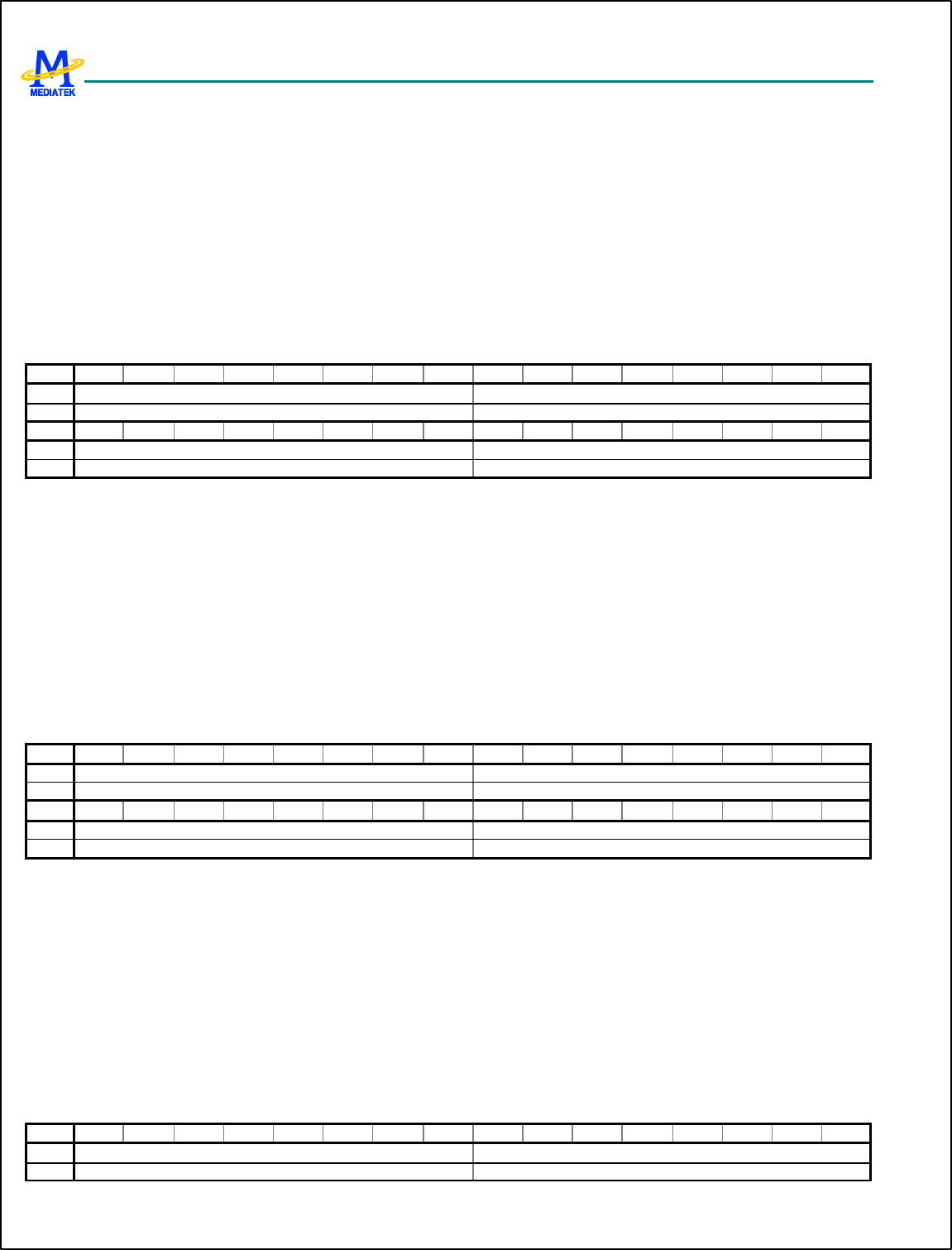
MT6217 GSM/GPRS Baseband Processor Data Sheet Revision 1.01
228/349 MediaTek Inc. Confidential
The register provides MCU access to the FIFO for the endpoint 0. Writing to this register loads data into the FIFO for the
endpoint 0. Reading from this register unloads data from the FIFO for the endpoint 0.
The register provides word, half-word, and byte mode access. If word or half-word accesses are performed, the less
significant byte corresponds to the prior byte to load in or unload from the FIFO.
DB0 The first byte to be loaded into or unloaded from the FIFO.
DB1 The second byte to be loaded into or unloaded from the FIFO.
DB2 The third byte to be loaded into or unloaded from the FIFO.
DB3 The forth byte to be loaded into or unloaded from the FIFO.
70000024h USB endpoint 1 FIFO access register USB_EP1_FIFO
Bit 31 30 29 28 27 26 25 24 23 22 21 20 19 18 17 16
Name
DB3 DB2
Type R/W R/W
Bit 15 14 13 12 11 10 9 8 7 6 5 4 3 2 1 0
Name
DB1 DB0
Type R/W R/W
The register provides MCU access to the IN FIFO and the OUT FIFO for the endpoint 1. Writing to the register loads data
into the IN FIFO for the endpoint 1. Reading from the register unloads data from the OUT FIFO for the endpoint 1.
The register provides word, half-word, and byte mode access. If word or half-word accesses are performed, the less
sig nificant byte corresponds to the prior byte to load in the IN FIFO or unload from the OUT FIFO.
DB0 The first byte to be loaded in the IN FIFO or unloaded from the OUT FIFO.
DB1 The second byte to be loaded in the IN FIFO or unloaded from the OUT FIFO.
DB2 The third byte to be loaded in the IN FIFO or unloaded from the OUT FIFO.
DB3 The forth byte to be loaded in the IN FIFO or unloaded from the OUT FIFO.
70000028h USB endpoint 2 FIFO access register USB_EP2_FIFO
Bit 31 30 29 28 27 26 25 24 23 22 21 20 19 18 17 16
Name
DB3 DB2
Type R/W R/W
Bit 15 14 13 12 11 10 9 8 7 6 5 4 3 2 1 0
Name
DB1 DB0
Type R/W R/W
The register provides MCU access to the IN FIFO and the OUT FIFO for the endpoint 2. Writing to the register loads data
into the IN FIFO for the endpoint 2. Reading from the register unloads data from the OUT FIFO for the endpoint 2.
The register provides word, half-word, and byte mode access. If word or half-word accesses are performed, the less
significant byte corresponds to the prior byte to load in the IN FIFO or unload from the OUT FIFO.
DB0 The first byte to be loaded into the IN FIFO or unloaded from the OUT FIFO.
DB1 The second byte to be loaded into the IN FIFO or unloaded from the OUT FIFO.
DB2 The third byte to be loaded into the IN FIFO or unloaded from the OUT FIFO.
DB3 The forth byte to be loaded into the IN FIFO or unloaded from the OUT FIFO.
7000002Ch USB endpoint 3 FIFO access register USB_EP3_FIFO
Bit 31 30 29 28 27 26 25 24 23 22 21 20 19 18 17 16
Name
DB3 DB2
Type R/W R/W

MT6217 GSM/GPRS Baseband Processor Data Sheet Revision 1.01
229/349 MediaTek Inc. Confidential
Bit 15 14 13 12 11 10 9 8 7 6 5 4 3 2 1 0
Name
DB1 DB0
Type R/W R/W
The register provides MCU access to the IN FIFO for the endpoint 3. Writing to the register loads data into the IN FIFO for
the endpoint 3.
The register provides word, half-word, and byte mode access. If word or half-word accesses are performed, the less
significant byte corresponds to the prior byte to load in the IN FIFO.
DB0 The first byte to be loaded into the IN FIFO.
DB1 The second byte to be loaded into the IN FIFO.
DB2 The third byte to be loaded into the IN FIFO.
DB3 The forth byte to be loaded into the IN FIFO.
6.6 Memory Stick and SD Memory Card Controller
6.6.1 Introduction
The controller fully supports the Memory Stick bus protocol as defined in Format Specification version 2.0 of Memory
Stick Standard (Memory Stick PRO) and the SD Memory Card bus protocol as defined in SD Memory Card Specification
Part 1 Physical Layer Specification version 1.0 as well as the MultiMediaCard (MMC) bus protocol as defined in MMC
system specification version 2.2. Since SD Memory Card bus protocol is backward compatible to MMC bus protocol, the
controller is capable of working well as the host on MMC bus under control of proper firmware. However, the controller
can only be configured as either the host of Memory Stick or the host of SD/MMC Memory Card at one time. Hereafter, the
controller is also abbreviated as MS/SD controller. The following are the main features of the controller.
l Interface with MCU by APB bus
l 16/32-bit access on APB bus
l 16/32-bit access for control registers
l 32 -bit access for FIFO
l Shared pins for Memory Stick and SD/MMC Memory Card
l Built-in 32 bytes FIFO buffers for transmit and receive, FIFO is shared for transmit and receive
l Built-in CRC circuit
l CRC generation can be disabled
l DMA supported
l Interrupt capabilities
l Automatic command execution capability when an interrupt from Memory Stick
l Data rate up to 26 Mbps in serial mode, 26x4 Mbps in parallel model, the module is targeted at 26 MHz operating
clock
l Serial clock rate on MS/SD/MMC bus is programmable
l Card detection capabilities
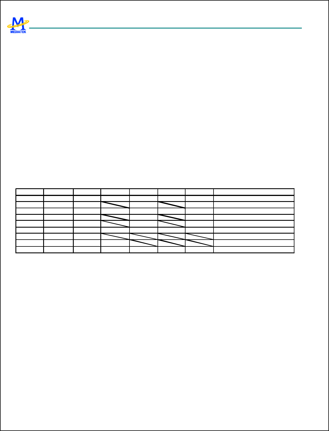
MT6217 GSM/GPRS Baseband Processor Data Sheet Revision 1.01
230/349 MediaTek Inc. Confidential
l Controllability of power for memory card
l Not support SPI mode for MS/SD/MMC Memory Card
l Not support multiple SD Memory Cards
6.6.2 Overview
6.6.2.1 Pin Assignment
Since the controller can only be configured as either the host of Memory Stick or the host of SD/MMC Memory Card at
one time, pins for Memory Stick and SD/MMC Memory Card are shared in order to save pin counts. The following lists
pins required for Memory Stick and SD/MMC Memory Card. Table 32 shows how they are shared. In Table 32, all I/O
pads have embedded both pull up and pull down resistor because they are shared by both the Memory Stick and SD/MMC
Memory Card. Pins 2,4,5,8 are only useful for SD/MMC Memory Card. Pull down resistor for these pins can be used for
power saving. All embedded pull-up and pull-down resistors can be disabled by programming the corresponding control
registers if optimal pull-up or pull-down resistors are required on the system board. The pin VDDPD is used for power
saving. Power for Memory Stick or SD/MMC Memory Card can be shut down by programming the corresponding control
register. The pin WP (Write Protection) is only valid when the controller is configured for SD/MMC Memory Card. It is
used to detect the status of Write Protection Switch on SD/MMC Memory Card.
No. Name Type MMC SD MS MSPRO Description
1SD_CLK OCLK CLK SCLK SCLK Clock
2SD_DAT3 I/O/PP CD/DAT3 DAT3 Data Line [Bit 3]
3SD_DAT0 I/O/PP DAT0 DAT0 SDIO DAT0 Data Line [Bit 0]
4SD_DAT1 I/O/PP DAT1 DAT1 Data Line [Bit 1]
5SD_DAT2 I/O/PP DAT2 DAT2 Data Line [Bit 2]
6SD_CMD I/O/PP CMD CMD BS BS Command Or Bus State
7SD_PWRON OVDD ON/OFF
8
SD_WP I
Write Protection Switch in SD
9
SD_INS
I
VSS2
VSS2
INS
INS
Card Detection
Table 32 Sharing of pins for Memory Stick and SD/MMC Memory Card Controller
6.6.2.2 Card Detection
For Memory Stick, the host or connector should provide a pull up resistor on the signal INS. Therefore, the signal INS will
be logic high if no Memory Stick is on line. The scenario of card detection for Memory Stick is shown in Figure 49. Before
Memory Stick is inserted or powered on, on host side SW1 shall be closed and SW2 shall be opened for card detection. It is
the default setting when the controller is powered on. Upon insertion of Memory Stick, the signal INS will have a transition
from high to low. Hereafter, if Memory Stick is removed then the signal INS will return to logic high. If card insertion is
intended to not be supported, SW1 shall be opened and SW2 closed always.
For SD/MMC Memory Card, detection of card insertion/removal by hardware is also supported. Because a pull down
resistor with about 470 KΩ resistance which is impractical to embed in an I/O pad is needed on the signal CD/DAT3, and it
has to be capable of being connected or disconnected dynamically onto the signal CD during initialization period, an
additional I/O pad is needed to switch on/off the pull down resistor on the system board. The scenario of card detection for
SD/MMC Memory Card is shown in Figure 50. Before SD/MMC Memory Card is inserted or powered on, SW1 and SW2
shall be opened for card detection on the host side. Meanwhile, pull down resistor RCD on system board shall attach onto the
signal CD/DAT3 by the output signal RCDEN. In addition, SW3 on the card is default to be closed. Upon insertion of
SD/MMC Memory Card, the signal CD/DAT3 will have a transition from low to high. If SD/MMC Memory Card is
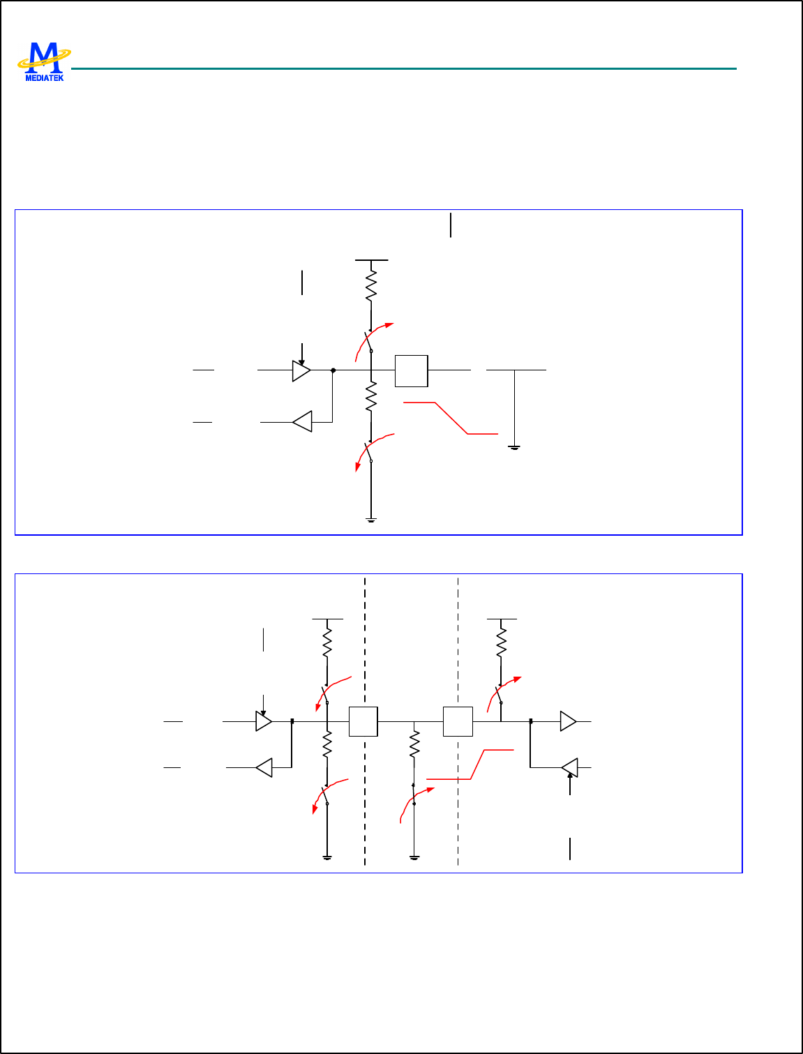
MT6217 GSM/GPRS Baseband Processor Data Sheet Revision 1.01
231/349 MediaTek Inc. Confidential
removed then the signal CD/DAT3 will return to logic low. After the card identification process, pull down resistor RCD on
system board shall disconnect with the signal CD/DAT3 and SW3 on the card shall be opened for normal operation.
Since the scheme above needs a mechanical switch such as a relay on system board, it is not ideal enough. Thus, a
dedicated pin “INS” is used to perform card insertion and removal for SD/MMC. The pin “INS” will connect to the pin
“VSS2” of a SD/MMC connector. Then the scheme of card detection is the same as that for MS. It is shown in Figure 49.
INS
R
PU
PAD
SW1
R
PD
SW2
DAT3 OUT
CD/DAT3 IN
HOST CARD
output enable
Figure 49 Card detection for Memory Stick
RPU
PAD
SW1
RPD
SW2
DAT3 OUT
CD/DAT3 IN
HOST CARD
10-90 K
SW3
output enable
output enable
470 Kohm
RCDEN
PAD
Figure 50 Card detection for SD/MMC Memory Card
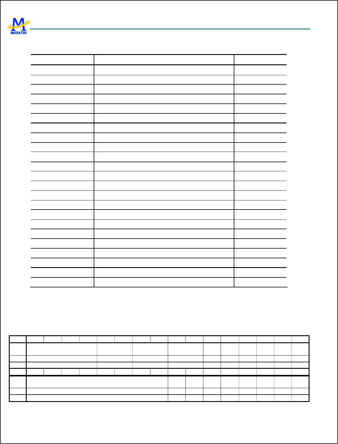
MT6217 GSM/GPRS Baseband Processor Data Sheet Revision 1.01
232/349 MediaTek Inc. Confidential
6.6.3 Register Definitions
REGISTER ADDRESS REGISTER NAME SYNONYM
MSDC + 0000h MS/SD Memory Card Controller Configuration Register MSDC_CFG
MSDC + 0004h MS/SD Memory Card Controller Status Register MSDC_STA
MSDC + 0008h MS/SD Memory Card Controller Interrupt Register MSDC_INT
MSDC + 000Ch MS/SD Memory Card Controller Data Register MSDC_DAT
MSDC + 00010h MS/SD Memory Card Pin Status Register MSDC_PS
MSDC + 00014h MS/SD Memory Card Controller IO Control Register MSDC_IOCON
MSDC + 0020h SD Memory Card Controller Configuration Register SDC_CFG
MSDC + 0024h SD Memory Card Controller Command Register SDC_CMD
MSDC + 0028h SD Memory Card Controller Argument Register SDC_ARG
MSDC + 002Ch SD Memory Card Controller Status Register SDC_STA
MSDC + 0030h SD Memory Card Controller Response Register 0 SDC_RESP0
MSDC + 0034h SD Memory Card Controller Response Register 1 SDC_RESP1
MSDC + 0038h SD Memory Card Controller Response Register 2 SDC_RESP2
MSDC + 003Ch SD Memory Card Controller Response Register 3 SDC_RESP3
MSDC + 0040h SD Memory Card Controller Command Status Register SDC_CMDSTA
MSDC + 0044h SD Memory Card Controller Data Status Register SDC_DATSTA
MSDC + 0048h SD Memory Card Status Register SDC_CSTA
MSDC + 004Ch SD Memory Card IRQ Mask Register 0 SDC_IRQMASK0
MSDC + 0050h SD Memory Card IRQ Mask Register 1 SDC_IRQMASK1
MSDC + 0060h Memory Stick Controller Configuration Register MSC_CFG
MSDC + 0064h Memory Stick Controller Command Register MSC_CMD
MSDC + 0068h Memory Stick Controller Auto Command Register MSC_ACMD
MSDC + 006Ch Memory Stick Controller Status Register MSC_STA
Table 33 MS/SD Controller Register Map
6.6.3.1 Global Register Definitions
MSDC+0000h MS/SD Memory Card Controller Configuration Register
MSDC_CFG
Bit 31 30 29 28 27 26 25 24 23 22 21 20 19 18 17 16
Name
FIFOTHD PRCFG2 PRCFG1 PRCFG0 VDDP
D RCDE
N DIRQ
EN PINEN
DMAE
N INTEN
Type R/W R/W R/W R/W R/W R/W R/W R/W R/W R/W
Reset
0001 01 01 01 0 0 0 0 0 0
Bit 15 14 13 12 11 10 9 8 7 6 5 4 3 2 1 0
Name
SCLKF SCLK
ON CRED
STDB
Y CLKS
RC RST NOCR
C RED MSDC
Type R/W R/W R/W R/W R/W W R/W R/W R/W
Reset
00000000 0 0 1 0 0 0 0 0

MT6217 GSM/GPRS Baseband Processor Data Sheet Revision 1.01
233/349 MediaTek Inc. Confidential
The register is for general configuration of the MS/SD controller. Note that MSDC_CFG[31:16] can be accessed by 16-bit
APB bus access.
MSDC The register bit is used to configure the controller as the host of Memory Stick or as the host of SD/MMC Memory
card. The default value is to configure the controller as the host of Memory Stick.
0 Configure the controller as the host of Memory Stick
1 Configure the controller as the host of SD/MMC Memory card
RED Rise Edge Data. The register bit is used to determine that serial data input is latched at the falling edge or the rising
edge of serial clock. The default setting is at the rising edge. If serial data has worse timing, set the register bit to
‘1’. When memory card has worse timing on return read data, set the register bit to ‘1’.
0 Serial data input is latched at the rising edge of serial clock.
1 Serial data input is latched at the falling edge of serial clock.
NOCRC CRC Disable. A ‘1’ indicates that data transfer without CRC is desired. For write data block, data will be
transmitted without CRC. For read data block, CRC will not be checked. It is for testing purpose.
0 Data transfer with CRC is desired.
1 Data transfer without CRC is desired.
RST Software Reset. Writing a ‘1’ to the register bit will cause internal synchronous reset of MS/SD controller, but does
not reset register settings.
0 Otherwise
1 Reset MS/SD controller
CLKSRC The register bit specifies which clock is used as source clock of memory card. If MUC clock is used, the
fastest clock rate for memory card is 52/2=26M Hz. If USB clock is used, the fastest clock rate for memory card is
48/2=24MHz.
0 Use MCU clock as source clock of memory card.
1 Use USB clock as source clock of memory card.
STDBY Standby Mode. If the module is powered down, operating clock to the module will be stopped. At the same time,
clock to card detection circuitry will also be stopped. If detection of memory card insertion and removal is desired,
write ‘1’ to the register bit. If interrupt for detection of memory card insertion and removal is enabled, interrupt
will take place whenever memory is inserted or removed.
0 Standby mode is disabled.
1 Standby mode is enabled.
CRED Card Rise Edge Data. The register bit is used to determine that serial data from memory card is output at the
falling edge or the rising edge of serial clock. The default setting is at the falling edge.
0 Serial data is output at the falling edge of serial clock.
1 Serial data is output at the rising edge of serial clock.
SCLKON Serial Clock Always On. It is for debugging purpose.
0 Not to have serial clock always on.
1 To have serial clock always on.
SCLKF The register field controls clock frequency of serial clock on MS/SD bus. Denote clock frequency of MS/SD bus
serial clock as fslave and clock frequency of the MS/SD controller as fhost which is 52 or 26 MHz. Then the value of
the register field is as follows. Note that the allowable maximum frequency of fslave is 26MHz.
00000000b fslave =(1/2) * f
host
00000001b fslave = (1/4) * fhost
00000010b fslave = (1/8) * fhost

MT6217 GSM/GPRS Baseband Processor Data Sheet Revision 1.01
234/349 MediaTek Inc. Confidential
00000011b fslave = (1/12)* fhost
…
00010000b fslave = (1/16*4)* f
host
…
11111111b fslave = (1/(255 * 4)) * fhost
INTEN Interrupt Enable. Note that if interrupt capability is disabled then application software must poll the status of the
register MSDC_STA to check for any interrupt request.
0 Interrupt induced by various conditions is disabled, no matter the controller is configured as the host of either
SD/MMC Memory Card or Memory Stick.
1 Interrupt induced by various conditions is enabled, no matter the controller is configured as the host of either
SD/MMC Memory Card or Memory Stick.
DMAEN DMA Enable. Note that if DMA capability is disabled then application software must poll the status of the
register MSDC_STA for checking any data transfer request. If DMA is desired, the register bit must be set before
command register is written.
0 DMA request induced by various conditions is disabled, no matter the controller is configured as the host of
either SD/MMC Memory Card or Memory Stick.
1 DMA request induced by various conditions is enabled, no matter the controller is configured as the host of
either SD/MMC Memory Card or Memory Stick.
PINEN Pin Interrupt Enable. The register bit is used to control if the pin for card detection is used as an interrupt source.
0 The pin for card detection is not used as an interrupt source.
1 The pin for card detection is used as an interrupt source.
DIRQEN Data Request Interrupt Enable. The register bit is used to control if data request is used as an interrupt source.
0 Data request is not used as an interrupt source.
1 Data request is used as an interrupt source.
RCDEN The register bit controls the output pin RCDEN that is used for card identification process when the controller is
for SD/MMC Memory Card. Its output will control the pull down resistor on the system board to connect or
disconnect with the signal CD/DAT3.
0 The output pin RCDEN will output logic low.
1 The output pin RCDEN will output logic high.
VDDPD The register bit controls the output pin VDDPD that is used for power saving. The output pin VDDPD will control
power for memory card.
0 The output pin VDDPD will output logic low. The power for memory card will be turned off.
1 The output pin VDDPD will output logic high. The power for memory card will be turned on.
PRCFG0*2 Pull Up/Down Register Configuration for the pin INS. The default value is 0b01.
00 Pull up resistor and pull down resistor in the I/O pad of the pin INS are all disabled.
01 Pull down resistor in the I/O pad of the pin INS is enabled.
10 Pull up resistor in the I/O pad of the pin INS is enabled.
11 Use keeper of IO pad.
PRCFG1 Pull Up/Down Register Configuration for the pin CMD/BS. The default value is 0b01.
00 Pull up resistor and pull down resistor in the I/O pad of the pin CMD/BS are all disabled.
01 Pull down resistor in the I/O pad of the pin CMD/BS is enabled.
2 Pull up/down resistor for the pin INS is under control of GPIO setting instead of the register in MT6217.

MT6217 GSM/GPRS Baseband Processor Data Sheet Revision 1.01
235/349 MediaTek Inc. Confidential
10 Pull up resistor in the I/O pad of the pin CMD/BS is enabled.
11 Use keeper of IO pad.
PRCFG2 Pull Up/Down Register Configuration for the pins DAT0, DAT1, DAT2, DAT3 and WP*3. The default value is
0b01.
00 Pull up resistor and pull down resistor in the I/O pads of the pins DAT0, DAT1, DAT2, DAT3 and WP. are all
disabled.
01 Pull down resistor in the I/O pads of the pins DAT0, DAT1, DAT2, DAT3 and WP. is enabled.
10 Pull up resistor in the I/O pads of the pins DAT0, DAT1, DAT2, DAT3 and WP. is enabled.
11 Use keeper of IO pad.
FIFOTHD FIFO Threshold. The register field determines when to issue a DMA request. For write transactions, DMA
requests will be asserted if the number of free entries in FIFO are larger than or equal to the value in the register
field. For read transactions, DMA requests will be asserted if the number of valid entries in FIFO are larger than or
equal to the value in the register field. The register field must be set according to the setting of data transfer count
in DMA burst mode. If single mode for DMA transfer is used, the register field shall be set to 0b0001.
0000 Invalid.
0001 Threshold value is 1.
0010 Threshold value is 2.
…
1000 Threshold value is 8.
others Invalid
MSDC+0004h MS/SD Memory Card Controller Status Register MSDC_STA
Bit 15 14 13 12 11 10 9 8 7 6 5 4 3 2 1 0
Name
BUSY FIFOC
LR FIFOCNT INT DRQ BE BF
Type R W RO RO RO RO RO
Reset
0 - 0000 0 0 0 0
The register contains the status of FIFO, interrupts and data requests.
BF The register bit indicates if FIFO in MS/SD controller is full.
0 FIFO in MS/SD controller is not full.
1 FIFO in MS/SD controller is full.
BE The register bit indicates if FIFO in MS/SD controller is empty.
0 FIFO in MS/SD controller is not empty.
1 FIFO in MS/SD controller is empty.
DRQ The register bit indicates if any data transfer is required. While any data transfer is required, the register bit still
will be active even if the register bit DIRQEN in the register MSDC_CFG is disabled. Data transfer can be
achieved by DMA channel alleviating MCU loading, or by polling the register bit to check if any data transfer is
requested. While the register bit DIRQEN in the register MSDC_CFG is disabled, the second method is used.
0 No DMA request exists.
1 DMA request exists.
3 Pull up/down resistor for the pin WP is under control of GPIO setting instead of the register in MT6217.

MT6217 GSM/GPRS Baseband Processor Data Sheet Revision 1.01
236/349 MediaTek Inc. Confidential
INT The register bit indicates if any interrupt exists. While any interrupt exists, the register bit still will be active even
if the register bit INTEN in the register MSDC_CFG is disabled. MS/SD controller can interrupt MCU by issuing
interrupt request to Interrupt Controller, or software/application polls the register endlessly to check if any
interrupt request exists in MS/SD controller. While the register bit INTEN in the register MSDC_CFG is disabled,
the second method is used. For read commands, it is possible that timeout error takes place. Software can read the
status register to check if timeout error takes place without OS time tick support or data request is asserted. Note
that the register bit will be cleared when reading the register MSDC_INT.
0 No interrupt request exists.
1 Interrupt request exists.
FIFOCNT FIFO Count. The register field shows how many valid entries are in FIFO.
0000 There is 0 valid entry in FIFO.
0001 There is 1 valid entry in FIFO.
0010 There are 2 valid entries in FIFO.
…
1000 There are 8 valid entries in FIFO.
others Invalid
FIFOCLR Clear FIFO. Writing ‘1’ to the register bit will cause the content of FIFO clear and reset the status of FIFO
controller.
0 No effect on FIFO.
1 Clear the content of FIFO clear and reset the status of FIFO controller.
BUSY Status of the controller. If the controller is in busy state, the register bit will be ‘1’. Otherwise ‘0’.
0 The controller is in busy state.
1 The controller is in idle state.
MSDC+0008h MS/SD Memory Card Controller Interrupt Register MSDC_INT
Bit 15 14 13 12 11 10 9 8 7 6 5 4 3 2 1 0
Name
SDR1
BIRQ MSIFI
RQ SDMC
IRQ SDDA
TIRQ SDCM
DIRQ PINIR
Q DIRQ
Type RC RC RC RC RC RC RC
Reset
0 0 0 0 0 0 0
The register contains the status of interrupts. Note that the register still show status of interrupt even though interrupt is
disabled, that is, the register bit INTEN of the register MSDC_CFG is set to ‘0. It implies that software interrupt can be
implemented by polling the register bit INT of the register MSDC_STA and this register. However, if hardware interrupt
is desired, remember to clear the register before setting the register bit INTEN of the register MSDC_CFG to ‘1’. Or
undesired hardware interrupt arisen from previous interrupt status may take place.
DIRQ Data Request Interrupt. The register bit indicates if any interrupt for data request exists. Whenever data request
exists and data request as an interrupt source is enabled, i.e., the register bit DIRQEN in the register MSDC_CFG
is set to ‘1’, the register bit will be active. It will be reset when reading it. For software, data requests can be
recognized by polling the register bit DRQ or by data request interrupt. Data request interrupts will be generated
every FIFOTHD data transfers.
0 No Data Request Interrupt.
1 Data Request Interrupt occurs.
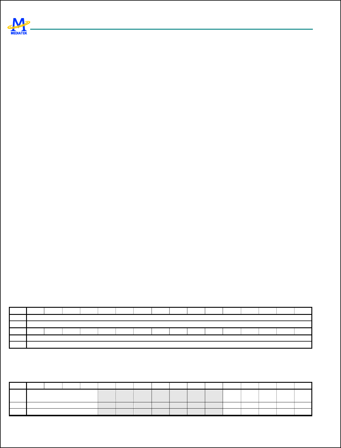
MT6217 GSM/GPRS Baseband Processor Data Sheet Revision 1.01
237/349 MediaTek Inc. Confidential
PINIRQ Pin Change Interrupt. The register bit indicates if any interrupt for memory card insertion/removal exists.
Whenever memory card is inserted or removed and card detection interrupt is enabled, i.e., the register bit PINEN
in the register MSDC_CFG is set to ‘1’, the register bit will be set to ‘1’. It will be reset when the register is read.
0 Otherwise.
1 Card is inserted or removed.
SDCMDIRQ SD Bus CMD Interrupt. The register bit indicates if any interrupt for SD CMD line exists. Whenever
interrupt for SD CMD line exists, i.e., any bit in the register SDC_CMDSTA is active, the register bit will be set to
‘1’ if interrupt is enabled. It will be reset when the register is read.
0 No SD CMD line interrupt.
1 SD CMD line interrupt exists.
SDDATIRQ SD Bus DAT Interrupt. The register bit indicates if any interrupt for SD DAT line exists. Whenever interrupt
for SD DAT line exists, i.e., any bit in the register SDC_ DATSTA is active, the register bit will be set to ‘1’ if
interrupt is enabled. It will be reset when the register is read.
0 No SD DAT line interrupt.
1 SD DAT line interrupt exists.
SDMCIRQ SD Memory Card Interrupt. The register bit indicates if any interrupt for SD Memory Card exists. Whenever
interrupt for SD Memory Card exists, i.e., any bit in the register SDC_CSTA is active, the register bit will be set to
‘1’ if interrupt is enabled. It will be reset when the register is read.
0 No SD Memory Card interrupt.
1 SD Memory Card interrupt exists.
MSIFIRQ MS Bus Interface Interrupt. The register bit indicates if any interrupt for MS Bus Interface exists. Whenever
interrupt for MS Bus Interface exists, i.e., any bit in the register MSC_STA is active, the register bit will be set to
‘1’ if interrupt is enabled. It will be reset when the register MSDC_STA or MSC_STA is read.
0 No MS Bus Interface interrupt.
1 MS Bus Interface interrupt exists.
SDR1BIRQ SD/MMC R1b Response Interrupt. The register bit will be active when a SD/MMC command with R1b
response finishes and the DAT0 line has transition from busy to idle state.
0 No interrupt for SD/MMC R1b response.
1 Interrupt for SD/MMC R1b response exists.
MSDC+000Ch MS/SD Memory Card Controller Data Register MSDC_DAT
Bit 31 30 29 28 27 26 25 24 23 22 21 20 19 18 17 16
Name
DATA[31:16]
Type R/W
Bit 15 14 13 12 11 10 9 8 7 6 5 4 3 2 1 0
Name
DATA[15:0]
Type R/W
The register is used to read/write data from/to FIFO inside MS/SD controller. Data access is in unit of 32 bits.
MSDC+0010h MS/SD Memory Card Pin Status Register MSDC_PS
Bit 15 14 13 12 11 10 9 8 7 6 5 4 3 2 1 0
Name
CDDEBOUNCE PINC
HG PIN0 POEN
0 PIEN0
CDEN
Type RW RC RO R/W R/W R/W
Reset
0000 0 0 0 0 0

MT6217 GSM/GPRS Baseband Processor Data Sheet Revision 1.01
238/349 MediaTek Inc. Confidential
The register is used for card detection. When the memory card controller is powered on, and the system is powered on, the
power for the memory card is still off unless power has been supplied by the PMIC. Meanwhile, pad for card detection
defaults to pull down when the system is powered on. The scheme of card detection for MS is the same as that for
SD/MMC.
For detecting card insertion, first pull up INS pin, and then enable card detection and input pin at the same time. After 32
cycles of controller clock, status of pin changes will emerge. For detecting card removal, just keep enabling card detection
and input pin.
CDEN Card Detection Enable. The register bit is used to enable or disable card detection.
0 Card detection is disabled.
1 Card detection is enabled.
PIEN0 The register bit is used to control input pin for card detection.
0 Input pin for card detection is disabled.
1 Input pin for card detection is enabled.
POEN0 The register bit is used to control output of input pin for card detection.
0 Output of input pin for card detection is disabled.
1 Output of input pin for card detection is enabled.
PIN0 The register shows the value of input pin for card detection.
0 The value of input pin for card detection is logic low.
1 The value of input pin for card detection is logic high.
PINCHG Pin Change. The register bit indicates the status of card insertion/removal. If memory card is inserted or
removed, the register bit will be set to ‘1’ no matter pin change interrupt is enabled or not. It will be cleared when
the register is read.
0 Otherwise.
1 Card is inserted or removed.
CDDEBOUNCE The register field specifies the time interval for card detection de-bounce. Its default value is
0. It means that de-bounce interval is 32 cycle time of 32KHz. The interval will extend one cycle time of
32KHz by increasing the counter by 1.
MSDC+0014h MS/SD Memory Card Controller IO Control Register MSDC_IOCON
Bit 15 14 13 12 11 10 9 8 7 6 5 4 3 2 1 0
Name
SRCF
G1 SRCF
G0 ODCCFG1 ODCCFG0
Type R/W R/W R/W R/W
Reset
1 1 000 011
The register specifies Output Driving Capability and Slew Rate of IO pads for MSDC. The reset value is suggestion
setting. If output driving capability of the pins DAT0, DAT1, DAT2 and DAT3 is too large, it’s possible to arise ground
bounce and thus result in glitch on SCLK.
ODCCFG0 Output driving capability the pins CMD/BS and SCLK
000 2mA
001 4mA
010 6mA
011 8mA
100 10mA
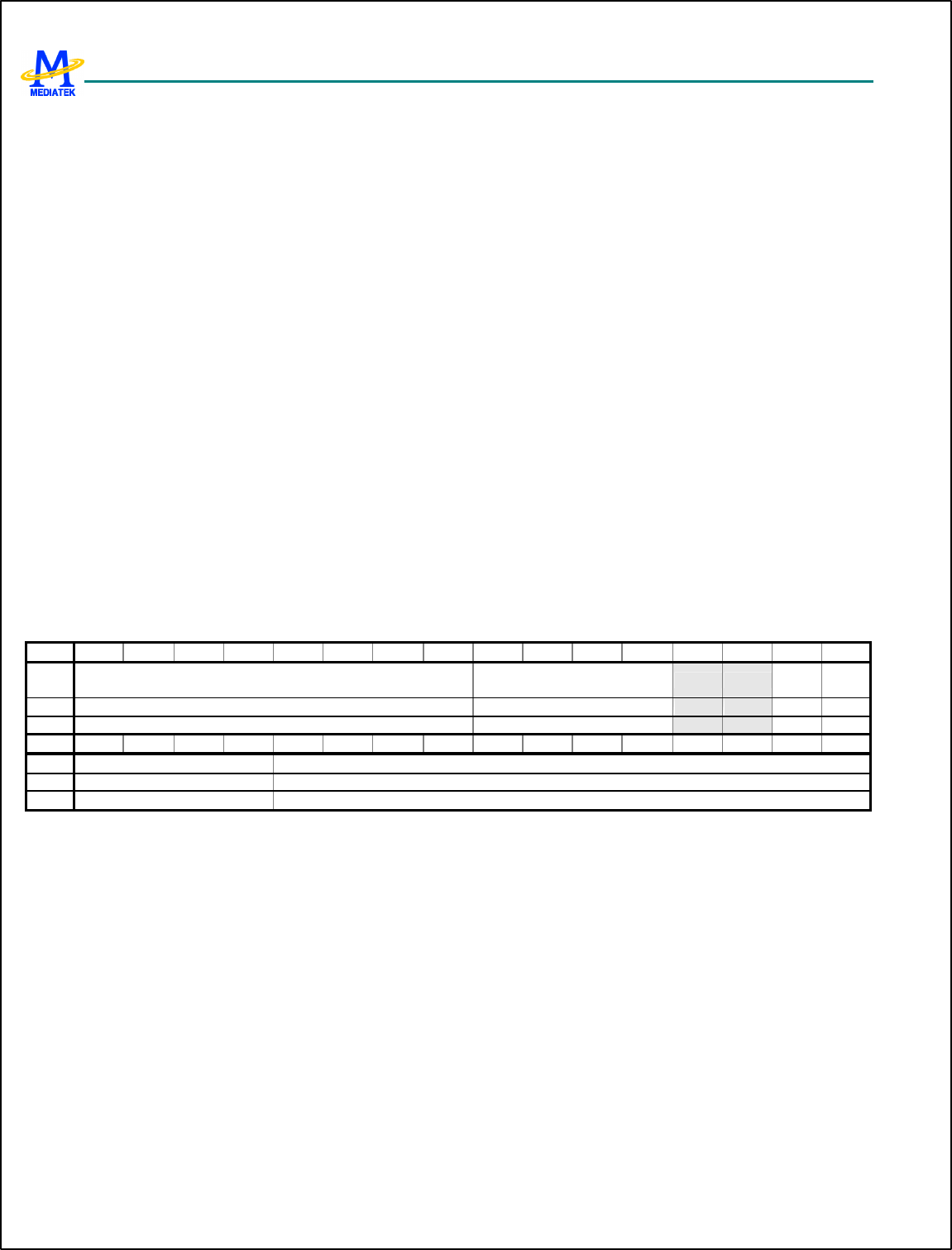
MT6217 GSM/GPRS Baseband Processor Data Sheet Revision 1.01
239/349 MediaTek Inc. Confidential
101 12mA
110 14mA
111 16mA
ODCCFG1 Output driving capability the pins DAT0, DAT1, DAT2 and DAT3
000 2mA
001 4mA
010 6mA
011 8mA
100 10mA
101 12mA
110 14mA
111 16mA
SRCFG0 Output driving capability the pins CMD/BS and SCLK
0 Fast Slew Rate
1 Slow Slew Rate
SRCFG1 Output driving capability the pins DAT0, DAT1, DAT2 and DAT3
0 Fast Slew Rate
1 Slow Slew Rate
6.6.3.2 SD Memory Card Controller Register Definitions
MSDC+0020h SD Memory Card Controller Configuration Register SDC_CFG
Bit 31 30 29 28 27 26 25 24 23 22 21 20 19 18 17 16
Name
DTOC WDOD MDLE
N SIEN
Type R/W R/W R/W R/W
Reset
00000000 0000 0 0
Bit 15 14 13 12 11 10 9 8 7 6 5 4 3 2 1 0
Name
BSYDLY BLKLEN
Type R/W R/W
Reset
1000 00000000000
The register is used for configuring the MS/SD Memory Card Controller when it is configured as the host of SD Memory
Card. If the controller is configured as the host of Memory Stick, the contents of the register have no impact on the
operation of the controller. Note that SDC_CFG[31:16] can be accessed by 16 -bit APB bus access.
BLKLEN It refers to Block Length. The register field is used to define the length of one block in unit of byte in a data
transaction. The maximal value of block length is 2048 bytes.
000000000000 Reserved.
000000000001 Block length is 1 byte.
000000000010 Block length is 2 bytes.
…
011111111111 Block length is 2047 bytes.
100000000000 Block length is 2048 bytes.
BSYDLY The register field is only valid for the commands with R1b response. If the command has a response of R1b
type, MS/SD controller must monitor the data line 0 for card busy status from the bit time that is two serial clock
cycles after the command end bit to check if operations in SD/MMC Memory Card have finished. The register

MT6217 GSM/GPRS Baseband Processor Data Sheet Revision 1.01
240/349 MediaTek Inc. Confidential
field is used to expand the time between the command end bit and end of detection period to detect card busy
status. If time is up and there is no card busy status on data line 0, then the controller will abandon the detection.
0000 No extend.
0001 Extend one more serial clock cycle.
0010 Extend two more serial clock cycles.
…
1111 Extend fifteen more serial clock cycle.
SIEN Serial Interface Enable. It should be enabled as soon as possible before any command.
0 Serial interface for SD/MMC is disabled.
1 Serial interface for SD/MMC is enabled.
MDLEN Multiple Data Line Enable. The register can be enabled only when SD Memory Card is applied and detected by
software application. It is the responsibility of the application to program the bit correctly when an
MultiMediaCard is applied. If an MultiMediaCard is applied and 4-bit data line is enabled, then 4 bits will be
output every serial clock. Therefore, data integrity will fail.
0 4-bit Data line is disabled.
1 4-bit Data line is enabled.
WDOD Write Data Output Delay. The period from finish of the response for the initial host write command or the last
write data block in a multiple block write operation to the start bit of the next write data block requires at least two
serial clock cycles. The register field is used to extend the period (Write Data Output Delay) in unit of one serial
clock.
0000 No extend.
0001 Extend one more serial clock cycle.
0010 Extend two more serial clock cycles.
…
1111 Extend fifteen more serial clock cycle.
DTOC Data Timeout Counter. The period from finish of the initial host read command or the last read data block in a
multiple block read operation to the start bit of the next read data block requires at least two serial clock cycles.
The counter is used to extend the period (Read Data Access Time) in unit of 65,536 serial clock. See the register
field description of the register bit RDINT for reference.
00000000 Extend 65,536 more serial clock cycle.
00000001 Extend 65,536x2 more serial clock cycle.
00000010 Extend 65,536x3 more serial clock cycle.
…
11111111 Extend 65,536x 256 more serial clock cycle.
MSDC+0024h SD Memory Card Controller Command Register SDC_CMD
Bit 15 14 13 12 11 10 9 8 7 6 5 4 3 2 1 0
Name
INTC STOP RW DTYPE IDRT RSPTYP BREA
K CMD
Type R/W R/W R/W R/W R/W R/W R/W R/W
Reset
0 0 0 00 0 000 0 000000
The register defines a SD Memory Card command and its attribute. Before MS/SD controller issues a transaction onto SD
bus, application shall specify other relative setting such as argument for command. After application writes the register,
MS/SD controller will issue the corresponding transaction onto SD serial bus. If the command is GO_IDLE_STATE, the
controller will have serial clock on SD/MMC bus run 128 cycles before issuing the command.

MT6217 GSM/GPRS Baseband Processor Data Sheet Revision 1.01
241/349 MediaTek Inc. Confidential
CMD SD Memory Card command. It is totally 6 bits.
BREAK Abort a pending MMC GO_IRQ_MODE command. It is only valid for a pending GO_IRQ_MODE command
waiting for MMC interrupt response.
0 Other fields are valid.
1 Break a pending MMC GO_IRQ_MODE command in the controller. Other fields are invalid.
RSPTYP The register field defines response type for the command. For commands with R1 and R1b response, the
register SDC_CSTA (not SDC_STA) will update after response token is received. This register SDC_CSTA
contains the status of the SD/MMC and it will be used as response interrupt sources. Note that if CMD7 is used
with all 0’s RCA then RSPTYP must be “000”. And the command “GO_TO_IDLE” also have RSPTYP=’000’.
000 There is no response for the command. For instance, broadcast command without response and
GO_INACTIVE_STATE command.
001 The command has R1 response. R1 response token is 48-bit.
010 The command has R2 response. R2 response token is 136-bit.
011 The command has R3 response. Even though R3 is 48-bit response, but it does not contain CRC checksum.
100 The command has R4 response. R4 response token is 48-bit. (Only for MMC)
101 The command has R5 response. R5 response token is 48-bit. (Only for MMC)
110 The command has R6 response. R6 response token is 48-bit.
111 The command has R1b response. If the command has a response of R1b type, MS/SD controller must monitor
the data line 0 for card busy status from the bit time that is two or four serial clock cycles after the command
end bit to check if operations in SD/MMC Memory Card have finished. There are two cases for detection of
card busy status. The first case is that the host stops the data transmission during an active write data transfer.
The card will assert busy signal after the stop transmission command end bit followed by four serial clock
cycles. The second case is that the card is in idle state or under a scenario of receiving a stop transmission
command between data blocks when multiple block write command is in progress. The register bit is valid
only when the command has a response token.
IDRT Identification Response Time. The register bit indicates if the command has a response with NID (that is, 5 serial
clock cycles as defined in SD Memory Card Specification Part 1 Physical Layer Specification version 1.0)
response time. The register bit is valid only when the command has a response token. Thus the register bit must be
set to ‘1’ for CMD2 (ALL_SEND_CID) and ACMD41 (SD_APP_OP_CMD).
0 Otherwise.
1 The command has a response with NID response time.
DTYPE The register field defines data token type for the command.
00 No data token for the command
01 Single block transaction
10 Multiple block transaction. That is, the command is a multiple block read or write command.
11 Stream operation. It only shall be used when an MultiMediaCard is applied.
RW The register bit defines the command is a read command or write command. The register bit is valid only when the
command will cause a transaction with data token.
0 The command is a read command.
1 The command is a write command.
STOP The register bit indicates if the command is a stop transmission command.
0 The command is not a stop transmission command.
1 The command is a stop transmission command.
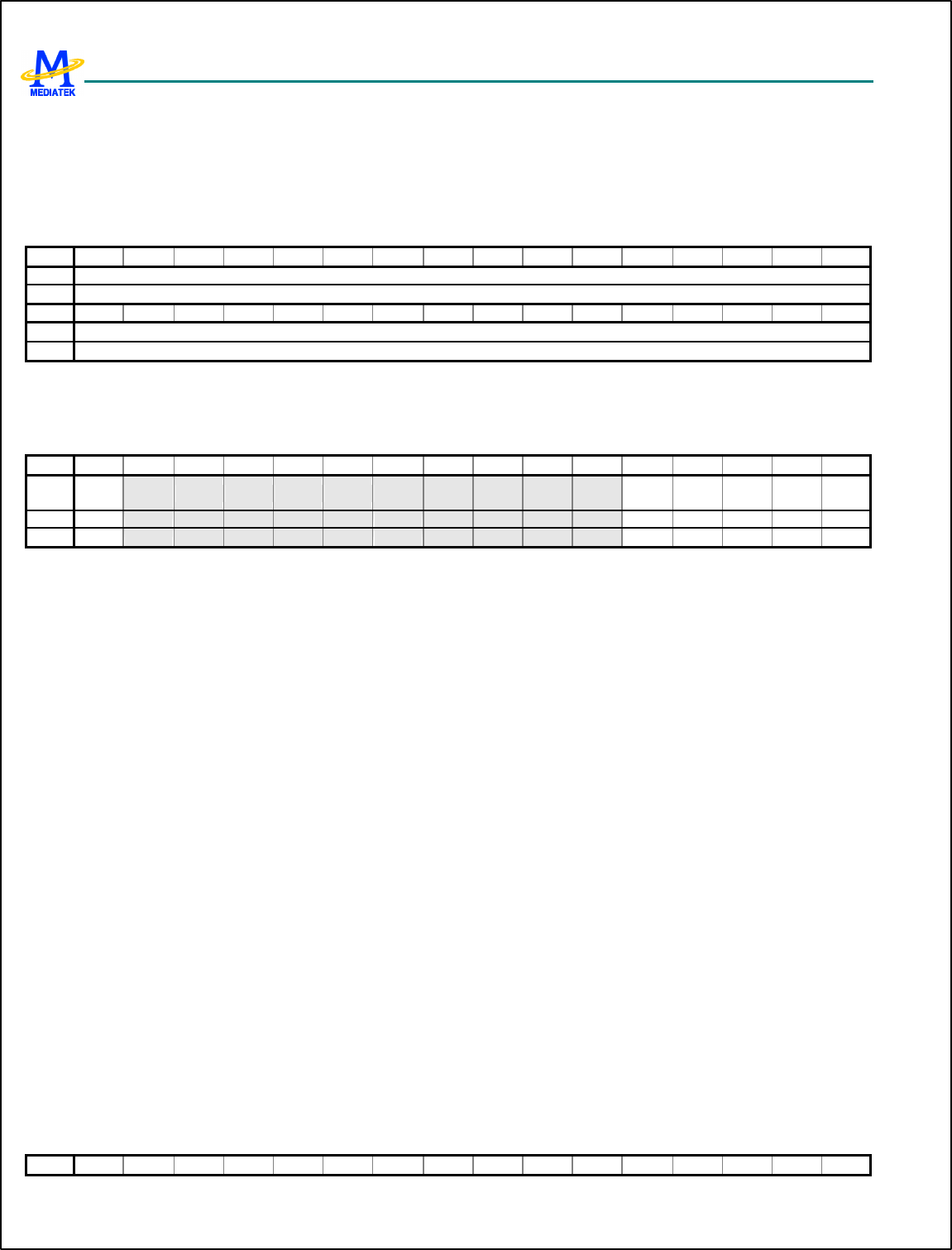
MT6217 GSM/GPRS Baseband Processor Data Sheet Revision 1.01
242/349 MediaTek Inc. Confidential
INTR The register bit indicates if the command is GO_IRQ_STATE. If the command is GO_IRQ_STATE, the period
between command token and response token will not be limited.
0 The command is not GO_IRQ_STATE.
1 The command is GO_IRQ_STATE.
MSDC+0028h SD Memory Card Controller Argument Register SDC_ARG
Bit 31 30 29 28 27 26 25 24 23 22 21 20 19 18 17 16
Name
ARG [31:16]
Type R/W
Bit 15 14 13 12 11 10 9 8 7 6 5 4 3 2 1 0
Name
ARG [15:0]
Type R/W
The register contains the argument of the SD/MMC Memory Card command.
MSDC+002Ch SD Memory Card Controller Status Register SDC_STA
Bit 15 14 13 12 11 10 9 8 7 6 5 4 3 2 1 0
Name
WP R1BS
Y RSV DATB
USY CMDB
USY SDCB
USY
Type R RO RO RO RO RO
Reset
- 0 0 0 0 0
The register contains various status of MS/SD controller as the controller is configured as the host of SD Memory Card.
SDCBUSY The register field indicates if MS/SD controller is busy, that is, any transmission is going on CMD or DAT
line on SD bus.
0 MS/SD controller is idle.
1 MS/SD controller is busy.
CMDBUSY The register field indicates if any transmission is going on CMD line on SD bus.
0 No transmission is going on CMD line on SD bus.
1 There exists transmission going on CMD line on SD bus.
DATBUSY The register field indicates if any transmission is going on DAT line on SD bus. For those commands
without data but still involving DAT line, the register bit is useless. For example, if an Erase command is
issued, then checking if the register bit is ‘0’ before issuing next command with data would not guarantee
that the controller is idle. In this situation, use the register bit SDCBUSY.
0 No transmission is going on DAT line on SD bus.
1 There exists transmission going on DAT line on SD bus.
R1BSY The register field shows the status of DAT line 0 for commands with R1b response.
0 SD/MMC Memory card is not busy.
1 SD/MMC Memory card is busy.
WP It is used to detect the status of Write Protection Switch on SD Memory Card. The register bit shows the status of
Write Protection Switch on SD Memory Card. There is no default reset value. The pin WP (Write Protection) is
also only useful while the controller is configured for SD Memory Card.
1 Write Protection Switch ON. It means that memory card is desired to be write-protected.
0 Write Protection Switch OFF. It means that memory card is writable.
MSDC+0030h SD Memory Card Controller Response Register 0 SDC_RESP0
Bit 31 30 29 28 27 26 25 24 23 22 21 20 19 18 17 16
MT6217 GSM/GPRS Baseband Processor Data Sheet Revision 1.01
243/349 MediaTek Inc. Confidential
Name
RESP [31:16]
Type RO
Bit 15 14 13 12 11 10 9 8 7 6 5 4 3 2 1 0
Name
RESP [15:0]
Type RO
The register contains parts of the last SD/MMC Memory Card bus response. See description for the register field
SDC_RESP3.
MSDC+0034h SD Memory Card Controller Response Register 1 SDC_RESP1
Bit 31 30 29 28 27 26 25 24 23 22 21 20 19 18 17 16
Name
RESP [63:48]
Type RO
Bit 15 14 13 12 11 10 9 8 7 6 5 4 3 2 1 0
Name
RESP [47:32]
Type RO
The register contains parts of the last SD/MMC Memory Card bus response. See description for the register field
SDC_RESP3.
MSDC+0038h SD Memory Card Controller Response Register 2 SDC_RESP2
Bit 31 30 29 28 27 26 25 24 23 22 21 20 19 18 17 16
Name
RESP [95:80]
Type RO
Bit 15 14 13 12 11 10 9 8 7 6 5 4 3 2 1 0
Name
RESP [79:64]
Type RO
The register contains parts of the last SD/MMC Memory Card bus response. See description for the register field
SDC_RESP3.
MSDC+003Ch SD Memory Card Controller Response Register 3 SDC_RESP3
Bit 31 30 29 28 27 26 25 24 23 22 21 20 19 18 17 16
Name
RESP [127:112]
Type RO
Bit 15 14 13 12 11 10 9 8 7 6 5 4 3 2 1 0
Name
RESP [111:96]
Type RO
The register contains parts of the last SD/MMC Memory Card bus response. The register fields SDC_RESP0, SDC_RESP1,
SDC_RESP2 and SDC_RESP3 compose the last SD/MMC Memory card bus response. For response of type R2, that is,
response of the command ALL_SEND_CID, SEND_CSD and SEND_CID, only bit 127 to 0 of response token is stored in
the register field SDC_RESP0, SDC_RESP1, SDC_RESP2 and SDC_RESP3. For response of other types, only bit 39 to 8
of response token is stored in the register field SDC_ RESP0.
MSDC+0040h SD Memory Card Controller Command Status Register
SDC_CMDSTA
Bit 15 14 13 12 11 10 9 8 7 6 5 4 3 2 1 0
Name
MMCI
RQ
RSPC
RCER
R
CMDT
O CMDR
DY
Type RC RC RC RC

MT6217 GSM/GPRS Baseband Processor Data Sheet Revision 1.01
244/349 MediaTek Inc. Confidential
Reset
0 0 0 0
The register contains the status of MS/SD controller during command execution and that of MS/SD bus protocol after
command execution when MS/SD controller is configured as the host of SD/MMC Memory Card. The register will also be
used as interrupt sources. The register will be cleared when reading the register. Meanwhile, if interrupt is enabled and thus
interrupt caused by the register is generated, reading the register will deassert the interrupt.
CMDRDY For command without response, the register bit will be ‘1’ once the command completes on SD/MMC bus. For
command with response, the register bit will be ‘1’ whenever the command is issued onto SD/MMC bus and its
corresponding response is received without CRC error.
0 Otherwise.
1 Command with/without response finish successfully without CRC error.
CMDTO Timeout on CMD detected. A ‘1’ indicates that MS/SD controller detected a timeout condition while waiting
for a response on the CMD line.
0 Otherwise.
1 MS/SD controller detected a timeout condition while waiting for a response on the CMD line.
RSPCRCERR CRC error on CMD detected. A ‘1’ indicates that MS/SD controller detected a CRC error after reading a
response from the CMD line.
0 Otherwise.
1 MS/SD controller detected a CRC error after reading a response from the CMD line.
MMCIRQ MMC requests an interrupt. A ‘1’ indicates that a MMC supporting command class 9 issued an interrupt
request.
0 Otherwise.
1 A ‘1’ indicates that a MMC supporting command class 9 issued an interrupt request.
MSDC+0044h SD Memory Card Controller Data Status Register SDC_DATSTA
Bit 15 14 13 12 11 10 9 8 7 6 5 4 3 2 1 0
Name
DATC
RCER
R
DATT
O BLKD
ONE
Type RC RC RC
Reset
0 0 0
The register contains the status of MS/SD controller during data transfer on DAT line(s) when MS/SD controller is
configured as the host of SD/MMC Memory Card. The register also will be used as interrupt sources. The register will be
cleared when reading the register. Meanwhile, if interrupt is enabled and thus interrupt caused by the register is generated,
reading the register will deassert the interrupt.
BLKDONE The register bit indicates the status of data block transfer.
0 Otherwise.
1 A data block was successfully transferred.
DATTO Timeout on DAT detected. A ‘1’ indicates that MS/SD controller detected a timeout condition while waiting for
data token on the DAT line.
0 Otherwise.
1 MS/SD controller detected a timeout condition while waiting for data token on the DAT line.
DATCRCERR CRC error on DAT detected. A ‘1’ indicates that MS/SD controller detected a CRC error after reading a
block of data from the DAT line or SD/MMC signaled a CRC error after writing a block of data to the DAT line.
0 Otherwise.
MT6217 GSM/GPRS Baseband Processor Data Sheet Revision 1.01
245/349 MediaTek Inc. Confidential
1 MS/SD controller detected a CRC error after reading a block of data from the DAT line or SD/MMC signaled
a CRC error after writing a block of data to the DAT line.
MSDC+0048h SD Memory Card Status Register SDC_CSTA
Bit 31 30 29 28 27 26 25 24 23 22 21 20 19 18 17 16
Name
CSTA [31:16]
Type RC
Reset
0000000000000000
Bit 15 14 13 12 11 10 9 8 7 6 5 4 3 2 1 0
Name
CSTA [15:0]
Type RC
Reset
0000000000000000
After commands with R1 and R1b response this register contains the status of the SD/MMC card and it will be used as
response interrupt sources. In all register fields, logic high indicates error and logic low indicates no error. The register will
be cleared when reading the register. Meanwhile, if interrupt is enabled and thus interrupt caused by the regis ter is
generated, reading the register will deassert the interrupt.
CSTA31 OUT_OF_RANGE. The command’s argument was out of the allowed range for this card.
CSTA30 ADDRESS_ERROR. A misaligned address that did not match the block length was used in the command.
CSTA29 BLOCK_LEN_ERROR. The transferred block length is not allowed for this card, or the number of
transferred bytes does not match the block length.
CSTA28 ERASE_SEQ_ERROR. An error in the sequence of erase commands occurred.
CSTA27 ERASE_PARAM. An invalid selection of write-blocks for erase occurred.
CSTA26 WP_VIOLATION. Attempt to program a write-protected block.
CSTA25 Reserved. Return zero.
CSTA24 LOCK_UNLOCK_FAILED. Set when a sequence or password error has been detected in lock/unlock card
command or if there was an attempt to access a locked card.
CSTA23 COM_CRC_ERROR. The CRC check of the previous command failed.
CSTA22 ILLEGAL_COMMAND. Command not legal for the card state.
CSTA21 CARD_ECC_FAILED. Card internal ECC was applied but failed to correct the data.
CSTA20 CC_ERROR. Internal card controller error.
CSTA19 ERROR. A general or an unknown error occurred during the operation.
CSTA18 UNDERRUN. The card could not sustain data transfer in stream read mode.
CSTA17 OVERRUN. The card could not sustain data programming in stream write mode.
CSTA16 CID/CSD_OVERWRITE. It can be either one of the following errors: 1. The CID register has been already
written and cannot be overwritten 2. The read only section of the CSD does not match the card. 3. An attempt to
reverse the copy (set as original) or permanent WP (unprotected) bits was made.
CSTA[15:4] Reserved. Return zero.
CSTA3 AKE_SEQ_ERROR. Error in the sequence of authentication process
CSTA[2:0] Reserved. Return zero.
MSDC+004Ch SD Memory Card IRQ Mask Register 0 SDC_IRQMASK0
Bit 31 30 29 28 27 26 25 24 23 22 21 20 19 18 17 16
Name
IRQMASK [31:16]
Type R/W
Reset
0000000000000000
Bit 15 14 13 12 11 10 9 8 7 6 5 4 3 2 1 0
MT6217 GSM/GPRS Baseband Processor Data Sheet Revision 1.01
246/349 MediaTek Inc. Confidential
Name
IRQMASK [15:0]
Type R/W
Reset
0000000000000000
The register contains parts of SD Memory Card Interrupt Mask Register. See the register description of the register
SDC_IRQMASK1 for reference. The register will mask interrupt sources from the register SDC_CMDSTA and
SDC_DATSTA. IRQMASK[15:0] is for SDC_CMDSTA and IRQMASK[31:16] for SDC_DATSTA. A ‘1’ in some bit of
the register will mask the corresponding interrupt source with the same bit position. For example, if IRQMASK[0] is ‘1’
then interrupt source from the register field CMDRDY of the register SDC_ CMDSTA will be masked. A ‘0’ in some bit
will not cause interrupt mask on the corresponding interrupt source from the register SDC_CMDSTA and SDC_DATSTA.
MSDC+0050h SD Memory Card IRQ Mask Register 1 SDC_IRQMASK1
Bit 31 30 29 28 27 26 25 24 23 22 21 20 19 18 17 16
Name
IRQMASK [63:48]
Type R/W
Reset
0000000000000000
Bit 15 14 13 12 11 10 9 8 7 6 5 4 3 2 1 0
Name
IRQMASK [47:32]
Type R/W
Reset
0000000000000000
The register contains parts of SD Memory Card Interrupt Mask Register. The registers SDC_IRQMASK1 and
SDC_IRQMASK0 compose the SD Memory Card Interrupt Mask Register. The register will mask interrupt sources from
the register SDC_CSTA. A ‘1’ in some bit of the register will mask the corresponding interrupt source with the same bit
position. For example, if IRQMASK[63] is ‘1’ then interrupt source from the register field OUT_OF_RANGE of the
register SDC_ CSTA will be masked. A ‘0’ in some bit will not cause interrupt mask on the corresponding interrupt source
from the register SDC_ CSTA.
6.6.3.3 Memory Stick Controller Register Definitions
MSDC+0060h Memory Stick Controller Configuration Register MSC_CFG
Bit 15 14 13 12 11 10 9 8 7 6 5 4 3 2 1 0
Name
PMOD
E PRED BUSYCNT SIEN
Type R/W R/W R/W R/W
Reset
0 0 101 0
The register is used for Memory Stick Controller Configuration when MS/SD controller is configured as the host of
Memory Stick.
SIEN Serial Interface Enable. It should be enabled as soon as possible before any command.
0 Serial interface for Memory Stick is disabled.
1 Serial interface for Memory Stick is enabled.
BUSYCNT RDY timeout setting in unit of serial clock cycle. The register field is set to the maximum BUSY timeout time
(set value x 4 +2) to wait until the RDY signal is output from the card. RDY timeout error detection is not
performed when BUSYCNT is set to 0. The initial value is 0x5. That is, BUSY signal exceeding 5x4+2=22 serial
clock cycles causes a RDY timeout error.
000 Not detect RDY timeout
001 BUSY signal exceeding 1x4+2=6 serial clock cycles causes a RDY timeout error.
MT6217 GSM/GPRS Baseband Processor Data Sheet Revision 1.01
247/349 MediaTek Inc. Confidential
010 BUSY signal exceeding 2x4+2=10 serial clock cycles causes a RDY timeout error.
…
111 BUSY signal exceeding 7x4+2=30 serial clock cycles causes a RDY timeout error.
PRED Parallel Mode Rising Edge Data. The register field is only valid in parallel mode, that is, MSPRO mode. In
parallel mode, data must be driven and latched at the falling edge of serial clock on MS bus. In order to mitigate
hold time issue, the regis ter can be set to ‘1’ such that write data is driven by MSDC at the rising edge of serial
clock on MS bus.
0 Write data is driven by MSDC at the falling edge of serial clock on MS bus.
1 Write data is driven by MSDC at the rising edge of serial clock on MS bus.
PMODE Memory Stick PRO Mode.
0 Use Memory Stick serial mode.
1 Use Memory Stick parallel mode.
MSDC+0064h Memory Stick Controller Command Register MSC_CMD
Bit 15 14 13 12 11 10 9 8 7 6 5 4 3 2 1 0
Name
PID DATASIZE
Type R/W R/W
Reset
0000 0000000000
The register is used for issuing a transaction onto MS bus. Transaction on MS bus is started by writing to the register
MSC_CMD. The direction of data transfer, that is, read or write transaction, is extracted from the register field PID. 16-bit
CRC will be transferred for a write transaction even if the register field DATASIZE is programmed as zero under the
condition where the register field NOCRC in the register MSDC_CFG is ‘0’. If the register field NOCRC in the register
MSDC_CFG is ‘1’ and the register field DATASIZE is programmed as zero, then writing to the register MSC_CMD will
not induce transaction on MS bus. The same applies for when the register field RDY in the register MSC_STA is ‘0’.
DATASIZE Data size in unit of byte for the current transaction.
0000000000 Data size is 0 byte.
0000000001 Data size is one byte.
0000000010 Data size is two bytes.
…
0111111111 Data size is 511 bytes.
1000000000 Data size is 512 bytes.
PID Protocol ID. It is used to derive Transfer Protocol Code (TPC). The TPC can be derived by cascading PID and its
reverse version. For example, if PID is 0x1, then TPC is 0x1e, that is, 0b0001 cascades 0b1110. In addition, the
direction of the bus transaction can be determined from the register bit 15, that is, PID[3].
MSDC+0068h Memory Stick Controller Auto Command Register MSC_ACMD
Bit 15 14 13 12 11 10 9 8 7 6 5 4 3 2 1 0
Name
APID ADATASIZE ACEN
Type R/W R/W R/W
Reset
0111 0000000001 0
The register is used for issuing a transaction onto MS bus automatically after the MS command defined in MSC_CMD
completed on MS bus. Auto Command is a function used to automatically execute a command like GET_INT or
READ_REG for checking status after SET_CMD ends. If auto command is enabled, the command set in the register will be
executed once the INT signal on MS bus is detected. After auto command is issued onto MS bus, the register bit ACEN will

MT6217 GSM/GPRS Baseband Processor Data Sheet Revision 1.01
248/349 MediaTek Inc. Confidential
become disabled automatically. Note that if auto command is enabled then the register bit RDY in the register MSC_STA
caused by the command defined in MSC_CMD will be suppressed until auto command completes. Note that the register
field ADATASIZE cannot be set to zero, or the result will be unpredictable.
ACEN Auto Command Enable.
0 Auto Command is disabled.
1 Auto Command is enabled.
ADATASIZE Data size in unit of byte for Auto Command. Initial value is 0x01.
0000000000 Data size is 0 byte.
0000000001 Data size is one byte.
0000000010 Data size is two bytes.
…
0111111111 Data size is 511 bytes.
1000000000 Data size is 512 bytes.
APID Auto Command Protocol ID. It is used to derive Transfer Protocol Code (TPC). Initial value is GSET_INT(0x7).
MSDC+006Ch Memory Stick Controller Status Register MSC_STA
Bit 15 14 13 12 11 10 9 8 7 6 5 4 3 2 1 0
Name
CMDN
K BREQ ERR CED HSRD
Y CRCE
R TOER SIF RDY
Type R R R R RO RO RO RO RO
Reset
0 0 0 0 0 0 0 0 1
The register contains various status of Memory Stick Controller, that is, MS/SD controller is configured as Memory Stick
Controller. These statuses can be used as interrupt sources. Reading the register will NOT clear it. The register will be
cleared whenever a new command is written to the register MSC_CMD.
RDY The register bit indicates the status of transaction on MS bus. The register bit will be cleared when writing to the
command register MSC_CMD.
0 Otherwise.
1 A transaction on MS bus is ended.
SIF The register bit indicates the status of serial interface. If an interrupt is active on MS bus, the register bit will be
active. Note the difference between the signal RDY and SIF. When parallel mode is enabled, the signal SIF will be
active whenever any of the signal CED, ERR, BREQ and CMDNK is active. In order to separate interrupts
caused by the signals RDY and SIF, the register bit SIF will not become active until the register MSDC_INT
is read once. That is, the sequence for detecting the register bit SIF by polling is as follows:
1. Detect the register bit RDY of the register MSC_STA
2. Read the register MSDC_INT
3. Detect the register bit SIF of the register MSC_STA

MT6217 GSM/GPRS Baseband Processor Data Sheet Revision 1.01
249/349 MediaTek Inc. Confidential
BS BS0 BS1 BS2 BS3 BS0
SDIO command execution command finished
INT
IRQ
RDY IRQ clear
SIF IRQ clear
0 Otherwise.
1 An interrupt is active on MS bus
TOER The register bit indicates if a BUSY signal timeout error takes place. When timeout error occurs, the signal BS will
become logic low ‘0’. The register bit will be cleared when writing to the command register MSC_CMD.
0 No timeout error.
1 A BUSY signal timeout error takes place. The register bit RDY will also be active.
CRCER The register bit indicates if a CRC error occurs while receiving read data. The register bit will be cleared when
writing to the command register MSC_CMD.
0 Otherwise.
1 A CRC error occurs while receiving read data. The register bit RDY will also be active.
HSRDY The register bit indicates the status of handshaking on MS bus. The register bit will be cleared when writing to the
command register MSC_CMD.
0 Otherwise.
1 A Memory Stick card responds to a TPC by RDY.
CED The register bit is only valid when parallel mode is enabled. In fact, it ’s value is from DAT[0] when serial interface
interrupt takes place. See Format Specification version 2.0 of Memory Stick Standard (Memory Stick PRO) for
more details.
0 Command does not terminate.
1 Command terminates normally or abnormally.
ERR The register bit is only valid when parallel mode is enabled. In fact, it’s value is from DAT[1] when serial interface
interrupt takes place. See Format Specification version 2.0 of Memory Stick Standard (Memory Stick PRO) for
more details.
0 Otherwise.
1 Indicate me mory access error during memory access command.
BREQ The register bit is only valid when parallel mode is enabled. In fact, it ’s value is from DAT[2] when serial interface
interrupt takes place. See Format Specification version 2.0 of Memory Stick Standard (Memory Stick PRO) for
more details.
0 Otherwise.
1 Indicate request for data.
CMDNK The register bit is only valid when parallel mode is enabled. In fact, it’s value is from DAT[3] when serial
interface interrupt takes place. See Format Specification version 2.0 of Memory Stick Standard (Memory Stick
PRO) for more details.
0 Otherwise
1 Indicate non-recognized command.

MT6217 GSM/GPRS Baseband Processor Data Sheet Revision 1.01
250/349 MediaTek Inc. Confidential
6.6.4 Application Notes
6.6.4.1 Initialization Procedures After Power On
Disable power down control for MSDC module
Remember to power on MSDC module before starting any operation to it.
6.6.4.2 Card Detection Procedures
The pseudo code is as follows:
MSDC_CFG.PRCFG0 = 2’b10
MSDC_PS = 2’b11
MSDC_CFG.VDDPD = 1
if(MSDC_PS.PINCHG) { // card is inserted
. . .
}
The pseudo code segment perform the fo llowing tasks:
1. First pull up CD/DAT3 (INS) pin.
2. Enable card detection and input pin at the same time.
3. Turn on power for memo ry card.
4. Detect insertion of memory card.
6.6.4.3 Notes on Commands
For MS, check if MSC_STA.RDY is ‘1’ before issuing any command.
For SD/MMC, if the command desired to be issued involves data line, for example, commands with data transfer or R1b
response, check if SDC_STA.SDCBUSY is ‘0’ before issuing. If the command desired to be issued does not involve data
line, only check if SDC_STA.CMDBUSY is ‘0’ before issuing.
6.6.4.4 Notes on Data Transfer
l For SD/MMC, if multiple -block-write command is issued then only issue STOP_TRANS command inter-blocks
instead of intra-blocks.
l Once SW decides to issue STOP_TRANS commands, no more data transfer from or to the controller.
6.6.4.5 Notes on Frequency Change
Before changing the frequency of serial clock on MS/SD/MMC bus, it is necessary to disable serial interface of the
controller. That is, set the register bit SIEN of the register SDC_CFG to ‘0’ for SD/MMC controller, and set the register bit
SIEN of the register MSC_CFG to ‘0’ for Memory Stick controller. Serial interface of the controller needs to be enabled
again before starting any operation to the memory card.
6.6.4.6 Notes on Response Timeout
If a read command doest not receive response, that is , it terminates with a timeout, then register SDC_DATSTA needs to be
cleared by reading it. The register bit “DATTO” should be active. However, it may take a while before the register bit

MT6217 GSM/GPRS Baseband Processor Data Sheet Revision 1.01
251/349 MediaTek Inc. Confidential
becomes active. The alternative is to send the STOP_TRANS command. However, this method will receive response with
illegal-command information. Also, remember to check if the register bit SDC_STA.CMDBUSY is active before issuing
the STOP_TRANS command. The procedure is as follows:
1. Read command => response time out
2. Issue STOP_TRANS command => Get Response
3. Read register SDC_DATSTA to clear it
6.6.4.7 Source or Destination Address is not word-aligned
It is possible that the source address is not word-aligned when data move from memory to MSDC. Similarly, destination
address may be not word -aligned when data move from MSDC to memory. This can be solved by setting DMA
byte-to-word functionality.
1. DMAn_CON.SIZE=0
2. DMAn_CON.BTW=1
3. DMAn_CON.BURST=2 (or 4)
4. DMAn_COUNT=byte number instead of word number
5. fifo threshold setting must be 1 (or 2), depending on DMAn_CON.BURST
Note n=4 ~ 11
6.6.4.8 Miscellaneous notes
l Sie mens MMC card: When a write command is issued and followed by a STOP_TRANS command, Siemens
MMC card will de-assert busy status even though flash programming has not yet finished. Software must use “Get
Status” command to make sure that flash progra mming finishes.
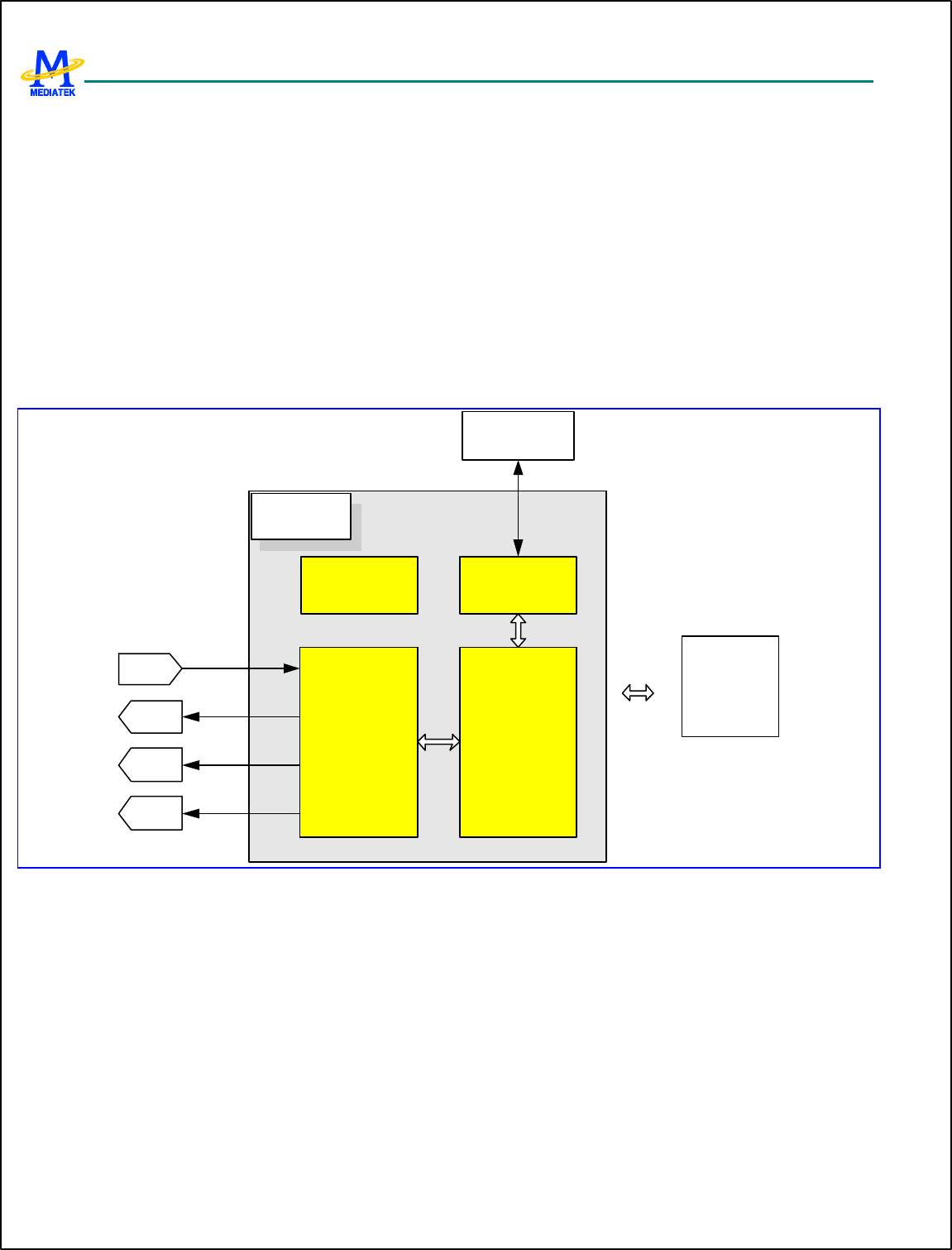
MT6217 GSM/GPRS Baseband Processor Data Sheet Revision 1.01
252/349 MediaTek Inc. Confidential
7 Audio Front-end
7.1 General Description
The audio front-end essentially consists of voice and audio data paths. The entire voice band data paths comply with the
GSM 03.50 specification. In addition, Mono hands-free audio or external FM radio playback path are provided. The audio
stereo audio path facilitates audio quality playback, external FM radio, and voice playback through headset.
Figure 51 shows the digital circuits block diagram of the audio front-end. The APB register block is an APB peripheral that
stores settings from the MCU. The DSP audio port block interfaces with the DSP for control and data communications. The
digital filter block performs filter operations for voice band and audio band signal processing. The Digital Audio Interface
(DAI) block communicates with the System Simulator for FTA or external Bluetooth modules.
Digital
Filters
DAC
ADC
Audio
Front-End
DSP
System
Simulator
DAI
APB
Registers
DSP
Audio
Port
DAC
DAC
Figure 51 Block diagram of digital circuits of the audio front-end
To communicate with the external Bluetooth module, the master mode PCM interface of 256-KHz clock with 8-KHz long
or short frame sync signal is supported. It can support up to 16-bit stereo or 32-bit mono 8-KHz sampling rate voice signal.
Figure 52 shows the timing diagram of the Bluetooth application. Please note that the serial data change when clock rising
and latched when clock falling.
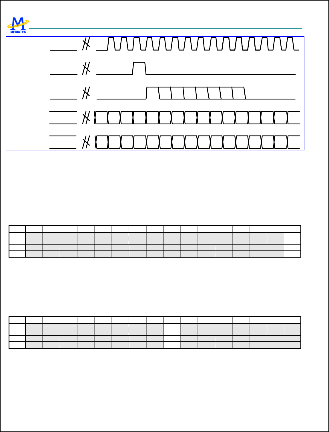
MT6217 GSM/GPRS Baseband Processor Data Sheet Revision 1.01
253/349 MediaTek Inc. Confidential
dai_clk
dai_tx
dai_rx
bt_sync(s)
bt_sync(l)
2 1 310 30 28 2427 2526 222329
2 1 310 30 28 2427 2526 222329
3
3
Figure 52 Timing diagram of Bluetooth application
7.2 Register Definitions
MCU APB bus registers in audio front-end are listed as followings.
AFE+0000h AFE Voice MCU Control Register AFE_VMCU_CO
N0
Bit 15 14 13 12 11 10 9 8 7 6 5 4 3 2 1 0
Name
VAFE
ON
Type R/W
Reset
0
MCU sets this register to start AFE voice operation. A synchronous reset signal will be issued. Then periodical interrupts of
8-KHz frequency will be issued. Clearing this register will stop the interrupt generation.
VAFEON turn on audio front-end operations
AFE+000Ch AFE Voice Analog-Circuit Control Register 1 AFE_VMCU_CO
N1
Bit 15 14 13 12 11 10 9 8 7 6 5 4 3 2 1 0
Name
VRSD
ON
Type R/W
Reset
0
Set this register for consistency of analog circuit setting. Suggested value is 80h
VRSDON voice-band redundant signed digit function on
0: 1-bit 2-level mode
1: 2-bit 3-level mode

MT6217 GSM/GPRS Baseband Processor Data Sheet Revision 1.01
254/349 MediaTek Inc. Confidential
AFE+0014h AFE Voice DAI Blue Tooth Control Register AFE_VDB_CON
Bit 15 14 13 12 11 10 9 8 7 6 5 4 3 2 1 0
Name
VDAI
ON VBTO
N VBTS
YNC VBTSLEN
Type R/W R/W R/W R/W
Reset
0 0 0 000
Set this register for DAI test mode and Blue Tooth application.
VDAION DAI function on
VBTON Blue Tooth function on
VBTSYNCBlue Tooth frame sync type
0: short
1: long
VBTSLEN Blue Tooth frame sync length = VBTSLEN+1
AFE+0018h AFE Voice Look-Back mode Control Register AFE_VLB_CON
Bit 15 14 13 12 11 10 9 8 7 6 5 4 3 2 1 0
Name
VBYP
ASSII
R
VDAPI
NMOD
E
VINTI
NMOD
E
VDEC
INMO
DE
Type R/W R/W R/W R/W
Reset
0 0 0 0
Set this register for AFE voice digital circuit configuration control. There are several loop back modes implemented for test
purposes. Default values correspond to the normal function mode
VBYPASSIIR bypass hardware IIR filters
VDAPINMODE DSP audio port input mode control
0: normal mode
1: loop back mode
VINTINMODE interpolator input mode control
0: normal mode
1: loop back mode
VDECINMODE decimator input mode control
0: normal mode
1: loop back mode
AFE+0020h AFE Audio MCU Control Register 0 AFE_AMCU_CO
N0
Bit 15 14 13 12 11 10 9 8 7 6 5 4 3 2 1 0
Name
AAFE
ON
Type R/W
Reset
0
MCU sets this register to start AFE audio operation. A synchronous reset signal will be issued. Then, periodical interrupts
of 1/6 sampling frequency will be issued. Clearing this register will stop the interrupt generation.

MT6217 GSM/GPRS Baseband Processor Data Sheet Revision 1.01
255/349 MediaTek Inc. Confidential
AFE+0024h AFE Audio Control Register 1 AFE_AMCU_CO
N1
Bit 15 14 13 12 11 10 9 8 7 6 5 4 3 2 1 0
Name
ADITH
ON ADITHVAL ARAMPSP AMUT
ER AMUT
EL AFS
Type R/W R/W R/W R/W R/W R/W
Reset
0 00 00 0 0 00
MCU set this register to inform hardware the sampling frequency of audio being played back.
ADITHON audio dither function on
ADITHVAL dither scaling setting
00: 1/4
01: 1/2
10: 1
11 : 2
ARAMPSP ramp up/down speed selection
00: 8, 4096/AFS
01: 16, 2048/AFS
10: 24, 1024/AFS
11 : 32, 512/AFS
AMUTER mute audio R-channel, with soft ramp up/down
AMUTEL mute audio L-channel, with soft ramp up/down
AFS sampling frequency setting
00: 32-KHz
01: 44.1-KHz
10: 48-KHz
11 : reserved
7.3 Programming Guide
There are several cases, including speech call, voice memo record, voice memo playback, melody playback and DAI tests,
where partial or whole audio front-end need to be turned on.
Following are the recommended voice band path programming procedures to turn on audio front-end:
l MCU programs the AFE_DAI_CON, AFE_LB_CON, AFE_ VAG_CON, AFE_ VAC_CON0, AFE_ VAC_CON1
and AFE_ VAPDN_CON registers for specific operation modes. Please also refer to analog chip interface
specification.
l MCU clear VAFE bit of PDN_CON2 register to un-gate the clock for voice band path. Please refer to software
power down control specification.
l MCU set AFE_ VMCU_CON to start the operation of voice band path.

MT6217 GSM/GPRS Baseband Processor Data Sheet Revision 1.01
256/349 MediaTek Inc. Confidential
Following are the recommended voice band path programming procedures to turn off audio front-end:
l MCU programs AFE_ VAPDN_CON to power down voice band path analog blocks .
l MCU clear AFE_ VMCU_CON to stop the operation of voice band path.
l MCU set VAFE bit of PDN_CON2 register to gate the clock for voice band path.
To start the DAI test, the MS first receives a GSM Layer 3 TEST_INTERFACE message from the SS and puts the speech
transcoder into one of the following modes:
l Normal mode (VDAIMODE[1:0]: 00)
l Test of speech encoder/DTX functions (VDAIMODE[1:0]: 10)
l Test of speech decoder/DTX functions (VDAIMODE[1:0]: 01)
l Test of acoustic devices and A/D & D/A (VDAIMODE[1:0]: 11)
It then waits for DAIRST# signaling from the SS. Recognizing this, DSP starts to transmit to and/or receive from DSP. For
more detail, please refer to GSM 11.10 specification.
Following are the recommended audio band path programming procedures to turn on audio front-end:
l MCU programs the AFE_MCU_CON1, AFE_AAG_CON, AFE_AAC_CON, and AFE_AAPDN_CON registers
for specific configurations. Please also refer to analog chip interface specification.
l MCU clear AAFE bit of PDN_CON2 register to un-gate the clock for audio band path. Please refer to software
power down control specification.
l MCU set AFE_AMCU_CON0 to start the operation of audio band path.
Following are the recommended audio band path programming procedures to turn off audio front-end:
l MCU programs the AFE_ AAPDN_ CON to power down audio band path analog blocks. Please refer to analog
block specification for more detail.
l MCU clear AFE_AMCU_CON0 to stop the operation of audio band path.
l MCU set AAFE bit of PDN_CON2 register to gate the clock for audio band path.

MT6217 GSM/GPRS Baseband Processor Data Sheet Revision 1.01
257/349 MediaTek Inc. Confidential
8 Radio Interface Control
This chapter details the controls of MT6217 baseband processor on the radio part of a GSM/GPRS terminal. To complete a
comprehensive control scheme yet being flexible , this radio interface is designed to be configurable to meet variety
parameters of radio devices. They consist of Baseband Serial Interface (BSI), Baseband Parallel Interface (BPI), Automatic
Power Control (APC) and Automatic Frequency Control (AFC) together with APC-DAC and AFC-DAC.
8.1 Base-band Serial Interface
The Base-band Serial Interface is used to control the external radio components. It utilizes a 3-wire serial bus to transfer
data to RF circuitry for PLL frequency change, reception gain setting, and other radio control purposes. In this unit, BSI
data registers are double-buffered in the same way as the TDMA event registers. The MCU writes data into the write buffer
and the data is transferred from the write buffer to the active buffer when TDMA_EVTVAL signal from the TDMA timer is
pulsed.
Each data register BSI_Dn_DAT is associated with one data control register BSI_Dn_CON, where n denotes the index. The
data control register with index n used to identify which events (signaled by TDMA_BSISTRn) generated by the TDMA
timer would trigger the download process of the word in register BSI_Dn_DAT through the serial bus, as well as the length
of the word in length of bits. A special event is defined. The event is triggered by the operation that the MCU writes 1 to the
IMOD flag. It provides immediate download process without programming the TDMA timer.
If more than one data word is to be downloaded on the same BSI event, the word with the lowest address among them will
be downloaded first, followed by the next lowest and so on.
The total time to download the words depends on the word length, the number of words to download, and the clock rates.
The programmer should space the successive event to provide enough time. If the download process of the previous event
isn’t complete before the new events come, the later will be suppressed.
The unit supports 2 external components. There are four output pins. BSI_CLK is the output clock, BSI_DATA is the serial
data port, and BSI_CS0 and BSI_CS1 are the select pins for 2 components, respectively. BSI_CS1 is multiplexed with other
function. Please refer to GPIO table for detail.
The block diagram of the BSI unit is as depicted in Figure 53.
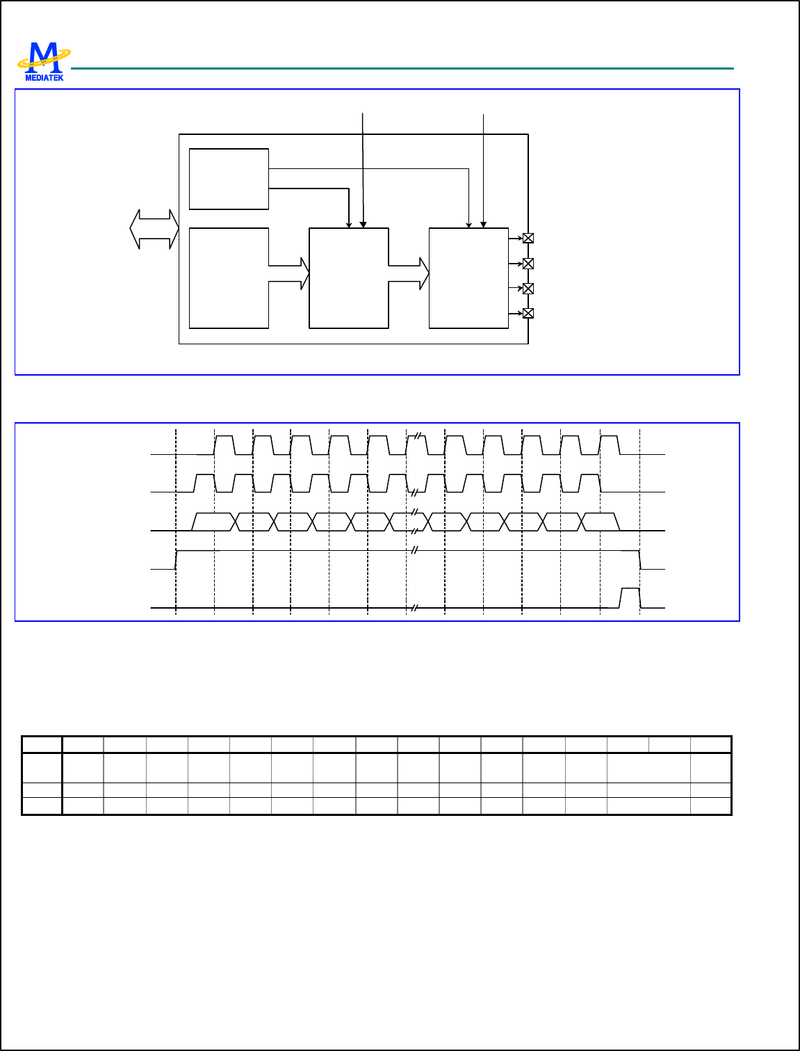
MT6217 GSM/GPRS Baseband Processor Data Sheet Revision 1.01
258/349 MediaTek Inc. Confidential
Control
Write
buffer Active
buffer Serial port
control
SETENV
IMOD
BSI_CS0
BSI_DATA
BSI_CLK
BSI_CS1 (GPIO)
BSI Unit
TDMA_BSISTR (0~15)
(from TDMA timer)
TDMA_EVTVAL
(from TDMA timer)
APB
BUS
Figure 53 Block diagram of BSI unit.
BSI_CSx
(long)
BSI_CLK
(true)
BSI_CSx
(short)
BSI_DATA
BSI_CLK
(invert)
LSBMSB
Figure 54 Timing characteristic of BSI interface
8.1.1 Register Definitions
BSI+0000h BSI control register BSI_CON
Bit 15 14 13 12 11 10 9 8 7 6 5 4 3 2 1 0
Name
SETE
NV EN1_
POL EN1_
LEN EN0_
POL EN0_
LEN IMOD CLK_SPD CLK_
POL
Type R/W R/W R/W R/W R/W WO R/W R/W
Reset
0 0 0 0 0 N/A 0 0
This register is the control register of the BSI unit. It controls the signal type of the 3-wire interface.
CLK_POL The flag controls the polarity of BSI_CLK. Refer to Figure 54.
0 True clock polarity
1 Inverted clock polarity
CLK_SPD The field defines the clock rate of BSI_CLK. The 3-wire interface provides 4 choices of data bit rate. The
default is 13/2 MHz.
00 13/2 MHz
MT6217 GSM/GPRS Baseband Processor Data Sheet Revision 1.01
259/349 MediaTek Inc. Confidential
01 13/4 MHz
10 13/6 MHz
11 13/8 MHz
IMOD The field enables the immediate mode. If the MCU writes 1 to the flag, the download will be triggered
immediately without waiting for the timer events. The words in which the event ID equals to 1Fh will be
downloaded following this signal. This flag is write-only. The immediate write can be exercised for once. That
means the programmer should write the flag again to start another immediate downloading. Setting the flag won’t
disable the other events from the timer. In case it’s required to turn off all the events, the programmer can disable
them by setting BSI_ENA to all zero.
ENX_LEN The field controls the type of the signal BSI_CS0 and BSI_CS1. Refer to Figure 54.
0 Long enable pulse
1 Short enable pulse
ENX_POL The field controls the pola rity of the signal BSI_CS0 and BSI_CS1.
0 True enable pulse polarity
1 Inverted enable pulse polarity
SETENV The flag enables the write operation of the active buffer.
0 The MCU writes to the write buffer. The data is then latched in the active buffer after TDMA_EVTVAL is
pulsed
1 The MCU directly write data to the active buffer.
BSI+0004h Control part of data register 0 BSI_D0_CON
Bit 15 14 13 12 11 10 9 8 7 6 5 4 3 2 1 0
Name
ISB LEN EVT_ID
Type R/W R/W R/W
The register is the control part of the data register 0. It decides the required length of the download data word, the event to
trigger the download process of the word, and which device it targets.
There are 26 data registers of this type as listed in Table 35.
EVT_ID This field stores the event ID that the data word is due to be downloaded.
00000~01111Synchronously download of the word with the selected EVT_ID event. The match between this
field and the event is listed as Table 7.
Event ID (in binary) – EVT_ID Event name
00000 TDMA_BSISTR0
00001 TDMA_BSISTR1
00010 TDMA_BSISTR2
00011 TDMA_BSISTR3
00100 TDMA_BSISTR4
00101 TDMA_BSISTR5
00110 TDMA_BSISTR6
00111 TDMA_BSISTR7
01000 TDMA_BSISTR8
01001 TDMA_BSISTR9
01010 TDMA_BSISTR10
MT6217 GSM/GPRS Baseband Processor Data Sheet Revision 1.01
260/349 MediaTek Inc. Confidential
01011 TDMA_BSISTR11
01100 TDMA_BSISTR12
01101 TDMA_BSISTR13
01110 TDMA_BSISTR14
01111 TDMA_BSISTR15
Table 34 The match between the value of EVT_ID field in the BSI control registers and the TDMA_BSISTR events.
10000~11110Reserved
11111 Immediate download
LEN The field stores the length of the data word. The actual length is defined as LEN + 1 in units of bits. The value
ranges from 0 to 31, corresponding to 1 to 32 bits in length.
ISB The flag selects the target device.
0 Device 0 is selected.
1 Device 1 is selected.
BSI +0008h Data part of data register 0 BSI_D0_DAT
Bit 31 30 29 28 27 26 25 24 23 22 21 20 19 18 17 16
Name
DAT [31:16]
Type R/W
Bit 15 14 13 12 11 10 9 8 7 6 5 4 3 2 1 0
Name
DAT [15:0]
Typ e R/W
The register is the data part of the data register 0. The illegal length of the data is up to 32 bits. The actual number of bits to
be transmitted is specified in LEN field in BSI_D0_CON register.
DAT The field signifies the data part of the data register.
There are totally 26 pairs of data registers. The address mapping and function is listed as
Register Address Register Function Acronym
BSI +0004h Control part of data register 0 BSI_D0_CON
BSI +0008h Data part of data register 0 BSI_D0_DAT
BSI +000Ch Control part of data register 1 BSI_D1_CON
BSI +0010h Data part of data register 1 BSI_D1_ DAT
BSI +0014h Control part of data register 2 BSI_D2_CON
BSI +0018h Data part of data register 2 BSI_D2_ DAT
BSI +001Ch Control part of data register 3 BSI_D3_CON
BSI +0020h Data part of data register 3 BSI_D3_ DAT
BSI +0024h Control part of data register 4 BSI_D4_CON
BSI +0028h Data part of data register 4 BSI_D4_ DAT
BSI +002Ch Control part of data register 5 BSI_D5_CON
BSI +0030h Data part of data register 5 BSI_D5_ DAT
BSI +0034h Control part of data register 6 BSI_D6_CON
BSI +0038h Data part of data register 6 BSI_D6_ DAT
BSI +003Ch Control part of data register 7 BSI_D7_CON

MT6217 GSM/GPRS Baseband Processor Data Sheet Revision 1.01
261/349 MediaTek Inc. Confidential
BSI +0040h Data part of data register 7 BSI_D7_ DAT
BSI +0044h Control part of data register 8 BSI_D8_CON
BSI +0048h Data part of data register 8 BSI_D8_ DAT
BSI +004Ch Control part of data register 9 BSI_D9_CON
BSI +0050h Data part of data register 9 BSI_D9_ DAT
BSI +0054h Control part of data register 10 BSI_D10_CON
BSI +0058h Data part of data register 10 BSI_D10_ DATA
BSI +005Ch Control part of data register 11 BSI_D11_CON
BSI +0060h Data part of data register 11 BSI_D11_ DAT
BSI +0064h Control part of data register 12 BSI_D12_CON
BSI +0068h Data part of data register 12 BSI_D12_ DAT
BSI +006Ch Control part of data register 13 BSI_D13_CON
BSI +0070h Data part of data register 13 BSI_D13_ DAT
BSI +0074h Control part of data register 14 BSI_D14_CON
BSI +0078h Data part of data register 14 BSI_D14_ DAT
BSI +007Ch Control part of data register 15 BSI_D15_CON
BSI +0080h Data part of data register 15 BSI_D15_ DAT
BSI +0084h Control part of data register 16 BSI_D16_CON
BSI +0088h Data part of data register 16 BSI_D16_ DAT
BSI +008Ch Control part of data register 17 BSI_D17_CON
BSI +0090h Data part of data register 17 BSI_D17_ DAT
BSI +0094h Control part of data register 18 BSI_D18_CON
BSI +0098h Data part of data register 18 BSI_D18_ DAT
BSI +009Ch Control part of data register 19 BSI_D19_CON
BSI +00A0h Data part of data register 19 BSI_D19_ DAT
BSI +00A4h Control part of data register 20 BSI_D20_CON
BSI +00A8h Data part of data register 20 BSI_D20_ DAT
BSI +00ACh Control part of data register 21 BSI_D21_CON
BSI +00B0h Data part of data register 21 BSI_D21_ DAT
BSI +00B4h Control part of data register 22 BSI_D22_CON
BSI +00B8h Data part of data register 22 BSI_D22_ DAT
BSI +00BCh Control part of data register 23 BSI_D23_CON
BSI +00C0h Data part of data register 23 BSI_D23_ DAT
BSI +00C4h Control part of data register 24 BSI_D24_CON
BSI +00C8h Data part of data register 24 BSI_D24_ DAT
BSI +00CCh Control part of data register 25 BSI_D25_CON
BSI +00D0h Data part of data register 25 BSI_D25_ DAT
Table 35 BSI data registers
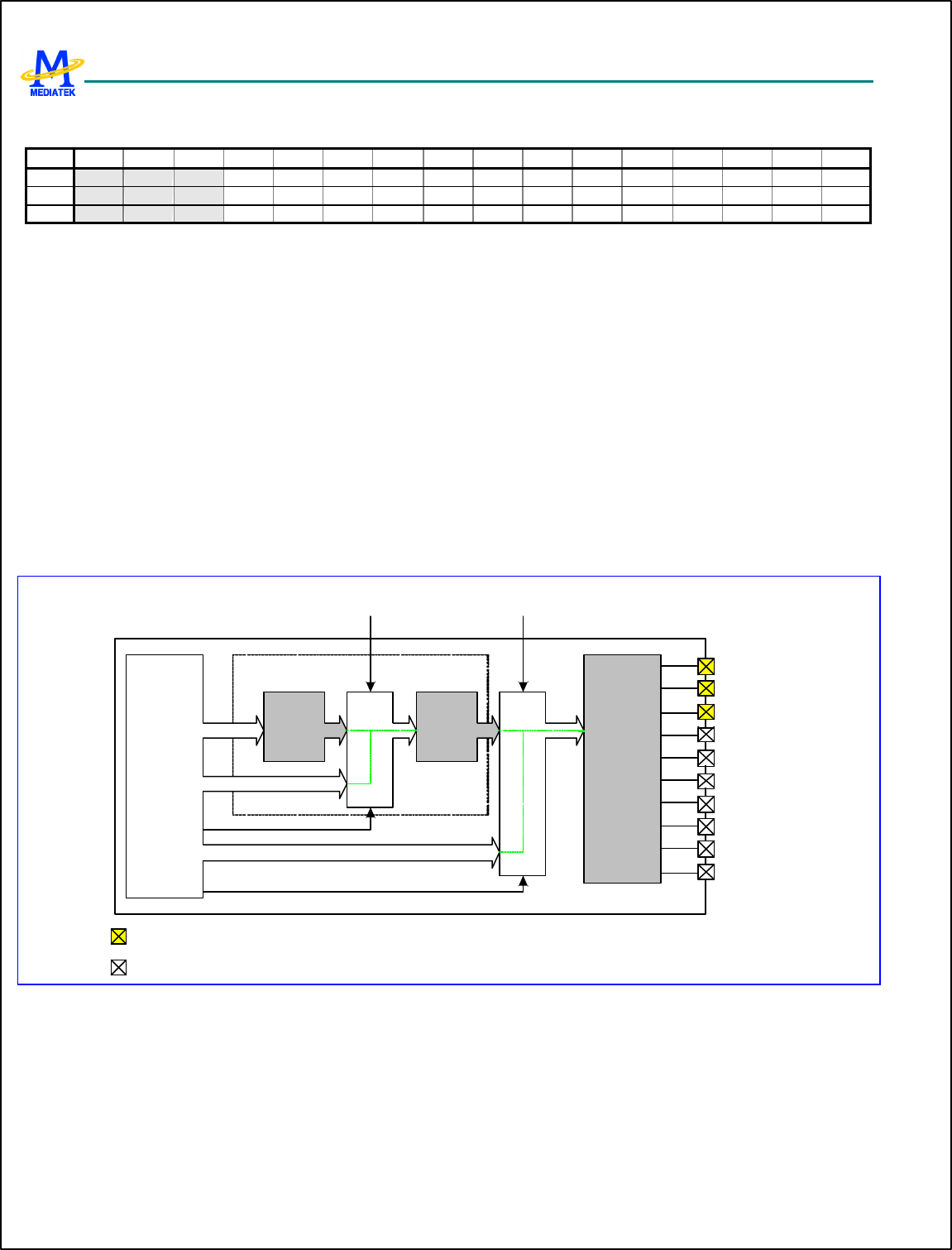
MT6217 GSM/GPRS Baseband Processor Data Sheet Revision 1.01
262/349 MediaTek Inc. Confidential
BSI +0190h BSI event enable register BSI_ENA
Bit 15 14 13 12 11 10 9 8 7 6 5 4 3 2 1 0
Name
BSI15
BSI14 BSI13
BSI12
BSI11
BSI10
BSI9 BSI8 BSI7 BSI6 BSI5 BSI4 BSI3 BSI2 BSI1 BSI0
Type R/W R/W R/W R/W R/W R/W R/W R/W R/W R/W R/W R/W R/W R/W R/W R/W
Reset
1 1 1 1 1 1 1 1 1 1 1 1 1 1 1 1
The register could enable the event by setting the corresponding bit. After hardware reset, all bits are initialized as 1.
Besides, those bits are set as 1 after TDMA_EVTVAL is pulsed.
BSIx The flag enables the downloading of the words that corresponds to the events signaled by TMDA_BSI.
0 The event is not enabled.
1 The event is enabled.
8.2 Base-band Parallel Interface
8.2.1 General description
The Base-band Parallel Interface features a 10-pin output bus used for timing-critical control of the external circuits. These
pins are typically used to control front-end components at the specified time along the GSM time -base, such as
transmit-enable, band switching, TR-switch, … etc.
Event Register
APB I/F
Active
buffer
Write
buffer
Output
buffer
TDMA_EVTVAL
(from TDMA timer) TDMA_BPISTR (0~21)
(from TDMA timer)
BPI_BUS0
BPI_BUS1
BPI_BUS2
BPI_BUS3
BPI_BUS4
BPI_BUS5
BPI_BUS6
BPI_BUS7
MUX
MUX
Immediate mode
petev
BPI_BUS8
BPI_BUS9
The driving capability is configurable.
The driving capability is fix.
Figure 55 Block diagram of BPI interface
22 sets of 10-bit register can be programmed by the MCU to define the output value of BPI_BUS0~BPI_BUS 9 with respect
to the TDMA timer. Each TDMA_BPISTR event triggers the transfer of the corresponding value in the registers to the
output buffer, thus change the value of the BPI bus. If any TDMA_BPI STR event is disabled in the TDMA timer, the
corresponding signal TDMA_BPI STR will not be pulsed, and the corresponding transfer will not take place and the value
on the BPI bus will remain unchanged.

MT6217 GSM/GPRS Baseband Processor Data Sheet Revision 1.01
263/349 MediaTek Inc. Confidential
The BPI data registers are double -buffered, the transfer from the write buffer to the active buffer takes place on assertion of
the TDMA_EVTVAL signal, and the transfer from the active buffer to the output buffer takes place on assertion of the
TDMA_BPISTR events signaled by the TDMA timer.
For applications in which BPI signals serve as the switch, typically some current-driving components are added to enhance
the driving capability. We provide 3 configurable output pins with up to 8mA current. It’s intended to reduce the number of
the external components.
The output pin BPI_BUS 9 is multiplexed with GPIO. Please refer to GPIO table for detail.
8.2.2 Register Definitions
BPI+0000h BPI control register BPI_CON
Bit 15 14 13 12 11 10 9 8 7 6 5 4 3 2 1 0
Name
PINM2
PINM1
PINM0
PETE
V
Type WO WO WO R/W
Reset
0 0 0 0
The register is the control register of the BPI unit. It controls the direct access mode of the active buffer and the current
driving mode for the output pins.
The driving capability of BPI_BUS0, BPI_BUS1, and BPI_BUS2 can be 4mA or 8mA, selected by PINM0, PINM1, and
PINM2, respectively. To provide high driving capability can save some external current-driving components. The driving
capability of BPI_BUS3, BPI_BUS4, BPI_BUS5, BPI_BUS6, and BPI_BUS7 is 2mA.
PETEV The flag is used to enable the direct access to the active buffer.
0 The MCU writes data to the write buffer. The data is latched in the active buffer after the TDMA_EVTVAL
signal is pulsed.
1 The MCU directly writes data to the active buffer without waiting for the TDMA_EVTVAL signal.
PINM0 The field controls the driving capability of BPI_BUS0.
0 The output driving capability is 4mA.
1 The output driving capability is 8mA.
PINM1 The field controls the driving capability of BPI_BUS1.
0 The output driving capability is 4mA.
1 The output driving capability is 8mA.
PINM2 The field controls the driving capability of BPI_BUS2.
0 The output driving capability is 4mA.
1 The output driving capability is 8mA.
BPI +0004h BPI data register 0 BPI_BUF0
Bit 15 14 13 12 11 10 9 8 7 6 5 4 3 2 1 0
Name
PO9 PO8 PO7 PO6 PO5 PO4 PO3 PO2 PO1 PO0
Type R/W R/W R/W R/W R/W R/W R/W R/W R/W R/W
The register defines the signals of the 10 BPI output pins if the event TDMA_BPI0 takes place. There are 22 registers,
which is associated with 22 events, of the same type as listed in Table 36. The data registers are all double-buffered. When
PETEV is set to 0, the MCU writes to the write buffer. When PETEV is set to 1, the MCU writes to the active buffer.
MT6217 GSM/GPRS Baseband Processor Data Sheet Revision 1.01
264/349 MediaTek Inc. Confidential
There is one register BPI_BUFI dedicated to be used in immediate mode. Writing the value to that register will take effect
at once. The value, however, might be updated whenever a TDMA event comes when the event is enabled. The immediate
mode provides an immediate operation on the programming of the BPI bus, but it doesn’t gate the signals from the TDMA
timer, nor does it revise the contents in the write or active buffers as well as the enable registers BPI_ENA0 and
BPI_ENA1.
POx The flag defines the corresponding value of the output pins BPIx after the event 0 takes place.
The overall data register definition is listed in Table 36.
Register Address Register Function Acronym
BPI +0004h BPI pin data for event TDMA_BPI 0 BPI_BUF0
BPI +0008h BPI pin data for event TDMA_BPI 1 BPI_BUF1
BPI +000Ch BPI pin data for event TDMA_BPI 2 BPI_BUF2
BPI +0010h BPI pin data for event TDMA_BPI 3 BPI_BUF3
BPI +0014h BPI pin data for event TDMA_BPI 4 BPI_BUF4
BPI +0018h BPI pin data for event TDMA_BPI 5 BPI_BUF5
BPI +001Ch BPI pin data for event TDMA_BPI 6 BPI_BUF6
BPI +0020h BPI pin data for event TDMA_BPI 7 BPI_BUF7
BPI +0024h BPI pin data for event TDMA_BPI 8 BPI_BUF8
BPI +0028h BPI pin data for event TDMA_BPI 9 BPI_BUF9
BPI +002Ch BPI pin data for event TDMA_BPI 10 BPI_BUF10
BPI +0030h BPI pin data for event TDMA_BPI 11 BPI_BUF11
BPI +0034h BPI pin data for event TDMA_BPI 12 BPI_BUF12
BPI +0038h BPI pin data for event TDMA_BPI 13 BPI_BUF13
BPI +003Ch BPI pin data for event TDMA_BPI 14 BPI_BUF14
BPI +0040h BPI pin data for event TDMA_BPI 15 BPI_BUF15
BPI +0044h BPI pin data for event TDMA_BPI 16 BPI_BUF16
BPI +0048h BPI pin data for event TDMA_BPI 17 BPI_BUF17
BPI +004Ch BPI pin data for event TDMA_BPI 18 BPI_BUF18
BPI +0050h BPI pin data for event TDMA_BPI 19 BPI_BUF19
BPI +0054h BPI pin data for event TDMA_BPI 20 BPI_BUF20
BPI +0058h BPI pin data for event TDMA_BPI 21 BPI_ BUF21
BPI +005Ch BPI pin data for immediate mode BPI_BUFI
Table 36 BPI Data Registers
BPI +0060h BPI event enable register 0 BPI_ENA0
Bit 15 14 13 12 11 10 9 8 7 6 5 4 3 2 1 0
Name
BEN1
5 BEN1
4 BEN1
3 BEN1
2 BEN1
1 BEN1
0 BEN9 BEN8 BEN7 BEN6 BEN5 BEN4 BEN3 BEN2 BEN1 BEN0
Type R/W R/W R/W R/W R/W R/W R/W R/W R/W R/W R/W R/W R/W R/W R/W R/W
Reset
1 1 1 1 1 1 1 1 1 1 1 1 1 1 1 1

MT6217 GSM/GPRS Baseband Processor Data Sheet Revision 1.01
265/349 MediaTek Inc. Confidential
The register is used to enable the events that are signaled by the TDMA timer. After hardware reset, all the enable bits are
initialized as 1. Upon receiving the TDMA_EVTVAL pulse, those bits are also set to 1.
BENx The flag controls the function of event x.
0 The event x is disabled.
1 The event x is enabled.
BPI+0064h BPI event enable register 1 BPI_ENA1
Bit 15 14 13 12 11 10 9 8 7 6 5 4 3 2 1 0
Name
BEN2
1 BEN2
0 BEN1
9 BEN1
8 BEN1
7 BEN1
6
Type R/W R/W R/W R/W R/W R/W
Reset
0 0 0 0 0 0
The register is used to enable the events that are signaled by the TDMA timing generator. After hardware reset, all the
enable bits are initialized as 1. Upon receiving the TDMA_EVTVAL pulse, those bits are also set to 1.
8.3 Automatic Power Control (APC) Unit
8.3.1 General description
Automatic Power Control unit is used to control the Power Amplifier (PA) module. Through APC unit, we can set the
proper transmit power level of the handset and to ensure that the burst power ramping requirements are met. In one TDMA
frame, up to 7 TDMA events can be enabled to support multi-slot transmission. In practice, 5 banks of ramp profiles are
used in one frame to make up 4 consecutive transmission slots.
The shape and magnitude of the ramp profiles are configurable to fit ramp -up (ramp up from zero), intermediate ramp
(ramp between Transmission windows), and ramp -down (ramp down to zero) profiles. Each bank of the ramp profile
consists of 16 8-bit unsigned values, which is adjustable for different conditions.
The entries from one bank of the ramp profile are partitioned into two parts, with 8 values in each part. In normal operation,
the entries in the left half part are multiplied by a 10-bit left scaling factor, and the entries in the right half part are
multiplied by a 10-bit right scaling factor. Those values are then truncated to form 16 10-bit intermediate values. Finally the
intermediate ramp profile are linearly interpolated into 32 10-bit values and sequentially used to update to the D/A
converter. The block diagram of the APC unit is shown in Figure 56.
The APB bus interface is 32 bits width. It takes 4 write accesses to program each bank of ramp profile. The detail register
allocation is as listed in Table 37.
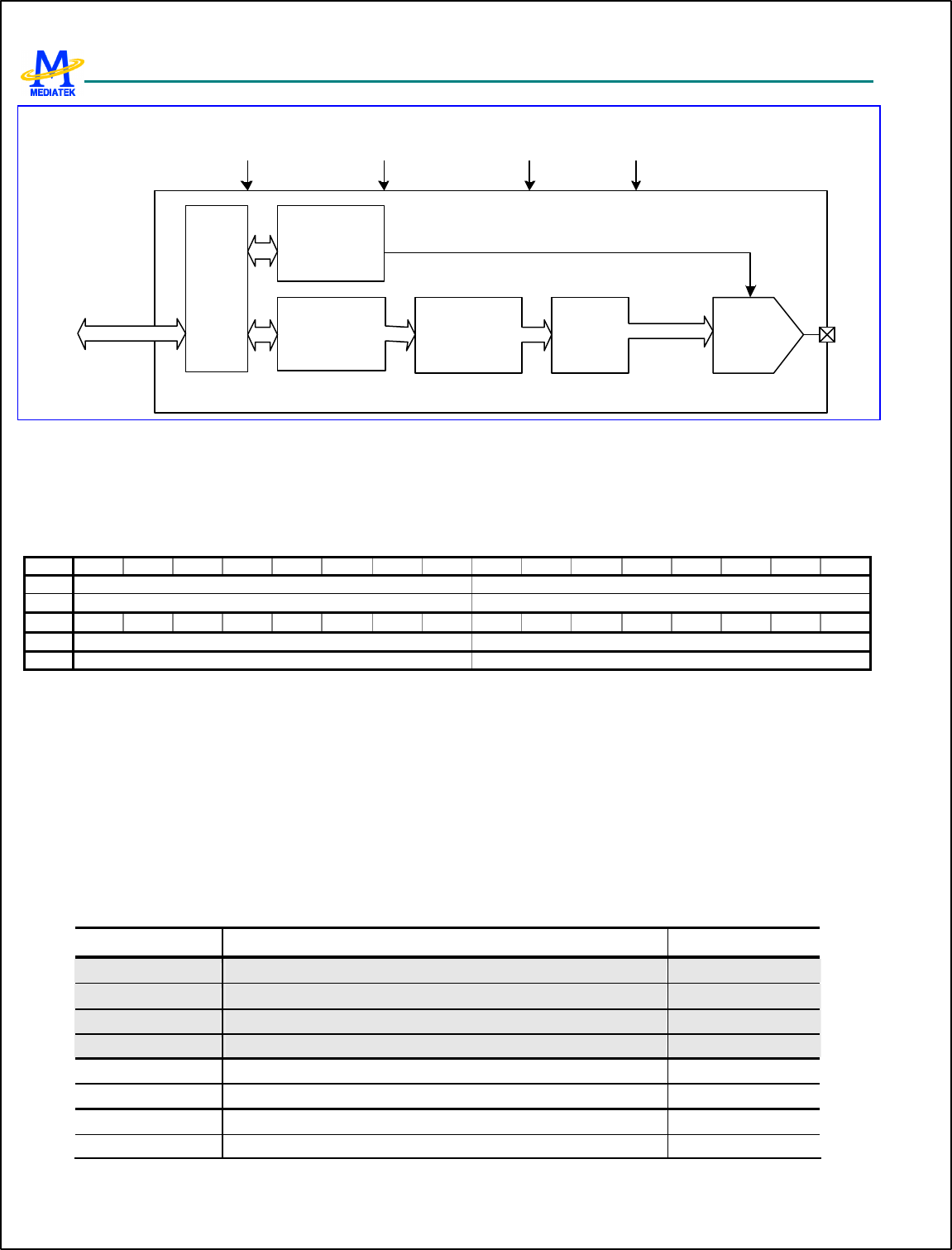
MT6217 GSM/GPRS Baseband Processor Data Sheet Revision 1.01
266/349 MediaTek Inc. Confidential
Ramp profile,
scaling factor,
& offset
Multiplier &
interpolator
APB
I/F
APB BUS
(32bits
data bus)
APC_BUS
(10 bits)
DAC_PU
DAC
Power and
clock
control
Output
buffer
TDMA_APCEN
( from TDMA timer ) TDMA_APCSTR (0~6)
( from TDMA timer) QBIT_EN
APC unit
PDN_APC
( from global
control)
Figure 56 Block diagram of APC unit.
8.3.2 Register Definitions
APC+0000h APC 1st ramp profile #0 APC_PFA0
Bit 31 30 29 28 27 26 25 24 23 22 21 20 19 18 17 16
Name
ENT3 ENT2
Type R/W R/W
Bit 15 14 13 12 11 10 9 8 7 6 5 4 3 2 1 0
Name
ENT1 ENT0
Type R/W R/W
The register stores the first four entries of the first power ramp profile. The first entry resides in the least significant byte
[7:0], the second in the second byte [15:8], the third in the third byte [23:16], and the forth in the most significant byte
[31:24]. Since this register provides no hardware reset, the programmer should configure it before any APC event takes
place.
ENT3 The field signifies the 4
th entry of the 1st ramp profile.
ENT2 The field signifies the 3
rd entry of the 1st ramp pro file.
ENT1 The field signifies the 2
nd entry of the 1st ramp profile.
ENT0 The field signifies the 1
st entry of the 1st ramp profile.
The overall ramp profile register definition is listed in Table 37.
Register Address Register Function Acronym
APC +0000h APC 1st ramp profile #0 APC_PFA0
APC +0004h APC 1st ramp profile #1 APC_PFA1
APC +0008h APC 1st ramp profile #2 APC_PFA2
APC +000Ch APC 1st ramp profile #3 APC_PFA3
APC +0020h APC 2nd ramp profile #0 APC_PFB0
APC +0024h APC 2nd ramp profile #1 APC_PFB1
APC +0028h APC 2nd ramp profile #2 APC_PFB2
APC +002Ch APC 2nd ramp profile #3 APC_PFB3
MT6217 GSM/GPRS Baseband Processor Data Sheet Revision 1.01
267/349 MediaTek Inc. Confidential
APC +0040h APC 3rd ramp profile #0 APC_PFC0
APC +0044h APC 3rd ramp profile #1 APC_PFC1
APC +0048h APC 3rd ramp profile #2 APC_PFC2
APC +004Ch APC 3rd ramp profile #3 APC_PFC3
APC +0060h APC 4th ramp profile #0 APC_PFD0
APC +0064h APC 4th ramp profile #1 APC_PFD1
APC +0068h APC 4th ramp profile #2 APC_PFD2
APC +006Ch APC 4th ramp profile #3 APC_PFD3
APC +0080h APC 5th ramp profile #0 APC_PFE0
APC +0084h APC 5th ramp profile #1 APC_PFE1
APC +0088h APC 5th ramp profile #2 APC_PFE2
APC +008Ch APC 5th ramp profile #3 APC_PFE3
APC +00A0h APC 6th ramp profile #0 APC_PFF0
APC +00A4h APC 6th ramp profile #1 APC_PFF1
APC +00A8h APC 6th ramp profile #2 APC_PFF2
APC +00ACh APC 6th ramp profile #3 APC_PFF3
APC +00C0h APC 7th ramp profile #0 APC_PFG0
APC +00C4h APC 7th ramp profile #1 APC_PFG1
APC +00C8h APC 7th ramp profile #2 APC_PFG2
APC +00CCh APC 7th ramp profile #3 APC_PFG3
Table 37 APC ramp profile registers
APC +0010h APC 1st ramp profile left scaling factor APC_SCAL0L
Bit 15 14 13 12 11 10 9 8 7 6 5 4 3 2 1 0
Name
SCAL
Type R/W
Reset
1_0000_0000
The register stores the left scaling factor of the 1
st ramp profile. This factor multiplies the first 8 entries of the 1
st ramp
profile to provide the scaled profile, which is then interpolated to control the D/A converter.
After hardware reset, the initial value of the register is 256. In that case, no scaling in done, that is, each entry of the ramp
profile is multiplied by 1. That’s because 8 least significant bits will be truncated after multiplication.
The overall scaling factor register definition is listed in Table 7.
SF The field is the scaling factor. After hardware reset, the value is 256.
APC +0014h APC 1st ramp profile right scaling factor APC_SCAL0R
Bit 15 14 13 12 11 10 9 8 7 6 5 4 3 2 1 0
Name
SF
Type R/W
Reset
1_0000_0000
The register stores the right scaling factor of the 1
st ramp profile. This factor multiplies the last 8 entries of the 1
st ramp
profile to provide the scaled profile, which is then interpolated to control the D/A converter.
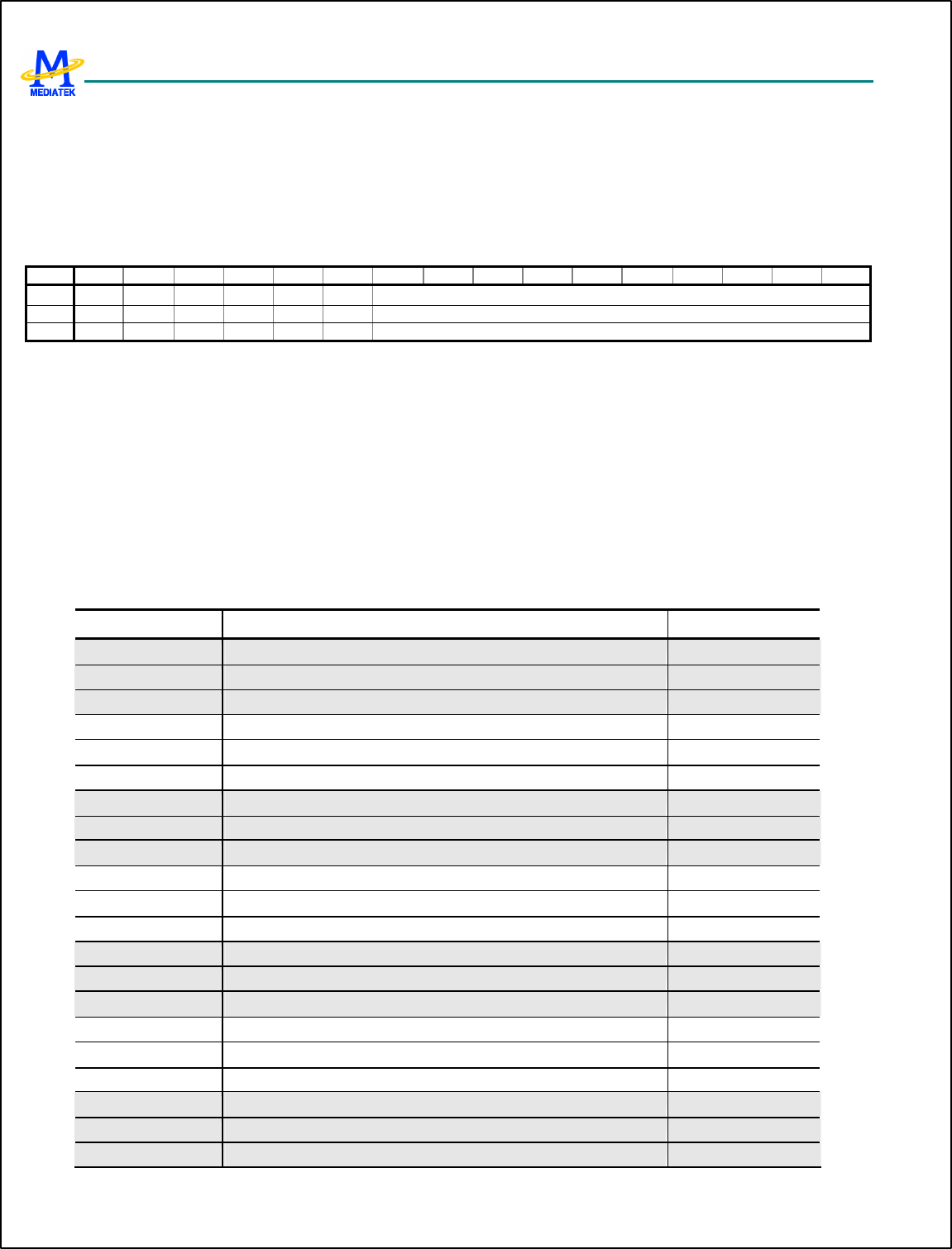
MT6217 GSM/GPRS Baseband Processor Data Sheet Revision 1.01
268/349 MediaTek Inc. Confidential
After hardware reset, the initial value of the register is 256. In that case, no scaling in done, that is, each entry of the ramp
profile is multiplied by 1. That’s because 8 least significant bits will be truncated after multiplication.
The overall scaling factor register definition is listed in Table 7.
SF The field is the scaling factor. After hardware reset, the value is 256.
APC+0018h APC 1st ramp profile offset value APC_OFFSET0
Bit 15 14 13 12 11 10 9 8 7 6 5 4 3 2 1 0
Name
OFFSET
Type R/W
Reset
0
There are 7 offset values for the corresponding ramp profile.
The 1
st offset value also serves as the pedestal value. It’s used to power up the APC D/A converter before the RF signals
start to transmit. The D/A converter is then biased on the value. It’s intended to provide initial control voltage of the
external control loop. The exact value depends on the characteristics of the external components. The timing to output the
pedestal value is configurable through the TDMA_BULCON2 register of the timing generator. It can be set to 0~127
quarter bit time after the base-band D/A converter is powered up.
OFFSET The field stores the offset value for the corresponding ramp profile. After hardware reset, the default value is
0.
The overall offset register definition is listed in Table 7.
Register Address Register Function Acronym
APC +0010h APC 1st ramp profile left scaling factor APC_SCAL0L
APC +0014h APC 1st ramp profile right scaling factor APC_SCAL0R
APC +0018h APC 1st ramp profile offset value APC_OFFSET0
APC +0030h APC 2nd ramp profile left scaling factor APC_SCAL1L
APC +0034h APC 2nd ramp profile right scaling factor APC_SCAL1R
APC +0038h APC 2nd ramp profile offset value APC_OFFSET1
APC +0050h APC 3rd ramp profile left scaling factor APC_SCAL2L
APC +0054h APC 3rd ramp profile right scaling factor APC_SCAL2R
APC +0058h APC 3rd ramp profile offset value APC_OFFSET2
APC +0070h APC 4th ramp profile left scaling factor APC_SCAL3L
APC +0074h APC 4th ramp profile right scaling factor APC_SCAL3R
APC +0078h APC 4th ramp profile offset value APC_OFFSET3
APC +0090h APC 5th ramp profile left scaling factor APC_SCAL4L
APC +0094h APC 5th ramp profile right scaling factor APC_SCAL4R
APC +0098h APC 5th ramp profile offset value APC_OFFSET4
APC +00B0h APC 6th ramp profile left scaling factor APC_SCAL5L
APC +00B4h APC 6th ramp profile right scaling factor APC_SCAL5R
APC +00B8h APC 6th ramp profile offset value APC_OFFSET5
APC +00D0h APC 7th ramp profile left scaling factor APC_SCAL6L
APC +00D4h APC 7th ramp profile right scaling factor APC_SCAL6R
APC +00D8h APC 7th ramp profile offset value APC_OFFSET6
MT6217 GSM/GPRS Baseband Processor Data Sheet Revision 1.01
269/349 MediaTek Inc. Confidential
Table 38 APC scaling factor and offset value registers
APC+00E0h APC control register APC_CON
Bit 15 14 13 12 11 10 9 8 7 6 5 4 3 2 1 0
Name
GSM FPU
Type R/W R/W
Reset
1 0
GSM This field defines the operation mode of the APC module. In GSM mode, since there is only one slot in one frame,
only one scaling factor and one offset value is required to configure. If the bit is set, the programmer needs only to
configure APC_SCAL0L and APC_OFFSET0. If the bit is not set, the APC module is operated in GPRS mode.
0 The APC module is operated in GPRS mode.
1 The APC module is operated in GSM mode. Default value.
FPU This field is used to force power on the APC D/A converter. Test only.
0 The APC D/A converter is not forced power up. It’s then only powered on when the transmission window is
opened. Default value.
1 The APC D/A converter is forced power up.
8.3.3 Ramp profile programming
The first value of the first normalized ramp profile should be written in the least significant byte of the APC_PFA0 register.
The second value should be written in the second least significant byte of the APC_PFA0, and vice versa.
Each ramp profile can be programmed to form arbitrary shape.
The start of ramping is triggered by one of the TDMA_APCSTR signals. The timing relationship of TDMA_APCSTR and
TDMA slots is as depicted in Figure 57 for 4 consecutive time slots case. The power ramping profile should comply with
the timing mask defined in GSM SPEC 05.05. The timing offset values for 7 ramp profiles are stored in TDMA timer
register from TDMA_APC0 to TDMA_APC6.
Since the APC unit provides more than 5 ramp profiles, it’s able to accommodate up to 4 consecutive transmission slots.
The additional 2 ramp profiles are used particularly when the timing relation between the last 2 transmission time slots and
CTIRQ is uncertain. That provides the possibility to use some of them interchangeably in one and its succeeding frames.
RX MXTX RX
TDMA_APCSTR0 TDMA_APCSTR1
TXTX TX
TDMA_APCSTR2 TDMA_APCSTR3 TDMA_APCSTR4
Figure 57 Timing diagram of TDMA_APCSTR.
In GPRS mode, in order to fit the intermediate ramp profile between different power levels, a simple scheme with scaling is
used to synthesize the ramp profile. The equation is as follows:

MT6217 GSM/GPRS Baseband Processor Data Sheet Revision 1.01
270/349 MediaTek Inc. Confidential
8 15 if 1,
0 8 if 0,
0,1,...,15,DNSOFFDA
,...,151 ,
2
DN DN
S OFFDA
2
DN DN
S OFFDA
12
1
2
0,15
00
≥≥
≥>
=
=⋅+=
=
+
⋅+=
+
⋅+=
+
−
k
k
l
k
k
klk
kk
lk
pre
where DA represents the data to present to the D/A converter, DN represents the normalized data which is stored in the
register APC_PFn, S0 represents the left scaling factor stored in register APC_SCALnL, S1 represents the right scaling
factor stored in register APC_SCALnR, and OFF represents the offset value stored in the register APC_OFFSETn. The
subscript n denotes the index of the ramp profile.
The ramp calculation before interpolation is as depicted in Figure 58.
During each ramp process, each word of the normalized profile is first multiplied by 10-bit scaling factors and added by an
offset value to form a bank of 18 -bit words. The first 8 words (in the left half part as in Figure 58) are multiplied by the left
scaling factor S0 and the last 8 words (in the right half part as in Figure 58) are multiplied by the right scaling factor S1. The
lowest 8-bit of each word will be then punctured to get a 10-bit result. The scaling factor is 100 in hexadecimal, which
represents no scaling, on reset. The value smaller than 100 will scale down the ramp profile, and the larger value will scale
up the ramp profile.
DN0 * S0 + OFF
DN4 * S0 + OFF
DN8 * S1 + OFF
DN12 * S1 + OFF
DN
15
* S
1
+ OFF
16 Qb
DN4 * S0DN 8 * S1
OFF
Figure 58 The timing diagram of the APC ramp.
The 16 10-bit words are linearly interpolated into 32 10-bit words. A 10-bit D/A converter is then used to convert these 32
ramp values in a rate of 1.0833MHz, that is, quarter bit rate. The timing diagram is shown in Figure 59 and the final value
will be retained on the output until the next event occurs.
MT6217 GSM/GPRS Baseband Processor Data Sheet Revision 1.01
271/349 MediaTek Inc. Confidential
TX TX
TX Burst TX Burst
TDMA_APCSTR0
Ramp ProfileRamp Profile Ramp Profile
TDMA_APCSTR2TDMA_APCSTR1
~29.5us ~29.5us
APC_DATA
TDMA_APCSTR1
1032 29 30 31
TDMA_APCEN
TDMA_APCSTRx
~29.5us
offset
Figure 59 Timing diagram of the APC ramping.
The APC unit will only be powered up when the APC window is opened. The APC window is controlled by configuring the
TDMA registers TDMA_BULCON1 and TDMA_BULCON2. Please refer to TDMA timer unit for detail information.
The first offset value stored in the register APC_OFFSET0 also serves as the pedestal value, which is used to provide the
initial power level for the PA.
Since the profile is not double-buffered, the timing to write the ramping profile would be critical. The programmer should
prevent from writing the data buffer at the time that the ramping process is taking place. Or it would result in the wrong
ramp profile and malfunction.
8.4 Automatic Frequency Control (AFC) Unit
8.4.1 General description
Automatic Frequency Control unit provides the direct control of the oscillator for frequency offset and Doppler shift
compensation. The block diagram is depicted in Figure 60. It utilizes a 13-bit D/A converter to achieve high-resolution
control. Two modes of operation are supported and described as follows.
In timer-triggered mode, the TDMA timer controls the AFC enabling events. There provided at most four events within one
TDMA frame. Double buffer architecture is supported. The AFC values can be written to the write buffers. When the signal
TDMA_EVTVAL takes place, the values in the write buffers will be latched in the active buffers. However, the AFC values
can also be written to the active buffers directly. When a TDMA event triggered by TDMA_AFC takes place, the value in
the corresponding active buffer with the same index take effect. Each event is associated wit h an active buffer. An
illustrative timing diagram of AFC events with respect to TX/RX/MX windows is depicted in Figure 61. In this mode, the
D/A converter can be either powered on continuously or for a programmable duration (of 256 quarter-bits by default). The
later option is for power saving.
MT6217 GSM/GPRS Baseband Processor Data Sheet Revision 1.01
272/349 MediaTek Inc. Confidential
In immediate mode, the MCU can directly control the AFC value without event triggering. The value written by the MCU
immediately takes effect. In this mode, the D/A converter should be powered on continuously. When entering
timer-triggered mode from immediate mode (by setting flag I_MODE in the register AFC_CON to be 0), the D/A converter
will be kept powered on for a programmable duration (of 256 quarter-bits by default) if the next TDMA_AFC has been not
pulsed in the duration. The duration will be prolonged upon receiving next events.
The two modes provide flexibility when controlling the oscillator. The 13-bit DAC proves to be monotonic. Associated with
proper AFC algorithm, baseband processor achieves good tracking of the RF channels and the highest performance.
Active
buffer
Power
control
APB
BUS
TDMA_AFC
( from TDMA timer )
Write
buffer
AFC_BUS
Control
register
TDMA_EVTVAL
( from TDMA timer )
DAC
oscillator
PDN_AFC
( from global control )
VC
AFC unit
Immediate write
Output
buffer
nPDN_DAC
F_MODE
I_MODE
AFC
Figure 60 The block diagram of the AFC controller
RX MX MXTX
AFC_STR0 AFC_STR3AFC_STR2AFC_STR1
Figure 61 The timing diagram of the AFC controller
8.4.2 Register Definitions
AFC+0000h AFC control register AFC_CON
Bit 15 14 13 12 11 10 9 8 7 6 5 4 3 2 1 0
Name
RDAC
T F_MO
DE FETE
NV I_MO
DE
Type R/W R/W R/W R/W
Reset
0 0 0 0
Four control modes are defined and can be controlled through the AFC control register. F_MODE enables the force power
up mode. FETENV enables the directly writing operation to the active buffer. I_MODE enables the immediate mode.
RDACT enables the directly reading operation from the active buffer.
RDACT The flag enables the directly reading operation from the active buffer. Note the control flag is only applicable to
the four data buffer including AFC_DAT0, AFC_DAT1, AFC_DAT2, and AFC_DAT3.
0 APB read from the write buffer.
1 APB read from the active buffer.
MT6217 GSM/GPRS Baseband Processor Data Sheet Revision 1.01
273/349 MediaTek Inc. Confidential
FETENV The flag enables the directly writing operation to the active buffer. Note the control flag is only applicable to
the for data buffer including AFC_DAT0, AFC_DAT1, AFC_DAT2, and AFC_DAT3.
0 APB write to the write buffer.
1 APB write to the active buffer.
F_MODE The flag enables the force power up mode.
0 The force power up mode is not enabled.
1 The force power up mode is enabled.
I_MODE The flag enables the immediate mode. To enable the immediate mode also enable the force power up mode.
0 The immediate mode is not enabled.
1 The immediate mode is enabled.
AFC +0004h AFC data register 0 AFC_DAT0
Bit 15 14 13 12 11 10 9 8 7 6 5 4 3 2 1 0
Name
AFCD
Type R/W
The register stores the AFC value for the event 0 triggered by the TDMA timer in timer-triggered mode. When RDACT or
FETENV is set, the data transfer operates on the active buffer. On the contrary, when RDACT or FETENV is not set, the
data transfer operates on the write buffer.
There are four registers (AFC_DAT0, AFC_DAT1, AFC_DAT2, AFC_DAT3) of the same type, which for each corresponds
to the event triggered by the TDMA timer. The four registers are summarized in Table 39.
AFC_DAT0 is particularly used for the immediate mode. In this mode, only the control value is the AFC_DAT0 write
buffer is used to control the D/A converter. Unlike in timer-triggered mode, the control value in AFC_DAT0 write buffer
could bypass the active buffer stage and is directly coupled to the output buffer in immediate mode. Intended to use
immediate mode, it’s recommended to program the AFC_DAT0 in advance and then enable the immediate mode by setting
the flag I_MODE in the register AFC_CON.
The register AFC_DATA0, AFC_DAT1, AFC_DAT2, and AFC_DAT3 have no initial values. So it has to be programmed
before any AFC event takes place. However, the AFC value for the D/A converter, i.e., the output buffer value, is initially 0
right after power up before any event takes place.
AFCD The field is the AFC sample for the D/A converter.
Register Address Register Function Acronym
AFC +0004h AFC control value 0 AFC_DAT0
AFC +0008h AFC control value 1 AFC_DAT1
AFC +000Ch AFC control value 2 AFC_DAT2
AFC +0010h AFC control value 3 AFC_DAT3
Table 39 AFC Data Registers
AFC +0014h AFC power up period AFC_PUPER
Bit 15 14 13 12 11 10 9 8 7 6 5 4 3 2 1 0
Name
PU_PER
Type R/W
Reset
ff

MT6217 GSM/GPRS Baseband Processor Data Sheet Revision 1.01
274/349 MediaTek Inc. Confidential
The register stores the AFC power up period, which is 13 bits width. The value ranges from 0 to 8191. If the flag I_MODE
or F_MODE is set, this register has no effect since the D/A converter is powered up continuously. If the flag I_MODE and
F_MODE is not set, the register controls the power up duration of the D/A converter. During that period, the signal
nPDN_DAC in Figure 60 is set to be 1.
PU_PER The field stores the AFC power up period. After hardware power up, the field is initialized as 255.

MT6217 GSM/GPRS Baseband Processor Data Sheet Revision 1.01
275/349 MediaTek Inc. Confidential
9 Baseband Front End
Baseband Front End is a modem interface between TX/RX mixed-signal modules and digital signal processor (DSP). We
can divide this block into two parts (see Figure 62). The first is the uplink (transmitting) path, which converts bit-stream
from DSP into digital in-phase (I) and quadrature (Q) signals for TX mixed-signal module. The second part is the downlink
(receiving) path, which receives digital in-phase (I) and quadrature (Q) signals from RX mixed-signal module, performs
FIR filtering and then sends results to DSP. Figure 62 illustrates interconnection around Baseband Front End. In the figure
the shadowed blocks compose Baseband Front End. The uplink path is mainly composed of GMSK Modulator and uplink
parts of Baseband Serial Ports, and the downlink path is mainly composed of RX digital FIR filter and downlink parts of
Baseband Serial Ports. Baseband Serial Ports is a serial interface used to communicate with DSP. In addition, there is a set
of control registers in Baseband Front End that is intended for control of TX/RX mixed-signal modules, inclusive of
calibration of DC offset and gain mismatch of downlink analog-to-digital (A/D) converters as well as uplink
digital-to-analog (D/A) converters in TX/RX mixed-signal modules. The timing of bit streaming through Baseband Front
End is completely under control of TDMA timer. Usually only either of uplink and downlink paths is active at one moment.
However, both of the uplink and downlink paths will be active simultaneously when Baseband Front End is in loopback
mode.
When either of TX windows in TDMA timer is opened, the uplink path in Baseband Front End will be activated.
Accordingly components on the uplink path such as GMSK Modulator will be powered on, and then TX mixed-signal
module is also powered on. The subblock Baseband Serial Ports will sink TX data bits from DSP and then forward them to
GMSK Modulator. The outputs from GMSK Modulator are sent to TX mixed-signal module in format of I/Q signals.
Finally D/A conversions are performed in TX mixed-signal module and the output analog signal is output to RF module.
Similarly, while either of RX windows in TDMA timer is opened, the downlink path in Baseband Front End will be
activated. Accordingly components on the downlink path such as RX mixed-signal module and RX digital FIR filter are
then powered on. First A/D conversions are performed in RX mixed-signal module, and then the results in format of I/Q
signals are sourced to RX digital FIR filter. Low-Pass filtering is performed in RX digital FIR filter. Finally the results will
be sourced to DSP through Baseband Serial Ports.
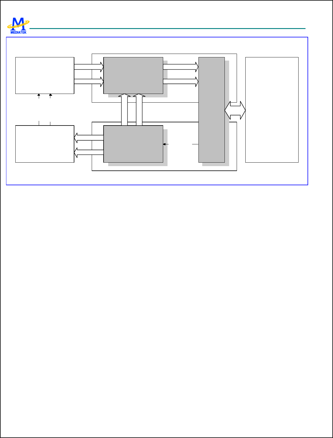
MT6217 GSM/GPRS Baseband Processor Data Sheet Revision 1.01
276/349 MediaTek Inc. Confidential
GSM RX
Mixed-Signal Module
GSM TX
Mixed-Signal Module
Analog Q Signal
Analog I Signal
RX Digital FIR
Filter
I-Signal
Q-Signal
GMSK
Modulator
I-Signal
Q-Signal
Baseband Serial Ports
I-Signal
Q-Signal
1-bit
TX bit-stream
I-Signal
Q-Signal
DSP
Downlink Path
Uplink Path
Figure 62 Block Diagram Of Baseband Front End
9.1 Baseband Serial Ports
9.1.1 General Description
Baseband Front End communicates with DSP through the sub block of Baseband Serial Ports. Baseband Serial Ports
interfaces with DSP in serial manner. It implies that DSP must be configured carefully in order to have Baseband Serial
Ports cooperate with DSP core correctly.
If downlink path is programmed in bypass-filter mode (NOT bypass-filter loopback mode), behavior of Baseband Serial
Ports will completely be different from that in normal function mode. The special mode is for testing purpose. Please see
the subsequent section of Downlink Path for details.
TX and RX windows are under control of TDMA timer. Please refer to functional specification of TDMA timer for the
details how to open/close a TX/RX window. Opening/Closing of TX/RX windows has two major effects on Baseband Front
End. They are power on/off of corresponding components and data souring/sinking. It is worth noticing that Baseband
Serial Ports is only intended for sinking TX data from DSP or sourcing data to DSP. It does not involve power on/off of
TX/RX mixed-signal modules.
As far as downlink path is concerned, if a RX window is opened by TDMA timer Baseband Front End will have RX
mixed-signal module proceed to make A/D conversion, RX digital filter proceed to perform filtering and Baseband Serial
Ports be activated to source data from RX digital filter to DSP no matter the data is meaningful or not. However, the
interval between the moment that RX mixed-signal module is powered on and the moment that data proceed to be dumped
by Baseband Serial Ports can be well controlled in TDMA timer. Lets denote as RX enable window the interval that RX
mixed-signal module is powered on and denote as RX dump window the interval that data is dumped by Baseband Serial
Ports. If the first samples from RX digital filter desire to be discarded, the corresponding RX enable window must cover the
corresponding RX dump window. Notes that RX dump windows always win over RX enable windows. It means that a RX

MT6217 GSM/GPRS Baseband Processor Data Sheet Revision 1.01
277/349 MediaTek Inc. Confidential
dump window will always raise a RX enable window. RX enable windows can be raised by TDMA timer or by
programming RX power-down bit in global control registers to be ‘0’. It is useful in debugging environment.
Similarly, a TX dump window refers to the interval that Baseband Serial Ports sinks data from DSP on uplink path and a
TX enable window refers to the interval that TX mixed-signal module is powered on. A TX window controlled by TDMA
timer involves a TX dump window and a TX enable window simultaneously. The interval between the moment that TX
mixed-signal module is powered on and the moment that data proceed to be forwarded from DSP to GMSK modulator by
Baseband Serial Ports can be well controlled in TDMA timer. TX dump windows always win over TX enable windows. It
means that a TX dump window will always raise a TX enable window. TX enable windows can be raised by TDMA timer
or by programming TX power-down bit in global control registers to be ‘0’. It is useful in debugging environment.
Accordingly, Baseband Serial Ports are only under control of TX/RX dump window. Note that if TX/RX dump window is
not integer multiplies of bit-time it will be extended to be integer multiplies of bit-time. For example, if TX/RX dump
window has interval of 156.25 bit -times then it will be extended as 157 bit -times in Baseband Serial Ports.
9.1.2 Register Definitions
BFE+0000h Base-band Common Control Register BFE_CON
Bit 15 14 13 12 11 10 9 8 7 6 5 4 3 2 1 0
Name
BCIE
N
Type R/W
Reset
0
This register is for common control of Baseband Front End. It consists of ciphering encryption control.
BCIEN The bit is for ciphering encryption control. If the bit is set to ‘1’, XOR will performed on some TX bits (payload of
Normal Burst) and ciphering pattern bit from DSP, and then the result is forwarded to GMSK Modulator.
Meanwhile, Baseband Front End will generate signals to drive DSP ciphering process produce corresponding
ciphering pattern bits if the bit is set to ‘1’. If the bit is set to ‘0’, the TX bit from DSP will be forwarded to GMSK
modulator directly. Baseband Front End will not activate DSP ciphering process.
0 Disable ciphering encryption.
1 Enable ciphering encryption.
BFE +0004h Base-band Common Status Register BFE_STA
Bit 15 14 13 12 11 10 9 8 7 6 5 4 3 2 1 0
Name
BULF
S BULE
N BDLF
S BDLE
N
Type RO RO RO RO
Reset
0 0 0 0
This register indicates status of Baseband Front End. Under control of TDMA timer, Baseband Front End can be driven in
several statuses. If downlink path is enabled, then the bit BDLEN will be ‘1’. Otherwise the bit BDLEN will be ‘0’. If
downlink parts of Baseband Serial Ports is enabled, the bit BDLFS will be ‘1’. Otherwise the bit BDLFS will be ‘0’. If
uplink path is enabled, then the bit BULEN will be ‘1’. Otherwise the bit BULEN will be 0. If uplink parts of Baseband
Serial Ports is enabled, the bit BULFS will be ‘1’. Otherwise the bit BULFS will be ‘0’. Once downlink path is enabled, RX
mixed-signal module will also be powered on. Similarly, once uplink path is enabled, TX mixed-signal module will also be
powered on. Furthermore, enabling Baseband Serial Ports for downlink path refers to dumping results from RX digital FIR
filter to DSP. Similarly, enabling Baseband Serial Ports for uplink path refers to forwarding TX bit from DSP to GMSK

MT6217 GSM/GPRS Baseband Processor Data Sheet Revision 1.01
278/349 MediaTek Inc. Confidential
modulator. BDLEN stands for “Baseband DownLink ENable”. BULEN stands for “Baseband UpLink ENable”. BDLFS
stands for “Baseband DownLink FrameSync”. BULFS stands for “Baseband UpLink FrameSync”.
BDLEN Indicate if downlink path is enabled.
0 Disabled
1 Enabled
BDLFS Indicate if Baseband Serial Ports for downlink path is enabled.
0 Disabled
1 Enabled
BULEN Indicate if uplink path is enabled.
0 Disabled
1 Enabled
BULFS Indicate if Baseband Serial Ports for uplink path is enabled.
0 Disabled
1 Enabled
9.2 Downlink Path (RX Path)
9.2.1 General Description
On downlink path, the subblock between RX mixed-signal module and Baseband Serial Ports is RX Path. It mainly consists
of a digital FIR filter, two sets of multiplexing paths for loopback modes, interface for RX mixed-signal module and
interface for Baseband Serial Ports. The block diagram is shown in Figure 63.
While RX enable windows are opened, RX Path will issue control signals to have RX mixed-signal module proceed to
make A/D conversion. As each conversion is finished, one set of I/Q signals will be latched. There exists a digital FIR filter
for these I/Q signals. The result of filtering will be dumped to Baseband Serial Ports whenever RX dump windows are
opened.
In addition to normal function, there are two loopback modes in RX Path. One is bypass-filter loopback mode, and the other
is through-filter loopback mode. They are intended for verification of DSP firmware and hardware. The bypass-filter
loopback mode refers to that RX digital FIR filter is not on the loopback path. However, the through-filter loopback mode
refers to that RX digital FIR filter is on the loopback path.
The I/Q swap functionality is used to swap I/Q channel signals from RX mixe d-signal module before they are latched into
RX digital FIR filter. It is intended to provide flexibility for I/Q connection with RF modules.
There is a special data path not shown in Figure 63. It is a data path from RX mixed-signal module to Baseband Serial
Ports. If downlink path is programmed in “Bypass RX digital FIR filter” mode, ADC outputs out of RX mixed-signal
module will be directed into Baseband Serial Ports directly. Therefore these data can be dumped into DSP and RX FI R
filtering will not be performed on them. Limited by bandwidth of the serial interface between Baseband Serial Ports and
DSP, only ADC outputs which are from either I-channel or Q-channel ADC can be dumped into DSP. Both of I- and
Q-channel ADC outputs cannot be dumped simultaneously. Which channel will be dumped is controlled by the register bit
SWAP of the register RX_CFG when downlink path is programmed in “Bypass RX digital FIR filter” mode. See register
definition below for details. The mode is for measurement of performance of A/D converters in RX mixed-signal module.
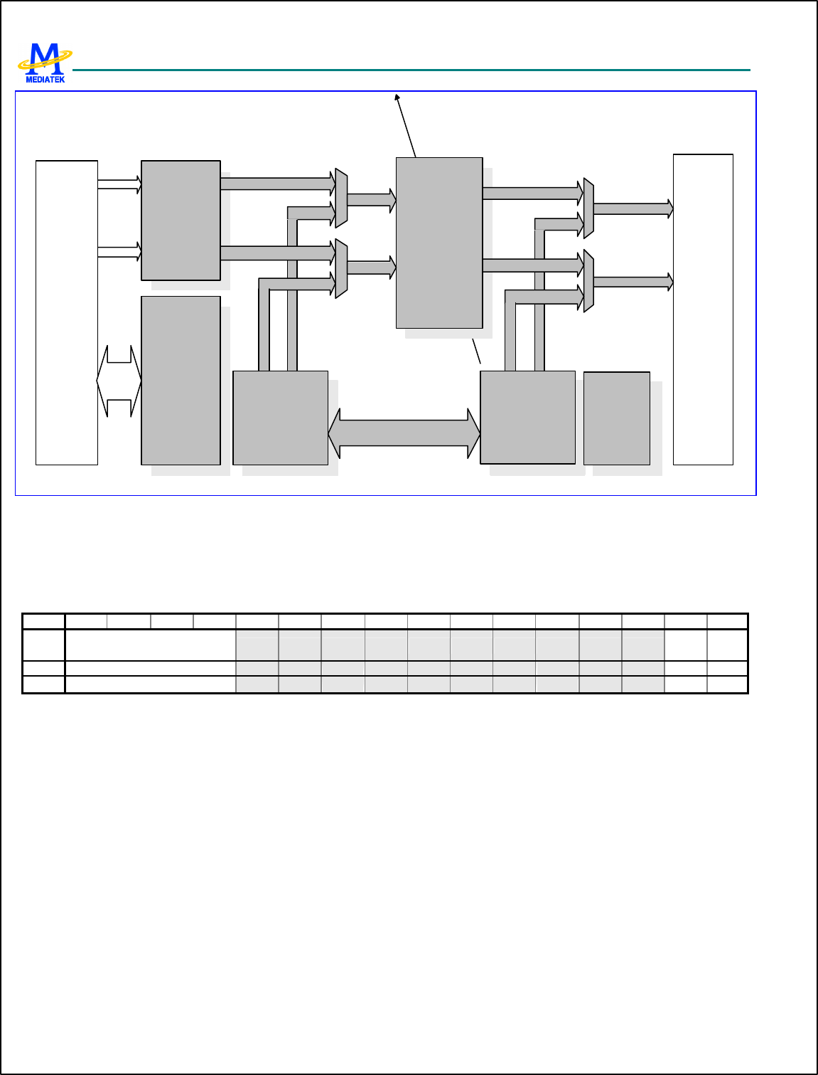
MT6217 GSM/GPRS Baseband Processor Data Sheet Revision 1.01
279/349 MediaTek Inc. Confidential
Loopback &
Decimation &
Sign Extension
Loopback &
Decimation &
Sign Extension I/Q channel signals
Programmable digital FIR with
symmetric coefficients
I/Q Swap or
Not
MUX
Interface with
GSM RX
Mixed-Signal
Module
I-Channel
Q-Channel
GSM RX
Mixed-
Signal
Module
Control &
Status
Signal
Baseband
Serial
Ports
From GMSK Modulaor
Interface
with
Baseband
Serial
Ports
RX Digital
FIR Filter
I-Channel
Q-Channel
I-Channel
Q-Channel
I-Channel
Q-Channel
I-Channel
Q-Channel
I-Channel
I-Channel
Q-Channel
Q-Channel
Figure 63 Block Diagram Of RX Path
9.2.2 Register Definitions
BFE +0010h RX Configuration Register RX_CFG
Bit 15 14 13 12 11 10 9 8 7 6 5 4 3 2 1 0
Name
LPDN BYPF
LTR SWA
P
Type R/W R/W R/W
Reset 0000 0 0
This register is for configuration of downlink path, inclusive of configuration of RX mixed-signal module and RX path in
Baseband Front End.
SWAP The register bit is for control of whether I/Q channel signals need swap before they are input to Baseband Front
End. It provides flexibility of connection of I/Q channel signals between RF module and baseband module. The
register bit has another purpose when the register bit “BYPFLTR” is set to 1. Please see description for the register
bit “BYPFLTR”.
0 I- and Q-channel signals are not swapped
1 I- and Q-channel signals are swapped
BYPFLTR Bypass RX FIR filter control. The register bit is used to configure Baseband Front End in the state called
“Bypass RX FIR filter state” or not. Once the bit is set to ‘1’, RX FIR filter will be bypassed. That is, ADC outputs
of RX mixed-signal module that are 11 -bit resolution and at sampling rate of 1.083MHz can be dumped into DSP
by Baseband Serial Ports and RX FIR filtering will not be performed on them. Limited by bandwidth of the serial
interface between Baseband Serial Ports and DSP, these ADC outputs are all from either I-channel or Q-channel
ADC. Both of I- and Q-channel ADC outputs cannot be dumped simultaneously. When the bit is set to ‘1’ and the
MT6217 GSM/GPRS Baseband Processor Data Sheet Revision 1.01
280/349 MediaTek Inc. Confidential
register bit “SWAP” is set to ‘0’, ADC outputs of I-channel will be dumped. When the bit is set to ‘1’ and the
register bit “SWAP” is set to ‘1’, ADC outputs of Q-channel will be dumped.
0 Not bypass RX FIR filter
1 Bypass RX FIR filter
LPDN Late power down control. RX mixed-signal module needs two power down signals. There must exist some delay
between them. The register field is used to control the late-arriving power-down signal.
0000 The delay between two power-down signals is one 13 MHz period.
0001 The delay between two power-down signals is two 13 MHz period.
0010 The delay between two power-down signals is three 13 MHz period.
…
0001 The delay between two power-down signals is 256 13 MHz period.
BFE +0014h RX Control Register RX_CON
Bit 15 14 13 12 11 10 9 8 7 6 5 4 3 2 1 0
Name
BLPEN[1:0]
Type R/W
Reset 0
This register is for control of downlink path, inclusive of control of RX mixed-signal module and RX path in Baseband
Front End module.
BLPEN The register field is for loopback configuration selection in Baseband Front End.
00 Configure Baseband Front End in normal function mode
01 Configure Baseband Front End in bypass-filter loopback mode
10 Configure Baseband Front End in through-filter loopback mode
11 Reserved
BFE +0020h RX Digital FIR Filter Coefficient Register 0 RX_FIR_COEF0
Bit 15 14 13 12 11 10 9 8 7 6 5 4 3 2 1 0
Name
D9 D8 D7 D6 D5 D4 D3 D2 D1 D0
Type R/W R/W R/W R/W R/W R/W R/W R/W R/W R/W
Reset
0 0 0 0 0 0 0 0 0 0
The register is for RX digital FIR filter coefficient 0. It is coded in 2’s complement. That is , its maximum is 255 and its
minimum is –256. It will be applied on the latest and the oldest taps of 31 taps. The equivalent process flow of RX digital
FIR filtering is shown in Figure 64.
MT6217 GSM/GPRS Baseband Processor Data Sheet Revision 1.01
281/349 MediaTek Inc. Confidential
TAP 0
TAP 1
TAP 2
RX FIR coef 0
RX FIR coef 1
RX FIR coef 2
TAP 13
TAP 14
TAP 15
RX FIR coef 13
TAP 16
TAP 17
TAP 28
TAP 29
TAP 30
RX FIR coef 14
RX FIR coef 15
RX FIR coef 14
RX FIR coef 13
RX FIR coef 0
RX FIR coef 1
RX FIR coef 2
+filtering result
Shift when new analog-to-digital
conversion result is available.
New ADC
result
Discard
Figure 64 Equivalent Process Flow Of RX Digital FIR Filtering
BFE +0024h RX Digital FIR Filter Coefficient Register 1 RX_FIR_COEF1
Bit 15 14 13 12 11 10 9 8 7 6 5 4 3 2 1 0
Name
D9 D8 D7 D6 D5 D4 D3 D2 D1 D0
Type R/W R/W R/W R/W R/W R/W R/W R/W R/W R/W
Reset
0 0 0 0 0 0 0 0 0 0
The register is for RX digital FIR filter coefficient 1. It is coded in 2’s complement. That is, its maximum is 255 and its
minimum is –256.
BFE +0028h RX Digital FIR Filter Coefficient Register 2 RX_FIR_COEF2
Bit 15 14 13 12 11 10 9 8 7 6 5 4 3 2 1 0
Name
D9 D8 D7 D6 D5 D4 D3 D2 D1 D0
Type R/W R/W R/W R/W R/W R/W R/W R/W R/W R/W
Reset
0 0 0 0 0 0 0 0 0 0
MT6217 GSM/GPRS Baseband Processor Data Sheet Revision 1.01
282/349 MediaTek Inc. Confidential
The register is for RX digital FIR filter coefficient 2. It is coded in 2’s complement. That is, its maximum is 255 and its
minimum is –256.
BFE +002Ch RX Digital FIR Filter Coefficient Register 3 RX_FIR_COEF3
Bit 15 14 13 12 11 10 9 8 7 6 5 4 3 2 1 0
Name
D9 D8 D7 D6 D5 D4 D3 D2 D1 D0
Type R/W R/W R/W R/W R/W R/W R/W R/W R/W R/W
Reset
0 0 0 0 0 0 0 0 0 0
The register is for RX digital FIR filter coefficient 3. It is coded in 2’s complement. That is, its maximum is 255 and its
minimum is –256.
BFE +0030h RX Digital FIR Filter Coefficient Register 4 RX_FIR_COEF4
Bit 15 14 13 12 11 10 9 8 7 6 5 4 3 2 1 0
Name
D9 D8 D7 D6 D5 D4 D3 D2 D1 D0
Type R/W R/W R/W R/W R/W R/W R/W R/W R/W R/W
Reset
0 0 0 0 0 0 0 0 0 0
The register is for RX FIR filter coefficient 4. It is coded in 2’s complement. That is, its maximum is 255 and its minimum
is –256.
BFE +0034h RX Digital FIR Filter Coefficient Register 5 RX_FIR_COEF5
Bit 15 14 13 12 11 10 9 8 7 6 5 4 3 2 1 0
Name
D9 D8 D7 D6 D5 D4 D3 D2 D1 D0
Type R/W R/W R/W R/W R/W R/W R/W R/W R/W R/W
Reset
0 0 0 0 0 0 0 0 0 0
The register is for RX digital FIR filter coefficient 5. It is coded in 2’s complement. That is, its maximum is 255 and its
minimum is –256.
BFE +0038h RX Digital FIR Filter Coefficient Register 6 RX_FIR_COEF6
Bit 15 14 13 12 11 10 9 8 7 6 5 4 3 2 1 0
Name
D9 D8 D7 D6 D5 D4 D3 D2 D1 D0
Type R/W R/W R/W R/W R/W R/W R/W R/W R/W R/W
Reset
0 0 0 0 0 0 0 0 0 0
The register is for RX digital FIR filter coefficient 6. It is coded in 2’s complement. That is, its maximum is 255 and its
minimum is –256.
BFE +003Ch RX Digital FIR Filter Coefficient Register 7 RX_FIR_COEF7
Bit 15 14 13 12 11 10 9 8 7 6 5 4 3 2 1 0
Name
D9 D8 D7 D6 D5 D4 D3 D2 D1 D0
Type R/W R/W R/W R/W R/W R/W R/W R/W R/W R/W
Reset
0 0 0 0 0 0 0 0 0 0
The register is for RX digital FIR filter coefficient 7. It is coded in 2’s complement. That is, its maximum is 255 and its
minimum is –256.
BFE +0040h RX Digital FIR Filter Coefficient Register 8 RX_FIR_COEF8
Bit 15 14 13 12 11 10 9 8 7 6 5 4 3 2 1 0
Name
D9 D8 D7 D6 D5 D4 D3 D2 D1 D0
MT6217 GSM/GPRS Baseband Processor Data Sheet Revision 1.01
283/349 MediaTek Inc. Confidential
Type R/W R/W R/W R/W R/W R/W R/W R/W R/W R/W
Reset
0 0 0 0 0 0 0 0 0 0
The register is for RX digital FIR filter coefficient 8. It is coded in 2’s complement. That is, its maximum is 255 and its
minimum is –256.
BFE +0044h RX Digital FIR Filter Coefficient Register 9 RX_FIR_COEF9
Bit 15 14 13 12 11 10 9 8 7 6 5 4 3 2 1 0
Name
D9 D8 D7 D6 D5 D4 D3 D2 D1 D0
Type R/W R/W R/W R/W R/W R/W R/W R/W R/W R/W
Reset
0 0 0 0 0 0 0 0 0 0
The register is for RX digital FIR filter coefficient 9. It is coded in 2’s complement. That is, its maximum is 255 and its
minimum is –256.
BFE +0048h RX Digital FIR Filter Coefficient Register 10 RX_FIR_COEF1
0
Bit 15 14 13 12 11 10 9 8 7 6 5 4 3 2 1 0
Name
D9 D8 D7 D6 D5 D4 D3 D2 D1 D0
Type R/W R/W R/W R/W R/W R/W R/W R/W R/W R/W
Reset
0 0 0 0 0 0 0 0 0 0
The register is for RX digital FIR filter coefficient 10. It is coded in 2’s complement. That is, its maximum is 255 and its
minimum is –256.
BFE +004Ch RX Digital FIR Filter Coefficient Register 11 RX_FIR_COEF1
1
Bit 15 14 13 12 11 10 9 8 7 6 5 4 3 2 1 0
Name
D9 D8 D7 D6 D5 D4 D3 D2 D1 D0
Type R/W R/W R/W R/W R/W R/W R/W R/W R/W R/W
Reset
0 0 0 0 0 0 0 0 0 0
The register is for RX digital FIR filter coefficient 11. It is coded in 2’s complement. That is, its maximum is 255 and its
minimum is –256.
BFE +0050h RX Digital FIR Filter Coefficient Register 12 RX_FIR_COEF1
2
Bit 15 14 13 12 11 10 9 8 7 6 5 4 3 2 1 0
Name
D9 D8 D7 D6 D5 D4 D3 D2 D1 D0
Type R/W R/W R/W R/W R/W R/W R/W R/W R/W R/W
Reset
0 0 0 0 0 0 0 0 0 0
The register is for RX digital FIR filter coefficient 12. It is coded in 2’s complement. That is, its maximum is 255 and its
minimum is –256.
BFE +0054h RX Digital FIR Filter Coefficient Register 13 RX_FIR_COEF1
3
Bit 15 14 13 12 11 10 9 8 7 6 5 4 3 2 1 0
Name
D9 D8 D7 D6 D5 D4 D3 D2 D1 D0
Type R/W R/W R/W R/W R/W R/W R/W R/W R/W R/W
Reset
0 0 0 0 0 0 0 0 0 0
MT6217 GSM/GPRS Baseband Processor Data Sheet Revision 1.01
284/349 MediaTek Inc. Confidential
The register is for RX digital FIR filter coefficient 13. It is coded in 2’s complement. That is, its maximum is 255 and its
minimum is –256.
BFE +0058h RX Digital FIR Filter Coefficient Register 14 RX_FIR_COEF1
4
Bit 15 14 13 12 11 10 9 8 7 6 5 4 3 2 1 0
Name
D9 D8 D7 D6 D5 D4 D3 D2 D1 D0
Type R/W R/W R/W R/W R/W R/W R/W R/W R/W R/W
Reset
0 0 0 0 0 0 0 0 0 0
The register is for RX digital FIR filter coefficient 14. It is coded in 2’s complement. That is, its maximum is 255 and its
minimum is –256.
BFE +005Ch RX Digital FIR Filter Coefficient Register 15 RX_FIR_COEF1
5
Bit 15 14 13 12 11 10 9 8 7 6 5 4 3 2 1 0
Name
D9 D8 D7 D6 D5 D4 D3 D2 D1 D0
Type R/W R/W R/W R/W R/W R/W R/W R/W R/W R/W
Reset
0 0 0 0 0 0 0 0 0 0
The register is for RX digital FIR filter coefficient 15. It is coded in 2’s complement. That is, its maximum is 255 and its
minimum is –256.
9.3 Uplink Path (TX Path)
9.3.1 General Description
The purpose of the uplink path in side Baseband Front End is to sink TX symbols, one bit for each symbol, from DSP, then
perform GMSK modulation on them, then perform offset cancellation on I/Q digital signals out of GMSK modulator, and
finally control TX mixed-signal module to make D/A conversion on I/Q signals out of GMSK Modulator with offset
cancellation. Accordingly, the uplink path is composed of uplink parts of Baseband Serial Ports, GSM Encryptor, GMSK
Modulator and Offset Cancellation. The block diagram of uplink path is shown in Figure 65. On uplink path, the content of
a burst, including tail bits, data bits, and training sequence bits is sent from DSP. Translated by GMSK Modulator, these bits
will become I/Q digital signals. Offset cancellation will be performed on these I/Q digital signals to compensate offset error
of D/A converters (DAC) in TX mixed-signal module. Finally the generated I/Q digital signals will be input to TX
mixed-signal module that contains two DAC for I/Q signal respectively. The details of each subblock will be described in
subsequent sections.
MT6217 GSM/GPRS Baseband Processor Data Sheet Revision 1.01
285/349 MediaTek Inc. Confidential
GMSK
Modulator GSM
Encryptor
Uplink Patrts
Of
Baseband
Serial
Ports
DSP
Offset
Cancellation 1-bit TX
Symbol
1-bit TX
Symbol
1-bit TX bit
GSM TX
Mixed-Signal
Module I/Q siignalsI/Q siignals
Figure 65 Block Diagram Of Uplink Path
TDMA timer having a quarter-bit timing accuracy gives the timing windows for uplink operation. Uplin k operation is
controlled by TX enable window and TX dump window of TDMA timer. Usually TX enable window is opened earlier than
TX dump window. When TX enable window of TDMA timer is opened, uplink path in Baseband Front End will power on
GSK TX mixed-signal module and thus has it drive valid outputs to RF module. However, uplink parts of Baseband Serial
Ports still don’t sink data from DSP through the serial interface between Baseband Serial Ports and DSP until now. Uplink
parts of Baseband Serial Ports wi ll not sink data from DSP until TX dump window of TDMA timer is opened.
9.3.2 Register Definitions
BFE +0060h TX Configuration Register TX_CFG
Bit 15 14 13 12 11 10 9 8 7 6 5 4 3 2 1 0
Name
APND
EN
Type R/W
Reset 0
This register is for configuration of uplink path, inclusive of configuration of TX mixed-signal module and TX path in
Baseband Front End.
APNDEN Appending Bits Enable. The register bit is used to control the ending scheme of GMSK modulation.
0 Suitable for GPRS. If a TX enable window contains several TX dump window, then GMSK modulator will
still output in the intervals between two TX dump window and all 1’s will be fed into GMSK modulator. Note
that when the bit is set to ‘0’, the interval between the moment at which TX enable window is activated
and the moment at which TX dump window is activated must be multiples of one bit time.
1 Suitable for GSM only. After a TX dump window, GMSK modulator will only output for some bit time.
BFE +0064h TX Control Register TX_CON
Bit 15 14 13 12 11 10 9 8 7 6 5 4 3 2 1 0
Name
CALR
CEN IQSW
P
Type R/W R/W
Reset 0 0
This register is for control of uplink path, inclusive of control of TX mixed-signal module and TX path in Baseband Front
End.

MT6217 GSM/GPRS Baseband Processor Data Sheet Revision 1.01
286/349 MediaTek Inc. Confidential
CALRCEN Calibration for TX low-pass-filter Enable. The procedure to make calibration processing for smoothing filter
in BBTX mixed-signal module is as follows:
1. Write ‘1’ to the register bit CARLC in the register TX_CON of Baseband Front End in order to activate clock
required for calibration process. Initiate calibration process.
2. Write ‘1’ to the register bit STARTCALRC of Analog Chip Interface. Start calibration process.
3. Read the register bit CALRCDONE of Analog Chip Interface. If read as ‘1’, then calibration process finished.
Otherwise repeat the step.
4. Write ‘0’ to the register bit STARTCALRC of Analog Chip Interface. Stop calibration process.
5. Write ‘0’ to the register bit CARLC in the register TX_CON of Baseband Front End in order to deactivate
clock required for calibration process. Terminate calibration process.
6. The result of calibration process can be read from the register field CALRCOUT of the register
BBTX_AC_CON1 of Analog Chip Interface. Software can set the value to the register field CALRCSEL for
3-dB cutoff frequency selection of smoothing filter in DAC of BBTX of Analog Chip Interface.
0 Dectivate clock required for calibration process.
1 Activate clock required for calibration process.
IQSWP The register bit is for control of I/Q swapping. When the bit is set to ‘1’, phase on I/Q plane will rotate in inverse
direction.
0: I and Q are not swapped.
1: I and Q are swapped.
BFE +0068h TX I/Q Channel Offset Compensation Register TX_OFF
Bit 15 14 13 12 11 10 9 8 7 6 5 4 3 2 1 0
Name
OFFQ[5:0] OFFI[5:0]
Type R/W R/W
Reset 000000 000000
The register is for offset cancellation of I-channel DAC in TX mixed-signal module. It is for compensation of offset error
caused by I/Q-channel DAC in TX mixed-signal module. It is coded in 2’s complement, that is, with maximum 31 and
minimum –32.
OFFI Value of offset cancellation for I-channel DAC in TX mixed-signal module
OFFQ Value of offset cancellation for Q-channel DAC in TX mixed-signal module
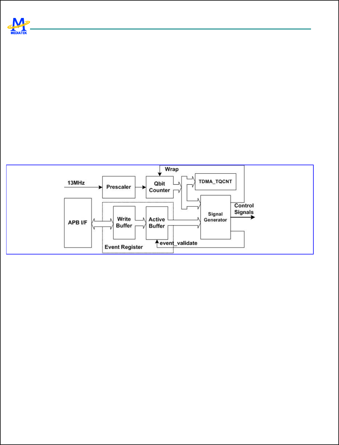
MT6217 GSM/GPRS Baseband Processor Data Sheet Revision 1.01
287/349 MediaTek Inc. Confidential
10 Timing Generator
Timing is the most critical issue in GSM/GPRS applications. The TDMA timer provides a simple interface for the MCU to
program all the timing-related events for receive event control, transmit event control and the timing adjustment. Detailed
descriptions are seen in Section 10.1.
In pause mode, the 13MHz reference clock may be switched off temporarily for the purpose of power saving and the
synchronization to the base-station is maintained by using a low power 32KHz crystal oscillator. The 32KHz oscillator is
not accurate and therefore it should be calibrated prior to entering pause mode. The calibration sequence, pause begin
sequence and the wake up sequence are described in Section 10.2.
10.1 TDMA timer
The TDMA timer unit is composed of three major blocks: Quarter bit counter, Signal generator and Event registers.
Figure 66 The block diagram of TDMA timer
By default, the quarter-bit counter continuously counts from 0 to the wrap position. In order to apply to cell synchronization
and neighboring cell monitoring, the wrap position can be changed by the MCU to shorten or lengthen a TDMA frame. The
wrap position is held in the TDMA_WRAP register and the current value of the TDMA quarter bit counter may be read by
the MCU via the TDMA_TQCNT register.
The signal generator handles the overall comparing and event-generating processes. When a match is occurred between the
quarter bit counter and the event register, a predefined control signal is generated. These control signals may be used for
on-chip and off-chip purpose. Signals that change state more than once per frame make use of more than one event register.
The event registers are programmed to contain the quarter bit position of the event to be occurred. The event registers are
double buffered. The MCU writes into the first register, and the event TDMA_EVTVAL transfers the data from the write
buffer to the active buffer, which is used by the signal generator for comparison with the quarter bit count. The
TDMA_EVTVAL signal itself may be programmed at any quarter bit position. These event registers could be classified into
four groups:
On-chip Control Events
TDMA_EVTVAL
This event allows the data values written by the MCU to pass through to the active buffers.
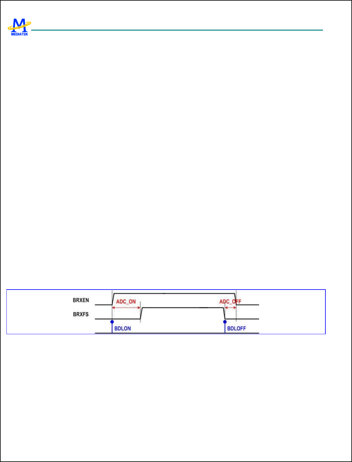
MT6217 GSM/GPRS Baseband Processor Data Sheet Revision 1.01
288/349 MediaTek Inc. Confidential
TDMA_WRAP
TDMA quarter bit counter wrap position. This sets the position at which the TDMA quarter bit counter resets back to zero.
The default value is 4999, changing this value will advance or retard the timing events in the frame following the next
TDMA_EVTVAL signal.
TDMA_DTIRQ
DSP TDMA interrupt requests. DTIRQ triggers the DSP to read the command from the MCU/DSP Shard RAM to schedule
the activities that will be executed in the current frame.
TDMA_CTIRQ1/CTIRQ2
MCU TDMA interrupt requests.
TDMA_AUXADC [1:0]
This signal triggers the monitoring ADC to measure the voltage, current, temperature, device id etc..
TDMA_AFC [3:0]
This signal powers up the automatic frequency control DAC for a programmed duration after this event.
Note: For both MCU and DSP TDMA interrupt requests, these signals are all active Low during one quarter bit duration
and they should be used as edge sensitive events by the respective interrupt controllers.
On-chip Receive Events
TDMA_BDLON [5:0]
These registers are a set of six which contain the quarter bit event that initiates the receive window assertion sequence
which powers up and enables the receive ADC, and then enables loading the receive data into the receive buffer.
TDMA_BDLOFF [5:0]
These registers are a set of six which contain the quarter bit event that initiates the receive window de-assertion sequence
which disables loading the receive data into the receive buffer, and then powers down the receive ADC.
TDMA_RXWIN[5:0]
DSP TDMA interrupt requests. TDMA_RXWIN is usually used to initiate the related RX processing including two modes.
In single-shot mode, TDMA_RXWIN is generated when the BRXFS signal is de-asserted. In repetitive mode,
TDMA_RXWIN will be generated both regularly with a specific interval after BRXFS signal is asserted and when the
BRXFS signal is de-asserted.
Figure 67 The timing diagram of BRXEN and BRXFS
Note: TDMA_BDLON/OFF event registers, together with TDMA_BDLCON register, generate the corresponding BRXEN
and BRXFS window used to power up/down baseband downlink path and control the duration of data transmission to the
DSP, respectively.
On-chip Transmit Events
TDMA_APC [6:0]
These registers initiate the loading of the transmit burst shaping values from the transmit burst shaping RAM into the
transmit power control DAC.
TDMA_BULON [3:0]
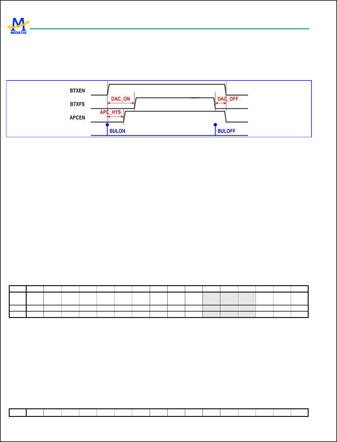
MT6217 GSM/GPRS Baseband Processor Data Sheet Revision 1.01
289/349 MediaTek Inc. Confidential
This register contains the quarter bit event that initiates the transmit window assertion sequence which powers up the
modulator DAC and then enables reading of bits from the transmit buffer into the GMSK modulator.
TDMA_BULOFF [3:0]
This register contains the quarter bit event that initiates the transmit window de -assertion sequence which disables the
reading of bits from the transmit buffer into the GMSK modulator, and then power down the modulator DAC.
Figure 68 The timing diagram of BTXEN and BTXFS
Note: TDMA_BULON/OFF event registers, together with TDMA_BULCON1, TDMA_BULCON2 register, generate the
corresponding BTXEN, BTXFS and APCEN window used to power up/down the baseband uplink path, control the duration
of data transmission from the DSP and power up/down the APC DAC, respectively.
Off-chip Control Events
TDMA_BSI [15:0]
The quarter bit positions of these 16 BSI events are used to initiate the transfer of serial words to the transceiver and
synthesizer for gain control, frequency adjustment.
TDMA_BPI [21:0]
The quarter bit positions of these 22 BPI events are used to generate changes of state on the output pins to control the
external radio components.
10.1.1 Register Definitions
TDMA+0150h Event Enable Register 0
TDMA_EVTENA
0
Bit 15 14 13 12 11 10 9 8 7 6 5 4 3 2 1 0
Name
AFC3 AFC2 AFC1 AFC0 BDL5 BDL4 BDL3 BDL2 BDL1 BDL0 CTIRQ
2 CTIRQ
1 DTIR
Q
Type R/W R/W R/W R/W R/W R/W R/W R/W R/W R/W R/W R/W R/W
Reset
0 0 0 0 0 0 0 0 0 0 0 0 0
DTIRQ Enable TDMA_DTIRQ
CTIRQn Enable TDMA_CTIRQn
AFCn Enable TDMA_AFCn
BDLn Enable TDMA_BDLONn and TDMA_BDLOFFn
For all these bits,
0 function is disabled
1 function is enabled
TDMA+0154h Event Enable Register 1
TDMA_EVTENA
1
Bit 15 14 13 12 11 10 9 8 7 6 5 4 3 2 1 0
MT6217 GSM/GPRS Baseband Processor Data Sheet Revision 1.01
290/349 MediaTek Inc. Confidential
Name
GPRS
BUL3 BUL2 BUL1 BUL0 APC6 APC5 APC4 APC3 APC2 APC1 APC0
Type R/W R/W R/W R/W R/W R/W R/W R/W R/W R/W R/W R/W
Reset
0 0 0 0 0 0 0 0 0 0 0 0
APCn Enable TDMA_APCn
BULn Enable TDMA_BULONn and TDMA_BULOFFn
For all these bits,
0 function is disabled
1 function is enabled
TDMA +0158h Event Enable Register 2
TDMA_EVTENA
2
Bit 15 14 13 12 11 10 9 8 7 6 5 4 3 2 1 0
Name
BSI15
BSI14 BSI13
BSI12
BSI11
BSI10
BSI9 BSI8 BSI7 BSI6 BSI5 BSI4 BSI3 BSI2 BSI1 BSI0
Type R/W R/W R/W R/W R/W R/W R/W R/W R/W R/W R/W R/W R/W R/W R/W R/W
Reset
0 0 0 0 0 0 0 0 0 0 0 0 0 0 0 0
BSIn BSI event enable control
0 Disable TDMA_BSIn
1 Enable TDMA_BSIn
TDMA +015Ch Event Enable Register 3
TDMA_EVTENA
3
Bit 15 14 13 12 11 10 9 8 7 6 5 4 3 2 1 0
Name
BPI15
BPI14 BPI13
BPI12
BPI11
BPI10
BPI9 BPI8 BPI7 BPI6 BPI5 BPI4 BPI3 BPI2 BPI1 BPI0
Type R/W R/W R/W R/W R/W R/W R/W R/W R/W R/W R/W R/W R/W R/W R/W R/W
Reset
0 0 0 0 0 0 0 0 0 0 0 0 0 0 0 0
TDMA+0160h Event Enable Register 4
TDMA_EVTENA
4
Bit 15 14 13 12 11 10 9 8 7 6 5 4 3 2 1 0
Name
BPI21
BPI20 BPI19
BPI18
BPI17
BPI16
Type R/W R/W R/W R/W R/W R/W
Reset
0 0 0 0 0 0
BPIn BPI event enable control
0 Disable TDMA_BPIn
1 Enable TDMA_BPIn
TDMA+0164h Event Enable Register 5
TDMA_EVTENA
5
Bit 15 14 13 12 11 10 9 8 7 6 5 4 3 2 1 0
Name
AUX1 AUX0
Type R/W R/W
Reset
0 0
AUX Auxiliary ADC event enable control
0 Disable Auxiliary ADC event
1 Enable Auxiliary ADC event
MT6217 GSM/GPRS Baseband Processor Data Sheet Revision 1.01
291/349 MediaTek Inc. Confidential
TDMA +0170h Qbit Timer Offset Control Register TDMA_WRAPOF
S
Bit 15 14 13 12 11 10 9 8 7 6 5 4 3 2 1 0
Name
TOI[1:0]
Type R/W
Reset
0
TOI This register defines the value used to advance the Qbit timer in unit of 1/4 quarter bit; the timing advance will be
taken place as soon as the TDMA_EVTVAL is occurred, and it will be cleared automatically.
TDMA +0174h Qbit Timer Biasing Control Register TDMA_REGBIA
S
Bit 15 14 13 12 11 10 9 8 7 6 5 4 3 2 1 0
Name
TQ_BIAS[13:0]
Type R/W
Reset
0
TQ_BIAS This register defines the Qbit offset value which will be added to the registers being programmed. It only
takes effects on AFC, BDLON/OFF, BULON/OFF, APC, AUXADC, BSI and BPI event registers.
TDMA +0180h DTX Control Register TDMA_DTXCON
Bit 15 14 13 12 11 10 9 8 7 6 5 4 3 2 1 0
Name
DTX3 DTX2 DTX1 DTX0
Type R/W R/W R/W R/W
DTX DTX flag is used to disable the associated transmit signals
0 BULON0, BULOFF0, APC_EV0 & APC_EV1 are controlled by TDMA_EVTENA1 register
1 BULON0, BULOFF0, APC_EV0 & APC_EV1 are disabled
TDMA +0184h Receive Interrupt Control Register TDMA_RXCON
Bit 15 14 13 12 11 10 9 8 7 6 5 4 3 2 1 0
Name
MOD5
MOD4 MOD3
MOD2
MOD1
MOD0
RXINTCNT[9:0]
Type R/W R/W R/W R/W R/W R/W R/W
RXINTCNT TDMA_RXWIN interrupt generation interval in quarter bit unit
MODn Mode of Receive Interrupts
0 Single shot mode for the corresponding receive window
1 Repetitive mode for the corresponding receive window
TDMA +0188h Baseband Downlink Control Register TDMA_BDLCON
Bit 15 14 13 12 11 10 9 8 7 6 5 4 3 2 1 0
Name
ADC_ON ADC_OFF
Type R/W R/W
ADC_ON BRXEN to BRXFS setup up time in quarter bit unit.
ADC_OFF BRXEN to BRXFS hold up time in quarter bit unit.
MT6217 GSM/GPRS Baseband Processor Data Sheet Revision 1.01
292/349 MediaTek Inc. Confidential
TDMA +018Ch Baseband Uplink Control Register 1 TDMA_BULCON
1
Bit 15 14 13 12 11 10 9 8 7 6 5 4 3 2 1 0
Name
DAC_ON DAC_OFF
Type R/W R/W
DAC_ON BTXEN to BTXFS setup up time in quarter bit unit.
DAC_OFF BTXEN to BTXFS hold up time in quarter bit unit.
TDMA +0190h Baseband Uplink Control Register 2 TDMA_BULCON
2
Bit 15 14 13 12 11 10 9 8 7 6 5 4 3 2 1 0
Name
APC_HYS
Type R/W
APC_HYS APCEN to BTXEN hysteresis time in quarter bit unit.
Address Type Width Reset Value Name Description
+0000h R [13:0] — TDMA_TQCNT Read quarter bit counter
+0004h R/W [13:0] 0x1387 TDMA_WRAP Latched Qbit counter reset position
+0008h R/W [13:0] 0x1387 TDMA_WRAPIMD Direct Qbit counter reset position
+000Ch R/W [13:0] 0x0000 TDMA_EVTVAL Event latch position
+0010h R/W [13:0] — TDMA_DTIRQ DSP software control
+0014h R/W [13:0] — TDMA_CTIRQ1 MCU software control 1
+0018h R/W [13:0] — TDMA_CTIRQ2 MCU software control 2
+0020h R/W [13:0] — TDMA_AFC0 The 1st AFC control
+0024h R/W [13:0] — TDMA_AFC1 The 2nd AFC control
+0028h R/W [13:0] — TDMA_AFC2 The 3rd AFC control
+002Ch R/W [13:0] — TDMA_AFC3 The 4th AFC control
+0030h R/W [13:0] — TDMA_BDLON0
+0034h R/W [13:0] — TDMA_BDLOFF0 Data serialization of the 1
st RX block
+0038h R/W [13:0] — TDMA_BDLON1
+003Ch R/W [13:0] — TDMA_BDLOFF1 Data serialization of the 2
nd RX block
+0040h R/W [13:0] — TDMA_BDLON2
+0044h R/W [13:0] — TDMA_BDLOFF2 Data serialization of the 3
rd RX block
+0048h R/W [13:0] — TDMA_BDLON3
+004Ch R/W [13:0] — TDMA_BDLOFF3 Data serialization of the 4
th RX block
+0050h R/W [13:0] — TDMA_BDLON4
+0054h R/W [13:0] — TDMA_BDLOFF4 Data serialization of the 5
th RX block
+0058h R/W [13:0] — TDMA_BDLON5
+005Ch R/W [13:0] — TDMA_BDLOFF5 Data serialization of the 6
th RX block
+0060h R/W [13:0] — TDMA_BULON0
+0064h R/W [13:0] — TDMA_BULOFF0 Data serialization of the 1
st TX slot
+0068h R/W [13:0] — TDMA_BULON1
+006Ch R/W [13:0] — TDMA_BULOFF1 Data serialization of the 2
nd TX slot
+0070h R/W [13:0] — TDMA_BULON2
+0074h R/W [13:0] — TDMA_BULOFF2 Data serialization of the 3
rd TX slot
+0078h R/W [13:0] — TDMA_BULON3
+007Ch R/W [13:0] — TDMA_BULOFF3 Data serialization of the 4
th TX slot
+0090h R/W [13:0] — TDMA_APC0 The 1st APC control

MT6217 GSM/GPRS Baseband Processor Data Sheet Revision 1.01
293/349 MediaTek Inc. Confidential
+0094h R/W [13:0] — TDMA_APC1 The 2nd APC control
+0098h R/W [13:0] — TDMA_APC2 The 3rd APC control
+009Ch R/W [13:0] — TDMA_APC3 The 4th APC control
+00A0h R/W [13:0] — TDMA_APC4 The 5th APC control
+00A4h R/W [13:0] — TDMA_APC5 The 6th APC control
+00A8h R/W [13:0] — TDMA_APC6 The 7th APC control
+00B0h R/W [13:0] — TDMA_BSI0 BSI event 0
+00B4h R/W [13:0] — TDMA_BSI1 BSI event 1
+00B8h R/W [13:0] — TDMA_BSI2 BSI event 2
+00BCh R/W [13:0] — TDMA_BSI3 BSI event 3
+00C0h R/W [13:0] — TDMA_BSI4 BSI event 4
+00C4h R/W [13:0] — TDMA_BSI5 BSI event 5
+00C8h R/W [13:0] — TDMA_BSI6 BSI event 6
+00CCh R/W [13:0] — TDMA_BSI7 BSI event 7
+00D0h R/W [13:0] — TDMA_BSI8 BSI event 8
+00D4h R/W [13:0] — TDMA_BSI9 BSI event 9
+00D8h R/W [13:0] — TDMA_BSI10 BSI event 10
+00DCh R/W [13:0] — TDMA_BSI11 BSI event 11
+00E0h R/W [13:0] — TDMA_BSI12 BSI event 12
+00E4h R/W [13:0] — TDMA_BSI13 BSI event 13
+00E8h R/W [13:0] — TDMA_BSI14 BSI event 14
+00ECh R/W [13:0] — TDMA_BSI15 BSI event 15
+0100h R/W [13:0] — TDMA_BPI0 BPI event 0
+0104h R/W [13:0] — TDMA_BPI1 BPI event 1
+0108h R/W [13:0] — TDMA_BPI2 BPI event 2
+010Ch R/W [13:0] — TDMA_BPI3 BPI event 3
+0110h R/W [13:0] — TDMA_BPI4 BPI event 4
+0114h R/W [13:0] — TDMA_BPI5 BPI event 5
+0118h R/W [13:0] — TDMA_BPI6 BPI event 6
+011Ch R/W [13:0] — TDMA_BPI7 BPI event 7
+0120h R/W [13:0] — TDMA_BPI8 BPI event 8
+0124h R/W [13:0] — TDMA_BPI9 BPI event 9
+0128h R/W [13:0] — TDMA_BPI10 BPI event 10
+012Ch R/W [13:0] — TDMA_BPI11 BPI event 11
+0130h R/W [13:0] — TDMA_BPI12 BPI event 12
+0134h R/W [13:0] — TDMA_BPI13 BPI event 13
+0138h R/W [13:0] — TDMA_BPI14 BPI event 14
+013Ch R/W [13:0] — TDMA_BPI15 BPI event 15
+0140h R/W [13:0] — TDMA_BPI16 BPI event 16
+0144h R/W [13:0] — TDMA_BPI17 BPI event 17
+0148h R/W [13:0] — TDMA_BPI18 BPI event 18
+014Ch R/W [13:0] — TDMA_BPI19 BPI event 19
+01A0h R/W [13:0] — TDMA_BPI20 BPI event 20
+01A4h R/W [13:0] — TDMA_BPI21 BPI event 21
+01B0h R/W [13:0] — TDMA_AUXEV0 Auxiliary ADC event 0
+01B4h R/W [13:0] — TDMA_AUXEV1 Auxiliary ADC event 1
+0150h R/W [15:0] 0x0000 TDMA_EVTENA0 Event Enable Control 0
+0154h R/W [15:0] 0x0000 TDMA_EVTENA1 Event Enable Control 1
+0158h R/W [15:0] 0x0000 TDMA_EVTENA2 Event Enable Control 2
+015Ch R/W [15:0] 0x0000 TDMA_EVTENA3 Event Enable Control 3
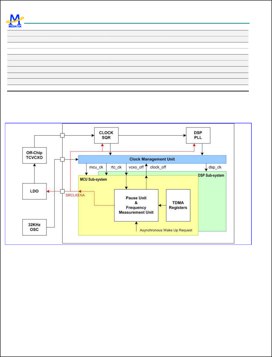
MT6217 GSM/GPRS Baseband Processor Data Sheet Revision 1.01
294/349 MediaTek Inc. Confidential
+0160h R/W [5:0] 0x0000 TDMA_EVTENA4 Event Enable Control 4
+0164h R/W [0] 0x0000 TDMA_EVTENA5 Event Enable Control 5
+0170h R/W [1:0] 0x0000 TDMA_WRAPOFS TQ Counter Offset Control Register
+0174h R/W [13:0] 0x0000 TDMA_REGBIAS Biasing Control Register
+0180h R/W [3:0] — TDMA_DTXCON DTX Control Register
+0184h R/W [15:0] — TDMA_RXCON Receive Interrupt Control Register
+0188h R/W [15:0] — TDMA_BDLCON Downlink Control Register
+018Ch R/W [15:0] — TDMA_BULCON1 Uplink Control Register 1
+0190h R/W [7:0] — TDMA_BULCON2 Uplink Control Register 2
Table 40 TDMA Timer Register Map
10.2 Slow Clocking Unit
Figure 69 The block diagram of the slow clocking unit
The slow clocking unit is provided to maintain the synchronization to the base-station timing using a 32KHz crystal
oscillator while the 13MHz reference clock is switched off. As shown in Figure 69 , this unit is composed of frequency
measurement unit, pause unit and clock management unit.
Because of the inaccuracy of the 32KHz oscillator, a frequency measurement unit is provided to calibrate the 32KHz crystal
taking the accurate 13MHz source as the reference. The calibration procedure always takes place prior to the pause period.
The pause unit is used to initiate and terminate the pause mode procedure and it also works as a coarse time -base during the
pause period.
The clock management unit is used to control the system clock while switching between the normal mode and the pause
mode. SRCLKENA is used to turn on/off the clock squarer, DSP PLL and off-chip TCVCXO. CLOCK_OFF signal is used
for gating the main MCU and DSP clock , and VCXO_OFF is used as the acknowledge signal of the CLOCK_OFF request.
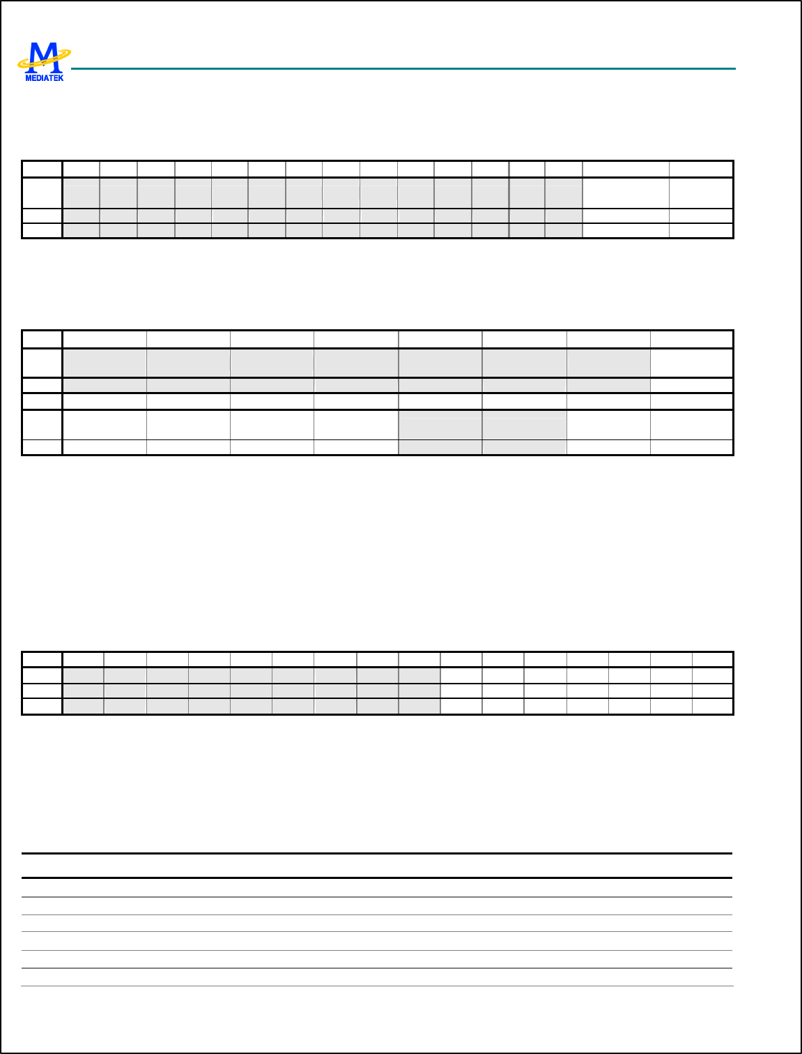
MT6217 GSM/GPRS Baseband Processor Data Sheet Revision 1.01
295/349 MediaTek Inc. Confidential
10.2.1 Register Definitions
TDMA +0218h Slow clocking unit control register SM_CON
Bit 15 14 13 12 11 10 9 8 7 6 5 4 3 2 1 0
Name
PAUSE_STA
RT FM_STAR
T
Type W W
Reset
0 0
FM_START Initiate the frequency measurement procedure
PAUSE_STARTInitiate the pause mode procedure at the next timer wrap position
TDMA +0220h Slow clocking unit status register SM_STA
Bit 15 14 13 12 11 10 9 8
Name
PAUSE_ABO
RT
Type R
Bit 7 6 5 4 3 2 1 0
Name
SETTLE_CP
L PAUSE_CPL
PAUSE_INT PAUSE_RQS
T FM_CPL FM_RQST
Type R R R R R R
FM_RQST Frequency measurement procedure is requested
FM_CPL Frequency measurement procedure is completed
PAUSE_RQST Pause mode procedure is requested
PAUSE_INT Asynchronous wake up from pause mode
PAUSE_CPL Pause period is completed
SETTLE_CPL Settling period is completed
PAUSE_ABORT Pause mode is aborted because of the reception of interrupt prior to entering pause mode
TDMA +022Ch Slow clocking unit configuration register SM_CNF
Bit 15 14 13 12 11 10 9 8 7 6 5 4 3 2 1 0
Name
GPT MSDC
RTC EINT KP SM FM
Type R/W R/W R/W R/W R/W R/W R/W
Reset
0 0 0 0 0 1 1
FM Enable interrupt generation upon completion of frequency measurement procedure
SM Enable interrupt generation upon completion of pause mode procedure
KP Enable asynchronous wake-up from pause mode by key press
EINT Enable asynchronous wake-up from pause mode by external interrupt
RTC Enable asynchronous wake-up from pause mode by real time clock interrupt
MSDC Enable asynchronous wake-up from pause mode by memory card insertion interrupt
Address Type Width Reset Value Name Description
+0200h R/W [2:0] — SM_PAUSE_M MSB of pause duration
+0204h R/W [15:0] — SM_PAUSE_L 16 LSB of pause duration
+0208h R/W [13:0] — SM_CLK_SETTLE Off -chip VCXO settling duration
+020Ch R [2:0] — SM_FINAL_PAUSE_M MSB of final pause count
+0210h R [15:0] — SM_FINAL_PAUSE_L 16 LSB of final pause count
+0214h R [13:0] — SM_QBIT_START TQ_ COUNT value at the start of the pause
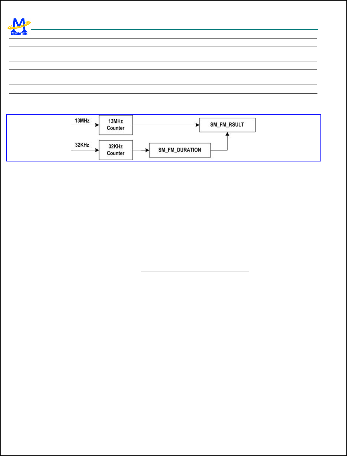
MT6217 GSM/GPRS Baseband Processor Data Sheet Revision 1.01
296/349 MediaTek Inc. Confidential
+0218h W [1:0] 0x0000 SM_CON SM control register
+021Ch R [7:3,1:0] 0x0000 SM_STA SM status register
+0220h R/W [15:0] — SM_FM_DURATION 32KHz measurement duration
+0224h R [9:0] — SM_FM_RESULT_M 10 MSB of frequency measurement result
+0228h R [15:0] — SM_FM_RESULT_L 16 LSB of frequency measurement result
+022Ch R/W [6:0] 0x0000 SM_CNF SM configuration register
10.2.2 Frequency Measurement
Figure 70 Block Diagram of Frequency Measurement Unit
The MCU writes into the SM_FM_DURATION register the number of clock cycles, during which the 32768 Hz clock will
be measured. Then, the MCU sets the FM_START bit in the SM_CON register, the hardware sets the FM_RQST flag and
resets the FM_CPL flag automatically and the 32kHz and 13MHz counters are simultaneously started from zero.
When the 32kHz counter reaches the terminal value determined by the SM_FM_DURATION register, the current value of
the 13MHz counter is stored in the SM_FM_RESULT register, the counters are stopped , the FM_RQST is reset and the
FM_CPL flag is set.
The SM_FM_DURATION is 16 bits wide, and the 32K counter counts )1(2
+
×
N cycles of 32768Hz. This gives a
maximum of almost 4.00s measurement duration.
RESULTFMSM
DURATIONFMSM
frequencyMeasured __
1013)1__(2
_6
××+×
=
10.2.3 Pause Mode Operation
The MCU writes the pause and settling time into the SM_PAUSE_M, SM_PAUSE_L and SM _CLK_SETTLE registers and
the sum of the pause time and settling time must be as close as possible to the TDMA frame boundary, taking into account
the frequency measurement result.
The MCU should set the PAUSE_START bit ahead of the TDMA_EVTVAL event. The hardware sets the PAUSE_RQST
flag and resets the PAUSE_INT, PAUSE_CPL, SETTLE_CPL, PAUSE_ABORT flags automatically and the pause mode
operation will be initiated at the next timer wrap position.
When the pause duration reaches the programmed terminal value or the asynchronous wake up event is received, the pause
mode operation is ended/stopped/aborted and the corresponding flag is set (PAUSE_CPL, PAUSE_INT and
PAUSE_ABORT). Then, the MCU calculates the timing offset and adjusts the TDMA_WRAPIMD position accordingly.
The number of quarter bit time elapsed during the pause operation is:

MT6217 GSM/GPRS Baseband Processor Data Sheet Revision 1.01
297/349 MediaTek Inc. Confidential
)__(
__
__
__
___
)____(__
1DURATIONFMSM24
RESULTFMSM
durationbitquarter
durationperiodk32
Kqbit
STARTQBITSMWRAPTQqbit
qbitSETTLECLKSMPAUSEFINALSMKqbitbitquarterNb
+×
==
−=∆
∆
−
+
×
=
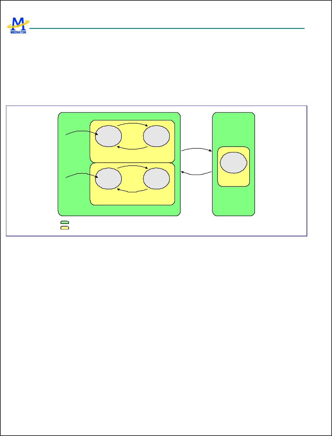
MT6217 GSM/GPRS Baseband Processor Data Sheet Revision 1.01
298/349 MediaTek Inc. Confidential
11 Power, Clocks and Reset
This chapter describes about the power, clock and reset management functions provided by MT6217. Together with Power
Management IC (PMIC), MT6217 offers both fine and coarse resolutions of power control by way of software
programming. With this efficient method, the developer can turn on selective resources accordingly in order to achieve
optimized power consumption. The operating modes of MT6217 as well as main power states provided by PMIC are shown
in Figure 71.
Active Mode Sleep Mode
Active Mode
Power Down
Mode
Power On Software
Program
Software
Program
Power On
Software
Program
Active State Standby State
Pause Mode
MT6217
Processors
MT6217
Peripherals
Phone Power State
MT6217 Operating Mode
MT6217
Figure 71 Major Phone Power States and Operating Modes for MT6217 based terminal
11.1 Baseband to PMIC Serial Interface
11.1.1 General Description
MT6217 use 3 wires B2PSI interface connected to PMIC, this bi-directional serial bus interface allows base-band to write
command to and read from PMIC. The bus protocol utilizes a 16 bits proprietary format. B2PSICK is the serial bus clock
and is driven by master. B2PSIDAT is the serial data; master or slave can drive it. B2PSICS is the bus selection signal.
Once This bus us active once B2PSICS goes low, base-band start to transfer the 4 register bits followed by a read/write bit,
then wait for 3 clocks for PMIC B2PSI state machine to decode the operation for succeeding 8 data bits. The stat machine
should count for 16 clocks to complete the data transfer.
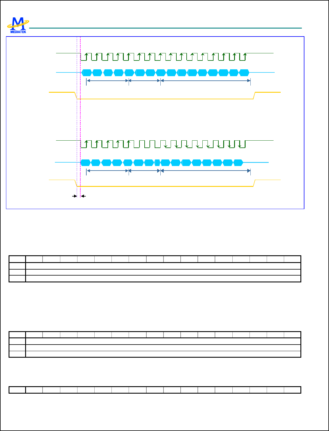
MT6217 GSM/GPRS Baseband Processor Data Sheet Revision 1.01
299/349 MediaTek Inc. Confidential
B2PSICK
B2PSICK
R3 R2 R1 R0 WXXXD7 D6 D5 D4 D3 D2 D1 D0
R3 R2 R1 R0 RX X X D7 D6 D5 D4 D3 D2 D1 D0
T>100nsec
Receive
Index Register
Decode Write Register Content
Receive
Index Register
Decode Read Register Content
B2PSIDAT
B2PSIDAT
B2PSICS
B2PSICS
Figure 72 B2PSI bus timing
11.1.2 Register Definitions
B2PSI+0000h B2PSI data register B2PSI_DATA
Bit 15 14 13 12 11 10 9 8 7 6 5 4 3 2 1 0
Name
B2PSI_DATA [15:0]
Type R/W
Reset
0
B2PSI_DATA The B2PSI DATA format is 4 bit register + 3 bit don’t care + write / read bit + 8 bit data.
Write / read bit: 0 for read operation; 1 for write operation.
B2PSI +0008h B2PSI baud rate divider register B2PSI _DIV
Bit 15 14 13 12 11 10 9 8 7 6 5 4 3 2 1 0
Name
B2PSI _DIV [15:0]
Type R/W
Reset
0
B2PSI_DIV It’s the B2PSI clock rate divisor. B2PSICK = system clock rate / div.
B2PSI+0010h B2PSI status register B2PSI_STAT
Bit 15 14 13 12 11 10 9 8 7 6 5 4 3 2 1 0
MT6217 GSM/GPRS Baseband Processor Data Sheet Revision 1.01
300/349 MediaTek Inc. Confidential
Name
WRIT
E_SU
CCES
S
READ
_REA
DT
Type RC RC
Reset
0 0
READ_READY Read data ready.
0 Read data isn’t ready yet.
1 Read data is ready. It will be cleared by reading B2PSI_STAT register or B2PSI initialize a new transmit.
WRITE_SUCCESS B2PSI write successfully.
0 B2PSI write isn’t finish yet.
1 B2PSI write finish. It will be cleared by reading B2PSI_STAT register or B2PSI initialize a new transmit
B2PSI+0014h B2PSI CS to CK time register B2PSI_TIME
Bit 15 14 13 12 11 10 9 8 7 6 5 4 3 2 1 0
Name
B2PSI_TIME
Type R/W
Reset
0
B2PSI_TIME The time interval that first B2PSICK will be started after the B2PSICS is active low.
Time interval = 1/system clock * B2PSI_time.
11.2 Clocks
There are two major time bases in the MT6217. For the faster one is the 13 MHz clock originating from an off-chip
temperature-compensated voltage controlled oscillator (TCVCXO) that can be either 13MHz or 26MHz. This signal is the
input from the SYSCLK pad then is converted to the square-wave signal. The other time base is the 32768 Hz clock
generated by an on-chip oscillator connected to an external crystal. Figure 73 shows the clock sources as well as their
utilizations inside the chip.
32KHz
OSC
/2
DSP PLL
Clock
Squarer
/2
AHB Bus Clock
APB Bus Clock
MCU Clock
DSP Clock
32KHz Clock
DPLL
AHB
MCU
DSP_DIV2
MCU_DIV2
CoreI/O
SYSCLK
XIN
XOUT
CLKSQ_PLD
MCU PLL
MPLL USB PLL USB Clock
DCM
MCU_FSEL
Figure 73 Clock distributions inside the MT6217.

MT6217 GSM/GPRS Baseband Processor Data Sheet Revision 1.01
301/349 MediaTek Inc. Confidential
11.2.1 32.768 KHz Time Base
The 32768 Hz clock is always running. It’s mainly used as the time base of the Real Time Clock (RTC) module, which
maintains time and date with counters. Therefore, both the 32768Hz oscillator and the RTC module is powered by separate
voltage supplies that shall not be powered down when the other supplies do.
In low power mode, the 13 MHz time base is turned off, so the 32768 Hz clock shall be employed to update the critical
TDMA timer and Watchdog Timer. This time base is also used to clocks the keypad scanner logic.
11.2.2 13 MHz Time Base
Two 1/2-dividers, one for MCU Clock and the other for DSP Clock, are exist to allow using 26 or 13 MHz TCVCXO .
Three phase-locked loops (MPLL, DPLL and UPLL) are used to generate three primary clocks, MCU_CLOCK,
DSP_CLOCK and USB_CLOCK, and to clock modules in MCU Clock Domain and DSP Clock Domain and USB,
respectively. These PLLs require no off-chip components for operations and can be turn off independently in order to save
power. After power-on, all the PLLs are off by default and the source clock signal is selected through multiplexers. The
software shall take cares of the PLL lock time while changing the clock selections. The PLLs and their usages are listed
below.
DPLL supplies the DSP system clock, DSP_CLOCK. DPLL can be programmed to provide 1X to 6X output of the
13 MHz reference. The MCU software may set the clock multiplier according to the DSP performance required.
Currently, the multiply factor is set to 6X in this version of chip.
MPLL supplies the MCU system clock, MCU_CLOCK, which paces the operations of the MCU cores, MCU
memory system, and MCU peripherals as well. MPLL has a programmable clock multiplier, which supports 2X
and 4X clock multiplication. The MCU software may change the multiplier setting according to different
workload conditions. Currently, the multiply factor must be set to 4X in this version of chip. The outputted
52MHz clock is connected to dynamic clock manager for dynamically adjusting clock rate by digital clock
divider.
UPLL supplies the USB clock, USB_CLOCK. The UPLL input is a 4 MHz clock, which comes from 52 MHz clock
generated by MPLL and then divided by 13. UPLL pumps the input clock source 12 times to generate 48 MHz for
USB module.
Note that PLLs need some time to become stable after being powered up. The software shall take cares of the PLL lock
time before switching them to the proper frequency. Usually, a software loop longer than the PLL lock time is employed to
deal with the problem.
For power management, the MCU software program may stop MCU Clock by setting the Sleep Control Register. Any
interrupt requests to MCU can pause the sleep mode, and thus MCU return to the running mode.
AHB also can be stop by setting the Sleep Control Register. However the behavior of AHB in sleep mode is a little different
from that of MCU. After entering Sleep Mode, it can be temporarily waked up by any “hreq” (bus request), and then goes
back to sleep automatically after all “hreqs” de-assert. Any transactions can take place as usual in sleep mode, and it can
save power while there is no transaction on it. However the penalty is losing a little system efficiency for switching on and
off bus clock, but the impact is small.

MT6217 GSM/GPRS Baseband Processor Data Sheet Revision 1.01
302/349 MediaTek Inc. Confidential
11.2.3 Dynamic Clock Switch of MCU Clock
Dynamic Clock Manager is implemented to allow MCU switching clock dynamically without any jitter, and enabling signal
drift, and system can operate stably during any clock rate switch.
Please note that MPLL must be enabled and the frequency shall be set as 52MHz. Before switching to 52MHz clock rate,
the clock from MCU DIV2 will feed through dynamic clock manager (DCM) directly. That means if MCU DIV2 is enabled,
the internal clock rate is the half of SYSCLK. Contrarily, the internal clock rate is identical to SYSCLK.
However, the settings of some hardware modules is required to be changed before or after clock rate change. Software has
the responsibility to change them at proper timing. The following table is list of hardware modules needed to be changed
their setting during clock rate change.
Module Name Programming Sequence
EMI
1. 26M -> 52M
Changing wait state before clock change. New wait state will not take effect until
current EMI access is complete. Software should insert a period of time before
switching clock.
2. 52M -> 26M
Changing wait state after clock change.
NAND
1. 26M -> 52M
Changing wait state before clock change. New wait state will not take effect until
current EMI access is complete. Software should insert a period of time before
switching clock.
2. 52M -> 26M
Changing wait state after clock change.
LCD Change wait state while LCD in IDLE state.
AHB
1. 26M -> 52M
Change AHB EMI interface register (0x80000500) to latch mode (0) before clock switching.
2. 52M -> 26M
Change AHB EMI interface register (0x80000500) to direct couple mode (1) after
clock switching.
Table 41 Programming sequence during clock switch
11.2.4 Register Definitions
CONFG+0100h
MPLL Frequency Register MPLL
Bit 15 14 13 12 11 10 9 8 7 6 5 4 3 2 1 0
Name
CALI RST SPD
Type R/W R/W R/W
Reset
0 0 0
SPD Select the Output Clock Rate for MPLL
00 power down
01 13MHz x 2
MT6217 GSM/GPRS Baseband Processor Data Sheet Revision 1.01
303/349 MediaTek Inc. Confidential
10 Not used
11 13MHz x 4
RST Reset Control of MPLL
0 Normal Operation
1 Reset the MPLL
CALI Calibration Control for MPLL
CONFG+104h DPLL Frequency register DPLL
Bit 15 14 13 12 11 10 9 8 7 6 5 4 3 2 1 0
Name
CALI RST SPD
Type R/W R/W R/W
Reset
0 0 0
SPD Select the Output Clock Rate for DPLL
000 power down
001 13MHz x 2
010 13MHz x 3
011 13MHz x 4
100 13MHz x 5
101 13MHz x 6
RST Reset Control of DPLL
0 Normal Operation
1 Reset the DPLL
CALI Calibration Control for DPLL
CONFG+110h DPLL Frequency register UPLL
Bit 15 14 13 12 11 10 9 8 7 6 5 4 3 2 1 0
Name
CALI RST
Type R/W R/W
Reset
0 0
RST Reset Control of DPLL
0 Normal Operation
1 Reset the UPLL
CALI Calibration Control for UPLL
CONFG+108h Clock Control Register CLK_CON
Bit 15 14 13 12 11 10 9 8 7 6 5 4 3 2 1 0
Name
UPLL
_TMA MPLL
_TMA DPLL
_TMA
CLKS
Q_PL
D
MCU_
DIV2 DPLL MPLL DSP_
DIV2
Type R/W R/W R/W R/W R/W R/W R/W R/W
Reset
0 0 0 0 0 0 0 0
DSP_DIV2 Control the x2 clock divider for DPLL input
0 Divider bypassed
1 Divider not bypassed
MPLL Select MCU Clock
0 MPLL bypassed

MT6217 GSM/GPRS Baseband Processor Data Sheet Revision 1.01
304/349 MediaTek Inc. Confidential
1 Using MPLL Clock
DPLL Select DSP Clock
0 DPLL bypassed
1 Using DPLL Clock
MCU_DIV2 Control the x2 clock divider for MCU clock domain
0 Divider bypassed
1 Divider not bypassed
CLKSQ_PLD Pull Down Control
0 Disable
1 Enables
DPLL_TMA DPLL test mode
0 Disable
1 Enables
MPLL_TMA MPLL test mode
0 Disable
1 Enable
UPLL_TMA UPLL test mode
0 Disable
1 Enable
CONFG+10Ch Sleep Control Register SLEEP_CON
Bit 15 14 13 12 11 10 9 8 7 6 5 4 3 2 1 0
Name
DSP AHB MCU
Type WO WO WO
Reset
0 0 0
MCU Stop the MCU Clock to force MCU Processor entering sleep mode. MCU clock will be resumed as long as there
comes an interrupt request or system is reset.
0 MCU Clock is running
1 MCU Clock is stopped
AHB Stop the AHB Bus Clock to force the entire bus entering sleep mode. AHB clock will be resumed as long as there
comes an interrupt request or system is reset.
0 AHB Bus Clock is running
1 AHB Bus Clock is stopped
DSP Stop the DSP Clock.
0 DSP Bus Clock is running
1 DSP Bus Clock is stopped
CONFG+0114h
MCU Clock Control Register MCUCLK_CON
Bit 15 14 13 12 11 10 9 8 7 6 5 4 3 2 1 0
Name
FSEL
Type R/W
Reset
3
FSEL MCU clock frequency selection. This control register is used to control the output clock frequency of Dynamic
Clock Manager. The clock frequency is from 13MHz to 52MHz. The waveform of the output clock is shown
below.
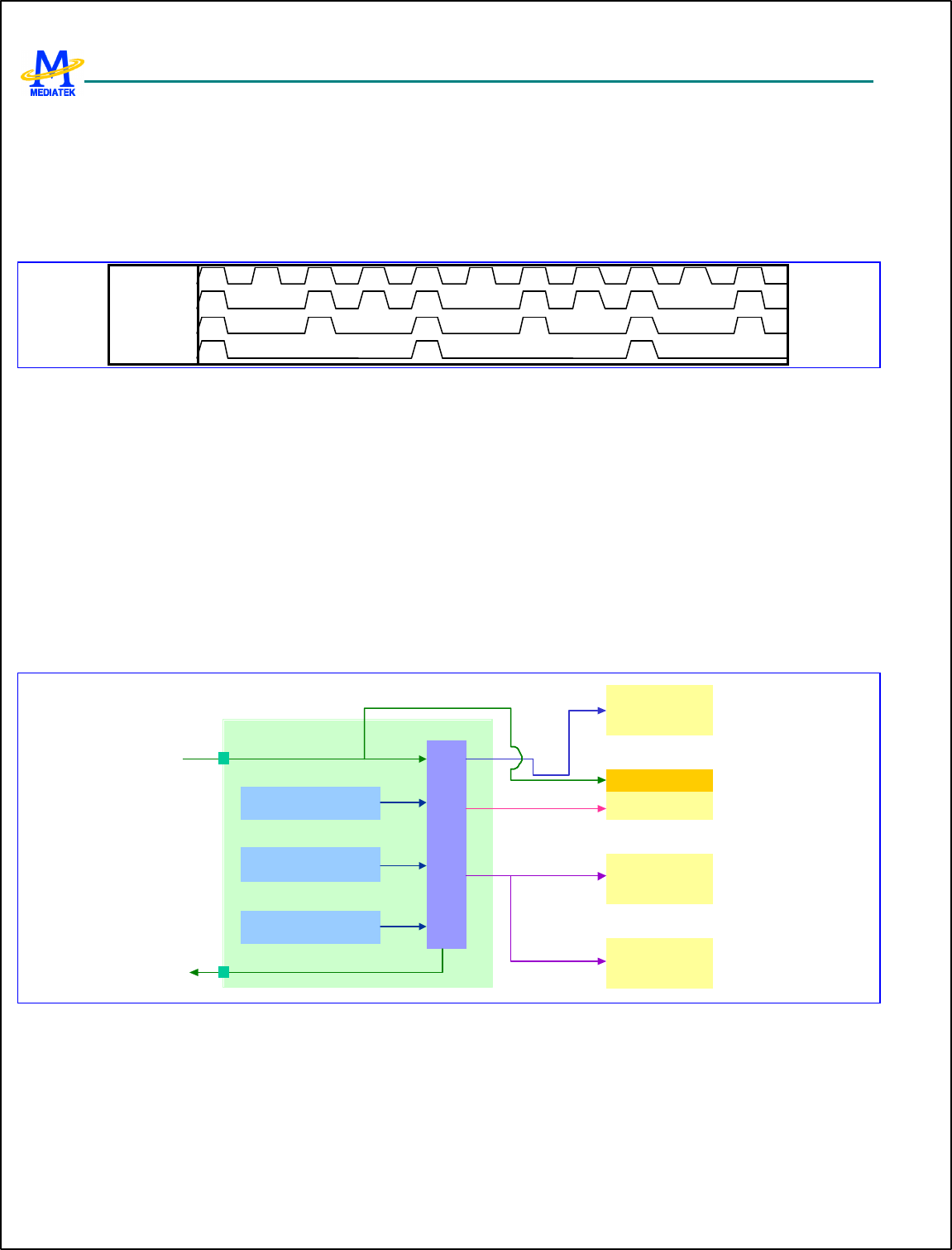
MT6217 GSM/GPRS Baseband Processor Data Sheet Revision 1.01
305/349 MediaTek Inc. Confidential
Please note that the clock period of 39MHz is not uniform. The shortest period of 39MHz clock is the same
as the period of 52MHz. As a result, the wait states of external interfaces, such as EMI, NAND, and so on,
have to be configured based on 52MHz timing. Therefore, the MCU performance executing in external
memory at 39MHz may be worse than at 26MHz.
Also note that the maximum latency of clock switch is 4 clock periods. Software shall provide 4T locking
time after clock switch command.
52M
39M
26M
13M
Figure 74 Output of Dynamic Clock Manager
0 13MHz
1 26MHz
2 39MHz
3 52MHz
Others reserved
11.3 Reset Management
Figure 75 shows reset scheme used in MT6217. There are three kinds of resets in the MT6217, i.e., hardware reset,
watchdog reset, and software resets.
Watchdog Timer
MCU Soft Reset
DSP Soft Reset
MUX
R1
R2
R3
R4
MCU
Subsystem
MCU
Peripherals
DSP
Subsystem
DSP
Coprocessors
GPIO
R124
R123
R12SYSRST#
WATCHDOG#
Figure 75 Reset Scheme Used in MT6217

MT6217 GSM/GPRS Baseband Processor Data Sheet Revision 1.01
306/349 MediaTek Inc. Confidential
11.3.1 General Description
11.3.1.1 Hardware Reset
This reset is input through the SYSRST# pin, which shall be driven to low during power-on. The hardware reset has a
global effect on the chip: it initializes all digital and analog circuits except the Real Time Clock module. The initial states of
the MT6217 sub-blocks are listed below.
l All analog circuits are turned off.
l All PLLs are turned off and bypassed. The 13MHz system clock is the default time base.
l Special Trap States in GPIO
11.3.1.2 Watchdog Reset
A watchdog reset is generated when the Watchdog Timer expires as the MCU software failed to re-program the timer
counter in time. This situation is typically induced by abnormal software execution, which can be aborted by a hardwired
watchdog reset. Hardware blocks that are affected by the watchdog reset are
l MCU subsystem
l DSP subsystem
l External Components (by software program)
11.3.1.3 Software Resets
These are local reset signals that initialize specific hardware. The MCU or DSP software may write to software reset trigger
registers to return hardware modules to their initial states, when hardware failures are detected, for example.
The following modules have software resets.
l MCU Peripherals
l DSP Core
l DSP Coprocessors
11.3.2 Register Definitions
RGU +0000h Watchdog Timer Control register WDT_MODE
Bit 15 14 13 12 11 10 9 8 7 6 5 4 3 2 1 0
Name
KEY[7:0] AUTO
-REST
ART IRQ EXTE
N EXTP
OL ENAB
LE
Type R/W R/W R/W R/W R/W
Reset
0 0 0 0 1
ENABLE
0 Disable Watchdog Timer
1 Enable Watchdog Timer
EXTPOL Define the polarity of the external watchdog pin
0 Active low
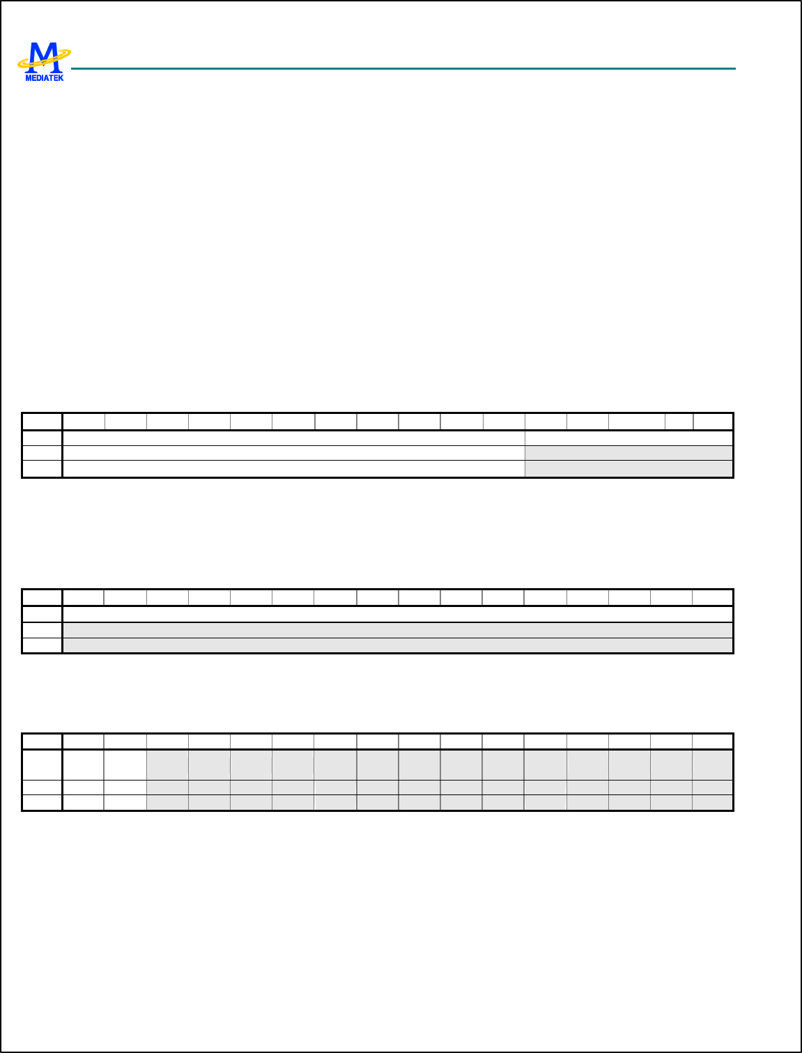
MT6217 GSM/GPRS Baseband Processor Data Sheet Revision 1.01
307/349 MediaTek Inc. Confidential
1 Active high
EXTEN
0 The watchdog can not generate an external watchdog reset signal
1 If the watchdog counter reaches zero, an external watchdog signal is generated
KEY Write access is allowed if KEY=0x22
IRQ issue interrupt instead of WDT reset. For debug purpose, RGU issues an interrupt to MCU instead of resetting
system.
0 Disable
1 Enable
AUTO-RESTART Re -start watch dog timer counter with the value of WDT_LENGTH while task ID is written into
Software Debug Unit.
0 Disable. Counter re -starts by writing KEY into WDT_RESTART register.
1 Enable. Counter re-starts by writing KEY into WDT_RESTART register or by writing task ID into software
debug unit.
RGU +0004h Watchdog Time-Out Interval register WDT_LENGTH
Bit 15 14 13 12 11 10 9 8 7 6 5 4 3 2 1 0
Name
TIMOUT[10:0] KEY[4:0]
Type WO
Reset
111_1111_1111b
KEY Write access is allowed if KEY=08h
TIMOUT The counter is restarted with {TIMEOUT [10:0], 1_1111_1111b}. So the Watchdog Timer time-out period is a
multiple of 512*T32k=15.6ms
RGU +0008h Watchdog Timer Restart register WDT_RESTART
Bit 15 14 13 12 11 10 9 8 7 6 5 4 3 2 1 0
Name
KEY[15:0]
Type
Reset
KEY Restart the counter if KEY=1971h
RGU +000Ch Watchdog Timer Status register WDT_STA
Bit 15 14 13 12 11 10 9 8 7 6 5 4 3 2 1 0
Name
WDT SW_W
DT
Type RO RO
Reset
0 0
WDT
0 Reset not due to Watchdog Timer
1 Reset due to that Watchdog Timer time -out period is reached
SW_WDT
0 Reset not due to Software-triggered Watchdog Timer
1 Reset due to Software-triggered Watchdog Timer
NOTE: The system reset does not affect this register. This bit is cleared when the bit ENABLE of WTU_MODE register is
written.
MT6217 GSM/GPRS Baseband Processor Data Sheet Revision 1.01
308/349 MediaTek Inc. Confidential
RGU +0010h CPU Peripheral Software Reset Register SW_PERIPH_RS
TN
Bit 15 14 13 12 11 10 9 8 7 6 5 4 3 2 1 0
Name
RESE
T DAMR
ST USBR
ST
Type R/W R/W R/W
Reset
0 0 0
RESET Controls the APB Peripherals Reset Control
0: No Reset
1: Reset Activated
DMARST Reset the DMA peripheral
0: No Reset
1: Reset Activated
USBRST Reset USB
0 No Reset
1 Reset Activated
RGU +0014h DSP Software Reset Register SW_DSP_RSTN
Bit 15 14 13 12 11 10 9 8 7 6 5 4 3 2 1 0
Name
RST
Type R/W
Reset
0
RST Controls the DSP System Reset Control
0: No reset
1: Reset activate
RGU +0018h Watchdog Timer Reset Signal Duration register WDT_RSTINTRE
VAL
Bit 15 14 13 12 11 10 9 8 7 6 5 4 3 2 1 0
Name
LENGTH[ 11:0]
Type R/W
Reset
FFFh
LENGTH This register indicates the reset duration when watchdog timer timeout. However, if bit IRQ in WDT_MODE
register is set to “1”, an interrupt will issue instead of a reset.
RGU+001Ch Watchdog Timer Software Reset Register WDT_SWRST
Bit 15 14 13 12 11 10 9 8 7 6 5 4 3 2 1 0
Name
KEY[15:0]
Type
Reset
Software -triggered watch dog timer reset. If the register content matches the KEY, a watch dog reset is issued. However, if
bit IRQ in WDT_MODE register is set to “1”, an interrupt will issue instead of a reset.
KEY 1209h
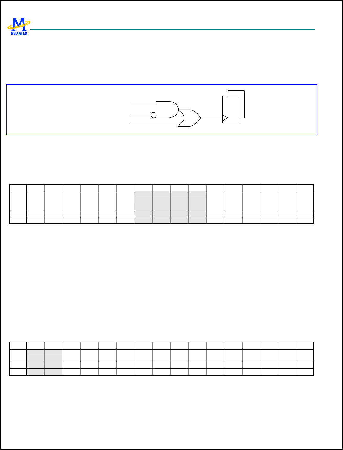
MT6217 GSM/GPRS Baseband Processor Data Sheet Revision 1.01
309/349 MediaTek Inc. Confidential
11.4 Software Power Down Control
In addition to have Pause Mode at Standby State, the software program can also put each peripherals independently in
Power Down Mode at Active State by gating their clock off. The typical logic implemented is described as Figure 76. For
all these configuration bits, 1 means that the function is Power Down Mode and 0 means that it is in the Active Mode.
CLOCK
POWER DOWN
TESTMODE
Figure 76 Power Down Control at Block Level
11.4.1 Register Definitions
CONFG+300h Power Down Control 0 Register PDN_CON0
Bit 15 14 13 12 11 10 9 8 7 6 5 4 3 2 1 0
Name
DSP_
DIV2 MPLL DPLL MCU_
DIV2 CLKS
Q UPLL RESZ JPEG WAVE
TABL
E GCU USB DMA
Type R/W R/W R/W R/W R/W R/W R/W R/W R/W R/W R/W R/W
Reset
1 1 1 1 0 1 1 1 1 1 1 1
DMA Controls the DMA Controller Power Down
USB Controls the USB Controller Power Down
GCU Controls the GCU Controller Power Down
WAVETALBE Controls the DSP WaveTable DMA Power Down
JPEG Controls the JPEG Decoder Power Down
RESZ Controls the Image Resizer Power Down
CLKSQ Controls the Clock squarer Power Down
MCU_DIV2 Controls the MUC DIV2 Power Down
DPLL Controls the DPLL Power Down
MPLL Controls the MPLL Power Down
DSP_DIV2 Controls the DSP DIV2 Power Down
CONFG +304h Power Down Control 1 Register PDN_CON1
Bit 15 14 13 12 11 10 9 8 7 6 5 4 3 2 1 0
Name
SPI NFI TRC PWM2 MSDC UART
2 LCD ALTE
R PWM SIM UART
1 GPIO KP GPT
Type R/W R/W R/W R/W R/W R/W R/W R/W R/W R/W R/W R/W R/W R/W
Reset
1 1 1 1 1 1 1 1 1 1 0 1 1 1
GPT Controls the General Purpose Timer Power Down
KP Controls the Keypad Scanner Power Down
GPIO Controls the GPIO Power Down
UART1 Controls the UART1 Controller Power Down
SIM Controls the SIM Controller Power Down
MT6217 GSM/GPRS Baseband Processor Data Sheet Revision 1.01
310/349 MediaTek Inc. Confidential
PWM Controls the PWM Generator Power Down
ALTER Controls the Alerter Generator Power Down
LCD Controls the Serial LCD Controller Power Down
UART2 Controls the UART2 Controller Power Down
MSDC Controls the MS/SD Controller Power Down
PWM2 Controls the PWM2 Generator Power Down
TRC Controls the MCU Tracer Power Down
NFI Controls the NAND FLASH Interface Power Down
SPI Controls the Serial Port Interface Power Down
CONFG +308h Power Down Control 2 Register PDN_CON2
Bit 15 14 13 12 11 10 9 8 7 6 5 4 3 2 1 0
Name
GMSK
BBRX AAFE DIV GCC BFE VAFE AUXA
D FCS APC AFC BPI BSI RTC TDMA
Type R/W R/W R/W R/W R/W R/W R/W R/W R/W R/W R/W R/W R/W R/W R/W
Reset
1 1 1 1 1 1 1 1 1 1 1 1 1 1 1
TDMA Controls the TDM A Power Down
RTC Controls the RTC Power Down
BSI Controls the BSI Power Down. This control will not be updated until both tdma_evtval and qbit_en are asserted.
BPI Controls the BPI Power Down. This control will not be updated until both tdma_evtval and qbit_en are asserted.
AFC Controls the AFC Power Down. This control will not be updated until both tdma_evtval and qbit_en are asserted.
APC Controls the APC Power Down. This control will not be updated until both tdma_evtval and qbit_en are asserted.
FCS Controls the FCS Power Down
AUXAD Controls the AUX ADC Power Down
VAFE Controls the Audio Front End of VBI Power Down
BFE Controls the Base-Band Front End Power Down
GCU Controls the GCU Power Down
DIV Controls the Divider Power Down
AAFE Controls the Audio Front End of MP3 Power Down
BBRX Controls the BB RX Power Down
GMSK Controls the GMSK Power Down
CONFG +30Ch Power Down Control 3 Register PDN_CON3
Bit 15 14 13 12 11 10 9 8 7 6 5 4 3 2 1 0
Name
ICE
Type R/W
Reset
1
ICE Enables the debug feature of the ARM7TDMI core. It controls the DBGEN pin of the ICEBreaker.
CONFG+0310h
Power Down Set 0 Register PDN_SET0
Bit 15 14 13 12 11 10 9 8 7 6 5 4 3 2 1 0
Name
DSP_
DIV2 MPLL DPLL MCU_
DIV2 CLKS
Q UPLL RESZ JPEG WAVE
TABL
E GCU USB DMA
Type W1S W1S W1S W1S W1S W1S W1S W1S W1S W1S W1S W1S W1S W1S W1S W1S
MT6217 GSM/GPRS Baseband Processor Data Sheet Revision 1.01
311/349 MediaTek Inc. Confidential
CONFG+0314h
Power Down Set 1 Register PDN_SET1
Bit 15 14 13 12 11 10 9 8 7 6 5 4 3 2 1 0
Name
SPI NFI TRC PWM2 MSDC UART
2 LCD ALTE
R PWM SIM UART
1 GPIO KP GPT
Type W1S W1S W1S W1S W1S W1S W1S W1S W1S W1S W1S W1S W1S W1S W1S W1S
CONFG+0318h
Power Down Set 2 Register PDN_SET2
Bit 15 14 13 12 11 10 9 8 7 6 5 4 3 2 1 0
Name
GMSK
BBRX AAFE DIV GCC BFE VAFE AUXA
D FCS APC AFC BPI BSI RTC TDMA
Type W1S W1S W1S W1S W1S W1S W1S W1S W1S W1S W1S W1S W1S W1S W1S W1S
CONFG+031C
h Power Down Set 3 Register PDN_SET3
Bit 15 14 13 12 11 10 9 8 7 6 5 4 3 2 1 0
Name
ICE
Type W1S W1S W1S W1S W1S W1S W1S W1S W1S W1S W1S W1S W1S W1S W1S W1S
These registers are used to individually set power down control bit. Only the bits set to 1 are in effect, and these power
down control bits will set to 1. Else the other bits keep original value.
EACH BIT Set the Associated Power Down Control Bit to 1.
0 no effect
1 Set corresponding bit to 1
CONFG+0320h
Power Down Clear 0 Register PDN_CLR0
Bit 15 14 13 12 11 10 9 8 7 6 5 4 3 2 1 0
Name
DSP_
DIV2 MPLL DPLL MCU_
DIV2 CLKS
Q UPLL RESZ JPEG WAVE
TABL
E GCU USB DMA
Type W1C W1C W1C W1C W1C W1C W1C W1C W1C W1C W1C W1C W1C W1C W1C W1C
CONFG+0324h
Power Down Clear 1 Register PDN_CLR1
Bit 15 14 13 12 11 10 9 8 7 6 5 4 3 2 1 0
Name
SPI NFI TRC PWM2 MSDC UART
2 LCD ALTE
R PWM1 SIM UART
1 GPIO KP GPT
Type W1C W1C W1C W1C W1C W1C W1C W1C W1C W1C W1C W1C W1C W1C W1C W1C
CONFG+0328h
Power Down Clear 2 Register PDN_CLR2
Bit 15 14 13 12 11 10 9 8 7 6 5 4 3 2 1 0
Name
GMSK
BBRX AAFE DIV GCC BFE VAFE AUXA
D FCS APC AFC BPI BSI RTC TDMA
Type W1C W1C W1C W1C W1C W1C W1C W1C W1C W1C W1C W1C W1C W1C W1C W1C
CONFG+032C
h Power Down Clear 3 Register PDN_CLR3
Bit 15 14 13 12 11 10 9 8 7 6 5 4 3 2 1 0
Name
ICE

MT6217 GSM/GPRS Baseband Processor Data Sheet Revision 1.01
312/349 MediaTek Inc. Confidential
Type W1C W1C W1C W1C W1C W1C W1C W1C W1C W1C W1C W1C W1C W1C W1C W1C
These registers are used to individually Clear power down control bit. Only the bits set to 1 are in effect, and these power
down control bits will set to 0. Else the other bits keep original value.
EACH BIT Clear the Associated Power Down Control Bit.
0 no effect
1 Set corresponding bit to 0

MT6217 GSM/GPRS Baseband Processor Data Sheet Revision 1.01
313/349 MediaTek Inc. Confidential
12 Analog Front-end & Analog Blocks
12.1 General Description
To communicate with analog blocks, a common control interface for all analog blocks is implemented. In addition, there are
some dedicated interfaces for data transfer. The common control interface translates APB bus write and read cycle for
specific addresses related to analog front-end control. During writing or reading of any of these control registers, there is a
latency associated with transferring of data to or from the analog front-end. Dedicated data interface of each analog block is
implemented in the corresponding digital block. The Analog Blocks includes the following analog function for complete
GSM/GPRS base-band signal processing:
1. Base-band RX: For I/Q channels base-band A/D conversion
2. Base-band TX: For I/Q channels base-band D/A conversion and smoothing filtering, DC level shifting
3. RF Control: Two DACs for automatic power control (APC) and automatic frequency control (AFC) are included.
Their outputs are provided to external RF power amplifier and VCXO), respectively.
4. Auxiliary ADC: Providing an ADC for battery and other auxiliary analog function monitoring
5. Audio mixed-signal blocks: It provides complete analog voice signal processing including microphone amplification,
A/D conversion, D/A conversion, earphone driver, and etc. Besides, dedicated stereo D/A conversion and
amplification for audio signals are included).
6. Clock Generation: A clock squarer for shaping system clock, and three PLLs that provide clock signals to DSP, MCU,
and USB units are included
7. XOSC32: It is a 32-KHz crystal oscillator circuit for RTC application Analog Block Descriptions
12.1.1 BBRX
12.1.1.1 Block Descriptions
The receiver (RX) performs base-band I/Q channels downlink analog-to-digital conversion:
1. Analog input multiplexer: For each channel, a 4-input multiplexer that supports offset and gain calibration is included.
2. A/D converter: Two 14-bit sigma -delta ADCs perform I/Q digitization for further digital signal processing.
12.1.1.2 Functional Specifications
The functional specifications of the base-band downlink receiver are listed in the following table.
Symbol Parameter Min Typical Max Unit
N Resolution 14 Bit
FC Clock Rate 26 MHz
FS Output Sampling Rate 13/12 MSPS
Input Swing
When GAIN=’0’
0.8*AVDD
0.4*AVDD
Vpk
Vpk

MT6217 GSM/GPRS Baseband Processor Data Sheet Revision 1.01
314/349 MediaTek Inc. Confidential
When GAIN=’1’
OE Offset Error +/- 10 mV
FSE Full Swing Error +/- 30 mV
I/Q Gain Mismatch 0.5 dB
SINAD Signal to Noise and Distortion Ratio
- 45kHz sine wave in [0:90] kHz bandwidth
- 145kHz sine wave in [10:190] kHz
bandwidth
65
65
dB
dB
ICN Idle channel noise
- [0:90] kHz bandwidth
- [10:190] kHz bandwidth
-74
-70
dB
dB
DR Dynamic Range
- [0:90] kHz bandwidth
- [10:190] kHz bandwidth
74
70
dB
dB
RIN Input Resistance 75 kO
DVDD Digital Power Supply 1.6 1.8 2.0 V
AVDD Analog Power Supply 2.5 2.8 3.1 V
T Operating Temperature 0 60 125 ℃
Current Consumption
Power-up
Power-Down
5
5
mA
µA
Table 42 Base-band Downlink Specifications
12.1.2 BBTX
12.1.2.1 Block Descriptions
The transmitter (TX) performs base-band I/Q channels up-link digital-to-analog conversion. Each channel includes:
1. 10-Bits D/A Converter: It converts digital GMSK modulated signals to analog domain. The input to the DAC is sampled
at 4.33-MHz rate with 10-bits resolution.
2. Smoothing Filter: The low-pass filter performs smoothing function for DAC output signals with a 350-kHz 2nd-order
Butterworth frequency response.
12.1.2.2 Function Specifications
The functional specifications of the base-band uplink transmitter are listed in the following table.
Symbol Parameter Min Typical Max Unit
N Resolution 10 Bit
FS Sampling Rate 4.33 MSPS
SINAD Signal to Noise and Distortion Ratio 57 60 dB
Output Swing 0.18*AVDD 0.89*AVDD V
VOCM Output CM Voltage 0.34*AVDD 0.5*AVDD 0.62*AVDD V

MT6217 GSM/GPRS Baseband Processor Data Sheet Revision 1.01
315/349 MediaTek Inc. Confidential
Output Capacitance 20 PF
Output Resistance 10 KO
DNL Differential Nonlinearity +/ - 0.5 LSB
INL Integral Nonlinearity +/ - 1.0 LSB
OE Offset Error +/ - 15 mV
FSE Full Swing Error +/ - 30 mV
FCUT Filter –3dB Cutoff Frequency 300 350 400 KHz
ATT Filter Attenuation at
100-KHz
270-KHz
4.33-MHz
0.1
2.2
46.4
0.0
1.3
43.7
0.0
0.8
41.4
dB
dB
dB
I/Q Gain Mismatch +/ - 0.5 dB
I/Q Gain Mismatch Correction Range -1.18 +1.18 dB
DVDD Digital Power Supply 1.6 1.8 2.0 V
AVDD Analog Power Supply 2.5 2.8 3.1 V
T Operating Temperature 0 60 125 ℃
Current Consumption
Power-up
Power-Down
5
5
mA
µA
Table 43 Base-band Uplink Transmitter Specifications
12.1.3 AFC-DAC
12.1.3.1 Block Descriptions
As shown in the following figure, together with a 2nd-oder digital sigma -delta modulator, AFC-DAC is designed to produce
a single-ended output signal at AFC pin. AFC pin should be connected to an external 1st-order R-C low pass filter to meet
the 13-bits resolution (DNL) requirement4.
The AFC_BYP pin is the mid-tap of a resistor divider inside the chip to offer the AFC output common-mode level. Nominal
value of this common-mode voltage is half the analog power supply, and typical value of output impedance of AFC_BYP
pin is about 21k?. To suppress the noise on common mode level, it is suggested to add an external capacitance between
AFC_BYP pin and ground. The value of the bypass capacitor should be chosen as large as possible but still meet the
settling time requirement set by overall AFC algorithm
5.
4 DNL performance depends on external output RC filter bandwidth: the narrower the bandwidth, the better the DNL. Thus,
there exists a tradeoff between output setting speed and DNL performance
5 AFC_BYP output impedance and bypass capacitance determine the common-mode settling RC time constant. Insufficient
common-mode settling will affect the INL performance. A typical value of 1nF is suggested.
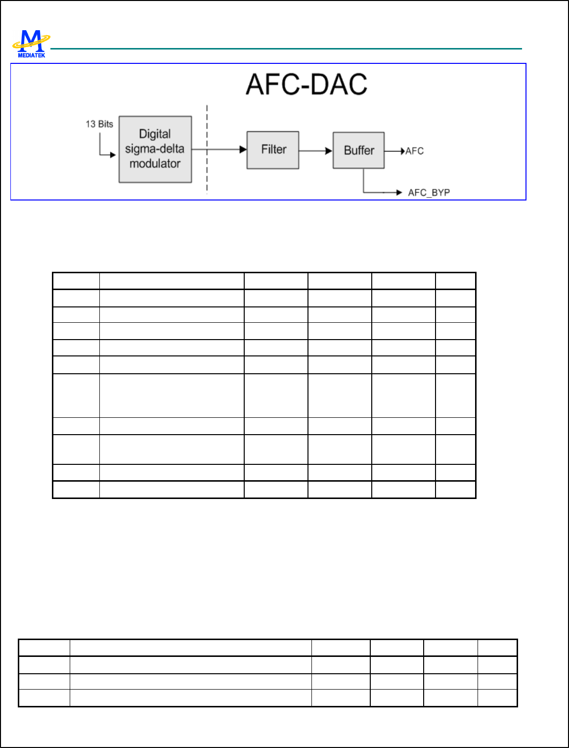
MT6217 GSM/GPRS Baseband Processor Data Sheet Revision 1.01
316/349 MediaTek Inc. Confidential
Figure 77 Block diagram of AFC-DAC
12.1.3.2 Functional Specifications
The following table gives the electrical specification of AFC-DAC.
Symbol Parameter Min Typical Max Unit
N Resolution 13 Bit
FS Sampling Rate 6500 KHz
DVDD Digital Power Supply 1.6 1.8 2.0 V
AVDD Analog Power Supply 2.6 2.8 3.1 V
T Operating Temperature 0 60 125 ℃
Current Consumption
Power-up
Power-Down
1.2
1 mA
µA
Output Swing 0.75*AVDD V
Output Resistor
(in AFC output RC network)
1 KO
DNL Differential Nonlinearity +1/-1 LSB
INL Integral Nonlinearity +4.0/-4.0 LSB
Table 44 Functional specification of AFC-DAC
12.1.4 APC-DAC
12.1.4.1 Block Descriptions
The APC-DAC is a 10-bits DAC with output buffer aimed for automatic power control. Here blow are its analog pin
assignment and functional specification tables.
12.1.4.2 Function Specifications
Symbol Parameter Min Typical Max Unit
N Resolution 10 Bit
FS Sampling Rate 1.0833 MSPS
SINAD Signal to Noise and Distortion Ratio 50 dB
MT6217 GSM/GPRS Baseband Processor Data Sheet Revision 1.01
317/349 MediaTek Inc. Confidential
(10-KHz Sine with 1.0V Swing & 100-KHz BW)
99% Settling Time (Full Swing on Maximal Capacitance) 5 µS
Output Swing AVDD-0.2 V
Output Capacitance 200 pF
Output Resistance 10 KO
DNL Differential Nonlinearity +/- 0.5 LSB
INL Integral Nonlinearity +/- 1.0 LSB
OE Offset Error +/- 10 mV
FSE Full Swing Error +/- 10 mV
DVDD Digital Power Supply 1.6 1.8 2.0 V
AVDD Analog Power Supply 2.5 2.8 3.1 V
T Operating Temperature 0 60 125 ℃
Current Consumption
Power-up
Power-Down
600
1
µA
µA
Table 45 APC-DAC Specifications
12.1.5 Auxiliary ADC
12.1.5.1 Block Descriptions
The auxilia ry ADC includes the following functional blocks:
1. Analog Multiplexer: The analog multiplexer selects signal from one of the seven auxiliary input pins. Real word
message to be monitored, like temperature, should be transferred to the voltage domain.
2. 10 bits A/D Converter: The ADC converts the multiplexed input signal to 10-bit digital data.
12.1.5.2 Function Specifications
The functional specifications of the auxiliary ADC are listed in the following table.
Symbol Parameter Min Typical Max Unit
N Resolution 10 Bit
FC Clock Rate 0.1 1.0833 5 MHz
FS Sampling Rate @ N-Bit 5/(N+1) MSPS
Input Swing 1.0 AVDD V
VREFP Positive Reference Voltage
(Defined by AUX_REF pin)
1.0 AVDD V
CIN Input Capacitance
Unselected Channel
Selected Channel
50
1.2
fF
pF
RIN Input Resistance
Unselected Channel
Selected Channel
10
1.8
MO
MO
MT6217 GSM/GPRS Baseband Processor Data Sheet Revision 1.01
318/349 MediaTek Inc. Confidential
RS Resistor String Between AUX_REF pin & ground
Power Up
Power Down
35
10
50 65 KO
MO
Clock Latency 11 1/FC
DNL Differential Nonlinearity +0.5/-0.5 LSB
INL Integral Nonlinearity +1.0/-1.0 LSB
OE Offset Error +/- 10 mV
FSE Full Swing Error +/- 10 mV
SINAD Signal to Noise and Distortion Ratio (10-KHz Full
Swing Input & 13-MHz Clock Rate)
50 dB
DVDD Digital Power Supply 1.6 1.8 2.0 V
AVDD Analog Power Supply 2.5 2.8 3.1 V
T Operating Temperature 0 60 125 ℃
Current Consumption
Power-up
Power-Down
300
1
µA
µA
Table 46 The Functional specification of Auxiliary ADC
12.1.6 Audio mixed-signal blocks
12.1.6.1 Block Descriptions
Audio mixed-signal blocks (AMB) integrate complete voice uplink/downlink and audio playback functions. As shown in
the following figure, it includes mainly three parts. The first consists of stereo audio DACs and speaker amplifiers for audio
playback. The second is the voice downlink path, including voice-band DACs and amplifiers, which produces voice signal
to earphone or other auxiliary output device. Amplifiers in these two blocks are equipped with multiplexers to accept
signals from internal audio/voice or external radio sources. The last is the voice uplink path, which is the interface between
microphone (or other auxiliary input device) input and MT6217 DSP. A set of bias voltage is provided for external electret
microphone..
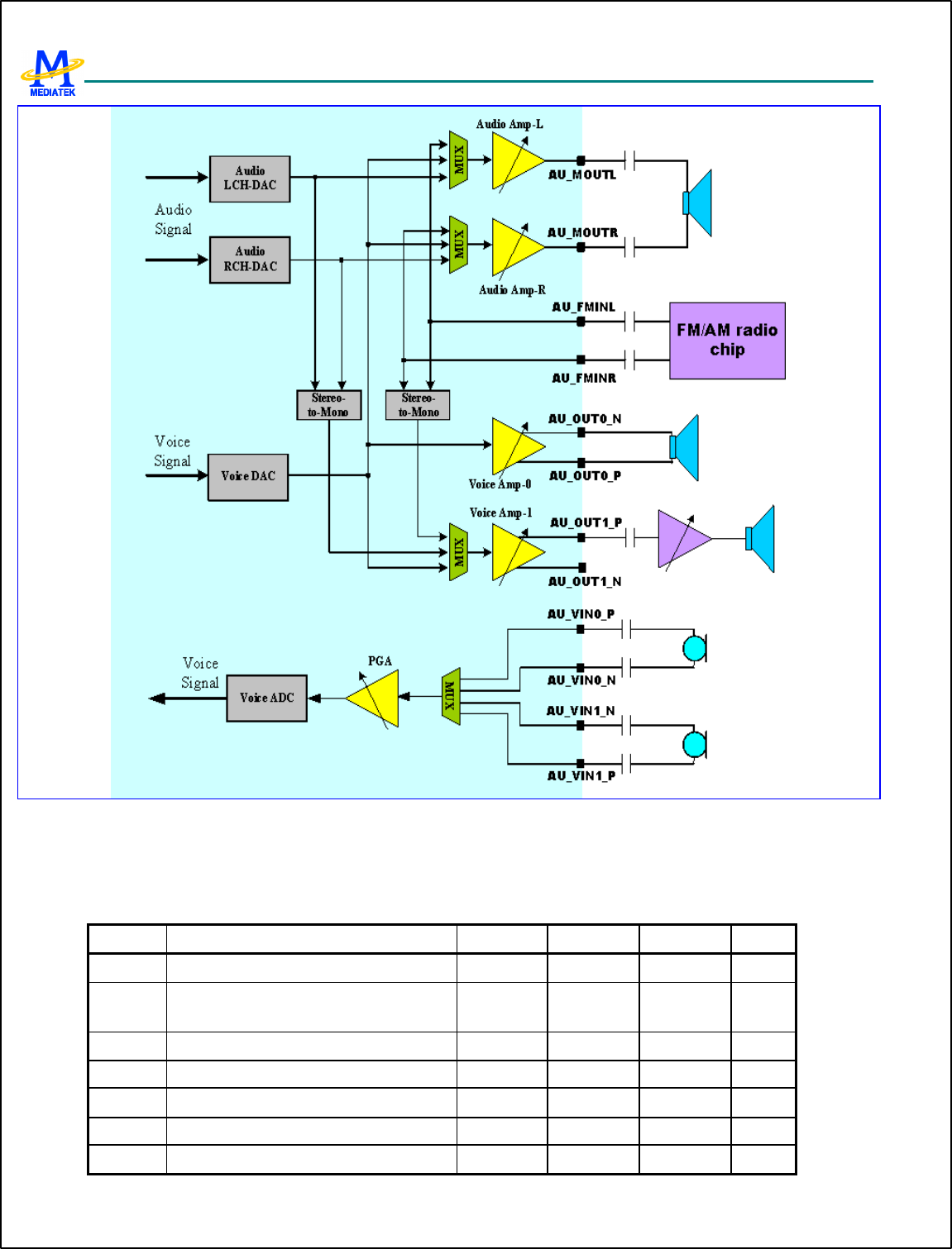
MT6217 GSM/GPRS Baseband Processor Data Sheet Revision 1.01
319/349 MediaTek Inc. Confidential
Figure 78 Block diagram of audio mixed-signal blocks.
12.1.6.2 Functional Specifications
The following table gives functional specifications of voice-band uplink/downlink blocks.
Symbol Parameter Min Typical Max Unit
FS Sampling Rate 4096 KHz
CREF Decoupling Cap Between AU_VREF_P
And AU_VREF_N
47 NF
DVDD Digital Power Supply 1.6 1.8 2.0 V
AVDD Analog Power Supply 2.5 2.8 3.1 V
T Operating Temperature 0 60 125 ℃
IDC Current Consumption 5 mA
VMIC Microphone Biasing Voltage 1.9 V
MT6217 GSM/GPRS Baseband Processor Data Sheet Revision 1.01
320/349 MediaTek Inc. Confidential
IMIC Current Draw From Microphone Bias
Pins
2 mA
Uplink Path6
SINAD Signal to Noise and Distortion Ratio
Input Level: -40 dbm0
Input Level: 0 dbm0
29
69
dB
dB
RIN Input Impedance (Differential) 13 20 27 KO
ICN Idle Channel Noise -67 dBm0
XT Crosstalk Level -66 dBm0
Downlink Path7
SINAD Signal to Noise and Distortion Ratio
Input Level: -40 dBm0
Input Level: 0 dBm0
29
69
dB
dB
RLOAD Output Resistor Load (Differential) 28 O
CLOAD Output Capacitor Load 200 pF
ICN Idle Channel Noise of Transmit Path -67 dBm0
XT Crosstalk Level on Transmit Path -66 dBm0
Table 47 Functional specifications of analog voice blocks
Functional specifications of the audio blocks are described in the following.
Symbol Parameter Min Typical Max Unit
FCK Clock Frequency Fs*128 KHz
Fs Sampling Rate 32 44.1 48 KHz
AVDD Power Supply 2.6 2. 8 3.1 V
T Operating Temperature 0 60 125 ℃
IDC Current Consumption 5 mA
PSNR Peak Signal to Noise Ratio 80 dB
DR Dynamic Range 80 dB
VOUT Output Swing for 0dBFS Input Level 0.85 Vrms
THD Total Harmonic Distortion
-40
-60
dB
6 For uplink-path, not all gain setting of VUPG meets the specification listed on table, especially for the several highest
gains. The maximum gain that meets the specification is to be determined.
7 For downlink-path, not all gain setting of VDPG meets the specification listed on table, especially for the several lowest
gains. The minimum gain that meets the specification is to be determined.
MT6217 GSM/GPRS Baseband Processor Data Sheet Revision 1.01
321/349 MediaTek Inc. Confidential
45mW at 16 O Load
22mW at 32 O Load
dB
RLOAD Output Resistor Load (Single-Ended) 16 O
CLOAD Output Capacitor Load 200 pF
XT L-R Channel Cross Talk TBD dB
Table 48 Functional specifications of the analog audio blocks
12.1.7 Clock Squarer
12.1.7.1 Block Descriptions
For most VCXO, the output clock waveform is sinusoidal with too small amplitude (about several hundred mV) to make
MT6217 digital circuits function well. Clock squarer is designed to convert such a small signal to a rail-to-rail clock signal
with excellent duty-cycle. It provides also a pull-down function when the circuit is powered-down.
12.1.7.2 Function Specifications
The functional specification of clock squarer is shown in Table 49.
Symbol Parameter Min Typical Max Unit
Fin Input Clock Frequency 13 MHz
Fout Ou tput Clock Frequency 13 MHz
Vin Input Signal Amplitude 500 AVDD mVpp
DcycIN Input Signal Duty Cycle 50 %
DcycOUT Output Signal Duty Cycle DcycIN-5 DcycIN+5 %
TR Rise Time on Pin CLKSQOUT 5 ns/pF
TF Fall Time on Pin CLKSQOUT 5 ns/pF
DVDD Dig ital Power Supply 1.3 1.5 1.7 V
AVDD Analog Power Supply 2.5 2.8 3.1 V
T Operating Temperature 0 60 125 ℃
Current Consumption TBD ?A
Table 49 The Functional Specification of Clock Squarer
12.1.7.3 Application Notes
Here below in the figure is an equivalent circuit of the clock squarer. Please be noted that the clock squarer is designed to
accept a sinusoidal input signal. If the input signal is not sinusoidal, its harmonic distortion should be low enough to not
produce a wrong clock output. As an reference, for a 13MHz sinusoidal signal input with amplitude of 0.2V the harmonic
distortion should be smaller than 0.02V.
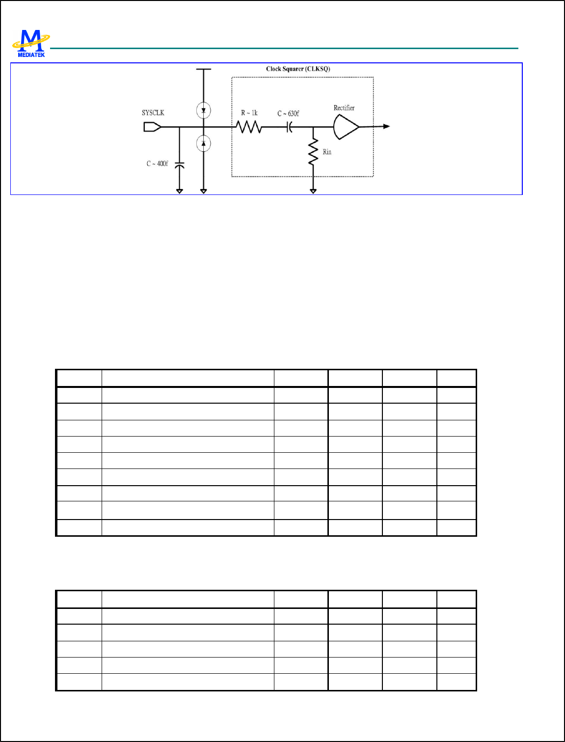
MT6217 GSM/GPRS Baseband Processor Data Sheet Revision 1.01
322/349 MediaTek Inc. Confidential
Figure 79 Equivalent circuit of Clock Squarer.
12.1.8 Phase Locked Loop
12.1.8.1 Block Descriptions
MT6217 includes three PLLs: DSP PLL, MCU PLL, and USB PLL. DSP PLL and MCU PLL are identical and
programmable to provide either 52MHz or 78 MHz output clock while accepts 13MHz signal. USB PLL is designed to
accept 4MHz input clock signal and provides 48MHz output clock.
12.1.8.2 Function Specifications
The functional specification of DSP/MCU PLL is shown in the following table.
Symbol Parameter Min Typical Max Unit
Fin Input Clock Frequency 13 MHz
Fout Output Clock Frequency 52 78 MHz
Lock-in Time TBD ?s
Output Clock Duty Cycle 40 50 60 %
Output Clock Jitter 650 ps
DVDD Digital Power Supply 1.6 1.8 2.0 V
AVDD Analog Power Supply 2.5 2.8 3.1 V
T Operating Temperature 0 60 125 ℃
Current Consumption TBD µA
Table 50 The Functional Specification of DSP/MCU PLL
The functional specification of USB PLL is shown below.
Symbol Parameter Min Typical Max Unit
Fin Input Clock Frequency 4 MHz
Fout Output Clock Frequency 48 MHz
Lock-in Time TBD µs
Output Clock Duty Cycle 40 50 60 %
Output Clock Jitter 650 ps
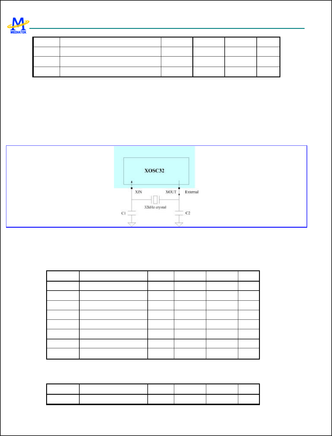
MT6217 GSM/GPRS Baseband Processor Data Sheet Revision 1.01
323/349 MediaTek Inc. Confidential
DVDD Digital Power Supply 1.3 1.5 1.7 V
AVDD Analog Power Supply 2.5 2.8 3.1 V
T Operating Temperature 0 60 125 ℃
Current Consumption TBD µA
Table 51 The Functional Specification of USB PLL
12.1.9 32-KHz Crystal Oscillator
12.1.9.1 Block Descriptions
The low-power 32-KHz crystal oscillator XOSC32 is designed to work with an external piezoelectric 32.768kHz crystal
and a load composed of two functional capacitors, as shown in the following figure.
Figure 80 Block diagram of XOSC32
12.1.9.2 Functional specifications
The functional specification of XOSC32 is shown in the following table.
Symbol Parameter Min Typical Max Unit
AVDDRTC Analog power supply 1.2 1.5 2 V
Tosc Start-up time 5 sec
Dcyc Duty cycle 50 %
TR Rise time on XOSCOUT TBD ns/pF
TF Fall time on XOSCOUT TBD ns/pF
Current consumption 5 µA
Leakage current 1 µA
T Operating temperature 0 60 125 ℃
Table 52 Functional Specification of XOSC32
Here below are a few recommendations for the crystal parameters for use with XOSC32.
Symbol Parameter Min Typical Max Unit
F Frequency range 32768 Hz
MT6217 GSM/GPRS Baseband Processor Data Sheet Revision 1.01
324/349 MediaTek Inc. Confidential
GL Drive level 5 uW
?f/f Frequency tolerance +/- 20 Ppm
ESR Series resistance 50 K?
C0 Static capacitance 1.6 pF
CL8 Load capacitance 6 12.5 pF
Table 53 Recommended Parameters of the 32kHz crystal
12.2 MCU Register Definitions
12.2.1 BBRX
MCU APB bus registers for BBRX ADC are listed as followings.
MIXED+0300h BBRX ADC Analog-Circuit Control Register BBRX_AC_CON
Bit 15 14 13 12 11 10 9 8 7 6 5 4 3 2 1 0
Name
QSEL ISEL RSV PDNC
HP GAIN CALBIAS
Type R/W R/W R/W R/W R/W R/W
Reset
00 00 0 0 0 00000
Set this register for analog circuit configuration controls.
CALBIAS The register field is for control of biasing current in BBRX mixed-signal module. It is coded in 2’s complement.
That is, its maximum is 15 and minimum is –16. Biasing current in BBRX mixed-signal module has impact on
the performance of A/D conversion. The larger the value of the register field, the larger the biasing current in
BBRX mixed-signal module, and the larger the SNR.
GAIN The register bit is for configuration of gain control of analog inputs in GSM RX mixed-signal module. When the
bit is set to 1, gain control for analog inputs will be turned on and thus GSM RX mixed-signal module can provide
higher resolutions. When the bit is set to 0, gain control for analog inputs will be turned off and thus GSM RX
mixed-signal module can only provide lower resolutions.
0 Gain control for analog inputs in GSM RX mixed-signal module will be turned off.
1 Gain control for analog inputs in GSM RX mixed-signal module will be turned on.
PDNCHP Power down control for charge pumping of GSM RX ADC.
0 Power down charge pumping of GSM RX ADC.
1 Power up charge pumping of GSM RX ADC.
ISEL Loopback configuration selection for I-channel in BBRX mixed-signal module
00 Normal mode
01 Loopback TX analog I
10 Loopback TX analog Q
11 Select the grounded input
QSEL Loopback configuration selection for Q-channel in BBRX mixed-signal module
00 Normal mode
8 CL is the parallel combination of C1 and C2 in the block diagram.

MT6217 GSM/GPRS Baseband Processor Data Sheet Revision 1.01
325/349 MediaTek Inc. Confidential
01 Loopback TX analog Q
10 Loopback TX analog I
11 Select the grounded input
12.2.2 BBTX
MCU APB bus registers for BBTX DAC are listed as followings.
MIXED+0400h BBTX DAC Analog-Circuit Control Register 0 BBTX_AC_CON
0
Bit 15 14 13 12 11 10 9 8 7 6 5 4 3 2 1 0
Name
CALR
CDON
E
STAR
TCAL
RC GAIN CALRCSEL TRIMI TRIMQ
Type R R/W R/W R/W R/W R/W
Reset
0 0 000 000 0000 0000
Set this register for analog circuit configuration controls. The procedure to perform calibration processing for smoothing
filter in BBTX mixed-signal module is as follows:
7. Write 1 to the register bit CARLC in the register TX_CON of Baseband Front End in order to activate clock
required for calibration process. Initiate calibration process.
8. Write 1 to the register bit STARTCALRC. Start calibration process.
9. Read the register bit CALRCDONE. If read as 1, then calibration process finished. Otherwise repeat the step.
10. Write 0 to the register bit STA RTCALRC. Stop calibration process.
11. Write 0 to the register bit CARLC in the register TX_CON of Baseband Front End in order to deactivate clock
required for calibration process. Terminate calibration process.
12. The result of calibration process can be read from the register field CALRCOUT of the register
BBTX_AC_CON1. Software can set the value to the register field CALRCSEL for 3-dB cutoff frequency
selection of smoothing filter in DAC of BBTX.
Remember to set the register field CALRCCONT of the register BBTX_AC_CON1 to 0xb before the calibration process. It
only needs to be set once.
TRIMQ The register field is used to control gain trimming of Q-channel DAC in BBTX mixed-signal module. It is coded
in 2’s complement, that is, with maximum 15 and minimum –16.
TRIMI The register field is used to control gain trimming of I-channel DAC in BBTX mixed-signal module. It is coded in
2’s complement, that is, with maximum 15 and minimum –16.
CALRCSEL The register field is for selection of cutoff frequency of smoothing filter in BBTX mixed-signal module.
It is coded in 2’s complement. That is, its maximum is 3 and minimum is –4.
GAIN The register field is used to control gain of DAC in BBTX mixed-signal module. It has impact on both of I- and
Q-channel DAC in BBTX mixed-signal module. It is coded in 2’s complement, that is, with maximum 3 and
minimum –4.
STARTCALRC Whenever 1 is writing to the bit, calibration process for smoothing filter in BBTX mixed-signal module
will be triggered. Once the calibration process is completed, the register bit CARLDONE will be read as 1.
MT6217 GSM/GPRS Baseband Processor Data Sheet Revision 1.01
326/349 MediaTek Inc. Confidential
CALRCDONE The register bit indicates if calibration process for smoothing filter in BBTX mixed-signal module has
finished. When calibration processing finishes, the register bit will be 1. When the register bit STARTCALRC is
set to 0, the register bit becomes 0 again.
MIXED+0404h BBTX DAC Analog-Circuit Control Register 1 BBTX_AC_CON
1
Bit 15 14 13 12 11 10 9 8 7 6 5 4 3 2 1 0
Name
CALRCOUT FLOA
T CALRCCNT CALBIAS CMV
Type R R/W R/W R/W R/W
Reset
- 0 0000 00000 000
Set this register for analog circuit configuration controls.
CMV The register field is used to control common voltage in BBTX mixed -signal module. It is coded in 2’s complement,
that is, with maximum 3 and minimum –4.
CALBIAS The register field is for control of biasing current in BBTX mixed-signal module. It is coded in 2’s
complement. That is, its maximum is 15 and minimum is –16. Biasing current in BBTX mixed-signal module has
impact on performance of D/A conversion. Larger the value of the register field, the larger the biasing current in
BBTX mixed-signal module.
CALRCCNT Parameter for calibration process of smoothing filter in BBTX mixed-signal module. Default value is
eleven. Note that it is NOT coded in 2’s complement. Therefore the range of its value is from 0 to 15. Remember
to set it to 0xb before BBTX calibration process. It only needs to be set once.
FLOAT The register field is used to have the outputs of DAC in BBTX mixed-signal module float or not.
CALRCOUT After calibration processing for smoothing filter in BBTX mixed-signal module, a set of 3-bit value is
obtained. It is coded in 2’s complement.
12.2.3 AFC DAC
MCU APB bus registers for AFC DAC are listed as follows.
MIXED+0500h AFC DAC Analog-Circuit Control Register AFC_AC_CON
Bit 15 14 13 12 11 10 9 8 7 6 5 4 3 2 1 0
Name
TEST PDN_
CHPU
MP CALI
Type R/W R/W R/W
Reset
0 0 0
Set this register for analog circuit configuration controls. Please refer to analog functional specification for more details.
TEST test control
PDN_CHPUMP charge pump power down
CALI biasing current control
12.2.4 APC DAC
MCU APB bus registers for APC DAC are listed as followings.
MT6217 GSM/GPRS Baseband Processor Data Sheet Revision 1.01
327/349 MediaTek Inc. Confidential
MIXED+0600h APC DAC Analog-Circuit Control Register APC_AC_CON
Bit 15 14 13 12 11 10 9 8 7 6 5 4 3 2 1 0
Name
BYP CALI
Type R/W R/W
Reset
0 0
Set this register for analog circuit configuration controls. Please refer to analog functional specification for more details.
BYP bypass output buffer
CALI biasing current control
12.2.5 Auxiliary ADC
MCU APB bus registers for AUX ADC are listed as followings.
MIXED+0700h Auxiliary ADC Analog-Circuit Control Register AUX_AC_CON
Bit 15 14 13 12 11 10 9 8 7 6 5 4 3 2 1 0
Name
CALI
Type R/W
Reset
0
Set this register for analog circuit configuration controls. Please refer to analog functional specification for more details.
CALI biasing current control
12.2.6 Voice Front-end
MCU APB bus registers for speech are listed as followings.
MIXED+0100h AFE Voice Analog Gain Control Register AFE_VAG_CON
Bit 15 14 13 12 11 10 9 8 7 6 5 4 3 2 1 0
Name
VUPG VDPG0 VDPG1
Type R/W R/W R/W
Reset
0000 0000 0000
Set this register for analog PGA gains. VUPG is set for microphone input volume control. And VDPG0 and VDPG1 are set
for two output volume controls
VUPG voice-band up-link PGA gain control bitsVDPG0 voice-band down-link PGA0 gain control bits
VDPG1 voice-band down -link PGA1 gain control bits
MIXED+0104h AFE Voice Analog-Circuit Control Register 0 AFE_VAC_CON0
Bit 15 14 13 12 11 10 9 8 7 6 5 4 3 2 1 0
Name
VCFG VDSEND VCALI
Type R/W R/W R/W
Reset
0000 00 00000
Set this register for analog circuit configuration controls.
VCFG[3] microphone biasing control
0 differential biasing

MT6217 GSM/GPRS Baseband Processor Data Sheet Revision 1.01
328/349 MediaTek Inc. Confidential
1 single-ended biasing
VCFG[2] gain mode control
0 amplification
1 attenuation
VCFG[1] coupling control
0 AC
1 DC
VCFG[0] input select control
0 input 0
1 input 1
VDSEND[1]single-ended configuration control for out1
VDSEND[0]single-ended configuration control for out0
VCALI biasing current control, in 2’s complement format
MIXED+0108h AFE Voice Analog-Circuit Control Register 1 AFE_VAC_CON1
Bit 15 14 13 12 11 10 9 8 7 6 5 4 3 2 1 0
Name
VBG_CTRL VPDN
_CHP
UMP
VFLO
AT VRSD
ON VRES
SW VBUF
0SEL VBUF1SEL VADC
INMO
DE
VDAC
INMO
DE
Type R/W R/W R/W R/W R/W R/W R/W R/W R/W
Reset
000 0 0 0 0 0 000 0 0
Set this register for analog circuit configuration controls. There are several loop back modes and test modes implemented
for test purposes. Suggested value is 0084h.
VBG_CTRL voice-band band-gap control
VPDN_CHPUMP voice-band charge pump power down
0: power down (normal operating mode)
1: charge pump on (for fab. process)
VFLOAT voice-band output driver float
0: normal operating mode
1: float mode
VRSDON voice-band redundant signed digit function on
0: 1-bit 2-level mode
1: 2-bit 3-level mode
VRESSW voice-band output buffer 1 output DC voltage control.
VBUF0SEL voice buffer 0 input selection (reserved.)
VBUF1SEL voice buffer 1 input selection
001: voice DAC output
010: external FM radio input
100: audio DAC output
OTHERS: reserved.
VADCINMODE Voice-band ADC output mode.
0: normal operating mode
1: the ADC input from the DAC output
MT6217 GSM/GPRS Baseband Processor Data Sheet Revision 1.01
329/349 MediaTek Inc. Confidential
VDACINMODE Voice-band DAC input mode.
0: normal operating mode
1: the DAC input from the ADC output
MIXED+010Ch AFE Voice Analog Power Down Control Register AFE_VAPDN_C
ON
Bit 15 14 13 12 11 10 9 8 7 6 5 4 3 2 1 0
Name
VPDN
_BIAS
VPDN
_LNA VPDN
_ADC VPDN
_DAC
VPDN
_OUT
1
VPDN
_OUT
0
Type R/W R/W R/W R/W R/W R/W
Reset
0 0 0 0 0 0
Set this register to power up analog blocks. 0: power down, 1: power up.
VPDN_BIAS bias block
VPDN_LNAlow noise amplifier block
VPDN_ADC ADC block
VPDN_DAC DAC block
VPDN_OUT1 OUT1 buffer block
VPDN_OUT0 OUT0 buffer block
MIXED+0110h AFE Voice AGC Control Register AFE_VAGC_CO
N
Bit 15 14 13 12 11 10 9 8 7 6 5 4 3 2 1 0
Name
AGCT
EST RELNOIDUR
SEL RELNOILEV
SEL FRELCKSEL
SRELCKSEL
ATTTHDCAL ATTC
KSEL HYST
EREN AGCE
N
Type R/W R/W R/W R/W R/W R/W R/W R/W R/W
Reset
0 00 00 00 00 00 0 0 0
Set this register for analog circuit configuration controls. There are several loop back modes and test modes implemented
for test purposes. Suggested value is 0dcfh.
AGCEN AGC function enable
HYSTEREN AGC hysteresis function enable
ATTCKSEL attack clock selection
0: 16 KHz
1: 32 KHz
ATTTHDCAL attack threshold calibration
SRELCKSEL release slow clock selection
00: 1000/512 Hz
01: 1000/256 Hz
10: 1000/128 Hz
11 : 1000/64 Hz
FRELCKSEL release fast clock selection
00: 1000/64 Hz
01: 1000/32 Hz
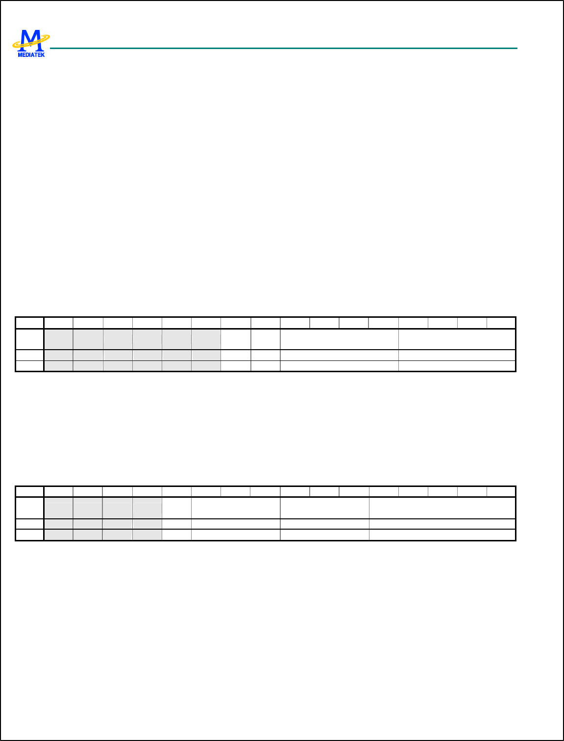
MT6217 GSM/GPRS Baseband Processor Data Sheet Revision 1.01
330/349 MediaTek Inc. Confidential
10: 1000/16 Hz
11 : 1000/8 Hz
RELNOILEVSEL release noise level selection
00: -8 dB
01: -14 dB
10: -20 dB
11 : -26 dB
RELNOIDURSEL release noise duration selection
00: 64 ms
01: 32 ms
10: 16 ms
11 : 8 ms, 32768/4096
12.2.7 Audio Front-end
MCU APB bus registers for audio are listed as followings.
MIXED+0200h AFE Audio Analog Gain Control Register AFE_AAG_CON
Bit 15 14 13 12 11 10 9 8 7 6 5 4 3 2 1 0
Name
AMUT
ER AMUT
EL APGR APGL
Type R/W R/W R/W R/W
Reset
0 0 0000 0000
Set this register for analog PGA gains.
AMUTER audio PGA L-channel mute control
AMUTEL audio PGA R-channel mute control
APGR audio PGA R-channel gain control
APGL audio PGA L-channel gain control
MIXED+0204h AFE Audio Analog-Circuit Control Register AFE_AAC_CON
Bit 15 14 13 12 11 10 9 8 7 6 5 4 3 2 1 0
Name
ARCO
N ABUFSELR ABUFSELL ACALI
Type R/W R/W R/W R/W
Reset
0 000 000 00000
Set this register for analog circuit configuration controls .
ARCON audio external RC control
ABUFSELR audio buffer R-channel input selection
000: audio DAC R/L-channel output; stereo to mono
001: audio DAC R-channel output
010: voice DAC output
100: external FM R/L-channel radio output, stereo to mono
101: external FM R-channel radio output
OTHERS: reserved.
ABUFSELL audio buffer L-channel input selection
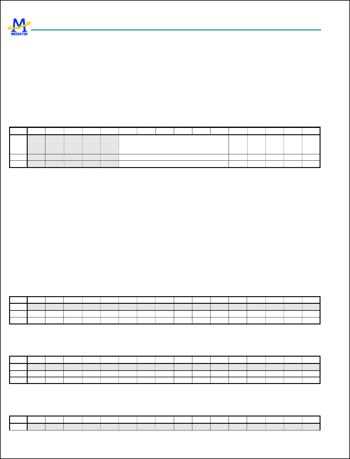
MT6217 GSM/GPRS Baseband Processor Data Sheet Revision 1.01
331/349 MediaTek Inc. Confidential
000: audio DAC R/L-channel output; stereo to mono
001: audio DAC L-channel output
010: voice DAC output
100: external FM R/L-channel radio output, stereo to mono
101: external FM L-channel radio output
OTHERS: reserved.
ACALI audio bias current control, in 2’s complement format
MIXED+0208h AFE Audio Analog Power Down Control Register AFE_AAPDN_C
ON
Bit 15 14 13 12 11 10 9 8 7 6 5 4 3 2 1 0
Name
ACNR APDN
_BIAS
APDN
_DAC
R
APDN
_DAC
L
APDN
_OUT
R
APDN
_OUT
L
Type R/W R/W R/W R/W R/W R/W
Reset
000000 0 0 0 0 0
Set this register to power up analog blocks. 0: power down, 1: power up. Suggested value is 00ffh.
ACNR audio click noise reduction
APDN_BIAS BIAS block
APDN_DACR R-channel DAC block
APDN_DACL L-channel DAC block
APDN_OUTR R-channel OUT buffer block
APDN_OUTL L-channel OUT buffer block
12.2.8 Reserved
Some registers are reserved for further extensions.
MIXED+0800h Reserved 0 Analog Circuit Control Register 0 RES0_AC_CON
0
Bit 15 14 13 12 11 10 9 8 7 6 5 4 3 2 1 0
Name
Type R/W R/W R/W R/W R/W R/W R/W R/W R/W R/W R/W R/W R/W R/W R/W R/W
Reset
0 0 0 0 0 0 0 0 0 0 0 0 0 0 0 0
MIXED+0804h Reserved 0 Analog Circuit Control Register 1 RES0_AC_CON
1
Bit 15 14 13 12 11 10 9 8 7 6 5 4 3 2 1 0
Name
Type R/W R/W R/W R/W R/W R/W R/W R/W R/W R/W R/W R/W R/W R/W R/W R/W
Reset
0 0 0 0 0 0 0 0 0 0 0 0 0 0 0 0
MIXED+0900h Reserved 1 Analog Circuit Control Register 0 RES1_AC_CON
0
Bit 15 14 13 12 11 10 9 8 7 6 5 4 3 2 1 0
Name
MT6217 GSM/GPRS Baseband Processor Data Sheet Revision 1.01
332/349 MediaTek Inc. Confidential
Type R/W R/W R/W R/W R/W R/W R/W R/W R/W R/W R/W R/W R/W R/W R/W R/W
Reset
0 0 0 0 0 0 0 0 0 0 0 0 0 0 0 0
MIXED+0904h Reserved 1 Analog Circuit Control Register 1 RES1_AC_CON
1
Bit 15 14 13 12 11 10 9 8 7 6 5 4 3 2 1 0
Name
Type R/W R/W R/W R/W R/W R/W R/W R/W R/W R/W R/W R/W R/W R/W R/W R/W
Reset
0 0 0 0 0 0 0 0 0 0 0 0 0 0 0 0
MIXED+0A00h Reserved 2 Analog Circuit Control Register 0 RES2_AC_CON
0
Bit 15 14 13 12 11 10 9 8 7 6 5 4 3 2 1 0
Name
Type R/W R/W R/W R/W R/W R/W R/W R/W R/W R/W R/W R/W R/W R/W R/W R/W
Reset
0 0 0 0 0 0 0 0 0 0 0 0 0 0 0 0
MIXED+0A04h Reserved 2 Analog Circuit Control Register 1 RES2_AC_CON
1
Bit 15 14 13 12 11 10 9 8 7 6 5 4 3 2 1 0
Name
Type R/W R/W R/W R/W R/W R/W R/W R/W R/W R/W R/W R/W R/W R/W R/W R/W
Reset
0 0 0 0 0 0 0 0 0 0 0 0 0 0 0 0
MIXED+0B00h Reserved 3 Analog Circuit Control Register 0 RES3_AC_CON
0
Bit 15 14 13 12 11 10 9 8 7 6 5 4 3 2 1 0
Name
Type R/W R/W R/W R/W R/W R/W R/W R/W R/W R/W R/W R/W R/W R/W R/W R/W
Reset
0 0 0 0 0 0 0 0 0 0 0 0 0 0 0 0
MIXED+0B04h Reserved 3 Analog Circuit Control Register 1 RES3_AC_CON
1
Bit 15 14 13 12 11 10 9 8 7 6 5 4 3 2 1 0
Name
Type R/W R/W R/W R/W R/W R/W R/W R/W R/W R/W R/W R/W R/W R/W R/W R/W
Reset
0 0 0 0 0 0 0 0 0 0 0 0 0 0 0 0
MIXED+0C00h Reserved 4 Analog Circuit Control Register 0 RES4_AC_CON
0
Bit 15 14 13 12 11 10 9 8 7 6 5 4 3 2 1 0
Name
Type R/W R/W R/W R/W R/W R/W R/W R/W R/W R/W R/W R/W R/W R/W R/W R/W
Reset
0 0 0 0 0 0 0 0 0 0 0 0 0 0 0 0
MT6217 GSM/GPRS Baseband Processor Data Sheet Revision 1.01
333/349 MediaTek Inc. Confidential
MIXED+0C04h Reserved 4 Analog Circuit Control Register 1 RES4_AC_CON
1
Bit 15 14 13 12 11 10 9 8 7 6 5 4 3 2 1 0
Name
Type R/W R/W R/W R/W R/W R/W R/W R/W R/W R/W R/W R/W R/W R/W R/W R/W
Reset
0 0 0 0 0 0 0 0 0 0 0 0 0 0 0 0
MIXED+0D00h Reserved 5 Analog Circuit Control Register 0 RES5_AC_CON
0
Bit 15 14 13 12 11 10 9 8 7 6 5 4 3 2 1 0
Name
Typ e R/W R/W R/W R/W R/W R/W R/W R/W R/W R/W R/W R/W R/W R/W R/W R/W
Reset
0 0 0 0 0 0 0 0 0 0 0 0 0 0 0 0
MIXED+0D04h Reserved 5 Analog Circuit Control Register 1 RES5_AC_CON1
Bit 15 14 13 12 11 10 9 8 7 6 5 4 3 2 1 0
Name
Type R/W R/W R/W R/W R/W R/W R/W R/W R/W R/W R/W R/W R/W R/W R/W R/W
Reset
0 0 0 0 0 0 0 0 0 0 0 0 0 0 0 0
MIXED+0E00h Reserved 6 Analog Circuit Control Register 0 RES6_AC_CON0
Bit 15 14 13 12 11 10 9 8 7 6 5 4 3 2 1 0
Name
Type R/W R/W R/W R/W R/W R/W R/W R/W R/W R/W R/W R/W R/W R/W R/W R/W
Reset
0 0 0 0 0 0 0 0 0 0 0 0 0 0 0 0
MIXED+0E04h Reserved 6 Analog Circuit Control Register 1 RES6_AC_CON1
Bit 15 14 13 12 11 10 9 8 7 6 5 4 3 2 1 0
Name
Type R/W R/W R/W R/W R/W R/W R/W R/W R/W R/W R/W R/W R/W R/W R/W R/W
Reset
0 0 0 0 0 0 0 0 0 0 0 0 0 0 0 0
MIXED+0F00h Reserved 7 Analog Circuit Control Register 0 RES7_AC_CON0
Bit 15 14 13 12 11 10 9 8 7 6 5 4 3 2 1 0
Name
Type R/W R/W R/W R/W R/W R/W R/W R/W R/W R/W R/W R/W R/W R/W R/W R/W
Reset
0 0 0 0 0 0 0 0 0 0 0 0 0 0 0 0
MIXED+0F04h Reserved 7 Analog Circuit Control Register 1 RES7_AC_CON1
Bit 15 14 13 12 11 10 9 8 7 6 5 4 3 2 1 0
Name
Type R/W R/W R/W R/W R/W R/W R/W R/W R/W R/W R/W R/W R/W R/W R/W R/W
Reset
0 0 0 0 0 0 0 0 0 0 0 0 0 0 0 0
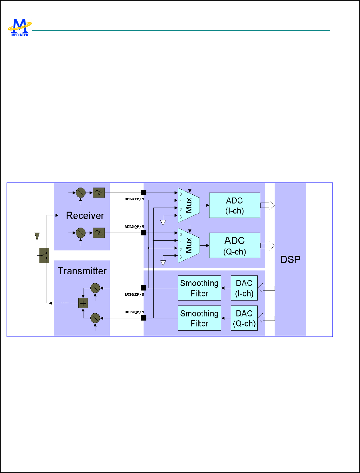
MT6217 GSM/GPRS Baseband Processor Data Sheet Revision 1.01
334/349 MediaTek Inc. Confidential
12.3 Programming Guide
12.3.1 BBRX Register Setup
The register used to control analog base-band receiver is BBRX_AC_CON.
12.3.1.1 Programmable Biasing Current
To maximize the yield in modern digital process, the receiver features providing 5-bit 32-level programmable current to
bias internal analog blocks. The 5-bits registers CALBIAS [4:0] is coded with 2’s complement format.
12.3.1.2 Offset / Gain Calibration
The base-band downlink receiver (RX), together with the base-band uplink transmitter (TX) introduced in the next section,
provides necessary analog hardware for DSP algorithm to correct the mismatch and offset error. The connection for
measurement of both RX/TX mismatch and gain error is shown in Figure 81, and the corresponding calibration procedure
is described below.
Figure 81 Base-band A/D and D/A Offset and Gain Calibration
12.3.1.3 Downlink RX Offset Error Calibration
The RX offset measurement is achieved by selecting grounded input to A/D converter (set ISEL [1:0] =’11’ and QSEL [1:0]
=’11’ to select channel 3 of the analog input multiplexer, as shown in Figure 82. The output of the ADC is sent to DSP for
further offset cancellation. The offset cancellation accuracy depends on the number of samples being converted. That is,
more accurate measurement can be obtained by collecting more samples followed by averaging algorithm.
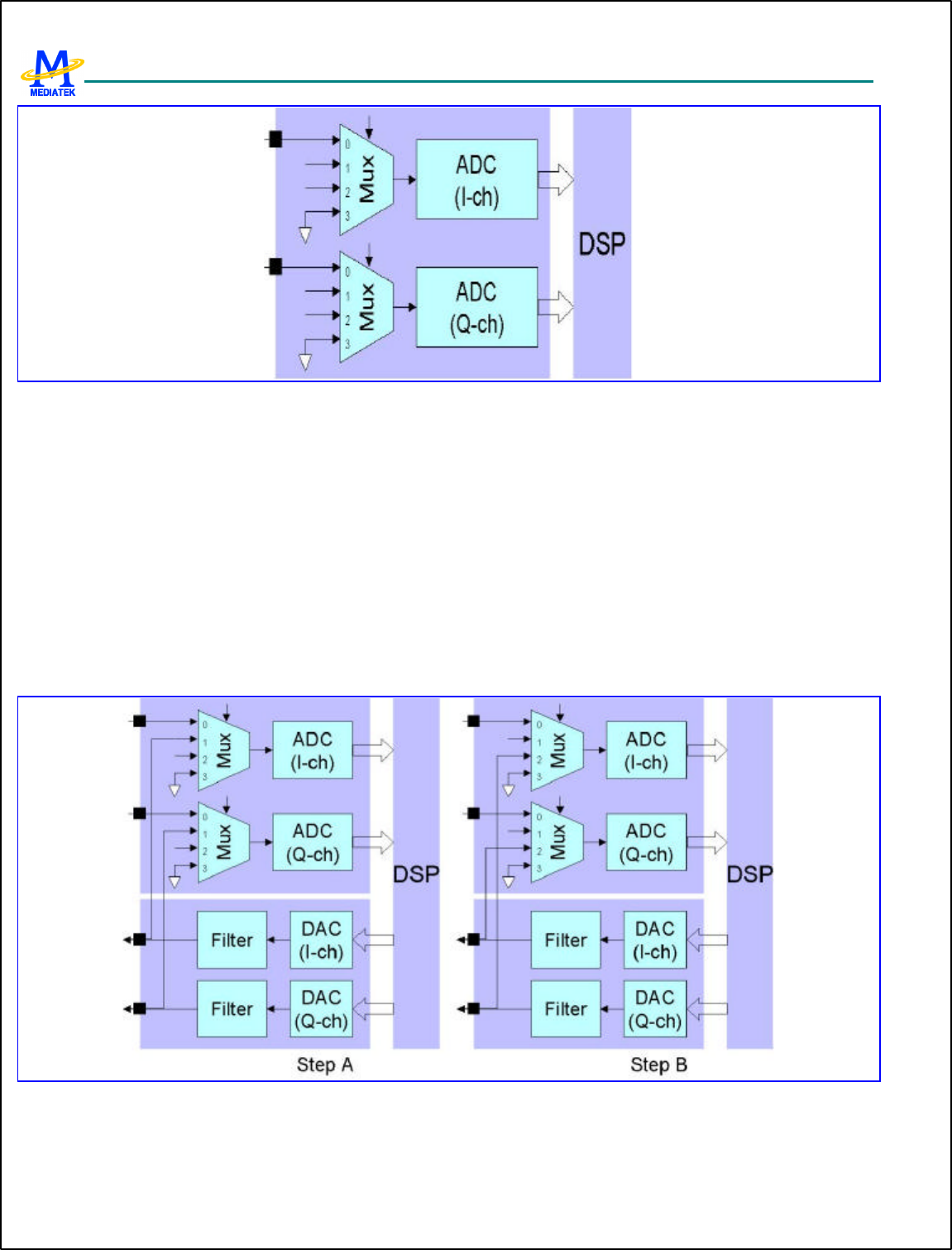
MT6217 GSM/GPRS Baseband Processor Data Sheet Revision 1.01
335/349 MediaTek Inc. Confidential
Figure 82 Downlink ADC Offset Error Measurement
12.3.1.4 Downlink RX and Uplink TX Gain Error Calibration
To measure the gain mismatch error, both I/Q uplink TXs should be programmed to produce full-scale pure sinusoidal
waves output. Such signals are then fed to downlink RX for A/D conversion, in the following two steps.
A. The uplink I-channel output are connected to the downlink I-channel input, and the uplink Q-channel output are
connected to the downlink Q-channel input. This can be achieved by setting ISEL [1:0] =’01’ and QSEL [1:0] =’01’
(shown in Figure 83 (A))..
B. The uplink I-channel output are then connected to the downlink Q-channel input, and the uplink Q-channel output are
connected to the downlink I-channel input. This can be achieved by setting ISEL [1:0] =’10’ and QSEL [1:0] =’10’
(shown in Figure 83 (B)).
Figure 83 Downlink RX and Up-link TX Gain Mismatch Measurement (A) I/Q TX connect to I/Q RX (B) I/Q TX connect
to Q/I RX

MT6217 GSM/GPRS Baseband Processor Data Sheet Revision 1.01
336/349 MediaTek Inc. Confidential
Once above successive procedures are completed, RX/TX gain mismatch could be easily obtained because the amplitude
mismatch on RX digitized result in step A and B is the sum and difference of RX and TX gain mismatch, respectively.
The gain error of the downlink RX can be corrected in the DSP section and the uplink TX gain error can be corrected by the
gain trimming facility that TX block provide.
12.3.1.5 Uplink TX Offset Error Calibration
Once the offset of the downlink RX is known and corrected, the offset of the uplink TX alone could be easily estimated.
The offset error of TX should be corrected in the digital domain by means of the programmable feature of the digital
GMSK modulator.
Finally, it is important that above three calibration procedures should be exercised in order, that is, correct the RX offset
first, then RX/TX gain mismatch, and finally TX offset. This is owing to that analog gain calibration in TX will affect its
offset, while the digital offset correction has no effect on gain.
12.3.2 BBTX Register Setup
The register used to control analog base-band transmitter is BBTX_AC_CON0 and BBTX_AC_CON1 .
12.3.2.1 Output Gain Control
The output swing of the uplink transmitter is controlled by register GAIN [2:0] coded in 2’s complement with about 2dB
step. When TRIMI [3:0] / TRIMQ [3:0] = 0 the swing is listed in Table 54, defined to be the difference between positive
and negative output signal.
GAIN [2:0] Output Swing For AVDD=2.8 (V)
+3 (011) AVDD*0.900 (+6.02 dB) 2.52
+2 (010) AVDD*0.720 (+4.08 dB) 2.02
+1 (001) AVDD*0.576 (+2.14 dB) 1.61
+0 (000) AVDD*0.450 (+0.00 dB) 1.26
-1 (111) AVDD*0.360 (-1.94 dB) 1
-2 (110) AVDD*0.288 (-3.88 dB) 0.81
-3 (101) AVDD*0.225 (-6.02 dB) 0.63
-4 (100) AVDD*0.180 ( -7.95 dB) 0.5
Table 54 Output Swing Control Table
12.3.2.2 Output Gain Trimming
I/Q channels can also be trimmed separately to compensate gain mismatch in the base-band transmitter or the whole
transmission path including RF module. The gain trimming is adjusted in 16 steps spread from –1.18dB to +1.18dB (Table
55 ), compared to the full-scale range set by GAIN [2:0].
TRIMI [3:0] / TRIMQ [3:0] Gain Step (dB)
+7 (0111) 1.18
MT6217 GSM/GPRS Baseband Processor Data Sheet Revision 1.01
337/349 MediaTek Inc. Confidential
+6 (0110) 1.00
+5 (0101) 0.83
+4 (0100) 0.66
+3 (0011) 0.49
+2 (0010) 0.32
+1 (0001) 0.16
+0 (0000) 0.00
-1 (1111) -0.16
-2 (1110) -0.31
-3 (1101) -0.46
-4 (1100) -0.61
-5 (1011) -0.75
-6 (1010) -0.90
-7 (1001) -1.04
-8 (1000) -1.18
Table 55 Gain Trimming Control Table
12.3.2.3 Output Common-Mode Voltage
The output common-mode voltage is controlled by CMV [2:0] with about 0.08*AVDD step, as listed in the following table.
CMV [2:0] Common-Mode Voltage
+3 (011) AVDD*0.62
+2 (010) AVDD*0.58
+1 (001) AVDD*0.54
+0 (000) AVDD*0.50
-1 (111) AVDD*0.46
-2 (110) AVDD*0.42
-3 (101) AVDD*0.38
-4 (100) AVDD*0.34
Table 56 Output Common-Mode Voltage Control Table
12.3.2.4 Programmable Biasing Current
The transmitter features providing 5-bit 32-level programmable current to bias internal analog blocks. The 5-bits registers
CALBIAS [4:0] is coded with 2’s complement format.
12.3.2.5 Smoothing Filter Characteristic
The 2nd –order Butterworth smoothing filter is used to suppress the image at DAC output: it provides more than 40dB
attenuation at the 4.44MHz sampling frequency. To tackle with the digital process component variation, programmable
cutoff frequency control bits CALRCSEL [2:0] are included. User can directly change the filter cut-off frequency by

MT6217 GSM/GPRS Baseband Processor Data Sheet Revision 1.01
338/349 MediaTek Inc. Confidential
different CALRCSEL value (coded with 2’s complement format and with a default value 0). In addition, an internal
calibration process is provided, by setting START CALRC to high and CALRCCNT to an appropriate value (default is 11).
After the calibration process, the filter cut-off frequency is calibrated to 350kHz +/- 50 kHz and a new CALRCOUT value
is stored in the register. During the calibration process, the output of the cell is high-impedance.
12.3.3 AFC-DAC Register Setup
The register used to control the APC DAC is AFC_AC_CON, which providing 5-bit 32-level programmable current to bias
internal analog blocks. The 5-bits registers CALI [4:0] is coded with 2’s complement format.
12.3.4 APC-DAC Register Setup
The register used to control the APC DAC is AFC_AC_CON, which providing 5-bit 32-level programmable current to bias
internal analog blocks. The 5-bits registers CALI [4:0] is coded with 2’s complement format.
12.3.5 Auxiliary A/D Conversion Register Setup
The register used to control the Aux-ADC is AUX_AC_CON. For this register, which providing 5-bit 32-level
programmable current to bias internal analog blocks. The 5-bits registers CALI [4:0] is coded with 2’s complement
format.
12.3.6 Voice-band Blocks Register Setup
The registers used to control AMB are AFE_VAG_CON, AFE_VAC_CON0, AFE_VAC_CON1, and AFE_VAPDN_CON.
For these registers, please refer to chapter “Analog Chip Interface”
12.3.6.1 Reference Circuit
The voice-band blocks include internal bias circuits, a differential bandgap voltage reference circuit and a differential
microphone bias circuit. Internal bias current could be calibrated by varying VCALI[4:0] (coded with 2’s complement
format).
The differential bandgap circuit generates a low temperature dependent voltage for internal use. For proper operation, there
should be an external 47nF capacitor connected between differential output pins AU_VREFP and AU_VREFN. The
bandgap voltage (~1.24V9, typical) also defines the dBm0 reference level through out the audio mixed-signal blocks. The
following table illustrates typical 0dBm0 voltage when uplink/downlink programmable gains are unity. For other gain
setting, 0dBm0 reference level should be scaled accordingly.
Symbol Parameter Min Typical Max Unit
V0dBm0,UP 0dBm0 Voltage for Uplink Path, Applied
Differentially Between Positive and
Negative Microphone Input Pins
0.2V V-rms
V0dBm0,Dn 0dBm0 voltage for Downlink Path, 0.6V V-rms
9 The bandgap voltage could be calibrated by adjusting control signal VBG_CTRL[1:0]. Its default value is [00].
VBG_CTRL not only adjust the bandgap voltage but also vary its temperature dependence. Optimal value of VBG_CTRL
is to be determined.
MT6217 GSM/GPRS Baseband Processor Data Sheet Revision 1.01
339/349 MediaTek Inc. Confidential
Appeared Differentially Between Positive
and Negative Power Amplifier Output Pins
Table 57 0dBm0 reference level for unity uplink/downlink gain
The microphone bias circuit generates a differential output voltage between AU_MICBIAS_P and AU_MICBIAS_N for
external electret type microphone. Typical output voltage is 1.9 V. In singled-ended mode, by set VCFG[3] =1,
AU_MICBIAS_N is pull down while output voltage is present on AU_MICBIAS_P, respect to ground. The max current
supplied by microphone bias circuit is 2mA.
12.3.6.2 Uplink Path
Uplink path of voice-band blocks includes an uplink programmable gain amplifier and a sigma -delta modulator.
12.3.6.2.1 Uplink Programmable Gain Amplifier
Input to the PGA is a multiplexer controlled by VCFG [3:0], as described in the following table. In normal operation, both
input AC and DC coupling are feasible for attenuation the input signal (gain <= 0dB). However, only AC coupling is
suggested if amplification of input signal is desired (gain>=0dB).
Control
Signal Function Descriptions
VCFG [0] Input Selector 0: Input 0 (From AU_VIN0_P / AU_VIN0_N) Is Selected
1: Input 1 (From AU_VIN1_P / AU_VIN1_N) Is Selected
VCFG [1] Coupling Mode 0: AC Coupling
1: DC Coupling
VCFG [2] Gain Mode 0: Amplification Mode (gain >= 0 dB)
1: Attenuation Mode (gain <= 0dB)
VCFG [3] Microphone
Biasing 0: Differential Biasing (Take Bias Voltage Between AU_MICBIAS_P
and AU_MICBIAS_N)
1: Signal-Ended Biasing (Take Bias Voltage From AU_MICBIAS_P
Respected to Ground. AU_MICBIAS_N Is Connected to Ground)
Table 58 Uplink PGA input configuration setting
The PGA itself provides programmable gain (through VUPG [3:0]) with step of 3dB, as listed in the following table.
VCFG [2] =’0’ VCFG [2] =’1’
VUPG [3:0] Gain VUPG [3:0] Gain
1111 NA X111 -21dB
1110 42dB X110 -18dB
1101 39dB X101 -15dB
1100 36dB X100 -12dB
1011 33dB X011 -9dB
1010 30dB X010 -6dB
1001 27dB X001 -3dB
1000 24dB X000 0dB
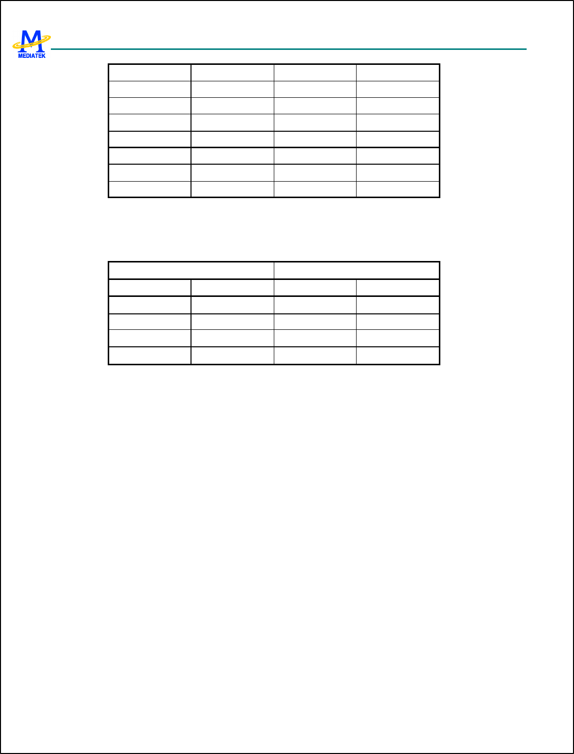
MT6217 GSM/GPRS Baseband Processor Data Sheet Revision 1.01
340/349 MediaTek Inc. Confidential
0111 21dB
0110 18dB
0101 15dB
0100 12dB
0011 9dB
0010 6dB
0001 3dB
0000 0dB
Table 59 Uplink PGA gain setting (VUPG [3:0])
The following table illustrates typically the 0dBm0 voltage applied at the microphone inputs, differentially, for several gain
settings.
VCFG [2] =’0’ VCFG [2] =’1’
VUPG [3:0] 0dBm0 (V-rms) VUPG [3:0] 0dBm0 (V-rms)
1100 3.17mV X110 1.59V
1000 12.6mV X100 0.8V
0100 50.2mV X010 0.4V
0000 0.2V X000 0.2V
Table 60 0dBm0 voltage at microphone input pins
12.3.6.2.2 Sigma-Delta Modulator
Analog-to-digital conversion in uplink path is made with a second-order sigma-delta modulator (SDM) whose sampling
rate is 4096kHz. Output signals are coded in either one-bit or RSD format, optionally controlled by VRSDON register.
For test purpose, one can set VADCINMODE to HI to form a look-back path from downlink DAC output to SDM input.
The default value of VADCINMODE is zero.
12.3.6.3 Downlink Path
Downlink path of voice-band blocks includes a digital to analog converter (DAC) and two programmable output power
amplifiers.
12.3.6.3.1 Digital to Analog Converter
The DAC converts input bit-stream to analog signal by sampling rate of 4096kHz. . Besides, it performs a 2nd-order 40kHz
butterworth filtering. The DAC receives input signals from MT6217 DSP by set VDACINMODE = 0. It can also take
inputs from SDM output by setting VDACINMODE = 1.
12.3.6.3.2 Downlink Programmable Power Amplifier
Voice-band analog blocks include two identical output power amplifiers with programmable gain. Amplifier 0 and amplifier
1 can be configured to either differential or single-ended mode by adjusting VDSEND [0] and VDSEND [1], respectively.
In single-ended mode, when VDSEND[0] =1, output signal is present at AU_VOUT0_P pin respect to ground. Same as
VDSEND[1] for AU_VOUT1_P pin.
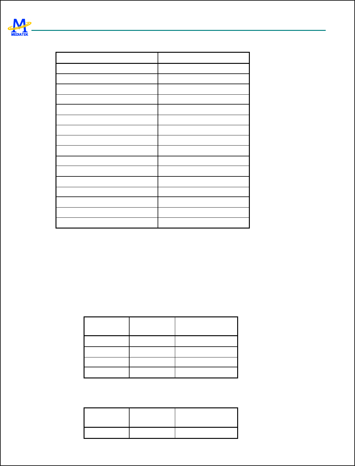
MT6217 GSM/GPRS Baseband Processor Data Sheet Revision 1.01
341/349 MediaTek Inc. Confidential
For the amplifier itself, programmable gain setting is described in the following table.
VDPG0 [3:0] / VDPG1 [3:0] Gain
1111 8dB
1110 6dB
1101 4dB
1100 2dB
1011 0dB
1010 -2dB
1001 -4dB
1000 -6dB
0111 -8dB
0110 -10dB
0101 -12dB
0100 -14dB
0011 -16dB
0010 -18dB
0001 -20dB
0000 -22dB
Table 61 Downlink power amplifier gain setting
Control signal VFLOAT, when set to ‘HI’, is used to make output nodes totally floatin g in power down mode. If VFLOAT
is set to ‘LOW” in power down mode, there will be a resistor of 50k ohm (typical) between AU_VOUT0_P and
AU_VOUT0_N, as well as between AU_VOUT0_P and AU_VOUT0_N.
The amplifiers deliver signal power to drive external earphone. The minimum resistive load is 28 ohm and the upper limit
of the output current is 50mA. On the basis that 3.14dBm0 digital input signal into downlink path produces DAC output
differential voltage of 0.87V-rms (typical), the following table illustrates the power amplifier output signal level (in V-rms)
and signal power for an external 32 ohm resistive load.
VDPG Output Signal
Level (V-rms) Output Signal Power
(mW / dBm)
0010 0.11 0.37/-4.3
0110 0.27 2.28/3.6
1010 0.69 14.8/11.7
1110 1.74 94.6/19.8
Table 62 Output signal level/power for 3.14dBm0 input. External resistive load = 32 ohm
The following table illustrates the output signal level and power for different resistive load when VDPG =1110.
RLOAD Output Signal
Level (V-rms) Output Signal Power
(mW / dBm)
30 1.74 101/20
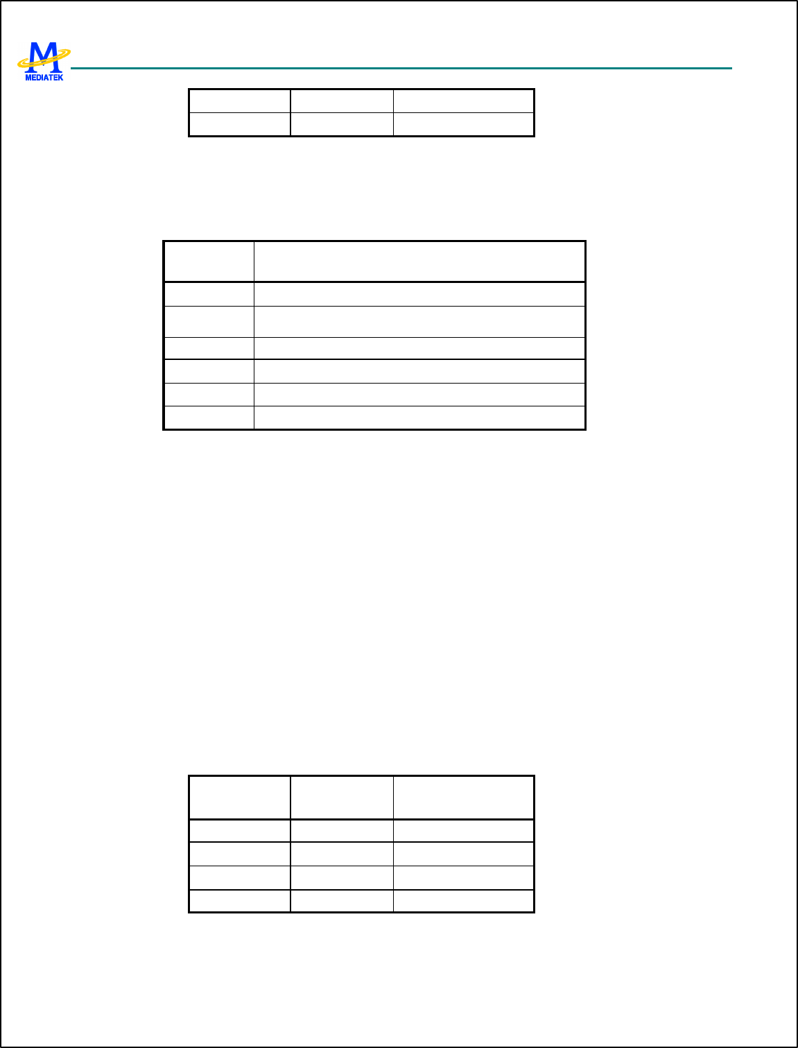
MT6217 GSM/GPRS Baseband Processor Data Sheet Revision 1.01
342/349 MediaTek Inc. Confidential
100 1.74 30.3/14.8
600 1.74 5/7
Table 63 Output signal level/power for 3.14dBm0 input, VDPG =1110
12.3.6.4 Power Down Control
Each block inside audio mixed-signal blocks features dedicated power-down control, as illustrated in the following table.
Control
Signal Descriptions
VPDN_BIAS Power Down Reference Circuits (Active Low)
VPDN_LNA Power Down Uplink PGA (Active Low)
VPDN_ADC Power Down Uplink SDM (Active Low)
VPDN_DAC Power Down DAC (Active Low)
VPDN_OUT0 Power Down Downlink Power Amp 0 (Active Low)
VPDN_OUT1 Power Down Downlink Power Amp 1 (Active Low)
Table 64 Voice-band blocks power down control
12.3.7 Audio-band Blocks Register Setup
The registers used to control audio blocks are AFE_AAG_CON, AFE_AAC_CON, and AFE_AAPDN_CON. For these
registers, please refer to chapter “Analog Chip Interface”
12.3.7.1 Output Gain Control
Audio blocks include stereo audio DACs and programmable output power amplifiers. The DACs convert input bit-stream
to analog signal by sampling rate of Fs*128 where Fs could be 32kHz, 44.1kHz, or 48kHz. Besides, it performs a 2nd-order
butterworth filtering. The two identical output power amplifiers with programmable gain are designed to driving external
AC-coupled single-end speaker. The minimum resistor load is 16 ohm and the maximum driving current is 50mA. The
programmable gain setting, controlled by APGR[] and APGL[] , is the same as that of the voice-band amplifiers.
Unlike voice signals, 0dBFS defines the full-scale audio signals amplitude. Based on bandgap reference voltage again, the
following table illustrates the power amplifier output signal level (in V-rms) and signal power for an external 16 ohm
resistive load.
APGR[]/
APGL[]
Output Signal
Level (V-rms)
Output Signal Power
(mW / dBm)
0010 0.055 0.19/-7.2
0110 0.135 1.14/0.6
1010 0.345 7.44/8.7
1110 0.87 47.3/16.7
Table 65 Output signal level/power for 0dBFS input. External resistive load = 16 ohm
MT6217 GSM/GPRS Baseband Processor Data Sheet Revision 1.01
343/349 MediaTek Inc. Confidential
12.3.7.2 Mute Function and Power Down Control
By setting AMUTER (AMUTEL) to high, right (Left) channel output will be muted.
Each block inside audio mixed-signal blocks features dedicated power-down control, as illustrated in the following table.
Control Signal Descriptions
APDN_BIAS Power Down Reference Circuits (Active Low)
APDN_DACL Power Down L-Channel DAC (Active Low)
APDN_DACR Power Down R-Channel DAC (Active Low)
APDN_OUTL Power Down L-Channel Audio Amplifier (Active Low)
APDN_OUTR Power Down R-Channel Audio Amplifier (Active Low)
Table 66 Audio-band blocks power down control
12.3.8 Multiplexers for Audio and Voice Amplifiers
The audio/voice amplifiers feature accepting signals from various signal sources including AU_FMINR/AU_FMINL pins,
that aimed to receive stereo AM/FM signal from external radio chip:
1) Voice-band amplifier 0 accepts signals from voice DAC output only.
2) Voice-band amplifier 1 accepts signal from either voice DAC, audio DAC, or AM/FM radio input pins (controlled
by register VBUF1SEL[] ). For the last two cases, left and right channel signals will be summed together to form a
mono signal first.
3) Audio left/right channel amplifiers receive signals from either voice DAC, audio DAC, or AM/FM radio input pins
(controlled by registers ABUFSELL[] and ABUFSELR[] ), too. Left and right channel amplifiers will produce
identical output waveforms when receiving mono signals from voice DAC.
12.3.9 Clock Squarer Register Setup
The register used to control clock squarer is CLK_CON. For this register, please refer to chapter “Clocks”
CLKSQ_PLD is used to bypass the clock squarer.
12.3.10 Phase-Locked Loop Register Setup
For registers control the PLL, please refer to chapter “Clocks” and “Software Power Down Control”
12.3.10.1 Frequency Setup
The DSP/MCU PLL itself could be programmable to output either 52MHz or 78MHz clocks. Accompanied with additional
digital dividers, 13/26/39/52/65/78 MHz clock outputs are supported.
12.3.10.2 Programmable Biasing Current
The PLLs feature providing 5-bit 32-level programmable current to bias internal analog blocks. The 5-bits registers CALI
[4:0] is coded with 2’s complement format.

MT6217 GSM/GPRS Baseband Processor Data Sheet Revision 1.01
344/349 MediaTek Inc. Confidential
12.3.11 32-khz Crystal Oscillator Register Setup
For registers that control the oscillator, please refer to chapter “Real Time Clock” and “Software Power Down Control”.
XOSCCALI[4:0] is the calibration control registers of the bias current, and is coded with 2’s complement format.
1 CL is the parallel combination of C1 and C2 in the block diagram.

MT6217 GSM/GPRS Baseband Processor Data Sheet Revision 1.01
345/349 MediaTek Inc. Confidential
13 Digital Pin Electrical Characteristics
l Based on Vio = 3.3 V
l Vil (max) = 0.8 V
l Vih (min) = 2.0 V
Ball PU/PD Resistor
13X13 Name Dir Driving Iol & Ioh
Typ (mA)
Vol at Iol
Max (V)
Voh at Ioh
Min (V) Pull Min Typ Max
Cin
(pF)
E4 JTRST# I PD 40K 75K 190K 5.2
E3 JTCK I PU 40K 75K 190K 5.2
E2 JTDI I PU 40K 75K 190K 5.2
E1 JTMS I PU 40K 75K 190K 5.2
F5 JTDO O 4 0.4 2.4 5.2
F4 JRTCK O 4 0.4 2.4 5.2
F3 BPI_BUS0 O 2/8 0.4 2.4 5.2
F2 BPI_BUS1 O 2/8 0.4 2.4 5.2
G5 BPI_BUS2 O 2/8 0.4 2.4 5.2
G4 BPI_BUS3 O 2/8 0.4 2.4 5.2
G3 BPI_BUS4 O 2 0.4 2.4 5.2
G2 BPI_BUS5 O 2 0.4 2.4 5.2
G1 BPI_BUS6 IO 2 0.4 2.4 PD 40K 75K 190K 5.2
H5 BPI_BUS7 IO 2 0.4 2.4 PD 40K 75K 190K 5.2
H4 BPI_BUS8 IO 2 0.4 2.4 PD 40K 75K 190K 5.2
H3 BPI_BUS9 IO 2 0.4 2.4 PD 40K 75K 190K 5.2
H1 BSI_CS0 O 2 0.4 2.4 5.2
J5 BSI_DATA O 2 0.4 2.4 5.2
J4 BSI_CLK O 2 0.4 2.4 5.2
R3 PWM1 IO 2 0.4 2.4 PD 40K 75K 190K 5.2
R2 PWM2 IO 2 0.4 2.4 PD 40K 75K 190K 5.2
T4 ALERTER IO 2 0.4 2.4 PD 40K 75K 190K 5.2
J3 LSCK IO 2/4/6/8 0.4 2.4 PD 40K 75K 190K 5.2
J2 LSA0 IO 2/4/6/8 0.4 2.4 PD 40K 75K 190K 5.2
J1 LSDA IO 2/4/6/8 0.4 2.4 PD 40K 75K 190K 5.2
K4 LSCE0# IO 2/4/6/8 0.4 2.4 PU 40K 75K 190K 5.2
K3 LSCE1# IO 2/4/6/8 0.4 2.4 PU 40K 75K 190K 5.2
K2 LPCE1# IO 2/4/6/8 0.4 2.4 PU 40K 75K 190K 5.2
L5 LPCE0# O 2/4/6/8 0.4 2.4 5.2
L4 LRST# O 2/4/6/8 0.4 2.4 5.2
L3 LRD# O 2/4/6/8 0.4 2.4 5.2
L2 LPA0 O 2/4/6/8 0.4 2.4 5.2
L1 LWR# O 2/4/6/8 0.4 2.4 5.2
L11 NLD15 IO 2/4/6/8 0.4 2.4 PD 40K 75K 190K 5.2
L10 NLD14 IO 2/4/6/8 0.4 2.4 PD 40K 75K 190K 5.2

MT6217 GSM/GPRS Baseband Processor Data Sheet Revision 1.01
346/349 MediaTek Inc. Confidential
K11 NLD13 IO 2/4/6/8 0.4 2.4 PD 40K 75K 190K 5.2
L9 NLD12 IO 2/4/6/8 0.4 2.4 PD 40K 75K 190K 5.2
J11 NLD11 IO 2/4/6/8 0.4 2.4 PD 40K 75K 190K 5.2
K9 NLD10 IO 2/4/6/8 0.4 2.4 PD 40K 75K 190K 5.2
J10 NLD9 IO 2/4/6/8 0.4 2.4 PD 40K 75K 190K 5.2
J9 NLD8 IO 2/4/6/8 0.4 2.4 PD 40K 75K 190K 5.2
M5 NLD7 IO 2/4/6/8 0.4 2.4 PD 40K 75K 190K 5.2
M4 NLD6 IO 2/4/6/8 0.4 2.4 PD 40K 75K 190K 5.2
M3 NLD5 IO 2/4/6/8 0.4 2.4 PD 40K 75K 190K 5.2
N5 NLD4 IO 2/4/6/8 0.4 2.4 PD 40K 75K 190K 5.2
N4 NLD3 IO 2/4/6/8 0.4 2.4 PD 40K 75K 190K 5.2
N3 NLD2 IO 2/4/6/8 0.4 2.4 PD 40K 75K 190K 5.2
N2 NLD1 IO 2/4/6/8 0.4 2.4 PD 40K 75K 190K 5.2
N1 NLD0 IO 2/4/6/8 0.4 2.4 PD 40K 75K 190K 5.2
P5 NRNB IO 4 0.4 2.4 PU 40K 75K 190K 5.2
P4 NCLE IO 4 0.4 2.4 PD 40K 75K 190K 5.2
P3 NALE IO 4 0.4 2.4 PD 40K 75K 190K 5.2
P2 NWE# IO 4 0.4 2.4 PU 40K 75K 190K 5.2
P1 NRE# IO 4 0.4 2.4 PU 40K 75K 190K 5.2
R4 NCE0# IO 4 0.4 2.4 PU 40K 75K 190K 5.2
L18 SIMRST O 2 0.4 2.4 5.2
L17 SIMCLK O 2 0.4 2.4 5.2
K15 SIMVCC O 2 0.4 2.4 5.2
K16 SIMSEL IO 2 0.4 2.4 PD 40K 75K 190K 5.2
K17 SIMDATA IO 2 0.4 2.4 5.2
U2 GPIO0 IO 2 0.4 2.4 PD 40K 75K 190K 5.2
M19 GPIO1 IO 2 0.4 2.4 PD 40K 75K 190K 5.2
L15 GPIO2 IO 2 0.4 2.4 PD 40K 75K 190K 5.2
L16 GPIO3 IO 2 0.4 2.4 PD 40K 75K 190K 5.2
C17 GPIO4 IO 4 0.4 2.4 PD 40K 75K 190K 5.2
A19 GPIO5 IO 4 0.4 2.4 PD 40K 75K 190K 5.2
B18 GPIO6 IO 4 0.4 2.4 PD 40K 75K 190K 5.2
B17 GPIO7 IO 4 0.4 2.4 PD 40K 75K 190K 5.2
A18 GPIO8 IO 4 0.4 2.4 PD 40K 75K 190K 5.2
A17 GPIO9 IO 4 0.4 2.4 PD 40K 75K 190K 5.2
U1 SYSRST# I 5.2
R18 WATCHDOG# O 4 0.4 2.4 5.2
T3 SRCLKENAN O 2 0.4 2.4 5.2
T1 SRCLKENA O 2 0.4 2.4 5.2
T2 SRCLKENAI IO 2 0.4 2.4 PD 40K 75K 190K 5.2
D3 TESTMODE I PD 40K 75K 190K 5.2
E5 IBOOT I 5.2
G17 KCOL6 I PU 40K 75K 190K 5.2
G18 KCOL5 I PU 40K 75K 190K 5.2

MT6217 GSM/GPRS Baseband Processor Data Sheet Revision 1.01
347/349 MediaTek Inc. Confidential
G19 KCOL4 I PU 40K 75K 190K 5.2
F15 KCOL3 I PU 40K 75K 190K 5.2
F16 KCOL2 I PU 40K 75K 190K 5.2
F17 KCOL1 I PU 40K 75K 190K 5.2
F18 KCOL0 I PU 40K 75K 190K 5.2
F19 KROW5 O 2 0.4 2.4 5.2
E16 KROW4 O 2 0.4 2.4 5.2
E17 KROW3 O 2 0.4 2.4 5.2
E18 KROW2 O 2 0.4 2.4 5.2
D16 KROW1 O 2 0.4 2.4 5.2
D19 KROW0 O 2 0.4 2.4 5.2
V1 EINT0 I PU 40K 75K 190K 5.2
U3 EINT1 I PU 40K 75K 190K 5.2
W1 EINT2 I PU 40K 75K 190K 5.2
V2 EINT3 I PU 40K 75K 190K 5.2
R5 MIRQ IO 4 0.4 2.4 PU 40K 75K 190K 5.2
R17 MFIQ IO 2 0.4 2.4 PU 40K 75K 190K 5.2
R16 ED0 IO 2/4/6/8/10/12/14/16 0.4 2.4 PU/PD 40K 75K 190K 5.2
R15 ED1 IO 2/4/6/8/10/12/14/16 0.4 2.4 PU/PD 40K 75K 190K 5.2
T19 ED2 IO 2/4/6/8/10/12/14/16 0.4 2.4 PU/PD 40K 75K 190K 5.2
T17 ED3 IO 2/4/6/8/10/12/14/16 0.4 2.4 PU/PD 40K 75K 190K 5.2
U19 ED4 IO 2/4/6/8/10/12/14/16 0.4 2.4 PU/PD 40K 75K 190K 5.2
U18 ED5 IO 2/4/6/8/10/12/14/16 0.4 2.4 PU/PD 40K 75K 190K 5.2
V18 ED6 IO 2/4/6/8/10/12/14/16 0.4 2.4 PU/PD 40K 75K 190K 5.2
W19 ED7 IO 2/4/6/8/10/12/14/16 0.4 2.4 PU/PD 40K 75K 190K 5.2
U17 ED8 IO 2/4/6/8/10/12/14/16 0.4 2.4 PU/PD 40K 75K 190K 5.2
V17 ED9 IO 2/4/6/8/10/12/14/16 0.4 2.4 PU/PD 40K 75K 190K 5.2
W17 ED10 IO 2/4/6/8/10/12/14/16 0.4 2.4 PU/PD 40K 75K 190K 5.2
T16 ED11 IO 2/4/6/8/10/12/14/16 0.4 2.4 PU/PD 40K 75K 190K 5.2
W16 ED12 IO 2/4/6/8/10/12/14/16 0.4 2.4 PU/PD 40K 75K 190K 5.2
T15 ED13 IO 2/4/6/8/10/12/14/16 0.4 2.4 PU/PD 40K 75K 190K 5.2
U15 ED14 IO 2/4/6/8/10/12/14/16 0.4 2.4 PU/PD 40K 75K 190K 5.2
V15 ED15 IO 2/4/6/8/10/12/14/16 0.4 2.4 PU/PD 40K 75K 190K 5.2
U14 ERD# O 2/4/6/8/10/12/14/16 0.4 2.4 5.2
W14 EWR# O 2/4/6/8/10/12/14/16 0.4 2.4 5.2
R13 ECS0# O 2/4/6/8/10/12/14/16 0.4 2.4 5.2
T13 ECS1# O 2/4/6/8/10/12/14/16 0.4 2.4 5.2
U13 ECS2# O 2/4/6/8/10/12/14/16 0.4 2.4 5.2
V13 ECS3# O 2/4/6/8/10/12/14/16 0.4 2.4 5.2
R12 ECS4# O 2/4/6/8/10/12/14/16 0.4 2.4 5.2
T12 ECS5# O 2/4/6/8/10/12/14/16 0.4 2.4 5.2
U12 ECS6# O 2/4/6/8/10/12/14/16 0.4 2.4 5.2
W12 ECS7# IO 2/4/6/8/10/12/14/16 0.4 2.4 PU 40K 75K 190K 5.2
R14 ELB# O 2/4/6/8/10/12/14/16 0.4 2.4 5.2
T14 EUB# O 2/4/6/8/10/12/14/16 0.4 2.4 5.2

MT6217 GSM/GPRS Baseband Processor Data Sheet Revision 1.01
348/349 MediaTek Inc. Confidential
T11 EPDN# O 2 0.4 2.4 5.2
U11 EADV# O 2/4/6/8/10/12/14/16 0.4 2.4 5.2
V11 ECLK O 2/4/6/8/10/12/14/16 0.4 2.4 5.2
R10 EA0 O 2/4/6/8/10/12/14/16 0.4 2.4 5.2
T10 EA1 O 2/4/6/8/10/12/14/16 0.4 2.4 5.2
U10 EA2 O 2/4/6/8/10/12/14/16 0.4 2.4 5.2
W10 EA3 O 2/4/6/8/10/12/14/16 0.4 2.4 5.2
T9 EA4 O 2/4/6/8/10/12/14/16 0.4 2.4 5.2
U9 EA5 O 2/4/6/8/10/12/14/16 0.4 2.4 5.2
V9 EA6 O 2/4/6/8/10/12/14/16 0.4 2.4 5.2
R8 EA7 O 2/4/6/8/10/12/14/16 0.4 2.4 5.2
T8 EA8 O 2/4/6/8/10/12/14/16 0.4 2.4 5.2
W8 EA9 O 2/4/6/8/10/12/14/16 0.4 2.4 5.2
R7 EA10 O 2/4/6/8/10/12/14/16 0.4 2.4 5.2
T7 EA11 O 2/4/6/8/10/12/14/16 0.4 2.4 5.2
U7 EA12 O 2/4/6/8/10/12/14/16 0.4 2.4 5.2
V7 EA13 O 2/4/6/8/10/12/14/16 0.4 2.4 5.2
R6 EA14 O 2/4/6/8/10/12/14/16 0.4 2.4 5.2
T6 EA15 O 2/4/6/8/10/12/14/16 0.4 2.4 5.2
U6 EA16 O 2/4/6/8/10/12/14/16 0.4 2.4 5.2
W6 EA17 O 2/4/6/8/10/12/14/16 0.4 2.4 5.2
T5 EA18 O 2/4/6/8/10/12/14/16 0.4 2.4 5.2
U5 EA19 O 2/4/6/8/10/12/14/16 0.4 2.4 5.2
V5 EA20 O 2/4/6/8/10/12/14/16 0.4 2.4 5.2
W5 EA21 O 2/4/6/8/10/12/14/16 0.4 2.4 5.2
V4 EA22 O 2/4/6/8/10/12/14/16 0.4 2.4 5.2
U4 EA23 O 2/4/6/8/10/12/14/16 0.4 2.4 5.2
W3 EA24 O 2/4/6/8/10/12/14/16 0.4 2.4 5.2
W2 EA25 O 2/4/6/8/10/12/14/16 0.4 2.4 5.2
P16 USB_DP IO
P17 USB_DM IO
P19 MCCM0 IO 2/4/6/8/10/12/14/16 0.4 2.4 PU/PD 40K 75K 190K 5.2
N15 MCDA0 IO 2/4/6/8/10/12/14/16 0.4 2.4 PU/PD 40K 75K 190K 5.2
N16 MCDA1 IO 2/4/6/8/10/12/14/16 0.4 2.4 PU/PD 40K 75K 190K 5.2
N17 MCDA2 IO 2/4/6/8/10/12/14/16 0.4 2.4 PU/PD 40K 75K 190K 5.2
N18 MCDA3 IO 2/4/6/8/10/12/14/16 0.4 2.4 PU/PD 40K 75K 190K 5.2
N19 MCCK O 2/4/6/8/10/12/14/16 0.4 2.4 5.2
M16 MCPWRON O 2 0.4 2.4 5.2
M17 MCWP I 2 0.4 2.4 PU 40K 75K 190K 5.2
M18 MCINS I 2 0.4 2.4 PU 40K 75K 190K 5.2
K18 URXD1 I 2 0.4 2.4 PU 40K 75K 190K 5.2
K19 UTXD1 O 2 0.4 2.4 5.2
J16 UCTS1 I 2 0.4 2.4 PU 40K 75K 190K 5.2
J17 URTS1 O 2 0.4 2.4 5.2
J18 URXD2 IO 2 0.4 2.4 PU 40K 75K 190K 5.2

MT6217 GSM/GPRS Baseband Processor Data Sheet Revision 1.01
349/349 MediaTek Inc. Confidential
J19 UTXD2 IO 2 0.4 2.4 PU 40K 75K 190K 5.2
H15 URXD3 IO 2 0.4 2.4 PU 40K 75K 190K 5.2
H16 UTXD3 IO 2 0.4 2.4 PU 40K 75K 190K 5.2
H17 IRDA_RXD IO 2 0.4 2.4 PU 40K 75K 190K 5.2
G15 IRDA_TXD IO 2 0.4 2.4 PU 40K 75K 190K 5.2
G16 IRDA_PDN IO 2 0.4 2.4 PU 40K 75K 190K 5.2
D17 DAICLK IO 4 0.4 2.4 PU 40K 75K 190K 5.2
D18 DAIPCMOUT IO 4 0.4 2.4 PU 40K 75K 190K 5.2
C19 DAIPCMIN IO 4 0.4 2.4 PU 40K 75K 190K 5.2
C18 DAIRST IO 4 0.4 2.4 PU 40K 75K 190K 5.2
B19 DAISYNC IO 4 0.4 2.4 PU 40K 75K 190K 5.2

