MTNK3N3 Datasheet. Www.s Manuals.com. Cystek
User Manual: Marking of electronic components, SMD Codes K3, K3***, K3-***, K31, K33, K3342, K3562, K3797, K3A, K3B, K3C, K3D, K3E, K3F, K3M, K3N, K3P, K3R, K3T, K3X. Datasheets 2SK3342, 2SK3562, 2SK3797, BZX384-B3V0, EM6K33, KDV804S, MMBT3906, MMBTA14, MMDT3906, MMST2222A, MMST2907A, MMST4401, MMST4403, MMSTA42, MMSTA92, MMSZ5253, MTNK3N3, RT9819C-15PV, TN0201K, UM6K31N.
Open the PDF directly: View PDF ![]() .
.
Page Count: 7
CYStech Electronics Corp.
Spec. No. : C447N3
Issued Date : 2010.08.18
Revised Date :
Page No. : 1/6
MTNK3N3 CYStek Product Specification
ESD protected N-CHANNEL MOSFET BVDSS 20V
ID 100mA
RDSON 3Ω
MTNK3N3
Description
• Low voltage drive, 1.8V
• Easy to use in parallel
• High speed switching
• ESD protected device
• Pb-free package
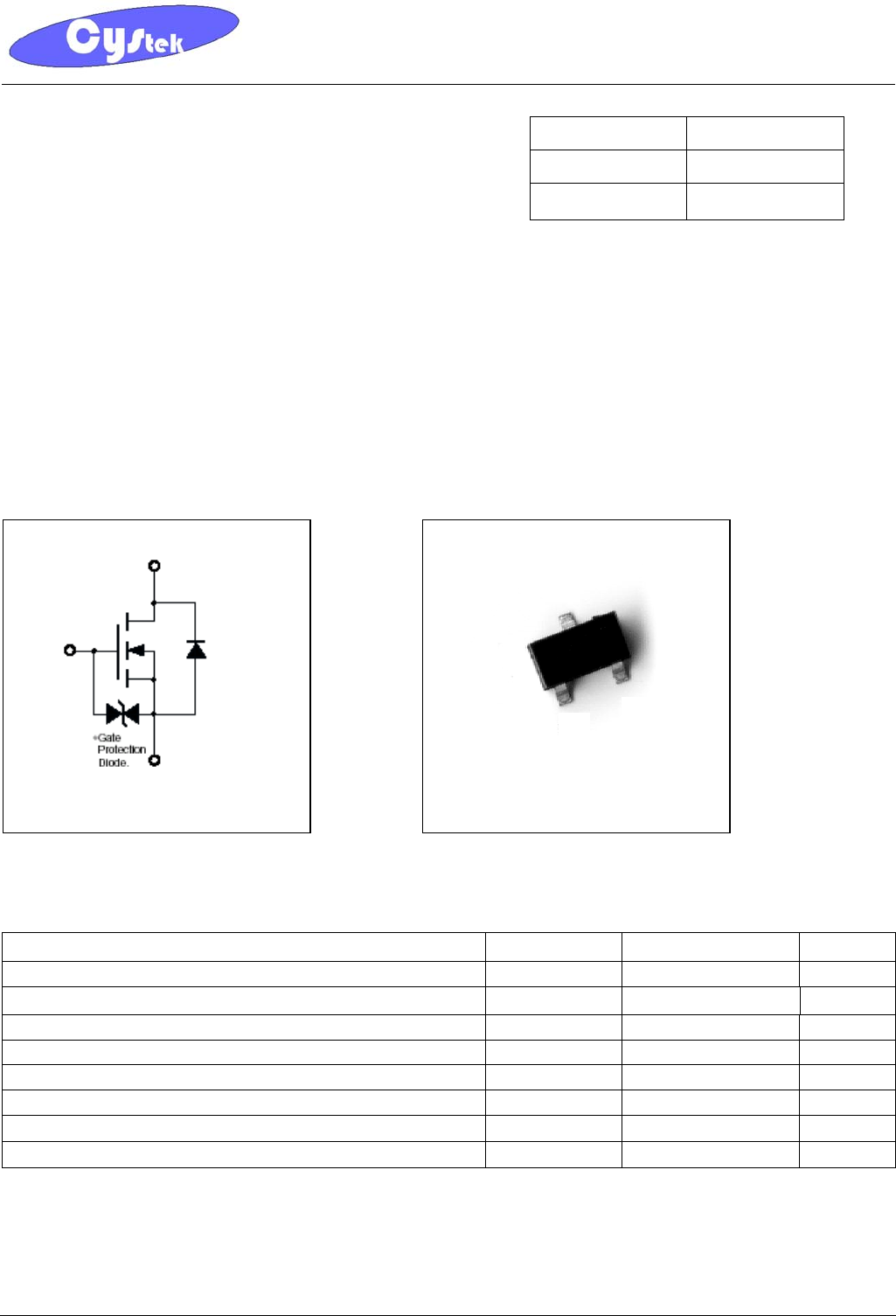
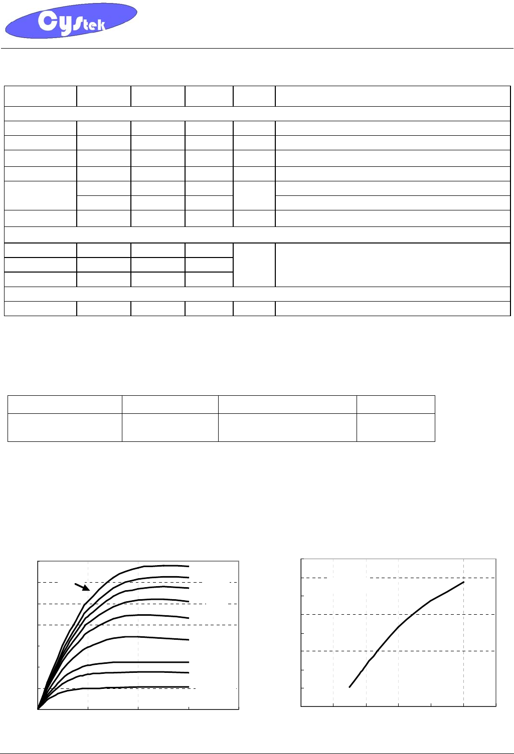
Symbol Outline
Absolute Maximum Ratings (Ta=25°C)
Parameter Symbol Limits Unit
Drain-Source Voltage BVDSS 20 V
Gate-Source Voltage VGS ±8 V
Continuous Drain Current ID 100 mA
Pulsed Drain Current IDM 400 *1 mA
Total Power Dissipation PD 300 mW
ESD susceptibility 350 *2 V
Operating Junction and Storage Temperature Range Tj -55~+150 °C
Thermal Resistance, Junction-to-Ambient Rth,ja 417 °C/W
Note : *1. Pulse Width ≤ 300μs, Duty cycle ≤2%
*2. Human body model, 1.5kΩ in series with 100pF
SOT-23 MTNK3N3
G:Gate
S:Source
D:Drain
D
G S
CYStech Electronics Corp.
Spec. No. : C447N3
Issued Date : 2010.08.18
Revised Date :
Page No. : 2/6
MTNK3N3 CYStek Product Specification
Electrical Characteristics (Ta=25°C)
Symbol Min. Typ. Max. Unit Test Conditions
Static
BVDSS 20 - - V VGS=0, ID=100μA
VGS(th) 0.5 - 1.0 V VDS=VGS, ID=250μA
IGSS - -
±1 μA VGS=±8V, VDS=0
IDSS - - 500 nA VDS=20V, VGS=0
- 1.7 3 VGS=4.5V, ID=100mA
RDS(ON) - 3.5 6
Ω VGS=1.8V, ID=20mA
GFS 100 - - mS VDS=5V, ID=100mA
Dynamic
Ciss - 23 50
Coss - 7.7 25
Crss - 5.8 5
pF VDS=10V, VGS=0, f=1MHz
Source-Drain Diode
*VSD - - 1 V VGS=0V, IS=10mA
*Pulse Test : Pulse Width ≤300μs, Duty Cycle≤2%
Ordering Information
Device Package Shipping Marking
MTNK3N3 SOT-23
(Pb-free) 3000 pcs / Tape & Reel K3
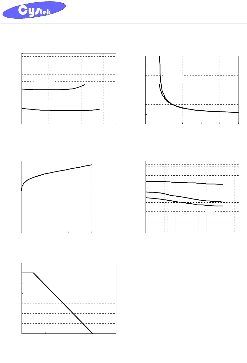
Typical Characteristics
Typical Output Characteristics
0
0.1
0.2
0.3
0.4
0.5
0.6
0.7
01234
Drain-Source Voltage -VDS(V)
Drain Current - ID(A)
VGS=1.5V
3.5V
4.5V
3V
1.8V
2.0V
2.5V
5V
4.0V
Typical Transfer Characteristics
0
0.1
0.2
0.3
0.4
0.5
0.6
0.7
0.8
0123456
Gate-Source Voltage-VGS(V)
Drain Current -ID(A)
VDS=3V
CYStech Electronics Corp.
Spec. No. : C447N3
Issued Date : 2010.08.18
Revised Date :
Page No. : 3/6
MTNK3N3 CYStek Product Specification
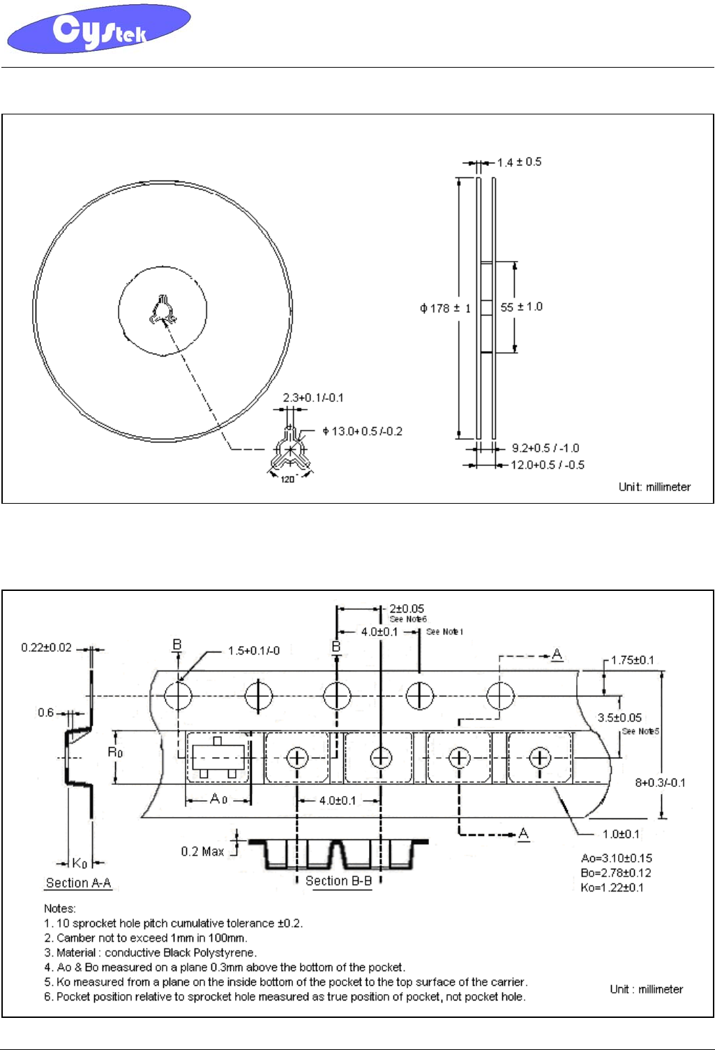
Characteristic Curves(Cont.)
Static Drain-Source On-State resistance vs Drain Current
1
10
0.001 0.01 0.1 1
Drain Current-ID(A)
Static Drain-Source On-State
Resistance-RDS(on)(Ω)
VGS=1.8V
VGS=4.5V
Static Drain-Source On-State Resistance vs Gate-Source
Voltage
0
1
2
3
4
5
6
7
024681
Gate-Source Voltage-VGS(V)
Static Drain-Source On-State
Resistance-RDS(ON)(Ω)
0
ID=100mA
ID=20mA
Reverse Drain Current vs Source-Drain Voltage
0.1
0.2
0.3
0.4
0.5
0.6
0.7
0.8
0.9
1
00.10.20.30
.4
Capacitance vs Drain-to-Source Voltage
1
10
100
0.1 1 10 100
Drain-Source Voltage -VDS(V)
Capacitance---(pF)
Reverse Drain Current -IDR(A)
Source-Drain Voltage-VSD(V)
Ciss
Coss
Crss
Power Derating Curve
0
50
100
150
200
250
300
350
0 50 100 150 200
Ambient Temperature---TA(℃)
Power Dissipation---PD(mW)
CYStech Electronics Corp.
Spec. No. : C447N3
Issued Date : 2010.08.18
Revised Date :
Page No. : 4/6
MTNK3N3 CYStek Product Specification
Reel Dimension
Carrier Tape Dimension
CYStech Electronics Corp.
Spec. No. : C447N3
Issued Date : 2010.08.18
Revised Date :
Page No. : 5/6
MTNK3N3 CYStek Product Specification
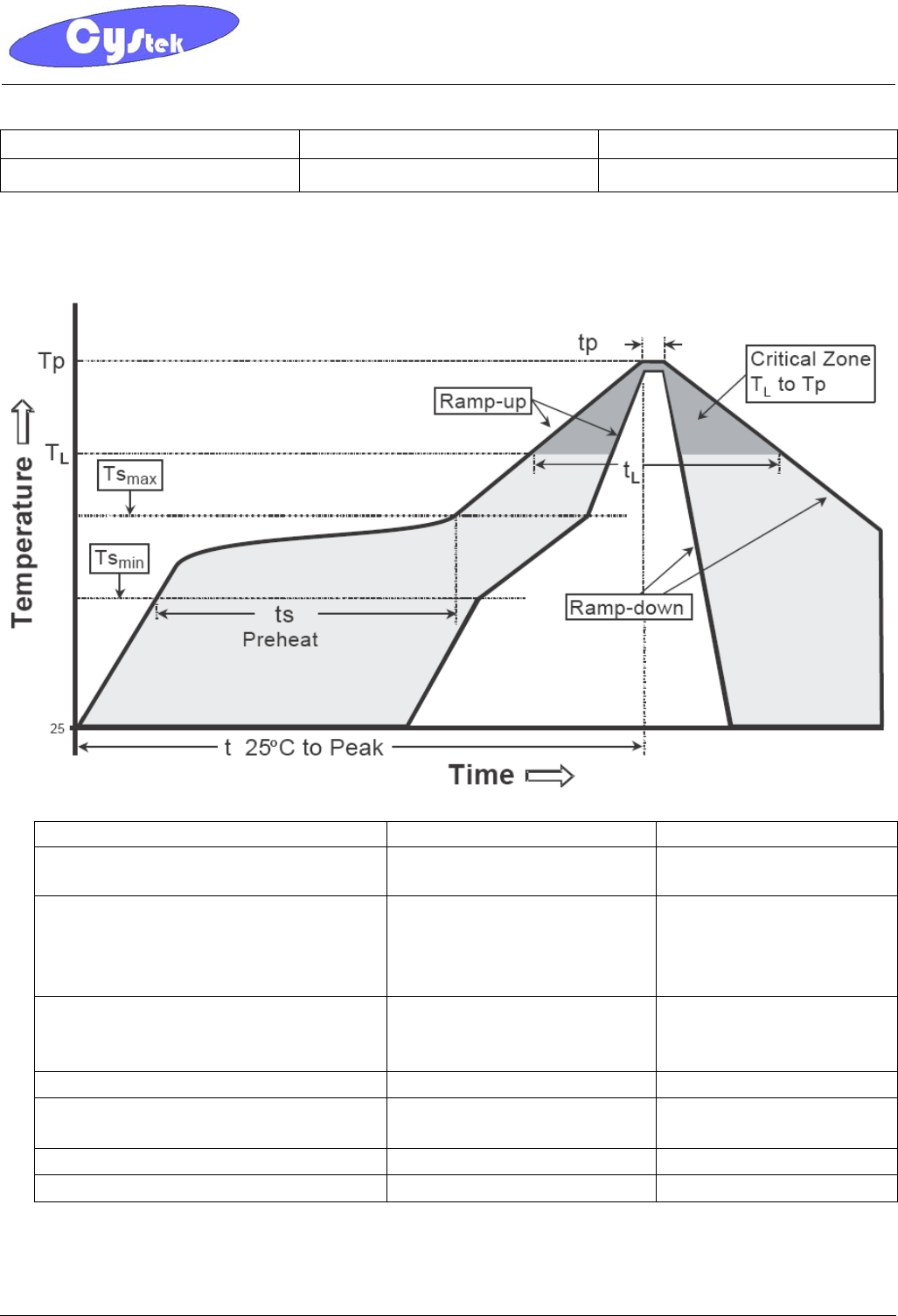
Recommended wave soldering condition
Product Peak Temperature Soldering Time
Pb-free devices 260 +0/-5 °C 5 +1/-1 seconds
Recommended temperature profile for IR reflow
Profile feature Sn-Pb eutectic Assembly Pb-free Assembly
Average ramp-up rate
(Tsmax to Tp) 3°C/second max. 3°C/second max.
Preheat
−Temperature Min(TS min)
−Temperature Max(TS max)
−Time(ts min to ts max)
100°C
150°C
60-120 seconds
150°C
200°C
60-180 seconds
Time maintained above:
−Temperature (TL)
− Time (tL)
183°C
60-150 seconds
217°C
60-150 seconds
Peak Temperature(TP) 240 +0/-5 °C 260 +0/-5 °C
Time within 5°C of actual peak
temperature(tp) 10-30 seconds 20-40 seconds
Ramp down rate 6°C/second max. 6°C/second max.
Time 25 °C to peak temperature 6 minutes max. 8 minutes max.
Note : All temperatures refer to topside of the package, measured on the package body surface.
CYStech Electronics Corp.
Spec. No. : C447N3
Issued Date : 2010.08.18
Revised Date :
Page No. : 6/6
MTNK3N3 CYStek Product Specification
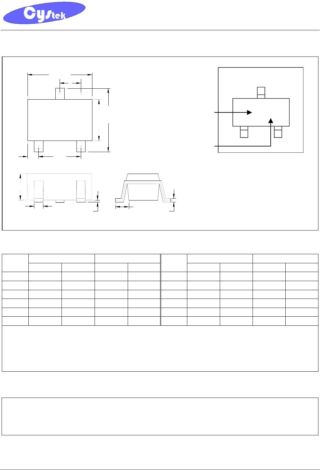
SOT-23 Dimension
*:Typical
HJ
K
D
A
L
G
V
C
B
3
2
1
S
Style : Pin 1.Gate 2.Source 3.Drain
3-Lead SOT-23 Plastic
Surface Mounted Package
CYStek Package Code: N3
Marking:
K3
xx
Device Code
Date Code
Inches Millimeters Inches Millimeters
DIM Min. Max. Min. Max.
DIM Min. Max. Min. Max.
A 0.1102 0.1204 2.80 3.04 J 0.0034 0.0070 0.085 0.177
B 0.0472 0.0630 1.20 1.60 K 0.0128 0.0266 0.32 0.67
C 0.0335 0.0512 0.89 1.30 L 0.0335 0.0453 0.85 1.15
D 0.0118 0.0197 0.30 0.50 S 0.0830 0.1083 2.10 2.75
G 0.0669 0.0910 1.70 2.30 V 0.0098 0.0256 0.25 0.65
H 0.0005 0.0040 0.013 0.10
Notes : 1.Controlling dimension : millimeters.
2.Maximum lead thickness includes lead finish thickness, and minimum lead thickness is the minimum thickness of base material.
3.If there is any question with packing specification or packing method, please contact your local CYStek sales office.
Material :
• Lead : Pure tin plated.
• Mold Compound : Epoxy resin family, flammability solid burning class:UL94V-0.
Important Notice:
• All rights are reserved. Reproduction in whole or in part is prohibited without the prior written approval of CYStek.
• CYStek reserves the right to make changes to its products without notice.
• CYStek semiconductor products are not warranted to be suitable for use in Life-Support Applications, or systems.
• CYStek assumes no liability for any consequence of customer product design, infringement of patents, or application assistance.