Nokia 2600C 2 RM 340, 341 Service Manual Level 3&4. Www.s Manuals.com. 34 V1.0
User Manual: Phone Nokia 2600 classic RM-340, RM-341 - Service manuals and Schematics, Disassembly / Assembly. Free.
Open the PDF directly: View PDF ![]() .
.
Page Count: 177 [warning: Documents this large are best viewed by clicking the View PDF Link!]
- Amendment Record Sheet
- Copyright
- Warnings and cautions
- For your safety
- Care and maintenance
- ESD protection
- Battery information
- Company Policy
- Nokia 2600c-2; Nokia 2600c-2b Service Manual Structure
- 1 General Information
- 2 Service Devices and Service Concepts
- 3 Baseband Troubleshooting Instructions
- General baseband troubleshooting
- SIM related faults
- User interface
- Audio troubleshooting
- Audio troubleshooting using phoenix
- Check microphone using "Hp microphone in Ext speaker out" loop
- Check earpiece using "Ext microphone in Hp speaker out" loop
- Check IHF & ringing tone function using "Buzzer"
- Check vibra function using "Vibra control"
- Earpiece fault
- IHF/ringing tone fault
- Microphone fault
- Headset earpiece fault
- Headset microphone fault
- 4 RF Troubleshooting Instructions
- 5 Camera Module Troubleshooting
- 6 System Module
- Glossary

Service Manual
RM-340; RM-341 (Nokia 2600c-2; Nokia
2600c-2b)
Mobile Terminal
Part No: 9205777 (Issue 1)
Nokia Customer Care
COMPANY CONFIDENTIAL
Copyright © 2007 Nokia. All rights reserved.

Amendment Record Sheet
Amendment No Date Inserted By Comments
Issue 1 12/2007 Y Liu
RM-340; RM-341
Amendment Record Sheet
Page ii COMPANY CONFIDENTIAL Issue 1
Copyright © 2007 Nokia. All rights reserved.

Copyright
Copyright © 2007 Nokia. All rights reserved.
Reproduction, transfer, distribution or storage of part or all of the contents in this document in any form
without the prior written permission of Nokia is prohibited.
Nokia, Nokia Connecting People, and Nokia X and Y are trademarks or registered trademarks of Nokia
Corporation. Other product and company names mentioned herein may be trademarks or tradenames of
their respective owners.
Nokia operates a policy of continuous development. Nokia reserves the right to make changes and
improvements to any of the products described in this document without prior notice.
Under no circumstances shall Nokia be responsible for any loss of data or income or any special, incidental,
consequential or indirect damages howsoever caused.
The contents of this document are provided "as is". Except as required by applicable law, no warranties of
any kind, either express or implied, including, but not limited to, the implied warranties of merchantability
and fitness for a particular purpose, are made in relation to the accuracy, reliability or contents of this
document. Nokia reserves the right to revise this document or withdraw it at any time without prior notice.
The availability of particular products may vary by region.
IMPORTANT
This document is intended for use by qualified service personnel only.
RM-340; RM-341
Copyright
Issue 1 COMPANY CONFIDENTIAL Page iii
Copyright © 2007 Nokia. All rights reserved.

Warnings and cautions
Warnings
• IF THE DEVICE CAN BE INSTALLED IN A VEHICLE, CARE MUST BE TAKEN ON INSTALLATION IN VEHICLES FITTED
WITH ELECTRONIC ENGINE MANAGEMENT SYSTEMS AND ANTI-SKID BRAKING SYSTEMS. UNDER CERTAIN FAULT
CONDITIONS, EMITTED RF ENERGY CAN AFFECT THEIR OPERATION. IF NECESSARY, CONSULT THE VEHICLE DEALER/
MANUFACTURER TO DETERMINE THE IMMUNITY OF VEHICLE ELECTRONIC SYSTEMS TO RF ENERGY.
•THE PRODUCT MUST NOT BE OPERATED IN AREAS LIKELY TO CONTAIN POTENTIALLY EXPLOSIVE ATMOSPHERES,
FOR EXAMPLE, PETROL STATIONS (SERVICE STATIONS), BLASTING AREAS ETC.
• OPERATION OF ANY RADIO TRANSMITTING EQUIPMENT, INCLUDING CELLULAR TELEPHONES, MAY INTERFERE
WITH THE FUNCTIONALITY OF INADEQUATELY PROTECTED MEDICAL DEVICES. CONSULT A PHYSICIAN OR THE
MANUFACTURER OF THE MEDICAL DEVICE IF YOU HAVE ANY QUESTIONS. OTHER ELECTRONIC EQUIPMENT MAY
ALSO BE SUBJECT TO INTERFERENCE.
• BEFORE MAKING ANY TEST CONNECTIONS, MAKE SURE YOU HAVE SWITCHED OFF ALL EQUIPMENT.
Cautions
• Servicing and alignment must be undertaken by qualified personnel only.
• Ensure all work is carried out at an anti-static workstation and that an anti-static wrist strap is worn.
• Ensure solder, wire, or foreign matter does not enter the telephone as damage may result.
• Use only approved components as specified in the parts list.
• Ensure all components, modules, screws and insulators are correctly re-fitted after servicing and
alignment.
• Ensure all cables and wires are repositioned correctly.
•Never test a mobile phone WCDMA transmitter with full Tx power, if there is no possibility to perform the
measurements in a good performance RF-shielded room. Even low power WCDMA transmitters may disturb
nearby WCDMA networks and cause problems to 3G cellular phone communication in a wide area.
• During testing never activate the GSM or WCDMA transmitter without a proper antenna load, otherwise
GSM or WCDMA PA may be damaged.
RM-340; RM-341
Warnings and cautions
Page iv COMPANY CONFIDENTIAL Issue 1
Copyright © 2007 Nokia. All rights reserved.

For your safety
QUALIFIED SERVICE
Only qualified personnel may install or repair phone equipment.
ACCESSORIES AND BATTERIES
Use only approved accessories and batteries. Do not connect incompatible products.
CONNECTING TO OTHER DEVICES
When connecting to any other device, read its user’s guide for detailed safety instructions. Do not connect
incompatible products.
RM-340; RM-341
For your safety
Issue 1 COMPANY CONFIDENTIAL Page v
Copyright © 2007 Nokia. All rights reserved.

Care and maintenance
This product is of superior design and craftsmanship and should be treated with care. The suggestions below
will help you to fulfil any warranty obligations and to enjoy this product for many years.
• Keep the phone and all its parts and accessories out of the reach of small children.
•Keep the phone dry. Precipitation, humidity and all types of liquids or moisture can contain minerals that
will corrode electronic circuits.
• Do not use or store the phone in dusty, dirty areas. Its moving parts can be damaged.
•Do not store the phone in hot areas. High temperatures can shorten the life of electronic devices, damage
batteries, and warp or melt certain plastics.
• Do not store the phone in cold areas. When it warms up (to its normal temperature), moisture can form
inside, which may damage electronic circuit boards.
• Do not drop, knock or shake the phone. Rough handling can break internal circuit boards.
• Do not use harsh chemicals, cleaning solvents, or strong detergents to clean the phone.
• Do not paint the phone. Paint can clog the moving parts and prevent proper operation.
• Use only the supplied or an approved replacement antenna. Unauthorised antennas, modifications or
attachments could damage the phone and may violate regulations governing radio devices.
All of the above suggestions apply equally to the product, battery, charger or any accessory.
RM-340; RM-341
Care and maintenance
Page vi COMPANY CONFIDENTIAL Issue 1
Copyright © 2007 Nokia. All rights reserved.

ESD protection
Nokia requires that service points have sufficient ESD protection (against static electricity) when servicing
the phone.
Any product of which the covers are removed must be handled with ESD protection. The SIM card can be
replaced without ESD protection if the product is otherwise ready for use.
To replace the covers ESD protection must be applied.
All electronic parts of the product are susceptible to ESD. Resistors, too, can be damaged by static electricity
discharge.
All ESD sensitive parts must be packed in metallized protective bags during shipping and handling outside
any ESD Protected Area (EPA).
Every repair action involving opening the product or handling the product components must be done under
ESD protection.
ESD protected spare part packages MUST NOT be opened/closed out of an ESD Protected Area.
For more information and local requirements about ESD protection and ESD Protected Area, contact your local
Nokia After Market Services representative.
RM-340; RM-341
ESD protection
Issue 1 COMPANY CONFIDENTIAL Page vii
Copyright © 2007 Nokia. All rights reserved.

Battery information
Note: A new battery's full performance is achieved only after two or three complete charge and
discharge cycles!
The battery can be charged and discharged hundreds of times but it will eventually wear out. When the
operating time (talk-time and standby time) is noticeably shorter than normal, it is time to buy a new battery.
Use only batteries approved by the phone manufacturer and recharge the battery only with the chargers
approved by the manufacturer. Unplug the charger when not in use. Do not leave the battery connected to
a charger for longer than a week, since overcharging may shorten its lifetime. If left unused a fully charged
battery will discharge itself over time.
Temperature extremes can affect the ability of your battery to charge.
For good operation times with Ni-Cd/NiMh batteries, discharge the battery from time to time by leaving the
product switched on until it turns itself off (or by using the battery discharge facility of any approved accessory
available for the product). Do not attempt to discharge the battery by any other means.
Use the battery only for its intended purpose.
Never use any charger or battery which is damaged.
Do not short-circuit the battery. Accidental short-circuiting can occur when a metallic object (coin, clip or
pen) causes direct connection of the + and - terminals of the battery (metal strips on the battery) for example
when you carry a spare battery in your pocket or purse. Short-circuiting the terminals may damage the battery
or the connecting object.
Leaving the battery in hot or cold places, such as in a closed car in summer or winter conditions, will reduce
the capacity and lifetime of the battery. Always try to keep the battery between 15°C and 25°C (59°F and 77°
F). A phone with a hot or cold battery may temporarily not work, even when the battery is fully charged.
Batteries' performance is particularly limited in temperatures well below freezing.
Do not dispose of batteries in a fire!
Dispose of batteries according to local regulations (e.g. recycling). Do not dispose as household waste.
RM-340; RM-341
Battery information
Page viii COMPANY CONFIDENTIAL Issue 1
Copyright © 2007 Nokia. All rights reserved.

Company Policy
Our policy is of continuous development; details of all technical modifications will be included with service
bulletins.
While every endeavour has been made to ensure the accuracy of this document, some errors may exist. If
any errors are found by the reader, NOKIA MOBILE PHONES Business Group should be notified in writing/e-
mail.
Please state:
• Title of the Document + Issue Number/Date of publication
• Latest Amendment Number (if applicable)
• Page(s) and/or Figure(s) in error
Please send to:
NOKIA CORPORATION
Nokia Mobile Phones Business Group
Nokia Customer Care
PO Box 86
FIN-24101 SALO
Finland
E-mail: Service.Manuals@nokia.com
RM-340; RM-341
Company Policy
Issue 1 COMPANY CONFIDENTIAL Page ix
Copyright © 2007 Nokia. All rights reserved.

RM-340; RM-341
Company Policy
(This page left intentionally blank.)
Page x COMPANY CONFIDENTIAL Issue 1
Copyright © 2007 Nokia. All rights reserved.

Nokia 2600c-2; Nokia 2600c-2b Service Manual Structure
1 General Information
2 Service Devices and Service Concepts
3 Baseband Troubleshooting Instructions
4 RF Troubleshooting Instructions
5 Camera Module Troubleshooting
6 System Module
Glossary
RM-340; RM-341
Nokia 2600c-2; Nokia 2600c-2b Service Manual
Structure
Issue 1 COMPANY CONFIDENTIAL Page xi
Copyright © 2007 Nokia. All rights reserved.

RM-340; RM-341
Nokia 2600c-2; Nokia 2600c-2b Service Manual
Structure
(This page left intentionally blank.)
Page xii COMPANY CONFIDENTIAL Issue 1
Copyright © 2007 Nokia. All rights reserved.

1 — General Information
Nokia Customer Care
Issue 1 COMPANY CONFIDENTIAL Page 1 –1
Copyright © 2007 Nokia. All rights reserved.

RM-340; RM-341
General Information
(This page left intentionally blank.)
Page 1 –2 COMPANY CONFIDENTIAL Issue 1
Copyright © 2007 Nokia. All rights reserved.

Table of Contents
RM-340/RM-341 product selection .......................................................................................................................1–5
Features...................................................................................................................................................................1–5
Hardware features ............................................................................................................................................1–5
Software features..............................................................................................................................................1–6
UI features..........................................................................................................................................................1–6
Mobile enhancements.......................................................................................................................................1–6
List of Tables
Table 1 Power.........................................................................................................................................................1–6
Table 2 Car...............................................................................................................................................................1–6
Table 3 Audio..........................................................................................................................................................1–7
List of Figures
Figure 1 RM-340/341 product picture ..................................................................................................................1–5
RM-340; RM-341
General Information
Issue 1 COMPANY CONFIDENTIAL Page 1 –3
Copyright © 2007 Nokia. All rights reserved.

RM-340; RM-341
General Information
(This page left intentionally blank.)
Page 1 –4 COMPANY CONFIDENTIAL Issue 1
Copyright © 2007 Nokia. All rights reserved.
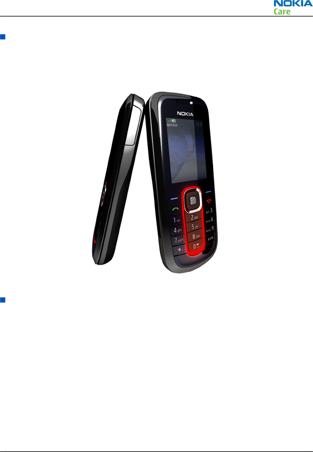
RM-340/RM-341 product selection
The RM-340 is the EU version of the telephone with a dual band transceiver unit designed for the GSM900
and GSM1800 networks.
The RM-341 is the US version of the telephone with a dual band transceiver unit designed for the GSM850
and GSM1900 networks.
Figure 1 RM-340/341 product picture
Features
Hardware features
• EGSM dualband 900/1800 for EMEA, APAC, China, LTA·
• GSM dualband 850/1900 for LTA
• Display: 128x160 TFT color display
• Codecs: HR, FR, EFR and AMR
• IHF Slim Malt 16mm Speaker
• Internal antenna
• Easy flash II system connector
• BT combined with FM radio
• VGA camera
• Built-in Vibra
• GPRS: Class 6
RM-340; RM-341
General Information
Issue 1 COMPANY CONFIDENTIAL Page 1 –5
Copyright © 2007 Nokia. All rights reserved.

Software features
• OS: ISA
• UI Style: S40
• MIDP 2.0 Java, with latest APIs
• Browser: XHTML over TCP/IP (WAP 2.0 compliant)
• Video capture and playback (7.5fps, H.263; MPEG4)
• MMS 1.2
• English-Chinese dictionary for China/APAC
• E-mail Client 4
• Nokia Xpress audio messaging
UI features
• Douglas V UI style with 3 soft keysl
• Nokia Series 40 user interface
• MP3 ringing tones & 40 polyphonic ringing tones
• Themes, colour games and wall papers
• Java games (downloadable)
• To-do list and Notes
• Countdown timer
• Phonebook image
• Menu with animated icons
• 2 font sizes are supported in the editor
• Calendar in day/week/month view
• Chinese lunar Calendar II (not for all regions)
• “Pulsating light” indicating missed call, unread messages, etc.
Mobile enhancements
Table 1 Power
Type Name
BL-5BT Battery 870 mAh Li-Ion
AC-3 Compact charger
AC-4 Travel charger
AC-5 Compact travel charger
CA-44 Charger adapter
DC-4 Mobile charger
Table 2 Car
Type Name
CK-15W Display car kit
RM-340; RM-341
General Information
Page 1 –6 COMPANY CONFIDENTIAL Issue 1
Copyright © 2007 Nokia. All rights reserved.
Type Name
CK-20W Multimedia car kit
CK-25W Multimedia car kit
Table 3 Audio
Type Name
HS-38W Nokia bluetooth headset BH-202
HS-40 Headset
HS-47 Stereo headset
HS-50W Nokia bluetooth headset BH-300
HS-51W Nokia bluetooth headset BH-301
HS-52W Nokia bluetooth headset BH-201
HS-58W Nokia bluetooth headset BH-200
HS-68W Nokia bluetooth headset BH-203
HS-73W Nokia bluetooth headset BH-302
HS-78W Nokia bluetooth headset BH-100
HS-79W Nokia bluetooth headset BH-303
HS-80W Nokia bluetooth headset BH-208
HS-84W/88W Nokia bluetooth headset BH-204
HS-85W Nokia bluetooth headset BH-206
HS-86W Nokia bluetooth headset BH-207
MD-4 Mini speakers
RM-340; RM-341
General Information
Issue 1 COMPANY CONFIDENTIAL Page 1 –7
Copyright © 2007 Nokia. All rights reserved.

RM-340; RM-341
General Information
(This page left intentionally blank.)
Page 1 –8 COMPANY CONFIDENTIAL Issue 1
Copyright © 2007 Nokia. All rights reserved.

2 — Service Devices and
Service Concepts
Nokia Customer Care
Issue 1 COMPANY CONFIDENTIAL Page 2 –1
Copyright © 2007 Nokia. All rights reserved.

RM-340; RM-341
Service Devices and Service Concepts
(This page left intentionally blank.)
Page 2 –2 COMPANY CONFIDENTIAL Issue 1
Copyright © 2007 Nokia. All rights reserved.

Table of Contents
Service devices........................................................................................................................................................2–5
CA-106DS ............................................................................................................................................................2–5
CA-111DS ............................................................................................................................................................2–5
CA-112DS ............................................................................................................................................................2–5
CA-41PS...............................................................................................................................................................2–6
CA-52PS...............................................................................................................................................................2–6
CA-58RS...............................................................................................................................................................2–6
DA-69 ..................................................................................................................................................................2–6
DAU-9S................................................................................................................................................................2–7
FLS-4S..................................................................................................................................................................2–7
FLS-5 ...................................................................................................................................................................2–7
FPS-10.................................................................................................................................................................2–8
JBV-1 ...................................................................................................................................................................2–8
MJ-138.................................................................................................................................................................2–9
PCS-1...................................................................................................................................................................2–9
PK-1.....................................................................................................................................................................2–9
PKD-1 ............................................................................................................................................................... 2–10
RJ-200 .............................................................................................................................................................. 2–10
RJ-51 ................................................................................................................................................................ 2–10
RJ-72 ................................................................................................................................................................ 2–10
SA-93................................................................................................................................................................ 2–11
SRT-6................................................................................................................................................................ 2–11
SS-88................................................................................................................................................................ 2–11
SS-93................................................................................................................................................................ 2–11
ST-30................................................................................................................................................................ 2–12
ST-32................................................................................................................................................................ 2–12
SX-4.................................................................................................................................................................. 2–12
XCS-4 ................................................................................................................................................................ 2–12
XRS-6................................................................................................................................................................ 2–13
Service concepts .................................................................................................................................................. 2–13
POS flash concept with FLS-4S....................................................................................................................... 2–13
POS flash concept with FLS-5 ........................................................................................................................ 2–14
Flash concept with FPS-10............................................................................................................................. 2–15
RF-test/BB-tune concept with JBV-1............................................................................................................. 2–16
EM calibration concept with JBV-1................................................................................................................ 2–17
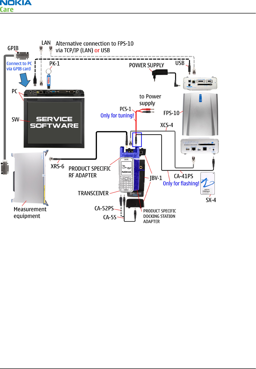
RF-test/BB-tune & flash concept with JBV-1, FPS-10................................................................................... 2–18
RF/BB tune& flash concept with MJ-137, FPS-10......................................................................................... 2–19
List of Figures
Figure 2 POS flash concept with FLS-4S............................................................................................................. 2–13
Figure 3 POS flash concept with FLS-5............................................................................................................... 2–14
Figure 4 Flash concept with FPS-10................................................................................................................... 2–15
Figure 5 RF-test/BB-tune concept with JBV-1................................................................................................... 2–16
Figure 6 EM calibration concept with JBV-1...................................................................................................... 2–17
Figure 7 RF-test/BB-tune & flash concept with JBV-1, FPS-10......................................................................... 2–18
Figure 8 RF/BB tune& flash concept with MJ-137, FPS-10 ............................................................................... 2–19
RM-340; RM-341
Service Devices and Service Concepts
Issue 1 COMPANY CONFIDENTIAL Page 2 –3
Copyright © 2007 Nokia. All rights reserved.

RM-340; RM-341
Service Devices and Service Concepts
(This page left intentionally blank.)
Page 2 –4 COMPANY CONFIDENTIAL Issue 1
Copyright © 2007 Nokia. All rights reserved.
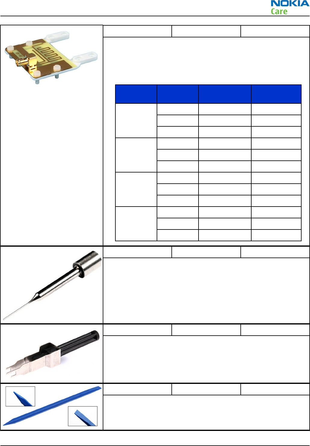
Service devices
The table below gives a short overview of service devices that can be used for testing, error analysis, and
repair of product RM-340; RM-341. For the correct use of the service devices, and the best effort of workbench
setup, please refer to various concepts.
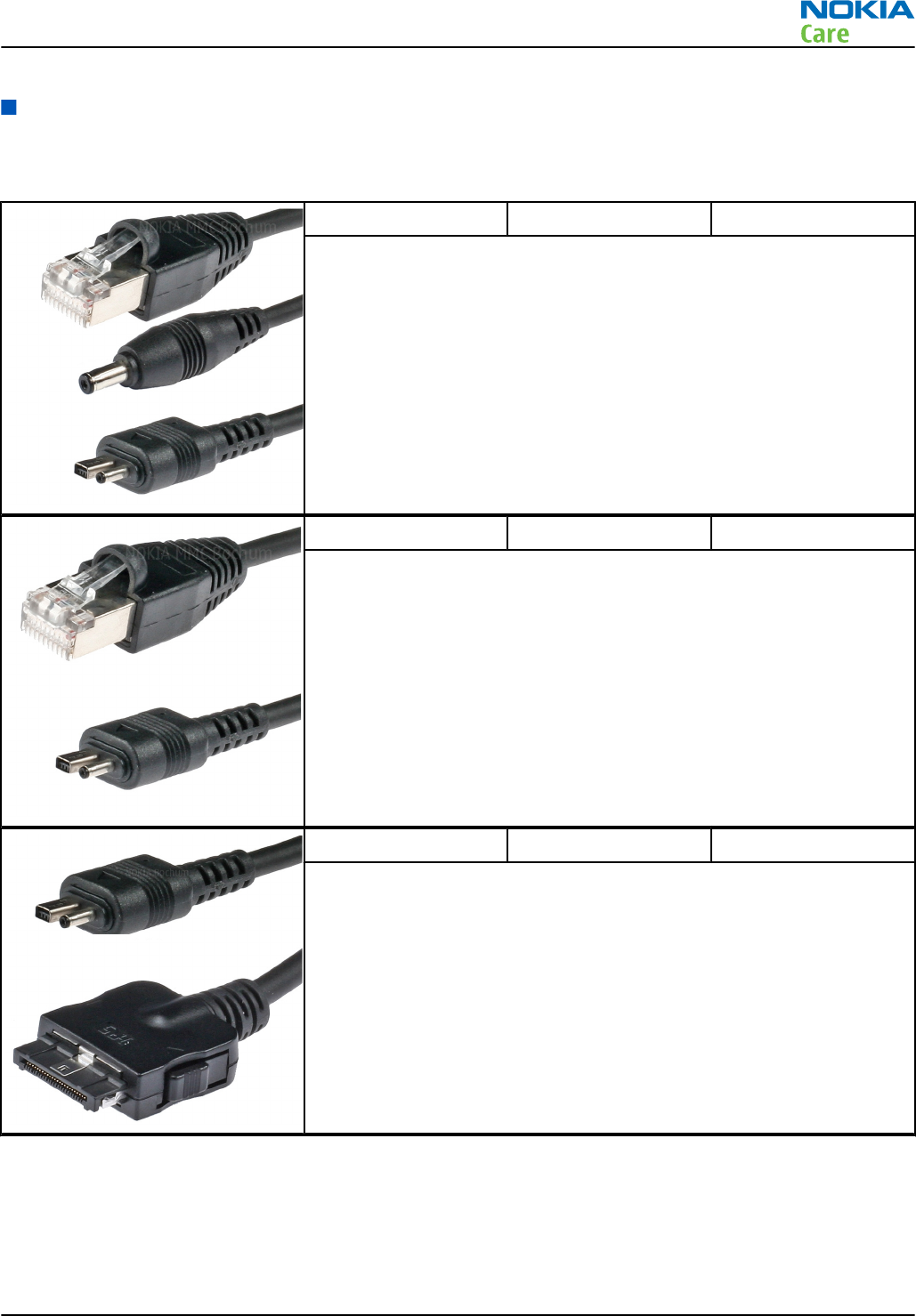
CA-106DS Easy flash II cable
The cable is used for connecting phone DC port to the flash prommer
FPS-10.
CA-111DS Easy flash II cable
The cable is used for connecting phone DC port to either POS flashing
device FLS-4S or to the PROMMER box FPS-11.
CA-112DS Easy flash II cable
The CA-112DS easy flash II cable is used for connecting phone DC port
to the PROMMER facilities (FLS-5, FPS-21).
RM-340; RM-341
Service Devices and Service Concepts
Issue 1 COMPANY CONFIDENTIAL Page 2 –5
Copyright © 2007 Nokia. All rights reserved.
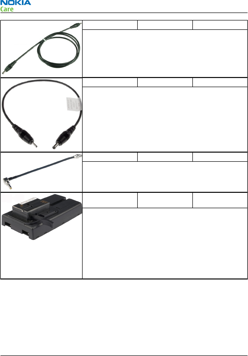
CA-41PS Power cable
Power cable for connection of e.g. the JBV-1 docking station to the
FPS-10 prommer box.
CA-52PS DC Cable
The cable is used to connect JBV-1 docking station to the phone
charger jack for ADC/VCHAR/ICHAR calibration.
CA-58RS RF Cable
This RF cable is used together with MJ-138 to connect to RF
measurement equipment.
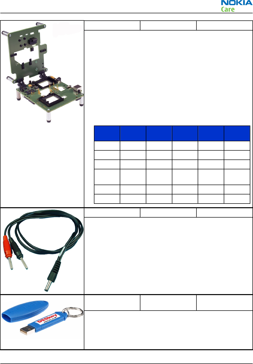
DA-69 Docking station
adapter
The docking station adapter is used for this phone in combination with
JBV-1. The adapter supports flashing and energy management
calibration,
Features include:
• compatible with JBV-1
• easy phone attachment and detachment
• reliable phone locking
• switch for detecting phone
• replaceable SIM interface
RM-340; RM-341
Service Devices and Service Concepts
Page 2 –6 COMPANY CONFIDENTIAL Issue 1
Copyright © 2007 Nokia. All rights reserved.
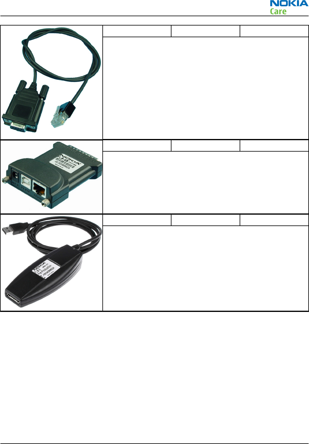
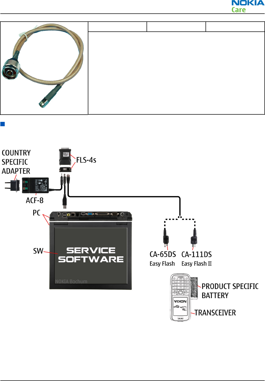
DAU-9S MBUS cable
The MBUS cable DAU-9S has a modular connector and is used, for
example, between the PC's serial port and module jigs, flash adapters
or docking station adapters.
Note: Docking station adapters valid for DCT4 products.
FLS-4S Flash device
FLS-4S is a dongle and flash device incorporated into one package,
developed specifically for POS use.
FLS-5 Flash device
FLS-5 is a dongle and flash device incorporated into one package,
developed specifically for POS use.
Note: FLS-5 can be used as an alternative to PKD-1.
RM-340; RM-341
Service Devices and Service Concepts
Issue 1 COMPANY CONFIDENTIAL Page 2 –7
Copyright © 2007 Nokia. All rights reserved.
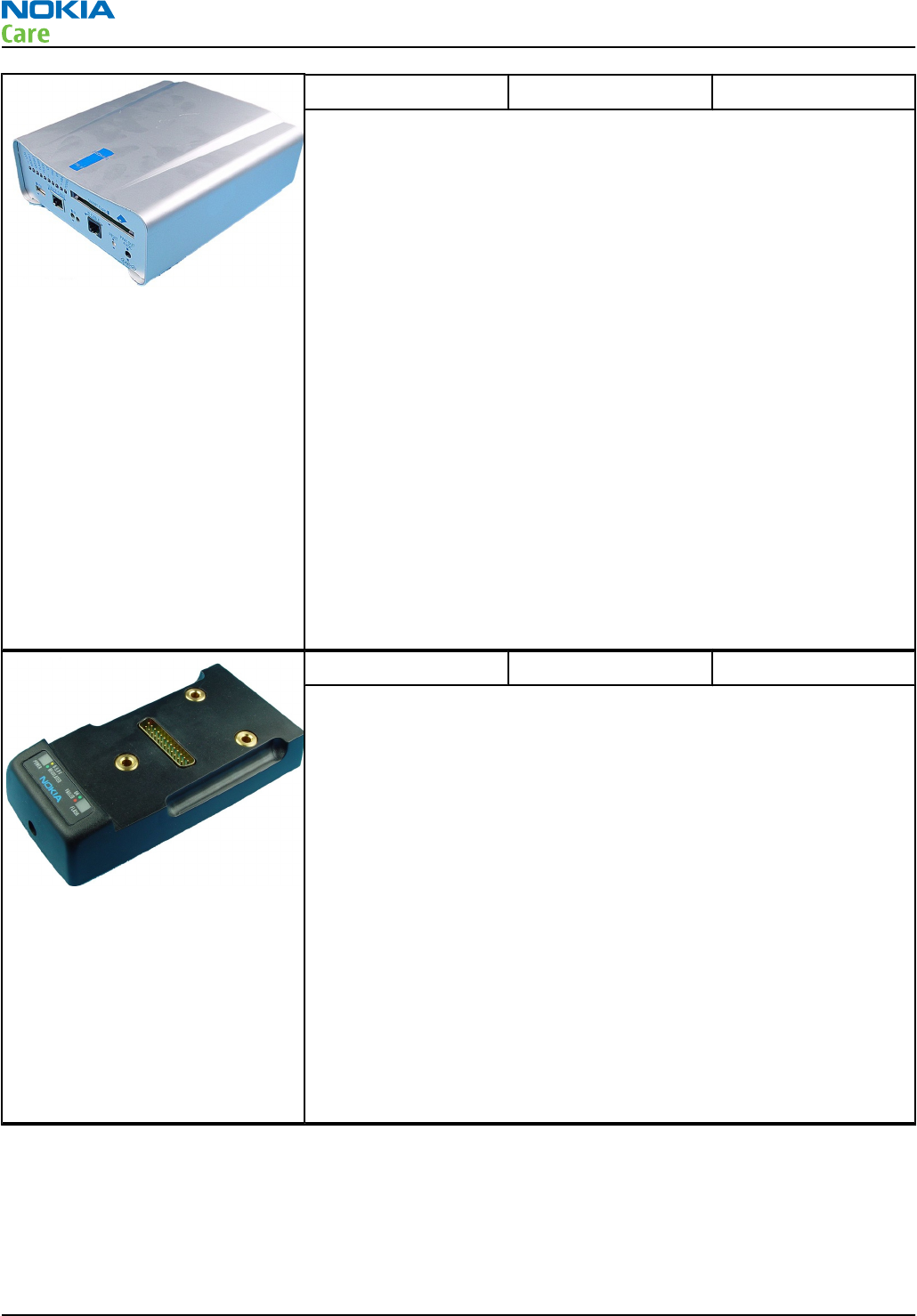
FPS-10 Flash prommer
FPS-10 interfaces with:
• PC
• Control unit
• Flash adapter
• Smart card
FPS-10 flash prommer features:
• Flash functionality for BB5 and DCT-4 terminals
• Smart Card reader for SX-2 or SX-4
• USB traffic forwarding
• USB to FBUS/Flashbus conversion
• LAN to FBUS/Flashbus and USB conversion
• Vusb output switchable by PC command
FPS-10 sales package includes:
• FPS-10 prommer
• Power Supply with 5 country specific cords
• USB cable
Note: FPS-21 is substitute FPS-10 if FPS-10 has not been set
up.
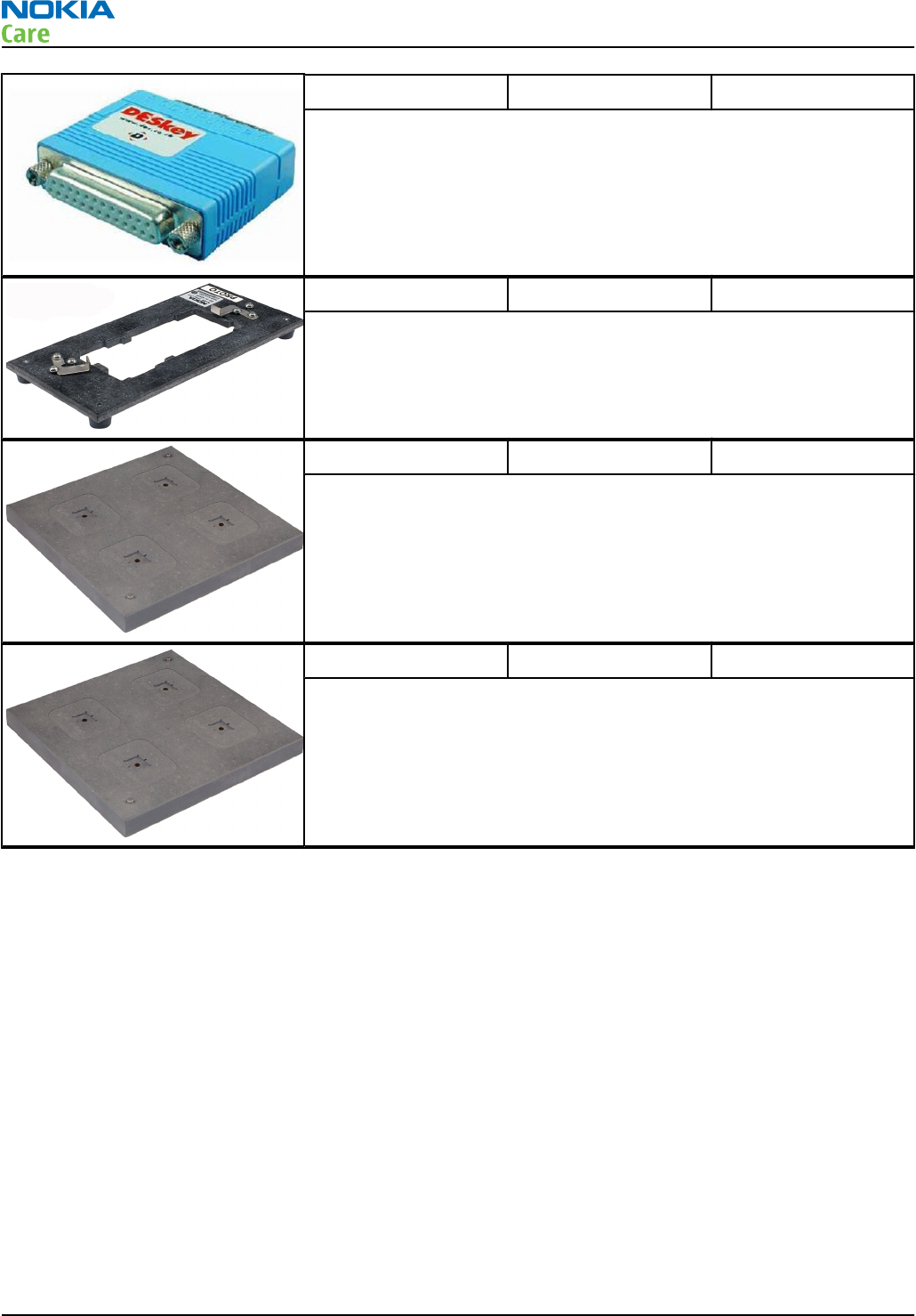
JBV-1 Docking station
The JBV-1 docking station is a general tool that has been designed for
calibration and software update use. The JBV-1 is used together with
a docking station adapter as one unit
In calibration mode the JBV-1 is powered by an external power supply:
11-16V DC. When flashing the power for the phone must be taken from
the flash prommer.
Note: JBV-1 main electrical functions are:
• adjustable VBATT calibration voltage, current
measurement limit voltage: VCHAR, current measurement:
ICHAR
• adjustable ADC calibration voltage via BTEM and the BSI
signal
• BTEMP and BSI calibration resistor
• signal from FBUS to the phone via the parallel jig
• control via FBUS or USB
• Flash OK/FAIL indication
RM-340; RM-341
Service Devices and Service Concepts
Page 2 –8 COMPANY CONFIDENTIAL Issue 1
Copyright © 2007 Nokia. All rights reserved.
MJ-138 Module jig
MJ-138 is meant for component level troubleshooting.
The jig includes an RF interface for GSM and Bluetooth. in addition, it
has the following features:
• Provides mechanical interface with the engine and UI module
• Provides galvanic connection to all needed test pads in module
• Duplicated SIM connector
• Audio components: IHF, MIC
• Connector for control unit
Note: CA-58RS(RF cable) is used together with MJ-138.
CA-58RS is not a part of the MJ-138 sales package and has to
be ordered separately.
The following table shows the attenuation values for MJ-138:
•Band Tuning
Channel Attenuat
ion RX Toleranc
e RX Attenuat
ion TX Toleranc
e TX
GSM 900 975 -6.0884 1 -6.9200 2
38 -6.4203 1 -7.4584 2
124 -6.6911 1 -8.4678 2
GSM
1800
512 -8.8416 1 -7.5614 2
700 -8.0418 1 -7.0011 2
885 -7.7039 1 -6.4946 2
PCS-1 Power cable
The PCS-1 power cable (DC) is used with a docking station, a module
jig or a control unit to supply a controlled voltage.
PK-1 Software protection
key
PK-1 is a hardware protection key with a USB interface. It has the same
functionality as the PKD-1 series dongle.
PK-1 is meant for use with a PC that does not have a series interface.
To use this USB dongle for security service functions please register
the dongle in the same way as the PKD-1 series dongle.
RM-340; RM-341
Service Devices and Service Concepts
Issue 1 COMPANY CONFIDENTIAL Page 2 –9
Copyright © 2007 Nokia. All rights reserved.
PKD-1 SW security device
SW security device is a piece of hardware enabling the use of the
service software when connected to the parallel (LPT) port of the PC.
Without the device, it is not possible to use the service software.
Printer or any such device can be connected to the PC through the
device if needed.
RJ-200 Soldering jig
The jig is used for soldering and as a rework jig for the system module.
It is made of lead-free rework compatible material.
RJ-51 Rework jig
To be used with ST-30!
RJ-72 Rework jig
To be used with rework stencil ST-32.
RM-340; RM-341
Service Devices and Service Concepts
Page 2 –10 COMPANY CONFIDENTIAL Issue 1
Copyright © 2007 Nokia. All rights reserved.
SA-93 RF coupler
The coupler is used for Go/No-Go test after changing components in
the RF part of the phone.
It is mounted on the docking station adapter.
The following table shows attenuations from the antenna pads of the
mobile terminal to the SMA connectors of SA-93:
•Band Tuning
channel Attenuation RX
(dB) Attenuation
TX(dB)
GSM850 128 8 8
190 8 8
251 8 8
GSM900 38 8 8
124 8 8
975 8 8
GSM1800 512 10 10
700 10 10
885 10 10
GSM1900 512 10 10
661 10 10
810 10 10
SRT-6 Opening tool
SRT-6 is used to open phone covers and B-to-B connectors.
Caution: Handle the tool with care because the tip is only 0.7
mm in diameter.
When not in use, store in a safe location.
SS-88 Camera removal tool
The camera removal tool SS-88 is used to remove/attach the front
camera module from/to the socket.
SS-93 Opening tool
SS-93 is used for opening JAE connectors.
RM-340; RM-341
Service Devices and Service Concepts
Issue 1 COMPANY CONFIDENTIAL Page 2 –11
Copyright © 2007 Nokia. All rights reserved.

ST-30 Rework stencil
It is used together with RJ-51 to rework N6301.
ST-32 Rework stencil for
B2100
Rework stencil to be used together with RJ-72 for rework of B2100.
SX-4 Smart card
SX-4 is a BB5 security device used to protect critical features in tuning
and testing.
SX-4 is also needed together with FPS-10 when DCT-4 phones are
flashed.
XCS-4 Modular cable
XCS-4 is a shielded (one specially shielded conductor) modular cable
for flashing and service purposes.
RM-340; RM-341
Service Devices and Service Concepts
Page 2 –12 COMPANY CONFIDENTIAL Issue 1
Copyright © 2007 Nokia. All rights reserved.
XRS-6 RF cable
The RF cable is used to connect, for example, a module repair jig to
the RF measurement equipment.
SMA to N-Connector approximately 610 mm.
Attenuation for:
• GSM850/900: 0.3+-0.1 dB
• GSM1800/1900: 0.5+-0.1 dB
• WLAN: 0.6+-0.1dB
Service concepts
POS flash concept with FLS-4S
Figure 2 POS flash concept with FLS-4S
RM-340; RM-341
Service Devices and Service Concepts
Issue 1 COMPANY CONFIDENTIAL Page 2 –13
Copyright © 2007 Nokia. All rights reserved.
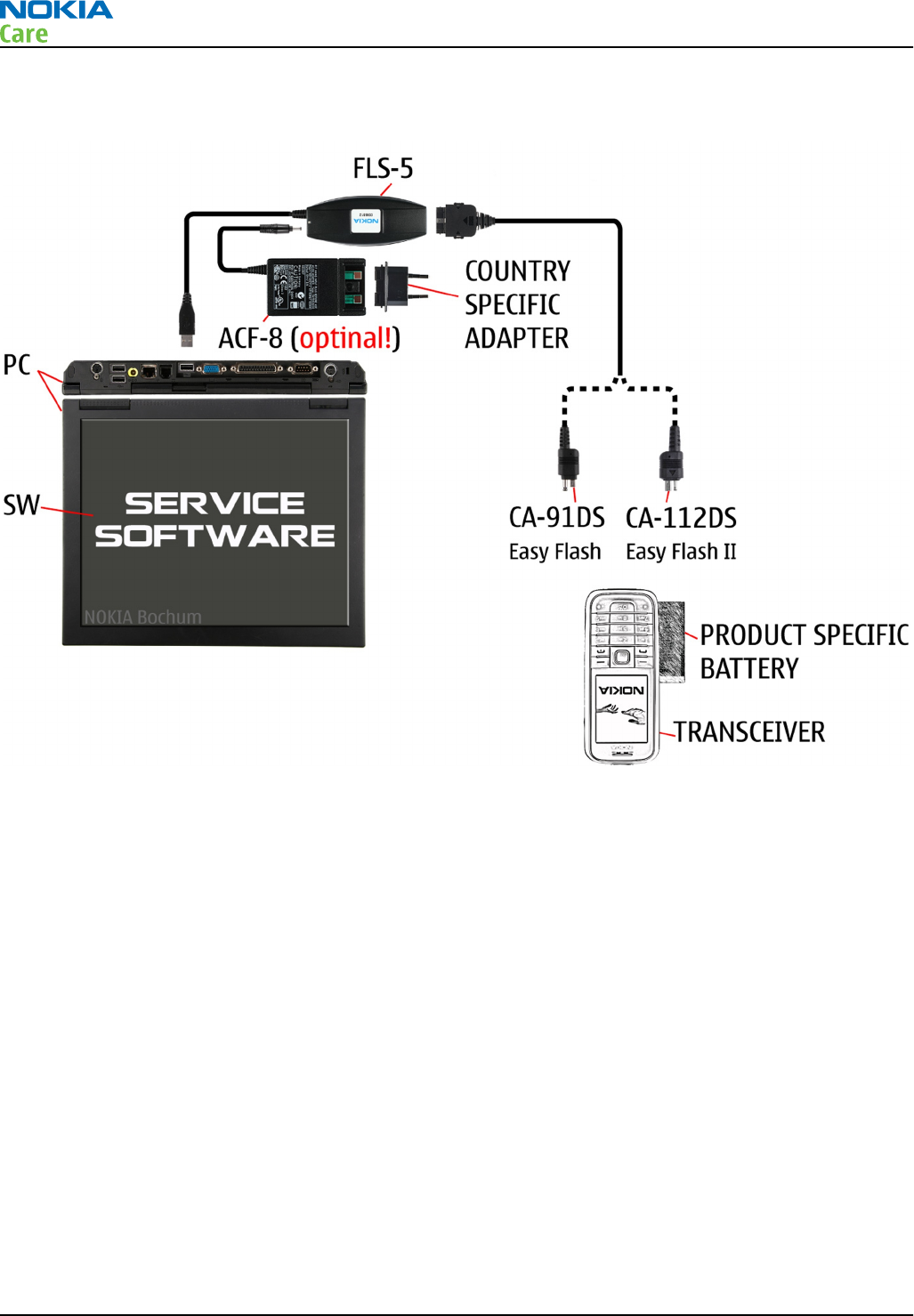
POS flash concept with FLS-5
Figure 3 POS flash concept with FLS-5
RM-340; RM-341
Service Devices and Service Concepts
Page 2 –14 COMPANY CONFIDENTIAL Issue 1
Copyright © 2007 Nokia. All rights reserved.

Flash concept with FPS-10
Figure 4 Flash concept with FPS-10
RM-340; RM-341
Service Devices and Service Concepts
Issue 1 COMPANY CONFIDENTIAL Page 2 –15
Copyright © 2007 Nokia. All rights reserved.
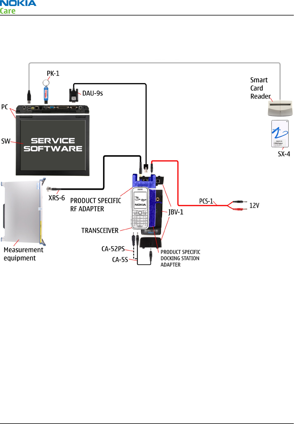
RF-test/BB-tune concept with JBV-1
Figure 5 RF-test/BB-tune concept with JBV-1
RM-340; RM-341
Service Devices and Service Concepts
Page 2 –16 COMPANY CONFIDENTIAL Issue 1
Copyright © 2007 Nokia. All rights reserved.

EM calibration concept with JBV-1
Figure 6 EM calibration concept with JBV-1
RM-340; RM-341
Service Devices and Service Concepts
Issue 1 COMPANY CONFIDENTIAL Page 2 –17
Copyright © 2007 Nokia. All rights reserved.
RF-test/BB-tune & flash concept with JBV-1, FPS-10
Figure 7 RF-test/BB-tune & flash concept with JBV-1, FPS-10
RM-340; RM-341
Service Devices and Service Concepts
Page 2 –18 COMPANY CONFIDENTIAL Issue 1
Copyright © 2007 Nokia. All rights reserved.

RF/BB tune& flash concept with MJ-137, FPS-10
Figure 8 RF/BB tune& flash concept with MJ-137, FPS-10
RM-340; RM-341
Service Devices and Service Concepts
Issue 1 COMPANY CONFIDENTIAL Page 2 –19
Copyright © 2007 Nokia. All rights reserved.

RM-340; RM-341
Service Devices and Service Concepts
(This page left intentionally blank.)
Page 2 –20 COMPANY CONFIDENTIAL Issue 1
Copyright © 2007 Nokia. All rights reserved.

3 — Baseband
Troubleshooting Instructions
Nokia Customer Care
Issue 1 COMPANY CONFIDENTIAL Page 3 –1
Copyright © 2007 Nokia. All rights reserved.

RM-340; RM-341
Baseband Troubleshooting Instructions
(This page left intentionally blank.)
Page 3 –2 COMPANY CONFIDENTIAL Issue 1
Copyright © 2007 Nokia. All rights reserved.

Table of Contents
General baseband troubleshooting......................................................................................................................3–5
Key components................................................................................................................................................3–5
Power supply test points..................................................................................................................................3–5
Phone cannot be powered on (I).....................................................................................................................3–5
Phone cannot be powered on (II)....................................................................................................................3–7
Phone cannot be flashed..................................................................................................................................3–8
Easy flash programming does not work...................................................................................................... 3–10
Display shows "Contact Service"................................................................................................................... 3–12
The phone does not register to the networks, or the phone cannot make a call................................... 3–13
SIM related faults................................................................................................................................................. 3–15
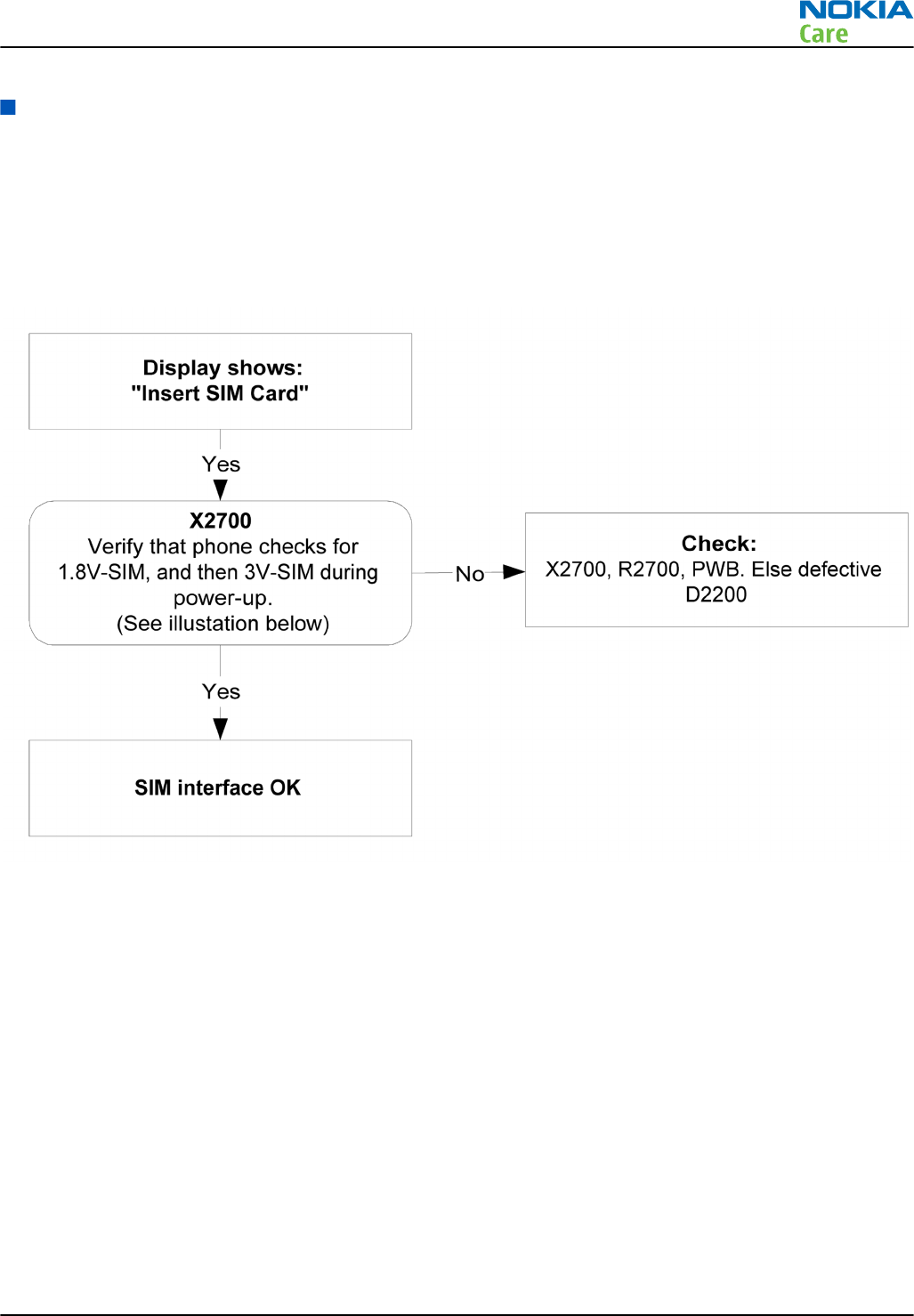
Insert SIM card fault....................................................................................................................................... 3–15
SIM card rejected............................................................................................................................................ 3–16
User interface....................................................................................................................................................... 3–16
Blank display................................................................................................................................................... 3–16
Corrupted display ........................................................................................................................................... 3–17
Dead keys ........................................................................................................................................................ 3–17
No backlight for display or/and keys ........................................................................................................... 3–18
Audio troubleshooting........................................................................................................................................ 3–19
Audio troubleshooting using phoenix......................................................................................................... 3–19
Check microphone using "Hp microphone in Ext speaker out" loop ........................................................ 3–20
Check earpiece using "Ext microphone in Hp speaker out" loop .............................................................. 3–21
Check IHF & ringing tone function using "Buzzer"...................................................................................... 3–21
Check vibra function using "Vibra control".................................................................................................. 3–22
Earpiece fault.................................................................................................................................................. 3–23
IHF/ringing tone fault.................................................................................................................................... 3–24
Microphone fault ............................................................................................................................................ 3–25
Headset earpiece fault................................................................................................................................... 3–26
Headset microphone fault............................................................................................................................. 3–27
List of Tables
Table 4 Connector for External Audio Accessories ........................................................................................... 3–20
List of Figures
Figure 9 Troubleshooting when phone cannot be powered on .......................................................................3–6
Figure 10 Troubleshooting when phone does not stay on or phone is jammed ............................................3–7
Figure 11 Flash programming fault......................................................................................................................3–9
Figure 12 Easy flash programming fault........................................................................................................... 3–11
Figure 13 Troubleshooting when the "Contact Service" message is seen .................................................... 3–13
Figure 14 No registering or call ......................................................................................................................... 3–14
Figure 15 Insert SIM card fault........................................................................................................................... 3–15
Figure 16 Signal diagram ................................................................................................................................... 3–16
Figure 17 Signal diagram ................................................................................................................................... 3–16
Figure 18 Phoenix audio test window.............................................................................................................. 3–19
Figure 19 4-pole jack plug for audio accessory................................................................................................ 3–20
Figure 20 Test arrangement for microphone................................................................................................... 3–21
Figure 21 Test arrangement for of earpiece..................................................................................................... 3–21
Figure 22 Checking IHF and ring tone by using "Buzzer"................................................................................ 3–22
Figure 23 Checking vibra function by using vibra control .............................................................................. 3–22
RM-340; RM-341
Baseband Troubleshooting Instructions
Issue 1 COMPANY CONFIDENTIAL Page 3 –3
Copyright © 2007 Nokia. All rights reserved.

Figure 24 Earpiece fault flow chart ................................................................................................................... 3–23
Figure 25 IHF/ringing tone fault flow chart...................................................................................................... 3–24
Figure 26 Microphone fault flow chart.............................................................................................................. 3–25
Figure 27 Headset earpiece fault flow chart .................................................................................................... 3–26
Figure 28 Headset microphone fault flow chart .............................................................................................. 3–27
RM-340; RM-341
Baseband Troubleshooting Instructions
Page 3 –4 COMPANY CONFIDENTIAL Issue 1
Copyright © 2007 Nokia. All rights reserved.
General baseband troubleshooting
Key components
Power supply test points
Phone cannot be powered on (I)
Context
This means that the phone does not use any current at all when the supply is connected and/or power key
is pressed. It is assumed that the voltage supplied is 3.6VDC. The UEMCLite will prevent any functionality at
battery/supply levels below 2.9VDC.
RM-340; RM-341
Baseband Troubleshooting Instructions
Issue 1 COMPANY CONFIDENTIAL Page 3 –5
Copyright © 2007 Nokia. All rights reserved.

Troubleshooting flow
Figure 9 Troubleshooting when phone cannot be powered on
RM-340; RM-341
Baseband Troubleshooting Instructions
Page 3 –6 COMPANY CONFIDENTIAL Issue 1
Copyright © 2007 Nokia. All rights reserved.
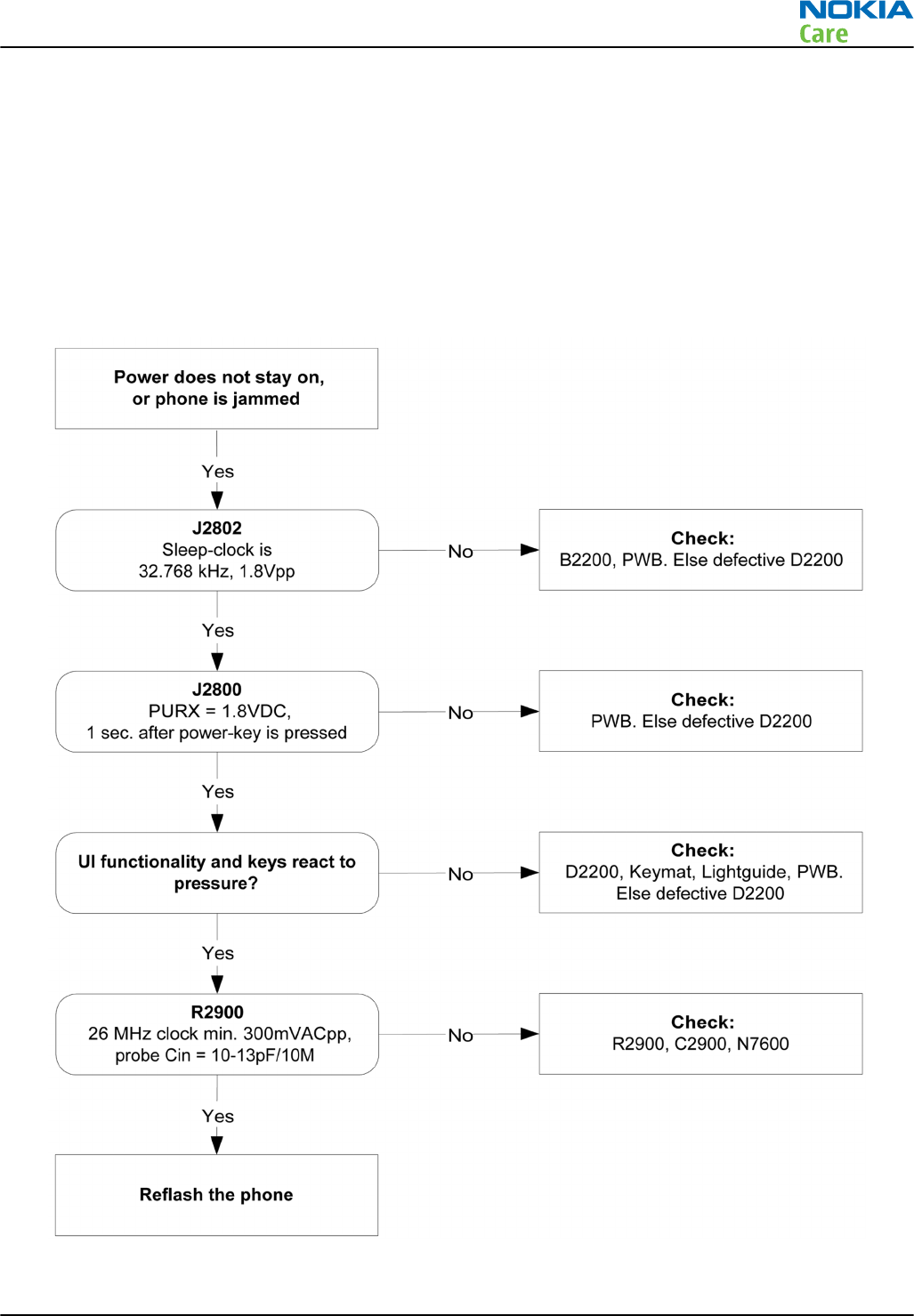
Phone cannot be powered on (II)
Context
If this kind of failure is presenting itself immediately after FLALI, it is most likely caused by ASIC's missing
contact with PWB.
If the MCU doesn’t service the watchdog register within the UEMCLite, the operations watchdog will run out
after approximately 32 seconds. Unfortunately, the service routine can not be measured.
Troubleshooting flow
Figure 10 Troubleshooting when phone does not stay on or phone is jammed
RM-340; RM-341
Baseband Troubleshooting Instructions
Issue 1 COMPANY CONFIDENTIAL Page 3 –7
Copyright © 2007 Nokia. All rights reserved.

Phone cannot be flashed
Context
The flash programming can be done via the pads on the PWB (J2060). If failed, then follow up the trouble
shooting flow chart.
In case of flash failure in the FLALI station, swap the phone and send it back to the care program for further
analysis. Possible failures could be short-circuit of balls under µBGAs (UEMCLite, UPP4M, FLASH), or missing
or misaligned components.
In flash programming error cases, the flash prommer can give some information about a fault. The fault
information messages could be:
Phone doesn't set FBUS_TX line low
Because of the use of uBGA components, it is not possible to verify if there is a short circuit in the control and
address lines of MCU (UPP8M) and the memory (flash).
RM-340; RM-341
Baseband Troubleshooting Instructions
Page 3 –8 COMPANY CONFIDENTIAL Issue 1
Copyright © 2007 Nokia. All rights reserved.
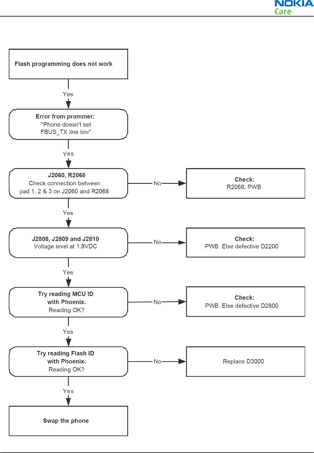
Troubleshooting flow
Figure 11 Flash programming fault
RM-340; RM-341
Baseband Troubleshooting Instructions
Issue 1 COMPANY CONFIDENTIAL Page 3 –9
Copyright © 2007 Nokia. All rights reserved.

Easy flash programming does not work
Context
The flash programming can be done via the easy flash connector. If failed, then follow up the trouble shooting
below.
It is not possible to verify if there is a short circuit in control and address lines of MCU (UPP8M) and memory
(flash) because BGA package is used in RM-340/341.
RM-340; RM-341
Baseband Troubleshooting Instructions
Page 3 –10 COMPANY CONFIDENTIAL Issue 1
Copyright © 2007 Nokia. All rights reserved.
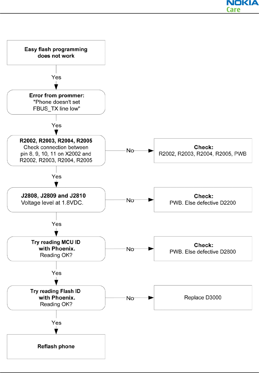
Troubleshooting flow
Figure 12 Easy flash programming fault
RM-340; RM-341
Baseband Troubleshooting Instructions
Issue 1 COMPANY CONFIDENTIAL Page 3 –11
Copyright © 2007 Nokia. All rights reserved.

Display shows "Contact Service"
Troubleshooting flow
This error can only happen at power up where several self-tests are run. If any of these test cases fails the
display will show the message: "Contact Service".
They are individual test cases, so the below lineup of error hunting's has no chronological order. Use common
sense and experience to decide which test case to start error hunting at.
RM-340; RM-341
Baseband Troubleshooting Instructions
Page 3 –12 COMPANY CONFIDENTIAL Issue 1
Copyright © 2007 Nokia. All rights reserved.
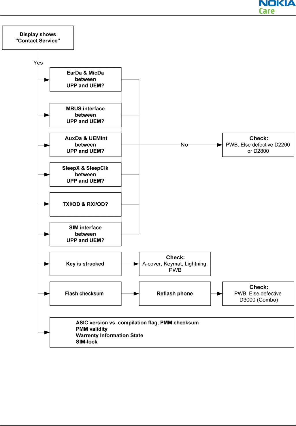
Figure 13 Troubleshooting when the "Contact Service" message is seen
The phone does not register to the networks, or the phone cannot make a call
Context
If the phone doesn't register to the network, the fault can be in either BB or RF. Only few signals can be tested
since several signals are 'buried' in one or more of the inner layers of the PWB.
First, check that SIM LOCK is not causing the error by using a Test-SIM card and connect the phone to a tester.
RM-340; RM-341
Baseband Troubleshooting Instructions
Issue 1 COMPANY CONFIDENTIAL Page 3 –13
Copyright © 2007 Nokia. All rights reserved.
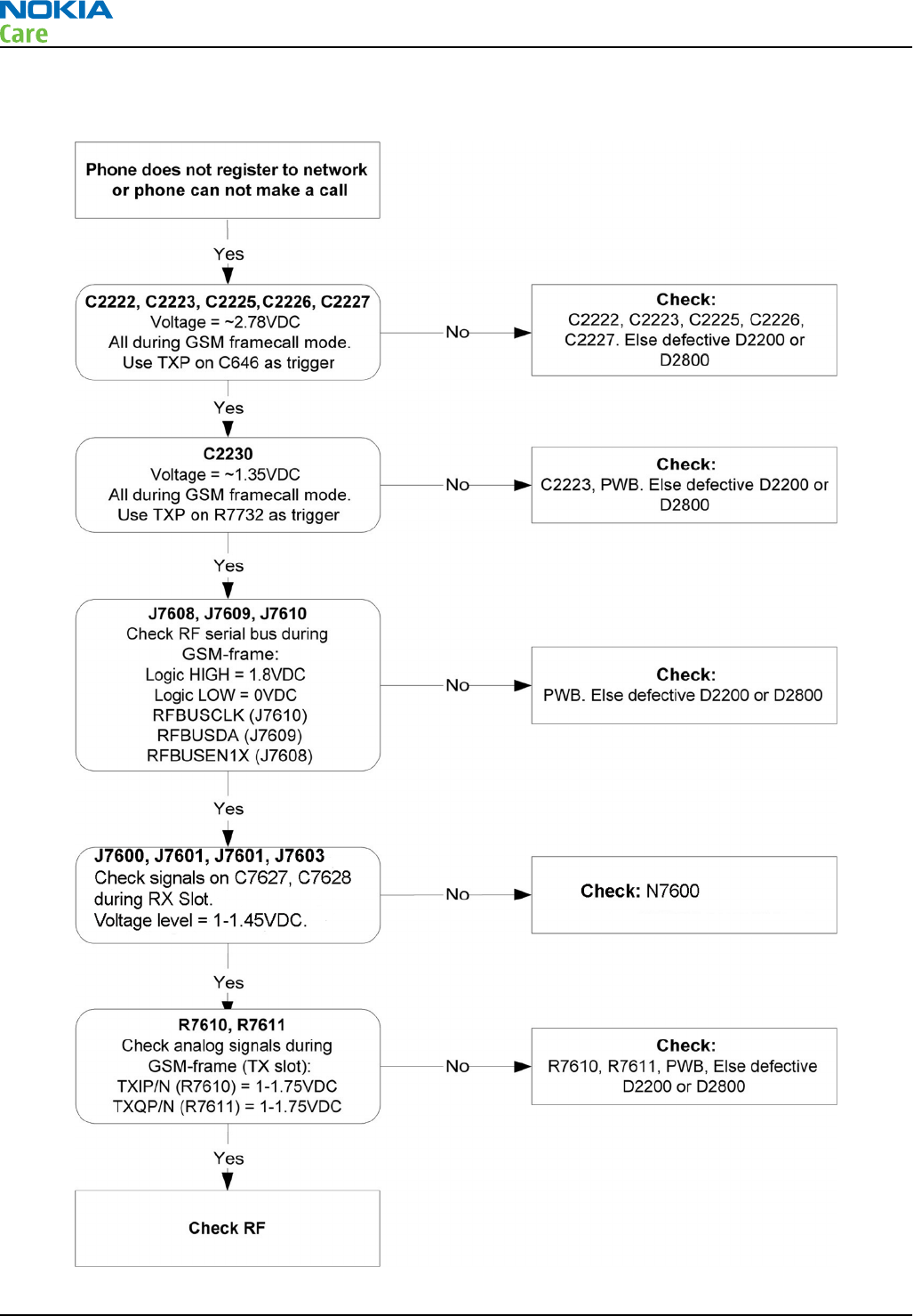
Troubleshooting flow
Figure 14 No registering or call
RM-340; RM-341
Baseband Troubleshooting Instructions
Page 3 –14 COMPANY CONFIDENTIAL Issue 1
Copyright © 2007 Nokia. All rights reserved.
SIM related faults
Insert SIM card fault
Troubleshooting flow
The hardware of the SIM interface from UEMCLite (D2200) to the SIM connector (X2700) can be tested without
a SIM card. When the power is switched on the phone first check for a 1.8V SIM card and then a 3V SIM card.
The phone will try this four times, where after it will display ”Insert SIM card”.
Figure 15 Insert SIM card fault
RM-340; RM-341
Baseband Troubleshooting Instructions
Issue 1 COMPANY CONFIDENTIAL Page 3 –15
Copyright © 2007 Nokia. All rights reserved.

Figure 16 Signal diagram
SIM card rejected
The error ”SIM card rejected” means that the ATR message received from SIM card is corrupted, e.g. data
signal levels are wrong. The first data is always ATR and it is sent from card to phone.
For reference a picture with normal SIM power-up is shown below.
Figure 17 Signal diagram
User interface
Blank display
Context
The display does not show any information at all. If there is only main or sub display blank, the problem
mostly exists in individual display. Replace related display first. For main and sub display blank, refer to
troubleshooting flow below.
RM-340; RM-341
Baseband Troubleshooting Instructions
Page 3 –16 COMPANY CONFIDENTIAL Issue 1
Copyright © 2007 Nokia. All rights reserved.
Troubleshooting flow
Corrupted display
Context
The display contains missing or fading segments, or color presentation is incorrect.
Troubleshooting flow
Dead keys
Context
One or more keys has no function.
RM-340; RM-341
Baseband Troubleshooting Instructions
Issue 1 COMPANY CONFIDENTIAL Page 3 –17
Copyright © 2007 Nokia. All rights reserved.
Troubleshooting flow
No backlight for display or/and keys
Context
There are 3 kinds of statuses: No backlight for both display and keys; No backlight for only display; No
backlight for only keys.
Troubleshooting flow
RM-340; RM-341
Baseband Troubleshooting Instructions
Page 3 –18 COMPANY CONFIDENTIAL Issue 1
Copyright © 2007 Nokia. All rights reserved.

Audio troubleshooting
Audio troubleshooting using phoenix
Figure 18 Phoenix audio test window
RM-340; RM-341
Baseband Troubleshooting Instructions
Issue 1 COMPANY CONFIDENTIAL Page 3 –19
Copyright © 2007 Nokia. All rights reserved.
Figure 19 4-pole jack plug for audio accessory
Table 4 Connector for External Audio Accessories
Pin Signal name Direction Description
5 PLUGDET Input Terminal internal
connection, plug
detection
4 HS EAR L Output Audio output
3 HS EAR R Output Audio output
2 HS MIC Input Multiplexed
microphone audio and
control data
1 HS GND - Ground contact
Check microphone using "Hp microphone in Ext speaker out" loop
Steps
1. Connect phone with Phoenix.
2. Open “audio test” window from “Testing -> Audio test”, as shown in
Figure Phoenix audio test window
above.
3. Select “Hp microphone in Ext speaker out”
4. Select "Acc. Detection" as "Off".
5. Select “Loop” as “On”
6. Input sound at microphone port, for example 94dB SPL 1kHz.
RM-340; RM-341
Baseband Troubleshooting Instructions
Page 3 –20 COMPANY CONFIDENTIAL Issue 1
Copyright © 2007 Nokia. All rights reserved.
7. Check if signal is detected at HS EAR L/R, shown in
Figure 4-pole jack plug for audio accessory
above.
Figure 20 Test arrangement for microphone
Check earpiece using "Ext microphone in Hp speaker out" loop
Steps
1. Connect phone with Phoenix.
2. Open the
Audio Test
window from Testing→ Audio test , as shown in Figure
Phoenix audio test
window
above.
3. Select Ext microphone in Hp speaker out.
4. Select Acc.Detection as Off.
5. Select Loop as On.
6. Input signal to HS MIC, as shown in Figure
4-pole jack plug for audio accessory
above, for example
100mVpp, 1kHz.
7. Check if sound is heard in the earpiece.
Figure 21 Test arrangement for of earpiece
Check IHF & ringing tone function using "Buzzer"
Steps
1. Connect phone with Phoenix.
2. Open “audio test” window from “Testing -> Audio test”, as shown in
Figure Phoenix audio test window
above.
3. In “Buzzer” area, select suitable signal to be played, for example 1 kHz, Strength 5”
4. Select “Volume” as “On”
RM-340; RM-341
Baseband Troubleshooting Instructions
Issue 1 COMPANY CONFIDENTIAL Page 3 –21
Copyright © 2007 Nokia. All rights reserved.
5. Check if sound is heard in IHF.
Figure 22 Checking IHF and ring tone by using "Buzzer"
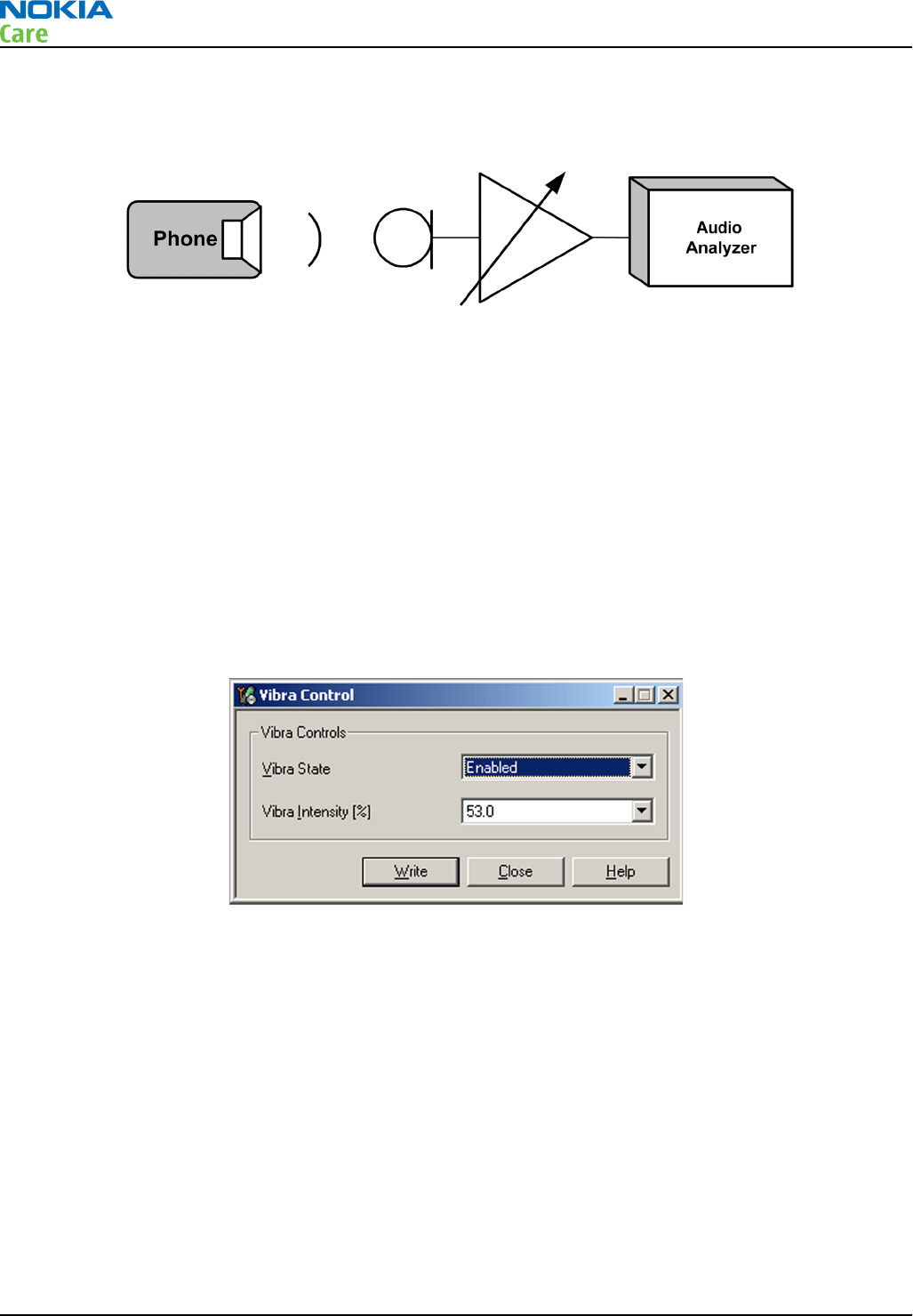
Check vibra function using "Vibra control"
Steps
1. Connect phone with Phoenix.
2. Open “Vibra control” window from “Testing -> Vibra control”, as shown in the figure below.
3. Select suitable intensity value, for example 53 %.
4. Select “Vibra state” as “Enabled”
5. Click “Write”.
6. Check if Vibra works.
Figure 23 Checking vibra function by using vibra control
RM-340; RM-341
Baseband Troubleshooting Instructions
Page 3 –22 COMPANY CONFIDENTIAL Issue 1
Copyright © 2007 Nokia. All rights reserved.

Earpiece fault
Troubleshooting flow
Figure 24 Earpiece fault flow chart
RM-340; RM-341
Baseband Troubleshooting Instructions
Issue 1 COMPANY CONFIDENTIAL Page 3 –23
Copyright © 2007 Nokia. All rights reserved.
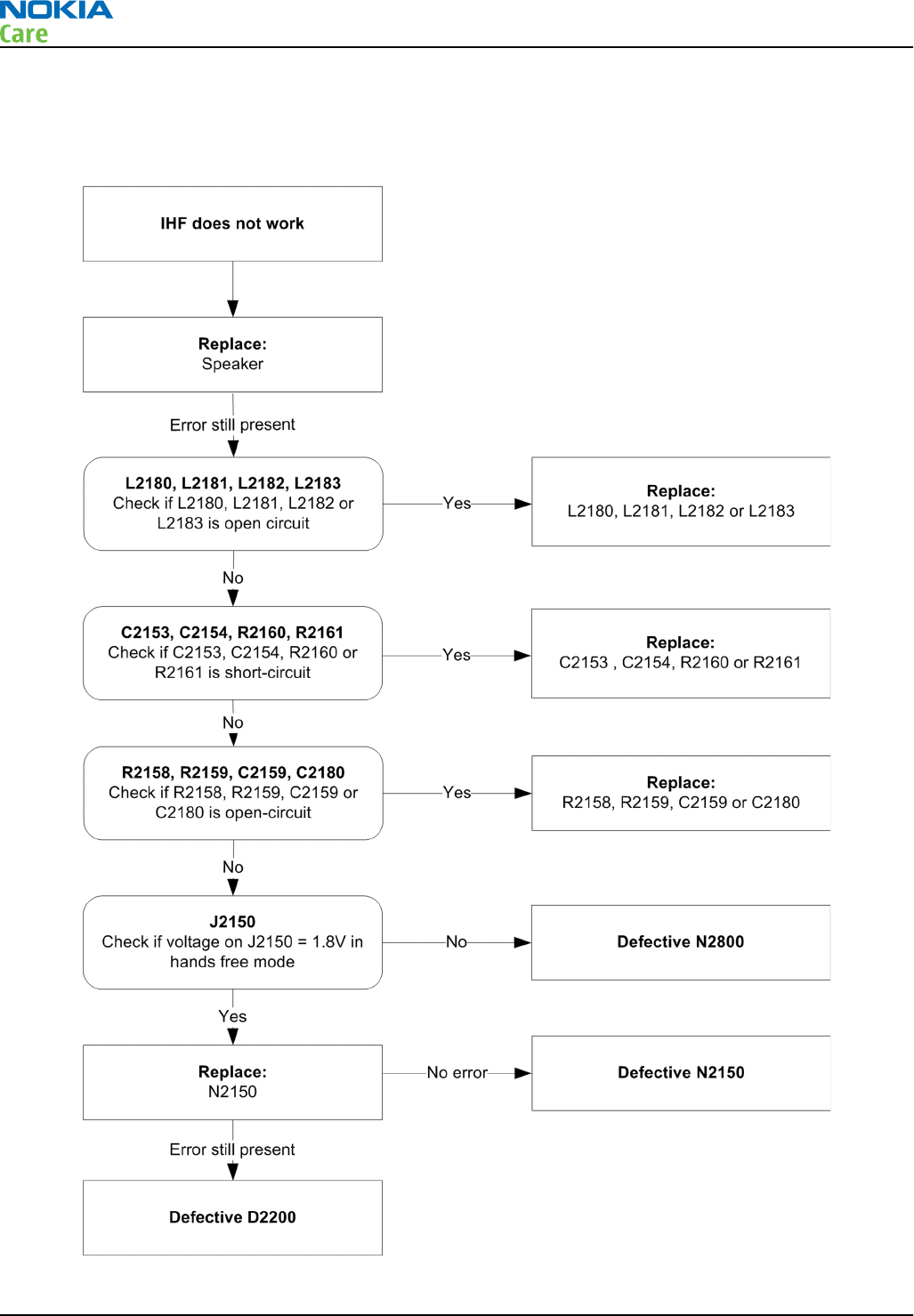
IHF/ringing tone fault
Troubleshooting flow
Figure 25 IHF/ringing tone fault flow chart
RM-340; RM-341
Baseband Troubleshooting Instructions
Page 3 –24 COMPANY CONFIDENTIAL Issue 1
Copyright © 2007 Nokia. All rights reserved.
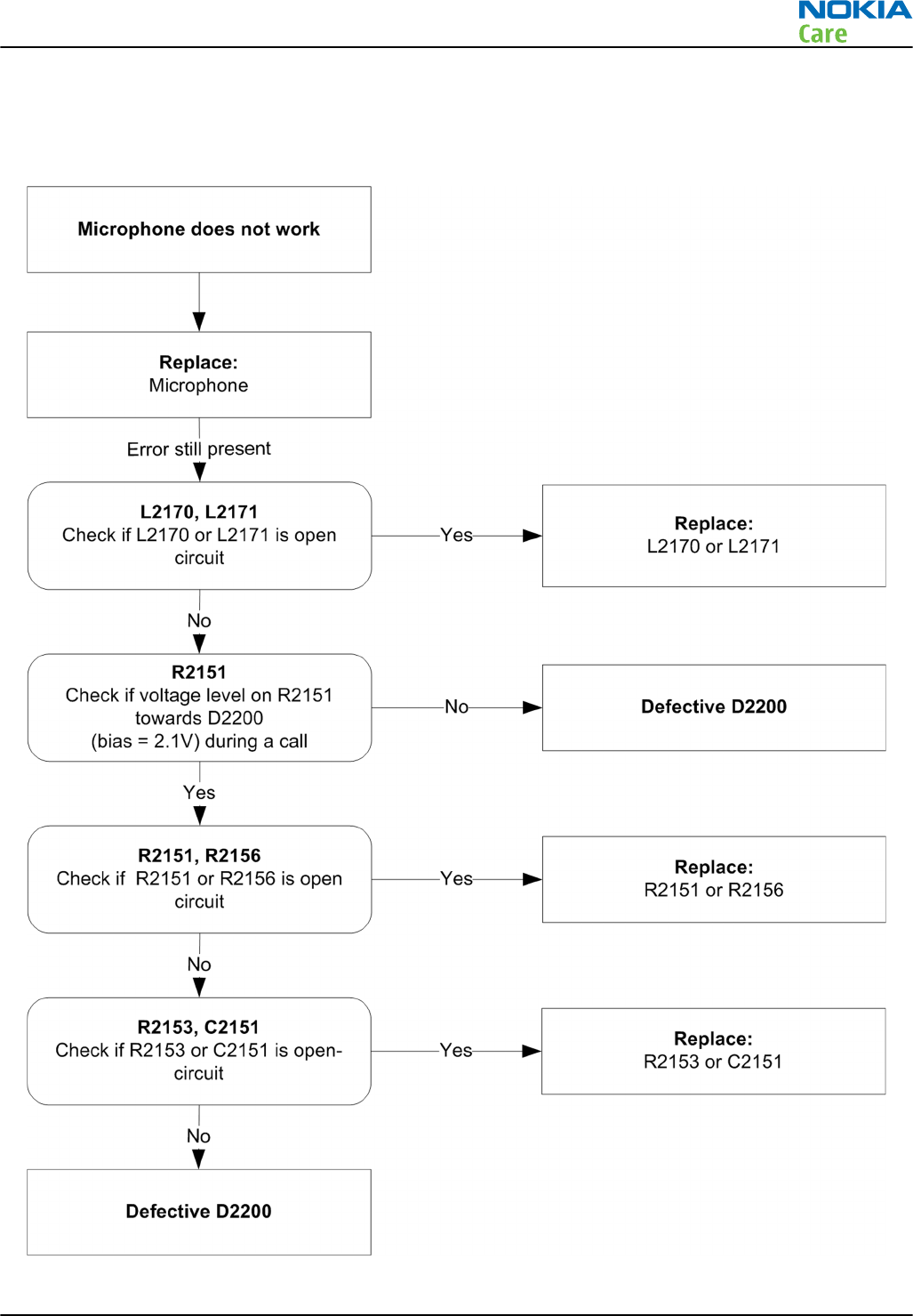
Microphone fault
Troubleshooting flow
Figure 26 Microphone fault flow chart
RM-340; RM-341
Baseband Troubleshooting Instructions
Issue 1 COMPANY CONFIDENTIAL Page 3 –25
Copyright © 2007 Nokia. All rights reserved.
Headset earpiece fault
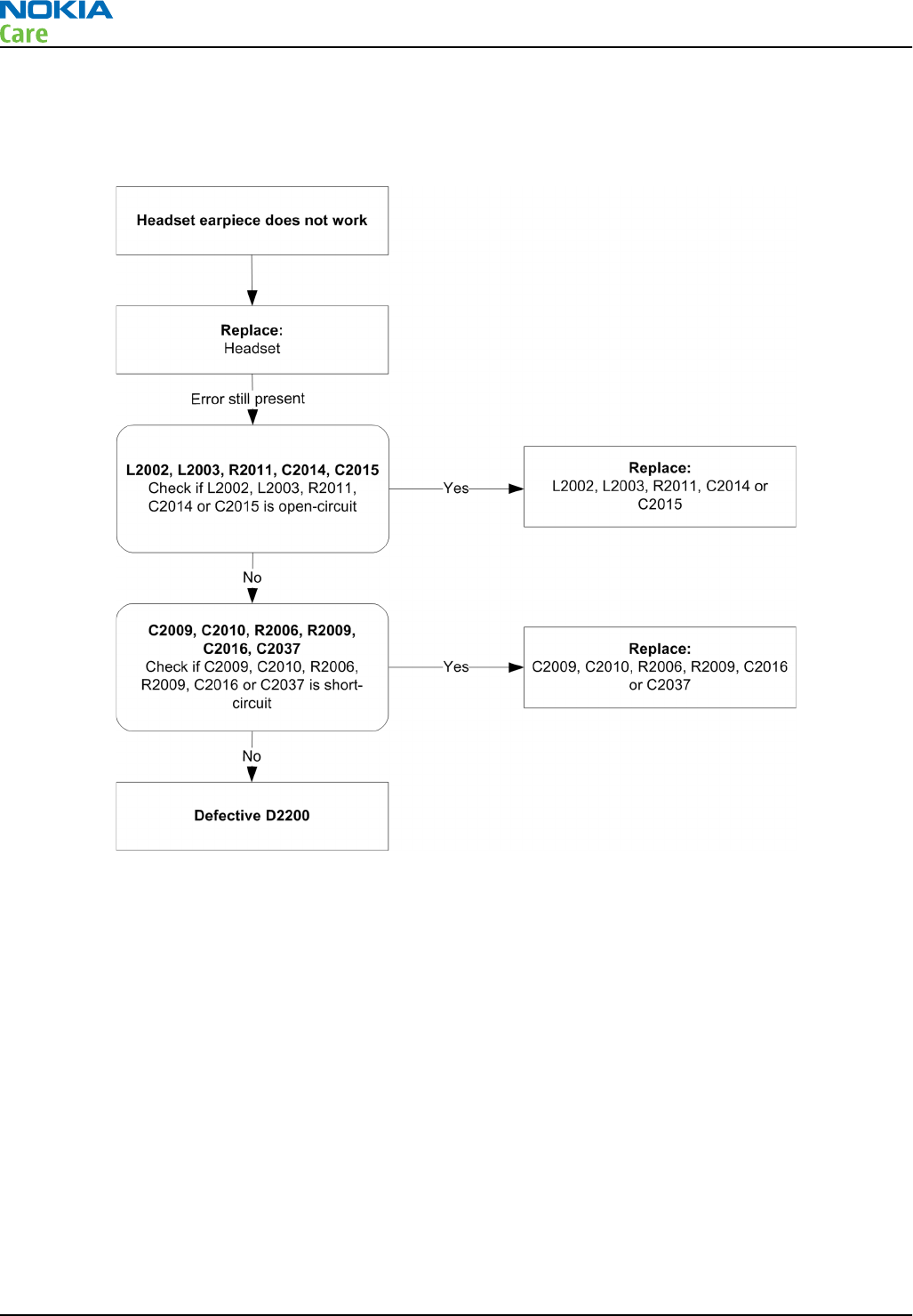
Troubleshooting flow
Figure 27 Headset earpiece fault flow chart
RM-340; RM-341
Baseband Troubleshooting Instructions
Page 3 –26 COMPANY CONFIDENTIAL Issue 1
Copyright © 2007 Nokia. All rights reserved.

Headset microphone fault
Troubleshooting flow
Figure 28 Headset microphone fault flow chart
RM-340; RM-341
Baseband Troubleshooting Instructions
Issue 1 COMPANY CONFIDENTIAL Page 3 –27
Copyright © 2007 Nokia. All rights reserved.

RM-340; RM-341
Baseband Troubleshooting Instructions
(This page left intentionally blank.)
Page 3 –28 COMPANY CONFIDENTIAL Issue 1
Copyright © 2007 Nokia. All rights reserved.

4 — RF Troubleshooting
Instructions
Nokia Customer Care
Issue 1 COMPANY CONFIDENTIAL Page 4 –1
Copyright © 2007 Nokia. All rights reserved.

RM-340; RM-341
RF Troubleshooting Instructions
(This page left intentionally blank.)
Page 4 –2 COMPANY CONFIDENTIAL Issue 1
Copyright © 2007 Nokia. All rights reserved.

Table of Contents
General RF troubleshooting ..................................................................................................................................4–7
General RF troubleshooting .............................................................................................................................4–7
RF key components ...........................................................................................................................................4–7
Auto tuning........................................................................................................................................................4–9
RM-340 receiver .................................................................................................................................................. 4–10
General instructions for GSM900 RX troubleshooting ................................................................................ 4–10
Troubleshooting diagram for GSM900 receiver .......................................................................................... 4–12
General instructions for GSM 1800 RX troubleshooting ............................................................................. 4–13
Troubleshooting diagram for GSM1800 receiver ........................................................................................ 4–15
Measurement points in the receiver ............................................................................................................ 4–16
RM-340 transmitter............................................................................................................................................. 4–17
General instructions for GSM 900 TX troubleshooting................................................................................ 4–17
Troubleshooting diagram for GSM900 transmitter .................................................................................... 4–19
GSM900 TX output power.............................................................................................................................. 4–19
General instructions for GSM1800 TX troubleshooting .............................................................................. 4–22
Troubleshooting diagram for GSM1800 transmitter .................................................................................. 4–24
GSM1800 TX output power............................................................................................................................ 4–24
RM-341 receiver................................................................................................................................................... 4–27
General instructions for GSM 850 RX troubleshooting ............................................................................... 4–27
Troubleshooting diagram for GSM850 receiver .......................................................................................... 4–29
General instructions for GSM1900 RX troubleshooting .............................................................................. 4–30
Troubleshooting diagram for GSM1900 receiver ........................................................................................ 4–32
Measurement points in the receiver ............................................................................................................ 4–34
RM-341 transmitter ............................................................................................................................................ 4–35
General instructions for GSM 850 TX troubleshooting................................................................................ 4–35
Troubleshooting diagram for GSM850 transmitter .................................................................................... 4–37
GSM850 TX output power.............................................................................................................................. 4–38
General instructions for GSM1900 TX troubleshooting .............................................................................. 4–40
Troubleshooting diagram for GSM1900 transmitter .................................................................................. 4–42
GSM1900 TX output power............................................................................................................................ 4–43
Synthesizer troubleshooting ............................................................................................................................. 4–45
Introduction.................................................................................................................................................... 4–45
Troubleshooting diagram for PLL synthesizer ............................................................................................ 4–47
Measurement points at the VCXO ................................................................................................................. 4–48
FM radio and bluetooth troubleshooting ......................................................................................................... 4–48
Measurement settings ................................................................................................................................... 4–48
Troubleshooting diagram for FM radio........................................................................................................ 4–50
Bluetooth and FM radio test points.............................................................................................................. 4–51
Introduction to Bluetooth troubleshooting ................................................................................................ 4–52
Bluetooth settings for Phoenix..................................................................................................................... 4–52
Bluetooth self tests in Phoenix..................................................................................................................... 4–53
Bluetooth BER failure troubleshooting........................................................................................................ 4–54
Antenna troubleshooting ................................................................................................................................... 4–56
Antenna troubleshooting diagram............................................................................................................... 4–56
List of Figures
Figure 29 RF key components on PWB.................................................................................................................4–7
Figure 30 Supply points at UEM (D2200)..............................................................................................................4–8
Figure 31 Supply point at RF IC (N7600) ..............................................................................................................4–9
RM-340; RM-341
RF Troubleshooting Instructions
Issue 1 COMPANY CONFIDENTIAL Page 4 –3
Copyright © 2007 Nokia. All rights reserved.

Figure 32 Supply point at BT & FM IC (N6000).....................................................................................................4–9
Figure 33 GSM900 RF controls window............................................................................................................. 4–11
Figure 34 GSM900 receiver troubleshooting .................................................................................................... 4–12
Figure 35 900 RX I/Q signal waveform.............................................................................................................. 4–13
Figure 36 GSM1800 RF controls window........................................................................................................... 4–14
Figure 37 GSM1800 receiver troubleshooting .................................................................................................. 4–15
Figure 38 1800 RX I/Q signal waveform............................................................................................................ 4–16
Figure 39 RX measurements point of the control voltages to FEM N7700.................................................... 4–16
Figure 40 Measurement points at the RX SAW Filters – Z7600/Z7602 ........................................................... 4–17
Figure 41 RX I/Q signals...................................................................................................................................... 4–17
Figure 42 GSM 900 RF controls window............................................................................................................ 4–18
Figure 43 GSM900 tarnsmitter troubleshooting .............................................................................................. 4–19
Figure 44 TX I/O signal........................................................................................................................................ 4–20
Figure 45 VC1, VC3 signals .................................................................................................................................. 4–20
Figure 46 TXP signal............................................................................................................................................ 4–21
Figure 47 TXC signals at PCL5 ............................................................................................................................. 4–21
Figure 48 TXC signals at PCL19........................................................................................................................... 4–22
Figure 49 GSM 1800 RF controls window.......................................................................................................... 4–23
Figure 50 GSM1800 transmitter troubleshooting ............................................................................................ 4–24
Figure 51 TX I/O signal........................................................................................................................................ 4–25
Figure 52 VC1, VC2, VC3 signals .......................................................................................................................... 4–25
Figure 53 TXP signal............................................................................................................................................ 4–26
Figure 54 TXC signals at PCL0 ............................................................................................................................. 4–26
Figure 55 TXC signals at PCL15........................................................................................................................... 4–27
Figure 56 GSM850 RF controls window............................................................................................................. 4–28
Figure 57 GSM850 receiver troubleshooting .................................................................................................... 4–29
Figure 58 850 RX I/Q signal waveform.............................................................................................................. 4–30
Figure 59 GSM 1900 RF controls window.......................................................................................................... 4–31
Figure 60 GSM1900 receiver troubleshooting .................................................................................................. 4–32
Figure 61 1900 RX I/Q signal waveform............................................................................................................ 4–33
Figure 62 RX measurements point of the control voltages to FEM N7700.................................................... 4–34
Figure 63 Measurement points at the RX SAW Filters – Z7600/Z7602 ........................................................... 4–34
Figure 64 RX I/Q signals...................................................................................................................................... 4–35
Figure 65 GSM 850 RF controls window............................................................................................................ 4–36
Figure 66 GSM850 transmitter troubleshooting .............................................................................................. 4–37
Figure 67 TX I/O signal........................................................................................................................................ 4–38
Figure 68 VC1, VC3 signal.................................................................................................................................... 4–38
Figure 69 TXP signal............................................................................................................................................ 4–39
Figure 70 TXC signals at PCL5 ............................................................................................................................. 4–39
Figure 71 TXC signals at PCL19........................................................................................................................... 4–40
Figure 72 GSM 1900 RF controls window.......................................................................................................... 4–41
Figure 73 GSM1900 transmitter troubleshooting ............................................................................................ 4–42
Figure 74 TX I/O signal........................................................................................................................................ 4–43
Figure 75 VC1, VC2, VC3 signals .......................................................................................................................... 4–43
Figure 76 TXP signal............................................................................................................................................ 4–44
Figure 77 TXC signals at PCL0 ............................................................................................................................. 4–44
Figure 78 TXC signals at PCL15........................................................................................................................... 4–45
Figure 79 VCXO 26 MHz waveform..................................................................................................................... 4–46
Figure 80 PLL Troubleshooting diagram........................................................................................................... 4–47
Figure 81 Measurement point for VCXO ............................................................................................................ 4–48
Figure 82 Phoenix settings................................................................................................................................. 4–49
Figure 83 FM circuit troubleshooting diagram................................................................................................. 4–50
RM-340; RM-341
RF Troubleshooting Instructions
Page 4 –4 COMPANY CONFIDENTIAL Issue 1
Copyright © 2007 Nokia. All rights reserved.

Figure 84 Bluetooth and FM radio test points.................................................................................................. 4–51
Figure 85 XAUDIO output signal......................................................................................................................... 4–51
Figure 86 FM module output signal................................................................................................................... 4–52
Figure 87 BER test result..................................................................................................................................... 4–53
Figure 88 Bluetooth self tests in Phoenix......................................................................................................... 4–54
Figure 89 Antenna troubleshooting.................................................................................................................. 4–56
RM-340; RM-341
RF Troubleshooting Instructions
Issue 1 COMPANY CONFIDENTIAL Page 4 –5
Copyright © 2007 Nokia. All rights reserved.

RM-340; RM-341
RF Troubleshooting Instructions
(This page left intentionally blank.)
Page 4 –6 COMPANY CONFIDENTIAL Issue 1
Copyright © 2007 Nokia. All rights reserved.
General RF troubleshooting
General RF troubleshooting
Most RF semiconductors are static discharge sensitive
Two types of measurements are used in the following. It will be specified if the measurement type is "RF" or
"LF".
• RF measurements are done with a Spectrum Analyzer and a high-frequency 500 ohm passive probe, for
example HP54006A. (Note that when measuring with the 500ohm probe the signal will be around 20dB
attenuated. The values in the following will have these 20dB subtracted and represent the real value seen
on the spectrum analyzer). Note that the testing have some losses which must be taken into consideration
when calibrating the test system.
•LF (Low frequency) and DC measurements should be done with a 10:1 probe and an oscilloscope. The probe
used in the following is 10Mohm/8pF passive probe. If using another probe then bear in mind that the
voltages displayed may be slightly different. Always make sure the measurement set-up is calibrated when
measuring RF parameters on the antenna pad. Remember to include the loss in the module repair jig when
realigning the phone.
So ESD protection must be applied during repair (ground straps and ESD soldering irons). Mjoelner and Bifrost
are moisture sensitive so parts must be pre-baked prior to soldering. Apart from key-components described
in this document there are a lot of discrete components (resistors, inductors and capacitors) for which
troubleshooting is done by checking if soldering of the component is done properly and checking if the
component is missing from PWB. Capacitors can be checked for short-circuiting and resistors for value by
means of an ohmmeter, but be aware in-circuit measurements should be evaluated carefully. In the following
both the name EGSM and GSM850 will be used for the lower band and both PCN and GSM1900 will be used
for the upper band.
RF key components
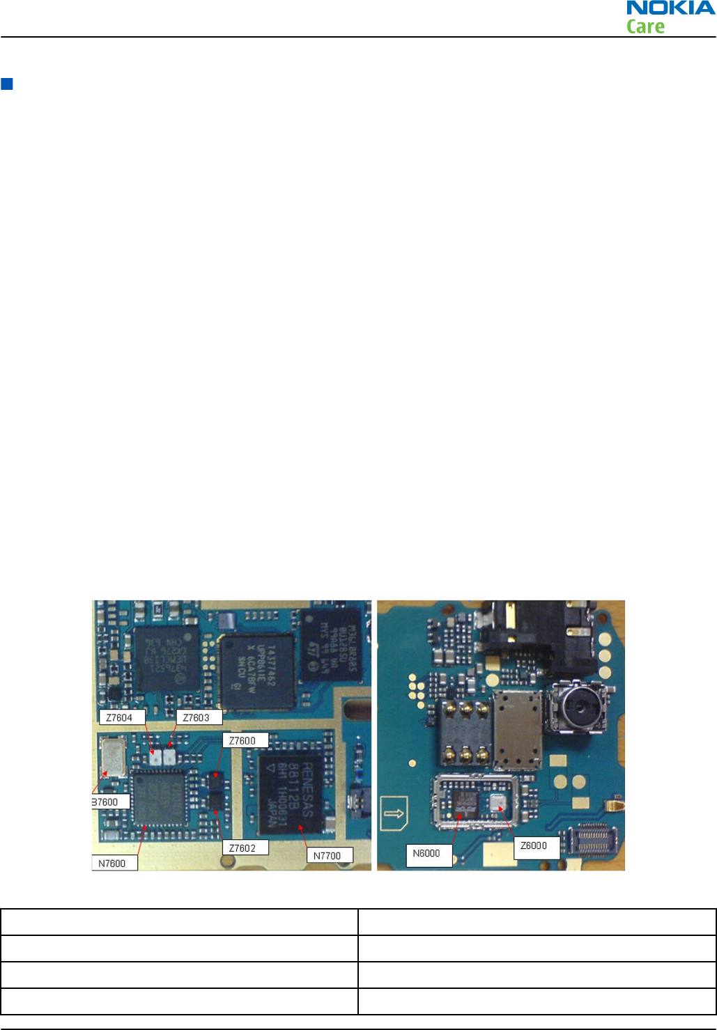
Figure 29 RF key components on PWB
N7600 PMB3258 RF IC
N7700 FEM (PA and antenna switch)
Z7602 EGSM 850/900 RX SAW filter
Z7600 DCS 1800/PCS1900 RX SAW filter
RM-340; RM-341
RF Troubleshooting Instructions
Issue 1 COMPANY CONFIDENTIAL Page 4 –7
Copyright © 2007 Nokia. All rights reserved.
Z7603 EGSM 850/900 TX filter
Z7604 DCS 1800/PCS1900 TX filter
B7600 26 MHz crystal
N6000 BT & FM IC
Z6000 BT SAW filter
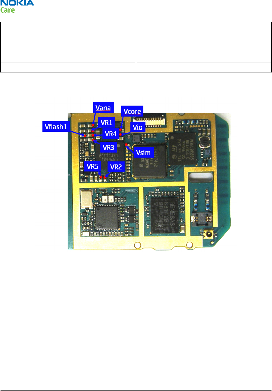
Refer to the picture below for measuring points at the UEM (D2200).
Figure 30 Supply points at UEM (D2200)
RM-340; RM-341
RF Troubleshooting Instructions
Page 4 –8 COMPANY CONFIDENTIAL Issue 1
Copyright © 2007 Nokia. All rights reserved.

Figure 31 Supply point at RF IC (N7600)
Figure 32 Supply point at BT & FM IC (N6000)
Auto tuning
This phone can be tuned automatically.
RM-340; RM-341
RF Troubleshooting Instructions
Issue 1 COMPANY CONFIDENTIAL Page 4 –9
Copyright © 2007 Nokia. All rights reserved.

Autotune is designed to align the phone's RF part easier and faster. It performs calibrations, tunings and
measurements of RX and TX. The results are displayed and logged in a result file, if initiated.
Hardware set up
Hardware requirements for auto tuning:
• PC (Windows 2000/NT) with GPIB card
• Power supply
• Product specific module jig
• Cables: 3 (alt.1) RF cable, 1 GPIB cable and DAU-9S
• Signal analyser (TX), signal generator (RX) and RF-splitter
or
one device including all.
Phoenix preparations
Copy the two phone specific ini-files, for example
rm_13_tunings.ini
and
autotune_RM-13.ini,
to a phone
specific folder, for example
\Phoenix\products\RM-13\
.
Auto tuning procedure
1 Make sure the phone (in the jig) is connected to the equipment. Else, some menus will not be shown in
Phoenix.
2 The first time you are using automatic tuning on this phone model, on this computer, you will have to
Set loss
for cables and jigs.
3 To go to autotune, select
Tuning (Alt-U)
>
Auto-Tune (Alt-A)
from the menu.
4 If you need more assistance, please refer to the Phoenix
Help
.
RM-340 receiver
General instructions for GSM900 RX troubleshooting
Steps
1. Connect the phone to a PC with the module repair jig.
2. Start
Phoenix
and establish a connection to the phone with the data cable e.g. FBUS.
3. Select File and Scan product.
4. Wait a while for the PC to read the information from the phone.
5. Select Testing and RF Controls.
6. Set the parameters as follows:
i Active Unit: RX
ii Band: GSM 900
iii Operation Mode: Continuous mode
iv RX/TX Channel 37
v AGC: 8: FEG_ON + DTOS_ON+BB_6=Vgain_36
Results
The setup should now look like this:
RM-340; RM-341
RF Troubleshooting Instructions
Page 4 –10 COMPANY CONFIDENTIAL Issue 1
Copyright © 2007 Nokia. All rights reserved.

Figure 33 GSM900 RF controls window
RM-340; RM-341
RF Troubleshooting Instructions
Issue 1 COMPANY CONFIDENTIAL Page 4 –11
Copyright © 2007 Nokia. All rights reserved.

Troubleshooting diagram for GSM900 receiver
Troubleshooting flow
Figure 34 GSM900 receiver troubleshooting
Results
By measuring with an oscilloscope at RXIP or RXQP on a working GSM900 receiver this picture should be seen.
Signal amplitude peak-peak 108mV. DC offset 1.0V.
RM-340; RM-341
RF Troubleshooting Instructions
Page 4 –12 COMPANY CONFIDENTIAL Issue 1
Copyright © 2007 Nokia. All rights reserved.

Figure 35 900 RX I/Q signal waveform
General instructions for GSM 1800 RX troubleshooting
Steps
1. Connect the phone to a PC with the module repair jig.
2. Start
Phoenix
and establish a connection to the phone with the data cable e.g. FBUS.
3. Select File and Scan product.
4. Wait a while for the PC to read the information from the phone.
5. Select Testing and RF Controls.
6. Set the parameters as follows:
i Active Unit: RX
ii Band: GSM 1800
iii Operation Mode: Continuous mode
iv RX/TX Channel 700
v AGC: 8: FEG_ON + DTOS_ON+BB_6=Vgain_36
Results
The setup should now look like this:
RM-340; RM-341
RF Troubleshooting Instructions
Issue 1 COMPANY CONFIDENTIAL Page 4 –13
Copyright © 2007 Nokia. All rights reserved.

Figure 36 GSM1800 RF controls window
RM-340; RM-341
RF Troubleshooting Instructions
Page 4 –14 COMPANY CONFIDENTIAL Issue 1
Copyright © 2007 Nokia. All rights reserved.
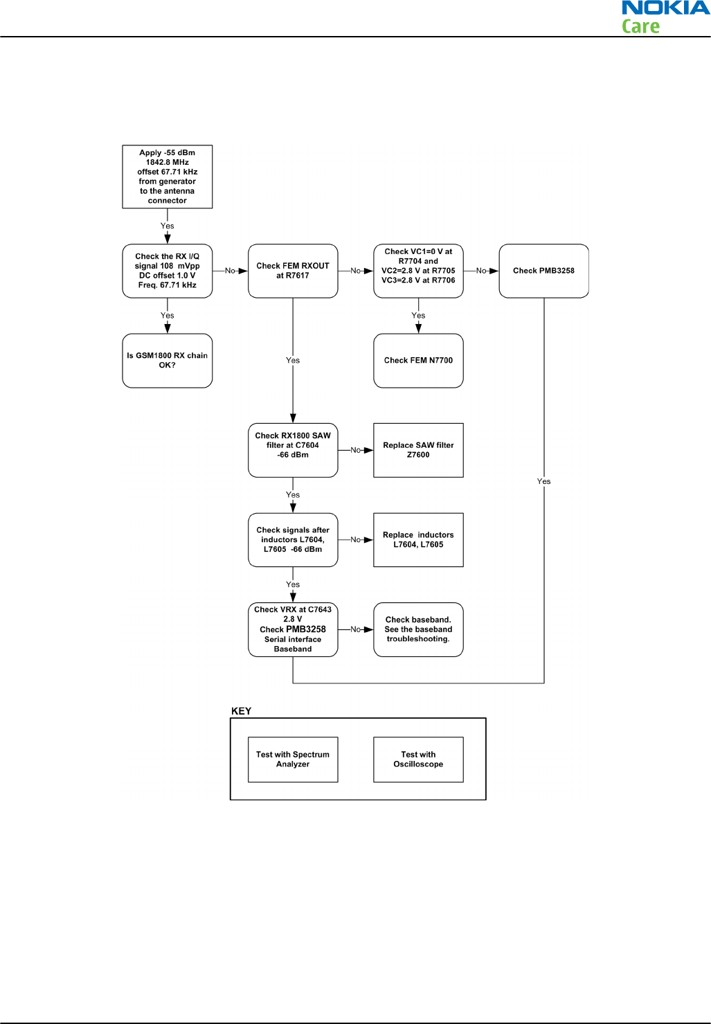
Troubleshooting diagram for GSM1800 receiver
Troubleshooting flow
Figure 37 GSM1800 receiver troubleshooting
Results
By measuring with an oscilloscope at RXIP or RXQP on a working GSM1800 receiver this picture should be
seen. Signal amplitude peak-peak 114mV. DC offset 1.0V.
RM-340; RM-341
RF Troubleshooting Instructions
Issue 1 COMPANY CONFIDENTIAL Page 4 –15
Copyright © 2007 Nokia. All rights reserved.

Figure 38 1800 RX I/Q signal waveform
Measurement points in the receiver
Figure 39 RX measurements point of the control voltages to FEM N7700
RM-340; RM-341
RF Troubleshooting Instructions
Page 4 –16 COMPANY CONFIDENTIAL Issue 1
Copyright © 2007 Nokia. All rights reserved.
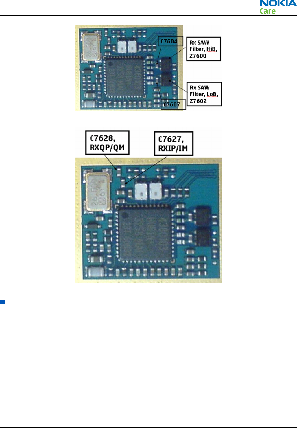
Figure 40 Measurement points at the RX SAW Filters – Z7600/Z7602
Figure 41 RX I/Q signals
RM-340 transmitter
General instructions for GSM 900 TX troubleshooting
Steps
1. Apply a RF-cable to the RF-connector to allow the transmitted signal act as normal. RF-cable should be
connected to an attenuator at least 10dB before connected to the measurement equipment, otherwise
the PA may be damaged.
2. Start
Phoenix
and establish a connection to the phone with the data cable e.g. FBUS.
3. Select File and Scan product.
4. Wait a while for the PC to read the information from the phone.
5. Select Testing and RF Controls.
6. Set the parameters as follows:
i Band: GSM 900
RM-340; RM-341
RF Troubleshooting Instructions
Issue 1 COMPANY CONFIDENTIAL Page 4 –17
Copyright © 2007 Nokia. All rights reserved.

ii Active Unit: TX
iii TX Power Level: 5
iv TX Data Type: Random
Results
The setup should now look like this:
Figure 42 GSM 900 RF controls window
RM-340; RM-341
RF Troubleshooting Instructions
Page 4 –18 COMPANY CONFIDENTIAL Issue 1
Copyright © 2007 Nokia. All rights reserved.
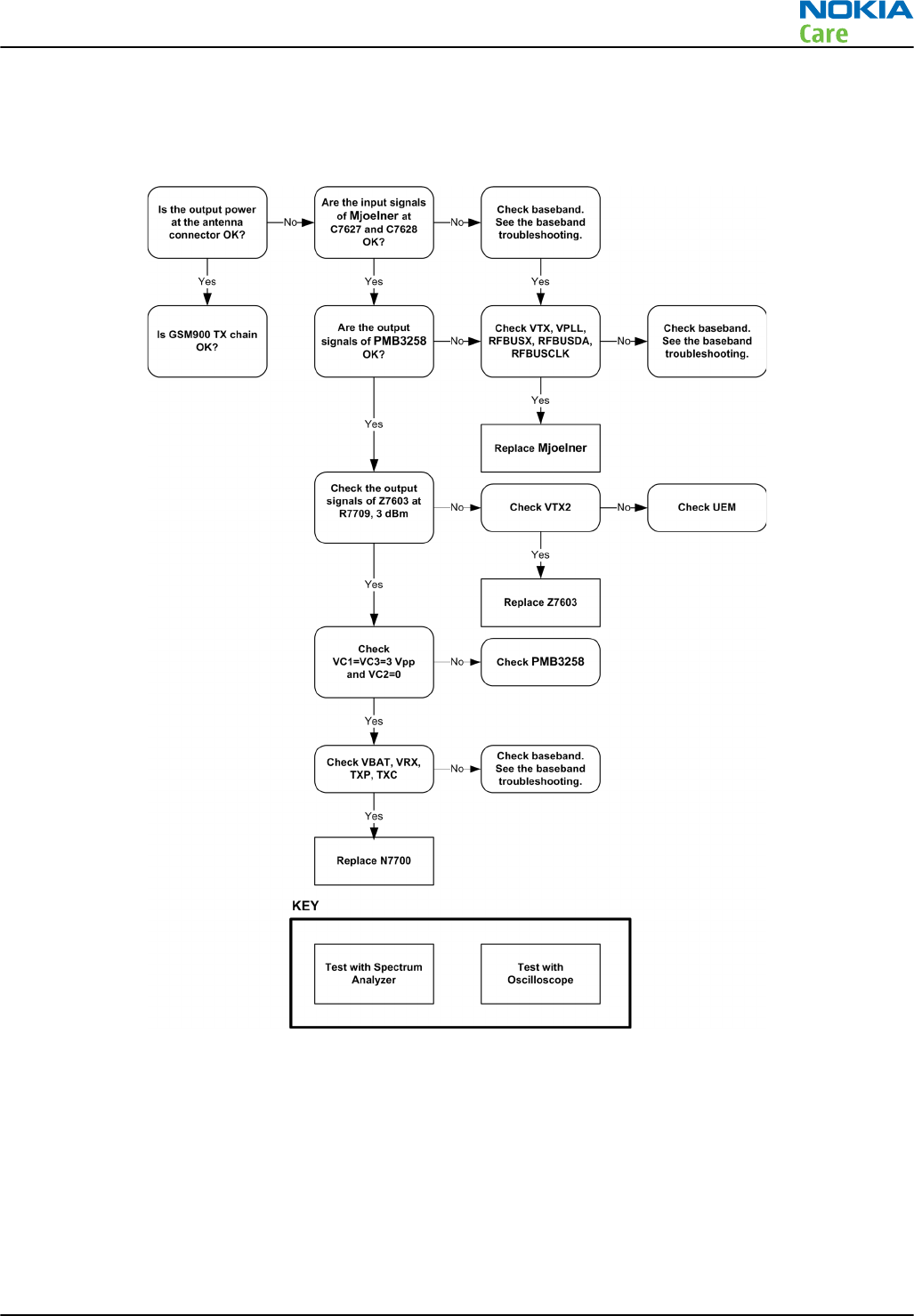
Troubleshooting diagram for GSM900 transmitter
Troubleshooting flow
Figure 43 GSM900 tarnsmitter troubleshooting
GSM900 TX output power
Measure the output power of the phone; it should be about 32.5dBm. Remember the cable loss is about
0.3dB.
RM-340; RM-341
RF Troubleshooting Instructions
Issue 1 COMPANY CONFIDENTIAL Page 4 –19
Copyright © 2007 Nokia. All rights reserved.
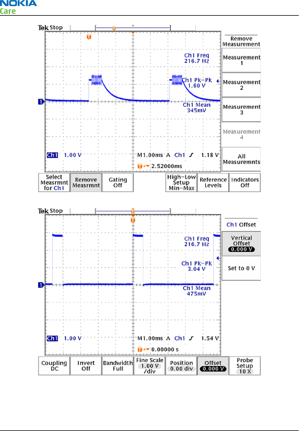
Figure 44 TX I/O signal
Figure 45 VC1, VC3 signals
RM-340; RM-341
RF Troubleshooting Instructions
Page 4 –20 COMPANY CONFIDENTIAL Issue 1
Copyright © 2007 Nokia. All rights reserved.
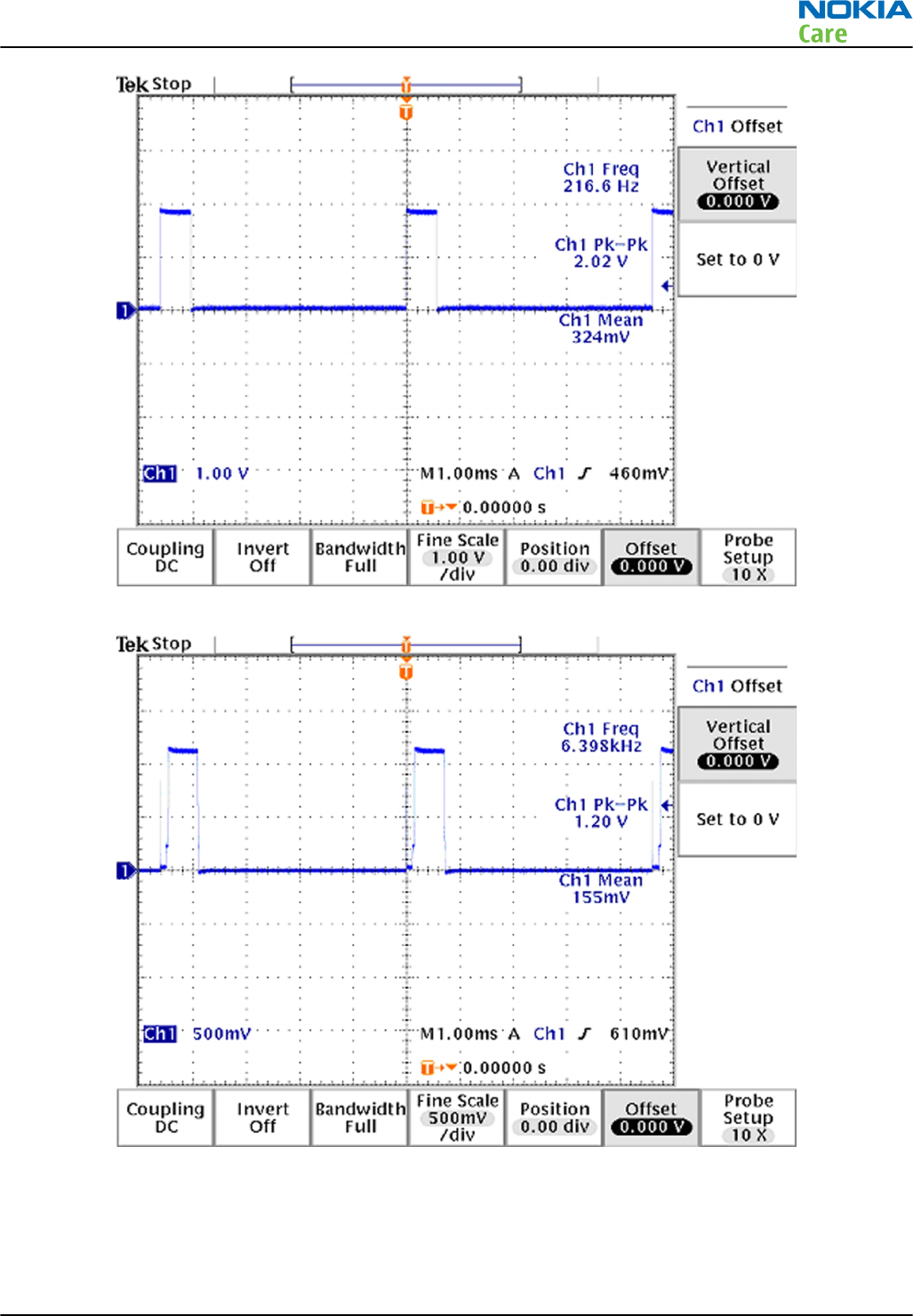
Figure 46 TXP signal
Figure 47 TXC signals at PCL5
RM-340; RM-341
RF Troubleshooting Instructions
Issue 1 COMPANY CONFIDENTIAL Page 4 –21
Copyright © 2007 Nokia. All rights reserved.
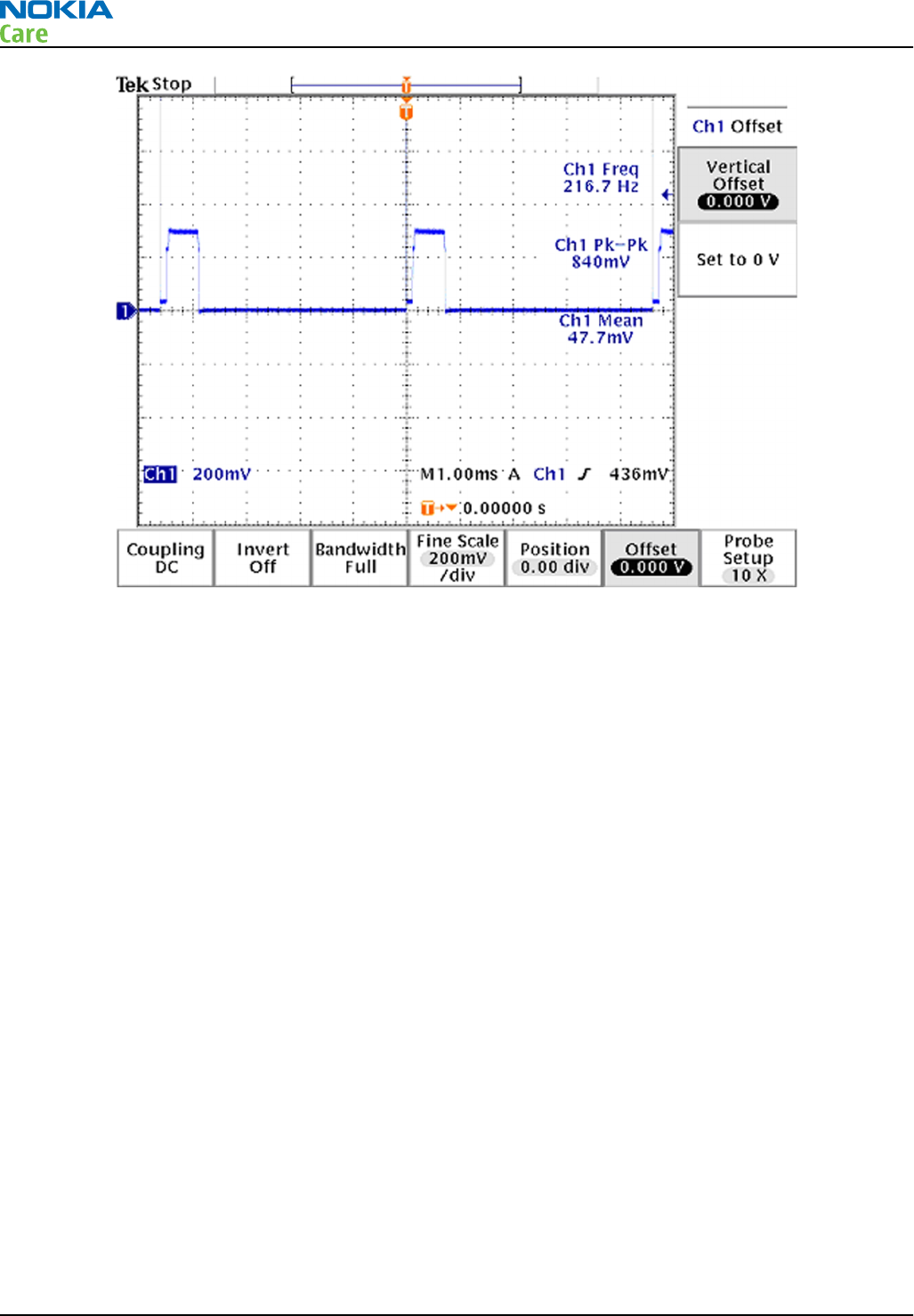
Figure 48 TXC signals at PCL19
General instructions for GSM1800 TX troubleshooting
Steps
1. Apply a RF-cable to the RF-connector to allow the transmitted signal act as normal. RF-cable should be
connected to an attenuator at least 10dB before connected to the measurement equipment, otherwise
the PA may be damaged.
2. Start
Phoenix
and establish a connection to the phone with the data cable e.g. FBUS.
3. Select File and Scan product.
4. Wait a while for the PC to read the information from the phone.
5. Select Testing and RF Controls.
6. Set the parameters as follows:
i Band: GSM 1800
ii Active Unit: TX
iii TX Power Level: 0
iv TX Data Type: Random
Results
The setup should now look like this:
RM-340; RM-341
RF Troubleshooting Instructions
Page 4 –22 COMPANY CONFIDENTIAL Issue 1
Copyright © 2007 Nokia. All rights reserved.

Figure 49 GSM 1800 RF controls window
RM-340; RM-341
RF Troubleshooting Instructions
Issue 1 COMPANY CONFIDENTIAL Page 4 –23
Copyright © 2007 Nokia. All rights reserved.

Troubleshooting diagram for GSM1800 transmitter
Troubleshooting flow
Figure 50 GSM1800 transmitter troubleshooting
GSM1800 TX output power
Measure the output power of the phone; it should be about 30.5dBm. Remember the cable loss is about
0.5dB.
RM-340; RM-341
RF Troubleshooting Instructions
Page 4 –24 COMPANY CONFIDENTIAL Issue 1
Copyright © 2007 Nokia. All rights reserved.
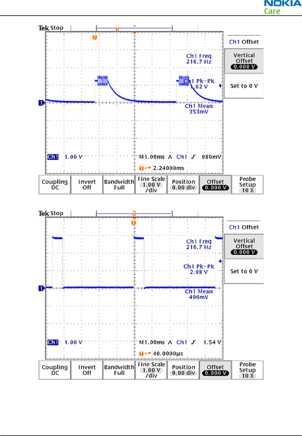
Figure 51 TX I/O signal
Figure 52 VC1, VC2, VC3 signals
RM-340; RM-341
RF Troubleshooting Instructions
Issue 1 COMPANY CONFIDENTIAL Page 4 –25
Copyright © 2007 Nokia. All rights reserved.
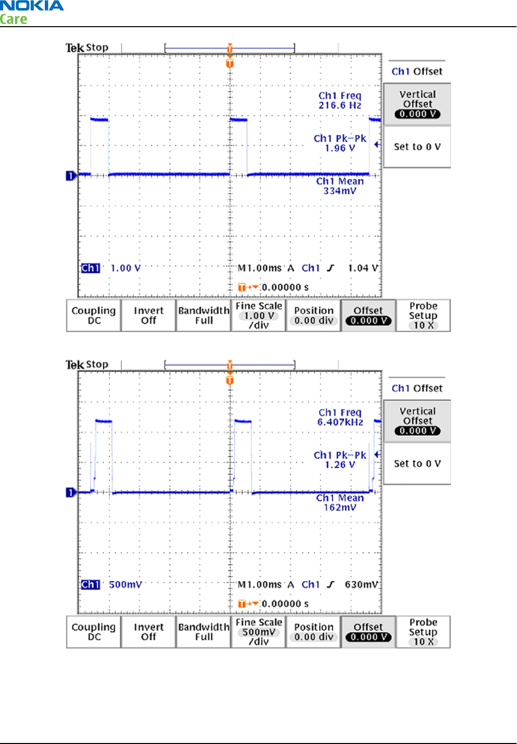
Figure 53 TXP signal
Figure 54 TXC signals at PCL0
RM-340; RM-341
RF Troubleshooting Instructions
Page 4 –26 COMPANY CONFIDENTIAL Issue 1
Copyright © 2007 Nokia. All rights reserved.
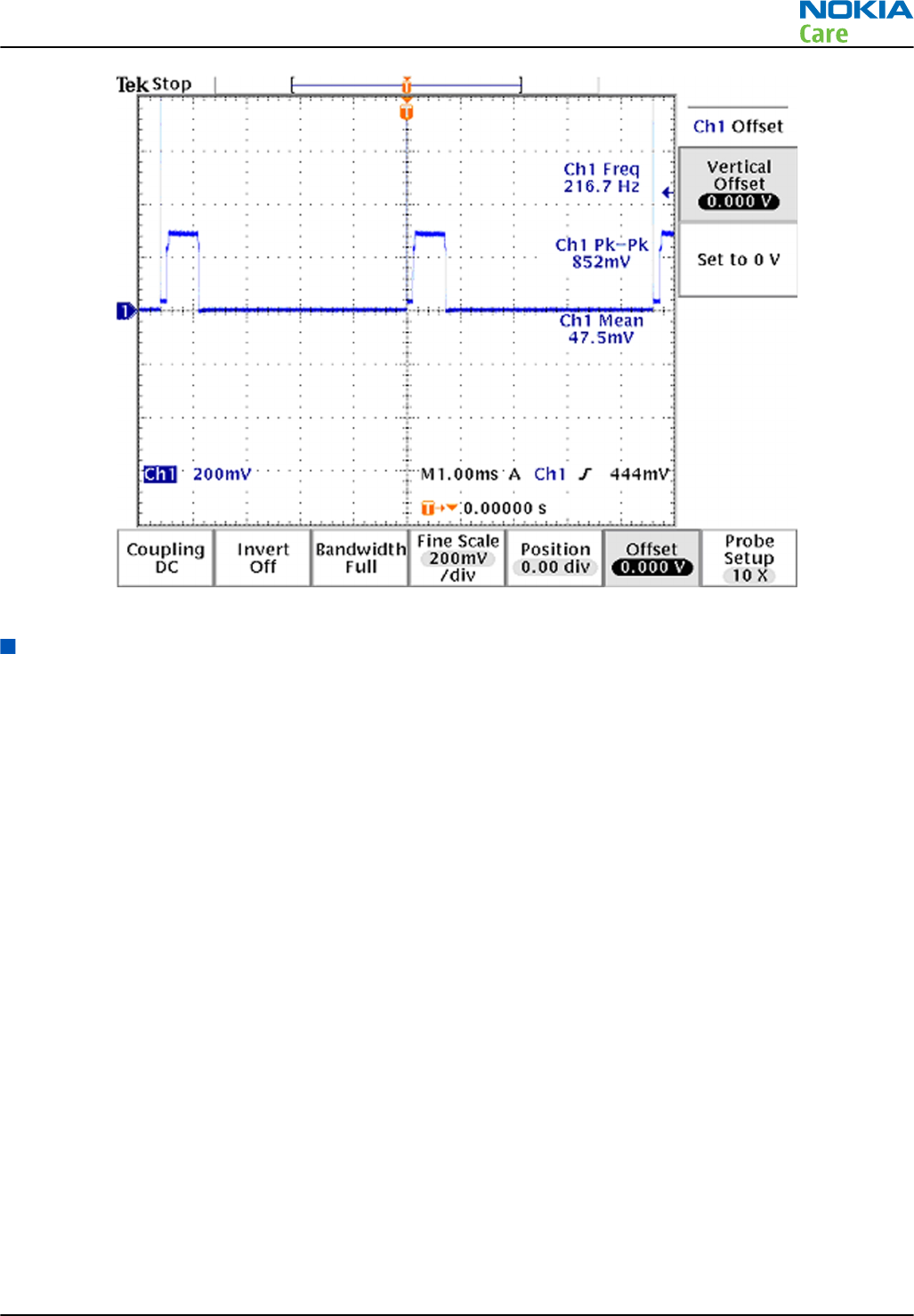
Figure 55 TXC signals at PCL15
RM-341 receiver
General instructions for GSM 850 RX troubleshooting
Steps
1. Connect the phone to a PC with the module repair jig.
2. Start
Phoenix
and establish a connection to the phone with the data cable e.g. FBUS.
3. Select File and Scan product.
4. Wait a while for the PC to read the information from the phone.
5. Select Testing and RF Controls.
6. Set the parameters as follows:
i Active Unit: RX
ii Band: GSM 850
iii Operation Mode: Continuous mode
iv RX/TX Channel 190
v AGC: 8: FEG_ON + DTOS_ON+BB_6=Vgain_36
Results
The setup should now look like this:
RM-340; RM-341
RF Troubleshooting Instructions
Issue 1 COMPANY CONFIDENTIAL Page 4 –27
Copyright © 2007 Nokia. All rights reserved.
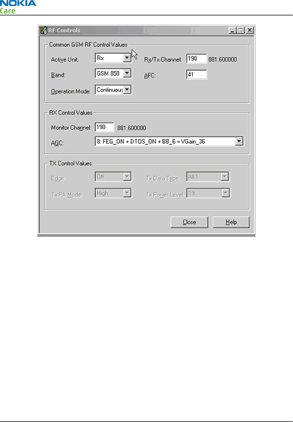
Figure 56 GSM850 RF controls window
RM-340; RM-341
RF Troubleshooting Instructions
Page 4 –28 COMPANY CONFIDENTIAL Issue 1
Copyright © 2007 Nokia. All rights reserved.
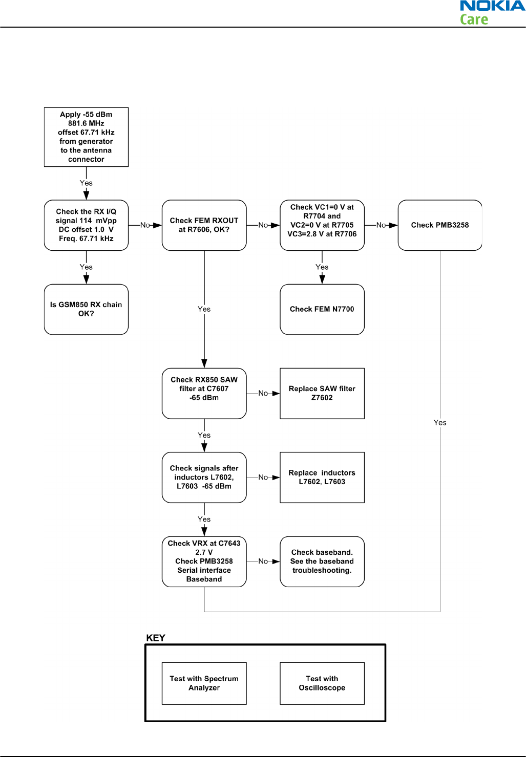
Troubleshooting diagram for GSM850 receiver
Troubleshooting flow
Figure 57 GSM850 receiver troubleshooting
RM-340; RM-341
RF Troubleshooting Instructions
Issue 1 COMPANY CONFIDENTIAL Page 4 –29
Copyright © 2007 Nokia. All rights reserved.

Results
By measuring with an oscilloscope at RXIP or RXQP on a working GSM850 receiver this picture should be seen.
Signal amplitude 114mVp-p. DC offset 1.0V.
Figure 58 850 RX I/Q signal waveform
General instructions for GSM1900 RX troubleshooting
Steps
1. Connect the phone to a PC with the module repair jig.
2. Start Phoenix and establish a connection to the phone with the data cable e.g. FBUS.
3. Select File and Scan product.
4. Wait a while for the PC to read the information from the phone.
5. Select Testing and RF Controls.
6. Set the parameters as follows:
i Active Unit: RX
ii Band: GSM 1900
iii Operation Mode: Continuous mode
iv RX/TX Channel 661
v AGC: 8: FEG_ON + DTOS_ON+BB_6=Vgain_36
Results
The setup should now look like this:
RM-340; RM-341
RF Troubleshooting Instructions
Page 4 –30 COMPANY CONFIDENTIAL Issue 1
Copyright © 2007 Nokia. All rights reserved.
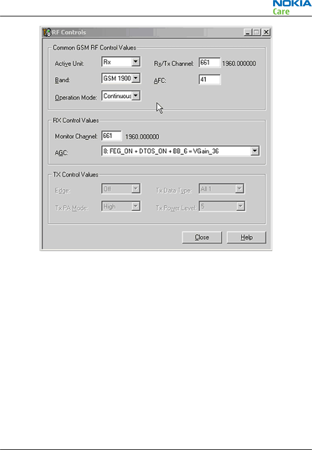
Figure 59 GSM 1900 RF controls window
RM-340; RM-341
RF Troubleshooting Instructions
Issue 1 COMPANY CONFIDENTIAL Page 4 –31
Copyright © 2007 Nokia. All rights reserved.
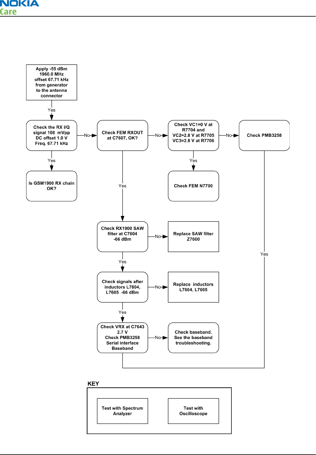
Troubleshooting diagram for GSM1900 receiver
Troubleshooting flow
Figure 60 GSM1900 receiver troubleshooting
RM-340; RM-341
RF Troubleshooting Instructions
Page 4 –32 COMPANY CONFIDENTIAL Issue 1
Copyright © 2007 Nokia. All rights reserved.

Results
By measuring with an oscilloscope at RXIP or RXQP on a working GSM1900 receiver this picture should be
seen. Signal amplitude 108 mVp-p. DC offset 1.0V.
Figure 61 1900 RX I/Q signal waveform
RM-340; RM-341
RF Troubleshooting Instructions
Issue 1 COMPANY CONFIDENTIAL Page 4 –33
Copyright © 2007 Nokia. All rights reserved.

Measurement points in the receiver
Figure 62 RX measurements point of the control voltages to FEM N7700
Figure 63 Measurement points at the RX SAW Filters – Z7600/Z7602
RM-340; RM-341
RF Troubleshooting Instructions
Page 4 –34 COMPANY CONFIDENTIAL Issue 1
Copyright © 2007 Nokia. All rights reserved.
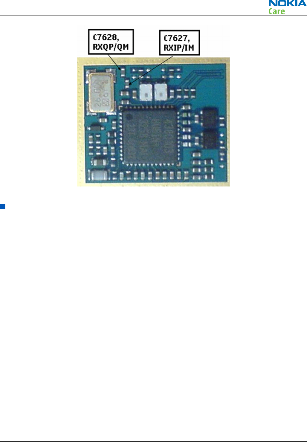
Figure 64 RX I/Q signals
RM-341 transmitter
General instructions for GSM 850 TX troubleshooting
Steps
1. Apply a RF-cable to the RF-connector to allow the transmitted signal act as normal. RF-cable should be
connected to an attenuator at least 10dB before connected to the measurement equipment, otherwise
the PA may be damaged.
2. Start
Phoenix
and establish a connection to the phone with the data cable e.g. FBUS.
3. Select File and Scan product.
4. Wait a while for the PC to read the information from the phone.
5. Select Testing and RF Controls.
6. Set the parameters as follows:
i Band: GSM 850
ii Active Unit: TX
iii TX Power Level: 5
iv TX Data Type: Random
Results
The setup should now look like this:
RM-340; RM-341
RF Troubleshooting Instructions
Issue 1 COMPANY CONFIDENTIAL Page 4 –35
Copyright © 2007 Nokia. All rights reserved.

Figure 65 GSM 850 RF controls window
RM-340; RM-341
RF Troubleshooting Instructions
Page 4 –36 COMPANY CONFIDENTIAL Issue 1
Copyright © 2007 Nokia. All rights reserved.
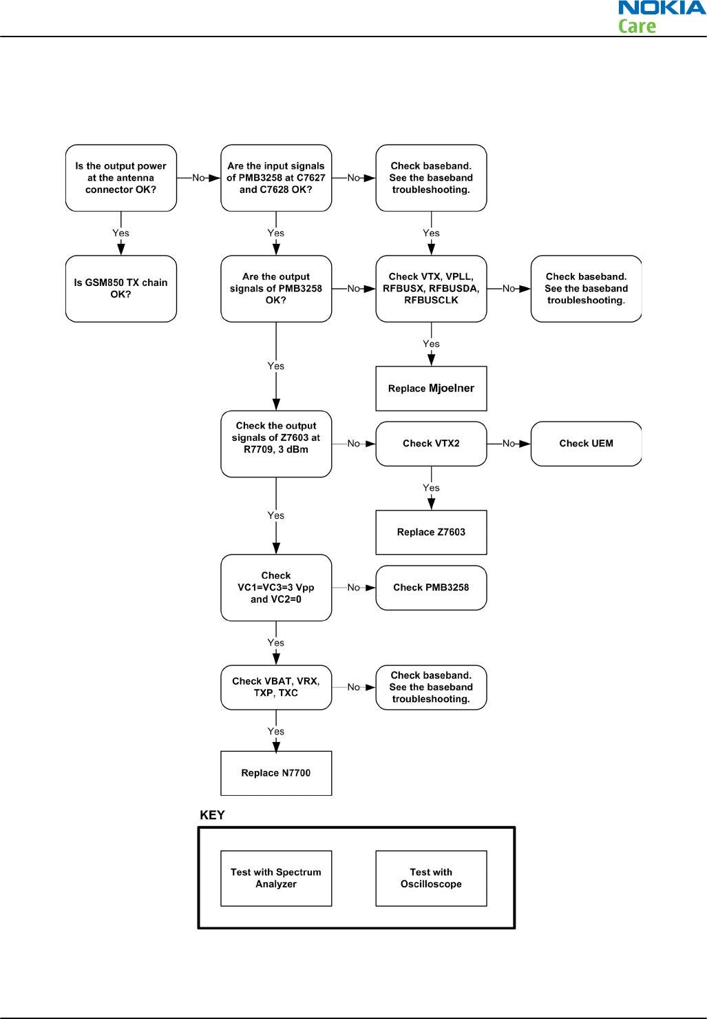
Troubleshooting diagram for GSM850 transmitter
Troubleshooting flow
Figure 66 GSM850 transmitter troubleshooting
RM-340; RM-341
RF Troubleshooting Instructions
Issue 1 COMPANY CONFIDENTIAL Page 4 –37
Copyright © 2007 Nokia. All rights reserved.
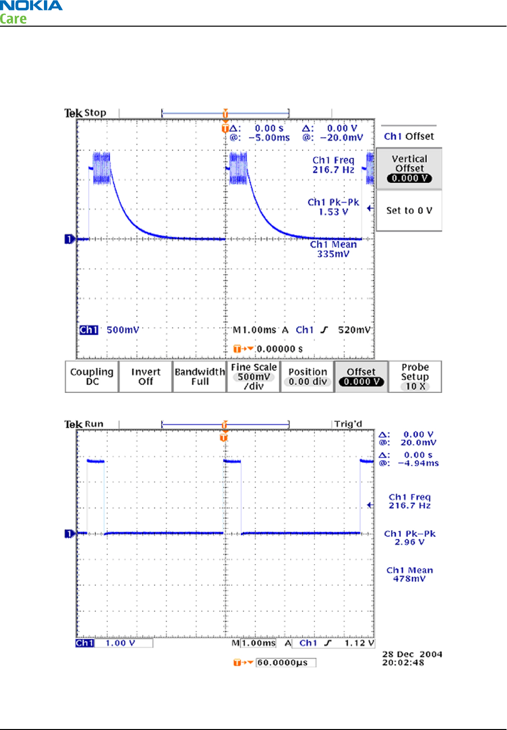
GSM850 TX output power
Measure the output power of the phone; it should be about 32.5 dBm. Remember the cable loss is about 0.3
dB.
Figure 67 TX I/O signal
Figure 68 VC1, VC3 signal
RM-340; RM-341
RF Troubleshooting Instructions
Page 4 –38 COMPANY CONFIDENTIAL Issue 1
Copyright © 2007 Nokia. All rights reserved.
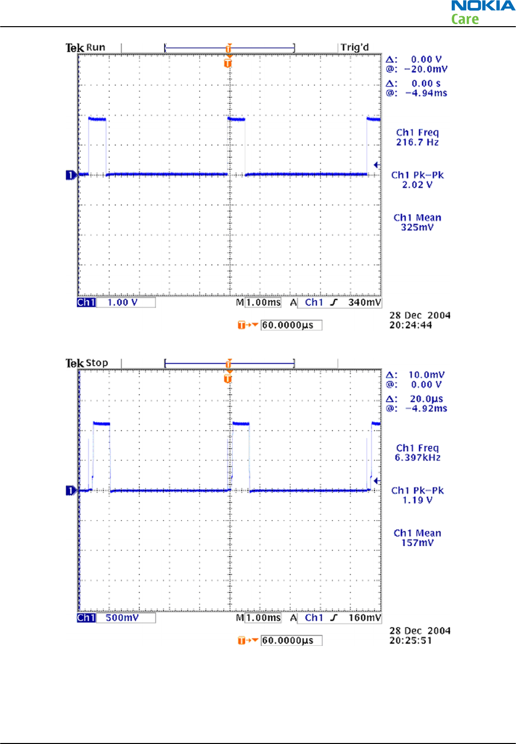
Figure 69 TXP signal
Figure 70 TXC signals at PCL5
RM-340; RM-341
RF Troubleshooting Instructions
Issue 1 COMPANY CONFIDENTIAL Page 4 –39
Copyright © 2007 Nokia. All rights reserved.
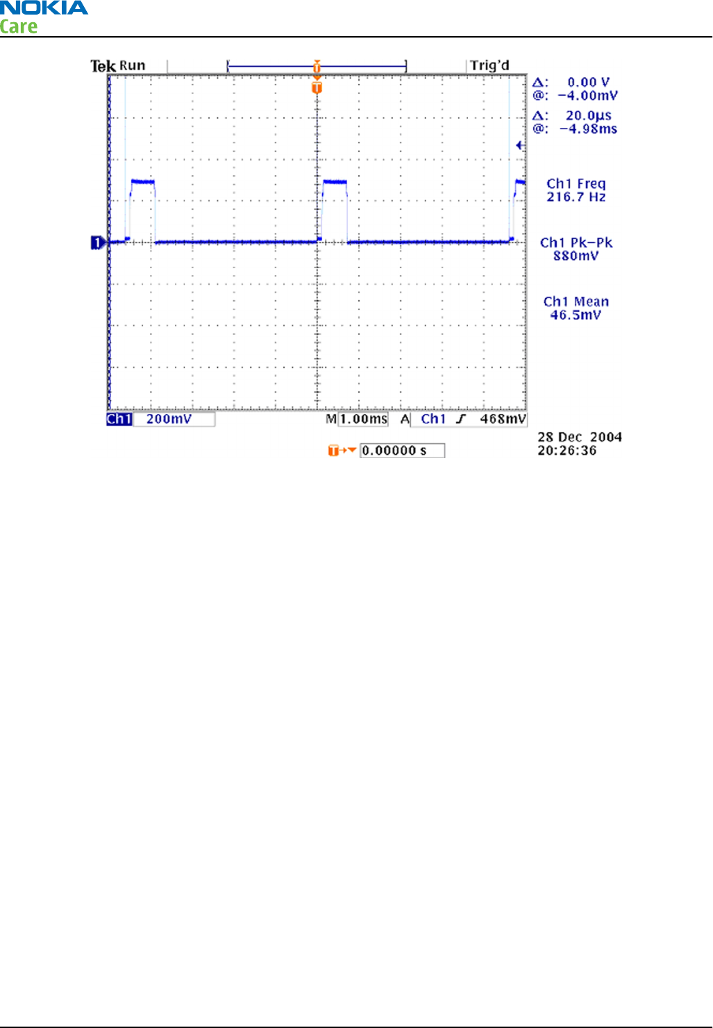
Figure 71 TXC signals at PCL19
General instructions for GSM1900 TX troubleshooting
Steps
1. Apply a RF-cable to the RF-connector to allow the transmitted signal act as normal. RF-cable should be
connected to an attenuator at least 10dB before connected to the measurement equipment, otherwise
the PA may be damaged.
2. Start
Phoenix
and establish a connection to the phone with the data cable e.g. FBUS.
3. Select File and Scan product.
4. Wait a while for the PC to read the information from the phone.
5. Select Testing and RF Controls.
6. Set the parameters as follows:
i Band: GSM 1900
ii Active Unit: TX
iii TX Power Level: 0
iv TX Data Type: Random
RM-340; RM-341
RF Troubleshooting Instructions
Page 4 –40 COMPANY CONFIDENTIAL Issue 1
Copyright © 2007 Nokia. All rights reserved.
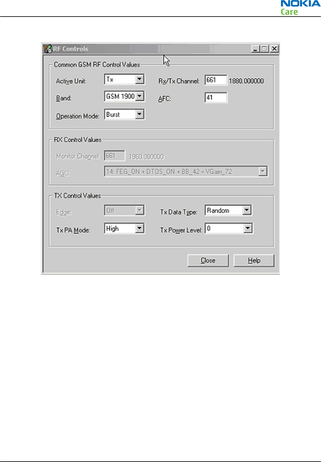
7. The setup should now look like this:
Figure 72 GSM 1900 RF controls window
RM-340; RM-341
RF Troubleshooting Instructions
Issue 1 COMPANY CONFIDENTIAL Page 4 –41
Copyright © 2007 Nokia. All rights reserved.
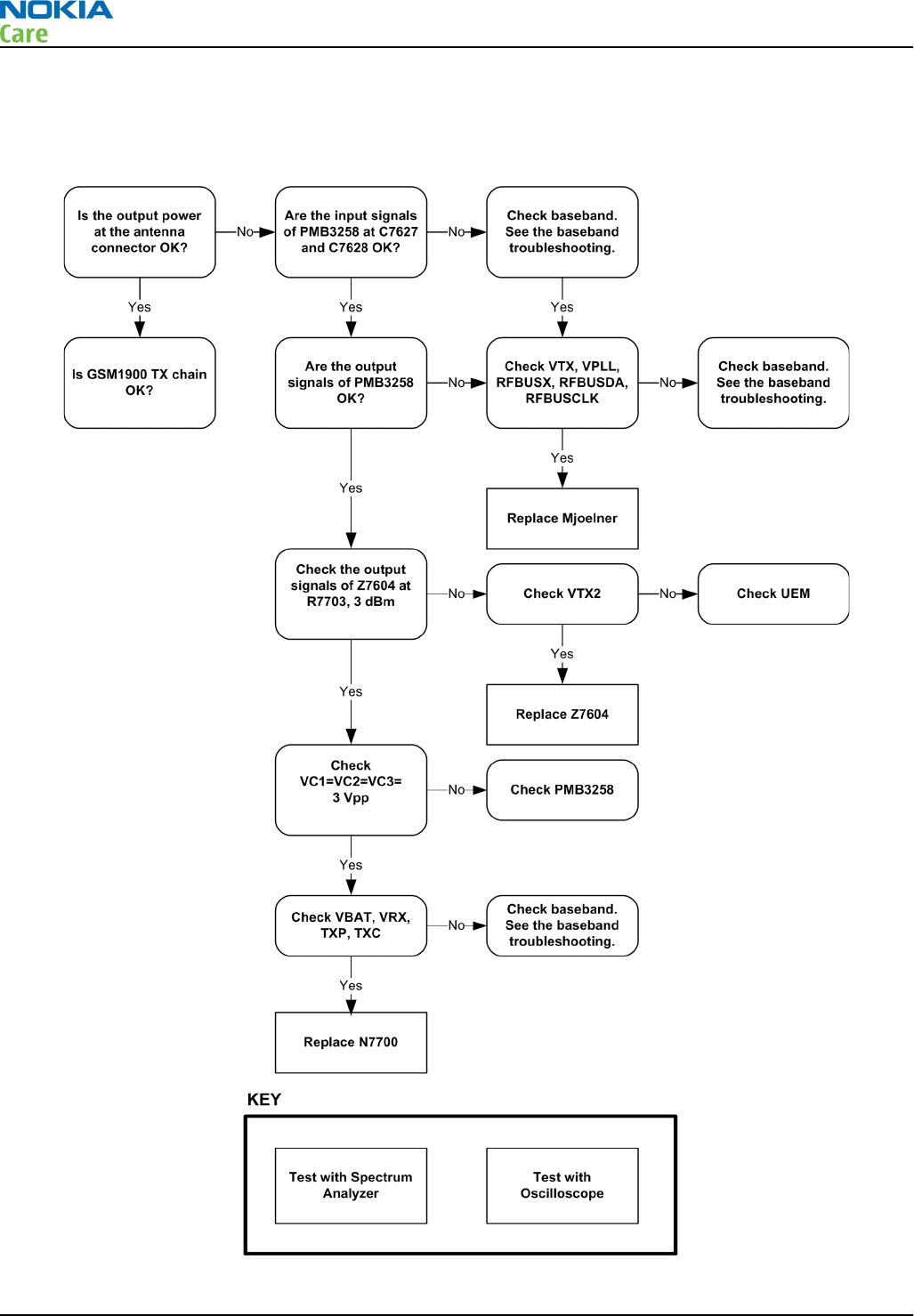
Troubleshooting diagram for GSM1900 transmitter
Troubleshooting flow
Figure 73 GSM1900 transmitter troubleshooting
RM-340; RM-341
RF Troubleshooting Instructions
Page 4 –42 COMPANY CONFIDENTIAL Issue 1
Copyright © 2007 Nokia. All rights reserved.
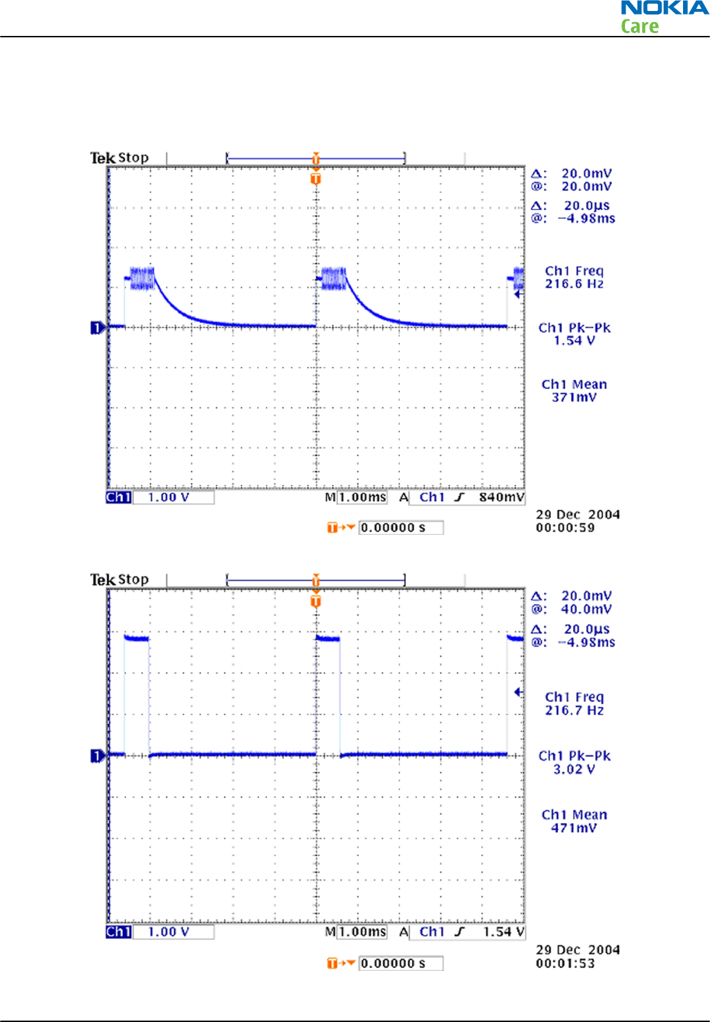
GSM1900 TX output power
Measure the output power of the phone; it should be about 29.1dBm. Remember the cable loss is about
0.5dB.
Figure 74 TX I/O signal
Figure 75 VC1, VC2, VC3 signals
RM-340; RM-341
RF Troubleshooting Instructions
Issue 1 COMPANY CONFIDENTIAL Page 4 –43
Copyright © 2007 Nokia. All rights reserved.
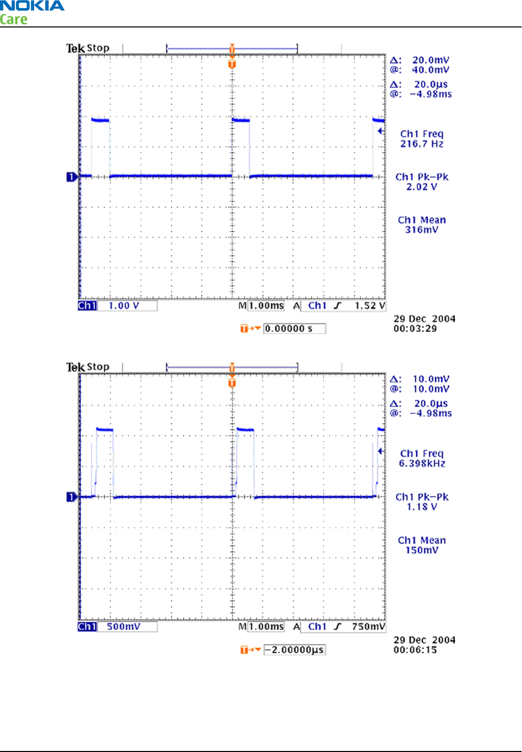
Figure 76 TXP signal
Figure 77 TXC signals at PCL0
RM-340; RM-341
RF Troubleshooting Instructions
Page 4 –44 COMPANY CONFIDENTIAL Issue 1
Copyright © 2007 Nokia. All rights reserved.
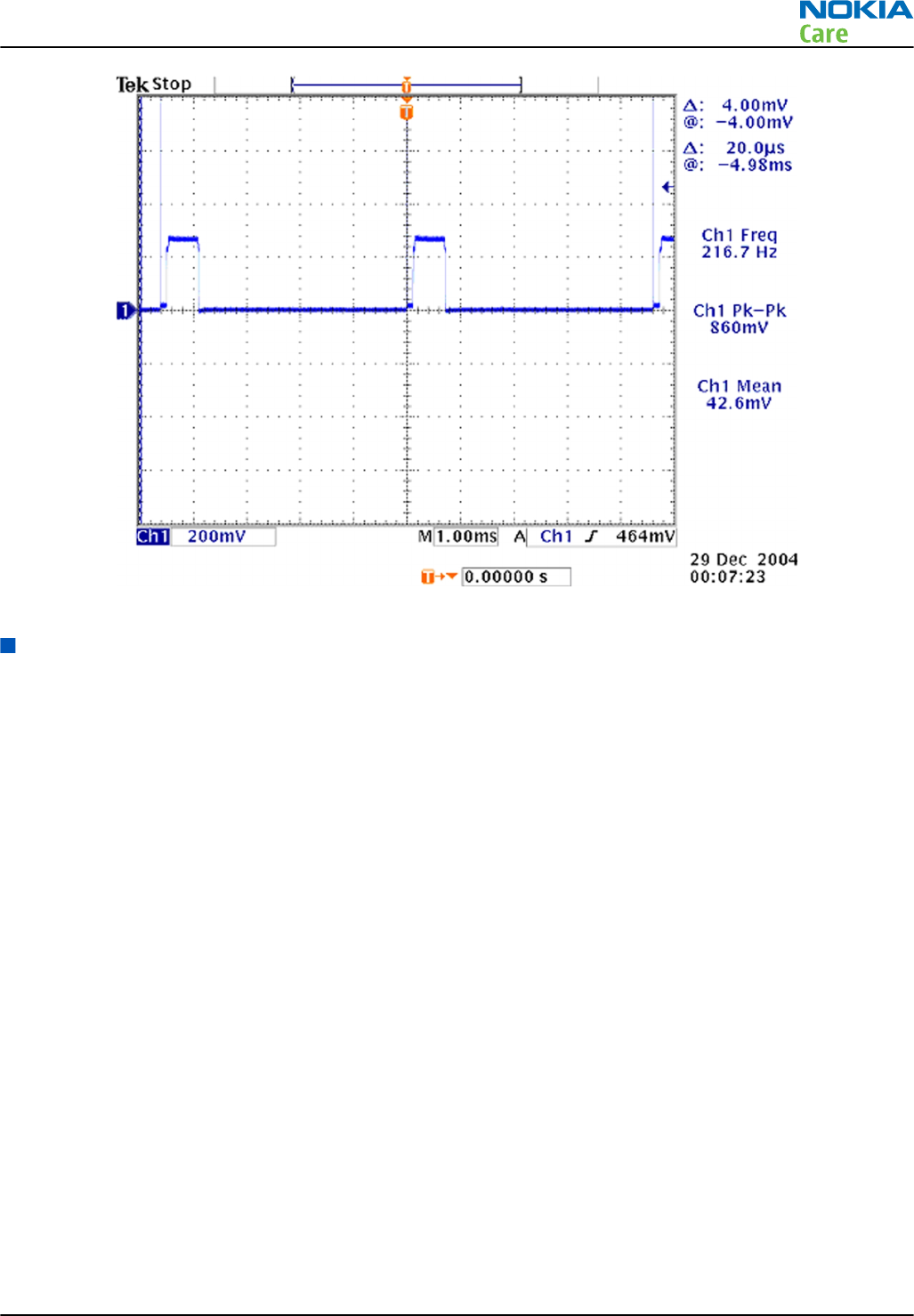
Figure 78 TXC signals at PCL15
Synthesizer troubleshooting
Introduction
26 MHz Reference Oscillator (VCXO)
There is only one PLL synthesizer generating Local Oscillator frequencies for both RX and TX in both bands
(PCN and EGSM). The VCO frequency is divided by 2 for PCN operation or by 4 for EGSM operation inside the
Mjoelner IC.
The 26MHz oscillator is located near the Mjoelner IC. (N7600). The coarse frequency for this oscillator is set
by an external crystal (B7600). The reference oscillator is used as a reference frequency for the PLL synthesizer
and as the system clock for the Baseband. The 26MHz signal is divided by 2 to achieve 13MHz inside the UPP
IC (D2800).
The 26MHz signal from the VCXO can be measured by probing R2900. The level at this point is approx.
770mVpp. Frequency of this oscillator is adjusted by changing the AFC-register inside the UEM IC. Example
Signal Measured at VCXO output (R2900).
RM-340; RM-341
RF Troubleshooting Instructions
Issue 1 COMPANY CONFIDENTIAL Page 4 –45
Copyright © 2007 Nokia. All rights reserved.
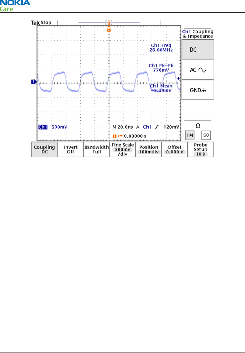
Figure 79 VCXO 26 MHz waveform
RM-340; RM-341
RF Troubleshooting Instructions
Page 4 –46 COMPANY CONFIDENTIAL Issue 1
Copyright © 2007 Nokia. All rights reserved.
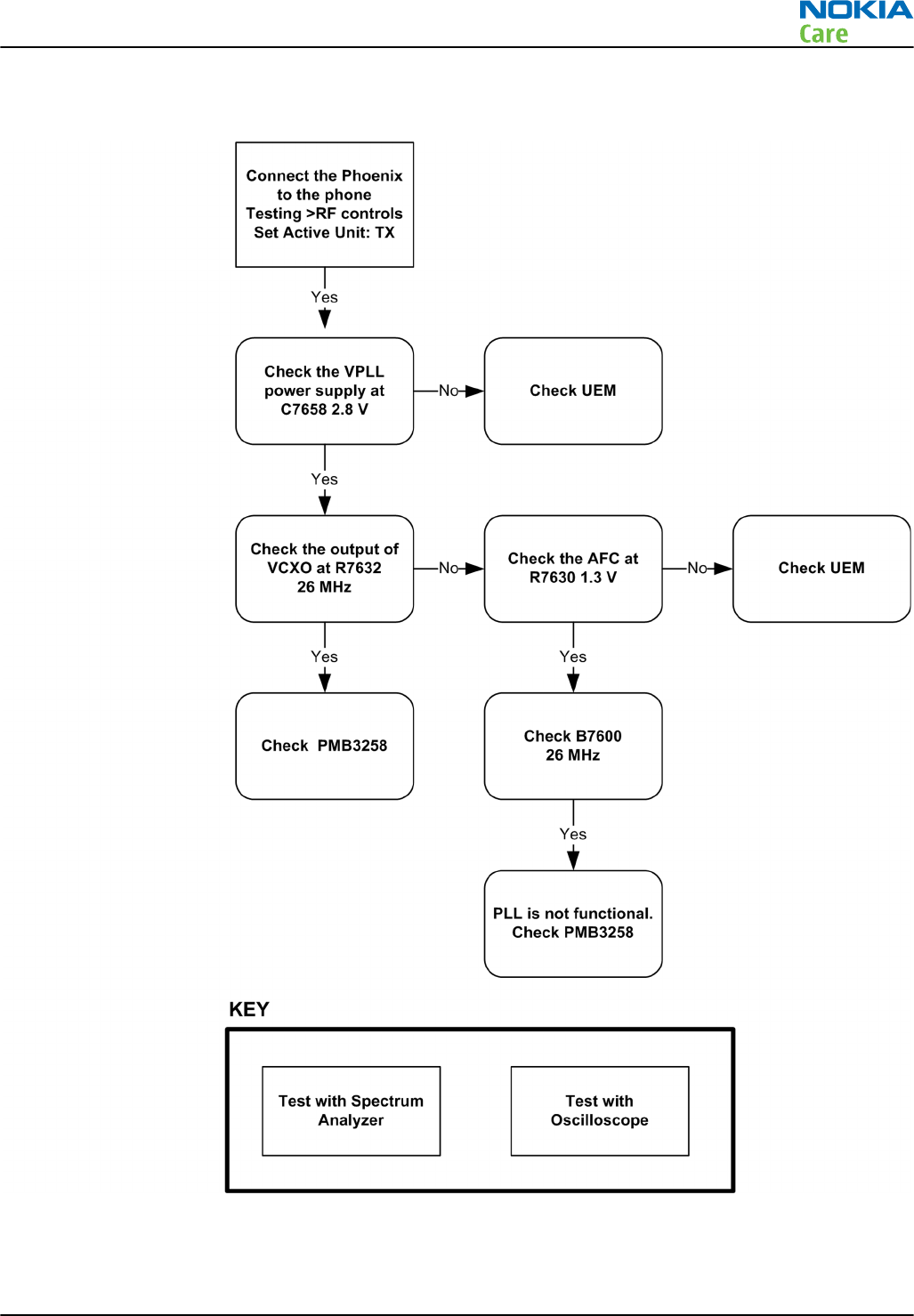
Troubleshooting diagram for PLL synthesizer
Figure 80 PLL Troubleshooting diagram
RM-340; RM-341
RF Troubleshooting Instructions
Issue 1 COMPANY CONFIDENTIAL Page 4 –47
Copyright © 2007 Nokia. All rights reserved.

Measurement points at the VCXO
Figure 81 Measurement point for VCXO
FM radio and bluetooth troubleshooting
Measurement settings
Steps
1. Connect the phone to a PC with the module repair jig.
2. Start Phoenix and establish a connection to the phone with the data cable e.g. FBUS.
3. Phoenix settings shall be as follows:
RM-340; RM-341
RF Troubleshooting Instructions
Page 4 –48 COMPANY CONFIDENTIAL Issue 1
Copyright © 2007 Nokia. All rights reserved.
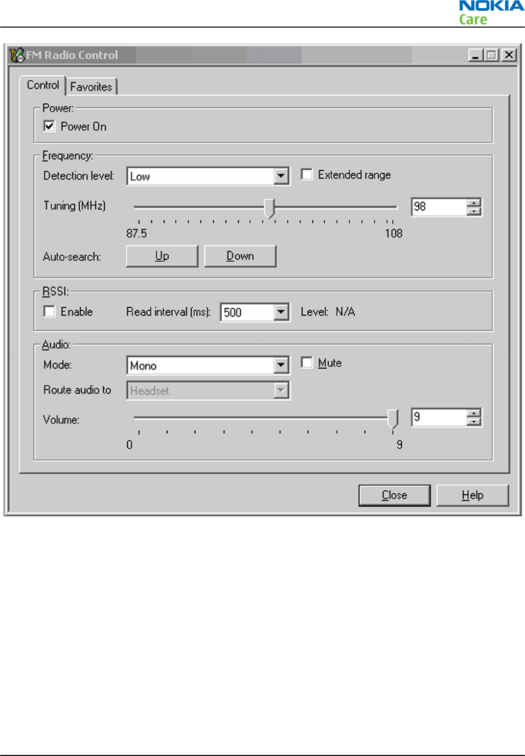
Figure 82 Phoenix settings
4. Establish input of a standard FM signal to the FM module.
5. Signal generator settings shall be as follows:
i Frequency: 98 MHz
ii Level: - 60 dBm
iii FM deviation: 75 kHz
iv LFGEN frequency: 1 kHZ
RM-340; RM-341
RF Troubleshooting Instructions
Issue 1 COMPANY CONFIDENTIAL Page 4 –49
Copyright © 2007 Nokia. All rights reserved.
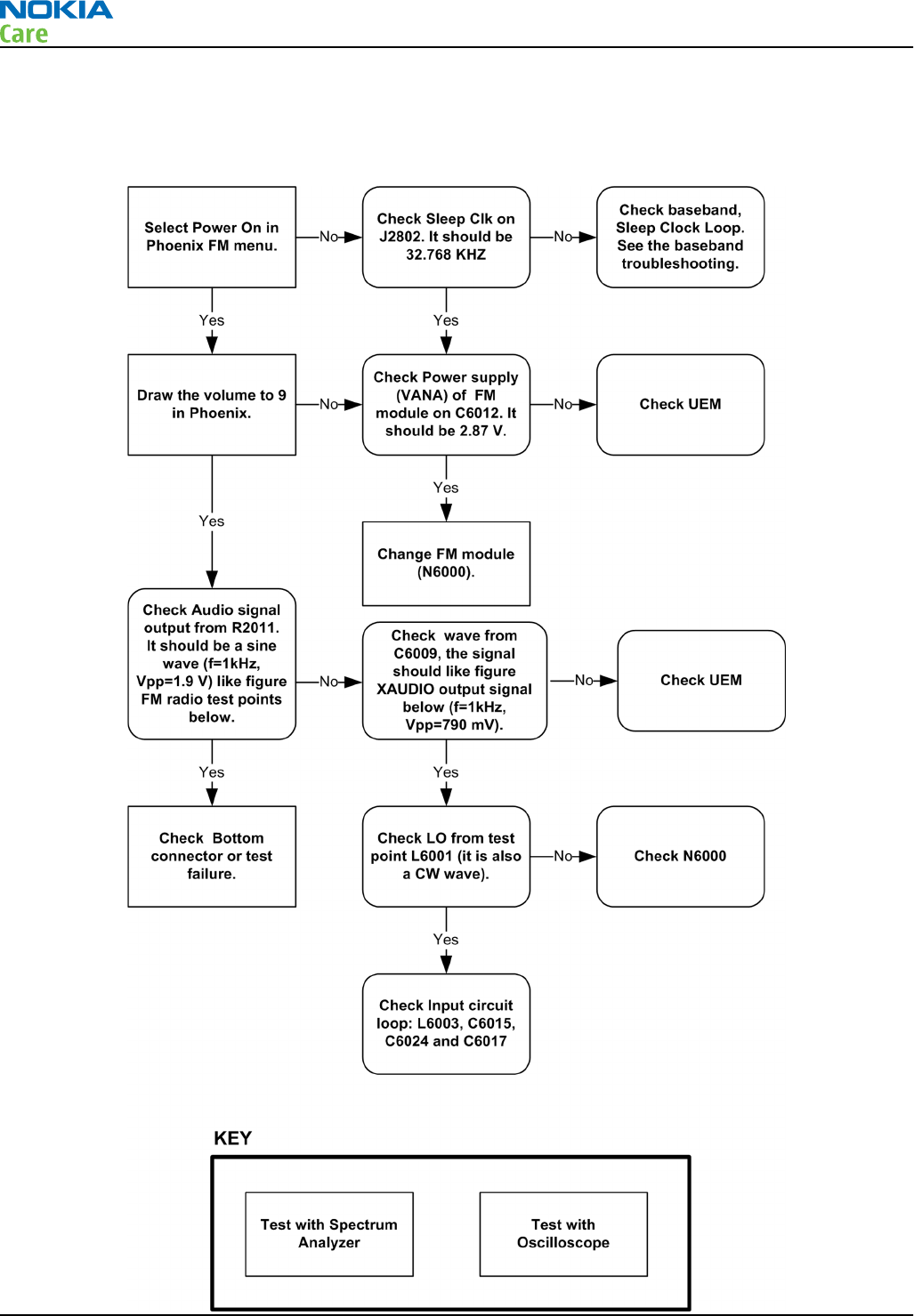
Troubleshooting diagram for FM radio
Troubleshooting flow
Figure 83 FM circuit troubleshooting diagram
RM-340; RM-341
RF Troubleshooting Instructions
Page 4 –50 COMPANY CONFIDENTIAL Issue 1
Copyright © 2007 Nokia. All rights reserved.
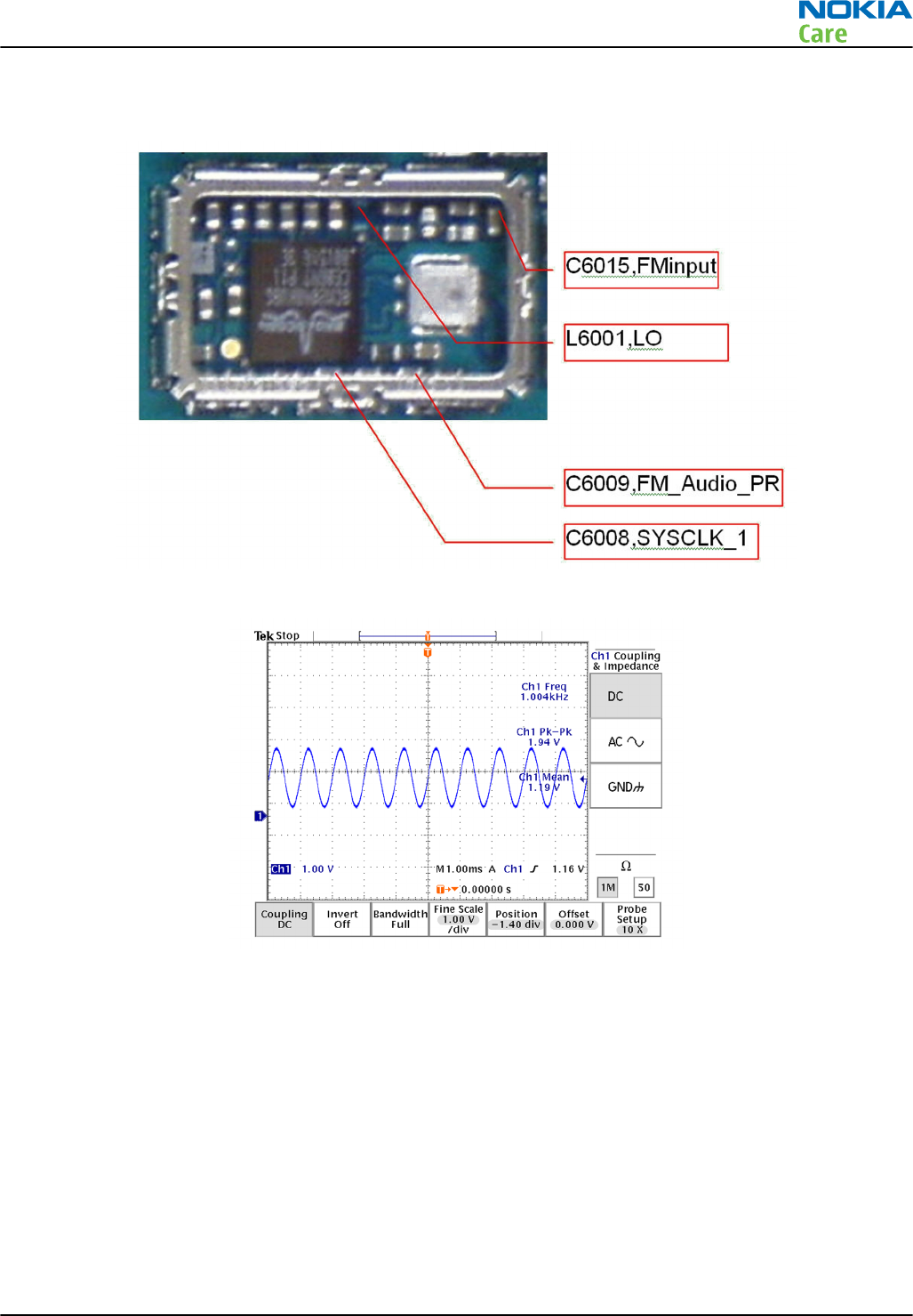
Bluetooth and FM radio test points
Figure 84 Bluetooth and FM radio test points
Figure 85 XAUDIO output signal
RM-340; RM-341
RF Troubleshooting Instructions
Issue 1 COMPANY CONFIDENTIAL Page 4 –51
Copyright © 2007 Nokia. All rights reserved.

Figure 86 FM module output signal
Introduction to Bluetooth troubleshooting
There are two main Bluetooth (BT) problems that can occur:
Problem Description
Detachment of the BT antenna. This would most likely happen if the device has
been dropped repeatedly to the ground. It could
cause the BT antenna to become loose or partially
detached from the PWB.
A malfunction in the BT ASIC, BB ASICs or the phone’s
BT SMD components.
This is unpredictable and could have many causes
i.e. SW or HW related.
The main issue is to find out if the problem is related to the BT antenna or related to the BT system or the
phone’s BB and then replace/fix the faulty component. For location of the antenna, please refer to the
exploded view in the Parts and layouts section.
Bluetooth settings for Phoenix
Steps
1. Start
Phoenix
service software.
2. From the File menu, choose Open Product, and then choose the correct type designator from the
Product list.
3. Place the phone to a flash adapter in the local mode.
4. Choose Testing→Bluetooth LOCALS .
5. Locate JBT-9’s serial number (12 digits) found in the type label on the back of JBT-9.
In addition to JBT-9, also SB-6, JBT-3 and JBT-6 Bluetooth test boxes can be used.
6. In the
Bluetooth LOCALS
window, write the 12-digit serial number on the
Counterpart BT Device Address line.
This needs to be done only once provided that JBT-9 is not changed.
7. Place the JBT-9 box near (within 10 cm) the BT antenna and click Run BER Test.
RM-340; RM-341
RF Troubleshooting Instructions
Page 4 –52 COMPANY CONFIDENTIAL Issue 1
Copyright © 2007 Nokia. All rights reserved.

Results
Bit Error Rate test result is displayed in the
Bit Error Rate (BER) Tests
pane in the
Bluetooth LOCALS
window.
Figure 87 BER test result
Bluetooth self tests in Phoenix
Steps
1. Start
Phoenix
service software.
2. ChooseFile→Scan Product.
3. Place the phone to a flash adapter.
4. From the Mode drop-down menu, set mode to Local.
5. Choose Testing→Self Tests.
6. In the
Self Tests
window check the following Bluetooth related tests:
•ST_LPRF_IF_TEST
•ST_LPRF_AUDIO_LINES_TEST
•ST_BT_WAKEUP_TEST
RM-340; RM-341
RF Troubleshooting Instructions
Issue 1 COMPANY CONFIDENTIAL Page 4 –53
Copyright © 2007 Nokia. All rights reserved.
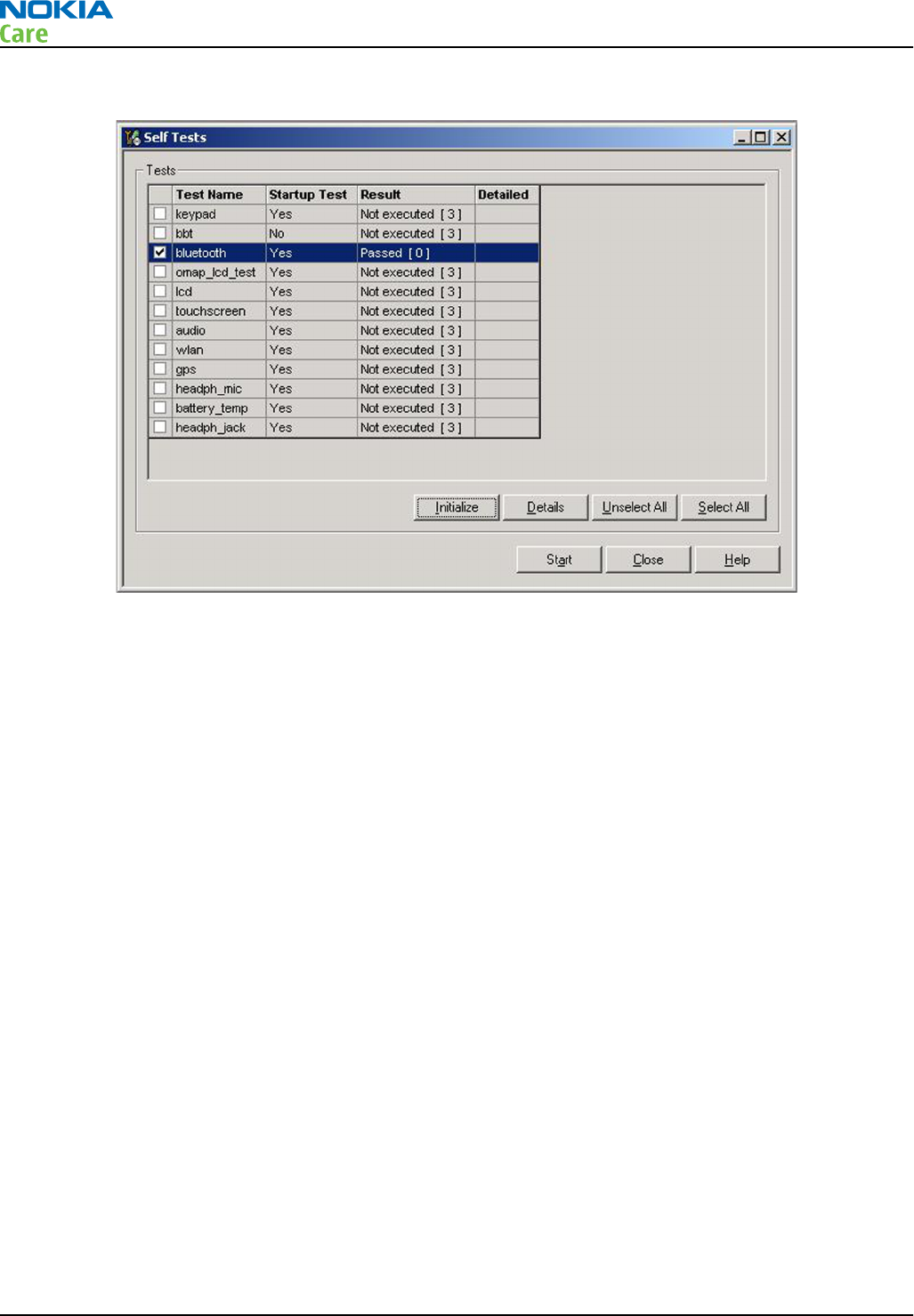
7. To run the tests, click Start.
Figure 88 Bluetooth self tests in
Phoenix
Bluetooth BER failure troubleshooting
Context
Basic encoding rules, BER, is a self-identifying and self-delimiting encoding scheme, which means that each
data value can be identified, extracted and decoded individually.
RM-340; RM-341
RF Troubleshooting Instructions
Page 4 –54 COMPANY CONFIDENTIAL Issue 1
Copyright © 2007 Nokia. All rights reserved.
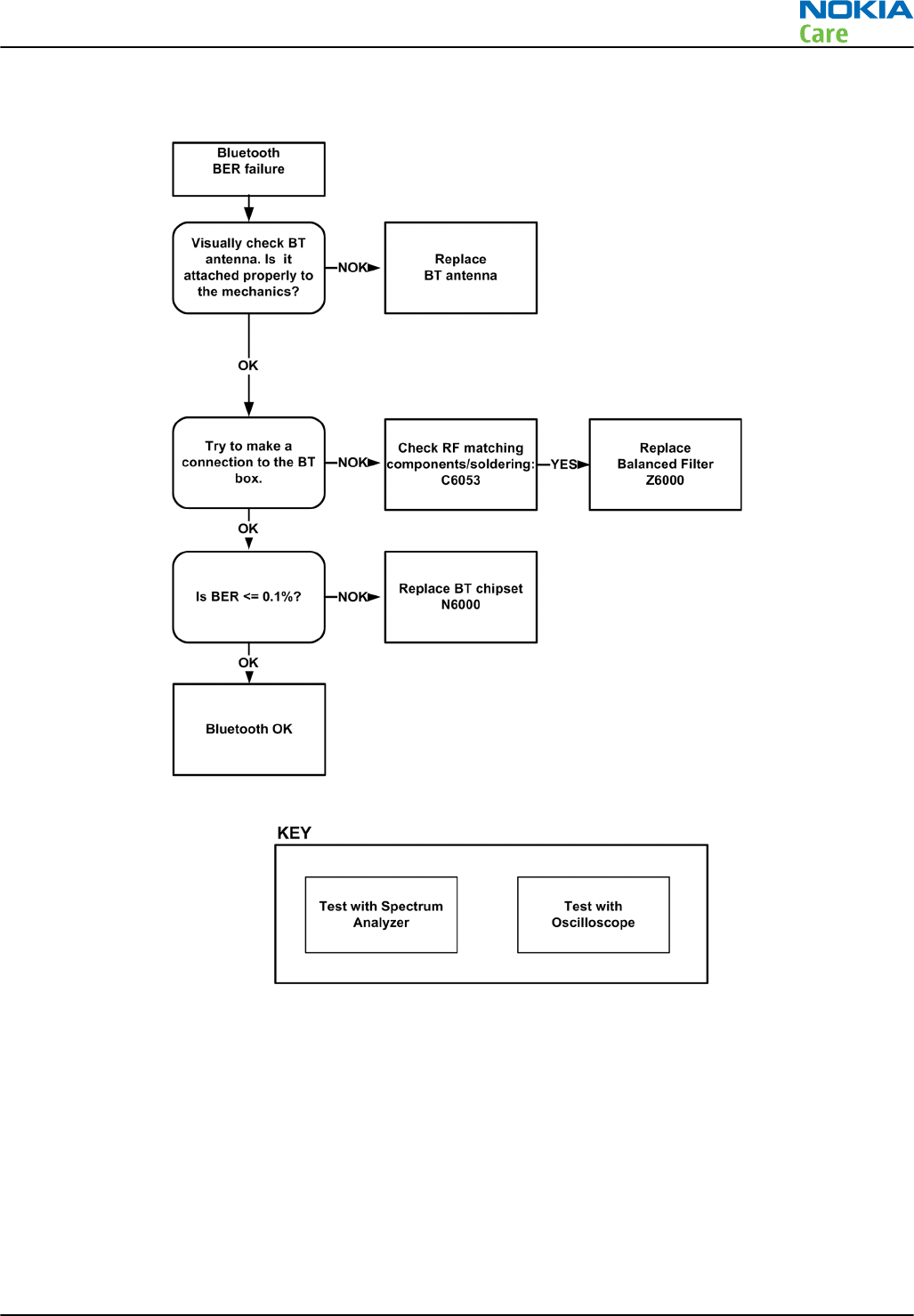
Bluetooth circuit troubleshooting diagram
RM-340; RM-341
RF Troubleshooting Instructions
Issue 1 COMPANY CONFIDENTIAL Page 4 –55
Copyright © 2007 Nokia. All rights reserved.
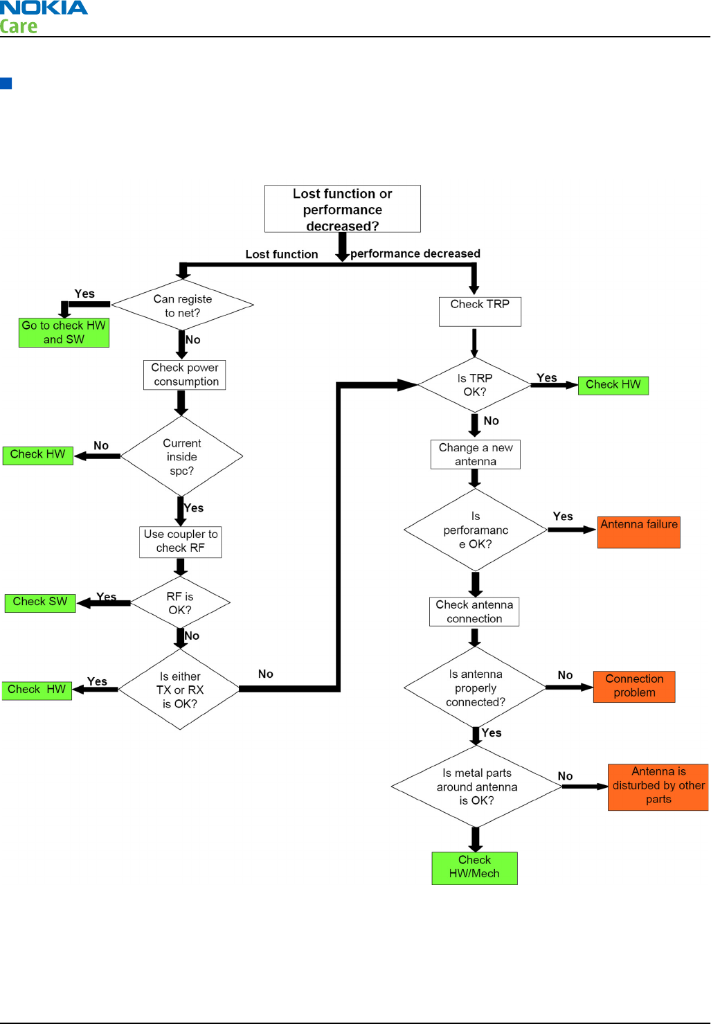
Antenna troubleshooting
Antenna troubleshooting diagram
Troubleshooting flow
Figure 89 Antenna troubleshooting
RM-340; RM-341
RF Troubleshooting Instructions
Page 4 –56 COMPANY CONFIDENTIAL Issue 1
Copyright © 2007 Nokia. All rights reserved.

5 — Camera Module
Troubleshooting
Nokia Customer Care
Issue 1 COMPANY CONFIDENTIAL Page 5 –1
Copyright © 2007 Nokia. All rights reserved.

RM-340; RM-341
Camera Module Troubleshooting
(This page left intentionally blank.)
Page 5 –2 COMPANY CONFIDENTIAL Issue 1
Copyright © 2007 Nokia. All rights reserved.

Table of Contents
Introduction to camera module troubleshooting ..............................................................................................5–5
The effect of image taking conditions on image quality...................................................................................5–6
Camera construction........................................................................................................................................... 5–10
Dynamic camera configuration.......................................................................................................................... 5–12
Image quality analysis ....................................................................................................................................... 5–13
Testing for dust in camera module .............................................................................................................. 5–13
Testing camera image sharpness................................................................................................................. 5–14
Dirty camera lens protection window ......................................................................................................... 5–15
Image bit errors ............................................................................................................................................. 5–15
Camera troubleshooting flowcharts.................................................................................................................. 5–16
Camera hardware failure message troubleshooting.................................................................................. 5–16
Camera baseband HW troubleshooting....................................................................................................... 5–18
Camera viewfinder troubleshooting ............................................................................................................ 5–19
Bad camera image quality troubleshooting................................................................................................ 5–20
List of Tables
Table 5 Camera specifications............................................................................................................................ 5–10
List of Figures
Figure 90 Blurred image. Target too close. .........................................................................................................5–6
Figure 91 Blurring caused by shaking hands ......................................................................................................5–7
Figure 92 Near objects get skewed when taking images from a moving vehicle...........................................5–7
Figure 93 Noisy image taken in +70 degrees Celsius .........................................................................................5–8
Figure 94 Image taken against light....................................................................................................................5–8
Figure 95 Flicker in an image; object illuminated by strong fluorescent light................................................5–9
Figure 96 A lens reflection effect caused by sunshine........................................................................................5–9
Figure 97 Good image taken indoors................................................................................................................ 5–10
Figure 98 Good image taken outdoors ............................................................................................................. 5–10
Figure 99 Camera module cross section and assembly principle................................................................... 5–11
Figure 100 Camera module bottom view including serial numbering.......................................................... 5–12
Figure 101 DCC data update .............................................................................................................................. 5–13
Figure 102 Effects of dust on optical path........................................................................................................ 5–14
Figure 103 Image taken with clean protection window................................................................................. 5–15
Figure 104 Image taken with greasy protection window .............................................................................. 5–15
Figure 105 Bit errors caused by JPEG compression.......................................................................................... 5–16
RM-340; RM-341
Camera Module Troubleshooting
Issue 1 COMPANY CONFIDENTIAL Page 5 –3
Copyright © 2007 Nokia. All rights reserved.

RM-340; RM-341
Camera Module Troubleshooting
(This page left intentionally blank.)
Page 5 –4 COMPANY CONFIDENTIAL Issue 1
Copyright © 2007 Nokia. All rights reserved.

Introduction to camera module troubleshooting
Background, tools and terminology
Faults or complaints in camera operation can be roughly categorised into three subgroups:
1 Camera is not functional at all; no image can be taken.
2 Images can be taken but there is nothing recognizable in them.
3 Images can be taken and they are recognizable but for some reason the quality of images is seriously
degraded.
Image quality is very hard to measure quantitatively, and even comparative measurements are difficult
(comparing two images) to do, if the difference is small. Especially if the user is not satisfied with his/her
device's image quality, and tells, for example, that the images are not sharp, it is fairly difficult to accurately
test the device and get an exact figure which would tell whether the device is functioning properly.
Often subjective evaluation has to be used for finding out if a certain property of the camera is acceptable
or not. Some training or experience of a correctly operating reference device may be needed in order to
detect what actually is wrong.
It is easy for the user to take bad images in bad conditions. Therefore the camera operation has to be checked
always in constant conditions (lighting, temperature) or by using a second, known-to-be good device as
reference.
When checking for possible errors in camera functionality, knowing what error is suspected significantly
helps the testing by narrowing down the amount of test cases. The following types of image quality problems
may be expected to appear:
• Dust (black spots)
• Lack of sharpness
• Bit errors
Terms
Dynamic range
Camera's ability to capture details in dark and bright areas of the scene
simultaneously.
Exposure time
Camera modules use silicon sensor to collect light and for forming an
image. The imaging process roughly corresponds to traditional film
photography, in which exposure time means the time during which the
film is exposed to light coming through optics. Increasing the time will
allow for more light hitting the film and thus results in brighter image. The
operation principle is exactly the same with silicon sensor, but the shutter
functionality is handled electronically i.e. there is no mechanical moving
parts like in film cameras.
Flicker
Phenomenon, which is caused by pulsating in scene lighting, typically
appearing as wide horizontal stripes in an image.
Noise
Variation of response between pixels with same level of input illumination.
Resolution
Usually the amount of pixels in the camera sensor; for example,
RM-340/341 has a 640 x 480 pixel sensor resolution. In some occasions the
term resolution is used for describing the sharpness of the images.
RM-340; RM-341
Camera Module Troubleshooting
Issue 1 COMPANY CONFIDENTIAL Page 5 –5
Copyright © 2007 Nokia. All rights reserved.

Sensitivity
Camera module's sensitivity to light. In equivalent illumination conditions,
a less sensitive camera needs a longer exposure time to gather enough
light in forming a good image. Analogous to ISO speed in photographic
film.
Sharpness
Good quality images are 'sharp' or 'crisp', meaning that image details are
well visible in the picture. However, certain issues, such as non-idealities
in optics or high levels of digital zoom, cause image blurring, making
objects in picture to appear 'soft'. Each camera type typically has its own
level of performance.
The effect of image taking conditions on image quality
There are some factors, which may cause poor image quality, if not taken into account by the end user when
shooting images, and thus may result in complaints. The items listed are normal to camera operation and
are not a reason for changing the camera module.
Distance to target
The lens in the module is specified to operate satisfactorily from 20 cm to infinite distance of scene objects.
In practice, the operation is such that close objects may be noticed to get more blurred when distance to
them is shorter than 20 cm. The lack of sharpness is first visible in full resolution images. If observing just
the viewfinder, even very close objects may seem to appear sharp. This is normal; do not change the camera
module.
Figure 90 Blurred image. Target too close.
The amount of light available
In dim conditions camera runs out of sensitivity. The exposure time is long (especially in the night mode)
and the risk of getting shaken (= blurred) images increases. In addition, image noise level grows. The
maximum exposure time in the night mode is ¼ seconds. Therefore, images need to be taken with extreme
care and by supporting the phone when the amount of light reflected from the target is low. Because of the
longer exposure time and larger gain value, noise level increases in low light conditions. Sometimes blurring
may even occur in daytime, if the image is taken very carelessly. See the figure below for an example. This
is normal; do not change the camera module.
RM-340; RM-341
Camera Module Troubleshooting
Page 5 –6 COMPANY CONFIDENTIAL Issue 1
Copyright © 2007 Nokia. All rights reserved.

Figure 91 Blurring caused by shaking hands
Movement in bright light
If an image is taken of moving objects or if the device is used in a moving vehicle, object 'skewing' or 'tilting'
may occur. This phenomenon is fundamental to most CMOS camera types, and usually cannot be avoided.
The movement of camera or object sometimes cause blurring indoors or in dim lighting conditions because
of long exposure time. This is normal; do not change the camera module.
Figure 92 Near objects get skewed when taking images from a moving vehicle
RM-340; RM-341
Camera Module Troubleshooting
Issue 1 COMPANY CONFIDENTIAL Page 5 –7
Copyright © 2007 Nokia. All rights reserved.
Temperature
High temperatures inside the mobile phone cause more noise to appear in images. For example, in +70
degrees (Celsius), the noise level may be very high, and it further grows if the conditions are dim. If the phone
processor has been heavily loaded for a long time before taking an image, the phone might have considerably
higher temperature inside than in the surrounding environment. This is also normal to camera operation;
do not change the camera module.
Figure 93 Noisy image taken in +70 degrees Celsius
Phone display
If the display contrast is set too dark, the image quality degrades: the images may be very dark depending
on the setting. If the display contrast is set too bright, image contrast appears bad and "faint". This problem
is solved by setting the display contrast correctly. This is normal behaviour; do not change the camera module.
Basic rules of photography (especially shooting against light)
Because of dynamic range limitations, taking images against bright light might cause either saturated image
or the actual target appear too dark. In practice, this means that when taking an image indoors and having,
for example, a window behind the object, the result is usually poor. This is normal behaviour; do not change
the camera module.
Figure 94 Image taken against light
RM-340; RM-341
Camera Module Troubleshooting
Page 5 –8 COMPANY CONFIDENTIAL Issue 1
Copyright © 2007 Nokia. All rights reserved.

Flicker
In some occasions a bright fluorescent light may cause flicker in the viewfinder and captured image. This
phenomenon may also be a result, if images are taken indoors under the mismatch of 50/60 Hz electricity
network frequency. The electricity frequency used is automatically detected by the camera module. In some
very few countries, both 50 and 60 Hz networks are present and thus probability for the phenomenon
increases. Flickering occurs also under high artificial illumination level. This is normal behaviour; do not
change the camera module.
Figure 95 Flicker in an image; object illuminated by strong fluorescent light
Bright light outside of image view
Especially the sun can cause clearly visible lens glare phenomenon and poor contrast in images. This happens
because of undesired reflections inside the camera optics. Generally this kind of reflections are common in
all optical systems. This is normal behaviour; do not change the camera module.
Figure 96 A lens reflection effect caused by sunshine
RM-340; RM-341
Camera Module Troubleshooting
Issue 1 COMPANY CONFIDENTIAL Page 5 –9
Copyright © 2007 Nokia. All rights reserved.
Examples of good quality images
Figure 97 Good image taken indoors
Figure 98 Good image taken outdoors
Camera construction
This section describes the mechanical construction of the camera module for getting a better understanding
of the actual mechanical structure of the module.
Table 5 Camera specifications
Sensor type CMOS Sensor
Photo detectors 0.3 million
F number/Aperture f/2.8
Focal length 1.78 mm
Focus range 20 cm to infinity
Still Image resolutions 640x480, 320x240, 160x120
Still images file format EXIF (JPEG), *.jpg
RM-340; RM-341
Camera Module Troubleshooting
Page 5 –10 COMPANY CONFIDENTIAL Issue 1
Copyright © 2007 Nokia. All rights reserved.

Video resolutions 128x96, at 13 frames per second
Video clip length 9 seconds or free, maximal clip length in free mode
is 2 minutes (limited by the data storing capabilities
of the device)
Video file format 3GPP, *.3gp
Exposure Automatic
White Balance Automatic
Colours 16.7 million / 24-bit
Capture Modes Night mode, Sequence mode, self timer
Figure 99 Camera module cross section and assembly principle
RM-340; RM-341
Camera Module Troubleshooting
Issue 1 COMPANY CONFIDENTIAL Page 5 –11
Copyright © 2007 Nokia. All rights reserved.
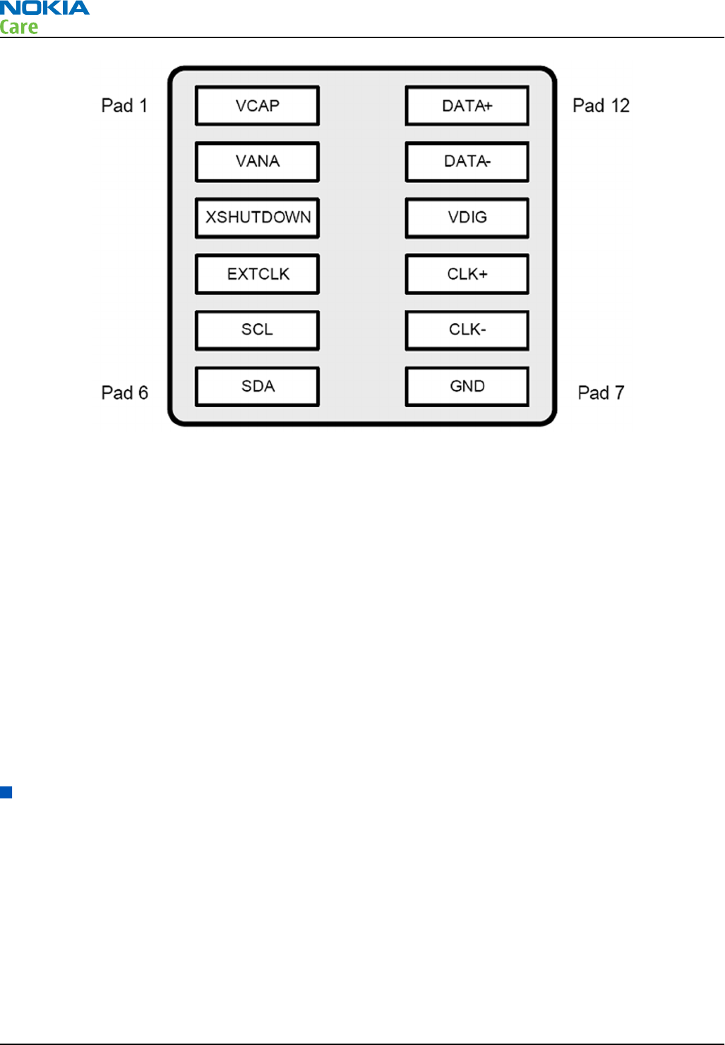
Figure 100 Camera module bottom view including serial numbering
The camera module as a component is not a repairable part, meaning that the components inside the module
may not be changed. Cleaning dust from the front face is allowed only. Use clean compressed air.
The camera module uses socket type connecting. For versioning, laser marked serial numbering is used on
the PWB.
The main parts of the module are:
• Lens unit including lens aperture.
•Infrared filter; used to prevent infrared light from contaminating the image colours. The IR filter is glued
to the EMI shielded camera body.
• Camera body; made of conductive metallized plastic and attached to the PWB with glue.
• Sensor array including DSP functions is glued and wire-bonded to the PWB.
• PWB, FR-4 type
• Passive components
• Camera protection window; part of the phone cover mechanics
• Dust gasket between the lens unit and camera protection window
Dynamic camera configuration
DCC (Dynamic Camera Configuration) is a system to allow final camera tuning values to be programmed on
Service Centre. DCC data generated for a camera hardware is set by Camera Entity IQ department and placed
into global DCC settings database. Service centres could replace a defective module with a spare one to get
camera function recovered by updating DCC data.
DCC data update instruction
Service software is used to update DCC data when camera configuration (a camera or a hardware accelerator)
of the terminal has been changed. Service software DCC update feature reads camera configuration
identification from the terminal, selects a new configuration data file from DP (data package) and writes
data into the memory of the terminal during the process. If the update fails, new camera configuration
installed into the terminal is not supported by DP. Always update DCC when a camera or a HWA has been
changed.
RM-340; RM-341
Camera Module Troubleshooting
Page 5 –12 COMPANY CONFIDENTIAL Issue 1
Copyright © 2007 Nokia. All rights reserved.
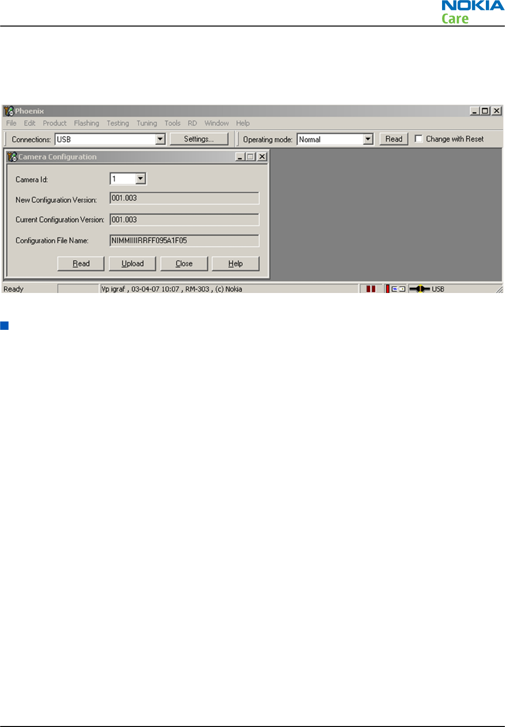
In Service software press “Read”, and the Camera Configuration window shows available DCC data file name
and its version to upload. If the previous camera configuration was the same as installed, then Current
Configuration Version displays DCC data version currently in the terminal memory, otherwise it shows xxx.xxx.
Press “Upload” and then the DCC data settings are updated.
Figure 101 DCC data update
Image quality analysis
Testing for dust in camera module
Symptoms and diagnosis
For detecting these kinds of problems, take an image of a uniform white surface and analyse it in full
resolution. A good quality PC monitor is preferred for analysis. Search carefully, since finding these defects
is not always easy. Figure "Effects of dust on optical path" is an example image containing easily detectable
dust problems.
When taking a white image, use uniformly lightened white paper or white wall. One possibility is to use
uniform light but in this case make sure that the camera image is not flickering when taking the test image.
In case flickering happens, try to reduce illumination level. Use JPEG image format for analysing, and set the
image quality parameter to ‘High Quality’.
Black spots in an image are caused by dirt particles trapped inside the optical system. Clearly visible and
sharp edged black dots in an image are typically dust particles on the image sensor. These spots are searched
for in the manufacturing phase, but it is possible that the camera body cavity contains a particle, which may
move onto the image sensor active surface, for example, when the phone is dropped. Thus it is also possible
that the problem will disappear before the phone is brought to service. The camera should be replaced if the
problem is present when the service technician analyses the phone.
If a dust particle is lying on the infrared filter surface on either side, they are hard to locate because they are
out of focus, and appear in the image as large, grayish and fading-edge 'blobs'. Sometimes they are invisible
to the eye, and thus the user probably does not notice them at all. However, it is possible that a larger particle
disturbs the user, causing need for service.
RM-340; RM-341
Camera Module Troubleshooting
Issue 1 COMPANY CONFIDENTIAL Page 5 –13
Copyright © 2007 Nokia. All rights reserved.
Figure 102 Effects of dust on optical path
If large dust particles get trapped on top of the lens surface in the cavity between camera window and lens,
they will cause image blurring and poor contrast. The dust gasket between the window and lens should
prevent any particles from getting into the cavity after the manufacturing phase. Dust in this position should
be blown away by using compressed air.
Unauthorized disassembling of the product can also be the root of the problem. However, in most cases it
should be possible to remove the particle(s) by using clean compressed air. Never wipe the lens surface before
trying compressed air; the possibility of damaging the lens is substantial. Always check the image sharpness
after removing dust.
Testing camera image sharpness
Symptoms and diagnosis
If pictures taken with a device are claimed to be blurry, there are six possible sources for the problem:
1 The protection window is fingerprinted, soiled, dirty, visibly scratched or broken.
2 The photographed object is too close – the camera lens operates with distances from 20 cm to infinity.
This is no cause to replace camera module.
3 User has tried to take pictures in too dark conditions, and images are blurred due to handshake or
movement. This is no cause to replace camera module.
4 There is dirt between the protection window and camera lens.
RM-340; RM-341
Camera Module Troubleshooting
Page 5 –14 COMPANY CONFIDENTIAL Issue 1
Copyright © 2007 Nokia. All rights reserved.
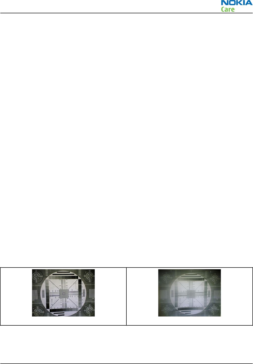
5The protection window is defective. This can be either a manufacturing failure or caused by the user. The
window should be changed.
6 The camera lens is misfocused because of a manufacturing error.
7 Very high level of digital zoom is used
A quantitative analysis of sharpness is very difficult to conduct in any other environment than optics
laboratory. Therefore, subjective analysis should be used.
If no visible defects (items 1-4) are found, a couple of test images should be taken. Generally, a well-
illuminated typical indoor scene can be used as a target. The main considerations are:
• The protection window has to be clean.
• The amount of light (300 – 600 lux (bright office lighting)) is sufficient.
• The scene should contain, for example, small objects for checking sharpness. Their distance should be 1
– 2 meters.
• If possible, compare the image to another image of the same scene, taken with a different device. Note
that the reference device has to be a similar Nokia phone.
Steps
1. Take several images of small objects in the distance of 1-2 metres.
2. Analyse the images on a PC screen at 100% scaling with the reference images.
Pay attention to the computer display settings: at least 65000 colors (16-bit) have to be used. True colour
(24-bit, 16 million colours) or 32-bit (full colour) setting is recommended.
Next actions
If there appears to be a clearly noticeable difference between the reference image and the test images, the
module might have a misfocused lens -> change the module.
Re-check the resolution after changing the camera module.
If the changed module produces the same result, the fault is probably in the camera window. Check the
window by looking carefully through it when replacing the module.
Dirty camera lens protection window
The following series of images demonstrates the effects of fingerprints on the camera protection window.
It should be noted that the effects of any dirt in images can vary much. It may be difficult to judge whether
the window has been dirty or if something else is wrong. Therefore, the cleanness of the protection window
should always be checked and the window should be wiped clean with a suitable cloth.
Figure 103 Image taken with clean protection window Figure 104 Image taken with greasy protection window
Image bit errors
Bit errors are image defects caused by data transmission errors between the camera module and the phone
baseband and/or errors inside the module.
RM-340; RM-341
Camera Module Troubleshooting
Issue 1 COMPANY CONFIDENTIAL Page 5 –15
Copyright © 2007 Nokia. All rights reserved.
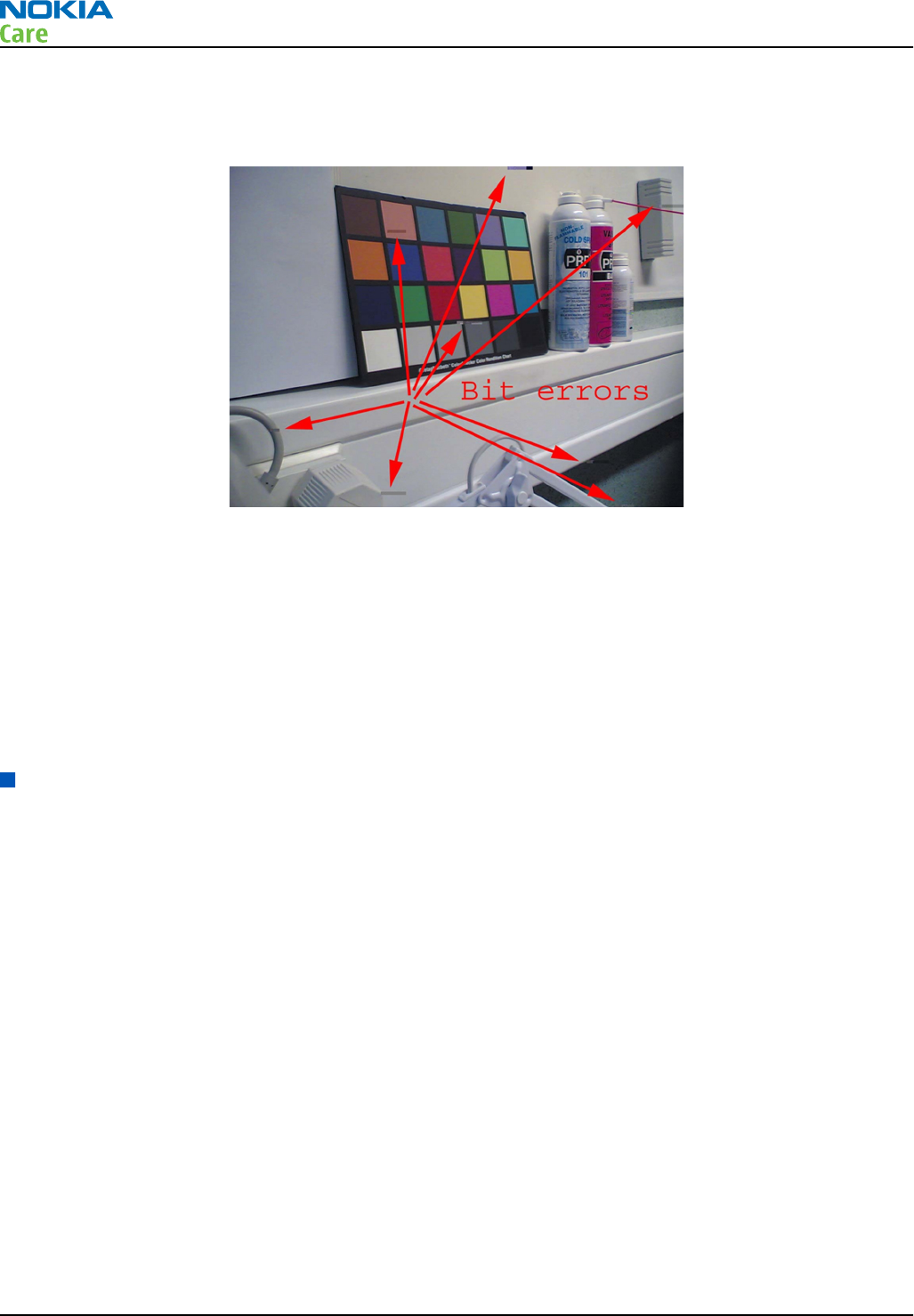
Usually bit errors can be easily detected in images, and they are best visible in full resolution images. A good
practice is to use a uniform white test target when analysing these errors. The errors are clearly visible,
colourful sharp dots or lines in camera images. See the following figure.
Figure 105 Bit errors caused by JPEG compression
One type of bit error is a lack of bit depth. In this case, the image is almost totally black under normal
conditions, and only senses something in very highly illuminated environments. Typically this is a contact
problem between the camera module and the phone main PWB. Very black images and viewfinder may also
be caused by failure of the 2.8V supply to the camera. You should check the camera assembly and connector
contacts.
If the fault is in the camera module, bit errors are typically visible only when using some specific image
resolution. For example, in case of a viewfinder fault, the error might exist but is not visible in a full size
image.
Camera troubleshooting flowcharts
Camera hardware failure message troubleshooting
Context
If you get a hardware failure message when using the camera, follow the next troubleshooting flowchart.
RM-340; RM-341
Camera Module Troubleshooting
Page 5 –16 COMPANY CONFIDENTIAL Issue 1
Copyright © 2007 Nokia. All rights reserved.
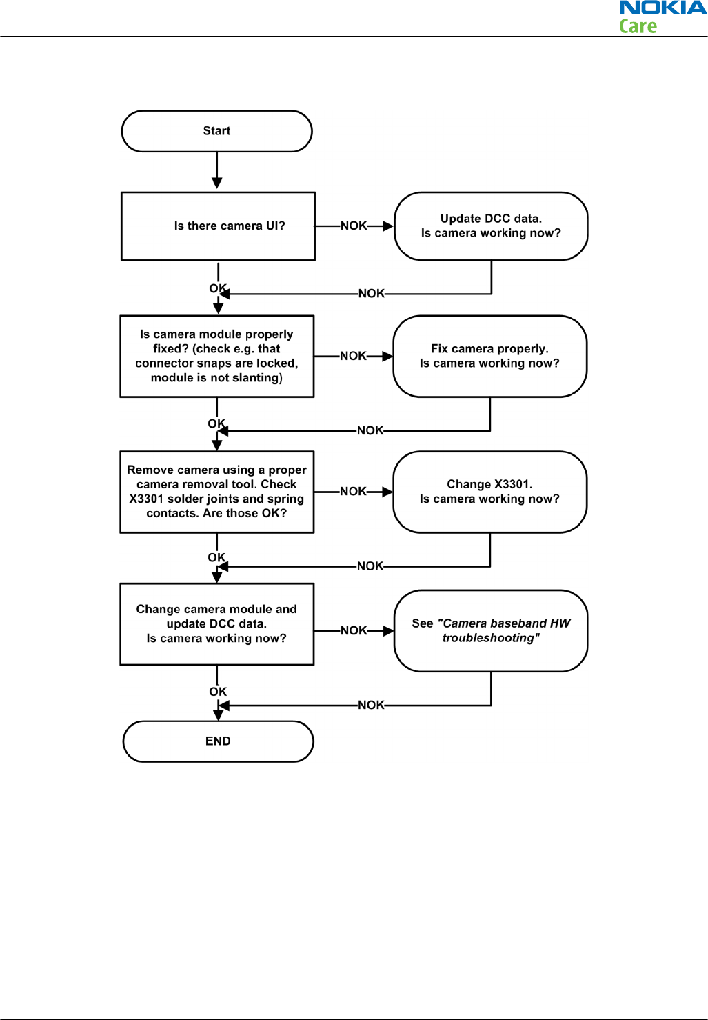
Troubleshooting flow
Note: Make sure that the phone has the latest software before continuing.
RM-340; RM-341
Camera Module Troubleshooting
Issue 1 COMPANY CONFIDENTIAL Page 5 –17
Copyright © 2007 Nokia. All rights reserved.
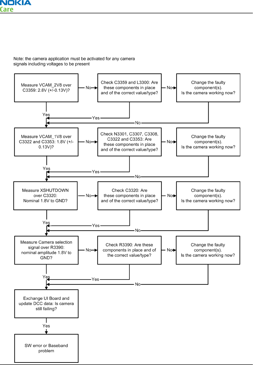
Camera baseband HW troubleshooting
Troubleshooting flow
RM-340; RM-341
Camera Module Troubleshooting
Page 5 –18 COMPANY CONFIDENTIAL Issue 1
Copyright © 2007 Nokia. All rights reserved.
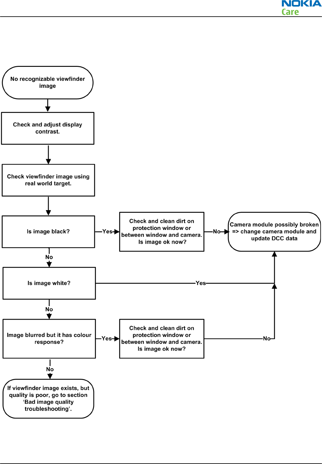
Camera viewfinder troubleshooting
Troubleshooting flow
RM-340; RM-341
Camera Module Troubleshooting
Issue 1 COMPANY CONFIDENTIAL Page 5 –19
Copyright © 2007 Nokia. All rights reserved.
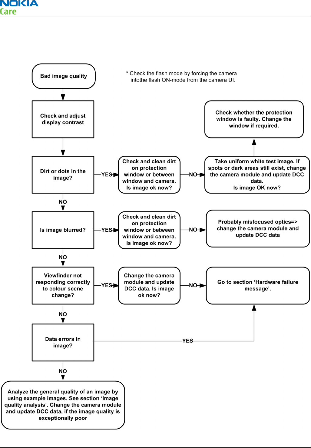
Bad camera image quality troubleshooting
Troubleshooting flow
RM-340; RM-341
Camera Module Troubleshooting
Page 5 –20 COMPANY CONFIDENTIAL Issue 1
Copyright © 2007 Nokia. All rights reserved.

6 — System Module
Nokia Customer Care
Issue 1 COMPANY CONFIDENTIAL Page 6 –1
Copyright © 2007 Nokia. All rights reserved.

RM-340; RM-341
System Module
(This page left intentionally blank.)
Page 6 –2 COMPANY CONFIDENTIAL Issue 1
Copyright © 2007 Nokia. All rights reserved.

Table of Contents
System module block diagram .............................................................................................................................6–5
Baseband description ............................................................................................................................................6–6
Functional description......................................................................................................................................6–6
UPP .....................................................................................................................................................................6–6
Memory ..............................................................................................................................................................6–6
UEMCLite .............................................................................................................................................................6–6
External regulators............................................................................................................................................6–6
Energy management.........................................................................................................................................6–7
Modes of operation...........................................................................................................................................6–8
Voltage limits.....................................................................................................................................................6–8
Audio function description...............................................................................................................................6–8
External audio connector .................................................................................................................................6–9
HALL sensor..................................................................................................................................................... 6–10
Interfaces ............................................................................................................................................................. 6–12
RF and baseband interfaces .......................................................................................................................... 6–12
Analogue Signals............................................................................................................................................ 6–14
LCD interface ................................................................................................................................................... 6–15
Keyboard ......................................................................................................................................................... 6–15
SIM interface ................................................................................................................................................... 6–16
External signals and connections ................................................................................................................. 6–18
Battery connector........................................................................................................................................... 6–18
Battery interface............................................................................................................................................. 6–19
PWB outline .................................................................................................................................................... 6–20
RF description ...................................................................................................................................................... 6–20
Frequency band, power and multi-slot class............................................................................................... 6–20
Transmitter - general description ................................................................................................................ 6–21
Transmitter - signal processing.................................................................................................................... 6–21
Receiver - general description ...................................................................................................................... 6–21
VCXO and PLL................................................................................................................................................... 6–22
Technical specifications...................................................................................................................................... 6–22
General specifications.................................................................................................................................... 6–22
Battery endurance.......................................................................................................................................... 6–23
Environmental conditions ............................................................................................................................. 6–23
Electrical characteristics ................................................................................................................................ 6–23
List of Tables
Table 6 Voltage limits ............................................................................................................................................6–8
Table 7 Connector for External Audio Accessories ........................................................................................... 6–10
Table 8 AC and DC Characteristics of BB4.0 LiteV2 RF-Base band Digital Signals .......................................... 6–12
Table 9 AC and DC Characteristics of RF-Base band Analogue Signals ........................................................... 6–14
Table 10 SIM interface......................................................................................................................................... 6–17
Table 11 System connector ................................................................................................................................ 6–18
Table 12 Battery IF .............................................................................................................................................. 6–18
Table 13 Pin numbering of battery pack .......................................................................................................... 6–19
Table 14 Frequency bands and TX power class................................................................................................ 6–20
Table 15 Multi-slot class ..................................................................................................................................... 6–21
Table 16 Normal and extreme voltages............................................................................................................ 6–23
Table 17 Current consumption........................................................................................................................... 6–24
RM-340; RM-341
System Module
Issue 1 COMPANY CONFIDENTIAL Page 6 –3
Copyright © 2007 Nokia. All rights reserved.

List of Figures
Figure 106 Module block diagram........................................................................................................................6–5
Figure 107 Power connection diagram................................................................................................................6–7
Figure 108 SIM filtering .........................................................................................................................................6–7
Figure 109 Audio block diagram...........................................................................................................................6–9
Figure 110 4-pole jack plug for audio accessory.............................................................................................. 6–10
Figure 111 HALL sensor....................................................................................................................................... 6–11
Figure 112 Keyboard schematics....................................................................................................................... 6–16
Figure 113 SIM interface block diagram ........................................................................................................... 6–17
Figure 114 BL-5BT battery pack contacts.......................................................................................................... 6–19
Figure 115 PWB top side component placement............................................................................................. 6–20
Figure 116 PWB bottom side component placement...................................................................................... 6–20
RM-340; RM-341
System Module
Page 6 –4 COMPANY CONFIDENTIAL Issue 1
Copyright © 2007 Nokia. All rights reserved.
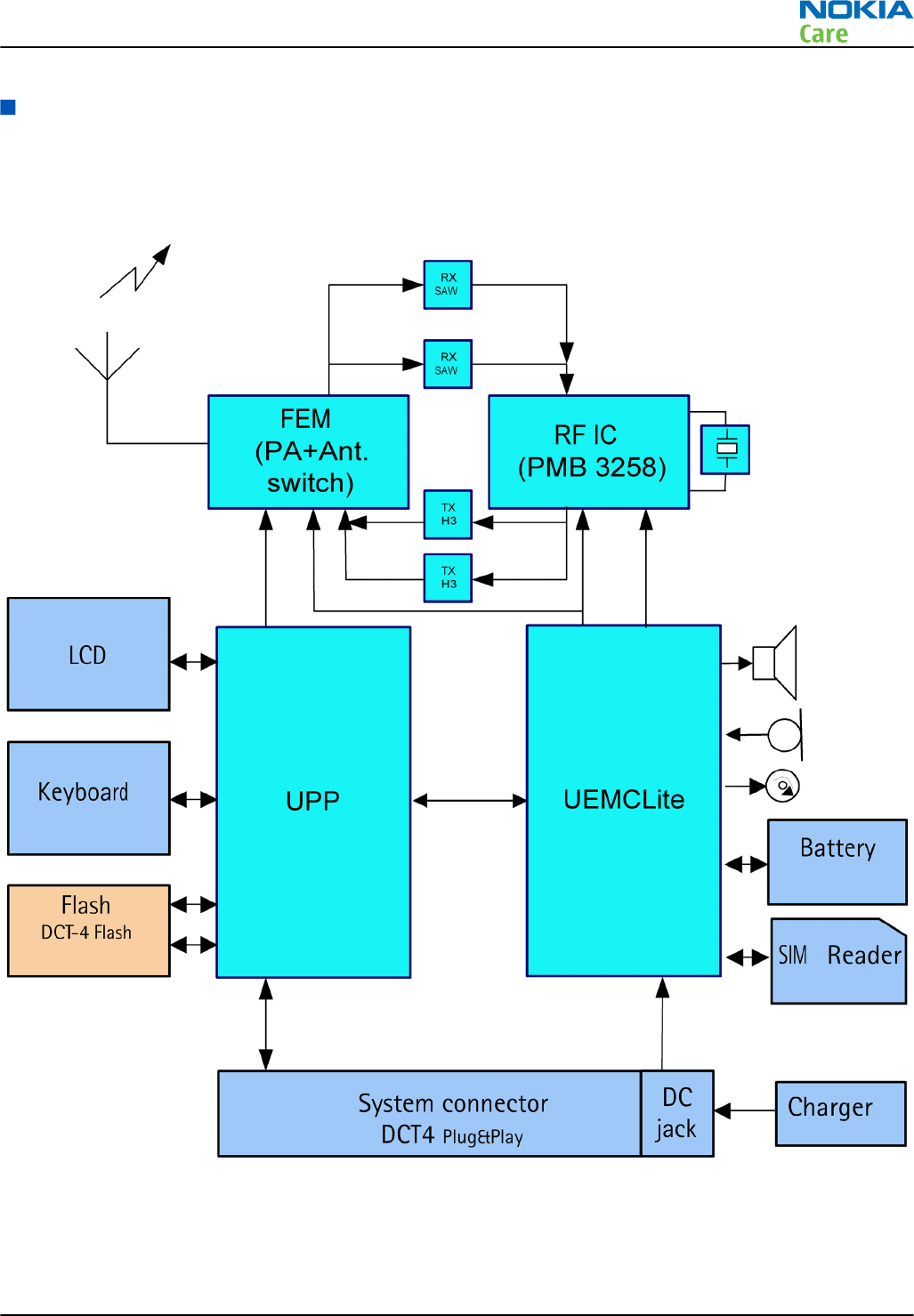
System module block diagram
The main board consists of a radio frequency part and a baseband part. The User Interface parts are situated
at the UI side, which is on the opposite side of the engine board. The 2CP is the engine module of the mobile
device, and the 2CQ is the UI module of module of the mobile device.
Figure 106 Module block diagram
RM-340; RM-341
System Module
Issue 1 COMPANY CONFIDENTIAL Page 6 –5
Copyright © 2007 Nokia. All rights reserved.

Baseband description
Functional description
The BB core is based on UPP8M CPU. UPP8M takes care of all the signal processing and operation controlling
tasks of the mobile device. For power management, there is one main ASIC for controlling charging and
supplying power UEMCLite plus a discrete power supply. The main reset for the system is generated by the
UEMCLite. The memory comprises of 128 Mbit flash and 16 Mbit PsRAM. memory devices that are stacked on
top of each other in a single Combo package.
The interface to the RF and audio sections is also handled by the UEMCLite. This ASIC provides A/D and D/A
conversion of the in-phase and quadrature receive and transmit signal paths and also A/D and D/A conversions
of received and transmitted audio signals. Data transmission between UEMCLite and RF and the UPP8M is
implemented using different serial connections (CBUS, DBUS and RFBUS). Digital speech processing is handled
by UPP8M ASIC.
A real time clock function is integrated into UEMCLite, which utilizes the same 32 kHz-clock source as the
sleep clock. The SLCK/RTC runs all time when the phone battery is connected. It is running also when the
phone is switched off. In UEMCLite there is no back up battery/capacitor connection.
There are three audio transducers in the product; 16 mm speaker, an earpiece and a microphone. The earpiece
is used to generate audios for earpiece; the speaker is used to generate audios for IHF and ringing tones. A
separate audio amplifier drives the speaker. There is only one microphone for both HS and IHF modes.
The display is an TFT type color display with 65536 colors and 128 x 160 pixels with backlighting. The keypad
module features a function keymat with a 4-way navigation key with a center selection key.
UPP
UPP (Universal Phone Processor) is the digital ASIC of the DCT4 generation base band. UPP8M includes 4.5
MBit internal RAM, 16/32-bit RISC MCU core. UPP8Mv6.11 includes ARM7TDMI rev4 16/32-bit RISC MCU core, TI
Lead3 16-bit DSP phase2+ core with DMA controller, ROM for MCU boot code and all digital control logic.
Memory
This mobile uses two kinds of memories, Flash and Synchronous RAM (SRAM). These memories have are
sharing the same bus interface to UPP8M. SDRAM is used as the working memory. The SRAM size is 16 Mbits.
SRAM I/O is 1.8 V and core 1.8 V supplied by UEMCLite regulator VIO. All memory contents are lost if the supply
voltage is switched off.
Multiplexed flash memory interface is used to store the MCU program code and user data.
Configuration of flash memory is a 128 Mbit NOR flash memory. Flash I/O and core voltage are 1.8 V.
UEMCLite
The UEMCLite is a low cost energy management ASIC contains for BB use two 2.78V LDO regulators, 1.8V linear
regulator, programmable 1.0 - 1.5 V linear regulator and 1.8/3.0 V LDO regulator. For RF use UEMCLite has
five 2.78 V LDOs. In addition, the UEMCLite contains audio codec, A/D converters, RF converters, many drivers,
etc.
External regulators
White LED Driver solution is implemented with DC/DC converter. The driver circuit is controlled by UEM output
pin DLIGHT, which add external pull up using a digital transistor and one resistor. The schematics also
combined the UEMIO (5) to control DC/DC enable as another optional using two jumper.
RM-340; RM-341
System Module
Page 6 –6 COMPANY CONFIDENTIAL Issue 1
Copyright © 2007 Nokia. All rights reserved.
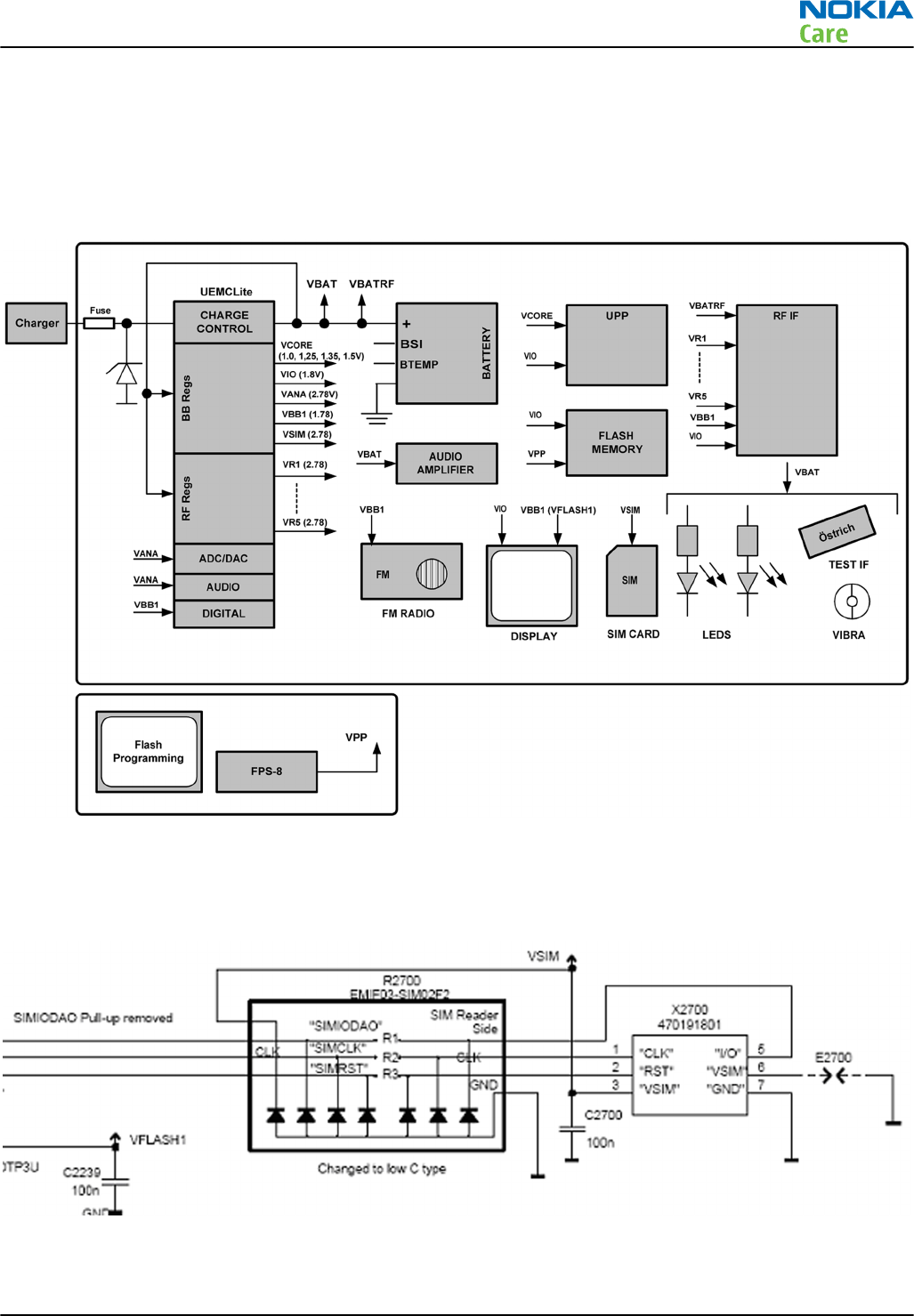
Energy management
Filter components
The master of EM control is UEMCLite and with SW it has the main control of the system voltages and operating
modes. The power distribution diagram is presented in the illustration below.
Figure 107 Power connection diagram
All connectors going to the “outside world” have filter components, ESD protection and EMC reduction.
The Digital/Data lines on SIM have special dedicated filter ASIP. The below figure show the SIM filtering.
Figure 108 SIM filtering
RM-340; RM-341
System Module
Issue 1 COMPANY CONFIDENTIAL Page 6 –7
Copyright © 2007 Nokia. All rights reserved.

The Audio circuit: Earpiece, IHF, internal microphone and external speaker are filtered with discrete
components (common mode reduction coils, Varistors, caps and resistors), where as the external microphone
uses differential mode mic. ASIP
The 16 UEMECLite BB & RF regulators are specified to have a decoupling cap of 1 µF ±20%.
Modes of operation
BB4.0 LiteV2 base band has five different functional modes, which are defined in UEMCLite specification:
• No supply: In NO_SUPPLY mode, the phone has no supply voltage. This mode is due to disconnection of
main battery or low battery voltage level in battery. Phone is exiting from NO_SUPPLY mode when sufficient
battery voltage level is detected. Battery voltage can rise either by connecting a new battery with VBAT >
VMSTR+ or by connecting charger and charging the battery above VMSTR+.
•Acting Dead: If the phone is off when the charger is connected, the phone is powered on but enters a state
called ”Acting Dead”. To the user, the phone acts as if it was switched off. A battery charging alert is given
and/or a battery charging indication on the display is shown to acknowledge the user that the battery is
being charged.
• Active: In the Active mode the phone is in normal operation, scanning for channels, listening to a base
station, transmitting and processing information. There are several sub-states in the active mode
depending on if the phone is in burst reception, burst transmission, if DSP is working etc.
In Active mode the RF regulators are controlled by SW writing into UEMCLite’s registers wanted settings:
VR regulators can be disabled, enabled or forced into low quiescent current mode. VR2 is always enabled
in Active mode for system clock chain supply
• Sleep: In sleep mode VCTCXO is shut down and 32 kHz sleep clock oscillator is used as reference clock for
the base band.
• Charging: Charging can be performed in any operating mode. The battery type / size is indicated by a
resistor inside the battery pack. The resistor value corresponds to a specific battery capacity. This capacity
value is related to the battery technology as different capacity values are achieved by using different
battery technology. The battery voltage, temperature, size and current are measured by the UEMCLite and
controlled by the charging software running in the UPP. The charging control circuitry (CHACON) inside the
UEMCLite controls the charging current delivered from the charger to the battery. The battery voltage rise
is limited by turning the UEMCLite switch off when the battery voltage has reached 4.2 V. Charging current
is monitored by measuring the voltage drop across a 220 mW resistor. The PWM output doesn’t exist any
more from UEMCLite to the bottom connector
Voltage limits
Table 6 Voltage limits
Parameter Description Value/V
Vmstr+ Master reset threshold (rising) 2.1 ±0.1
Vmstr- Master reset threshold (falling) 1.9 ±0.1
Vcoff+ Hardware cutoff (rising) 3.1 ±0.1
Vcoff- Hardware cutoff (falling) 2.8 ±0.1
SW shutdown SW cutoff limit (> regulator drop-
out limit) MIN!
3.2 V
Audio function description
The basic audio structure and communication between HW-audio modules and the audio ASIC's is illustrated
in the block diagram below.
RM-340; RM-341
System Module
Page 6 –8 COMPANY CONFIDENTIAL Issue 1
Copyright © 2007 Nokia. All rights reserved.
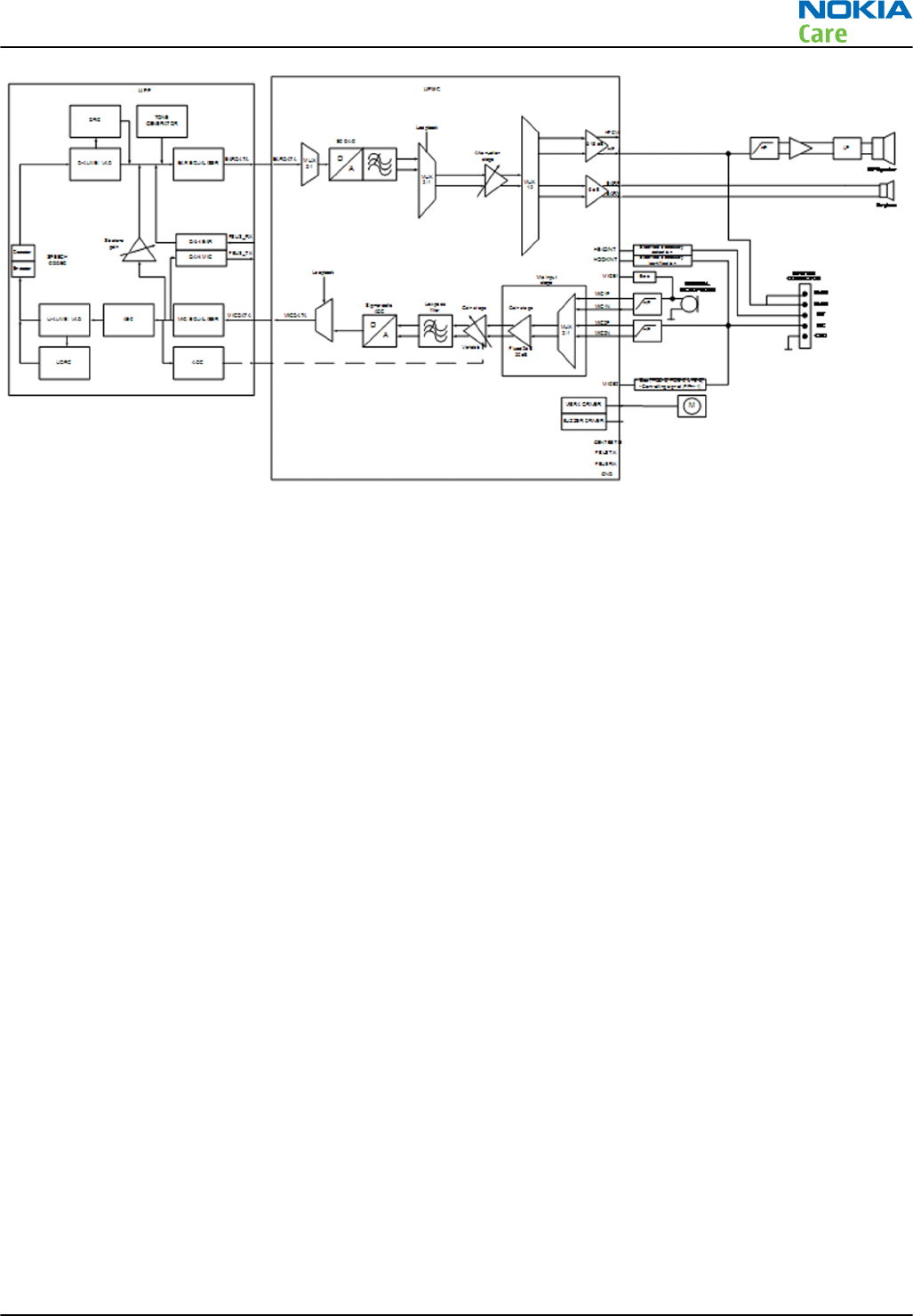
Figure 109 Audio block diagram
UEMcLite supports three microphone inputs and two outputs. The inputs can be used for internal, headset
or handsfree microphones. The microphone signals from different sources are connected to separate inputs
at the UEMcLite ASIC. The inputs and outputs are all differential.
Three inputs (MIC1, MIC2) and two outputs (EAR, HF) are used in the phone.
MIC1P/MIC1N inputs are used for the internal microphone, using single-ended biasing circuitry. EARP/EARN
outputs from UEMcLite are used for hand-portable mode.
Uplink external audio (headset as well as carkit) is connected to MIC2P/MIC2N, while downlink audio is
provided via the HF outputs from UEMcLite. A special situation exists since the carkit can be used with two
different microphones: either the phone's internal microphone (MIC1-inputs) or an external microphone that
connects to the carkit. In these cases UEMcLite is capable of switching between MIC1 and MIC2.
The audio control is taken care of by UEMcLite, which contains the MCU and audio codec. UPP contains DSP
blocks, and handling and processing of the audio signals.
Input and output selection, and gain control is performed inside UEMcLite. DTMF-tones and other audio tones
are generated and encoded by UPP and transmitted to UEMcLite for decoding.
External audio connector
The system connector, containing a 4-pole Jack plug, gains the access to the external audio interface. The
Jack plug, which is integrated in the system connector, contains a mechanical switch, which is used to detect
the connection of the accessories. The configuration for the 4-pole Jack-plug is shown in the following figure.
RM-340; RM-341
System Module
Issue 1 COMPANY CONFIDENTIAL Page 6 –9
Copyright © 2007 Nokia. All rights reserved.

Figure 110 4-pole jack plug for audio accessory
Table 7 Connector for External Audio Accessories
Pin Signal name Direction Description
5 PLUGDET Input Terminal internal
connection, plug
detection
4 HS EAR L Output Audio output
3 HS EAR R Output Audio output
2 HS MIC Input Multiplexed
microphone audio and
control data
1 HS GND - Ground contact
HALL sensor
The HALL sensor is used to recognize the position of the flap.
The HALL sensor incorporates advanced chopper-stabilization techniques to provide accurate and stable
magnetic switch points. The circuit design provides an internally controlled clocking mechanism to cycle
power to the HALL element and analog signal processing circuits. This serves to place the high current-
consuming portions of the circuit into the sleep mode. Periodically the device is awakened by this internal
logic and the magnetic flux from the HALL element is evaluated against the predefined thresholds. If the flux
density is above or below the BOP/BRP thresholds, the output transistor is driven to change states accordingly.
While in the sleep cycle, the output transistor is latched in its previous state.
The output transistor of the SH248CSP is latched on at the presence of a sufficiently strong south or north
magnetic field facing the marked side of the package. The output is latched off in the absence of a magnetic
field.
The output of hall sensor is sent to GENIO24 of UPP. Baseband knows the status of the hall sensor that
represents the phone position (folded or not).
RM-340; RM-341
System Module
Page 6 –10 COMPANY CONFIDENTIAL Issue 1
Copyright © 2007 Nokia. All rights reserved.
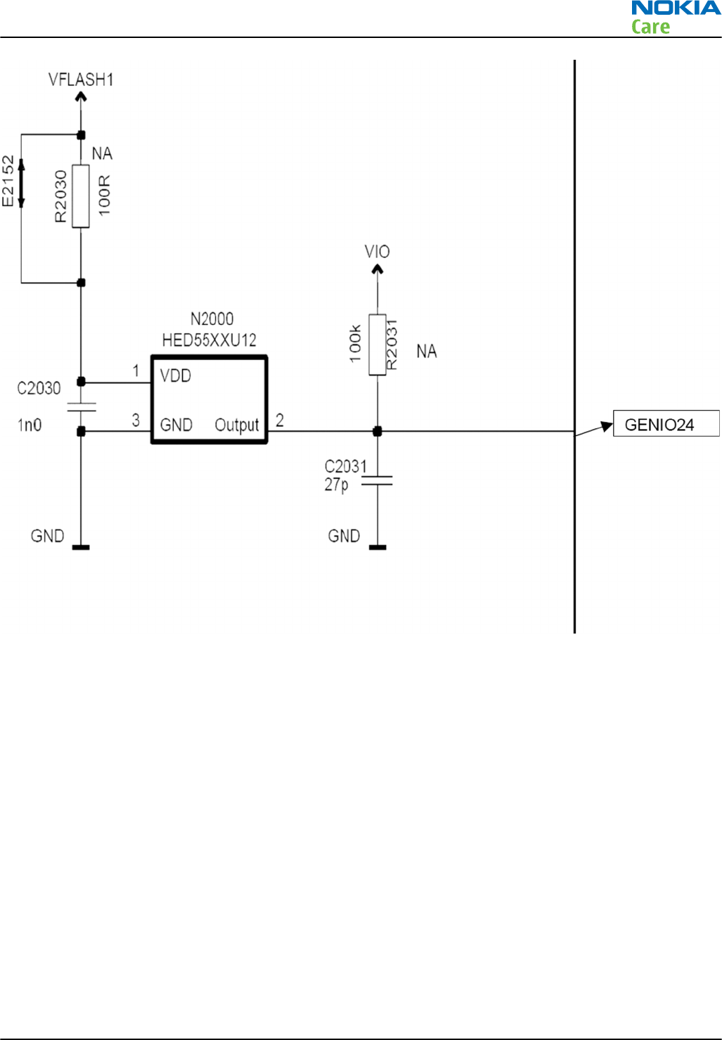
Figure 111 HALL sensor
RM-340; RM-341
System Module
Issue 1 COMPANY CONFIDENTIAL Page 6 –11
Copyright © 2007 Nokia. All rights reserved.
Interfaces
RF and baseband interfaces
Table 8 AC and DC Characteristics of BB4.0 LiteV2 RF-Base band Digital Signals
Signal
name From To Para-meter Input characteristics Function
Min Typ Max Unit
TXP1 UPP RF-IC 1 1.38 1.88 V Depends of
the RF design
RFGenOu
t3
GenIO5 0 0 0.4 V
Load
Resistance
10 kW
Load
Capacitanc
e
20 pF
Timing
Accuracy
¼ symbo
l
TXP2 UPP RF-IC 1 1.38 1.88 V Depends of
the RF design
(GenIO6
)
0 0 0.4 V
Load
Resistance
10 kW
Load
Capacitanc
e
20 pF
Timing
Accuracy
¼ symbo
l
RFBusEn1
X
UPP RF-IC 1 1.38 1.88 V RFIC Chip SelX
0 0 0.4 V
Internal PU
Current
50 uA
Load
resistance
10 kW
Load
capacitanc
e
20 pF
RM-340; RM-341
System Module
Page 6 –12 COMPANY CONFIDENTIAL Issue 1
Copyright © 2007 Nokia. All rights reserved.
Signal
name From To Para-meter Input characteristics Function
Min Typ Max Unit
RFBusDa UPP /
RF-IC
RF-
IC/
UPP
1 1.38 1.88 V Bi-directional
RF Control
serial bus
data,
0 0 0.4 V
Load
resistance
10 kW
Load
capacitanc
e
20 pF
Data
frequency
13 MHz
RFBusClk UPP RF IC 1 1.38 1.88 V RF Control
serial bus bit
clock
0 0 0.4 V
Load
resistance
10 kW
Load
capacitanc
e
20 pF
Data
frequency
13 MHz
GENIO3 UEMCLit
e
RF IC 1 2.78 V RF Control *
0 V Depends of
the RF design
Load
resistance
kW
Output
current
4 mA
GENIO4 UEMCLit
e
RF IC 1 2.78 V Audio clock
input in
UEMCLiteV3
and LittiV2
0 V
Load
resistance
kW
Output
current
4 mA
GENIO5 UEMCLit
e
RF IC 1 2.78 V RF Control *
0 V Depends of
the RF design
Load
resistance
kW
Output
current
4 mA
RM-340; RM-341
System Module
Issue 1 COMPANY CONFIDENTIAL Page 6 –13
Copyright © 2007 Nokia. All rights reserved.
Analogue Signals
Table 9 AC and DC Characteristics of RF-Base band Analogue Signals
Signal
name From To Parameter Min Typ Max Unit Function
RFCLK VCTCXO UPP Frequency 13/26 MHz System Clk from RF to
BB,
Signal
amplitude
0.2 0.8 1.32 Vpp 13/26 MHz Depending
on RF chipset
Input
Impedance
10 kW UPP minimum
recommended
amplitude is 0.3Vpp.
Input
Capacitanc
e
10 pF
Harmonic
Content
-8 dBc
Clear signal
window
(no glitch)
200 mVpp
Duty Cycle 40 60 %
RFCLKGnd VCTCXO UPP DC Level 0 V System Clock slicer Ref
GND, not separated
from pwb GND layer
RXIP,
RXIN,
RXQP,
RXQN
RF-IC UEMCL
ite
Voltage
swing
(static)
1.4 1.45 Vpp Differential positive /
negative in-phase
and quadrature Rx
Signals.
DC level 1.3 1.35 1.4 V
I/Q
amplitude
mismatch
0.2 dB
I/Q phase
mismatch
-0.5 0.5 deg
TXIP,
TXIN,
TXQP,
TXQN
UEMCLit
e
RF-IC Differential
voltage
swing
(static)
2.25 2.45 Vpp Differential positive /
negative in-phase
and quadrature Tx
Signals
In High-Z when RX is
receiving.
DC level 1.17 1.20 1.23 V
Source
Impedance
200 W
RM-340; RM-341
System Module
Page 6 –14 COMPANY CONFIDENTIAL Issue 1
Copyright © 2007 Nokia. All rights reserved.
Signal
name From To Parameter Min Typ Max Unit Function
AFC UEMCLit
e
VCTCX
O
Voltage Min 0.0 0.1 V Automatic Frequency
Control signal for
VCTCXO
Programmable
(AFCOUT
)
Max 2.4 2.55
Resolution 11 bits
Load
resistance
1 kW
and
capacitanc
e
100 nF
Source
Impedance
200 W
Output
impedance
10 MW Path powered down
TxC UEMCLit
e
RF-IC Voltage Min 0.1 V Transmitter power
level and ramping
control, Ref UEMCLite
RF converter
specification
(AUXOUT
)
Max 2.4
Source
Impedance
200 W
Resolution 10 bits
VCXOTEMP RF-IC UEMCL
ite
Input
voltage
range
0 2.7 V
Input
resistance
900 6000 Ohm
Resolution 10 bits
PATEMP RF-IC UEMCL
ite
Voltage at
-20oC
1.57 V Usage depends of the
RF design
LCD interface
The display is controlled by phone processor UPP.
The main LCD module is connected to the PWB by a 24-pin board-to-board connector.
The sub LCD module is connected to the PWB by a 10-pin board-to-board connector.
Keyboard
A 5 X 5 matrix keyboad consists of 21 keys, one 10-channel integrated passive filiter arrays with downstream
ESD protection of >8KV connect the matrix keyboard to UPP.
RM-340; RM-341
System Module
Issue 1 COMPANY CONFIDENTIAL Page 6 –15
Copyright © 2007 Nokia. All rights reserved.
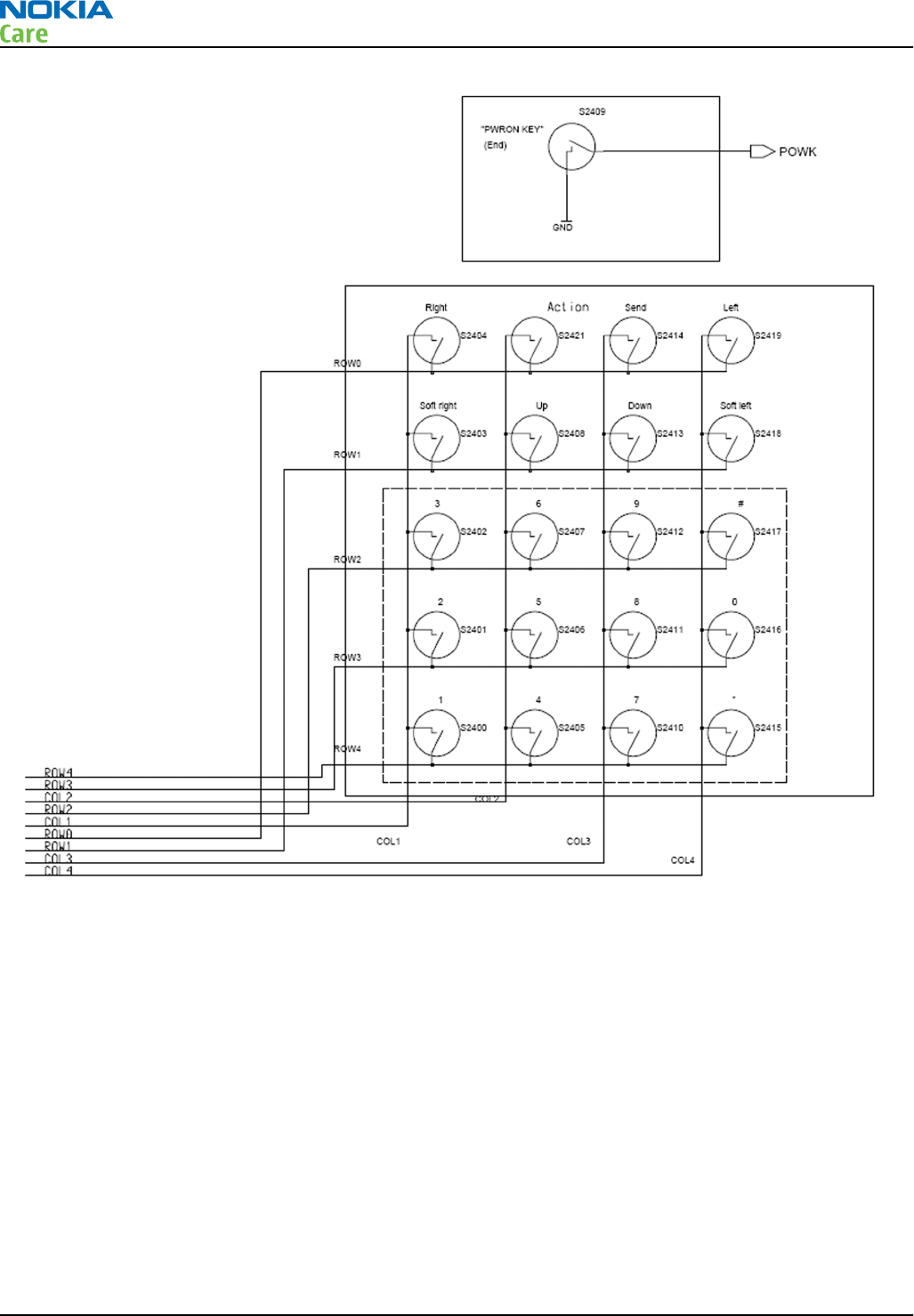
Figure 112 Keyboard schematics
SIM interface
The UEMCLite contains the SIM interface logic level shifting. The SIM interface can be programmed to support
3V and 1.8V SIMs. SIM supply voltage is selected by with register in the UEMCLite. It is only allowed to change
the SIM supply voltage when the SIM IF is powered down.
The SIM power up/down sequence is generated in the UEMCLite. This means that the UEMCLite generates the
RST signal to the SIM. In addition, the SIMCardDet signal is connected to UEMCLite. The detection is taken from
the BSI signal, which detects the removal of the battery. The monitoring of the BSI signal is done by a
comparator inside UEMCLite. The comparator offset is such that the comparator outputs do not alter state as
long as the battery is connected. The threshold voltage is calculated from the battery size specifications.
The SIM interface is powered up when the SIMCardDet signal indicates ”card in”. This signal is derived from
the BSI signal.
RM-340; RM-341
System Module
Page 6 –16 COMPANY CONFIDENTIAL Issue 1
Copyright © 2007 Nokia. All rights reserved.

Table 10 SIM interface
Pin Name Parameter Min Typ Max Unit Notes
4 DATA 1.8V Voh 0.9xVSI
M
VSIM V SIM data (output)
1.8V Vol 0 0.15xVSIM
3V Voh 0.9xVSI
M
VSIM
3V Vol 0 0.15xVSIM
1.8V Vih 0.7xVSI
M
VSIM V SIM data (input)
1.8V Vil 0 0.15xVSIM Trise/Tfall max
1us
3V Vil 0.7xVSI
M
VSIM
3V Vil 0 0.15xVSIM
5 NC Not connected
6 GND GND 0 0 V Ground
VSIM specified in regulator section in this document
Figure 113 SIM interface block diagram
RM-340; RM-341
System Module
Issue 1 COMPANY CONFIDENTIAL Page 6 –17
Copyright © 2007 Nokia. All rights reserved.

External signals and connections
Table 11 System connector
Signal From To Min Nom Max Condi-tion Note
XMICP HS/HF Mic UEMC
Lite
2/60m
V diff
Analog
audio in
Headset Mic bias and
audio signal 2mV
nominal. HF Mic signal
60mV nominal.
Differential symmetric
input.
DC bias
2V2kohm
Accessory detection by
bias loading
XMICN 2/60m
V diff
Ana in / 1k
to GND
Hook interrupt by heavy
bias loading
XEARP HS/HF UEMC
Lite
100 mV
diff
Ana in Quasi-differential DC-
coupled earpiece/HF
amplifier signal to
accessory. DC biased to
0.8V
XEARN EAR/
Amp.
INT
HEADINT
Switch UEMC
Lite
0/2.7V Dig in HS interrupt from bottom
connector switch when
plug inserted.
VCHARIN Charger UEMC
Lite
11.1Vp
eak
16.9
Vpeak
Standard Vch from Charger
Connector, max 20V
7.9
VRMS
1.0
Apeak
7.0
VRMS
8.4
VRMS
9.2
VRMS
Fast charger
850 mA
GND GND GND from/to Charger
connector
Battery connector
Table 12 Battery IF
Signal From To Min Nom Max Note
GND Global Batt (-) Global GND
VBAT Batt (+) 3.1 5.1 Battery Voltage
RM-340; RM-341
System Module
Page 6 –18 COMPANY CONFIDENTIAL Issue 1
Copyright © 2007 Nokia. All rights reserved.
Signal From To Min Nom Max Note
BSI UEMCLite 0 2.78 Analog input, Battery Size
Indicator Resistor, 100
kohm pull up to 2.78V
(VBB1). FDL Init, refer to
flash download.
Battery interface
• Type: BL-5BT
• Technology: Li-Ion, 4.2 V charging, 3.1 V cut-off
• Capacity: 870 mAh.
BL-5BT has a 3 pin interface with overcharge / discharge protection (safety circuit) and battery size indication
BSI with an internal resistor. The BSI fixed resistor value indicates type and default capacity of a battery.
Figure 114 BL-5BT battery pack contacts
Table 13 Pin numbering of battery pack
Signal name Pin number Function
GND 2 Negative/common battery
terminal
BSI 3 Battery capacity measurement
(fixed resistor inside the battery
pack)
VBAT 1 Positive battery terminal
RM-340; RM-341
System Module
Issue 1 COMPANY CONFIDENTIAL Page 6 –19
Copyright © 2007 Nokia. All rights reserved.
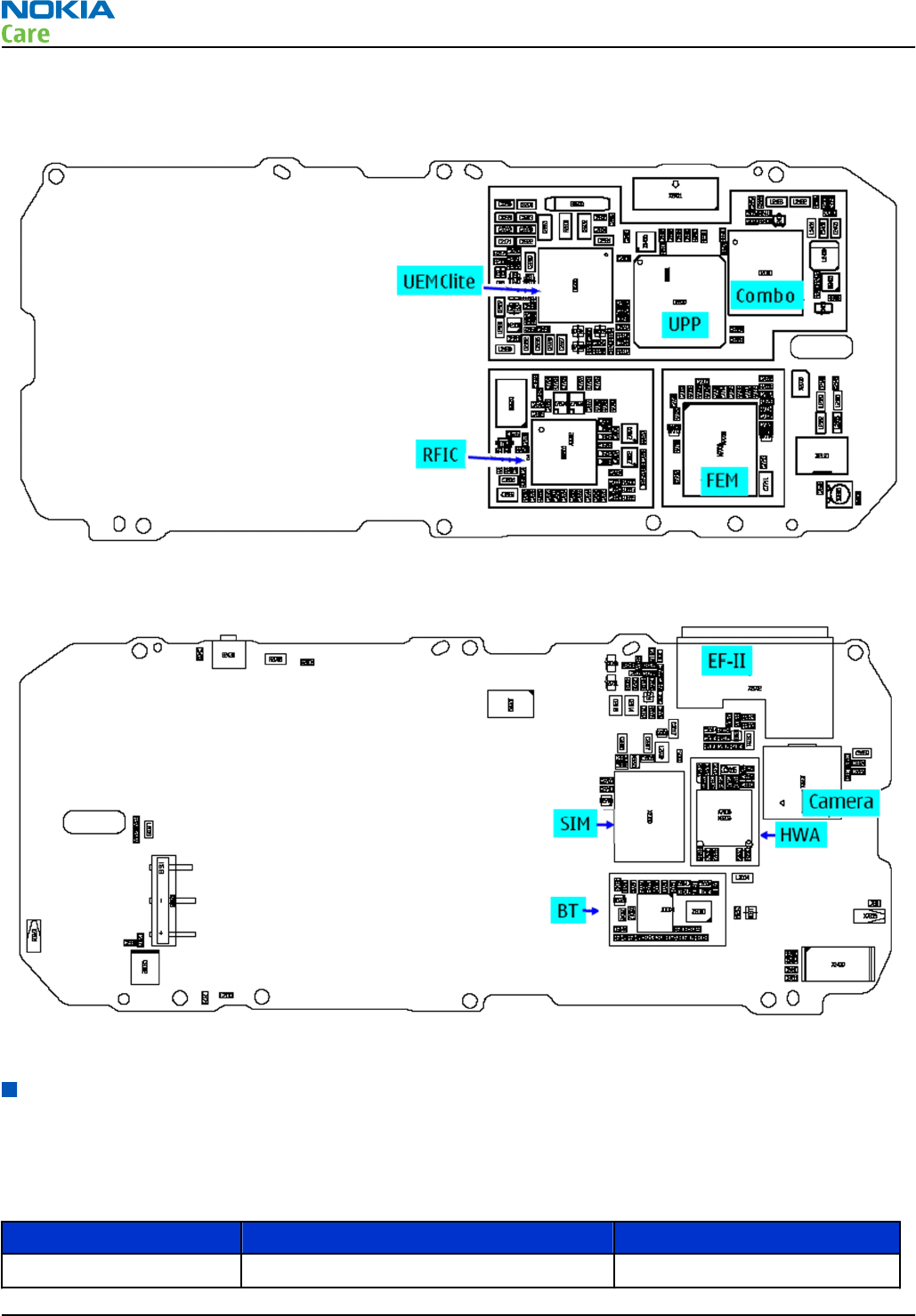
PWB outline
Figure 115 PWB top side component placement
Figure 116 PWB bottom side component placement
RF description
Frequency band, power and multi-slot class
The requirement leads to the specification in the table below:
Table 14 Frequency bands and TX power class
System Frequency band TX power class
GSM900 Tx: 880 – 915 MHz 4 (33dBm)
RM-340; RM-341
System Module
Page 6 –20 COMPANY CONFIDENTIAL Issue 1
Copyright © 2007 Nokia. All rights reserved.

System Frequency band TX power class
Rx: 925 – 960 MHz
GSM1800 Tx: 1710 – 1785 MHz 1 (30dBm)
Rx: 1805 – 1880 MHz
Table 15 Multi-slot class
Multislot Class
GPRS MSC 10 (4Dn/2Up), sum=5
E-GPRS MSC 6 in DL, max. 3Dn
Transmitter - general description
The transmitter has separate, parallel paths covering the different bands. The transmitter operates in GMSK
mode only. The power level control circuitry is integrated in the front-end module.
Each path of the transmitter is composed of a baseband lowpass filter for the I/Q signals and a quadrature
direct modulator integrated in PMB3258. At the modulator’s output there is a bandpass filter for each band
(so-called H3 filter) and a balun transformer to convert the differential output signal from the modulator into
a single-ended 50 ohm signal. This signal is fed into the input of the PA. The two power amplifiers and the
antenna switch are integrated in a single module with built-in power control loop.
The two control methods used are open-loop Vcc control (RFMD) and feedback control with current sensing.
The reference waveform (TXC) for the control loop comes from the baseband. The output of the PA goes into
a low pass filter located inside the FEM (Front End Module). Finally the transmit signal goes through the band
selection and TX/RX switches to the antenna port.
The FEM is controlled with four digital control signals (TXP, Vc1, Vc2 and Vc3) to meet the TDMA frame timing
requirements.
Transmitter - signal processing
The I/Q signals coming from the baseband section are fed into the modulator and converted up to the carrier
frequency. The I/Q are post filtered by a 1st order passive RC filter (discrete components on PWB) and a 3rd
order active filter (Legendre type) inside PMB3258.
The nominal output level of the modulator is +3.5 dBm in both bands. The modulator's output is an open-
collector type and need an external load and a DC supply feed. The load and the DC supply feed are
implemented as the part of the H3 filter.
The filtered signal is fed into the input of the FEM, which amplifies it to the desired power level and provides
the signal at the antenna port.
There is also a temperature sensor close to the FEM to enable SW temperature compensation for e.g. the
power levels. The sensor is connected to one of the slow ADC channels in the baseband.
Receiver - general description
The receiver is a direct conversion linear receiver. It is a dual-band receiver with receiver paths for either
GSM850/1900 or GSM900/1800 configuration.
From the antenna, the received RF-signal is fed into the front-end module, which routes the signal to the
appropriate RX path. After the FEM, the RX signals are filtered by SAW filters (one for each band), which reject
the out-of band blocking signals to low enough level to be handled by the RF ASIC.
RM-340; RM-341
System Module
Issue 1 COMPANY CONFIDENTIAL Page 6 –21
Copyright © 2007 Nokia. All rights reserved.

There are two paths – one for each band. In each path, the signal is then fed to the low noise amplifier (LNA).
One LNA can handle both the GSM850 and GSM900 signals and another is used for GSM1800 and GSM1900.
The LNA inputs are matched to the SAW filter outputs by means of discrete LC matching networks. The SAW
filters and the matching networks are different for different band combinations, but the PWB layout is the
same for both 850/1900 and 900/1800 versions.
The RX front-end circuitry contains the LNA and the quadrature down converting mixers. The front-end gain
is programmable so that the gain can be reduced in strong-signal conditions. The mixers at each signal path
convert the RF signal directly down to baseband I/Q signals. Local oscillator signals for the mixers are
generated by an on-chip VCO.
The output signals (I/Q) of each demodulator are all differential. They are combined to two differential signal
paths, one for I-channel and one for Q-channel, common for all bands. The baseband RX signals are then fed
into a 3rd order active blocking filter, which has programmable gain. One of the three poles is implemented
by an off-chip capacitor connected directly between the mixer outputs. There are a total of two off-chip
capacitors, one for I-channel and one for Q-channel, respectively.
After the blocking filter, the signal is fed into a buffer amplifier, which also has programmable gain. Around
the amplifier there is the first DC-offset compensation block, which removes most of the cumulated DC offset
so far. The DC offset compensation method is based on digital successive approximation technique.
The next block in the RX chain is a switched-capacitor (SC) channel filter, which provides the close-in selectivity
for the analog receiver. Because the SC-filter is insensitive to the IC process tolerances, no production
calibration of the filter is necessary. The SC-filter operates on 6.5 MHz clock, which is generated by dividing
the 26 MHz reference clock by four.
After the SC-filter there is a continuous-time smoothing filter which attenuates the alias signals generated
by the sampling process inherent in the SC-filter. The smoothing filter also has programmable gain.
The next block is a programmable gain amplifier (PGA), which has the second DC-offset compensation block
around it. The DC-offset compensation method is again based on digital successive approximation technique.
The last block in the analog receiver is an output buffer amplifier, which feeds the differential I/Q signals off-
chip to be A/D converted in the digital baseband.
VCXO and PLL
The VCO frequency is locked by a PLL (phase locked loop) into a stable frequency source given by a VCXO. The
frequency of the VCXO is in turn locked into the frequency of the base station with the help of an AFC (automatic
frequency control) voltage, which is generated in the UEM. The reference frequency is 26 MHz.
The VCXO also provides a 26 MHz system clock for the digital baseband.
The PLL is located in PMB3258 and it is controlled via the RFBUS.
Technical specifications
General specifications
Unit Dimension LxWxT (mm) Weight (g) Volume (cc)
Transceiver with BL-5BT
870mAh Li-Ion battery
pack
109.34x46.48x12 73 55
RM-340; RM-341
System Module
Page 6 –22 COMPANY CONFIDENTIAL Issue 1
Copyright © 2007 Nokia. All rights reserved.
Battery endurance
Nokia measurements of operation times in GSM900/1800
Talk time
Battery: BL-5BT 870mAh 380 mins
Standby time
Battery: BL-5BT 870mAh 580 mins
Note: Variation in operation times will occur depending on SIM card, network settings and usage.
Talk time is increased by up to 30% if half rate is active and reduced by 5% if enhanced full rate is
active.
Environmental conditions
Environmental
condition Ambient temperature Notes
Normal operation -15 oC ... +55 oCSpecifications fulfilled
Reduced performance -30 ...15 oC and +55oC ... +70 oCOperational only for short periods
Intermittent or no
operation -40 oC ... -30 oC and +70 oC ... +85oCOperation not guaranteed but an
attempt to operate will not damage
the phone
No operation or
storage <-40 oC and >+85 oCNo storage. An attempt to operate
may cause permanent damage
Charging allowed -15 oC ... +55 oC
Long term storage
conditions 0 oC ... +85 oC
Humidity and water
resistance
Relative humidity range is 5 to 95%.
Condensed or dripping water may
cause intermittent malfunctions.
Protection against dripping water
has to be implemented in (enclosure)
mechanics.
Continuous dampness will cause
permanent damage to the module.
Electrical characteristics
Table 16 Normal and extreme voltages
Voltage Voltage (V) Condition
General conditions
RM-340; RM-341
System Module
Issue 1 COMPANY CONFIDENTIAL Page 6 –23
Copyright © 2007 Nokia. All rights reserved.
Voltage Voltage (V) Condition
Nominal voltage 3.90V a
Lower extreme voltage 3.30V b
Higher extreme voltage 4.30V c
HW shutdown voltages
Vmstr+ 2.1V ± 0,1V Off to on
Vmstr- 1.9V ± 0,1V On to off
SW shutdown voltages
SW shutdown 3. 1V In call
SW shutdown 3. 2V In idle
Min operating voltage
Vcoff+ 3. 1V ± 0,1V Off to on
Vcoff- 2. 8V ± 0,1V On to off
HW reset demands
Min 1. 0V d
Max --
a. The nominal voltage is defined as being 15% higher than the lower extreme voltage. TA will test with this
nominal voltage at an 85% range (0.85x3.9V a 3.3V).
b. This limit is set to be above SW shutdown limit in TA.
c. During fast charging of an empty battery, this voltage might exceed this value. Voltages between 4.20 and
4.60 might appear for a short while.
d. The minimum battery cell voltage required for the reset circuitry to turn on. This is not confirmed by
measures at pt.
Table 17 Current consumption
Condition Min Typical Max Unit
Call (MoU)
(E)GSM 900
GSM 1800
GSM 1900
235
165
226
mA
Idle (MoU) 1.47 mA
Power off 30 33 35 uA
RM-340; RM-341
System Module
Page 6 –24 COMPANY CONFIDENTIAL Issue 1
Copyright © 2007 Nokia. All rights reserved.

Glossary
Nokia Customer Care
Issue 1 COMPANY CONFIDENTIAL Page Glossary–1
Copyright © 2007 Nokia. All rights reserved.

RM-340; RM-341
Glossary
(This page left intentionally blank.)
Page Glossary–2 COMPANY CONFIDENTIAL Issue 1
Copyright © 2007 Nokia. All rights reserved.

A/D-converter Analogue-to-digital converter
ACI Accessory Control Interface
ADC Analogue-to-digital converter
ADSP Application DPS (expected to run high level tasks)
AGC Automatic gain control (maintains volume)
ALS Ambient light sensor
AMSL After Market Service Leader
ARM Advanced RISC Machines
ARPU Average revenue per user (per month or per year)
ASIC Application Specific Integrated Circuit
ASIP Application Specific Interface Protector
B2B Board to board, connector between PWB and UI board
BB Baseband
BC02 Bluetooth module made by CSR
BIQUAD Bi-quadratic (type of filter function)
BSI Battery Size Indicator
BT Bluetooth
CBus MCU controlled serial bus connected to UPP_WD2, UEME and Zocus
CCP Compact Camera Port
CDMA Code division multiple access
CDSP Cellular DSP (expected to run at low levels)
CLDC Connected limited device configuration
CMOS Complimentary metal-oxide semiconductor circuit (low power consumption)
COF Chip on Foil
COG Chip on Glass
CPU Central Processing Unit
CSD Circuit-switched data
CSR Cambridge silicon radio
CSTN Colour Super Twisted Nematic
CTSI Clock Timing Sleep and interrupt block of Tiku
CW Continuous wave
D/A-converter Digital-to-analogue converter
DAC Digital-to-analogue converter
DBI Digital Battery Interface
DBus DSP controlled serial bus connected between UPP_WD2 and Helgo
DCT-4 Digital Core Technology
RM-340; RM-341
Glossary
Issue 1 COMPANY CONFIDENTIAL Page Glossary–3
Copyright © 2007 Nokia. All rights reserved.

DMA Direct memory access
DP Data Package
DPLL Digital Phase Locked Loop
DSP Digital Signal Processor
DTM Dual Transfer Mode
DtoS Differential to Single ended
EDGE Enhanced data rates for global/GSM evolution
EGSM Extended GSM
EM Energy management
EMC Electromagnetic compatibility
EMI Electromagnetic interference
ESD Electrostatic discharge
FCI Functional cover interface
FPS Flash Programming Tool
FR Full rate
FSTN Film compensated super twisted nematic
GMSK Gaussian Minimum Shift Keying
GND Ground, conductive mass
GPIB General-purpose interface bus
GPRS General Packet Radio Service
GSM Group Special Mobile/Global System for Mobile communication
HSDPA High-speed downlink packet access
HF Hands free
HFCM Handsfree Common
HS Handset
HSCSD High speed circuit switched data (data transmission connection faster than GSM)
HW Hardware
I/O Input/Output
IBAT Battery current
IC Integrated circuit
ICHAR Charger current
IF Interface
IHF Integrated hands free
IMEI International Mobile Equipment Identity
IR Infrared
IrDA Infrared Data Association
RM-340; RM-341
Glossary
Page Glossary–4 COMPANY CONFIDENTIAL Issue 1
Copyright © 2007 Nokia. All rights reserved.

ISA Intelligent software architecture
JPEG/JPG Joint Photographic Experts Group
LCD Liquid Crystal Display
LDO Low Drop Out
LED Light-emitting diode
LPRF Low Power Radio Frequency
MCU Micro Controller Unit (microprocessor)
MCU Multiport control unit
MIC, mic Microphone
MIDP Mobile Information Device Profile
MIN Mobile identification number
MIPS Million instructions per second
MMC Multimedia card
MMS Multimedia messaging service
MTP Multipoint-to-point connection
NTC Negative temperature coefficient, temperature sensitive resistor used as a
temperature sensor
OMA Object management architecture
OMAP Operations, maintenance, and administration part
Opamp Operational Amplifier
PA Power amplifier
PDA Pocket Data Application
PDA Personal digital assistant
PDRAM Program/Data RAM (on chip in Tiku)
Phoenix Software tool of DCT4.x and BB5
PIM Personal Information Management
PLL Phase locked loop
PM (Phone) Permanent memory
PUP General Purpose IO (PIO), USARTS and Pulse Width Modulators
PURX Power-up reset
PWB Printed Wiring Board
PWM Pulse width modulation
RC-filter Resistance-Capacitance filter
RF Radio Frequency
RF PopPort™ Reduced function PopPort™ interface
RFBUS Serial control Bus For RF
RM-340; RM-341
Glossary
Issue 1 COMPANY CONFIDENTIAL Page Glossary–5
Copyright © 2007 Nokia. All rights reserved.
RSK Right Soft Key
RS-MMC Reduced size Multimedia Card
RSS Web content Syndication Format
RSSI Receiving signal strength indicator
RST Reset Switch
RTC Real Time Clock (provides date and time)
RX Radio Receiver
SARAM Single Access RAM
SAW filter Surface Acoustic Wave filter
SDRAM Synchronous Dynamic Random Access Memory
SID Security ID
SIM Subscriber Identity Module
SMPS Switched Mode Power Supply
SNR Signal-to-noise ratio
SPR Standard Product requirements
SRAM Static random access memory
STI Serial Trace Interface
SW Software
SWIM Subscriber/Wallet Identification Module
TCP/IP Transmission control protocol/Internet protocol
TCXO Temperature controlled Oscillator
Tiku Finnish for Chip, Successor of the UPP
TX Radio Transmitter
UART Universal asynchronous receiver/transmitter
UEME Universal Energy Management chip (Enhanced version)
UEMEK See UEME
UI User Interface
UPnP Universal Plug and Play
UPP Universal Phone Processor
UPP_WD2 Communicator version of DCT4 system ASIC
USB Universal Serial Bus
VBAT Battery voltage
VCHAR Charger voltage
VCO Voltage controlled oscillator
VCTCXO Voltage Controlled Temperature Compensated Crystal Oscillator
VCXO Voltage Controlled Crystal Oscillator
RM-340; RM-341
Glossary
Page Glossary–6 COMPANY CONFIDENTIAL Issue 1
Copyright © 2007 Nokia. All rights reserved.

Vp-p Peak-to-peak voltage
VSIM SIM voltage
WAP Wireless application protocol
WCDMA Wideband code division multiple access
WD Watchdog
WLAN Wireless local area network
XHTML Extensible hypertext markup language
Zocus Current sensor (used to monitor the current flow to and from the battery)
RM-340; RM-341
Glossary
Issue 1 COMPANY CONFIDENTIAL Page Glossary–7
Copyright © 2007 Nokia. All rights reserved.

RM-340; RM-341
Glossary
(This page left intentionally blank.)
Page Glossary–8 COMPANY CONFIDENTIAL Issue 1
Copyright © 2007 Nokia. All rights reserved.

