Nokia 6030 Rm 74 Service Manual 34 V1
User Manual: Phone Nokia 6030 RM-74, RM-75 - Service manuals and Schematics, Disassembly / Assembly. Free.
Open the PDF directly: View PDF ![]() .
.
Page Count: 194 [warning: Documents this large are best viewed by clicking the View PDF Link!]
- Amendment Record Sheet
- Copyright
- Warnings and cautions
- For your safety
- Care and maintenance
- ESD protection
- Battery information
- Company Policy
- NOKIA 6030 Service Manual Structure
- 1 General information
- 2 Parts and layouts
- 3 Phoenix service SW
- 4 Service Tools
- 5 Disassembly and reassembly instructions
- 6 Baseband troubleshooting
- General baseband troubleshooting
- SIM related faults
- User interface
- Audio troubleshooting
- Audio troubleshooting using phoenix
- Check microphone using "Hp microphone in Ext speaker out" loop
- Check earpiece using "Ext microphone in Hp speaker out" loop
- Check IHF & ringing tone function using "Buzzer"
- Check vibra function using "Vibra control"
- Earpiece fault
- IHF/ringing tone fault
- Headset earpiece fault
- Microphone fault
- Headset microphone fault
- 7 RF troubleshooting
- 8 System module
- 9 Schematics
- Glossary

Service Manual
RM-74 (NOKIA 6030)
Mobile Terminal
Part No: (9242678 (Issue 1))
Nokia Customer Care
Company Confidential
Copyright ©2005 Nokia. All Rights Reserved.

Amendment Record Sheet
Amendment No Date Inserted By Comments
Issue 1 06/2005 Gillis Rudh
RM-74
Nokia Customer Care Amendment Record Sheet
Page ii Company Confidential 9242678 (Issue 1)
Copyright ©2005 Nokia. All Rights Reserved.

Copyright
Copyright © 2005 Nokia. All rights reserved.
Reproduction, transfer, distribution or storage of part or all of the contents in this document in any form without
the prior written permission of Nokia is prohibited.
Nokia, Nokia Connecting People, and Nokia X and Y are trademarks or registered trademarks of Nokia
Corporation. Other product and company names mentioned herein may be trademarks or tradenames of their
respective owners.
Nokia operates a policy of continuous development. Nokia reserves the right to make changes and
improvements to any of the products described in this document without prior notice.
Under no circumstances shall Nokia be responsible for any loss of data or income or any special, incidental,
consequential or indirect damages howsoever caused.
The contents of this document are provided “as is”. Except as required by applicable law, no warranties of any
kind, either express or implied, including, but not limited to, the implied warranties of merchantability and
fitness for a particular purpose, are made in relation to the accuracy, reliability or contents of this document.
Nokia reserves the right to revise this document or withdraw it at any time without prior notice.
The availability of particular products may vary by region.
IMPORTANT
This document is intended for use by qualified service personnel only.
RM-74
Copyright Nokia Customer Care
9242678 (Issue 1) Company Confidential Page iii
Copyright ©2005 Nokia. All Rights Reserved.

Warnings and cautions
Warnings
•IF THE DEVICE CAN BE INSTALLED IN A VEHICLE, CARE MUST BE TAKEN ON INSTALLATION IN VEHICLES FITTED WITH
ELECTRONIC ENGINE MANAGEMENT SYSTEMS AND ANTI-SKID BRAKING SYSTEMS. UNDER CERTAIN FAULT
CONDITIONS, EMITTED RF ENERGY CAN AFFECT THEIR OPERATION. IF NECESSARY, CONSULT THE VEHICLE DEALER/
MANUFACTURER TO DETERMINE THE IMMUNITY OF VEHICLE ELECTRONIC SYSTEMS TO RF ENERGY.
• THE PRODUCT MUST NOT BE OPERATED IN AREAS LIKELY TO CONTAIN POTENTIALLY EXPLOSIVE ATMOSPHERES, FOR
EXAMPLE, PETROL STATIONS (SERVICE STATIONS), BLASTING AREAS ETC.
• OPERATION OF ANY RADIO TRANSMITTING EQUIPMENT, INCLUDING CELLULAR TELEPHONES, MAY INTERFERE WITH
THE FUNCTIONALITY OF INADEQUATELY PROTECTED MEDICAL DEVICES. CONSULT A PHYSICIAN OR THE
MANUFACTURER OF THE MEDICAL DEVICE IF YOU HAVE ANY QUESTIONS. OTHER ELECTRONIC EQUIPMENT MAY ALSO
BE SUBJECT TO INTERFERENCE.
• BEFORE MAKING ANY TEST CONNECTIONS, MAKE SURE YOU HAVE SWITCHED OFF ALL EQUIPMENT.
Cautions
• Servicing and alignment must be undertaken by qualified personnel only.
• Ensure all work is carried out at an anti-static workstation and that an anti-static wrist strap is worn.
• Ensure solder, wire, or foreign matter does not enter the telephone as damage may result.
• Use only approved components as specified in the parts list.
• Ensure all components, modules, screws and insulators are correctly re-fitted after servicing and alignment.
Ensure all cables and wires are repositioned correctly.
Use only approved components as specified in the parts list.
• Never test a mobile phone WCDMA transmitter with full Tx power, if there is no possibility to perform the
measurements in a good performance RF-shielded room. Even low power WCDMA transmitters may disturb
nearby WCDMA networks and cause problems to 3G cellular phone communication in a wide area.
• During testing never activate the GSM or WCDMA transmitter without a proper antenna load, otherwise GSM
or WCDMA PA may be damaged.
RM-74
Nokia Customer Care Warnings and cautions
Page iv Company Confidential 9242678 (Issue 1)
Copyright ©2005 Nokia. All Rights Reserved.

For your safety
QUALIFIED SERVICE
Only qualified personnel may install or repair phone equipment.
ACCESSORIES AND BATTERIES
Use only approved accessories and batteries. Do not connect incompatible products.
CONNECTING TO OTHER DEVICES
When connecting to any other device, read its user’s guide for detailed safety instructions. Do not connect
incompatible products.
RM-74
For your safety Nokia Customer Care
9242678 (Issue 1) Company Confidential Page v
Copyright ©2005 Nokia. All Rights Reserved.

Care and maintenance
This product is of superior design and craftsmanship and should be treated with care. The suggestions below
will help you to fulfil any warranty obligations and to enjoy this product for many years.
• Keep the phone and all its parts and accessories out of the reach of small children.
• Keep the phone dry. Precipitation, humidity and all types of liquids or moisture can contain minerals that
will corrode electronic circuits.
• Do not use or store the phone in dusty, dirty areas. Its moving parts can be damaged.
• Do not store the phone in hot areas. High temperatures can shorten the life of electronic devices, damage
batteries, and warp or melt certain plastics.
• Do not store the phone in cold areas. When it warms up (to its normal temperature), moisture can form
inside, which may damage electronic circuit boards.
• Do not drop, knock or shake the phone. Rough handling can break internal circuit boards.
• Do not use harsh chemicals, cleaning solvents, or strong detergents to clean the phone.
• Do not paint the phone. Paint can clog the moving parts and prevent proper operation.
• Use only the supplied or an approved replacement antenna. Unauthorised antennas, modifications or
attachments could damage the phone and may violate regulations governing radio devices.
All of the above suggestions apply equally to the product, battery, charger or any accessory.
RM-74
Nokia Customer Care Care and maintenance
Page vi Company Confidential 9242678 (Issue 1)
Copyright ©2005 Nokia. All Rights Reserved.

ESD protection
Nokia requires that service points have sufficient ESD protection (against static electricity) when servicing the
phone.
Any product of which the covers are removed must be handled with ESD protection. The SIM card can be replaced
without ESD protection if the product is otherwise ready for use.
To replace the covers ESD protection must be applied.
All electronic parts of the product are susceptible to ESD. Resistors, too, can be damaged by static electricity
discharge.
All ESD sensitive parts must be packed in metallized protective bags during shipping and handling outside any
ESD Protected Area (EPA).
Every repair action involving opening the product or handling the product components must be done under
ESD protection.
ESD protected spare part packages MUST NOT be opened/closed out of an ESD Protected Area.
For more information and local requirements about ESD protection and ESD Protected Area, contact your local
Nokia After Market Services representative.
RM-74
ESD protection Nokia Customer Care
9242678 (Issue 1) Company Confidential Page vii
Copyright ©2005 Nokia. All Rights Reserved.

Battery information
Note: A new battery's full performance is achieved only after two or three complete charge and
discharge cycles!
The battery can be charged and discharged hundreds of times but it will eventually wear out. When the
operating time (talk-time and standby time) is noticeably shorter than normal, it is time to buy a new battery.
Use only batteries approved by the phone manufacturer and recharge the battery only with the chargers
approved by the manufacturer. Unplug the charger when not in use. Do not leave the battery connected to a
charger for longer than a week, since overcharging may shorten its lifetime. If left unused a fully charged battery
will discharge itself over time.
Temperature extremes can affect the ability of your battery to charge.
For good operation times with Ni-Cd/NiMh batteries, discharge the battery from time to time by leaving the
product switched on until it turns itself off (or by using the battery discharge facility of any approved accessory
available for the product). Do not attempt to discharge the battery by any other means.
Use the battery only for its intended purpose.
Never use any charger or battery which is damaged.
Do not short-circuit the battery. Accidental short-circuiting can occur when a metallic object (coin, clip or pen)
causes direct connection of the + and - terminals of the battery (metal strips on the battery) for example when
you carry a spare battery in your pocket or purse. Short-circuiting the terminals may damage the battery or the
connecting object.
Leaving the battery in hot or cold places, such as in a closed car in summer or winter conditions, will reduce the
capacity and lifetime of the battery. Always try to keep the battery between 15°C and 25°C (59°F and 77°F). A
phone with a hot or cold battery may temporarily not work, even when the battery is fully charged. Batteries'
performance is particularly limited in temperatures well below freezing.
Do not dispose of batteries in a fire!
Dispose of batteries according to local regulations (e.g. recycling). Do not dispose as household waste.
RM-74
Nokia Customer Care Battery information
Page viii Company Confidential 9242678 (Issue 1)
Copyright ©2005 Nokia. All Rights Reserved.

Company Policy
Our policy is of continuous development; details of all technical modifications will be included with service
bulletins.
While every endeavour has been made to ensure the accuracy of this document, some errors may exist. If any
errors are found by the reader, NOKIA MOBILE PHONES Business Group should be notified in writing/e-mail.
Please state:
• Title of the Document + Issue Number/Date of publication
• Latest Amendment Number (if applicable)
• Page(s) and/or Figure(s) in error
Please send to:
NOKIA CORPORATION
Nokia Mobile Phones Business Group
Nokia Customer Care
PO Box 86
FIN-24101 SALO
Finland
E-mail: Service.Manuals@nokia.com
RM-74
Company Policy Nokia Customer Care
9242678 (Issue 1) Company Confidential Page ix
Copyright ©2005 Nokia. All Rights Reserved.

RM-74
Nokia Customer Care Company Policy
(This page left intentionally blank.)
Page x Company Confidential 9242678 (Issue 1)
Copyright ©2005 Nokia. All Rights Reserved.

NOKIA 6030 Service Manual Structure
1 General information
2 Parts and layouts
3 Phoenix service SW
4 Service Tools
5 Disassembly and reassembly instructions
6 Baseband troubleshooting
7 RF troubleshooting
8 System module
9 Schematics
RM-74
NOKIA 6030 Service Manual Structure Nokia Customer Care
9242678 (Issue 1) Company Confidential Page xi
Copyright ©2005 Nokia. All Rights Reserved.

RM-74
Nokia Customer Care NOKIA 6030 Service Manual Structure
(This page left intentionally blank.)
Page xii Company Confidential 9242678 (Issue 1)
Copyright ©2005 Nokia. All Rights Reserved.

1 — General information
Nokia Customer Care
9242678 (Issue 1) Company Confidential Page 1–1
Copyright ©2005 Nokia. All Rights Reserved.

RM-74
Nokia Customer Care General information
(This page left intentionally blank.)
Page 1–2 Company Confidential 9242678 (Issue 1)
Copyright ©2005 Nokia. All Rights Reserved.

Table of Contents
Product selection.............................................................................................................................................................................1–5
Display and keypad features.......................................................................................................................................................1–5
Features..............................................................................................................................................................................................1–5
Hardware features....................................................................................................................................................................1–5
Software features......................................................................................................................................................................1–5
UI features...................................................................................................................................................................................1–6
Mobile enhancements..............................................................................................................................................................1–7
Technical specifications................................................................................................................................................................1–7
General specifications..............................................................................................................................................................1–7
Battery endurance....................................................................................................................................................................1–8
Environmental conditions......................................................................................................................................................1–8
Electrical characteristics..........................................................................................................................................................1–8
List of Tables
Table 1 Power...................................................................................................................................................................................1–7
Table 2 Car.........................................................................................................................................................................................1–7
Table 3 Audio....................................................................................................................................................................................1–7
Table 4 Xpress-on™ covers...........................................................................................................................................................1–7
Table 5 Normal and extreme voltages.....................................................................................................................................1–8
Table 6 Current consumption......................................................................................................................................................1–9
List of Figures
Figure 1 RM-74 product picture..................................................................................................................................................1–5
RM-74
General information Nokia Customer Care
9242678 (Issue 1) Company Confidential Page 1–3
Copyright ©2005 Nokia. All Rights Reserved.

RM-74
Nokia Customer Care General information
(This page left intentionally blank.)
Page 1–4 Company Confidential 9242678 (Issue 1)
Copyright ©2005 Nokia. All Rights Reserved.
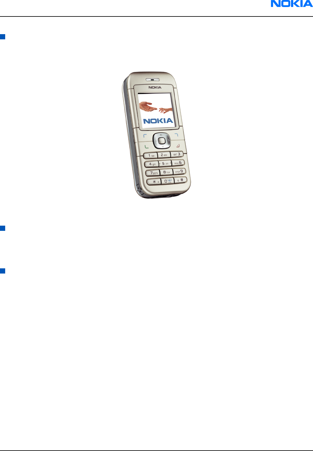
Product selection
The RM-74 is the EU version of the telephone with a dual band transceiver unit designed for the GSM900 and
GSM1800 networks.
Figure 1 RM-74 product picture
Display and keypad features
• High resolution CSTN display (128x128 pixels) with 65,536 colors
• 4UI-style, 5-way navigation key including selection key,
• Hardtop keymat
Features
Hardware features
• GSM E900/1800
• AMR/HR/FR/EFR codecs
• Internal antenna
• Charger plug
• Headset connector
• Mono FM Radio
• GPRS: Class B, multislot class 6
• Internal vibrator
• User changeable front- and back covers and top cap
• SIM (1.8 and 3.0 V)
Software features
• OS: ISA
• UI Style: S40
• MIDP 2.0 Java, with latest APIs
• Browser: XHTML over WAP stack (WAP 1.2.1 compliant)
• MMS 1.2
RM-74
General information Nokia Customer Care
9242678 (Issue 1) Company Confidential Page 1–5
Copyright ©2005 Nokia. All Rights Reserved.
• 16 polyphonic ringing tones
• OTA downloading - ringing tones, wallpapers, operator logos, business cards, settings
UI features
Messaging • Multimedia messaging: send and receive messages containing text, an audio
clip, and an image to other compatible devices (maximum message size: up
to 100kB)
• SMS messaging
• Predictive text input
• Asia-Pacific: English, Chinese Simplified, Chinese Traditional, Thai, Philipino,
Vietnamese, Bahasa Indonesia, Bahasa Malaysia, Hindi
• Europe and Africa: Danish, Dutch, English, French, Finnish, German, Icelandic,
Italian, Portugese, Spanish, Swedish, Norwegian, Turkish, Greek, Bulgarian,
Ukranian, Hebrew, Arabic, Slovakian, Czech, Hungarian, Polish, Romanian,
Serbian, Croatian, Slovenian, Russian, Estonian, Latvian, Lithuanian
• Non-predictive text input: Urdu, Farsi, Zulu, Xhosa, Sesotho, Swahili, Merathi,
Tamil, Gujarati, Bengali
Memory functions • Phone book (up to 300 entries)
• Calendar notes (up to 500 entries)
Connectivity • Plug and play connector
Java™ applications • Java™ MIDP 2.0
• Over-the-air download of Java™-based applications and games
Browsing • Integrated XHTML browser over WAP
• OMA DRM for content protection
Data transfer • GPRS, class 6 (up to 40 kbps)
• WAP 2.0
Call management • Speed dialing: up to 8 names (keys 2-9)
• Last number redial from dialed calls list (dial key brings out the dialed calls
list)
• Automatic redial (max 10 attempts)
• Automatic answer (works with headset or car kit only)
• Call waiting, call hold, call divert, and call timer
• Automatic and manual network selection
• Vibrating alert
Voice features • Integrated handsfree speaker
Personalise • Graphics, icons, animations, logos
• Games: possibility to download new games
• Ringing tones: Polyphonic tones
• Themes: possibility to download new themes
Phone features • Phone Features
• Alarm clock Calendar
RM-74
Nokia Customer Care General information
Page 1–6 Company Confidential 9242678 (Issue 1)
Copyright ©2005 Nokia. All Rights Reserved.
Mobile enhancements
Table 1 Power
Type Name
BL-5C Battery 900 mAh Li-Ion
AC-1 Retractable charger
ACP-12 Travel charger
LCH-12 Mobile charger
Table 2 Car
Type Name
BHF-2 Headrest hands free
CK-10 Nokia car kit
HF-8 Nokia plug-in car handsfreet
MP-2 Microphone
CR-39 Nokia universal holder
Table 3 Audio
Type Name
HDB-5 Boom Headset
HDC-5 Headset
HDE-2 Headset
HS-7 Dual Headset
HDA-9 TTY Adapter
Table 4 Xpress-on™ covers
Type Name
CC 232D EMEA colors: Gray, Blue, Orange, except APAC, which only have gray and blue.
Technical specifications
General specifications
Unit Dimension (mm) Weight (g) Volume (cc)
Transceiver with BL-5C
900mAh Li-Ion battery
pack
101x44x18 90 75
RM-74
General information Nokia Customer Care
9242678 (Issue 1) Company Confidential Page 1–7
Copyright ©2005 Nokia. All Rights Reserved.
Battery endurance
Nokia measurements of operation times in GSM900/1800
Talk time
Battery: BL-5C 900mAh Up to 180 min
Standby time
Battery: BL-5C 900mAh Up to 300 min
Note: Variation in operation times will occur depending on SIM card, network settings and usage. Talk
time is increased by up to 30% if half rate is active and reduced by 5% if enhanced full rate is active.
Environmental conditions
Environmental
condition
Ambient temperature Notes
Normal operation -15 oC ... +55 oCSpecifications fulfilled
Reduced performance -30 ...15 oC and +55oC ... +70 oCOperational only for short periods
Intermittent or no
operation
-40 oC ... -30 oC and +70 oC ... +85oCOperation not guaranteed but an
attempt to operate will not damage
the phone
No operation or
storage
<-40 oC and >+85 oCNo storage. An attempt to operate
may cause permanent damage
Charging allowed -15 oC ... +55 oC
Long term storage
conditions
0 oC ... +85 oC
Humidity and water
resistance
Relative humidity range is 5 to 95%.
Condensed or dripping water may
cause intermittent malfunctions.
Protection against dripping water has
to be implemented in (enclosure)
mechanics.
Continuous dampness will cause
permanent damage to the module.
Electrical characteristics
Table 5 Normal and extreme voltages
Voltage Voltage (V) Condition
General conditions
Nominal voltage 3.90V a
Lower extreme voltage 3.30V b
RM-74
Nokia Customer Care General information
Page 1–8 Company Confidential 9242678 (Issue 1)
Copyright ©2005 Nokia. All Rights Reserved.
Voltage Voltage (V) Condition
Higher extreme voltage 4.30V c
HW shutdown voltages
Vmstr+ 2.1V ± 0,1V Off to on
Vmstr- 1.9V ± 0,1V On to off
SW shutdown voltages
SW shutdown 3. 1V In call
SW shutdown 3. 2V In idle
Min operating voltage
Vcoff+ 3. 1V ± 0,1V Off to on
Vcoff- 2. 8V ± 0,1V On to off
HW reset demands
Min 1. 0V d
Max --
a. The nominal voltage is defined as being 15% higher than the lower extreme voltage. TA will test with this
nominal voltage at an 85% range (0.85x3.9V a 3.3V).
b. This limit is set to be above SW shutdown limit in TA.
c. During fast charging of an empty battery, this voltage might exceed this value. Voltages between 4.20 and
4.60 might appear for a short while.
d. The minimum battery cell voltage required for the reset circuitry to turn on. This is not confirmed by measures
at pt.
Table 6 Current consumption
Condition Min Typical Max Unit
Call (MoU)
(E)GSM 900
GSM 1800
GSM 1900
208
188
168
mA
Idle (MoU) 2.72
Power off 150 250 mA
RM-74
General information Nokia Customer Care
9242678 (Issue 1) Company Confidential Page 1–9
Copyright ©2005 Nokia. All Rights Reserved.

RM-74
Nokia Customer Care General information
(This page left intentionally blank.)
Page 1–10 Company Confidential 9242678 (Issue 1)
Copyright ©2005 Nokia. All Rights Reserved.

2 — Parts and layouts
Nokia Customer Care
9242678 (Issue 1) Company Confidential Page 2–1
Copyright ©2005 Nokia. All Rights Reserved.

RM-74
Nokia Customer Care Parts and layouts
(This page left intentionally blank.)
Page 2–2 Company Confidential 9242678 (Issue 1)
Copyright ©2005 Nokia. All Rights Reserved.

Table of Contents
Exploded view..................................................................................................................................................................................2–5
Mechanical parts list.......................................................................................................................................................................2–6
Spare parts overview.....................................................................................................................................................................2–7
SWAP phones....................................................................................................................................................................................2–8
Component parts list......................................................................................................................................................................2–8
Component layouts......................................................................................................................................................................2–15
List of Tables
Table 7 Mechanical parts list.......................................................................................................................................................2–6
Table 8 SWAP phones for RM-74.................................................................................................................................................2–8
Table 9 Component parts.............................................................................................................................................................2–8
List of Figures
Figure 2 Exploded view.................................................................................................................................................................2–5
Figure 3 Spare parts overview....................................................................................................................................................2–7
Figure 4 Component layout, RM-74, 1mf_51a, bottom.....................................................................................................2–16
Figure 5 Component layout, RM-74, 1mf_51a, top.............................................................................................................2–16
RM-74
Parts and layouts Nokia Customer Care
9242678 (Issue 1) Company Confidential Page 2–3
Copyright ©2005 Nokia. All Rights Reserved.

RM-74
Nokia Customer Care Parts and layouts
(This page left intentionally blank.)
Page 2–4 Company Confidential 9242678 (Issue 1)
Copyright ©2005 Nokia. All Rights Reserved.
Exploded view
Figure 2 Exploded view
RM-74
Parts and layouts Nokia Customer Care
9242678 (Issue 1) Company Confidential Page 2–5
Copyright ©2005 Nokia. All Rights Reserved.

Mechanical parts list
Table 7 Mechanical parts list
ITEM/
CIRCUIT
REF.
QTY PART NAME
* = not available as spare part
I001* 1 A-cover
I002* 1 Soft Keys
I003 1 KEYMAT
I004 6 Screws T6+
I005 1 LCD shielding
I006 1 Acoustic channel
I007 1 LCD module
I008 1 Locking clip
I009 1 Light guide assembly
I010 1 Domesheet
I011 1 Engine module (not supplied)
I012 1 BB shieldning lid assembly
I013 1 RF shielding lid
I014 1 FEM shielding lid
I015* 1 Antenna (A2)
I016* 1 IHF (A2)
I017* 1 Power button (A3)
I018* 1 SIM lid (A3)
I019 4 Microphone
I020 1 Easy flash connector (A3)
I021* 1 D-cover (A3)
I022 1 Type label
I023 1 B-cover
I024 1 Top cap
I025 1 Easy flash connector cap
RM-74
Nokia Customer Care Parts and layouts
Page 2–6 Company Confidential 9242678 (Issue 1)
Copyright ©2005 Nokia. All Rights Reserved.
Spare parts overview
Figure 3 Spare parts overview
RM-74
Parts and layouts Nokia Customer Care
9242678 (Issue 1) Company Confidential Page 2–7
Copyright ©2005 Nokia. All Rights Reserved.
SWAP phones
Table 8 SWAP phones for RM-74
SWAP phones for RM-74
RM-74 SWAP ENGINE EURO-C
RM-74 SWAP ENGINE EURO-C FRANCE
RM-74 EURO-C TURKEY
RM-74 SWAP ENGINE EURO-K
RM-74 SWAP ENGINE UKR
RM-74 SWAP ENGINE EURO-L SOUTH AFRICA
RM-74 SWAP ENGING APAC-S, Singapore
RM-74 SWAP ENGINE APAC-T, Philippines
Component parts list
Table 9 Component parts
Item ref Name Side X/Y Value
A7001 BB SHIELDING ASSY Top O 5 ~
A7002 RF ASIC SHIELDING ASSY Top J 6 ~
A7003 FEM SHIELDING ASSY Top J 3 ~
B2200 CRYSTAL 32.768KHZ+-20PPM 12.5PF Top O 7 32.768KHz
B7600 CRYSTAL 26.OMHZ+-10PPM 15.5PF Top K 5 26MHz
C2000 CHIPCAP NP0 27P J 50V 0402 Top G 3 27p
C2001 CHIPCAP NP0 10P J 50V 0402 Top G 2 10p
C2002 CHIPTCAP 150U M 10V 6X3.2X1.5 Top G 4 150u_10V
C2003 CHIPCAP NP0 22P J 50V 0402 Top S 5 22p
C2004 CHIPCAP NP0 22P J 50V 0402 Top R 5 22p
C2005 CHIPCAP NP0 22P J 50V 0402 Top R 5 22p
C2006 CHIPCAP NP0 22P J 50V 0402 Top R 5 22p
C2007 CHIPCAP Y5V 100N Z 25V 0603 Top S 7 100n
C2008 CHIPCAP X7R 10N K 16V 0402 Top S 4 10n
C2009 CHIPCAP X7R 10N K 16V 0402 Top R 4 10n
C2010 CHIPCAP X7R 10N K 16V 0402 Top R 5 10n
C2011 CHIPCAP X5R 1U K 6V3 0603 Top S 3 1u0
C2012 CHIPCAP X7R 10N K 16V 0402 Top R 4 10n
C2013 CHIPCAP X7R 1N0 K 50V 0402 Top
C2017 CHIPCAP NP0 33P J 50V 0402 Top G 5 33p
RM-74
Nokia Customer Care Parts and layouts
Page 2–8 Company Confidential 9242678 (Issue 1)
Copyright ©2005 Nokia. All Rights Reserved.

Item ref Name Side X/Y Value
C2151 CHIP ARRAY X5R 2X33N K 10V 0405 Top N 7 2x33n
C2152 CHIPCAP NP0 10P J 50V 0402 Top S 3 10p
C2153 CHIPCAP NP0 47P J 50V 0402 Bottom B 6 47p
C2154 CHIPCAP NP0 47P J 50V 0402 Bottom B 7 47p
C2155 CHIP ARRAY X5R 2X33N K 10V 0405 Top N 7 2x33n
C2157 CHIPCAP NP0 100P J 50V 0402 Top O 8 100p
C2159 CHIPCAP X7R 15N K 16V 0402 Top N 7 8n2
C2161 CHIPCAP X5R 100N M 16V 0402 Top N 8 100n
C2164 CHIP ARRAY NP0 2X27P K 25V 0405 Top N 6 2x27p
C2165 CHIP ARRAY X5R 2X1N K 16V 0405 Top N 6 2x27p
C2171 CHIPCAP X5R 2U2 K 6V3 0603 Top N 8 2u2
C2180 CHIPCAP X7R 15N K 16V 0402 Top N 7 8n2
C2181 CHIPCAP X5R 100N K 10V 0402 Top M 7 100n
C2182 CHIPCAP X5R 1U K 6V3 0603 Top M 7 1u0
C2200 CHIPCAP X5R 1U K 6V3 0603 Top O 7 1u0
C2202 CHIPCAP X5R 1U K 6V3 0603 Top O 7 1u0
C2203 CHIPCAP X5R 1U K 6V3 0603 Top O 7 1u0
C2204 CHIPCAP X5R 1U K 6V3 0603 Top P 5 1u0
C2205 CHIPCAP X5R 1U K 6V3 0603 Top P 5 1u0
C2208 CHIPCAP X5R 1U K 6V3 0603 Top P 4 1u0
C2220 CHIPCAP X7R 10N K 16V 0402 Top M 7 10n
C2222 CHIPCAP X5R 1U K 6V3 0603 Top P 7 1u0
C2223 CHIPCAP X5R 1U K 6V3 0603 Top O 7 1u0
C2225 CHIPCAP X5R 1U K 6V3 0603 Top M 6 1u0
C2226 CHIPCAP X5R 1U K 6V3 0603 Top P 7 1u0
C2227 CHIPCAP X5R 1U K 6V3 0603 Top M 6 1u0
C2230 CHIPCAP X5R 1U K 6V3 0603 Top O 7 1u0
C2233 CHIPCAP X5R 1U K 6V3 0603 Top O 7 1u0
C2235 CHIPCAP X5R 1U K 6V3 0603 Top M 7 1u0
C2236 CHIPCAP X5R 100N K 10V 0402 Top M 5 100n
C2237 CHIPCAP X5R 100N K 10V 0402 Top M 5 100n
C2239 CHIPCAP X5R 100N K 10V 0402 Top P 5 100n
C2240 CHIPCAP X7R 10N K 16V 0402 Top M 6 10n
C2241 CHIPCAP X7R 1N0 K 50V 0402 Top M 6 1n0
C2242 CHIPCAP X7R 1N0 K 50V 0402 Top M 6 1n0
RM-74
Parts and layouts Nokia Customer Care
9242678 (Issue 1) Company Confidential Page 2–9
Copyright ©2005 Nokia. All Rights Reserved.

Item ref Name Side X/Y Value
C2261 CHIPCAP X5R 4U7 K 10V 0805 Top P 6 4u7
C2262 CHIPCAP X5R 100N K 10V 0402 Top Q 8 100n
C2263 CHIPCAP X5R 100N K 10V 0402 Top R 8 100n
C2287 CHIPCAP X5R 100N K 10V 0402 Top M 5 100n
C2330 CHIPCAP NP0 33P J 50V 0402 Top G 2 33p
C2331 CHIPCAP X5R 1U K 6V3 0603 Top P 5 1u0
C2332 CHIPCAP X5R 4U7 K 10V 0805 Top P 5 4u7
C2400 CHIPCAP X5R 1U K 16V 0603 Bottom U 4 1u0
C2401 CHIPCAP X5R 1U K 6V3 0603 Bottom U 6 1u0
C2402 CHIPCAP X5R 100N K 10V 0402 Bottom C 2 100n
C2403 CHIPCAP X5R 100N K 10V 0402 Bottom C 2 100n
C2404 CHIPCAP NP0 22P J 50V 0402 Top C 4 22p
C2405 CHIPCAP NP0 47P J 50V 0402 Top P 5 47p
C2700 CHIPCAP X5R 100N K 10V 0402 Top R 4 100n
C2880 CHIPCAP X7R 10N K 16V 0402 Top O 4 10n
C2881 CHIPCAP X5R 100N K 10V 0402 Top P 3 100n
C2882 CHIPCAP X7R 10N K 16V 0402 Top P 3 10n
C2883 CHIPCAP X7R 10N K 16V 0402 Top O 2 10n
C2884 CHIPCAP X5R 100N K 10V 0402 Top O 2 100n
C2885 CHIPCAP X7R 10N K 16V 0402 Top P 3 10n
C2886 CHIPCAP X5R 100N K 10V 0402 Top P 3 100n
C2887 CHIPCAP X7R 10N K 16V 0402 Top O 2 10n
C2900 CHIPCAP X7R 1N0 K 50V 0402 Top K 7 1n0
C3030 CHIPCAP X7R 10N K 16V 0402 Top N 2 10n
C3031 CHIPCAP X5R 100N K 10V 0402 Top N 2 100n
C3032 CHIPCAP X5R 100N M 16V 0402 Top N 2 100n
C6157 CHIPCAP X7R 10N K 16V 0402 Top R 6 10n
C6158 CHIPCAP X5R 100N K 10V 0402 Top R 6 100n
C6159 CHIPCAP X7R 33N K 10V 0402 Top Q 7 33n
C6162 CHIPCAP X7R 33N K 10V 0402 Top Q 6 33n
C6163 CHIPCAP X7R 33N K 10V 0402 Top R 6 33n
C6165 CHIPCAP X7R 33N K 10V 0402 Top Q 8 33n
C6170 CHIPCAP X7R 10N K 16V 0402 Top R 7 10n
C6176 CHIPCAP NP0 100P J 50V 0402 Top R 7 100p
C6178 CHIPCAP NP0 27P J 50V 0402 Top R 7 27p
RM-74
Nokia Customer Care Parts and layouts
Page 2–10 Company Confidential 9242678 (Issue 1)
Copyright ©2005 Nokia. All Rights Reserved.
Item ref Name Side X/Y Value
C6179 CHIPCAP NP0 47P J 50V 0402 Top R 7 47p
C7604 CHIPCAP NP0 1P0 C 50V 0402 Top I 6 1p0
C7607 CHIPCAP NP0 1P2 C 50V 0402 Top I 7 1p2
C7610 CHIPCAP NP0 10P J 50V 0402 Top I 8 10p
C7611 CHIPCAP NP0 10P J 50V 0402 Top I 7 10p
C7612 CHIPCAP NP0 10P J 50V 0402 Top I 7 10p
C7613 CHIPCAP X5R 1U K 6V3 0402 Top I 8 1u0
C7614 CHIPCAP NP0 4P7 C 50V 0402 Top J 7 4p7
C7620 CHIPCAP X5R 2U2 K 6V3 0603 Top K 7 2u2
C7623 CHIPCAP NP0 22P J 50V 0402 Top J 7 22p
C7624 CHIPCAP X5R 100N K 10V 0402 Top J 8 100n
C7625 CHIPCAP NP0 22P J 50V 0402 Top J 6 22p
C7627 CHIPCAP NP0 56P J 50V 0402 Top J 5 56p
C7628 CHIPCAP NP0 56P J 50V 0402 Top J 5 56p
C7630 CHIPCAP NP0 22P J 50V 0402 Top K 6 22p
C7631 CHIPCAP NP0 0P5 C 50V 0402 Top D 3 0p5
C7634 CHIPCAP X5R 100N K 10V 0402 Top I 7 100n
C7635 CHIPCAP X5R 100N K 10V 0402 Top K 6 100n
C7636 CHIPCAP NP0 1P8 C 50V 0402 Top K 6 1p0
C7637 CHIPCAP X7R 1N0 J 50V 0402 Top K 2 1n0
C7638 CHIPCAP NP0 33P J 50V 0402 Top K 2 33p
C7639 CHIPCAP NP0 270P J 50V 0402 Top J 7 270p
C7641 CHIPCAP NP0 270P J 50V 0402 Top J 7 270p
C7643 CHIPCAP X5R 100N K 10V 0402 Top K 6 100n
C7644 CHIPCAP X7R 560P J 50V 0402 Top J 7 560p
C7645 CHIPCAP X7R 560P J 50V 0402 Top I 7 560p
C7655 CHIPCAP NP0 10P J 50V 0402 Top I 5 10p
C7656 CHIPCAP X5R 100N K 10V 0402 Top J 5 100n
C7657 CHIPCAP NP0 22P J 50V 0402 Top K 7 22p
C7658 CHIPCAP NP0 22P J 50V 0402 Top J 7 22p
C7659 CHIPCAP NP0 22P J 50V 0402 Top I 6 22p
C7668 CHIPCAP NP0 22P J 50V 0402 Top I 6 22p
C7669 CHIPCAP NP0 3N9 J 25V 0805 Top K 8 3n9
C7700 CHIPCAP NP0 33P J 50V 0402 Top K 3 33p
C7701 CHIPCAP NP0 33P J 50V 0402 Top K 3 33p
RM-74
Parts and layouts Nokia Customer Care
9242678 (Issue 1) Company Confidential Page 2–11
Copyright ©2005 Nokia. All Rights Reserved.

Item ref Name Side X/Y Value
C7702 CHIPCAP NP0 33P J 50V 0402 Top K 4 33p
C7711 CHIPCAP X5R 2U2 K 10V 0805 Top I 2 2u2
C7712 CHIPCAP NP0 15P J 50V 0402 Top I 4 15p
C7713 CHIPCAP NP0 27P J 50V 0402 Top I 2 27p
C7714 CHIPCAP NP0 27P J 50V 0402 Top K 3 27p
C7720 CHIPCAP NP0 33P J 50V 0402 Top K 4 33p
C7725 CHIPCAP NP0 120P J 50V 0402 Top K 3 120p
C7726 CHIPCAP NP0 22P J 50V 0402 Top J 2 22p
C7727 CHIPCAP NP0 10P J 50V 0402 Top K 2 10p
C7728 CHIPCAP NP0 0P5 C 50V 0402 Top K 2 0p5
D2200 UEMCLITE V2.2 WD ENA LEADFREE TFB Top O 5 ~
D2800 UPP4M v3 F761522 10x10 uBGA173 Top O 3 ~
D3000 COMBO 128M NOR + 16M PSRAM TFBGA4 Top M 3 8Mx16/1Mx16
F2000 SM FUSE FF 2A 32V 0402 Top T 7 2.0A
H2400 SM CONN 2X5F P0.5 PWB/PWB Bottom C 3 ~
L2000 FERR.BEAD 0R03 42R/100MHZ 3A 0805 Top T 7 42R/100MHz
L2001 CHIP BEAD ARRAY 2X1000R 0405 Top R 3 2x1000R/100MHz
L2002 CHIP BEAD ARRAY 2X1000R 0405 Top R 4 2x1000R/100MHz
L2005 CHIP COIL 68NH J Q12/100MHZ 0603 Top R 6 68nH
L2170 FERRITE BEAD 0R5 600R/100MHZ 0603 Top S 3 600R/100MHz
L2180 FERR.BEAD 220R/100M 2A 0R05 0603 Top M 7 220R/100MHz
L2181 FERR.BEAD 220R/100M 2A 0R05 0603 Top M 7 220R/100MHz
L2182 CHIP COIL 33N J Q23/800MHZ 0402 Bottom B 6 33nH
L2183 CHIP COIL 33N J Q23/800MHZ 0402 Bottom B 6 33nH
L2400 CHOKE 22U M 0.33A 1R5 3.3X3.3X1.3 Bottom U 6 22uH
L6156 CHIP COIL 47N G Q38/200MHz 0603 Top Q 6 47nH
L6176 CHIP COIL 120N J Q32/150MHZ 0603 Top R 7 120nH
L7602 CHIP COIL 10N J Q30/800MHZ 0402 Top I 7 10nH
L7603 CHIP COIL 10N J Q30/800MHZ 0402 Top I 7 10nH
L7604 CHIP COIL 2N2 +-0N3 Q30/800M 0402 Top I 6 2n2H
L7605 CHIP COIL 2N2 +-0N3 Q30/800M 0402 Top I 6 2n2H
M2000 SMD VIBRA MOTOR 1.3V 90MA 9000RPM Top G 6 ~
N2150 PW AMP TPA2010D1YZF 250kHz CSP9 Top M 7 ~
N2160 TI Analog Switch TS5A3159DCKR Top L 7 ~
N2161 TI Analog Switch TS5A3159DCKR Top L 7 ~
RM-74
Nokia Customer Care Parts and layouts
Page 2–12 Company Confidential 9242678 (Issue 1)
Copyright ©2005 Nokia. All Rights Reserved.

Item ref Name Side X/Y Value
N2400 DC/DC CONV TK65600 USMD8 Bottom T 6 ~
N6156 FM RECEIVER TEA5761UK N3D (Ti) CS Top Q 7 ~
N7600 HUGIN+ PMB3258V1.1 B9C PGVQFN48-4 Top J 7 ~
N7700 FEM RF3282E5.1 2B TX/RX (900/1800 Top J 3 ~
R2000 CHIP VARISTOR VWM5.6V VC15.5V 040 Top G 3 5/50V
R2001 NTC RES 0W1 47K J B 4050+-3% 0402 Top Q 3 47k
R2002 CHIPRES 0W06 100R J 0402 Top R 5 100R
R2003 CHIPRES 0W06 100R J 0402 Top R 5 100R
R2004 CHIPRES 0W06 100R J 0402 Top R 5 100R
R2005 CHIPRES 0W06 100R J 0402 Top S 5 100R
R2006 RES VARISTOR 14/350V 3pF 0402 Top R 5 5/50V
R2007 CHIP VARISTOR VWM14V VC50V 0402 Top R 4 14V/50V
R2008 CHIP VARISTOR VWM14V VC50V 0402 Top S 4 14V/50V
R2009 CHIP VARISTOR VWM14V VC50V 0402 Top R 4 14V/50V
R2010 CHIPRES 0W06 100K J 0402 Top S 3 100k
R2011 RES NETWORK 0W06 2X10R J 0404 Top R 4 2x10R
R2013 CHIP VARISTOR VWM5.6V VC15.5V 040 Top R 5 5.6V/15V/0.05J
R2020 ASIP 4XESD *** PB-FREE *** BGA5 Top R 5 ~
R2027 CHIPRES 0W06 10K J 0402 Top R 5 10k
R2068 RES NETWORK 0W03 4X22R J 0804 Top S 2 4x22R
R2069 CHIPRES 0W06 1K0 J 0402 Top S 2 1k0
R2070 CHIP VARISTOR VWM5.6V VC15.5V 040 Top S 2 5.6V/15V/0.05J
R2150 RES NETWORK 0W06 2X1K0 J 0404 Top N 7 2x1k0
R2151 CHIPRES 0W06 10R J 0402 Top M 7 10R
R2152 CHIPRES 0W06 10K J 0402 Top N 7 10k
R2153 RES NETWORK 0W06 2X2K2 J 0404 Top N 7 2x2k2
R2154 RES NETWORK 0W06 2X2K2 J 0404 Top N 7 2x2k2
R2155 CHIPRES 0W06 10R J 0402 Top L 6 10R
R2156 CHIPRES 0W06 2K2 J 0402 Top O 7 2k2
R2158 CHIPRES 0W06 18K J 0402 Top N 7 39k
R2159 CHIPRES 0W06 18K J 0402 Top N 7 39k
R2160 CHIPRES 0W06 100K J 0402 Top L 6 100k
R2171 CHIPRES 0W06 220R J 0402 Top N 8 220R
R2200 CHIPRES 0W25 0R22 J 0805 Top P 6 0R22
R2202 CHIPRES 0W06 100K J 0402 Top M 7 100k
RM-74
Parts and layouts Nokia Customer Care
9242678 (Issue 1) Company Confidential Page 2–13
Copyright ©2005 Nokia. All Rights Reserved.
Item ref Name Side X/Y Value
R2203 CHIPRES 0W06 100K J 0402 Top M 7 100k
R2204 CHIPRES 0W06 100K J 0402 Top M 6 100k
R2205 RES NETWORK 0W06 2X10K J 0404 Top M 6 2x10k
R2206 CHIPRES 0W06 100K J 0402 Top M 7 100k
R2207 CHIPRES 0W06 1K0 J 0402 Top L 4 1k0
R2400 CHIPRES 0W06 33R J 0402 Bottom U 5 33R
R2406 CHIPRES 0W06 220R J 0402 Top O 2 220R
R2407 CHIPRES 0W06 220R J 0402 Top P 2 220R
R2408 CHIPRES 0W06 220R J 0402 Top P 2 220R
R2409 CHIPRES 0W06 10K J 0402 Bottom T 4 10k
R2410 CHIPRES 0W06 27K J 0402 Top C 4 27k
R2700 ASIP SIM INTERFACE **low cap** BG Top P 4 ~
R2900 CHIPRES 0W06 330R J 0402 Top K 7 330R
R3030 CHIPRES 0W06 4K7 J 0402 Top O 2 4k7
R6110 CHIPRES 0W06 1K0 J 0402 Top Q 8 1k0
R6156 CHIPRES JUMPER 0R0 0402 Top Q 7 0R
R6159 CHIPRES 0W06 10K J 0402 Top R 6 10k
R6160 CHIPRES 0W06 100K J 0402 Top R 6 100k
R6161 CHIPRES JUMPER 0R0 0402 Top R 7 0R
R6163 CHIPRES JUMPER 0R0 0402 Top Q 6 0R
R6170 CHIPRES JUMPER 0R0 0402 Top R 8 0R
R7605 CHIPRES 0W06 22R J 0402 Top K 7 22R
R7606 CHIPRES JUMPER 0R0 0402 Top
R7607 CHIPRES JUMPER 0R0 0402 Top
R7609 CHIPRES 0W06 12K F 0402 Top K 6 12k
R7610 RES NETWORK 0W06 2X5K6 J 0404 Top M 5 2x5k6
R7611 RES NETWORK 0W06 2X5K6 J 0404 Top M 5 2x5k6
R7615 CHIPRES 0W06 100R J 0402 Top H 8 100R
R7616 CHIPRES 0W06 100R J 0402 Top H 7 100R
R7617 CHIPRES 0W06 100R J 0402 Top H 7 100R
R7619 CHIPRES 0W06 3K3 J 0402 Top J 8 3k3
R7630 CHIPRES 0W06 100K J 0402 Top K 6 100k
R7631 CHIPRES 0W06 18K J 0402 Top K 7 18k
R7632 CHIPRES 0W06 39R J 0402 Top K 6 39R
R7633 NTC RES 0W1 47K J B 4050+-3% 0402 Top K 2 47k
RM-74
Nokia Customer Care Parts and layouts
Page 2–14 Company Confidential 9242678 (Issue 1)
Copyright ©2005 Nokia. All Rights Reserved.
Item ref Name Side X/Y Value
R7635 CHIPRES 0W06 1K0 J 0402 Top K 2 1k0
R7663 CHIPRES 0W06 4K7 J 0402 Top K 8 4k7
R7700 CHIPRES 0W06 1K0 J 0402 Top I 5 1k0
R7701 CHIPRES 0W06 1K0 J 0402 Top I 5 1k0
R7703 CHIPRES JUMPER 0R0 0402 Top J 5 0R
R7704 CHIPRES 0W06 1K0 J 0402 Top K 3 1k0
R7705 CHIPRES 0W06 1K0 J 0402 Top K 3 1k0
R7706 CHIPRES 0W06 1K0 J 0402 Top K 3 1k0
R7707 CHIPRES 0W06 1K0 J 0402 Top I 5 1k0
R7709 CHIPRES JUMPER 0R0 0402 Top I 5 0R
R7711 RES NETWORK 0W04 1DB ATT 0404 Top J 4 870R/5R77/870R
R7714 RES NETWORK 0W04 1DB ATT 0404 Top J 2 870R/5R77/870R
R7720 CHIPRES 0W06 1K0 J 0402 Top K 4 1k0
R7732 CHIPRES 0W06 10K J 0402 Top K 2 10k
R7733 CHIPRES 0W06 100R J 0402 Top K 2 100R
S2422 SM SW TACT SPST 12V SIDE KEY 3N Top B 4 ~
V2000 ASIP TVS BGA4 Top S 7 ~
V2160 TR PDTC114EE N50V RB RBE 10K SC75 Top L 6 ~
V2400 LED WHITE 112-355MCD 15MA 0DEG 16 Bottom U 5 ~
V2401 TR PDTA114EE RB RBE 10K 50V SC75 Bottom U 3 ~
V7600 DI CAP 40/15.8PF 1/3V SCD80 Top K 6 ~
X2005 SM LYNX BATT CONN 3POL 12V 2A H7. Top G 3 ~
X2060 MODULE ID COMPONENT 2.8X1.8X0.3 Bottom T 3 ~
X2700 SM SIM CONN 6POL P2.54 H1.8 Top Q 4 ~
Z2400 ASIP KEYBOARD INTERFACE *PB-FREE* Top Q 3 ~
Z7600 SAW FILT 1842.5+-37.5MHZ/2.0X1.6 Top H 6 1842.5MHz
Z7602 SAW FILT 942.5+-17.5MHZ/2.0X1.6 Top H 7 942.5MHz
Z7603 SILICON FILT 869.5±45.5MHZ P-TSLP Top J 5 824-915MHz
Z7604 SILICON FILT 1810±100MHZ P-TSLP- Top J 5 1710-1910MHz
PWB M6 4/PA
Component layouts
Note: See also lager size layouts in the Schematics section (Page 9–8).
RM-74
Parts and layouts Nokia Customer Care
9242678 (Issue 1) Company Confidential Page 2–15
Copyright ©2005 Nokia. All Rights Reserved.
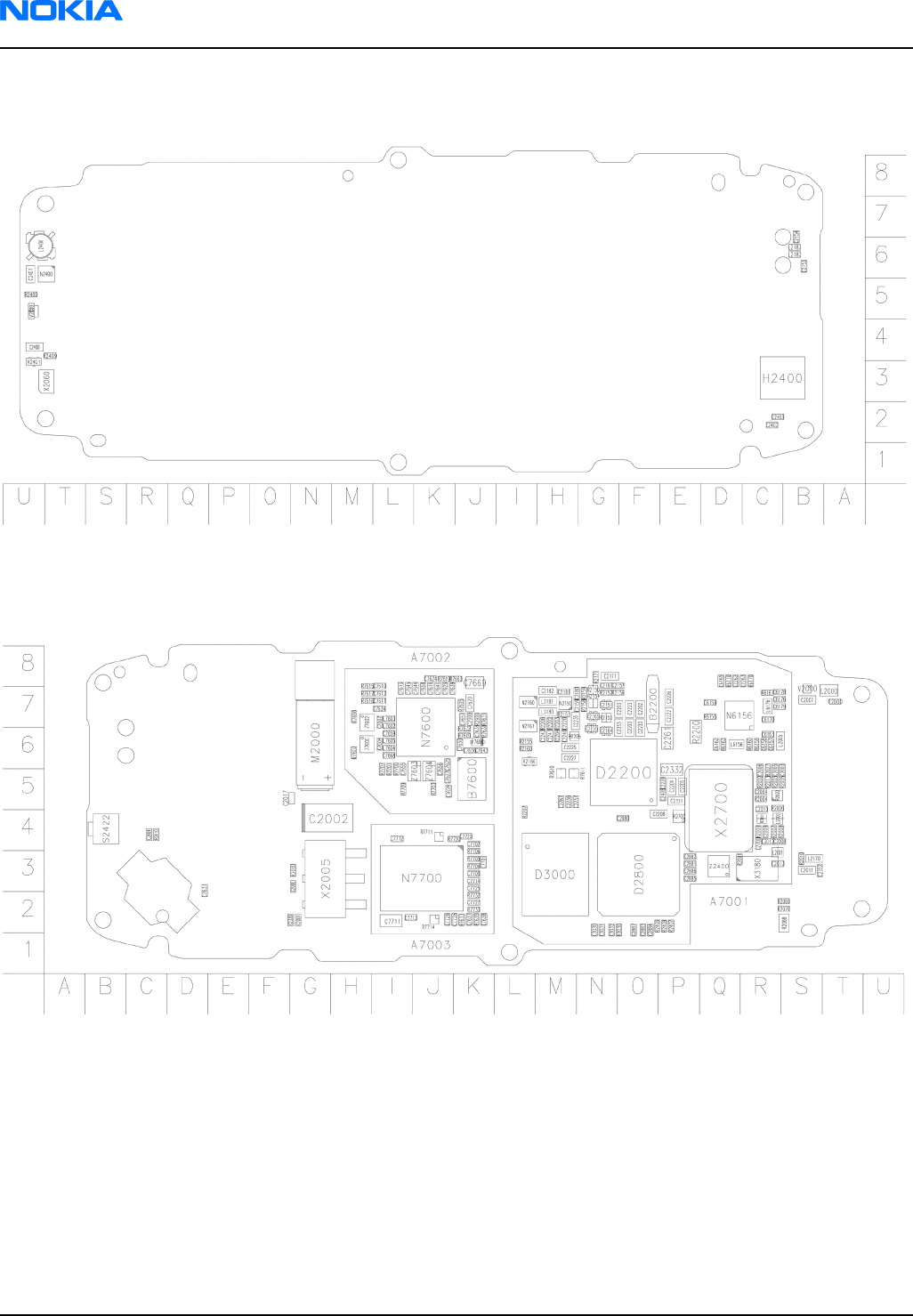
Component layout, bottom
Figure 4 Component layout, RM-74, 1mf_51a, bottom
Component layout, top
Figure 5 Component layout, RM-74, 1mf_51a, top
RM-74
Nokia Customer Care Parts and layouts
Page 2–16 Company Confidential 9242678 (Issue 1)
Copyright ©2005 Nokia. All Rights Reserved.

3 — Phoenix service SW
Nokia Customer Care
9242678 (Issue 1) Company Confidential Page 3–1
Copyright ©2005 Nokia. All Rights Reserved.

RM-74
Nokia Customer Care Phoenix service SW
(This page left intentionally blank.)
Page 3–2 Company Confidential 9242678 (Issue 1)
Copyright ©2005 Nokia. All Rights Reserved.

Table of Contents
Service software installation.......................................................................................................................................................3–5
Phoenix installation steps in brief.......................................................................................................................................3–5
Installing Phoenix.....................................................................................................................................................................3–5
Phoenix update installation................................................................................................................................................3–11
Uninstalling Phoenix..............................................................................................................................................................3–12
Repairing Phoenix installation...........................................................................................................................................3–14
Phoenix service software data package overview.......................................................................................................3–15
Installing Phoenix data package........................................................................................................................................3–16
Uninstalling Phoenix data package..................................................................................................................................3–20
Service software instructions...................................................................................................................................................3–21
Configuring users in Phoenix..............................................................................................................................................3–21
Managing connections in Phoenix....................................................................................................................................3–22
Installing Flash support files for FPS-8* and FLS-4*.....................................................................................................3–25
Updating FPS-8 Flash prommer software.......................................................................................................................3–28
Activating FPS-8.......................................................................................................................................................................3–30
Deactivating FPS-8..................................................................................................................................................................3–32
Updating JBV-1 docking station software.......................................................................................................................3–33
List of Figures
Figure 6 Dongle not found...........................................................................................................................................................3–6
Figure 7 Preparing setup..............................................................................................................................................................3–6
Figure 8 Welcome dialog..............................................................................................................................................................3–7
Figure 9 Disclaimer text................................................................................................................................................................3–7
Figure 10 Destination folder........................................................................................................................................................3–8
Figure 11 Installation status 1....................................................................................................................................................3–8
Figure 12 Installation status 2....................................................................................................................................................3–9
Figure 13 Registering components 1........................................................................................................................................3–9
Figure 14 Restart computer.......................................................................................................................................................3–10
Figure 15 Registering components 2.....................................................................................................................................3–10
Figure 16 Finish installation......................................................................................................................................................3–11
Figure 17 Installation interrupted...........................................................................................................................................3–12
Figure 18 Remove program.......................................................................................................................................................3–12
Figure 19 Uninstallation status................................................................................................................................................3–13
Figure 20 Finish uninstallation.................................................................................................................................................3–13
Figure 21 Restart computer.......................................................................................................................................................3–14
Figure 22 Repair program..........................................................................................................................................................3–15
Figure 23 Finish repair installation.........................................................................................................................................3–15
Figure 24 Extracting files............................................................................................................................................................3–16
Figure 25 Continue data package installation.....................................................................................................................3–17
Figure 26 Data package setup information..........................................................................................................................3–17
Figure 27 Data package destination folder..........................................................................................................................3–18
Figure 28 Start copying files......................................................................................................................................................3–18
Figure 29 Data package installation status..........................................................................................................................3–19
Figure 30 Finish data package installation..........................................................................................................................3–19
Figure 31 Uninstalling Phoenix data package.....................................................................................................................3–20
Figure 32 Finish data package uninstallation.....................................................................................................................3–20
Figure 33 Login..............................................................................................................................................................................3–21
Figure 34 Add information for new user 1...........................................................................................................................3–21
Figure 35 Add information for new user 2...........................................................................................................................3–21
RM-74
Phoenix service SW Nokia Customer Care
9242678 (Issue 1) Company Confidential Page 3–3
Copyright ©2005 Nokia. All Rights Reserved.

Figure 36 Login, user configured.............................................................................................................................................3–22
Figure 37 Phoenix icon...............................................................................................................................................................3–22
Figure 38 Manage connections................................................................................................................................................3–22
Figure 39 Connections list..........................................................................................................................................................3–23
Figure 40 Select mode: Manual................................................................................................................................................3–23
Figure 41 FLS virtual port icon..................................................................................................................................................3–23
Figure 42 Connections list..........................................................................................................................................................3–24
Figure 43 Connection information..........................................................................................................................................3–24
Figure 44 Scan product...............................................................................................................................................................3–24
Figure 45 Product support module information................................................................................................................3–25
Figure 46 Flash update welcome dialog...............................................................................................................................3–25
Figure 47 Uninstall flash update package.............................................................................................................................3–26
Figure 48 Flash installation interrupted................................................................................................................................3–26
Figure 49 Continue flash update..............................................................................................................................................3–26
Figure 50 Flash destination folder..........................................................................................................................................3–27
Figure 51 Flash installation status..........................................................................................................................................3–27
Figure 52 Finish flash update....................................................................................................................................................3–28
Figure 53 Phoenix icon...............................................................................................................................................................3–28
Figure 54 FPS-8 maintenance...................................................................................................................................................3–28
Figure 55 Prommer SW update................................................................................................................................................3–29
Figure 56 Prommer SW update done.....................................................................................................................................3–29
Figure 57 FPS-8 info window....................................................................................................................................................3–30
Figure 58 Flash directory window...........................................................................................................................................3–30
Figure 59 FPS-8 maintenance...................................................................................................................................................3–31
Figure 60 FPS-8 info window....................................................................................................................................................3–31
Figure 61 Box activation.............................................................................................................................................................3–32
Figure 62 Deactivation warning..............................................................................................................................................3–32
Figure 63 Extracting JBV-1 update files.................................................................................................................................3–33
Figure 64 JBV-1 update information.......................................................................................................................................3–34
Figure 65 JBV-1 update destination folder...........................................................................................................................3–34
Figure 66 Select installation: Full.............................................................................................................................................3–35
Figure 67 Select program folder..............................................................................................................................................3–35
Figure 68 Finish JBV-1 update installation...........................................................................................................................3–36
Figure 69 Checking JBV-1 SW version.....................................................................................................................................3–36
Figure 70 JBV-1 update directory window...........................................................................................................................3–37
Figure 71 JBV-1 SW update done.............................................................................................................................................3–37
Figure 72 JBV-1 SW status..........................................................................................................................................................3–37
RM-74
Nokia Customer Care Phoenix service SW
Page 3–4 Company Confidential 9242678 (Issue 1)
Copyright ©2005 Nokia. All Rights Reserved.

Service software installation
Phoenix installation steps in brief
Phoenix is the DCT-4 generation service software for reprogramming, testing and tuning the phone.
To install Phoenix, you need to:
• Connect a DK2 Dongle or FLS-4S POS Flash Device
• Install the Phoenix Service SW
• Install the Data Package for Phoenix
• Configure users
• Manage connection settings (depends on the tools you are using)
Phoenix is now ready for FLS-4S Point Of Sales Flash Device use.
If you use FPS-8:
• Update FPS-8 SW
• Activate FPS-8
• Update JBV-1 Docking Station SW (only when needed)
Phoenix is now ready to be used with FPS-8 flash prommer and other tools as well.
The Phoenix Service Software installation contains:
• Service software support for all phone models included in the package
• Flash update package files for FPS-8* and FLS-4S programming devices
• All needed drivers for:
• DK2 dongle
• FLS-4S point of sales flash device
• USB devices
Note: Separate installation packages for flash update files and drivers are also available, but it is not
necessary to use them unless updates appear between Phoenix Service SW releases. If separate update
packages are used, they should be used after Phoenix and data packages have been installed.
Supported operating systems
• Windows 2000 and XP.
Hardware requirements for using Phoenix
• Minimum: Processor 300 MHz, RAM memory 64 MB, disk space 100 MB.
• Recommended for Windows 2000: Processor 700 MHz, RAM memory 256 MB, disk space 150 MB.
Installing Phoenix
Before you begin
• Check that a Dongle is attached to the parallel port of your computer.
• Download the installation package (for example, phoenix_service_sw_a15_2004_24_7_55.exe) to your
computer (in C:\TEMP, for instance).
• Close all other programs.
• Run the application file (for example, phoenix_service_sw_a15_2004_24_7_55.exe) and follow the instructions
on the screen.
Note: Administrator rights may be required to be able to install Phoenix depending on the operating
system.
RM-74
Phoenix service SW Nokia Customer Care
9242678 (Issue 1) Company Confidential Page 3–5
Copyright ©2005 Nokia. All Rights Reserved.
If uninstalling or rebooting is needed at any point, you will be prompted by the Install Shield program.
Context
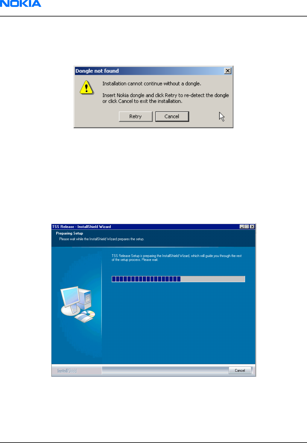
If at any point during installation you get this message, Dongle is not found and installation cannot continue:
Figure 6 Dongle not found
Possible reasons may be a defective or too old PKD-1 Dongle (a new dongle has a six digit serial number).
Check the COM/parallel ports used first! After correcting the problem the installation can be restarted.
For more detailed information, please refer to Phoenix Help files. Each feature in Phoenix has its own Help
function, which can be activated while running the program. Press the F1 key or the Help button to activate a
Help file.
Steps
1. Run the phoenix_service_sw_a15_2004_24_7_55.exe to start installation. Install Shield prepared the setup.
Figure 7 Preparing setup
Install Shield will prepare.
RM-74
Nokia Customer Care Phoenix service SW
Page 3–6 Company Confidential 9242678 (Issue 1)
Copyright ©2005 Nokia. All Rights Reserved.
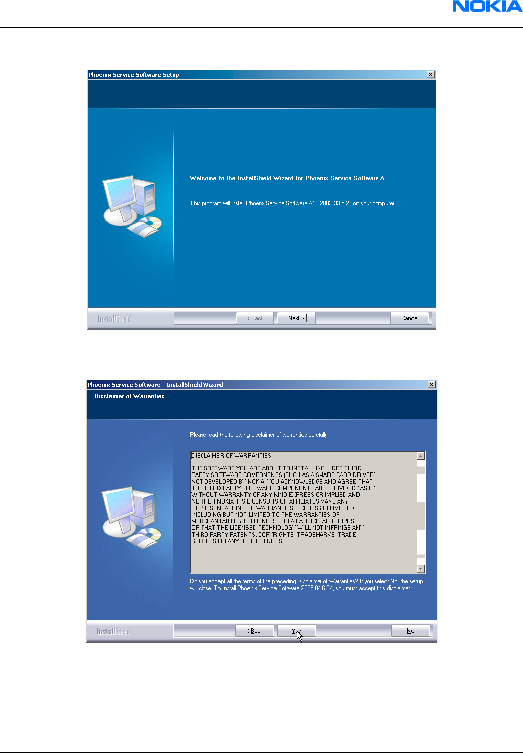
2. Click Next in Welcome dialog to continue.
Figure 8 Welcome dialog
3. Read the disclaimer carefully.
Figure 9 Disclaimer text
RM-74
Phoenix service SW Nokia Customer Care
9242678 (Issue 1) Company Confidential Page 3–7
Copyright ©2005 Nokia. All Rights Reserved.
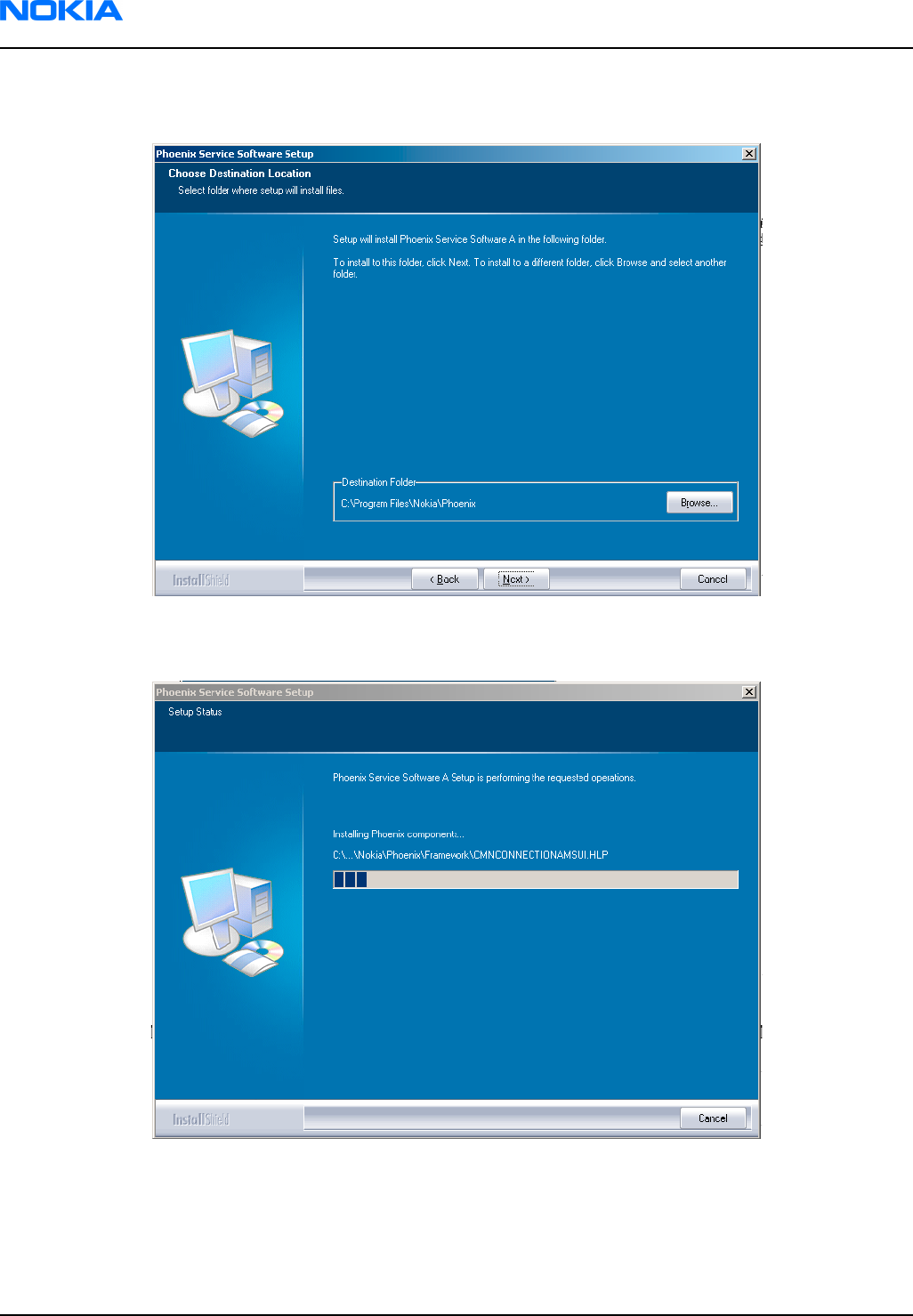
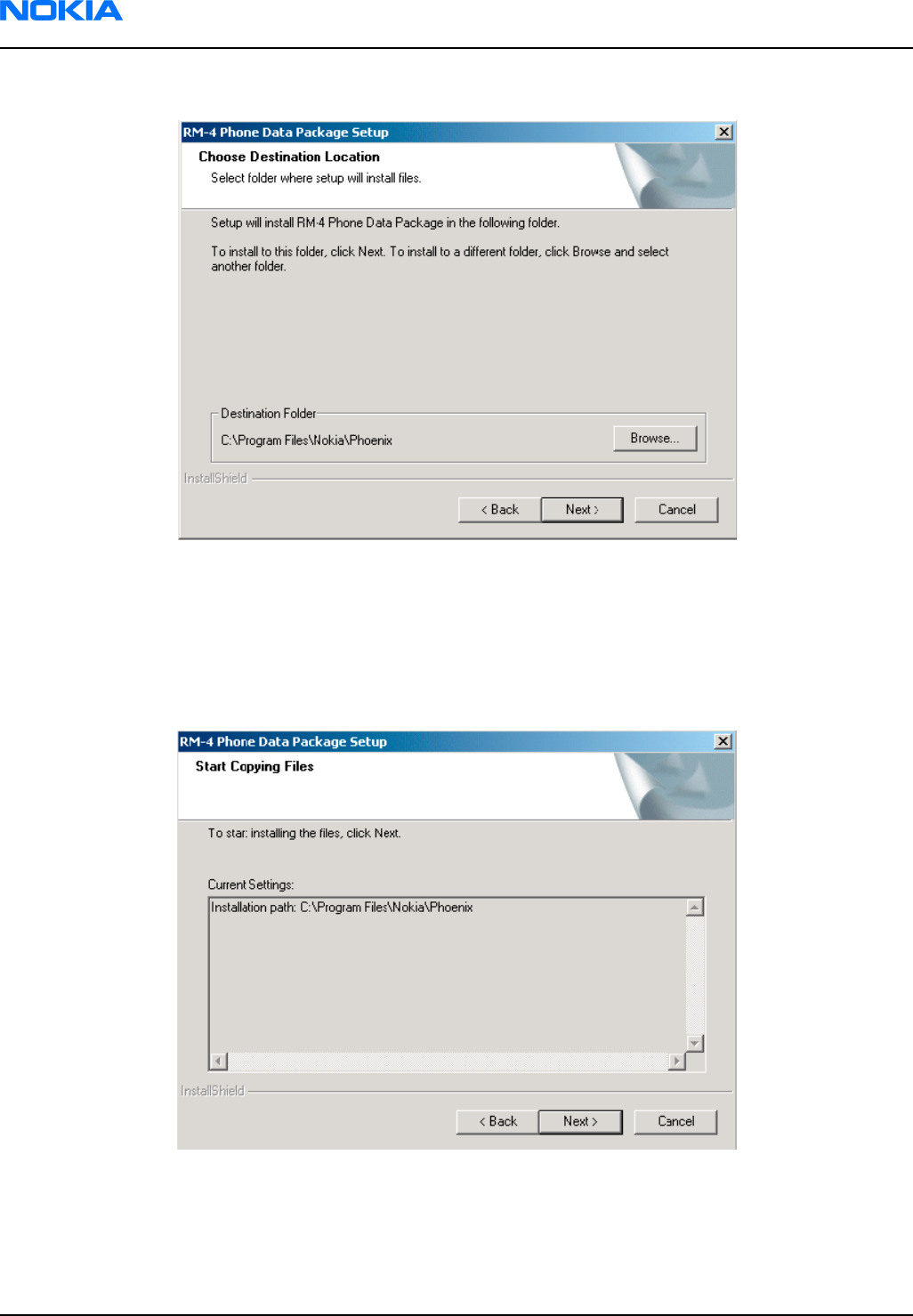
4. Choose destination folder. The default folder C:\ProgramFiles\Nokia\Phoenix is recommended. Then click
Next to continue. You may choose another location by selecting Browse (not recommended).
Figure 10 Destination folder
5. Wait for the components to be copied. The progress of the setup is shown in the Setup Status window.
Figure 11 Installation status 1
6. Wait for the drivers to be installed and updated.
The process may take several minutes to complete.
If the operating system does not require rebooting (Windows 2000, XP) the PC components are registered
right away.
RM-74
Nokia Customer Care Phoenix service SW
Page 3–8 Company Confidential 9242678 (Issue 1)
Copyright ©2005 Nokia. All Rights Reserved.
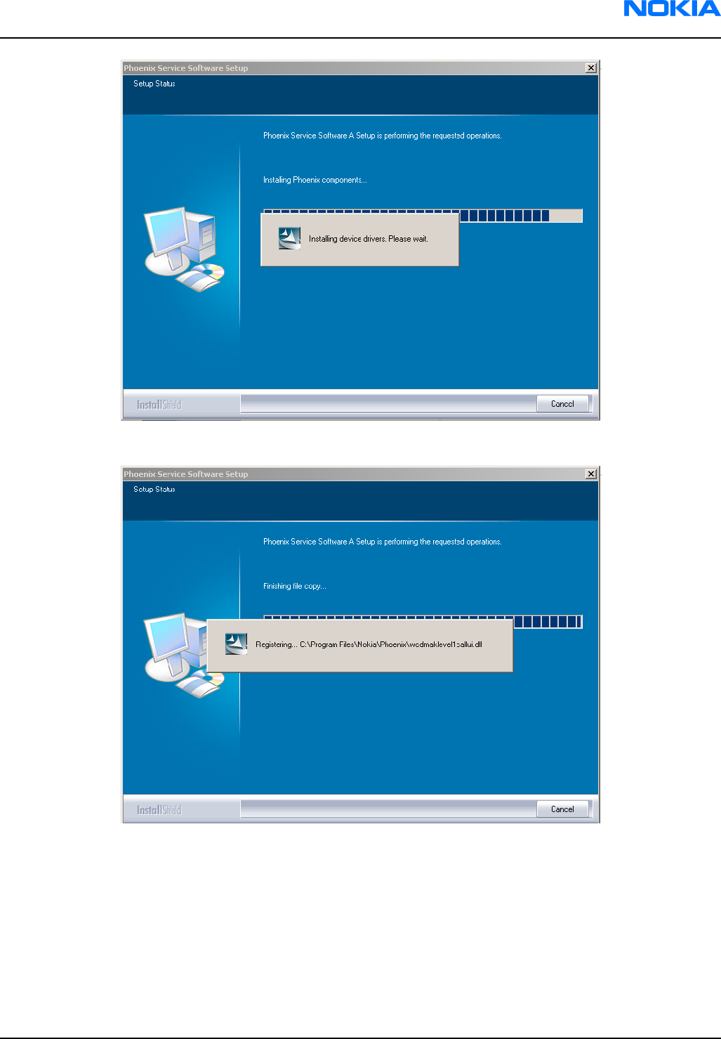
Figure 12 Installation status 2
Figure 13 Registering components 1
If the operating system requires restarting your computer (Windows 98, SE, ME) the Install Shield Wizard
will tell you about it. Select Yes... to reboot the PC immediately and No... to reboot the PC manually afterwards.
RM-74
Phoenix service SW Nokia Customer Care
9242678 (Issue 1) Company Confidential Page 3–9
Copyright ©2005 Nokia. All Rights Reserved.
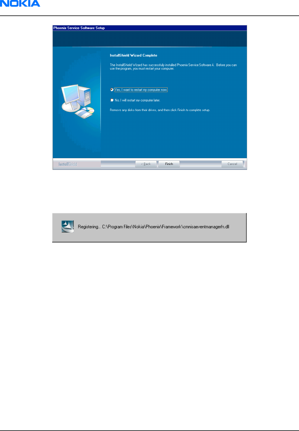
Figure 14 Restart computer
After the reboot, components are registered and Phoenix is ready for use.
Note: Phoenix does not work, if components have not been registered.
Figure 15 Registering components 2
RM-74
Nokia Customer Care Phoenix service SW
Page 3–10 Company Confidential 9242678 (Issue 1)
Copyright ©2005 Nokia. All Rights Reserved.
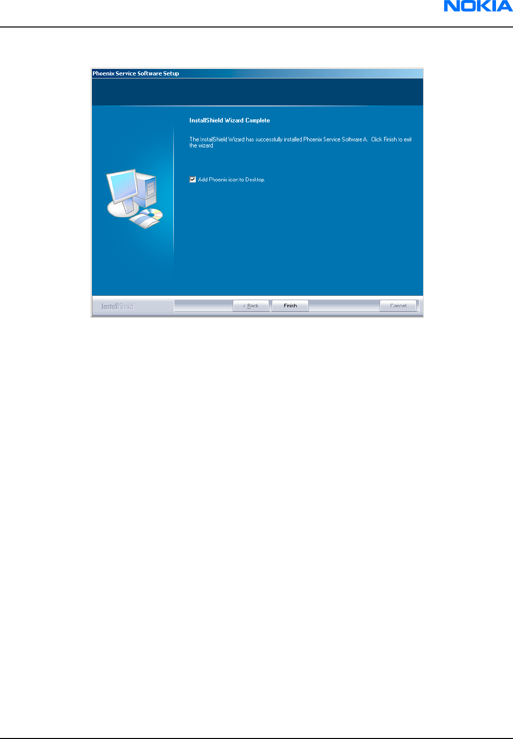
7. Click Finish to end installation.
Figure 16 Finish installation
Phoenix is now ready for use.
Next action
Before using Phoenix Service Software, you must:
• install phone model specific data package for Phoenix, and
• configure users and connections.
FPS-8* can be used after updating its Flash Update Package files.
Phoenix update installation
If you already have the Phoenix Service SW installed on your computer, sooner or later there will be need to
update it when new versions are released.
Always use the latest available versions of both the Phoenix Service SW and the phone-specific Data Package.
Instructions can be found in phone model specific Technical Bulletins and Phone Data Package readme.txt files
(shown during installation).
To update the Phoenix Service Software you need to take exactly the same steps as when installing it for the
first time:
• Download the installation package to your computer hard disk.
• Close all other programs.
• Run the application file (for example, phoenix_service_sw_a15_2004_24_7_55.exe).
• New version of Phoenix will be installed.
• Driver versions will be checked and updated.
When you update Phoenix from old to new version (for example, a14_2004_16_4_47 to a15_2004_24_7_55), the
update will take place automatically without uninstallation.
RM-74
Phoenix service SW Nokia Customer Care
9242678 (Issue 1) Company Confidential Page 3–11
Copyright ©2005 Nokia. All Rights Reserved.
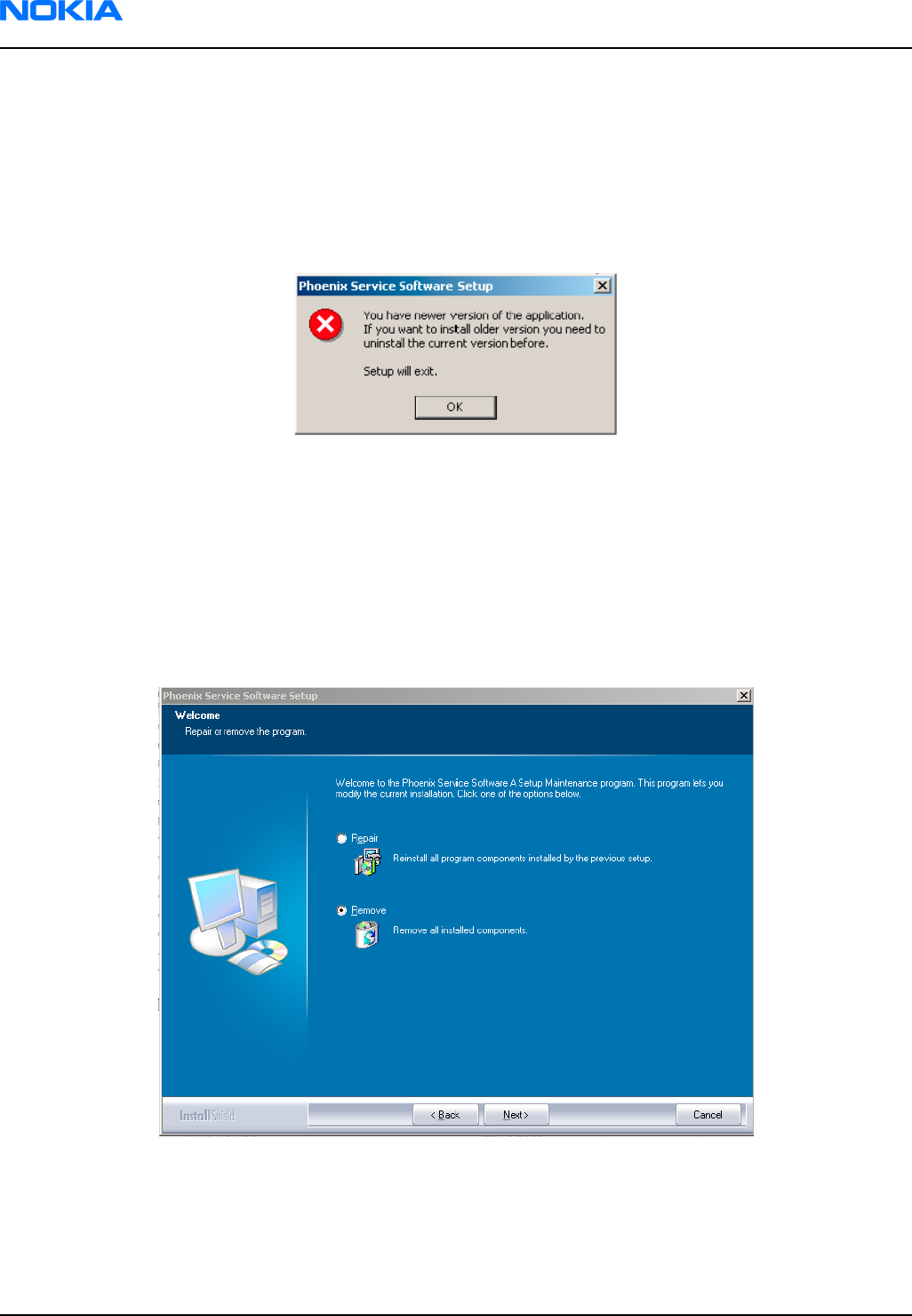
If you try to update the Phoenix Service Software with the same version that you already have (for example,
a15_2004_24_7_55 to a15_2004_24_7_55) you are asked if you want to uninstall the version of Phoenix you have
on your PC. In this case you can choose between total uninstallation and repair just like when you choose to
uninstall Phoenix service software from the Windows Control panel.
If you try to install an older version (for example, downgrade from a15_2004_24_7_55 to a14_2004_16_4_47),
installation will be interrupted.
Always follow the instructions on the screen.
Figure 17 Installation interrupted
Uninstalling Phoenix
Context
Uninstallation can be done manually from Windows Control Panel → Add/Remove Programs .
Steps
1. Choose Phoenix Service Software → Add/Remove → Remove to uninstall Phoenix.
Figure 18 Remove program
The progress of the uninstallation is shown.
RM-74
Nokia Customer Care Phoenix service SW
Page 3–12 Company Confidential 9242678 (Issue 1)
Copyright ©2005 Nokia. All Rights Reserved.
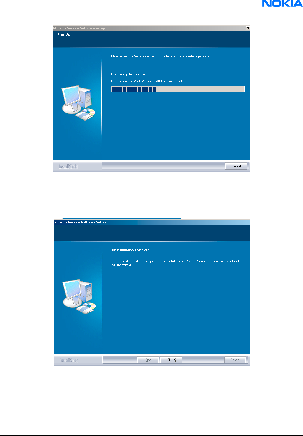
Figure 19 Uninstallation status
2. If the operating system does not require rebooting, click Finish to complete.
Else, Install Shield Wizard will tell you about it. Select Yes... to reboot the PC immediately and No... to reboot
the PC manually afterwards.
Figure 20 Finish uninstallation
RM-74
Phoenix service SW Nokia Customer Care
9242678 (Issue 1) Company Confidential Page 3–13
Copyright ©2005 Nokia. All Rights Reserved.
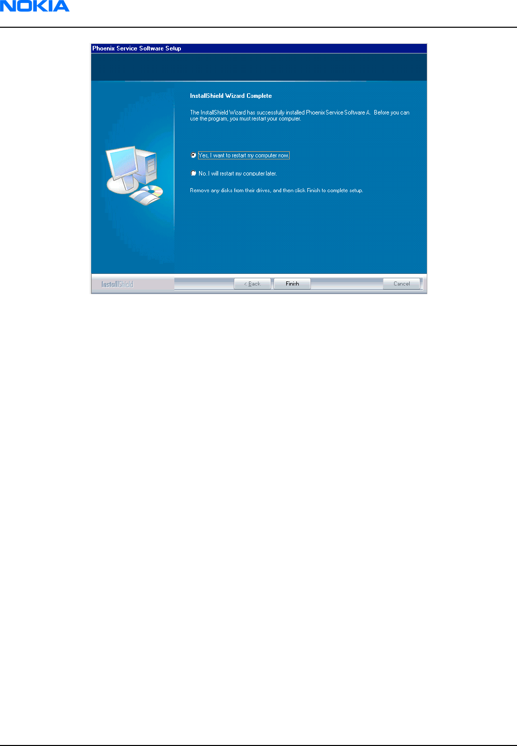
Figure 21 Restart computer
Repairing Phoenix installation
Context
If you experience any problems with the service software, or suspect that files have been lost, you can use the
repair function before completely reinstalling Phoenix.
Note: The original installation package (for example, phoenix_service_sw_a15_2004_24_7_55.exe) must
be found on your PC when you run the repair setup.
Steps
1. Open Windows Control Panel → Add/Remove Programs .
2. Select Phoenix Service Software → Add/Remove .
3. In the following view, choose Repair.
Phoenix will now reinstall components and register them. The procedure is the same as in the update
installation.
RM-74
Nokia Customer Care Phoenix service SW
Page 3–14 Company Confidential 9242678 (Issue 1)
Copyright ©2005 Nokia. All Rights Reserved.
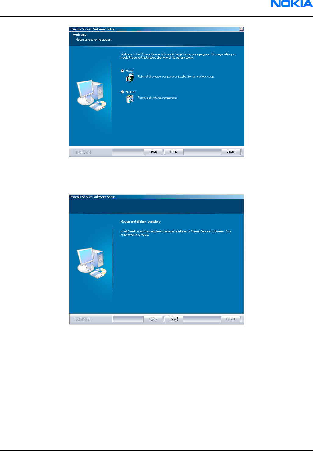
Figure 22 Repair program
4. Click Finish to complete repair.
Figure 23 Finish repair installation
Phoenix service software data package overview
Each product has its own data package (DP). This contains all product-specific data files to make the Phoenix
Service Software and tools usable with a certain phone model:
• Product software binary files
• Files for type label printing
• Validation file for the faultlog repair data reporting system
• All product-specific configuration files for Phoenix Service Software components
Data files are stored under C:\Program Files\Nokia\Phoenix (default).
RM-74
Phoenix service SW Nokia Customer Care
9242678 (Issue 1) Company Confidential Page 3–15
Copyright ©2005 Nokia. All Rights Reserved.
Installing Phoenix data package
Before you begin
1 Verify that The data package contains all product-specific data to make the Phoenix Service Software and
tools usable with a certain phone model.
2 Check that the dongle is attached to the parallel port of your computer.
3 Install Phoenix Service SW.
4 Download the installation package (for example, RM-51_dp_EA_v_1_0.exe) to your computer (for example, in
C:\TEMP).
5 Close all other programs.
6 Run the application file (for example, RM-51_dp_EA_ v_1_0.exe) and follow the instructions on the screen.
If you already have the Phoenix Service SW installed on your computer, you will need to update it when a new
version is released.
Note: Very often the Phoenix Service SW and the phone-specific data package for Phoenix come in
pairs, meaning that a certain version of Phoenix can only be used with a certain version of the data
package. Always use the latest available versions of both. Instructions can be found in phone model
specific Technical Bulletins and readme.txt files of the data packages.
Steps
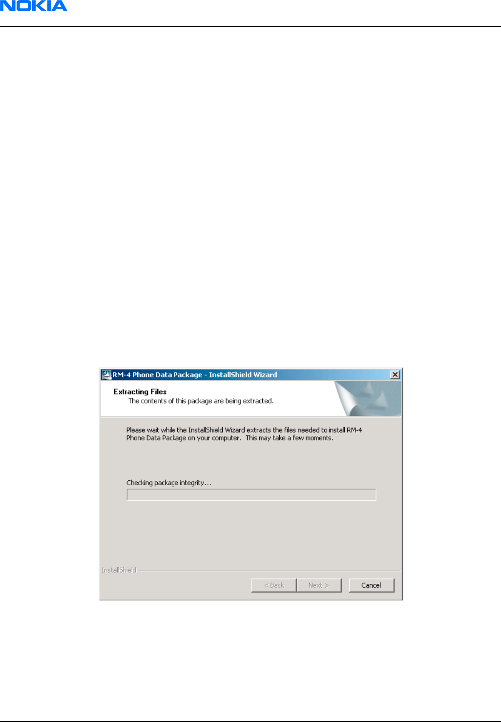
1. To start installation, run the application file (for example, RM-51_dp_EA_ v_1_0.exe).
2. Click Next, and wait for the installation files to be extracted.
Figure 24 Extracting files
RM-74
Nokia Customer Care Phoenix service SW
Page 3–16 Company Confidential 9242678 (Issue 1)
Copyright ©2005 Nokia. All Rights Reserved.
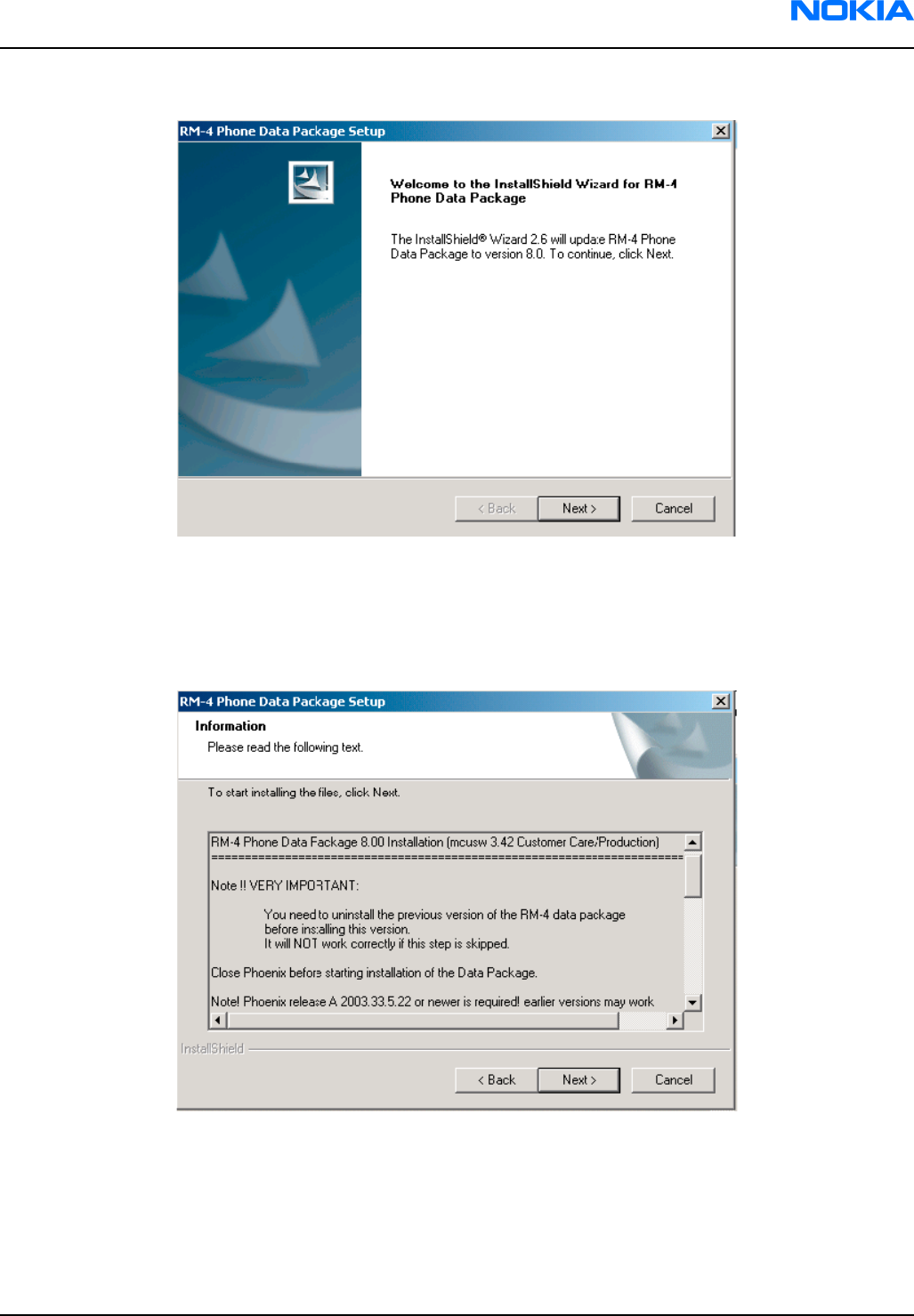
3. Click Next to continue.
Figure 25 Continue data package installation
In this view you can see the contents of the data package. Read the text carefully. There should be information
about the Phoenix version required with this data package.
Click Next to continue.
Figure 26 Data package setup information
RM-74
Phoenix service SW Nokia Customer Care
9242678 (Issue 1) Company Confidential Page 3–17
Copyright ©2005 Nokia. All Rights Reserved.
4. Confirm location and click Next to continue.
Figure 27 Data package destination folder
The install shield checks where the Phoenix application is installed and the directory is shown.
Click Next to continue.
5. Click Next to start copying the files.
Phone model specific files will be installed. Please wait.
Figure 28 Start copying files
RM-74
Nokia Customer Care Phoenix service SW
Page 3–18 Company Confidential 9242678 (Issue 1)
Copyright ©2005 Nokia. All Rights Reserved.
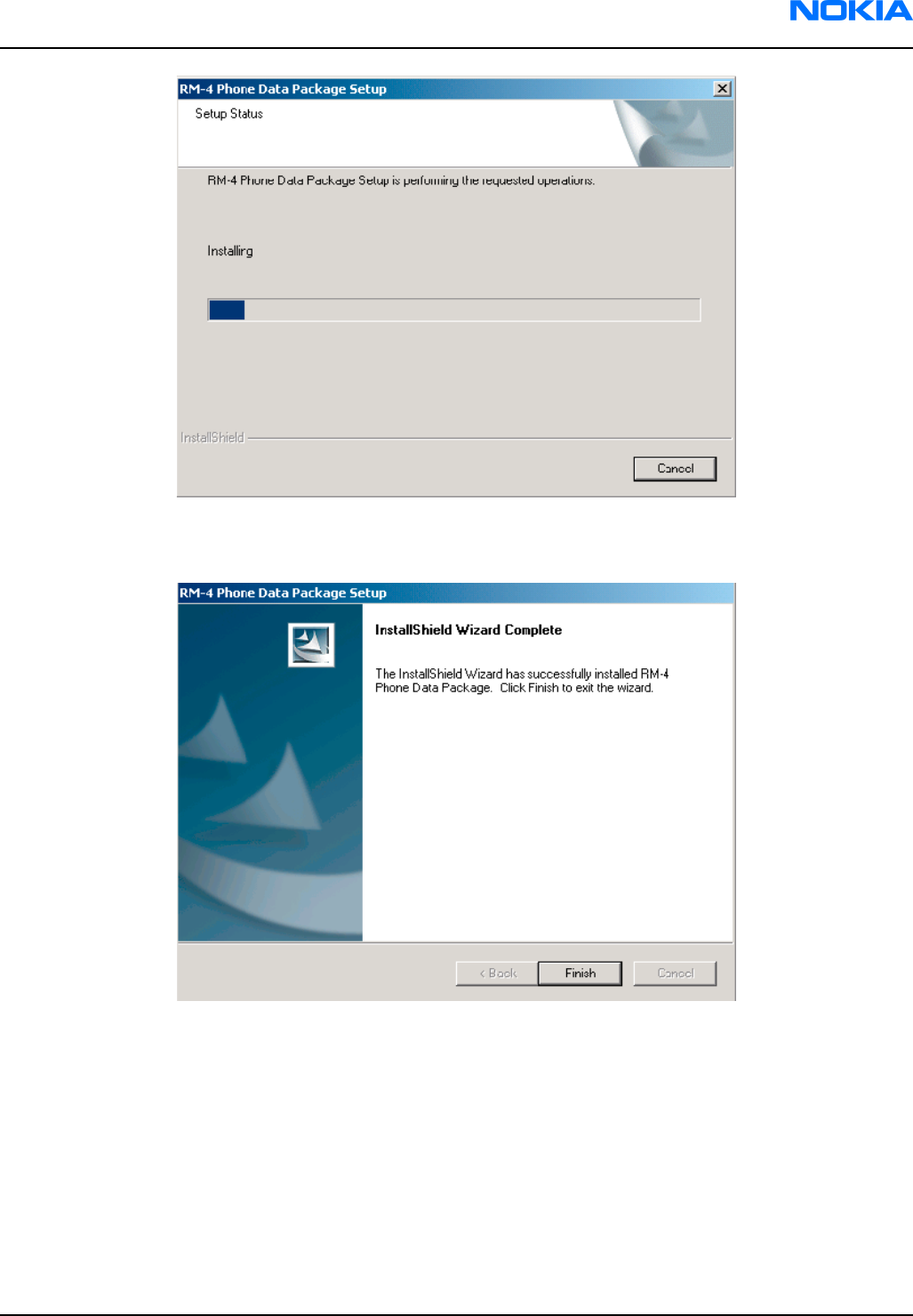
Figure 29 Data package installation status
6. Click Finish to complete the installation.
Figure 30 Finish data package installation
You now have all phone model specific files installed in your Phoenix Service SW.
Next action
Phoenix can be used, for example, for flashing phones and printing type labels. But first you must:
• configure users, and
• manage connections.
FLS-4S can be used right away.
FPS-8* can be used after updating Flash Update Package files.
RM-74
Phoenix service SW Nokia Customer Care
9242678 (Issue 1) Company Confidential Page 3–19
Copyright ©2005 Nokia. All Rights Reserved.
Uninstalling Phoenix data package
Context
If you try to install the same version of Phoenix data package that you already have, you are asked if you want
to uninstall the version you have on your PC. Older versions of data packages don´t need to be uninstalled unless
instructions to do so are given in the readme.txt file of the data package and bulletins concerning the release.
Please read all related documents carefully.
Steps
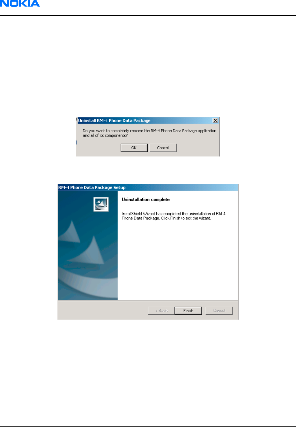
1. Click OK to uninstall, Cancel if you don’t want to uninstall.
Figure 31 Uninstalling Phoenix data package
2. Once the previously installed data package is uninstalled, click Finish.
Figure 32 Finish data package uninstallation
Alternative steps
•Uninstallation can also be done manually from Windows Control Panel → Add/Remove Programs →
xx-xx (* Phone Data Package) . (*= type designator of the phone
Next action
Run the installation package again to continue installation from the beginning.
RM-74
Nokia Customer Care Phoenix service SW
Page 3–20 Company Confidential 9242678 (Issue 1)
Copyright ©2005 Nokia. All Rights Reserved.
Service software instructions
Configuring users in Phoenix
Steps
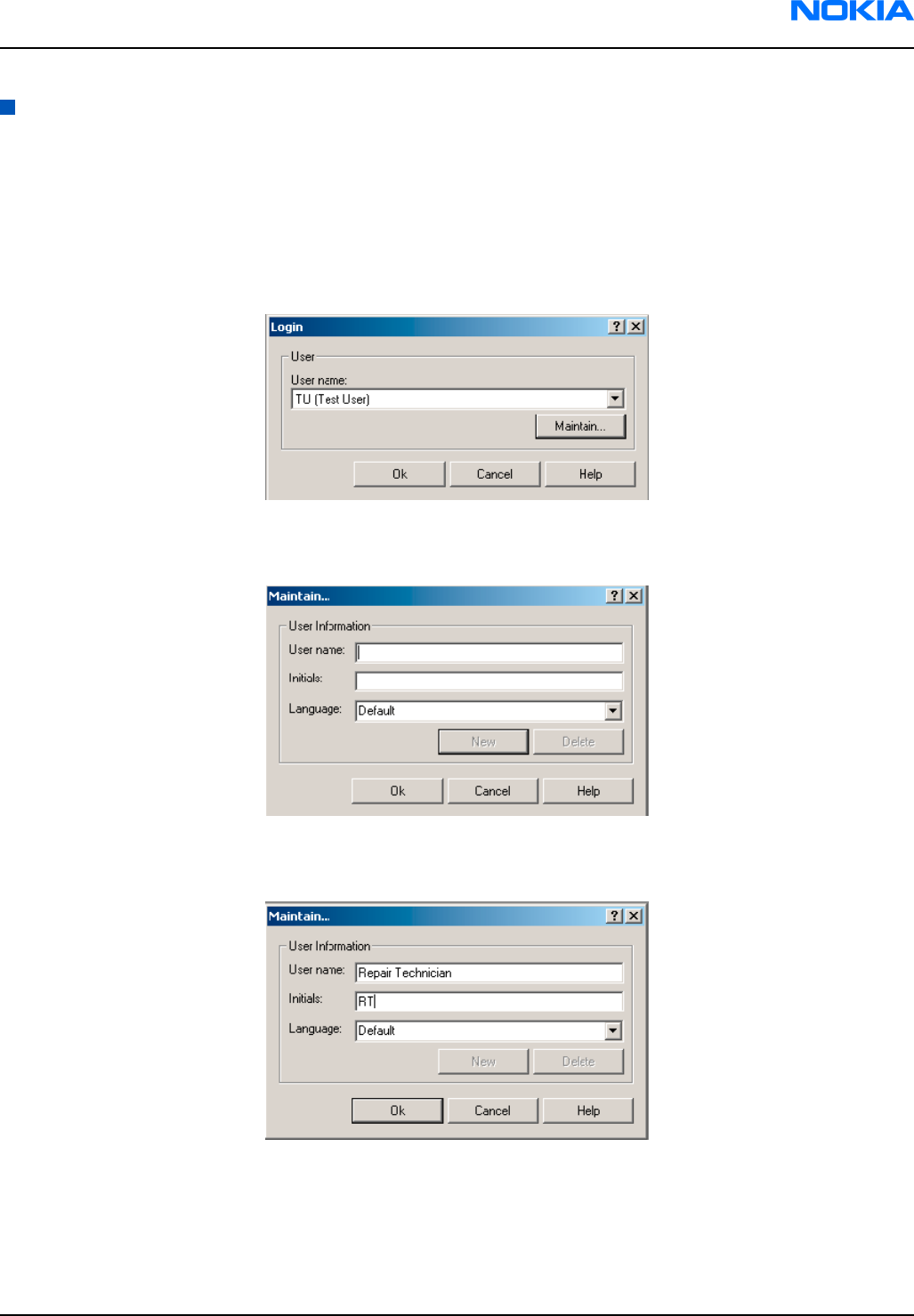
1. Start Phoenix Service SW and log in.
If your user ID is already configured, choose it from the dropdown list and click OK. To add a new user or
edit existing ones click Maintain.
Figure 33 Login
2. Choose New to add information for a new user.
Figure 34 Add information for new user 1
3. Type in your name and initials and click OK.
Figure 35 Add information for new user 2
A new user is now created.
4. Click OK.
You are now able to login with this user name.
RM-74
Phoenix service SW Nokia Customer Care
9242678 (Issue 1) Company Confidential Page 3–21
Copyright ©2005 Nokia. All Rights Reserved.
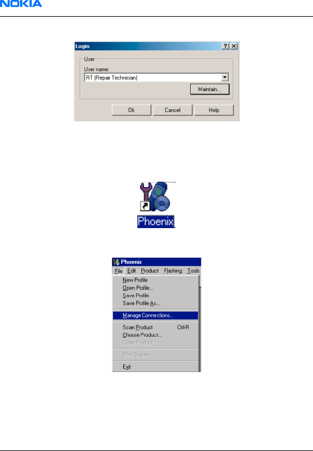
5. Click OK.
Figure 36 Login, user configured
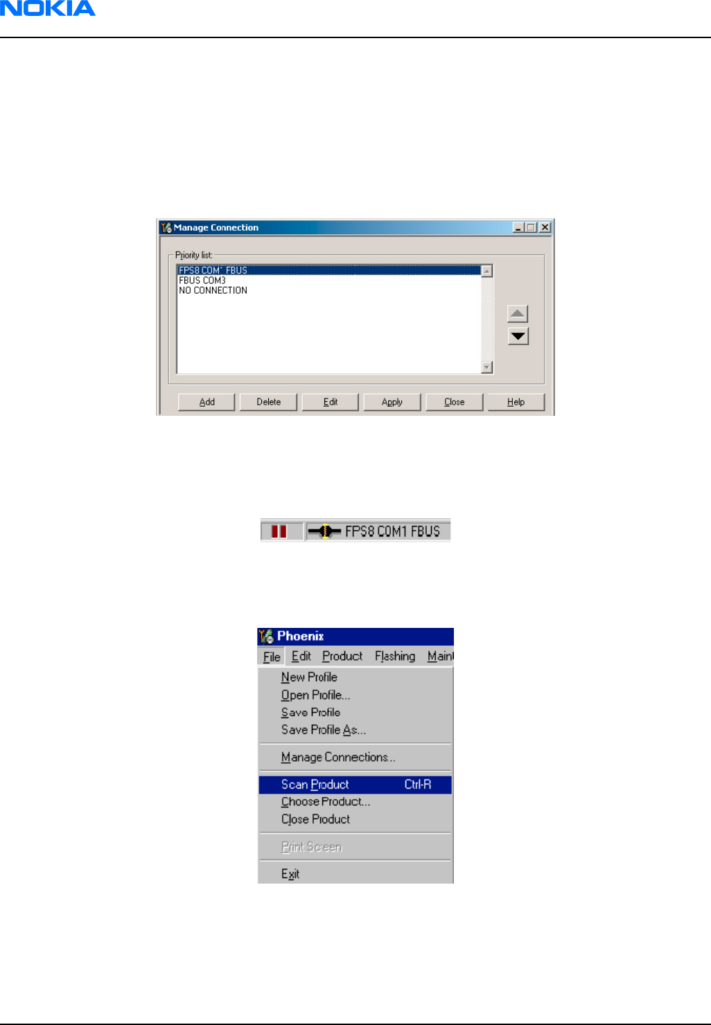
Managing connections in Phoenix
Steps
1. Start Phoenix Service SW and log in.
Figure 37 Phoenix icon
2. Choose File → Manage Connections .
Figure 38 Manage connections
Existing connections can be selected, edited, deleted, and new ones created by using this dialog.
RM-74
Nokia Customer Care Phoenix service SW
Page 3–22 Company Confidential 9242678 (Issue 1)
Copyright ©2005 Nokia. All Rights Reserved.
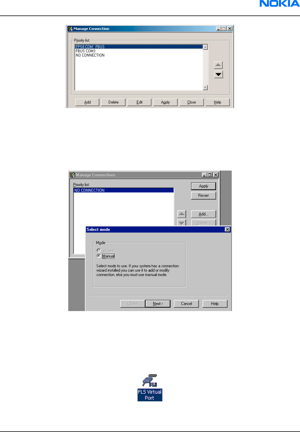
Figure 39 Connections list
3. Click Add to add a new connection, and select if you want to create it manually or by using the Connection
Wizard.
In the following dialogs you will be asked to select settings for the connection. If you use the Wizard, connect
the tools and a phone to your PC and the wizard will automatically try to configure the correct connection.
4. Select Manual mode, and click Next to continue.
Figure 40 Select mode: Manual
i For FLS-4S POS Flash Device, choose the following connection settings:
• Media: FBUS
• COM Port: Virtual COM Port used by FLS-4
Note: ALWAYS check this. Go to Windows → Control Panel → FLS Virtual Port → Configuration .
Figure 41 FLS virtual port icon
RM-74
Phoenix service SW Nokia Customer Care
9242678 (Issue 1) Company Confidential Page 3–23
Copyright ©2005 Nokia. All Rights Reserved.
ii For FPS-8 Flash Prommer, choose the following connection settings:
• Media: FPS-8
• Port Num: COM Port where FPS-8 is connected
• COMBOX_DEF_MEDIA: FBUS
5. Click Finish to complete the configuration.
6. Activate the connection you want to use by clicking it, use up/down arrows to move it on top of the list, and
click Apply.
Figure 42 Connections list
The connection is now selected and can be used after closing the Manage Connections window.
Selected connection will be shown on the right hand bottom corner of the screen.
Figure 43 Connection information
7. To use the selected connection, connect the phone to Phoenix with correct service tools, make sure that it
is switched on and select Scan Product.
Figure 44 Scan product
When a product is found, Phoenix will load product support. Name of the loaded product support module
and its version information will be shown on the bottom of the screen.
RM-74
Nokia Customer Care Phoenix service SW
Page 3–24 Company Confidential 9242678 (Issue 1)
Copyright ©2005 Nokia. All Rights Reserved.
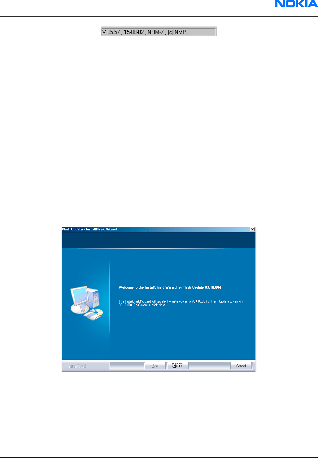
Figure 45 Product support module information
Installing Flash support files for FPS-8* and FLS-4*
Before you begin
Note: This is a separate installation package.
• Install Phoenix Service SW.
• Install phone model specific data package for Phoenix.
• The flash support files are delivered in the same installation package with Phoenix data packages or newer
Phoenix packages since September 2003.
• Normally it is enough to install Phoenix and the phone-specific data package because the Phoenix installation
always includes the latest flash update package files for FLS-4S/FPS-8*.
• A separate installation package for flash support files is available, and the files can be updated according to
this instruction if updates appear between Phoenix/data package releases.
Context
If you are not using a separate installation package, you can skip this section and continue with FPS-8 Flash
prommer SW update (Page 3–28) after installing a new phone data package.
Steps
1. Start by double clicking flash_update_03_13_001.exe to begin installation.
Figure 46 Flash update welcome dialog
RM-74
Phoenix service SW Nokia Customer Care
9242678 (Issue 1) Company Confidential Page 3–25
Copyright ©2005 Nokia. All Rights Reserved.
2. If the same version of Flash Update package already exists, and you want to reinstall it, the previous package
is first uninstalled. Run the installation again.
Figure 47 Uninstall flash update package
If you try to downgrade the existing version to older ones, the setup will be aborted. If you really want to
downgrade, uninstall newer files manually from Control Panel and then rerun the installation again.
Figure 48 Flash installation interrupted
If an older version exists on your PC and it needs to be updated, click Next to continue installation.
Figure 49 Continue flash update
RM-74
Nokia Customer Care Phoenix service SW
Page 3–26 Company Confidential 9242678 (Issue 1)
Copyright ©2005 Nokia. All Rights Reserved.
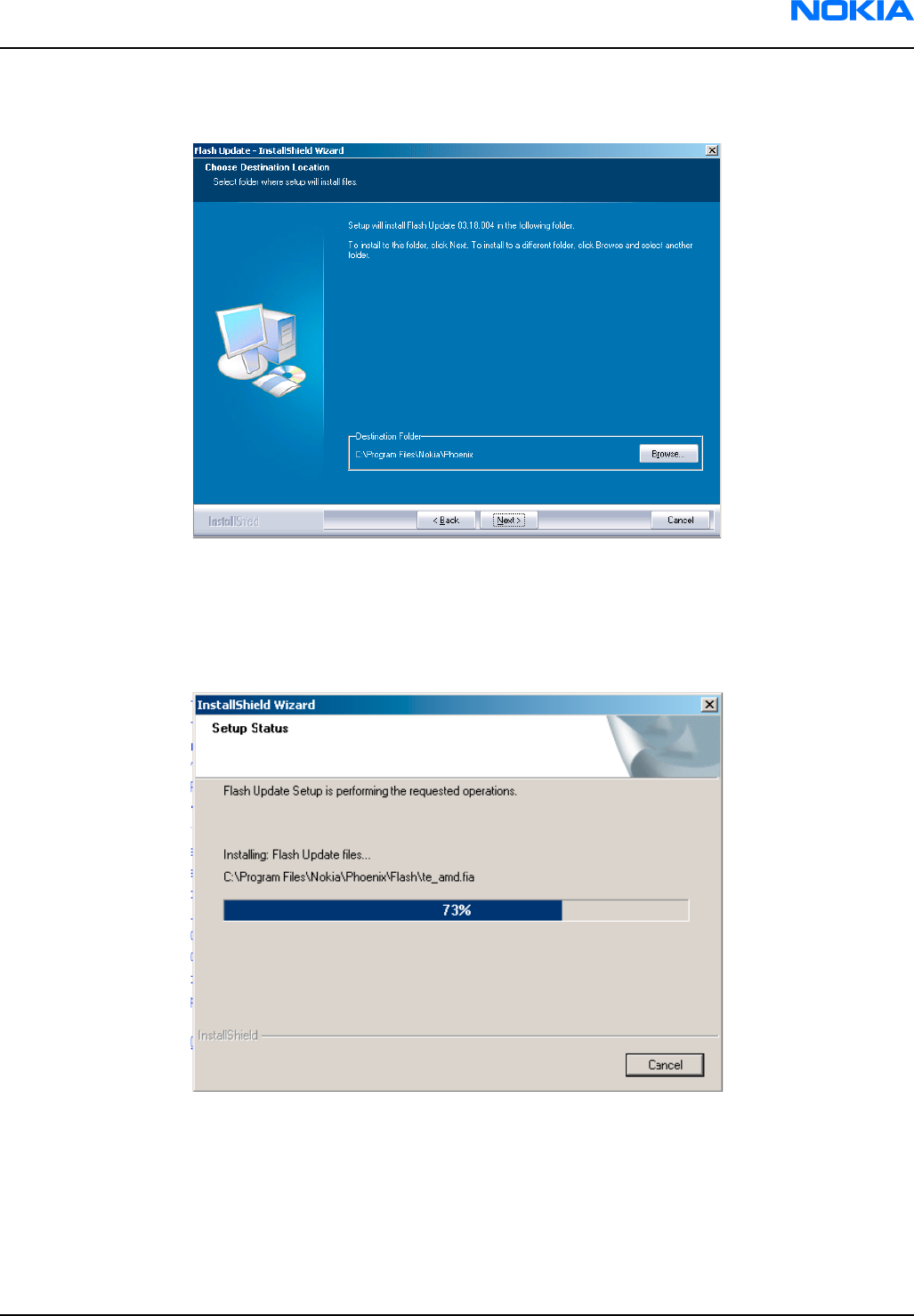
3. It is highly recommended to install the files to the default destination folder C:\Program Files\Nokia
\Phoenix. Click Next to continue.
Figure 50 Flash destination folder
When installing the flash update files for the first time you may choose another location by selecting
Browse. However, this is not recommended.
Installation will continue.
Figure 51 Flash installation status
RM-74
Phoenix service SW Nokia Customer Care
9242678 (Issue 1) Company Confidential Page 3–27
Copyright ©2005 Nokia. All Rights Reserved.
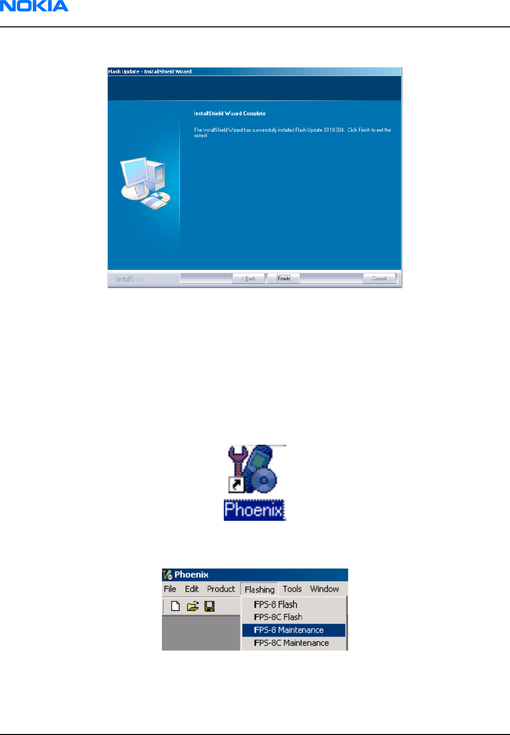
4. Choose Finish to complete the installation procedure.
Figure 52 Finish flash update
Next action
FLS-4 can be used right after the Flash Update Package is installed.
FPS-8* flash prommer must be updated using Phoenix!
Updating FPS-8 Flash prommer software
Steps
1. Start Phoenix Service Software and log in, manage connection correctly for the FPS-8* flash prommer.
Figure 53 Phoenix icon
2. Choose Flashing → FPS-8 Maintenance .
Figure 54 FPS-8 maintenance
Note: Screen shots may be different depending on the Phoenix version used and the connected
components.
RM-74
Nokia Customer Care Phoenix service SW
Page 3–28 Company Confidential 9242678 (Issue 1)
Copyright ©2005 Nokia. All Rights Reserved.
3. When the new FPS-8 flash update package is installed to computer you will be asked to update the files to
your FPS-8 Prommer. Select Yes to update files.
Figure 55 Prommer SW update
4. Wait until you are notified that update has been successful; the procedure will take a couple of minutes.
Click OK to close the FPS-8 Maintenance window.
Figure 56 Prommer SW update done
View after successful prommer software update:
RM-74
Phoenix service SW Nokia Customer Care
9242678 (Issue 1) Company Confidential Page 3–29
Copyright ©2005 Nokia. All Rights Reserved.
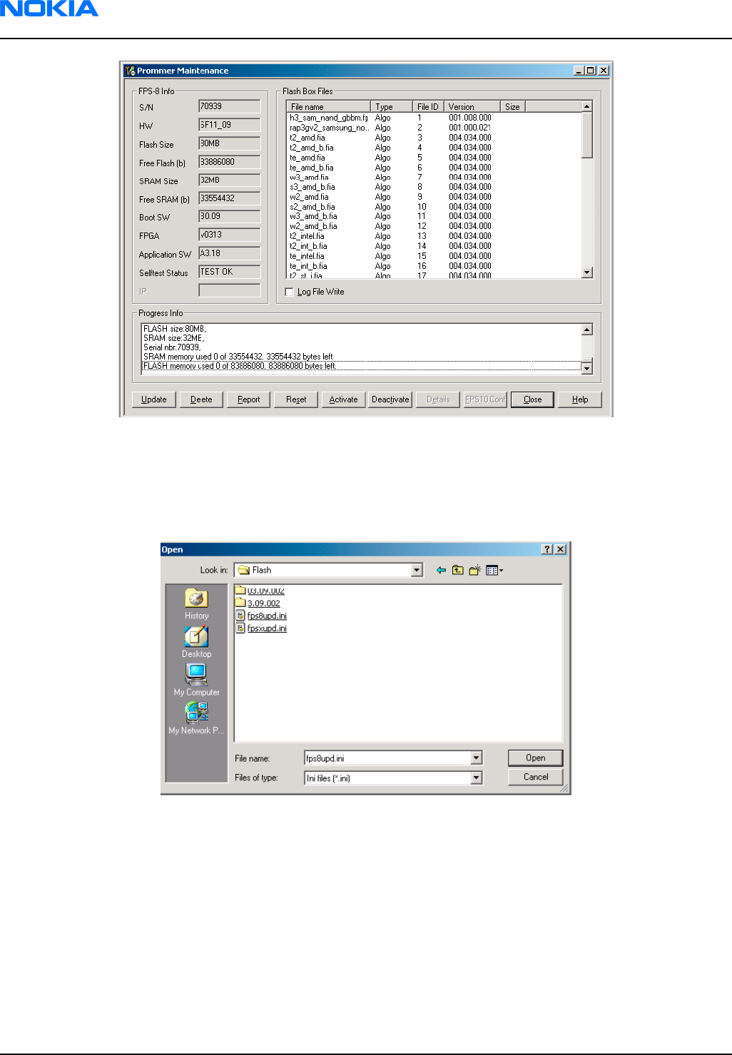
Figure 57 FPS-8 info window
Alternative steps
• FPS-8 SW can also be updated by pressing Update button and selecting appropriate fps8upd.ini file in C:
\Program Files\Nokia\Phoenix\Flash.
Figure 58 Flash directory window
• All files can be loaded separately to FPS-8. To do this, just press the right mouse button in the Flash box
files window and select the file type to be loaded.
More information can be found in Phoenix Help.
Activating FPS-8
Context
Before FPS-8 can be successfully used for phone programming, it must first be activated. Fill in first the FPS-8
activation request sheet in the FPS-8 sales package and follow the instructions on the sheet (included in sales
package CD-ROM or from partner web site).
RM-74
Nokia Customer Care Phoenix service SW
Page 3–30 Company Confidential 9242678 (Issue 1)
Copyright ©2005 Nokia. All Rights Reserved.
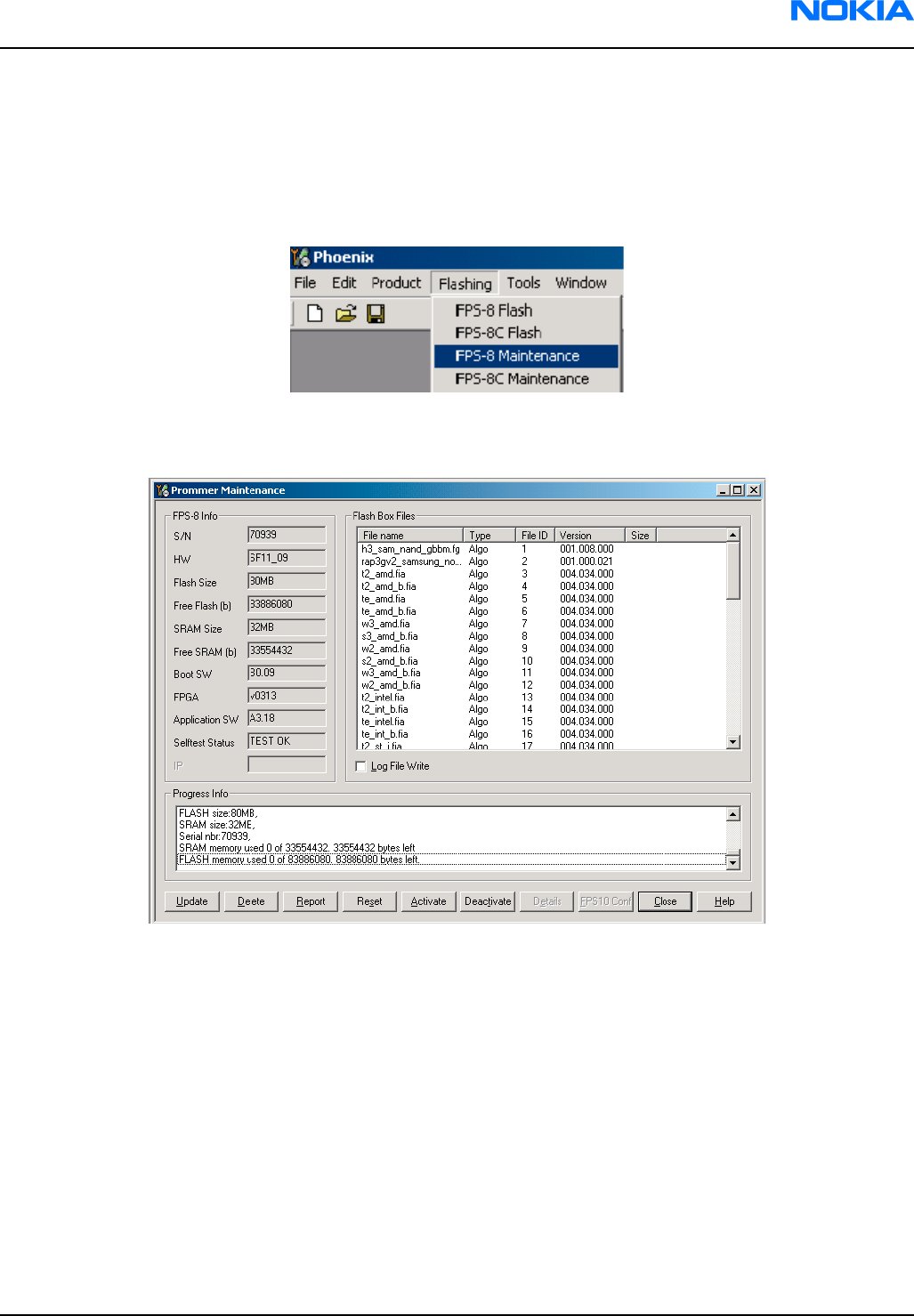
When activation file is received (for example, 00000.in), copy it to C:\ProgramFiles\Nokia\Phoenix
\BoxActivation directory on your computer (this directory is created when Phoenix is installed).
Steps
1. Start Phoenix Service Software.
2. Select Flashing → FPS-8 maintenance .
Figure 59 FPS-8 maintenance
3. Click Activate in the FPS-8 Maintenance window.
Figure 60 FPS-8 info window
If you saved the activation file to some other directory on your PC, Browse to find it
RM-74
Phoenix service SW Nokia Customer Care
9242678 (Issue 1) Company Confidential Page 3–31
Copyright ©2005 Nokia. All Rights Reserved.
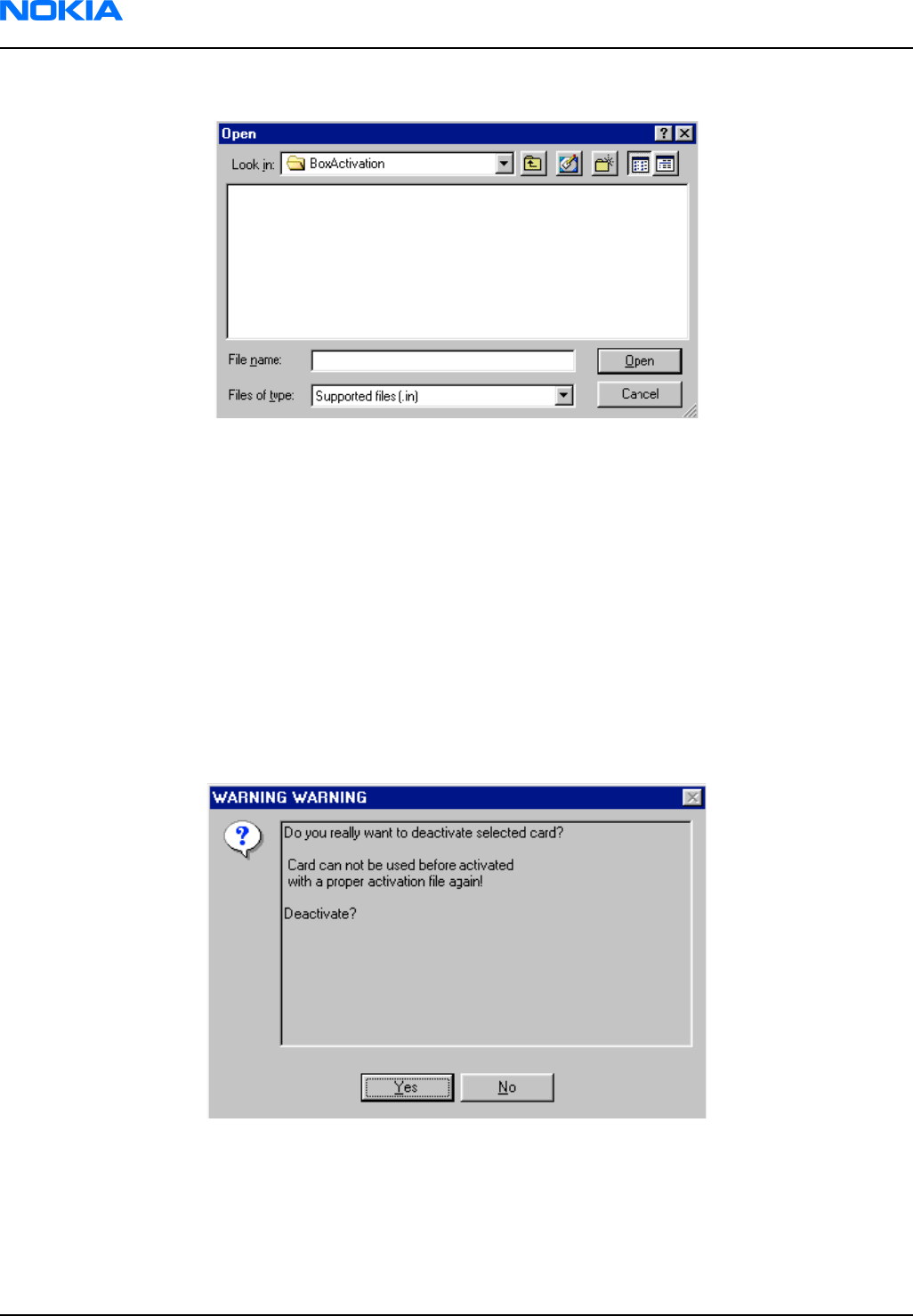
4. Click Open to activate the box.
Figure 61 Box activation
5. Turn the FPS-8's power off and on to complete activation.
Deactivating FPS-8
Context
If there is, for example, a need to send the FPS-8 box for repair, it must be deactivated first.
Steps
1. Start Phoenix Service Software.
2. Choose Maintenance → Prommer Maintenance .
3. In the Prommer Maintenance window, click Deactivate.
4. To confirm the deactivation, click Yes.
Figure 62 Deactivation warning
The box is deactivated.
5. To complete the deactivation, restart FPS-8.
RM-74
Nokia Customer Care Phoenix service SW
Page 3–32 Company Confidential 9242678 (Issue 1)
Copyright ©2005 Nokia. All Rights Reserved.
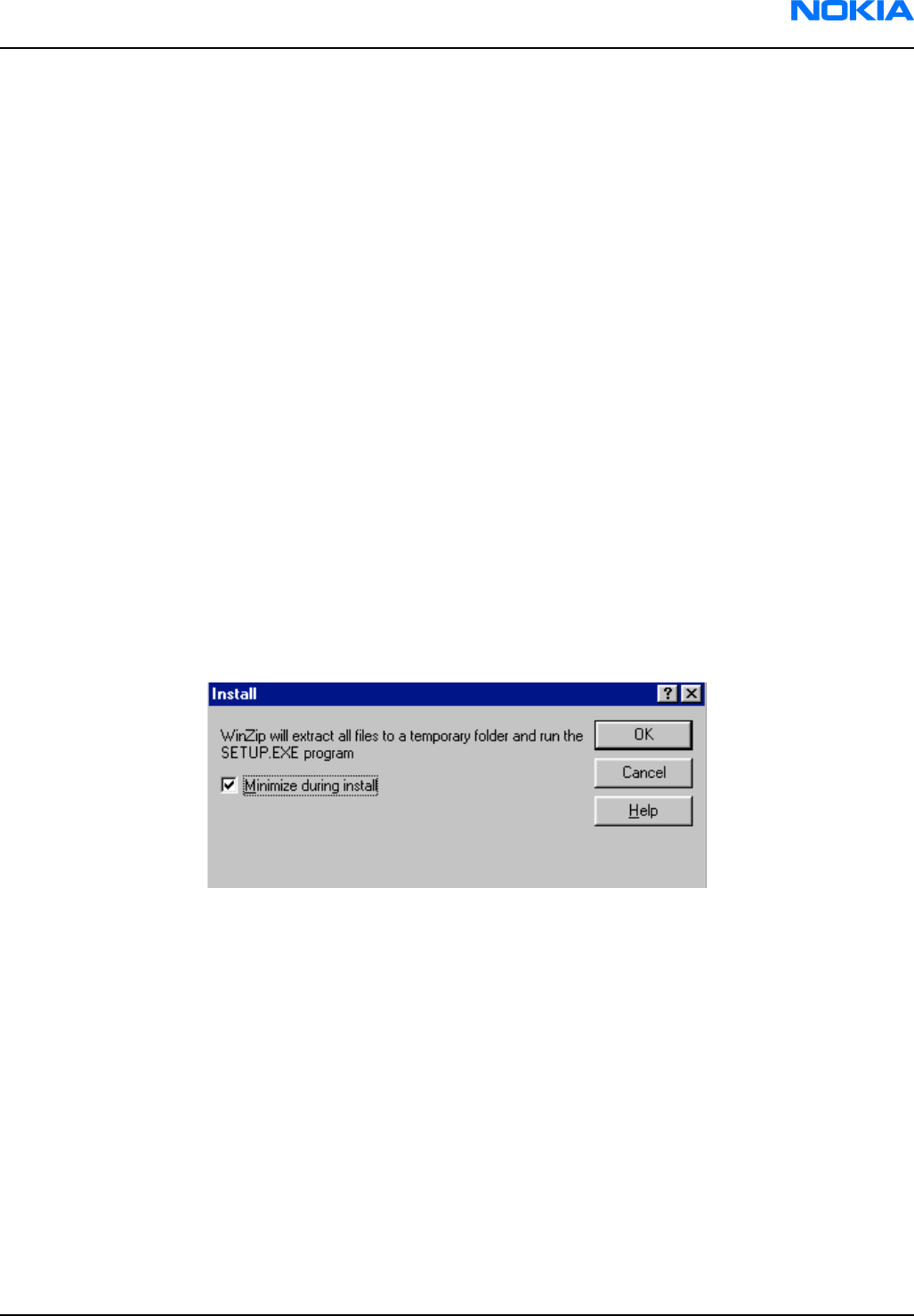
Updating JBV-1 docking station software
Before you begin
The JBV-1 docking station contains software (firmware) which can be updated. You need the following
equipment to update the software:
• PC with USB connection
• operating system supporting USB (Not Win 95 or NT)
• USB Cable (can be purchased from shops or suppliers providing PC hardware and accessories)
• JBV-1 docking station
• external power supply (11-16V)
Before installation:
• Download Jbv1_18_update.zip file to your computer (in C:\TEMP for example) from your download web site.
• Close all other programs.
• Follow instructions on the screen.
Context
The JBV-1 docking station is a common tool for all DCT-4 generation products. In order to make the JBV-1 usable
with different phone models, a phone-specific docking station adapter is used.
Steps
1. Run Jbv1_18_update.zip file and start software installation by double clicking Setup.exe.
Note: DO NOT CONNECT THE USB CABLE/JBV-1 TO YOUR COMPUTER YET!
Figure 63 Extracting JBV-1 update files
Files needed for JBV-1 package setup program will be extracted.
RM-74
Phoenix service SW Nokia Customer Care
9242678 (Issue 1) Company Confidential Page 3–33
Copyright ©2005 Nokia. All Rights Reserved.
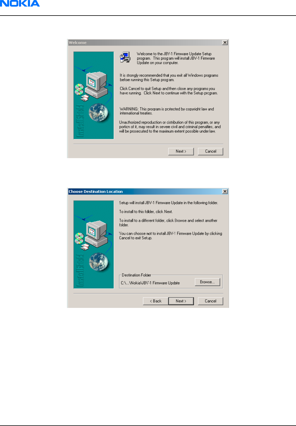
2. Read the instructions in the dialog box and click Next to continue.
Figure 64 JBV-1 update information
3. Accept the suggested destination folder for installing the JBV-1 SW Package, and click Next to continue.
Figure 65 JBV-1 update destination folder
4. Select Full installation and click Next to continue.
RM-74
Nokia Customer Care Phoenix service SW
Page 3–34 Company Confidential 9242678 (Issue 1)
Copyright ©2005 Nokia. All Rights Reserved.
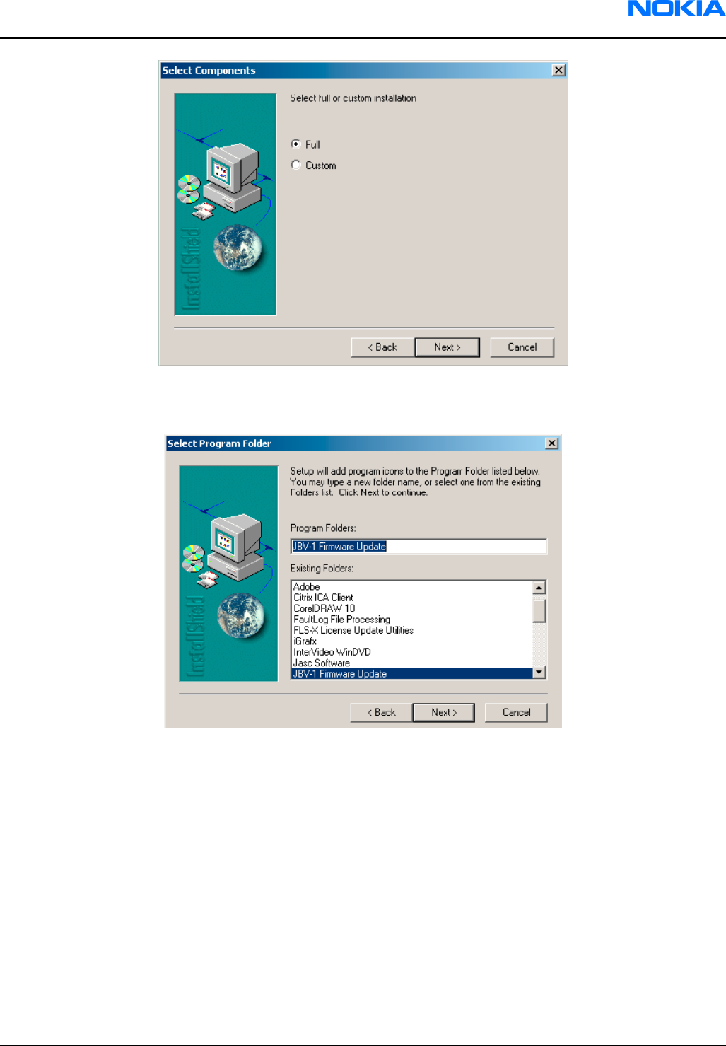
Figure 66 Select installation: Full
5. A program folder is created and the software files are installed there. Click Next to continue.
Figure 67 Select program folder
RM-74
Phoenix service SW Nokia Customer Care
9242678 (Issue 1) Company Confidential Page 3–35
Copyright ©2005 Nokia. All Rights Reserved.
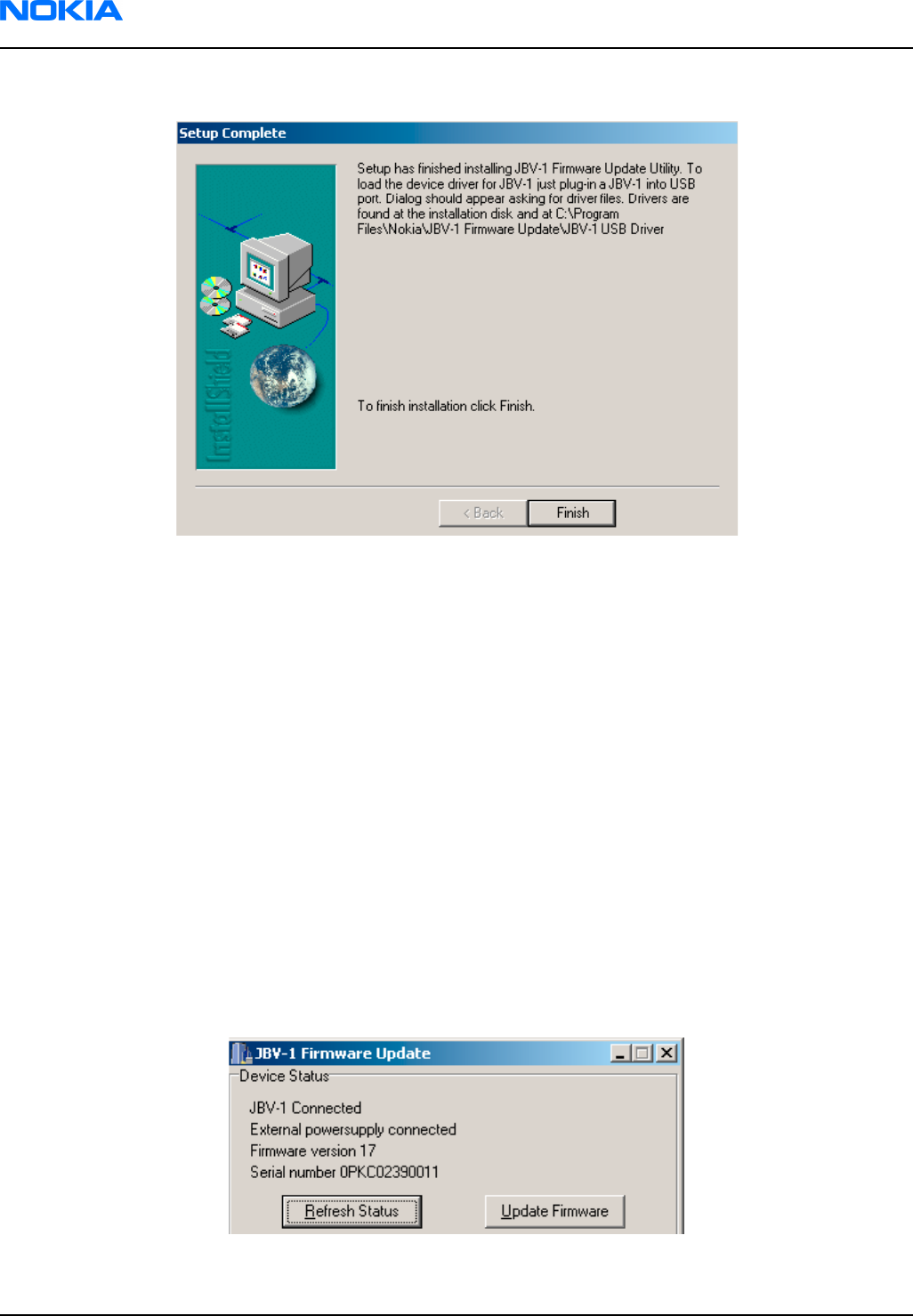
6. Click Finish to complete the installation.
Figure 68 Finish JBV-1 update installation
7. Connect the USB cable/JBV-1 to your computer. Connect power to JBV-1 (11-16V DC) from an external power
supply, then connect the USB Cable between the JBV-1 USB connector and the PC.
8. Install or update the JBV-1 USB drivers which are delivered with the JBV-1 SW installation package.
The drivers can be found in C:\Program Files\Nokia\ JBV-1 Firmware Update\JBV-1USB driver
•If there is no previously installed JBV-1 Firmware update package installed on your computer, Windows
will detect connected USB cable and detect drivers for new HW. You will be prompted about this, please
follow the instructions and allow Windows to search and install the best drivers available.
• If there is a previously installed JBV-1 Firmware update package (v.17 or older) on your computer, please
update the JBV-1 USB driver. Please see the readme.txt file in C:\Program Files\Nokia\JBV-1 Firmware
Update\JBV-1USB driver folder for instructions on how to update the JBV-1 USB Driver.
After you have installed or updated the JBV-1 USB driver, the actual JBV-1 SW update can begin.
9. Go to folder C:\Program Files\Nokia\JBV-1 Firmware Update\JBV-1 Firmware Update and start JBV-1 Update
SW by double clicking fwup.exe.
JBV-1 Firmware update starts and shows current status of the connected JBV-1. If firmware version read
from your JBV-1 is not the latest one available (v.17 or older), it needs to be updated to version 18 by
clicking Update Firmware.
10. Choose Refresh Status to check the SW version.
Figure 69 Checking JBV-1 SW version
RM-74
Nokia Customer Care Phoenix service SW
Page 3–36 Company Confidential 9242678 (Issue 1)
Copyright ©2005 Nokia. All Rights Reserved.
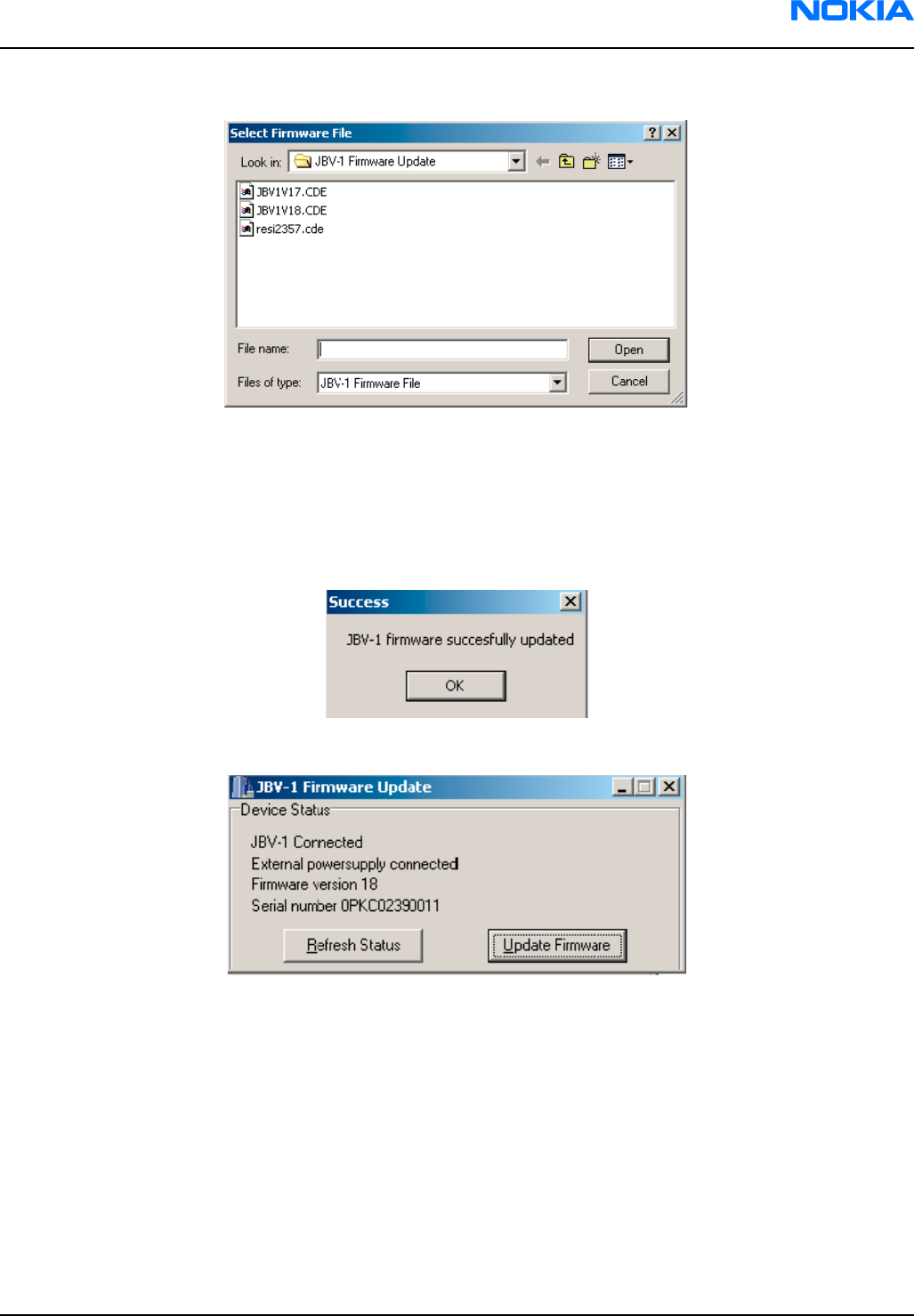
11. Choose file JBV1v18.CDE and click Open to update your JBV-1 to a new version (v.18).
Figure 70 JBV-1 update directory window
Wait until you hear a "click" from the JBV-1.
The older SW file JBV1v17.CDE is visible in this view only if the previous JBV-1 SW package has been installed
on your computer.
12. Click OK to see the current JBV-1 status (after a successful update).
Figure 71 JBV-1 SW update done
Figure 72 JBV-1 SW status
You have now updated the software of your JBV-1 docking station and it is ready for use.
Next action
If you have several docking stations you need to update, disconnect the power and USB cables from the previous
one and connect them to the next docking station. First, click Refresh Status to see the current SW version and
then Update Firmware to update the software.
After you have updated all docking stations, close the JBV-1 Firmware Update dialog box.
RM-74
Phoenix service SW Nokia Customer Care
9242678 (Issue 1) Company Confidential Page 3–37
Copyright ©2005 Nokia. All Rights Reserved.

RM-74
Nokia Customer Care Phoenix service SW
(This page left intentionally blank.)
Page 3–38 Company Confidential 9242678 (Issue 1)
Copyright ©2005 Nokia. All Rights Reserved.

4 — Service Tools
Nokia Customer Care
9242678 (Issue 1) Company Confidential Page 4–1
Copyright ©2005 Nokia. All Rights Reserved.

RM-74
Nokia Customer Care Service Tools
(This page left intentionally blank.)
Page 4–2 Company Confidential 9242678 (Issue 1)
Copyright ©2005 Nokia. All Rights Reserved.

Table of Contents
Service tools......................................................................................................................................................................................4–5
ACF-8..............................................................................................................................................................................................4–5
CA-45.........................................................................................................................................................................................4–0
CA-5S..............................................................................................................................................................................................4–5
CA-65DS....................................................................................................................................................................................4–0
CA-67DS....................................................................................................................................................................................4–0
DA-49........................................................................................................................................................................................4–0
DAU-9S......................................................................................................................................................................................4–0
FLC-2..............................................................................................................................................................................................4–6
FLS-4S............................................................................................................................................................................................4–7
FPS-10.......................................................................................................................................................................................4–0
FPS-8..............................................................................................................................................................................................4–7
JBV-1..............................................................................................................................................................................................4–8
MJ-59.........................................................................................................................................................................................4–0
PCS-1.........................................................................................................................................................................................4–0
PKD-1........................................................................................................................................................................................4–0
RJ-51 PA...................................................................................................................................................................................4–0
RJ-79.........................................................................................................................................................................................4–0
SA-41........................................................................................................................................................................................4–0
SF-10.........................................................................................................................................................................................4–0
SS-54.........................................................................................................................................................................................4–0
ST-30.........................................................................................................................................................................................4–0
SX-4...........................................................................................................................................................................................4–0
XCS-1...........................................................................................................................................................................................4–10
XCS-4...........................................................................................................................................................................................4–11
XRF-1.........................................................................................................................................................................................4–0
Service software concept...........................................................................................................................................................4–12
POS (Point of Sales) flash concept.....................................................................................................................................4–12
FPS-8 Prommer box flash concept.....................................................................................................................................4–13
JBV-1 flash concept.................................................................................................................................................................4–14
Module jig (MJ-59) service concept...................................................................................................................................4–15
List of Figures
Figure 73 POS flash concept......................................................................................................................................................4–12
Figure 74 FPS-8 Prommer box flash concept.......................................................................................................................4–13
Figure 75 JBV-1 flash concept...................................................................................................................................................4–14
Figure 76 Module jig service concept.....................................................................................................................................4–15
RM-74
Service Tools Nokia Customer Care
9242678 (Issue 1) Company Confidential Page 4–3
Copyright ©2005 Nokia. All Rights Reserved.

RM-74
Nokia Customer Care Service Tools
(This page left intentionally blank.)
Page 4–4 Company Confidential 9242678 (Issue 1)
Copyright ©2005 Nokia. All Rights Reserved.
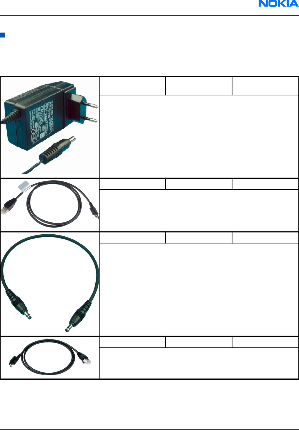
Service tools
List of Service Tools
The table below gives a short overview of service tools that can be used for testing, error analysis and repair
of product , refer to various concepts.
ACF-8 Universal power
supply
ACF-8 universal power supply is used to power FPS-8. ACF-8 has 6V DC
and 2.1A output.
CA-45 DS easy flash cable
The CA-45 DS easy flash cable is used to connect the phone bottom
connector to either POS flashing device (FLS-4S) or to one of the
PROMMER boxes (FPS-8/FPS-10).
CA-5S DC cable
The DC cable CA-5S is used to connect JBV-1 to the phone charger jack
for ADC/VCHAR/ICHAR calibration
Note: Old SCB-3 can be used as well.
CA-65DS Easy flash cable
This cable connects the phone DC port to the FLS-4S prommer.
RM-74
Service Tools Nokia Customer Care
9242678 (Issue 1) Company Confidential Page 4–5
Copyright ©2005 Nokia. All Rights Reserved.
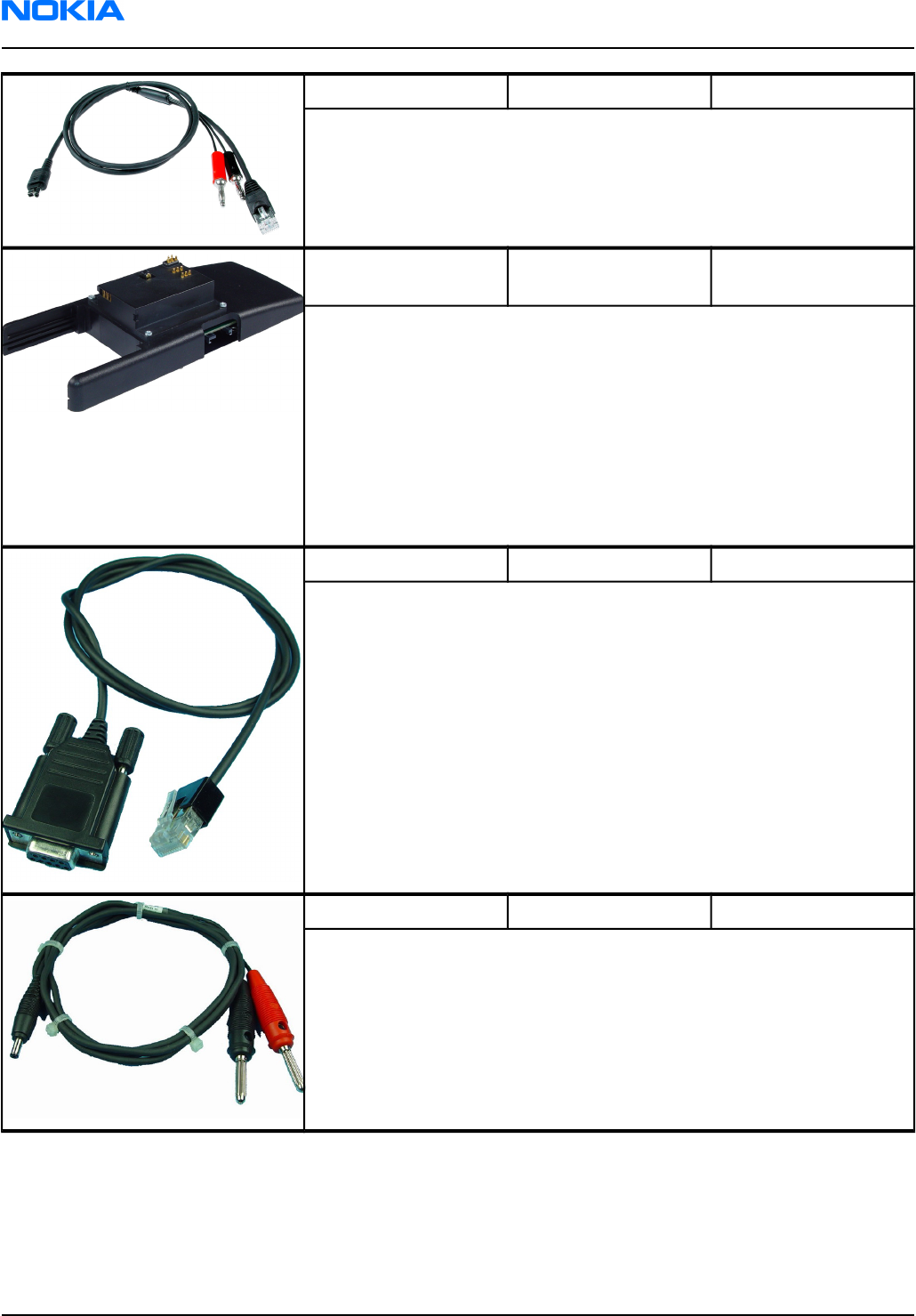
CA-67DS Easy flash cable
This cable connects the phone DC port to the FPS-10 prommer.
DA-49 Docking station
adapter
The Docking Station adaptor is used for this phone in combination with
JBV-1. The adapter supports flashing and energy management
calibration.
Features include:
• compatible with the JBV-1
• easy phone attachment and detachment.
• reliable phone locking
• switch for detecting phone
• replaceable SIM interface
DAU-9S MBUS cable
The MBUS cable DAU-9S has a modular connector and is used, for
example, between the PC's serial port and module jigs, flash adapters or
docking station adapters.
Note: Docking station adapters valid for DCT4 products.
FLC-2 DC cable
FLC-2 is used with a flash adapter to supply a controlled operating
voltage.
RM-74
Nokia Customer Care Service Tools
Page 4–6 Company Confidential 9242678 (Issue 1)
Copyright ©2005 Nokia. All Rights Reserved.
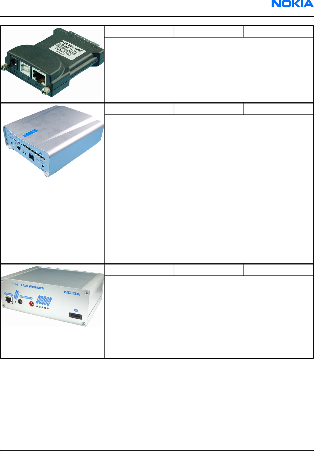
FLS-4S Flash device
FLS-4S is a dongle and flash device incorporated into one package,
developed specifically for POS use.
FPS-10 Flash prommer
FPS-10 interfaces with:
• PC
• Control unit
• Flash adapter
• Smart card
FPS-10 flash prommer features:
• Flash functionality for BB5 terminals
• Smart Card reader for SX-2 or SX-4
• USB traffic forwarding
• USB to FBUS/Flashbus conversion
• LAN to FBUS/Flashbus and USB conversion
• Vusb output switchable by PC command
FPS-10 sales package includes:
• FPS-10 prommer
• Power Supply with 5 country specific cords
• USB cable
FPS-8 FLASH prommer
The flash prommer FPS-8 is used for example with flash adapters,
docking station adapters and flash/docking stations. Power is supplied
to FPS-8 from the universal power supply, ACF-8.
The sales pack includes:
• FPS-8 flash prommer
• FPS-8 activation sheet
• ACF-8 universal power supply
• AXS-4 service cable (D9-D9)
• Printer cable
RM-74
Service Tools Nokia Customer Care
9242678 (Issue 1) Company Confidential Page 4–7
Copyright ©2005 Nokia. All Rights Reserved.
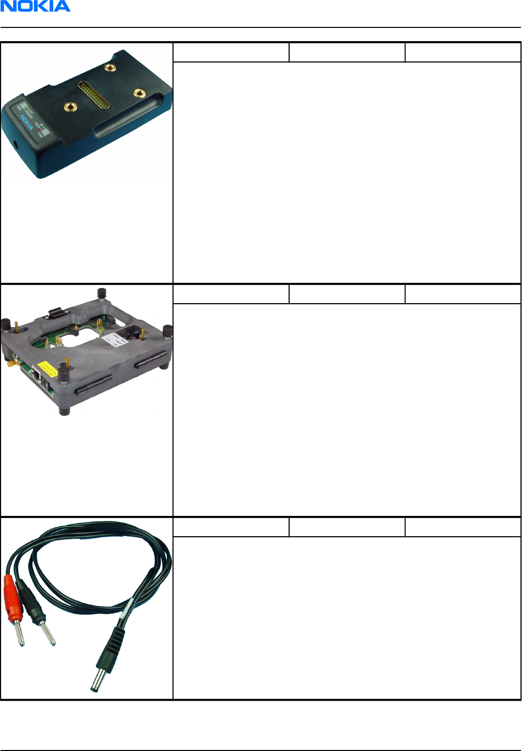
JBV-1 Docking station
The JBV-1 docking station is a general tool that has been designed for
calibration and software update use. The JBV-1 is used together with a
docking station adapter as one unit
In calibration mode the JBV-1 is powered by an external power supply:
11-16V DC. When flashing the power for the phone can be taken from
the flash prommer or external power supply: 11-16 V DC.
Note: JBV-1 main electrical functions are:
• adjustable VBATT calibration voltage, current measurement
limit voltage: VCHAR, current measurement: ICHAR
• adjustable ADC calibration voltage via BTEM and the BSI
signal
• BTEMP and BSI calibration resistor
• signal from FBUS to the phone via the parallel jig
• control via FBUS or USB
• Flash OK/FAIL indication
MJ-59 Module jig
MJ-59 is meant for component level troubleshooting.
The jig includes an RF interface for GSM and WCDMA. In addition, it has
the following features:
• Provides mechanical interface with Engine module
• Provides galvanic connection to all needed test pads in module
• Multiplexing between USB and FBUS media, controlled by Vusb
• UI test interface
• MMC interface
• Duplicated SIM connector
• Audio components: IHF, MIC, earpiece
• Connector for control unit
•Access for Pop-PortTM system connector
Note: In the picture CU-4 is connected to MJ-59 . CU-4 is not part
of the MJ-59 sales package and has to be ordered separately.
PCS-1 Power cable
The PCS-1 power cable (DC) is used with a docking station, a module jig
or a control unit to supply a controlled operating voltage.
RM-74
Nokia Customer Care Service Tools
Page 4–8 Company Confidential 9242678 (Issue 1)
Copyright ©2005 Nokia. All Rights Reserved.
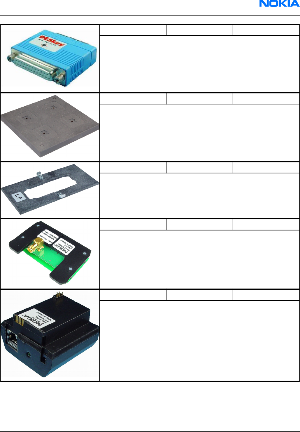
PKD-1 SW security device
SW security device is a piece of hardware enabling the use of the service
software when connected to the parallel (LPT) port of the PC.
Without the device, it is not possible to use the service software.
Printer or any such device can be connected to the PC through the device
if needed.
RJ-51 PA Rework jig
To be used with ST-30!
RJ-79 Soldering jig
The soldering jig RJ-79 is used for soldering and as a rework jig for system
module. It is made of lead-free rework compatible material.
SA-41 RF Coupler
SA-41 RF Coupler is used for Go/No-Go test after changing components
in the RF part of the phone.
The SA-41 is mounted on the docking station adapter, after which the
phone can be placed in the docking station adapter.
Note: For RF attenuation values, please refer to the Service
bulletin.
SF-10 POS flash adapter
The POS flash adapter SF-10 allows FBUS/MBUS connections for flashing.
RM-74
Service Tools Nokia Customer Care
9242678 (Issue 1) Company Confidential Page 4–9
Copyright ©2005 Nokia. All Rights Reserved.
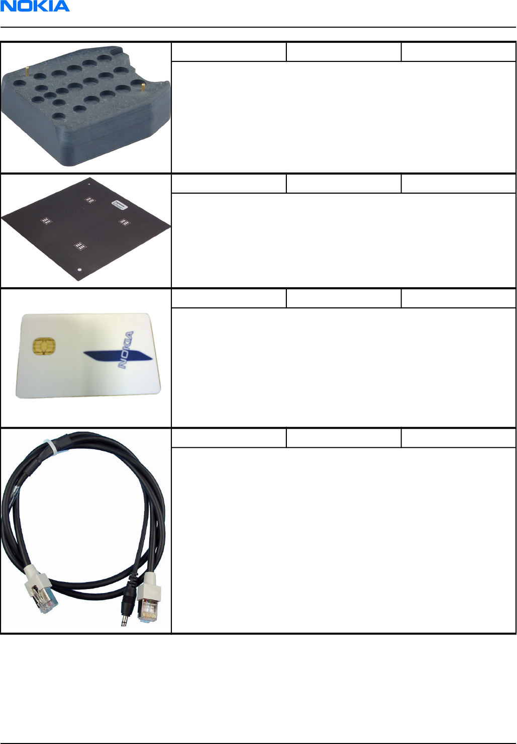
SS-54 Alignment Jig
Alignment jig is used to efficiently assemble the dome-sheet to the
pone's PWB. The jig is made of EDS proof material.
ST-30 Rework stencil
Front End Module (FEM)
SX-4 Smart card
SX-4 is a BB5 security device used to protect critical features in tuning
and testing.
SX-4 is also needed together with FPS-10 when DCT-4 phones are flashed.
XCS-1 Service cable
The XCS-1 service cable is used to connect FLS-4S to the POS flash adapter
for supplying a controlled operating voltage and data connection.
RM-74
Nokia Customer Care Service Tools
Page 4–10 Company Confidential 9242678 (Issue 1)
Copyright ©2005 Nokia. All Rights Reserved.
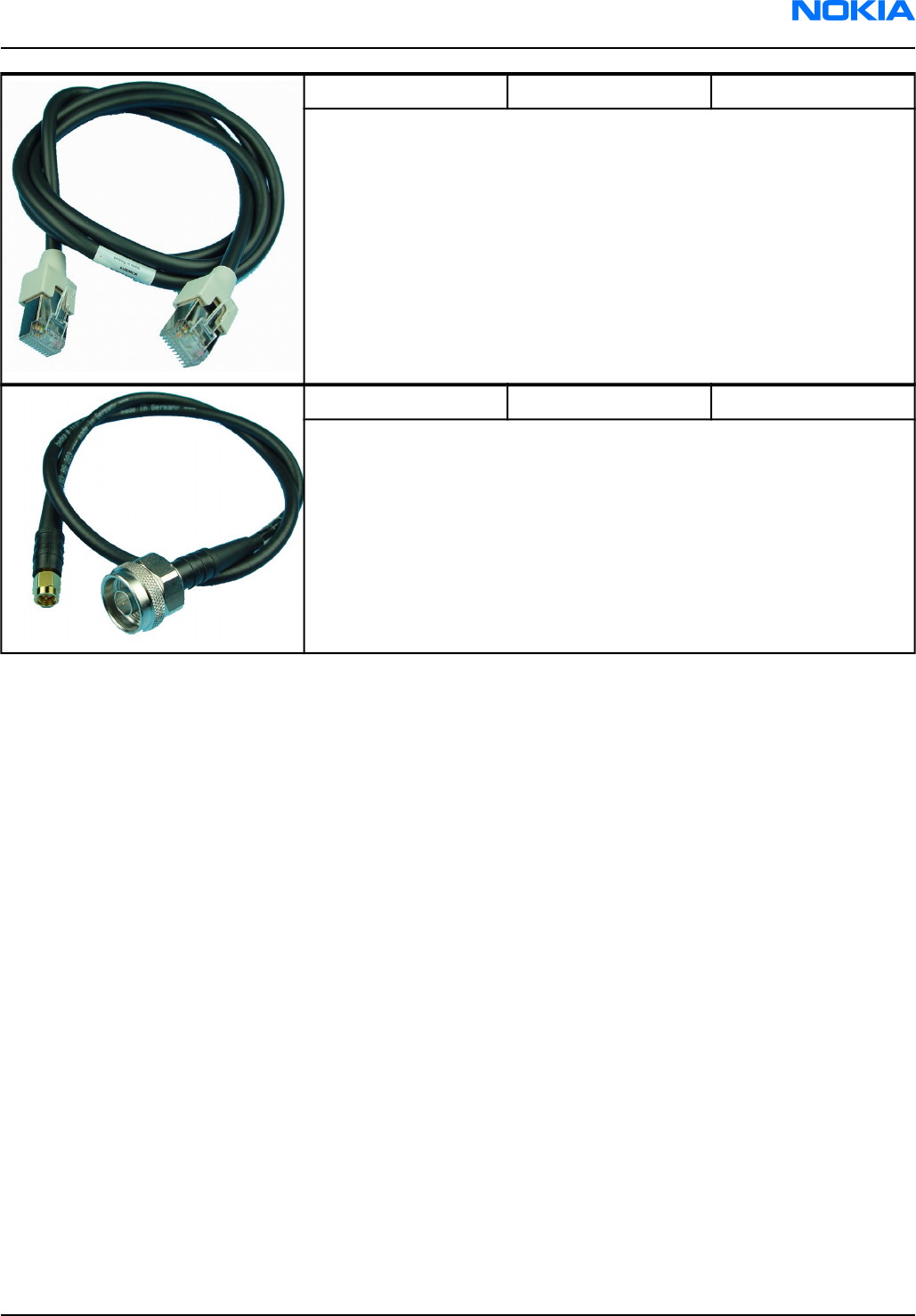
XCS-4 Modular cable
XCS-4 is a shielded (one specially shielded conductor) modular cable for
flashing and service purposes.
XRF-1 RF cable
The RF cable is used to connect, for example, a module repair jig to the
RF measurement equipment.
SMA to N-Connector ca. 610mm.
Attenuation for:
• GSM850/900: 0.3+-0.1 dB
• GSM1800/1900: 0.5+-0.1 dB
• WLAN: 0.6+-0.1dB
RM-74
Service Tools Nokia Customer Care
9242678 (Issue 1) Company Confidential Page 4–11
Copyright ©2005 Nokia. All Rights Reserved.
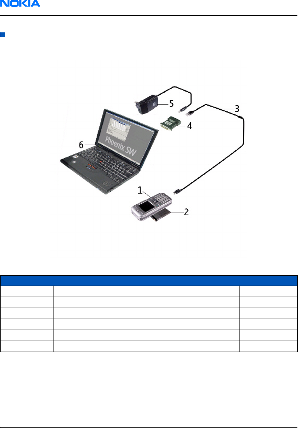
Service software concept
POS (Point of Sales) flash concept
Figure 73 POS flash concept
Item Description Type
1Phone
2 Battery
3 Easy flash cable CA-67DS
4 FLS-4S sales pack FLS-4S
5 AC charger ACF-8
6 PC with Service SW CD-ROM
RM-74
Nokia Customer Care Service Tools
Page 4–12 Company Confidential 9242678 (Issue 1)
Copyright ©2005 Nokia. All Rights Reserved.
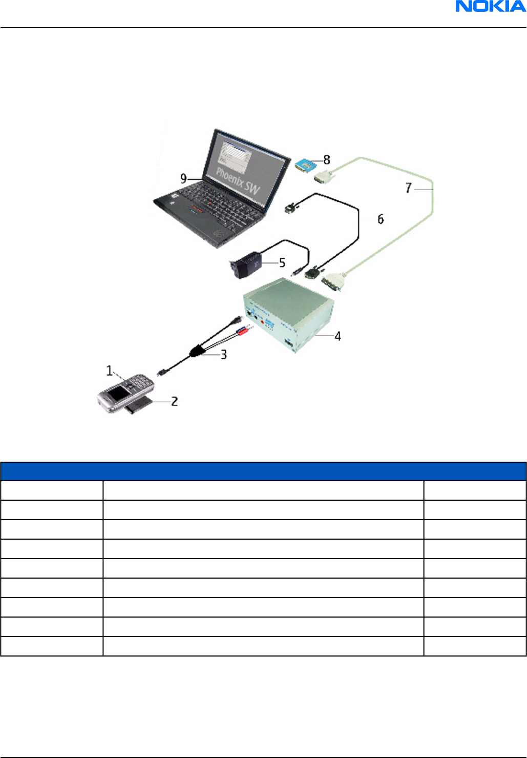
FPS-8 Prommer box flash concept
Figure 74 FPS-8 Prommer box flash concept
Item Description Type
1Phone
2 Battery
3 Service cable CA-65DS
4 Flash prommer box sales pack including 2 pcs SF12 SRAM FPS-8
5 AC Charger, included in FPS-8 sales package ACF-8
6 RS-232 (D9 – D9) cable, included in FPS-8 sales pack AXS-4
6 Printer cable, included in FPS-8 sales package
8 Software protection key PKD-1
9 PC with service SW
Note: More than 32MB SRAM required in FPS-8.
RM-74
Service Tools Nokia Customer Care
9242678 (Issue 1) Company Confidential Page 4–13
Copyright ©2005 Nokia. All Rights Reserved.
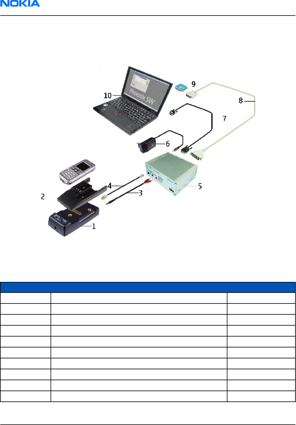
JBV-1 flash concept
Figure 75 JBV-1 flash concept
Item Description Type
1Docking station JBV-1
2 Docking station adapter DA-49
3 DC power cable PCS-1
4 Modular cable XCS-4
5 Flash prommer box sales pack FPS-8
6 Power supply, included in FPS-8 sales package AFC-8
7 RS-232 (D9 – D9) cable, included in FPS-8 sales package AXS-4
8 Printer cable, included in FPS-8 sales package
9 Software protection key PKD-1
10 Service SW (PHOENIX)
Note: More than 32MB SRAM required in FPS-8.
RM-74
Nokia Customer Care Service Tools
Page 4–14 Company Confidential 9242678 (Issue 1)
Copyright ©2005 Nokia. All Rights Reserved.
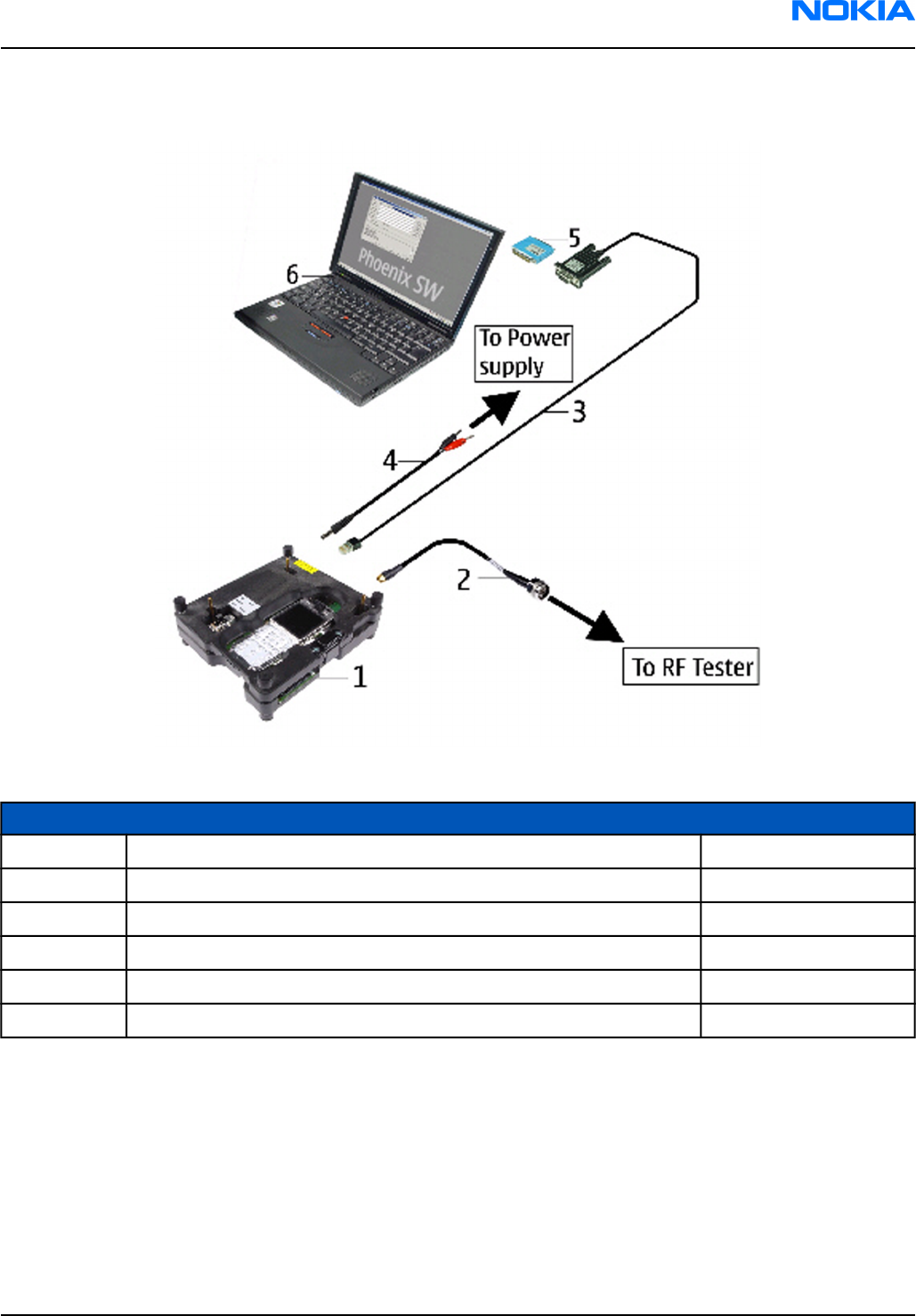
Module jig (MJ-59) service concept
Figure 76 Module jig service concept
Item Description Type
1Module jig MJ-59
2 RF test cable XCF-4
3 Service MBUS/FBUS cable DAU-9S
4 DC power cable PCS-1
5 Software protection key PKD-1
6 PC with Service SW (PHOENIX)
RM-74
Service Tools Nokia Customer Care
9242678 (Issue 1) Company Confidential Page 4–15
Copyright ©2005 Nokia. All Rights Reserved.

RM-74
Nokia Customer Care Service Tools
(This page left intentionally blank.)
Page 4–16 Company Confidential 9242678 (Issue 1)
Copyright ©2005 Nokia. All Rights Reserved.

5 — Disassembly and
reassembly instructions
Nokia Customer Care
9242678 (Issue 1) Company Confidential Page 5–1
Copyright ©2005 Nokia. All Rights Reserved.

RM-74
Nokia Customer Care Disassembly and reassembly instructions
(This page left intentionally blank.)
Page 5–2 Company Confidential 9242678 (Issue 1)
Copyright ©2005 Nokia. All Rights Reserved.

Table of Contents
Disassembly instructions..............................................................................................................................................................5–5
Reassembly instructions...............................................................................................................................................................5–9
RM-74
Disassembly and reassembly instructions Nokia Customer Care
9242678 (Issue 1) Company Confidential Page 5–3
Copyright ©2005 Nokia. All Rights Reserved.

RM-74
Nokia Customer Care Disassembly and reassembly instructions
(This page left intentionally blank.)
Page 5–4 Company Confidential 9242678 (Issue 1)
Copyright ©2005 Nokia. All Rights Reserved.
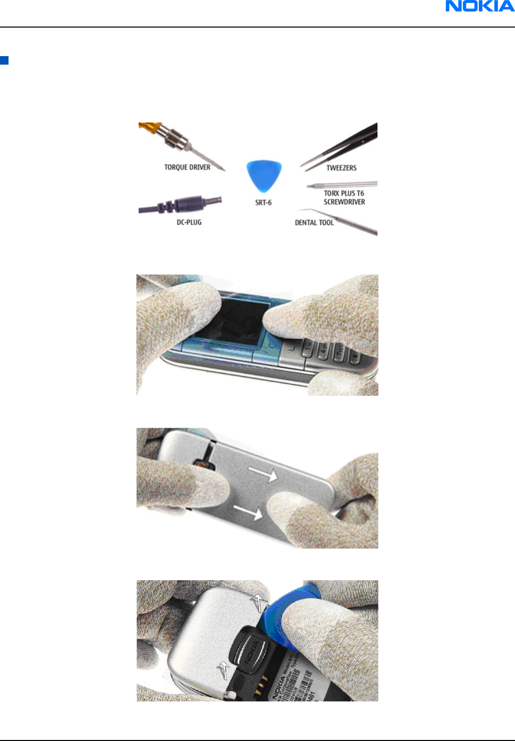
Disassembly instructions
Steps
1. Tools needed for disassembly and reassembly
2. Protect the window with a film.
3. Unlock and remove the B-cover.
4. Place the SRT-6 between the D-cover assy and the top cap as shown in the picture.
RM-74
Disassembly and reassembly instructions Nokia Customer Care
9242678 (Issue 1) Company Confidential Page 5–5
Copyright ©2005 Nokia. All Rights Reserved.
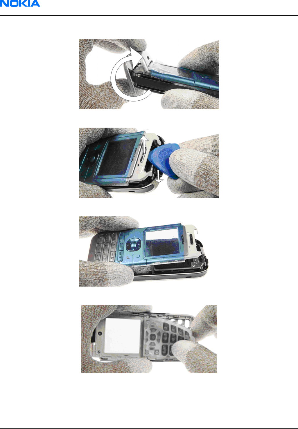
5. First turn the top cap as shown in the picture and then remove it carefully.
6. Use the SRT-6 as a lever to unlock the A-cover assy.
7. Remove the A-cover assy.
8. Remove the keymat and protect the inner side of the window with a film.
9. Unscrew the six Torx Plus size 6 screws in the shown order.
Note: For reassembly ALWAYS USE NEW SCREWS!
For reassembly, use the reverse order and a Torx Plus size 6 driver with a torque setting of 28 Ncm.
RM-74
Nokia Customer Care Disassembly and reassembly instructions
Page 5–6 Company Confidential 9242678 (Issue 1)
Copyright ©2005 Nokia. All Rights Reserved.
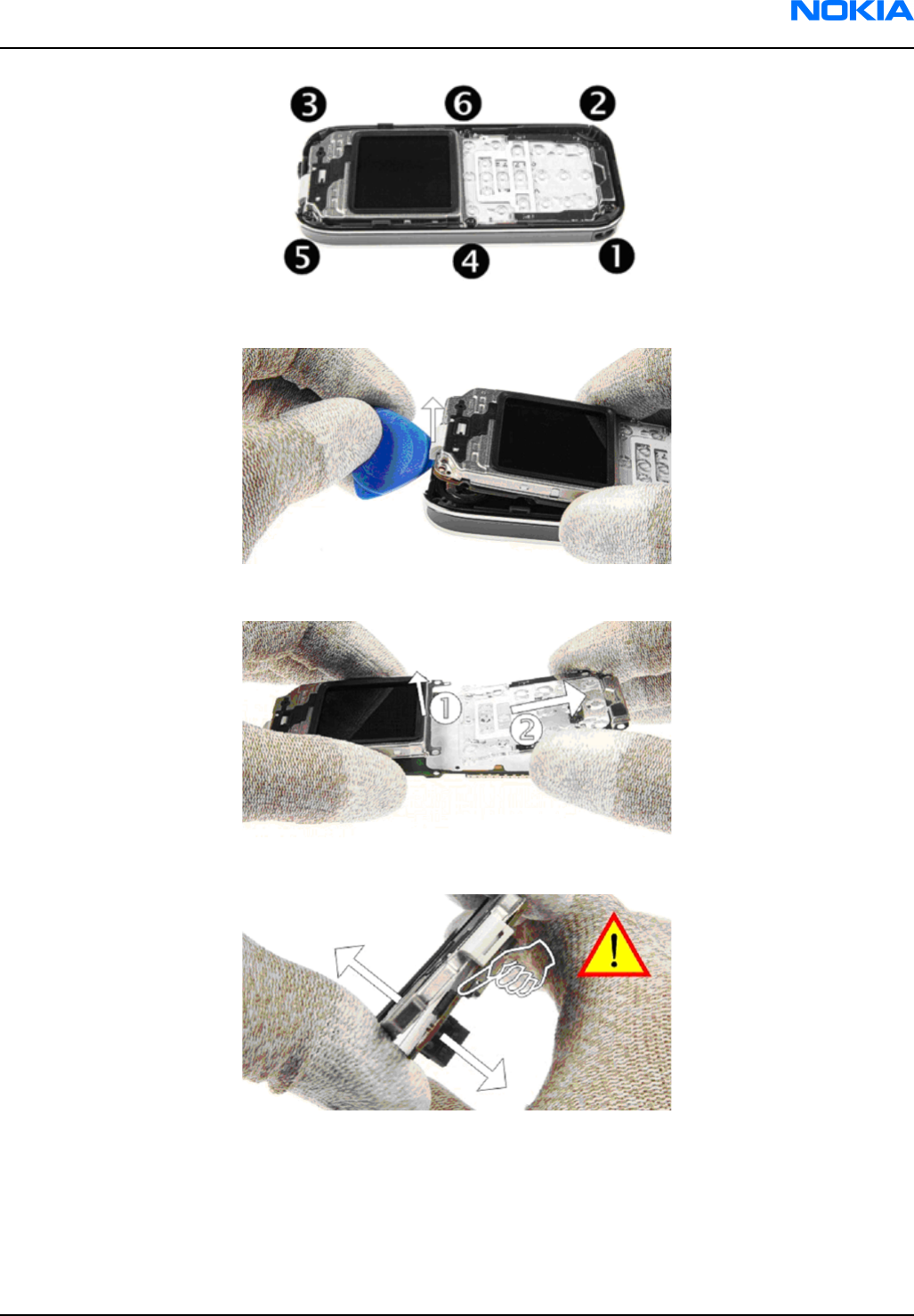
10. Lift the modules a bit with SRT-6 and remove them from the D-cover assy.
11. First, lift the LCD shielding with LCD module a little and then remove the Light guide assy.
12. Separate the modules carefully to open the board-to-board connector.
RM-74
Disassembly and reassembly instructions Nokia Customer Care
9242678 (Issue 1) Company Confidential Page 5–7
Copyright ©2005 Nokia. All Rights Reserved.
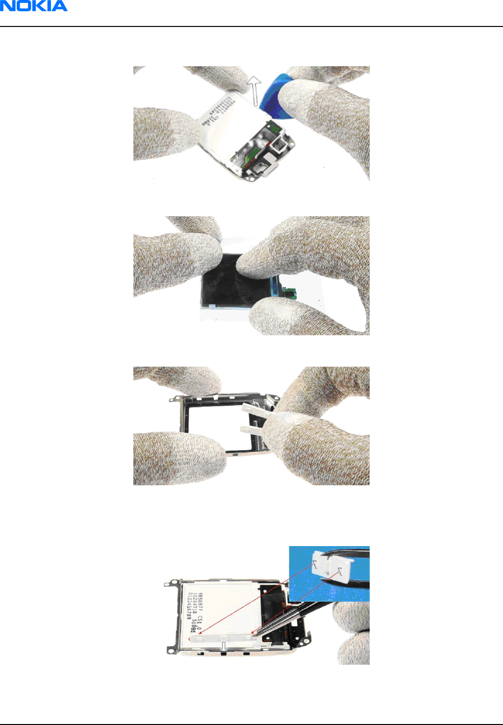
13. Unlock the LCD module...
14. ...and protect it with a film.
15. Remove the Locking clips.
16. Note: For reassembly only!
First place the LCD module into the LCD shielding and then insert the locking clips to secure the LCD
module. Note the correct position of the clips.
RM-74
Nokia Customer Care Disassembly and reassembly instructions
Page 5–8 Company Confidential 9242678 (Issue 1)
Copyright ©2005 Nokia. All Rights Reserved.
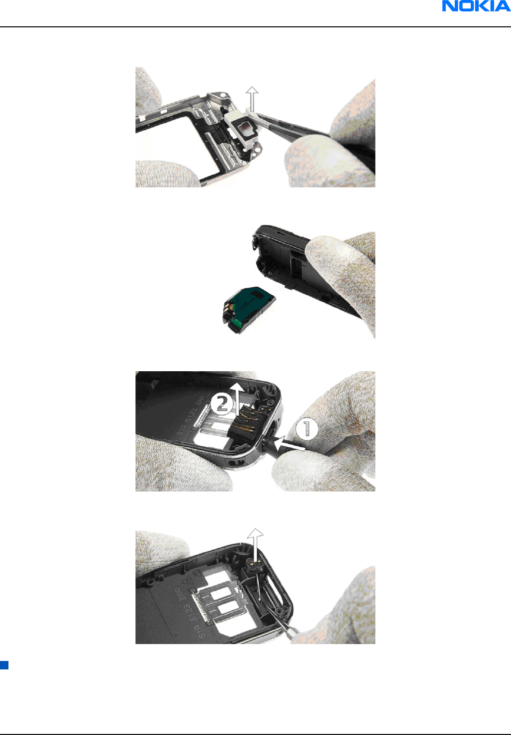
17. Remove the acoustic channel.
18. The antenna IHF assy drops out when turning the D-cover assy.
19. Press out the easy flash connector by using the DC-plug.
20. Remove the microphone with the dental tool.
Reassembly instructions
For reassembly, follow the Disassembly instructions, but in reversed order
Note: Pay special attention to step 16 and 9.
Note: For reassembly, ALWAYS USE NEW SCREWS.
RM-74
Disassembly and reassembly instructions Nokia Customer Care
9242678 (Issue 1) Company Confidential Page 5–9
Copyright ©2005 Nokia. All Rights Reserved.

RM-74
Nokia Customer Care Disassembly and reassembly instructions
(This page left intentionally blank.)
Page 5–10 Company Confidential 9242678 (Issue 1)
Copyright ©2005 Nokia. All Rights Reserved.

6 — Baseband
troubleshooting
Nokia Customer Care
9242678 (Issue 1) Company Confidential Page 6–1
Copyright ©2005 Nokia. All Rights Reserved.

RM-74
Nokia Customer Care Baseband troubleshooting
(This page left intentionally blank.)
Page 6–2 Company Confidential 9242678 (Issue 1)
Copyright ©2005 Nokia. All Rights Reserved.

Table of Contents
General baseband troubleshooting..........................................................................................................................................6–5
Phone is dead.............................................................................................................................................................................6–5
Flash programming do not work.........................................................................................................................................6–6
Easy flash programming does not work............................................................................................................................6–7
Power does not stay on or the phone is jammed...........................................................................................................6–9
Display shows "Contact Service"........................................................................................................................................6–10
The phone does not register to the networks, or the phone can not make a call............................................6–11
SIM related faults..........................................................................................................................................................................6–12
Insert SIM card fault...............................................................................................................................................................6–12
SIM card rejected.....................................................................................................................................................................6–12
User interface.................................................................................................................................................................................6–13
Blank display............................................................................................................................................................................6–13
Display is corrupt....................................................................................................................................................................6–13
Dead keys..................................................................................................................................................................................6–14
No backlight for display or keys.........................................................................................................................................6–14
Audio troubleshooting................................................................................................................................................................6–16
Audio troubleshooting using phoenix.............................................................................................................................6–16
Check microphone using "Hp microphone in Ext speaker out" loop.....................................................................6–17
Check earpiece using "Ext microphone in Hp speaker out" loop.............................................................................6–18
Check IHF & ringing tone function using "Buzzer".......................................................................................................6–18
Check vibra function using "Vibra control".....................................................................................................................6–19
Earpiece fault...........................................................................................................................................................................6–20
IHF/ringing tone fault............................................................................................................................................................6–21
Headset earpiece fault..........................................................................................................................................................6–22
Microphone fault.....................................................................................................................................................................6–23
Headset microphone fault...................................................................................................................................................6–24
List of Figures
Figure 77 Phone is dead troubleshooting...............................................................................................................................6–6
Figure 78 Flash programming fault..........................................................................................................................................6–7
Figure 79 Easy flash programming fault..................................................................................................................................6–8
Figure 80 Power does not stay on or the phone is jammed.............................................................................................6–9
Figure 81 Troubleshooting when the "Contact Service" message is seen.................................................................6–10
Figure 82 No registering or call................................................................................................................................................6–11
Figure 83 Insert SIM card fault..................................................................................................................................................6–12
Figure 84 Signal diagram...........................................................................................................................................................6–12
Figure 85 Signal diagram...........................................................................................................................................................6–13
Figure 86 Blank display...............................................................................................................................................................6–13
Figure 87 Display is corrupt.......................................................................................................................................................6–14
Figure 88 Dead keys.....................................................................................................................................................................6–14
Figure 89 No backlight for display or keys...........................................................................................................................6–15
Figure 90 Phoenix audio test window...................................................................................................................................6–16
Figure 91 PWB audio test points.............................................................................................................................................6–17
Figure 92 Test arrangement for microphone......................................................................................................................6–18
Figure 93 Test arrangement for of earpiece........................................................................................................................6–18
Figure 94 Checking IHF and ring tone by using "Buzzer".................................................................................................6–19
Figure 95 Checking vibra function by using vibra control...............................................................................................6–19
Figure 96 Earpiece fault flow chart.........................................................................................................................................6–20
Figure 97 IHF/ringing tone fault flow chart.........................................................................................................................6–21
RM-74
Baseband troubleshooting Nokia Customer Care
9242678 (Issue 1) Company Confidential Page 6–3
Copyright ©2005 Nokia. All Rights Reserved.

Figure 98 Headset earpiece fault flow chart........................................................................................................................6–22
Figure 99 Microphone fault flow chart..................................................................................................................................6–23
Figure 100 Headset microphone fault flow chart..............................................................................................................6–24
RM-74
Nokia Customer Care Baseband troubleshooting
Page 6–4 Company Confidential 9242678 (Issue 1)
Copyright ©2005 Nokia. All Rights Reserved.

General baseband troubleshooting
Phone is dead
This means that the phone does not use any current at all when the supply is connected and/or power key is
pressed.
It is assumed that the voltage supplied is 3.6 VDC. The UEMCLite will prevent any functionality at battery/supply
levels below 2.9 VDC.
RM-74
Baseband troubleshooting Nokia Customer Care
9242678 (Issue 1) Company Confidential Page 6–5
Copyright ©2005 Nokia. All Rights Reserved.
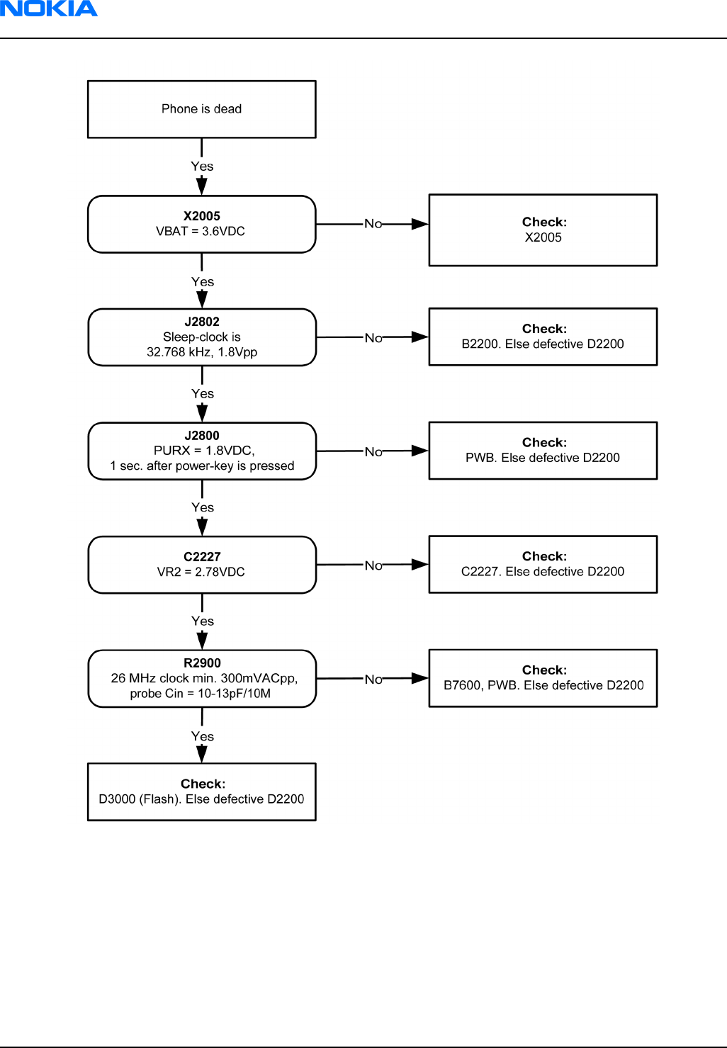
Figure 77 Phone is dead troubleshooting
Flash programming do not work
The flash programming can be done via the pads on the PWB (J2060).
In case of Flash failure in FLALI station, swap the phone and send it back to the care program for further analysis.
Possible failures could be short-circuit of balls under µBGAs (UEMCLite, UPP4M, FLASH). Missing or misaligned
components. In flash programming error cases the flash prommer can give some information about a fault. The
fault information messages could be:
Phone doesn't set FBUS_TX line low
RM-74
Nokia Customer Care Baseband troubleshooting
Page 6–6 Company Confidential 9242678 (Issue 1)
Copyright ©2005 Nokia. All Rights Reserved.
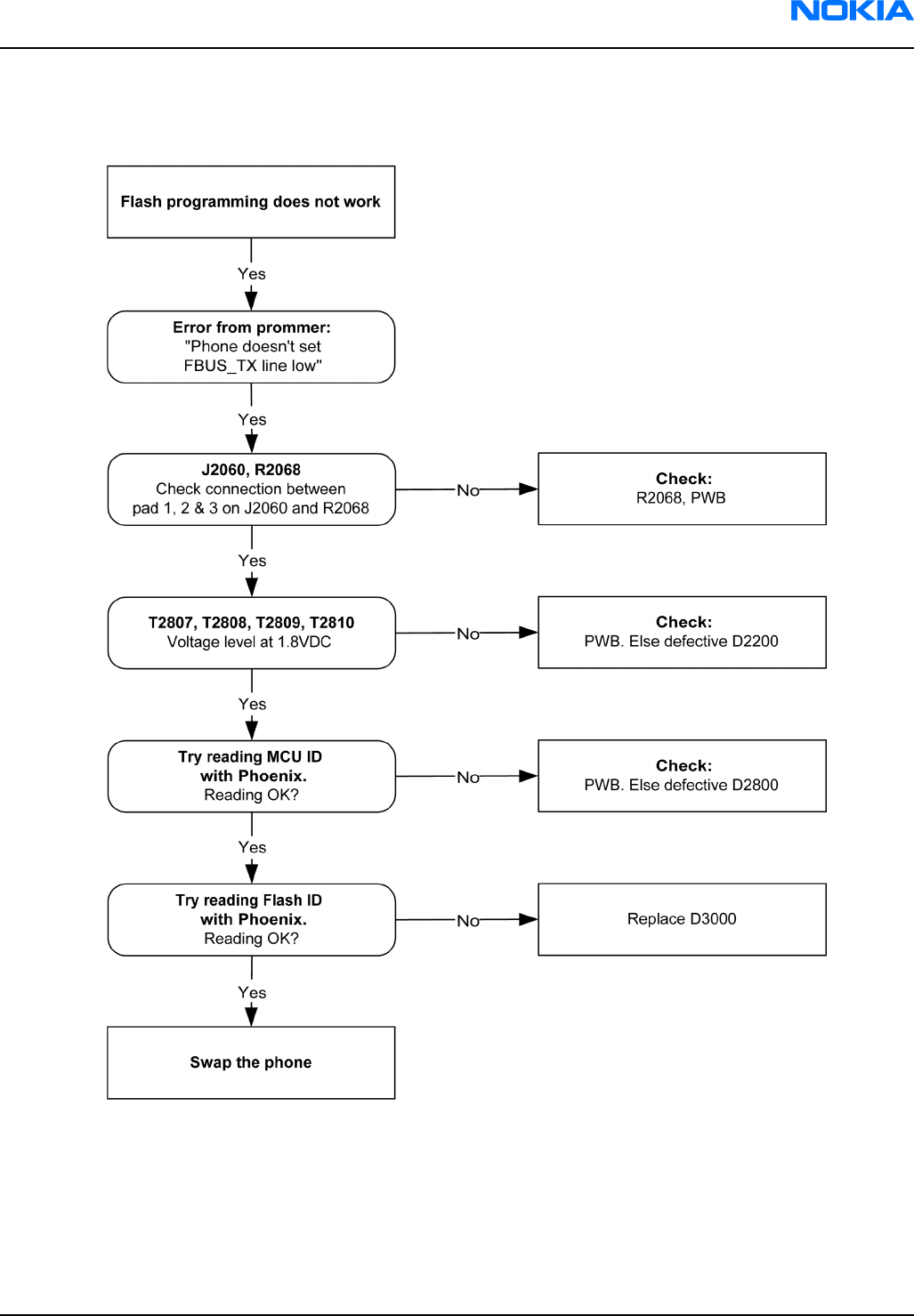
Because of the use of uBGA components it is not possible to verify if there is a short circuit in control- and address
lines of MCU (UPP4M) and memory (flash).
Figure 78 Flash programming fault
Easy flash programming does not work
The flash programming can also be done via the easy flash connector.
RM-74
Baseband troubleshooting Nokia Customer Care
9242678 (Issue 1) Company Confidential Page 6–7
Copyright ©2005 Nokia. All Rights Reserved.
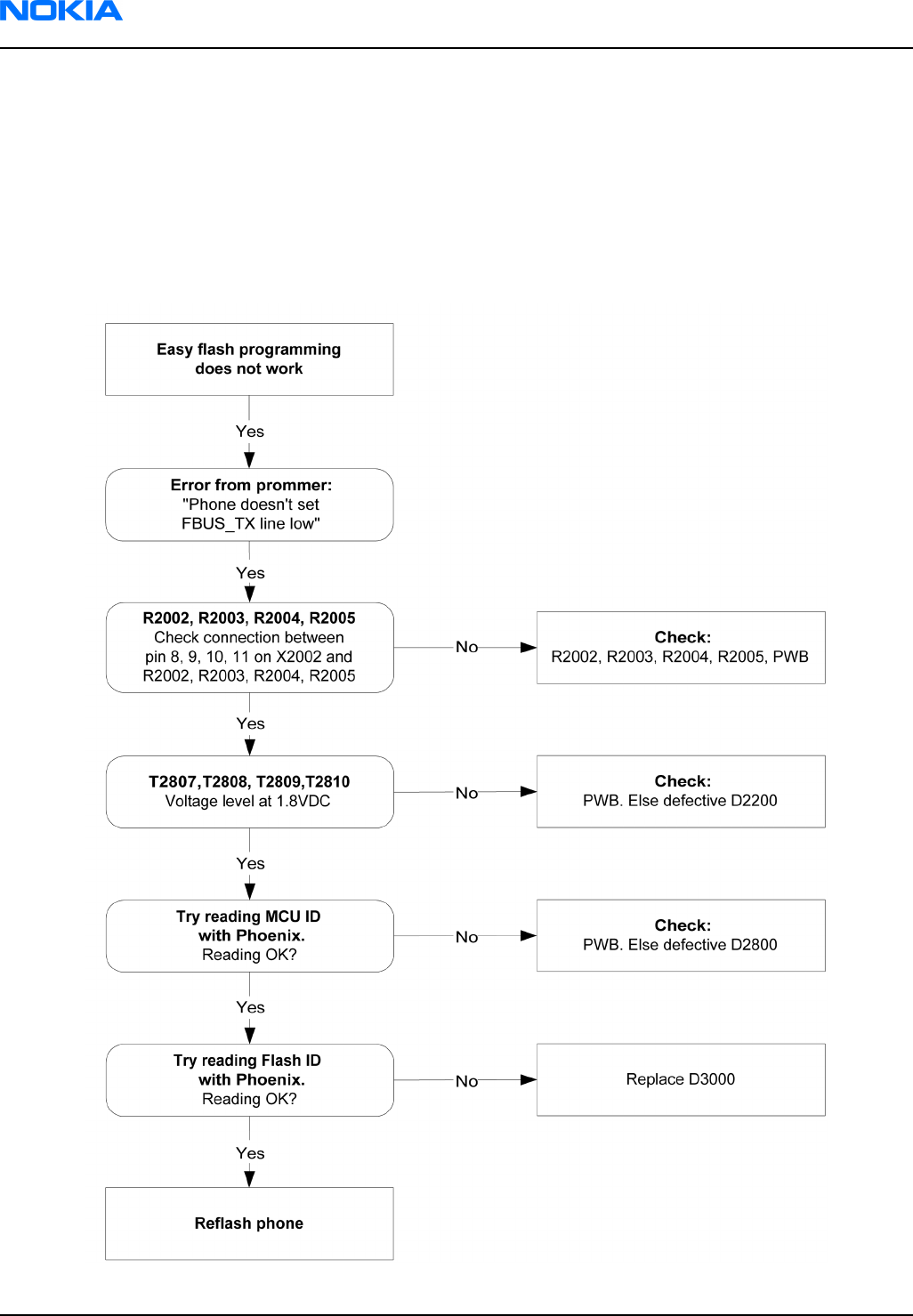
In case of Flash failure in FLALI station, swap the phone and send it back to the care program for further analysis.
Possible failures could be short-circuit of balls under µBGAs (UEMCLite, UPP4M, FLASH). Missing or misaligned
components.
In flash programming error cases the flash prommer can give some information about a fault. The fault
information messages could be:
- Phone does not set FBUS_TX line low
Because of the use of uBGA components it is not possible to verify if there is a short circuit in control- and address
lines of MCU (UPP4M) and memory (flash).
Figure 79 Easy flash programming fault
RM-74
Nokia Customer Care Baseband troubleshooting
Page 6–8 Company Confidential 9242678 (Issue 1)
Copyright ©2005 Nokia. All Rights Reserved.
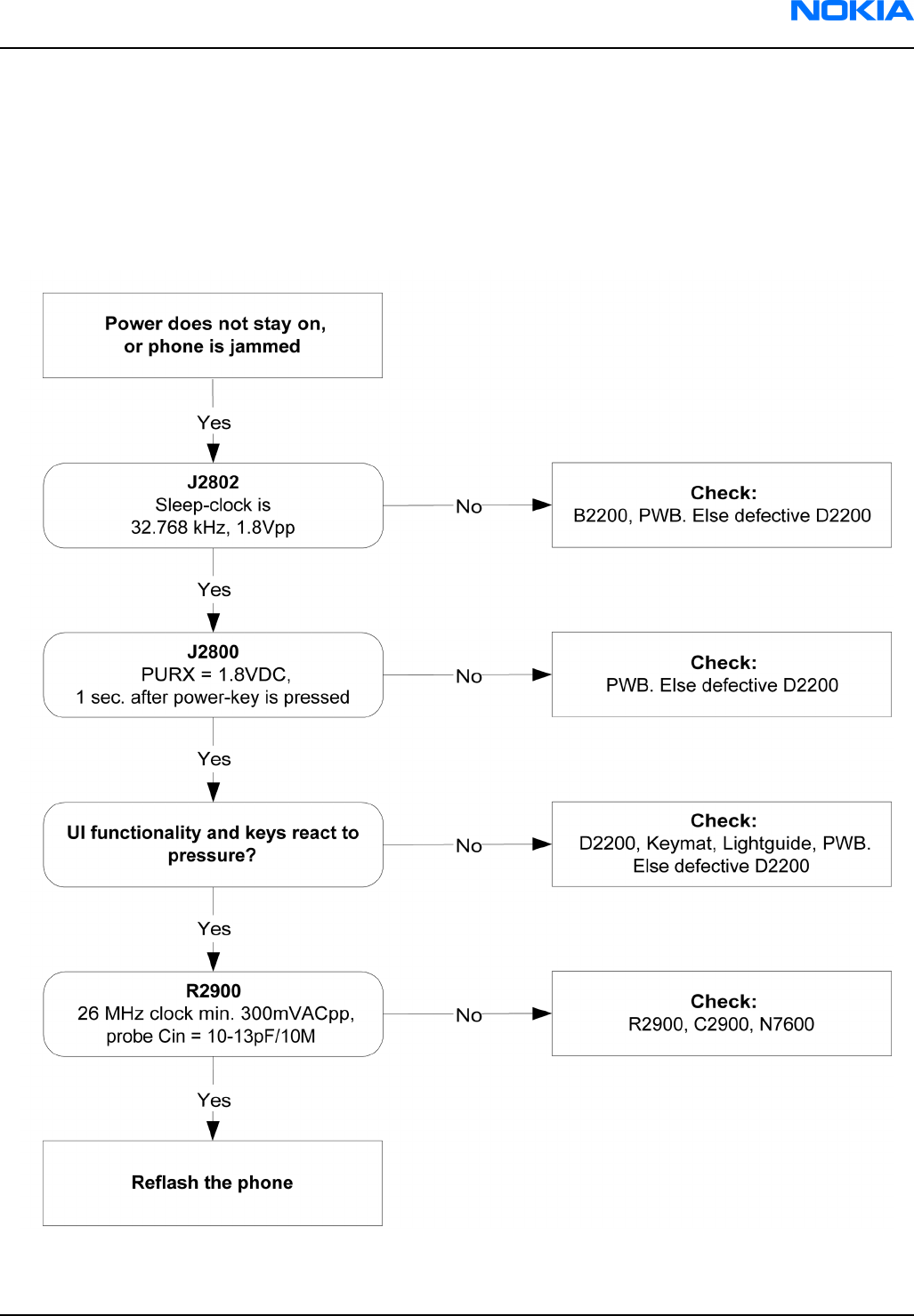
Power does not stay on or the phone is jammed
If this kind of a failure is presenting itself immediately after FLALI, it is most likely caused by ASIC's missing
contact with PWB.
If the MCU doesn’t service the watchdog register within the UEMCLite, the operations watchdog will run out
after approximately 32 seconds. Unfortunately, the service routine can not be measured.
Figure 80 Power does not stay on or the phone is jammed
RM-74
Baseband troubleshooting Nokia Customer Care
9242678 (Issue 1) Company Confidential Page 6–9
Copyright ©2005 Nokia. All Rights Reserved.
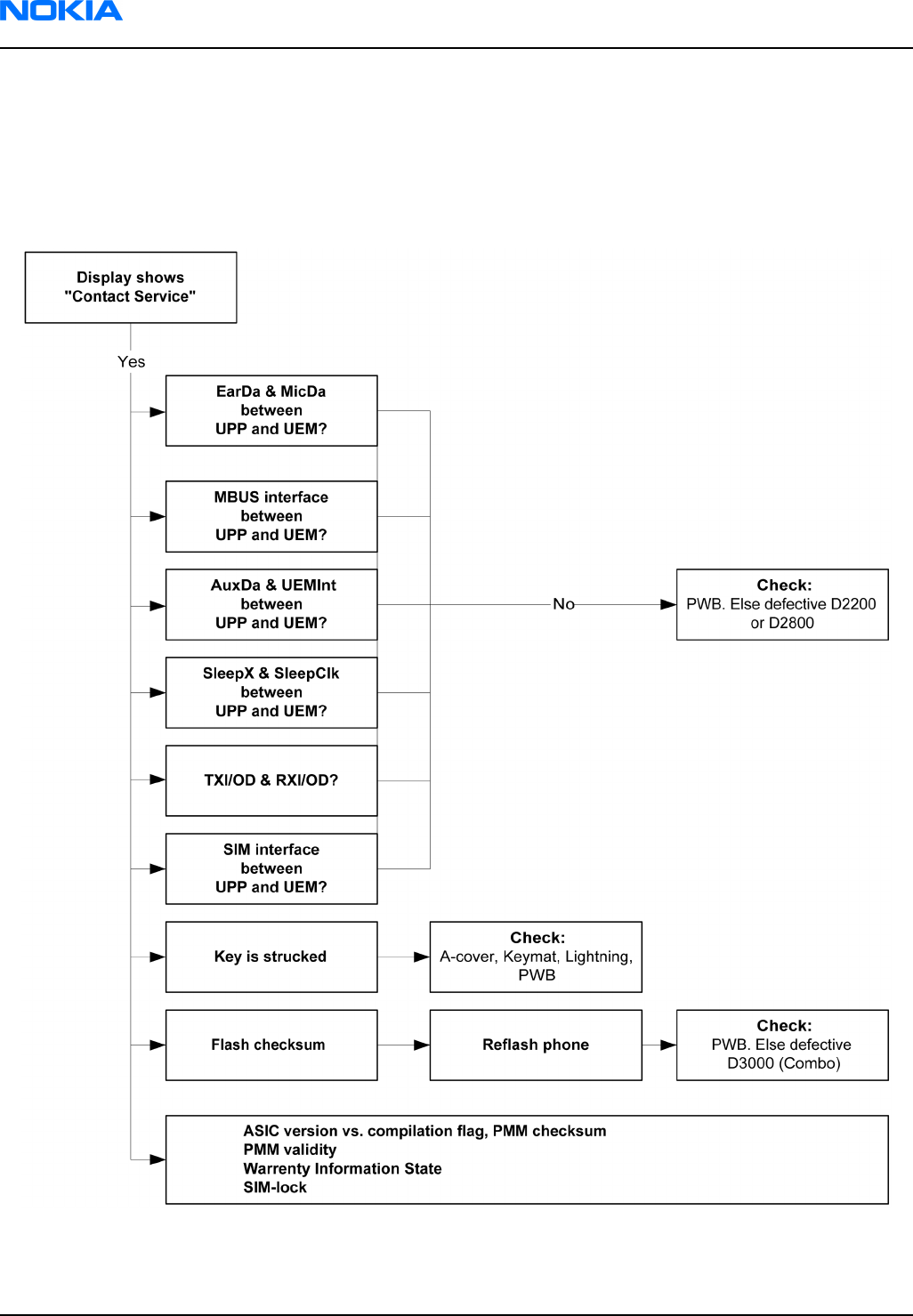
Display shows "Contact Service"
This error can only happen at power up where several self-tests is run. If any of these test cases fails the display
will show the message: "Contact Service".
It's individual test cases so the below lineup of error hunting's has no chronological order. Use common sense
and experience to decide which test case to start error hunting at.
Figure 81 Troubleshooting when the "Contact Service" message is seen
RM-74
Nokia Customer Care Baseband troubleshooting
Page 6–10 Company Confidential 9242678 (Issue 1)
Copyright ©2005 Nokia. All Rights Reserved.
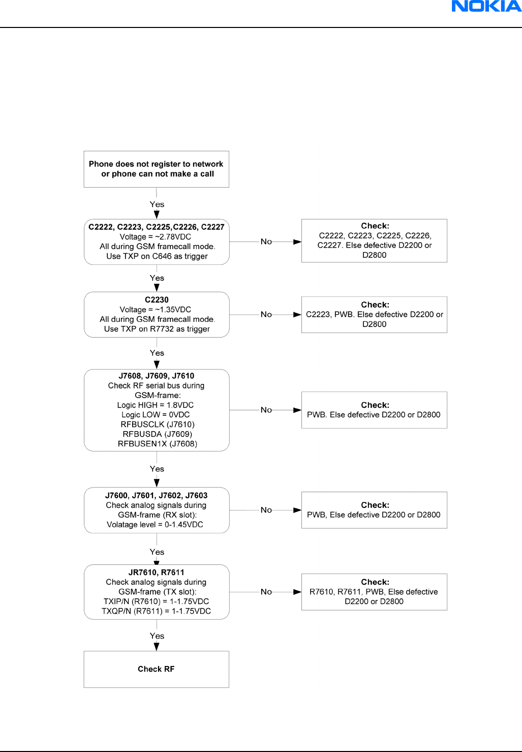
The phone does not register to the networks, or the phone can not make a call
If the phone doesn't register to the network, the fault can be in either BB or RF. Only few signals can be tested
since several signals is 'buried' in one or more of the inner layers of the PWB.
First of all check that SIM LOCK is not causing the error by using a Test-SIM card and connect the phone to a tester.
Figure 82 No registering or call
RM-74
Baseband troubleshooting Nokia Customer Care
9242678 (Issue 1) Company Confidential Page 6–11
Copyright ©2005 Nokia. All Rights Reserved.
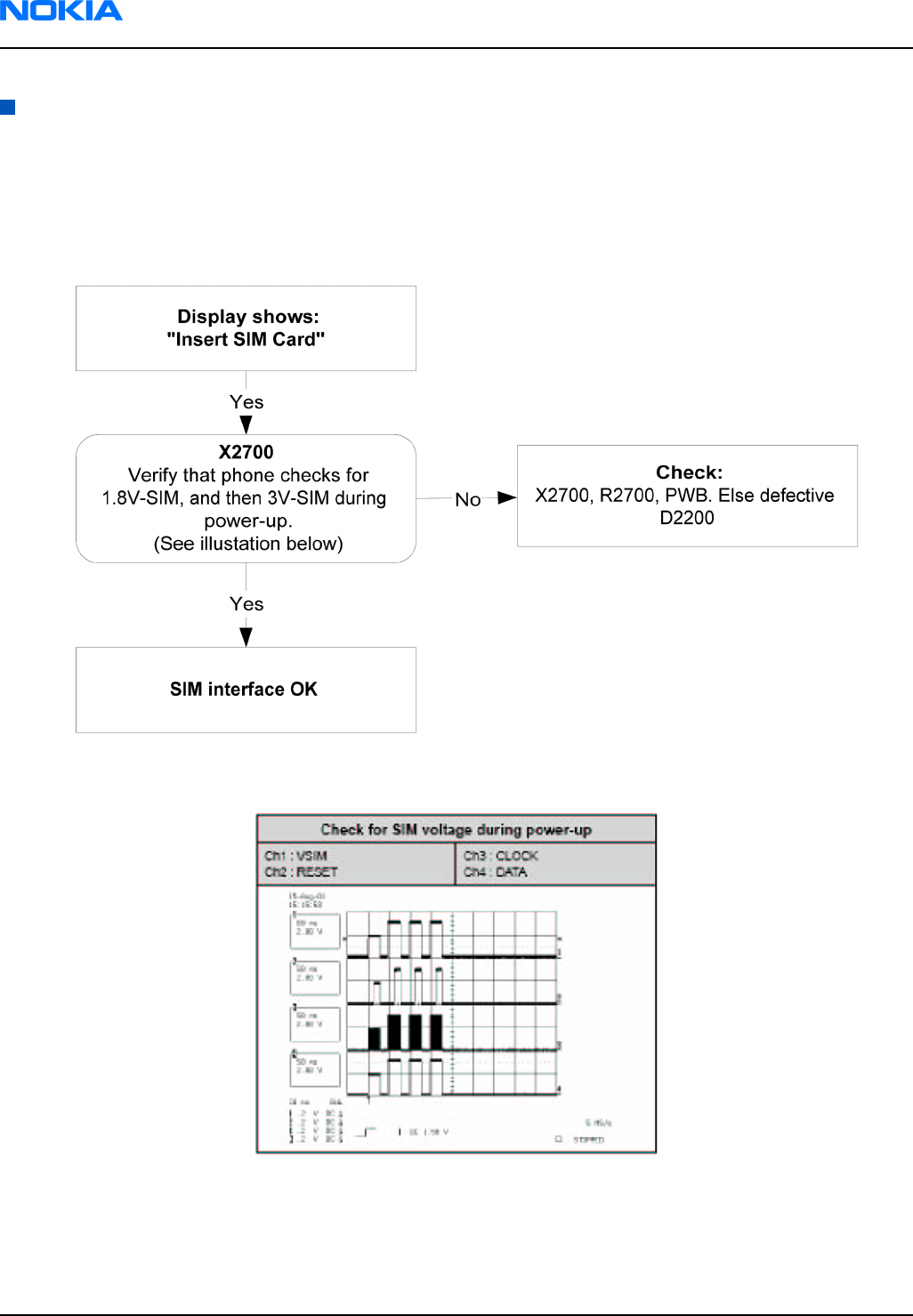
SIM related faults
Insert SIM card fault
The hardware of the SIM interface from UEMCLite (D2200) to the SIM connector (X2700) can be tested without
a SIM card. When the power is switched on the phone first check for a 1.8 V SIM card and then a 3 V SIM card.
The phone will try this four times, where after it will display ”Insert SIM card”.
Figure 83 Insert SIM card fault
Figure 84 Signal diagram
SIM card rejected
The error ”SIM card rejected” means that the ATR message received from SIM card is corrupted, e.g. data signal
levels are wrong. The first data is always ATR and it is sent from card to phone.
RM-74
Nokia Customer Care Baseband troubleshooting
Page 6–12 Company Confidential 9242678 (Issue 1)
Copyright ©2005 Nokia. All Rights Reserved.
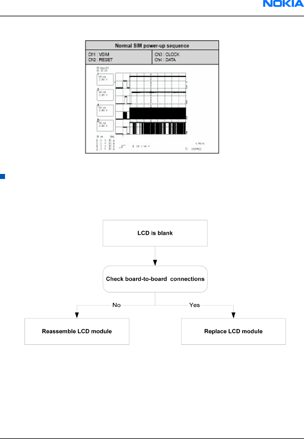
For reference a picture with normal SIM power-up is shown below.
Figure 85 Signal diagram
User interface
Blank display
The display does not show any information at all.
Figure 86 Blank display
Display is corrupt
The display contains missing or fading segments or color presentation is incorrect.
RM-74
Baseband troubleshooting Nokia Customer Care
9242678 (Issue 1) Company Confidential Page 6–13
Copyright ©2005 Nokia. All Rights Reserved.
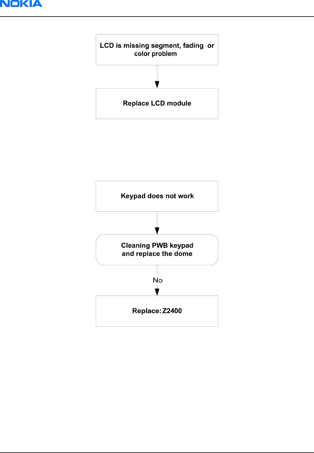
Figure 87 Display is corrupt
Dead keys
Not a single key is responding.
Figure 88 Dead keys
No backlight for display or keys
There is no backlight on the display or on the keys.
RM-74
Nokia Customer Care Baseband troubleshooting
Page 6–14 Company Confidential 9242678 (Issue 1)
Copyright ©2005 Nokia. All Rights Reserved.
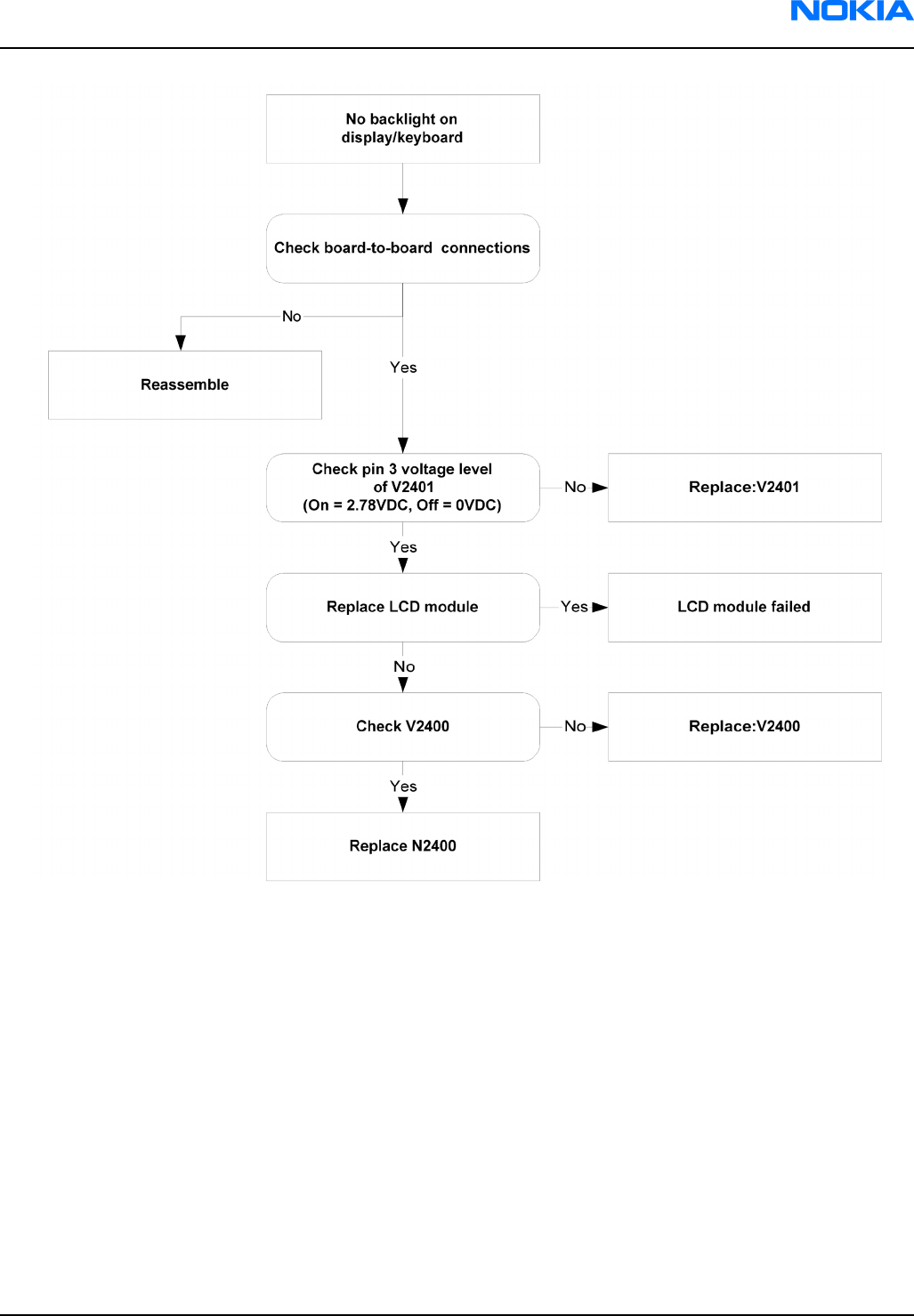
Figure 89 No backlight for display or keys
RM-74
Baseband troubleshooting Nokia Customer Care
9242678 (Issue 1) Company Confidential Page 6–15
Copyright ©2005 Nokia. All Rights Reserved.
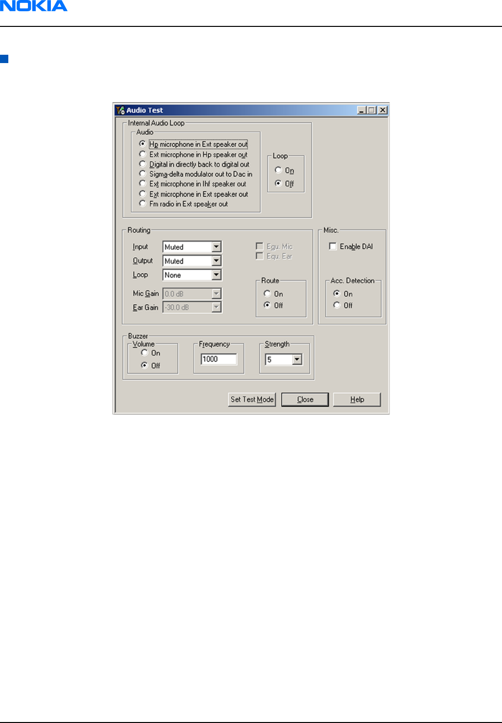
Audio troubleshooting
Audio troubleshooting using phoenix
Figure 90 Phoenix audio test window
RM-74
Nokia Customer Care Baseband troubleshooting
Page 6–16 Company Confidential 9242678 (Issue 1)
Copyright ©2005 Nokia. All Rights Reserved.
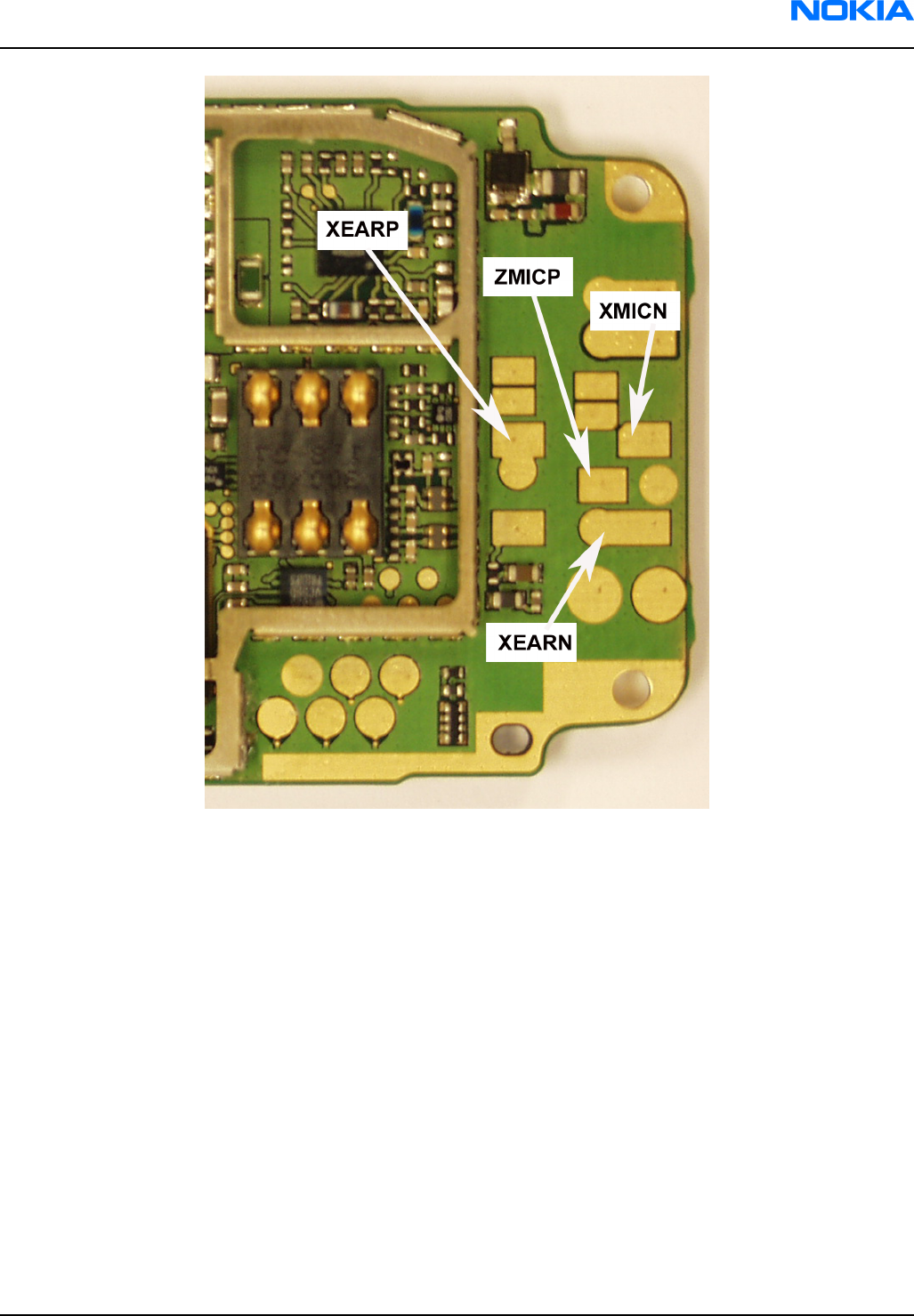
Figure 91 PWB audio test points
Check microphone using "Hp microphone in Ext speaker out" loop
Steps
1. Connect phone with Phoenix.
2. Open “audio test” window from “Testing -> Audio test”, as shown in Figure Phoenix audio test window above.
3. Select “Hp microphone in Ext speaker out”
4. Select “Loop” as “On”
5. Input sound at microphone port, for example 94 dB SPL 1 kHz.
6. Check if signal is detected at XEARP/N pads, shown in Figure PWB audio test points above.
RM-74
Baseband troubleshooting Nokia Customer Care
9242678 (Issue 1) Company Confidential Page 6–17
Copyright ©2005 Nokia. All Rights Reserved.
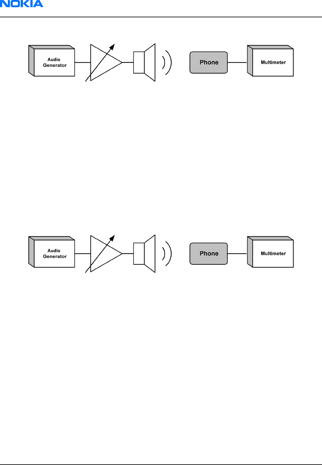
Figure 92 Test arrangement for microphone
Check earpiece using "Ext microphone in Hp speaker out" loop
Steps
1. Connect phone with Phoenix.
2. Open “audio test” window from “Testing -> Audio test”, as shown in Figure Phoenix audio test window above.
3. Select “Ext microphone in Hp speaker out”
4. Select “Loop” as “On”
5. Input signal to XMICP/N pads, as shown in Figure PWB audio test points above, for example 100 mVpp, 1 kHz.
6. Check if sound is heard in earpiece.
Figure 93 Test arrangement for of earpiece
Check IHF & ringing tone function using "Buzzer"
Steps
1. Connect phone with Phoenix.
2. Open “audio test” window from “Testing -> Audio test”, as shown in Figure Phoenix audio test window above.
3. In “Buzzer” area, select suitable signal to be played, for example 1 kHz, Strength 5”
4. Select “Volume” as “On”
5. Check if sound is heard in IHF.
RM-74
Nokia Customer Care Baseband troubleshooting
Page 6–18 Company Confidential 9242678 (Issue 1)
Copyright ©2005 Nokia. All Rights Reserved.
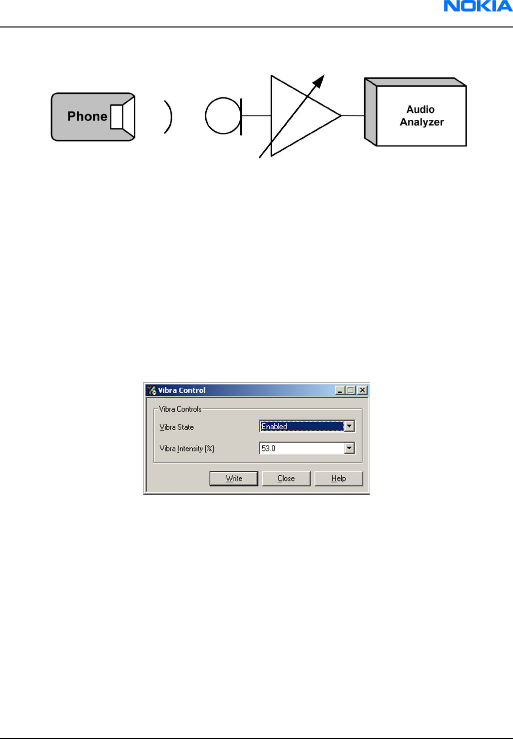
Figure 94 Checking IHF and ring tone by using "Buzzer"
Check vibra function using "Vibra control"
Steps
1. Connect phone with Phoenix.
2. Open “Vibra control” window from “Testing -> Vibra control”, as shown in the figure below.
3. Select suitable intensity value, for example 53 %.
4. Select “Vibra state” as “Enabled”
5. Click “Write”.
6. Check if Vibra works.
Figure 95 Checking vibra function by using vibra control
RM-74
Baseband troubleshooting Nokia Customer Care
9242678 (Issue 1) Company Confidential Page 6–19
Copyright ©2005 Nokia. All Rights Reserved.
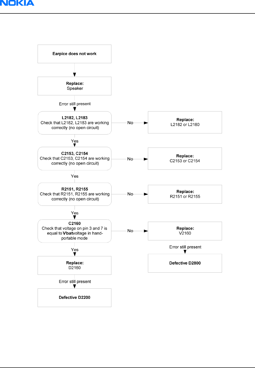
Earpiece fault
Figure 96 Earpiece fault flow chart
RM-74
Nokia Customer Care Baseband troubleshooting
Page 6–20 Company Confidential 9242678 (Issue 1)
Copyright ©2005 Nokia. All Rights Reserved.
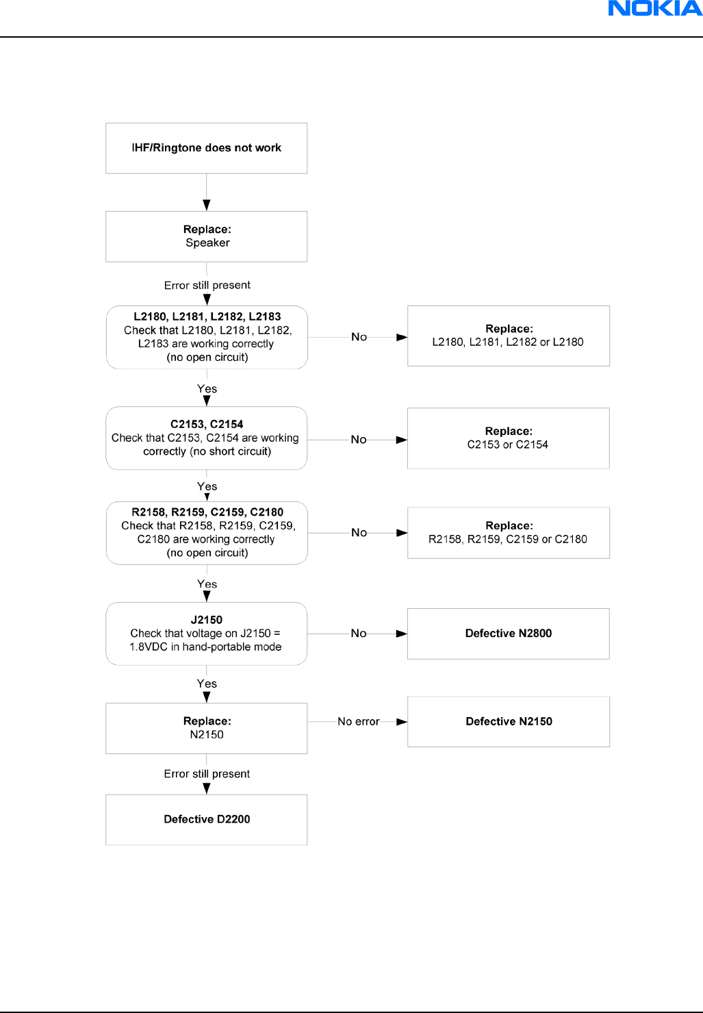
IHF/ringing tone fault
Figure 97 IHF/ringing tone fault flow chart
RM-74
Baseband troubleshooting Nokia Customer Care
9242678 (Issue 1) Company Confidential Page 6–21
Copyright ©2005 Nokia. All Rights Reserved.
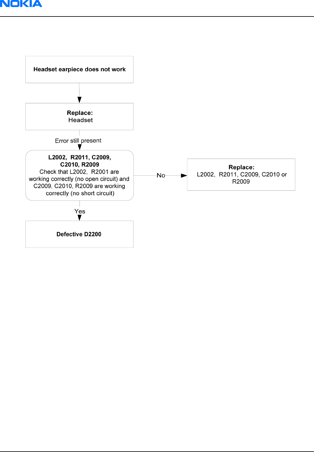
Headset earpiece fault
Figure 98 Headset earpiece fault flow chart
RM-74
Nokia Customer Care Baseband troubleshooting
Page 6–22 Company Confidential 9242678 (Issue 1)
Copyright ©2005 Nokia. All Rights Reserved.
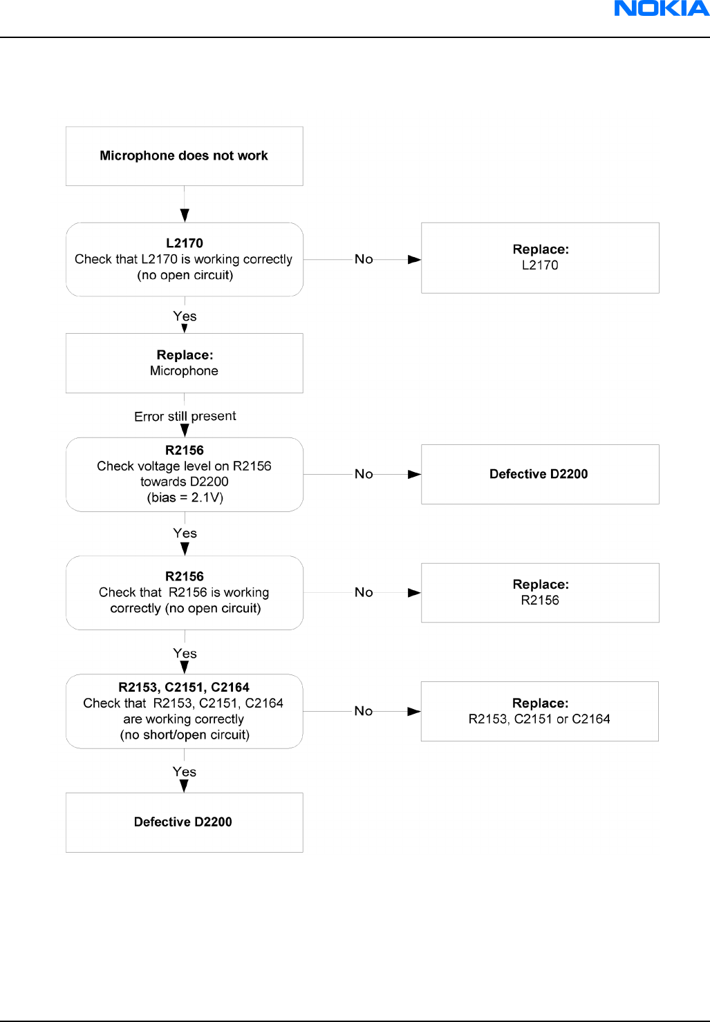
Microphone fault
Figure 99 Microphone fault flow chart
RM-74
Baseband troubleshooting Nokia Customer Care
9242678 (Issue 1) Company Confidential Page 6–23
Copyright ©2005 Nokia. All Rights Reserved.
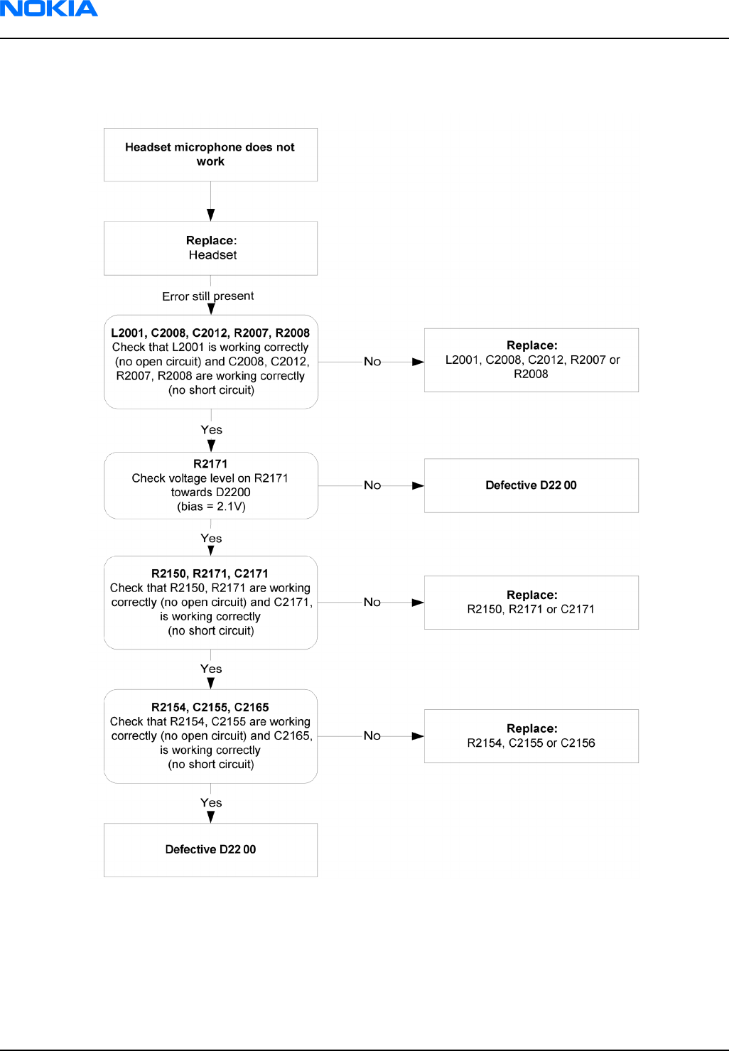
Headset microphone fault
Figure 100 Headset microphone fault flow chart
RM-74
Nokia Customer Care Baseband troubleshooting
Page 6–24 Company Confidential 9242678 (Issue 1)
Copyright ©2005 Nokia. All Rights Reserved.

7 — RF troubleshooting
Nokia Customer Care
9242678 (Issue 1) Company Confidential Page 7–1
Copyright ©2005 Nokia. All Rights Reserved.

RM-74
Nokia Customer Care RF troubleshooting
(This page left intentionally blank.)
Page 7–2 Company Confidential 9242678 (Issue 1)
Copyright ©2005 Nokia. All Rights Reserved.

Table of Contents
General RF troubleshooting.........................................................................................................................................................7–5
General RF troubleshooting...................................................................................................................................................7–5
RF key components...................................................................................................................................................................7–6
Auto tuning.......................................................................................................................................................................................7–8
Auto tuning.................................................................................................................................................................................7–8
Receiver..............................................................................................................................................................................................7–8
General instructions for GSM 900 RX troubleshooting..................................................................................................7–8
Troubleshooting diagram for GSM 900 receiver...........................................................................................................7–10
General instructions for GSM 1800 RX troubleshooting.............................................................................................7–11
Troubleshooting diagram for GSM 1800 receiver.........................................................................................................7–13
Measurement points in the receiver.................................................................................................................................7–14
Transmitter.....................................................................................................................................................................................7–15
General instructions for GSM 900 TX troubleshooting................................................................................................7–15
Troubleshooting diagram for GSM 900 transmitter....................................................................................................7–17
GSM 900 TX output power....................................................................................................................................................7–17
General instructions for GSM 1800 TX troubleshooting..............................................................................................7–20
Troubleshooting diagram for GSM 1800 transmitter..................................................................................................7–22
GSM 1800 TX output power.................................................................................................................................................7–22
Synthesizer troubleshooting ....................................................................................................................................................7–25
Introduction.............................................................................................................................................................................7–25
Troubleshooting diagram for PLL synthesizer..............................................................................................................7–27
Measurement points at the VCXO.......................................................................................................................................7–28
FM radio troubleshooting..........................................................................................................................................................7–28
Measurement settings...........................................................................................................................................................7–28
Troubleshooting diagram for FM radio............................................................................................................................7–29
Measurement points in the receiver.................................................................................................................................7–30
Antenna troubleshooting...........................................................................................................................................................7–31
Antenna troubleshooting.....................................................................................................................................................7–31
List of Figures
Figure 101 RF key components on PWB..................................................................................................................................7–6
Figure 102 Supply points at UEM (D2200)...............................................................................................................................7–7
Figure 103 Supply point at RF IC (N7600)................................................................................................................................7–7
Figure 104 Supply point at FM Radio IC (N6156)...................................................................................................................7–7
Figure 105 GSM 900 RF controls window................................................................................................................................7–9
Figure 106 GSM 900 Receiver troubleshooting...................................................................................................................7–10
Figure 107 900 RX I/Q signal waveform................................................................................................................................7–11
Figure 108 GSM 1800 RF controls window...........................................................................................................................7–12
Figure 109 GSM 1800 Receiver troubleshooting.................................................................................................................7–13
Figure 110 1800 RX I/Q signal waveform.............................................................................................................................7–14
Figure 111 RX measurements point of the control voltages to FEM N7700..............................................................7–14
Figure 112 Measurement points at the RX SAW Filters – Z7600/Z7602......................................................................7–15
Figure 113 RX I/Q signals............................................................................................................................................................7–15
Figure 114 GSM 900 RF controls window..............................................................................................................................7–16
Figure 115 GSM 900 transmitter troubleshooting.............................................................................................................7–17
Figure 116 TX I/O signal..............................................................................................................................................................7–18
Figure 117 VC1, VC3 signals.......................................................................................................................................................7–18
Figure 118 TXP signal..................................................................................................................................................................7–19
Figure 119 TXC signals at PCL5.................................................................................................................................................7–19
RM-74
RF troubleshooting Nokia Customer Care
9242678 (Issue 1) Company Confidential Page 7–3
Copyright ©2005 Nokia. All Rights Reserved.

Figure 120 TXC signals at PCL19...............................................................................................................................................7–20
Figure 121 GSM 1800 RF controls window...........................................................................................................................7–21
Figure 122 GSM 1800 transmitter troubleshooting...........................................................................................................7–22
Figure 123 TX I/O signal..............................................................................................................................................................7–23
Figure 124 VC1, VC2, VC3 signals..............................................................................................................................................7–23
Figure 125 TXP signal..................................................................................................................................................................7–24
Figure 126 TXC signals at PCL0.................................................................................................................................................7–24
Figure 127 TXC signals at PCL15...............................................................................................................................................7–25
Figure 128 VCXO 26 MHz waveform........................................................................................................................................7–26
Figure 129 PLL Troubleshooting diagram............................................................................................................................7–27
Figure 130 Measurement point for VCXO..............................................................................................................................7–28
Figure 131 Phoenix settings......................................................................................................................................................7–28
Figure 132 FM circuit troubleshooting diagram.................................................................................................................7–29
Figure 133 RX measurements point of the control voltages to FEM N7700..............................................................7–30
Figure 134 Measurement points at the RX SAW Filters – Z7600/Z7602......................................................................7–30
Figure 135 RX I/Q signals............................................................................................................................................................7–30
Figure 136 Antenna troubleshooting.....................................................................................................................................7–31
RM-74
Nokia Customer Care RF troubleshooting
Page 7–4 Company Confidential 9242678 (Issue 1)
Copyright ©2005 Nokia. All Rights Reserved.

General RF troubleshooting
General RF troubleshooting
Most RF semiconductors are static discharge sensitive
Two types of measurements are used in the following. It will be specified if the measurement type is "RF" or "LF".
• RF measurements are done with a Spectrum Analyzer and a high-frequency 500 ohm passive probe, for
example HP54006A. (Note that when measuring with the 500 ohm probe the signal will be around 20 dB
attenuated. The values in the following will have these 20 dB subtracted and represent the real value seen
on the spectrum analyzer). Note that the testing have some losses which must be taken into consideration
when calibrating the test system.
• LF (Low frequency) and DC measurements should be done with a 10:1 probe and an oscilloscope. The probe
used in the following is 10 Mohm/8pF passive probe. If using another probe then bear in mind that the
voltages displayed may be slightly different. Always make sure the measurement set-up is calibrated when
measuring RF parameters on the antenna pad. Remember to include the loss in the module repair jig when
realigning the phone.
So ESD protection must be applied during repair (ground straps and ESD soldering irons). RF IC N7600 and FEM
are moisture sensitive so parts must be pre-baked prior to soldering. Apart from key-components described in
this document there are a lot of discrete components (resistors, inductors and capacitors) for which
troubleshooting is done by checking if soldering of the component is done properly and checking if the
component is missing from PWB. Capacitors can be checked for short-circuiting and resistors for value by means
of an ohmmeter, but be aware in-circuit measurements should be evaluated carefully. In the following both
the name EGSM and GSM 850 will be used for the lower band and both PCN and GSM 1900 will be used for the
upper band.
RM-74
RF troubleshooting Nokia Customer Care
9242678 (Issue 1) Company Confidential Page 7–5
Copyright ©2005 Nokia. All Rights Reserved.
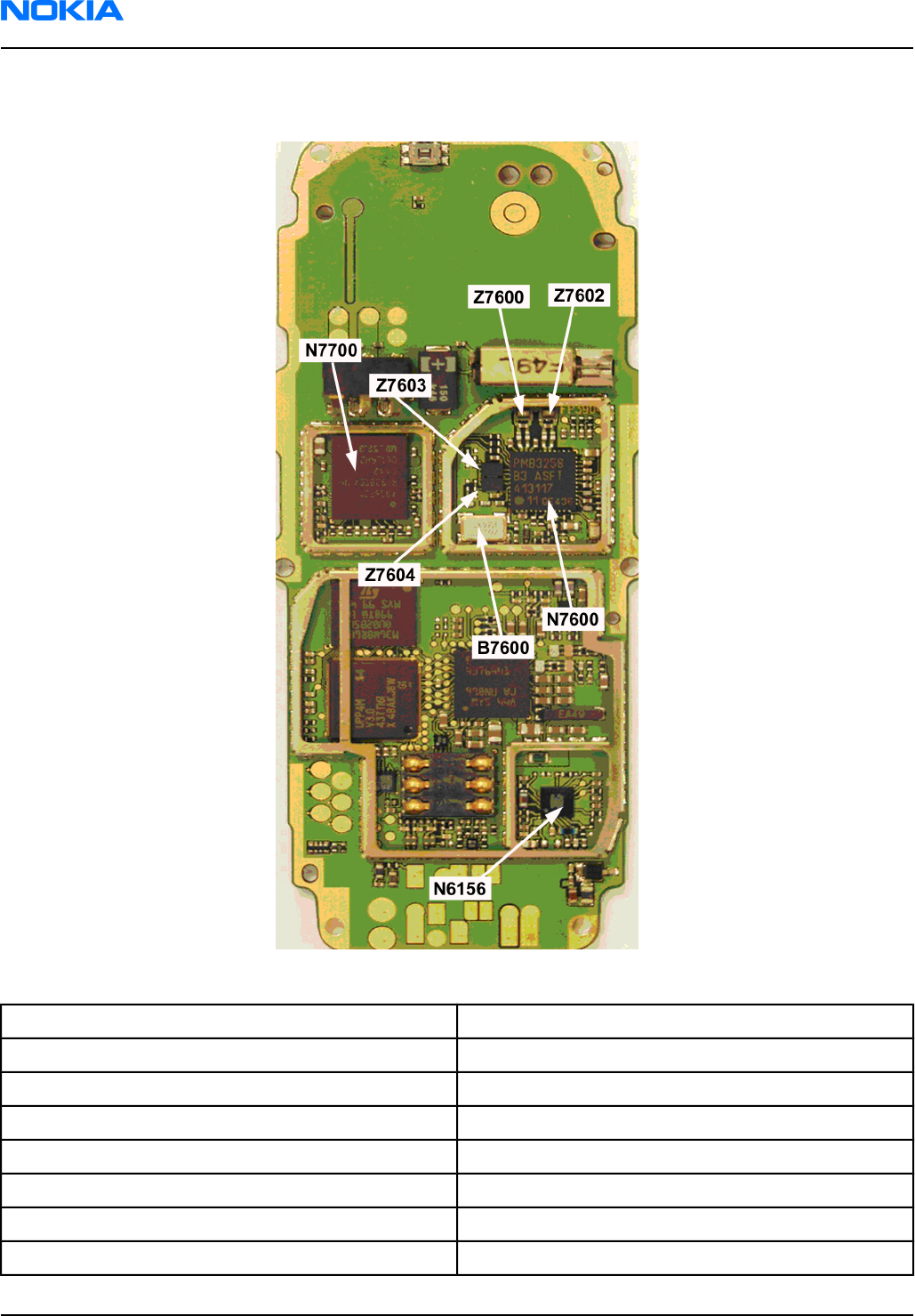
RF key components
Figure 101 RF key components on PWB
N7600 RF IC
N7700 FEM (PA and antenna switch)
Z7602 EGSM 850/900 RX SAW filter
Z7600 DCS 1800/PCS1900 RX SAW filter
Z7603 EGSM 850/900 TX filter
Z7604 DCS 1800/PCS1900 TX filter
B7600 26 MHz crystal
N6156 FM radio IC
RM-74
Nokia Customer Care RF troubleshooting
Page 7–6 Company Confidential 9242678 (Issue 1)
Copyright ©2005 Nokia. All Rights Reserved.
Refer to the picture below for measuring points at the UEM (D2200).
Figure 102 Supply points at UEM (D2200)
Figure 103 Supply point at RF IC (N7600)
Figure 104 Supply point at FM Radio IC (N6156)
RM-74
RF troubleshooting Nokia Customer Care
9242678 (Issue 1) Company Confidential Page 7–7
Copyright ©2005 Nokia. All Rights Reserved.

Auto tuning
Auto tuning
This phone can be tuned automatically.
Autotune is designed to align the phone's RF part easier and faster. It performs calibrations, tunings and
measurements of RX and TX. The results are displayed and logged in a result file, if initiated.
Hardware set up
Hardware requirements for auto tuning:
• PC (Windows 2000/NT) with GPIB card
• Power supply
• Product specific module jig
• Cables: 3 (alt.1) RF cable, 1 GPIB cable and DAU-9S
• Signal analyser (TX), signal generator (RX) and RF-splitter or one device including all.
Phoenix preparations
Copy the two phone specific ini-files, for example rm_13_tunings.ini and autotune_RM-13.ini, to a phone specific
folder, for example \Phoenix\products\RM-13\.
Auto tuning procedure
1 Make sure the phone (in the jig) is connected to the equipment. Else, some menus will not be shown in
Phoenix.
2 The first time you are using automatic tuning on this phone model, on this computer, you will have to Set
loss for cables and jigs.
3 To go to autotune, select Tuning (Alt-U) > Auto-Tune (Alt-A) from the menu.
4 If you need more assistance, please refer to the Phoenix Help.
Receiver
General instructions for GSM 900 RX troubleshooting
1 Connect the phone to a PC with the module repair jig.
2 Start Phoenix and establish a connection to the phone with the data cable e.g. FBUS.
3 Select File and Scan product
4 Wait a while for the PC to read the information from the phone
5 Select Testing and RF Controls
6 Set the parameters as follows:
• Active Unit: RX
• Band: GSM 900
• Operation Mode: Continuous mode
• RX/TX Channel 37
• AGC: 8: FEG_ON + DTOS_ON+BB_6=Vgain_36
The setup should now look like this:
RM-74
Nokia Customer Care RF troubleshooting
Page 7–8 Company Confidential 9242678 (Issue 1)
Copyright ©2005 Nokia. All Rights Reserved.
Figure 105 GSM 900 RF controls window
RM-74
RF troubleshooting Nokia Customer Care
9242678 (Issue 1) Company Confidential Page 7–9
Copyright ©2005 Nokia. All Rights Reserved.
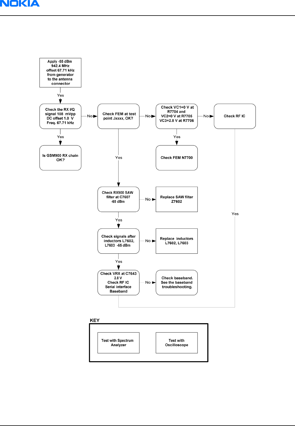
Troubleshooting diagram for GSM 900 receiver
Figure 106 GSM 900 Receiver troubleshooting
By measuring with an oscilloscope at RXIP or RXQP on a working GSM 900 receiver this picture should be seen.
Signal amplitude 114 mVp-p. DC offset 1.0 V.
RM-74
Nokia Customer Care RF troubleshooting
Page 7–10 Company Confidential 9242678 (Issue 1)
Copyright ©2005 Nokia. All Rights Reserved.
Figure 107 900 RX I/Q signal waveform
General instructions for GSM 1800 RX troubleshooting
1 Connect the phone to a PC with the module repair jig.
2 Start Phoenix and establish a connection to the phone with the data cable e.g. FBUS.
3 Select File and Scan product
4 Wait a while for the PC to read the information from the phone
5 Select Testing and RF Controls
6 Set the parameters as follows:
• Active Unit: RX
• Band: GSM 1800
• Operation Mode: Continuous mode
• RX/TX Channel 700
• AGC: 8: FEG_ON + DTOS_ON+BB_6=Vgain_36
The setup should now look like this:
RM-74
RF troubleshooting Nokia Customer Care
9242678 (Issue 1) Company Confidential Page 7–11
Copyright ©2005 Nokia. All Rights Reserved.
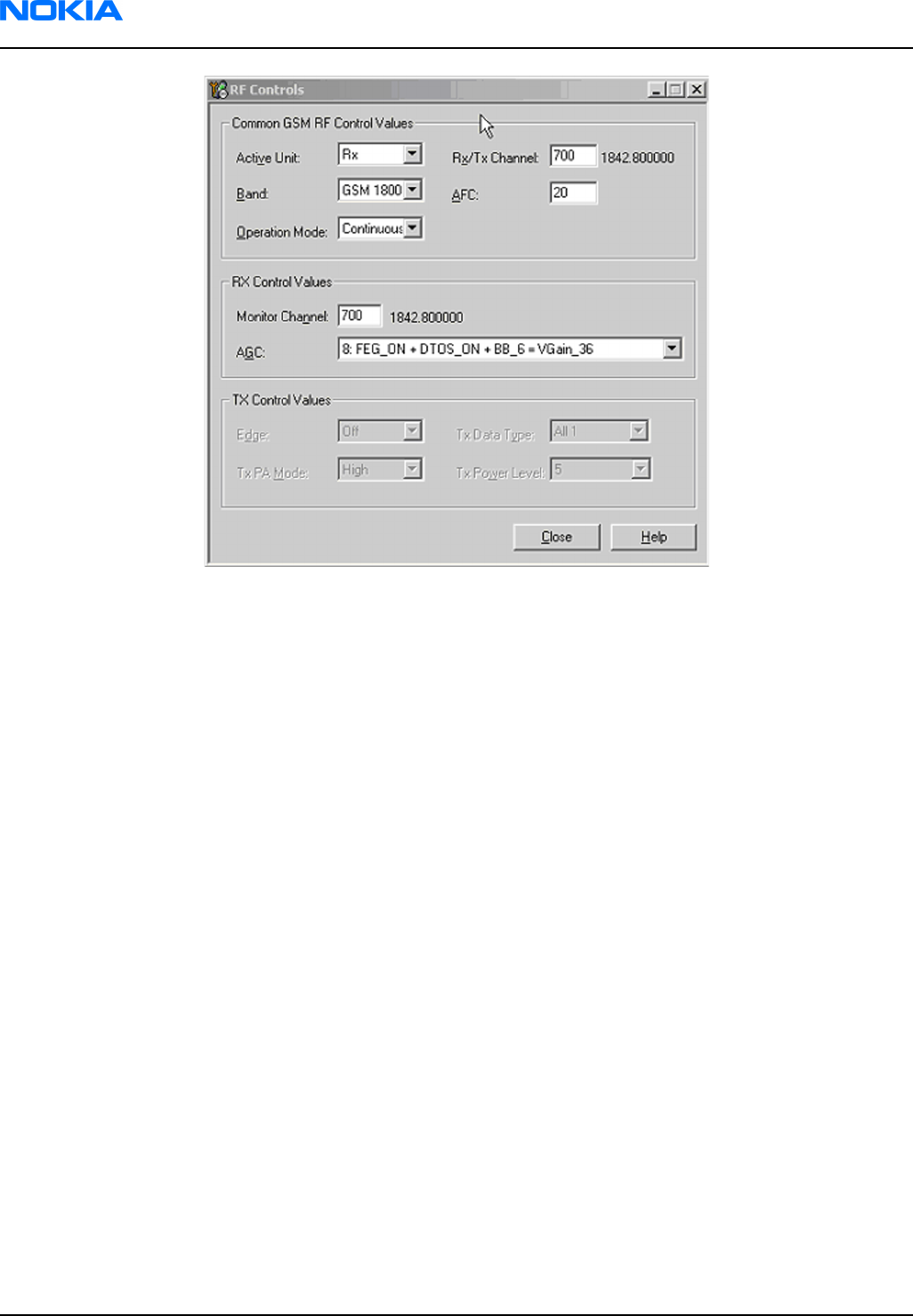
Figure 108 GSM 1800 RF controls window
RM-74
Nokia Customer Care RF troubleshooting
Page 7–12 Company Confidential 9242678 (Issue 1)
Copyright ©2005 Nokia. All Rights Reserved.
Troubleshooting diagram for GSM 1800 receiver
Figure 109 GSM 1800 Receiver troubleshooting
By measuring with an oscilloscope at RXIP or RXQP on a working GSM 1800 receiver this picture should be seen.
Signal amplitude 114 mVp-p. DC offset 1.0 V.
RM-74
RF troubleshooting Nokia Customer Care
9242678 (Issue 1) Company Confidential Page 7–13
Copyright ©2005 Nokia. All Rights Reserved.
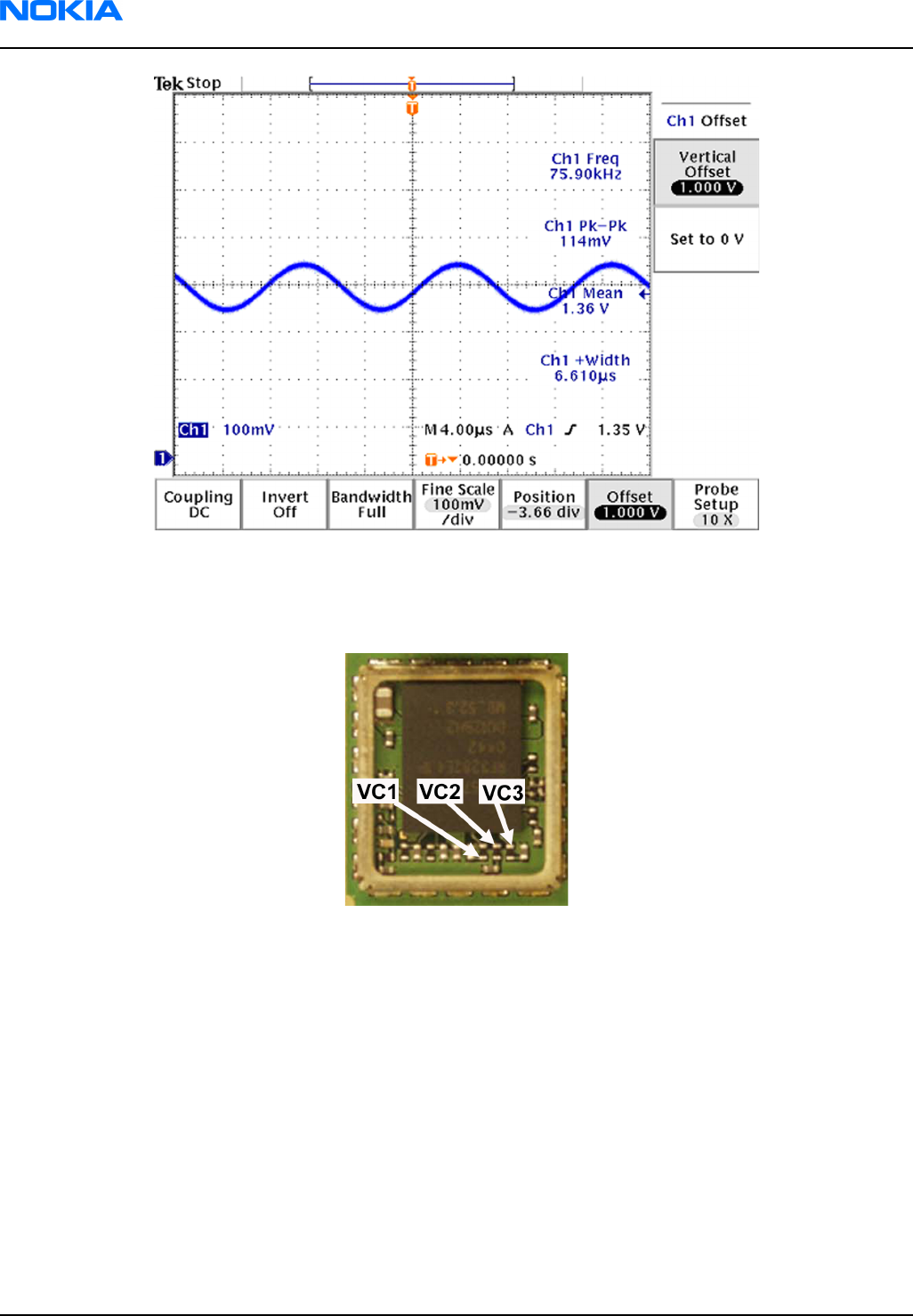
Figure 110 1800 RX I/Q signal waveform
Measurement points in the receiver
Figure 111 RX measurements point of the control voltages to FEM N7700
RM-74
Nokia Customer Care RF troubleshooting
Page 7–14 Company Confidential 9242678 (Issue 1)
Copyright ©2005 Nokia. All Rights Reserved.
Figure 112 Measurement points at the RX SAW Filters – Z7600/Z7602
Figure 113 RX I/Q signals
Transmitter
General instructions for GSM 900 TX troubleshooting
1 Apply a RF-cable to the RF-connector to allow the transmitted signal act as normal. RF-cable should be
connected to an attenuator at least 10 dB before connected to the measurement equipment, otherwise the
PA may be damaged.
2 Start Phoenix and establish a connection to the phone with the data cable e.g. FBUS.
3 Select File and Scan product
4 Wait a while for the PC to read the information from the phone
5 Select Testing and RF Controls
6 Set the parameters as follows:
• Band: GSM 900
• Active Unit: TX
RM-74
RF troubleshooting Nokia Customer Care
9242678 (Issue 1) Company Confidential Page 7–15
Copyright ©2005 Nokia. All Rights Reserved.
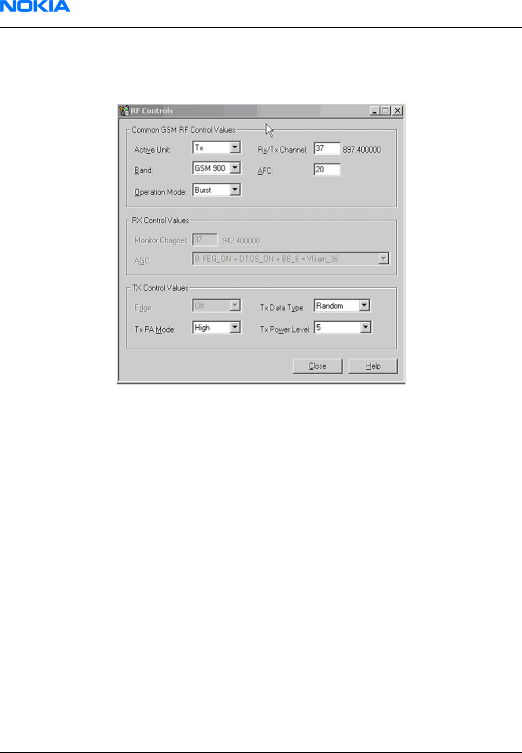
• TX Power Level: 5
• TX Data Type: Random
The setup should now look like this:
Figure 114 GSM 900 RF controls window
RM-74
Nokia Customer Care RF troubleshooting
Page 7–16 Company Confidential 9242678 (Issue 1)
Copyright ©2005 Nokia. All Rights Reserved.
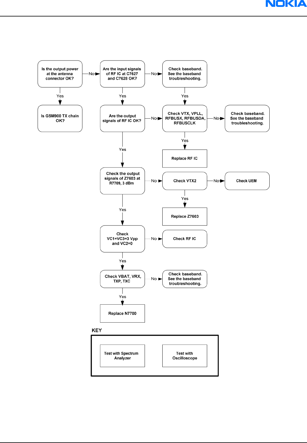
Troubleshooting diagram for GSM 900 transmitter
Figure 115 GSM 900 transmitter troubleshooting
GSM 900 TX output power
Measure the output power of the phone; it should be about 32.5 dBm. Remember the cable loss is about 0.3 dB.
RM-74
RF troubleshooting Nokia Customer Care
9242678 (Issue 1) Company Confidential Page 7–17
Copyright ©2005 Nokia. All Rights Reserved.
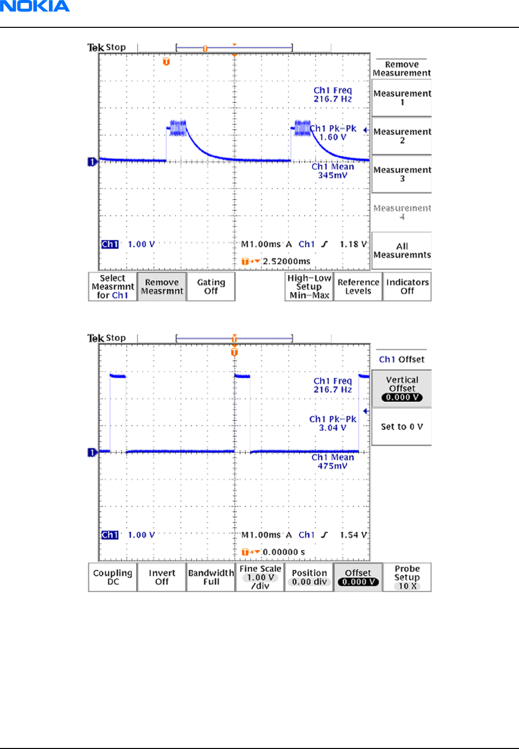
Figure 116 TX I/O signal
Figure 117 VC1, VC3 signals
RM-74
Nokia Customer Care RF troubleshooting
Page 7–18 Company Confidential 9242678 (Issue 1)
Copyright ©2005 Nokia. All Rights Reserved.
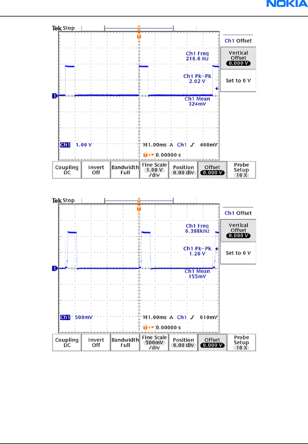
Figure 118 TXP signal
Figure 119 TXC signals at PCL5
RM-74
RF troubleshooting Nokia Customer Care
9242678 (Issue 1) Company Confidential Page 7–19
Copyright ©2005 Nokia. All Rights Reserved.
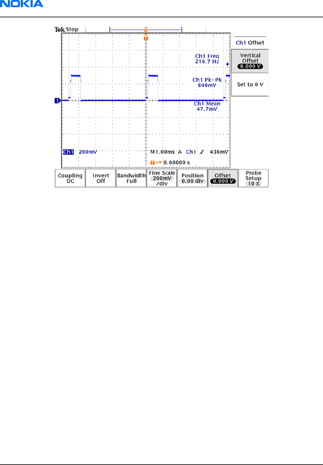
Figure 120 TXC signals at PCL19
General instructions for GSM 1800 TX troubleshooting
1 Apply a RF-cable to the RF-connector to allow the transmitted signal act as normal. RF-cable should be
connected to an attenuator at least 10 dB before connected to the measurement equipment, otherwise the
PA may be damaged.
2 Start Phoenix and establish a connection to the phone with the data cable e.g. FBUS.
3 Select File and Scan product
4 Wait a while for the PC to read the information from the phone
5 Select Testing and RF Controls
6 Set the parameters as follows:
• Band: GSM 1800
• Active Unit: TX
• TX Power Level: 0
• TX Data Type: Random
The setup should now look like this:
RM-74
Nokia Customer Care RF troubleshooting
Page 7–20 Company Confidential 9242678 (Issue 1)
Copyright ©2005 Nokia. All Rights Reserved.
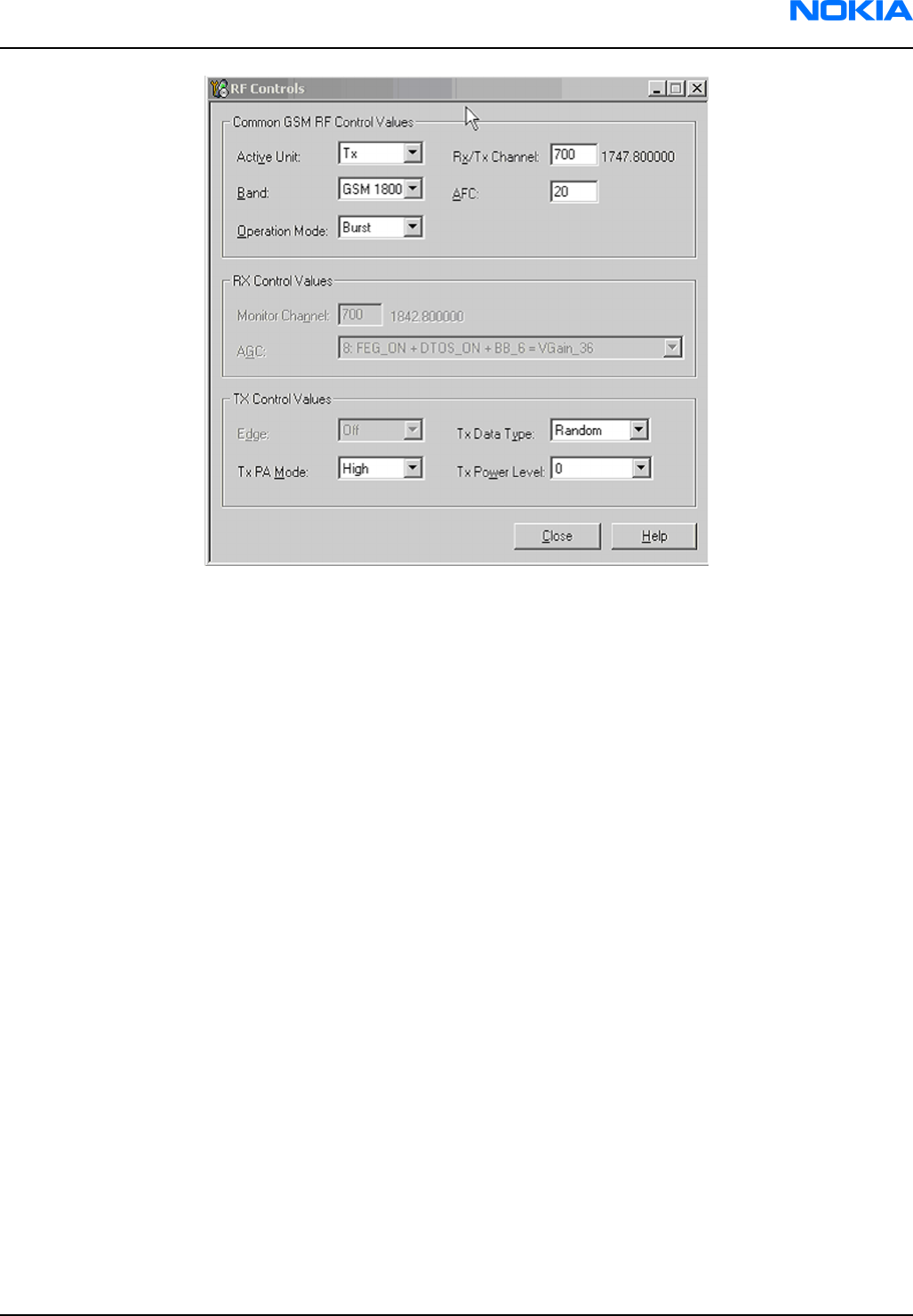
Figure 121 GSM 1800 RF controls window
RM-74
RF troubleshooting Nokia Customer Care
9242678 (Issue 1) Company Confidential Page 7–21
Copyright ©2005 Nokia. All Rights Reserved.
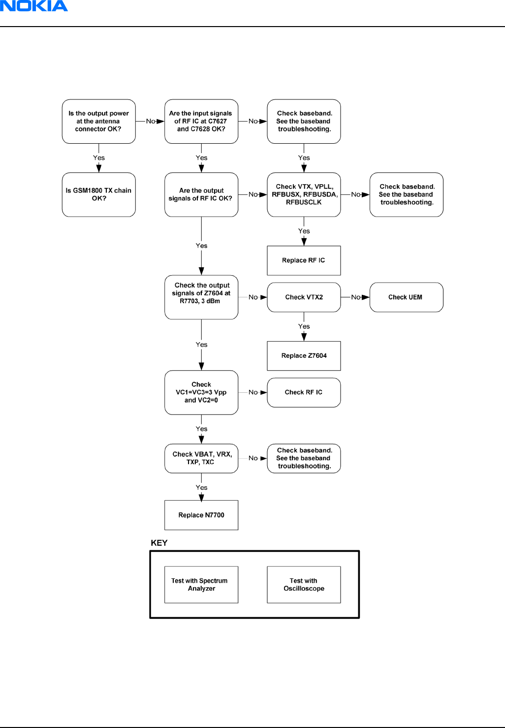
Troubleshooting diagram for GSM 1800 transmitter
Figure 122 GSM 1800 transmitter troubleshooting
GSM 1800 TX output power
Measure the output power of the phone; it should be about 29.5 dBm. Remember the cable loss is about 0.5 dB.
RM-74
Nokia Customer Care RF troubleshooting
Page 7–22 Company Confidential 9242678 (Issue 1)
Copyright ©2005 Nokia. All Rights Reserved.
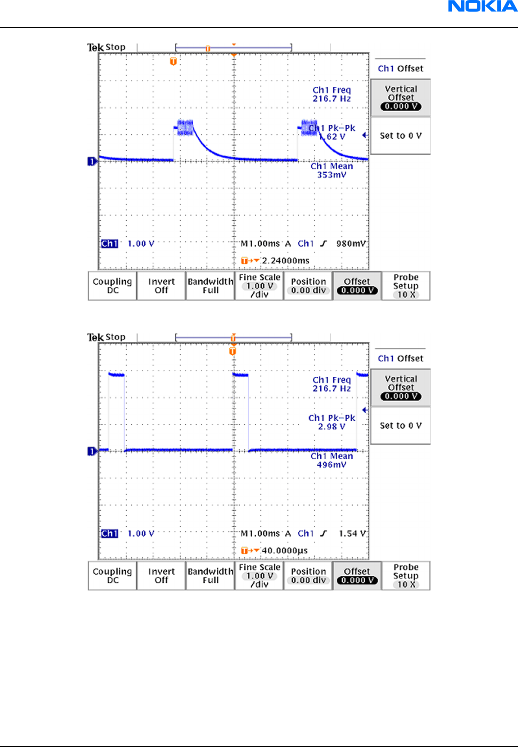
Figure 123 TX I/O signal
Figure 124 VC1, VC2, VC3 signals
RM-74
RF troubleshooting Nokia Customer Care
9242678 (Issue 1) Company Confidential Page 7–23
Copyright ©2005 Nokia. All Rights Reserved.
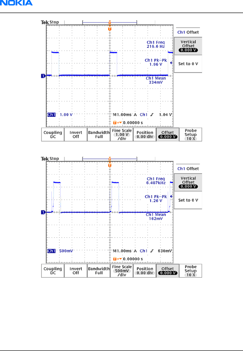
Figure 125 TXP signal
Figure 126 TXC signals at PCL0
RM-74
Nokia Customer Care RF troubleshooting
Page 7–24 Company Confidential 9242678 (Issue 1)
Copyright ©2005 Nokia. All Rights Reserved.
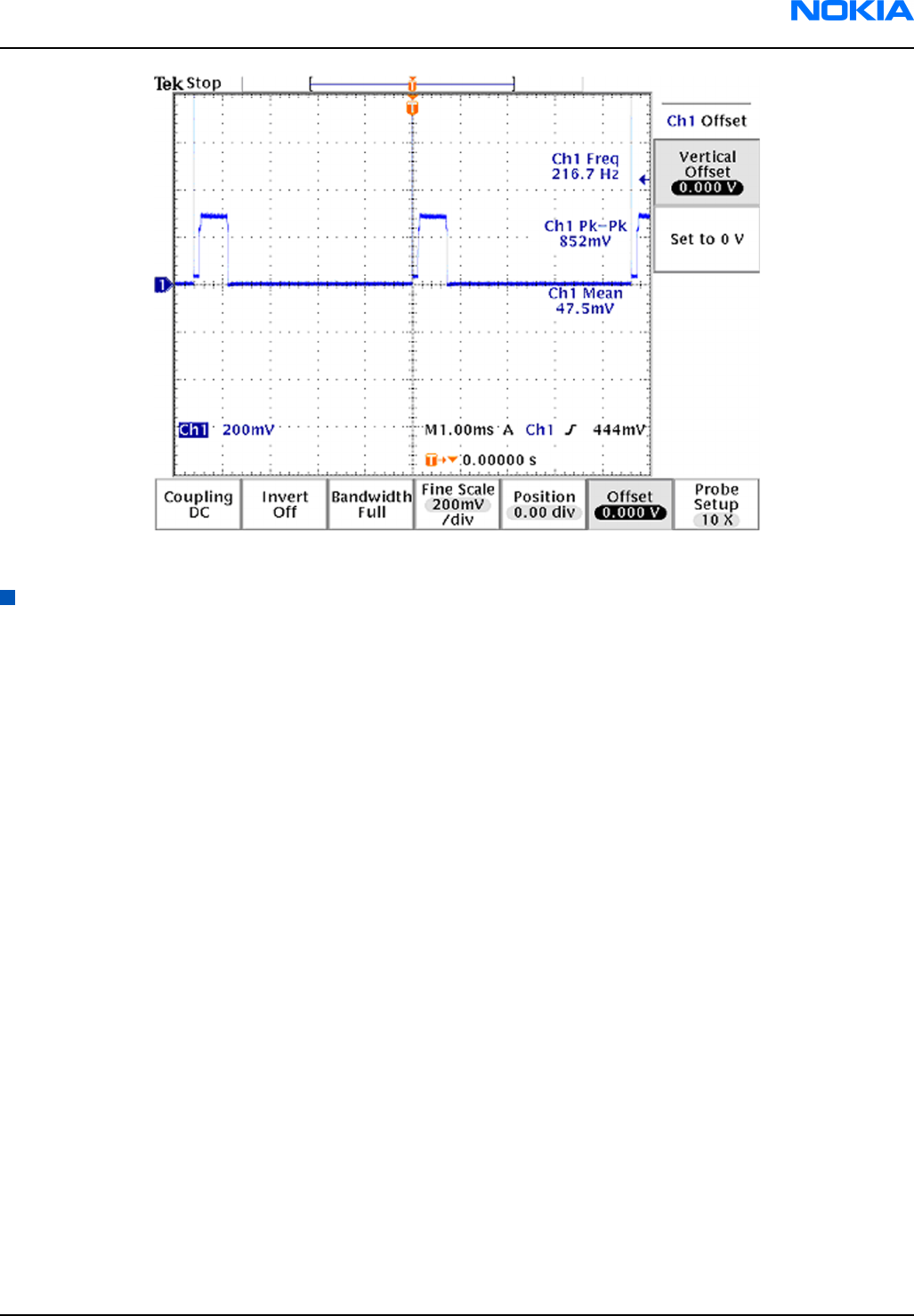
Figure 127 TXC signals at PCL15
Synthesizer troubleshooting
Introduction
26 MHz Reference Oscillator (VCXO)
There is only one PLL synthesizer generating Local Oscillator frequencies for both RX and TX in both bands (PCN
and EGSM). The VCO frequency is divided by 2 for PCN operation or by 4 for EGSM operation inside the RF IC.
The 26 MHz oscillator is located near the RF IC (N7600). The coarse frequency for this oscillator is set by an
external crystal (B7600). The reference oscillator is used as a reference frequency for the PLL synthesizer and
as the system clock for the Baseband. The 26 MHz signal is divided by 2 to achieve 13 MHz inside the UPP IC
(D2800).
The 26 MHz signal from the VCXO can be measured by probing R2900. The level at this point is approx. 770 mVpp.
Frequency of this oscillator is adjusted by changing the AFC-register inside the UEM IC. Example Signal Measured
at VCXO output (R2900).
RM-74
RF troubleshooting Nokia Customer Care
9242678 (Issue 1) Company Confidential Page 7–25
Copyright ©2005 Nokia. All Rights Reserved.
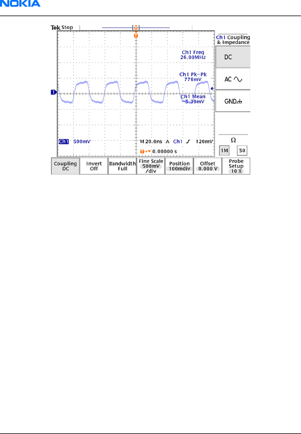
Figure 128 VCXO 26 MHz waveform
RM-74
Nokia Customer Care RF troubleshooting
Page 7–26 Company Confidential 9242678 (Issue 1)
Copyright ©2005 Nokia. All Rights Reserved.
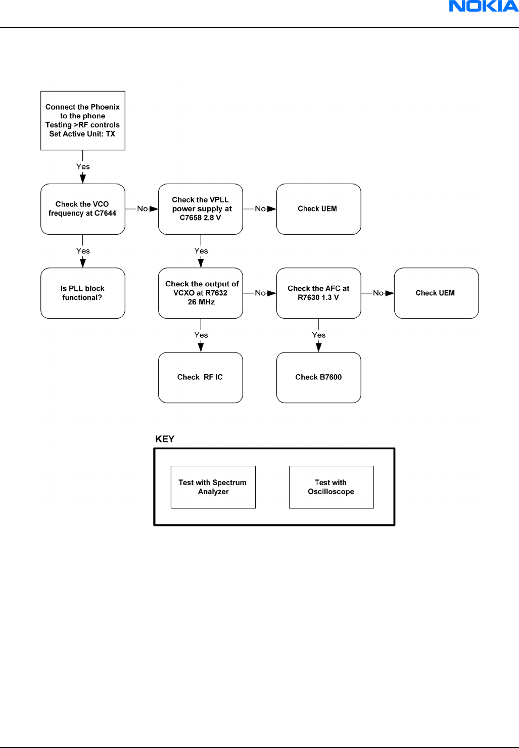
Troubleshooting diagram for PLL synthesizer
Figure 129 PLL Troubleshooting diagram
RM-74
RF troubleshooting Nokia Customer Care
9242678 (Issue 1) Company Confidential Page 7–27
Copyright ©2005 Nokia. All Rights Reserved.
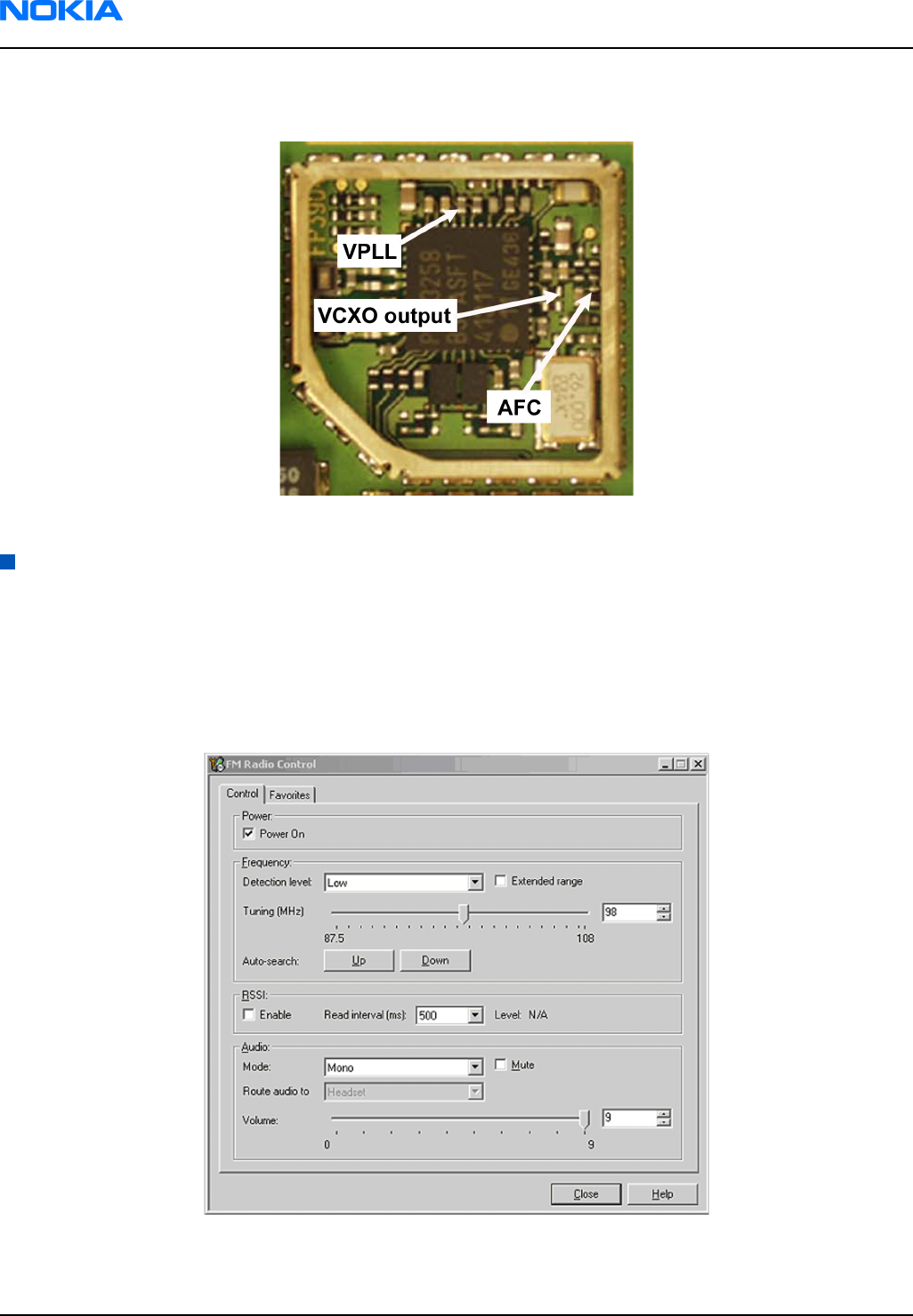
Measurement points at the VCXO
Figure 130 Measurement point for VCXO
FM radio troubleshooting
Measurement settings
1 Connect the phone to a PC with the module repair jig.
2 Start Phoenix and establish a connection to the phone with the data cable e.g. FBUS.
3 Phoenix settings shall be as follows:
Figure 131 Phoenix settings
1 Establish input of a standard FM signal to the FM module.
RM-74
Nokia Customer Care RF troubleshooting
Page 7–28 Company Confidential 9242678 (Issue 1)
Copyright ©2005 Nokia. All Rights Reserved.
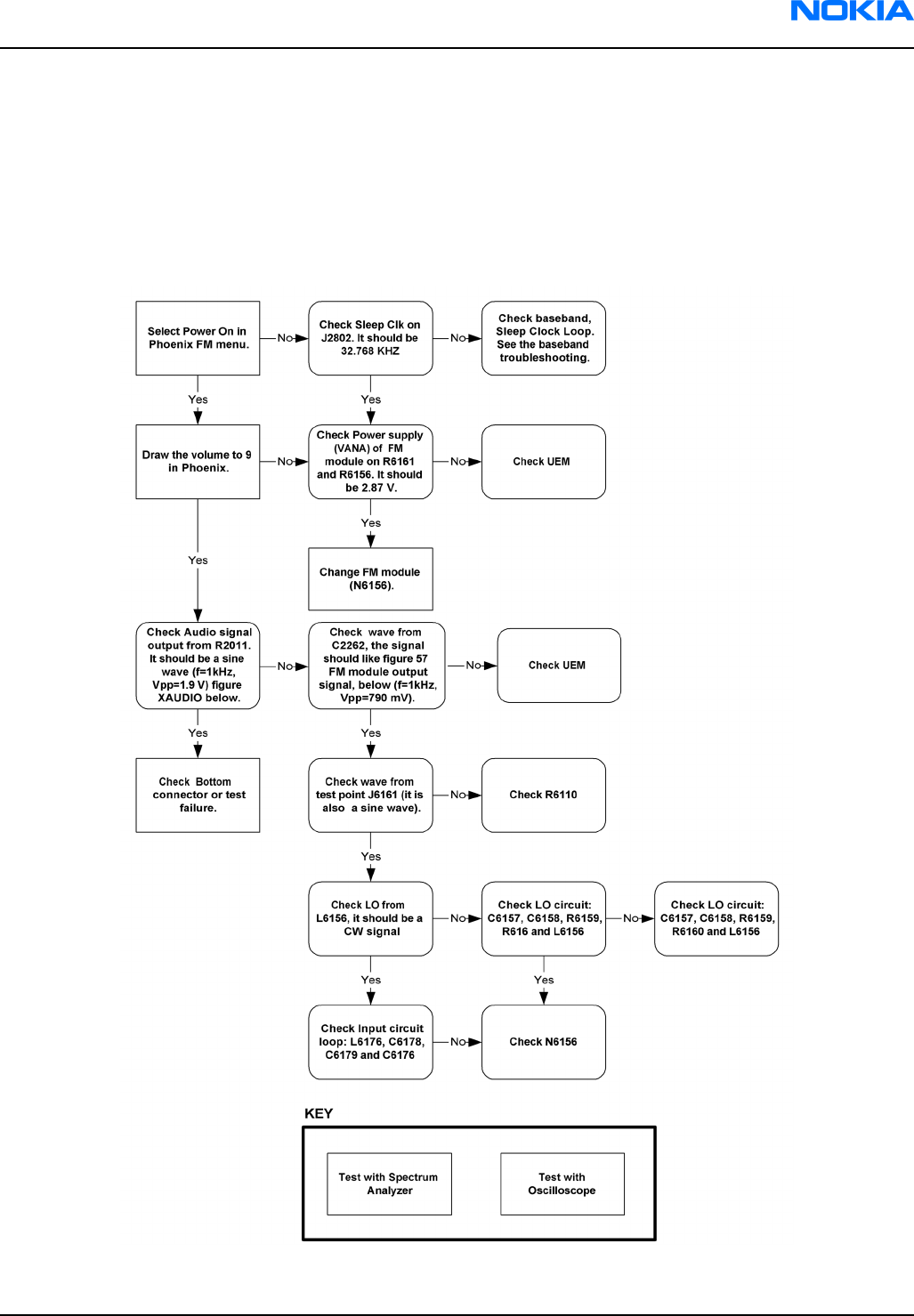
2 Signal generator settings shall be as follows:
• Frequency: 98 MHz
• Level: 60 dBm
• FM deviation: 75 kHz
• LFGEN frequency: 1 kHZ
Troubleshooting diagram for FM radio
Figure 132 FM circuit troubleshooting diagram
RM-74
RF troubleshooting Nokia Customer Care
9242678 (Issue 1) Company Confidential Page 7–29
Copyright ©2005 Nokia. All Rights Reserved.

Measurement points in the receiver
Figure 133 RX measurements point of the control voltages to FEM N7700
Figure 134 Measurement points at the RX SAW Filters – Z7600/Z7602
Figure 135 RX I/Q signals
RM-74
Nokia Customer Care RF troubleshooting
Page 7–30 Company Confidential 9242678 (Issue 1)
Copyright ©2005 Nokia. All Rights Reserved.
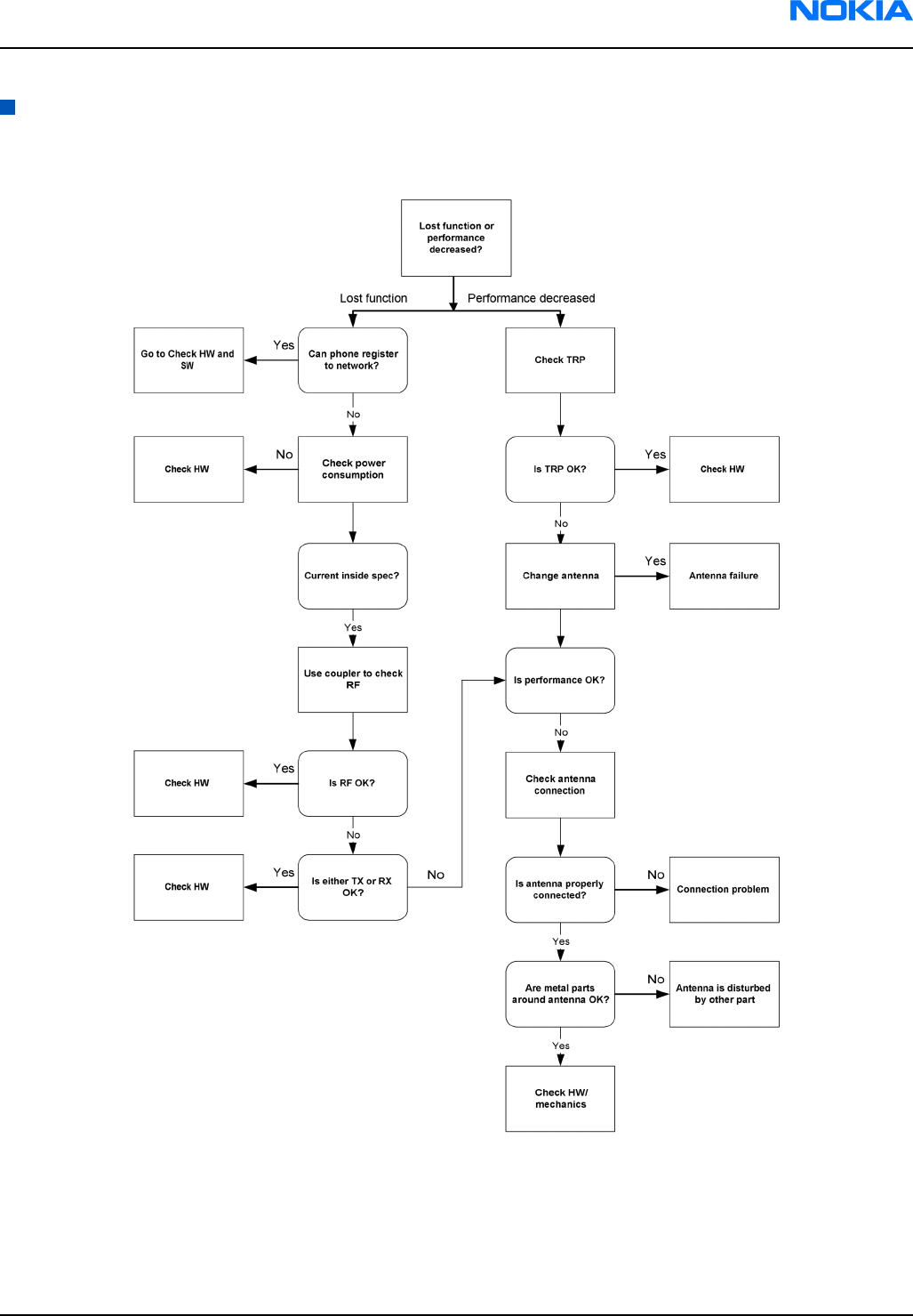
Antenna troubleshooting
Antenna troubleshooting
Figure 136 Antenna troubleshooting
RM-74
RF troubleshooting Nokia Customer Care
9242678 (Issue 1) Company Confidential Page 7–31
Copyright ©2005 Nokia. All Rights Reserved.

RM-74
Nokia Customer Care RF troubleshooting
(This page left intentionally blank.)
Page 7–32 Company Confidential 9242678 (Issue 1)
Copyright ©2005 Nokia. All Rights Reserved.

8 — System module
Nokia Customer Care
9242678 (Issue 1) Company Confidential Page 8–1
Copyright ©2005 Nokia. All Rights Reserved.

RM-74
Nokia Customer Care System module
(This page left intentionally blank.)
Page 8–2 Company Confidential 9242678 (Issue 1)
Copyright ©2005 Nokia. All Rights Reserved.

Table of Contents
Block diagram..................................................................................................................................................................................8–5
System module block diagram.............................................................................................................................................8–5
Functional description.............................................................................................................................................................8–6
Baseband description....................................................................................................................................................................8–6
UPP ................................................................................................................................................................................................8–6
UEMCLite.......................................................................................................................................................................................8–6
External regulators...................................................................................................................................................................8–7
Energy management................................................................................................................................................................8–7
Modes of operation...................................................................................................................................................................8–8
Voltage limits..............................................................................................................................................................................8–9
Audio function description.....................................................................................................................................................8–9
External audio connector.....................................................................................................................................................8–11
External signals and connections......................................................................................................................................8–11
Interfaces.........................................................................................................................................................................................8–12
RF and baseband interfaces................................................................................................................................................8–12
Analogue Signals.....................................................................................................................................................................8–15
FM radio.....................................................................................................................................................................................8–16
LCD interface.............................................................................................................................................................................8–16
Keyboard....................................................................................................................................................................................8–17
SIM interface.............................................................................................................................................................................8–18
External signals and connections......................................................................................................................................8–11
Battery connector...................................................................................................................................................................8–19
Battery........................................................................................................................................................................................8–20
PWB outline..............................................................................................................................................................................8–21
RF description................................................................................................................................................................................8–21
Frequency band, power and multi-slot class.................................................................................................................8–21
Transmitter - general description.....................................................................................................................................8–22
Transmitter - signal processing..........................................................................................................................................8–22
VCXO and PLL............................................................................................................................................................................8–22
List of Tables
Table 10 RF power supply.............................................................................................................................................................8–7
Table 11 Baseband power supply..............................................................................................................................................8–7
Table 12 Voltage limits..................................................................................................................................................................8–9
Table 13 Connector for External Audio Accessories...........................................................................................................8–11
Table 14 System connector........................................................................................................................................................8–11
Table 15 AC and DC Characteristics of BB4.0 LiteV2 RF-Base band Digital Signals...................................................8–12
Table 16 AC and DC Characteristics of RF-Base band Analogue Signals.......................................................................8–15
Table 17 The electrical parameters.........................................................................................................................................8–18
Table 18 System connector........................................................................................................................................................8–11
Table 19 Battery IF........................................................................................................................................................................8–19
Table 20 Frequency bands and TX power class...................................................................................................................8–21
Table 21 Multi-slot class..............................................................................................................................................................8–22
List of Figures
Figure 137 Module block diagram.............................................................................................................................................8–5
Figure 138 Power connection diagram....................................................................................................................................8–8
Figure 139 SIM filtering.................................................................................................................................................................8–8
RM-74
System module Nokia Customer Care
9242678 (Issue 1) Company Confidential Page 8–3
Copyright ©2005 Nokia. All Rights Reserved.

Figure 140 Audio block diagram..............................................................................................................................................8–10
Figure 141 4-pole jack plug for audio accessory................................................................................................................8–11
Figure 142 Keyboard schematics.............................................................................................................................................8–17
Figure 143 Keyboard layout in UI side...................................................................................................................................8–17
Figure 144 BL-5C battery connection order..........................................................................................................................8–20
Figure 145 BL-5C battery block.................................................................................................................................................8–20
Figure 146 PWB top side component placement...............................................................................................................8–21
RM-74
Nokia Customer Care System module
Page 8–4 Company Confidential 9242678 (Issue 1)
Copyright ©2005 Nokia. All Rights Reserved.
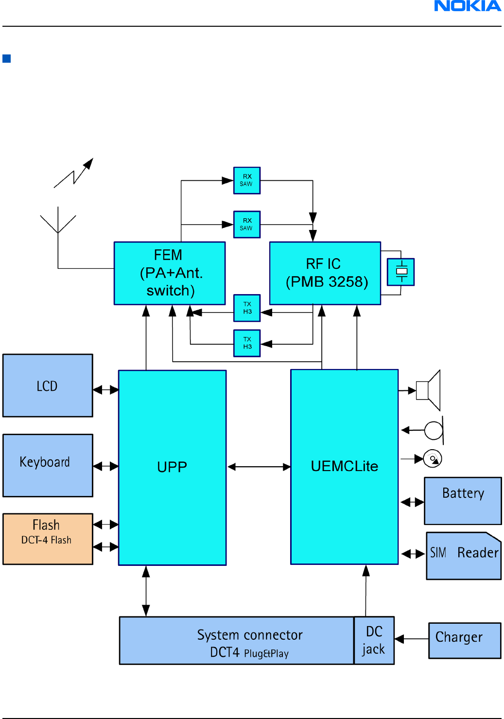
Block diagram
System module block diagram
The main board consists of a radio frequency part and a baseband part. The User Interface parts are situated
at the UI side, which is on the opposite side of the engine board. The 1MF is the system module of the mobile
device.
Figure 137 Module block diagram
RM-74
System module Nokia Customer Care
9242678 (Issue 1) Company Confidential Page 8–5
Copyright ©2005 Nokia. All Rights Reserved.

Functional description
The BB core is based on UPP4M CPU. UPP4M takes care of all the signal processing and operation controlling
tasks of the mobile device. For power management, there is one main ASIC for controlling, charging and
supplying power UEMCLite plus a discrete power supply. The UEMCLite generates the main reset for the system.
Memories comprise 128 Mbit flash and 16 Mbit PsRAM. Memory devices are stacked on top of each other in a
single Combo package.
The UEMCLite also handles the interface to the RF and audio sections. This ASIC provides A/D and D/A conversion
of the in-phase and quadrate receive and transmit signal paths and also A/D and D/A conversions of received
and transmitted audio signals. Data transmission between UEMCLite and RF and the UPP4M is implemented
using different serial connections (CBUS, DBUS and RFBUS). UPP4M ASIC handles digital speech processing.
A real time clock function is integrated into UEMCLite, which utilizes the same 32 kHz-clock source as the sleep
clock. The SLCK/RTC runs all time when the phone battery is connected. It is running also when the phone is
switched off. In UEMCLite there is no back up battery/capacitor connection.
There are two audio transducers in the product; 13 mm speaker and a microphone. The speaker is used to
generate audios for earpiece, IHF and ringing tones. A separate audio amplifier drives the speaker. There is only
one microphone for both HS and IHF modes.
The display is a CSTN type color display with 65536 colors and 128 x 128 pixels with backlighting. The UI module
features a function key mat with a 4-way navigation key with a center selection key.
Baseband description
UPP
UPP (Universal Phone Processor) is the digital ASIC of the DCT4 generation base band. In LiteV2 BB the UPP4M_v3/
UPP4Mv4 and UPP2Mv2 are supported types. UPP4Mv3 includes 4.5 MBit internal RAM, ARM7TDMI rev4 16/32-
bit RISC MCU core, TI Lead3 16-bit DSP phase2+ core with DMA controller, ROM for MCU boot code and all digital
control logic. UPP general purpose IO (GENIO) can be used for predefined HW purpose or but they can also be
controlled with SW for product specific features.
Memory
This mobile uses two kinds of memories, Flash and Synchronous RAM (SRAM). These memories have are sharing
the same bus interface to UPP4M. SDRAM is used as the working memory. Interface is 16 bit wide data and 14
bit address. Memory clocking speed is 52 MHz. The SRAM size is 16 Mbits.
SRAM I/O is 1.8 V and core 1.8 V supplied by UEMCLite regulator VIO. All memory contents are lost if the supply
voltage is switched off.
Multiplexed flash memory interface is used to store the MCU program code and user data. The memory interface
is a burst type FLASH with multiplexed address/data bus, running at 52 MHz.
Configuration of flash memory is a 128 Mbit NOR flash memory. Flash I/O and core voltage are 1.8 V supplied
by UEMCLite’s VIO.
UEMCLite
Power management in the RM-74/75 follows the DCT4 Core design, having anyhow less regulators than
traditional architecture. The UEMCLite, that is a low cost energy management ASIC with completely new design
contains for BB use two 2.78V LDO regulators, 1.8V linear regulator, programmable 1.0 - 1.5 V linear regulator
and 1.8/3.0 V LDO regulator. For RF use UEMCLite has five 2.78 V LDOs. In addition, the UEMCLite contains audio
codec, A/D converters, RF converters, many drivers, etc.
Below is a list of the supply voltages.
RM-74
Nokia Customer Care System module
Page 8–6 Company Confidential 9242678 (Issue 1)
Copyright ©2005 Nokia. All Rights Reserved.
Table 10 RF power supply
Vmin/V Vtyp/V Vmax/V ItypmA Imax
mA
Notes
VR1 2.7 2.78 2.86 65 75 VTX (Supply voltage for PMB3258 LO and RX parts
VR2 2.7 2.78 2.78 2.4 3.0 VXO (VCXO supply voltage)
VR3 2.7 2.78 2.86 41 47 VTX2 (Supply voltage for PMB3258 modulator
output stage)
VR4 2.7 2.78 2.86 43 48 VRX (Supply for RFIC RX and TX parts)
VR5 2.7 2.78 2.86 29 35 VPLL (Supply for VCO, PLL and digital parts
VBATTRF 3.1 3.6 4.7 1.5 3.5 Supply voltage for the front-end module (Vbatt,
max=6.0 V)
The table below shows the typical current consumption in different operation modes.
Table 11 Baseband power supply
Signal, Nom Volt.,
Max Current
Min-Max Voltage (V) Iqmax PSSR(dB)* Notes
VANA, 2,78V, 80mA 2.7-2.86 200 50, 40 Disabled in sleep
mode
VBB1 2,78V, sleep
2mA, norm. 50mA
2.7-2.86 15 sleep, 200 40, - Sleep mode
possibility
VSIM, 1.8/3.0, 25mA 1.745- 1.8552.910-
3.090
30 sleep, 80 40, - Sleep mode
possibility,
programmable
VIO, 1.8V 1.72 - 1.88 15 sleep, 100 45, - Sleep mode
possibility
VCORE,1.055/1.25/
1.35/1.5V
1.0 - 1.111.188 -
1.3131.285
-1.4151.425 -1.575
20 sleep, 200 40, - Sleep,
programmable,
Initial voltage
1.35V from reset
External regulators
White LED Driver solution is implemented with DC/DC converter. The driver circuit is controlled by UEM output
pin DLIGHT, which add external pull up using a digital transistor and one resistor. The schematics also combined
the UEMIO (5) to control DC/DC enable as another optional using two jumper.
Energy management
Filter components
The master of EM control is UEMCLite and with SW it has the main control of the system voltages and operating
modes. The RM-74 power distribution diagram is presented in the illustration below.
RM-74
System module Nokia Customer Care
9242678 (Issue 1) Company Confidential Page 8–7
Copyright ©2005 Nokia. All Rights Reserved.
Figure 138 Power connection diagram
All connectors going to the “outside world” have filter components, ESD protection and EMC reduction.
The Digital/Data lines on SIM have special dedicated filter ASIP. The below figure show the SIM filtering.
Figure 139 SIM filtering
The Audio circuit: Earpiece, IHF, internal microphone and external speaker are filtered with discrete components
(common mode reduction coils, Varistors, caps and resistors), where as the external microphone uses
differential mode mic. ASIP
The 16 UEMECLite BB & RF regulators are specified to have a decoupling cap of 1 µF ±20%.
Modes of operation
BB4.0 LiteV2 base band has five different functional modes, which are defined in UEMCLite specification:
RM-74
Nokia Customer Care System module
Page 8–8 Company Confidential 9242678 (Issue 1)
Copyright ©2005 Nokia. All Rights Reserved.

• No supply: In NO_SUPPLY mode, the phone has no supply voltage. This mode is due to disconnection of main
battery or low battery voltage level in battery. Phone is exiting from NO_SUPPLY mode when sufficient battery
voltage level is detected. Battery voltage can rise either by connecting a new battery with VBAT > VMSTR+ or
by connecting charger and charging the battery above VMSTR+.
• Acting Dead: If the phone is off when the charger is connected, the phone is powered on but enters a state
called ”Acting Dead”. To the user, the phone acts as if it was switched off. A battery charging alert is given
and/or a battery charging indication on the display is shown to acknowledge the user that the battery is
being charged.
• Active: In the Active mode the phone is in normal operation, scanning for channels, listening to a base station,
transmitting and processing information. There are several sub-states in the active mode depending on if
the phone is in burst reception, burst transmission, if DSP is working etc. One of the sub-states of the active
mode is FM radio on state. In that case, Audio Amplifier and FM radio are powered on. FM radio circuitry is
controlled by the MCU and 32kHz-reference clock is generated in the UPP. BBLite supports also the MIC3 audio
path enabling also in the sleep mode allowing for example the FM radio listening during sleep mode. This
requires that the FM radio work with 32kHz sleep clock frequency.
In Active mode the RF regulators are controlled by SW writing into UEMCLite’s registers wanted settings: VR
regulators can be disabled, enabled or forced into low quiescent current mode. VR2 is always enabled in
Active mode for system clock chain supply
• Sleep: In sleep mode VCTCXO is shut down and 32 kHz sleep clock oscillator is used as reference clock for the
base band.
• Charging: Charging can be performed in any operating mode. The battery type / size is indicated by a resistor
inside the battery pack. The resistor value corresponds to a specific battery capacity. This capacity value is
related to the battery technology as different capacity values are achieved by using different battery
technology. The battery voltage, temperature, size and current are measured by the UEMCLite and controlled
by the charging software running in the UPP. The charging control circuitry (CHACON) inside the UEMCLite
controls the charging current delivered from the charger to the battery. The battery voltage rise is limited
by turning the UEMCLite switch off when the battery voltage has reached 4.2 V. Charging current is monitored
by measuring the voltage drop across a 220 mW resistor. The PWM output doesn’t exist any more from
UEMCLite to the bottom connector
Voltage limits
Table 12 Voltage limits
Parameter Description Value/V
Vmstr+ Master reset threshold (rising) 2.1 ±0.1
Vmstr- Master reset threshold (falling) 1.9 ±0.1
Vcoff+ Hardware cutoff (rising) 3.1 ±0.1
Vcoff- Hardware cutoff (falling) 2.8 ±0.1
SW shutdown SW cutoff limit (> regulator drop-
out limit) MIN!
3.2 V
Audio function description
Audio
The basic audio structure and communication between HW-audio modules and the audio ASIC's is illustrated
in the block diagram below.
RM-74
System module Nokia Customer Care
9242678 (Issue 1) Company Confidential Page 8–9
Copyright ©2005 Nokia. All Rights Reserved.
Figure 140 Audio block diagram
UEMCLite supports three microphone inputs and two earphone outputs. The microphone signals from different
sources are connected to separate inputs at the UEMCLite ASIC. The inputs and outputs are all differential.
Three inputs (MIC1, MIC2, MIC3) and two outputs (EAR, HF/HFCM) are used. MIC1P/MIC1N input is used for the
internal microphone, using single-ended biasing circuitry. EARP/EARN output from UEMCLite is used for hand-
portable mode.
Uplink external audio (headset as well as car kit) is connected to MIC2P/MIC2N, while downlink audio is provided
via the HF/HFCM output from UEMCLite. The car kit only can be used with external microphone connected.
MIC3 (positive input) connects to single ended outputs from the FM radio. The other input MIC3N is AC-coupled
to GND.
The audio control is taken care of by UEMCLite, which contains the MCU and audio codec. Input and output
selection, and gain control is performed inside UEMCLite. DTMF-tones and other audio tones are generated and
encoded by UPP and transmitted to UEMCLite for decoding.
An external amplifier (D-class) is connected to provide sufficient power for an 8 W load. The inputs are wired
to the headset connections HF and HFCM from UEMCLite.
EARP/N output is used for hand-portable speech, connected with PA output through switches.
Under normal conditions HF and HFCM is used for downlink audio to the headset/car kit. During headset/car kit
usage the audio amplifier is disabled by means of the shutdown pin. Keeping the shutdown pin "low" also
during sleep, secures a minimum amount of standby current to be consumed.
SMD vibra has a diameter is about 4.0-mm. Vibra is driven by PWM signal, generating vibration by rotating an
un-balanced mass (counter weight) with radius of R=2.3-mm. The vibration signal is used as a silent alert call
and also as a noticeable shock in gaming.
RM-74
Nokia Customer Care System module
Page 8–10 Company Confidential 9242678 (Issue 1)
Copyright ©2005 Nokia. All Rights Reserved.
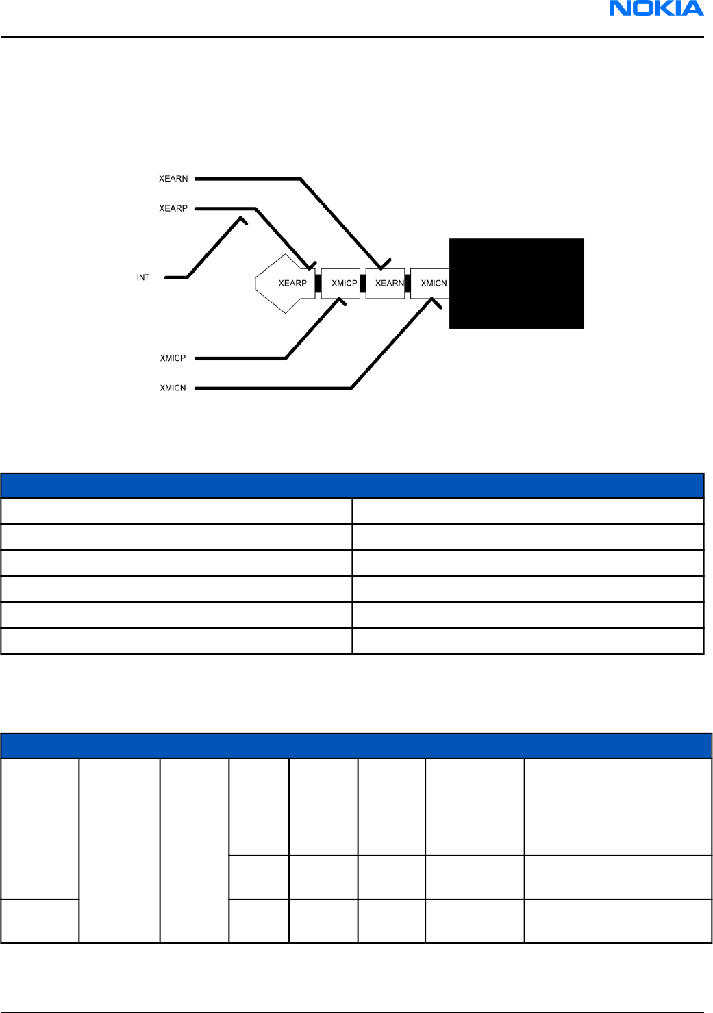
External audio connector
The system connector, containing a 4-pole Jack plug, gains the access to the external audio interface. The Jack
plug, which is integrated in the system connector, contains a mechanical switch, which is used to detect the
connection of the accessories. The configuration for the 4-pole Jack-plug is shown in the following figure.
Figure 141 4-pole jack plug for audio accessory
Table 13 Connector for External Audio Accessories
Line symbol Function
XMICP External microphone signal input
XMICN External microphone signal input
XEARP External earphone signal output
XEARN External earphone signal output
INT Accessory detection
GND Ground (Only used by PPH-1)
External signals and connections
Table 14 System connector
Signal From To Min Nom Max Condi-tion Note
XMICP HS/HF Mic UEMC
Lite
2/60mV
diff
Analog
audio in
Headset Mic bias and audio
signal 2mV nominal. HF Mic
signal 60mV nominal.
Differential symmetric
input.
DC bias
2V2kohm
Accessory detection by
bias loading
XMICN 2/60mV
diff
Ana in / 1k to
GND
Hook interrupt by heavy
bias loading
RM-74
System module Nokia Customer Care
9242678 (Issue 1) Company Confidential Page 8–11
Copyright ©2005 Nokia. All Rights Reserved.
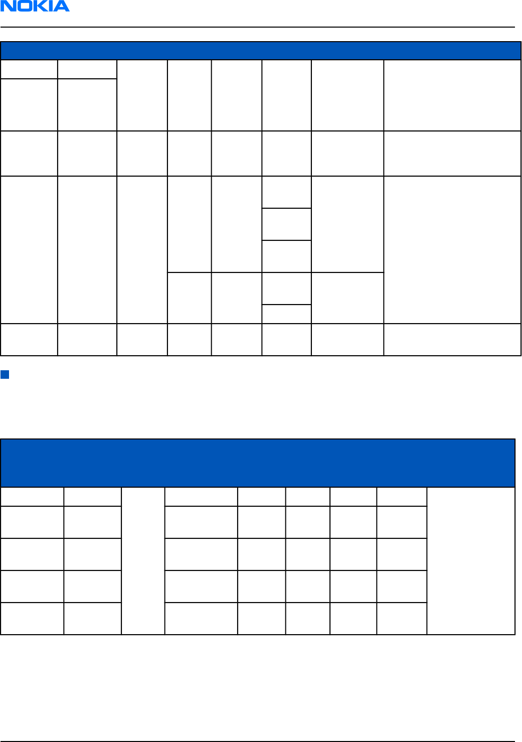
Signal From To Min Nom Max Condi-tion Note
XEARP HS/HF UEMC
Lite
100 mV
diff
Ana in Quasi-differential DC-
coupled earpiece/HF
amplifier signal to
accessory. DC biased to
0.8V
XEARN EAR/
Amp.
INT
HEADINT
Switch UEMC
Lite
0/2.7V Dig in HS interrupt from bottom
connector switch when
plug inserted.
VCHARIN Charger UEMC
Lite
11.1Vp
eak
16.9
Vpeak
Standard Vch from Charger
Connector, max 20V
7.9
VRMS
1.0
Apeak
7.0
VRMS
8.4
VRMS
9.2
VRMS
Fast charger
850 mA
GND GND GND from/to Charger
connector
Interfaces
RF and baseband interfaces
Table 15 AC and DC Characteristics of BB4.0 LiteV2 RF-Base band Digital Signals
Signal
name
From To Para-meter Input characteristics Function
Min Typ Max Unit
TXP1 UPP RF-IC 1 1.38 1.88 V Depends of the
RF design
RFGenOut
3
GenIO5 0 0 0.4 V
Load
Resistance
10 kW
Load
Capacitance
20 pF
Timing
Accuracy
¼ symbol
RM-74
Nokia Customer Care System module
Page 8–12 Company Confidential 9242678 (Issue 1)
Copyright ©2005 Nokia. All Rights Reserved.
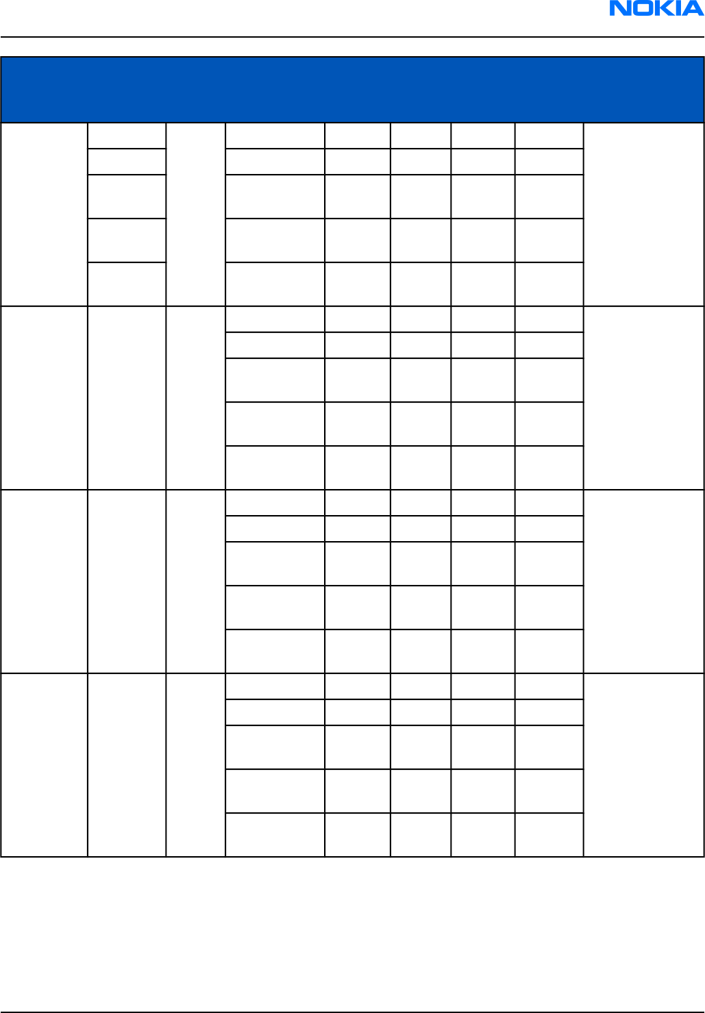
Signal
name
From To Para-meter Input characteristics Function
Min Typ Max Unit
TXP2 UPP RF-IC 1 1.38 1.88 V Depends of the
RF design
(GenIO6) 0 0 0.4 V
Load
Resistance
10 kW
Load
Capacitance
20 pF
Timing
Accuracy
¼ symbol
RFBusEn1
X
UPP RF-IC 1 1.38 1.88 V RFIC Chip SelX
0 0 0.4 V
Internal PU
Current
50 uA
Load
resistance
10 kW
Load
capacitance
20 pF
RFBusDa UPP / RF-
IC
RF- IC/
UPP
1 1.38 1.88 V Bi-directional
RF Control serial
bus data,
0 0 0.4 V
Load
resistance
10 kW
Load
capacitance
20 pF
Data
frequency
13 MHz
RFBusClk UPP RF IC 1 1.38 1.88 V RF Control serial
bus bit clock
0 0 0.4 V
Load
resistance
10 kW
Load
capacitance
20 pF
Data
frequency
13 MHz
RM-74
System module Nokia Customer Care
9242678 (Issue 1) Company Confidential Page 8–13
Copyright ©2005 Nokia. All Rights Reserved.
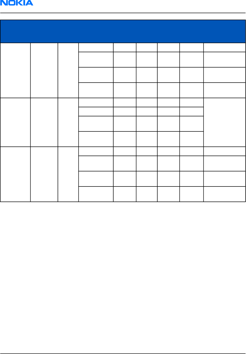
Signal
name
From To Para-meter Input characteristics Function
Min Typ Max Unit
GENIO3 UEMCLite RF IC 1 2.78 V RF Control *
0 V Depends of the
RF design
Load
resistance
kW
Output
current
4 mA
GENIO4 UEMCLite RF IC 1 2.78 V Audio clock
input in
UEMCLiteV3 and
LittiV2
0 V
Load
resistance
kW
Output
current
4 mA
GENIO5 UEMCLite RF IC 1 2.78 V RF Control *
0 V Depends of the
RF design
Load
resistance
kW
Output
current
4 mA
RM-74
Nokia Customer Care System module
Page 8–14 Company Confidential 9242678 (Issue 1)
Copyright ©2005 Nokia. All Rights Reserved.
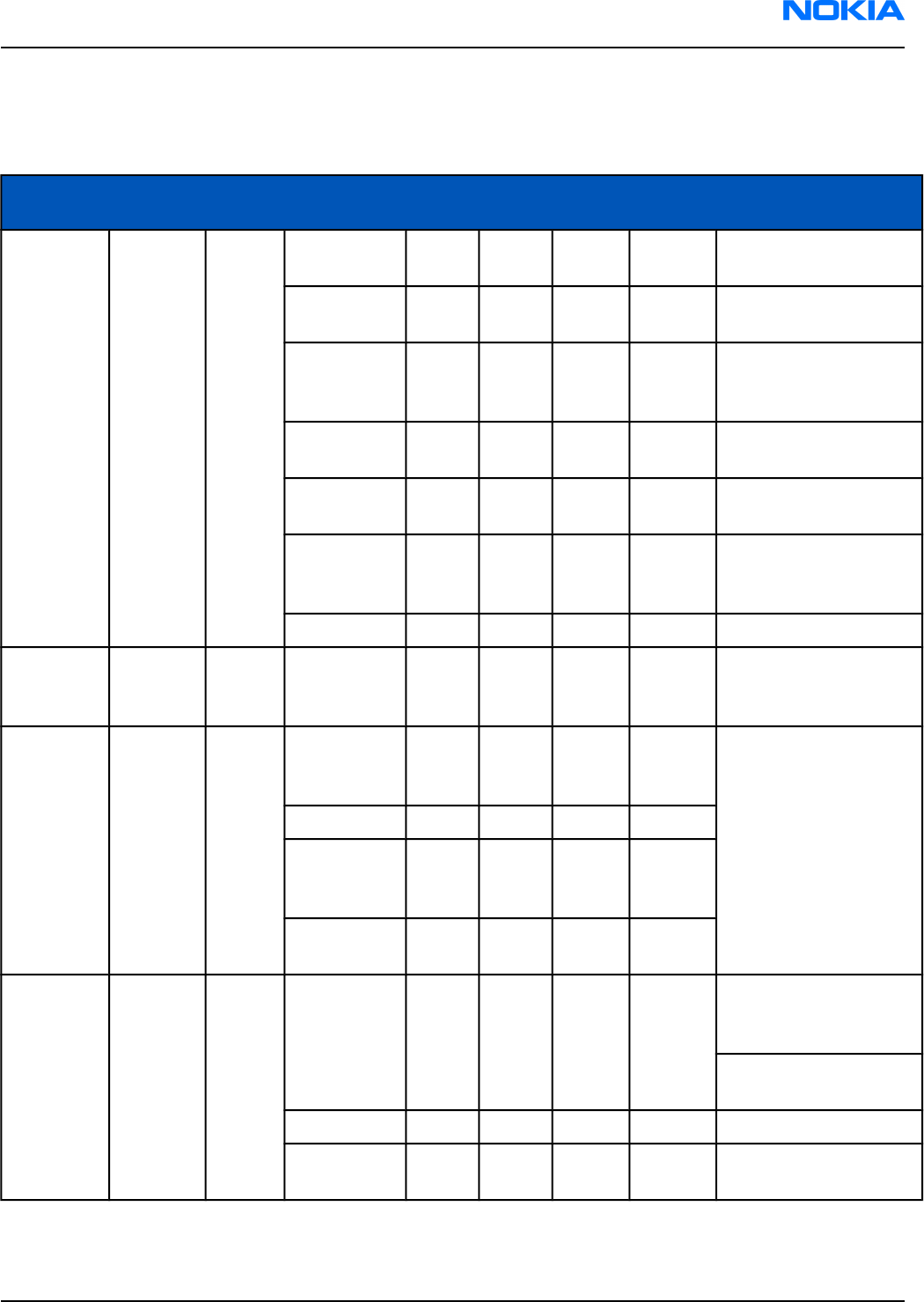
Analogue Signals
Table 16 AC and DC Characteristics of RF-Base band Analogue Signals
Signal
name
From To Parameter Min Typ Max Unit Function
RFCLK VCTCXO UPP Frequency 13/26 MHz System Clk from RF to
BB,
Signal
amplitude
0.2 0.8 1.32 Vpp 13/26 MHz Depending
on RF chipset
Input
Impedance
10 kW UPP minimum
recommended
amplitude is 0.3Vpp.
Input
Capacitance
10 pF
Harmonic
Content
-8 dBc
Clear signal
window (no
glitch)
200 mVpp
Duty Cycle 40 60 %
RFCLKGnd VCTCXO UPP DC Level 0 V System Clock slicer Ref
GND, not separated
from pwb GND layer
RXIP,
RXIN,
RXQP,
RXQN
RF-IC UEMCL
ite
Voltage
swing
(static)
1.4 1.45 Vpp Differential positive /
negative in-phase and
quadrature Rx Signals.
DC level 1.3 1.35 1.4 V
I/Q
amplitude
mismatch
0.2 dB
I/Q phase
mismatch
-0.5 0.5 deg
TXIP,
TXIN,
TXQP,
TXQN
UEMCLite RF-IC Differential
voltage
swing
(static)
2.25 2.45 Vpp Differential positive /
negative in-phase and
quadrature Tx Signals
In High-Z when RX is
receiving.
DC level 1.17 1.20 1.23 V
Source
Impedance
200 W
RM-74
System module Nokia Customer Care
9242678 (Issue 1) Company Confidential Page 8–15
Copyright ©2005 Nokia. All Rights Reserved.
Signal
name
From To Parameter Min Typ Max Unit Function
AFC UEMCLite VCTCX
O
Voltage Min 0.0 0.1 V Automatic Frequency
Control signal for
VCTCXO
Programmable
(AFCOUT
)
Max 2.4 2.55
Resolution 11 bits
Load
resistance
1 kW
and
capacitance
100 nF
Source
Impedance
200 W
Output
impedance
10 MW Path powered down
TxC UEMCLite RF-IC Voltage Min 0.1 V Transmitter power
level and ramping
control, Ref UEMCLite
RF converter
specification
(AUXOUT
)
Max 2.4
Source
Impedance
200 W
Resolution 10 bits
VCXOTEMP RF-IC UEMCL
ite
Input
voltage
range
0 2.7 V
Input
resistance
900 6000 Ohm
Resolution 10 bits
PATEMP RF-IC UEMCL
ite
Voltage at
-20oC
1.57 V Usage depends of the
RF design
FM radio
Signal From To Min Nom Max Cond Note
KEYB1 /
MIC3P
FM radio UEMCLite Differential/single ended
signal from internal
additional audio device,
Muxed with analog
keyboard inputs.
KEYB2 /
MIC3N
LCD interface
The figure below illustrates the structure of LCD module. LCD module includes UV tape, Driver IC, Prism sheet,
LGP, Flex Assy, label Tape, Adhesive Tape, Protection film, LCD glass, Rim Tape, Diffuser, Reflector and Holder
Frame.
LCD panel includes upper and lower polarizers, LCD transflective glass, single chip COG driver with
132x132x116bit RAM, 10-pin board-to-board connector and FPC with discrete components.
RM-74
Nokia Customer Care System module
Page 8–16 Company Confidential 9242678 (Issue 1)
Copyright ©2005 Nokia. All Rights Reserved.
Keyboard
A 5 X 5 matrix keyboad consists of 21keys, one 10-channel integrated passive filiter arrays with downstream
ESD protection of >8KV connect the matrix keyboard to UPP.
Figure 142 Keyboard schematics
The layout is shown in Keyboard layout in UI side.
Figure 143 Keyboard layout in UI side
RM-74
System module Nokia Customer Care
9242678 (Issue 1) Company Confidential Page 8–17
Copyright ©2005 Nokia. All Rights Reserved.
SIM interface
The SIM interface is programmed to support 3V and 1.8V SIMs. SIM supply voltage is selected by with register
in the UEMCLite. It is only allowed to change the SIM supply voltage when the SIM IF is powered down. The SIM
power up/down sequence is generated in the UEMCLite.
The SIM interface is powered up when the SIMCardDet signal indicates ”card in”. This signal is derived from the
BSI signal.
SIM interface is implemented in two ASICs, UPP and UEMCLite. The SIM interface is the electrical interface between
the Subscriber Identity Module Card (SIM Card) and mobile phone (via UEMCLite device).
Table 17 The electrical parameters
Pin Name Parameter Min Typ Max Unit Notes
1VSIM 1.8V SIM Card 1.6 1.8 1.9 V Supply voltage
3V SIM Card 2.8 3.0 3.2 V
2 SIMRST 1.8V SIM Card 0.9xVSIM VSIM V SIM reset (output)
0 0.15xVSIM
3V SIM Card 0.9xVSIM VSIM V
0 0.15xVSIM
3 SIMCLK Frequency 3.25 MHz SIM clock. UPP4Mv3
and UPP4mv4
support 3GPP
Release 5, SIMCLK/8
data rate. UPP2Mv2
supports SIMCLK/16
data rate.
Trise/Tfall 50 ns
1.8V Voh 0.9xVSIM VSIM V
1.8V Vol 0
3V Voh 0.9xVSIM VSIM V
3V Vol 0
4 DATA 1.8V Voh 0.9xVSIM VSIM V SIM data (output)
1.8V Vol 0 0.15xVSIM
3V Voh 0.9xVSIM VSIM
3V Vol 0 0.15xVSIM
1.8V Vih 0.7xVSIM VSIM V SIM data (input)
1.8V Vil 0 0.15xVSIM Trise/Tfall max 1us
3V Vil 0.7xVSIM VSIM
3V Vil 0 0.15xVSIM
5 NC Not connected
6 GND GND 0 0 V Ground
VSIM specified in regulator section in this document
RM-74
Nokia Customer Care System module
Page 8–18 Company Confidential 9242678 (Issue 1)
Copyright ©2005 Nokia. All Rights Reserved.
External signals and connections
Table 18 System connector
Signal From To Min Nom Max Condi-tion Note
XMICP HS/HF Mic UEMC
Lite
2/60mV
diff
Analog
audio in
Headset Mic bias and audio
signal 2mV nominal. HF Mic
signal 60mV nominal.
Differential symmetric
input.
DC bias
2V2kohm
Accessory detection by
bias loading
XMICN 2/60mV
diff
Ana in / 1k to
GND
Hook interrupt by heavy
bias loading
XEARP HS/HF UEMC
Lite
100 mV
diff
Ana in Quasi-differential DC-
coupled earpiece/HF
amplifier signal to
accessory. DC biased to
0.8V
XEARN EAR/
Amp.
INT
HEADINT
Switch UEMC
Lite
0/2.7V Dig in HS interrupt from bottom
connector switch when
plug inserted.
VCHARIN Charger UEMC
Lite
11.1Vp
eak
16.9
Vpeak
Standard Vch from Charger
Connector, max 20V
7.9
VRMS
1.0
Apeak
7.0
VRMS
8.4
VRMS
9.2
VRMS
Fast charger
850 mA
GND GND GND from/to Charger
connector
Battery connector
Internal, user-changeable batteries. Semi-fixed. Types: Li-Ion, NiMH. Interface, 4 terminals (VBATT, GND, BSI,
BTEMP) Janette battery interface is used. The battery type and size are defined in the next chapter.
Table 19 Battery IF
Signal From To Min Nom Max Condi-tion Note
GND Global Batt (-) Global GND
VBAT Batt (+) 3.1 5.1 Battery Voltage
RM-74
System module Nokia Customer Care
9242678 (Issue 1) Company Confidential Page 8–19
Copyright ©2005 Nokia. All Rights Reserved.
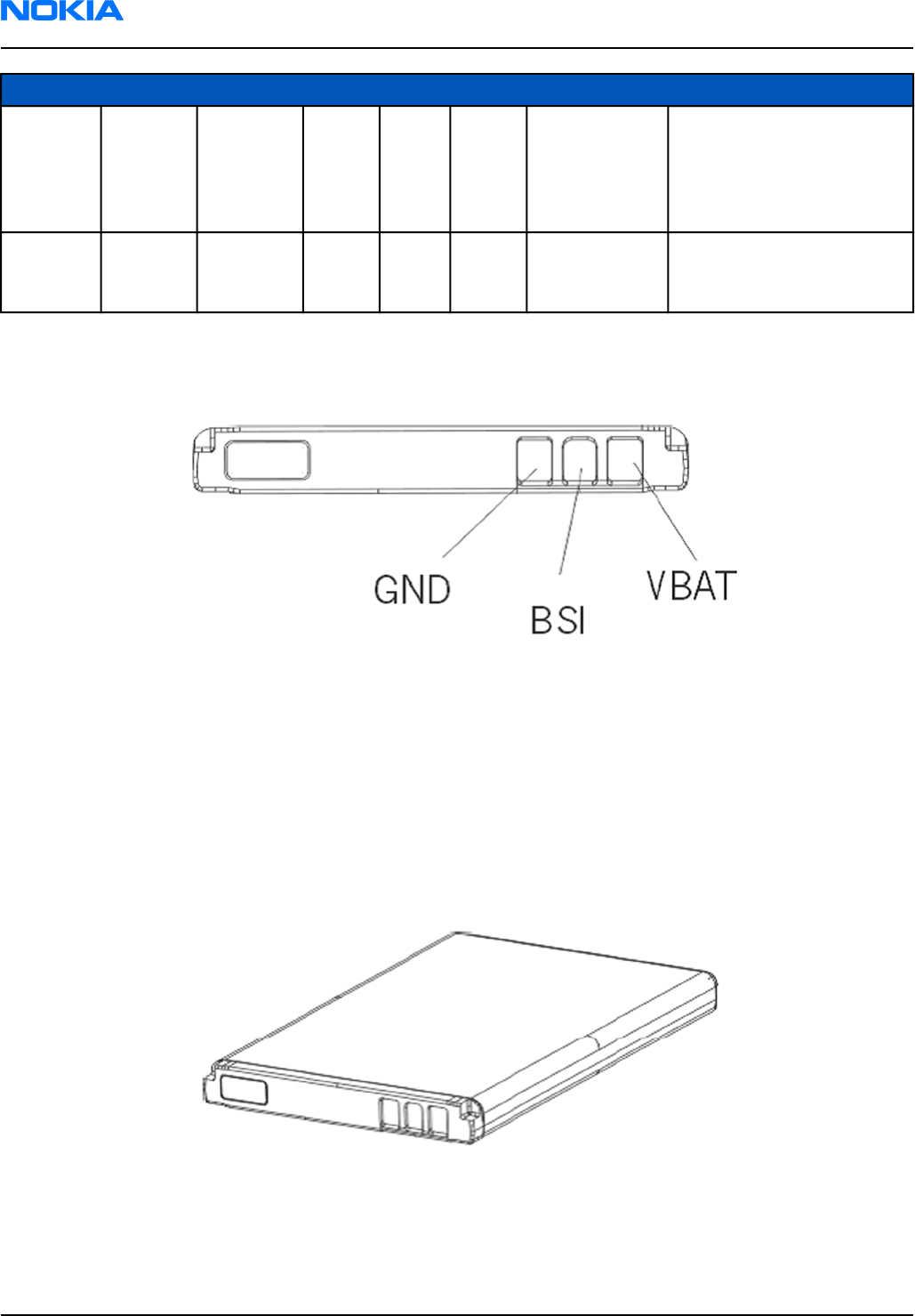
Signal From To Min Nom Max Condi-tion Note
BSI UEMCLite 0 2.78 Analog input, Battery Size
Indicator Resistor, 100
kohm pull up to 2.78V
(VBB1). FDL Init, refer to
flash download.
BTEMP UEMCLite 0 2.78 Btemp NTC Resistor, 100
kohm pull up to 2.78V
(VANA)
* Note! In BL-5C battery IF the BTEMP signal doesn’t exists. Temperature measurement is done on system board
with NTC resistor.
Figure 144 BL-5C battery connection order
Battery
• Type: BL-5C
• Technology: Li-Ion, 4.2 V charging, 3.1 V cut-off
• Capacity: 900 mAh.
The BSI resistor is placed on the main PWB as the telephone supports only one battery capacity. Further a BSI
connection is added to the Flash interface. The battery temperature is measured by a NTC resistor placed on
the main PWB, opposite to the Battery. Battery pack has an impedance of 130 - 150 mΩ (0 – 45 °C).
Figure 145 BL-5C battery block
RM-74
Nokia Customer Care System module
Page 8–20 Company Confidential 9242678 (Issue 1)
Copyright ©2005 Nokia. All Rights Reserved.
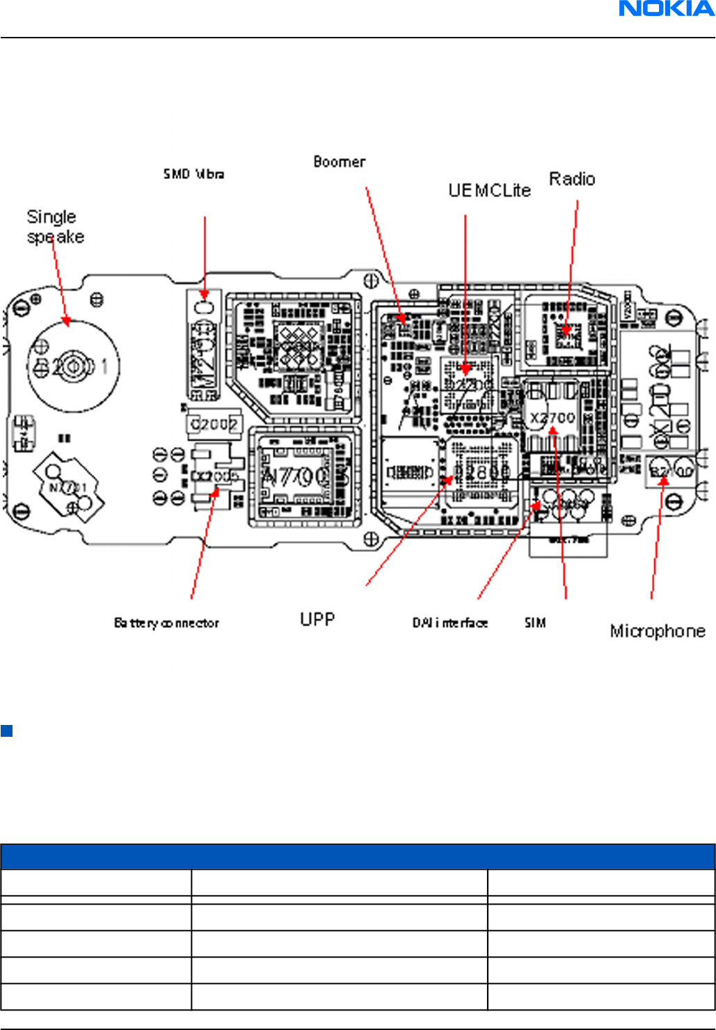
PWB outline
Figure 146 PWB top side component placement
RF description
Frequency band, power and multi-slot class
The requirements leads to the specification in the table below:
Table 20 Frequency bands and TX power class
System Frequency band TX power class
GSM850 Tx: 824 – 849 MHz 4 (33dBm)
GSM900 Tx: 880 – 915 MHz 4 (33dBm)
Rx: 925 – 960 MHz
GSM1800 Tx: 1710 – 1785 MHz 1 (30dBm)
Rx: 1805 – 1880 MHz
RM-74
System module Nokia Customer Care
9242678 (Issue 1) Company Confidential Page 8–21
Copyright ©2005 Nokia. All Rights Reserved.
System Frequency band TX power class
GSM1900 Tx: 1850 – 1910 MHz 1 (30dBm)
Rx: 1930 – 1990 MHz
Table 21 Multi-slot class
Multislot Class
GPRS MSC 6 (up to 3+1 and 2+2)
Transmitter - general description
The transmitter has 2 separate parallel paths one covering either the 850 or the 900 band and the other the
1800/1900 bands. The transmitter operates in GMSK mode only. The power level control circuitry is integrated
in the front-end module.
Each path of the transmitter is composed of a baseband lowpass filter for the I/Q signals and a quadrature direct
modulator integrated in PMB3258. At the modulator’s output there is a bandpass filter for each band (so-called
H3 filter) and a balun transformer to convert the differential output signal from the modulator into a single-
ended 50 ohm signal. This signal is fed into the input of the PA. The two power amplifiers and the antenna
switch are located in a single module with built-in power control loop.
The two control methods used are open-loop Vcc control (RFMD) and feedback control with current sensing
(Renesas, Philips). The reference waveform (TXC) for the control loop comes from the baseband. The output of
the PA goes into a low pass filter located inside the FEM (Front End Module). Finally the transmit signal goes
through the band selection and TX/RX switches to the antenna port.
The FEM is controlled with four digital control signals (TXP, Vc1, Vc2 and Vc3) to meet the TDMA frame timing
requirements.
Transmitter - signal processing
The I/Q signals coming from the baseband section are fed into the modulator and converted up to the carrier
frequency. The I/Q are post filtered by a 1st order passive RC filter (discrete components on PWB) and a 3rd
order active filter (Legendre type) inside PMB3258.
The nominal output level of the modulator is +3.5 dBm in both bands. The modulator's output is an open-
collector type and need an external load and a DC supply feed. The load and the DC supply feed are implemented
as the part of the H3 filter. The H3 filter will attenuate mainly the 2nd and 3rd harmonics of the modulated RF
signal and provide suitable termination impedance for the modulator on the fundamental and harmonic
frequencies. Owing to the low noise floor of the PMB3258 modulator a narrow-band filter for the TX noise is
not required on either band, although the margin to the specification limit is quite narrow in the GSM850/900
bands.
The filtered signal is fed into the input of the FEM, which amplifies it to the desired power level and provides
the signal at the antenna port. There are built-in lowpass filters for the TX harmonics in the front-end module.
There is also a temperature sensor close to the FEM to enable SW temperature compensation for e.g. the power
levels. The sensor is connected to one of the slow ADC channels in the baseband.
VCXO and PLL
The VCO frequency is locked by a PLL (phase locked loop) into a stable frequency source given by a VCXO. The
frequency of the VCXO is in turn locked into the frequency of the base station with the help of an AFC (automatic
frequency control) voltage, which is generated in the UEM. The reference frequency is 26 MHz.
The VCXO also provides a 26 MHz system clock for the digital baseband.
The PLL is located in PMB3258 and it is controlled via the RFBUS.
RM-74
Nokia Customer Care System module
Page 8–22 Company Confidential 9242678 (Issue 1)
Copyright ©2005 Nokia. All Rights Reserved.

9 — Schematics
Nokia Customer Care
9242678 (Issue 1) Company Confidential Page 9–1
Copyright ©2005 Nokia. All Rights Reserved.

RM-74
Nokia Customer Care Schematics
(This page left intentionally blank.)
Page 9–2 Company Confidential 9242678 (Issue 1)
Copyright ©2005 Nokia. All Rights Reserved.

Table of Contents
Schematics.........................................................................................................................................................................................9–4
List of Figures
Figure 147 RM-74, 1mf_07a: UPP, UEM, Combo memory, Radio, SIM..............................................................................9–4
Figure 148 RM-74, 1mf_07a: UI, Keyboard, Audio.................................................................................................................9–5
Figure 149 RM-74, 1mf_07a: RF part.........................................................................................................................................9–6
Figure 150 RM-74, 1mf_07a: Signal overview........................................................................................................................9–7
Figure 151 RM-74, 1mf_07a: Component finder....................................................................................................................9–8
RM-74
Schematics Nokia Customer Care
9242678 (Issue 1) Company Confidential Page 9–3
Copyright ©2005 Nokia. All Rights Reserved.
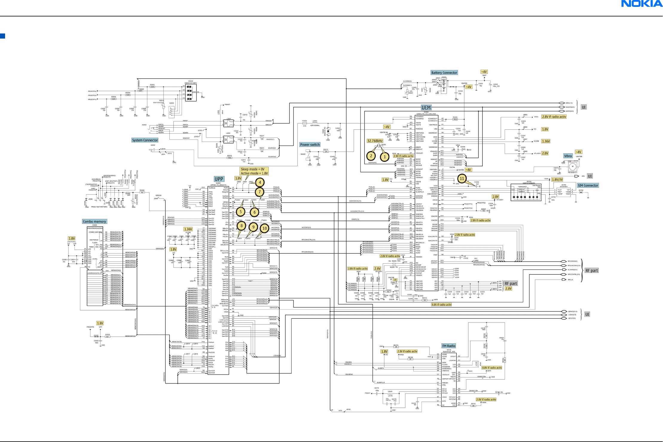
Schematics
UPP, UEM, Combo memory, Radio, SIM
Figure 147 RM-74, 1mf_07a: UPP, UEM, Combo memory, Radio, SIM
RM-74
Schematics Nokia Customer Care
9242678 (Issue 1) Company Confidential Page 9–4
Copyright ©2005 Nokia. All Rights Reserved.
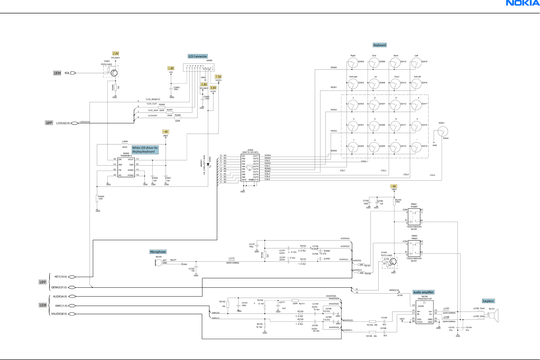
UI, Keyboard, Audio
Figure 148 RM-74, 1mf_07a: UI, Keyboard, Audio
RM-74
Schematics Nokia Customer Care
9242678 (Issue 1) Company Confidential Page 9–5
Copyright ©2005 Nokia. All Rights Reserved.
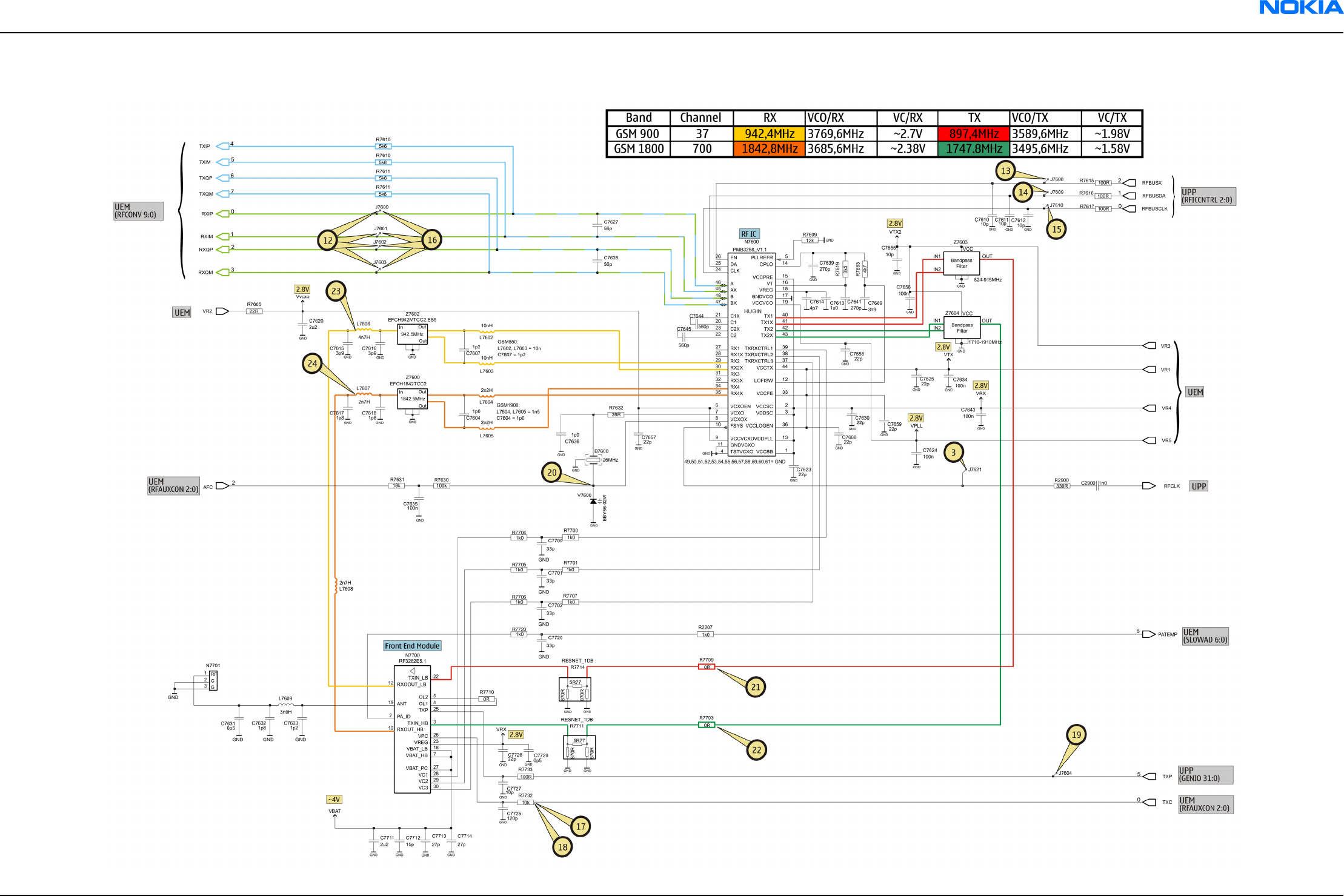
RF part
Figure 149 RM-74, 1mf_07a: RF part
RM-74
Schematics Nokia Customer Care
9242678 (Issue 1) Company Confidential Page 9–6
Copyright ©2005 Nokia. All Rights Reserved.
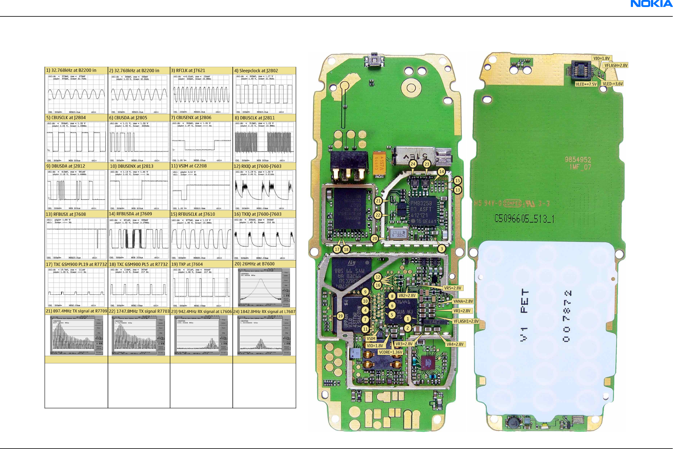
Signal overview
Figure 150 RM-74, 1mf_07a: Signal overview
RM-74
Schematics Nokia Customer Care
9242678 (Issue 1) Company Confidential Page 9–7
Copyright ©2005 Nokia. All Rights Reserved.

Component finder
Figure 151 RM-74, 1mf_07a: Component finder
RM-74
Schematics Nokia Customer Care
9242678 (Issue 1) Company Confidential Page 9–8
Copyright ©2005 Nokia. All Rights Reserved.

Glossary
Nokia Customer Care
9242678 (Issue 1) Company Confidential Page Glossary–1
Copyright ©2005 Nokia. All Rights Reserved.

RM-74
Nokia Customer Care Glossary of terms
(This page left intentionally blank.)
Page Glossary–2 Company Confidential 9242678 (Issue 1)
Copyright ©2005 Nokia. All Rights Reserved.
A/D-converter Analog-to-digital converter
ACI Accessory Control Interface
ADC Analog-to-digital converter
ADSP Application DPS (expected to run high level tasks)
AGC Automatic gain control (maintains volume)
ALS Ambient light sensor
AMSL After Market Service Leader
ARM Advanced RISC Machines
ARPU Average revenue per user (per month or per year)
ASIC Application Specific Integrated Circuit
ASIP Application Specific Interface Protector
B2B Board to board, connector between PWB and UI board
BB Baseband
BC02 Bluetooth module made by CSR
BIQUAD Bi-quadratic ,type of filter function)
BSI Battery Size Indicator
BT Bluetooth
CBus MCU controlled serial bus connected to UPP_WD2,UEME and Zocus
CCP Compact Camera Port
CDSP Cellular DSP (expected to run at low levels)
CLDC Connected limited device configuration
CMOS Complimentary metal-oxide semiconductor circuit (low power consumption)
COF Chip on Foil
COG Chip on Glass
CPU Central Processing Unit
CSR cambridge silicon radio
CSTN Color Super Twisted Nematic
CTSI Clock Timing Sleep and interrupt block of Tiku
CW Continuous wave
D/A-converter Digital-to-analouge converter
DAC Digital-to-analouge converter
DBI Digital Battery Interface
DBus DSP controlled serial bus connected between UPP_WD2 and Helgo
DCT-4 Digital Core Technology
DMA Direct memory access
DP Data Package
RM-74
Glossary of terms Nokia Customer Care
9242678 (Issue 1) Company Confidential Page Glossary–3
Copyright ©2005 Nokia. All Rights Reserved.
DPLL Digital Phase Locked Loop
DSP Digital Signal Processor
DtoS Differential to Single ended
EDGE Enhanced data rates for global/GSM evaluation
EGSM Extended GSM
EM Energy management
EMC Electromagnetic compability
EMI Electromagnetic interference
ESD Electrostatic discharge
FCI Functional cover interface
FPS Flash Programming Tool
FR Full rate
FSTN Film compensated super twisted nematic
GND Ground, conductive mass
GPIB General-purpose interface bus
GPRS General Packet Radio Service
GSM Group Special Mobile/Global System for Mobile communication
HF Hands free
HFCM Handsfree Common
HS Handset
HSCSD High speed circuit switched data (data transmission connection faster than GSM)
HW Hardware
I/O Input/Output
IBAT Battery current
IC Integrated circuit
ICHAR Charger current
IF Interface
IHF Integrated hands free
IMEI International Mobile Equipment Identity
IR Infrared
IrDA Infrared Data Associasion
ISA Intelligent software architecture
JPEG/JPG Joint Photographic Experts Group
LCD Liquid Crystal Display
LDO Low Drop Out
LED Light-emitting diode
RM-74
Nokia Customer Care Glossary of terms
Page Glossary–4 Company Confidential 9242678 (Issue 1)
Copyright ©2005 Nokia. All Rights Reserved.
LPRF Low Power Radio Frequency
MCU Micro Controller Unit (microprocessor)
MCU Multiport control unit
MIC, mic Microphone
MIDP Mobile Information Device Profile
MIN Mobile identification number
MIPS Million instructions per second
MMC Multimedia card
MMS Multimedia messaging service
NTC Negative temperature coefficient, temperature sensitive resistor used as a
temperature sensor
OMA Object management architechture
OMAP Operations, maintenance, and administartion part
Opamp Operational Amplifier
PA Power amplifier
PDA Pocket Data Application
PDA Personal digital assistant
PDRAM Program/Data RAM (on chip in Tiku)
Phoenix Software tool of DCT4.x
PIM Personal Information Management
PLL Phase locked loop
PM (Phone) Permanent memory
PUP General Purpose IO (PIO), USARTS and Pulse Width Modulators
PURX Power-up reset
PWB Printed Wiring Board
PWM Pulse width modulation
RC-filter Resistance-Capacitance filter
RF Radio Frequency
RF PopPort TM Reduced function PopPortTM interface
RFBUS Serial control Bus For RF
RSK Right Soft Key
RS-MMC Reduced size Multi Media Card
RSSI Receiving signal strength indicator
RST Reset Switch
RTC Real Time Clock (provides date and time)
RX Radio Receiver
RM-74
Glossary of terms Nokia Customer Care
9242678 (Issue 1) Company Confidential Page Glossary–5
Copyright ©2005 Nokia. All Rights Reserved.
SARAM Single Access RAM
SAW filter Surface Acoustic Wave filter
SDRAM Synchronous Dynamic Random Access Memory
SID Security ID
SIM Subscriber Identity Module
SMPS Switched Mode Power Supply
SNR Signal-to-noice ratio
SPR Standard Product requirements
SRAM Static random access memory
STI Serial Trace Interface
SW Software
SWIM Subscriber/Wallet Identification Module
TCXO Temperature controlled Oscillator
Tiku Finnish for Chip, Successor of the UPP, Official Tiku3G
TX Radio Transmitter
UART Universal asynchronous receiver/transmitter
UEME Universal Energy Management chip (Enhanced version)
UEMEK See UEME
UI User Interface
UPP Universal Phone Processor
UPP_WD2 Communicator version of DCT4 system ASIC
USB Universal Serial Bus
VBAT Battery voltage
VCHAR Charger voltage
VCO Voltage controlled oscillator
VCTCXO Voltage Controlled Temperature Compensated Crystal Oscillator
VCXO Voltage Controlled Crystal Oscillator
Vp-p Peak-to-peak voltage
VSIM SIM voltage
WAP Wireless application protocol
WD Watchdog
XHTML Extensible hypertext markup language
Zocus Current sensor, (used to monitor the current flow to and from the battery)
RM-74
Nokia Customer Care Glossary of terms
Page Glossary–6 Company Confidential 9242678 (Issue 1)
Copyright ©2005 Nokia. All Rights Reserved.
