Nokia C6 00 Rm 612 624 Service Manual 34 V1
User Manual: Smartphone Nokia C6-00 RM-612, RM-624 - Service manuals and Schematics, Disassembly / Assembly. Free.
Open the PDF directly: View PDF ![]() .
.
Page Count: 228 [warning: Documents this large are best viewed by clicking the View PDF Link!]
- Amendment Record Sheet
- Copyright
- Warnings and cautions
- ESD protection
- Care and maintenance
- Company policy
- Battery information
- Nokia C6-00; L3&4 Service Manual Structure
- 1 General Information
- 2 Service Tools and Service Concepts
- Service tools
- Service concepts
- POS (Point of Sale) flash concept
- Flash concept with FPS-21
- CU-4 flash concept with FPS-21
- Flash concept with FPS-21 and SB-6
- Flash concept with SS-46 and CA-89DS
- Flash concept with SS-62 and CA-89DS
- Flash concept with FPS-21, SS-62 and SB-6
- Flash concept with FPS-21, SS-62 and SB-7
- Module jig service concept
- Module jig service concept with SB-6
- Service concept for RF testing and RF/BB tuning
- 3 BB Troubleshooting and Manual Tuning Guide
- Baseband main troubleshooting
- Dead or jammed device troubleshooting
- General power checking
- Clocking troubleshooting
- Charging troubleshooting
- Backup battery troubleshooting
- Flash programming troubleshooting
- Combo memory troubleshooting
- MicroSD card troubleshooting
- USB troubleshooting
- SIM card troubleshooting
- Power key troubleshooting
- Vibra troubleshooting
- Accelerometer troubleshooting
- Touch screen troubleshooting
- Hardware keys troubleshooting
- Display module troubleshooting
- LED and LED driver troubleshooting
- Ambient Light Sensor troubleshooting
- GPS troubleshooting
- WLAN troubleshooting
- Bluetooth and FM radio troubleshooting
- Audio troubleshooting
- Baseband manual tuning guide
- 4 RF Troubleshooting
- 5 System Module and User Interface
- Introduction
- Energy management
- Bluetooth and FM RDS radio module
- I/O Expander
- GPS interface
- WLAN interface
- High-speed USB
- CBUS interface
- FBUS interface
- ECI interface
- SIM interface
- MicroSD card interface
- Camera concept
- User interface
- ASICs
- Device memories
- Audio concept
- Baseband technical specifications
- RF technical description
- Frequency mappings
- Glossary

Service Manual
RM-612; RM-624 (Nokia C6-00; L3&4)
Mobile Terminal
Part No: (Issue 1)
Nokia Customer Care
COMPANY CONFIDENTIAL
Copyright © 2010 Nokia. All rights reserved.

Amendment Record Sheet
Amendment No Date Inserted By Comments
Issue 1 4/2010 AP-K
RM-612; RM-624
Amendment Record Sheet
Page ii COMPANY CONFIDENTIAL Issue 1
Copyright © 2010 Nokia. All rights reserved.

Copyright
Copyright © 2010 Nokia. All rights reserved.
Reproduction, transfer, distribution or storage of part or all of the contents in this document in any form
without the prior written permission of Nokia is prohibited.
Nokia, Nokia Connecting People, and Nokia X and Y are trademarks or registered trademarks of Nokia
Corporation. Other product and company names mentioned herein may be trademarks or tradenames of
their respective owners.
Nokia operates a policy of continuous development. Nokia reserves the right to make changes and
improvements to any of the products described in this document without prior notice.
Under no circumstances shall Nokia be responsible for any loss of data or income or any special, incidental,
consequential or indirect damages howsoever caused.
The contents of this document are provided "as is". Except as required by applicable law, no warranties of
any kind, either express or implied, including, but not limited to, the implied warranties of merchantability
and fitness for a particular purpose, are made in relation to the accuracy, reliability or contents of this
document. Nokia reserves the right to revise this document or withdraw it at any time without prior notice.
The availability of particular products may vary by region.
IMPORTANT
This document is intended for use by qualified service personnel only.
RM-612; RM-624
Copyright
Issue 1 COMPANY CONFIDENTIAL Page iii
Copyright © 2010 Nokia. All rights reserved.

Warnings and cautions
Warnings
•IF THE DEVICE CAN BE INSTALLED IN A VEHICLE, CARE MUST BE TAKEN ON INSTALLATION IN VEHICLES FITTED
WITH ELECTRONIC ENGINE MANAGEMENT SYSTEMS AND ANTI-SKID BRAKING SYSTEMS. UNDER CERTAIN FAULT
CONDITIONS, EMITTED RF ENERGY CAN AFFECT THEIR OPERATION. IF NECESSARY, CONSULT THE VEHICLE DEALER/
MANUFACTURER TO DETERMINE THE IMMUNITY OF VEHICLE ELECTRONIC SYSTEMS TO RF ENERGY.
•THE PRODUCT MUST NOT BE OPERATED IN AREAS LIKELY TO CONTAIN POTENTIALLY EXPLOSIVE ATMOSPHERES,
FOR EXAMPLE, PETROL STATIONS (SERVICE STATIONS), BLASTING AREAS ETC.
•OPERATION OF ANY RADIO TRANSMITTING EQUIPMENT, INCLUDING CELLULAR TELEPHONES, MAY INTERFERE
WITH THE FUNCTIONALITY OF INADEQUATELY PROTECTED MEDICAL DEVICES. CONSULT A PHYSICIAN OR THE
MANUFACTURER OF THE MEDICAL DEVICE IF YOU HAVE ANY QUESTIONS. OTHER ELECTRONIC EQUIPMENT MAY
ALSO BE SUBJECT TO INTERFERENCE.
•BEFORE MAKING ANY TEST CONNECTIONS, MAKE SURE YOU HAVE SWITCHED OFF ALL EQUIPMENT.
Cautions
•Servicing and alignment must be undertaken by qualified personnel only.
•Ensure all work is carried out at an anti-static workstation and that an anti-static wrist strap is worn.
•Ensure solder, wire, or foreign matter does not enter the telephone as damage may result.
•Use only approved components as specified in the parts list.
•Ensure all components, modules, screws and insulators are correctly re-fitted after servicing and
alignment.
•Ensure all cables and wires are repositioned correctly.
•Never test a mobile phone WCDMA transmitter with full Tx power, if there is no possibility to perform the
measurements in a good performance RF-shielded room. Even low power WCDMA transmitters may disturb
nearby WCDMA networks and cause problems to 3G cellular phone communication in a wide area.
•During testing never activate the GSM or WCDMA transmitter without a proper antenna load, otherwise
GSM or WCDMA PA may be damaged.
RM-612; RM-624
Warnings and cautions
Page iv COMPANY CONFIDENTIAL Issue 1
Copyright © 2010 Nokia. All rights reserved.

ESD protection
Nokia requires that service points have sufficient ESD protection (against static electricity) when servicing
the phone.
Any product of which the covers are removed must be handled with ESD protection. The SIM card can be
replaced without ESD protection if the product is otherwise ready for use.
To replace the covers ESD protection must be applied.
All electronic parts of the product are susceptible to ESD. Resistors, too, can be damaged by static electricity
discharge.
All ESD sensitive parts must be packed in metallized protective bags during shipping and handling outside
any ESD Protected Area (EPA).
Every repair action involving opening the product or handling the product components must be done under
ESD protection.
ESD protected spare part packages MUST NOT be opened/closed out of an ESD Protected Area.
For more information and local requirements about ESD protection and ESD Protected Area, contact your local
Nokia After Market Services representative.
RM-612; RM-624
ESD protection
Issue 1 COMPANY CONFIDENTIAL Page v
Copyright © 2010 Nokia. All rights reserved.

Care and maintenance
This product is of superior design and craftsmanship and should be treated with care. The suggestions below
will help you to fulfil any warranty obligations and to enjoy this product for many years.
•Keep the phone and all its parts and accessories out of the reach of small children.
•Keep the phone dry. Precipitation, humidity and all types of liquids or moisture can contain minerals that
will corrode electronic circuits.
•Do not use or store the phone in dusty, dirty areas. Its moving parts can be damaged.
•Do not store the phone in hot areas. High temperatures can shorten the life of electronic devices, damage
batteries, and warp or melt certain plastics.
•Do not store the phone in cold areas. When it warms up (to its normal temperature), moisture can form
inside, which may damage electronic circuit boards.
•Do not drop, knock or shake the phone. Rough handling can break internal circuit boards.
•Do not use harsh chemicals, cleaning solvents, or strong detergents to clean the phone.
•Do not paint the phone. Paint can clog the moving parts and prevent proper operation.
•Use only the supplied or an approved replacement antenna. Unauthorised antennas, modifications or
attachments could damage the phone and may violate regulations governing radio devices.
All of the above suggestions apply equally to the product, battery, charger or any accessory.
RM-612; RM-624
Care and maintenance
Page vi COMPANY CONFIDENTIAL Issue 1
Copyright © 2010 Nokia. All rights reserved.

Company policy
Our policy is of continuous development; details of all technical modifications will be included with service
bulletins.
While every endeavour has been made to ensure the accuracy of this document, some errors may exist. If
any errors are found by the reader, NOKIA MOBILE PHONES Business Group should be notified in writing/e-
mail.
Please state:
•Title of the Document + Issue Number/Date of publication
•Latest Amendment Number (if applicable)
•Page(s) and/or Figure(s) in error
Please send to:
NOKIA CORPORATION
Nokia Mobile Phones Business Group
Nokia Customer Care
PO Box 86
FIN-24101 SALO
Finland
E-mail: Service.Manuals@nokia.com
RM-612; RM-624
Company policy
Issue 1 COMPANY CONFIDENTIAL Page vii
Copyright © 2010 Nokia. All rights reserved.

Battery information
Note: A new battery's full performance is achieved only after two or three complete charge and
discharge cycles!
The battery can be charged and discharged hundreds of times but it will eventually wear out. When the
operating time (talk-time and standby time) is noticeably shorter than normal, it is time to buy a new battery.
Use only batteries approved by the phone manufacturer and recharge the battery only with the chargers
approved by the manufacturer. Unplug the charger when not in use. Do not leave the battery connected to
a charger for longer than a week, since overcharging may shorten its lifetime. If left unused a fully charged
battery will discharge itself over time.
Temperature extremes can affect the ability of your battery to charge.
For good operation times with Li-Pol batteries, discharge the battery from time to time by leaving the product
switched on until it turns itself off (or by using the battery discharge facility of any approved accessory
available for the product). Do not attempt to discharge the battery by any other means.
Use the battery only for its intended purpose.
Never use any charger or battery which is damaged.
Do not short-circuit the battery. Accidental short-circuiting can occur when a metallic object (coin, clip or
pen) causes direct connection of the + and - terminals of the battery (metal strips on the battery) for example
when you carry a spare battery in your pocket or purse. Short-circuiting the terminals may damage the battery
or the connecting object.
Leaving the battery in hot or cold places, such as in a closed car in summer or winter conditions, will reduce
the capacity and lifetime of the battery. Always try to keep the battery between 15°C and 25°C (59°F and 77°
F). A phone with a hot or cold battery may temporarily not work, even when the battery is fully charged.
Batteries' performance is particularly limited in temperatures well below freezing.
Do not dispose of batteries in a fire!
Dispose of batteries according to local regulations (e.g. recycling). Do not dispose as household waste.
RM-612; RM-624
Battery information
Page viii COMPANY CONFIDENTIAL Issue 1
Copyright © 2010 Nokia. All rights reserved.

Nokia C6-00; L3&4 Service Manual Structure
1 General Information
2 Service Tools and Service Concepts
3 BB Troubleshooting and Manual Tuning Guide
4 RF Troubleshooting
5 System Module and User Interface
Glossary
RM-612; RM-624
Nokia C6-00; L3&4 Service Manual Structure
Issue 1 COMPANY CONFIDENTIAL Page ix
Copyright © 2010 Nokia. All rights reserved.

RM-612; RM-624
Nokia C6-00; L3&4 Service Manual Structure
(This page left intentionally blank.)
Page x COMPANY CONFIDENTIAL Issue 1
Copyright © 2010 Nokia. All rights reserved.

1 — General Information
Nokia Customer Care
Issue 1 COMPANY CONFIDENTIAL Page 1 – 1
Copyright © 2010 Nokia. All rights reserved.

RM-612; RM-624
General Information
(This page left intentionally blank.)
Page 1 – 2 COMPANY CONFIDENTIAL Issue 1
Copyright © 2010 Nokia. All rights reserved.

Table of Contents
Product selection................................................................................................................................................... 1–5
Product features and sales package.................................................................................................................... 1–5
Mobile enhancements........................................................................................................................................... 1–9
Technical Specifications..................................................................................................................................... 1–12
Transceiver general specifications .............................................................................................................. 1–12
Main RF characteristics for GSM 850/900/1800/1900, WCDMA 900/1900/2100 and WCDMA
850/1900/2100 phones...................................................................................................................... 1–12
Battery endurance......................................................................................................................................... 1–14
Environmental conditions ............................................................................................................................ 1–14
List of Tables
Table 1 Audio......................................................................................................................................................... 1–9
Table 2 Car........................................................................................................................................................... 1–10
Table 3 Data ........................................................................................................................................................ 1–11
Table 4 Messaging.............................................................................................................................................. 1–11
Table 5 Positioning ............................................................................................................................................ 1–12
Table 6 Power..................................................................................................................................................... 1–12
List of Figures
Figure 1 View of RM-612/RM-624 ........................................................................................................................ 1–5
RM-612; RM-624
General Information
Issue 1 COMPANY CONFIDENTIAL Page 1 – 3
Copyright © 2010 Nokia. All rights reserved.

RM-612; RM-624
General Information
(This page left intentionally blank.)
Page 1 – 4 COMPANY CONFIDENTIAL Issue 1
Copyright © 2010 Nokia. All rights reserved.
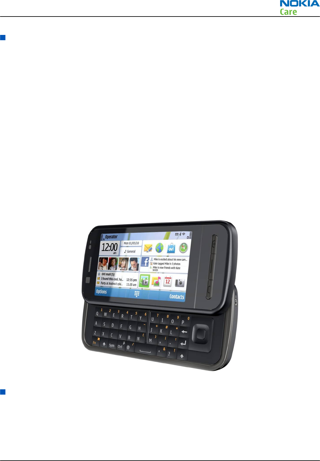
Product selection
RM-612/RM-624 is a GSM/HSDPA/WCDMA tri-mode handportable multimedia computer with a person centric
touch UI, integrated GPS (A-GPS OMA SUPL), WLAN and side slide form factor. RM-612 supports EGSM
850/900/1800/1900 and WCDMA 900/1900/2100 bands. RM-624 supports EGSM 850/900/1800/1900 and
WCDMA 850/1900/2100 bands. The device supports CSD/HSCSD, GPRS/EGPRS and WCDMA/HSDPA data bearers.
For WCDMA the maximum bit rate is up to 384 kbit/s for downlink and 384 kbit/s for uplink with simultaneous
CS speech or CS video (max. 64 kbit/s). The HSDPA peak is 3.6 Mbit/s downlink (with limited use cases).
For 2G and 2.5G networks the device is a Class A EGPRS DTM MSC 11 which means a maximum download speed
of up to 296 kbit/s with EGPRS, and up to 107kbit/s with GPRS. According to GSM standard 05.05 it responds
to class 4 (max. 2W) in GSM 850 and EGSM 900 class 1 (1W) in DCS 1800 and class 1 in PCS 1900. The device
supports EGPRS (EDGE) class B as well as Bluetooth 2.0 + EDR standard.
The device has a large nHD 3.2” (640 x 360 pixels) colour display (active area 39.6 mm x 70.4 mm) with 16
million colors. It also has a 5 megapixel autofocus main camera with 4 x digital zoom and an integrated LED
flash and secondary camera (QCIF) for video calls. The device supports two way video calls with two integrated
cameras, one on the front and one on the back.
The MMS implementation follows the OMA MMS standard release 1.3. The Browser is a highly advanced
internet browser also capable of viewing operator domain XHTML Mobile Profile (MP) content.
The device uses a S60 5.0 operating system and supports the full Web Browser for S60, which brings desktop-
like Web browsing experience to mobile devices. It also supports MIDP Java 2.0, providing a good platform
for compelling 3rd party applications.
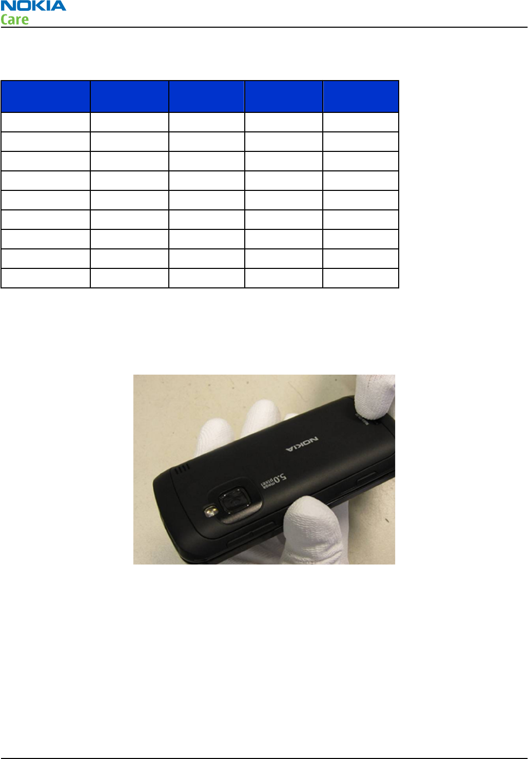
Figure 1 View of RM-612/RM-624
Product features and sales package
Imaging
Main camera:
•Sensor: 5 megapixel
•Optics: Tessar TM™ lens
•F number/Aperture: F2.8
RM-612; RM-624
General Information
Issue 1 COMPANY CONFIDENTIAL Page 1 – 5
Copyright © 2010 Nokia. All rights reserved.

•Focal length: 4.7 mm
•Focus range: 10 cm ~ infinity
•Macro focus distance: 10-50 cm
•Shutter speed: Mechanical shutter 1/1000 ~ 2 s
Secondary camera:
•Sensor: QVGA (320 x 240 pixels)
•F number/Aperture: F2.8
•Focal length: 43 mm (35 mm equivalent)
•Focus range: 10 cm ~ infinity
Video:
•Video resolution: QHD or VGA at 30 fps
•Audio recording: AAC (AMR for MMS)
•Video stabilization
•Video clip length: 90 min or limited to MMS size
•Video file format: .mp4 (default), .3gp (for MMS)
•White balance: automatic, sunny, cloudy, incandescent, fluorescent
•Scene: Auto, Night
•Colour tone: normal, sepia, black & white, vivid, negative
•Zoom (digital): up to 4x
•Tone for video indicator
Photo:
•Still image resolutions: up to 5 megapixel: 2592 x 1944
•Still image file format: JPEG/EXIF
•Auto focus
•Auto exposure: center weighted AE
•Image orientation: automatic
•Exposure compensation: +2 ~ -2EV at 0.5 step
•White balance: automatic, sunny, cloudy, incandescent, fluorescent
•Scene: auto, sports, portrait, close-up, landscape, night, user defined
•Colour tone: normal, sepia, B&W, vivid, negative
•Zoom (digital): up to 4x
•LED flash
Edit
•On device Photo editor and Video editor (manual & automatic)
View
•3.2” nHD (640 x 360 pixels) colour display (active area 39.6 mm x 70.4 mm), up to 16M colors, 16:9 aspect
ratio
•Digital Ambient Light Sensor (ALS) – used to optimize display/key brightness and power consumption
•Slide show from Gallery
RM-612; RM-624
General Information
Page 1 – 6 COMPANY CONFIDENTIAL Issue 1
Copyright © 2010 Nokia. All rights reserved.

Share
•Nokia XpressShare - share effortlessly from Gallery or after capture via Email, Bluetooth or MMS
•Video call and video sharing support (WCDMA services)
•Online Album: Image/Video uploading from Gallery
Print
•Nokia XpressPrint – direct printing via USB (PictBridge), Bluetooth (BPP), and WLAN (UPnP), from memory
card or via online printing
Store
•Up to 32 GB internal user memory
•Nokia XpressTransfer – easy to transfer and organize photos and video between your device and a
compatible PC
•Nokia Lifeblog (mobile & PC)
Music
•Digital music player: supports MP3/ AAC/ AAC+/ eAAC+/ WMA with playlists, equalizer and album art.
•Synchronise music with Microsoft Windows Media Player 10 & 11
•One click CD ripping, converting and transferring music to your device using Nokia Music Manager
•Stereo FM radio (87.5-108MHz /76-90MHz) with Visual Radio™ support
•Integrated handsfree speaker
•Nokia Stereo Headset (WH-102), inbox
Media
•Full-screen video playback to view downloaded, streamed or recorded video clips
•Supported video formats: MPEG-4 , H.264/AVC, H.263/3GPP, RealVideo 8/9/10
Productivity
Messaging:
•Email (SMTP, IMAP4, POP3), MMS, SMS
Office applications:
•Viewing of email attachments – .doc, .xls, .ppt, . pdf
PIM:
•Contacts, calendar, to-do, notes, recorder, calculator, clock, converter
Synchronization:
•Local/Remote (using SyncML)
•Data: Calendar, Contacts, To-do, Notes, E-mail
•PC Applications: Microsoft Outlook (98, 2000, 2002, 2003), Outlook Express, Lotus Organizer (5.0, 6.0),
Lotus Notes (5.0, 6.0)
Call management:
•Call logs, speed dial, voice dialling (with SIND) and voice commands
•Nokia Push to Talk (PoC)
RM-612; RM-624
General Information
Issue 1 COMPANY CONFIDENTIAL Page 1 – 7
Copyright © 2010 Nokia. All rights reserved.

Connectivity
•Integrated GPS (A-GPS OMA SUPL)
•WLAN - IEEE802.11 g/b with UPnP support
•Micro USB interface with USB 2.0 high speed
•Bluetooth wireless technology 2.0 + EDR + A2DP
•MicroSD memory card - support up to 16 GB
•Nokia 3.5 mm AV connector
Add-on software framework
•Symbian 9.4 OS
•Nokia Series 60, 5th edition, feature pack 2
•Java: MIDP2.0
•C++ and Java SDKs
Additional technical specifications
•Vibrating alert
•3GPP Rel 5/6 WCDMA , Rel 4 EGSM compliant
•Speech codecs supported in WCDMA: AMR
•Speech codecs supported in GSM: FR AMR/HR AMR/EFR/FR/HR
•WCDMA 2 Mbps, HSDPA 7.2 Mbps
•Dual Transfer Mode (DTM) support for simultaneous voice and packet data connection in GSM/EDGE
networks. Simple class A, multi slot class 11, max speed DL/UL: 118.4/118.4 kbits/s
•EGPRS class B, multi slot class 32, (5 Rx + 3 Tx / Max Sum 6), max speed DL/UL= 296 / 177.6 kbits/s
•GPRS class B, multi slot class 32 (5 Rx + 3 Tx / Max Sum 6), max speed DL/UL= 107 / 64.2 kbits/s
Sales package
•Transceiver RM-612/RM-624
•Charger (AC-8 or AC-15)
•Battery (BL-4J)
•Stereo headset (WH-102)
•Connectivity cable (CA-101D)
•Video connectivity cable (CA-75U)
•2 GB MicroSD card
•User Guide
RM-612; RM-624
General Information
Page 1 – 8 COMPANY CONFIDENTIAL Issue 1
Copyright © 2010 Nokia. All rights reserved.
Mobile enhancements
Table 1 Audio
Enhancement Type
Stereo headset HS-16
HS-43
HS-45 with AD-54 3.5 mm stereo plug
HS-48
Mono headset HS-41
Mini speakers MD-6
MD-8
MD-9
Wireless loopset LPS-5
Wired headsets WH-102
WH-201
WH-205
WH-500
WH-600
WH-601
WH-700
WH-701
WH-800
WH-900
RM-612; RM-624
General Information
Issue 1 COMPANY CONFIDENTIAL Page 1 – 9
Copyright © 2010 Nokia. All rights reserved.
Enhancement Type
Bluetooth headsets BH-102
BH-104
BH-105
BH-106
BH-108
BH-200
BH-201
BH-208
BH-212
BH-213
BH-215
BH-216
BH-504
BH-505
BH-602
BH-604
BH-606
BH-607
BH-703
BH-704
BH-803
BH-804
BH-900
BH-902
BH-903
BH-904
BH-905
Bluetooth speakers MD-7W
Table 2 Car
Enhancement Type
Nokia Universal Mobile Holder CR-39
CR-82
CR-99
CR-114
RM-612; RM-624
General Information
Page 1 – 10 COMPANY CONFIDENTIAL Issue 1
Copyright © 2010 Nokia. All rights reserved.
Enhancement Type
Nokia Holder Easy Mount HH-12
HH-17
Speakerphone HF-33W
HF-200
HF-310
HF-510
Car kit CK-100
CK-200
CK-300
CK-600
CK-7W
CK-15W
Mobile charger DC-4
DC-8
DC-9
DC-11
Table 3 Data
Enhancement Type
Connectivity cable CA-100
CA-101C
CA-101
CA-126
MicroSD card MU-22 1 GB
MU-37 2 GB
MU-41 4 GB
MU-43 8 GB
MU-44 16 GB
Table 4 Messaging
Enhancement Type
Stylus STYLUS PEN ASSY
RM-612; RM-624
General Information
Issue 1 COMPANY CONFIDENTIAL Page 1 – 11
Copyright © 2010 Nokia. All rights reserved.
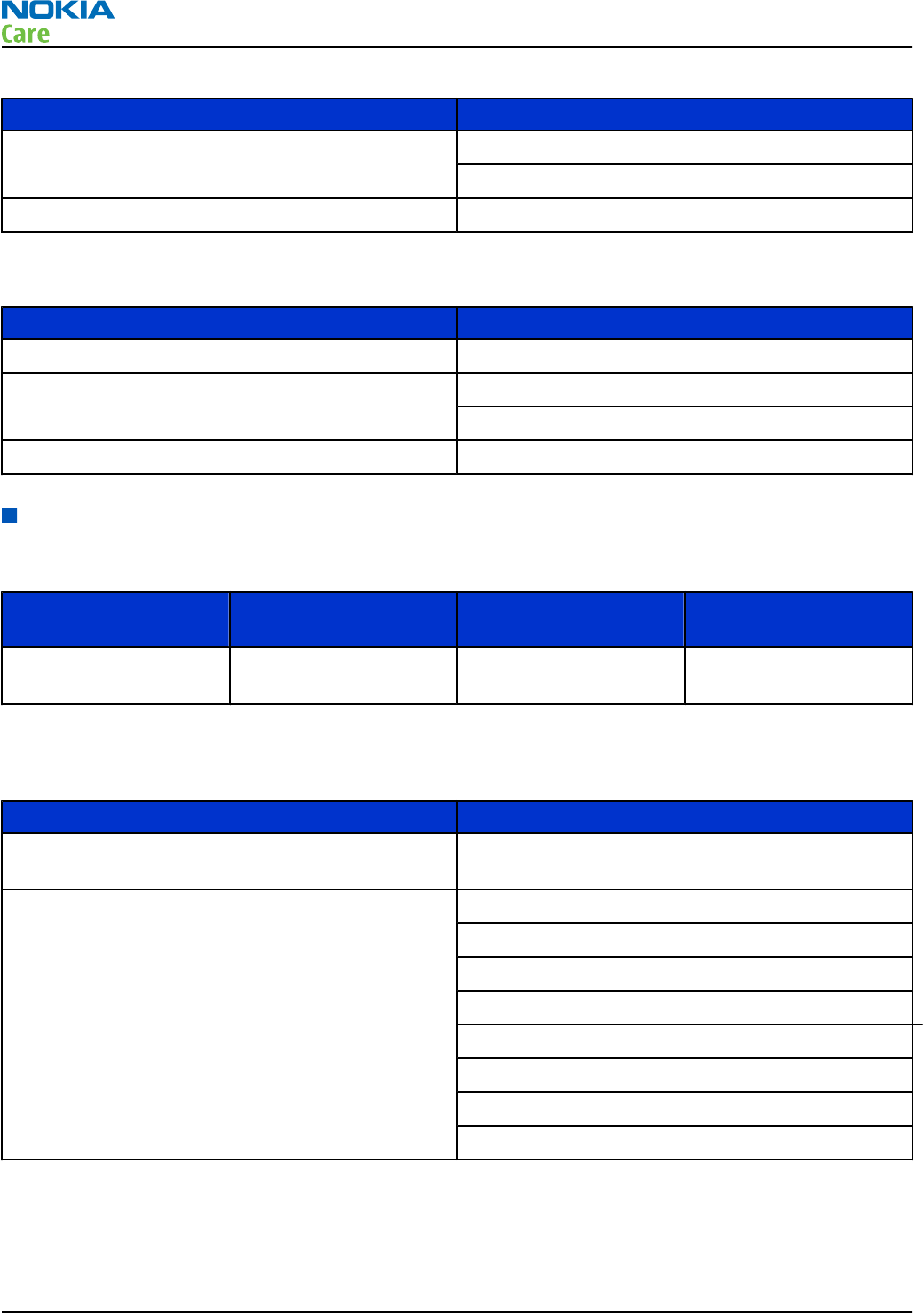
Table 5 Positioning
Enhancement Type
Wireless GPS module LD-3W
LD-4W
Home connectivity HD-1
Table 6 Power
Enhancement Type
Battery 1200mAh Li-ion BL-4J
Travel charger AC-5
AC-8
Charger adapter CA-44
Technical Specifications
Transceiver general specifications
Unit Dimensions (L x W x T)
(mm) Weight (g) Volume (cm3)
Transceiver with BL-4J
1200 mAh Li-Ion battery
113.4 x 53 x 16.8 150 101
Main RF characteristics for GSM 850/900/1800/1900, WCDMA 900/1900/2100 and WCDMA
850/1900/2100 phones
Parameter Unit
Cellular system GSM850, EGSM900, GSM1800/1900, WCDMA VIII
(900), WCDMA II (1900) and WCDMA I (2100)
Rx frequency band GSM850: 869 - 894 MHz
EGSM900: 925 - 960 MHz
GSM1800: 1805 - 1880 MHz
GSM1900: 1930 - 1990 MHz
WCDMA VIII (900): 925- 960 MHz
WCDMA V (850): 869 - 894 MHz
WCDMA II (1900): 1930-1990MHz
WCDMA I (2100): 2110 - 2170 MHz
RM-612; RM-624
General Information
Page 1 – 12 COMPANY CONFIDENTIAL Issue 1
Copyright © 2010 Nokia. All rights reserved.
Parameter Unit
Tx frequency band GSM850: 824 - 849 MHz
EGSM900: 880 - 915 MHz
GSM1800: 1710 - 1785 MHz
GSM1900: 1850 - 1910 MHz
WCDMA VIII (900): 880 - 915 MHz
WCDMA V (850): 824 - 849 MHz
WCDMA II (1900): 1850-1910MHz
WCDMA I (2100): 1920 - 1980 MHz
Output power GSM850: +5 ...+33dBm/3.2mW ... 2W
GSM900: +5 … +33dBm/3.2mW … 2W
GSM1800: +0 … +30dBm/1.0mW … 1W
GSM1900: +0 … +30dBm/1.0mW … 1W
WCDMA VIII (900): -50 ... +24 dBm/0.01μW ...
251.2mW
WCDMA V (850): -50 ... +24 dBm/0.01μW ... 251.2mW
WCDMA II (1900): -50 ... +24dBm/0.01µW ...
251.2mW
WCDMA I (2100): -50 ... +24 dBm/0.01μW ...
251.2mW
EDGE output power EDGE850: +5 … +29dBm/3.2mW … 794mW
EDGE900: +5 … +29dBm/3.2mW … 794mW
EDGE1800: +0 … +26dBm/1.0mW … 400mW
EDGE1900:+0 … +26dBm/1.0mW … 400mW
Number of RF channels GSM850: 124
GSM900: 174
GSM1800: 374
GSM1900: 299
WCDMA VIII (900): 152
WCDMA V (850): 108
WCDMA II (1900): 289
WCDMA I (2100): 277
Channel spacing 200 kHz (WCDMA V and II 100/200 kHz)
RM-612; RM-624
General Information
Issue 1 COMPANY CONFIDENTIAL Page 1 – 13
Copyright © 2010 Nokia. All rights reserved.
Parameter Unit
Number of Tx power levels GSM850: 15
GSM900: 15
GSM1800: 16
GSM1900: 16
WCDMA VIII (900): 75
WCDMA V (850): 75
WCDMA II (1900): 75
WCDMA I (2100): 75
Battery endurance
Battery Capacity (mAh) Talk time Stand-by
time
Charging time
with AC-8
BL-4J 1200 GSM: up to 7 h GSM: up to 400 h 1 h 45 min
WCDMA: up to 5 h WCDMA: up to 400
h
Environmental conditions
Environmental
condition Ambient temperature Notes
Normal operation -10 oC ... +55 oCSpecifications fulfilled
Reduced performance 55 oC ... +70 oCOperational only for short periods
Intermittent or no
operation -40 oC ... -15 oC and +70 oC ... +85oCOperation not guaranteed but an
attempt to operate will not damage
the phone
No operation or
storage <-40 oC and >+85 oCNo storage. An attempt to operate
may cause permanent damage
Charging allowed -15 oC ... +55 oC
Long term storage
conditions 0 oC ... +85 oC
Humidity and water
resistance
Relative humidity range is 5 to 95%.
Condensed or dripping water may
cause intermittent malfunctions.
Protection against dripping water
has to be implemented in (enclosure)
mechanics.
Continuous dampness will cause
permanent damage to the module.
RM-612; RM-624
General Information
Page 1 – 14 COMPANY CONFIDENTIAL Issue 1
Copyright © 2010 Nokia. All rights reserved.

2 — Service Tools and Service
Concepts
Nokia Customer Care
Issue 1 COMPANY CONFIDENTIAL Page 2 – 1
Copyright © 2010 Nokia. All rights reserved.

RM-612; RM-624
Service Tools and Service Concepts
(This page left intentionally blank.)
Page 2 – 2 COMPANY CONFIDENTIAL Issue 1
Copyright © 2010 Nokia. All rights reserved.

Table of Contents
Service tools........................................................................................................................................................... 2–5
Product specific tools....................................................................................................................................... 2–5
FS-141........................................................................................................................................................... 2–5
MJ-263 .......................................................................................................................................................... 2–5
RJ-230 ........................................................................................................................................................... 2–5
SA-131 .......................................................................................................................................................... 2–5
Module jig attenuation values................................................................................................................... 2–6
Disassembly instructions............................................................................................................................ 2–6
QWERTY Domesheet assembly instructions........................................................................................... 2–22
General tools.................................................................................................................................................. 2–24
AC-35.......................................................................................................................................................... 2–24
CU-4............................................................................................................................................................ 2–25
FLS-5 .......................................................................................................................................................... 2–26
FPS-21........................................................................................................................................................ 2–26
JXS-1........................................................................................................................................................... 2–27
PK-1............................................................................................................................................................ 2–27
SB-6............................................................................................................................................................ 2–27
SB-7............................................................................................................................................................ 2–27
SRT-6.......................................................................................................................................................... 2–28
SS-210........................................................................................................................................................ 2–28
SS-46.......................................................................................................................................................... 2–28
SS-62.......................................................................................................................................................... 2–28
SS-93.......................................................................................................................................................... 2–28
SX-4............................................................................................................................................................ 2–29
Cables.............................................................................................................................................................. 2–29
CA-101 ....................................................................................................................................................... 2–29
CA-158RS ................................................................................................................................................... 2–29
CA-31D ....................................................................................................................................................... 2–29
CA-89DS ..................................................................................................................................................... 2–30
PCS-1.......................................................................................................................................................... 2–30
XRS-6.......................................................................................................................................................... 2–30
Service concepts ................................................................................................................................................. 2–31
POS (Point of Sale) flash concept ................................................................................................................. 2–31
Flash concept with FPS-21............................................................................................................................ 2–32
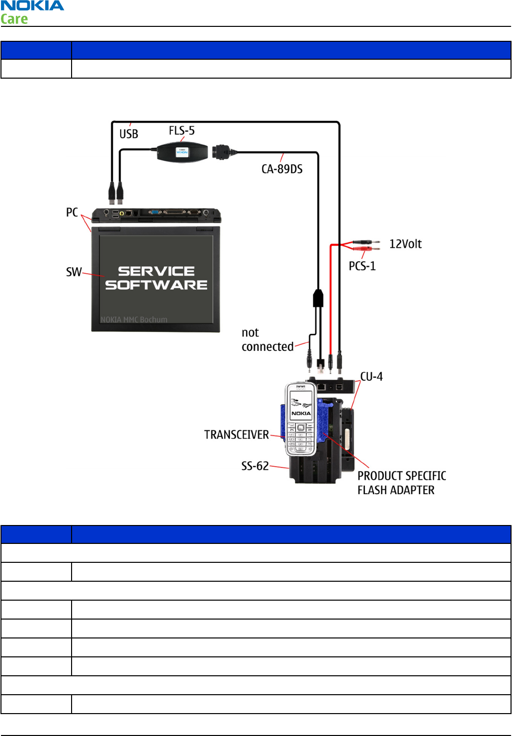
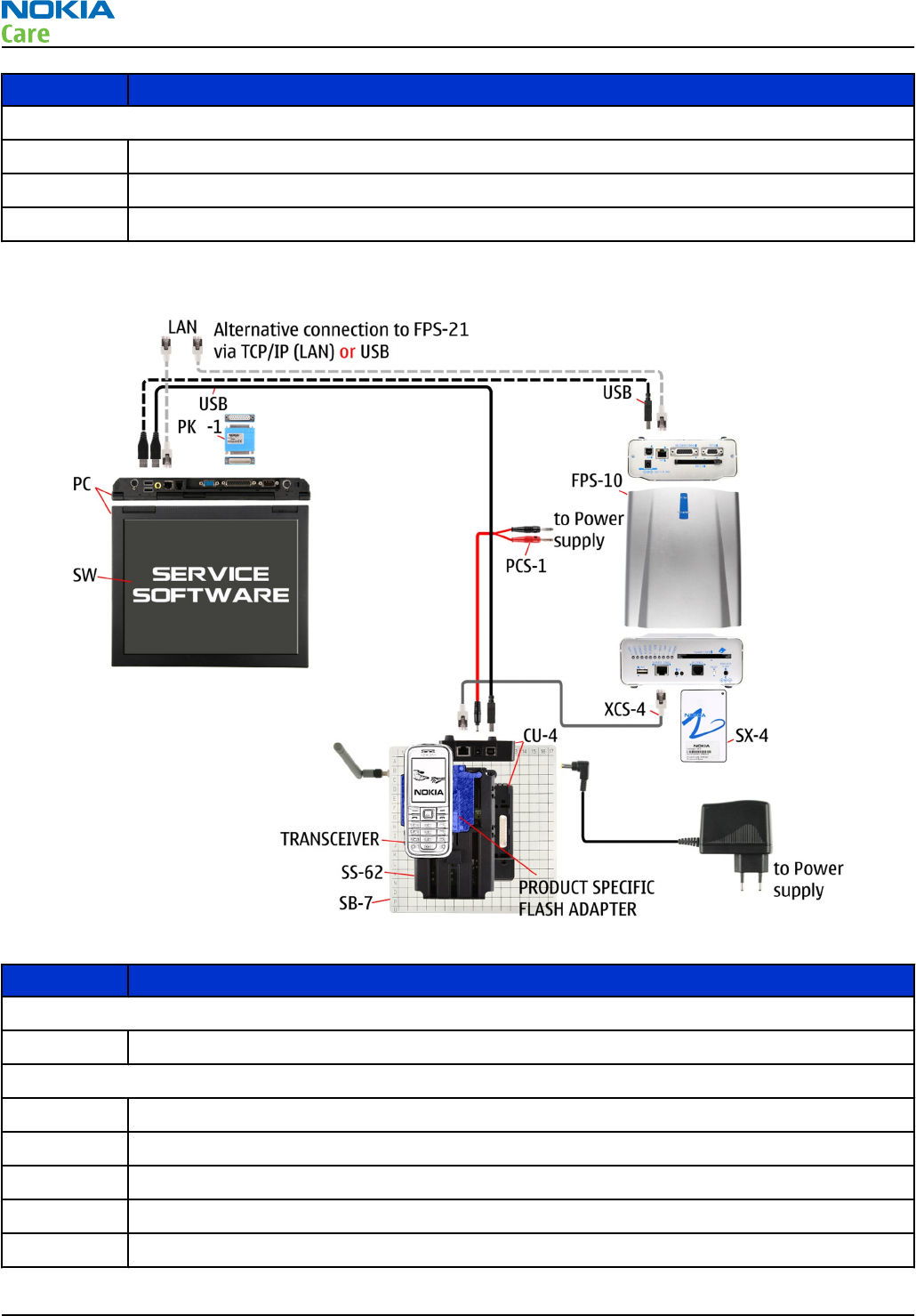
CU-4 flash concept with FPS-21.................................................................................................................... 2–33
Flash concept with FPS-21 and SB-6............................................................................................................ 2–34
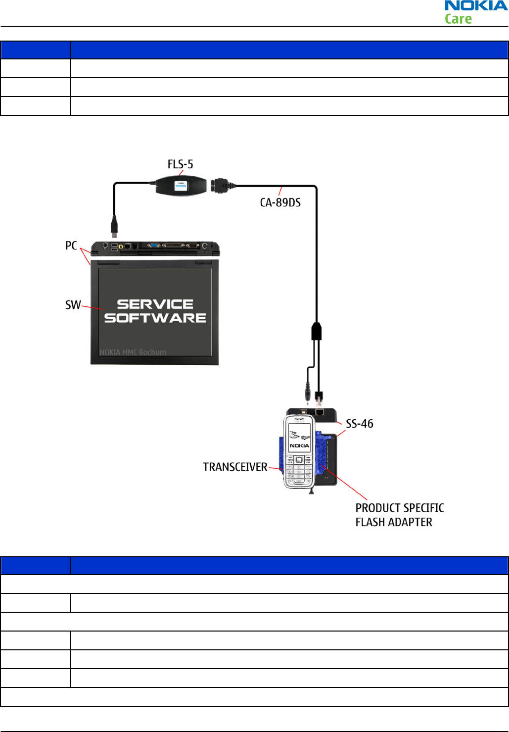
Flash concept with SS-46 and CA-89DS ....................................................................................................... 2–35
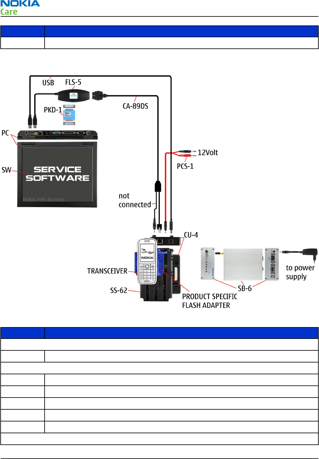
Flash concept with SS-62 and CA-89DS ....................................................................................................... 2–36
Flash concept with FPS-21, SS-62 and SB-6 ................................................................................................ 2–37
Flash concept with FPS-21, SS-62 and SB-7 ................................................................................................ 2–38
Module jig service concept........................................................................................................................... 2–39
Module jig service concept with SB-6.......................................................................................................... 2–40
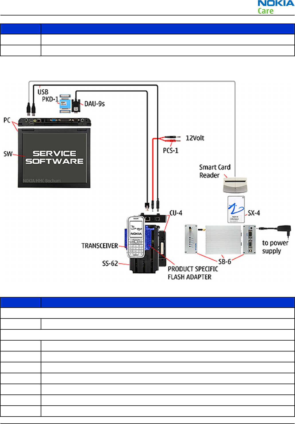
Service concept for RF testing and RF/BB tuning....................................................................................... 2–41
List of Figures
Figure 2 POS flash concept ................................................................................................................................ 2–31
Figure 3 Basic flash concept with FPS-21......................................................................................................... 2–32
Figure 4 CU-4 flash concept with FPS-21.......................................................................................................... 2–33
Figure 5 Flash concept with FPS-21 and SB-6.................................................................................................. 2–34
RM-612; RM-624
Service Tools and Service Concepts
Issue 1 COMPANY CONFIDENTIAL Page 2 – 3
Copyright © 2010 Nokia. All rights reserved.

Figure 6 Flash concept with SS-46 and CA-89DS ............................................................................................. 2–35
Figure 7 Flash concept with SS-62 and CA-89DS ............................................................................................. 2–36
Figure 8 Flash concept with FPS-21, SS-62 and SB-6 ...................................................................................... 2–37
Figure 9 Flash concept with FPS-21, SB-7 and JBT-9....................................................................................... 2–38
Figure 10 Module jig service concept............................................................................................................... 2–39
Figure 11 Module jig service concept with SB-6.............................................................................................. 2–40
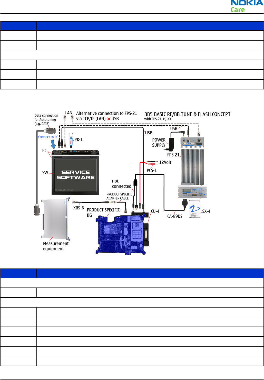
Figure 12 Service concept for RF testing and RF/BB tuning........................................................................... 2–41
RM-612; RM-624
Service Tools and Service Concepts
Page 2 – 4 COMPANY CONFIDENTIAL Issue 1
Copyright © 2010 Nokia. All rights reserved.
Service tools
Product specific tools
The table below gives a short overview of service devices that can be used for testing, error analysis, and
repair of product RM-612; RM-624. For the correct use of the service devices, and the best effort of workbench
setup, please refer to various concepts.
FS-141 Flash adapter
FS-141 is meant for flashing (also dead phones) with SS-46, RF testing
and tuning, and EM calibration on ATO level with SS-62 (mechanical
locking concept). CU-4 supported.
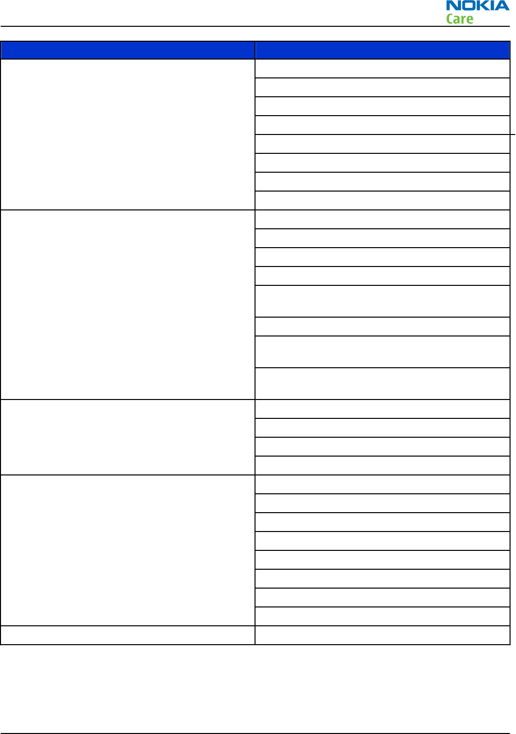
MJ-263 Light Module Jig
MJ-263 is meant for component level troubleshooting.
The jig includes RF interface for Bluetooth, WLAN and GPS. In addition,
it has the following features:
•Provides mechanical interface with the engine module
•Provides galvanic connection to all needed test pads in module
•Multiplexing between USB and FBUS media, controlled by Vusb
•Connector for control unit
•Access for Audio-, MMC, and USB connectors
For MJ-263 module jig attenuation values, see Module jig attenuation
values (page 2–6 ) .
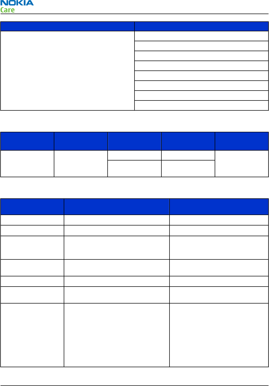
RJ-230 Soldering jig
The jig is used for soldering and as a rework jig for the system module.
It is made of lead-free rework compatible material.
SA-131 RF coupler
SA-131 is a generic device for GPS testing. It is used together with
SS-62.
RM-612; RM-624
Service Tools and Service Concepts
Issue 1 COMPANY CONFIDENTIAL Page 2 – 5
Copyright © 2010 Nokia. All rights reserved.
Module jig attenuation values
Band F RX Attenuation
RX F TX Attenuation
TX
GSM 850 881.6 -0.2 836.6 -0.2
GSM 900 942.4 -0.2 897.4 -0.2
GSM 1800 1842.8 -0.3 1747.8 -0.3
GSM 1900 1960.0 -0.3 1880.0 -0.3
WCDMA I 2140.0 -0.4 1950.0 -0.3
WCDMA II 1960.0 -0.3 1880.0 -0.3
WCDMA V 880.0 -0.2 835.0 -0.2
WCDMA VIII 942.6 -0.2 897.6 -0.2
WLAN N/A N/A 2442.0 -0.4
Disassembly instructions
Steps
1. Open the locking mechanism of the battery cover.
RM-612; RM-624
Service Tools and Service Concepts
Page 2 – 6 COMPANY CONFIDENTIAL Issue 1
Copyright © 2010 Nokia. All rights reserved.
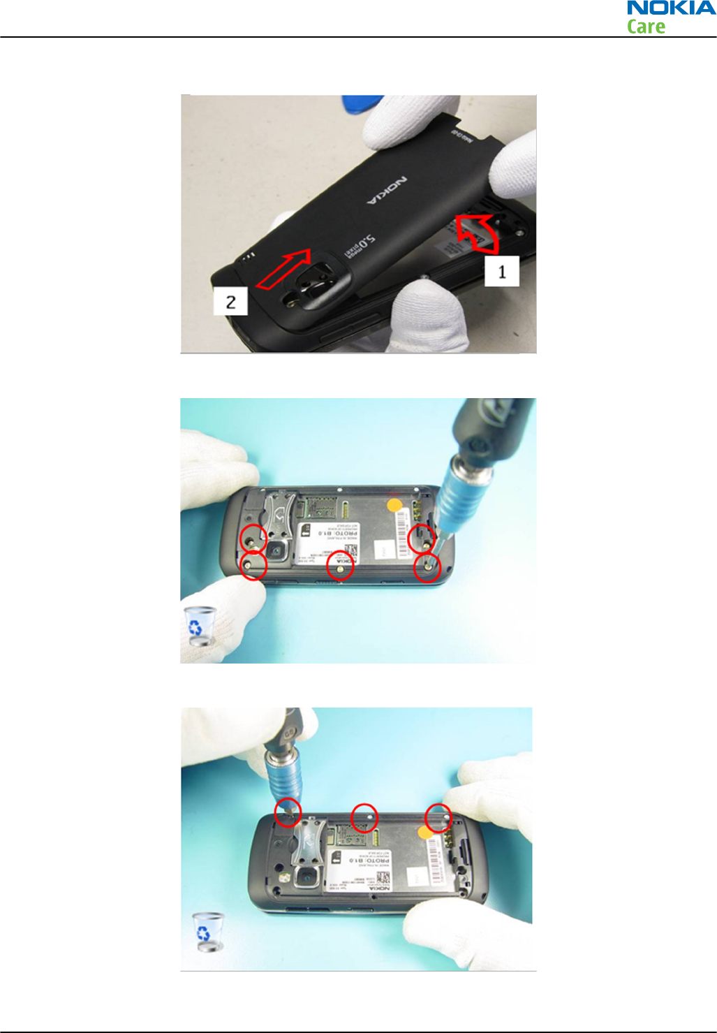
2. Lift the lower end up and pull the battery cover from the phone (and remove the battery).
3. Remove 5 pcs M1.6 x 5.0 torx+ 6IP slide module screws with a Torx screwdriver.
4. Remove 3 pcs M1.4 x 3.4 torx+ 4IP press fit insert screws.
RM-612; RM-624
Service Tools and Service Concepts
Issue 1 COMPANY CONFIDENTIAL Page 2 – 7
Copyright © 2010 Nokia. All rights reserved.
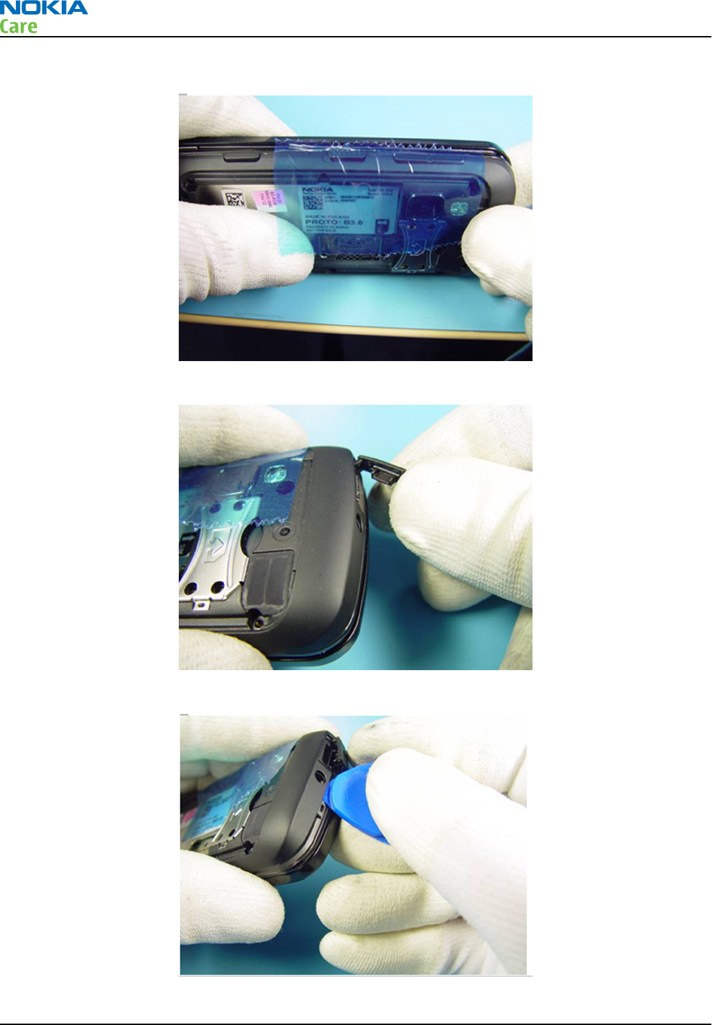
5. To avoid losing the Locking key, use the blue protection foil to fix it.
6. Open the USB door.
7. Open the QWERTY frame latches from both sides.
RM-612; RM-624
Service Tools and Service Concepts
Page 2 – 8 COMPANY CONFIDENTIAL Issue 1
Copyright © 2010 Nokia. All rights reserved.
8. Remove the B-Cover from the QWERTY frame.
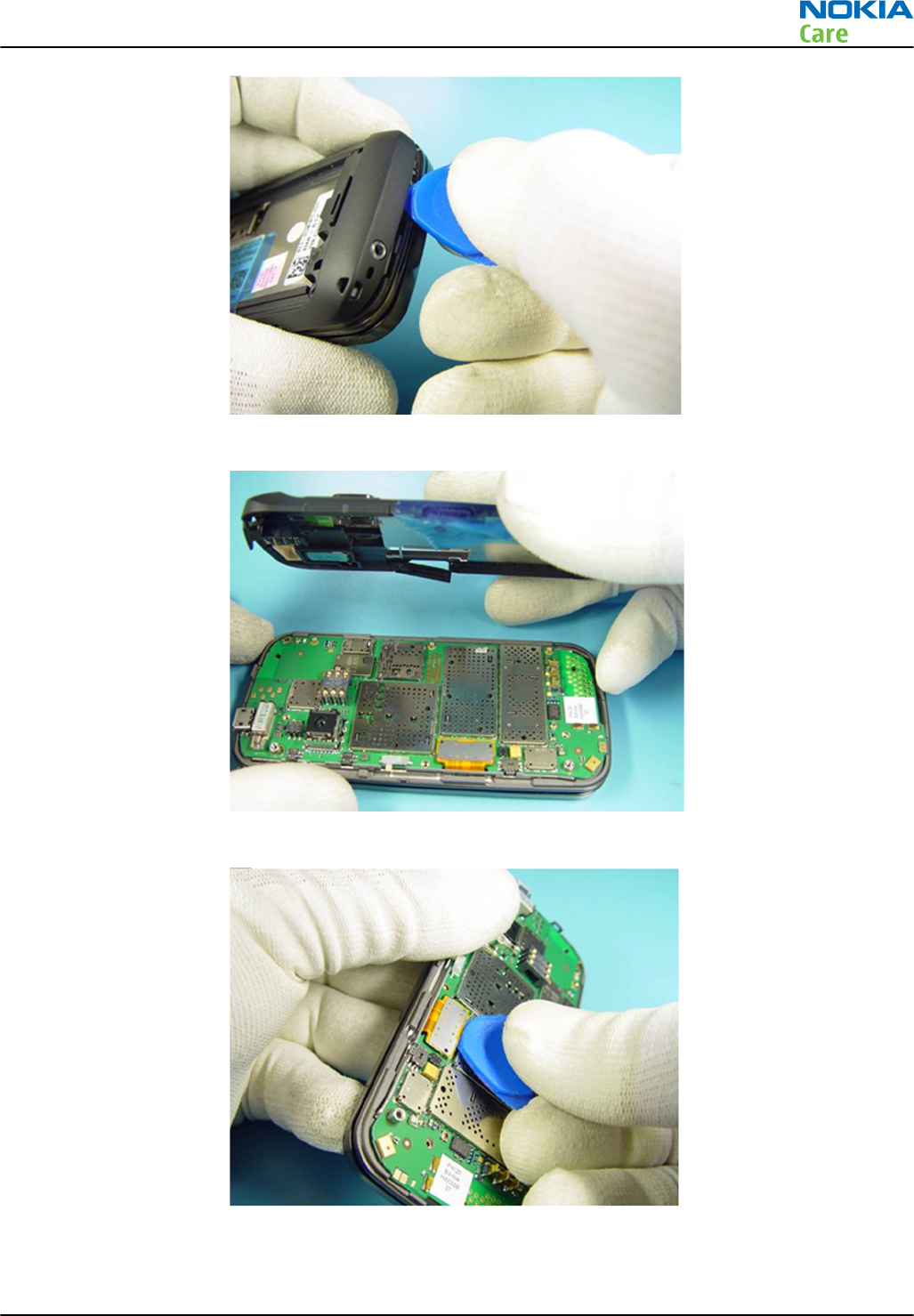
9. Open the Dynamic flex B2B connector using the SRT-6 tool.
RM-612; RM-624
Service Tools and Service Concepts
Issue 1 COMPANY CONFIDENTIAL Page 2 – 9
Copyright © 2010 Nokia. All rights reserved.
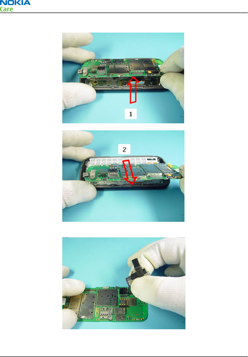
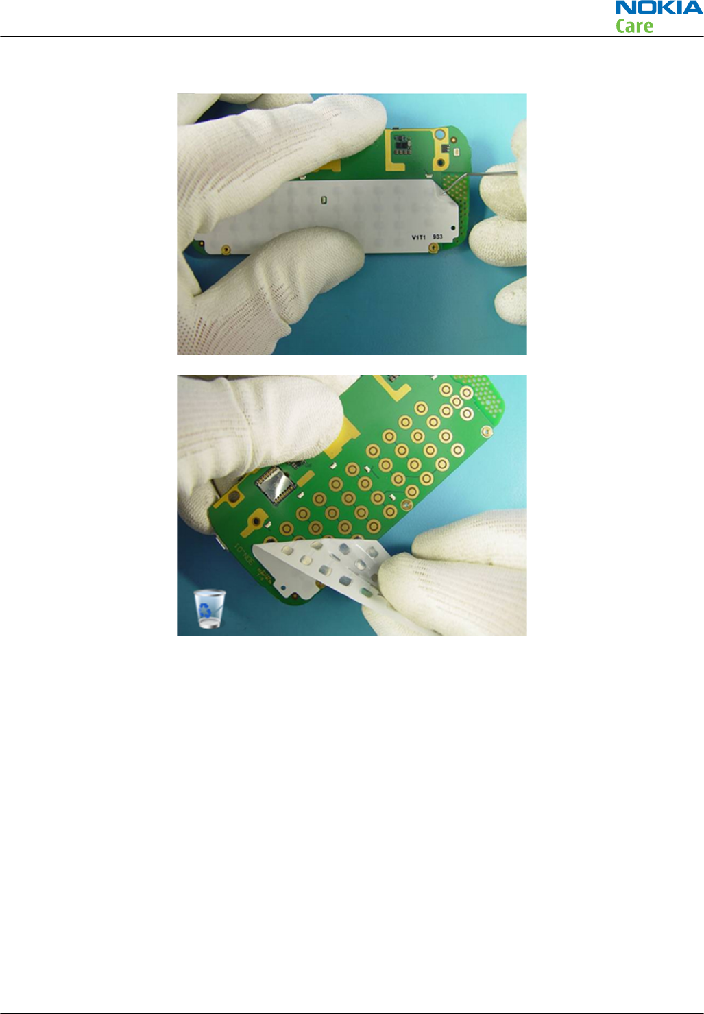
10. Lift up the PWB to the direction shown in the pictures below and remove it.
11. Remove the Camera Module using the SS-210 v2 tool.
RM-612; RM-624
Service Tools and Service Concepts
Page 2 – 10 COMPANY CONFIDENTIAL Issue 1
Copyright © 2010 Nokia. All rights reserved.
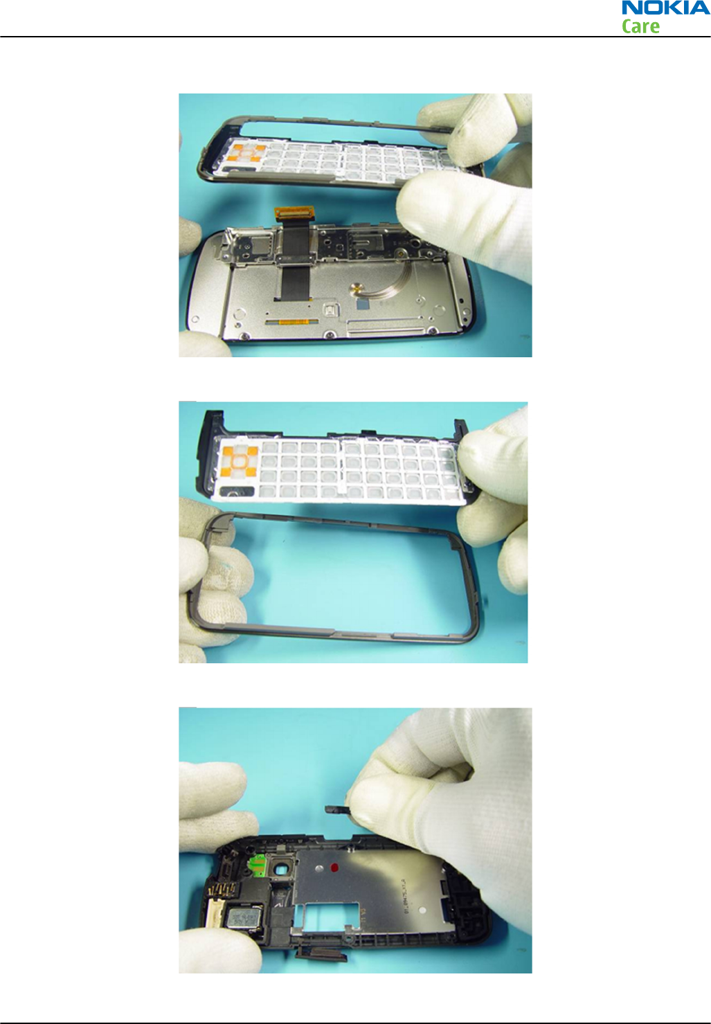
12. Remove the QWERTY Frame and QWERTY keymat.
13. Separate the QWERTY frame from the QWERTY keymat.
14. Remove the Locking key.
RM-612; RM-624
Service Tools and Service Concepts
Issue 1 COMPANY CONFIDENTIAL Page 2 – 11
Copyright © 2010 Nokia. All rights reserved.
15. Remove the DC Jack using a DC Plug.
16. Remove the USB door.
RM-612; RM-624
Service Tools and Service Concepts
Page 2 – 12 COMPANY CONFIDENTIAL Issue 1
Copyright © 2010 Nokia. All rights reserved.
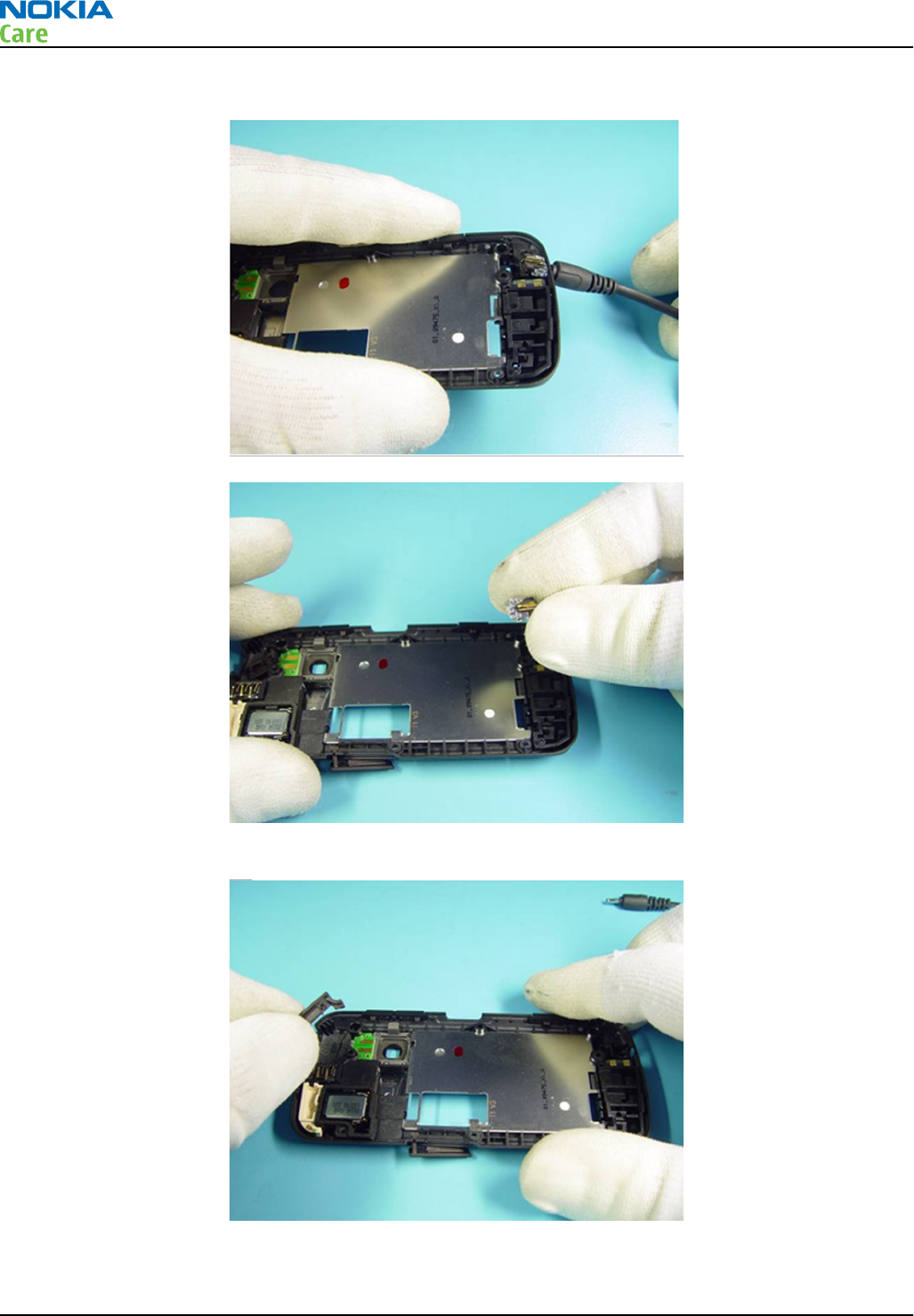
17. Lift up the AV connector using an AV plug and remove it.
18. Remove the main Antenna.
RM-612; RM-624
Service Tools and Service Concepts
Issue 1 COMPANY CONFIDENTIAL Page 2 – 13
Copyright © 2010 Nokia. All rights reserved.
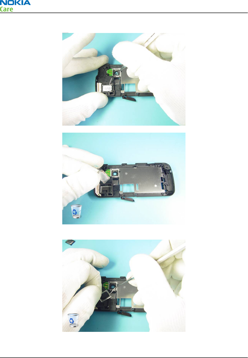
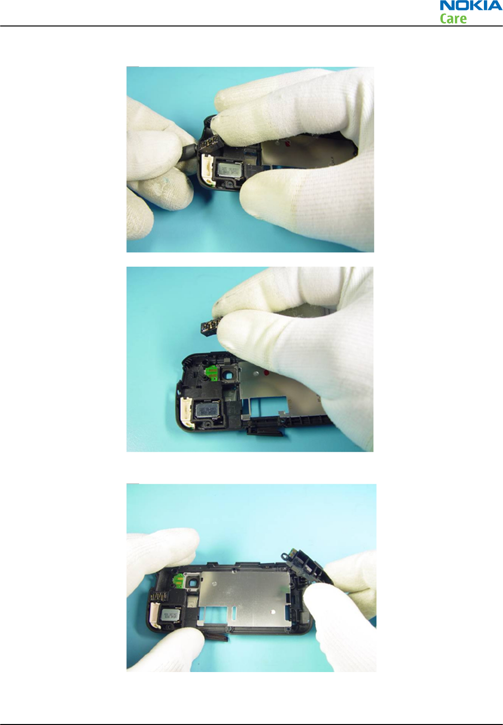
19. Release the IHF speaker using the Dental tool and remove it.
20. Remove the IHF adhesive.
RM-612; RM-624
Service Tools and Service Concepts
Page 2 – 14 COMPANY CONFIDENTIAL Issue 1
Copyright © 2010 Nokia. All rights reserved.
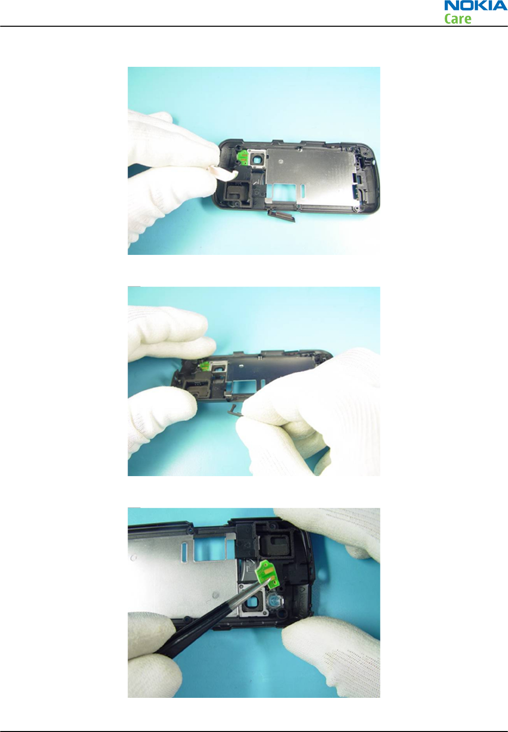
21. Separate the GPS/BT/WLAN ANTENNA.
22. Separate the SD DOOR.
23. Remove the FLASH LED ASSY from the B-COVER using tweezers.
RM-612; RM-624
Service Tools and Service Concepts
Issue 1 COMPANY CONFIDENTIAL Page 2 – 15
Copyright © 2010 Nokia. All rights reserved.
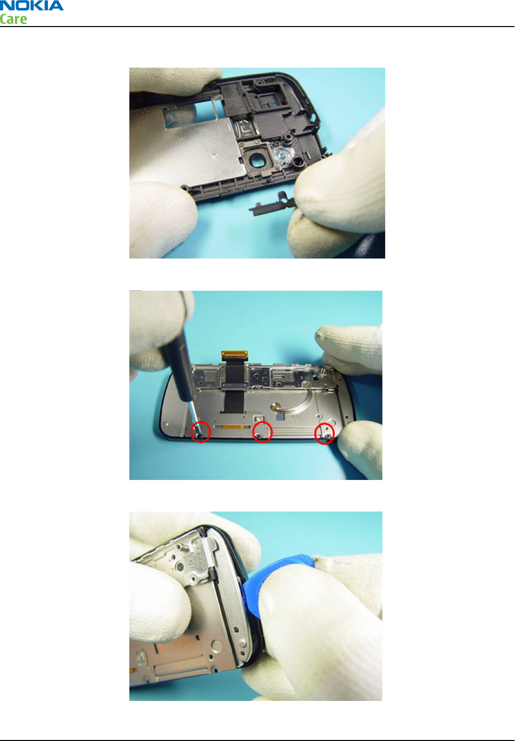
24. Separate the Volume keys.
25. Remove 3 pcs lid screws M1.4 x 2.5 torx+ 4IP.
26. Open the A-Cover latches from both sides.
RM-612; RM-624
Service Tools and Service Concepts
Page 2 – 16 COMPANY CONFIDENTIAL Issue 1
Copyright © 2010 Nokia. All rights reserved.
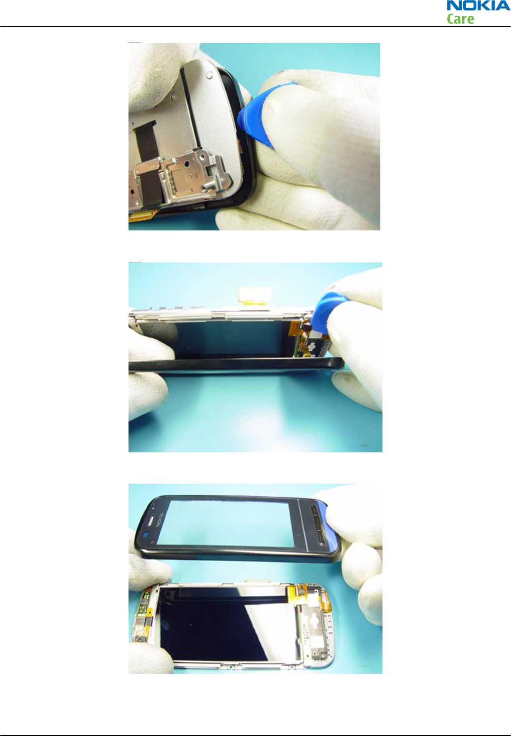
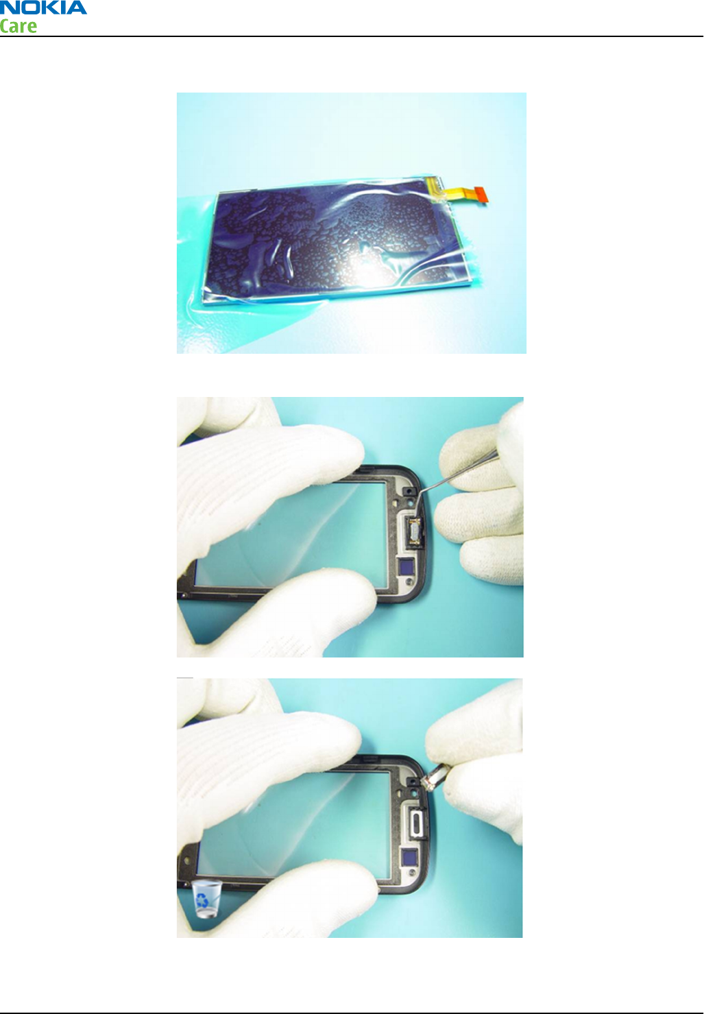
27. Release the touch connector from the UI flex assy.
28. Separate the A-Cover from the slide module.
RM-612; RM-624
Service Tools and Service Concepts
Issue 1 COMPANY CONFIDENTIAL Page 2 – 17
Copyright © 2010 Nokia. All rights reserved.
29. Lift up the function key support from the slide module.
30. Open the lid from the LCD flex zif connector.
RM-612; RM-624
Service Tools and Service Concepts
Page 2 – 18 COMPANY CONFIDENTIAL Issue 1
Copyright © 2010 Nokia. All rights reserved.
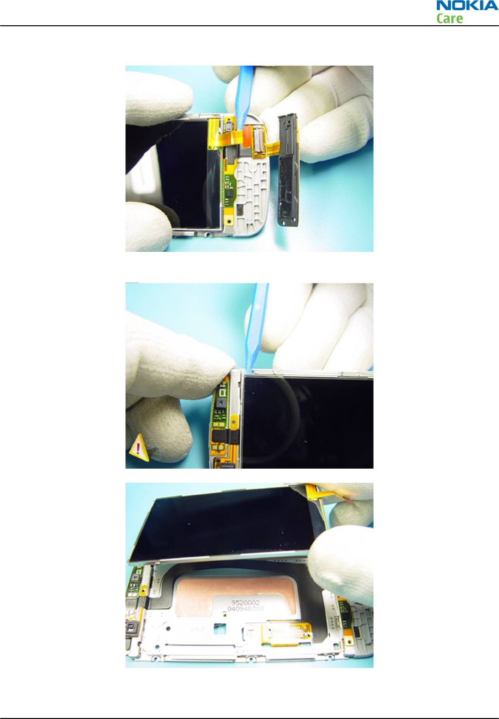
31. Lift the LCD flex from the zif connector.
32. Fit the SS-93 tool carefully under the LCD and lift it up. Be extremely careful not to break the LCD.
RM-612; RM-624
Service Tools and Service Concepts
Issue 1 COMPANY CONFIDENTIAL Page 2 – 19
Copyright © 2010 Nokia. All rights reserved.
33. Protect the LCD with protection foil to avoid scratches.
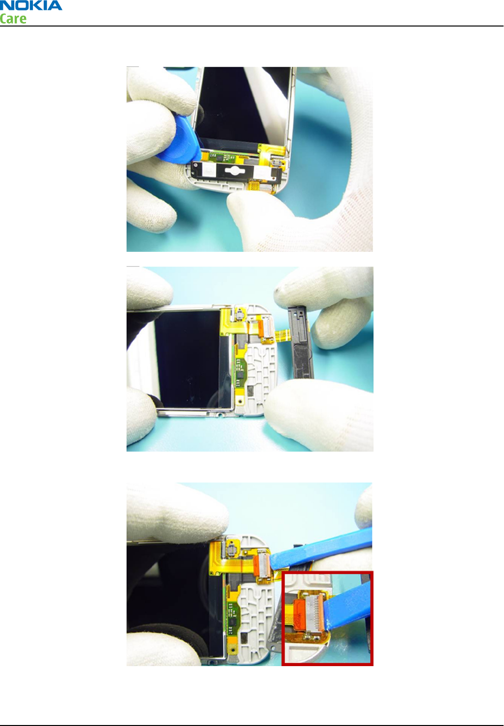
34. Lift up the Earpiece using the Dental tool and remove it.
RM-612; RM-624
Service Tools and Service Concepts
Page 2 – 20 COMPANY CONFIDENTIAL Issue 1
Copyright © 2010 Nokia. All rights reserved.
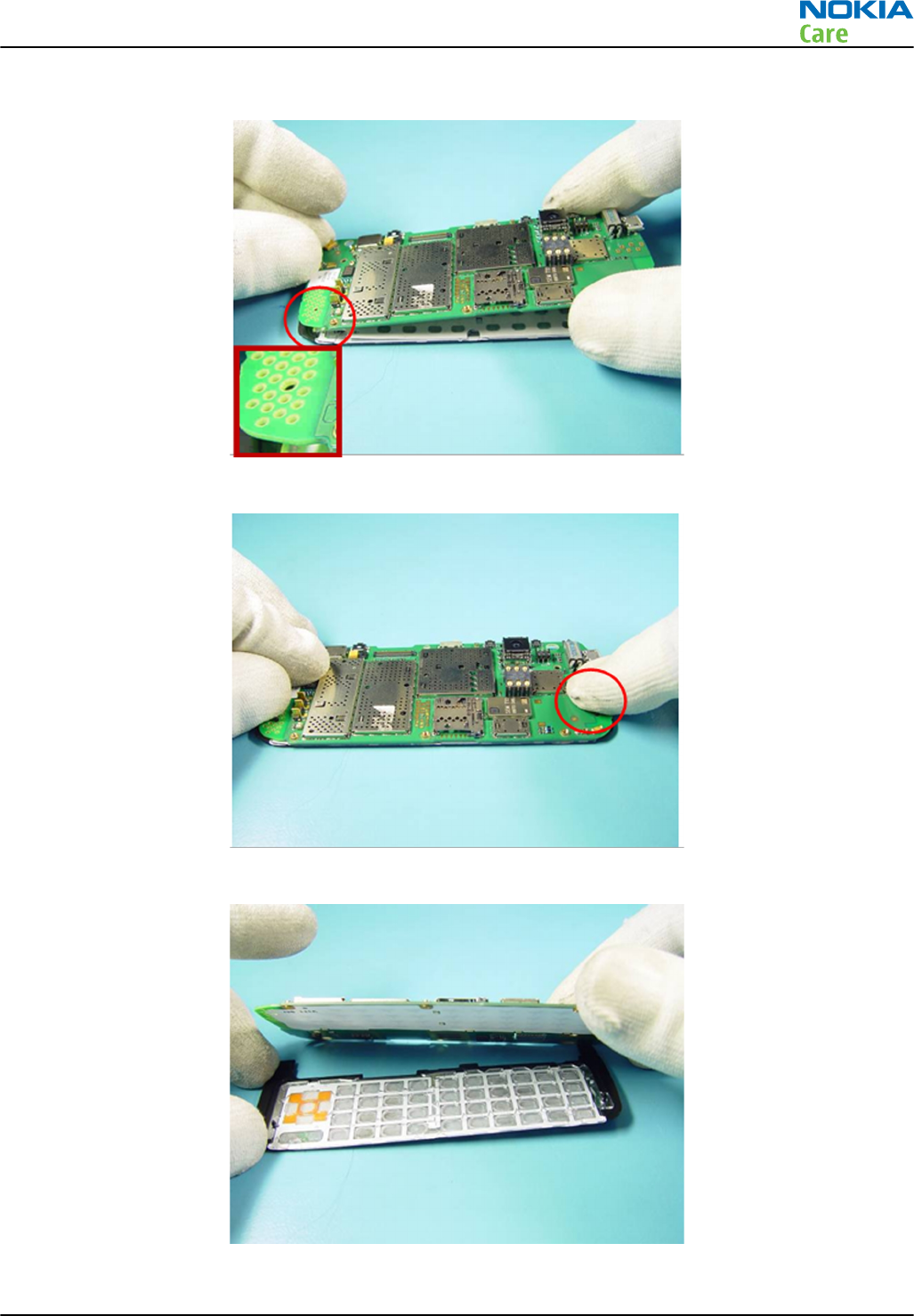
35. Use the Dental tool to lift up the Domesheet and remove it.
RM-612; RM-624
Service Tools and Service Concepts
Issue 1 COMPANY CONFIDENTIAL Page 2 – 21
Copyright © 2010 Nokia. All rights reserved.
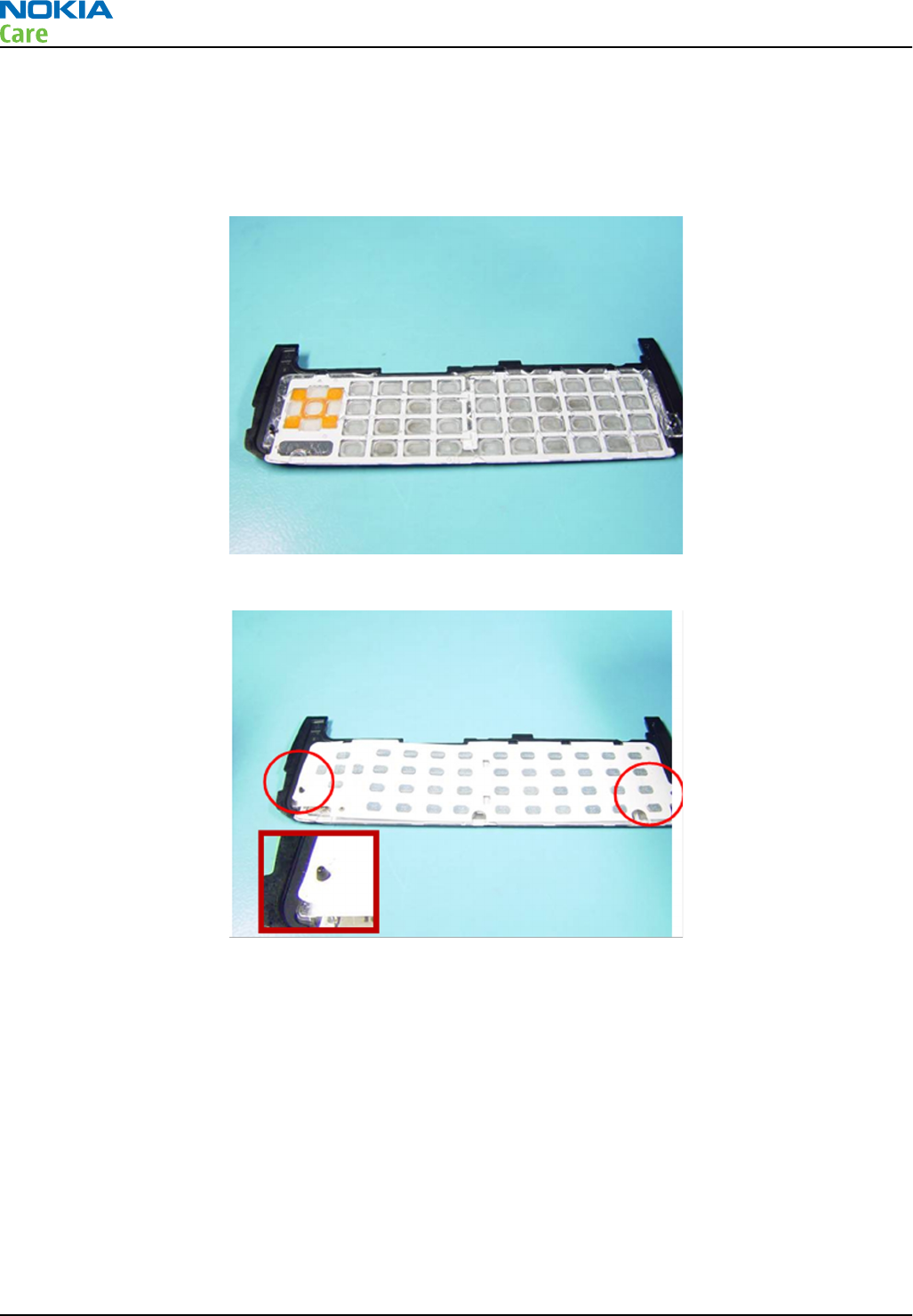
QWERTY Domesheet assembly instructions
Steps
1. Take the QWERTY keymat and...
2. ...place the Domesheet on the QWERTY keymat.
RM-612; RM-624
Service Tools and Service Concepts
Page 2 – 22 COMPANY CONFIDENTIAL Issue 1
Copyright © 2010 Nokia. All rights reserved.
3. Place the PWB to the QWERTY/Domesheet first from the left side.
4. Then place the PWB from the right side.
5. Lift up the PWB.
RM-612; RM-624
Service Tools and Service Concepts
Issue 1 COMPANY CONFIDENTIAL Page 2 – 23
Copyright © 2010 Nokia. All rights reserved.
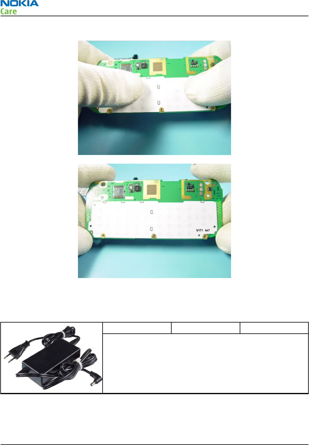
6. Make sure the Domesheet is properly attached to the PWB.
General tools
The table below gives a short overview of service devices that can be used for testing, error analysis, and
repair of product RM-612; RM-624. For the correct use of the service devices, and the best effort of workbench
setup, please refer to various concepts.
AC-35 Power supply
Universal power supply for FPS-21; included in the FPS-21 sales
package.
Input 100V…230V 50Hz…60Hz, output voltage of 12 V and output
current up to 3 A.
RM-612; RM-624
Service Tools and Service Concepts
Page 2 – 24 COMPANY CONFIDENTIAL Issue 1
Copyright © 2010 Nokia. All rights reserved.
CU-4 Control unit
CU-4 is a general service tool used with a module jig and/or a flash
adapter. It requires an external 12 V power supply.
The unit has the following features:
•software controlled via USB
•EM calibration function
•Forwards FBUS/Flashbus traffic to/from terminal
•Forwards USB traffic to/from terminal
•software controlled BSI values
•regulated VBATT voltage
•2 x USB2.0 connector (Hub)
•FBUS and USB connections supported
When using CU-4, note the special order of connecting cables and
other service equipment:
Instructions
1 Connect a service tool (jig, flash adapter) to CU-4.
2 Connect CU-4 to your PC with a USB cable.
3 Connect supply voltage (12 V)
4 Connect an FBUS cable (if necessary).
5 Start Phoenix service software.
Note: Phoenix enables CU-4 regulators via USB when it is
started.
Reconnecting the power supply requires a Phoenix restart.
RM-612; RM-624
Service Tools and Service Concepts
Issue 1 COMPANY CONFIDENTIAL Page 2 – 25
Copyright © 2010 Nokia. All rights reserved.
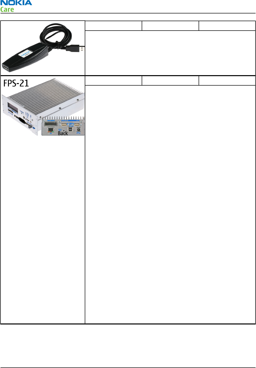
FLS-5 Flash device
FLS-5 is a dongle and flash device incorporated into one package,
developed specifically for POS use.
Note: FLS-5 can be used as an alternative to PK-1.
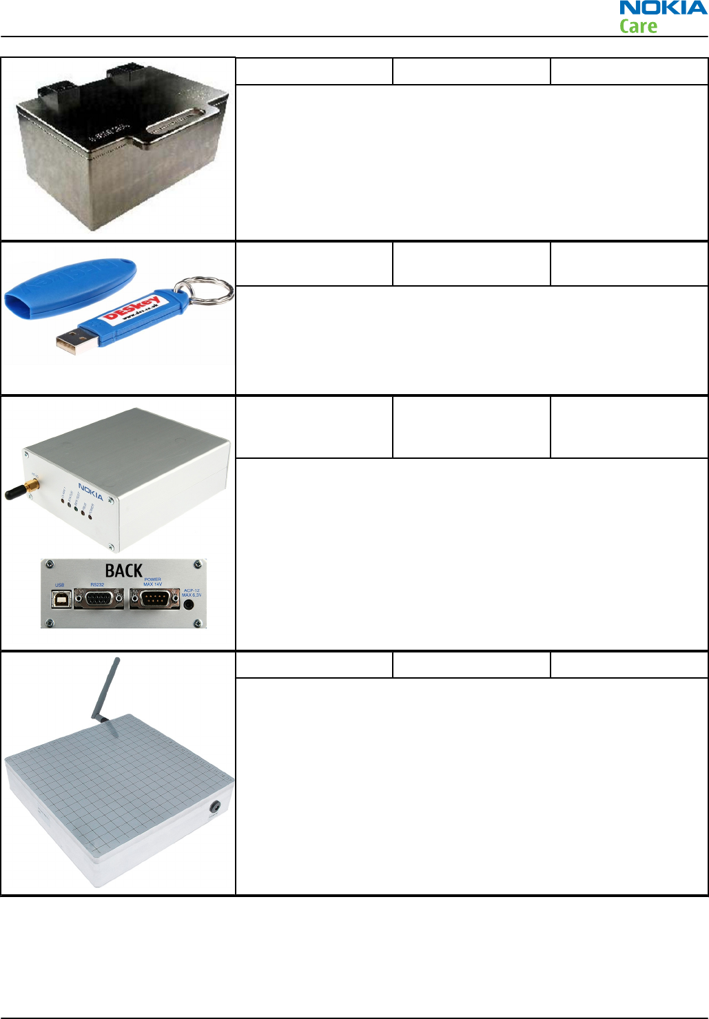
FPS-21 Flash prommer
FPS-21 sales package:
•FPS-21 prommer
•AC-35 power supply
•CA-31D USB cable
FPS-21 interfaces:
Front
•Service cable connector
Provides Flashbus, USB and VBAT connections to a mobile device.
•SmartCard socket
A SmartCard is needed to allow DCT-4 generation mobile device
programming.
Rear
•DC power input
For connecting the external power supply (AC-35).
•Two USB A type ports (USB1/USB3)
Can be used, for example, for connecting external storage memory
devices or mobile devices
•One USB B type device connector (USB2)
For connecting a PC.
•Phone connector
Service cable connection for connecting Flashbus/FLA.
•Ethernet RJ45 type socket (LAN)
For connecting the FPS-21 to LAN.
Inside
•Four SD card memory slots
For internal storage memory.
Note: In order to access the SD memory card slots inside
FPS-21, the prommer needs to be opened by removing the
front panel, rear panel and heatsink from the prommer body.
RM-612; RM-624
Service Tools and Service Concepts
Page 2 – 26 COMPANY CONFIDENTIAL Issue 1
Copyright © 2010 Nokia. All rights reserved.
JXS-1 RF shield box
Because the WCDMA network disturbs the RX side testing of the WCDMA
phone and the Tx signal of the WCDMA phone can severely disturb the
WCDMA network, a shield box is needed in all testing, tuning and fault
finding which requires WCDMA RF signal.
The shield box is not an active device, it contains only passive filtering
components for RF attenuation.
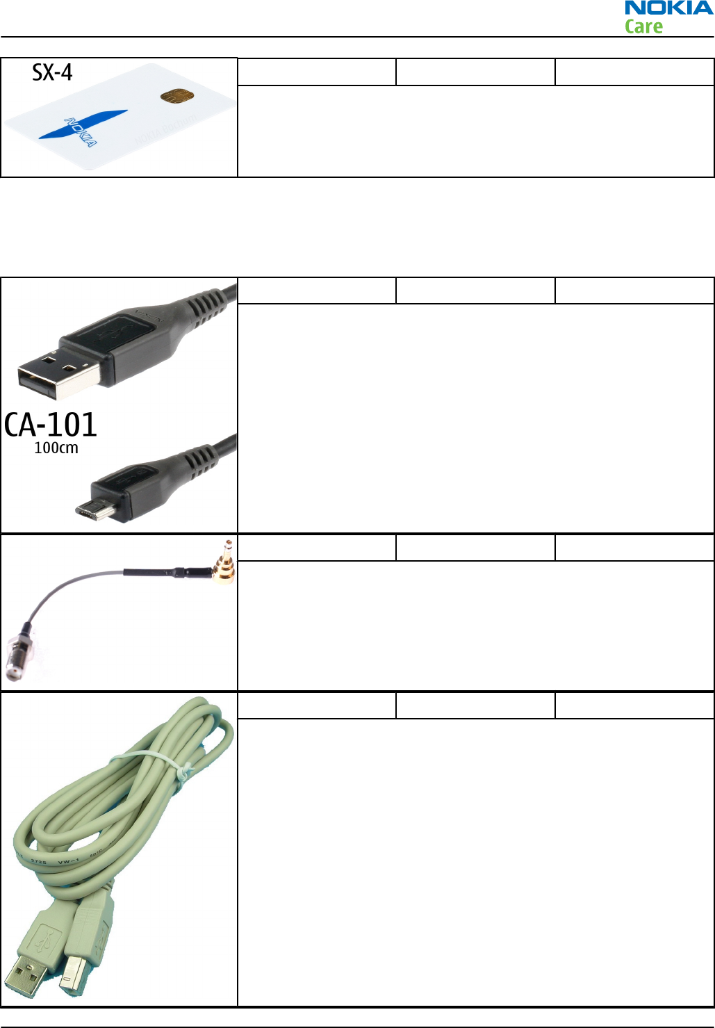
PK-1 Software protection
key
PK-1 is a hardware protection key with a USB interface. It has the same
functionality as the PKD-1 series dongle.
PK-1 is meant for use with a PC that does not have a series interface.
To use this USB dongle for security service functions please register
the dongle in the same way as the PKD-1 series dongle.
SB-6 Bluetooth test and
interface box (sales
package)
The SB-6 test box is a generic service device used to perform Bluetooth
bit error rate (BER) testing, and establishing cordless FBUS connection
via Bluetooth. An ACP-8x charger is needed for BER testing and an
AXS-4 cable in case of cordless interface usage testing .
Sales package includes:
•SB-6 test box
•Installation and warranty information
SB-7 WLAN test box
WLAN test requires defined position for the device.
RM-612; RM-624
Service Tools and Service Concepts
Issue 1 COMPANY CONFIDENTIAL Page 2 – 27
Copyright © 2010 Nokia. All rights reserved.
SRT-6 Opening tool
SRT-6 is used to open phone covers.
Note: The SRT-6 is included in the Nokia Standard Toolkit.
SS-210 Camera removal tool
The camera removal tool SS-210 is used to remove/attach the camera
module from/to the socket.
SS-46 Interface adapter
SS-46 acts as an interface adapter between the flash adapter and
FPS-21.
SS-62 Generic flash adapter
base for BB5
•generic base for flash adapters and couplers
•SS-62 equipped with a clip interlock system
•provides standardised interface towards Control Unit
•multiplexing between USB and FBUS media, controlled by VUSB
SS-93 Opening tool
SS-93 is used for opening JAE connectors.
Note: The SS-93 is included in Nokia Standard Toolkit.
RM-612; RM-624
Service Tools and Service Concepts
Page 2 – 28 COMPANY CONFIDENTIAL Issue 1
Copyright © 2010 Nokia. All rights reserved.
SX-4 Smart card
SX-4 is a BB5 security device used to protect critical features in tuning
and testing.
SX-4 is also needed together with FPS-21 when DCT-4 phones are
flashed.
Cables
The table below gives a short overview of service devices that can be used for testing, error analysis, and
repair of product RM-612; RM-624. For the correct use of the service devices, and the best effort of workbench
setup, please refer to various concepts.
CA-101 Micro USB cable
The CA-101 is a USB-to-microUSB data cable that allows connections
between the PC and the phone.
CA-158RS RF tuning cable
Product-specific adapter cable for RF tuning.
CA-31D USB cable
The CA-31D USB cable is used to connect FPS-21 to a PC. It is included
in the FPS-21 sales package.
RM-612; RM-624
Service Tools and Service Concepts
Issue 1 COMPANY CONFIDENTIAL Page 2 – 29
Copyright © 2010 Nokia. All rights reserved.
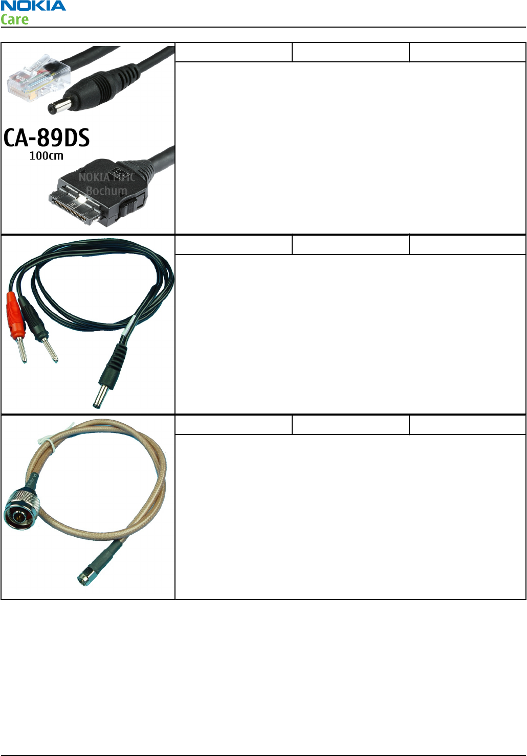
CA-89DS Cable
Provides VBAT and Flashbus connections to mobile device
programming adapters.
PCS-1 Power cable
The PCS-1 power cable (DC) is used with a docking station, a module
jig or a control unit to supply a controlled voltage.
XRS-6 RF cable
The RF cable is used to connect, for example, a module repair jig to
the RF measurement equipment.
SMA to N-Connector approximately 610 mm.
Attenuation for:
•GSM850/900: 0.3+-0.1 dB
•GSM1800/1900: 0.5+-0.1 dB
•WCDMA/WLAN: 0.6+-0.1dB
RM-612; RM-624
Service Tools and Service Concepts
Page 2 – 30 COMPANY CONFIDENTIAL Issue 1
Copyright © 2010 Nokia. All rights reserved.
Service concepts
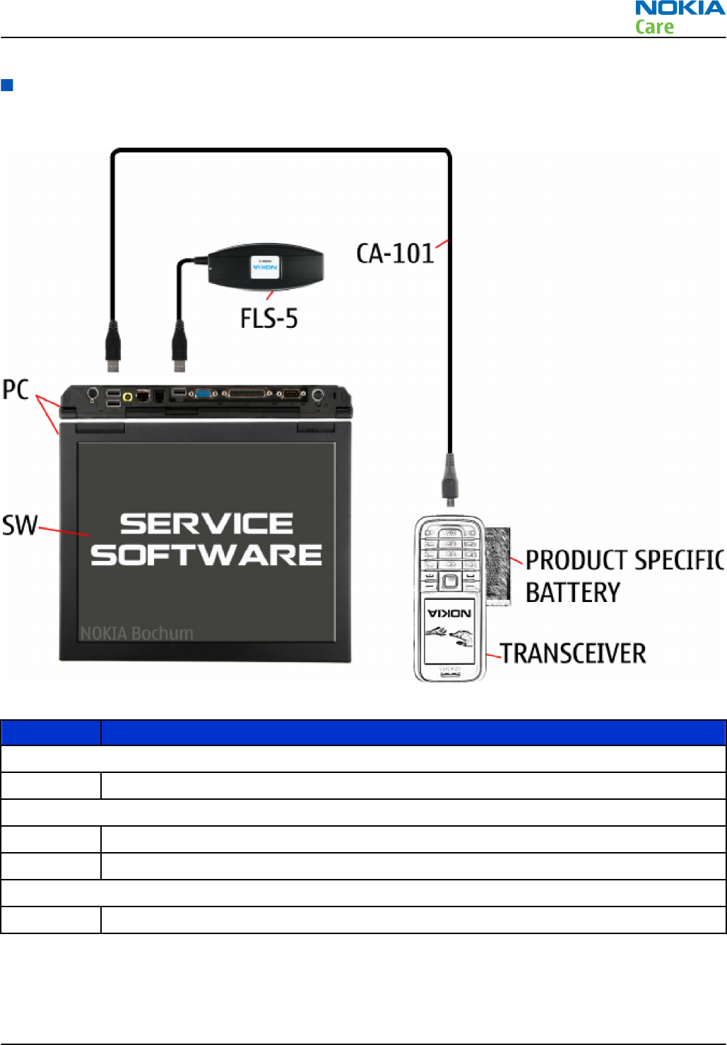
POS (Point of Sale) flash concept
Figure 2 POS flash concept
Type Description
Product specific tools
BL-4J Battery
Other tools
FLS-5 POS flash dongle
PC with Phoenix service software
Cables
CA-101 USB connectivity cable
RM-612; RM-624
Service Tools and Service Concepts
Issue 1 COMPANY CONFIDENTIAL Page 2 – 31
Copyright © 2010 Nokia. All rights reserved.
Flash concept with FPS-21
Figure 3 Basic flash concept with FPS-21
Type Description
Product specific devices
FS-141 Flash adapter
Other devices
FPS-21 Flash prommer box
AC-35 Power supply
PK-1 SW security device
SS-46 Interface adapter
PC with Phoenix service software
Cables
CA-89DS Service cable
USB cable
RM-612; RM-624
Service Tools and Service Concepts
Page 2 – 32 COMPANY CONFIDENTIAL Issue 1
Copyright © 2010 Nokia. All rights reserved.
CU-4 flash concept with FPS-21
Figure 4 CU-4 flash concept with FPS-21
Type Description
Product specific devices
FS-141 Flash adapter
Other devices
CU-4 Control unit
FPS-21 Flash prommer box
AC-35 Power supply
PK-1 SW security device
SS-62 Flash adapter base
SX-4 Smart card (for DCT-4 generation mobile device programming)
PC with Phoenix service software
Cables
PCS-1 Power cable
CA-89DS Service cable
Standard USB cable
RM-612; RM-624
Service Tools and Service Concepts
Issue 1 COMPANY CONFIDENTIAL Page 2 – 33
Copyright © 2010 Nokia. All rights reserved.
Type Description
USB cable
Flash concept with FPS-21 and SB-6
Figure 5 Flash concept with FPS-21 and SB-6
Type Description
Product specific tools
FS-141 Flash adapter
Other tools
FPS-21 Flash prommer box
PKD-1/PK-1 SW security device
SS-46 Interface adapter
SB-6 Bluetooth test and interface box
PC with Phoenix service software
Cables
RM-612; RM-624
Service Tools and Service Concepts
Page 2 – 34 COMPANY CONFIDENTIAL Issue 1
Copyright © 2010 Nokia. All rights reserved.
Type Description
XCS-4 Modular cable
CA-35S Power cable
USB cable
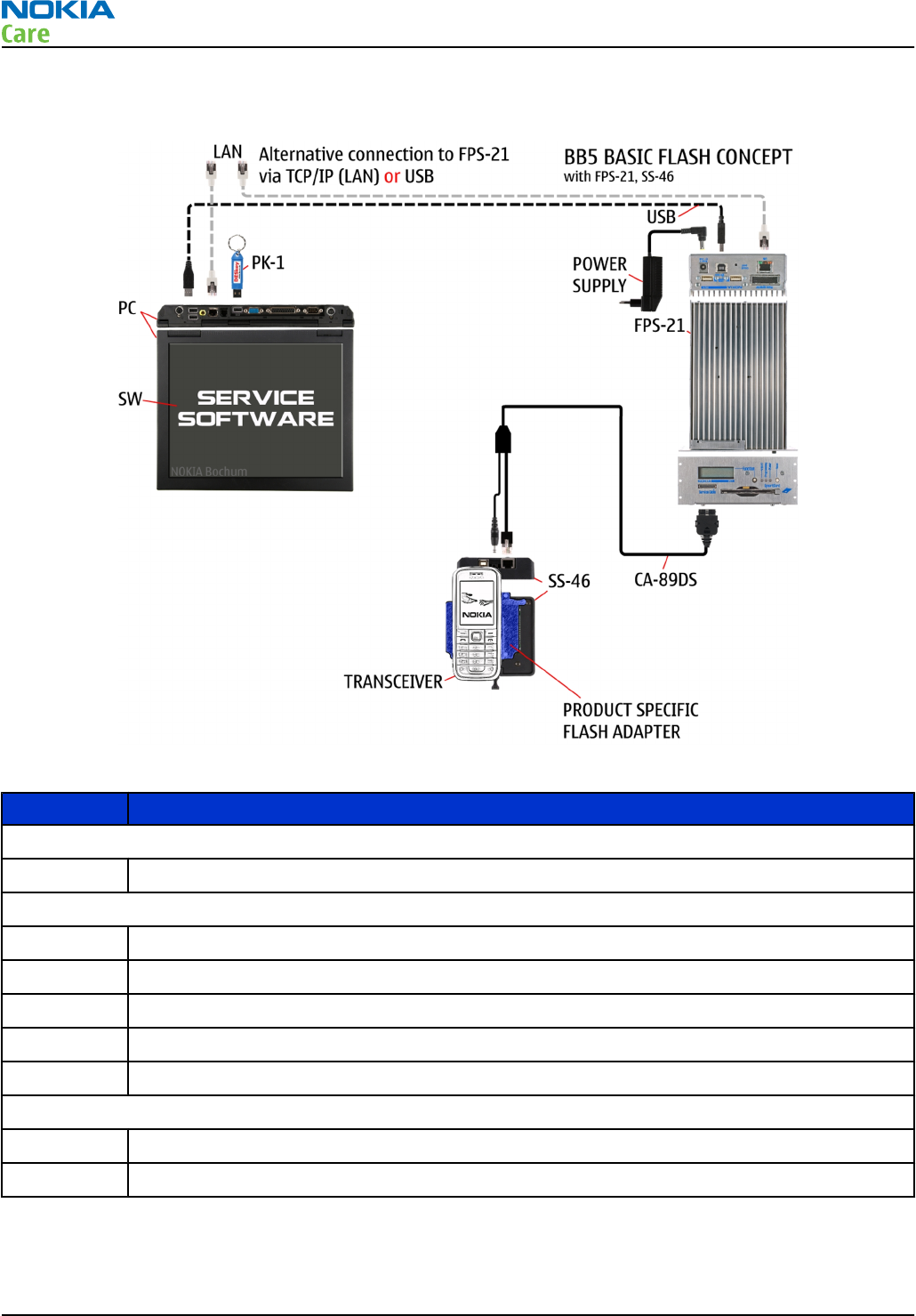
Flash concept with SS-46 and CA-89DS
Figure 6 Flash concept with SS-46 and CA-89DS
Type Description
Product specific tools
FS-141 Flash adapter
Other tools
FLS-5 Flash device
SS-46 Interface adapter
PC with Phoenix service software
Cables
RM-612; RM-624
Service Tools and Service Concepts
Issue 1 COMPANY CONFIDENTIAL Page 2 – 35
Copyright © 2010 Nokia. All rights reserved.
Type Description
CA-89DS Cable
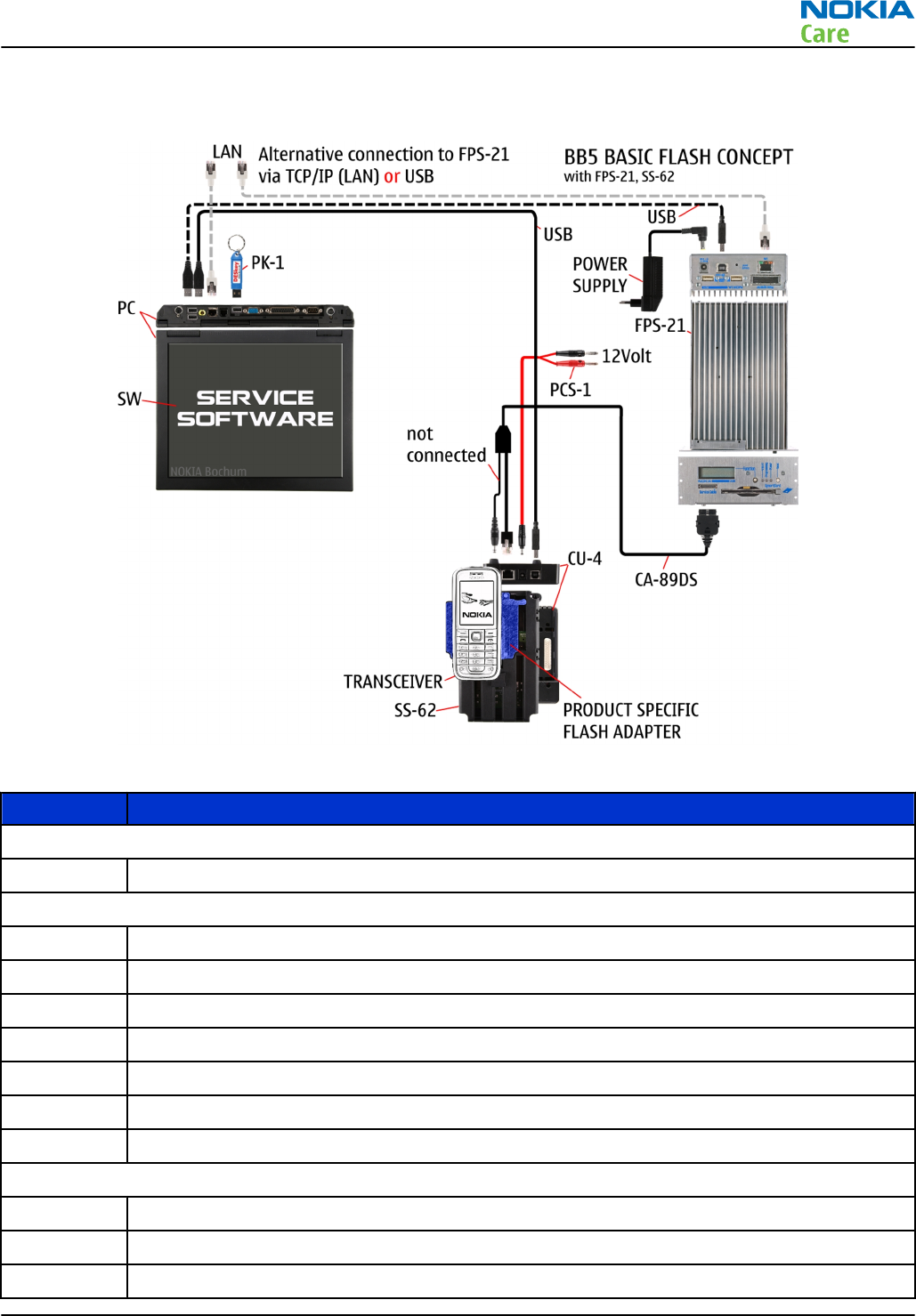
Flash concept with SS-62 and CA-89DS
Figure 7 Flash concept with SS-62 and CA-89DS
Type Description
Product specific tools
FS-141 Flash adapter
Other tools
CU-4 Control unit
FLS-5 Flash device
SS-62 Flash adapter base
PC with Phoenix service software
Cables
CA-89DS Cable
RM-612; RM-624
Service Tools and Service Concepts
Page 2 – 36 COMPANY CONFIDENTIAL Issue 1
Copyright © 2010 Nokia. All rights reserved.
Type Description
PCS-1 Power cable
USB cable
Flash concept with FPS-21, SS-62 and SB-6
Figure 8 Flash concept with FPS-21, SS-62 and SB-6
Type Description
Product specific tools
FS-141 Flash adapter
Other tools
CU-4 Control unit
FPS-21 Flash prommer box
PKD-1/PK-1 SW security device
SS-62 Flash adapter base
SB-6 Bluetooth test and interface box
SX-4 Smart card
PC with Phoenix service software
RM-612; RM-624
Service Tools and Service Concepts
Issue 1 COMPANY CONFIDENTIAL Page 2 – 37
Copyright © 2010 Nokia. All rights reserved.
Type Description
Cables
XCS-4 Modular cable
PCS-1 Power cable
USB cable
Flash concept with FPS-21, SS-62 and SB-7
Figure 9 Flash concept with FPS-21, SB-7 and JBT-9
Type Description
Product specific tools
FS-141 Flash adapter
Other tools
CU-4 Control unit
FPS-21 Flash prommer box
PK-1 SW security device
SB-7 WLAN test box
SS-62 Flash adapter base
RM-612; RM-624
Service Tools and Service Concepts
Page 2 – 38 COMPANY CONFIDENTIAL Issue 1
Copyright © 2010 Nokia. All rights reserved.
Type Description
SX-4 Smart card
PC with Phoenix service software
Cables
XCS-4 Modular cable
PCS-1 Power cable
USB cable
Module jig service concept
Figure 10 Module jig service concept
Type Description
Phone specific tools
MJ-263 Light Module Jig
Other tools
CU-4 Control unit
FPS-21 Flash prommer box
PK-1 SW security device
SX-4 Smart card
PC with Phoenix service software
Measurement equipment
RM-612; RM-624
Service Tools and Service Concepts
Issue 1 COMPANY CONFIDENTIAL Page 2 – 39
Copyright © 2010 Nokia. All rights reserved.
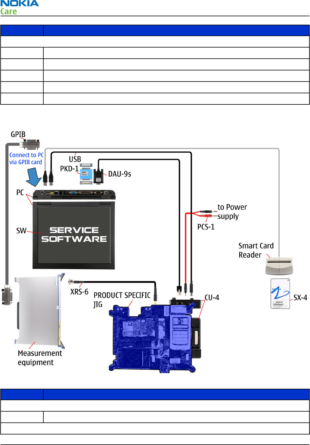
Type Description
Cables
CA-89DS Service cable
PCS-1 DC power cable
XRS-6 RF cable
USB cable
GPIB control cable
Module jig service concept with SB-6
Figure 11 Module jig service concept with SB-6
Type Description
Product specific tools
MJ-263 Light Module Jig
Other tools
RM-612; RM-624
Service Tools and Service Concepts
Page 2 – 40 COMPANY CONFIDENTIAL Issue 1
Copyright © 2010 Nokia. All rights reserved.
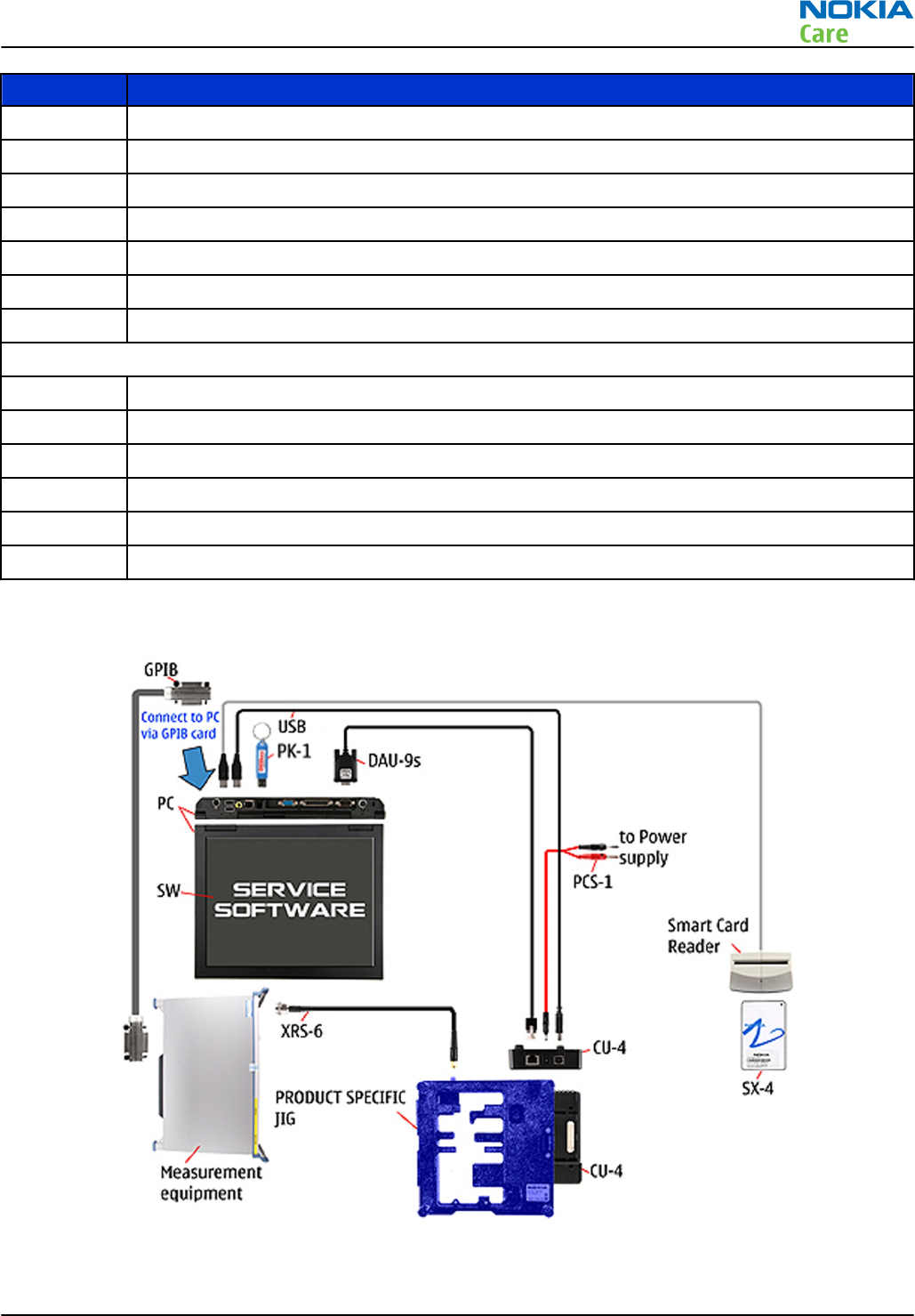
Type Description
CU-4 Control unit
FPS-21 Flash prommer box
SB-6 Bluetooth test and interface box
PK-1/PKD-1 SW security device
SX-4 Smart card
Measurement equipment
PC with Phoenix service software
Cables
PCS-1 DC power cable
XCS-4 Modular cable
XRS-6 RF cable
CA-158RS RF tuning cable
GPIB control cable
USB cable
Service concept for RF testing and RF/BB tuning
Figure 12 Service concept for RF testing and RF/BB tuning
RM-612; RM-624
Service Tools and Service Concepts
Issue 1 COMPANY CONFIDENTIAL Page 2 – 41
Copyright © 2010 Nokia. All rights reserved.
Type Description
Product specific devices
MJ-263 Light Module Jig
Other devices
CU-4 Control unit
PK-1/PKD-1 SW security device
SX-4 Smart card
Measurement equipment
Smart card reader
PC with Phoenix service software
Cables
DAU-9S MBUS cable
PCS-1 DC power cable
XRS-6 RF cable
CA-158RS RF tuning cable
GPIB control cable
USB cable
RM-612; RM-624
Service Tools and Service Concepts
Page 2 – 42 COMPANY CONFIDENTIAL Issue 1
Copyright © 2010 Nokia. All rights reserved.

3 — BB Troubleshooting and
Manual Tuning Guide
Nokia Customer Care
Issue 1 COMPANY CONFIDENTIAL Page 3 – 1
Copyright © 2010 Nokia. All rights reserved.

RM-612; RM-624
BB Troubleshooting and Manual Tuning Guide
(This page left intentionally blank.)
Page 3 – 2 COMPANY CONFIDENTIAL Issue 1
Copyright © 2010 Nokia. All rights reserved.

Table of Contents
Baseband main troubleshooting......................................................................................................................... 3–5
Dead or jammed device troubleshooting........................................................................................................... 3–8
General power checking ....................................................................................................................................... 3–9
Clocking troubleshooting .................................................................................................................................. 3–11
Charging troubleshooting ................................................................................................................................. 3–12
Backup battery troubleshooting....................................................................................................................... 3–13
Flash programming troubleshooting............................................................................................................... 3–15
Combo memory troubleshooting ..................................................................................................................... 3–18
MicroSD card troubleshooting........................................................................................................................... 3–19
USB troubleshooting .......................................................................................................................................... 3–21
SIM card troubleshooting .................................................................................................................................. 3–22
Power key troubleshooting............................................................................................................................... 3–24
Vibra troubleshooting........................................................................................................................................ 3–25
Accelerometer troubleshooting........................................................................................................................ 3–26
Touch screen troubleshooting.......................................................................................................................... 3–26
Introduction to touch screen troubleshooting .......................................................................................... 3–26
Proximity sensor troubleshooting............................................................................................................... 3–27
Resistive touch screen troubleshooting ..................................................................................................... 3–30
Hardware keys troubleshooting ....................................................................................................................... 3–33
Display module troubleshooting ...................................................................................................................... 3–36
General instructions for display troubleshooting...................................................................................... 3–36
Display troubleshooting ............................................................................................................................... 3–37
Display backlight troubleshooting .............................................................................................................. 3–38
LED and LED driver troubleshooting................................................................................................................. 3–40
Ambient Light Sensor troubleshooting............................................................................................................ 3–42
Introduction to ALS troubleshooting .......................................................................................................... 3–42
GPS troubleshooting .......................................................................................................................................... 3–43
GPS antenna................................................................................................................................................... 3–43
GPS settings for Phoenix............................................................................................................................... 3–44
GPS control................................................................................................................................................ 3–44
Oscillator test............................................................................................................................................ 3–45
Receiver self test ...................................................................................................................................... 3–46
CW Test...................................................................................................................................................... 3–47
Quick Test window................................................................................................................................... 3–48
GPS failure troubleshooting......................................................................................................................... 3–49
WLAN troubleshooting....................................................................................................................................... 3–50
WLAN functional description........................................................................................................................ 3–50
WLAN settings for Phoenix........................................................................................................................... 3–51
WLAN functional tests................................................................................................................................... 3–53
WLAN auto tuning......................................................................................................................................... 3–56
Bluetooth and FM radio troubleshooting ........................................................................................................ 3–58
Introduction to Bluetooth/FM radio troubleshooting............................................................................... 3–58
Bluetooth BER test......................................................................................................................................... 3–61
Bluetooth and FM radio self tests in Phoenix............................................................................................. 3–62
FM radio testing............................................................................................................................................. 3–63
Audio troubleshooting....................................................................................................................................... 3–64
Audio troubleshooting test instructions..................................................................................................... 3–64
Internal earpiece troubleshooting .............................................................................................................. 3–67
Internal microphone troubleshooting ....................................................................................................... 3–68
Internal handsfree speaker troubleshooting ............................................................................................ 3–69
RM-612; RM-624
BB Troubleshooting and Manual Tuning Guide
Issue 1 COMPANY CONFIDENTIAL Page 3 – 3
Copyright © 2010 Nokia. All rights reserved.

External microphone troubleshooting ....................................................................................................... 3–70
External headset earpiece troubleshooting ............................................................................................... 3–71
Acoustics troubleshooting............................................................................................................................ 3–72
Introduction to acoustics troubleshooting ........................................................................................... 3–72
Earpiece troubleshooting........................................................................................................................ 3–73
IHF troubleshooting................................................................................................................................. 3–74
Microphone troubleshooting .................................................................................................................. 3–75
Baseband manual tuning guide........................................................................................................................ 3–76
Certificate restoring ...................................................................................................................................... 3–76
Energy management calibration................................................................................................................. 3–77
List of Tables
Table 7 Display module troubleshooting cases............................................................................................... 3–36
Table 8 Pixel defects .......................................................................................................................................... 3–36
Table 9 Calibration value limits ........................................................................................................................ 3–77
List of Figures
Figure 13 Proximity sensor troubleshooting - part 2..................................................................................... 3–28
Figure 14 Touch controller basic checks .......................................................................................................... 3–32
Figure 15 Touch screen basic checks................................................................................................................ 3–33
Figure 16 Keymatrix........................................................................................................................................... 3–35
Figure 17 Send, End, Home LEDs....................................................................................................................... 3–41
Figure 18 QWERTY LEDs...................................................................................................................................... 3–42
Figure 19 ALS placement ................................................................................................................................... 3–43
Figure 20 GPS antenna....................................................................................................................................... 3–43
Figure 21 C-clip and RF connector location...................................................................................................... 3–44
Figure 22 GPS Control dialog box...................................................................................................................... 3–45
Figure 23 Simple Tests – Oscillator Test........................................................................................................... 3–46
Figure 24 Simple Tests – Receiver Self Test ..................................................................................................... 3–47
Figure 25 CW Test window................................................................................................................................ 3–48
Figure 26 GPS Quick Test window for GPS troubleshooting .......................................................................... 3–49
Figure 27 WLAN circuitry ................................................................................................................................... 3–51
Figure 28 WLAN component placement........................................................................................................... 3–51
Figure 29 WLAN auto tune settings.................................................................................................................. 3–57
Figure 30 WLAN autotuning results ................................................................................................................. 3–58
Figure 31 WLAN/BT/GPS antenna...................................................................................................................... 3–59
Figure 32 Bluetooth/FM radio component layout and test points................................................................ 3–61
Figure 33 Bluetooth BER test............................................................................................................................. 3–62
Figure 34 Bluetooth and FM radio self tests in Phoenix................................................................................. 3–63
Figure 35 Single-ended output waveform of the AV Mic to HP Ear measurement when earpiece is
connected. ................................................................................................................................................ 3–65
Figure 36 Single-ended output waveform of the Ext_microphone in Int handsfree out loop
measurement when speaker is connected (measured at speaker pads). No filter is used. ............ 3–66
Figure 37 Single-ended output waveform of the AV Mic to AV Ear loop....................................................... 3–66
Figure 38 Single-ended output waveform of the HP Mic to AV Ear loop. ..................................................... 3–66
RM-612; RM-624
BB Troubleshooting and Manual Tuning Guide
Page 3 – 4 COMPANY CONFIDENTIAL Issue 1
Copyright © 2010 Nokia. All rights reserved.
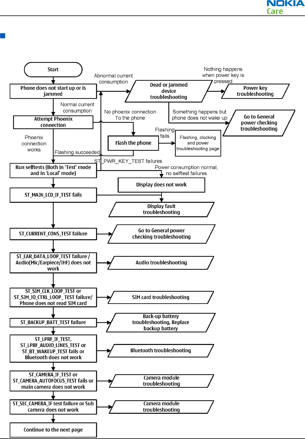
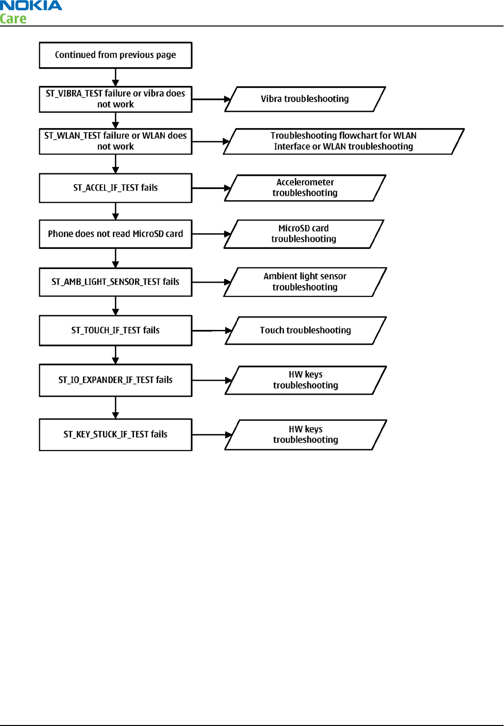
Baseband main troubleshooting
Troubleshooting flow
RM-612; RM-624
BB Troubleshooting and Manual Tuning Guide
Issue 1 COMPANY CONFIDENTIAL Page 3 – 5
Copyright © 2010 Nokia. All rights reserved.
RM-612; RM-624
BB Troubleshooting and Manual Tuning Guide
Page 3 – 6 COMPANY CONFIDENTIAL Issue 1
Copyright © 2010 Nokia. All rights reserved.
RM-612; RM-624
BB Troubleshooting and Manual Tuning Guide
Issue 1 COMPANY CONFIDENTIAL Page 3 – 7
Copyright © 2010 Nokia. All rights reserved.
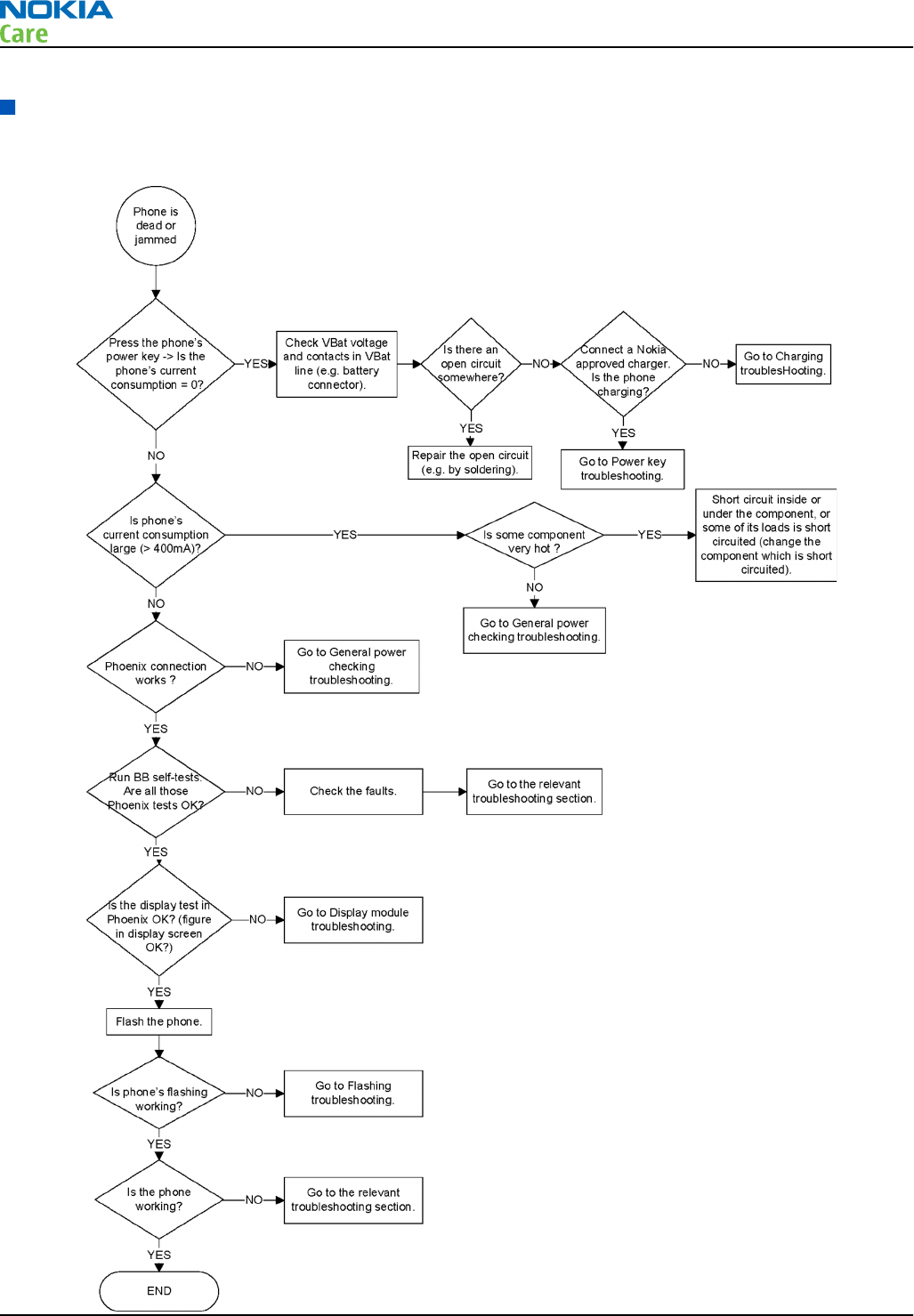
Dead or jammed device troubleshooting
Troubleshooting flow
RM-612; RM-624
BB Troubleshooting and Manual Tuning Guide
Page 3 – 8 COMPANY CONFIDENTIAL Issue 1
Copyright © 2010 Nokia. All rights reserved.
General power checking
General power checking
Signal
name Regulator Sleep Idle Nominal
voltage Main user Notes Supply
VIO_V AVILMA ON ON 1.82 Vilma I/O VBAT1
VBACK AVILMA ON ON 2.5 RTC circuitry
VSIM1 AVILMA ON ON 1.8/3.0 SIM card VBAT3
VSIM2 AVILMA OFF 1.0 Digital
microphone
VBAT3
VAUX AVILMA ON ON 2.78 Accelerometer,
proximity
sensor, Hall
sensor, display
VBAT5
VANA AVILMA ON ON 2.5 Vilma internal VBAT4
VR1 AVILMA OFF ON 2.5 VCTCXO VBAT4
VRFC AVILMA OFF 1.8 Rapido RF
converter
VRCP1 AVILMA OFF 4.75 RF module VBATCP
VOUT BETTY ON ON 2.5 Audio switch VBAT
VDAC LP3985 ON ON 3.0 DAC33 VBAT
VCAM_1V8 TPS62600 OFF 1.8 Camera HWA ,
LP5952,
cameras
VBAT
VCAM_1V3 LP5952 OFF 1.3 Camera HWA
core
VCAM_1V8
VCAM_2V8 BH28SA2 OFF 2.8 Cameras VBAT
VCORE TPS62350 ON ON 1.2 Rapido core VBAT
VIO TPS62600 ON ON 1.8 VIO, VDRAM VBAT
VSD SD level
shifter
OFF 2.9 SD card VBAT
SETCURR TK65604 OFF Display
backlights
VBAT
LP5521 OFF QWERTY key LED VBAT
LED End,
Send,
Chg,
Home
LP5521 OFF Menu key, Send/
End key, BEZEL
LED
VBAT
AS3645A OFF 4.5/5.5 Camera flash VBAT
VBAT 3.7
RM-612; RM-624
BB Troubleshooting and Manual Tuning Guide
Issue 1 COMPANY CONFIDENTIAL Page 3 – 9
Copyright © 2010 Nokia. All rights reserved.

Signal
name Regulator Sleep Idle Nominal
voltage Main user Notes Supply
VOUT
(camera)
BH30SA2 OFF 3.0 Camera VBAT
RM-612; RM-624
BB Troubleshooting and Manual Tuning Guide
Page 3 – 10 COMPANY CONFIDENTIAL Issue 1
Copyright © 2010 Nokia. All rights reserved.
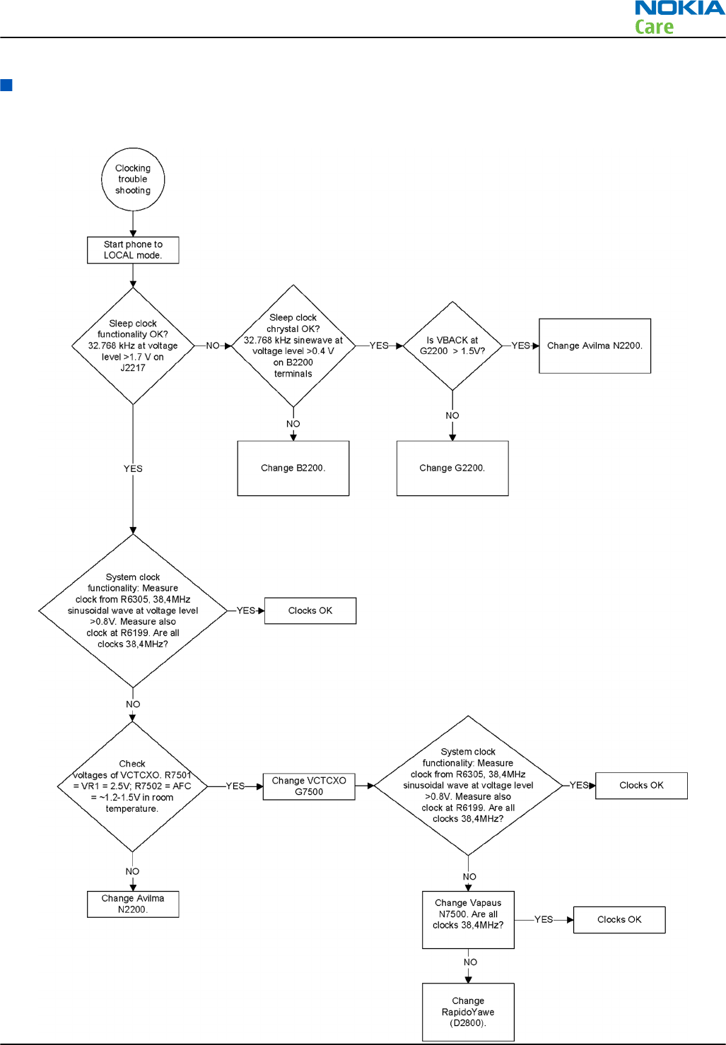
Clocking troubleshooting
Troubleshooting flow
RM-612; RM-624
BB Troubleshooting and Manual Tuning Guide
Issue 1 COMPANY CONFIDENTIAL Page 3 – 11
Copyright © 2010 Nokia. All rights reserved.
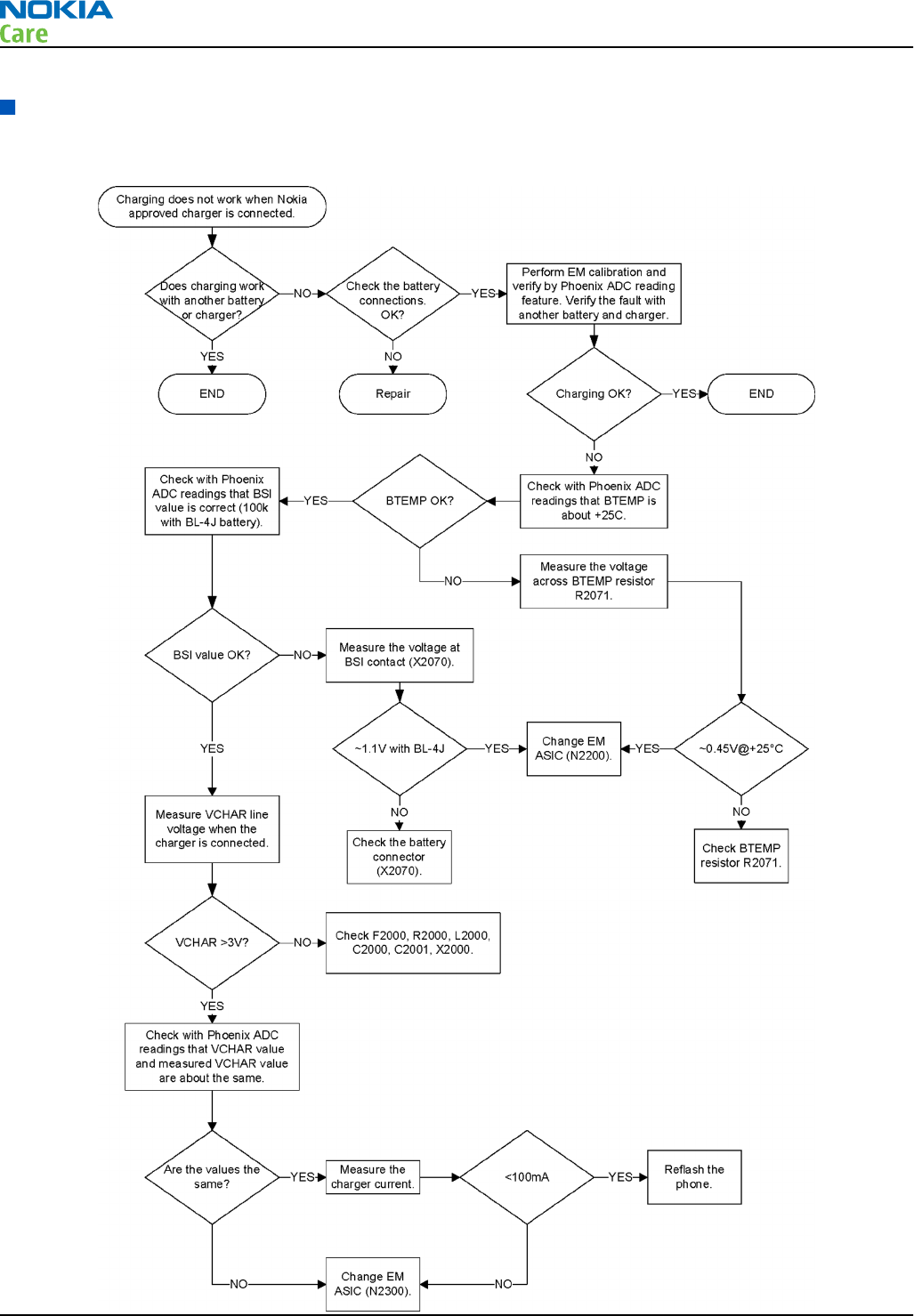
Charging troubleshooting
Troubleshooting flow
RM-612; RM-624
BB Troubleshooting and Manual Tuning Guide
Page 3 – 12 COMPANY CONFIDENTIAL Issue 1
Copyright © 2010 Nokia. All rights reserved.
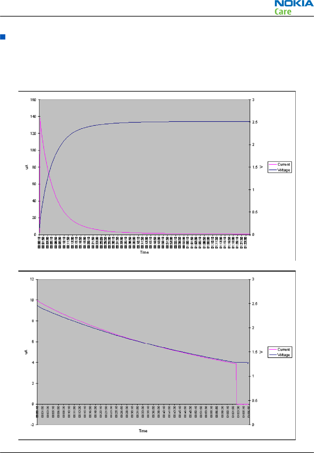
Backup battery troubleshooting
Verify that the backup battery G2200 is empty (U<1V). Switch the phone on. Measure voltage of the battery
when the main battery is connected to the phone and the phone is switched on. Wait a few minutes and
monitor that the backup battery voltage rises. Switch off the phone, disconnect the main battery and monitor
that the voltage of the backup battery decreases. Normal behaviour of the voltage is described in the figures
below:
RM-612; RM-624
BB Troubleshooting and Manual Tuning Guide
Issue 1 COMPANY CONFIDENTIAL Page 3 – 13
Copyright © 2010 Nokia. All rights reserved.

If the voltage rises and falls quickly, check the back-up battery G2200 contacts for loose soldering or short-
circuit, and repair or change G2200 if necessary. If the voltage stays ~0V, check resistance VBACK against GND.
If there is no shortcircuit, AVILMA N2200 is faulty. Replace N2200.
RM-612; RM-624
BB Troubleshooting and Manual Tuning Guide
Page 3 – 14 COMPANY CONFIDENTIAL Issue 1
Copyright © 2010 Nokia. All rights reserved.
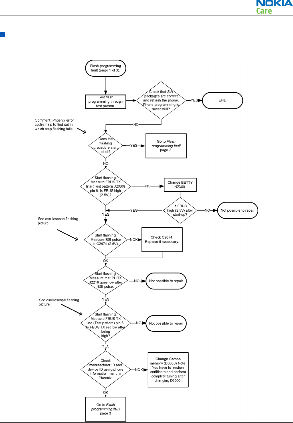
Flash programming troubleshooting
Troubleshooting flow
RM-612; RM-624
BB Troubleshooting and Manual Tuning Guide
Issue 1 COMPANY CONFIDENTIAL Page 3 – 15
Copyright © 2010 Nokia. All rights reserved.
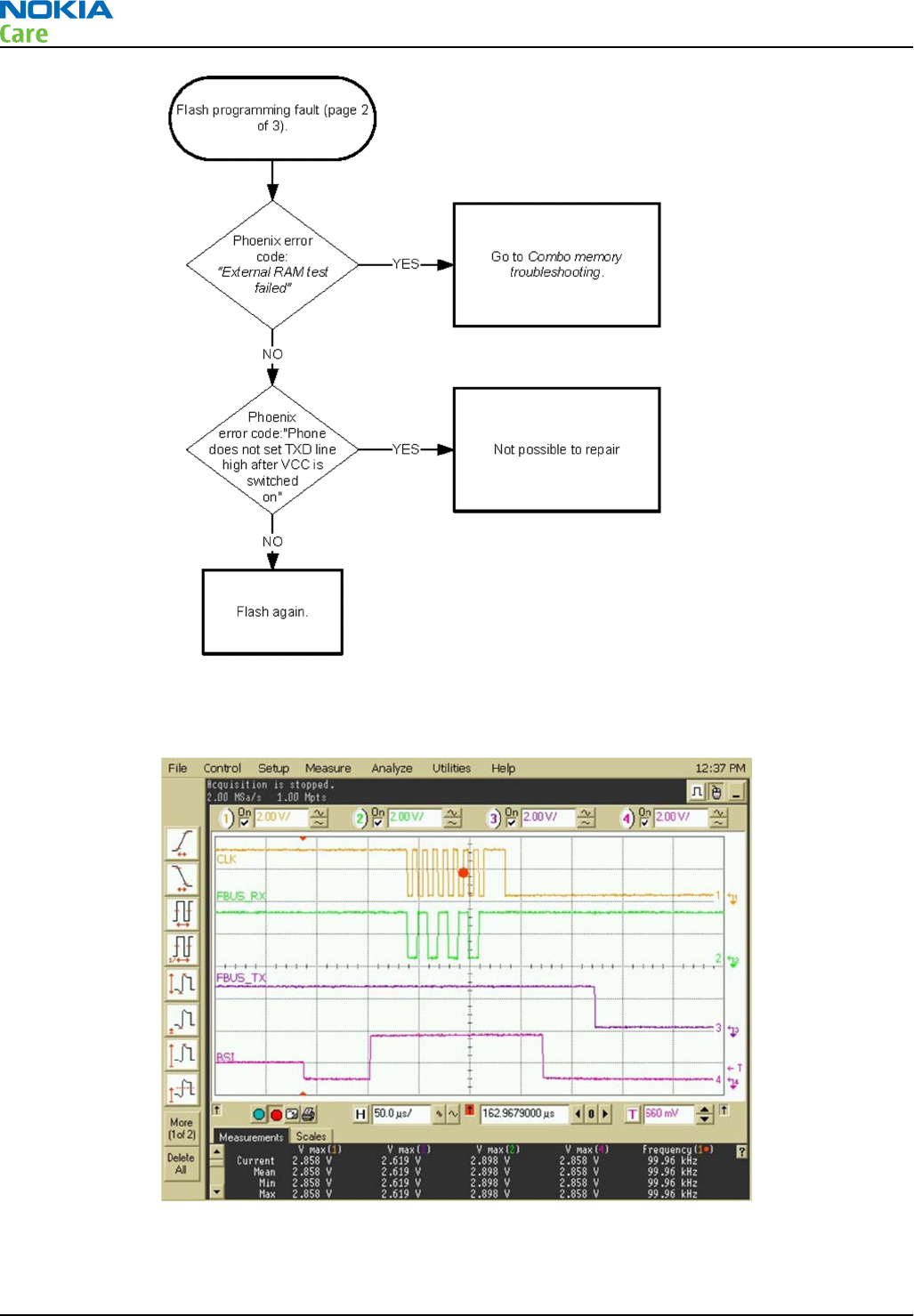
RM-612; RM-624
BB Troubleshooting and Manual Tuning Guide
Page 3 – 16 COMPANY CONFIDENTIAL Issue 1
Copyright © 2010 Nokia. All rights reserved.
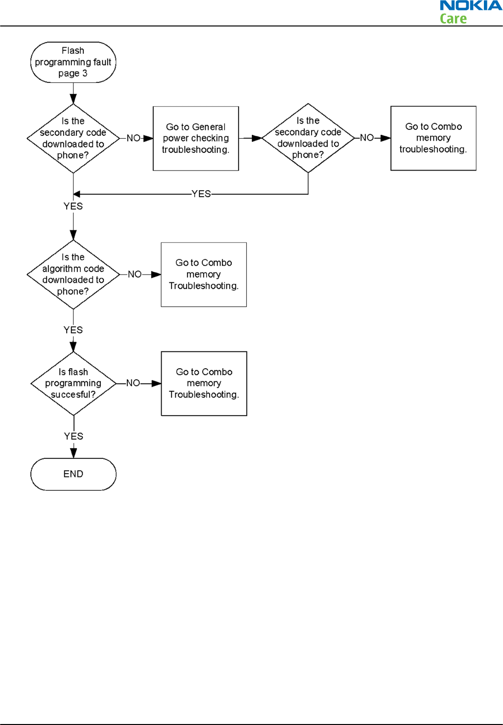
RM-612; RM-624
BB Troubleshooting and Manual Tuning Guide
Issue 1 COMPANY CONFIDENTIAL Page 3 – 17
Copyright © 2010 Nokia. All rights reserved.
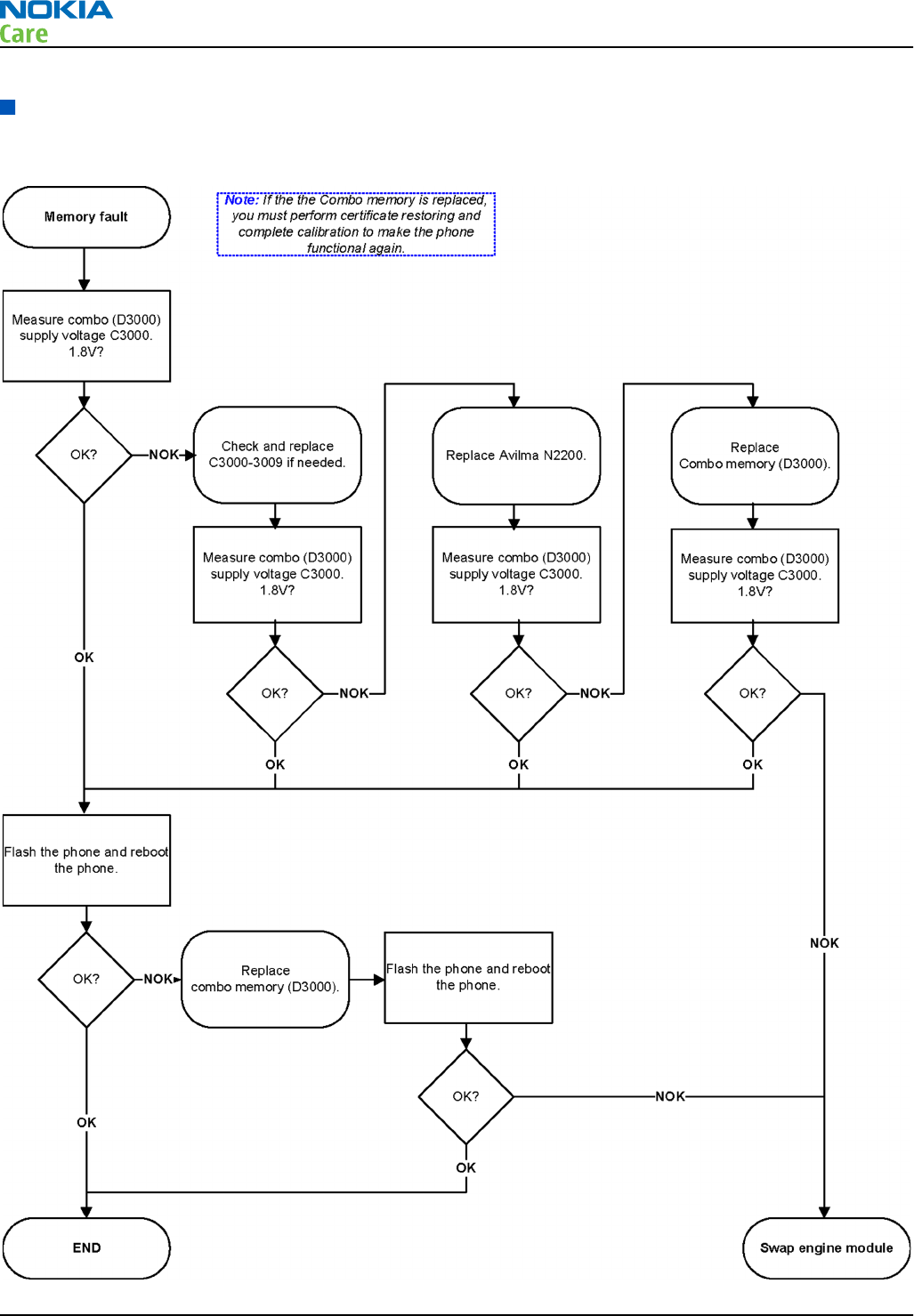
Combo memory troubleshooting
Troubleshooting flow
RM-612; RM-624
BB Troubleshooting and Manual Tuning Guide
Page 3 – 18 COMPANY CONFIDENTIAL Issue 1
Copyright © 2010 Nokia. All rights reserved.
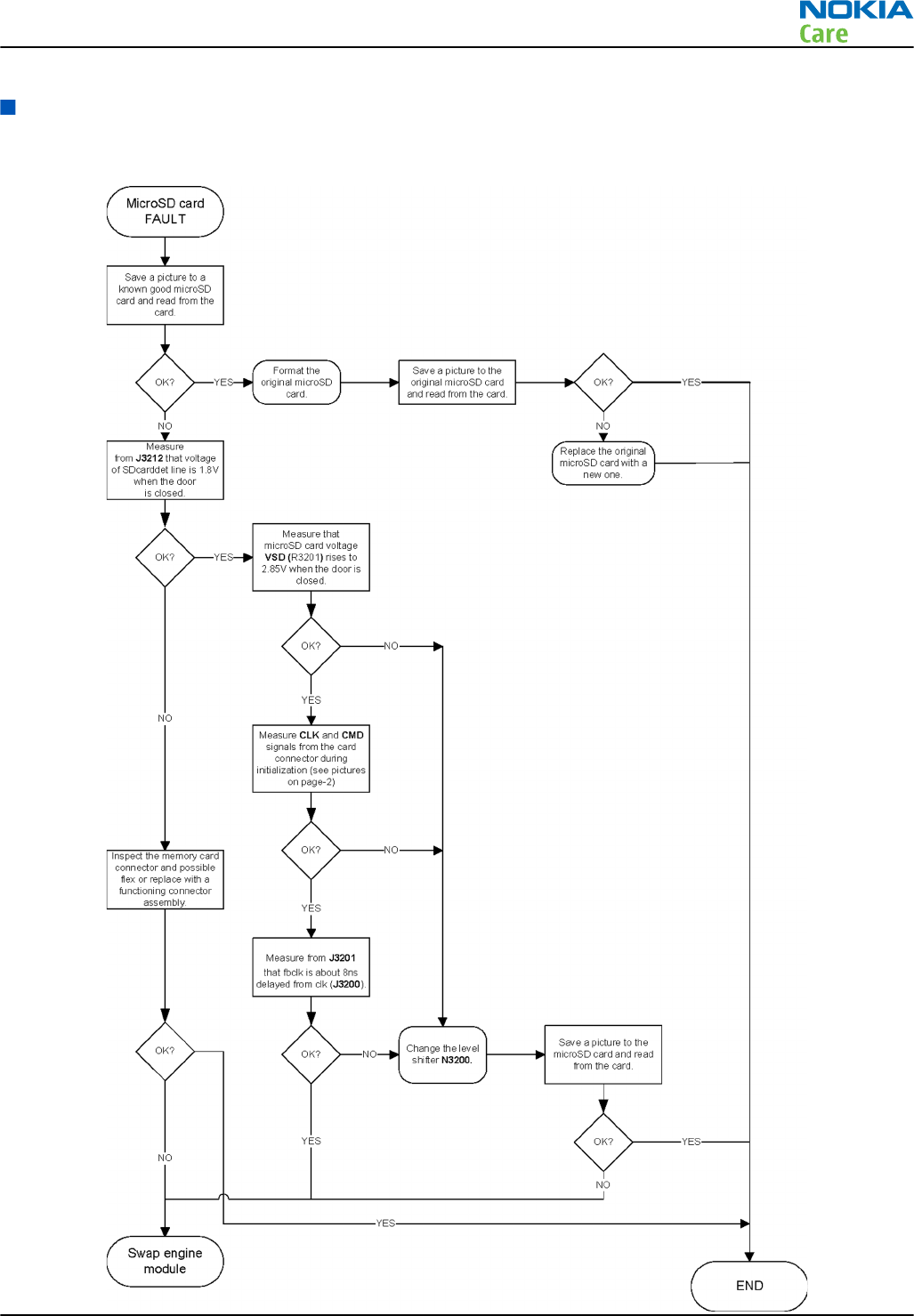
MicroSD card troubleshooting
Troubleshooting flow
RM-612; RM-624
BB Troubleshooting and Manual Tuning Guide
Issue 1 COMPANY CONFIDENTIAL Page 3 – 19
Copyright © 2010 Nokia. All rights reserved.
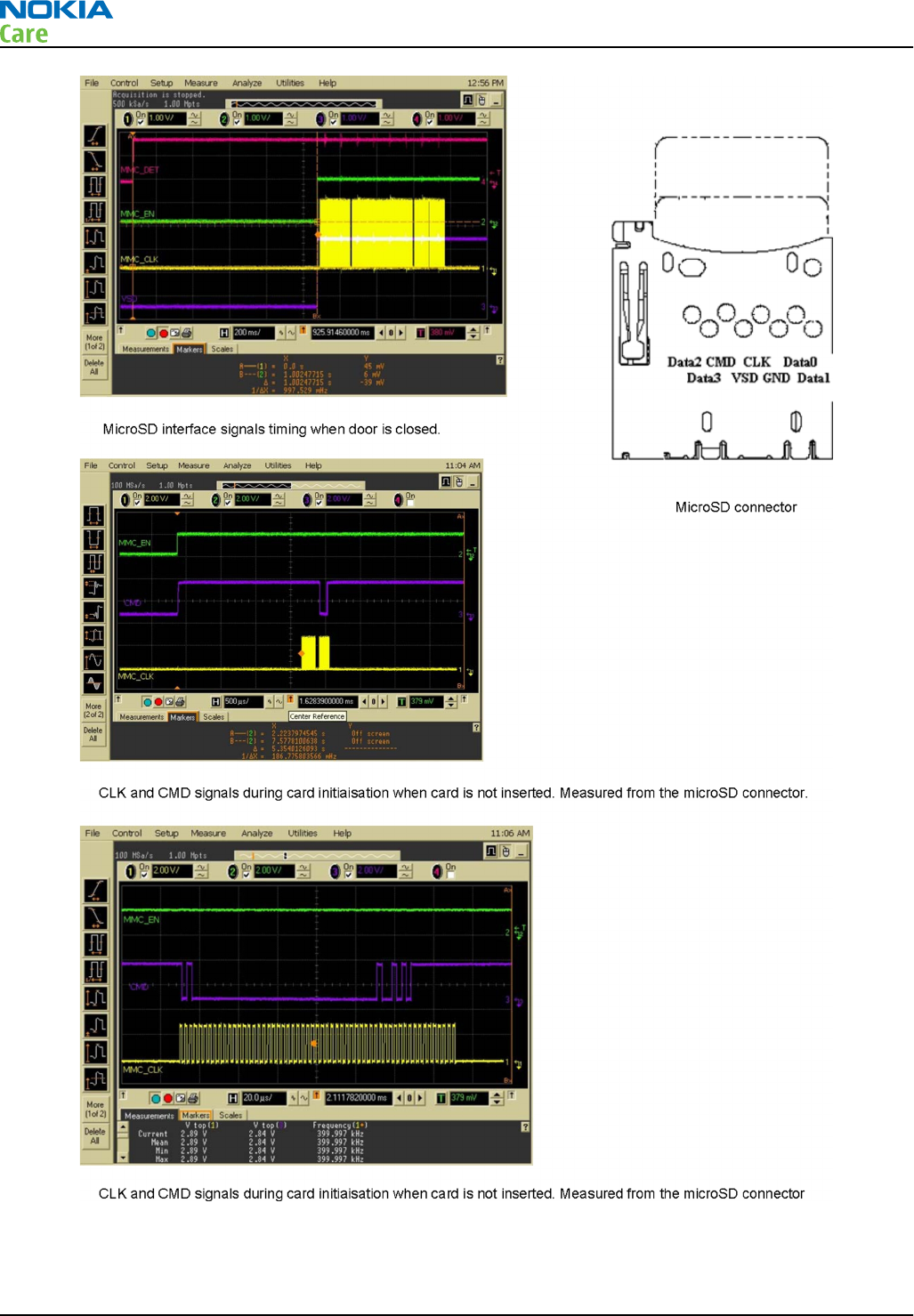
RM-612; RM-624
BB Troubleshooting and Manual Tuning Guide
Page 3 – 20 COMPANY CONFIDENTIAL Issue 1
Copyright © 2010 Nokia. All rights reserved.
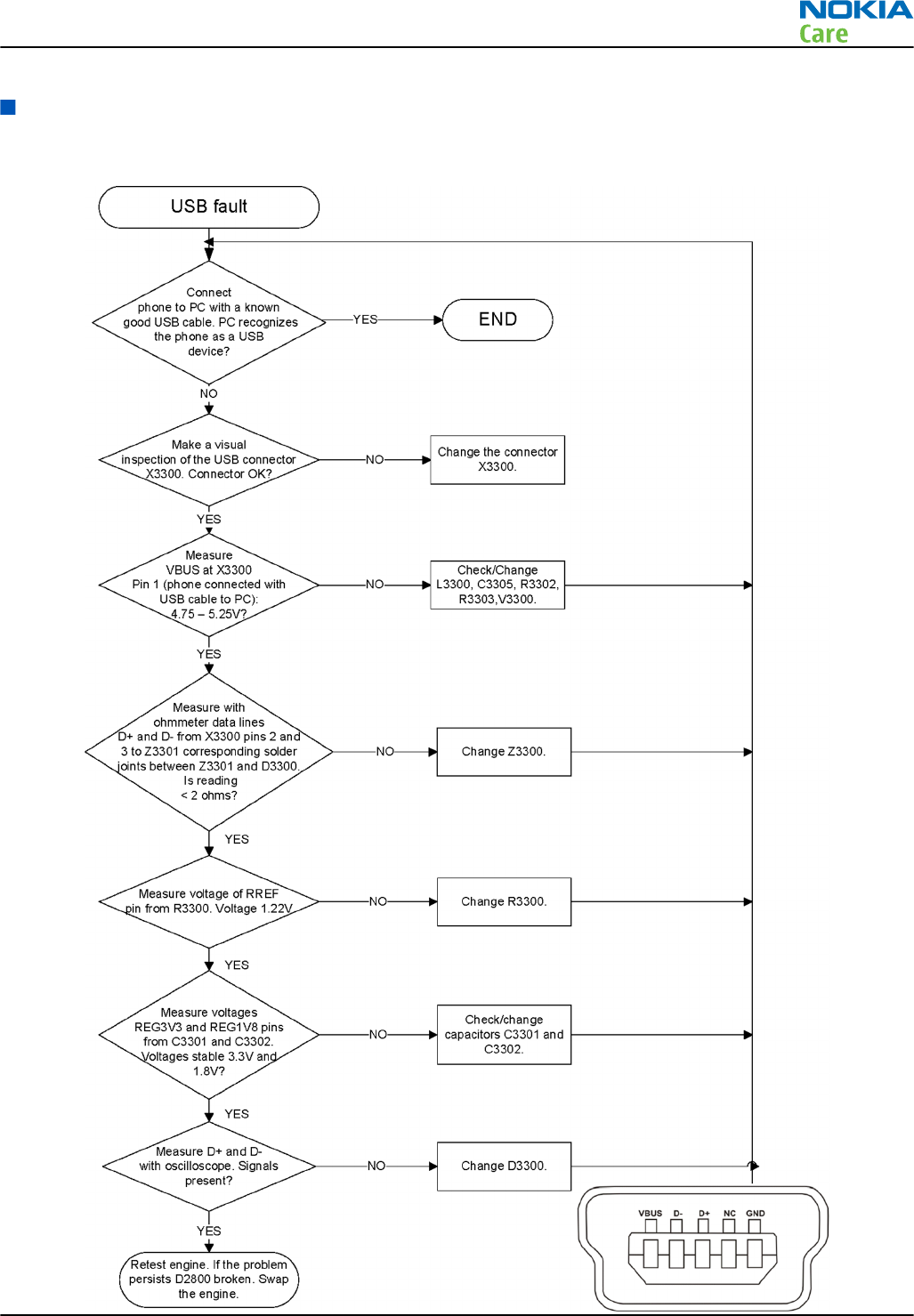
USB troubleshooting
Troubleshooting flow
RM-612; RM-624
BB Troubleshooting and Manual Tuning Guide
Issue 1 COMPANY CONFIDENTIAL Page 3 – 21
Copyright © 2010 Nokia. All rights reserved.
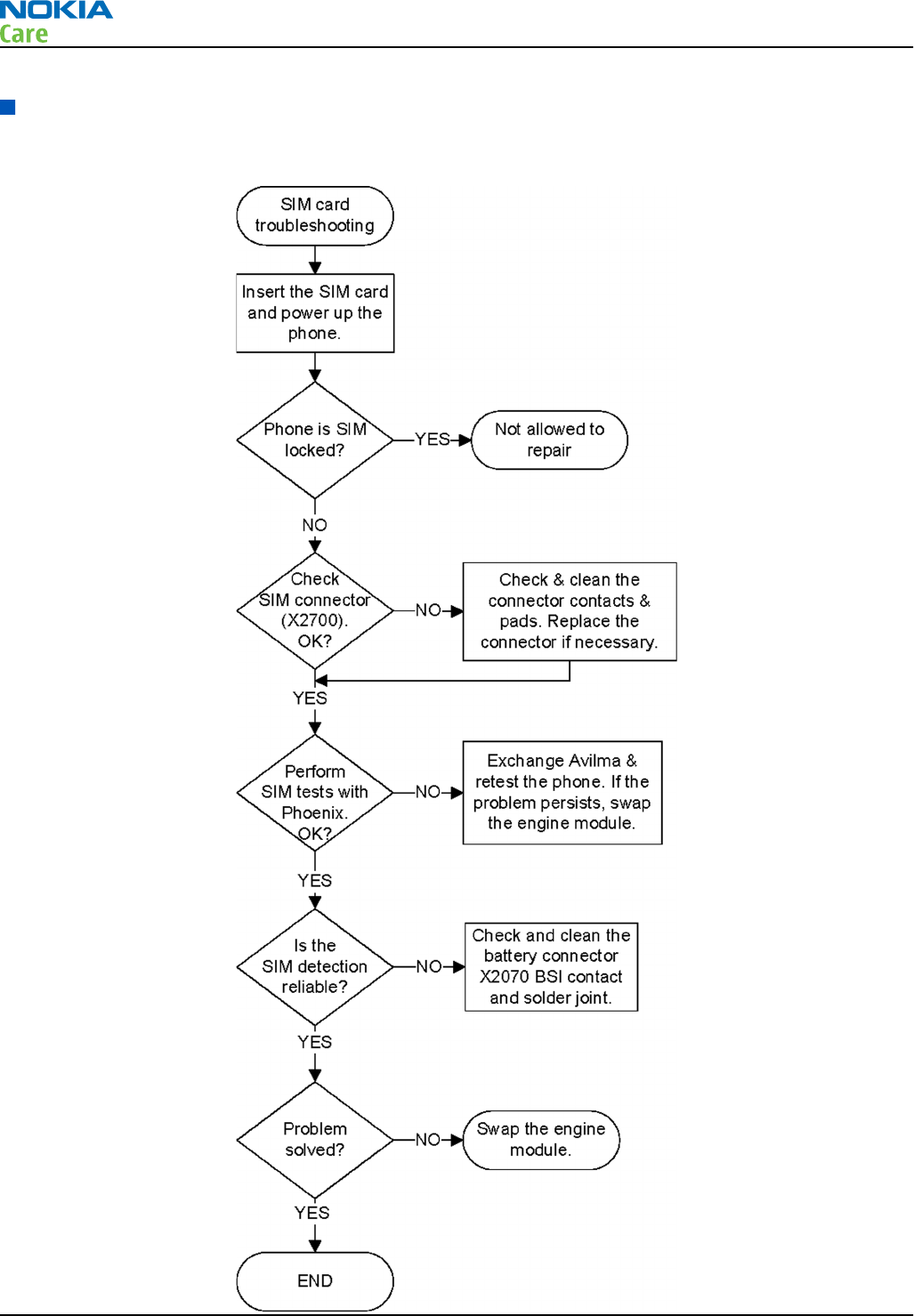
SIM card troubleshooting
Troubleshooting flow
RM-612; RM-624
BB Troubleshooting and Manual Tuning Guide
Page 3 – 22 COMPANY CONFIDENTIAL Issue 1
Copyright © 2010 Nokia. All rights reserved.
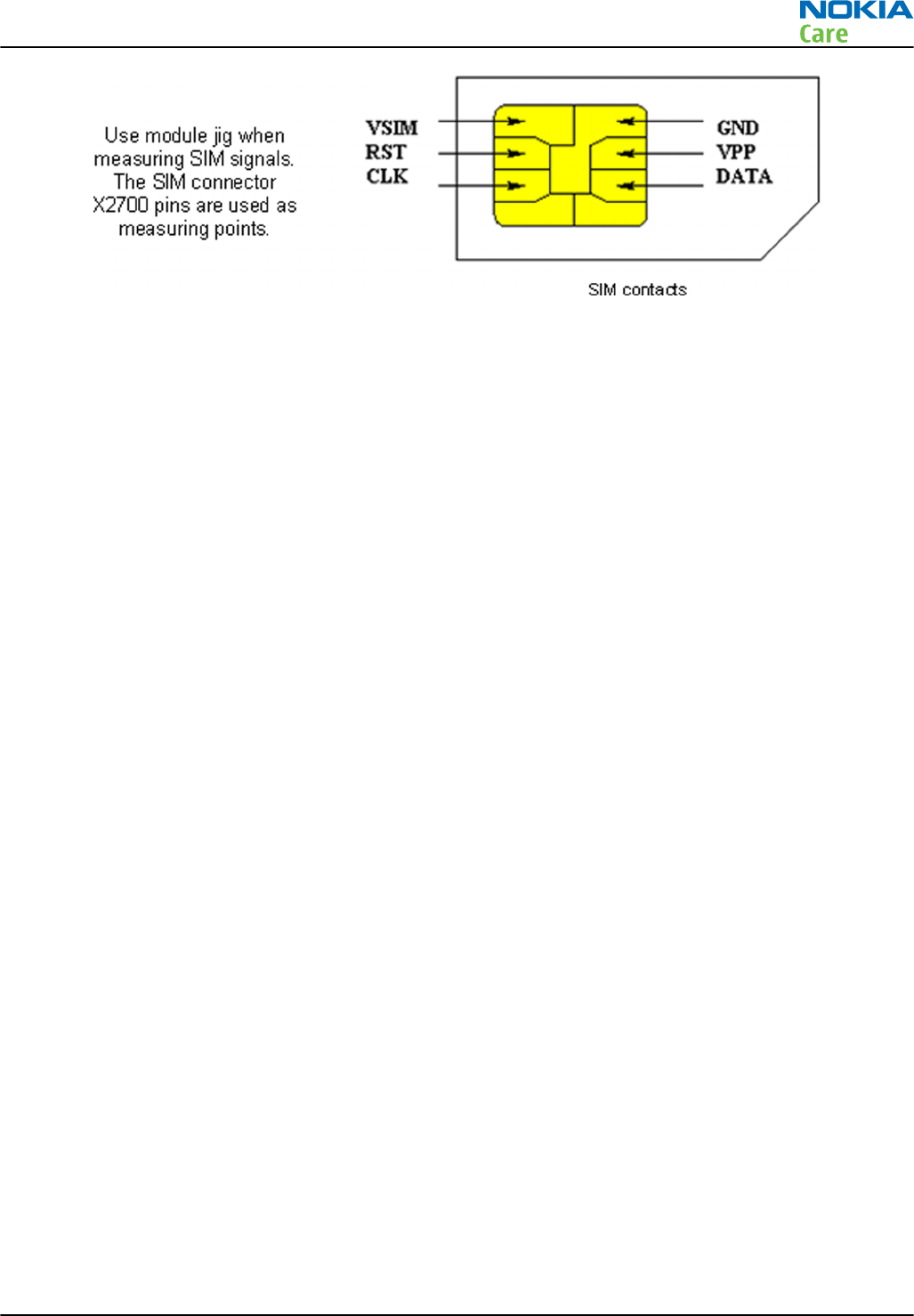
RM-612; RM-624
BB Troubleshooting and Manual Tuning Guide
Issue 1 COMPANY CONFIDENTIAL Page 3 – 23
Copyright © 2010 Nokia. All rights reserved.
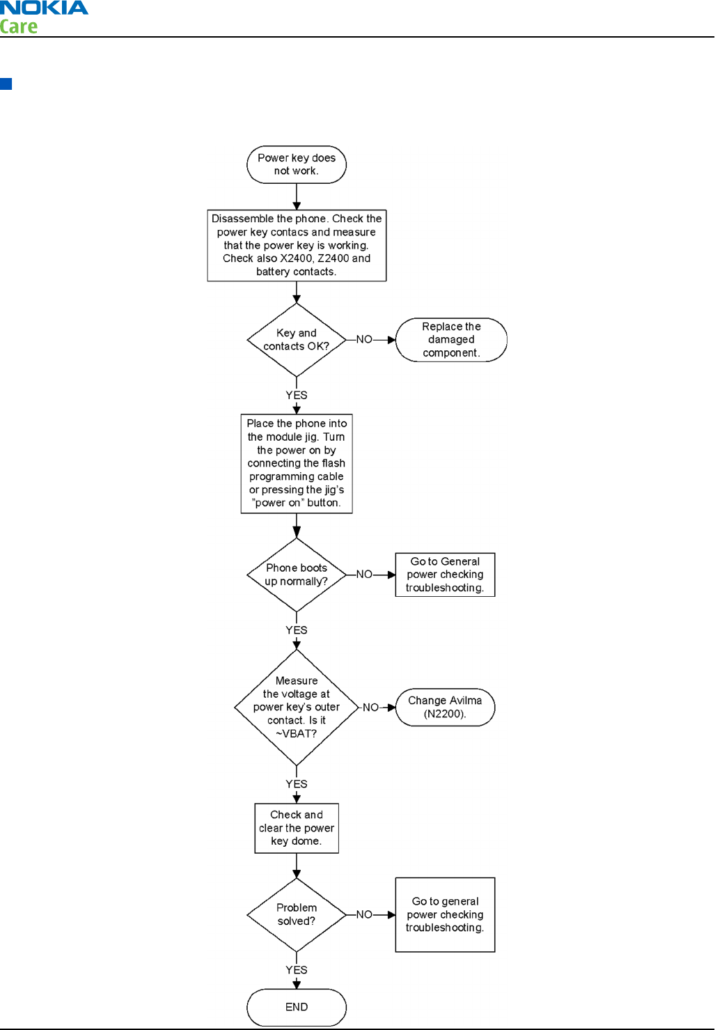
Power key troubleshooting
Troubleshooting flow
RM-612; RM-624
BB Troubleshooting and Manual Tuning Guide
Page 3 – 24 COMPANY CONFIDENTIAL Issue 1
Copyright © 2010 Nokia. All rights reserved.
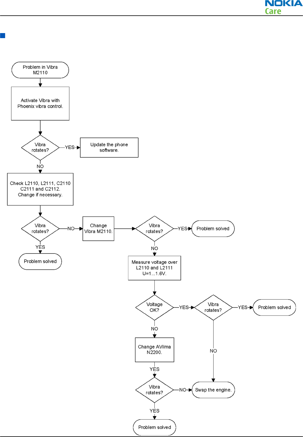
Vibra troubleshooting
Troubleshooting flow
RM-612; RM-624
BB Troubleshooting and Manual Tuning Guide
Issue 1 COMPANY CONFIDENTIAL Page 3 – 25
Copyright © 2010 Nokia. All rights reserved.
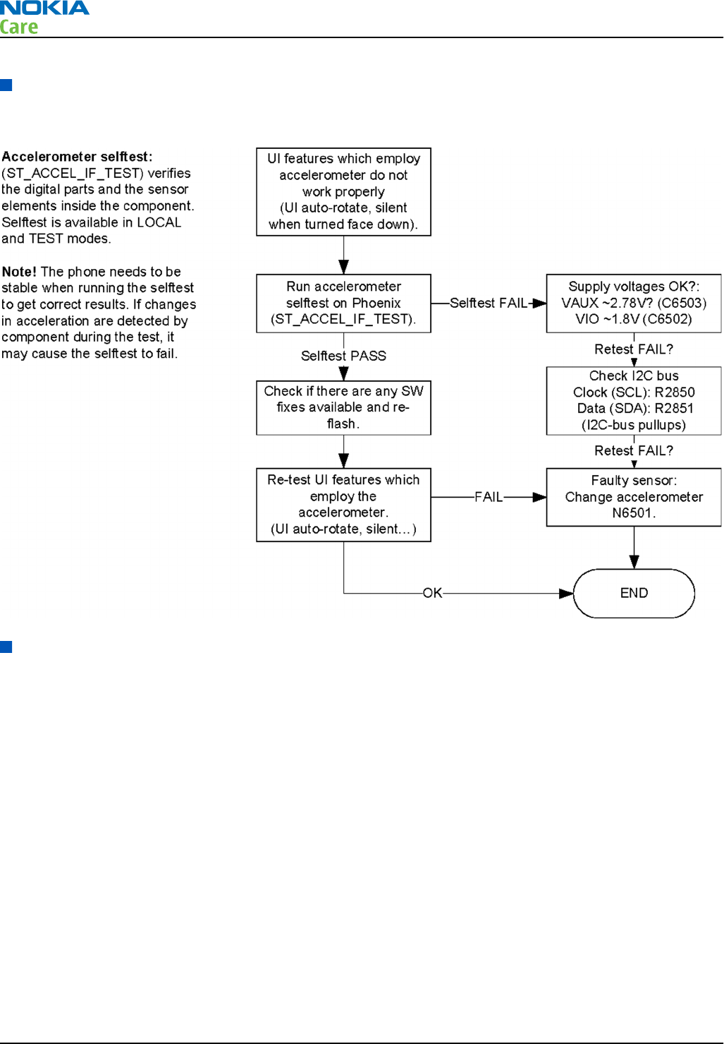
Accelerometer troubleshooting
Troubleshooting flow
Touch screen troubleshooting
Introduction to touch screen troubleshooting
The device has a resistive touch screen user interface, which means that the device does not have a traditional
ITU-T keypad. The key components of the touch screen user interface are:
•Touch window with touch controller (TSC2004)
•Proximity sensor
The resistive touch window is located above the display. It enables finger as well as stylus touch, and it
provides tactile feedback. The tactile feedback is implemented by using the same vibra that is used for
alerting. The touch controller includes drivers and the control logic to measure touch pressure.
The proximity sensor is attached to the upper flex assembly. It sends out a beam of IR light, and then computes
the distance to any nearby objects from the characteristics of the returned (reflected) signal. There is a booth
between the sensor and the touch window, which isolates the IR transmitter from the IR receiver by
preventing the reflection from the touch window surface.
RM-612; RM-624
BB Troubleshooting and Manual Tuning Guide
Page 3 – 26 COMPANY CONFIDENTIAL Issue 1
Copyright © 2010 Nokia. All rights reserved.

Proximity sensor troubleshooting
Context
Proximity sensor troubleshooting is broken down into two parts. The main purpose of the automatic check
is to identify the fault automatically without any manual checks. If the automatic flow does not provide
enough information, a manual check can be done to narrow down the cause of the fault.
RM-612; RM-624
BB Troubleshooting and Manual Tuning Guide
Issue 1 COMPANY CONFIDENTIAL Page 3 – 27
Copyright © 2010 Nokia. All rights reserved.
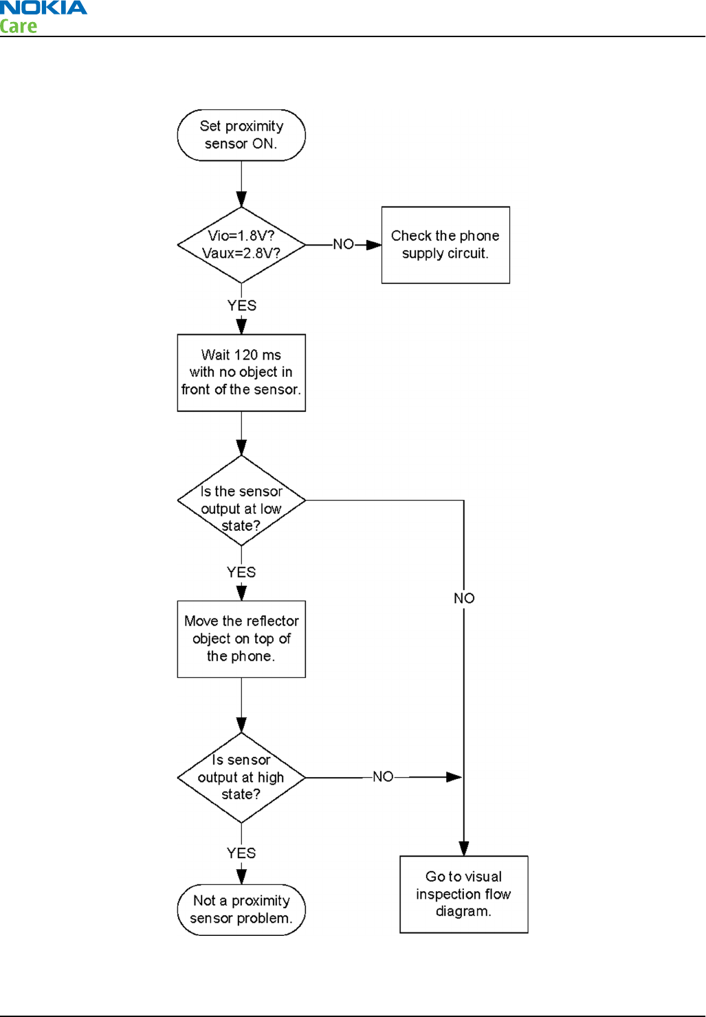
Troubleshooting flow
RM-612; RM-624
BB Troubleshooting and Manual Tuning Guide
Page 3 – 28 COMPANY CONFIDENTIAL Issue 1
Copyright © 2010 Nokia. All rights reserved.
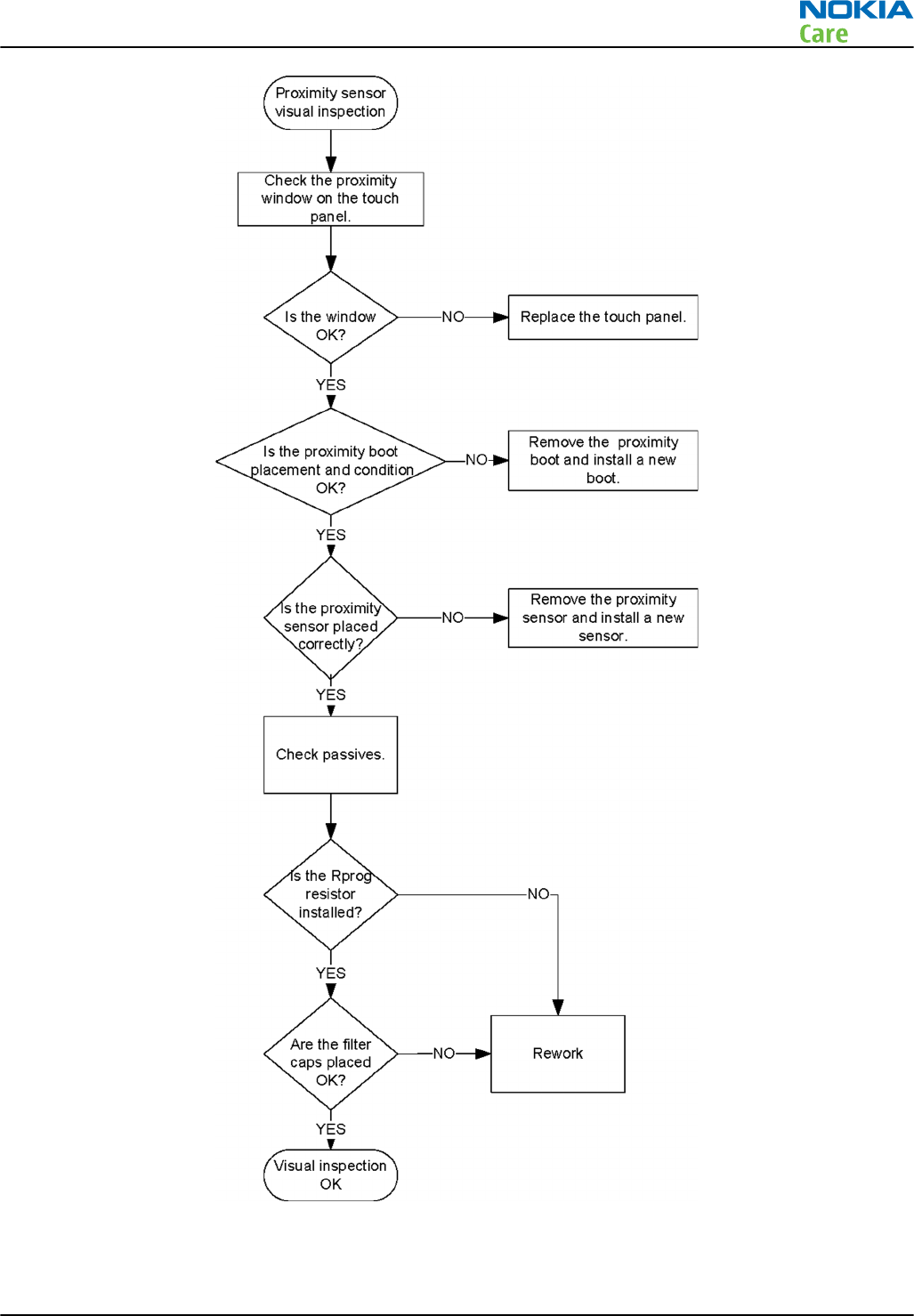
Figure 13 Proximity sensor troubleshooting - part 2
RM-612; RM-624
BB Troubleshooting and Manual Tuning Guide
Issue 1 COMPANY CONFIDENTIAL Page 3 – 29
Copyright © 2010 Nokia. All rights reserved.
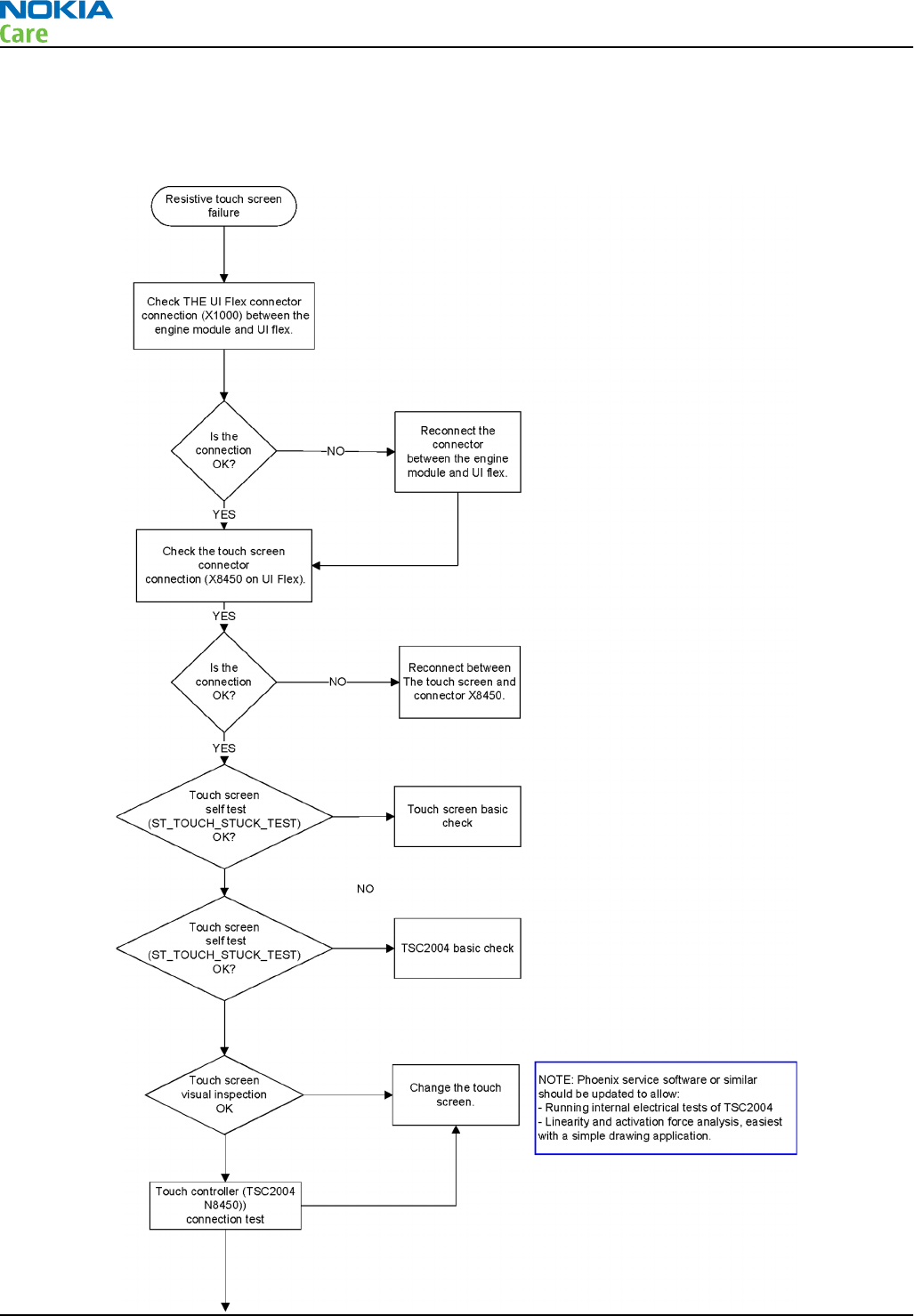
Resistive touch screen troubleshooting
Troubleshooting flow
RM-612; RM-624
BB Troubleshooting and Manual Tuning Guide
Page 3 – 30 COMPANY CONFIDENTIAL Issue 1
Copyright © 2010 Nokia. All rights reserved.
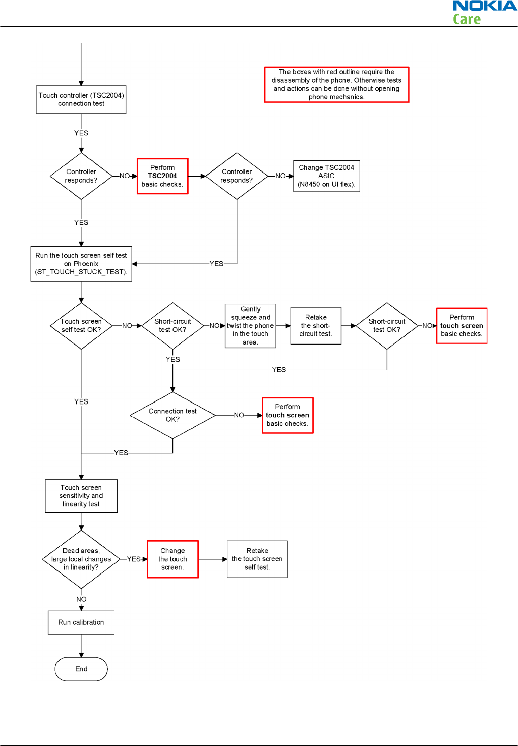
RM-612; RM-624
BB Troubleshooting and Manual Tuning Guide
Issue 1 COMPANY CONFIDENTIAL Page 3 – 31
Copyright © 2010 Nokia. All rights reserved.
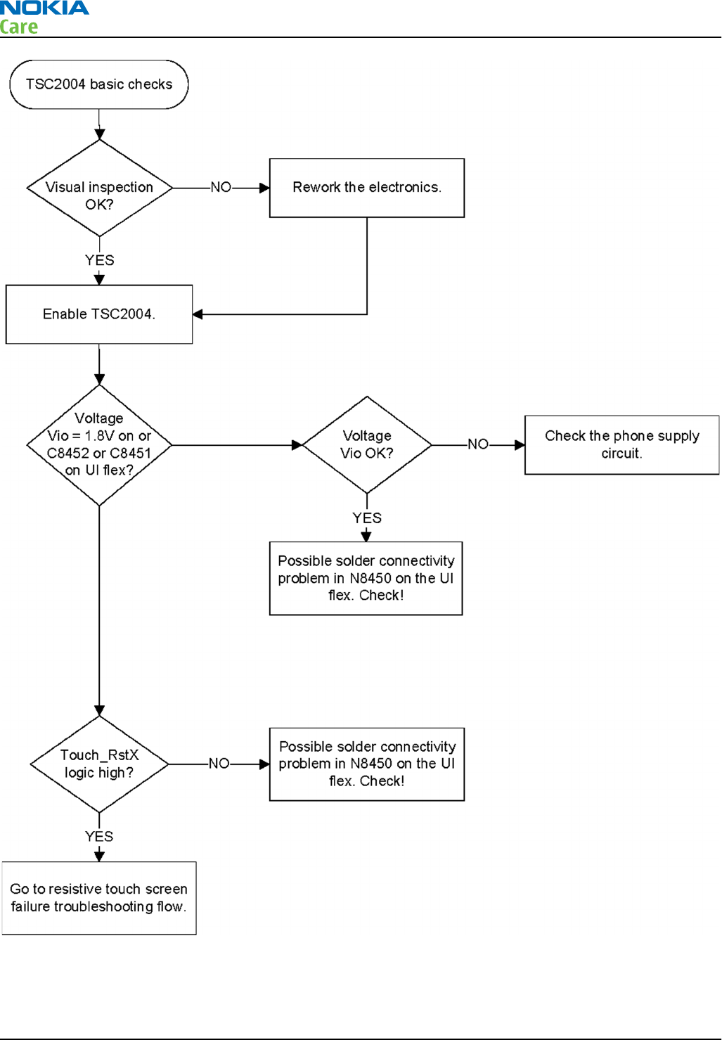
Figure 14 Touch controller basic checks
RM-612; RM-624
BB Troubleshooting and Manual Tuning Guide
Page 3 – 32 COMPANY CONFIDENTIAL Issue 1
Copyright © 2010 Nokia. All rights reserved.
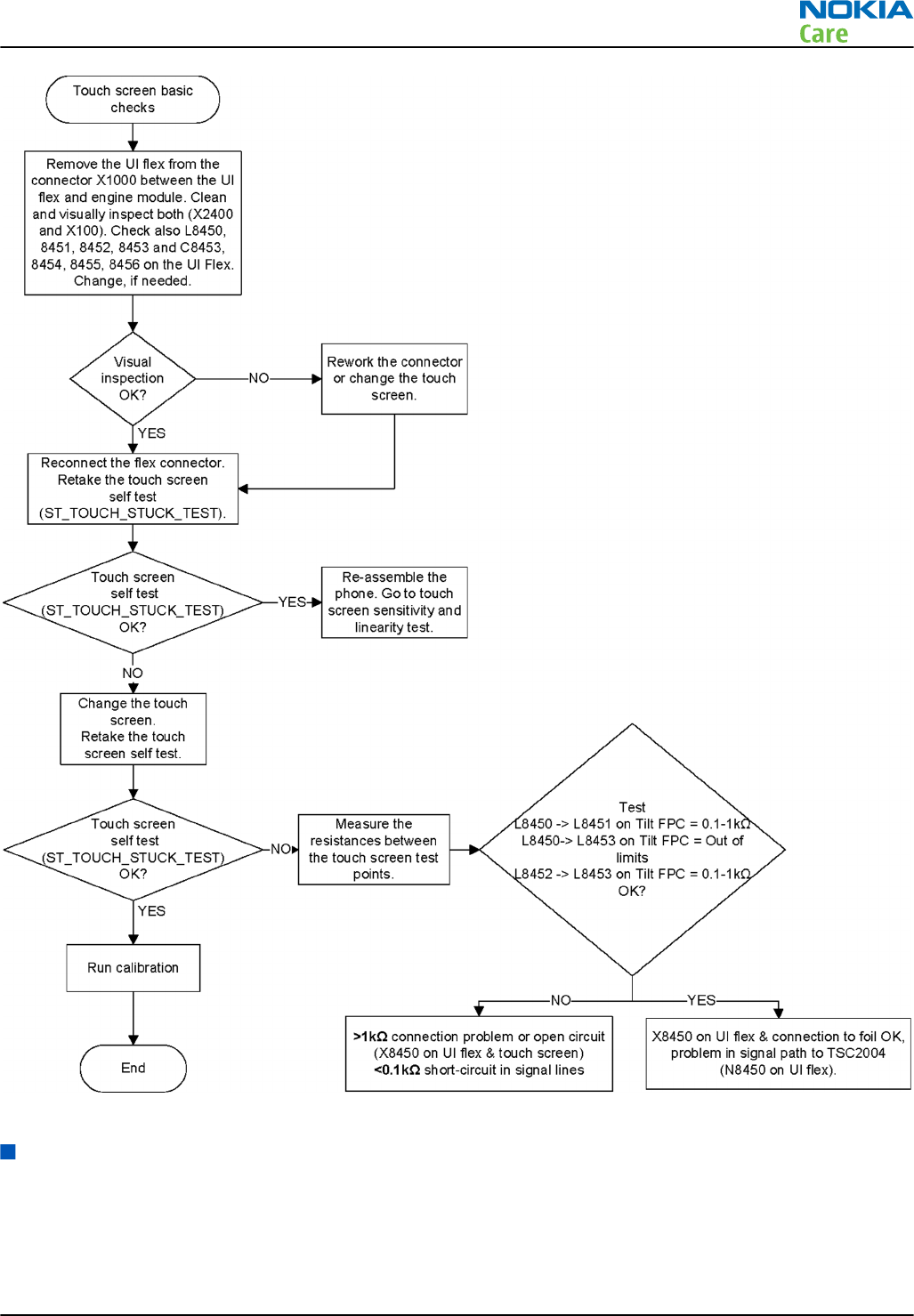
Figure 15 Touch screen basic checks
Hardware keys troubleshooting
Context
There are two possible failure modes in the keyboard module:
•One or more keys can be stuck, so that the key does not react when a keydome is pressed. This kind of
failure is caused by mechanical reasons (dirt, rust).
RM-612; RM-624
BB Troubleshooting and Manual Tuning Guide
Issue 1 COMPANY CONFIDENTIAL Page 3 – 33
Copyright © 2010 Nokia. All rights reserved.
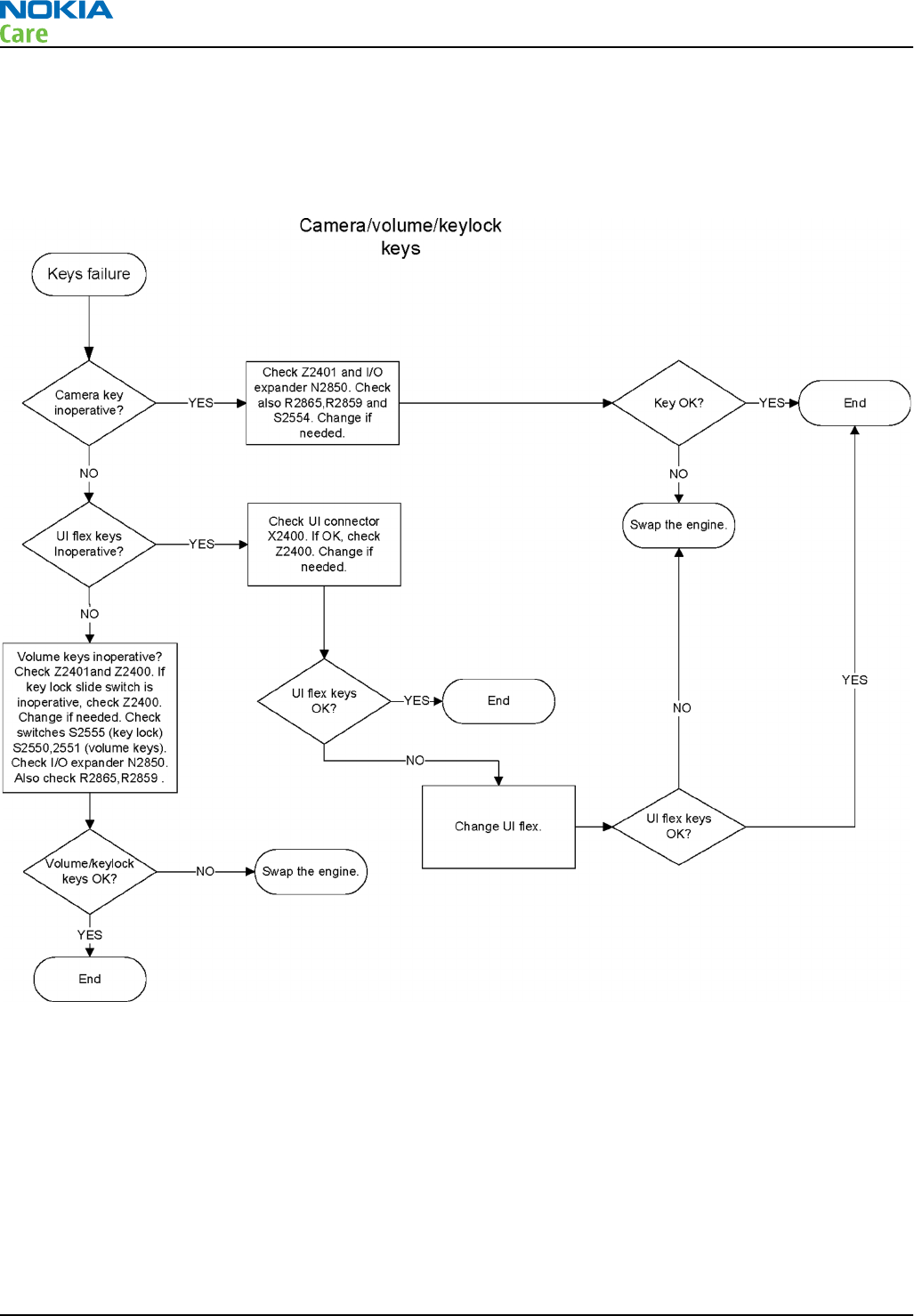
•Malfunction of several keys at the same time; this happens when one or more rows or columns are failing
(short circuit or open connection).
If the failure mode is not clear, start with the Keyboard Test in Phoenix.
Troubleshooting flow
RM-612; RM-624
BB Troubleshooting and Manual Tuning Guide
Page 3 – 34 COMPANY CONFIDENTIAL Issue 1
Copyright © 2010 Nokia. All rights reserved.
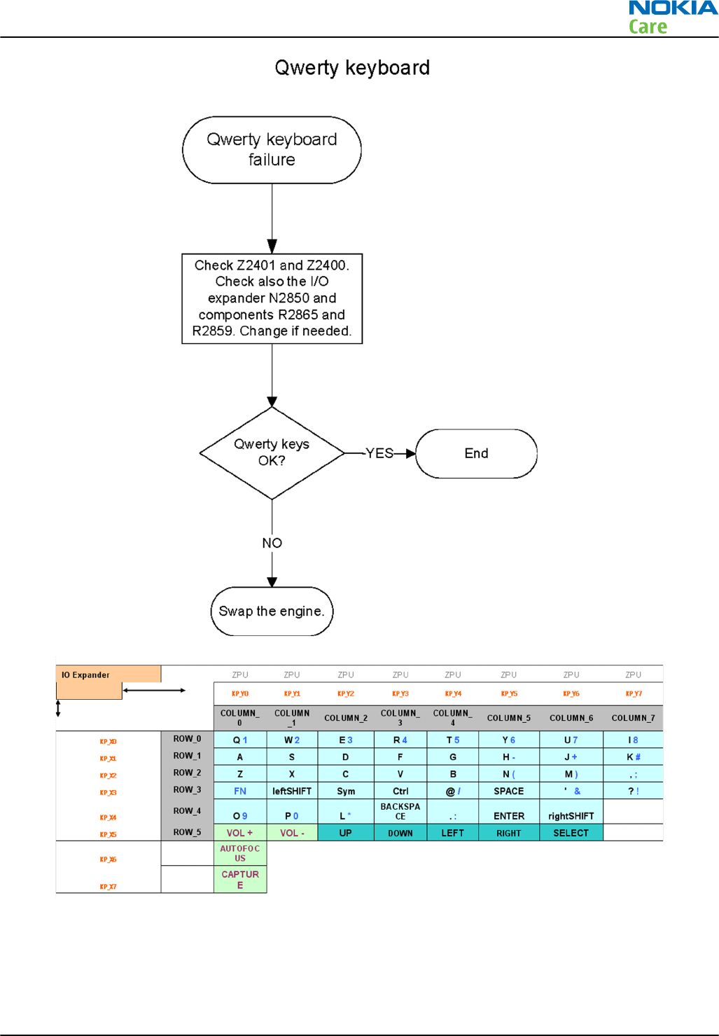
Figure 16 Keymatrix
RM-612; RM-624
BB Troubleshooting and Manual Tuning Guide
Issue 1 COMPANY CONFIDENTIAL Page 3 – 35
Copyright © 2010 Nokia. All rights reserved.
Display module troubleshooting
General instructions for display troubleshooting
Context
•The display is in a normal mode when the phone is in active use.
•Display is in a partial idle mode when the phone is in the screen saver mode.
•The operating modes of the display can be controlled with the help of
Phoenix
.
Table 7 Display module troubleshooting cases
Display blank There is no image on the display. The display looks
the same when the phone is on as it does when the
phone is off. The backlight can be on in some cases.
Image on the display not correct Image on the display can be corrupted or a part of
the image can be missing. If a part of the image is
missing, change the display module. If the image is
otherwise corrupted, follow the appropriate
troubleshooting diagram.
Backlight dim or not working at all Backlight LED components are inside the display
module. Backlight failure can also be in the
connector or in the backlight power source in the
main engine of the phone.
Visual defects (pixel) Pixel defects can be checked by controlling the
display with Phoenix. Use both colours, black and
white, on a full screen.
The display may have some random pixel defects
that are acceptable for this type of display. The
criteria when pixel defects are regarded as a display
failure, resulting in a replacement of the display, are
presented the following table.
Table 8 Pixel defects
Item White dot defect Black dot
defect Total
1Defect counts R G B White Dot
Total
1 1
1 1 1 1
2 Combined
defect counts
Not allowed.
Two single dot defects that are within 5 mm of each other should be
interpreted as combined dot defect.
Steps
1. Verify with a working display that the fault is not on the display module itself.
Note: The display module cannot be repaired.
RM-612; RM-624
BB Troubleshooting and Manual Tuning Guide
Page 3 – 36 COMPANY CONFIDENTIAL Issue 1
Copyright © 2010 Nokia. All rights reserved.

2. Check that the cellular engine is working normally.
i To check the functionality, connect the phone to a docking station.
ii Start
Phoenix
service software.
iii Read the phone information to check that the engine is functioning normally (you should be able to
read the Phone ID).
3. Proceed to the display troubleshooting flowcharts.
Use the Display Test tool in
Phoenix
to find the detailed fault mode.
Display troubleshooting
Context
Before going to display troubleshooting flow, make sure that the engine is working and starting up correctly.
If the problem is in the engine, go to baseband troubleshooting.
RM-612; RM-624
BB Troubleshooting and Manual Tuning Guide
Issue 1 COMPANY CONFIDENTIAL Page 3 – 37
Copyright © 2010 Nokia. All rights reserved.
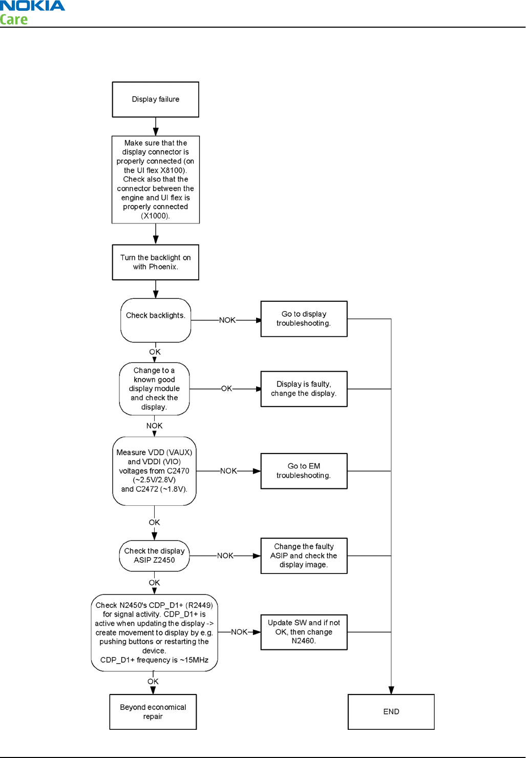
Troubleshooting flow
RM-612; RM-624
BB Troubleshooting and Manual Tuning Guide
Page 3 – 38 COMPANY CONFIDENTIAL Issue 1
Copyright © 2010 Nokia. All rights reserved.
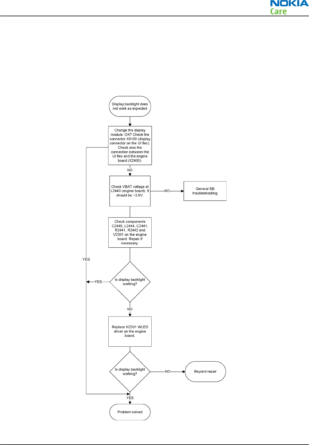
Display backlight troubleshooting
Context
The device has a dedicated display WLED driver whose intensity is controlled by Display itself by CABC (content
adaptive backlight control) signal.
Troubleshooting flow
RM-612; RM-624
BB Troubleshooting and Manual Tuning Guide
Issue 1 COMPANY CONFIDENTIAL Page 3 – 39
Copyright © 2010 Nokia. All rights reserved.

LED and LED driver troubleshooting
Context
The device has two LED drivers that provide current for the keyboard and several LEDs (Send, End, Home) .
The brightness of the backlights can be adjusted manually, and it affects the keypad. The keyboard backlights
and some LEDs can be turned ON/OFF separately but not without switching on the display lights.
RM-612; RM-624
BB Troubleshooting and Manual Tuning Guide
Page 3 – 40 COMPANY CONFIDENTIAL Issue 1
Copyright © 2010 Nokia. All rights reserved.
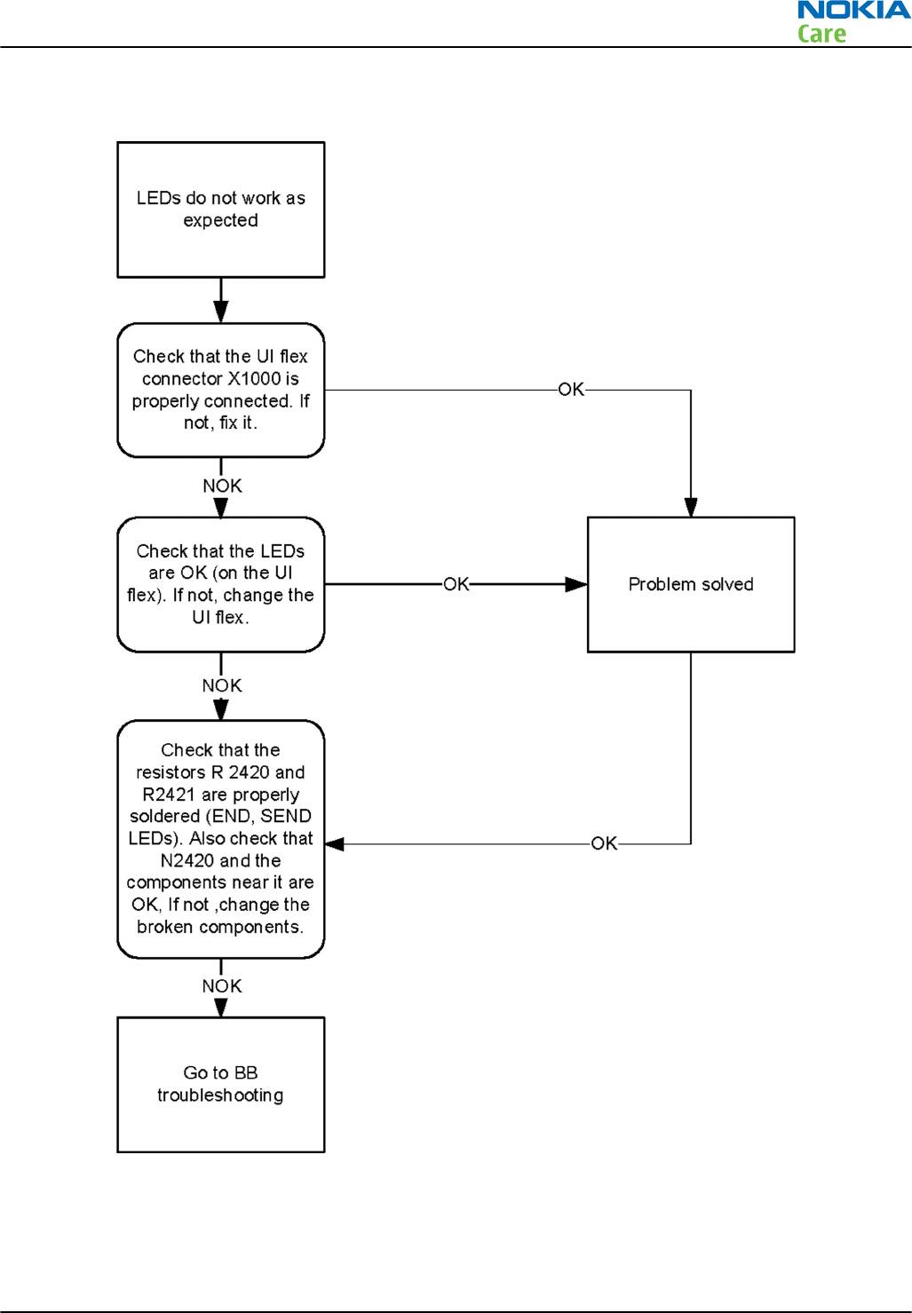
Troubleshooting flow
Figure 17 Send, End, Home LEDs
RM-612; RM-624
BB Troubleshooting and Manual Tuning Guide
Issue 1 COMPANY CONFIDENTIAL Page 3 – 41
Copyright © 2010 Nokia. All rights reserved.
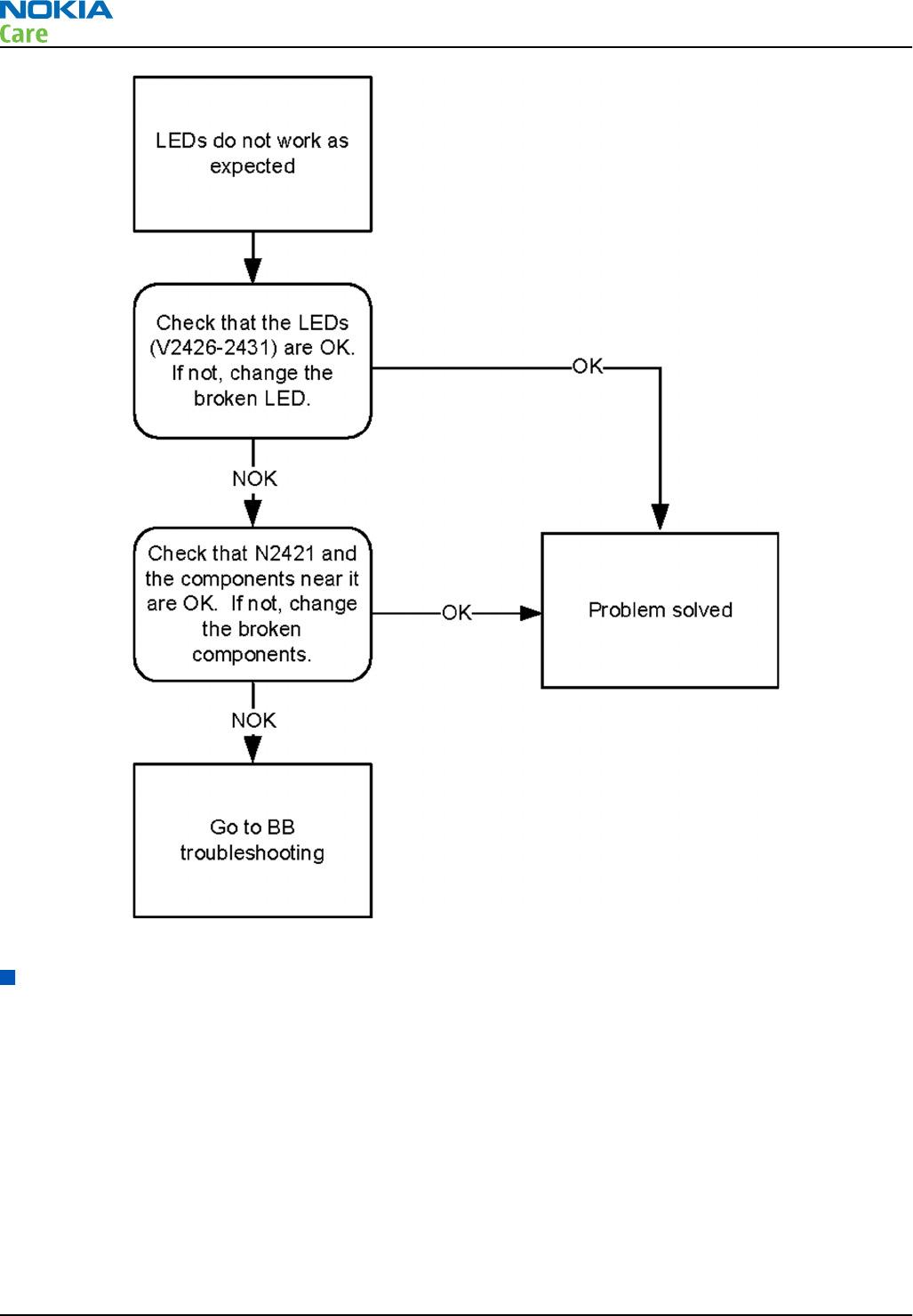
Figure 18 QWERTY LEDs
Ambient Light Sensor troubleshooting
Introduction to ALS troubleshooting
If the Ambient Light Sensor (ALS) functionality is inoperative, check the ambient light sensor (N8104) and
change it, if necessary. Also, check the capacitor C8102 (100n).
The ALS components are located at the top of the UI flex as illustrated in the figure below.
RM-612; RM-624
BB Troubleshooting and Manual Tuning Guide
Page 3 – 42 COMPANY CONFIDENTIAL Issue 1
Copyright © 2010 Nokia. All rights reserved.
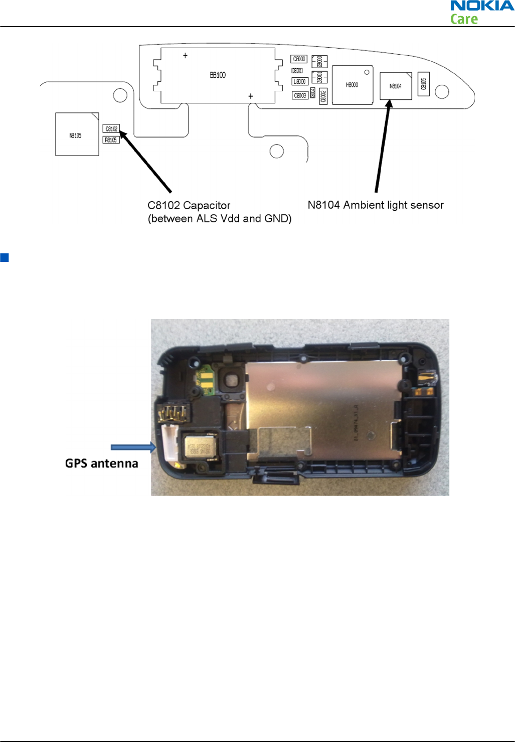
Figure 19 ALS placement
GPS troubleshooting
GPS antenna
The GPS antenna is located on the back side of the B-cover (right-hand side, next to the IHF speaker).
Figure 20 GPS antenna
The GPS antenna is connected to the PWB with a c-clip. The RF connector for conducted measurements and
testing is located next to the c-clip.
RM-612; RM-624
BB Troubleshooting and Manual Tuning Guide
Issue 1 COMPANY CONFIDENTIAL Page 3 – 43
Copyright © 2010 Nokia. All rights reserved.
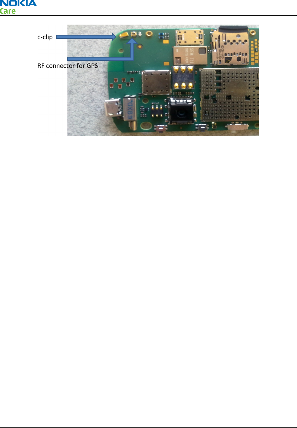
Figure 21 C-clip and RF connector location
GPS settings for Phoenix
GPS control
Context
Use the following to test GPS using Phoenix.
Steps
1. Start Phoenix service software.
2. From the File menu, select Scan Product and check that the correct product version is displayed.
3. From the Testing menu, select GPS Control. This opens up
GPS Control
dialog box, as shown in the figure
below, and enables the GPS.
Select Idle to confirm the GPS is enabled and is in idle mode.
RM-612; RM-624
BB Troubleshooting and Manual Tuning Guide
Page 3 – 44 COMPANY CONFIDENTIAL Issue 1
Copyright © 2010 Nokia. All rights reserved.
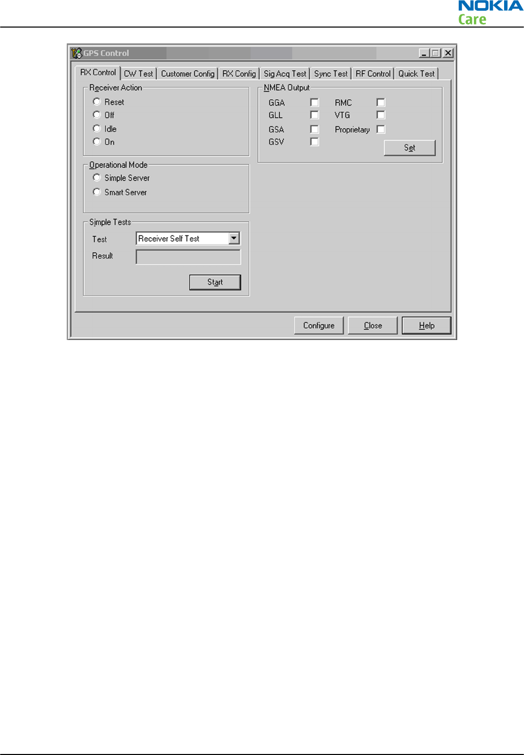
Figure 22 GPS Control dialog box
Oscillator test
Context
The 16.368 MHz GPS Clk is compared against the CE Ref Clk and the output is the GPS Clk offset.
Steps
1. Start Phoenix service software.
2. From the Testing menu, select GPS Control. This opens up
GPS Control
dialogue box and enables the GPS.
In the
Rx Control
window, go to the Simple Tests section, select Oscillator Test and click Start. The Offset
result will be returned and should be within the limits of +- 84Hz.
RM-612; RM-624
BB Troubleshooting and Manual Tuning Guide
Issue 1 COMPANY CONFIDENTIAL Page 3 – 45
Copyright © 2010 Nokia. All rights reserved.
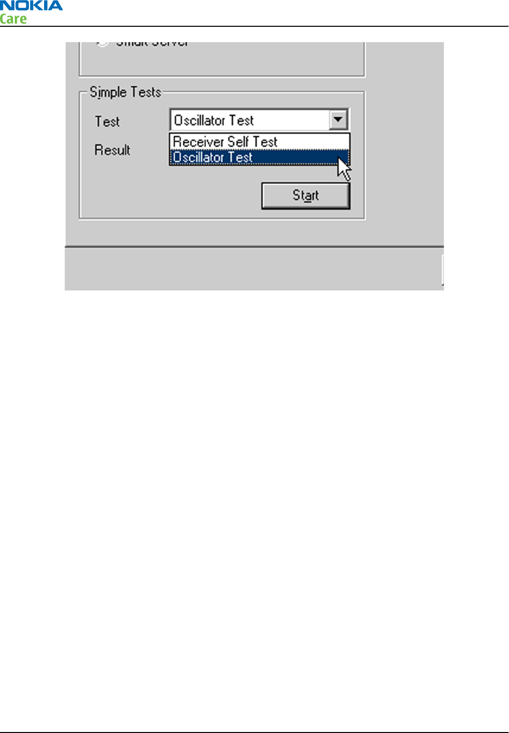
Figure 23 Simple Tests – Oscillator Test
Receiver self test
Context
Receiver self test can be used to check the correct functionality of the receiver core. For the test, GPS software
configures internal test source to generate synthetic GPS-like data, processing it in the baseband and writing
the results into the channel processor memory. The test compares the data in the channel memory against
the expected value and reports a PASS/FAIL status.
Steps
1. Start Phoenix service software.
2. From the Testing menu, select GPS Control. This opens up
GPS Control
dialogue box and enables the GPS.
In the
Rx Control
window, go to the Simple Tests section, select Receiver Self Test and click Start. The
test returns a PASS/FAIL result.
Note: The Oscillator Test should not be run after the Receiver Self Test. This sequence of tests may
cause the Oscillator test to prolong and result in Phoenix timing out. If you are carrying out both of
these tests, run the Oscillator Test first, after which you can run the Receiver Self Test.
RM-612; RM-624
BB Troubleshooting and Manual Tuning Guide
Page 3 – 46 COMPANY CONFIDENTIAL Issue 1
Copyright © 2010 Nokia. All rights reserved.
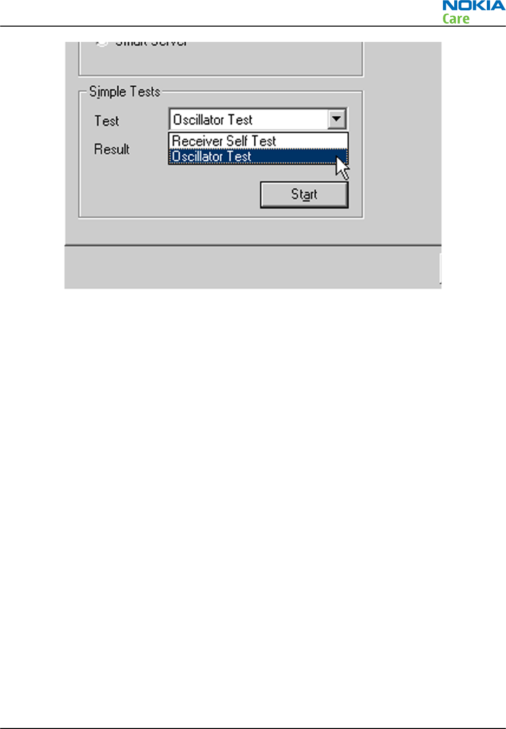
Figure 24 Simple Tests – Receiver Self Test
CW Test
Context
This test reports the SNR of a CW signal input to the GPS antenna port.
Steps
1. Start Phoenix service software.
2. From the Testing menu, select GPS Control. This opens up
GPS Control
dialog box and enables the GPS.
In the
CW Test
window, ensure that the input settings are as shown in the figure below. Inject
1575.520152 MHz tone at the GPS RF connector at a level of -110dBm and click Start.
For Pin = -110dBm and negligible other losses, the expected result ranges are:
•Galvanic 29.8dB to 38.1dB
•Radiated 25.8dB to 38.1dB
RM-612; RM-624
BB Troubleshooting and Manual Tuning Guide
Issue 1 COMPANY CONFIDENTIAL Page 3 – 47
Copyright © 2010 Nokia. All rights reserved.
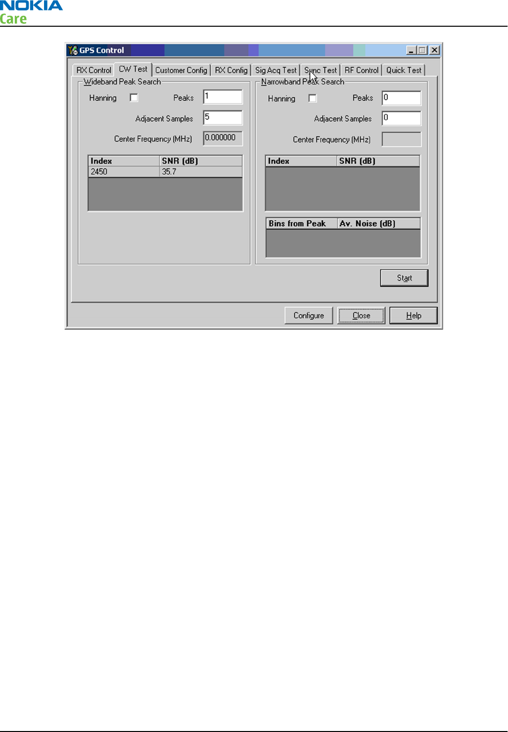
Figure 25 CW Test window
Quick Test window
Because the
Quick Test
runs the
Receiver Self Test
before the
Oscillator Test
, it may cause a timeout on the
Oscillator Test
. It does not necessarily mean that Oscillator Test has failed, but carrying out the Oscillator
Test (page 3–45 ) , Receiver Self Test (page 3–46 ) and CW Test (page 3–47 ) individually will give more
valid results.
RM-612; RM-624
BB Troubleshooting and Manual Tuning Guide
Page 3 – 48 COMPANY CONFIDENTIAL Issue 1
Copyright © 2010 Nokia. All rights reserved.
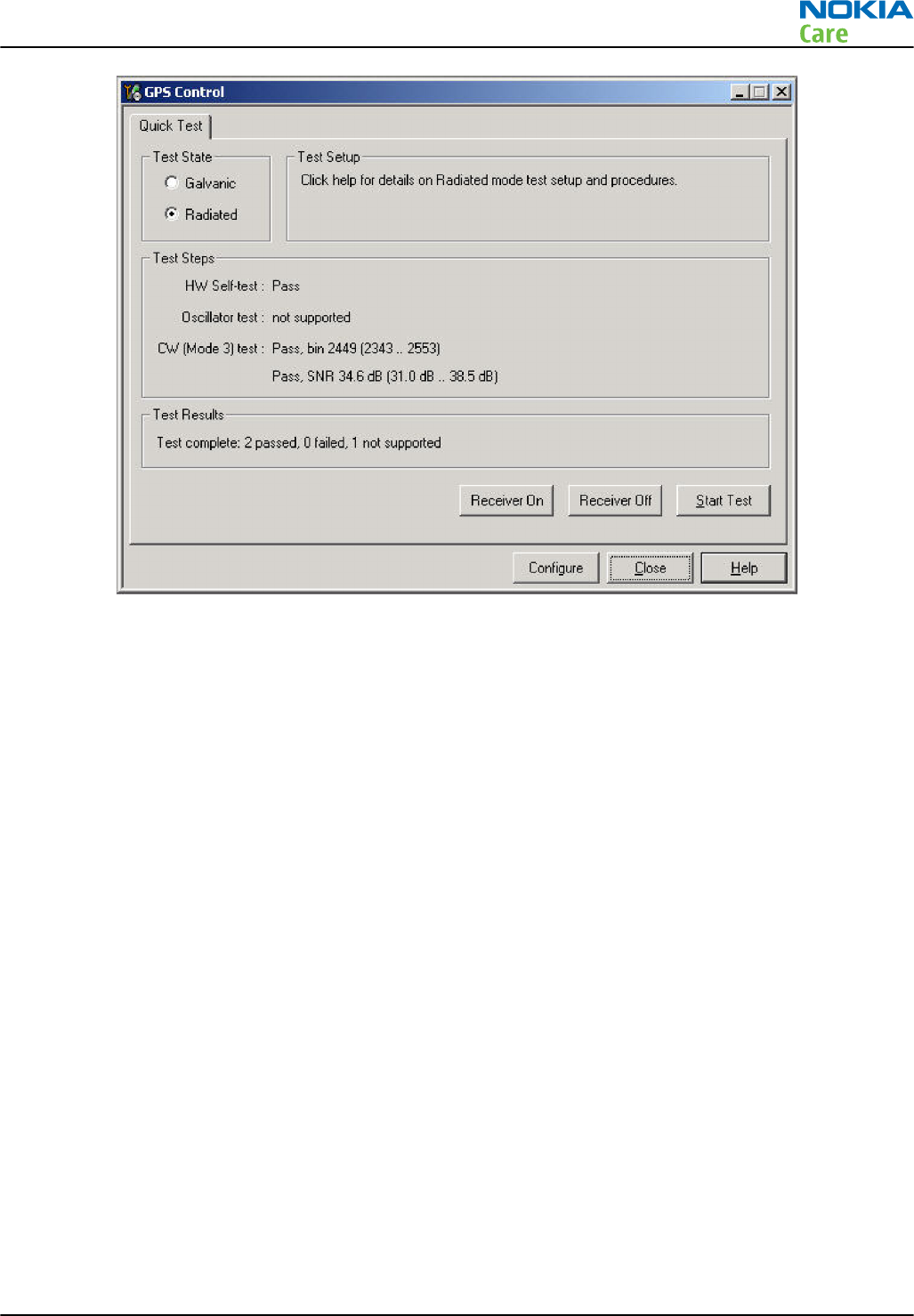
Figure 26 GPS Quick Test window for GPS troubleshooting
GPS failure troubleshooting
Context
The GPS failure troubleshooting flow can be followed and, where applicable, will feed into the basic checks.
RM-612; RM-624
BB Troubleshooting and Manual Tuning Guide
Issue 1 COMPANY CONFIDENTIAL Page 3 – 49
Copyright © 2010 Nokia. All rights reserved.
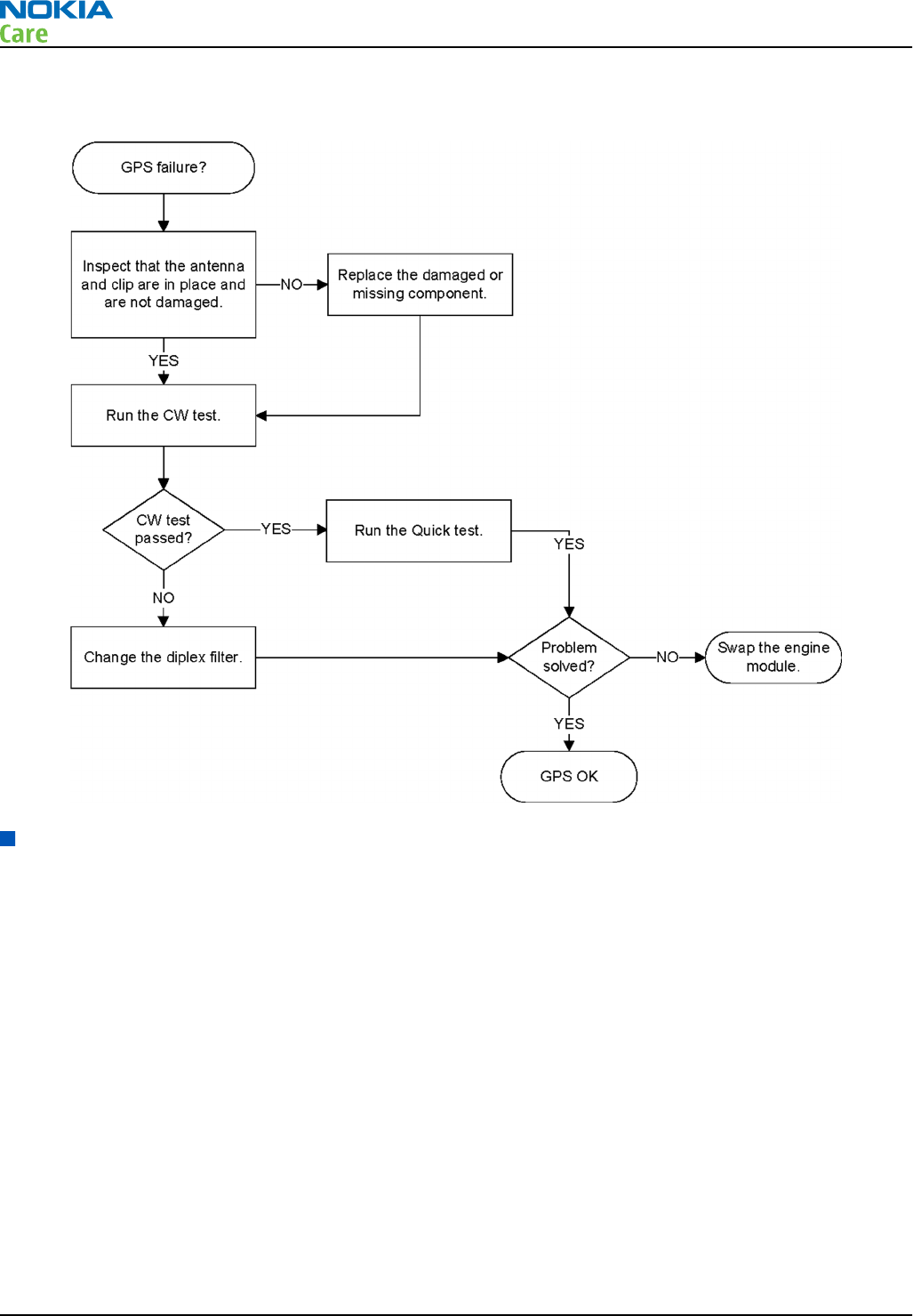
Troubleshooting flow
WLAN troubleshooting
WLAN functional description
The Size 4 WLAN module is designed for use with a single antenna shared between itself and a co-located
BT device. The WLAN SW is downloaded from the host engine when the WLAN is turned on over the dedicated
SPI interface. The BT and WLAN engines use common reference clock from the RF engine.
RM-612; RM-624
BB Troubleshooting and Manual Tuning Guide
Page 3 – 50 COMPANY CONFIDENTIAL Issue 1
Copyright © 2010 Nokia. All rights reserved.
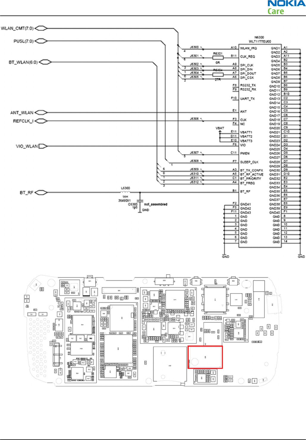
Figure 27 WLAN circuitry
Figure 28 WLAN component placement
WLAN settings for Phoenix
Use the following to test WLAN using Phoenix:
1 Set phone into Local Mode .
RM-612; RM-624
BB Troubleshooting and Manual Tuning Guide
Issue 1 COMPANY CONFIDENTIAL Page 3 – 51
Copyright © 2010 Nokia. All rights reserved.
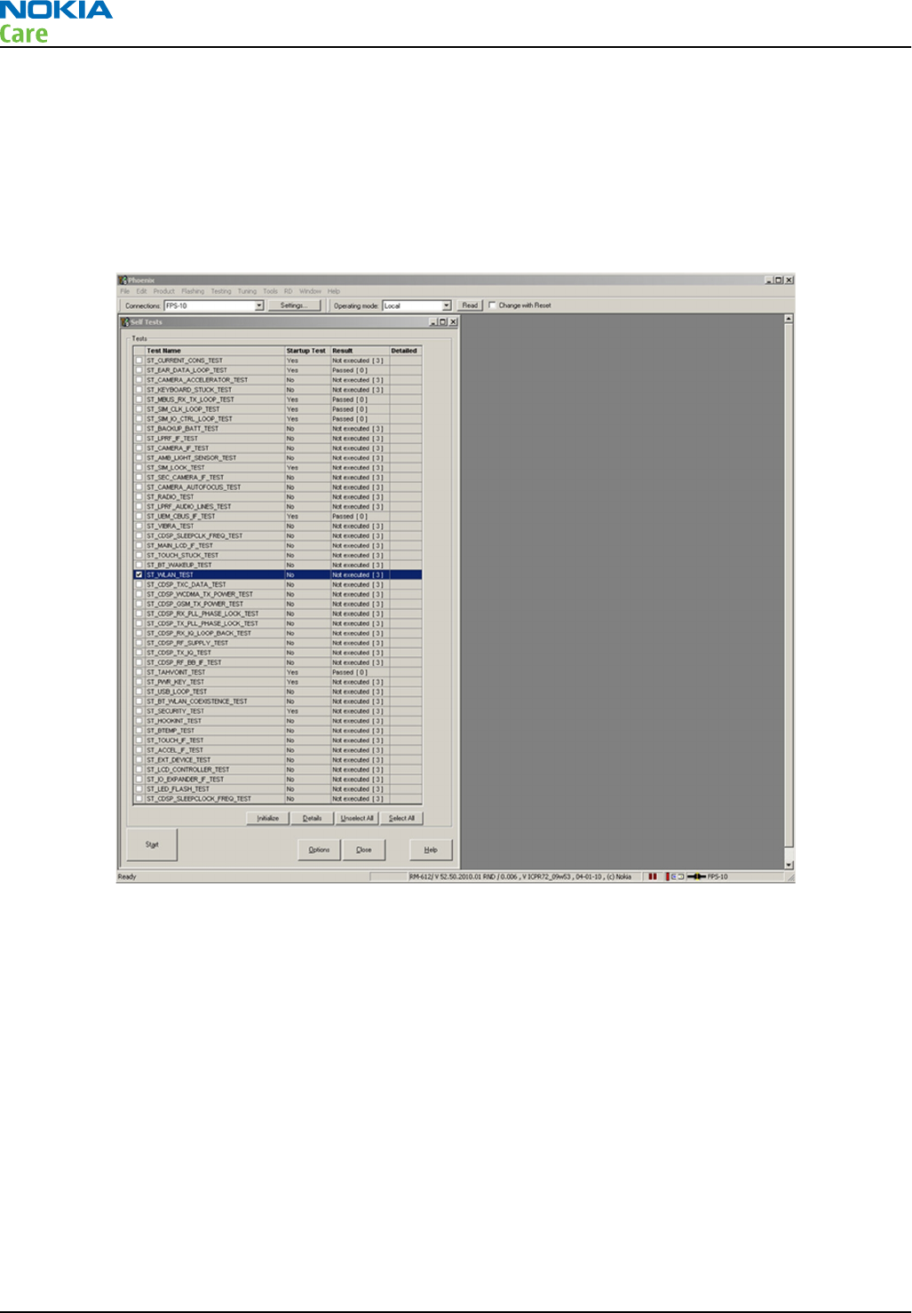
2 From the File menu, select Scan Product and check that the correct product version is displayed
3 From the Testing menu, select Self Test. This opens up a Self Testsdialog, as shown below.
Select the ST_WLAN_TEST check box as shown and then press the Start button. The test turns the WLAN on ,
sets up the SPI interface and then downloads the WLAN firmware into the WLAN module. During the download
the WLAN acknowledges the data blocks and so the self test is a good way to confirm that the WLAN module
is communicating with the Host. The result column changes to Passed after a few seconds if it is operating
properly.
In addition, a test of the WLAN to BTH interface can be done by selecting the
ST_BT_WLAN_COEXISTENCE_TEST check box and pressing the Start button.
This test verifies that the WLAN to BTH co-existence interface signals are properly connected and there are
no open circuist or shorts on the four interface signals.
The co-existence interface comprises BTH Txconfig, BTH RF Active, BTH Priority, and BTH Frequency.
RM-612; RM-624
BB Troubleshooting and Manual Tuning Guide
Page 3 – 52 COMPANY CONFIDENTIAL Issue 1
Copyright © 2010 Nokia. All rights reserved.
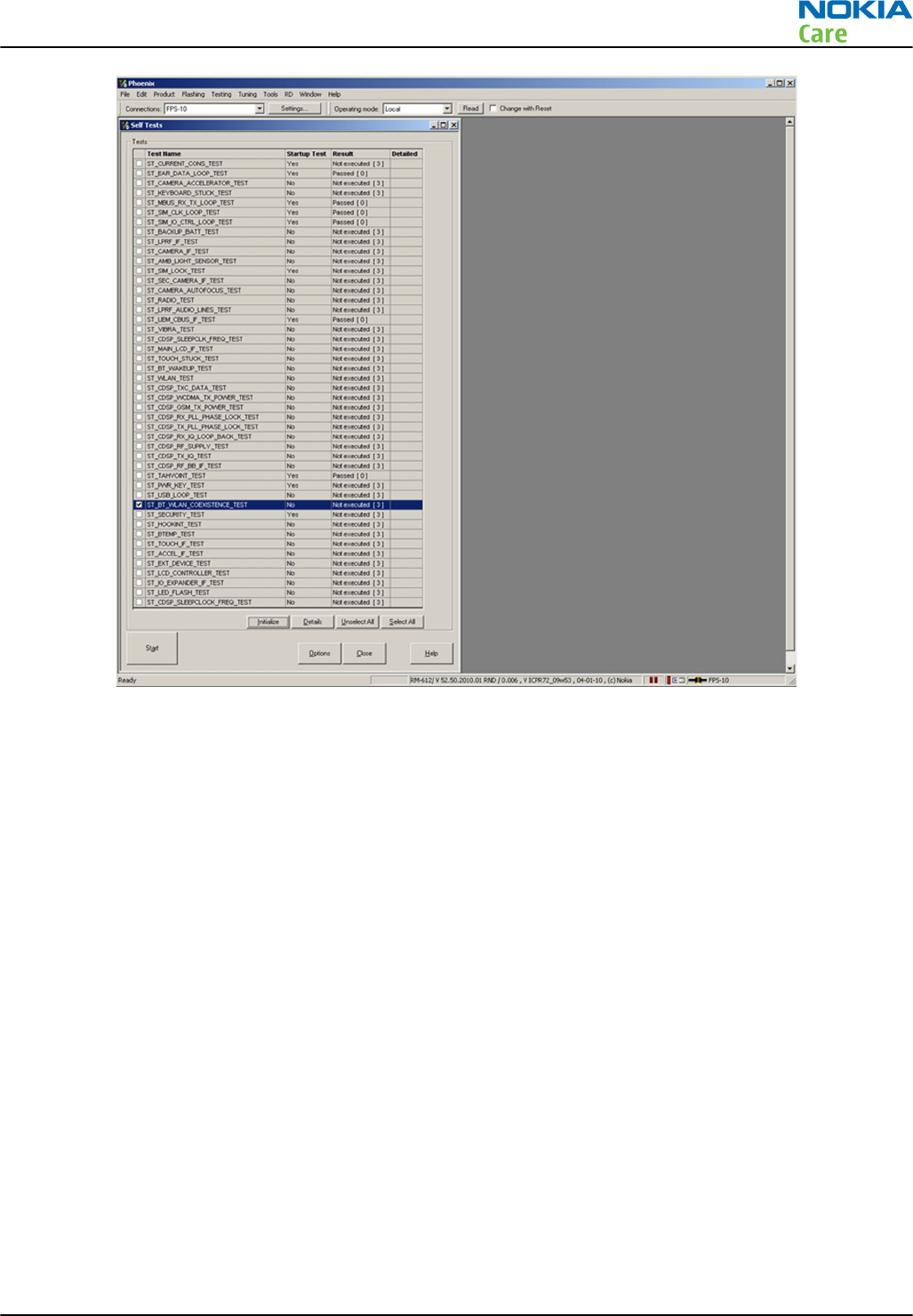
In summary these two Self Tests provide a simple means of ensuring that the Host engine is able to
communicate with the WLAN module and check the interface to BTH. A more detailed WLAN performance
test is covered in the WLAN functional tests (page 3–53 ) section.
WLAN functional tests
On/Off test
Prerequisites
A flash adapter connected to a PC with Phoenix service software is required.
From the Testing toolbar, select WLAN Configuration option. This opens the WLAN Configuration dialog
as shown below. WLAN can be turned ON and OFF by selecting On or Off from the Power state drop-down
list (as indicated in the picture below):
1 With Power State set to Off, measure the dc power supply current consumption of the flash adaptor.
2 Next return the Power State to On and re-measure the dc power supply current of the flash adaptor.
The difference between the currents in (1) and (2) should be between 190 to 220 mA. When WLAN is ON, the
firmware has been downloaded and the WLAN module is in the receive state. When WLAN in OFF, WLAN is
powered down.
RM-612; RM-624
BB Troubleshooting and Manual Tuning Guide
Issue 1 COMPANY CONFIDENTIAL Page 3 – 53
Copyright © 2010 Nokia. All rights reserved.
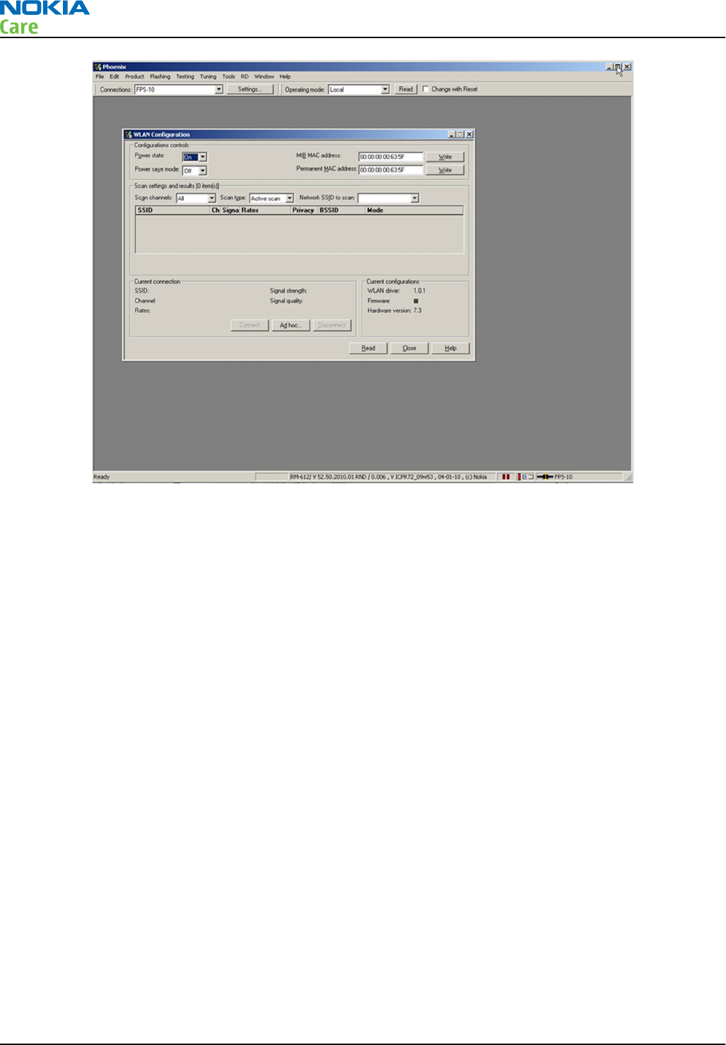
TX tests
Prerequisites
Connect a complete phone assembly with C-cover to a PC with Phoenix service software using a USB data
cable.
From the Testing toolbar, select WLAN Tx Tests option as shown below. This test can be used to verify TX
configuration and functionality. The default settings are sufficient for testing the TX operation, although
other channels and data rates are equally suitable. To start the test, press the Start button:
1 Monitor the WLAN TX spectrum on a Spectrum analyser. (When making a radiated test ensure that other
WLAN devices are not transmitting as these may be detected as well, confusing the result). A typical 11
Mbps TX spectrum is shown in the figure below.
2 To finish the test, Press the Finish button.
The difference between the two readings should be approximately 150 mA and measures the transmit current
in 11 Mbps, 802.11b mode of operation.
RM-612; RM-624
BB Troubleshooting and Manual Tuning Guide
Page 3 – 54 COMPANY CONFIDENTIAL Issue 1
Copyright © 2010 Nokia. All rights reserved.
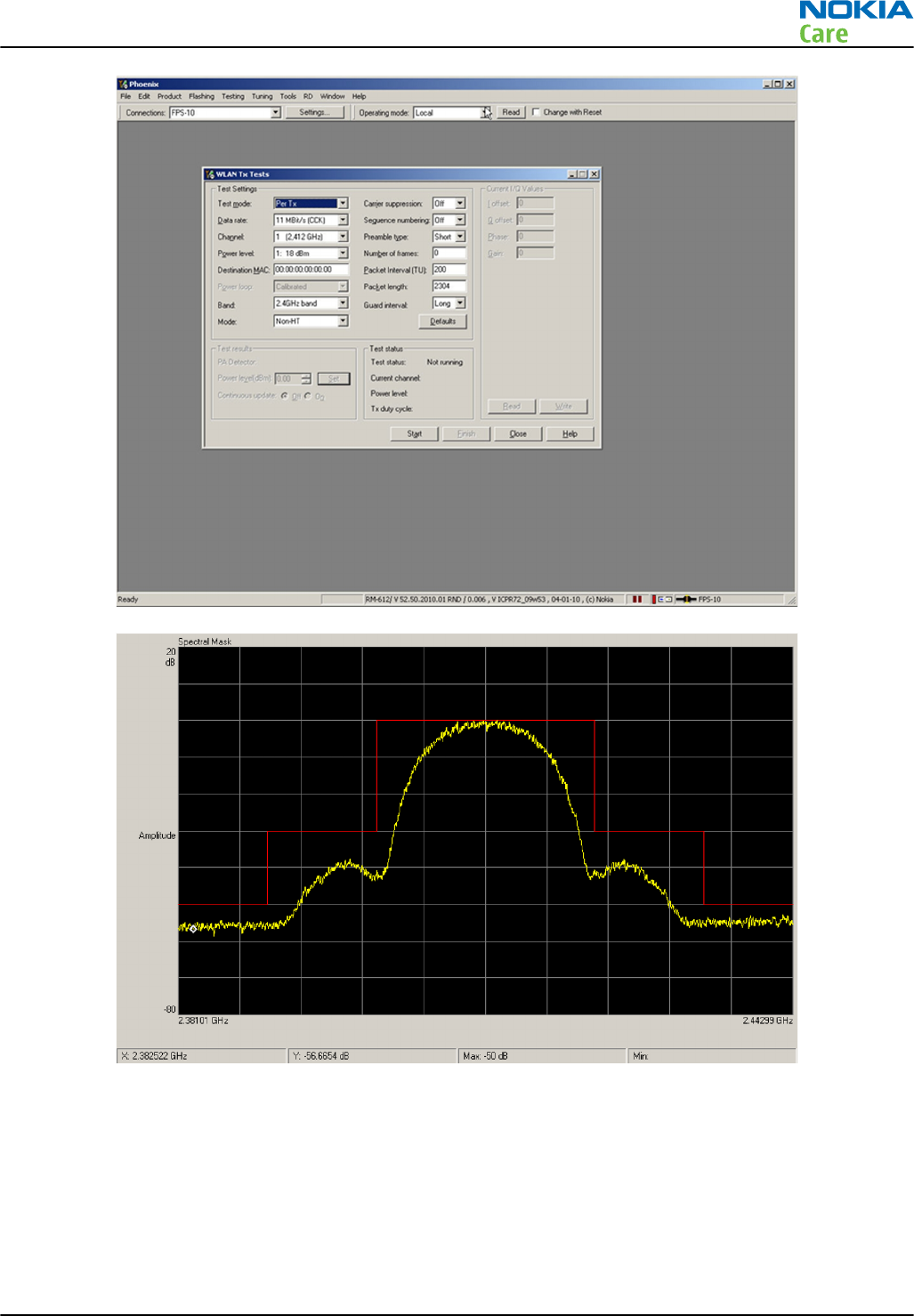
RX Tests
Prerequisites
Connect a complete phone assembly with C-cover to a PC with Phoenix service software using a USB data
cable.
There are different options available for testing the Rx path. The simplest is to use the WLAN to report Rx
packets when operating in an area where there is an active WLAN network. Simply starting an Rx test shows
the number of packets detected by the WLAN module as it monitors the network. However, it requires a
properly configured WLAN network.
RM-612; RM-624
BB Troubleshooting and Manual Tuning Guide
Issue 1 COMPANY CONFIDENTIAL Page 3 – 55
Copyright © 2010 Nokia. All rights reserved.
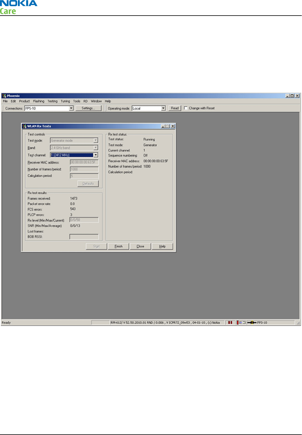
From the Testing toolbar, select WLAN Rx Tests option as shown below. This test can be used to verify Rx
configuration and functionality.
To start the test, press the Start button.
As the WLAN monitors an active WLAN network, the Rx test results window updates and shows the number
of Frames received, as well as the Packer error rate.
Monitoring the detected frames is a simple method to verify that the WLAN antenna and receiver path are
working properly.
WLAN auto tuning
In case of WLAN ASIC change, RF power auto tuning is needed. Connect WLAN RF test connector to CMU200
input using proper RF cable. Start Phoenix WLAN autotune window. Check the settings and verify your PC
communicates with CMU200 via GPIB.
Auto tuning procedure
1 Start tuning by pressing Tune.
RM-612; RM-624
BB Troubleshooting and Manual Tuning Guide
Page 3 – 56 COMPANY CONFIDENTIAL Issue 1
Copyright © 2010 Nokia. All rights reserved.
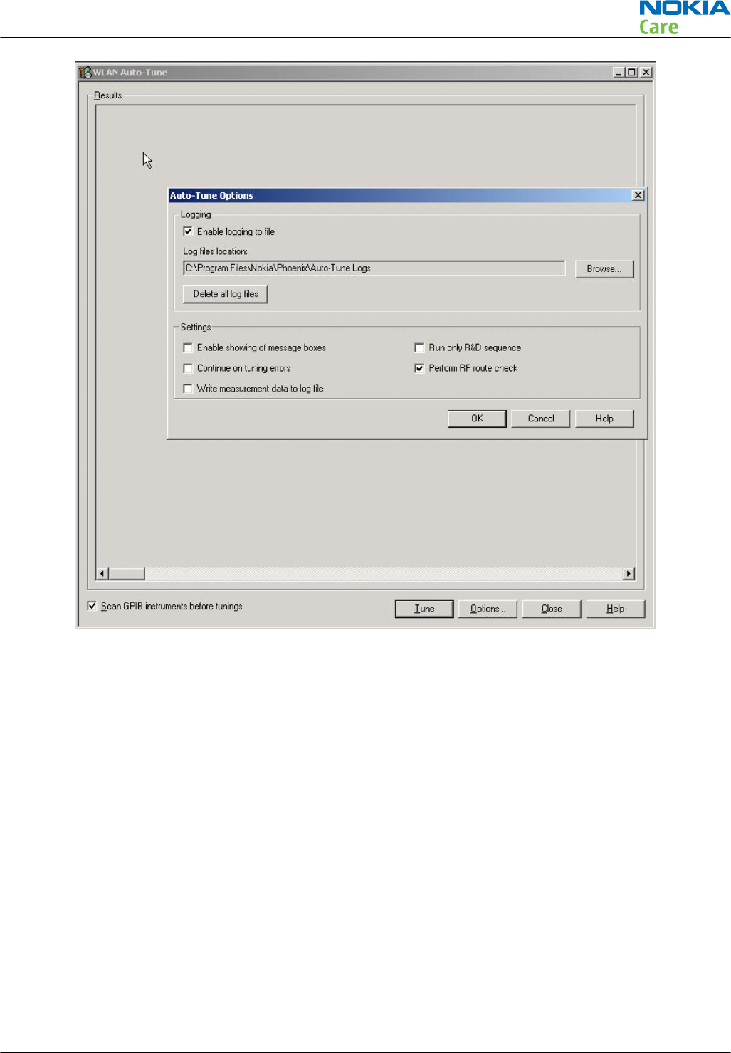
Figure 29 WLAN auto tune settings
RM-612; RM-624
BB Troubleshooting and Manual Tuning Guide
Issue 1 COMPANY CONFIDENTIAL Page 3 – 57
Copyright © 2010 Nokia. All rights reserved.
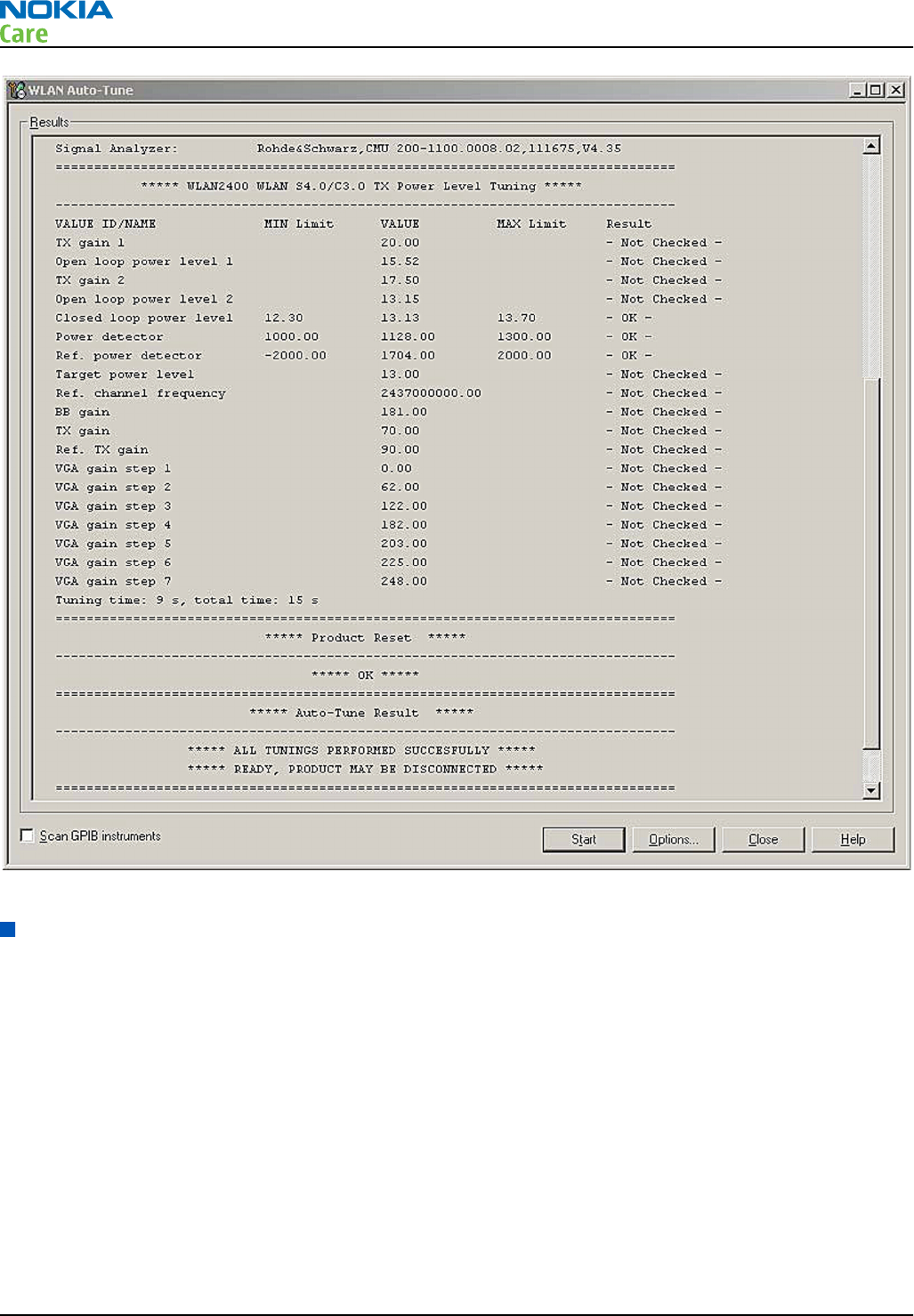
Figure 30 WLAN autotuning results
Bluetooth and FM radio troubleshooting
Introduction to Bluetooth/FM radio troubleshooting
Bluetooth/WLAN antenna
The BT RF signal is routed from BTHFMRDS2.2D through the WLAN module to the shared WLAN/BT/GPS antenna
in the phone's top side on the B cover. The antenna has two resonators for BT/WLAN ISM band and also the
GPS band and antenna are conducted with a feed (spring) on the PWB.
RM-612; RM-624
BB Troubleshooting and Manual Tuning Guide
Page 3 – 58 COMPANY CONFIDENTIAL Issue 1
Copyright © 2010 Nokia. All rights reserved.
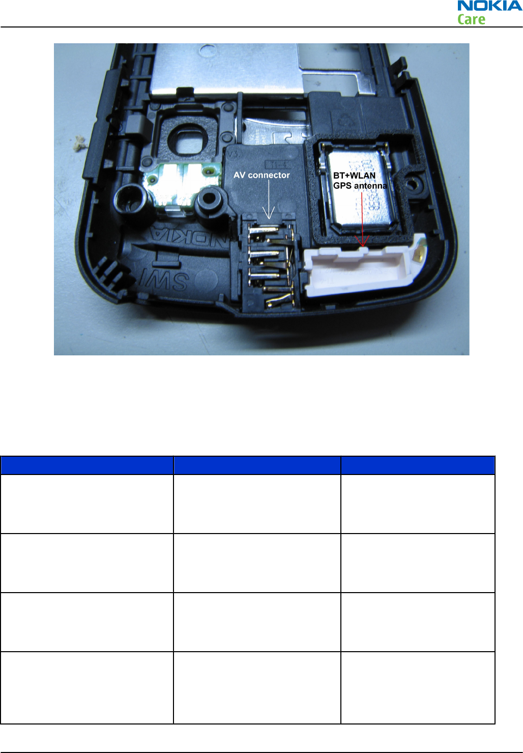
Figure 31 WLAN/BT/GPS antenna
Introduction to Bluetooth/FM radio troubleshooting
The Bluetooth and FM radio are combined in the same ASIC, so both features are checked when
troubleshooting.
The following problems can occur with the Bluetooth and FM radio hardware:
Symptom Problem Repair solution
Unable to switch on the
Bluetooth on the phone user
interface
Open circuit solder joints or
component failure of BTH/FM
ASIC/module BB ASICs or SMD
components
Replacement of engine
Able to send a data file to another
Bluetooth device, but unable to
hear audio through a functional
Bluetooth headset
Open circuit solder joints or
component failure of BTH/FM
ASIC/module BB ASICs
Replacement of engine
Able to switch on Bluetooth on
the phone user interface, but
unable to detect other Bluetooth
devices
Open circuit solder joints or
Pogo Pins not making contact
with c-cover
Repair of antenna circuit or
replacement of BT/WLAN/
GPS antenna
Able to turn on FM radio and
Bluetooth on the phone user
interface, but unable to detect
local FM radio stations with a
Nokia headset inserted
Open circuit solder joints or
detached component in FM
antenna circuit
Repair of FM antenna circuit
or replacement of AV
connector
RM-612; RM-624
BB Troubleshooting and Manual Tuning Guide
Issue 1 COMPANY CONFIDENTIAL Page 3 – 59
Copyright © 2010 Nokia. All rights reserved.
Symptom Problem Repair solution
Able to perform scans to detect
local FM radio stations with a
functional Nokia headset
inserted, but unable to hear FM
audio through the headset
Open circuit solder joints or
detached component in FM
audio path between Bluetooth/
FM ASIC and headset
Repair or replacement of FM
audio AV connector and
circuits
Users may experience the following problems resulting in functional phones being returned to the repair
centre:
Symptom Problem Repair solution
Bluetooth feature does not
operate as desired with another
Bluetooth device.
Bluetooth Profile implemented
in a Bluetooth accessory not
supported in a Nokia phone
Use a Bluetooth accessory
with Bluetooth profiles
supported by the phone.
Poor FM radio reception (unable
to detect many radio stations)
Nokia headset not being used Use a Nokia headset.
Test coverage
The tests listed in the table below should be performed to verify whether the Bluetooth and FM receiver and
transmitter are functional. The use of Self Tests are described in section
BT and FM Self Tests in Phoenix
Test Test Coverage Repair solution
Blueooth Self Test: ST_LPRF_IF_TEST Bluetooth-FM ASIC UART interface
(controls Bluetooth and FM
receiver and transmitter)
Replacement of engine (or
repair of the phone BB)
Bluetooth Self Test:
ST_BT_WAKEUP_TEST
Bluetooth ASIC interrupt control
interface
Replacement of engine (or
repair of the phone BB)
Bluetooth Self Test:
ST_LPRF_AUDIO_LINES_TEST
Bluetooth ASIC PCM interface Replacement of engine (or
repair of the phone BB)
Bluetooth Functional Test: BER test
with BT-Box or functional test with
another Bluetooth device
Bluetooth antenna circuit Repair of Bluetooth antenna
matching circuit or
replacement of B/WLAN/GPS
antenna
FM Radio Self Test: ST_RADIO_TEST FM Radio I2C interface Replacement of engine (or
repair of the phone BB)
FM Radio Functional Test: Perform
a scan for local radio stations and
check the station list displayed on
the phone.
FM receiver antenna circuit Repair of FM antenna
matching circuit or
replacement of AV connector
and flex
FM Radio Functional Test: Listen to
a local radio station.
FM receiver audio circuit Repair of FM antenna
matching circuit or
replacement of AV connector
and flex
The self tests run from the Phoenix software are used for fault diagnosis.
RM-612; RM-624
BB Troubleshooting and Manual Tuning Guide
Page 3 – 60 COMPANY CONFIDENTIAL Issue 1
Copyright © 2010 Nokia. All rights reserved.
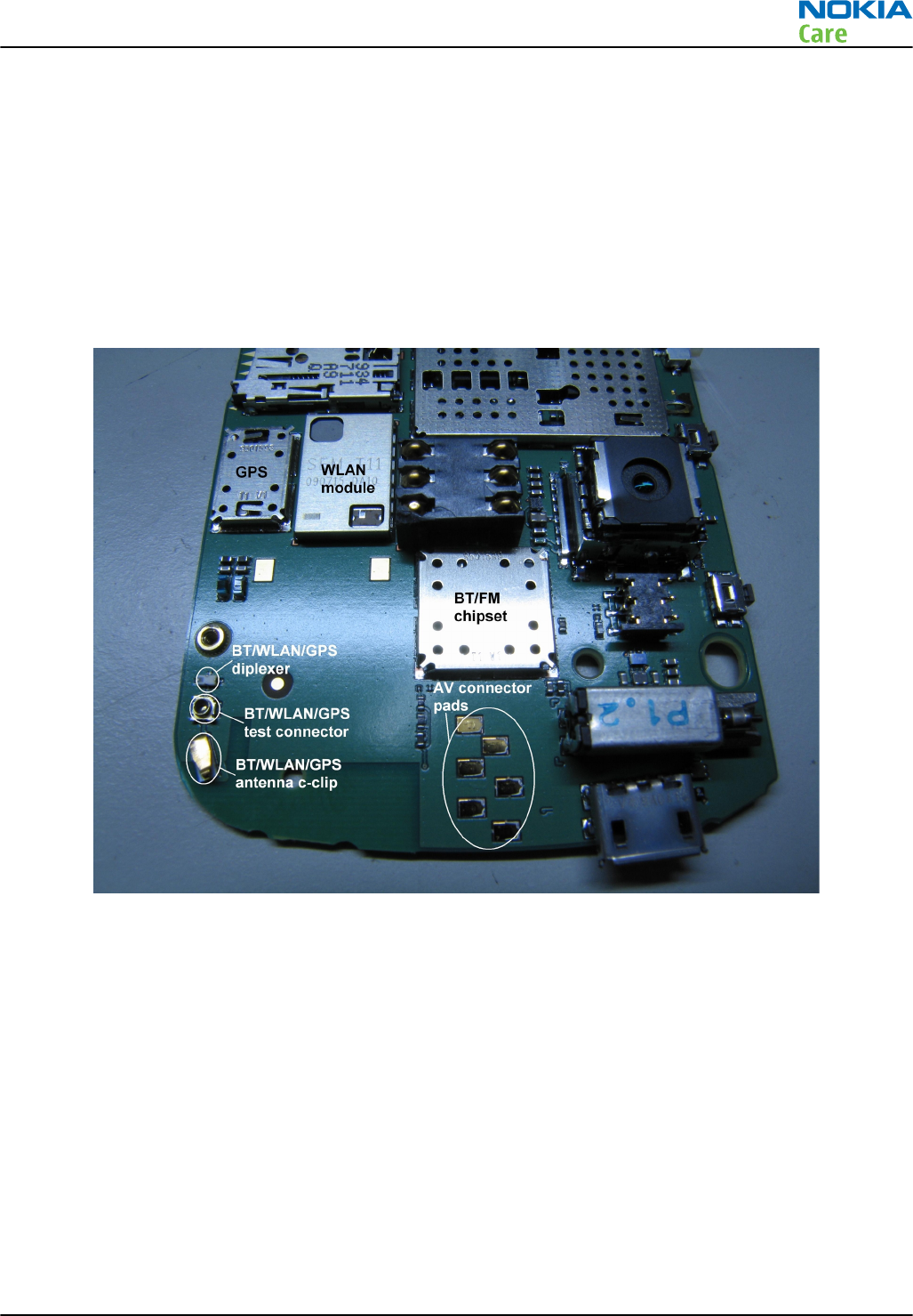
If the Phoenix software is not available the functional tests with phone accessories are sufficient to verify
the functionality of the Bluetooth and FM radio receiver and transmitter.
Bluetooth/FM radio component layout and test points
The Bluetooth antenna is product specific (ceramic antenna conducted by feed on the PWB). On phones with
WLAN and GPS, the Bluetooth RF signal is routed through a WLAN front-end module via diplexer and a shared
Bluetooth/WLAN/GPS antenna is used.
The FM RF signal is routed through the FM antenna matching circuit to the phone headset AV connector.
The FM radio audio signal is routed to the headset AV connector through the BB ASIC shared by the phone
audio functions.
Figure 32 Bluetooth/FM radio component layout and test points
Bluetooth BER test
Prerequisites
JBT-9, or SB-6 Bluetooth test box (BT-box) is required to perform a BER test. If a BT-box if not available
Bluetooth functionality can be checked by transfering a file to another Bluetooth phone.
Steps
1. Place the phone in the flash adapter or connect data cable to phone.
2. Start
Phoenix
service software.
3. Choose File → Scan Product.
4. Choose Testing → Bluetooth LOCALS .
5. Locate the BT-box serial number (12 digits) found in the type label on the back of the JBT-9, or SB-6
Bluetooth test box.
RM-612; RM-624
BB Troubleshooting and Manual Tuning Guide
Issue 1 COMPANY CONFIDENTIAL Page 3 – 61
Copyright © 2010 Nokia. All rights reserved.
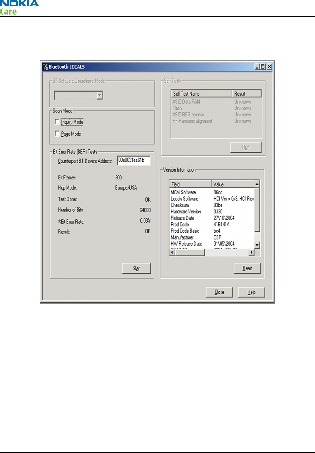
6. In the Bluetooth
LOCALS
window, write the 12-digit serial number on the
Counterpart BT Device
Address
line.
7. Place the BT-box near (within 10 cm) of the phone and click Start BER Test.
Figure 33 Bluetooth BER test
Bluetooth and FM radio self tests in Phoenix
Prerequisites
A flash adapter (or phone data cable) connected to a PC with Phoenix service software is required.
Steps
1. Place the phone in the flash adapter or connect data cable to phone.
2. Start
Phoenix
service software.
3. Choose File → Scan Product.
4. From the Mode drop-down menu, set mode to Local.
5. Choose Testing → Self Tests.
6. In the
Self Tests
window check the following Bluetooth and FM radio related tests:
•ST_LPRF_IF_TEST
RM-612; RM-624
BB Troubleshooting and Manual Tuning Guide
Page 3 – 62 COMPANY CONFIDENTIAL Issue 1
Copyright © 2010 Nokia. All rights reserved.
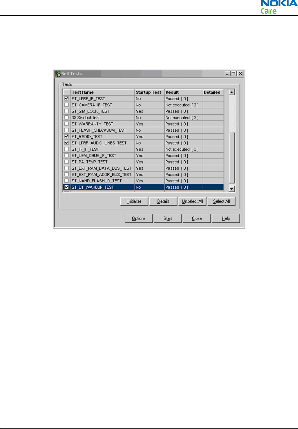
•ST_LPRF_AUDIO_LINES_TEST
•ST_BT_WAKEUP_TEST
•ST_RADIO_TEST
7. To run the tests, click Start.
Figure 34 Bluetooth and FM radio self tests in
Phoenix
FM radio testing
Steps
1. Set signal generator parameters:
•FM modulation on
•Frequency 100MHz
•FM deviation 22kHz
•Modulation frequency 1kHz
•RF level should be varied during the test to obtain good audio signal quality
•Connect suitable antenna to signal generator
Note: You may alternately use a known good FM radio broadcast as a test signal.
2. Attach the Nokia headset to the phone’s AV connector.
3. Use Scroll button to autotune to the radio frequency.
4. Set volume to suitable level.
5. Check audio quality with a headset.
RM-612; RM-624
BB Troubleshooting and Manual Tuning Guide
Issue 1 COMPANY CONFIDENTIAL Page 3 – 63
Copyright © 2010 Nokia. All rights reserved.

Audio troubleshooting
Audio troubleshooting test instructions
Single-ended external earpiece and differential internal earpiece outputs can be measured either with a
single-ended or a differential probe.
When measuring with a single-ended probe each output is measured against the ground.
Internal handsfree output is measured using a current probe, if a special low-pass filter designed for
measuring a digital amplifier is not available. Note also that when using a current probe, the input signal
frequency must be set to 2 kHz.
The input signal for each loop test can be either single-ended or differential. Exception to this is a digital
microphone, which needs input signal from an external sound source (laptop speaker) to playback for
example 1 kHz sine wave from 5 cm distance.
Required equipment
The following equipment is needed for the tests:
•Oscilloscope
•Function generator (sine waveform)
•Current probe (Internal handsfree PWM output measurement)
•Phoenix service software
•Battery voltage 3.7V
•Sound source (laptop speaker or B&K type 4231 calibrator)
Test procedure
Audio can be tested using the Phoenix audio routings option. Three different audio loop paths can be
activated:
•AV microphone to AV earpiece
•AV microphone to HP earpiece
•External microphone in Internal handsfree out
•HP microphone to AV earpiece
Each audio loop sets routing from the specified input to the specified output enabling a quick in-out test.
Loop path gains are fixed and they cannot be changed using Phoenix. Correct pins and signals for each test
are presented in the following table.
Phoenix audio loop tests and test results
The results presented in the table apply when no accessory is connected and battery voltage is set to 3.7V.
Earpiece, internal microphone and speaker are in place during measurement. Applying a headset accessory
during measurement causes a significant drop in measured quantities.
The gain values presented in the table apply for a differential output vs. single-ended/differential input.
RM-612; RM-624
BB Troubleshooting and Manual Tuning Guide
Page 3 – 64 COMPANY CONFIDENTIAL Issue 1
Copyright © 2010 Nokia. All rights reserved.
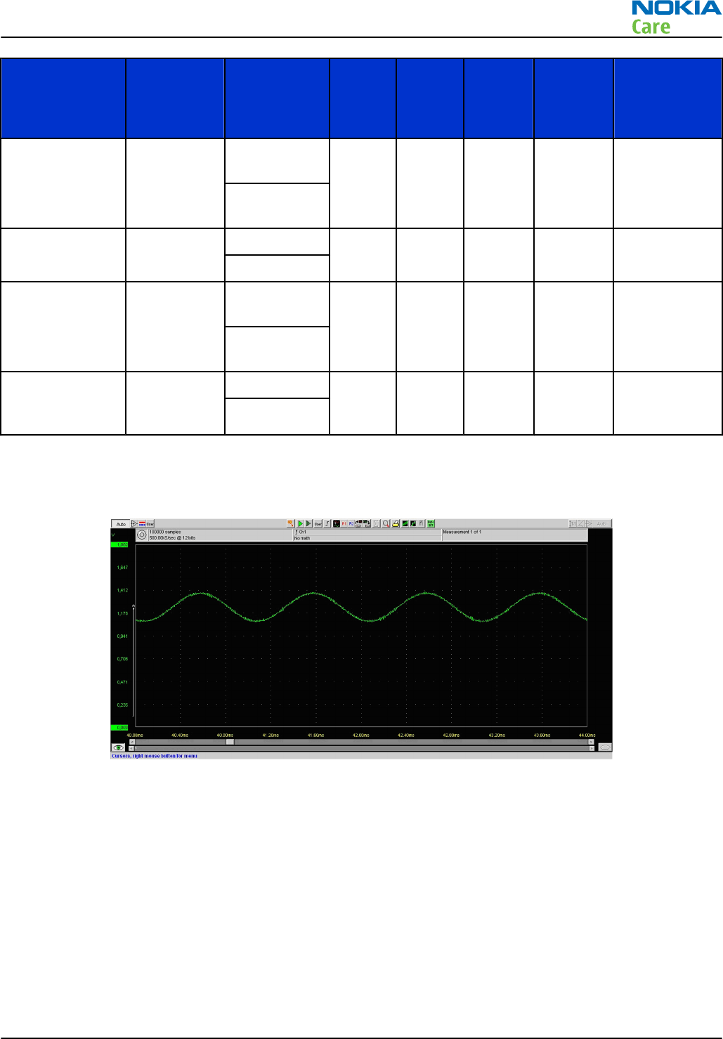
Loop test Input
terminal Output
terminal Path
gain
[dB]
(fixed)
Input
voltage
[mVp-
p]
Output
voltage
[mVp-p]
Output
DC level
[V]
Output
current [mA]
AV Mic to AV
Earpiece
HS_MIC &
GND
HS_EAR_L &
GND
100 1.2 NA
HS_EAR_R &
GND
AV Mic to HP
Earpiece
HS_MIC &
GND
EarP & GND 100 1.2 NA
EarN & GND
HP Mic to AV
Earpiece
Acoustical
input, 1kHz
sine wave
HS_EAR_L &
GND
NA 94 dB
SPL
100 NA
HS_EAR_R &
GND
External Mic in
Internal
handsfree out
HS_MIC &
GND
E2002 1000
E2005
Measurement data
Earpiece signal
Figure 35 Single-ended output waveform of the AV Mic to HP Ear measurement when earpiece is connected.
Integrated handsfree signal
RM-612; RM-624
BB Troubleshooting and Manual Tuning Guide
Issue 1 COMPANY CONFIDENTIAL Page 3 – 65
Copyright © 2010 Nokia. All rights reserved.
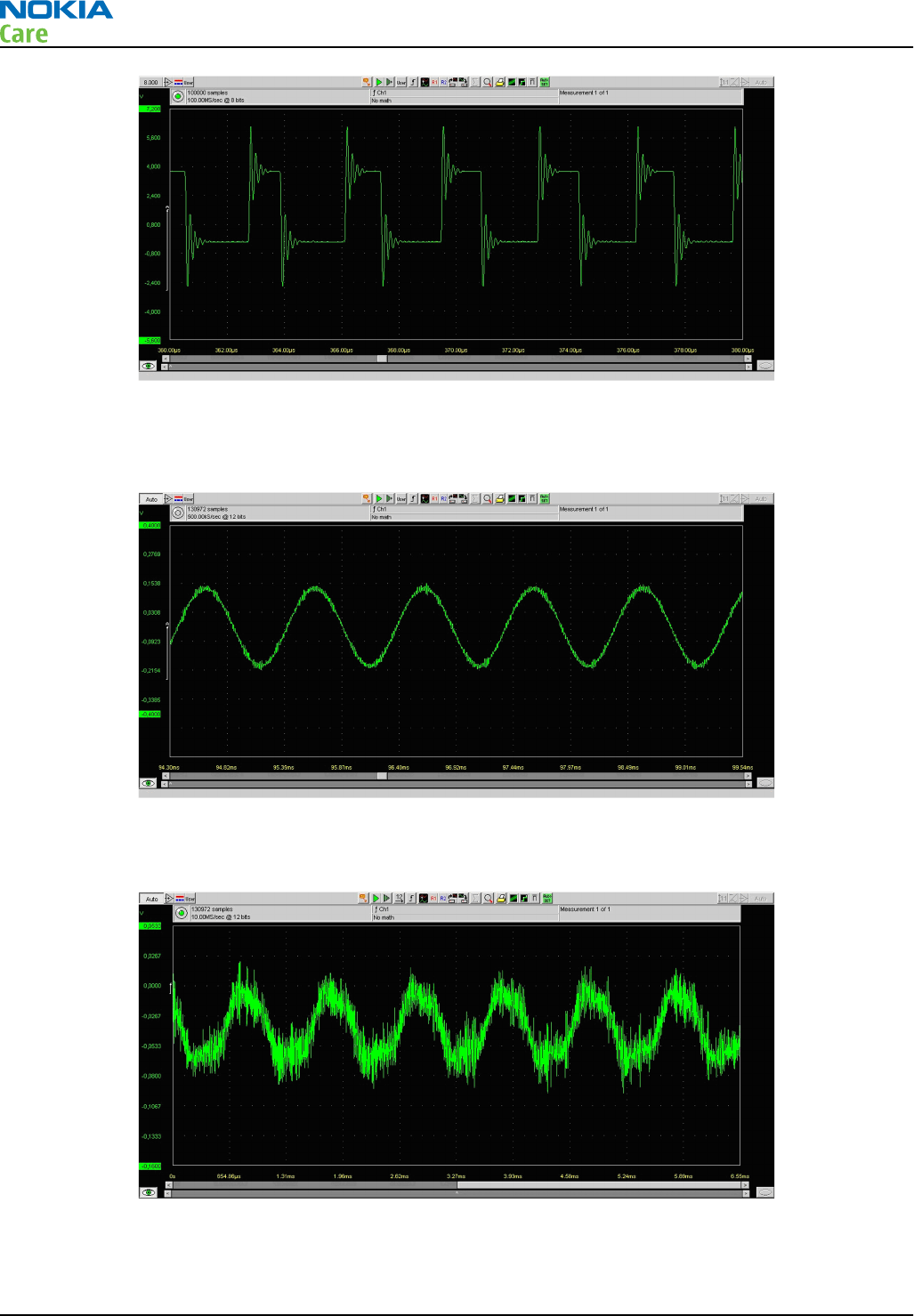
Figure 36 Single-ended output waveform of the Ext_microphone in Int handsfree out loop measurement when speaker is
connected (measured at speaker pads). No filter is used.
External output from AV
Figure 37 Single-ended output waveform of the AV Mic to AV Ear loop.
External output from AV (acoustic input)
Figure 38 Single-ended output waveform of the HP Mic to AV Ear loop.
RM-612; RM-624
BB Troubleshooting and Manual Tuning Guide
Page 3 – 66 COMPANY CONFIDENTIAL Issue 1
Copyright © 2010 Nokia. All rights reserved.
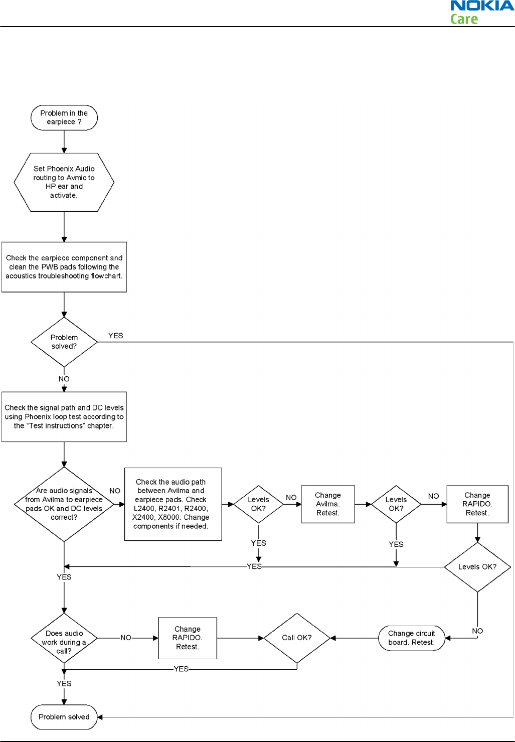
Internal earpiece troubleshooting
Troubleshooting flow
RM-612; RM-624
BB Troubleshooting and Manual Tuning Guide
Issue 1 COMPANY CONFIDENTIAL Page 3 – 67
Copyright © 2010 Nokia. All rights reserved.
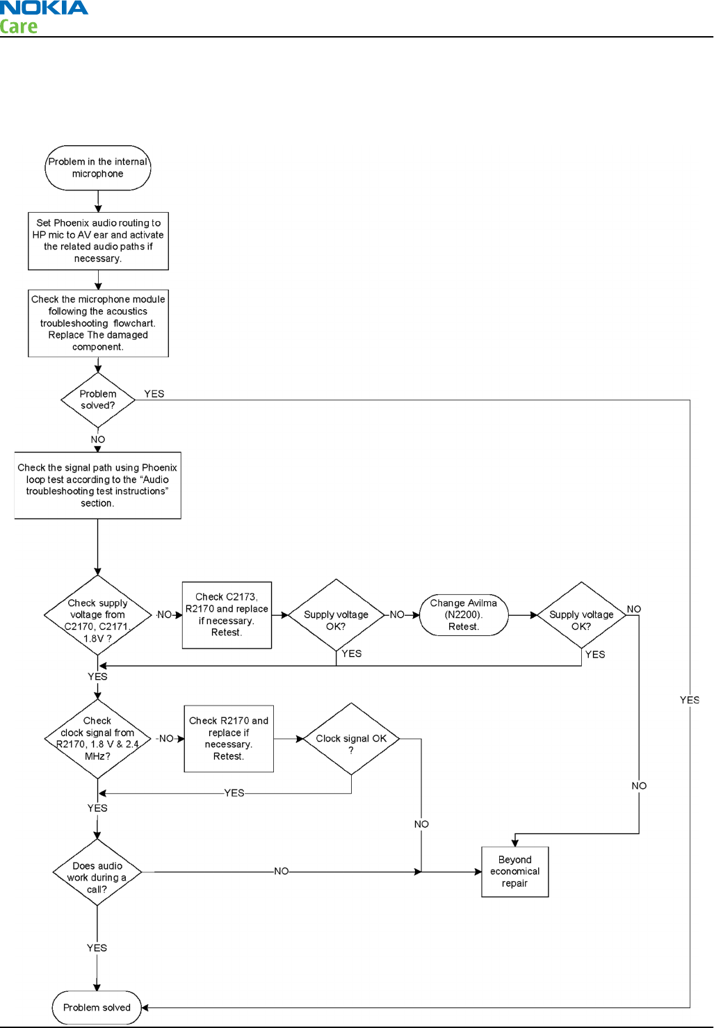
Internal microphone troubleshooting
Troubleshooting flow
RM-612; RM-624
BB Troubleshooting and Manual Tuning Guide
Page 3 – 68 COMPANY CONFIDENTIAL Issue 1
Copyright © 2010 Nokia. All rights reserved.
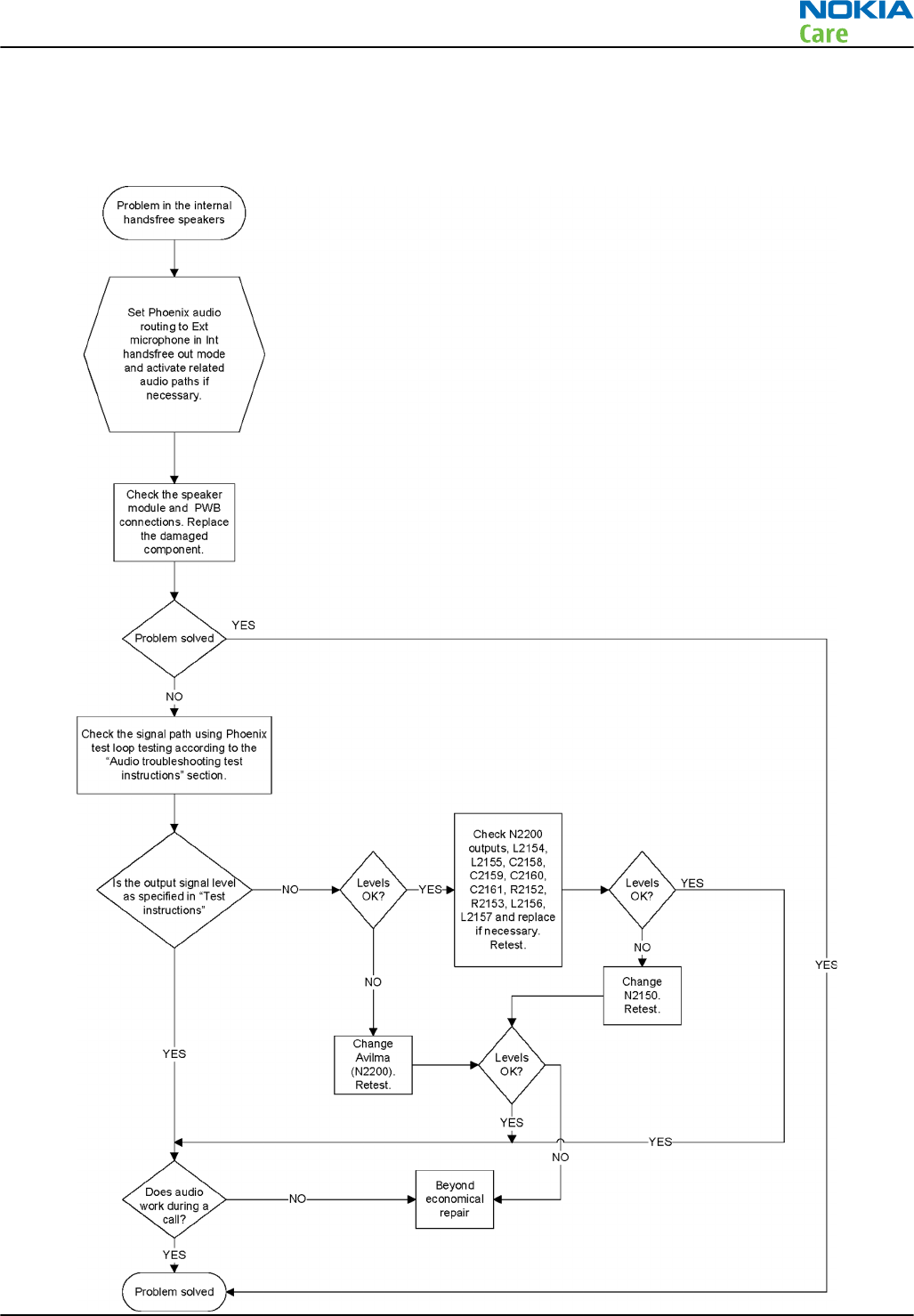
Internal handsfree speaker troubleshooting
Troubleshooting flow
RM-612; RM-624
BB Troubleshooting and Manual Tuning Guide
Issue 1 COMPANY CONFIDENTIAL Page 3 – 69
Copyright © 2010 Nokia. All rights reserved.
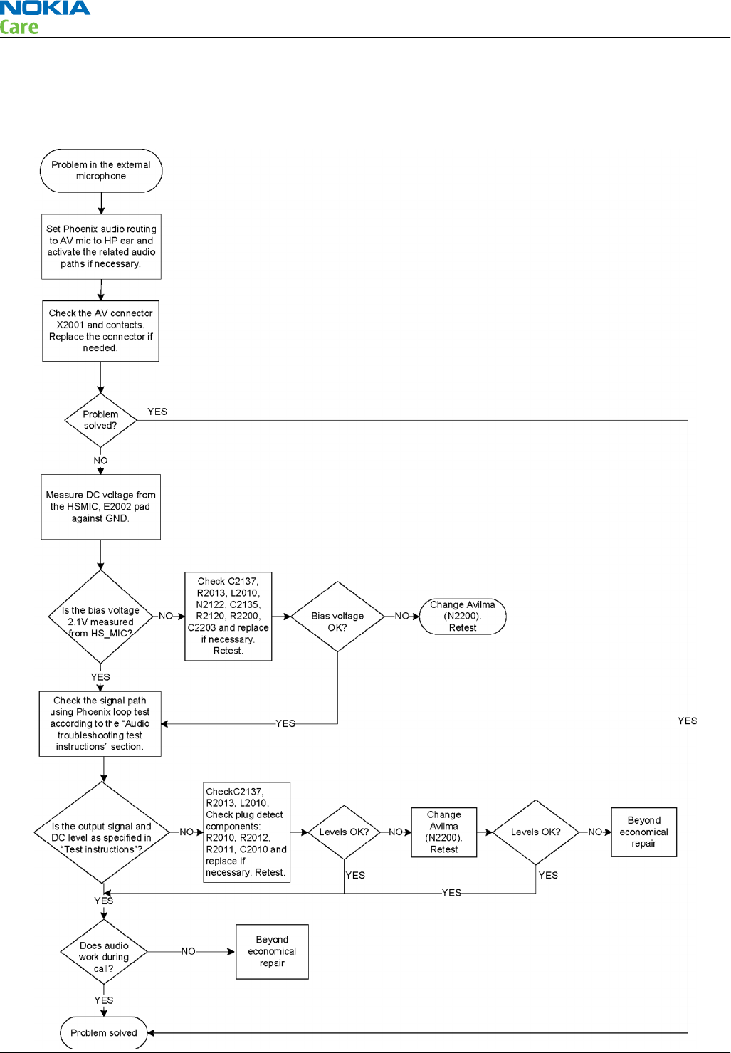
External microphone troubleshooting
Troubleshooting flow
RM-612; RM-624
BB Troubleshooting and Manual Tuning Guide
Page 3 – 70 COMPANY CONFIDENTIAL Issue 1
Copyright © 2010 Nokia. All rights reserved.
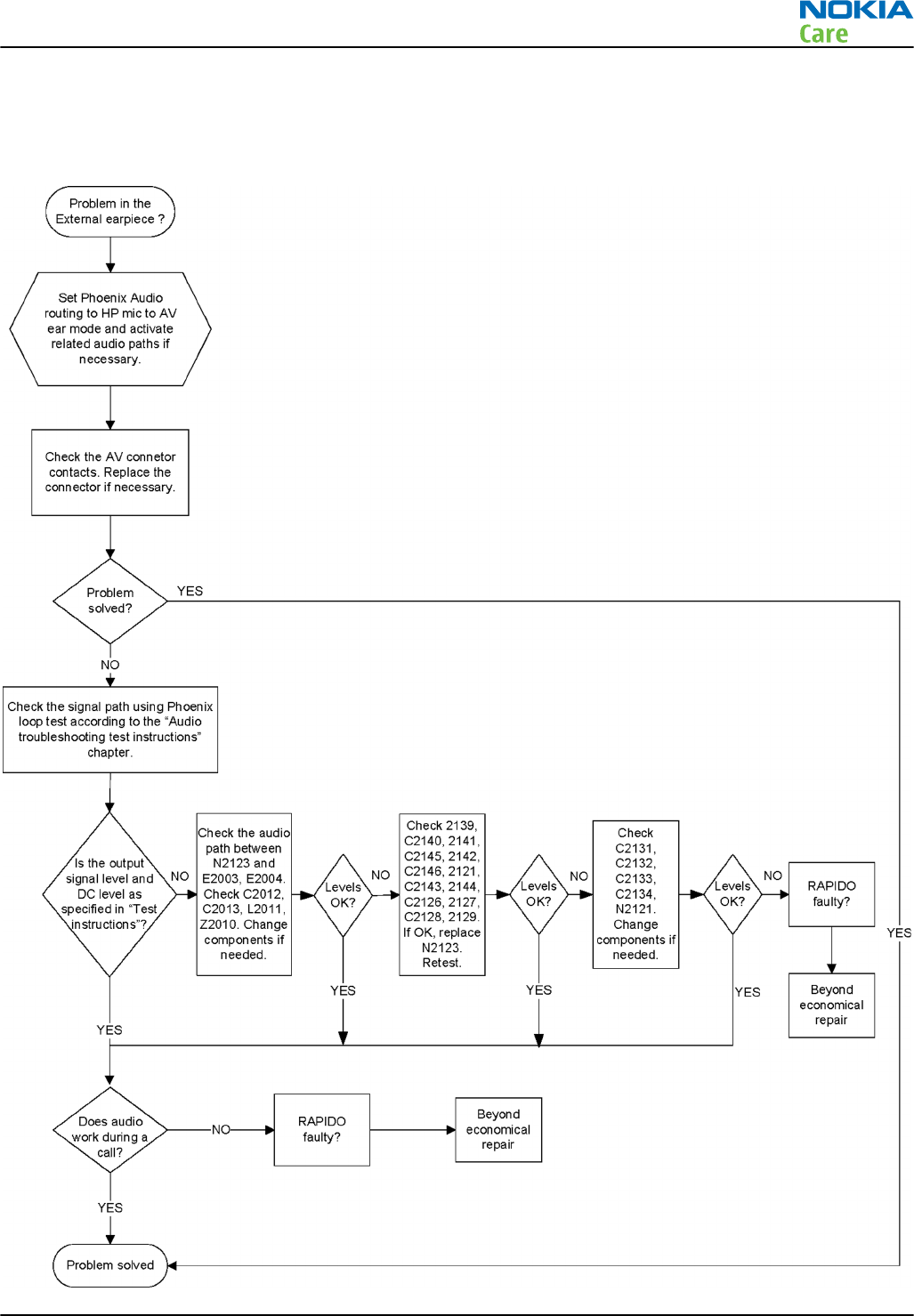
External headset earpiece troubleshooting
Troubleshooting flow
RM-612; RM-624
BB Troubleshooting and Manual Tuning Guide
Issue 1 COMPANY CONFIDENTIAL Page 3 – 71
Copyright © 2010 Nokia. All rights reserved.

Acoustics troubleshooting
Introduction to acoustics troubleshooting
Acoustics design ensures that the sound is detected correctly with a microphone and properly radiated to
the outside of the device by the speaker. The acoustics of the phone includes three basic systems: earpiece,
Integrated Hands Free (IHF) and microphone.
The sound reproduced from the earpiece radiates through a single hole on the front cover (A-cover). The
sound reproduced from the IHF speakers radiate through dual sound holes located at the top and bottom of
the phone. The microphone is located around the 'space' key in the keymat of the phone.
For a correct functionality of the phone, all sound holes must be always open. When the phone is used, care
must be taken not to close any of those holes with a hand or fingers. The phone should be dry and clean,
and no objects must be located in such a way that they close any of the holes.
RM-612; RM-624
BB Troubleshooting and Manual Tuning Guide
Page 3 – 72 COMPANY CONFIDENTIAL Issue 1
Copyright © 2010 Nokia. All rights reserved.
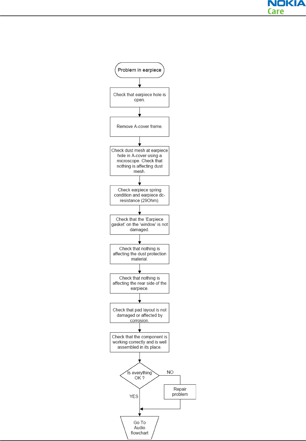
Earpiece troubleshooting
Troubleshooting flow
RM-612; RM-624
BB Troubleshooting and Manual Tuning Guide
Issue 1 COMPANY CONFIDENTIAL Page 3 – 73
Copyright © 2010 Nokia. All rights reserved.
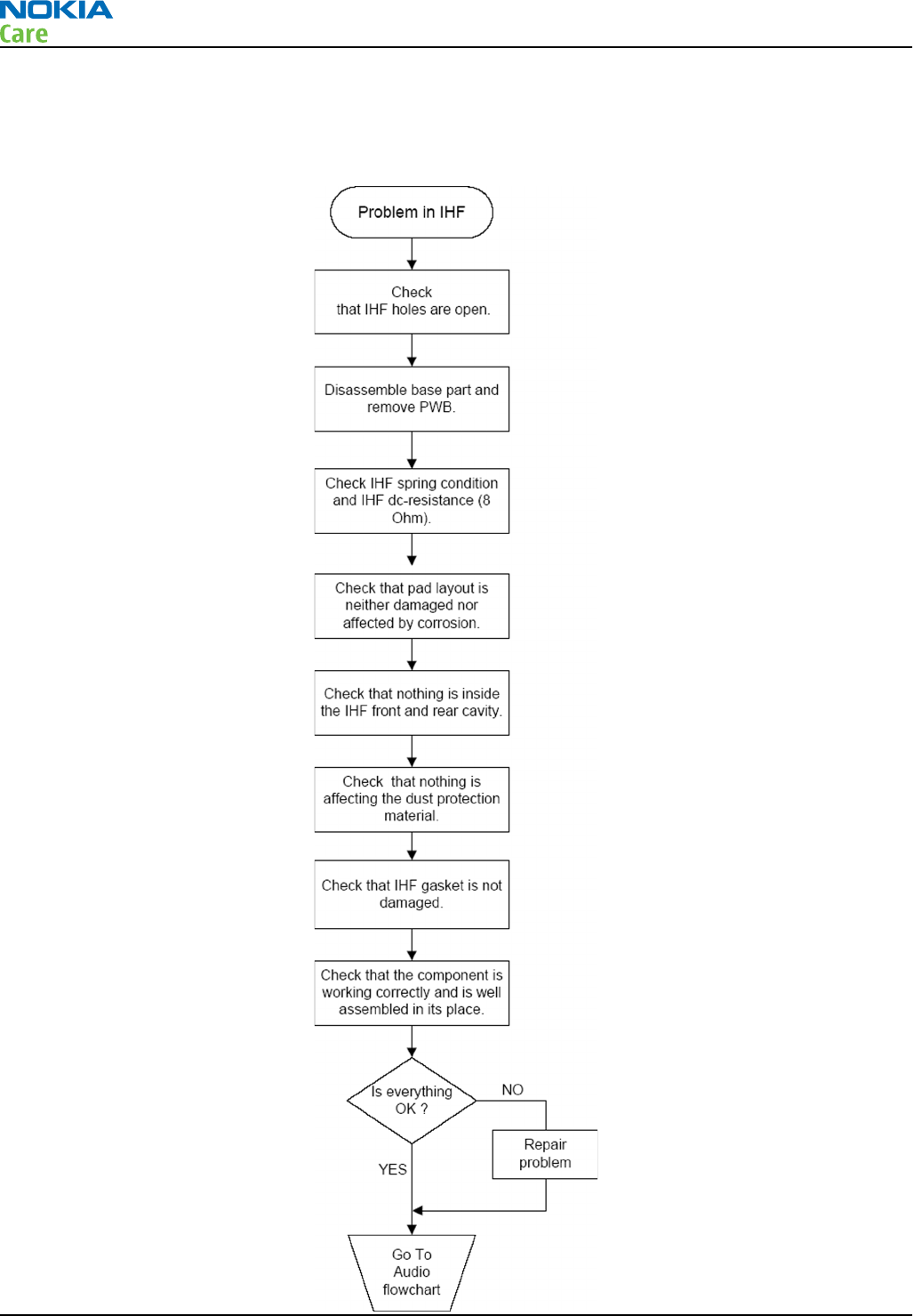
IHF troubleshooting
Troubleshooting flow
RM-612; RM-624
BB Troubleshooting and Manual Tuning Guide
Page 3 – 74 COMPANY CONFIDENTIAL Issue 1
Copyright © 2010 Nokia. All rights reserved.
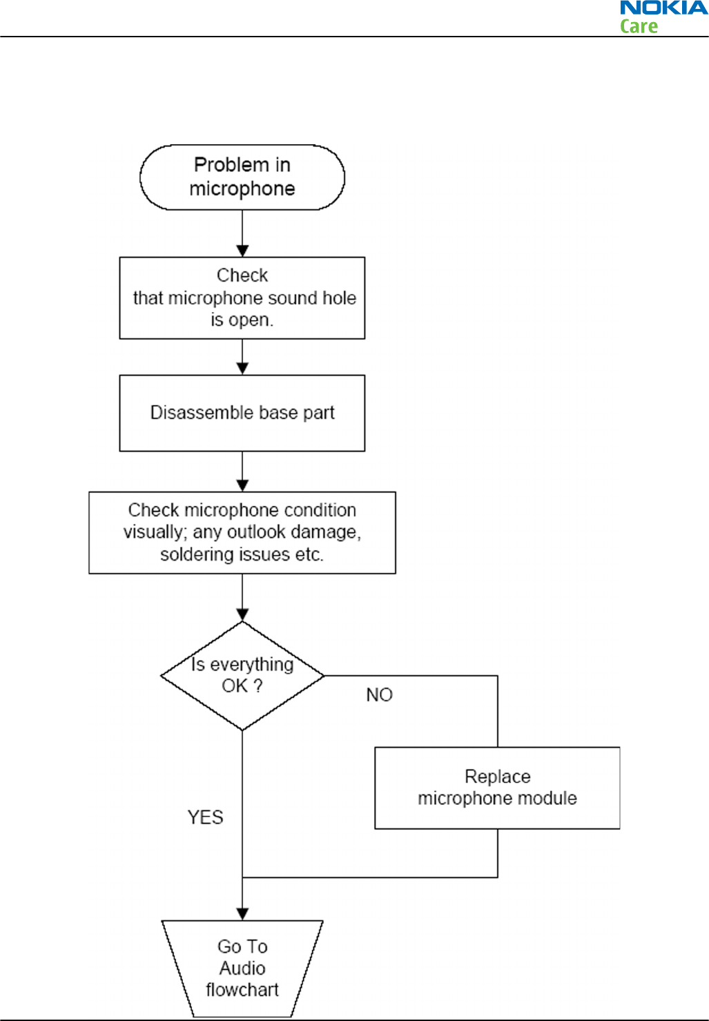
Microphone troubleshooting
Troubleshooting flow
RM-612; RM-624
BB Troubleshooting and Manual Tuning Guide
Issue 1 COMPANY CONFIDENTIAL Page 3 – 75
Copyright © 2010 Nokia. All rights reserved.

Baseband manual tuning guide
Certificate restoring
Context
This procedure is performed when the device certificate is corrupted for some reason.
All tunings (RF & Baseband, UI) must be done after performing the certificate restoring procedure.
The procedure for certificate restoring is the following:
•Flash the phone with the latest available software using FPS-10 or FPS-21.
Note: If the COMBO memory of a phone is replaced, the ENO SW must be flashed first before
performing the "normal" firmware flashing.
•Execute the certificate restore process in Phoenix.
•Tune the phone completely.
Note: SX-4 smart card is needed.
•If the phone resets after certificate restoring, reflash the phone again.
Required equipment and setup:
•
Phoenix
service software v 2008.34.6 or newer.
•The latest phone model specific
Phoenix
data package.
•PKD-1 dongle
•SX-4 smart card (Enables testing and tuning features)
•External smart card reader
•Activated FPS-10 OR FPS-21 flash prommer
•Latest flash update package for FPS-10 or FPS-21 flash prommers
•CU-4 control unit
•USB cable from PC USB Port to CU-4 control unit
•Phone model specific adapter for CU-4 control unit
•PCS-1 cable to power CU-4 from external power supply
•XCS-4 modular cable between flash prommer and CU-4
Note: CU-4 must be supplied with +12 V from an external power supply in all steps of certificate
restoring.
Steps
1. Program the phone software.
Note: If the COMBO memory of a phone is replaced, the ENO SW must be flashed first before
performing the "normal" firmware flashing.
2. Execute the certificate restore process in Phoenix.
Next actions
After a successful rewrite, you must retune the phone completely by using
Phoenix
tuning functions.
Important: Perform all tunings: RF, BB, and UI.
RM-612; RM-624
BB Troubleshooting and Manual Tuning Guide
Page 3 – 76 COMPANY CONFIDENTIAL Issue 1
Copyright © 2010 Nokia. All rights reserved.

Energy management calibration
Prerequisites
Energy Management (EM) calibration is performed to calibrate the setting (gain and offset) of AD converters
in several channels (that is, battery voltage, BSI, battery current) to get an accurate AD conversion result.
Hardware setup:
•An external power supply is needed.
•Supply 12V DC from an external power supply to CU-4 to power up the phone.
•The phone must be connected to a CU-4 control unit with a product-specific flash adapter.
Steps
1. Place the phone to the docking station adapter (CU-4 is connected to the adapter).
2. Start
Phoenix
service software.
3. Choose File → Scan Product.
4. Choose Tuning → Energy Management Calibration.
5. To show the current values in the phone memory, click Read, and check that communication between
the phone and CU-4 works.
6. Check that the CU-4 used check box is checked.
7. Select the item(s) to be calibrated.
Note: ADC calibration has to be performed before other item(s). However, if all calibrations are
selected at the same time, there is no need to perform the ADC calibration first.
8. Click Calibrate.
The calibration of the selected item(s) is carried out automatically.
The candidates for the new calibration values are shown in the
Calculated values
column. If the new
calibration values seem to be acceptable (please refer to the following "Calibration value limits" table),
click Write to store the new calibration values to the phone permanent memory.
Table 9 Calibration value limits
Parameter Min. Max.
ADC Offset -20 20
ADC Gain 12000 14000
BSI Gain 1100 1300
VBAT Offset 2400 2650
VBAT Gain 19000 23000
VCHAR Gain N/A N/A
IBAT (ICal) Gain 9000 11000
9. Click Read, and confirm that the new calibration values are stored in the phone memory correctly. If the
values are not stored to the phone memory, click Write and/or repeat the procedure again.
10. To end the procedure, close the
Energy Management Calibration
window.
RM-612; RM-624
BB Troubleshooting and Manual Tuning Guide
Issue 1 COMPANY CONFIDENTIAL Page 3 – 77
Copyright © 2010 Nokia. All rights reserved.

RM-612; RM-624
BB Troubleshooting and Manual Tuning Guide
(This page left intentionally blank.)
Page 3 – 78 COMPANY CONFIDENTIAL Issue 1
Copyright © 2010 Nokia. All rights reserved.

4 — RF Troubleshooting
Nokia Customer Care
Issue 1 COMPANY CONFIDENTIAL Page 4 – 1
Copyright © 2010 Nokia. All rights reserved.

RM-612; RM-624
RF Troubleshooting
(This page left intentionally blank.)
Page 4 – 2 COMPANY CONFIDENTIAL Issue 1
Copyright © 2010 Nokia. All rights reserved.

Table of Contents
General RF troubleshooting ................................................................................................................................. 4–5
Introduction to RF troubleshooting ............................................................................................................... 4–5
RF key components .......................................................................................................................................... 4–5
Auto tuning............................................................................................................................................................ 4–6
Introduction to RF tunings.............................................................................................................................. 4–6
Auto tuning....................................................................................................................................................... 4–6
Self test troubleshooting...................................................................................................................................... 4–7
Troubleshooting with RF self tests................................................................................................................. 4–7
Receiver troubleshooting .................................................................................................................................. 4–20
Introduction to receiver (RX) troubleshooting........................................................................................... 4–20
GSM RX chain activation for manual measurements/GSM RSSI measurement ....................................... 4–20
GSM receiver troubleshooting flowchart .................................................................................................... 4–22
WCDMA RX chain activation for manual measurement............................................................................. 4–22
WCDMA RSSI measurement .......................................................................................................................... 4–23
WCDMA receiver troubleshooting flowchart............................................................................................... 4–25
Transmitter troubleshooting ............................................................................................................................ 4–25
General instructions for transmitter (TX) troubleshooting....................................................................... 4–25
GSM transmitter troubleshooting................................................................................................................ 4–26
WCDMA transmitter troubleshooting .......................................................................................................... 4–28
Antenna troubleshooting .................................................................................................................................. 4–30
Antenna troubleshooting............................................................................................................................. 4–30
List of Figures
Figure 39 RF key components .............................................................................................................................. 4–6
Figure 40 Phoenix GSM RSSI reading window................................................................................................. 4–21
Figure 41 Phoenix WCDMA RX Control window............................................................................................... 4–23
Figure 42 WCDMA RX generator settings ......................................................................................................... 4–24
Figure 43 Phoenix WCDMA RX power measurement window ....................................................................... 4–24
Figure 44 Phoenix GSM RF controls window.................................................................................................... 4–26
Figure 45 Antenna contacts .............................................................................................................................. 4–30
Figure 46 Antenna contact clips and matching coil on the PWB................................................................... 4–30
RM-612; RM-624
RF Troubleshooting
Issue 1 COMPANY CONFIDENTIAL Page 4 – 3
Copyright © 2010 Nokia. All rights reserved.

RM-612; RM-624
RF Troubleshooting
(This page left intentionally blank.)
Page 4 – 4 COMPANY CONFIDENTIAL Issue 1
Copyright © 2010 Nokia. All rights reserved.

General RF troubleshooting
Introduction to RF troubleshooting
Most RF semiconductors are static discharge sensitive
ESD protection must be applied during repair (ground straps and ESD soldering irons).
Measuring equipment
All measurements should be done using:
•An oscilloscope for low frequency and DC measurements. Recommended probe: 10:1, 10Mohm//8pF.
•A radio communication tester including RF generator and spectrum analyser, for example Rohde & Schwarz
CMU200. (Alternatively a spectrum analyser and an RF generator can be used. Some tests in this guide are
not possible to perform if this solution is chosen).
Note: A mobile phone WCDMA transmitter should never be tested with full TX power (it is only
possible to perform the measurements in a good RF-shielded room). Even low power WCDMA
transmitters may disturb nearby WCDMA networks and cause problems to 3G cellular phone
communication in a wide area.
Note: All communication Test Set Screen dumps are from CMU200. Other testers are different.
Note: All measurements with an RF coupler should be performed in an RF-shielded environment
because nearby base stations can disturb sensitive receiver measurements. If there is no possibility
to use RF shielded environment, testing at frequencies of nearby base stations should be avoided.
Level of repair
The scope of this guideline is to verify functionality of the cellular RF block without removing RF shield.
RF key components
The figure below shows the key components of RM-612 and RM-624.
RM-612; RM-624
RF Troubleshooting
Issue 1 COMPANY CONFIDENTIAL Page 4 – 5
Copyright © 2010 Nokia. All rights reserved.
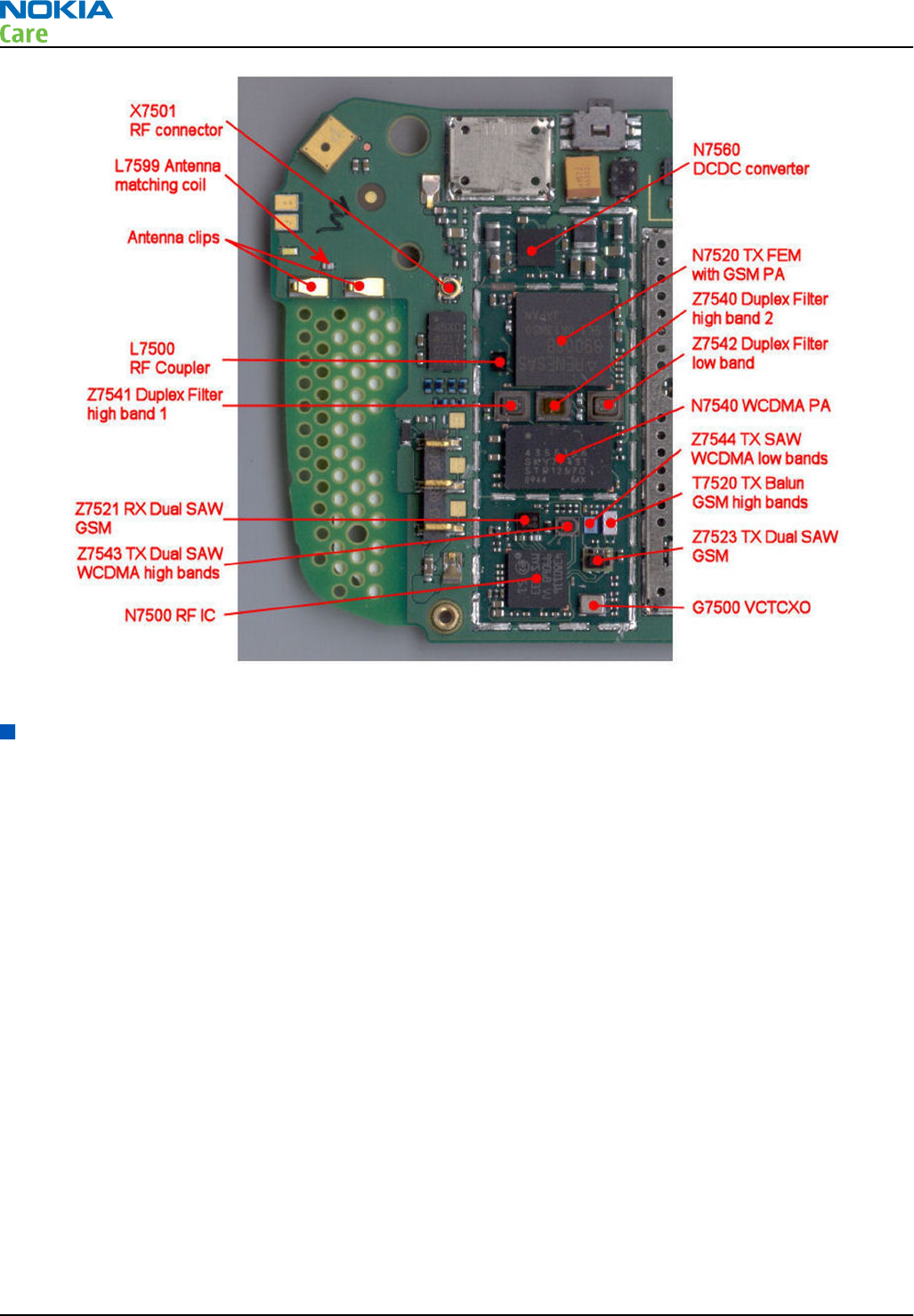
Figure 39 RF key components
Auto tuning
Introduction to RF tunings
RF tuning is always performed with the help of a product-specific module jig, never with an RF coupler. Using
an RF coupler in the tuning phase will cause a complete mistuning of the RF part.
Cable and adapter losses
RF cables and adapters have some losses. They have to be taken into account when the phone is tuned. As
all RF losses are frequency dependent, the user has to act very carefully and understand the measurement
setup. For RF attenuations of the module jig and RF cable, please refer to the Service Tools section.
Auto tuning
This phone can be tuned automatically.
Auto tuning is designed to align the phone's RF part easier and faster. It performs calibrations, tunings and
measurements of RX and TX. The results are displayed and logged in a result file, if initiated.
Hardware set up
For hardware requirements for auto tuning, please refer to Service concept for RF testing and RF/BB
tuning (page 4–41 ) .
Phoenix preparations
Install the phone specific data package, for example
_dp_1.78_sw_sh3.26.exe
. This defines phone specific
settings.
RM-612; RM-624
RF Troubleshooting
Page 4 – 6 COMPANY CONFIDENTIAL Issue 1
Copyright © 2010 Nokia. All rights reserved.

Auto tuning procedure
1Make sure the phone (in the jig) is connected to the equipment. Otherwise some menus will not be shown
in Phoenix.
2 To go to autotune, select Tuning (Alt-U) → Auto-Tune (Alt-A) from the menu.
3 Start autotuning by clicking the
Tune
button.
Self test troubleshooting
Troubleshooting with RF self tests
Context
Vapaus (N7500) RF ASIC contains test structures that can be used to detect certain RF related errors. In order
to use these self tests most efficient way, it is very important that the tests are performed in a certain order,
or at least that the error data is analysed in this order. The tests are designed so that by going through them
in this order it is easy to find the problem component without any redundant checks. The flowchart presented
in this document is based on that idea. So, if RFBUS fails , there is no need to spend time wondering why
there is no power at TX, and so on.
The testing order recommended and used in this troubleshooting guide is the following:
1 ST_CDSP_RF_BB_IF test (86)
•Tests the functionality of the BB/Vapaus serial interface & Reset lines.
•If this test fails, it means that there is a problem in programming of the N7500 and all of the following
tests can not give correct data.
2 ST_CDSP_RF_SUPPLY_TEST (83)
•Tests the functionality of N7500 bias block, regulators, reference voltage line and, supply connections.
•If these fail, all other N7500 tests can/will fail.
3 ST_CDSP_TX_IQ_TEST (85)
•Test checks that the TXIQ lines between BB and N7500 are properly connected.
•If this fails also power tests and RXIQ loopback will fail.
4 ST_CDSP_TXC_DATA_TEST (74)
•This tests that the TXC line between AVILMAS (N2200) & Vapaus (N7500) is properly connected.
•If this fails TX power tests will also fail.
5 ST_CDSP_RX_PLL_PHASE_LOCK_TEST (79)
•Tests the functionality of RX PLL.
•If this fails none of the RX related measurements can be trusted.
6 ST_CDSP_TX_PLL_PHASE_LOCK_TEST (80)
•Tests the functionality of TX PLL.
•If this fails the TX power tests will also fail.
7 ST_CDSP_TX_WCDMA_POWER_TEST (75)
•Checks the output power of the WCDMA transmitter.
8 ST_CDSP_RX_IQ_LOOPBACK (81)
•Tests that the RXI lines and VREFCM line between BB and N7500 are connected.
9 ST_CDSP_TX_GSM_POWER_TEST (77)
•Checks the output power of the GSM transmitter.
RM-612; RM-624
RF Troubleshooting
Issue 1 COMPANY CONFIDENTIAL Page 4 – 7
Copyright © 2010 Nokia. All rights reserved.

To get the best out of these instructions you need to be have the valid schematics at hand, see Chapter 10
in this document.
RM-612; RM-624
RF Troubleshooting
Page 4 – 8 COMPANY CONFIDENTIAL Issue 1
Copyright © 2010 Nokia. All rights reserved.
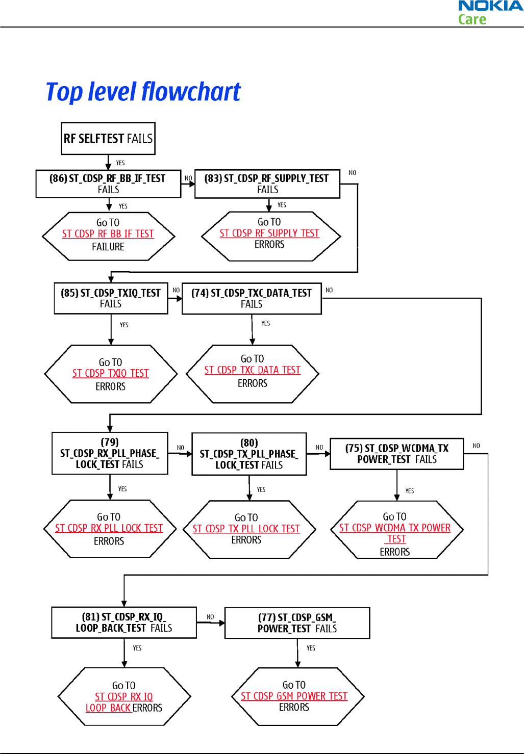
Troubleshooting flow
RM-612; RM-624
RF Troubleshooting
Issue 1 COMPANY CONFIDENTIAL Page 4 – 9
Copyright © 2010 Nokia. All rights reserved.
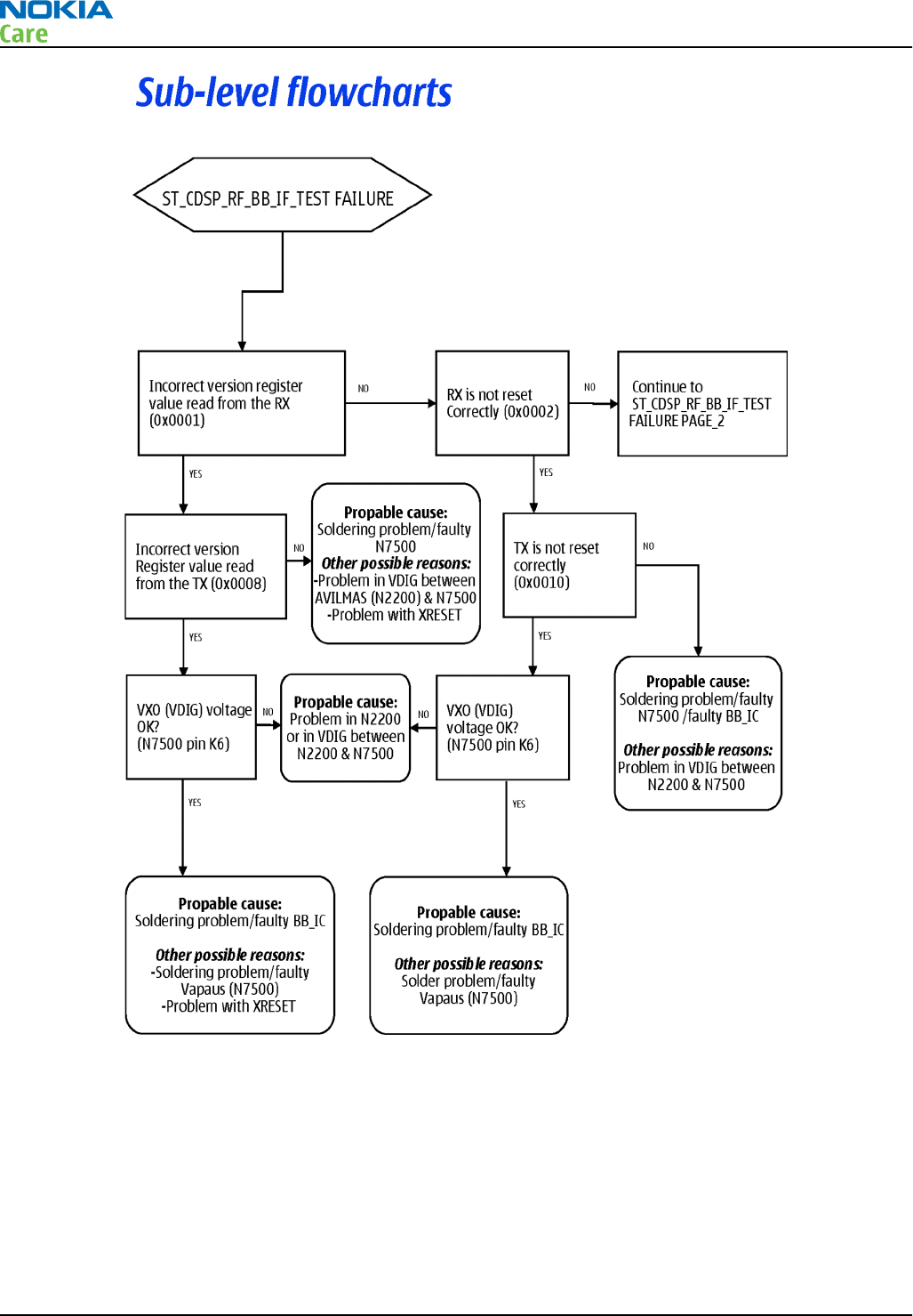
RM-612; RM-624
RF Troubleshooting
Page 4 – 10 COMPANY CONFIDENTIAL Issue 1
Copyright © 2010 Nokia. All rights reserved.
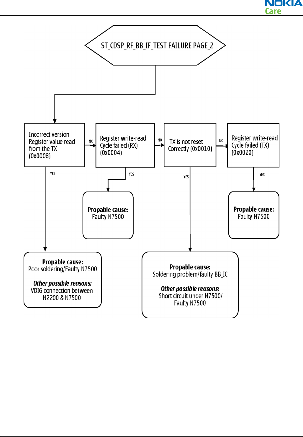
RM-612; RM-624
RF Troubleshooting
Issue 1 COMPANY CONFIDENTIAL Page 4 – 11
Copyright © 2010 Nokia. All rights reserved.
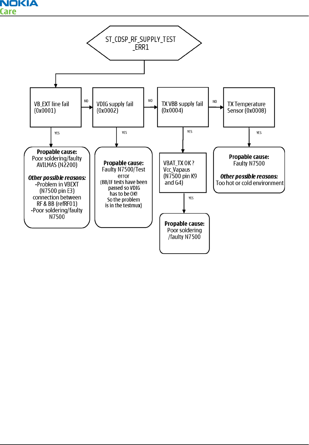
RM-612; RM-624
RF Troubleshooting
Page 4 – 12 COMPANY CONFIDENTIAL Issue 1
Copyright © 2010 Nokia. All rights reserved.
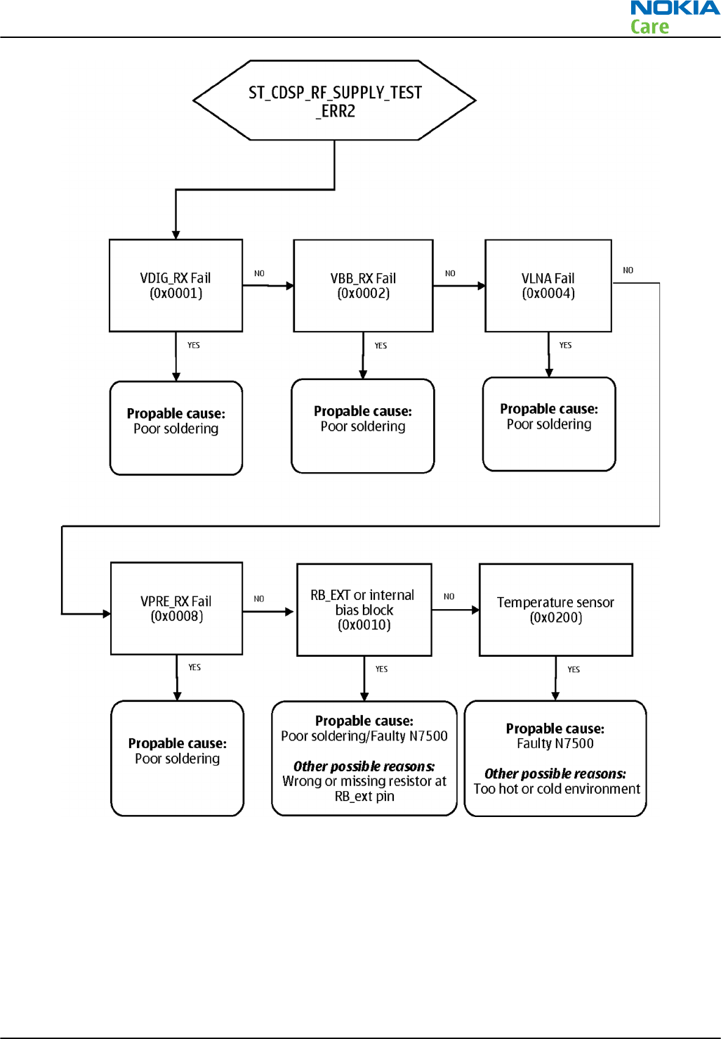
RM-612; RM-624
RF Troubleshooting
Issue 1 COMPANY CONFIDENTIAL Page 4 – 13
Copyright © 2010 Nokia. All rights reserved.
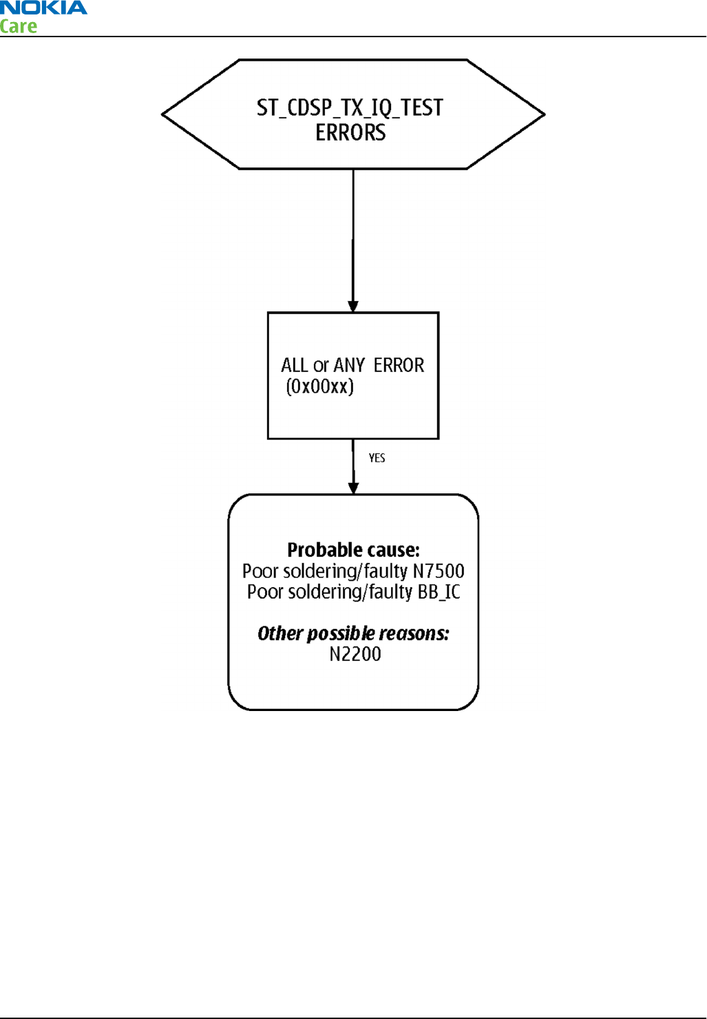
RM-612; RM-624
RF Troubleshooting
Page 4 – 14 COMPANY CONFIDENTIAL Issue 1
Copyright © 2010 Nokia. All rights reserved.
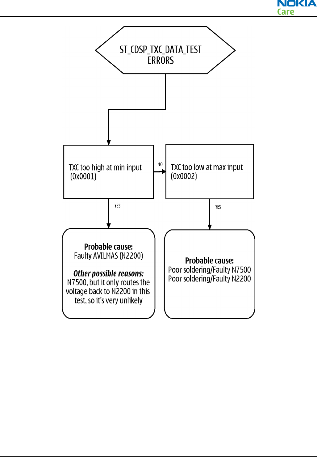
RM-612; RM-624
RF Troubleshooting
Issue 1 COMPANY CONFIDENTIAL Page 4 – 15
Copyright © 2010 Nokia. All rights reserved.
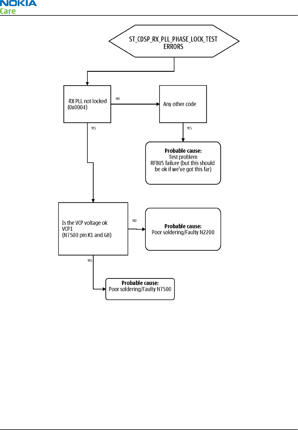
RM-612; RM-624
RF Troubleshooting
Page 4 – 16 COMPANY CONFIDENTIAL Issue 1
Copyright © 2010 Nokia. All rights reserved.
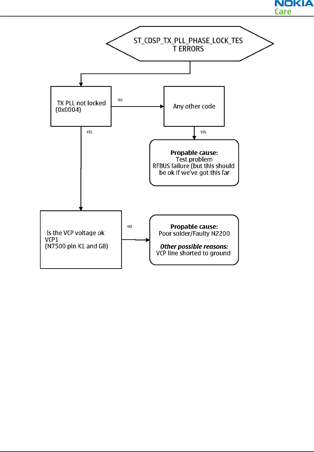
RM-612; RM-624
RF Troubleshooting
Issue 1 COMPANY CONFIDENTIAL Page 4 – 17
Copyright © 2010 Nokia. All rights reserved.
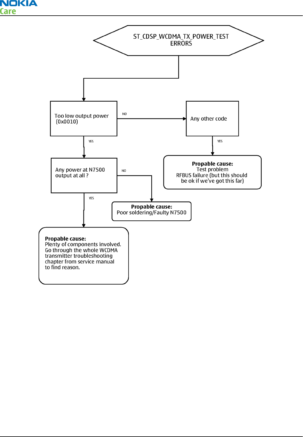
RM-612; RM-624
RF Troubleshooting
Page 4 – 18 COMPANY CONFIDENTIAL Issue 1
Copyright © 2010 Nokia. All rights reserved.
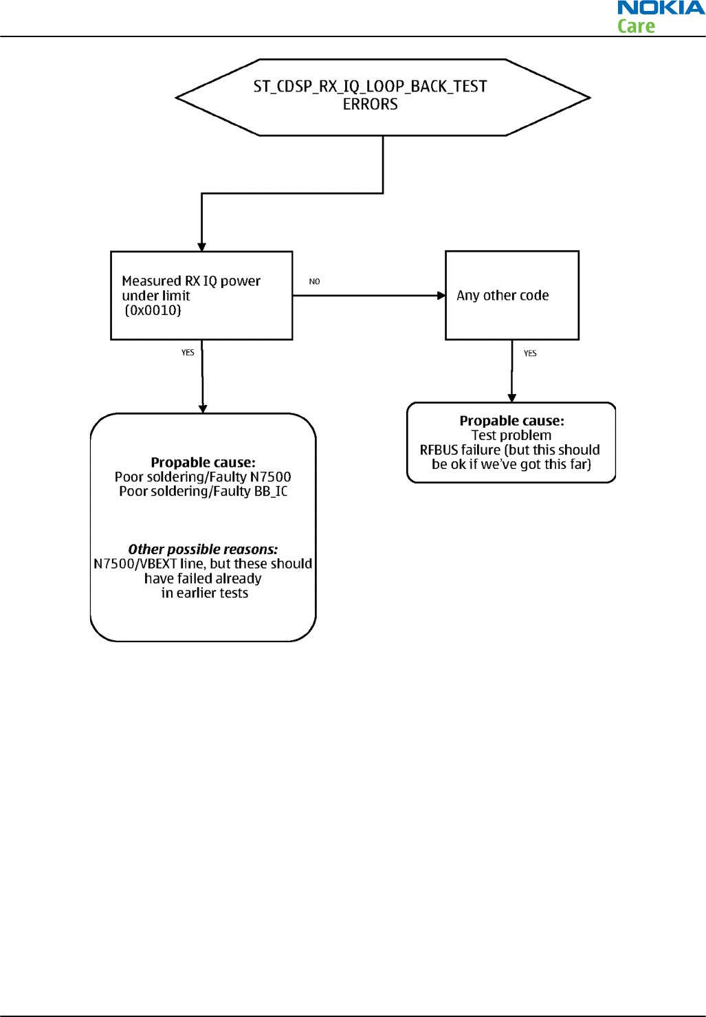
RM-612; RM-624
RF Troubleshooting
Issue 1 COMPANY CONFIDENTIAL Page 4 – 19
Copyright © 2010 Nokia. All rights reserved.
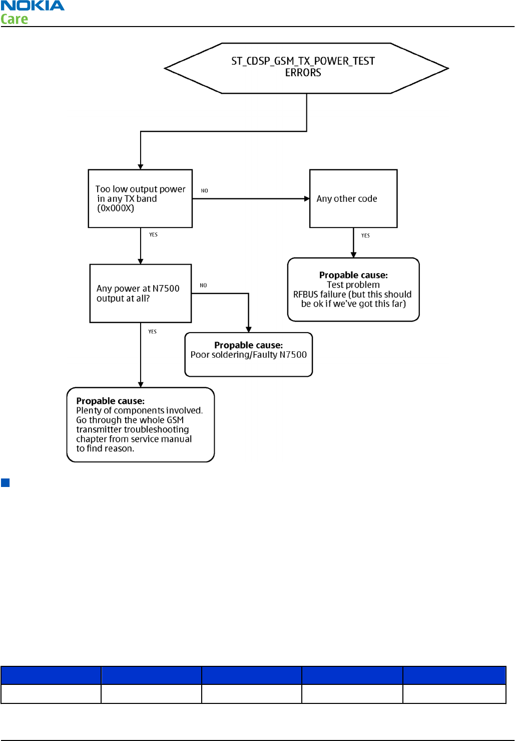
Receiver troubleshooting
Introduction to receiver (RX) troubleshooting
RX can be tested by making a phone call or in local mode. For the local mode testing, use Phoenix service
software.
The main RX troubleshooting measurement is RSSI reading. This test measures the signal strength of the
received signal. For GSM RSSI measurements, see
GSM RX chain activation for manual measurements/GSM
RSSI measurement
. For a similar test in WCDMA mode, see
WCDMA RSSI measurement
.
GSM RX chain activation for manual measurements/GSM RSSI measurement
Prerequisites
Make the following settings in Phoenix service software:
Setting GSM850 GSM900 GSM1800 GSM1900
Phoenix Channel 190 37 700 661
RM-612; RM-624
RF Troubleshooting
Page 4 – 20 COMPANY CONFIDENTIAL Issue 1
Copyright © 2010 Nokia. All rights reserved.
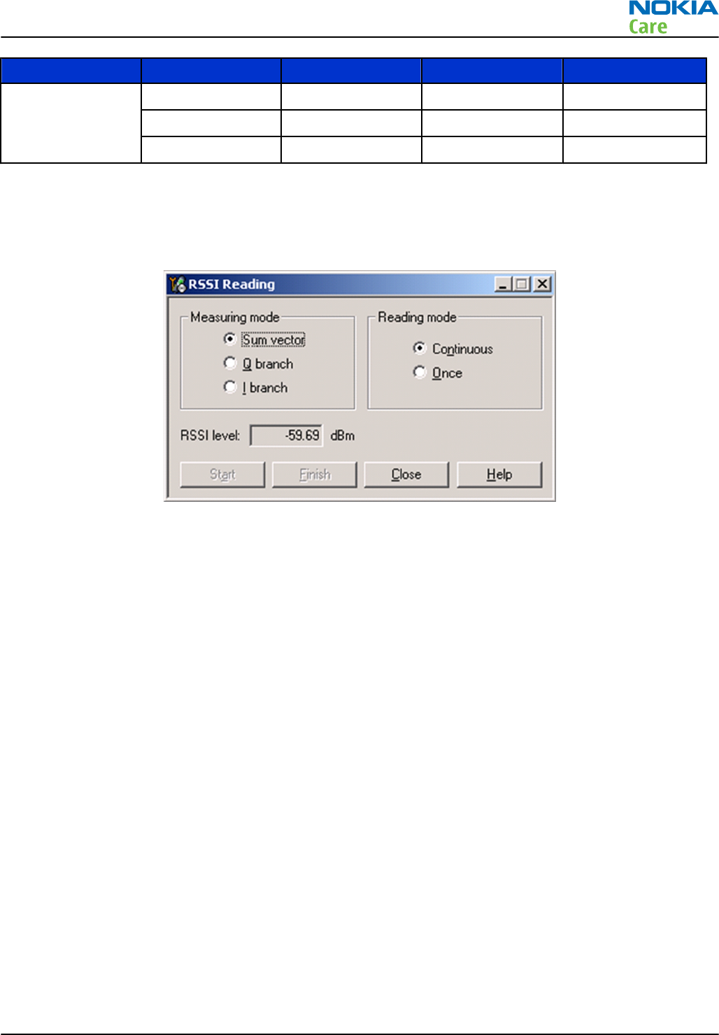
Setting GSM850 GSM900 GSM1800 GSM1900
Signal generator
to antenna
connector
881.66771MHz 942.46771MHz 1842.86771MHz 1960.06771MHz
(67.71kHz offset) (67.71kHz offset) (67.71kHz offset) (67.71kHz offset)
at -60dBm at -60dBm at -60dBm at -60dBm
Steps
1. Set the phone to local mode.
2. Activate RSSI reading in Phoenix ( Testing → GSM → RSSI reading )
Figure 40 Phoenix GSM RSSI reading window
Results
The reading should reflect the level of the signal generator (-losses) +/- 5 dB.
When varying the level in the range -30 to -102 dBm the reading should then follow within +/-5 dB.
RM-612; RM-624
RF Troubleshooting
Issue 1 COMPANY CONFIDENTIAL Page 4 – 21
Copyright © 2010 Nokia. All rights reserved.
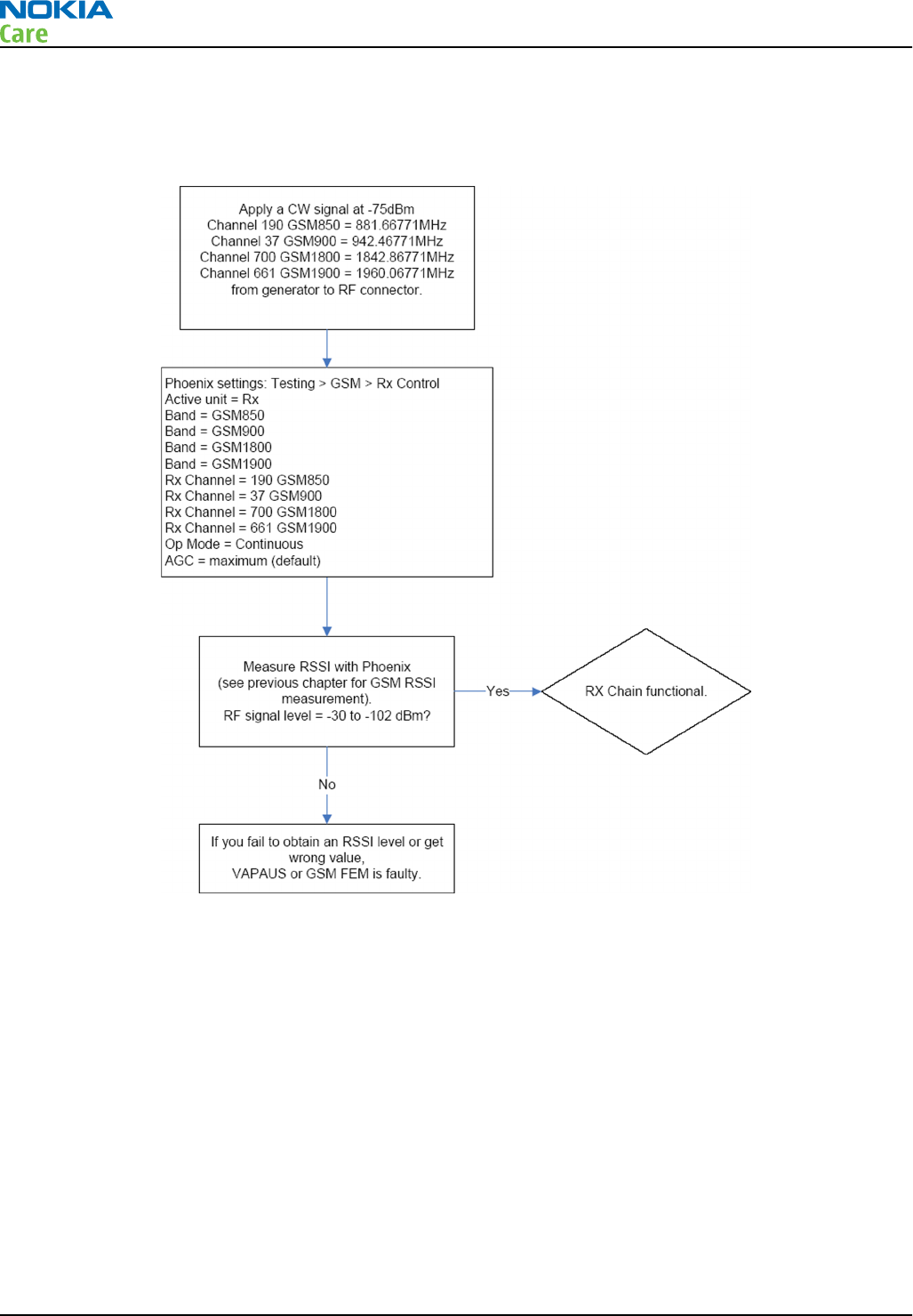
GSM receiver troubleshooting flowchart
Troubleshooting flow
WCDMA RX chain activation for manual measurement
Steps
1. Via Phoenix Testing menu, choose WCDMA/RX Control.
2. In the RX control window, make the following settings:
RM-612; RM-624
RF Troubleshooting
Page 4 – 22 COMPANY CONFIDENTIAL Issue 1
Copyright © 2010 Nokia. All rights reserved.
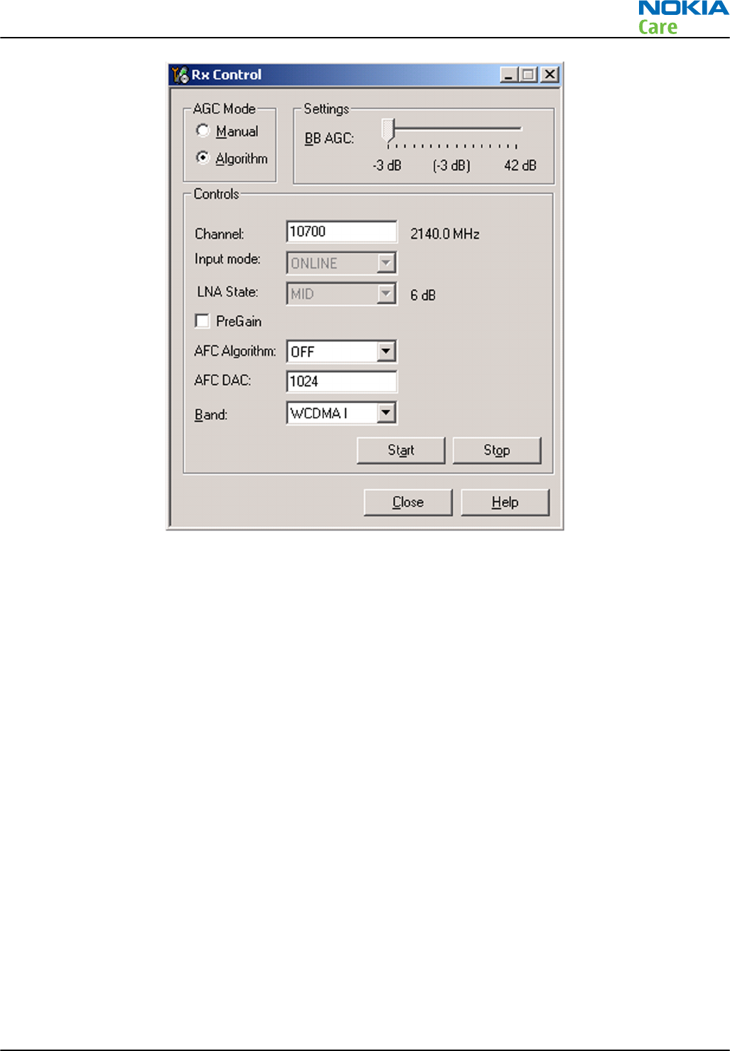
Figure 41 Phoenix WCDMA RX Control window
Note: Channel for band WCDMA II 9800, V 4408, VIII 3012
3. Click Start to activate the settings.
If the settings are changed later on (for example, change of channel) you have to click Stop and Start
again.
Note: Clicking Stop also disables TX control if it was active.
WCDMA RSSI measurement
Prerequisites
WCDMA RX must be activated before RSSI can be measured. For instructions, please refer to WCDMA RX chain
activation. Connect signal generator to RF connector and use appropriate frequency for each channel
(2141MHz for channel 10700 WCDMA band I, WCDMA modulation).
Steps
1. Set the following RF generator settings:
RM-612; RM-624
RF Troubleshooting
Issue 1 COMPANY CONFIDENTIAL Page 4 – 23
Copyright © 2010 Nokia. All rights reserved.
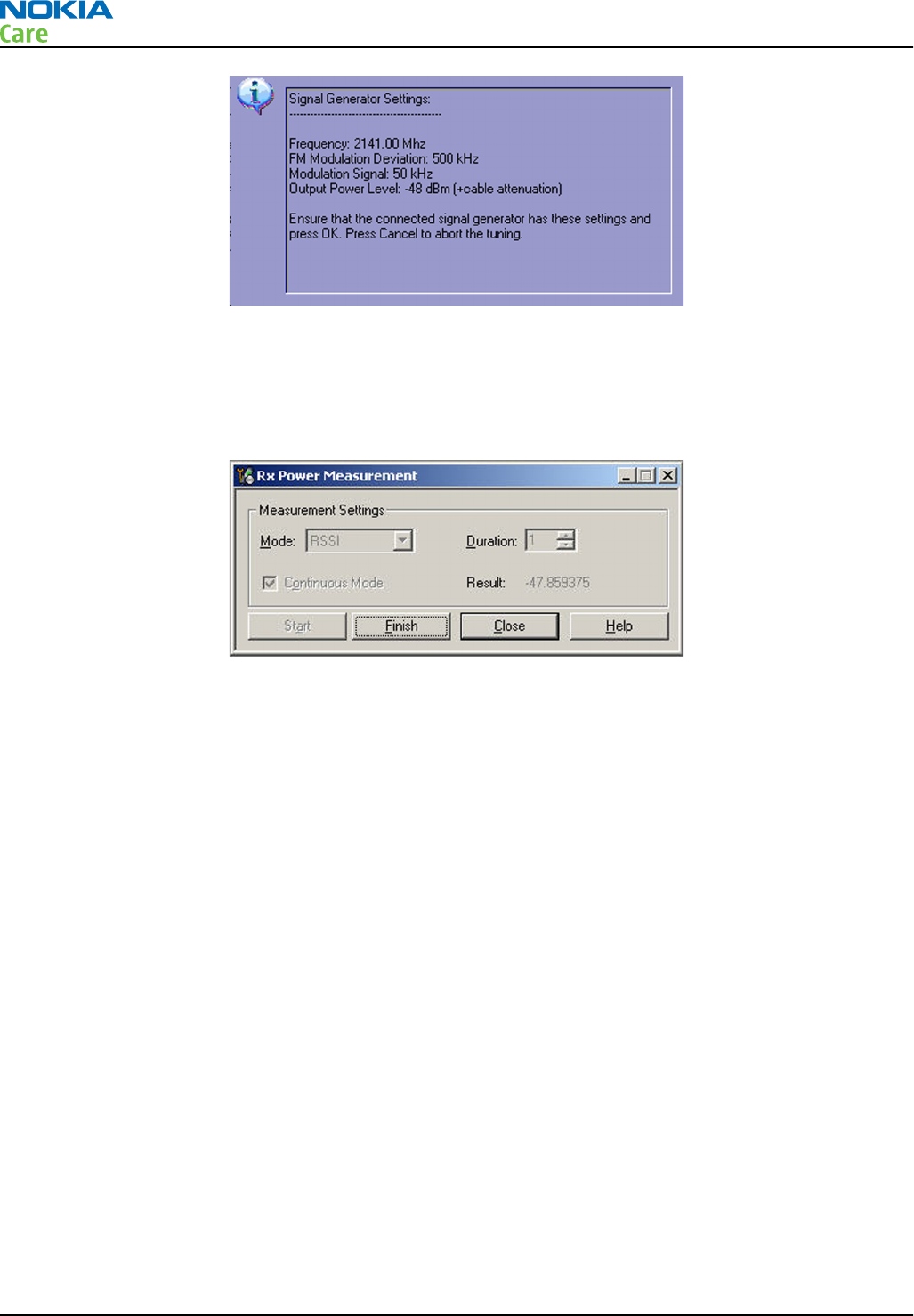
Figure 42 WCDMA RX generator settings
Note: Frequency for band WCDMA II 1961.0MHz, V 882.6MHz, VIII 943.4MHz
2. From the Phoenix testing menu, select WCDMA → RX Power measurement
3. In the RX power measurement window, make the following settings:
Figure 43 Phoenix WCDMA RX power measurement window
4. Click Start to perform the measurement.
Note: WCDMA RSSI measurement is accurate only with WCDMA modulated signal.
RM-612; RM-624
RF Troubleshooting
Page 4 – 24 COMPANY CONFIDENTIAL Issue 1
Copyright © 2010 Nokia. All rights reserved.
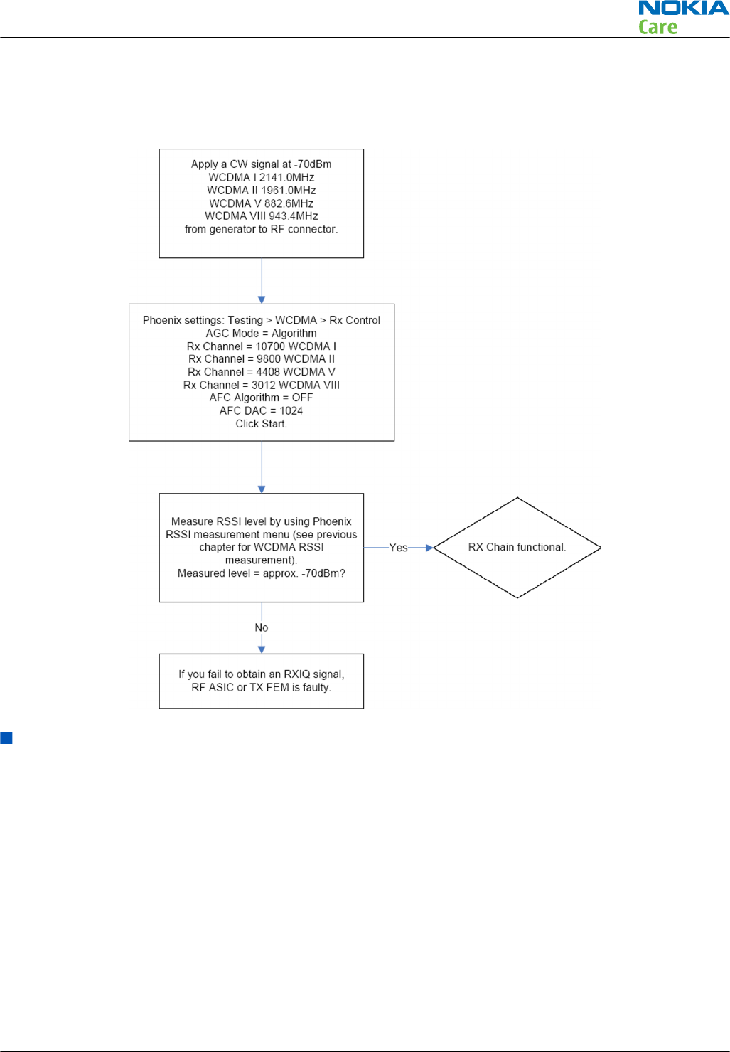
WCDMA receiver troubleshooting flowchart
Troubleshooting flow
Transmitter troubleshooting
General instructions for transmitter (TX) troubleshooting
Please note the following before performing transmitter tests:
•TX troubleshooting requires TX operation.
•Do not transmit on frequencies that are in use.
•The transmitter can be controlled in local mode for diagnostic purposes.
•The most useful Phoenix tool for GSM transmitter testing is “RF Controls”, in WCDMA transmitter testing
the best tool is “TX Control”.
•Remember that re-tuning is not a fix! Phones are tuned correctly in production.
Note: Never activate the GSM or WCDMA transmitter without a proper antenna load. Always connect
a 50 Ω load to the RF connector (antenna, RF-measurement equipment or at least a 2 W dummy
load); otherwise the GSM or WCDMA Power amplifier (PA) may be damaged.
RM-612; RM-624
RF Troubleshooting
Issue 1 COMPANY CONFIDENTIAL Page 4 – 25
Copyright © 2010 Nokia. All rights reserved.
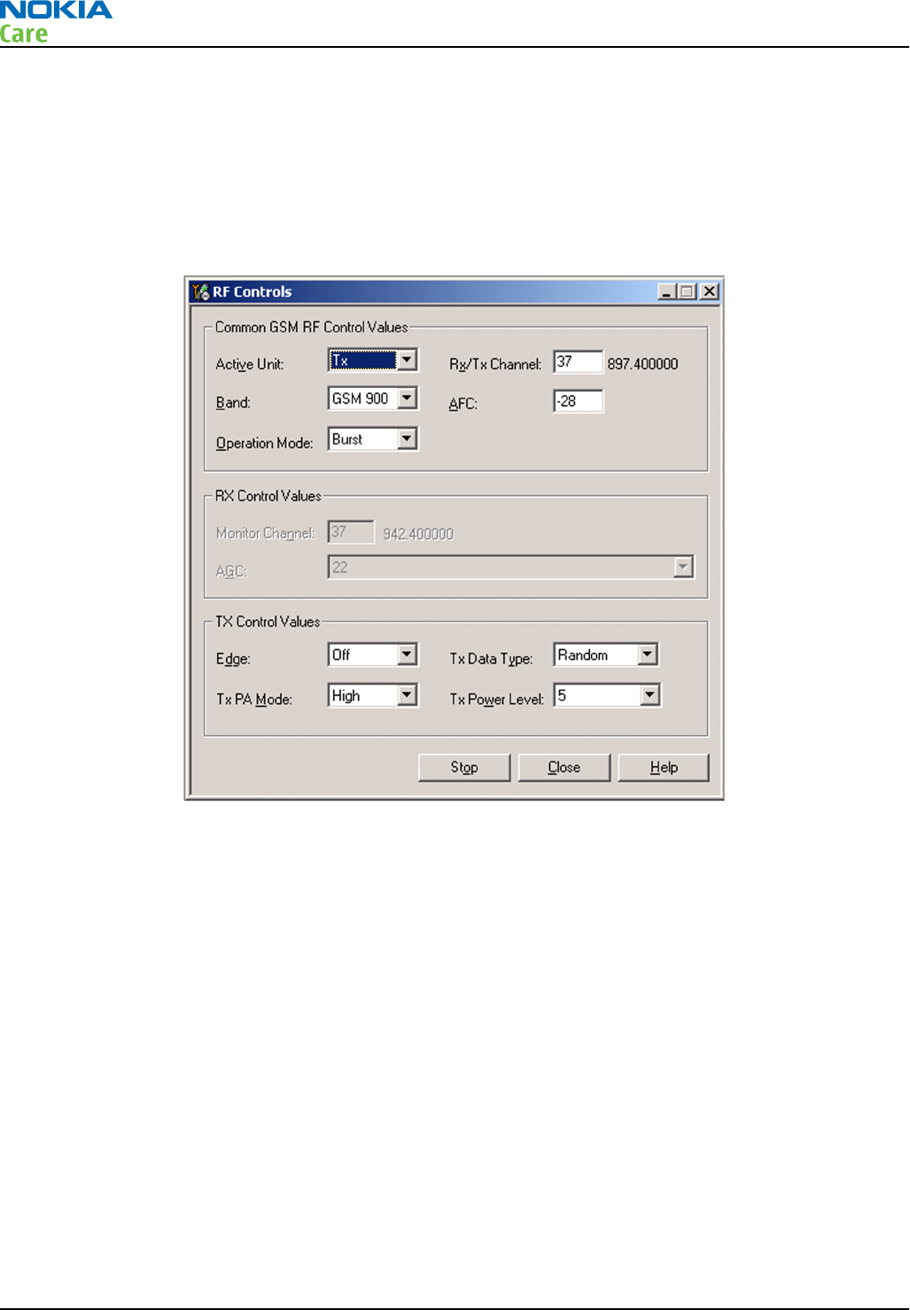
GSM transmitter troubleshooting
Steps
1. Set the phone to local mode.
2. Activate RF controls in Phoenix ( Testing → GSM → Rf Controls ).
Make settings as shown in the figure:
Figure 44 Phoenix GSM RF controls window
3. Check the basic TX parameters (i.e. power, phase error, modulation and switching spectrum), using a
communication analyser (for example CMU200).
RM-612; RM-624
RF Troubleshooting
Page 4 – 26 COMPANY CONFIDENTIAL Issue 1
Copyright © 2010 Nokia. All rights reserved.
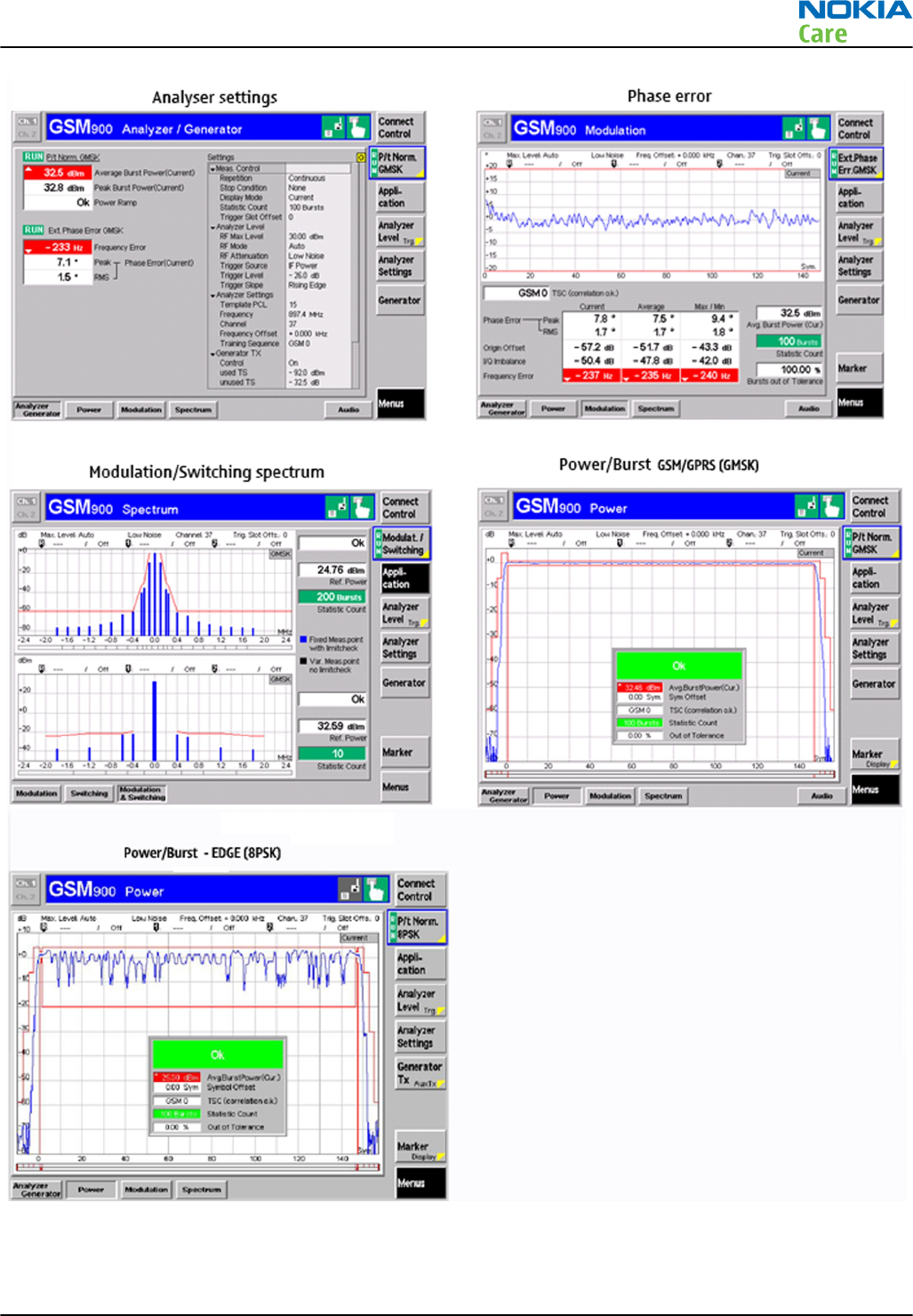
4. Change power level (RF controls) and make sure the power reading follows accordingly.
RM-612; RM-624
RF Troubleshooting
Issue 1 COMPANY CONFIDENTIAL Page 4 – 27
Copyright © 2010 Nokia. All rights reserved.
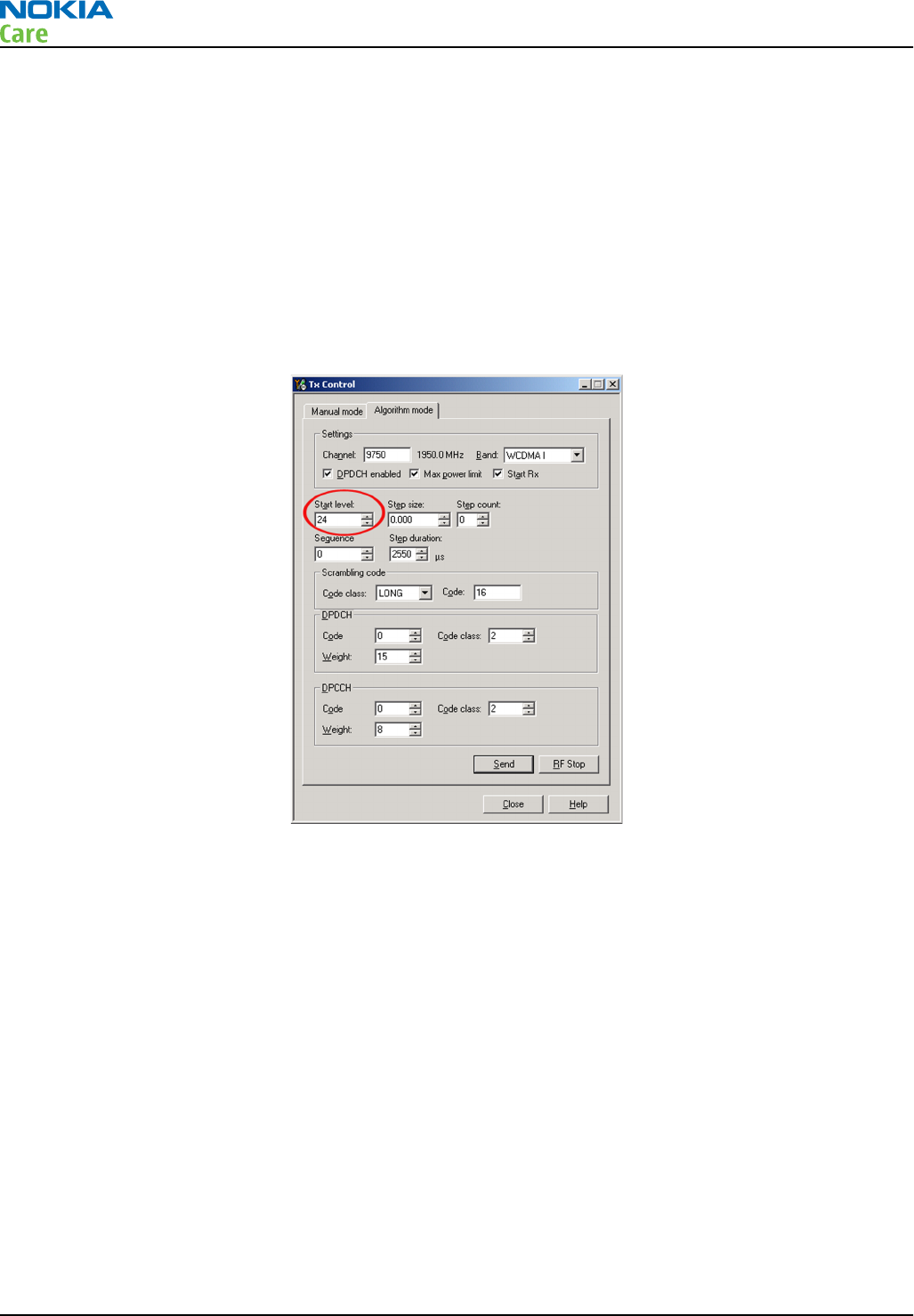
Next actions
If you want to troubleshoot the other bands, change band with RF controls and set the communication
analyser accordingly.
WCDMA transmitter troubleshooting
Steps
1. Set the phone to local mode.
2. In Phoenix, select Testing → WCDMA → TX control .
3. In the TX control window, make settings as in the picture:
Note: For WCDMA TX channels: band V 4183, VIII 2787
4. Click Send to enable the settings and activate TX.
If settings are changed (eg. new channel), you have to click RF Stop and Send again.
5. Check the basic TX parameters using a communication analyzer (for example CMU200).
RM-612; RM-624
RF Troubleshooting
Page 4 – 28 COMPANY CONFIDENTIAL Issue 1
Copyright © 2010 Nokia. All rights reserved.
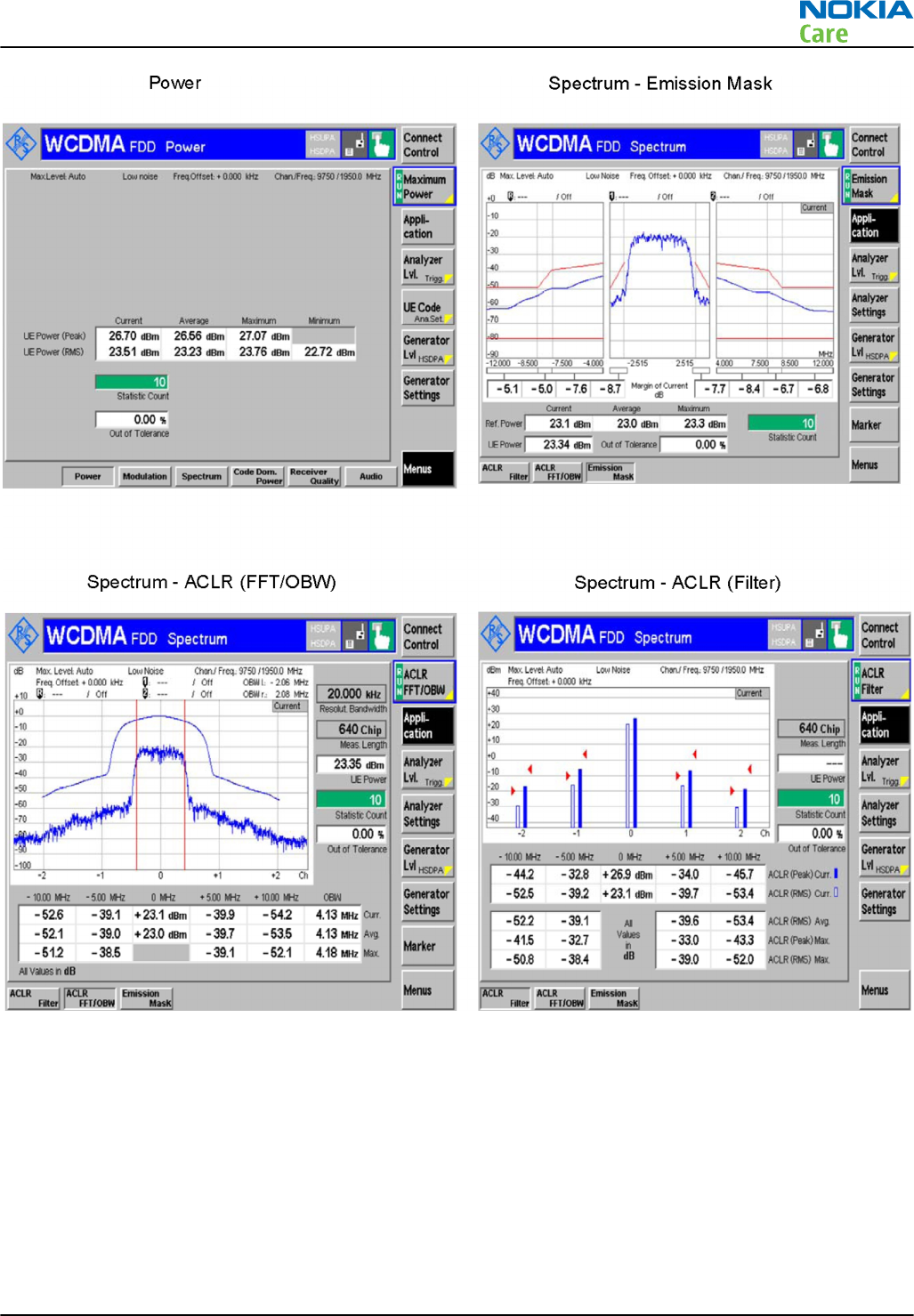
Next actions
If you want to troubleshoot the other bands, change band with RF controls and set the communication
analyser accordingly.
RM-612; RM-624
RF Troubleshooting
Issue 1 COMPANY CONFIDENTIAL Page 4 – 29
Copyright © 2010 Nokia. All rights reserved.
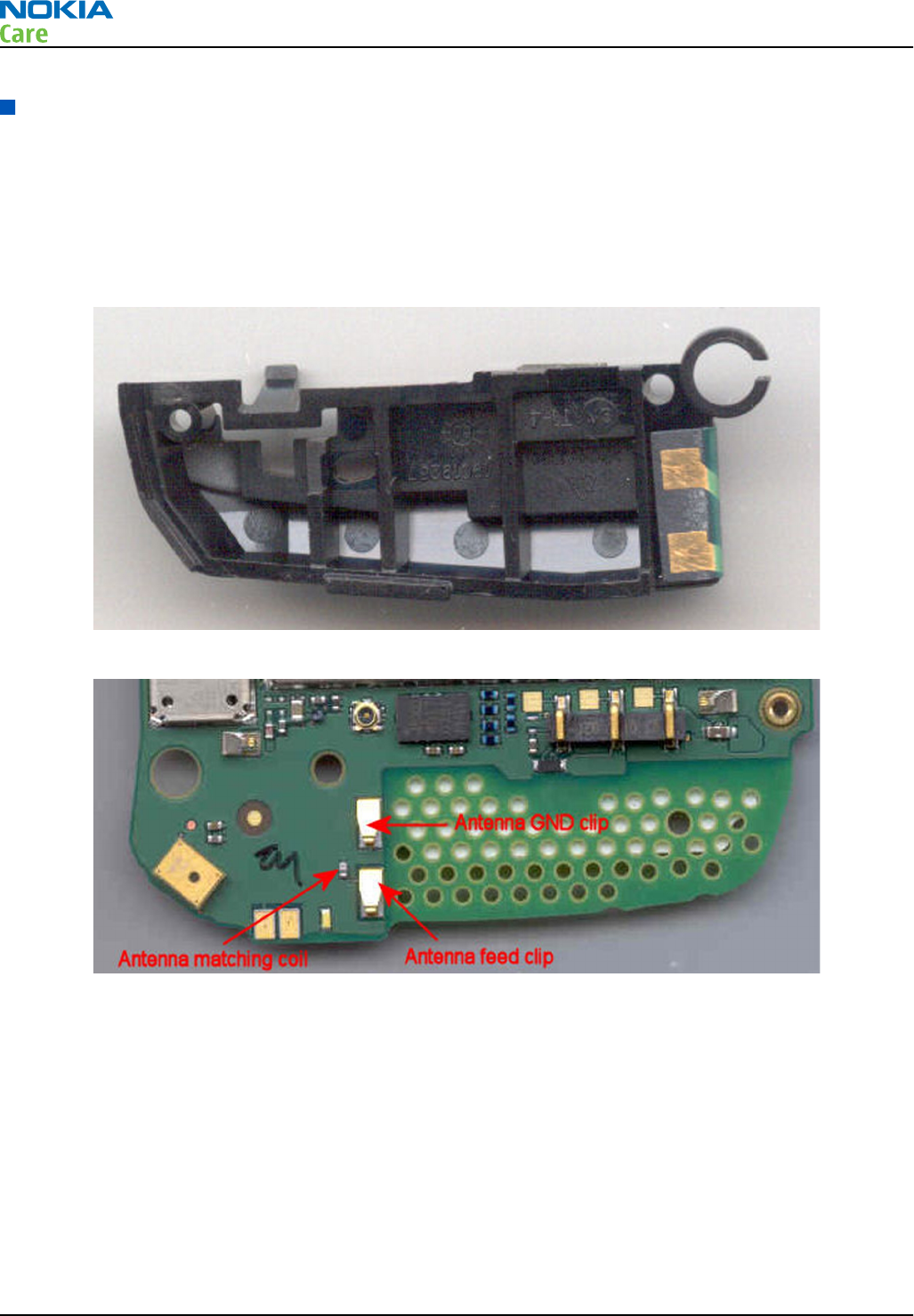
Antenna troubleshooting
Antenna troubleshooting
Antenna contacts and matching components, visual check
In the main antenna there is one feed and one GND contact. Check that the GND and feed pads take proper
contact to the C-clips on the main PWB. There is a matching coil (L7599) on the PWB. Check that it is properly
soldered on the PWB. In case there is damage, you need to replace the component.
Figure 45 Antenna contacts
Figure 46 Antenna contact clips and matching coil on the PWB
RM-612; RM-624
RF Troubleshooting
Page 4 – 30 COMPANY CONFIDENTIAL Issue 1
Copyright © 2010 Nokia. All rights reserved.

5 — System Module and User
Interface
Nokia Customer Care
Issue 1 COMPANY CONFIDENTIAL Page 5 – 1
Copyright © 2010 Nokia. All rights reserved.

RM-612; RM-624
System Module and User Interface
(This page left intentionally blank.)
Page 5 – 2 COMPANY CONFIDENTIAL Issue 1
Copyright © 2010 Nokia. All rights reserved.

Table of Contents
Introduction........................................................................................................................................................... 5–7
Phone description ............................................................................................................................................ 5–7
Energy management............................................................................................................................................. 5–9
Battery and charging ....................................................................................................................................... 5–9
Backup battery............................................................................................................................................... 5–10
Normal and extreme voltages ..................................................................................................................... 5–10
Battery drains fast troubleshooting............................................................................................................ 5–11
Power key and system power-up................................................................................................................ 5–11
Power distribution........................................................................................................................................ 5–12
Clocking scheme............................................................................................................................................ 5–13
Bluetooth and FM RDS radio module................................................................................................................ 5–14
I/O Expander ....................................................................................................................................................... 5–15
GPS interface....................................................................................................................................................... 5–16
WLAN interface ................................................................................................................................................... 5–19
High-speed USB................................................................................................................................................... 5–19
CBUS interface..................................................................................................................................................... 5–20
FBUS interface..................................................................................................................................................... 5–20
ECI interface ........................................................................................................................................................ 5–20
SIM interface ....................................................................................................................................................... 5–20
MicroSD card interface ....................................................................................................................................... 5–21
Camera concept .................................................................................................................................................. 5–22
Camera concept............................................................................................................................................. 5–22
User interface...................................................................................................................................................... 5–23
Resistive touch screen .................................................................................................................................. 5–23
Proximity sensor ...................................................................................................................................... 5–23
Touch screen controller........................................................................................................................... 5–24
Display ............................................................................................................................................................ 5–25
Display ............................................................................................................................................................ 5–25
Backlight and illumination........................................................................................................................... 5–26
Digital Ambient Light Sensor (ALS) ............................................................................................................. 5–27
Hall sensor...................................................................................................................................................... 5–28
ASICs..................................................................................................................................................................... 5–28
RAPIDOYAWE ................................................................................................................................................. 5–28
EM ASIC BETTY N2300 .................................................................................................................................... 5–28
EM ASIC VILMA N2200 .................................................................................................................................... 5–29
Device memories................................................................................................................................................ 5–29
Combo memory ............................................................................................................................................. 5–29
Audio concept..................................................................................................................................................... 5–29
Audio HW architecture.................................................................................................................................. 5–29
Internal microphone..................................................................................................................................... 5–30
Internal earpiece........................................................................................................................................... 5–30
Internal speaker ............................................................................................................................................ 5–31
Vibra circuitry ................................................................................................................................................ 5–31
Accessory AV connector ................................................................................................................................ 5–31
DA converter and headphone amplifier...................................................................................................... 5–32
Baseband technical specifications.................................................................................................................... 5–33
External interfaces ........................................................................................................................................ 5–33
SIM IF connections......................................................................................................................................... 5–33
Charging IF electrical characteristics........................................................................................................... 5–33
Internal interfaces......................................................................................................................................... 5–33
RM-612; RM-624
System Module and User Interface
Issue 1 COMPANY CONFIDENTIAL Page 5 – 3
Copyright © 2010 Nokia. All rights reserved.

Back-up battery interface electrical characteristics................................................................................... 5–34
RF technical description..................................................................................................................................... 5–34
RF block diagram........................................................................................................................................... 5–34
Receiver (RX).................................................................................................................................................. 5–35
Transmitter (TX) ............................................................................................................................................ 5–35
Frequency mappings.......................................................................................................................................... 5–36
GSM850 frequencies...................................................................................................................................... 5–36
EGSM900 frequencies.................................................................................................................................... 5–36
GSM1800 frequencies.................................................................................................................................... 5–37
GSM1900 frequencies.................................................................................................................................... 5–39
WCDMA 2100 Rx frequencies........................................................................................................................ 5–40
WCDMA 2100 Tx frequencies ........................................................................................................................ 5–41
WCDMA II (1900) frequencies....................................................................................................................... 5–42
WCDMA VIII (900) frequencies...................................................................................................................... 5–43
WCDMA V (850) frequencies ......................................................................................................................... 5–48
List of Tables
Table 10 Nominal voltages................................................................................................................................ 5–10
Table 11 Average current consumption........................................................................................................... 5–11
Table 12 Charging IF electrical characteristics ................................................................................................ 5–33
Table 13 Back-up battery electrical characteristics ........................................................................................ 5–34
List of Figures
Figure 47 System module block diagram ........................................................................................................... 5–8
Figure 48 Board and module connections.......................................................................................................... 5–9
Figure 49 Battery pin order.................................................................................................................................. 5–9
Figure 50 Blade battery connector ................................................................................................................... 5–10
Figure 51 Small (right) and wide (left) charger plugs .................................................................................... 5–10
Figure 52 Power distribution............................................................................................................................ 5–12
Figure 53 Clocking scheme................................................................................................................................ 5–13
Figure 54 Bluetooth & FM radio block diagram .............................................................................................. 5–15
Figure 55 I/O expander...................................................................................................................................... 5–16
Figure 56 Keymatrix........................................................................................................................................... 5–16
Figure 57 Block diagram of the GPS system .................................................................................................... 5–18
Figure 58 WLAN module .................................................................................................................................... 5–19
Figure 59 HS USB block diagram....................................................................................................................... 5–20
Figure 60 SIM interface ...................................................................................................................................... 5–21
Figure 61 MicroSD card interface ...................................................................................................................... 5–21
Figure 62 Camera subsystem block diagram................................................................................................... 5–23
Figure 63 Proximity sensor and boot............................................................................................................... 5–23
Figure 64 Proximity sensor reference design and measurement points ..................................................... 5–24
Figure 65 Touch screen controller.................................................................................................................... 5–25
Figure 66 Display block diagram ...................................................................................................................... 5–26
Figure 67 Backlight control for HW keys.......................................................................................................... 5–27
Figure 68 Display backlighting system............................................................................................................. 5–27
Figure 69 Digital Ambient Light Sensor location ............................................................................................ 5–28
Figure 70 Digital Ambient light sensor schematics ........................................................................................ 5–28
Figure 71 Audio system block ........................................................................................................................... 5–30
Figure 72 Internal microphone......................................................................................................................... 5–30
Figure 73 Internal earpiece circuitry................................................................................................................ 5–31
RM-612; RM-624
System Module and User Interface
Page 5 – 4 COMPANY CONFIDENTIAL Issue 1
Copyright © 2010 Nokia. All rights reserved.

Figure 74 Internal speaker ................................................................................................................................ 5–31
Figure 75 Vibra circuitry .................................................................................................................................... 5–31
Figure 76 Accessory (AV) connector.................................................................................................................. 5–32
Figure 77 Accessory (AV) connector with DAC33 and TPA6130 audio enhancements ................................ 5–32
Figure 78 DA converter and headphone amplifier.......................................................................................... 5–32
Figure 79 RF block diagram using RF ASIC N7500 (with WCDMA VIII/II/I) .................................................... 5–34
Figure 80 RF block diagram using RF ASIC N7500 (with WCDMA V/II/I)........................................................ 5–35
RM-612; RM-624
System Module and User Interface
Issue 1 COMPANY CONFIDENTIAL Page 5 – 5
Copyright © 2010 Nokia. All rights reserved.

RM-612; RM-624
System Module and User Interface
(This page left intentionally blank.)
Page 5 – 6 COMPANY CONFIDENTIAL Issue 1
Copyright © 2010 Nokia. All rights reserved.
Introduction
Phone description
RAPIDOYAWE is the main digital baseband ASIC in the HW52. It contains functionality for both WCDMA and
GSM EDGE.
AVILMA is power management ASIC having voltage regulators and audio transceiver and BETTY is energy
management ASIC having charging switch and FBUS transceiver.
Memory components are internal COMBO 1 Gb/2 Gb and a card reader for MicroSD.
Function Description Item ref
EM ASIC AVILMAS N2200
BETTY N2300
System ASIC RAPIDOYAWE D2800
Memory Combo 1Gb DDR + 2Gb M3 D3000
Camera accelerator OMAP-DM500 N1400
Display controller Zonda N2460
Back-up battery RTC BACKUP CAPAC 3225 G2200
FM-radio with RDS BTHFMRD2.2 module N6000
Bluetooth BTHFMRD2.2 module N6000
WLAN WLAN Size 4.0b N6300
GPS GPS5350_ROM3.0 N6200
RF ASIC Vapaus N7500
GSM PA 850/900/1800/1900 N7520
WCDMA PA 850/900/1900/2100 N7540
Oscillator VCTCXO 38.4MHZ G7500
TCXO 38.4 MHz G6450
Crystal 32.768KHZ B2200
IO-expander BASIC IO Expander N2850
SIM card reader X2700
HS USB transceiver ISP1707 D3300
Accelerometer AHTI_A 3-AXIS N6501
RM-612; RM-624
System Module and User Interface
Issue 1 COMPANY CONFIDENTIAL Page 5 – 7
Copyright © 2010 Nokia. All rights reserved.
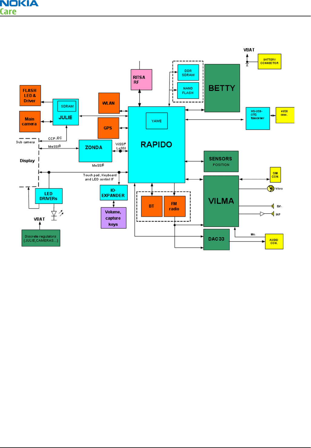
System module block diagram
Figure 47 System module block diagram
RM-612; RM-624
System Module and User Interface
Page 5 – 8 COMPANY CONFIDENTIAL Issue 1
Copyright © 2010 Nokia. All rights reserved.
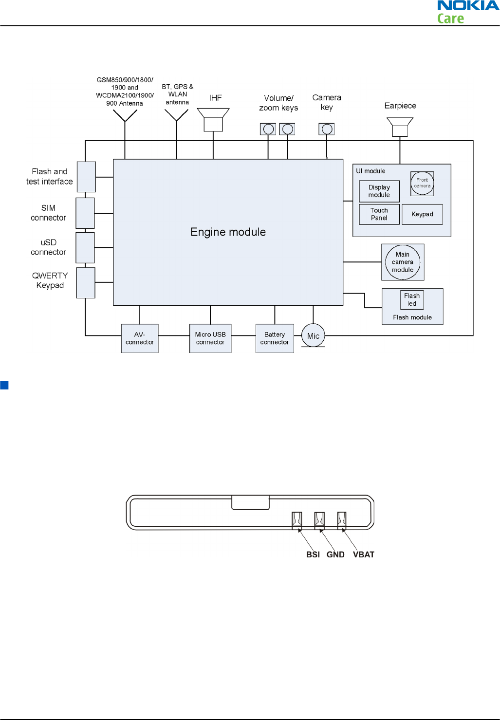
Board and module connections
Figure 48 Board and module connections
Energy management
Battery and charging
BL-4J battery
The phone is powered by a 3-pole BL-4J battery pack (1200 mAh). The three poles are named VBAT, BSI and
GND where the BSI line is used to recognize the battery capacity. This is done by means of an internal battery
pull down resistor.
Figure 49 Battery pin order
The battery temperature is estimated by measuring separate battery temperature NTC via the BTEMP line.
This is located on the main PWB, at the place where the phone temperature is closest to the battery
temperature.
Battery connector
The battery connector is a blade connector. It has three blades;
•BSI (Battery size indicator)
•GND (Ground)
RM-612; RM-624
System Module and User Interface
Issue 1 COMPANY CONFIDENTIAL Page 5 – 9
Copyright © 2010 Nokia. All rights reserved.
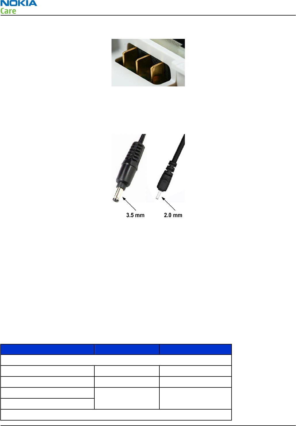
•VBAT (Battery voltage)
Figure 50 Blade battery connector
Charging
This phone is charged through the smaller Nokia standard interface (2.0 mm plug). The wider standard
charger (3.5 mm) can be used together with the CA-44 charger adapter.
Figure 51 Small (right) and wide (left) charger plugs
Charging is controlled by energy management, and external components are needed to protect the baseband
module against EMC, reverse polarity and transient frequency deviation.
Backup battery
When the main battery is not attached EM ASIC (N2200) goes in backup mode using back-up battery that
supplies voltage to RTC in EM ASIC (N2200).
Normal and extreme voltages
Energy management is mainly carried out in the two Application Specific Integrated Circuits (ASICs) BETTY
and AVILMA. These two circuits contains a number of regulators. In addition there are some external
regulators too.
In the table below normal and extreme voltages are shown when a BL-4J battery is used.
Table 10 Nominal voltages
Voltage Voltage [V] Condition
General Conditions
Nominal voltage 3.700
Lower extreme voltage 3.145
Higher extreme voltage
4.230(fast charging)
HW Shutdown Voltages
RM-612; RM-624
System Module and User Interface
Page 5 – 10 COMPANY CONFIDENTIAL Issue 1
Copyright © 2010 Nokia. All rights reserved.
Voltage Voltage [V] Condition
Vmstr+ 2.1 ± 0.1 Off to on
Vmstr- 1.9 ± 0.1 On to off
SW Shutdown Voltages
Sw shutdown 3.15 In call
Sw shutdown 3.3 In idle
Min Operating Voltage
Vcoff+ 2.9 ± 0.1 Off to on
Vcoff- 2.6 ± 0.1 On to off
Battery drains fast troubleshooting
Table 11 Average current consumption
Use case Current
consumption
Video call 540mA
Video streaming HSDPA QVGA
Mpeg4 30fps BT hs 510mA
Video recording 640x352 30fps 400mA
Video playback 640x352 30fps 340mA
WCDMA voice call 250mA
Power key and system power-up
This device has no separate power key. The power key is the same as the end key. When the battery is placed
in the phone, the power/end key circuits are energized. When the power/end key is pressed, the system
boots up (if an adequate battery voltage is present).
Power down can be initiated by pressing the power/end key again (the system is powered down with the
aid of SW). The power/end key is connected to EM ASIC N2200 (AVILMA) via PWRONX signal.
The power/end key may be disabled in certain charging cases.
RM-612; RM-624
System Module and User Interface
Issue 1 COMPANY CONFIDENTIAL Page 5 – 11
Copyright © 2010 Nokia. All rights reserved.
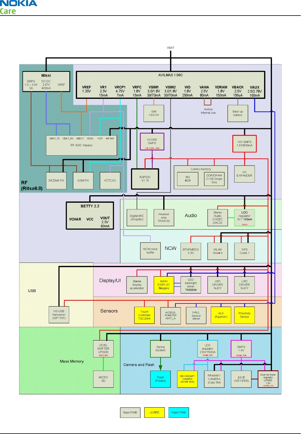
Power distribution
Figure 52 Power distribution
RM-612; RM-624
System Module and User Interface
Page 5 – 12 COMPANY CONFIDENTIAL Issue 1
Copyright © 2010 Nokia. All rights reserved.
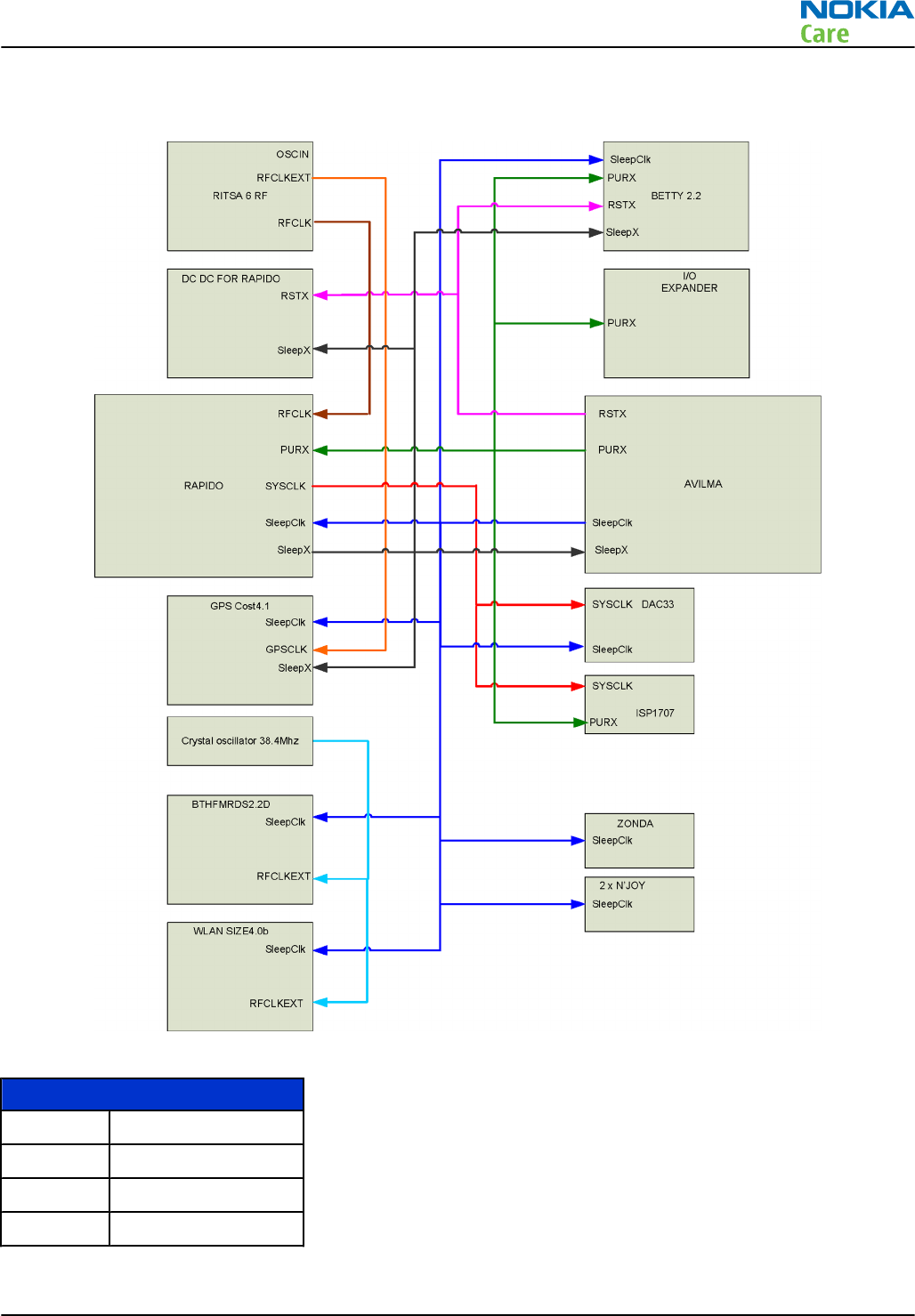
Clocking scheme
Figure 53 Clocking scheme
Engine clocks
RFCLK 38.4 MHz
SleepClk 32.768kHz
RFCLKEXT 38.4 MHz
SYSCLK 19.2 MHz
RM-612; RM-624
System Module and User Interface
Issue 1 COMPANY CONFIDENTIAL Page 5 – 13
Copyright © 2010 Nokia. All rights reserved.

Bluetooth and FM RDS radio module
Bluetooth and FM radio receiver are provided by the same ASIC (Broadcom BCM2048). The device supports
Bluetooth operation and FM radio rececption in both European/USA and Japanese bands (the appropriate
region-specific FM radio band is pre-configured in the phone software). The UART interface allows the device
to communicate with the phone baseband engine using Bluetooth HCI commands. Commands to the FM radio
can also be sent over the I2C interface.
When Bluetooth is switched on, the phone user interface the BT_RESETX line is toggled to reset the Bluetooth
device, and commands are sent over the UART interface to configure the device. If UART communication fails
(due to a hardware fault) it will not be possible to switch on Bluetooth from the phone user interface.
The device has two clock signals: SYS_CLK (19.2MHz, 26.0MHz, or 38.4MHz supported) and SLEEP_CLK
(32.768kHz). The SLEEP_CLK is supplied all the time the phone is switched on. To maximise the phone standby
time, it is only necessary to provide a SYS_CLK signal when Bluetooth activity occurs, such as sending Bluetooth
data to another device, or checking periodically if there are any other Bluetooth devices attempting to
communicate with it. At other times when the Bluetooth device is in standby mode or the FM radio is switched
on it is only necessary to provide a SLEEP_CLK signal. The Bluetooth-FM ASIC is powered directly from the
phone battery voltage line (VBAT). An internal regulator is enabled when Bluetooth or FM radio is switched
on.
Bluetooth audio signals are sent to and from the device using a PCM interface. The Bluetooth RF signal is
routed via a buried track to the Bluetooth antenna on the side of the PWB. An RF filter is needed between
the Bluetooth antenna and Bluetooth ASIC to prevent interference to and from the celluar phone antenna.
Phones that have both Bluetooth and WLAN use a shared antenna, as both services occupy the 2.4GHz ISM
frequency band. The co-existence signaling interface between Bluetooth and WLAN ASICs controls the RF
activity in the shared frequency band.
The audio signal from the FM radio is routed via the phone Audio ASIC to the phone headset or loudspeaker.
The external wired headset is also used as an Antenna for the FM radio. The FM radio receiver RF signal is
routed from the ASIC via a buried track to an impedance matching circuit placed near the headset connector.
The following block diagram shows how Bluetooth-FM is connected to the host engine.
RM-612; RM-624
System Module and User Interface
Page 5 – 14 COMPANY CONFIDENTIAL Issue 1
Copyright © 2010 Nokia. All rights reserved.
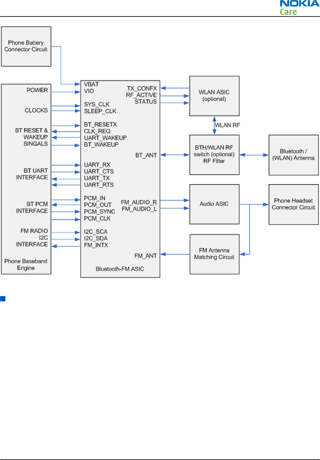
Figure 54 Bluetooth & FM radio block diagram
I/O Expander
I/O Expander is used for control signals that are not time critical, such as for keyboard inputs, enable & reset
signals etc. It is connected to the I2C bus, and has its own interrupt. PURX is used as the I/O Expander’s reset.
The I/O Expander is powered from VIO 1.8V.
This device has a keyboard matrix. The keys are connected to the I/O expander.
RM-612; RM-624
System Module and User Interface
Issue 1 COMPANY CONFIDENTIAL Page 5 – 15
Copyright © 2010 Nokia. All rights reserved.
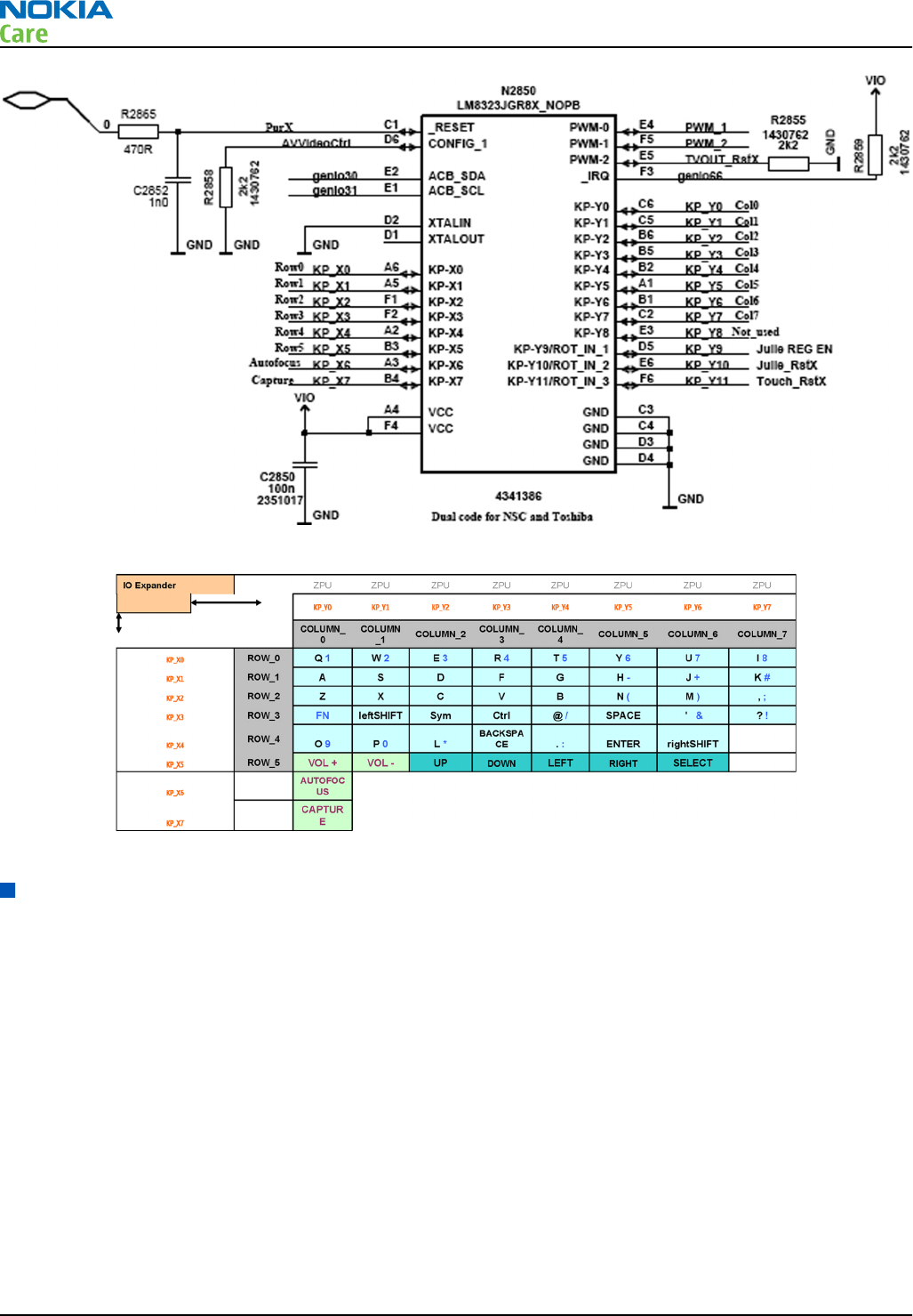
Figure 55 I/O expander
Figure 56 Keymatrix
GPS interface
Functional description
The device includes an inbuilt GPS receiver and it works as a stand-alone positioning device.
The GPS solution provides a full GPS HW and SW engine for devices capable of operation in all GPS modes:
•Autonomous (standalone) - no communication with network is required for GPS fix
•MS based - the device receives aiding information from the network and computes fix internally
•MS assisted - the device receives aiding information from the network and computes pseudorange
measurements. The measurements are then sent back to the network for the fix calculation.
At the heart of the GPS solution is GPS5350 GPS receiver IC, which has GPS RF receiver and GPS BB processor
integrated into a single IC. RF section performs down conversion, filtering and IF sampling, whereas BB
section contains an enhanced version of multimode GPS with twelve hardware matched filters, post detection
logic and an ARM controller core.
The features of the GPS solution include:
•12 channels
RM-612; RM-624
System Module and User Interface
Page 5 – 16 COMPANY CONFIDENTIAL Issue 1
Copyright © 2010 Nokia. All rights reserved.

•Integrated regulators for RF and BB (including external LNA)
•Direct connection to a battery
•Fast clock calibration through availability of 261MHz clock from RF PLL
•Improved tracking and Hot start (TTFF) reacquisition performance
•Advanced Power Management and Host Wakeup capability.
The I2C interface handles data transfer between GPS and the Rapido. GPS uses the CE RF system clock to
calibrate its own GPS Clk.
GPS has three clock sources:
•16.368MHz clock from a dedicated TCXO (G6200)
•38.4MHz reference clock from Ahneus RF ASIC
•32.768kHz Sleepclk
The GPS module is powered from VIO 1.8V and VBAT.
Block diagram
The following block diagram shows how the GPS module is connected to the host side.
RM-612; RM-624
System Module and User Interface
Issue 1 COMPANY CONFIDENTIAL Page 5 – 17
Copyright © 2010 Nokia. All rights reserved.
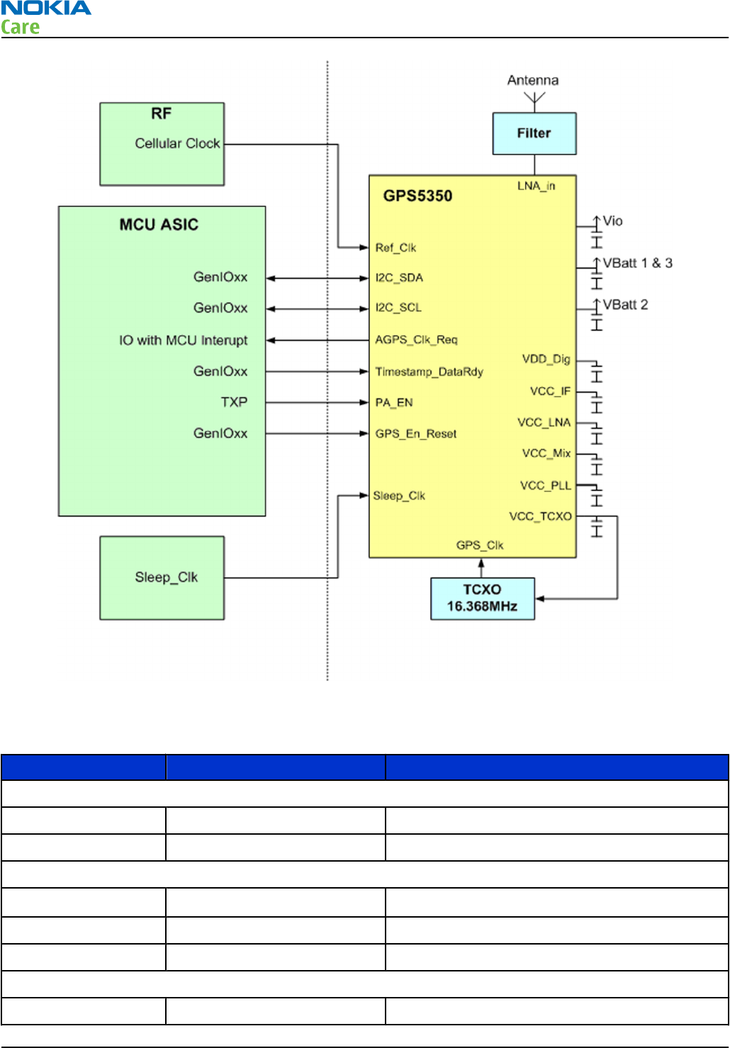
Figure 57 Block diagram of the GPS system
Interface signals
Signal name I/O Function
RF
ANT_GPS I GPS antenna port
LNA_In I GPS ASIC RF input
Clocking
REF_CLK I Reference Clock = RF Cellular clock, Min 0.2Vpk-pk
GPS_CLK I Connection of 16.368MHz GPS TCXO
RTC_CLK I Cellular engine 32768 Hz sleep clock
Control
GPS_EN_RESET I GPS engine reset
RM-612; RM-624
System Module and User Interface
Page 5 – 18 COMPANY CONFIDENTIAL Issue 1
Copyright © 2010 Nokia. All rights reserved.
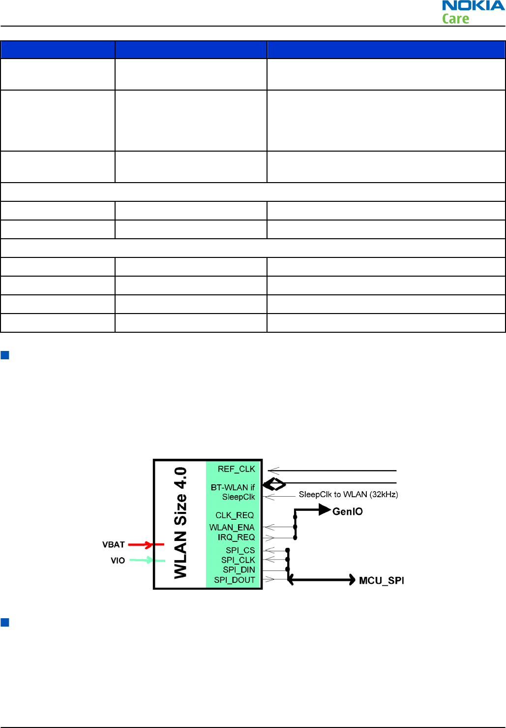
Signal name I/O Function
AGPS_CLK_REQ O MCU Interrupt when GPS requires CE to be awake
(Host Wakeup)
IO_TIMESTAMP_DATAR
DY
I Strobe for accurately marking in real time,
timing information from the cellular engine.
DATARDY indication to download code through
synchronous operation from cellular engine.
IO_PA_EN I Used to implement PA blanking when cellular PA
is ON
Comms
I2C_SCL_U1TX B I2C clk line
I2C_SDA_U1RX B I2C data line
Power
VDDS P Cellular engine I/O supply
VBatt 1 & 3 P Phone battery power or SMPS power
VBatt 2 P Phone battery power
VSS P Ground plane
WLAN interface
The phone contains a WLAN transceiver that provides a fully integrated wireless radio solution. The WLAN
transceiver supports the IEEE 802.11 standards for low error rate data transfer between mobiles and WLAN
networks. Data rates up to 54Mbps are possible in 802.11g mode of operation. WLAN shares the antenna
with Bluetooth.
The WLAN software is downloaded from the host engine when WLAN is turned on, over the dedicated SPI
interface. The WLAN and Bluetooth co-existence is supported via BTH-WLAN interface.
Figure 58 WLAN module
High-speed USB
High-speed USB
The device can transmit and receive USB data at high-speed (480 Mbit/s), full-speed (12 Mbit/s) and low-
speed (1.5Mbit/s). The external interface is the micro-B connector X3300. The interface between D3300 USB
transceiver and micro-B receptacle is the standard USB interface specified in the Universal Serial Bus
specification Rev. 2.0. The USB transfers signal and power over four-wire interface, which carries differential
RM-612; RM-624
System Module and User Interface
Issue 1 COMPANY CONFIDENTIAL Page 5 – 19
Copyright © 2010 Nokia. All rights reserved.
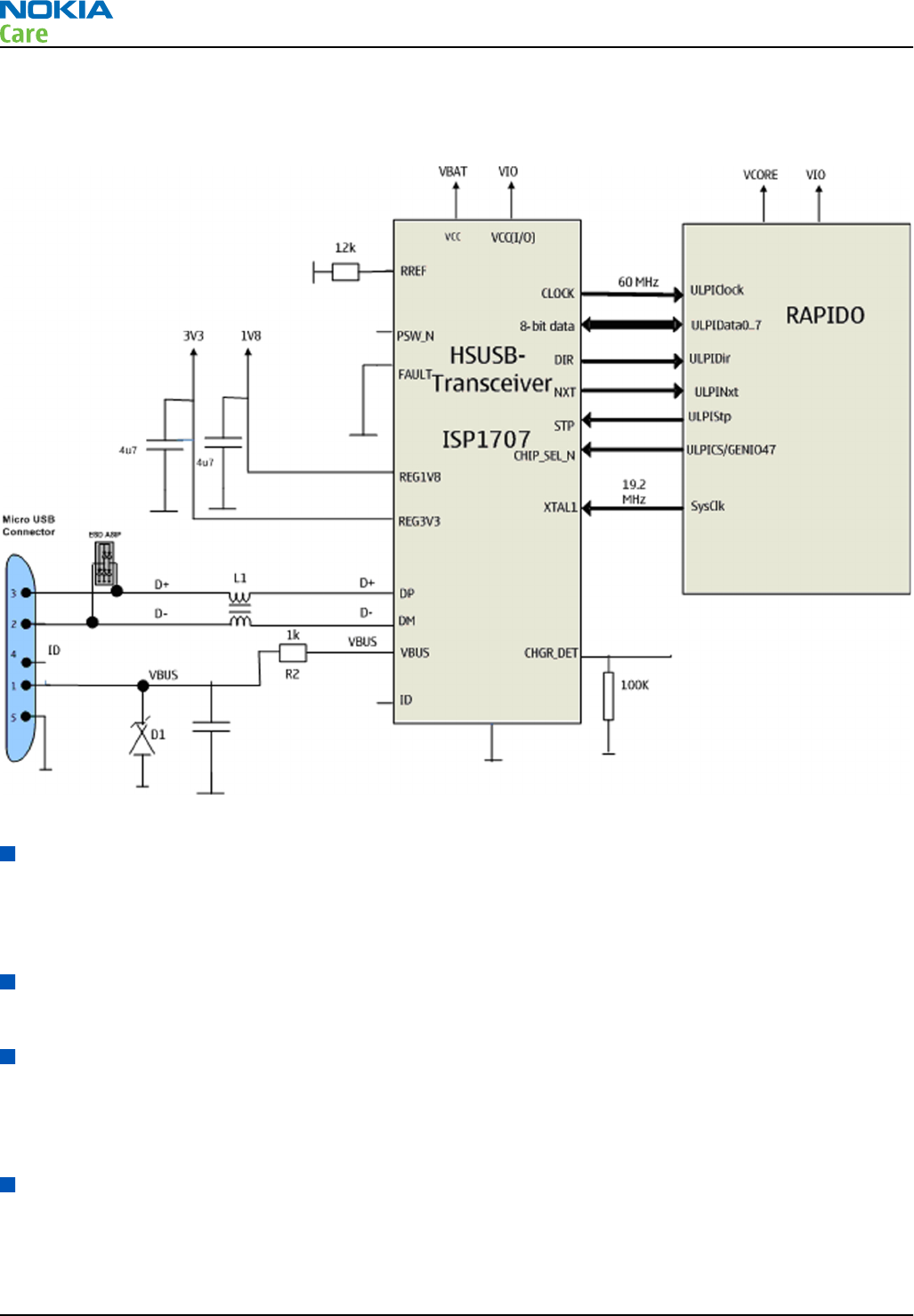
data, Vbus and GND. Signalling occurs over differential data line D+ and D-. The clock is transmitted encoded
along with the differential data. ESD protection is done with USB ASIP Z3300. VBUS (+5V) is provided by the
host device. The circuit is protected from an overvoltage condition by reference zenner diode V3301.
Figure 59 HS USB block diagram
CBUS interface
CBUS is a main system control bus in BB5. RAPIDO controls the functionality of EM ASICs AVilma (N2200) and
Betty (N2300) with CBUS.
CBUS is a four-wire half-duplex master-slave interface. In HW52 CBUS clock frequency is 4.39 MHz.
FBUS interface
FBUS is a 2-wire serial communication bus between HW52 engine and service SW.
ECI interface
The ECI (Enhancement Control Interface) is a point-to-point, bi-directional, single line serial bus.
The purpose of the ECI is to identify and authenticate the accessory, and to act as a data bus (intended for
control purposes) between the phone and the accessory .
SIM interface
The device has one SIM (Subscriber Identification Module) interface. It is only accessible if battery is removed.
The SIM interface consists of an internal interface between RAPIDO and EM ASIC (N2200), and of an external
interface between N2200 and SIM contacts.
RM-612; RM-624
System Module and User Interface
Page 5 – 20 COMPANY CONFIDENTIAL Issue 1
Copyright © 2010 Nokia. All rights reserved.
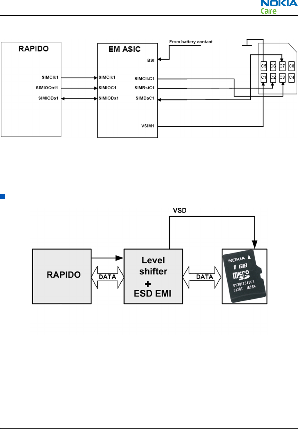
The SIM IF is shown in the following figure:
Figure 60 SIM interface
The EM ASIC handles the detection of the SIM card. The detection method is based in the BSI line. Because of
the location of the SIM card, removing the battery causes a quick power down of the SIM IF.
The EM ASIC SIM1 interface supports both 1.8 V and 3.0 V SIM cards. The SIM interface voltage is first 1.8 V
when the SIM card is inserted, and if the card does not response to the ATR a 3 V interface voltage is used.
MicroSD card interface
Figure 61 MicroSD card interface
The MicroSD card is connected to the engine by an external level shifter with an ESD protection filter. Supplied
voltages:
•VSD: 2.85 V (from level shifter)
•VIO: 1.8 V (from VIO SMPS)
Hot swap is supported, which means that the card may be plugged in/out at any time, without removing the
battery.
RM-612; RM-624
System Module and User Interface
Issue 1 COMPANY CONFIDENTIAL Page 5 – 21
Copyright © 2010 Nokia. All rights reserved.

Camera concept
Camera concept
Camera subsystem concept
The camera subsystem contains the complete imaging system for the main 5 Mpixel camera. The main
features of the imaging and video baseband subsystem are
•Hardware acceleration for image processing
•Support for 5 MPixel main camera
•Support for secondary VGA camera module
•Support for flash LEDs and its driver from ADI
Key components
•DM5001D processor
Imaging Video baseband is implemented using DM5001D processor. DM5001D processor is a hardware
accelerator for Imaging and Video application. This processor controls all the cameras and flashes in the
system.
This processor is controlled by Rapido processors via SPI interface. Boot code is downloaded into DM5001D
internal memory via the SPI interface at power on. Further application code (self-test, image capture, video
capture) is transferred depending on the usage case.
Video and still image data is passed to the Rapido for display and storage after processing over a CCP bus
(CCP_CMT).
•Primary camera module (5 Mpixel camera)
The camera module is a SMIA95 compliant and is configured by the DM5001D using I2C control bus. Image
data is transferred to the DM5001D over a CCP balanced bus (HIRES_CCP)
•Secondary VGA camera module
The camera module is electrically a SMIA compliant module (not mechanically) and is configured by the
DM5001D using I2C control bus. Image data is transferred to the DM5001D over a CCP balanced bus
(LORES_CCP)
•Flash LED
The camera flash LED is controlled from the DM5001D via the ADP1653 driver. The driver has GPIO control
for STROBE/ENABLE and I2C bus control for configuring.
Powering
The camera subsystem is powered from 1.3V, 1.8V and 2.8V discrete regulators. The 1.3V regulator is powered
from 1.8V regulator. The 1.8V and 2.8V regulators are powered from VBAT. The LED driver is powered directly
from the VBAT supply. These supplies are turned off/on by the host processor using the GPIO (Julie_REG_EN),
depending on the camera usage.
Block diagram
The high-level camera subsystem block diagram is presented in the following figure:
RM-612; RM-624
System Module and User Interface
Page 5 – 22 COMPANY CONFIDENTIAL Issue 1
Copyright © 2010 Nokia. All rights reserved.
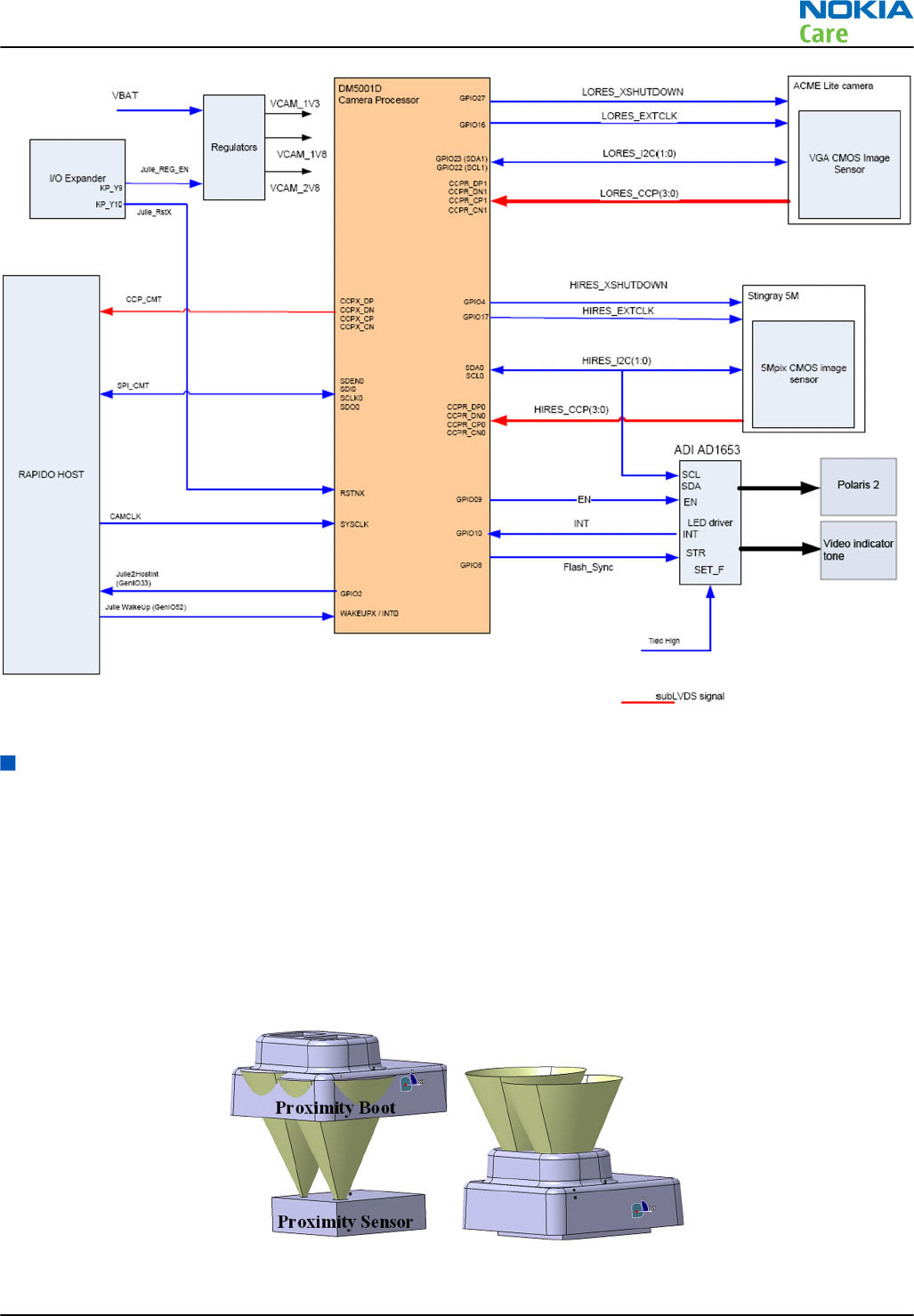
Figure 62 Camera subsystem block diagram
User interface
Resistive touch screen
Proximity sensor
The proximity sensor is used to turn off the touch input, when the phone is against user’s ear during call.
This prevents accidental touch signals that could happen when, for example, user’s cheek touches the phone.
The main parts of the proximity sensor subsystem are:
•Proximity sensor
•Proximity boot (mechanical part)
Figure 63 Proximity sensor and boot
RM-612; RM-624
System Module and User Interface
Issue 1 COMPANY CONFIDENTIAL Page 5 – 23
Copyright © 2010 Nokia. All rights reserved.
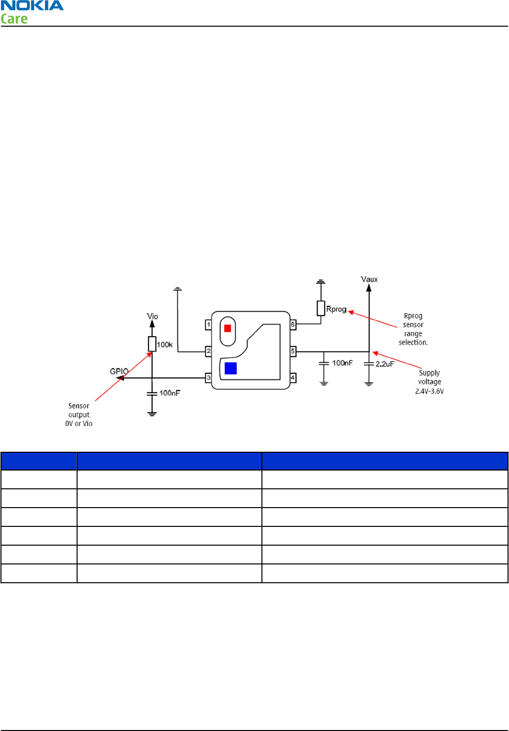
The proximity sensor is located on the upper flex assembly.
Features
The Proximity sensor has following features:
•2.8V
•1.8V compatible IOs
•Low power consumption
•20 mm working area
•Factory calibrated, no calibration required in care
•Pb free/RoHS compliancy
The proximity sensor works by sending out a beam of IR light, and then computing the distance to any nearby
objects from characteristics of the returned (reflected) signal. When the object is under 20 mm distance
detection will happen and output will go to high state (1.8V).
Reference design
Figure 64 Proximity sensor reference design and measurement points
Pin Signal name Description
1 Anode LED No connection
2 GND Ground
3 OUT Sensor output (0V or 1.8V Push-Pull)
4 TEST No connection
5 VCC Supply voltage (2.4V - 2.8V)
6 Rprog Program resistor
Touch screen controller
TSC2004 (N8105 0n UI-flex) is a touch screen controller for resistive touch pads. It contains a complete
ultralow-power, 12-bit, analog-to-digital (A/D) resistive touch screen converter, including drivers and control
logic to measure touch pressure.
It also has embedded pre-processing function to reduce the output bus load. The host interface in TSC2004
is I2C.
RM-612; RM-624
System Module and User Interface
Page 5 – 24 COMPANY CONFIDENTIAL Issue 1
Copyright © 2010 Nokia. All rights reserved.
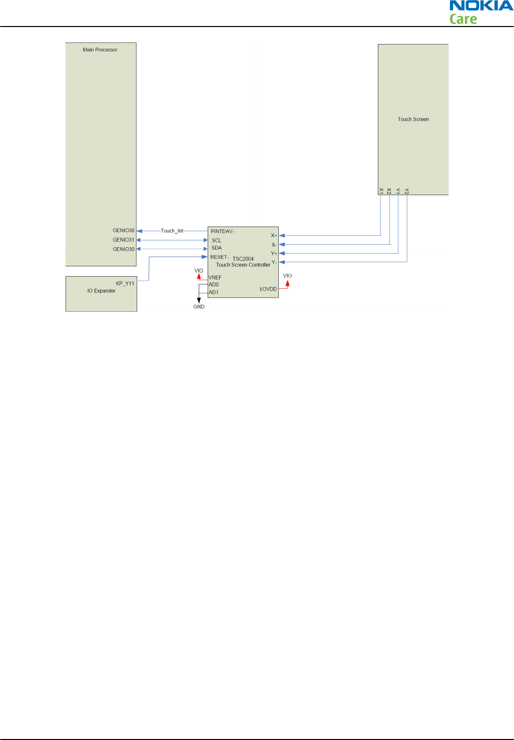
Figure 65 Touch screen controller
Display
Display
Rapido has an external display buffer with 8Mbit display RAM. The input interfaces for display buffer are
ViSSI-12 for image data and LoSSI for commands.
The data interface between display buffer and display is CDP (Compact Display Port), display commands are
sent by LoSSI interface. The display backlight control is controlled by the display.
RM-612; RM-624
System Module and User Interface
Issue 1 COMPANY CONFIDENTIAL Page 5 – 25
Copyright © 2010 Nokia. All rights reserved.
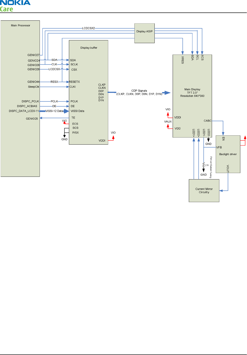
Figure 66 Display block diagram
Backlight and illumination
This device has two backlighting systems; one for the display and one for the HW keys and other illumination
zones.
Backlighting for HW keys
The L5521 LED contoller is used for backlightning the HW keys . There is one LP5521 in the reference HW
making it possible to have up to three LED zones. It can also drive the RGB LED.
RM-612; RM-624
System Module and User Interface
Page 5 – 26 COMPANY CONFIDENTIAL Issue 1
Copyright © 2010 Nokia. All rights reserved.
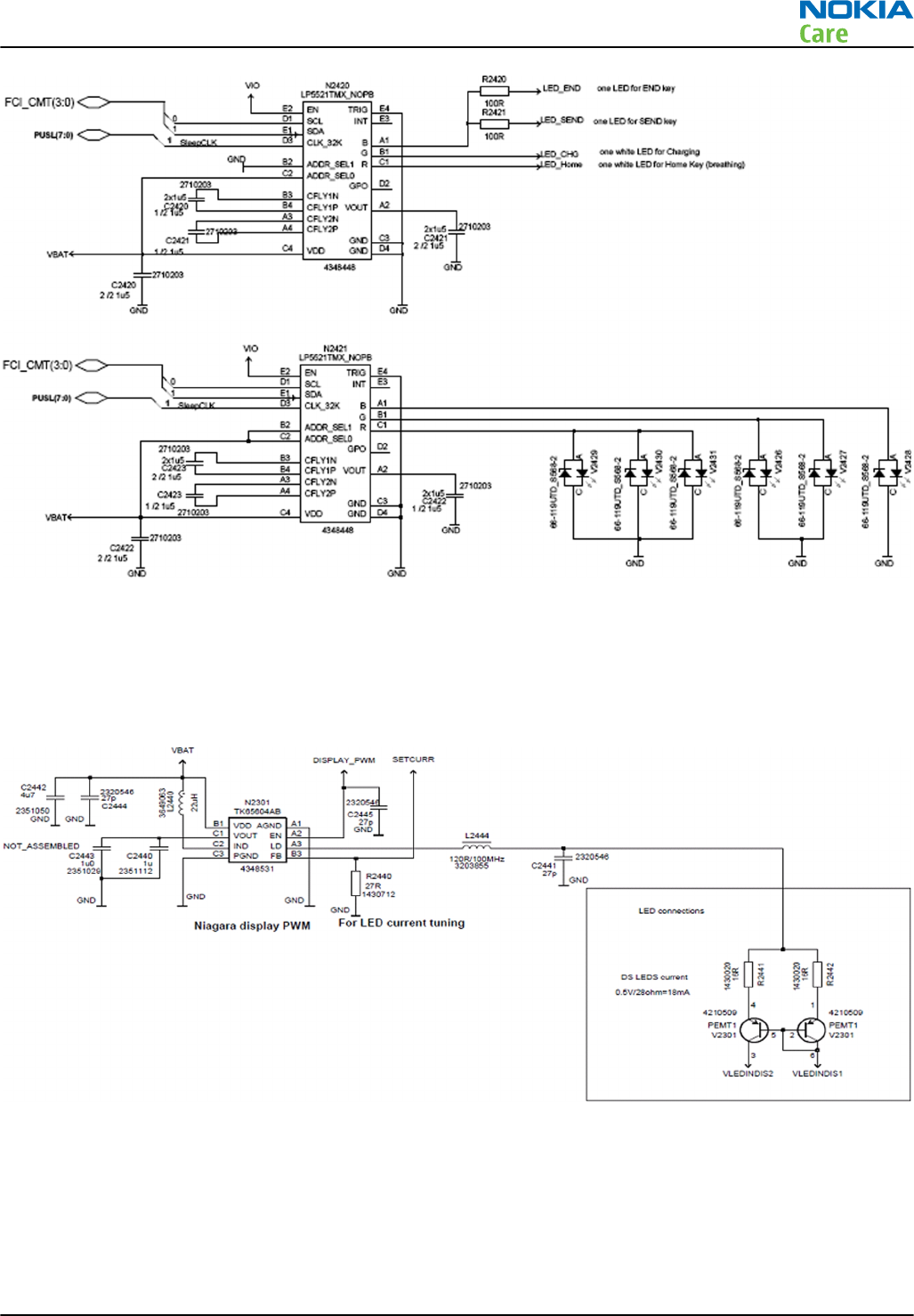
Figure 67 Backlight control for HW keys
Display backlights
Display backlights consist of two LED chains, each containing three LEDs in series powered by TK65604AB
switching mode power supply. Display backlight brightness is controlled by the CABC signal, and the equality
of the current (and thus the brightness) through the two LED chains is ensured by a current mirror.
Figure 68 Display backlighting system
Digital Ambient Light Sensor (ALS)
The Digital Ambient Light Sensor (N8104 on UI-Flex) approximates ambient light. Ambient light level together
with CABC and user settings adjust the display and keyboard illumination brightness. The Ambient Light
Sensor is located on the UI-Flex.
RM-612; RM-624
System Module and User Interface
Issue 1 COMPANY CONFIDENTIAL Page 5 – 27
Copyright © 2010 Nokia. All rights reserved.
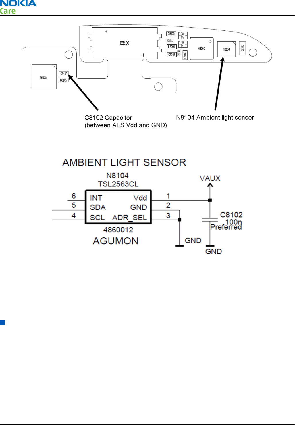
Figure 69 Digital Ambient Light Sensor location
It is connected to the I2C bus, and powered by the VOUT (2.5V) voltage.
Figure 70 Digital Ambient light sensor schematics
Hall sensor
The hall sensor system is comprised of a hall sensor in the lower part of the phone and a magnet in the upper
sliding/pivoting part of the phone.
When the sensor detects a magnet, the output is triggered and the phone changes mode from open to closed
accordingly.
ASICs
RAPIDOYAWE
RAPIDOYAWE ASIC (D2800) is a die-stacked Processor (RAPIDO) with 3G HDSPA logic (YAWE). RAM memory is
integrated into RAPIDO.
EM ASIC BETTY N2300
The EM ASIC (N2300) includes the following functional blocks:
•Core supply generation
•Charge control circuitry
•Level shifter and regulator for USB/FBUS
RM-612; RM-624
System Module and User Interface
Page 5 – 28 COMPANY CONFIDENTIAL Issue 1
Copyright © 2010 Nokia. All rights reserved.

•Current gauge for battery current measuring
•LED control for display backlighting
•Digital interface (CBUS)
EM ASIC VILMA N2200
The EM ASIC (N2200) includes the following functional blocks:
•Start up logic and reset control
•Charger detection
•Battery voltage monitoring
•32.768kHz clock with external crystal
•Real time clock with external backup battery
•SIM card interface
•Stereo audio codecs and amplifiers
•A/D converter
•Regulators
•Vibra interface
•Digital interface (CBUS)
EMC ASIP (Appcation Specified Integrated Passive) have been integrated inside the ASIC. It includes biasing
passives for microphone , EMC filter for SIM, microphones etc.
Device memories
Combo memory
The memory of the device consists of stacked DDR SDRAM and MuxedMassMemory (M3). Combo memory DDR/
M3 memory has 1Gb DDR + 2Gb M3.
Audio concept
Audio HW architecture
The functional core of the audio hardware is built around three ASICs: RAPIDOYAWE engine ASIC, mixed signal
ASIC Avilma and D/A converter DAC33.
DAC33 converts the digital audio signal to analog and is routed to the FM Transmitter and amplifier TPA6130
which provides an interface for the transducers and the accessory connector.
AVilma provides analog signal for the earpiece and for the D-class audio amplifier TPA2012D2, which drives
the integrated stereo handsfree speaker.
There are four audio transducers:
•5 x 10 mm dynamic earpiece
•One 8 x 12 mm dynamic speaker
•Digital microphone
Avilma provides an output for the dynamic vibra component. All wired audio accessories are connected to
the AV accessory connector. A Bluetooth audio and FM radio module, which is connected to RAPIDOYAWE,
supports the Bluetooth audio and FM radio functionality.
RM-612; RM-624
System Module and User Interface
Issue 1 COMPANY CONFIDENTIAL Page 5 – 29
Copyright © 2010 Nokia. All rights reserved.
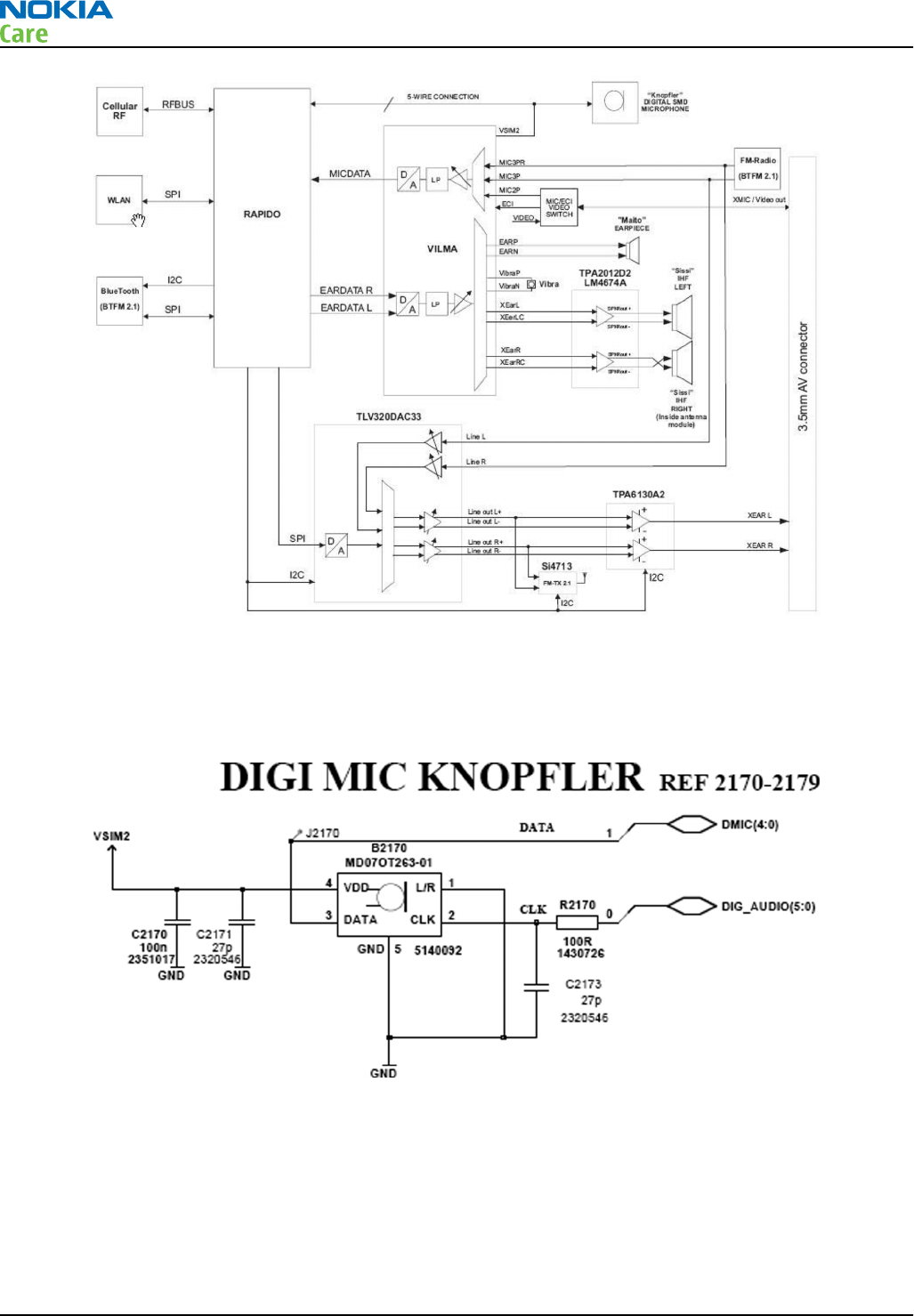
Figure 71 Audio system block
Internal microphone
The internal microphone is used for HandPortable (HP) and Internal HandsFree (IHF) call modes. A digital
microphone data and clock line are connected to Rapidoyawe and operating voltage is received from Avilma.
Figure 72 Internal microphone
Internal earpiece
Internal earpiece is used for the HandPortable (HP) call mode. A dynamic 5 x 10 mm earpiece capsule is
connected to Avilma ASIC’s differential output EarP and EarN.
RM-612; RM-624
System Module and User Interface
Page 5 – 30 COMPANY CONFIDENTIAL Issue 1
Copyright © 2010 Nokia. All rights reserved.
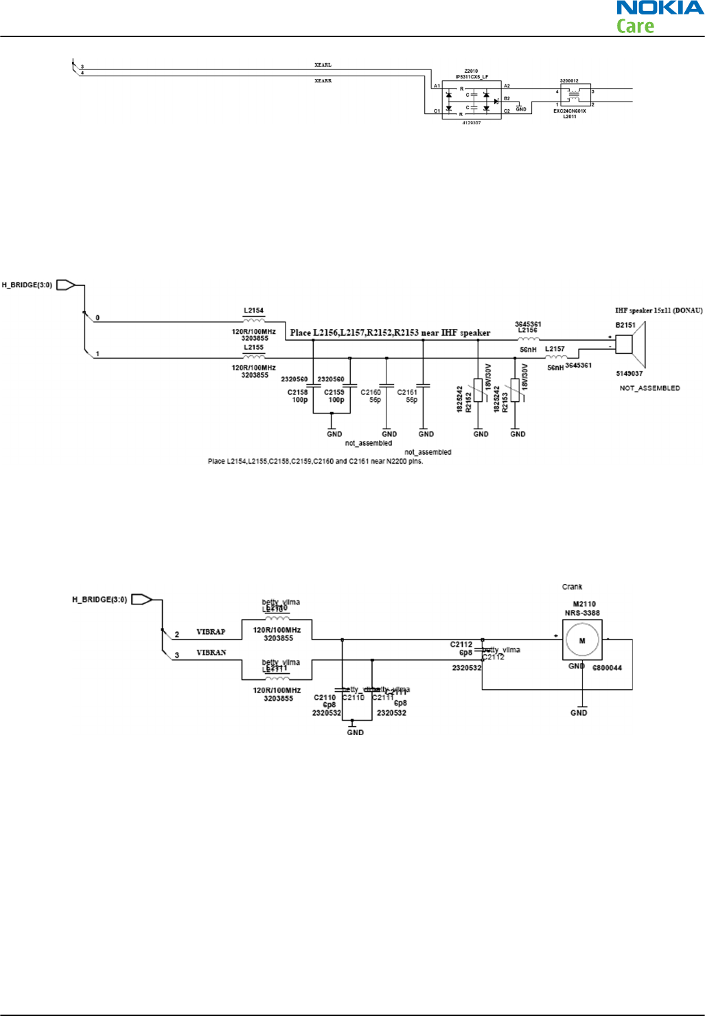
Figure 73 Internal earpiece circuitry
Internal speaker
The internal speaker is used for Internal HandsFree (IHF) call mode, video call, ringing tones, FM radio and
music listening.
The dynamic 15 x 11 mm speaker is connected to Avilma ASIC’s outputs XearR/XearL via stereo D-class IHF
amplifier TPA2012D2. The amplifier has 12 dB fixed gain and it is put to shutdown mode when not in use.
Figure 74 Internal speaker
Vibra circuitry
Vibra is used for the vibra alarm function.
The vibra motor is connected to the Avilma ASIC VibraP and VibraN Pulse Width Modulated (PWM) outputs.
Figure 75 Vibra circuitry
Accessory AV connector
The features that are supported by the accessory interface are the following:
•Audio output (stereo headset/headphones having the impedance >16ohm)
•Audio input (mono microphone from the headset)
•Control data (ECI)
•Connects the FM receiver to the headphones, which serves as the FM antenna
RM-612; RM-624
System Module and User Interface
Issue 1 COMPANY CONFIDENTIAL Page 5 – 31
Copyright © 2010 Nokia. All rights reserved.
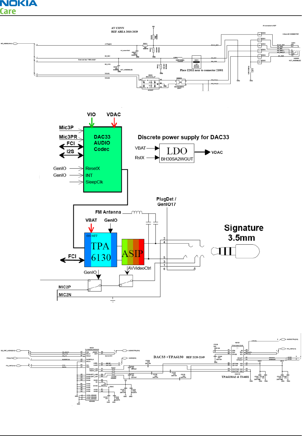
Figure 76 Accessory (AV) connector
Figure 77 Accessory (AV) connector with DAC33 and TPA6130 audio enhancements
DA converter and headphone amplifier
Figure 78 DA converter and headphone amplifier
RM-612; RM-624
System Module and User Interface
Page 5 – 32 COMPANY CONFIDENTIAL Issue 1
Copyright © 2010 Nokia. All rights reserved.
Baseband technical specifications
External interfaces
Name of connection Connector reference
HS USB X3300
MicroSD card X3200 on Bezel FPC
Battery connector X2070
SIM card reader X2700
Accessory (AV)
connector
X2001 on Audio FPC
Charging connector X2000
SIM IF connections
Pin Signal I/O Engine connection Notes
1 VSIM1 Out EM ASIC N2200 VSIM1 Supply voltage
to SIM card,
1.8V or 3.0V.
2 SIMRST Out EM ASIC N2200 SIM1Rst Reset signal to
SIM card
3 SIMCLK Out EM ASIC N2200 SIM1ClkC Clock signal to
SIM card
5 GND - GND Ground
7 SIMDATA In/Out EM ASIC N2200 SIM1DaC Data input /
output
Charging IF electrical characteristics
Table 12 Charging IF electrical characteristics
Description Parameter Min Max Unit
VCHAR Vcharge 5.50 9.30 V
VCHAR Icharge 0.95 A
Internal interfaces
Name of connection Component reference
Earpiece B8100 on UI-Flex
Microphone B2170
IHF speaker B2151 on Audio FPC
Main camera X1450
RM-612; RM-624
System Module and User Interface
Issue 1 COMPANY CONFIDENTIAL Page 5 – 33
Copyright © 2010 Nokia. All rights reserved.
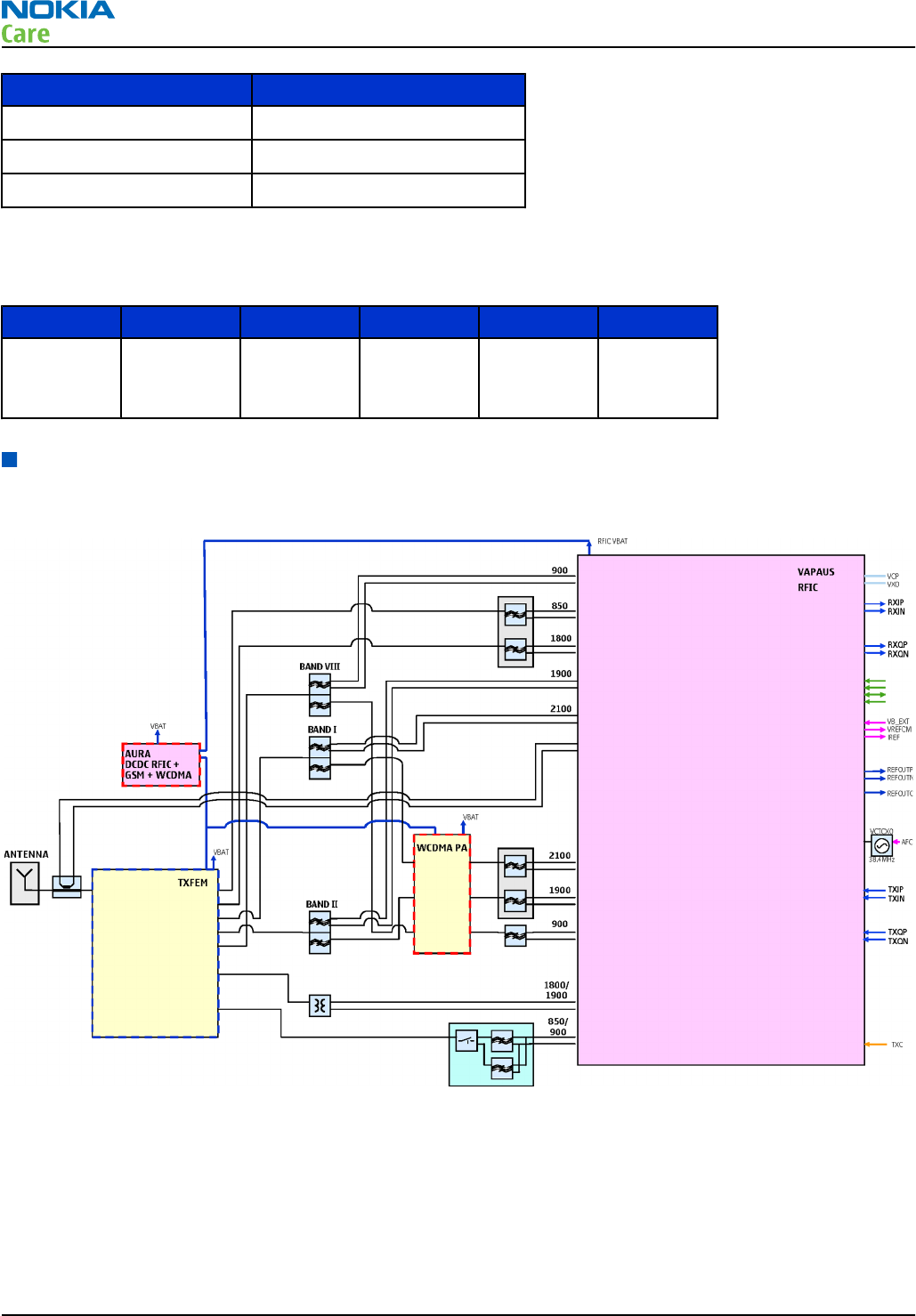
Name of connection Component reference
Sub-camera H8000 on UI-Flex
Main display connector X8100 on UI-Flex
Vibra M2110
Back-up battery interface electrical characteristics
Table 13 Back-up battery electrical characteristics
Description Parameter Min Typ Max Unit
Back-Up
Battery
Voltage
Vback 0 2.5 2.7 V
RF technical description
RF block diagram
Figure 79 RF block diagram using RF ASIC N7500 (with WCDMA VIII/II/I)
RM-612; RM-624
System Module and User Interface
Page 5 – 34 COMPANY CONFIDENTIAL Issue 1
Copyright © 2010 Nokia. All rights reserved.
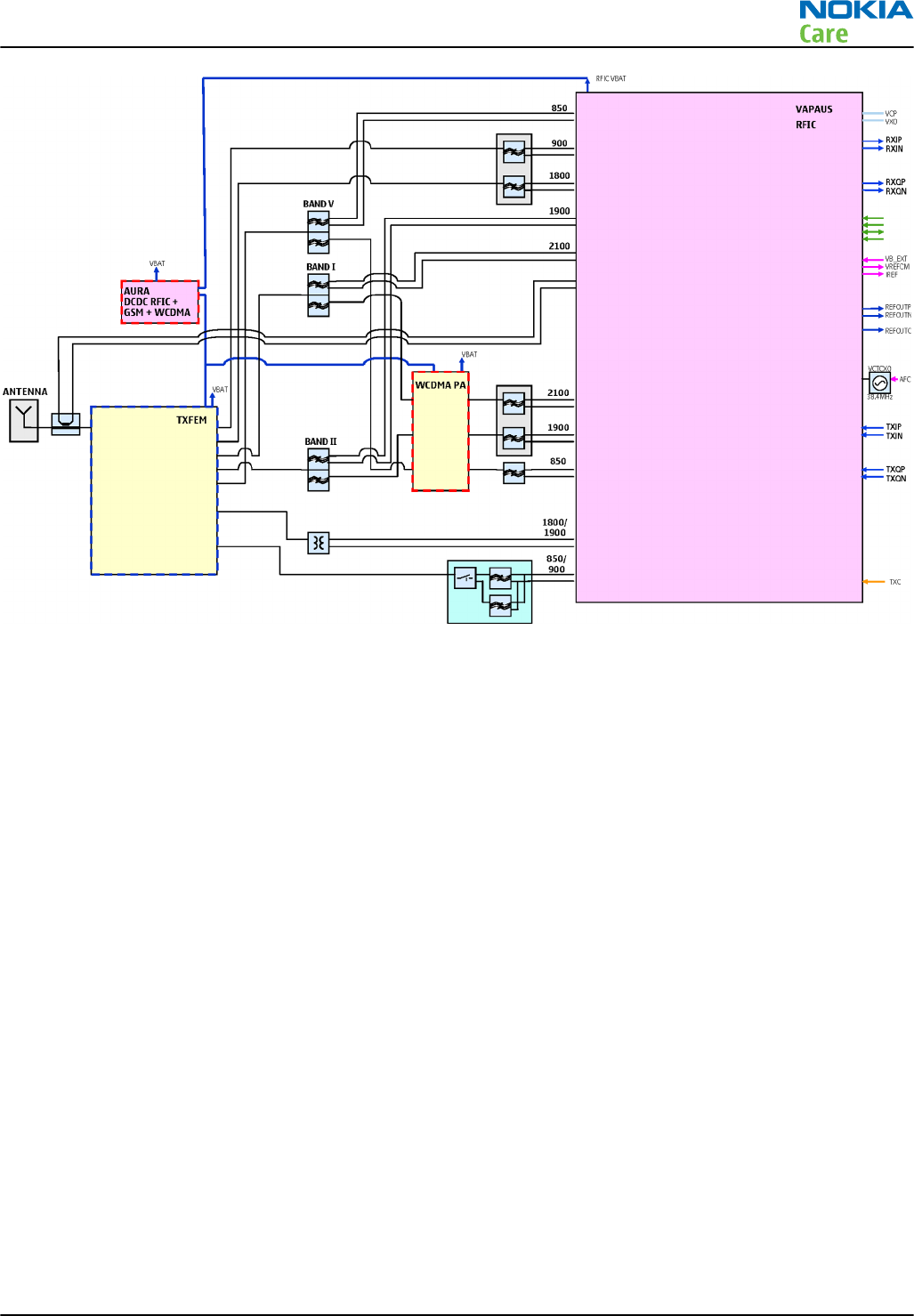
Figure 80 RF block diagram using RF ASIC N7500 (with WCDMA V/II/I)
The RF block diagram uses RF ASIC N7500 that performs the RF back-end functions of receive and transmit
function of the cellular transceiver.
Receiver (RX)
An analogue signal is received by the phone's antenna. The signal is converted to a digital signal and is then
transferred further to the baseband (eg. to the earpiece).
The receiver functions are implemented in the RF ASIC.
Signals with different frequencies take different paths, therefore being handled by different components.
The principle of GSM and WCDMA is the same.
Transmitter (TX)
The digital baseband signal (eg. from the microphone) is converted to an analogue signal, which is then
amplified and transmitted from the antenna. The frequency of this signal can be tuned to match the bandwith
of the system in use (eg. GSM900).
The transmitter functions are implemented in the RF ASIC.
Even though the GSM and WCDMA signals are sent via different components, the principles of the transmission
is the same.
RM-612; RM-624
System Module and User Interface
Issue 1 COMPANY CONFIDENTIAL Page 5 – 35
Copyright © 2010 Nokia. All rights reserved.
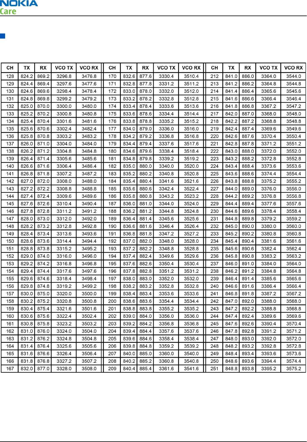
Frequency mappings
GSM850 frequencies
RM-612; RM-624
System Module and User Interface
Page 5 – 36 COMPANY CONFIDENTIAL Issue 1
Copyright © 2010 Nokia. All rights reserved.
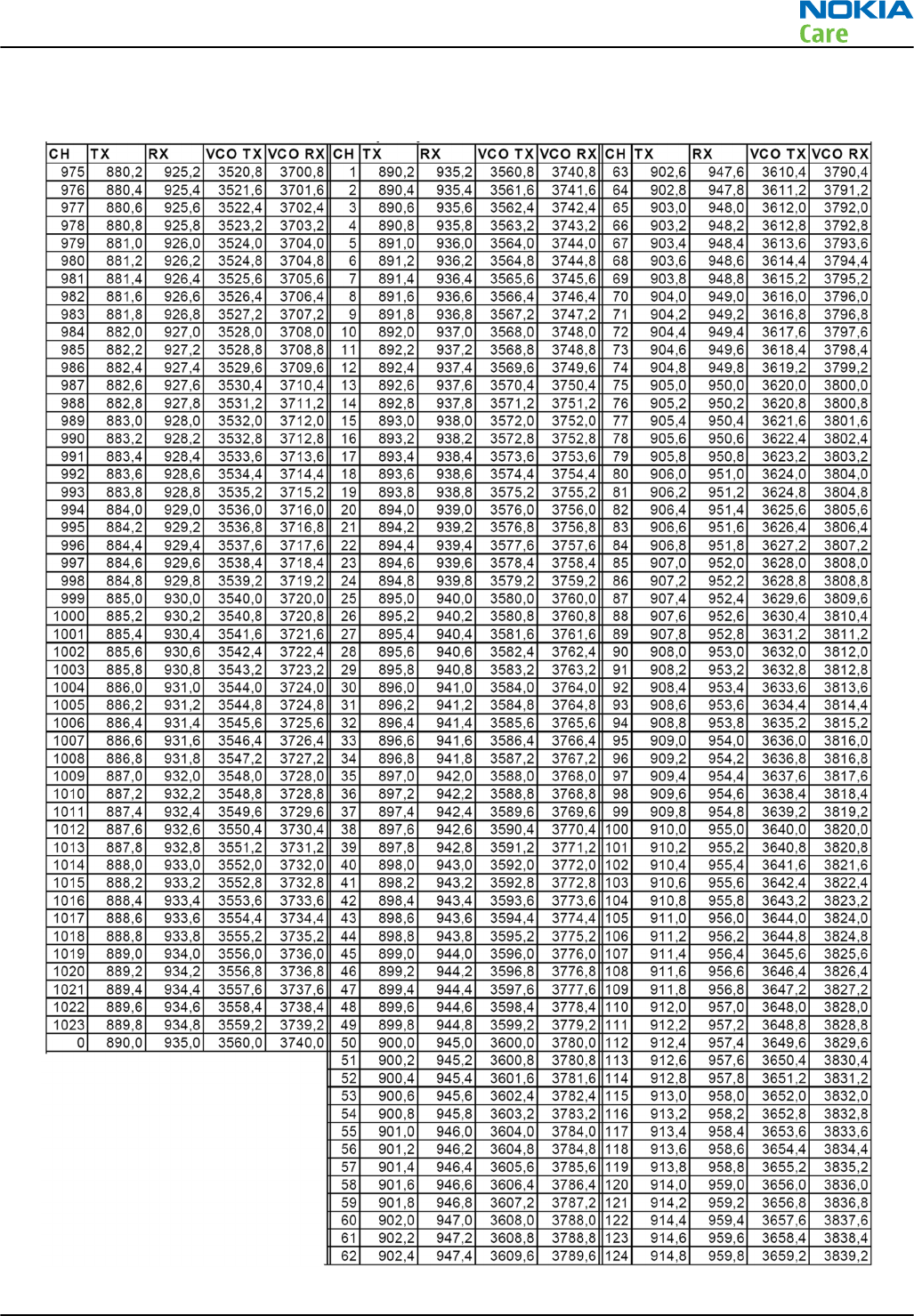
EGSM900 frequencies
RM-612; RM-624
System Module and User Interface
Issue 1 COMPANY CONFIDENTIAL Page 5 – 37
Copyright © 2010 Nokia. All rights reserved.
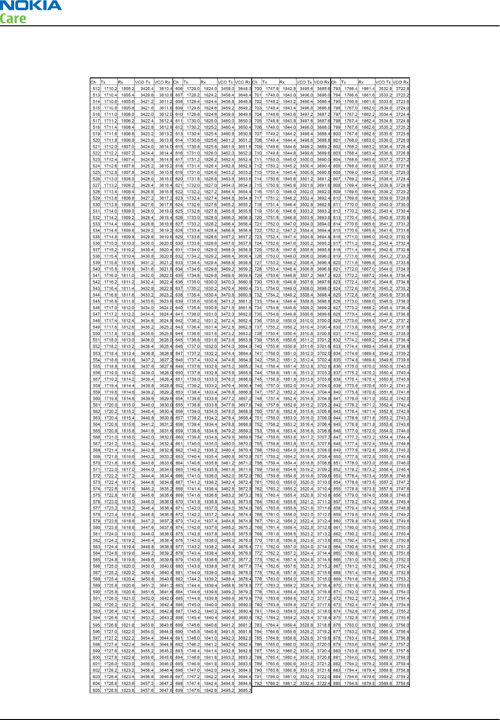
GSM1800 frequencies
RM-612; RM-624
System Module and User Interface
Page 5 – 38 COMPANY CONFIDENTIAL Issue 1
Copyright © 2010 Nokia. All rights reserved.
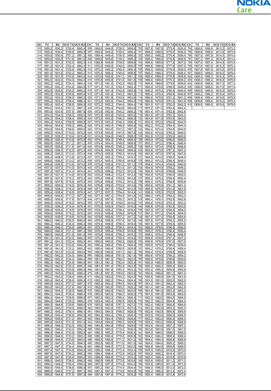
GSM1900 frequencies
RM-612; RM-624
System Module and User Interface
Issue 1 COMPANY CONFIDENTIAL Page 5 – 39
Copyright © 2010 Nokia. All rights reserved.
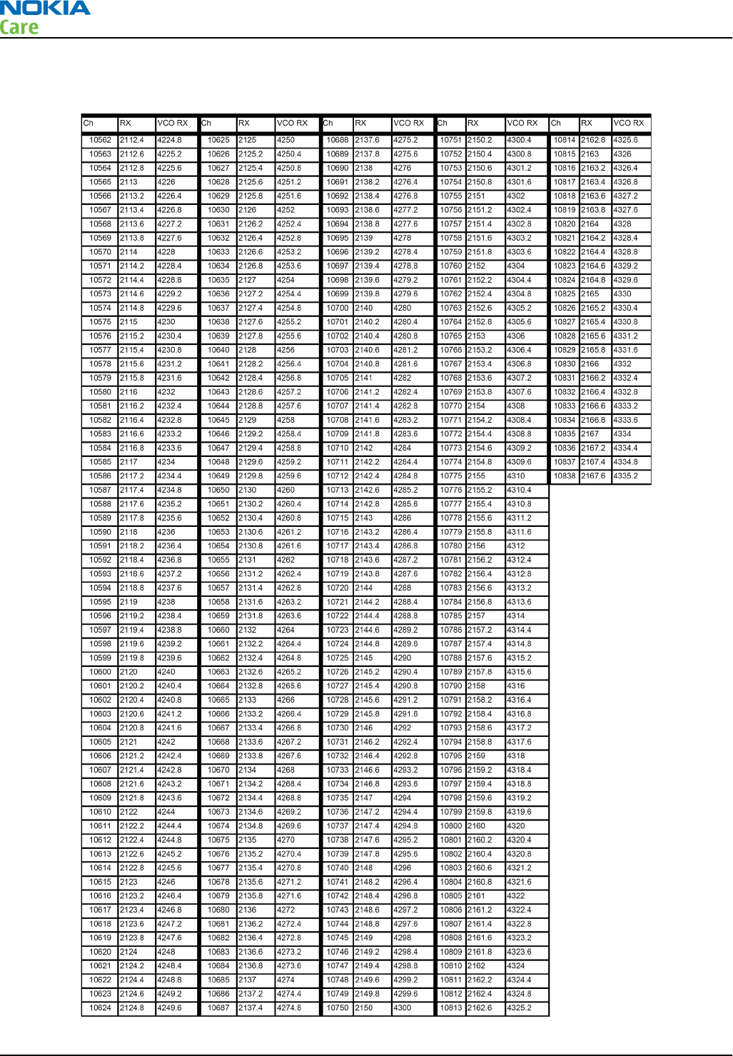
WCDMA 2100 Rx frequencies
RM-612; RM-624
System Module and User Interface
Page 5 – 40 COMPANY CONFIDENTIAL Issue 1
Copyright © 2010 Nokia. All rights reserved.
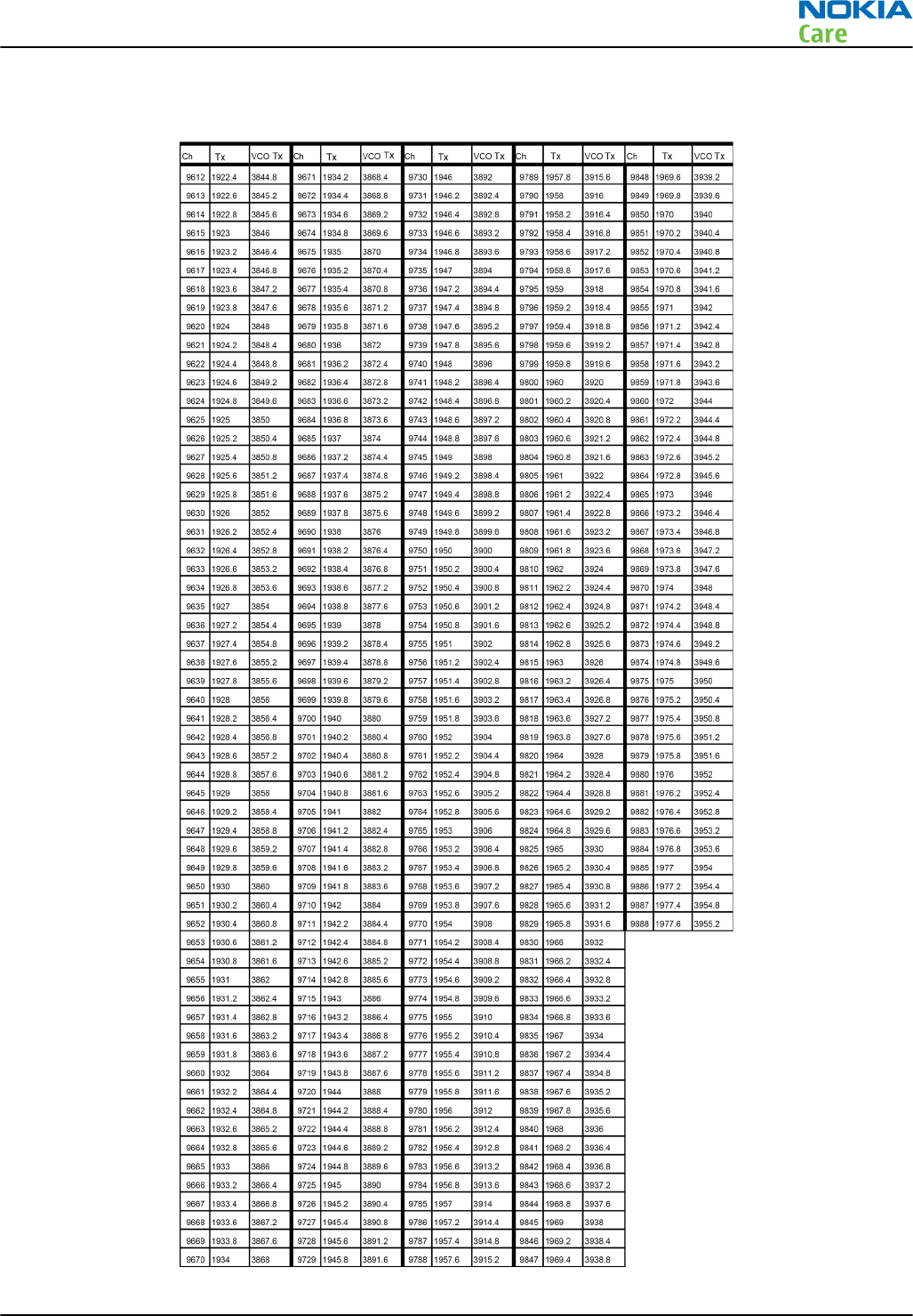
WCDMA 2100 Tx frequencies
RM-612; RM-624
System Module and User Interface
Issue 1 COMPANY CONFIDENTIAL Page 5 – 41
Copyright © 2010 Nokia. All rights reserved.
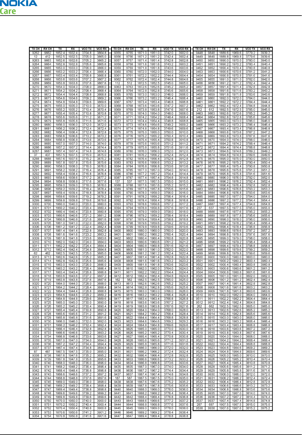
WCDMA II (1900) frequencies
RM-612; RM-624
System Module and User Interface
Page 5 – 42 COMPANY CONFIDENTIAL Issue 1
Copyright © 2010 Nokia. All rights reserved.

WCDMA VIII (900) frequencies
Uplink CH (TX) Freq (MHz) VCO (MHz) Downlink CH (RX) Freq (MHz) VCO (MHz)
2712 882,4 3529,6 2937 927,4 3709,6
2713 882,6 3530,4 2938 927,6 3710,4
2714 882,8 3531,2 2939 927,8 3711,2
2715 883 3532 2940 928 3712
2716 883,2 3532,8 2941 928,2 3712,8
2717 883,4 3533,6 2942 928,4 3713,6
2718 883,6 3534,4 2943 928,6 3714,4
2719 883,8 3535,2 2944 928,8 3715,2
2720 884 3536 2945 929 3716
2721 884,2 3536,8 2946 929,2 3716,8
2722 884,4 3537,6 2947 929,4 3717,6
2723 884,6 3538,4 2948 929,6 3718,4
2724 884,8 3539,2 2949 929,8 3719,2
2725 885 3540 2950 930 3720
2726 885,2 3540,8 2951 930,2 3720,8
2727 885,4 3541,6 2952 930,4 3721,6
2728 885,6 3542,4 2953 930,6 3722,4
2729 885,8 3543,2 2954 930,8 3723,2
2730 886 3544 2955 931 3724
2731 886,2 3544,8 2956 931,2 3724,8
2732 886,4 3545,6 2957 931,4 3725,6
2733 886,6 3546,4 2958 931,6 3726,4
2734 886,8 3547,2 2959 931,8 3727,2
2735 887 3548 2960 932 3728
2736 887,2 3548,8 2961 932,2 3728,8
2737 887,4 3549,6 2962 932,4 3729,6
2738 887,6 3550,4 2963 932,6 3730,4
2739 887,8 3551,2 2964 932,8 3731,2
2740 888 3552 2965 933 3732
2741 888,2 3552,8 2966 933,2 3732,8
2742 888,4 3553,6 2967 933,4 3733,6
2743 888,6 3554,4 2968 933,6 3734,4
2744 888,8 3555,2 2969 933,8 3735,2
RM-612; RM-624
System Module and User Interface
Issue 1 COMPANY CONFIDENTIAL Page 5 – 43
Copyright © 2010 Nokia. All rights reserved.

Uplink CH (TX) Freq (MHz) VCO (MHz) Downlink CH (RX) Freq (MHz) VCO (MHz)
2745 889 3556 2970 934 3736
2746 889,2 3556,8 2971 934,2 3736,8
2747 889,4 3557,6 2972 934,4 3737,6
2748 889,6 3558,4 2973 934,6 3738,4
2749 889,8 3559,2 2974 934,8 3739,2
2750 890 3560 2975 935 3740
2751 890,2 3560,8 2976 935,2 3740,8
2752 890,4 3561,6 2977 935,4 3741,6
2753 890,6 3562,4 2978 935,6 3742,4
2754 890,8 3563,2 2979 935,8 3743,2
2755 891 3564 2980 936 3744
2756 891,2 3564,8 2981 936,2 3744,8
2757 891,4 3565,6 2982 936,4 3745,6
2758 891,6 3566,4 2983 936,6 3746,4
2759 891,8 3567,2 2984 936,8 3747,2
2760 892 3568 2985 937 3748
2761 892,2 3568,8 2986 937,2 3748,8
2762 892,4 3569,6 2987 937,4 3749,6
2763 892,6 3570,4 2988 937,6 3750,4
2764 892,8 3571,2 2989 937,8 3751,2
2765 893 3572 2990 938 3752
2766 893,2 3572,8 2991 938,2 3752,8
2767 893,4 3573,6 2992 938,4 3753,6
2768 893,6 3574,4 2993 938,6 3754,4
2769 893,8 3575,2 2994 938,8 3755,2
2770 894 3576 2995 939 3756
2771 894,2 3576,8 2996 939,2 3756,8
2772 894,4 3577,6 2997 939,4 3757,6
2773 894,6 3578,4 2998 939,6 3758,4
2774 894,8 3579,2 2999 939,8 3759,2
2775 895 3580 3000 940 3760
2776 895,2 3580,8 3001 940,2 3760,8
2777 895,4 3581,6 3002 940,4 3761,6
2778 895,6 3582,4 3003 940,6 3762,4
2779 895,8 3583,2 3004 940,8 3763,2
RM-612; RM-624
System Module and User Interface
Page 5 – 44 COMPANY CONFIDENTIAL Issue 1
Copyright © 2010 Nokia. All rights reserved.

Uplink CH (TX) Freq (MHz) VCO (MHz) Downlink CH (RX) Freq (MHz) VCO (MHz)
2780 896 3584 3005 941 3764
2781 896,2 3584,8 3006 941,2 3764,8
2782 896,4 3585,6 3007 941,4 3765,6
2783 896,6 3586,4 3008 941,6 3766,4
2784 896,8 3587,2 3009 941,8 3767,2
2785 897 3588 3010 942 3768
2786 897,2 3588,8 3011 942,2 3768,8
2787 897,4 3589,6 3012 942,4 3769,6
2788 897,6 3590,4 3013 942,6 3770,4
2789 897,8 3591,2 3014 942,8 3771,2
2790 898 3592 3015 943 3772
2791 898,2 3592,8 3016 943,2 3772,8
2792 898,4 3593,6 3017 943,4 3773,6
2793 898,6 3594,4 3018 943,6 3774,4
2794 898,8 3595,2 3019 943,8 3775,2
2795 899 3596 3020 944 3776
2796 899,2 3596,8 3021 944,2 3776,8
2797 899,4 3597,6 3022 944,4 3777,6
2798 899,6 3598,4 3023 944,6 3778,4
2799 899,8 3599,2 3024 944,8 3779,2
2800 900 3600 3025 945 3780
2801 900,2 3600,8 3026 945,2 3780,8
2802 900,4 3601,6 3027 945,4 3781,6
2803 900,6 3602,4 3028 945,6 3782,4
2804 900,8 3603,2 3029 945,8 3783,2
2805 901 3604 3030 946 3784
2806 901,2 3604,8 3031 946,2 3784,8
2807 901,4 3605,6 3032 946,4 3785,6
2808 901,6 3606,4 3033 946,6 3786,4
2809 901,8 3607,2 3034 946,8 3787,2
2810 902 3608 3035 947 3788
2811 902,2 3608,8 3036 947,2 3788,8
2812 902,4 3609,6 3037 947,4 3789,6
2813 902,6 3610,4 3038 947,6 3790,4
2814 902,8 3611,2 3039 947,8 3791,2
RM-612; RM-624
System Module and User Interface
Issue 1 COMPANY CONFIDENTIAL Page 5 – 45
Copyright © 2010 Nokia. All rights reserved.

Uplink CH (TX) Freq (MHz) VCO (MHz) Downlink CH (RX) Freq (MHz) VCO (MHz)
2815 903 3612 3040 948 3792
2816 903,2 3612,8 3041 948,2 3792,8
2817 903,4 3613,6 3042 948,4 3793,6
2818 903,6 3614,4 3043 948,6 3794,4
2819 903,8 3615,2 3044 948,8 3795,2
2820 904 3616 3045 949 3796
2821 904,2 3616,8 3046 949,2 3796,8
2822 904,4 3617,6 3047 949,4 3797,6
2823 904,6 3618,4 3048 949,6 3798,4
2824 904,8 3619,2 3049 949,8 3799,2
2825 905 3620 3050 950 3800
2826 905,2 3620,8 3051 950,2 3800,8
2827 905,4 3621,6 3052 950,4 3801,6
2828 905,6 3622,4 3053 950,6 3802,4
2829 905,8 3623,2 3054 950,8 3803,2
2830 906 3624 3055 951 3804
2831 906,2 3624,8 3056 951,2 3804,8
2832 906,4 3625,6 3057 951,4 3805,6
2833 906,6 3626,4 3058 951,6 3806,4
2834 906,8 3627,2 3059 951,8 3807,2
2835 907 3628 3060 952 3808
2836 907,2 3628,8 3061 952,2 3808,8
2837 907,4 3629,6 3062 952,4 3809,6
2838 907,6 3630,4 3063 952,6 3810,4
2839 907,8 3631,2 3064 952,8 3811,2
2840 908 3632 3065 953 3812
2841 908,2 3632,8 3066 953,2 3812,8
2842 908,4 3633,6 3067 953,4 3813,6
2843 908,6 3634,4 3068 953,6 3814,4
2844 908,8 3635,2 3069 953,8 3815,2
2845 909 3636 3070 954 3816
2846 909,2 3636,8 3071 954,2 3816,8
2847 909,4 3637,6 3072 954,4 3817,6
2848 909,6 3638,4 3073 954,6 3818,4
2849 909,8 3639,2 3074 954,8 3819,2
RM-612; RM-624
System Module and User Interface
Page 5 – 46 COMPANY CONFIDENTIAL Issue 1
Copyright © 2010 Nokia. All rights reserved.
Uplink CH (TX) Freq (MHz) VCO (MHz) Downlink CH (RX) Freq (MHz) VCO (MHz)
2850 910 3640 3075 955 3820
2851 910,2 3640,8 3076 955,2 3820,8
2852 910,4 3641,6 3077 955,4 3821,6
2853 910,6 3642,4 3078 955,6 3822,4
2854 910,8 3643,2 3079 955,8 3823,2
2855 911 3644 3080 956 3824
2856 911,2 3644,8 3081 956,2 3824,8
2857 911,4 3645,6 3082 956,4 3825,6
2858 911,6 3646,4 3083 956,6 3826,4
2859 911,8 3647,2 3084 956,8 3827,2
2860 912 3648 3085 957 3828
2861 912,2 3648,8 3086 957,2 3828,8
2862 912,4 3649,6 3087 957,4 3829,6
2863 912,6 3650,4 3088 957,6 3830,4
RM-612; RM-624
System Module and User Interface
Issue 1 COMPANY CONFIDENTIAL Page 5 – 47
Copyright © 2010 Nokia. All rights reserved.
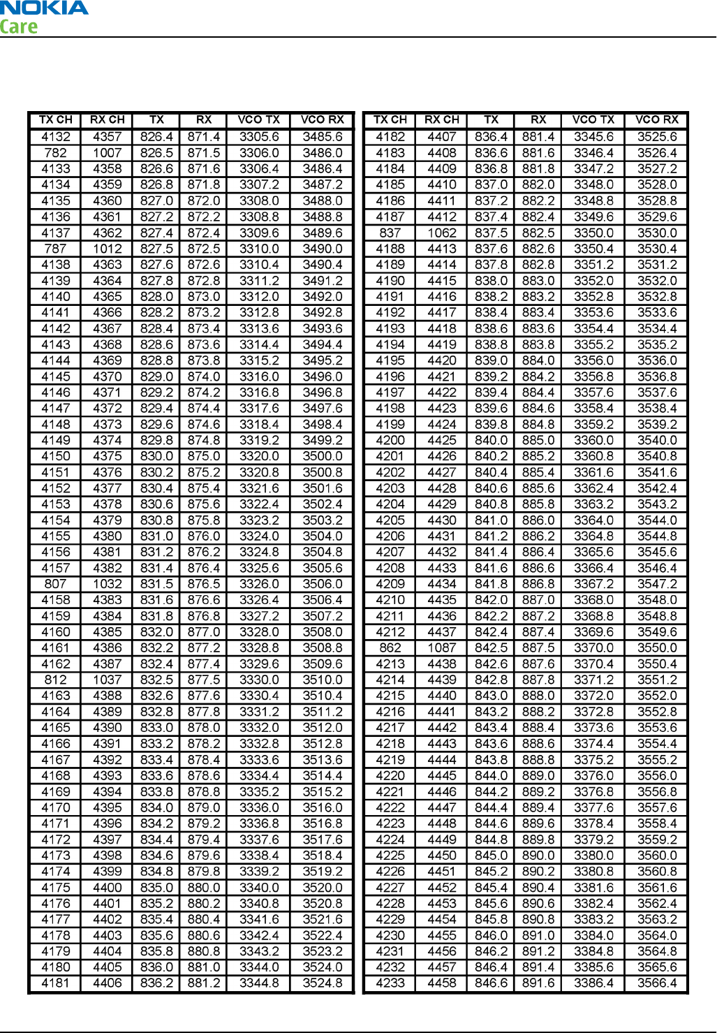
WCDMA V (850) frequencies
RM-612; RM-624
System Module and User Interface
Page 5 – 48 COMPANY CONFIDENTIAL Issue 1
Copyright © 2010 Nokia. All rights reserved.

Glossary
Nokia Customer Care
Issue 1 COMPANY CONFIDENTIAL Page Glossary– 1
Copyright © 2010 Nokia. All rights reserved.

RM-612; RM-624
Glossary
(This page left intentionally blank.)
Page Glossary– 2 COMPANY CONFIDENTIAL Issue 1
Copyright © 2010 Nokia. All rights reserved.

A/D-converter Analogue-to-digital converter
ADC Analogue-to-digital converter
ALS Ambient light sensor
ARM Advanced RISC Machines
ASIC Application Specific Integrated Circuit
ASIP Application Specific Interface Protector
B2B Board to board, connector between PWB and UI board
BA Board Assembly
BB Baseband
BCM2048 Bluetooth module made by BROADCOM
BSI Battery Size Indicator
BT Bluetooth
CBus MCU controlled serial bus connected to UPP_WD2, UEME and Zocus
CCP Compact Camera Port
CDMA Code division multiple access
CMOS Complimentary metal-oxide semiconductor circuit (low power consumption)
COG Chip on Glass
CPU Central Processing Unit
CSD Circuit-switched data
CSR Cambridge silicon radio
CSTN Colour Super Twisted Nematic
CTSI Clock Timing Sleep and interrupt block of Tiku
CW Continuous wave
D/A-converter Digital-to-analogue converter
DAC Digital-to-analogue converter
DMA Direct memory access
DP Data Package
DPLL Digital Phase Locked Loop
DSP Digital Signal Processor
DTM Dual Transfer Mode
DtoS Differential to Single ended
EDGE Enhanced data rates for global/GSM evolution
EGSM Extended GSM
EM Energy management
EMC Electromagnetic compatibility
EMI Electromagnetic interference
RM-612; RM-624
Glossary
Issue 1 COMPANY CONFIDENTIAL Page Glossary– 3
Copyright © 2010 Nokia. All rights reserved.

ESD Electrostatic discharge
FCI Functional cover interface
FPS Flash Programming Tool
FR Full rate
FSTN Film compensated super twisted nematic
GMSK Gaussian Minimum Shift Keying
GND Ground, conductive mass
GPIB General-purpose interface bus
GPRS General Packet Radio Service
GSM Group Special Mobile/Global System for Mobile communication
HSDPA High-speed downlink packet access
HF Hands free
HFCM Handsfree Common
HS Handset
HSCSD High speed circuit switched data (data transmission connection faster than GSM)
HW Hardware
I/O Input/Output
IBAT Battery current
IC Integrated circuit
ICHAR Charger current
IF Interface
IHF Integrated hands free
IMEI International Mobile Equipment Identity
IR Infrared
ISA Intelligent software architecture
JPEG/JPG Joint Photographic Experts Group
LCD Liquid Crystal Display
LDO Low Drop Out
LED Light-emitting diode
LPRF Low Power Radio Frequency
MCU Micro Controller Unit (microprocessor)
MCU Multiport control unit
MIC, mic Microphone
MIDP Mobile Information Device Profile
MIN Mobile identification number
MIPS Million instructions per second
RM-612; RM-624
Glossary
Page Glossary– 4 COMPANY CONFIDENTIAL Issue 1
Copyright © 2010 Nokia. All rights reserved.

MMS Multimedia messaging service
NFC Near field communication
NTC Negative temperature coefficient, temperature sensitive resistor used as a
temperature sensor
OMA Object management architecture
OMAP Operations, maintenance, and administration part
Opamp Operational Amplifier
PA Power amplifier
PDA Pocket Data Application
PDA Personal digital assistant
PDRAM Program/Data RAM (on chip in Tiku)
Phoenix Software tool of DCT4.x and BB5
PIM Personal Information Management
PLL Phase locked loop
PM (Phone) Permanent memory
PUP General Purpose IO (PIO), USARTS and Pulse Width Modulators
PURX Power-up reset
PWB Printed Wiring Board
PWM Pulse width modulation
RC-filter Resistance-Capacitance filter
RF Radio Frequency
RFBUS Serial control Bus For RF
RSS Web content Syndication Format
RSSI Receiving signal strength indicator
RST Reset Switch
RTC Real Time Clock (provides date and time)
RX Radio Receiver
SAW filter Surface Acoustic Wave filter
SDRAM Synchronous Dynamic Random Access Memory
SID Security ID
SIM Subscriber Identity Module
SMPS Switched Mode Power Supply
SNR Signal-to-noise ratio
SPR Standard Product requirements
SRAM Static random access memory
STI Serial Trace Interface
RM-612; RM-624
Glossary
Issue 1 COMPANY CONFIDENTIAL Page Glossary– 5
Copyright © 2010 Nokia. All rights reserved.
SW Software
TCP/IP Transmission control protocol/Internet protocol
TCXO Temperature controlled Oscillator
TX Radio Transmitter
UART Universal asynchronous receiver/transmitter
UI User Interface
UPnP Universal Plug and Play
USB Universal Serial Bus
VBAT Battery voltage
VCHAR Charger voltage
VCO Voltage controlled oscillator
VCTCXO Voltage Controlled Temperature Compensated Crystal Oscillator
VCXO Voltage Controlled Crystal Oscillator
Vp-p Peak-to-peak voltage
VSIM SIM voltage
WCDMA Wideband code division multiple access
WD Watchdog
WLAN Wireless local area network
XHTML Extensible hypertext markup language
RM-612; RM-624
Glossary
Page Glossary– 6 COMPANY CONFIDENTIAL Issue 1
Copyright © 2010 Nokia. All rights reserved.
