Nokia N85 Rm 333 334 335 Service Manual 34 V2
User Manual: Smartphone Nokia N85 RM-333, RM-334, RM-335 - Service manuals and Schematics, Disassembly / Assembly. Free.
Open the PDF directly: View PDF ![]() .
.
Page Count: 1
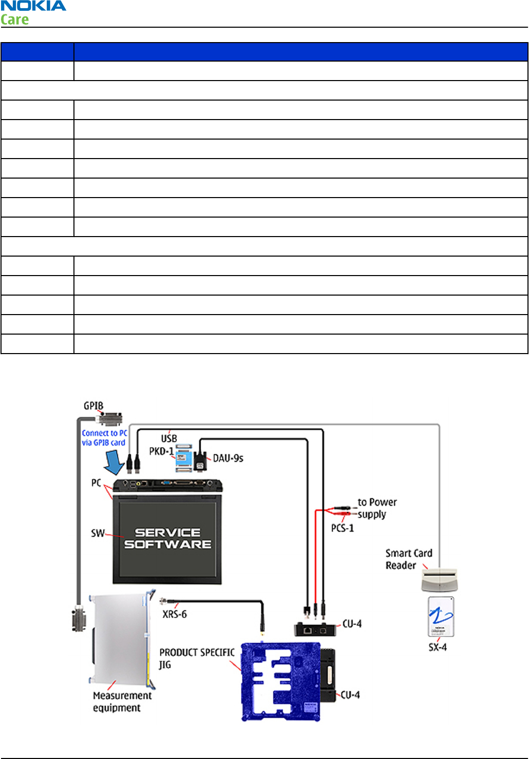
- Amendment Record Sheet
- Copyright
- Warnings and cautions
- ESD protection
- Care and maintenance
- Company policy
- Battery information
- Nokia N85; L3&4 Service Manual Structure
- 1 General Information
- 2 Service Tools and Service Concepts
- Service tools
- Service concepts
- POS (Point of Sale) flash concept
- Flash concept with FPS-10
- CU-4 flash concept with FPS-10
- Flash concept with FPS-10 and SB-6
- Flash concept with SS-46 and CA-89DS
- Flash concept with SS-62 and CA-89DS
- Flash concept with FPS-10, SS-62 and SB-6
- Flash concept with FPS-10, SS-62 and SB-7
- Module jig service concept
- Module jig service concept with SB-6
- RF testing concept with RF coupler
- Service concept for RF testing and RF/BB tuning
- 3 BB Troubleshooting
- Baseband main troubleshooting
- General power checking
- Backup battery troubleshooting
- Dead or jammed device troubleshooting
- Keyboard troubleshooting
- Hall sensor troubleshooting
- TV- out troubleshooting
- General power checking troubleshooting
- USB troubleshooting
- SIM card troubleshooting
- MicroSD card troubleshooting
- Combo memory troubleshooting
- Flash programming troubleshooting
- USB charging troubleshooting
- Clocking troubleshooting
- Power key troubleshooting
- Naviscroll troubleshooting
- User interface troubleshooting
- Display Troubleshooting
- Audio Troubleshooting
- ALS Technical Description and Troubleshooting
- Bluetooth and FM Radio Troubleshooting
- GPS Troubleshooting
- WLAN Troubleshooting
- 4 RF Troubleshooting
- 5 Camera Module Troubleshooting
- 6 FMTx 2.1 Technical Description
- 7 FMTx 2.1 Troubleshooting
- FMTx 2.1 schematic
- FMTx 2.1 component layout
- FMTx 2.1 PWB traces
- Specific digital and power supply test points
- FMTx2.1 specific RF test points
- Specific clock test points
- General visual inspection guidelines
- FMTx2.1 troubleshooting
- FMTx2.1 antenna visual inspection troubleshooting
- FMTx2.1 audio path visual inspection troubleshooting
- FMTx2.1 Si4713 visual inspection troubleshooting
- Checking validity of signals
- FMTx2.1 troubleshooting faults
- Phoenix PC tool
- 8 System Module and User Interface
- Introduction
- Energy management
- Bluetooth and FM RDS radio module
- GPS module
- WLAN module
- FM transmitter module
- High-speed USB
- CBUS interface
- FBUS interface
- ECI interface
- USB charger interface
- SIM interface
- MicroSD card interface
- Camera concept
- User interface
- ASICs
- Device memories
- Audio concept
- Baseband technical specifications
- RF technical description
- Frequency mappings
- 9 Service information differences between RM-335 and RM-333
- Glossary

Service Manual
RM-333; RM-334; RM-335 (Nokia N85; L3&4)
Mobile Terminal
Part No: (Issue 2)
Nokia Customer Care
COMPANY CONFIDENTIAL
Copyright © 2008 Nokia. All rights reserved.

Amendment Record Sheet
Amendment No Date Inserted By Comments
Issue 1 09/2008 A. Salo
Issue 2 10/2008 A. Salo New chapter added:
Service information differences
between RM-335 and RM-333
RM-333; RM-334; RM-335
Amendment Record Sheet
Page ii COMPANY CONFIDENTIAL Issue 2
Copyright © 2008 Nokia. All rights reserved.

Copyright
Copyright © 2008 Nokia. All rights reserved.
Reproduction, transfer, distribution or storage of part or all of the contents in this document in any form
without the prior written permission of Nokia is prohibited.
Nokia, Nokia Connecting People, and Nokia X and Y are trademarks or registered trademarks of Nokia
Corporation. Other product and company names mentioned herein may be trademarks or tradenames of
their respective owners.
Nokia operates a policy of continuous development. Nokia reserves the right to make changes and
improvements to any of the products described in this document without prior notice.
Under no circumstances shall Nokia be responsible for any loss of data or income or any special, incidental,
consequential or indirect damages howsoever caused.
The contents of this document are provided "as is". Except as required by applicable law, no warranties of
any kind, either express or implied, including, but not limited to, the implied warranties of merchantability
and fitness for a particular purpose, are made in relation to the accuracy, reliability or contents of this
document. Nokia reserves the right to revise this document or withdraw it at any time without prior notice.
The availability of particular products may vary by region.
IMPORTANT
This document is intended for use by qualified service personnel only.
RM-333; RM-334; RM-335
Copyright
Issue 2 COMPANY CONFIDENTIAL Page iii
Copyright © 2008 Nokia. All rights reserved.

Warnings and cautions
Warnings
•IF THE DEVICE CAN BE INSTALLED IN A VEHICLE, CARE MUST BE TAKEN ON INSTALLATION IN VEHICLES FITTED
WITH ELECTRONIC ENGINE MANAGEMENT SYSTEMS AND ANTI-SKID BRAKING SYSTEMS. UNDER CERTAIN FAULT
CONDITIONS, EMITTED RF ENERGY CAN AFFECT THEIR OPERATION. IF NECESSARY, CONSULT THE VEHICLE DEALER/
MANUFACTURER TO DETERMINE THE IMMUNITY OF VEHICLE ELECTRONIC SYSTEMS TO RF ENERGY.
•THE PRODUCT MUST NOT BE OPERATED IN AREAS LIKELY TO CONTAIN POTENTIALLY EXPLOSIVE ATMOSPHERES,
FOR EXAMPLE, PETROL STATIONS (SERVICE STATIONS), BLASTING AREAS ETC.
•OPERATION OF ANY RADIO TRANSMITTING EQUIPMENT, INCLUDING CELLULAR TELEPHONES, MAY INTERFERE
WITH THE FUNCTIONALITY OF INADEQUATELY PROTECTED MEDICAL DEVICES. CONSULT A PHYSICIAN OR THE
MANUFACTURER OF THE MEDICAL DEVICE IF YOU HAVE ANY QUESTIONS. OTHER ELECTRONIC EQUIPMENT MAY
ALSO BE SUBJECT TO INTERFERENCE.
•BEFORE MAKING ANY TEST CONNECTIONS, MAKE SURE YOU HAVE SWITCHED OFF ALL EQUIPMENT.
Cautions
•Servicing and alignment must be undertaken by qualified personnel only.
•Ensure all work is carried out at an anti-static workstation and that an anti-static wrist strap is worn.
•Ensure solder, wire, or foreign matter does not enter the telephone as damage may result.
•Use only approved components as specified in the parts list.
•Ensure all components, modules, screws and insulators are correctly re-fitted after servicing and
alignment.
•Ensure all cables and wires are repositioned correctly.
•Never test a mobile phone WCDMA transmitter with full Tx power, if there is no possibility to perform the
measurements in a good performance RF-shielded room. Even low power WCDMA transmitters may disturb
nearby WCDMA networks and cause problems to 3G cellular phone communication in a wide area.
•During testing never activate the GSM or WCDMA transmitter without a proper antenna load, otherwise
GSM or WCDMA PA may be damaged.
RM-333; RM-334; RM-335
Warnings and cautions
Page iv COMPANY CONFIDENTIAL Issue 2
Copyright © 2008 Nokia. All rights reserved.

ESD protection
Nokia requires that service points have sufficient ESD protection (against static electricity) when servicing
the phone.
Any product of which the covers are removed must be handled with ESD protection. The SIM card can be
replaced without ESD protection if the product is otherwise ready for use.
To replace the covers ESD protection must be applied.
All electronic parts of the product are susceptible to ESD. Resistors, too, can be damaged by static electricity
discharge.
All ESD sensitive parts must be packed in metallized protective bags during shipping and handling outside
any ESD Protected Area (EPA).
Every repair action involving opening the product or handling the product components must be done under
ESD protection.
ESD protected spare part packages MUST NOT be opened/closed out of an ESD Protected Area.
For more information and local requirements about ESD protection and ESD Protected Area, contact your local
Nokia After Market Services representative.
RM-333; RM-334; RM-335
ESD protection
Issue 2 COMPANY CONFIDENTIAL Page v
Copyright © 2008 Nokia. All rights reserved.

Care and maintenance
This product is of superior design and craftsmanship and should be treated with care. The suggestions below
will help you to fulfil any warranty obligations and to enjoy this product for many years.
•Keep the phone and all its parts and accessories out of the reach of small children.
•Keep the phone dry. Precipitation, humidity and all types of liquids or moisture can contain minerals that
will corrode electronic circuits.
•Do not use or store the phone in dusty, dirty areas. Its moving parts can be damaged.
•Do not store the phone in hot areas. High temperatures can shorten the life of electronic devices, damage
batteries, and warp or melt certain plastics.
•Do not store the phone in cold areas. When it warms up (to its normal temperature), moisture can form
inside, which may damage electronic circuit boards.
•Do not drop, knock or shake the phone. Rough handling can break internal circuit boards.
•Do not use harsh chemicals, cleaning solvents, or strong detergents to clean the phone.
•Do not paint the phone. Paint can clog the moving parts and prevent proper operation.
•Use only the supplied or an approved replacement antenna. Unauthorised antennas, modifications or
attachments could damage the phone and may violate regulations governing radio devices.
All of the above suggestions apply equally to the product, battery, charger or any accessory.
RM-333; RM-334; RM-335
Care and maintenance
Page vi COMPANY CONFIDENTIAL Issue 2
Copyright © 2008 Nokia. All rights reserved.

Company policy
Our policy is of continuous development; details of all technical modifications will be included with service
bulletins.
While every endeavour has been made to ensure the accuracy of this document, some errors may exist. If
any errors are found by the reader, NOKIA MOBILE PHONES Business Group should be notified in writing/e-
mail.
Please state:
•Title of the Document + Issue Number/Date of publication
•Latest Amendment Number (if applicable)
•Page(s) and/or Figure(s) in error
Please send to:
NOKIA CORPORATION
Nokia Mobile Phones Business Group
Nokia Customer Care
PO Box 86
FIN-24101 SALO
Finland
E-mail: Service.Manuals@nokia.com
RM-333; RM-334; RM-335
Company policy
Issue 2 COMPANY CONFIDENTIAL Page vii
Copyright © 2008 Nokia. All rights reserved.

Battery information
Note: A new battery's full performance is achieved only after two or three complete charge and
discharge cycles!
The battery can be charged and discharged hundreds of times but it will eventually wear out. When the
operating time (talk-time and standby time) is noticeably shorter than normal, it is time to buy a new battery.
Use only batteries approved by the phone manufacturer and recharge the battery only with the chargers
approved by the manufacturer. Unplug the charger when not in use. Do not leave the battery connected to
a charger for longer than a week, since overcharging may shorten its lifetime. If left unused a fully charged
battery will discharge itself over time.
Temperature extremes can affect the ability of your battery to charge.
For good operation times with Li-Ion batteries, discharge the battery from time to time by leaving the product
switched on until it turns itself off (or by using the battery discharge facility of any approved accessory
available for the product). Do not attempt to discharge the battery by any other means.
Use the battery only for its intended purpose.
Never use any charger or battery which is damaged.
Do not short-circuit the battery. Accidental short-circuiting can occur when a metallic object (coin, clip or
pen) causes direct connection of the + and - terminals of the battery (metal strips on the battery) for example
when you carry a spare battery in your pocket or purse. Short-circuiting the terminals may damage the battery
or the connecting object.
Leaving the battery in hot or cold places, such as in a closed car in summer or winter conditions, will reduce
the capacity and lifetime of the battery. Always try to keep the battery between 15°C and 25°C (59°F and 77°
F). A phone with a hot or cold battery may temporarily not work, even when the battery is fully charged.
Batteries' performance is particularly limited in temperatures well below freezing.
Do not dispose of batteries in a fire!
Dispose of batteries according to local regulations (e.g. recycling). Do not dispose as household waste.
RM-333; RM-334; RM-335
Battery information
Page viii COMPANY CONFIDENTIAL Issue 2
Copyright © 2008 Nokia. All rights reserved.

Nokia N85; L3&4 Service Manual Structure
1 General Information
2 Service Tools and Service Concepts
3 BB Troubleshooting
4 RF Troubleshooting
5 Camera Module Troubleshooting
6 FMTx 2.1 Technical Description
7 FMTx 2.1 Troubleshooting
8 System Module and User Interface
9 Service information differences between RM-335 and RM-333
Glossary
RM-333; RM-334; RM-335
Nokia N85; L3&4 Service Manual Structure
Issue 2 COMPANY CONFIDENTIAL Page ix
Copyright © 2008 Nokia. All rights reserved.

RM-333; RM-334; RM-335
Nokia N85; L3&4 Service Manual Structure
(This page left intentionally blank.)
Page x COMPANY CONFIDENTIAL Issue 2
Copyright © 2008 Nokia. All rights reserved.
1 — General Information
Nokia Customer Care
Issue 2 COMPANY CONFIDENTIAL Page 1 –1
Copyright © 2008 Nokia. All rights reserved.

RM-333; RM-334; RM-335
General Information
(This page left intentionally blank.)
Page 1 –2 COMPANY CONFIDENTIAL Issue 2
Copyright © 2008 Nokia. All rights reserved.

Table of Contents
Product selection....................................................................................................................................................1–5
Product features and sales package.....................................................................................................................1–5
Mobile enhancements............................................................................................................................................1–8
Technical Specifications...................................................................................................................................... 1–10
Transceiver general specifications ............................................................................................................... 1–10
Main RF characteristics for GSM850/900/1800/1900 and WCDMA VIII/II/I phones ................................. 1–10
Main RF characteristics for GSM850/900/1800/1900 and WCDMA V/II/I phones ..................................... 1–11
Battery endurance.......................................................................................................................................... 1–13
Environmental conditions ............................................................................................................................. 1–13
List of Tables
Table 1 Audio..........................................................................................................................................................1–8
Table 2 Car...............................................................................................................................................................1–9
Table 3 Data ............................................................................................................................................................1–9
Table 4 Messaging..................................................................................................................................................1–9
Table 5 Power...................................................................................................................................................... 1–10
List of Figures
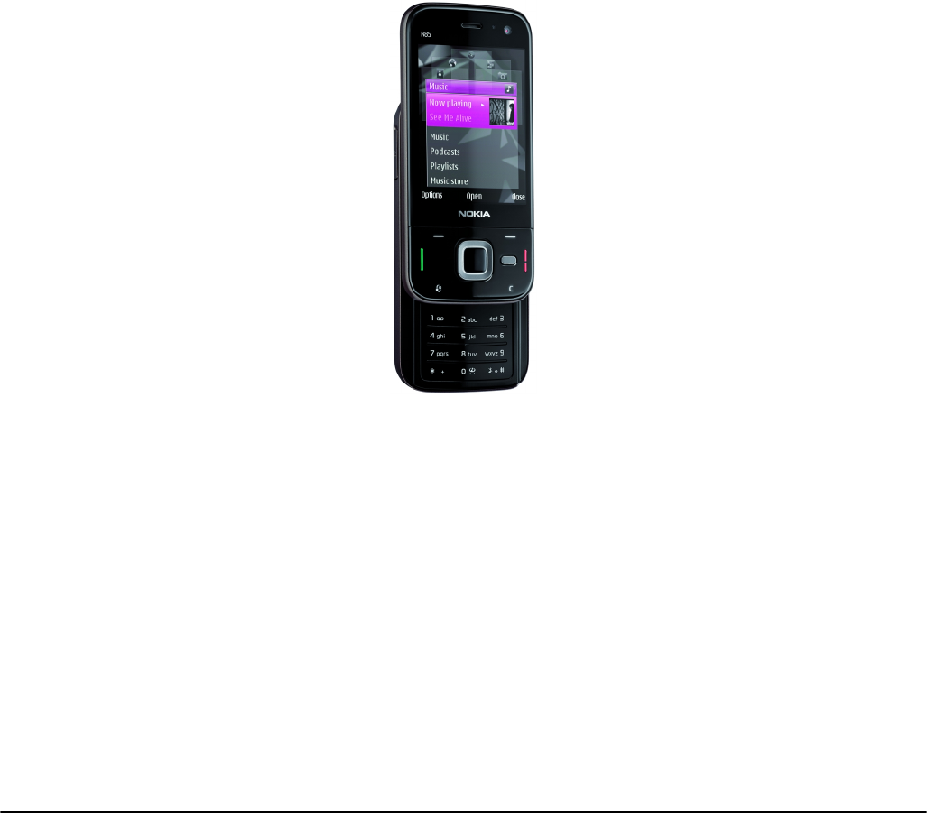
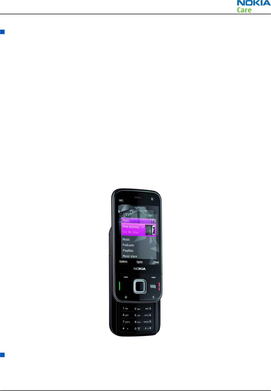
Figure 1 View of RM-333/RM-334 .........................................................................................................................1–5
RM-333; RM-334; RM-335
General Information
Issue 2 COMPANY CONFIDENTIAL Page 1 –3
Copyright © 2008 Nokia. All rights reserved.

RM-333; RM-334; RM-335
General Information
(This page left intentionally blank.)
Page 1 –4 COMPANY CONFIDENTIAL Issue 2
Copyright © 2008 Nokia. All rights reserved.
Product selection
RM-333 is a dual mode handportable multimedia computer, supporting GSM/GPRS/
EGPRS850/900/1800/1900, with WCDMA VIII (900)/ II (1900)/ I (2100) HSDPA and WLAN. RM-334 supports
GSM/GPRS/EGPRS850/900/1800/1900, with WCDMA V (850)/ II (1900)/ I (2100) HSDPA and WLAN.
The device is a 3GPP Release 5 terminal supporting WCDMA/HSDPA, EGPRS and GPRS data bearers. For WCDMA
HSDPA the maximum bit rate is up to 3.6 Mbps for downlink and 384 kbps for uplink with simultaneous CS
speech or CS video (max. 64 kbps).
For 2G and 2.5G networks the device is a Class A EGPRS DTM MSC 11 which means a maximum download speed
of up to 296kbit/s with EGPRS, and up to 107kbit/s with GPRS.
According to GSM standard 05.05 it responds to class 4 (max. 2W) in GSM 850 and EGSM 900 class 1 (1W) in
DCS 1800 and class 1 in PCS 1900. The device supports EGPRS (EDGE) class B as well as Bluetooth 2.0 EDR
standard.
The device supports two way video calls with two integrated cameras, one on the front and one on the back.
The device is an MMS (Multimedia Messaging Service) enabled multimedia computer with a large 2.6’’ QVGA
(240 x 320 pixels) TFT colour display capable of displaying 16 million colours and an integrated 5 Megapixel
auto focus camera. The MMS implementation follows the OMA MMS standard release 1.2. The Browser is a
highly advanced internet browser also capable of viewing operator domain XHTML Mobile Profile (MP)
content.
The device uses Symbian 9.3 operating system and supports MIDP Java 2.0 & CLDC1.1, providing a good
platform for compelling 3rd party applications.
Figure 1 View of RM-333/RM-334
Product features and sales package
Imaging
Main camera:
RM-333; RM-334; RM-335
General Information
Issue 2 COMPANY CONFIDENTIAL Page 1 –5
Copyright © 2008 Nokia. All rights reserved.

•Sensor: 5 megapixel
•Carl Zeiss Optics: Tessar™ lens
•F number/Aperture: F2.8
•Focal length: 4.6 mm
35 mm (35 mm equivalent)
•Focus range: 10 cm ~ infinity
•Macro focus distance: 10-50 cm
•Shutter speed: Mechanical shutter 1/1000~1/4 s
Secondary camera:
•Sensor: CIF (352 x 288 pixels)
•F number/Aperture: F2.8
•Focal length: 43 mm (35mm equivalent)
•Focus range: 10 cm ~ infinity
Video:
•Video resolution: QCIF at 15 fps
•Audio recording: AAC (AMR for MMS)
•Video stabilization
•Video clip length: 60 min
•Video file format: .mp4 (default), .3gp (for MMS)
•White balance: automatic, sunny, cloudy, incandescent, fluorescent
•Scene: Auto, Night
•Colour tone: normal, sepia, B&W, vivid, negative
•Zoom (digital): up to 8x
Photo:
•Still image resolutions: up to 3.2 megapixel: 2048 x 1536
•Still image file format: JPEG/EXIF
•Auto focus
•Auto exposure: center weighted AE
•Image orientation: automatic
•Exposure compensation: +2 ~ -2EV at 0.5 step
•White balance: automatic, sunny, cloudy, incandescent, fluorescent
•Scene: auto, sports, portrait, close-up, landscape, night, user defined
•Colour tone: normal, sepia, B&W, vivid, negative
•Zoom (digital): up to 20x
Other camera features:
•LED flash and recording indicator
•Front camera, CIF (352 x 288) sensor
Edit
•On device Photo editor and Video editor (manual & automatic)
RM-333; RM-334; RM-335
General Information
Page 1 –6 COMPANY CONFIDENTIAL Issue 2
Copyright © 2008 Nokia. All rights reserved.

View
•2.6” QVGA (240 x 320 pixels) 16 million colour TFT display with wide viewing angle and ambient light
detector - used to optimize display and keypad backlight brightness and power consumption
•Slideshow from Gallery
Share
•Nokia XpressShare - share effortlessly from Gallery or after capture via Email, Bluetooth, MMS or IrDA
•Direct connection to TV via cable or WLAN (UPnP)
•Video call and video sharing support. (WCDMA services)
•Online Album : Image/Video uploading from Gallery
Print
•Nokia XpressPrint – direct printing via USB (PictBridge), Bluetooth (BPP), and WLAN (UPnP), from memory
card or via online printing
Store
•Nokia XpressTransfer – easy to transfer and organize photos and video between your device and a
compatible PC
•Nokia Lifeblog (mobile & PC)
Music
•Digital music player: supports MP3/ AAC/ AAC+/ eAAC+/ WMA with playlists, equalizer and album art.
•Synchronise music with Microsoft Windows Media Player 10 & 11
•One click CD ripping, converting and transferring music to your device using Nokia Music Manager
•Stereo FM radio (87.5-108MHz /76-90MHz) with Visual Radio™ support
•Stereo speakers
•Integrated FM transmitter (88.1 – 107.9 MHz)
•Integrated handsfree speaker
•Nokia Stereo Headset (HS-45), in-box
Media
•Full-screen video playback to view downloaded, streamed or recorded video clips
•Supported video formats: MPEG-4 , H.264/AVC, H.263/3GPP, RealVideo 8/9/10
Productivity
Messaging:
•E-mail (SMTP, IMAP4, POP3), MMS, SMS
Office applications:
•Viewing of email attachments – .doc, .xls, .ppt, . pdf
PIM:
•Contacts, calendar, to-do, notes, recorder, calculator, clock, converter
Synchronization:
•Local/Remote (using SyncML)
RM-333; RM-334; RM-335
General Information
Issue 2 COMPANY CONFIDENTIAL Page 1 –7
Copyright © 2008 Nokia. All rights reserved.

•Data: Calendar, Contacts, To-do, Notes, E-mail
•PC Applications: Microsoft Outlook (98, 2000, 2002, 2003), Outlook Express, Lotus Organizer (5.0, 6.0),
Lotus Notes (5.0, 6.0)
Call management:
•Call logs, speed dial, voice dialling (with SIND) and voice commands
•Nokia Push to Talk (PoC)
Connectivity
•WLAN - IEEE802.11 g/b with UPnP support
•Mini USB type B interface with USB 2.0 full speed
•Bluetooth wireless technology 2.0 + EDR
•Nokia 3.5 mm AV connector
Add-on software framework
•Symbian 9.3 OS
•Nokia Series 60, 3rd edition, feature pack 2
•Java: MIDP2.0
•C++ and Java SDKs
Additional technical specifications
•Vibrating alert
•3GPP Rel 5 WCDMA , Rel 4 EGSM compliant
•Speech codecs supported in WCDMA: AMR
•Speech codecs supported in GSM: FR AMR/HR AMR/EFR/FR/HR
•WCDMA HSDPA with simultaneous voice and packet data (PS max speed DL/UL= 3.6Mbps/384kbps, CS max
speed 64kbps)
•Dual Transfer Mode (DTM) support for simultaneous voice and packet data connection in GSM/EDGE
networks. Simple class A, multi slot class 11, max speed DL/UL: 118.4/118.4kbits/s
•EGPRS class B, multi slot class 32, (5 Rx + 3 Tx / Max Sum 6), max speed DL/UL= 296 / 177.6 kbits/s
•GPRS class B, multi slot class 32 (5 Rx + 3 Tx / Max Sum 6), max speed DL/UL= 107 / 64.2 kbits/s
•GPS
Sales package
•Transceiver RM-333 or RM-334
•Charger (AC-10)
•Battery (BL-5K)
•Music headset (HS-45/AD-54)
•Connectivity cable (CA-101)
Mobile enhancements
Table 1 Audio
Enhancement Type
Music headset HS-45 with AD-45 3.5mm stereo plug
RM-333; RM-334; RM-335
General Information
Page 1 –8 COMPANY CONFIDENTIAL Issue 2
Copyright © 2008 Nokia. All rights reserved.
Enhancement Type
Basic headset HS-41
Stereo headset HS-48
Bluetooth headset BH-101
BH-201
BH-208
BH-600
BH-604
BH-800
BH-801
BH-803
BH-900
BH-903
Mini speaker MD-6
Table 2 Car
Enhancement Type
Nokia Universal Holder CR-99
Car kit Nokia 616
Multimedia car kit CK-7W
Table 3 Data
Enhancement Type
Connectivity cable CA-101
Video connectivity cable CA-75U
MicroSD card MU-28, 512 MB MicroSD Card
MU-22, 1 GB MicroSD Card
MU-37, 2 GB MicroSD Card
MU-41, 4 GB MicroSD Card
MU-43, 8 GB MicroSD Card
Table 4 Messaging
Enhancement Type
Wireless keyboard SU-8W
RM-333; RM-334; RM-335
General Information
Issue 2 COMPANY CONFIDENTIAL Page 1 –9
Copyright © 2008 Nokia. All rights reserved.
Table 5 Power
Enhancement Type
Battery 1200mAh Li-ion BL-5K
Travel charger AC-10
Technical Specifications
Transceiver general specifications
Unit Dimensions (L x W x T)
(mm) Weight (g) Volume (cm3)
Transceiver with BL-5K
1200mAh li-ion battery
back
103 x 50 x 16.0 126.5 76
Main RF characteristics for GSM850/900/1800/1900 and WCDMA VIII/II/I phones
Parameter Unit
Cellular system GSM850, EGSM900, GSM1800/1900, WCDMA VIII
(900), WCDMA II (1900) and WCDMA I (2100)
Rx frequency band GSM850: 869 - 894 MHz
EGSM900: 925 - 960 MHz
GSM1800: 1805 - 1880 MHz
GSM1900: 1930 - 1990 MHz
WCDMA VIII (900): 925- 960 MHz
WCDMA II (1900): 1930-1990MHz
WCDMA I (2100): 2110 - 2170 MHz
Tx frequency band GSM850: 824 - 849 MHz
EGSM900: 880 - 915 MHz
GSM1800: 1710 - 1785 MHz
GSM1900: 1850 - 1910 MHz
WCDMA VIII (900): 880 - 915 MHz
WCDMA II (1900): 1850-1910MHz
WCDMA I (2100): 1920 - 1980 MHz
RM-333; RM-334; RM-335
General Information
Page 1 –10 COMPANY CONFIDENTIAL Issue 2
Copyright © 2008 Nokia. All rights reserved.
Parameter Unit
Output power GSM850: +5 ...+33dBm/3.2mW ... 2W
GSM900: +5 … +33dBm/3.2mW … 2W
GSM1800: +0 … +30dBm/1.0mW … 1W
GSM1900: +0 … +30dBm/1.0mW … 1W
WCDMA VIII (900): -50 ... +24 dBm/0.01μW ...
251.2mW
WCDMA II (1900): -50 ... +24dBm/0.01µW ...
251.2mW
WCDMA I (2100): -50 ... +24 dBm/0.01μW ...
251.2mW
EDGE output power EDGE850: +5 … +29dBm/3.2mW … 794mW
EDGE900: +5 … +29dBm/3.2mW … 794mW
EDGE1800: +0 … +26dBm/1.0mW … 400mW
EDGE1900:+0 … +26dBm/1.0mW … 400mW
Number of RF channels GSM850: 124
GSM900: 174
GSM1800: 374
GSM1900: 299
WCDMA VIII (900): 152
WCDMA II (1900): 289
WCDMA I (2100): 277
Channel spacing 200 kHz (WCDMA II 100/200 kHz)
Number of Tx power levels GSM850: 15
GSM900: 15
GSM1800: 16
GSM1900: 16
WCDMA VIII (900): 75
WCDMA II (1900): 75
WCDMA I (2100): 75
Main RF characteristics for GSM850/900/1800/1900 and WCDMA V/II/I phones
Parameter Unit
Cellular system GSM850, EGSM900, GSM1800/1900, WCDMA V (850), WCDMA II
(1900) and WCDMA I (2100)
RM-333; RM-334; RM-335
General Information
Issue 2 COMPANY CONFIDENTIAL Page 1 –11
Copyright © 2008 Nokia. All rights reserved.
Parameter Unit
Rx frequency band GSM850: 869 - 894MHz
EGSM900: 925 - 960 MHz
GSM1800: 1805 - 1880 MHz
GSM1900: 1930 - 1990 MHz
WCDMA V (850): 869 - 894 MHz
WCDMA II (1900): 1930 - 1990 MHz
WCDMA I (2100): 2110 - 2170 MHz
Tx frequency band GSM850: 824 - 849MHz
EGSM900: 880 - 915 MHz
GSM1800: 1710 - 1785 MHz
GSM1900: 1850 - 1910 MHz
WCDMA V (850): 824 - 849 MHz
WCDMA II (1900): 1850 - 1910 MHz
WCDMA I (2100): 1920 - 1980 MHz
Output power GSM850: +5 ...+33dBm/3.2mW ... 2W
GSM900: +5 … +33dBm/3.2mW … 2W
GSM1800: +0 … +30dBm/1.0mW … 1W
GSM1900: +0 … +30dBm/1.0mW … 1W
WCDMA V (850): -50 ... +24 dBm/0.01μW ... 251.2mW
WCDMA II (1900): -50 ... +24 dBm/0.01μW ... 251.2mW
WCDMA I (2100): -50 ... +24 dBm/0.01μW ... 251.2mW
EDGE output power EDGE850: +5 … +29dBm/3.2mW … 794mW
EDGE900: +5 … +29dBm/3.2mW … 794mW
EDGE1800: +0 … +26dBm/1.0mW … 400mW
EDGE1900:+0 … +26dBm/1.0mW … 400mW
Number of RF channels GSM850: 124
GSM900: 174
GSM1800: 374
GSM1900: 299
WCDMA V (850): 108
WCDMA II (1900): 289
WCDMA I (2100): 277
Channel spacing 200 kHz (WCDMA V and II 100/200 kHz)
RM-333; RM-334; RM-335
General Information
Page 1 –12 COMPANY CONFIDENTIAL Issue 2
Copyright © 2008 Nokia. All rights reserved.
Parameter Unit
Number of Tx power levels GSM850: 15
GSM900: 15
GSM1800: 16
GSM1900: 16
WCDMA V (850): 75
WCDMA II (1900): 75
WCDMA I (2100): 75
Battery endurance
Battery Capacity (mAh) Talk time Stand-by
BL-5K 1200 up to 190 mins (WCDMA)
& 260 mins (GSM)
up to 320 hrs (WCDMA) &
320 hrs (GSM)
Charging times
AC-10
1h 30 min
Environmental conditions
Environmental
condition Ambient temperature Notes
Normal operation -10 oC ... +55 oCSpecifications fulfilled
Reduced performance 55 oC ... +70 oCOperational only for short periods
Intermittent or no
operation -40 oC ... -15 oC and +70 oC ... +85oCOperation not guaranteed but an
attempt to operate will not damage
the phone
No operation or
storage <-40 oC and >+85 oCNo storage. An attempt to operate
may cause permanent damage
Charging allowed -15 oC ... +55 oC
Long term storage
conditions 0 oC ... +85 oC
RM-333; RM-334; RM-335
General Information
Issue 2 COMPANY CONFIDENTIAL Page 1 –13
Copyright © 2008 Nokia. All rights reserved.

Environmental
condition Ambient temperature Notes
Humidity and water
resistance
Relative humidity range is 5 to 95%.
Condensed or dripping water may
cause intermittent malfunctions.
Protection against dripping water
has to be implemented in (enclosure)
mechanics.
Continuous dampness will cause
permanent damage to the module.
RM-333; RM-334; RM-335
General Information
Page 1 –14 COMPANY CONFIDENTIAL Issue 2
Copyright © 2008 Nokia. All rights reserved.

2 — Service Tools and Service
Concepts
Nokia Customer Care
Issue 2 COMPANY CONFIDENTIAL Page 2 –1
Copyright © 2008 Nokia. All rights reserved.

RM-333; RM-334; RM-335
Service Tools and Service Concepts
(This page left intentionally blank.)
Page 2 –2 COMPANY CONFIDENTIAL Issue 2
Copyright © 2008 Nokia. All rights reserved.

Table of Contents
Service tools............................................................................................................................................................2–5
Product specific tools........................................................................................................................................2–5
FS-73..............................................................................................................................................................2–5
MJ-161 ...........................................................................................................................................................2–6
RJ-230 ............................................................................................................................................................2–6
SA-154 ...........................................................................................................................................................2–6
SS-100............................................................................................................................................................2–7
SS-157............................................................................................................................................................2–7
General tools......................................................................................................................................................2–7
RJ-166 ............................................................................................................................................................2–7
RJ-209 ...........................................................................................................................................................2–7
RJ-227 ............................................................................................................................................................2–8
RJ-93 ..............................................................................................................................................................2–8
ST-53..............................................................................................................................................................2–8
ST-64..............................................................................................................................................................2–8
ST-70..............................................................................................................................................................2–8
Cables..................................................................................................................................................................2–8
CA-101 ...........................................................................................................................................................2–9
CA-128RS .......................................................................................................................................................2–9
CA-31D ...........................................................................................................................................................2–9
CA-35S............................................................................................................................................................2–9
PCS-1........................................................................................................................................................... 2–10
XCS-1........................................................................................................................................................... 2–10
XCS-4........................................................................................................................................................... 2–10
Service concepts .................................................................................................................................................. 2–11
POS (Point of Sale) flash concept .................................................................................................................. 2–11
Flash concept with FPS-10............................................................................................................................. 2–12
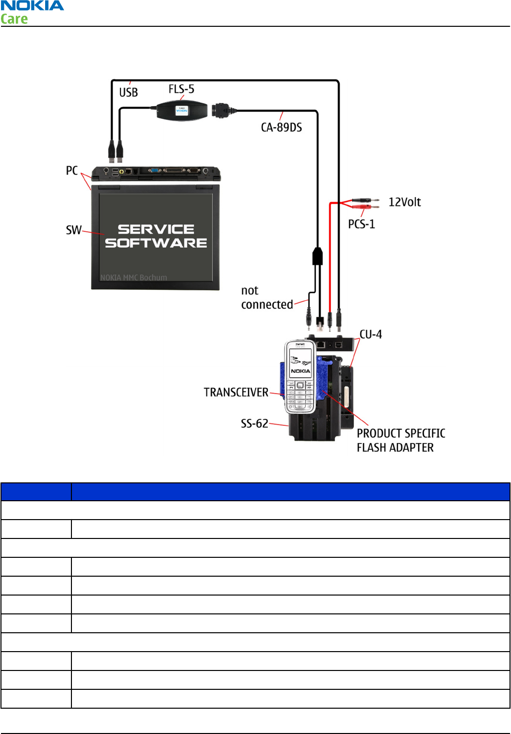
CU-4 flash concept with FPS-10..................................................................................................................... 2–13
Flash concept with FPS-10 and SB-6............................................................................................................. 2–14
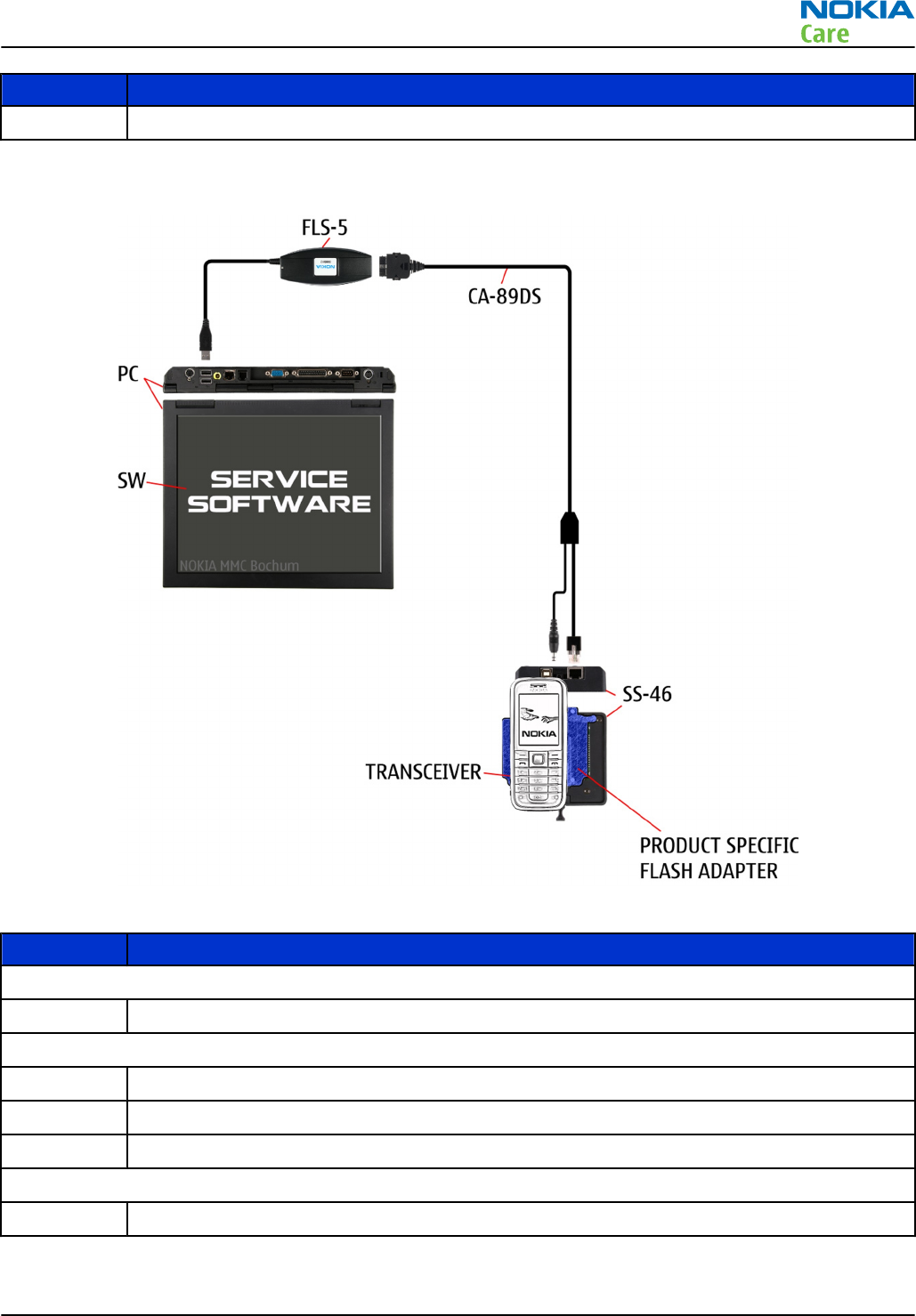
Flash concept with SS-46 and CA-89DS ........................................................................................................ 2–15
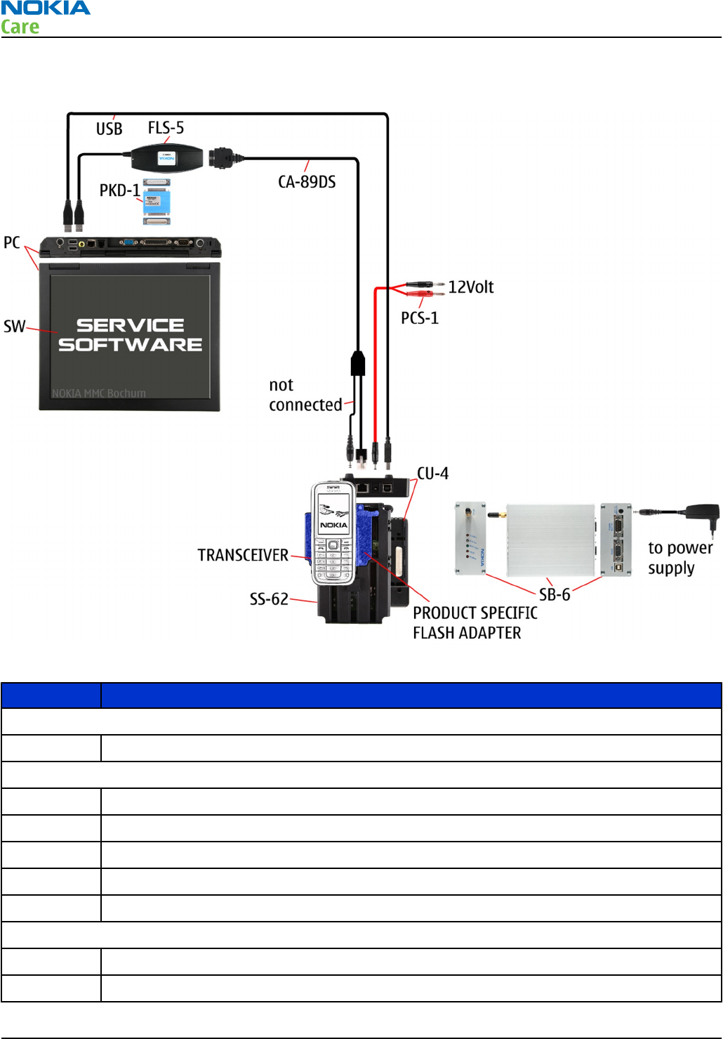
Flash concept with SS-62 and CA-89DS ........................................................................................................ 2–16
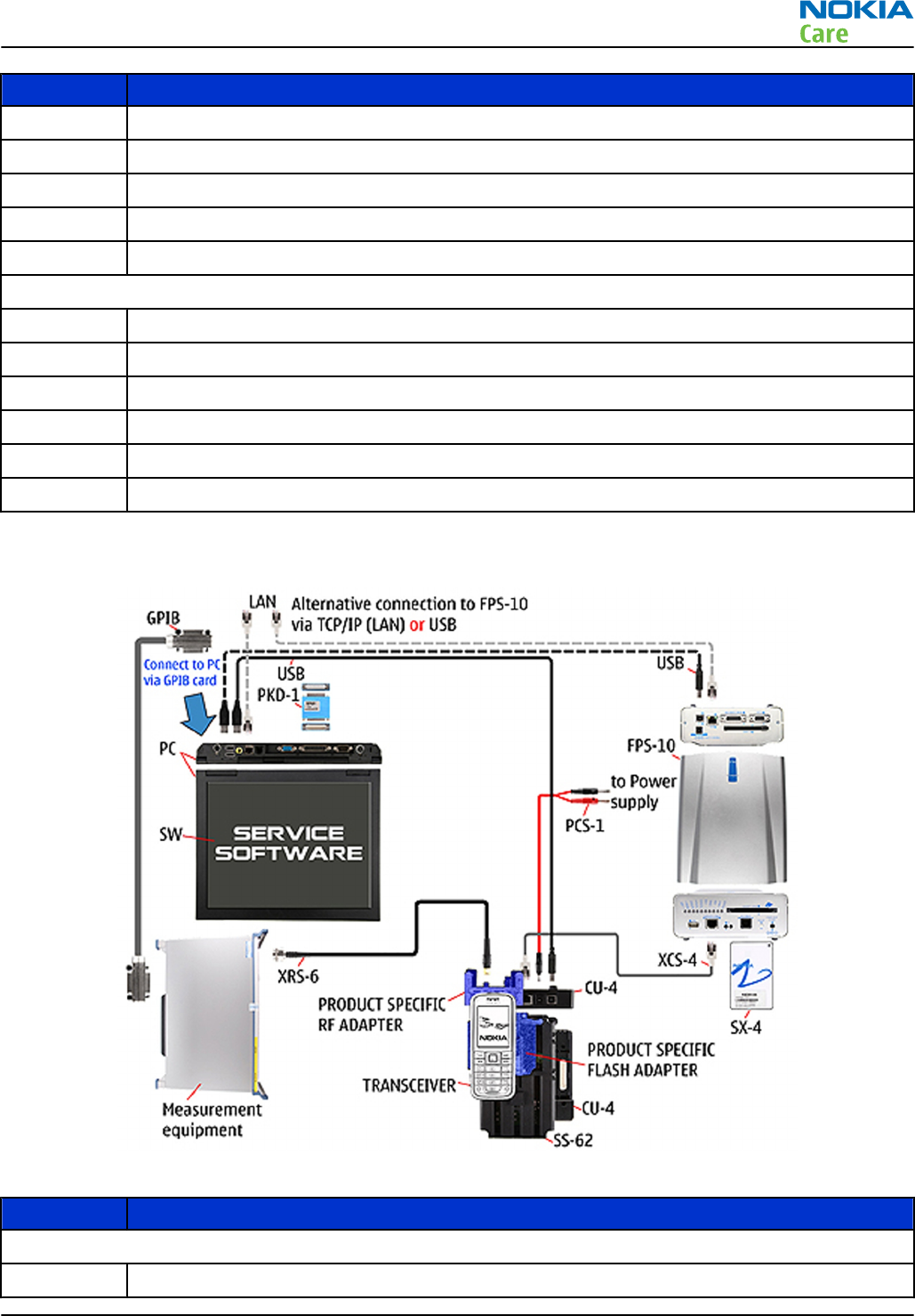
Flash concept with FPS-10, SS-62 and SB-6 ................................................................................................. 2–17
Flash concept with FPS-10, SS-62 and SB-7 ................................................................................................. 2–18
Module jig service concept............................................................................................................................ 2–19
Module jig service concept with SB-6........................................................................................................... 2–20
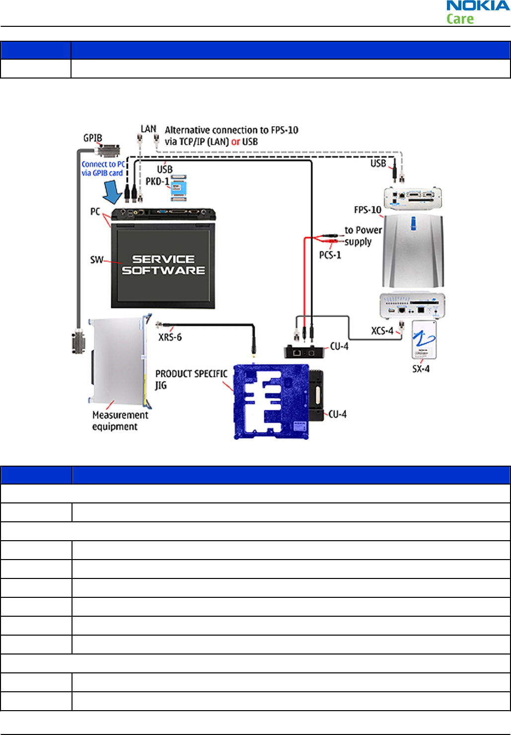
RF testing concept with RF coupler .............................................................................................................. 2–21
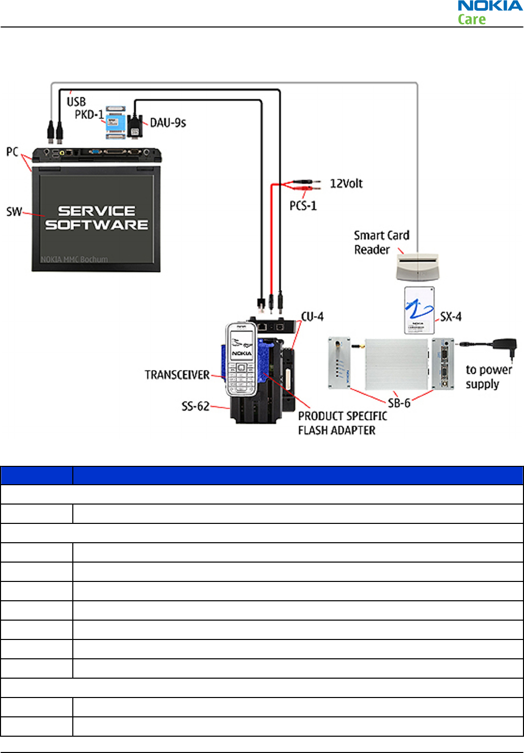
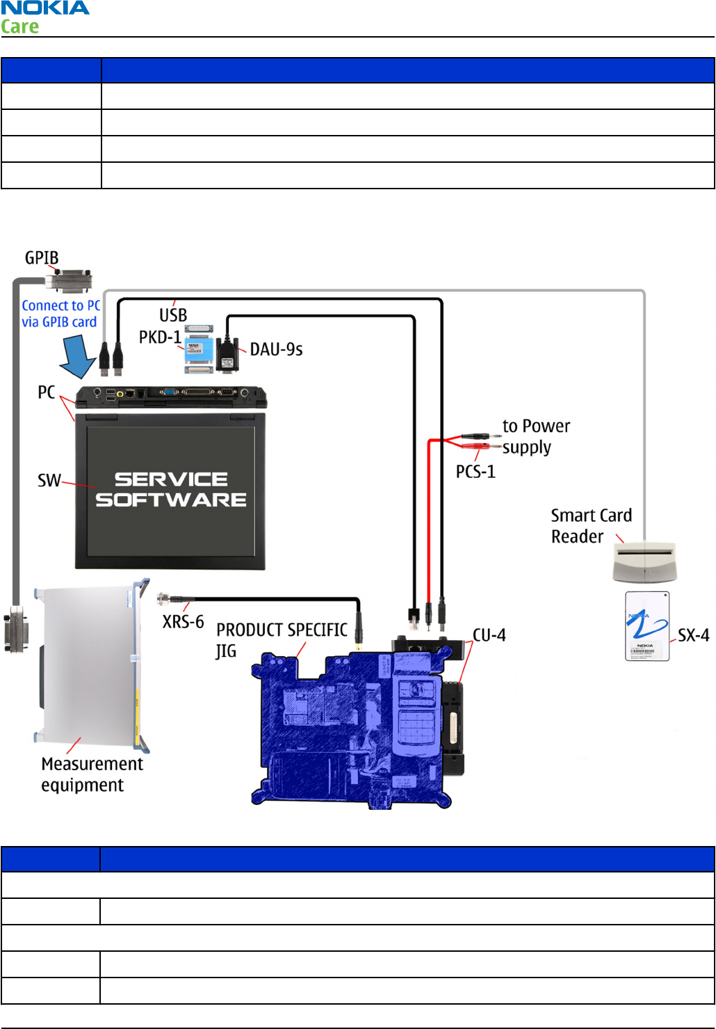
Service concept for RF testing and RF/BB tuning........................................................................................ 2–22
List of Figures
Figure 2 POS flash concept ................................................................................................................................. 2–11
Figure 3 Basic flash concept with FPS-10.......................................................................................................... 2–12
Figure 4 CU-4 flash concept with FPS-10........................................................................................................... 2–13
Figure 5 Flash concept with FPS-10 and SB-6................................................................................................... 2–14
Figure 6 Flash concept with SS-46 and CA-89DS .............................................................................................. 2–15
Figure 7 Flash concept with SS-62 and CA-89DS .............................................................................................. 2–16
Figure 8 Flash concept with FPS-10, SS-62 and SB-6 ....................................................................................... 2–17
Figure 9 Flash concept with FPS-10, SB-7 and JBT-9........................................................................................ 2–18
Figure 10 Module jig service concept................................................................................................................ 2–19
Figure 11 Module jig service concept with SB-6............................................................................................... 2–20
RM-333; RM-334; RM-335
Service Tools and Service Concepts
Issue 2 COMPANY CONFIDENTIAL Page 2 –3
Copyright © 2008 Nokia. All rights reserved.

Figure 12 RF testing concept with RF coupler.................................................................................................. 2–21
Figure 13 Service concept for RF testing and RF/BB tuning............................................................................ 2–22
RM-333; RM-334; RM-335
Service Tools and Service Concepts
Page 2 –4 COMPANY CONFIDENTIAL Issue 2
Copyright © 2008 Nokia. All rights reserved.
Service tools
Product specific tools
The table below gives a short overview of service devices that can be used for testing, error analysis, and
repair of product RM-333; RM-334; RM-335. For the correct use of the service devices, and the best effort of
workbench setup, please refer to various concepts.
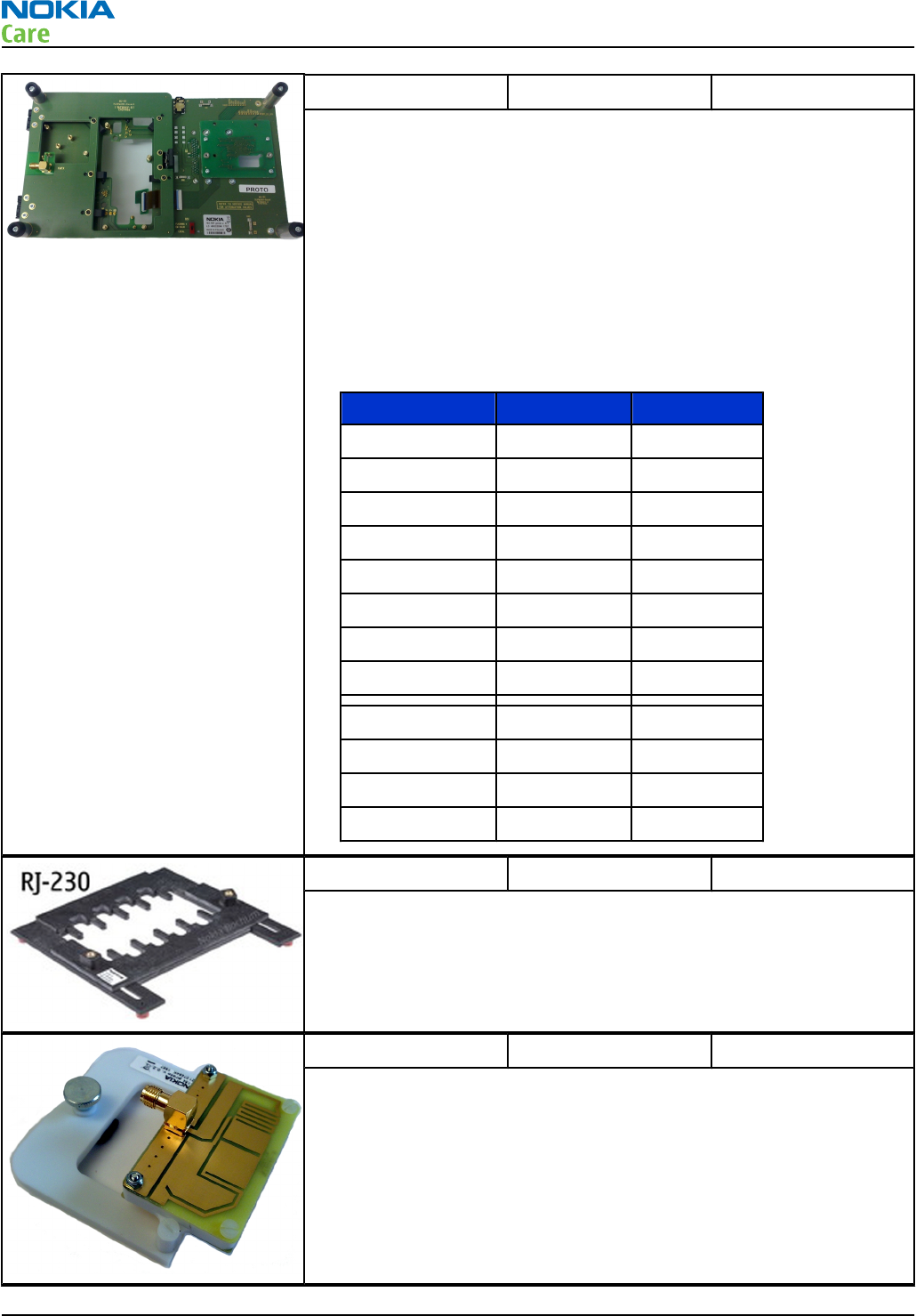
FS-73 Flash adapter
•FS-73 is equipped with a clip interlock system
•provides standardised interface towards Control Unit
•multiplexing between USB and FBUS media, controlled by VUSB
RM-333; RM-334; RM-335
Service Tools and Service Concepts
Issue 2 COMPANY CONFIDENTIAL Page 2 –5
Copyright © 2008 Nokia. All rights reserved.
MJ-161 Module jig
MJ-161 is meant for component level troubleshooting.
The jig includes RF interface for Bluetooth, WLAN and GPS. In addition,
it has the following features:
•Provides mechanical interface with the engine module
•Provides galvanic connection to all needed test pads in module
•Multiplexing between USB and FBUS media, controlled by Vusb
•Connector for control unit
•Access for Audio-, MMC, and USB connectors
•Module jig attenuation values:
Band F Attenuation
GSM850 TX 824-849 0.4dB
GSM850 RX 869-894 0.4dB
EGSM900 TX 880-915 0.4dB
EGSM900 RX 935-960 0.4dB
GSM1800 TX 1710-1785 0.6dB
GSM1800 RX 1805-1880 0.6dB
GSM1900 TX 1850-1910 0.6dB
GSM1900 RX 1930-1990 0.6dB
WCDMA850 TX 824-849 0.4dB
WCDMA850 RX 869-894 0.4dB
WCDMA1900 TX 1850-1910 0.6dB
WCDMA1900 RX 1930-1990 0.6dB
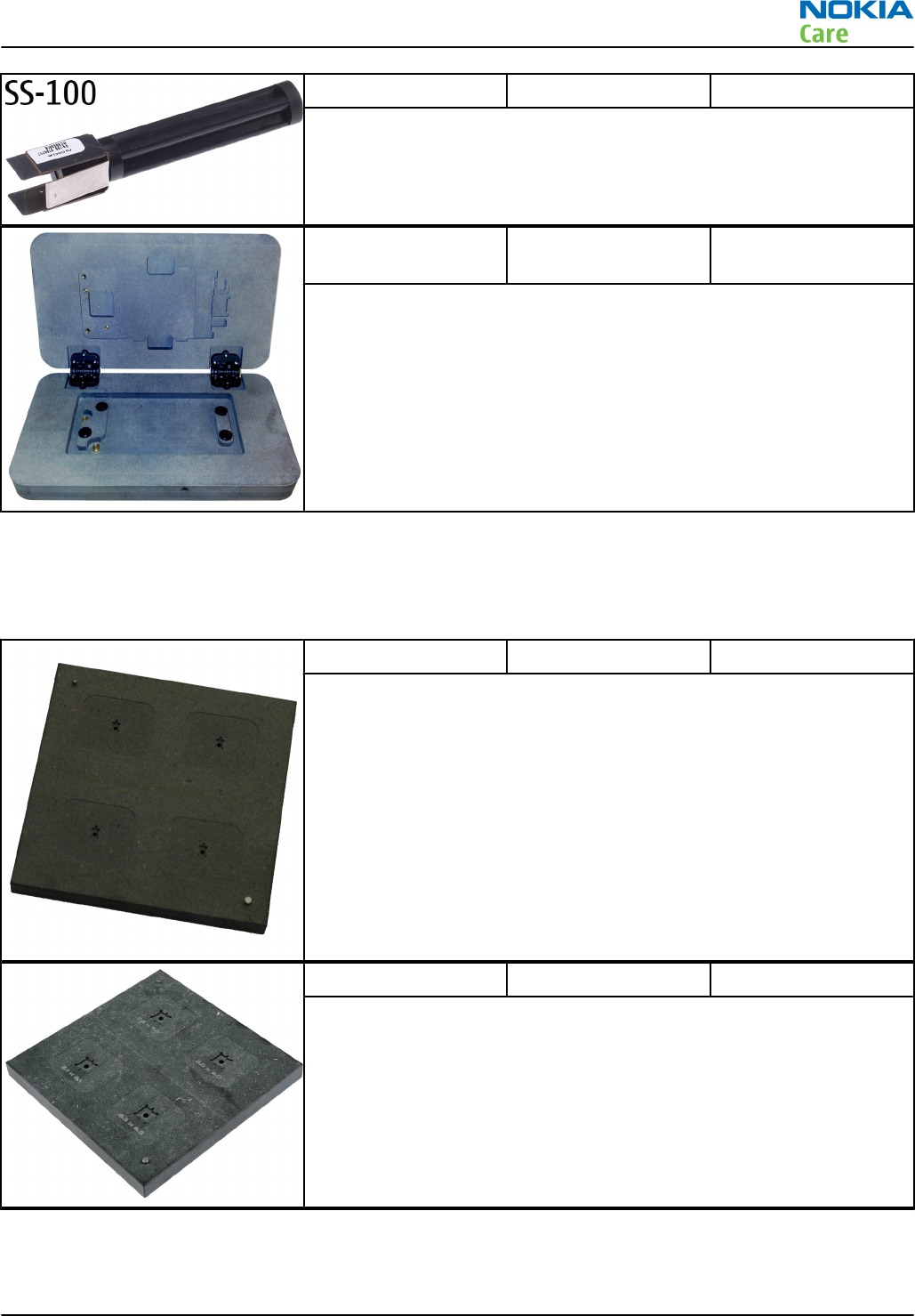
RJ-230 Soldering jig
The jig is used for soldering and as a rework jig for the system module.
It is made of lead-free rework compatible material.
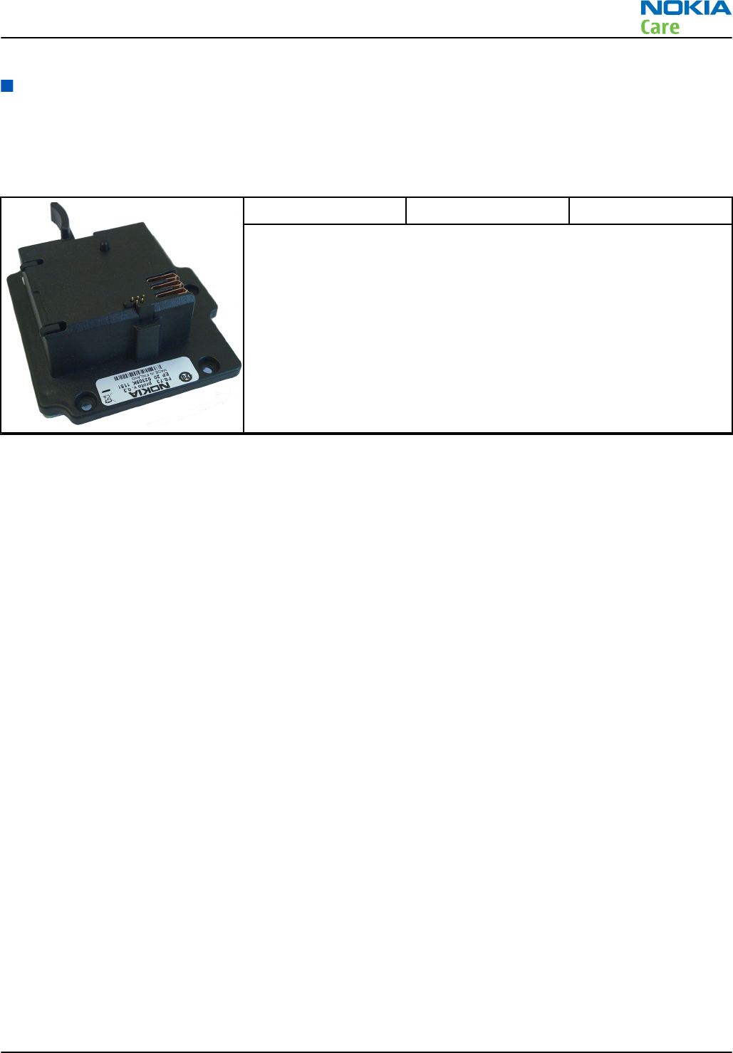
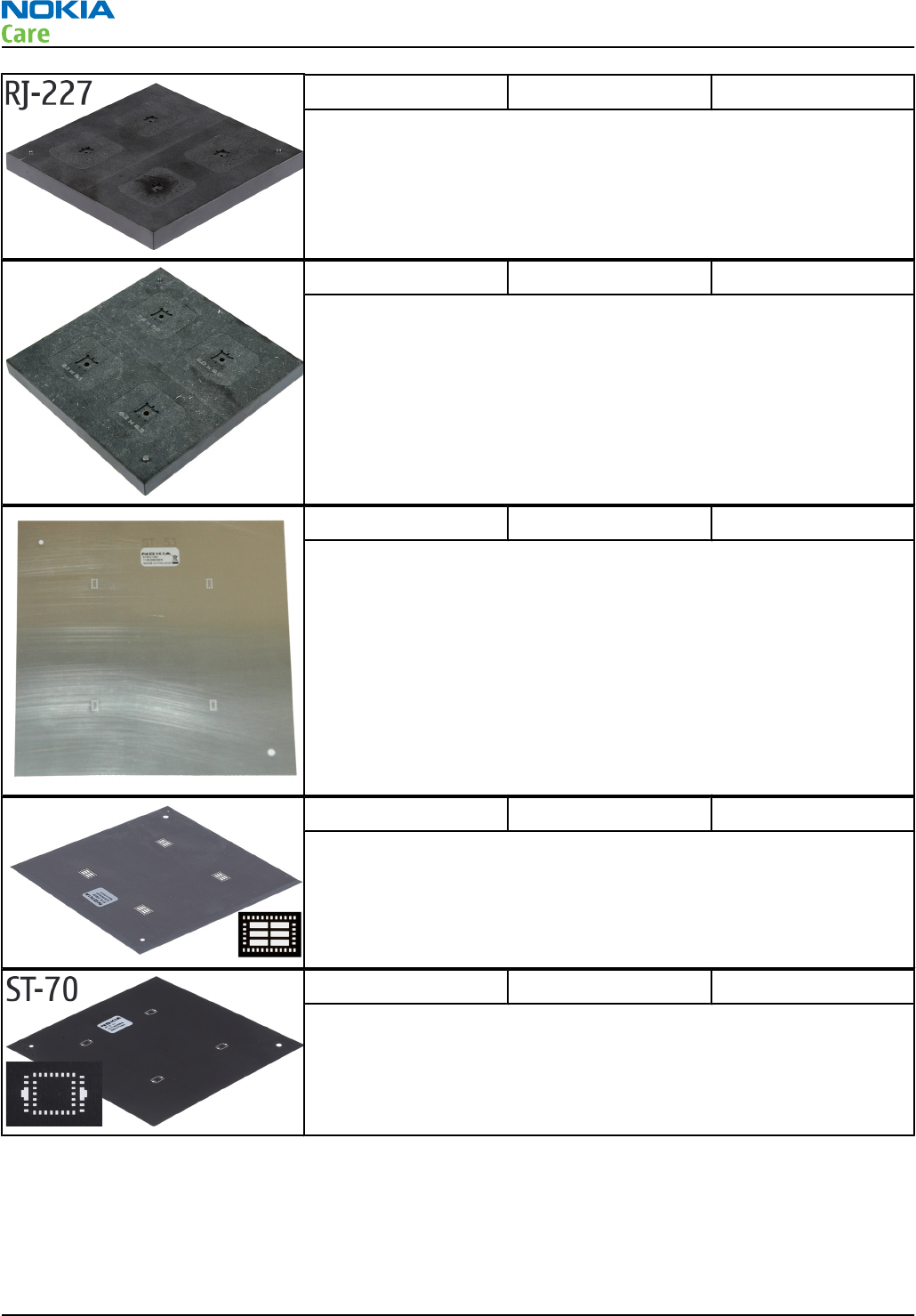
SA-154 RF coupler
SA-154 is an RF coupler for WCDMA and GSM RF testing. It is used
together with the product-specific flash adapter.
RM-333; RM-334; RM-335
Service Tools and Service Concepts
Page 2 –6 COMPANY CONFIDENTIAL Issue 2
Copyright © 2008 Nokia. All rights reserved.
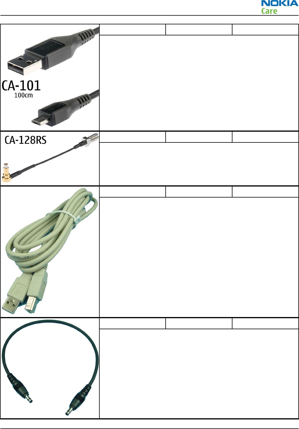
SS-100 Camera removal tool
The camera removal tool SS-100 is used to remove/attach a camera
module from/to the camera socket of the phone PWB.
SS-157 Domesheet
alignment jig
SS-157 is used for domesheet alignment.
General tools
The table below gives a short overview of service devices that can be used for testing, error analysis, and
repair of product RM-333; RM-334; RM-335. For the correct use of the service devices, and the best effort of
workbench setup, please refer to various concepts.
RJ-166 Rework jig
RJ-166 is a jig used for soldering and as a rework jig for the engine
module. It is used together with the ST-53 stencil.
RJ-209 Rework jig
RJ-209 is used as a rework jig for the WLAN 4.0 module
This stencil takes the WLAN 4.0 module for spreading soldering paste
onto the component. This must be used together with the ST-64
rework stencil.
RM-333; RM-334; RM-335
Service Tools and Service Concepts
Issue 2 COMPANY CONFIDENTIAL Page 2 –7
Copyright © 2008 Nokia. All rights reserved.
RJ-227 Rework jig
RJ-227 is a rework jig used when servicing the BTHFM module (D6000).
It is used together with the ST-70 rework stencil.
RJ-93 Rework jig
RJ-93 is a rework jig used with ST-40.
ST-53 Rework stencil
ST-53 is a rework stencil used with rework jig RJ-166.
ST-64 Rework stencil
ST-64 is the stencil used during rework of the WLAN 4.0 module. It
must be used together with the RJ-209 rework jig.
ST-70 Rework stencil
ST-70 rework stencil is used with RJ-227 rework jig to service the
BTHFM module (D6000).
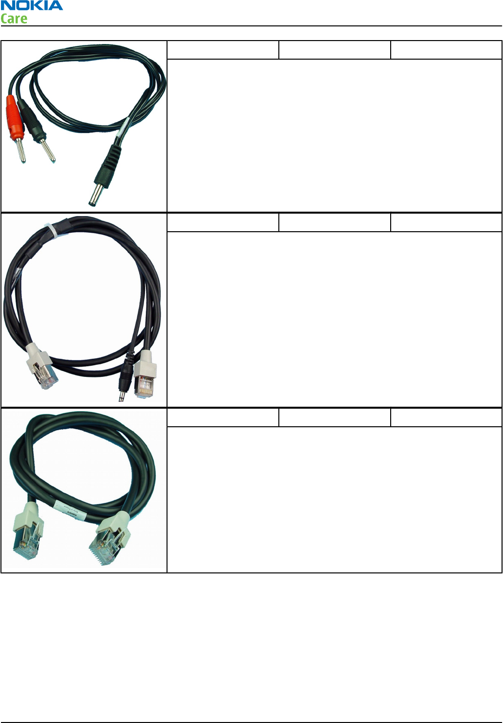
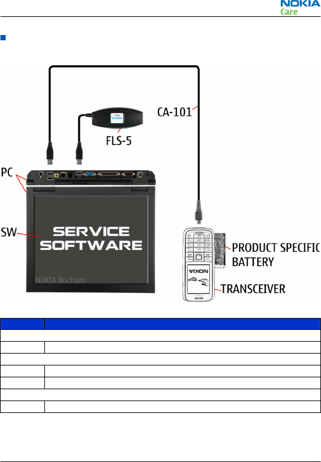
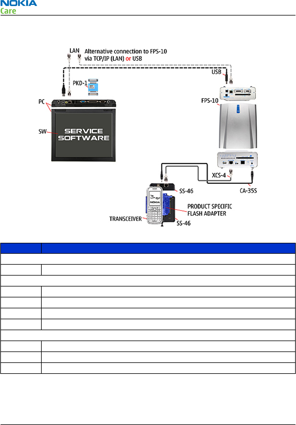
Cables
The table below gives a short overview of service devices that can be used for testing, error analysis, and
repair of product RM-333; RM-334; RM-335. For the correct use of the service devices, and the best effort of
workbench setup, please refer to various concepts.
RM-333; RM-334; RM-335
Service Tools and Service Concepts
Page 2 –8 COMPANY CONFIDENTIAL Issue 2
Copyright © 2008 Nokia. All rights reserved.
CA-101 Micro USB cable
The CA-101 is a USB-to-microUSB data cable that allows connections
between the PC and the phone.
CA-128RS RF tuning cable
Product-specific adapter cable for RF tuning.
CA-31D USB cable
The CA-31D USB cable is used to connect FPS-10 or FPS-11 to a PC. It is
included in the FPS-10 and FPS-11 sales packages.
CA-35S Power cable
CA-35S is a power cable for connecting, for example, the FPS-10 flash
prommer to the Point-Of-Sales (POS) flash adapter.
RM-333; RM-334; RM-335
Service Tools and Service Concepts
Issue 2 COMPANY CONFIDENTIAL Page 2 –9
Copyright © 2008 Nokia. All rights reserved.
PCS-1 Power cable
The PCS-1 power cable (DC) is used with a docking station, a module
jig or a control unit to supply a controlled voltage.
XCS-1 Service cable
The XCS-1 service cable is used to connect FLS-4S to the POS flash
adapter for supplying a controlled operating voltage and data
connection.
XCS-4 Modular cable
XCS-4 is a shielded (one specially shielded conductor) modular cable
for flashing and service purposes.
RM-333; RM-334; RM-335
Service Tools and Service Concepts
Page 2 –10 COMPANY CONFIDENTIAL Issue 2
Copyright © 2008 Nokia. All rights reserved.
Service concepts
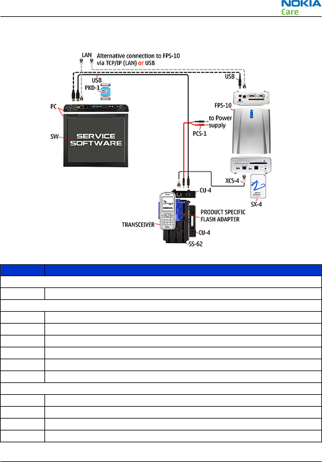
POS (Point of Sale) flash concept
Figure 2 POS flash concept
Type Description
Product specific tools
BL-5K Battery
Other tools
FLS-5 POS flash dongle
PC with Phoenix service software
Cables
CA-101 USB connectivity cable
RM-333; RM-334; RM-335
Service Tools and Service Concepts
Issue 2 COMPANY CONFIDENTIAL Page 2 –11
Copyright © 2008 Nokia. All rights reserved.
Flash concept with FPS-10
Figure 3 Basic flash concept with FPS-10
Type Description
Product specific devices
FS-73 Flash adapter
Other devices
FPS-10 Flash prommer box
PKD-1/PK-1 SW security device
SS-46 Interface adapter
PC with Phoenix service software
Cables
XCS-4 Modular cable
CA-35S Power cable
USB cable
RM-333; RM-334; RM-335
Service Tools and Service Concepts
Page 2 –12 COMPANY CONFIDENTIAL Issue 2
Copyright © 2008 Nokia. All rights reserved.
CU-4 flash concept with FPS-10
Figure 4 CU-4 flash concept with FPS-10
Type Description
Product specific devices
FS-73 Flash adapter
Other devices
CU-4 Control unit
FPS-10 Flash prommer box
PKD-1/PK-1 SW security device
SS-62 Flash adapter base
SX-4 Smart card
PC with Phoenix service software
Cables
PCS-1 Power cable
XCS-4 Modular cable
Standard USB cable
USB cable
RM-333; RM-334; RM-335
Service Tools and Service Concepts
Issue 2 COMPANY CONFIDENTIAL Page 2 –13
Copyright © 2008 Nokia. All rights reserved.
Flash concept with FPS-10 and SB-6
Figure 5 Flash concept with FPS-10 and SB-6
Type Description
Product specific tools
FS-73 Flash adapter
Other tools
FPS-10 Flash prommer box
PKD-1/PK-1 SW security device
SS-46 Interface adapter
SB-6 Bluetooth test and interface box
PC with Phoenix service software
Cables
XCS-4 Modular cable
CA-35S Power cable
RM-333; RM-334; RM-335
Service Tools and Service Concepts
Page 2 –14 COMPANY CONFIDENTIAL Issue 2
Copyright © 2008 Nokia. All rights reserved.
Type Description
USB cable
Flash concept with SS-46 and CA-89DS
Figure 6 Flash concept with SS-46 and CA-89DS
Type Description
Product specific tools
FS-73 Flash adapter
Other tools
FLS-5 Flash device
SS-46 Interface adapter
PC with Phoenix service software
Cables
CA-89DS Cable
RM-333; RM-334; RM-335
Service Tools and Service Concepts
Issue 2 COMPANY CONFIDENTIAL Page 2 –15
Copyright © 2008 Nokia. All rights reserved.
Flash concept with SS-62 and CA-89DS
Figure 7 Flash concept with SS-62 and CA-89DS
Type Description
Product specific tools
FS-73 Flash adapter
Other tools
CU-4 Control unit
FLS-5 Flash device
SS-62 Flash adapter base
PC with Phoenix service software
Cables
CA-89DS Cable
PCS-1 Power cable
USB cable
RM-333; RM-334; RM-335
Service Tools and Service Concepts
Page 2 –16 COMPANY CONFIDENTIAL Issue 2
Copyright © 2008 Nokia. All rights reserved.
Flash concept with FPS-10, SS-62 and SB-6
Figure 8 Flash concept with FPS-10, SS-62 and SB-6
Type Description
Product specific tools
FS-73 Flash adapter
Other tools
CU-4 Control unit
FPS-10 Flash prommer box
PKD-1/PK-1 SW security device
SS-62 Flash adapter base
SB-6 Bluetooth test and interface box
SX-4 Smart card
PC with Phoenix service software
Cables
XCS-4 Modular cable
PCS-1 Power cable
RM-333; RM-334; RM-335
Service Tools and Service Concepts
Issue 2 COMPANY CONFIDENTIAL Page 2 –17
Copyright © 2008 Nokia. All rights reserved.
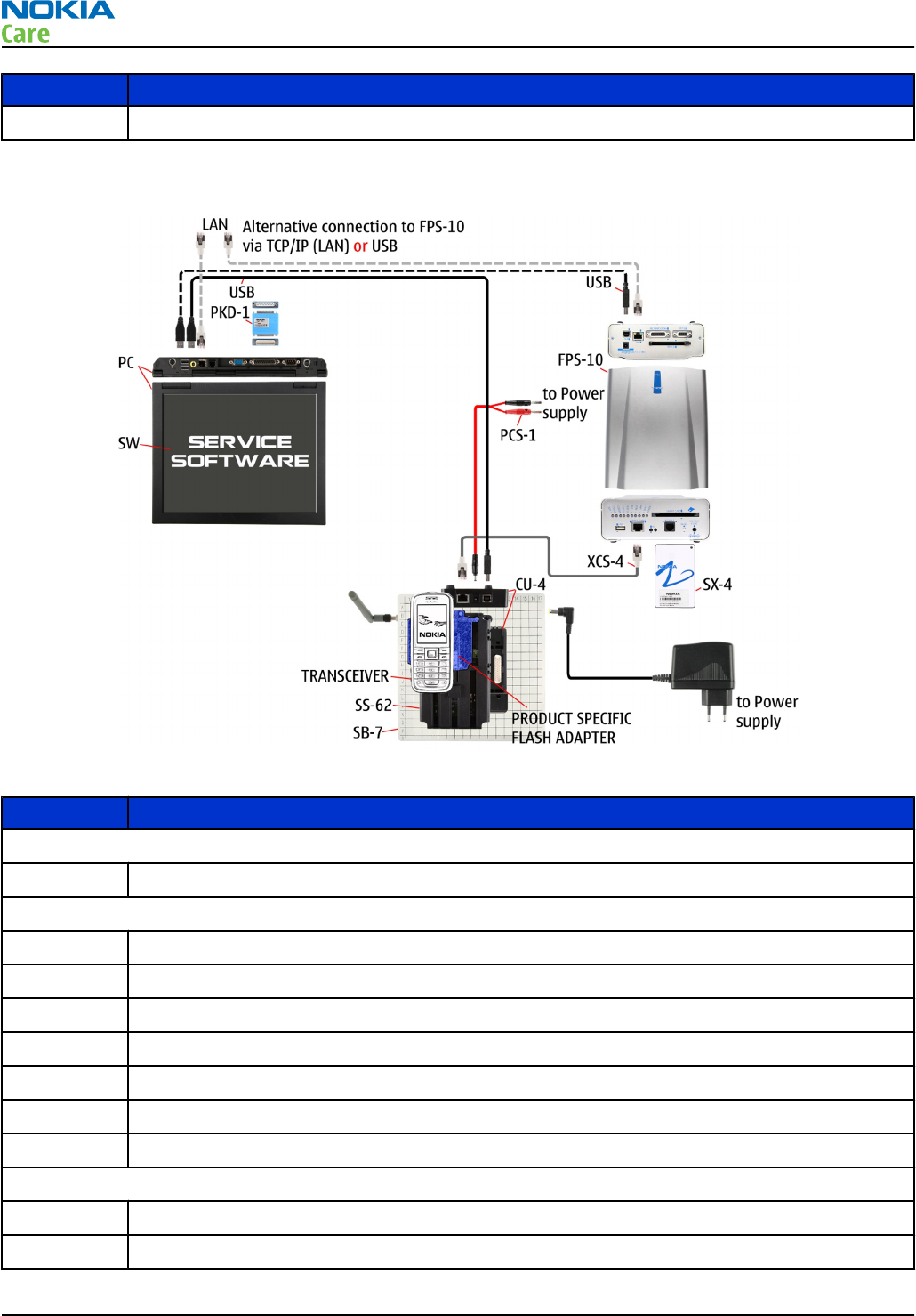
Type Description
USB cable
Flash concept with FPS-10, SS-62 and SB-7
Figure 9 Flash concept with FPS-10, SB-7 and JBT-9
Type Description
Product specific tools
FS-73 Flash adapter
Other tools
CU-4 Control unit
FPS-10 Flash prommer box
PKD-1/PK-1 SW security device
SB-7 WLAN test box
SS-62 Flash adapter base
SX-4 Smart card
PC with Phoenix service software
Cables
XCS-4 Modular cable
PCS-1 Power cable
RM-333; RM-334; RM-335
Service Tools and Service Concepts
Page 2 –18 COMPANY CONFIDENTIAL Issue 2
Copyright © 2008 Nokia. All rights reserved.
Type Description
USB cable
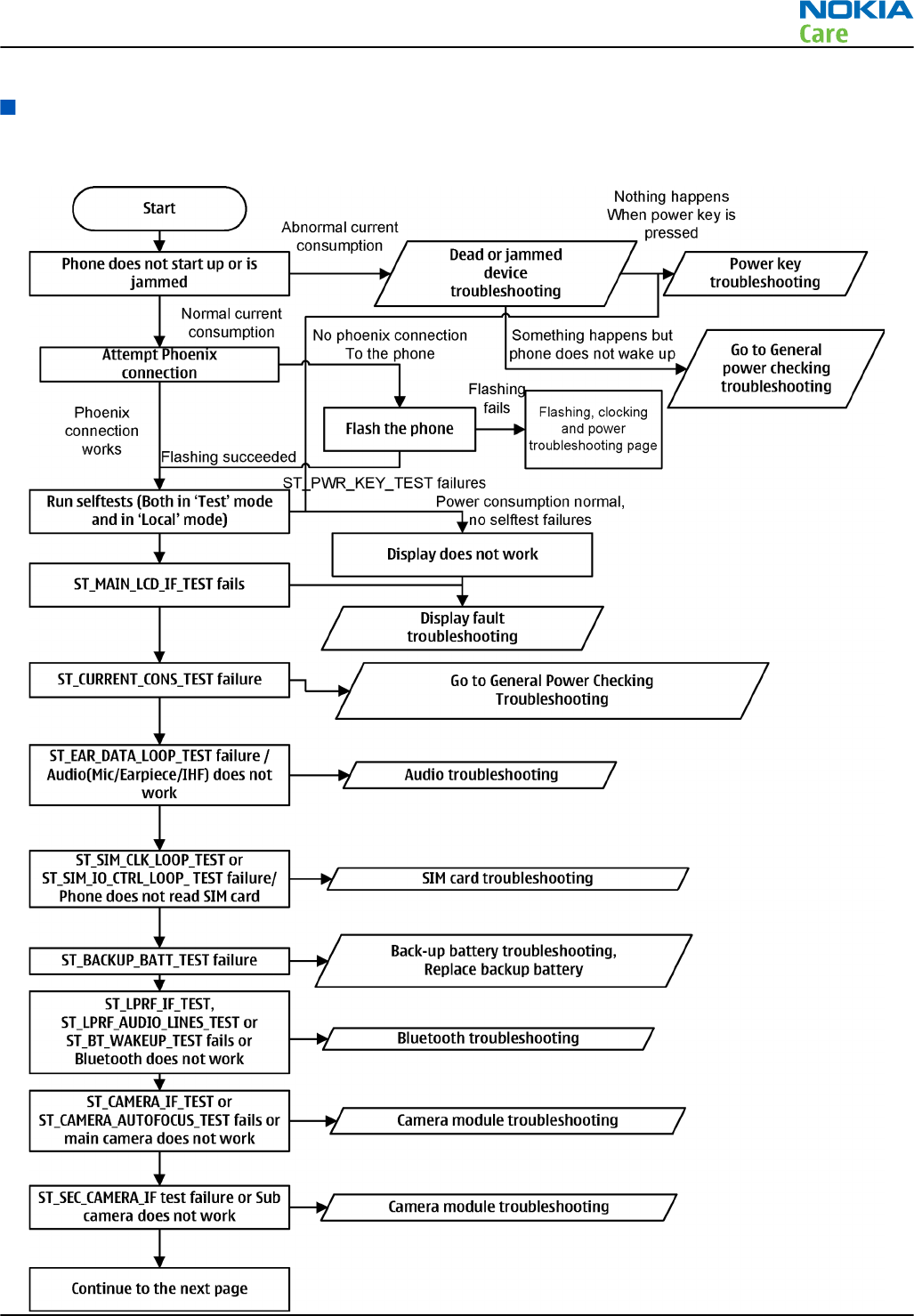
Module jig service concept
Figure 10 Module jig service concept
Type Description
Phone specific devices
MJ-161 Module jig
Other devices
CU-4 Control unit
FPS-10 Flash prommer box
PK-1 SW security device
SX-4 Smart card
PC with VPOS and Phoenix service software
Measurement equipment
Cables
PCS-1 DC power cable
XCS-4 Modular cable
RM-333; RM-334; RM-335
Service Tools and Service Concepts
Issue 2 COMPANY CONFIDENTIAL Page 2 –19
Copyright © 2008 Nokia. All rights reserved.
Type Description
XRF-1 RF cable
CA-128RS RF tuning cable
USB cable
GPIB control cable
Module jig service concept with SB-6
Figure 11 Module jig service concept with SB-6
Type Description
Product specific tools
MJ-161 Module jig
Other tools
CU-4 Control unit
FPS-10 Flash prommer box
RM-333; RM-334; RM-335
Service Tools and Service Concepts
Page 2 –20 COMPANY CONFIDENTIAL Issue 2
Copyright © 2008 Nokia. All rights reserved.
Type Description
SB-6 Bluetooth test and interface box
PKD-1 SW security device
SX-4 Smart card
Measurement equipment
PC with Phoenix service software
Cables
PCS-1 DC power cable
XCS-4 Modular cable
XRS-6 RF cable
CA-128RS RF tuning cable
GPIB control cable
USB cable
RF testing concept with RF coupler
Figure 12 RF testing concept with RF coupler
Type Description
Product specific devices
FS-73 Flash adapter
RM-333; RM-334; RM-335
Service Tools and Service Concepts
Issue 2 COMPANY CONFIDENTIAL Page 2 –21
Copyright © 2008 Nokia. All rights reserved.
Type Description
SA-154 RF coupler
Other devices
CU-4 Control unit
SX-4 Smart card
FPS-10 Flash prommer box
PKD-1/PK-1 SW security device
SS-62 Flash adapter base
Measurement equipment
PC with Phoenix service software
Cables
PCS-1 Power cable
XCS-4 Modular cable
XRS-6 RF cable
GPIB control cable
USB cable
Service concept for RF testing and RF/BB tuning
Figure 13 Service concept for RF testing and RF/BB tuning
RM-333; RM-334; RM-335
Service Tools and Service Concepts
Page 2 –22 COMPANY CONFIDENTIAL Issue 2
Copyright © 2008 Nokia. All rights reserved.

Type Description
Product specific devices
MJ-161 Module jig
Other devices
CU-4 Control unit
PK-1/PKD-1 SW security device
SX-4 Smart card
Measurement equipment
Smart card reader
PC with Phoenix service software
Cables
DAU-9S MBUS cable
PCS-1 DC power cable
XRS-6 RF cable
CA-128RS RF tuning cable
GPIB control cable
USB cable
RM-333; RM-334; RM-335
Service Tools and Service Concepts
Issue 2 COMPANY CONFIDENTIAL Page 2 –23
Copyright © 2008 Nokia. All rights reserved.

RM-333; RM-334; RM-335
Service Tools and Service Concepts
(This page left intentionally blank.)
Page 2 –24 COMPANY CONFIDENTIAL Issue 2
Copyright © 2008 Nokia. All rights reserved.

3 — BB Troubleshooting
Nokia Customer Care
Issue 2 COMPANY CONFIDENTIAL Page 3 –1
Copyright © 2008 Nokia. All rights reserved.

RM-333; RM-334; RM-335
BB Troubleshooting
(This page left intentionally blank.)
Page 3 –2 COMPANY CONFIDENTIAL Issue 2
Copyright © 2008 Nokia. All rights reserved.

Table of Contents
Baseband main troubleshooting..........................................................................................................................3–5
General power checking ........................................................................................................................................3–7
Backup battery troubleshooting...........................................................................................................................3–8
Dead or jammed device troubleshooting......................................................................................................... 3–10
Keyboard troubleshooting ................................................................................................................................. 3–11
Hall sensor troubleshooting............................................................................................................................... 3–13
TV- out troubleshooting ..................................................................................................................................... 3–14
General power checking troubleshooting ........................................................................................................ 3–15
USB troubleshooting ........................................................................................................................................... 3–16
SIM card troubleshooting ................................................................................................................................... 3–17
MicroSD card troubleshooting............................................................................................................................ 3–18
Combo memory troubleshooting ...................................................................................................................... 3–20
Flash programming troubleshooting................................................................................................................ 3–21
USB charging troubleshooting........................................................................................................................... 3–24
Clocking troubleshooting ................................................................................................................................... 3–25
Power key troubleshooting................................................................................................................................ 3–26
Naviscroll troubleshooting................................................................................................................................. 3–27
User interface troubleshooting.......................................................................................................................... 3–28
Display Troubleshooting..................................................................................................................................... 3–29
Display Troubleshooting................................................................................................................................ 3–29
Illumination troubleshooting ....................................................................................................................... 3–30
LED driver troubleshooting ........................................................................................................................... 3–33
I/O expander troubleshooting ...................................................................................................................... 3–35
Audio Troubleshooting....................................................................................................................................... 3–35
Audio troubleshooting test instructions...................................................................................................... 3–35
External earpiece troubleshooting............................................................................................................... 3–39
DAC33 troubleshooting.................................................................................................................................. 3–40
External microphone troubleshooting ........................................................................................................ 3–41
Internal earpiece troubleshooting .............................................................................................................. 3–42
Internal handsfree speaker troubleshooting ............................................................................................. 3–43
Internal microphone troubleshooting ........................................................................................................ 3–44
Vibra troubleshooting.................................................................................................................................... 3–45
ALS Technical Description and Troubleshooting.............................................................................................. 3–46
Ambient Light Sensor..................................................................................................................................... 3–46
ALS troubleshooting....................................................................................................................................... 3–46
Re-tuning ALS.................................................................................................................................................. 3–47
Bluetooth and FM Radio Troubleshooting........................................................................................................ 3–48
Introduction to Bluetooth/FM radio troubleshooting................................................................................ 3–48
Bluetooth BER test.......................................................................................................................................... 3–51
Bluetooth and FM radio self tests in Phoenix.............................................................................................. 3–52
Bluetooth troubleshooting ........................................................................................................................... 3–53
FM radio troubleshooting.............................................................................................................................. 3–53
FM radio testing.............................................................................................................................................. 3–55
GPS Troubleshooting........................................................................................................................................... 3–55
GPS layout and basic test points................................................................................................................... 3–55
GPS Settings for Phoenix ............................................................................................................................... 3–56
GPS control................................................................................................................................................. 3–56
Quick Test window.................................................................................................................................... 3–57
GPS failure troubleshooting.......................................................................................................................... 3–59
WLAN Troubleshooting....................................................................................................................................... 3–59
RM-333; RM-334; RM-335
BB Troubleshooting
Issue 2 COMPANY CONFIDENTIAL Page 3 –3
Copyright © 2008 Nokia. All rights reserved.

WLAN functional description......................................................................................................................... 3–59
WLAN settings for Phoenix............................................................................................................................ 3–60
WLAN functional tests.................................................................................................................................... 3–62
WLAN auto tuning.......................................................................................................................................... 3–64
List of Figures
Figure 14 Single-ended output waveform of the Ext_in_HP_out measurement when earpiece is
connected .................................................................................................................................................. 3–37
Figure 15 Single-ended output waveform of the Ext_in_IHF_out out loop measurement when speaker
is connected (measured at speaker pads), no filter is used ................................................................. 3–37
Figure 16 Single-ended output waveform of the Ext_in_Ext_out loop........................................................... 3–38
Figure 17 Single-ended output waveform of the Digital_stereo_microphone_in_Ext_out loop.................. 3–38
Figure 18 Ambient Light Sensor ........................................................................................................................ 3–46
Figure 19 Bluetooth/WLAN antenna ................................................................................................................. 3–49
Figure 20 BT/FM component layout .................................................................................................................. 3–51
Figure 21 Bluetooth and FM radio self tests in Phoenix.................................................................................. 3–52
Figure 22 GPS layout and basic test points....................................................................................................... 3–56
Figure 23 GPS Control dialogue box .................................................................................................................. 3–57
Figure 24 GPS Quick Test window ..................................................................................................................... 3–58
Figure 25 WLAN circuitry .................................................................................................................................... 3–60
Figure 26 WLAN auto tune settings................................................................................................................... 3–65
Figure 27 WLAN auto tune results..................................................................................................................... 3–66
RM-333; RM-334; RM-335
BB Troubleshooting
Page 3 –4 COMPANY CONFIDENTIAL Issue 2
Copyright © 2008 Nokia. All rights reserved.
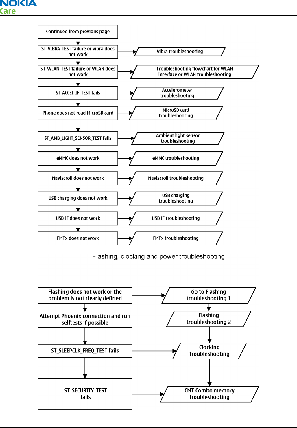
Baseband main troubleshooting
Troubleshooting flow
RM-333; RM-334; RM-335
BB Troubleshooting
Issue 2 COMPANY CONFIDENTIAL Page 3 –5
Copyright © 2008 Nokia. All rights reserved.
RM-333; RM-334; RM-335
BB Troubleshooting
Page 3 –6 COMPANY CONFIDENTIAL Issue 2
Copyright © 2008 Nokia. All rights reserved.
General power checking
Check the following voltages:
Signal
name Regulator Sleep Idle Nominal
voltage Main user Notes
VIO_V AVILMA ON ON 1.82 Not used
VBACK AVILMA ON ON 2.5 RTC circuitry
VSIM1 AVILMA ON ON 1.8/3.0 Sim card
VSIM2 AVILMA ON ON 3.0 Digital microphone
VAUX AVILMA OFF OFF 2.78 Accelerometer, Hall
switches, 2nd
camera
VANA AVILMA ON ON 2.5 Vilma internal
VR1 AVILMA OFF ON 2.5 VCTXO
VRFC AVILMA ON OFF 1.8 RAPIDO converter
VRCP1 AVILMA OFF OFF 4.75 RFmodule RF active
VIO LM3677 ON ON 1.8 Rapido , Betty I/O
VDRAM LM3677 ON ON 1.8 M3 Memory
VCORE TPS62350 ON ON 1.2 Rapido core
VDAC LP3985 3.0 DAC33 On when
used
VCAM_1V8 LM3677 OFF OFF 1.8 Julie, LP5952
VCAM_1V3 OFF OFF 1.3 Julie,core
VCAM_2V8 OFF OFF 2.8 Main camera
VSD LP3930 OFF OFF 2.9 SD card On when
used
V_ELVDD TPS65136 OFF OFF 4.6 Falcon OLED Display
V_ELVSS TPS65136 OFF OFF -4.9 Falcon OLED Display
VCORE_WD LP5952 OFF OFF 1.5 White Dwarf Core
VBAT 3.6
VCORE BETTY OFF OFF 1.2 Not used
VDRAM_V AVILMA ON 1.82 Not used
VLED BETTY 6-18 Not used
RM-333; RM-334; RM-335
BB Troubleshooting
Issue 2 COMPANY CONFIDENTIAL Page 3 –7
Copyright © 2008 Nokia. All rights reserved.
Backup battery troubleshooting
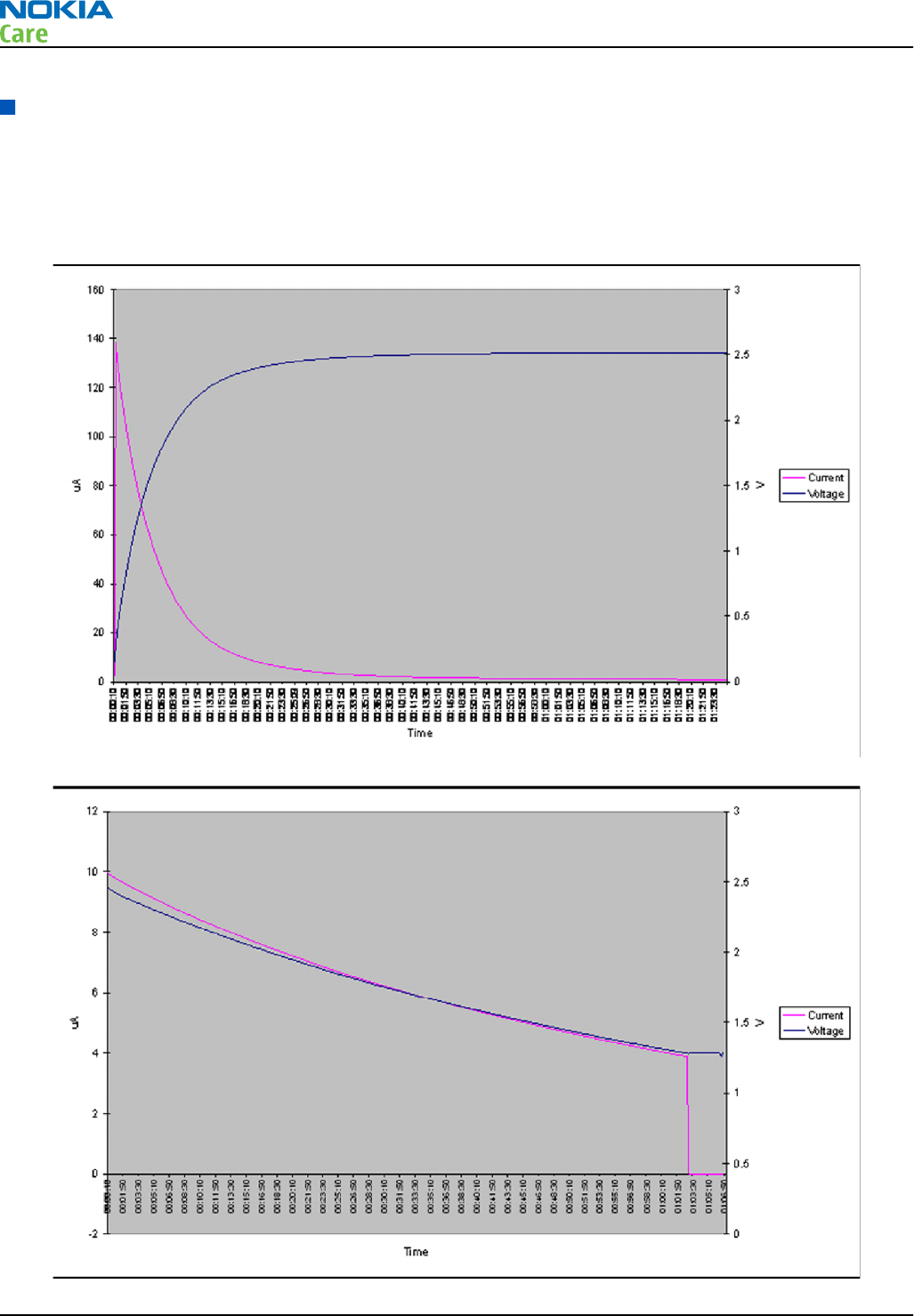
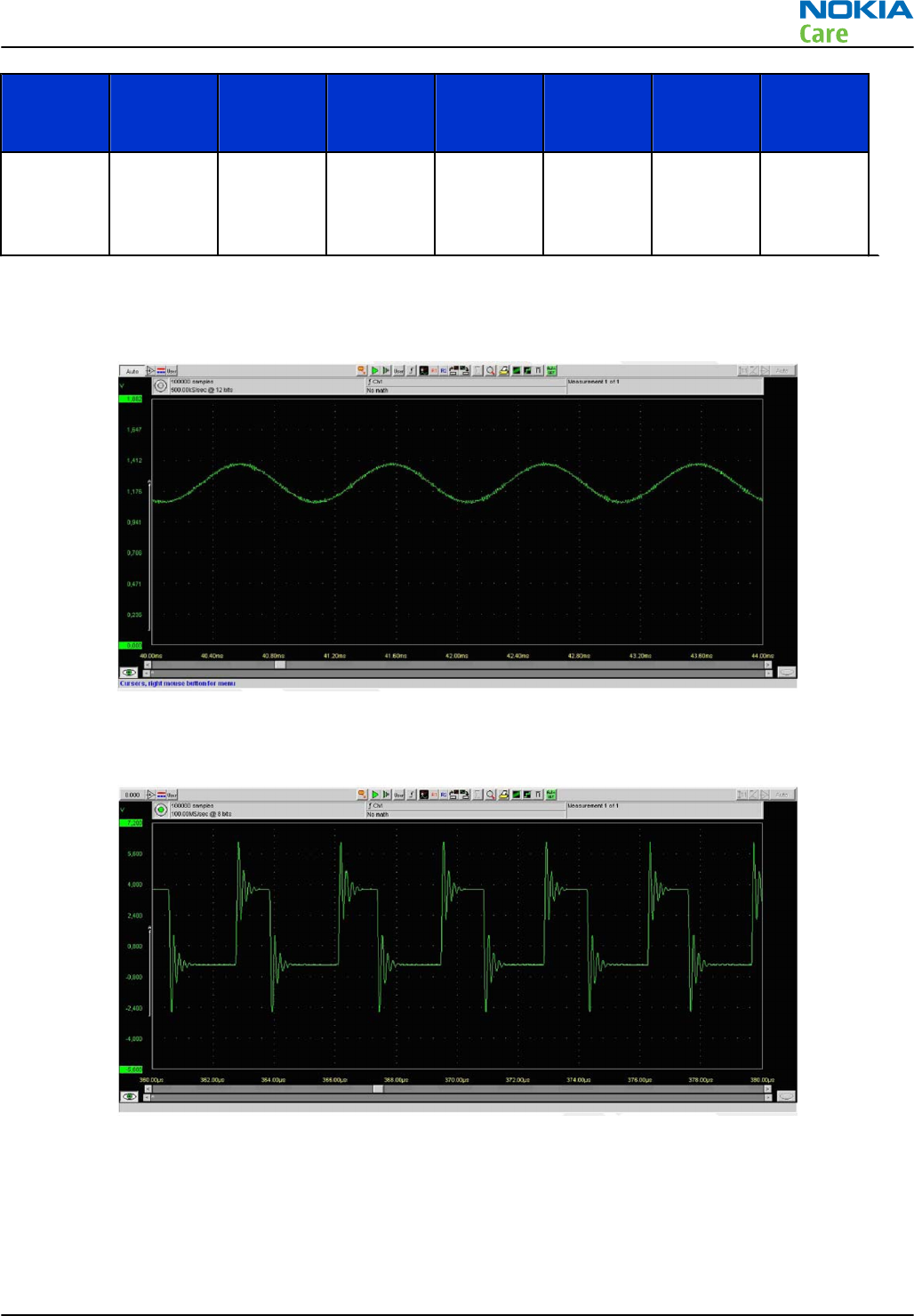
Verify that the backup battery G2200 is empty (U<1V). Switch the phone on. Measure voltage of the battery
when the main battery is connected to the phone and the phone is switched on. Wait a few minutes and
monitor that the backup battery voltage rises. Switch off the phone, disconnect the main battery and monitor
that the voltage of the backup battery decreases. Normal behaviour of the voltage is described in the figures
below:
RM-333; RM-334; RM-335
BB Troubleshooting
Page 3 –8 COMPANY CONFIDENTIAL Issue 2
Copyright © 2008 Nokia. All rights reserved.

If the voltage rises and falls quickly, check the back-up battery G2200 contacts for loose soldering or short-
circuit, and repair or change G2200 if necessary. If the voltage stays ~0V, check resistance VBACK against GND.
If there is no shortcircuit, AVILMA N2200 is faulty. Replace N2200.
RM-333; RM-334; RM-335
BB Troubleshooting
Issue 2 COMPANY CONFIDENTIAL Page 3 –9
Copyright © 2008 Nokia. All rights reserved.
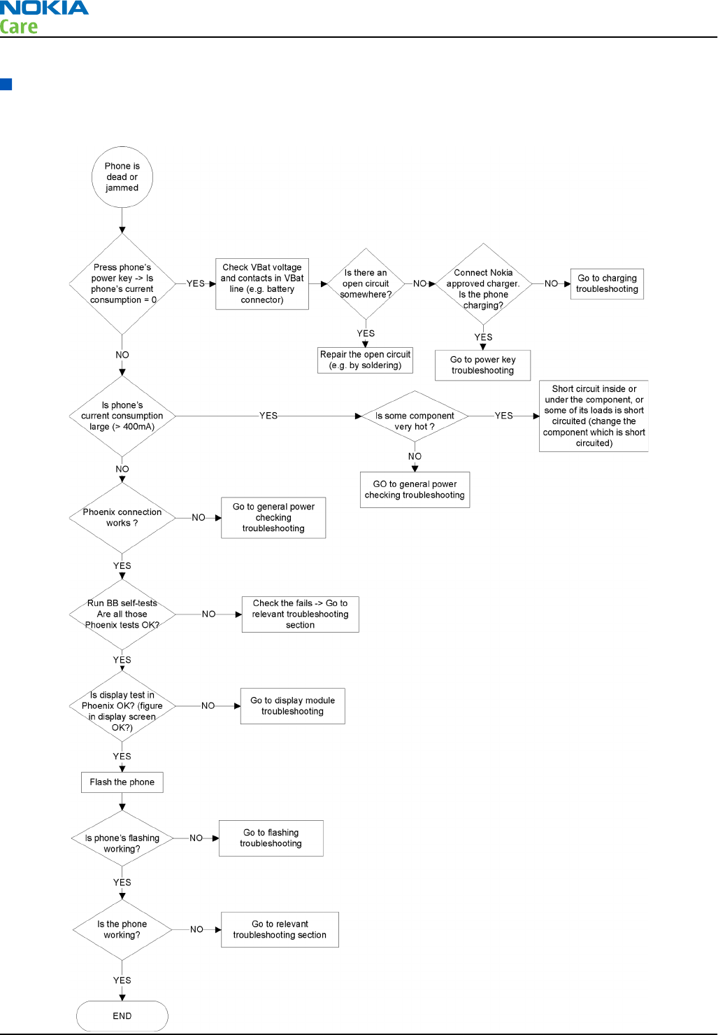
Dead or jammed device troubleshooting
Troubleshooting flow
RM-333; RM-334; RM-335
BB Troubleshooting
Page 3 –10 COMPANY CONFIDENTIAL Issue 2
Copyright © 2008 Nokia. All rights reserved.

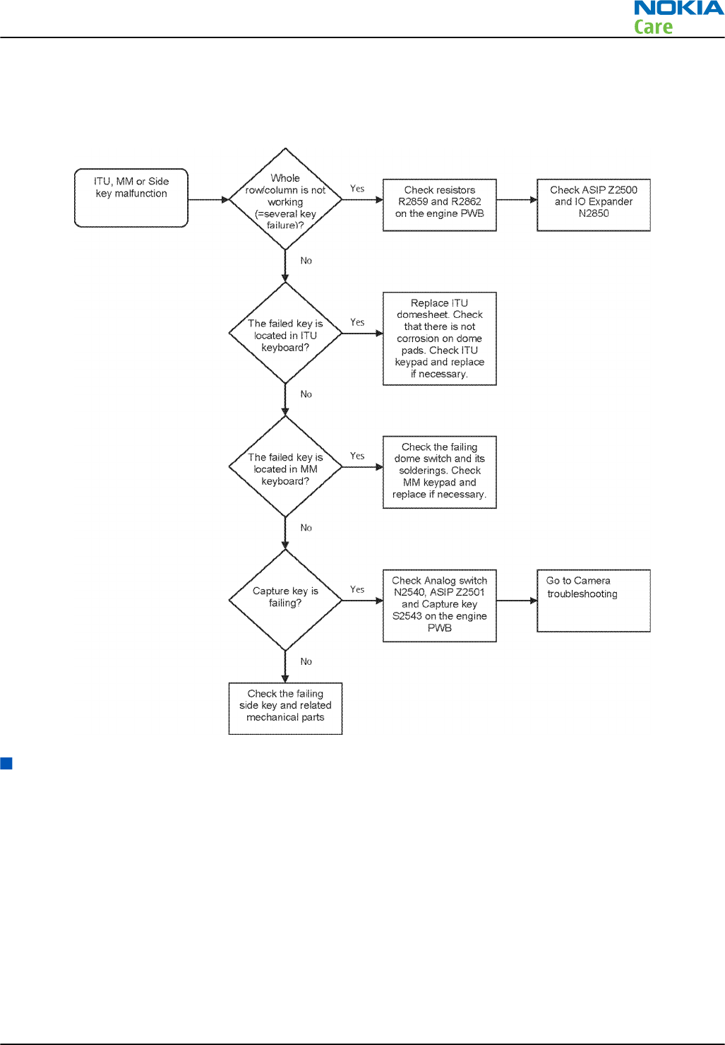
Keyboard troubleshooting
Context
There are two possible failure modes in the keyboard module:
1 One or more keys are stuck, so that the key(s) does not react when you press a keydome. This kind of
failure is caused by mechanical reasons (dirt, corrosion).
2Malfunction of several keys at the same time; this happens when one or more rows or columns are failing
(shortcut or open connection). For a more detailed description of the keyboard and keymatrix, see section
Keyboard.
If the failure mode is not clear, start with the Keyboard Test in
Phoenix
.
RM-333; RM-334; RM-335
BB Troubleshooting
Issue 2 COMPANY CONFIDENTIAL Page 3 –11
Copyright © 2008 Nokia. All rights reserved.
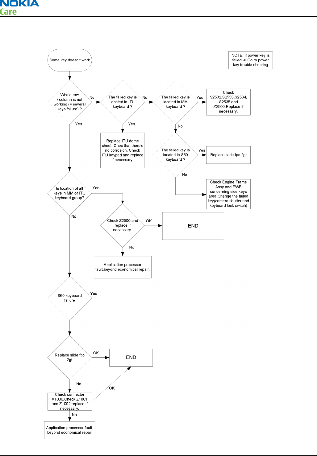
Troubleshooting flow
RM-333; RM-334; RM-335
BB Troubleshooting
Page 3 –12 COMPANY CONFIDENTIAL Issue 2
Copyright © 2008 Nokia. All rights reserved.
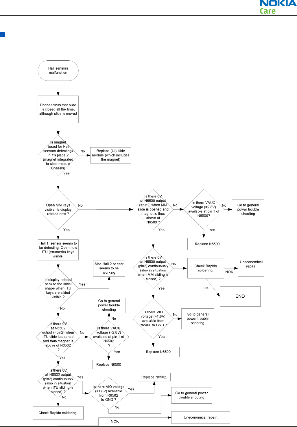
Hall sensor troubleshooting
Troubleshooting flow
RM-333; RM-334; RM-335
BB Troubleshooting
Issue 2 COMPANY CONFIDENTIAL Page 3 –13
Copyright © 2008 Nokia. All rights reserved.
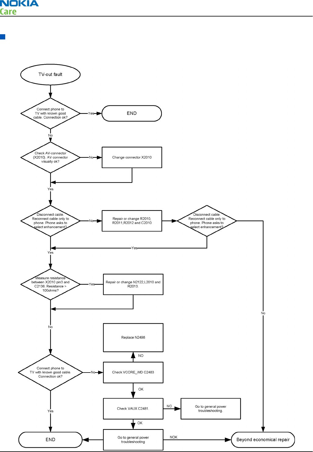
TV- out troubleshooting
Troubleshooting flow
RM-333; RM-334; RM-335
BB Troubleshooting
Page 3 –14 COMPANY CONFIDENTIAL Issue 2
Copyright © 2008 Nokia. All rights reserved.
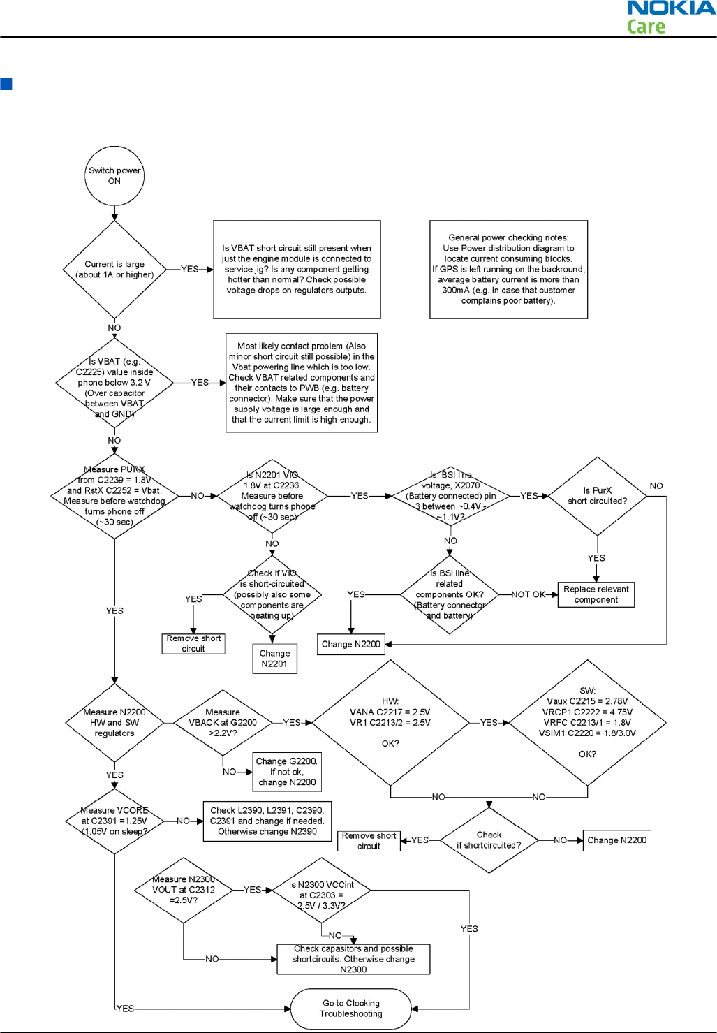
General power checking troubleshooting
Troubleshooting flow
RM-333; RM-334; RM-335
BB Troubleshooting
Issue 2 COMPANY CONFIDENTIAL Page 3 –15
Copyright © 2008 Nokia. All rights reserved.
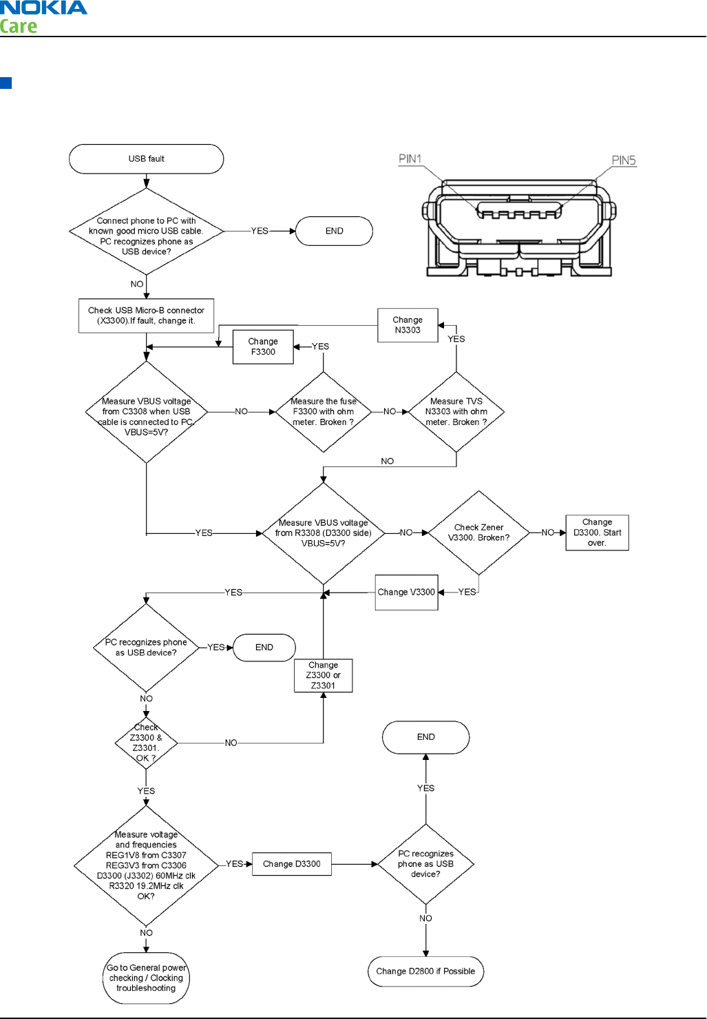
USB troubleshooting
Troubleshooting flow
RM-333; RM-334; RM-335
BB Troubleshooting
Page 3 –16 COMPANY CONFIDENTIAL Issue 2
Copyright © 2008 Nokia. All rights reserved.
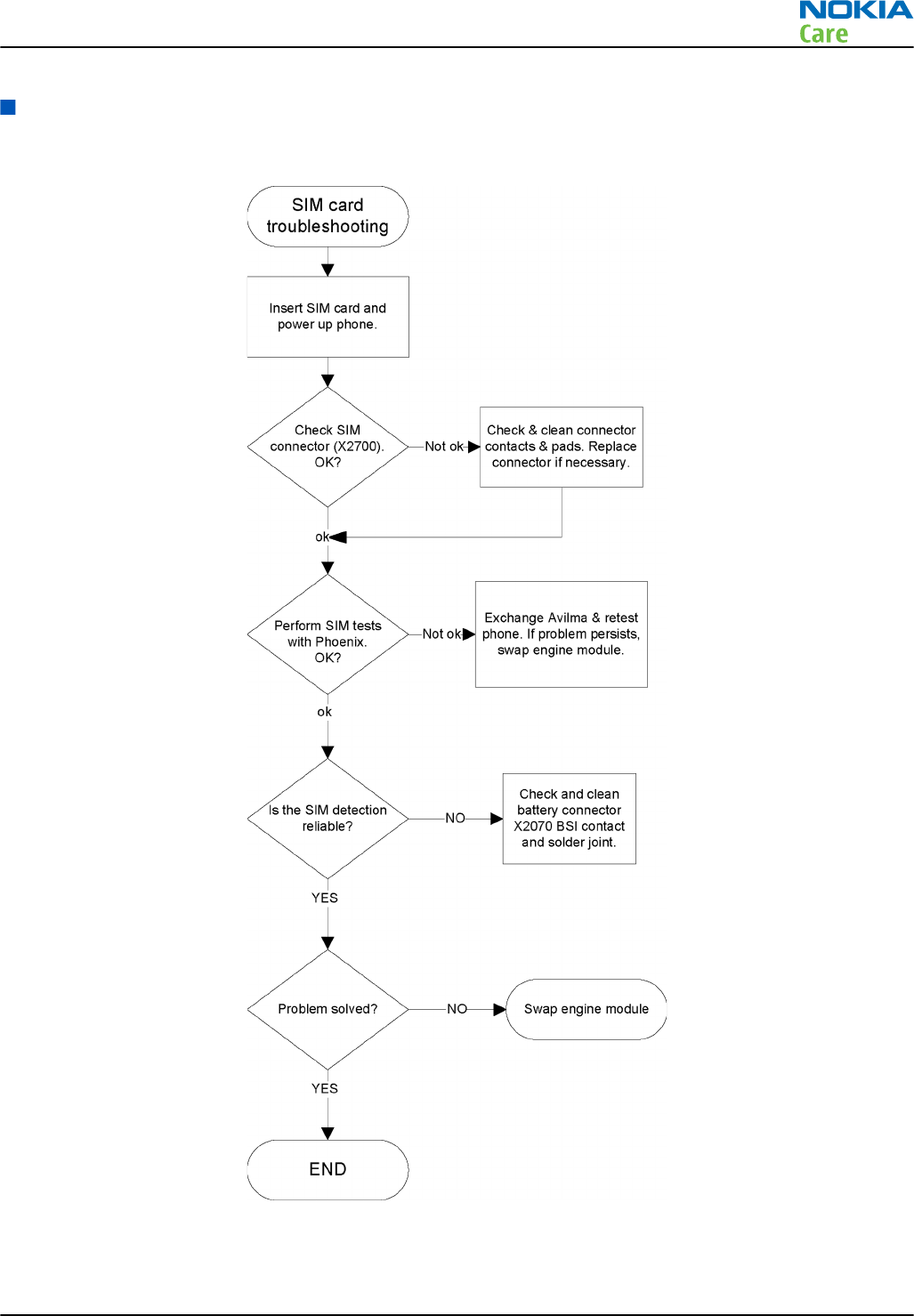
SIM card troubleshooting
Troubleshooting flow
RM-333; RM-334; RM-335
BB Troubleshooting
Issue 2 COMPANY CONFIDENTIAL Page 3 –17
Copyright © 2008 Nokia. All rights reserved.
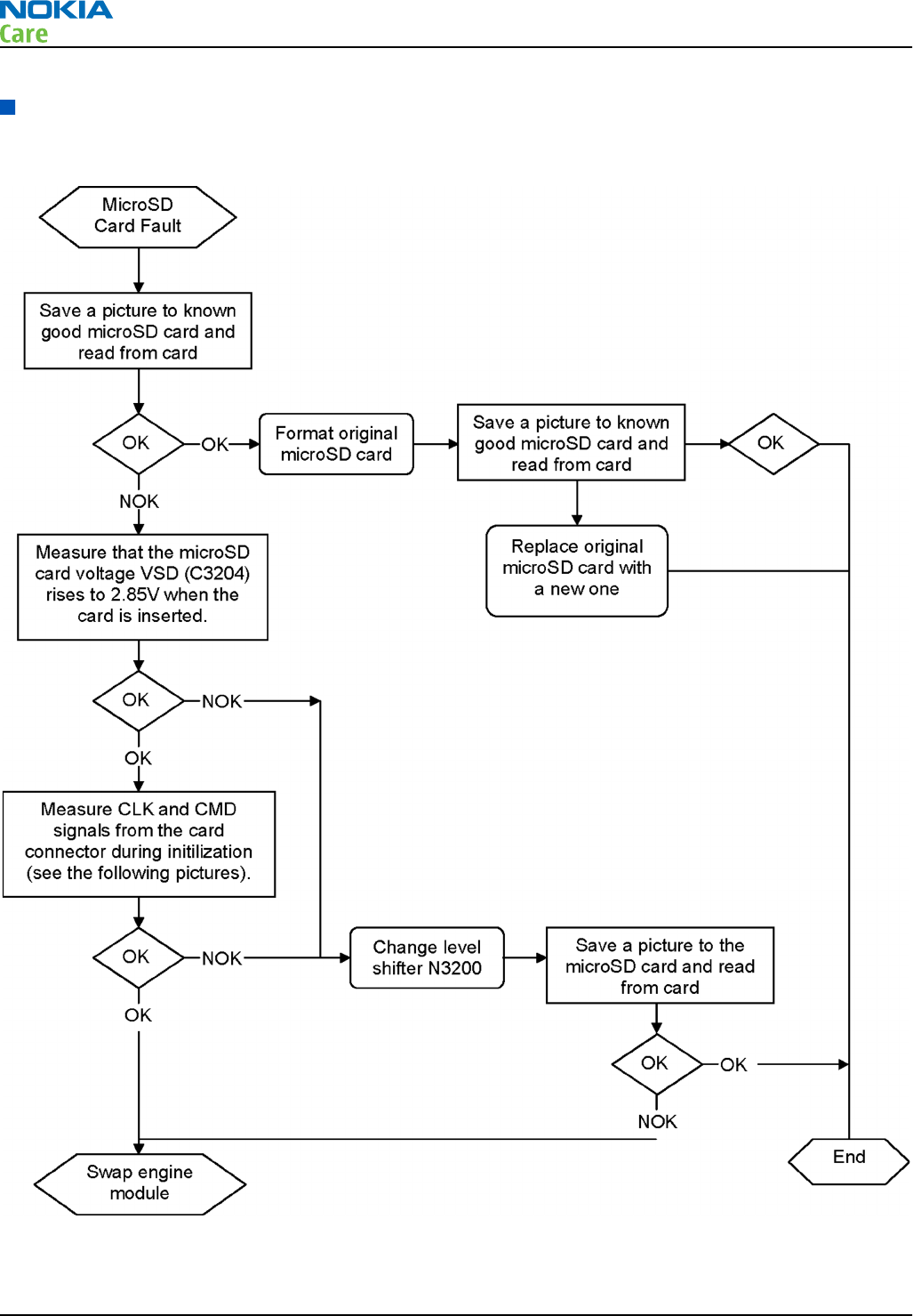
MicroSD card troubleshooting
Troubleshooting flow
RM-333; RM-334; RM-335
BB Troubleshooting
Page 3 –18 COMPANY CONFIDENTIAL Issue 2
Copyright © 2008 Nokia. All rights reserved.
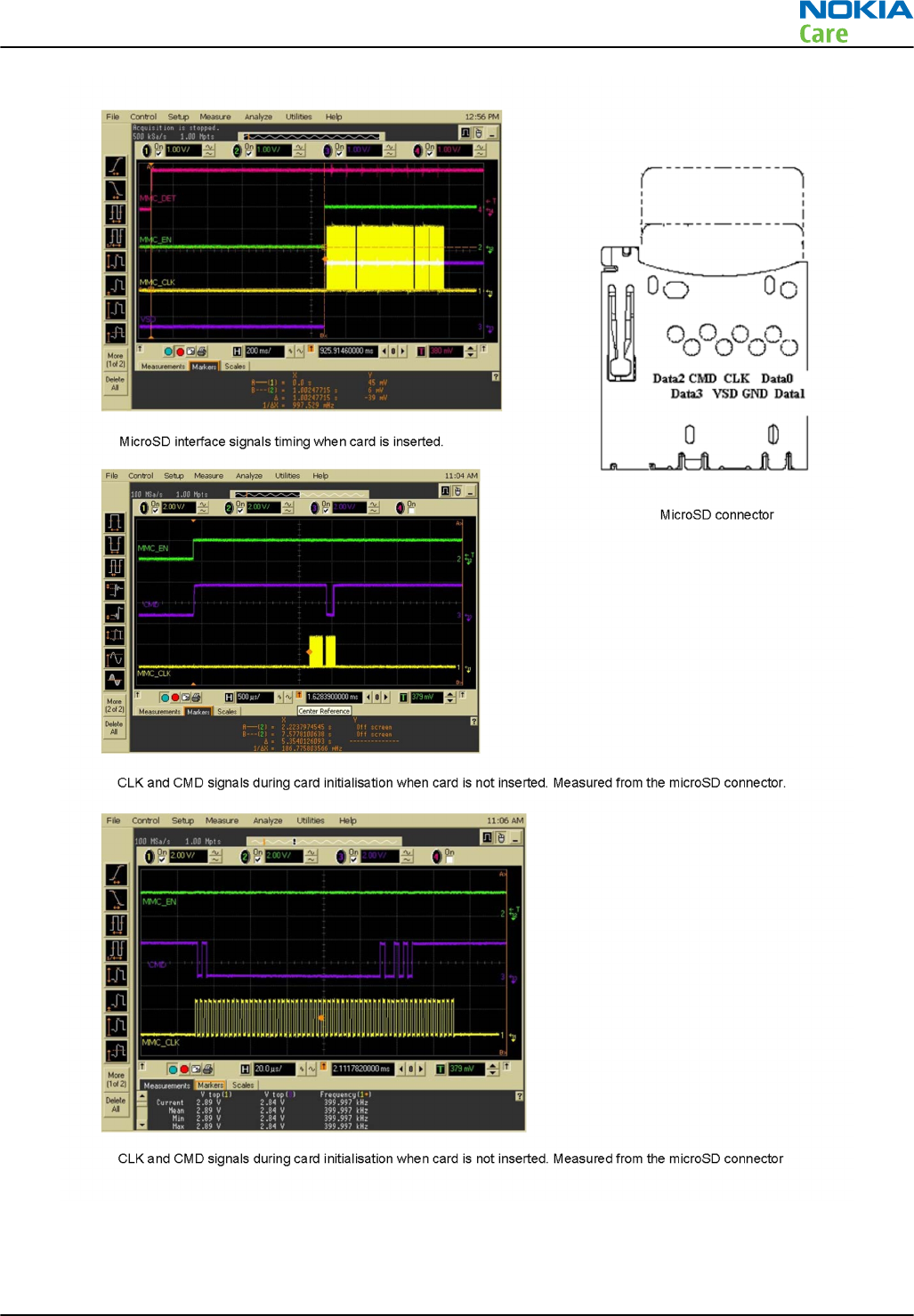
RM-333; RM-334; RM-335
BB Troubleshooting
Issue 2 COMPANY CONFIDENTIAL Page 3 –19
Copyright © 2008 Nokia. All rights reserved.
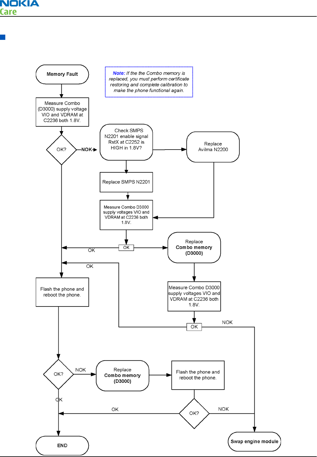
Combo memory troubleshooting
Troubleshooting flow
RM-333; RM-334; RM-335
BB Troubleshooting
Page 3 –20 COMPANY CONFIDENTIAL Issue 2
Copyright © 2008 Nokia. All rights reserved.
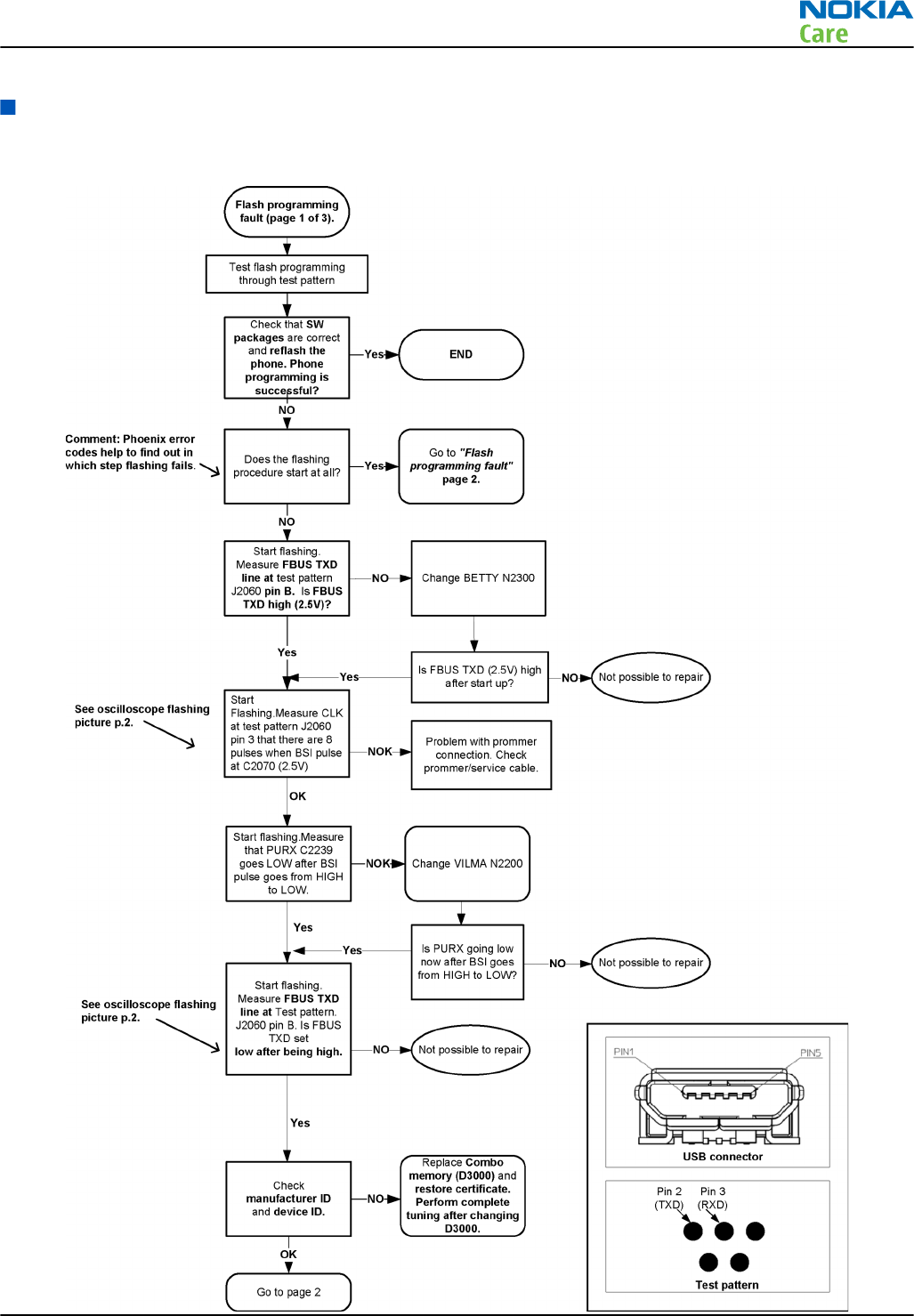
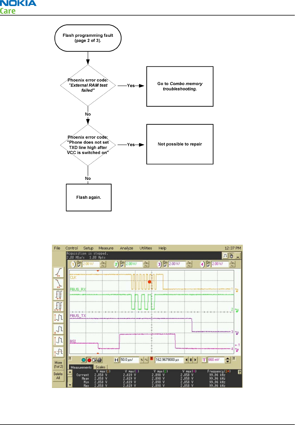
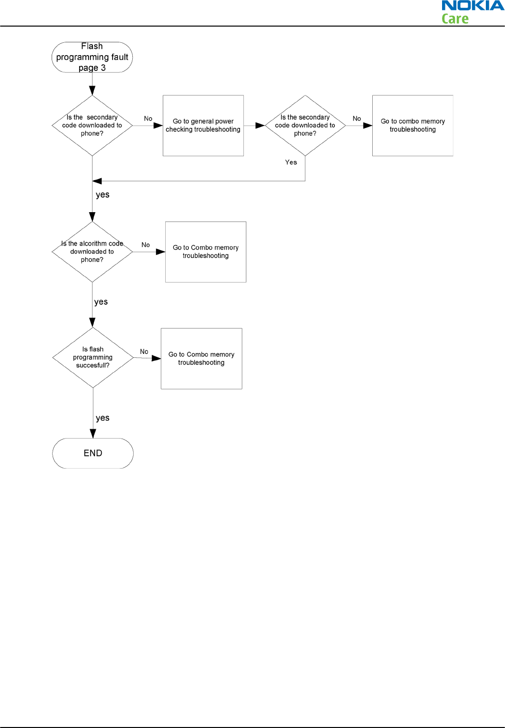
Flash programming troubleshooting
Troubleshooting flow
RM-333; RM-334; RM-335
BB Troubleshooting
Issue 2 COMPANY CONFIDENTIAL Page 3 –21
Copyright © 2008 Nokia. All rights reserved.
RM-333; RM-334; RM-335
BB Troubleshooting
Page 3 –22 COMPANY CONFIDENTIAL Issue 2
Copyright © 2008 Nokia. All rights reserved.
RM-333; RM-334; RM-335
BB Troubleshooting
Issue 2 COMPANY CONFIDENTIAL Page 3 –23
Copyright © 2008 Nokia. All rights reserved.
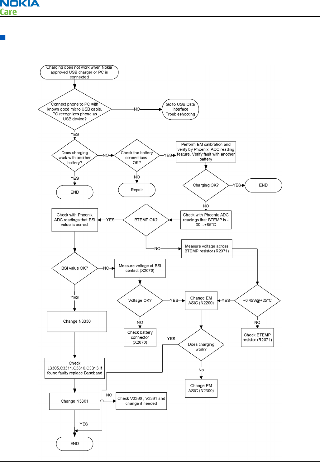
USB charging troubleshooting
Troubleshooting flow
RM-333; RM-334; RM-335
BB Troubleshooting
Page 3 –24 COMPANY CONFIDENTIAL Issue 2
Copyright © 2008 Nokia. All rights reserved.
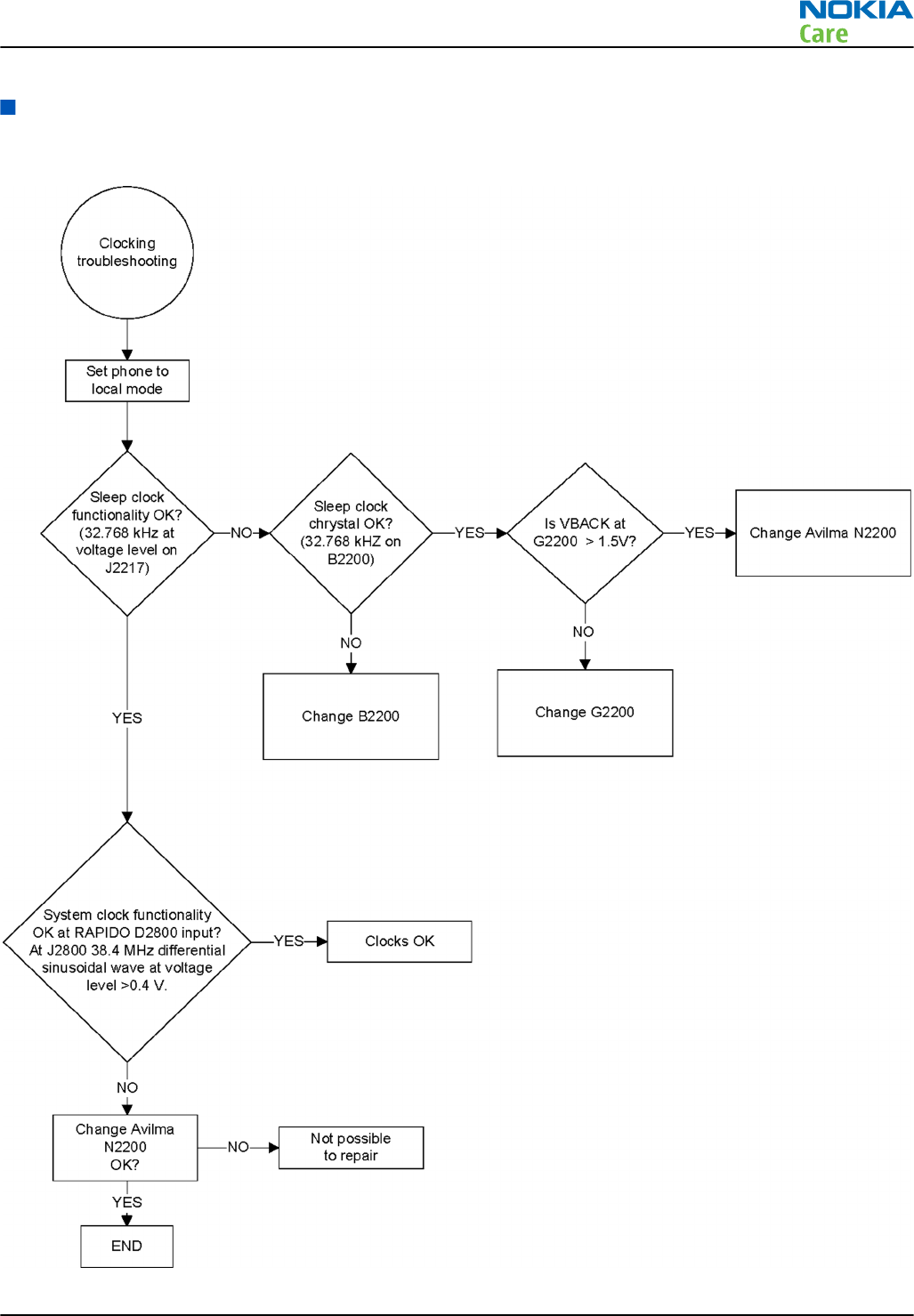
Clocking troubleshooting
Troubleshooting flow
RM-333; RM-334; RM-335
BB Troubleshooting
Issue 2 COMPANY CONFIDENTIAL Page 3 –25
Copyright © 2008 Nokia. All rights reserved.
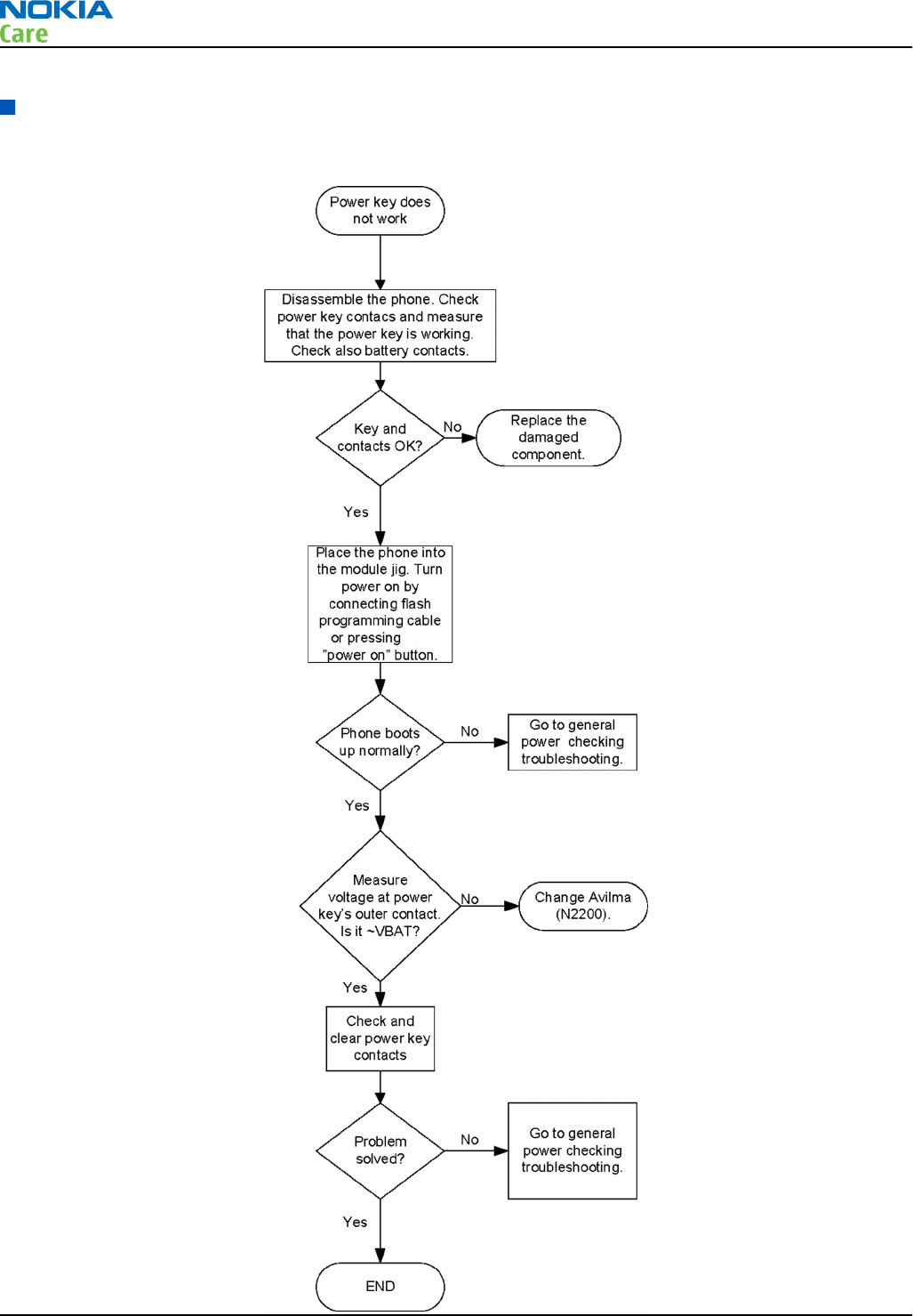
Power key troubleshooting
Troubleshooting flow
RM-333; RM-334; RM-335
BB Troubleshooting
Page 3 –26 COMPANY CONFIDENTIAL Issue 2
Copyright © 2008 Nokia. All rights reserved.
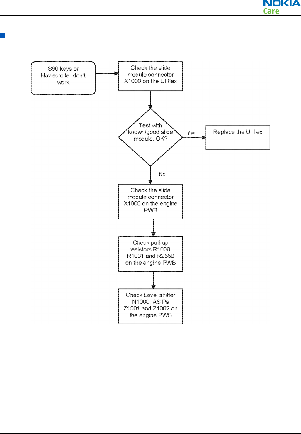
Naviscroll troubleshooting
Troubleshooting flow
RM-333; RM-334; RM-335
BB Troubleshooting
Issue 2 COMPANY CONFIDENTIAL Page 3 –27
Copyright © 2008 Nokia. All rights reserved.
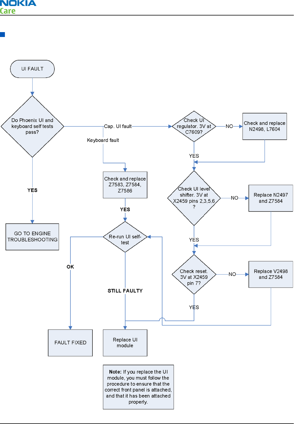
User interface troubleshooting
Troubleshooting flow
RM-333; RM-334; RM-335
BB Troubleshooting
Page 3 –28 COMPANY CONFIDENTIAL Issue 2
Copyright © 2008 Nokia. All rights reserved.
Display Troubleshooting
Display Troubleshooting
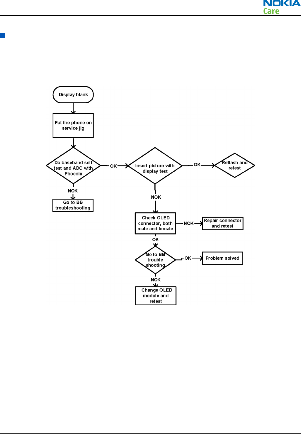
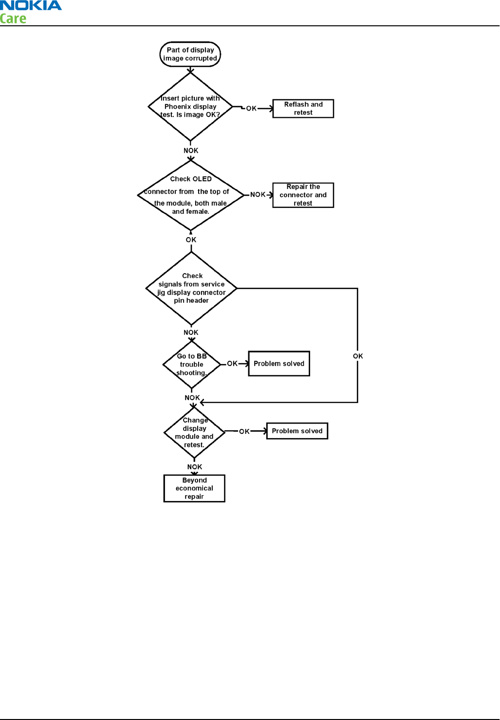
Display blank
There is no image on the display. Display looks the same as if the phone is off even when the phone is on.
Image on display not correct
Image on the display can be corrupted or part of the image can be missing. If part of image is missing change
the UI module. If the image is otherwise corrupted, follow the path below.
RM-333; RM-334; RM-335
BB Troubleshooting
Issue 2 COMPANY CONFIDENTIAL Page 3 –29
Copyright © 2008 Nokia. All rights reserved.
RM-333; RM-334; RM-335
BB Troubleshooting
Page 3 –30 COMPANY CONFIDENTIAL Issue 2
Copyright © 2008 Nokia. All rights reserved.
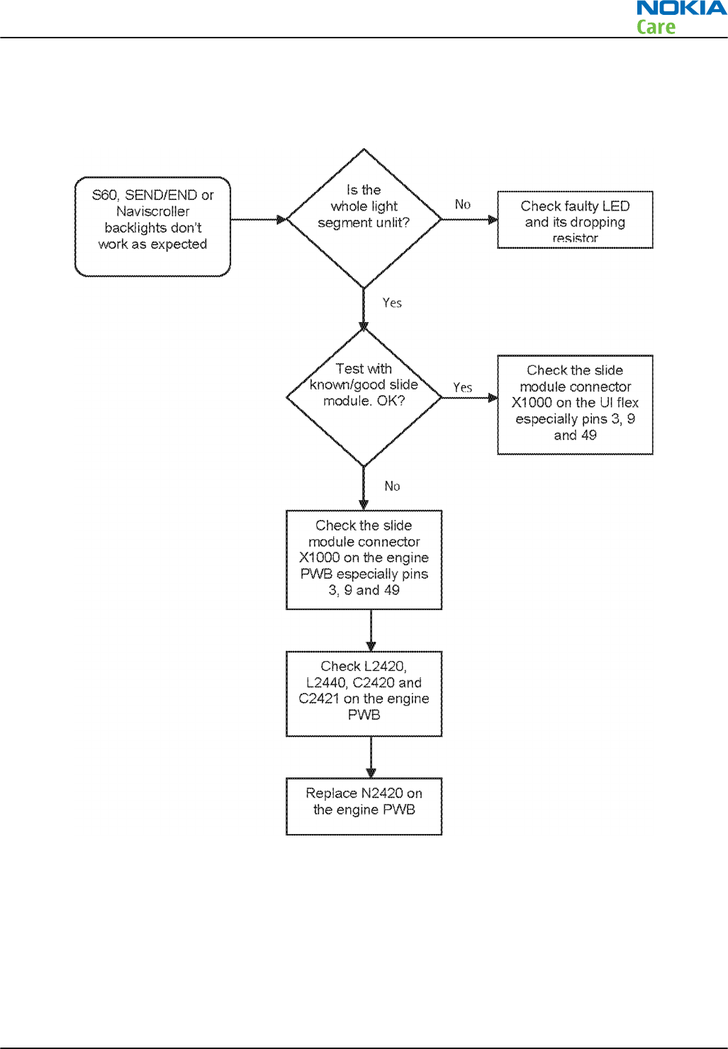
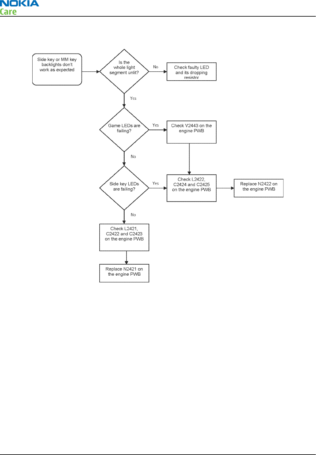
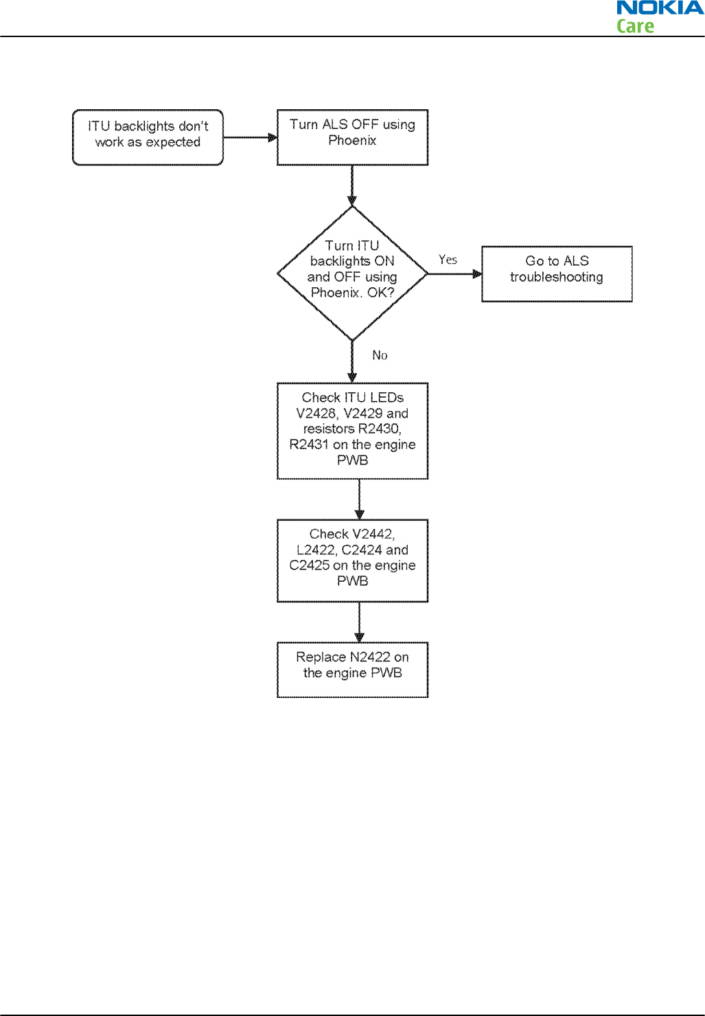
Illumination troubleshooting
Troubleshooting flow
RM-333; RM-334; RM-335
BB Troubleshooting
Issue 2 COMPANY CONFIDENTIAL Page 3 –31
Copyright © 2008 Nokia. All rights reserved.
Troubleshooting flow
RM-333; RM-334; RM-335
BB Troubleshooting
Page 3 –32 COMPANY CONFIDENTIAL Issue 2
Copyright © 2008 Nokia. All rights reserved.
Troubleshooting flow
RM-333; RM-334; RM-335
BB Troubleshooting
Issue 2 COMPANY CONFIDENTIAL Page 3 –33
Copyright © 2008 Nokia. All rights reserved.
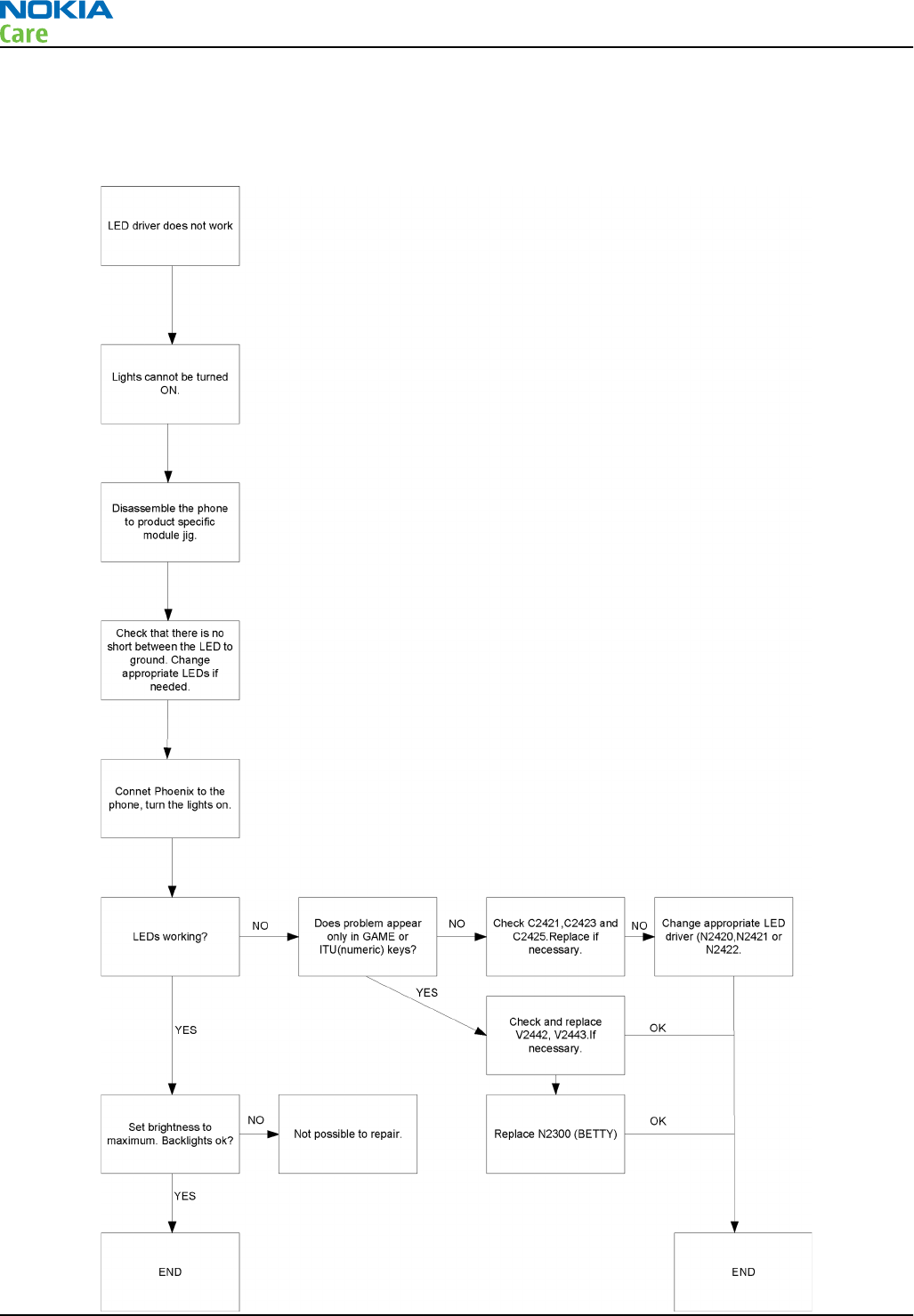
LED driver troubleshooting
Troubleshooting flow
RM-333; RM-334; RM-335
BB Troubleshooting
Page 3 –34 COMPANY CONFIDENTIAL Issue 2
Copyright © 2008 Nokia. All rights reserved.
I/O expander troubleshooting
Troubleshooting flow
Audio Troubleshooting
Audio troubleshooting test instructions
Single-ended external earpiece and differential internal earpiece outputs can be measured either with a
single-ended or a differential probe.
When measuring with a single-ended probe each output is measured against the ground.
Internal handsfree output is measured using a current probe, if a special low-pass filter designed for
measuring a digital amplifier is not available. Note also that when using a current probe, the input signal
frequency must be set to 2 kHz.
The input signal for each loop test can be either single-ended or differential. Exception to this is a digital
microphone, which needs input signal from an external sound source (laptop speaker) to playback eg. 1kHz
sine wave from 5cm distance
RM-333; RM-334; RM-335
BB Troubleshooting
Issue 2 COMPANY CONFIDENTIAL Page 3 –35
Copyright © 2008 Nokia. All rights reserved.

Required equipment
The following equipment is needed for the tests:
•Oscilloscope
•Function generator (sine waveform)
•Current probe (Internal handsfree DPMA output measurement)
•Phoenix service software
•Battery voltage 3.7V
•Sound source (laptop speaker or B&K type 4231 calibrator)
Test procedure
Audio can be tested using the Phoenix audio routings option. Three different audio loop paths can be
activated:
•External microphone to Internal earpiece
•External microphone to Internal handsfree speaker
•Internal microphone to External earpiece
Each audio loop sets routing from the specified input to the specified output enabling a quick in-out test.
Loop path gains are fixed and they cannot be changed using Phoenix. Correct pins and signals for each test
are presented in the following table.
Phoenix audio loop tests and test results
The results presented in the table apply when no accessory is connected and battery voltage is set to 3.7V.
Earpiece, internal microphone and speaker are in place during measurement. Applying a headset accessory
during measurement causes a significant drop in measured quantities.
The gain values presented in the table apply for a differential output vs. single-ended/differential input.
Loop test Input
terminal Output
terminal Path gain
[dB]
(fixed)
Input
voltage
[mVp-p]
Outout
voltage
[mVp-p]
Output DC
level [V] Output
current
[mA]
External
Mic to
External
Earpiece
HS_MIC &
GND
HS_EAR_L
& GND
-8.6 1000 367 1.2 NA
HS_EAR_R
& GND
External
Mic to
Internal
Earpiece
HS_MIC &
GND
EarP & -10 1000 310 1.2 NA
GND
EarN &
GND
External
Mic to
Internal
handsfre
e
HS_MIC &
GND
J2103 &
J2104
-6 1000
J2101 &
J2102
RM-333; RM-334; RM-335
BB Troubleshooting
Page 3 –36 COMPANY CONFIDENTIAL Issue 2
Copyright © 2008 Nokia. All rights reserved.
Loop test Input
terminal Output
terminal Path gain
[dB]
(fixed)
Input
voltage
[mVp-p]
Outout
voltage
[mVp-p]
Output DC
level [V] Output
current
[mA]
Digital
Mic to
External
Earpiece
Acoustica
l input,
1KHz sine
wave
HS_EAR_L
& GND
NA 94 dB SPL 100 NA
Measurement data
Earpiece signal
Figure 14 Single-ended output waveform of the Ext_in_HP_out measurement when earpiece is connected
Integrated handsfree signal
Figure 15 Single-ended output waveform of the Ext_in_IHF_out out loop measurement when speaker is connected
(measured at speaker pads), no filter is used
External output from AV
RM-333; RM-334; RM-335
BB Troubleshooting
Issue 2 COMPANY CONFIDENTIAL Page 3 –37
Copyright © 2008 Nokia. All rights reserved.
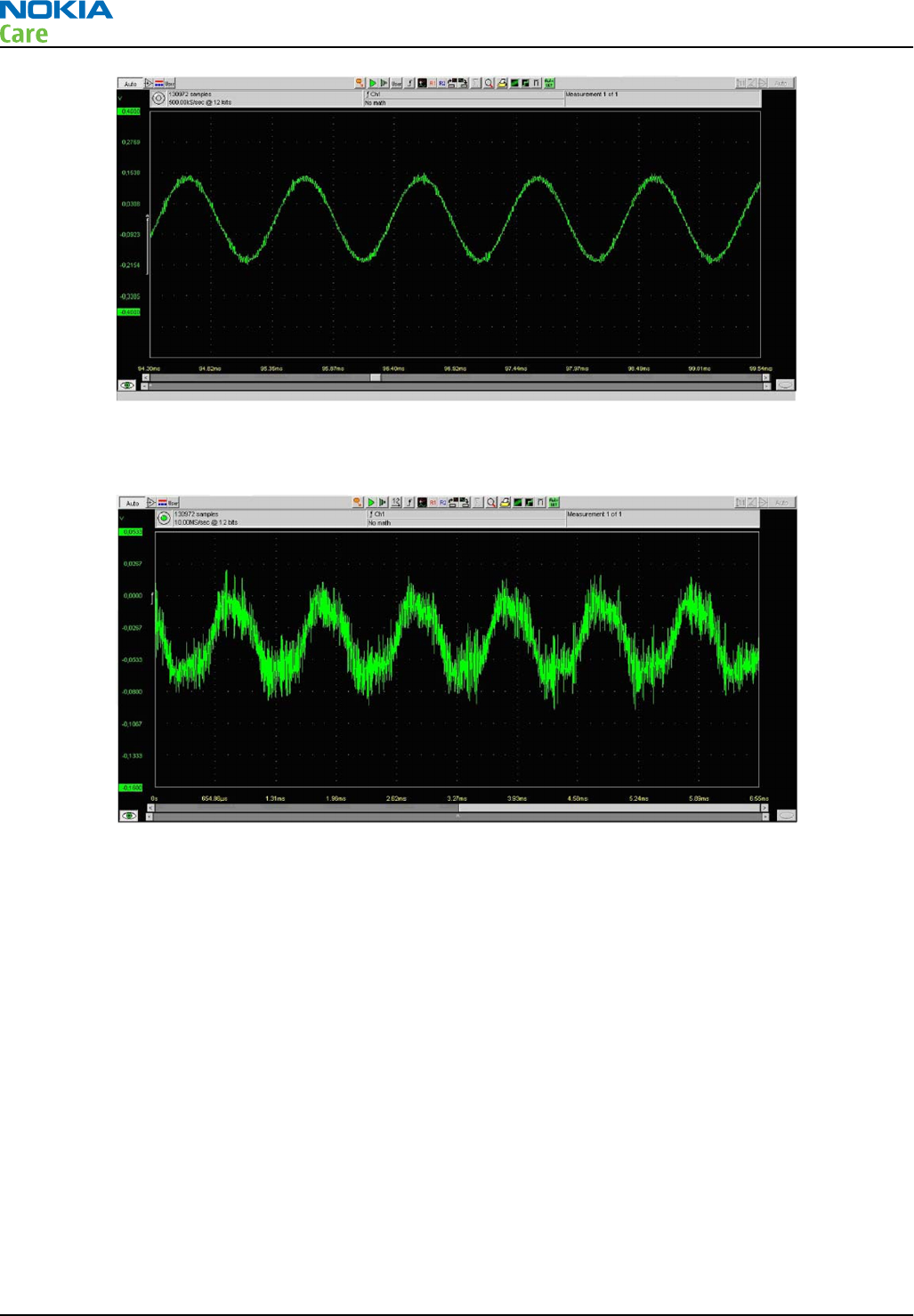
Figure 16 Single-ended output waveform of the Ext_in_Ext_out loop
External output from AV (acoustic input)
Figure 17 Single-ended output waveform of the Digital_stereo_microphone_in_Ext_out loop
RM-333; RM-334; RM-335
BB Troubleshooting
Page 3 –38 COMPANY CONFIDENTIAL Issue 2
Copyright © 2008 Nokia. All rights reserved.
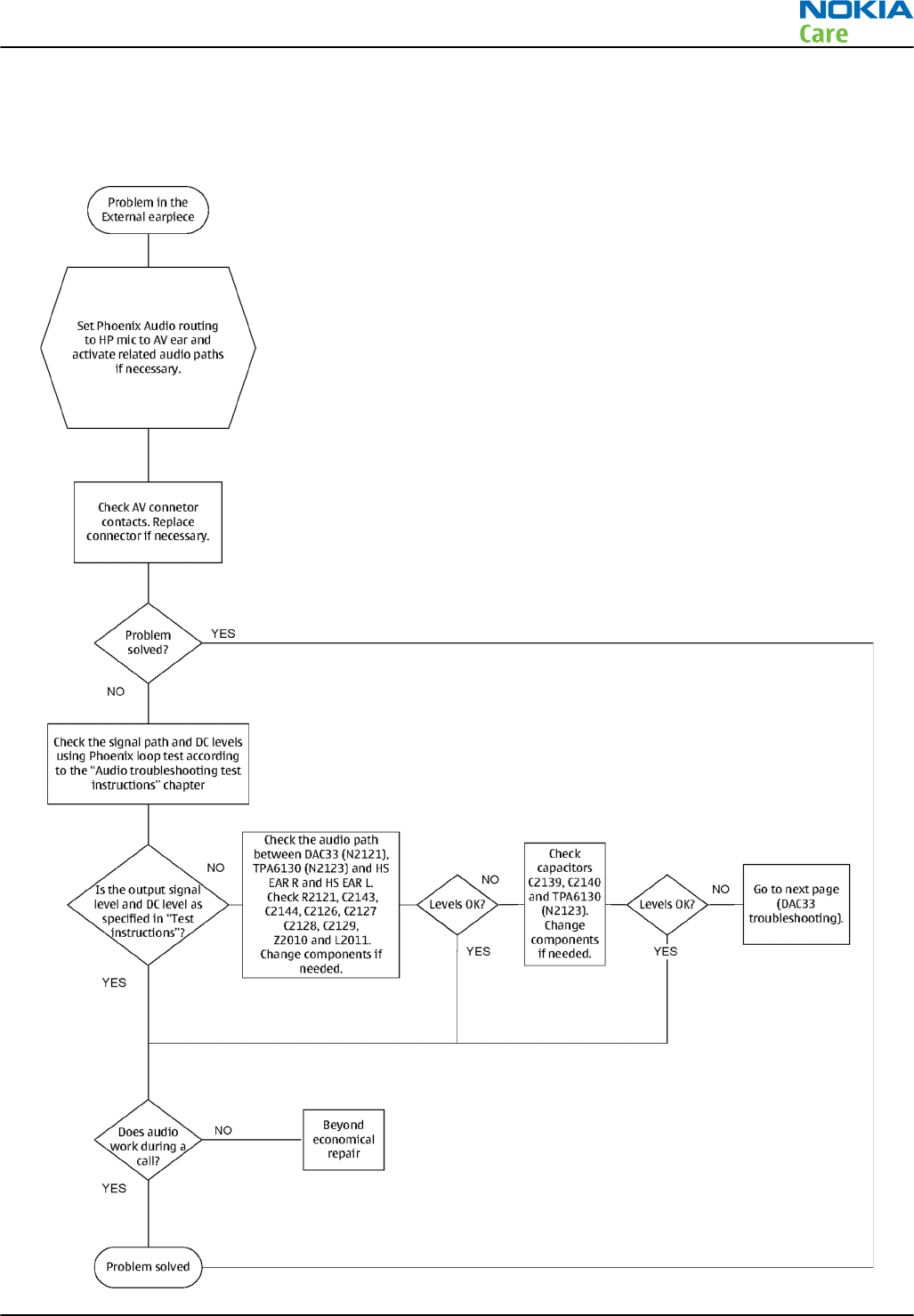
External earpiece troubleshooting
Troubleshooting flow
RM-333; RM-334; RM-335
BB Troubleshooting
Issue 2 COMPANY CONFIDENTIAL Page 3 –39
Copyright © 2008 Nokia. All rights reserved.
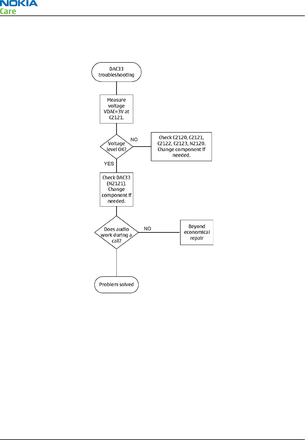
DAC33 troubleshooting
Troubleshooting flow
RM-333; RM-334; RM-335
BB Troubleshooting
Page 3 –40 COMPANY CONFIDENTIAL Issue 2
Copyright © 2008 Nokia. All rights reserved.
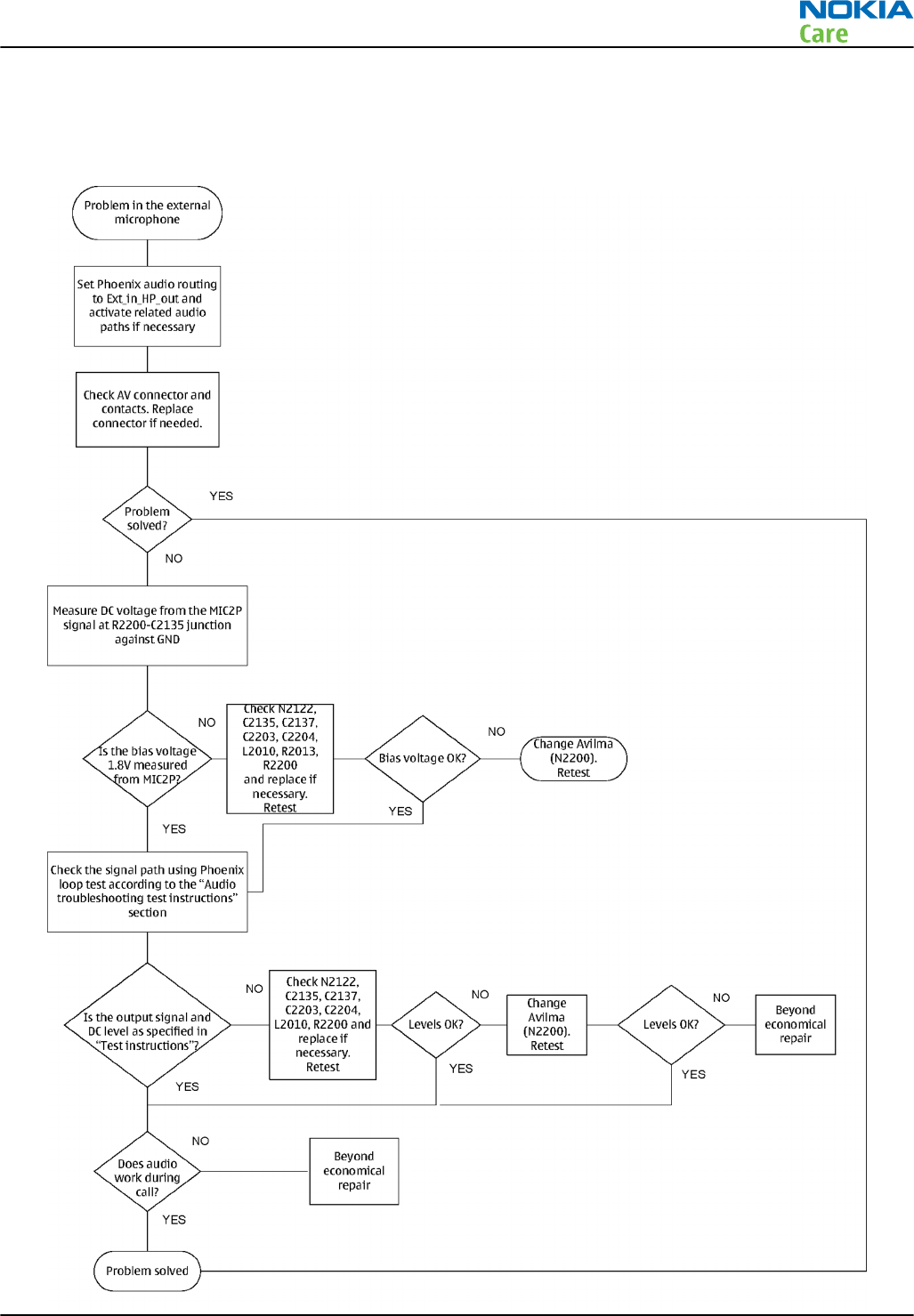
External microphone troubleshooting
Troubleshooting flow
RM-333; RM-334; RM-335
BB Troubleshooting
Issue 2 COMPANY CONFIDENTIAL Page 3 –41
Copyright © 2008 Nokia. All rights reserved.
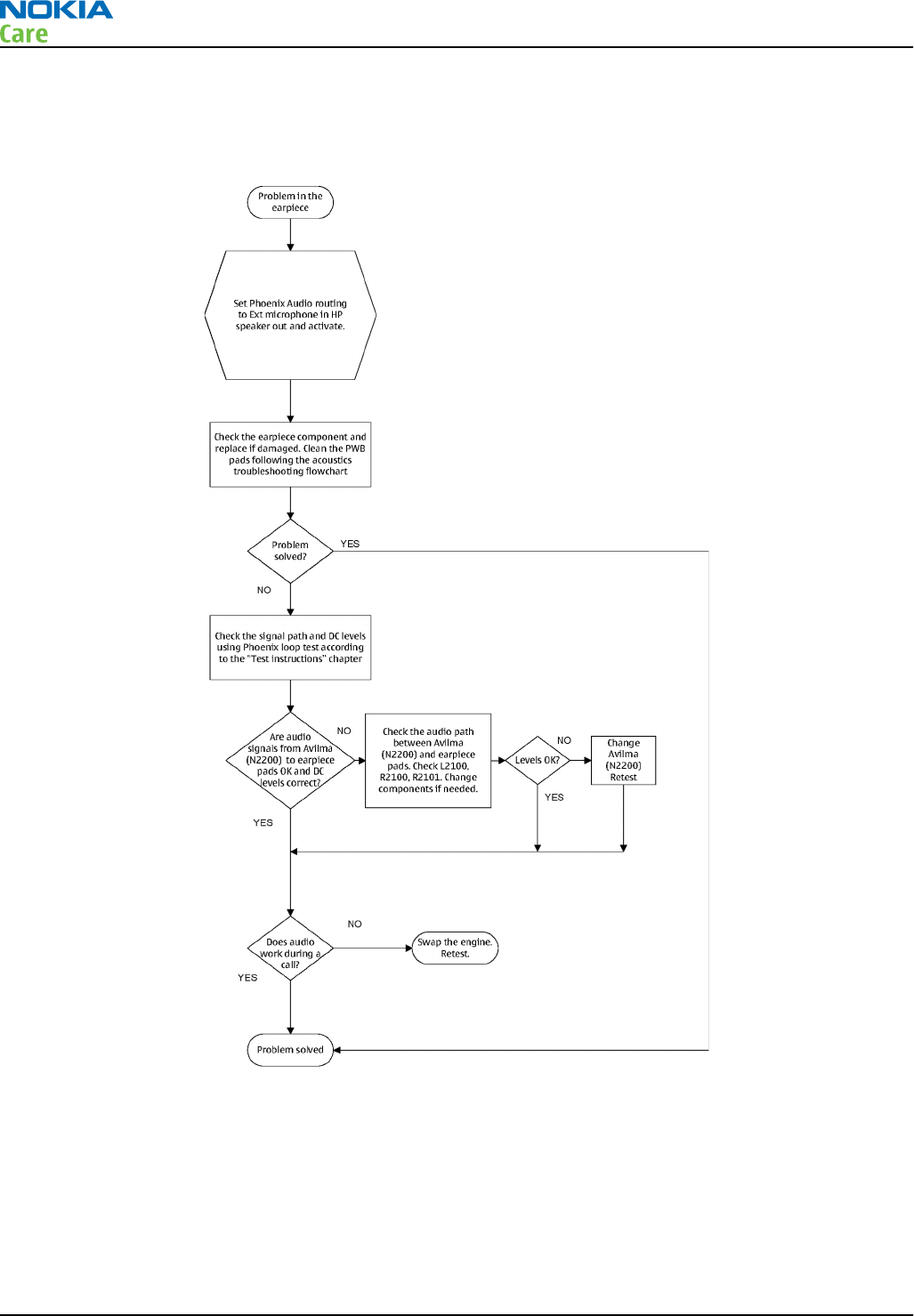
Internal earpiece troubleshooting
Troubleshooting flow
RM-333; RM-334; RM-335
BB Troubleshooting
Page 3 –42 COMPANY CONFIDENTIAL Issue 2
Copyright © 2008 Nokia. All rights reserved.
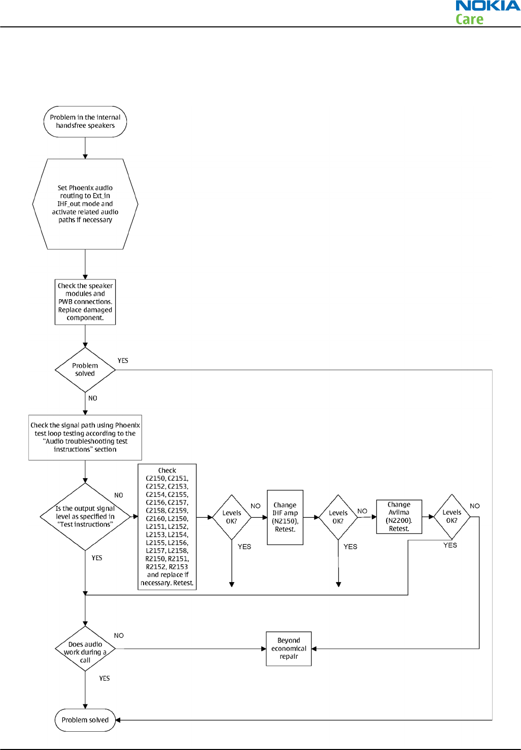
Internal handsfree speaker troubleshooting
Troubleshooting flow
RM-333; RM-334; RM-335
BB Troubleshooting
Issue 2 COMPANY CONFIDENTIAL Page 3 –43
Copyright © 2008 Nokia. All rights reserved.
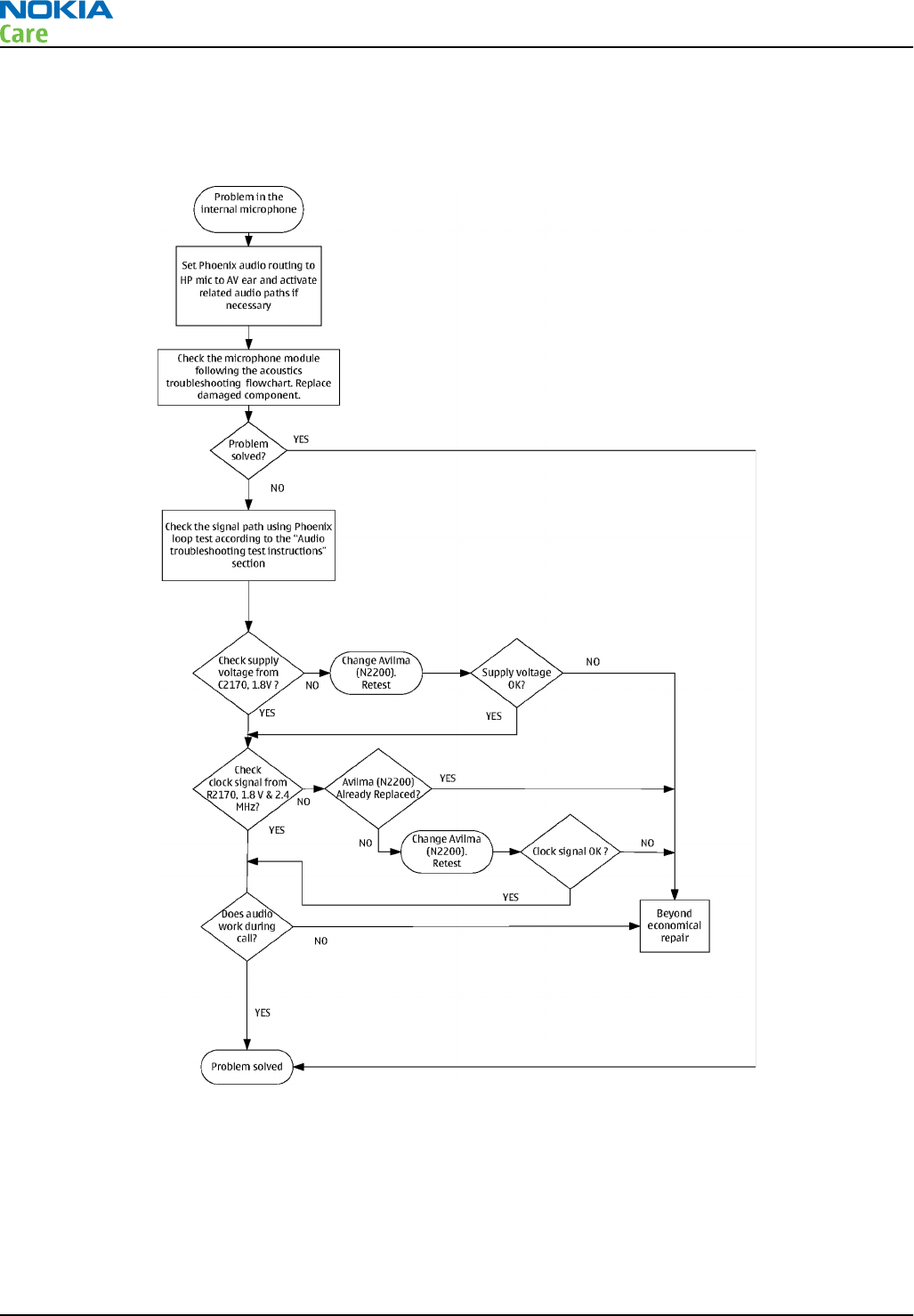
Internal microphone troubleshooting
Troubleshooting flow
RM-333; RM-334; RM-335
BB Troubleshooting
Page 3 –44 COMPANY CONFIDENTIAL Issue 2
Copyright © 2008 Nokia. All rights reserved.
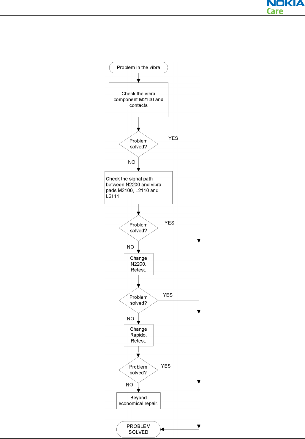
Vibra troubleshooting
Troubleshooting flow
RM-333; RM-334; RM-335
BB Troubleshooting
Issue 2 COMPANY CONFIDENTIAL Page 3 –45
Copyright © 2008 Nokia. All rights reserved.
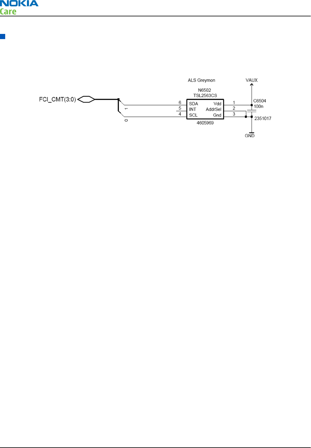
ALS Technical Description and Troubleshooting
Ambient Light Sensor
Ambient Light Sensor
Figure 18 Ambient Light Sensor
Ambient Light Sensor consists of the following components:
•Light guide
•Ambient Light Sensor (ALS)
ALS is a digital I2C interface component, having two channels with different spectral sensitivities. When
combined, the component responds to illuminance similar as human eye.
•Vdd Filtering capacitor C1103
Ambient Light Sensor information is used to control keypad and display brightness of the phone.
Keyboard backlight is turned OFF, when it’s not needed. Display brightness is dimmed, when environment
lighting is dark.
Ambient Light Sensor is calibrated in production and can be re-tuned in service points though not
recommended unless calibration coefficient are lost for some reason
ALS troubleshooting
Context
Functionality check:
Steps
1. Connect phone to Phoenix and set the phone (e.g. on the table) so that the amount of ambient light seen
by ALS is as stable as possible.
2. Start Phoenix
3. Choose File -> Scan product
4. Choose Testing -> Display Test
5. Open the Lights tab, check Ambient Light Sensor check box, click Read, cover the sensor and click Read
again. When covered, Luminance reading should be less than after clicking Read without covering the
sensor.
RM-333; RM-334; RM-335
BB Troubleshooting
Page 3 –46 COMPANY CONFIDENTIAL Issue 2
Copyright © 2008 Nokia. All rights reserved.
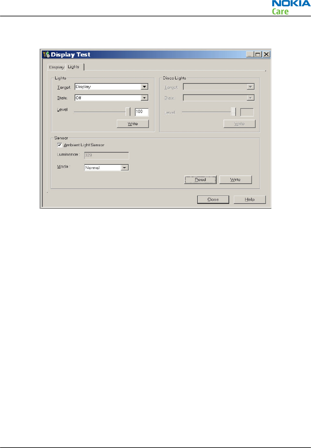
6. If component doesn’t give any reading or reading doesn’t change when sensor is/is not covered, replace
the part.
Note: After replacing the ALS. If calibration values of the new sensor are lost or for some other
reason, ALS re-tuning is required (see instructions later in this document).
When doing the ALS calibration procedure, it is required to have a reference phone, which includes
calibrated ALS. ALS re-tuning instructions show why the reference phone is needed.
Re-tuning ALS
Steps
1. Connect reference phone to Phoenix and set the phone (e.g. on the table) so that the amount of ambient
light seen by ALS is as stable as possible.
2. Start Phoenix.
3. Choose File→Scan Product.
RM-333; RM-334; RM-335
BB Troubleshooting
Issue 2 COMPANY CONFIDENTIAL Page 3 –47
Copyright © 2008 Nokia. All rights reserved.
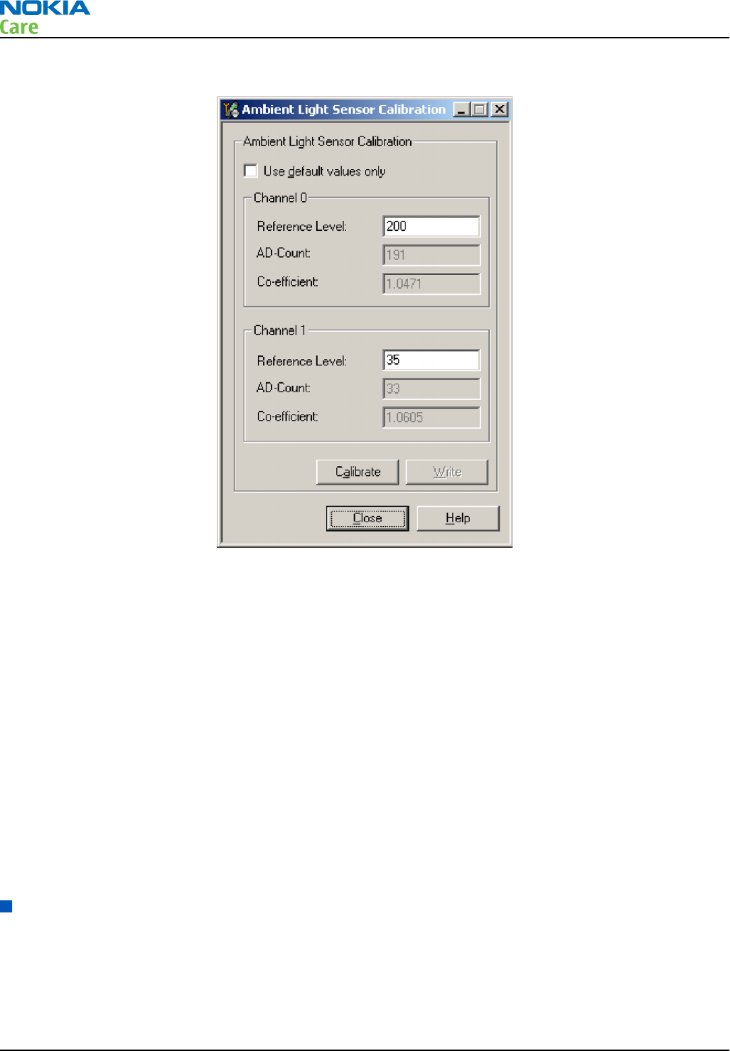
4. Choose Tuning -> Ambient Light Sensor Calibration. You should see the following window:
5. Read AD-count values for Channel 0 and Channel 1 by click Read button and write them down.
6. Repeat 1-5 for the phone to be calibrated and make sure the phone to be calibrated is located in the
same place as reference phone was when luminance reading was taken.
7. Calculate co-efficient from reference phone and phone to be calibrated AD-count values by division: Co-
efficient = AD-count(reference phone) / AD-count(phone to be calibrated), write down the calculated co-
efficient values.
8. -> Iterate by changing Channel 0 and Channel 1 (reference level) values (remove cross from ‘Use default
values only’). After writing some value to Channel 0 and Channel 1 (reference value), calibrate button
must be pressed. Stop iterating when Co-efficient is equal to Co-efficient calculated in step 7. Note that
decimal numbers should be used in the iteration in order to achieve enough precision (e.g. 200.2455)
9. After having same Co-efficient value in “Co-efficient” textbox as the calculated value, make sure that
ambient light values (read using Testing → Display Test → “Luminance” textbox) are almost the same
in reference phone and calibrated phone. Remember that illuminance readings for reference and
calibrated phones must be done in the same ambient light conditions. If illuminance values differs a lot
(difference max. +- 10%), repeat whole ALS re-tuning procedure.
10. To end the calibration, click Close.
Bluetooth and FM Radio Troubleshooting
Introduction to Bluetooth/FM radio troubleshooting
Bluetooth/WLAN antenna
The BT RF signal is routed from BTFMRDS2.1 through the WLAN module to the shared WLAN/BT antenna in
the phone's C-cover.
RM-333; RM-334; RM-335
BB Troubleshooting
Page 3 –48 COMPANY CONFIDENTIAL Issue 2
Copyright © 2008 Nokia. All rights reserved.
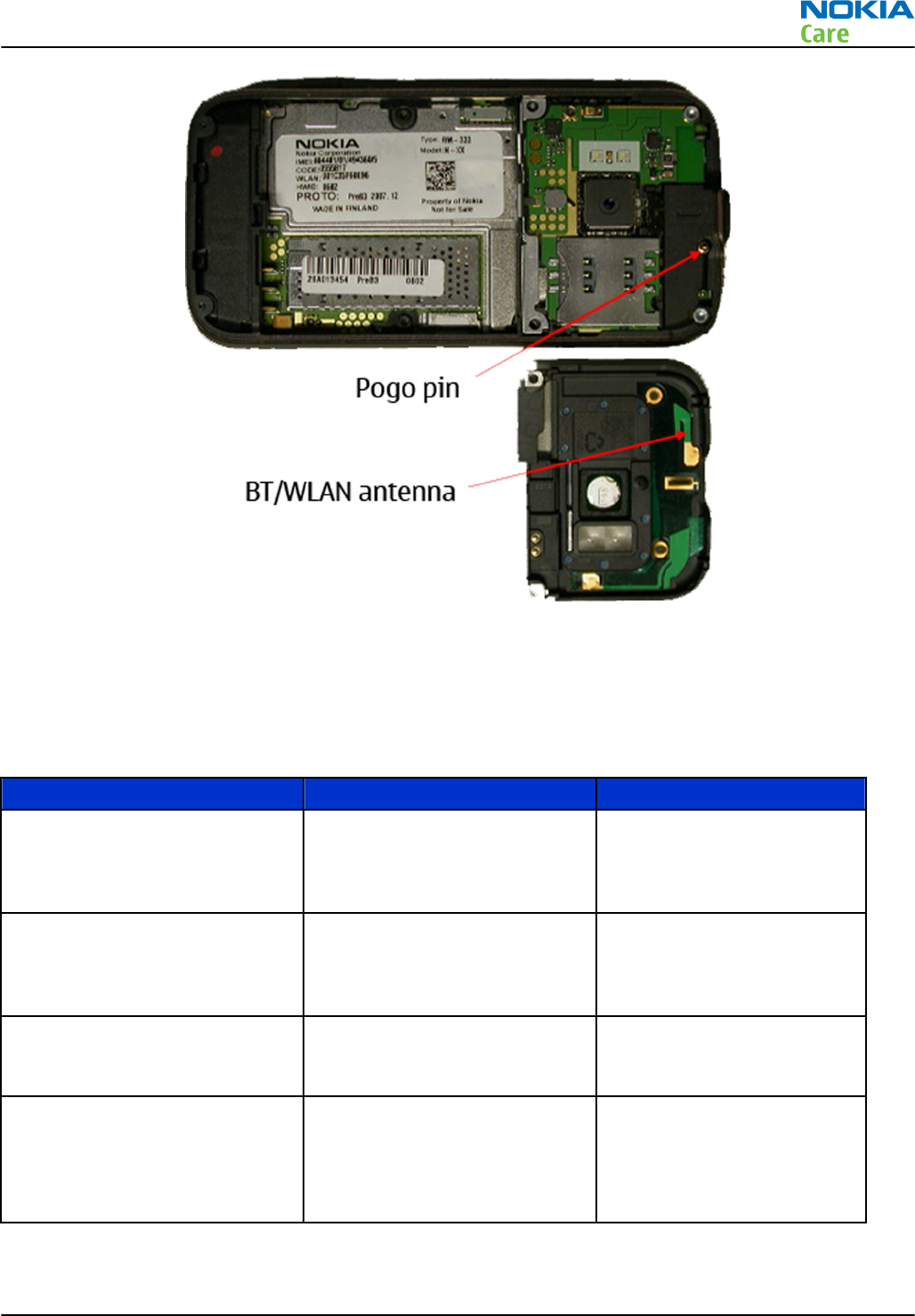
Figure 19 Bluetooth/WLAN antenna
Introduction to Bluetooth/FM radio troubleshooting
The Bluetooth and FM radio are combined in the same ASIC, so both features are checked when
troubleshooting.
The following problems can occur with the Bluetooth and FM radio hardware:
Symptom Problem Repair solution
Unable to switch on Bluetooth on
phone user interface
Open circuit solder joints or
component failure of BTH/FM
ASIC/module BB ASICs or SMD
components.
Replacement of Bluetooth/
FM ASIC/module
Able to send data file to another
Bluetooth device, but unable to
hear audio through functional
Bluetooth headset
Open circuit solder joints or
component failure of BTH/FM
ASIC/module BB ASICs.
Replacement of Bluetooth/
FM ASIC/module
Able to switch on Bluetooth on
phone user interface, but unable
to detect other Bluetooth devices
Open circuit solder joints or
Pogo Pins not making contact
with c-cover
Repair or replace c-cover
Able to turn on FM radio and
Bluetooth on phone user
interface, but unable to detect
local FM radio stations with Nokia
headset inserted
Open circuit solder joints or
detached component in FM
antenna circuit
Repair of FM antenna
connection or FM circuit
component
RM-333; RM-334; RM-335
BB Troubleshooting
Issue 2 COMPANY CONFIDENTIAL Page 3 –49
Copyright © 2008 Nokia. All rights reserved.

Symptom Problem Repair solution
Able to perform scans to detect
local FM radio stations with
functional Nokia headset
inserted, but unable to hear FM
audio through headset
Open circuit solder joints or
detached component in FM
audio path between Bluetooth/
FM ASIC and headset
Repair of FM audio circuit
Users may experience the following problems resulting in functional phones being returned to the repair
centre:
Symptom Problem Repair solution
Bluetooth feature does not
operate as desired with another
Bluetooth device
Bluetooth Profile implemented
in Bluetooth accessory not
supported in Nokia phone
Use Bluetooth accessory with
Bluetooth profiles supported
by phone
Poor FM radio reception (unable
to detect many radio stations)
Nokia headset not being used Use Nokia headset
Test coverage
The tests listed in the table below should be performed to verify whether the Bluetooth and FM receiver and
transmitter are functional. The use of Self Tests are described in section
BT and FM Self Tests in Phoenix
Test Test Coverage Repair solution
Blueooth Self Test: ST_LPRF_IF_TEST Bluetooth-FM ASIC UART interface
(controls Bluetooth and FM
receiver and transmitter)
Replacement of Bluetooth/FM
ASIC (or repair of phone BB)
Bluetooth Self Test:
ST_BT_WAKEUP_TEST
Bluetooth ASIC interrupt control
interface
Replacement of Bluetooth/FM
ASIC (or repair of phone BB)
Bluetooth Self Test:
ST_LPRF_AUDIO_LINES_TEST
Bluetooth ASIC PCM interface Replacement of Bluetooth/FM
ASIC (or repair of phone BB)
Bluetooth Functional Test: BER test
with BT-Box or functional test with
other Bluetooth device
Bluetooth antenna circuit Repair of Bluetooth antenna
circuit (including RF filter or
WLAN switch if fitted)
FM Radio Self Test: ST_RADIO_TEST FM Radio I2C interface Replacement of Bluetooth/FM
ASIC (or repair of phone BB)
FM Radio Functional Test: Perform
scan for local radio stations and
check station list displayed on
phone
FM receiver antenna circuit Repair of FM antenna circuit
(between BTHFM ASIC and
headset connector)
FM Radio Functional Test: Listen to
local radio station
FM receiver audio circuit Repair of FM receiver audio
circuit (between BTHFM ASIC
and headset connector)
The self tests run from Phoenix software are used for fault diagnosis.
If Phoenix software is not available the functional tests with phone accessories are sufficient to verify the
functionality Bluetooth and FM radio receiver and transmitter.
RM-333; RM-334; RM-335
BB Troubleshooting
Page 3 –50 COMPANY CONFIDENTIAL Issue 2
Copyright © 2008 Nokia. All rights reserved.
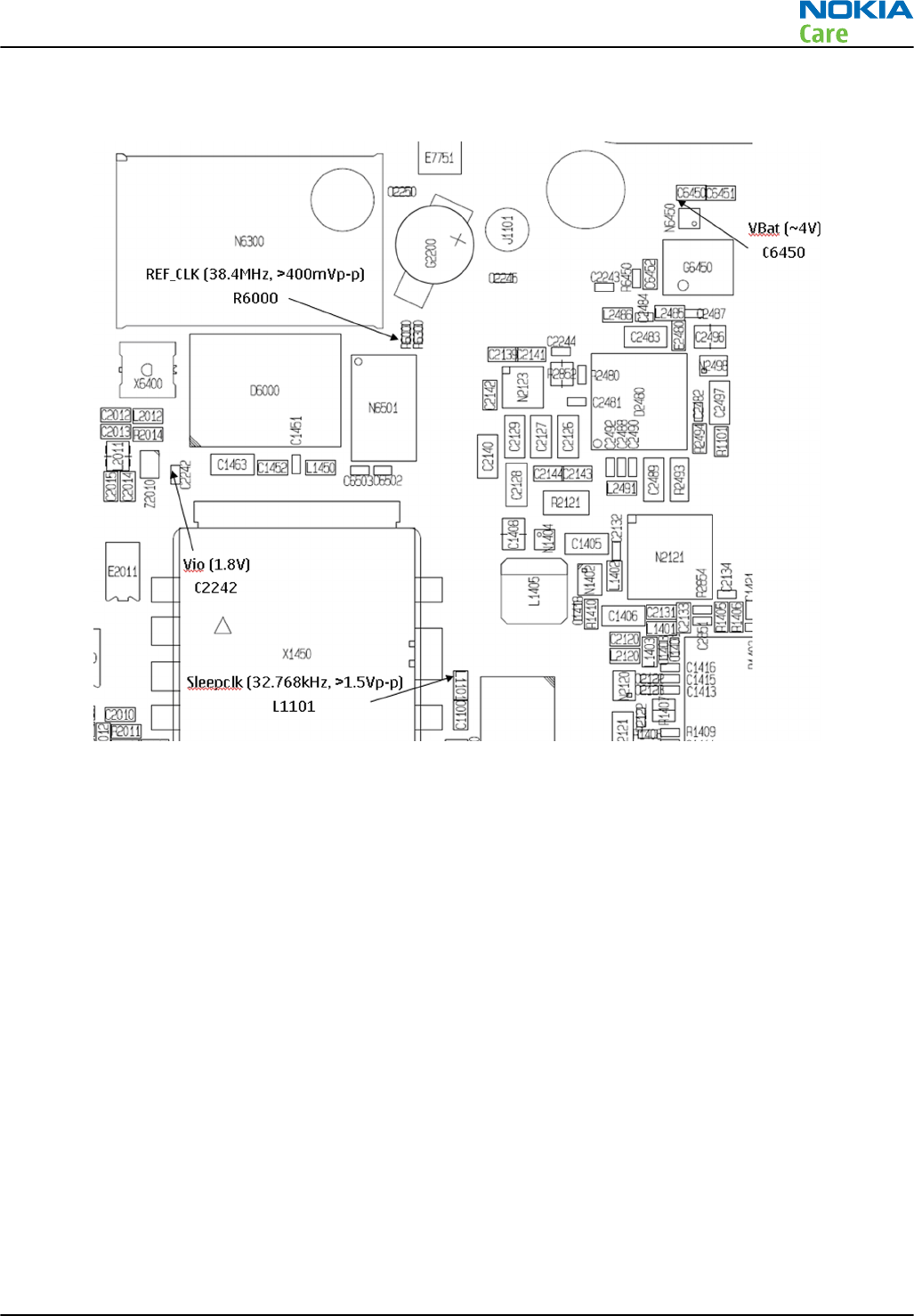
Bluetooth/FM radio component layout and test points
Figure 20 BT/FM component layout
The Bluetooth antenna is product specific (antenna integrated into phone C cover). On phones with WLAN,
the Bluetooth RF signal is routed through a WLAN front-end module and a shared Bluetooth / WLAN antenna
is used. The FM RF signal is routed through a product specific FM antenna matching circuit to the phone
headset connector. The FM radio audio signal is routed to the headset connector through the BB ASIC shared
by the phone audio functions.
Bluetooth BER test
Prerequisites
JBT-9, or SB-6 Bluetooth test box (BT-box) is required to perform a BER test. If a BT-box not available Bluetooth
functionality can be checked by transferring a file to another Bluetooth phone. For the BER or file transfer
test the C-cover should be fitted as the BT antenna is on the C-cover.
Steps
1. Connect data cable to phone.
2. Start
Phoenix
service software.
3. Choose File → Scan Product.
4. Choose Testing → Bluetooth LOCALS .
5. Locate the BT-box serial number (12 digits) found in the type label on the back of the JBT-9, or SB-6
Bluetooth test box.
RM-333; RM-334; RM-335
BB Troubleshooting
Issue 2 COMPANY CONFIDENTIAL Page 3 –51
Copyright © 2008 Nokia. All rights reserved.
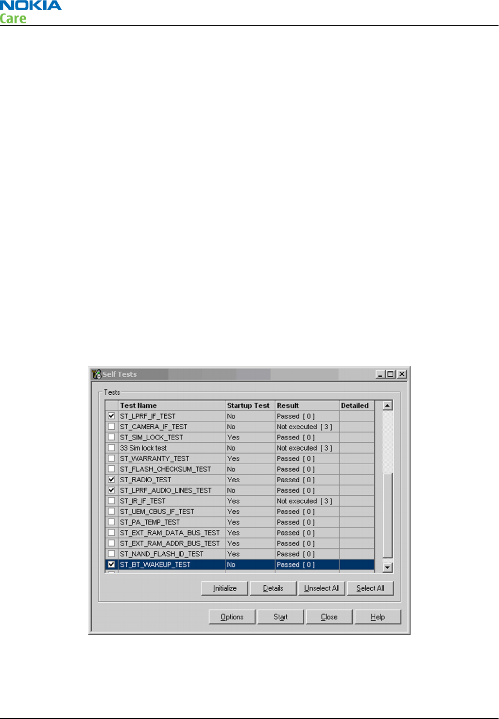
6. In the Bluetooth
LOCALS
window, write the 12-digit serial number on the
Counterpart BT Device
Address
line.
7. Place the BT-box near (within 10 cm) of the phone and click Start BER Test.
Bluetooth and FM radio self tests in Phoenix
Prerequisites
A flash adapter (or phone data cable) connected to a PC with Phoenix service software is required.
Steps
1. Place the phone in the flash adapter or connect data cable to phone.
2. Start
Phoenix
service software.
3. Choose File→Scan Product.
4. From the Mode drop-down menu, set mode to Local.
5. Choose Testing→Self Tests.
6. In the
Self Tests
window check the following Bluetooth and FM radio related tests:
•ST_LPRF_IF_TEST
•ST_LPRF_AUDIO_LINES_TEST
•ST_BT_WAKEUP_TEST
•ST_RADIO_TEST
7. To run the tests, click Start.
Figure 21 Bluetooth and FM radio self tests in
Phoenix
RM-333; RM-334; RM-335
BB Troubleshooting
Page 3 –52 COMPANY CONFIDENTIAL Issue 2
Copyright © 2008 Nokia. All rights reserved.
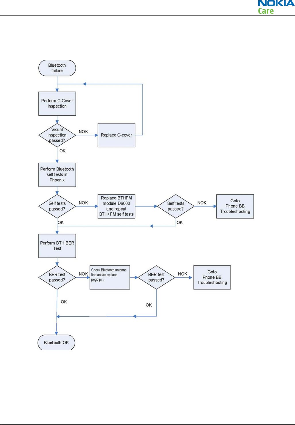
Bluetooth troubleshooting
Troubleshooting flow
RM-333; RM-334; RM-335
BB Troubleshooting
Issue 2 COMPANY CONFIDENTIAL Page 3 –53
Copyright © 2008 Nokia. All rights reserved.
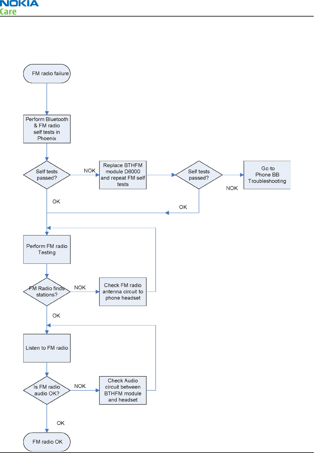
FM radio troubleshooting
Troubleshooting flow
RM-333; RM-334; RM-335
BB Troubleshooting
Page 3 –54 COMPANY CONFIDENTIAL Issue 2
Copyright © 2008 Nokia. All rights reserved.

FM radio testing
Steps
1. Set signal generator parameters:
•FM modulation on
•Frequency 100MHz
•FM deviation 22kHz
•Modulation frequency 1kHz
•RF level should be varied during the test to obtain good audio signal quality
•Connect suitable antenna to signal generator
Note: You may alternately use a known good FM radio broadcast as a test signal.
2. Attach the Nokia headset to the phone’s AV connector.
3. Use Scroll button to autotune to the radio frequency.
4. Set volume to suitable level.
5. Check audio quality with a headset.
GPS Troubleshooting
GPS layout and basic test points
The GPS components are located on small 2nd PWB. Satellite signals are picked up by the phones GPS antenna
in the C-cover. The signal is then routed through a filter before being processed by the GPS5350 receiver ASIC.
Verify that the GPS voltage and clock signal levels are as in RM-333 GPS schematics.
RM-333; RM-334; RM-335
BB Troubleshooting
Issue 2 COMPANY CONFIDENTIAL Page 3 –55
Copyright © 2008 Nokia. All rights reserved.
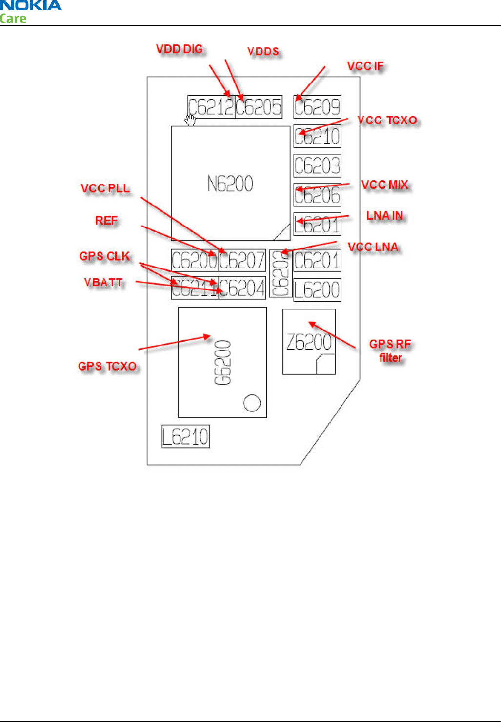
Figure 22 GPS layout and basic test points
GPS Settings for Phoenix
GPS control
Prerequisites
A flash adapter with RF coupler connected to a PC with Phoenix service software is required. The GPS signal
should be connected to the RF coupler. Calibrate the signal level with a known good phone. Signal level will
be high (approx -45dBm) because it is a leakage connection.
Context
Use the following to test GPS using Phoenix.
Steps
1. Place phone to Flash Adaptor.
2. Start Phoenix service software.
RM-333; RM-334; RM-335
BB Troubleshooting
Page 3 –56 COMPANY CONFIDENTIAL Issue 2
Copyright © 2008 Nokia. All rights reserved.
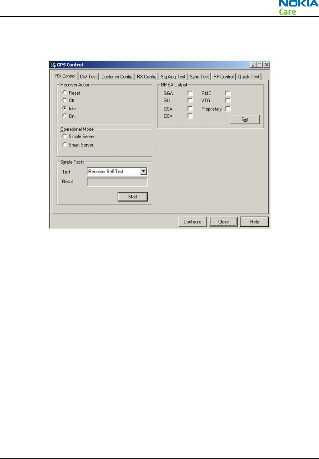
3. From the File menu, select Scan Product and check that the correct product version is displayed.
4. From the Testing menu, select GPS Control. This opens up
GPS Control
dialogue box, as shown in the
figure below, and enables the GPS.
Figure 23 GPS Control dialogue box
Select Idle to confirm the GPS is enabled and is in idle mode; at this point all clocks should be present,
GPS_En_Reset & SleepX should be high, and Vdd_Dig, Vcc_TCXO & Vcc_PLL/VCO will be present.
Receiver On turns on all RF sections of the ASIC and so all LDOs will be on.
Quick Test window
This test will perform 3 tests in one: Self test, Oscillator Test and CW Test and will provide a Pass/Fail Response
for each. The HW Self Test confirms basic communication with the GPS ASIC. The oscillator test confirms the
frequency accuracy of the GPS TCXO against the Ref_Clk. The CW Test confirms end-to-end connectivity
between the GPS antenna pogo pins and the GPS ASIC. It also contains a receive button.
Before this test is performed a known good phone should be tested in order to calibrate the setup. The signal
level of the Signal Generator should be adjusted so a reading of SNR 40 dB is achieved with the reference
unit. A good starting point is to set up the signal generator to -45dBm.
These checks are part of GPS failure troubleshooting (page 3–59).
RM-333; RM-334; RM-335
BB Troubleshooting
Issue 2 COMPANY CONFIDENTIAL Page 3 –57
Copyright © 2008 Nokia. All rights reserved.
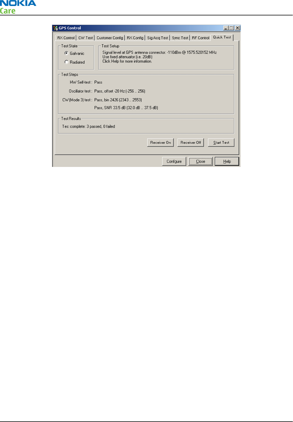
Figure 24 GPS Quick Test window
RM-333; RM-334; RM-335
BB Troubleshooting
Page 3 –58 COMPANY CONFIDENTIAL Issue 2
Copyright © 2008 Nokia. All rights reserved.
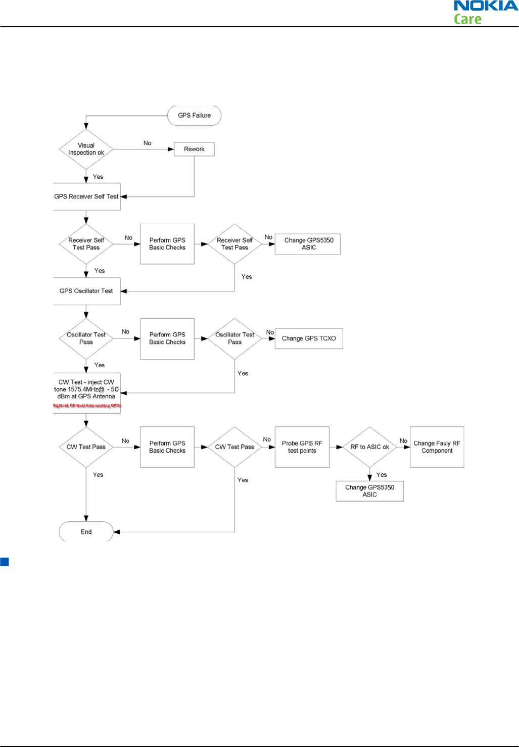
GPS failure troubleshooting
Troubleshooting flow
WLAN Troubleshooting
WLAN functional description
The Size 4 WLAN module is designed for use with a single antenna shared between itself and a co-located
BT device. The WLAN SW is downloaded from the host engine when the WLAN is turned on over the dedicated
SPI interface. BT and WLAN have their own 38,4MHz TCXO.
RM-333; RM-334; RM-335
BB Troubleshooting
Issue 2 COMPANY CONFIDENTIAL Page 3 –59
Copyright © 2008 Nokia. All rights reserved.
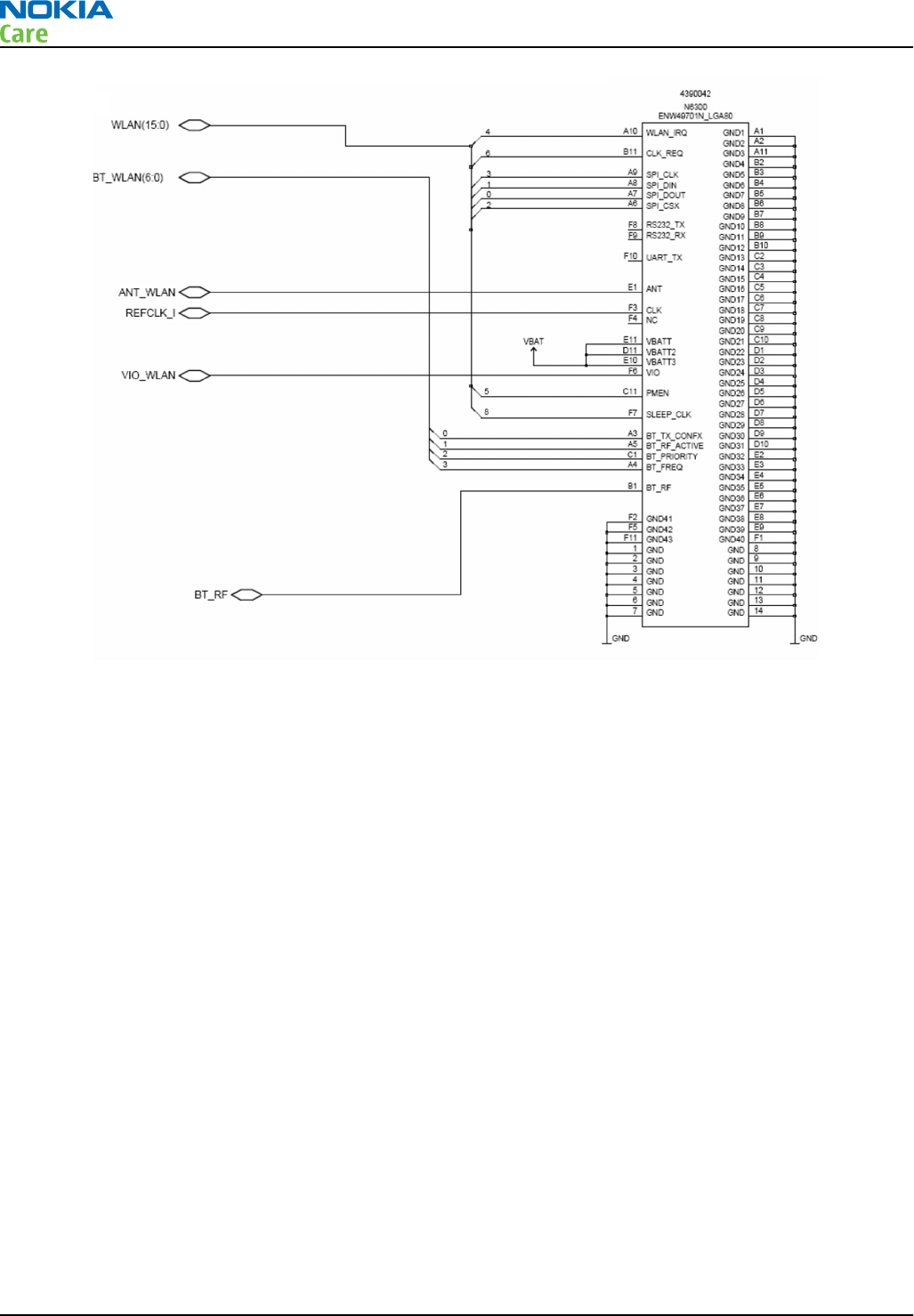
Figure 25 WLAN circuitry
WLAN settings for Phoenix
Use the following to test WLAN using Phoenix:
1 Set phone into Local Mode .
2 From the File menu, select Scan Product and check that the correct product version is displayed
3 From the Testing menu, select Self Test. This opens up a Self Test dialogue box, as shown below.
Select the ST_WLAN_TEST check box as shown and then select Start button. The test turns on the WLAN, sets
up the SPI interface and then downloads the WLAN firmware into the WLAN module. During the download
the WLAN acknowledges the data blocks and so the self test is a good way to confirm that the WLAN module
is communicating with the Host. The result column will change to Passed after a few seconds if operating
properly.
RM-333; RM-334; RM-335
BB Troubleshooting
Page 3 –60 COMPANY CONFIDENTIAL Issue 2
Copyright © 2008 Nokia. All rights reserved.
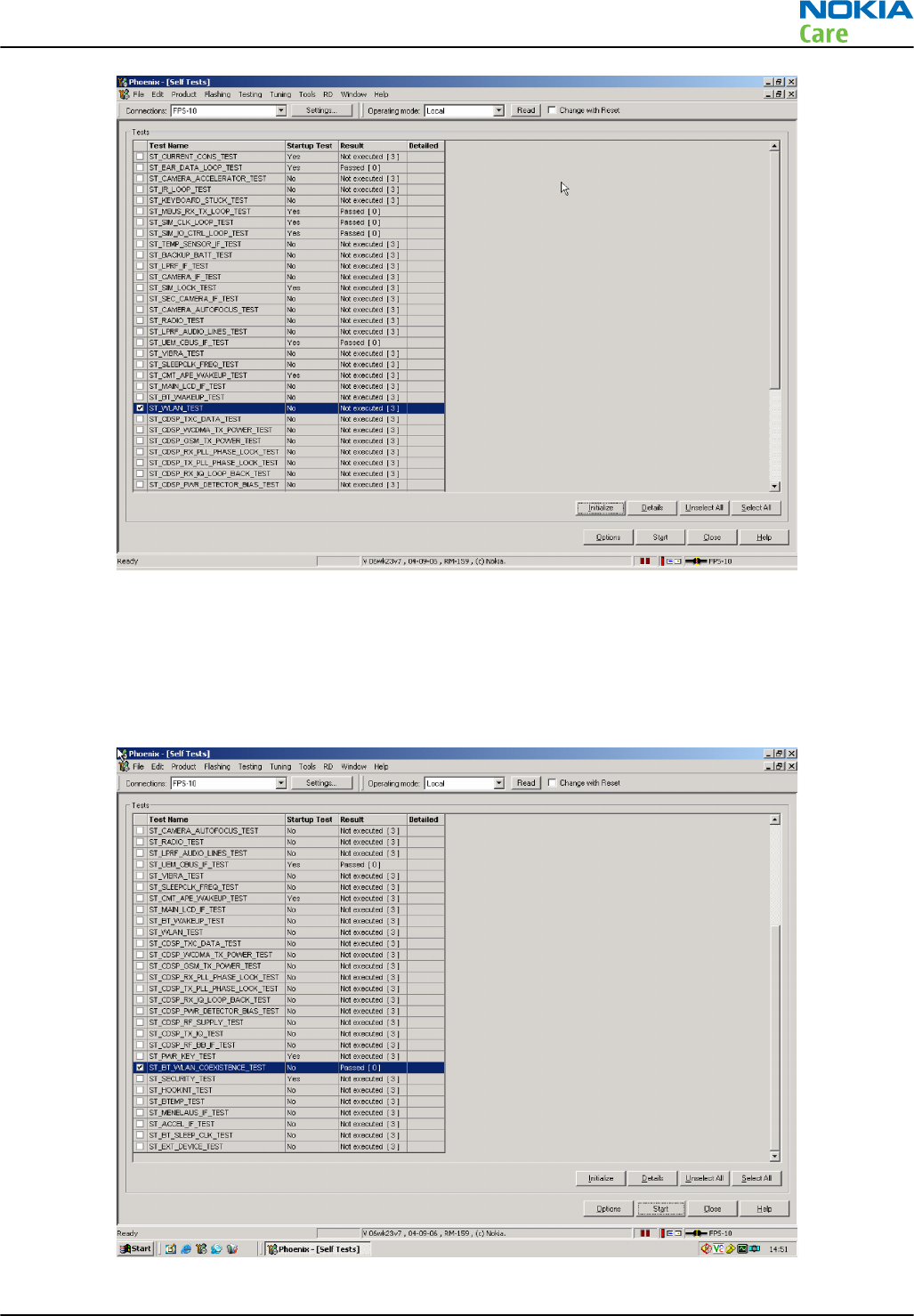
In addition, a test of the WLAN to BTH interface can be done by selecting the
ST_BT_WLAN_COEXISTENCE_TEST check box and selecting Start button.
This test verifies that the WLAN to BTH co-existence interface signals are properly connected and there are
no open circuit or shorts on the four interface signals.
The co-existence interface comprises BTH Txconfig, BTH RF Active, BTH Priority, and BTH Frequency.
RM-333; RM-334; RM-335
BB Troubleshooting
Issue 2 COMPANY CONFIDENTIAL Page 3 –61
Copyright © 2008 Nokia. All rights reserved.
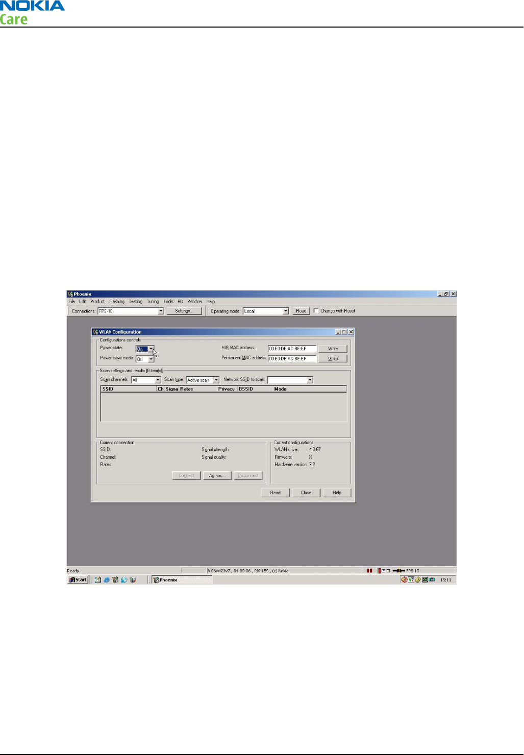
In summary these two Self tests provide a simple means of ensuring the Host engine is able to communicate
with the WLAN module and check the interface to BTH. More detailed WLAN performance test is covered in
WLAN functional test section.
WLAN functional tests
On/Off test
Prerequisites
A flash adapter connected to a PC with Phoenix service software is required.
From the testing toolbar select WLAN Configuration option. This opens the WLAN configuration dialogue
box below. Selecting the Power state option button (as indicated), the WLAN can be turned ON and OFF:
1 With Power State set to OFF, measure the dc power supply current consumption of the flash adaptor.
2 Next return the Power state to ON and re-measure the dc power supply current of the flash adaptor.
The difference between the currents in (1) and (2) should be between 190 to 220mA. When WLAN is ON, the
firmware has been downloaded and the WLAN module is in the receive state. When OFF WLAN is powered
down.
TX tests
Prerequisites
Connect complete phone assembly with C-cover to a PC with Phoenix service software using a USB data cable.
From the testing toolbar select WLAN Tx Test option shown below. This test can be used to verify TX
configuration and functionality. The default settings are sufficient for testing the TX operation, although
other channels and data rates are equally suitable. To start the test, select the Start option button:
1 Monitor the WLAN TX spectrum on a Spectrum analyser. (When making a radiated test ensure that other
WLAN devices are not transmitting as these may be detected as well, confusing the result). A typical
11MBPS TX spectrum is shown in figure below.
RM-333; RM-334; RM-335
BB Troubleshooting
Page 3 –62 COMPANY CONFIDENTIAL Issue 2
Copyright © 2008 Nokia. All rights reserved.
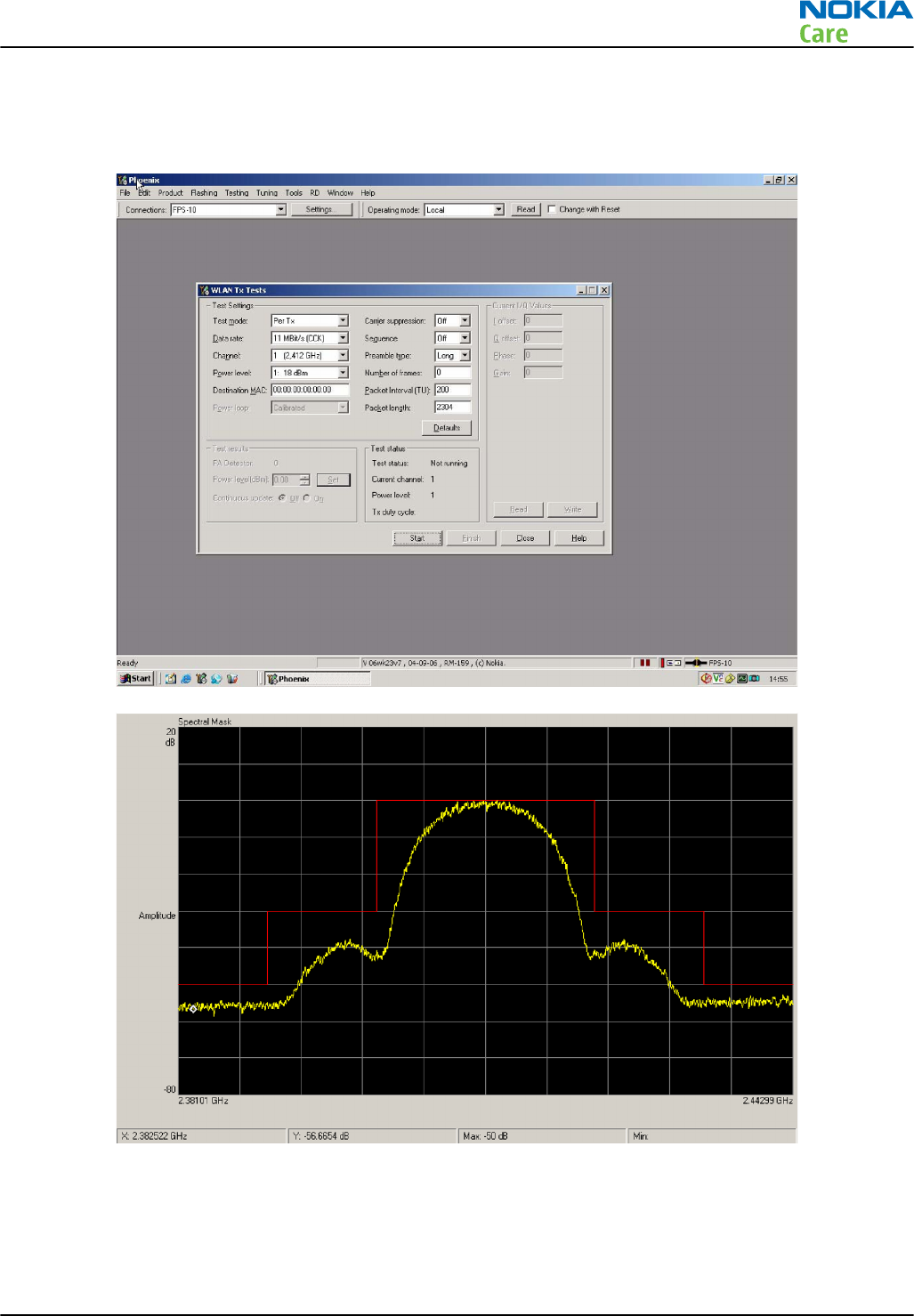
2 To finish the test select the Finish option button.
The difference between the two readings should be approximately 150mA and measures the transmit current
in 11MBPS, 802.11b mode of operation.
RX Tests
Prerequisites
Connect complete phone assembly with C-cover to a PC with Phoenix service software using a USB data cable.
RM-333; RM-334; RM-335
BB Troubleshooting
Issue 2 COMPANY CONFIDENTIAL Page 3 –63
Copyright © 2008 Nokia. All rights reserved.
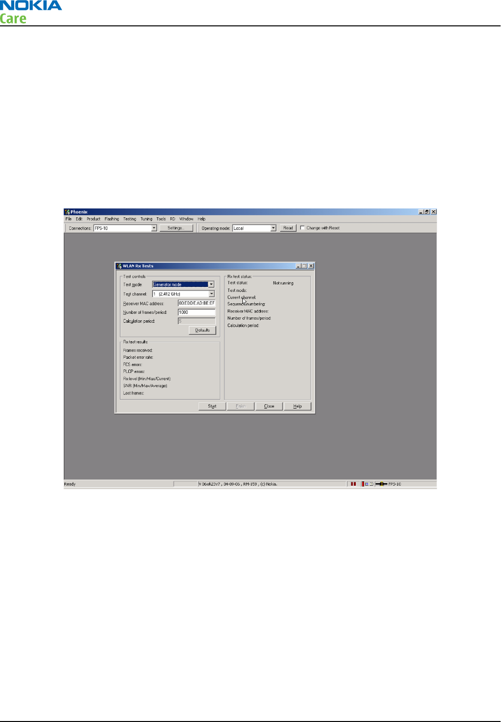
There are different options available for testing the Rx path. The simplest is to use the WLAN to report Rx
packets when operating in an area where there is an active WLAN network. Simply starting an Rx test will
show the number of packets detected by the WLAN module as it monitors the network. However, it does
require a properly configured WLAN network.
From the testing toolbar select WLAN Rx Test option shown below. This test can be used to verify Rx
configuration and functionality.
To start the test, select the Start option button.
As the WLAN monitors an active WLAN network, the Rx test results window will update and show the number
of Frames received, as well as the Packer error rate.
Monitoring the detected frames is a simple method to verify the WLAN antenna and receiver path is working
properly.
WLAN auto tuning
In case of WLAN ASIC change, RF power auto tuning is needed. Connect WLAN RF test connector to CMU200
input using proper RF cable. Start Phoenix WLAN autotune window. Check the settings and verify your PC
communicates with CMU200 via GPIB.
Auto tuning procedure
1 Start tuning by pressing Tune.
RM-333; RM-334; RM-335
BB Troubleshooting
Page 3 –64 COMPANY CONFIDENTIAL Issue 2
Copyright © 2008 Nokia. All rights reserved.
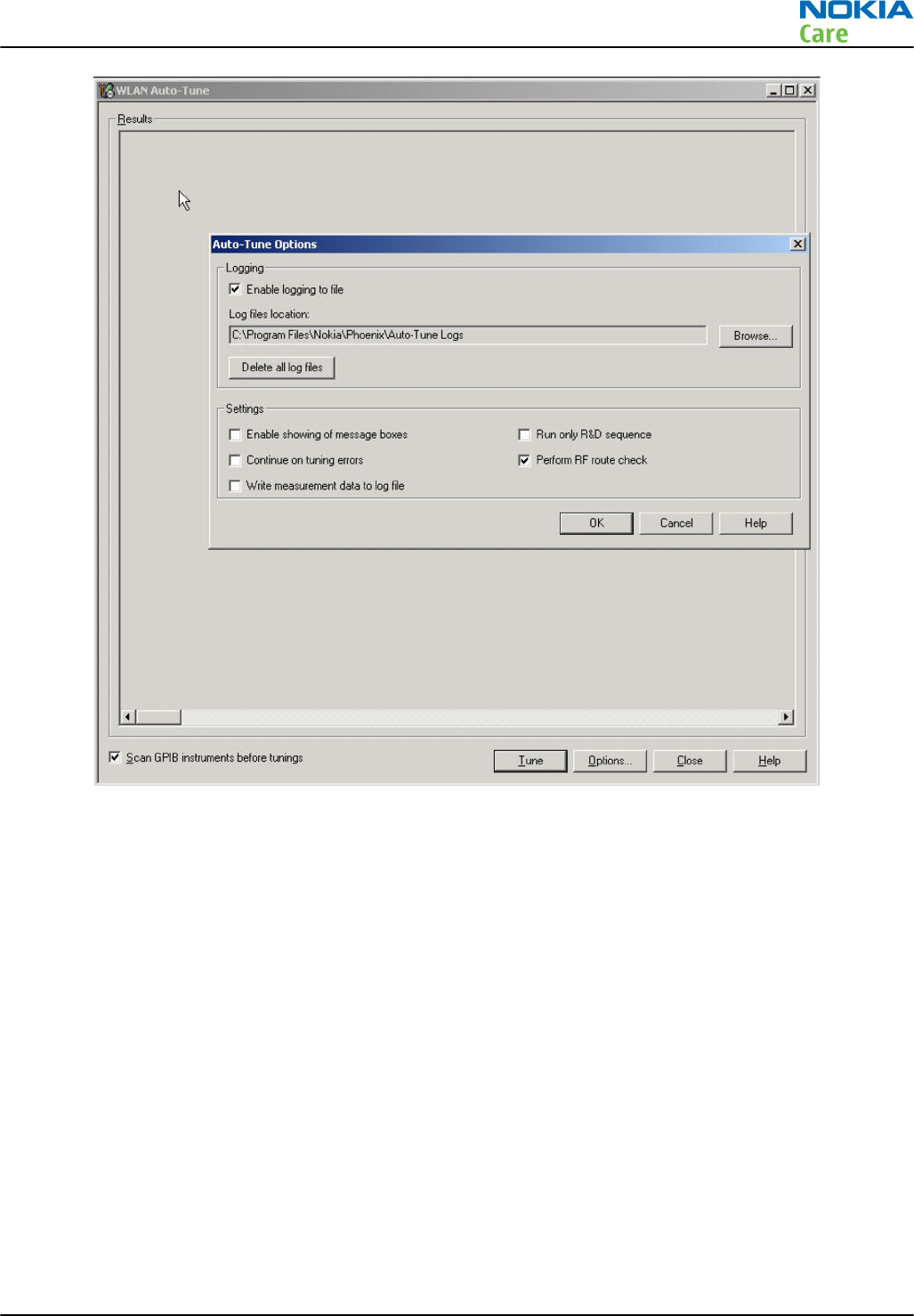
Figure 26 WLAN auto tune settings
RM-333; RM-334; RM-335
BB Troubleshooting
Issue 2 COMPANY CONFIDENTIAL Page 3 –65
Copyright © 2008 Nokia. All rights reserved.
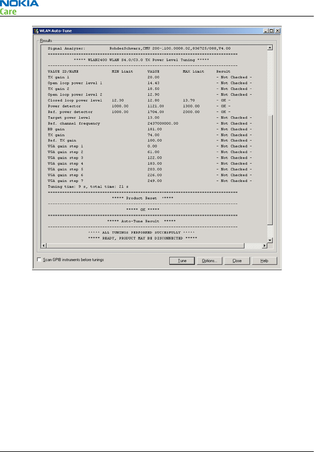
Figure 27 WLAN auto tune results
RM-333; RM-334; RM-335
BB Troubleshooting
Page 3 –66 COMPANY CONFIDENTIAL Issue 2
Copyright © 2008 Nokia. All rights reserved.

4 — RF Troubleshooting
Nokia Customer Care
Issue 2 COMPANY CONFIDENTIAL Page 4 –1
Copyright © 2008 Nokia. All rights reserved.

RM-333; RM-334; RM-335
RF Troubleshooting
(This page left intentionally blank.)
Page 4 –2 COMPANY CONFIDENTIAL Issue 2
Copyright © 2008 Nokia. All rights reserved.

Table of Contents
General RF troubleshooting ..................................................................................................................................4–5
Introduction to RF troubleshooting ................................................................................................................4–5
RF key components and test points ................................................................................................................4–6
Auto tuning.............................................................................................................................................................4–7
Introduction to RF tunings...............................................................................................................................4–7
Auto tuning........................................................................................................................................................4–7
Self Test Troubleshooting......................................................................................................................................4–7
Self test troubleshooting..................................................................................................................................4–7
Receiver Troubleshooting .....................................................................................................................................4–9
Introduction to receiver (RX) troubleshooting...............................................................................................4–9
GSM RX chain activation for manual measurements/GSM RSSI measurement ...........................................4–9
GSM receiver troubleshooting flowchart ..................................................................................................... 4–10
WCDMA RX chain activation for manual measurement.............................................................................. 4–10
WCDMA RSSI measurement ........................................................................................................................... 4–11
WCDMA receiver troubleshooting flowchart................................................................................................ 4–13
Transmitter Troubleshooting............................................................................................................................. 4–13
General instructions for transmitter (TX) troubleshooting........................................................................ 4–13
GSM transmitter troubleshooting................................................................................................................. 4–13
WCDMA transmitter troubleshooting ........................................................................................................... 4–16
Antenna Troubleshooting .................................................................................................................................. 4–17
Antenna troubleshooting.............................................................................................................................. 4–17
List of Figures
Figure 28 RF key components ...............................................................................................................................4–6
Figure 29 RF test points.........................................................................................................................................4–6
Figure 30 Phoenix GSM RSSI reading window.....................................................................................................4–9
Figure 31 Phoenix WCDMA RX Control window................................................................................................ 4–11
Figure 32 WCDMA RX generator settings .......................................................................................................... 4–12
Figure 33 Phoenix WCDMA RX power measurement window ........................................................................ 4–12
Figure 34 Phoenix GSM RF controls window..................................................................................................... 4–14
Figure 35 Antenna contacts and matching components ................................................................................ 4–18
RM-333; RM-334; RM-335
RF Troubleshooting
Issue 2 COMPANY CONFIDENTIAL Page 4 –3
Copyright © 2008 Nokia. All rights reserved.

RM-333; RM-334; RM-335
RF Troubleshooting
(This page left intentionally blank.)
Page 4 –4 COMPANY CONFIDENTIAL Issue 2
Copyright © 2008 Nokia. All rights reserved.

General RF troubleshooting
Introduction to RF troubleshooting
Most RF semiconductors are static discharge sensitive
ESD protection must be applied during repair (ground straps and ESD soldering irons).
Measuring equipment
All measurements should be done using:
•An oscilloscope for low frequency and DC measurements. Recommended probe: 10:1, 10Mohm//8pF.
•A radio communication tester including RF generator and spectrum analyser, for example Rohde & Schwarz
CMU200. (Alternatively a spectrum analyser and an RF generator can be used. Some tests in this guide are
not possible to perform if this solution is chosen).
Note: A mobile phone WCDMA transmitter should never be tested with full TX power (it is only
possible to perform the measurements in a good RF-shielded room). Even low power WCDMA
transmitters may disturb nearby WCDMA networks and cause problems to 3G cellular phone
communication in a wide area.
Note: All communication Test Set Screen dumps are from CMU200. Other testers are different.
Note: All measurements with an RF coupler should be performed in an RF-shielded environment
because nearby base stations can disturb sensitive receiver measurements. If there is no possibility
to use RF shielded environment, testing at frequencies of nearby base stations should be avoided.
Level of repair
The scope of this guideline is to verify functionality of the cellular RF block without removing RF shield.
RM-333; RM-334; RM-335
RF Troubleshooting
Issue 2 COMPANY CONFIDENTIAL Page 4 –5
Copyright © 2008 Nokia. All rights reserved.
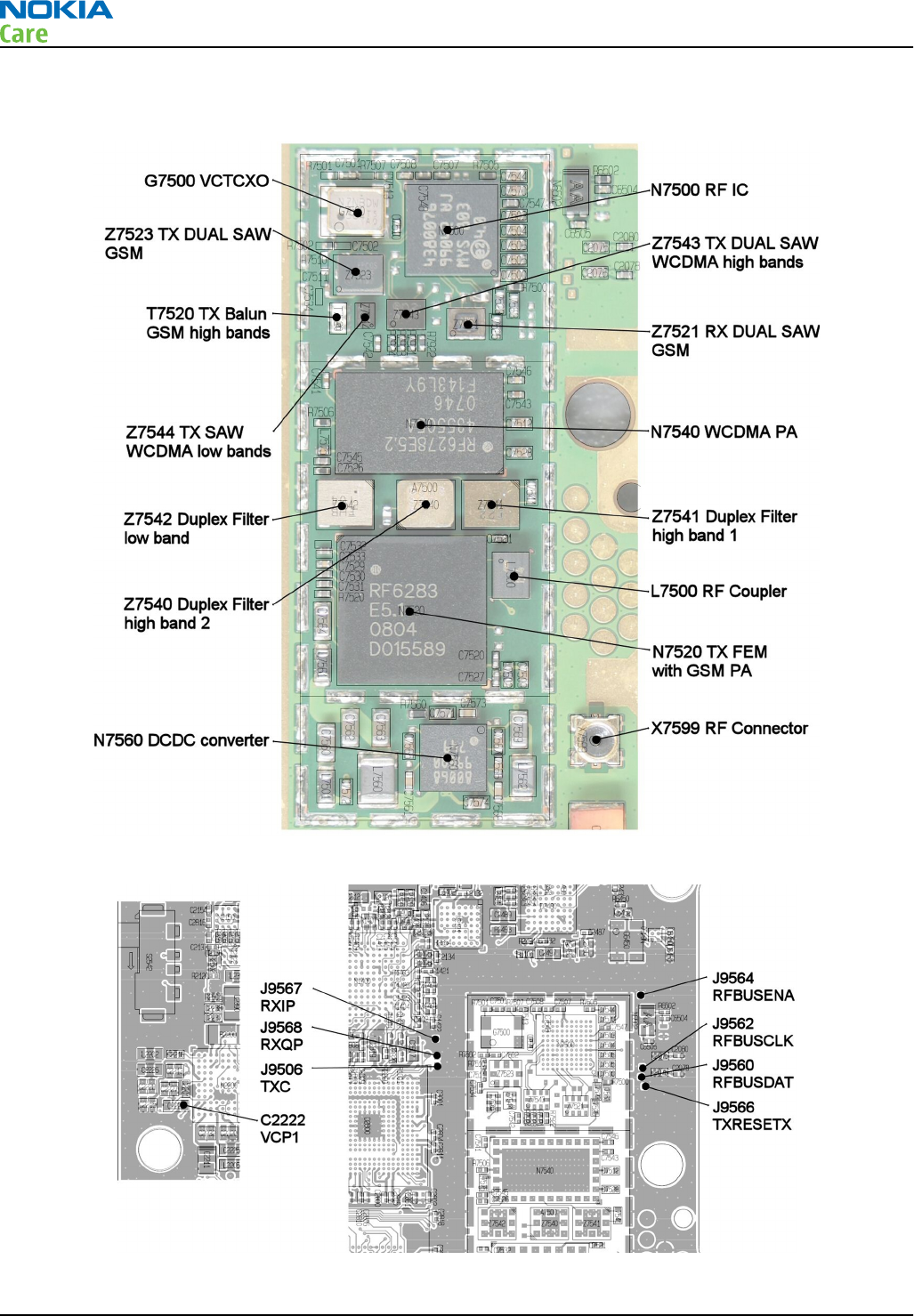
RF key components and test points
Figure 28 RF key components
Figure 29 RF test points
RM-333; RM-334; RM-335
RF Troubleshooting
Page 4 –6 COMPANY CONFIDENTIAL Issue 2
Copyright © 2008 Nokia. All rights reserved.

Auto tuning
Introduction to RF tunings
RF tuning is always performed with the help of a product-specific module jig, never with an RF coupler. Using
an RF coupler in the tuning phase will cause a complete mistuning of the RF part.
Cable and adapter losses
RF cables and adapters have some losses. They have to be taken into account when the phone is tuned. As
all RF losses are frequency dependent, the user has to act very carefully and understand the measurement
setup. For RF attenuations of the module jig and RF cable, please refer to the Service Tools section.
Auto tuning
This phone can be tuned automatically.
Auto tuning is designed to align the phone's RF part easier and faster. It performs calibrations, tunings and
measurements of RX and TX. The results are displayed and logged in a result file, if initiated.
Hardware set up
For hardware requirements for auto tuning, please refer to Service concept for RF testing and RF/BB tuning
(page 4–22).
Phoenix preparations
Install the phone specific data package, for example
Nokia_firmware_RM-333_EUROPE_10.014_v41.0.exe
. This
defines phone specific settings.
Auto tuning procedure
1Make sure the phone (in the jig) is connected to the equipment. Otherwise some menus will not be shown
in Phoenix.
2 To go to autotune, select Tuning (Alt-U)→Auto-Tune (Alt-A) from the menu.
3 Start autotuning by clicking the
Tune
button.
Self Test Troubleshooting
Self test troubleshooting
Troubleshooting flow
Note: Self tests are recommended to be made when phone is in jig and 50 Ohm load is connected
to RF connector. Otherwise powertests may fail depending on antenna load.
RM-333; RM-334; RM-335
RF Troubleshooting
Issue 2 COMPANY CONFIDENTIAL Page 4 –7
Copyright © 2008 Nokia. All rights reserved.
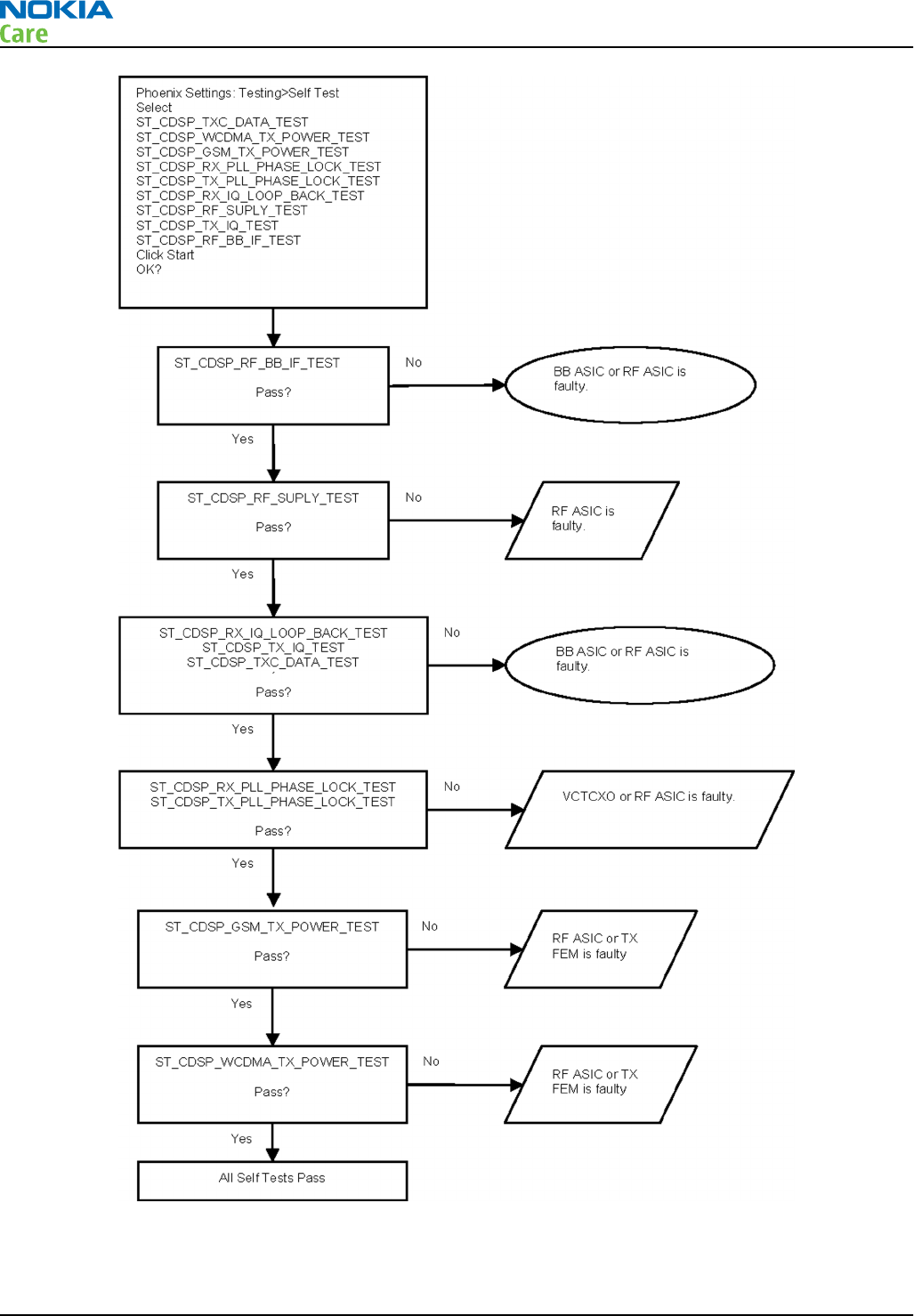
RM-333; RM-334; RM-335
RF Troubleshooting
Page 4 –8 COMPANY CONFIDENTIAL Issue 2
Copyright © 2008 Nokia. All rights reserved.
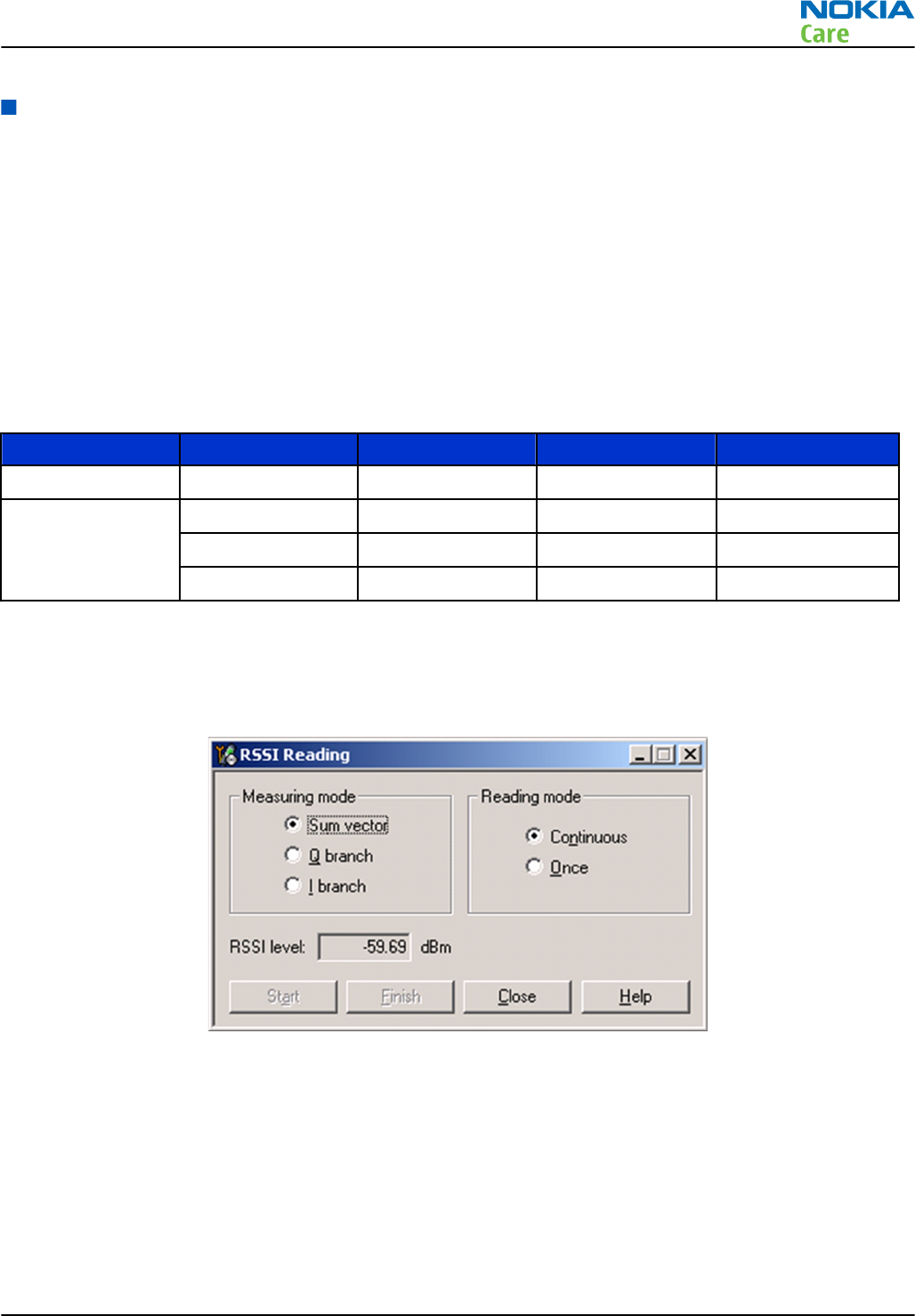
Receiver Troubleshooting
Introduction to receiver (RX) troubleshooting
RX can be tested by making a phone call or in local mode. For the local mode testing, use Phoenix service
software.
The main RX troubleshooting measurement is RSSI reading. This test measures the signal strength of the
received signal. For GSM RSSI measurements, see
GSM RX chain activation for manual measurements/GSM
RSSI measurement
. For a similar test in WCDMA mode, see
WCDMA RSSI measurement
.
GSM RX chain activation for manual measurements/GSM RSSI measurement
Prerequisites
Make the following settings in Phoenix service software:
Setting GSM850 GSM900 GSM1800 GSM1900
Phoenix Channel 190 37 700 661
Signal generator
to antenna
connector
881.66771MHz 942.46771MHz 1842.86771MHz 1960.06771MHz
(67.71kHz offset) (67.71kHz offset) (67.71kHz offset) (67.71kHz offset)
at -60dBm at -60dBm at -60dBm at -60dBm
Steps
1. Set the phone to local mode.
2. Activate RSSI reading in Phoenix (Testing→GSM→RSSI reading )
Figure 30 Phoenix GSM RSSI reading window
Results
The reading should reflect the level of the signal generator (-losses) +/- 5 dB.
When varying the level in the range -30 to -102 dBm the reading should then follow within +/-5 dB.
RM-333; RM-334; RM-335
RF Troubleshooting
Issue 2 COMPANY CONFIDENTIAL Page 4 –9
Copyright © 2008 Nokia. All rights reserved.
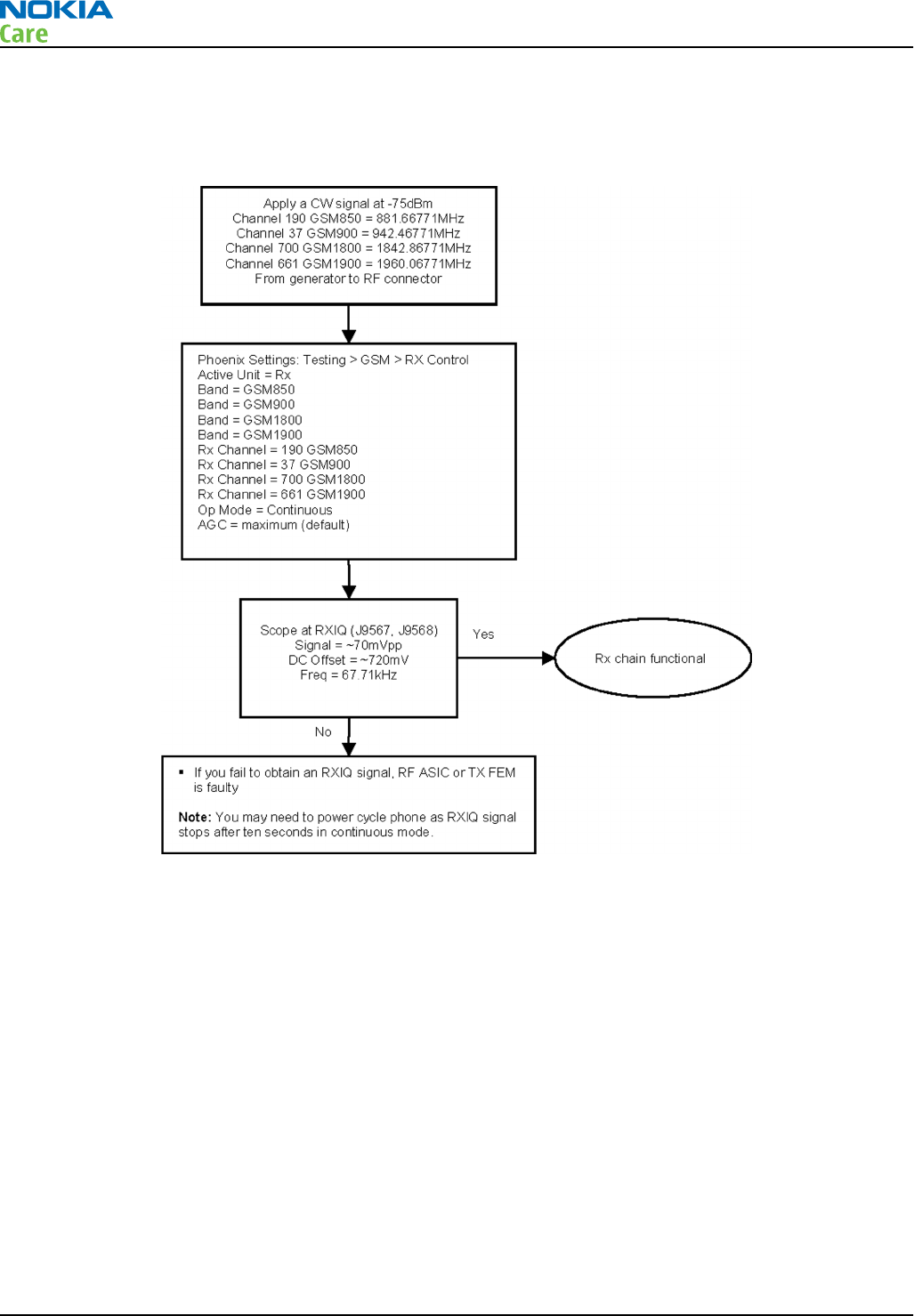
GSM receiver troubleshooting flowchart
Troubleshooting flow
WCDMA RX chain activation for manual measurement
Steps
1. Via Phoenix Testing menu, choose WCDMA/RX Control.
2. In the RX control window, make the following settings:
RM-333; RM-334; RM-335
RF Troubleshooting
Page 4 –10 COMPANY CONFIDENTIAL Issue 2
Copyright © 2008 Nokia. All rights reserved.
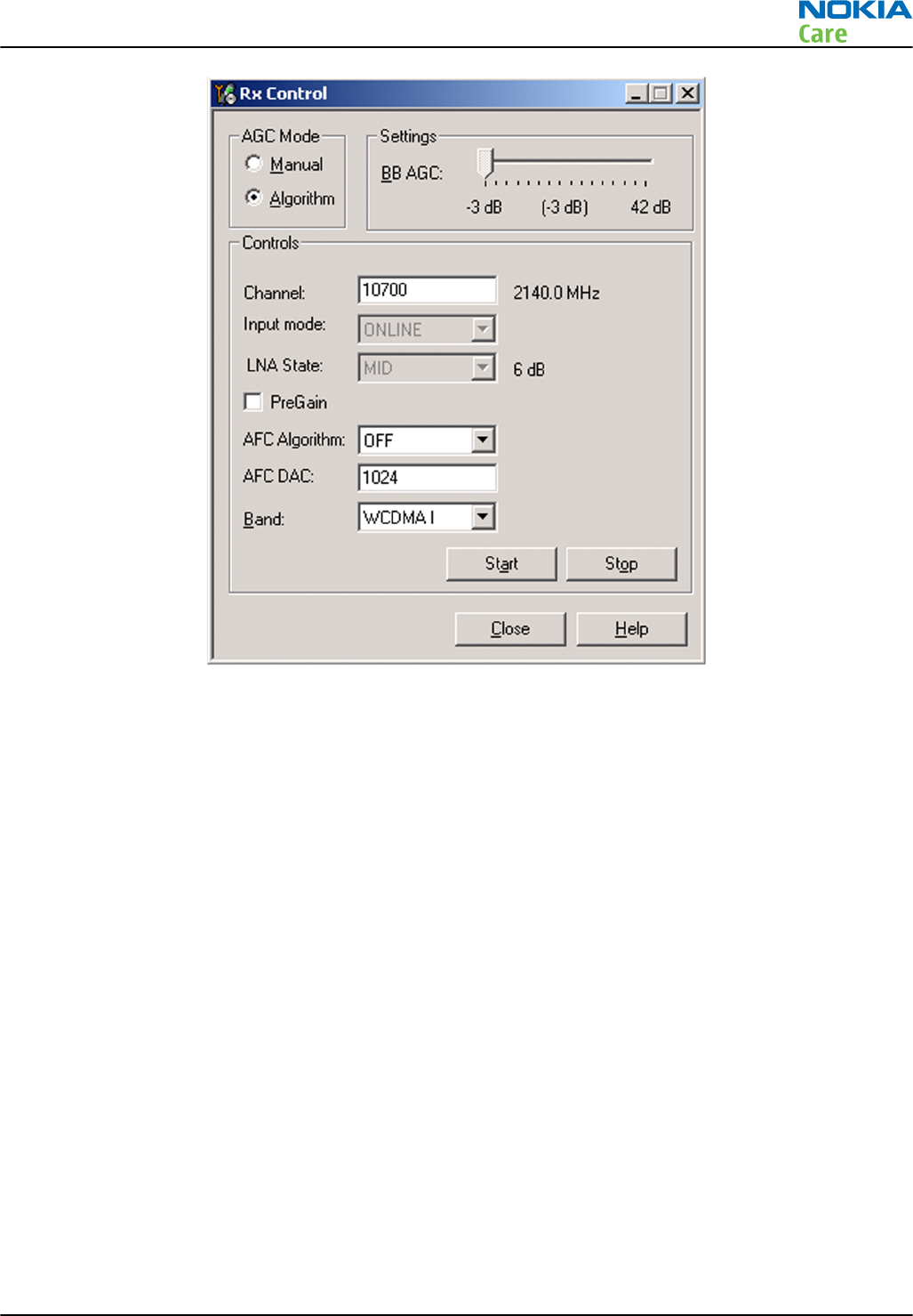
Figure 31 Phoenix WCDMA RX Control window
Note: Channel for band WCDMA II 9800, V 4408, VIII 3012
3. Click Start to activate the settings.
If the settings are changed later on (for example, change of channel) you have to click Stop and Start
again.
Note: Clicking Stop also disables TX control if it was active.
WCDMA RSSI measurement
Prerequisites
WCDMA RX must be activated before RSSI can be measured. For instructions, please refer to WCDMA RX chain
activation. Connect signal generator to RF connector and use appropriate frequency for each channel
(2141MHz for channel 10700 WCDMA band I, WCDMA modulation).
Steps
1. Set the following RF generator settings:
RM-333; RM-334; RM-335
RF Troubleshooting
Issue 2 COMPANY CONFIDENTIAL Page 4 –11
Copyright © 2008 Nokia. All rights reserved.
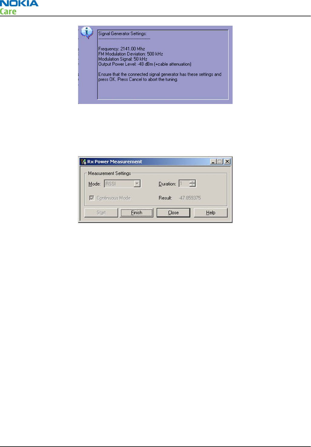
Figure 32 WCDMA RX generator settings
Note: Frequency for band WCDMA II 1961.0MHz, V 882.6MHz, VIII 943.4MHz
2. From the Phoenix testing menu, select WCDMA→RX Power measurement
3. In the RX power measurement window, make the following settings:
Figure 33 Phoenix WCDMA RX power measurement window
4. Click Start to perform the measurement.
Note: WCDMA RSSI measurement is accurate only with WCDMA modulated signal.
RM-333; RM-334; RM-335
RF Troubleshooting
Page 4 –12 COMPANY CONFIDENTIAL Issue 2
Copyright © 2008 Nokia. All rights reserved.
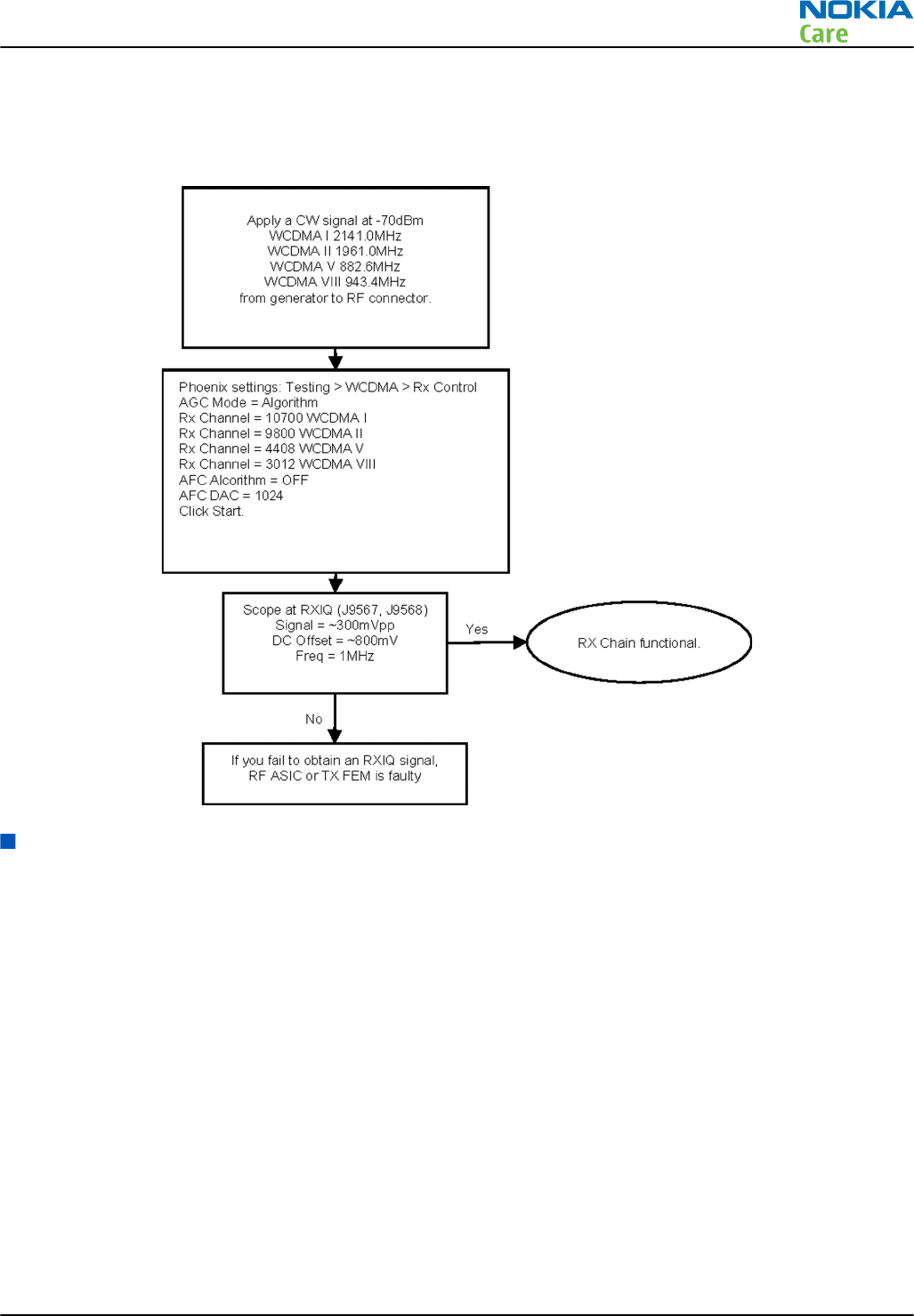
WCDMA receiver troubleshooting flowchart
Troubleshooting flow
Transmitter Troubleshooting
General instructions for transmitter (TX) troubleshooting
Please note the following before performing transmitter tests:
•TX troubleshooting requires TX operation.
•Do not transmit on frequencies that are in use.
•The transmitter can be controlled in local mode for diagnostic purposes.
•The most useful Phoenix tool for GSM transmitter testing is “RF Controls”, in WCDMA transmitter testing
the best tool is “TX Control”.
•Remember that re-tuning is not a fix! Phones are tuned correctly in production.
Note: Never activate the GSM or WCDMA transmitter without a proper antenna load. Always connect
a 50 Ω load to the RF connector (antenna, RF-measurement equipment or at least a 2 W dummy
load); otherwise the GSM or WCDMA Power amplifier (PA) may be damaged.
GSM transmitter troubleshooting
Steps
1. Set the phone to local mode.
RM-333; RM-334; RM-335
RF Troubleshooting
Issue 2 COMPANY CONFIDENTIAL Page 4 –13
Copyright © 2008 Nokia. All rights reserved.
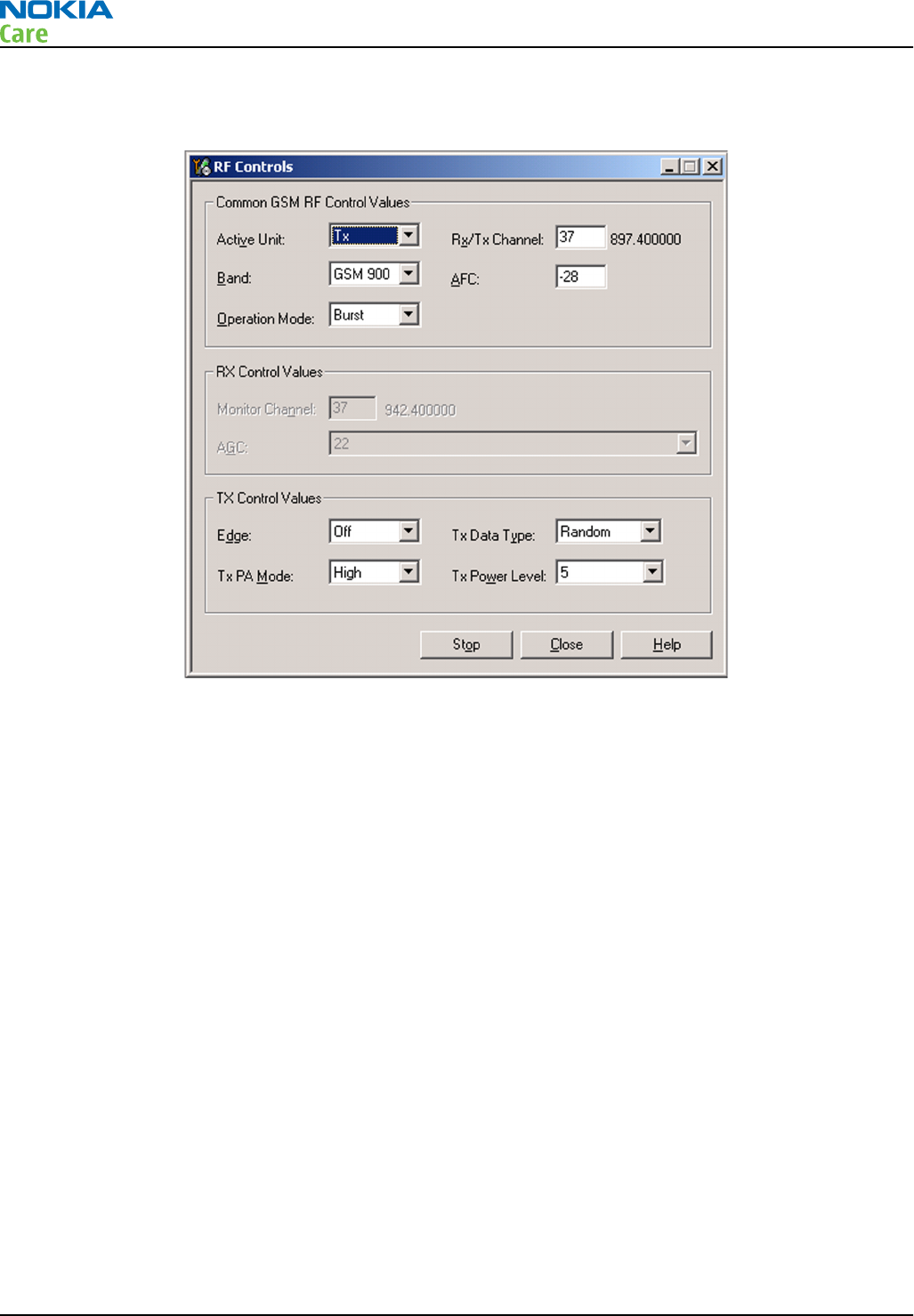
2. Activate RF controls in Phoenix (Testing→GSM→Rf Controls ).
Make settings as shown in the figure:
Figure 34 Phoenix GSM RF controls window
3. Check the basic TX parameters (i.e. power, phase error, modulation and switching spectrum), using a
communication analyser (for example CMU200).
RM-333; RM-334; RM-335
RF Troubleshooting
Page 4 –14 COMPANY CONFIDENTIAL Issue 2
Copyright © 2008 Nokia. All rights reserved.
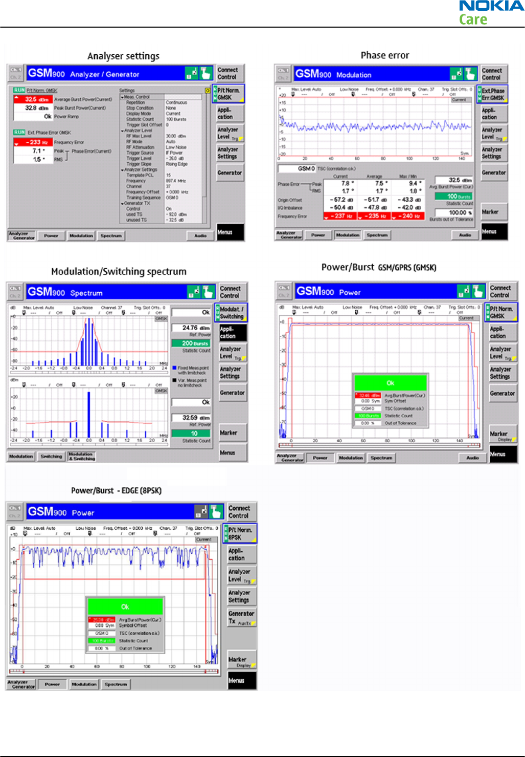
4. Change power level (RF controls) and make sure the power reading follows accordingly.
RM-333; RM-334; RM-335
RF Troubleshooting
Issue 2 COMPANY CONFIDENTIAL Page 4 –15
Copyright © 2008 Nokia. All rights reserved.
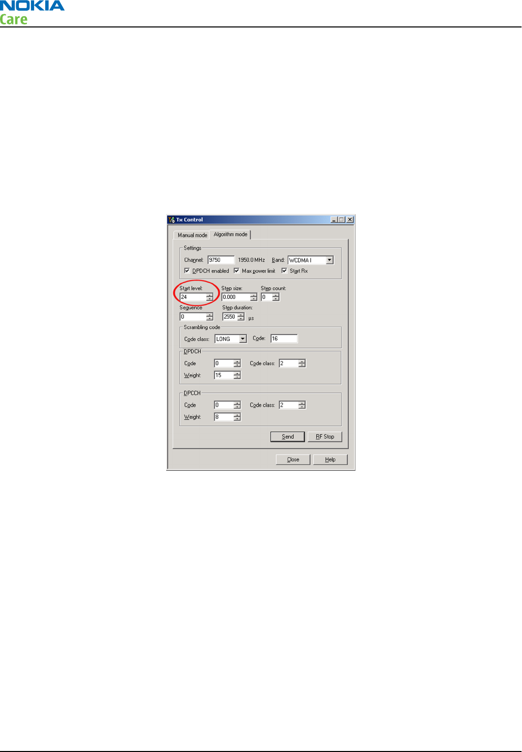
Next actions
If you want to troubleshoot the other bands, change band with RF controls and set the communication
analyser accordingly.
WCDMA transmitter troubleshooting
Steps
1. Set the phone to local mode.
2. In Phoenix, select Testing→WCDMA→TX control .
3. In the TX control window, make settings as in the picture:
Note: For WCDMA TX channels: band V 4183, VIII 2787
4. Click Send to enable the settings and activate TX.
If settings are changed (eg. new channel), you have to click RF Stop and Send again.
5. Check the basic TX parameters using a communication analyzer (for example CMU200).
RM-333; RM-334; RM-335
RF Troubleshooting
Page 4 –16 COMPANY CONFIDENTIAL Issue 2
Copyright © 2008 Nokia. All rights reserved.
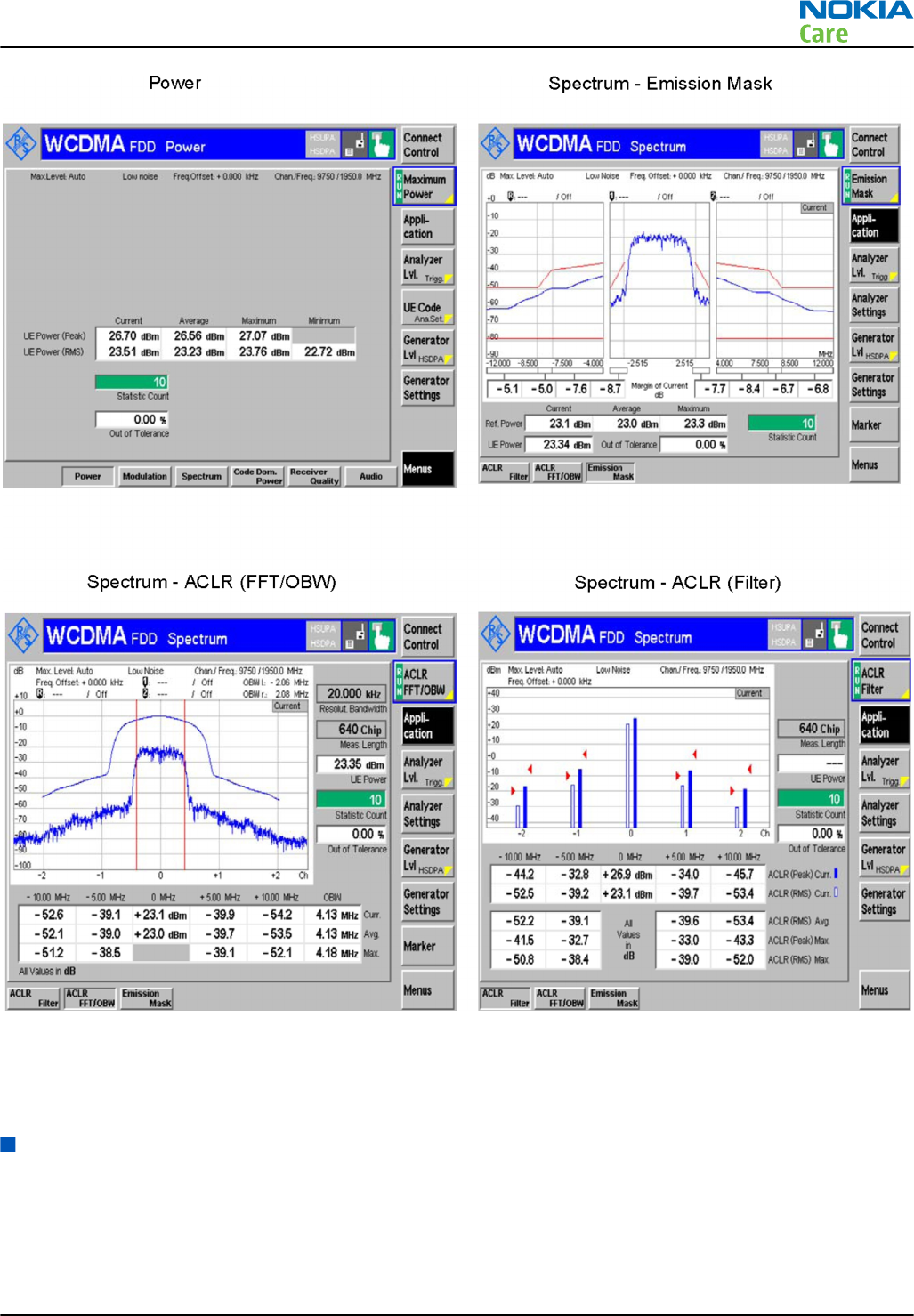
Next actions
If you want to troubleshoot the other bands, change band with RF controls and set the communication
analyser accordingly.
Antenna Troubleshooting
Antenna troubleshooting
Antenna contacts, visual check
In the main antenna there is one feed and two GND contacts. Check that GND and feed pads take proper
contact to the C-clips on main PWB.
RM-333; RM-334; RM-335
RF Troubleshooting
Issue 2 COMPANY CONFIDENTIAL Page 4 –17
Copyright © 2008 Nokia. All rights reserved.
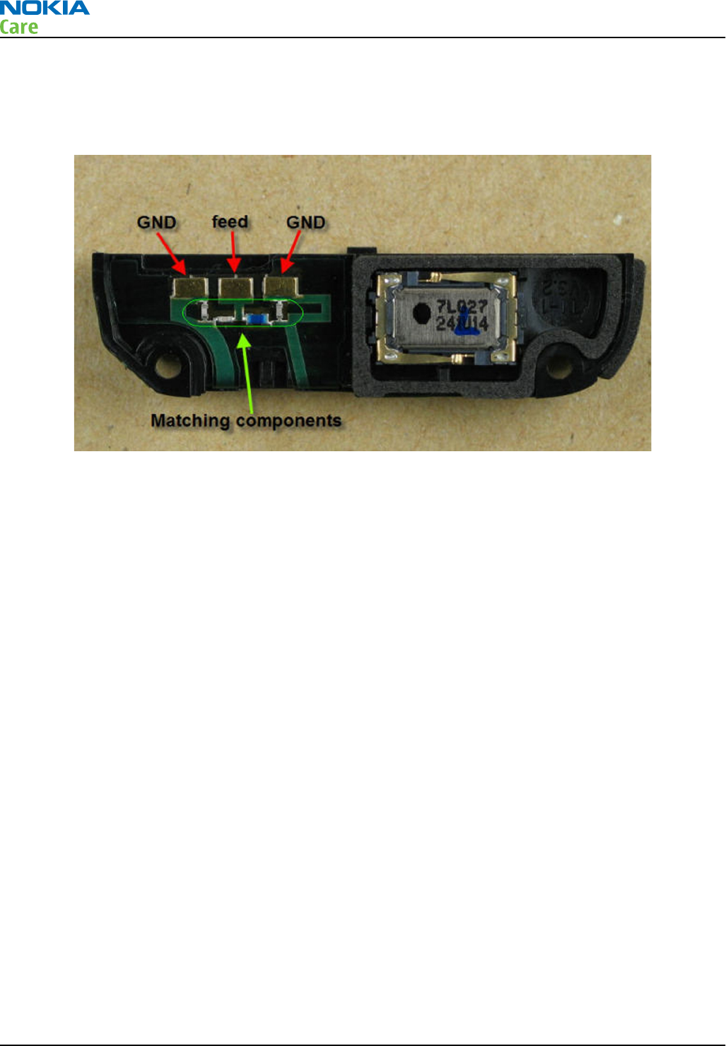
Antenna matching components, visual check
There are four matching components on the antenna flex. Check visually that all components are properly
soldered on the flex. In the case damage you need to replace the whole antenna.
Figure 35 Antenna contacts and matching components
RM-333; RM-334; RM-335
RF Troubleshooting
Page 4 –18 COMPANY CONFIDENTIAL Issue 2
Copyright © 2008 Nokia. All rights reserved.

5 — Camera Module
Troubleshooting
Nokia Customer Care
Issue 2 COMPANY CONFIDENTIAL Page 5 –1
Copyright © 2008 Nokia. All rights reserved.

RM-333; RM-334; RM-335
Camera Module Troubleshooting
(This page left intentionally blank.)
Page 5 –2 COMPANY CONFIDENTIAL Issue 2
Copyright © 2008 Nokia. All rights reserved.

Table of Contents
Introduction to camera module troubleshooting ..............................................................................................5–5
The effect of image taking conditions on image quality...................................................................................5–6
Image quality analysis ....................................................................................................................................... 5–10
Possible faults in image quality.................................................................................................................... 5–10
Testing for dust in camera module .............................................................................................................. 5–11
Testing camera image sharpness................................................................................................................. 5–12
Effects of dirty or defective camera lens protection window.................................................................... 5–13
Faulty pixels in images .................................................................................................................................. 5–14
Flash photography problems........................................................................................................................ 5–15
Main (back) camera troubleshooting flowcharts............................................................................................. 5–16
Main camera troubleshooting....................................................................................................................... 5–16
Main camera baseband troubleshooting..................................................................................................... 5–16
Main camera baseband troubleshooting - powerings ............................................................................... 5–18
No recognizable viewfinder image .............................................................................................................. 5–19
Bad image quality troubleshooting ............................................................................................................. 5–20
Flash troubleshooting.................................................................................................................................... 5–21
Secondary (front) camera troubleshooting flow ............................................................................................. 5–22
Accelerometer troubleshooting......................................................................................................................... 5–23
List of Figures
Figure 36 Only center part of image is in focus due to limited depth of focus ...............................................5–6
Figure 37 Blurring caused by shaking hands ......................................................................................................5–7
Figure 38 Near objects get skewed when taking images from a moving vehicle...........................................5–7
Figure 39 Noisy image taken in +70 degrees Celsius .........................................................................................5–8
Figure 40 Image taken against light....................................................................................................................5–8
Figure 41 Flicker in an image; object illuminated by strong fluorescent light................................................5–9
Figure 42 A lens reflection effect caused by sunshine........................................................................................5–9
Figure 43 Good image taken indoors................................................................................................................ 5–10
Figure 44 Good image taken outdoors ............................................................................................................. 5–10
Figure 45 Effects of dust on optical path .......................................................................................................... 5–11
Figure 46 Image taken with clear protection window ................................................................................... 5–13
Figure 47 Image taken with greasy protection window ................................................................................ 5–13
Figure 48 Image of point light sources taken with a clean protective window........................................... 5–14
Figure 49 Image of point light sources taken with a dirty (finger print) protective window .................... 5–14
Figure 50 Enlargement of a hot pixel................................................................................................................ 5–15
Figure 51 Light from the flash has reflected on particles in front of the camera ........................................ 5–15
RM-333; RM-334; RM-335
Camera Module Troubleshooting
Issue 2 COMPANY CONFIDENTIAL Page 5 –3
Copyright © 2008 Nokia. All rights reserved.

RM-333; RM-334; RM-335
Camera Module Troubleshooting
(This page left intentionally blank.)
Page 5 –4 COMPANY CONFIDENTIAL Issue 2
Copyright © 2008 Nokia. All rights reserved.

Introduction to camera module troubleshooting
Background, tools and terminology
Faults or complaints in camera operation can be roughly categorised into three subgroups:
1 Camera is not functional at all; no image can be taken.
2 Images can be taken but there is nothing recognizable in them.
3 Images can be taken and they are recognizable but for some reason the quality of images is seriously
degraded, or customer complains about image quality.
Image quality is very hard to measure quantitatively, and even comparative measurements are difficult
(comparing two images) to do, if the difference is small. Especially if the user is not satisfied with his/her
device's image quality, and tells, for example, that the images are not sharp, it is fairly difficult to accurately
test the device and get an exact figure which would tell whether the device is functioning properly.
Often subjective evaluation has to be used for finding out if a certain property of the camera is acceptable
or not. Some training or experience of a correctly operating reference device may be needed in order to
detect what actually is wrong, or is there anything wrong at all.
It is easy for the user to take bad images in bad conditions. Therefore the camera operation has to be checked
always in constant conditions (lighting, temperature) or by using a second, known-to-be good device as
reference. Experience helps significantly in analysing image quality.
Terms
Autofocus Camera module contains lens movement mechanics for focus adjustment.
Autofocus enables camera to take sharp images of objects positioned
between 10cm to infinity. During AF the viewfinder image will be
momentarily blurred as the camera searches for the right focus setting.
Digital zoom Digital zoom is done by first cropping the image by the zoom ratio and
then upscaling it to the output resolution. This will decrease the image
quality especially with high zoom ratios.
Dynamic range Camera's ability to capture details in dark and bright areas of the scene
simultaneously.
Exposure time Camera modules use silicon sensor to collect light and for forming an
image. The imaging process roughly corresponds to traditional film
photography, in which exposure time means the time during which the
film is exposed to light coming through optics. Increasing the time will
allow for more light hitting the film and thus results in brighter image. The
operation principle is exactly the same with silicon sensor, but the shutter
functionality is handled electronically i.e. there is no mechanical moving
parts like in film cameras.
Flicker Phenomenon, which is caused by pulsating in scene lighting, typically
appearing as wide horizontal stripes in an image.
ND-filter Neutral density filter is a filter which is used in very bright conditions to
reduce the amount of light hitting the sensor. The filter is built into the
camera module and applied automatically when needed.
Noise Variation of response between pixels with same level of input illumination.
Resolution Usually the amount of pixels in the camera sensor. In some occasions the
term resolution is used for describing the sharpness of the images.
RM-333; RM-334; RM-335
Camera Module Troubleshooting
Issue 2 COMPANY CONFIDENTIAL Page 5 –5
Copyright © 2008 Nokia. All rights reserved.
Sensitivity Camera module's sensitivity to light. In equivalent illumination conditions,
a less sensitive camera needs a longer exposure time to gather enough
light in forming a good image. Analogous to ISO speed in photographic
film.
Sharpness Good quality images are 'sharp' or 'crisp', meaning that image details are
well visible in the picture. However, certain issues, such as non-idealities
in optics, cause image blurring, making objects in picture to appear 'soft'.
Each camera type typically has its own level of performance.
Shutter The electronic shutter is used when short exposure times are needed and
in video. When the mechanical shutter is used a black sheet will cover the
lens after the exposure.
The effect of image taking conditions on image quality
There are some factors, which may cause poor image quality, if not taken into account by the end user when
shooting images, and thus may result in complaints. The items listed are normal to camera operation and
are not a reason for changing the camera module.
Autofocus
When the camera is focusing a lens is moved inside the module to give the sharpest possible image. This
camera module is specified to operate satisfactorily from 10 cm to infinite distance of scene objects. Trying
to photograph objects closer than 10 cm is likely to result in a blurred out of focus image. The lack of sharpness
is first visible in full resolution images. Images taken very close to the subject, a limited depth of focus will
be visible, that is the upper or lower parts of the image may be out of focus. This is normal; do not change
the camera module.
Figure 36 Only center part of image is in focus due to limited depth of focus
The amount of light available
In dim conditions camera runs out of sensitivity. The exposure time is long (especially in the night mode)
and the risk of getting shaken (= blurred) images increases. In addition, image noise level grows. The
maximum exposure time in the night mode is ¼ seconds. Therefore, images need to be taken with extreme
care and by supporting the phone when the amount of light reflected from the target is low. Because of the
longer exposure time and larger gain value, noise level increases in low light conditions. Sometimes blurring
may even occur in daytime, if the image is taken very carelessly. See the figure below for an example. This
is normal; do not change the camera module.
RM-333; RM-334; RM-335
Camera Module Troubleshooting
Page 5 –6 COMPANY CONFIDENTIAL Issue 2
Copyright © 2008 Nokia. All rights reserved.
Figure 37 Blurring caused by shaking hands
Movement in bright light
If an image is taken of moving objects or if the device is used in a moving vehicle, object 'skewing' or 'tilting'
may occur. This phenomenon is fundamental to most CMOS camera types, and may happen when using the
electronic shutter. The movement of camera or object sometimes cause blurring indoors or in dim lighting
conditions because of long exposure time. This is normal; do not change the camera module.
Figure 38 Near objects get skewed when taking images from a moving vehicle
Temperature
High temperatures inside the mobile phone cause more noise to appear in images. For example, in +70
degrees (Celsius), the noise level may be very high, and it further grows if the conditions are dim. If the phone
processor has been heavily loaded for a long time before taking an image, the phone might have considerably
higher temperature inside than in the surrounding environment. This is also normal to camera operation;
do not change the camera module.
RM-333; RM-334; RM-335
Camera Module Troubleshooting
Issue 2 COMPANY CONFIDENTIAL Page 5 –7
Copyright © 2008 Nokia. All rights reserved.
Figure 39 Noisy image taken in +70 degrees Celsius
Phone display
If the display contrast is set too dark, the image quality degrades: the images may be very dark depending
on the setting. If the display contrast is set too bright, image contrast appears bad and "faint". This problem
is solved by setting the display contrast correctly. This is normal behaviour; do not change the camera module.
Basic rules of photography (especially shooting against light)
Because of dynamic range limitations, taking images against bright light might cause either saturated image
or the actual target appear too dark. In practice, this means that when taking an image indoors and having,
for example, a window behind the object, the result is usually poor. This is normal behaviour; do not change
the camera module.
Figure 40 Image taken against light
Flicker
In some occasions a bright fluorescent light may cause flicker in the viewfinder and captured image. This
phenomenon may also be a result, if images are taken indoors under the mismatch of 50/60 Hz electricity
network frequency. The electricity frequency used is automatically detected by the camera module. In some
very few countries, both 50 and 60 Hz networks are present and thus probability for the phenomenon
increases. Flickering occurs also under high artificial illumination level. Flickering only occurs when the rolling
shutter is used. This is normal behaviour; do not change the camera module.
RM-333; RM-334; RM-335
Camera Module Troubleshooting
Page 5 –8 COMPANY CONFIDENTIAL Issue 2
Copyright © 2008 Nokia. All rights reserved.
Figure 41 Flicker in an image; object illuminated by strong fluorescent light
Bright light outside of image view
Especially the sun can cause clearly visible lens glare phenomenon and poor contrast in images. This happens
because of undesired reflections inside the camera optics. Generally this kind of reflections are common in
all optical systems. This is normal behaviour; do not change the camera module.
Figure 42 A lens reflection effect caused by sunshine
RM-333; RM-334; RM-335
Camera Module Troubleshooting
Issue 2 COMPANY CONFIDENTIAL Page 5 –9
Copyright © 2008 Nokia. All rights reserved.
Examples of good quality images
Figure 43 Good image taken indoors
Figure 44 Good image taken outdoors
Image quality analysis
Possible faults in image quality
When checking for possible errors in camera functionality, knowing what error is suspected significantly
helps the testing by narrowing down the amount of test cases. The following types of image quality problems
may be expected to appear:
•Dust (black spots)
•Lack of sharpness
•Bit errors
In addition, there are many other kinds of possibilities for bad image quality, but those are ruled out from
the scope of this document since the probability of their appearance is small.
RM-333; RM-334; RM-335
Camera Module Troubleshooting
Page 5 –10 COMPANY CONFIDENTIAL Issue 2
Copyright © 2008 Nokia. All rights reserved.
Testing for dust in camera module
Symptoms and diagnosis
For detecting these kinds of problems, take an image of a uniform white surface and analyse it in full
resolution. A good quality PC monitor is preferred for analysis. Search carefully, since finding these defects
is not always easy. Figure "Effects of dust on optical path" is an example image containing easily detectable
dust problems.
When taking a white image, use uniformly lightened white paper or white wall. One possibility is to use
uniform light but in this case make sure that the camera image is not flickering when taking the test image.
In case flickering happens, try to reduce illumination level. Use JPEG image format for analysing, and set the
image quality parameter to ‘High Quality’.
Black spots in an image are caused by dirt particles trapped inside the optical system. Clearly visible and
sharp edged black dots in an image are typically dust particles on the image sensor. These spots are searched
for in the manufacturing phase, but it is possible that the camera body cavity contains a particle, which may
move onto the image sensor active surface, for example, when the phone is dropped. Thus it is also possible
that the problem will disappear before the phone is brought to service. The camera should be replaced if the
problem is present when the service technician analyses the phone.
If a dust particle is lying on the infrared filter surface on either side, they are hard to locate because they are
out of focus, and appear in the image as large, grayish and fading-edge 'blobs'. Sometimes they are invisible
to the eye, and thus the user probably does not notice them at all. However, it is possible that a larger particle
disturbs the user, causing need for service.
Figure 45 Effects of dust on optical path
If large dust particles get trapped on top of the lens surface in the cavity between camera window and lens,
they will cause image blurring and poor contrast. The dust gasket between the window and lens should
prevent any particles from getting into the cavity after the manufacturing phase.
If dust particles are found on the sensor, this is classified as a manufacturing error of the module and the
camera should be replaced. Any particles inside the cavity between the protection window and lens have
most probably been trapped there in the assembly phase at a Nokia factory. Unauthorized disassembling of
the product can also be the root of the problem. However, in most cases it should be possible to remove the
particle(s) by using clean compressed air. Never wipe the lens surface before trying compressed air; the
possibility of damaging the lens is substantial. Always check the image sharpness after removing dust.
RM-333; RM-334; RM-335
Camera Module Troubleshooting
Issue 2 COMPANY CONFIDENTIAL Page 5 –11
Copyright © 2008 Nokia. All rights reserved.

Testing camera image sharpness
Symptoms and diagnosis
If pictures taken with a device are claimed to be blurry, there are five possible sources for the problem:
1 The protection window is fingerprinted, soiled, dirty, visibly scratched or broken.
2 The camera module has failed to focus correctly, producing a blurred image.
3 User has tried to take pictures in too dark conditions and images are blurred due to handshake or
movement. This is not a cause to replace camera module.
4 There is dirt between the protection window and the camera lens.
5The protection window is defective. This can be either a manufacturing failure or caused by the user. The
window should be changed.
A quantitative analysis of sharpness is very difficult to conduct in any other environment than optics
laboratory. Therefore, subjective analysis should be used.
If no visible defects (items 1-4) are found, a couple of test images should be taken. Generally, a well-
illuminated typical indoor scene, such as the one in Figure "Good image taken indoors", can be used as a
target. The main considerations are:
•The camera module has to be given time to focus correctly. Correct focusing is normally indicated with a
flashing icon or green bracket in the viewfinder. During focusing, the image in the viewfinder moves
slightly back and fourth, this is normal and shows that the lens unit is moving. During the movement a
faint sound can be heard from the camera head.
•The protection window has to be clean.
•The amount of light (300 – 600 lux (bright office lighting)) is sufficient.
•The scene should contain, for example, small objects for checking sharpness. Their distance should be 1
– 2 meters.
•If possible, compare the image to another image of the same scene, taken with a different device. Note
that the reference device has to be a similar Nokia phone.
There are several conditions in which AF operation is challenging for the camera module, i.e. failing from
time to time. These include:
•Low light scenes and night mode
•Scenes with low contrast
•Fast-moving objects
AF operation is disabled on purpose in “night”, “landscape”, “sports”, and “video” modes. When using these
modes the lens is set to a predetermined focal position and isn’t moved during use.
Under low light and night mode the AF function is slower than under good light, it may even fail to find
correct focus position. Low contrast scenes or fast moving objects may also slow down or cause AF to fail.
This is normal operation, and is not a cause to replace camera.
The operation of AF can be tested by taking images of objects at different distances. Good distances are 20
cm, 60 cm and infinity (>3 m). Any LED or xenon flashes should not be used while taking the images.
The taken images should be analysed on PC screen at 100% scaling simultaneously with a reference image.
Pay attention to the computer display settings; at least 65000 colors (16 bit) have to be used. 256 (8-bit)
color setting is not sufficient; true color (24 bit, 16 million colors) or 32 bit (full color) setting is recommended.
If the differences are noticeable at a glance and also if the one under investigation is significantly inferior,
the module might have a faulty lens. In this case, the module should be changed. Always recheck the
resolution after changing the camera module. If a different module produces a clearly noticeable quality gap,
RM-333; RM-334; RM-335
Camera Module Troubleshooting
Page 5 –12 COMPANY CONFIDENTIAL Issue 2
Copyright © 2008 Nokia. All rights reserved.
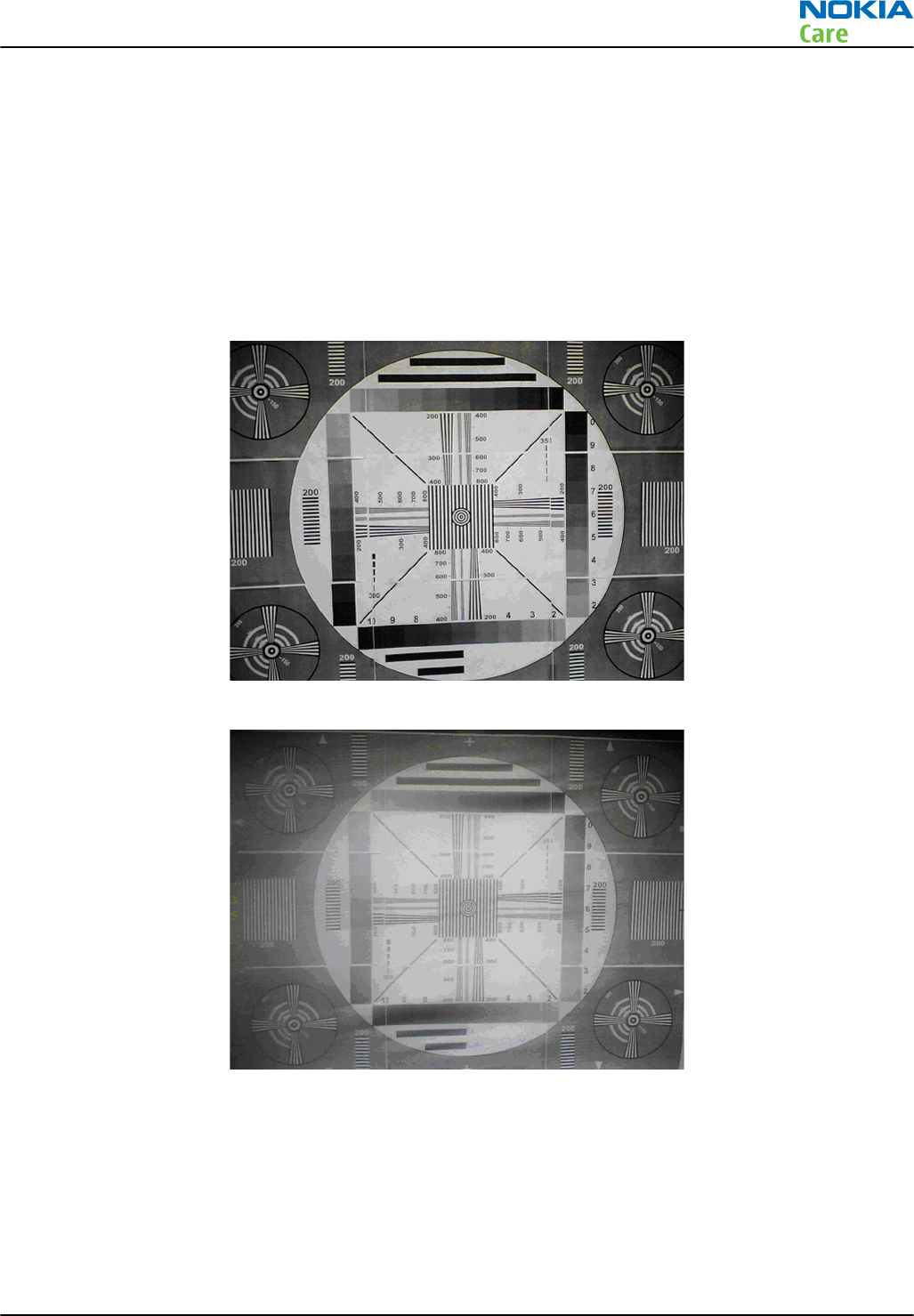
the fault is probably in the camera window. Check the window by looking carefully through it when replacing
the module. As references Figure "Good image taken indoors" and Figure "Good image taken outdoors" can
be used. Another possibility is to use a service point comparison phone, if available.
Effects of dirty or defective camera lens protection window
The following series of images demonstrates the effects of fingerprints on the camera protection window.
Note: The effects of any dirt in images can vary very much; it may be difficult to judge if the window
has been dirty when some image has been taken or if something else has been wrong. That is why
the cleanness of the protection window should always be checked and the window should be wiped
clean with a suitable cloth.
Figure 46 Image taken with clear protection window
Figure 47 Image taken with greasy protection window
Bright point light sources might cause images that have flares around the light source if the protection
window is dirty. A smeared fingerprint may be hard to see on the protective window but if will affect the
image quality. These flares can be avoided by cleaning the window with a suitable cloth.
RM-333; RM-334; RM-335
Camera Module Troubleshooting
Issue 2 COMPANY CONFIDENTIAL Page 5 –13
Copyright © 2008 Nokia. All rights reserved.
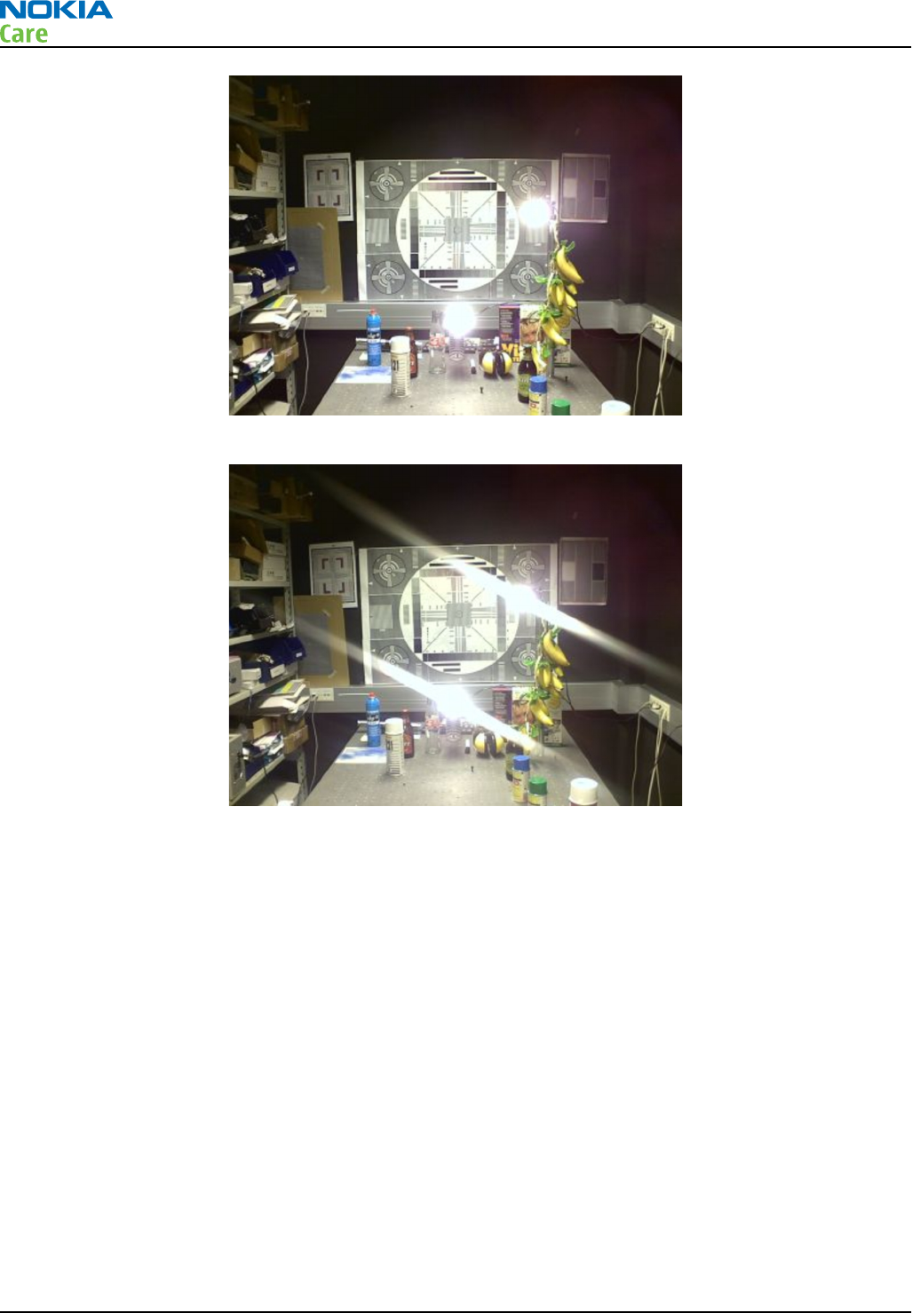
Figure 48 Image of point light sources taken with a clean protective window
Figure 49 Image of point light sources taken with a dirty (finger print) protective window
Faulty pixels in images
Faulty pixels are pixels that do not respond to light in the same way as the pixels around them. There are
three main types of faulty pixels, dead, stuck and hot pixels.
Dead pixels are always black or significantly darker than their surrounding. Dead pixels appear as black spots
in all lightning conditions. Camera modules producing images with dead pixels that are clearly noticeable
should be replaced.
If the pixel remains always saturated to its maximum value it is stuck. Stuck pixels may appear as red, green,
blue or white spots in all lightning conditions. Camera modules producing images with one or more stuck
pixels should be replaced.
Hot pixels are pixels that easily saturate in dim light conditions. It is normal to get a lot of noise and hot
pixels in night conditions or otherwise dark conditions. The hot pixels should disappear when the ambient
light is increased, but may still appear in darker areas of an otherwise well illuminated scene.
When examining an image for defect pixels, test images should be viewed as 100% enlargements on a PC
monitor.
RM-333; RM-334; RM-335
Camera Module Troubleshooting
Page 5 –14 COMPANY CONFIDENTIAL Issue 2
Copyright © 2008 Nokia. All rights reserved.
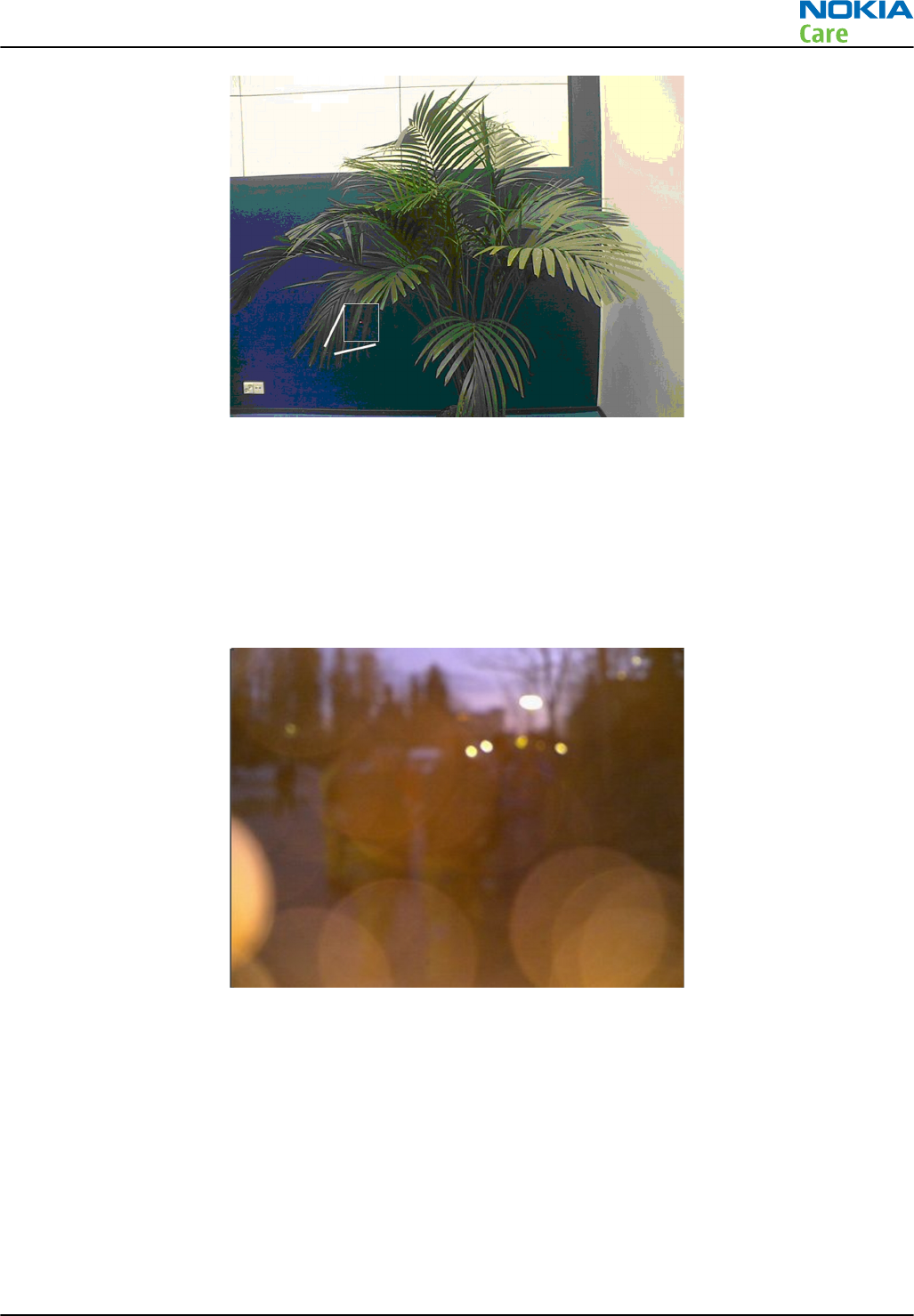
Figure 50 Enlargement of a hot pixel
Flash photography problems
Use of flash device may affect the image in many ways.
•White balance errors. The image may get a wrong tone due to mixing of flash colour temperature and
ambient lightning. This is unwanted but normal feature.
•Dust reflections. Dust or water drops in front of the flash unit may reflect strongly to the camera sensor.
See the following figure.
Figure 51 Light from the flash has reflected on particles in front of the camera
RM-333; RM-334; RM-335
Camera Module Troubleshooting
Issue 2 COMPANY CONFIDENTIAL Page 5 –15
Copyright © 2008 Nokia. All rights reserved.
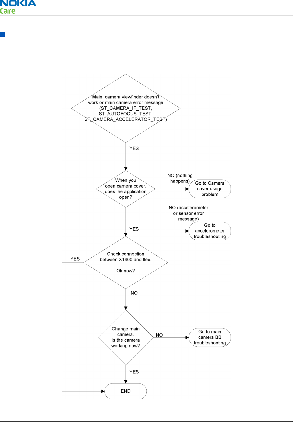
Main (back) camera troubleshooting flowcharts
Main camera troubleshooting
Troubleshooting flow
RM-333; RM-334; RM-335
Camera Module Troubleshooting
Page 5 –16 COMPANY CONFIDENTIAL Issue 2
Copyright © 2008 Nokia. All rights reserved.
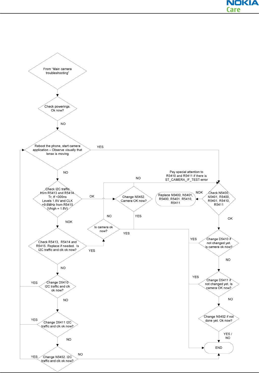
Main camera baseband troubleshooting
Troubleshooting flow
RM-333; RM-334; RM-335
Camera Module Troubleshooting
Issue 2 COMPANY CONFIDENTIAL Page 5 –17
Copyright © 2008 Nokia. All rights reserved.
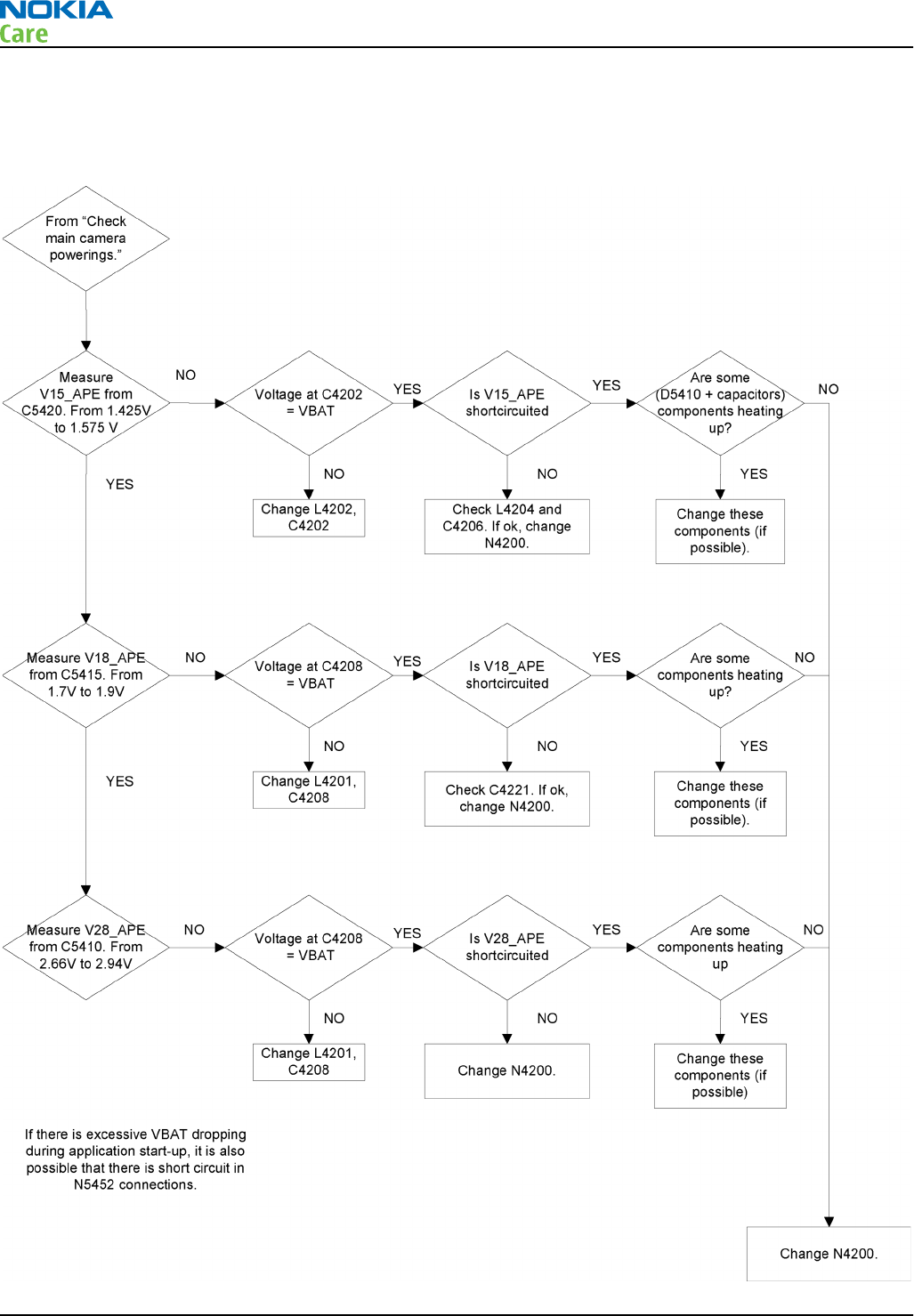
Main camera baseband troubleshooting - powerings
Troubleshooting flow
RM-333; RM-334; RM-335
Camera Module Troubleshooting
Page 5 –18 COMPANY CONFIDENTIAL Issue 2
Copyright © 2008 Nokia. All rights reserved.
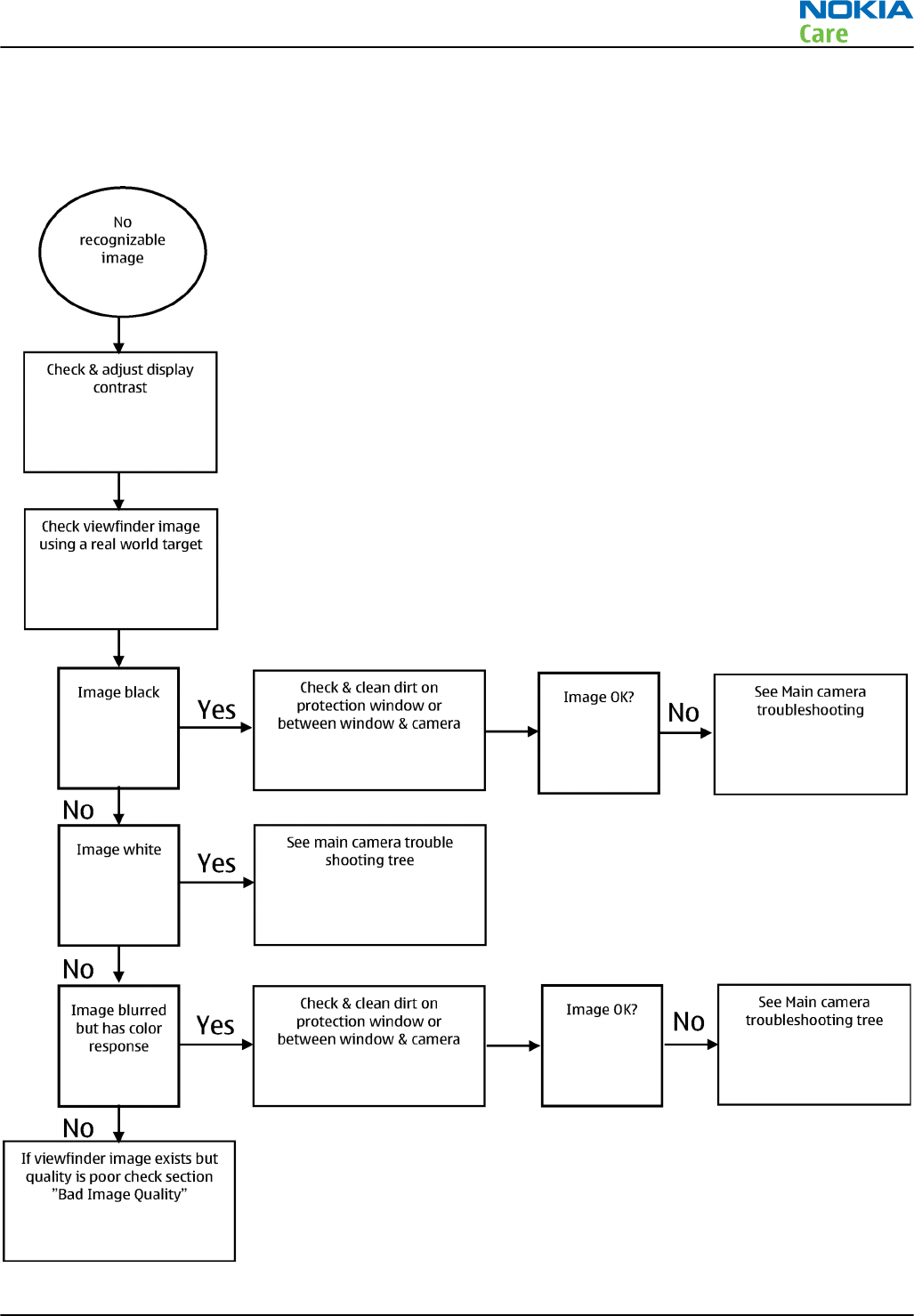
No recognizable viewfinder image
Troubleshooting flow
RM-333; RM-334; RM-335
Camera Module Troubleshooting
Issue 2 COMPANY CONFIDENTIAL Page 5 –19
Copyright © 2008 Nokia. All rights reserved.
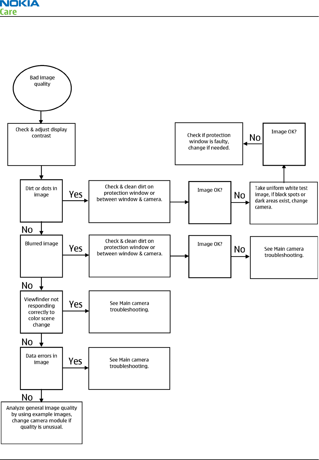
Bad image quality troubleshooting
Troubleshooting flow
RM-333; RM-334; RM-335
Camera Module Troubleshooting
Page 5 –20 COMPANY CONFIDENTIAL Issue 2
Copyright © 2008 Nokia. All rights reserved.
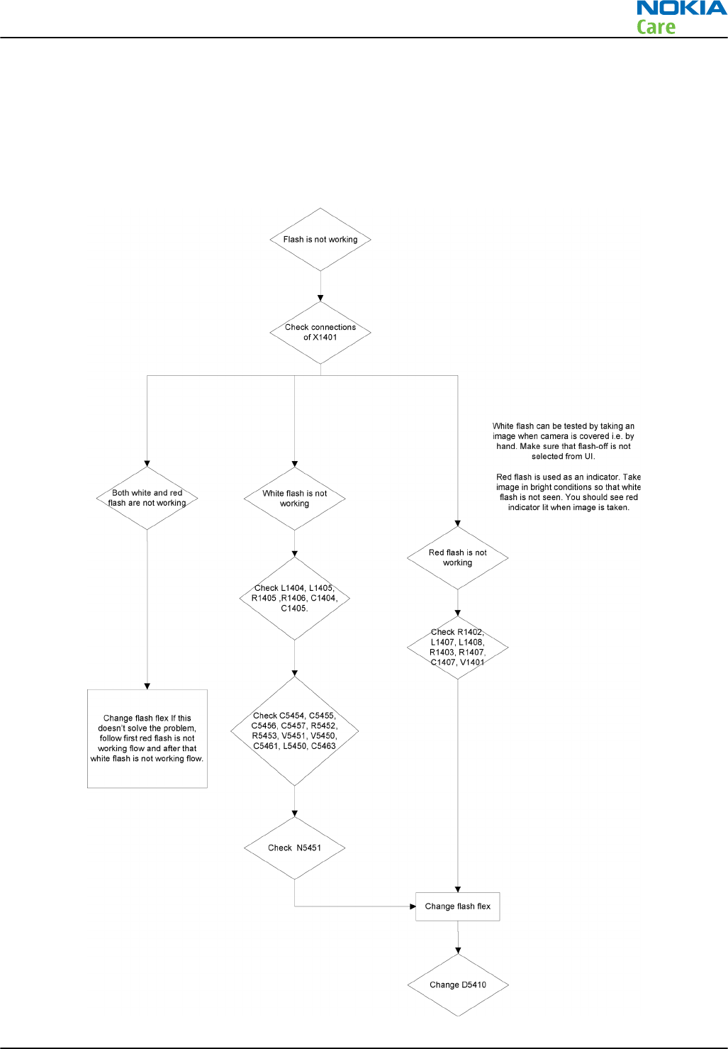
Flash troubleshooting
Context
Note: Before checking flash functionality, make sure that the main camera is working ok.
Troubleshooting flow
RM-333; RM-334; RM-335
Camera Module Troubleshooting
Issue 2 COMPANY CONFIDENTIAL Page 5 –21
Copyright © 2008 Nokia. All rights reserved.
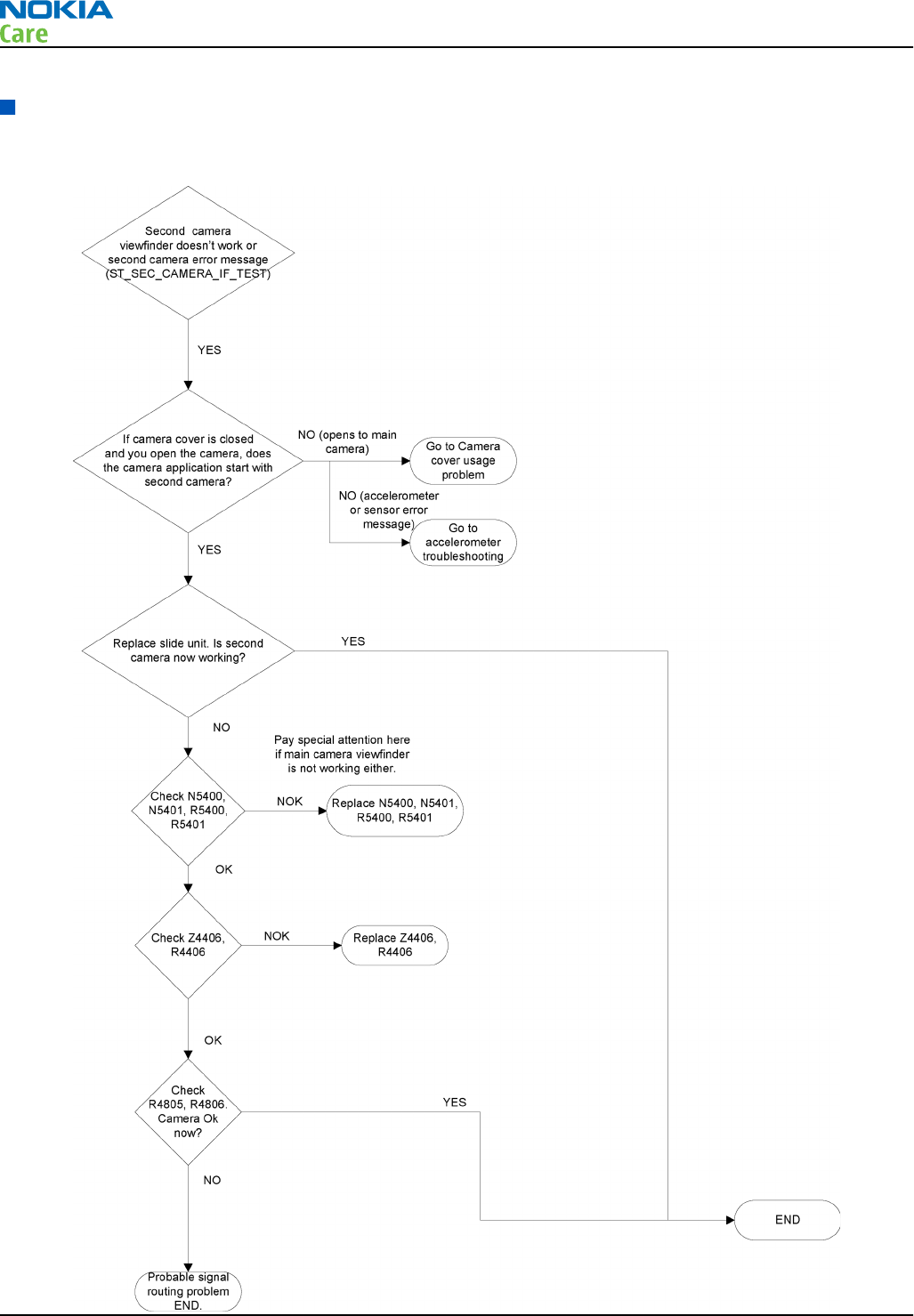
Secondary (front) camera troubleshooting flow
Troubleshooting flow
RM-333; RM-334; RM-335
Camera Module Troubleshooting
Page 5 –22 COMPANY CONFIDENTIAL Issue 2
Copyright © 2008 Nokia. All rights reserved.
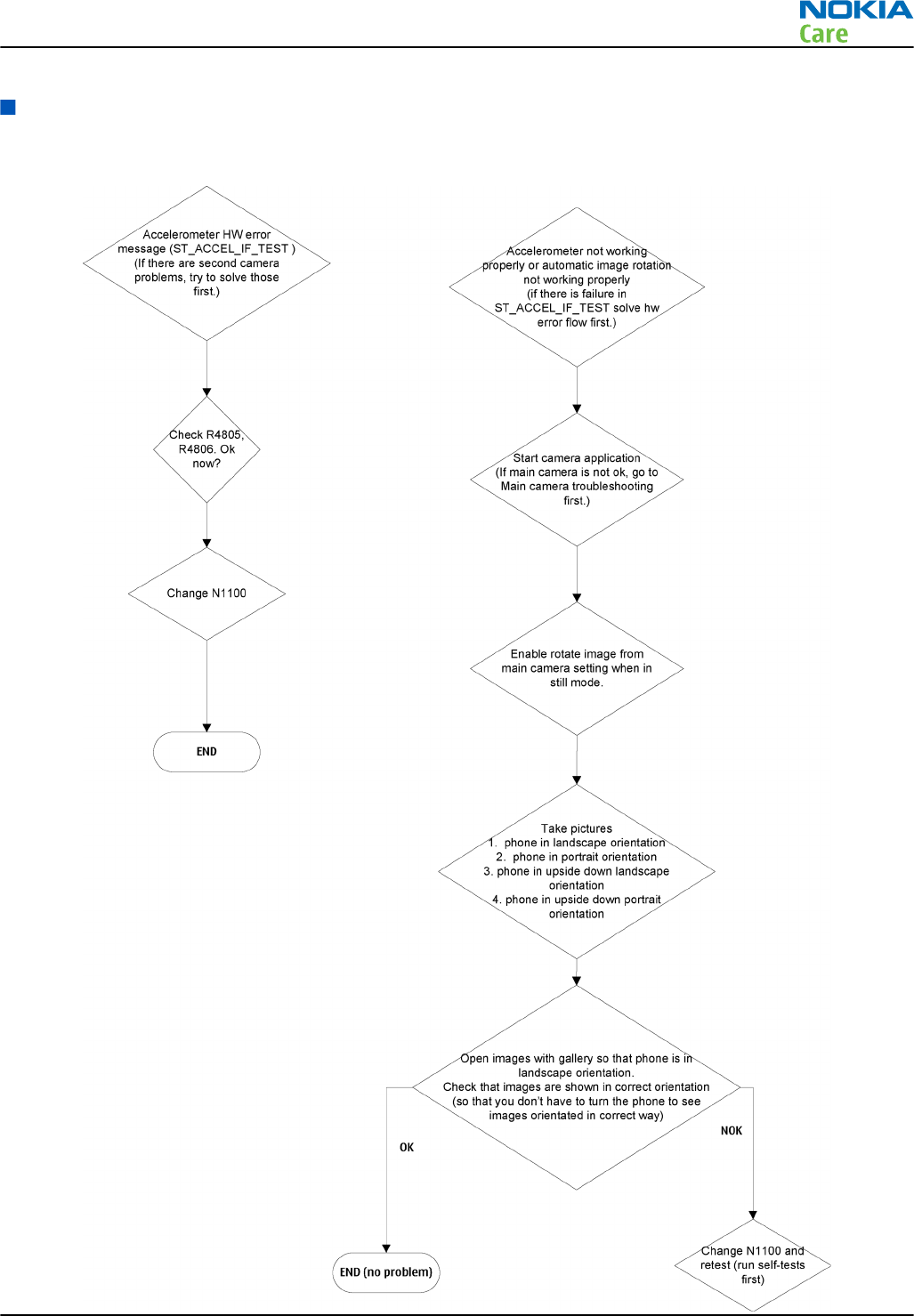
Accelerometer troubleshooting
Troubleshooting flow
RM-333; RM-334; RM-335
Camera Module Troubleshooting
Issue 2 COMPANY CONFIDENTIAL Page 5 –23
Copyright © 2008 Nokia. All rights reserved.

RM-333; RM-334; RM-335
Camera Module Troubleshooting
(This page left intentionally blank.)
Page 5 –24 COMPANY CONFIDENTIAL Issue 2
Copyright © 2008 Nokia. All rights reserved.

6 — FMTx 2.1 Technical
Description
Nokia Customer Care
Issue 2 COMPANY CONFIDENTIAL Page 6 –1
Copyright © 2008 Nokia. All rights reserved.

RM-333; RM-334; RM-335
FMTx 2.1 Technical Description
(This page left intentionally blank.)
Page 6 –2 COMPANY CONFIDENTIAL Issue 2
Copyright © 2008 Nokia. All rights reserved.

Table of Contents
Glossary ...................................................................................................................................................................6–5
FMTx2.1 HW block...................................................................................................................................................6–5
Device pin layout (Si4713-GM) and interfaces.....................................................................................................6–7
List of Figures
Figure 52 FMTx 2.1 system block diagram...........................................................................................................6–6
RM-333; RM-334; RM-335
FMTx 2.1 Technical Description
Issue 2 COMPANY CONFIDENTIAL Page 6 –3
Copyright © 2008 Nokia. All rights reserved.

RM-333; RM-334; RM-335
FMTx 2.1 Technical Description
(This page left intentionally blank.)
Page 6 –4 COMPANY CONFIDENTIAL Issue 2
Copyright © 2008 Nokia. All rights reserved.
Glossary
AF Audio Frequency
RF Radio Frequency
FM Frequency Modulation
Tx Transmitter
Rx Receiver
FMTx FM Transmitter
LPD Low Power Device
LNA Low Noise Amplifier
LDO Low Drop Out regulator
RSSI
Received Signal Strength Indicator
(same as RPS)
RPS
Received Power Scan (Same as
RSSI)
QFN Quad Flat No-Lead
FMTx2.1 HW block
The FMTx 2.1 implementation is based on the Silicon Laboratories Si4713 low power FM transmitter device.
This device has some state of the art features which have been utilised in the Nokia implementation. Apart
from having excellent RF transmitter performance and exceptional AF performance the device offers a number
of unique features, including the ability to retune the output stage of the device to ensure optimal matching
between the Tx antenna and the output stage of the device.
Functional description
The FMTx 2.1 solution comprises of the Si4713 device and ten external components. These components
consist of:
•A filter - an inductor and a varistor for filtering of emissions from the chip
•ESD protection - a resistor and diode package
•A dual capacitor package which is connected to the analogue audio input pins LIN & RIN. The fundamental
purpose of these capacitors is as DC blocking caps
•A filter on the reset line comprising a capacitor and a resistor
•An antenna which also provides the inductive load required by the Si4713 device
The Si4713 device is in a 3 x 3mm 20 pin QFN package.
Current implementations make use of the DAC33 device which allows data to be digitally clocked into the
DAC at high data rates, buffered and then streamed out at the correct rate while the rest of the baseband is
put to sleep in order to save power. This solution significantly increases playback time of audio content.
The Si4713 device has the following features:
•88.1MHz – 107.9MHz FM band support.
•Programmable pre-emphasis (50/75us).
•Analogue audio interface
•Audio silence/signal present detection.
RM-333; RM-334; RM-335
FMTx 2.1 Technical Description
Issue 2 COMPANY CONFIDENTIAL Page 6 –5
Copyright © 2008 Nokia. All rights reserved.
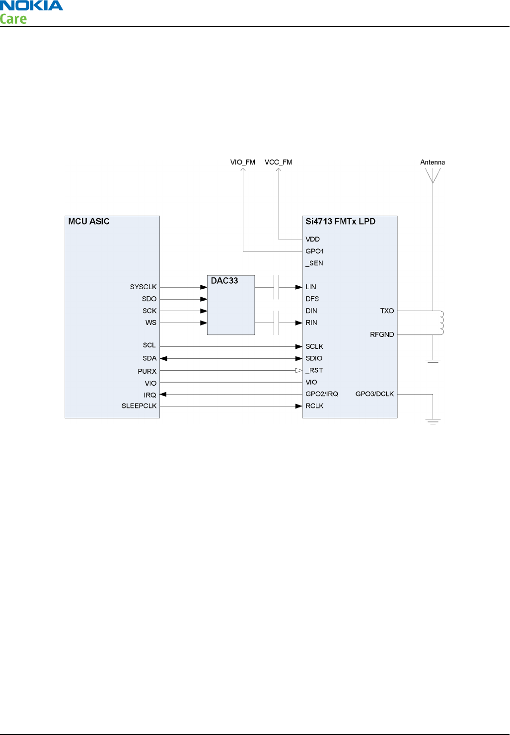
•Programmable reference clock.
•RDS/RBDS encoder
•Loop and monopole antenna support with self-calibrated capacitor tuning.
•Programmable transmit level.
•Audio dynamic range control.
System block diagram
Figure 52 FMTx 2.1 system block diagram
The figure above shows the basic system block diagram for the FMTx 2.1 implementation. _SEN is shown here
unconnected since this pin decides which I2C address is used depending on if this pin is pulled low or high.
On RM-333 the _SEN is pulled high by connecting it to VIO.
RM-333 uses a loop antenna which is located in the removable C-cover of the device. The loop antenna also
acts as the tuning inductor which is required by the Si4713 chip. The location of the antenna in the removable
cover means that ESD protection is required to prevent damage to the Si4713 device.
RM-333; RM-334; RM-335
FMTx 2.1 Technical Description
Page 6 –6 COMPANY CONFIDENTIAL Issue 2
Copyright © 2008 Nokia. All rights reserved.
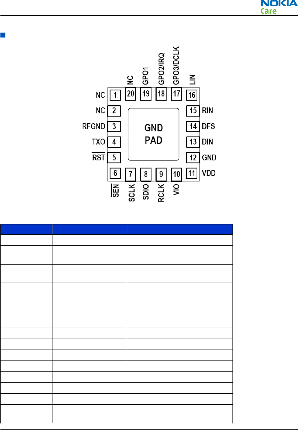
Device pin layout (Si4713-GM) and interfaces
Inteface pin descriptions
Pin Number(s) Name Description
1, 2, 20 NC No connect, left floating.
3 RFGND RF ground. Connected to ground
plane on PCB.
4 TXO FM transmitter output connection
to Tx antenna.
5 RST Device reset (active low) input.
6 SEN Serial enable input (active low).
7 SCLK Serial clock input.
8 SDIO Serial data input/output.
9 RCLK External reference oscillator input.
10 VIO I/O supply voltage.
11 VDD Supply voltage.
13 DIN Digital input data.
14 DFS Digital frame synchronisation.
15 RIN Right audio line input.
16 LIN Left audio line input.
17 GPO3/DCLK General purpose output – Digital bit
synchronous clock.
RM-333; RM-334; RM-335
FMTx 2.1 Technical Description
Issue 2 COMPANY CONFIDENTIAL Page 6 –7
Copyright © 2008 Nokia. All rights reserved.

Pin Number(s) Name Description
18 GPO2/IRQ General purpose output – Interrupt
request.
19 GPO1 General purpose output.
12, GND PAD GND Ground. Connect to ground plane on
PCB.
RM-333; RM-334; RM-335
FMTx 2.1 Technical Description
Page 6 –8 COMPANY CONFIDENTIAL Issue 2
Copyright © 2008 Nokia. All rights reserved.

7 — FMTx 2.1 Troubleshooting
Nokia Customer Care
Issue 2 COMPANY CONFIDENTIAL Page 7 –1
Copyright © 2008 Nokia. All rights reserved.

RM-333; RM-334; RM-335
FMTx 2.1 Troubleshooting
(This page left intentionally blank.)
Page 7 –2 COMPANY CONFIDENTIAL Issue 2
Copyright © 2008 Nokia. All rights reserved.

Table of Contents
FMTx 2.1 schematic ................................................................................................................................................7–5
FMTx 2.1 component layout ..................................................................................................................................7–5
FMTx 2.1 PWB traces ..............................................................................................................................................7–6
Specific digital and power supply test points .....................................................................................................7–6
FMTx2.1 specific RF test points .............................................................................................................................7–7
Specific clock test points........................................................................................................................................7–7
General visual inspection guidelines....................................................................................................................7–7
FMTx2.1 troubleshooting.......................................................................................................................................7–8
FMTx2.1 antenna visual inspection troubleshooting .........................................................................................7–9
FMTx2.1 audio path visual inspection troubleshooting.................................................................................. 7–10
FMTx2.1 Si4713 visual inspection troubleshooting ......................................................................................... 7–11
Checking validity of signals................................................................................................................................ 7–11
FMTx2.1 troubleshooting faults......................................................................................................................... 7–12
Phoenix PC tool.................................................................................................................................................... 7–12
List of Tables
Table 6 Bus mode selection truth table...............................................................................................................7–6
Table 7 I2C 7-bit bus address selection summary...............................................................................................7–7
Table 8 Left and right audio self test truth table............................................................................................. 7–15
List of Figures
Figure 53 FMTx 2.1 schematic ...............................................................................................................................7–5
Figure 54 FMTx 2.1 Component References and Location..................................................................................7–5
Figure 55 FMTx 2.1 layout......................................................................................................................................7–6
Figure 56 FMTx panel before connection to the handset................................................................................ 7–13
Figure 57 FMTx panel after connection to the handset................................................................................... 7–13
Figure 58 FMTx panel in action .......................................................................................................................... 7–15
RM-333; RM-334; RM-335
FMTx 2.1 Troubleshooting
Issue 2 COMPANY CONFIDENTIAL Page 7 –3
Copyright © 2008 Nokia. All rights reserved.

RM-333; RM-334; RM-335
FMTx 2.1 Troubleshooting
(This page left intentionally blank.)
Page 7 –4 COMPANY CONFIDENTIAL Issue 2
Copyright © 2008 Nokia. All rights reserved.
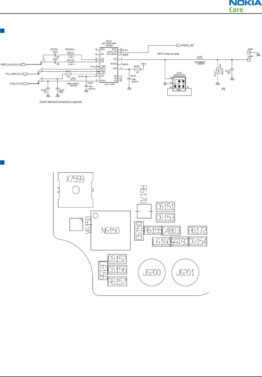
FMTx 2.1 schematic
Figure 53 FMTx 2.1 schematic
The handset uses an antenna that is integral to the removable cover. The connection to the cover is exposed
when the cover is removed.
The loop antenna requires two connection points, J6200 and J6201 (the signal and the ground). It is important
to check these connection points for damage or dirt since the performance of the FMTx 2.1 implementation
will be severely impaired if these connections are not in good condition.
FMTx 2.1 component layout
Figure 54 FMTx 2.1 Component References and Location
The main component of the FMTx 2.1 solution is the Si4713 low power transmitter device (N6150).
RM-333; RM-334; RM-335
FMTx 2.1 Troubleshooting
Issue 2 COMPANY CONFIDENTIAL Page 7 –5
Copyright © 2008 Nokia. All rights reserved.
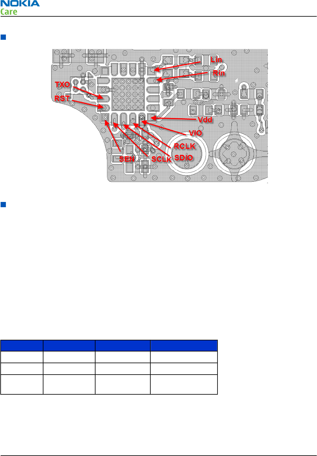
FMTx 2.1 PWB traces
Figure 55 FMTx 2.1 layout
Specific digital and power supply test points
Using access to signals figure as a reference it can be seen that supplies to the Si4713 device VIO (pin 10) and
VDD (pin 11) can be accessed easily. The FMTx 2.1 solution utilises a QFN package. This type of package lends
itself well to analysis of signals on the various pins of the device.
VIO & VDD
VIO should be in the range 1.5 to 3.6 Volts.
VDD should be in the range 2.7 to 5.5 Volts.
_RST
Also, the _RST signal to the device can be monitored. This is an active low signal and should only be asserted
during power up. The _RST signal is driven by the PURX line.
The state of pins 19 & 18 (GPO1 and GP02 respectively) on the rising edge of the _RST pin determines what
interface is selected when the device powers up.
Table 6 Bus mode selection truth table
Bus Name Bus Mode GPO1 GPO2/IRQ
I2C 2-Wire High Low
SPI SPI High Low (must drive)
CBus 3-Wire Low (must
drive)
Low
It’s possible that if GP01 and/or GPO2 are not at the correct state when the Si4713 device has power applied
then the wrong bus mode could be selected and the handset would be unable to communicate with the
device. For RM-333, the bus mode should be I2C.
RM-333; RM-334; RM-335
FMTx 2.1 Troubleshooting
Page 7 –6 COMPANY CONFIDENTIAL Issue 2
Copyright © 2008 Nokia. All rights reserved.

_SEN
The _SEN pin is used to select one of two possible 7-bit I2C bus addresses. When _SEN is low, the I2C bus
address for the Si4713 device is 0010001 (0x11). When _SEN is high, the I2C bus address for the Si4713 is
1100011 (0x63).
If the _SEN signal is not correct (i.e. not selecting the correct I2C address), then this is also another possible
reason why control of the FMTx 2.1 feature might not be possible. For RM-333 the I2C address used for FMTx
2.1 will be 0x63.
Table 7 I2C 7-bit bus address selection summary
I2C address _SEN
0010001 (0x11). High
1100011 (0x63). Low
FMTx2.1 specific RF test points
TXO
Pin 4 is the TXO pin. This is the transmitter output pin and probe access can be obtained easily. Using a high
impedance probe and a spectrum analyser it would be possible to examine the TXO pin and check that the
transmitter is outputting a signal.
Specific clock test points
RCLK
Pin 9 is the RCLK (Reference Clock) input to the device. This is typically 32.768KHz and is driven from the sleep
clock from the base band. When measuring this clock frequency, it may be seen to vary by as much as +/-
120 ~ 200ppm. The device can only typically tolerate +/- 20ppm in order to maintain transmit frequency
accuracy. To overcome this, the software driver for the device calculates what the actual sleep clock (RCLK)
frequency is and periodically programs the device with this frequency.
The device then internally adjusts its dividers in order to maintain the required output frequency. Using this
method it is possible to reduce the effective ppm of the reference clock down to +/- 14ppm over the full
operating temperature range of -15 to +50 degrees Centigrade.
General visual inspection guidelines
•If the handset has the FMTx antenna in the back cover then check the condition of the cover, the antenna
trace and any mechanical interfaces for the antenna e.g. pogo pins.
•Check that the Si4713 device is placed correctly on the PWB and that there are no obvious signs of damage.
•Check the surrounding components and ensure correct placement on the PWB and that there is no visual
damage. Check that there are no missing components.
RM-333; RM-334; RM-335
FMTx 2.1 Troubleshooting
Issue 2 COMPANY CONFIDENTIAL Page 7 –7
Copyright © 2008 Nokia. All rights reserved.
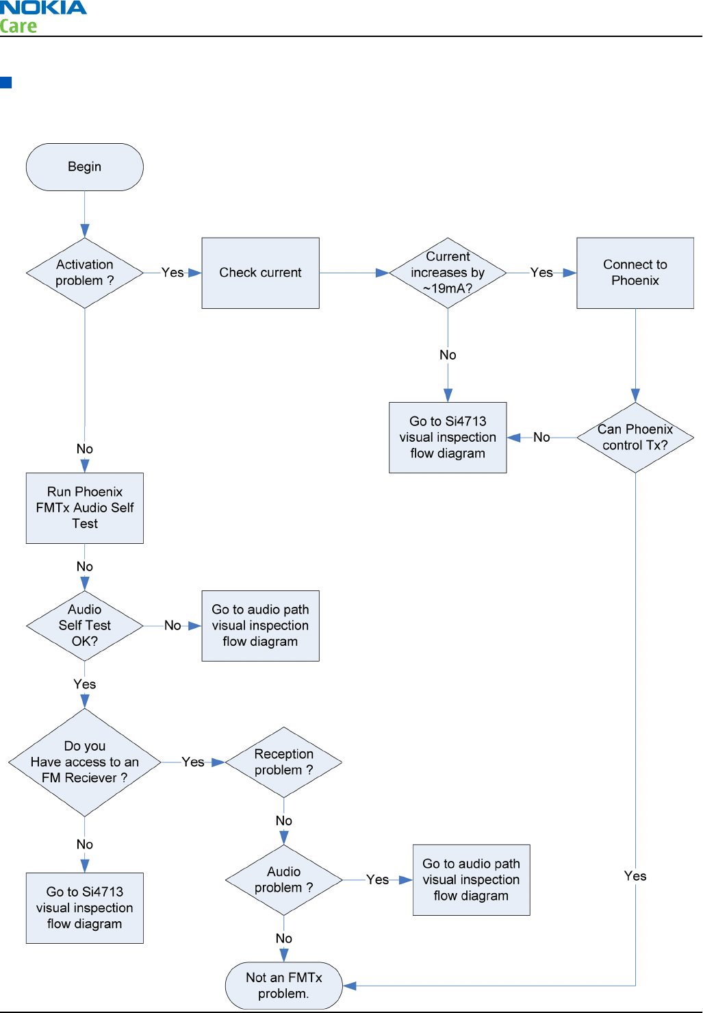
FMTx2.1 troubleshooting
Troubleshooting flow
RM-333; RM-334; RM-335
FMTx 2.1 Troubleshooting
Page 7 –8 COMPANY CONFIDENTIAL Issue 2
Copyright © 2008 Nokia. All rights reserved.
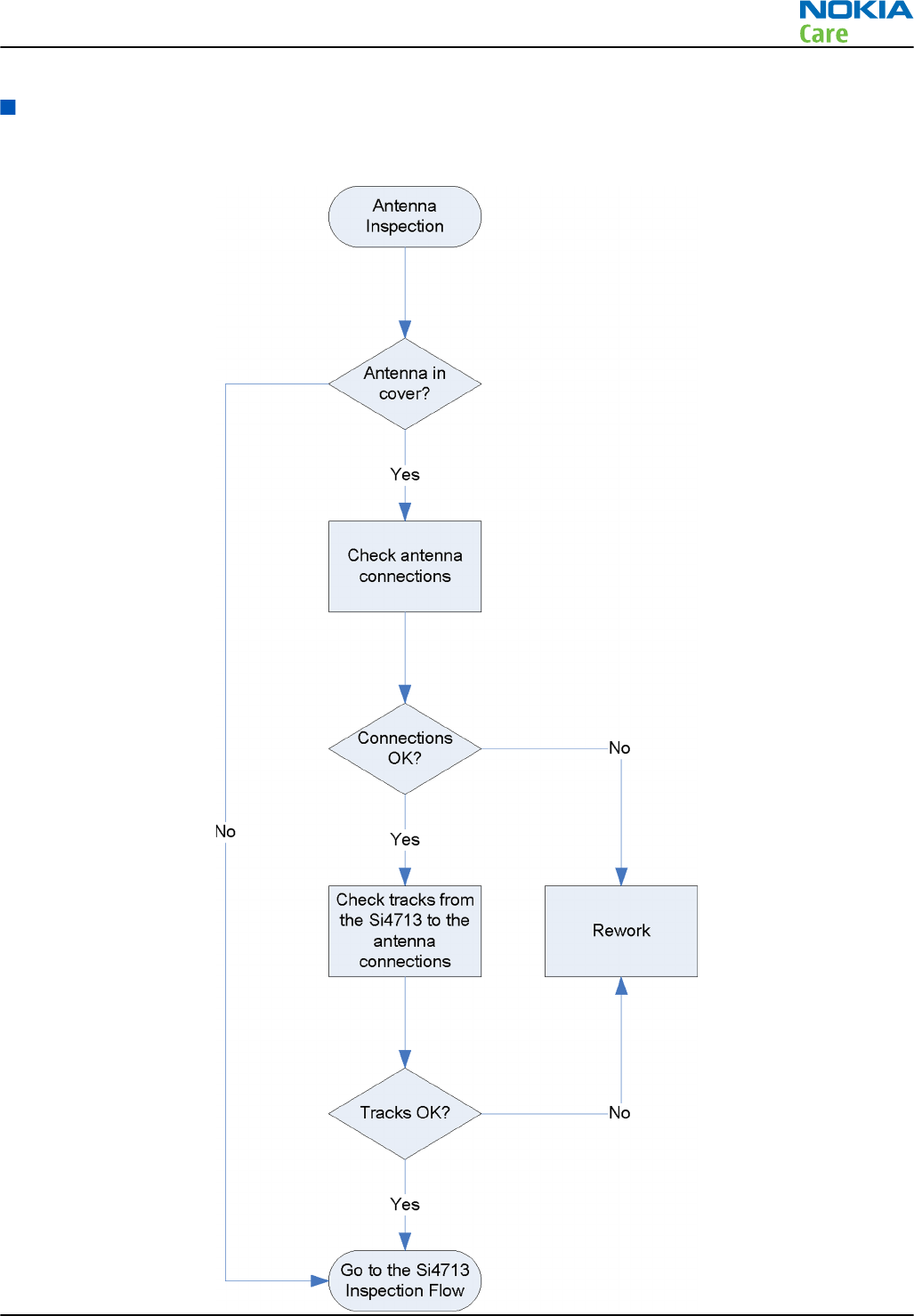
FMTx2.1 antenna visual inspection troubleshooting
Troubleshooting flow
RM-333; RM-334; RM-335
FMTx 2.1 Troubleshooting
Issue 2 COMPANY CONFIDENTIAL Page 7 –9
Copyright © 2008 Nokia. All rights reserved.
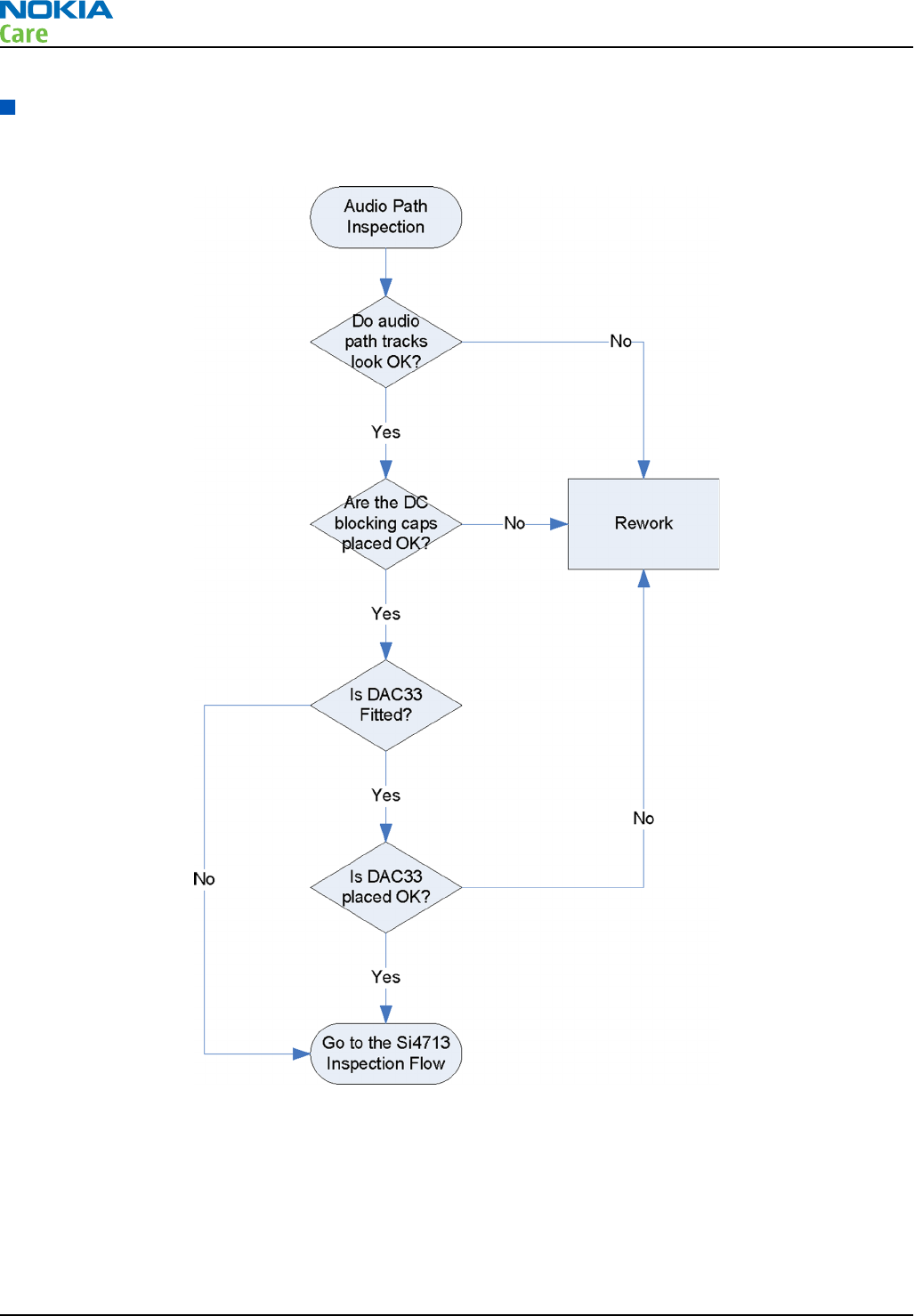
FMTx2.1 audio path visual inspection troubleshooting
Troubleshooting flow
RM-333; RM-334; RM-335
FMTx 2.1 Troubleshooting
Page 7 –10 COMPANY CONFIDENTIAL Issue 2
Copyright © 2008 Nokia. All rights reserved.
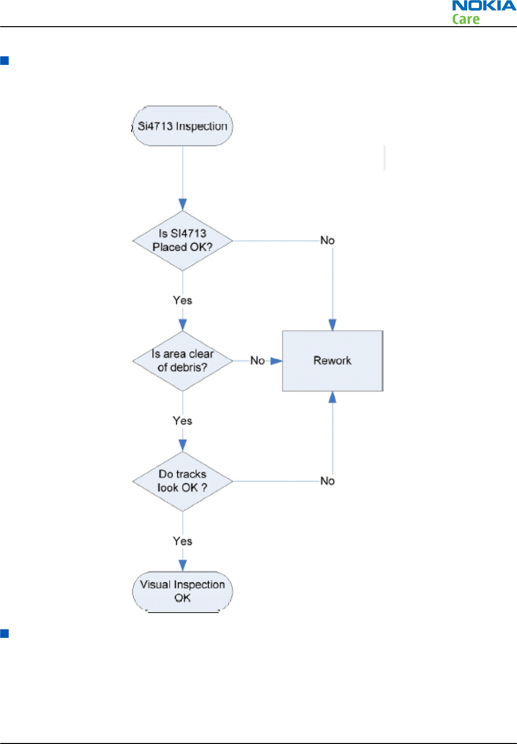
FMTx2.1 Si4713 visual inspection troubleshooting
Troubleshooting flow
Checking validity of signals
Please refer to Access to signals figure as a reference. Generally all power supply levels and clocks willbe
consistent. Signals on the analogue audio input pins (RIN & LIN – pins 15 and 16 respectively) will be
dependant on the audio content being injected to the device. During the audio self test (initiated from
Phoenix) it is possible to monitor these pins and check that the DSP generated 1KHz tones can be seen at
some point during the test. Check that the signals are clean and that no obvious distortion can be seen such
RM-333; RM-334; RM-335
FMTx 2.1 Troubleshooting
Issue 2 COMPANY CONFIDENTIAL Page 7 –11
Copyright © 2008 Nokia. All rights reserved.

as clipping of the signals. Typical maximum swing of these tones will be ~636mV peak to peak. The maximum
swing may vary between Nokia handsets but for the FMTx 2.1 implementation, the swing should not be
greater than the aforementioned value.
FMTx2.1 troubleshooting faults
Possible faults
Expected fault reports relating to the FMTx 2.1 implementation may consist of one or more of the following;
1 No left audio
2 No right audio
3 No audio
4 Can’t start FMTx
5 Can’t locate FM transmission on an FM receiver or no FM transmission
6 Distortion on audio
7 Poor reception on FM receiver
8 No RDS information
Initial fault analysis
Where possible, attempt to reproduce and verify the reported fault. Intermittent problems are likely to be
due to bad connections or broken components/solder joints. Any faults relating to poor FM transmitter
performance or frequent failure to locate usable frequencies when performing a scan are likely to be due to
some kind of antenna issues.
In handsets that utilise an antenna solution in a removable cover it is likely that the connecting interface
pins are either damaged, dirty or that the cover fits poorly perhaps due to broken tabs/latching lugs. Poor
audio fault reports may also be due to the above antenna issues.
Phoenix PC tool
Setting Up Phoenix
Required equipment:
•A Deskey security dongle for Phoenix to run.
•The latest version of Phoenix that has the FMTx 2.1 GUI installed on a PC (version 2007.21.000.27897 or
greater).
•A jig suitable for the handset.
•A cable to connect the jig/handset to the PC. Run Phoenix and select the FMTx panel.
RM-333; RM-334; RM-335
FMTx 2.1 Troubleshooting
Page 7 –12 COMPANY CONFIDENTIAL Issue 2
Copyright © 2008 Nokia. All rights reserved.
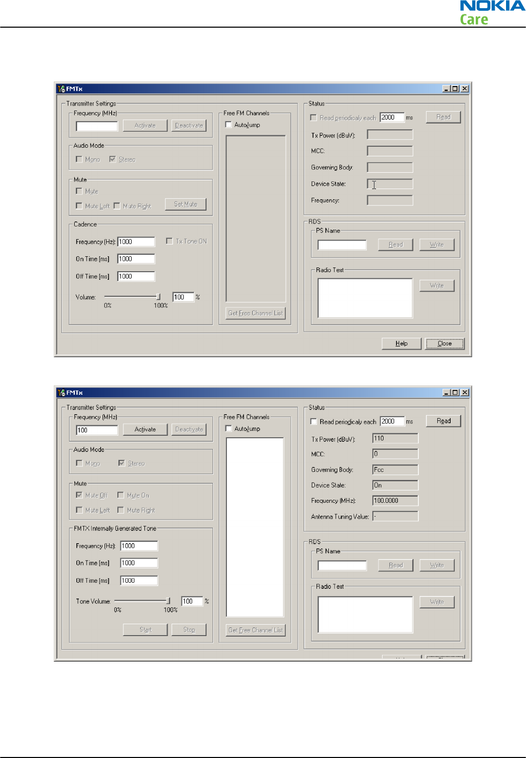
Using the FMTx panel to drive the FMTx 2.1 features
Figure 56 FMTx panel before connection to the handset
Figure 57 FMTx panel after connection to the handset
Typing in a valid FM transmitter frequency and clicking on ‘Activate’ will turn on the FMTx feature and will
begin transmitting the carrier on the selected frequency. Note: Unless this carrier signal is modulated with
some audio (either via the music player or a DSP or Si4713 generated tone) then all that will be heard if an
RM-333; RM-334; RM-335
FMTx 2.1 Troubleshooting
Issue 2 COMPANY CONFIDENTIAL Page 7 –13
Copyright © 2008 Nokia. All rights reserved.

FM receiver is tuned to the same frequency would be silence. After approximately 10 seconds of silence the
handset should begin to ‘chirp’ periodically with a short 1Khz tone that repeats every 5 seconds. This indicates
that there is no audio input and reminds the user that the feature is on.
The Phoenix FMTx 2.1 panel can be used to control the following features;
•Set the FM frequency to transmit on (88.1 to 107.9MHz).
•Select Stereo or Mono mode (generally all Nokia handsets will only use stereo)
•Mute both left and right audio channels.
•Mute only the left or the right audio channels.
•Allow an internal tone to be generated and transmitted from the Si4713 device. The audio frequency of
this tone can be selected along with the on/off time and the volume of the tone. Selecting 0 (zero) in either
the on or off time will produce a continuous tone.
•Obtain a list of suitable ‘quiet or free’ channels. This effectively performs an RSSI (RPS) scan to locate quiet
channels to transmit on. If the ‘AutoJump’ tick box is checked then this list will be transmitted to the FM
receiver to allow the handset to perform AF jumps. This is dependent on the Nokia handset and if the FM
receiver is RDS capable. The use of AF feature allows an RDS capable FM receiver to follow the transmissions
of the FM transmitter automatically.
•FMTx 2.1 status panel. This provides information on the state of the FMTx feature. This can be polled by
Phoenix at regular intervals defined by the user when the ‘Read periodically each...’ check box is checked.
The status can otherwise be read at any point by clicking on the ‘Read’ button. The MCC value is the ‘Mobile
Country Code’ and provided the phone is registered on a network will provide the code pertaining to the
country in which it resides. The antenna tuning value is a good indicator of the state of the antenna and
the other components connected to the TXO pin. For RM-333 the tuning values should be in the range 0 –
80. Any value outside of this range will indicate some problem with the components connected to the TXO
pin (including the antenna). In the case of a removable antenna, the cause of the out of range value is like
to be because of a poor antenna connection. This might be because of broken or dirty connections between
the handset and the cover in which the antenna is fitted.
•The RDS panel can be used to set the PS name and/or to enter a Radio Text (RT) string. If access to an FM
receiver is available that supports RDS then these strings can be observed on the display of the FM receiver.
RM-333; RM-334; RM-335
FMTx 2.1 Troubleshooting
Page 7 –14 COMPANY CONFIDENTIAL Issue 2
Copyright © 2008 Nokia. All rights reserved.
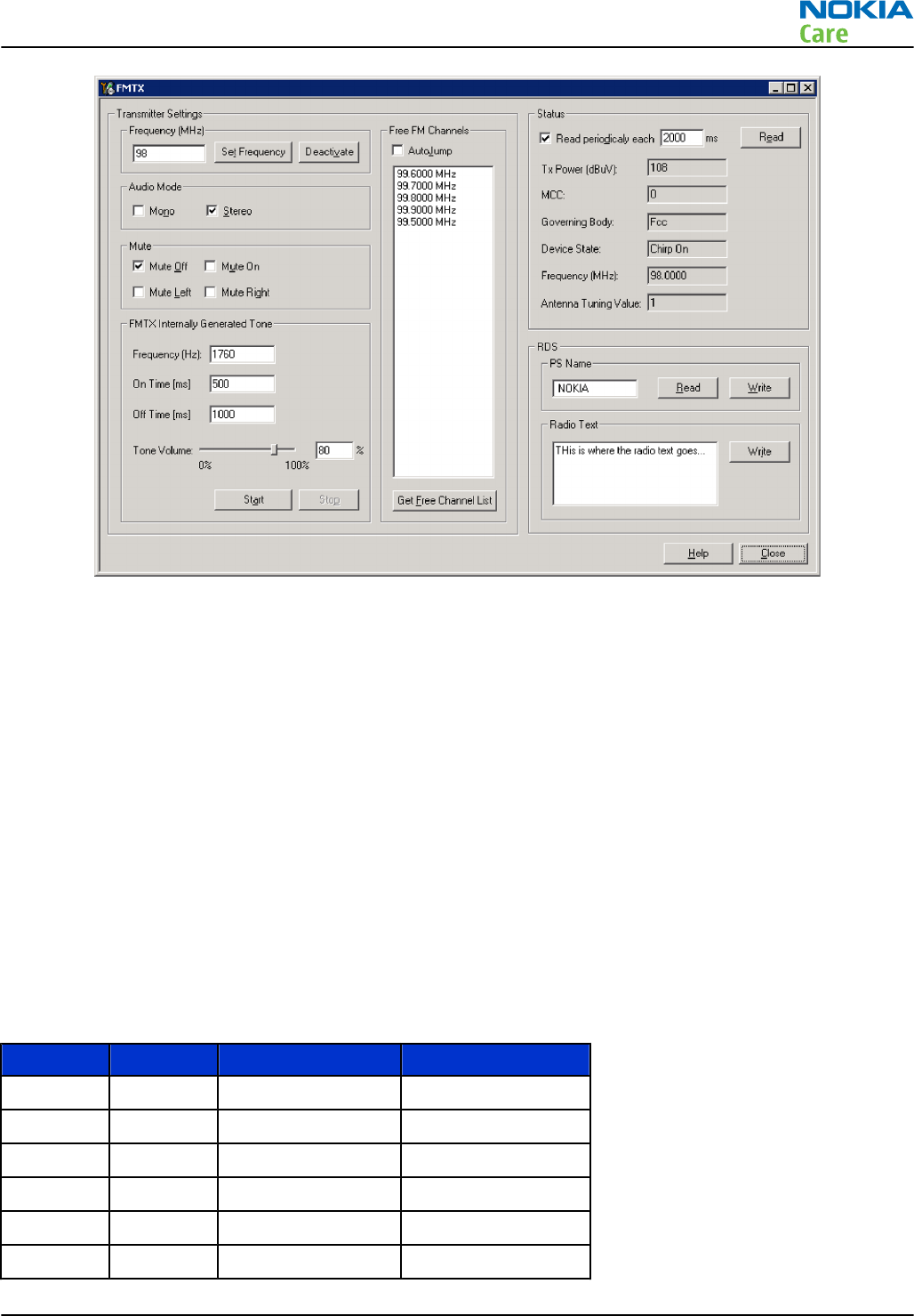
Figure 58 FMTx panel in action
Using the audio self test
The audio self test can be used to quickly determine if the left and right audio paths are intact.
The left and right audio connectivity self test process performs the following steps:
1 Measure and store silence.
2 Inject 1KHz tone (left or right) to give 75KHz deviation. Measure and store.
3 Inject same tone on both left and right analogue audio inputs. Measure and store. Compare result from
(2) with result from (1). If the delta is NOT more than a specified threshold level then fail. This would
indicate that the selected channel is open circuit. If an over deviation indication is detected on (2), then
the audio channels must be shorted together. This is a fail condition. For (3), a returned value of zero is
expected. This indicates that there is an over deviation condition which in turn indicates that the ‘other’
audio input channel is connected correctly.
If on (3) there is no over deviation response, then the ‘other’ channel must be open circuit at some point in
the audio path. This is a fail condition.
The table shows the truth table for the left and right audio self test.
Table 8 Left and right audio self test truth table
LEFT RIGHT ASQ Condition Comment
0 0 0 SILENCE
1 0 0 OPEN/SHORT
1 0 1 OK
1 0 2 SHORT
0 1 X Don’t Care
0 1 X Don’t Care
RM-333; RM-334; RM-335
FMTx 2.1 Troubleshooting
Issue 2 COMPANY CONFIDENTIAL Page 7 –15
Copyright © 2008 Nokia. All rights reserved.

LEFT RIGHT ASQ Condition Comment
0 1 X Don’t Care
1 1 0 ALL OPEN/SHORT
1 1 1 OPEN
1 1 2 OK
Using the auto tune panel
The Auto Tune panel should only be used if one or more of the following components have been changed:
•The Si4713 device.
•The Inductor connected to the TXO pin 4.
•The inline resistor connected to the TXO pin 4 (if fitted).
•The ESD diode package connected to the TXO pin 4 (if fitted).
This procedure follows the alignment that is done in the factory to ensure that the FMTx 2.1 solution is aligned
to provide the correct Tx output power for the relevant legislations such as FCC and ETSI.
RM-333; RM-334; RM-335
FMTx 2.1 Troubleshooting
Page 7 –16 COMPANY CONFIDENTIAL Issue 2
Copyright © 2008 Nokia. All rights reserved.

8 — System Module and User
Interface
Nokia Customer Care
Issue 2 COMPANY CONFIDENTIAL Page 8 –1
Copyright © 2008 Nokia. All rights reserved.

RM-333; RM-334; RM-335
System Module and User Interface
(This page left intentionally blank.)
Page 8 –2 COMPANY CONFIDENTIAL Issue 2
Copyright © 2008 Nokia. All rights reserved.

Table of Contents
Introduction............................................................................................................................................................8–5
Phone description .............................................................................................................................................8–5
Energy management..............................................................................................................................................8–7
Battery and charging ........................................................................................................................................8–7
Backup battery...................................................................................................................................................8–7
Normal and extreme voltages .........................................................................................................................8–8
Power key and system power-up....................................................................................................................8–8
Power distribution............................................................................................................................................8–9
Clocking scheme............................................................................................................................................. 8–10
Bluetooth and FM RDS radio module................................................................................................................. 8–11
GPS module .......................................................................................................................................................... 8–12
WLAN module ...................................................................................................................................................... 8–13
FM transmitter module....................................................................................................................................... 8–13
High-speed USB.................................................................................................................................................... 8–13
CBUS interface...................................................................................................................................................... 8–14
FBUS interface...................................................................................................................................................... 8–14
ECI interface ......................................................................................................................................................... 8–14
USB charger interface.......................................................................................................................................... 8–14
SIM interface ........................................................................................................................................................ 8–15
MicroSD card interface ........................................................................................................................................ 8–16
Camera concept ................................................................................................................................................... 8–16
Camera concept.............................................................................................................................................. 8–16
User interface....................................................................................................................................................... 8–17
User interface.................................................................................................................................................. 8–17
Display module............................................................................................................................................... 8–18
I/O expander and keyboard .......................................................................................................................... 8–19
Illumination .................................................................................................................................................... 8–21
Naviscroll......................................................................................................................................................... 8–22
ASICs...................................................................................................................................................................... 8–23
RAPIDOYAWE .................................................................................................................................................. 8–23
EM ASIC BETTY N2300 ..................................................................................................................................... 8–23
EM ASIC VILMA N2200 ..................................................................................................................................... 8–23
Device memories................................................................................................................................................. 8–24
Combo memory .............................................................................................................................................. 8–24
Audio concept...................................................................................................................................................... 8–24
Audio HW architecture................................................................................................................................... 8–24
Internal microphone...................................................................................................................................... 8–25
Internal earpiece............................................................................................................................................ 8–25
Internal speakers............................................................................................................................................ 8–26
Vibra circuitry ................................................................................................................................................. 8–26
Accessory AV connector ................................................................................................................................. 8–27
External earpiece and microphone .............................................................................................................. 8–28
Baseband technical specifications..................................................................................................................... 8–29
External interfaces ......................................................................................................................................... 8–29
SIM IF connections.......................................................................................................................................... 8–29
Charger connector and charging interface connections & electrical characteristics .............................. 8–29
Internal interfaces.......................................................................................................................................... 8–30
Back-up battery interface electrical characteristics.................................................................................... 8–30
RF technical description...................................................................................................................................... 8–31
RF block diagram............................................................................................................................................ 8–31
RM-333; RM-334; RM-335
System Module and User Interface
Issue 2 COMPANY CONFIDENTIAL Page 8 –3
Copyright © 2008 Nokia. All rights reserved.

Receiver (RX)................................................................................................................................................... 8–32
Transmitter (TX) ............................................................................................................................................. 8–32
Frequency mappings........................................................................................................................................... 8–33
GSM850 frequencies....................................................................................................................................... 8–33
EGSM900 frequencies..................................................................................................................................... 8–33
GSM1800 frequencies..................................................................................................................................... 8–34
GSM1900 frequencies..................................................................................................................................... 8–36
WCDMA 2100 Rx frequencies......................................................................................................................... 8–37
WCDMA 2100 Tx frequencies ......................................................................................................................... 8–38
WCDMA V (850) frequencies .......................................................................................................................... 8–39
WCDMA VIII (900) frequencies....................................................................................................................... 8–40
List of Tables
Table 9 Nominal voltages......................................................................................................................................8–8
Table 10 Keyboard matrix .................................................................................................................................. 8–20
Table 11 Charging interface connections ......................................................................................................... 8–30
Table 12 Charging IF electrical characteristics ................................................................................................. 8–30
Table 13 Back-up battery electrical characteristics ......................................................................................... 8–30
List of Figures
Figure 59 System module block diagram ............................................................................................................8–6
Figure 60 Board and module connections...........................................................................................................8–7
Figure 61 Power distribution................................................................................................................................8–9
Figure 62 Clocking scheme................................................................................................................................. 8–10
Figure 63 Bluetooth & FM radio block diagram ............................................................................................... 8–12
Figure 64 GPS module......................................................................................................................................... 8–12
Figure 65 WLAN module ..................................................................................................................................... 8–13
Figure 66 FM transmitter.................................................................................................................................... 8–13
Figure 67 HS USB block diagram........................................................................................................................ 8–14
Figure 68 USB charging interface block diagram............................................................................................. 8–15
Figure 69 SIM interface ....................................................................................................................................... 8–15
Figure 70 MicroSD card interface ....................................................................................................................... 8–16
Figure 71 Camera block diagram....................................................................................................................... 8–17
Figure 72 User interface block diagram............................................................................................................ 8–18
Figure 73 Display interface block diagram ....................................................................................................... 8–19
Figure 74 I/O expander and keyboard matrix.................................................................................................. 8–20
Figure 75 Illumination block diagram .............................................................................................................. 8–21
Figure 76 Light segments................................................................................................................................... 8–22
Figure 77 Block diagram of Naviscroll Interface .............................................................................................. 8–23
Figure 78 Audio system block ............................................................................................................................ 8–25
Figure 79 Internal microphone.......................................................................................................................... 8–25
Figure 80 Internal earpiece circuitry................................................................................................................. 8–26
Figure 81 Internal speakers................................................................................................................................ 8–26
Figure 82 Vibra circuitry ..................................................................................................................................... 8–26
Figure 83 Accessory (AV) connector................................................................................................................... 8–27
Figure 84 Accessory (AV) connector with DAC33 and TPA6130 audio enhancements ................................. 8–28
Figure 85 External earpiece and microphone audio circuit............................................................................ 8–28
Figure 86 Charger connector.............................................................................................................................. 8–29
Figure 87 RF block diagram RM-333 using RF ASIC N7500 .............................................................................. 8–31
Figure 88 RF block diagram RM-334 using RF ASIC N7500 .............................................................................. 8–32
RM-333; RM-334; RM-335
System Module and User Interface
Page 8 –4 COMPANY CONFIDENTIAL Issue 2
Copyright © 2008 Nokia. All rights reserved.
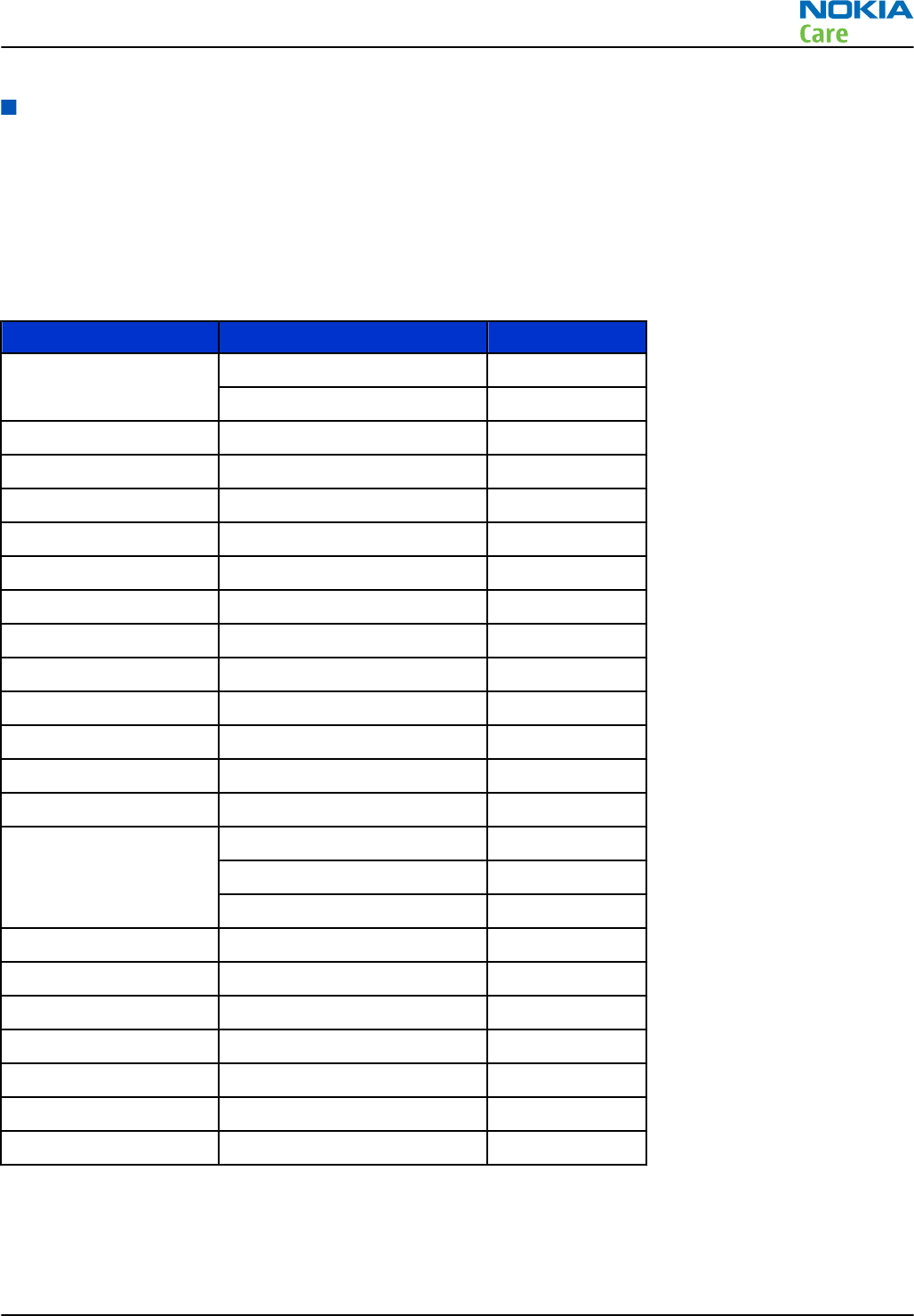
Introduction
Phone description
RAPIDOYAWE is the main digital baseband ASIC in the HW53. It contains functionality for both WCDMA and
GSM EDGE.
AVILMA is power management ASIC having voltage regulators and audio transceiver and BETTY is energy
management ASIC having charging switch and FBUS transceiver.
Memory components are internal COMBO 1 Gb/2 Gb and a card reader for MicroSD.
Function Description Item ref
EM ASIC AVILMA N2200
BETTY N2300
System ASIC RAPIDOYAWE D2800
Memory Combo 1Gb DDR + 2Gb M3 D3000
Camera accelerator OMAP-DM500 N1400
Display controller S1D13747 D2450
Back-up battery RTC BACKUP CAPAC 311 G2200
FM-radio with RDS BTHFMRDS2.1 module D6000
Bluetooth BTHFMRDS2.1 module D6000
WLAN WLAN module ENW49701N N6300
GPS GPS5350_ROM3.0 N6200
RF ASIC Vapaus N7500
GSM PA 850/900/1800/1900 N7520
WCDMA PA 850/900/1900/2100 N7540
Oscillator VCTCXO 38.4MHZ G7500
TCXO 38.4 MHz G6450
Crystal 32.768KHZ B2200
IO-expander BASIC IOExpander N2850
SIM card reader X2700
HS USB transceiver ISP1704 D3300
FM transmitter SI4713 N6150
TV out graphics engine S1D13771B D2480
Naviscroll driver QTC12C15 N2525
Accelerometer AHTI_A 3-AXIS N6501
RM-333; RM-334; RM-335
System Module and User Interface
Issue 2 COMPANY CONFIDENTIAL Page 8 –5
Copyright © 2008 Nokia. All rights reserved.
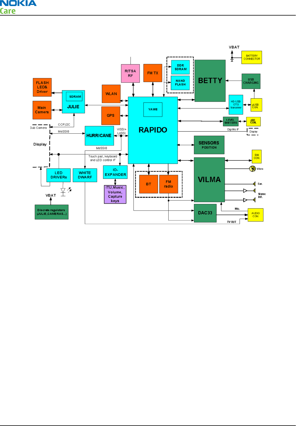
System module block diagram
Figure 59 System module block diagram
RM-333; RM-334; RM-335
System Module and User Interface
Page 8 –6 COMPANY CONFIDENTIAL Issue 2
Copyright © 2008 Nokia. All rights reserved.
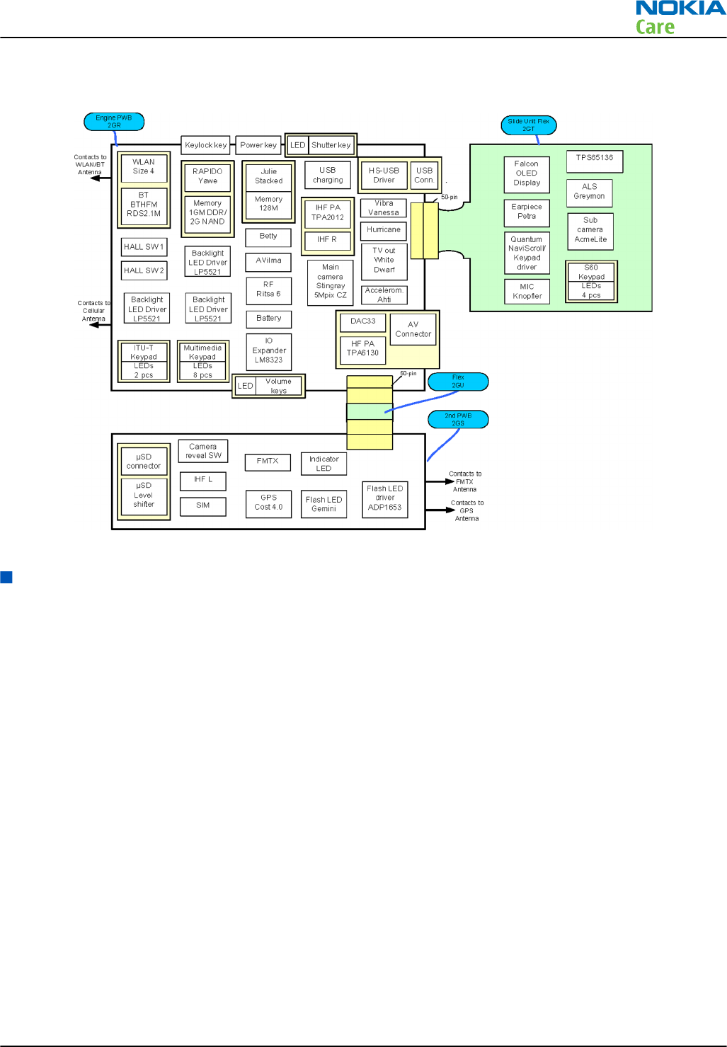
Board and module connections
Figure 60 Board and module connections
Energy management
Battery and charging
Battery
Supported battery type is BL-5K.
Battery connector
Blade battery connector type.
•VBAT (Battery voltage)
•BSI (Battery size indication)
•GND (Battery ground)
Charging
This phone is charged through the micro USB connector. The phone supports dedicated, host or hub chargers.
Charging is controlled by energy management, and external components are needed to protect the baseband
module against EMC, reverse polarity and transient frequency deviation.
Backup battery
When the main battery is not attached EM ASIC (N2200) goes in backup mode using back-up battery that
supplies voltage to RTC in EM ASIC (N2200).
RM-333; RM-334; RM-335
System Module and User Interface
Issue 2 COMPANY CONFIDENTIAL Page 8 –7
Copyright © 2008 Nokia. All rights reserved.
Normal and extreme voltages
Energy management is mainly carried out in the two Application Specific Integrated Circuits (ASICs) BETTY
and AVILMA. These two circuits contains a number of regulators. In addition there are some external
regulators too.
In the table below normal and extreme voltages are shown when a BL-5K battery is used.
Table 9 Nominal voltages
Voltage Voltage [V] Condition
General Conditions
Nominal voltage 3.700
Lower extreme voltage 3.145
Higher extreme voltage
4.230(fast charging)
HW Shutdown Voltages
Vmstr+ 2.1 ± 0.1 Off to on
Vmstr- 1.9 ± 0.1 On to off
SW Shutdown Voltages
Sw shutdown 3.15 In call
Sw shutdown 3.3 In idle
Min Operating Voltage
Vcoff+ 2.9 ± 0.1 Off to on
Vcoff- 2.6 ± 0.1 On to off
Power key and system power-up
When the battery is placed in the phone the power key circuits are energized. When the power key is pressed,
the system boots up (if an adequate battery voltage is present).
Power down can be initiated by pressing the power key again (the system is powered down with the aid of
SW). The power key is connected to EM ASIC N2200 (AVILMA) via PWRONX signal.
The power key may be disabled in certain charging cases.
RM-333; RM-334; RM-335
System Module and User Interface
Page 8 –8 COMPANY CONFIDENTIAL Issue 2
Copyright © 2008 Nokia. All rights reserved.
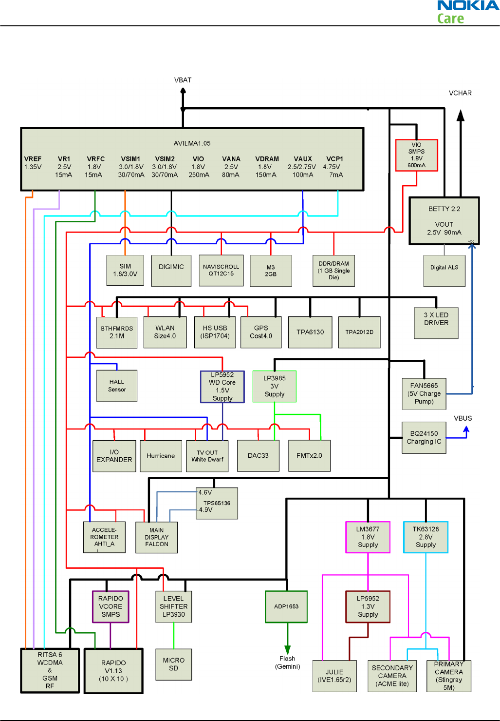
Power distribution
Figure 61 Power distribution
RM-333; RM-334; RM-335
System Module and User Interface
Issue 2 COMPANY CONFIDENTIAL Page 8 –9
Copyright © 2008 Nokia. All rights reserved.
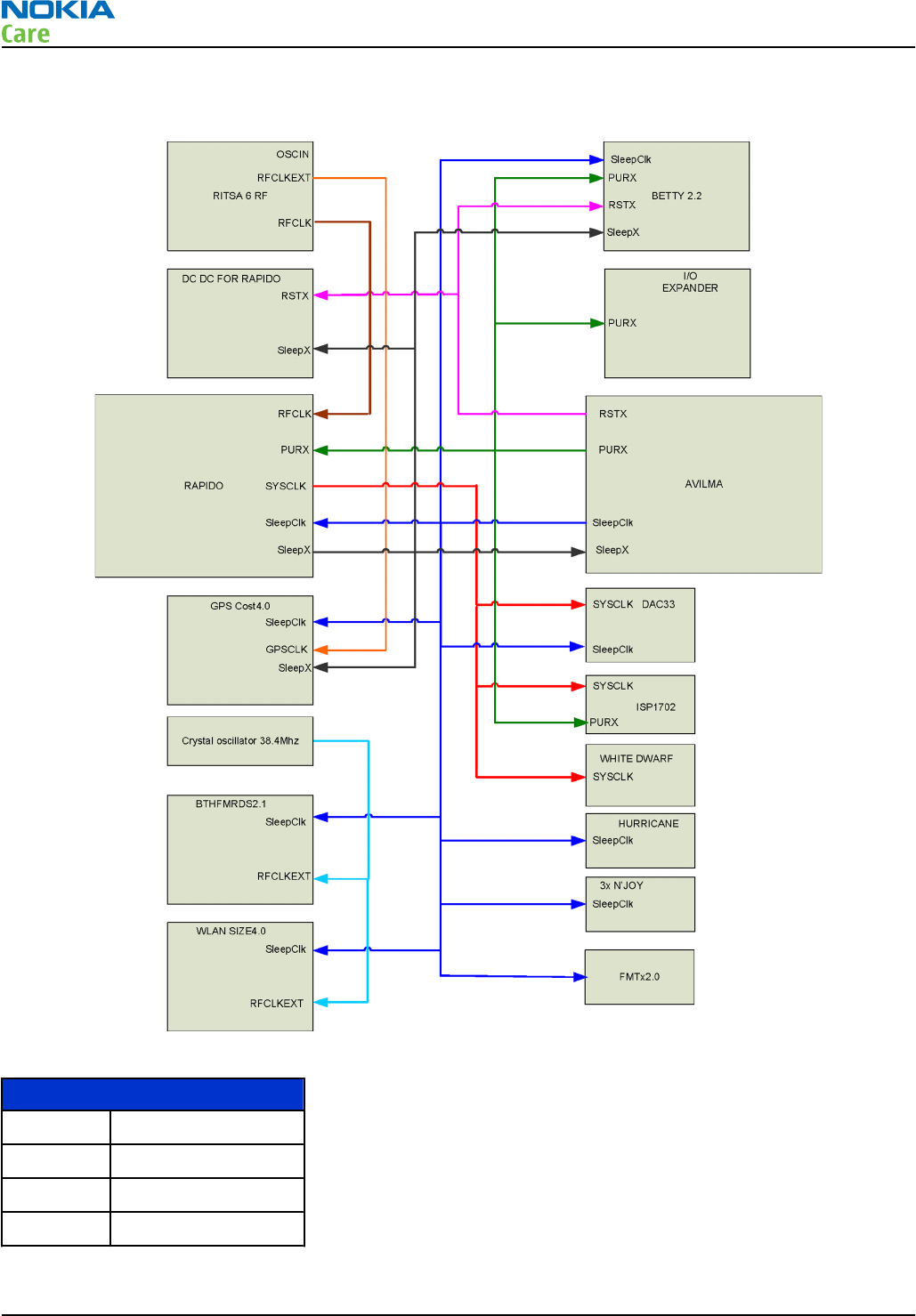
Clocking scheme
Figure 62 Clocking scheme
HW 53 engine clocks
RFCLK 38.4 MHz
SleepClk 32.768kHz
RFCLKEXT 38.4 MHz
SYSCLK 19.2 MHz
RM-333; RM-334; RM-335
System Module and User Interface
Page 8 –10 COMPANY CONFIDENTIAL Issue 2
Copyright © 2008 Nokia. All rights reserved.

Bluetooth and FM RDS radio module
Bluetooth and FM radio receiver are provided by the same ASIC (Broadcom BCM2048). The device supports
Bluetooth operation and FM radio rececption in both European/USA and Japanese bands (the appropriate
region-specific FM radio band is pre-configured in the phone software). The UART interface allows the device
to communicate with the phone baseband engine using Bluetooth HCI commands. Commands to the FM radio
can also be sent over the I2C interface.
When Bluetooth is switched on, the phone user interface the BT_RESETX line is toggled to reset the Bluetooth
device, and commands are sent over the UART interface to configure the device. If UART communication fails
(due to a hardware fault) it will not be possible to switch on Bluetooth from the phone user interface.
The device has two clock signals: SYS_CLK (19.2MHz, 26.0MHz, or 38.4MHz supported) and SLEEP_CLK
(32.768kHz). The SLEEP_CLK is supplied all the time the phone is switched on. To maximise the phone standby
time, it is only necessary to provide a SYS_CLK signal when Bluetooth activity occurs, such as sending Bluetooth
data to another device, or checking periodically if there are any other Bluetooth devices attempting to
communicate with it. At other times when the Bluetooth device is in standby mode or the FM radio is switched
on it is only necessary to provide a SLEEP_CLK signal. The Bluetooth-FM ASIC is powered directly from the
phone battery voltage line (VBAT). An internal regulator is enabled when Bluetooth or FM radio is switched
on.
Bluetooth audio signals are sent to and from the device using a PCM interface. The Bluetooth RF signal is
routed via a buried track to the Bluetooth antenna on the side of the PWB. An RF filter is needed between
the Bluetooth antenna and Bluetooth ASIC to prevent interference to and from the celluar phone antenna.
Phones that have both Bluetooth and WLAN use a shared antenna, as both services occupy the 2.4GHz ISM
frequency band. The co-existence signaling interface between Bluetooth and WLAN ASICs controls the RF
activity in the shared frequency band.
The audio signal from the FM radio is routed via the phone Audio ASIC to the phone headset or loudspeaker.
The external wired headset is also used as an Antenna for the FM radio. The FM radio receiver RF signal is
routed from the ASIC via a buried track to an impedance matching circuit placed near the headset connector.
The following block diagram shows how Bluetooth-FM is connected to the host engine.
RM-333; RM-334; RM-335
System Module and User Interface
Issue 2 COMPANY CONFIDENTIAL Page 8 –11
Copyright © 2008 Nokia. All rights reserved.
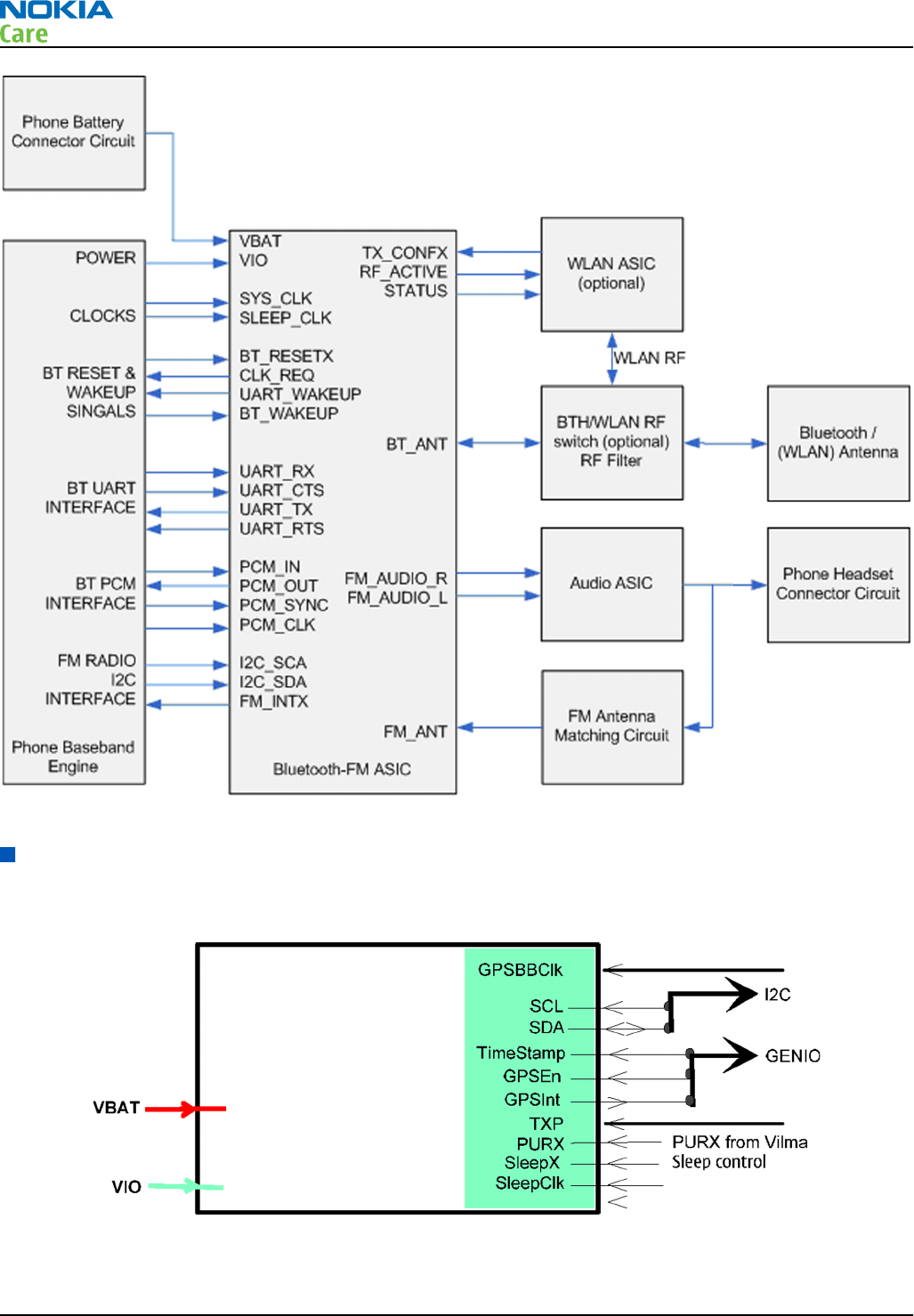
Figure 63 Bluetooth & FM radio block diagram
GPS module
HW53 supports GPSCost4.0 release. GPS module is connected to cellular engine via I2C interface and GenIO
control signals. GPS clock configuration includes dedicated GPS TCXO and reference clock from Ahneus.
Figure 64 GPS module
RM-333; RM-334; RM-335
System Module and User Interface
Page 8 –12 COMPANY CONFIDENTIAL Issue 2
Copyright © 2008 Nokia. All rights reserved.
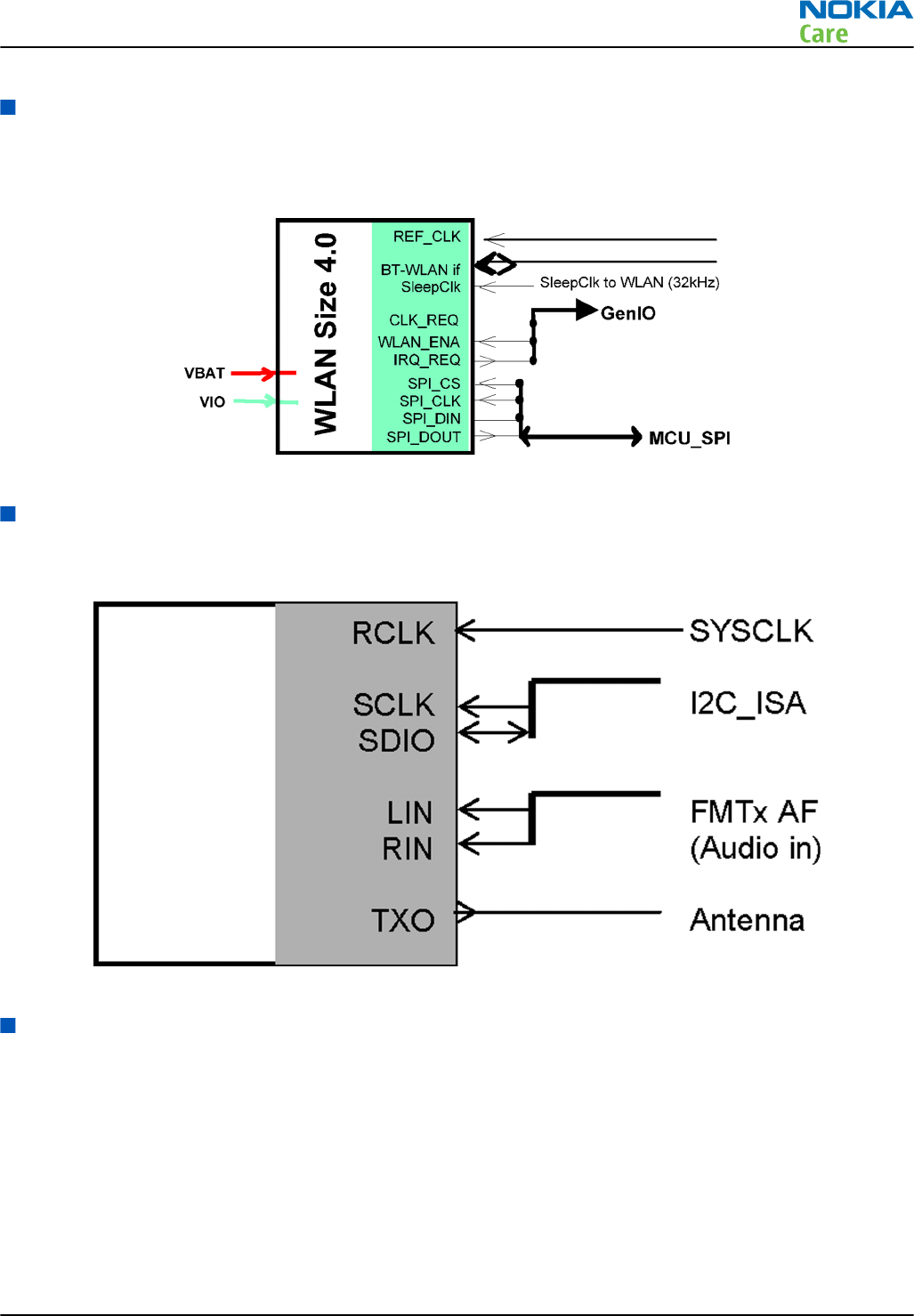
WLAN module
WLAN module HW53 supports WLANSize4.0 release. WLAN module is configured as Cellular engine SPI slave.
WLAN and Bluetooth co-existence is supported via BTH-WLAN interface. WLANSize4.0 has a reference clock
of external oscillator 38.4MHz and it is shared with BTHFMRDS2.1.
Figure 65 WLAN module
FM transmitter module
The FM transmitter module Si4713 is controlled by I2C from RAPIDO with left and right analog audio input
from the DAC33.
Figure 66 FM transmitter
High-speed USB
High-speed USB
The device can transmit and receive USB data at high-speed (480 Mbit/s), full-speed (12 Mbit/s) and low-
speed (1.5Mbit/s). The external interface is the micro-B connector X3300. The interface between D3300 USB
transceiver and micro-B receptacle is the standard USB interface specified in the Universal Serial Bus
specification Rev. 2.0. The USB transfers signal and power over four-wire interface, which carries differential
data, Vbus and GND. Signalling occurs over differential data line D+ and D-. The clock is transmitted encoded
along with the differential data. ESD protection is done with USB ASIP Z3300. VBUS (+5V) is provided by the
host device. The circuit is protected from an overvoltage condition by transistor pair V3300 and reference
zenner diode V3301.
RM-333; RM-334; RM-335
System Module and User Interface
Issue 2 COMPANY CONFIDENTIAL Page 8 –13
Copyright © 2008 Nokia. All rights reserved.
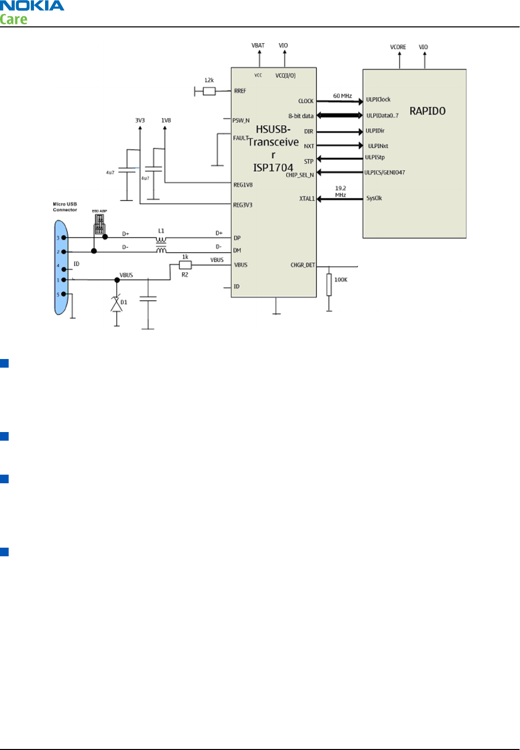
Figure 67 HS USB block diagram
CBUS interface
CBUS is a main system control bus in BB5. RAPIDO controls the functionality of EM ASICs AVilma (N2200) and
Betty (N2300) with CBUS.
CBUS is a four-wire half-duplex master-slave interface. In HW53 CBUS clock frequency is 4.39 MHz.
FBUS interface
FBUS is a 2-wire serial communication bus between HW53 engine and service SW.
ECI interface
The ECI (Enhancement Control Interface) is a point-to-point, bi-directional, single line serial bus.
The purpose of the ECI is to identify and authenticate the accessory, and to act as a data bus (intended for
control purposes) between the phone and the accessory .
USB charger interface
The main battery can be charged from the USB port. Default charging current level is 80 – 100 mA during the
initial charging. Primary charging current level is up to 500 mA from USB Host and up to 1.25A from USB wall
charger with external switch-mode USB Charger BQ24150.
RM-333; RM-334; RM-335
System Module and User Interface
Page 8 –14 COMPANY CONFIDENTIAL Issue 2
Copyright © 2008 Nokia. All rights reserved.
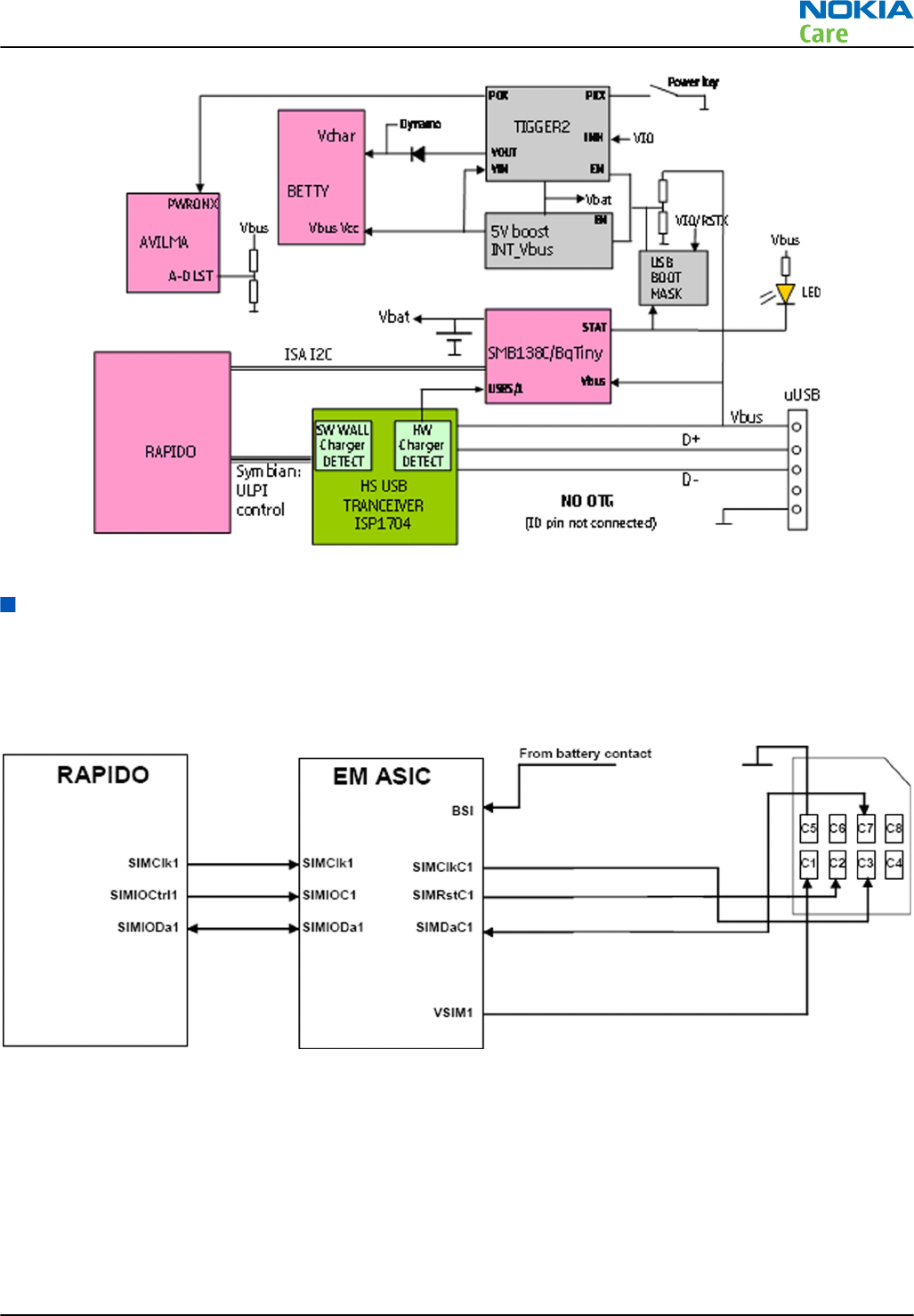
Figure 68 USB charging interface block diagram
SIM interface
The device has one SIM (Subscriber Identification Module) interface. It is only accessible if battery is removed.
The SIM interface consists of an internal interface between RAPIDO and EM ASIC (N2200), and of an external
interface between N2200 and SIM contacts.
The SIM IF is shown in the following figure:
Figure 69 SIM interface
The EM ASIC handles the detection of the SIM card. The detection method is based in the BSI line. Because of
the location of the SIM card, removing the battery causes a quick power down of the SIM IF.
The EM ASIC SIM1 interface supports both 1.8 V and 3.0 V SIM cards. The SIM interface voltage is first 1.8 V
when the SIM card is inserted, and if the card does not response to the ATR a 3 V interface voltage is used.
RM-333; RM-334; RM-335
System Module and User Interface
Issue 2 COMPANY CONFIDENTIAL Page 8 –15
Copyright © 2008 Nokia. All rights reserved.
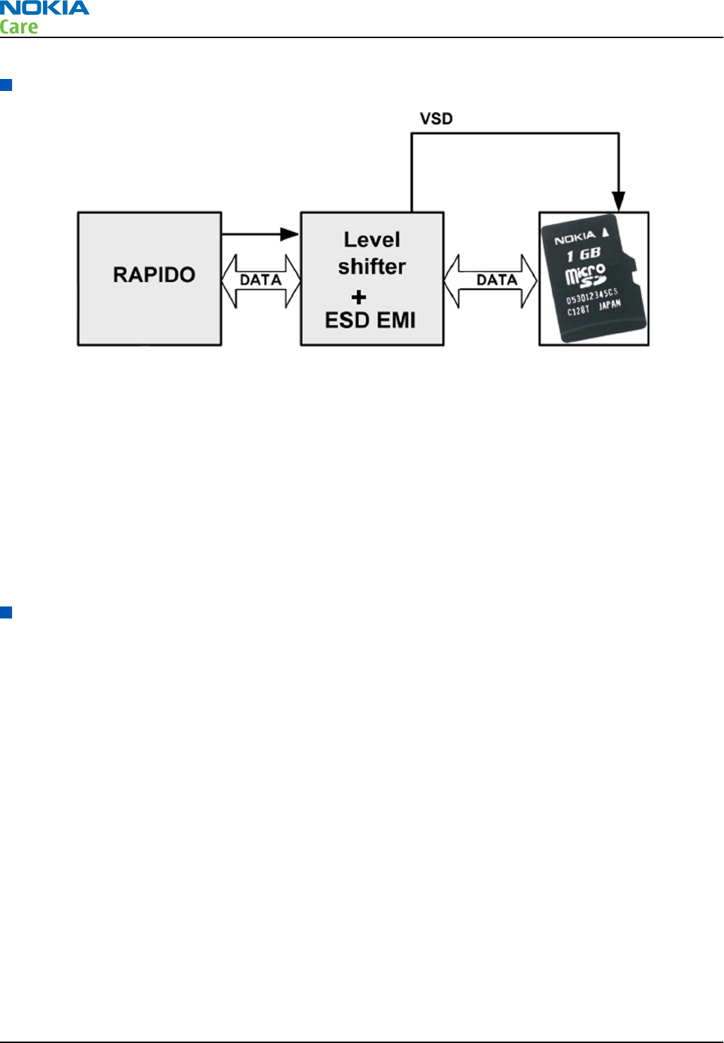
MicroSD card interface
Figure 70 MicroSD card interface
The MicroSD card is connected to the engine by an external level shifter with an ESD protection filter. Supplied
voltages:
•VSD: 2.85 V (from level shifter)
•VIO: 1.8 V (from VIO SMPS)
Hot swap is supported, which means that the card may be plugged in/out at any time, without removing the
battery.
Camera concept
Camera concept
The camera is supported by DM299 (N1400) Camera accelerator, which is used for image and video processing.
DM-299 uses 64Mbit discrete SDRAM. The camera module includes 3MPix main camera, CIF+ secondary camera,
Flash LED and TPS61052 LED driver which are connected to DM-299.
RM-333; RM-334; RM-335
System Module and User Interface
Page 8 –16 COMPANY CONFIDENTIAL Issue 2
Copyright © 2008 Nokia. All rights reserved.
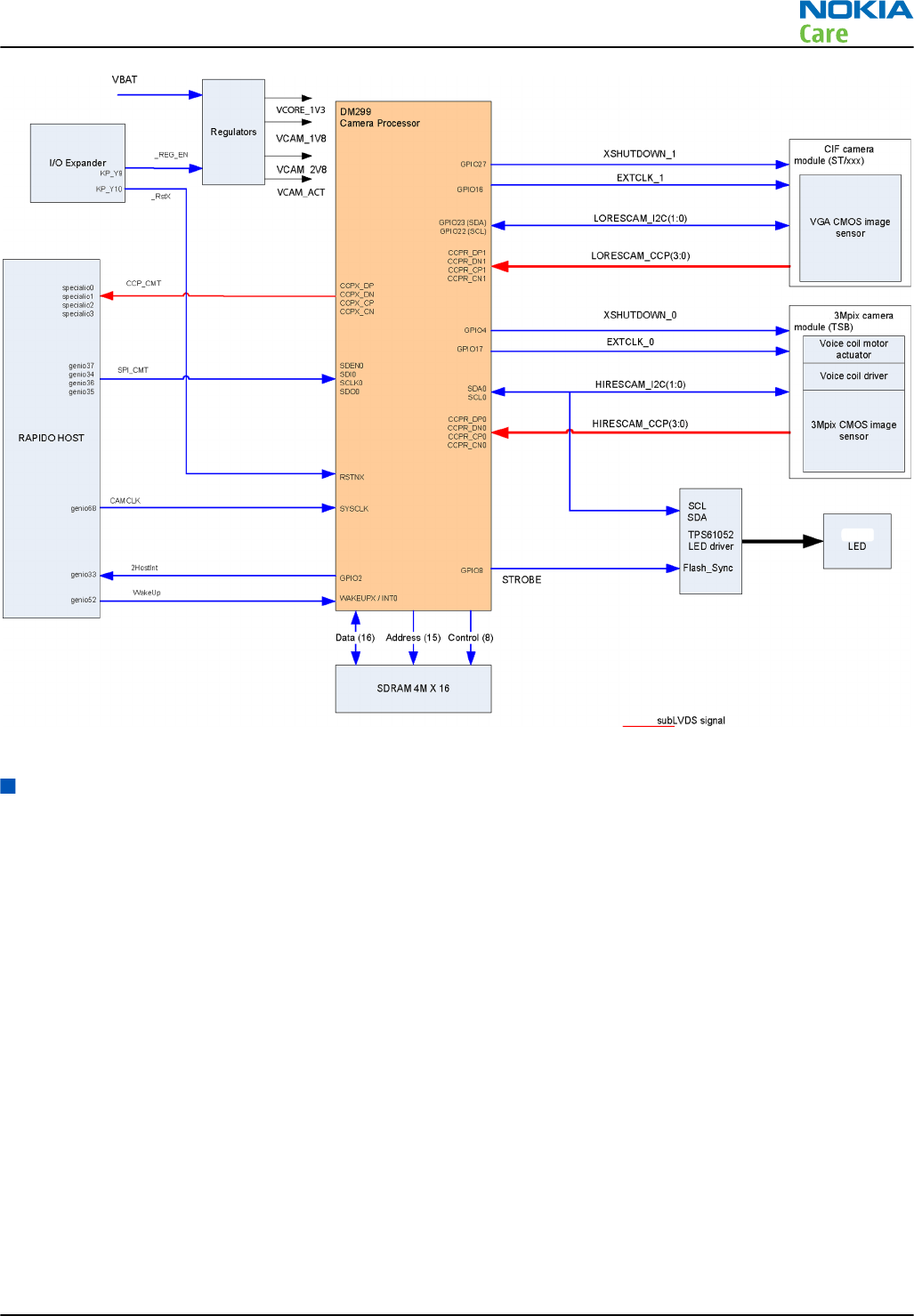
Figure 71 Camera block diagram
User interface
User interface
The UI module contains the following main features:
•ITU keypad and five-way cursor control and dedicated multimedia key implemented on a standard cross-
point matrix
•Finger position sensing keys for functions not part of the ITU matrix
•Finger position sensing beneath the five-way cursor control for the implementation of scrolling features
in the UI
•The handset microphone and one of the IHF speakers
•Various independently controlled lighting zones for the UI features described above
The cross-point matrix, LEDs, microphone and IHF are connected to the handset engine using the I/O expander
described below, and the finger position sensing controller is connected via an I2C bus.
A block diagram of the UI module is shown below. For clarity, the filtering components are not shown.
RM-333; RM-334; RM-335
System Module and User Interface
Issue 2 COMPANY CONFIDENTIAL Page 8 –17
Copyright © 2008 Nokia. All rights reserved.
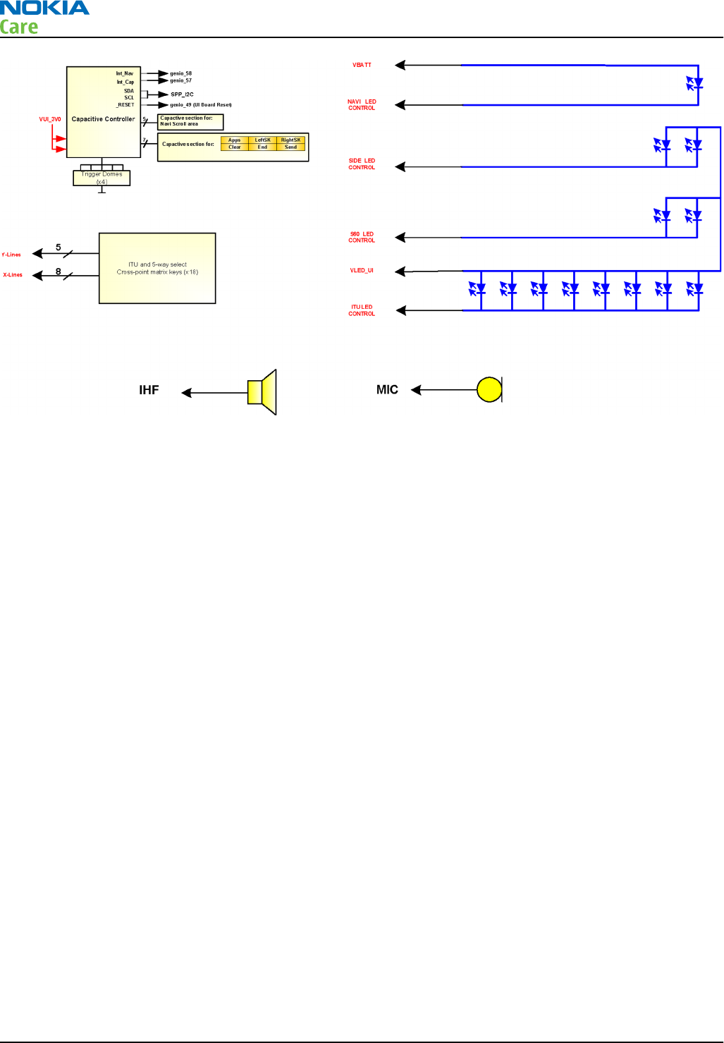
Figure 72 User interface block diagram
The interface to the UI capacitive sensing controller is at 3.0V, which is provided from the engine by a
dedicated linear regulator, and a dedicated level shifter provides the interface to allow the otherwise 1.8V
logic levels of the engine to be used on the UI.
The capacitive sensors function by sensing changes in the the charge coupled from one electrode to another
when the users finger is placed close to the electrodes patterns. There are further mechanical domes
associated with this sensing arrangement which only allows the scanning of the charge transfer to occur
when the user presses down on the front of the UI module – this is intended to prevent false key-activations.
Due to the construction of the module (it is mostly glued together) service is not possible, and if faultly, must
be replaced. This includes any faults that are found in the internal microphone or the lower of the two IHF
speakers.
For operational reasons, the modules are supplied unlocalised, and the correct localization front-panel needs
to be attached after the ‘bare’ module has been installed in the handset.
Display module
Display features
•2.6” AM OLED QVGA display (240 columns x 320 rows) supports up to 16.7M colors
•Ambient Light Sensor to optimize display brightness and power consumption
Display interface
Figure
Display interface block diagram
below shows how the display related signals are routed. Hurricane
display HWA controlling is done via LoSSI bus and pixel data is transferred via ViSSI-12 bus. MeSSI-8 is the
interface between Hurricane display HWA and Falcon OLED display.
As Falcon is self-emissive AM OLED display, no LED driver based backlighting is needed. An external DC-DC
convertor TPS65136 is used for the display powering.
Supply voltages for Falcon display:
1 VIO from the baseband SMPS (1.8V )
2 VBAT from Battery(3.7V)
RM-333; RM-334; RM-335
System Module and User Interface
Page 8 –18 COMPANY CONFIDENTIAL Issue 2
Copyright © 2008 Nokia. All rights reserved.
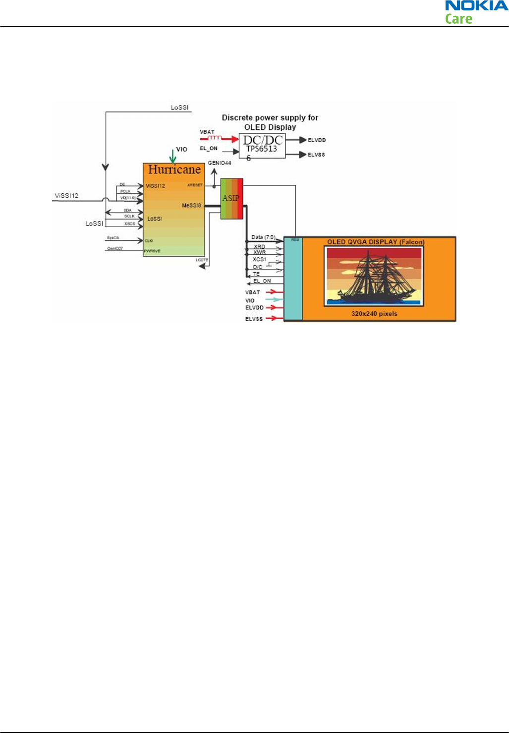
3 ELVDD supply from external DC/DC converter TPS65136 (+4.6V)
4 ELVSS supply from external DC/DC converter TPS65136 (-4.9V)
EL_ON signal from Falcon display is enable for the DC/DC converter TPS65136.
Figure 73 Display interface block diagram
I/O expander and keyboard
HW53 supports LM8323 I/O Expander. I/O expander is connected to Rapido via I2C bus and Genio66 is used
as an I/O Expander interrupt pin. Keyboard matrix 6x4 is connected to I/O expander. In addition, the I/O
expander has general purpose IO’s. Camera accelerator RSTX and Regulator enable, TVout Accelarator reset
and Regulator enable are connected to I/O expander GPIO’s.
RM-333; RM-334; RM-335
System Module and User Interface
Issue 2 COMPANY CONFIDENTIAL Page 8 –19
Copyright © 2008 Nokia. All rights reserved.
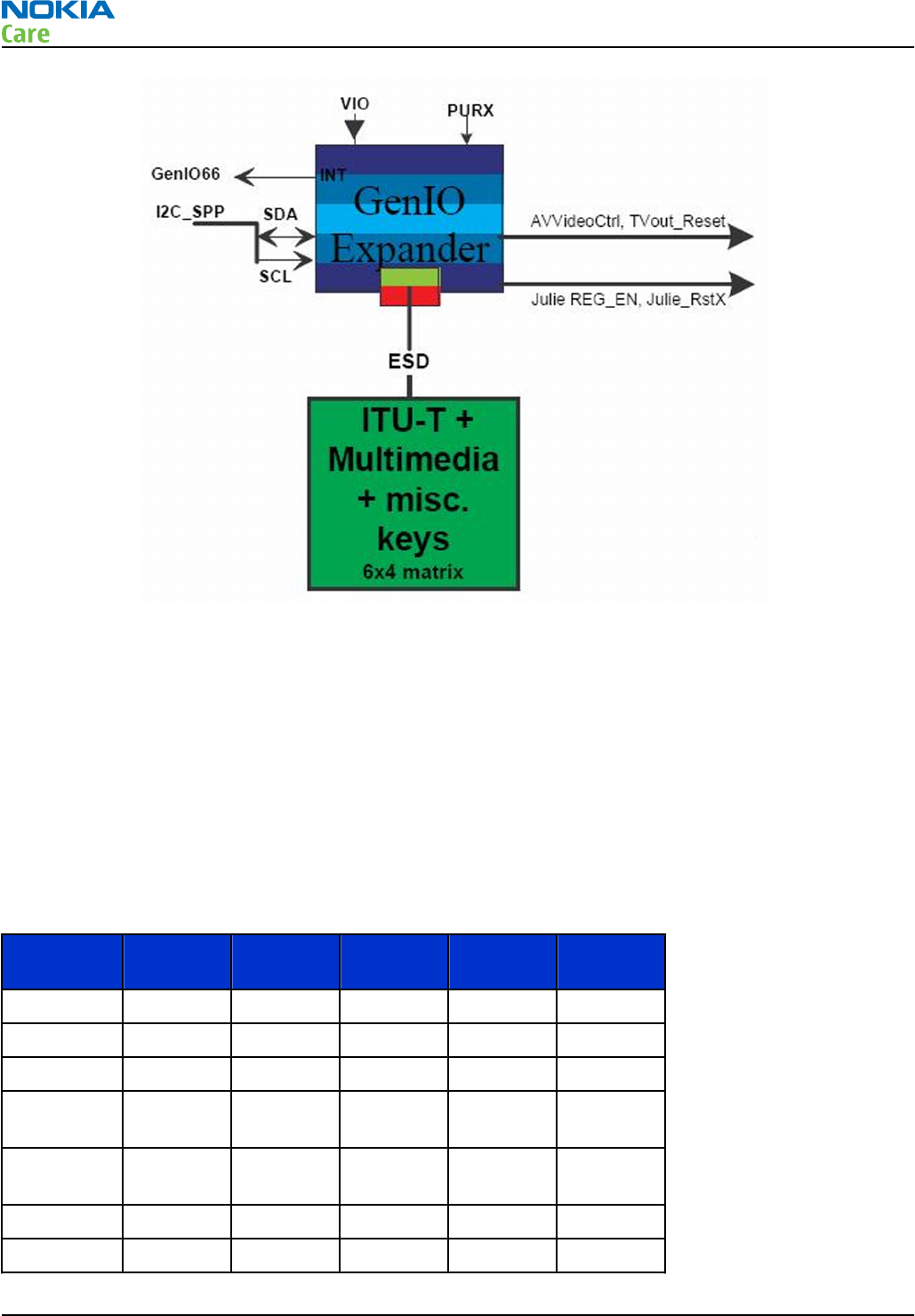
Figure 74 I/O expander and keyboard matrix
RM-333 has three separate keyboards:
•ITU keyboard
•Multimedia Keyboard
•S60 keyboard
ITU keyboard is visible when the slider is moved upwards. ITU keypads are located on the system/RF module.
System/RF module includes also side keys (volume keys, 2-position capture key and keylock switch) and MM
dome switches. MM keyboard is visible when the slider is moved downwards. S60 keys are located on UI/
slide module. They are connected as 3x4 key matrix to the Naviscroll driver which operates like I/O Expander.
More detailed description of S60 keyboard can be found in chapter
Naviscroll technical description
.
Table 10 Keyboard matrix
Expander’s
PINS KP-Y0 KP-Y1 KP-Y2 KP-Y3
Lines COL0 COL1 COL2 COL3
KP-X0 ROW0 1 6 2 Vol Up
KP-X1 ROW1 5 9 # Vol Down
KP-X2 ROW2 3 0 8
Capture
half
KP-X3 ROW3 * 7 4
Capture
full
KP-X4 ROW4 MM1 MM2 MM3 MM4
KP-X5 ROW5 Keylock
RM-333; RM-334; RM-335
System Module and User Interface
Page 8 –20 COMPANY CONFIDENTIAL Issue 2
Copyright © 2008 Nokia. All rights reserved.
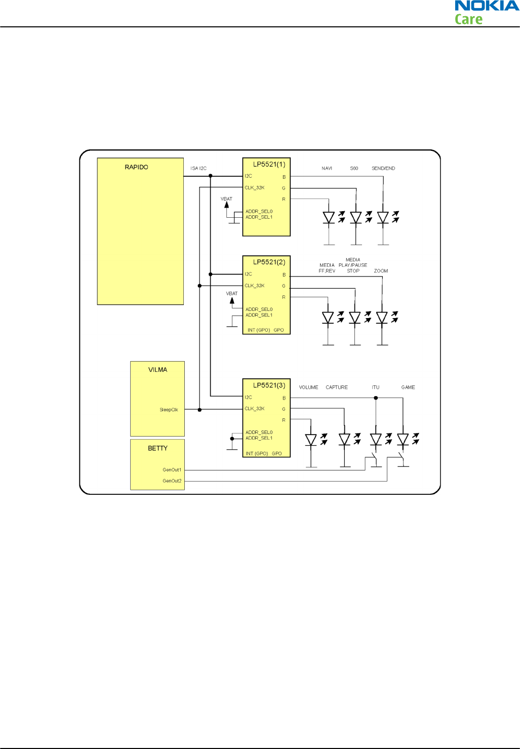
Illumination
LED driver solution
Three LP5521 ‘NJOY LED drivers are used to supply power for different light segments. Each LED driver has
three independently programmable constant current outputs (R, G and B). LED drivers are controlled by
Rapido via ISA_I2C bus and they use 32kHz external clock from Vilma.
Figure 75 Illumination block diagram
Light segments
9+1 different light segments are used for illumination, each having 1-4 parallel connected LEDs (see Figure
2). ITU and Game light segments are connected to the same LED driver output. Betty controls them via GenOut1
and GenOut2 outputs (see Figure 1). Parallel connected LEDs which are in same LED driver output branch have
serial resistor to even their currents. As ITU keyboard backlights are controlled by the Ambient Light Sensor
(ALS) they are turned ON only in dark ambient light.
RM-333 has a self-emissive AM OLED display, therefore it does not need LEDs for backlighting
RM-333; RM-334; RM-335
System Module and User Interface
Issue 2 COMPANY CONFIDENTIAL Page 8 –21
Copyright © 2008 Nokia. All rights reserved.
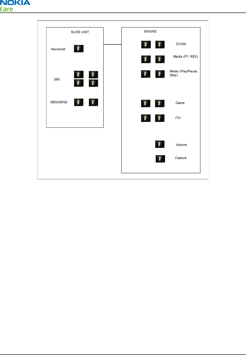
Figure 76 Light segments
Naviscroll
HW53 uses Quantum QT12C15 as Naviscroll Driver. As shown in Figure 1, it is interfaced to RAPIDO via SPP I2C
bus for control and data, two change lines TouchPadInt and KeyInt used by Naviscroll Driver to report to
RAPIDO any changes in the touchpad state or changes in the S60 key states, Rst is used as a reset signal from
RAPIDO to Naviscroll Driver.
On the other side, Naviscroll Driver interfaces Naviscroll touchpad and S60 keys as 3x4 matrix. When there is
a change in the touchpad state i.e. when the finger is scrolled over the naviscroll touchpad the Naviscroll
Driver gives an interrupt to RAPIDO via TouchPadInt line by pulling it low. Similarly when any of the S60 keys
is pressed the Naviscroll Driver gives an interrupt to RAPIDO via KeyInt line by pulling it low. When receiving
either of the Interrupts, RAPIDO performs an I2C data read from Naviscroll Driver internal registers to
determine Naviscroll touchpad XY position change if TouchPadInt was detected and to determine which S60
keys were pressed if KeyInt was detected. After that, the interrupt lines change state from low to high. 2V8
voltage regulator located on the UI flex supplies power for the Naviscroll driver.
RM-333; RM-334; RM-335
System Module and User Interface
Page 8 –22 COMPANY CONFIDENTIAL Issue 2
Copyright © 2008 Nokia. All rights reserved.
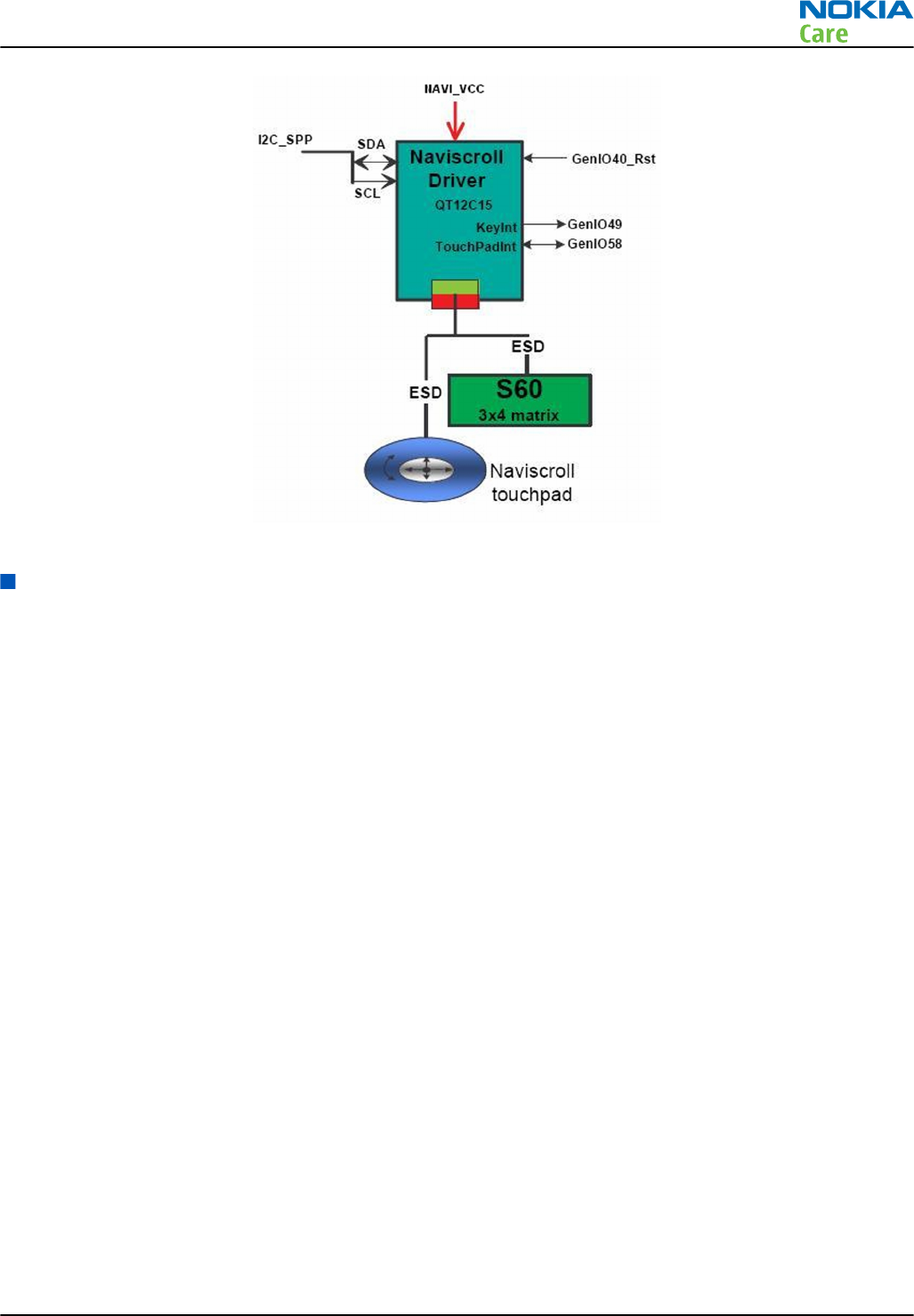
Figure 77 Block diagram of Naviscroll Interface
ASICs
RAPIDOYAWE
RAPIDOYAWE ASIC (D2800) is a die-stacked Processor (RAPIDO) with 3G HDSPA logic (YAWE). RAM memory is
integrated into RAPIDO.
EM ASIC BETTY N2300
The EM ASIC (N2300) includes the following functional blocks:
•Core supply generation
•Charge control circuitry
•Level shifter and regulator for USB/FBUS
•Current gauge for battery current measuring
•LED control for display backlighting
•Digital interface (CBUS)
EM ASIC VILMA N2200
The EM ASIC (N2200) includes the following functional blocks:
•Start up logic and reset control
•Charger detection
•Battery voltage monitoring
•32.768kHz clock with external crystal
•Real time clock with external backup battery
•SIM card interface
•Stereo audio codecs and amplifiers
•A/D converter
RM-333; RM-334; RM-335
System Module and User Interface
Issue 2 COMPANY CONFIDENTIAL Page 8 –23
Copyright © 2008 Nokia. All rights reserved.

•Regulators
•Vibra interface
•Digital interface (CBUS)
EMC ASIP (Appcation Specified Integrated Passive) have been integrated inside the ASIC. It includes biasing
passives for microphone , EMC filter for SIM, microphones etc.
Device memories
Combo memory
The memory of the device consists of stacked DDR SDRAM and MuxedMassMemory (M3). Combo memory DDR/
M3 memory has 768Mb DDR + 2Gb M3.
Audio concept
Audio HW architecture
The functional core of the audio hardware is built around three ASICs: RAPIDOYAWE engine ASIC, mixed signal
ASIC Avilma and D/A converter DAC33.
DAC33 converts digital audio signal to analog and is routed to the FM Transmitter and amplifier TPA6130
which provides an interface for the transducers and the accessory connector.
AVilma provides analog signal for earpiece and for D-class audio amplifier TPA2012D2, which drives
integrated stereo handsfree speakers.
There are four audio transducers:
•8x12 mm dynamic earpiece
•Two 8x12 mm dynamic speakers
•Digital MEMS (microelectromechanical systems) microphone
Avilma provides an output for the dynamic vibra component. All wired audio accessories are connected to
the AV accessory connector. A Bluetooth audio and FM radio module, which is connected to RAPIDOYAWE,
supports Bluetooth audio and FM radio functionality.
RM-333; RM-334; RM-335
System Module and User Interface
Page 8 –24 COMPANY CONFIDENTIAL Issue 2
Copyright © 2008 Nokia. All rights reserved.
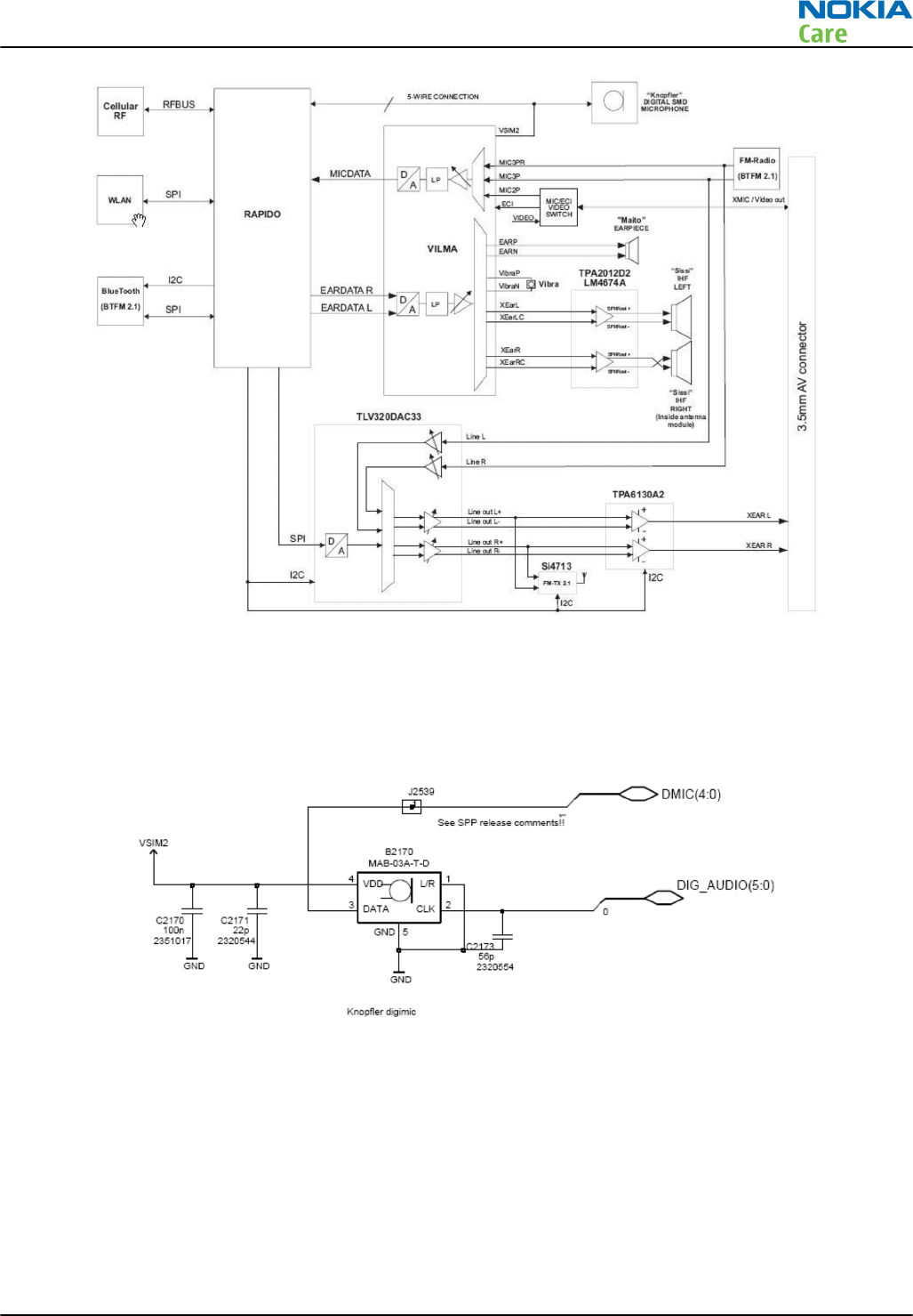
Figure 78 Audio system block
Internal microphone
The internal microphone is used for HandPortable (HP) and Internal HandsFree (IHF) call modes. A digital
MEMS microphone data and clock line are connected to Rapidoyawe and operating voltage is received from
Avilma.
Figure 79 Internal microphone
Internal earpiece
Internal earpiece is used for the HandPortable (HP) call mode. A dynamic 8x12 mm earpiece capsule is
Connected to Avilma ASIC’s differential output EarP and EarN.
RM-333; RM-334; RM-335
System Module and User Interface
Issue 2 COMPANY CONFIDENTIAL Page 8 –25
Copyright © 2008 Nokia. All rights reserved.
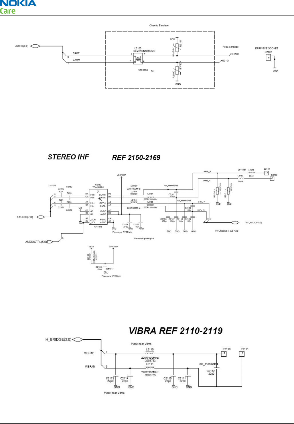
Figure 80 Internal earpiece circuitry
Internal speakers
Internal speakers are used for Internal HandsFree (IHF) call mode, video call, ringing tones, FM radio and
music listening.
Two dynamic 8x12mm speakers are connected to Avilma ASIC’s outputs XearR/XearL via stereo D-class IHF
amplifier TPA2012D2. The amplifier has 12 dB fixed gain and it is put to shutdown mode when not in use.
Figure 81 Internal speakers
Vibra circuitry
Vibra is used for the vibra alarm function.
The vibra motor is connected to the Avilma ASIC VibraP and VibraN Pulse Width Modulated (PWM) outputs.
Figure 82 Vibra circuitry
RM-333; RM-334; RM-335
System Module and User Interface
Page 8 –26 COMPANY CONFIDENTIAL Issue 2
Copyright © 2008 Nokia. All rights reserved.
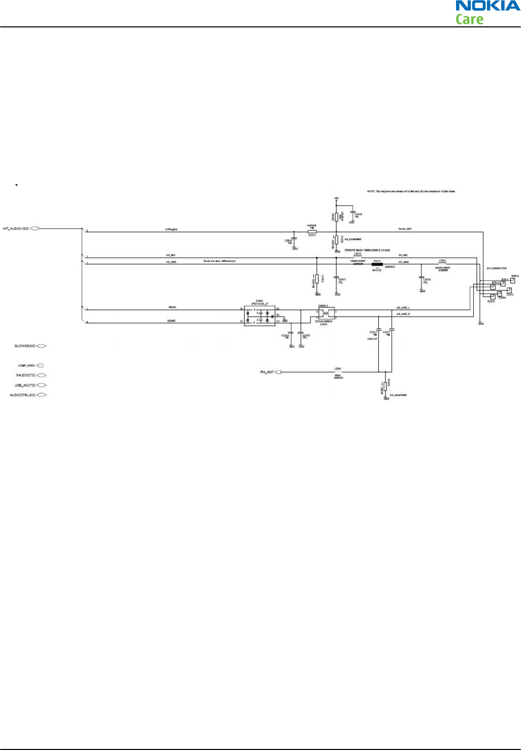
Accessory AV connector
The features that are supported by Gadget accessory interface are the following:
•Audio output (stereo headset/headphones having the impedance >16ohm)
•Audio input (mono microphone from headset)
•Control data (ECI)
•TV-out with composite signal to 75ohm coax cable
•Connects FM receiver to headphones, which serves as FM antenna
Figure 83 Accessory (AV) connector
RM-333; RM-334; RM-335
System Module and User Interface
Issue 2 COMPANY CONFIDENTIAL Page 8 –27
Copyright © 2008 Nokia. All rights reserved.
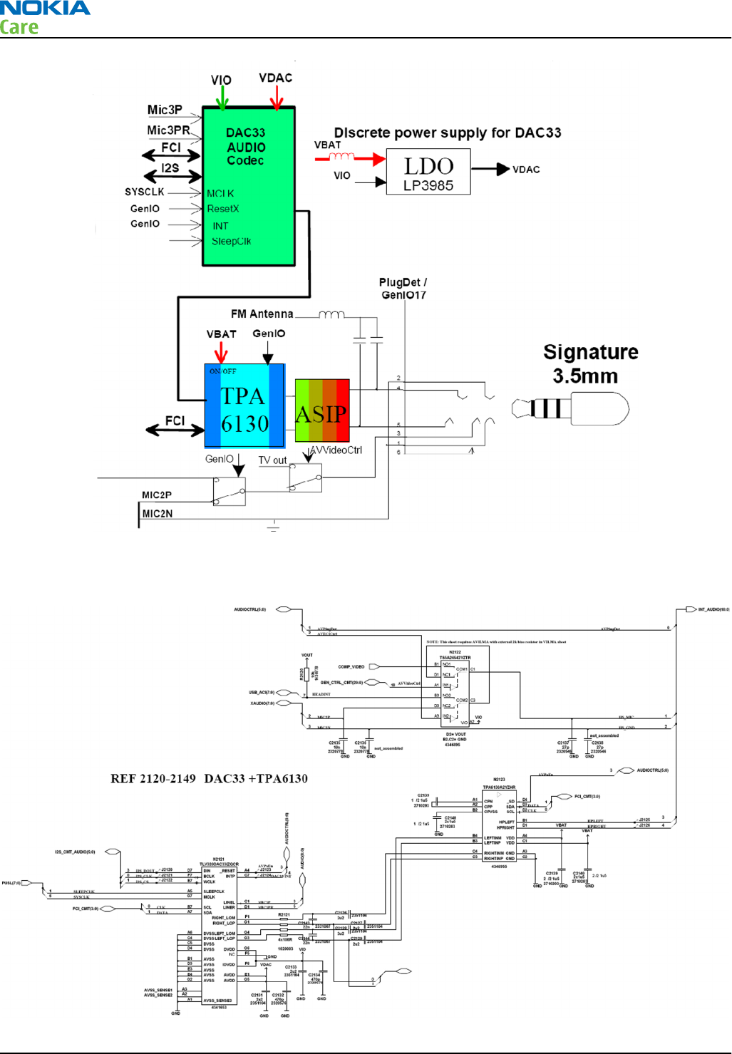
Figure 84 Accessory (AV) connector with DAC33 and TPA6130 audio enhancements
External earpiece and microphone
Figure 85 External earpiece and microphone audio circuit
RM-333; RM-334; RM-335
System Module and User Interface
Page 8 –28 COMPANY CONFIDENTIAL Issue 2
Copyright © 2008 Nokia. All rights reserved.
Baseband technical specifications
External interfaces
Name of connection Connector reference
HS USB X3300
MicroSD card X3200
Battery connector X2070
SIM card reader X2700
Accessory (AV)
connector
X2010
Charger X3300
SIM IF connections
Pin Signal I/O Engine connection Notes
1 VSIM Out EM ASIC N2200 VSIM1 Supply voltage
to SIM card,
1.8V or 3.0V.
2 SIMRST Out EM ASIC N2200 SIM1Rst Reset signal to
SIM card
3 SIMCLK Out EM ASIC N2200 SIM1ClkC Clock signal to
SIM card
5 GND - GND Ground
7 SIMDATA In/Out EM ASIC N2200 SIM1DaC Data input /
output
Charger connector and charging interface connections & electrical characteristics
Figure 86 Charger connector
RM-333; RM-334; RM-335
System Module and User Interface
Issue 2 COMPANY CONFIDENTIAL Page 8 –29
Copyright © 2008 Nokia. All rights reserved.
Table 11 Charging interface connections
PIN Signal I/O Engine connection Description
1 VBUS IN
D3300/
N3301 VBUS/DCIN 5V
2 D- IN/OUT D3300 DM Data minus
3 D+ IN/OUT D3300 DN Data plus
4 ID Not in use
5 ground Ground
Signal
ground
Table 12 Charging IF electrical characteristics
Description Parameter Min Max Unit
VBUS Vcharge 4.75 5.25 V
VBUS Icharge 1.8 A
D+,D-,Ground 1 A
Internal interfaces
Name of connection Component reference
DALS N6502
Earpiece B2100
Microphone B2 (On UI Module)
IHF speakers B2151 / B1
Main camera socket X1450
Sub-camera N1450
Main display connector X2450
Vibra M2110
Back-up battery interface electrical characteristics
Table 13 Back-up battery electrical characteristics
Description Parameter Min Typ Max Unit
Back-Up
Battery
Voltage
Vback 0 2.5 2.7 V
RM-333; RM-334; RM-335
System Module and User Interface
Page 8 –30 COMPANY CONFIDENTIAL Issue 2
Copyright © 2008 Nokia. All rights reserved.
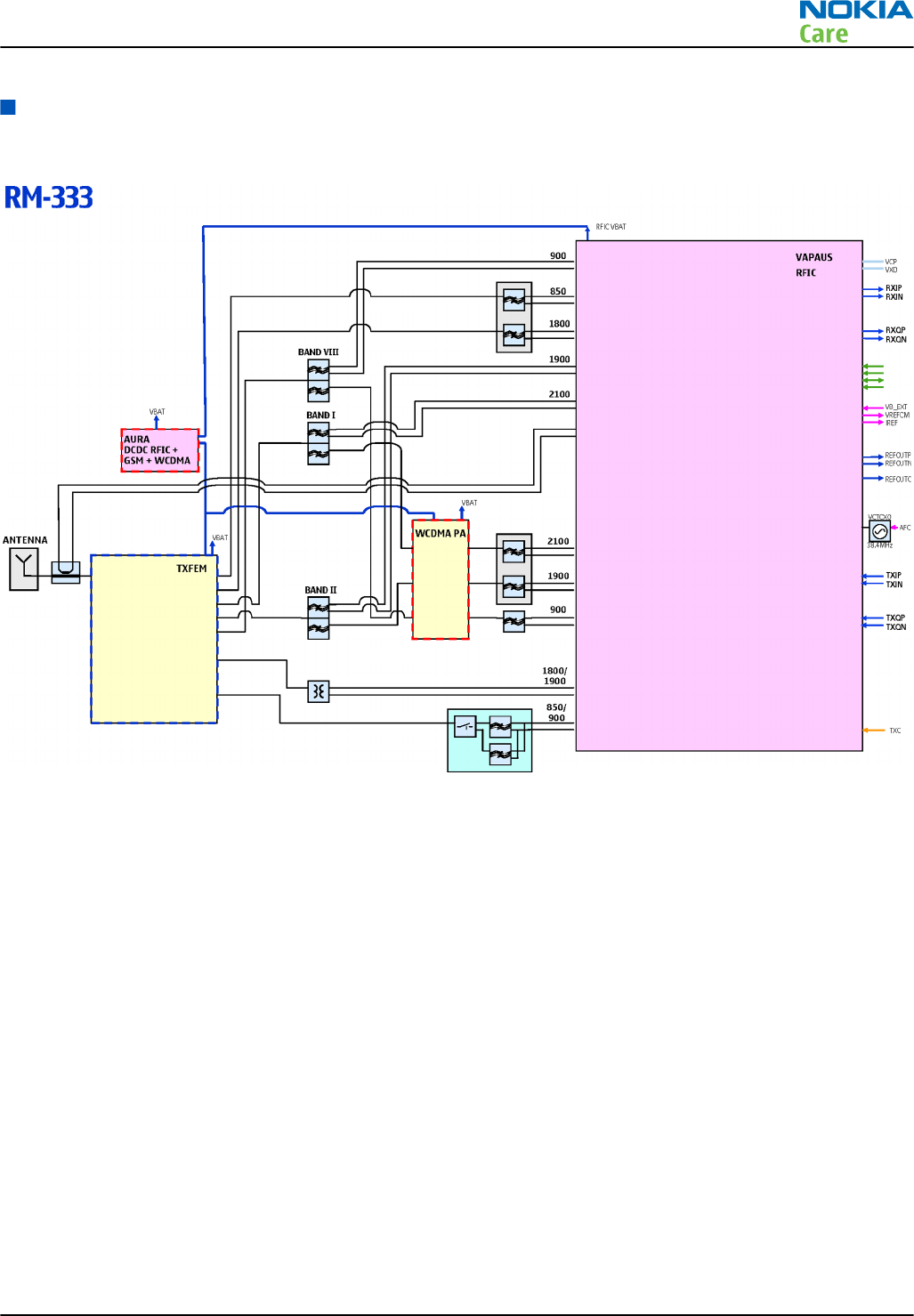
RF technical description
RF block diagram
Figure 87 RF block diagram RM-333 using RF ASIC N7500
RM-333; RM-334; RM-335
System Module and User Interface
Issue 2 COMPANY CONFIDENTIAL Page 8 –31
Copyright © 2008 Nokia. All rights reserved.
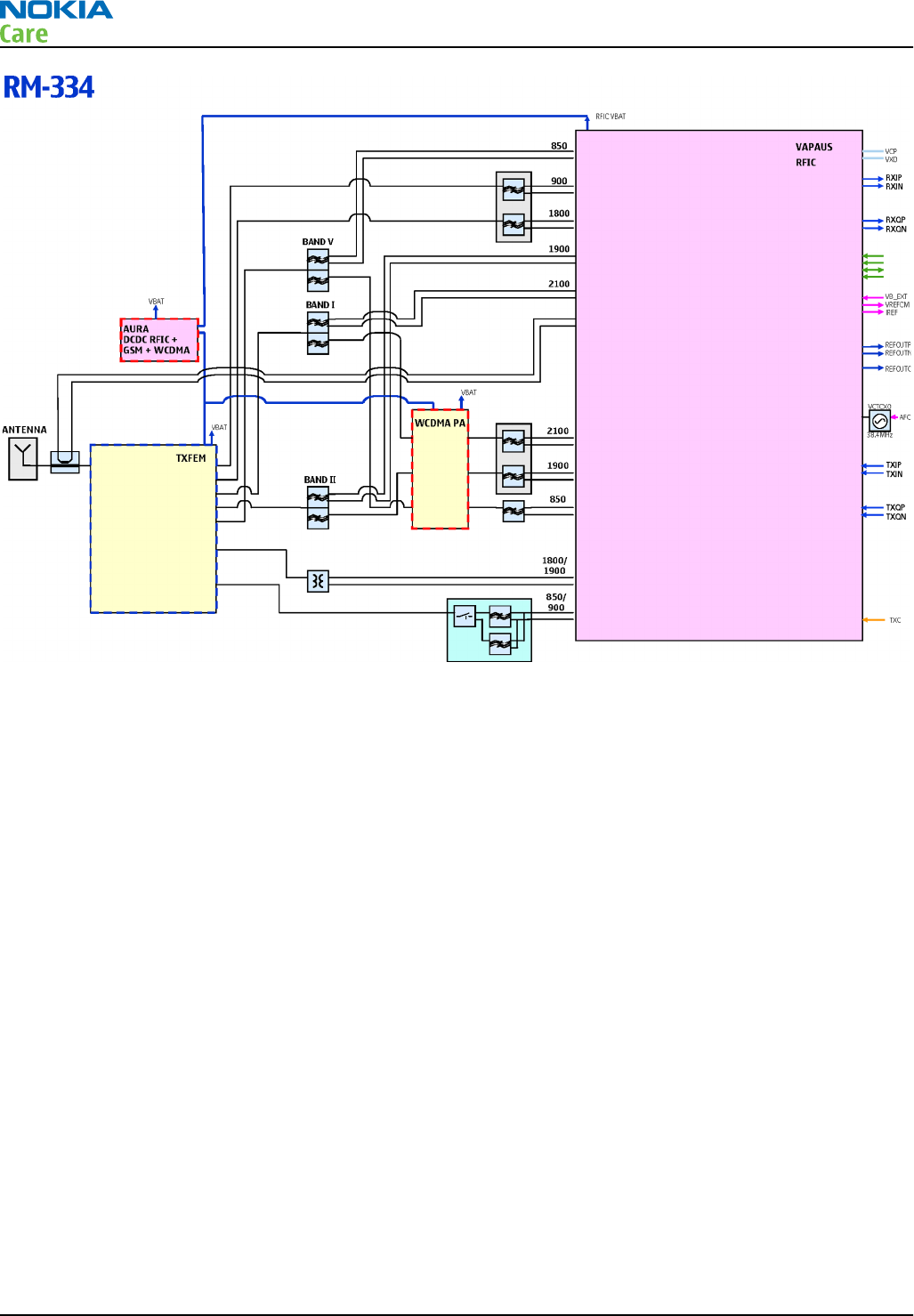
Figure 88 RF block diagram RM-334 using RF ASIC N7500
The RF block diagram uses RF ASIC N7500 that performs the RF back-end functions of receive and transmit
function of the cellular transceiver.
Receiver (RX)
An analogue signal is received by the phone's antenna. The signal is converted to a digital signal and is then
transferred further to the baseband (eg. to the earpiece).
The receiver functions are implemented in the RF ASIC.
Signals with different frequencies take different paths, therefore being handled by different components.
The principle of GSM and WCDMA is the same.
Transmitter (TX)
The digital baseband signal (eg. from the microphone) is converted to an analogue signal, which is then
amplified and transmitted from the antenna. The frequency of this signal can be tuned to match the bandwith
of the system in use (eg. GSM900).
The transmitter functions are implemented in the RF ASIC.
Even though the GSM and WCDMA signals are sent via different components, the principles of the transmission
is the same.
RM-333; RM-334; RM-335
System Module and User Interface
Page 8 –32 COMPANY CONFIDENTIAL Issue 2
Copyright © 2008 Nokia. All rights reserved.
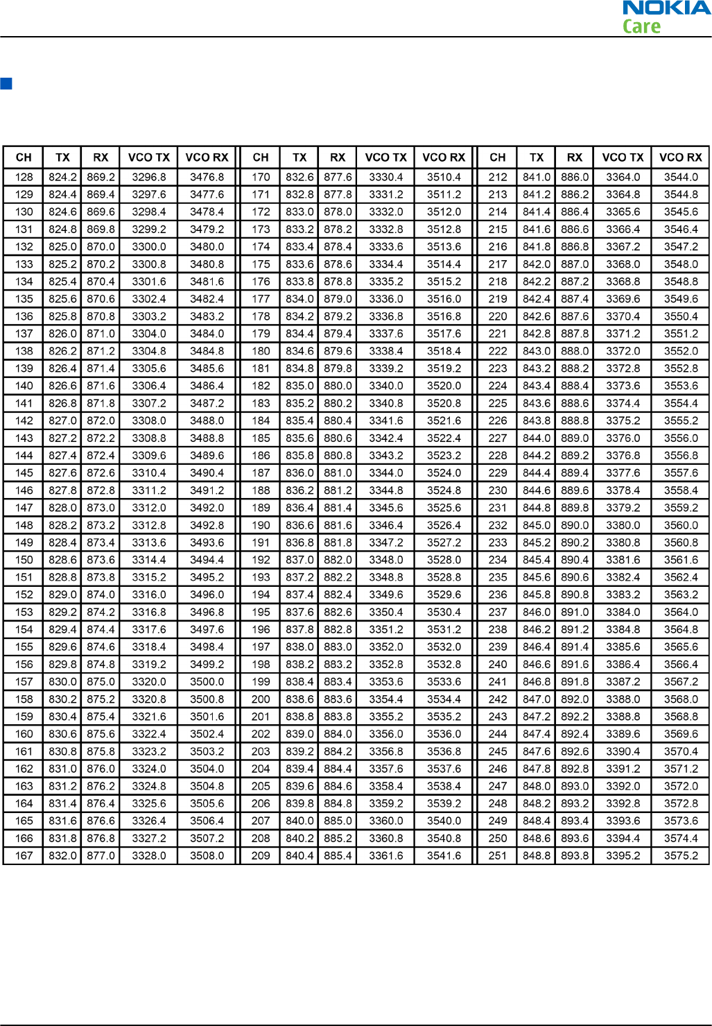
Frequency mappings
GSM850 frequencies
RM-333; RM-334; RM-335
System Module and User Interface
Issue 2 COMPANY CONFIDENTIAL Page 8 –33
Copyright © 2008 Nokia. All rights reserved.
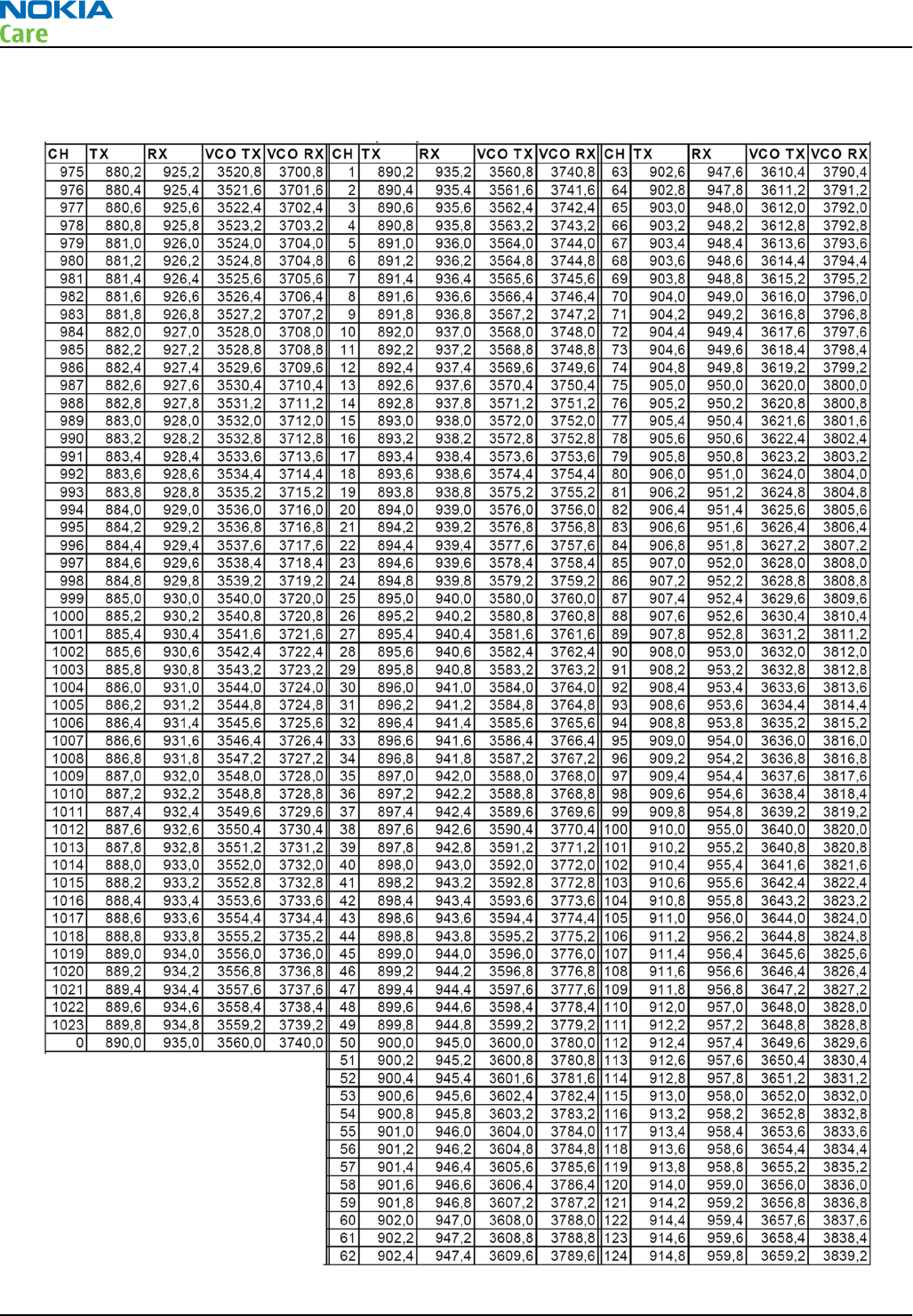
EGSM900 frequencies
RM-333; RM-334; RM-335
System Module and User Interface
Page 8 –34 COMPANY CONFIDENTIAL Issue 2
Copyright © 2008 Nokia. All rights reserved.
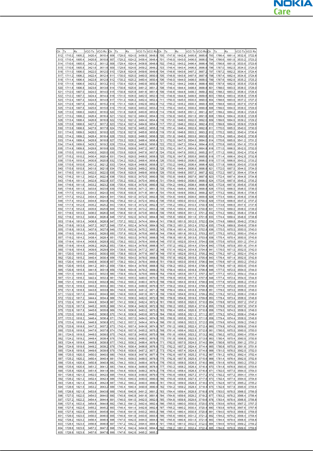
GSM1800 frequencies
RM-333; RM-334; RM-335
System Module and User Interface
Issue 2 COMPANY CONFIDENTIAL Page 8 –35
Copyright © 2008 Nokia. All rights reserved.
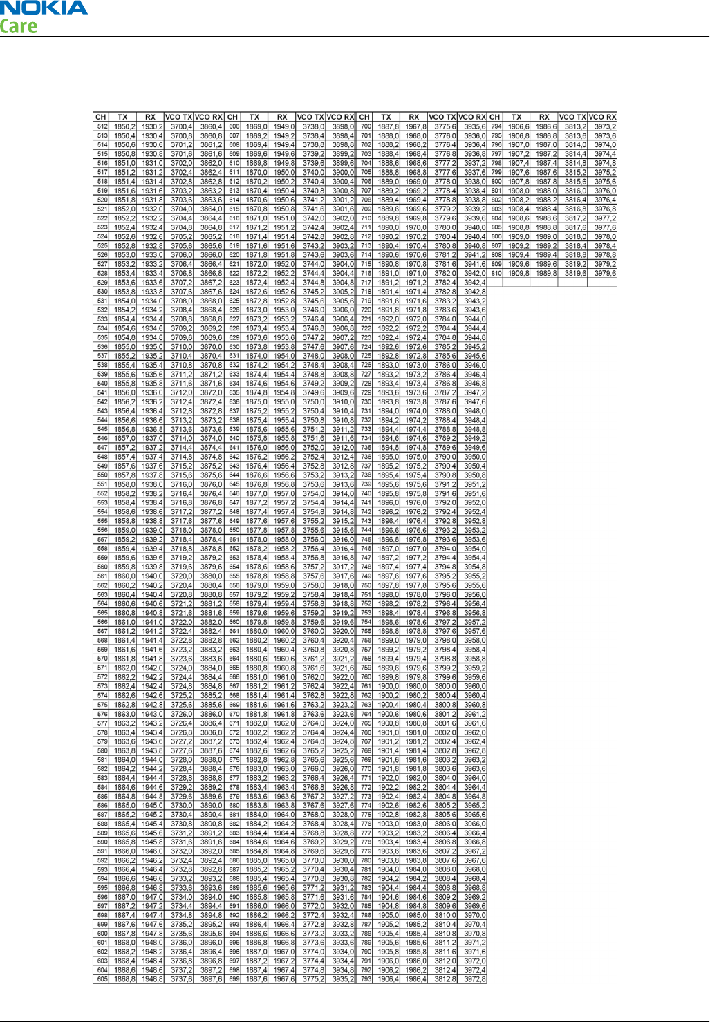
GSM1900 frequencies
RM-333; RM-334; RM-335
System Module and User Interface
Page 8 –36 COMPANY CONFIDENTIAL Issue 2
Copyright © 2008 Nokia. All rights reserved.
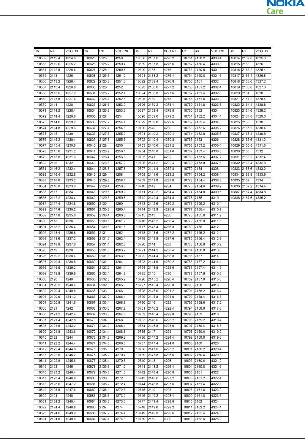
WCDMA 2100 Rx frequencies
RM-333; RM-334; RM-335
System Module and User Interface
Issue 2 COMPANY CONFIDENTIAL Page 8 –37
Copyright © 2008 Nokia. All rights reserved.
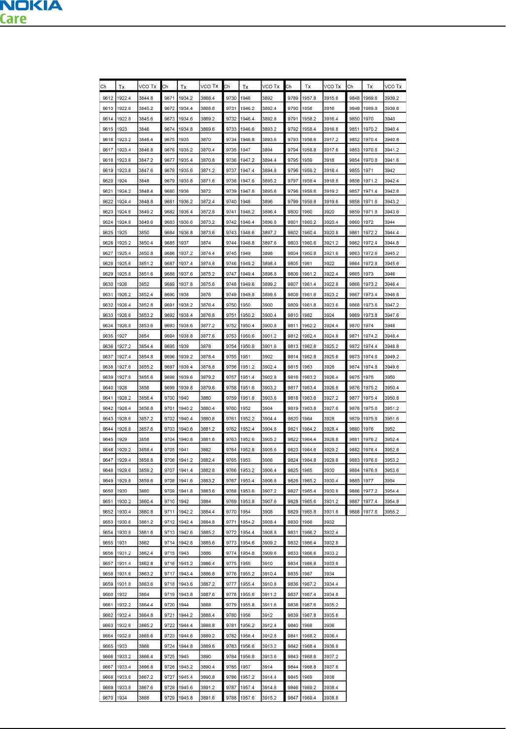
WCDMA 2100 Tx frequencies
RM-333; RM-334; RM-335
System Module and User Interface
Page 8 –38 COMPANY CONFIDENTIAL Issue 2
Copyright © 2008 Nokia. All rights reserved.
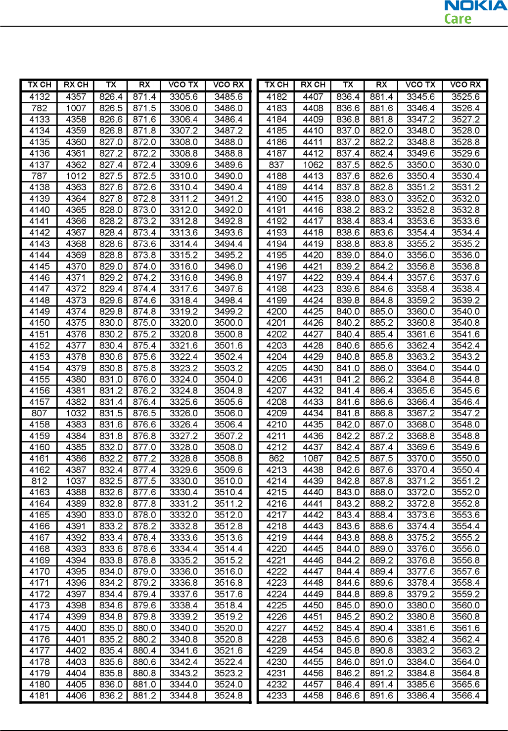
WCDMA V (850) frequencies
RM-333; RM-334; RM-335
System Module and User Interface
Issue 2 COMPANY CONFIDENTIAL Page 8 –39
Copyright © 2008 Nokia. All rights reserved.

WCDMA VIII (900) frequencies
Uplink CH (TX) Freq (MHz) VCO (MHz) Downlink CH (RX) Freq (MHz) VCO (MHz)
2712 882,4 3529,6 2937 927,4 3709,6
2713 882,6 3530,4 2938 927,6 3710,4
2714 882,8 3531,2 2939 927,8 3711,2
2715 883 3532 2940 928 3712
2716 883,2 3532,8 2941 928,2 3712,8
2717 883,4 3533,6 2942 928,4 3713,6
2718 883,6 3534,4 2943 928,6 3714,4
2719 883,8 3535,2 2944 928,8 3715,2
2720 884 3536 2945 929 3716
2721 884,2 3536,8 2946 929,2 3716,8
2722 884,4 3537,6 2947 929,4 3717,6
2723 884,6 3538,4 2948 929,6 3718,4
2724 884,8 3539,2 2949 929,8 3719,2
2725 885 3540 2950 930 3720
2726 885,2 3540,8 2951 930,2 3720,8
2727 885,4 3541,6 2952 930,4 3721,6
2728 885,6 3542,4 2953 930,6 3722,4
2729 885,8 3543,2 2954 930,8 3723,2
2730 886 3544 2955 931 3724
2731 886,2 3544,8 2956 931,2 3724,8
2732 886,4 3545,6 2957 931,4 3725,6
2733 886,6 3546,4 2958 931,6 3726,4
2734 886,8 3547,2 2959 931,8 3727,2
2735 887 3548 2960 932 3728
2736 887,2 3548,8 2961 932,2 3728,8
2737 887,4 3549,6 2962 932,4 3729,6
2738 887,6 3550,4 2963 932,6 3730,4
2739 887,8 3551,2 2964 932,8 3731,2
2740 888 3552 2965 933 3732
2741 888,2 3552,8 2966 933,2 3732,8
2742 888,4 3553,6 2967 933,4 3733,6
2743 888,6 3554,4 2968 933,6 3734,4
2744 888,8 3555,2 2969 933,8 3735,2
RM-333; RM-334; RM-335
System Module and User Interface
Page 8 –40 COMPANY CONFIDENTIAL Issue 2
Copyright © 2008 Nokia. All rights reserved.

Uplink CH (TX) Freq (MHz) VCO (MHz) Downlink CH (RX) Freq (MHz) VCO (MHz)
2745 889 3556 2970 934 3736
2746 889,2 3556,8 2971 934,2 3736,8
2747 889,4 3557,6 2972 934,4 3737,6
2748 889,6 3558,4 2973 934,6 3738,4
2749 889,8 3559,2 2974 934,8 3739,2
2750 890 3560 2975 935 3740
2751 890,2 3560,8 2976 935,2 3740,8
2752 890,4 3561,6 2977 935,4 3741,6
2753 890,6 3562,4 2978 935,6 3742,4
2754 890,8 3563,2 2979 935,8 3743,2
2755 891 3564 2980 936 3744
2756 891,2 3564,8 2981 936,2 3744,8
2757 891,4 3565,6 2982 936,4 3745,6
2758 891,6 3566,4 2983 936,6 3746,4
2759 891,8 3567,2 2984 936,8 3747,2
2760 892 3568 2985 937 3748
2761 892,2 3568,8 2986 937,2 3748,8
2762 892,4 3569,6 2987 937,4 3749,6
2763 892,6 3570,4 2988 937,6 3750,4
2764 892,8 3571,2 2989 937,8 3751,2
2765 893 3572 2990 938 3752
2766 893,2 3572,8 2991 938,2 3752,8
2767 893,4 3573,6 2992 938,4 3753,6
2768 893,6 3574,4 2993 938,6 3754,4
2769 893,8 3575,2 2994 938,8 3755,2
2770 894 3576 2995 939 3756
2771 894,2 3576,8 2996 939,2 3756,8
2772 894,4 3577,6 2997 939,4 3757,6
2773 894,6 3578,4 2998 939,6 3758,4
2774 894,8 3579,2 2999 939,8 3759,2
2775 895 3580 3000 940 3760
2776 895,2 3580,8 3001 940,2 3760,8
2777 895,4 3581,6 3002 940,4 3761,6
2778 895,6 3582,4 3003 940,6 3762,4
2779 895,8 3583,2 3004 940,8 3763,2
RM-333; RM-334; RM-335
System Module and User Interface
Issue 2 COMPANY CONFIDENTIAL Page 8 –41
Copyright © 2008 Nokia. All rights reserved.

Uplink CH (TX) Freq (MHz) VCO (MHz) Downlink CH (RX) Freq (MHz) VCO (MHz)
2780 896 3584 3005 941 3764
2781 896,2 3584,8 3006 941,2 3764,8
2782 896,4 3585,6 3007 941,4 3765,6
2783 896,6 3586,4 3008 941,6 3766,4
2784 896,8 3587,2 3009 941,8 3767,2
2785 897 3588 3010 942 3768
2786 897,2 3588,8 3011 942,2 3768,8
2787 897,4 3589,6 3012 942,4 3769,6
2788 897,6 3590,4 3013 942,6 3770,4
2789 897,8 3591,2 3014 942,8 3771,2
2790 898 3592 3015 943 3772
2791 898,2 3592,8 3016 943,2 3772,8
2792 898,4 3593,6 3017 943,4 3773,6
2793 898,6 3594,4 3018 943,6 3774,4
2794 898,8 3595,2 3019 943,8 3775,2
2795 899 3596 3020 944 3776
2796 899,2 3596,8 3021 944,2 3776,8
2797 899,4 3597,6 3022 944,4 3777,6
2798 899,6 3598,4 3023 944,6 3778,4
2799 899,8 3599,2 3024 944,8 3779,2
2800 900 3600 3025 945 3780
2801 900,2 3600,8 3026 945,2 3780,8
2802 900,4 3601,6 3027 945,4 3781,6
2803 900,6 3602,4 3028 945,6 3782,4
2804 900,8 3603,2 3029 945,8 3783,2
2805 901 3604 3030 946 3784
2806 901,2 3604,8 3031 946,2 3784,8
2807 901,4 3605,6 3032 946,4 3785,6
2808 901,6 3606,4 3033 946,6 3786,4
2809 901,8 3607,2 3034 946,8 3787,2
2810 902 3608 3035 947 3788
2811 902,2 3608,8 3036 947,2 3788,8
2812 902,4 3609,6 3037 947,4 3789,6
2813 902,6 3610,4 3038 947,6 3790,4
2814 902,8 3611,2 3039 947,8 3791,2
RM-333; RM-334; RM-335
System Module and User Interface
Page 8 –42 COMPANY CONFIDENTIAL Issue 2
Copyright © 2008 Nokia. All rights reserved.

Uplink CH (TX) Freq (MHz) VCO (MHz) Downlink CH (RX) Freq (MHz) VCO (MHz)
2815 903 3612 3040 948 3792
2816 903,2 3612,8 3041 948,2 3792,8
2817 903,4 3613,6 3042 948,4 3793,6
2818 903,6 3614,4 3043 948,6 3794,4
2819 903,8 3615,2 3044 948,8 3795,2
2820 904 3616 3045 949 3796
2821 904,2 3616,8 3046 949,2 3796,8
2822 904,4 3617,6 3047 949,4 3797,6
2823 904,6 3618,4 3048 949,6 3798,4
2824 904,8 3619,2 3049 949,8 3799,2
2825 905 3620 3050 950 3800
2826 905,2 3620,8 3051 950,2 3800,8
2827 905,4 3621,6 3052 950,4 3801,6
2828 905,6 3622,4 3053 950,6 3802,4
2829 905,8 3623,2 3054 950,8 3803,2
2830 906 3624 3055 951 3804
2831 906,2 3624,8 3056 951,2 3804,8
2832 906,4 3625,6 3057 951,4 3805,6
2833 906,6 3626,4 3058 951,6 3806,4
2834 906,8 3627,2 3059 951,8 3807,2
2835 907 3628 3060 952 3808
2836 907,2 3628,8 3061 952,2 3808,8
2837 907,4 3629,6 3062 952,4 3809,6
2838 907,6 3630,4 3063 952,6 3810,4
2839 907,8 3631,2 3064 952,8 3811,2
2840 908 3632 3065 953 3812
2841 908,2 3632,8 3066 953,2 3812,8
2842 908,4 3633,6 3067 953,4 3813,6
2843 908,6 3634,4 3068 953,6 3814,4
2844 908,8 3635,2 3069 953,8 3815,2
2845 909 3636 3070 954 3816
2846 909,2 3636,8 3071 954,2 3816,8
2847 909,4 3637,6 3072 954,4 3817,6
2848 909,6 3638,4 3073 954,6 3818,4
2849 909,8 3639,2 3074 954,8 3819,2
RM-333; RM-334; RM-335
System Module and User Interface
Issue 2 COMPANY CONFIDENTIAL Page 8 –43
Copyright © 2008 Nokia. All rights reserved.
Uplink CH (TX) Freq (MHz) VCO (MHz) Downlink CH (RX) Freq (MHz) VCO (MHz)
2850 910 3640 3075 955 3820
2851 910,2 3640,8 3076 955,2 3820,8
2852 910,4 3641,6 3077 955,4 3821,6
2853 910,6 3642,4 3078 955,6 3822,4
2854 910,8 3643,2 3079 955,8 3823,2
2855 911 3644 3080 956 3824
2856 911,2 3644,8 3081 956,2 3824,8
2857 911,4 3645,6 3082 956,4 3825,6
2858 911,6 3646,4 3083 956,6 3826,4
2859 911,8 3647,2 3084 956,8 3827,2
2860 912 3648 3085 957 3828
2861 912,2 3648,8 3086 957,2 3828,8
2862 912,4 3649,6 3087 957,4 3829,6
2863 912,6 3650,4 3088 957,6 3830,4
RM-333; RM-334; RM-335
System Module and User Interface
Page 8 –44 COMPANY CONFIDENTIAL Issue 2
Copyright © 2008 Nokia. All rights reserved.

9 — Service information
differences between RM-335
and RM-333
Nokia Customer Care
Issue 2 COMPANY CONFIDENTIAL Page 9 –1
Copyright © 2008 Nokia. All rights reserved.

RM-333; RM-334; RM-335
Service information differences between RM-335 and
RM-333
(This page left intentionally blank.)
Page 9 –2 COMPANY CONFIDENTIAL Issue 2
Copyright © 2008 Nokia. All rights reserved.

Table of Contents
General Information...............................................................................................................................................9–5
RM-335 Product data ........................................................................................................................................9–5
Main RF characteristics for GSM850/900/1800/1900 (quadband) and EDGE phones .................................9–6
BB Troubleshooting................................................................................................................................................9–7
BB HW differences between RM-335 and RM-333..........................................................................................9–7
RF Troubleshooting................................................................................................................................................9–7
RM-335 RF block ................................................................................................................................................9–7
List of Tables
Table 14 Main RF characteristics...........................................................................................................................9–6
List of Figures
Figure 89 View of RM-335......................................................................................................................................9–5
Figure 90 USB charging components in RM-335 and RM-333............................................................................9–7
Figure 91 RM-335 RF key components .................................................................................................................9–8
Figure 92 RM-335 RF block diagram.....................................................................................................................9–9
RM-333; RM-334; RM-335
Service information differences between RM-335 and
RM-333
Issue 2 COMPANY CONFIDENTIAL Page 9 –3
Copyright © 2008 Nokia. All rights reserved.

RM-333; RM-334; RM-335
Service information differences between RM-335 and
RM-333
(This page left intentionally blank.)
Page 9 –4 COMPANY CONFIDENTIAL Issue 2
Copyright © 2008 Nokia. All rights reserved.
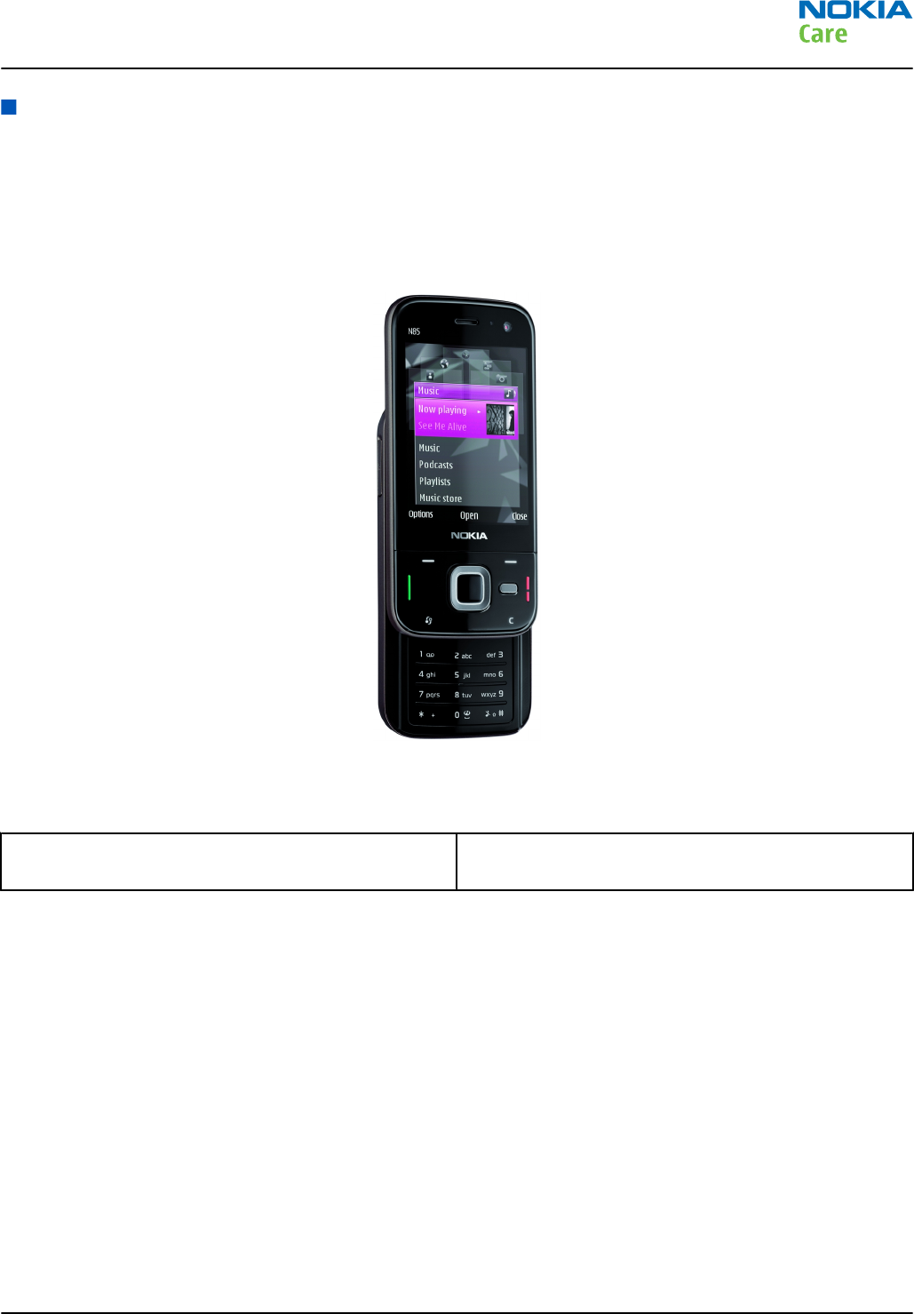
General Information
RM-335 Product data
RM-335 is a 2G variant of the Nokia N85. The key product data differences between the RM-335 (2G) and
RM-333 (3G) are described below.
RM-335 is a GSM handportable phone, supporting GSM/ GPRS/ EGPRS 850/900/1800/1900. RM-335 does not
support WCDMA or WLAN.
Figure 89 View of RM-335
Connectivity
Operating bands EGSM900/GSM850/1800/1900 MHz (no WCDMA/
HSDPA)
Sales package
•Transceiver RM-335
•Nokia Battery (BL-5K)
•Nokia Charger (AC-10)
•Nokia Music Headset (HS-45/AD-54)
•Nokia Connectivity Cable (CA-101) (micro USB)
•CD-ROM
•User Guide
•Sales carton
•Warranty card
RM-333; RM-334; RM-335
Service information differences between RM-335 and
RM-333
Issue 2 COMPANY CONFIDENTIAL Page 9 –5
Copyright © 2008 Nokia. All rights reserved.
Main RF characteristics for GSM850/900/1800/1900 (quadband) and EDGE phones
Table 14 Main RF characteristics
Parameter Unit
Cellular system GSM850, EGSM900, GSM1800/1900 and EDGE
Rx frequency band GSM850: 869 - 894 MHz
EGSM900: 925 - 960 MHz
GSM1800: 1805 - 1880 MHz
GSM1900: 1930 - 1990 MHz
Tx frequency band GSM850: 824 - 849 MHz
EGSM900: 880 - 915 MHz
GSM1800: 1710 - 1785 MHz
GSM1900: 1850 - 1910 MHz
Output power GSM850: +5 … +33dBm/3.2mW … 2W
GSM900: +5 … +33dBm/3.2mW … 2W
GSM1800: +0 … +30dBm/1.0mW … 1W
GSM1900: +0 … +30dBm/1.0mW … 1W
EDGE output power EDGE850: +5 … +27dBm/3.2mW … 500mW
EDGE900: +5 … +27dBm/3.2mW … 500mW
EDGE1800: +0 … +26dBm/1.0mW … 400mW
EDGE1900:+0 … +26dBm/1.0mW … 400mW
Number of RF channels GSM850: 124
GSM900: 194
GSM1800: 374
GSM1900: 299
Channel spacing 200 kHz
Number of Tx power levels GSM850: 15
GSM900: 15
GSM1800: 16
GSM1900: 16
Number of EDGE Tx power levels GSM850 EDGE: 12
GSM900 EDGE: 12
GSM1800 EDGE: 14
GSM1900 EDGE: 14
RM-333; RM-334; RM-335
Service information differences between RM-335 and
RM-333
Page 9 –6 COMPANY CONFIDENTIAL Issue 2
Copyright © 2008 Nokia. All rights reserved.
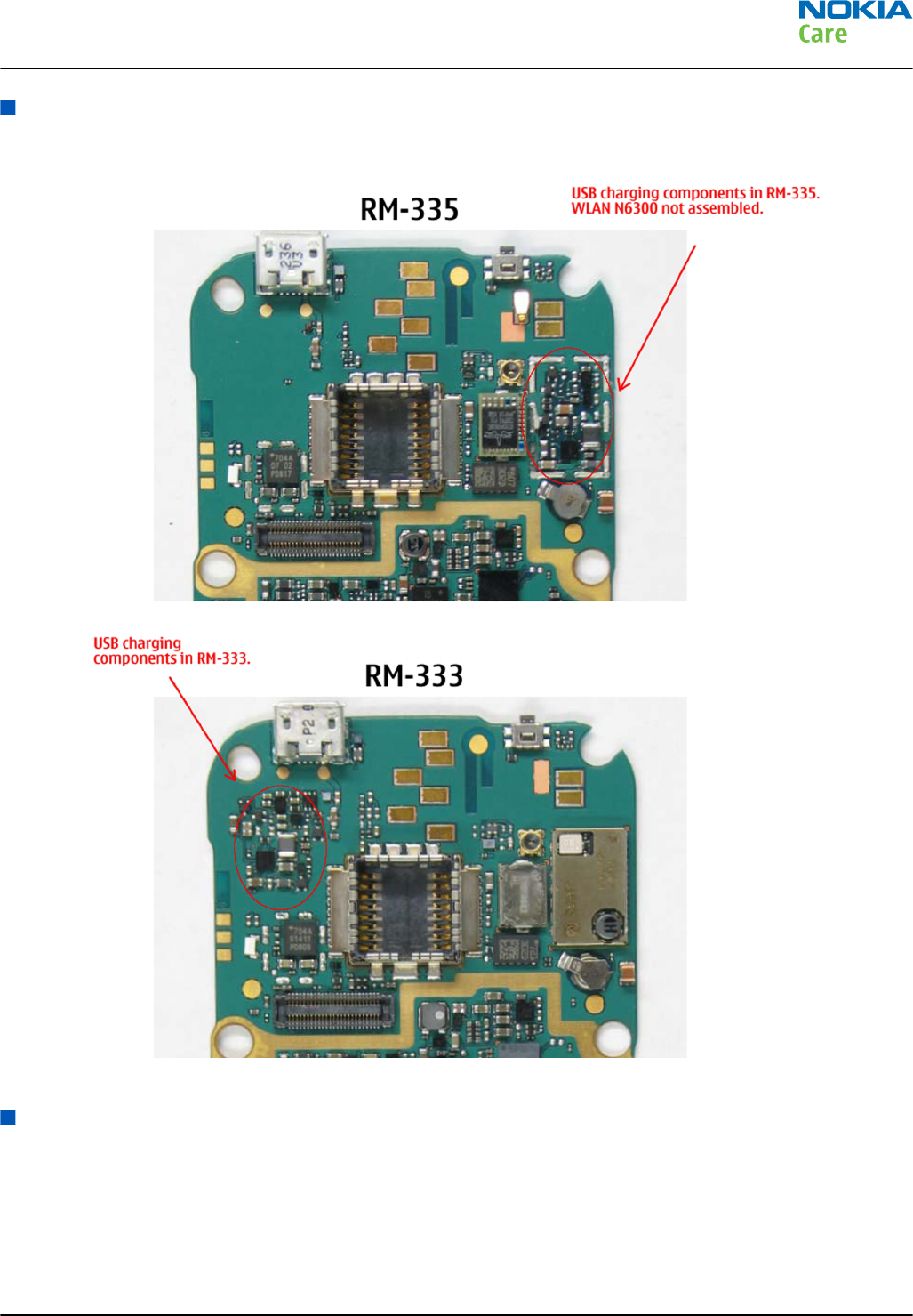
BB Troubleshooting
BB HW differences between RM-335 and RM-333
Figure 90 USB charging components in RM-335 and RM-333
RF Troubleshooting
RM-335 RF block
As RM-335 is a 2G variant of the RM-333/334, there are no WCDMA RF components in the RF block of the
RM-335. For example, the following WCDMA RF components are not assembled in RM-335:
•N7540 WCDMA PA
•Z7541 WCDMA duplex filter high band 1
RM-333; RM-334; RM-335
Service information differences between RM-335 and
RM-333
Issue 2 COMPANY CONFIDENTIAL Page 9 –7
Copyright © 2008 Nokia. All rights reserved.
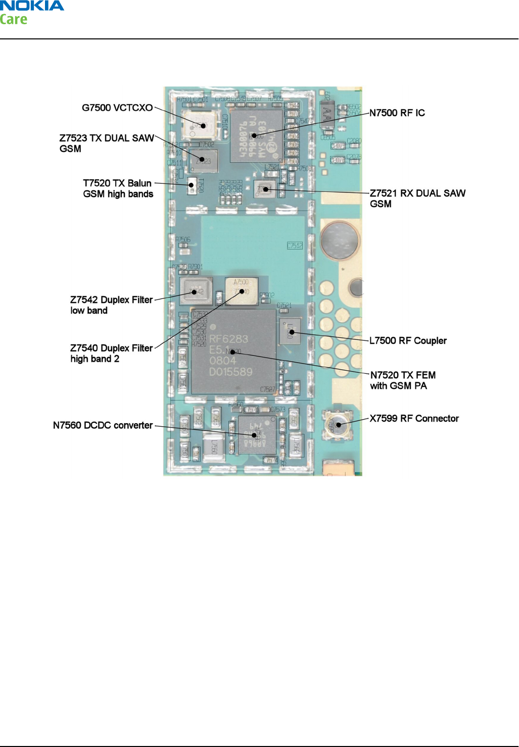
•Z7543 WCDMA TX dual SAW filter high bands
•Z7544 WCDMA TX SAW filter low bands
Figure 91 RM-335 RF key components
Note: The attenuation values for the SA-154 RF coupler as well as the TX power level tuning targets
are the same for the GSM bands in both RM-335 and RM-333.
RM-333; RM-334; RM-335
Service information differences between RM-335 and
RM-333
Page 9 –8 COMPANY CONFIDENTIAL Issue 2
Copyright © 2008 Nokia. All rights reserved.
Figure 92 RM-335 RF block diagram
RM-333; RM-334; RM-335
Service information differences between RM-335 and
RM-333
Issue 2 COMPANY CONFIDENTIAL Page 9 –9
Copyright © 2008 Nokia. All rights reserved.

RM-333; RM-334; RM-335
Service information differences between RM-335 and
RM-333
(This page left intentionally blank.)
Page 9 –10 COMPANY CONFIDENTIAL Issue 2
Copyright © 2008 Nokia. All rights reserved.

Glossary
Nokia Customer Care
Issue 2 COMPANY CONFIDENTIAL Page Glossary–1
Copyright © 2008 Nokia. All rights reserved.

RM-333; RM-334; RM-335
Glossary
(This page left intentionally blank.)
Page Glossary–2 COMPANY CONFIDENTIAL Issue 2
Copyright © 2008 Nokia. All rights reserved.

A/D-converter Analogue-to-digital converter
ACI Accessory Control Interface
ADC Analogue-to-digital converter
ADSP Application DPS (expected to run high level tasks)
AGC Automatic gain control (maintains volume)
ALS Ambient light sensor
AMSL After Market Service Leader
ARM Advanced RISC Machines
ARPU Average revenue per user (per month or per year)
ASIC Application Specific Integrated Circuit
ASIP Application Specific Interface Protector
B2B Board to board, connector between PWB and UI board
BA Board Assembly
BB Baseband
BC02 Bluetooth module made by CSR
BIQUAD Bi-quadratic (type of filter function)
BSI Battery Size Indicator
BT Bluetooth
CBus MCU controlled serial bus connected to UPP_WD2, UEME and Zocus
CCP Compact Camera Port
CDMA Code division multiple access
CDSP Cellular DSP (expected to run at low levels)
CLDC Connected limited device configuration
CMOS Complimentary metal-oxide semiconductor circuit (low power consumption)
COF Chip on Foil
COG Chip on Glass
CPU Central Processing Unit
CSD Circuit-switched data
CSR Cambridge silicon radio
CSTN Colour Super Twisted Nematic
CTSI Clock Timing Sleep and interrupt block of Tiku
CW Continuous wave
D/A-converter Digital-to-analogue converter
DAC Digital-to-analogue converter
DBI Digital Battery Interface
DBus DSP controlled serial bus connected between UPP_WD2 and Helgo
RM-333; RM-334; RM-335
Glossary
Issue 2 COMPANY CONFIDENTIAL Page Glossary–3
Copyright © 2008 Nokia. All rights reserved.

DCT-4 Digital Core Technology
DMA Direct memory access
DP Data Package
DPLL Digital Phase Locked Loop
DSP Digital Signal Processor
DTM Dual Transfer Mode
DtoS Differential to Single ended
EDGE Enhanced data rates for global/GSM evolution
EGSM Extended GSM
EM Energy management
EMC Electromagnetic compatibility
EMI Electromagnetic interference
ESD Electrostatic discharge
FCI Functional cover interface
FPS Flash Programming Tool
FR Full rate
FSTN Film compensated super twisted nematic
GMSK Gaussian Minimum Shift Keying
GND Ground, conductive mass
GPIB General-purpose interface bus
GPRS General Packet Radio Service
GSM Group Special Mobile/Global System for Mobile communication
HSDPA High-speed downlink packet access
HF Hands free
HFCM Handsfree Common
HS Handset
HSCSD High speed circuit switched data (data transmission connection faster than GSM)
HW Hardware
I/O Input/Output
IBAT Battery current
IC Integrated circuit
ICHAR Charger current
IF Interface
IHF Integrated hands free
IMEI International Mobile Equipment Identity
IR Infrared
RM-333; RM-334; RM-335
Glossary
Page Glossary–4 COMPANY CONFIDENTIAL Issue 2
Copyright © 2008 Nokia. All rights reserved.

IrDA Infrared Data Association
ISA Intelligent software architecture
JPEG/JPG Joint Photographic Experts Group
LCD Liquid Crystal Display
LDO Low Drop Out
LED Light-emitting diode
LPRF Low Power Radio Frequency
MCU Micro Controller Unit (microprocessor)
MCU Multiport control unit
MIC, mic Microphone
MIDP Mobile Information Device Profile
MIN Mobile identification number
MIPS Million instructions per second
MMC Multimedia card
MMS Multimedia messaging service
MTP Multipoint-to-point connection
NFC Near field communication
NTC Negative temperature coefficient, temperature sensitive resistor used as a
temperature sensor
OMA Object management architecture
OMAP Operations, maintenance, and administration part
Opamp Operational Amplifier
PA Power amplifier
PDA Pocket Data Application
PDA Personal digital assistant
PDRAM Program/Data RAM (on chip in Tiku)
Phoenix Software tool of DCT4.x and BB5
PIM Personal Information Management
PLL Phase locked loop
PM (Phone) Permanent memory
PUP General Purpose IO (PIO), USARTS and Pulse Width Modulators
PURX Power-up reset
PWB Printed Wiring Board
PWM Pulse width modulation
RC-filter Resistance-Capacitance filter
RF Radio Frequency
RM-333; RM-334; RM-335
Glossary
Issue 2 COMPANY CONFIDENTIAL Page Glossary–5
Copyright © 2008 Nokia. All rights reserved.

RF PopPort™ Reduced function PopPort™ interface
RFBUS Serial control Bus For RF
RSK Right Soft Key
RS-MMC Reduced size Multimedia Card
RSS Web content Syndication Format
RSSI Receiving signal strength indicator
RST Reset Switch
RTC Real Time Clock (provides date and time)
RX Radio Receiver
SARAM Single Access RAM
SAW filter Surface Acoustic Wave filter
SDRAM Synchronous Dynamic Random Access Memory
SID Security ID
SIM Subscriber Identity Module
SMPS Switched Mode Power Supply
SNR Signal-to-noise ratio
SPR Standard Product requirements
SRAM Static random access memory
STI Serial Trace Interface
SW Software
SWIM Subscriber/Wallet Identification Module
TCP/IP Transmission control protocol/Internet protocol
TCXO Temperature controlled Oscillator
Tiku Finnish for Chip, Successor of the UPP
TX Radio Transmitter
UART Universal asynchronous receiver/transmitter
UEME Universal Energy Management chip (Enhanced version)
UEMEK See UEME
UI User Interface
UPnP Universal Plug and Play
UPP Universal Phone Processor
UPP_WD2 Communicator version of DCT4 system ASIC
USB Universal Serial Bus
VBAT Battery voltage
VCHAR Charger voltage
VCO Voltage controlled oscillator
RM-333; RM-334; RM-335
Glossary
Page Glossary–6 COMPANY CONFIDENTIAL Issue 2
Copyright © 2008 Nokia. All rights reserved.
VCTCXO Voltage Controlled Temperature Compensated Crystal Oscillator
VCXO Voltage Controlled Crystal Oscillator
VF View Finder
Vp-p Peak-to-peak voltage
VSIM SIM voltage
WAP Wireless application protocol
WCDMA Wideband code division multiple access
WD Watchdog
WLAN Wireless local area network
XHTML Extensible hypertext markup language
Zocus Current sensor (used to monitor the current flow to and from the battery)
RM-333; RM-334; RM-335
Glossary
Issue 2 COMPANY CONFIDENTIAL Page Glossary–7
Copyright © 2008 Nokia. All rights reserved.

RM-333; RM-334; RM-335
Glossary
(This page left intentionally blank.)
Page Glossary–8 COMPANY CONFIDENTIAL Issue 2
Copyright © 2008 Nokia. All rights reserved.
