NTMFS4835N Datasheet. Www.s Manuals.com. R7 On
User Manual: Marking of electronic components, SMD Codes 48, 4800, 4800B, 4810, 4816, 4816B, 4835B, 4835N, 4870, 48N025S, 48T. Datasheets 1N4448X, BSC048N025S G, NTMFS4835NT1G, SD4870TR, Si4800, Si4800BDY, Si4800DY, Si4810DY, Si4816BDY, Si4816DY, Si4835BDY, TK71548AS.
Open the PDF directly: View PDF ![]() .
.
Page Count: 8
© Semiconductor Components Industries, LLC, 2012
May, 2012 − Rev. 7
1Publication Order Number:
NTMFS4835N/D
NTMFS4835N
Power MOSFET
30 V, 104 A, Single N−Channel, SO−8FL
Features
•Low RDS(on) to Minimize Conduction Losses
•Low Capacitance to Minimize Driver Losses
•Optimized Gate Charge to Minimize Switching Losses
•These are Pb−Free Devices
Applications
•Refer to Application Note AND8195/D
•CPU Power Delivery
•DC−DC Converters
•Low Side Switching
MAXIMUM RATINGS (TJ = 25°C unless otherwise stated)
Parameter Symbol Value Unit
Drain−to−Source Voltage VDSS 30 V
Gate−to−Source Voltage VGS ±20 V
Continuous Drain
Current RqJA
(Note 1)
Steady
State
TA = 25°CID20 A
TA = 85°C 14
Power Dissipation
RqJA (Note 1)
TA = 25°C PD2.27 W
Continuous Drain
Current RqJA
(Note 2)
TA = 25°CID12 A
TA = 85°C 9.0
Power Dissipation
RqJA (Note 2)
TA = 25°C PD0.89 W
Continuous Drain
Current RqJC
(Note 1)
TC = 25°CID104 A
TC = 85°C 75
Power Dissipation
RqJC (Note 1)
TC = 25°C PD62.5 W
Pulsed Drain
Current
TA = 25°C,
tp = 10 ms
IDM 208 A
Operating Junction and Storage
Temperature
TJ,
TSTG
−55 to
+150
°C
Source Current (Body Diode) IS52 A
Drain to Source DV/DT dV/dt6 V/ns
Single Pulse Drain−to−Source Avalanche
Energy TJ = 25°C, VDD = 50 V, VGS = 10 V,
IL = 28 Apk, L = 1.0 mH, RG = 25 W
EAS 392 mJ
Lead Temperature for Soldering Purposes
(1/8″ from case for 10 s)
TL260 °C
Stresses exceeding Maximum Ratings may damage the device. Maximum
Ratings are stress ratings only. Functional operation above the Recommended
Operating Conditions is not implied. Extended exposure to stresses above the
Recommended Operating Conditions may affect device reliability.
1. Surface−mounted on FR4 board using 1 sq−in pad, 1 oz Cu.
2. Surface−mounted on FR4 board using the minimum recommended pad size.
SO−8 FLAT LEAD
CASE 488AA
STYLE 1
MARKING
DIAGRAM
http://onsemi.com
A = Assembly Location
Y = Year
W = Work Week
ZZ = Lot Traceability
4835N
AYWZZ
1
V(BR)DSS RDS(ON) MAX ID MAX
30 V
3.5 mW @ 10 V
104 A
5.0 mW @ 4.5 V
G (4)
S (1,2,3)
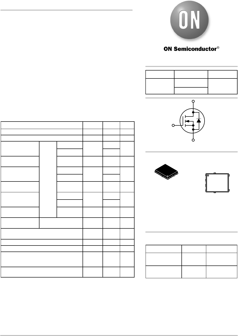
N−CHANNEL MOSFET
D (5,6)
Device Package Shipping†
ORDERING INFORMATION
NTMFS4835NT1G SO−8FL
(Pb−Free)
1500 /
Tape & Reel
NTMFS4835NT3G SO−8FL
(Pb−Free)
5000 /
Tape & Reel
†For information on tape and reel specifications,
including part orientation and tape sizes, please
refer to our Tape and Reel Packaging Specifications
Brochure, BRD8011/D.
S
S
S
G
D
D
D
D
NTMFS4835N
http://onsemi.com
2
THERMAL RESISTANCE MAXIMUM RATINGS
Parameter Symbol Value Unit
Junction−to−Case (Drain) RqJC 2.0
°C/W
Junction−to−Ambient – Steady State (Note 3) RqJA 55.1
Junction−to−Ambient – Steady State (Note ) RqJA 140.1
3. Surface−mounted on FR4 board using 1 sq−in pad, 1 oz Cu.
4. Surface−mounted on FR4 board using the minimum recommended pad size.
ELECTRICAL CHARACTERISTICS (TJ = 25°C unless otherwise specified)
Parameter Symbol Test Condition Min Typ Max Unit
OFF CHARACTERISTICS
Drain−to−Source Breakdown Voltage V(BR)DSS VGS = 0 V, ID = 250 mA30 V
Drain−to−Source Breakdown Voltage
Temperature Coefficient
V(BR)DSS/
TJ
22.4 mV/°C
Zero Gate Voltage Drain Current IDSS VGS = 0 V,
VDS = 24 V
TJ = 25 °C 1.0
mA
TJ = 125°C 10
Gate−to−Source Leakage Current IGSS VDS = 0 V, VGS = ±20 V ±100 nA
ON CHARACTERISTICS (Note 5)
Gate Threshold Voltage VGS(TH) VGS = VDS, ID = 250 mA1.5 1.9 2.5 V
Negative Threshold Temperature Coefficient VGS(TH)/TJ5.3 mV/°C
Drain−to−Source On Resistance RDS(on) VGS = 10 V to
11.5 V
ID = 30 A 2.9 3.5
mW
ID = 15 A 2.5
VGS = 4.5 V ID = 30 A 4.3 5.0
ID = 15 A 3.9
Forward Transconductance gFS VDS = 15 V, ID = 15 A 21 S
CHARGES, CAPACITANCES & GATE RESISTANCE
Input Capacitance CISS
VGS = 0 V, f = 1 MHz, VDS = 12 V
3100
pF
Output Capacitance COSS 670
Reverse Transfer Capacitance CRSS 360
Total Gate Charge QG(TOT)
VGS = 4.5 V, VDS = 15 V; ID = 30 A
22 39
nC
Threshold Gate Charge QG(TH) 4.7
Gate−to−Source Charge QGS 8.3
Gate−to−Drain Charge QGD 8.8
Total Gate Charge QG(TOT) VGS = 11.5 V, VDS = 15 V;
ID = 30 A
52 nC
SWITCHING CHARACTERISTICS (Note 6)
Turn−On Delay Time td(ON)
VGS = 4.5 V, VDS = 15 V, ID = 15 A,
RG = 3.0 W
16
ns
Rise Time tr31
Turn−Off Delay Time td(OFF) 22
Fall Time tf13
Turn−On Delay Time td(ON)
VGS = 11.5 V, VDS = 15 V,
ID = 15 A, RG = 3.0 W
10
ns
Rise Time tr23
Turn−Off Delay Time td(OFF) 30
Fall Time tf10
5. Pulse Test: pulse width v 300 ms, duty cycle v 2%.
6. Switching characteristics are independent of operating junction temperatures.

NTMFS4835N
http://onsemi.com
3
ELECTRICAL CHARACTERISTICS (TJ = 25°C unless otherwise specified)
Parameter UnitMaxTypMinTest ConditionSymbol
DRAIN−SOURCE DIODE CHARACTERISTICS
Forward Diode Voltage VSD VGS = 0 V,
IS = 30 A
TJ = 25°C 0.77 1.0
V
TJ = 125°C 0.70
Reverse Recovery Time tRR
VGS = 0 V, dIS/dt = 100 A/ms,
IS = 30 A
27 50
ns
Charge Time ta15
Discharge Time tb12
Reverse Recovery Charge QRR 18 nC
PACKAGE PARASITIC VALUES
Source Inductance LS
TA = 25°C
0.65 nH
Drain Inductance LD0.005 nH
Gate Inductance LG1.84 nH
Gate Resistance RG1.3 5.0 W
5. Pulse Test: pulse width v 300 ms, duty cycle v 2%.
6. Switching characteristics are independent of operating junction temperatures.
NTMFS4835N
http://onsemi.com
4
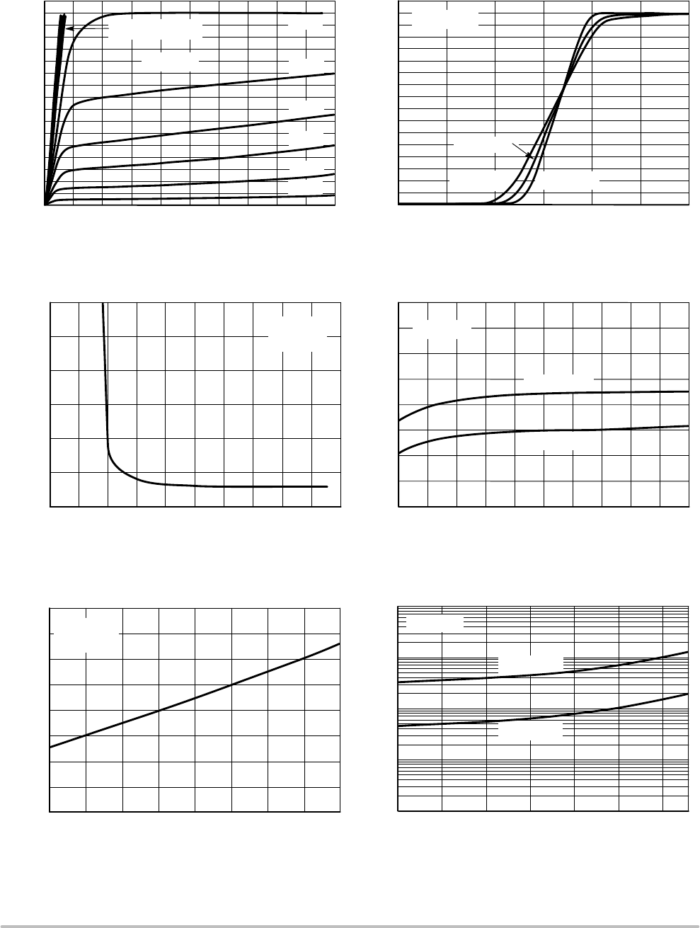
TYPICAL PERFORMANCE CURVES
2.8 V
2.6 V
60
0.003
0
35
2.0
1.0
0
1,000
100,000
021
VDS, DRAIN−TO−SOURCE VOLTAGE (VOLTS)
ID, DRAIN CURRENT (AMPS)
0
VGS, GATE−TO−SOURCE VOLTAGE (VOLTS)
Figure 1. On−Region Characteristics Figure 2. Transfer Characteristics
ID, DRAIN CURRENT (AMPS)
2
0.015
0
4
Figure 3. On−Resistance vs. Gate−to−Source
Voltage
VGS, GATE−TO−SOURCE VOLTAGE (VOLTS)
Figure 4. On−Resistance vs. Drain Current and
Gate Voltage
ID, DRAIN CURRENT (AMPS)
RDS(on), DRAIN−TO−SOURCE RESISTANCE (W)
RDS(on), DRAIN−TO−SOURCE RESISTANCE (W)
Figure 5. On−Resistance Variation with
Temperature
TJ, JUNCTION TEMPERATURE (°C)
Figure 6. Drain−to−Source Leakage Current
vs. Voltage
VDS, DRAIN−TO−SOURCE VOLTAGE (VOLTS)
RDS(on), DRAIN−TO−SOURCE RESISTANCE
(NORMALIZED)
IDSS, LEAKAGE (nA)
−50 250−25 50 75
23
1612 304
3
VDS ≥ 10 V
TJ = 25°C
TJ = −55°CTJ = 125°C
VGS = 4.5 V
125
VGS = 0 V
ID = 30 A
VGS = 10 V
TJ = 150°C
30
0
46
TJ = 25°C
20
VGS = 5.0 to 10 V
100
40
615
0.001
20
3.0 V
3.2 V
3.5 V
30
10
170
10
170
ID = 30 A
TJ = 25°C
8
VGS = 11.5 V
100
TJ = 25°C
0.002
10
5
50
1
10 12
0.004
24
50
70
90
110
130
70
130
0.005
0.010
0.020
40 5045
1.5
0.5
TJ = 125°C
150
0.030
90
110
10,000
8
768910
150 4.0 V
5
150
0.025 0.007
0.005
0.006
0.008
25 30 55
10
28
NTMFS4835N
http://onsemi.com
5
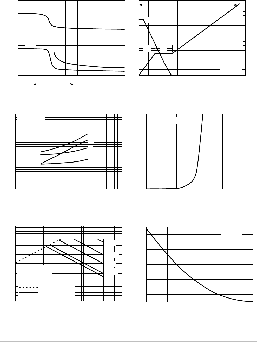
TYPICAL PERFORMANCE CURVES
tr
td(off)
td(on)
tf
VGS
15 0 10 15
GATE−TO−SOURCE OR DRAIN−TO−SOURCE VOLTAGE (VOLTS)
C, CAPACITANCE (pF)
Figure 7. Capacitance Variation
3500
0
VGS VDS
55
TJ = 25°C
Ciss
Coss
Crss
Ciss
Figure 8. Gate−To−Source and Drain−To−Source
Voltage vs. Total Charge
0
4
0
QG, TOTAL GATE CHARGE (nC)
2
8
30
ID = 30 A
TJ = 25°C
QT
35
0
VSD, SOURCE−TO−DRAIN VOLTAGE (VOLTS)
IS, SOURCE CURRENT (AMPS)
Figure 9. Resistive Switching Time
Variation vs. Gate Resistance
RG, GATE RESISTANCE (W)
1 10 100
1000
t, TIME (ns)
VGS = 0 V
Figure 10. Diode Forward Voltage vs. Current
100
0.5 0.6
5
10
15
1
VDS = 15 V
ID = 15 A
VGS = 11.5 V
0.7 0.8
20
30
25
TJ = 25°C
Figure 11. Maximum Rated Forward Biased
Safe Operating Area
0.1 1 100
VDS, DRAIN−TO−SOURCE VOLTAGE (VOLTS)
1000
ID, DRAIN CURRENT (AMPS)
RDS(on) LIMIT
THERMAL LIMIT
PACKAGE LIMIT
10
10
VGS = 20 V
SINGLE PULSE
TC = 25°C
1 ms
100 ms
10 ms
dc
10 ms
20
1
100
0
25
TJ, STARTING JUNCTION TEMPERATURE (°C)
ID = 28 A
Figure 12. Maximum Avalanche Energy vs.
Starting Junction Temperature
50 75
120
100 125
200
400
EAS, SINGLE PULSE DRAIN−TO−SOURCE
AVALANCHE ENERGY (mJ)
150
500
40
30
5000
3000
2500
1500
1000
0.4 1.1
VGS, GATE−TO−SOURCE VOLTAGE (VOLTS)
6
2010 25 504540
Qgs
320
360
12
55
4500
10
Qgd
0.1
80
160
240
280
10 25
2000
4000
155
20
18
16
14
12
10
8
6
4
2
0
VDS, DRAIN−TO−SOURCE VOLTAGE (VOLTS)
VDS
10
0.9 1.0

NTMFS4835N
http://onsemi.com
6
TYPICAL PERFORMANCE CURVES
125°C
100°C
25°C
Figure 13. Avalanche Characteristics
100001 100
PULSE WIDTH (ms)
ID, DRAIN CURRENT (AMPS)
10
10
1
1000
100
1000
NTMFS4835N
http://onsemi.com
7
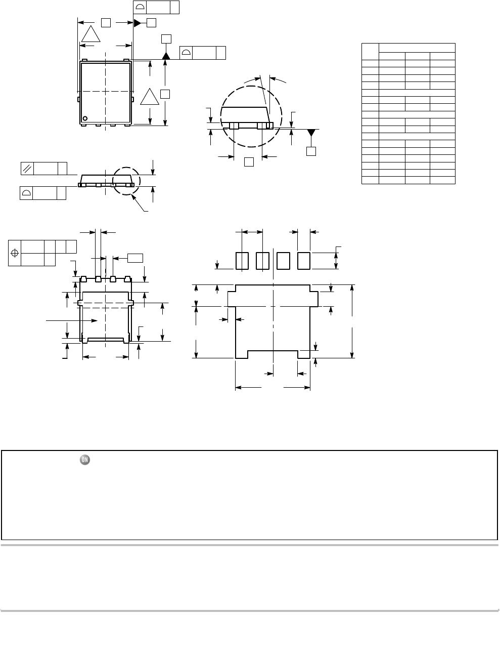
PACKAGE DIMENSIONS
M3.00 3.40
q0 −−−
_
3.80
12
_
DFN5 5x6, 1.27P
(SO−8FL)
CASE 488AA
ISSUE G
NOTES:
1. DIMENSIONING AND TOLERANCING PER
ASME Y14.5M, 1994.
2. CONTROLLING DIMENSION: MILLIMETER.
3. DIMENSION D1 AND E1 DO NOT INCLUDE
MOLD FLASH PROTRUSIONS OR GATE
BURRS.
1234
TOP VIEW
SIDE VIEW
BOTTOM VIEW
D1
E1 q
D
E
2
2
B
A
0.20 C
0.20 C
2 X
2 X
DIM MIN NOM
MILLIMETERS
A0.90 1.00
A1 0.00 −−−
b0.33 0.41
c0.23 0.28
D5.15 BSC
D1 4.50 4.90
D2 3.50 −−−
E6.15 BSC
E1 5.50 5.80
E2 3.45 −−−
e1.27 BSC
G0.51 0.61
K1.20 1.35
L0.51 0.61
L1 0.05 0.17
A
0.10 C
0.10 C
DETAIL A
14
L1
e/2
8X
D2
G
E2
K
b
A0.10 BC
0.05 cL
DETAIL A
A1
e
3 X
c
4 X
C
SEATING
PLANE
MAX
1.10
0.05
0.51
0.33
5.10
4.22
6.10
4.30
0.71
1.50
0.71
0.20
STYLE 1:
PIN 1. SOURCE
2. SOURCE
3. SOURCE
4. GATE
5. DRAIN
M
*For additional information on our Pb−Free strategy and soldering
details, please download the ON Semiconductor Soldering and
Mounting Techniques Reference Manual, SOLDERRM/D.
SOLDERING FOOTPRINT*
1.270
2X
0.750
1.000
0.905
0.475
4.530
1.530
4.560
0.495
3.200
1.330
0.965
2X
2X
3X 4X
4X
PIN 5
(EXPOSED PAD)
ON Semiconductor and are registered trademarks of Semiconductor Components Industries, LLC (SCILLC). SCILLC reserves the right to make changes without further notice
to any products herein. SCILLC makes no warranty, representation or guarantee regarding the suitability of its products for any particular purpose, nor does SCILLC assume any liability
arising out of the application or use of any product or circuit, and specifically disclaims any and all liability, including without limitation special, consequential or incidental damages.
“Typical” parameters which may be provided in SCILLC data sheets and/or specifications can and do vary in different applications and actual performance may vary over time. All
operating parameters, including “Typicals” must be validated for each customer application by customer’s technical experts. SCILLC does not convey any license under its patent rights
nor the rights of others. SCILLC products are not designed, intended, or authorized for use as components in systems intended for surgical implant into the body, or other applications
intended to support or sustain life, or for any other application in which the failure of the SCILLC product could create a situation where personal injury or death may occur. Should
Buyer purchase or use SCILLC products for any such unintended or unauthorized application, Buyer shall indemnify and hold SCILLC and its officers, employees, subsidiaries, affiliates,
and distributors harmless against all claims, costs, damages, and expenses, and reasonable attorney fees arising out of, directly or indirectly, any claim of personal injury or death
associated with such unintended or unauthorized use, even if such claim alleges that SCILLC was negligent regarding the design or manufacture of the part. SCILLC is an Equal
Opportunity/Affirmative Action Employer. This literature is subject to all applicable copyright laws and is not for resale in any manner.
PUBLICATION ORDERING INFORMATION
N. American Technical Support: 800−282−9855 Toll Free
USA/Canada
Europe, Middle East and Africa Technical Support:
Phone: 421 33 790 2910
Japan Customer Focus Center
Phone: 81−3−5817−1050
NTMFS4835N/D
LITERATURE FULFILLMENT:
Literature Distribution Center for ON Semiconductor
P.O. Box 5163, Denver, Colorado 80217 USA
Phone: 303−675−2175 or 800−344−3860 Toll Free USA/Canada
Fax: 303−675−2176 or 800−344−3867 Toll Free USA/Canada
Email: orderlit@onsemi.com
ON Semiconductor Website: www.onsemi.com
Order Literature: http://www.onsemi.com/orderlit
For additional information, please contact your local
Sales Representative