PVS 50 P 33(LP) HA Old 02 143
User Manual: PVS 50 P-33(LP) HA
Open the PDF directly: View PDF ![]() .
.
Page Count: 52
SILICON PHOTONICS
Intel and UCSB
team comes up
with hybrid laser
Switchable lotus
effect creates self-
cleaning surfaces
SURFACE TREATMENT
IN-SITU METHOD
ENSURES PRECISE
OPTICAL LAYERS
OPTICAL MONITORING
BEAM SHAPING
DOEs offer big
benefits thanks to
unique properties
October 2006 Issue 143 The European magazine for photonics professionals optics.org
OLEOct06COVERp01 25/9/06 14:28 Page 1

4AKING,IGHT
&URTHER
"REAULT
2ESEARCH
64" ]$BOBEB
8PSMEXJEF
#SFBVMUDPN
ASAP
"4"10QUJDBM4PGUXBSF
*OUSPEVDJOHUIFOFYUHFOFSBUJPO
PGPQUJDBMFOHJOFFSJOHTPGUXBSF
5IFXPSMETNPTUBDDVSBUF
PQUJDBMTPGUXBSFGPSUVSOJOH
ZPVSDSFBUJWFWJTJPOTJOUP
XPSLJOHQSPUPUZQFTJTOPX
NPSFBDDFTTJCMFUIBOFWFS
$IPPTFGSPNPVSOFXTVJUF
PG"4"1TPGUXBSFQBDLBHFT
UPNFFUZPVSNPEFMJOH
SFRVJSFNFOUT
"4"1MJUF
"4"1$"%
"4"1015*$"-
"4"1#*0
"4"1"%7"/$&%
"4"1$0.1-&5&
&OHJOFFSJOH4FSWJDFT
0QUJDBMFOHJOFFSJOHGPSBMM
JOEVTUSJFTBOEQSPKFDUUZQFT
GSPNDPODFQUJPOBOEBOBMZTJT
UPEFTJHOBOEQSPUPUZQJOH
0QUJDT5SBJOJOH
$MBTTFTUBVHIUCZTFOJPS
PQUJDBMFOHJOFFSTFOBCMFZPV
UPFöDJFOUMZBOEBDDVSBUFMZ
TPMWFZPVSPQUJDTQSPCMFNT

NEWS
5Business Intel and UCSB scientists claim hybrid silicon laser
revolution •Consortium wins funding to tackle LCD recycling
•Photonex focuses on interaction
9Editorial New technology galore
TECHNOLOGY
11 Applications Embedded LEDs light up clothing •Sommelier
robot helps choose wine •Laser-etched silicon delivers a response
in the near-infrared
16 R&D Doubled VECSEL emits light in the ultraviolet
•‘See-through’ silver boosts LEDs
17 Patents UK imaging firm AST receives US patent for its
infrared camera •Kodak signs up Tohoku of Japan as licensee of
OLED technology
FEATURES
19 Eye scan shows first sign of Alzheimer’s disease
Scanning the lens of a human eye with infrared laser light can
reveal the earliest signs of Alzheimer’s disease in a matter of
seconds, according to US start-up Neuroptix.
23 Lasers meet fluids: an integrated approach
An optical manipulation and analysis platform that can fit onto
a fingernail could significantly change the field of microfluidics.
26 ZnO-based LEDs begin to show full-colour
potential
Start-up MOXtronics has recently produced the first coloured
ZnO-based LEDs. Although the efficiency of these LEDs is not
high, the emitters have the potential to outperform GaN rivals.
29 In situ method drives up yields and reduces costs
There is a lot more to making an optical filter than meets the eye.
Dominik Goessi looks at the role of in situ monitoring in the
production process and reviews the technology.
33 Hybrid diffractive optics offer an elegant solution
Thanks to a set of unique properties, diffractive optical elements
have the potential to transform light into almost any desired
distribution. Joshika Akhil gives the low-down on the technology.
PRODUCTS
37 Oscilloscope•Chromatic confocal sensors •Colour CCD camera
REGULARS
50 People/Sudoku
EDITORIAL
Editor Jacqueline Hewett
Tel: +44 (0)117 930 1194
jacqueline.hewett@iop.org
News editor James Tyrrell
Tel: +44 (0)117 930 1256
james.tyrrell@iop.org
Science/technology reporter Darius Nikbin
Tel: +44 (0)117 930 1247
darius.nikbin@iop.org
Production editor Alison Gardiner
Technical illustrator Alison Tovey
EUROPE/ROW SALES
Group advertisement manager Adrian Chance
Tel: +44 (0)117 930 1193
adrian.chance@iop.org
Group advertisement manager Rob Fisher
Tel: +44 (0)117 930 1260
robert.fisher@iop.org
Deputy advertisement manager Cadi Jones
Tel: +44 (0) 117 930 1090
cadi.jones@iop.org
Senior sales executive Katrina Davis
Tel: +44 (0) 117 930 1284
katrina.davis@iop.org
US SALES
US sales executive Meghan Cavanaugh
IOP Publishing Inc, Suite 929, 150 South
Independence Mall West, Philadelphia PA 19106, USA
Tel: +1 215 627 0880. Fax: +1 215 627 0879
cavanaugh@ioppubusa.com
CHINA SALES
Ann Hou
Shenzhen Yongge Advertising Co Ltd, Rm 1106,
Xinwen Building, No. 2 Shennan Zhong Road,
Shenzhen, Guangdong, PRC
Tel: +86 755 82091822. Fax: +86 755 82090566
ann@indus-sources.com
ADVERTISING PRODUCTION
Advertising production coordinator Rachel Sermon
Tel: +44 (0)117 930 1277
rachel.sermon@iop.org
Advertising production editors Jo Derrick/Mark Trimnell
CIRCULATION AND MARKETING
Subscription and circulation manager Jenny Brown
Tel: +44 (0)117 930 1034
jenny.brown@iop.org
ART DIRECTOR
Andrew Giaquinto
PUBLISHER
Geraldine Pounsford
Tel: +44 (0)117 930 1022
geraldine.pounsford@iop.org
OPTICS & LASER EUROPE
Dirac House, Temple Back, Bristol BS1 6BE, UK
Tel: +44 (0)117 929 7481
Editorial fax: +44 (0)117 925 1942
Advertising fax: +44 (0)117 930 1178
Internet: optics.org/ole
ISSN 0966-9809 CODEN OL EEEV
SUBSCRIPTIONS
Complimentary copies are sent to qualifying
individuals. For readers outside registration
requirements: £116/7168 ($208 US and Canada)
per year. Single issue £11/715 ($19 US, Canada
and Mexico). CONTACT: IOPP Magazines, WDIS Ltd,
Units 12 & 13, Cranleigh Gardens Industrial Estate,
Southall, Middlesex UB1 2DB, UK.
Tel: +44 (0)20 8606 7518. Fax: +44 (0)20 8606 7303
© 2006 IOP Publishing Ltd. The contents of OLE do
not represent the views or policies of the Institute of
Physics, its council or its officers unless so identified.
Printed by Warners (Midlands) plc, The Maltings,
West Street, Bourne, Lincolnshire PE10 9PH, UK.
Issue 143 October 2006 Contents
IMEC installs ASML’s EUV
Alpha Demo Tool. p5
UK researchers’ doubled
VECSEL emits UV light. p16
Chip combines microfluidics
and integrated optics. p23
ZnO-based LEDs look set to
challenge GaN devices. p26
SILICON PHOTONICS
Intel and UCSB
team comes up
with hybrid laser
Switchable lotus
effect creates self-
cleaning surfaces
SURFACE TREATMENT
IN-SITU METHOD
ENSURES PRECISE
OPTICAL LAYERS
OPTICAL MONITORING
BEAM SHAPING
DOEs offer big
benefits thanks to
unique properties
October 2006 Issue 143 The European magazine for photonics professionals optics.org
For the latest news on optics and photonics don’t forget to visit optics.org
Cover (Evatec) Optical
monitoring systems give
manufacturers a high level
of process control. p29
OLEOct06CONTENTSp03 25/9/06 15:15 Page 3
Imagine. Together.
www.ELCAN.com/create
NORTH AMERICA • PRECISION OPTICS AND ELECTRONICS • EUROPE
ELCAN was there at the invention of 35mm photography and for over 150 years
has excelled at developing new optical technologies. ELCAN works with customers
seeking to revolutionize the science of medical imaging and photonic treatments.
From initial design and testing to cost-efficient high-volume production, ELCAN
is your complete optical and electronic manufacturing partner.
Delivering advanced medical products to market quickly takes an optics and elec-
tronics manufacturing partner of uncommon experience that knows how to deliv-
er dependable “no doubt” performance. Our unrivaled capabilities in designing
and building precision systems for digital radiography, endoscopic laser surgery,
ophthalmic examination and many other health science applications makes us
your partner of choice.
You have a vision. Let us show you the light.
OLEOctAdElcan4 29/8/06 10:33 Page 1
Intel and UCSB scientists claim
hybrid silicon laser revolution
NEWS
BUSINESS 5EDITORIAL 9
5
OLE • October 2006 • optics.org/ole
SILICON PHOTONICS
By Michael Hatcher
A huge increase in speed for high-
end computing applications could
be on the cards after a US team
announced that it had created the
world’s first electrically pumped
“hybrid” silicon laser. In making
the device, researchers at Intel and
the University of California Santa
Barbara (UCSB) claim to have
combined the light-emitting prop-
erties of indium phosphide (InP)
with the manufacturability of sili-
con for the first time.
“This could bring low-cost, ter-
abit-level optical ‘data pipes’ inside
future computers and help make
possible a new era of high-perfor-
mance computing applications,”
said Mario Paniccia, director of
Intel’s Photonics Technology Lab.
In the hybrid structure, InP mat-
erial generates and amplifies light
to create the laser, while the silicon
structure acts as a laser cavity and
is used to route and control the
emission. Light enters into the sili-
con through a physical effect
known as evanescent coupling.
The initial laser made by Intel emits
at 1.58 µm, although this wave-
length can be adjusted by modify-
ing the silicon waveguides used.
According to Intel, the key to
making the device is the use of a
low-temperature oxygen plasma.
This creates a thin oxide layer on
the surface of both materials.
When heated and pressed together,
this oxide layer acts like a glue and
fuses the two different materials
into a single chip. Intel claims that
unlike other methods that have
been tried, this eliminates any
problems due to lattice mismatch
between the two materials.
UCSB’s Jon Bowers says that
this bonding method can be used
at the die, partial-wafer and full-
wafer level, and could become a
solution for large-scale optical
integration on a silicon platform.
Intel’s chief technical officer
Justin Rattner says that if the latest
development can be scaled up for
mass production, it ought to solve
the cost issue with current photonic
chip manufacturing. Presently, the
cost of a laser chip for communica-
tions can be up to 100 times that of
a silicon chip.
Infinera, the Sunnyvale, CA, US,
company that has developed an
integrated approach for current
telecommunications applications,
says that Intel’s work is a “great
endorsement” of the photonic
integration concept.
However, it disagrees with Intel’s
conjecture that InP is an “exotic”
material that is inherently expen-
sive. Infinera believes that the cost
of manufacturing devices is dic-
tated more by the level of volume
production required.
Intel has previously claimed sili-
con photonics breakthroughs,
such as last year’s optically excited
Raman laser. However, this latest
research is the first to detail a chip
that can be powered electrically.
The company says that its vision is
to produce chips containing hun-
dreds of hybrid silicon lasers using
established high-volume, low-cost
manufacturing methods.
Michael Hatcher is editor of
Compound Semiconductor
(www.compoundsemiconductor.net).
IMEC of Leuven, Belgium, which is
Europe’s leading independent
nanoelectronics and nanotechnol-
ogy research institute, has taken
delivery of an extreme ultraviolet
(EUV) Alpha Demo Tool, developed
by Dutch firm ASML.
EUV is the most likely candidate
technology for the 32 nm half-
pitch node. Over the past two
years, IMEC and its partners have
been busy building up the photore-
sist know-how necessary for EUV
lithography, which can now be
exploited using the new tool.
“We are convinced that we will
be able to make EUV available for
production at the 32 nm half-pitch
node,” said Luc van den Hove, vice-
president of Silicon Process and
Device Technology at IMEC.
Along with more than 30 litho-
graphy programme partners,
including nine of the world’s lead-
ing IC manufacturers or foundries
– Infineon, Intel, Matsushita/
Panasonic, Micron, Philips Semi-
conductor, Samsung, STMicro-
electronics, Texas Instruments and
TSMC – IMEC leads the world’s
largest research and development
effort on lithography targeting the
(sub-)32 nm node.
IMEC installs full-field EUV system
LITHOGRAPHY
Hybrid laser: when a voltage is applied to the bonded chip, light generated from
InP-based material couples directly into a silicon waveguide. Intel hopes that the
device will drive a new era of high-performance computing applications.
ASML’s Alpha Demo Tool will be put
through its paces at IMEC.
ASML
Intel
OLEOct06NEWSp5-9 25/9/06 15:53 Page 5

Consortium wins funding
to tackle LCD recycling
NEWS
BUSINESS
DISPLAYS
6OLE • October 2006 • optics.org/ole
Scientists from the University of
York, UK, have won a competition,
organized by the UK government’s
Department of Trade and Industry
(DTI), to investigate ways of extract-
ing and recycling liquid crystals
from waste LCD devices.
Researchers estimate that the
value of recycled LCD material from
the UK alone could be as much as
$60 m (747.3 m) per year.
Some 40 million LCD television
sets were sold worldwide in 2005
with expected sales likely to exceed
100 million by 2009. However, the
chemicals they contain are poten-
tially hazardous, and technologi-
cal advances are so rapid that
society is already discarding mil-
lions of LCD screens each year.
The York team is part of a con-
sortium of nine partners and is
supported by both the Resource
Efficiency and the Displays and
Lighting Knowledge Transfer Net-
works. The DTI is funding 50% of
the total project development bid
worth £1.7 m (72.5 m).
LCD screens usually comprise
two glass sheets, with a thin film of
viscous liquid-crystal material
deposited between them. The mat-
erial is made up of a combination
of up to 20 different compounds,
typically polar organic compounds
that are often fluorinated. EU legis-
lation now prevents disposal of
electronic materials in landfill.
Incineration, the other disposal
route, has also been banned.
“We have developed a technology
that offers a clean, efficient way to
recover the mixture of liquid crys-
tals from waste LCDs,” said Avtar
Matharu, of York’s Department of
Chemistry. “Once recovered, the
liquid-crystal mixture will be recy-
cled into LCDs or separated into indi-
vidual components for resale.”
So-called active disassembly, is
an important feature of the project.
To aid recycling, liquid-crystal mat-
erial stuck between the glass layers
needs to be isolated easily. For
example, this could be achieved by
inserting intelligent polymers in
between display panels to pop them
apart for dismantling.
LASERS
nLight, US, a manufacturer of high-
power semiconductor lasers, has
acquired the assets of Flextronics
Photonics, a US subsidiary of
Singapore-based Flextronics
International. The acquisition adds
an array of new fibre-coupled and
hybrid microelectronics to nLight’s
existing range of products.
IMAGING
Infrared-camera developer Cedip
Infrared Systems, France, has
reported that its turnover for the
first half of 2006 totalled 77.7 m,
representing growth of 19% on the
same period last year. Exports
accounted for 86% of sales, with
strong growth in Asia–Pacific. The
firm has also announced the
signing of a new million-dollar
contract with the US Army.
LASERS
Sony has blamed delays in the
production of GaN-based laser
diodes as it put back the European
launch of its PLAYSTATION 3
console from autumn 2006 to
March 2007.
SPECTROSCOPY
PerkinElmer, a developer of
photonics and health science testing
systems, has acquired Avalon
Instruments, Belfast, UK. The
acquisition will add a range of bench-
top dispersive Raman spectrometers
to PerkinElmer’s portfolio.
For more business news from the
world of lasers, optics and
photonics, please visit
optics.org/optics/Business.do.
IN BRIEF
Fibre laser specialist IPG Photonics
is looking to float on the US stock
market to raise cash that will be
partly used to fund its diode manu-
facturing expansion. The firm has
filed a registration statement with
the US government’s Securities
and Exchange Commission (SEC)
for a proposed initial public offer-
ing (IPO) of its common stock.
Although the firm is yet to reveal
details of the anticipated timing
and value of the IPO, its S-1 regis-
tration statement with the SEC does
contain plenty of information.
IPG’s high-power, diodes are key
components in the company’s
fibre laser systems, which are used
in materials processing applica-
tions, and provide a much smaller,
more convenient alternative to tra-
ditional carbon dioxide and solid-
state lasers.
Currently with 900 employees
and 300 customers, IPG posted
sales of $64.9 m (750.6 m)and a
net profit of $6.1 m in the first half
of 2006. Its chief executive officer
and founder Valentin Gapontsev is
the majority shareholder, owning
62.6% of shares prior to the IPO.
Valentin’s son Denis Gapontsev
acts as vice-president of research
and development at the firm.
On its balance sheet, IPG lists
total assets worth $132 m, with
cash and cash equivalents
totalling $11.3 m and long-term
debt of $22.7 m.
IPG Photonics files
for public offering
FIBRE LASERS
LCD recycling know-how: (left to right)
Avtar Matharu and his colleague John
Goodby from the University of York’s
Department of Chemistry, UK.
University of York
OLEOct06NEWSp5-9 25/9/06 15:54 Page 6
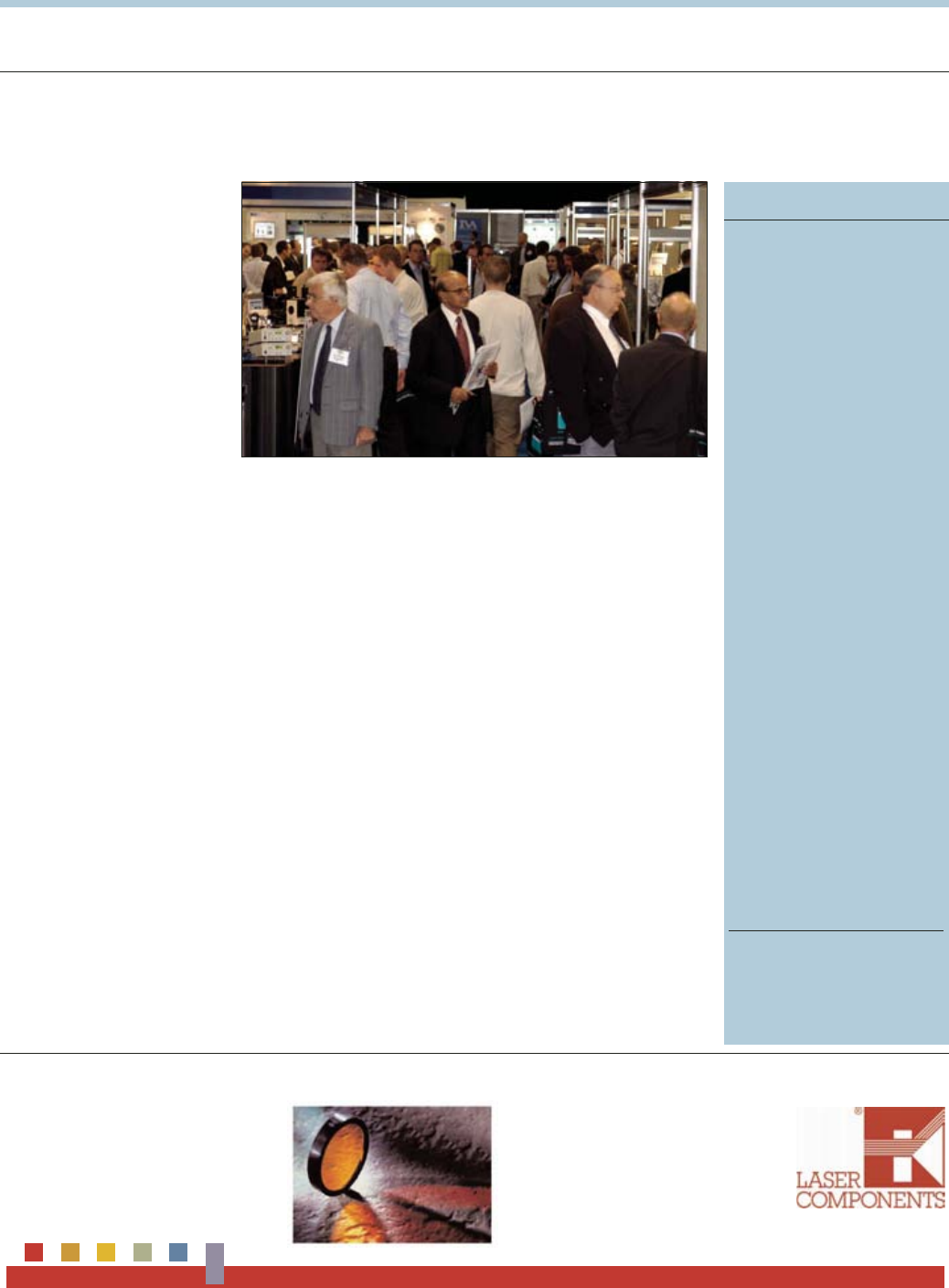
Photonex focuses on interaction
NEWS
BUSINESS
EXHIBITIONS
7
OLE • October 2006 • optics.org/ole
OPTICAL FILTERS
UV Filters, NBP
LWP, SWP, BP, Custom
Fluorescence
Colour Imaging
Raman Spectroscopy
Microscopy
www.lasercomponents.co.uk
The 15th annual Photonex exhibi-
tion returns to Stoneleigh Park
near Coventry in the UK on 18–19
October. With 125 exhibitors and
more than 1500 visitors expected,
a dedicated demonstration area
and packed programme of sup-
porting seminars, the event will
certainly offer something for every-
one with an interest in photonics.
“This year’s Photonex will be an
interactive and educational oppor-
tunity,” organizer Laurence Dev-
ereux told OLE. “It is only face to
face that you can truly have a
dynamic discussion, and by seeing
live demonstrations you can make
a real evaluation of the technol-
ogies available to you. We have
arranged to bring more technol-
ogies than ever to this year’s event.”
One of the new additions this
year is the “Wonder of Photonics”
demonstration area, which is being
managed by Photonics Cluster, UK.
According to Devereux, visitors
will be able to see how users in
areas such as healthcare, automo-
tive and aerospace are applying
photonics technologies.
“There will be 10 demonstrations
running throughout both days in a
separate area on the exhibition
floor,” said Devereux. “Photonics
Cluster has invited people to demon-
strate in areas such as laser scan-
ning, optical sensing, thermal
imaging and personal projection.
All attendees can visit this area free
of charge.” Companies demonstra-
ting their technologies include TRW
Conekt, Light Blue Optics, Faro,
Rofin Baasel and FLIR Systems.
In addition, visitors can expect to
see a range of demonstrations at
exhibitors’ booths. For example,
Pro-Lite Technology will be showing
off the ProMetric imaging sphere
developed by Radiant Imaging of
the US. Pro-Lite says that the prod-
uct is the only non-moving-part
goniophotometer on the market,
measuring the luminous intensity
distribution from an LED over 2 /sr
in a couple of seconds. Various spec-
troscopic techniques will also be on
show, such as fluorescence imaging
at LOT Oriel’s booth and single pho-
ton counting at Alrad’s stand.
According to Devereux, two
other opportunities that delegates
should take advantage of at Pho-
tonex are speaking to the newly
launched UK photonics knowledge
transfer network (KTN) and meet-
ing representatives of delegations
from Singapore and Switzerland.
“The KTN will have a stand at
Photonex and they are very keen
for people to come and talk and be
involved,” said Devereux. “The
Singapore delegation has expertise
in silicon photonics and wants to
build links with UK companies.”
Running alongside Photonex is a
comprehensive programme of sem-
inars, all of which are free to attend
(see box). Just one of the events on
offer is the one-day “Innovations in
Imaging” seminar, which has been
put together by SPIE Europe.
Delegates attending the seminar
will be treated to a mixture of speak-
ers working in diverse applications.
Richard Duddley from NPL, UK, for
example, will share his thoughts on
optical coherence tomography.
Nigel Allinson from the University of
Sheffield, UK, will discuss the future
imaging need in academia. Bill
Proud from the University of Cam-
bridge, UK, will present work on
high-speed photography of explo-
sives and ballistics. Finally, Grant
Hall from Wide Blue will round off
the day by offering advice on how to
commercialize imaging systems.
Wednesday only
GPhotonics in Medicine,
Healthcare and Life Sciences –
Making Light Work
Organized by Photonics Cluster,
UK, this one-day seminar will
feature a series of talks focusing
on biophotonics.
GInnovations in Imaging –
Analysis, Insights and Ideas for
Imaging Applications
This one-day event has been put
together by SPIE Europe and
looks at high-speed imaging in
industries such as medicine,
automotive and defence.
Wednesday and Thursday
GImaging for Science and
Industry
This one-day seminar, organized
by UKIVA, is free to attend,
although advance booking is
requested. Topics will range from
extracting 3D information from 2D
images to the use of infrared
images for machine vision.
Thursday only
GApplied Photonics in High-
technology Engineering
This one-day seminar is organized
by Photonics Cluster, UK.
For more information on all
aspects of Photonex, including
the series of seminars running
alongside the main event, please
see www.photonex.org.
Photonex events
Jam packed: the 2006 show features a demonstration area and a seminar programme.
OLEOct06NEWSp5-9 25/9/06 15:55 Page 7

4AKING,IGHT
&URTHER
"REAULT
2ESEARCH
64" ]$BOBEB
8PSMEXJEF
#SFBVMUDPN
ASAP
"4"10QUJDBM4PGUXBSF
*OUSPEVDJOHUIFOFYUHFOFSBUJPO
PGPQUJDBMFOHJOFFSJOHTPGUXBSF
5IFXPSMETNPTUBDDVSBUF
PQUJDBMTPGUXBSFGPSUVSOJOH
ZPVSDSFBUJWFWJTJPOTJOUP
XPSLJOHQSPUPUZQFTJTOPX
NPSFBDDFTTJCMFUIBOFWFS
$IPPTFGSPNPVSOFXTVJUF
PG"4"1TPGUXBSFQBDLBHFT
UPNFFUZPVSNPEFMJOH
SFRVJSFNFOUT
"4"1MJUF
"4"1$"%
"4"1015*$"-
"4"1#*0
"4"1"%7"/$&%
"4"1$0.1-&5&
&OHJOFFSJOH4FSWJDFT
0QUJDBMFOHJOFFSJOHGPSBMM
JOEVTUSJFTBOEQSPKFDUUZQFT
GSPNDPODFQUJPOBOEBOBMZTJT
UPEFTJHOBOEQSPUPUZQJOH
0QUJDT5SBJOJOH
$MBTTFTUBVHIUCZTFOJPS
PQUJDBMFOHJOFFSTFOBCMFZPV
UPFöDJFOUMZBOEBDDVSBUFMZ
TPMWFZPVSPQUJDTQSPCMFNT
Project10 25/9/06 15:45 Page 1
New technology galore
NEWS
EDITORIAL
OLE • October 2006 • optics.org/ole
Welcome to the October issue of OLE. Looking
through the contents page of this issue, it is
clear that a lot has happened in the world of
optics and photonics this month. New tech-
nologies, applications and milestones all high-
light the benefits that optics can bring to society
today and in the future.
Take Intel’s announcement of the first
electrically pumped indium phosphide–
silicon laser, for example. According to the
development team, a huge increase in speed
for high-end computing applications could be
on the cards, all thanks to this hybrid laser.
Mario Paniccia, the director of Intel’s
Photonics Technology Lab, is upbeat in saying
that “this [device] could bring low-cost,
terabit-level optical ‘data pipes’ inside future
computers and help to make possible a new
era of high-performance computing
applications”. For more information, see p5.
From one success to another, details of a US
start-up pioneering an optics-based system
that probes for early signs of Alzheimer’s
disease can be found on p19. With ageing
populations, Neuroptix says that the ability to
catch this degenerative illness early and begin
treatment is enormously significant.
The Neuroptix system combines infrared
excitation, fluorescence imaging and light-
scattering analysis. It uses infrared light to
detect any build-up of “amyloid protein” in
the lens of the eye – a sign that the patient
could be at increased risk of developing
Alzheimer’s.
On p23, researchers from the University of
St Andrews in Scotland, UK, present details of
a device that monolithically integrates lasers
and microfluidic channels. “We believe that
any research group with access to
semiconductor processing facilities could
replicate the device at a cost of just a few
pounds in materials,” says the team. “We hope
that this technology can be spread rapidly
amongst the biophotonics community.”
The technology section, starting on p11,
also offers our regular round-up of
applications and R&D news. This time, we
feature fabrics with integrated LED displays,
a material that emulates the lotus effect to
produce self-cleaning surfaces and a robot
that uses infrared spectroscopy to help you to
choose a bottle of wine. I wonder how long it
will be before we see all three of these ideas
in everyday society?
Jacqueline Hewett, editor
E-mail: jacqueline.hewett@iop.org
Shop kentek.com or Call +1 603 435 5580
T
H
E
U
L
T
I
M
A
T
E
M
E
T
A
L
L
A
S
E
R
R
B
A
A
R
R
R
I
I
E
E
R
R
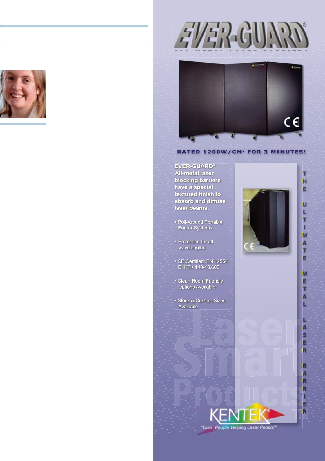
EVER-GUARD®
Curtain Systems
Ensure the sa
f
ety o
f
your personne
l
.
Designed for high power
laser applications,
Kentek’s EVER-GUARD®
Curtain Systems are the
most protective laser
curtain commercially
available.
This retractable curtain
system glides easily
along a ceiling mounted
track and folds compactly
when not in use.
Available in any width and
heights up to 8 feet
ALL
-
M
ETAL
L
ASE
R
BA
RR
IE
R
S
“Optical
technology
is becoming
increasingly
prevalent in
society
today .”
Jacqueline
Hewett
OLEOct06NEWSp5-9 25/9/06 15:55 Page 9
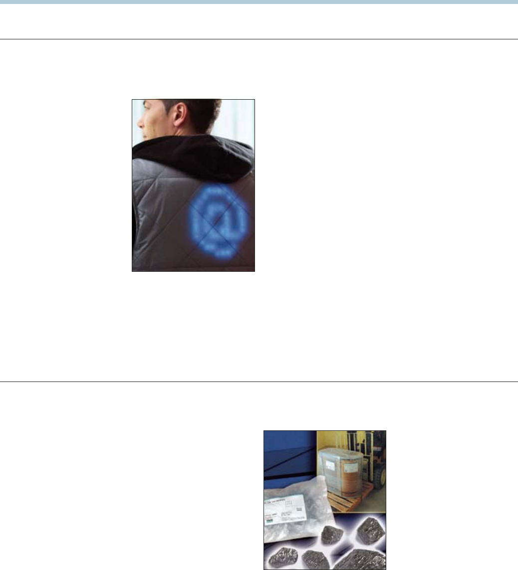
Embedded LEDs light up clothing
TECHNOLOGY
APPLICATIONS 11 R&D 16 PATENTS 17
11
OLE • October 2006 • optics.org/ole
DISPLAYS
Last month, Philips Research of the
Netherlands impressed visitors at
the Internationale Funkausstellung
(IFA) show in Germany by demon-
strating promotional jackets and
furniture featuring the company’s
Lumalive technology.
Lumalive textiles allow fabrics to
carry dynamic advertisements and
graphics and feature constantly
changing colour surfaces. Since
exhibiting early prototypes at IFA
2005, Philips Research has man-
aged to fully integrate Lumalive fab-
rics into garments. First-generation
jackets are now ready for commer-
cialization by companies partner-
ing with Philips Research. The
textiles are of particular interest to
those in the promotions industry
looking for a high-impact medium.
“Taking the Lumalive fabrics
from prototypes to integrated
products has been a major chal-
lenge,” said Bas Zeper, managing
director of Photonic Textiles at
Philips Research. “The light-emit-
ting textiles have to be flexible,
durable and operated by reason-
ably compact batteries. Fitting all
that into a comfortable, light-
weight garment is a considerable
engineering success.”
“Last year Philips Research dis-
played its research prototypes. This
year the jackets and furniture rep-
resent versions that are ready to go
into commercial production and
they include integrated power
sources and control electronics,”
added Zeper.
Lumalive fabrics use flexible
arrays of coloured LEDs that are
integrated into the fabric without
compromising the softness and
flexibility of the cloth. The light-
emitting textiles can then carry
dynamic messages and graphics.
According to Philips Research, fab-
rics such as curtains, cushions and
sofa coverings can even contain
the light-emitting technology.
Philips Research says that the
jackets are comfortable to wear
and that the electronics, batteries
and LED arrays are fully integrated
and invisible to the observer and
wearer. The Lumalive fabrics are
said to become obvious only when
they light up to display various
vivid coloured patterns, logos,
short text messages or even full-
colour animations.
The jackets feature panels of up
to 200 ×200 mm2, although the
active sections can be scaled up to
cover larger areas such as a sofa.
The products include features
that make them practical for daily
use. For example, when integrating
the Lumalive fabrics into a gar-
ment, Philips Research has made
the parts that cannot be easily
washed – such as the batteries and
control electronics – simple to dis-
connect and reconnect after the
garment has been cleaned. Even the
light-emitting layer can be easily
removed and refitted into the jacket.
A solar-grade (SoG) silicon derived
by metallurgical silicon purifi-
cation will increase the availability
of feedstock to the ever-hungry
photovoltaic (PV) industry, accord-
ing to its developer Dow Corning
Solar Solutions (DCSS). When the
SoG silicon is blended with tradi-
tional polysilicon feedstock, the
resulting material is said to exhibit
performance characteristics sim-
ilar to polycrystalline silicon.
The new silicon feedstock mat-
erial is called PV 1101 SoG Silicon.
Its production method from quartz
(sand) can be likened to the refin-
ing process of iron ore into steel. A
key advantage of the novel (and
confidential) process is that it
enables economical, volume pro-
duction of high-quality silicon.
PV 1101 can then be blended
with lower-grade polysilicon to
produce material of sufficient qual-
ity for photovoltaic cells. DCSS says
that this is the first commercially
available feedstock produced from
such technology using large-scale
manufacturing processes.
A major obstacle facing the
growth of solar energy in recent
years has been the availability of
silicon. To date, the solar industry
has relied on the supply of poly-
crystalline silicon, a high-grade
purity product, originally devel-
oped for the semiconductor indus-
try. However, this has meant that
the industry has in turn been sub-
ject to resource restraint.
DCSS believes that PV 1101,
produced by a different route, will
alleviate this restraint and will
offer a new source and new techni-
cal and business options for the
solar industry.
“PV 1101 is certainly one of the
most innovative technologies to
come along in the solar-energy
industry since the manufacture of
the first silicon solar cells,” said Gae-
tan Borgers, director of DCSS. “For
years now, the solar industry has
hoped to be supplied by new sources
of silicon designed and dedicated to
them. PV 1101 is a step in that
direction, which gives a means of
growth for the solar industry.”
The PV 1101 blend material has
already been tested in independent
institutes and at several of DCSS’
customer production sites world-
wide. The testing showed that the
blended feedstock exhibits perfor-
mance characteristics on a par
with polysilicon in terms of solar-
cell manufacturing and efficiency.
The typical power conversion effi-
ciency of a silicon photovoltaic cell
remains just 15–16%.
“Dow Corning has worked
closely with several customers to
test and qualify our material,” said
Rudy Miller, marketing manager of
DCSS. “The results are very posi-
tive and we have recorded a high
interest in our product. Orders
have already been placed.”
DCSS began production of
PV 1101 earlier this summer and
bulk customer shipments began in
August. The company is now pro-
gressively ramping up its PV 1101
SoG silicon production facility in
Santos Dumont, Brazil.
Purified silicon eases solar-grade supply issues
SOLAR CELLS
Lumalive jackets contain panels up to
200 ×200 mm2that can display logos
and messages. Philips Research says
that it is now ready to be commercialized.
Philips Research
Bags more: high-quality silicon in bulk.
Dow Corning Solar Solutions
OLEOct06TECHNOLOGYp11-17 25/9/06 16:18 Page 11
Sommelier robot helps choose wine
TECHNOLOGY
APPLICATIONS
SPECTROSCOPY
12 OLE • October 2006 • optics.org/ole
Choosing a bottle of wine is often a
tough task revolving around ques-
tions such as price, grape variety
and the product’s origin. Now,
thanks to a sommelier robot devel-
oped by NEC System Technologies
and Mie University in Japan, help
could be at hand to take the uncer-
tainty out of the decision.
“The robot contains a wine data-
base,” Yukie Endo of NEC System
Technologies told OLE. “The data-
base includes various attributes,
such as country, winery, colour,
taste and price. The robot automati-
cally generates questions using the
attributes of the database.”
The wine-tasting robot builds on
research by NEC and Mie Univer-
sity. The team’s first robot used
infrared spectroscopy to analyse
food and estimate the quantities of
components such as sugar and fat.
“The robot can identify the food
by referring to characteristics in the
database,” said Endo. “It uses con-
tinuous-wave infrared light and pro-
duces almost a real-time response.
Some foods are easy to distinguish;
others are difficult. Wine is a typical
example of the latter.”
Keen to take up the challenge,
Endo and his colleagues modified
their food-tasting robot to create a
sommelier robot. One of the key
modifications was extending the
spectroscopy system.
“The sommelier robot uses mid-
infrared spectroscopic informa-
tion,” said Endo. “Red or white wine
is simply poured onto the sensor.
The robot is also equipped with the
ability to ask questions to determine
a customer’s wine preference.”
The team is now developing the
spectroscopic “tasting” technol-
ogy. “We plan to improve the tast-
ing technology and wish to
commercialize it as a component,”
concluded Endo. “It may be used
for various applications, such as
quality-control, games, dieting
and health applications. We hope
that the wine robot or wine-tasting
machine will be commercialized
by someone in the near future.”
Scientists in Japan have developed a
material that becomes water repel-
lent when it is illuminated with
ultraviolet (UV) light. The proper-
ties of the material mimic those of
the lotus blossom – a flower that is
renowned for being immaculately
clean. What’s more, the effect is
reversible because the material can
be switched back to its original
state using visible light (Ange-
wandte Chemie International Edition
10.1002/anie.200602126).
The secret behind the lotus effect
is a special microstructure on the
plant’s leaves. This forces water
droplets to form beads that roll off
the surface, picking up any dirt par-
ticles that they encounter.
To date, scientists have not been
able to duplicate this natural phe-
nomenon, but now this synthe-
sized material could find uses
wherever a self-cleaning surface is
required. Windows and car body-
work are just two examples.
Kingo Uchida and Shinichiro
Nakamura from Ryukoku Univer-
sity synthesized their material from
a family of compounds known as
diarylethenes. “The thickness of
the film is between 20 and 40µm,”
Uchida told OLE. “When we illu-
minate the surface with UV light at
254 nm from a mercury lamp, fib-
rils start to grow within five min-
utes, but one day later is enough to
observe superhydrophoboicity.”
Uchida and his colleagues switch
the material back to its original
form by illuminating it with light in
the 450–600 nm range. “It takes
only 10 minutes for the material to
return,” commented Uchida.
The infrared sommelier uses spectroscopic analysis to taste red or white wine.
Switchable lotus effect
creates clean surfaces
MATERIALS
The starting point is a 20–40 µm thick film synthesized from a family of compounds
known as diarylethenes (left). When the researchers shine UV light on the surface,
small fibres approximately 1 µm in diameter begin to grow. This creates a super-
water-repellent surface exhibiting the same properties as the lotus blossom (right).
NEC System Technologies
Kingo Uchida, Ryukoku University
OLEOct06TECHNOLOGYp11-17 25/9/06 16:19 Page 12
US 1-800-835-2626 |Europe +31 (0) 316 333041
Asia +81 (03) 3407-3614 |www.mellesgriot.com
Turn Your Design Ideas into Product Realities
Catalog X in Print
Browse our award-winning, printed version of
Catalog X from cover to cover and discover our wide
selection of products. Perfect for handy reference.
Create Control Position Light
Catalog X on CD
Pop in Catalog X on CD and find everything you
need in an interactive PDF format. Easy-to-use
and small enough to tuck away for quick access.
And of course, our Customer Service Representatives
are always available by phone.
The Practical Application of Light
www.mellesgriot.com
Melles Griot provides the products that enable the practical application
of light for all your product development and general laboratory work.
3 easy ways to find the products you want
Catalog X on the Web
Just bookmark www.mellesgriot.com
to shop online and find products, tutorials, and
specifications. It’s as easy as using your keyboard.
Shop Catalog X
Laser-etched silicon delivers a
response in the near-infrared
TECHNOLOGY
APPLICATIONS
DETECTORS
14 OLE • October 2006 • optics.org/ole
www.ophiropt.com
BEST SERVICE, BEST QUALITYINFRA RED BUILD TO PRINT
You Design It We Shape It We Cut It We Coat It
Researchers are using the same
microstructuring approach that
enhances the efficiency of silicon
solar cells to widen the spectral
response of photodetectors (Appl.
Phys. Lett. 89 033506).
“The challenges lay in under-
standing the material’s physical
properties and how they can be
controlled and used to improve
device performance,” Jim Carey of
Harvard University, US, told OLE.
Conventionally, silicon is trans-
parent to wavelengths longer than
1 µm, which makes it unsuitable for
use in many near-infrared appli-
cations. However, the researchers
have found a way of modifying the
material’s bandgap to make it
absorb at longer wavelengths.
Using a Ti:sapphire laser, Carey
and colleagues irradiated an
n-doped silicon wafer with a 1 kHz
train of 100 fs pulses in a sulphur-
rich atmosphere to generate a sur-
face covered with 2–3 µm-sized
structures. According to the team,
the laser causes ablation and melt-
ing of the silicon surface, which
evolves and interacts with the gas
before re-solidifying with an
altered morphology.
The detector’s microstructured
surface encourages multiple reflec-
tions, which promote the absorp-
tion of light. However, this is only
part of the picture. “It is a combi-
nation of increased absorption in
the infrared [region] and large gain
that leads to the extension of the
operating wavelength,” said Carey.
“The incorporation of large
amounts of sulphur during laser
irradiation is responsible for signifi-
cant absorption beyond 1100 nm.”
Photodetectors made from the
textured silicon were found to have
a responsivity of 92 A/W at 850 nm
and 119 A/W at 960 nm (3 V
reverse bias in both cases). What’s
more, the devices continued to
exhibit a photoresponse at 1.31
and 1.55 µm.
The group, which also includes
scientists from the University of
Texas and the University of Vir-
ginia, both US, is now looking to
commercialize its new technology.
Carey expects that the first big
market will be in specialized ima-
ging applications such as security
and surveillance. He thinks that it
is unlikely that devices will make
their way into consumer items
such as camera phones.
“Margins are too low and the
end customer doesn’t care enough
about the infrared to drive a pre-
mium,” he commented.
Scientists at Rensselaer Polytechnic
Institute (RPI), US, will develop
high-brightness LEDs based on
native GaN substrates from mater-
ials firm Kyma Technologies in a bid
to plug the so-called “green gap”.
While highly efficient blue and
red emitters based on GaN or AlIn-
GaP are routinely made using sap-
phire, SiC or GaAs substrates, the
development of green LEDs has
not been quite so successful.
Now, under the US Department
of Energy’s solid-state lighting core
technologies programme, RPI and
Kyma will work together to produce
improved materials and develop
better processes that should lead to
higher-performance green emit-
ters. The improvement should
result from the use of Kyma’s low-
defect-density native GaN sub-
strates. Both polar and cutting-edge
non-polar materials will feature in
the development programme.
Because they do not suffer from
electric fields in the crystal lattice
that can degrade device perfor-
mance, non-polar LEDs should
have much better performance
characteristics than the conven-
tional polar GaN devices that are
the mainstay of today’s high-
brightness LED industry.
However, initial results with
devices grown on r-plane sapphire
substrates have suffered from a rel-
atively low power output that is
thought to result from high defect
densities in the crystal lattice.
“The use of Kyma’s native GaN
substrates should enable a reduc-
tion of such defects by a factor of
over 10 000 compared with such
non-native approaches,” claimed
the US-based firm.
Kyma’s CTO and co-founder
Drew Hanser will work closely with
Christian Wetzel and Fred Schubert
from RPI’s Future Chips Constella-
tion on the new programme. They
will focus on developing improved,
commercially viable green emitters
that should help to fulfil the promise
of solid-state lighting for general
lighting applications.
Kyma aims to plug ‘green gap’ through DoE project
LEDS
Textured silicon: this scanning electron
micrograph shows the photodetector’s
laser etched surface. The micro-
structures are 2–3 µm in height and are
spaced at intervals of roughly 2–3 µm.
Harvard University
OLEOct06TECHNOLOGYp11-17 25/9/06 16:19 Page 14
UNIFORM
LINES
•635 to 1550 nm
•Power up to 150 mW
•660 nm, 100 mW option
available
•Choose pattern and fan
angle
•2 year warranty -10-8-6-4-2 0 2 4 6 8 10
Relative Intensity
Relative Angular Position
0
0.2
0.4
0.6
0.8
1.0
NEW! Improve line uniformity
to ± 25, 20 or 15%
Lasiris™SNF Laser
NASDAQ: STKR
Copyright ©2006 StockerYale Inc. All rights reserved.
StockerYale Inc.
Tel.: (514) 685-1005
Fax: (514) 685-3307
lasers@stockeryale.com
www.stockeryale.com
For a list of our distributors,
please visit our website:
Your Product – Our Service
Polymer-based optical solutions for your products, just ask.
product development · optical design
tooling · injection molding
coating · assembly · electronic packaging
JENOPTIK Polymer Systems GmbH
Am Sandberg 2 · 07819 Triptis, Germany
Telefon +49 36482 45-0 · Telefax +49 36482 45-111
info@jenoptik-ps.de · www.jenoptik-ps.de
Visit us at Photonex Hall 5, Booth E24!
The World of
Polymer Optics –
Our Focus!
Realize your product ideas by making full use of our
comprehensive know-how and experience.
Precision lenses Micro-lenses and arrays
Ophthalmic glasses Precision mirrors
Optical freeform Optical gratings
Hybrid surfaces Micro-fl uidics
Hybrid systems Prototyping
Polymer optical systems
Fuji Magnetics GmbH · Polymer Optics · Germany
Fujistrasse 1 · D-47533 Kleve · www.polymer-optics.com
Polymer Optics by FUJIFILM.
Contact: +49 2821 509-132 · polymer-optics@fuji-magnetics.com
OLEOctAdverts15 19/9/06 11:08 Page 1
Doubled VECSEL emits
light in the ultraviolet
TECHNOLOGY
R&D
SOURCES
16 OLE • October 2006 • optics.org/ole
Piezo •Nano •Positioning
PI is the global leader in Nanopositioning.
ISO 9001 certified since 1994. www.pi.ws/smole
High-Speed, Piezo-Driven, Multi-Axis
Steering Mirrors
■Fixed Pivot Point ■µsec Response ■Nanorad Resolution
PI (Physik Instrumente) D: (0721) 4846-0 UK: (01582) 764334
Researchers in the UK have intra-
cavity frequency doubled a 675 nm
vertical external-cavity surface-
emitting laser (VECSEL) to produce
120 mW of ultraviolet (UV) light
at 338 nm. Also boasting a tuning
range of 5 nm, the team believes
that its all-solid-state system shows
promise as a continuous-wave
(CW) rival to nitrogen lasers emit-
ting at 337 nm (Applied Physics Let-
ters 89 061114).
“The advantage of the VECSEL
over conventional solid-state lasers
is that the gain region can be
designed for a specific wavelength
within the constraints of the semi-
conductor material,” researcher
Jennifer Hastie from Strathclyde
University explained to OLE. “Using
AlGaInP quantum wells, it should
be possible to demonstrate red
VESCELs in the 640–690 nm
range, translating to 320–345nm
via frequency doubling.”
Hastie says that the UV VECSEL
has been made possible thanks to
the availability of watt-level CW
power at 675 nm.
The initial red-emitting VECSEL
structure was grown by MOCVD
on a GaAs substrate. It consisted of
a gain region of 20 compressively
strained GaInP quantum wells
separated by AlInGaP pump-
absorbing barriers all grown on
top of an AlGaAs-based distrib-
uted Bragg reflector.
Hastie and colleagues used their
VESCEL structure as the end mirror
in a three-mirror cavity alongside a
spherical folding mirror and a plane
output coupler. The structure was
optically pumped with up to 7 W of
green light at 532 nm yielding
1.1 W of output power at 675 nm.
Inserting a BBO crystal into the cav-
ity produced a maximum UV out-
put power of 120 mW at 338 nm.
Rotating a birefringent filter
within the cavity tuned this output
wavelength over 5 nm centred on
338 nm. “Here we have an all-
solid-state laser with the advantage
of broad gain from the semicon-
ductor gain region,” said Hastie.
“Our 5 nm tuning range is at least
an order of magnitude larger than
that of a trebled Nd:YAG. Also,
most practical UV lasers, including
all-solid-state lasers, are by neces-
sity, pulsed.”
According to Hastie, the current
set-up measures approximately
400 ×150 mm excluding the com-
mercial pump laser. “There is no
reason why it couldn’t be more com-
pact,” she commented. “It should be
possible to diode-pump the VECSEL
once high-power GaN diode lasers
are more readily available.”
The Strathclyde team and its
collaborators are now looking to
improve the efficiency of the second
harmonic generation. “We have no
plans for commercialization at pre-
sent,” concluded Hastie. “This tech-
nology will lead to very practical
sources in application-rich areas so
there are likely to be real opportun-
ities for commercialization as the
technology matures.”
SPECTROSCOPY
Using Fourier transform infrared
(FTIR) spectroscopy in tandem with
pattern-recognition techniques is an
ideal way to obtain the
geographical origin of the Chinese
medicine danshen, according to
Ning Li, Yan Wang and Kexin Xu at
Tianjin University in China (Optics
Express 14 7630).
In Chinese medicine, danshen is
used to promote coronary circulation.
The problem is that the quality of
danshen varies with the growing
conditions in different geographical
regions.“Infrared spectroscopy can
be an excellent candidate for the
determination of danshen origins
because it is fast, accurate, non-
destructive and completely
dependable,” said the authors.
Li and colleagues collected 53
samples from four regions in China.
The samples were pressed into a
tablet, scanned 16 times and
spectra were collected between 400
and 4000 cm–1.
“The results showed that it is
feasible to discriminate [between
samples] using FTIR spectroscopy
ascertained by principal components
analysis [PCA],” concluded the
authors. “An effective model was
built by employing the Soft
Independent Modeling of Class
Analogy and PCA, and 82% of the
samples were discriminated
correctly. Through the use of an
artificial neural network, the origins of
danshen were completely classified.”
JOURNAL WATCH
The intracavity frequency-doubled
VECSEL produces 120 mW at 338 nm
and has a tuning range of 5 nm. The
team believes that the source shows
promise as a CW rival to nitrogen lasers.
Jennifer Hastie, Strathclyde University
OLEOct06TECHNOLOGYp11-17 25/9/06 16:19 Page 16

TECHNOLOGY
R&D/PATENTS
17
OLE • October 2006 • optics.org/ole
INFRINGEMENT
Toyoda Gosei issues warning over
its blue and white LED portfolio
Toyoda Gosei, the Japanese LED manufacturer,
has advised its competitors to exercise caution to
avoid infringement of its patents covering GaN-
based LEDs. To date, Toyoda Gosei has signed
agreements with its rivals Nichia and Philips
Lumileds that allow the parties to use each other’s
LED-related patents.
The press release goes on to say that “because
the manufacture, sale or use of GaN-based
semiconductor LEDs by any entity other than these
may constitute infringement of Toyoda Gosei’s
patents, Toyoda Gosei advises the fullest caution
to avoid infringement.” The firm says that it has
filed more than 2000 patent applications related
to GaN-based semiconductor LEDs and has
acquired patent rights on 600 of these.
In the same press release, Toyoda Gosei also
issued a warning regarding white-light emitters
that use blue LEDs in tandem with yellow silicate
phosphors. “Toyoda Gosei has recently received
information that companies other than licensees
have been manufacturing and selling white LEDs
using silicate phosphors,” said the firm.
Toyoda Gosei says that there are roughly 20
licensees of this technology worldwide. Again the
firm advised “fullest caution” as non-licensed
entities producing white LEDs using silicate
phosphors may constitute infringement.
APPLICATION
US firm Finisar unveils integrated
source and detector in application
Finisar of the US has integrated a light source
(either a vertical-cavity surface-emitting laser or a
resonant-cavity LED) and a photodiode into a single
device. The invention is detailed in international
patent application WO 2006/073958.
AWARD
UK imaging firm AST receives US
patent for its infrared camera
UK-based Applied Scintillation Technologies (AST)
has been granted US patent number 7075576 for
its compact, low-cost infrared camera
CamIR1550. The product is now protected by both
European and US patents.
“The CamIR1550 uses our specialized
knowledge of phosphor selection and coating
techniques to offer a highly cost-effective
alternative to infrared cameras with specially
processed detectors,” said Stuart Quinn of AST.
“This lightweight portable system has high
sensitivity to 0.2 µJ/cm2and is optimized between
1500 and 1600 nm.”
Typical applications are listed by the firm as
being on- and off-site beam-finding from
communications band emitters; laser alignment of
positioning machines; imaging optical outputs of
high-speed fibre-optics; and device alignment.
LICENSING
Kodak signs up Tohoku of Japan
as licensee of OLED technology
Kodak of the US has signed a licensing
agreement with Tohoku Device of Japan. The
deal will allow Tohoku to incorporate Kodak’s
organic display technology into white OLED
modules for use as backlights in flat-panel-
display applications.
The royalty-bearing licence also includes a
cross-licence to Tohoku’s patent portfolio. It also
gives Tohoku the opportunity to purchase Kodak’s
patented OLED materials. Tohoku joins more than
15 companies that have licensed this organic
technology from Kodak.
PATENTS
To search for recently published applications, visit http://www.wipo.int/pct/en/ and http://ep.espacenet.com.
Scientists have discovered that thin
films of silver – a normally opaque
material – can be made highly
transparent by sandwiching them
between zinc-sulphide-coated glass
blocks. Ian Hooper and colleagues
at the University of Exeter, UK,
said that light passes through the
silver in a way that is similar to
how particles tunnel through bar-
riers. The work could help to
improve the efficiency of OLEDs
and enable a new generation of
semiconductor devices (Phys. Rev.
Lett. 97 053902).
It is well known that light travel-
ing through a solid block will
undergo total internal reflection if
it strikes the surface at a very shal-
low angle. Some of the electromag-
netic field, however, strays into the
air – a so-called evanescent wave.
This can form a beam of lower
intensity if it passes into another
solid block placed nearby. Hooper
and colleagues then wondered
what would happen if each block
was coated with another material.
According to their calculations,
light would be transmitted with
perfect efficiency.
In practice, the researchers
coated the surface of a silica prism
with a film of zinc sulphide just
200 nm thick. They then clamped
two such prisms together, leaving a
very thin air gap sandwiched
between them. When light at the
correct wavelength was used, it
passed through the sandwich with
about 85% efficiency.
The physicists then replaced the
air gap with a 40 nm thick layer of
silver. On its own, silver of this
thickness is almost opaque to light.
But when sandwiched between
the two coated prisms in this way,
the silver was found to transmit
light with an efficiency as high as
35% at certain wavelengths.
According to the researchers,
the light is transmitted because the
reflections from the silica/zinc sul-
phide and the zinc sulphide/silver
interfaces are 180º out of phase
with each other and of equal
amplitude. Therefore they cancel
out to give no net reflection – that
is, all the light is transmitted.
“The reflection from the front
interface combined with the multi-
ple reflections from the subsequent
interfaces also interfere such that
they cancel,” said Hooper. “With
no net reflection and with a non-
absorbing system all the light must
be transmitted.”
The researchers say that their
technique could be used to
improve the efficiency of a new
generation of top-emitting OLEDs,
whose performance is limited by
the light passing through a metal
cathode. It could also be used to
improve semiconductor devices,
where an analogous quantum
effect should be seen.
‘See-through’ silver boosts LEDs
LEDS
Silver lining: light can penetrate silver
metal that is sandwiched between thin,
transparent layers of zinc sulphide and
a pair of prisms (left and right with the
vertical boundary in the centre).
Ian Hooper, University of Exeter
OLEOct06TECHNOLOGYp11-17 25/9/06 16:20 Page 17
O
ver
100
L
a
b
or-
S
av
i
ng
S
toc
k
Protective Packages
Our Copolymer Foams are
Cleanroom Compatible!
Test Reports Available at
www.tempo-foam.com
for Organic Analysis
and Liquid Particle Counts
Modular Molds for Low Cost
Customization
Stock Package for
Round Substrates
V-Groove Edge
Protectors for Glass
Stock Fiber Coil Pack
See Us at Optical Society of America Annual Meeting
Rochester, NY Booth #400!
www.tempo-foam.com 559-651-7711
Booking deadline is Thursday 2 November 2006
Secure your position early and ensure proximity
to the relevant section in the supplement.
To include:
•electron-
multiplying CCDs
•diode-pumped
solid-state lasers
•waveplates
•micro-optics
•mirrors
•beam-profiling
equipment
•optical design
software
•excimer lasers
•diffractive optics
•high-brightness
LEDs
•photonic crystal
fibre
●Print or electronic
delivery to 30 000 key
industry professionals
●Distributed at all major
optics and photonics
events in 2007
●Online throughout 2007
at optics.org
PRODUCT GUIDE 2007
BOOK
NOW
Unrivalled distribution
Tel: +44 (0)117 930 1090 E-mail: cadi.jones@iop.org
Outstanding
Quality and Value
■Highest FOM material available
■Absorption in the 0.4 to 7.0/cm
Alpha 514 range
■Tunable from 0.66 to 1.2
µ
m
■Free of internal scatter
■100 mm diameter and larger
TI:SAPPHIRE
For Lasers
27 Congress Street, Salem, MA 01970
TEL: 978-745-0088 FAX: 978-744-5059
www.crystalsystems.com
CRYSTAL
SYSTEMS
HEM SAPPHIRE
■Windows to 13” ∅
■Domes and Lenses
■Laser Optics, IR windows
■Rods, blanks and wafers
available
Serving your diverse
markets with high quality
and high purity sapphire
OLEOctAdverts18 26/9/06 08:51 Page 1

Scanning the lens of a human eye with infrared laser light can reveal the earliest signs of
Alzheimer’s disease in a matter of seconds, according to US start-up Neuroptix. Matthew
Peach speaks to the firm’s chief executive officer, Paul Hartung, about the technology.
Eye scan shows first sign
of Alzheimer’s disease
INTERVIEW
19
OLE • October 2006 • optics.org/ole
Neuroptix has developed an optical technique
for early diagnosis of Alzheimer’s disease (AD)
– the degenerative illness that is becoming a
growing problem as the population is always
getting older as people are living longer.
Instead of having to wait until a patient shows
signs of mental degeneration, Neuroptix’s
optical technique can indicate the likely onset
of the disease many years earlier, giving a
patient time to make adjustments to lifestyle,
diet and exercise, which could improve their
chances of avoiding the worst aspects of this
currently incurable disease.
The Neuroptix system, known as the QEL
2400, measures the presence of telltale
amyloids in the lens of the eye with a combi-
nation of dye treatment and scanning by an
infrared laser. OLE interviews Paul Hartung,
president and chief executive officer of Neu-
roptix, about the technology.
OLE: What are the origins and
objectives of Neuroptix’s work into
early diagnosis of AD?
PH: Neuroptix was founded in 2001 follow-
ing the breakthrough discovery by our com-
pany founder Lee Goldstein at Harvard
Medical School. He discovered that beta
amyloid proteins, which create plaque in the
brain of patients suffering from AD, can also
be identified in the lens of the eye. Our objec-
tive is to develop and commercialize a non-
invasive eye test for early diagnosis of AD.
Why are you focusing on AD?
AD is now the eighth most common cause of
death (in the US). But this does not represent
the true scale of the problem because AD suf-
ferers often die from other causes. It is also
believed that as we get older the likelihood of
getting this disease increases. It is a devastat-
ing illness not only for the victims, but also for
their families. There is a great need for diag-
nostics to detect the disease at an early stage
and to enable effective treatment. Pharma-
ceutical companies need more sensitive diag-
nostics to striate subjects in clinical trials and
to measure the efficacy of their new therapies.
What is Neuroptix’s test set-up?
Eye drops are applied that contain a fluor-
escent ligand (dye), which is temporarily
absorbed by the lens and binds to amyloid pro-
teins. A low-power class I laser scans the lens,
exciting the fluorescent dye and scattering off
the protein aggregates. The fluorescent dye
provides the biochemical specificity, identify-
ing the type of protein. Using a technique
called quasi-elastic light scattering, we are able
to quantify the size of the protein aggregates.
We can make a judgment on the likelihood of
the patient becoming an AD sufferer based on
the light measurements and post-processing
that data using our software.
In the late stages of the disease, the aggre-
gates in the lens become so dense that they
are visible in the supranucleus of the lens.
Our technique is essentially a molecular
diagnostic technique, with the ability to take
measurements on a clear lens. Pre-clinical
testing has shown that it is sensitive enough
to pick up amyloids in the eye before plaque
forms in the brain.
What is the test timescale?
The test takes a matter of seconds; it is done
within the timeframe of a normal physical
exam. It is similar to, but much less invasive
than, a retinal scan and the equipment is
similar to a laser-scanning ophthalmoscope.
How do you differentiate AD from
other diseases detected this way?
Our dye agent provides the biochemical
specificity of indication for AD. In addition,
there is anatomical specificity based on the
location of the aggregates in the supranu-
cleus of the lens. We are focused on AD but
we believe that it could be applied to prion
diseases. For example, the US Department of
Agriculture is testing this technique to assess
prion-affected deer, sheep etc, using Neur-
optix’s dyes to achieve rapid screening.
What are the limitations of other AD
diagnosis methods?
Clinical diagnosis generally occurs in the
later stages of the disease, based on psycho-
analysis and other factors. The new tests that
are in development include:
Cerebrospinal fluid tests. This requires an
invasive and complication-prone spinal tap
and is not sensitive enough to detect AD;
Brain scans (MRI and PET). These are
expensive and are only of use in the later
stages of the disease. Neuroptix’s technique
will be a feeder technology for these more
expensive tests;
Blood tests. These can only determine
genetic predisposition in some cases;
Urine tests. These have been rejected by
the Food and Drug Administration. They are
not sensitive enough and have highly vari-
able results.
Above: the test, which could be part of a medical
exam, takes a few seconds. Bottom: Paul Hartung,
Neuroptix’s chief executive officer.
NeuroptixNeuroptix
L
OLEOct06INTERVIEWp19-21 25/9/06 15:48 Page 19
SR850 Lock-In Amplifier
Our flagship model with CRT display and built-in
data analysis
•1 mHz to 100 kHz range
•64,000 point data buffer
•Chart recording, numeric displays, polar plots
•Smoothing, curve fitting and statistics
•Direct printing and plotting, & 3.5” disk drive
•0.001 degree phase resolution
•$8250 (Int’l list)
SR844 RF Lock-In Amplifier
For high frequency applications - no other lock-in
goes to 200 MHz
•25 kHz to 200 MHz range
•80 dB dynamic reserve (5 ppm stability)
•Auto gain, phase, reserve and offset
•Time constants from 100 µs to 30 ks
(up to 24 dB/oct rolloff)
•No Time Constant mode (10 to 20 µs update rate)
•$8745 (Int’l list)
The power of
DSP Lock-In Amplifiers
SRS lock-in amplifiers use digital signal processing (DSP) to bring the highest performance possible to
synchronous detection experiments. Each instrument comes with GPIB and RS-232 interfaces, multi-
purpose analog I/O ports and a synthesized reference source. Features include harmonic detection,
ratio measurement and auto setup functions. Contact us for details on our full line of
lock-in amplifiers starting at $2745.
Stanford Research Systems
1290-D Reamwood Ave. Sunnyvale, CA 94089 · email: info@thinkSRS.com
Phone (408) 744-9040 · Fax (408) 744-9049 · www.thinkSRS.com
SR830 Lock-In Amplifier
The industry standard
providing exceptional value
•1 mHz to 100 kHz range
•256 kHz front-end sampling rate
•100 dB dynamic reserve (5 ppm stability)
•Auto gain, phase, reserve and offset
•Time constants from 10 µs to 30 ks
(up to 24 dB/oct rolloff)
•$4620 (Int’l list)
Project1 22/9/06 14:08 Page 1
How is the Neuroptix’s technique an
improvement on existing methods?
To date there has been no in vivo commercial
biomarker for AD. The “gold standard” so far
has been the mental analysis of a patient, but
by the time that diagnosis is made, the patient
has typically lost 50% neural function – an
irreversible state of brain damage. We can
identify the disease prior to any cognitive
signs developing. Therefore, our aim is to
diagnose the condition prior to any brain
damage occurring.
The potential applications of our tech-
nique will be as an early confirmation test for
AD in those who present with mental prob-
lems and eventually as a preventative AD
check-up technique.
How can an optics-based
assessment help in this endeavour?
Optics-based techniques are suitable for
non-invasive measurement of biophysical
changes to the eye. The methods that we are
developing are non-contact, sensitive, fast
and relatively inexpensive.
What have you achieved in terms of
developing this method?
Initial work has been done using human
cadavers. A preclinical version of the system
has been developed and results show that
the technology is sensitive and can identify
amyloid pathology in the eye at a very early
stage in the disease. Clinical prototypes have
been developed, which are safe for human
use, and it has been proven that in vivo meas-
urements can be performed.
How is this a significant medical
breakthrough and will it save lives?
This is a major medical breakthrough.
Around 4.5 million people in the US are
already diagnosed with AD, with care costs
alone estimated to be $100 bn per year. The
number of sufferers is growing as people are
living longer. The opportunity to catch the
disease prior to cognitive loss, and to enable
early treatment, is enormously significant.
Are there any existing medical
techniques to counter AD?
There are drugs available today that work for
some patients but they are prescribed at a
much later stage in the disease than that
which we are identifying. There are also rec-
ommended lifestyle changes, including bet-
ter diet and physical and intellectual exercise.
On the drug development front, I have to
say that AD therapeutic development is a
high priority for large pharmaceutical com-
panies. There are more than 500 possible
solutions currently under development that
are expected to be fundamentally different
from what is available today. At Neuroptix,
we believe that in the next three years or so
there will be better drugs available.
What are the next stages of
development and are there any
technical or financial barriers?
The next stage of development will be the cre-
ation of instruments for clinical trials and the
safety testing of the fluorescent ligands for
human use. Neuroptix has already raised $1 m
through non-exclusive big pharmaceutical
R&D funds and “angel” investors. We are seek-
ing to raise series A equity financing in 2006.
We are developing partnerships with large
pharmaceutical companies interested in using
the technology as a drug-development tool.
We are also developing partnerships with
medical-equipment and diagnostics compan-
ies to support development, manufacturing
and worldwide commercialization.
Matthew Peach is a contributing editor to OLE and
optics.org.
INTERVIEW
The
Pan-European
Distributor
www.bfioptilas.com
www.bfioptilas.com/
instrumentation.htm
■Spectroscopy
■Photometry, Colour Measurement
■Laser Beam Characterisation
[Wavefront, Wavelength, Spectral Profile, Spectrum]
www.bfioptilas.com/
cvi.htm
■Lenses, Mirrors, Prisms, Beamsplitters
■Prototype Optics at Catalog Prices
■Opto-Mechanical Mounts
www.bfioptilas.com/
ophir.htm
■Laser Power/Energy Meters
■Beam Profile
■Spectrum, Temporal Profile
www.bfioptilas.com/
lasers.htm
■Industrial Lasers [Fiber Laser, CO2 Lasers]
■Laser Diodes & Diode Modules
[Blue, Green, Red, IR]
■Laser Scanners & Modulation
■Laser Safety
BFi OPTiLAS European Offices :
>Belgium: info.be@bfioptilas.com
>Denmark: info.dk@bfioptilas.com
>France: info.fr@bfioptilas.com
>Germany: info.de@bfioptilas.com
>Italy: info.it@bfioptilas.com
>Spain: info.es@bfioptilas.com
>The Netherlands: info.nl@bfioptilas.com
>Sweden: info.se@bfioptilas.com
>UK: info.uk@bfioptilas.com
Laurent PHILIPPE - 01 60 82 17 88
21
OLE • October 2006 • optics.org/ole
I
OLEOct06INTERVIEWp19-21 25/9/06 15:49 Page 21

An optical manipulation and analysis platform that can fit onto a fingernail could signal a
significant change in the field of microfluidics. Simon Cran-McGreehin, Thomas Krauss
and Kishan Dholakia from the University of St Andrews reveal what’s on offer.
Lasers meet fluids: an
integrated approach
OPTICAL TRAPPING
23
OLE • October 2006 • optics.org/ole
The 21st century could herald a revolution
in the way we perform biological science. Our
aim is to produce microfluidic systems that
analogously provide scientists with the abil-
ity to perform large-scale and parallel auto-
mated studies in the physical sciences –
notably in biology.
Light is the cornerstone for such studies. It
offers a powerful, non-invasive and recon-
figurable way in which to image cellular
samples; induce fluorescence and scatter-
ing; and move and manipulate objects at the
cellular level and below. For lab-on-a-chip
and microfluidic applications, we need to
explore ways to actuate, move and study
small volumes of analyte in extremely small
and confined volumes.
The motivation behind our approach is
simple. To date, physicists have relied on
external macroscopic laser systems and dis-
crete optical components to couple light into
microfluidic platforms to manipulate and
sense micro- and nanoparticles. This intro-
duces problems of alignment and coupling
losses, as well as placing a lower limit on the
size of the apparatus – typically a bench top
is needed for a conventional system.
However, recent work between the Optical
Trapping and Photonic Crystal groups at the
University of St Andrews, UK, bypasses these
issues by combining microfluidics and integ-
rated optics. In our monolithic optical micro-
manipulation and particle sensors, the lasers
are integrated right next to the microfluidic
flows in channels that are less than the width
of a strand of human hair.
Chip layout
Each laser is defined, lithographically, in a
single piece of GaAs-based laser material giv-
ing perfect intrinsic alignment. Microfluidic
channels are then fabricated directly on top
of the laser material, allowing the light to
couple directly into the sample without the
need for additional optics. This drastically
reduces the size of the system, making it
portable and simple to incorporate into exist-
ing microscope systems.
Both the concept and device design are
fairly simple. We believe that any research
group with access to semiconductor pro-
cessing facilities could replicate the device
using materials costing just a few pounds.
Indeed, we hope that this technology can be
spread rapidly among the biophotonics
community, giving access to the advantages
of optical methods without the need for spe-
cific optics knowledge.
The aim is to make the device as user-
friendly and robust as possible. Care has also
been taken to avoid any problems arising
from sending lasers in and out of the ports of
a microscope system. To this end, the device is
mounted onto a circuit board and the lasers
are wire-bonded to copper tracks, which in
turn are connected to a power supply.
The optical power of each laser is controlled
by varying the applied voltage (and hence cur-
rent), up to a maximum of around 20 mW at
about 3 V (approximately 200 mA). Such
electrical powers can be provided by a com-
puter interface board, opening up the way for
automated operation.
Fabricating the device
The starting point is a GaAs chip, typically
6×6 mm. The actual device is dominated by
2 mm-long lasers that determine the surface
area of the chip.
At the heart of each laser is an AlGaAs/
GaAs singlemode heterostructure, centred
1 µm beneath the chip’s surface. Grown epi-
taxially by German firm Nanosemiconductor
of Dortmund, the structure provides vertical
waveguiding and contains InAs quantum
dots that emit at 1290 nm.
Horizontal waveguiding is provided by
etching away the GaAs to leave a ridge 3 µm
wide and 750 nm deep that supports only a
single vertical transverse mode. An electri-
cal current is injected into the ridges via gold
contact pads and SU8-2000 polymer insu-
Miniature manipulator: the entire system, including fluid injection and electrical connections can fit into
the palm of a hand. At the heart of the device is a GaAs chip (inset) that measures only 6 ×6 mm.
University of St Andrews
OLEOct06INTEGRATEDp23-25 25/9/06 15:45 Page 23
OPTICAL TRAPPING
GWU-Lasertechnik
+49 . (0) 22 35.95522-0
info@gwu-group.de
www.gwu-group.de/laser
24 OLE • October 2006 • optics.org/ole
lation on the etched GaAs confines the cur-
rent to the ridges where a useful optical
mode is generated.
The length of the laser cavity is defined by
facets that are etched to a depth of at least
2 µm. The tight vertical confinement of the
heterostructure leads to large vertical diver-
gence of the output beam, up to as much as
40˚, so the optical power density falls off
quickly with distance from the facet.
Of greatest interest is the interface between
the lasers and the fluids. The microfluidic
channel is etched into the GaAs at right
angles to the lasers and passes between pairs
of facing lasers. This allows the laser beams to
enter from both sides of the channel to give a
dual-beam trap configuration.
The electrical activity of the lasers is insu-
lated from the fluid by lining the microfluidic
channels with SU8-2000 polymer. A thin
layer covers the base and a thicker layer lines
the walls, essentially determining the depth of
the channel. A glass lid is then adhered to the
top of the chip and sealed with adhesive to cre-
ate a watertight microfluidic channel that can
be fabricated in any desired configuration.
The size and position of the features can be
tailored to the application. The facet spacing
determines the optical power at the centre of
the microfluidic channel where facing
beams overlap. Closer facet spacings give
higher power densities resulting in stronger
trapping and larger detection signals.
Meaningful optical forces are exerted up to
around 200 µm from the facets, placing an
upper limit on their spacing. The lower limit
on the facet spacing is determined by the
resolution of the current photolithographic
techniques that define the SU8-2000 lining
on the walls. This places a lower limit of
about 20 µm on the facet spacing.
Typical microfluidic channels measuring
30 µm high and 40 µm wide, with a facet
spacing of 75 µm, allow the passage of biolo-
gical cells. The channels can be arranged in
various configurations, ranging from straight
channels to junctions for sorting and cham-
bers for mixing. Using water or biological
buffer solutions in the microfluidic channels
provides a medium in which particles can
flow into the paths of the laser beams.
Applications
Using a single laser, we have guided particles
over ranges of around 200 µm. Essentially,
the gradient force draws objects onto the
optical axis and the radiation pressure
pushes them away from the facet.
Pairs of facing lasers have been used to cre-
ate dual-beam traps, in which the objects are
held at the equilibrium point between the
two facets. Once trapped, particles can be
interrogated. We have demonstrated fluor-
escence spectroscopy in this configuration
and Raman spectroscopy is an obvious can-
didate for future studies.
Useful operations are possible even when
the optical powers are insufficient to trap
particles. This has led to the development of
two detection methods, both of which make
use of the fact that facing lasers feed light
into one another.
Trapping trio: (from left to right) Kishan Dholakia, Simon Cran-McGreehin and Thomas Krauss
demonstrate their versatile optical manipulation and analysis platform. The integrated module’s 50 µm-
wide trapping channel can be seen on the monitor as a bright stripe running across the middle of the
screen. Lasers located at either side of the channel are used to push and trap particles.
University of St Andrews
OLEOct06INTEGRATEDp23-25 25/9/06 15:45 Page 24
In the first method, the output power of
one laser is found to decrease when a particle
passes between the facets. In the second, one
laser is reverse-biased to create a photo-
detector whose photocurrent decreases
when a particle passes by.
These methods use the intrinsic properties
of the semiconductor lasers and require no
external light source – the second method
requires no external optics whatsoever. We
now plan to combine these operations into
more complex arrangements in which the
particles are moved around a device, either by
optical forces or by an externally generated
fluid flow, to different interrogation sites.
A look to the future
As a first step, this new technology makes the
power and versatility of optical manipula-
tion more widely available by simplifying the
operation and reducing the cost. We believe
that this technology lends itself to the world
of lab-on-a-chip, in which miniaturized test
and measurement systems are integrated
into microfluidic circuits.
By configuring the lasers and channels in
order to usefully combine the functions of
guiding, trapping and detection, a wide variety
of multiplexed processes could be conducted,
in parallel, on a single chip. This range could be
extended further by using external analysis
techniques such as Raman spectroscopy.
A more compact approach would modify
the laser material to allow the direct, on-chip
excitation and detection of fluorescence in
particles, such as violet-emitting GaN-based
material in conjunction with green fluor-
escent protein. The technology could also
have a use in the realm of atom optics, cre-
ating dipole traps that could hold Bose–Ein-
stein condensates.
Thomas Krauss heads the Microphotonics and
Photonic Crystals group and Kishan Dholakia
leads the Optical Trapping group at St Andrews
University, UK. Simon Cran-McGreehin is a
research assistant working in both groups. For
more information, including links to optical
trapping groups worldwide, please see www.st-
andrews.ac.uk/~atomtrap/.
OPTICAL TRAPPING
The fastest scanners on the market…just got faster.
Some might say we’re obsessed with speed. Perhaps that explains
how we can consistently deliver the industry’s fastest and most
accurate galvanometers and servo drivers. Like our new H line of
62xx galvos – pushing the technology envelope with better
performance and speeds that are 25% faster than what’s available
in today’s market.
We’re also introducing two new servo-driver boards. A dual-axis
analog servo that provides a 50% board space reduction and
higher speed at lower cost, and a self-tuning digital servo driver
that delivers speeds faster than analog servo technology.
■New 6215H Galvanometer
Highest frequency galvo in the market
Ideal for high-speed raster scan applications
■62xxH Series Galvanometers
25% torque increase for higher speeds
Compatible with 62xx standard product line
■DC900 State-Space
Digital Servo Driver
Self-tuning – no adjustment pots
Up to twice as fast as analog servos
■MicroMax 673xx
Dual-Axis Analog Servo Driver
Half the size of 2 single-axis servos
The most attractive combination of
size, speed and cost
Talk is cheap. Our prices are not bad, either.
While the rest of the industry talks about performance, we
deliver it. So go ahead, put us to the test. We’re making it
even easier by increasing performance without increasing prices.
Speed Freaks
11
109 Smith Place, Cambridge, MA 02138 USA
Tel: (617) 441-0600 • Fax: (617) 497-8800
www.cambridgetechnology.com
25
OLE • October 2006 • optics.org/ole
guide laser
trapping lasers
trapping lasers
Concept diagram showing particles being pushed
and trapped by integrated lasers.
I
OLEOct06INTEGRATEDp23-25 25/9/06 15:46 Page 25
The attractiveness of zinc oxide (ZnO) LEDs
stems from the potential for phosphor-free
spectral coverage from the deep ultraviolet
(UV) to the red, coupled with a quantum effi-
ciency that could approach 90% and a com-
patibility with high-yield low-cost volume
production. One day these LEDs could even
outperform their GaN-based cousins (which
offer a narrower spectral range) thanks to
three key characteristics – superior material
quality, an effective dopant and the availabil-
ity of better alloys.
The superior material quality is seen in the
low defect densities of ZnO layers. At MOX-
tronics, our development of a viable p-type
dopant has provided hole-conducting layers
for ZnO-based devices. And our growth of
BeZnO layers has shown that it is possible to
fabricate ZnO-based high-quality hetero-
structures (see box “The advantages of ZnO
over GaN” p27).
ZnO also promises very high quantum effi-
ciencies, and UV detectors based on this mat-
erial have produced external quantum
efficiencies (EQE) of 90%, three times that of
equivalent GaN-based detectors. The physical
processes associated with detection suggest
that similarly high efficiency values should be
possible for the conversion of electrical carri-
ers to photons. So it is plausible that ZnO LEDs
will have an EQE upper limit that is three
times higher than that of GaN-based devices.
Finding the right dopant
However, ZnO is yet to fulfill all of its promise
because of the delay in developing p-doped
material. Early progress throughout the
community was hampered by focusing
efforts on using nitrogen as a p-type dopant.
Nitrogen was the first choice because it was
an effective dopant in ZnSe, and also because
it was deemed, erroneously, to be of a suit-
able size to sit on an oxygen lattice site.
Although we also tried to obtain p-type
doping using nitrogen, a switch to arsenic
enabled us to report the first successful
p-type doping of ZnO in 1997. By 2000 we
could produce hole concentrations into the
1017 cm–3 range with this approach.
Later in 2000 we reported our hybrid
beam deposition (HBD) process that offers a
viable approach to growing doped and
undoped ZnO films, alloys and devices. The
HBD process is comparable to MBE. However,
it uses a ZnO plasma source, which is pro-
duced by illuminating a polycrystalline ZnO
target with either a pulsed laser or an elec-
tron beam, and a high-pressure oxygen
plasma created by a radio-frequency oxygen
generator. Additional sources for either dop-
ing or ZnO-based alloy growth can be added
to the growth chamber by conventional
evaporation or injection methods.
We used the HBD process to fabricate the
first ZnO-based UV detectors (see box “Highly
efficient detectors” p27), UV LEDs, FETs, and
red, green, blue and white phosphor-coated
LEDs. Our LEDs incorporate BeZnO, an alloy
that allows bandgap engineering into the UV
and the formation of multiple quantum
wells and other heterostructures.
Why BeZnO beats MgZnO
BeZnO alloys of varying composition have
significantly boosted the development of our
deep UV high-power LEDs. These alloys do
not phase-segregate, because BeO and ZnO
have the same hexagonal crystal structures,
and the extremely high-energy bandgap of
BeO could potentially lead to devices emitting
at just 117 nm. UV LEDs containing BeZnO
alloys produce a narrow spectral profile, with
very little emission in the visible, suggesting
that the alloy is of high crystal quality.
Until we had produced BeZnO films, the pri-
mary choice for a compatible higher bandgap
alloy was ZnMgO, a material developed by a
group at Tohoku University, Toyo University,
Tokyo Institute of Technology and Japan’s
Institute of Physical and Chemical Research.
In 1997 this team reported that crystal phase
separation occurs between MgO and ZnO
when the atomic fraction of magnesium
exceeds 0.33, which corresponds to a bandgap
of 3.99 eV. The separation is driven by differ-
ent crystalline structures; MgO is a cubic
structure with a lattice spacing of 0.422 nm,
while ZnO is a hexagonal wurtzite structure
with a lattice spacing of 0.325 nm.
We recently produced and characterized the
first UV LEDs made from ZnO and BeZnO. The
device’s emission can be tuned from the deep
UV to around 380 nm, the wavelength associ-
ated with ZnO. Our devices have been built
with several different active layer structures,
including double heterostructures and single
or multiple quantum wells, to try to improve
efficiencies and optical output powers.
Our latest UV LEDs have a typical wall-
plug efficiency of 0.1%, which would equate
to an efficacy of 0.6 lm/W if the emission
were in the visible spectrum. Although the
efficiency is far lower than that of GaN LEDs,
we are making rapid progress by addressing
the various phenomena that degrade device
performance. If progress continues at the
same rate we will produce LEDs with a 1%
wall-plug efficiency within one year, 1–5%
within two years and about 10% or more
within three years.
Our ZnO LED development programme
has used various substrates manufactured
by several vendors and has shown that the
LED’s performance is directly dependent on
the substrate’s material type and crystalline
quality. Single-crystal ZnO produces the best
devices. This material has been available for
Start-up company MOXtronics has recently produced the
first coloured ZnO-based LEDs. Although the efficiency of
these LEDs is not high, improvements are rapid and the
emitters have the potential to outperform their GaN rivals,
say Henry White and Yungryel Ryu from MOXtronics.
ZnO-based LEDs begin to s
OPTOELECTRONICS
26 OLE • October 2006 • optics.org/ole
MOXtronics has recently produced the first-ever ZnO-based LEDs emit
to its devices. Further development of ZnO-based materials could lea
MOXtronics
OLEOct06ZNOLEDSp26-27 25/9/06 16:21 Page 26
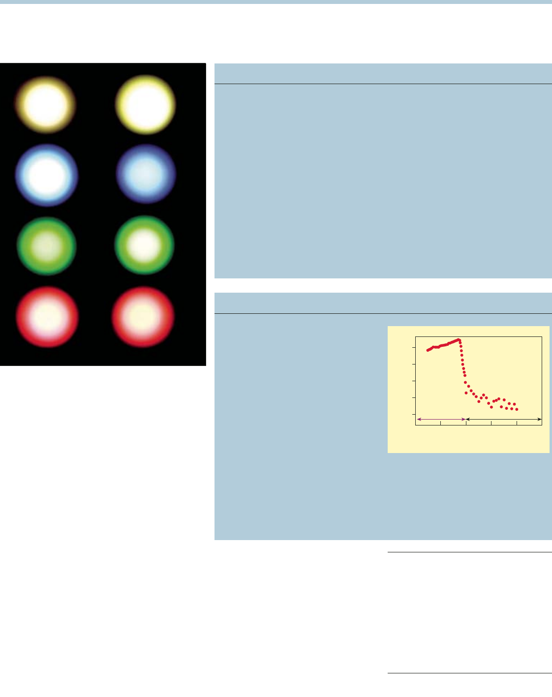
many years and interest is rapidly increasing
for the growth of high-quality single-crystal
ZnO with a diameter of 50 mm or more or
ZnO-based LEDs and other devices.
What’s needed
Major improvements in the efficiency and
power output of ZnO UV and visible LEDs are
still needed to enable these devices to compete
in the market-place. Advances will depend on
the availability of higher-quality single-crys-
tal substrates and improved processes for pro-
ducing reliable and highly ohmic electrical
contacts to various different layers. Addi-
tional bandgap engineering development is
needed for the UV C-band (100–280 nm) and
visible region, along with optimization of the
multiple quantum well and related structures
in the device’s active region.
Looking ahead
With the output power of our ZnO LEDs
increasing rapidly, these devices appear to
have a promising future. We expect them to
first be deployed in white-light lamps and
replace incandescent sources in applications
such as liquid-crystal display backlights. The
promise of emission from the UV through
the visible will then allow ZnO LEDs to target
applications where no other single semicon-
ductor material can operate today. At this
time, for example, red–green–blue sources
that are fabricated on a single wafer will offer
unique advantages for the development of
bright, compact displays and projectors.
Laser diodes built from ZnO-based materials
could also be produced that emit in the vis-
ible and UV and offer compact alternatives
for larger tube-type laser sources, ushering
in a new era for colour printing.
Yungryel Ryu (ryuy@moxtronics.com) is
president and CEO of MOXtronics. Henry White
(whiteh@ moxtronics.com) is chair of the
MOXtronics board and a professor at the University
of Missouri, MO, US. Both were members of the
company’s original start-up team. MOXtronics Inc
was formed in December 2000 as a spin-out
company of the University of Missouri. The firm
has obtained funding from both the Office of Naval
Research and NASA, and also through equity sales.
This article originally appeared in the August issue of
Compound Semiconductor magazine.
27
OLE • October 2006 • optics.org/ole
show full-colour potential
The three major benefits of ZnO over GaN are:
superior material quality, which has been
demonstrated by the growth of high-purity ZnO
with defect densities below 105 cm–2, a value
typically associated with the best GaN films;
improved doping performance, which results
from the arsenic p-type dopant that has an
activation energy of 119 meV in ZnO films, far
less than the 215 meV for magnesium-doped
p-type GaN. This lower activation energy
produces a 10-fold increase in the proportion
of activated acceptor atoms that are needed for
electrical conduction (assuming the same
atomic dopant concentrations are used) and
also reduces the number of defects for a given
hole carrier density;
the availability of better alloys, due to our
recent development of high-quality BeZnO films.
These layers have driven the fabrication of LEDs,
lasers and transistors that have less disorder
than the structures produced using the
AlGaN/GaN material system. The reduced
disorder is a consequence of the large
difference in bandgap between ZnO and BeO,
and enables only small changes in the alloy’s
composition to produce relatively large changes
in bandgap. In comparison, a much larger shift
in aluminium composition is required to
produce the equivalent changes in AlGaN and
this leads to greater disorder. The ZnO-based
material system could also be extended into the
visible using alloys such as CdO, CdSe and CdS.
The advantages of ZnO over GaN
MOXtronics has also developed the first UV
detectors based on ZnO. The sensitivity of
these devices is three times higher than that
of any other UV solid-state detector and they
have a responsivity of 0.27 A/W at 372 nm
(see figure, right). The detector’s noise floor at
visible wavelengths is four orders of
magnitude lower than its response in the UV,
making it an attractive option for visible-blind
applications. The device’s temporal response
is typically 50 µs, but it can be shortened
considerably and approach the theoretical
limit of 10 ns by optimizing the structure and
the electrodes’ dimensions.
MOXtronics expects to develop high-speed
focal-plane arrays, with pixel dimensions of
typically 128 ×128, by the end of next year.
These arrays, and single-element detectors,
should become important components in both
portable UV spectrometers and in the ultrafast
UV spectrometers designed for the analysis and
temporal de-convolution of fluorescence spectra.
Highly efficient detectors
s emitting in the white, red, blue and green, by attaching phosphors
ld lead to phosphor-free ZnO LEDs serving all these colours.
wavelength (nm)
responsivity (A/W)
100
200 300 400 500 600 700
10–1
10–2
10–3
10–4
UV visible
MOXtronics’ highly sensitive UV detectors have a
very fast response time and can analyse the change
in fluorescence spectra over very short timescales.
I
OLEOct06ZNOLEDSp26-27 25/9/06 16:21 Page 27
Evatec – A new name...
but a huge history!
50 years
The production experience, know-how and
build quality of Balzers BAK, now under a new
name and with renewed energy, drive and ambition.
■Unbeatable batch processing know-how
from 800 systems in daily production
■Industry standard Balzers BAK platforms
■Complete range of deposition processes –
PVD to ion-assisted deposition and ion plating
Evatec – delivering new components, new
machines and new ideas for the optics industry.
To learn more call our local sales offices,
visit www.evatecnet.com or visit us for a
celebratory drink at booth C25, Photonex UK
on October 18th and 19th.
www.evatecnet.com United Kingdom +44 7802 784406
Benelux +31 3465 81510
Head office +41 81 720 1080
solutions
laser diode
www.photonic-products.com
sales@photonic-products.com
Looking for a laser diode
solution?
We can design and build
a laser diode assembly to
maximize the performance
of your system.
Contact the specialists
for laser diodes, laser
modules and custom-
designed laser solutions
tailored to your exact
requirements.
OLEOctAdverts28 20/9/06 09:02 Page 1
There is a lot more to making an optical filter than meets the eye. Dominik Goessi looks
at the role of in situ monitoring in the production process and reviews the technology.
In situ method drives up
yields and reduces costs
OPTICAL MONITORING
29
OLE • October 2006 • optics.org/ole
The humble interference filter often plays a
critical role in optical experiments. Made up of
tens of layers, each one precisely deposited and
monitored, there is certainly a lot more to this
standard component than meets the eye. Its
manufacture typically involves in situ mon-
itoring and control systems to minimize pro-
duction time and cost, and to maximize yields.
Enhanced electron-beam deposition pro-
cesses such as reactive low-voltage ion plating
(RLVIP) are ideal for producing complex opti-
cal filters with 50 layers or more. These tech-
niques can generate thin films with high
density, high-temperature stability and a min-
imum of absorption. However, expensive coat-
ing materials, long process times and costly
substrates, that cannot always be reworked in
the event of an error in the coating process,
mean that monitoring is essential.
Monitoring techniques
Thin-film deposition processes are typically
controlled by one of two techniques: quartz
or optical monitoring.
Quartz crystal is the most commonly used
monitoring system. Here, an oscillator
excites a quartz crystal to high frequencies of
around 5 MHz. When the crystal is coated, its
frequency decreases and this change gives a
measure of the film’s thickness.
On the plus side, the hardware is relatively
inexpensive and easy to operate, and is used
successfully in many semiconductor and opti-
cal applications. However, the monitoring sys-
tem is not optimal for complex optical coatings
because the layer thickness on the substrate or
on a test glass is not measured directly.
Optical film-thickness measurements rely
on the fact that the intensity of a mono-
chromatic light beam reflected by a film
changes periodically with increasing film
thickness. The technique has the advantage
that a film’s optical properties are measured
directly using test glasses, which can then
be kept and checked for process and quality
control. However, the initial hardware
investment and set-up costs are higher than
that of crystal monitoring.
To compare quartz crystal and optical mon-
itoring systems, 15 samples, each having an
identical two-layer sequence of high and low
refractive index materials, were coated in an
Evatec BAP800 evaporating system.
The reproducibility of the layer density
using RLVIP on a BAP800 system is very
good, so one would expect the quartz crystal
to give the same thickness result for each
sample. However, results varied between
24.1 and 25.2 nm for the first layer and
between 54.0 and 56.2 nm for the second
layer. This highlights the reduced control of
quartz monitoring.
In practice, it is possible to correct coating
errors with crystal monitoring for designs
with approximately 10 layers. However, for
coatings with 20, 30 and 50 layers or more,
the error within each layer is unacceptably
large with insufficient reproducibility to
achieve the highest yields. A more precise
monitoring system is required.
Optical approach
Deposition processes such as RLVIP in com-
bination with optical monitoring systems are
therefore ideal for manufacturing complex
interference filters with high accuracy and
reproducibility. The theory and practice are
well matched. The actual spectral curves
achieved are identical to the calculated ones,
proving that optical monitoring systems jus-
tify their higher initial investment and set-up
costs through better process control and
higher yields.
An optical monitoring system has two
senders: one for transmission and another for
reflection measurements. The receiver is the
same for both modes of operation. White
light reflected from, or transmitted through,
a test glass passes through a monochromator
before being focused onto a detector. The sig-
nal from the detector is then fed into a lock-in
amplifier where it is processed and digitized.
Consider a test glass with a refractive index
of nGthat has already been coated with a film
of thickness dand refractive index nL. In
reflection mode, for example, a light beam
from the sender (R) hits the coated test glass
and is refracted and partially reflected (R1)
when it enters the optically thicker medium.
The refracted light reaches the interface
between the film and the test glass after it has
passed through the optical film thickness nLd.
One part of the light is reflected (R2) and the
other part penetrates the test glass. The
reflected light passes back through the film
again and multiple reflections occur at the
interfaces. The intensity of the reflected light
decreases continuously but the intensity of
the individual reflected light beams add
together to give the total intensity.
When monochromatic light with the wave-
Production benefits: optical monitoring systems give manufacturers a high level of process control.
Evatec
OLEOct06EVATECp29-30 25/9/06 14:39 Page 29
length hcrosses the interface from optically
thinner to thicker material, the reflection is
also accompanied by a phase shift of h/2. The
phase difference of reflected or transmitted
light is determined by the difference in optical
path lengths 2nLdand the phase shift that
occurs at the interfaces. We can therefore see
a turning point in the total intensity curve of
superimposed, reflected monochromatic light
beams depending on the light wavelength, the
refractive index and the instantaneous thick-
ness of the coated material.
In practice, as the film thickness increases
continuously during the coating process
itself, the turning point condition is fulfilled
at regular intervals and the intensity of the
reflected light beam detected at the receiver
reaches various maxima and minima with a
periodic structure. The distance between the
turning points depends on standard vari-
ables including evaporation rate r. If the
evaporation rate and the refractive index of
the film material are known, then it is poss-
ible to monitor film thickness using the
intensity curve measured at the receiver. A
special cut-off algorithm is used to control
the coater and terminate evaporation when
the desired film thickness is reached.
Successive manufacturing runs for a typ-
ical edge filter consisting of 24 optimized lay-
ers in an Evatec BAK760 with the optical
monitoring system GSM1100 demonstrate
the level of production control that can be
achieved with optical monitoring. The spec-
tral transmission curves for three batches
with 50% transmission values of 653.5,
651.5 and 652.8 nm respectively show an
excellent reproducibility of ±1nm.
The future of optical monitoring
A new generation of fast CCD image sensors
specifically designed for low-light-level detec-
tion in combination with an imaging spec-
trograph enables the precise monitoring of a
whole spectral range (broadband monitor-
ing). The coating process can be controlled by
direct measurement on the substrate and the
whole optical spectrum of each layer is
known and can be controlled. This means
that even in the event of a coating error mid-
process, the remaining layers can be recalcu-
lated in situ to give the correct end result.
Currently, the sampling frequency of these
set-ups is lower than those used in mono-
chromatic monitoring. As a result, special
algorithms are required to terminate a coat-
ing process precisely between two measure-
ments. However, given the rapid progress in
the quality and speed of CCD sensors, the
future of optical monitoring systems looks
set to become broadband.
Dominik Goessi is a physicist with a special
interest in the development of optical monitoring
systems. He works in Evatec’s development
laboratory at the company’s manufacturing facility
in Flums, Switzerland. See: www.evatecnet.com.
OPTICAL MONITORING
30 OLE • October 2006 • optics.org/ole
Need an affordable infrared camera
combining flexibility and superior
performance in terms of sensitivity,
speed and user interface?
XenICs cameras are used world-
wide for a wide variety of industrial
imaging applications in spectro-
scopy, telecom, process control,
security…
XenICs products include standard
cameras as well as custom design
solutions.
Vision, Stuttgart
7.-9. November 2006
Hall 4, Booth 22
XenICs NV, Ambachtenlaan 44, 3001 Leuven, Belgium
Tel: +32-16-389900, Fax: +32-16-389901, sales@xenics.com, www.xenics.com
T1
T
RR1 R2 R3
vacuum chamber nv
test glass nG
film nL
d
Principle of operation: a light beam from the
sender (R) hits the coated test glass and is
refracted and partially reflected (R1). Multiple
reflections occur at the interfaces. The intensity of
individual, reflected light beams add together to
give the total intensity (Rtotal = R1 + R2 + R3 = ...).
Evatec
I
OLEOct06EVATECp29-30 25/9/06 14:40 Page 30

18th INTERNATIONAL TRADE FAIR AND CONGRESS FOR OPTICAL
TECHNOLOGIES—COMPONENTS, SYSTEMS AND APPLICATIONS
LASER 2007
World of PHOTONICS
NEW MUNICH
TRADE FAIR CENTRE
JUNE 18–21, 2007
LIGHT
AT WORK
THEVISIBILITYOFSUCCESS As the world’s leading trade fair for optical technologies, LASER. World
of Photonics isthemostimportantinternationalinformationandnetworkingplatformfortheindustrial,scientificand
researchsectors.Itiswheremarketleadersandinnovativestartupspresentproductsandtechnologiesaswellastheir
applicationsinawiderangeofsectors.Inshort:itfocuseson“light at work”.ThatmakesLASER.WorldofPhotonics
akeysourceofmomentumfordecision-makersandtradeprofessionals.AndtogetherwiththeWorldofPhotonics
Congress,whichisheldatthesametime,itisahighlightfortheentireindustry,ineverysenseoftheword.
Hotline: (+4989) 949-114 68, Fax: (+4989) 949-114 69
info@laser.de, www.world-of-photonics.net
Project1 25/9/06 09:02 Page 1

•Stock and Custom parts
•Multi-Spots (from 1X2 till
5X85 spots), Top-Hats,
Homogenizers, Samplers
•High Efficiency.
From 193nm till 10600nm.
Fused Silica, ZnSe & Sapphire
Diffractive Optics
Since 1989
www.holoor.co.il
holoor@holoor.co.il
Edmund Optics
Edmund Optics UK Ltd catalogue contains more than
7200 products to assist in your demanding
applications. Over 200 new products include EO
Designed High Resolution MVO (R) Line Scan Lenses,
ReflX™ Reflective Microscope Objectives, and TECH
SPEC™ Precision Aspheric Lenses. In addition, this
resource guide contains real-world application notes
to assist you in applications ranging from lens design
to machine-vision illumination. Choose from our
extensive inventory or work with our engineers on
custom optical solutions. OEM discounts and just-in-
time shipping are available.
Pricing available in Euro or Pounds Sterling.
www.edmundoptics.co.uk
E-mail: uksales@edmundoptics.co.uk
FREE LITERATURE
Optikos’s Lens Measurement
Services can measure MTF, EFL,
BFL and other optical
performance specifications for
lenses operating from the UV to
the IR.
Using our state-of-the-art
OpTest™ measurement system
and patented VideoMTF™
software, we offer contract
measurement services for lens
quality evaluation.
Visit www.optikos.com today
and complete the LMS
questionnaire to receive a quote.
Optikos Corporation
286 Cardinal Medeiros Ave, Cambridge, MA 02141
Tel: +1 617 354 7557 Fax: +1 617 354 5946
E-mail: sales@optikos.com
Optikos Corporation
OLEOctAdverts32 26/9/06 08:41 Page 1
Thanks to a set of unique properties, diffractive optical elements have the potential to
transform light into almost any desired distribution. Joshika Akhil gives the low-down on
the technology that can benefit laser marking, material processing, heat treatment,
sensing, non-contact testing and optical metrology, to name just a few applications.
Hybrid diffractive optics
offer an elegant solution
PRODUCT GUIDE
33
OLE • October 2006 • optics.org/ole
Diffractive optical elements (DOEs) can mod-
ify laser beams in almost all of the same ways
as conventional refractive optics, but with
the added attraction of beam manipulation.
Elements such as beam homogenizers, dif-
fusers, beam samplers, diffractive focal
lenses, beam splitters and various grating
structures can transform light into almost
any desired distribution. Furthermore, the
modulation of light is not limited to laser
beams – DOEs can be used to modulate par-
tially and non-coherent light sources as well.
User benefits
DOEs have the unique ability to transform
the original beam into a variety of shapes,
distributions and numbered spots without
unduly affecting the output intensity of the
entire system. One of their greatest advant-
ages is that a single optical element can often
replace multiple optical systems to customize
the beam profile to the desired shape and
intensity distribution.
Recent developments in design and process
control now allow DOEs to be manufactured
in a compact, reliable and cost-effective way.
Using lithographic techniques, a microrelief
diffraction grating can be etched into the opti-
cal element to create a single optical device.
Diffractive optics redistribute the energy
between the centre and the periphery of a
laser beam, making them ideal for beam
shaping (figure 1). Beam homogenizers
smooth out the intensity profile of an inci-
dent beam and suit applications such as laser
ablation and heat treatment, where hot spots
within the beam are undesirable.
Traditionally, beam homogenizers have
been restricted to operation within the focal
plane of a lens (spot operation) or have a min-
imum working distance. If operated outside of
these conditions, undesired peaks can appear
in the distribution. However, there is a new
device on the market that is less sensitive to
positioning, called an HM-type homogenizer.
Beam shapers create specific energy-distri-
bution patterns with sharp edges. The basic
technique involves remapping the intensity-
distribution profile of the incident beam into a
uniform spot distribution of a specific size and
shape, and at a specific distance. In principle,
any transverse spot shape can be obtained,
although the most useful geometries are typ-
ically round, rectangular and square. Adding
a lens to the diffractive element shifts the loca-
tion and changes the scale of the distribution,
tailoring it to specific applications.
One great advantage of the so-called dif-
fractive top-hat beam shaper over other uni-
form illumination systems is that it eliminates
the trade-off between efficiency and spot uni-
formity by diffractively redistributing the
beam energy. Other techniques can simply
block out a significant part of the energy.
Users should remember that to achieve out-
standing results, the incident beam must have
a collimated Gaussian profile and be centred
on the element. Beam expanders and spatial
filters can be used to optimize the input beam.
Important role
Top-hat intensity distributions suit appli-
cations where a controlled transfer of energy
at the spot is essential, particularly in pro-
cesses that have an exposure level and dam-
age threshold for a given power density.
Examples include raster-scan-picture gener-
ators and high-power laser treatments in mat-
erial processing and medical applications.
As a result, DOEs are proving to be an
essential component in industry sectors such
as laser ablation; welding and drilling; med-
ical and aesthetic lasers; and laser displays.
The uniform-intensity spot, steep transition
region and sharp profile offer unmatched
manageability and accuracy.
However, beam shaping is not limited to
simply a top-hat output intensity profile. Cus-
tom optical elements can be manufactured to
give various spot shapes and intensity distri-
collimated Gaussian
incident beam from
laser and expander
plano-convex lens
diffractive pattern
top-hat spot
L
Dout
Dinc, 1/e2
incident beam intensity distribution output profile – after transformation
Fig. 1: top-hat beam shapers can deliver outstanding results, transforming a near-Gaussian incident laser beam into a uniform-intensity spot.
OLEOct06PRODUCTGUIDEp33-35 25/9/06 16:06 Page 33
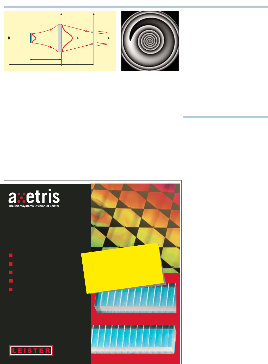
butions while maintaining high efficiencies.
Conventional lenses generate focused
spots, whereas a diffractive focusing ele-
ment can provide the required caustic line
in the focal plane (figure 2). Using a plano-
convex lens as the focusing element with a
diffractive microrelief pattern on its plano
surface, the DOE directs laser light towards
the line contour (straight line, ring, poly-
gons etc) instead of at a single focal spot.
Thus, a line-contour focal image is achieved
from the collimated laser beam without any
scanning system.
The line-contour focusing element provides
novel opportunities in laser marking, drilling
and in the welding of plastics and metals
using high-power lasers. Applications also
exist in machinery and microelectronics; the
optical heads of scanning laser writers; opti-
cal information processing; and laser surgery.
Splitting and multiplication
Recent advances in diffractive optics theory
and technology have made beam splitting/
multiplication a valuable resource for optical
designers. Applications range from spot-array
generation and fibre-optic coupling through to
laser heat treatment of material surfaces and
laser ablation. Other promising opportunities
for the technique include multiple and multi-
focal imaging, laser-beam mode selection and
simultaneous contour shaping.
Diffractive beam splitters have been widely
used in laser perforation as they allow high
throughput and accurate positioning, with-
out leaving any working residual materials
(figure 3, p35). By integrating diffractive
beam splitters into these systems, several per-
forations can be achieved simultaneously
with extremely accurate distances between
the spots, removing the need for a moving
x–ytable and improving performance.
Multiple-spot (including double-spot) DOEs
provide a line or an array of identical focal
spots located in the focal plane and can be
arranged in a one or two-dimensional pat-
tern. DOE beam splitters offer advantages
including uniformity in power between the
spots (±1% can be achieved for standard 1 ×
2 and 2 ×2 splitters and significantly more
for other designs). The positional predictabil-
ity of each beam/spot is also enhanced.
Beam sampling
Another DOE closely related to the beam split-
ter is the beam sampler, which enables inline
measurements of high-power laser beams to
be made. The device produces two exact
copies (samples) of the input beam with only
a small fraction of the total power, while the
main part of the master beam continues in
the optical train. This allows the sample
beams to be measured and analysed while the
main beam remains unaffected and opera-
tional. Beam samplers can be produced to
suit custom angles, wavelengths and various
power fractions of the main beam.
Diffractive beam samplers are being used
in place of conventional optics more and
more, because they offer a clean, non-inva-
sive analytical solution. For example, they
are replacing burn-off modal measurements
for CO2lasers. Since there are no burning ele-
ments in the system, no by-products are pro-
duced. Also, the diffractive beam samplers
are not polarization dependent and so meas-
urements can be taken while the laser is
operating online.
Diffractive beam samplers can be used to
monitor high-power CO2, Nd:YAG and other
lasers in materials processing, medical appli-
cations and in laser radar systems.
A single diffractive corrected focusing lens
can equal the high performance of a complex
multiple-optical-element objective lens. The
Leister ProcessTechnologies
Axetris Microsystems Division
Switzerland
Phone +41 41 662 74 74
axetris@leister.com
www.axetris.com
Laser diode collimation
Beam homogenization
Wavefront sensor optics
Fibre collimation
Custom micro-optics
ISO 9001:2000
Micro-Optics
Solutions
Visit us at the
Photonex 06
Stoneleigh Park /
Coventry, UK
PRODUCT GUIDE
34 OLE • October 2006 • optics.org/ole
ux
A
S
L0L
z0
I0I
I0,^0I0,^
Fig. 2: Schematic view of a line contour set-up (left) and the corresponding output pattern (right).
“DOEs can
modulate partially
and non-coherent
light sources as
well .”
OLEOct06PRODUCTGUIDEp33-35 25/9/06 16:07 Page 34
diffractive microrelief pattern on the plane
side of the lens gives a diffraction-limited spot
size that demonstrates a sharp focusing effect
and a dramatic increase in power densities,
even for long focal length DOEs.
Diffractive corrected focusing lenses offer
unique properties not matched by conven-
tional optics. “Special effects” include off-axis
sharp focusing; control of the focal spot
shape; controlled introduction of spherical
aberration; longer depth of focus; chromatic
correction; and double (multiple) spot focus.
Combining two beams
Many medical CO2(10.6 µm) laser systems
use a red He:Ne (632.8 nm) laser or laser
diode (635 nm) module (LDM) to generate
an aiming or pilot beam. It is essential that
the visible He:Ne/LDM beam coincides with
the invisible CO2beam so that the CO2focal
spot can be easily identified. Conventional
methods often use lens doublets and crys-
talline optics such as potassium bromide ele-
ments, which are hygroscopic and relatively
inconvenient to work with.
An elegant solution to this problem is a sin-
gle hybrid diffractive element called a dual-
wavelength beam combiner. This is a zinc
selenide lens with a microrelief diffraction
pattern etched into the plane side. The dif-
fractive pattern can be designed to control
just one wavelength. When placed in the path
of the 10.6 µm and 633 nm laser beams the
DOE superimposes both wavelengths at the
same focal spot, without the need of doublets.
The durability of the diffractive beam
combiner far exceeds the two-lens system
alternative. Also, the integral light trans-
mittance of the diffractive dual wavelength
element outperforms any on-axis reflective
systems, with figures exceeding 98%.
Joshika Akhil is technical sales engineer at Laser
Components (UK) Ltd. For more information, see
www.lasercomponents.co.uk.
PRODUCT GUIDE
35
OLE • October 2006 • optics.org/ole
The natural
selection for
ti:sapphire
pumping.
Now available at 6 Watts, the finesse
from Laser Quantum is the smart
choice for optical pumping applications.
Noise <0.5% rms; stability <1.0%rms;
automatic power control; 22,000 hour MTBF
diode life; no external cooling; proprietary
DEP cavity design; compact and robust
construction; advanced PSU with large LCD
and intuitive controls; remote interlock;
RS232 interface.
the evolution of technology
t: +44 (0)161 975 5300 f: +44 (0)161 975 5309
www.laserquantum.com
sales@laserquantum.com
incident
beam
mask
mask
rotating web
in focal plane
lens
DOE
Fig. 3: the beam splitter DOE accepts a collimated
beam and produces a number of beams with the
same characteristics as the incident beam except
for angle of propagation and power. By placing a
focusing lens close to the element, all beams can
be focused into spots. A mask is recommended for
blocking higher order diffraction fringes.
I
OLEOct06PRODUCTGUIDEp33-35 25/9/06 16:08 Page 35

More
machine
vision
enquiries
than ever
before.
Mark Williamson, Firstsight Vision, IPOT 2006
To find out more call Marlene Carr on +44 (0)1822 614671
or email: mc@trident-exhibitions.co.uk or visit the web @
www.ipot.co.uk
supported by
PLUS IPOT, Machine Vision & Displays Technology is co-located alongside: Mtec (Sensors,
Measurement & Instrumentation);Machine Building; Practical Vacuum;MDT and 3C
NEC,Birmingham, UK, 14 & 15 February, 2007
www.photon-energy.de
Nd - Lasers Diode pumped Arclamp pumped
Application: Marking-Structuring-Cutting-Welding
Designed for industrial environment
Frequency:
up to
100 kHz
Power range:
3W - 120W
Beam quality:
up to TEM
00
Photon Energy GmbH
Bräunleinsberg 10
D-91242 Ottensoos - Germany Tel: +49 - 9123 - 99034 - 0
Fax: +49 - 9123 - 99034 - 22 www.photon-energy.de
E-Mail: info@photon-energy.de
LASERSOURCES
•Scintillation crystals •Linear & two dimensional arrays
•Detector assemblies •Infra-red optics •Custom products
Crystal
Materials
Westwood, Margate, Kent CT9 4JL, UK
Tel: +44(0)1843 231166
Fax: +44(0)1843 290310
email: sales@hilger-crystals.co.uk
www.hilger-crystals.co.uk
www.newport.com
OLEOctAdverts36 22/9/06 13:29 Page 1
Oscilloscope
Tektronix
Test and measurement
specialist Tektronix has
released the
DPO70000 digital
phosphor oscilloscope
and the DSA70000
digital serial analyser.
According to the firm, these new 4, 6 and 8 GHz
bandwidth instruments provide industry-best
hardware and software for data-acquisition,
debug, validation and compliance testing.
With a sample rate of 25 GS/s on all four
channels simultaneously, the new models are
said to provide the fastest four-channel sample-
rate performance of any oscilloscope available.
For example, the 8 GHz DPO70804 and
DSA70804 have a typical rise time of 35 ps and
provide a jitter noise floor down to 400 fs rms
(typical) for critical jitter measurements. The
DPO70000 offers 10 million data points as
standard per channel while the DSA70000
offers 20 million as standard per channel.
www.tektronix.com
Tunable filter
Yenista Optics
Yenista Optics of France has unveiled a low-loss
tunable filter. The device is said to tune over
120 nm from 1510 to 1630 nm with a full
spectral sweep time of 200 ms, an
autopositioning wavelength accuracy of 2 pm,
PDL of maximum 0.2 dB and insertion loss of
3 dB. Yensita adds that the 3 dB bandwidth of
the filter is 0.35 nm although other bandwidths
are available on request. The product is offered
in rack-mount and benchtop versions for test
and measurement applications in the laboratory
as well as in the field.
www.yenista.com
Laser welding system
ROFIN Laser Micro
The StarWeld Select
from ROFIN Laser Micro
can be operated as an
ergonomically
optimized manual
welding laser, as a
deposit welding laser
with joystick and as a
high-precision CNC
system. All process
steps are controlled via
a multifunctional joystick and a large
multicolour touch-screen display enabling
semi-automatic laser welding, CNC teach-in or
jogging of heavy workpieces.
The system can cope with workpieces
weighing up to 50 kg, which it can position with
an accuracy of 10 µm.
ROFIN adds that the TrackMode allows direct
storage of manually controlled paths and can
be used for deposit welding along curved
contours and for semi automatic operations.
The AreaFill option allows several parallel offset
welding seams to be generated for 3D surface
deposit welding.
www.rofin.com
DC current source
Optronic Laboratories
Optronic Laboratories
has introduced the
OL400-C controller,
which it has designed
for use with its OL
series 426 and 455
integrating sphere calibration standards.
According to the firm, the precision-constant
DC current source features microprocessor
control, a lamp-hours monitor, a wide viewing
angle two-line display, USB 2.0 interface and an
adjustable tilt handle. An optional software
development kit is also available.
www.olinet.com
488 nm laser
Coherent
The latest Sapphire
laser from Coherent is a
small-footprint OEM
source delivering
50 mW of continuous-
wave output power at
488 nm. Primarily
intended for biomedical
instrumentation such
as flow cytometry and drug discovery, the
50 mW power level will deliver increased
sensitivity leading to faster throughput and/or
higher signal-to-noise for these applications,
according to Coherent.
The Sapphire 50 mW is based on the same
optically pumped semiconductor laser
technology as its 10 and 20 mW counterparts
and also shares the same form factor, power
requirements and beam characteristics.
Coherent says that, compared with air-cooled
argon lasers, its all-solid-state Sapphire offers
the advantages of smaller size, greater electrical
efficiency, lower heat dissipation and
substantially longer lifetime.
www.coherent.com
PRODUCTS
If you would like your company’s products to be featured in this section,
please send press releases and images to James Tyrrell (james.tyrrell@iop.org).
37
OLE • October 2006 • optics.org/ole
Pulsed Tunable
Dye Laser
quantel@quantel.fr - +33 1 69 29 17 00 / sales@bigskylaser.com-(406) 586 0131
Quantel & Big Sky Laser
Quantel’s TDL90 offers researchers an extremely versatile
nanosecond tunable laser source.
• 200nm to 4.5
µ
m tuning using wavelength extension options
• High Efficiency
• Compact Design
• User-Friendly
• Low ASE Oscillator Design
Quantel provides you with a complete Nd:YAG pump / dye
laser system, for an optimal mechanical stability.
Contact Quantel, Big Sky Laser or your local representative
for more details.
OLEOct06PRODUCTSp37-49 25/9/06 16:09 Page 37
Pulsed UV laser
Newport
The Explorer Scientific
from Newport is a low-
power, intracavity,
frequency-tripled and
actively Q-switched
diode-pumped solid-
state laser that delivers pulse energies of up to
120 µJ at 349 nm. The source is said to be an
ideal research tool for applications requiring
high pulse energies and peak powers at low
kilohertz repetition rates.
The Explorer can be operated from single shot
up to a 5 kHz pulse repetition rate at variable
pulse energies. Pulse widths are typically less than
5 ns and, with a pulse-to-pulse stability of less
than 3% rms, the company says that applications
will benefit from an extremely low signal-to-noise
ratio. A LabView-based GUI allows customers to
interface with the laser via a USB port.
www.newport.com
Chromatic confocal sensors
Armstrong Optical
The latest line of
confocal chromatic
optical pens
manufactured by STIL of France is now available
through Armstrong Optical of the UK. Typical
applications are listed as profilometry,
microtopography, roughness, autofocus
vibrometry, in-line inspection quality control and
thickness measurements.
A modular design allows up to 30 different
configurations for specific depth-of-field, spot
size, working distance, object slope and
photometric efficiency. Five magnifiers with focal
lengths ranging from 3.3 to 29.0 mm and six
chromatic lenses with depths of fields from
130 µm to 27 mm are available. The pens are
said to achieve a maximum axial resolution of
5 nm, an accuracy of 20 nm and a maximum
slope of 87° for diffusive objects.
www.armstrongoptical.co.uk
Fibre-coupled diode laser
Point Source
Point Source has
launched a higher-
power version of its
iFLEX2000 fibre-
coupled laser. The
latest addition delivers
30 mW at 405 nm in a
TEM00 Gaussian beam.
Laser beam
conditioning is
performed using a
singlemode fibre, which
acts as a spatial filter while also providing a
flexible beam-delivery mechanism.
The company also claims that the laser is
unique in employing forward, closed-loop power
control that is immune to optical feedback, which
in turn provides a long-term ultra-stable output
and low short-term amplitude noise. Target
biomedical applications include flow cytometry
and fluorescence imaging, although the laser is
said to be ideal for optical media applications
where spot size and resolution are critical.
www.point-source.com
Laser barriers
LaserVision
LaserVision says that its
new Laserbarrier
product is a modular
system that meets the
changing needs and
requirements of laser
users. Based on a
patent-pending material
system, the barrier
offers protection from CO2and Nd:YAG lasers up
to a power density of 10 MW/cm2. LaserVision
says that this equates to protection levels of AL4
at 10600 nm and AL6 at 1064 nm at 100 s of
direct illumination.
The barrier has a specially designed surface,
which is said to make it suitable for applications
in industry, research and even cleanroom and
medical environments. LaserVision adds that the
product can contain different or full segmented
protection modules such as cabin windows.
www.lvg.com
Fizeau interferometer
4D Technology
4D Technology, US,
has introduced the
FizCam 2000. “This is
the first-of-its-kind ‘on-
axis’ vibration Fizeau
featuring a short
coherence length source that enables
measurement of transparent samples and
assemblies that are difficult or impossible to
measure with traditional laser
interferometers,” said James Millerd, 4D’s
chief technical officer.
According to 4D, the short coherence feature
eliminates the need for extraneous coatings to
control interfering fringes by isolating and
measuring only the desired surface. In addition
to measuring parallel optical grade surfaces, the
FizCam 2000 is said to be well suited to
separating and measuring surfaces within an
optical assembly, making remote cavity
measurements, testing index homogeneity,
measuring thin optics and environmental
chamber testing.
www.4DTechnology.com
PRODUCTS
38 OLE • October 2006 • optics.org/ole
OLEOct06PRODUCTSp37-49 25/9/06 16:10 Page 38

NASDAQ: STKR
Copyright ©2006 StockerYale Inc. All rights reserved.
StockerYale Inc.
Tel: +353-21-4320750
Fax: +353-21-4327451
saleseurope@stockeryale.com
www.stockeryale.com
•220,000 lux @ 630 nm
•395 nm, 470 nm, 630 nm,
740 nm, white
•Frontlight and backlight
configurations
•125 mm, 250 mm and
500 mm line lengths
Applications include:
•Linescan
•Web inspection
•Inspection of currency, lumber,
FPD, foil, paper, plastics,
non-wovens
Generates a uniform, bright stripe
of illumination for linescan
LINESCAN ILLUMINATOR
COBRATM
OLEOctAdverts39 22/9/06 13:35 Page 1
Fusion splicer
Sumitomo Electric Industries
The T-39 single fibre
core aligning fusion
splicer from Sumitomo
Electric Industries has
been designed under
the company’s ECO-
21/2 programme,
which considers the environmental effects of a
product over its lifetime. As such, the company
says that this is the first in a new generation of
splicers that comply with the European Union’s
RoHS regulations.
Sumitomo says that the T-39 has dual
independent heat-shrink ovens that improve
splice throughput and productivity. The device
also features “hands-free” operation, thanks to
the automatic starting of the splice and heat-
shrink processes.
www.sumielectric.com
Polarization-maintaining fibre
Liekki
Liekki of Finland has added a highly doped,
large-mode-area fibre with a very high cladding
absorption (Yb1200-20/125DC-PM) to its
ytterbium-doped fibre product family. Typical
applications are listed as materials processing
(cutting, marking and drilling), laser ranging,
remote chemical detection and nonlinear
frequency conversion.
The fibre has a highly doped 20 µm diameter
core and a large core-to-cladding ratio. These
features result in a nominal cladding pump
absorption of 7.1 dB/m at 920 nm, rising to
around 30 dB/m for absorption at 976 nm.
According to Liekki, this enables very short
active fibre lengths – less than 1 m for
976 nm pumping.
www.liekki.com
Gigabit Ethernet camera
JAI PULNiX
JAI PULNiX has added a
new member to its line
of gigabit Ethernet
cameras. The
TM-1327GE is a
compact progressive scan CCD camera featuring
a 2
/3inch image sensor and a frame rate of 30 fps
at the full resolution of 1392 ×1040 pixels.
Contained in a 50.8 ×50.8 ×84.8 mm
housing, the camera is said to have a wide
dynamic range with sensitivity in both the visible-
and near-infrared. Its interline transfer CCD
permits full vertical and horizontal resolution with
shutter speeds of up to 1/21 000 s.
Asynchronous reset combined with a no-delay
pulse-width-controlled shutter provides flexible
triggering and the exposure control necessary for
machine vision applications.
www.jaipulnix.com
PRODUCTS
FEMTO42!).»
&EMTOSECOND/SCILLATORS
NMTONM
5PTO7
$OWNTOFS
-(ZTO-(Z
PICO2%'%.»
0ICOSECOND!MPLIFIERS
.)2'REEN56
5PTOM*7
$OWNTOPS
5PTOK(Z
FEMTO2%'%.»
&EMTOSECOND!MPLIFIERS
NMTONM
5PTOM*7
$OWNTOFS
5PTOK(Z
PICO42!).»
0ICOSECOND/SCILLATORS
.)2'REEN56
5PTO7
$OWNTOPS
-(ZTO'(Z
0RODUCT2ANGE
PICOFEMTO./6!»
#AVITY$UMPED/SCILLATORS
NMTONM
5PTO*
$OWNTOFS
5PTO-(Z44,TRIGGER
$IODEPUMPED
ULTRAFAST
SOLIDSTATELASERS
s 0ASSIVEANDSELFSTARTING3EMICONDUCTOR3ATURABLE
!BSORBER-ODELOCKING3%3!-
s 5SER2EPLACEABLE$IODE-ODULE52$-
s (IGHTEMPORALANDSPATIALSTABILITY
s #OMPACTANDMODULARSETUP
s 3EALEDOFFTECHNOLOGY
s (ANDSFREETRUETURNKEYOPERATION
s 3INGLEPHASEPOWERSUPPLY
(IGH1,ASER7E4HINK5LTRAFAST»
(IGH1,ASER0RODUCTION'MB(
+AISER&RANZ*OSEF3TRASSE
(OHENEMS\!USTRIA
0HONE
SALES HIGH1LASERAT
WWWHIGH1LASERAT
(IGH1,ASER53)NC
7ALTHAM3TREET
7ATERTOWN-!\53!
0HONE
SALES HIGH1USCOM
WWWHIGH1USCOM
OLE • October 2006 • optics.org/ole
OLEOct06PRODUCTSp37-49 25/9/06 16:11 Page 40
PYSER-SGI
200LP /MM
New Calibration and
Resolution Standards For
Optical and Vision Systems
High precision multi image
slide.
USAF resolution chart down to
Group 9/3.
High definition ronchi rulings
Centre Detail
NEW
PYSER - SGI LIMITED
Tel: +44(0)1732 864111
Fax:+44(0)1732 865544
E-mail: sales@pyser-sgi.com
www.pyser-sgi.com
OLEOctAdverts41 22/9/06 13:50 Page 1
561 nm DPSS laser
Laser Lines
Laser Lines of the UK is
now distributing the
561 nm Jive 75 laser
from Cobolt. Emitting
75 mW, the Jive 75 is
said to offer low noise,
excellent beam quality, long lifetime and single
longitudinal mode operation, all in a compact
package. The beam size and divergence match
those of an air-cooled ion or HeNe laser, which
is said to make the Jive a direct drop-in
replacement in flow-cytometry and microscopy
applications. A narrow spectral bandwidth and
long coherence length also make the source
useful for applications such as spectroscopy,
holography and interferometry.
www.laserlines.co.uk
SLEDs
Exalos
Exalos of Switzerland
says that its 750 nm
line of superluminescent
light-emitting diodes is
especially suited to
optical coherence tomography (OCT) and
biomedical applications. The firm claims that
its devices, which combine the spatial
coherence of a laser diode with the temporal
incoherence of an LED, provide high
suppression of second coherence peaks.
Typical values for the EXS7505-1411 are 3 mW
optical output power in a singlemode fibre and
21 nm 3 dB spectral bandwidth.
The EXS7510-1411 is said to achieve 5 mW
optical output power in a singlemode fibre and
14 nm 3 dB spectral bandwidth. Featuring a
built-in thermoelectric cooler and monitor diode,
the standard product is delivered in a 14 PIN DIL
housing. Uncooled devices in TOSA housings are
also available. The firm also offers devices at
850 and 1300 nm, which may be of interest to
developers of biomedical and OCT apparatus.
www.exalos.com
VCSELs
Vertilas
German VCSEL expert Vertilas says that its latest
generation of 1310 and 1550 nm sources
enables applications up to 10 Gbit/s, thanks to
a benzocyclobutene-based optimized device
structure. It says that this high performance
coupled with a low threshold current makes the
components valuable for the newest generation
of small-form-factor optical modules, such as
SFP+ and XFP.
The lasers are offered in standard TO-46
packages and are being integrated into
application-specific assemblies, such as pigtails
and receptacles.
www.vertilas.com
PRODUCTS
Picosecond
Picosecond
Diode Lasers
Diode Lasers
EPL 375
EPL 405
EPL 445
EPL 473EPL 635
10 Pre-set Repetition rates:
20 kHz - 20 MHz
Pulsewidths*down to 75ps
with optimised pulse characteristics
at each repetition rate.
Spectrally Purified Output
Fully Integrated, Compact
Design, No External Controller
Optimised for Time-Resolved
Spectroscopy
Optimised Beam Collimation
Applications include:
•Time Correlated Single Photon
Counting (TCSPC)
•Fluorescence Lifetime Imaging (FLIM)
•Fluorescence Resonance Energy
Transfer (FRET)
•Optical Tomography of Biological
Samples
www.edinst.com
For more information contact us at:
sales@edinst.com
Edinburgh Instruments Ltd
2 Bain Square, Livingston
EH54 7DQ, UK
Tel: +44 (0)1506 425300
Fax: +44 (0)1506 425320
*Typical value may vary with model.
Bertha-von-Suttner-Str. 5 · D - 37085 Goettingen
tel. + 49 (0) 5 51 - 79 76 70 · info@metrolux.de
optical metrology
Laser Beam
Diagnostics
For Pulsed & CW Lasers
BeamLux II Software
Multiple Camera
Support
Beam Analysis in
Compliance with ISO
High Data Processing
Automation of
Measuring Tasks
Cameras for
Beam Profiling
Industry Standard
USB / Fire Wire/
Analog
XUV-VUV-VIS-IR
Highest Resolution
Energy and Power
Measurement
Devices
Wide Range of
Detectors
Implementation
in BeamLux II
Optimized and reliable systems
for industry and research.
Contact us for your individual
application.
42 OLE • October 2006 • optics.org/ole
OLEOct06PRODUCTSp37-49 25/9/06 16:11 Page 42
LEDs
Osram Opto Semiconductors
Osram Opto
Semiconductors says
that its new advanced
power TopLED devices
are 50% brighter than
their predecessors,
thanks to thin-film
technology. The company quotes an output of
19 lm for green and amber, 15 lm for white and
red, 14 lm for yellow and 5 lm for blue, all at
140 mA. Osram says that this new range is
positioned between standard and high-power
LEDs and is ideal for area and effect lighting. An
SMT package ensures that the LEDs are
compatible with standard solder processes.
www.osram-os.com
Microinspection system
Moritex
Moritex of the UK says
that its MS804
Scopeman is a powerful
and easy-to-use
microinspection system
that is able to
undertake almost any
real-time industrial
inspection or quality-assurance task. The system
is available with a range of zoom lenses
(16–200×); x, y and z stages; camera mounts
and a variety of imaging peripherals.
The company says that a combination of
multi-exposure, high-intensity LED lighting and
intuitive software for fast and simple acquisition
allows the system to deliver high-resolution,
1280 ×960 pixel images. It adds that, by
changing the camera’s shutter speed and
combining “bright” and “dark” images, the
MS804 provides an enlarged dynamic range.
www.moritex.com
Photon-counting training
SensL
SensL of Ireland has launched two
complementary training courses for academics,
researchers and engineers who wish to learn
more about the technology and techniques used
in photon detection. The products are called
PCEdu-1: photon counting fundamentals and
PCEdu-1T: photon timing upgrade.
PCEdu-1 is an entry level lecture and
laboratory series that SensL says is ideal for
academics looking to start a low-light sensing or
semiconductor device physics training module.
It is also said to be ideal for OEMs looking to
bring an R&D team up to speed quickly.
PCEdu-1T is an upgrade package that takes
the training to a higher level through a series of
lectures and lab experiments dealing with real
photon-counting scenarios.
www.sensl.com
PRODUCTS
1 Bay Street
Stirling, NJ 07980
Telephone: 908-647-6601
Fax: 908-647-8464
info@fiberguide.com
THE PHOTONICS PACKAGING COMPANY
fiberguide
industries
SM
www.fiberguide.com
Contact Fiberguide today and ask
for our new CD-ROM. It's free!
Eduraguide HOPC™ Fibers
The Power
To Heal
Apowerful laser delivery system in a
surgeon’s skilled hand helps cure people.
These medical laser systems are made
possible by utilizing Fiberguide Industries
new Eduraguide HOPC™ fibers.
The Eduraguide HOPC™ line of large
core multi-mode fibers have a numerical
aperture of 0.39 and employ a Hard Optical
Polymer Coating (HOPC™). With increased
beam intensity, this exceptional coating
offers superior fiber strength and reduces
static fatigue in humid environments.
Eduraguide HOPC™ fibers offer excellent
connection alignment and they have a high
core to clad ratio. Eduraguide HOPC™ is
also made available in silica/silica HOPC™
fibers that have a N.A. of 0.22 and an
attenuation of <10dB/km@850nm.
The finest medical laser delivery system
starts with Eduraguide HOPC™ fibers.
Call Fiberguide Industries to discuss your
specific requirements.
www.photonlines.com
Streak Camera
UV-LED module
High speed Camera
44 OLE • October 2006 • optics.org/ole
OLEOct06PRODUCTSp37-49 25/9/06 16:12 Page 44
Colour CCD camera
Toshiba
The IK-TF9C from
Toshiba’s Imaging
Systems Division is a
three-chip, colour CCD
camera with a resolution
of 2048 ×1536 pixels.
Also incorporating Toshiba’s progressive scan
technology to eliminate image jitter, the camera
is said to be ideal for high-speed industrial
machine vision applications.
Measuring 44 ×44 ×78.3 mm and weighing
165 g, the camera has a frame rate of 20 fps
(full frame) and 40 fps (partial scan). Other
specifications include a C-mount for lenses, an
8-bit RGB digital output and CameraLink
compatibility for ease of operation.
www.cameras.toshiba.com
Software-development kit
Prosilica
Industrial CCD camera
maker Prosilica has
released Linux and QNX
software-development
kits (SDKs) for its range
of GigE Vision cameras,
complementing the
company’s existing Microsoft Windows SDK.
According to Prosilica, the GigE Vision SDKs
provide programmers with the means to control
and capture images from its gigabit Ethernet
cameras. In addition the Linux SDK works on
both Intel ×86 and PowerPC hardware. The SDK
also includes sample code to help
programmers to use Prosilica’s cameras in their
Linux-based applications.
www.prosilica.com
Deep-cooled CCD
Princeton Instruments/Acton
Princeton Instruments/Acton has added the
2048 series of front- and back-illuminated
cameras to its PIXIS line of CCD cameras. Based
on e2v technologies’ 42-40-2048 ×2048
format sensor with an imaging area of
26.7 ×26.7 mm, PI/Acton says that the
PIXIS:2048 offers deep cooling better than
–70 °C (via a thermoelectric Peltier) with a
vacuum guaranteed for the life of the camera.
The new cameras come with the familiar
traits of the PIXIS line, such as dual
100 kHz/2 MHz digitizers, ultra-low read noise
of 3e–rms read noise (at 100 kHz), all-metal
hermetic seals, USB 2.0 interface and single
optical window design.
Other specifications include flexible binning,
ROI capabilities and WinView software. The
company adds that a toolkit with LabView
examples and its own PVCAM library of function
calls is available.
www.piacton.com
Raman workstation
McPherson
The McPherson Raman
workstation is available
for the popular laser
lines between 325 and
830 nm. Systems
include a solid-state
laser, speciality filters and a sample chamber
with laser focusing and signal-collection optics.
Sample chambers compatible with cryogenic
sample holders are also available for
photoluminescence work.
All elements in the workstation are mounted,
aligned and integrated with a research grade
350 nm, f4.8 spectrometer with CCD and
software. The user-friendly single-stage
instrument is said to ensure good signal to noise
and ease of use for detecting Raman-shifted
emission above 300 wavenumbers.
www.mcphersoninc.com
Imaging spectrometer
HORIBA Jobin Yvon
HORIBA Jobin Yvon has
released the iHR550
imaging spectrometer.
With a focal length of
0.55 m, the device
offers the ability to perform multitrack
experiments with up to 20 fibre inputs. Incorrect
and rediffracted spectra are eliminated using an
asymmetric Czerny–Turner design in conjunction
with an on-axis grating drive system.
The iHR550 has two entrance and two exit
ports. Each exit port can be configured for use
with either an array detector, such as a CCD, or
a slit for use with a PMT. The company can
supply the iHR550 in a variety of configurations
for all spectroscopic measurements, including
Raman, photoluminescence, emission and
imaging or multitrack spectroscopy.
www.jobinyvon.co.uk
Dual-wavelength laser diode
Rohm
The RLD2WMUV2 from
Rohm is a singlemode,
dual-wavelength laser
diode that emits at
both 785 and 655 nm,
making it an ideal source for both DVD-ROM
and DVD players. The firm says that
optimization of a strained quantum well has
allowed a reduction in threshold current and
good temperature characteristics.
Rohm quotes a threshold current of 18 mA for
785 nm and 20 mA at 655 nm, both at 25 °C.
The emission pointing distance is specified at
110 µm. The device can be combined with
Rohm’s high-frequency modulation IC
(BU9369FVM) for reduced noise.
www.rohmelectronics.com
PRODUCTS
45
OLE • October 2006 • optics.org/ole
OLEOct06PRODUCTSp37-49 25/9/06 16:12 Page 45
Beam profiler
Photon Inc
Photon Inc has
released a 12-bit beam
profiler with FireWire
(IEEE 1394)
connectivity and a
large dynamic range.
Available in two
versions, model 2523 features a 2
/3inch
format (9.0 ×6.7 mm) CCD with 6.45 µm
pixels, whereas model 2512 is based on a 1/2
inch format (6.5 ×4.8 mm) CCD with 8.3 µm
pixels. Both profilers have a small form factor
(49 ×62 ×62 mm), making them easy to insert
into optical paths. According to the firm, the
beam profiling system does not require a
frame-grabber card so can be moved easily
between different computers.
The device measures both continuous-wave
and pulsed beams over the 190–1100 nm
wavelength range. The firm claims that by using
extended range imaging, the unit can obtain
profiles with a dynamic range as high as 144 dB
(24 bits of digitization). The company adds that
very large dynamic range is important in many
applications, especially lens characterization,
where lens aberrations are apparent from faint
features around a strong central peak in the
beam profile.
www.photon-inc.com
785 nm laser
B&WTek
B&WTek has introduced its Cleanlaze high-
resolution and wavelength-stabilized laser
technology for Raman spectroscopy. Emitting at
785 nm, multimode models offer 0.2 nm FWHM
while singlemode versions feature a typical
linewidth of 0.02 nm. Output power options
range from 25 mW to more than 1 W at 785 nm.
Sources emitting at 980 nm and other
custom wavelengths are available. The lasers
are said to be ideal for OEM Raman
instrumentation, process, portable and lab
applications, thanks to their light weight, small
footprint, high stability, narrow linewidth and
low maintenance cost.
www.bwtek.com
Waveguide optics simulation
Optiwave Systems
Optiwave Systems has
released OptiBPM8 –
the latest version of its
waveguide optics
design suite. This has
advanced LP and
vector-mode solvers for circular fibres. Optiwave
says that these meshless fibre-mode solvers find
modes using a transfer matrix method in
cylindrical co-ordinates.
Other new features in OptiBPM8 include
intelligent optimization engines, the ability to
import DXF and GDSII mask file formats and a
simulation engine performance boost that the
company says allows the software to run 50%
faster than previous versions.
www.optiwave.com
High-power diode laser
LIMO
LIMO has introduced a prototype 25 W diode laser
that emits a 10 ×10 mm beam with a divergence
of 2 ×2 mrad. The company says that the laser,
called LIMO25-C10x10-DL980, has a beam-
parameter-product of 5 mm mrad and yields
power densities of 5 MW/cm2in a 25 µm spot. It
hopes to double the output power to 50 W in the
near future.
LIMO also offers a fibre-coupled version of
this source. The LIMO25-F50-DL980 delivers
25 W via a 50 µm fibre core with a numerical
aperture of 0.22.
www.limo.de
Translation stage
PI
PI’s P-652 piezoelectric
linear-motor-driven
translation stage
consists of four parts
and, according to the
firm, can replace
classical drive
elements, such as rotary motor/leadscrew
assemblies or electromagnetic linear motors in
a microsystem. Measuring only
9.0 ×6.5 ×2.4 mm, the P-652 stage offers a
travel range of 3.2 mm and can move at
velocities of up to 80 mm/s. Other
specifications include a resolution of better than
0.1 µm, a holding force of 20 g and an operating
current of 55 mA. Highly integrated electronics
are available for 3 V control.
www.pi.ws
Encapsulant
Nusil Technology
Nusil Technology has added the GEL-9617-30
to its range of Lightspan materials for the
photonics industry. Designed as a protective
encapsulant for LED or other photonic
applications, the gel has a high refractive index
of 1.54 to maximize optical efficiency. Nusil
says that the encapsulant resists optical
degradation when exposed to ultraviolet
radiation or extreme temperatures. It adds that
the gel also serves as an effective medium for
phosphor incorporation. Formulated to cure at
room temperature, the gel can be cured rapidly
with heat to address issues of substrate and
lens delamination. The GEL-9617-30 is
available in 50 ml side-by-side kits for
evaluation purposes.
www.nusil.com
PRODUCTS
ALL FIBER
BEAM
COMBINER
A brand new singlemode fused
fiber beam combiner for visible
laser beams.
Blue/Red, Green/Red, Blue/Green
versions available.
www.point-source.com/ole
47
OLE • October 2006 • optics.org/ole
OLEOct06PRODUCTSp37-49 25/9/06 16:13 Page 47
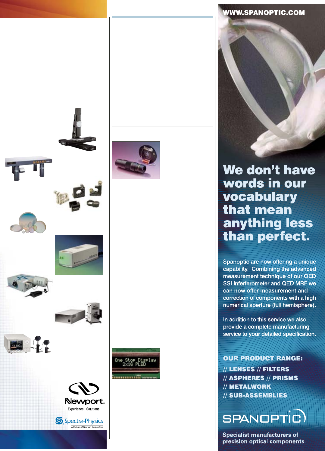
Power supply
Power-One
The BLP30-3000G AC–DC power supply is
now available from Power-One. Measuring just
2×4 inches, the 30 W unit is quoted as
producing 5 V at 3.5 A (5 A peak), 12 V DC at
2 A and –12 V DC at 0.5 A. The supply is said
to be the ideal power source for space-
constrained, 1U-high applications, such as
data networking, medical instrumentation and
external disk storage. RoHS compliant, the
unit operates over a wide 90–264 V AC input
range and provides short-circuit and
overvoltage protection.
www.power-one.com
Shutters and machine vision
Melles Griot
Melles Griot, a provider
of photonic
components, has added
shutters and machine
vision products to its
online catalogue. The
firm’s IES series shutters include an adjustable
iris diaphragm, xsynchronization and a manual
actuation lever that allows the device to operate
without an electrical signal. The firm also
supplies UltraThin versions designed to fit into
restricted spaces. Both IES and UltraThin designs
feature spring-steel blades with a Teflon
impregnated, matte-black finish and include a
multiblade shutter mechanism that is said to
give near 100% light extinction.
According to Melles Griot, its range of four
high-performance telecentric lenses suit
machine vision, metrology and precision-
gauging applications. The firm claims that the
lenses provide low optical distortion and a high
degree of telecentricity for accurate image
reproduction, particularly when viewing 3D
objects. Lens accessories such as
teleconverters, right-angle attachments, fibre-
bundle collimators and anodized mounting
brackets are also available from the firm.
www.mellesgriot.com
16 ×2 character PLED
One Stop Displays
One Stop Displays has
released its 16 ×2
character PLED in a
new module size of
84 ×44 mm. Dubbed
OSD1602M03-F, the RoHS compatible unit
features 160˚ viewing angles, over 100:1
contrast ratios and a low 20 mA of current draw
at 40 nits of uniform brightness. The display
uses the standard Hitachi HD44780 character
LCD interface and command set, and suits
hand-held products, instrumentation and
security panels to name just a few applications.
www.onestopdisplays.net
PRODUCTS
MAKE LIGHT |MANAGE LIGHT |MEASURE LIGHT
Newport
Your One-Source Partner
To Equip Your Laboratory
With Newport, you can rely on a partner who has over
40 years of experience in serving the research market to
provide you with the best possible solutions to equip
your laboratory. From the latest instrumentations for
motion control, vibration control, opto-mechanics, light
sources, optics to leading-edge lasers, spectrometers
and many more, Newport is your one-stop source for all
the products and solutions you need to Make, Manage
and Measure LightSM.
䉳Vibration
Control
䉳Optics
Laser 䉴
䉳Spectroscopy
Light 䉴
䉳Photonic
Instruments
Your One-Source Partner
To Equip Your Laboratory
AD-090622-EN
Call us to receive a free
copy of the Newport
2006-07 Catalog
5000+ new products!
Belgium
Tel: +32-(0)16 402927
France
Tel: +33 (0)1.60.91.68.68
Germany
Tel: +49 (0)61 51 / 708-0
Italy
Tel: +39 (0)2/92.90.921
Netherlands
Tel: +31-(0)30 6592111
United Kingdom
Tel: +44 (0)1635.521757
Opto- 䉴
Mechanics
Motion 䉴
Control
Your One-Source Partner
To Equip Your Laboratory
Your One-Source Partner
To Equip Your Laboratory
48 OLE • October 2006 • optics.org/ole
OLEOct06PRODUCTSp37-49 25/9/06 16:14 Page 48

Anti-reflective ball lenses
DSI
Deposition Sciences Inc
(DSI) is offering
antireflection (AR)
coated ball lenses in a
variety of glass indices
and in new larger sizes up to 10 mm diameter.
Highly durable and scratch resistant, the firm’s
IsoSphere range of AR coated lenses is
available with transmission values > 99.5% in
indices of up to nd2.0 at 550 nm. DSI claims
that its ball lenses are an affordable and
mechanically compact way of collimating the
output of an optical fibre or laser diode. Lenses
are resistant to most chemicals and are said to
suit aerospace, oil-field exploration, oil refining,
marine and undersea applications.
www.depsci.com
Off-the-shelf aspheres
Asphericon
Asphericon of Germany has launched a range of
“off the shelf” aspheres. Dubbed Standard
Precision Apsheres (SPAs), the lenses are
available in a number of diameters from 6 to
100 mm and are made primarily from high-index
material with low dispersion. The lenses are
manufactured by CNC grinding and polishing
and can be supplied with a choice of three
standard coatings. According to the firm, all
SPAs are available directly from stock.
www.asphericon.com
UV radiometer
Dymax
Dymax has added the
ACCU-CAL 50
radiometer to its range
of technical adhesives
and ultraviolet (UV)
curing systems. The unit
allows users to monitor
the intensity of a UV
curing source and assess adhesion
performance. Compatible with all types of
DYMAX UV curing systems, such as spot lamps,
flood lamps and conveyors, the device is said to
be simple to operate. It offers repeatable
measurement in the UVA spectrum
(320–395 nm) from 1 mW/cm2to 40 W/cm2.
www.dymax.com
PRODUCTS
Single-mode, single-frequency,
tunable diode lasers for
industrial applications
·· Spectral range 760 .. 2300 nm
··Narrow linewidth (1 .. 4 MHz)
··Up to 1400 GHz
mode-hop free tuning
··Very compact size
(e.g. 58 x 44 x 30 mm3)
·· Full computer control
Fields of application
··Gas sensing
·· Combustion monitoring
·· Drug screening
·· Interferometry
·· Tunable THz generation
OEM applications are encouraged
TOPTICA - Your Partner for
• Diode laser systems
• Femtosecond fi ber lasers
• Industrial lasers
• Optical media testing
Graefelfi ng, Germany
T (49) 89 85 837-0
sales@toptica.com
www.toptica.com
Tune it to Your
Wavelength
OLE • October 2006 • optics.org/ole
B&W Tek www.bwtek.com 39
BFI Optilas www.bfioptilas.com 21
Breault Research Organization
www.breault.com IFC, 8
Cambridge Technology
www.cambridgetechnology.com 25
Crystal Systems www.crystalsystems.com 18
CVI Technical Optics www.cvilaser.com OBC
Duma Optronics www.duma.co.il 35
Edinburgh Instruments www.edinst.com 42
Edmund Optics www.edmundoptics.co.uk 32
EKSPLA www.ekspla.com 38
ELCAN Optical Technologies
www.ELCAN.com/create 4
Electron Tubes www.electrontubes.com 41
Electro-Optical Products www.EOPC.com 32
Esco Products www.escoproducts.com 28
Evatec Process Systems www.evatecnet.com 28
Femto Messtechnik www.femto.de 40
Fiberguide Industries www.fiberguide.com 44
Fuji Magnetics www.polymer-optics.com 15
GPD Optoelectronics www.gpd-ir.com 28
GWU Lasertechnik www.gwu-group.de 24
HC Photonics www.hcphotonics.com 39
High Q Laser www.highqlaser.com 40
Hilger Crystals www.hilger-crystals.co.uk 36
Holo Or www.holoor.co.il 32
IPOT 2007 www.ipot.co.uk 36
Jenoptik Polymer Systems www.jenoptik-ps.de 15
Kentek Corporation www.kentek.com 9
Laser 2007 www.world-of-photonics.net 31
Laser Components (UK) Ltd
www.lasercomponents.co.uk 7
Lasermet www.lasermet.com 39
Laser Quantum www.laserquantum.com 35
Leister Process Technologies www.axetris.com 34
Melles Griot www.mellesgriot.com 13
Metrolux Optische www.metrolux.de 42
Möller-Wedel Optical
www.moeller-wedel-optical.com 18
Multiwave Photonics
www.multiwavephotonics.com 41
New Focus www.newfocus.com 22
Newport Spectra-Physics www.newport.com 48
Ophir Optronics
www.ophiropt.com 6, 14, 50, IBC
Optikos www.optikos.com 32
Opto Taiwan 2007 www.optotaiwan.com 43
PCO AG www.pco.de 45
Photon Energy www.photon-energy.de 36
Photonex 2006 www.photonex.org 12
Photonic Products
www.photonic-products.com 28
Photonics West 2007
www.spie.org/events/pw 46
Photon Lines www.photonlines.com 44
Physik Instrumente www.pi.ws 16
Point Source www.point-source.com 47
Pyser-SGI www.pyser-sgi.com 41
Quantel www.quantel.fr 37
Quintessence Photonics
www.QPClasers.com 10
Scitec Instruments www.scitec.uk.com 32
Spanoptic www.spanoptic.com 48
Stanford Research Systems
www.thinkSRS.com 20
StockerYale Inc www.stockeryale.com 15, 39
Tempo Plastic www.tempo-foam.com 18
Toptica www.toptica.com 49
XeniCs www.xenics.com 30
ADVERTISERS’ INDEX
The index is provided as a service and, while every effort is made to ensure its accuracy, Optics & Laser
Europe accepts no liability for error.
OLEOct06PRODUCTSp37-49 25/9/06 16:14 Page 49
PEOPLE
To advertise your job vacancies, contact Cadi Jones (tel: +44 (0)117 930 1090; e-mail: cadi.jones@iop.org).
50 OLE • October 2006 • optics.org/ole
SUDOKU PUZZLE
We hope you enjoyed September’s Sudoku
puzzle. You can check your answers against last
month’s solution on the left.
If you are new to Sudoku, this is how it works:
each puzzle consists of a 9 ×9 grid that is
subdivided into 9 smaller grids of 3 ×3 squares.
To complete the puzzle, you must ensure that
each row, column and 3 ×3 square contains the
numbers 1–9. All it takes is logic so try not to
guess at the numbers.
GERMANY
Gretschel takes director
role at QioptiQ GmbH
Ingo Gretschel has
been named as the
managing director at
QioptiQ GmbH,
which is based in
Asslar, Germany.
Formerly head of
optoelectronic sales at German firm Docter
Optics, Gretschel has many years’ experience
in optomechanical design and in the
manufacture of products and components
for both military and commercial
applications. Gretschel took up his new role
on 1 August and reports to QioptiQ group
chief executive officer Benoit Bazire.
FINLAND
Orsila continues as the
chairman at Modulight
Modulight has announced that Seppo Orsila
has been re-elected to the position of
chairman of the board but has withdrawn
from his operational role as chief financial
officer and vice-president of marketing at the
Finnish firm. A founder of Modulight, Orsila
will continue to contribute to the strategic
planning of the firm in his role as chairman.
Modulight was founded in 2000.
US
Optical software expert
adds to developer team
BRO, US, has
appointed Jianhua
Jiang as a
computational
optical scientist.
Jiang joins the firm
after nearly 10 years
of optical training and research at the
University of Alabama in Huntsville (UAH),
most recently as the leader of the
simulation group at the UAH Nano and
Micro Devices Center.
The firm has also recently made additions
to its Technical Customer Service Group
through the appointment of William
Donnelly as senior optical engineer and
Robert Shroder as optical engineer.
FRANCE/US
Liebowitz to lead Teem
Photonics in the US
Teem Photonics of
France, a specialist
in passively
Q-switched
microlasers and ion-
exchange integrated
optics, has appointed
Jay Liebowitz as president of its wholly
owned US subsidiary. Liebowitz had
previously been executive vice-president.
“Jay has helped to diversify our business
from telecoms and towards a wider breadth
of industries, including biophotonics,
instrumentation, remote sensing and
materials processing,” said Antoine
Kevorkian, chief executive officer of Teem
Photonics SA. “We see a significant growth
opportunity for our Q-switched microlaser
business in North America, so it makes
sense to elevate Jay’s position for leading
our expansion in this continent.”
US
Albe steps into a crucial
sales role at BinOptics
US-based BinOptics, a
maker of integrated
microphotonic
components for
optical
communications
and data-storage
applications, has named Edward Albe as vice-
president (VP) of sales and marketing. Most
recently, as VP of sales and customer service
at Picolight, Albe led the firm’s resurgence in
the fibre-optic transceiver market-place.
Founded in 2000, BinOptics is
headquartered in Ithaca, New York.
SPONSORED BY
LAST MONTH’S
SOLUTION
Copyright © Michael Mepham 2005
OLEOct06PEOPLEp50 25/9/06 15:57 Page 50


;T]bTbk<^d]cbk5X[cTabk<Xaa^abk?^[PaXiTabk1TP\b_[XccTab
4da^_T## %!#%#& k0\TaXRPb ' !(%($# k0bXP'!"!%&"% #
D_c^cWTRWP[[T]VT
2E8Xbd_c^cWTRWP[[T]VTFTWPeT#$fPeT[T]VcWbX]bc^RZaTPShc^bWX_^U^da
WXVWTbc[PbTaVaPST`dP[XchRahbcP[`dPacifPeT_[PcTb8Uh^d]TTSPRdbc^\
fPeT[T]VcW^abXiTfTRP]VTccW^bTc^h^dX]WP[UcWTcX\T
;TPa]PQ^dcfPeT_[PcTbPcfffReX[PbTaR^\fPeT_[PcTPacXR[TPb_g
5X]Sh^dafPeT[T]VcWPcfffReX[PbTaR^\`dPacifPeT_[PcTbPb_g
7HFKQLFDO
2SWLFV
,62406
h*AI¬BESOIN¬DUNE¬LAME¬DONDE¬Ì¬¬NMv
h)¬NEED¬A¬WAVEPLATE¬AT¬¬NMv
h.ECESITO¬UN¬WAVEPLATE¬A¬¬NMv
h(O¬BISOGNO¬DI¬UN¬LAMINA¬DI¬RITARDO¬A¬¬NMv
h)CH¬BRAUCHE¬EINE¬6ERZÚGERUNGSPLATTE¬FàR¬¬NMv
FOR¬!USTRIA¬"ELGIUM¬$ENMARK¬
&INLAND¬&RANCE¬'ERMANY¬
,UXEMBOURG¬.ORWAY¬0ORTUGAL¬
3PAIN¬3WEDEN¬3WITZERLAND¬AND¬THE¬.ETHERLANDS¬GET¬
YOUR¬LOCAL¬CONTACT¬NUMBER¬AT¬WWWCVILASERCOM
