Philips Chassis ES1E AA Service Manual. Www.s Manuals.com. Tv Ch Manual
User Manual: TV Philips ES1E AA Chassis - Service manuals and Schematics. Free.
Open the PDF directly: View PDF ![]() .
.
Page Count: 104 [warning: Documents this large are best viewed by clicking the View PDF Link!]
- Frontpage
- 1. Technical Specifications, Connections, and Chassis Overview
- 2. Safety Instructions, Warnings, and Notes
- 3. Directions for Use
- 4. Mechanical Instructions
- 5. Service Modes, Error Codes, and Fault Finding
- 5.1 Test Points
- 5.2 Service Modes
- 5.3 Problems and Solving Tips (related to CSM)
- 5.4 ComPair
- 5.5 Error Codes
- 5.6 The Blinking LED Procedure
- 5.7 Software Downloading
- 6. Block Diagrams, Testpoint Overviews, and Waveforms
- 7. Circuit Diagrams and PWB Layouts
- LSP: Power Supply
- LSP: Deflection
- LSP: Class D Audio Amplifier (Res)
- LSP: Audio Amplifier
- LSP: Tuner IF
- LSP: Interfacing
- LSP: SCART I/O
- Layout LSP (Top Side)
- Layout LSP (Overview Bottom Side)
- Layout LSP (Part 1 Bottom Side)
- Layout LSP (Part 2 Bottom Side)
- Layout LSP (Part 3 Bottom Side)
- Layout LSP (Part 4 Bottom Side)
- SSB: If & SAW Filter
- SSB: Video Source Selection & Data Link
- SSB: Audio Source Select
- SSB: MPIF-Supply, E/W, & Control
- SSB: Video Decoder
- SSB: Feature Box
- SSB: RGB Processing
- SSB: Sync & Deflection Processing
- SSB: Protection
- SSB: Audio Processing
- SSB: Control
- SSB: Control-Memory Interface (EBIU)
- SSB: Control-Memory Interface (SDRAM)
- SSB: ADOC Supply
- SSB: Low Voltage Supply ADOC
- SSB: Connector Interface
- Layout SSB (Overview LOT Side)
- Layout SSB (Part 1 LOT Side)
- Layout SSB (Part 2 LOT Side)
- Layout SSB (Part 3 LOT Side)
- Layout SSB (Part 4 LOT Side)
- Layout SSB (Overview Tuner Side)
- Layout SSB (Part 1 Tuner Side)
- Layout SSB (Part 2 Tuner Side)
- Layout SSB (Part 3 Tuner Side)
- Layout SSB (Part 4 Tuner Side)
- Side I/O Panel (FL9)
- Layout Side I/O Panel (FL9) (Top Side)
- Layout Side I/O Panel (FL9) (Bottom Side)
- Side I/O Panel (SL5/PV2)
- Layout Side I/O Panel (SL5/PV2) (Top Side)
- Layout Side I/O Panel (SL5/PV2) (Bottom Side)
- Front Control Panel
- Layout Front Control Panel (Top Side)
- Layout Front Control Panel (Bottom Side)
- Top Control Panel (PV2)
- Layout Top Control Panel (PV2) (Top Side)
- Layout Top Control Panel (PV2) (Bottom Side)
- Top Control Panel (FL9)
- Layout Top Control Panel (FL9) (Top Side)
- Layout Top Control Panel (FL9) (Bottom Side)
- CRT Panel
- Layout CRT Panel (Top Side)
- Layout CRT Panel (Bottom Side)
- Mains Switch Panel (FL9)
- Layout Mains Switch Panel (FL9) (Top Side)
- Layout Mains Switch Panel (FL9) (Bottom Side)
- Mains Switch Panel (SL5)
- Layout Mains Switch Panel (SL5) (Top Side)
- Layout Mains Switch Panel (SL5) (Bottom Side)
- Front Interface Panel (PV2)
- Layout Front Interface Panel (PV2) (Top Side)
- Layout Front Interface Panel (PV2) (Bottom Side)
- 8. Alignments
- 9. Circuit Descriptions, Abbreviation List, and IC Data Sheets
- 10. Spare Parts List
- 11. Revision List

Published by BB 0564 TV Service Printed in the Netherlands Subject to modification EN 3122 785 15040
©
Copyright 2005 Philips Consumer Electronics B.V. Eindhoven, The Netherlands.
All rights reserved. No part of this publication may be reproduced, stored in a
retrieval system or transmitted, in any form or by any means, electronic,
mechanical, photocopying, or otherwise without the prior permission of Philips.
Colour Television Chassis
ES1E
AA
F_15040_000.eps
040405
Contents Page Contents Page
1. Technical Specifications, Connections, and Chassis
Overview 2
2. Safety Instructions, Warnings, and Notes 4
3. Directions for Use 7
4. Mechanical Instructions 8
5. Service Modes, Error Codes, and Fault Finding 10
6. Block Diagrams, Testpoint Overviews, and
Waveforms
Wiring Diagram 15
Block Diagram LSP Supply and Deflection 16
Testpoint Overview LSP 17
Block Diagram 1 Audio & Video 18
Block Diagram 2 Audio & Video 19
Block Diagram 3 Audio & Video 20
Testpoint Overview SSB 21
I2C Overview 22
Supply Lines Overview 23
7. Circuit Diagrams and PWB Layouts Diagram PWB
LSP: Power Supply (A1)24 31-36
LSP: Deflection (A2)25 31-36
LSP: Class D Audio Amplifier (Res) (A3)26 31-36
LSP: Audio Amplifier (A4)27 31-36
LSP: Tuner IF (A5)28 31-36
LSP: Interfacing (A6)29 31-36
LSP: SCART I/O (A7)30 31-36
SSB: If & SAW Filter (B1)37 53-62
SSB: Video Source Selection & Data Link (B2)38 53-62
SSB: Audio Source Select (B3)39 53-62
SSB: MPIF-Supply, E/W, & Control (B4)40 53-62
SSB: Video Decoder (B5)41 53-62
SSB: Feature Box (B6)42 53-62
SSB: RGB Processing (B7)43 53-62
SSB: Sync & Deflection Processing (B8)44 53-62
SSB: Protection (B9)45 53-62
SSB: Audio Processing (B10)46 53-62
SSB: Control (B11)47 53-62
SSB: Control-Memory Interface (EBIU) (B12)48 53-62
SSB: Control-Memory Interface (SDRAM) (B13)49 53-62
SSB: ADOC Supply (B14)50 53-62
SSB: Low Voltage Supply ADOC (B15)51 53-62
SSB: Connector Interface (B18)52 53-62
Side I/O Panel (FL9) (D)63 64
Side I/O Panel (SL5/PV2) (D)65 66
Front Control Panel (E)67 68
Top Control Panel (PV2) (E)69 70
Top Control Panel (FL9) (E)71 72
CRT Panel (F)73 74
Mains Switch Panel (FL9) (M)75 76
Mains Switch Panel (SL5) (M)77 78
Front Interface Panel (PV2) (Q1)79 80
8. Alignments 81
9. Circuit Descriptions, Abbreviation List, and IC Data
Sheets 88
Abbreviation List 93
IC Data Sheets 96
10. Spare Parts List 97
11. Revision List 103
Technical Specifications, Connections, and Chassis Overview
EN 2 ES1E1.
1. Technical Specifications, Connections, and Chassis Overview
Index of this chapter:
1.1 Technical Specifications
1.2 Connection Overview
1.3 Chassis Overview
Note: Data below can deviate slightly from the actual situation,
due to the different set executions.
1.1 Technical Specifications
1.1.1 Vision
Display type : CRT, DV, RF
Screen size : 28” (70 cm), 4:3
: 28” (70 cm), 16:9
: 29” (72 cm), 4:3
: 32” (82 cm), 16:9
Tuning system : PLL
TV Colour systems : PAL B/G, D/K, I
: SECAM B/G, D/K, L/L’
Video playback : NTSC M/N 3.58, 4.43
: PAL B/G
: SECAM L/L’
Presets/channels : 100/125 presets
Tuner bands : VHF
: UHF
: S-band
:Hyper-band
1.1.2 Sound
Sound systems : FM-mono
: AM-mono
: FM-stereo B/G
: NICAM B/G, D/K, I, L
: AV Stereo
Maximum power (WRMS) : 2 x 10
1.1.3 Miscellaneous
Power supply:
- Mains voltage (VAC) : 230
- Mains frequency (Hz) : 50 / 60
Ambient conditions:
- Temperature range (°C) : -5 to +40
- Maximum humidity : 95% R.H.
Power consumption
- Normal operation (W) : ≈ 160
- Stand-by (W) : < 1
Dimensions (WxHxD cm) : ?x?x?
Weight (kg) : ?
1.2 Connection Overview
Note: The following connector colour abbreviations are used
(acc. to DIN/IEC 757): Bk= Black, Bu= Blue, Gn= Green, Gy=
Grey, Rd= Red, Wh= White, and Ye= Yellow.
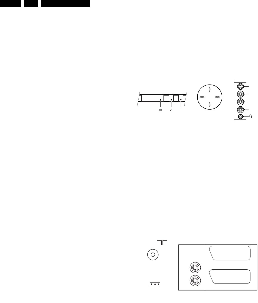
1.2.1 Front / Side Connections
Figure 1-1 Front and top control, side I/O connections
Cinch: Video CVBS - In, Audio - In
Ye - Video CVBS 1 VPP / 75 ohm jq
Wh - Audio L 0.5 VRMS / 10 kohm jq
Rd - Audio R 0.5 VRMS / 10 kohm jq
SVHS (Hosiden): Video Y/C - In
1 - Ground Y Gnd H
2 - Ground C Gnd H
3 - Video Y 1 VPP / 75 ohm j
4 - Video C 0.3 VPPP / 75 ohm j
Mini Jack: Audio Headphone - Out
Bk - Head phone 32 - 600 ohm / 10 mW ot
1.2.2 Rear Connections
Figure 1-2 Rear connections
Aerial - In
- - IEC-type (EU) Coax, 75 ohm D
Cinch: Video CVBS - Out, Audio - Out
Ye - Video CVBS 1 VPP / 75 ohm kq
Wh - Audio L 0.5 VRMS /10 kohm kq
Rd - Audio R 0.5 VRMS / 10 kohm kq
Service Connector (ComPair)
1 - SDA-S I2C Data (0 - 5 V) jk
2-SCL-S I
2C Clock (0 - 5 V) j
3 - Ground Gnd H
CL 06532130_002.eps
031000
S-Video
Video
L
Audio
R
SIDE I/OFRONT CONTROL
V+V-
P-
P+
IR
RED
TOP CONTROL
L
R
AUDIO
OUT
75 Ohm
SERVICE
CONNECTOR
F_15040_052.eps
040405
EXTERNAL 2
EXTERNAL 1
Technical Specifications, Connections, and Chassis Overview EN 3ES1E 1.
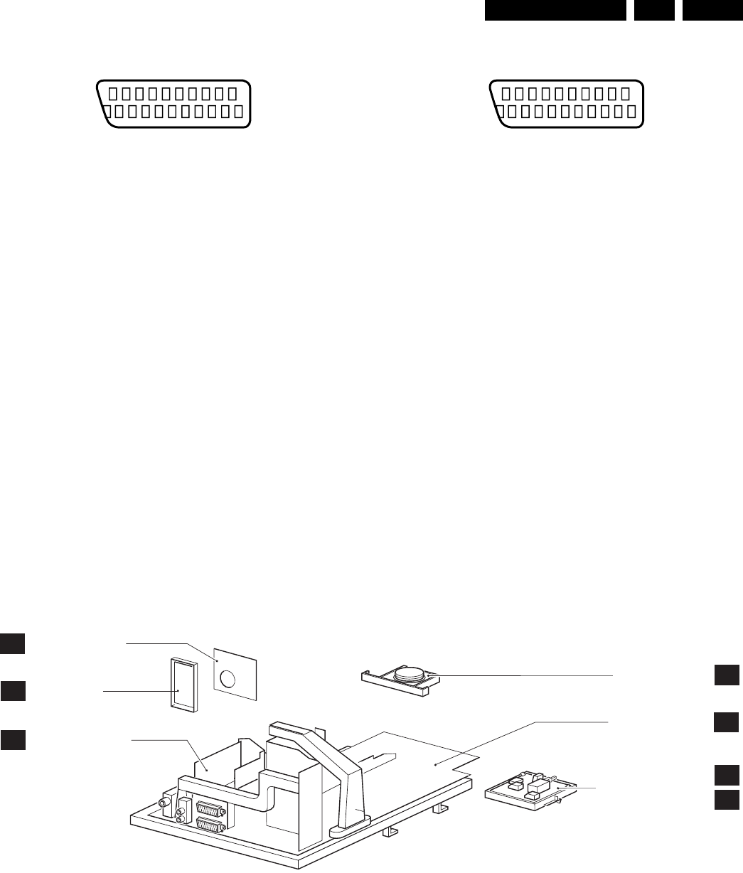
EXT1: Video RGB - In, CVBS - In/Out, Audio - In/Out
Figure 1-3 SCART connector
1 - Audio R 0.5 VRMS / 1 kohm k
2 - Audio R 0.5 VRMS / 10 kohm j
3 - Audio L 0.5 VRMS / 1 kohm k
4 - Ground Audio Gnd H
5 - Ground Blue Gnd H
6 - Audio L 0.5 VRMS / 10 kohm j
7 - Video Blue/U 0.7 VPP / 75 ohm j
8 - Function Select 0 - 2 V: INT
4.5 - 7 V: EXT 16:9
9.5 - 12 V: EXT 4:3 j
9 - Ground Green Gnd H
10 - n.c.
11 - Video Green/Y 0.7 VPP / 75 ohm j
12 - n.c.
13 - Ground Red Gnd H
14 - Ground FBL Gnd H
15 - Video Red/V 0.7 VPP / 75 ohm j
16 - Status/FBL 0 - 0.4 V: INT
1 - 3 V: EXT / 75 ohm j
17 - Ground Video Gnd H
18 - Ground Video Gnd H
19 - Video CVBS 1 VPP / 75 ohm k
20 - Video CVBS 1 VPP / 75 ohm j
21 - Shield Gnd H
EXT2: Video YC - In, CVBS - In/Out, Audio - In/Out
Figure 1-4 SCART connector
1 - Audio R 0.5 VRMS / 1 kohm k
2 - Audio R 0.5 VRMS / 10 kohm j
3 - Audio L 0.5 VRMS / 1 kohm k
4 - Ground Audio Gnd H
5 - Ground Blue Gnd H
6 - Audio L 0.5 VRMS / 10 kohm j
7 - C-FRONT 0.7 VPP / 75 ohm j
8 - Function Select 0 - 2 V: INT
4.5 - 7 V: EXT 16:9
9.5 - 12 V: EXT 4:3 j
9 - Ground Green Gnd H
10 - Easylink P50 0 - 5 V / 4.7 kohm jk
11 - n.c.
12 - n.c.
13 - Ground Red Gnd H
14 - Ground Data Gnd H
15 - C 0.7 VPP / 75 ohm j
16 - n.c.
17 - Ground Video Gnd H
18 - Ground FBL Gnd H
19 - Video CVBS 1 VPP / 75 ohm k
20 - Video CVBS/Y 1 VPP / 75 ohm j
21 - Shield Gnd H
1.3 Chassis Overview
Figure 1-5 PWB location
21
20
1
2
E_06532_001.eps
050404
21
20
1
2
E_06532_001.eps
050404
F_15040_053.eps
290405
LARGE SIGNAL PANEL A
SMALL SIGNAL BOARD
B
CRT/SCAVEM PANEL
F
FRONT INTERFACE PANEL (PV2) Q
MAINS SWITCH PANEL (FL9 & SL5) M
TOP CONTROL PANEL E
SIDE I/O PANEL
D

Safety Instructions, Warnings, and Notes
EN 4 ES1E2.
2. Safety Instructions, Warnings, and Notes
Index of this chapter:
2.1 Safety Instructions
2.2 Maintenance Instructions
2.3 Warnings
2.4 Notes
2.1 Safety Instructions
Safety regulations require the following during a repair:
• Connect the set to the Mains (AC Power) via an isolation
transformer (> 800 VA).
• Replace safety components, indicated by the symbol h,
only by components identical to the original ones. Any
other component substitution (other than original type) may
increase risk of fire or electrical shock hazard.
• Wear safety goggles when you replace the CRT.
Safety regulations require that after a repair, the set must be
returned in its original condition. Pay in particular attention to
the following points:
• General repair instruction: as a strict precaution, we advise
you to re-solder the solder connections through which the
horizontal deflection current flows. In particular this is valid
for the:
1. Pins of the line output transformer (LOT).
2. Fly-back capacitor(s).
3. S-correction capacitor(s).
4. Line output transistor.
5. Pins of the connector with wires to the deflection coil.
6. Other components through which the deflection current
flows.
Note: This re-soldering is advised to prevent bad connections
due to metal fatigue in solder connections, and is therefore only
necessary for television sets more than two years old.
• Route the wire trees and EHT cable correctly and secure
them with the mounted cable clamps.
• Check the insulation of the Mains (AC Power) lead for
external damage.
• Check the strain relief of the mains (AC Power) cord for
proper function, to prevent the cord from touching the CRT,
hot components, or heat sinks.
• Check the electrical DC resistance between the Mains (AC
Power) plug and the secondary side (only for sets that have
a Mains (AC Power) isolated power supply):
1. Unplug the Mains (AC Power) cord and connect a wire
between the two pins of the Mains (AC Power) plug.
2. Set the Mains (AC Power) switch to the "on" position
(keep the Mains (AC Power) cord unplugged!).
3. Measure the resistance value between the pins of the
Mains (AC Power) plug and the metal shielding of the
tuner or the aerial connection on the set. The reading
should be between 4.5 Mohm and 12 Mohm.
4. Switch "off" the set, and remove the wire between the
two pins of the Mains (AC Power) plug.
• Check the cabinet for defects, to prevent touching of any
inner parts by the customer.
2.2 Maintenance Instructions
We recommend a maintenance inspection carried out by
qualified service personnel. The interval depends on the usage
conditions:
• When a customer uses the set under normal
circumstances, for example in a living room, the
recommended interval is three to five years.
• When a customer uses the set in an environment with
higher dust, grease, or moisture levels, for example in a
kitchen, the recommended interval is one year.
• The maintenance inspection includes the following actions:
1. Perform the “general repair instruction” noted above.
2. Clean the power supply and deflection circuitry on the
chassis.
3. Clean the picture tube panel and the neck of the picture
tube.
2.3 Warnings
• In order to prevent damage to ICs and transistors, avoid all
high voltage flashovers. In order to prevent damage to the
picture tube, use the method shown in figure “Discharge
picture tube”, to discharge the picture tube. Use a high
voltage probe and a multi-meter (position VDC). Discharge
until the meter reading is 0 V (after approx. 30 s).
Figure 2-1 Discharge picture tube
• All ICs and many other semiconductors are susceptible to
electrostatic discharges (ESD w). Careless handling
during repair can reduce life drastically. Make sure that,
during repair, you are connected with the same potential as
the mass of the set by a wristband with resistance. Keep
components and tools also at this same potential. Available
ESD protection equipment:
– Complete kit ESD3 (small tablemat, wristband,
connection box, extension cable and earth cable) 4822
310 10671.
– Wristband tester 4822 344 13999.
• Be careful during measurements in the high voltage
section.
• Never replace modules or other components while the unit
is switched "on".
• When you align the set, use plastic rather than metal tools.
This will prevent any short circuits and prevents circuits
from becoming unstable.
2.4 Notes
2.4.1 General
• Measure the voltages and waveforms with regard to the
chassis (= tuner) ground (H), or hot ground (I), depending
on the tested area of circuitry. The voltages and waveforms
shown in the diagrams are indicative. Measure them in the
Service Default Mode (see chapter 5) with a colour bar
signal and stereo sound (L: 3 kHz, R: 1 kHz unless stated
otherwise) and picture carrier at 475.25 MHz for PAL, or
61.25 MHz for NTSC (channel 3).
• Where necessary, measure the waveforms and voltages
with (D) and without (E) aerial signal. Measure the
voltages in the power supply section both in normal
operation (G) and in stand-by (F). These values are
indicated by means of the appropriate symbols.
• The semiconductors indicated in the circuit diagram and in
the parts lists, are interchangeable per position with the
semiconductors in the unit, irrespective of the type
indication on these semiconductors.
V
E_06532_007.eps
250304

Safety Instructions, Warnings, and Notes EN 5ES1E 2.
• Manufactured under license from Dolby Laboratories.
“Dolby”, “Pro Logic” and the “double-D symbol”, are
trademarks of Dolby Laboratories.
2.4.2 Schematic Notes
• All resistor values are in ohms, and the value multiplier is
often used to indicate the decimal point location (e.g. 2K2
indicates 2.2 kohm).
• Resistor values with no multiplier may be indicated with
either an "E" or an "R" (e.g. 220E or 220R indicates 220
ohm).
• All capacitor values are given in micro-farads (µ= x10-6),
nano-farads (n= x10-9), or pico-farads (p= x10-12).
• Capacitor values may also use the value multiplier as the
decimal point indication (e.g. 2p2 indicates 2.2 pF).
• An "asterisk" (*) indicates component usage varies. Refer
to the diversity tables for the correct values.
• The correct component values are listed in the Spare Parts
List. Therefore, always check this list when there is any
doubt.
2.4.3 Rework on BGA (Ball Grid Array) ICs
General
Although (LF)BGA assembly yields are very high, there may
still be a requirement for component rework. By rework, we
mean the process of removing the component from the PWB
and replacing it with a new component. If an (LF)BGA is
removed from a PWB, the solder balls of the component are
deformed drastically so the removed (LF)BGA has to be
discarded.
Device Removal
As is the case with any component that is being removed, it is
essential when removing an (LF)BGA, that the board, tracks,
solder lands, or surrounding components are not damaged. To
remove an (LF)BGA, the board must be uniformly heated to a
temperature close to the reflow soldering temperature. A
uniform temperature reduces the risk of warping the PWB.
To do this, we recommend that the board is heated until it is
certain that all the joints are molten. Then carefully pull the
component off the board with a vacuum nozzle. For the
appropriate temperature profiles, see the IC data sheet.
Area Preparation
When the component has been removed, the vacant IC area
must be cleaned before replacing the (LF)BGA.
Removing an IC often leaves varying amounts of solder on the
mounting lands. This excessive solder can be removed with
either a solder sucker or solder wick. The remaining flux can be
removed with a brush and cleaning agent.
After the board is properly cleaned and inspected, apply flux on
the solder lands and on the connection balls of the (LF)BGA.
Note: Do not apply solder paste, as this has been shown to
result in problems during re-soldering.
Device Replacement
The last step in the repair process is to solder the new
component on the board. Ideally, the (LF)BGA should be
aligned under a microscope or magnifying glass. If this is not
possible, try to align the (LF)BGA with any board markers.
So as not to damage neighbouring components, it may be
necessary to reduce some temperatures and times.
More Information
For more information on how to handle BGA devices, visit this
URL: www.atyourservice.ce.philips.com (needs subscription,
not available for all regions). After login, select “Magazine”,
then go to “Workshop Information”. Here you will find
Information on how to deal with BGA-ICs.
2.4.4 Lead-free Solder
Philips CE is producing lead-free sets (PBF) from 1.1.2005
onwards.
Identification: The bottom line of a type plate gives a 14-digit
serial number. Digits 5 and 6 refer to the production year, digits
7 and 8 refer to production week (in example below it is 1991
week 18).
Figure 2-2 Serial number example
Regardless of the special lead-free logo (which is not always
indicated), one must treat all sets from this date onwards
according to the rules as described below.
Figure 2-3 Lead-free logo
Due to lead-free technology some rules have to be respected
by the workshop during a repair:
• Use only lead-free soldering tin Philips SAC305 with order
code 0622 149 00106. If lead-free solder paste is required,
please contact the manufacturer of your soldering
equipment. In general, use of solder paste within
workshops should be avoided because paste is not easy to
store and to handle.
• Use only adequate solder tools applicable for lead-free
soldering tin. The solder tool must be able:
– To reach a solder-tip temperature of at least 400°C.
– To stabilise the adjusted temperature at the solder-tip.
– To exchange solder-tips for different applications.
• Adjust your solder tool so that a temperature of around
360°C - 380°C is reached and stabilised at the solder joint.
Heating time of the solder-joint should not exceed ~ 4 sec.
Avoid temperatures above 400°C, otherwise wear-out of
tips will increase drastically and flux-fluid will be destroyed.
To avoid wear-out of tips, switch “off” unused equipment or
reduce heat.
• Mix of lead-free soldering tin/parts with leaded soldering
tin/parts is possible but PHILIPS recommends strongly to
avoid mixed regimes. If this cannot be avoided, carefully
clean the solder-joint from old tin and re-solder with new
tin.
• Use only original spare-parts listed in the Service-Manuals.
Not listed standard material (commodities) has to be
purchased at external companies.
• Special information for lead-free BGA ICs: these ICs will be
delivered in so-called "dry-packaging" to protect the IC
against moisture. This packaging may only be opened
shortly before it is used (soldered). Otherwise the body of
the IC gets "wet" inside and during the heating time the
structure of the IC will be destroyed due to high (steam-)
pressure inside the body. If the packaging was opened
before usage, the IC has to be heated up for some hours
(around 90°C) for drying (think of ESD-protection!).
Do not re-use BGAs at all!
E_06532_024.eps
230205
P
b

Safety Instructions, Warnings, and Notes
EN 6 ES1E2.
• For sets produced before 1.1.2005, containing leaded
soldering tin and components, all needed spare parts will
be available till the end of the service period. For the repair
of such sets nothing changes.
In case of doubt whether the board is lead-free or not (or with
mixed technologies), you can use the following method:
• Always use the highest temperature to solder, when using
SAC305 (see also instructions below).
• De-solder thoroughly (clean solder joints to avoid the
mixing of two alloys).
Caution: For BGA-ICs, you must use the correct temperature-
profile, which is coupled to the 12NC. For an overview of these
profiles, visit the website www.atyourservice.ce.philips.com
(needs subscription, but is not available for all regions).
You will find this and more technical information within the
"Magazine", chapter "Workshop information".
For additional questions please contact your local repair help
desk.
2.4.5 Practical Service Precautions
•It makes sense to avoid exposure to electrical shock.
While some sources are expected to have a possible
dangerous impact, others of quite high potential are of
limited current and are sometimes held in less regard.
•Always respect voltages. While some may not be
dangerous in themselves, they can cause unexpected
reactions that are best avoided. Before reaching into a
powered TV set, it is best to test the high voltage insulation.
It is easy to do, and is a good service precaution.

Directions for Use EN 7ES1E 3.
3. Directions for Use
You can download this information from the following websites:
http://www.philips.com/support
http://www.p4c.philips.com
Mechanical Instructions
EN 8 ES1E4.
4. Mechanical Instructions
Index of this chapter:
4.1 Service Connector (for ComPair)
4.2 Set Disassembly
4.3 Service Positions
4.4 Assy / Board Removal
4.5 Set Re-assembly
Note: Figures below can deviate slightly from the actual
situation, due to the different set executions.
4.1 Service Connector (for ComPair)
For service diagnostics with ComPair, it is not necessary to
disassemble the set. You only have to connect the ComPair
interface box, via the appropriate cable, to the service
connector (on the rear of the set, see figure 1-2), and start the
program (see also chapter 5 "Service Modes, Error Codes, and
Fault Finding ").
4.2 Set Disassembly
Follow the disassemble instructions in described order.
4.2.1 Rear Cover Removal
Warning: disconnect the mains power cord before you remove
the rear cover.
1. Remove all the fixation screws of the rear cover.
2. Now the rear cover can be removed.
4.3 Service Positions
This chassis has several predefined service positions, for
better accessibility. They are explained below in more detail.
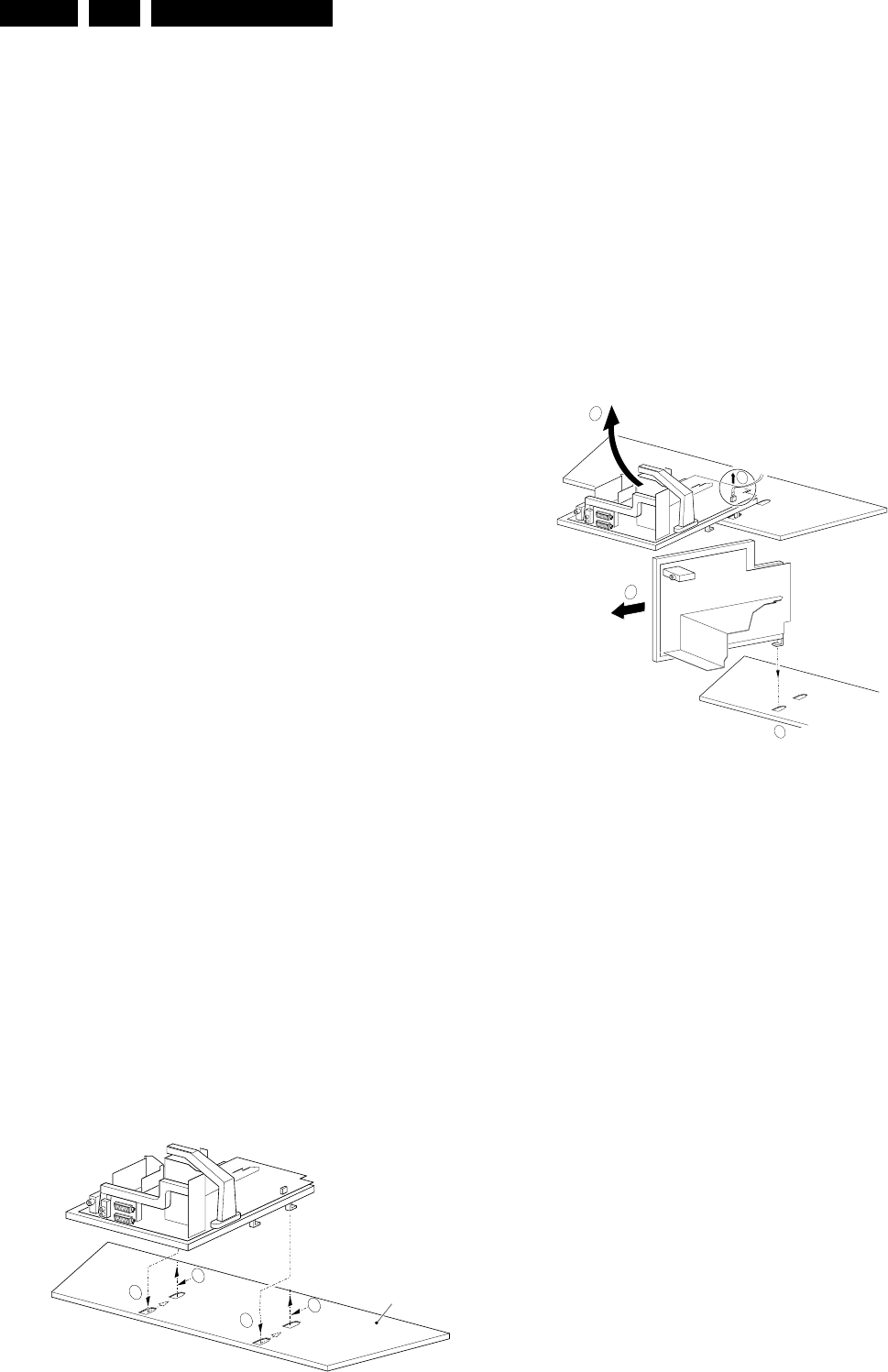
4.3.1 Large Signal Panel (LSP)
Component Side LSP
For better accessibility of the LSP, do the following (see Figure
“Service position 1”):
1. Simultanuously do the following: a) pull the two plastic
locking handles at the mid left and mid right side of the
bracket gently backwards to unlock the bracket, and b)
loosen the bracket from the bottom tray, by pulling it
backwards. N.B.: You do not need to pull the other two
locking handles backwards.
2. Remove the LSP-bracket from the bottom tray by lifting it
upwards.
3. Hook the bracket in the first row of fixation holes of the
bottom tray. In other words, reposition the bracket from [1]
to [2].
Figure 4-1 Service position 1
Solder Side LSP
To get access to the bottom side (solder side) of the LSP, do
the following (see figure 4-1):
1. Remove the connector of the mains cable (coming from the
mains switch-module) from the LSP.
2. Remove the cable (connector) from the side I/O panel.
3. Release some wiring from their fixation clamps, in order to
get room for repositioning the LSP.
4. Flip the LSP 90 degrees clockwise [2], and place it in the
fixation hole at the left side of the bottom tray [3].
5. Push the LSP forward to fix it. (Alternatively, the LSP may
also be placed on your work bench without being
positioned in its fixation hole, or it may even be removed
from the bracket for better accessibility, see “Assy / Board
Removal: Large Signal Panel (LSP)” on the next pages.)
Figure 4-2 Service position 2
4.3.2 Small Signal Board (SSB)
In fact, there is no predefined service position for the SSB. Most
test points are located on the A-side (side that is facing the
tuner). If you have to replace ICs, you must take the complete
SSB module out of the SIMM-connector.
Notes:
• For better access to the SSB, it is possible to order an
“extension tool” with cables. You can use this service
extension tool to connect a Small Signal Board (SSB) of an
ES1E, A02, A10, or EMG (EMx) chassis, via two “IDE”
cables to the SIMM connector in the set. In this way, you
can service the SSB more easily outside the TV set. You
can order this tool under 12nc: 9965 000 14526.
• If necessary for the measurement, you can put the LSP in
“service position 2” (as described above).
4.4 Assy / Board Removal
Sometimes, it can be necessary to swap a complete assy or
Printed Wiring Board (PWB). How that can be done is
explained below.
CL 36532058_079.eps
081003
Bottom tray
2
2
1
1
CL 36532058_078.eps
081003
4
2
1
3
Mechanical Instructions EN 9ES1E 4.
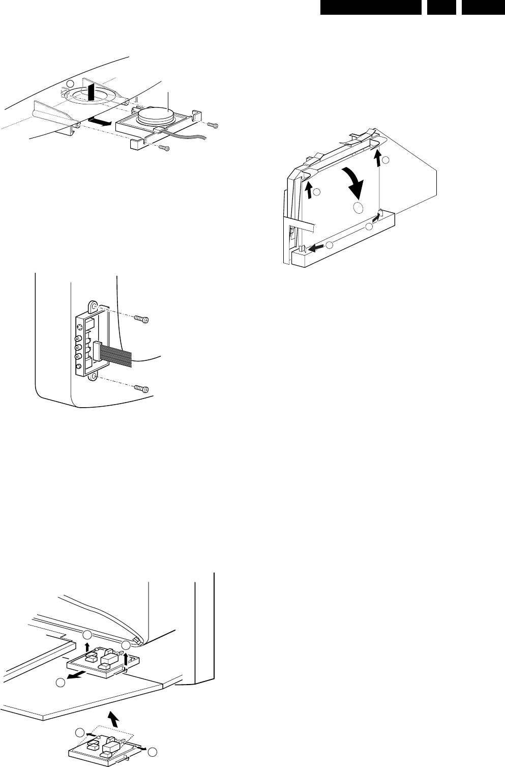
4.4.1 Top Control Assy/Panel
Figure 4-3 Top control panel
1. Remove the two fixation screws that hold the panel.
2. Pull the board backwards (i.e., release it from the front
hinge).
3. The board can be lifted out of the bracket after releasing
the two fixation clamps at the connector side.
4.4.2 Side I/O Assy and Panel
Figure 4-4 Side-I/O panel
1. The complete side I/O-assembly can be removed by
unscrewing the two fixation screws.
2. The board can be lifted out of the bracket after releasing
the two fixation clamps.
4.4.3 Mains Switch Assy/Panel
4.4.4 Accessing the Mains Switch/LED panel
Figure 4-5 Mains Switch/LED panel
1. Release the two fixation clamps (1) by pushing them
upward.
2. At the same time, the complete assy must be pulled
backward (2).
3. If the board has to be removed, release the two clamps at
the sides of the bracket and lift the panel out (3).
4.4.5 Small Signal Board (SSB)
Figure 4-6 SSB removal
1. Push the top of the SSB towards the LOT [1].
2. Due to the pressure, the two metal clamps at both sides of
the SIMM-connector will release [2].
3. Take the complete SSB out [3].
4.4.6 Large Signal Panel (LSP)
1. Remove the SSB (see paragraph “Small Signal Board
(SSB)” above).
2. Remove the two fixation screws from the large plastic
bracket on the right hand side of the LSP (above the EHT
shield), and remove the bracket, after releasing the EHT
cable and the CRT cables from the fixation clamps on this
bracket.
3. Disconnect the other cables (loudspeaker, mains, etc.)
from the LSP, and release some cables from their fixation
clamps.
4. Press the fixation clamp on the left front side of the LSP-
bracket (close to the white arrow/loudspeaker connector)
to unlock the LSP, and tilt it upwards (the board hinges at
the right side).
5. Remove the board from the bracket by unhooking it from its
fixation clamps on the right side.
4.5 Set Re-assembly
To re-assemble the whole set, do all processes in reverse
order.
Be sure that, before the rear cover is mounted:
• The mains cord is postioned correctly in its guiding
brackets (make sure that the strain relief will function
correctly!).
• All wires/cables are returned in their original positions. This
is very important, in view of the “hot” and “EHT” areas of the
set.
CL 06532012_003.eps
030200
M
Top control board
CL 06532012_004.eps
030200
2
3
1
1
1
3
CL 06532012_005.eps
030200
CL 06532153_002.eps
211103
2
2
3
1
1
3

Service Modes, Error Codes, and Fault Finding
EN 10 ES1E5.
5. Service Modes, Error Codes, and Fault Finding
Index of this chapter:
5.1 Test Points
5.2 Service Modes
5.3 Problems and Solving Tips (related to CSM)
5.4 ComPair
5.5 Error Codes
5.6 The Blinking LED Procedure
5.7 Software Downloading
5.1 Test Points
See chapter 6 " Block Diagrams, Testpoint Overview, and
Waveforms".
Perform measurements under the following conditions:
• Service Default Mode.
• Video: colour bar signal.
• Audio: 3 kHz left, 1 kHz right.
5.2 Service Modes
Service Default Mode (SDM) and Service Alignment Mode
(SAM) offer several features for the service technician, while
the Customer Service Mode (CSM) is used for communication
between a Philips Customer Care Centre (P3C) and a
customer.
There is also the option of using ComPair, a hardware interface
between a computer (see requirements below) and the TV
chassis. It offers the ability of structured troubleshooting, test
pattern generation, error code reading, software version
readout, and software upgrading.
Minimum requirements: a Pentium processor, Windows 95/
98, and a CD-ROM drive (see also paragraph “ComPair”).
5.2.1 Service Default Mode (SDM)
Purpose
• To create a pre-defined setting for measurement purposes.
• To override SW protections (only when SDM is activated
via shorting the SDM pins on the SSB).
• To start the blinking LED procedure.
• Inspection of error buffer, life timer, and software version.
Specifications
• Tuning frequency: 475.25 MHz for PAL/SECAM.
• Colour system: SECAM L for France or PAL B/G for the
rest of Europe.
• All picture settings at 50 % (brightness, colour, contrast).
• All sound settings at 50 %, except volume at 25 %.
• All service-unfriendly modes (if present) are disabled, like:
– (Sleep) timer.
– Child/parental lock.
–Blue mute.
– Automatic volume limiter (AVL).
– Auto switch-off (when no video signal was received for
10 minutes).
– Skip/blank of non-favourite pre-sets.
– Hotel or hospital mode.
– Local keyboard block.
– Smart modes.
– Auto store of personal presets.
– Auto user menu time-out.
How to Activate SDM
Use one of the following methods:
• Use the standard RC-transmitter and key in the code
“062596”, directly followed by the “MENU” button.
Note: It is possible that, together with the SDM, the main
menu will appear. To switch it "off", push the “MENU”
button again.
• Short circuit, during switch "on" of the set, the two solder
pads on the SSB with the indication “FOR SERVICE”.
These solder pads are located at the "tuner" side of the
SSB (just above the large BGA IC).
Caution: If the SDM is activated via these pins, all the
software-controlled protections are de-activated for 15 s.
When these 15 s are expired, the set will shutdown to
protection mode.
• Use the DST-emulation feature of ComPair.
After activating this mode:
• “SDM” will appear in the upper right corner of the screen.
• Also, the error buffer, operating hours, and software
version are displayed (can be toggled "on/off" with the
"STATUS / OSD / [i+]" button).
• Blinking LED procedure will be started.
• All software-controlled protections are overridden for 15 s.
When these 15 s are expired, the set will shutdown to
protection mode.
Contents of SDM:
•HRS. Displays the accumulated total of operation hours
(not the standby hours) in hexadecimal value.
•SW. Displays the date of the software and the software
version of the ROM;
example: A2EU04-5.10 = AAABBC-X.YY.
–AAA= chassis name.
–BB= region and/or function name: E= Europe, A= Asia
Pacific, U= NAFTA, L= LATAM, B= Basic, T= Top, P=
PAL, N= NTSC, S= Stereo, M= Mono.
–C= the language cluster number.
–X.Y= the software version, where X is the main version
number (different numbers are not compatible with one
another) and Y is the sub version number (a higher
number is always compatible with a lower number).
•ERR (followed by maximal 8 errors). The most recent error
is displayed at the upper left (for an error explanation see
paragraph “Error Codes”).
How to Navigate
• When you press the “MENU” button on the RC transmitter,
the set will toggle between the SDM and the normal user
menu (with the SDM mode still active in the background).
• When you press the “STATUS / OSD / [i+]” button on the
RC transmitter, the set will toggle between the full SDM
screen or a screen with only the text "SDM" displayed on it.
This mode is useful when performing measurements, then
the OSD info will not generate interference.
How to Exit SDM
Use one of the following methods:
• Switch the set to STANDBY via a standard customer RC-
transmitter (the error buffer is erased).
• Via a standard customer RC-transmitter: key in “00”-
sequence (the error buffer is not erased).
5.2.2 Service Alignment Mode (SAM)
Purpose
• To perform alignments.
• To change option settings.
• To easily identify the used software version.
• To view operation hours.
• To display / clear the error code buffer.
Specifications
• Operating hours counter.
• Software version.

Service Modes, Error Codes, and Fault Finding EN 11ES1E 5.
• Option settings.
• Error buffer reading and erasing.
• Software alignments.
• Disable service unfriendly modes.
How to Activate SAM
Use one of the following methods:
• Via a standard RC transmitter: key in the code “062596”
directly followed by the “STATUS / OSD / [i+]” button.
• Use the DST-emulation feature of ComPair.
After activating this mode, “SAM” will appear in the upper right
corner of the screen.
Contents of SAM:
•HRS. Displays the accumulated total of operation hours
(not the standby hours) in hexadecimal value
Note: every time the set is switched "on" by the mains
switch or the RC, the timer is increased by 0.5.
•SW ID. Displays the software version of the ROM
example: A2EU04-5.10 = AAABBC-X.YY.
–AAA= chassis name.
–BB= region and/or function name: E= Europe, A= Asia
Pacific, U= NAFTA, L= LATAM, B= Basic, T= Top, P=
PAL, N= NTSC, S= Stereo, M= Mono.
–C= the language cluster number.
–X.Y= the software version, where X is the main version
number (different numbers are not compatible with one
another) and Y is the sub version number (a higher
number is always compatible with a lower number).
•ERR (followed by maximal 8 errors). The most recent error
is displayed at the upper left (for an error explanation see
paragraph “Error Codes”).
•OPTIONS. Extra features for Service.
•CLEAR ERRORS. When you press the “OK” button, the
error buffer is reset.
•AKB. Disable (off) or enable (on) the "black current loop"
(AKB= Auto Kine Bias). For Vg2 alignment.
•TUNER. This will activate the “TUNER” alignments sub-
menu.
•WHITE TONE. This will activate the “WHITE TONE”
alignments sub-menu.
•GEOMETRY. This will activate the “GEOMETRY”
alignments sub-menu.
•SOUND. This will activate the “SOUND” alignments sub-
menu.
•SMART SETTINGS. This will activate the “SMART
SETTINGS” alignments sub-menu.
•STORE. This will save the new settings/alignments.
•EEPROM TEST. This will report if the SW checksum is OK.
Convenient after SW upgrading.
•VID RAM TEST. This will check the continuity of the
address bus and data bus of the Video RAM.
•VG2. This feature is not implemented yet. Do not use.
Note: Alignments are described in chapter 8 "Alignments".
How to Navigate
• In SAM, you can select the menu items with the “CURSOR
UP/DOWN” key on the RC-transmitter. The selected item
will be highlighted. When not all menu items fit on the
screen, move the “CURSOR UP/DOWN” key to display the
next/previous menu items.
• With the “CURSOR LEFT/RIGHT” keys, it is possible to:
– (De) activate the selected menu item.
– Change the value of the selected menu item.
– Activate the selected submenu.
• When you press the “MENU” button on the RC transmitter,
the set will toggle between the SAM and the normal user
menu (with the SAM mode still active in the background).
How to Exit SAM
Use one of the following methods:
• Switch the set to STANDBY via the RC-transmitter (the
error buffer is erased).
• Via a standard customer RC-transmitter: key in “00”-
sequence (the error buffer is not erased).
5.2.3 Customer Service Mode (CSM)
Purpose
When a customer is having problems with his TV-set, he can
call his dealer or the Philips helpdesk (P3C). The service
technician can than ask the customer to activate the CSM, in
order to identify the status of the set. Now, the service
technician can judge the severity of the complaint. In many
cases, he can advise the customer how to solve the problem,
or he can decide if it is necessary to visit the customer.
The CSM is a read only mode; therefore, modifications in this
mode are not possible.
How to Activate CSM
Use one of the following methods:
• Press the “MUTE” button on the RC-transmitter
simultaneously with any key on the TV for at least 4
seconds.
• Key in the code “123654” via the standard RC transmitter.
Notes:
• Activation of the CSM is only possible if there is no (user)
menu on the screen!
• During CSM, sound volume is set to 25% of the scale,
"Smart Sound" is set to "Theatre" mode, and "Smart
Picture" is set to "Rich/Movies" mode temporarily to ensure
a good picture and sound of the working set. After leaving
CSM, the original settings are restored.
How to Navigate
By means of the “CURSOR-DOWN/UP” knob on the RC-
transmitter, you can navigate through the menus.
Contents of CSM
The following information is displayed on screen:
• Text “CSM” on the first line.
• Line number for every line (to make CSM language
independent).
• Option code information.
• Configuration information.
• Service-unfriendly modes.
1. SET TYPE. Type/model number (if present) according to
the Philips standard (example: 28PW8720/12).
2. SOFTWARE. Software version AAABBC-X.YY.
3. HOURS ON. Operating hours (in hexadecimal code).
4. CODE1. Shows the contents of the error buffer (the word
“error” may not be used on this screen, instead “code1” and
“code2” is used).
5. CODE2. Idem.
6. OPTION1. Option code information.
7. OPTION2. Idem.
8. OPTION3. Idem.
9. OPTION4. Idem.
10. SIGNAL. "Ident" signal present or not present (VID status
bit in MPIF) on selected source.
11. TIMER. Timer is activated (in "FEATURE" menu) or
deactivated.
12. CHANNEL. Child Lock (if present) is activated or
deactivated (i.e. when local keyboard is locked).
13. PRESET. (If present). Current channel is defined as
skipped or non-preferred.
14. HOTELMODE. Shows if the HOTEL mode is activated or
deactivated (only for Europe and AP).
15. SOURCE. Selected source before entry of CSM; XXX
(channel no.), external source name (i.e. AV1, CVI, EXT1,
etc...).

Service Modes, Error Codes, and Fault Finding
EN 12 ES1E5.
16. SOUND. Selected SOUND mode; "XX"= MONO, NICAM,
STEREO, L1 (Language 1), L2 (Language 2), SAP,
VIRTUAL, or DIGITAL prior entry to CSM.
17. VOLUME. Volume level before entry of CSM (typ. 00..100).
18. BALANCE. Balance level before entry of CSM (typ. -
50..50).
19. BRIGHTNESS. Brightness level before entry of CSM (typ.
00..100).
20. COLOUR. Colour level before entry of CSM (typ. 00..100).
21. CONTRAST. Contrast level before entry of CSM (typ.
00..100).
22. HUE (if present). Hue level before entry of CSM (typ. -
50..100).
How to exit CSM
Use one of the following methods:
• After you press a key on the RC-transmitter (with exception
of the “CHANNEL”, “VOLUME” and digit (0-9) keys), or
• After you switch the TV-set “OFF” with the mains switch.
• After 15 min. no RC or local keyboard actions.
5.3 Problems and Solving Tips (related to CSM)
Note: The problems described below are all related to the TV
settings. The procedures to change the value (or status) of the
different settings are described above. New value(s) are
automatically stored.
5.3.1 Picture Problems
Picture too Dark
1. Press SMART PICTURE on the RC. In case the picture
improves, increase the “Brightness” or the “Contrast”
value. The new value(s) are automatically stored (in
“personal” pre-set) for all TV channels.
2. Check in CSM lines BRIGHTNESS and/or CONTRAST. If
the value of line BRIGHTNESS is low (< 10) or the value of
line CONTRAST is low (< 10), increase them.
Picture too Bright
1. Press SMART PICTURE on the RC. In case the picture
improves, decrease the “Brightness” or the “Contrast”
value. The new value(s) are automatically stored (in
“personal” pre-set) for all TV channels.
2. Check in CSM lines BRIGHTNESS and/or CONTRAST. If
the value of line BRIGHTNESS is high (> 50) or the value
of line CONTRAST is high (> 50), decrease the
“Brightness” or the “Contrast” value.
White Line Around Picture Elements and Text
1. Press SMART PICTURE on the RC. In case the picture
improves, decrease the “Sharpness” value. The new value
is automatically stored (in “personal” pre-set) for all TV
channels.
2. Check in CSM line SHARPNESS. Decrease the
“Sharpness” value. The new value is automatically stored
for all TV channels.
No Picture
Check in CSM line 10 (SIGNAL). In case this line shows NO
SIGNAL, check the aerial cable/aerial system.
Blue Picture
No proper signal is received. Check the aerial cable/aerial
system.
Blue Picture and/or Unstable Picture
A scrambled or coded signal is received.
Black and White Picture
Check in CSM line COLOR. In case the value is low (< 10),
increase the “Color” value. The new value is automatically
stored for all TV channels.
No Colours/colour Lines around Picture Elements or
Colours not Correct or Unstable Picture
1. Check in CSM line SYSTEM. If a “strange” system pops up,
something has gone wrong during installation. Re-install
the channel.
2. In case line SYSTEM is “FRANCE”, the installed system for
this pre-set is SECAM, while PAL is required. Install the
required program again: open the installation menu and
perform manual installation. Select system “West Europe”.
Menu Text not Sharp Enough
1. Press “SMART PICTURE”. In case picture improves,
decrease the "Contrast" value. The new value(s) are
automatically stored for all TV channels.
2. Check in CSM line CONTRAST. If the value of this line is
high (> 50), decrease the "Contrast" value.
5.3.2 Sound Problems
No Sound from Left and Right Speaker
Check in CSM line VOLUME. If the value is high, increase the
value of “Volume”. The new value(s) are automatically stored
(in “personal” pre-set) for all TV channels.
Sound too Loud for Left and Right Speaker
Check in CSM line VOLUME. If the value is low, decrease the
value of “Volume”. The new value(s) are automatically stored
(in “personal” pre-set) for all TV channels.
5.4 ComPair
5.4.1 Introduction
ComPair (Computer Aided Repair) is a service tool for Philips
Consumer Electronics products. ComPair is a further
development on the European DST (service remote control),
which allows faster and more accurate diagnostics. ComPair
has three big advantages:
• ComPair helps you to quickly get an understanding on how
to repair the chassis in a short time by guiding you
systematically through the repair procedures.
• ComPair allows very detailed diagnostics (on I2C level) and
is therefore capable of accurately indicating problem areas.
You do not have to know anything about I2C commands
yourself because ComPair takes care of this.
• ComPair speeds up the repair time since it can
automatically communicate with the chassis (when the
microprocessor is working) and all repair information is
directly available. When ComPair is installed together with
the SearchMan electronic manual of the defective chassis,
schematics and PWBs are only a mouse click away.
5.4.2 Specifications
ComPair consists of a Windows based faultfinding program
and an interface box between PC and the (defective) product.
The ComPair interface box is connected to the PC via a serial
or RS232 cable.
For this chassis, the ComPair interface box and the TV
communicate via a bi-directional service cable via the service
connector.
The ComPair faultfinding program is able to determine the
problem of the defective television. ComPair can gather
diagnostic information in two ways:
•Automatically (by communicating with the television set):
ComPair can automatically read out the contents of the

Service Modes, Error Codes, and Fault Finding EN 13ES1E 5.
entire error buffer. Diagnosis is done on I2C level. ComPair
can access the I2C bus of the television. ComPair can send
and receive I2C commands to and from the micro controller
of the television set. In this way, it is possible for ComPair
to communicate (read and write) to devices on the I2C
busses of the TV-set.
•Manually (by asking questions to you): This option is
helpful, because automatic diagnosis is only possible if the
micro controller of the television is working correctly (also,
the diagnostic possibilities of automatic diagnosis are more
limited). When you choose manual diagnosis, ComPair will
guide you through the faultfinding tree by asking you
questions (e.g. Does the screen give a picture? Click on
the correct answer: YES / NO) and by showing you
examples (e.g. Measure test-point I7 and click on the
correct oscillogram you see on the oscilloscope). You can
answer by clicking on a link (e.g. a piece of text or a
waveform picture) that will bring you to the next step in the
faultfinding process.
By a combination of automatic diagnostics and an interactive
question / answer procedure, ComPair will enable you to find
most problems in a fast and effective way.
Besides fault finding, ComPair provides some additional
features like:
• Up- or downloading of pre-sets.
• Managing of pre-set lists.
• Emulation of the Dealer Service Tool (DST).
• If both ComPair and SearchMan (Electronic Service
Manual) are installed, all the schematics and the PWBs of
the set are available by clicking on the appropriate
hyperlink.
Example: Measure the DC-voltage on capacitor C2568
(Schematic/Panel) at the Mono-carrier.
– Click on the “Panel” hyperlink to automatically show
the PWB with a highlighted capacitor C2568.
– Click on the “Schematic” hyperlink to automatically
show the position of the highlighted capacitor.
• SW upgrading
5.4.3 How To Order
ComPair order codes:
• Starter kit ComPair32/SearchMan32 software and
ComPair interface (excl. transformer): 3122 785 90450.
• ComPair interface (excluding transformer): 4822 727
21631.
• Starter kit ComPair32 software (registration version): 3122
785 60040.
• Starter kit SearchMan32 software: 3122 785 60050.
• ComPair32 CD (2003 update): 3122 785 60110.
• SearchMan32 CD (2003 update): 3122 785 60120.
• ComPair interface cable: 3122 785 90004.
• ComPair firmware upgrade IC: 3122 785 90510.
• Transformer Europe: 4822 727 21632.
• Transformer UK: 4822 727 21633.
5.5 Error Codes
5.5.1 Introduction
The error code buffer contains all detected errors since the last
time the buffer was erased. The buffer is written from left to
right, new errors are logged at the left side, and all other errors
shift one position to the right.
When an error has occurred, the error is added to the list of
errors, provided the list is not full or the error is a protection
error.
When an error occurs and the error buffer is full, then the new
error is not added, and the error buffer stays intact (history is
maintained), except when the error is a protection error.
To prevent that an occasional error stays in the list forever, the
error is removed from the list after 50+ operation hours.
When multiple errors occur (errors occurred within a short time
span), there is a high probability that there is some relation
between them.
5.5.2 How to Read the Error Buffer
Use one of the following methods:
• On screen via the SAM (only if you have a picture).
Examples:
–0 0 0 0: No errors detected
–6 0 0 0: Error code 6 is the last and only detected error
–9 6 0 0: Error code 6 was first detected and error code
9 is the last detected error
• Via the blinking LED procedure (when you have no
picture). See next paragraph.
•Via ComPair.
5.5.3 How to Clear the Error Buffer
Use one of the following methods:
• By activation of the “CLEAR ERRORS” command in the
SAM menu.
• With a normal RC, key in sequence “MUTE” followed by
“062599” and “OK”.
• When you transmit the commands “DIAGNOSE” - “99” -
“OK” with ComPair (or with a DST).
• If the content of the error buffer has not changed for 50+
hours, it resets automatically.
5.5.4 Error Codes
The function of error codes is to indicate failures in the TV set.
In principle a unique error code is available for every:
•I
2C device error.
•I
2C bus error (for every bus containing two or more I2C
devices).
• Protection error (e.g. +8V protection or Horizontal
protection).
• Error not related to an I2C device, but of importance (e.g.
BC-loop, RAM error).

Service Modes, Error Codes, and Fault Finding
EN 14 ES1E5.
Table 5-1 Error Table
Service Tips:
• In case of non-intermittent faults, clear the error buffer
before you begin the repair. This to ensure that old error
codes are no longer present. Before clearing the buffer,
write down the content, as this history can give you
significant information.
• If possible, check the entire contents of the error buffer. In
some situations, an error code is only the result of another
error code and not the actual cause (e.g., a fault in the
protection detection circuitry can also lead to a protection).
5.6 The Blinking LED Procedure
5.6.1 Introduction
Via this procedure, you can make the contents of the error
buffer visible via the front LED. This is especially useful for fault
finding, when there is no picture.
When the SDM is activated, the front LED will show (by
blinking) the contents of the error-buffer. Error-codes > 10 are
shown as follows:
1. A long blink of 750 ms (which is an indication of the decimal
digit),
2. A pause of 1500 ms,
3. “n” short blinks (where “n” = 1 - 9),
4. When all the error-codes are displayed, the sequence
finishes with a LED blink of 3000 ms,
5. The sequence starts again.
Example: Error 12 9 6 0 0.
After activation of the SDM, the front LED will show:
1. 1 long blink of 750 ms (which is an indication of the decimal
digit) followed by a pause of 1500 ms,
2. 2 short blinks of 250 ms, followed by a pause of 3000 ms,
3. 9 short blinks of 250 ms, followed by a pause of 3000 ms,
4. 6 short blinks of 250 ms, followed by a pause of 3000 ms,
5. 1 long blink of 3000 ms to finish the sequence,
6. The sequence starts again.
5.6.2 How to Activate
Use one of the following methods:
• Activate the SDM (only via soldering pads marked “FOR
SERVICE” on the SSB). The blinking front LED will show
the entire contents of the error buffer (this works in “normal
operation” mode and in “protection” mode). In order to
avoid confusion with RC5 signal reception blinking, this
LED blinking procedure is terminated when an RC5
command is received.
• Transmit the commands “MUTE”, “06250x”, and “OK” with
a normal RC (where “x” is the position in the error buffer
that has to be displayed). With x= 1, the last detected error
is shown, x= 2 the second last error, etc.... When x= 0, all
errors are shown.
• “DIAGNOSE X” with the DST (where “x” is the position in
the error buffer that has to be displayed). With x= 1, the last
detected error is shown, x= 2 the second last error, etc....
When x= 0, all errors are shown.
Note: It can take some seconds before the blinking LED starts.
5.7 Software Downloading
In this chassis, you can upgrade the software via ComPair.
You can find more information on how this procedure works in
the ComPair file. It is possible that not all sets are equipped
with the hardware, needed to make software upgrading
possible. To speed up the programming process the firmware
of the ComPair interface can be upgraded. See paragraph
“How To Order” for the order numbers.
Error Description
0 No error
1 Horizontal Protection (via NOHFB bit in ADOC)
3 +8V error (missing/protection active by checking
MPIF ASUP bit))
4 X-ray/High beam current protection signal (via
XPROT bit in ADOC)
5 Highbeam protection
7 Under-voltage protection
11 MPIF I2C communication failure / MPIF test failed
12 BC-loop not stabilised within the time limit (i.e. after
timer is expired)
13 NVM I2C communication failure
14 Main tuner 1232 I2C failure UV13xx
17 3D Y/C 7823 Combfilter I2C communication failure
18 PIP Tuner I2C failure
19 2fH component input I2C failure (PCF8574)
21 PIP IF demodulator IC TDA988x communication
failed (only for PIP/DW sets)
22 Flash over protection error (to register CRT flash-
overs, via FPR status bit in ADOC)
Block Diagrams, Testpoint Overviews, and Waveforms 15ES1E AA 6.
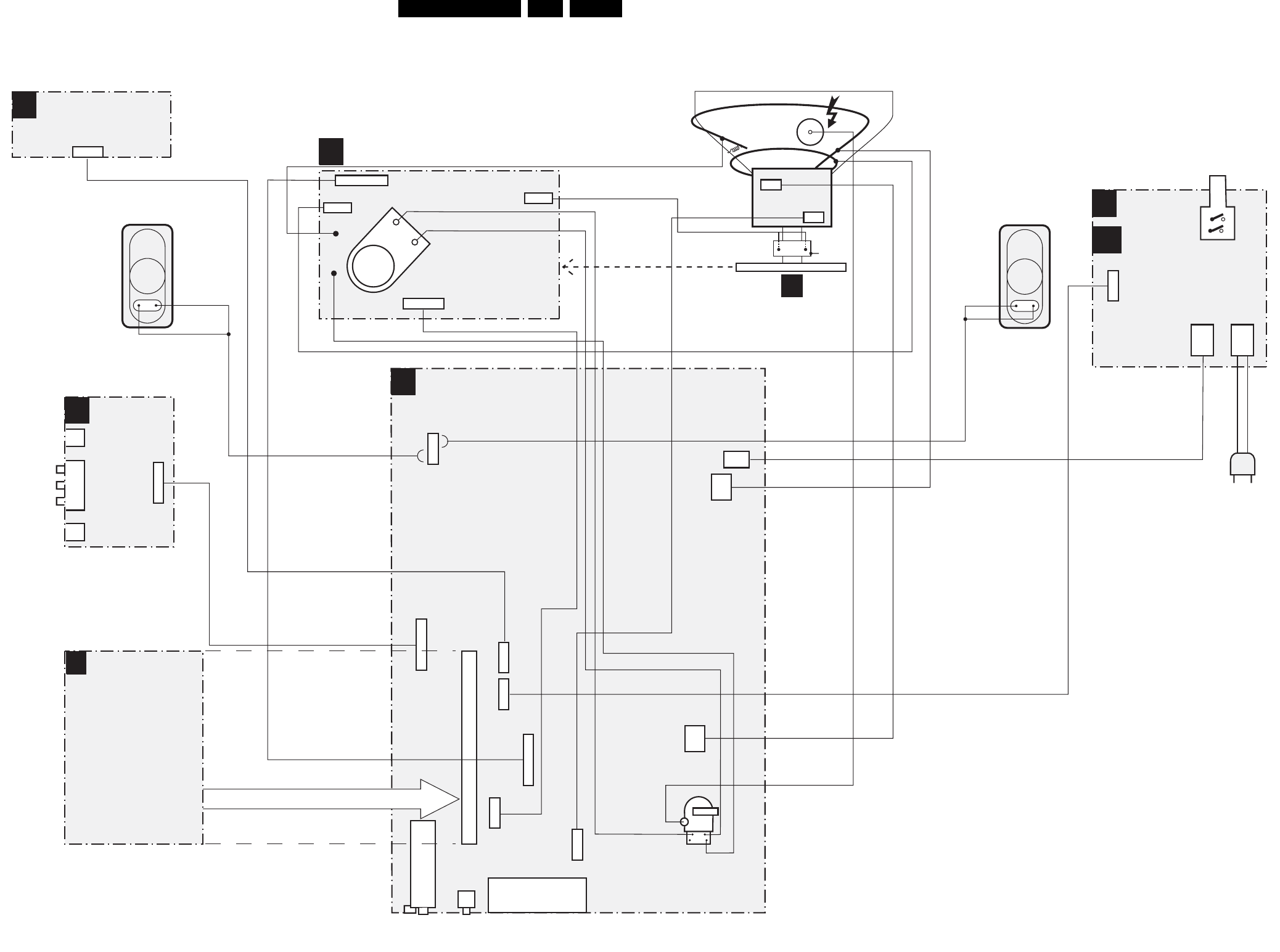
6. Block Diagrams, Testpoint Overviews, and Waveforms
Wiring Diagram
F_15040_054.eps
250405
SIDE
I/O PANEL
D
0240
CRT PANEL
(COMPONENT VIEW)
F
TOP CONTROL PANEL
E
A
B
1340
RED
WHITE
EHT
1361
1336
1335
1351
HEADPHONE
SVHS
RIGHT (RED)
LEFT (WHITE)
CVBS (YELLOW)
0215
0203
1951
1502
1505
1911
1404
1620
1401
TUNER
1943
Compair
connector
LOT
FRONT
INTERFACE
PANEL
Q1
M
MAINS
SWITCH
SPEAKER L
SPEAKER R
CRT PANEL
F
SCAVEM
COIL
AQUADAG
DEGAUSSING COIL
ROTATING
COIL
CRT
LSP(LARGE SIGNAL PANEL)
1645
TUNER
0201
MAINS
CORD
0202
CRT
SOCKET
7p
3p
1382
2p
7p
3p
2p
2p
2p
80p
SCART
2p
CINCH
2p
7p
5p
2p
3p
2p2p
11p
4p
3p
1624
5p
1629
5p
1452
3p
11p
SSB
SMALL SIGNAL BOARD
B
16ES1E AA 6.
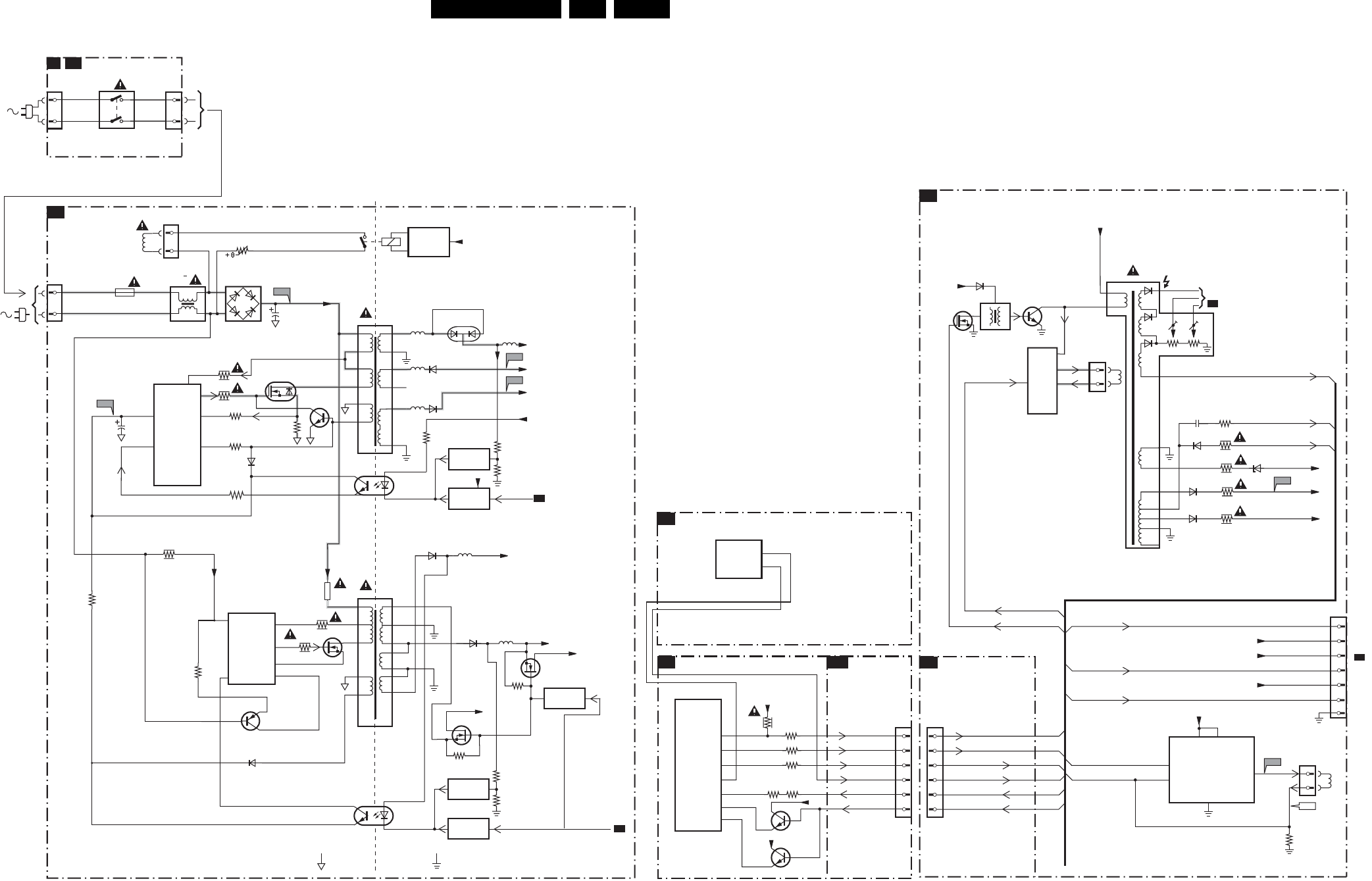
Block Diagrams, Testpoint Overviews, and Waveforms
Block Diagram LSP Supply and Deflection
POWER SUPPLY
1504
24
3
9
8
4
17
18
13
14
5
6
3
2
1
F508
3575
3576
6511
7517
2511
A1
FRONT INTERFACE
M Q1
Degaussing
Coil
1503
5512
7541
7511
TEA1507
DRAIN
DRIVER
SENSE
DEMAG
CONTROL
IC
CTRL
ENERGIZING
CIRCUIT
(optional)
AC
DC
6500
5500 :
5502
10
11,12
1
2
4
3
1500
T4E
2505
0201
1051
1031
1951
MAINS
SWITCH
+Vaudio
+3V3
F563
F561
-Vaudio
+Vaudio
+9VA
5551
5552
5561 6562
5562 6563
Vbatt
A6
STANDBY
7571
REFERENCE
CIRCUIT
7573
STANDBY
CIRCUIT
7513
TCET1103
2Vcc
3513
3522
3514
3516
7512
14
11
9
3517
7
D
S
G
I511
1505
0202
1
2
1
2
3518
3571
or
1
2
3523
VDC
3519
6551
6
4
14
8
9
10
5
2
1
3545
3544
5504
12
11
1
2
3
4
1532
A4
STANDBY
7542
REFERENCE
CIRCUIT
STANDBY
CIRCUIT
7516
TCET1103
VDC
3536
3526
7510
SUPPLY
CONTROL
14
7525
11
7
9
2
6
HOT GROUND COLD GROUND
3598
7532
3527
6581
13
5505 +9VA
6536
5564 +5V2
6535
7545
+5V
3546 STANDBY
CIRCUIT
7535
3537
+Vaux
6469
F_15040_060.eps
290405
LINE + FRAME DEFLECTION
LINE
FRAME
A2
F453
SVM_ROT
-14V
VideoSupply
Vbatt
+5V
+12V_LOT
7405
BU4508DX
5402
LINE
OUTPUT
CIRCUIT
+
E/W
CORR.
7404
1404
1
2
HOR.
DEFL.
COIL
1452
1
3
VER.
DEFL.
COIL
5450
3
1
FOCUS G2
EHT TO
CRT
1401
7
6
5
4
3
10
7
B1
TO 1351
CRT
F
5
8
9
12
6461
6465
3471
3450
F459
F466
7455
TDA4863J
7INP
6INN
5V-OUT
+13V
6452
6453 3458
11
6
3485
3456
Filament
EHTinfo
0230
32
34
1670
26
28
29
31
SYNC & DEFLECTION PROCESSING
B8
3350
3374
L1
R1
L3
R2
T2
7300-F
ADOC
3354
N3
HDROUT
VDRP
VDRN
EWP
HFB
EHT
HFB_XRAY_PROT
LINEDRIVE1
FRAMEDRIVE+
FRAMEDRIVE-
EW_DRIVE
INTERFACING
A6
3477
2477
HFB
+12V_LOT
Vbatt
EHTinfo
VideoSupply
Filament 2
1
HDRIVE
EW_DRIVE
EW_DRIVE
3358
+5V
3375
7361 +5V
7365
+8V
N2
BCL
EHT-INFO
HFB_XRAY_PROT
HDRIVE
INN
INP
EW_DRIVE
EHT-INFO
3353
SSB
CONNECTOR
INTERFACE
B18
7300-D
ADOC
EWVIN
EWIOUT
MPIF-SUPPLY, E/W &CONTROL
B4
36
37
32
34
26
28
29
31
4
GND
VP1
13
VP2
Block Diagrams, Testpoint Overviews, and Waveforms 17ES1E AA 6.
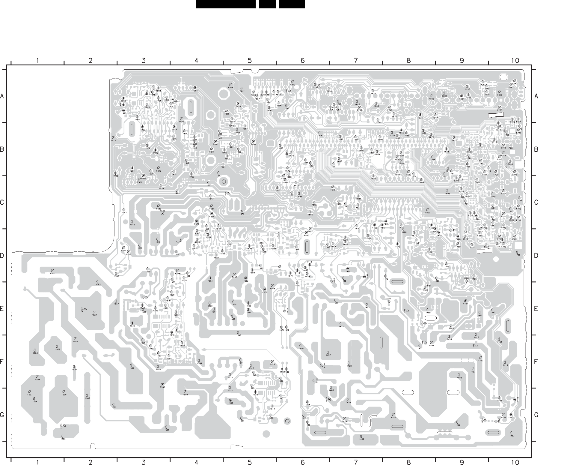
Testpoint Overview LSP
3139 123 5895.4 F_15040_010.eps
220305
F232 A8
F233 A8
F234 A9
F235 A10
F241 A10
F242 A10
F243 A10
F246 B8
F247 A8
F248 A8
F249 A7
F250 A6
F401 D6
F402 E7
F404 F8
F416 G6
F418 G7
F419 G8
F451 F9
F452 G10
F453 C7
F455 C7
F456 G10
F457 G10
F458 D8
F459 G7
F462 F9
F464 F6
F465 F6
F466 D9
F469 D9
F472 C8
F475 C8
F476 D8
F478 D9
F481 E9
F482 C8
F483 D8
F500 D1
F501 F2
F502 E2
F503 G1
F504 F1
F506 G1
F507 G1
F508 F3
F509 G4
F535 C3
F537 C5
F541 D3
F542 D3
F552 E5
F561 D4
F562 D5
F563 D5
F573 D6
F574 D4
F575 F5
F576 C4
F578 C4
F580 D6
F581 C4
F582 C3
F583 E5
F620 C8
F627 A5
F628 A5
F629 B8
F630 B8
F631 B8
F632 B8
F672 A6
F673 B8
F674 C6
F675 B6
F676 B6
F677 B9
F678 C6
F679 C7
F701 D9
F702 D10
F703 D10
F704 D10
F705 C9
F706 C10
F708 C10
F710 C10
F711 B10
F712 C10
F713 C9
F714 B10
F715 B9
F716 B10
F717 C10
F718 B9
F719 B10
F720 B10
F721 B9
F722 B10
F723 B10
F724 B10
F901 B4
F903 A4
F904 B3
F905 C3
F910 B3
F911 B4
F912 A5
F913 B2
F950 A5
F951 B5
F952 A4
F955 B4
F956 C3
F958 A5
F959 A5
I232 A9
I239 A9
I240 A9
I241 A6
I242 A6
I247 A6
I248 B8
I249 A7
I253 A7
I254 A7
I255 A7
I256 B6
I259 A7
I260 A9
I261 A9
I402 G9
I410 F10
I413 D6
I414 C7
I415 D7
I418 G6
I419 G6
I420 E6
I423 D7
I428 F7
I432 E8
I435 D8
I436 D8
I437 D6
I438 D9
I439 E8
I440 E8
I442 E10
I443 F9
I445 D7
I446 D7
I447 D6
I448 D6
I449 D6
I450 F6
I453 G9
I455 F9
I457 F8
I458 F8
I459 F9
I460 D8
I462 G7
I463 G10
I464 F10
I466 E8
I468 E8
I469 E9
I470 D8
I473 E7
I475 F9
I476 D9
I480 D9
I481 D9
I482 G10
I487 D7
I488 G6
I489 G7
I490 D7
I491 D7
I492 E9
I493 G10
I494 E8
I495 D9
I496 E7
I497 F6
I499 D7
I500 F3
I501 G3
I502 G2
I503 G1
I504 G1
I506 F3
I507 E2
I509 F4
I510 E3
I511 G5
I512 E4
I513 F5
I514 F5
I515 F5
I516 G5
I517 G5
I518 F5
I519 G5
I520 F6
I521 G5
I522 D6
I523 F6
I525 E3
I526 F3
I527 G6
I528 E4
I529 D4
I530 F3
I531 E3
I532 E3
I533 E4
I534 F2
I536 E3
I537 E3
I538 D4
I539 D3
I540 D3
I542 D2
I543 C3
I544 E4
I545 C3
I546 F5
I547 C4
I548 F5
I550 E3
I551 E5
I552 E5
I553 F3
I554 F3
I555 E4
I557 E2
I558 D4
I559 G2
I560 F4
I561 E4
I562 E4
I563 E2
I564 F6
I565 D4
I566 D4
I568 D3
I569 D5
I570 D5
I571 E6
I572 F1
I573 D5
I574 D6
I575 E6
I577 C4
I578 E6
I579 E5
I580 D5
I581 D4
I582 G5
I583 F1
I586 E5
I587 D4
I588 C4
I589 D5
I590 D4
I591 D4
I592 D4
I593 D4
I596 D6
I597 D5
I599 D5
I602 A9
I603 C6
I604 B7
I605 C7
I606 C6
I608 C6
I609 C9
I610 B9
I611 C9
I612 A7
I616 B8
I621 A6
I622 A6
I623 A5
I624 A5
I625 A5
I626 A5
I627 C6
I628 C6
I629 C6
I630 B6
I631 C6
I632 A8
I633 B8
I634 C7
I635 A7
I636 B8
I637 B8
I638 C8
I639 C8
I640 B7
I650 C7
I672 B8
I674 A7
I677 B7
I678 B9
I680 B7
I685 B6
I686 B6
I687 B6
I688 B7
I689 B7
I690 B7
I691 A5
I693 C7
I694 C7
I695 B7
I696 A6
I701 D9
I702 D10
I703 C9
I704 D10
I705 C9
I707 C10
I708 C10
I709 C9
I710 C9
I711 B9
I712 B10
I713 B10
I714 B10
I715 B10
I716 B10
I717 C10
I719 D9
I720 C9
I721 D9
I722 C10
I723 B9
I724 B9
I725 B9
I726 C9
I727 A10
I728 B10
I729 A10
I731 D9
I732 D9
I733 C9
I734 C9
I735 C9
I736 B10
I737 B9
I738 C10
I739 D10
I740 C10
I741 C10
I901 B4
I902 C2
I903 A3
I904 A3
I908 A3
I909 A3
I913 A4
I914 A4
I915 B4
I916 B4
I918 B4
I920 C4
I921 A3
I922 B3
I924 B3
I925 A3
I926 B3
I927 A3
I928 B4
I930 B4
I934 B4
I935 C3
I936 A3
I938 B3
I941 A3
I943 A3
I945 B4
I948 A3
I951 B5
I952 B5
I953 A5
I954 B5
I956 B4
I957 B5
I958 C5
I959 B4
I960 B5
I962 B5
I963 B4
I964 C4
I965 B5
I967 C4
18ES1E AA 6.
Block Diagrams, Testpoint Overviews, and Waveforms
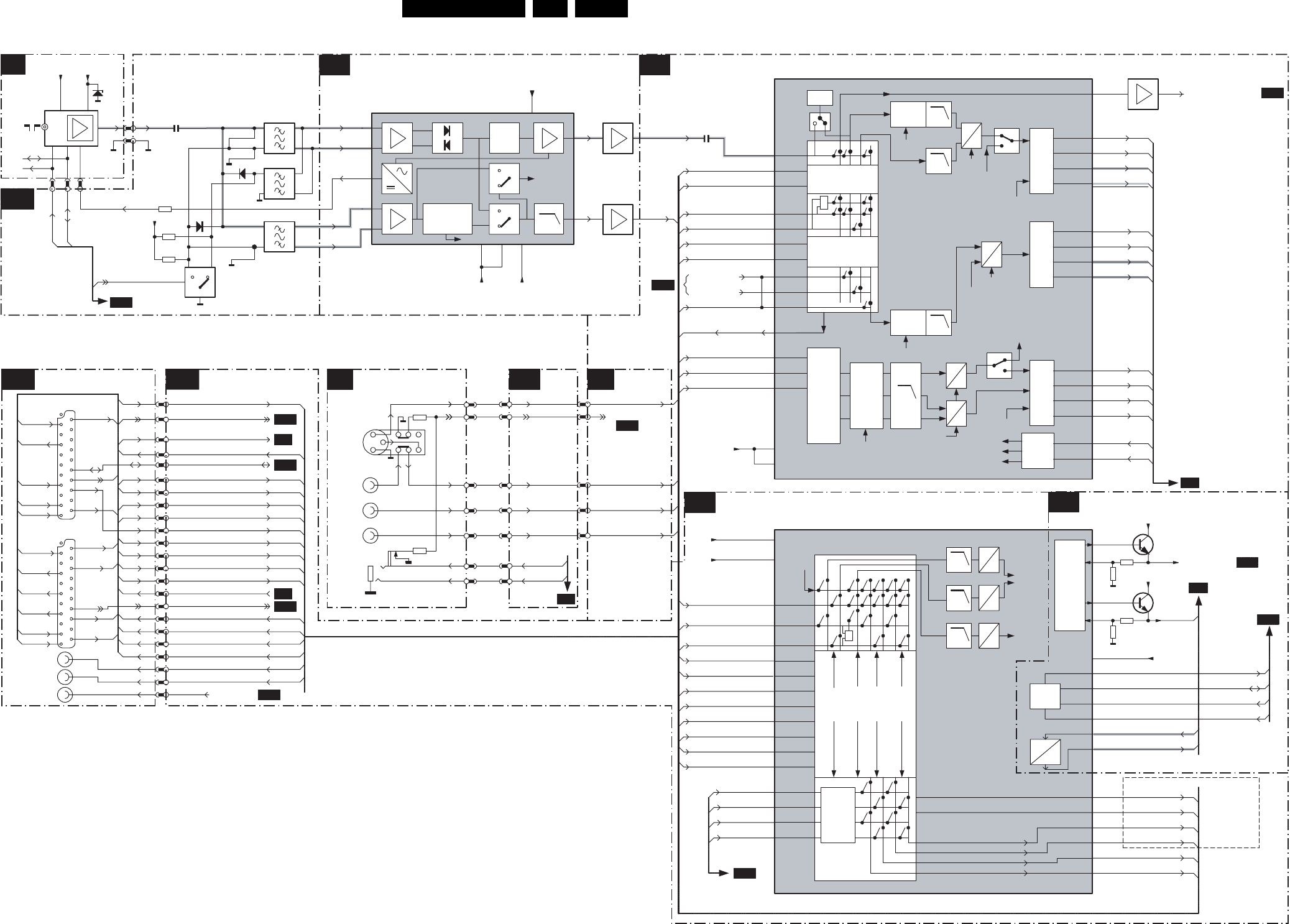
Block Diagram 1 Audio & Video
A
Sound
Tra p s
+5Vb
1232
+5V
SDA
SCL
0230
7,3 9
451
11 13
154849
SCL0
SDA0
1113
1114(1)
1112(2)
SEL-IF-LL
VIFINP
TUNER_AGC
107
110
120
116
7131
SIF_MAIN
TUNER
IF-TER
7100-C
7
7
7
8
8
8
QSS Mixer
AM Demod.
14
108
VIFINN
99
100
SIFINP
SIFINN
105
3132
AGC
6101
6102
3102
3101
+8Va LPF
2
3
2
3
2
3
SIF A/D
CVBS-IF
CVBS-1
CVBS-2
CVBS/Y-3
C3
CVBS/Y-4
C4
Y-COMB
C-COMB
R/Pr/V1
G/Y/Y-1
B/Pb/U1
+
YUV
RGB
Source
Switch
CLAMP LPF
Data
Link
2
Yyuv
U
V
CLAMP
LPFCLAMP
A
D
LPF
Data
Link
1
A
D
Data
Link
3
CVBS-outA
STROBE1N
STROBE1P
DATA1N
DATA 1P
CVBS/Y prim
C prim
CVBS sec
Yyuv
2Fh
SIFA/D
LR prim
Dig
Yyuv
2Fh
STROBE3N
STROBE3P
DATA3N
DATA 3P
STROBE2N
STROBE2P
DATA2N
DATA 2P
U,V
LPF
A
D
A
D
Timing
Circuit
CLP prim
CLP sec
CLP Yyuv
CLP prim
CLP sec
CLP Yyuv
CVBS-SC1_AV1-IN
CVBS2_PIP_TUN2
Y-CVBS-SC2_AV2-IN
C-SC2_SVHS-IN
Y-CVBS-FRO NT-IN
C-FRONT-IN
YOU T- C O M B
COUT-C OMB
R-SC1_V-IN
G-SC1-IN_Y-IN
B-SC1-IN_U-IN
7063
7100-B
MPIF VIDEO SWITCH
MPIF IF + QSS
19
60
61
63
62
50
51
53
54
55
56
57
58
46
45
7060
123
126
9
8
5
4
1
15
16
25
26
27
+5V 49
64
CVBS_SC2_MON_OUT
STROBE1N
STROBE1P
DATA1N
DATA 1P
STROBE3N
STROBE3P
DATA3N
DATA 3P
STROBE2N
STROBE2P
DATA2N
DATA 2P
HV_PRIM
HV_SEC
Mono Sec.
Dig.
+
LR
prim
A/D
Mono
sec
A/D
LR
Line
LR
Scart
AUDIO
AMPs
LPF A
D
LPF A
D
LPF A
D
L prim
R prim
Mono sec
LR prim
Dig
Mono sec
Dig
AM
Int
AM EXT
L1
R1
L2
R2
L3
R3
L4
R4
DSNDL1
DSNDR1
DSNDL2
DSNDR2 SCART1L
SCART1R
LINER
LINEL
MPIF AUDIO SW ITCH
69
70
67
68
PIP-AUDIO
L-SC1_AV1-IN
R-SC1_AV1-IN
L-SC2_AV2-IN
R-SC2_AV2-IN
AUD-R1
L-FRONT-IN
R-FRONT-IN
DSNDL1
DSNDR1
DSNDL2
DSNDR2
17
86
85
84
83
82
81
80
79
74
73
72
75
+5V 91,77
98,88
R-SC1_AV-O UT
L-SC1_AV-O UT
L-CL_VL-OUT
R-CL_VL-OUT
L-SC2-OUT
R-SC2-OUT
AV3 L
R
3242
SVHS 2
3242
4
10
7
2
6
8
11
4
10
7
2
6
8
11
INTER-
FACING
HP
SIDE IO PANEL
64
62
63
65
66
1620
1936 OR 0240
43
44
7101//7104
Ident
27/54 MHz
54MHz
54MHz
I2C
IRQ 42 MPIF-IRQ
4107
4108
CVBS-SC3
CVBS_TER_OUT
2101
EW
V
I
EWVIN
EWIOUT
SCL
SDA
SCL1
SDA1
EW_MPIF
EW-DRIVE
F_REF
VIDEO SOURCE SELECT & DATA LINK
AUDIO SOURCE SELECT
7100-A
IF & SAW FILTER
MPIF-SUPPLY
EW & CONTROL
XREF 40
36
37
C
Y
12
Supply
+
Ref.
7150-A
3151
3150
7150-B
3153
3152
+5V
+5V
2
3
20
21
VREF_AUD_POS
VREF_DEFL
4152 CVBS-DTV
B10
B10
B11
B8
B5
B11
HEADPH-R
HEADPH-L
B18
C-FRONT-IN
Y-CVBS-FRO NT-IN
FRONT- DETECT
B11
AUD-L1
SIMM CONN
B18
0230
0230
B17
DA6 B18
(PIP/DW)
2062
7100-D
(1) Present for China only
(2) Present for AP-Multi, China & EU only
HV-PRIM
HV-S EC
VTUN
6200
SIMM
CONN
B18
+8V
4101
4102
4103
4104
122 125 118
+5Va +5Vd
66
65
SCART2R
SCART2L
AUDIO-OUT OR
MONITOR-OUT
2ND SCART
1ST & 3RD SCART
VCC-DIG
VCC-I2D
CVBS
L-FRONT-IN
R-FRONT-IN
AUD_L2
AUD_R2
L5
R5
127
128
+5V
14,28,35
EUROPE ONLY
AM Int
7062
CVBS-outB
22
EF
C-SC2_SVHS-IN
SEL-SVHS-RR_STATUS2
Y-CVBS-SC2_AV2-IN
CVBS-SC1_AV1-IN
L-SC1_AV1-IN
R-SC2_AV2-IN
CVBS-SC2_MON-OUT
G-SC1-IN_Y-IN
B-SC1-IN_U-IN
R-SC1-IN_V-IN
L-SC1_AV-O UT
7
19
6
10
52
60
53
58
2
1
3
56
61 R-SC1_AV-O UT
L-SC2_AV2-IN
R-SC1_AV1-IN
9
INPUTS/OUTPUTS SIMM CONNECTOR
4FBL-SC1-IN
CVBS_TER_OUT
B11
B2
R-CL_VL-OUT
69
70
B5
L-CL_VL-OUT
0230
B11
COMM_LINE
12
20
21
AUDIO-L OUT
AUDIO-R OUT
12
20
21
SCART 2
SCART 1
R-Out R-In
L-Out
L-In
B-In Status
G-In
R-In FBL-In
TER-Out CVBS-In
1
12
2
3
3
4
4
5
5
STATUS1_PIP-AFT-5 0-60HZ18 B11
6
6
7
7
8
8
9
9
10
10
R-Out
L-Out R-In
L-In
C-Out Status
P50
C-In
MON-Out Y/CVBS-In
L-SC2-OUT
R-SC2-OUT59
55
11
11
12
12
13
13
14
14
15
15
16
16
17
17
AUDIO-SL OUT AUDIO-SURR B10
72
20
A5
B18
B1 B2
B3 B4
A11
F_15040_055.eps
250405
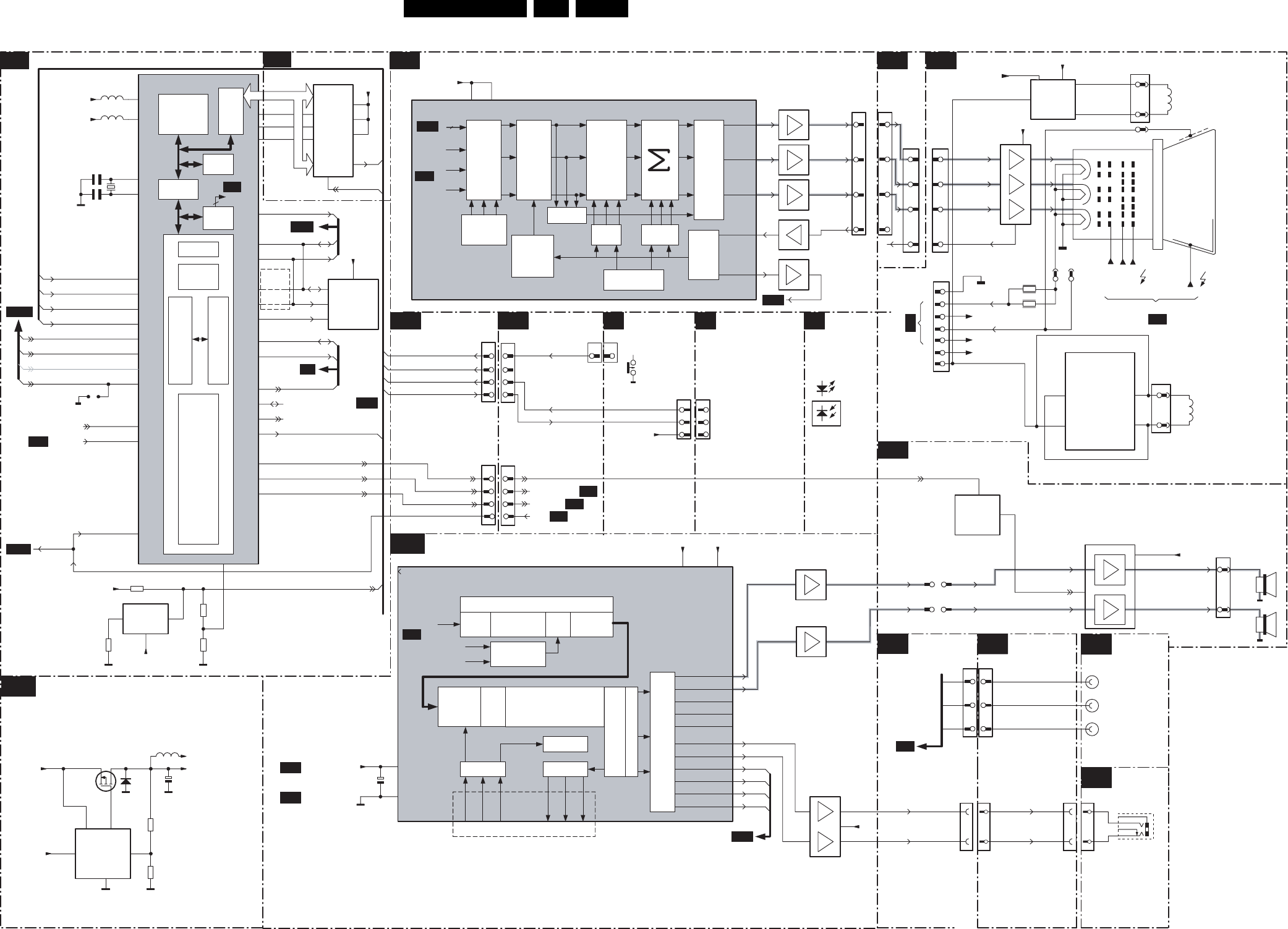
Block Diagrams, Testpoint Overviews, and Waveforms 19ES1E AA 6.
Block Diagram 2 Audio & Video
DAC
DDEP
Down
Mix Preprocessing SRC Dematrix
and Select
Level
Adj.
I/P
X-
Bar
I2SOUT
O/P
X-
Bar
Noise Shaper
Demodulation and Decoding DSP
AUD_SPK_SW
AUD_SPK_R
AUD_SPK_L
AUD_SPK_C
AUD_SPK_SL
AUD_HP_R
AUD_HP_L
DSNDL1
DSNDR1
DSNDL2
DSNDR2
SSIF
ADOC SOUND & AUDIO PROCESSING
7433
7432
DRIVE
ADJUST CDAC
BLENDER
CONTROL
ADC
LEAKAGE
COMPASATOR
7310
7330
R-CRT
G-CRT
B-CRT
CUTOFF
ROUTP
GOUTP
BOUTP
DRIVE
ADJUST CDAC
RGB
CUTOFF
RGB
GAIN
BLENDER
CONTROL
ADC
LEAKAGE
COMPASATOR
FIXED
BEAM
CURRENT
SWITCH
OFF
GFX ROUTP
BOUTP
IBC
IBCRANGE
ADOC RGB
7300-H
R
G
B
7320
3
7307
3
1
28
9
7
CRT
5
R
G
B
SCAVEM
PROC.
SCAVEM
COIL
CUTOFF
200V
+141V
3307
TO/FROM 14
OF LSP
2
4
1
2
3
5
1
2
3
5
CRT PANEL
INTER-
FACE
EHT- INFO
25
24
23
21
25
24
23
21
76
75
AUDIO-R
AUDIO-L
HEADPHONE-R
HEADPHONE-L
EHT
FOCUSA
FOCUSB
FROM LOT
VG2
3
1
MIPS EBIU
SRAM
128KB
PI-PI
BRIDGE
GFX
GEN
GPIO
I2C
A/DADC
TIME R
GFX
FAST
PI_BUS
SLOW
PI_BUS
1581
2582
2581
KEYBOARD
FRONT- DETECT
STATUS1_PIP-AFT-5 0-60HZ
SEL-SHVS-RR_STATUS2
LIGHT-SEN SOR
RC5
SDA0
SCL0
SDA1
SCL1
ON-OFF-LED
ON-OFF-LED
SEL-IF-LL
SOUND-ENABLE
SEL-2FH-SRC_STATU S3
DEGAUSS
STANDBY
VDDCO VDDE
MPIF-IRQ
W
E
G
VDDE
7790 VDDE
CONTROL
SEL-2FH-SRC_STATU S3
DTV_EXPENSION
COMM_LINE (SCART)
F_REF
ADOC-uP & CONTROL
POR_FLASH
EXT. STER EO
EXT. MONO
79
37
78
77
79
37
78
77
36
80
51
KEYBOARD
RC5
LIGHT-SEN SOR
TOP CONTROL
2
1091~4
3
41002
1008
INTERFACING
STANDBY
DEGAUSSING
VOL_MUTE
7990
4
RIGHT
LEFT
1
SOUND
ENABLE
7
6
4
9
1
10
VREF_AUD_POS
AUDIO PROCESSING
POR
POR_FLASH
50
36
80
51
50
RGB PROCESSING
B3
HEADPH-R
HEADPH-L
B3
7651
Vgate
Vfb
Vc
Vcc
Gnd
81
65
4
3651
3652
+1V8+5V2
+3V3
7650
LOW VOLTAGE SUPPLY - ADOC
B8
B4
B18
B4
A3
A1
B4
(FROM 0223)
A3
B18
B1
B10
B15
EMAINS SWITCH
PANEL
MFRONT
INTERFACE
Q1
7300-A,C,E & K
6651
7300-x
7300-B
2
1
3
1
+5V2
4
+Vaudio
ADC1
ADC4
P2-6
P3-0
ADC3
ADC0
ADC5
P0-7
P0-3
P0-1
P3-2
P0-6
P0-4
P2-4
P2-2
P0-5
P1-1
P1-0
P1-3
P1-2
MPIFCLK
XOUT
XIN
(SCART)
FOR 2FH I/P or SCART- 3
EBIU BUS
A1..A21 D0..D15
A2
A2
200V
6
3306
FROM
VDD
MEMORY INTERFACE
B6
B7
B11
CDAC2-
VDDA
CDAC1-
VDDA
B5
SDAC1-V DDA
SDAC1-3V3
BLENDER
BLANKING
SCAVEM
SVMP
+5V
7480
2
6
1
7
8
VREF_AUD_NEG
B4
2447
VDDCO
5600
9,37
VDDQ 43
FLASH
RESET_
FLASH_RST
FLASH_RST
16
RP
ADC2
VDDE
VDDCO
ADC-
VDDA
XVDD
5570
5583
7525
WC_
5
6
7
VDDE
8
P1-5
SCL
SDA NVM
VPP
SDM
7346
7356
TILT
B8
Decimation
Filter
I2SIN
WS PLL
Audio Processing DSP
SDI
SCKI
WSI
SD02
SCK02
WS02
4565
4564
RES
2651
N.C. N.C.
SYSTEM
RESET
(50ms)
7581
VDDE
+5V2
3582
3590
3583
3586
1
5
4
SCART I/O
INTERFACING
15
RB
RB
RB53
P0-2
N.C.
1
DC_FILAMMENT
1629 1340
1351
5
6
7
912
+8V_+12V
SVM_ROT
+141V
+8V_+12V
SCAVEM
PROC.
ROTATION
COIL
3
1
1361
TDA8941P
7366
IN-
3
IN+
5
5
OUT-
OUT+
5
1382
0230 1670
02151645
02150215
7991
1911
1670
0230
1670
0230
1705-1
1705-2
1705-3
AUDIO-SURROUND
AUDIO-R
AUDIO-L
SSB CONN
INTERFACE
69
72
0230
70
0230
70
69
72
1670
1670 1620
1254
0240
1936
0230
A6 A7
SIDE I/O
D
68
67
68
67
11
10
11
10
B18
F_15040_056.eps
250405
B7 A6 F
AUDIO
AMPLIFIER
A4
A6
SSB CONN
INTERFACE
B18
B11 B12
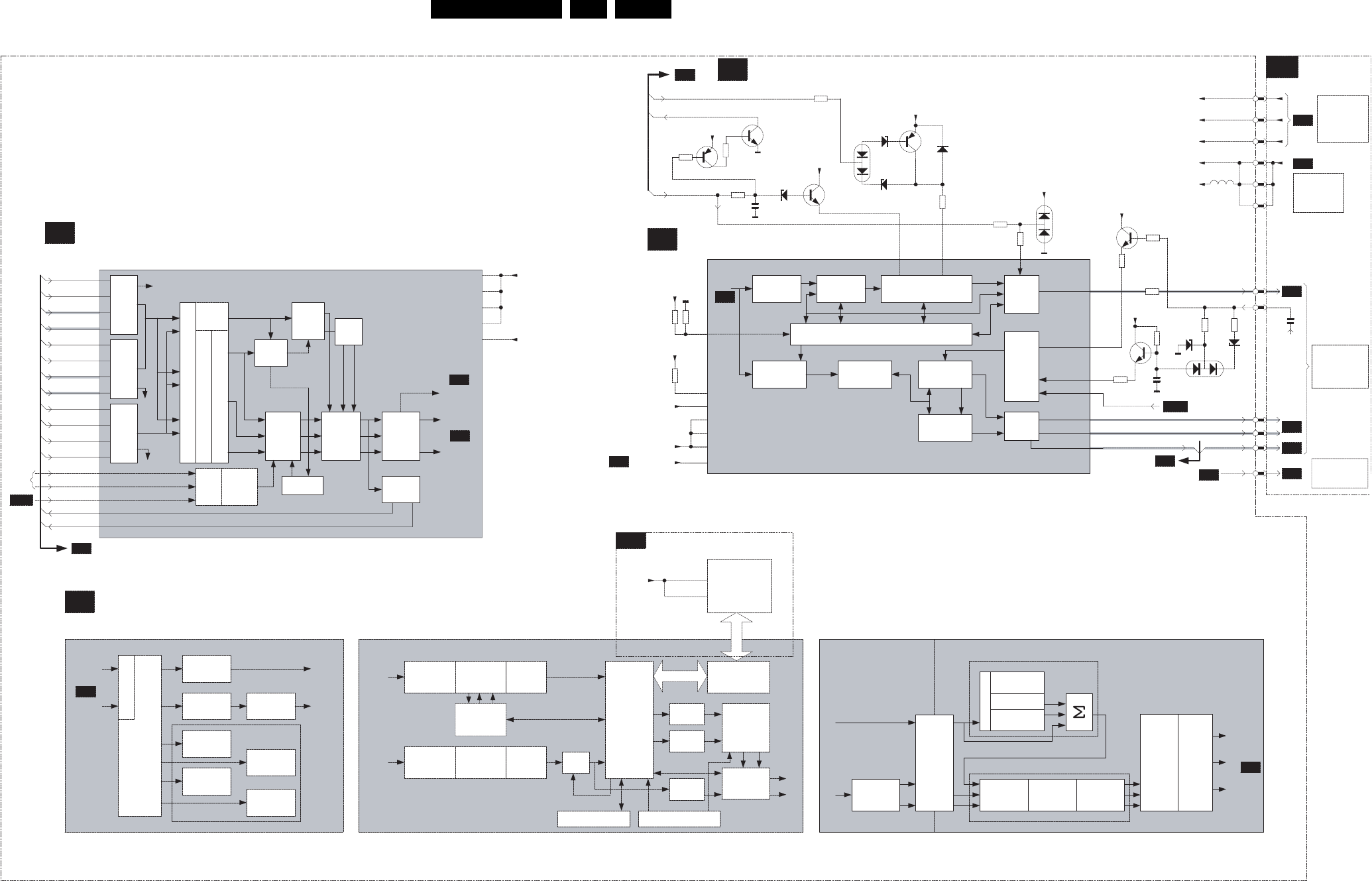
20ES1E AA 6.
Block Diagrams, Testpoint Overviews, and Waveforms
Block Diagram 3 Audio & Video
STROBE1N
STROBE1P
DATA1N
DATA 1P
STROBE3N
STROBE3P
DATA3N
DATA 3P
STROBE2N
STROBE2P
DATA2N
DATA 2P
HV_PRIM
HV_SEC
I2D1
I2D3
I2D2 FAST-
BLANK
FIFO
DMSD
CHR.
MUX
DE-
MUX
FAST
BLANK
SWITCH
FOR-
MATER
SYNC
2Fh HV
INFO
HVSYNC
ADOC VIDDEC (PRI & SEC)
7300-J
DATA S YNC
SAMPLE RATE CONVERTER
AGC_AMP
Hor. TIMEBASE GEN.
DTO & CONTROL LOOP
SLOW START/STOP
L0W POWER STARTUP
1st
CONTROL
LOOP
SDAC
HIRES.
TIMING
GEN.
HOR. TIMEBASE GEN.
DTO & CONTROL LOOP
SLOW START/STOP
L0W POWER STARTUP
1st
CONTROL
LOOP
SDAC
HIRES.
TIMING
GEN.
ADC
2nd
CONTROL
LOOP
VERT.
WAVEFORM
EAST-WEST
WAVEFORM
VERT.
SAWTOOTH
VERT.
DRIVER
HDROUT
HFB
EHT
BCL
FBCIN
EWP
VDRP
VDRN
6365
3368
3367
ADOC DOP
PRI
SEC
SSIF
VIDDEC1
VIDDEC2
HVSYNC
SKIN
TONE
CONTROL
BLUE
STRETCH
GREEN
ENHANCE
RGB
MATRIX
FRAME
PROC.
PAN O-
RAMA
DCTI
SHARPNES
S
MEASURE
LTI
DYN.
PEAKING
F
I
L
T
E
R
LUMINANCE SHARPNESS
COLOUR FEATURES
Y
UV
Y
U
V
U
V
YY
U
V
R
G
B
ADOC BEF
HOR.
COMPRESS
HOR.
COMPRESS
MAIN
CH.
SUB
CH.
VERT.
COMPRESS
SUB
FIFO
CACHE
NOISE
SHAPER
MAIN
FIFO
CACHE
NOISE
SHAPER DNR
MEMORY
BUS
DEVICE
INTERF.
UNDI-
THER
UNDI-
THER
SCAN
RATE
CONVERT
OUTPUT
MUX.
UNDI-
THER
DISPLAY CONTROLMODE CONTROL
SDRAM
ADOC MBF
Y
UV
INPUT
SWITCH
MATRIX
BLACK
STRETCH
BLACK
STRETCH
HISTOG.
MODIFY
HISTOG.
MEAS.
BLACK
BAR DET.
BLACK
LEVEL DET
NOISE
MEAS.
MEASUREMENT
BLOCKS
VIDDEC1
VIDDEC2
MAIN
CH.
SUB
CH.
ADOC FEF 13.5 / 27 MHz
@ 720 ppl
27 / 54 MHz
@ 1440 ppl
LINEDRIVE1
HFB_X-RAY-PROT
FRAMEDRIVE+
FRAMEDRIVE-
VDDE
7730
7382
7393
3398 6397
6381
6382
6385
FLASH
X-PROT
+8V
EW_MPIF
(YUV)
(YUV)
(YUV)
(YUV)
Ext
Syn
c
Mux
SRC for
HFB1/
H-Sync
Sync
Mux.
H-2FH
V-2FH
FBL-SC1-IN
VDDCO
VDDE
VIDEO DECODER
POR_FLASH
EXT. STEREO
EXT. MONO
3380
3385
1,14,27
3,9,43,49
VDDE
VREF_DEFL
FEATURE BOX
SYNC & DEFLECTION PROCESSING
+5V2
+5V
+8V
+3V3
40
43
45
26
34
2
8
2
9
PROTECTION
B18
B2
B4
B7
B4
B11
31
EW-DRIVE
FROM
1116
B 5
B 6
B 8
B 9
3346
BPA
SDAC-VDDA
DOP-DTC-VDDA
DOP-DTC-VDD3
IMEAS-VDDA
SDAC-3V3
7300-I
TO BLOCK
DIAGRAM
DEFLECTION
2455
EHT-INFO
A3
A4
A4
FROM
BLOCK
DIAGRAM
STAND-BY
SUPPLY
A2
A8
0230
INTERFACING
A 6
VDD
VDDQ
FIELD MEMORY & TXT PG
DLINK-VDDA
DLINK-VDDD
VID1-DTC-VDDA
PLLVDDA
VID1-DTC-VDD3
7300-F
SAMPLE RATE
CO NVERTER
MEMORY
CTRL/SWI.
MMI BUS
SA0...SA11
SD0...SD15
DTL I/F
B6
B5
B8
B5
B7
TO
47
46
44
MEMORY INTERFACE
3350
7300 7300
7300
6353
3353
3354
+3V3
6367
7365
3372
TILT
VDDE
3340
3341
SEL2FH
VDDE
3387
3384
7383-B
7383-A
+8V
KEYBOARD
6384
A5
35
FROM
TUNER
SIMM
CONN.
TO
ROTATION
CIRCUITRY
5601
VDDE
B7
2397
7361
3364
3361
6368
+8V
3373
+5V
2361
VDDCO
B13
DMSD=Digital Multi Standard Decoder
DCTI=Digital Color
Transient Imrpovement
+3V3
EHT-INFO
EHT-INFO
F_15040_059.eps
290405
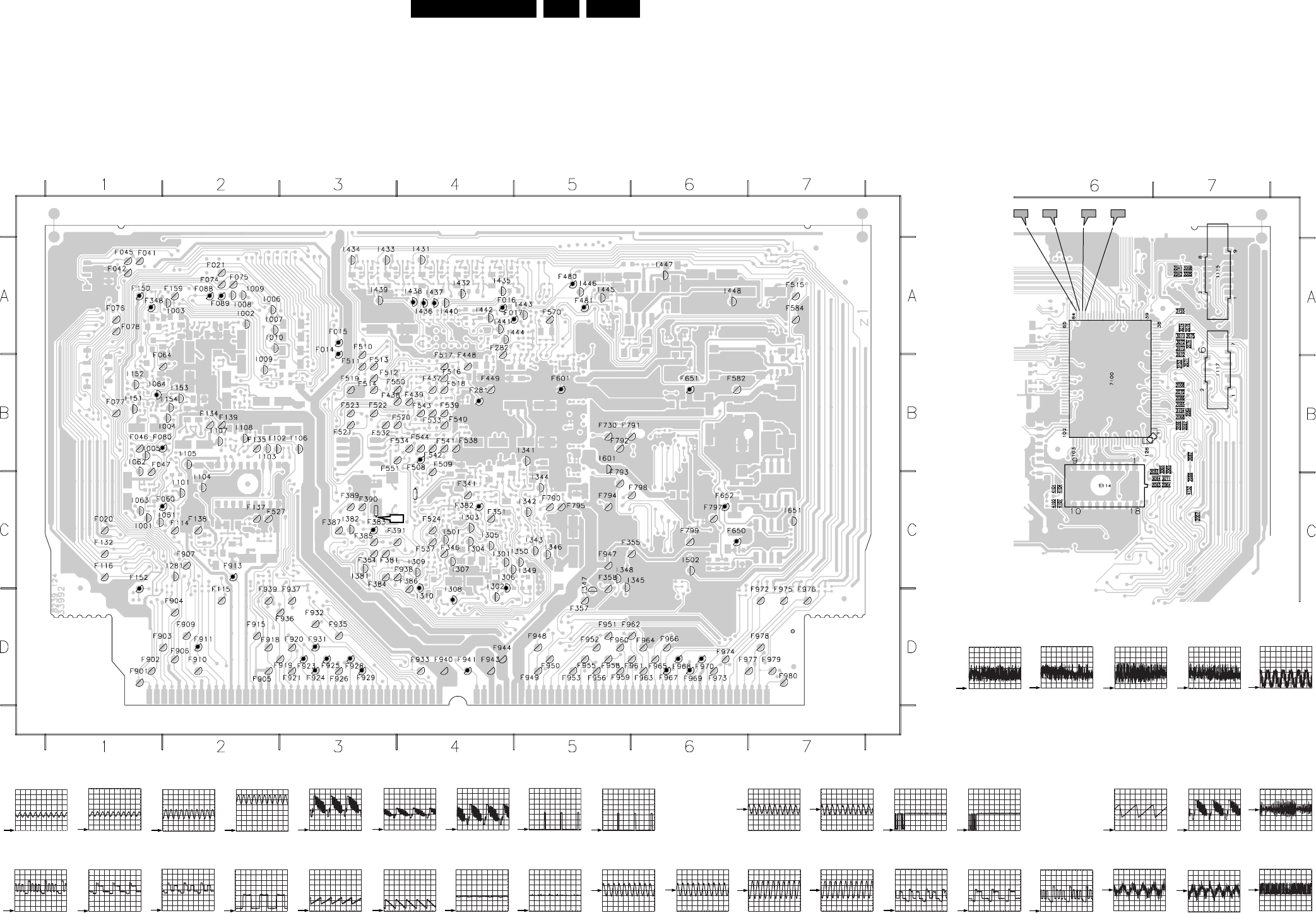
Block Diagrams, Testpoint Overviews, and Waveforms 21ES1E AA 6.
Testpoint Overview SSB
S1
100mV / div DC
20µs / div
S4
100mV / div DC
20µs / div
S3
100mV / div DC
20µs / div
S2
100mV / div DC
20µs / div
F014
1 V / div DC
1ms / div
F015
1 V / div DC
1ms / div
F016
500mV / div DC
1ms / div
F017
500mV / div DC
1ms / div
F060
500mV / div DC
20µs / div
F080
500mV / div DC
20µs / div
F064
500mV / div DC
20µs / div
F088
1 V / div DC
20µs / div
F089
1 V / div DC
20µs / div
F150: 3V2 DC
F152: 3V2 DC
F281: 3V2 DC
F381: 0V DC
F382: 0V DC
F383: 0V DC
F480
100mV / div AC
1ms / div
F481
100mV / div AC
1ms / div
F509
1 V / div DC
200µs / div
F508
1 V / div DC
500µs / div
F601: 1V8 DC
F650: 3V2 DC
F651: 1V8 DC
F652
500mV / div DC
500ns / div
F911
500mV / div DC
20µs / div
F913
500mV / div AC
10µs / div
F967
200mV / div AC
1ms / div
F941
2 V / div DC
20µs / div
F931
1 V / div DC
5ms / div
F929
500mV / div DC
5ms / div
F928
500mV / div DC
5ms / div
F926
1 V / div DC
10µs / div
F925
1 V / div DC
10µs / div
F969
500mV / div AC
1ms / div
F968
200mV / div AC
1ms / div
F970
500mV / div AC
1ms / div
F923
1 V / div DC
10µs / div
F924
1 V / div DC
10µs / div
I310
200mV / div DC
10µs / div
I308
200mV / div DC
10µs / div
I306
200mV / div DC
10µs / div
I437
20mV / div AC
200µs / div
I438
100mV / div AC
1ms / div
I436
20mV / div AC
500µs / div
S5
500mV / div DC
50ns / div
CL 36532058_008.eps
211103
I442 A4
I443 A5
I444 A5
I445 A5
I446 A5
I447 A6
I448 A6
I501 C4
I502 C6
I601 B5
I651 C7
I381 C3
I382 C3
I431 A4
I432 A4
I433 A3
I434 A3
I435 A4
I436 A4
I437 A4
I438 A4
I439 A3
I440 A4
I441 A4
I308 D4
I309 C4
I310 D4
I341 B5
I342 C5
I343 C5
I344 C5
I345 C6
I346 C5
I347 C5
I348 C5
I349 C5
I350 C5
I108 B2
I151 B1
I152 B1
I153 B2
I154 B2
I281 C2
I301 C4
I302 C4
I303 C4
I304 C4
I305 C4
I306 C4
I307 C4
I009 B2
I010 A2
I061 C2
I062 B1
I063 C1
I064 B1
I101 C2
I102 B2
I103 B2
I104 C2
I105 B2
I106 B3
I107 B2
F976 D7
F977 D6
F978 D7
F979 D7
F980 D7
I001 C1
I002 A2
I003 A2
I004 B2
I005 B1
I006 A2
I007 A2
I008 A2
F962 D5
F963 D6
F964 D6
F965 D6
F966 D6
F967 D6
F968 D6
F969 D6
F970 D6
F972 D7
F973 D6
F974 D6
F975 D7
F947 C5
F948 D5
F949 D5
F950 D5
F951 D5
F952 D5
F953 D5
F955 D5
F956 D5
F958 D5
F959 D5
F960 D5
F961 D6
F929 D3
F931 D3
F932 D3
F933 D4
F935 D3
F936 D3
F937 D3
F938 C4
F939 D2
F940 D4
F941 D4
F943 D4
F944 D4
F910 D2
F911 D2
F913 C2
F915 D2
F918 D2
F919 D3
F920 D3
F921 D3
F923 D3
F924 D3
F925 D3
F926 D3
F928 D3
F794 C5
F795 C5
F797 C6
F798 C6
F799 C6
F901 D1
F902 D1
F903 D1
F904 D2
F905 D2
F906 D2
F907 C2
F909 D2
F551 B3
F570 A5
F582 B6
F584 A7
F601 B5
F650 C6
F651 B6
F652 C6
F730 B5
F790 C5
F791 B5
F792 B5
F793 C5
F527 C2
F532 B3
F533 B4
F534 B4
F537 C4
F538 B4
F539 B4
F540 B4
F541 B4
F542 B4
F543 B4
F544 B4
F550 B3
F512 B3
F513 B3
F514 B3
F515 A7
F516 B4
F517 B4
F518 B4
F519 B3
F520 B4
F521 B3
F522 B3
F523 B3
F524 C4
F390 C3
F391 C3
F437 B4
F438 B3
F439 B4
F448 B4
F449 B4
F480 A5
F481 A5
F508 B4
F509 B4
F510 A3
F511 B3
F351 C4
F354 C3
F355 C5
F357 D5
F358 C5
F381 C3
F382 C4
F383 C3
F384 C3
F385 C3
F386 C4
F387 C3
F389 C3
F134 B2
F135 B2
F137 C2
F138 C2
F139 B2
F150 A1
F152 C1
F159 A2
F281 B4
F282 A4
F341 C4
F346 C4
F348 A1
F064 B1
F074 A2
F075 A2
F076 A1
F077 B1
F078 A1
F080 B1
F088 A2
F089 A2
F114 C2
F115 D2
F116 C1
F132 C1
1009 A2
F014 A3
F015 A3
F016 A4
F017 A4
F020 C1
F021 A2
F041 A1
F042 A1
F045 A1
F046 B1
F047 B1
F060 C2
2583
2582
S5
S4
63 62 61 60
S3 S2 S1
SIDE A SIDE B
3139 123 5536.2
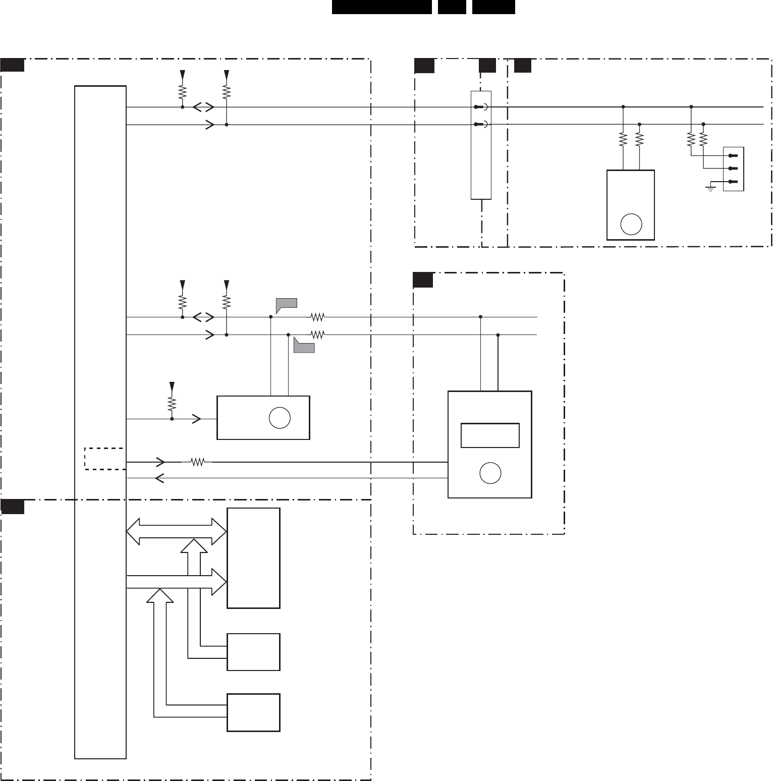
22ES1E AA 6.
Block Diagrams, Testpoint Overviews, and Waveforms
I2C Overview
CONTROL
MEMORY
INTERFACE
ADOC
A7
SSB.
CONN.
B1
I2C Overview
SDA0
SCL0
AF6
7300-C
AE6
3511
3513
3523
3581
3515
SDA1
F-REF
0291
0290
IRQ-MPIF
SCL1
+5V2 +5V2
VDDE
VDEE
VDDE
3509 3510
AF7
3512
AD6
AF8
A26
AF2
WC
B11
7025
M24C64
(NVM)
EEPROM
7790
M58LW032A
RAM
FLASH
CONN.
DATA
FLASH
CONN.
ADDRESS
ERR
13
ERR
14
ERR
11
5
7
6
3239
54
3240 3241 3242
1232
TUNER
TEDE9
1205
SDA-S
SCL-S
0230
48
49
1
2
3
1241
COMPAIR
CONNECTOR
FOR SERVICE
(REACHABLE VIA
HOLE IN REAR
COVER)
F_15040_057.eps
250405
A6 TUNER
A7
A5B18
MPIF
B1
B4
F509
F508
DATA
ADDRESS
B12
7100-D
MPIF
43
40
42
44
DIGITAL
BLOCK
7300-E
7300-k
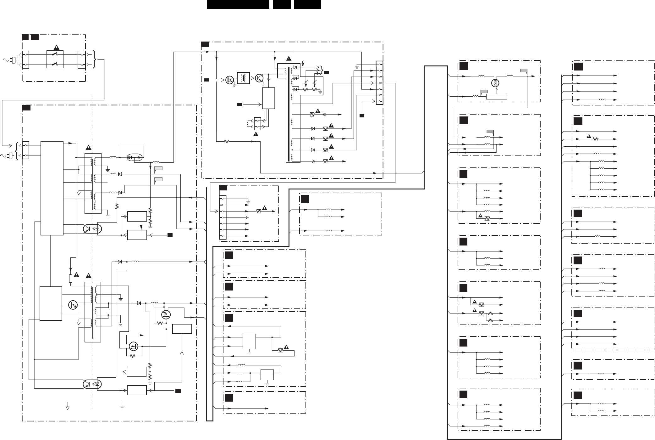
Block Diagrams, Testpoint Overviews, and Waveforms 23ES1E AA 6.
Supply Lines Overview
8x
4x
B5
VDDE 5283 To N23 7300-J (ADOC)
To AF3 7300-J (ADOC)
To P23 7300-J (ADOC)
To F23 7300-J (ADOC)
VIDEO DECODER
VDDCO 5281
5282
5285
B4
To 35 7100-D (MPIF)
To 28 7100-D (MPIF)
To 14 7100-D (MPIF)
+5V
MPIF - SUPPLY
+5V
+8V
5150
5151
5152
B13
To 3, 9 43, 49, 7730
To 1, 14, 27, 7730
CONTROL MEMORY (SDRAM)
VDDE
5731
5730
B11
+5V
CONTROL
+5V
+5V2
+5V2
VDDCO
VDDCO
VDEE
VDDE
B10
To 8 - 7480 (HP AMPL.)
AUDIO PROCESSING
+5V
+8V
+8v
To AD22-7300-B (ADOC)
VDDCO
To AC22-7300-B (ADOC)
VDDE
B12
To 9, 37, 43, - 7790 (RAM)
CONTROL MEMORY (RAM)
VDDE VDDE
B14
B15
VDDE
VDDCO
B14 ADOC SUPPLY
5600
5601
7650
CS51033YDR8
LOW VOLTAGE SUPPLY-ADOC
+5V2 +1V8
+3V3
+1V8
VDDE
VDDCO
5654 5651
+3V3 5659
CONTROL
B1
+5Vd
+5Vb
+5Va
+5V
IF & SAW FILTER
+5V
5135
5134
5102
5112
B3
To 98 7100-A (MPIF)
To 88 7100-A (MPIF)
To 77 7100-A (MPIF)
+5V
AUDIO SOURCE
SELECTION
+5V
3018
3019 3010
3011
B2
To 64 7100-B (MPIF)
To 49 7100-B (MPIF)
+5V
VIDEO SOURCE
SELECTION
+5V
5060
5061
+8Vc
+8Va
+8V
3134
(For PIP D/W Only)
F601
7651
STS5PF30L
F650
F651
5480
5452
5450
B9
3V3
PROTECTION
+3V3
+8V
+8v
To W1-7300-G (ADOC)
VDDE 3388
+8V
+8v
+3V3
+3V3
+5v
To M1-7300-F (ADOC)
VDDCO 5342
B8
To AA4 - 7300-F (ADOC)
To R3 - 7300-F (ADOC)
To N4 - 7300-F (ADOC)
To L2 - 7300-F (ADOC)
To M1 - 7300-F (ADOC)
SYNC & DEFLECTION
VDDE
5345
3340
5344
5343
5342
To L1 - 7300-F (ADOC)
3358
B7
+3V3
RGB PROCESSING
+3V3
+8V
+8v
+5V
+5v
To W4-7300-H (ADOC)
VDDE 5300
F_15040_058.eps
290405
POWER SUPPLY
9
8
4
17
18
13
14
5
3
2
3575
3576
A1
FRONT INTERFACE
M Q1
5512
SUPPLY
PRIMARY
SIDE
10
11,12
1
2
4
3
0201
1051
1031
1951
MAINS
SWITCH
+3V3
F563
F561
-Vaudio
+Vaudio
+9VA
5551
5552
5561 6562
5562 6563
Vbatt
A6
STANDBY
7571
REFERENCE
CIRCUIT
7573
STANDBY
CIRCUIT
7513
TCET1103
1505
0202
1
2
1
2
SUPPLY LINES OVERVIEW
3571
or
VDC
6551
6
4
14
8
9
10
5
2
1
3545
3544
5504
12
11
1
2
3
4
1532
A4
STANDBY
7542
REFERENCE
CIRCUIT
STANDBY
CIRCUIT
7516
TCET1103
VDC
SUPPLY
CONTROL
7525
HOT GROUND COLD GROUND
13
5505 +9VA
6536
5564 +5V2
6535
7545
+5V
3546
STANDBY
CIRCUIT
7535
3537
+Vaux
LINE + FRAME DEFLECTION
A2
+Vbatt
A5
Vbatt
VideoSupply
VideoSupply
Filament
EW_DRIVE
A5
-14V
+12V_LOT
SVM_ROT
+14V
7405
5402
LINE
OUTPUT
CIRCUIT
+
E/W
CORR.
7404
1404
1
2
HOR.
DEFL.
COIL
5450
3
1
FOCUS VG2
EHT TO
CRT
1401
1
2
Filament
3
4
5
6
7
10
6
B1
6453
6467
6456
6452
12
8
9
5
6461
3458
3485
3450
HD
+33V
+33V
EHTinfo
3455
3401
A5
3456
CRT
F
Filament
5
4
3
2
1
1351
SVM_ROT
+141V
+12V_LOT
+200VA
+200V 3351
EHTinfo
7
6
+9VA A3
+Vaudio 5913 Vaudio+
-V
Vaudio-
CLASS D - AUDIO AMP (RES)
-Vaudio 5914
5910
A4
+Vaudio
AUDIO AMPLIFIER
-Vaudio -Vaudio
+Vaudio
A5
+33V
TUNER / IF
+5V +5V
+33V
A6
INTERFACING
+9VA
7674
VI VO
VDIS
+5V
+8VS
3670
+8V
+5V2
7673
IN OUT
+5V
+3V3
9686
9675
5681
A7
SCART I/O
+8VS +8VS
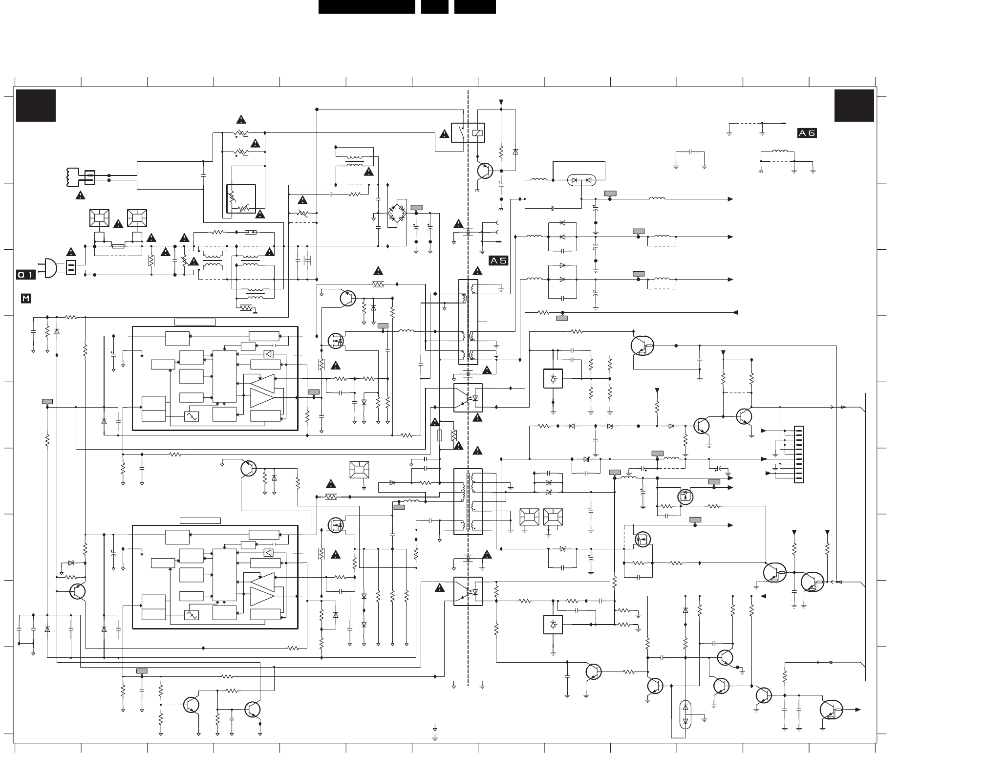
24ES1E AA 7.
Circuit Diagrams and PWB Layouts
7. Circuit Diagrams and PWB Layouts
LSP: Power Supply
+t
+t
KA
REF
+T
Rs
Rh
Vcc
Gnd
Ctrl
START-UP
CURRENT SOURCE
VALLEY
START-UP
CURRENT SOURCE
CURRENT
SENSING
OUTPUT
DRIVER
OVER
POWER
LOGIC
CONTROL
CIRCUIT
MAXIMUM
ON-TIME
PROTECTION
VOLTAGE
CONTRLLED
OSCILLATOR
OVER
TEMPERATURE
PROTECTIOM
POWER-ON
RESET
SUPPLY
MANAGEMENT
FREQUENCY
PROTECTION
CONTROL
INPUT
CONTROL
CIRCUIT
BURST
DETECTOR
Drain
HVS
Sense
Demag
Driver
-T
KA
REF
V
Vcc
Gnd
Ctrl
START-UP
CURRENT SOURCE
VALLEY
START-UP
CURRENT SOURCE
CURRENT
SENSING
OUTPUT
DRIVER
OVER
POWER
LOGIC
CONTROL
CIRCUIT
MAXIMUM
ON-TIME
PROTECTION
VOLTAGE
CONTRLLED
OSCILLATOR
OVER
TEMPERATURE
PROTECTIOM
POWER-ON
RESET
SUPPLY
MANAGEMENT
FREQUENCY
PROTECTION
CONTROL
INPUT
CONTROL
CIRCUIT
BURST
DETECTOR
Drain
HVS
Sense
Demag
Driver
I519
I557
I579
*
D
43
*
*
*
1
HOT GROUND
1500 B2
1501 B2
1502 B2
POWER SUPPLY
2
13
A1,A6
FOR MAINS 120V AC 170V (177V)
6
6578 H5
6581 H1
6582 F6
7510 G2
7511 D2
7512 D5
7513 E7
7516 H7
7517 C5
7525 G5
7532 H2
7535 G10
F537 G11
F541 A8
F542 B8
F552 B9
F561 C10
F562 C9
F563 B10
F573 D10
F574 B7
F575 C7
3505 C3
3507 A4
2540 G9
2541 B8
2542 B7
2543 H9
2544 F7
2546 F10
2551 B9
2552 B9
2553 A11
2561 C9
2562 C9
2563 B9
2564 E9
2565 B9
2570 D7
220R
3523 A4
S
3524 I4
*
2505 B6
123456789101112
9
*
2506 B5
*
6V5
7V4
3587 H8
3588 H5
3589 E11
3590 H11
3591 H11
3592 F7
3593 I3
3594 I3
3595 I4
3596 I4
3597 H5
3598 D2
4550 E11
5500 C4
5501 C3
6550 C9
6551 A9
6562 C9
6563 B9
6564 E9
6565 E9
6567 F4
6574 I11
6575 E6
6576 H11
10R - PTC
(..V..) Standy Mode
2538 F9
2539 F9
7
0V
2571 D9
3V4
I
A
B
C
D
E
F
G
H
I
1M5
*
0V
14
2572 D11
*
D
*
9532 B10
*
*
*
2
9
TEA1507
330K
6549 B9
9501 B3
9502 B4
9503 C3
9504 C4
9506 B6
9507 F10
9511 B5
9512 G10
9513 A12
2V5
0V
I592 H8
15V
I538 F9
I539 G8
I540 F8
I542 A7
I543 A8
I544 H3
I545 G10
I546 G2
I547 G10
I548 E9
I550 H6
I591 H9
I580 I11
I581 I9
I582 C6
I583 C4
I586 B8
I587 E9
I588 E9
I589 I10
I590 H9
0V
1V
G
0V5
13V
300V
300V
3
5V
5V
D
*
*
OR
I569 D12
I570 G11
I571 E8
I572 B4
I573 H11
I574 D10
I575 E8
I577 E10
I578 D10
I579 B8
S
7
*
15V
for ITV only
F576 D9
F578 F10
F580 F11
F581 I11
F582 F10
F583 B9
I500 I1
I501 A6
I502 C6
MAINS
230V AC
G
SS25113-00
I532 G6
I533 G7
I534 B4
I536 F6
I537 F7
1V5
3525 H5
3526 G5
2577 I12
2578 H9
2579 I10
2580 F7
2582 H1
2583 I4
2584 F10
2585 H1
2586 H1
2587 D9
2588 G7
2589 G10
2590 I12
2591 H12
3501 C4
*
COLD GROUND
3546 F10
3544 H10
0V
*
470U
3545 G10
220V AC 309V (317V)
*
3543 H9
5511 D6
5512 C7
3549 C6
3550 C6
3551 D11
3552 D12
3553 H10
3554 G12
3563 E8
3565 E10
3566 G10
3567 F5
3568 F4
3571 C8
3573 D9
3574 E9
3575 D9
0V
SMPS CONTROL
6533 H6
6535 F9
6536 F9
6537 G9
6538 D1
6539 G1
6541 A8
6548 F9
1V5
COLD GROUND
3585 H12
3586 H11
3527 G2
3528 D1
3529 C1
3530 G5
3531 G6
3532 H6
3533 H6
3534 G6
3535 E7
3536 F5
3537 G10
3538 H6
3540 F11
3541 A8
3542 H8
3
"$"
5504 F7
5505 F10
5506 C4
*
5502 A6
*
FRONT INTERFACE
11
*
TEA1507
7571 D8
7573 D10
7575 I9
7576-1 I11
7576-2 I10
7583-1 I11
7583-2 I12
7584 I12
9500 C2
I503 B2
I504 C2
I506 A5
I507 C5
I509 G2
I510 G2
I511 D2
I512 I2
I513 D5
I514 C6
1n5
2
HOT GROUND
3547 G13
3548 H8
3508 B6
3509 A4
3510 B5
3511 E6
3512 F2
3513 C6
3514 D5
3515 D6
3516 E6
3517 E5
3518 F3
3519 E1
3520 E6
3521 I2
3522 D5
330K
330p
1N5392
315mA
4m7
*
*
3584 I10
3576 E10
3579 D9
3580 G1
3581 I12
3583 H10
56
1505 C1
1506 A13
1532 E7
1538 E12
1542 B8
1543 B8
1544 B8
1550 F6
1551 F8
1552 F9
2500 C3
2501 A3
2502 C5
2503 B6
2504 B6
8V5
7V4
16V
16V
TO
1246 OF
TUNER/IF
*
*
DEGAUSSING COIL
S
*
G
5532 F7
5551 A8
5552 B10
5561 C8
5562 B8
5564 F10
5565 A12
5566 B10
5567 C10
6500 B6
6509 H2
6511 E2
6512 E10
6514 D6
6532 H6
7541 A8
7542 H8
7545 F11
7547 G12
7548 H13
7549-1 I3
7549-2 I4
7561 E11
7562 E11
7567 F4
*
2575 I9
2576 H11
2509 H2
2510 G2
2511 D2
2512 F2
2513 E5
2514 D6
2515 D7
2516 E5
2517 E2
2519 H6
2520 H5
2521 I3
2522 G7
2523 G6
2524 F11
*
3503 B4
T4E.250V
*
3502 B4
33R
3504 C2
1503 A7
1504 A2
0V
2V9
2V9
0V
0V
300V
1V5
11
*
7V4
..V.. Normal Operation
14
ATSC
9533 C10
9553 A12
F500 A2
F501 A2
F502 A5
F503 C2
F504 C2
F506 B3
F507 C3
F508 B7
F509 B7
F535 F10
I521 D6
I522 I12
I523 E7
I525 F5
I526 G5
I527 F2
I528 I5
I529 I7
I530 H5
I531 G6
6
2507 B7
2508 C5
7 8 9 10 11 12 13
A
B
C
D
E
F
G
H
2528 D1
10R - PTC
*
5V4
2535 F9
2537 G9
2536 F10
2526 E6
*
I593 H9
I596 G12
300V
0V6
0V
8V6
0V5
0202 OF
FROM
0V
0V
I562 C8
I563 A4
I564 E1
I565 H1
I566 E11
I568 F6
I597 I10
I599 I12
"$"
*
6V6
0V
0V
0V7
0V7
0V
TO
1506 OF
INTERFACING
*
SMPS CONTROL
A6
*
1V
14V
OR
PANEL
MAINS SWITCH
FROM 0220 OF
A1
I515 D7
I516 D6
I517 D5
I518 D6
I519 E5
I520 E5
I551 B8
I552 B9
I553 C1
I554 D1
I555 H5
I557 F7
I558 F8
I559 A5
I560 I4
I561 D8
15V
1V
13V
12V
0V
2
+5.2V
2506
33n
7562
BC847BW
1
3
TCET1103(G)
1
4
32
3535
4R7
7516
I547
3598
I537
Vaux_GND
9532
3588
470K
Vaux_GND
I596
Vaux_GND
F578
3504
1M5
AUDIO_GND1
1501
PFC5000
I587
Vaux_GND
I563
9553
2523
I503
Vaux_GND
F561
6511
RGP10D
2517
1n0
SB260
6536
BAV21WS
6533
3519
15K
I550
I523
2m2
2562
1n0
2515
F581
15K
3573
PDTC114ET
7547
+5V
I516
2572
10n
I500
I532
3574
180K
3M3
3501
I580
F537
I559
BYV29X-500
6550
22u
2510
6565
I522
3532
5511
+9VA
F509
F508
9503
I566
BAS316
6512
5552
27u
AUDIO_GND1
I526
I592
7512
2542
Vaux_GND
3576
1K5
I583
1n0
2509
2n2
2501
RGP10D
6509
6564
BAS316
3590
82K
I515
2565
1n0
68K
3566
3538
3507
1505
1
2
3593
3568 47K
3502
10K
5562
2537
2m2
1
3
2
5567
BC847BW
7561
3K3
3524
9506
Vaux_GND
7532
BC857B
6562
SB360L
F583
Vaux_GND
2519
470p
I521
5561
3K3
3550
6581
BAV21WS
9512
2587
1n0
I568
3529
+Vaudio
F500
3
6
7
8
9
I511
10
11
12
13
14
17
18
2
5512
10K
3543
330u
2507
I545
I501
5565
I502
I581
9502
7576-1
IMX1
5
3
4
2522
470p
I565
10u
2577
6538
BAS316
3530
6574
56K
I589
BAW56W
3592
33K
3591
10K
I518
-Vaudio
Vaux_GND
BAS3166567
100n
2520
1
4
2
3
470p
2539
5501
DMF2405H60
I528
AUDIO_GND2
Vaux_GND
I571
22u
I509
2524
2K2
47K3549
I525
3545
9501
Audio_Gnd
2526
100p
4
23
5500
DMF28
1
7584
PDTC114ET
4550
1542 I586
1543
F506
1K0
3531
+5V
47n
2521
220K
3580
I551
6563
SB360L
220R
3508
AUDIO_GND1
I506
I534
BAS316
6578
Vaux_GND
3547
3596
10K
Vaux_GND
4K7
BC847B
7517
I520
100n
2591
STPS10L60D
6548
82K
3575
2552
100u
9533
300K3517
3514
3587
2K2
2516
100n
I548
I529
9507
2m2
2563
3
21
2
Vaux_GND
T890-B60-A110
3523
4R5
4R5
SI2305DS
7545
3
1
100n
I527
21
3
2543
F504
TL431CZ-AP
7571
2579
47n
Vaux_GND
3565
27K
7567
BC847B
DSP-301N
3503
I588
2544
2n2
PFC5000
1502
7511
Vaux_GND1
I553
7583-2
IMX1
470p
2513
1551
HEATSINK
12
Vaux_GND
I562
I504
Vaux_GND
3533
6
8
9
Vaux_GND
1
10
11
12
13
14
2
4
5
5504
7541
BC857B
7573
PDTC114ET
5566
F563
100n
2508
1500
12
34
3525
300K
220R
3563
I538
I507
6582
3536
I512
LKS1AF
1503
56K
3585
F507
1K0
3548
3537
68K
3528
1M0
F501
3567
3K3
3516
I558
7525
2571
15n
9500
Vaux_GND1
3521
1K2
I555
2511
22u
4
+Vaudio
I575
IMX1
7549-1
5
3
470u
2584
+5.2V
Vaux_GND
3513
2K2 F575
Vaux_GND
I574
+5.2V
HEATSINK
1550
12
Vaux_GND
1u0
2585
I554
68K
3546
1n5
2514
3571
680R
Vaux
I590
5532
10n
2575
6575
2564
2
AUDIO_GND2
+9VA
100n
1504
1
F503
6514 BAS316
2588
3541
47K
Vaux_GND
I517
5551
3534
3510
4R7
3551
+9VA
1532
22K
T
3594
22K
I536
2n2
2578
6549
BYV29X-500
F535
2
6
1
I513
F552
IMX1
7549-2
F582 F580
I531
2535
Vaux_GND
I530
I599
2505
I552
1n0
2561
3540
68K
3597
220K
Vaux_GND1
I542
2538
1n0
7542
21
3
3595
100K
32
TL431CZ-AP
7513
TCET1103(G)
14
Vaux_GND
+9VA
I514
3586
5K6
3526
1K2
3512
I593
I540
3520
I573
45
81
F574
SP48012-00
5502
I591
3522
56K
F573
7548
PDTC114ET
5u6
5505
I564
I546
3515
1K0
47K
Vaux_GND
I570
3527
3583
5K6
Audio_Gnd
6541
BZX384-C12
AUDIO_GND2
2540
1n0
2500
+9VA
470n
I544
Vaux_GND
3584 10K
I578
3552
10K
9513
Vaux_GND
1m0 2536
2582
1u0
12
I577
2570
HEATSINK
1552
2512
100n
F576
14
23
Vaux_GND1
DMF35
5506
3589
7510
2553
82p
10K
3554
10K
4R7
6532
BAV21WS
3511
3579
2K2
5
3
4
Vbatt
+5.2V
7583-1
IMX1
I560
Audio_Gnd
680R
3542
6500
2
3
14
I533
GBU4J
I572
I582
3505
2589
2u2
7575
BC847B
2n2
2503
9511
Vaux_GND
1544
6576
SB340L-7010
6535
10u
2583
3581
22K
Vaux_GND1
Vaux_GND
6539
UDZS-13B
I543
3509
1n0
2551
6537
STPS10L60D
5564
2n2
2580
3
1
2
F542
SI2307DS
7535
100n
2576
BYT28
6551
3544
2K2
2504
2n2
7576-2
IMX1
2
6
1
9504
F502
11
2
3
4
5
6
7
8
9
1538
B11B-PH-K
1
10
2502
2u2
2546
3553
27K
2586
I561
330p
F541
I569
I539
Vaux
2528
470n
Audio_Gnd
2590
10u
3518 3K3
F562
47u
2541
I510
Vaux_GND
RT-01T-1.0B
1506
I597
STANDBY
STANDBY
POWER_DOWN
A1
A1
F_15040_001.eps
230305
3139 123 5895.4
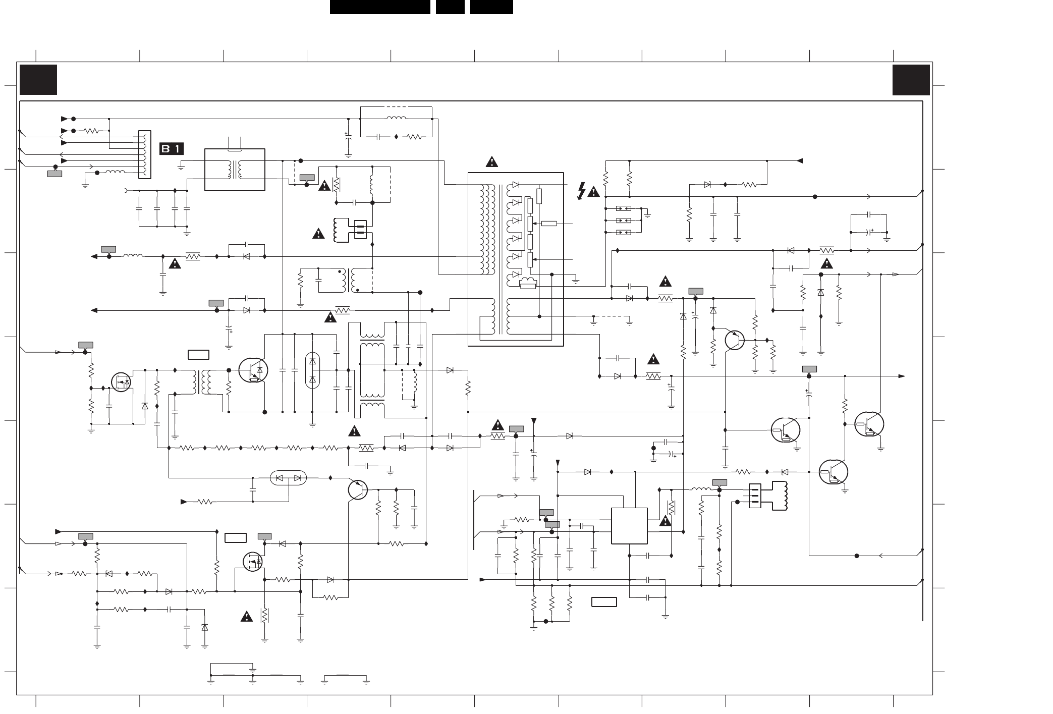
Circuit Diagrams and PWB Layouts 25ES1E AA 7.
LSP: Deflection
EHT
SCREEN
FOCUS
INP
INN
GND
VP1
V-OUT
VP2
VFB
NC
A2
A2
F_15040_002.eps
220305
3139 123 5895.4
RES
K
A2
DEFLECTION
0V
A
B
C
D
E
F
G
A
B
C
D
E
F
G
1401 A1
1402 B1
1403 B7
1404 B4
1405 B7
1406 B7
1452 E9
2402 B2
2403 B2
2404 A4
2405 B1
2406 B2
2407 C4
FROM LOT
*
5450
27V
D
G
S
G
2V3
HORIZONTAL
*
DEFLECTION
1 2345678910
1 2345678910
220K
*
12n
A6
-15V2
12V2
150R
3V
L.LIN
2409 E2
2410 E4
2411 D3
2412 D4
2413 D4
2414 D3
2416 D4
2417 D5
2418 D5
2419 D4
2422 G1
2425 G3
2427 A4
2431 B4
2432 E9
2437 G2
2448 D7
2449 D8
2450 B9
2451 B8
2452 F7
2453 F7
2454 C2
FRAME
*
2457 E5
2458 C2
2459 E5
2460 E6
2461 E8
2462 F6
2463 F6
2464 F8
2465 G8
2466 C9
2468 F8
2469 C8
2470 E8
2471 E6
2473 F7
2476 C9
2477 C9
2478 E3
2479 F6
2487 B10
2488 D2
2489 B10
2490 D9
2492 C7
2493 C3
2494 B3
2495 F5
2496 G2
2497 D1
2498 F8
F483
140V
LINE
*
0V
*
10K
A
2499 F8
3401 A1
3402 D1
3403 C3
3408 D1
3412 B4
3414 E2
6V6
11V
S
*
*
6V6
D
0V
3415 E2
3416 D3
3417 F5
3418 F2
3419 E3
3421 E2
3422 F1
3423 F1
3424 F1
3425 F3
3426 G3
3432 E3
3433 A5
3434 F3
3435 F1
3436 G4
3437 G1
3443 D10
3450 D8
3451 E4
3452 F8
3453 B8
3455 E6
3456 C4
A2,A6
3458 C2
3459 E9
3460 D9
3461 F6
3462 C9
3463 F6
3465 D9
3466 F8
3467 F8
3468 F8
3469 D8
3470 G7
3471 G6
3472 G6
3473 F5
3474 C10
3476 F6
3477 C9
3479 D5
3480 B7
3485 B10
3486 C8
3487 D8
3488 F4
3490 D2
3491 B7
3492 B9
3493 E4
3499 F2
5401 B4
5402 D2
0V
A2
*
COIL
A6
TO PICTURE TUBE
4V8
5406 C4
5408 D4
5409 C4
5410 A5
5411 D5
5450 A6
5452 B1
5453 E8
5455 A2
5456 B1
6403 E5
6404 D4
6405 D5
6424 F1
6425 F2
6426 G2
6427 F4
6452 C3
6453 C3
6456 E5
6457 E7
6458 E7
6459 E9
6461 D7
6464 D2
COIL
TO 1351 OF
RES
*
8n2
6465 E3
6466 C7
6469 B9
6471 F3
6474 C10
6476 C8
6478 B8
6480 C9
7403 E4
7404 D1
7405 D3
7406 F3
7407 D9
7408 C9
7455 E7
7456 E10
7486 E10
9401 C4
9402 B5
9410 A5
9411 B3
9412 D5
9447 C7
F401 A1
F402 A1
F404 B1
F416 B4
220K
0V
F418 D3
F419 D3
F451 G6
F452 C2
F453 B1
F455 B1
F456 E6
F457 E8
F458 F10
F459 A3
F462 B10
F464 B4
F465 C5
F466 E8
F469 F9
F472 C10
F475 D1
F476 F1
F478 D10
F481 C8
F482 F6
F483 F6
I402 B2
I410 E3
I413 D1
I414 D1
I415 F3
I418 D2
I419 D2
I420 E2
DEFLECTION
*
*
*
*
I423 F3
I428 D5
I432 A5
I435 E9
I436 E10
I437 E8
I438 F8
I439 C8
I440 C9
I442 E4
I443 E4
I445 F1
I446 F2
I447 G2
I448 E4
I449 E5
I450 B4
I453 C3
I455 C5
I457 B3
I458 B7
I459 D7
I460 C10
I462 E2
I463 E3
I464 E4
I466 C2
*
E/W
*
A6
I468 B10
I469 C8
I470 B2
I473 D4
I475 E5
I476 E7
I480 F8
I481 F8
I482 F7
I487 B8
I488 D2
I489 B4
I490 F3
I491 G1
I492 D7
I493 E5
I494 C9
I495 E8
I496 F2
I497 F5
I499 F3
*
A2,A6
*
A6
A2
A6
48V
0V
50V
0V
12V2
*
CRT BOARD
*
A6
A2
FRAME
J
13V5
1R
3485
7405
BU2520DX
9412
GND_HOR
6n8
2427
2K2
CRT_GND
6
-14V
3434
PSD10-204B
5402
1
3
5
GND_DEF
GND_HOR
7404
BSH103
10u
5452
F462
I435
1K0
3403
3490
I428
100n
2499 2498
100n
3452
5R6
2479
I497
GND_DEF
2413
3419
I410
F466
I450
I448
GND_DEF
3472
F418
5
6
7
89
JF0101
5450
1
10
11
12
3
3488
GND_EW
220K
BZX79-C5V6
6426
3415
3422
100K
2418
6404
DMV1500M
I455
2K2
3436
6453
RGP10G
I419
GND_DEF
2437
15n
3416
47R
1
2
4
3
I495
5408
312813834922
I418
470p2448
6480
GND_DEF
BZX79-B33
2411
1K0
I432
3433
GND_HOR
9410
RGP10D
6471
F455
VideoSupply
150R
3412
5411
560n
MainSupplyGnd
I463
2459 470p
F401
F416
+13V
GND_EW
1402
I499
F469
1R0
8K2
3460
3486
I453
2414
2n2
I460
6459
BZX384-C18
BYV29X-500
6469
2461
10u
GND_HOR
2477
3476
3421
15R
2419
2425
4
GND
6
75
2
1
3
GND_DEF
7455
TDA4863J
BYG10
I481
6461
F464
3470
150K
3417
2468
100n
2402
2412
I438
I443
BYG10 6403 2460
3408
100K
1m0
2417
100p
2457
GND_DEF
7406
470p 2493
GND-LINEDRIVE
GND_EW
2462 220n
F475
220p
2497
BZX384-C27
6464
F482
3418
1K0
GND_HOR
+33V
100n
2464
I475
I457
GND_DEF
2463 220n
6456
RGP10G
5456
12u
+5V
5410
100n
2495
F457
3426
3R3
2473 2n2
9447
GND_DEF
22K3437
2454
470u
GND_HOR
I414
F472
GND_DEF
I494
F481
330R
3402
10K
3491
GND_DEF
I439
100n
2422
BC857B
7408
2453
GND_EW
2n2
1404
1
2
1R0
3455
B2P-VA-BF
I402
10n
2496
I446
3493
1R0
9402
I415
GND-LINEDRIVE
F476
2409
33n
10n
2476
BZX384-C27
CRT_GND
6458
1K0
3453
3487
GND_HOR
I473
2451
100n
2410
GND_HOR
F402
7486
PDTC143ZT
3477
820R
I469
100n
2458
4R7 3458
I442
F451
PDTC144ET
7456
GND_DEF
3479
1K0
I490
BAS316
6405
+12V_LOT
680K3435
47u
2404
2432
100n
PDTC144ET
7407
I464
F452
I459
6474
CRT_GND
BZX79-C22
3471
3469
8K2
6466
8K2
3465
2
3
4
5
6
7
3473
1401
1
1406
I440
GND_DEF
GND_DEF
6425
BAS316
+12V_LOT
3461
1K5
I496
7
99
82K
3425
5455
CD25405-00
1
22
44
5
7
2465
100n
2487
RGP10D
3492
6452
I468
6476
BZV85-C6V8
GND_DEF
Vbatt
6424
BZX384-C6V8
GND_DEF
3423
680K
F419
6K8
3462
1403
F453
470p 2494
1
2
4
3
5409
312813831423
330p
2478
BAW56W
6465
470p2492
7403
BC557B
I413
GND_HOR
3443
100K
2403
F458
I420
MainSupplyGnd
GND_DEF
GND_DEF
1u0
2488
6478
BZX384-C27
CRT_GND
9411
47u
2490
CRT_GND
I423
F404
470p
2406
I492
I437
3463
1K5
GND_DEF
I449
3450
1R0
3451
BYV27-200-TAP
6457
47K3401
GND_EW
CRT_GND
3499
1M0
I482
2489
4u7
I488
220R
3467
1
2
3
4
CRT_GND
C948
5406
3424 22K
3
5453 1452
1
2
2416
3432
I436
GND_DEF
6427
220R
3468
BAS316
2405
470p
I445
I491
F459
F456
2n2
2431
GND_DEF
5R6
3466
1405
Vbatt
470p
2466
GND_EW
1R0
3456
I470
2469 10u
I480
1K0
3459
3480
10K
24702n2
I487
9401
I466
GND_DEF
I489
F465
I462
CRT_GND
F478
2471
2n2
2449
470u
GND_DEF
5401
I458
I493
GND_HOR
3414
2450
3474
3K9
I447
GND_DEF
GND_EW
I476
2407
VideoSupply
2452 2n2
HFB_X-RAY-PROT
EHT-INFO
Filament
Frame_FB
INN
Filament
HDRIVE
VGUARD
+12V_LOT
SVM-ROT
INP
-14V
EHT-INFO
EW_DRIVE
EHT-INFO
+13V
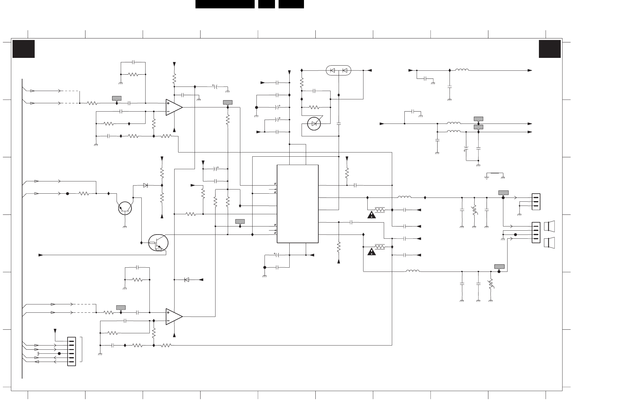
26ES1E AA 7.
Circuit Diagrams and PWB Layouts
LSP: Class D Audio Amplifier (Res)
V
DIAG
VSS2
POWERUP
EN2
REL2
VDD1
SW2
VDD2
VSS1
BOOT2
OUT2
SW1
EN1
STAB
BOOT1
REL1
OUT1
V
5914 B8
6904 E3
6905 B6
6906 A6
6962 C3
7901-1 A3
7901-2 E3
7902 C5
3935 B3
PASSIVE
9917 B1
3952 C6
3942 B4
3943 C4
9918 E1
3936 E2
7904 C2
3947 C3
3949 C4
7903 D3
I922 D4
I924 A5
I925 E2
I926 B8
I927 B8
I928 A5
I930 A6
LM393N
F905 D9
F910 F1
LM393N
F901 C1
A3,A6
A3,A6
R
A6
*
L
F904 C9
F903 D9
2948 B5
2949 B5
2950 A5
2951 A5
2952 C6
2953 D6
2954 D7
25
For ITV
2970 D7
2961 A5
3
2965 B7
14
2963 B6
2964 A7
1234
F912 B4
F913 D5
I901 A5
I902 A8
I903 F2
I904 E3
I908 B2
5913 A8
I914 B3
3962 C1
I909 A2
I913 B2
A3
5901 C7
5902 D7
5910 B8
4931 E1
A3
6789
A
B
C
A6
2934 B2
2935 E2
2933 B2
SUBWOOFER
2938 F2
2936 D2
2983 E8
2984 E8
3930 B2
3931 A2
3932 B2
3933 B2
3934 B3
2945 D5
2947 B5
3940 F3
2946 D5
3941 F3
2930 B2
2942 C4
2931 A2
3939 F2
2939 E2
3938 F2
3937 E2
D
E
F
A
B
C
D
E
F
1901 C9
1902 D9
1904 F1
2911 A8
2913 B8
2914 A3
65897
3953 D6
3955 C7
3956 C8
3958 A5
3959 C3
3960 B5
3961 C3
4930 A1
2979 B8
3974 C4
2960 C4
2971 D7
From Hybrid board
2982 C8
3972 E8
3973 A3
2977 A4
2978 B8
3971 D7
2955 C7
2957 C8
I915 C3
I920 C2
*
I918 D2
I921 C4
And
A3,A6
I934 C6
I935 C7
I936 C7
I938 D6
I941 A3
I943 D7
I945 D4
I948 F3
CLASS D - AUDIO AMP(RES)
A3
I916 B4
A3
A4
680p
2971
F905
47n
2979
5913
3K9
3959
F904
3938
1K0
I901
Audio_Gnd
3956
I903
220K
3931
5914
3942
2K2
7901-2
5
6
7
8
4
2955
680p Audio_Gnd
Audio_Gnd
I928
100n
2914
F903
BC857B
7904
2961
10u
Audio_Gnd
100K
Audio_Gnd
3960
6
3943
2K2
1
2
3
4
5
B6B-PH-K
1904
470u
2949
P0102DA
6905
1
2
3
I918
2939
3n3
39K
3952
5910
2960
22u
3K9
I930
I925
3934
I922
I941
Audio_Gnd
220n
2946
2950
47n
Audio_Gnd
F910
2964
100n
2K2
3958
Audio_Gnd
2983
15n
6n8
2938
2931
3n3
I938
100n
2913
2970
680p
13
8
10
9917
15
2
16
9
1
17
5
6
12
3
4
14
7
11
22K
Φ
AMPLIFIER
CLASS-D
TDA8925J
7902
Audio_Gnd
3949
I914
3961
470R
3n3
2934
2977
22u
15n
2982
2942
100n
3971
4R7
Audio_Gnd
100n
2965
I936
3935
120R
3933
10K
I916
GND-AUD
470n
2984
F912
2945
470u
3973
10K
3
2
1
8
4
7901-1
BZX384-C33
6962
3974
4K7
Audio_Gnd
3953
39K
1
2
3
4
Audio_Gnd
1902
BZX384-C27
6904
Audio_Gnd
100n
2935
BAV99
6906
5902
33u
I920
I927
I913
I909
4R7
3955
7903
PDTC143ZT Audio_Gnd
I915
I948
I934
3947
39K
2933
6n8
22u
2978
F901
100n
2911
4931
3932
9918
1K0
3937
220K
33u
5901
I924
I945
I926
3936
3K9
33K
3962
3941
10K
2953
1u0
3K9
3940
680p
2954
F913
I935
47n
2951
Audio_Gnd
3972
47n
2947
Audio_Gnd
1u0
2952
1901
1
2
3
I902
B3B-EH-A
2963
I921
I904
10p
Audio_Gnd
I908
2930
100n
2957
470n
Audio_Gnd
3n3
2936
Audio_Gnd
3K9
3930
Audio_Gnd
I943
22u
2948
3939
100R
4930
Vaudio+
Vaudio-
Vaudio-
AUDIO-L
VOL_MUTE
+Vaudio
AUDIO-C
AUDIO-C
VOL_MUTE
SUB_MUTE
-Vaudio
Audio_Gnd
-V
AUDIO-R
AUDIO-R
Vaudio-
-Vaudio
Vaudio-
AUDIO-SW
AUDIO-L
AUDIO-SW
-V
Vaudio-
-V
Vaudio-
Vaudio-
Vaudio+
Vaudio+
Vaudio+
Vaudio-
Vaudio+
Vaudio-
Vaudio+
Vaudio-
-V
+Vaudio
Vaudio+
A3A3
F_15040_003.eps
230305
3139 123 5895.4
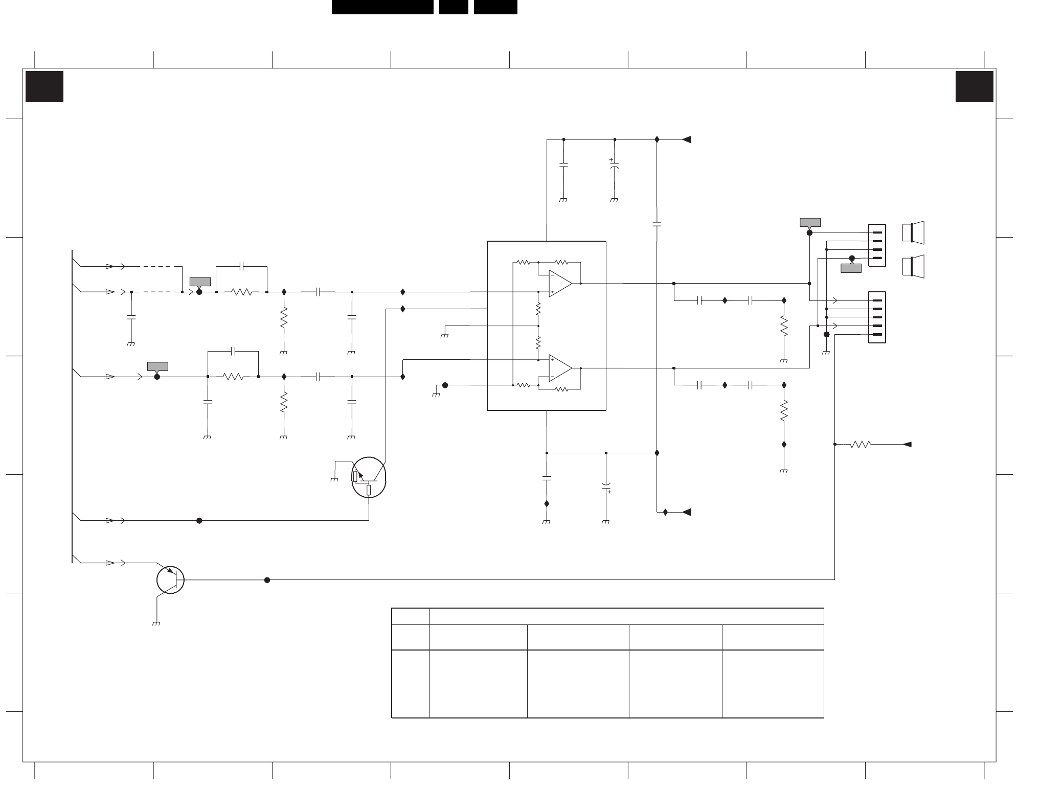
Circuit Diagrams and PWB Layouts 27ES1E AA 7.
LSP: Audio Amplifier
RES
R
A6
A6
12345678
12345678
A
B
C
D
E
A
B
C
D
E
1910 B8
A6
1911 A8
2975 B1
2976 C2
2981 B2
2985 B2
2986 A6
2987 A5
2988 D5
2989 B3
2990 B3
2991 A5
2992 C3
2993 C3
2994 B6
2995 C6
2996 B7
2997 C7
2998 D5
3957 C7
3985 B2
3988 B3
3989 B7
3991 C2
3992 C3
3993 C7
4984 B2
7962 D2
7990 A4
7991 D4
9916 B2
F911 D2
L
RESERVE
F950 B2
F951 C2
F952 A7
F955 B7
F956 B7
F958 C4
F959 D2
I951 B4
I952 C4
I953 B3
I954 C3
I956 B7
I957 C7
I958 C6
I959 B6
I960 C6
I962 B4
I963 C7
I964 D6
I965 D5
I967 A6
0V
15V7
-15V6
RES
+15V9
AUDIO AMPLIFIER
A6
+15V9
RES
A3
*
*
*
I951
VP-
V|GND
3
Audio_Gnd
Audio_Gnd
+Vaudio
INV12
8
9INV2-
MUTE
2
OUT1 4
OUT2 6
7
VP+
5
7990
TDA2616Q
1INV1- I959
I960
220n
2989
220n
2992
I962
2986
100n
I967
I956
I957
3988
12K
Audio_Gnd
Audio_Gnd
220p
2976
2975
220p
4984
I965 I964
4
5
47n
2994 1
2
3
7962
BC857B
1910
Audio_Gnd
47n
2995
F952
1n0
2990
47n
2996
3989
10R
F911
2993
1n0
2997
47n
Audio_Gnd
Audio_Gnd
3957
39K
2985
7991
PDTC124ET
3991
Audio_Gnd
F958
10K
2981
2988
100n
Audio_Gnd
2987
F959
100n
Audio_Gnd
Audio_Gnd
47u
2998
47u
2991
10R
3993
Audio_Gnd
F956
I958
I954
I952
Audio_Gnd
Audio_Gnd
Audio_Gnd
Audio_Gnd
F951
10K
3985
3992
12K
-Vaudio
F950 I953
3
4
Audio_Gnd
I963
B4B-EH-A
1911
1
2
9916
AmpOutR
F955
AUDIO-L
+Vaudio
SUB_MUTE
AmpOutL
AUDIO-SW
AUDIO-R
VOL_MUTE
A4A4
F_15040_004.eps
230305
3139 123 5895.4
"985" ~ "999"
1911 USED USED USED USED
1910 NOT USED NOT USED NOT USED NOT USED
4984 NOT USED NOT USED NOT USED NOT USED
7962 NOT USED NOT USED NOT USED NOT USED
9916 USED USED USED USED
A66ERF172X044
ITEM
For Europe
29RF
A68ERF182X044
SIZE/TUBE
28WSRF
A66ERF172X044
28BLD
A66EAK075X054
32WSRF
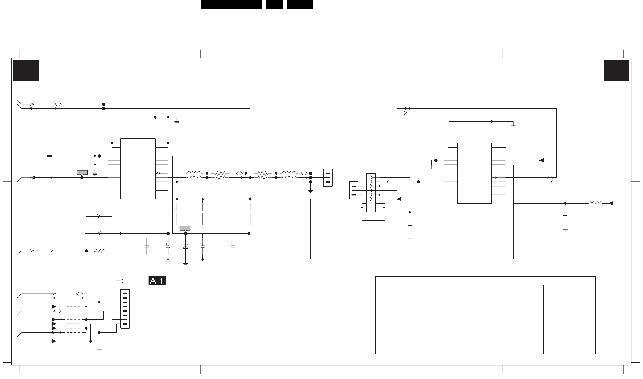
28ES1E AA 7.
Circuit Diagrams and PWB Layouts
LSP: Tuner IF
+33V
+33V
A6
B
D
33V
89
0V
*
A
10
5V
3239 B4
3240 C4
E
C
1V7
24 7
CONNECTOR
A5
6
5V
3
34
*For PP Europe
5
1270 B6
8910
1
4V9
5248 B3
33V
5250 B5
5249 C3
PIP PANEL
COMPAIR
3241 B4
3242 C4
4220 E1
5247 C10
F250 B7
I232 C4
I242 C4
Autoscavem CRT
I247 E2
I248 D4
FROM 1542 OF
A
B
C
POWER SUPPLY
I255 E2
I256 A3
1241 B6
1243 B8
1245 D2
I259 C10
I260 B5
I261 B55251 B5
6234 D3
6238 C2
6239 C2
9230 E1
9231 E1
9233 E1
9234 E1
4V9
F233 B2
F234 C3
F235 C3
*
A5
F246 B7
F247 D2
F248 A2
5V
I239 B4
I240 B4
I241 B4
567
I249 A8
I253 E2
I254 E2
A5,A6
A6
A5,A6
5V
A6
*
TUNER
2
1V7
D
E
1232 B2
TUNER / IF
1
1246 D2
1268 B6
1269 B1
*
*
0V
*
2236 D3 3238 D2
A6
2251 C32247 C9
2248 D3
2250 C3
2268 C7
TO 1937
TUNER
2232 C4
2233 D4
2235 D3
9235 E1
9646 E1
F232 B2
F241 B5
F242 B5
F243 B5
F249 A2
9646
*
*
*
I256
F247
5250
I242
5249
220n
2232
I239
F249
+5.2V
6238
F248
+5V
+5V
RT-01T-1.0B
1269
F235
I240
10n
2268
1m0
2250
100R
3241
9235
I253
1
2
3
F233
6
7
8
S3B-EH
1241
1245
B8B-EH-A
1
2
3
4
5
F243
I260
+33V
4
SCL
5
SDA
9
TU2
MB1
7
MB2
12
13
14
15
2NC1
8NC2
10 NC3
TEDE9-031A
1232
1
AGC
3
AS
11 IF1
6
I259
47n
2233
I249
BZX384-C33
6234
F246
10K
3238
6239
F234
2235
68u
F241
4
5
6
7
8
9
10
1268
06JL-BT-E
1
2
3
+33V
5248
2247
220n
3242
100R
I254
I248
1246
I247
I241
SIN-21T-1.8S(B)
F250
F242
47u
2248
4220
F232
9234
+8V
+5V 5247
I255
5u6
10
4
SCL
SDA 5
TU2 9
2251
4n7
11
MB1 6
MB2 7
12
13
14
15
NC1
2NC2
8NC3
1243
TEDE9-031A
AGC 1
AS 3
IF1
2236
10n
5251
I261
9231
9230
I232
B3B-EH-A
1
2
3
1270
22R3240
3239 22R
9233
IF-TER
SCL-S
SCL-S
SDA-S
SDA-S
SCL-S
SDA-S
AGC
IRQ-DIGITAL
AUDIO-SL
A5A5
F_15040_005.eps
220305
3139 123 5895.4
NOT USED NOT USED NOT USED NOT USED
9235 NOT USED NOT USED NOT USED NOT USED
UV1316E/A1-4 UV1316E/A1-4 UV1316E/A1-4
NOT USED NOT USED NOT USED NOT USED
NOT USED NOT USED NOT USED NOT USED
BAS316BAS316 BAS316
For Europe
29RF
A68ERF182X044
SIZE/TUBE
28WSRF
A66ERF172X044
28BLD
A66EAK075X054
32WSRF
A66ERF172X044
1243
1232 UV1316E/A1-4
1245 NOT USED NOT USED NOT USED NOT USED
1268 NOT USED NOT USED NOT USED NOT USED
1270
9230
USED USED USED USED
6238 BAS316
9231
ITEM
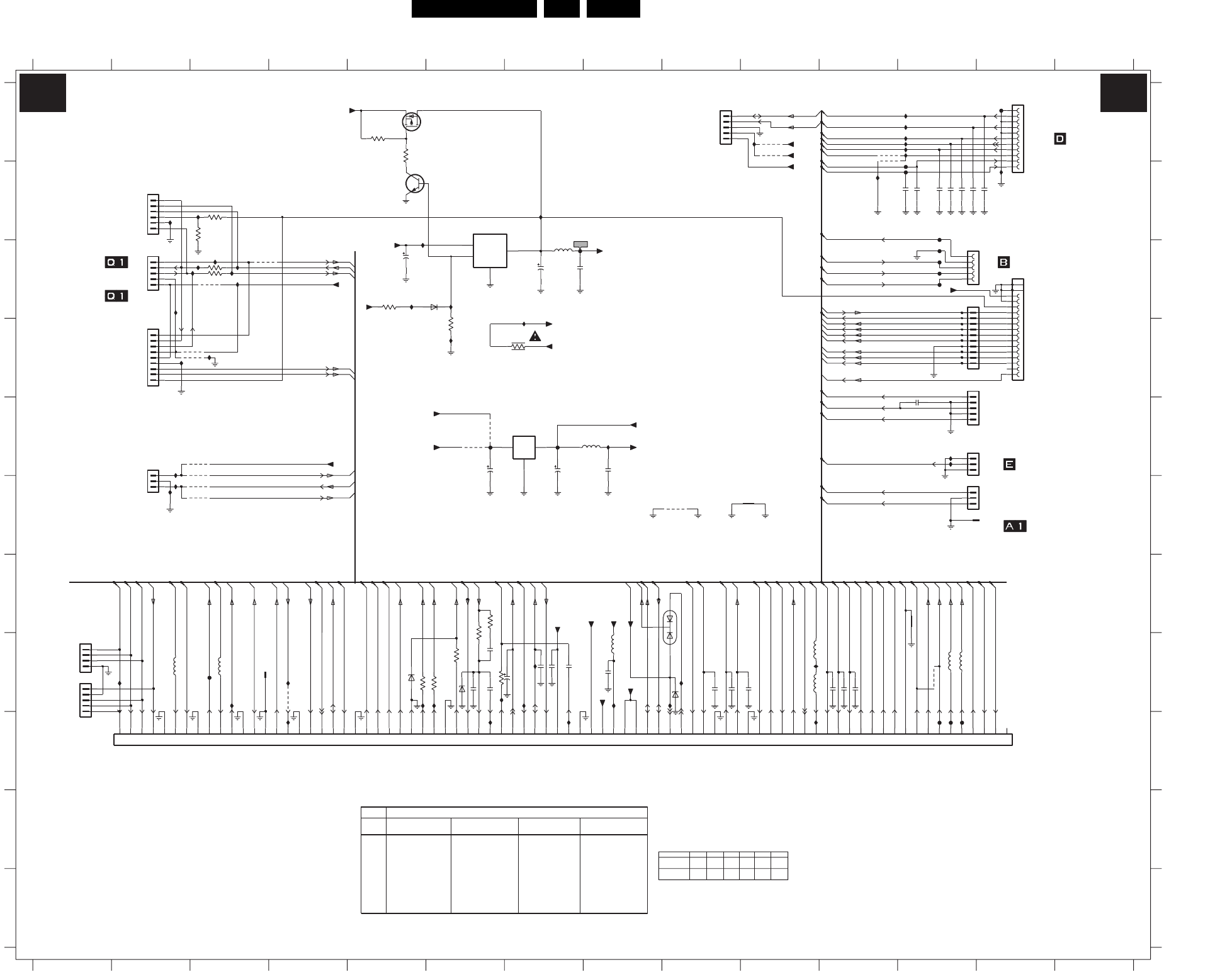
Circuit Diagrams and PWB Layouts 29ES1E AA 7.
LSP: Interfacing
VO
VI
VDIS
GND
COM
OUTIN
RES
RES
RES
RES
B
C
D
E
F
G
H
I
J
K
A
B
C
D
E
F
G
H
I
J
K
1607 H1
1608 I1
1620 A13
1621 A9
1623 B2
1624 C2
1625 D2
RES
TO 0215 OF
POWER SUPPLY
1234567891011121314
1234567891011121314
A
RES
RES
SIDE I/O PANEL
PANEL
MAINS SWITCH
TO 0242/0247 OF
OR
PANEL
1629 C12
1630 C12
1631 D13
1635 D12
1645 E13
1646 F13
1669 H3
1670 I1
1683 F12
1684 E2
2663 H11
2666 B12
2667 B12
2669 B12
2670 B12
2671 B12
2672 B12
2673 B13
2674 C7
2675 E12
2676 H7
2677 H7
2678 H7
2679 H6
0V
TO A10
2V5
3V5
4V5
2680 H8
2681 H7
2682 H6
2688 E6
2689 E7
2690 E8
2691 C8
2692 C5
2693 H9
2694 H9
2695 H10
2696 H11
2697 H11
2698 H6
3623 B3
3624 B3
3625 C3
3626 C3
3627 H6
3628 H6
3629 A5
3630 A5
3670 D7
3677 H6
3683 C5
3685 D6
3686 G6
0V
A6
0V
0V
A3
A6
0V
A6
3687 H6
3688 G6
4624 D3
4625 D3
4683 H12
4684 F9
4694 A11
5680 H8
5681 E8
5682 C7
5683 H12
5684 H12
5685 H10
5686 H10
5687 H2
5688 H3
6681 G9
6682 H9
6683 C6
6684 H5
6685 H6
7673 E7
7674 B6
7675 A6
CRT PANEL
TO SSB PANEL
3V5
INTERFACING
3V5
3rd SCART HDMI
0V
A6,A7
*
*
A7
TO 1936 OR 0240 OF
5n6
TO 1340 OF
0V
A6
7676 B5
9620 A10
9621 A10
9626 A11
9664 C3
9669 E3
9670 E3
9671 F3
9672 F3
9674 C3
9675 E6
9686 E6
9691 H4
A5
A5
A6
3V5
A6,A7
A6
SCART SET ONLY
0V
A6
0V
A6
A6
F620 A13
F627 B12
F628 B12
F629 C12
F630 C12
F631 C12
F632 B12
F672 C12
F673 C7
F674 I12
F675 I12
F676 I12
F677 H3
F678 E6
F679 E7
I602 E12
PANEL
A7
A6
A6
A7
A7
3V
5V1
I603 E12
I604 H7
I605 B5
I606 D6
I608 B2
I609 D3
I610 F2
I611 B11
I612 B13
A3,A4
SCART SET ONLY
A6
0V
A6
A7
A5,A6
*
A7
SCART SET ONLY
0V
4V
A6
A5,A7
A6
TO A10
RES
0V8
I616 D3
I621 A12
I622 A12
I623 A12
I624 A12
I625 A12
I626 A12
I627 C3
I628 C3
I629 C2
I630 C3
I631 C2
270K
A5,A6
0R
A2,A6
A7
A6
A6
A6
4V1
A6
A6,B1
0V
A2,A6
A6
A6
A6
A6
0R
I632 E2
I633 F2
I634 C5
I635 A10
I636 C7
I637 I4
I638 H6
I639 H6
I640 I6
I650 H9
I672 H3
I674 H4
I677 H7
I678 H1
A7
1V1
A2
0V
SCART SET ONLY
SCART SET ONLY
0V
A7
A6
2FH PANEL,
5n6
A7
SCART SET ONLY
2T PIP DW
*
4V3
*
A6
3V3
A6
A6
A2,A6
I680 H8
I685 B3
I686 C3
I687 C3
I688 H9
I689 H6
I690 I7
I691 I10
I693 B7
I694 C6
0V
*
1V6
0V
3V6
A6
A6
A6,A7
0V
0V
A6,A7
0V
A6
A6
A6
A6
A6
A6,B1
I695 E8
I696 H10
0V
5n6
*
0V
A2,A6
5n6
A6,A7
A6
A3,A4
A3,A4
A7
2T PIP DW
SCART SET ONLY
PANEL
2V3
A1,A6
A2,A6
A3
A6
A6
3V5
0V
0V
A2,A6
A2,A6
0V
A7
TOP CONTROL
2V8
0V
A6
A6,B1
1V4
A6
ITV
0V
*
2V7
0V
A6
2T PIP DW
FRONT INTERFACE
2V7
TO
0V
0V
3V2
5V
0V
0V
0V
A6
3V
TO PIXEL PLUS
0V
0V
PANEL
A7
4V5
8V1
5n6
TO A10
A7
0V
0V
6V
3V
A7
0V9
FROM 1506 OF
A6
A6
A6
A6
0V
TO 0203 OF
A6
A6
A6
A6
FRONT INTERFACE
A1,A6
A5
A6
A7
0V
A7
A6
A7
0V
5V
5V2
*
PANEL
0V
0V
*
0V
5V7
2T PIP DW
3V1
4683
9691
9664
3685
1K0
5687
I688
2666
2667
Vaux_GND
11
2
3
4
5
6
7
8
9
1620
1
10
3
+8V
1683
B3B-EH-A
1
2
2678 100n
9675
Vaux_GND
I635
2691
1u0
3670
6R8
I685
SUP_GND
7675
SI2305DS I624
5688
7
8
9
16 17
18 19
10
11
12
13
14
15
2
3
4
5
6
15JL-BT-E
1631
1
I632
9672
+8V
2694 1n0
10u
Vaux_GND
+5.2V
2689
5680
GND-LINEDRIVE
F629
5681
I691
SUP_GND
F676
1n0
2695
RT-01T-1.0B
F672
F631
1646
GND-LINEDRIVE
I637
2696
1n02677
SUP_GND
+3V3
3686
Vaux_GND
+3V3
3
4
5
6
SUP_GND
B6B-EH-A
1623
1
2
I677
9674
I640
RT-01T-1.0B
1669
Vaux_GND
I634
2670
2673 15p
15p
2672
F674
I621
I625
SUP_GND
F673
100p
2682 100R
3688
SUP_GND
3626
100n2681
BZX384-C6V2
6684
I696
3687
100R
F675
I622
100n2680
2697 220p
1
2
3
+5.2V
B3B-EH-A
1684
2
3
4
5
I687
B5B-EH-A
1608
1
5682
3629
68K
7674
KA78R08
3
4
1
2
3624
+5.2V
Φ
10K
5686
I672
5685
I638
+5.2V
I695
BC847BW
7676
+9VA
I690
2663 220p
BZX384-C5V1
6685
4
5
I631
B5B-EH-A
1635
1
2
3
F632
I680
F679
1
2
3
4
5
9626
1629
697 70 71 72 73 74 75 76 77 78 798 8094 40 41 42 43 44 45 46 47 48 495 50 51 52 53 54 55 56 57 58 596 60 61 62 63 64 65 66 67 6810 11 12 13 14 15 16 17 18 192 20 21 22 23 24 25 26 27 28 293 30 31 32 33 34 35 36 37 38 39
SIMM
1670
1
2675
1n0
I626
I612
4625
1
2
3
4
5
B5B-EH-A
1621
2671
I627
I623
I636
+8VS
Vaux_GND
Vaux_GND
I605
I611
F627
+5V
9670
I604
2688
47u
I694
1
2
3
4
9686
F620
B4B-EH-A
1607
8K2
3623
+8V
Vaux_GND
I633
2690
7
8
9
1u0
1
10
2
3
4
5
6
9669
B10B-EH-A
1630
6682
2698 47n
BZX384-C3V3
I609
I693
1
32
LD1117V33
7673
3625
3
4
5
6
7
8
9
1625
1
2
9671
B9B-EH-A
2676 4u7
F677
1
2
3
Vaux_GND
1645
1n0
2693
3683
1K0
I610
+5V
I608
3677
POWER_DOWN
+3V3
10K
9620
9621
+8V I603
+9VA
4684
I606
+5V
1
2
3
4
5
1624
I650
68K
3630
1n02679
I674
5683 6u8
4624
+8V
+5.2V
SUP_GND
I628
F628
10u
2674
47u
2692
I686
+5V
I629
BAV70
1
2
3
I602
6681
6u8
5684
I678
I630
2669
BAS316
I689
6683
3628
100R
100R3627
F678
I639
I616
+3V3P
4694
F630
SDA-S
CUTOFF
EW_DRIVE
RC
L-SC2_AV2-IN
EHT-INFO
Y_CVBS-FRONT-IN
Y_CVBS-SC2_AV2-IN
CVBS-SC1_AV1-IN
SCL-S
HEADPH-R
R-FRONT-IN
FRONT-DETECT
L-FRONT-IN
C-FRONT-IN
Y_CVBS-FRONT-IN
SVM-ROT
G-SC1-IN_Y-IN
B-SC1-IN_U-IN
CVBS-PIP_TUN1-2-CVBS-IN
CVBS-TER-OUT
PIP-MONO
KEYBOARD
INP
INN
STANDBY
R-SC1_V-IN
FBL-SC1-IN
SVM-ROT
INN
EW_DRIVE
EHT-INFO
HFB_X-RAY-PROT
STANDBY
B-CRT
G-CRT
R-CRT
CVBS-SC2_MON-OUT
HDRIVE
INP
POWER_DOWN
VGUARD
C-FRONT-IN
Y_CVBS-FRONT-IN
G-CRT
B-CRT
SEL-SVHS-RR_STATUS2
AUDIO-R
AUDIO-L
C-FRONT-IN
SCL-S
SDA-S
AGC
CVBS-PIP_TUN1-2-CVBS-IN
PIP-MONO
IF-TER
GND-AUD
R-CL_VL-OUT
C-SC2_SVHS-IN
L-CL_VL-OUT
HEADPH-L
R-SC1_AV-OUT
R-SC2-OUT
R-SC2_AV2-IN
L-SC1_AV-OUT
L-SC2-OUT
HFB_X-RAY-PROT
HDRIVE
R-CRT
L-SC1_AV1-IN
R-SC1_AV1-IN
KEYBOARD
KEYBOARD
KEYBOARD
ON-OFF-LED
RC
LIGHT-SENSOR
LIGHT-SENSOR
CVBS-TER-OUT
AUDIO-SW
AUDIO-C
AUDIO-SL
ON-OFF-LED
CUTOFF
CVBS-SC1_AV1-IN
C-SC2_SVHS-IN
Y_CVBS-SC2_AV2-IN
VOL_MUTE
SC1-STATUS
P50
DYN-PH
TILT
IRQ-DIGITAL
Y-SCAVEM
FRONT-DETECT
L-FRONT-IN
R-FRONT-IN
HEADPH-L
HEADPH-R
GND-AUD
--
4624
SALSA
JMP
JMPJMP
9674
9626
USED USED USED USED
USED USED USED USED
NOT USED NOT USED NOT USED NOT USED
--
9675
JMP
--JMP
--
PIXEL PLUS --
968646259664
--
JMP
USED USED
1625 NOT USED NOT USED NOT USED NOT USED
1645
4694
4683
9620
NOT USED NOT USED NOT USED NOT USED
9621 USED USED USED USED
NOT USED NOT USED NOT USED NOT USED
USED USED USED USED
USED USED USED USED
ITEM
For Europe
29RF
A68ERF182X044
SIZE/TUBE
28WSRF
A66ERF172X044
28BLD
A66EAK075X054
32WSRF
A66ERF172X044
1623
1620
1624 USED USED
A6 A6
F_15040_006.eps
250405
3139 123 5895.4
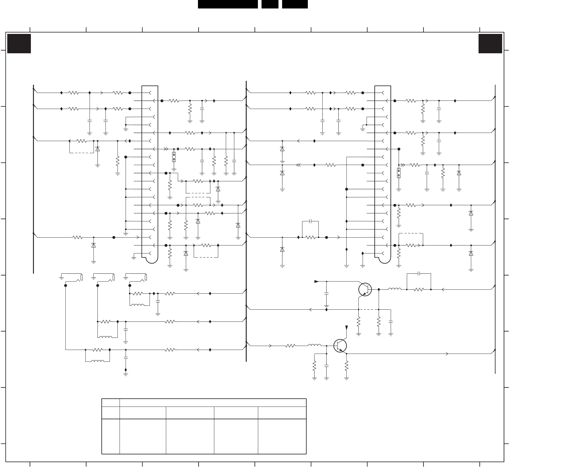
30ES1E AA 7.
Circuit Diagrams and PWB Layouts
LSP: SCART I/O
AUDIO -SURROUND
OUT
A6
A6
G
1701-1 A7
1701-2 A3
1703 B3
1704 C7
1705-1 D2
1705-2 D1
1705-3 D2
2703 B2
2704 B2
2705 B6
2706 B6
2708 B4
2710 C8
2711 C5
2712 D7
2713 E3
2714 E2
2715 F2
2716 E6
2717 B8
2718 B8
2719 B4
2720 B4
2721 F6
1234567
OUT
SCART I/O
INPUTs
2V1
RES
RES
8
12345678
A
B
C
D
E
F
G
A
B
C
D
E
F
A6
0R
A7
2722 E7
3701 A1
3702 A2
3703 A5
3704 A6
3705 A3
3706 A7
3707 A1
3708 A2
3709 A5
3710 A6
3711 B3
3712 B7
3713 B1
3714 B3
3715 B2
3716 B4
3717 B6
3718 B7
3719 C8
3720 C3
3721 C3
3722 C3
3723 C7
3724 C4
3725 C7
3726 D3
3727 D3
A6
0R
0R
3728 D1
3729 D5
3730 D4
3731 D7
3732 D3
3733 D7
3734 E2
3735 E3
3736 E7
3737 E2
3738 E3
3739 E6
3740 E7
3741 F2
3742 F3
3743 B3
3744 B7
3745 B7
3746 B4
3747 F6
3748 F5
3749 F6
5704 E7
5705 F6
5706 E2
5707 F2
A6
(SCART1)
A6
5708 F2
6701 B2
6702 B5
6703 C5
6704 C8
6705 C4
6706 C8
6707 D3
6708 D4
6709 D1
6710 D5
6711 D3
6712 D8
7701-1 E6
7701-2 F6
9701 E6
9702 B1
9703 C3
9704 C3
9705 D4
9706 D7
F701 A2
F702 A6
F703 A3
F704 A7
RES
0R
RES
(SCART2)
A6
A6
AUDIO - L
F705 A2
F706 B6
F708 B7
F710 B7
F711 B2
F712 C6
F713 C3
F714 C6
F715 C3
F716 C7
F717 C3
F718 D2
F719 D6
F720 D3
F721 D7
F722 E1
F723 E2
F724 E2
I701 A2
I702 A6
I703 A2
I704 B6
I705 B4
1V6
A6
OUT
A6
A6
I707 B2
I708 B6
I709 B4
I710 B8
I711 D5
I712 E3
I713 E7
I714 E6
I715 E2
I716 F2
I717 F2
I719 A1
I720 B1
I721 A4
I722 B3
I723 C4
I724 C4
I725 C4
I726 D4
I727 E4
I728 E4
I729 F4
I731 A5
I732 A8
RES
A6
A6
I733 A5
I734 B8
I735 B6
I736 C8
I737 D8
I738 D6
I739 D6
I740 D6
I741 B3
1V6
2V7
*
*
*
A6 A6
A7
A7
A6
A6
A7
0R
A6
A6
A6
A6
*
*
A6
AUDIO - R
8V1
8V1
0R
*
*
A6
*
A6
I741
2716
1u0
3715
75R
0001
1703
560R
3747
3720
2720
1n0
3713
3725
75R
I710
3745
33K
3710
150R
2713
1n0
F718
F710
F722
3742
150R
3n3
2714
75R
3733
F719
I728
1704
0001
6
3
F704
2705
1705-3
6B
7B
8B
9B
1n0
16B
17B
18B
19B
2B
20B
21B
3B
4B
5B
1B
10B
11B
12B
13B
14B
15B
F706
ROW_B
1701-2
PPTV/90
I729
3727
75R
I721
I712
3730
3702
150R
F711
150R
3708
1n0
1705-1
4
1
2718
390p
2711
39K
37183717
100R
PDZ6.8-B
6702
1n0
2717
3712
100R
PDZ6.8-B
6711
9706
5706
2704
1n0
I714
I704
3719
10K
3731
I717
I702
F720
6703
PDZ6.8-B
150R
3707
75R
3721
F714
F713
33K
3743
9701
150R
3734
F716
I737
I736
3722
9703
6708
PDZ6.8-B
I724
47p
2721
100R
3748
I707
I713
PDZ6.8-B
6706
75R
3729
I708
3714
39K
100R
3706
75R
3726
150R
3738
3746
33K
3735
150R
I739
2710
I723
330p
3723
F712
5708
4u7
5705
PDZ6.8-B
6709
3740
10K
3736
100R
I731
I733
1n0
2715
F701
2706
1n0
IMX1
7701-1 5
3
4
10K
3749
I734
I732
7701-2
2
6
1
6704
BZX384-C12
IMX1
I726
3701
150R
I711
I705
F721
F715
3705
100R
I719
1n0
F703
I709
2703
F705
I722
I725
I715
I738
I740
6701
PDZ6.8-B
1705-2
5
2
F708
9702
6707
PDZ6.8-B 330p
2708
I727
F724
I735
33K
3744
560R
3739
1u0
2712
21A
3A
4A
5A
6A
7A
8A
9A
12A
13A
14A
15A
16A
17A
18A
19A
2A
20A
ROW_A
1701-1
PPTV/90
1A
10A
11A
2722
47p
3716
10K
I703
PDZ6.8-B
6705
F717
1n0
2719
75R
3728
3703
150R
3732
75R
150R
3741
9704
9705
I720
F702
F723
I716
150R
3709
150R
3704
5707
PDZ6.8-B
6710
3711
100R
3737
150R
5704
4u7
100R
3724
6712
PDZ6.8-B
CVBS-TER-OUT
R-SC2-OUT
I701
R-SC1_AV-OUT
L-SC1_AV-OUT
R-CL_VL-OUT
AUDIO-SL
L-CL_VL-OUT
R-SC2_AV2-IN
L-SC2_AV2-IN
FBL-SC1-IN
C-SC2_SVHS-IN
P50
L-SC2-OUT
SC1-STATUS
L-SC1_AV1-IN
SEL-SVHS-RR_STATUS2
B-SC1-IN_U-IN
SC2-CVBS_MON-OUT
TER-CVBS-OUT
R-SC1_AV1-IN
C-FRONT-IN
TER-CVBS-OUT
SC2-CVBS_MON-OUT
G-SC1-IN_Y-IN
R-SC1_V-IN
CVBS-SC1_AV1-IN
Y_CVBS-SC2_AV2-IN
CVBS-SC2_MON-OUT
+8VS
+8VS
A7 A7
F_15040_007.eps
220305
3139 123 5895.4
A66EAK075X054
28BLD
USED USED
29RF
A68ERF182X044
SIZE/TUBE
28WSRF
A66ERF172X044 32WSRF
A66ERF172X044
9702 USED USED USED USED
3725
9703
9704
9705 USED USED USED USED
9706 USED USED USED USED
USED USED USED USED
USED USED USED USED
USED USED
ITEM
For Europe
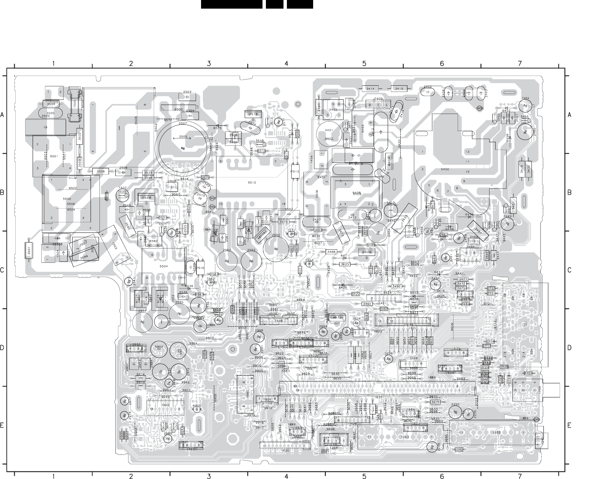
Circuit Diagrams and PWB Layouts 31ES1E AA 7.
Layout LSP (Top Side)
F_15040_008.eps
220305
3139 123 5895.4
1232 E7
1241 E7
1243 E6
1245 E5
1246 E7
1268 E5
1269 E7
1270 E5
1401 C5
1402 A6
1404 B4
1452 C6
1500 A1
1501 A1
1502 A1
1503 C2
1504 C1
1505 A1
1506 D3
1532 B2
1538 D4
1542 B3
1543 B3
1544 B3
1550 B2
1551 C2
1552 C3
1607 D6
1608 D6
1620 E4
1621 E6
1623 D4
1624 D4
1625 D4
1629 D6
1630 D6
1631 D6
1635 D6
1645 D4
1646 E4
1669 D6
1670 E5
1683 E4
1684 E6
1701 D7
1705 E7
1901 D2
1902 D2
1904 E4
1910 E3
1911 E3
2235 E6
2248 E6
2250 E6
2402 A6
2403 A7
2404 C5
2405 A6
2406 A6
2407 B4
2411 A5
2412 A5
2413 B5
2414 A5
2416 B5
2417 B5
2418 B5
2419 B5
2431 A5
2449 B7
2450 A7
2451 A7
2454 A7
2458 C6
2460 A7
2461 C6
2468 C6
2469 C6
2488 A5
2489 C6
2490 C6
2500 A1
2501 C1
2502 C1
2503 A3
2504 A3
2505 A3
2506 B2
2507 A3
2508 C1
2510 C3
2511 A4
2514 A4
2523 B2
2524 D3
2528 B3
2535 C3
2536 C3
2537 D2
2539 C3
2540 C2
2541 C2
2542 B3
2544 B2
2551 B4
2552 C4
2561 C3
2562 C3
2563 C4
2565 C3
2570 B3
2580 C2
2584 D3
2588 C3
2674 D5
2676 D5
2688 D5
2689 D4
2692 D5
2945 D2
2948 D3
2949 D3
2957 D2
2960 E2
2977 E2
2978 E2
2984 D2
2991 D4
2998 D4
3240 E6
3401 C5
3402 D5
3403 B4
3412 A5
3414 A5
3415 A5
3418 C5
3419 B7
3421 C4
3422 C5
3425 C5
3426 C5
3432 B7
3433 B6
3434 C5
3450 B7
3451 B7
3455 A7
3456 A7
3458 B6
3462 C6
3466 C7
3467 C6
3468 C6
3469 C6
3470 C6
3471 C6
3472 C6
3473 C5
3477 B6
3485 B6
3486 B7
3487 B6
3488 C5
3490 A4
3492 C5
3499 C5
3501 C1
3502 A1
3503 B1
3504 A1
3505 A1
3507 C1
3508 B2
3509 C1
3510 B2
3511 B4
3513 A4
3514 A4
3515 A4
3516 A3
3519 B3
3520 A3
3523 C2
3524 B3
3525 B3
3529 B2
3531 B2
3535 B2
3536 B2
3550 A4
3563 C3
3566 D3
3571 C4
3575 B4
3579 C4
3587 C3
3592 B2
3598 B2
3627 D6
3628 D6
3670 E6
3683 D5
3687 D6
3701 C7
3703 C7
3713 D7
3714 D7
3717 D7
3720 D7
3722 D7
3724 D7
3725 D7
3726 D7
3728 D7
3729 D7
3730 D7
3731 D7
3930 E2
3933 E3
3936 E2
3955 E3
3957 D3
3959 D3
3971 E2
5247 E5
5401 A5
5402 A5
5406 B4
5408 B5
5409 B5
5410 B5
5411 B5
5450 B6
5452 C6
5453 C7
5455 A5
5456 C6
5500 B1
5501 B1
5502 A2
5504 C2
5505 D3
5506 B1
5511 A3
5512 B4
5532 B2
5551 B4
5552 B4
5561 B3
5562 B3
5564 D2
5565 D3
5566 D4
5567 D3
5680 E5
5681 D5
5682 D5
5683 D4
5684 D4
5901 D3
5902 D2
5913 D2
5914 D2
6404 B5
6426 C5
6452 A7
6453 B6
6456 A7
6457 C6
6469 B6
6471 C5
6474 C6
6476 B6
6480 C6
6500 A3
6509 C3
6511 A4
6535 C2
6536 C3
6537 C2
6548 C2
6549 B4
6550 C3
6551 C4
6562 C3
6563 B3
6575 A3
6582 C2
6905 E3
7403 C4
7405 A5
7406 C5
7455 C6
7512 A4
7513 B4
7516 C3
7525 B2
7542 C3
7571 B4
7673 D5
7674 D5
7902 E2
7990 E4
9230 E5
9231 E5
9233 E5
9234 E5
9235 E5
9401 B4
9402 A5
9410 B5
9411 A5
9412 B5
9413 C6
9415 C6
9417 C7
9422 C6
9423 D6
9424 C5
9425 C6
9426 C6
9427 C5
9429 A5
9434 C4
9435 C6
9436 C6
9437 C5
9438 C5
9440 C5
9441 C6
9442 B5
9443 C7
9444 B5
9447 C6
9500 A1
9501 B1
9502 B1
9503 B1
9504 B1
9506 A2
9507 D3
9511 B2
9512 D3
9513 D3
9514 B3
9524 D3
9527 C4
9530 C4
9532 D4
9533 D3
9535 B3
9539 D4
9540 B3
9543 A3
9544 A3
9547 B3
9548 A4
9549 C4
9552 D3
9553 D3
9554 C4
9555 C3
9556 C3
9557 C4
9560 C4
9561 D4
9562 D4
9570 A2
9574 B2
9620 E4
9621 E4
9622 D4
9623 D5
9624 D4
9625 E6
9626 E4
9627 D5
9628 D5
9629 D4
9630 D5
9631 E4
9632 E4
9633 E6
9634 D4
9635 D5
9636 E4
9637 D4
9641 E4
9642 D4
9644 D6
9646 E5
9650 D5
9653 D6
9654 D6
9655 E4
9656 D4
9658 D6
9659 D6
9660 E6
9661 D5
9662 D5
9663 D6
9665 D6
9666 D6
9667 D4
9668 E5
9669 E5
9670 E6
9671 E6
9672 E5
9673 D4
9674 D4
9675 D5
9677 E4
9680 D4
9681 E4
9682 E4
9683 E4
9685 E4
9686 D5
9687 E5
9688 E5
9689 E6
9690 E4
9691 E5
9692 E5
9693 E5
9694 E6
9695 E6
9696 E5
9699 D6
9702 D7
9703 D7
9704 D7
9705 D7
9706 D7
9720 D7
9721 C7
9722 D7
9723 E6
9903 E3
9904 D3
9905 D4
9906 D4
9907 D2
9908 E2
9909 E3
9910 D4
9916 E4
9917 E4
9918 E4
9942 D3
9949 E2
9951 E2
9952 E4
9953 D3
9990 D3
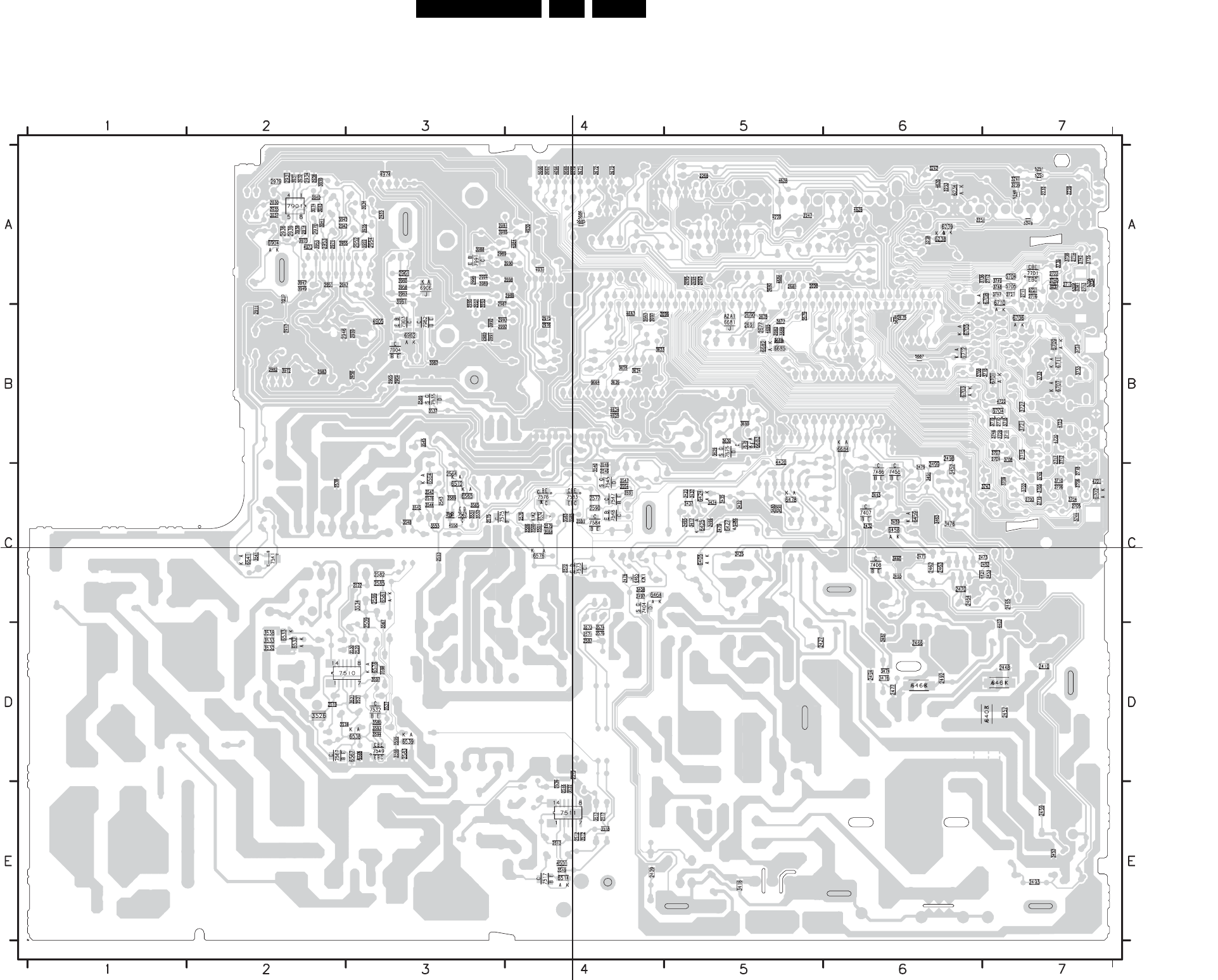
32ES1E AA 7.
Circuit Diagrams and PWB Layouts
Layout LSP (Overview Bottom Side)
F_15040_009.eps
220305
3139 123 5895.4
Part 1
F_15040_009a.eps
Part 2
F_15040_009b.eps
Part 4
F_15040_009d.eps
Part 3
F_15040_009c.eps
2232 A7
2233 A6
2236 A7
2247 A5
2251 A6
2268 A5
2409 E4
2410 D7
2422 C5
2425 C5
2427 D5
2432 C6
2437 C5
2448 D7
2452 C7
2453 C7
2457 D7
2459 E7
2462 C6
2463 C6
2464 C6
2465 C7
2466 D6
2470 C6
2471 C6
2473 C7
2476 D6
2477 D6
2478 C4
2479 C6
2487 D6
2492 D6
2493 E7
2494 D6
2495 C5
2496 C5
2497 C4
2498 B6
2499 C6
2509 D3
2512 E4
2513 E4
2515 D4
2516 E4
2517 E4
2519 D2
2520 D3
2521 D3
2522 C3
2526 E4
2538 C2
2543 C3
2546 C4
2553 C3
2564 C3
2571 D4
2572 C4
2575 C3
2576 C4
2577 C4
2578 C3
2579 C4
2582 C3
2583 D3
2585 C3
2586 C3
2587 D4
2589 B3
2590 C4
2591 C4
2663 B4
2666 A4
2667 A4
2669 A4
2670 A4
2671 A4
2672 A4
2673 A4
2675 B6
2677 B5
2678 B5
2679 B5
2680 A5
2681 A5
2682 B5
2690 B5
2691 B5
2693 A5
2694 A5
2695 A5
2696 B5
2697 B4
2698 A5
2703 C7
2704 B7
2705 C7
2706 C7
2708 B6
2710 B7
2711 A7
2712 A7
2713 A7
2714 A7
2715 A7
2716 A7
2717 B7
2718 C7
2719 C7
2720 B7
2721 A7
2722 A7
2911 B2
2913 B2
2914 A2
2930 A2
2931 A2
2933 A3
2934 A2
2935 A2
2936 A2
2938 A2
2939 A2
2942 A2
2946 B2
2947 A2
2950 B3
2951 A2
2952 A3
2953 A2
2954 A3
2955 A2
2961 A3
2963 A3
2964 B3
2965 B3
2970 A2
2971 A2
2975 B4
2976 B4
2979 A2
2981 A3
2982 B2
2983 B2
2985 B3
2986 A4
2987 A3
2988 A4
2989 A3
2990 A4
2992 B3
2993 B3
2994 A3
2995 A3
2996 A3
2997 A3
3238 A6
3239 A7
3241 A7
3242 A6
3408 C4
3416 E5
3417 C5
3423 C5
3424 C5
3435 C5
3436 C5
3437 C5
3443 C6
3452 C6
3453 E7
3459 C6
3460 C6
3461 C6
3463 C6
3465 C6
3474 D6
3476 C6
3479 C5
3480 C5
3491 C5
3512 E4
3517 E4
3518 E4
3521 D3
3522 E4
3526 D2
3527 D3
3528 D2
3530 D3
3532 D2
3533 D2
3534 C3
3537 B3
3538 D2
3540 C4
3541 C2
3542 C3
3543 C3
3544 C3
3545 B3
3546 C4
3547 C4
3548 C3
3549 E4
3551 C3
3552 C3
3553 C3
3554 C4
3565 C3
3567 D3
3568 D3
3573 D4
3574 D4
3576 D4
3580 D3
3581 C4
3583 C4
3584 C4
3585 C4
3586 C4
3588 D3
3589 C3
3590 C4
3591 C4
3593 D3
3594 D3
3595 D3
3596 D3
3597 D3
3623 B4
3624 B4
3625 B4
3626 B4
3629 B5
3630 B5
3677 B5
3685 B5
3686 B5
3688 B5
3702 C7
3704 C7
3705 C7
3706 C7
3707 B7
3708 B7
3709 C7
3710 C7
3711 B7
3712 B7
3715 B7
3716 B7
3718 B7
3719 B7
3721 B7
3723 B7
3727 B7
3732 B7
3733 B7
3734 A7
3735 A7
3736 A6
3737 A7
3738 A7
3739 A7
3740 A7
3741 A7
3742 A7
3743 C7
3744 C7
3745 C7
3746 B7
3747 A7
3748 A7
3749 A7
3931 A2
3932 A2
3934 A3
3935 A3
3937 A2
3938 A2
3939 A2
3940 A2
3941 A2
3942 A2
3943 A2
3947 A2
3949 A2
3952 A3
3953 A2
3956 B3
3958 A3
3960 A3
3961 A3
3962 B3
3972 B2
3973 A2
3974 A2
3985 A3
3988 A3
3989 A3
3991 B3
3992 B3
3993 A3
4220 A5
4403 D7
4420 B5
4421 C6
4501 E4
4550 C3
4624 B4
4625 B4
4626 A6
4628 A5
4630 A6
4683 B4
4684 A5
4694 A4
4695 B5
4720 B7
4721 C7
4722 B7
4723 B7
4905 B3
4930 A4
4931 A4
4973 A2
4974 A3
4984 A4
5248 A7
5249 A7
5250 A7
5251 A7
5685 A4
5686 A4
5687 B6
5688 B6
5704 A7
5705 A7
5706 A7
5707 A7
5708 A7
5910 A2
6234 A6
6238 A6
6239 A6
6403 D7
6405 C5
6424 C5
6425 C5
6427 C5
6458 C6
6459 C6
6461 D7
6464 C4
6465 C4
6466 D6
6478 C5
6512 C3
6514 E4
6532 D2
6533 D2
6538 D3
6539 D3
6541 C2
6564 C3
6565 C3
6567 D3
6574 C4
6576 C4
6578 D3
6581 C3
6681 B5
6682 B5
6683 B5
6684 B6
6685 B5
6701 B7
6702 C7
6703 B6
6704 B7
6705 B6
6706 B7
6707 B7
6708 A7
6709 B7
6710 A7
6711 B7
6712 B6
6904 A2
6906 A3
6962 B3
7404 C4
7407 C6
7408 C6
7456 C6
7486 C6
7510 D3
7511 E4
7517 E4
7532 D3
7535 B3
7541 C2
7545 C4
7547 C4
7548 C4
7549 D3
7561 C3
7562 C3
7567 D2
7573 C4
7575 C3
7576 C4
7583 C4
7584 C4
7675 B5
7676 B5
7701 A7
7901 A2
7903 B3
7904 B3
7962 B3
7991 A3
9664 B4
9701 A7
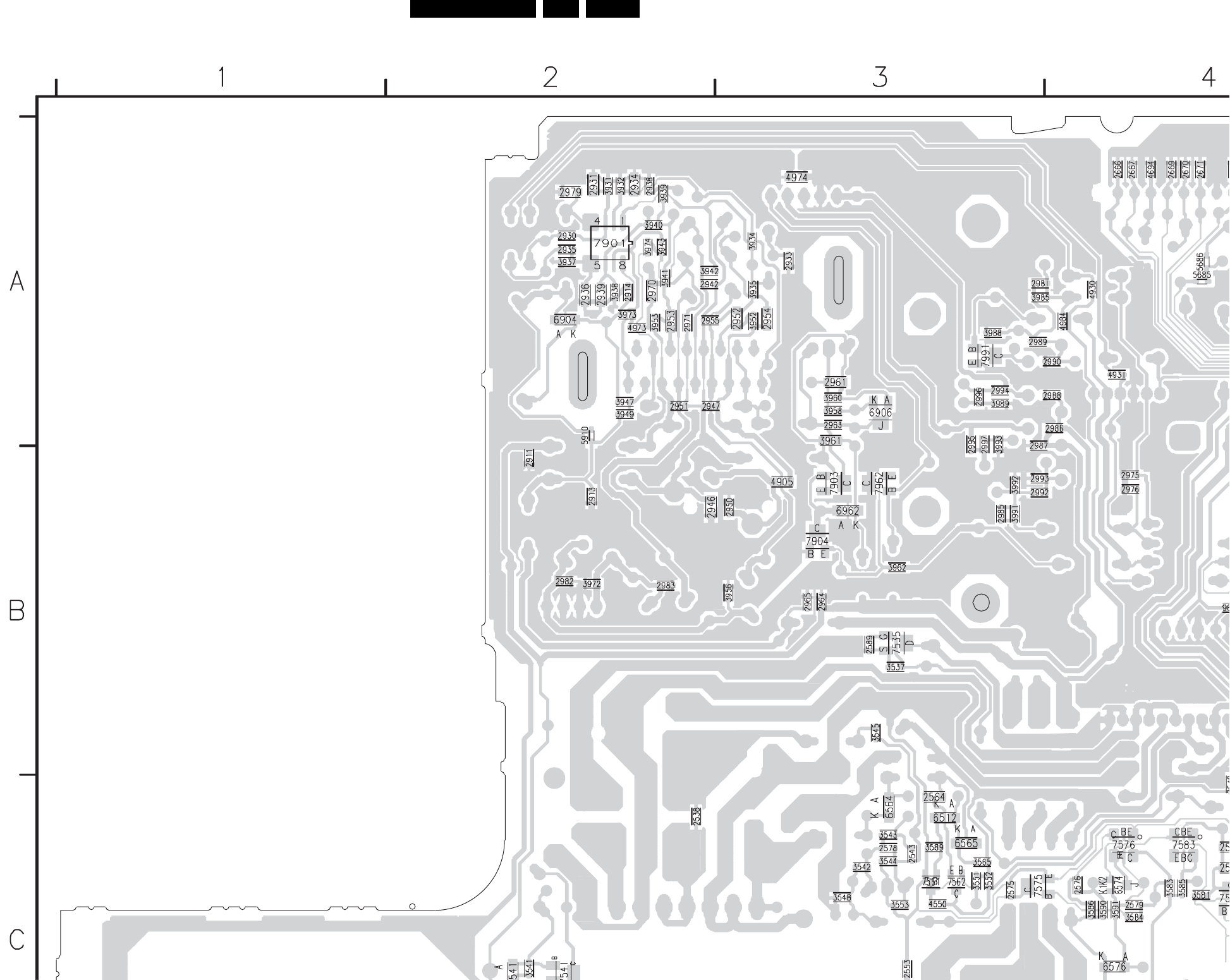
Circuit Diagrams and PWB Layouts 33ES1E AA 7.
Layout LSP (Part 1 Bottom Side)
Part 1
F_15040_009a.eps
310305
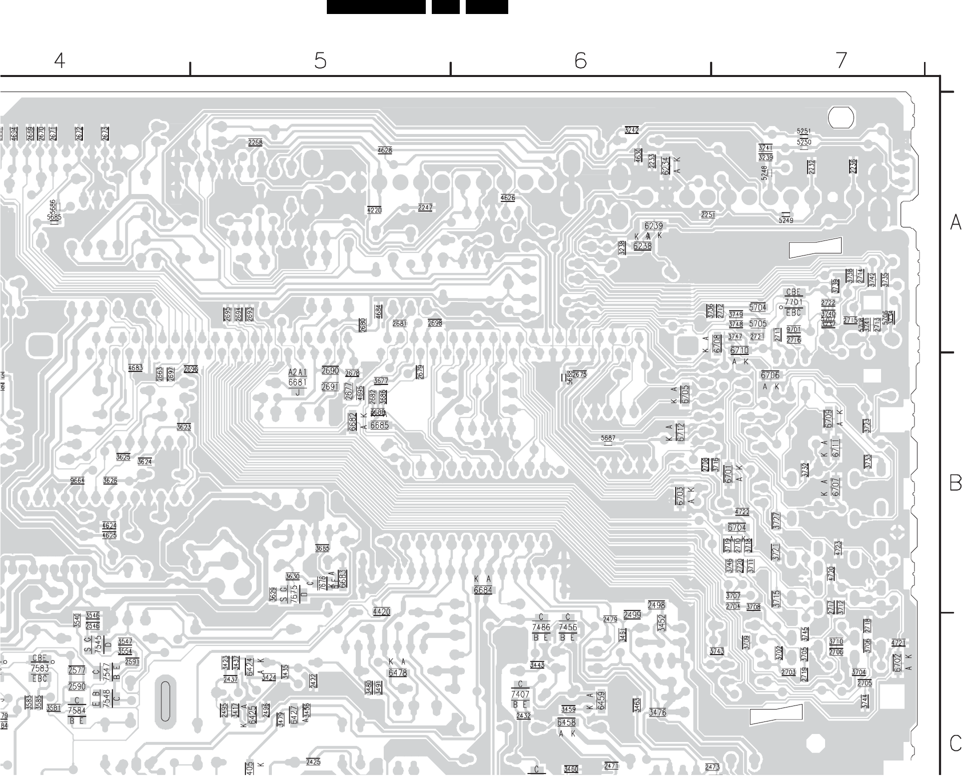
34ES1E AA 7.
Circuit Diagrams and PWB Layouts
Layout LSP (Part 2 Bottom Side)
Part 2
F_15040_009b.eps
310305
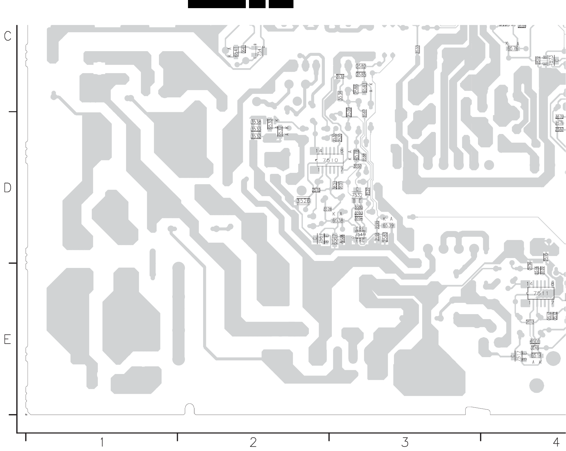
Circuit Diagrams and PWB Layouts 35ES1E AA 7.
Layout LSP (Part 3 Bottom Side)
Part 3
F_15040_009c.eps
310305
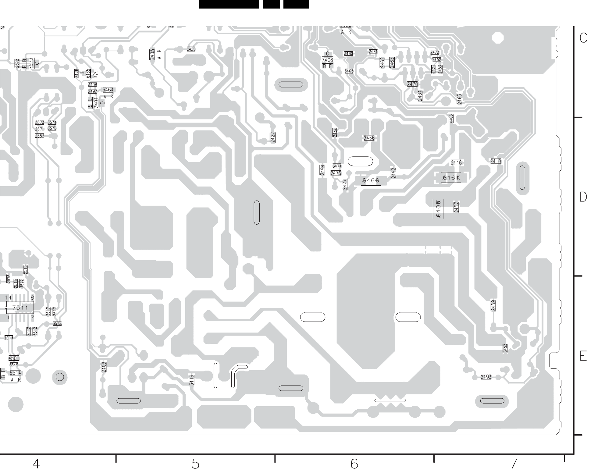
36ES1E AA 7.
Circuit Diagrams and PWB Layouts
Layout LSP (Part 4 Bottom Side)
Part 4
F_15040_009d.eps
310305
Circuit Diagrams and PWB Layouts 37ES1E AA 7.
SSB: If & SAW Filter
NCMT
NCMT
NCMT
AGC
HPF
IF PLL
CALIBRATOR
VCO
LPF
SIF
I/V
BPF
LPF
LPF
AGC
DET
VSW
TO
VIDEO LPF
LPF
AFC AFA
AFB
LOCK
TRAP
GROUP
DELAY
LPF 2ndSIF A/D
SLPM
PMOD
QSS QSSOUT
DSIF,DDIF
ST1...0 GD
VAI, VA1...0
AUDIO SWITCH
TO AM INTERNAL
LOCK
SOUND
2nd SIF
AGC
DET
PMOD,AGC O/IGATING
FFI,IFO IFA/B/C,IFLH
F138
5101 C1
C
D
B
5102 A1
100MHZ/220R
A
5112 B2
9
1113-B A10
1114-A B5
1114-B A10
1115 D10
45678910
A
I108 E6
2132 B10
6101 C2
6102 C4
2134 A2
2136 C10
2135 B1
2137 B22133 B1
E
1112-A A4
1112-B A10
2101 C1
2102 A1
2103 D2
2115 D5
2119 B2
2126 A6
2127 A6
2128 C6
B
C
D
E
7100-C A6
2130 E7
IF & SAW FILTER
3132 D7
4104 B3
4102 A3
3116 D6
3112 D3
3131 D7
NC
4103 B3
3133 E7
B18-5
4101 A33104 B3
3105 D3
3106 D1
4108 A3
4107 A3
1
TO/FROM 1115 OF PIP PANEL
3
10
B18-11
2
B11-7
(TO CON 0221)
100MHZ/220R
NC
100MHZ/220R
100MHZ/220R
B1-2
B1-1
B1-2
B2-4
NC
B3-3
NC
B1-1
3101 C2
3102 C4
3103 B3
B2-12
3137 C10
3138 A6
3134 B1
3135 B9
5678
7101 D2
7104 D4
7131 B10
F114 E10
2138 A2
5128 B6
2V
2V
2V
2V2
2V
FOR PIP/DW
ONLY
5129 B6
I101 B1
I102 A4
I103 A4
I104 B6
I105 B6
I106 C6
I107 C9
F115 D10
F116 E10
F132 E10
F134 D6
F135 A9
F137 D3
F138 B4
F139 A8
1234
1113-A B4
5134 A2
5135 A2
4V9
0V
FOR /93 ONLY
1V9
1V9
1V9
7V9
2K2
3104
2135
10u
14 15 11 12 16 17
4107
OFWK3955L
1114-B
118
456910 13
456910 13 14 15 11 12 16 17
16 17
1113-B
OFWK3953L
118
118
456910 13 14 15 11 12
+5Vd
OFWK9656L
1112-B
+8Vc
+8Vc
+8V +8Va
+8Va
2132
10n
7101
3106
27K
3137
1K
BC847BW
2119
10n100n
2133
5112
3134
10R
100R
3135
7131
BC847BW
100n
2127
6102
+5V
2K2
3101
1SS356
2103
1n
22n
2130
I102
+5V
I101
7
8
9
2136
10u
1
2
3
4
5
6
F139
1115
1u0
5128
2126
100p
3
7
8
+8Va
F137
3138
390R
OFWK3955L
1114-A
2
10n
2101
3132
100R
+5Vd
+5Va
+5Vb
+5Vb
15K
3133
4102
+5Va
4108
2128
2u2
6K8
5101
0u82
5102
3103
100n
2138
100u
2137
I108
I107
4101
I106
I105
3
7
8
4104
I104
2
3
7
8
OFWK9656L
1112-A
2
2115
10n
1113-A
OFWK3953L
3131
10K
5129
1u0
I103
4103
F135
5134
2134
100n
2102
10n
47K
3112
BC847BW
7104
3105
3102
2K2
22K
5135
1SS356
220R
3116
+8Va
6101
SIFAGC101
SIFINN100
SIFINP99
TESTPIN1
124
TUNERAGC105
VCC-IF
110
VCC-SUP 118
VCC1-VSW 122
VCC2-VSW 125
VIFINN108
VIFINP
107
VIFPLL111
F134
2NDSIFAGC 114
2NDSIFEXT
113
CVBSOUTIF 120
DTVIFAGC 102
DTVIFINN
104
DTVIFINP
103
DTVIFPLL
109
DTVOUTN 117
DTVOUTP 116
FUSE4
106
FUSE5
119 GND-SUP
121
GND1-IF
112
GND2-IF
115
7100-C
MPIF
+5Va
SIF_PIP
CVBS_PIP_TUN2
SIF_MAIN
SIF_PIP
2ndSIFEXT
VIFINN
VIFINP
IF-TER
SEL-IF-LL
TUNER_AGC AGC
CVBSOUTIF
SIFINN
SIFNP
PIP_AUDIO
SIF_MAIN
CL 36532058_022.eps
211103
3139 123 5536.2
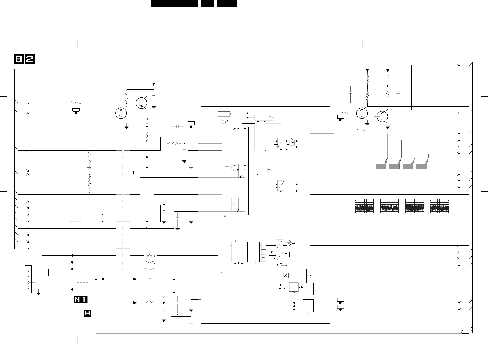
38ES1E AA 7.
Circuit Diagrams and PWB Layouts
SSB: Video Source Selection & Data Link
VIM
CVBS/Y PRIM
C- PRIM
CLP
PRIM
LPF
SEC 3...0
CVO 3...0
CVBS SEC
CLAMP
LPF
CLP
SEC
A
D
ICPL
DM 1...0
PRIM
LR
DIG
2Fh
Yyuv
MHz
54
DATA
LINK
3
MHz
54
SIF
2nd
A/D HV-P/S
TEST
DIG
DATA
LINK
3
RGB
SOURCE
SWITCH
CLAMP
HDTV
CLON
CLPS
LEVEL
ADAPT
INVERSE
PAL
MATRIX
LPF
LPF
LPF
A
D
A
D
DM 1...0
SEC
MONO
DIG
U,V
U
V
Yyuv
DVD
MAT
CLP
yuv
ICPL
ICPL
RSEL
DATA
LINK
54MHz
DM 1...0 297MHz
Yyuv
2Fh
PLL
CIRCUIT
CLP PRIM
CLP SEC
CLP yuv
CLPS
YUV
CLK
PLL
27MHz
TIMING
ROK
IDENT
VID CVBS-OUTA
CLAMP
LPF
A
D
+
PRI 3...0
DATA
LINK
1
BC857B
7062
100n
2085
B1-12
876543
D
B1-4
F
B5-25
2060 A3
2062 B4
2063 C2
2064 C2
2065 C2
2066 D2
2067 D2
21 9
F078 E1
F080 B4
F088 F7
F089 F7
I061 C3
I062 C3
I063 D3
8
I064 D3
A
E
1116 E1
RES
B5-40
B17-28
B17-27
B18-22
B18-18
100MHz/220R
RES
2073 E2
2079 F42074 E2
2075 E2
2076 E2
2078 E3
100MHz/220R
B3-15
1 234567
2082 A7
9
2084 C4
B
C
D
E
F
A
B
C
B5-44
B5-33
B18-17
B18-30
B17-14
B5-38
B5-31
4153 E2
5061 F3
5063 A8
7060-A A3
7060-B B2
7062 B8
7063 B7
2081 F3 7100-B B4
2083 C4
F060 B1
2085 D3
2086 D4
2087 C2
2088 A8
3060 A2
3061 A8
3062 B3
3063 B3
3064 C2
3065 C2
3066 A8
3067 B7
3068 B7
3070 B1
3071 B3
3072 E3
3073 E3
3074 E3
4062 E2
4152 D1
5060 E3
100HZ/220R
B18-20
B5-34
B5-36
VIDEO SOURCE SELECTION AND DATA LINK
B5-35
B5-37
B3-21
B18-29
B18-19
B5-26
B5-32
B5-43
2068 D2
2069 D2
2070 D2
2071 D2
2072 E2
B5-39
B5-41
B18-16
100HZ/220R
B5-42
B18-23
TO/FROM 1002 OF 2Fh IO PNL
OR
TO/FROM 1103 OF 3RD SCART PNL
(CONNECT TO 3D COMB FILTER)
B18-24
2V8
2V2
2V2
1V6
1V4
1V9
0V3
0V3
0V3
0V3
0V3
0V4
F064 B7
F074 E2
F075 F1
F076 E1
F077 E1
3072 100R
150R
3065
2K2
3066
S1 S2
2078
100n
100n
2083
S3 S4
2084
100n
F080
F078
F076
F077
100n2063
7060-B
BC847BPN
+5V
100n
100n2075
100n2073
2074
2072 100n
F089
100n2069
F088
3063
180R
7060-A
BC847BPN 2u2
2088
1K0
3068
1K0
3067
100n
2067
4152
100n2070
4062
3064
150R
+5V
100n
2087
5063
4153
100R3071
100n
100n2068
46HV-PRIM
45HV-SEC
25 R|PR|V-1
R|PR|V-230
60STROBE1N
61STROBE1P
56STROBE2F
55STROBE2N
50STROBE3N
51STROBE3P
49 VCC-DIG
64 VCC-I2D
47 VD2V5
15 Y-COMB
2065
19CVBS-OUTA
22CVBS-OUTB
4 CVBS|Y-3
8 CVBS|Y-4
62DATA1N
63DATA1P
57DATA2N
58DATA2P
52DATA3N
53DATA3P
54 FUSE10
48 GND-DIG
59 GND-I2D
6 GND-VSW
26 G|Y|Y-1
G|Y|Y-231
MPIF
7100-B
27 B|PB|U-1
B|PB|U-232
5C-3
9C-4
16 C-COMB
126 CVBS-1
1 CVBS-2
12 CVBS-DTV
123 CVBS-IF
5061
100R3070
100R
3074
3073 100R
5060
2079
100n
2081
100n
2076
+5V
3060
2K2
3061
2K2
100n
100n
2064
100n2071
I062
3062
180R
2066 100n
I061
2
3
4
5
6
7
+5V
1116
1
2086
100n
F074
F064
F075
7063
BC857B
F060
I063
I064
2u2
2082
2062 100n
+5V
2060
100n
5062
YOUT-COMB
FBL
H-2FH
V-2FH
CVBS-SC3
CVBS-TERR
COUT-COMB
CVBS-SC2_MON-OUT
CVBS_TER_OUT
STROBE2P
DATA2N
DATA2P
HV_PRM
HV_SEC
CVBS-SC1_AV1-IN
CVBS_PIP_TUN2
C-SC2_SVHS-IN
Y-CVBS-FRONT-IN
C-FRONT-IN
B-PB-2FH
CVBS
G-SC1-IN_Y-IN
STROBE1N
STROBE1P
DATA1N
DATA1P
STROBE3N
STROBE3P
DATA3N
DATA3P
STROBE2N
CVBSOUTIF
Y-CVBS-SC2_AV2-IN
R-SC1_V-IN
B-SC1-IN_U-IN
R-PR-2FH
G-Y-2FH
CL 36532058_023.eps
030903
3139 123 5536.2
S1
100mV / div DC
20µs / div
S2
100mV / div DC
20µs / div
S3
100mV / div DC
20µs / div
S4
100mV / div DC
20µs / div
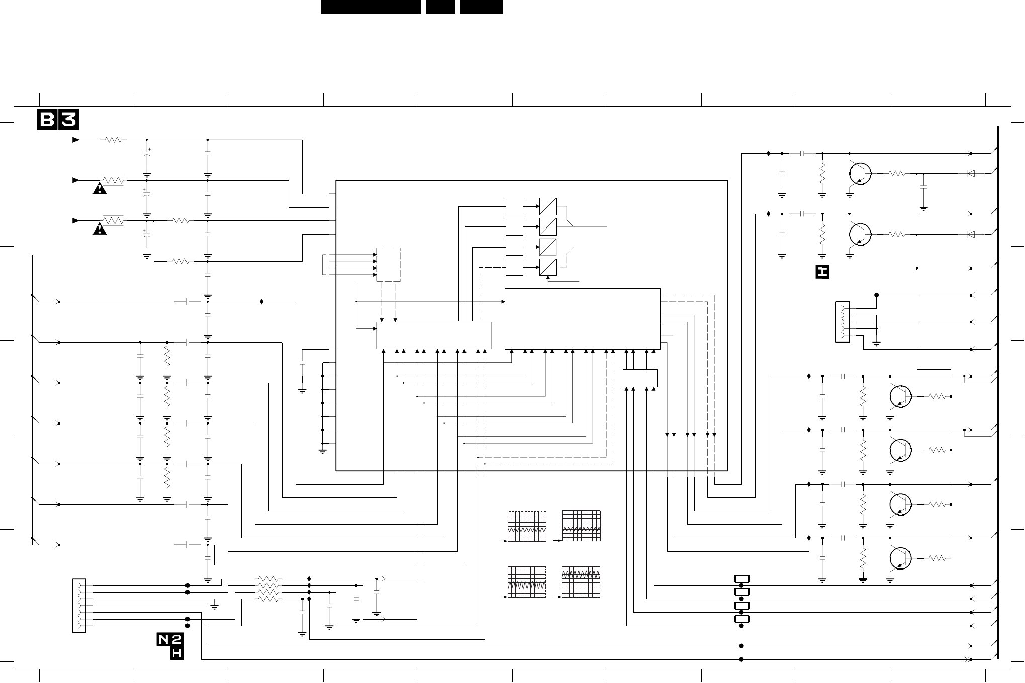
Circuit Diagrams and PWB Layouts 39ES1E AA 7.
SSB: Audio Source Select
MIC1
AM
LPF
LPF
LPF
AD
AD
A
D
DLINK2MIC1/L2/PIPM
MIC2/R2
AUDIO SWITCH
( ANALOG OUT )
A
D
MIC
AMPS
AUDIO SWITCH
( DIGITAL OUT )
AM
SOUND
LPF
DLINK1
L1/AM-INT
R1/AM-EXT
AUDIO
AMPS
6.75 MHz
I009
I010
I005
6030
BAS316
10u
2006 A8
2007 B2
2008 B2
TO/FROM 1104 OF
87
OR
345621 9
3026 C9
3027 D9
3028 A10
3031 D10
3032 D10
B18
B18
3019 A1
3022 D9
3024 E9
3030 C10
3029 A10
3008 E3
3009 E3
3010 A2
3011 B2
3012 E3
3013 E3
3016 A1
3018 A1
B3-59
B10-65
B10-64
B10-63
B18-66
B18-61
B18-49
B3-58
0R
B18-67
B10-62
2039 D9
2040 D9
2041 E4
2042 E4
2043 E3
2044 E3
2045 A2
2046 A2
2047 A2
2048 A2
2049 A2
2050 A2
2051 B2
3002 D2
3003 C2
3004 C2
3005 C2
3006 A9
3007 A9
D
456
AUDIO SOURCE SELECT
B2-21
78910
A
B
C
23
10
1
B10
I010 D9
0R
B1-3
B3-58
B2-15
B18-60
B18-57
B18-56
2005 A8
2004 C1
2003 A9
2002 A9
TO/FROM 1062 OF 2Fh IO PNL
TO/FROM 1102 OF 3RD SCART PNL
1118 B9
1117 E1
1009 A8
E
A
B
C
D
E
7V9
7V9
3V6
3V6
3V6
3V6
3V6
3V6
3V6
3V6
3V6
3V6
3033 E10
6029 A10
6030 A10
7029-1 A9
7029-2 A9
7030-1 C9
7030-2 D9
7031-1 D9
7031-2 E9
7100-A A4
F014 E8
F015 E8
F016 E8
F017 E8
F020 E8
F021 E8
F041 E2
F042 E2
F045 B10
F046 E2
F047 E2
I001 B3
I002 E3
I003 E3
I004 E3
I005 E3
I006 A8
I007 C9
I008 C9
I009 D9
5V
4V9
B18-54
B18-51
B18-50
B18-52
B11-53
NC
B18-48
2009 C1
2010 C1
2011 D1
2012 B2
2013 C2
2014 C3
2015 C2
2016 C2
2018 C2
2019 C2
2021 D2
2022 D2
2024 D2
2025 D2
2027 E2
2028 E2
2029 A10
2030 D9
2031 C9
2032 E9
2033 D9
2037 C9
2038 C9
3RD SCART PNL
B3-59
1K8
3029
BC847BS
7029-2
47K
3027
100n
2049
F014
470p
2018
2028
470n
2014
100n
2011
100p
100p
2010
2009
100p
100p
2004
BC847BS
7031-2
2006
1n
2038
F045
10u
I001
1K8
3033
2024
470p
2039
2021
470p 10u
1n
1n
2033
I004 2042
I008
BAS316
6029
1u0
2029
3028
1K8
7029-1
BC847BS
2003
10u
2002
10u
1117
1
2
3
4
5
6
7
100R
F047
3013
F046
1009
I007
47K
3024
+5V
3016
220R
3030
1K8
7030-1
BC847BS
1K8
3031
BC847BS
7030-2
3032
1K8
7031-1
BC847BS
3010
3019
10R
3026
47K
47K
2037
10u
3007
47K
3006
470n
2019
2016
470n
1118
1
2
3
4
5
2041
1n
I003
I002
47K
2015
47K
3002
3003
2013
470p
470p
2040
F015
3008 100R
100n
2050
100R3012
I006
2007
470n
2008
1n
2032
1n
2030
1n
2031
1n
470n
3018
4R7
2012
16V10u
2047
3011
+5V
+8V
F042
F041
2044
1n
3004
47K
3005
47K
1n
2043
F020
2027
2045
50V
2u2
470p
VAADCP91
VAADCREF89
VCC-AADC77
VCC1-ASW98
VCC2-ASW88
2048
100n
LINEL
68 LINER
67
MIC1N94
MIC1P95
MIC2N92
MIC2P93
R1
85
R2
83
R3
81
R4
79
R5
128
SCART1L
70 SCART1R
69
SCART2L
66 SCART2R
65
VAADCN90
AMEXT
17
DSNDL1
75
DSNDL2
73
DSNDR1
74
DSNDR2
72
FUSE196
FUSE278
FUSE371
GND-AADC76
GND1-ASW97
GND2-ASW87
L1
86
L2
84
L3
82
L4
80
L5
127
MPIF
7100-A
470n
2025
470n
2022
2046
22u 16V
100n
3022
F021
2051
1n
47K
F017
2005
100R
3009
SOUND-ENABLE_1
F016
R-SC1_AV-OUT
L-SC1_AV-OUT
CVBS-SC3
SEL-2FH-SRC_STATUS3
L-CL_VL-OUT
R-CL_VL-OUT
L-SC1_AV-OUT
R-SC1_AV-OUT
L-SC2-OUT
R-SC2-OUT
SOUND-ENABLE_2
POR_FLASH_1
DSNDL2
DSNDR2
PIP_AUDIO
AUD-L1
AUD-R1
AUD_L2
AUD_R2
CVBS-TERR
L-SC1_AV1-IN
R-SC1_AV1-IN
L-SC2_AV2-IN
R-SC2_AV2-IN
L-FRONT-IN
R-FRONT-IN
DSNDL1
DSNDR1
CL 36532058_024.eps
211103
3139 123 5536.2
F014
1 V / div DC
1ms / div
F015
1 V / div DC
1ms / div
F016
500mV / div DC
1ms / div
F017
500mV / div DC
1ms / div
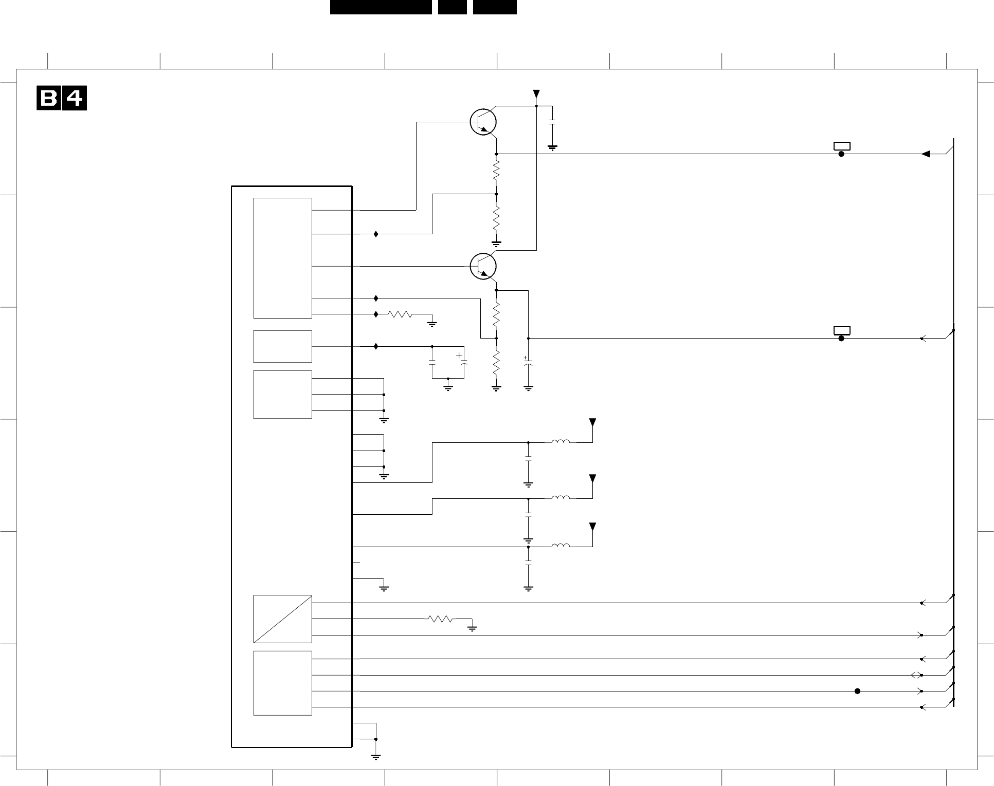
40ES1E AA 7.
Circuit Diagrams and PWB Layouts
SSB: MPIF-Supply, E/W, & Control
BAND GAP
EW
I
V
DIGITAL
BLOCK
SUPPLY
&
REFERENCE
BAND GAP
7150-A
BC847BS
I153
100n
100n
2156
8
B10-68
3153 C5
MPIF-SUPPLY,E/W, & CONTROL
A
B8-70
5
2
76
C
D
B8-69
5151 D5
I151 B3
7100-D A2
F159 F8
5150 D5
5152 E5
D
E
F
NC
58
B18-71
F
I154 C3
7
A
B
3152 B5
3154 B4
6
I152 B3
I153 B3
1
2155 D5
2150 A5
B11-72
B11-73
B
E
C
2151 C4
2
3
1
2152 C4
2154 C5
3V9
1V3
2V
2V5
3V2
3V2
3V2
0V8
7150-B B5
F150 A8
7150-A A5
F152 C8
34
4
100MHZ/220R
100MHZ/220R
100MHZ/220R
2157 E5
3155 E4
3151 B5
3150 A5
2156 D5
5152
+5V
3V3
1V3
5151
2154
10u 16V
43SDA
24TESTPIN2
18TESTPIN3
2VAUDO
3VAUDS
14VCC-FILT
28VCC-RGB
35VCC-VADC
20VDEFLO
21VDEFLS
40XREF
39ADR
7BGDEC
37EWIOUT
36EWVIN
41FUSE6
23FUSE7
10FUSE8
33FUSE9
11GND-FILT
29GND-RGB
34GND-VADC
42IRQ
38REW
13RREF
44SCL
MPIF
7100-D
+5V
VREF_AUD_POS
3V2 DC
3V2 DC
+5V
2150
100n
47K
3154
5150
2155
2152
100n
I154
I152
2151
100n
2157
2u2
820R3155
1K2
3151
1K8
3152
1K2
3153
1K8
3150
BC847BS
7150-B
F159
F152
I151
+5V
F150
VREF_DEFL
EW-DRIVE
EW_MPIF
IRQ_MPIF
F_REF
SCL1
SDA1
CL 36532058_025.eps
211103
3139 123 5536.2
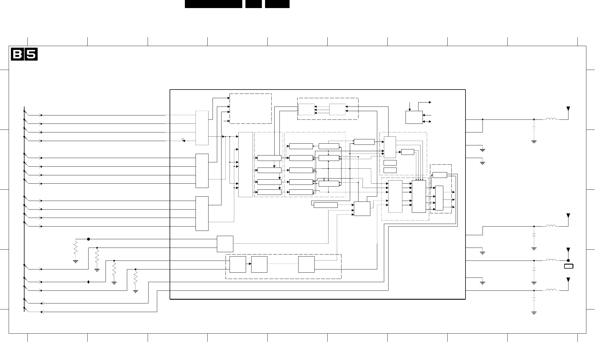
Circuit Diagrams and PWB Layouts 41ES1E AA 7.
SSB: Video Decoder
2
ID3
2
ID2
( A-ADC1, A-ADC2 )
SSIF
EXT SUB MONO-CHANNEL
( A-ADC3 )
A-ADC4
SEC DECODER
TDC-
ANA
TDC-
DIG
SRC-YYUV-CYC
SRC-UYUV
SRC-VYUV
AMP-YYC
AMP-YYUV-CYC
AMP-UYUV
AMP-VYUV
AMP-SYNCYC SYNC-GAIN
CVBS-Y-GAIN
UV-GAIN
AGC
INCR
INCR
OVERFL.
DAV. INCR
CVBS-YYC-DELTA
+DAV
UV-DELTA
+DAV
SYNC-GAIN
PRF-SYNC-2FH SYNC-
MODULE-
2FH
EXT-
SYNC
HSYNC-FBL+DELTA HSYNC+DELTA
FBL+DELTA
COMB
YC DET
DEMUX
FBLANK
SWITCH
DMSD
FORMATTER
HV-INFO
Y
SYNC
FORMAT
H/V
REGISTER
AND
PI INTERF
BANDOUTS VIDDEC-INT
PI-A
PI-D
EXT MAIN STEREO CHANNEL
I2
DATA
SYNC
PRI DECODER
EXT
SYNC-
MUX
SRC-YYC
SRC
DELTA
GEN
FREQ-SELECT
DTO
ITS
DEC
FBLANK
FIFO
DELAY AND FAST-BLANK
’SRC’ FOR HFB1/H-SYNC
UV
D1
5283
100Mhz / 220R
B
5282 C95281 A9 I281 D23284 D2 5285 D95283 D9
2345
B2-44
78
3282 D2 3283 D2
B2-33
C
B2-31
B2-35
B2-34
B2-32
9
C
2
A
1
B2-37
B2-38
1
3
B2-36
B2-40
B2-39
6
5281
100Mhz / 220R
B2-41
B2-26
B18-45
B2-25
D
VIDEO DECODER
B2-42
3281 C1
54
2285 D92284 D9 F282 C2F281 D97300-J A3
8
100Mhz / 220R
100Mhz / 220R
B2-43
67 9
A
2281 A9 2282 C9
B
D
AE3PLLVSSA
N23VID1-DTC-VDD3
P23VID1-DTC-VDDA
N26VID1-DTC-VSSA
P24 VSYNC1
P25 VSYNC2
F281
H26 DLINK1DP
H23 DLINK1SN
H24 DLINK1SP
G24 DLINK2DN
G25 DLINK2DP
F24 DLINK2SN
F25 DLINK2SP
E25 DLINK3DN
E26 DLINK3DP
E23 DLINK3SN
E24 DLINK3SP
N24 HSYNCFBL1
N25 HSYNCFBL2
P26 HVINFO1
R23 HVINFO2
AF3PLLVDDA
ADOC
7300-J
F23DLINK-VDDA
D26DLINK-VDDD
G26DLINK-VSSA
J23DLINK-VSSD
H25 DLINK1DN
3283
1K
100n
2282
100n
VDDCO
2281
5282
VDDCO
VDDCO
5285
100n
2285
1K
3284
F282
1K
3281
3282
1K
VDDE
I281
2284
100n
HV_SEC
HV_PRM
STROBE1N
STROBE1P
DATA1N
DATA1P
STROBE3N
STROBE3P
DATA3N
DATA3P
STROBE2N
STROBE2P
DATA2N
DATA2P
FBL-SC1-IN
H-2FH
V-2FH
CL 36532058_026.eps
211103
3139 123 5536.2
3V2 DC
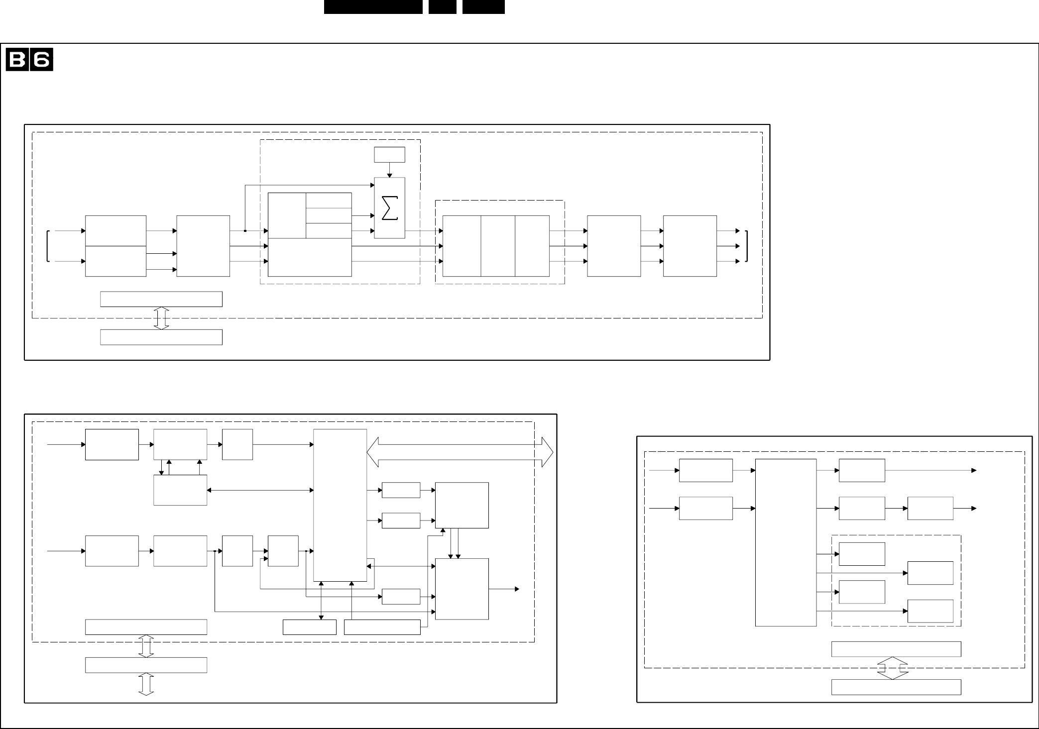
42ES1E AA 7.
Circuit Diagrams and PWB Layouts
SSB: Feature Box
MAIN CHANNEL
TO MBF
CONTROL INTERFACE
PI-DTL MMIO ADAPTER
YUV
YUV
YUV
YUV
FRONT END PROCESSING
MEMORY BASED PROCESSING
BACK END PROCESSING
7300
7300
7300
COLOUR FEATURES
Y
U
V
COLOUR
SPACE
CONVERSION
FRAME
PROCESSING
R
G
B
TO DOP
FROM MBF
LUMINANCE SHARPNESS
CONTROL INTERFACE
PI-DTL MMIO ADAPTER
SUB
SHAPE
R
G
B
HORIZONTAL
COMPRESSION
CHANNEL
SUB
YUV VERTICAL
COMPRESSION
NOISE
FEATURE BOX
COMPENSATION
DELAY
DCTI
Y
UV
Y
U
V
PANORAMA
Y
U
V
FILTERS
COMPENSATION
DELAY
SHARPNESS
MEASURE
DYNAMIC
PEAKING
LTI
256
Y
U
V
SKIN
TONE
CONTROL
BLUE
STRETCH
GREEN
ENHANCE
FIFO CACHE
HORIZONTAL
COMPRESSION
CHANNEL
MAIN
YUV NOISE
SHAPE
MAIN
FIFO CACHE DNR
MEMORY BUS
DEVICE
INTERFACE
UNDITHER
UNDITHER
UNDITHER
SCAN RATE
CONVERSION
DISPLAY CONTROLLERMODE CONTROL
OUTPUT
MULTIPLEXER
DTL INTERFACE
SDRAM
VIA
MMI
TO BEF YUV
CONTROL INTERFACE
MMIO ADAPTER
DTL MMIO
PI-BUS
MEMORY BASED FEATURES
SAMPLE RATE
CONVERTER
SAMPLE RATE
CONVERTER
VIDDEC2
FROM
VIDDEC1
FROM
BLACK
STRETCH
BLACK
STRETCH
HISTOGRAM
MODIFY
HISTOGRAM
MEASURE
BLACKLEVEL
DETECTION
BLACKBAR
DETECTION
NOISE
MEASURE
Y
Y
INPUT
SWITCH
MATRIX MEASUREMENT BLOCKS
SUB CHANNEL
TO MBF
CL 36532058_027.eps
020903
3139 123 5536.2
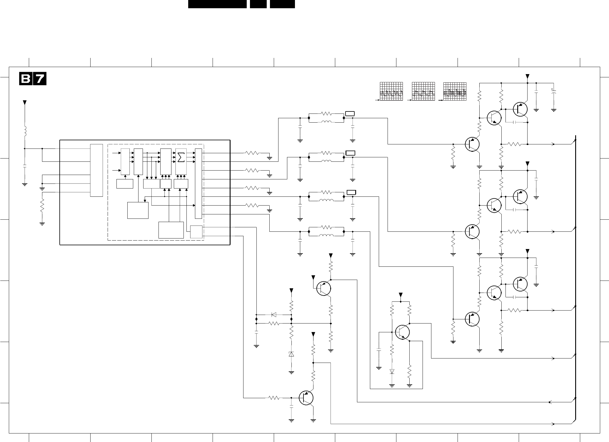
Circuit Diagrams and PWB Layouts 43ES1E AA 7.
SSB: RGB Processing
RGB
BLANKING
CTRL SCAVEM
FIXED
BEAM
CURRENT
SWITCH OFF
CDAC
RGB
GAIN
RGB
CUTOFF
LEAKAGE
COMPENSATOR
RGB
POWER
SOURCE
GFX
BLENDER
DRIVE
ADJUST
BLENDER
ADC
RGB PROCESSING
B18-75
B18-76
B18-77
B18-78
B18-79
100Mhz / 220R
B18-112
RES
RES
0R
0R
0R
RES RES
RES
RES
RES
RES
RES
RES
RES
RES
RES
18R
18R
18R
1 2 3 4 5 6 7 8 9
1 2 3 4 5 6 7 8 9
A
B
C
D
E
A
B
C
D
E
2300 B1
2305 E6
2307 A6
2308 A5
2310 A9
2311 A9
2317 B6
2318 B5
2319 A8
2321 B9
2324 D4
2325 C5
2326 C6
2327 B6
2328 B5
2329 B8
2331 C9
2339 D8
2346 E5
3302 B1
3303 D7
3304 D7
3305 E7
3306 E7
3307 A8
3308 A5
3309 A8
3310 A8
3311 A8
3312 A8
3313 A8
3316 B8
3317 A5
3318 D5
3319 B8
3320 B8
3321 C8
3322 C8
3323 C8
3324 D5
3326 D4
3328 C5
3329 C8
3330 C8
3331 D8
3332 D8
3333 D8
3334 A4
3335 B4
3336 B4
3337 B4
3338 D8
3339 B5
3343 E4
3345 E5
3347 D6
3348 D6
3349 C6
3356 E5
5300 A1
5307 A5
5317 B5
5327 B5
5328 C5
6301 E7
6326 D4
6327 E5
7300-H A1
7301 A8
7302 C8
7303 D8
7304 D7
7310-A A8
7310-B A9
7320-A B8
7320-B B9
7330-A D8
7330-B D9
7346 D5
7356 E5
I301 C5
I302 C6
I303 D4
I304 D5
I305 A5
I306 A6
I307 A5
I308 A6
I309 B5
I310 B6
2307
2327
2317
2326
2305
1u0
2339
100p
7303
BC857B
100p
2329
2319
100p
BC857B
7302
82p
2325
7301
BC857B
33R
3306
BC847BW
7304
BAS316
6301
1K2
3305
330R
3304
+8V
6K8
3303
I309 I310
I307 I308
I306
I303
I305
I304
+3V3
I301 I302
6326
BAS316
47K
3324
+5V
7346
BC857B
22K
3348
+8V
22K
3347
47K
3349
3328
33R
3339
3338
3316
3317
3307
3308
PDZ-2.7B
6327
1K2
3318
100n
2346
+8V
3345
6K8
820R
3356
BC857B
7356
10K
3343
16V10u
2310
3335
33R
33R
3334
33R
3336
3331
33R
3337
33R
2328
33R
3321
2318
220p
220p
W4 CDAC2-VDDA
Y3 CDAC2-VSSA
V2COUTN
V3GOUTP
N1IBC
AA2IBCRANGE
U2ROUTN
U3ROUTP
Y1SVMN
Y2SVMP
220p
2308
ADOC
7300-H
W2BOUTN
W3BOUTP
U1 CDAC-REF
V1 CDAC1-VDDA
U4 CDAC1-VSSA
10n
2331
2321
10n
10n
2311
2324
100p
5328
2u2
1K2
3302
7330-A
BC847BPN
7320-A
BC847BPN
7330-B
BC847BPN
7320-B
BC847BPN
7310-A
BC847BPN
7310-B
BC847BPN
VDDE
100n
2300
4K7
5300
+8V
3326
3332 1K2
3330
1K2
3333
330R
5327
2u2
3329
330R
+8V
1K23322
3320
330R
3323
5317
2u2
1K2
+8V
330R
3319
3313
3312 1K2
33R
1K2
3310
330R
2u2
5307
3311
330R
3309
R-CRT
G-CRT
B-CRT
TILT
CUTOFF
Y-SCAVEM
CL 36532058-083.eps
211103
3139 123 5536.2
I310
200mV / div DC
10µs / div
I308
200mV / div DC
10µs / div
I306
200mV / div DC
10µs / div
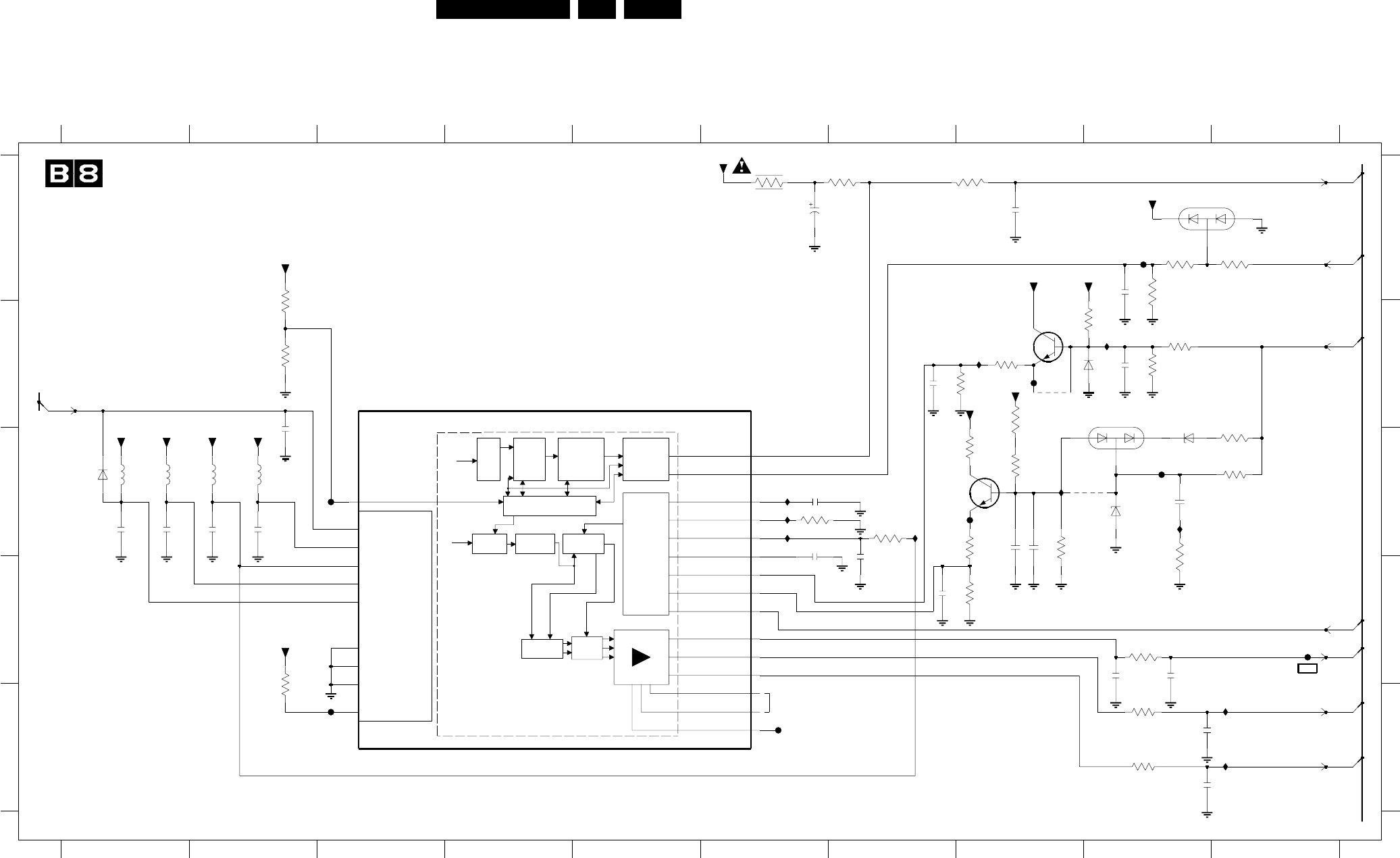
44ES1E AA 7.
Circuit Diagrams and PWB Layouts
SSB: Sync & Deflection Processing
DRIVE
CTRL
LOOP
PH1-2
SECOND
CTRL
LOOP
PH1-2
SLOW START
AND
SLOW START
LOW POWER
SUPPLY
HIRES
TIMING
GENERATOR
1/64 CLOCK
HORIZONTAL TIME BASE GEN.
DTO AND CONTROL LOOP
EW
WAVEFORM
VERTICAL
SAWTOOTH
VERTICAL
WAVEFORM
VERTICAL
DRIVER
VERT.
DRIVE
HOR.
FIRST
ADC
SDAC
GEOMETRY
22K
+8V
3353
5344
2343 C2
2344 C1
2345 C1 F341 C3
F346 E3
B
C
D
E
100Mhz /
220R
B4-69
2364 C8 3355 C6
3354 A10
4
3374 E9
220R 220R
2371 D9
2372 D9
2377 E10
2379 E10
8910
123
RES
6353 A9
6361 B9
6365 C9
6367 C9
F348 D10
F351 E6
F354 A9
F355 B8
2361 C8
2362 B9
2363 B7 I342 C6
I343 C6
I344 C7
3373 C8
3341 B2
3346 D2
3350 A8
2360 C6
3353 A9
3352 A9
3351 A7
3340 A2
56
I350 E10
3375 E9
3376 D8
5345 C1
6341 C1
220R
B18-84
SYNC & DEFLECTION PROCESSING
10
A
B18-83
B18-82
100Mhz /
RES
1234567
RES
I346 B8
I347 C8
I348 C9
I349 E10
789
3361 B8
3362 B9 4361 C9
3378 B8
3377 C8
0R
5342 C22342 C2
2341 B2 4363 B8
5343 C2
5344 C1
3357 C7
3358 A6
3360 B8
I345 B9
RES
3363 B9
3364 B9
3365 C8
3366 C9
D
E
2366 C9
3372 C8
B
A
C
5
100Mhz /
2365 D8
I341 C6
F358 C9
F357 C8
2359 C6
B4-70
B18-87
B18-89
B18-88
NC
3367 B10
3368 C10
3371 D9
7365 C8
7361 B8
7300-F B3
6368 C9
100Mhz /
2350 A7
2351 A8
2352 A9
2358 D7
+8V
3V2
3V2
1V7
0V3
1V2
1V2
1V2
1V2
1V2
1V2
0V
2V
1V5
1V4
7V9
3V5
4V
2V9
2V4
2351
F348
10p
F341
BC847B
7365
10K
10K
3354
2366
2u2
1K
3371
1K0
3341
3374
2K7
F346 F351
F357
3363
27K
3362
100K
2379
2n2
3355
3361
3365
15K
6361
BAS316
2371
1n
100p
2360
+3V3
2344
100n
2M2
3377
F358
AA3
HDROUT L1
HFB L3
IMEAS-CAL P2
IMEAS-VDDAN4
IMEAS-VREF-C M3
IMEAS-VREF-R M4
IMEAS-VSSAP1
IMEAS-ZERO P3
NSP AA1
SDAC-3V3R3
SDAC-VDDAT1
SDAC-VSSAR4
SEL2FHAA4
VDRN R2
VDRP R1
7300-F
ADOC
AUXP T3
BCL N2
BPAAC1
DAFP Y4
DOP-DTC-VDD3L2
DOP-DTC-VDDAM1
DOP-DTC-VSSAM2
EHT N3
EWP T2
FBCIN
3360
15K
3346
5343
1K0
+5V
2345
100n
3376
10K
VDDE
100p
2365
F355
100u
2350
16V
VDDE
I347
I348
I343 I344
I342
BAV99
6353
2372
1n
3375
2K7
I346
I345
4363
5345
3352
47K
6368
BZX384-C6V8
I350
3372
330K
3373
10K
5342
2361
2u2
3340
1K0
2343
100n 22K
3357
BAS316
6341
3378
1M
2341
100n
VDDEVDDE
100n
2342
+8V
VDDE
3366
2K2
10n
2u2
2364
2363
100p
2362
I349
2352
10p
BAV99
6365
1K
8K2
3368
6367 3367
4361
BZX384-C22
3358
10R
+8V
1K
3350
220R
3351
VDDCO
I341
2377
2n2
2358
100p
100n
2359
3364 68K
F354
7361
BC847B
FRAMEDRIVE+
FRAMEDRIVE-
HFB_X-RAY-PROT
POR_FLASH
EW_MPIF
VREF_DEFL
LINEDRIVE1
EHT-INFO
CL 36532058_029.eps
030903
3139 123 5536.2
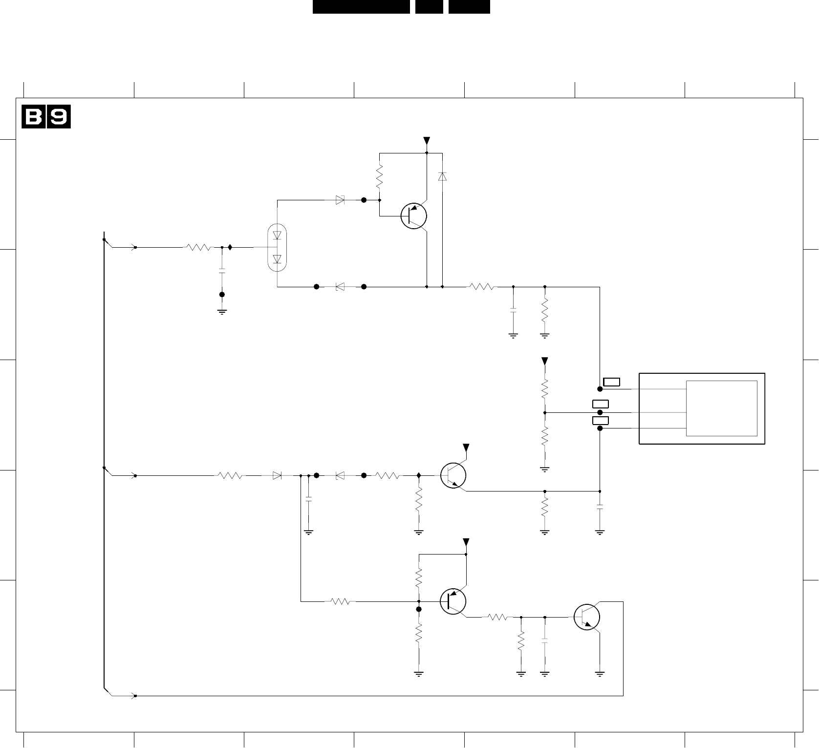
Circuit Diagrams and PWB Layouts 45ES1E AA 7.
SSB: Protection
PROTECTION
2397
100n
F391
3393
3K3
I382
1
7393 D5
F381 C6
F382 C6
F383 C6
3
6382 A3
6384 B3
7300-G C6
I382 C4
6398 C3
E
D
7
D
E
C
A
F387 E4
B18-91
RES
F384 A4
F389 C32395 E5
PROTECTION
2380 B2
0V
10V4 3V2
F391 B4
B18-92
I381 A2
F390 C4
F385 B3
F386 B2
RES
B
B18-91
2395 D6
3390 C5
2386 B5
3456
3386 B5
A
B
C
7383-B E5
2397 D3
756
3397 C4
4
3380 B2
3382 A4
3384 E5
3385 B5
3398 C2
6381 A3
3388 C5
3391 E4
6385 A4
6397 C3
3392 E3
3393 D5
7382 A4
7383-A E6
3394 D4
3395 E5
12
3396 D4
2
2395
10n
7V9
0V
0V DC
0V DC
0V DC
0V
0V
0V
1K0
3390
F389 F390
7383-B
BC847BPN
BAS316
6398 BZX384-C27
BC847BPN
6397
FLASHAB1
VGUARDW1
XPROTAB2
VDDE
+3V3
7383-A
7300-G
ADOC
3395
10K
3392 47K
6381
BAV99
F383
7382
3380
10K
3382
1K
BC857B
3391
39K
3396
470R
7393
BC847BW
3397
470R
+8V
3385
47K
3386
27K
3384
10K
10K
3394
3388
1K0
F382
2384
1n
100R
2380
470p
F386
3398
F384
2386
10p
BAS316
6385
6382
BZX284-C47
F381
+8V
F387
I381
6384
BZX384-C22
HFB_X-RAY-PROT
KEYBOARD
EHT-INFO
F385
CL 36532058_030.eps
211103
3139 123 5536.2
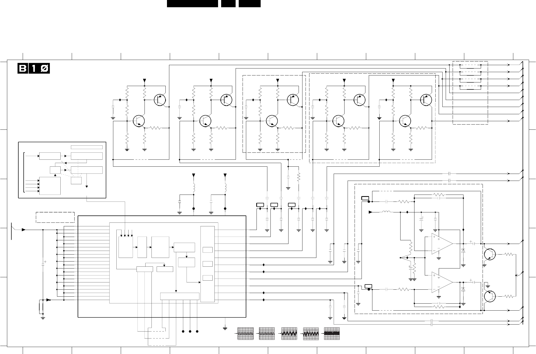
46ES1E AA 7.
Circuit Diagrams and PWB Layouts
SSB: Audio Processing
PROCESSING
INPUT
X-BAR
WS PLL
NOISE
SHAPER
I2SOUT
I2SIN
DAC
5D/A
2D/A
4D/A
FROM AUDIO DEMDEC & DD-DSP
AUDIO DSP
LEVEL
ADJ
INPUT
X-BAR
2u2
VREF_AUD_NEG
3447
56K
3460
1K2
5678910
FOR DPL SET
PROVISION FOR DVD INTERFACE
2439 B9
REMOVE FOR DVD
D
E
A
B
C
D
E
2430 C7
2431 C6
2432 C6
2433 C5
2434 C5
2435 C6
2436 C6
2437 C7
2438 B9
2134
REFER TO SHT B10a
2440 D7
2441 D7
2442 D8
2443 E7
2444 E7
2445 E7
2447 D1
2450 C4
2451 A8
3453 A2
3454 A3
3455 B3
3456 B3
3457 A3
3458 A5
2453 A7
2454 A4
2457 A2
2458 C6
10
A
B
C
2452 C4
2462 E9
2461 E9
2465 A5
2467 C6
2468 B6
2480 C8
2481 E8
2483 C9
123456789
2V7
UAB 12 NEED TO BE RAISE :
AE25 : AUD-SPKR-R-VRNEG
AF26 : AUD-SPKR-R-VRPOS
7V3
4V
I437 C6
I438 C6
I439 C6
I440 C7
I441 D5
I442 D5
I443 E5
I444 E5
I445 C8
I446 D8
I447 D10
I448 E10
100MHZ / 220R 100MHZ / 220R
REMOVE FOR DVD
ALL STRAPS TO BE
REFER TO SHT B10a
B18-100
PROVISION FOR DVD INTERFACE
PREPROCESSING
7V3
2V7
4V
1K8
B3
1V6
4V9
4V9
2V5
2V5
2V5
2V5
2V5
2V5
ALL STRAPS TO BE
4451 A10
4452 A10
4453 A10
4480 C8
4481 E8
5450 C4
2484 D8
2485 E9
2486 C9
2487 C9
2488 D10
2489 D10
3433 B9
3434 B8
3435 A8
AE25 : AUD-SPKR-R-VRNEG
UAB 12 NEED TO BE RAISE :
3436 A8
3437 A8
3439 A7
3440 A7
3441 A7
3442 B7
3443 B7
3444 A7
3445 A4
3446 A4
3447 B4
3448 B4
3449 A5
3450 A4
3452 A3
7434-A A6
7434-B A6
7480-A D9
7480-B E9
7486-A D10
7486-B E10
3459 A5
3460 A6
3461 B5
3462 B6
3463 A6
3465 A9
3468 B6
3480 C8
3481 E8
100MHZ / 220R
SRC
3482 D8
3483 C9
3484 D9
3485 E9
3486 D10
3487 E10
4430 B3
4431 B4
4432 B6
4433 B7
4434 B8
4435 E3
4436 E3
4437 E3
4450 A10
PROCESSING
B18-95
I433 A5
I434 A7
I435 A8
I436 C5
5452 C4
5480 C8
6480 D10
6481 E10
7300-B C2
7430-A A8
7430-B A9
7431-A A7
7431-B A7
DDEP
7300
B18-96
SSIF
A_ADC1
SELECT
B4-68
DECIMATION
B18-98
B18-97
AF26 : AUD-SPKR-R-VRPOS
DEMDEC & DD_DSP
A_ADC2
7432-A A4
7432-B A4
7433-A A3
7433-B A3
FOR
SUBWOOFER
SET
1V6
1V6
1V6
F437 E4
F438 E4
F439 E4
F448 C4
F449 C4
F480 C7
F481 E8
I431 A2
I432 A4
AUDIO DEMODULATION
B3-65
DEMATRIX AND
AUDIO PROCESSING
TO AUDIO
B18-99
FILTER
FROM VIDDEC
B3-64
HEADPHONE AMPLIFIER
B18-94
B3-63
FOR DPL SET
A_ADC3
A_ADC4
B3-62
DOWNMIX
7486-B
3487
7486-A
BC847BS
BC847BS
4453
4452
3435
56K
2454
3434
56K
2437
470n
F438
2436
470n
F437
3439
470n2480
7431-B
BC847BPN
47K
100u
2488
7432-A
BC847BPN
I448
2442
1n
2443
1n
2441
1n
100R
3468
I438 I439
+8V
3462
1K2
3463
1K5
2481
470n
8K23485
3481
2K7
4480
I436
4481
I434 I435I432 I433
BC847BPN
7433-B
2467
470n
+8V
1K8
3486
SDAC1-3V3
AD22
SDAC1-VDDA
AE22
SDAC1-VSSA
AF16
SDI
AE17
SDO1
AD17
SDO2
AD16
WSI
AE19
WSO1
WSO2
AD19
2450
10n
AUD-SPKR-C-VRPOS
AD25AUD-SPKR-L
AD26 AUD-SPKR-L-VRNEG
AD24 AUD-SPKR-L-VRPOS
AE26AUD-SPKR-R
AF26 AUD-SPKR-R-VRNEG
AE25 AUD-SPKR-R-VRPOS
AB23AUD-SPKR-SL
AB24 AUD-SPKR-SL-VRNEG
AA26 AUD-SPKR-SL-VRPOS
AE24AUD-SPKR-SW
AF24 AUD-SPKR-SW-VRNEG
AF25 AUD-SPKR-SW-VRPOS
SCKI
AE16
AE18
SCKO1
AD18
SCKO2
AC22
AUD-DAC1-R-VRNEG
Y24 AUD-DAC1-R-VRPOS
W26AUD-DAC2-L
W25 AUD-DAC2-L-VRNEG
Y23 AUD-DAC2-L-VRPOS
W23AUD-DAC2-R
W24 AUD-DAC2-R-VRNEG
V26 AUD-DAC2-R-VRPOS
AB26AUD-HP-L
AC23 AUD-HP-L-VRNEG
AB25 AUD-HP-L-VRPOS
AC25AUD-HP-R
AUD-HP-R-VRNEGAC24
AC26 AUD-HP-R-VRPOS
AE23AUD-SPKR-C
AD23 AUD-SPKR-C-VRNEG
AF23
ADOC
7300-B
AUD-DAC1-L AA24
AA23 AUD-DAC1-L-VRNEG
AA25 AUD-DAC1-L-VRPOS
Y25AUD-DAC1-R
Y26
2440
1n
4434
F448
F439
F449
3443
56K
3433
1K2
7434-A
BC847BPN
1K2
3442
3459
56K
+8V
2435
470n
7430-A
BC847BPN
10n
2452
2453
2u2
3456
2451
2u2
56K
3455
1K2
3454
56K
2433
1n
2434
470n
2458
1n
2457
2u2
1n
2444
I444
I443
I440
4451
2K7
3480
+5V
6480
BZX384-C12
I437
3458
47K
3450
1K2
3446
56K
7432-B
BC847BPN
3445
47K
F481
F480
TDA1308T
7480-A
3
2
1
8
4
4450
5450 5452
2465
2u2
BC847BPN
7433-A
3461
56K
2486
100n
2487
10u 16V
3441
56K
VDDE VDDCO
3440
1K2
2462 470n
2461 470n
I447
VREF_AUD_POS
I445
I446
3452
3453
47K 1K2
2439 470n
2447
100u
470n2438
I442
I441
4432 4433
7434-B
BC847BPN
2489
100u
3449
1K5
BZX384-C12
6481
3448
1K2
I431
3483 8K2
1n
2445
5
6
7
8
4
1n
2483
3457
1K5
TDA1308T
7480-B
4430 4431
5480
4437
2431
1n
2432
1n
4436
3437
1K2
1n
2468
4435
+8V
3436
47K
3444
1K5
+8V
7430-B
BC847BPN
3465
1K5
BC847BPN
7431-A
16V10u
2484 3484
4K7
2485 1n
4K7
3482
HEADPHONE-L
SOUND-ENABLE_2
2430
1n
AUDIO-L
AUDIO-R
AUDIO-SW
DSNDR2
DSNDL2
DSNDR1
DSNDL1
AUDIO-C
AUDSPKR_R
AUDSPKR_L
AUDSPKR_C
AUDSPKR_SR
AUDIO-SURR
C_TV_IN
SW_TV_IN
L_TV_IN
R_TV_IN
HEADPHONE-R
CL 36532058_031.eps
211103
3139 123 5536.2
F480
100mV / div AC
1ms / div
F481
100mV / div AC
1ms / div
I437
20mV / div AC
200µs / div
I438
100mV / div AC
1ms / div
I436
20mV / div AC
500µs / div
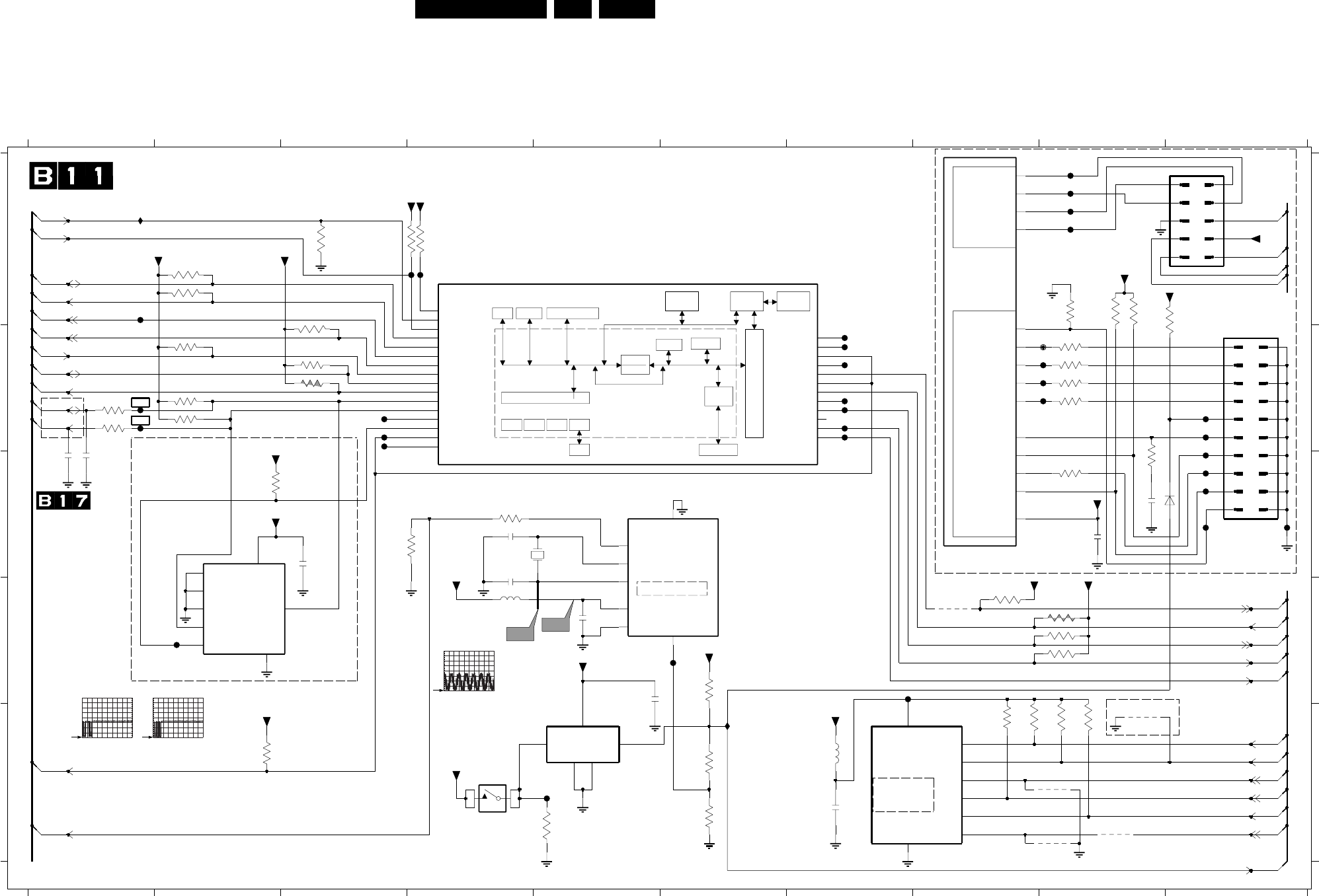
Circuit Diagrams and PWB Layouts 47ES1E AA 7.
SSB: Control
XTAL & RESET
UART
E-JTAG
DEBUGGING
INTERFACE
ANALOG TO
DIGITAL
CONVERTER
SLOW PI-BUS
A/D
PI-PI
BRIDGE
MIPS-
FAST PI-BUS
SRAM
CTRL
SRAM 96KB
SUB-SYSTEM
PR1910
GEN CLK
BLOCK MMI SDRAM
DCU
EBIU E-JTAG
UART GRAPHICS GEN.
SLAVE GROUP INTERFACE
TIMER I2C GPIO ADC
F538
3580
1K0
F544
3503 10K
3504
8
(FOR USE WITH SCART3 ONLY)
3504 A2
0201 A10 3507 B3
CONNECT
EEPROM
RES
E
2516 C1
2525 C3
(NVM)
B18-117
FOR FACTORY &
DEVELOPMENT USE ONLY
P50_INT
B18-114
B18-116
RES
F541 B7
B18-118
F540 B7
13.5MHZ
COMB
FOR SERVICE ONLY
F539 B7
F543 B7
F542 B7
F532 D2
F533 B7
F537 A4
EEPROM
F538 B3
100Mhz / 220R
F534 B3
F527 A1
B18-109
M24C64
B18-119
4570 E9
4571 E9
F524 A4
NC
B17-??
F512 C10
F513 C10
3570 E8
3571 E9
3572 E9
3573 E8
3580 C3
3581 C4
3582 E4
3583 E6
3586 E6
3590 D6
A
B
C
D
E
A
B
C
D
3515 B2
3518 A3
789 10
123456
3550 A9
3557 C9
910
I502 E6
I501 A1
B4-73
F582 E5
F570 E7
F584 D6
F509 B1
F510 C10
F511 C10
CONTROL
F551 B3F514 B10
F515 B10
F516 B9
F517 B9
F518 B9
F519 C10
F520 A9
F521 A9
F522 A9
F523 A9
3V2
3V2
0V
4V9
4V9
3V2
3V2
3V2
0V
0V9
0V9
3V2
2V6
0V
3V2
1V
0V
3V2
B12
6
7
B18-107
B1-7
12345
(TO CONNECTOR 0222)
B18-113
7300-D A8
TO 3D
F508 B1
FILTER
B18-111
B8-121
B18-120
7300-C A4
7300-A E8
F544 B7
F550 B9
B18-115
7581 E56589 C10
4573 E9
5570 E7
5583 D4
3561 D8
B18-110
SDM
B18-108
7525 D2
3510 B3
3511 B1
3512 B1
3513 B2
7300-K C63563 D8
3523 C3
3530 E3
3541 A10
3542 A9
3543 B9
3544 A9
3546 B9
3547 C9
3548 B9
3549 B9
B12
B3-53
100Mhz / 220R
B4-72
B18-106
0202 A10
1581 C5
1582 E4
2514 B1
3564 D9
3565 D8
2546 C9
2557 C9
2571 E7
2581 C4
2582 C4
2583 D5
2584 D5
3501 A3
3502 A4
3503 A2
4501 E9
4560 D8
3508 B2
3509 B3
10K
F511
VDDE
F534
3501
F523
F524
3507 10K
4K73508
F551
5570
F533
3515 4K7
F582
VDDCO
2571
100n
2581 22p F519
3509 4K7
CP15C
1581
F508
100n
2584
S5 S6
3563 10K
18p
2516
3510 4K7
F532
F550 19
2
20
34
56
78
9
TYPE
0201
1
10
11 12
13 14
15 16
17 18
F542
F541
F540
VDDE
33R
3548
VDDE
F521
4570
SKQR
1582
5583
3590
F509
1K0
4501
F515
3549 33R
F514
2582 22p
+5V2
F513
VDDE
2514
18p
TD1
AF18
TMS
AF17
TRST_
AF20
VDDE-JTAG
7300-D
AE20
DCLK
AD14
P3-4|RTS
AF15P3-5|CTS
AE15
P3-6|RXD
AD15
P3-7|TXD
AE21
PCST0
AD21PCST1
AD20
PCST2
AF21
TCK
AF22TD0
AF19
ADOC
22K
3586
33R
3547
3581 1K0
I501
I502
VDDE
F517
VDDE
10K
3582
F520
3557
+5V2
47R
3512 100R
4K7
3513
J26
ADC-VDDA
L25
ADC-VSSA
K23
ADC0
K24
ADC1
K25
ADC2
K26
ADC3
L23
ADC4
L24
ADC5
1MR
2SUB 5
VCC
4
VOUT
ADOC
7300-A
NE56610-45
7581
3GND
3570
2K7
3571
2K2
33R
+5V2
10K
+5V2
3543
F512
3544
+5V
P3-3
3565 10K
AD7 P1-4|GPT0-CNT
AF8 P1-5|GPT0-GATE
AE8 P1-6|GPT0-CAP
AD8 P1-7|GPT0-PWM
AF9P2-0|GPT1-CNT0
AE9P2-1|GPT1-CNT1
AF10P2-2|GPT1-GATE
AE10P2-3|GPT1-CAP0
AF11P2-4|GPT1-CAP1
AE11P2-5|GPT1-PWM
AF12P2-6|RCIN
AE12P2-7|RCOUT
AF13P3-0|RCRXPWR
AE13P3-1|RCCARDET
AD13P3-2
AF14
AC3 P0-0|INT0
AD1 P0-1|INT1
AD2 P0-2|INT2
AD3 P0-3|INT3
AE1 P0-4|INT4
AE2 P0-5|INT5
AF1 P0-6|INT6
AF2 P0-7|MPIF-INT
AF6 P1-0|SDA0
AE6 P1-1|SCL0
AF7 P1-2|SDA1
AD6 P1-3|SCL1
ADOC
7300-C
VDDE
10K
3518
33R
3546
10K
3573
4573
100n
2583
10K
+5V2
10K
3542
3541
F584
F518
VDDE
F543
10K3564
BAT254
6589
F527
+5V2
3583
18K
100n
2546
F537
10
2
34
56
78
9
0202 TYPE
1
4K7
3550
10K
3502
F570
10K3561
2525
100n
3530
100K
4560
A26 MPIFCLK
AB3
RESET-SEL
AC2
RESET_
AF5 XGND
AE4 XIN
AD4 XOUT
AF4 XVDD
F539
3511 100R
ADOC
7300-K
10K
10K
3572
4571
VDDE
VDDE
3523
10K
F510
F516
E0
1
E1
2
E2
3
SCL
6
SDA 5
VCC
8
VSS
4
WC_
7
2557 100p
7525
F522
SEL-2FH-SRC_STATUS3
DEGAUSS
RESET_3D
SDA1
SCL0
SDA1
SCL1
SDA0
SCL1
FRONT-DETECT
COMM_LINE
STAND-BY
RB
RST_JTAG
FLASH_RST
STATUS1_PIP-AFT_PIP-50-60HZ
F_REF
SEL-SVHS-RR_STATUS2
DTV_EXPANSION
ON-OFF-LED
SOUND-ENABLE
IRQ_MPIF
SEL-2FH-SRC_STATUS3
RC5
LIGHTSENSOR
KEYBOARD
SCL0
SDA0
SEL-IF-LL
POR_FLASH
CL 36532058_032.eps
211103
3139 123 5536.2
S5
500mV / div DC
50ns / div
F509
1 V / div DC
200µs / div
F508
1 V / div DC
500µs / div
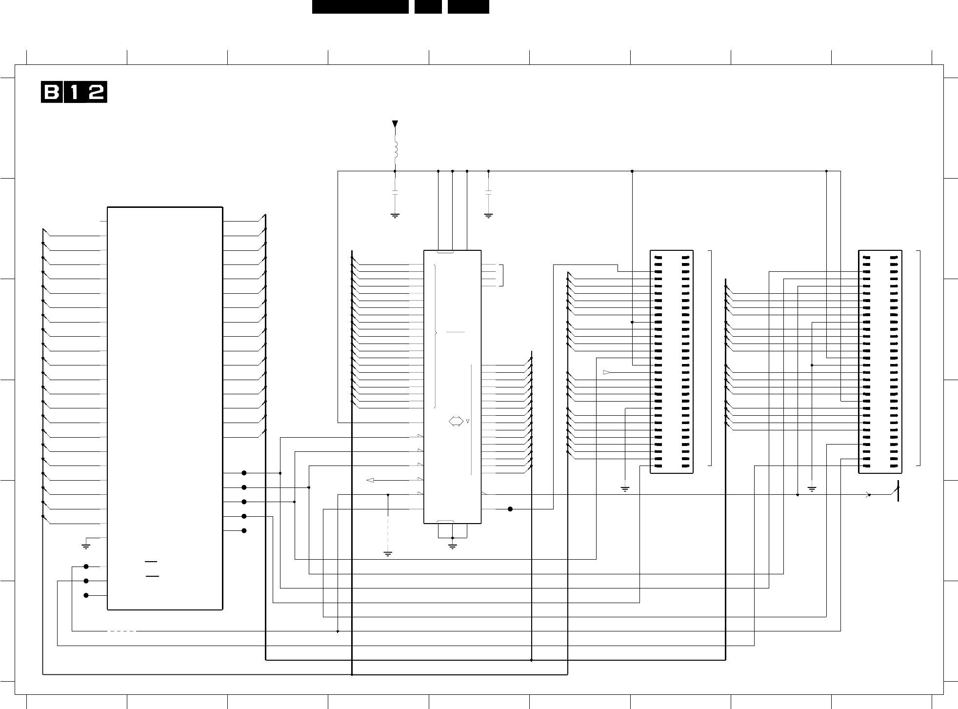
48ES1E AA 7.
Circuit Diagrams and PWB Layouts
SSB: Control-Memory Interface (EBIU)
EBIU
W
VPP
VDDQ
VSSQ
VDD
R
RB
VSS
19
18
15
1
2
3
4
5
6
7
8
D
0
9
10
11
12
13
14
3
4
1
E
G
RP
0
2
17
16
15
14
13
2048k-1
12
11
10
9
8
7
5
A
6
L
K
20
21
F794
35
NC
CONTROL-MEMORY INTERFACE (EBIU)
NC
NC
B11
NC
F799 E3
NC
F793 E3
B
4790 F1
NC
NC
100MHZ / 220R
A(1:21)
A
2792 B4
2793 B6
0290 B7
9
0291 B9
B
5792 A4
4791 E4
F792 F1
NC
A
F795 D3
NC
NC
7
C
D
E
F
F798 E3
21
F797 E5
NC
F794 E3
4
7790 B4
6
C
D
E
F
F790 E1
7300-E B1
F791 E1
D(0:15)
89
12345678
F799
F798
F792
F793
F791
F790
B7
EBIU-D14 C5
EBIU-D15 C4
EBIU-D2 A7
EBIU-D3 A9
EBIU-D4 C10
EBIU-D5 C8
EBIU-D6 B6
EBIU-D7 C7
EBIU-D8 A4
EBIU-D9 A6
EBIU-ENH|BAA
A11
EBIU-ENL|LBA
K2
EBIU-OE_ A3
EBIU-WE_ K1
EBIU-A5
E3
EBIU-A6
F2
EBIU-A7
G1
EBIU-A8
G3
EBIU-A9
H1
EBIU-BOOT8
C9
EBIU-CLK-OUT
B11
EBIU-CS0_ A2
EBIU-CS1_ C6
EBIU-CS2_ D3
EBIU-D0 B4
EBIU-D1 A5
EBIU-D10 A8
EBIU-D11 A10
EBIU-D12 B9
EBIU-D13
EBIU-A1
A1
EBIU-A10
G2
EBIU-A11
F3
EBIU-A12
F1
EBIU-A13
E1
EBIU-A14
D1
EBIU-A15
C1
EBIU-A16
B1
EBIU-A17
B3
EBIU-A18
H3
EBIU-A19
J2
EBIU-A2
C3
EBIU-A20
J1
EBIU-A21
J3
EBIU-A3
C2
EBIU-A4
D2
7300-E
ADOC
EBIU-A0|A22
K3
5792
59
6
60
7
8
9
2793
100n
47
48
49
5
50
51
52
53
54
55
56
57
58
35
36
37
38
39
4
40
41
42
43
44
45
46
23
24
25
26
27
28
29
3
30
31
32
33
34
12
13
14
15
16
17
18
19
2
20
21
22
0290
TYPE
1
10
11
F797
2792
100n
VDDE
F795
4791
4790
9
37
43
15
21
48
42
55
31
29
1
30
32
56
2
53
16
52
38
40
44
46
49
51
34
36
14
54
22
20
19
33
35
39
41
45
47
50
8
7
6
5
27
4
3
26
25
24
23
2Mx16
28
18
17
13
12
11
10
RAM
M58LW032A
7790
58
59
6
60
78
9
46
47 48
49
5
50
51 52
53 54
55 56
57
34
35 36
37 38
39
4
40
41 42
43 44
45
22
23 24
25 26
27 28
29
3
30
31 32
33
11 12
13 14
15 16
17 18
19
2
20
21
A(2)
A(12)
0291
TYPE
1
10
A(10)
A(11)
A(1)
A(13)
FLASH_RST
A(14)
A(15)
A(16)
A(17)
A(18)
A(19)
A(20)
A(21)
A(3)
A(4)
D(15)
D(7)
D(14)
D(6)
D(13)
D(5)
D(12)
D(4)
D(11)
D(3)
D(10)
D(2)
D(9)
D(1)
D(8)
D(0)
D(6)
D(7)
D(8)
D(9)
D(10)
D(11)
D(12)
D(13)
D(14)
A(20)
D(15)
A(21)
D(15)
A(21)
RB
FLASH_RST
A(5)
A(6)
A(7)
A(8)
A(9)
A(11)
A(12)
A(13)
A(14)
A(15)
A(17)
A(18)
A(19)
A(20)
A(16)
D(0)
D(1)
D(2)
D(3)
D(4)
D(5)
D(6)
D(7)
D(8)
D(9)
D(10)
D(11)
D(12)
D(13)
D(14)
D(0)
D(1)
D(2)
D(3)
D(4)
D(5)
A(1)
A(2)
A(3)
A(4)
A(5)
A(6)
A(7)
A(8)
A(9)
A(10)
A(11)
A(12)
A(13)
A(14)
A(16)
A(17)
A(18)
A(19)
A(15)
A(1)
A(2)
A(3)
A(4)
A(5)
A(6)
A(7)
A(8)
A(9)
A(10)
CL 36532058_033.eps
211103
3139 123 5536.2
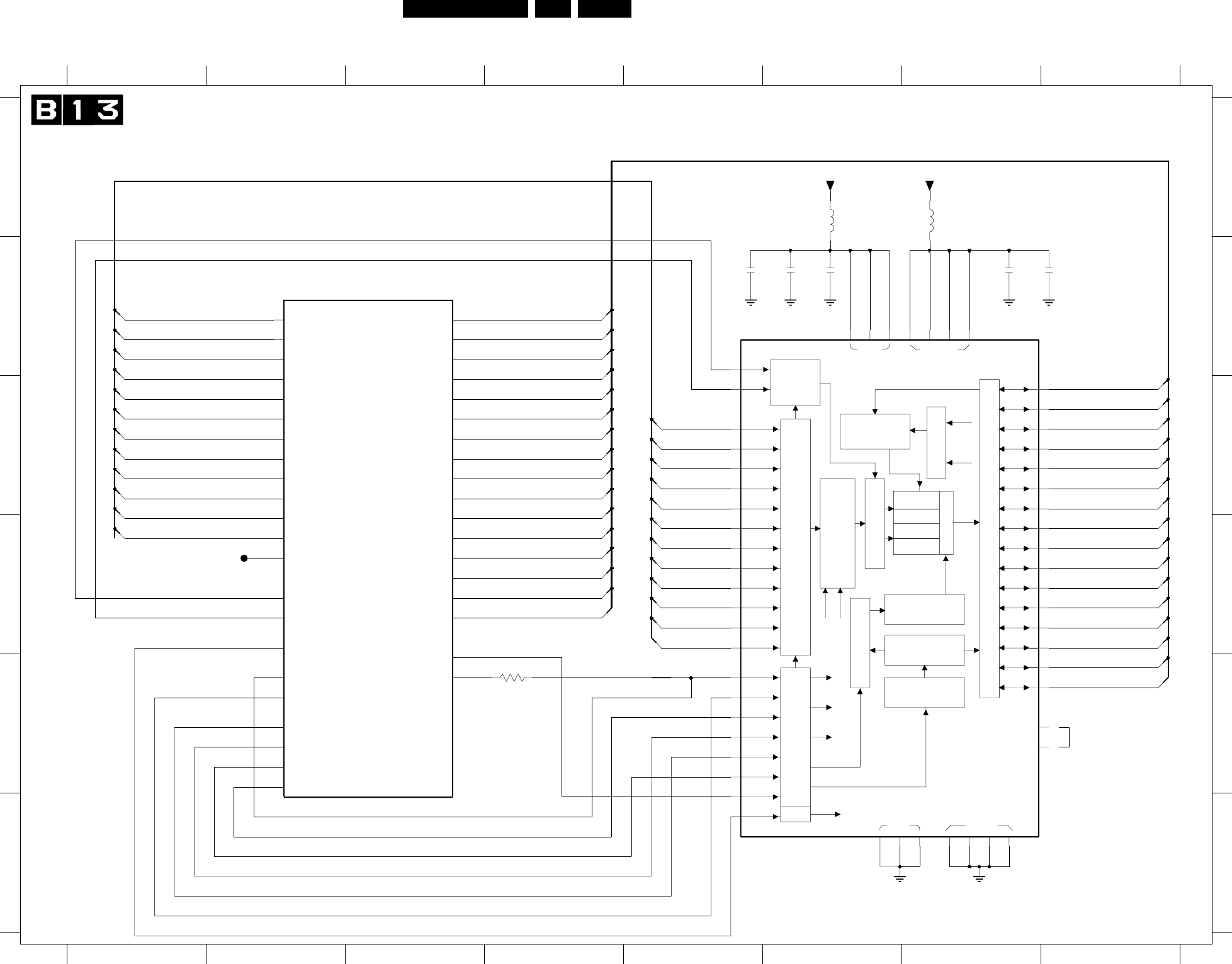
Circuit Diagrams and PWB Layouts 49ES1E AA 7.
SSB: Control-Memory Interface (SDRAM)
1M x 16
1M x 16
1M x 16
1M x 16
BANK
SELECT
OUTPUT BUFFER
VSS VSSQ
TIMING REGISTER
NC
ADDRESS REGISTER
LCKE
BURST LENGTH
LATENCY &
DECODER
COLUMN
LWCBR
LCAS
LWE
REGISTER
COL. BUFFER
LQDM
ROW DECODER
REFRESH COUNTER
ROW BUFFER
LDQM
LWE
I/O CONTROL
SENSE AMP
LRAS
VDD VDDQ
LCBR
DATA INPUT
REGISTER
PROGRAMMING
LRAS
LCBR
SDRAM
2733
100n
F730 D2
7730 B6
N.C.
2734 B7
3737 E4
5730 A6
5731 A7
B
C
D
E
F
2730 B6
2731 B6
2732 B5
78
A
7300-I B2
1 3452
F
A
220R
E
CONTROL-MEMORY INTERFACE (SDRAM)
6
76
2733 B7
1
B
C
D
4
8
5
100Mhz /
220R
32
100Mhz /
2731
100n
5730
2732
VDDE
100n 100n
2734
52
16 WE_
3737
33R
RAS_
39 UDQM
11427394349
28 41 54 6 12 46
47
DQ12 48
DQ13 50
DQ14 51
DQ15 53
5DQ2
7DQ3
8DQ4
10DQ5
11DQ6
13DQ7
DQ8 42
DQ9 44
LDQM15
36
NC|RFU 40
18
26
A429
A530
A631
A732
A833
A934
20 BA0
BA121
17 CAS_
CKE37
CLK38
CS_19
2DQ0
4DQ1
DQ10 45
DQ11
SDRAM-RASN
A14
SDRAM-UDQM
A23 SDRAM-WEN
7730
K4S641632D
A023
A124
22 A10|AP
A1135
A225
A3
SDRAM-D10
B15
SDRAM-D11
C15
SDRAM-D12
C16
SDRAM-D13
A16
SDRAM-D14
A17
SDRAM-D15
C26
SDRAM-D2
A25
SDRAM-D3
C24
SDRAM-D4
B24
SDRAM-D5
A24
SDRAM-D6
C23
SDRAM-D7
B14
SDRAM-D8
C14
SDRAM-D9
B23 SDRAM-LDQM
A22
SDRAM-A3
C18 SDRAM-A4
B18 SDRAM-A5
A18 SDRAM-A6
C17 SDRAM-A7
B17 SDRAM-A8
C11 SDRAM-A9
B21 SDRAM-BS0
A21 SDRAM-BS1
C22 SDRAM-CASN
C12 SDRAM-CKE
C13 SDRAM-CLK-IN A13
SDRAM-CLK-OUT
C21 SDRAM-CSN
B26
SDRAM-D0
C25
SDRAM-D1
A15
ADOC
7300-I
B20 SDRAM-A0
A20 SDRAM-A1
C20 SDRAM-A10
A12 SDRAM-A11
B12 SDRAM-A12
C19 SDRAM-A2
A19
VDDE
5731
2730
F730
100n
SD(11)
SD(10)
SD(9)
SD(8)
SD(7)
SD(6)
SD(5)
SD(4)
SD(3)
SD(2)
SD(1)
SD(0)
SD(0)
SD(1)
SD(2)
SD(3)
SD(4)
SD(5)
SD(6)
SD(7)
SD(8)
SD(9)
SD(10)
SD(11)
SD(12)
SD(13)
SD(14)
SD(15)
SA(11)
SA(10)
SA(9)
SA(8)
SA(7)
SA(6)
SA(5)
SA(4)
SA(3)
SA(2)
SA(1)
SA(0)
SA(0)
SA(1)
SA(2)
SA(3)
SA(4)
SA(5)
SA(6)
SA(7)
SA(8)
SA(9)
SA(10)
SA(11)
SD(15)
SD(14)
SD(13)
SD(12)
CL 36532058_034.eps
030903
3139 123 5536.2
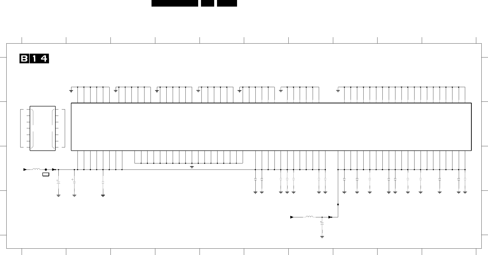
50ES1E AA 7.
Circuit Diagrams and PWB Layouts
SSB: ADOC Supply
SUPPLY
NC
NC
2601 100n
VDDE
+1V8
30R
5600
2607
100n
2609
7300-L B65600 C1
2649 C2 5601 D7 7300-M A1
9
RES
F601 C12629 C6
100Mhz /
2628 C72612 C9
2615 C8
2618 C8
2620 C8
2644 D7
2645 C1
A
NC
NC
10
I601 D8
45678
2600 C10
2601 C10
2604 C10
23
2611 C9
1234
2622 C7 2630 C6
2633 C6
2634 C6
2638 C22607 C9
2609 C9
100Mhz/
1
10956
2623 C7
78
C
B
ADOC SUPPLY
D
A
B
C
D
2633
100n100n
2634 2622
100n
100n2623
2615
2629 100n
100n100n
2630
2628 100n
VDDCO
2645
10u 16V
+3V3
100u
2649
F601
100n
26002611
100n
2604 100n
100n
2612
2644
22u 16V
100n
100n
2638
2618
100n100n
2620
L4
U24
U23
T25
T24
T23
P4
V4
F26
G23
R24
R25 V25
U25
D7 VSSIS18
K4 VSSIS2
AD5 VSSIS3
AE5 VSSIS4
AC7 VSSIS5
AD9 VSSIS6
AD10 VSSIS7
AD12 VSSIS8
AC15 VSSIS9
ADOC
7300-M
T14
VSSE54
T15
VSSE55
T16
VSSE56
B10
VSSE6
B8
VSSE7
B5
VSSE8
B2
VSSE9
G4 VSSIS1
M24 VSSIS10
M25 VSSIS11
L26 VSSIS12
D23 VSSIS13
D20 VSSIS14
D18 VSSIS15
D14 VSSIS16
D12 VSSIS17
B16
VSSE4
P12
VSSE40
P13
VSSE41
P14
VSSE42
P15
VSSE43
P16
VSSE44
R11
VSSE45
R12
VSSE46
R13
VSSE47
R14
VSSE48
R15
VSSE49
B13
VSSE5
R16
VSSE50
T11
VSSE51
T12
VSSE52
T13
VSSE53
L15
VSSE25
L16
VSSE26
M11
VSSE27
M12
VSSE28
M13
VSSE29
B19
VSSE3
M14
VSSE30
M15
VSSE31
M16
VSSE32
N11
VSSE33
N12
VSSE34
N13
VSSE35
N14
VSSE36
N15
VSSE37
N16
VSSE38
P11
VSSE39
E2
VSSE10
H2
VSSE11
T4
VSSE12
AE7
VSSE13
AD11
VSSE14
AE14
VSSE15
AC20
VSSE16
AC21
VSSE17
V24
VSSE18
T26
VSSE19
B22
VSSE2
J24
VSSE20
L11
VSSE21
L12
VSSE22
L13
VSSE23
L14
VSSE24
D8 VDDE7
D5 VDDE8
D4 VDDE9
J4 VDDI1
D15 VDDI10
D11 VDDI11
D9 VDDI12
AB4 VDDI2
AC9 VDDI3
AC12 VDDI4
AC14 VDDI5
R26 VDDI6
M23 VDDI7
D24 VDDI8
D21 VDDI9
B25
VSSE1
H4 VDDE11
AC4 VDDE12
AC5 VDDE13
AC6 VDDE14
AC11 VDDE15
AC17 VDDE16
AC18 VDDE17
AC19 VDDE18
V23 VDDE19
D22 VDDE2
U26 VDDE20
J25 VDDE21
D19 VDDE3
D16 VDDE4
D13 VDDE5
D10 VDDE6
ADOC
7300-L
F4 VDDCO1
AC8 VDDCO2
AC10 VDDCO3
AC13 VDDCO4
AC16 VDDCO5
M26 VDDCO6
D17 VDDCO7
D6 VDDCO8
D25 VDDE1
E4 VDDE10
5601
30R
I601
CL 36532058_035.eps
030903
3139 123 5536.2
1V8 DC
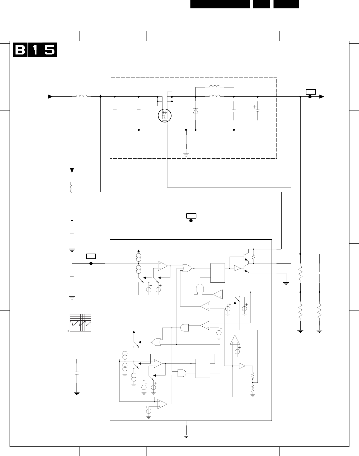
Circuit Diagrams and PWB Layouts 51ES1E AA 7.
SSB: Low Voltage Supply ADOC
R
S
Q
Q_
F2
VCC
G2
G4
G3
G5
A2
A3
A1
A4
A6
G1
F1
Q_
QR
VCC
S
+1V8
1u
5654
RES
RES
F652 D2
1
RES
5
with star point ground
Compts. Close to each other
LOW VOLTAGE SUPPLY - ADOC
I651 A2
2
F
A
B
6651 A3
5659 C2
C
D
E
F
2651 A4
12
5652 A4
7650 C2
7651 B3
2657 D2
2655 A2
2656 E2
F651 A5
F650 C3
2652 A4
2654 A2
4V9 1V7
2V9
1V9
2V5
1V3
2658 D5
E
345
A
B
C
D
34
3651 D5
3652 D5
3653 D5
5651 A4
2659 C2
5654 A2
10u
5651
2655
10u
3651
1K2
5652
10u
+5V2
100n
2658
+3V3
2K7
3652
6u8
5659
220n
2659
100p
2657
100u
2651
SS14
6651
10u
2652
100n
2656
I651
F652
F650
F651
3653
2K7
1
2
3
10u
2654
VGATE 1
7651
STS5PF30L
5
6
7
8
4
CS51033YDR8
7650
COSC3
7CS
GND
4
PGND 2
VC 8
VCC
6
VFB 5
CL 36532058_036.eps
211103
3139 123 5536.2
1V8 DC
F652
500mV / div DC
500ns / div
3V2 DC
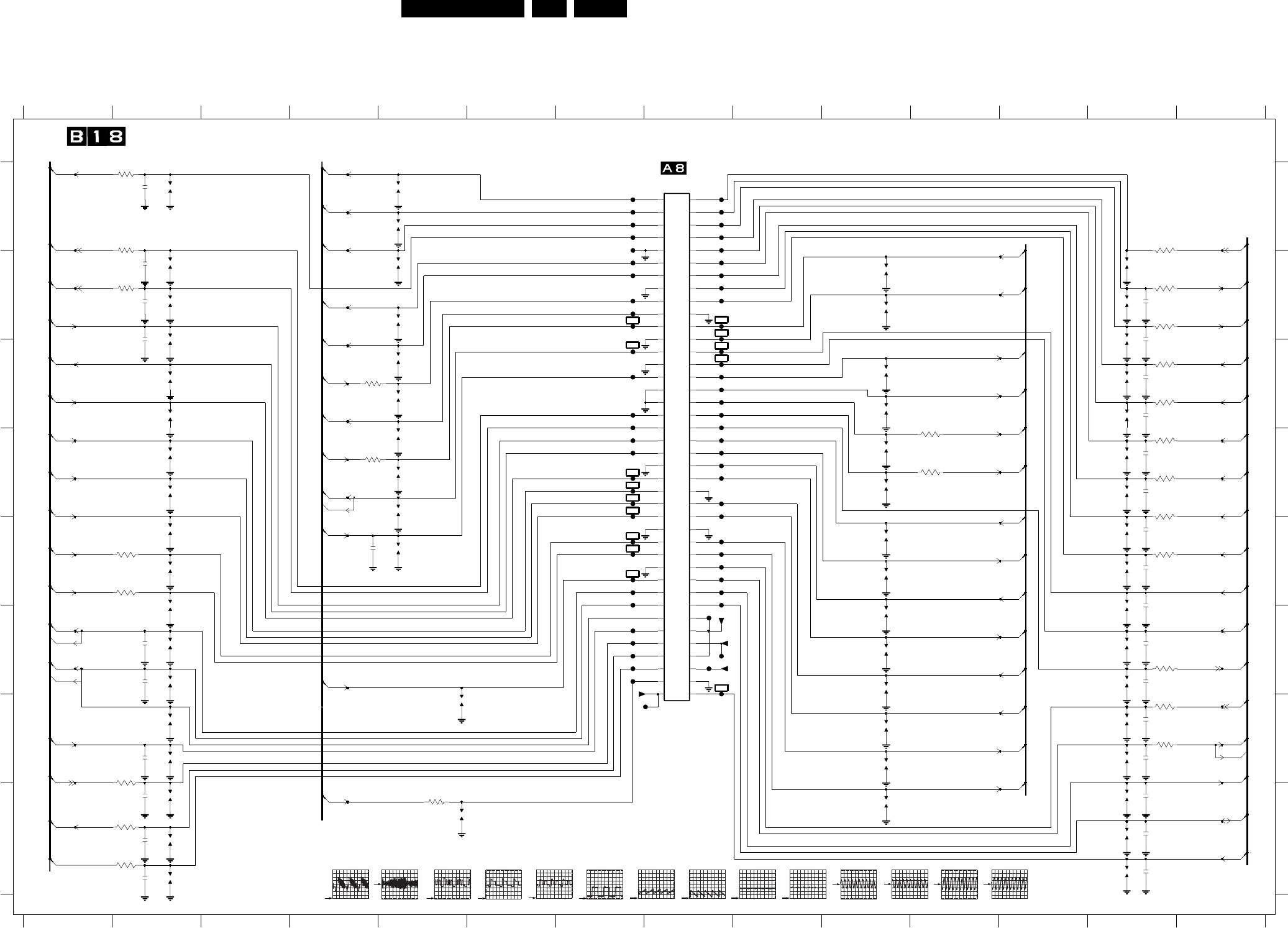
52ES1E AA 7.
Circuit Diagrams and PWB Layouts
SSB: Connector Interface
1975
1920
ON-OFF-LED
RC5
KEYBOARD
DEGAUSS
PIP_AUDIO
2951 G13
B11-116
2950 G13
2968 E13
2962 F13
F941 F8
F943 F8
F944 F8
F947 F8
F948 E8
F949 E8
F950 E8
F951 E8
2967 F13
2972 E13
2937 H2
2938 H2
2941 H13
2948 H131955 G10
TO/FROM 1205 OF LSSB
1906 B5
1903 B5
B10-100
10
B8-87
C
B7-79
1907 C5
8
B4-71
9
1909 C5
1902 A5
B3-66
B2-24
4567
1962 F13
1953 G10
1958 F10
1959 F10
1961 E10
1918 B2
B3-61
B3-54
B3-52
B3-51
B3-57
1956 F10
1960 E10
2935 G2
2936 H21950 G13
1951 G13
1952 H10
2915 E5
2918 B2
2919 B2
2904 A2
2973 E13
F902 A7
F903 A7
F904 A7
F905 A7
F906 B7
F907 B7
F909 B7
F910 B7
3911 D4
3918 A2
1974 D13
1975 D13
1976 C13
1977 C131931 G6
1979 B13
1980 B13
MPIF
B8-83
1921 C2
B10-99
1924 D2
B11-118
1919 B2
1920 B2
1923 C2
1925 D2 2920 B2
2932 F2
2933 F21948 H13
1949 H13
1910 D5
1911 D5
1913 D5
1915 E5
3
F936 F7
B11-115
F965 C8
SSB-CONNECTOR INTERFACE
B5-45
B10-98
B10-97
B10-96
F966 C8F960 D8
F962 C8
F964 C8
F963 C8
B11-113
B8-89
F955 D8
F956 D8
F958 D8
F959 D8
3975 D13
F961 D8
B3-67
F937 F7
F938 F7
F939 F7
F940 G8
B2-19
B2-20
F901 A7
3980 A13
3979 B13
3977 C13
3978 B13
3976 C13
F952 E8
F953 E8
3964 D11
3972 E13
3973 D13
3974 D13
2949 H13
B11-107
B10-95
1937 H2
1936 H2
B3-50
2974 D13
2975 D13
2976 C13
2977 C13
2978 C13
2979 B13
3904 A2
3909 C4
1972 E13
1973 E13
B3-56
1926 E2
1928 E2
1929 E2
9
1932 F2
1933 F2
1934 G2
1935 G2
B
ADOC
B11-121
B2-22
B
B11-119
E
F
G
B2-16
1938 H2
1939 H6
1941 H13
D
C
H
B9-91
12
B2-23
B3-49
B11-111
F923 D7
F929 E7
F928 E7
B8-82
F935 F7
F933 E7
F932 E7
B7-75
F924 D7
F925 D7
F926 D7
F967 C8
F968 C8F915 C7
F918 C7
F919 C7
F920 D7
3937 H2
3938 H2
B7-76
B7-77
3951 G13
B3-60
1978 C13
B11-114
MPIF
3962 F13
3963 D11
B8-88
3950 G13
3939 H5 F911 B7
F913 C7
3919 B2
3928 E2
3929 E2
3936 G2
ADOC
14
A
B9-92
B11-106
1963 D10
1964 D10
1965 C10
1966 C10
1967 F13
1968 E13
1969 B10
1970 B10
B3-48
B10-94
5678
1901 A5
10 11 12 13
B1-9
F978 A8
F977 A8
F976 A8
F931 E7
F969 B8
F970 B8
F979 A8
F980 A8
F921 D7
F972 B8
F973 B8
F974 B8
F975 B8
1904 A2
B11-120
B11-112
B11-108
B11-117
B7-78
B2-18
B2-30
B11-109
B2-29
B1-5
B1-11
B4-71
34
F
G
H
0230 A8
B2-17
B11-110
1972
11 12 13 14
12
D
E
A
B8-84
1934
1901
1913
1918
F961
1970
F964
3972
100R
1n
2972
F973
F974
1936
1973
1921
1965
F947
2950
100p
1915
1950
1906
100R
3980
3928
1980
1928
100R
1937
3962
100R
1961
1923
100p
2919
100p
2933
3975
100R
2975
1n
100R
3976
1n
2976
1978
100R
3909
3979
100R
1953
1956
1938
1959
1960
2949
100p
100R
2935
100p
F919
3963
F920
1966
2978
100p
1952
F939
2951
1n
1958
100p
2938
1962
F967
2918
100p
F966
100p
2904
3904
100R
3978
100R
1n
2968
1939
F948
F901
F941
76
77
78
79
8
80
9
61
62
63
64
65
66
67
68
69
7
70
71
72
73
74
75
47
48
49
5
50
51
52
53
54
55
56
57
58
59
6
60
32
33
34
35
36
37
38
39
4
40 41
42
43
44
45
46
18
19
2
20
21
22
23
24
25
26
27
28
29
3
30
31
CON-BOARD-EDGE
0230
1
10
11
12
13
14
15
16
17
F909
1941
F977
F978
F923
F921
F924
F925
F931
F929
3951
100R
F938
F959
F960
1n
2962
F958
F975
+3V3
2937
100p
2920
82p
1974
F965
3919
100R
3918
100R
1949
100R
3939
F949
F903
F902
F905
F907
F911
F910
100R
3974
1935
F918
1948
F976
100p
F928
F926
1932
2932
1n
1967 2967
19681929
1969
3936
+5V2
100R
3973
+8V
100R
1n
2974
1963
1951
1964
2977
100p
F933
F932
1909
100R
3929
1907
100R
1n
2973
3938
+5V
1903
1904
2948
100p
F970
1933
F969
F944
100R
3950
1979
1931
1955
3937
100R
F979
1919
3964
1911
100R
100p
2979
1977
F953
3911
100R
1910
F963
1925
F962
1924
1902
F972
F935
F943
F936
100p
2941
F937
F951
F952
F950
F955
F956
100p
2915
F906
F904
100p
2936
F968
F915
F913
F940
1976
F980
3977
100R
1926
Y-CVBS-FRONT-IN
B-SC1-IN_U-IN
R-SC1_V-IN
Y-CVBS-SC2_AV2-IN
C-SC2_SVHS-IN
CVBS-SC1_AV1-IN
CVBS_TER_OUT
IF-TER
AGC
G-SC1-IN_Y-IN
FBL-SC1-IN
STATUS1_PIP-AFT_PIP-50-60HZ
SEL-SVHS-RR_STATUS2
R-SC1_AV1-IN
R-SC2-OUT
R-SC2_AV2-IN
L-SC1_AV-OUT
L-SC2-OUT
L-SC2_AV2-IN
L-SC1_AV1-IN
SOUND-ENABLE_1
SOUND-ENABLE
POR_FLASH_1 POR_FLASH
SCL0
SDA0
Y-SCAVEM
AUDIO-L
AUDIO-SW
AUDIO-C
AUDIO-SURR
R-CL_VL-OUT
L-CL_VL-OUT
HEADPHONE-R
HEADPHONE-L
R-FRONT-IN
L-FRONT-IN
C-FRONT-IN
FRONT-DETECT
R-SC1_AV-OUT
CVBS-SC2_MON-OUT
COMM_LINE
CUTOFF
B-CRT
G-CRT
R-CRT
LINEDRIVE1
FRAMEDRIVE+
FRAMEDRIVE-
EW-DRIVE
HFB_X-RAY-PROT
EHT-INFO
TILT
STAND-BY
LIGHTSENSOR
DTV_EXPANSION
AUDIO-R
CL 36532058_037.eps
211103
3139 123 5536.2
F911
500mV / div DC
20µs / div
F913
500mV / div AC
10µs / div
F967
200mV / div AC
1ms / div
F941
2 V / div DC
20µs / div
F931
1 V / div DC
5ms / div
F929
500mV / div DC
5ms / div
F928
500mV / div DC
5ms / div
F926
1 V / div DC
10µs / div
F925
1 V / div DC
10µs / div
F969
500mV / div AC
1ms / div
F968
200mV / div AC
1ms / div
F970
500mV / div AC
1ms / div
F923
1 V / div DC
10µs / div
F924
1 V / div DC
10µs / div
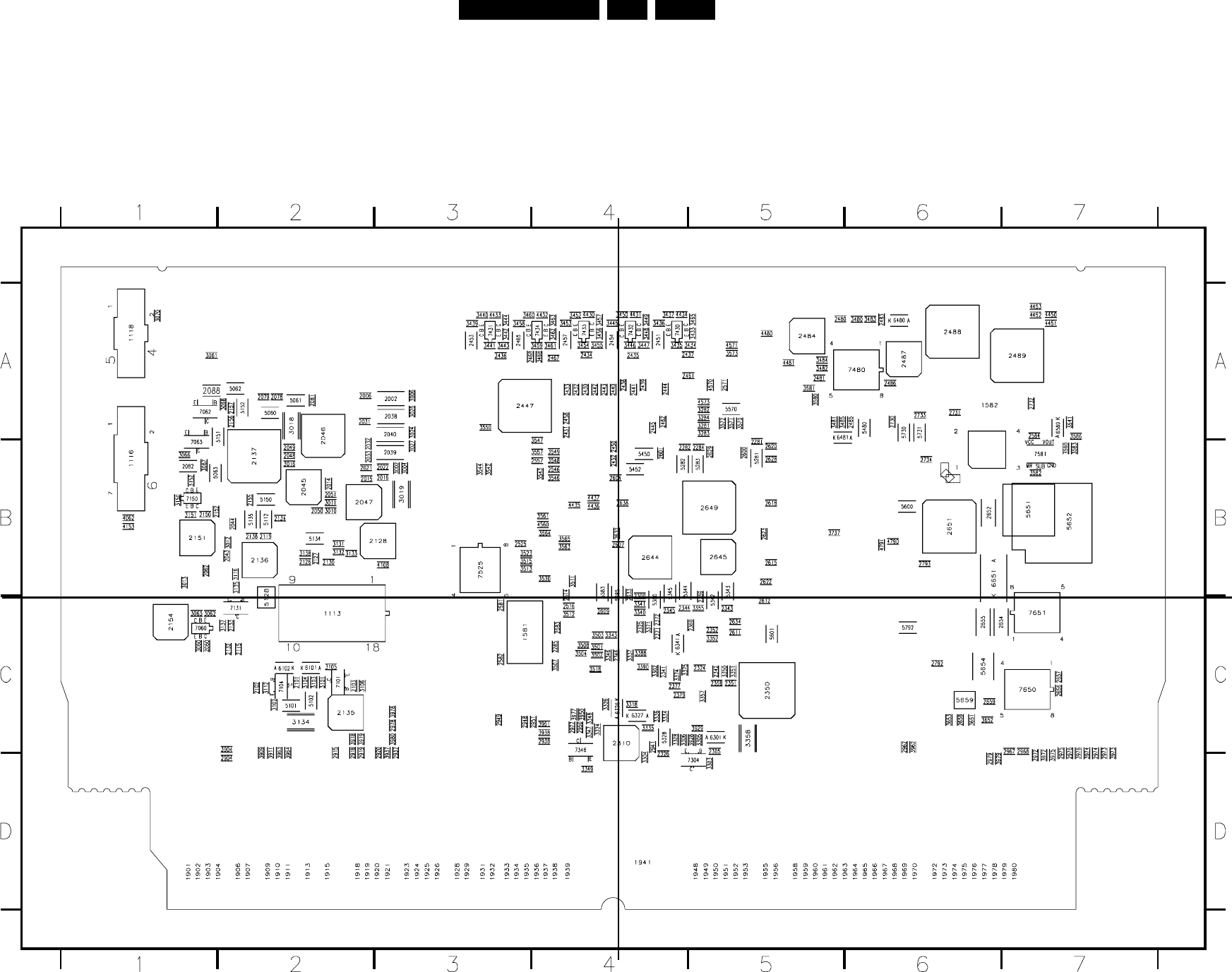
Circuit Diagrams and PWB Layouts 53ES1E AA 7.
Layout SSB (Overview LOT Side)
CL 36532058_038.eps
030903
Part 1
CL 36532058_38a.eps
Part 2
CL 36532058_38b.eps
Part 3
CL 36532058_38c.eps
Part 4
CL 36532058_38d.eps
3139 123 5536.2
1113 C2
1116 B1
1118 A1
1581 C3
1582 A6
2002 A3
2006 A2
2014 B2
2015 B2
2016 B3
2021 B2
2022 B3
2031 A2
2032 B2
2033 B2
2038 A3
2039 B3
2040 A3
2043 B2
2044 B2
2045 B2
2046 A2
2047 B2
2048 B2
2049 B2
2050 B2
2051 B2
2060 C1
2062 B1
2078 A2
2079 A2
2081 A2
2082 B1
2088 A1
2101 C2
2102 C2
2103 C2
2115 C2
2119 B2
2126 B2
2127 B2
2128 B3
2130 B2
2132 C2
2133 C2
2134 B2
2135 C2
2136 B2
2137 B2
2138 B2
2150 B1
2151 B1
2152 B1
2154 C1
2155 B2
2156 A2
2157 A2
2281 B5
2282 B4
2284 B5
2285 C4
2300 B4
2305 C5
2310 C4
2324 C5
2325 C4
2326 D4
2341 C4
2342 C5
2343 C5
2344 C4
2345 C4
2346 C4
2350 C5
2351 C5
2352 C5
2358 C5
2359 C5
2360 C5
2371 C4
2372 C4
2377 C4
2379 C4
2430 A4
2431 A4
2432 A4
2433 A4
2434 A4
2435 A4
2436 A3
2437 A5
2438 A4
2439 A4
2440 A4
2441 A4
2442 A4
2443 A4
2444 A4
2445 A4
2447 A3
2450 B4
2451 A4
2452 B4
2453 A3
2454 A4
2457 A4
2458 A4
2461 A5
2462 A4
2465 A3
2467 A4
2468 A3
2480 A5
2481 A5
2483 A6
2484 A5
2485 A6
2486 A6
2487 A6
2488 A6
2489 A7
2514 B4
2516 C4
2525 B3
2546 B4
2557 B4
2571 A5
2581 C3
2582 C3
2583 C4
2584 A7
2600 B5
2601 B4
2604 B4
2607 B4
2609 C4
2611 C5
2612 C5
2615 B5
2618 B5
2620 B5
2622 B5
2623 B5
2628 B5
2629 B5
2630 B4
2633 B4
2634 C5
2638 B4
2644 B4
2645 B5
2649 B5
2651 B6
2652 B6
2654 C6
2655 C6
2656 C7
2657 C7
2658 C6
2659 C6
2730 A6
2731 A6
2732 A7
2733 A6
2734 B6
2792 C6
2793 B6
2904 D2
2915 D2
2918 D2
2919 D2
2920 D3
2937 D3
2938 C4
2941 C4
2948 C3
2949 C3
2950 C4
2951 C4
2962 C6
2967 C7
2968 C7
2972 D7
2973 D7
2974 D7
2975 D7
2976 D7
2977 C4
2978 C3
2979 D6
3002 B3
3004 B3
3006 A3
3010 B2
3011 B2
3012 B2
3013 B1
3016 B2
3018 A2
3019 B3
3024 A3
3026 A3
3027 B3
3060 C1
3061 A1
3062 C1
3063 C1
3066 B1
3067 B1
3068 A2
3070 A1
3101 C2
3102 C2
3103 C2
3104 C2
3105 C2
3106 C2
3112 C2
3116 B2
3131 B2
3132 B2
3133 B2
3134 C2
3135 B2
3137 C2
3138 B2
3150 B1
3151 B1
3152 B1
3281 A5
3282 A5
3283 A5
3284 A5
3302 C4
3303 D5
3304 D4
3305 C5
3306 C4
3318 C4
3324 C4
3326 C4
3328 C4
3334 C4
3335 C4
3336 C4
3337 C4
3340 C4
3341 C4
3343 C4
3346 C4
3347 C4
3348 C4
3349 D4
3350 C5
3351 C5
3352 C5
3355 C5
3357 C5
3358 C5
3371 C4
3374 C4
3375 C4
3388 C4
3390 C4
3433 A5
3434 A5
3435 A4
3436 A4
3437 A4
3439 A3
3440 A3
3441 A3
3442 A3
3443 A3
3444 A3
3445 A4
3446 A4
3447 A4
3448 A4
3449 A4
3450 A4
3452 A4
3453 A4
3454 A4
3455 A4
3456 A4
3457 A4
3458 A3
3459 A4
3460 A3
3461 A4
3462 A4
3463 A4
3465 A5
3468 A4
3480 A6
3481 A5
3482 A5
3483 A6
3484 A5
3485 A5
3501 C4
3502 C4
3503 C4
3504 C4
3507 C4
3508 C4
3511 B4
3512 C4
3513 B3
3515 B3
3518 C4
3523 B3
3530 B4
3541 A7
3542 B3
3543 B4
3544 B3
3546 B4
3547 B4
3548 B4
3549 B4
3550 A3
3557 B4
3561 B4
3563 B4
3564 B4
3565 B4
3570 A5
3571 A5
3572 A5
3573 A5
3580 A5
3581 A5
3582 B7
3583 B7
3586 A7
3590 B7
3651 C6
3652 C6
3653 C6
3737 B5
3904 C2
3909 D2
3911 D2
3918 C2
3919 C2
3928 C5
3929 C5
3937 D3
3938 C4
3950 C4
3951 C4
3962 C6
3963 D2
3964 D2
3972 D7
3973 D7
3974 D7
3975 D7
3976 D7
3977 C4
3978 C3
3979 D6
3980 C3
4062 B1
4108 B3
4153 B1
4430 A4
4431 A4
4432 A4
4433 A3
4434 A4
4435 B4
4436 B4
4437 B4
4450 A7
4451 A7
4452 A7
4453 A7
4480 A5
4481 A5
4560 B4
4570 A5
4571 A5
4573 A5
4790 B6
4791 B6
5060 A2
5061 A2
5062 A2
5063 B1
5101 C2
5102 C2
5112 B2
5128 C2
5134 B2
5135 B2
5150 B2
5151 A2
5152 A2
5281 B5
5282 B4
5283 B5
5285 B4
5300 C4
5328 C4
5342 C5
5343 B5
5344 B4
5345 B4
5450 B4
5452 B4
5480 A6
5570 A5
5583 B4
5600 B6
5601 C5
5651 B7
5652 B7
5654 C6
5659 C6
5730 A6
5731 A6
5792 C6
6101 C2
6102 C2
6301 C5
6326 C4
6327 C4
6341 C4
6480 A6
6481 A5
6589 A7
6651 B6
7060 C1
7062 A1
7063 B1
7101 C2
7104 C2
7131 C2
7150 B1
7304 D5
7346 C4
7430 A4
7431 A3
7432 A4
7433 A4
7434 A4
7480 A6
7525 B3
7581 B7
7650 C7
7651 C7
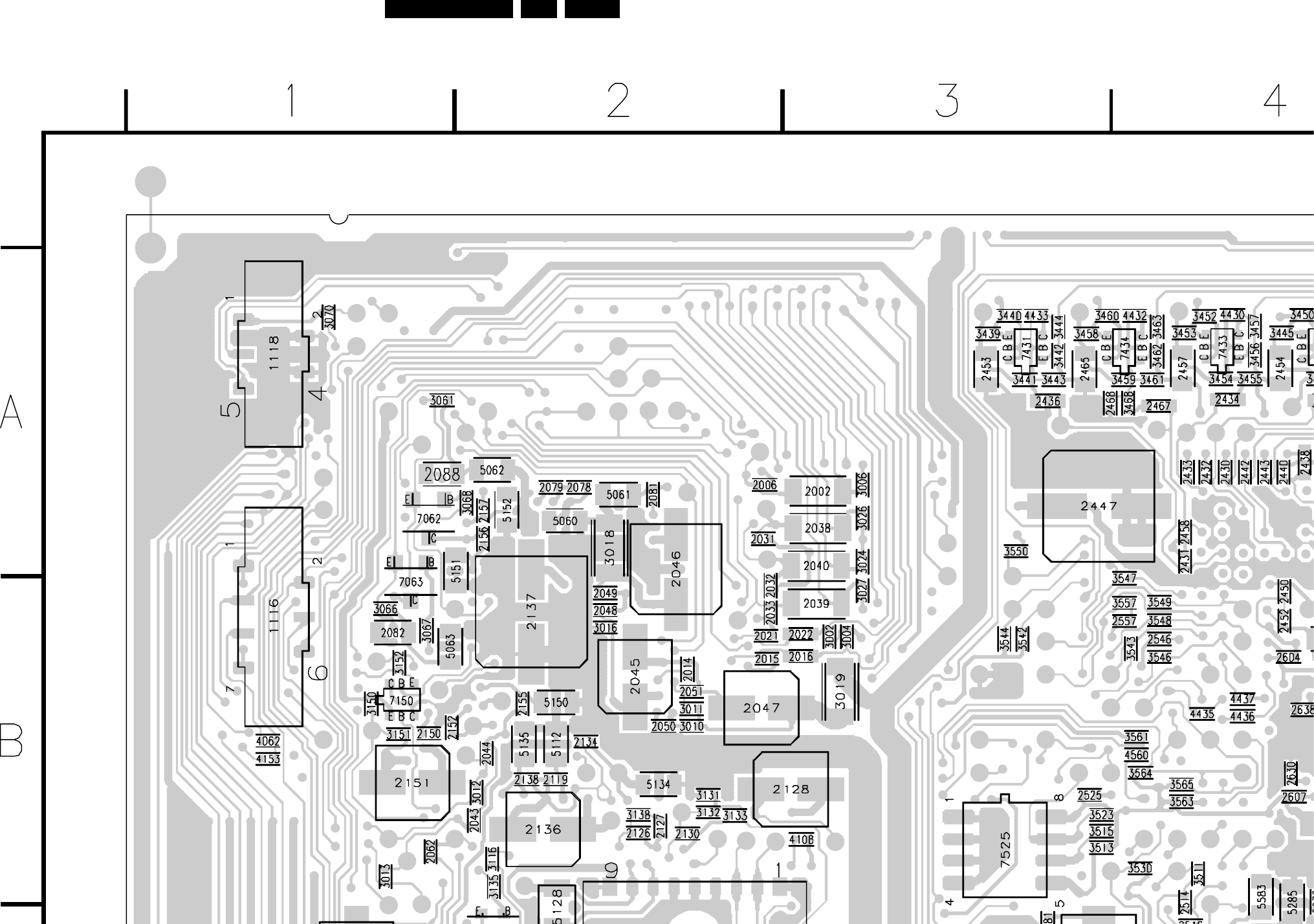
54ES1E AA 7.
Circuit Diagrams and PWB Layouts
Layout SSB (Part 1 LOT Side)
CL 36532058_38a.eps
030903
Part 1
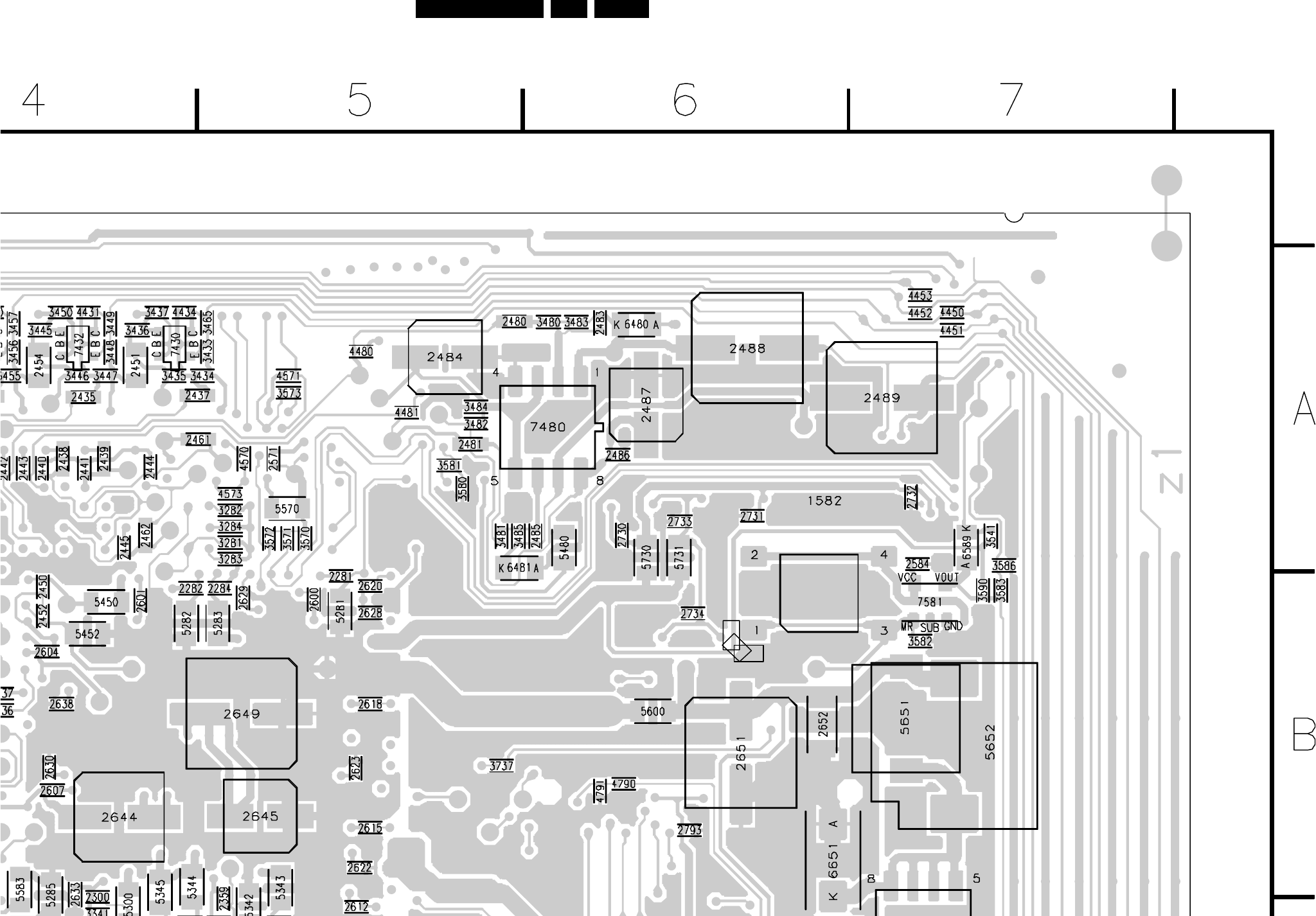
Circuit Diagrams and PWB Layouts 55ES1E AA 7.
Layout SSB (Part 2 LOT Side)
CL 36532058_38b.eps
030903
Part 2
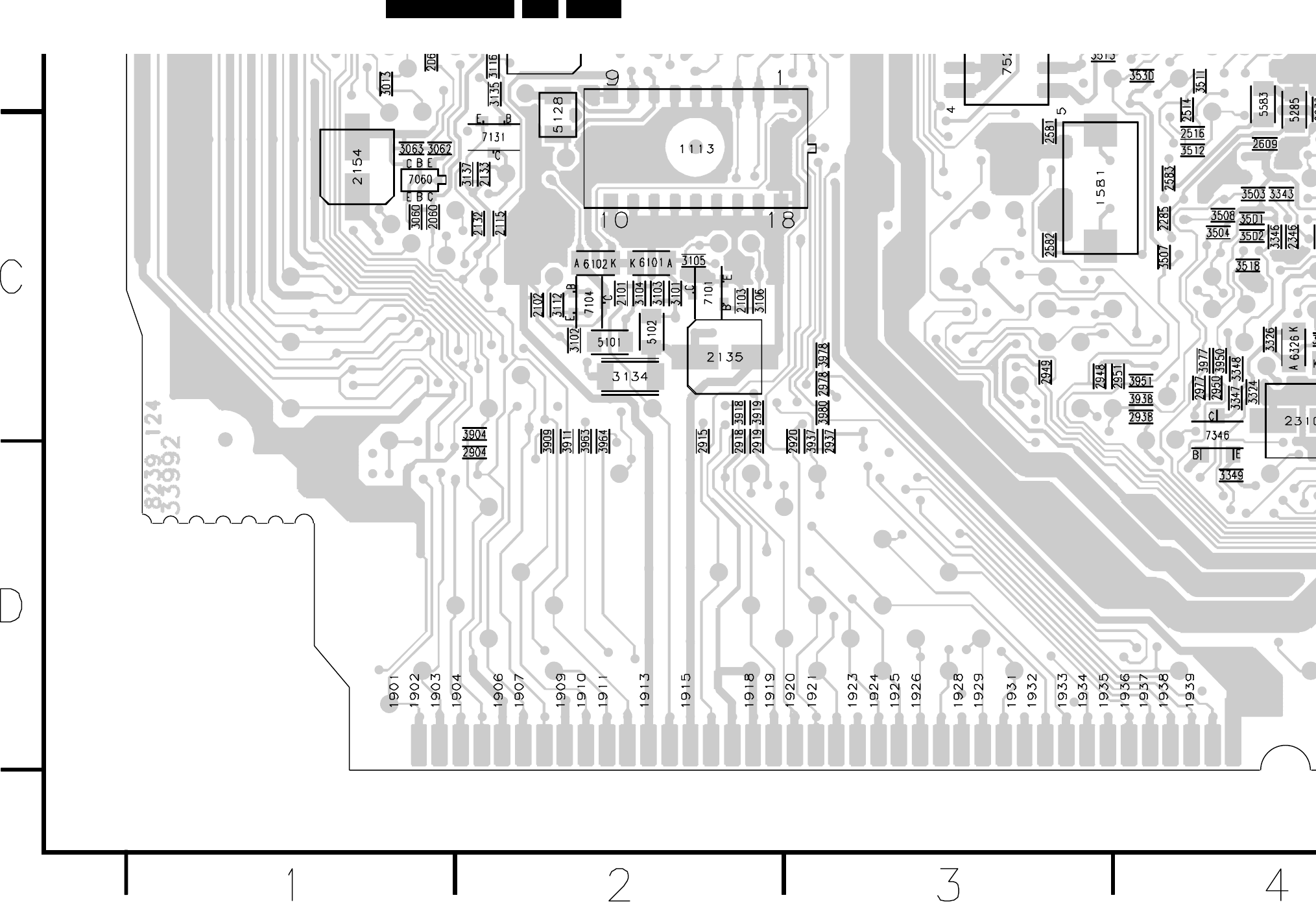
56ES1E AA 7.
Circuit Diagrams and PWB Layouts
Layout SSB (Part 3 LOT Side)
CL 36532058_38c.eps
030903
Part 3

Circuit Diagrams and PWB Layouts 57ES1E AA 7.
Layout SSB (Part 4 LOT Side)
CL 36532058_38d.eps
030903
Part 4
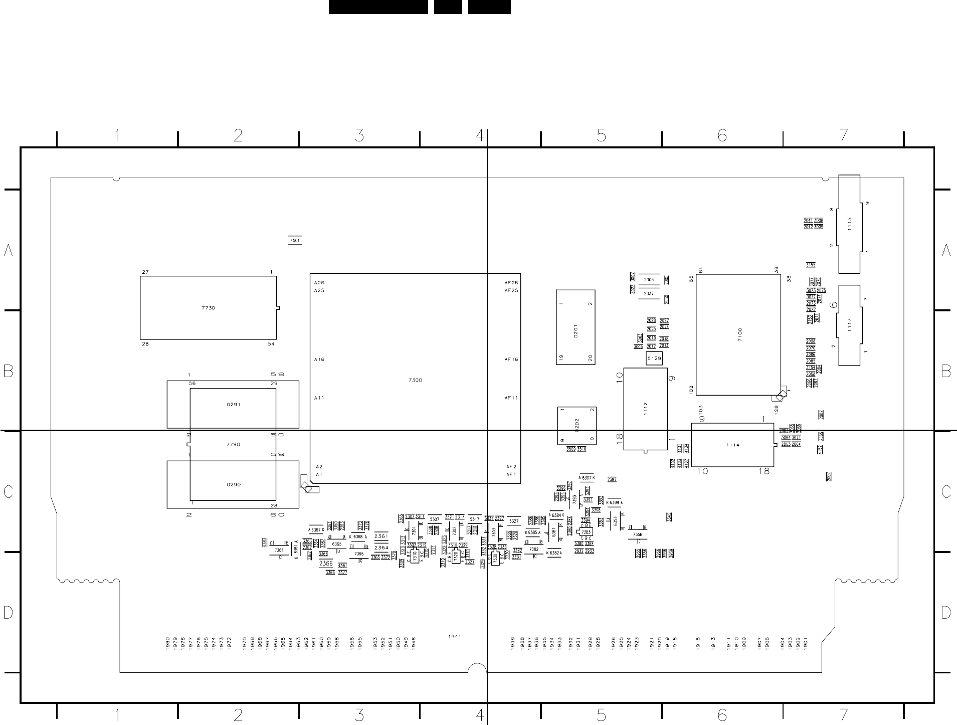
58ES1E AA 7.
Circuit Diagrams and PWB Layouts
Layout SSB (Overview Tuner Side)
CL 36532058_039.eps
030903
3139 123 5536.2
CL 36532058_038.eps
030903
Part 1
CL 36532058_39a.eps
Part 2
CL 36532058_39b.eps
Part 3
CL 36532058_039c.eps
Part 4
CL 36532058_039d.eps
0201 B5
0202 B5
0290 C2
0291 B2
1112 B5
1114 C6
1115 A7
1117 B7
1901 D7
1902 D7
1903 D7
1904 D6
1906 D6
1907 D6
1909 D6
1910 D6
1911 D6
1913 D6
1915 D6
1918 D6
1919 D6
1920 D5
1921 D5
1923 D5
1924 D5
1925 D5
1926 D5
1928 D5
1929 D5
1931 D5
1932 D5
1933 D5
1934 D5
1935 D5
1936 D4
1937 D4
1938 D4
1939 D4
1941 D4
1948 D3
1949 D3
1950 D3
1951 D3
1952 D3
1953 D3
1955 D3
1956 D3
1958 D3
1959 D3
1960 D3
1961 D3
1962 D3
1963 D2
1964 D2
1965 D2
1966 D2
1967 D2
1968 D2
1969 D2
1970 D2
1972 D2
1973 D2
1974 D2
1975 D2
1976 D2
1977 D2
1978 D2
1979 D1
1980 D1
2003 A5
2005 A6
2007 C7
2008 B7
2012 B5
2013 B6
2018 B6
2019 B5
2024 B6
2025 B5
2027 B6
2028 B5
2030 A6
2037 A5
2041 A7
2042 A7
2063 C7
2064 C7
2065 B7
2066 B7
2067 B7
2068 B7
2069 C7
2070 B7
2071 B7
2072 A7
2073 A7
2074 A7
2075 A7
2076 A7
2083 B7
2084 B7
2085 B7
2086 B7
2087 B7
2307 C3
2308 C4
2311 C4
2317 C4
2318 C4
2319 C4
2321 D4
2327 C4
2328 C4
2329 C4
2331 D4
2339 C4
2361 C3
2362 C3
2363 C3
2364 C3
2365 C3
2366 D3
2380 C5
2384 C5
2386 C4
2395 C5
2397 C5
2932 C5
2933 C5
2935 D5
2936 D5
3003 B5
3005 B5
3007 A5
3008 A7
3009 A7
3022 A5
3064 C7
3065 B7
3071 C7
3072 A7
3073 A7
3074 A7
3153 B7
3154 B7
3155 A7
3307 C3
3308 C4
3309 D3
3310 D4
3311 C3
3312 C3
3313 C3
3316 C4
3317 C4
3319 D4
3320 D4
3321 C4
3322 C4
3323 C4
3329 D4
3330 D4
3331 C4
3332 C4
3333 C4
3338 C4
3339 C4
3345 C6
3353 C5
3354 C5
3356 D5
3360 C3
3361 C3
3362 D3
3363 C3
3364 C3
3365 D3
3366 D3
3367 C3
3368 D3
3372 D3
3373 C3
3376 C3
3377 D3
3378 D3
3380 C5
3382 C4
3384 C5
3385 C5
3386 C4
3391 C5
3392 C5
3393 C5
3394 C5
3395 C5
3396 C5
3397 C5
3398 C5
3509 C5
3510 C5
3936 D6
3939 D6
4101 C6
4102 C6
4103 C6
4104 C6
4107 C6
4152 C7
4361 D3
4363 C2
4501 A2
5129 B5
5307 C4
5317 C4
5327 C4
6353 C5
6361 C2
6365 C3
6367 C3
6368 C3
6381 C5
6382 D5
6384 C5
6385 C4
6397 C5
6398 C5
7100 B6
7300 B3
7301 C3
7302 C4
7303 C4
7310 D3
7320 D4
7330 D4
7356 C5
7361 C2
7365 D3
7382 C4
7383 C5
7393 C5
7730 A2
7790 C2
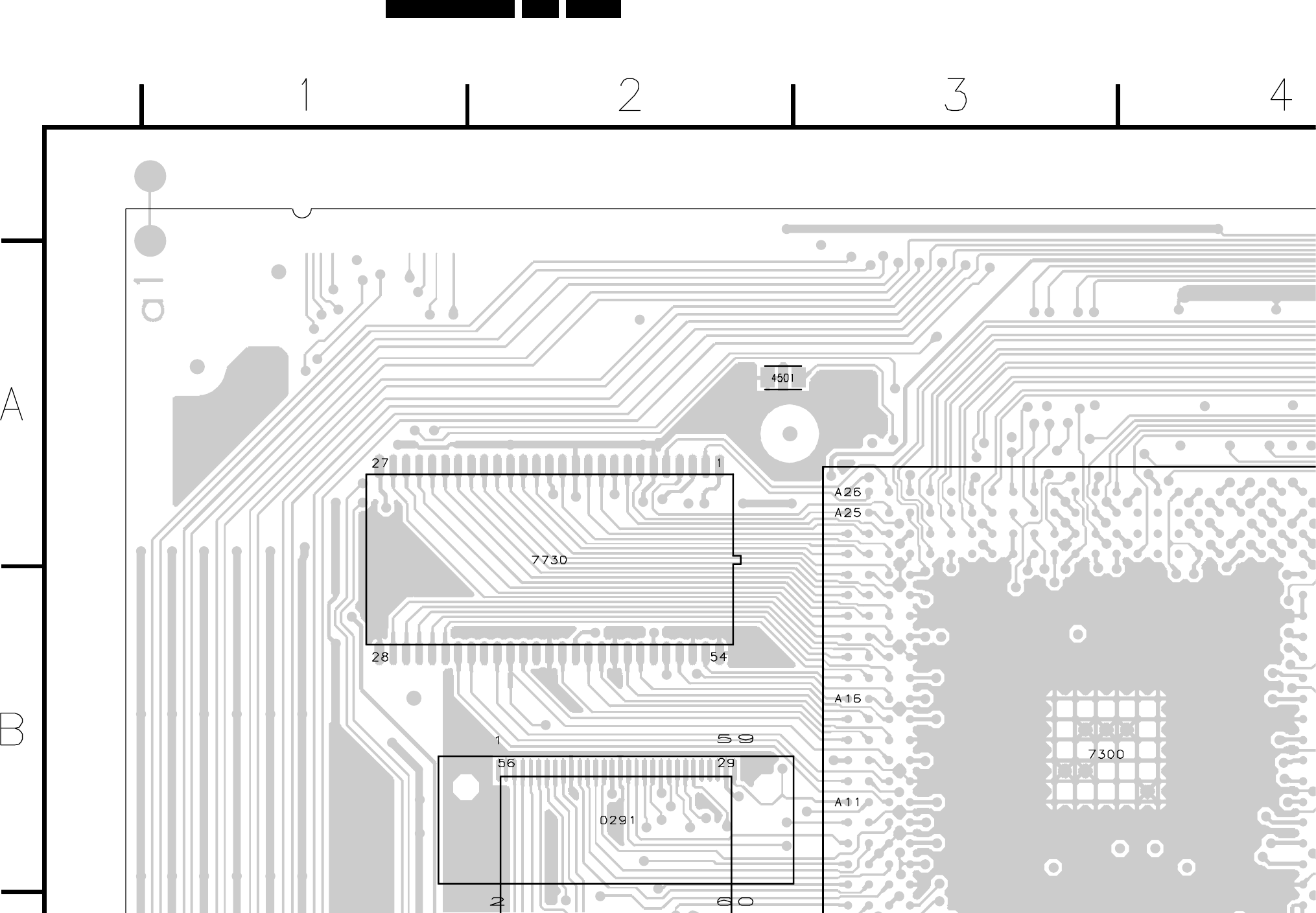
Circuit Diagrams and PWB Layouts 59ES1E AA 7.
Layout SSB (Part 1 Tuner Side)
CL 36532058_39a.eps
030903
Part 1
60ES1E AA 7.
Circuit Diagrams and PWB Layouts
Layout SSB (Part 2 Tuner Side)
CL 36532058_39b.eps
030903
Part 2
Circuit Diagrams and PWB Layouts 61ES1E AA 7.
Layout SSB (Part 3 Tuner Side)
CL 36532058_39c.eps
030903
Part 3
62ES1E AA 7.
Circuit Diagrams and PWB Layouts
Layout SSB (Part 4 Tuner Side)
CL 36532058_38d.eps
030903
Part 4
Circuit Diagrams and PWB Layouts 63ES1E AA 7.
Side I/O Panel (FL9)
3139 123 6007.2 F_15040_015.eps
230305
6808 B2
I814 C3
I815 D3
I816 E3
I817 A3
I818 B4
I819 D2
I820 E2
I821 D2
F011 A6
F013 A8
F014 C9
F015 A8
F016 C6
3999 F6
F017 C8
F018 B8
F019 C7
F020 F9
F021 F9
F022 F9
F023 F6
F024 F7
SOUND R-HEADPHONE-OUT
Y
I803 A4
I809 B5
I810 B5
I811 B4
I812 C4
I813 B3
5801 F3
5802 F3
6801 B3
6802 C2
6803 C3
6804 D2
6805 D3
6806 E2
6807 A3
L
7811 B4
7812 B5
7813 A5
9800 F6
9810 A6
9811 A6
9812 F9
9820 C3
I822 F5
I823 F6
1936
R
F006 D2
F007 D2
F008 E2
F009 E2
F010 E2
9829 F3
F001 A2
F002 B2
F003 B2
F005 C2
3830 F4
3835 D5
3842 E5
3845 A3
3846 A4
3847 A4
3848 A5
3849 A5
3850 A4
2811 B5
4800 D2
4801 D2
4803 F5
4804 C6
4805 A3
4806 F8
4808 F9
4809 E8
I801 B3
I802 A3
I804 A4
I805 A3
I806 A4
I807 A5
I808 B5
Y
4812 F8
4830 E3
4831 F3
SOUND R-HEADPHONE-OUT
3806 D3
3808 A4
3809 A3
3810 C4
3811 C4
3812 B4
3813 B5
3814 C5
9821 D3
9827 E5
3826 E5
3827 E5
3828 F3
3829 F3
1806 A2
1936 C9
2803 C3
2804 C4
2805 D4
2806 D3
2807 A3
2810 B4
2
2813 C6
2832 E6
2834 F4
2840 F2
2841 F2
3801 A3
3802 C3
3803 C3
4810 F8
4811 F8
CVBS
DETECT
C
R
1327 E1
1328 B1
1344 F9
1346 E9
1800 E2
1801 C2
1802 F2
1803 F2
3815 C3
3816 B3
SIDE I/O PANEL
1
*
SOUND L-HEADPHONE-OUT
CVBS
3456789
A
3804 D3
3805 C3
SVHS
1326-3 D1
RES
RES
L
HEADPHONE-OUT
N.C
OF
R
1804 E3
1805 B2
**
56789
*
*
L
SOUND L-HEADPHONE-OUT
N.C
1234
OR
FROM 1620 OF
INTERFACING
E
F
B
C
D
*
*
* DIVERSITY
FROM/TO
A
B
C
D
E
F
1326-1 C1
1326-2 C1
*
*
*
*
c/ 16/9
680p
2806
4830
4831
4809
F005
680K
3810
4808
1K0
3804
F019
BC857B
7812
5
7
6
I804
1328
1
2
3
4
6808
YKF51-5304
4800
BZX384-C6V8
I806
GND_AUD
2K2
3814
150K
3812
F020
4801
4803
33n
2810
F006
GND_AUD
10K
3846
F013
47K
3806
100R
I810
3809
GND_AUD
I805
4805
F001
9810
F018
I813
GNDB
I807
1805
1K8
3850
F007
I815
1804
I823
120R3829
GND_AUD
5K6
3848
1
2
3
GNDB
1346
75R
3802
1K0
3803
3K9
3813
4806
4810
10K
3847
9800
GNDB
F016
9811
I818
F014
BC857B
7811
F009
9821
GNDB
2840
100p
1326-2
6
4
5
GND_AUD
4K7
3845
1803
GND_AUD
F008
F002
I819
I817
2841
100p
120R3826
100p
2805
GNDB
9827
I812I814
1801
I808
GNDB
BZX384-C10
6803
F003
F017
GNDB
GNDB
F015
680p
2803
F011
120R3827
9812
BZX384-C10
6805
10K
3842
GNDB
150R
3999
GNDB
I822
3808
I821
3K9
3835
9829
5802
F022
39R
3816
F021
GND_AUD
10n
2807
1802
GNDB
GNDB
9820
F010
1
2
3
1344
I811
I802
BZX384-C10
6806
3K3
3849
BZX384-C6V8
6807
8
9
F023
10
11
2
3
4
5
6
7
1936
1
39K
3811
5801
3828
39R
3815
120R
F024
100p
2804
2
BZX384-C10
6804
1326-1
1
I816
1326-3
9
7
8
GND_AUD
BC847B
7813
4812
GND_AUD
150n
2834
5
7
8
75R
3801
1
2
3
4
YKB21-5101A
1327
I820
2u2
2813
150n
2832
10K
3830
4804
RES (SDM-EMG_S)
100u
2811
I801
BZX384-C6V8
6801
BZX384-C6V8
6802
I803
4811
GNDB
1806
I809
1800
47K
3805
+8V6
+8V6
+8V6
D D
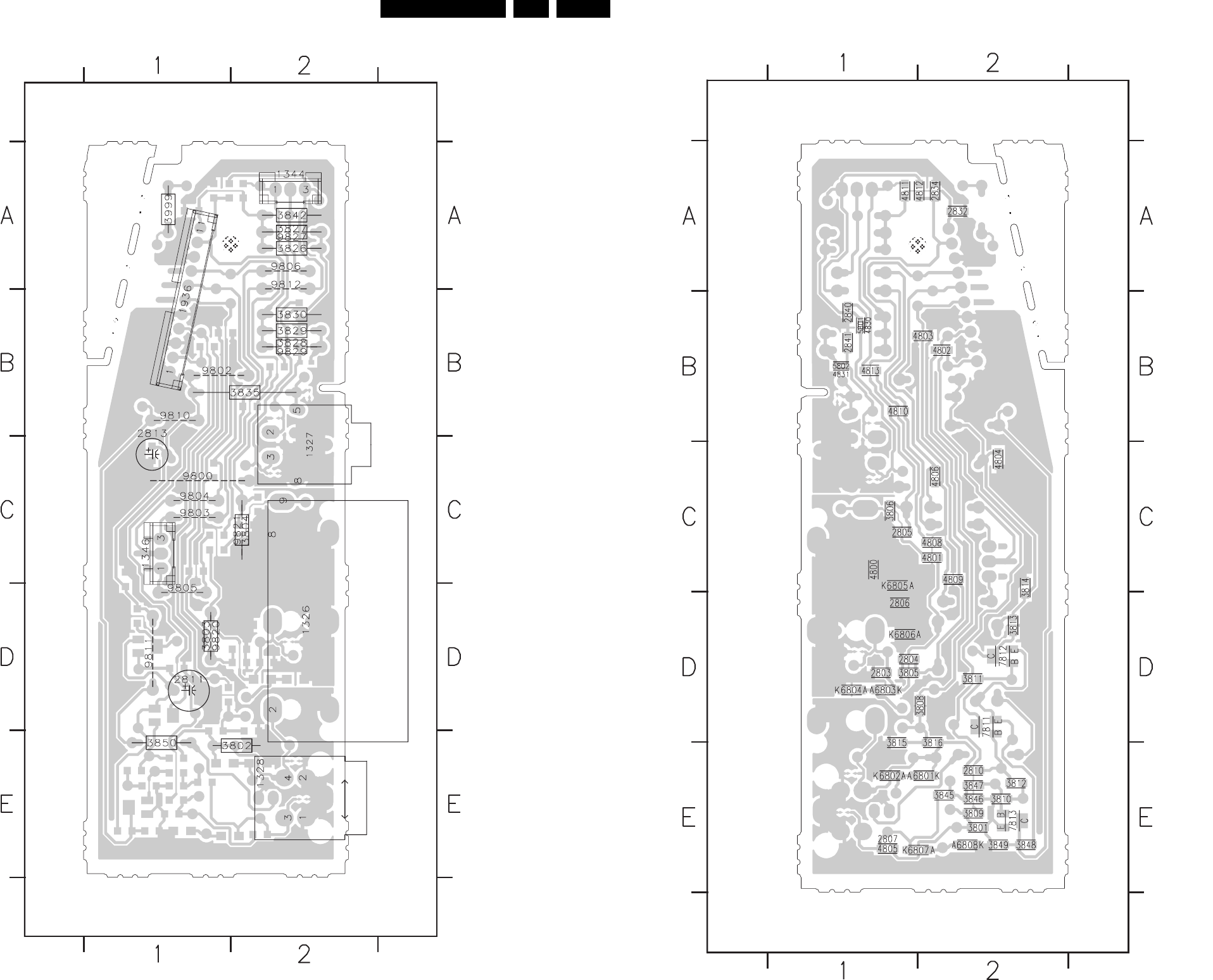
64ES1E AA 7.
Circuit Diagrams and PWB Layouts
Layout Side I/O Panel (FL9) (Top Side)
3139 123 6007.2 F_15040_016.eps
230305
1326 D2
1327 C2
1328 E2
1344 A2
1346 C1
1936 B1
2811 D1
2813 B1
3802 E2
3803 D1
3804 C2
3826 A2
3827 A2
3828 B2
3829 B2
3830 B2
3835 B2
3842 A2
3850 E1
3999 A1
9800 C1
9802 B1
9803 C1
9804 C1
9805 D1
9806 A2
9810 B1
9811 D1
9812 A2
9820 D1
9821 C2
9827 A2
9829 B2
Layout Side I/O Panel (FL9) (Bottom Side)
3139 123 6007.2 F_15040_017.eps
230305
2803 D1
2804 D1
2805 C1
2806 D1
2807 E1
2810 E2
2832 A2
2834 A2
2840 B1
2841 B1
3801 E2
3805 D1
3806 C1
3808 D2
3809 E2
3810 E2
3811 D2
3812 E2
3813 D2
3814 C2
3815 E1
3816 E2
3845 E2
3846 E2
3847 E2
3848 E2
3849 E2
4800 C1
4801 C2
4802 B2
4803 B2
4804 C2
4805 E1
4806 C2
4808 C2
4809 C2
4810 B1
4811 A1
4812 A2
4813 B1
4830 B1
4831 B1
5801 B1
5802 B1
6801 E2
6802 E1
6803 D1
6804 D1
6805 C1
6806 D1
6807 E2
6808 E2
7811 D2
7812 D2
7813 E2
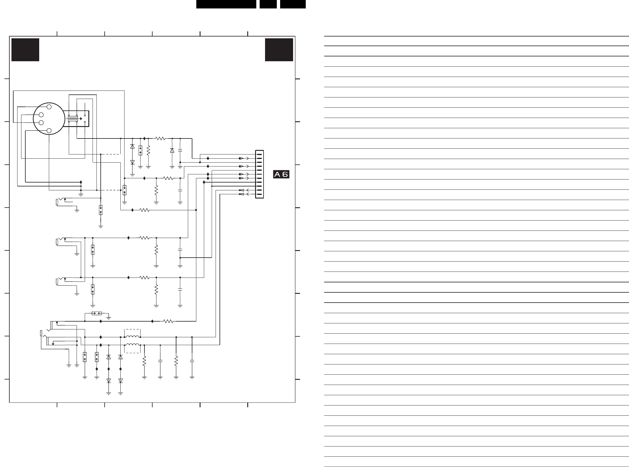
Circuit Diagrams and PWB Layouts 65ES1E AA 7.
Side I/O Panel (SL5/PV2)
3
H
B
SIDE I/O PANEL
B
C
D
45
5
C
6
F
D
E
G
1
1
S_VHS
HEADPHONE
62
E
23
RES
VIDEO IN
A
Y
4
RIGHT
LEFT
G
H
C
FROM 1620 OF
INTERFACING
F
RES
A
4201
I209
T
6291
47K
3294
4202
6293
T
6296
T
2292
470p
1257
I222
I218
3291
1K0
1262
I217
10K
3296
2288
100p
I201
1258
I206
I219
1259
I221
5292
5291
3286
100R
2294
3288
470p
I205
100R
105
1
94
116
YKF51-5347
1256
2
7
3
8
I203
3
4
5
6
7
8
9
0240
1
10
11
2
1260
75R
3285
T
I204
6292
1264
3287
75R
6295
T
3289
1K8
1K0
3293
10K
3297
1261
2286
100p
I213
I211
150n
2297
2
I208
YKC21-5599
3
1
1255-1
8
YKC21-5599
1255-3
9
7
1
2
3
4
5
7
8
1254
YKB21-5101A
150n
2296
3295
3K9
I202
T6294
3292
47K
6297
T
YKC21-5599
1255-2
6
4
5
I210
4292
I215
4291
1263
I220
R_FRONT_IN
FRONT_DETECT
HP_OUT_L
HP_OUT_R
Y_CVBS_FRONT
C_FRONT_IN
L_FRONT_IN
D D
3139 123 6009.2 F_15040_019.eps
300305
Personal Notes:
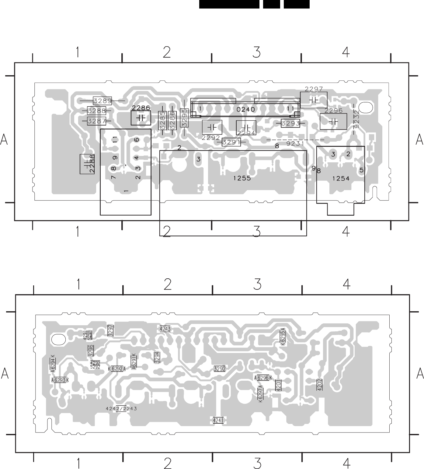
66ES1E AA 7.
Circuit Diagrams and PWB Layouts
Layout Side I/O Panel (SL5/PV2) (Top Side)
Layout Side I/O Panel (SL5/PV2) (Bottom Side)
F_15040_020.eps
300305
3139 123 6009.2
0240 A3
1254 A4
1255 A3
1256 A2
2286 A2
2288 A1
2292 A2
2294 A3
2296 A4
2297 A4
3285 A2
3286 A2
3287 A1
3288 A1
3289 A1
3291 A3
3293 A3
3295 A2
9231 A3
9232 A4
F_15040_021.eps
300305
3139 123 6009.2
3292 A3
3294 A2
3296 A1
3297 A1
4201 A3
4202 A4
4241 A3
4242/2243 A1
4243 A2
4291 A1
4292 A1
5291 A1
5292 A1
6291 A2
6292 A1
6293 A1
6294 A1
6295 A3
6296 A3
6297 A3
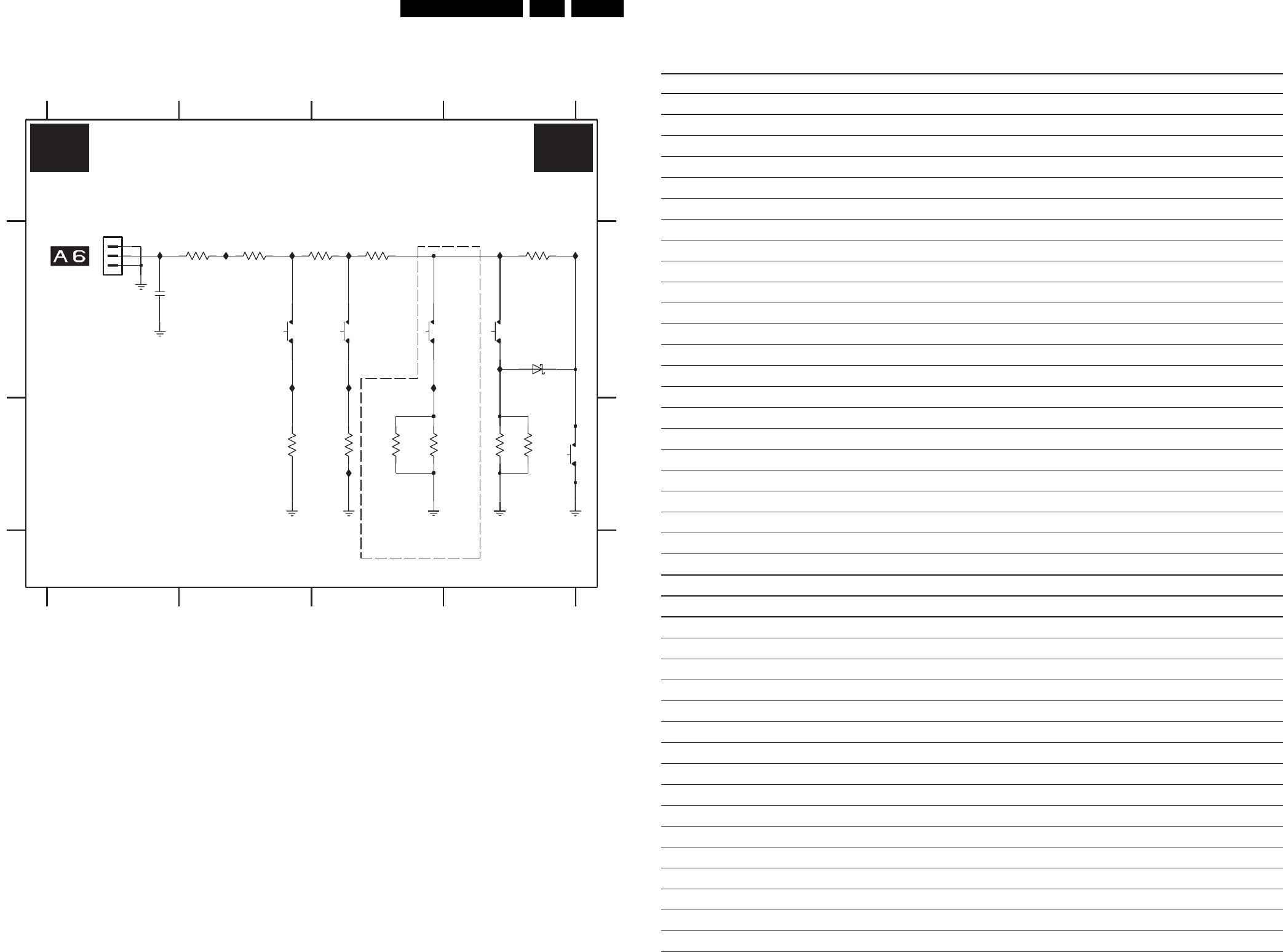
Circuit Diagrams and PWB Layouts 67ES1E AA 7.
Front Control Panel
B
0215 A1
1091 A2
MENU BUTTON FOR
TO 1645 OF
INTERFACING
2K
*
PLUG&PLAY MENU
A
1092 A3
1093 A4
1094 B4
1095 A4
2010 A1
5 KEYS CONFIGURATION
V-
V+
1234
1234
A
B
FRONT CONTROL PANEL
3087 B4
3088 B3
3089 B3
3090 B2
3091 A2
I009 A4
I012 B3
I021 A4
*
C+ C-
3092 A2
3093 A3
3094 A3
3095 A4
3096 B4
3098 B3
6091 A4
I001 A1
I002 A2
I003 A3
I004 A4
I005 A4
I006 A2
I007 A2
I008 A3
I006 I002
I001
BAT54 COL
6091
3096
1K5
3094
270R
560R
3093
3092
390R
3091
560R
I007
2010
10n
I008
1091
I012
I021
3095
3K3
3088
1094
1K1
3089
620R
3090
1
2
3
0215
1092
3K3
3098
1093
1095
200R
3087
I009
I004 I005
I003
E E
3139 123 5570.2 F_15040_023.eps
310305
Personal Notes:
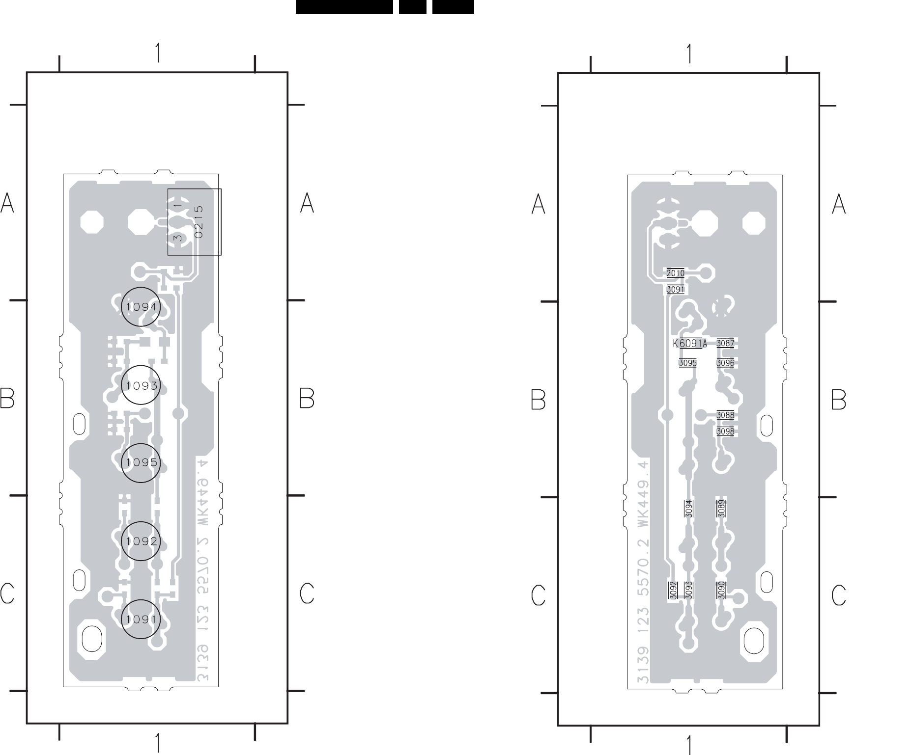
68ES1E AA 7.
Circuit Diagrams and PWB Layouts
Layout Front Control Panel (Top Side)
3139 123 5570.2 F_15040_024.eps
310305
0215 A1
1091 C1
1092 C1
1093 B1
1094 B1
1095 B1
Layout Front Control Panel (Bottom Side)
3139 123 5570.2 F_15040_025.eps
310305
2010 A1
3087 B1
3088 B1
3089 C1
3090 C1
3091 A1
3092 C1
3093 C1
3094 C1
3095 B1
3096 B1
3098 B1
6091 B1
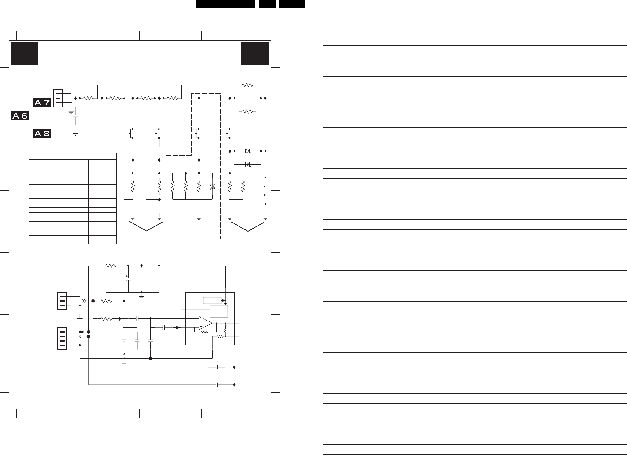
Circuit Diagrams and PWB Layouts 69ES1E AA 7.
Top Control Panel (PV2)
MIC V+
444E
13.7K
EXT
MIC V+
AMP
100K
4
RES
*
*
3096
V+
TO 1945 OF
Painter based
(EM1)
FRONT
1
TO 1645
OF
INTER-
FACING
3092
1094
4 Keys
C-
2010
ArtistIC based
MICROPHONE
34
123
1094 B4
1095 B4
2010 A2
2011 D2
2012 D3
2013 E2
2014 E3
2015 E2
2016 E3
2017 E4
2018 E4
2019 D3
A
B
C
D
E
0215 A1
0216 E1
0217 D1
1090 D2
1091 B2
3095
6091
1091
OF
5 KEYS CONFIGURATION
1093
3010 D2
3011 D2
3012 E2
3086 A4
3087 B4
3088 B3
3089 B3
3090 B2
3091 A2
3092 A2
2
TOP CONTROL PANEL
PLUG&PLAY
TO 0215
MENU
*
*
*
3088
3089
3087
30864089
1092 B3
1093 B4
3094 A3
3095 A4
3096 B4
3097 B3
3098 B3
4089 B3
4090 B2
2020 E2
1092
1093
4094
1093
6093
1091
1091
1092
1094
4092
4093
*
3096
3095
RES
(RES)
4093 A3
4094 A3
6091 B4
6092 B4
6093 B4
7091 D3
F001 D2
F002 E2
F003 E2
F004 E3
I001 A2
I002 A2
3093 A3
3094
3093
*
C+
5 Keys
1095
1095
2010
1094
*
*
3091
I006 A2
I007 B2
I008 B3
I009 B4
I010 D3
I011 D2
I012 C3
I013 D2
I016 D3
I017 E3
I019 E4
I020 E4
4091 A2
1092
3094
3093
3097
3098
3090
4090
Painter based
(A10)
4092 A2
**
3092
MENU BUTTON FOR
I003 A3
VOICE CONTROL
FRONT
V-
4091
I004 A4
I005 A4
I021 B4
4089
4090
(LSP)
RES
3091
100n
2013
1090
2017
1u0
3098
3K3
3097
1K5
6
AMPNFB
7AMPOUT
2 EXTMICV+
4
GND
1 MICV+
8
V+
3VIN+
5 VIN-
NJM2110M
7091
470R
3012
4R7
3010
4094
F004
I017
47u
2015
F002
2014
1n0
I002 270R
3094
I008
3K3
3095
1
2
3
4
I001
0216
BAT54 COL
6093
3093
560R
I007
I009
I005
I012
I004
I011
3086
390R
1
2
3
I010
0215
10n
2010
3087
200R
1u0
2018
F001
4092
F003
1092
2019
2012
100n
1093
3088
2K0
I006
I016
1n0
2016
3011
4089
1K8
3089
1K1
3090
620R
1095
47u
2011
I013
I019
I020
4090
1091
4091
1094
I003
I021
3091
560R
4093
6091
BAT85
1
2
3
1K5
3096
0217
390R
3092
2020
6092
BAT54 COL
GND
3V3
OUT1
3139 123 5440.6 F_15040_027.eps
310305
E E
Personal Notes:
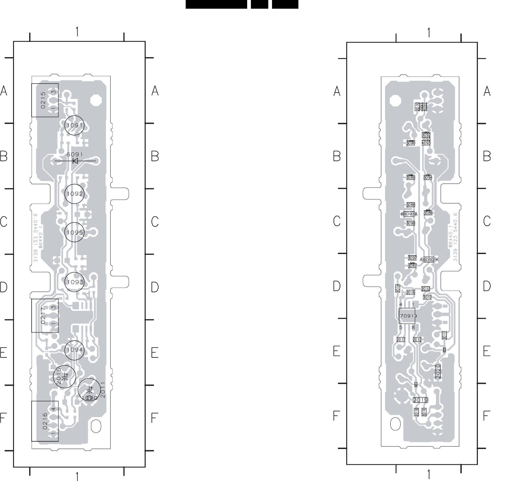
70ES1E AA 7.
Circuit Diagrams and PWB Layouts
Layout Top Control Panel (PV2) (Top Side)
3139 123 5440.6 F_15040_028.eps
310305
0215 A1
0216 F1
0217 D1
1090 F1
1091 B1
1092 C1
1093 D1
1094 E1
1095 C1
2011 F1
2015 E1
6091 B1
Layout Top Control Panel (PV2) (Bottom Side)
3139 123 5440.6 F_15040_029.eps
310305
2010 A1
2012 E1
2013 D1
2014 D1
2016 D1
2017 E1
2018 F1
2019 F1
2020 E1
3010 F1
3011 E1
3012 D1
3086 C1
3087 D1
3088 C1
3089 B1
3090 B1
3091 A1
3092 B1
3093 B1
3094 B1
3095 C1
3096 D1
3097 D1
3098 C1
4010 E1
4011 F1
4089 B1
4090 B1
4091 A1
4092 B1
4093 B1
4094 B1
6092 D1
6093 C1
7091 D1
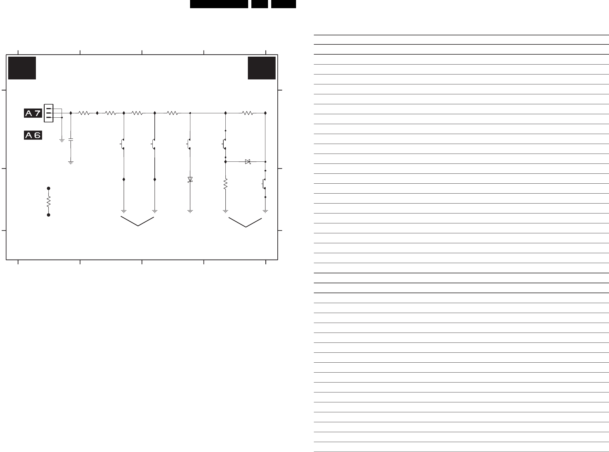
Circuit Diagrams and PWB Layouts 71ES1E AA 7.
Top Control Panel (FL9)
V+
A
B
A
B
0215 A1
1091 A2
1092 A3
1093 A4
1094 B4
1095 A3
2010 A1
3091 A2
3092 A2
3093 A2
TO 1645 OF
INTERFACING
C-C+
V-
1234
1234
(LSP)
TO 0215
MENU
PLUG&PLAY
MENU
3094 A3
3095 A4
3096 B4
3099 B1
6091 A4
6092 B3
F001 B1
F002 B1
I001 A1
I002 A2
I003 A2
I004 A3
I005 A4
I006 A4
I007 B2
I008 B3
I009 A4
FRONT
OF
F001
1K5
3096
3K3
3095
270R
30943093
560R390R
3092
560R
3091
0215
1
2
3
I008
I007
10n
2010
1092
1094
1093
1091
1095
6092
BAT54 COL
I009
I005 I006I004I002 I003I001
6091
BAT54 COL
3099
1K0
F002
TOP CONTROL PANEL
3139 123 5699.2 F_15040_031.eps
310305
E E
Personal Notes:
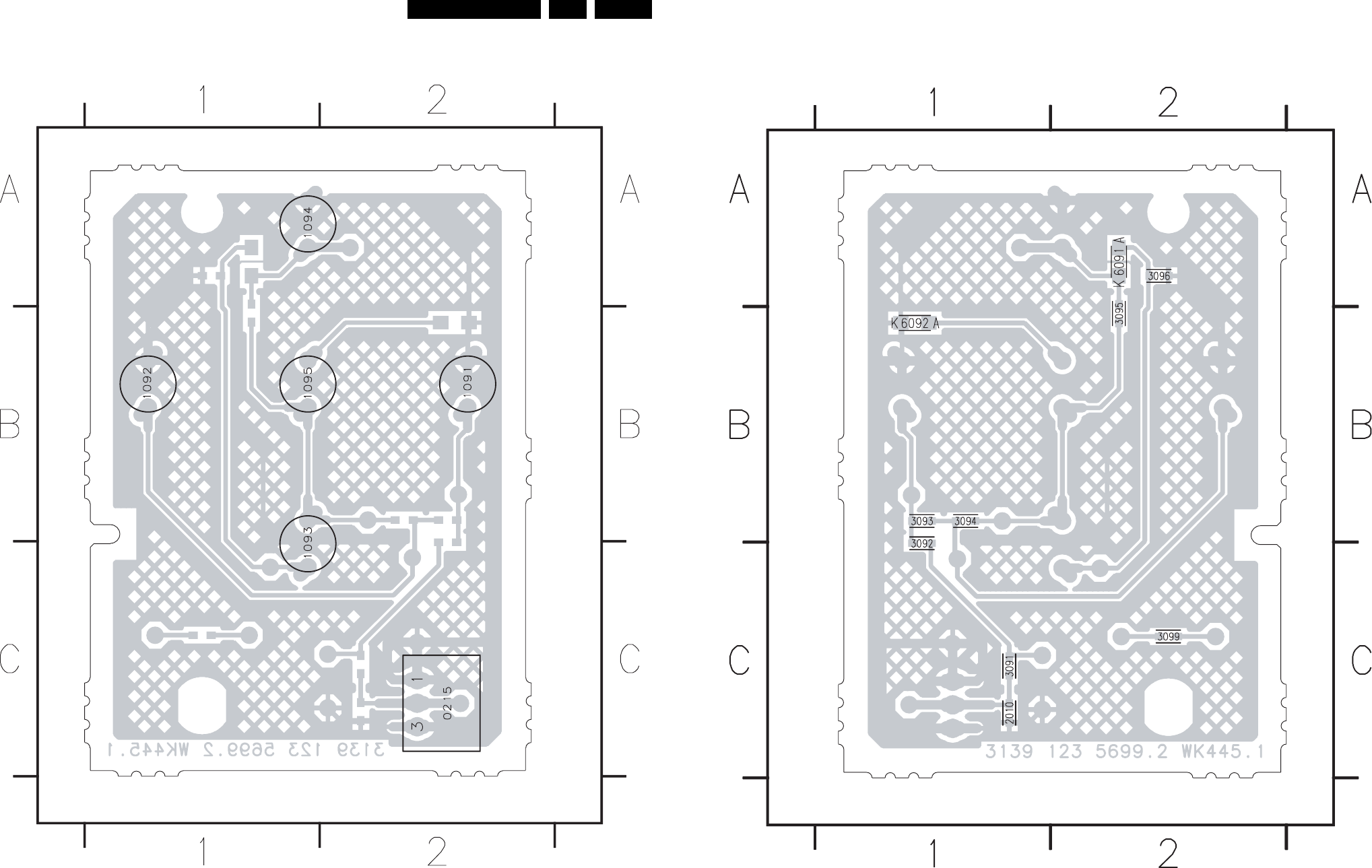
72ES1E AA 7.
Circuit Diagrams and PWB Layouts
Layout Top Control Panel (FL9) (Top Side)
3139 123 5699.2
F_15040_032.eps
310305
0215 C2 1091 B2 1092 B1 1093 C1 1094 A1 1095 B1
Layout Top Control Panel (FL9) (Bottom Side)
3139 123 5699.2 F_15040_033.eps
310305
2010 C1 3091 C1 3092 C1 3093 B1 3094 B1 3095 B2 3096 A2 3099 C2 6091 A2 6092 B1
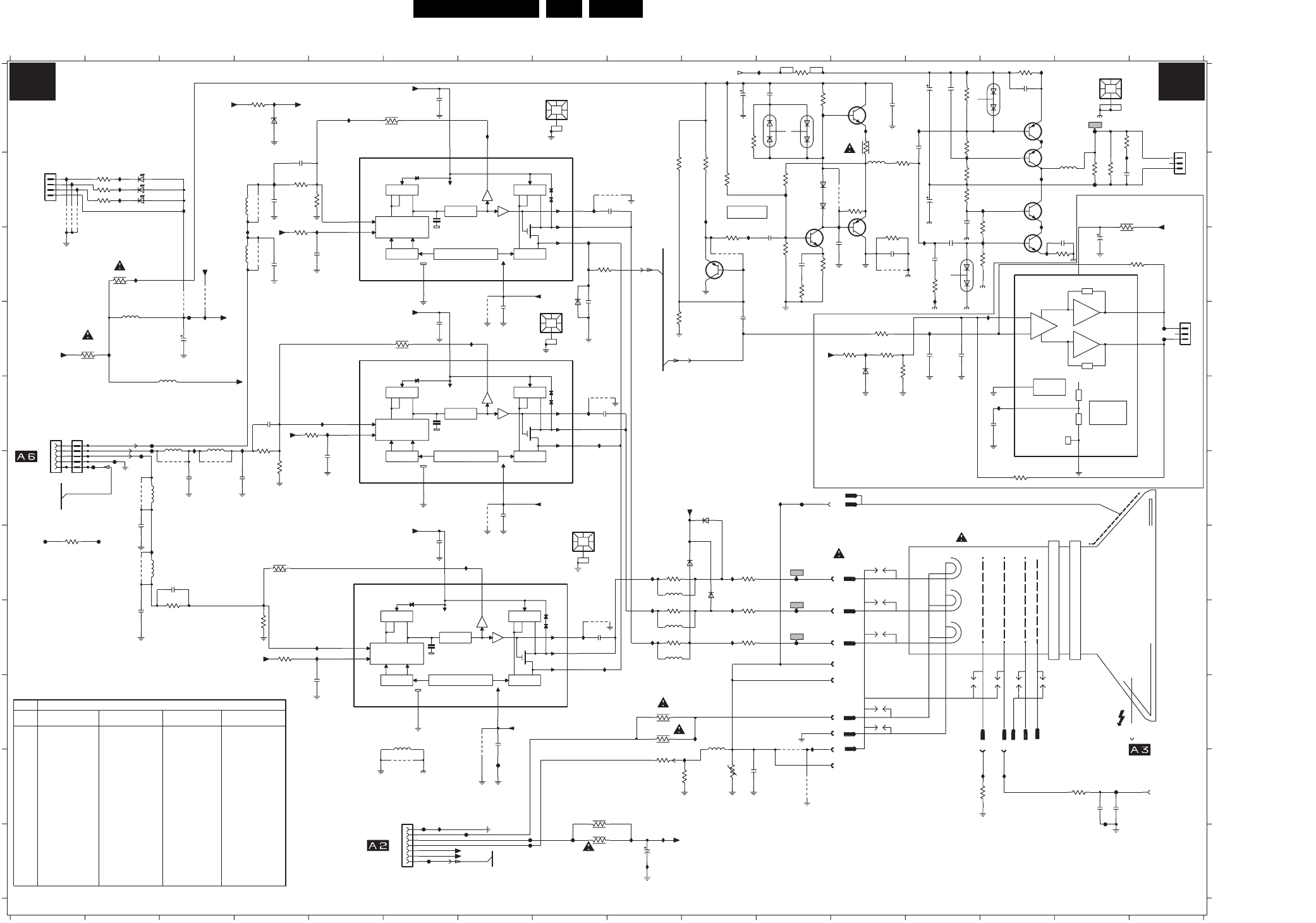
Circuit Diagrams and PWB Layouts 73ES1E AA 7.
CRT Panel
Blue
Green
Red
Vcc
TEMPERATURE
PROTECTION
AND
SHORT CIRCUIT
20K
20K
STANDBY/
MUTE LOGIC
V
3V1
11 12 13 14 15 16
A
B
C
D
E
F
G
H
I
J
K
A
B
C
D
E
F
G
H
I
J
K
1316 A15
1317 E1
*
0V
1 2 3 4 5 6 7 8 9 10111213141516
12345678910
3V1
1330 A8
1331 D8
1334 G8
1335 F11
1336 J16
1340 E1
1351 J6
1354-A I12
1354-B J13
1354-C H12
1354-D J14
1354-E H12
1354-F I12
1354-G I12
1354-H G12
1354-I I12
1354-J J12
1354-K I12
1361 A16
1382 D16
1388 B1
2313 K9
2317 J15
2319 J10
2324 J15
2332 C5
2333 B9
CRT PANEL
FROM 1401 OF
3V4
*
Bleeder Gun
112V
*
*
3V4
2336 D7
2338 A6
2339 D6
2340 G6
2343 E8
2344 F5
2346 F7
2347 D3
2352 I5
2353 H8
2354 B4
2355 C4
2356 I7
2357 C12
2358 F3
2359 F4
2360 G2
2361 A12
2362 H2
2363 A13
2364 A13
Rotation Coil
CRT
TO
R-CRT
2365 C13
2367 D13
2368 B13
2369 C8
2370 D13
2371 B4
2372 E4
2373 G3
2374 A11
2375 C11
2376 A14
2377 C15
2381 A10
2382 C11
2383 B15
2384 A13
2385 B13
2386 C13
2387 C12
2388 D10
2389 E14
2390 C15
3305 D2
3306 I9
3307 I9
3317 C8
1V2
3V2
3V4
3V6
*
50V
LOT
*
3318 B15
3319 C16
3320 D12
3321 D12
3322 F14
3325 A4
3331 G9
3332 G10
3333 H9
3334 H10
3335 H9
3336 H10
3337 A6
3338 B4
3339 B5
3340 C4
3341 D6
3342 F4
3343 E4
3344 E5
3345 J9
*
R
STATIC FOCUS
EHT
3347 J15
3348 J13
3349 J9
3350 D12
3351 K8
3352 G4
3353 H3
3354 H4
3355 H4
3356 K8
3357 J10
3358 A10
3359 B10
3360 C11
3361 A11
3362 A12
3363 A13
3364 A14
3365 A13
3366 B13
3367 B13
3368 C13
**
*
*
*
3370 C15
3371 B15
3372 B15
3373 A11
3374 C12
3375 C11
3377 C11
3378 C10
3379 B11
3380 B9
3381 D9
3382 B12
3385 C13
3386 B2
3387 B2
3388 B2
3389 C2
3392 A15
3393 B12
3394 C13
3395 B10
3396 D12
*
SCAVEM COIL
VG2
TO
3R3
3998 G1
4301 B12
4302 J11
4303 B4
4304 C4
4305 F3
4306 F3
4307 F2
4308 G2
4309 C3
4310 C12
4311 D7
4312 E8
4313 F7
4314 H8
4315 I7
4316 C10
4386 B1
4387 B1
4388 B1
4389 D3
5303 E3
5304 I10
114V
*
6V
B-CRT
*
6V
200V
3R3
5308 D2
5339 B12
5340 B4
5341 C4
5342 F3
5343 F3
5344 F2
5345 G2
5346 I6
5347 G9
5348 H9
5349 H9
5361 B15
6307 C8
6325 A4
6331 F10
6332 G10
6333 G10
6334 D12
6335 A11
6336 A11
6361 B11
6362 B11
6386 B2
117V
VG1
117V
118V
*
3V4
3V4
6387 B2
6388 B2
6390 A14
6391 C13
7330 A5
7331 C10
7332 A14
7333 C14
7340 D5
7350 G5
7361 A12
7362 B12
7363 B14
7364 B14
7365 B11
7366 C14
9301 B9
9302 I11
9324 J6
F330 D3
F331 K6
F332 E3
F334 E2
TO
B
EHT-INFO
F335 F2
F336 F2
F337 F2
F338 H11
F339 H11
F340 K7
F341 G11
F342 K15
F345 F11
F346 K7
F347 J15
F348 J7
F352 K6
F354 K8
F361 A15
F362 B15
F381 D16
F382 D16
G
AQUADAG
*
*
F383 K7
F398 G1
F399 G2
I301 B1
I302 B1
I303 B1
I304 B2
I305 B2
I306 B2
I307 B3
I308 A4
I309 B4
I310 C4
I311 E4
I312 F3
I313 G3
I314 A14
I315 C14
I316 C14
I317 B16
I318 B12
I319 D12
G-CRT
*
3V4
3V4
115V
115V
112V
112V
DC_Filament
4V6
3V9
*
*
7V2
4V6
4V
112V
I320 D13
I321 A11
I322 K9
I323 K9
I324 F11
I325 C10
*
I326 B11
I327 K6
I328 H5
I329 H5
I330 H9
I331 H9
I332 G9
I333 H10
I334 H10
I335 G10
I336 D3
I342 C8
I346 E8
I347 H8
I348 J10
I350 I10
I351 K9
I360 A13
I361 A11
I362 A12
I364 C13
I365 B14
I366 B13
I367 A13
I368 A14
I369 B14
I370 B10
I371 C14
I373 I11
I374 E14
*
I376 J13
I377 J14
I378 C2
I379 D2
I380 D14
I381 D13
I386 A10
I389 A5
I390 A7
I391 B8
I392 B5
I393 D7
I394 E8
I395 E5
I396 E5
I397 G7
I398 H8
*
6334
BZX384-C3V3
3370
3R3
1599
2K7
0V7
FROM 1629 OF
INTERFACING *
*
5V3
w/o bleeder
112V
TDA8941P
3V1
2R7
4V3
ROTATION FOR WIDE SCREEN ONLY
SCAVEM
B1
DEFLECTION
DYN FOCUS
*
*
*
*
*
114V
6V
B1
B1
B1
112V
GND_RGB
GND_LS1
I368
5
GND_RGB
4305
1340
1
2
3
4
I391
GND_RGB
I348
+12A1
I396
22K
3320
I323
GND_RGB
2381
47u
I395
680p
2343
GND_RGB
1354-F
H1
9
F335
2356
33n
3344
100n
2340
1K0
3336
6390
470R
6307
3348
1K0
GND_RGB
F340
4312
2371
I364
GND_RGB
I346
I302
2352
4n7
3345
10R
2382
47n
I334
5308
5u6
2364
4n7
3377
3339
2K7
3322
1354-K
SG2
2
150K
BAV21WS
6331
5345
I333
GND_RGB
+141V
+12V_SVM
GND_RGB
820p
F345
2324
GND_RGB
+200A
I310
5303
5u6
I316
3363
560R
680K
3321
F354
F331 +8V_+12V
GND_RGB
5
560R
3372
B5B-PH-K
1
2
3
4
I376
1317
I331
GND_RGB
CR
1354-E
8
GND_LS1
I386
I342
GND_RGB
1330
270R
4306
3385
5
I347
G1
1354-B
I306
1K5
3373
I305
3379
3337
100K
18K
3305
1R0
I350
5u6
5349
4301
2354
GND_RGB
4p7
GND_RGB
I379
3353
2K2
2374
1
2
3
1382
9301
3360
2369
330p
I320
I321
+3V
2387
GND_RGB
680p
18p
F398
2353
1354-G
H2
10
2K7
3342
GND_RGB
+200A
I325
I369
I393
5347
5u6
GND_RGB
3392
270R
220p
2373
2383
2K2
3343
3364
6336
BAV99
GND_RGB
BAV99
6335
3371
560R
BC327-25
7332
2319
10n
HEATSINK
1316
1336
1
F338
4n7
2388
680p
2386
3358
GND_RGB
I373
+200A
GND_RGB
BC847B
7361
GND_RGB
4316
3368
560R
2339
100n
GND_RGB
I322
4p7
2362
I380
F361
3366
68K
3380
2K2
GND_RGB
2K2
3381
3352
100K
GND_RGB
5342
GND_RGB
7365
I374
3354
BC847B
4308
2K7
4309
5346
6333
BAV21WS
3332
470R
GND_RGB
4313
1
33R
3349
I315
SG1
1354-A
+12A
F399
3382
330R
100n
3393
56R
GND_RGB
2361
2385
100n
I307
GND_RGB
GND_RGB
F337
F332
22u
2368
F341
10u
2390
3318
10R
1K8
4
4315
3325
B4B-PH-K
1388
1
2
3F362
5304
+3V
5340
I366
4388
GND_RGB
4387
F342
4303
4p7
+3V
4310
2359
I308
GND_RGB
I394
100n
2338
5344
3335
470R
I309
I314
GND_RGB
I335
GND_RGB
100n
2370
+8V_+12V
+200A
F334
I390
10n
2357
KTB631K
7363
I313
I327
1
VOC 8
GND_RGB
GND_RGB
I360
4
GND
5
IOM
VCN 7
VDDH
6
2VDDL
VFB
9
VIN
3
VIP
TDA6111Q
7340
MIRROR
MIRROR
DIFFERENTIAL
STAGE
MIRROR
MIRROR
V BIAS
CURRENT SOURCE
3365
GND_RGB
4K7
I330
I397
I392
I371
GND_LS1
3361
470R
I377
5343
2372
I389
4n7
2344
100K
3341
I361
GND_LS1
3338
2K2
I303
I304
I370
3378
1K2
22u
2363
3340
1K0
2333
680p
1334
1331
I336
VOC 8
F339
4
IOM 5
VCN 7
VDDH 6
2VDDL
9VFB
3VIN
VIP
1
MIRROR
MIRROR
DIFFERENTIAL
STAGE
MIRROR
MIRROR
V BIAS
CURRENT SOURCE
7330
TDA6111Q
GND
I351
330R
3388
F347
3362
10R
F330
100R
3374
5u6
5348
3359
I365
11
F346
CB
1354-H
10R
3389
1335
GND_RGB
4307
3396
1K8
3334
470R
2375
47n
3375
1K0
6362
BAS316
7364
KTD600K
150K
3319
2360
4p7
3317
1K0
+12A1
33n
2346
5361
BC857B
7331
3333
470R
4389
3998
1K2
2347
470u
6391
I317
+12V_SVM
CG
1354-C
6
+200A
3356
150R
9302
3367
68K
2332
4n7
3347
1K5
I328
9324
GND_RGB
BAS316
6361
GND_RGB
3306
2365
4n7
IN-
MODE
4
OUT+ 2
OUT- 7
SVR
6
VCC
1
F381
7366
8
GND
3IN+
5
F348
I301
6325
I312
BZX384-C3V3
3307
I311
10K
3350
2336
33n
GND_LS1
330R
3387
2389
100n
1361
1
2
3
F382
I318
4p7
2358
I319
I329
F336
F352
I398
GND_RGB
GND_RGB
4386
2376
47u
2377
2313
7333
BC337-25
4
5
6
7
1351
1
2
3
GND_RGB
5341
I378
150R
3351
GND_RGB
GND_RGB
GND_RGB
I367
4p7
GND_RGB
2355
3355
GND_RGB
4304
GND_RGB
1K0
6332
BAV21WS
I362
GND
1354-I
12
GND_RGB
4311
3395
3357
330R
G2
7
2384
100n
13
4302
1354-D
+12V_SVM
1354-J
GND-BL
3VIN
VIP
1
VOC 8
I381
GND
4
IOM 5
VCN 7
VDDH
6
VDDL
2
VFB
9
MIRROR
MIRROR
DIFFERENTIAL
STAGE
MIRROR
MIRROR
V BIAS
CURRENT SOURCE
7350
TDA6111Q
+3V
GND_LS1
GND_LS1
4314
GND_RGB
2367
100n
5339
GND_LS1
I332
LTL-10224WHCR
6388
I324
LTL-10224WHCR
6386
2317
4n7
3331
470R
6387 LTL-10224WHCR
I326
5K1
3394
3386
F383
GND_RGB
330R
BC857B
7362
+12A1
SVM_ROT
CUT_OFF
+12A1
SVM_ROT
+141V
+12A1
CUT_OFF
FF
3139 123 5817.4 F_15040_011.eps
290405
5R6
5R6 5R6
SIZE/TUBE
28WSRF
5R6
3R3
NON-DAF SOCKET DAF SOCKET NON-DAF SOCKET
A66ERF172X044
28BLD
A66EAK075X054
32WSRF
A66ERF172X044
3306
3307
A68ERF182X044
ITEM
For Europe
29RF
DAF SOCKET1354
6R85R6
5R6
6390
6391
NOT USED
NOT USED NOT USED NOT USED
NOT USED
NOT USED NOT USED NOT USED
USED
USED USED USED
9324
Rotation crt USED
NOT USED USED NOT USED
9302
USED USED
4310 USED
USED USED USED
4311 NOT USED
NOT USED NOT USED NOT USED
4312 NOT USED
NOT USED NOT USED NOT USED
4313 NOT USED
NOT USED NOT USED NOT USED
6335 BAV99
BAV99 BAV99 BAV99
6336 BAV99
BAV99 BAV99 BAV99
NOT USED
NOT USED NOT USED NOT USED
4303 USED
USED USED USED
4304 USED
USED USED USED
4305 USED
USED USED USED
4306 USED
USED USED USED
4307 USED
USED USED USED
4308 USED
USED
5.6pF
2373 5.6pF
5.6pF 5.6pF 5.6pF
2374
3358
330nF
330nF 330nF 330nF
4K7
4K7 4K7 4K7
3359 6K8
6K8 6K8 6K8
3360 220R
220R 220R 220R
4301 NOT USED
NOT USED NOT USED NOT USED
4302
NOT USED
NOT USED NOT USED NOT USED
2371
2372
5.6pF
5.6pF 5.6pF 5.6pF
5.6pF
5.6pF 5.6pF
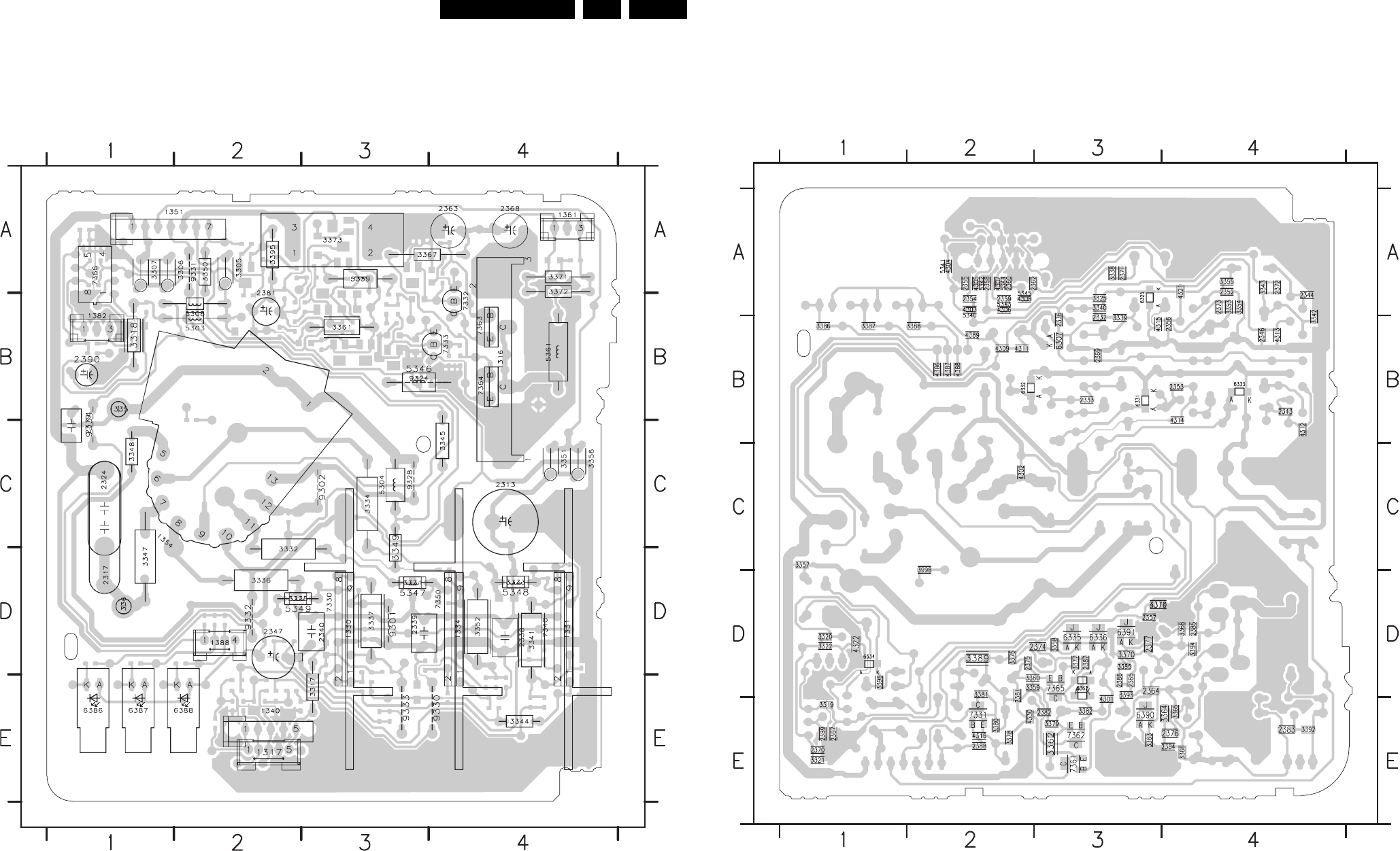
74ES1E AA 7.
Circuit Diagrams and PWB Layouts
Layout CRT Panel (Top Side)
3139 123 5817.4 F_15040_012.eps
230305
1316 B4
1317 E2
1330 D3
1331 D4
1334 D4
1335 B1
1336 D1
1340 E2
1351 A1
1354 C1
1361 A4
1382 B1
1388 D2
2313 C4
2317 D1
2319 C1
2324 C1
2338 D4
2339 D3
2340 D3
2347 D2
2363 A4
2368 A4
2381 B2
2390 B1
3305 A2
3306 A2
3307 A1
3317 E3
3318 B1
3331 D3
3332 D2
3333 D4
3334 C3
3335 D2
3336 D2
3337 D3
3341 D4
3344 E4
3345 C4
3347 D1
3348 C1
3349 D3
3350 A2
3351 C4
3352 D4
3356 C4
3361 B3
3367 A3
3371 A4
3372 A4
3373 A3
3395 A2
5303 B2
5304 C3
5308 B2
5339 A3
5346 B3
5347 D3
5348 D4
5349 D2
5361 B4
6386 E1
6387 E1
6388 E2
7330 D3
7332 B4
7333 B4
7340 D4
7350 D4
7363 B4
7364 B4
7366 A1
9301 D3
9302 C3
9324 B3
9328 C3
9330 E4
9331 A2
9332 D2
9333 E3
9334 C1
Layout CRT Panel (Bottom Side)
3139 123 5817.4 F_15040_013.eps
230305
2332 D2
2333 D2
2336 D2
2343 D1
2344 E1
2346 D1
2352 E1
2353 D1
2354 E3
2355 E3
2356 D1
2357 B2
2358 E3
2359 E3
2360 E3
2361 B3
2362 E3
2364 B2
2365 B2
2367 A4
2369 D2
2370 A4
2382 A2
2383 A1
2384 A1
2385 B1
2386 B2
2387 B2
2388 A3
2389 A4
3319 A4
3320 B4
3321 A4
3322 B4
3325 E2
3339 D2
3340 E2
3342 D1
3343 E1
3354 E1
3355 E1
3357 B4
3362 A2
3363 A2
3364 A1
3365 A1
3366 A1
3368 B1
3370 B2
3377 B2
3378 A3
3379 A2
3380 A3
3381 A3
3386 D4
3387 D4
3388 D3
3392 A1
3394 B1
3396 B4
3999 B3
4302 C3
4303 E3
4304 E3
4305 E3
4306 E3
4307 E3
4308 E3
4309 D3
4311 D3
4312 D1
4313 D1
4314 D1
4315 D2
4321 E1
4330 A3
4386 D3
4387 D3
4388 D3
4389 D3
5340 E3
5341 E3
5342 E3
5343 E3
5344 E3
5345 E3
6307 D2
6308 A3
6325 E2
6331 D2
6332 D3
6333 D1
6334 B4
6361 B2
7331 A3
7361 A2
7362 A2
7365 B2
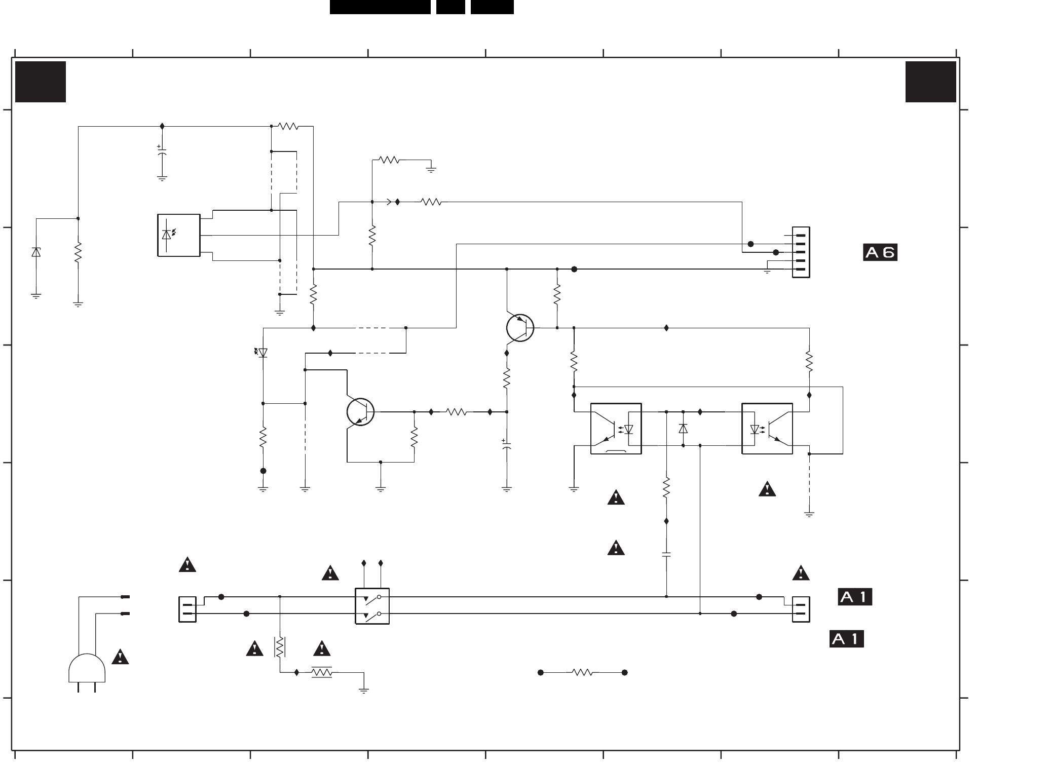
Circuit Diagrams and PWB Layouts 75ES1E AA 7.
Mains Switch Panel (FL9)
NC
E
0201 E2
0202 E7
0247 A7
1010 A2
RES
AC
12345678
1
3057 E3
3066 E3
3078 A4
3081 B3
3082 A3
2 8
A
B
C
D
34567
RC5
E
A
B
C
D
3088 C5
3089 C4
3090 C4
3091 D6
3092 A4
1051 E4
OF
3099 E5
4000 C3
4001 B4
4003 C4
6001 C3
6053 B1
6054 C6
7000 B5
7001 C3
2030 A2
2031 C5
2032 D6
F006 E7
F007 B7
F008 B7
F009 B5
F010 D3
3083 C3
RES
TO 0010
ON-OFF-LED
only for AP
MAINS SWITCH PANEL(FL9)
5V2
RC 5 OUT
3084 B1
3085 B5
3086 C5
3087 C7
I003 A4
I004 B3
I005 E3
I006 B6
I007 C5
3093 B3
RES
4004 D7
4006 B3
4008 B3
4009 A3
4010 A3
I012 C6
I014 D6
I015 D3
I016 D4
7002 C5
7003 C7
F003 E2
F004 E7
F005 E2
F011 E6
BZX284-C3V3
RECEIVER
178 - 250V
MAINS
RES
F012 E5
I001 A2
I002 B3
I009 C7
I010 C4
I008 C5
TO 1505 OF
OR
POWER SUPPLY
*
*
*
*
*
TO 1624 OF
INTERFACING
I011 C5
IN
7001
BC847BW
3090
100K
100R
3078
6053
I004
3086
220R
1
2
F009
0201 24
56
F007
3
4
5
1051
SDDF
13
0247
1
2
4001
3083
1K0
I015
I002
4000
F006
3084
2K2
I001
F010
I003
3081
1K5
1K0
1
3
3099
6001
I012
2031
47u
2
GND
1
OUT
3
VS
3087
220R
42
TSOP34836
1010
TCDT1102G
7002
1
5
F011F012
14
3
2
3085
100K
7003
TCET1102(G)
1N4148
6054
I014
I010
I005
3M3
3057
I009
I007
I006
3091
1K0
F003
F008
I016
I011
3088
47R
2032
22n
I008
F004
F005
4004
3089
1K0
3092
10K
4010
3093
6K8
4009
4008
1
2
4006
0202
330R
3082
3066
4003
3M3
7000
BC857BW
100u
2030
3139 123 6041.2 F_15040_035.eps
310305
M M
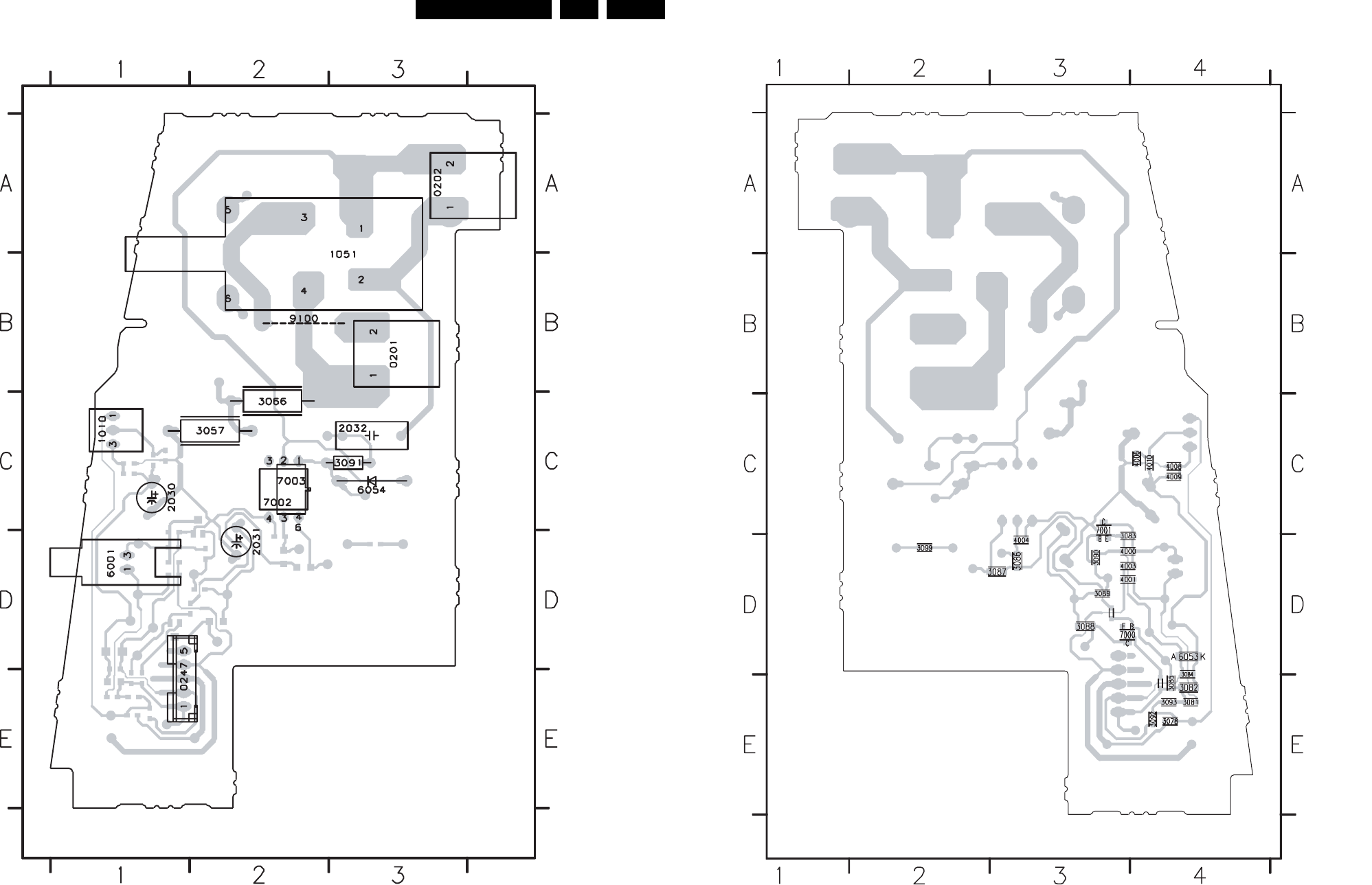
76ES1E AA 7.
Circuit Diagrams and PWB Layouts
Layout Mains Switch Panel (FL9) (Top Side)
0201 B3
0202 A3
0247 E1
1010 C1
1051 B3
2030 C1
2031 D2
2032 C3
3057 C2
3066 C2
3091 C3
6001 D1
6054 C3
7002 C2
7003 C2
9100 B2
3139 123 6041.2
F_15040_036.eps
310305
Layout Mains Switch Panel (FL9) (Bottom Side)
3139 123 6041.2 F_15040_037.eps
310305
4907
4905
3078 E4
3081 E4
3082 E4
3083 D3
3084 E4
3085 E4
3086 D3
3087 D3
3088 D3
3089 D3
3090 D3
3092 E4
3093 E4
3099 D2
4000 D3
4001 D3
4003 D3
4004 D3
4006 C4
4008 C4
4009 C4
4010 C4
4905 E4
4907 D3
6053 D4
7000 D3
7001 C3
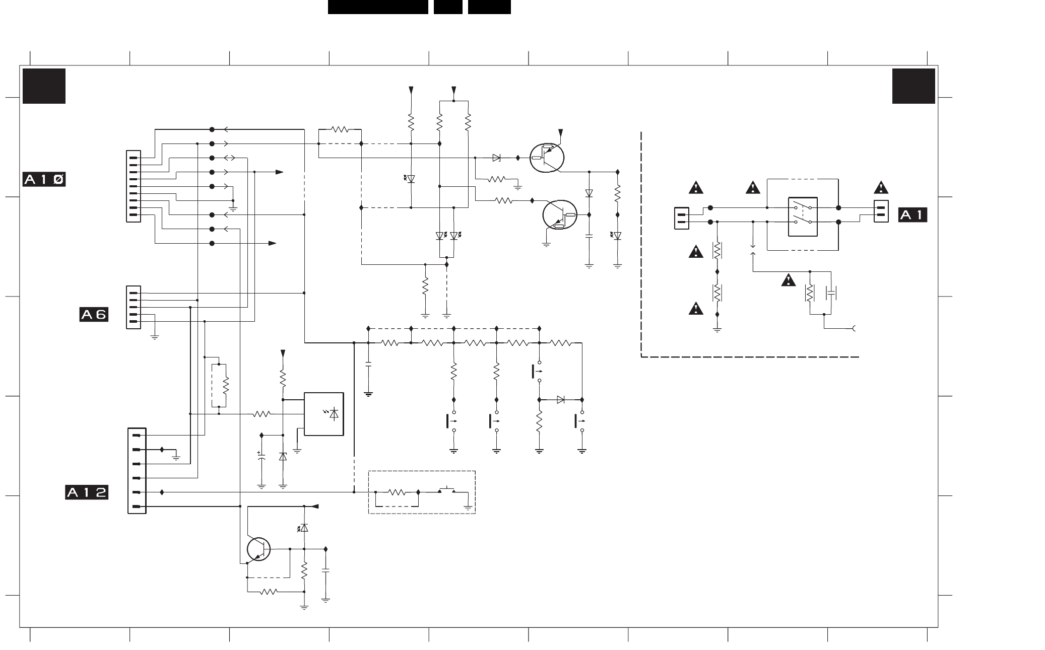
Circuit Diagrams and PWB Layouts 77ES1E AA 7.
Mains Switch Panel (SL5)
F013 B9
I005 D2
I006 B5
I009 D3
9017 C5
9019 D4
9020 E4
9031 A8
9032 B8
F001 A2
F002 A2
CONTROL
POWER
MAINS
I027 A5
I028 A6
I029 A6
I030 B6
**
*
*
*
****
SUPPLY
TO 1624 OF
INTERFACING
I031 B6
F012 B9
6006 E3
6007 B6
6008 A5
6009 A6
6022-2 B4
7001 E3
7002 A6
KEYBOARD
I002 B7
I003 C7
I004 A4
*
*
I010 C4
I011 D4
I012 A5
I013 D2
I016 E3
I018 D5
I019 D5
I020 B4
I021 C5
I023 C6
I024 D6
I025 C4
I025 C5
I026 D6
3031 B7
3032 C7
4001 A4
4002 A4
4003 A4
4004 B4
4005 B4
USA ONLY
RES
LTR-301
RES
BLUE LED
F003 A2
F004 A2
F005 A2
F007 B2
F008 B2
F009 B2
F010 B7
F011 B7
3009 E3
3010 C2
3011 C4
3013 C5
3014 C5
3015 C5
3016 C5
0V
MAINS SWITCH PANEL(SL5)
HOT MAINS SWITCH
RC5
5V-STANDBY
GND
ON/OFF LED
7003 B6
9010 C2
9011 C4
9013 C5
9015 C5
89
A
B
C
D
E
*
LSP
4006 B5
4007 A3
4008 E3
6001 A4
6002-1 B5
6003 C6
6004 C3
6005 D3
9
123456
0V
0V5
IN
1505 OF
TO
0V
0V
*
BACKLIGHT_TOP
COLD
3017 C5
3018 D6
3019 C6
3020 D4
3021 A5
3022 A5
3023 A6
3030 B8
0242 B2
1002 D5
1003 D5
1004 C6
1005 D6
1006 D5
1031 A8
1032 C9
1693 D2
5V3
POWER
2001 D3
2002 E3
2003 C4
2004 B6
2030 B8
3001 A4
3002 A5
3003 A5
3004 A4
3005 B4
3006 C3
3007 D3
3008 E3
C-
V+
FRONT
OF
RES
3V
*
+8V6
AC
FROM 1693
LIGHT SENSOR
GND KEYBOARD
TO
1946
C+
7
A
B
C
D
E
0201 B7
0202 B9
0241 A1
V-
1n5
12345678
2003
10n
I029
I027
I030
I028
I031
10K
3008
7001
6006
100R
3022
PDTC114ET
7003
21
LTL-10224WHCR
6007
2030
3005
1K0
4K7
3021
3
4
5
6
BZX384-C3V3
6008
9031
1693
1
2
4005
1
2
4002
0201
I019
3
4
5
3016
390R
0242
S5B-EH
1
2
100R
3004
3006
330R
3007
I011
F012
I013
1
2
F010
0202
1
3
5
6
2
4
1003
SDDF
1031
3020
560R
1002
3015
560R
4006
3M3
3032
4001
I026
F004
4004
F005
I012
3002
330R
I006
1004
3014
150R
I004
3030
3M3
F003
3010
9010
1006
ORANGE-RED
TLUV5300
6002-1
12
F007
6005
BZX384-C3V3
I024
4007
4003
I018
1
I009
6001
LTL-10224WHCR
2
3003
330R
I003
I002
3M3
3031
1005
BAS316
6009
4n7
2004
270R
3023
PDTA114ET
7002
1K5
3018
3011
560R
9020
I010
9032
4008
2001
100u 10V
I021
3017
270R
F001
TSOP1836
6004
2GND
1OUT
3VS
F009
I020
I016
2002
47n
680K
3009
9017
F002
90159013
BAT85
6003
F013
F008
I017 9011
F011
1032
GREEN
6022-2
TLUV5300
3
2
3001
560R
5
6
7
8
9
I005
0241
1
2
3
4
9019
390R
3013
I025
3K3
3019
I023
ON_OFF_LED
5V-STANDBY
LIGHT_SENSOR
8V6
5V-STANDBY
RC5_SWITCH
5V-STANDBY
KEYBOARD
8V6
5V-STANDBY
5V-STANDBY
3139 123 6015.1 F_15040_039.eps
310305
M M
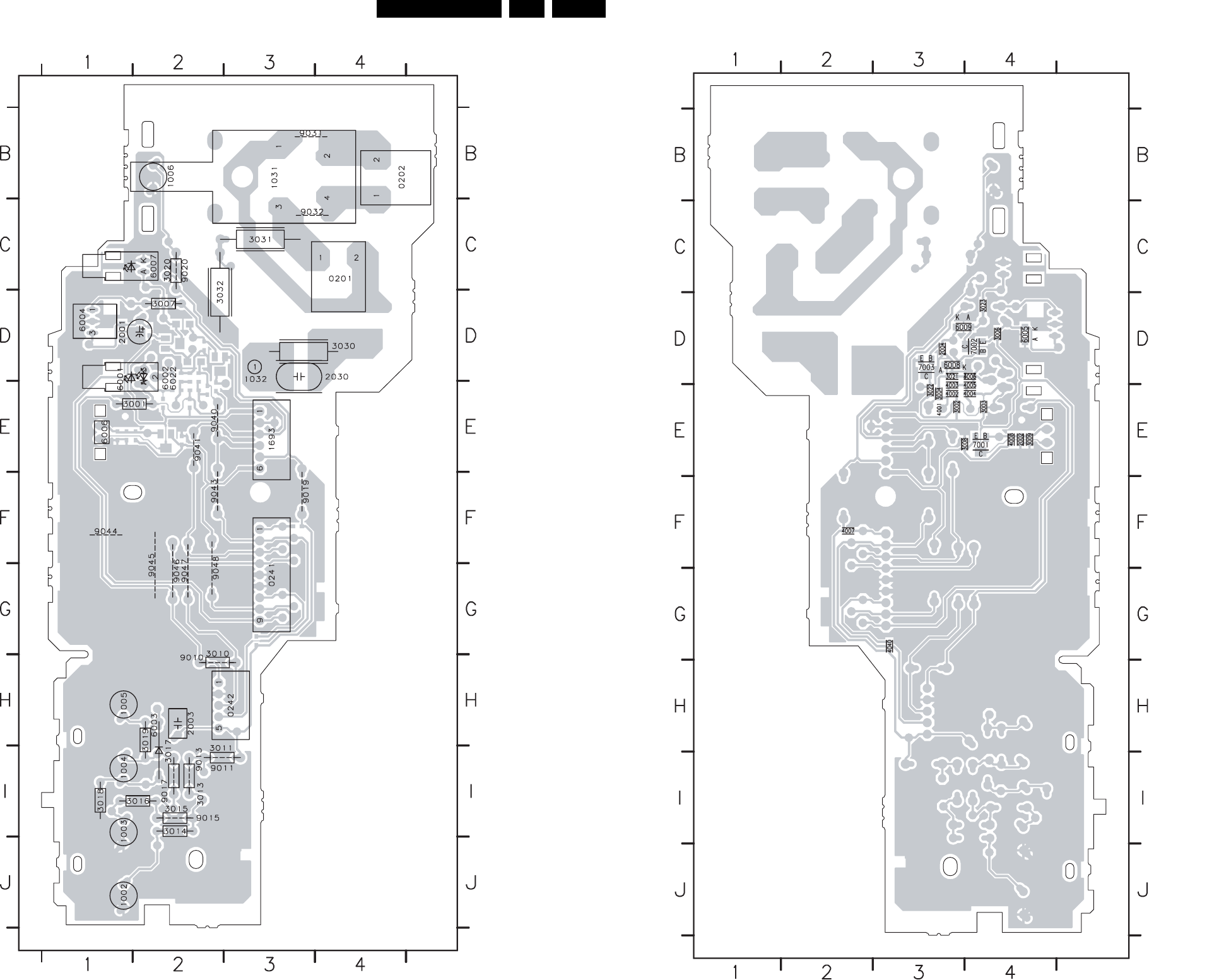
78ES1E AA 7.
Circuit Diagrams and PWB Layouts
Layout Mains Switch Panel (SL5) (Top Side)
3139 123 6015.1
F_15040_040.eps
310305
0201 C4
0202 B4
0241 G3
0242 H3
1002 J1
1003 I1
1004 I1
1005 H1
1006 B2
1031 B3
1032 D3
1693 E3
2001 D1
2003 H2
2030 D4
3001 E2
3007 D2
3010 G2
3011 I2
3013 I2
3014 I2
3015 I2
3016 I2
3017 I2
3018 I1
3019 H2
3020 C2
3030 D4
3031 C3
3032 D2
6001 D1
6002 D2
6003 H2
6004 D1
6006 E1
6007 C2
6022 D2
9010 H2
9011 I2
9013 I2
9015 I2
9017 I2
9019 F3
9020 C2
9031 B3
9032 C3
9040 E2
9041 E2
9043 F2
9044 F1
9045 G2
9046 G2
9047 G2
9048 G2
Layout Mains Switch Panel (SL5) (Bottom Side)
3139 123 6015.1 F_15040_041.eps
310305
2002 E4
2004 D3
3002 E3
3003 E4
3004 E3
3005 D4
3006 D4
3008 E4
3009 E4
3021 D3
3022 E3
3023 D4
4001 E3
4002 E3
4003 E3
4004 E4
4005 E4
4006 D4
4007 F2
4008 E4
4040 G3
6005 D4
6008 D3
6009 D3
7001 E4
7002 D4
7003 D3
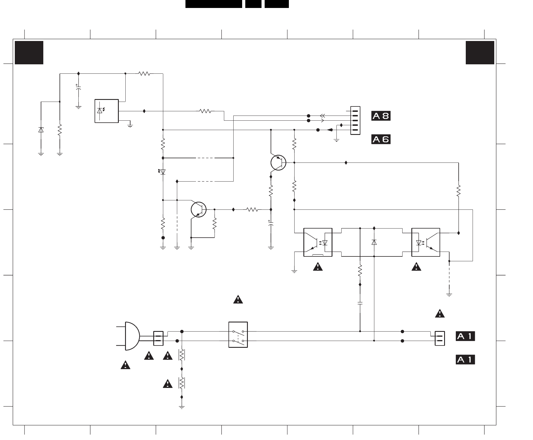
Circuit Diagrams and PWB Layouts 79ES1E AA 7.
Front Interface Panel (PV2)
NC
3984 A1
3985 A5
AC MAINS
TO 0947 OF
A
B
C
D
E
0201 D2
0202 D7
0203 A6
1910 A2
1951 D4
2930 A1
2931 C4
2932 D6
3957 E3
3966 E3
3978 A3
3981 A3
3982 A2
3983 C3
RES
RES
220V
67
1234567
A
B
C
D
E
RC 5 OUT
RES
3986 B5
3987 B7
3988 B4
3989 B4
3990 C3
3991 C6
4900 C3
4901 B3
4903 B3
4904 D7
ON-OFF-LED
*
T4.0AE
6901 B3
6953 A1
6954 C6
7900 B4
7901 B3
7902 C5
7903 D6
F903 D3
F904 D6
F905 D3
F906 D6
F907 A5
F908 A5
F909 A5
F910 C3
I901 A1
I902 B3
I903 A2
I904 B2
I905 E3
RES
OR
TO 0010 OF
*
*
I906 B5
I907 B4
I908 B5
I909 C7
I910 C4
I911 B4
I912 C6
I913 A5
I914 D5
I915 E3
FRONT INTERFACE PANEL PV2
*
12345
INPUT
3985
100K
OR
TO 1624 OF
INTERFACING
*
TO 1505 OF
POWER SUPPLY
F908
2
0202
1
3988
47R
220R
3987
3986
220R
7900
BC857BW
1
2
3
4
5
I905
0203
F905
2932
22n
2
GND
1
OUT
3
VS
1910
TSOP34836
3978
470R
1N4148
6954
4904
I904
F910
I903
I911
3981
1K5
6901
2930
100u
I913
F907
F909
3991
1K0
3990
F904
3989
1K0
100K
4903
4
3983
1K0
1
3
56
2
SDDF
1951
15
42
I902
TCDT1102G
7902
4901
I901 3982
330R
32
I910
TCET1101(G)
7903
14
I907
I912
4900
7901
BC847BW
3957
3M3
BZX384-C3V3
6953
0201
1
2
3M3
3966
I915
F903
F906
I906
I909
2931
47u
I914
3984
2K2
I908
5V2
Q1 Q1
3139 123 5499.3
F_15040_043.eps
310305
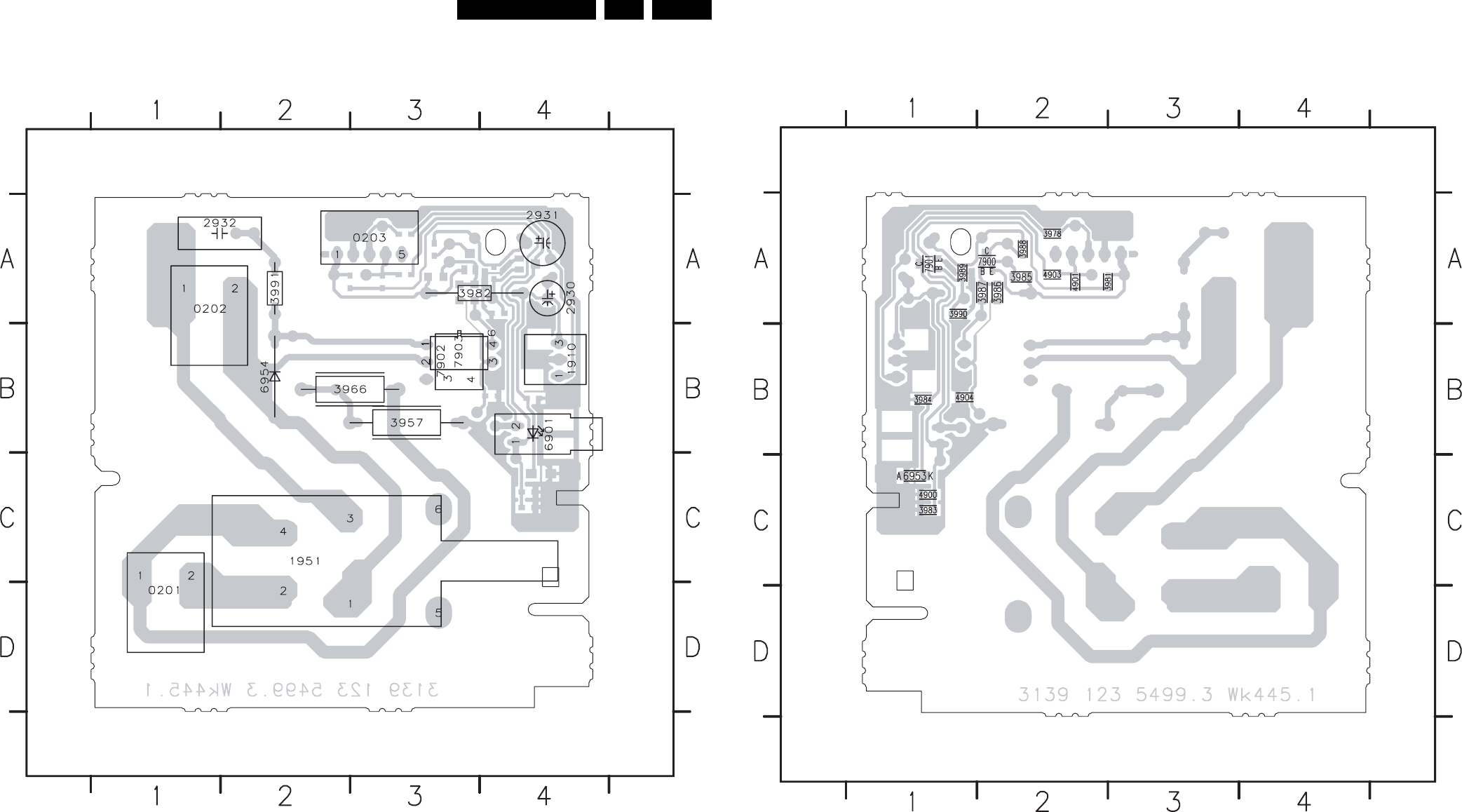
80ES1E AA 7.
Circuit Diagrams and PWB Layouts
Layout Front Interface Panel (PV2) (Top Side)
3139 123 5499.3 F_15040_044.eps
310305
0201 D1
0202 A1
0203 A3
1910 B4
1951 C2
2930 A4
2931 A4
2932 A1
3957 B3
3966 B3
3982 A3
3991 A2
6901 B4
6954 B2
7902 B3
7903 B3
Layout Front Interface Panel (PV2) (Bottom Side)
3139 123 5499.3 F_15040_045.eps
310305
3978 A2
3981 A2
3983 C1
3984 B1
3985 A2
3986 A2
3987 A2
3988 A2
3989 A1
3990 A1
4900 C1
4901 A2
4903 A2
4904 B1
6953 C1
7900 A2
7901 A1
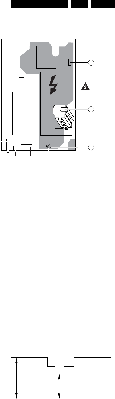
Alignments EN 81ES1E 8.
8. Alignments
Index of this chapter:
8.1 General Alignment Conditions
8.2 Hardware Alignments
8.3 Software Alignments
8.4 Option Settings
8.1 General Alignment Conditions
8.1.1 Default Alignment Settings
Perform all electrical adjustments under the following
conditions:
• Power supply voltage: 230 VAC / 50 Hz (± 10 %).
• Connect the set to the mains via an isolation transformer
with low internal resistance.
• Allow the set to warm up for approximately 20 to 30
minutes.
• Measure voltages and waveforms in relation to chassis
ground (with the exception of the voltages on the primary
side of the power supply).
Caution: never use heatsinks as ground.
• Test probe: 100 : 1, Ri > 10 Mohm, Ci < 3.5 pF.
• Use an isolated trimmer/screwdriver to perform
alignments.
Perform all electrical adjustments with the following default
settings (for all CRTs):
• Choose "Soft" picture mode with the "Smart Picture" button
on the remote control.
• Set "Dynamic Contrast" and "Active Control" to "off" (if
either one of them is present).
• Set "Brightness" to aligned value unless otherwise
specified.
• Set "Contrast value" to 99.
8.1.2 Adjustment Sequence
Use the following adjustment sequence:
1. Set the correct TV-set OPTIONS as described in
paragraph "Options". After storing, re-start the set.
2. Rough adjustment of VG2 and FOCUS (potentiometers in
“midway” positions).
3. RF-AGC alignment.
4. IF-PLL OFFSET adjustment.
5. Rough adjustment of GEOMETRY.
6. Allow the set to warm up.
7. Precise adjustment of VG2 and FOCUS.
8. Precise adjustment of GEOMETRY.
9. PIP alignments (if present).
10. COLOUR alignments.
11. Other software alignments.
8.2 Hardware Alignments
Notes:
• The Service Alignment Mode (SAM) is described in chapter
5 "Service Modes, Error Codes, and Fault Finding".
• Use the cursor-, menu-, and OK-buttons of the remote
control (RC) transmitter for navigation.
Figure 8-1 Top view LSP
8.2.1 Vg2 Adjustment
In the frame-blanking period of the R, G, and B signals applied
to the CRT, the video processor inserts a measuring pulse with
different DC levels. Measure the black level pulse during the
vertical flyback at the RGB cathodes of the CRT.
1. Connect the RF output of a pattern generator to the
antenna input. Input a "black" picture (blank screen on CRT
without any OSD info) test pattern.
2. In the SAM mode, set the “Normal Red”, “Normal Green”
and “Normal Blue” values to “0” for “White Tone”.
3. Disable the black current loop (via the AKB bit).
4. Use the MENU key to enter the "user" menu, select
"Picture", and set "Brightness" and "Contrast" to “0”.
5. Set the oscilloscope to 20 V/div and the time base to 20 us/
div. Use external triggering on the vertical pulse.
Caution: use a trigger point on the "cold" side!
6. Ground the scope on the CRT panel ("cold" side) and
connect a 10:1 probe to one of the cathodes of the picture
tube socket (see circuit diagram B1).
7. Measure at test points F338, F339 and F341 on the picture
tube socket the DC-level of the measuring pulse (1st full
line after the frame blanking) with respect to earth.
8. Select the pin with the highest level found and adjust
V_cutoff by means of the Vg2-potmeter (lowest-one) on the
Line Output Transformer (LOT) to 160 +/- 5 VDC (for all
screen sizes).
9. Reset "Contrast" and "Brightness" to their original values.
Figure 8-2 Waveform Vg2 alignment
CL 26532041_060.eps
110402
SSB
V.SHIFTCINCH SCART
TUNER 3642
1502
5430
Focus 2
Focus 1
Screen
VG2
LOT
Warning
All alignments
are on hot-part !
A
B
C
0V Ref.
CL 06532130_014.eps
131000
V
CUTOFF
[V
DC
]
max.

Alignments
EN 82 ES1E8.
8.2.2 Focus alignment
The LOT has the following outline:
– Focus 1 (F1) = Static alignment (red wire).
– Focus 2 (F2) = Dynamic alignment (white wire).
1. Use an external video pattern generator to input a "circle"
or "crosshatch" test pattern to the set.
2. Choose "Natural" picture mode with the "Smart Picture"
button on the remote control transmitter.
3. Adjust the "dynamic focus 2" potentiometer (in the middle
on the LOT) until the horizontal lines at the centre of the
screen are of minimum width without introducing a visible
haze.
4. Adjust the "static focus 1" potentiometer (highest of the
LOT) until the horizontal lines at the sides of the screen are
of minimum width without introducing a visible haze.
5. Repeat these two steps to achieve the best result.
8.3 Software Alignments
Put the set in the SAM (see the "Service Modes, Error Codes
and Fault Finding" section). The SAM menu will now appear on
the screen. The different alignment parameters are described
further on.
Notes:
• All changes to menu items and alignments must be stored
manually.
• If an empty EAROM (permanent memory) is detected, all
settings are set to pre-programmed default values, so the
set must be re-aligned.
8.3.1 Tuner
AGC
1. Set an external pattern generator to a colour bar video
signal and connect the RF output to the aerial input of the
TV. Set the amplitude to 10 mV and the frequency to
475.25 MHz. Use system PAL B/G if possible, otherwise
match the system of your generator with the received
signal in the set.
2. Put the set in the SAM mode.
3. Select via the TUNER menu, the AGC sub-menu.
4. Connect a DC multi-meter to pin 1 of the tuner (F235, AGC
pin).
5. Adjust the AGC until the voltage at pin 1 (F235, AGC pin)
of the tuner is 3.3 V (+/- 0.1 V). The value can be
incremented or decremented by pressing the right/left
CURSOR button on the RC.
6. After alignment, save the value(s) with the STORE
command in the SAM main menu.
IF PLL OFFSET
No adjustments needed: default value is "35".
If the mentioned default value does not give the required result,
use the following alignment method:
1. Set an external pattern generator to a crosshatch video
signal and connect the RF output to the aerial input of the
TV. Set the amplitude to 10 mV and the frequency to
475.25 MHz. Use system PAL B/G if possible, otherwise
match the system of your generator with the received
signal in the set.
– For "Negative modulation", the sound signal must be
a non-modulated FM signal.
– For "Positive modulation", the video signal must have
high modulation (100% or above).
2. Put the set in the SAM mode.
3. Select via the TUNER menu, the IF-PLL OFFSET sub-
menu.
4. Measure and align:
– For "Negative modulation", on SCART pin 1 or 3
(audio out): Adjust IF-PLL OFFSET until the largest
Signal Noise Ratio (SNR) is reached.
– For "Positive modulation", on SCART pin 19 (video
out): Adjust IF-PLL OFFSET until you get minimal V-
sync disturbance.
8.3.2 Geometry
Notes:
• Set an external pattern generator to a crosshatch video
signal and connect the RF output to the aerial input of the
TV. Set the amplitude at least 1 mVRMS (60 dBµV) and the
frequency to 475.25 MHz. Use system PAL B/G if possible,
otherwise match the system of your generator with the
received signal in the set.
Note: Do not use the internal test pattern from the
GEOMETRY menu!
• Use the default alignment settings, but set "Brightness" to
"32".
• For wide screen models, set to "wide screen" mode, for
"classic" models, set to "4:3".
• After alignment, save the value(s) with the STORE
command in the SAM main menu.
Service tip: When the set is equipped with a rotation coil, use
this menu item to check its correct alignment. If alignment is not
correct, go to the user MENU, choose FEATURES, and select
ROTATION. With the use of a crosshatch test pattern, align it
to a correct horizontal picture.
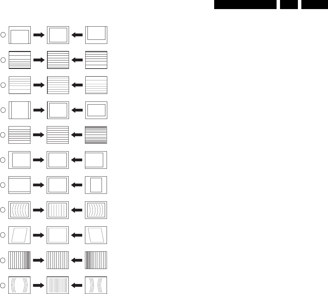
Alignments EN 83ES1E 8.
Alignment
Figure 8-3 Geometry Alignments
Use the following software regulations to modify the geometry:
1. VER. SHIFT (Vertical Shift): Align for the vertical picture
centre, range from -32 to +32.
2. VER. AMPL (Vertical Amplitude): Compensating for any
gain error in amplifier, adjust range from -32 to +32 to the
proper amplitude.
3. VER. SCOR (Vertical S-Correction): Align for equal height
of the blocks in the top, the bottom and the middle, range
from -63 to +63.
4. VER. U_LIN (Vertical Upper Linearity): Align for linearity of
the upper screen, range from -63 to +63.
5. VER. L_LIN (Vertical Lower Linearity): Align for linearity of
the lower screen, range from -63 to +63.
6. HOR. SHIFT (Horizontal Shift): Adjust for the horizontal
centre of the screen, range from -127 to +128.
Next step is to align the East/West geometry.
1. First, set the parameters EW_5 and EW_6 to "0"
2. EW. WIDTH (East-West Width): This sets the (overall)
horizontal size of the picture on the screen. Range from -
63 to +63 (with the following EW alignments, these lines
can be straightened).
3. EW_1 (East-West parameter 1): Has effect on the length of
the upper part of the vertical E/W lines.
4. EW_2 (East-West parameter 2): Has effect on the length of
the vertical E/W lines just below EW_1.
5. EW_3 (East-West parameter 3): Has effect on the length of
the vertical E/W lines just below EW_2.
6. EW_4 (East-West parameter 4): Has effect on the length of
the vertical E/W lines just below EW_3.
7. EW_5 (East-West parameter 5): Has effect on the length of
the vertical E/W lines just below EW_4.
8. EW_6 (East-West parameter 6): Has effect on the length of
the vertical E/W lines just below EW_5.
9. EW_7 (East-West parameter 7): Has effect on the length of
the vertical E/W lines just below EW_6.
10. EW_8 (East-West parameter 8): Has effect on the length of
the vertical E/W lines just below EW_7.
11. EW_9 (East-West parameter 9): Has effect on the length of
the vertical E/W lines just below EW_8.
12. EW_10 (East-West parameters 10): Has effect on the
length of the lowest part of the vertical E/W lines.
13. HOR. BOW (Horizontal Bow): Align the EW parabola to be
symmetrical, range from -63 to +63.
14. HOR. PARALLEL (Horizontal Parallel): Align for straight
vertical lines on the picture sides, range from -63 to +63.
15. HOR. LIN (Horizontal Linearity): Align for equal width of
horizontal blocks on the left, the right and the centre, range
from -63 to +63.
16. HOR. SCOR (Horizontal S-correction): Align for equal
height of the blocks on the left, the right and the centre,
range from -63 to +63.
17. HOR. IN_PIN (Horizontal Inner Pincushion): Align for the
inner straight vertical lines, range from -15 to +15.
8.3.3 White Tone
In the WHITE TONE sub menu, the colour values for the
different colour temperatures can be changed.
The colour temperature mode (NORMAL, DELTA COOL,
DELTA WARM) can be selected per colour (R, G, and B) with
the RIGHT/LEFT cursor keys. The mode or value can be
changed with the UP/DOWN cursor keys.
First, the values for the NORMAL colour temperature must be
selected. Then the offset values for the DELTA COOL and
DELTA WARM mode can be selected. Note that the alignment
values are non-linear.
CL 36532058_084.eps
211103
4
2
6
7
9
8
VERT. AMPLITUDE
VERT UPPER LINEARITY
HOR. SHIFT
E/W WIDTH
11 HOR. IN. PIN
HOR. PARALLELOGRAM
HOR. BOW
3 VERT LOWER LINEARITY
5 V.S-CORRECTION
10 HOR. LIN
1 VERT. SHIFT

Alignments
EN 84 ES1E8.
Alignment
Normally, no adjustments are needed.
If the white tone alignment values used in CSM of the the TV
set do not give the required result, use the following alignment
method:
1. Set the external pattern generator to a 100% white pattern,
and connect its RF output to the aerial input of the TV. Set
the amplitude to at least 1 mVRMS (60 dBuV) and the
frequency to 475.25 MHz. Use system PAL B/G if possible,
otherwise match the system of your generator with the
received signal in the set.
2. Set "Smart Picture" to "Natural".
3. Set "Dynamic NR" to "off".
4. Put the set in the SAM mode.
5. Select via the WHITE TONE menu, the PATTERN sub-
menu.
6. Set PATTERN to "on".
7. Set NORMAL GREEN to "0".
8. Measure with the colour analyser (Minolta CA100 Colour
Analyser or equivalent), calibrated with the spectra, on the
centre of the screen.
9. Adjust with the cursor left/right command the Red and Blue
register for the right xy-coordinates (see the table below).
10. Repeat the white tone adjustment also for the colour
temperatures COOL and WARM.
Table 8-1 White tone alignment (with colour analyser)
8.3.4 Sound
No adjustments needed. Use the given default values:
• PRESCALE LEVEL
–FM: "+1".
– NICAM: "+3".
– EXTAM Gain: "0".
– PIPMONO: "0".
–ExtLR-in: "0".
• THRESHOLD LEVEL
– Over Mod Tresh: "+3dB".
– NIC ErrLmt_Hi: "200".
– NIC ErrLmt_Lo: "100".
– NoiseThres SC2: "+2".
– NoiseHyst SC2: "+4".
• EFFECTS LEVEL
– BMT CutOffFrq: "50Hz".
– Incredible SND: "60%".
– VDolby: "100%".
8.3.5 Smart Settings
No adjustments needed.
8.4 Option Settings
8.4.1 Introduction
The microprocessor communicates with a large number of I2C
ICs in the set. To ensure good communication and to make
digital diagnosis possible, the microprocessor has to know
which ICs to address. The presence / absence of these specific
ICs (or functions) is made known by the option codes.
Notes:
• After changing the option(s), save them with the STORE
command.
• All changes are disregarded when the OPTIONS submenu
is left without using the STORE command.
• The new option setting is only active after the TV is
switched "off" and "on" again with the Mains switch (the
EAROM is then read again).
8.4.2 Changing Options
Options are used to control the presence / absence of certain
features and hardware. There are two ways to change the
option settings. All changes in the option settings are saved by
selecting STORE and pressing the CURSOR RIGHT key.
Some changes will only take affect after the set has been
switched OFF and ON with the mains switch (cold start).
Changing Multiple Options by Changing Option Byte
Values
Option Bytes (OB) makes it possible to set all options very fast.
An option byte represents a number of different options. All
options are controlled via option bytes (OB1 to OB13; each
“OB” number represents 16 bits; bit numbers that are not used
are omitted in the second column). Select an Option Byte you
want to change with the CURSOR UP/DOWN keys, and key in
the new value. See the table for more details. An explanation
per option is listed in paragraph "Option Bit Definition".
Changing a Single Option
It is also possible to change an option one at a time. Therefore,
select the option with the CURSOR UP/DOWN keys and
change its setting with the LEFT/RIGHT keys.
8.4.3 Option Settings
In the table below, you will find the option settings.
White D mode Temperature DUV x y
Normal 8500 K +-0.004 288 +/- 4 300 +/- 4
Cool 11500 K +-0.005 273 +/- 5 282 +/- 5
Warm 7000 K +-0.005 305 +/- 5 312 +/- 5

Alignments EN 85ES1E 8.
Table 8-2 Option bit overview
Option
Bytes
(OB1...
OB13)
Number
of Bits
Decimal
value
Name Features
32PW8720/12
28PW8720/12
32PW8620/12
28PW8620/12
29PT8640/12
29PT8520/12
28PT7120/12
28PW8720/05
32PW8720/05
32PW8820/12
32PW8820/12
32PW8820/12
32PW8820/12
1 5 32 RCMX RC for Teletext Mix Mode 0 0 0 0 0 0 0 0 0 0 0 0 0
6 64 EQTO Equalizer/Tone 0 0 0 0 0 0 0 0 0 0 0 0 0
8 256 WSSB Wide Screen Signal Bit 1 1 1 1 0 0 0 1 1 1 1 0 0
12 4096 DGSC Digital Scan 1 1 1 1 1 1 1 1 1 1 1 1 1
14 16384 SSHT Subtitle Shift 1 1 1 1 0 0 0 1 1 1 1 0 0
2 5 32 DBYV Dolby Virtual 1 1 1 1 1 1 1 1 1 1 1 1 1
7 128 SWOF Swoofer** (1st bit) 0 0 0 0 0 0 0 0 0 0 0 0 0
8 256 SWOF Swoofer** (2nd bit) 0 0 0 0 0 0 0 0 0 0 0 0 0
9 512 P50 P50 1 1 1 1 1 1 1 1 1 1 1 1 1
11 2048 QPEAK AV Sound Mode Detection 0 0 0 0 0 0 0 0 0 0 0 0 0
3 0 1 AV3 Side AV Source 1 1 1 1 1 1 1 1 1 1 1 1 1
1 2 SCT3 Scart 3 Input 0 0 0 0 0 0 0 0 0 0 0 0 0
8 256 ASPR Aspect Ratio 1 1 1 1 0 0 0 1 1 1 1 0 0
9 512 ROTI Rotation Tilt 1 1 1 1 0 0 0 1 1 1 1 0 0
4 3 8 PITN Philips tuner*** (1st bit) 1 1 1 1 1 1 1 1 1 1 1 1 1
4 16 PITN Philips tuner*** (2nd bit) 0 0 0 0 0 0 0 0 0 0 0 0 0
5 6 64 AAVL Automatic Volume Leveller 1 1 1 1 1 1 1 1 1 1 1 1 1
6 12 4096 BASF Bass Feature* (1st bit) 1 1 1 1 1 1 1 1 1 1 1 1 1
13 8192 BASF Bass Feature* (2nd bit) 0 0 0 0 0 0 0 0 0 0 0 0 0
8 4 16 PIPC PIP control 0 0 0 0 0 0 0 0 0 1 1 1 1
5 32 PIPT PIP tuner 0 0 0 0 0 0 0 0 0 0 0 0 0
6 64 W4X3 DW 4:3 0 0 0 0 0 0 0 0 0 1 1 1 1
7 128 W169 DW 16:9 0 0 0 0 0 0 0 0 0 1 1 1 1
9 0 1 APC Auto Picture Control (Auto TV) 1 1 1 1 1 1 1 1 1 1 1 1 1
5 32 VMOD Virgin Mode 0 0 0 0 0 0 0 1 1 0 0 0 0
7 128 TIME Timer 1 1 1 1 1 1 1 1 1 1 1 1 1
8 256 DNR Dynamic Noise Reduction 1 1 1 1 1 1 1 1 1 1 1 1 1
9 512 BBD Black Bar Detect 1 1 1 1 0 0 0 1 1 1 1 0 0
10 5 32 UKPNP UK plug and play 0 0 0 0 0 0 0 1 1 0 0 0 0
6 64 DTXT Dual Text 1 1 1 1 0 0 0 1 1 1 1 0 0
7 128 VTXT Video Text 1 1 1 1 0 0 0 1 1 1 1 0 0
8 256 SBNP Auto Standby with no picture 1 1 1 1 1 1 1 1 1 1 1 1 1
9 512 AUSB Auto Standby Auto On 0 0 0 0 0 0 0 0 0 0 0 0 0
10 1024 CZOM Continuous Zoom 1 1 1 1 0 0 0 1 1 1 1 0 0
11 2048 HSHT Heading Shift 1 1 1 1 0 0 0 1 1 1 1 0 0
13 8192 HOSP Hospitality Mode 1 1 1 1 1 1 1 1 1 1 1 1 1
14 16384 CHLK Child Lock 1 1 1 1 1 1 1 1 1 1 1 1 1
11 3 8 SOSD Smart OSD 0 0 0 0 0 0 0 0 0 0 0 0 0
9 512 T1H0 100 Page Text 0 0 0 0 0 0 0 0 0 0 0 0 0
13 8192 FAPG Favorite page 1 1 1 1 1 1 1 1 1 1 1 1 1
14 16384 ACI Automatic Channel Installation 1 1 1 1 1 1 1 1 1 1 1 1 1
12 8 256 PLST Program List 1 1 1 1 1 1 1 1 1 1 1 1 1
12 4096 HPMN Headphone Menu 1 1 1 1 1 1 1 1 1 1 1 1 1
13 0 1 T2H5 250 Page Text 0 0 0 0 0 0 0 0 0 0 0 0 0
2 4 T12H 1200 Page Text 1 1 1 1 1 1 1 1 1 1 1 1 1
7 128 SMCK Smart clock 1 1 1 1 1 1 1 1 1 1 1 1 1
8 256 ATS Automatic Tuning System 1 1 1 1 1 1 1 1 1 1 1 1 1
12 4096 SSD SplitScreenDemo 1 1 1 1 1 1 1 1 1 1 1 1 1

Alignments
EN 86 ES1E8.
8.4.4 Option Bit Definition
Sources
AV3: Side AV source.
Function: Disable/Enable side AV source.
Values: OFF= Disabled, side AV source is not available. ON=
Enabled, side AV source is available.
SCT3: SCART 3 input.
Function: Disable/Enable Scart3 input.
Values: OFF= Disabled. ON= Enabled.
Video
ASPR: Aspect Ratio Setting.
Function: Select between 4 by 3 or 16 by 9 set.
Values: OFF= 4 by 3 set. ON= 16 by 9 set.
W4X3: Screen size 4x3.
Function: Disable/Enable Screen size 4x3.
Values: OFF= Disabled. Screen size 4x3 is not available. ON=
Enabled. Screen size 4x3 is available.
W169: Screen size 16x9.
Function: Disable/Enable Screen size 16x9.
Values: OFF= Disabled. Screen size 16x9 is not available.
ON= Enabled. Screen size 16x9 is available.
DNR: Dynamic Noise Reduction.
Function: Disable/Enable (Dynamic) Noise Reduction function.
Values: OFF=Disabled. ON= Enabled.
BBD: Black Bar Detection.
Function: Disable/Enable Black Bar Detection.
Values: OFF=Disabled, Black Bar Detection not available. ON=
Enabled, Black Bar Detection available.
Note: The Auto Screen Fit will not be included in the picture
size loop when BBD is OFF (WS = 1; 4 : 3 = 0).
CZOM: Continuous Zoom.
Function: Disable/Enable Continuous Zoom.
Values: OFF=Disabled. ON= Enabled (WS = 1; 4 : 3 = 0).
HSHT: Heading Shift.
Function: Disable/Enable Heading Shift.
Values: OFF=Disabled. ON= Enabled (WS = 1; 4 : 3 = 0).
SSHT: Subtitle Shift.
Function: Disable/Enable Subtitle Shift.
Values: OFF=Disabled. ON= Enabled (WS = 1; 4 : 3 = 0).
APC: Auto Picture Control (Auto TV).
Function: Disable/Enable Auto picture control.
Values: OFF= Disabled. ON= Enabled.
WSSB: Wide Screen Signalling Bit.
Function: Disable/Enable Wide screen Signalling bit function.
Values: OFF= Disabled. ON= Enabled (WS = 1; 4 : 3 = 0).
ROTI: Rotation Tilt.
Function: Change the tilt level of picture tube.
Values: OFF= Disabled, menu item ROTATION is not
available. ON= Enabled, menu item ROTATION is available
(WS = 1; 4 : 3 = 0).
DGSC: Digital Scan.
Function: Enable/Disable the Digital Scan in the DIGITAL OPT
menu.
Values: OFF= Disabled, menu item DIG SCAN is not available.
ON= Enabled, menu item DIG SCAN is available.
SSD: Split Screen Demo.
Function: Disable/Enable Split Screen Demo.
Values: OFF= Disabled. Split Screen Demo is not available.
ON= Enabled. Split Screen Demo is available.
Audio
AAVL: Automatic Volume Level control.
Function: Disable/Enable automatic volume leveller function.
Values: OFF=Disabled, menu item AVL is not available. ON=
Enabled, menu item AVL is available.
DBYV: Dolby Virtual.
Function: Select surround setting.
Values: OFF= Disabled, DOLBY VIRTUAL setting is not
available. ON= Enabled, DOLBY VIRTUAL setting is available.
Note: Incredible surround & Dolby virtual are mutually
exclusive.
EQTO: Equalizer or Tone control.
Function: Selection between Equalizer and Tone control (Bass
and Treble).
Values: OFF= Tone control (Bass and Treble). ON= Equalizer.
Note: Equalizer and Tone (Bass and treble) control are
mutually exclusive.
QPEAK: AV Sound Mode detection.
Function: The current Sound Mode detection in AV is not
working correctly. The optimal threshold value for the correct
sound mode detection is still being investigated. Therefore, this
is needed to disable the Sound Mode detection in AV until the
correct threshold is identified.
Value: OFF= Disabled, AV sound auto detection is not
available. ON= Enabled. AV sound auto detection is available.
BASF: Bass Feature.
Function: Disable/Enable Bass Feature.
Values: OFF= Disabled. Bass Feature is not available. ON=
Enabled. Bass Feature is available.
Note: For this feature, 2 bits are used: bit 5 and bit 4 of NVM
address 21hex. The following combinations are possible:
00 = Disable DBE and DUB;
01 = Enable DBE (bit 5 @ 21hex = 0; bit 4 @ 21hex= 1);
10 = Enable DUB (bit 5 @ 21hex= 1; bit 4 @ 21hex= 0);
11 = not used.
HPMN: Headphone menu.
Function: Disable/Enable Headphone menu.
Values: OFF= Disabled. Headphone menu is not available.
ON= Enabled. Headphone menu is available.
SWOF: Subwoofer.
Function: Disable/Enable Subwoofer.
Values: OFF= Disabled. Subwoofer is not available. ON=
Enabled. Subwoofer is available.
Note: For this feature, 2 bits are used: bit 1 of NVM address
19hex and bit 7 of NVM address 18hex. The following
combinations are possible:
00 = None;
01 = Subwoofer (bit 1@19hex = 0; bit 7@18hex = 1);
10 = Woox (bit 1@19hex = 1; bit 7@18hex = 0);
11 = not used.
Tuning
PITN: Philips Tuner.
Function: Choose the tuner type that is configured in the
hardware.
Values: OFF= Disabled, Other (non-Philips) tuner is used. ON=
Enabled, Philips compatible tuner is used.
Note: For this feature, 2 bits are used: bit 4 and bit 3 of NVM
address 1Chex. The following combinations are possible:
00 = Other tuner;
11 = Philips tuner (bit 4 and bit 3@ 1Chex = 1).
Installation
ACI: Automatic Channel Installation.
Function: Disable/Enable automatic channel installation.
Values: OFF= Disabled Automatic Channel Installation. ON=
Enabled Automatic Channel Installation.
Note: Download present program when ACI is ON.

Alignments EN 87ES1E 8.
ATS: Automatic Tuning System.
Function: Disable/Enable automatic tuning system.
Values: OFF= Disabled, automatic tuning system is ignored.
ON= Enabled Automatic Tuning System, sort the program in an
ascending order starting from Program 1.
Note: Sort the program in an ascending order starting from
Program 1 when ATS is ON.
VMOD: Virgin Mode.
Function: Disable/Enable virgin mode.
Values: OFF= Disabled, cannot access virgin mode. ON=
Enabled, can access virgin mode.
Note: Plug and Play menu item will be displayed to perform
installation at the initial start up of the TV when MOD is ON and
after installation is done, VMOD will be automatically set to
OFF.
UKPNP: UK Plug and Play.
Function: Disable/Enable UK’s default Plug and Play setting.
Values: OFF= Disabled, UK’s default Plug and Play setting is
not available. ON= Enabled, UK’s default Plug and Play setting
is available.
Note: When UKPNP and VMOD are ON at the initial set-up,
LANGUAGE= ENGLISH, COUNTRY= GREAT BRITAIN and
after auto store is complete, VMOD will be set automatically to
OFF while UKPNP remain ON.
Program Selection
PLST: Program List.
Function: Disable/Enable Program List function.
Values: OFF= Disabled, the access to Program List Command
is ignored. ON= Enabled, the access to Program List
Command is processed.
Picture In Picture
PIPC: PIP Control.
Function: Disable/Enable submenu to adjust PIP Picture
settings
Values: OFF= Disabled, PIP feature is not available. ON=
Enabled, PIP feature is available
Note: PIP is present in FEATURES submenu when PIPC is
ON. When PIPC is switched OFF, bits PIPT, W4X3, and W169
must be automatically set to OFF.
PIPT: PIP Tuner.
Function: To determine the presence of second tuner.
Values: OFF= Disabled, second tuner is not available. ON=
Enabled, second tuner is available.
Note: When PIPC is switched OFF, bits PIPT, W4X3, and
W169 must be automatically set to OFF.
Clock
SMCK: Smart Clock/Autochron.
Function: Disable/Enable smart clock/AutoChron function.
Values: OFF= Disabled, menu item smart clock function not
available. ON= Enabled, menu item smart clock function
available.
Note: For NAFTA, AUTOCHRON is present in INSTALL
submenu when SMCK is ON. For AP-PAL and EUROPE,
Smart clock downloaded from Teletext is enabled when SMCK
is ON.
TIME: Timer.
Function: Disable/Enable menu item TIMER.
Values: OFF= Disabled, menu item TIMER not available. ON=
Enabled, menu item TIMER available.
Note: TIMER submenu is present in FEATURES submenu
when TIME is ON.
Data Service
DTXT: Dual Text.
Function: Disable/Enable Dual Text.
Values: OFF= Disabled. Dual text is not available. ON=
Enabled. Dual text is available (WS = 1; 4 : 3 = 0).
RCMX: RC for Teletext Mix Mode.
Function: Disable/Enable RC for Teletext Mix mode support.
Values: OFF= Disabled. RC for mix mode is not available. ON=
Enabled, RC for mix mode is available.
FAPG: Favourite Page.
Function: Disable/Enable favourite page in Teletext mode.
Values: OFF= Disabled favourite page in Teletext mode. ON=
Enabled favourite page in Teletext mode.
T1H0: 100-Page Text.
Function: Disable/Enable 100-page Text.
Values: OFF= Disabled. 100-page text is not available. ON=
Enabled, 100-page text is available.
T2H5: 250-Page Text.
Function: Disable/Enable 250-page Text.
Values: OFF= Disabled. 250-page text is not available. ON=
Enabled, 250-page text is available.
T12H: 1200-Page Text.
Function: Disable/Enable 1200-page Text.
Values: OFF= Disabled. 1200-page text is not available. ON=
Enabled, 1200-page text is available.
VTXT: Video Text.
Function: Disable/Enable Video Text.
Values: OFF= Disabled. Video text is not available. ON=
Enabled. Video text is available (WS = 1; 4 : 3 = 0).
Lock Features
CHLK: Child Lock.
Function: Disable / Enabled function to block/unblock
channels.
Values: OFF= Disabled. ON= Enabled.
OSD/Menu Related
SOSD: Smart OSD.
Function: Disable/Enable full display of SMART SOUND and
SMART PICTURE OSD.
Values: OFF= Disabled, full display of SMART SOUND and
SMART PICTURE OSD not available. ON= Enabled, full
display of SMART SOUND and SMART PICTURE OSD
available.
Miscellaneous
HOSP: Hospitality mode.
Function: Disable/Enable Hospitality mode.
Values: OFF= Disabled. Hospitality mode is not available. ON=
Enabled. Hospitality mode is available.
SBNP: Auto Standby with No Picture.
Function: Disable/Enable automatic switch to standby after 15
minutes when no ident.
Values: OFF= Disabled, no automatic switch to standby. ON=
Enabled, set switches to standby after 15 minutes when no
ident.
AUSB: Auto Standby Auto On.
Function: Disable/Enable automatic switch to standby if no RC
or local keyboard response after 4 hours provided that the set
is ON from standby mode by the timer.
Values: OFF= Disabled, no automatic switch to standby. ON=
Enabled, set switches to standby after 4 hours.
P50: P50 (Easylink).
Function: Disable/Enable P50 feature.
Values: OFF= Disabled, P50 feature not available. ON=
Enabled, P50 feature is available.
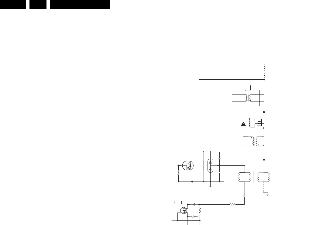
Circuit Descriptions, Abbreviation List, and IC Data Sheets
EN 88 ES1E9.
9. Circuit Descriptions, Abbreviation List, and IC Data Sheets
Index of this chapter:
9.1 Introduction
9.2 Deflection
9.3 Software Upgrading
9.4 Abbreviation List
9.5 IC Data Sheets
Note: Only new circuits (circuits that have not been published
recently) are described. For the other circuits, see the A02E
manual.
9.1 Introduction
The ES1E is a flat screen type CRT TV set for the year 2005 -
2006. It is based on the SSB of the A02, but the LSP, called
Esplanade, has been redesigned in order to reduce the “hot”
part of the chassis. In this chapter, only the deflection circuits,
the correction circuits and the X-ray protection circuits are
described.
9.1.1 Large Signal Panel
The Esplanade chassis has a full sized LSP, which is has been
redesigned with respect to the previous A02 chassis in order to
reduce the “hot” parts of the circuit.
The main functionalities of the LSP are:
• Supply,
• Deflection,
• Sound amplification.
The LSP (single sided) is built up very conventional, with hardly
any surface mounted components on the copper side.
9.2 Deflection
Figure 9-1 Deflection Principle
NC
9
5455 1
2
4
5
7
DEFLECTION
HORIZONTAL
COIL
1
2
5409
2
1
1
2
3
4
C948
5406
*
9412
GND_HOR
2417
2
1
5408
2419
3473
5409
3
4
3
4
5408
K
0V
140V
A
0V
*
*
J
7405
BU2520DX
2413
F418
6404
DMV1500M
3416
47R
2414
2n2
GND_HOR
2412
I473
F419
2416
Vbatt
Deflection Principle Diagram ES1E
S CAP.
DEFLECTION
DAF
27V
D
G
S0V
4V8
E/W
2K2
3434
6471
I499
7406
I415
82K
3425
EAST WEST MODULATION
2nd ORDER S-CORRECTION
F_15040_051.eps
040405
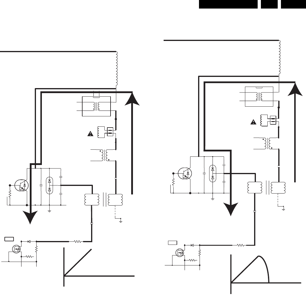
Circuit Descriptions, Abbreviation List, and IC Data Sheets EN 89ES1E 9.
9.2.1 Basic Description.
T0 - T1
Figure 9-2 Deflection T0 - T1
At switch on of the TV set Scap (2417/2418) is charged by
Vbatt. At T0 line transistor 7405 starts conducting. Now the
current flows as shown in figure (T0 - T1), as a result of which
the horizontal deflection will bend the electron beam from the
centre of the screen to the right. Note that the deflection current
has an almost linear waveform.
T1 - T2
Figure 9-3 Deflection T1 - T2
At T1 line transistor 7405 is switched off and the line fly-back
starts. When the line transistor stops conducting, the line
current is at its maximum level. The current charges fly-back
capacitors 2412 and 2413, and also capacitor 2414. This
causes a decrease of line current. (Note that this current has a
half-cosine waveform). The deflection position (i.e. the electron
beam) is in the middle of the screen now.
NC
7
9
5455 1
2
4
5
DEFLECTION
HORIZONTAL
COIL
1
2
5409
2
1
1
2
3
4
C948
5406
*
9412
GND_HOR
2417
2
1
5408
2419
3473
5409
3
4
3
4
5408
K
0V
140V
A
0V
*
*
J
7405
BU2520DX
2413
F418
6404
DMV1500M
3416
47R
2414
2n2
GND_HOR
2412
I473
F419
2416
Vbatt
Deflection T0-T1
27V
D
GS0V
4V8
E/W
2K2
3434
6471
I499
7406
I415
82K
3425
T
I
T0 T1
F_15040_047.eps
040405
Line transistor
CONDUCTS
NC
9
5455 1
2
4
5
7
DEFLECTION
HORIZONTAL
COIL
1
2
5409
2
1
1
2
3
4
C948
5406
*
9412
GND_HOR
2417
2
1
5408
2419
3473
5409
3
4
3
4
5408
K
0V
140V
A
0V
*
*
J
7405
BU2520DX
2413
F418
6404
DMV1500M
3416
47R
2414
2n2
GND_HOR
2412
I473
F419
2416
Vbatt
Deflection T1-T2
27V
D
GS0V
4V8
E/W
2K2
3434
6471
I499
7406
I415
82K
3425
T
I
Line transistor
OPENS
T0 T1 T2
F_15040_048.eps
040405
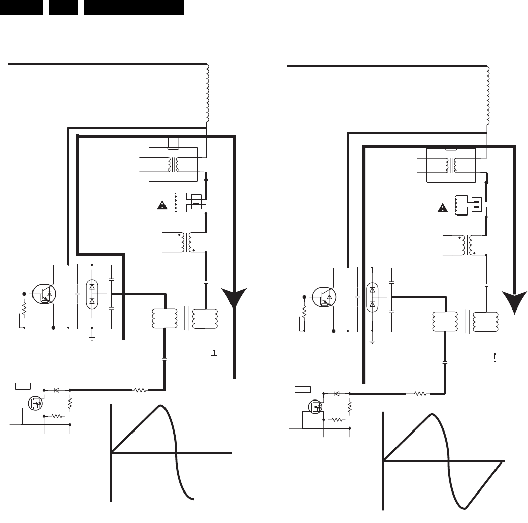
Circuit Descriptions, Abbreviation List, and IC Data Sheets
EN 90 ES1E9.
T2 - T3
Figure 9-4 Deflection T2 - T3
At T2 the deflection current is 0 Amp. The fly-back capacitor
(2412/2413/2414) is charged to approximately 1200 V and will
discharge now. As a result of this, the deflection current will
bend the electron beam to the left of the screen.
T3 - T4
Figure 9-5 Deflection T3 - T4
When the fly-back capacitor (2412/2413/2414) is discharged,
the current is at its maximum negative level. This maximum
negative current will then charge the fly-back capacitor (2412/
2413/2414) with a negative voltage. At this moment, fly-back
diode 6404 will start conducting. The voltage at Scap 2418
causes a linear current flow from T3 - T4. This causes a
deflection current which bends the electron beam back from
the left to the centre of the screen.
9.2.2 Standby and Start Up
In Standby mode, both +5V and Vbatt are not available in order
to meet the standby power saving requirement.
During the start-up phase, +5V is switched on by STANDBY via
7548/7547/7545 and Vbatt is switched on by STANDBY via
7573.
After this, Hdrive is output from the SSB to driver 7404 (see
circuit diagram A2), and consequently to the deflection output
stage (7405). During the slow start-up phase, the Hdrive duty
cycle gradually increases from small to normal. At the
NC
7
9
5455 1
2
4
5
DEFLECTION
HORIZONTAL
COIL
1
2
5409
2
1
1
2
3
4
C948
5406
*
9412
GND_HOR
2417
2
1
5408
2419
3473
5409
3
4
3
4
5408
K
0V
140V
A
0V
*
*
J
7405
BU2520DX
2413
F418
6404
DMV1500M
3416
47R
2414
2n2
GND_HOR
2412
I473
F419
2416
Vbatt
Deflection T2-T3
27V
D
G
S0V
4V8
E/W
2K2
3434
6471
I499
7406
I415
82K
3425
T
I
Line transistor
OPEN
Fly-back caps
DISCHARGE
T0 T1 T2 T3
F_15040_050.eps
040405
NC
9
5455 1
2
4
5
7
DEFLECTION
HORIZONTAL
COIL
1
2
5409
2
1
1
2
3
4
C948
5406
*
9412
GND_HOR
2417
2
1
5408
2419
3473
5409
3
4
3
4
5408
K
0V
140V
A
0V
*
*
J
7405
BU2520DX
2413
F418
6404
DMV1500M
3416
47R
2414
2n2
GND_HOR
2412
I473
F419
2416
Vbatt
Deflection T3-T4
27V
D
G
S0V
4V8
E/W
2K2
3434
6471
I499
7406
I415
82K
3425
T
I
Diode
CONDUCTS
T0 T1 T2 T3 T4
F_15040_049.eps
040405

Circuit Descriptions, Abbreviation List, and IC Data Sheets EN 91ES1E 9.
beginning of the start-up phase, the driver receives its +5V
supply via 3421 and 6465 (see circuit diagram A2). During the
slow start-up phase, the LOT 5450 pin9 voltage gradually
increases, and finally takes over the supply of the +5V voltage,
to supply 5402/7404 via 6403/3493/3451/3419/3432/3415/
3414.
At the end of the slow start-up phase, the deflection stage is
operating at its normal operating condition and all the voltages
are stabilized. Then, the +13V volt supply has fully replaced the
+5V supply to power the horizontal output stage.
At that moment, not only the horizontal deflection, but also the
vertical deflection is functioning at its normal operating
conditions.
9.2.3 Normal Operation and Horizontal Deflection
In normal operation mode, the Hdrive with its 45/55 duty cycle
is switching on and off 7404 (see circuit diagram A2). The driver
stage is working in flyback mode: When 7404 is on, 5402
retains its flux energy and also switches off 7405 via its
secondary coil during flyback mode. When 7404 is switched
off, 5402 releases its energy and turns on 7405. By means of
the on-off switching process, a sawtooth yoke deflection
current is generated.
There are various circuits that are part of the horizontal
deflection circuit.
These will be discussed below:
Horizontal Output Stage:
This a standard circuit (see circuit diagram A2), in which the
main horizontal output stage consists of driver 7404/5402, line
output transistor 7405, tuning capacitor 2411/2414, Scap 2417/
2418 and diode modulator 6404/2413/2416.
Anti-Curtain Effect (Anti-Beta Ringing) Circuit:
5410/2427/3433 (see circuit diagram A2) are the anti-beta
ringing circuit that is tuned to and suppresses the parasitic
ringing frequencies normally occurring in Slot type LOTs to an
acceptable level. For Layer type LOTs, these components are
not required and 9410 is the jumper alternative for Layer type
LOTs.
Beta Ringing, if not suppressed, will cause a type of
interference which is visible as a curtain effect at the left edge
of the screen. This interference is caused by the high amplitude
ringing energy being coupled magnetically or via an electrically
conducting path from the LOT to the small signal circuit. If the
ringing is suppressed to a specific level, the interference will
not be visible anymore.
DAF Circuit:
5455/2402/2403/2405/2406 (see circuit diagram A2) are the
DAF circuit that will be used in DAF or double focus CRT tubes.
For single focus tubes, these components are not required;
9411 is the jumper alternative for non-DAF tubes.
The DAF circuit is used to improve the dynamic focusing of the
tube, particularly in the edge areas. The DC high voltage of
constant level which is supplied to the focus electrode is
referred to as static focus or single focus. In addition to that, an
AC parabolic waveform (derived from the vertical and/or the
horizontal deflection voltages) can be superimposed onto the
DC static focus voltage; this extra AC focusing voltage will then
correct the focus dynamically, corresponding to the scan
position at that particular moment. This is what we refer to as
DAF (Dynamic Astigmatism and Focusing; a method to keep
the electron spot round and focused during the whole scan).
Transformer 5455 takes the horizontal deflection current as its
input and transfers its energy to the capacitor (2402/2403/
2405/2406) on its secondary side. The current in the secondary
coil of the transformer charges the capacitor and this results in
a parabolic waveform. The parabolic waveform is fed to
connector 1402 of the LOT focus cable and is coupled via an
internal 500 pF capacitor inside the LOT and superimposed
onto the static focus voltage.
2nd order S-correction circuit:
5406/2407/3403 (see circuit diagram A2) are the 2nd order S-
correction circuit, which is used mainly in large wide screen
tubes, because they are prone to scanning imperfections that
need 2nd order S-correction. For 4x3 tubes or relatively small
wide screen tubes, these components are not required, and
then 9401 is the jumper alternative for them.
Due to the relatively wide angle of large wide screen flat tubes,
the inner tube surface (which is flat) and the surface scanned
by the electron beam (which is spherical) are very far apart,
especially at the edges. This is because both areas are
nowhere parallel with respect to each other (as they ideally
would have to be). The larger and wider the screen size is, the
more visible the unwanted phenomenon resulting from this
optical misalignment will be. The phenomenon manifests itself,
because the horizontal scanning will be wider at the 1/4 and 3/
4 position, but narrower at the centre and edge position. Note
that this is different from S-correction (correct centre-versus-
edge scanning) and Linearity Correction (correct left-versus-
right scanning).
To carry out the 2nd order S-correction, transformer 5406 takes
the horizontal deflection current as its input and transfers it to
capacitor 2407 on its secondary side. Together with the yoke
coil, capacitor 2407 forms a tuning circuit, and this circuit
modifies the yoke current during the 1/4 and 3/4 scanning
position. In this way, the modified yoke currect compensates
the imperfections that are caused by the CRT geometry.
The function of resistor 3403 is to prevent the secondary circuit
from floating. It pulls DC components of the correction voltages
to gnd.
Dynamic S-correction Circuit (Inner-Pincushion):
5408/5409/2419 (see circuit diagram A2) form the dynamic S-
correction circuit, which is mainly used in relatively large wide
screen tubes. This is, because they are prone to optical inner
pincushion distortions. For 4x3 tubes or relatively small wide
screen tubes, these components are not required; in that case,
9412 is the jumper alternative for them.
As has been explained earlier, due to the relatively wide angle
of large wide screen flat tubes, the inner tube surface (flat) and
the scanning surface (spherical) can never be perfectly parallel
to each other, so optical distortions will be the result, especially
at the edges of the screen. The first imperfection that will
become visible is the phenomenon called pin-cushion
distortion; this can be corrected by the East West circuit for
distortions in the proportions of the top/bottom versus centre
area (distortions in the proportions in the vertical direction have
to be corrected as well, see further down in this text).
Additionally, the larger and wider the screen size becomes, the
more clearly a second unwanted phenomenon will become
visible, called inner pincushion distortion. This happens
because, when two corresponding horizontal scanning lines
are compared, the top one and the centre one will have
different centre-versus-edge scanning length ratios (when the
vertical line at the edge of the screen has been corrected by the
East West circuit, the vertical lines at the 1/4 and 3/4 positions
will still be concave. Note that this phenomenon is different
from 2nd-order S-distortion.)
To correct the dynamic S-distortion, the East West correction
circuit has to generate a deflection current which is higher at
the centre scanning position of the screen than at the top/
bottom positions. With the Bridge coil 5408/5409, this higher

Circuit Descriptions, Abbreviation List, and IC Data Sheets
EN 92 ES1E9.
extra current generates a parabolic waveform across 2419 at
the centre scanning position. The parabolic waveform is
superimposed (series-added) onto the S-cap voltage (2417/
2418); in this way, a more parabolic waveform is obtained
which corrects the inner pincushion distortion.
East West correction Circuit:
Together with diode modulator 2413/2416/6404, components
6471/7406/3425/2425 form the main East-West correction
circuit. The circuit is a current drive circuit driven by MOSFET
7406. 3425 and 2425 function as a simple RC filter with the task
of filtering the horizontal pulses in the diode modulator stage.
The parabolic current source for the EW-drive comes from the
SSB and modulates the diode modulator voltage by means of
7406. Because 7406 is in series with Scap 2417/2418), the
diode modulator voltage plus the Scap voltage are always
equal to Vbatt. So, by modulating the diode modulator voltage,
we are able to modulate the Scap voltage, and so the deflection
current and scanning width as well.
EHT-info Compensation:
In addition to the EHT-info compensation feedback to the SSB
IC, components 3422/3423/6424/3424/3435/6425/3437/2437/
2422 are the EHT-info compensation circuit that injects beam
information into the East-West correction circuit to achieve
better compensation.
Waveform "EHT-info" is a voltage source which is derived from
Ibeam; the voltage is injected via the EHT-info compensation
circuit mentioned above, and modulates the East West circuit.
Beam Current and Horizontal Flyback:
The beam current is determined by 3480/3491/3453/3492/
6478 (see circuit diagram A2), while 2450/2451 filters out the
high frequency info.
The horizontal flyback circuit is provided with an X-ray
protection function; for this reason the combined circuit bears
the name Hfb_Xray_Prot. Hfb is derived from the heater pulses
via 2477 and 2476 and clamped by 3477/6474. The protection
is realized by 7486. The SSB monitors the Hfb_Xray_Prot
voltage and will go into protection mode if this voltage is low
without pulses.
9.2.4 Vertical Deflection
IC 7455 (see circuit diagram A2) is the differential vertical
deflection amplifier. The amplification gain is determined only
by 3461/3476 and 3470/3471/3472. The SSB IC output is a
differential vertical current source to 7455 and its signal is
amplified and output as a vertical deflection current through the
vertical yoke coil.
IC 7455 has a separate flyback supply (on its VFB pin) which is
tapped from the positive portion of the heater voltage. The
flyback heater voltage charges 2461 via 6476/3487 and is
clamped by 6458.
The vertical scanning voltage (on pin V-OUT of 7455) varies
between +13V and -14V.
Components 3466/2468 are for pole-zero compensation
purposes and suppress oscillation tendencies.
Components 3467/3468 suppress horizontal coupling, and
also suppress noise.
Components 3459/6459 are part of the circuit which protects
the CRT tube from burning in, in case someone accidentally
unplugs the vertical yoke or disconnects the power supply of
7455. Without this protection, the picture tube neck may be
damaged if the vertical scanning circuit is not working and all
the beam energy is concentrated on one spot of the CRT neck.
The function of diode 6457 is to isolate the small signal supply
from the flyback supply boost up voltages.
9.2.5 Protection
The protections are realized by 7407/7456/7486. All the
protection voltages coming from the various protection circuits
like: the vertical protection (3459/6459), the bridge coil
protection (5411/6405/3479), the X-ray protection (6480/7408/
3460/3462/3465/3469) and the East West protection (7403/
3473/3488/3417/2495) are combined in 7407/7456/7586.
If a protection circuit is triggered, the protection triggering
voltage will turn on 7407 and consequently 7486, which will pull
the Hfb-Xray_Prot voltage low. The SSB will respond to this
triggering signal and will shut down the deflection circuit
9.3 Software Upgrading
In this chassis, you can upgrade the software via ComPair.
This offers the possibility, to replace the entire SW image
without having to remove the flash-RAM from its socket. You
can find more information on how this procedure works in the
ComPair file. It is possible that not all sets are equipped with
the hardware, needed to make software upgrading possible. To
speed up the programming process, the firmware of the
ComPair interface can be upgraded. See Chapter "Service
Modes ..."; paragraph "ComPair" - “How To Order” for the order
number.

Circuit Descriptions, Abbreviation List, and IC Data Sheets EN 93ES1E 9.
9.4 Abbreviation List
0/6/12 SCART switch control signal on A/V
board. 0 = loop through (AUX to TV), 6
= play 16:9 format, 12 = play 4:3
format
2CS 2 Carrier Sound
A2 Commonly known as 2 Carrier Sound
(2CS) system
AC Alternating Current
ACI Automatic Channel Installation:
algorithm that installs TV channels
directly from a cable network by
means of a predefined TXT page
ADC Analogue to Digital Converter
ADOC Analogue Digital One Chip
AFC Automatic Frequency Control: control
signal used to tune to the correct
frequency
AGC Automatic Gain Control: algorithm that
controls the video input of the feature
box
AM Amplitude Modulation
ANC Automatic Noise Reduction; One of
the algorithms of Auto TV
AP Asia Pacific
AR Aspect Ratio: 4 by 3 or 16 by 9
ASD Automatic Standard Detection
AUDIO-SL Audio Surround Left
AV Audio Video
AVL Automatic Volume Level control
B-SC1-IN Blue SCART1 in
B-SC2-IN Blue SCART2 in
B-TXT Blue teletext
B/G Monochrome TV system. Sound
carrier distance is 5.5 MHz
BBD Black Bar Detection
BCL Beam Current Limiter
BC-PROT PROTection signal to the
microprocessor in case of a too high
Beam Current.
BLC-INFO BLack Current INFO.
BLD BLack Level Detection.
BS BLack Stretch.
BTSC Broadcast Television Standard
Committee; Multiplex FM stereo sound
system, originating from the USA and
used e.g. in LATAM and AP-NTSC
countries.
C Centre channel (audio) or Chroma;
The NTSC/PAL/SECAM video signal
contains two parts that make up what
we see on the display; the luminance
(or intensity) part and the colour (or
chroma) part
CBA Circuit Board Assembly (or PWB)
CL Constant Level: audio output to
connect with an external amplifier
CLUT Colour Look Up Table
ComPair Computer aided rePair
CRT Cathode Ray Tube (or picture tube)
CSM Customer Service Mode
CTI Colour Transient Improvement;
Manipulation of the steepness of the
chroma transients
CVBS Composite Video Blanking and
Synchronisation
CVBS-EXT CVBS signal from external source
(VCR, VCD, etc.)
CVBS-INT CVBS signal from Tuner
CVBS-MON CVBS monitor signal
CVBS-TER-OUT CVBS terrestrial out
CVI Component Video Input
D/K Monochrome TV system. Sound
carrier distance is 6.5 MHz. D= VHF-
band, K= UHF-band
DAC Digital to Analogue Converter
DAF Dynamic Astigmatism and Focusing; a
method to keep the electron spot
round and focused during the whole
scan
DBE Dynamic Bass Enhancement; extra
low frequency amplification
DC Direct Current
DCC Dynamic Contrast Control
DC-filament Filament supply voltage
DEGAUSS Control line. Logic LOW to enable
CRT degaussing. Logic HIGH to
disable the CRT degaussing.
DFU Directions For Use: owner's manual
DNR Digital Noise Reduction; Noise
reduction feature of the set / Dynamic
Noise Reduction
DNR Digital Noise Reduction; Noise
reduction feature of the set / Dynamic
Noise Reduction
DOP Digital Output Processor (Part of
ADOC which takes care of RGB
control and deflection)
DPL Dolby Pro Logic
DPL Dolby Pro Logic
DRAM Dynamic RAM; dynamically refreshed
RAM
DRAM Dynamic RAM; dynamically refreshed
RAM
DS Digital Scan
DSP Digital Signal Processing
DST Dealer Service Tool; Special remote
control designed for dealers to enter
e.g. service mode (a DST-emulator is
available in ComPair)
DTS Digital Theatre Sound
DVD Digital Versatile Disc
DVI(-d)(-i) Digital Visual Interface (d= digital only)
(i= integrated); A digital video interface
to a display, designed to replace the
analogue YPbPr or RGB interface
DW Double Window
DYN-FASE-COR Dynamic phase correction, to correct
the phase of the H-drive
EEPROM Electrically Erasable and
Programmable Read Only Memory
EHT Extreme High Tension; the voltage
between the cathode and the shadow
mask that accelerates the electrons
towards the screen (around 25 kV)
EHT-INFO Extra High Tension INFOrmation,
used for contrast reduction, vertical
and horizontal amplitude correction,
beam current protection, and flash
detection
EMI Electro Magnetic Interference;
Leakage of high-frequency radiation
from a transmission medium
EPG Electronic Program Guide; System
used by broadcasters to transmit TV
guide information (= NexTView)
EPLD Erasable Programmable Logic Device
EU EUrope
EW East West, related to horizontal
deflection of the set
EW-DRIVE East -West correction drive signal.
EXT EXTernal (source), entering the set by
SCART or by cinches (jacks)
FBL Fast Blanking: DC signal
accompanying RGB signals
FBL-SC1-IN Fast blanking signal for SCART1 in
FBL-SC2-IN Fast blanking signal for SCART2 in

Circuit Descriptions, Abbreviation List, and IC Data Sheets
EN 94 ES1E9.
FBL-TXT Fast Blanking Teletext
FBX Feature BoX; Part of the small signal
board /separate module which
contains 100 Hz processing, extra
features and AutoTV algorithms
(FBX6= based on PICNIC, FBX7=
based on PICNIC and Eagle, FBX8=
based on PICNIC, Eagle, and
Columbus)
FE Front End; Tuner and RF part together
FLASH FLASH memory
Field Each interlaced broadcast FRAME is
composed of two Fields, each Field
consists of either Odd or Even lines
Filament Filament of CRT
FLASH FLASH memory
FM Field Memory / Frequency Modulation
FM-Radio Radio receiver that can receive the FM
Band 87.5 - 108 MHz
FMR FM Radio
Frame A complete TV picture comprising all
lines (625/525)
FRAMEDRIVE - Differential frame (vertical) drive signal
(negative)
FRAMEDRIVE + Differential frame (vertical) drive signal
(positive)
FRC Frame Rate Converter
FRONT-C Front input chrominance (SVHS)
FRONT-DETECT Control line for detection of
headphone insertion, Service Mode
jumper, power failure detection
FRONT-Y_CVBS Front input luminance or CVBS
(SVHS)
FTV Flat TeleVision
G Green
G-SC1-IN Green SCART1 in
G-SC2-IN Green SCART2 in
G-TXT Green teletext
Gb/s Giga bits per second
H H_sync to the module
H-2FH Horizontal sync input for the 2fH
source
H-A50 Horizontal Acquisition 1fH: horizontal
sync pulse coming out of the HIP
H-D100 Horizontal Drive 2fH; Horizontal sync
pulse coming out of the Feature Box
H-DRIVE Horizontal Drive
H-FLYBACK Horizontal Flyback
H-OUT H_sync output of the module /
Horizontal Output pulse
HA Horizontal Acquisition; horizontal sync
pulse
HD High Definition: 720p, 1080i, 1080p
HDMI High Definition Multimedia Interface,
digital audio and video interface
HEADPHONE-L Stereo headphone (Left) signal output.
HEADPHONE-R Stereo headphone (Right) signal
output.
HFB Horizontal Flyback Pulse; Horizontal
sync pulse from large signal deflection
HP Head Phone
HW Hardware
I Monochrome TV system. Sound
carrier distance is 6.0 MHz. VHF- and
UHF-band
I2C Inter IC bus (also called IIC)
I2S Inter IC Sound bus
IC Integrated Circuit
IDRIVE- Vertical drive -
IDRIVE+ Vertical drive +
IF Intermediate Frequency
IF-TER IF signal from main tuner
IIC Inter IC bus (also called I2C)
Interlaced Scan mode where two fields are used
to form one frame. Each field contains
half the number of the total amount of
lines. The fields are written in "pairs",
causing line flicker.
IO In/Out
IR Infra Red
IROM Internal ROM (inside the
microcontroller)
IRQ Interrupt ReQuest
ITV Institutional TV
JTAG Joint Test Action Group; Definition for
a standardised serial test interface
KEYB Front panel keyboard
KEYBOARD Input line. Carries the voltage value of
the corresponding tact switch on TOP-
control or FRONT-control keypad
L Left audio channel
L/L’ Monochrome TV system. Sound
carrier distance is 6.5 MHz. L' is Band
I, L is all bands except for Band I
Last Status The settings last chosen by the
customer and read and stored in RAM
or in the NVM. They are called at start-
up of the set to configure it according
to the customer's preferences
LATAM LATin AMerica
LCD Liquid Crystal Display
L-CL_VLOUT REAR CINCH stereo output
LED Light Emitting Diode
LFE Low Frequency Enhancement audio
channel
L-FRONT-IN EXT3 stereo input
LIGHT-SENSOR Ambient light intensity signal.
LINE DRIVE Horizontal (line) deflection drive signal
(for the Line transistor)
LNA Low Noise Adapter / Low Noise
Amplifier
LOT Line Output Transformer (also called
FBT); The transformer in which the
EHT is generated
LS Loud Speaker
Ls, Rs Left surround and Right surround
channel (audio)
LSP Large Signal Panel
Lt, Rt Left total and Right total in case of a
Dolby ProLogic encoded signal
(audio)
LTI Luminance Transient Improvement
LTP Luminance Transient Processor
LUT Look Up Table
LVDS Low Voltage Differential Signalling,
data transmission system for high
speed and low EMI communication.
M/N Monochrome TV system. Sound
carrier distance is 4.5 MHz. M= 525
lines @ 60 Hz, N= 625 lines @ 50 Hz
Mb/s / Mbps Mega bits per second
MCS Multi Channel Sound: refers to Dolby
Pro Logic Surround in ES1E ADOC
MDO Mode control data output
MIPS Microprocessor without Interlocked
Pipeline-Stages; A RISC-based
microprocessor
Mips Million instructions per second
MMI Multi Media Interface
MOSFET Metal Oxide Semiconductor Field
Effect Transistor
MPEG Motion Pictures Experts Group
MPIF Multi Platform InterFace (Part of Salsa
chipset, sister-chip of ADOC IC)
MPIP Multi Picture in Picture; Commercial
feature showing several frozen or
moving pips
MPX MultiPleX
MSP Multi-standard Sound Processor: ITT
sound decoder

Circuit Descriptions, Abbreviation List, and IC Data Sheets EN 95ES1E 9.
MUTE MUTE Line
NAFTA North American Free Trade
Association: Trade agreement
between Canada, USA and Mexico
NC Not Connected
NDF No vertical Deflection; Vertical fly back
protection
NHF No Horizontal deflection; Horizontal fly
back protection
NICAM Near Instantaneously Companded
Audio Multiplexing; This is a digital
sound system, mainly used in Europe
NTC Negative Temperature Coefficient,
non-linear resistor (resistance
decreases if temperature increases)
NTSC National Television Standard
Committee. Colour system used
mainly in North America and Japan.
Colour carrier NTSC M/N = 3.579545
MHz, NTSC 4.43 = 4.433619 MHz
(this is a VCR norm, it is not
transmitted off-air)
NVM Non Volatile Memory; IC containing
data such as alignment values, preset
stations
O/C Open Circuit
OB Option Byte
OC Open Circuit
ON/OFF LED On/Off control signal for the LED
ON/STBY On/Standby
ON-OFF-LED Active-LOW control line. Logic LOW =
red LED "on", HIGH = red LED "off"
OP Option Byte
OSD On Screen Display
P50 Project 50; Communication protocol
between TV and peripherals
PAL Phase Alternating Line; Colour system
mainly used in West Europe (colour
carrier= 4.433619 MHz) and South
America (colour carrier PAL M=
3.575612 MHz and PAL N= 3.582056
MHz)
PC Personal Computer
PCB Printed Circuit Board (or PWB)
PCM Pulse Code Modulation
PILOT Pilot Signal
PIG Picture In Graphic
PIP Picture In Picture
PLL Phase Locked Loop; Used for e.g.
FST tuning systems. The customer
can directly provide the desired
frequency
POR Power On Reset; Signal to reset the
µP
POR-FLASH Signal that informs the micro controller
(painter) that set will switch "off"
Progressive Scan Scan mode where all scan lines are
displayed in one frame at the same
time, creating a double vertical
resolution.
PTC Positive Temperature Coefficient, non
linear resistor (resistance increases if
temperature increases)
PTP Picture Tube Panel
PWB Printed Wiring Board (also called PCB
or CBA)
PWM Pulse Width Modulation
QSS Quasi Split Sound
R Right audio channel / Red
RAM Random Access Memory
RC Remote Control transmitter
RC5 (6) Remote Control system 5 (6), the
signal from the remote control receiver
RDS Radio Data System (European); This
is an MPX signal carried in FM radio
channels (87.5 … 108 MHz)
RESET RESET signal
RF Real Flat (picture tube) or Radio
Frequency
RGB Red, Green, and Blue colour space;
The primary colour signals for TV. By
mixing levels of R, G, and B, all colours
(Y/C) are reproduced
RGBHV Red, Green, Blue, Horizontal sync,
and Vertical sync
RISC Reduced Instruction Set Computer; A
processor architecture based on ultra-
high speed processing technology that
uses a far simpler set of operating
commands than a normal
microprocessor does
RMS Root Mean Square value
ROM Read Only Memory
S Surround channel or mono surround
channel (audio)
SALSA System Application for Low Segment
of Analogue TV
SAM Service Alignment Mode
SAP Secondary Audio Program; Generally
used to transmit audio in a second
language
SAW Surface Acoustic Wave
SC SandCastle: two-level pulse derived
from sync signals
SCART Syndicat des Constructeurs
d'Appareils Radiorécepteurs et
Téléviseurs; This is a 21-pin connector
used in EU, that carries various audio,
video, and control signals (it is also
called Péritel connector)
SCAVEM Scan Velocity Modulation; Advanced
beam control technology, which
results in sharper edges on all images
for outstanding clarity
SC1-OUT SCART output of the MSP audio IC
SC2-B-IN SCART2 Blue in
SC2-C-IN SCART2 chrominance in
SC2-OUT SCART output of the MSP audio IC
S/C Short Circuit
SCL Serial Clock signal on I2C bus
SCL-F Serial CLock signal on Fast I2C bus
SD Standard Definition
SDA Serial Data line of I2C bus
SDA-F Data Signal on Fast I2C bus
SDM Service Default Mode
SDAM Service Default / Alignment Mode
SDRAM Synchronous DRAM
SECAM SÉquence Couleur Avec Mémoire;
Colour system mainly used in France
and East Europe. The chroma is FM
modulated and the R-Y and B-Y
signals are transmitted line
sequentially. Colour carriers=
4.406250 MHz and 4.250000 MHz
SEL-SVHS-RR-
STATUS2 SVHS Selection Signal
SIF Sound Intermediate Frequency
SIMM Single In-line Memory Module; 80-fold
connector between LSP and SSB
SL Single In-line Memory Module; 80-fold
connector between LSP and SSB
SLDP Smart Local Dooming Prevention (HW
and SW)
SMC Surface Mounted Component
SMPS Switched Mode Power Supply
SND SouND
SNDL-SC1-IN Sound left SCART1 in
SNDL-SC1-OUT Sound left SCART1 out

Circuit Descriptions, Abbreviation List, and IC Data Sheets
EN 96 ES1E9.
SNDL-SC2-IN Sound left SCART2 in
SNDL-SC2-OUT Sound left SCART2 out
SNDR-SC1-IN Sound right SCART1 in
SNDR-SC1-OUT Sound right SCART1 out
SNDR-SC2-IN Sound right SCART2 out
SNDR-SC2-OUT Sound right SCART2 out
SNDS-VL-OUT Surround sound left variable level out
SNDS-VR-OUT Surround sound right variable level out
SNERT Synchronous No parity Eight bit
Reception and Transmission
SOG Sync On Green
SOPS Self Oscillating Power Supply
SOUND-ENABLE Control line to do hardware mute or
un-mute of loudspeakers.
SRAM Static RAM
SRAM Static RAM
SS Small Screen
ST-BY STandBY
STANDBY (POR) Signal coming from Main Supply
informing the supply is switching "off"
STATUS Status signal from pin 8 of SCART
connector
STBY STandBY
SVHS Super Video Home System
SW Software or Subwoofer or Switch
TBD To Be Defined
THD Total Harmonic Distortion
TILT PWM Output signal (variable DC level)
to control the picture tilt from the DOP
block of the ADOC.
TXT Teletext; TXT is a digital addition to
analogue TV signals that contain
textual and graphical information (25
rows x 40 columns). The information is
transmitted within the first 25 lines
during the Vertical Blank Interval (VBI)
TXT-SW Teletext switch
U-100 U signal 1fH (after Feature Box)
UART Universal Asynchronous Receiver
Transmitter
UBE Ultra Bass Enhancement
µC Microcontroller
UI User Interface
UOC Ultimate One Chip
µP Microprocessor
UV Colour difference signals
VV_sync
V-100 V_sync from Feature Box (2fH)
V-2FH Vertical sync input for the 2fH source.
VA50 Vertical Acquisition 1fH
V-AMP Vertical Amplitude DAC output
V-BAT Main supply for deflection (usually 141
V)
VD-100 Vertical Drive 2fH; vertical sync pulse
from deflection
VD-NEG One of the symmetrical drive signals
for the DC frame output stage.
VD-POS One of the symmetrical drive signals
for the DC frame output stage
V-OSD Vertical sync OSD
VA Vertical Acquisition
VBI Vertical Blanking Interval; Time during
which the video signal is blanked when
going from bottom to top of the display
V-chip Violence chip. Adds content filtering
capabilities to NTSC video
VCR Video Cassette Recorder
VD Vertical Drive; Vertical sync pulse
coming from the Feature Box
VDS Virtual Dolby Surround
VERT Vertical Output pulse
VESA Video Electronics Standards
Association
VGA Video Graphics Array
VGND Video ground
VGUARD Vertical guard voltage
VIF Video Intermediate Frequency
VL Variable Level out; Processed audio
output towards external amplifier
VOL (+/-) Volume (+/-)
V-SYNC-VGA V_sync on VGA connector
WD Watch Dog
WE Write Enable control line
WS Wide Screen; Screens with an aspect
ratio of 16:9
WSS Wide Screen Signalling; Used by
broadcasters to transmit e.g.
PALPLUS and 16:9 Aspect Ratio
WST World System Teletext
WXGA 1280x768 (15:9) or 1366x768 (16:9)
WYSIWYR What You See Is What You Record:
record selection that follows main
picture and sound
XGA Extended Graphics Array; 1024x768
(4:3)
XTAL Quartz crystal
Y Luminance signal
YPbPr Component video (Y= Luminance, Pb/
Pr= Colour difference signals B-Y and
R-Y, other amplitudes w.r.t. to YUV)
Y/C Y consists of luminance signal,
blanking level and sync; C consists of
chroma (colour) signal
Y-OUT Luminance-signal
YUV Colour space used by the NTSC and
PAL video systems. Y is the luminance
and U/V are the colour difference
signals
9.5 IC Data Sheets
This section shows the internal block diagrams and pin layouts
of ICs that are drawn as "black boxes" in the electrical diagrams
(with the exception of "memory" and "logic" ICs). This is not
applicable to this manual.

Spare Parts List EN 97ES1E 10.
10. Spare Parts List
Large Signal Panel [A]
Various
0080 4822 492 70789 Transistor clamp
0136 3104 301 24181 Spring for Bracket
0137 3104 301 24181 Spring for Bracket
0138 4822 255 41371 Transistor clamp
0139 4822 492 62076 Transistor clamp
0261 3104 304 10661 Cable clamp
0262 3104 304 10722 Cable clamp
0320 4822 255 41371 Transistor clamp
0341 4822 492 70788 IC clamp
0389 4822 492 70789 Transistor clamp
0395 4822 492 70789 Transistor clamp
0396 4822 492 70789 Transistor clamp
1205 2422 025 17242 Connector 80p f
1417 4822 265 20723 Connector 2p m
1424 2422 025 11244 Connector 7p m
1491 4822 267 10973 Connector 1p m
1498 2422 025 04849 Connector 2p m
1499 2422 025 04849 Connector 2p m
1501 4822 070 35002 Fuse 5A
1502 4822 267 10774 Connector 2p m Rd
1503 4822 070 12502 Fuse 2.5A
1505 2422 025 16374 Connector 2p m
1511 4822 265 11253 Fuse holder 2p
1512 4822 265 11253 Fuse holder 2p
1550 2422 132 07411 Relay 1p 5V 5A
1590 4822 252 60151 Sparkgap dsp501
1591 4822 252 60151 Sparkgap dsp501
1601 2422 086 10919 Fuse 65V 125mA
1620 4822 267 10735 Connector 3p m
1625 2422 025 16382 Connector 3p m
1735 4822 267 10565 Connector 4p
1901 4822 267 10771 Socket 2 x SCART
1902 4822 267 10982 Connector 2p
1936 2422 025 12485 Connector 11p m
1940 2422 025 12485 Connector 11p m
1943 4822 267 10748 Connector 3p m
1945 4822 267 10735 Connector 3p m
1947 4822 267 10734 Connector 5p m
8000 3104 311 03272 Cable 640mm EHT
8193 4822 320 20216 Focus cable 364 mm
8194 4822 320 20189 Cable HT-focus 44cm Rd
8417 3104 311 04561 Cable 2p3/400/2p3
8424 3104 311 02991 Cable 7p/560/7p Wh
8625 3104 311 03101 Cable 3p/560/3p Bk
8625 3104 311 06261 Cable 2p/560/2p3 HR BK
INS
8936 3104 311 04121 Cable 11p/680/11p INS
8936 4822 320 12514 Cable 11p 680mm
8940 3104 311 01161 Cable 11p/340/11p Bk
8940 4822 323 10458 Cable 11p 480mm HR
WH
g
2100 4822 126 13841 1nF 20% 250V
2101 4822 121 51598 2.2nF 5% 400V
2102 4822 124 40248 10µF 20% 63V
2103 2020 552 94427 100pF 5% 50v 0603
2104 4822 123 14025 2200µF 20% 16V
2105 2020 552 94427 100pF 5% 50v 0603
2107 4822 121 43855 3.3nF 5% 400V
2108 4822 121 70162 10nF 5% 400V
2109 4822 126 14472 1µF 10% 10V 0805
2110 4822 126 14472 1µF 10% 10V 0805
2111 4822 121 43526 47nF 5% 250V
2112 5322 126 11583 10nF 10% 50V 0603
2115 4822 124 40764 22µF 100 V
2116 4822 126 13682 100pF 5% 1kV
2118 4822 124 80061 1000µF 20% 25V
2119 4822 123 14025 2200µF 20% 16V
2120 4822 126 13862 1.5nF 10% 2kV
2126 4822 123 14025 2200µF 20% 16V
2130 5322 126 11583 10nF 10% 50V 0603
2131 4822 126 13881 470pF 5% 50V
2132 4822 126 10206 2.2nF 10% 500V
2140 4822 124 40248 10µF 20% 63V
2141 4822 124 40248 10µF 20% 63V
2143 4822 126 10206 2.2nF 10% 500V
2144 4822 126 14472 1µF 10% 10V 0805
2145 4822 126 13881 470pF 5% 50V
2147 3198 017 31530 15nF 20% 50V 0603
2148 4822 126 13599 3.3nF 10% 500V
2149 4822 126 14472 1µF 10% 10V 0805
2150 5322 126 11583 10nF 10% 50V 0603
2153 5322 126 11582 6.8nF 10% 63V
2154 4822 126 14549 33nF 16V 0603
2161 2020 558 90556 680pF 10%b 1kV
2161 4822 126 14152 680pF 10% 1kV
2163 2222 338 22104 100nF 20% 275V
2200 4822 124 40248 10µF 20% 63V
2201 4822 126 13879 220nF 20% 16V
2202 4822 126 13473 220nF 80-20% 50V
2203 4822 124 41584 100µF 20% 10V
2400 4822 124 11936 47µF 20% 160V
2401 4822 121 42077 6.8nF 10% 400V
2402 4822 124 12373 47µF 20% 250V
2403 2238 916 15641 22nF 10% 25V 0603
2404 2238 916 15641 22nF 10% 25V 0603
2405 4822 126 13841 1nF 20% 250V
2412 3198 024 44730 47nF 50V 0603
2413 4822 124 12255 10µF 20% 50V
2414 3198 024 44730 47nF 50V 0603
2415 4822 126 13883 220pF 5% 50V
2417 4822 126 14076 220nF 25V. 20%
2419 4822 126 14237 470pF 10% 2kV
2420 4822 121 70581 1.5nF 5% 2kV
2420 4822 121 70594 1nF 5% 2kV
2421 2038 301 00312 1.2µF 5% 250V
2421 4822 121 42634 560nF 5% 250V
2425 4822 121 10526 9.1nF 5% 2kV
2425 4822 121 70435 10nF 5% 2kV
2426 4822 121 10653 22nF 5% 630V
2430 4822 126 10206 2.2nF 10% 500V
2431 4822 126 10206 2.2nF 10% 500V
2433 2022 333 00087 510nF 5% 250V
2433 2022 333 00163 360nF 5% 250V
2440 2020 552 96448 1µF 10% 16V
2443 9965 000 09661 470pF 50V 10%
2448 5322 122 32268 470pF 5% 63V
2450 4822 121 42408 220nF 10% 50V
2450 5322 121 42578 100nF 5% 250V
2451 2020 012 93757 1000µF 20% 10V
2454 3198 017 31530 15nF 20% 50V 0603
2455 5322 126 11578 1nF 10% 50V 0603
2457 4822 126 13188 15nF 5% 63V
2458 4822 126 14241 330pF 50V 0603
2460 4822 124 81144 1000µF 16V
2461 4822 122 31169 1.5nF 10% 500V
2461 4822 126 11524 1.5nF 10% 1kV
2462 4822 124 11767 470µF 20% 25V
2463 4822 122 31177 470pF 10% 500V
2464 4822 124 11767 470µF 20% 25V
2465 4822 122 31177 470pF 10% 500V
2466 2238 586 59812 100nF 20-80% 50V 0603
2468 4822 122 31177 470pF 10% 500V
2480 5322 126 11582 6.8nF 10% 63V
2482 3198 017 34730 47nF 16V 0603
2483 3198 017 31530 15nF 20% 50V 0603
2490 4822 124 41584 100µF 20% 10V
2491 4822 124 81151 22µF 50V
2492 4822 124 41584 100µF 20% 10V
2494 2238 780 15654 220nF 10% 16V
2495 2238 780 15654 220nF 10% 16V
2496 2238 586 59812 100nF 20-80% 50V 0603
2497 4822 126 12105 33nF 5% 50V
2498 2020 552 96448 1µF 10% 16V
2499 5322 126 11579 3.3nF 10% 63V
2501 4822 126 13449 1nF 10% 2KV
2501 4822 126 14053 1nF 10% 2kV
2503 5322 121 42489 33nF 5% 250V
2504 2238 916 15641 22nF 10% 25V 0603
2505 2020 554 90169 470pF 20% 250V
2507 2222 338 22474 470nF 20% 275V
2508 4822 124 11913 22nF 20% 275V
2509 4822 124 11913 22nF 20% 275V
2510 4822 126 12263 220pF 10% 2kV
2512 4822 124 12056 1000µF 20% 35V
2513 4822 126 13881 470pF 5% 50V
2514 4822 126 14238 2.2nF 50V 0603
2515 4822 124 80096 47µF 200V
2516 2222 057 36221 220µF 20% 400V 057
2518 4822 122 31211 100pF 10% 500V
2519 4822 126 10206 2.2nF 10% 500V
2524 5322 126 11583 10nF 10% 50V 0603
2525 4822 126 14247 1.5nF 50V 0603
2526 2020 558 90571 2.2nF 10% 1kV
2527 4822 126 14237 470pF 10% 2kV
2528 4822 126 14472 1µF 10% 10V 0805
2530 4822 126 14472 1µF 10% 10V 0805
2531 4822 122 31175 1nF 10% 500V
2532 4822 126 14472 1µF 10% 10V 0805
2533 2020 557 90732 4.7nF 10% 250V
2535 4822 126 13193 4.7nF 10% 63V
2537 4822 124 11913 22nF 20% 275V
2538 4822 122 33177 10nF 20% 50V
2540 4822 124 21913 1µF 20% 63V
2541 4822 122 31211 100pF 10% 500V
2544 4822 126 14238 2.2nF 50V 0603
2547 2222 338 22104 100nF 20% 275V
2601 2238 586 59812 100nF 20-80% 50V 0603
2603 4822 126 13883 220pF 5% 50V
2604 4822 126 13473 220nF 80-20% 50V
2605 4822 126 13883 220pF 5% 50V
2620 4822 126 13473 220nF 80-20% 50V
2621 2238 586 59812 100nF 20-80% 50V 0603
2622 4822 124 40255 100µF 20% 63V
2623 4822 126 14238 2.2nF 50V 0603
2624 4822 121 51252 470nF 5% 63V
2625 4822 121 51252 470nF 5% 63V
2627 5322 124 40641 10µF 20% 100V
2628 4822 124 40255 100µF 20% 63V
2630 4822 126 14491 2.2µF -20+80% 10V 0805
2631 4822 126 14491 2.2µF -20+80% 10V 0805
2633 5322 126 11579 3.3nF 10% 63V
2635 2238 586 59812 100nF 20-80% 50V 0603
2642 4822 124 40255 100µF 20% 63V
2653 2238 586 15628 2.7nF 10% 50V 0603
2653 5322 126 11579 3.3nF 10% 63V
2656 2238 916 15641 22nF 10% 25V 0603
2657 2238 916 15641 22nF 10% 25V 0603
2659 2238 916 15641 22nF 10% 25V 0603
2660 5322 126 11578 1nF 10% 50V 0603
2701 4822 126 14043 1µF 20% 16V
2702 3198 016 31020 1nF 10% 25V 0603
2703 4822 126 14043 1µF 20% 16V
2704 3198 016 31020 1nF 10% 25V 0603
2707 4822 126 14043 1µF 20% 16V
2708 4822 124 11767 470µF 20% 25V
2709 3198 026 51020 1000µF 50V 20%
2710 4822 126 14585 100nF 10% 50V
2711 4822 124 80061 1000µF 20% 25V
2712 3198 017 34730 47nF 16V 0603
2713 3198 017 34730 47nF 16V 0603
2714 4822 124 80061 1000µF 20% 25V
2715 3198 017 34730 47nF 16V 0603
2716 3198 017 34730 47nF 16V 0603
2722 4822 124 40255 100µF 20% 63V
2914 4822 124 40248 10µF 20% 63V
2915 4822 124 40248 10µF 20% 63V
2918 4822 126 14585 100nF 10% 50V
2940 4822 124 41584 100µF 20% 10V
2941 4822 126 14585 100nF 10% 50V
2942 4822 126 14585 100nF 10% 50V
2943 4822 126 14585 100nF 10% 50V
2945 4822 126 14491 2.2µF -20+80% 10V 0805
2946 4822 126 14491 2.2µF -20+80% 10V 0805
2947 4822 124 40769 4.7µF 20% 100V
2950 5322 126 11583 10nF 10% 50V 0603
2951 5322 126 11583 10nF 10% 50V 0603
2987 5322 122 31863 330pF 5% 63V
2989 5322 122 31863 330pF 5% 63V
2990 5322 122 31863 330pF 5% 63V
2991 4822 051 20333 33kΩ 5% 0.1W
2991 5322 122 32531 100pF 5% 50V
2992 5322 122 31863 330pF 5% 63V
2993 4822 051 20333 33kΩ 5% 0.1W
2993 5322 122 32531 100pF 5% 50V
2994 5322 122 31863 330pF 5% 63V
2995 5322 122 31863 330pF 5% 63V
2996 5322 122 31863 330pF 5% 63V
2997 5322 122 31863 330pF 5% 63V
2998 4822 051 20333 33kΩ 5% 0.1W
2998 5322 122 32531 100pF 5% 50V
2999 4822 051 20333 33kΩ 5% 0.1W
2999 5322 122 32531 100pF 5% 50V
f
3101 4822 053 20475 4.7MΩ 5% 0.25W
3102 4822 050 21002 1kΩ 1% 0.6W
3103 4822 050 21002 1kΩ 1% 0.6W
3104 4822 116 52195 47Ω 5% 0.5W
3105 4822 050 11002 1kΩ 1% 0.4W
3106 4822 116 52256 2.2kΩ 5% 0.5W
3107 4822 116 52256 2.2kΩ 5% 0.5W
3108 2122 101 01363 2.2Ω 5%
3111 4822 053 10152 1.5kΩ 5% 1W
3113 4822 116 52186 22Ω 5% 0.5W
3114 4822 116 52219 330Ω 5% 0.5W
3115 4822 116 52257 22kΩ 5% 0.5W
3116 4822 116 52257 22kΩ 5% 0.5W
3117 4822 116 52195 47Ω 5% 0.5W

Spare Parts List
EN 98 ES1E10.
3118 2122 101 01363 2.2Ω 5%
3120 4822 051 20109 10Ω 5% 0.1W
3123 4822 116 52176 10Ω 5% 0.5W
3124 4822 116 52199 68Ω 5% 0.5W
3125 4822 116 52182 15Ω 5% 0.5W
3126 4822 050 21003 10kΩ 1% 0.6W
3127 4822 116 52289 5.6kΩ 5% 0.5W
3130 4822 051 30479 47Ω 5% 0.062W
3131 4822 051 20471 470Ω 5% 0.1W
3132 4822 051 20479 47Ω 5% 0.1W
3133 4822 117 12925 47kΩ 1% 0.063W 0603
3134 4822 051 30102 1kΩ 5% 0.062W
3135 4822 051 30101 100Ω 5% 0.062W
3136 4822 051 30109 10Ω 5% 0.062W
3137 4822 050 24702 4.7kΩ 1% 0.6W
3138 4822 051 20105 1MΩ 5% 0.1W
3140 4822 051 20223 22kΩ 5% 0.1W
3141 4822 116 52263 2.7kΩ 5% 0.5W
3142 4822 051 30332 3.3kΩ 5% 0.062W
3143 4822 051 30101 100Ω 5% 0.062W
3144 4822 053 10221 220Ω 5% 1W
3150 4822 117 11373 100Ω 1% 0805
3151 4822 051 30109 10Ω 5% 0.062W
3152 4822 051 30102 1kΩ 5% 0.062W
3153 4822 051 20472 4.7kΩ 5% 0.1W
3155 4822 051 30101 100Ω 5% 0.062W
3156 5322 117 13017 100Ω 1% 0.063W 0603
3157 4822 051 30103 10kΩ 5% 0.062W
3158 2322 704 61801 180Ω 1% 0603
3158 5322 117 13061 180Ω 1% 0.063W 0603
3159 4822 051 30103 10kΩ 5% 0.062W
3160 4822 051 30102 1kΩ 5% 0.062W
3161 4822 052 10101 100Ω 5% 0.33W
3164 4822 117 13632 100kΩ 1% 0.62W 0603
3165 2322 704 61801 180Ω 1% 0603
3165 5322 117 13061 180Ω 1% 0.063W 0603
3168 4822 051 20472 4.7kΩ 5% 0.1W
3171 4822 116 52297 68kΩ 5% 0.5W
3172 4822 116 52297 68kΩ 5% 0.5W
3200 4822 051 20229 22Ω 5% 0.1W
3201 4822 051 20229 22Ω 5% 0.1W
3250 4822 117 10833 10kΩ 1% 0.1W
3261 4822 117 11373 100Ω 1% 0805
3262 4822 117 11373 100Ω 1% 0805
3400 4822 052 11108 1Ω 5% 0.5W
3401 4822 053 12279 27R00 5% 3W
3402 4822 053 10121 120Ω 5% 1W
3403 4822 116 52175 100Ω 5% 0.5W
3404 4822 051 30471 470Ω 5% 0.062W
3406 4822 117 11373 100Ω 1% 0805
3407 4822 051 30103 10kΩ 5% 0.062W
3409 4822 050 11002 1kΩ 1% 0.4W
3410 4822 051 20479 47Ω 5% 0.1W
3411 2122 101 02111 39Ω 5% 0,5W
3412 4822 117 11817 1.2kΩ 1% 0.062W
3414 4822 051 30331 330Ω 5% 0.062W
3415 3198 012 31590 15Ω 5% 3W
3417 4822 116 52176 10Ω 5% 0.5W
3418 4822 050 25603 56kΩ 1% 0.6W
3419 4822 051 30474 470kΩ 5% 0.062W
3420 4822 051 30332 3.3kΩ 5% 0.062W
3421 4822 051 30474 470kΩ 5% 0.062W
3422 4822 051 30332 3.3kΩ 5% 0.062W
3423 4822 053 10688 6.8Ω 5% 1W
3425 4822 116 52176 10Ω 5% 0.5W
3426 4822 116 52176 10Ω 5% 0.5W
3427 4822 051 30683 68kΩ 5% 0.062W
3427 4822 117 13632 100kΩ 1% 0.62W 0603
3428 4822 051 30684 680kΩ 5% 0.062W
3429 4822 051 30103 10kΩ 5% 0.062W
3429 4822 051 30223 22kΩ 5% 0.062W
3430 4822 051 30123 12kΩ 5% 0.062W
3430 4822 051 30223 22kΩ 5% 0.062W
3431 2306 207 03151 150Ω 5% 0.5W
3440 4822 051 30102 1kΩ 5% 0.062W
3441 4822 051 30223 22kΩ 5% 0.062W
3442 4822 051 30474 470kΩ 5% 0.062W
3443 4822 051 30684 680kΩ 5% 0.062W
3447 4822 117 11373 100Ω 1% 0805
3449 4822 052 10101 100Ω 5% 0.33W
3450 4822 050 21003 10kΩ 1% 0.6W
3451 4822 050 21003 10kΩ 1% 0.6W
3454 4822 051 20108 1Ω 5% 0.1W
3455 4822 117 12902 8.2kΩ 1% 0.063W 0603
3455 5322 117 13056 8.2kΩ 1% 0.063W 0603
3456 4822 117 12903 1.8kΩ 1% 0.063W 0603
3457 4822 051 30152 1.5kΩ 5% 0.062W
3458 4822 051 30471 470Ω 5% 0.062W
3459 4822 051 30272 2.7kΩ 5% 0.062W
3460 4822 052 10108 1Ω 5% 0.33W
3461 4822 052 10108 1Ω 5% 0.33W
3462 4822 052 11108 1Ω 5% 0.5W
3463 4822 052 11108 1Ω 5% 0.5W
3464 4822 052 11108 1Ω 5% 0.5W
3465 4822 052 11108 1Ω 5% 0.5W
3466 4822 051 30472 4.7kΩ 5% 0.062W
3467 4822 117 13632 100kΩ 1% 0.62W 0603
3472 4822 051 30393 39kΩ 5% 0.062W
3474 4822 051 30563 56kΩ 5% 0.062W
3475 4822 051 30472 4.7kΩ 5% 0.062W
3476 4822 116 83874 220kΩ 5% 0.5W
3478 4822 116 52175 100Ω 5% 0.5W
3479 4822 052 10478 4.7Ω 5% 0.33W
3480 4822 052 10478 4.7Ω 5% 0.33W
3480 4822 052 10688 6.8Ω 5% 0.33W
3481 2322 750 61001 100Ω 5% 1206
3482 4822 051 30221 220Ω 5% 0.062W
3483 4822 117 12903 1.8kΩ 1% 0.063W 0603
3485 4822 051 30471 470Ω 5% 0.062W
3486 2322 704 67502 7.5kΩ 1% 0,5W
3487 5322 117 13056 8.2kΩ 1% 0.063W 0603
3488 4822 050 21005 1MΩ 1% 0.6W
3489 4822 051 30103 10kΩ 5% 0.062W
3490 4822 051 30332 3.3kΩ 5% 0.062W
3491 4822 117 12925 47kΩ 1% 0.063W 0603
3492 4822 116 52175 100Ω 5% 0.5W
3493 4822 050 21504 150kΩ 1% 0.6W
3495 4822 050 21503 15kΩ 1% 0.6W
3496 4822 051 30272 2.7kΩ 5% 0.062W
3497 4822 051 30333 33kΩ 5% 0.062W
3501 2120 103 90057 100Ω 20% 0.5W
3504 4822 051 30222 2.2kΩ 5% 0.062W
3505 4822 116 52257 22kΩ 5% 0.5W
3506 4822 051 30562 5.6kΩ 5% 0.063W 0603
3507 4822 050 21604 160kΩ 1% 0.6W
3508 4822 116 52182 15Ω 5% 0.5W
3509 2122 550 00158 VDR 1mA 612V
3510 5322 117 12487 1kΩ 1% 0.125W
3511 4822 053 11222 2.2kΩ 5% 2W
3512 4822 117 12891 220kΩ 1% 0.063W 0603
3513 4822 116 52272 330k 5% 0.5W
3514 2322 193 53397 0.39Ω 5% 0.6W
3515 2322 193 53397 0.39Ω 5% 0.6W
3517 4822 117 10834 47kΩ 1% 0.1W
3518 4822 116 52234 100kΩ 5% 0,5W
3519 4822 051 30102 1kΩ 5% 0.062W
3520 4822 053 11333 33kΩ 5% 2W
3521 4822 053 21155 1.5Ω 5% 0.5W
3522 4822 117 11507 6.8kΩ 1% 0.1W
3523 4822 051 20105 1MΩ 5% 0.1W
3524 4822 051 30333 33kΩ 5% 0.062W
3525 4822 051 30479 47Ω 5% 0.062W
3527 4822 117 11951 2kΩ 1% 0.1W
3528 4822 051 30103 10kΩ 5% 0.062W
3529 4822 051 30472 4.7kΩ 5% 0.062W
3530 4822 051 30102 1kΩ 5% 0.062W
3531 4822 117 11507 6.8kΩ 1% 0.1W
3532 4822 117 12925 47kΩ 1% 0.063W 0603
3533 4822 116 52182 15Ω 5% 0.5W
3534 4822 117 12925 47kΩ 1% 0.063W 0603
3535 4822 051 30479 47Ω 5% 0.062W
3536 4822 051 30152 1.5kΩ 5% 0.062W
3537 4822 052 10102 1kΩ 5% 0.33W
3540 4822 050 23303 33k 1% 0.6W
3541 4822 116 52186 22Ω 5% 0.5W
3543 4822 050 24708 4.7Ω 1% 0.6W
3547 4822 051 30008 Jumper 0603
3549 4822 051 30393 39kΩ 5% 0.062W
3550 2122 663 00018 PTC 4.7Ω 20%
3552 4822 051 30222 2.2kΩ 5% 0.062W
3553 4822 051 30103 10kΩ 5% 0.062W
3610 4822 051 30223 22kΩ 5% 0.062W
3611 4822 051 30222 2.2kΩ 5% 0.062W
3620 4822 050 21808 1.8Ω 1% 0,6W
3620 4822 116 80176 1Ω 5% 0.5W
3621 4822 116 80176 1Ω 5% 0.5W
3622 4822 116 81154 2.2Ω 5% 0.5W
3622 5322 116 53564 3.3Ω 5% 0.5W
3623 4822 116 52251 18kΩ 5% 0.5W
3624 4822 052 10158 1.5Ω 5% 0.33W
3625 4822 116 52206 120Ω 5% 0.5W
3625 4822 116 52219 330Ω 5% 0.5W
3626 4822 116 52175 100Ω 5% 0.5W
3626 4822 116 52219 330Ω 5% 0.5W
3627 4822 051 20223 22kΩ 5% 0.1W
3630 4822 051 30333 33kΩ 5% 0.062W
3631 4822 051 30222 2.2kΩ 5% 0.062W
3632 4822 051 30393 39kΩ 5% 0.062W
3633 4822 051 30563 56kΩ 5% 0.062W
3634 4822 116 83882 39kΩ 5% 0.5W
3635 4822 116 52219 330Ω 5% 0.5W
3636 4822 051 30223 22kΩ 5% 0.062W
3637 4822 051 30103 10kΩ 5% 0.062W
3638 4822 051 30474 470kΩ 5% 0.062W
3639 4822 051 30563 56kΩ 5% 0.062W
3640 4822 051 30222 2.2kΩ 5% 0.062W
3641 4822 116 83883 470Ω 5% 0.5W
3642 4822 101 11193 47kΩ 30% 0.1W
3643 4822 051 30334 330kΩ 5% 0.062W
3644 4822 051 30221 220Ω 5% 0.062W
3645 4822 116 52245 150kΩ 5% 0.5W
3646 4822 117 12925 47kΩ 1% 0.063W 0603
3647 4822 051 20228 2.2Ω 5% 0.1W
3652 4822 051 20479 47Ω 5% 0.1W
3653 4822 051 20223 22kΩ 5% 0.1W
3655 4822 051 30123 12kΩ 5% 0.062W
3656 4822 117 11817 1.2kΩ 1% 0.062W
3657 4822 051 30223 22kΩ 5% 0.062W
3658 4822 051 30223 22kΩ 5% 0.062W
3659 4822 051 30222 2.2kΩ 5% 0.062W
3660 4822 051 30562 5.6kΩ 5% 0.063W 0603
3661 4822 116 52226 560Ω 5% 0.5W
3662 4822 051 30152 1.5kΩ 5% 0.062W
3681 4822 116 52207 1.2kΩ 5% 0.5W
3682 4822 117 13632 100kΩ 1% 0.62W 0603
3683 4822 051 30103 10kΩ 5% 0.062W
3684 4822 051 30682 6.8kΩ 5% 0.062W
3685 4822 051 30273 27kΩ 5% 0.062W
3686 4822 051 30563 56kΩ 5% 0.062W
3687 4822 116 52207 1.2kΩ 5% 0.5W
3688 4822 051 20684 680kΩ 5% 0.1W
3690 4822 051 30109 10Ω 5% 0.062W
3701 4822 051 30103 10kΩ 5% 0.062W
3701 4822 117 12925 47kΩ 1% 0.063W 0603
3702 4822 051 30223 22kΩ 5% 0.062W
3703 4822 051 30103 10kΩ 5% 0.062W
3703 4822 117 12925 47kΩ 1% 0.063W 0603
3704 4822 051 30223 22kΩ 5% 0.062W
3707 4822 051 30103 10kΩ 5% 0.062W
3708 4822 117 12925 47kΩ 1% 0.063W 0603
3710 4822 117 12925 47kΩ 1% 0.063W 0603
3711 4822 051 30103 10kΩ 5% 0.062W
3713 2322 702 81828 8.2Ω 5% 0.1W 0603
3714 2322 702 81828 8.2Ω 5% 0.1W 0603
3716 4822 050 21003 10kΩ 1% 0.6W
3719 4822 051 30103 10kΩ 5% 0.062W
3720 4822 052 10108 1Ω 5% 0.33W
3721 4822 052 10108 1Ω 5% 0.33W
3725 4822 116 52251 18kΩ 5% 0.5W
3726 4822 050 21003 10kΩ 1% 0.6W
3904 4822 052 10688 6.8Ω 5% 0.33W
3905 4822 051 30101 100Ω 5% 0.062W
3912 4822 051 30008 Jumper 0603
3928 4822 051 30101 100Ω 5% 0.062W
3929 4822 051 30103 10kΩ 5% 0.062W
3930 4822 051 20561 560Ω 5% 0.1W
3938 4822 117 11373 100Ω 1% 0805
3939 4822 051 30103 10kΩ 5% 0.062W
3940 4822 051 20561 560Ω 5% 0.1W
3941 4822 052 10688 6.8Ω 5% 0.33W
3959 4822 117 10353 150Ω 1% 0.1W
3960 4822 117 10353 150Ω 1% 0.1W
3961 4822 117 10353 150Ω 1% 0.1W
3962 4822 117 10353 150Ω 1% 0.1W
3965 4822 117 10353 150Ω 1% 0.1W
3966 4822 117 10353 150Ω 1% 0.1W
3967 4822 116 52201 75Ω 5% 0.5W
3968 4822 116 52201 75Ω 5% 0.5W
3969 4822 051 20008 Jumper 0805
3969 4822 117 11373 100Ω 1% 0805
3970 4822 051 20008 Jumper 0805
3970 4822 117 11373 100Ω 1% 0805
3971 4822 116 52201 75Ω 5% 0.5W
3972 4822 116 52201 75Ω 5% 0.5W
3973 4822 116 52201 75Ω 5% 0.5W
3974 4822 116 52201 75Ω 5% 0.5W
3975 4822 116 52201 75Ω 5% 0.5W
3976 4822 117 11373 100Ω 1% 0805
3977 4822 051 20008 Jumper 0805
3977 4822 117 11373 100Ω 1% 0805
3978 4822 051 20008 Jumper 0805
3978 4822 117 11373 100Ω 1% 0805
3979 4822 116 52201 75Ω 5% 0.5W
3980 4822 051 20008 Jumper 0805
3980 4822 117 11373 100Ω 1% 0805
3981 4822 051 10102 1kΩ 2% 0.25W
3981 4822 117 10833 10kΩ 1% 0.1W
3982 4822 051 20392 3.9kΩ 5% 0.1W
3982 4822 051 20393 39kΩ 5% 0.1W
3983 4822 116 52175 100Ω 5% 0.5W
3984 4822 051 10102 1kΩ 2% 0.25W
3984 4822 117 10833 10kΩ 1% 0.1W
3985 4822 116 52201 75Ω 5% 0.5W
3986 4822 116 52276 3.9kΩ 5% 0.5W
3986 4822 116 83882 39kΩ 5% 0.5W
3987 4822 116 52175 100Ω 5% 0.5W
3988 4822 051 10102 1kΩ 2% 0.25W
3988 4822 117 11373 100Ω 1% 0805
3989 4822 050 11002 1kΩ 1% 0.4W
3989 4822 116 52175 100Ω 5% 0.5W
3990 4822 117 10353 150Ω 1% 0.1W
3991 4822 117 10353 150Ω 1% 0.1W

Spare Parts List EN 99ES1E 10.
3992 4822 117 10353 150Ω 1% 0.1W
3993 4822 116 83868 150Ω 5% 0.5W
3994 4822 051 10102 1kΩ 2% 0.25W
3994 4822 117 11373 100Ω 1% 0805
3995 4822 051 10102 1kΩ 2% 0.25W
3995 4822 117 11373 100Ω 1% 0805
3996 4822 117 10353 150Ω 1% 0.1W
3997 4822 117 10353 150Ω 1% 0.1W
4xxx 4822 051 30008 Jumper 0603
9xxx 4822 051 20008 Jumper 0805
9xxx 4822 051 30008 Jumper 0603
b
5100 3104 308 20431 Transformer BS25126-03
5101 4822 526 10704 Bead 45Ω at 50MHz
5102 2422 535 94639 10µH 20%
5103 4822 526 10704 Bead 45Ω at 50MHz
5104 4822 157 11411 Bead 83Ω at 100MHz
5105 2422 535 94632 1µH 30%
5106 4822 157 11716 Bead 30Ω at 100MHz
5107 4822 157 11716 Bead 30Ω at 100MHz
5108 4822 526 10704 Bead 45Ω at 50MHz
5110 4822 526 10704 Bead 45Ω at 50MHz
5111 4822 157 11411 Bead 83Ω at 100MHz
5113 4822 157 11411 Bead 83Ω at 100MHz
5130 4822 157 11411 Bead 83Ω at 100MHz
5400 4822 157 11869 33µH 10%
5401 2422 536 00059 12µH 10%
5402 3198 018 21510 150µH 10%
5410 3128 138 39091 Transformer CE165T
5411 4822 157 71097 0.56µH 10%
5421 3104 308 20471 Linearity coil 28"/29”
5421 3104 308 20591 Linearity coil 32"
5422 2422 531 02357 Bridge coil W7132-004Y
29”
5422 4822 146 11137 Bridge coil W7131-003
28”/32”
5423 4822 157 71097 0.56µH 10%
5425 4822 157 11411 Bead 83Ω at 100MHz
5426 4822 157 11411 Bead 83Ω at 100MHz
5430 3104 308 20491 LOT 1392.9014A
5461 4822 157 11411 Bead 83Ω at 100MHz
5463 4822 157 11411 Bead 83Ω at 100MHz
5465 4822 157 11411 Bead 83Ω at 100MHz
5467 4822 157 11411 Bead 83Ω at 100MHz
5469 4822 157 11411 Bead 83Ω at 100MHz
5503 2422 549 44877 Filter 45mH DMF2845H
5505 4822 157 11411 Bead 83Ω at 100MHz
5506 2422 531 02575 Transformer SMT
BS30029-01
5506 2422 531 02635 Transformer SMT
SS30327-01 B
5507 4822 157 11411 Bead 83Ω at 100MHz
5511 3104 308 20511 Filter mains 40mH
5515 4822 157 11869 33µH 10%
5517 4822 157 11411 Bead 83Ω at 100MHz
5518 4822 526 10704 Bead 45Ω at 50MHz
5519 4822 157 11716 Bead 30Ω at 100MHz
5520 4822 157 11411 Bead 83Ω at 100MHz
5620 4822 157 11771 0.09µH 10%
5621 3104 308 20571 Transf. S13974-03
5901 4822 157 11299 10µH 5%
5902 3198 018 71010 100µF 10%
5903 4822 157 10359 33µH 10%
5904 4822 157 11411 Bead 83Ω at 100MHz
d
6080 4822 130 11397 BAS316
6082 4822 130 80622 BAT54
6103 4822 130 41601 BYV95A
6104 9340 548 67115 PDZ22B
6105 4822 130 34281 BZX79-B15
6106 3198 010 52290 BZX79-B22
6108 4822 130 80622 BAT54
6109 4822 130 31083 BYW55
6110 4822 130 41487 BYV95C
6111 9322 161 78682 SB360L-7024
6112 4822 130 11551 UDZS10B
6115 4822 130 80622 BAT54
6120 4822 130 30621 1N4148
6121 4822 130 30621 1N4148
6122 3198 010 53980 BZX79-B3V9
6130 4822 130 11596 BYW29EX-200
6132 9322 171 80685 BZX384-B6V8
6133 4822 130 11397 BAS316
6134 4822 130 11397 BAS316
6141 4822 130 11522 UDZ15B
6142 4822 130 80622 BAT54
6144 4822 130 11397 BAS316
6147 4822 130 34278 BZX79-B6V8
6148 5322 130 31938 BYV27-200
6149 4822 130 11397 BAS316
6200 9340 548 71115 PDZ33B
6202 4822 130 11397 BAS316
6400 4822 130 41601 BYV95A
6402 4822 130 11397 BAS316
6405 4822 130 34383 BZX79-B47
6406 4822 130 11397 BAS316
6407 4822 130 11397 BAS316
6408 4822 130 41601 BYV95A
6421 4822 130 10753 BY359X-1500
6422 4822 130 10218 BY229X-800
6442 4822 130 11522 UDZ15B
6455 4822 130 11397 BAS316
6456 5322 130 34337 BAV99
6457 9322 102 64685 UDZ2.7B
6458 3198 020 55680 BZX384-C5V6
6460 4822 130 41487 BYV95C
6462 9340 559 53112 BYW95C-24
6464 9340 559 53112 BYW95C-24
6480 4822 130 31607 RGP10D
6481 4822 130 11522 UDZ15B
6482 4822 130 11397 BAS316
6483 4822 130 80622 BAT54
6493 4822 130 80622 BAT54
6499 4822 130 11551 UDZS10B
6505 4822 130 34281 BZX79-B15
6506 4822 130 80622 BAT54
6509 4822 130 11397 BAS316
6510 4822 130 61219 BZX79-B10
6511 4822 130 11397 BAS316
6512 4822 130 11397 BAS316
6514 5322 130 31932 BZT03-C200
6515 4822 130 33657 BZV85-C6V8
6516 4822 130 11397 BAS316
6517 4822 130 80622 BAT54
6525 3198 010 10640 Bridge cell GBU4K
6530 4822 130 41487 BYV95C
6534 9322 165 72687 DTV1500MFP
6535 4822 130 11572 STPS8H100F
6537 4822 130 11397 BAS316
6538 4822 130 11397 BAS316
6614 4822 130 80622 BAT54
6615 4822 130 11397 BAS316
6616 4822 130 11397 BAS316
6617 4822 130 11397 BAS316
6618 4822 130 11397 BAS316
6619 4822 130 31607 RGP10D
6620 5322 130 31938 BYV27-200
6621 4822 130 31607 RGP10D
6623 4822 130 11397 BAS316
6624 4822 130 11397 BAS316
6625 4822 130 11397 BAS316
6626 4822 130 11397 BAS316
6627 4822 130 11397 BAS316
6901 4822 130 11416 PDZ6.8B
6950 4822 130 11416 PDZ6.8B
6951 4822 130 11416 PDZ6.8B
6953 4822 130 11416 PDZ6.8B
6954 4822 130 11416 PDZ6.8B
6955 4822 130 11416 PDZ6.8B
6956 4822 130 11416 PDZ6.8B
6957 4822 130 11416 PDZ6.8B
6958 4822 130 11416 PDZ6.8B
6959 4822 130 11416 PDZ6.8B
6960 9340 548 61115 PDZ12B
6961 4822 130 11416 PDZ6.8B
6962 4822 130 11416 PDZ6.8B
ce
7100 4822 130 44568 BC557B
7101 4822 130 40981 BC337-25
7102 9322 160 34687 FQPF3N60
7103 9322 149 04682 TCET1102
7130 5322 130 60159 BC846B
7131 4822 130 11336 STP16NE06FP
7132 5322 130 60159 BC846B
7133 4822 130 60373 BC856B
7140 5322 130 60159 BC846B
7141 4822 130 11336 STP16NE06FP
7408 5322 130 44647 BC368
7409 5322 130 60159 BC846B
7421 9340 210 30127 BU2520DX
7440 4822 209 70672 LM358N SEL.
7441 4822 130 60373 BC856B
7442 4822 130 60373 BC856B
7443 5322 130 60159 BC846B
7445 5322 130 60159 BC846B
7450 5322 209 61472 LM393M
7455 4822 209 73852 PMBT2369
7480 4822 130 11417 STP3NB60FP
7482 4822 130 11418 TCDT1102G
7486 5322 130 60159 BC846B
7487 5322 130 60159 BC846B
7501 5322 130 60159 BC846B
7502 4822 130 40959 BC547B
7504 9322 194 20687 STP5NK50ZFP
7506 4822 209 14933 TL431IZ
7507 9322 149 04682 TCET1102
7528 4822 130 40981 BC337-25
7529 4822 130 44461 BC546B
7530 5322 130 60159 BC846B
7611 5322 130 60159 BC846B
7612 5322 130 60159 BC846B
7613 4822 209 81397 TL431CLPST
7614 5322 130 60159 BC846B
7620 4822 209 90009 TDA8177
7641 5322 130 60159 BC846B
7652 5322 130 60159 BC846B
7653 5322 130 60159 BC846B
7654 4822 130 60373 BC856B
7680 4822 209 60956 TDA7052/N2
7681 5322 130 60159 BC846B
7682 5322 130 44647 BC368
7701 9322 166 94682 TDA7495S
7710 5322 130 60159 BC846B
7711 5322 130 60159 BC846B
7901 5322 130 60159 BC846B
7902 5322 130 60159 BC846B
7910 9322 152 53687 LD1086V33
7912 5322 209 86445 LM7805CT
Small Signal Board [B]
Various
1112 2422 549 44369 SAW 38.9MHz K9656L
1113 2422 549 44372 SAW 38.9MHz K3953L
1581 2422 543 01359 Xtal 13.5MHz 12pF
NX8045
g
2002 2020 552 96507 10µF 10V
2003 2020 552 96507 10µF 10V
2005 2020 552 96618 1nF 10% 50V 0402
2006 2020 552 96618 1nF 10% 50V 0402
2008 2020 552 96618 1nF 10% 50V 0402
2012 3198 017 44740 470nF 10V 0603
2013 3198 035 04710 470pF 50V 0402
2014 3198 035 71040 100nF 10% 16V 0402
2015 3198 035 04710 470pF 50V 0402
2016 3198 017 44740 470nF 10V 0603
2018 3198 035 04710 470pF 50V 0402
2019 3198 017 44740 470nF 10V 0603
2021 3198 035 04710 470pF 50V 0402
2022 3198 017 44740 470nF 10V 0603
2024 3198 035 04710 470pF 50V 0402
2025 3198 017 44740 470nF 10V 0603
2027 3198 035 04710 470pF 50V 0402
2028 3198 017 44740 470nF 10V 0603
2030 2020 552 96618 1nF 10% 50V 0402
2031 2020 552 96618 1nF 10% 50V 0402
2032 2020 552 96618 1nF 10% 50V 0402
2033 2020 552 96618 1nF 10% 50V 0402
2037 2020 552 96507 10µF 10V
2038 2020 552 96507 10µF 10V
2039 2020 552 96507 10µF 10V
2040 2020 552 96507 10µF 10V
2045 3198 030 82280 2.2µF 20% 50V
2046 5322 124 41945 22µF 20% 35V
2047 4822 124 23002 10µF 20% 16V
2048 3198 035 71040 100nF 10% 16V 0402
2049 3198 035 71040 100nF 10% 16V 0402
2050 3198 035 71040 100nF 10% 16V 0402
2051 3198 035 71040 100nF 10% 16V 0402
2060 3198 035 71040 100nF 10% 16V 0402
2062 3198 035 71040 100nF 10% 16V 0402
2063 3198 035 71040 100nF 10% 16V 0402
2065 3198 035 71040 100nF 10% 16V 0402
2066 3198 035 71040 100nF 10% 16V 0402
2067 3198 035 71040 100nF 10% 16V 0402
2068 3198 035 71040 100nF 10% 16V 0402
2071 3198 035 71040 100nF 10% 16V 0402
2072 3198 035 71040 100nF 10% 16V 0402
2073 3198 035 71040 100nF 10% 16V 0402
2078 3198 035 71040 100nF 10% 16V 0402
2079 3198 035 71040 100nF 10% 16V 0402
2081 3198 035 71040 100nF 10% 16V 0402
2082 4822 126 14491 2.2µF -20+80% 10V 0805
2083 3198 035 71040 100nF 10% 16V 0402
2084 3198 035 71040 100nF 10% 16V 0402
2085 3198 035 71040 100nF 10% 16V 0402

Spare Parts List
EN 100 ES1E10.
2088 4822 126 14491 2.2µF -20+80% 10V 0805
2101 3198 035 71030 10nF 16V 0402
2102 3198 035 71030 10nF 16V 0402
2119 3198 035 71030 10nF 16V 0402
2126 2238 869 15101 100pF 5% 50V 0402
2127 3198 035 71040 100nF 10% 16V 0402
2128 3198 030 82280 2.2µF 20% 50V
2130 3198 035 71030 10nF 16V 0402
2134 3198 035 71040 100nF 10% 16V 0402
2135 4822 124 23002 10µF 20% 16V
2136 4822 124 23002 10µF 20% 16V
2137 4822 124 12095 100µF 20% 16V
2138 3198 035 71040 100nF 10% 16V 0402
2150 3198 035 71040 100nF 10% 16V 0402
2151 3198 030 82280 2.2µF 20% 50V
2152 3198 035 71040 100nF 10% 16V 0402
2154 4822 124 23002 10µF 20% 16V
2155 3198 035 71040 100nF 10% 16V 0402
2156 3198 035 71040 100nF 10% 16V 0402
2157 3198 035 71040 100nF 10% 16V 0402
2281 3198 035 71040 100nF 10% 16V 0402
2282 3198 035 71040 100nF 10% 16V 0402
2284 3198 035 71040 100nF 10% 16V 0402
2285 3198 035 71040 100nF 10% 16V 0402
2300 3198 035 71040 100nF 10% 16V 0402
2305 3198 017 41050 1µF 10V 0603
2307 2238 869 15101 100pF 5% 50V 0402
2308 2238 869 15101 100pF 5% 50V 0402
2310 4822 124 23002 10µF 20% 16V
2311 3198 035 71030 10nF 16V 0402
2317 2238 869 15101 100pF 5% 50V 0402
2318 2238 869 15101 100pF 5% 50V 0402
2321 3198 035 71030 10nF 16V 0402
2324 2238 869 15101 100pF 5% 50V 0402
2325 2238 869 75829 82pF 5% 50V 0402
2327 2238 869 15101 100pF 5% 50V 0402
2328 2238 869 15101 100pF 5% 50V 0402
2331 3198 035 71030 10nF 16V 0402
2341 3198 035 71040 100nF 10% 16V 0402
2342 3198 035 71040 100nF 10% 16V 0402
2343 3198 035 71040 100nF 10% 16V 0402
2344 3198 035 71040 100nF 10% 16V 0402
2345 3198 035 71040 100nF 10% 16V 0402
2346 3198 035 71040 100nF 10% 16V 0402
2350 4822 124 12095 100µF 20% 16V
2351 2238 869 15109 10pF 5% 50V 0402
2352 2238 869 15109 10pF 5% 50V 0402
2358 2238 869 15101 100pF 5% 50V 0402
2359 3198 035 71040 100nF 10% 16V 0402
2360 2238 869 15101 100pF 5% 50V 0402
2361 4822 126 14491 2.2µF -20+80% 10V 0805
2363 2238 869 15101 100pF 5% 50V 0402
2364 4822 126 14491 2.2µF -20+80% 10V 0805
2365 2238 869 15101 100pF 5% 50V 0402
2366 4822 126 14491 2.2µF -20+80% 10V 0805
2371 2020 552 96618 1nF 10% 50V 0402
2372 2020 552 96618 1nF 10% 50V 0402
2377 2020 552 96623 2.2nF 10% 50V 0402
2379 2020 552 96623 2.2nF 10% 50V 0402
2380 3198 035 04710 470pF 50V 0402
2384 2020 552 96618 1nF 10% 50V 0402
2386 2238 869 15109 10pF 5% 50V 0402
2395 3198 035 71030 10nF 16V 0402
2397 3198 035 71040 100nF 10% 16V 0402
2432 2020 552 96618 1nF 10% 50V 0402
2433 2020 552 96618 1nF 10% 50V 0402
2434 3198 017 44740 470nF 10V 0603
2435 3198 017 44740 470nF 10V 0603
2438 3198 017 44740 470nF 10V 0603
2439 3198 017 44740 470nF 10V 0603
2440 2020 552 96618 1nF 10% 50V 0402
2441 2020 552 96618 1nF 10% 50V 0402
2442 2020 552 96618 1nF 10% 50V 0402
2443 2020 552 96618 1nF 10% 50V 0402
2444 2020 552 96618 1nF 10% 50V 0402
2445 2020 552 96618 1nF 10% 50V 0402
2447 4822 124 12095 100µF 20% 16V
2450 3198 035 71030 10nF 16V 0402
2452 3198 035 71030 10nF 16V 0402
2454 4822 126 14491 2.2µF -20+80% 10V 0805
2457 4822 126 14491 2.2µF -20+80% 10V 0805
2461 3198 017 44740 470nF 10V 0603
2462 3198 017 44740 470nF 10V 0603
2480 3198 017 44740 470nF 10V 0603
2481 3198 017 44740 470nF 10V 0603
2483 2020 552 96618 1nF 10% 50V 0402
2484 4822 124 23002 10µF 20% 16V
2485 2020 552 96618 1nF 10% 50V 0402
2486 3198 035 71040 100nF 10% 16V 0402
2487 4822 124 23002 10µF 20% 16V
2488 4822 124 12095 100µF 20% 16V
2489 4822 124 12095 100µF 20% 16V
2514 2238 869 15189 18pF 5% 50V 0402
2516 2238 869 15189 18pF 5% 50V 0402
2525 3198 035 71040 100nF 10% 16V 0402
2546 3198 035 71040 100nF 10% 16V 0402
2557 2238 869 15101 100pF 5% 50V 0402
2571 3198 035 71040 100nF 10% 16V 0402
2581 4822 126 14519 22pF 5% 50V 0402
2582 4822 126 14519 22pF 5% 50V 0402
2583 3198 035 71040 100nF 10% 16V 0402
2584 3198 035 71040 100nF 10% 16V 0402
2600 3198 035 71040 100nF 10% 16V 0402
2601 3198 035 71040 100nF 10% 16V 0402
2604 3198 035 71040 100nF 10% 16V 0402
2607 3198 035 71040 100nF 10% 16V 0402
2609 3198 035 71040 100nF 10% 16V 0402
2611 3198 035 71040 100nF 10% 16V 0402
2612 3198 035 71040 100nF 10% 16V 0402
2615 3198 035 71040 100nF 10% 16V 0402
2618 3198 035 71040 100nF 10% 16V 0402
2620 3198 035 71040 100nF 10% 16V 0402
2622 3198 035 71040 100nF 10% 16V 0402
2623 3198 035 71040 100nF 10% 16V 0402
2628 3198 035 71040 100nF 10% 16V 0402
2629 3198 035 71040 100nF 10% 16V 0402
2630 3198 035 71040 100nF 10% 16V 0402
2633 3198 035 71040 100nF 10% 16V 0402
2634 3198 035 71040 100nF 10% 16V 0402
2638 3198 035 71040 100nF 10% 16V 0402
2644 5322 124 41945 22µF 20% 35V
2645 4822 124 23002 10µF 20% 16V
2651 2020 021 91679 100µF 20% 6.3V
2652 2020 552 96507 10µF 10V
2654 2020 552 96507 10µF 10V
2655 2020 552 96507 10µF 10V
2656 3198 035 71040 100nF 10% 16V 0402
2657 2238 869 15101 100pF 5% 50V 0402
2659 4822 126 13879 220nF 20% 16V
2730 3198 035 71040 100nF 10% 16V 0402
2731 3198 035 71040 100nF 10% 16V 0402
2732 3198 035 71040 100nF 10% 16V 0402
2733 3198 035 71040 100nF 10% 16V 0402
2734 3198 035 71040 100nF 10% 16V 0402
2792 3198 035 71040 100nF 10% 16V 0402
2793 3198 035 71040 100nF 10% 16V 0402
2918 2238 869 15101 100pF 5% 50V 0402
2919 2238 869 15101 100pF 5% 50V 0402
2920 2238 869 75829 82pF 5% 50V 0402
2932 2238 869 15101 100pF 5% 50V 0402
2933 2238 869 15101 100pF 5% 50V 0402
2935 2238 869 15101 100pF 5% 50V 0402
2936 2238 869 15101 100pF 5% 50V 0402
2938 2238 869 15101 100pF 5% 50V 0402
2948 2238 869 15189 18pF 5% 50V 0402
2949 2238 869 15189 18pF 5% 50V 0402
2950 2238 869 15101 100pF 5% 50V 0402
2951 2238 869 15101 100pF 5% 50V 0402
2962 2238 869 15101 100pF 5% 50V 0402
2967 2020 552 96618 1nF 10% 50V 0402
2968 2020 552 96618 1nF 10% 50V 0402
2975 2020 552 96793 4.7nF 10% 50V 0402
2976 2020 552 96793 4.7nF 10% 50V 0402
2977 2238 869 15101 100pF 5% 50V 0402
2978 2238 869 15101 100pF 5% 50V 0402
2979 2238 869 15101 100pF 5% 50V 0402
f
3002 3198 031 04730 47Ω 5% 0402
3003 3198 031 04730 47Ω 5% 0402
3004 3198 031 04730 47Ω 5% 0402
3005 3198 031 04730 47Ω 5% 0402
3006 3198 031 04730 47Ω 5% 0402
3007 3198 031 04730 47Ω 5% 0402
3010 4822 117 13605 Jumper 0402
3011 4822 117 13605 Jumper 0402
3018 4822 117 11152 4.7Ω 5% 0.062W
3019 5322 117 11726 10Ω 5%
3022 3198 031 04730 47Ω 5% 0402
3024 3198 031 04730 47Ω 5% 0402
3026 3198 031 04730 47Ω 5% 0402
3027 3198 031 04730 47Ω 5% 0402
3060 4822 117 13602 2.2kΩ 5% 0.01W 0402
3061 4822 117 13602 2.2kΩ 5% 0.01W 0402
3062 3198 031 01810 180Ω 5% 0402
3063 3198 031 01810 180Ω 5% 0402
3066 4822 117 13602 2.2kΩ 5% 0.01W 0402
3067 4822 117 13548 1kΩ 5% 0402
3068 4822 117 13548 1kΩ 5% 0402
3101 4822 117 13602 2.2kΩ 5% 0.01W 0402
3103 3198 031 06820 6.8kΩ 5% 0.01W 0402
3104 4822 117 13602 2.2kΩ 5% 0.01W 0402
3106 3198 031 02730 27kΩ 5% 0402
3131 3198 031 04720 4.7kΩ 5% 0402
3132 4822 117 13545 100Ω 1% 0402
3138 3198 031 03910 390Ω 1% 0402
3150 3198 031 01820 1K8 5% 0402
3151 3198 031 01220 1K2 5% 0402
3152 3198 031 01820 1K8 5% 0402
3153 3198 031 01220 1K2 5% 0402
3154 3198 031 04730 47Ω 5% 0402
3155 3198 031 08210 820Ω 5% 0,5W
3281 4822 117 13548 1kΩ 5% 0402
3282 4822 117 13548 1kΩ 5% 0402
3283 4822 117 13548 1kΩ 5% 0402
3284 4822 117 13548 1kΩ 5% 0402
3302 3198 031 01220 1K2 5% 0402
3303 3198 031 06820 6.8kΩ 5% 0.01W 0402
3304 4822 117 13597 330Ω 5% 0402 0.01W
3305 4822 117 13548 1kΩ 5% 0402
3306 3198 031 03390 33Ω 1% 0402
3307 2322 705 87189 18Ω 5% 0402
3309 4822 051 30331 330Ω 5% 0.062W
3310 3198 031 01220 1K2 5% 0402
3311 3198 031 03390 33Ω 1% 0402
3312 3198 031 01220 1K2 5% 0402
3313 4822 117 13597 330Ω 5% 0402 0.01W
3316 2322 705 87189 18Ω 5% 0402
3318 3198 031 01220 1K2 5% 0402
3319 4822 051 30331 330Ω 5% 0.062W
3320 3198 031 01220 1K2 5% 0402
3321 3198 031 03390 33Ω 1% 0402
3322 3198 031 01220 1K2 5% 0402
3323 4822 117 13597 330Ω 5% 0402 0.01W
3325 3198 031 04720 4.7kΩ 5% 0402
3326 4822 117 13543 470Ω 5% 0402
3329 4822 051 30331 330Ω 5% 0.062W
3330 3198 031 01220 1K2 5% 0402
3331 3198 031 03390 33Ω 1% 0402
3332 3198 031 01220 1K2 5% 0402
3333 4822 117 13597 330Ω 5% 0402 0.01W
3334 3198 031 03390 33Ω 1% 0402
3335 3198 031 03390 33Ω 1% 0402
3336 3198 031 03390 33Ω 1% 0402
3337 3198 031 03390 33Ω 1% 0402
3338 2322 705 87189 18Ω 5% 0402
3340 4822 117 13548 1kΩ 5% 0402
3343 4822 117 13606 10kΩ 5% 0.01W 0402
3345 3198 031 06820 6.8kΩ 5% 0.01W 0402
3346 4822 117 13548 1kΩ 5% 0402
3347 4822 117 13601 22kΩ 5% 0402
3348 4822 117 13601 22kΩ 5% 0402
3349 3198 031 04730 47Ω 5% 0402
3350 4822 117 13596 220Ω 5% 0.01W 0402
3351 4822 117 13548 1kΩ 5% 0402
3352 3198 031 04730 47Ω 5% 0402
3353 4822 117 13606 10kΩ 5% 0.01W 0402
3354 4822 117 13606 10kΩ 5% 0.01W 0402
3355 4822 117 13601 22kΩ 5% 0402
3356 3198 031 08210 820Ω 5% 0,5W
3357 4822 117 13601 22kΩ 5% 0402
3358 5322 117 11726 10Ω 5%
3361 4822 117 13605 Jumper 0402
3364 2322 705 70124 120kΩ 5% 0402
3365 4822 117 13605 Jumper 0402
3366 4822 117 13602 2.2kΩ 5% 0.01W 0402
3367 4822 117 13548 1kΩ 5% 0402
3368 3198 031 06830 68kΩ 5% 0.01W 0402
3371 4822 117 13548 1kΩ 5% 0402
3372 2322 705 70155 1.5MΩ 5% 0402
3373 4822 117 13606 10kΩ 5% 0.01W 0402
3374 3198 031 02720 2.7kΩ 5% 0.01W 0402
3375 3198 031 02720 2.7kΩ 5% 0.01W 0402
3376 4822 117 13606 10kΩ 5% 0.01W 0402
3377 3198 031 02250 2.2MΩ 5% 0402
3378 3198 031 03340 330kΩ 5% 0402
3380 4822 117 13606 10kΩ 5% 0.01W 0402
3382 4822 117 13548 1kΩ 5% 0402
3384 4822 117 13606 10kΩ 5% 0.01W 0402
3385 3198 031 04730 47Ω 5% 0402
3386 3198 031 02730 27kΩ 5% 0402
3390 4822 117 13548 1kΩ 5% 0402
3391 3198 031 03930 39kΩ 5% 0402
3392 3198 031 04730 47Ω 5% 0402
3393 3198 031 03320 3.3kΩ 5% 0402
3395 4822 117 13606 10kΩ 5% 0.01W 0402
3396 4822 117 13543 470Ω 5% 0402
3397 4822 117 13543 470Ω 5% 0402
3398 4822 117 13545 100Ω 1% 0402
3445 3198 031 04730 47Ω 5% 0402
3446 3198 031 05630 56kΩ 5% 0402
3447 3198 031 05630 56kΩ 5% 0402
3448 3198 031 01220 1K2 5% 0402
3449 3198 031 01520 1.2kΩ 5% 0.01W 0402
3450 3198 031 01220 1K2 5% 0402
3452 3198 031 01220 1K2 5% 0402
3453 3198 031 04730 47Ω 5% 0402
3454 3198 031 05630 56kΩ 5% 0402
3455 3198 031 05630 56kΩ 5% 0402
3456 3198 031 01220 1K2 5% 0402

Spare Parts List EN 101ES1E 10.
3457 3198 031 01520 1.2kΩ 5% 0.01W 0402
3480 3198 031 02720 2.7kΩ 5% 0.01W 0402
3481 3198 031 02720 2.7kΩ 5% 0.01W 0402
3482 3198 031 04720 4.7kΩ 5% 0402
3483 3198 031 08220 8.2kΩ 5% 0.5W
3484 3198 031 04720 4.7kΩ 5% 0402
3485 3198 031 08220 8.2kΩ 5% 0.5W
3501 4822 117 13606 10kΩ 5% 0.01W 0402
3502 4822 117 13606 10kΩ 5% 0.01W 0402
3503 4822 117 13606 10kΩ 5% 0.01W 0402
3504 4822 117 13606 10kΩ 5% 0.01W 0402
3507 4822 117 13606 10kΩ 5% 0.01W 0402
3508 3198 031 04720 4.7kΩ 5% 0402
3509 3198 031 02720 2.7kΩ 5% 0.01W 0402
3510 3198 031 02720 2.7kΩ 5% 0.01W 0402
3511 4822 117 13546 47Ω 5% 0402
3512 4822 117 13546 47Ω 5% 0402
3513 3198 031 02720 2.7kΩ 5% 0.01W 0402
3515 3198 031 02720 2.7kΩ 5% 0.01W 0402
3518 4822 117 13601 22kΩ 5% 0402
3523 4822 117 13606 10kΩ 5% 0.01W 0402
3530 4822 117 11297 100kΩ 5% 0.1W
3547 3198 031 03390 33Ω 1% 0402
3550 3198 031 04720 4.7kΩ 5% 0402
3557 4822 117 13546 47Ω 5% 0402
3563 4822 117 13606 10kΩ 5% 0.01W 0402
3564 4822 117 13606 10kΩ 5% 0.01W 0402
3565 4822 117 13606 10kΩ 5% 0.01W 0402
3570 4822 117 13602 2.2kΩ 5% 0.01W 0402
3571 3198 031 02720 2.7kΩ 5% 0.01W 0402
3572 4822 117 13606 10kΩ 5% 0.01W 0402
3581 4822 117 13545 100Ω 1% 0402
3582 4822 117 13606 10kΩ 5% 0.01W 0402
3583 3198 031 01830 18kΩ 5% 0.01W 0402
3586 4822 117 13601 22kΩ 5% 0402
3590 4822 117 13548 1kΩ 5% 0402
3651 5322 117 13036 1.2kΩ 1% 0.063W 0603
3652 5322 117 13052 2.7kΩ 1% 0.063W 0603
3737 3198 031 03390 33Ω 1% 0402
3904 4822 117 13605 Jumper 0402
3909 4822 117 13545 100Ω 1% 0402
3911 4822 117 13545 100Ω 1% 0402
3918 4822 117 13545 100Ω 1% 0402
3919 4822 117 13545 100Ω 1% 0402
3928 4822 117 13545 100Ω 1% 0402
3929 4822 117 13545 100Ω 1% 0402
3936 4822 117 13545 100Ω 1% 0402
3938 4822 117 13545 100Ω 1% 0402
3950 4822 117 13545 100Ω 1% 0402
3951 4822 117 13545 100Ω 1% 0402
3962 4822 117 13545 100Ω 1% 0402
3963 4822 117 13545 100Ω 1% 0402
3964 4822 117 13545 100Ω 1% 0402
3975 4822 117 13545 100Ω 1% 0402
3976 4822 117 13545 100Ω 1% 0402
3977 4822 117 13545 100Ω 1% 0402
3978 4822 117 13545 100Ω 1% 0402
3979 4822 117 13545 100Ω 1% 0402
3980 4822 117 13545 100Ω 1% 0402
4xxx 4822 117 13605 Jumper 0402
b
5060 2422 549 44197 Bead 220Ω at 100MHz
5061 2422 549 44197 Bead 220Ω at 100MHz
5062 2422 549 44197 Bead 220Ω at 100MHz
5063 2422 549 44197 Bead 220Ω at 100MHz
5101 4822 157 71303 0.39µH 10% 0805
5102 2422 549 44197 Bead 220Ω at 100MHz
5112 2422 549 44197 Bead 220Ω at 100MHz
5134 2422 549 44197 Bead 220Ω at 100MHz
5135 2422 549 44197 Bead 220Ω at 100MHz
5150 2422 549 44197 Bead 220Ω at 100MHz
5151 2422 549 44197 Bead 220Ω at 100MHz
5152 2422 549 44197 Bead 220Ω at 100MHz
5281 2422 549 44197 Bead 220Ω at 100MHz
5282 2422 549 44197 Bead 220Ω at 100MHz
5283 2422 549 44197 Bead 220Ω at 100MHz
5285 2422 549 44197 Bead 220Ω at 100MHz
5300 2422 549 44197 Bead 220Ω at 100MHz
5307 4822 051 20008 Jumper 0805
5317 4822 051 20008 Jumper 0805
5327 4822 051 20008 Jumper 0805
5328 4822 051 20008 Jumper 0805
5342 2422 549 44197 Bead 220Ω at 100MHz
5343 2422 549 44197 Bead 220Ω at 100MHz
5344 2422 549 44197 Bead 220Ω at 100MHz
5345 2422 549 44197 Bead 220Ω at 100MHz
5450 2422 549 44197 Bead 220Ω at 100MHz
5452 2422 549 44197 Bead 220Ω at 100MHz
5480 2422 549 44197 Bead 220Ω at 100MHz
5570 2422 549 44197 Bead 220Ω at 100MHz
5583 2422 549 44197 Bead 220Ω at 100MHz
5600 4822 157 11716 Bead 30Ω at 100MHz
5601 2422 549 44197 Bead 220Ω at 100MHz
5651 2422 535 94134 10µH 20% 0805
5654 4822 157 11258 1µH 20% NLC322522T
5659 4822 157 71334 0.68µH
5730 2422 549 44197 Bead 220Ω at 100MHz
5731 2422 549 44197 Bead 220Ω at 100MHz
5792 2422 549 44197 Bead 220Ω at 100MHz
d
6101 4822 130 11525 1SS356
6301 4822 130 11397 BAS316
6327 9322 102 64685 UDZ2.7B
6341 4822 130 11397 BAS316
6353 5322 130 34337 BAV99
6365 5322 130 34337 BAV99
6367 9340 548 67115 PDZ22B
6368 4822 130 11397 BAS316
6381 5322 130 34337 BAV99
6382 4822 130 11594 BZX284-C47
6384 9340 548 67115 PDZ22B
6385 4822 130 11397 BAS316
6397 9340 548 69115 PDZ27B
6398 4822 130 11397 BAS316
6480 9340 548 61115 PDZ12B
6481 9340 548 61115 PDZ12B
6651 9322 128 70685 SMSS14
ce
7060 9340 425 30115 BC847BPN
7062 4822 130 60373 BC856B
7063 4822 130 60373 BC856B
7100 9352 712 54557 PNX3000HL/N1
7101 3198 010 42310 BC847BW
7150 9340 425 20115 BC847BS
7300 9352 735 54557 PNX3002E/N302
7301 4822 130 60373 BC856B
7302 4822 130 60373 BC856B
7303 4822 130 60373 BC856B
7304 3198 010 42310 BC847BW
7310 9340 425 30115 BC847BPN
7320 9340 425 30115 BC847BPN
7330 9340 425 30115 BC847BPN
7346 4822 130 60373 BC856B
7356 4822 130 60373 BC856B
7365 5322 130 60159 BC846B
7382 4822 130 60373 BC856B
7383 9340 425 30115 BC847BPN
7393 3198 010 42310 BC847BW
7432 9340 425 30115 BC847BPN
7433 9340 425 30115 BC847BPN
7480 4822 209 33165 TDA1308T/N1
7525 9322 130 41668 M24C64-WMN6
7581 9352 691 56115 NE56610-45GW
7650 9322 170 61668 CS51033YDR8
7651 9322 170 87668 STS5PF30L
7730 9322 180 88668 K4S641632F-TC75
7790 9322 199 76668 M58LW032C90N1
Side I/O Panel [D]
Various
0240 2422 025 12485 Connector 11p m
0241 4822 267 10734 Connector 5p m
0242 4822 267 10734 Connector 5p m
1254 4822 267 31014 Socket headphone
1255 4822 265 11606 Connector 3p
1256 2422 026 04926 Socket SVHS 4p f
g
2286 4822 122 33642 150pF 5% 50V
2288 4822 122 33642 150pF 5% 50V
2292 5322 122 32311 470pF 10% 100V
2294 5322 122 32311 470pF 10% 100V
2296 4822 122 30103 22nF 80% 63V
2297 4822 122 30103 22nF 80% 63V
f
3285 4822 116 52201 75Ω 5% 0.5W
3286 4822 116 52176 10Ω 5% 0.5W
3287 4822 116 52201 75Ω 5% 0.5W
3288 4822 116 52176 10Ω 5% 0.5W
3289 4822 116 52249 1.8kΩ 5% 0.5W
3291 4822 050 11002 1kΩ 1% 0.4W
3292 4822 117 10834 47kΩ 1% 0.1W
3293 4822 050 11002 1kΩ 1% 0.4W
3294 4822 117 10834 47kΩ 1% 0.1W
3295 4822 116 52276 3.9kΩ 5% 0.5W
3296 4822 117 10833 10kΩ 1% 0.1W
3297 4822 117 10833 10kΩ 1% 0.1W
4xxx 4822 051 20008 Jumper 0805
d
6291 9340 548 61115 PDZ12B
6292 9340 548 61115 PDZ12B
6293 9340 548 61115 PDZ12B
6294 9340 548 61115 PDZ12B
6296 9340 548 61115 PDZ12B
6297 9340 548 61115 PDZ12B
Top Control Panel [E]
Various
0135 3104 311 04671 Cable 3p/1200/3p
0215 2422 025 16601 Connector 3p m
1091 4822 276 13775 Switch
1092 4822 276 13775 Switch
1093 4822 276 13775 Switch
1094 4822 276 13775 Switch
g
2010 4822 122 33177 10nF 20% 50V
f
3088 4822 051 30008 Jumper 0603
3089 4822 051 30008 Jumper 0603
3091 4822 051 30561 560Ω 5% 0.062W
3092 4822 051 30391 390Ω 5% 0.062W
3093 4822 051 30561 560Ω 5% 0.062W
3094 4822 051 30271 270Ω 5% 0.062W
3095 4822 051 30332 3.3kΩ 5% 0.062W
3096 4822 051 30152 1.5kΩ 5% 0.062W
4092 4822 051 30008 Jumper 0603
d
6092 4822 130 10654 BAT254
CRT Panel [F]
Various
0032 4822 492 70788 IC clamp
1298 2422 500 80063 Connector CRT 10p f
1424 2422 025 11244 Connector 7p m
1434 4822 267 10973 Connector 1p m
1483 4822 267 10735 Connector 3p m
1940 2422 025 12485 Connector 11p m
8483 3104 311 03111 Cable 3p/340/3p ferrite
g
2300 4822 124 40764 22µF 100 V
2301 4822 124 40196 220µF 20% 16V
2304 4822 121 41856 22nF 5% 250V
2306 2238 586 59812 100nF 20-80% 50V 0603
2307 4822 121 41856 22nF 5% 250V
2309 3198 017 42230 22nF 50V
2313 4822 124 12373 47µF 20% 250V
2315 5322 126 11583 10nF 10% 50V 0603
2316 4822 121 40518 100nF 10% 250V
2318 5322 122 32654 22nF 10% 63V
2319 4822 122 30043 10nF 80% 63V
2320 2238 586 59812 100nF 20-80% 50V 0603
2324 5322 121 44356 4.7nF 5% 2kV
2325 2238 586 59812 100nF 20-80% 50V 0603
2330 4822 126 13879 220nF 20% 16V
2338 2238 786 19856 330nF 16V 0603
2409 4822 051 30008 Jumper 0603
2410 3198 017 44740 470nF 10V 0603
2411 4822 126 14585 100nF 10% 50V
2420 4822 051 30008 Jumper 0603
f
3300 4822 052 10109 10Ω 5% 0.33W
3301 4822 053 12103 10K00 5% 3W
3302 4822 051 30681 680Ω 5% 0.062W

Spare Parts List
EN 102 ES1E10.
3303 4822 051 30682 6.8kΩ 5% 0.062W
3304 4822 051 10102 1kΩ 2% 0.25W
3306 4822 117 13608 4.7Ω 5% 0603 0.62W
3307 4822 051 30109 10Ω 5% 0.062W
3308 4822 051 30563 56kΩ 5% 0.062W
3310 4822 051 10102 1kΩ 2% 0.25W
3311 4822 051 30181 180Ω 5% 0.062W
3312 4822 051 30222 2.2kΩ 5% 0.062W
3316 4822 051 30563 56kΩ 5% 0.062W
3318 4822 117 12971 15Ω 5% 0.62W 0603
3319 4822 051 30102 1kΩ 5% 0.062W
3323 4822 050 24708 4.7Ω 1% 0.6W
3324 4822 051 30221 220Ω 5% 0.062W
3329 4822 050 24708 4.7Ω 1% 0.6W
3334 4822 050 11002 1kΩ 1% 0.4W
3335 4822 051 30271 270Ω 5% 0.062W
3336 4822 051 30271 270Ω 5% 0.062W
3337 4822 051 30271 270Ω 5% 0.062W
3338 3198 013 01020 1kΩ 2% 0.5W
3339 3198 013 01020 1kΩ 2% 0.5W
3340 3198 013 01020 1kΩ 2% 0.5W
3341 2306 207 03151 150Ω 5% 0.5W
3342 4822 116 83883 470Ω 5% 0.5W
3345 4822 116 52191 33Ω 5% 0.5W
3347 3198 013 01520 1.5kΩ 2% 0.5W
3349 3198 013 01020 1kΩ 2% 0.5W
3350 4822 116 83883 470Ω 5% 0.5W
3351 4822 116 83883 470Ω 5% 0.5W
3352 4822 116 83883 470Ω 5% 0.5W
3354 4822 051 30222 2.2kΩ 5% 0.062W
3355 4822 117 13608 4.7Ω 5% 0603 0.62W
3356 4822 051 10102 1kΩ 2% 0.25W
3357 4822 117 13608 4.7Ω 5% 0603 0.62W
3370 4822 117 13016 VDR 1mA/50V
3371 4822 051 30472 4.7kΩ 5% 0.062W
3401 4822 116 52175 100Ω 5% 0.5W
3403 4822 052 11228 2R20 5% 0,5W
3404 4822 052 11228 2R20 5% 0,5W
3410 4822 051 30103 10kΩ 5% 0.062W
3411 4822 051 30103 10kΩ 5% 0.062W
3412 2322 750 61509 15Ω 5% 1206 fusible
3413 4822 051 30181 180Ω 5% 0.062W
3414 4822 051 30109 10Ω 5% 0.062W
3417 4822 051 30109 10Ω 5% 0.062W
3418 4822 051 30181 180Ω 5% 0.062W
3420 4822 051 30008 Jumper 0603
3427 4822 051 30008 Jumper 0603
3999 4822 051 30152 1.5kΩ 5% 0.062W
9402 4822 051 20008 Jumper 0805
9405 4822 051 30008 Jumper 0603
b
5300 3104 308 20571 Transf. S13974-03
5400 4822 157 11869 33µH 10%
5401 4822 157 71334 0.68µH
d
6300 4822 130 83757 BAS216
6301 4822 051 20008 Jumper 0805
6305 9340 553 52115 BAS321
6306 9340 553 52115 BAS321
6307 9340 553 52115 BAS321
6310 4822 130 11397 BAS316
6311 4822 130 11397 BAS316
6312 4822 130 11397 BAS316
6313 4822 130 11397 BAS316
6314 4822 130 11397 BAS316
ce
7300 5322 130 42718 BFS20
7301 5322 130 42718 BFS20
7302 5322 130 62804 BCP53
7303 5322 130 63033 BCP56
7304 4822 130 60383 BF824
7307 9352 561 40112 TDA6108
7308 5322 130 60159 BC846B
DC Shift Panel [G]
Various
0317 4822 265 20723 Connector 2p m
0318 4822 265 20723 Connector 2p m
1430 2422 086 10581 Fuse 400mA 65V
8317 3104 311 01421 Cable 2p3/220/2p3 Wh
g
2430 4822 122 31177 470pF 10% 500V
2431 4822 122 31177 470pF 10% 500V
b
5430 3128 138 38911 DC-shift coil CU15
d
6432 9340 317 00133 BYD33V
6433 9340 317 00133 BYD33V
DAF + 2nd order [I]
Various
0034 3104 304 23041 DAF bracket EMGS
1417 4822 265 20723 Connector 2p m
1418 2422 025 16374 Connector 2p m
1419 4822 265 20723 Connector 2p m
1497 4822 267 10973 Connector 1p m
8418 3104 311 01951 Cable 2p3/560/2p4 Bk
g
2800 2222 375 90498 470pF 5% 2kV
2821 2222 479 90166 68nF 5% 400V
2890 2222 375 90276 220pF 5% 2kV
f
3898 4822 116 21211 VDR 420V
3899 4822 116 21211 VDR 420V
b
5800 2422 531 02437 Transformer S21975-03
5801 2422 531 02435 Transformer C948-02
5801 8228 001 34391 Driver Transformer CU15
Front Interface Panel [J]
Various
0157 3104 311 02421 Cable 5p/480/5p
0177 3104 311 03011 Cable 2p/340/2p Bk
0201 2422 025 16268 Connector 2p m
0202 2422 025 16268 Connector 2p m
0203 2422 025 06353 Connector 5p m
1910 9322 127 54667 TSOP1836UH1
1951 2422 128 02972 Mains switch
g
2930 4822 124 41584 100µF 20% 10V
f
3957 4822 053 21335 3.3MΩ 5% 0.5W
3966 4822 053 21335 3.3MΩ 5% 0.5W
3978 4822 051 30008 Jumper 0603
3981 4822 051 30681 680Ω 5% 0.062W
3982 4822 116 52219 330Ω 5% 0.5W
4903 4822 051 30008 Jumper 0603
d
6901 9322 050 99682 LTL-10224WHCR

Revision List EN 103ES1E 11.
11. Revision List
Manual xxxx xxx xxxx.0
• First release.