Philips Chassis FTL2.4E AA Service Manual. Www.s Manuals.com. Tv Ch Manual
User Manual: LCD TV Philips FTL2.4E AA Chassis - Service manuals and Schematics. Free.
Open the PDF directly: View PDF ![]() .
.
Page Count: 119 [warning: Documents this large are best viewed by clicking the View PDF Link!]
- Contents
- 1. Technical Specifications, Connections, and Chassis Overview
- 1.1 Technical Specifications
- 1.2 Connections
- 1.2.1 Side I/O
- 1.2.2 Rear Connections
- Figure 1-2 Rear connections
- Aerial - In
- SCART2: Video RGB/YC - In, CVBS - In/Out, Audio - In/Out
- SCART1: Video RGB - In, CVBS - In/Out, Audio - In/Out
- Cinch: Sub woofer - Out, Centre - In
- Cinch: Audio - Out
- Cinch: DVI Audio - In
- DVI-I: Digital/Analogue Video - In
- Service connector (ComPair)
- SCART3: Video CVBS - In, Audio - In
- 1.3 Chassis Overview
- 2. Safety Instructions, Warnings, and Notes
- 3. Directions for Use
- 4. Mechanical Instructions
- 4.1 Cable Dressing
- 4.2 Service Position
- 4.3 Assy/PWB Removal
- 4.4 Display (Dis)Assembly
- 4.5 Set Re-assembly
- 5. Service Modes, Error Codes, and Fault Finding
- 5.1 Test Points
- 5.2 Service Modes
- 5.3 Problems and Solving Tips (related to CSM)
- 5.4 Service Tools
- 5.5 Error Codes
- 5.6 The Blinking LED Procedure
- 5.7 Protections
- 5.8 Repair tips
- 5.9 Software Downloading
- 6. Block Diagrams, Testpoint Overviews, and Waveforms
- 7. Circuit Diagrams and PWB Layouts
- LCD Supply Panel: Mains Filter + Standby
- LCD Supply Panel: Supply
- Layout LCD Supply Panel (Top Side)
- Layout LCD Supply Panel (Bottom Side)
- Layout LCD Supply Panel (Part 1 Bottom Side)
- Layout LCD Supply Panel (Part 2 Bottom Side)
- Ambi Light
- Layout Ambi Light (Top Side)
- Layout Ambi Light (Bottom Side)
- SSB: IF, I/O Video Processing
- SSB: PICNIC
- SSB: (FEM) Falconic Embedded Memory
- SSB: Eagle
- SSB: Columbus
- SSB: FBX Supply
- SSB: HOP
- SSB: OTC-Flash
- SSB: Backlight Control
- SSB: OTC-Flash
- SSB: Audio Demodulator
- SSB: Dolby Digital Decoder
- SSB: Dolby Pro Logic Processor
- SSB: Audio Delay
- SSB: DC/DC Convertor
- SSB: Main Tuner
- SSB: Sub Tuner
- SSB: DC/DC Converter
- SSB: I/O1: MMC
- SSB: I/O2: Connections
- SSB: I/O3: Switch
- SSB: I/O4: Audio
- SSB: I/O: 5
- SSB: I/O6: Digital Input
- SSB: I/O: 7
- SSB: PIP HIP
- SSB: PIP Switch
- SSB: PIP Muppet
- SSB: HDI A/D Converter
- SSB: EPLD Control
- SSB: EPLD OSD
- SSB: EPLD I/O
- SSB: Backlight Control
- SSB: Screen Interface
- SSB: Connection
- Layout SSB (Top Side Overview)
- Layout SSB Mapping (Top Side)
- Layout SSB (Top Side Part 1)
- Layout SSB (Top Side Part 2)
- Layout SSB (Top Side Part 3)
- Layout SSB (Top Side Part 4)
- Layout SSB (Overview Bottom Side)
- Layout SSB Mapping (Bottom Side)
- Layout SSB (Bottom Side Part 1)
- Layout SSB (Bottom Side Part 2)
- Layout SSB (Bottom Side Part 3)
- Layout SSB (Bottom Side Part 4)
- Side I/O Panel
- Layout Side I/O Panel (Top Side)
- Layout Side I/O Panel (Bottom Side)
- Top Control Panel
- Layout Top Control Panel (Top Side)
- Layout Top Control Panel (Bottom Side)
- SCART 3 Panel
- Layout SCART 3 Panel (Top Side)
- Layout SCART 3 Panel (Bottom Side)
- LED and Switch Panel
- Layout LED and Switch Panel (Top Side)
- Layout LED and Switch Panel (Bottom Side)
- LCD Standby & Audio Panel: Connections
- LCD Standby & Audio Panel: Standby
- LCD Standby & Audio Panel: Audio
- Layout LCD Standby & Audio Panel (Top Side)
- Layout LCD Standby & Audio Panel (Overview Bottom Side)
- Layout LCD Standby & Audio Panel (Part 1 Bottom Side)
- Layout LCD Standby & Audio Panel (Part 2 Bottom Side)
- 8. Alignments
- 9. Circuit Descriptions, Abbreviation List, and IC Data Sheets
- 10. Spare Parts List
- 11. Revision List

Published by EL 0566 TV Service Printed in the Netherlands Subject to modification EN 3122 785 15490
©
Copyright 2005 Philips Consumer Electronics B.V. Eindhoven, The Netherlands.
All rights reserved. No part of this publication may be reproduced, stored in a
retrieval system or transmitted, in any form or by any means, electronic,
mechanical, photocopying, or otherwise without the prior permission of Philips.
Colour television Chassis
FTL2.4E
AA
E_14650_000.eps
160604
Contents Page Contents Page
1. Technical Specifications, Connections, and Chassis
Overview 2
2. Safety Instructions, Warnings, and Notes 5
3. Directions for Use 6
4. Mechanical Instructions 7
5. Service Modes, Error Codes, and Fault Finding 12
6. Block Diagrams, Testpoint Overviews, and
Waveforms
Wiring Diagram (32”) 23
Block Diagram Supply (32”) 24
Block Diagram Video 25
Block Diagram Audio 26
I2C IC’s overview 27
Supply Lines Overview 28
7. Circuit Diagrams and PWB Layouts Drawing PWB
LCD Supply Panel: Mains Filter + Standby (A1) 29 31-34
LCD Supply Panel: Supply (A2) 30 31-34
Ambi Light (AL) 35 36-34
SSB: IF, I/O Video Processing (B2) 37 71-82
SSB: PICNIC (B3A) 38 71-82
SSB: (FEM) Falconic Embedded Memory (B3B) 39 71-82
SSB: Eagle (B3C) 40 71-82
SSB: Columbus (B3D) 41 71-82
SSB: FBX Supply (B3E) 42 71-82
SSB: HOP (B4) 43 71-82
SSB: OTC-Flash (B5A) 44 71-82
SSB: Backlight Control (B5B) 45 71-82
SSB: OTC-Flash (B5C) 45 71-82
SSB: Audio Demodulator (B6A) 46 71-82
SSB: Dolby Digital Decoder (B6B) 47 71-82
SSB: Dolby Pro Logic Processor (B6C) 48 71-82
SSB: Audio Delay (B6D) 49 71-82
SSB: DC/DC Convertor (B12) 50 71-82
SSB: Main Tuner (B13A) 51 71-82
SSB: Sub Tuner (B13B) 52 71-82
SSB: DC/DC Converter (B13C) 53 71-82
SSB: I/O1: MMC (B14A) 54 71-82
SSB: I/O2: Connections (B14B) 55 71-82
SSB: I/O3: Switch (B14C) 56 71-82
SSB: I/O4: Audio (B14D) 57 71-82
SSB: I/O: 5 (B14E) 58 71-82
SSB: I/O6: Digital Input (B14F) 59 71-82
SSB: I/O: 7 (B14G) 60 71-82
SSB: PIP HIP (B15A) 61 71-82
SSB: PIP Switch (B15B) 62 71-82
SSB: PIP Muppet (B15C) 63 71-82
SSB: HDI A/D Converter (B19A) 64 71-82
SSB: EPLD Control (B19B) 65 71-82
SSB: EPLD OSD (B19C) 66 71-82
SSB: EPLD I/O (B19D) 67 71-82
SSB: Backlight Control (B19E) 68 71-82
SSB: Screen Interface (B20) 69 71-82
SSB: Connection (B21) 70 71-82
Side I/O Panel (D) 83 84
Top Control Panel (E) 85 86
SCART 3 Panel (H) 87 88
LED and Switch Panel (J) 89 90
LCD Standby & Audio Panel: Connections(SA1) 91 94-96
LCD Standby & Audio Panel: Standby (SA2) 92 94-96
LCD Standby & Audio Panel: Audio (SA3) 93 94-96
8. Alignments 97
9. Circuit Descriptions, Abbreviation List, and IC Data
Sheets 103
10. Spare Parts List 106
11. Revision List 118
Technical Specifications, Connections, and Chassis Overview
EN 2 FTL2.4E AA1.
1. Technical Specifications, Connections, and Chassis Overview
Index of this chapter:
1.1 Technical Specifications
1.2 Connections
1.3 Chassis Overview
Notes:
• Figures can deviate due to the different set executions.
• Specifications are indicative (subject to change).
1.1 Technical Specifications
1.1.1 Vision
Display type : LCD, VA
Screen size : 32” (82 cm), 16:9
Resolution (HxV pixels) : 1366(*3)x768 WXGA
Contrast ratio : 800:1 (32-inch)
Light output (cd/m2) : 500 (32-inch)
LCD response time (ms) : 12
Viewing angle (HxV degrees) : 176 (32-inch)
Tuning system : PLL
Colour systems : PAL B/G, D/K, I
: SECAM B/G, D/K, L/L’
Supported computer formats (60 Hz) : VGA (640x480)
: SVGA (800x600)
: XVGA (1024x768)
: WXGA (1280x768)
Supported video formats : 640x480i - 1fH
: 720x576i - 1fH
: 640x480p - 2fH
: 720x576p - 2fH
: 1920x1080i - 2fH
: 1920x1152i - 2fH
: 1280x720p - 3fH
AV (playback only) : NTSC, PAL, SECAM
Tuner bands : UHF, VHF, S, Hyper
1.1.2 Sound
Sound systems : AV stereo,
:FM/FM B/G
: NICAM B/G, D/K, I
Maximum power (WRMS) : 2 x 15 (int.)
1.1.3 Miscellaneous
Mains voltage (VAC) : 220 - 240
Mains frequency : 50 / 60 Hz
Ambient temperature (qC) : +5 to +40
Maximum humidity (R.H>) : 90%
Power consumption
- Normal operation (W) : 145 (32-inch)
- Stand-by (W) : < 2
1.2 Connections
Note: The following connector colour abbreviations are used
(acc. to DIN/IEC 757): Bk= Black, Bu= Blue, Gn= Green,
Gy= Grey, Rd= Red, Wh= White, Ye= Yellow.
1.2.1 Side I/O
Figure 1-1 Side I/O connections
Headphone (Output)
- Headphone 32 - 600 ohm / 10 mW ot
Cinch: Video CVBS - In, Audio - In
Rd - Audio R 0.5 VRMS / 10 kohm jq
Wh - Audio L 0.5 VRMS / 10 kohm jq
Ye - Video CVBS 1 VPP / 75 ohm jq
SVHS (Hosiden): Video Y/C - In
1 - Ground Y Gnd H
2 - Ground C Gnd H
3 - Video Y 1 VPP / 75 ohm j
4 - Video C 0.3 VPPP / 75 ohm j
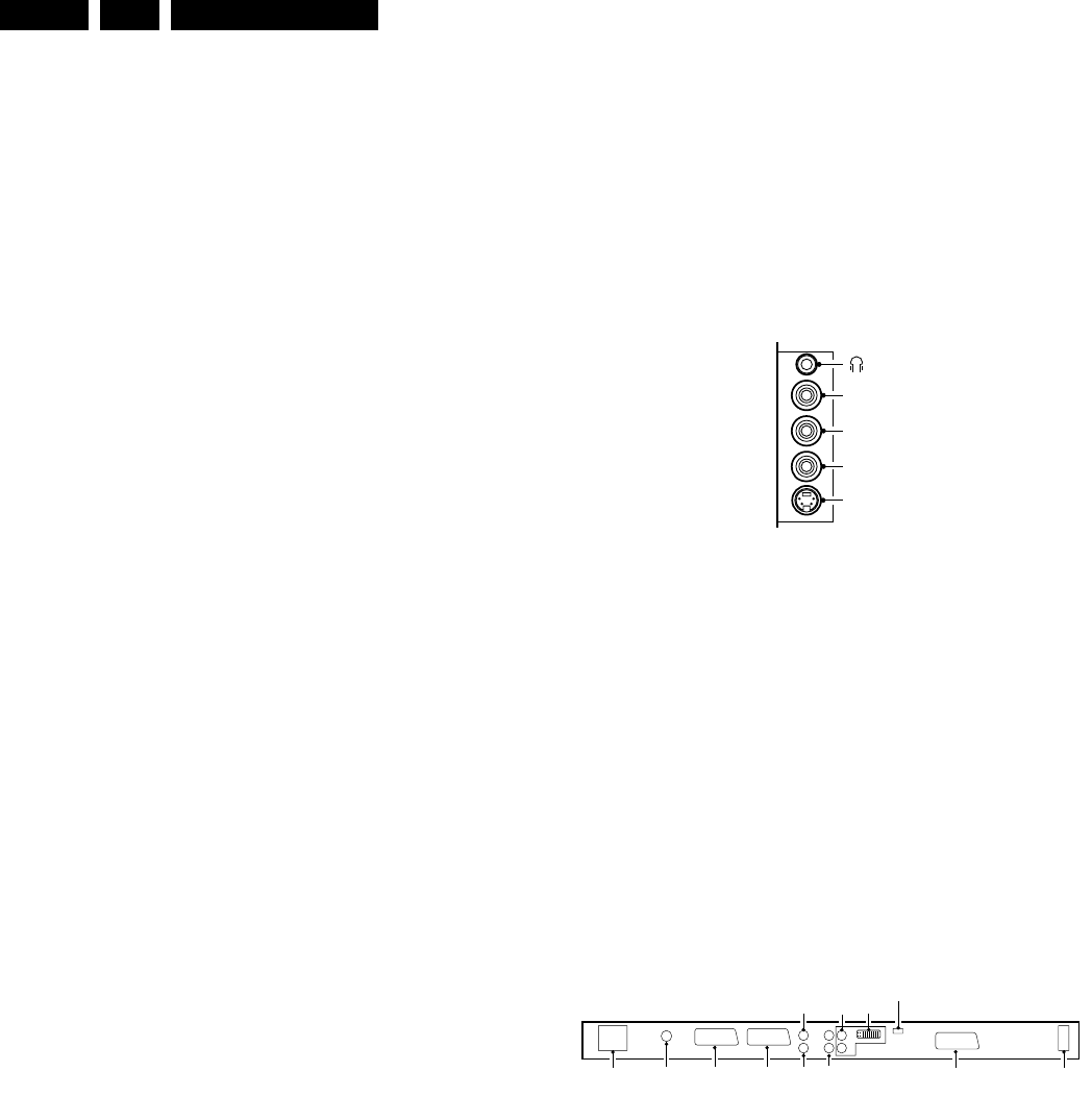
1.2.2 Rear Connections
Figure 1-2 Rear connections
Aerial - In
- IEC-type Coax, 75 ohm D
E_14620_022.eps
050404
SIDE I/O
SVHS
CVBS
R
AUDIO
L
E_14620_023.eps
170604
AERIAL IN EXT2 EXT1
R
L
R
L
EXT3
SUBW
OUT
CENTRE
IN
DVI
SERVICE
AUDIO
OUT
AUDIO
IN
MAINS
(LCD SETS)
MAINS
(PLASMA SETS)
Technical Specifications, Connections, and Chassis Overview EN 3FTL2.4E AA 1.
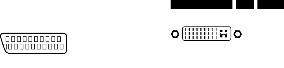
SCART2: Video RGB/YC - In, CVBS - In/Out, Audio - In/Out
Figure 1-3 SCART connector
1 - Audio R 0.5 VRMS / 1 kohm k
2 - Audio R 0.5 VRMS / 10 kohm j
3 - Audio L 0.5 VRMS / 1 kohm k
4 - Ground Audio Gnd H
5 - Ground Blue Gnd H
6 - Audio L 0.5 VRMS / 10 kohm j
7 - Video Blue/C-out 0.7 VPP / 75 ohm jk
8 - Function Select 0 - 2 V: INT
4.5 - 7 V: EXT 16:9
9.5 - 12 V: EXT 4:3 j
9 - Ground Green Gnd H
10 - Easylink P50 0 - 5 V / 4.7 kohm jk
11 - Video Green 0.7 VPP / 75 ohm j
12 - n.c.
13 - Ground Red Gnd H
14 - Ground P50 Gnd H
15 - Video Red/C 0.7 VPP / 75 ohm j
16 - Status/FBL 0 - 0.4 V: INT
1 - 3 V: EXT / 75 ohm j
17 - Ground Video Gnd H
18 - Ground FBL Gnd H
19 - Video CVBS 1 VPP / 75 ohm k
20 - Video CVBS/Y 1 VPP / 75 ohm j
21 - Shield Gnd H
SCART1: Video RGB - In, CVBS - In/Out, Audio - In/Out
1 - Audio R 0.5 VRMS / 1 kohm k
2 - Audio R 0.5 VRMS / 10 kohm j
3 - Audio L 0.5 VRMS / 1 kohm k
4 - Ground Audio Gnd H
5 - Ground Blue Gnd H
6 - Audio L 0.5 VRMS / 10 kohm j
7 - Video Blue 0.7 VPP / 75 ohm jk
8 - Function Select 0 - 2 V: INT
4.5 - 7 V: EXT 16:9
9.5 - 12 V: EXT 4:3 j
9 - Ground Green Gnd H
10 - Easylink P50 0 - 5 V / 4.7 kohm jk
11 - Video Green 0.7 VPP / 75 ohm j
12 - n.c.
13 - Ground Red Gnd H
14 - Ground P50 Gnd H
15 - Video Red 0.7 VPP / 75 ohm j
16 - Status/FBL 0 - 0.4 V: INT
1 - 3 V: EXT / 75 ohm j
17 - Ground Video Gnd H
18 - Ground FBL Gnd H
19 - Video CVBS 1 VPP / 75 ohm k
20 - Video CVBS 1 VPP / 75 ohm j
21 - Shield Gnd H
Cinch: Sub woofer - Out, Centre - In
Bu - Centre 0.5 VRMS / 10 kohm jq
Bk - Sub woofer 0.5 VRMS / 10 kohm kq
Cinch: Audio - Out
Rd - Audio - R 0.5 VRMS / 10 kohm kq
Wh - Audio - L 0.5 VRMS / 10 kohm kq
Cinch: DVI Audio - In
Rd - Audio - R 0.5 VRMS / 10 kohm jq
Wh - Audio - L 0.5 VRMS / 10 kohm jq
DVI-I: Digital/Analogue Video - In
Figure 1-4 DVI-I connector
1 - D2- j
2 - D2+ j
3 - Shield Gnd H
4 - D4- j
5 - D4+ j
6 - DDC_SCL DDC clock k
7 - DDC_SDA DDC data jk
8 - V-sync 0 - 5 V j
9 - D1- j
10 - D1+ j
11 - Shield Gnd H
12 - D3- j
13 - D3+ j
14 - +5V j
15 - Ground Gnd H
16 - HPD Hot Plug Detect j
17 - D0- j
18 - D0+ j
19 - Shield Gnd H
20 - D5- j
21 - D5+ j
22 - Shield Gnd H
23 - CLK+ j
24 - CLK- j
C1 - Video Red 0.7 VPP / 75 ohm j
C2 - Video Green 0.7 VPP / 75 ohm j
C3 - Video Blue 0.7 VPP / 75 ohm j
C4 - H-sync 0 - 5 V j
C5 - Ground Gnd H
Service connector (ComPair)
1 - SDA-S I2C Data (0 - 5 V) jk
2 - SCL-S I2C Clock (0 - 5 V) j
3 - Ground Gnd H
SCART3: Video CVBS - In, Audio - In
1 - n.c.
2 - Audio R 0.5 VRMS / 10 kohm j
3 - n.c.
4 - Ground Audio Gnd H
5 - Ground Blue Gnd H
6 - Audio L 0.5 VRMS / 10 kohm j
7 - n.c.
8 - Function Select 0 - 2 V: INT
4.5 - 7 V: EXT 16:9
9.5 - 12 V: EXT 4:3 j
9 - Ground Green Gnd H
10 - n.c.
11 - n.c.
12 - n.c.
13 - Ground Red Gnd H
14 - Ground Data Gnd H
15 - n.c.
16 - n.c.
17 - Ground Video Gnd H
18 - Ground FBL Gnd H
19 - n.c.
20 - Video CVBS 1 VPP / 75 ohm j
21 - Shield Gnd H
21
20
1
2
E_06532_001.eps
050404
18
916
17
24
C5
C1 C2
C3 C4
E_06532_004.eps
050404
Technical Specifications, Connections, and Chassis Overview
EN 4 FTL2.4E AA1.
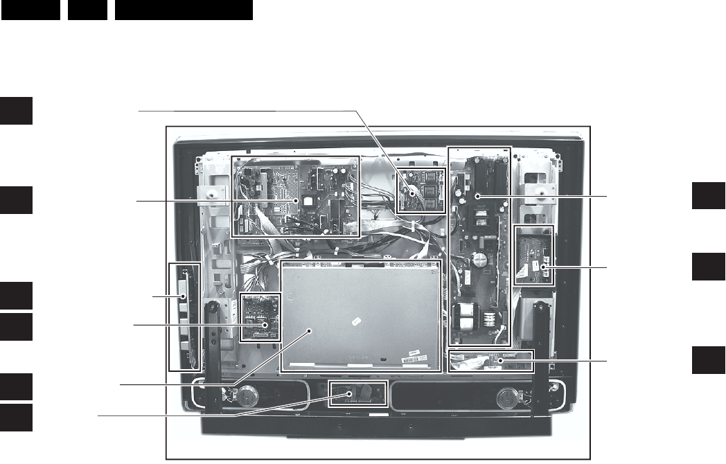
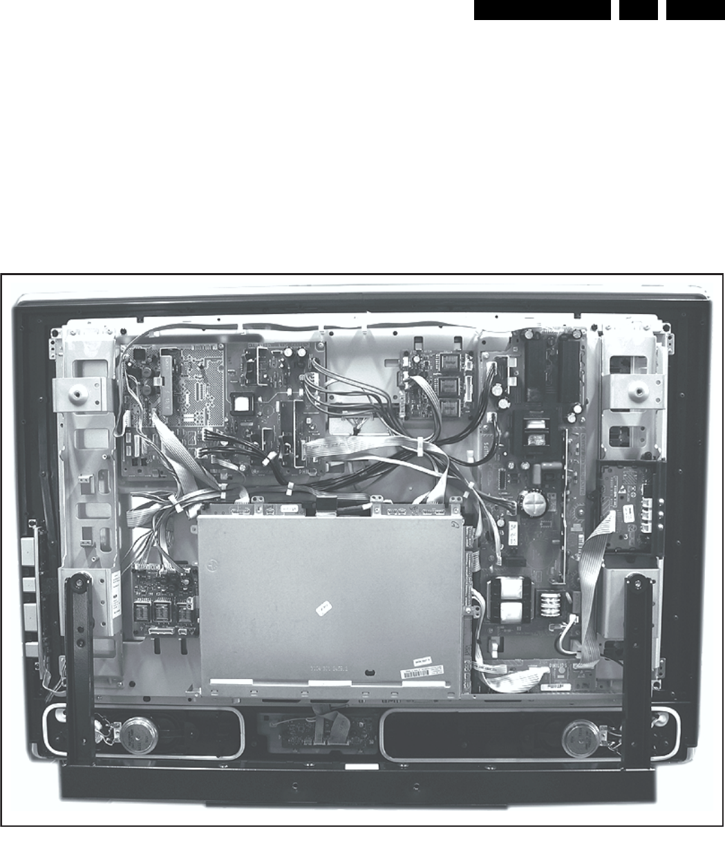
1.3 Chassis Overview
Figure 1-5 PWB locations
E_14620_167.eps
310105
SA
AL
STANDBY SUPPLY/
AUDIO PANEL
E
SIDE CONTROL PANEL
B
SMALL SIGNAL
BOARD
J
LED PANEL
D
SIDE I/O PANEL
H
SCART3 PANEL
A
MAIN SUPPLY
PANEL
AMBI LIGHT PANEL
AL
AMBI LIGHT PANEL

Safety Instructions, Warnings, and Notes EN 5FTL2.4E AA 2.
2. Safety Instructions, Warnings, and Notes
Index of this chapter:
2.1 Safety Instructions
2.2 Warnings
2.3 Notes
2.1 Safety Instructions
Safety regulations require the following during a repair:
• Connect the set to the Mains (AC Power) via an isolation
transformer (> 800 VA).
• Replace safety components, indicated by the symbol h,
only by components identical to the original ones. Any
other component substitution (other than original type) may
increase risk of fire or electrical shock hazard.
Safety regulations require that after a repair, the set must be
returned in its original condition. Pay in particular attention to
the following points:
• Route the wire trees correctly and fix them with the
mounted cable clamps.
• Check the insulation of the Mains (AC Power) lead for
external damage.
• Check the strain relief of the Mains (AC Power) cord for
proper function.
• Check the electrical DC resistance between the Mains (AC
Power) plug and the secondary side (only for sets that have
a Mains (AC Power) isolated power supply):
1. Unplug the Mains (AC Power) cord and connect a wire
between the two pins of the Mains (AC Power) plug.
2. Set the Mains (AC Power) switch to the "on" position
(keep the Mains (AC Power) cord unplugged!).
3. Measure the resistance value between the pins of the
Mains (AC Power) plug and the metal shielding of the
tuner or the aerial connection on the set. The reading
should be between 4.5 Mohm and 12 Mohm.
4. Switch "off" the set, and remove the wire between the
two pins of the Mains (AC Power) plug.
• Check the cabinet for defects, to prevent touching of any
inner parts by the customer.
2.2 Warnings
• All ICs and many other semiconductors are susceptible to
electrostatic discharges (ESD w). Careless handling
during repair can reduce life drastically. Make sure that,
during repair, you are connected with the same potential as
the mass of the set by a wristband with resistance. Keep
components and tools also at this same potential. Available
ESD protection equipment:
– Complete kit ESD3 (small tablemat, wristband,
connection box, extension cable and earth cable) 4822
310 10671.
– Wristband tester 4822 344 13999.
• Be careful during measurements in the high voltage
section.
• Never replace modules or other components while the unit
is switched "on".
• When you align the set, use plastic rather than metal tools.
This will prevent any short circuits and the danger of a
circuit becoming unstable.
2.3 Notes
2.3.1 General
• Measure the voltages and waveforms with regard to the
chassis (= tuner) ground (H), or hot ground (I), depending
on the tested area of circuitry. The voltages and waveforms
shown in the diagrams are indicative. Measure them in the
Service Default Mode (see chapter 5) with a colour bar
signal and stereo sound (L: 3 kHz, R: 1 kHz unless stated
otherwise) and picture carrier at 475.25 MHz for PAL, or
61.25 MHz for NTSC (channel 3).
• Where necessary, measure the waveforms and voltages
with (D) and without (E) aerial signal. Measure the
voltages in the power supply section both in normal
operation (G) and in stand-by (F). These values are
indicated by means of the appropriate symbols.
• The semiconductors indicated in the circuit diagram and in
the parts lists, are interchangeable per position with the
semiconductors in the unit, irrespective of the type
indication on these semiconductors.
• Manufactured under license from Dolby Laboratories.
“Dolby”, “Pro Logic” and the “double-D symbol”, are
trademarks of Dolby Laboratories.
2.3.2 Schematic Notes
• All resistor values are in ohms, and the value multiplier is
often used to indicate the decimal point location (e.g. 2K2
indicates 2.2 kohm).
• Resistor values with no multiplier may be indicated with
either an "E" or an "R" (e.g. 220E or 220R indicates 220
ohm).
• All capacitor values are given in micro-farads (P x10-6),
nano-farads (n= x10-9), or pico-farads (p= x10-12).
• Capacitor values may also use the value multiplier as the
decimal point indication (e.g. 2p2 indicates 2.2 pF).
• An "asterisk" (*) indicates component usage varies. Refer
to the diversity tables for the correct values.
• The correct component values are listed in the Spare Parts
List. Therefore, always check this list when there is any
doubt.
2.3.3 Rework on BGA (Ball Grid Array) ICs
General
Although (LF)BGA assembly yields are very high, there may
still be a requirement for component rework. By rework, we
mean the process of removing the component from the PWB
and replacing it with a new component. If an (LF)BGA is
removed from a PWB, the solder balls of the component are
deformed drastically so the removed (LF)BGA has to be
discarded.
Device Removal
As is the case with any component that, is being removed, it is
essential when removing an (LF)BGA, that the board, tracks,
solder lands, or surrounding components are not damaged. To
remove an (LF)BGA, the board must be uniformly heated to a
temperature close to the reflow soldering temperature. A
uniform temperature reduces the risk of warping the PWB.
To do this, we recommend that the board is heated until it is
certain that all the joints are molten. Then carefully pull the
component off the board with a vacuum nozzle. For the
appropriate temperature profiles, see the IC data sheet.
Area Preparation
When the component has been removed, the vacant IC area
must be cleaned before replacing the (LF)BGA.
Removing an IC often leaves varying amounts of solder on the
mounting lands. This excessive solder can be removed with
either a solder sucker or solder wick. The remaining flux can be
removed with a brush and cleaning agent.
After the board is properly cleaned and inspected, apply flux on
the solder lands and on the connection balls of the (LF)BGA.
Note: Do not apply solder paste, as this has been shown to
result in problems during re-soldering.

Directions for Use
EN 6 FTL2.4E AA3.
Device Replacement
The last step in the repair process is to solder the new
component on the board. Ideally, the (LF)BGA should be
aligned under a microscope or magnifying glass. If this is not
possible, try to align the (LF)BGA with any board markers.
So as not to damage neighbouring components, it may be
necessary to reduce some temperatures and times.
More Information
For more information on how to handle BGA devices, visit this
URL: www.atyourservice.ce.philips.com (needs subscription,
not available for all regions). After login, select “Magazine”,
then go to “Workshop Information”. Here you will find
Information on how to deal with BGA-ICs.
2.3.4 Lead-free Solder
Philips CE is producing lead-free sets (PBF) from 1.1.2005
onwards.
Identification: The bottom line of a type plate gives a 14-digit
serial number. Digits 5 and 6 refer to the production year, digits
7 and 8 refer to production week (in example below it is 1991
week 18).
Figure 2-1 Serial number example
Regardless of the special lead-free logo (which is not always
indicated), one must treat all sets from this date onwards
according to the rules as described below.
Figure 2-2 Lead-free logo
Due to lead-free technology some rules have to be respected
by the workshop during a repair:
• Use only lead-free soldering tin Philips SAC305 with order
code 0622 149 00106. If lead-free solder paste is required,
please contact the manufacturer of your soldering
equipment. In general, use of solder paste within
workshops should be avoided because paste is not easy to
store and to handle.
• Use only adequate solder tools applicable for lead-free
soldering tin. The solder tool must be able:
– To reach a solder-tip temperature of at least 400°C.
– To stabilise the adjusted temperature at the solder-tip.
– To exchange solder-tips for different applications.
• Adjust your solder tool so that a temperature of around
360°C - 380°C is reached and stabilised at the solder joint.
Heating time of the solder-joint should not exceed ~ 4 sec.
Avoid temperatures above 400°C, otherwise wear-out of
tips will increase drastically and flux-fluid will be destroyed.
To avoid wear-out of tips, switch “off” unused equipment or
reduce heat.
• Mix of lead-free soldering tin/parts with leaded soldering
tin/parts is possible but PHILIPS recommends strongly to
avoid mixed regimes. If this cannot be avoided, carefully
clear the solder-joint from old tin and re-solder with new tin.
• Use only original spare-parts listed in the Service-Manuals.
Not listed standard material (commodities) has to be
purchased at external companies.
• Special information for lead-free BGA ICs: these ICs will be
delivered in so-called "dry-packaging" to protect the IC
against moisture. This packaging may only be opened
shortly before it is used (soldered). Otherwise the body of
the IC gets "wet" inside and during the heating time the
structure of the IC will be destroyed due to high (steam-)
pressure inside the body. If the packaging was opened
before usage, the IC has to be heated up for some hours
(around 90°C) for drying (think of ESD-protection!).
Do not re-use BGAs at all!
• For sets produced before 1.1.2005, containing leaded
soldering tin and components, all needed spare parts will
be available till the end of the service period. For the repair
of such sets nothing changes.
In case of doubt whether the board is lead-free or not (or with
mixed technologies), you can use the following method:
• Always use the highest temperature to solder, when using
SAC305 (see also instructions below).
• De-solder thoroughly (clean solder joints to avoid the
mixing of two alloys).
Caution: For BGA-ICs, you must use the correct temperature
profile, which is coupled to the 12NC. For an overview of these
profiles, visit the website www.atyourservice.ce.philips.com
(needs subscription, but is not available for all regions).
You will find this and more technical information within the
"Magazine", chapter "Workshop information".
For additional questions please contact your local repair help
desk.
2.3.5 Practical Service Precautions
•It makes sense to avoid exposure to electrical shock.
While some sources are expected to have a possible
dangerous impact, others of quite high potential are of
limited current and are sometimes held in less regard.
•Always respect voltages. While some may not be
dangerous in themselves, they can cause unexpected
reactions that are best avoided. Before reaching into a
powered TV set, it is best to test the high voltage insulation.
It is easy to do, and is a good service precaution.
3. Directions for Use
You can download this information from the following websites:
http://www.philips.com/support
http://www.p4c.philips.com
E_06532_024.eps
230205
P
b
Mechanical Instructions EN 7FTL2.4E AA 4.
4. Mechanical Instructions
Index of this chapter:
4.1 Cable Dressing
4.2 Service Position
4.3 Assy/PWB Removal
4.4 Display (Dis)Assembly
4.5 Set Re-assembly
Notes:
• Figures below can deviate slightly from the actual situation,
due to the different set executions.
• Follow the disassemble instructions in described order.
4.1 Cable Dressing
4.1.1 Chassis
Figure 4-1 Chassis cable dressing
F_15490_010.eps
230605
Mechanical Instructions
EN 8 FTL2.4E AA4.
4.2 Service Position
For easy servicing of this set, there are a few possibilities
created:
• The buffers from the packaging.
• Foam bars (created for Service).
• Aluminium service stands (created for Service).
4.2.1 Foam Bars
Figure 4-2 Foam bars
The foam bars (order code 3122 785 90580 for two pieces) can
be used for all types and sizes of Flat TVs. By laying the TV
face down on the (ESD protective) foam bars, a stable situation
is created to perform measurements and alignments.
By placing a mirror under the TV, you can monitor the screen.
4.2.2 Aluminium Stands
Figure 4-3 Aluminium stands (Mk1)
The new (Mk2) aluminium stands (order code 3122 785 90690)
can also be used to do measurements, alignments, and
duration tests. The stands can be (dis)mounted quick and easy
by means of sliding them in/out the "mushrooms".
Important: For (older) FTV sets without these "mushrooms", it
is obligatory to use the provided screws, otherwise it is possible
to damage the monitor inside!.
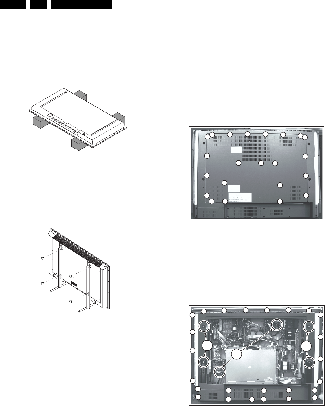
4.3 Assy/PWB Removal
4.3.1 Metal Back Plate
Caution: Disconnect the mains power cord before you remove
the metal back plate.
1. Place the TV set upside down on a table top, using the
foam bars (see part "Foam Bars").
Caution: do not put pressure on the display, but let the
monitor lean on the speakers or the Front cover.
2. Remove all T10 parker screws [1] from the top, left, and
right sides of the metal back plate.
3. Remove all T10 tapping screws [2] from the centre and
bottom of the metal back plate.
4. Lift the back plate from the TV. Make sure that wires and
flat foils are not damaged during the removal.
Figure 4-4 Metal back plate
4.3.2 Rear Cover
1. Disconnect all connectors [1] at both AmbiLight Inverters.
2. Remove all T10 parker screws [2] around the edges of the
rear cover.
3. Remove the four "mushrooms" [3] from the back plate.
4. Lift the rear cover from the TV.
Figure 4-5 Rear cover
4.3.3 LCD Supply Panel
1. Disconnect all cables from the LCD supply panel.
2. Remove all mounting screws from the LCD supply panel.
3. Take out the panel.
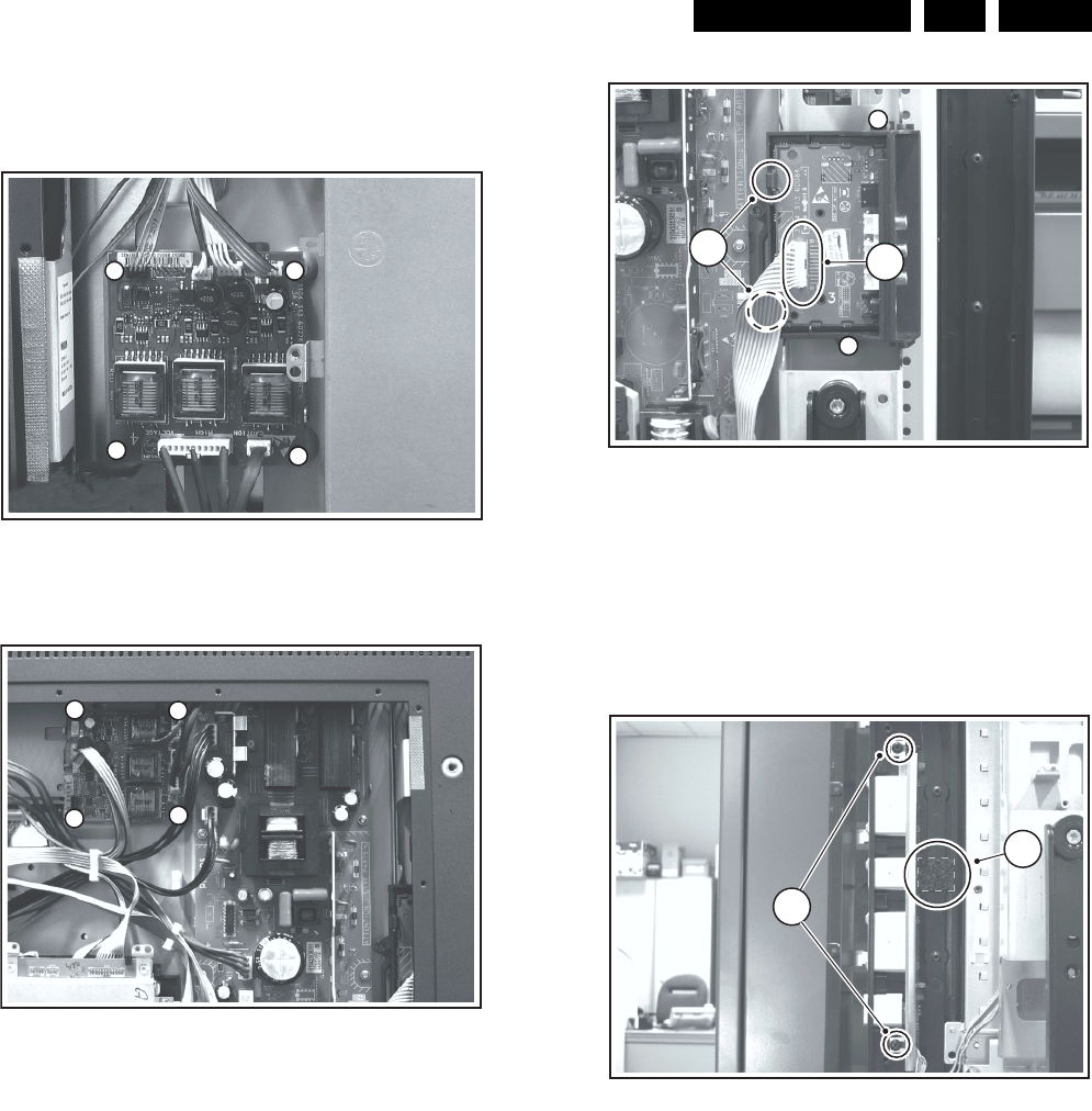
4.3.4 AmbiLight Inverter Panel These models are equipped with two AmbiLight Inverters.
E_06532_018.eps
170504
E_06532_019.eps
170504
F_15490_011.eps
230605
1
1
1
11111111
1
1
1
2
2
2
2
2
2
2
1
F_15490_012.ep
s
23060
5
2
2
2
22 2 22
2
2
2
2
2
2222 2 2 22
2
2
2
33
1
2
Mechanical Instructions EN 9FTL2.4E AA 4.
1. Disconnect all cables from the AmbiLight Inverter panel.
2. Remove all mounting screws [1] from the AmbiLight
Inverter panel.
3. Take out the panel.
Figure 4-6 AmbiLight inverter (left lower side)
Figure 4-7 AmbiLight inverter (right upper side)
4.3.5 3th SCART Panel
1. Disconnect all cables from the 3th SCART panel.
2. Remove the two mounting screws near the SCART
connector at the connector plate (see [7] in figure
“Connector plate” further on).
3. Take out the panel.
4.3.6 Stand-by Supply/Audio Panel
1. Disconnect all cables from the Stand-by Supply/Audio
panel.
2. Remove all T10 mounting screws at the top of the Stand-
by Supply/Audio panel.
3. Take out the panel (it hinges at the bottom side).
4.3.7 Side I/O Panel
1. Disconnect the cable [1] from the Side I/O panel.
2. Remove the assy mounting screws [2].
3. Take out the assy.
4. Release the clamps [3] and take out the panel.
Figure 4-8 Side I/O panel
4.3.8 (Top) Control Panel
1. Remove the glued foam block [1].
2. Remove the assy mounting screws [2].
3. Take out the assy.
4. Release the clamps and take out the panel.
Figure 4-9 Local keyboard
4.3.9 LED Panel
1. Disconnect all cables from the LED panel.
2. Remove the mounting screws from the LED panel.
3. Take out the panel.
4.3.10 Speakers
1. After removal of the cover plate, you can access the
speakers.
2. Be sure that the foam that makes the unit airtight is not
damaged. Otherwise replace it.
F_15490_014.eps
230605
1
11
1
F_15490_013.eps
230605
1
11
1
F_15490_024.eps
240605
2
2
31
F_15490_016.eps
240605
1
2
Mechanical Instructions
EN 10 FTL2.4E AA4.
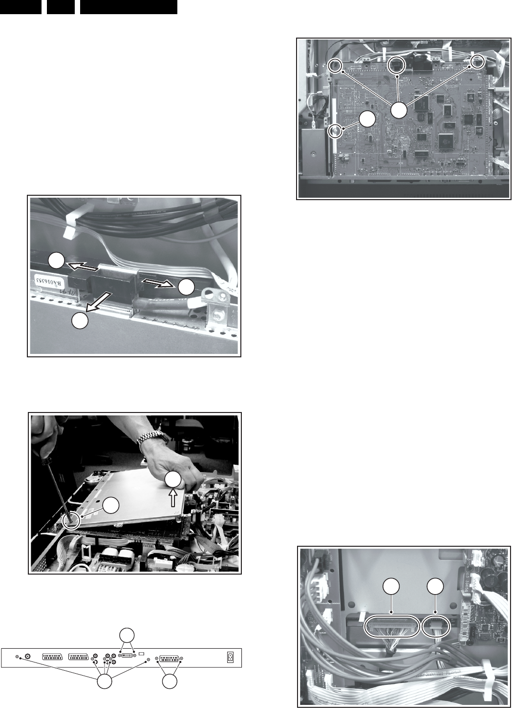
4.3.11 SSB
1. Remove the LVDS connector locking bracket [1][2].
2. Remove all shielding fixing screws.
3. Slide, and lift the shielding at the top [3]. The panel hinges
at the SCART side. At the same time, use a screwdriver to
carefully prize the shielding at the bottom side [4], and
remove the shielding. The SSB is now accessible.
4. To remove the whole SSB, unscrew all connector fixing
screws from the connector plate [5][6]. Use a 5 mm socket
screwdriver to remove both DVI connector distance bolts
[6].
5. Disconnect the LVDS cable, and all other cables.
6. Remove the mounting screw [8] from the SSB.
7. Bend the brackets [9] away (may require some force), lift
the SSB, and take it out.
Figure 4-10 LVDS connector locking bracket
Figure 4-11 SSB top shielding
Figure 4-12 Connector plate
Figure 4-13 SSB brackets
4.3.12 AmbiLight Lamp Unit
The AmbiLight lamp units are located in the TV’s rear cover.
1. Remove the cable clamps.
2. Remove all mounting AmbiLight screws.
3. Slide the AmbiLight unit to the side and take out the unit.
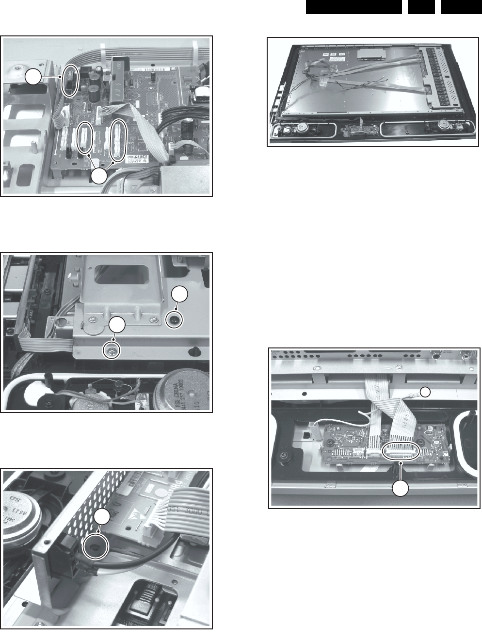
4.4 Display (Dis)Assembly
Important: Be sure to work in a dust free environment during
the following activities. In addition, the use of (fabric) hand
gloves is advised.
1. Important: Unplug the cables [1][2] at the LCD panel. Be
careful, as the LVDS connector [1] is very fragile!
2. Unplug the backlight and loudspeaker connectors [3][4].
3. Remove all T10 screws [5] from the mounting frame.
4. Remove all mounting LCD panel screws [6]. One of them
[7] is somewhat hidden underneath the SCART panel.
The best way to remove this screw is to loosen the 3th
SCART panel first via the 2 screws at the SCART
connector (see [7] in figure “Connector plate” earlier).
5. Lift the metal frame (together with all PWBs) from the LCD
panel. During lift, free the backlight and speaker cables.
6. After removal of the frame, you can lift the LCD display
from the set.
Figure 4-14 LCD panel connectors
F_15490_017.eps
240605
1
1
2
F_15490_015.eps
230605
4
3
F_15490_026.eps
240605
75
6
F_15490_027.eps
240605
9
For
PDP
8
F_15490_018.eps
240605
1 2
Fragile !
Mechanical Instructions EN 11FTL2.4E AA 4.
Figure 4-15 Speaker and LCD backlight cables
Figure 4-16 LCD panel disassembly (part 1)
Figure 4-17 LCD panel disassembly (part 2)
Figure 4-18 Bare LCD panel after frame removal
4.5 Set Re-assembly
To re-assemble the whole set, execute all processes in reverse
order.
Note: While re-assembling the TV, make sure that:
• All cables are placed and connected in their original
position (see figure “Chassis cable dressing” in the
beginning of this chapter and/or the “Wiring Diagram” in
chapter 6).
• LVDS connector (SSB) is secured with plastic clamp.
• The "grounding" wire between metal speaker grid and
frame [1] is reconnected.
–
Figure 4-19 Metal speaker grid grounding wire
F_15490_021.eps
240605
4
3
F_15490_019.eps
240605
6
5
F_15490_020.eps
240605
7
F_15490_022.eps
240605
F_15490_025.eps
240605
1
2
Service Modes, Error Codes, and Fault Finding
EN 12 FTL2.4E AA5.
5. Service Modes, Error Codes, and Fault Finding
Index of this chapter:
5.1 Test Points
5.2 Service Modes
5.3 Problems and Solving Tips (related to CSM)
5.4 Service Tools
5.5 Error Codes
5.6 The Blinking LED Procedure
5.7 Protections
5.8 Repair tips
5.9 Software Downloading
5.1 Test Points
The chassis is equipped with test points printed on the circuit
board assemblies.
Perform measurements under the following conditions:
• Service Default Mode.
• Video: colour bar signal.
• Audio: 3 kHz left, 1 kHz right.
5.2 Service Modes
Service Default Mode (SDM) and Service Alignment Mode
(SAM) offer several features for the service technician, while
the Customer Service Mode (CSM) is used for communication
between a Philips Customer Care Centre (P3C) and a
customer.
There is also the option of using ComPair, a hardware interface
between a computer (see requirements below) and the TV
chassis. It offers the ability of structured troubleshooting, test
pattern generation, error code reading, software version read-
out, and software upgrading.
Minimum requirements: a Pentium processor, Windows 95/
98, and a CD-ROM drive (see also paragraph “ComPair”).
Remark: The silk screen printing is not correct for the SAM/
SDM indication. For the correct location of these pins, see
figure ”Service pads”.
5.2.1 Service Default Mode (SDM)
Purpose
• To create a pre-defined setting, to get the same
measurement results as given in this manual.
• To override SW protections.
• To start the blinking LED procedure.
Specifications
Table 5-1 SDM default settings
• All picture settings at 50% (brightness, colour, contrast).
• All sound settings at 50%, except volume at 25%.
• All service-unfriendly modes (if present) are disabled, like:
– (Sleep) timer.
– Child/parental lock.
– Blue mute.
– Automatic volume limiter (AVL).
– Auto switch-off (when no video signal was received for
10 minutes).
– Skip/blank of non-favourite pre-sets.
– Smart modes.
– Auto store of personal presets.
– Auto user menu time-out.
How to activate SDM
Use one of the following methods:
• Use the standard RC-transmitter and key in the code
“062596”, directly followed by the “MENU” button.
Note: It is possible that, together with the SDM, the main
menu will appear. To switch it off, push the “MENU” button
again.
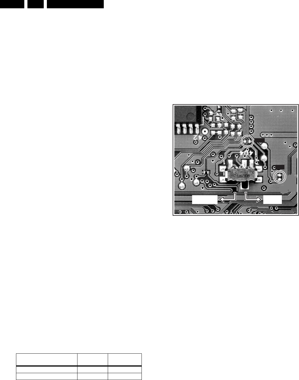
Figure 5-1 Service pads
• Short for a moment the two solder pads on the SSB, with
the indication “SDM” (see figure ”Service pads”). Activation
can be performed in all modes, except when the TV has a
problem with the main microprocessor.
Caution: If the SDM is activated via the pins, all the
software-controlled protections are de-activated.
• Use the DST-emulation feature of ComPair.
• Use the “DEFAULT” button on the Dealer Service Tool
(RC7150).
How to navigate
When you press the “MENU” button on the RC transmitter, the
TV will toggle between the SDM and the normal user menu
(with the SDM mode still active in the background).
How to exit SDM
Use one of the following methods:
• Switch the TV to STANDBY via the RC-transmitter.
• Press the “EXIT” button on the DST.
• Via a standard customer RC-transmitter: key in “00”-
sequence.
5.2.2 Service Alignment Mode (SAM)
Purpose
• To perform (software) alignments.
• To change option settings.
• To easily identify the used software version.
• To view operation hours.
• To display (or clear) the error code buffer.
Specifications
• Operation hours counter.
• Software version.
Region Freq. (MHz)
Default
system
Europe, AP-PAL/Multi 475.25 PAL B/G
NAFTA, AP-NTSC, LATAM 61.25 (ch. 3) NTSC M
E_14620_151.eps
290704
SDM
SAM
NORMAL
TV MODE
SW UPGRADE
MODE

Service Modes, Error Codes, and Fault Finding EN 13FTL2.4E AA 5.
• Option settings.
• Error buffer reading and erasing.
• Software alignments.
How to activate SAM
Use one of the following methods:
• Via a standard RC transmitter: key in the code “062596”
directly followed by the “OSD [i+]” button. After activating
SAM with this method a service warning will appear on the
screen, you can continue by pressing any digit key on the
RC.
• Short for a moment the two solder pads on the SSB with
the indication "SAM" (see figure ”Service pads”).
Depending on the software version, it is possible that a
service warning will appear. You can continue by pressing
any digit key on the RC.
• Use the DST-emulation feature of ComPair.
• Press the ALIGN button on the DST while the TV is in the
normal operation
After activating this mode, “SAM” will appear in the upper right
corner of the screen.
Contents of SAM:
•Operation Hours. Displays the accumulated total of
operation hours (not the stand-by hours).
•Hardware Info.
–ROM Version. Displays the date of the software and
the software version of the ROM
Ex.: TX24EU_1.0_01234 = AAAABB_X.Y_NNNNN.
•AAAA= the chassis name.
•BB= the region: EU= Europe, AP= Asia Pacific
PAL/Multi, AN= Asia Pacific NTSC, US= USA, LT=
LATAM.
•X.Y= the software version, where X is the main
version number (different numbers are not
compatible with one another) and Y is the sub
version number (a higher number is always
compatible with a lower number).
•NNNNN= last five digits of 12nc code software.
–FBX Version. Displays the software version of the
FBX
–SW VERSION EPLD. Displays the software version of
the EPLD.
•Errors. (followed by maximal 10 errors). The most recent
error is displayed at the upper left (for an error explanation
see paragraph “Error Codes”).
•Defective Module. Here the module that generates the
error is displayed. If there are multiple errors in the buffer,
which are not all generated by a single module, there is
probably another defect. It will then display the message
“UNKNOWN” here.
•Reset Error Buffer. When you press the “OK” button, the
error buffer is reset.
•Alignments. This will activate the “ALIGNMENTS” sub-
menu.
•Dealer Options. Extra features for the dealers.
•Service Options. Extra features for Service.
•Initialise NVM. The moment the processor recognises a
corrupted NVM, the “initialise NVM” line will be highlighted.
Now, you can do two things (dependent of the service
instructions at that moment):
– Save the content of the NVM via ComPair for
development analysis, before initialising. This will give
the Philips Service department an extra possibility for
diagnosis (e.g. when Development asks for this).
– Initialise the NVM (same as in the past, however now it
happens conscious).
Note: When you have a corrupted NVM, or you have replaced
the NVM, there is a high possibility that you will not have picture
any more because your display option is not correct. So, before
you can initialize your NVM via the SAM, you need to have a
picture and therefore you need the correct display option. This
code can be found on the option code sticker inside the set.
•Store. All options and alignments are stored when
pressing the “OK”-button
•Functional Test. All devices are tested via the “OK”
button. Eventual errors are displayed in the error buffer.
The error buffer is not erased, the content returns when this
test is terminated.
•Daily Menus. With the “OK” button, you can go to the
normal user menu. SAM is still active in the background.
With the “MENU” button, you return from the user menu to
SAM menu. This feature can be helpful to quickly change
some settings in the user menu.
•SW Maintenance.
•Upgrade. More info see paragraph Software
downloading.
•Events. Not useful for service purposes. In case of
specific software problems, the development
department can ask for this info.
•BDM Info. Broadcast Debug Menu info. The purpose
of this menu is to debug the broadcast, not the TV. The
menu gives an overview of what is received on the
current preset.
Following items are displayed:
Figure 5-2 Broadcast debug menu overview
Table 5-2 Broadcast debug menu explanation
Item Source Description
Presetnr Set Preset number of the current selected preset.
Presetname Set Preset name of the current selected preset.
CNI NVM Broadcaster CNI number stored in NVM for the current preset.
CNI F1 Broadcaster CNI number from transmitted Packet 8/30 Format
1.
CNI F2 Broadcaster CNI number from transmitted Packet 8/30 Format
2.
CNI VPS Broadcaster CNI number from transmitted VPS line.
Morning Prog Broadcaster "ARD" or "ZDF" according to dedicated bit in 8/30
Format 1.
Name 8/30 F1 Broadcaster Name extracted from status message of 8/30
Format 1.
Name 8/30 F2 Broadcaster Name extracted from status message of 8/30
Format 2.
Name TXT Broadcaster Name extracted from TXT header.
Signal Strength FBX Noise figure measured for selected preset.
EPG Service Set EPG Service stored in NVM for current preset
displayed as "TXT", "MCP", "SCP", "OCP".
UTC Set UTC (Universal Time Code formerly known as
Greenwich Mean Time) used in the TV.
LTO Set LTO (Local Time Offset) used in the TV. Used by
EPG for all NextView displays. (= Time TXT
header - Time 8/30 F1)
Time Set Current time running in the TV. Was extracted at
start-up, then maintained by software.
Date Set Current date running in the TV. Was extracted at
start-up, then maintained by software.
Time TXT Broadcaster TXT header time from the selected preset.
Time 8/30 F1 Broadcaster UTC time from 8/30 Format 1.
Date 8/30 F1 Broadcaster Date from 8/30 Format 1.
LTO 8/30 F1 Broadcaster LTO from 8/30 Format 1.
WSS G1 Broadcaster WSS Group 1 (Aspect Ratio) bits 0 1 2 3
WSS G2 Broadcaster WSS Group 2 (Enhanced Services) bits 4 5 6 7
WSS G3 Broadcaster WSS Group 3 (Subtitles) bits 8 9 10
WSS G4 Broadcaster WSS Group 4 (Reserved) bits 11 12 13
Presetnr: -- UTC: --:--:--
Presetname: ----- LTO: --:--:--
Time: --:--:--
CNI NVM: ---- Date: --/--/----
CNI F1: ----
CNI F2: ---- Time TXT: --:--:--
CNI VPS: ---- Time 8/30 F1: --:--:--
Morning Prog: --- Date 8/30 F1: --/--/----
Name 8/30 F1: ----- LTO 8/30 F1: --:--:--
Name 8/30 F2: -----
Name TXT: ----- WSS G1: ----
Signal Strength:--- WSS G2: ----
WSS G3: ---
EPG Service: --- WSS G4: ---
E_14620_050.eps
170504

Service Modes, Error Codes, and Fault Finding
EN 14 FTL2.4E AA5.
How to navigate
• In SAM, you can select the menu items with the “CURSOR
UP/DOWN” key on the RC-transmitter. The selected item
will be highlighted. When not all menu items fit on the
screen, move the “CURSOR UP/DOWN” key to display the
next/previous menu items.
• With the “CURSOR LEFT/RIGHT” keys, it is possible to:
– (De) activate the selected menu item.
– Change the value of the selected menu item.
– Activate the selected sub-menu.
How to exit SAM
Use one of the following methods:
• Press the “MENU” button on the RC-transmitter, or
• Switch the TV to STANDBY via the RC-transmitter, or
• Press the “EXIT” button on the DST.
5.2.3 Customer Service Mode (CSM)
Purpose
When a customer is having problems with his TV-set, he can
call his dealer. The service technician can than ask the
customer to activate the CSM, in order to identify the status of
the TV. Now, the service technician can judge the severity of
the complaint. In many cases, he can advise the customer how
to solve the problem, or he can decide if it is necessary to visit
the customer.
The CSM is a read only mode; therefore, modifications in this
mode are not possible.
How to activate CSM
Use the following method:
Key in the code “123654” via the standard RC transmitter.
Note: Activation of the CSM is only possible if there is no (user)
menu on the screen!
How to navigate
By means of the “CURSOR-DOWN/UP” knob on the RC-
transmitter, you can navigate through the menus.
Contents of CSM
CUSTOMER SERVICE MENU 1
•Software Version (example: TX24EU_1.0_01234).
Displays the built-in software version. In case of field
problems related to software, software can be upgraded
(for more details, see paragraph Software downloading).
You will find details of the software versions in the chapter
“Software Survey” of the “Product Survey - Colour
Television” publication. This publication is generated four
times a year.
•Feature Box. The 12NC-number of the built-in Feature
Box software.
•Set Type. This information is very helpful for a help desk/
workshop as reference for further diagnosis. In this way, it
is not necessary for the customer to look at the rear of the
TV-set.
•Code 1. Gives the latest five errors of the error buffer. As
soon as the built-in diagnose software has detected an
error the buffer is adapted. The last occurred error is
displayed on the left most position. Each error code is
displayed as a 3-digit number. When less than 10 errors
occur, the rest of the buffer is empty (000). See also
paragraph Error Codes for a description.
•Code 2. Gives the first five errors of the error buffer. See
also paragraph Error Codes for a description.
•Volume. Gives the last status of the volume as set by the
customer. The value can vary from 0 (volume is minimum)
to 100 (volume is maximum). Volume values can be
changed via the volume key on the RC-transmitter.
•Brightness. Gives the last status of the brightness as set
by the customer. The value can vary from 0 (brightness is
minimum) to 100 (brightness is maximum). Brightness
values can be changed via the “CURSOR LEFT” and
“CURSOR RIGHT” keys on the RC-transmitter after
pressing the “MENU” button and selecting “PICTURE” and
“BRIGHTNESS”.
•Contrast. Gives the last status of the contrast as set by the
customer. The value can vary from 0 (contrast is minimum)
to 100 (contrast is maximum). Contrast values can be
changed via “CURSOR LEFT” and “CURSOR RIGHT”
keys on the RC-transmitter after pressing the “MENU”
button and selecting “PICTURE” and “CONTRAST”.
•Colour. Gives the last status of the colour saturation, as
set by the customer. The value can vary from 0 (colour is
minimum) to 100 (colour is maximum). Colour values can
be changed via “CURSOR LEFT” and “CURSOR RIGHT”
keys on the RC-transmitter after pressing the “MENU”
button and selecting “PICTURE” and “COLOUR”.
•Hue. Only relevant for NTSC-signals (e.g. some NTSC-
DVD-discs).
CUSTOMER SERVICE MENU 2
•Sharpness. Gives the sharpness value. The value can
vary from 0 (sharpness is minimum) to 7 (sharpness is
maximum). In case of bad antenna signals, a too high
value of the sharpness can result in a noisy picture.
Sharpness values can be changed via the “CURSOR
LEFT” and “CURSOR RIGHT” keys on the RC-transmitter
after pressing the “MENU” button and selecting “PICTURE”
and “SHARPNESS”.
•Headphone Volume. Gives the last status of the head
phone volume, as set by the customer. The value can vary
from 0 (volume is minimum) to 100 (volume is maximum).
Head phone volume values can be changed via the
“CURSOR LEFT” and “CURSOR RIGHT” keys on the RC-
transmitter after pressing the “MENU” button and selecting
“SOUND” and “HEADPHONE VOLUME”.
•Dolby. Indicates whether the received transmitter
transmits Dolby sound (“ON”) or not (“OFF”). Attention: The
presence of Dolby can only be tested by the software on
the Dolby Signalling bit. If a Dolby transmission is received
without a Dolby Signalling bit, this indicator will show “OFF”
even though a Dolby transmission is received.
•Surround Mode. Indicates the by the customer selected
surround mode (or automatically chosen mode). Possible
values are “OFF”, “INCREDIBLE SURROUND” OR
“DOLBY VIRTUAL”. These settings can be influenced after
pressing the “MENU” button and selecting “SOUND” and
SURROUND MODE”. It can also have been selected
automatically by signalling bits (internal software).
•Tuner Frequency. Indicates the frequency the selected
transmitter is tuned to. The tuner frequency can be
changed via the “CURSOR LEFT” and “CURSOR RIGHT”
keys for fine tune after opening the installation menu and
selecting “INSTALL” and “MANUAL INSTALL”.
•Digital Option. Gives the selected digital mode,
“PROGRESSIVE SCAN”, “MOVIE PLUS” or “PIXEL
PLUS”. Change via “MENU”, “PICTURE”, “DIGITAL
OPTIONS”.
•Centre Trim. Not applicable for this set.
•TV System. Gives information about the video system of
the selected transmitter.
– BG: PAL BG signal received.
– DK: PAL DK signal received.
– I: PAL I signal received.
– L/La: SECAM L/La signals received.
– M: NTSC M signal received with video carrier on 38.9
MHz.
CUSTOMER SERVICE MENU 3
•Balance. Indicates the balance settings, between “-50”
and “+50”. Change via “MENU”, “SOUND”, and
“BALANCE”. Not applicable for Dolby Pro Logic sets.
•Centre Mode. Not applicable for this TV.

Service Modes, Error Codes, and Fault Finding EN 15FTL2.4E AA 5.
•DNR. Gives the selected DNR setting (Dynamic Noise
Reduction), “OFF”, “MINIMUM”, “MEDIUM”, or
“MAXIMUM”. Change via “MENU”, “PICTURE”, “DNR”
•Noise Figure. Gives the noise ratio for the selected
transmitter. This value can vary from 0 (good signal) to 127
(average signal) and to 255 (bad signal). For some
software versions, the noise figure will only be valid when
“Active Control” is set to “medium” or “maximum”.
•Source. Indicates which source is used and the video/
audio signal quality of the selected source.
Example: Tuner, Video/NICAM) Source: “TUNER”,
“EXT1”, “EXT2”, “EXT3”, “EXT4”, “SIDE”, “AV1”, “AV2”,
“AV3” or “AV4”. Video signal quality: “VIDEO”, “S-VIDEO”,
“RGB 1FH”, “YPBPR 1FH 480P”, “YPBPR 1FH 576P”,
“YPBPR 1FH 1080I”, “YPBPR 2FH 480P”, “YPBPR 2FH
576P”, “YPBPR 2FH 1080I”, “RGB 2FH 480P”, “RGB 2FH
576P” or “RGB 2FH 1080I”. Audio signal quality:
“STEREO”, “SPDIF 1”, “SPDIF 2”, or “SPDIF”.
•Audio System. Gives information about the audio system
of the selected transmitter: “ANALOGUE MONO”,
“ANALOGUE STEREO”, “PCM 2/0”, “DD 1/0”, “DD 2/0
LtRt”, “DD 2/0 L0R0”, “DD 2/1”, “DD 2/2”, “DD 3/0”, “DD 3/
1”, “DD 3/2”, “DD 1+1”, “MPEG 1/0”, “MPEG 2/0”, “MPEG
2/0 LtRt”, “MPEG 2/1”, “MPEG 2/2”, “MPEG 3/0”, “MPEG
3/1”, “MPEG 3/2”, “MPEG 1+1” or “MPEG 2+2”.
•Tuned Bit. Gives information about the tuning method of
the stored pre-set. If a channel is found via “automatic
installation”, you will see the value “YES”. When you
change this (automatically found) frequency via “fine tune”
adjustment (installation menu - manual installation), the
displayed value will change to “NO”. Therefore, when you
see the value “NO” in this line, it is an indication that the
received channel is a non-standard signal (e.g. of a VCR).
•Surround Speakers. Not applicable in this set.
•On Timer. Indicates if the “On Timer” is set “ON” or “OFF”
and if the timer is “ON” also displays start time, start day
and program number. Change via “MENU”, “TV”,
“FEATURES”, and “ON TIMER”.
•Preset Lock. Indicates if the selected preset has a child
lock: “LOCKED” or “UNLOCKED”. Change via “MENU”,
“TV”, “FEATURES”, “CHILD LOCK”, and “CUSTOM
LOCK”.
CUSTOMER SERVICE MENU 4
•Child Lock. Indicates the last status of the general child
lock: “UNLOCK”, “LOCK”, or “CUSTOM LOCK”. Change
via “MENU”, “TV”, “FEATURES”, “CHILD LOCK”, and
“LOCK”.
•Age Lock. Indicates the last status of the EPG rating for
child lock: “OFF”, “4 YEARS”, “6 YEARS”, “8 YEARS”, “10
YEARS”, “12 YEARS”, “14 YEARS” or “16 YEARS”. This is
only displayed if child lock is set to “CUSTOM LOCK”
•Lock After. Indicates at what time the child lock is set:
“OFF” or e.g. “18:45” (lock time). This is only displayed if
child lock is set to “CUSTOM LOCK”
•Category Lock. Indicates the last status of the EPG theme
child lock: “MOVIES”, “NEWS”, “SHOWS”, “SPORTS”,
“CHILDREN”, “MUSIC”, “CULTURE”, or “SERIES”. This is
only displayed if child lock is set to “CUSTOM LOCK”. It is
possible that more than one value is shown.
•Program Category. Indicates the theme of the selected
transmitter: “MOVIES”, “NEWS”, “SHOWS”, “SPORTS”,
“CHILDREN”, “MUSIC”, “CULTURE”, or “SERIES”.
•TV Ratings Lock. Only applicable for US.
•Movie Ratings Lock. Only applicable for US.
•V-Chip TV Status. Only applicable for US.
CUSTOMER SERVICE MENU 5
•V-Chip Movie Status. Only applicable for US.
•Options 1. Gives the option codes of option group 1 as set
in SAM (Service Alignment Mode).
•Options 2. Gives the option codes of option group 2 as set
in SAM (Service Alignment Mode).
•AVL. Indicates the last status of AVL (Automatic Volume
Level): “ON” or “OFF”. Change via “MENU”, “TV”,
“SOUND”, “AVL”
•Delta Volume. Indicates the last status of the delta volume
for the selected preset as set by the customer: from “-12”
to “+12”. Change via “MENU”, “TV”, “SOUND”, “DELTA
VOLUME”.
•Front Spkr Dist. Not applicable for this TV.
•Front Spkr Dist. Not applicable for this TV.
How to exit CSM
Use one of the following methods:
• After you press a key on the RC-transmitter (with exception
of the “CHANNEL”, “VOLUME” and digit (0-9) keys), or
• After you switch the TV-set “OFF” with the mains switch.
Note: When you de-activate CSM, it is possible (depending on
the software version) that the size of the picture changes. This
can be solved by pushing “P+” and then “P-”.
5.3 Problems and Solving Tips (related to CSM)
Note: Below described problems are all related to the TV
settings (visible in the CSM menu). The procedures to change
the value (or status) of the different settings are described
above. New value(s) are automatically stored.
5.3.1 Picture Problems
Snowy/noisy picture
1. Check in CSM line NOISE FIGURE. In case the value is
"127" or higher, and the value is also high on other
programs, check the aerial cable/aerial system. For some
software versions, the noise figure will only be valid when
“Active Control” is set to “medium” or “maximum”.
2. Check in CSM lines SHARPNESS and NOISE FIGURE. In
case the value of line SHARPNESS is "3" or "4" and the
value of line NOISE FIGURE is high ("127" or higher),
decrease the "Sharpness” value.
Picture too dark
1. Press “Menu”, “TV”, “Picture”, “Smart Picture”. In case the
picture improves, increase the “Brightness” or the
“Contrast” value. The new value(s) are automatically
stored (in “personal” pre-set) for all TV channels.
2. Check in CSM line BRIGHTNESS and CONTRAST. If the
value of these lines is low (< "10"), increase the
“Brightness” or the “Contrast” value via the user menu.
Picture too bright
1. Press “Menu”, “TV”, “Picture”, “Smart Picture”. In case the
picture improves, decrease the “Brightness” or the
“Contrast” value. The new value(s) are automatically
stored (in “personal” pre-set) for all TV channels.
2. Check in CSM lines BRIGHTNESS and CONTRAST. If the
value of these line is high (> 50), decrease the “Brightness”
value or increase the “Contrast” value via the user menu.
White line around picture elements and text
1. Press “Menu”, “TV”, “Picture”, “Smart Picture”. In case the
picture improves, decrease the “Sharpness” value. The
new value is automatically stored (in “personal” pre-set) for
all TV channels.
2. Check in CSM line “Sharpness”. If the value is high,
decrease it. The new value is automatically stored for all
TV channels.
No picture
Check in CSM line TUNED BIT. In case the value is “No”, install
the required program again. Open the installation menu and
perform manual installation.
Service Modes, Error Codes, and Fault Finding
EN 16 FTL2.4E AA5.
No picture or unstable picture
A scrambled or decoded signal is received.
Black and white picture
Check in CSM line COLOUR. In case the value is low (< "10"),
increase the “Colour” value via the user menu. The new value
is automatically stored for all TV channels.
No colours/colour lines around picture elements or
colours not correct or unstable picture
1. Check in CSM line TV SYSTEM. If a “strange” system pops
up, something has gone wrong during installation. Re-
install the channel.
2. If in CSM line TV SYSTEM is “L”, then the installed system
for this pre-set is “France” (SECAM standard). if the
country requires a PAL standard, “West Europe” is
required. Install the required program again: open the
installation menu and perform manual installation. Select
system “West Europe”.
Menu text not sharp enough
1. Press “MENU”, “TV”, “PICTURE”, “SMART PICTURE”. In
case picture improves, decrease the contrast value. The
new value(s) are automatically stored for all TV channels.
2. Check line “Contrast”. If the value is high, decrease the
contrast value.
5.3.2 Sound Problems
No sound from left and right speaker
Check line 6 “Volume”. The value is low. Increase the value of
“Volume”. The new value(s) are automatically stored (in
“personal” pre-set) for all TV channels.
5.4 Service Tools
5.4.1 ComPair
Introduction
ComPair (Computer Aided Repair) is a service tool for Philips
Consumer Electronics products. ComPair is a further
development on the European DST (service remote control),
which allows faster and more accurate diagnostics. ComPair
has three big advantages:
1. ComPair helps you to quickly get an understanding on how
to repair the chassis in a short time by guiding you
systematically through the repair procedures.
2. ComPair allows very detailed diagnostics (on I2C level) and
is therefore capable of accurately indicating problem areas.
You do not have to know anything about I2C commands
yourself because ComPair takes care of this.
3. ComPair speeds up the repair time since it can
automatically communicate with the chassis (when the
microprocessor is working) and all repair information is
directly available. When ComPair is installed together with
the Force/SearchMan electronic manual of the defective
chassis, schematics and PWBs are only a mouse click
away.
Specifications
ComPair consists of a Windows based fault finding program
and an interface box between PC and the (defective) product.
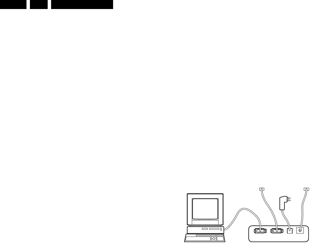
The ComPair interface box is connected to the PC via a serial
(or RS-232) cable.
For this chassis, the ComPair interface box and the TV
communicate via a bi-directional service cable via the service
connector(s).
The ComPair fault finding program is able to determine the
problem of the defective television. ComPair can gather
diagnostic information in two ways:
• Automatic (by communication with the television): ComPair
can automatically read out the contents of the entire error
buffer. Diagnosis is done on I2C/UART level. ComPair can
access the I2C/UART bus of the television. ComPair can
send and receive I2C/UART commands to the micro
controller of the television. In this way, it is possible for
ComPair to communicate (read and write) to devices on
the I2C/UART buses of the TV-set.
• Manually (by asking questions to you): Automatic
diagnosis is only possible if the micro controller of the
television is working correctly and only to a certain extend.
When this is not the case, ComPair will guide you through
the fault finding tree by asking you questions (e.g. Does the
screen give a picture? Click on the correct answer: YES /
NO) and showing you examples (e.g. Measure test-point I7
and click on the correct oscillogram you see on the
oscilloscope). You can answer by clicking on a link (e.g.
text or a waveform picture) that will bring you to the next
step in the fault finding process.
By a combination of automatic diagnostics and an interactive
question / answer procedure, ComPair will enable you to find
most problems in a fast and effective way.
How To Connect
This is described in the chassis fault finding database in
ComPair.
Figure 5-3 ComPair interface connection
How To Order
• Starter kit ComPair32/SearchMan32 software and
ComPair interface (excl. transformer): 3122 785 90450.
• ComPair interface (excl. transformer): 4822 727 21631.
• Starter kit ComPair32 software (registration version): 3122
785 60040.
• Starter kit SearchMan32 software: 3122 785 60050.
• ComPair32 CD (update): 3122 785 60070 (year 2002),
3122 785 60110 (year 2003 onwards).
• SearchMan32 CD (update): 3122 785 60080 (year 2002),
3122 785 60120 (year 2003), 3122 785 60130 (year 2004).
• ComPair firmware upgrade IC: 3122 785 90510.
• Transformer (non-UK): 4822 727 21632.
• Transformer (UK): 4822 727 21633.
• ComPair interface cable: 3122 785 90004.
• ComPair interface extension cable: 3139 131 03791.
• ComPair UART interface cable: 3122 785 90630.
Note: If you encounter any problems, contact your local
support desk.
Stepwise Start-up
Under normal circumstances, a fault in the power supply, or an
error during start-up, will switch the television to protection
mode. ComPair can take over the initialisation of the television.
In this way, it is possible to distinguish which part of the start-
up routine (hence which circuitry) is causing the problem.
Take notice that the transition between two steps can take
some time, so give the set some time to reach a stable state.
During the transition time, the LED can blink strangely.
E_06532_021.eps
180804
PC VCR I2CPower
9V DC
TO
UART SERVICE
CONNECTOR
TO
I2C SERVICE
CONNECTOR
Service Modes, Error Codes, and Fault Finding EN 17FTL2.4E AA 5.
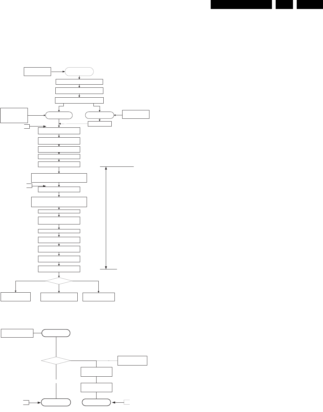
Stepwise start- up explanation
This is realised via ComPair and is very helpful when a
protection is activated (see also chapter “Protections”). The
following diagram shows the start-up procedure of the set.
Every step of the stepwise start-up (also called trapped start-
up) in the diagram corresponds with the number of times the
led blinks.
Figure 5-4 Stepwise start-up part 1
Figure 5-5 Stepwise start-up part 2
Note: When the set is in stepwise mode and, due to stepping-
up, a protection is activated, the set will really go into protection
(blinking LED). The set will not leave the stepwise-mode
however. If state X is the state where the set went to protection,
stepwise start-up will return to state X-1. At state (X-1)
diagnostic measurements can be performed. Also, in the short
time the set is in state X but not yet in protection, you can also
do some measurements.
5.4.2 LVDS Tool
Introduction
This service tool (also called “ComPair Assistant 1“) may help
you to identify, in case the TV does not show any picture,
whether the Small Signal Board (SSB) or the display of a Flat
TV is defective.
Furthermore it is possible to program EPLDs with this tool
(Byteblaster). Read the user manual for an explanation of this
feature.
Since 2004, the LVDS output connectors in our Flat TV models
are standardised (with some exceptions). With the two
delivered LVDS interface cables (31p and 20p) you can cover
most chassis (in special cases, an extra cable will be offered).
When operating, the tool will show a small (scaled) picture on
a VGA monitor. Due to a limited memory capacity, it is not
possible to increase the size when processing high-resolution
LVDS signals (>= 1280x768). Generally this tool is intended to
determine if the SSB is working or not. Thus to determine if
LVDS, RGB, and sync signals are okay.
How to Connect
Connections are explained in the user manual, which is
delivered with the tool.
Note: To use the LVDS tool, you must have ComPair release
2004-1 (or later) on your PC (engine version >= 2.2.05).
For every TV type number and screen size, one must choose
the proper settings via ComPair. The ComPair file will be
updated regularly with new introduced chassis information.
How to Order
• LVDS tool (incl. two LVDS cables: 31p and 20p):
3122 785 90671.
• Service Manual LVDS tool:
3122 785 00810.
5.5 Error Codes
5.5.1 Introduction
The error code buffer contains all detected errors since the last
time the buffer was erased. The buffer is written from left to
right, new errors are logged at the left side, and all other errors
shift one position to the right.
When an error has occurred, the error is added to the list of
errors, provided the list is not full or the error is a protection
error.
When an error occurs and the error buffer is full, then the new
error is not added, and the error buffer stays intact (history is
maintained), except when the error is a protection error.
To prevent that an occasional error stays in the list forever, the
error is removed from the list after 50+ operation hours.
When multiple errors occur (errors occurred within a short time
span), there is a high probability that there is some relation
between them.
5.5.2 How to read the Error Buffer
Use one of the following methods:
• On screen via the SAM (only if you have a picture).
Examples:
–0 0 0 0 0: No errors detected
–6 0 0 0 0: Error code 6 is the last and only detected
error
–9 6 0 0 0: Error code 6 was first detected and error code
9 is the last detected error
• Via the blinking LED procedure (when you have no
picture). See next paragraph.
• Via ComPair.
Initialize PICNIC + screen info
Start TXT acquisition
and time extraction
Reset Audio = low
and Initialize MSP
Screen type
400msec>t>200msec
Trapped Startup 2
+5V and +8V is switched on
Put Stand-by line LOW
CPU GO becomes HIGH
Keep sound amplifiers muted with
sound enable = high
+8V and +5V get their nominal level,
detected by the OTC
Read rest of NVM information
activate protection algorithms for +8V and +5V and
I²C (start I²C protection the moment the component
is initialised).
Initialize 3D Combfilter
or Initialize Columbus
Initialize HIP: IF, source selection, 2fh input, video
processing
Switch on the syncoutput: set_syncout_tristate= off
Stand-by
start time extraction
start P50 recording
start EPG loading
Standby bit = off
Ambient light ON
Initialize rest of PIP/DW module
Initialize tuner
Start up LCD
opt 3,4,5,6
Initialize PDP SDI
opt 0,1,7 E_14620_048.eps
170504
Initialize PDP FHP
opt 2,8
OFF
Read NVM identification
enable watchdog
OUT
OTC gets supply voltage
Mains cord IN
OTC resets, Initialise IO pins
Reset Audio=high
Tact switch
Stand-by bit = OFF
Set STBYEN,VCCON,PFCON = 1
Only FHP (opt 2, 8)
Initialize EBILD
Trapped Startup 1
Start
Semi stand by
yes
Ebild Power ON
Output Blanking OFF
ON
Stand-by bit set ? no
Start up LCD
Trapped Startup 3
LAMP ON
LCD ON
Trapped Startup 4
E_14620_049.eps
170504

Service Modes, Error Codes, and Fault Finding
EN 18 FTL2.4E AA5.
5.5.3 How to clear the Error Buffer
Use one of the following methods:
• By activation of the “RESET ERROR BUFFER” command
in the SAM menu.
• With a normal RC, key in sequence “MUTE” followed by
“062599” and “OK”.
• When you transmit the commands “DIAGNOSE” - “99” -
“OK” with ComPair (or with a DST).
• If the content of the error buffer has not changed for 50+
hours, it resets automatically.
5.5.4 Error Codes
In case of non-intermittent faults, clear the error buffer before
you begin the repair. This to ensure that old error codes are no
longer present. Before clearing the buffer, write down the
content, as this history can give you significant information.
If possible, check the entire contents of the error buffer. In
some situations, an error code is only the result of another error
code and not the actual cause (e.g., a fault in the protection
detection circuitry can also lead to a protection).
There are various errors:
•I
2C device errors.
•I
2C bus errors.
• Protection errors.
• Errors not related to an I2C device, but of importance:
–FEM (Falconic with Embedded Memory) (Error 26):
at start-up, after initialisation of the PICNIC, the
presence of the FEM can be checked.
–Eagle (Error 27): at start-up, after initialisation of the
PICNIC, the presence of the Eagle can be checked.
Table 5-3 Error Code Overview
Note:
• Error codes 1, 6, or 18 are protection codes and in this
case, supplies of some circuits will be switched “off”. Also,
in protection, the LED will blink the number of times
equivalent to the most recent error code.
Error Device Description Def. item Def. Module indication Diagr.
1 M24Cxx NVM, spontaneous blinking error 1 7011 - B5a
3 SAA4978 PICNIC 7713 Feature Box B3a
4 Supply 5 V 5V protection - +5V Supply B5a
5 Supply 8 V 8V protection - +8V Supply B5a
6 Slow I2C bus blocked Spontaneous blinking error 6 - Slow I2C Blocked -
8 TDA932x HIP High-end Input Processor 7323 Chroma IF IO B2
13 UV1318/... Tuner protection 1T01 Tuner B13a
14 MSPxxxx ITT sound processor 7A02 Audio module B6a
18 Fast I2C bus blocked Spontaneous blinking error 18 - Fast I2C Blocked -
21 M62320 I/O Expander 7P56 Video Dual Screen B15b
26 SAA4998 FEM (Falconic with Embedded Memory) 7760 +3V (FBX) Supply B3b
27 T6TX5 Eagle 1C 7720 +3V (FBX) Supply B3c
32 M29W400xx Flash Ram (EPG) 7012 EPG Memory B5a
35 T6TU5 Columbus 7752 Video Control B3d
55 DC/DC converter One of the voltages is not ok + protection error - MSB -
76 Audio supply Audio supply protection - - -
118 AD9883A AD converter 7L01 HD B19a
121 EPLD EPLD error 7V01 Video control B19d
Note: If error 3 or error 55 appears, sometimes error 16 is also logged. Error 16 is a non existing error.
Service Modes, Error Codes, and Fault Finding EN 19FTL2.4E AA 5.
5.6 The Blinking LED Procedure
5.6.1 Introduction
Via this procedure, you can make the contents of the error
buffer visible via the front LED. This is especially useful for fault
finding, when there is no picture.
When the SDM is activated, the front LED will show (blink) the
contents of the error-buffer. Error-codes > 10 are shown as
follows:
– A long blink of 750 ms (which is an indication of the decimal
digit),
– A pause of 1.5 s,
– “n” short blinks (where “n” = 1 - 9),
– When all the error-codes are displayed, the sequence
finishes with a LED blink of 3 s,
– The sequence starts again.
Note: For error codes >100, the first two digits (hundred-and-
ten) are considered as one digit (one long blink)
Example: Error 12 9 6 121 0.
After activation of the SDM, the front LED will show:
– 1 long blink of 750 ms (which is an indication of the decimal
digit) followed by a pause of 1.5 s,
– 2 short blinks followed by a pause of 3 s,
– 9 short blinks followed by a pause of 3 s,
– 6 short blinks followed by a pause of 3 s,
– 12 long blinks of 750 ms (which is an indication of “120”)
followed by a pause of 1.5 s,
– 1 short blink followed by a pause of 3 s,
– 1 long blink of 3 s to finish the sequence,
– The sequence starts again.
Note: If errors 1, 6, or 18 occur, the LED always gives the last
occurred error even if the TV is NOT in service mode.
5.6.2 How to Activate
Use one of the following methods:
• Activate the SDM (only via soldering pads marked “SDM”
on SSB, see figure “Service pads”). The blinking front LED
will show the entire contents of the error buffer (this works
in “normal operation” mode and in “protection” mode).
• Transmit the commands “MUTE” - “062500” - “OK” with a
normal RC. The complete error buffer is shown. Take
notice that it takes some seconds before the blinking LED
starts.
• Transmit the commands “MUTE” - “06250x” - “OK” with a
normal RC (where “x” is a number between 1 and 5). When
x= 1 the last detected error is shown, x= 2 the second last
error, etc.... Take notice that it takes some seconds before
the blinking LED starts.
• “DIAGNOSE X” with the DST (where “x” is a number
between 1 and 5). When x= 1 the last detected error is
shown, x= 2 the second last error, etc.... When x = 0 all
errors are shown.
5.7 Protections
5.7.1 Introduction
This chassis has only one microprocessor (OTC), which
remains active during Stand-by. This because power of the
microprocessor and the attached memory chip set is coming
from the 3V3 supply, which is derived from the 5V Stand-by-
circuitry. Therefore, in both Power-on as in Stand-by mode, the
microprocessor is connected to this power supply.
If a fault situation is detected, an error code will be generated
and if necessary, the TV is put in protection mode. The
protection mode is indicated by the blinking of the front LED at
a frequency of 3 Hz (or by a coded blinking in special cases).
The content of the error buffer can be read via the service menu
(SAM), the blinking LED procedure or via DST/ComPair.
To get a quick diagnosis, this chassis has three service-modes
implemented:
• The Customer Service Mode (CSM).
• The Service Default Mode (SDM). Start-up of the TV in a
predefined way.
• The Service Alignment Mode (SAM). In this mode, items
of the TV can be adjusted via a menu.
You can activate both SDM and SAM modes via the “service
pads” on the SSB (see figure “Service pads”), via an RC-
transmitter (DST or standard RC), or via ComPair. It is not
possible to activate the SAM in “stand-by”; the TV has to be in
“normal operation” mode.
The “Protection Diagram” shows the structure of the protection
system. See diagram below.
Figure 5-6 Protection diagram
There are several types of protections:
•I
2C related protections.
• OTC related protections (via polling on I/O pins or via
algorithms).
• Hardware protection
All protections are explained below.
5.7.2 I2C Related Protections
In normal operation, some registers of the I2C controlled ICs
are refreshed every 200 ms. During this sequence, the I2C
buses and the I2C ICs are checked.
An I2C protection will take place if the SDA and SCL lines are
short-circuited to ground, or to each other. An I2C error will also
occur, if the power supply of the IC is missing.
DC/DC protection: When a 3V3 supply is short-circuited, the
DC/DC converter switches “off” and goes in protection. The
FBX, EPLD IC, and 3D comb IC have no supply voltage and
give no acknowledge. In this case, the TV should go into
protection. An error code is written in the NVM: DC/DC error.
FBX protection: the FBX protection is not available any more.
It is replaced by the DC/DC protection.
5.7.3 OTC Related Protections
If a protection is detected at an OTC input, the OTC will start to
scan all protection inputs every 200 ms for 5 times. If the
protection on one of the inputs is still active after 1 s, the
microprocessor will put the TV in the protection mode. Before
the scanning is started, a so-called “ESD refresh” is carried out.
DC_PROT (from audio) IRQ-DIGITAL (98)
+8V_CON +8V SENSE (105)
+5V_CON +5V SENSE (106)
OTC
TUNER
FAST I2C BUS BLOCKED
SLOW I2C BUS BLOCKED
DC/DC I2C
PROTECTION
EPLD
+
FBX
+
3D COMB
E_14650_032.eps
170604

Service Modes, Error Codes, and Fault Finding
EN 20 FTL2.4E AA5.
This is done, because the interrupt on one of the inputs is
possibly caused either by a flash or by ESD. As a flash or ESD
can influence IC settings, the HIP, MSP, 3D Comb and wireless
module (not used in this set) are initialised again, to ensure the
normal picture and sound conditions of the TV.
8 V and 5 V protections: The microprocessor senses the
presence of the 8 V and 5 V (via the “+5V_CON” and
“+8V_CON” lines). If one (or both) of these voltages is (are) not
present, an error code is stored in the error buffer of the NVM,
and the TV is put in the protection mode.
Audio Supply protection: The OTC senses if the audio
module is in protection via IRQ-DIGITAL (pin 98 of OTC). If this
is the case, the OTC puts the TV in protection.
5.7.4 Hardware Protection
Short-circuiting the 3V3 supply from the DC/DC converter will
shut down the DC/DC converter. The absence of the 3V3
supply line is also sensed via I2C (see description Audio Supply
protection above), this is useful if there is something wrong in
the detection circuit of the DC/DC converter.
Audio DC Protection: This protection occurs when there is a
DC voltage on the speakers. In that case, the Main Supply is
switched “off”. The Stand-by Supply is still working.
Repair tip: If there is an audio DC protection (DC voltage on
your speakers), you will probably see error 18 blink. To be sure
this is an audio DC protection, disconnect the cable between
the SSB and the audio PWB and also the cable between the
Main Supply and the Audio PWB. If the TV starts up, it is very
likely that there is DC on the speakers. Check, and replace if
necessary, the audio amplifiers.
Note: It is also possible that you have an Audio DC Protection
because of an interruption in one or both speakers (the DC
voltage that is still on the circuit can not disappear through the
speakers).
5.8 Repair tips
5.8.1 3V3 Supply (DC/DC converter on the SSB)
As mentioned above, the DC/DC converter is switched “off”
when something goes wrong (detection of a missing 3V3
supply at one of the devices supplied by the 3V3). Because of
this, the TV goes to protection (I2C protection). Error code “55”
is logged.
For further diagnoses, you need to overrule the I2C protection:
put the TV in Service Default Mode by means of the solder
pads on the SSB (see figure “Service pads”).
The DC/DC converter is still not working because it is switched
“off” by the 3V3_FAULT line (schematic B12). Now you have
some possibilities:
1. First, measure the impedance over diode 6U06. In normal
conditions, you should measure approximately 120 ohm (if
possible, verify this with another set). If the impedance is
much too low, do not try to start up the converter as
mentioned below. Remind that if FET 7U03 is short-
circuited, this will also influence your measurement.
2. Desolder coils 5U05 and 5U06, connect an external 3V3
supply at capacitor 2U23 (current limitation to 500 mA) and
a second external 3V3 supply at capacitor 2U31 (current
limitation to 800 mA). The normal working current of the
3V3_SIM line is approximately 400 mA and the normal
working current for the 3V3_DCDCFBX line is
approximately 700 mA. Therefore, if one of the currents
exceeds their nominal value you can determine in which
circuit the overload is situated. If the TV would start up and
you have normal picture, there is probably no overload but
a problem in the detection circuits.
3. If you do not have two external power supplies, you can do
the following: Desolder coils 5U02, 5U03, and 5U04 (you
must desolder all three, otherwise the circuit could be
damaged), connect an external power supply of 3V3 at the
cathode of diode 6U06. Make sure to limit the current of this
external supply to approximately 1200 mA. If the supplied
current exceeds 1100 mA (approximately normal working
current) you can conclude that one of the devices supplied
by 3V3 is short-circuited.
4. Another possibility is to force the converter to start up by
short-circuiting (and keep short-circuited) resistor 3U25
(B12).
Caution: Be aware that this can damage the TV. Even if
you measure approximately 120 ohm over diode 6U06,
there can still be something wrong in the converter itself.
By short-circuiting resistor 3U25, the internal protection of
the converter is disabled.
5.8.2 Protections
Activating SDM via the “service pads” will overrule the
processor-controlled protections, but not the hardware
protections. This means, that the A/D-input protections (5 and
8 V) and the I2C “not-acknowledging” info of FBX + EPLD + 3D
Comb and of the tuner are overruled.
Caution: When doing this, the service technician must know
what he is doing, as it could lead to damaging the TV.
Note: It can sometimes take up to half a minute before the TV
goes to protection!

Service Modes, Error Codes, and Fault Finding EN 21FTL2.4E AA 5.
5.8.3 Repair tip table
Table 5-4 Repair tips
5.9 Software Downloading
In this chassis, you can upgrade the main software via
ComPair without removing the back cover of the TV (it is
possible that early production sets don’t have a hole in the back
plate, in this case you have to remove the back plate). The
switch, which is needed for the software downloading
procedure, can be reached through a gap in the back cover or
the SSB shielding. The switch can be operated with a toothpick
or something like that. Make sure that you do not damage the
PWB with sharp objects. You can find more information on how
this procedure works in the ComPair file. It is possible that not
all sets are equipped with the hardware, needed to make
software upgrading possible. To speed up the programming
process the firmware of the ComPair interface can be
upgraded. See paragraph “How To Order” for the order
number.
Phenomenon Possible Cause Repair tip
“F” in right corner of the screen and set is not reacting on
remote control. The local keyboard is functioning.
TV is in factory mode. Press MENU button on local keyboard for at least 3 seconds. Set will leave
factory mode and function normally again.
No picture, LED blinking at 3 Hz. Set is in protection due to various causes.
For error codes see error-code list.
You have no picture, so:
- Read the error buffer via ComPair (error buffer is accessible when set is in
protection, ComPair-file will guide you to this).
- Read the blinking LED information via standard remote command
<mute>06250x<ok>.
- Or you read the error code sequence via standard remote command
<mute>062500<ok>.
When you have found the error, check the circuitry related to the supply voltage
and I2C-communication or the circuitry that triggers the protection.
No picture, LED blinking with code 6-6-6 or 18-18-18. No communication on slow I2C- or fast I2C-bus. As processor cannot communicate with one of the 2 buses, the Stand-by-LED
spontaneously starts blinking 6-6-6-etc. or 18-18-18-etc...
If in the error buffer somewhere is an error 6 or 18, these will have the highest
priority starting the mentioned blinking.
Measure, dependent of the error on the I2C-bus, which device is loading the bus
(use I2C-overview).
No picture, LED blinking with code 1-1-1. No communication on NVM-I2C bus to the uP. As the uP cannot communicate with the NVM I2C bus, it spontaneously starts
blinking 1-1-1. Note: when there is no access to the NVM, a lot of picture setting
can go wrong.
No RC-reception. Blue LED does not echo RC-
commands.
uP circuitry or RC-receiver is defective. In case the TV does react on a local keyboard operation, you must check the
RC-receiver circuitry (diagram “J”).
Picture is not synchronised. The sync is derived in the HIP. Check crystals in the HIP circuit on bad contacts.
Picture is distorted. Check video-path in Service Default Mode. Investigate whether there is an error code present in the error buffer. In case
there is one, check the I2C-bus and/or supply lines (see overview supply lines).
Measure and check signal path Tuner-HIP-FBX-EPLD.
Picture with horizontal stripes. Pixel Plus processing is malfunctioning Check functionality on circuitry (B3a, B3b, B3c and B3d) of PICNIC, FEM,
EAGLE, COLUMBUS and/or field memories. Tip: the whole Pixel Plus chipset
can be diagnosed via ComPair.
No NextView (EPG). IC7012 defective or not powered. Check circuitry around IC7012 on diagram “B5a”.
No Teletext. IC7007 defective or not powered. Check circuitry around IC7007 on diagram “B5a”.
Problems caused by EPG (Electronic Program Guide).
The TV set "hangs".
Problems with NexTView EPG broadcasts. To switch from EPG 2C3 to Teletext guide, press for 4 seconds, simultaneously
the MENU button on the TV and digit 0 on the remote. The option settings for
NexTView type and FlashRAM will not change.
NexTView EPG is not functioning only Teletext guide. EPG version 2C3 is switched “off” during
production.
To switch from Teletext guide to EPG 2C3, press for 4 seconds, simultaneously
the MENU button on the TV and digit 1 on the remote. The option settings for
NexTView type and Flashram will not change.
Various symptoms, due to missing local supply voltage. An interrupted fuse, NFR-resistor or connection. When no symptom or error code leads you to a specific circuitry, use the supply
lines overview (see supply lines overview), for a quick scan of all supply lines.
No sound at the speakers but sound at monitor out. Possible problem with the class D amplifier Check circuitry around IC7700 on diagram “SA3” (LCD) or “C” (PDP).
No sound at the speakers but sound at monitor out. Sound enable from OTC is HIGH, speakers are
muted
Check pin 95 of OTC on diagram “B5a”.
No sound at the speakers not at monitor out, but sound
at SCART 1 output.
POR line is low, anti plop circuit mutes the sound Check pin 8 on connector 1739 on audio panel. Diagram “C” for PDP sets and
diagram “SA3” for LCD sets
No sound from any output (except headphone) Reset audio is high or MSP is not properly reset Check pin 16 of MSP (diagram “B6a”) and circuitry around MSP.
No sound from the tuner but sound from any other input. Problem with the delay line (PDP sets only) Check circuitry on diagram “B6d”.

Service Modes, Error Codes, and Fault Finding
EN 22 FTL2.4E AA5.
Personal Notes:
E_06532_012.eps
131004
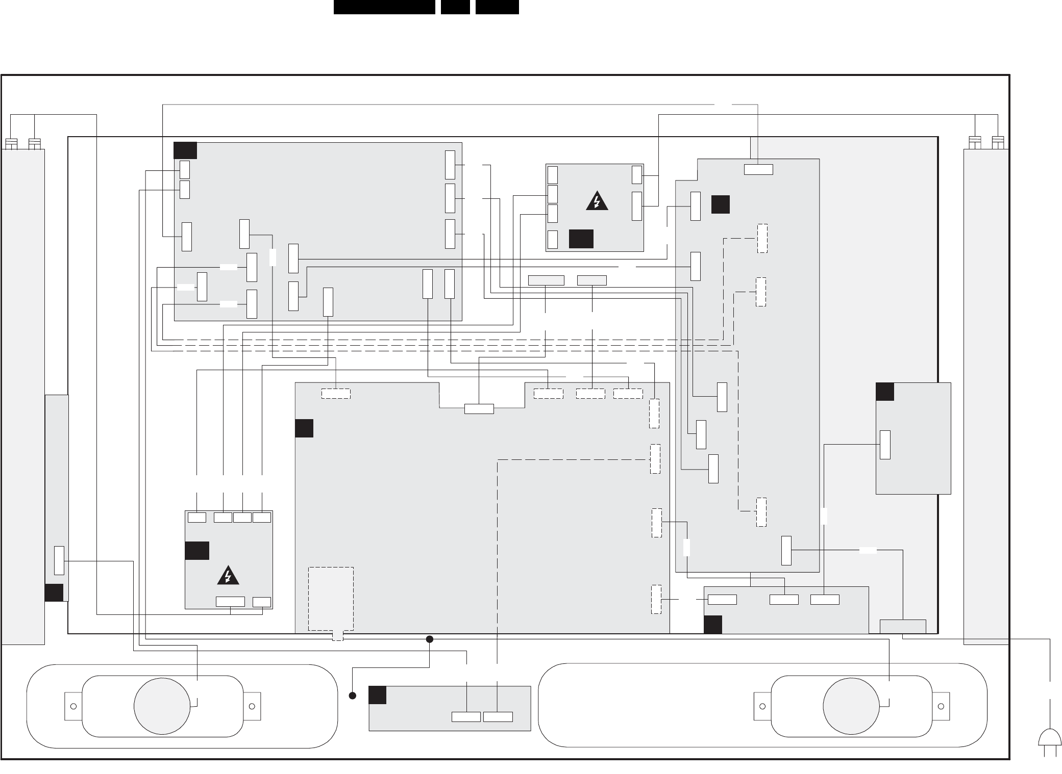
Block Diagrams, Testpoint Overviews, and Waveforms EN 23FTL2.4E AA 6.
6. Block Diagrams, Testpoint Overviews, and Waveforms
Wiring Diagram (32”)
Wiring 32"
Ambient light lamps right
LED panel
SSB
AUDIO STANDBY INVERTERS
AC inlet
LS
left
LS
right
8505
8317
8504
8509
8303
8346
8352
8318
8315
8735
8736
8308
8302
8314
8220
Ambient light lamps left
A
B
E
SA
J
D
8192
F_15490_029.eps
240605
H
8337
8336
8307
6P
0345
12P
1M20
5P
1M07
11P
1M37
11P
1M36
5P
1M07
11P
1M36
12P
1M20
10P
1M03
2P3
1308
10P
CN5
4P
1307
2P3
1606
3P
1305
11P
1M36
6P
CN3
10P
CN4
4P
1304
3P
1309
7P
1MO2
2P3
1306
4P
1307
3P
1305
8506
8507
11P
1M46
10P
1M03
4P
1M10
4P
1304
3P
1309
9P
1739
10P
1315
6P
1318
10P
1314
7P
1M02
2P3
1736
2P3
1735
9P
1M52
31P
1G50
4P
1M51
7P
1M17
11P
1M46
6P
0345
AL
4P
1M49
4P
1M10
4P
1M08
3P
1M48
11P
1M11
3P
1M12
8345
AMBIENT
LIGHT 2
TOP CONTROL
SIDE I/O
3th SCART
MF +SUPPLY
31P
LVDS
7P
TUNER
AL
4P
1M49
4P
1M10
4P
1M08
3P
1M48
11P
1M11
3P
1M12
AMBIENT
LIGHT 1
8250
8310
8349
8548
8508
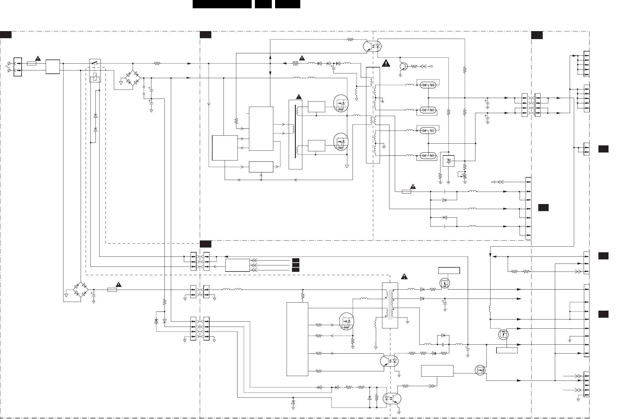
EN 24FTL2.4E AA 6.
Block Diagrams, Testpoint Overviews, and Waveforms
Block Diagram Supply (32”)
SUPPLY PART A
A2
STANDBY
SA2
CONNECTIONS
SA1
MAINS FILTER + STANDBY PART A
A1
SUPPLY + STANDBY 32"
6807
GBJ6J
-+
7001
MC34067P 15
7017
7018
7007
HIGH
SIDE
DRIVE
7004
7009
5001
BIAS SUPPLY
SOFT
START
+
CURRENT
PROTECTION
CONTROL
VCC
OSCC
ERROR
SOST
OB
OA
FI
2
4
11
7
11
14
12
10
7005
STP15NK50ZFP
6
7
5
3
7
8
9
10
11
12
13
5002
7008
LOW
SIDE
DRIVE
7006
STP15NK50ZFP
10
9
3007
7010
TS2431AI
VS Voltage
Adj.
+12V_A
+12V_+24V
5401
5403
23
MAINS
FILTER
14
6506
DF06M
-+
1450
OVER
VOLTAGE
PROTECTION
400V_HOT_A
25V_HOT_A
14
15
16
HOT COLD
HOT COLD
HOT
COLD
MAINS INPUT
HOT
COLD
CONTROL
3
7501
TCET1102
2
1
4
3
+5V2-RELAY-IO2_PWM
7100
7101
7105
7150
TCET1102
2
14
7511
7131
VTUN
+11V
+8V6
+5V2
+5V_SW
5500
7531
+12V
6
7
10
STANDBY
7507
7506
7512
STANDBY
OVERVOLTAGE
PROTECTION
8
B21
TO 1M46
CONNECTION
3
5
2
1
7102
B21
TO 1M03
CONNECTION
+5V2
STANDBY: LOW = ON
HIGH = STBY
3V MAX
1V MAX STBY
2021
2022
CONTROL
7505/7509/7560/
7510
Prot-OVV
STANDBY
+12V_A
DC_PROT
PROT-OVV
F_15490_030.eps
240605
VREF
5
TO
DISPLAY
AL
TO 1M10
AMBI LIGHT
7002
TCET1102
2
1
4
3
2
1308
11400
F4A
1401
T1A
2503
3810
6155
6154
2815
RES
2816
1305
11
1305
22
33
1306
11
1306
22
1307
11
1307
22
33
44
3000 6080 6078
2003
5040
3022
3052
3026
3030
1304
44
1304
33
22
11
3057
+12V
+24V
3025
6504
6140
3509
5110
5507
5103
6107
6122
3158
PROT_AUDIOSUPPLY
2512
5506
2513
3128 3113
3124
2141
5504 5505
5104
5105
3108
3127
3104
3150
3101
3155
6151
6150 3156
6153
3157
6156
1314
1
2
3
4
5
1M10
1
2
1M03
9
1M46
3
4
5
7
8
6077 5010
5017
3028
5007 5008
5009
3100
11
9
6
1315
1
2
3
4
5
6044
STPS20L45CT
1
2
3
6045
1
2
3
5027
5028
5025
5026
6021
STPS20H100CT
1
2
3
6025
1
2
3
1M02
7
6
4
1007
T5A
2291
6291
2293
6293
5293
5291
5292
5
3
2
1
VSND_POS
VSND_NEG
GND_SND
DC_PROT
SA3
TO 1M02
AUDIO
TO
DISPLAY
3101
7030 3031
5
2
+5V_SW
POR
3534 3539
SA1
SA1
SA2
9814
RES
RES RES
6460 6461
TO
DISPLAY
1M18
1
2
3
4
6
ON_OFF
DIM_CONTROL
+5V_SW
+5V_SW
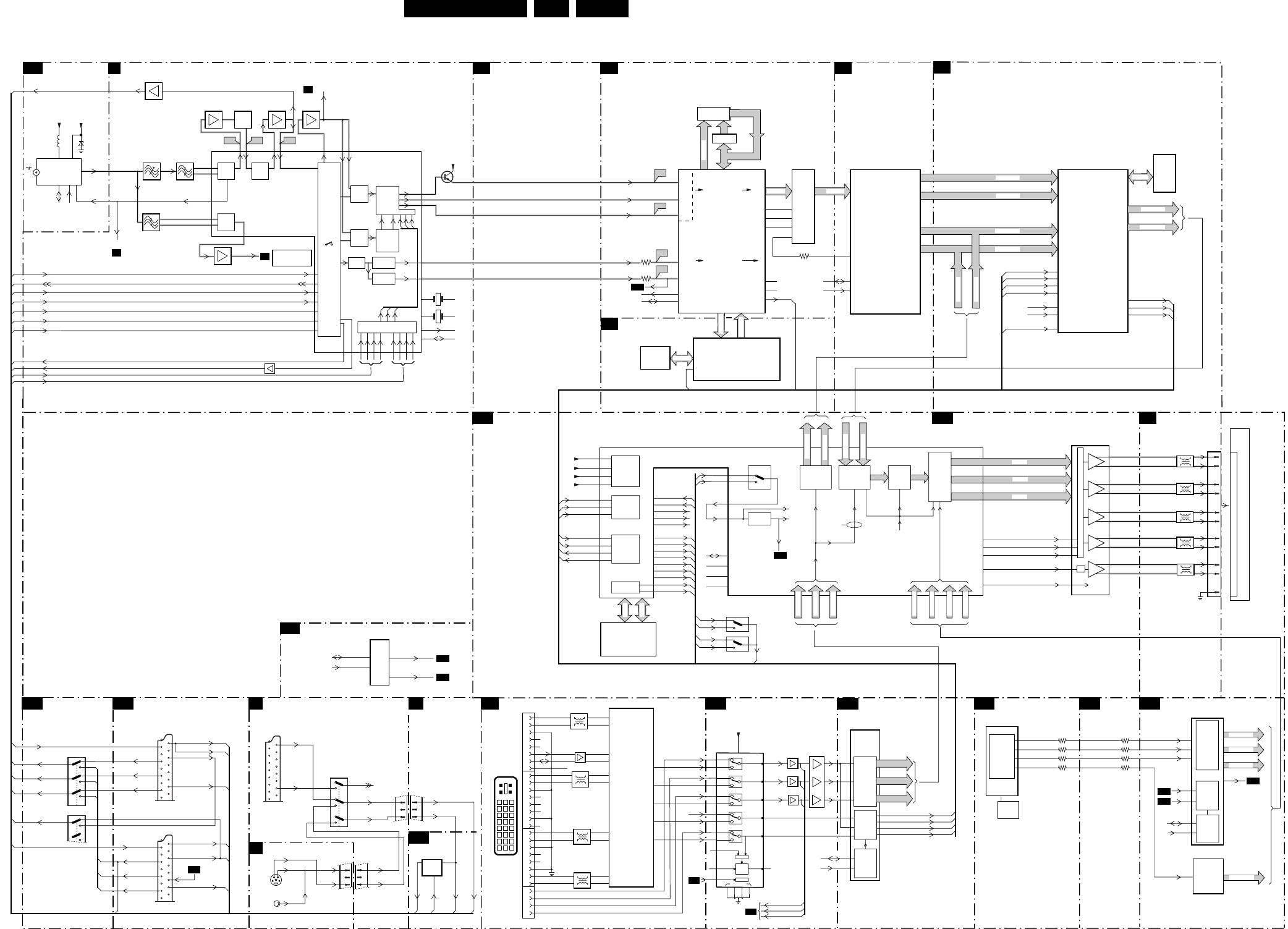
Block Diagrams, Testpoint Overviews, and Waveforms EN 25FTL2.4E AA 6.
Block Diagram Video
B14C B14B
CONNECT
B21
SIDE I/O
D
MMC
B14A
B14F
DIGITAL INPUT
B6A
PICNIC
B3A
COLUMBUS
B3D
FALCONIC
B3B
OTC
B5A B3A B19C
EPLD OSDPICNICSCART3
H
B14B CONNECTIONSIO3 SWITCH
B14G
I/O7
B19A
B20
MAIN TUNER
B13A B3C
B2
B19B
EPLD I/O
B19D
HDI A/D CONVERTER
IF, I/O VIDEOPROCESSING EAGLE
AUDIO DEMODULATOR
EPLD CONTROL SCREEN INTERFACE
PIP SWITCH
B15B
1T01
UV1318ST
S-SDA-PIP
S-SCL-PIP
+33V
1410
1408
AGC
MONITOR
1407 7322
EF
1409-A
17
CVBS-SC1_AV1-IN
CVBS-AV3-IN
Y-CVBS-SC2_AV2-IN
C-SC2_SVHS-IN 21
32 34
SAW FILTER
AUDIO
SAW FILTER
VIDEO
SOUND
FILTER
CVBS-TXT
OTC
7323
TDA9321H
PLL
DEM
GROUP
DELAY
COR.
VIDEO
SWITCH
+
CONTROL
QSS
MIXER
AM
DEMO
QSS-AM
QSS-AM
SOUND-OUTPUT
7,3
2
10 12 13 14
Y
PROC. Y/U/V
SWITCH
UU
Y
U
V
VY V
UY
R
SCART1
SCART2
V
Y
C
PROC.
SYNC
SEPAR.
61
60 HA50
VA50
51
50
49
H-SYNC
PROC.
V-SYNC
PROC.
DECODER
PAL
NTSC
SECAM
C
3
62
63
64
5
MAIN TUNER
AGC
7411
RGB/YUV
MATRIX
40,4
5403
7410
7415
20
I6
TUNER AGC
V1
SIF2
SIF1
VIF1
VIF2
7320
12
EF
26 29
CY
28
EF
GB
36 37 38 39
RGB
41 42 43 40
9
1
5
11
6TO8
4
+5V
IF-TER
V2
CVBS-TER-OUT
16
SEE
BLOCK DIAGRAM
AUDIO
23
24
B6A
B5A
B5A
Y-CVBS-FRONT-IN
C-FRONT-IN
CVBS-SC2-MON-OUT
R/G/B-SC1-Y/U/V-IN
SC2-FBL-IN
SC2-R_C-IN_AV2
SC2-G-IN
SC2-B-IN_C-OUT
7402
VIDEO
Y50
7414
U50
V50
Y-PIP+MAIN-OUT
U-PIP+MAIN-OUT
V-PIP+MAIN-OUT
HIP
54
57
46
47
1305
4.43MHz
PAL
1308
3.57MHz
NTSC M
SCL-F
SDA-F
SCL-F
SDA-F
FIELD
MEMORY
FM1
SN-DA
SN-CL
Href-EXT
23
64K
PROM
25
SYNC PROCESSING
DIGITAL
SIGNAL PROCESSING
PICNIC
FALCONIC
EMBEDDED
MEMORY
3x
ADC
26
28
29
LATCH
7712
74HC573
7713
SAA4978H
7711
M27C512
7714
MS81V04160A
3724
3728
HA50
F165
F162
F164
F166
4
5
CLI6
WEC
RSTW
FALREF
CLK32I
REFIN
Vref
SNDA
SNCL
HREF_EXT_E
CLK-64
CLK-VID
SDA-F3
CLK-2FH
CLK64
HD-E
VD-E
DA (0-15)
7760
SAA4998H
EAGLE
7720
TBF24EF
7V01
EP1C12F256C8
7E23
AD9883AKST
7719
MSM56V16160F
5T25
EPLD
CVBS-SC1_AV1-IN
SC1-FBL
SC1-STATUS
SC1-R
SC1-G
SC1-B
CVBS-TER-OUT
SCART 1
20
16
8
21
19
15
11
7
CVBS-SC3-IN
20
16
8
11
21
19
15
7
SEL-SVHS-RR_STATUS2
B5A
OTC
C-SC2_SVHS-IN
SC2-G
SC2-B_C-OUT
SC2-FBL
P50
CVBS-SC2_MON-OUT
SCART 2
SCART 3
20
16
8
21
19
15
11
7
STATUS-SC3-F
2
5
1
34
1M36
C
CVBS
SVHS
Y
2
4
Y
C
5
2
12
4
15
14
3
1
13
7516
74HC4053
1:2
STANDARD
DEFLECTION
INPUT
CONTROL
SYNC
CONTROL
YUV
to
RGB
CLKP
OSD
INSERTION
UV DEMUX
CONTRAST
SATURATION
BRIGHTNESS
PATH
FOR
3FH
ONLY
UV
CONVERTION
Y-OUT (0-9)
U-VOUT (0-9)
R-OSD (0-5)
G-OSD (0-5)
B-OSD (0-5)
BL-OSD (0-4)
Href-EXT
VA
HD_E
VD_E
H-2FH-AD-OUT
V-2FH-AD-OUT
SYNCDET
TXLCD0-
TXLCD0+
TXLCD1-
TXLCD1+
TXLCD2-
TXLCD2+
TXLCD3-
TXLCD3+
TXCLKLCD-
TXCLKLCD+
R (0-7)
G (0-7)
B (0-7)
A/D
COVERTER
DIPLAY
INTERFACE
SEE ALSO
BLOCK
DIAGRAM
CONTROL
18
1G50
17
16
15
14
13
10
9
12
11
11,14,17,20,23,26,27,28,29
DISPLAY
MF (1-17)
U-VOUT (0-9)
Y-OUT (0-9)
G-OSD (0-5)
R-OSD (0-5)
BL-OSD (0-5)
B-OSD (0-5)
UVG (0-7)
YG (0-7)
YF (0-7)
UVF (0-7)
1
2
3
4
5
6
7
8
9
10
11
12
13
14
15
CLK-OSD
10
11
7L01
AD9883AKST
2-9
70-77
12-19
V-2FH
Y-2FH
U-2FH
7001
SAA5801H
3064-1 3858
77 R-TXT 2FHR-GFX R-OSD
3064-2 3859
78 G-TXT 2FHG-GFX G-OSD
3064-3 3860
79 B-TXT 2FHB-GFX B-OSD
3064-4 3861
80 FB-TXT 2FHFB-GFX
BL-OSD
HD3-OTC
B14b
B14b
B14b
B14b
B14b
B14a
B14a
B14b
B14c
B14g
SNDA
SNCL
1
2
30
B19b
B19d
B19d
B19d
B19d
DRAM
512KX16X2
B19b
B3a
B3a
SDA-F3
SCL-F3
SUPPLY
SCL-F3
SN-CL
SN-DA
CLK-OSD
HD3-OTC
VD-OTC
PWR-OK-PDP
LCD-PWR-ON
LAMP-ON
B3a
B3c
B19a
Vref
Href
RSTR
B3c
B3c
REF
FALREF
REFIN
CLKP
U-AD (0-7)
UV-AD (0-7)
Y-AD (0-7)
7752-1
T6TU5XB
COLUMBUS
I/O
7753
MSN56V16160F-7TS
SDRAM
VA50
16
17
18
19
20
21
22
23
SCL_DVI
SDA_DVI
AV6-V
1I59
1I56
1I57
1I53
49
48
52
51
3
2
5
6
RX2-
RX2+
RX1-
RX1+
RX0-
RX0+
RXC+
RXC-
24
C1
C2
C3
C4
GROUND
1
LOGIC
SEPA
SYNC
DET
2
1
1
1
2
1
2
2
2
VD1-IN
12
VD2-IN
HD-S-SIG-DET
2
HD1-IN
24
HD2-IN
23
R-OUT 21
R1-IN
1
R2-IN
7
20
VCC
VD-OUT 14
18
CTL
16
G-OUT 19
G1-IN
3
G2-IN
9
4
6
8
10
HD-OUT
7I55
BA7657F
B-OUT
B1-IN
5
B2-IN
11
C-S-OUT 17
C-V-IN
SWITCH-MAIN
+5VIO
7I56
7I57
7I58
7154
TSH95
R-VGA
G-VGA
B-VGA
43
48
54
SYNC
PROC.
+
CLOCK
GENERATOR
SERIAL
REGISTER
+
POWER
MAN.
30
31
49
67
65
64
66
CLK-2FH
SYNCDET
V-2FH-AD-OUT
H-2FH-AD-OUT
HSYNC
VSYNC
IOB
IOG
IOR 23
26
31
19
18 HDVI
V-DVI
B-DVI
G-DVI
R-DV1
AV6-H
AV6-V
AV6-B
AV6-G
AV6-R
7I51
7I52
SCLS
SDAS
DVI
RECEIVER
18
916
17
24
C5
C1 C2
C3 C4
DVI-I INPUT
CONNECTOR
B15B
7I18
SII907
7E24
AD9283BRS-80
VD-OTC
8-BIT
ADC
5
3
1
12
7I12
74HC4053
13
2
4
15
14
5
3
1
7I32
74HC4053
4
15 2
3
2
4
3
1M36
1M36
2
4
3
2
4
3
1M36
FRONT-SC3-Y-CVBS
FRONT-SC3-Y-C
32
PIP-OUT
R-SC1_V-IN
G-SC1-IN_Y-IN
B-SC1-IN_U-IN
B2
B2
B2
B2
FBL-SC1-IN
B2
B2
e
f
g
e
f
g
B2
B2
B2
B2
FRONT-Y-CVBS
FRONT-C
SEL_FRONT_SC3
B2
B2
SDA-F3
SCL-F3
SERIAL
REGISTER
+
POWER
MAN.
A/D
COVERTER
SYNC
PROC.
+
CLOCK
GENERATOR
B19d
B19b
B15a
B19d
B19d
B3a
Href-EXT
B3a
B3c,d,B19d
5Z01
5Z02
5Z03
5Z05
5Z04
7V03
MSM56V16160F
DRAM
512KX16X2
SD-A
SD-DQ
BUS A BUS B
BUS C
UVA / YA
UVB / YB
AD(0-7)
B3a
B3a
B19d
OTC
YF (0-7)
UVF (0-7)
UVF (0-7)
YF (0-7)
Y-CVBS-SC2_AV2-IN
B14a
IN-CVBS-SC1_AV1-SUB
B15A
SEL-SVHS-RR_STATUS2
18
B15a
N.C.
B3a
B3a
B3a
B19a
B19a
B19a
VA
B19d
SC2-R_C-IN_AV2
SC2-G-IN
SC2-B-IN_C-OUT
B2
C-FRONT-IN
Y-CVBS-FRONT-IN
FRONT-Y-CVBS-IN
FRONT-C-IN
SC2-B_C-OUT
CONTROL
7I35
7I36
7I37
SC2-FBL
B14b,c
B14b
B2
B2
B19C
B3c
7E03
7E04
SWITCH-1FH
SWITCH-2FH
SWITCH-2FH
SWITCH-2FH
CLK32I
B19b
B19b
B19d
B19d
CLK32P_EPLD
CLK32E
B19b
B19d
CLK32E
B19d
B3a
B3c
B3c
B3c
EAG_SD
COL_SD
+2V5-IO
+3V3-IO
+1V5-INT
+1V5-PLL
10
12
3I/O
EXP
7P56
M62320
2
SDA-S
SCL-S
SWITCH-MAIN
SWITCH-SUB
B14C
B14C
34
41
1D01
E_14650_019.eps
240605
118
26
27
163
46
47
32
33
24
35
+8VP
CLK32FM1 CLK32 83
3727
13
15
22
7V02
DS90C385AMT
TTL PARALLEL-TO-LVDS
PLL
CLK-OUT
LVDS-PWR-DOWN
VS-OUT
HS-OUT
DE-OUT
48
47
46
45
42
41
38
37
40
39
27
28
30
31
32
L3
K1
K5
J1
L1
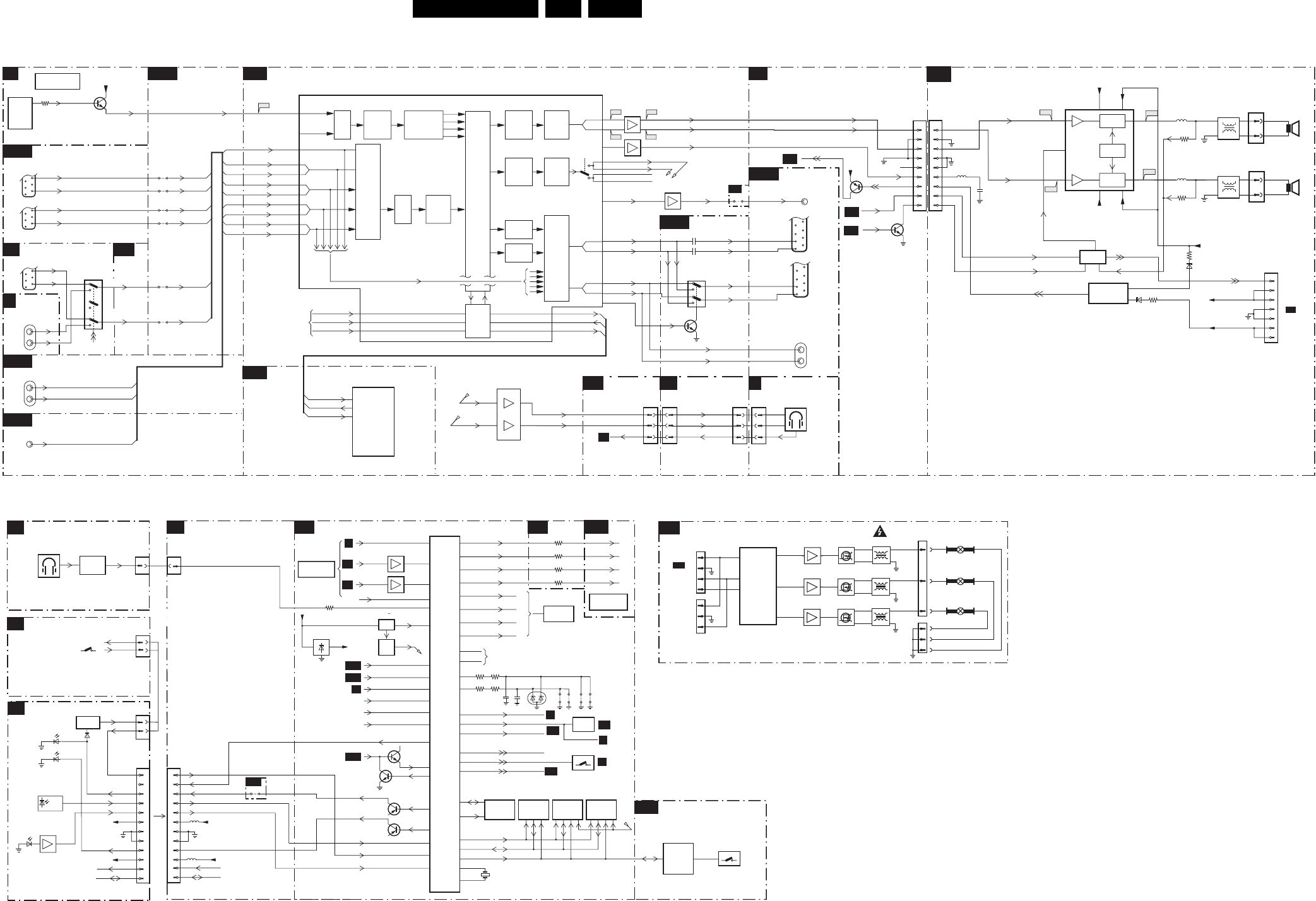
EN 26FTL2.4E AA 6.
Block Diagrams, Testpoint Overviews, and Waveforms
Block Diagram Audio
AUDIO
SA3
B14B
I/O 2 CONNEC.
B14D
SIDE I/O
D
H
SCART 3CONNECTIONS
I/O 2 CONNECTIONS
B14B
IF
B2
I/O 4 AUDIO
B14D
LED + SWITCH
J
OTC FLASH
B5A B3A B19C
CONNECTIONS
B21
TOP CONTROL
E
B6A B21
B21
B14C
B14B
SIDE I/O
D
H
SCART 3
B21
AUDIO DEMODULATOR
J
CONNECTIONS
OTC-FLASH
B5C
SIDE I/O
D
B6D
AUDIO
DELAY
AMBI LIGHT
AL
I/O 3 SWITCH
I/O 4 SWITCH
I/O 4 AUDIO
7323
TDA9321H
QSS_AM
HIP
MAIN
SEE ALSO
BLOCK DIAGRAM
VIDEO
3380
5SOUND-OUTPUT
B68
B69
B67
B66
7410
AL-SC1-IN
SCART 1
AR-SC1-IN
SNR-DVI-IN
SND-DVI-IN
1
3
2
6
AL-SC2-IN
SCART 2
AR-SC2-IN
1
3
2
6
SNDL-SC3-IN
SCART 3
SNDR-SC3-IN
1
3
2
6
45
47
IF1
7A02
MSP3411G
IF2
50
44
SC3 ADC
SC4
I2S-MSP-OUT
I2S-MSP-IN
I2S-MSP-CLK
I2S-DPL-OUT
I2S-DPL-CLK
I2S-DPL-WS
5
6
3
SNDR-MAIN-IN
MONO-IN
SNDR-SC2-IN
12
15
14
SCART
DSP
INPUT
SELECT
SNDR-DVI-IN
SNDR-SEC-IN
N.C.
36
38
39
41
42
35
SC1
N.C.
N.C.
SOURCE
SELECT
PRESCALE
I2S
INTERFACE
DE-
MODULATOR
ADC PRE-PROCESSING
PRESCALE LOUD-
SPEAKER
SOUND
PROCESSING
DAC
HEADPHONE/
SURROUND
SOUND
PROCESSING
DAC
SCART
OUTPUT
SELECT
DAC
DAC
LOUD
SC
20
21
23
17
18
DACM-SUB
FRONT-DECT
7
1
AUDIO-R
AUDIO-L
AUDIO-R
AUDIO-L
AUDIO-SW
HPN-R
HPN-L
MSP-CENTER
MSP-SURR
18
18
28
25
26
61
SNDL-MON-OUT
SNDR-MON-OUT
SNDL-MON-OUT
SNDR-MON-OUT
SNDR-SC2-OUT
SNDL-SC2-OUT
SNDR-SC1-OUT
SNDL-SC1-OUT
SNDR-SC1-OUT-DC
SNDL-SC1-OUT-DC
29
5
3
7
5
2
115
4
REG-SW
5
3
9.10
HPN-L
HPN-R
10
1M36
11
7
L
R
DETECT
HEADPHONE-L
HEADPHONE-R
3
5
1
7
7A07
MC33178D
1M36
11
7
7A03
LM833D
7A00
LM833D
7I22-B
2I99
2IA2
7I20
B65
3858
1M52
1M02
7
6
5
4
3
2
1
-16V-19V
5Y11
9Y06
10
EPG-
FLASH-RAM
4Mbit
AUXILIARY
FLASH
PROGRAM
CIRCUIT
FOR
FLASH RAM
SEE ALSO
BLOCK DIAGRAM
VIDEO
SEE ALSO
BLOCK DIAGRAM
VIDEO
7015
7016
B2
CONTROL
AUDIO
74LVC245APW
74LVC245APW
775
OTC
CVBS-TXT
CVBS-Y-RECORD-IN
R-TXT
B14B
B14B
B14B
109
OUT +3V3
INTOTC
N.C.
IN
+5V2-CON
STATUS_SC3
STATUS_SC4 108
97
120
7009
7022
B4 99POR-FLASH
98IRQ-DIGITAL
93HD@HOME
96IRQ-FTV
N.C.
N.C.
N.C.
115
P50
7008
LED2
107KEYBOARD
LIGHTSENSOR 110
LIGHT_SENSOR
100
RC
6x
+3V3
RC
SA
B6A
84
7
N.C.
114
RESET 74
RESET
83
B3A HD3-EPLD
B3A VD-EPLD
78 G-TXT
SEE ALSO
IIC DIAGRAM
79 B-TXT
80 FBL-TXT
R-OSD
G-OSD
B-OSD
BL-OSD
88 SDA-F
87 SCL-F
86 SDA-S
85 SCL-S
104 STANDBY
90 TXD
89
119
96
RXD
3099-3 3081
3074-4 3097
SAM
SDM
95 SOUND-ENABLE
94 RESET AUDIO
117
116
SEL_IN_2
91 SDA
92
5
6
SCL
16
17 1001
6Mhz
SEL_IN_1
7006
M29W320DT
7007
MSM51V18165F
7012
M29W400DT
7018
7019
103 PWW-BLACKLIGHT B5B
ADDRESS
DATA
CONTROL
MENU
CHANNEL+
CHANNEL-
VOLUME+
VOLUME-
1M36
RP
RESET
FLASH
RAM
7002 :
7004
7013, 7014
DRAM
(TXT)
16Mbit
PROGRAM
FLASH-RAM
SET SW
32Mbit
7011
M24C64
EEPROM
NVM.
4kByte
RP
7005
LF33AB
(OCTAL BUS TRANSCEIVER)
3859
3860
3861
9ID0
1M20
RED
BLUE
1M20
1
2
72
6060
6070
7070
LM358P
3
4
5
6
7
8
9
10
1
+8V
LIGHT-SENSOR
RC-IN
2
3
4
5
6
7
8
9
10 +5V2-STBY
+8V
PWM
-16V-19V
-16V-19V +16V+19V
I722
18
3
24 22
+16 +19V
24
10
6
I778
3
1
1735
15W/
8Ω
15W/
8Ω
23
I776
3
1
5702
5701
OSC
STBY-MUTE
7700
TDA7490
PWM
+16V+19V
3717
3718
3761
6702
I711
L
R
7701 : 7707
SOUND-ENABLE
POR-CLASSD PROT1
PROT-AUDIO-SUPPLY
SOUND
ENABLE
3
2
4
5
6
7
8
9
1
1739
AUDIO-L
AUDIO-R
1736
5730
5731
AUDIO
SUPPLY
PROT, CIRCUIT
SCART 1
1
3
6
SCART 2
1
3
6
+8VP
DCPROT
+16V+19V
DCPROT
TO 1002
A6
SUPPLY
HEADPHONE-OUT
5
2
12
4
15
14
3
1
13
7515
74HC4053
SNDL-IN
SEL_FRONT_SC3
SNDR-IN
FRONT-L
FRONT-R
SND-CENTRE-IN
SNDL-SEC-IN
SND-CENTER-IN
3
2
4
5
6
7
8
9
1
POR
7Y01
7010
IRQ-AUDIOSUPPLY
AUDIO-SW
SOUND-ENABLE
B5A
B5A
1I05
1I07
10
1M37
11
7
FRONT-L
1M36
11
7
10
11
7
ON / OFF
2
KEYBOARD
0345
11
12
6051
+5V2-STBY
SCL-S
SDA-S
LIGHT SENSOR
11
12
SCL-SF
SDA-SF
KEYBOARD
7022 115
ON-OFFOLED
+3V3
LED2
LED1
B14E
118
CON-SND
CON-SND
6005
2061
7516
74HC4053
H
N.C.
A-PLOP
SA
B14B
1404
SSSS811
SWITCH FOR
SOFTWARE
DOWNLOAD
B14b
1002
SNDL-DVI-IN
B6a
B6a
B6a
DACM-SUB
23
1I06
SUBW
9ID0
B6C
AUDIO_SW
1I06
SA
B5A
+5V2-STBY
IR
SENSOR
1040
LED2
LED1
GND-AUD
N.C.
4
6061
CONTROL
7030
7031
7032 BLACKLIGHT-TC
7
2725
5701
HEADPHONE-OUT
FRONT
DETECT
9I33
9I34
9I32
9I35
9I31
9I30
SNDR-MAIN-IN
SNDL-MAIN-IN
SNDLSC2-IN
SNDR-SC2-IN
SNDLSC2-IN
SNDR-SEC-IN
SNDL-SEC-IN
B14d
B14d
B14d
B14d
B14c
B14c
B14d
B14d
SNDL-MAIN-IN
B6a
B6a
B6a
B6a
B6a
B6a
7A00-A
1
3
B5A
1M36
7
3073-2
2
0345
4
KEYBOARD
BLACKLIGHT-TC
FRONT-R
FRONT-DETECT
F_15490_031.eps
240605
EXT 3
AUDIO
L/R IN
FRONT
AUDIO
L/R IN
DVI
AUDIO
L/R IN
CENTER
IN
EXT 1
AUDIO
L/R IN
EXT 2
AUDIO
L/R IN EXT 1
AUDIO
L/R OUT
EXT 2
AUDIO
L/R OUT
AUDIO
L/R OUT
SUBW
OUT
2060
9005
9006
9018
9017
I2S-MSP-OUT
I2S-MSP-IN
I2S-MSP-CLK
(Optional)
7708 : 7711
3764
6703
7001
P87LPC760
MICRO
CONTROLLER
7018
7009 7015
5014
1M11
11
6
1
7019
7010 7016
5015
7020
7011 7017
5016
1M12
1
2
3
RED
BLUE
GREEN
1M49
1
2
3
4
SCL
SDA
RXD
1M48
1
2
3
TO 2nd
AMBI LIGHT
PWB
(Optional)
TO 1M49
B21
See also
block diagram
I2C
7
6
8
14
12
13
AUDIO
DELAY
7001
SAA5801H
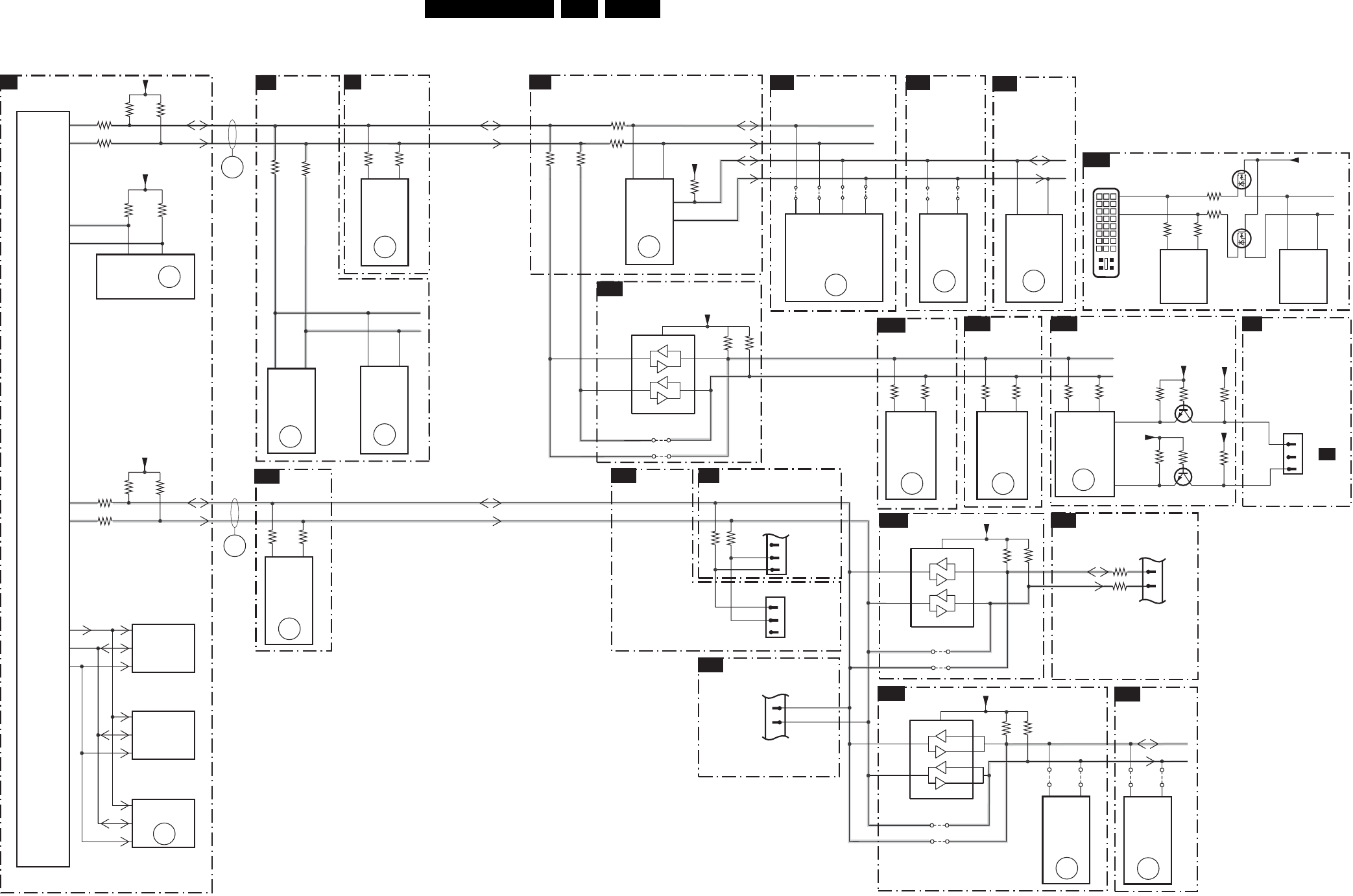
Block Diagrams, Testpoint Overviews, and Waveforms EN 27FTL2.4E AA 6.
I2C IC’s overview
45
7A06
TDA7309
AUDIO
DECODER
ERR
82
21
7A02
MSP3411G
AUDIO
DEMODUL
ERR
14
SDA-F-AUD
SCL-F-AUD
SDA-S
SCL-S
SDA-F
SCL-F
SN-DA
SN-CL
SDA-D
SCL-D
SDA-F
SCL-F
SDA-DISP
SCL-DISP
SDA-F3
SCL-F3
AL-CL-IN
AL-DA-IN
AL-CL
AL-DA
SDA-SF
SCL-SF
SDA-S
SCL-S
1
2
54
7713
SAA4978H
PICNIC
ERR
3
9E57
9E58
21
7V01-4
EP1C12F256C8
BANK3
ERR
56
SDA
SCL
+3V3-INTOTC
3001 3002
91
92
7011
M24C64
(NVM)
EEPROM
7006
M29W320DT
PROGRAM
FLASH-RAM
ERR
1
ERR
32
56
7007
MSM51V18165F
DRAM
(TXT)
7012
M29W400DT
3P66
32
3P65
7P56
M62320FP
I/O
EXPANDER
ERR
21
1I11
19
20
RES
FOR MMC
1
2
3
COMPAIR
SERVICE
CONNECTOR
1M15
7
6
3I49 3I46
65
7I19
M24C02
EEPROM
14 15
7I18
SII907BCQ
DVI
RECEIVER
D
S
G
D
3377 3376 3826
47 46
7323
TDA9321H
HIP
ERR
8
18
916
17
24
C5
C1 C2
C3 C4
7001
SAA5801H
SET
PROCESSOR
3064-4
3064-3
88
87
ERR
18
3079
+5V2_CON
3069
SN-DA
SN-CL
3A19
3A17
+5V2Pr
3758
3710
3709
3827
SDA-EPLD
SCL-EPLD
VCC
7E10
PCA9515DP
6
7
8
RES
3
2
3E69
3E70
+3V3-EPLD
C14 D14
7752-2
T6TU5XB
COLUMBUS
CTRL
ERR
35
9815 9816
A15 B15
9817 9818
33 24
7720
T6TX5AF
EAGLE1C
ERR
27
9757 9755
3064-2
86
3064-1
85
3092
+5V2_CON
3088
DVI INPUT
CONNECTOR
9T10
54
9T09
1T02
UV1318S
SUB
TUNER
ERR
23
9T08
54
9T07
1T01
UV1318ST
MAIN
TUNER
ERR
13
RES
VCC
7T50
P82B96TD
3L06 3L03
57 56
7L01
AD9883AKST
A/D
CONVERTER
ERR
53
3E18 3E19
57 56
7E23
AD9883AKST
A/D
CONVERTER
ERR
53
3V38 3V37
1G50
31
30 TO
DISPLAY
11
12
1M20
LED SWITCH
PANEL
(ITV)
3T05
3T06
3Y09
3Y40
7V04-1
+3V3-IO +5V
3V50
3V51
3V52
7V04-2
+3V3-IO +5V
3V55
3V54
3V53
1
2
3
TO CON2
AMBI LIGHT
1M49
I2C BUFFER
RES
3Z51
3Z50
ADDRESS
34 41
7760
SAA4998H/V1
FEM
ERR
26
ERR
6
DATA
CONTROL
RES
VCC
7I10
PCA9515DP
3
2
6
7
9T50
9T12
1
7
3
5
2
6
9I06
9I05
8
3IB3
3IB1
8
S-SDA-PIP
S-SCL-PIP
3V3-Si-IO
7I52
7I51
G
SCL-DVI
SDA-DVI
AL
+5V
+3V3_SIM
3IQ7
S
3IQ6
SDA-S
SCL-S
OTC
B5
I/O, VIDEO
PROCESSING
B2
PICNIC
B3A
FALCONIC
B3B
EAGLE
B3C
IIC
COLUMBUS
B3D
AUDIO
DEMODULATOR
B6A
EPLD OSD
B19A
HDI A/D
CONVERTER
B19C
EPLD I/0
B19D
I/O6 DIGITAL INPUT
B14F
I/O5
PIP SWITCH
I/O2 CONNECTIONS
B14B
MAIN TUNER
B13A
SUB TUNER
B13B
I/05
B14E
B15B B14E
EPLD
CONTROL
B19B
SCREEN
INTERFACE
B20
CONNECTIONS
B21
CONNECTIONS
B21
E_14650_021.eps
230804
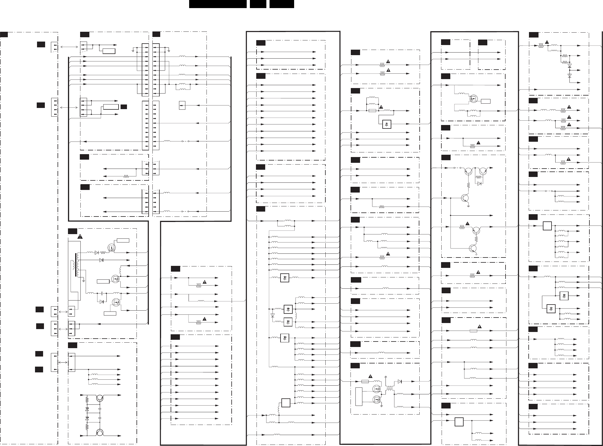
EN 28FTL2.4E AA 6.
Block Diagrams, Testpoint Overviews, and Waveforms
Supply Lines Overview
SCREEN INTERFACE
B20
EPLD I/O
B19D
EPLD OSD
B19C
EPLD CONTROL
B19B
HDI A/D CONVERTER
B19A
PIP MUPPET
B15C
PIP SWITCH
B15B
PIP HIP
B15A
I/O7
B14G
I/O5
B14E
I/O4 AUDIO
B14D
I/O3 SWITCH
B14C
I/O2 CONNECTIONS
B14B
I/O1 MMC
B14A
DC-DC CONVERTER
B13C
SUB TUNER
B13B
MAIN TUNER
B13A
MAIN TUNER
B12
AUDIO DELAY
B6D
DOLBY PROLOGIC PROCESSOR
B6C
DOLBY DIGITAL DECODER
B6B
AUDIO DEMODULATOR
B6A
BACKLIGHT CONTROL
B5C
OTC FLASH
B5A
HOP
B4
FBX SUPPLY
B3E
COLUMBUS
B3D
EAGLE
B3C
FALCONIC EMBEDDED MEMORY
B3B
PICNIC
B3A
IF,I/O VIDEOPROCESSING
B2
CONNECTIONS
B21
BACKLIGHT CONTROL
B5B
LED SWITCH PANEL
J
SCART 3
H
SUPPLY LINES OVERVIEW
CONNECTIONS
SA1
AUDIO
SA3
STANDBY
SA2
SUPPLY
A
I/O6 DIGITAL INPUTS
B14F
VDISP
+3V3_SIM
VDISP
+3V3_SIM
+11V
+11V
+3V3-SD
+3V3-IO
+3V3-SD
+3V3-IO
+5V
+5V
+3V3_EPLD
+3V3_EPLD
+3V3-AD
5E02
5E03
VDDO
PVDO
5E01 VDO
5E00 VBL
5E50 +1V5-INT
5E52 +1V5-PLL
7E05
13
+3V3-SIM
5E51
5E54 +3V3-SD
5E53 +3V3-EPLD
7E01
13+2V5-IO
+3V3-IO
+5V
5L17
5L16 VD
+3V3-AD
7L02
32
VDD
5L14
5L13
5L18 PVD
5L15
IN OUT 2
+3V3_SIM
5PB0 +3VD
5PA9 +3V
+3.3V
+5VPIP +5VPIP
9PB2
+5V
+5VPIP
+5VD
+8VPIP +8VPIP
5P51
3P74
+8V
+8VPIP
+8VHIP
+5V +5VHIP
5P01
3P02
3P01
5P03 5P00 3P00
5I13 +8V-VIDEO
5I12
3I40
3IG9
+8V
3IW1
REF1
REF2
REF3
6I80
6IA1
+5VIO +5VIO
+5V2_STBY
+11V
+5V2_STBY
+11V_DC
+3V3_SIM
+3V3_SIM
1I79
T300mA
+11V_S +11V_SF
5IEE
+5V
+5V_CON
5I46
+5V_VDP
5I45
+5V
+5V
+8V
+5V
+8V
+5V +5VIO
3IN4
+5V
+5V2-APLOP
3
1
2
3ID0
3IC1
7I09
7I07
+11V +11V_S
3I37
6
2
1
7I21-1
3ID9
7I21-2 7I05-1
9IA5
+5V
+5V2-STBY
5
43
+8V
+8VA
3IK7
+8V
5T14 VDISP
5T15
5T11
+11V_DC
+11V_DC
7T01-1 7TO4
DC-DC
5T10
+5V +5V
+33V
+33V
7U03
7U04
CONTROL
5U02
+11V 1U01
T1500mA
6U02
5U05
+3V3_
DCDCFBX
5U06
+3V3_SIM
+3V3-LINK
RES
5U01
+5M +5D
5A07
+8VC
+5DB
+11V_AUD
+5DA
+8VC
+5DB
+11V_AUD
+5DA
+5V +5M
5A38
5A03 +5DB
5A02 +5DA
+5VF
5A06
+11V_S +11V_AUD
5A01
+5V +5V
5A00
+8V +8VC
3A03
+3V3_INTOTC
+8V_CON
+3V3_INTOTC
EAn
7005
+5V2-STBY 1000
F500mA
5000
5001
+5V2_CON
VPP_SW
5003
+8V_CON
EAn
VPP-SW
+5V_VDP +5VS
3304
+8V_VDP +8VS
3329
5768
5770
+3V3PB
+3V3PC
5779 +3V3GA
5767 +3V3PA
5772
+3V3FB
+1V8FA
5771
+3V3FA
5769
+3V3Pr
5773 RES
5775 +2V5_FBXA
7774
7773
5763
+8V_CON 5702 +8VPA
5709 +1V5_FBXB
7701
6719
5760 +1V5_FBXA
7770 5761
5777 +3V3_FBXB
7774
5764
IN OUT
5756 +3V3CA
+3V3CB
5764 +2V5EC
5752 +2V5ED
5753
5780 +3V3ED
+3V3EC
5751 +3V3EB
5750 +3V3EA
5801
5713 +2V5EA
+2V5EB
5762
5719
5720
+3V3_DCDCFBXA
+3V3_DCDCFBX
5721
5722
+5V_FBXA
+5VF
RES
+5V2Pr
5775
+3V3CA
+3V3CB
+1V5CA
+5V2Pr
+3V3CA
+3V3CB
+1V5CA
+5V2Pr
+2V5ED
+2V5EC
+1V5EA
+1V5EB
+2V5EB
+2V5EA
+3V3EA
+3V3EB
+5V2Pr
+3V3EC
+3V3ED
+2V5ED
+2V5EC
+1V5EA
+1V5EB
+2V5EB
+2V5EA
+3V3EA
+3V3EB
+5V2Pr
+3V3EC
+3V3ED
+3V3FB
+3V3FA
+1V8FA
+1V8FA
+3V3_DCDCFBXA
+1V5_FBXA
+3V3_FBXB
+5V2Pr
+2V5_FBXA
+3V3PA
+8VPA
+3V3Pr
+3V3PB
+3V3PC
+3V3GA
+3V3FB
+3V3FA
+1V8FA
+5VS
+8V
5416
+5V_VDP
3402
+1V8FA
+3V3_DCDCFBXA
+1V5_FBXA
+3V3_FBXA
+5V2Pr
+2V5_FBXA
+3V3PA
+8VPA
+3V3Pr
+3V3PB
+3V3PC
+3V3GA
+8V_VDP
+8VP
+5VS
+8V
+5V_VDP
+5VCOM
+8V_CON
1M46
1
2
3
4
5
6
7
+33V
+8V
8
9
10
11
1M20
1M03
1
2
3
4
5
6
7
8
9
10
5Y06
+5V
5Y15
+11V
5Y02
+5V2-STBY
5Y07
5Y03
+5V
5Y09 9Y01 +5V2-STBY
+1V5
6
7
8
9
10 5Y12 9Y06 +5V2-STBY
5Y11 +8V
1M07
3
4
5
+11V_SF
+8V_CON
+5V_CON
+8V_CON
+5V_CON
+3V3_INTOTC
+1V5EA
5753
5758 +1V5EB
5759 +1V5CA
EAn
3C01 B5a
3400
+8V_VDP
B14e,B15c,
B19b,B20,
B21
B14e
B21
B14e
B4
B3e
B3e
B3e
B3e
B3e
B3e
B3e
B3e
B3e
B3e
B3e
B3e
B3e
B3e
B3e
B3e
B3e
B3e
B3e
B3e
B3e
B3e
B3e
B3e
B3e
B3e
B3e
B3e
B3e
B3e
B12
B6a
B2
B14e
B14e
B21
B5c
B2
B5c
B14e
B2
B5a
B21
B21
B14b
B21
B6a
B6a
B6a
B6a
B6b
B21
B21
B21
B14e
B21
B21
B21
B21
B21
B21
B21
B14b
B21
B21
B12
B21
B14c
B21
B21
B15a
B21
B15b
B12
B21
B12
B14eB14e
B19a
B19b
B19b
B21
B19b
B12
B13c
B21
B3e,B5a,B5b
B3a
B3a
B3a
B3a
B3b
B3b
B3a
B3a,B3b
B3a
B3c
B3d
B3a
B3c
B3a
B3c
B3c
B3c
B3c
B3a
B3c
B3c
B3c
B3c
B3d
B3d
B3a,B3c,B3d
B3a
B3c
B2
B3e
B6c
B6c
B6c
B6c
B6b
N.C.
B20
B3a,B3c
B6a,B14e
B14g
B13c
B21
B5a,B5b
B2,B4
B14f
B15b
B15c
B19c
B19d
B19d
B19d
B2,B6a,
B14a,d,e,g,B15a
B6a,b,B13a,b,B14b,
c,d,e,f,B15a,b,19a,d
B14b,e,B20
B13a,B13b
+8V +8V_VDP
5I47
B21 B2,B4
RES
B21
B5a,B14b,e,
6I11
B21
B21
B21
B21
B14e
+8V
+5V2-STBY
+11V_SF
+11V_SFS 3511-3516
1M46
1
2
3
4
5
6
7
8
9
10
11
+12V
VTUN
+5V2
+5V_SW
+8V6
+12V
+24V_2
1
2
3
4
5
6
7
8
9
10
1M03
+5V2-RELAY-IO2
1
2
3
4
+12V_+24V
+12V_A
6
1
+16V+19V
-16V-19V
-Vf21
5723
-Vf11
5707
-Vf1
5711
1M02
1M20
6
7
8
9
10
1M07
3
4
5
7511
7131
VTUN
+11V
+8V6
+5V2
+5V_SW
5500
5110 6504 3509
6140
5103 2513 5506
7531
6107
+12V
6
7
8
5
1
2
1306
1
2
1303
1304
A4
TO 1303
42" SUPPLY
PAR T B
A2
TO 1304
SUPPLY
(PART A 42")
SA2
SA2
SA2
SA2
SA2
SA2
SA2
A1
TO 1306
MAINS FILTER
(PART A 42")
A2
TO 1M02
SUPPLY 30"/37"
OR
SA1
SA1
SA1
SA1
SA1
+5V2-RELAY-IO2 SA1
A4
TO 1M02
SUPPLY 42"
1
2
1303
1
2
3
4
1304
1
2
1306
6
1
1M02
SEE ALSO
BLOCK DIAGRAM
SUPPLY
1
2
1305
3
1
2
1305
3
A1
TO 1305
MAINS FILTER
(PART A 42")
SA2
DISPLAY
AMBI LIGHT AL
CONTROL
CONTROL
CONTROL
5507
SA1
+12V_A
F_15490_032.eps
240605
10
1M17
1B12
+3V3_SIM
Only for
SHARP display
To
Display
+8V-VIDEO
3V3-SI-IO
+8V-VIDEO
+3V3-SI
+5V
5I34
B14g
B21
3V3-TMDS
5I35
7I65
3IN OUT 2
+16V+19V
-16V-19V
Vp
Vm
3760 3759
7712
7713
2797
2798
67106711
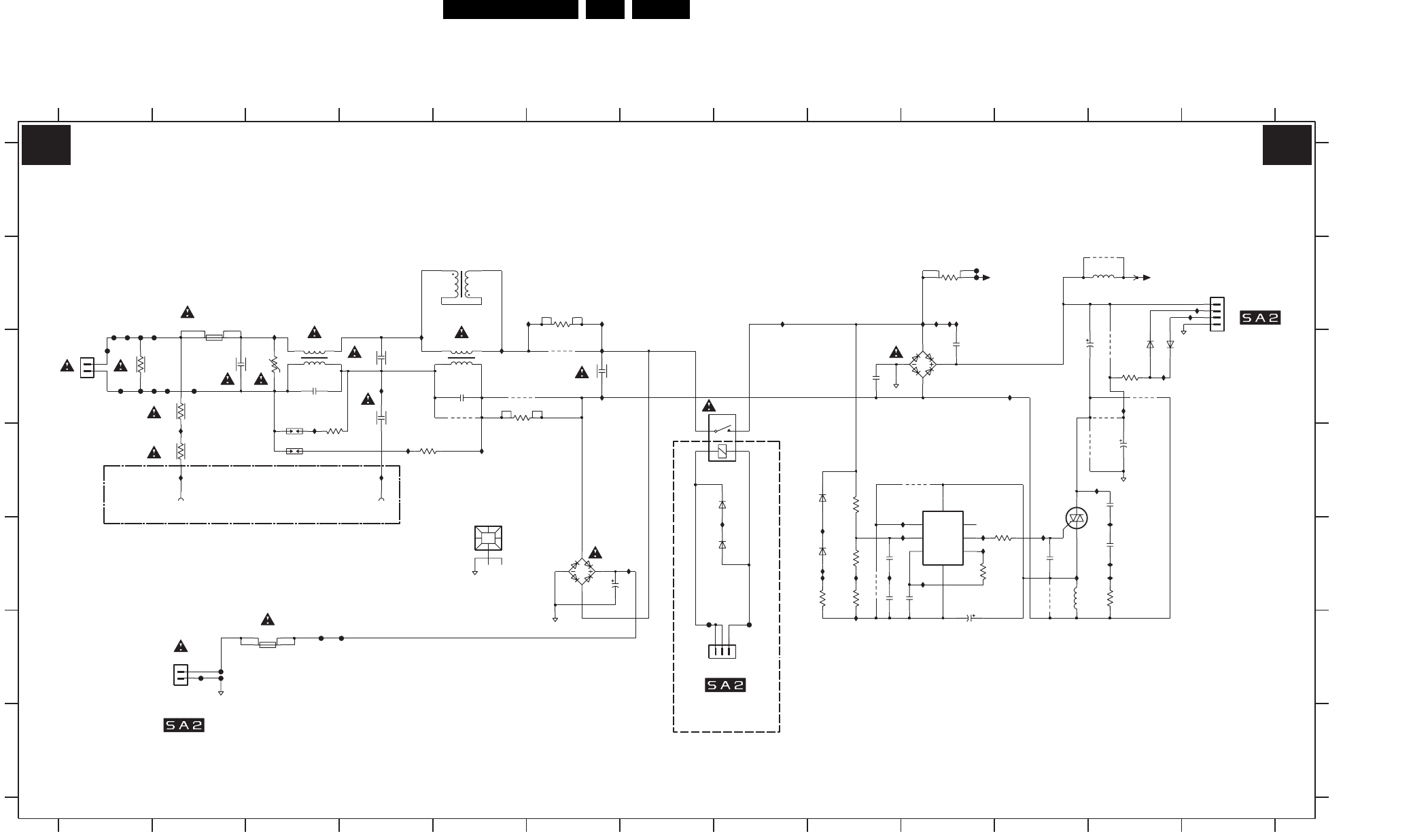
Circuit Diagrams and PWB Layouts EN 29FTL2.4E AA 7.
7. Circuit Diagrams and PWB Layouts
LCD Supply Panel: Mains Filter + Standby
MODE
VM
OSIN
VSS
OSOUT
VG
NC
VDD
V
I812 B10
I813 B10
I814 E9
I815 E9
I420 D12
I421 E11
I422 E11
I423 E10
I424 E7
I425 E10
I426 E10
I427 E10
I830 C12
I445 C6
RELAY -
AUDIO-STANDBY
AUDIO-STANDBY
I455 D4
I456 E7
I810 B10
I811 B10
RELAY +
MAINS FILTER + STANDBY
F426 F2
F427 F3
F428 F4
I410 B3
I411 C4
I816 E9
I817 C11
I820 F9
I824 E12
I825 E12
I826 E12
I828 E9
I419 D2
T5AH 250V(US)
TO 1307
F414 B1
F415 C1
F416 C2
F417 C2
I428 E10
I429 D2
I430 D4
I431 D3
I432 D5
I442 B6
I444 B6
F425 F2
HOT
95-264Vac
COLD GROUND
9005 C6
9050 B12
9806 E9
9808 C12
9810 D10
I412 C5
I413 B8
I414 B13
I415 C6
I416 C4
I417 B13
I418 C12
F413 B1
288V (0)
5401 C3
5402 C5
5403 B5
5804 E11
6154 C12
6155 C12
6460 E8
6461 D8
F418 C1
F419 C2
F420 F7
F421 F8
F422 B10
F423 B10
F424 F2
9003 C5
TO 1305
T3.15AH 250V(EUR)
3101 C12
3400 C3
3401 C1
3402 C2
3403 D2
3404 D4
3405 D3
3450 B6
3451 C5
3800 D9
9811 D12
9812 E11
9813 C12
9814 C12
F410 C1
F411 B1
F412 B1
5006 B12
290V (303V)
2401 C4
2404 C3
2406 C5
2407 C4
2408 C6
2503 E6
6506 E6
6807 C10
6808 E9
6809 D9
7805 D10
7806 E11
9001 C5
2809 E12
2810 D12
2815 C11
2816 D12
234567891011
3802 E10
3803 E11
3804 E9
3805 E12
3806 E9
3807 E9
3810 B10
F
COLD
MAINS FILTER
COLD
2802 E10
2803 C10
2804 C9
2805 E9
2806 F10
2807 E9
2808 E11
7
TO 1306
8 9 10 11 12 13
1
C
D
E
F
G
1000 D2
1001 D4
1011 E5
1305 F7
1306 F2
12 13
A
B
C
D
E
1308 C1
1400 C2
1401 F3
1402 D3
1403 D3
1450 C8
2400 C2
MAINS INPUT
AUDIO-STANDBY
T5AH 250V(AP)
1307 B13
123456
I831 E9
4V8 (0V)
G
A
B
I816
F410
F411
I826
I421
3803
390R
23
F422
DMF3547HB60
5402
14
9812
I414
400V_HOT
I420
I444
I432
I424
9001
1R0
3451
20K
3804
2407
220p
5006
I413
I455
330u
2815
9814
3404
I416
220R
F416
2802
I422
100p
I825
I429
GNDHOT
GND screw
1001
1
2408
100n
I817
4M7
3403
I812
1306
1
2
F417
I828
DF06M
6506
2809
100n
I820
3
470n
2401
1305
B3B-EH-A
1
2
F427
1
2
3405
220R
1308
56n
2803
1
9003
1000
GND screw
1N5062
6808
9050
4M7
3402
3806
470R
F412
F426
I411
BAS316
6461
2805
47n
9811
PTF/65
I415
I811
1401
T1AE 250V F421
F414
I430
GNDHOT
I814
I442
F415
F418
3802
91K
4M7
3401
2808
47n
I824
GBJ6J
6807
1011
HEATSINK
I418
1K0
3101
1403
500V
PTF/65
1400
F419 9808
I831
9005
2503
10u
1307
B4P-VH
1
2
3
4
47p
2406
3400
F424
F425
1N5062
6809
3807
22K
I428
F413
25V_HOT
I815
I410
470n
2400
14
23
DMF3547HB60
5401
9813
I427
I445
9810
I830
F420
I417
33u
5804
I419
I456
76
23
4
58
1
AVS1ACP08
7805
47p
2404
I423
I425
6155
BYG10
2804
56n
I431
1402
500V
2816
I810
330u
3800
9806
1M0
I412
100n
2810
F428
I813
4R7
3805
2806
47u 50V
BYG10
6154
F423
I426
G5PA-1-5VDC
1450
BAS316
6460
AVS10CB
7806
47n
2807
3450
1R0
1
2
4
3
5403
3810
12K
A1 A1
F_15490_001.eps
120405
3104 313 6063.2

EN 30FTL2.4E AA 7.
Circuit Diagrams and PWB Layouts
LCD Supply Panel: Supply
A2
F_15490_002.eps
120405
3104 313 6063.2
8
F
G
H
I
A2005 D2
2006 C2
2007 E2
2008 F4
B
C
D
2012 E8
E
F
G
H
I
6789
1234
345
2023 A12
10 11 12 13
2028 B10
2029 D11
2030 F12
2031 B12
567
2035 C2
91011
12V (0V) for US
VSND_NEG
FLM 1/6W
VSND_POS
BIAS SUPPLY
Vs
DRIVE
CONTROL
HIGH SIDE
2002 A2
2003 A5
2004 C2
2048 I6
2050 E3
2051 D13
2052 D13
2009 D1
2010 H3
2011 E9
2062 D6
2013 C8
2014 F9
2015 F5
1007 G10
1009 H10
1010 H11
1012 H11
1304 H13
1309 I13
1M02 G13
2000 E9
12
2024 E12
2025 E13
2026 G3
2027 E3
3003 C1
3004 D1
3005 C3
3006 D2
2032 E13
2033 E13
2034 C1
3010 H4
2036 A13
2037 B13
2038 D11
12 13
A
B
C
D
E
2046 I6
2047 I7
3023 E12
3024 E13
3025 F13
3026 G13
2053 D13
2060 C6
2061 B7
3030 F11
2063 C5
2064 D5
2065 D7
2016 E4
2017 D9
2018 F6
2019 H4
2020 C11
2021 B11
2022 E11
SUPPLY
2294 H11
3000 A2
3001 G5
3002 C1
3042 B13
3043 D1
3044 A13
3045 F6
3007 E2
3008 E2
3009 E2
3049 A12
3011 H4
3012 F3
3013 F4
2039 B10
2040 C1
2041 D13
2042 D13
2043 D13
2044 C10
2045 E11
CURRENT
AUDIO - STBY
Voltage
PROTECTION
3021 F6
3022 C11
3064 F3
3065 E4
3066 F2
3067 H2
3027 G3
3028 E6
3029 C7
3071 H6
3031 A11
3032 B10
3033 A5
2071 E7
2072 C7
2077 H6
2290 G10
2291 G11
2292 G11
2293 H11
3041 F13
5013 D8
5015 C5
5016 D5
5017 A3
3046 F6
3047 H5
3048 D2
5028 C10
3050 E3
3051 B12
3052 C12
3014 B7
3015 C7
3016 C7
3017 D7
3018 E7
3019 F6
3020 E6
0V (0V)
COLD GROUND
3061 E4
6009 H3
6010 F4
6011 F4
6012 E7
3068 G5
3069 A10
3070 H5
6017 I7
3075 G6
3089 H7
3100 A9
3034 F13
3035 C7
3036 A13
3037 C12
3038 E13
3039 A13
3040 E13
GND_SND
5008 B8
5009 B5
5010 A6
6077 A5
6078 A6
6079 A4
6080 A4
5025 D10
5026 E10
5027 B10
6293 G11
5040 D9
5041 E8
5291 G11
3053 E3
3054 C12
3055 I7
3056 I6
3057 A12
3058 E2
3059 A13
6006 I6
6007 C7
6008 D6
7030 A10
7031 B13
9002 G13
9004 B5
6013 C8
6014 H7
6015 G7
9015 H3
6020 H3
6021 D11
6022 H4
3292 G10
3999 A11
5001 C6
5002 C9
5004 C8
5005 C9
5007 B8
Adj.
DRIVE
24V4 (0V)
6051 H5
6054 A13
A2
F009 D5
F010 H12
F012 D11
6081 A2
6082 A3
6291 G11
F018 B7
7001 C3
7002 A9
7004 H6
5292 H11
5293 G11
6001 D2
6002 D7
6003 C6
6004 C5
6005 D5
AUDIO - STBY
TO 1304
7018 F3
F296 G13
F297 G12
F298 H12
F299 B7
9008 A4
9009 A3
9010 C11
I003 B6
9024 C8
9025 E7
F001 H12
6023 E13
6025 E11
6027 C7
6028 E7
6030 A12
6044 B10
6045 C10
32" SHARP
288V(0V)
A2
I016 A12
I017 B13
I018 E3
I020 E3
F014 F12
F016 B11
F017 D11
I024 F4
F021 A11
F022 A12
F023 F9
7005 C8
7006 D7
7007 C7
7008 F7
7009 G6
7010 E12
7017 F3
10V2 (0V)
CONTROL
I042 B7
I045 C6
I046 C7
HOT GROUND
F293 G12
F294 H12
F295 H12
I059 E7
I062 A10
I063 A10
I064 B6
F300 F9
I001 B8
I002 B9
I074 D10
I004 D7
I005 A10
I006 B2
F002 C8
F003 C4
F004 D4
F005 D8
F006 I12
F007 F3
F008 D5
16V (0V) for US
16V (0V) for US
122V(0V) for US
I094 F12
I095 A4
I014 A13
I015 A13
I100 A6
I101 A6
I103 C1
I104 D2
I021 E2
I022 F3
I023 F3
I108 D5
I025 F2
I027 C3
I028 G3
F024 D11
F025 D11
F027 C11
F028 C11
F029 D8
F290 G12
F292 G12
AUDIO - STBY
TO 1309
LOW SIDE
I121 E13
I122 E13
I123 F10
I051 E7
I052 D6
I055 F8
I057 E7
I134 I5
I135 G5
I136 H5
I137 G5
I070 B10
I072 C10
I073 D10
I141 H3
I076 E10
I077 D10
I080 F10
I007 C2
I008 C2
I009 C2
I010 D2
I011 H7
I012 D4
I013 A13
20V4 (0V)
20V4 (0V)
20V4 (0V)
VS-CONTROLLER
I096 A3
I097 A3
I098 A5
I099 A6
I294 C8
I295 H7
I296 G7
c001 F8
I105 E3
I106 G5
I107 C5
I109 C7
I110 D8
I111 C8
I029 G4
I033 F5
I034 F8
I036 F6
I037 C7
I038 B8
I039 D6
TO 1M02
COLD GROUND
16V (0V) for US
16V (0V) for US
I146 A3
I124 G10
I131 I8
I132 I7
I133 I6
I147 A4
I148 A5
I149 A9
I150 B13
I138 H6
I139 G6
I140 G6
I290 G11
I142 H3
I143 H3
I145 E7
I081 F9
I084 F9
I085 E12
I088 E13
I089 E12
I092 F13
I093 F13
20V4 (0V)
20V4 (0V)
I291 G11
SOFTSTART
11V3 (0V)
I292 H10
I293 H11
c002 F8
HOT GROUND
I112 E8
I113 E8
I114 D9
I116 C10
I117 C10
I119 C12
I120 C12
ONLY FOR
22V(0V)
3000
4R7
2020
2m2 25V
820K
3050
2000V
2013
1n5
2022
4m7 16V
3046
22R
22R
3045
6
7
50V
2029
1n0
1M02
1
2
3
4
5
F290
+12V
400V_HOT
I027
I141
2038
4m7 16V
I052
BAS316
6006
I073
33u
5291
I100
5015
I114
I072
BAS316
6002
3068
2K2
6025
STPS20H100CT
13
2
I025
I004
I046
I112
220n
2051
220n
2053
I096
+24V
12
BC857BW
7008
372(5.000)
1007
250V
T5A
3004
27K
3040
8K2
3056
220R
5008
33K
3038
RES
5040
9024
5009
1
2
3
4
10K
3013
I008
1304
I077
1010
HEATSINK
I001
I294
2032
4n7
RES
I089
BAS316
6011
BC847BW
7004
47R
3018
F005
BC847BW
7018
2048
1n0
7007
BC857BW
470R
3011
I039
3010
470R
F022
3015
47R
9025
1n0
2071
400V_HOT
5041
6017
BAS316
9004
100R
3067
I007
I116
I034
I106
470p
2000
9002
6028
BAS316
6080
BYG22D
I290
I111
25V
2006
1n0
I295
I038
2061
2n2
I062
6013
SML4744
2K7
3048
10K
3089
3016
3K3
I051
I103
3001
100R
HEATSINK
1009
2040
560p
3014
100R
100p 2035
100p
2005
630V
7017
BC857BW
I104
F300
5007
50V
2028
1n0
I105
BC857BW
7009
3071
10K
BAS316
6027
33K
3041
1309
1
2
3
I291
I293
3K3
3035
+24V
3022
680R
I133
I109
GND3
1
3
2
2043
220n
STPS20H100CT
6021
I296
I097
I101
470n
2008
16V
I137
I136
F023
I076
3042
12K
3K3
3009
470n
2023
10n
2017
1600V
5M6
3058
5005
I094
I121
3065
100K
3023
15K
3005
33K
6012
SML4744
3025
1K8
1%
I012
I145
I148
I085
9009
I146 6082 3049
33K
RES
BAS316
3069
2K2
F018
3036
100K
6079
BYG22D
I135
50V
2293
470p
I081
2025
220n
15
VCC
VREF 5
I010
OA
OB 12
16 OS
1OSCC
OSCCC
3
2OSCR
13
PGND
11 SOST
EAO
6
EN|UA
9
FI 10
GND
4
In
7
8Ip
14
7001
MC34067P
I099
I292
I138
15K
3037
RES
25V_HOT
25V_HOT
6081
BZX384-C22
7031
BC847BW
I017
3066
10K
10R
3100
I084
I006
BAS316
6007
6044
STPS20L45CT
1
3
2
I022
I003
3K3
3020
I033
3034
RES
1%
3999
1K0
16V
2024
220n
1n0
I009
2045 50V
I122
50V
2015
10n
I057
2065
2n2
A
3K1
R
2
7010
TS2431
I063
I028
F297
3059
2K2
GND_SND
5026
2046
47n
STP15NK50ZFP
7006
I045
I149
I147 I014
+12V
I013
470n
2036
I024
47K
3032
I092
I021
100p
2009
+12V
GND_SND
470p
2063
25V_HOT
I059
25V_HOT
F002
F016
RES
3061
68K
6001
BAS316
100u
2010
BZX384-C4V7
6022
3006
10K
10n
2011
1600V
3003
2K7
2292
2m2
220n
2052
I037
3057
220R
2016
16V100n
STPS8H100FP
6293
I002
3K3
3019
I020
F001
32
I029
7002
TCET1102(G)
14
1n0
2050
I132
470p
2291
50V
I098
1012
HEATSINK
BYG22D
6078
I113
I064
I119
3055
220R
I093
2047
10n
2034
100p
3026
I070
470R
5027
100R
3017
F027
6010
BAS316
3052
33K
10n 50V
2290
BC847BW
7030
3007
10K
F009
25V_HOT
5016
I042
I018
I016
I131
I015
470n
5025
2037
I143 3047
47R
5004
I095
I011
100n
2018 RES
9008 RES
3075
1K0
2060
2077
2n2
I117
2n2
F029
2042
220n
5028
I055
c001
2
3
4
6
7
9
3039
1K0
5001
S13932-04
10
F017
3054
4K7
3051
4K7
I080
F024
2003
1m0
F292
1n0
2044
50V
470n
2039
1m0
5010
7005
STP15NK50ZFP
F296
I110
9015
470u
2002
F012
BAT54 COL
6004
2021
25V2m2
F025
I139
3027
100K
2033
220n
F021
F028
I123
3033
1R0
3044
470R
470p
I074
2064
2072
1n0
BAS316
6030
F007
c002
3064
10K
2n2
2062
F014
470n
2007
16V
50V
2026
2n2
16V
2030
100n
BAS316
6023
10K 3031
9010
6005
BAT54 COL
I142
BZX384-C10
6054
3002
39K
BYG22D
F294
6077
F293
2000V
2014
2n2
2
50V
2027
15n
RES
STPS20L45CT
6045
13
I088
F299
F004
F008
3053
680K
3008
F003
330R
BAS316
6020
I036
MRS25 1%
3043
10R
33K
3024
3K3
BAS316
3029
6003
2031
10n
RES
BAS316
6051
560R
3292
5017
6009
PDZ18-B
1n5
2012
I120
2000V
2294
I005
I108
2m2
I107
F010
F298
6015
BAS316
3028
3K3
I140
I150
5292
33u
2
3
5
6
7
89
3070
1K0
1
10
11
12
13
14
15
16
2652.0002 A
5002
33u
5293
I134
BZX384-C22
6014
5013
2019
10n
22R
3021
15K
3012
F295
400V_HOT
6008
BAS316
I023
I124
6291
STPS8H100FP
3030
18K
200p
2004
630V
F006
GND3
2041
220n
GND3
DC_PROT
DC_PROT
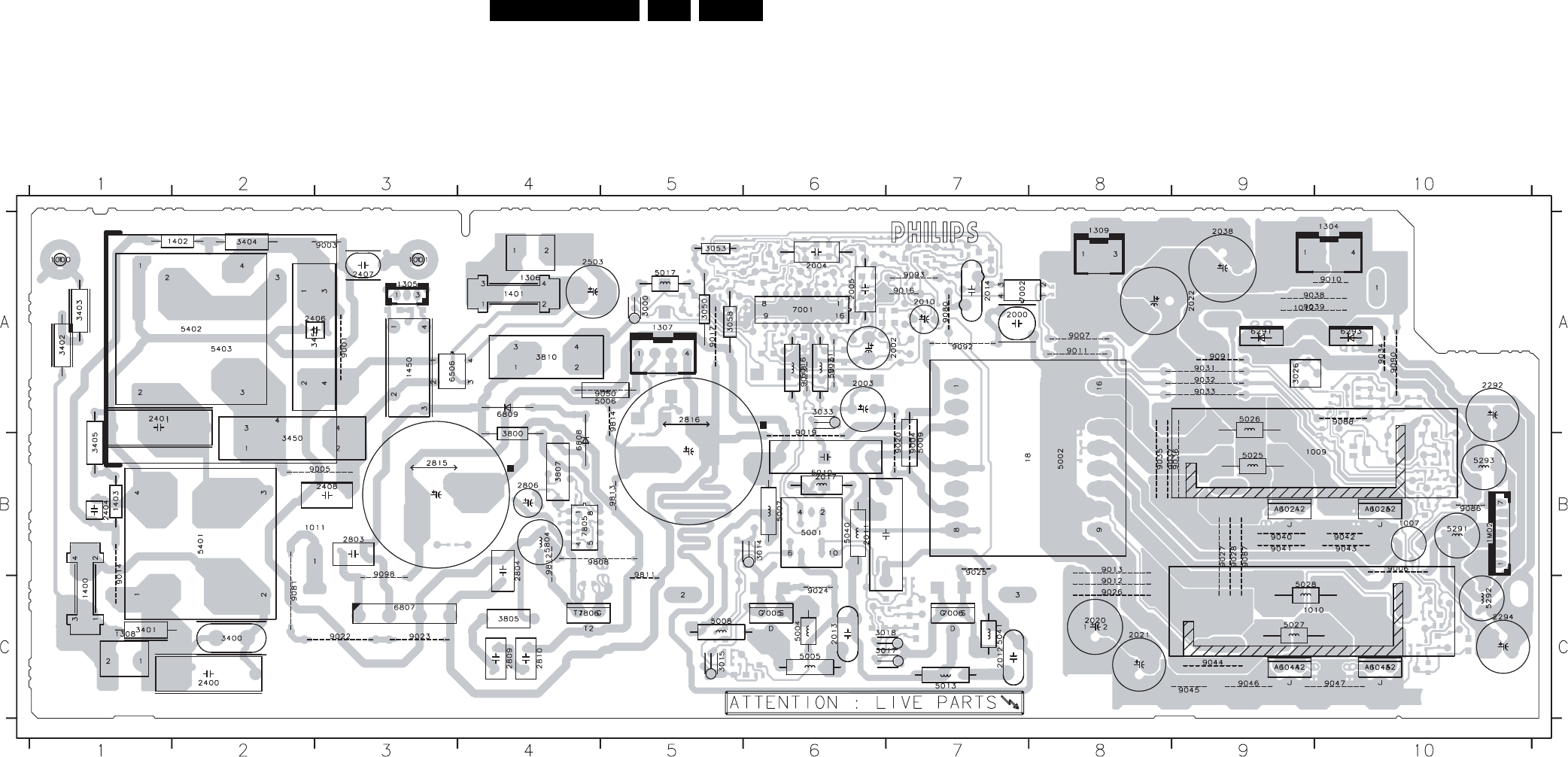
Circuit Diagrams and PWB Layouts EN 31FTL2.4E AA 7.
Layout LCD Supply Panel (Top Side)
F_15490_003.eps
120405
3104 313 6063.2
1000 A1
1001 A3
1007 B10
1009 B9
1010 C9
1011 C3
1012 A9
1304 A10
1305 A3
1306 A4
1307 A5
1308 C1
1309 A8
1400 C1
1401 A4
1402 A2
1403 B1
1450 A3
1M02 B10
2000 A7
2002 A7
2003 A6
2004 A6
2005 A6
2010 A7
2011 B7
2012 C7
2013 C6
2014 A7
2017 B6
2020 C8
2021 C8
2022 A8
2038 A9
2292 A10
2294 C10
2400 C2
2401 B1
2404 B1
2406 A3
2407 A3
2408 B3
2503 A4
2803 B3
2804 B4
2806 B4
2809 C4
2810 C4
2815 A3
2816 A6
3000 A5
3014 B6
3015 C5
3017 C7
3018 C7
3026 A9
3033 A6
3050 A5
3053 A5
3058 A5
3400 C2
3401 C2
3402 A1
3403 A1
3404 A2
3405 B1
3450 A2
3451 A2
3800 A4
3805 C4
3807 B4
3810 A4
5001 B6
5002 A7
5004 C6
5005 C6
5006 A4
5007 B6
5008 C5
5009 B7
5010 B6
5013 C7
5015 A6
5016 A6
5017 A5
5025 B9
5026 A9
5027 C9
5028 C9
5040 B6
5041 C7
5291 B10
5292 C10
5293 B10
5401 B2
5402 A1
5403 A2
5804 B4
6021 B9
6025 B10
6044 C10
6045 C10
6291 A9
6293 A10
6506 A4
6807 C3
6808 A4
6809 A4
7001 A6
7002 A7
7005 C6
7006 C7
7805 B4
7806 C4
9001 A3
9003 A3
9004 A7
9005 B3
9006 C10
9007 A8
9010 A10
9011 A8
9012 C8
9013 B8
9014 B1
9016 A7
9017 A5
9018 A6
9019 A6
9020 B7
9021 A6
9022 C3
9023 C3
9024 C6
9025 B7
9026 C8
9027 B9
9028 B9
9031 A9
9032 A9
9033 A9
9034 A10
9035 B8
9036 B9
9037 B8
9038 A9
9039 A9
9040 B9
9041 B9
9042 B10
9043 B10
9044 C9
9045 C9
9046 C9
9047 C10
9050 A5
9080 A7
9081 C2
9086 B10
9087 B9
9088 A10
9090 A10
9091 A9
9092 A7
9093 A7
9098 B3
9808 B5
9811 B5
9812 C4
9813 B5
9814 A5
EN 32FTL2.4E AA 7.
Circuit Diagrams and PWB Layouts
Layout LCD Supply Panel (Bottom Side)
F_15490_004.eps
120405
3104 313 6063.2
Part 1
F_15490_004a.eps
Part 2
F_15490_004b.eps
2006 A5
2007 A6
2008 A5
2009 A5
2015 A5
2016 A5
2018 A5
2019 A5
2023 B1
2024 B1
2025 A1
2026 A6
2027 A6
2028 C2
2029 B2
2030 B1
2031 A1
2032 A1
2033 A1
2034 A5
2035 A5
2036 C1
2037 C1
2039 B1
2040 A5
2041 A1
2042 A1
2043 A1
2044 C1
2045 B1
2046 A4
2047 A5
2048 A5
2050 A5
2051 A1
2052 A1
2053 A1
2060 C6
2061 B5
2062 C5
2063 A5
2064 A5
2065 C4
2071 C4
2072 C5
2077 A4
2290 B3
2291 A2
2293 A1
2802 B7
2805 B7
2807 B7
2808 C7
3001 A4
3002 A5
3003 A5
3004 A5
3005 A5
3006 A5
3007 A6
3008 A6
3009 A6
3010 A4
3011 A5
3012 A5
3013 A5
3016 C6
3019 C4
3020 C4
3021 A4
3022 B1
3023 B1
3024 A1
3025 B1
3027 A6
3028 C4
3029 C6
3030 B1
3031 B1
3032 B1
3034 B1
3035 C6
3036 C1
3037 A1
3038 B1
3039 C1
3040 B1
3041 B1
3042 C1
3043 A5
3044 C1
3045 A5
3046 A4
3047 A4
3048 A5
3049 C1
3051 C1
3052 A1
3054 C1
3055 A4
3056 A4
3057 A1
3059 C1
3061 A5
3064 A5
3065 A6
3066 A5
3067 A4
3068 A4
3069 A3
3070 A4
3071 A4
3075 A4
3089 A4
3100 A4
3101 B6
3292 B3
3802 B7
3803 B6
3804 B7
3806 B7
3999 B8
6001 A5
6002 C4
6003 C6
6004 A5
6005 A5
6006 A5
6007 B6
6008 C5
6009 A4
6010 A5
6011 A5
6012 B4
6013 C5
6014 A4
6015 A4
6017 A5
6020 A4
6022 A5
6023 A1
6027 C6
6028 C4
6030 C1
6051 A4
6054 C1
6077 A5
6078 B5
6079 A5
6080 A6
6081 A4
6082 A6
6154 A6
6155 B6
6460 A8
6461 A8
7004 A4
7007 C5
7008 C4
7009 A4
7010 B1
7017 A5
7018 A5
7030 B1
7031 C1
9002 B1
9008 A6
9009 A6
9015 A4
9030 A1
9085 B1
9806 B7
9810 B7
9820 B1
Circuit Diagrams and PWB Layouts EN 33FTL2.4E AA 7.
Layout LCD Supply Panel (Part 1 Bottom Side)
F_15490_004a.eps
120405
Part 1
EN 34FTL2.4E AA 7.
Circuit Diagrams and PWB Layouts
Layout LCD Supply Panel (Part 2 Bottom Side)
F_15490_004b.eps
120405
Part 2
Circuit Diagrams and PWB Layouts EN 35FTL2.4E AA 7.
Ambi Light
COM
OUTIN
P0<3:6>
X2
P2<0:1>
P1<0:3>
T0
SDA
P1.5
P1.7
CIN1B
X1
CLKOUT
CMP1
CMPREF
CIN1A
VDD
RST
INT0
SCL
RXD
TXD
VSS
F060 D5
F098 E4
F099 E4
I001 A2
I002 C2
I003 D2
I004 D5
I005 C5
I006 B5
I007 A6
I008 A6
I009 B6
I010 C6
I011 D6
I012 D6
SSB
F026 A3
F027 A10
F028 B10
F029 C10
F030 E10
F031 E10
F032 E9
F033 E9
F034 E7
F035 D7
F036 D7
F037 C7
F038 C7
F040 B7
F041 B7
F042 A7
F043 A7
F045 B5
F046 C5
LIGHT PWB
STANDBY
TO SDI SUPPLY
PDP
LIGHT PWB
AUDIO
(OPTIONAL)
F047 D5
F048 A5
F050 B5
F007 E2
F008 E1
F009 E1
F010 E1
F011 E1
F012 E1
F013 E1
F014 E1
F015 D1
F016 C1
F017 C1
F018 B2
F019 B2
F020 B2
F021 B1
F022 B1
F023 A2
F024 A2
F025 A1
TO 1M49
TO
CCFL
TO
TO
WARNING HIGH VOLTAGE
TO
(OPTIONAL)
CCFL
7015-1 A7
7015-2 A7
7016-1 C7
7016-2 C7
7017-1 D7
7017-2 D7
7018 A5
7019 B5
7020 D5
A001 E10
A002 B10
A003 A10
A004 A10
F001 C4
F002 C4
F003 C4
F004 C4
F005 C2
F006 D2
OR
SUPPLY
CCFL
OR
1M10 TO
5014 A9
5015 B9
5016 C9
6000 A6
6001 B6
6002 C6
6003 C6
6004 D6
6005 D5
6006 B6
6007 B6
6008 C6
6009 C6
6010 E6
6011 E6
7001 C3
7002 A3
7009 B5
7010 C5
7011 E5
NC
AMBI LIGHT
TO 2nd AMBI
SI4946
SI4946
3017 B4
3018 A4
3019 A4
3020 A4
3022 E2
3023 E2
3024 D4
3025 C4
3026 D2
3027 D2
3028 C2
3029 A4
3030 B4
3031 C5
3042 E8
3999 E4
5002 A9
5007 A8
5008 A8
1M10
3007 D7
3008 C6
3009 C6
3010 C7
3011 B7
3012 B6
3013 B6
3014 B7
3015 A7
3016 C2
2032 B8
2040 C7
2041 C8
2042 C8
2050 C7
2051 C8
2052 C8
2060 D7
2061 D8
2062 D8
2070 D7
2071 D8
2072 D8
3001 C1
3002 D1
3003 D4
3004 E6
3005 E6
3006 D7
F 3A
SI4946
TO
GREEN
2002 A3
2003 C2
2004 D2
2005 D4
2006 D4
2007 E6
2008 E6
2009 C6
2010 C6
2011 B6
2012 B6
2020 A7
2021 A8
2022 A8
2030 B7
2031 B8
TO 2nd AMBI
45678910
12345678910
A
B
C
D
ECCFL
SI4946
SI4946
SI4946
BLUE
RED A
B
C
D
E
1004 D1
1010 A2
1050 C4
1M08 A1
1M10 B1
1M11 B10
1M12 E10
1M48 C1
1M49 E1
2001 A2
123
F023
1M12
1
2
3
7
9
B03B-XASK-1
1
11
13
2
3
4
5
6
BD21416-00
5016
6003
BAS316
1M0
3042
F032 F031
A002
A001
A003
4
5
A004
B5B-PH-K
1004
1
2
3
20M
DSX840GA
1050
4
3
I010
7015-2
5
6
F099
F002
1K0
3015
2030 47n
7009
BC847BW
BC847BW
7010
3024
4K7
3025
4K7
F003
2005
3016
4K7
15p
6000
BAS316
F022
6n82011
3012 470R
5
6
7
9
3011
1K0 1
11
13
2
3
4
5
6
4
3
BD21416-00
5015
7
8
2
1
7017-2
7017-1
3027
1K0
2
3
4
3004 470R
2
B4B-PH-K
1M08
1
7002
LD1117DT
1
3
6007
47n2072
BZX384-C18
2071 47n
6006
BZX384-C18
F015
5008
22u
F028
F027
F042
I002
6002
10K
BAS316
3999
7019
BC847BW
F060
BAS316
6005
6004
BAS316
F030
F009
F029
F010
+5V
22u
5007
7011
BC847BW
F004
2007 6n8
I005
GND-HV
7
8
2
1
4
113
7015-1
13
12
10
9
8
7
6
2
1
5
MICROCONTROLLER
Φ
7001
P87LPC760BDH
14
1
11
132
3
4
5
6
7
9
5014
BD21416-00
1010
15p
2006
I006
22u
5002
47n2021
F098
F008
F007
BAS316
6001
1
2
3
4
1M10
B4B-PH-K
I008
I007
3026
1K0
560R
3002
1n0
2003
I009
2004
1n0
3003
220R
3
4
F035
1M49
B4B-PH-K
1
2
6n82009
2070 47n 47n
2060
2002
100n
3018
4K7
2001
1m0 16V
F005
F011
3017
4K7
3014
1K0
F020
47n
2050
2010 6n8
4K7
3029
2041 47n
47n2042
3010
1K0
3005 560R
3028
10K
I012
2062 47n 2052 47n
47n
2020
9
4K7
3019
1
10
11
2
3
4
5
6
7
8
1M11
B11B-XASK-1
2031 47n
F048
BC847BW
7020
4K7
3031
BZX384-C18
6008
6010
BZX384-C18
6n82012
6009
BZX384-C18
7
8
2
1
7016-1
3030
4K7
F021
3013 560R
47n2051
47n2061
47n2032
F024
I011
F047
100R
3023
6n82008
1
2
3
B3B-PH-K
1M48
3006
1K0
F006
I004
3001
560R
2040 47n
100R
3022
F026
6
4
3
F043
7016-2
5
F040
F041
+5V
BZX384-C18
6011
1K0
3007
I001
2022 47n
F013
I003
560R
3009
3020
4K7
470R
3008
F025
F037
F038
F001
F036
F034
F033
F014
F012
F050
BC847BW
7018
F046
F045
F016
F017
F018
F019
AL AL
F_15460_010.eps
060405
3104 313 6072.6
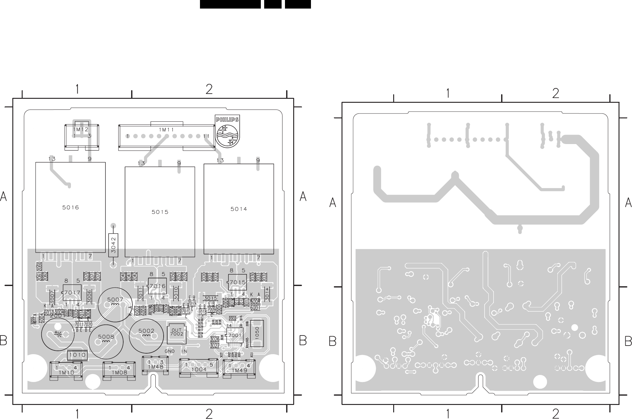
EN 36FTL2.4E AA 7.
Circuit Diagrams and PWB Layouts
Layout Ambi Light (Top Side)
F_15460_011.eps
060405
3104 313 6072.6
1004 B2
1010 B1
1050 B2
1M08 B1
1M10 B1
1M11 A2
1M12 A1
1M48 B2
1M49 B2
2001 B1
2002 B2
2003 B2
2004 B2
2005 B2
2006 B2
2007 B1
2008 B1
2009 B2
2010 B2
2011 B2
2012 B2
2020 A2
2021 A2
2022 A2
2030 A2
2031 A2
2032 A2
2040 A1
2041 A1
2042 A2
2050 A2
2051 A2
2052 A2
2060 A1
2061 A1
2062 A1
2070 A1
2071 A1
2072 A1
3001 B2
3002 B2
3003 B2
3004 B1
3005 B1
3006 B1
3007 B1
3008 B2
3009 B2
3010 B2
3011 B2
3012 B2
3013 B2
3014 B2
3015 B2
3016 B2
3017 B2
3018 B2
3019 B2
3020 B2
3022 B2
3023 B2
3024 B2
3025 B2
3026 B2
3027 B2
3028 B2
3029 B2
3030 B2
3031 B2
3042 A1
3999 B1
5002 B2
5007 B1
5008 B1
5014 A2
5015 A1
5016 A1
6000 B2
6001 B2
6002 B2
6003 B2
6004 B1
6005 B1
6006 B2
6007 B2
6008 B2
6009 B2
6010 B1
6011 B1
7001 B2
7002 B2
7009 B2
7010 B2
7011 B1
7015 B2
7016 B2
7017 B1
7018 B2
7019 B2
7020 B1
Layout Ambi Light (Bottom Side)
F_15460_012.eps
060405
3104 313 6072.6
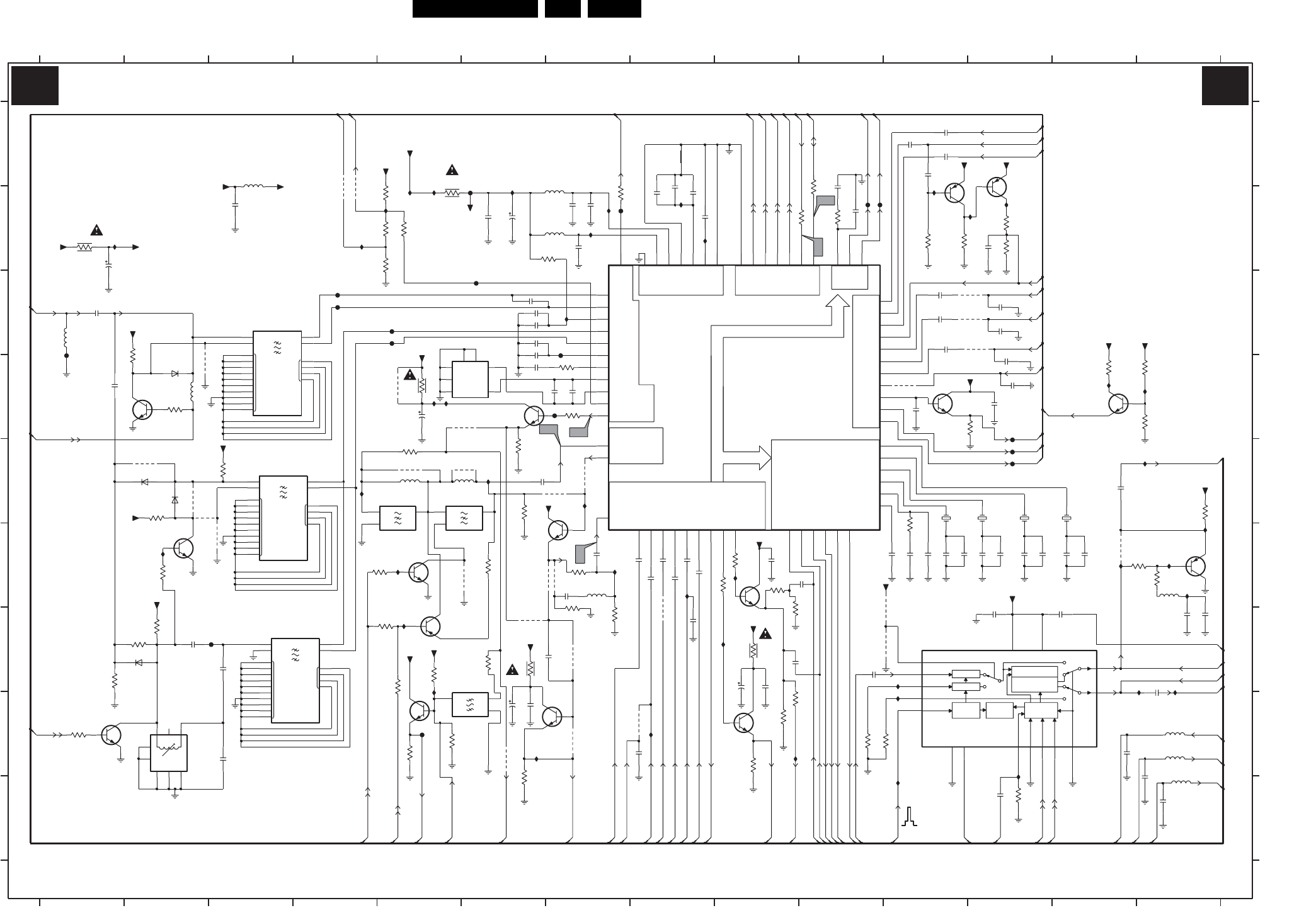
Circuit Diagrams and PWB Layouts EN 37FTL2.4E AA 7.
SSB: IF, I/O Video Processing
2H/4H DELAY
ADAPTIVE
COMB FILTER
FILTER
TUNING
CLOCK
CLAMP
GEN
CLAMP
SAND-
CASTLE
O
GND
I
IF DEM
SUPPLY CTRL SYNC
OUTP SWITCH
LUMA & CHROMA PROC.
I/O SWITCH
DELAY COR.
GROUP
NC
I2
I1
O2
GND
O1
O
GND
I
O
GND
I
NC
I2
I1
O2
GND
O1
NC
ISWI
I
O2
GND
O1
2373 B8
2374 B8
2375 B8
2376 B7
2377 B6
2378 B7
G
H
I
1307 E12
1308 E13
1406 E5
2406 G2
2407 G3
2408 H3
2358 F11
2359 F11
2360 F11
B6a
2357 F11
789
B14c
5V0
7V7
B14a
nc
COIL 40.4 SUPPRESSION
2379 F12
10 11 12 13
2382 F12
A
B
C
B15a(4x)
E
F
G
H
I
1305 E11
1306 E12
11 12 13 14
123456
2355 C12
2356 F11
2422 E13
2383 D12
2384 F7
2385 G13
B2
B2
12
nc
D
14
A
B
C
D
E
F
2380 F12
2381 F12
3303 H10
2409 C7
2410 G9
2411 D6
B13a
B14b
B2(3x)
345678910
2327 D12
2339 H8
2350 A11
2351 A11
2352 A11
2353 I12
2354 G12
2420 G8
2421 F14
3404 I6
2423 G14
2424 G10
2425 B1
5V
B14b
B14c
IF,I/O VIDEOPROCESSING
1407 E5
1408 G4
1409 C3
1410 E4
1411 G6
2300 F7
2302 G14
2305 C11
2316 C11
2322 C11
2392 B8
2394 B6
2401 C6
2402 G6
2403 F9
2404 C7
2405 D1
3300 F7
3301 I12
3422 G9
3370 F9
3371 H9
3372 H9
SAW-FILTER AUDIO
0V
2361 F13
2362 F13
2364 C12
2365 F8
2366 F8
2367 F8
2368 F8
2369 F8
2370 F8
2371 B10
2372 B10
2413 D5
2414 H6
2415 H6
2416 C7
2417 E6
2418 D6
2419 D7
3401 B7
3402 B1
3452 F14
3405 H5
3406 G2
3407 F2
nc
RES
B6a
B2,B6a
B2(3x)
B2
B2
B14c
2387 B7
2388 A11
2389 B12
2391 B3
2428 I14
2430 D11
2432 D12
2433 G9
2434 F10
2435 G9
2436 C7
3420 G6
3421 F5
5309 H14
3423 H1
3433 G1
3434 E2
nc
SAW-FILTER VIDEO
NTSC M
B14b
2412 C1
3377 B10
3378 B10
3380 B7
3382 F7
3385 G7
3393 F11
3400 B5
3450 E14
3451 F14
7320 F9
3456 G5
3457 H5
3460 D13
PAL N
5V0
4V2
RES
B14b
PAL M
4V2
B2
B2
2426 H13
2427 I14
3413 F9
3414 D2
3415 B5
3416 D5
3417 G5
3418 D7
3419 E5
3475 G9
3476 H9
9405 E2
5310 H14
5311 I14
5312 F14
B2(3x),B15a(4x)
B2,B15a(2x)
B2
B2
4V1
B6a
MODULATOR
HIP
3376 B9
3439 E6
3441 B5
3444 B11
3445 F6
3447 B11
3448 B12
3449 B12
6405 E2
7307 G11
9416 D5
7322 E7
7323 D9
7401 F2
B13a
B14c
B2
B2
B2
B2
3408 B5
3409 G2
3410 E3
3411 D2
3412 G6
3461 D14
3462 D14
3463 B5
3468 H10
3473 D11
3474 F9
9403 E2
9404 F7
F437 D1
9406 F13
9407 B4
9408 H7
B14a,b,c(2x)
B2
COIL
B3a,B6a
B5a
B5a
B2
B2
3435 G5
3436 E6
3437 D7
5406 E6
5408 D6
5411 C1
5416 A3
6402 E2
6403 D2
6404 G2
9414 E7
9415 D2
I450 H6
9417 D6
9418 E5
9419 E7
0V4
B2(2x),B5a
4V5
2V8
B2(3x),B15a(4x)
B2
B2(2x)
B14a
B2(2x),B5a
B2,B15a(2x)
B14b,g,B15a
7414 D11
7415 H9
9318 G11
9319 G11
9322 G8
9401 F3
9402 E2
F411 C6
F413 B6
F440 B8
I401 H10
I402 C7
0V4
I411 B5
I415 H8
I417 F8
B3a,B6a
B14b
5318 F7
5401 D2
5402 E5
5403 H2
5404 B7
5405 B7
RES
7V7
9409 E6
9410 B4
9412 G6
9413 F7
I448 E6
I449 F7
I455 B12
I456 D13
I457 D14
I458 E4
I460 F2
I461 F5
I462 G5
I463 G5
I464 F9
B14a(2x)
7402 H7
7403 D2
7405 H1
7406 F5
7407 F5
7408 A11
7409 A12
7410 H5
7411 D6
7412 F14
7413 D13
F401 D7
F403 C7
F404 D12
F405 E12
F406 E12
F407 B10
F408 B10
B2
I421 B8
I422 B8
I424 E14
I425 F14
I426 F14
I427 F14
B14a,b
B2
B2
SAW-FILTER-VIDEO
B14a,B14g,B15a
B15a
I441 B7
I442 B7
I443 B6
I444 B5
I445 B5
I446 D5
I447 D5
I454 B12
I451 H5
I452 B1
I453 B11
B2
9420 F6
9422 H6
9423 C11
9424 C11
9425 C12
I465 G9
I467 E7
9426 D11
9427 G7
9428 H8
A400 G3
A409 C5
A410 C5
A411 C4
A412 C4
B14b,g,B15a
B14c,g,B15a
B2,B6a
B14b,B15a
c002 A8
B15a(4x)
BC857BW
I428 F13
I430 G14
I431 H14
I432 H12
I433 I11
I434 G11
I435 H11
I440 B4
+8V_CON
7408
100n
2434
470R
3385
9407
SYS1
11
SYS2
10
VCC
6
VDD
5
Y|CVBS1
12
Y|CVBS2
3
Y|CVBSO 14
COUT 16
DGND
4
FSC
9
FSCSEL
8
INPSEL
2
OUTSEL
15
SC
7
TDA9181
7307
AGND
13
CIN
1
3419
390R
7322
2381
15p
BC847BW
7407
BC857BW
1u0
2387
3475
10R
V2
F440
680K
3444
9404
5401
6u8
V9
I415
c002
BC847BW
7405
9414
9424
3R9
3402
I421
5309
+8VP
3M579545
1308
NR-18
+8VP
I464
I467
5K6
3421
2404 1u0
BA591
6403
2305
100n
9318
1K0
3405
F451
2435
1n0
1u0
2394
I424
100u
2425
I446
2355 10p
+8VP
V1
10n
2401
100n
2302
33u
5318
1K0
3422
4K7
3414
150R
3452
9413
2353
100n
9406
2375
22n
2371
4n7
5404
I458
2420150p
2417
470n
I425
2367
100n
+5VCOM
BC857BW
100n
2424
7412
I434
I454
9319
1K2
3462
100n
2354
I417
3404
560R
1SS356
6405
+5V_VDP
2p7
2361
BC847BW
7410
10p2426
3436
270R
+8V_VDP
+8VP
4R7
3400
I430
I401
2368
2K7
3411
100n
+8VP
BC847BW
7403
9412
X3.575 56
X3.579 57
X3.582 55
X4.43 54
YCOMBIN
28
YOUT 49
Y_CVBS3
20
Y_CVBS4
23
UOUT 50
VA
61
VCO1
7
VCO2
8
VIF1
2
VIF2
3
VIFOUT
10
VOUT 51
SIF1
63
SIF2
64
SVBCOUT
30
SW0
19
SW01
22
SYS1
25
SYS2
27
TUNERAGC
62
PLLRILT
6
QSS_AM
5
R1IN 36
R2IN 41
SCL
46
SCOUT
59
SDA
47
SEC_DEC 53
42
GND_1
44
GND_2
9
HA
60
HPLL
58
IN
12
OUT
13
PIPOUT
32
14
CVBSOUT
34
DEC
35
DIGDEC
33
DIGGND
31
FBL1IN 39
FBL2IN 40
G1IN 37
G2IN
C3
21
C4
24
CCOMBIN
29
COL_PLL 52
COMBOUT
26
CVBS1
16
CVBS2
18
CVBSINT
+8_2
45
ADSEL
48
AGCDEC
4
AGCSIF
1
AV1
15
AV2
17
B1IN 38
B2IN 43
7323
TDA9321H/N2
+8_1
11
3K3
3460
2
13
1406
TPWKA
9402
5K6
3423
+8VP
3473
1K0
9422
2389
1u0
BC847BW
7414
I455
I456
I444
2K2
3415
3417
5K6
3441
22K
I433
I435
100u
2410
3376
100R
7401
BC847BW
F401
9322
+8VP
9403
NR-18
1306
3M582056
2392
1u0
+5VS
9401
+8VP
68p
2407
270R
3451
7409
BC857BW
A412
3409
4K7
F403
3378
15K
33p
2430
5310
2383 10p
2372
1u0
3M575611
1307
NR-18
+5VCOM
9417
2366
100n
3434
4K7
2K2
3449
100n
2391
2418
12p
2436 1u0
2416 1u0
7
8
2376
100n
9
10
13
14
15
2
3
11
12
16
17
OFWK3953L
1409
38M9
1
18
4
5
6
330p
2402
I448
100n
2369
I457
3K9
3433
9420
270R
3413
3416
6R8
I443 I453
3476
560R
1
2
34
6
78
5CCB
5408
2403
100n
2414 100u
10p 2327
+8VP
A409
3
A400
TPWKA
1407
2
1
I441
2373
100n
I440
2382
2p2
+5VCOM
I431
I427
5416
3457
4K7
4M433619
1305
NR-18
4K7
3463
2360
1p2
9409
2300 47p
1u02409
5311
3370
100R
7406
BC847BW
100n
2378
F404
F405
2362
+8V
I428
10p
6404
1SS356
2356
100n
220p
2406
I461
+8VP
I411
3439
1K2
9405
3437
1K0
100K
3301
I445
9418
2413
47u
4M5
SFSKA
1411
2
13
100n
2384
3468
100K
100K
3303
I6
9427
+8VP
3371
47R
10p
2364
BC847BW
7411
3408
100R
7402
BC847BW
6402
1SS356
1K0
3300
100K
3401
9408
5
6
78
2385
100n
5403
5CCE
1
2
34
I422
3407
5K6
9410
2359
15p
100n
2357
I432
F406
+8VP
100n
100n
2433
2322
2358
3n3
3372
470R
I465
I463
+5VS
2377
100u
F411
I402
3
11
12
16
17
7
8
1
18
4
5
6
9
10
13
14
15
2
1408
OFWK3953L
38M9
100n
2422
1K0
3420
4R7
3412
4n7
2405
7415
BC847BW
1K0
3450
10p2428
2374
1u0
39K
3447
10p
2423
+8VP
1K8
3461
2380
F407
4K7
3435
2p2
3393
100K
2411
100n
A410
I450
9415
2
3
11
12
16
17
7
8
1
18
4
5
6
9
10
13
14
15
40M4
OFWK9656L
1410
2419
5p6
F413
9428
9416
100n
2316
9423
9425
2388
220n
15p
2379
3474
10R
6p8
2421
100n
2415
3448
2352
100n
100R
10K
3380
3445
120R
F408
2370
100n
100n
2365
100n
2432
27R
3406
5406
3u3
7320
BC847BW
100n
2351
560R
3382
I462
100R
3377
I460
330n
5411
BFR93AW
7413
+8VP
I447
33u
5312
+8V_VDP
3u9
5402
+8V_VDP
F437
4n7
2412
4K7
3410
I452
3456
5405
4K7
I426
9419
A411
I442
2350
100n
I449
3418
390R
+8V_VDP
10p
2339
10p
2427
3p3
2408
9426
CVBS-TXT
SC
LMN
COMB-C-OUT
SOUND-OUTPUT
QSS_AM
FBL-SC1-IN
CVBS-PIP_TUN1-2-CVBS-IN
COMB-Y_CVBS-OUT
CVBS-SC2_MON-OUT
R-SC1_V-IN
G-SC1-IN_Y-IN
AGC
C-FRONT-IN
CVBS-TER-OUT
SOUND-OUTPUT
PIP-OUT
Y-CVBS-FRONT-IN
Y50
LMN
SC2-R_C-IN_AV2
SC2-G-IN
SC2-B-IN_C-OUT
U50
V50
SC2-FBL-IN
CVBS-AV3-IN
AV3-CVBS-IN
CVBS-3D-COMB
YOUT-3D-COMB
COUT-3D-COMB
CVBS-TXT
COUT-3D
YOUT-3D
Y50
AGC-MONITOR
LMN
FSC
7307-p4
COMB-C-OUT
COMB-Y_CVBS-OUT
COUT-3D
YOUT-3D
IF-TER
BG
SC1-STATUS
HA50
SC
LMN
SYS1
SYS2
VA50
B-SC1-IN_U-IN
SCL-F
SDA-F
CVBS-TXT
CVBS-SC1_AV1-IN
C-SC2_SVHS-IN
Y-CVBS-SC2_AV2-IN
BG
SEL-SVHS-RR_STATUS2
FSC
SYS1
SYS2
7307-p4
V10
B2 B2
F_15460_013.eps
070405
8204 000 8483.1
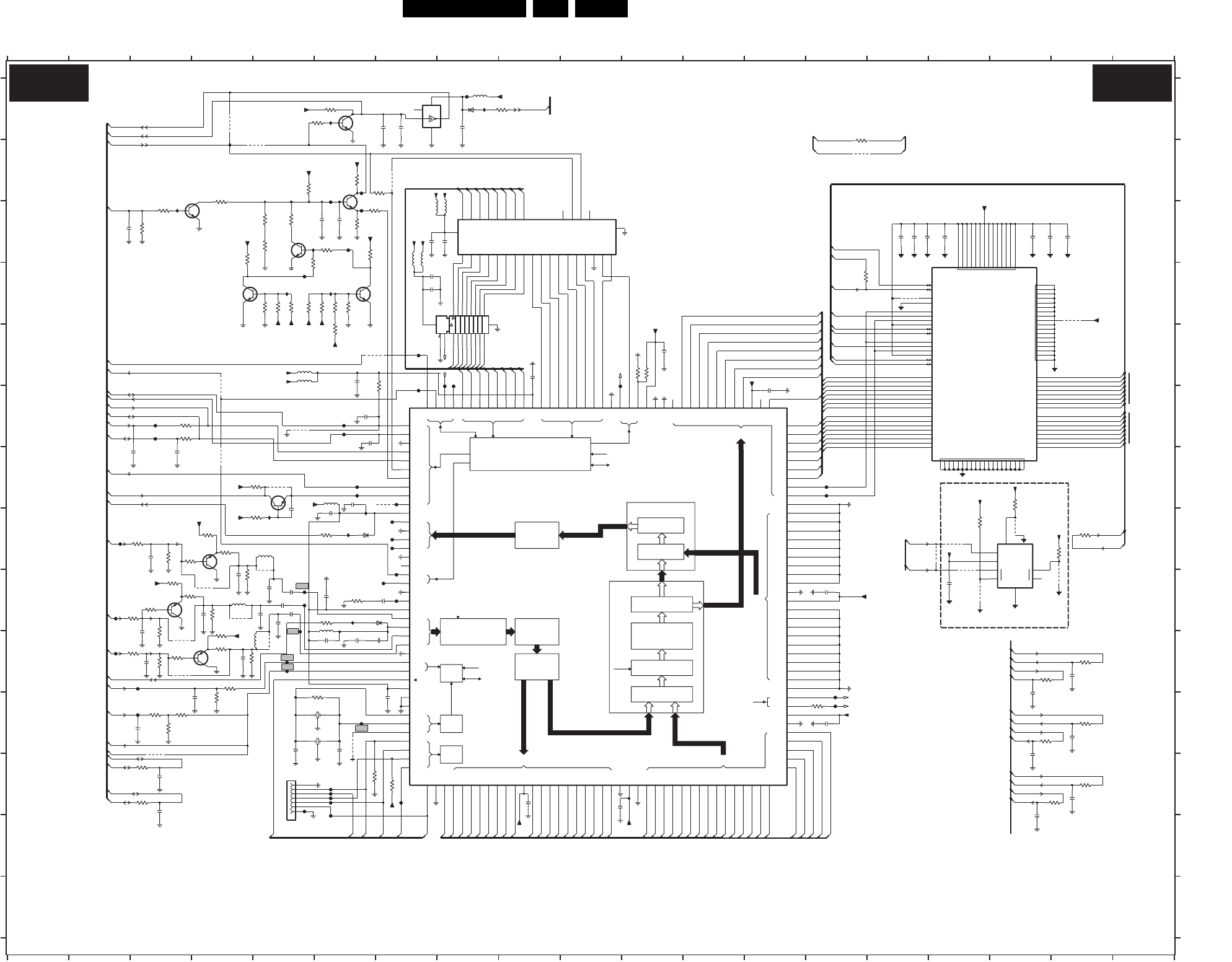
EN 38FTL2.4E AA 7.
Circuit Diagrams and PWB Layouts
SSB: PICNIC
EN
C1
1D
FS
1
OUT
VDD
FBIN
IN
0
1
GND
2
VCC
VSS
NC
25
24
23
22
21
20
17
16
15
14
13
12
11
1010
11
12
13
14
15
16
17
20
21
22
23
24
25
26
27
26
27
SWCK
RSTR2
RSTW2
OE2
IE2
RE2
WE2
RSTR1
RSTW1
OE1
IE1
RE1
WE1
MODE2
MODE1
SRCK
PROM
PEAKING
BACK END
MICRO-PROCESSOR
PSP
PROCESSING
ANALOG
CLK
BUS C
3 X ADC
FRONT
END
PLL
3 X DAC
P0
BUS A
BUS D
MUX
OSC
TIMING
CLK
BST
BUS B
P2
MID END
HISTOGRAM
NOISE
REDUCTION
TBC/SRC
MUX
TIMING
TIMING
CLK
B3a,b
123
B3a,b
B3a,d
B5a
15 16 1745678910
B19c
16 17 18 19
12
F148 G14
F149 G14
F151 F10
F152 L7
F155 G6
F156 G6
F157 H7
F158 H7
F159 H7
11 12
2710 C17
2711 C17
2712 C15
2713 G2
FM1
B3d
B3a(2x)
B19c
9769 I16
9770 I16
9771 H16
9772 H16
9776 G5
9809 B5
9825 I4
9826 J3
9827 J3
A139 K14
F107 A8
F108 H2
F109 I2
F110 J2
F112 K3
7714 D16
18
14 15
* SEE MAPPING I1 ON B3c
N
B3b,c(2x),d
B19c
B19d
B3a(2x),b
B3e,B19d
B5a
intern
7777 J4
9700 B7
9701 F5
9702 E6
9703 G7
I820 D5
B3c
F785 F7
F786 E8
RESERVED
9767 I18
9768 H17
12MHz
B19b
B3b
F163 I5
I720 A4
I727 G6
I802 A8
I803 I6
I804 H6
I805 D6
I810 H5
I813 A6
I814 C3
F160 I7
F161 I7
RES
7715 G5
F145 B6
B3c,d
B3c
7775 H4
7776 I3
F164 J5
F165 J5
F166 J5
F706 B6
F707 C6
F708 C6
F709 D5
F710 K6
F784 E7
F114 F3
F115 F3
B3d
B19d
B3a
B3c
N.C.
B3e
B3e
B3b,c(2x),d
F787 F8
9707 I5
9708 I4
9709 J5
9710 F4
9720 L3
9726 G4
9727 D18
9728 D15
9729 A4
5724 E5
5725 C8
B3c,d,B19d
B6a
B6a
B2,B6a
B19c
B3d
B3a
B3a
F162 I5
I815 C5
7705 A6
7706 A7
7707 D5
7708 B6
7709 C5
7710 D6
7711 C8
7712 D7
7713 I9
3922 H3
3923 H4
RES
B19c,d
B3a(2x),c
F118 I7
F119 J3
F122 L6
F123 L6
F124 L6
F125 L6
F126 M6
F127 L5
F128 F6
F129 F6
F140 K14
F788 G7
3932 J4
3933 J4
5703 A8
5705 I6
5706 H5
5707 I4
5708 J4
5714 G6
5723 E5
3758 F7
3759 I6
B3a(2x)
B5a
** SEE MAPPING G1 ON B3c
5726 C7
5727 C7
5728 C7
6701 A8
6703 I7
6710 H6
7702 H17
9820 B14
3856 J18
3857 J17
3858 K18
3859 K17
3860 L18
3861 L18
3903 C5
3905 E6
3909 A9
3738 D5
3739 D5
3924 H4
3925 I4
3926 I4
3927 I3
3928 I3
3929 I3
3930 J3
9706 K6
3748 B5
3749 C4
3750 D6
3751 B6
3752 B7
3753 C6
3754 C6
3755 D5
3756 D5
3715 J3
3716 H3
B3a,b
SOFTWARE
RES
FBX
B2,B6a
B3b,c,d
3760 D15
3761 A14
3826 L3
7703 C4
3726 K3
3727 J4
3728 K3
3730 K3
3732 A6
3733 C3
3734 B4
3736 C5
3737 C6
2920 J7
2926 L17
RES
N.C.
B3a,b,c
B3d
3740 A6
3741 D5
3742 D6
3743 D6
3746 C6
3931 J4
3704 G17
3705 H18
3706 I6
3709 F3
3710 F3
3711 E11
3712 L7
3713 H3
3714 I3
2804 J6
2806 G6
B3a
B3a(2x),c
B3c(2x),d
3717 J3
3718 J3
3719 G5
3720 H5
3721 H6
3722 C3
3723 K6
3724 H18
3827 L3
2841 L3
2881 J6
2900 I4
2901 I4
2902 J4
2915 I5
2916 I5
2917 A7
2918 A7
2737 F6
2738 C18
RES
B19b
B6a
B5a
PICNIC
2927 M17
2928 L18
2929 K6
2931 I5
2935 K5
3700 K14
3701 L6
3702 E11
3747 C5
2744 C6
2745 C8
2746 D7
2747 H5
2748 E6
2749 H6
2754 D7
2757 I7
2800 I6
J
K
B3a,b,c
B3b
B3b,c
2807 K7
2837 J18
2838 K17
2839 K18
3725 K4
2725 C16
2726 F13
2727 E11
2731 E9
2732 C7
2733 I14
2734 K14
2735 L9
2736 L10
19
A
B19b(2x)
B3a(2x),c
B3e
PICNIC
B3b,c,d
2740 I5
2741 I5
2742 I5
3703 H16
A
B
C
D
E
F
G
H
I
13 14
B3a
RES
2714 G3
2716 C16
2717 C15
2718 H3
2719 I3
2720 J3
2721 K3
2722 K3
2840 L3
5678910111213
RES
B19d
B3b,c,d
B5a
B
C
D
E
F
G
H
I
J
K
L
M
2743 C6
L
M
N
3
1702 K6
1703 K6
1710 L5
2707 C2
2708 I16
2709 A8
4
B3a(2x)
B3a,d
B5a
2724 F6
+5V2Pr
B3b
B3a,b
B3a(2x),c
F166
F123
F706
3856
10R
1K0 100R
3734
3722
9720
+3V3PA
RES
680R
3926
9776
RES 2900
47p
5728
47p
22p
2707
RES 2902
RES
680R
3933
BC847BW
7703
F124
F163
2737
100p
9706
A139
F107
F707
18p
2929
F118
BC847BW
7708
+1V8FA
VCC
5
Y4
3709
100R
74LVC1G14GW
7706
A2
GND
3
NC
1
3742
22K
RES
5725
100n
2735
1K0
3733
F115
F114
F108
RES 100p
2926
3748
120K
F151
F152
F155
F159
F157
+8VPA
F158
F125
+3V3_DCDCFBXA
F145
+3V3_FBXB
F140
F148
F149
F164
F122
9728
2710
100n
3719
3K3
3720
10K
+3V3_DCDCFBXA
1M0
3723
RES
2747
68p
100n
2920
9710
680RRES
3925
3743
1K0
3711
RES
10K
F787
F786
5708 RES
6u8
3730
560R
22n
2740
BAS316
6703
9771
F156
F160
10R
3857
2741
22n
RES
150p
2916
9820
3
4
5
6
789
F708
07FMN-BMT-A-TFT
1
2
2733
100n
1710
100R
3909
3701
1K0
100R
3710
3714
180R
I803
2725
100n
2717
100n
F784
22p
2713
res
+3V3_DCDCFBXA
+3V3PB
27p2881
4K7
14
13
12
20
3740
8
9
GND 10
11
1
19
18
17
16
15
7712
74HC573PW
2
3
4
5
6
7
2712
100n
9701
RES
3736
100R
9727
3717
100K
+3V3PC
F788
F785
22n
2742
100R
3826
2714
22p
res
100K
3903
2727
100n
BAS316
6710
5727
RES
I727
2841
22p
res
100R
3706
I813
I805
3721 100R
+3V3_DCDCFBXA
15p
2720
RES
6u8
5707
220R
3759
2708
100n
2748
100n
3726
1K2
4K7
3905
+1V5_FBXA
100K
3718
3737
1K0
9707
22R
3700
10R
3702
2745
100n
RES
5724 +3V3PB
5726
+3V3_DCDCFBXA
7705
BC847BW
F710 10R
3739
12K
3858
I814
I815
I810
2744
100n
I804
I802
3K9
5723
3746
3703
4K7
+3V3PB
3704
100R
RES 2915
150p
+3V3PB
F109
100R
3705
3751
3K3
res
7710
BC847BW
2
6
8
7
9726
MULTI.
FREQ.
7702
CY2302S
Φ
& ZDB
1
4
5
3
2731
100n
RES
3741
+3V3PB
150R
3727
2838
100p
2806
100n
47K
3747
F112
5714
21
Q7 22
VCC
32
VSS
16
9768
NC2 12
Q0 13
Q1 14
Q2 15
Q3 18
Q4 19
Q5 20
Q6
4
A8
29
A9
28
DU1 1
DU2 17
E_
23
G_
25
NC1 26
A14
31
A15
2
A2
9
A3
8
A4
7
A5
6
A6
5
A7
M27C512-90-C1
7711
A0
11
A1
10
A10
24
A11
27
A12
3
A13
30
RES
9700
100n
2746
100n
2711
100n
23
33
35
39
32
94
2804
72
77
78
87
91
9
93
10
16
17
34
37
43
51
62
3
48
49
54
59
67
63
13
11
64
75
83
89
92
12
14
15
40
42
46
80
45
81
44
82
30
96
84
86
88
90
100
8
18
25
26
36
38
66
65
31
95
85
41
1
47
50
76
79
57
58
60
61
74
73
71
70
69
68
98
99
2
4
5
6
7
52
53
55
56
DUAL FIFO
(262,214 x 8) x 2
29
28
27
24
22
21
20
19
97
MS81V04160A
7714
Φ
5703
3
RES
680R
3923
12M
CSTCV
1702
2
1
RES
7775
BC857BW
RES
3922
220R
F709
RES
3928
680R
220R
9826
RES
3927
BC857BW
7776
220R
3929 RES
220R
3930
RES
+8VPA
RES
RES
BC857BW
7777
9827
3932
680R
+8VPA
1703
RES
100p
2724
RES
47p
2901
100R
+3V3PA
3761
3K9
+2V5_FBXA
3750
F162
F165
7709
BC847BW
2800
100n
100K
3716
9729
3713
180R
2754
1n0
9767
1n0
2732
+3V3PB
+3V3_DCDCFBXA
2736
100n
100n
2734
220R
3924 RES
2716
100n
4K7
3758
2722
100p
2927
2749
100n
RES
100p
10R
3861
I720
3931
220R
+3V3PC
RES
2935
18p
9702
9770
3760
9769
2709
100R
res
100n
220n
2918
3755
4K7
2757
22n
RES 2931
150p
6u8
2738
100n
RES
5706
9703
RES
9709
1R0
3752
3715
180R
15p
2718
3724
100R
100p
2928
47K
3712
RES 100p
2837
9708
F127
F126
F129
F128
3756
10K
F119
3728
150R
6701
BAS316
100p
2721
3K3
3725
2719
15p
2917
100n
1R0
3753
YD6 107
YD7 108
YD8 109
3860
10R
YC7 115
YC8 114
YD0 101
YD1 102
YD2 103
YD3 104
YD4 105
YD5 106
67
YC0
122
YC1
121
YC2 120
YC3 119
YC4 118
YC5 117
YC6 116
75
YB1
74
YB2
73
YB3
72
YB4
71
YB5
70
YB6
69
YB7
68
YB8
54
YA2
55
YA3
56
YA4
57
YA5
58
YA6
59
YA7
60
YA8
61
YB0
33
WD-RST
7
WE-A
62
WE-B
66
WE-C 113
Y-IN
23
Y-OUT
12
YA0
53
YA1
134
VSSD4
139
VSSO1
42
VSSO2
63
VSSO3 86
VSSO4 111
VSSO5
133
VSSO6
3
VSSX
148
VIN
26
VSSA1
13
VSSA2
16
VSSA3
27
VSSA4
32
VSSD1
65
VSSD2 90
VSSD3
24
VDDA4
31
VDDD1
64
VDDD2 87
VDDD3 100
VDDD4
135
VDDO1
52
VDDO2
123
VDDO3
97
UVD7 98
UVD8 99
V-A
29
V-D
19
V-OUT
15
VDDA1
11
VDDA2
22
VDDA3
125
UVC8
124
UVD0 91
UVD1 92
UVD2 93
UVD3 94
UVD4 95
UVD5 96
UVD6
76
UVC0
132
UVC1
131
UVC2
130
UVC3
129
UVC4
128
UVC5
127
UVC6
126
UVC7
84
UVB1 83
UVB2 82
UVB3 81
UVB4
80
UVB5
79
UVB6
78
UVB7
77
UVB8
44
UVA2
45
UVA3
46
UVA4
47
UVA5
48
UVA6
49
UVA7
50
UVA8
51
UVB0
TEST
36
TMS
38
TRST
37
U-IN
25
U-OUT
14
UP-RST
6
UVA0
43
UVA1
5
SN-CL
2
SN-DA
1
T0
159
T1
160
TCK
41
TDI
39
TDO
40
142
P2-6
141
P2-7
140
PSEN
137
RE-D 110
RSTR
9
RSTW
8
SCL
4
SDA
151
P0-6
150
P0-7
149
P2-0
147
P2-1
146
P2-2
145
P2-3
144
P2-4
143
P2-5
158
OSC-I
34
OSC-O
35
P0-0
156
P0-1
155
P0-2
154
P0-3
153
P0-4
152
P0-5
21
EAN
136
FBL
10
H-A
28
H-D
18
HREF-EXT
30
IE-C 112
INT0
157
INT1
SAA4978H/V203
AGND
20
ALE
138
BGEXT
17
CLK-AS 85
CLK16 88
CLK32 89
DIFFIN
7713
BC847BW
7707
100n
2743
9809
F161
2807
100n
100R
3754
2839
100p
2726 100n
RES
3859
10R
3738
1K0
+1V8FA
5705 6u8
9825
100R
res
3827
2840
22p
I820
7715
PMBT2369
9772
3K9
3749
47K
3732
TMS
TDOC
TRST
TCK
TDO
F110
+5V2Pr
+3V3Pr
3V3_FAULT_FBX
SN-CL
VAP
CLK32P
CLK32G
RSTR_I
HD_E_T0
RST-FBX
SN-DA
3V3_FAULT_FBX
+3V3GA
+3V3GA
RST_PIC_EAG
RST-FEM
RST_COL
CLK32G
CLK32P_EPLDCLK32G
+3V3GA
+3V3GA
RSTW
INT1
HREF_EXT
ALE
3V3_FAULT_FBX
+3V3Pr
CL16
CLK32P
SDA-D
SCL-D
DA(00)
2FHG-GFX
G-OSD
RSTR_O
MF(11)
MF(12)
MF(13)
MF(14)
MF(15)
MF(16)
DA(08)
DA(09)
DA(10)
DA(11)
DA(12)
DA(13)
DA(14)
DA(15)
DA(07)
DA(06)
DA(05)
DA(04)
DA(03)
DA(02)
DA(01)
CLK32FM1
RSTW
RSTR_O
MF(17)
MF(17)
MF(8)
MF(7)
MF(6)
MF(5)
MF(4)
MF(3)
MF(2)
MF(1)
MF(9)
MF(10)
SDA-F
SDA-EPLD
SCL-F
SCL-EPLD
VA
BL-OSD
2FHFB-GFX
B-OSD
2FHB-GFX
R-OSD
2FHR-GFX
HD3-OTC
HD3-EPLD
VD-OTC
VD-EPLD
CLK32NE
UVB(2)
CLK32NE
YB(4)
YB(5)
YA(8)
YA(7)
YA(6)
YA(5)
YA(4)
YA(3)
YA(2)
YA(1)
YA(0)
UVB(1)
UVB(0)
CLK-AS
+5V2Pr
CLK32
CLK32FM1
WE-B
YB(8)
YB(7)
YB(6)
YB(2)
YB(1)
YB(0)
UVB(6)
UVB(5)
UVB(4)
UVB(7)
UVB(8)
YB(3)
AD(01)
AD(02)
AD(03)
AD(04)
AD(05)
AD(06)
AD(07)
MF(17)
+3V3Pr
V-PIP+MAIN-IN
AD(02)
AD(03)
AD(04)
AD(05)
AD(06)
AD(07)
AD(00)
AD(01)
AD(02)
AD(03)
AD(04)
AD(05)
AD(06)
AD(07)
AD(00)
+5V2Pr
Y-PIP+MAIN-IN
U-PIP+MAIN-IN
CL16
SCL-F
SDA-F
AD(00)
AD(01)
DA(12)
DA(11)
DA(10)
DA(09)
DA(08)
+3V3PB
WE-A
DA(07)
DA(06)
DA(05)
DA(04)
DA(03)
DA(02)
DA(01)
DA(00)
HA50
VA50
ALE
UVB(3)
RSTW
UVA(0)
UVA(1)
UVA(2)
UVA(3)
UVA(4)
UVA(5)
UVA(6)
UVA(7)
UVA(8)
DA(15)
DA(14)
DA(13)
B3A B3A
F_15460_014.eps
120405
8204 000 8481.1
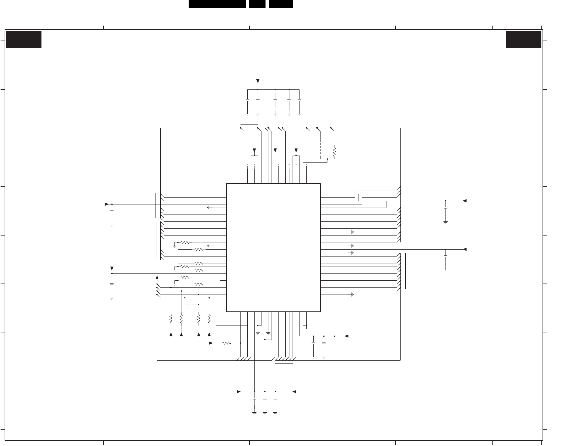
Circuit Diagrams and PWB Layouts EN 39FTL2.4E AA 7.
SSB: (FEM) Falconic Embedded Memory
3886 E4
3887 E5
3888 E4
3889 E5
3890 E4
3891 E4
7760 E6
9808 C7
9810 F4
9811 G5
FEM
B3c
B3a,c,d
B3a(2x),c
B3c
B3a
2886 D3
2887 B6
2888 B6
3876 C7
3880 F4
3881 F4
3882 F4
3883 F5
3884 G5
3885 E4
B3c,B19d
B
C
D
E
F
G
B3a,c,d
B3c,B19d
B3c,B19d
B3c
F
B3a,c(2x),d
RES
B3a,c,d
2879 E9
2880 G7
2882 H6
2883 H6
2884 H6
2885 F3
FEM
567891011
1234
H
A
B
C
D
E
B3c
B3a,c
11
A
B3a
4
B3a
G
5678910
B3a
B3c(2x)
B3a,c(2x),d
123
B3d
H
2723 G7
2875 B5
2876 B6
2877 B6
2878 D9
FALCONIC EMBEDDED MEMORY
3888
1K0
1K0
3887
+1V8FA
+1V8FA
2883
100n
2875
100n
100n
2884
+3V3FA
+3V3FA
3876
100R
2888
100n
100n
2887
100n
2878
+1V8FA+1V8FA
100n
2876
3884
47K
3890
1K0
9811
+3V3FA
3886
1K0
1K0
3885
+1V8FA
100
YG6|DPIP6
95
YG7|DPIP7
69
YF6 68
YF7
8YG0|DPIP0
7YG1|DPIP1
6YG2|DPIP2
5YG3|DPIP3
2YG4|DPIP4
1YG5|DPIP5
61
YA6
62
YA7
76
YF0 75
YF1 74
YF2 73
YF3 72
YF4 71
YF5
52
VSSS1
85
VSSS2
55
YA0
56
YA1
57
YA2
58
YA3
59
YA4
60
YA5
4VSSE1
15 VSSE2
70
VSSE3
82
VSSE4
37 VSSM1
39 VSSM2
97
VSSM3
99
VSSM4 98
VDDM4
23 VDDP
51
VDDS1
84
VDDS2
90
VSSA
49 VSSD1
66
VSSD2
87
VSSD3
65
VDDD2
86
VDDD3
3VDDE1
35 VDDE2
77
VDDE3
38 VDDM1
40 VDDM2
96
VDDM3
13 UVG3|QPIP3
12 UVG4|QPIP4
11 UVG5|QPIP5
10 UVG6|QPIP6
9UVG7|QPIP7
94
VD
91
VDDA
48 VDDD1
88
UVF3
81
UVF4
80
UVF5 79
UVF6 78
UVF7
19 UVG0|QPIP0
18 UVG1|QPIP1
17 UVG2|QPIP2
45 UVA3
46 UVA4
47 UVA5
53
UVA6
54
UVA7
93
UVF0 92
UVF1
89
UVF2
29 TDI
30 TDO
28 TMS
27 TRSTN
50 TWOFMON
42 UVA0
43 UVA1
44 UVA2
36 PIPON
63
REA
67
REF
32 RST
41 SNCL
34 SNDA
33 SNRST
31 TCK
64
IE
22 NC|IE2
14 NC|LLC
21 NC|OIE2
26 NC|RSTR2
20 NC|RSTW2
16 NC|SWCK2
24 NC|WE2
SAA4998H/V1
7760
25 ACV|RE2
83
CLK32
2886
100n
2877
100n
+3V3FA
2880
100n
1K0
3891
+3V3FB
1K0
3889
+3V3FA
100n
100n
2723
9808
2885
+3V3FA
47K
3883
100n
2882
9810
3882
47K
+1V8FA
+3V3FA +3V3FA
3881
47K
47K
3880
2879
100n
RSTR_O
SN-CL
+1V8FA
TRST
TDOA
TDOB
TCK
CLK32
CLK32NE
TMS
UVF(5)
RST-FEM YG(6)
YG(7)
MF(12)
MF(13)
MF(14)
MF(15)
MF(16)
YF(0)
YF(1)
YF(2)
YF(3)
YF(4)
YF(5)
YF(6)
YF(7)
YG(0)
YG(1)
YG(2)
YG(3)
YG(4)
YG(5)
UVF(3)
UVF(4)
UVF(6)
UVF(7)
UVG(0)
UVG(1)
UVG(2)
UVG(3)
UVG(4)
UVG(5)
UVG(6)
UVG(7)
MF(9)
MF(10)
MF(11)
MF(17)
RE_F
SN-DA
MF(1)
MF(2)
MF(3)
MF(4)
MF(5)
MF(6)
MF(7)
MF(8)
UVF(0)
UVF(1)
UVF(2)
B3B B3B
F_15460_015.eps
070405
8204 000 8481.1
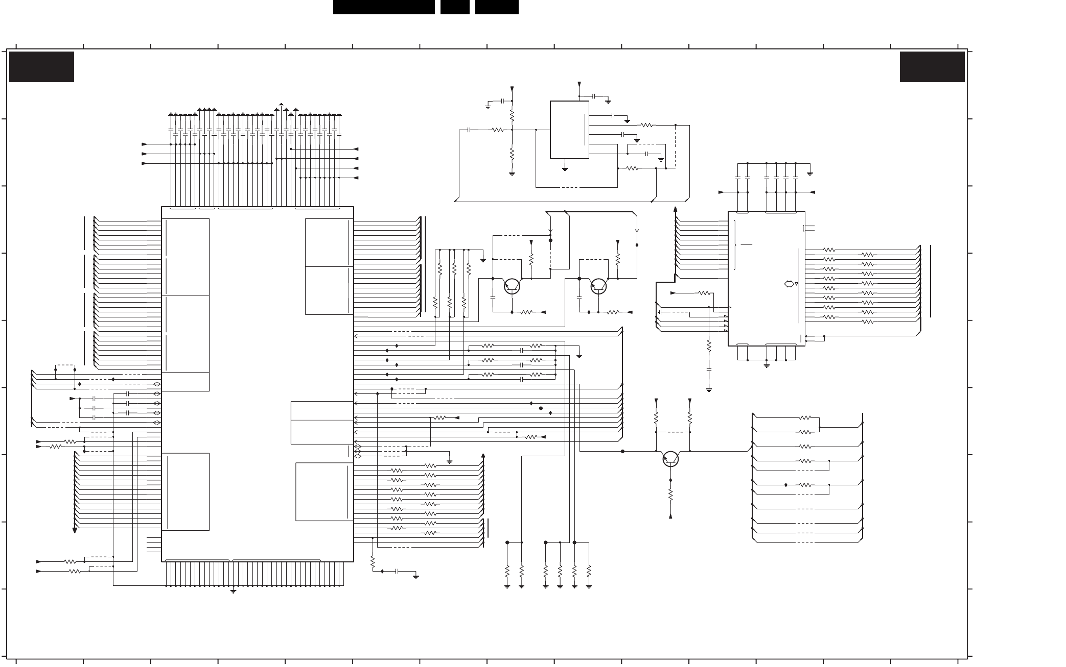
EN 40FTL2.4E AA 7.
Circuit Diagrams and PWB Layouts
SSB: Eagle
8
NC
L
U
10
16
1
2
3
4
5
9
10
11
12
13
512K-1
DQM
VDD
0
VSSQ
A
14
15
RAS
CAS
WE
A11
3
2
CLK
D
VSS
VDDQ
1
0
CKE
CS
9
8
7
6
5
4
6
7
2
1
CLKOUT
3
CLK
VDD
4
GND
REF
BISTEN
PLLND2
0
1
2
4
5
8
YG
Y
UV
ADDR
TESTSEL
2
3
4
5
6
DQ
DATA SDRAM
4
5
6
7
0
2
7
6
5
4
3
2
1
0
FALREF
11
SNRSTO
ADDRESS SDRAM
OUTP_VAL
VA
HD
9
8
7
6
5
4
3
2
1
6
7
8
9
10
11
12
13
3
14
15
8
7
6
5
4
3
2
1
0
9
SDCLKIN
UVG
CLK32O
CLKI
2
1
0
TCK
TDO
TDI
TMS
7
0
1
2
3
4
5
6
7
0
1
FSADJV
AOUTPV
AOUTNV
FSADJU
AOUTPU
AOUTNU
FSADJY
AOUTPY
AOUTNY
HREF
AVSPLL
DVSS
1
2
3
4
5
6
7
VDD
VSS
0
9
SNCL
SNRST
BOUNDARY SCAN
INPUT BUS F
INPUT BUS G
SNERT
COLOUR DIFFERENCE
CLOCK
LUMINANCE
DQM
RESET
IS0
IS1
UVF
3
YF
AVDDU
CLKSEL
CLK64O
SNDA
VREFY
VBSY
VREFU
VBSU
VREFV
VBSV
TRST
VD
REFIN
0
1
10
WEN
CASN
RASN
SDCLKOUT
INTR
VSS2
VDD2 VDDC VDDS
AVDDV
AVDDY
AVDPLL
AVSSU
AVSSV
AVSSY
B3a,b,c,d
B3a,b
B3c
B3a,c,d
I817 E6
I818 E6
I819 D9
I717 F8
I719 F8
I730 D8
I731 E1
I732 E1
I733 F1
I734 G12
I735 D7
I736 C10
I806 H6
I808 E6
I809 E6
I811 E6
I812 E6
I816 G10
RES
B19d
RES
RES
B3a
B3c
9766 F2
9773 F6
9774 G6
9775 G6
9777 F10
9821 B10
9822 B10
9823 G7
F714 C9
F715 D9
F718 F8
F720 G10
F765 H8
F766 H8
F767 H9
B3a(2x),b
B3c
I713 E2
I714 E1
I715 E6
I716 F6
9732 C8
9740 F2
9750 D8
9751 D9
9752 D10
9753 E6
9754 E6
9755 E2
9756 E2
9757 F2
9758 F2
9759 F6
9760 F6
9761 F6
9762 F7
B19d
B19d
RES
3918 G7
9763 F1
9764 F8
9765 F2
7719 C11
7720 C3
7721 A8
7725 F10
9704 H2
9705 H2
9711 B10
9712 E1
9713 H12
9714 H12
9715 H6
9716 F7
9717 G12
9718 G12
9719 G12
B19d
B3a,b,c,d
B3c
RES
9721 H12
9723 F1
9730 C9
9731 D8
3896 B8
3897 A8
3898 B10
3900 H7
3901 H6
3902 H7
3906 E11
3911-1 G6
3911-2 G7
3911-3 G6
3911-4 G7
3912-1 G6
3912-2 G7
3912-3 G7
3912-4 G6
B3c
B3a,d,B19d
3919 G6
3921 G6
7717 D8
7718 D9
3803 E13
3804 D13
3811 H8
3812 H8
3814 H8
3815 H9
3817 H9
3818 H9
3819 H1
3820 H1
3821 F12
3822 F12
3823 F12
3824 G12
3825 G12
EAGLE
B3a,b,c,d
B3b,c
B19d
3850 H6
3894 E7
3895 B8
3779 D13
3780 D13
3781 D13
3782 D8
3783 D9
3784 D13
3792 E7
3793 F10
3794 D7
3795 E8
3796 F7
3797 F8
3798 F1
3799 F1
3800 D7
RES
B19d
RES
B19d
3801 E7
3802 E8
3757 E8
3762 C13
3763 D13
3764 D13
3765 D9
3766 D8
3767 D13
3768 D13
3769 D13
3770 D13
3771 D7
3772 D7
3773 D7
3774 D13
3775 D13
B3b
EAGLE - IC
RES
B3c
B3a,c,d
B3c
3776 D7
3777 D13
3778 D11
2822 B5
2823 E8
2824 F2
2825 E8
2827 E8
2830 B11
2831 B11
2832 B12
2833 B12
2834 B12
2835 B12
2925 H6
2936 E11
3729 B10
B3a,b,c,d
B3a,b,d
B3c
B3c
B3c
B3b
B3c
3744 F11
3745 G10
2793 F2
2794 B4
2795 B4
2796 B4
2797 B4
2798 B4
2799 B5
2805 B3
2808 B3
2809 B3
2812 B7
2814 B10
2815 A9
2816 B10
2821 B5
B3c
B19d
B3b,c
B3a
RES
RES
RES
B19d
B3a,b,d
B19d
2773 B4
2777 B4
2778 B4
2780 B4
2781 B5
2782 B5
2784 B5
2785 B5
2786 D8
2787 D9
2788 F2
B3c
B3a,19d
B19b
B3a,d
2789 F2
2790 F2
2791 F2
2755 B3
2756 B3
2758 A9
2759 B3
2760 B5
2761 B5
2762 B5
2763 B5
2764 B5
2765 A8
2768 B4
2769 B4
2770 B4
2771 B4
2772 B4
B19b
B3a(3x)
RES
RES
1
B3b,B19d
B3b,B19d
RES
67891011121314
123456
B3c
B3a,b,d
RES
12 13 14
A
2753 B3
B
C
D
E
F
G
H
I
A
B
C
D
E
F
G
H
I
2750 B3
2751 B3
2752 B3
4K7
2345
B3c
B3b
B3a
7 8 9 10 11
3797
15
9721
25
7
13
38
44
26
50
4
10
41
47
8
9
11
12
39
14
33
37
17
36
1
40
42
43
45
46
48
49
3
5
6
28
29
30
31
32
16
34
35
18
2
21
22
20
19
23
24
27
3784
7719
MSM56V16160F-6TS
Φ
512K X 16 X 2
DRAM
68R
res
9731
9762
9732
9730
2790
100n
2797
2812
1n0
1n0
3
2
5
7
8
4
1
6
DELAY
ZERO
Φ
BUFFER
CY2305SC-1
7721
I811
I817
I808 3757
I806
150R
1n0
2759
2808
1n0
1n0
2780
10R
3824
68p
2786
1n0
2782
1n0
2778
68R
3779
I717
2753
1n0
68R
3804
68R
3764
3762
68R
1n0
2795
9761
1n0
2798
1K0
3765
I733
F767
75R
2823
100n
3773
I715
2784
1n0
I732
2785
1n0
2758
1n0
I819
I812
I818
I809
I730
I716
68R
3912-4
I731
F714
9754
150R
2822
1n0
3792
2791 I719
F718
100n
2833
9717
100n
F715
9758
9760
2K2
3744
3793
33R
2K2
3821
1n0
2770
3823
68R
2925
1n0
I816
1n0
2799
75R
3818
9775
68R
3921
3763
9773
68R
1n0
2781
68R
3768
100n
2831
150R
3802
F720
2755
1n0
3894
150R
3801
150R
3783
1K0
3775
2793
100n
68R
2809
1n0
9765
68R
3900
9823
1n0
68R
68R
3769
2752
9766
9740
9759
3795
150R
2751
1n0
68R
3774
3771
75R
I735
68R
3803
1n0
2773
3796
RES
82R
3850
4K7
9715
4K7
3778
75R
3811
10R
3825
9712
3911-4
4K7
68R
3798
75R
1n0
2762
9705
3776
9752
2768
1n0
3800
75R
2761
1n0
68R
3919
2764
3912-2
1n0
F766
68R
9716
100n
2789
1K0
3745
3822
7717
PMBT2369
27R
3782
1K0
68R
3912-1
68R
3911-1
I713
9763
68R
3767
2835
100n
9718
75R
3817
100n
2830
9774
2769
1n0
2756
1n0
1n0
2771
68R
3918
9713
2825
100n
9714
9723
2936
1n0
68R
3911-3
9757
9751
I734
1n0
2772
2760
1n0
2815
10p
1n0
2805
2765
1n0
68R
3777
I714
2794
1n0
9704
2796
1n0
RES
9764
2787
68p
1n0
2821
9753
3912-3
9756
68R
3820
100n
2824
4K7
3729
100R
PMBT2369
7718
2814
15p
2816
10p
3781
3766
1K0
68R
100n
75R
3772
2834
9777
3895
2K2
res
9750
1n0 2750
F765
9821 9822
9711
9719
68R
3911-2
PMBT2369
7725
1n0
4K7
3799
2777
75R
3794
82R
3896
75R
3814
3901
100n
68R
3780
2827
68R
3815
75R
1n0
2763
75R
3812
RES
9755
3819
4K7
100R
I736
3898
2K2
3897
68R
3902
208
2788
100n
16
17
18
19
201
202
203
204
205
206
207
109
106
105
103
102
100
99
12
13
14
15
85
98
107
117
124
135
142
116
115
110
183
200
20
34
43
77
86
97
108
114
52
184
28
11
123
130
144
150
156
161
168
178
185
198
66
73
57
1
145
148
160
173
113
131
143
151
22
51
125
139
149
162
172
95
104
111
10
167
182
199
21
44
78
96
74
58
27
29
83
30
87
101
112
90
9
190
191
192
193
194
195
196
197 32
67
84
82
81
80
2
3
4
5
6
7
8
42
45
37
36
94
93
92
91
89
88
48
128
129
24
33
25
23
40
38
39
41
31
159
158
53
153
154
164
79
50
140
47
179
146
61
62
46
68
75
59
26
35
186
187
188
189
174
171
170
169
166
165
177
54
49
141
147
118
163
157
176
175
180
181
65
72
56
69
76
60
152
155
63
70
133
132
119
120
121
122
126
127
64
71
55
EAGLE1C
7720
136
134
137
138
68R
3770
Φ
VIDEO ENHANCEMENT
PROCESSOR
3906
2832
100n
INT1
+3V3ED
EAG_SD_CLK
EAG_SD_CLKIN
75R
EAG_DQM
TDOB
TDOC
+3V3EB
EAG_SD_WEN
EAG_SD_CLK
EAG_SD_CLKOUT
+3V3ED
HD_E_T0
HD_E
EAG_SD_A(2)
EAG_SD_A(11)
EAG_SD_A(9)
EAG_SD_A(7)
EAG_SD_A(5)
EAG_SD_A(3)
EAG_SD_A(1)
EAG_SD_CLKOUT
RST_PIC_EAG
+5V2Pr
VAP
TMS
TCK
SN-DA
SN-CL
HREF_EXT
EAG_SD_A(0)
EAG_SD_A(10)
EAG_SD_A(8)
EAG_SD_A(6)
EAG_SD_A(4)
SN-CL_EPLD
RSTR_EPLD
+3V3EA
+3V3EA
+3V3EA
+3V3EA
RSTR_O
TRST
UVF(1)
YF(6)
RE_F
VD_E
CLK32G
+3V3EA
+3V3EC
+2V5EB
+1V5EB
+2V5EA
+1V5EA
+2V5EC
+2V5ED+2V5ED
YG(6)
UVG(1)
SN-DA_EPLD
EAG_DQM
HREF
HREF_EXT_E
VREF
VAP_E
REF
SN-DA
SN-CL
RSTR_I
CLK32IN
CLK32O
EAG_SD_DQ(2)
+3V3EA
+3V3EA
RSTR_I
FALREF
REFIN
CLK32O CLK32
CLK32IN
CLK32I
EAG_SD_DQ(6)
EAG_SD_DQ(7)
EAG_SD_DQ(8)
EAG_SD_DQ(9)
EAG_SD_DQ(10)
EAG_SD_DQ(11)
EAG_SD_DQ(12)
EAG_SD_DQ(13)
EAG_SD_DQ(14)
EAG_SD_DQ(15)EAG_SD_RASN
EAG_SD_CASN
+3V3EA
+3V3EB
EAG_SD_DQ(0)
EAG_SD_DQ(1)
EAG_SD_DQ(3)
EAG_SD_DQ(4)
EAG_SD_DQ(5)
EAG_SD_A(0)
EAG_SD_A(1)
EAG_SD_A(10)
EAG_SD_A(11)
EAG_SD_A(2)
EAG_SD_A(3)
EAG_SD_A(4)
EAG_SD_A(5)
EAG_SD_A(6)
EAG_SD_A(7)
EAG_SD_A(8)
EAG_SD_A(9)
EAG_SD_A(0:11)
EAG_SD_DQ(0:15)
HREF_EXT_E
RE_F
+3V3EA
EAG_SD_A(0:11)
EAG_SD_RASN
EAG_SD_CASN
EAG_SD_WEN
EAG_SD_DQ(8)
EAG_SD_DQ(9)
O_VAL
EAG_SD_CLKIN
+2V5ED
+2V5EA
+3V3EA
+3V3EA
EAG_SD_DQ(0:15)
VAP_E
U_VOUT(3)
U_VOUT(2)
U_VOUT(1)
U_VOUT(0)
CLK64
EAG_SD_DQ(0)
EAG_SD_DQ(1)
EAG_SD_DQ(10)
EAG_SD_DQ(11)
EAG_SD_DQ(12)
EAG_SD_DQ(13)
EAG_SD_DQ(14)
EAG_SD_DQ(15)
EAG_SD_DQ(2)
EAG_SD_DQ(3)
EAG_SD_DQ(4)
EAG_SD_DQ(5)
EAG_SD_DQ(6)
EAG_SD_DQ(7)
YOUT(4)
YOUT(3)
YOUT(2)
YOUT(1)
YOUT(0)
UVG(7)
UVG(6)
UVG(5)
UVG(4)
UVG(3)
UVG(2)
UVG(0)
UVF(7)
UVF(6)
UVF(5)
UVF(4)
UVF(3)
UVF(2)
UVF(0)
U_VOUT(9)
U_VOUT(8)
U_VOUT(7)
U_VOUT(6)
U_VOUT(5)
U_VOUT(4)
YF(0:7) UVF(0:7)
UVG(0:7)
YG(0:7)
YG(7)
YG(5)
YG(4)
YG(3)
YG(2)
YG(1)
YG(0)
YF(7)
YF(5)
YF(4)
YF(3)
YF(2)
YF(1)
YF(0)
YOUT(9)
YOUT(8)
YOUT(7)
YOUT(6)
YOUT(5)
B3C B3C
F_15460_016.eps
070405
8204 000 8481.1
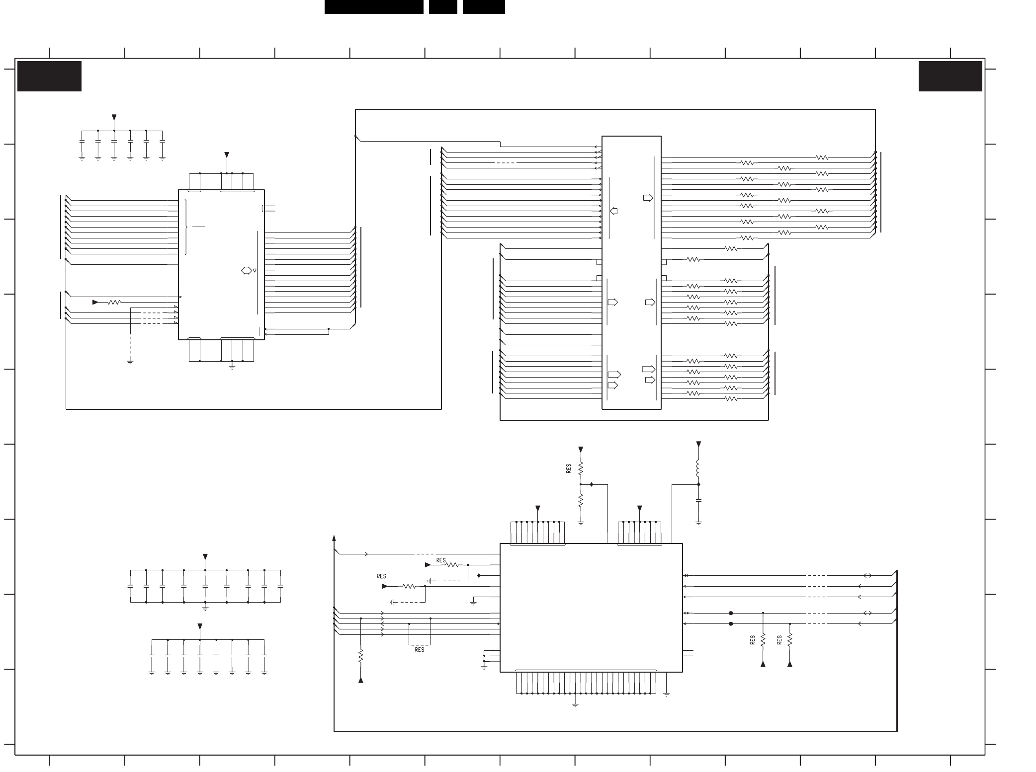
Circuit Diagrams and PWB Layouts EN 41FTL2.4E AA 7.
SSB: Columbus
8
NC
L
U
10
16
1
2
3
4
5
9
10
11
12
13
512K-1
DQM
VDD
0
VSSQ
A
14
15
RAS
CAS
WE
A11
3
2
CLK
D
VSS
VDDQ
1
0
CKE
CS
9
8
7
6
5
4
6
7
CLKASA
8
0
1
2
3
4
5
6
7
2
5
3
DQM
WE
6
0
1
2
3
4
5
7
2
1
0
3
4
5
15
6
5
4
8
7
14
5
6
8
11
10
WEA
6
VA
7
YA
0
1
2
4
38
7
11
12
13
HREF
9
8
CLKASB
7
16
8
WEB
3
2
1
0
6
10
9
4
1
A
DAVA
DI9
UVA
DI
UVB
DO
DO9
YB
DAVB
DQ
RAS
CAS
CLK
BISTEN VDDC
VSS
VDDS
A0IIC
RESET
CLKSEL
CLKEXT
656SEL
TRST
TCK
TDO
TMS
TDI
TST3
TST1
TST2
SNRST
SNDA
SCL
AVD
SNCL
SDA
NC1
NC2
AVS
9816 G11
9817 H11
9818 H11
F735 H10
F736 H10
I718 F9
I801 G6
I807 F8
C4
9800 D2
9801 D2
9802 D2
9803 D2
9804 G6
9805 G6
B3a
B3a
C11
9806 H5
9807 H5
9812 B7
9815 G11
3915-4 E9
3916-1 E9
3916-2 E9
3916-3 E9
3916-4 C9
3917-1 D9
B3a,b,c(2x)
E13
COLUMBUS_CTRL
B3a,b,c
3832 B10
3833 B11
3834 B10
3835 B10
3836 B11
3837 B10
3838 B10
3839 B10
3840 B11
3841 B10
3917-2 D9
3917-3 D9
3917-4 E9
5800 F9
7752-1 A8
7752-2 G7
7753 C3
9722 H11
3853 H5
3854 F8
3855 F8
3913-1 D9
3913-2 D9
3913-3 D9
B3d
B3a,c
B3d
B3b
B3a,b,c
3913-4 C9
3914-1 C9
3914-2 D9
3914-3 D9
3914-4 D9
3915-1 C9
3915-2 C9
3915-3 E9
2867 H2
2868 H2
2869 H3
2870 H3
3830 B11
3831 B10
K3
N8
B3a
B3a
B3d
3842 C10
3843 C10
3844 C11
3845 C10
3846 D1
3847 G5
3848 G6
3849 H10
3851 H10
2855 A2
2856 G2
2857 G2
2858 G2
2859 G2
2860 G3
B3a
B3a,c,B19d
B3d
N11
B3a
2861 G3
2862 G3
2863 G3
2864 G4
2865 H2
2866 H2
G
H
B3d
B3d
B3a,b,c(2x)
B3a
B3a,b,c
2850 A1
2851 A1
2852 A1
2853 A2
2854 A2
A
B
C
D
E
F
L13
B3d
678
COLUMBUS
N6
67891011
G3
B3a,B3c(2x)
B3a
B3d
D3
12
12345
C7/B8
C12
N9
P13/N14
9 101112
12345
I
A
B
C
D
E
F
G
H
I
2792 F9
2819 H3
2836 H3
(ONLY FOR 3D COMB)
G13
M3/N3
H13
SDRAM
2866
100n
2819
100n
9722
100n
2856
2865
100n
100n
2857
+3V3CB
9803
9815
9817
9816
9818
68R
3845
I718
9801
100n
2836
4K7
3851
2858
100n
2863
100n
+3V3CA
3838
68R
F735
+3V3CA
3839
68R
3830
4K7
3848
68R
3836
68R
3835
68R
9812
9807
4K7
3849
+3V3CB
3833
4K7
3855
68R
3846
4K7
2868
100n
9804
2859
100n
47K
3853
22R
3917-1
2870
+3V3CA
+5V2Pr
100n
I801
9802
100n
2853
68R
3837
9805
+3V3CA
5800
68R
3844
100n
2851
100n
2864
3840
100n
2861
68R
100n
2867
3914-3
3834
22R
68R
+1V5CA
+1V5CA
3913-3 22R
68R
3843
22R
3917-3
68R
3832
A12
G2
F2
E2
E1
D2
D1
C2
C1
B1
A1
J15
B7
B9
A9
B10
A10
B11
A11
B12
M2
M1
L2
L1
K2
K1
J2
J1
H2
A13
B13
K15
A2
B3
A3
B4
A4
B5
A5
B6
A6
L15
R12
P11
P10
R10
P9
P8
R8
R13
L14
A14
K14
J14
H1 G1
P12
R14
R15
P15
N15
M14
M15R7
P7
P5
R5
R1
R2
R3
P3
R4
P4
7752-1
T6TU5XBG
ΙΟ
P6
R6
22R
3916-4
3915-2
2855
100n
22R
3913-2
3914-2
22R
10
41
47
15
22R
36
1
25
7
13
38
44
26 50
4
5
6
8
9
11
12
39
14
33
37
17
35
18
2
40
42
43
45
46
48
49
3
23
24
27
28
29
30
31
32
16
34
MSM56V16160F-7TS
7753
DRAM
512K X 16 X 2
Φ
21
22
20
19
3915-3
3915-4
22R
3916-1
22R
22R
2852
100n
+1V5CA
2850
100n
3841
68R
100n
2862
2854
F736
100n
I807
22R
3913-4
9800
22R
3916-3
3917-4
9806
22R
3847
4K7
3914-1
2792
100n
22R
3842
68R
22R
3915-1
22R
3913-1
2860
100n
3916-2
+3V3CA
C13
D13
22R
N12
N13
P2
P14
R9
R11
C3
C5
C6
C9
C10
F13
J3
J13
K13
L3
M13
N4
N5
B14
N7
N10
G3
G13
L13
M3
N3
N8
N11
B2
E3
F3
C11
D3
E13
H13
K3
N6
N9
C4
N14
P13
C12
D15
F15
E15
E14
F14
A8
F1
H3
C7
C8
P1
B8
H14
H15
D4
N2
G15
B15
A15
D14
C14
C15
7752-2
T6TU5XBG
CTRL
A7
G14
N1
3917-2
+5V2Pr
22R
68R
3831
+3V3CB
+3V3CA
22R
3914-4
100n
2869
3854
4K7
COL_DQM
YB(8)
TCK
TDO
TDOA
TMS
TRST
UVB(3)
UVB(2)
UVB(1)
UVB(0)
WE-B
CLK-AS
RST_COL
SCL-D
SN-CL
SN-DA
SDA-D
YB(0)
YB(1)
YB(2)
YB(3)
YB(4)
YB(5)
YB(6)
YB(7)
UVB(8)
UVB(7)
UVB(6)
UVB(5)
UVB(4)
RSTR_I
YA(5)
YA(6)
YA(7)
YA(8)
YA(0)
COL_SD_CLK
CL16
WE-A
YA(1)
YA(2)
YA(3)
YA(4)
COL_SD_DQ8
COL_SD_DQ7
COL_SD_DQ6
COL_SD_DQ5
COL_SD_DQ4
COL_SD_DQ3
COL_SD_DQ16
COL_SD_DQ15
COL_SD_DQ14
COL_SD_DQ13
COL_SD_DQ12
COL_SD_DQ11
COL_SD_DQ10
COL_SD_DQ9
COL_SD_DQ1
COL_SD_A1
COL_SD_CLK
HREF_EXT
COL_SD_RASN
UVA(0)
UVA(1)
UVA(2)
UVA(3)
UVA(4)
UVA(5)
UVA(6)
UVA(7)
UVA(8)
VAP
COL_SD_WEN
COL_SD_DQ2
COL_DQM
COL_SD_WEN
COL_SD_CASN
COL_SD_RASN
COL_SD_A0
COL_SD_A10
COL_SD_A11
COL_SD_A2
COL_SD_A3
COL_SD_A4
COL_SD_A5
COL_SD_A6
COL_SD_A7
COL_SD_A8
COL_SD_A9
COL_SD_CASN
COL_SD_A0
COL_SD_A1
COL_SD_A10
COL_SD_A11
COL_SD_A2
COL_SD_A3
COL_SD_A4
COL_SD_A5
COL_SD_A6
COL_SD_A7
COL_SD_A8
COL_SD_A9
COL_SD_DQ1
COL_SD_DQ10
COL_SD_DQ11
COL_SD_DQ12
COL_SD_DQ13
COL_SD_DQ14
COL_SD_DQ15
COL_SD_DQ16
COL_SD_DQ2
COL_SD_DQ3
COL_SD_DQ4
COL_SD_DQ5
COL_SD_DQ6
COL_SD_DQ7
COL_SD_DQ8
COL_SD_DQ9
B3D B3D
F_15460_017.eps
070405
8204 000 8481.1
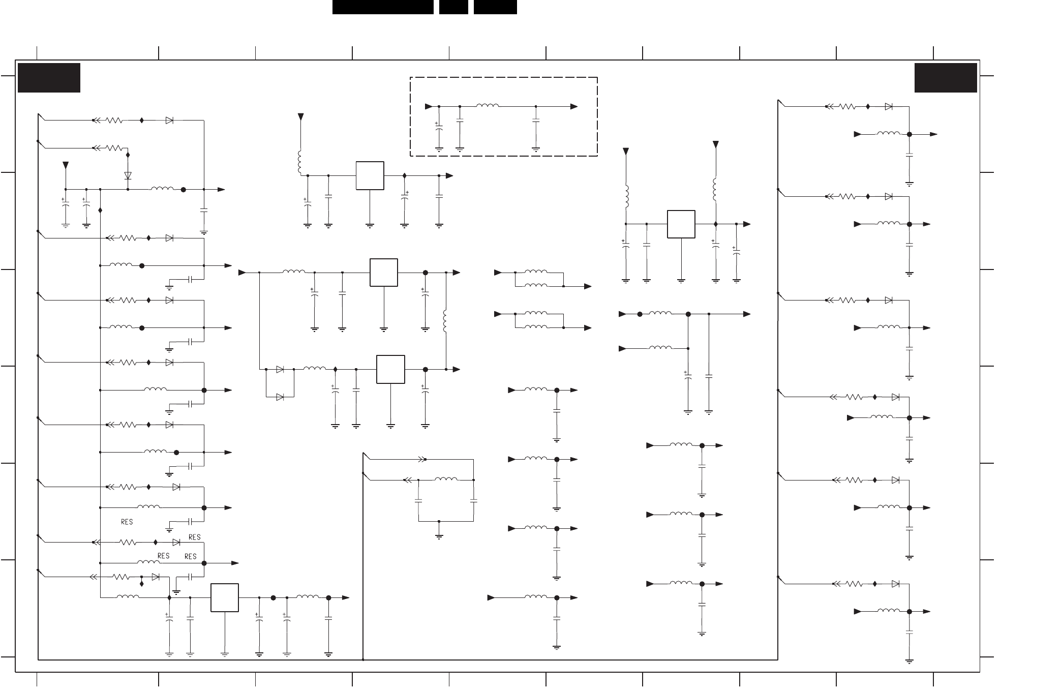
EN 42FTL2.4E AA 7.
Circuit Diagrams and PWB Layouts
SSB: FBX Supply
B3E B3E
F_15460_018.eps
070405
8204 000 8481.1
COM
OUTIN
COM
OUTIN
COM
OUTIN
COM
OUTIN
COM
OUTIN
I749 D1
I750 E1
I751 E1
I752 F2
I753 F1
I754 E9
I755 F9
I756 A1
I758 A1
I759 C1
I760 D9
B3e
B3e
F799 B4
I712 C9
I721 B1
I742 A9
I743 A4
I744 B1
I745 B7
B12
B3a(3x)B3e(14x)
7774 A4
F711 E6
RESERVED
I746 B9
I747 C1
I748 C3
F748 E2
F749 C6
F750 C7
F789 D9
F790 B2
F791 C1
F792 D2
B3e
B3e
B3e
B3e
B3e 6709 C9
F793 D2
F794 E2
F795 F3
F796 F3
F797 F6
F798 D6
6721 F9
6722 B2
6723 D9
7701 B4
7770 B7
7772 C4
7773 F2
5763 F3
5764 D5
F712 D6
F713 C4
F734 B1
F740 A9
F741 B9
F743 F9
F744 E9
F745 D7
F746 E7
F747 F7
5778 E4
5779 B1
5780 C9
5801 D9
6702 C2
6704 D3
6705 F1
B3e
3872 D1
3873 E1
3874 E1
3875 B1
3877 C9
5702 A5
5709 B3
5713 E5
6711 A2
6712 B1
6713 D2
6714 D2
6715 E2
6716 E2
6717 A9
6718 B9
6719 C3
6720 E9
5756 E9
5757 D7
5758 E7
5759 F7
5760 C3
5761 C4
5762 F5
B3e
2896 C4
2897 C3
2898 D3
2899 D4
2914 C2
2919 F2
2921 E6
2922 E4
5767 B2
5768 C1
5769 D1
5770 D1
5771 E1
5772 F1
5773 E1
5775 A3
5776 C7
5777 B7
3864 F9
3865 E9
3867 B9
3868 A9
3869 A1
3870 A1
3871 C1
2818 C9
2820 B6
2826 E7
2828 B6
2829 B7
2843 F2
5719 B5
5720 C5
5721 C5
5722 C5
5750 A9
5751 B9
5752 D5
5753 F9
5754 B6
5755 C7
2889 B4
2890 B2
2891 C2
2892 D2
2893 D2
2894 E2
2895 B3
1 234
2923 E5
2924 B4
2932 A5
2933 A5
2937 B7
2938 A4
2939 B1
3707 F1
3805 D9
3829 C1
6789
A
B
C
B3e
B3e
B3e
D
E
2844 E7
2845 E9
2846 F9
2847 D7
2848 D7
2849 D6
2871 D4
2872 E6
2873 F6
2874 F7
C
D
E
F
2715 C3
2728 F2
2729 F2
2730 F3
2739 B1
2802 B3
2810 B9
2811 A9
2813 D9
2817 F3
B3e
FBX SUPPLY
B3e
B3e
56789
1 2345
I753
F
A
B
5775
2921
100n
GND
2
IN
1
OUT
3
+3V3_FBXB
7772
LF15ABDT
16V100u
2939
2919
100u
5752
+1V5_FBXA
+3V3_FBXB
2802
100n
F796
2914
F750
+3V3_DCDCFBXA
RES
100n
5776
+3V3_FBXB
BAS316
6709
5751
100n
2872
10u
2895
F744
F741
5778
6u8
RES
5779
5758
+2V5_FBXA
+8V_CON +8VPA
2848
100n
100n
2932
I758
BAS316
6705
I756
6712
BAS316
6715
BAS316
F740
S1D
F734
6719
5773
5750
16V10u
2938
3868
100R
100R
3874
3871
100R 6713
F797
BAS316
3707
100R
S1D
6704
res
+2V5_FBXA
F795
100n
2813
F789
5801
5702
2933
100n
5755
5759
GND
10n
2922
+5V_FBXA
6723
BAS316
I760
6718
BAS316
100R
3805
100u
2730
I712
3877
100R
I759
I754
+3V3_FBXB
3870
100R
+1V5_FBXB
2892
100n
3864
100R
2818
100n
5780
10u
2828
100R
3867
I742
+2V5_FBXA
I745
5753
I744
F793
F794
5761
BAS316
6721
3873
100R
5777
5767
+3V3_FBXB
5713
+2V5_FBXA
GND
5762
2873
100n
5756
100n
2810
10u
2898
100R
3829
2874
100n
5768
2896
100u
2811
100n
100u
2889
I755
BAS316
6717
2847
10u
+3V3_DCDCFBXA
+3V3_DCDCFBXA
100u
2829
2843
100n
I748
F743
F747
F711
I752
I750
5757
5763
2897
100n
res
F792
5754
I743
F749
2844
100n
5720
F790
F791
100n
2846
6722
+3V3_DCDCFBXA
+3V3_FBXB
+3V3_FBXB
RES
BAS316
+5VF
2890
100n
I721
100R
3865
6702
BAS316
5770
F798
+1V5_FBXA
RES5721
BAS316
BAS316
6711
6716
2715
10u
res
5709
res
5771
100n
2894
6720
BAS316
2891
100n
I747
+3V3_DCDCFBX
I746
F748
100n
2899
3869
100R
3
OUT
100n
2849
7773
LF18ABDT
2
GND
IN
1
I751
3872
+3V3_DCDCFBXA
6714
BAS316
100R
220u
2739
2937
220u 4V
F713
GND
F746
100n
2826
+2V5_FBXA
+3V3_DCDCFBXA
RES
3875
100R
5760
2893
100n
5769
2845
100n
7774
KF25BDT25
GND
2
IN
1
OUT
3
GND
+5V2Pr
GND
100n
2820
2924
100n
2923
10n
GND
F745
10u
2728
2817
100n
220u
2871
5722
3
OUT
I749
LF15ABDT
7701
res
2
GND
1
IN
5764 F712
+1V5_FBXB
F799
+5V_FBXA
+1V5_FBXB
5719
2729
100n
5772
1
32
3V3_FAULT_FBX
+5V_FBXA
RES
7770
LD1117DT33C
3V3_FAULT_FBX
3V3_FAULT_FBX
+3V3EC
+3V3ED
+2V5ED
+3V3Pr
3V3_FAULT_FBX
3V3_FAULT_FBX
3V3_FAULT_FBX
+3V3GA
3V3_FAULT_FBX
3V3_FAULT_FBX
3V3_FAULT_FBX
3V3_FAULT_FBX
3V3_FAULT_FBX
3V3_FAULT_FBX
3V3_FAULT
+2V5EC
3V3_FAULT_FBX
3V3_FAULT_FBX
3V3_FAULT_FBX
+3V3PB
+1V8FA
+3V3PA
3V3_FAULT_FBX
+3V3FA +1V5EA
+1V5EB
+1V5CA
+2V5EB
+2V5EA
+3V3FB
+3V3PC
+3V3EA
+3V3EB
+3V3CA
+3V3CB
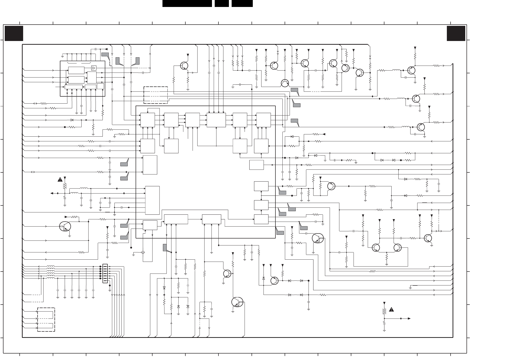
Circuit Diagrams and PWB Layouts EN 43FTL2.4E AA 7.
SSB: HOP
SPEC-
TRAL
PROC
WIN-
DOW
ADC
CHROMA
PROCESSING
LUMA
NC
CONTROL
PROCESSING
AMPL
MATRIX
START/STOP
H-DRIVE
6-BITS
DAC
EW
FRAME
RAMP
CONTR
BRIGHT
CONTROL
COLOUR
MATRIX
CONTRAST
BRIGHTNESS
CONTROL
RGB-YUV
SAT
BLACK
STRETCH
RGB-INSERTION
WHITE
POINT
CONTROL
OUTPUT
+ BUFFER
+ BLUE
STRETCH
WHITE P.
PWL +
BEAM CURR
LIMITER
CONTIN’S
CATHODE
CALIBR’N
I2C
SUPPLY
1PHI-
PHI-2
DIFF
AND
R
G
BB
G
GENERATOR
R
B
G
R
B
G
R
V
U
Y
Y
VUY
DIGGND
DIGSUP
ANAGND
BANDGAP
RGB
SYNC+GEO
SC
Hsel
SWITCH
SATUR’N
B5a
2334 D8
2335 F11
2336 D9
2337 B12
2338 B12
2340 I11
2341 C12
2342 A7
2343 A9
3324 I5
3325 A9
3326 G5
3327 G6
B4
HOP (NOT USED, UNLESS OTHERWISE INDICATED)
B4(2x)
2304 G7
nc
0V2
nc
nc
nc
RES ONLY PTV
B4
B4
B4
ONLY FOR NO HOP
nc
B4
B4(2x)
9 101112
G
1412 E13
2301 B2
2303 E9
B5a,B21
B4
B5a
B20
B4(2x)
3310 E10
2330 A6
2331 A6
2332 E2
2333 D10
B
C
D
E
F
G
H
I
1301 G4
1304 G3
nc
13
12
B4
B4(3x),B5a
B4(2x)
B4(2x)
5V2
B4(3x)
B4
nc
B4
B4,B5a
1V3
12345678
C
D
E
F
nc
B14b
B4(2x)
0V8
N.C.
B4
B4
B4
H
I
A
nc
nc
nc
nc
2324 I6
2325 G5
2326 E12
2328 B7
0V
B4(2x)
1V1
B5a
ONLY FOR NO HOP
nc
B5a
B4,B5a
nc
B4
B5a
B4
6 7 8 9 10 11 12 13
A
B
2344 H3
2345 H2
2346 H2
2347 H2
B4(2x)
B14b
B5a
B3a,B4(3x)
2306 H9
2307 F4
2308 G9
2312 F9
2313 F9
2314 E2
2315 E3
2317 E3
2318 E3
2319 G10
2320 G3
2321 B3
2323 B4
3305 C3
3306 E9
3307 E9
3308 E9
B4(2x)
B4
B4
NC
B4,B5a
3328 F9
B4,B5a
B4
2329 A6
345
2386 F12
2393 E13
2395 D3
2396 D3
2397 D3
2398 A3
2429 A4
2431 B4
3302 C4
3304 I11
3345 D9
3346 C9
3347 D9
3348 D10
B4,B5a
B4(2x)
B4
B5b
B4
B4,B5a
B3a,B4(3x),B5a
2309 D3
2310 E3
2311 H6
3314 G8
3315 H8
3316 H10
3317 G9
3318 F9
3319 E13
3320 D3
3321 D3
3322 D12
3323 H5
3364-2 F11
3364-3 G10
3364-4 G10
3365 F13
B4(2x)
B4
B4(2x)
nc
3329 E2
3330 A7
3331 G3
2348 H2
2349 H2
2363 F3
3335 A7
3336 H6
3337 A11
3338 A12
3339 C3
3340 A13
3341 B13
3342 C13
3343 D12
3344 D10
3399 B6
3442 E13
3443 E13
3453 C2
HOP
B4
2V5
4V0
3349 F2
3350 B10
3351 B9
3311 G7
3312 E11
3313 E11
3355 B8
3356 G12
3357 F12
3358 A11
3359 B10
3360 A8
3361 G7
3362 F11
3363 F3
3364-1 F11
5306 H2
5307 H2
5308 H2
5313 A12
5314 B12
3366 H11
3367 F11
3369 B12
3332 A7
3333 F3
3334 H5
3387 G2
3388 B5
3389 C13
3390 D9
3391 F12
3394 D9
3395 C3
3396 D3
3397 D2
3398 D3
6334 H5
7301 B4
7302 A1
7303 H8
B4(2x)
B4
B4(2x)
B4(2x)
1V1
3352 A10
3353 A10
3354 A11
3465 A9
3467 A8
3470 A8
3471 A8
3472 I6
5301 E2
5302 E2
5303 G2
5304 G2
5305 G2
7340 A6
7361 H7
7362 H7
7375 A8
B4
7V9
5315 C12
6301 E12
6303 H9
3383 B13
3384 C12
3386 F13
6308 C2
6309 D11
6310 D10
6311 D12
6312 H8
6313 H9
6314 H9
6316 C9
6317 E12
6319 D9
9421 B9
C001 H12
F309 D11
F311 C2
B14b,B21(2x)
0V2
7304 F2
3454 B2
3455 C2
3459 B11
7310-1 G11
7310-2 G12
7312 F10
7313 A11
7314 A10
7315 A10
7316 A12
7317 B12
7318 E10
7319 C12
I305 G5
I306 G5
I307 G7
I308 A12
B5a
I309 B11
I310 B12
I311 D9
6304 H9
6306 I5
6307 I6
9305 A4
9308 B5
9309 B5
9310 B5
9311 I1
9312 I1
9313 F13
9314 H1
9315 H1
9316 I6
I330 B4
I331 B4
I332 B3
I333 C3
I338 E3
I365 E10
I366 B3
I367 D10
I368 A7
I369 A8
I370 A10
F312 E9
7305 B9
7306 A9
7309 G13
F349 G3
F350 G3
F351 H3
F352 H3
F353 H3
F362 H3
F364 F4
I302 E2
I303 E4
I304 B11
I315 D8
I316 D9
I317 C12
I319 A11
I320 A11
7V9
I321 F3
I326 B7
I339 E4
I357 E8
I358 D4
I359 F4
I312 E3
I313 C12
I314 C9
9302 A3
9303 A4
9304 A4
2343
100n
I363 H5
I371 I12
c200 F3
1V5
F329 H9
F347 D12
F348 G3
F351
10K
3467
+8VS
3341
47R
3339
6K8
100n
2307
7315
PMBT2369
1u0
2303
3472
22K
F350
+8VS
F364
I309
F362
1K0
3322
+8VS
68K
3343
F352
F17
BAS316
6317
+8VS
7318
BC857BW
33K
3355
+8VS
4K7
3394
10p
2346
2332
100n
9304
I331
7309
BC847BW
3311
100K
1K0
3333
3454
100R
V21
22p
2328
19
14
SOUT 21
UIN
8UOUT 17
VCC
20
VIN
9VOUT 16
YIN
6
YOUT
122 102324
SC
1
SCL
11
SDA
3
AD2
4
AD3
5
ADR
7
CF
22
DEC
15
GND
1813
7302
TDA9178T
AD1
7314
BC847BW
3319
100R
1n0
2319
2317
1u0
100R
3455
GND-RGB-CRT
2309
10p
3387
100R
PDTC144EU
7304
I304
3453
33K
9308
I333
PDTC144EU
7361
6307
BAT54 COL
+8VS+8VS
2326
10n
RES
3323
100K
3397
100R
I308
33n
2312
3470
33K
2393
1u0
6u8
5302
2349
10p
I305
1K0
3350
V29
100K
I315
3312
100K
3352
3362
3K9
3305
68K
680K
3364-2
27
I370
6303
BZX384-C47
820R
3384
2335
1n0
10p
2344
I302
10K
3345
47R
3342
2315
100n
9303
+8VS
3361
47K
22K
3347
10u
2340
3383
680R
2301
100n
L12
5315
5u6
7316
BC857BW
6334
BAS316
220R
3317
3369
820R
+8VS
5313
5u6
2320
10p
10K
3391
10n
2324
BZX384-C22
6311
3314
10K
100n
2429
6316
BAS316
BC847BW
7340
7319
BC857BW
9309
+8VS
I306
6301
BAS316
+5VS
I313
I371
1K8
3358
V32
V22
1412
7303
BC857BW
100n
2329
+5V_VDP
3332
+8VS
1K0
I358
2323
100n
GND-RGB-CRT
6p8
2338
F19
5307
I310
680R
3338
1K0
3302
+8VS
I330
2342
100n
VDOB 2
VIN
26
VP1
17
VP2
39
VSC 15
XTALI
20
XTALO
21
YIN
28
RI2
35
RO 40
SCL
10
SCO
9
SDA
11
UIN
27
VD
23
VDOA 1
HD
24
HFB
13
HOUT 8
HSEL
12
IREF 16
LPSU
22
PWL
34
RI1
30
EWO 3
FBCSO
29
FLASH
5
GI1
31
GI2
36
GND1
6
GND2
19
GO 41
BL2
38
BLKIN 44
BO 42
DACOUT 25
DECBG
18
DECVD
7
DPC
14
EHTIN 4
TDA9330H/N1
7301
BCL 43
BI1
32
BI2
37
BL1
33
2337
6p8
2u2
2334
I317
7312
PDTC144EU
I368
1K0
3334
+5VS
PMBT2369
7313
I307
2341
6p8
I367
100R
3398
10K
3399
100n
2331
6312
BAS316
4K7
3365
2321
100n
+8VS
5301
6u8
9310
3336
1K0
10p
2348
820R
3337
45
680K
3364-4
BC847BS
2
6
1
I369
7310-1
470K
3308
47R
3340
3313
100K
9305
3363
1K0
100n
2397
+8VS
6314
BAS316
I366
V19
5303
I311
5u6
5314
2
13
V31
1301
CSTCV
12M
2396
100n
RES
100K
3326
2336
2u2
1K03335
3324
4K7
3367
220R
100K
3325
100K
3360
2306
470p
I365
3320
100R
2347
10p
I303
3395
100R
2K2
3354
1K0
3331
F309
2330
100n
BZX384-C6V8
6310
2386
1n0
680K
3364-1 18
F329
BAS316
6308
680R
3389
BAS316
6309
4K7
3349
100R
3396
+8VS
BC847BW
7305
7375
BC847BW
33K
3346
L13
100K
3386
RES
2311
68p
5306
F312
3329
6R8
I319
2325
100n
3388
10R
39K
3328
+5VS
I326
2K2
3348
6304
BAS316
2318
22n
+8VS
3459
2K2
2K2
3356
3351
10K
+8VS
+8V_VDP
+8VS
I359
9313
6306
BZX384-C5V6
220K
3443
3316
47K
5305
220R
3306
F353
+8VS
BZX384-C22
6313
220R
3390
9302
F20
+8VS
7310-2
BC847BS
5
3
4
+8VS
+8VS
9311
3471
100K
I316
5308
100n
2398
+8VS
9314
5304
I357
2308
10p
+8VS
2u2
2333
F348
10p
2310
100n
2395
c200
I314
BC847BW
7306
2K2
3344
2345
10p
I320
680K
3364-3 36
33K
3465
V20
I363
3327
100K
+8VS
47K
3310
22K
3442
9421
I321
V23
3353
1K0
+8VS
BC857BW
7317
F311
9315
1K0
3315
I312
BAS316
6319
3R9
3304
2304
10p
7362
BC847BW
100R
3321
I338
3318
1K0
C001
2
3
4
5
6
7
1304
1
220R 3366
1K03330
F349
18K
3307
V30
2313
100n
I332
GND-RGB-CRT
V28
I339
100K
3359
9312
9316
3K9
3357
+8VS
2314
100u
F347
2431
100n
2FH-R
470p
2363
GND-LINEDRIVE
2FH-FBL
2FH-B
2FH-G
ANTI-MOIRE
BACKLIGHT-CNTRL
POR
POR_FLASH
HD@HOME
NOHOP1B
HFB
VSYNC
FBL-TXT
Y-SCAVEM
Yltp
G_2FH
B_2FH
R_2FH
FBL_2FH
VSYNC
FBL_2FH
HD100
VD
2FH-HD100
2FH-VD100
GND-RGB-CRT
NOHOP1A
NOHOP1B
HD100
NOHOP2B
FRAMEDRIVE+
LINEDRIVE1
TILT
HFB_X-RAY-PROT
HD100
U100
V100
VD
TILT
HFB_X-RAY-PROT
HFB
LIGHT-SENSOR
Yltp
NOHOP1A
VD100
R_2FH
G_2FH
B_2FH
R_2FH
G_2FH
B_2FH
FBL_2FH
BCL
U100
V100
Y100
SDA-F
SCL-F
HD100
SANDCASTLE
CUTOFF
SANDCASTLE
Y100
FBL-TXT
SCL-F
SDA-F
DYN-FASE-COR
EHT-INFO
NOHOP2B
B-CRT
G-CRT
R-CRT
EHT-INFO
EW-DRIVE
B-TXT
G-TXT
R-TXT
EHT-INFO
F18
B4 B4
F_15460_019.eps
240405
8204 000 8483.1
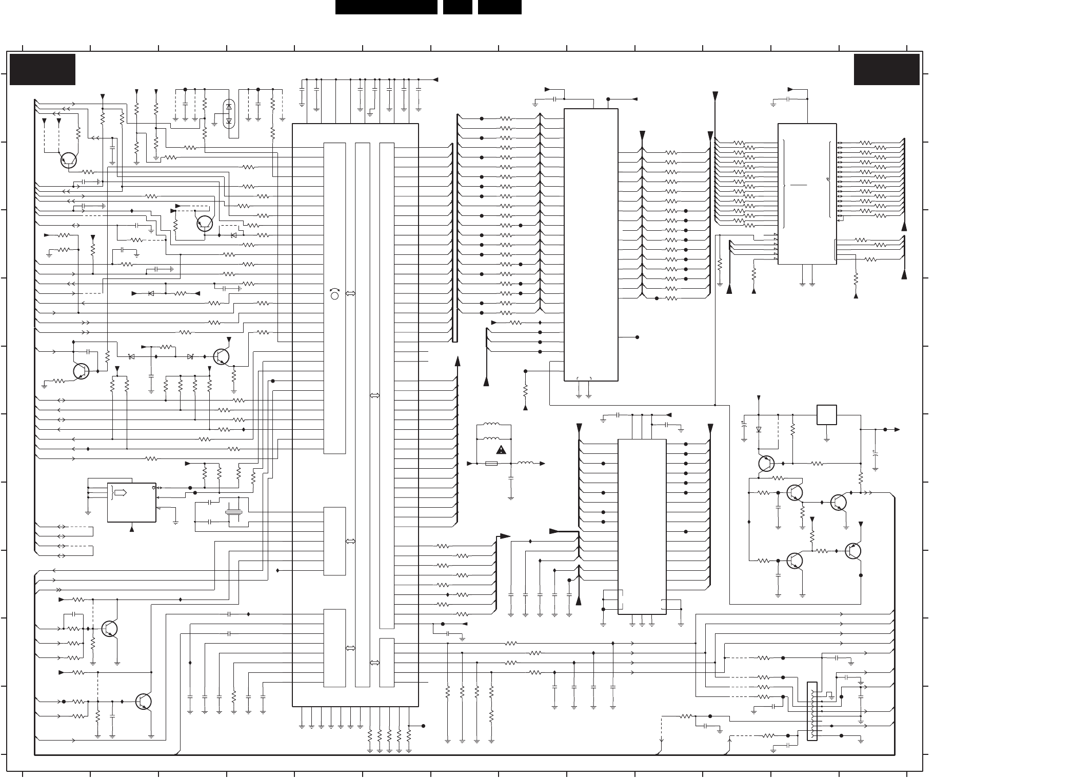
EN 44FTL2.4E AA 7.
Circuit Diagrams and PWB Layouts
SSB: OTC-Flash
GND
CLOCK GENERATOR
CLOSE AND
EXTERNAL CODE AND DATA INTERFACE
TXT
DISPLAY TIMING
TXT
CAPTION
EPG
USA
INTERFACE
DISPLAY
VIDEOn
SCL
ADR
0
1
2 SDA
WC
COM
OUTIN
A
D
5
11
2
1
17
OE
12
13
14
15
16
RB
4
3
2
CE
7
6
WE
RP
1
0
BYTE
3
NC
5
8
9
10
11
12
13
14
15
A-1
10
4
9
8
7
6
0
4M-1
0
NC
NC
G
B3a
FC43 G10
I
J
A
B
C
D
E
F
G
H
I
J
1000 F7
123
B21
IC18 H8
IC20 H7
IC21 H3
IC22 H4
FC57 A3
B3a,B4 (4X)
RES
B5c(3x)
(TXT)
678910111213
A
B
C
D
E
2019 F10
2020 E1
2022 E2
FC44 C10
FC45 H8
FC46 H9
FC47 J6
FC48 G3
FC49 G3
FC50 E8
FC51 D7
FC52 I12
FC53 I12
FC54 J12
FC55 J12
FC56 J13
F
G
H
12345678910111213
2056 I13
2057 I12
2058 C2
4
B5a(2x)
B5a(2x),C(3x)
OTC-FLASH
C
B4
1001 G3
1401 I12
5
2005 J3
2006 J3
2007 J3
2008 H4
2009 J8
2010 J9
2011 J9
2012 J9
2013 F11
2014 I4
2016 F13
2017 G12
2018 G3
3006 J6
3007-1 J6
3007-2 J6
2023 A5
F
B14b,B21
B5a
2024 A5
2025 A5
2026 A6
2027 A6
2033 H8
2034 H8
2035 H8
2036 H8
2037 H8
2038 F9
2039 H12
2040 A12
2041 H1
2052 J12
2053 J11
2054 J11
2055 J13
3015 G11
3016 G12
3017 F13
2059 C2
B14b
RES
B21
B5c(3x)
B5a
2002 G3
2003 J4
2004 J4
2067 I7
2068 J2
2070 B2
2071 B1
2072 B1
2073 C3
2074 D4
2075 F8
3001 F3
3002 F3
3003 J4
3004 F12
3005 D13
3034-2 H7
3034-3 H7
3034-4 H7
3007-3 J6
B21
B4,B21
C
B5a
EPG-
RES
2028 A6
2029 A6
2031 A8
3008-1 J7
3008-2 J7
3008-3 J7
3008-4 J7
3009 A1
3010 E8
3011 E2
3012-1 I8
3012-2 I8
3012-3 I8
3012-4 I8
3013 F12
3014 F12
3048-1 B8
3048-2 D8
3048-3 D8
3018 A2
H
B5c(3x)
B5c(3x)
B5a(2x),C(3x)
B5c(3x)
3019 B2
2060 A4
2061 A3
3025 E1
3026 E4
3027 E2
3029-1 B11
3029-2 B11
3029-3 B11
3029-4 B11
3031-1 B11
3031-2 C13
3031-3 C13
3031-4 C13
3033 C3
3034-1 G7
3054-3 D10
3054-4 B10
3055-1 B10
3035-1 H7
B21 PROGRAM
B4
2V8
RES
H
B5a(2x)
B5a(2x)
(Set SW)
B5a(2x),C(3x)
3V4
3007-4 J6
3035-3 H7
3035-4 H7
3038 B1
3039 B2
3040 I1
3041 I1
3042 J1
3045 J11
3046-1 J12
3046-2 J12
3046-3 I11
3046-4 I11
3047 C2
3064-4 E4
3065 G12
3066 G12
3048-4 D8
B3a
B4(2x)
B5a(2x)
B5a
B5a(2x)
3049-1 D8
3049-2 B8
3049-3 A8
3020 A2
3021 B2
3024 D3
3050-3 B8
3050-4 B8
3051-1 B8
3051-2 C8
3051-3 C8
3051-4 C8
3052-1 C8
3052-2 C8
3052-3 C8
3052-4 C8
3053 E2
3054-1 D10
3054-2 C10
3076-3 D3
3076-4 D4
3077 D3
3055-2 C10
B5a
B5a(2x)
3055-3 B10
3055-4 C10
3056-1 B10
3056-2 C10
B5c(3x)
3035-2 H7
3057-2 C10
3057-3 B10
3057-4 C10
3058 C1
3059 C1
3061-1 B11
3061-2 B11
3061-3 C11
3061-4 C11
3062 C11
3064-1 F3
3064-2 F4
3064-3 E3
3086-3 B11
3086-4 B11
3087 A11
3067 H11
SAM
B6a,B14b
RAM_CSn
F
B2(3x)
FLASH-RAM
3068 A2
3049-4 A8
3050-1 B8
3050-2 B8
3072-3 A13
3072-4 B13
3073-1 C4
3073-2 C4
3073-3 C4
3073-4 B4
3074-1 F2
3074-2 F4
3074-3 F3
3074-4 A3
3075 C1
3076-1 D4
3076-2 D3
3099-3 A4
3099-4 B4
3100 F4
3078-1 D4
RES
OTC
E
B5c(3x)
3078-2 B3
3078-3 B3
3079 E3
3080 A2
3056-3 B10
3056-4 C10
3057-1 B10
3082-3 B13
3082-4 B13
3083-1 B13
3083-2 B13
3083-3 B13
3083-4 B13
3084 D8
3085-1 B11
3085-2 B11
3085-3 B11
3085-4 B11
3086-1 C11
3086-2 B11
6002 F11
6003 E3
6004 D2
3088 E3
A
B5a
B5c(3x)
DRAM
OTC
B3a
3069 E3
3072-1 B13
3072-2 B13
3090-2 C4
3090-3 C4
3090-4 C4
3091 C2
3092 E3
3093 C11
3094 H1
3095 I1
3096 J2
3097 A3
3098 J10
3099-1 B4
3099-2 B4
7014 G13
7015 I2
7016 J2
3101 F4
2V9
B4
3V4
3081 A4
3082-1 B13
3082-2 B13
3102-1 C13
3102-2 B13
3102-3 B13
3102-4 B13
3103 D3
3C09 I1
3C10 I1
3C11 J1
3C12 J7
5000 F7
5001 F7
5003 F8
6001 E2
9014 C2
9015 D2
9016 C2
6005 A3
B3a
0V
FLASH-RAM
B14b,B21
0V2
B5a
B2
B14d
B5b
3089 A8
3090-1 C4
6006 C4
7002 F11
7003 G12
7004 G13
7005 E12
7006 A9
7007 F10
7008 E1
7009 D3
7010 C3
7011 F2
7012 A12
7013 H12
FC08 C7
FC09 C7
FC10 C7
7022 B1
B4 (2X)
B21
A
1V3
9001 H2
9002 J2
9003 G1
9004 G1
9005 A4
9006 A3
9007 F12
9008 J10
9009 J11
9010 I11
9011 I11
9012 I11
9013 J11
FC27 F10
FC28 B7
FC29 B10
9017 A4
RES
B4
E
3V4
RES
RES
B5a
B14e(2x),B21
9018 A3
9021 A1
9022 B3
9023 B3
9024 A1
9025 C4
FC01 A9
FC02 A7
FC03 C7
FC04 C8
FC05 C10
FC06 C7
FC07 C8
FC39 G9
FC40 C10
FC41 C10
FC11 D8
C
3V4
B14e
RES
B4
7023 A4
FC13 D10
FC15 D7
FC16 D8
FC17 D10
FC18 D8
FC19 E8
FC20 F13
FC21 F10
FC22 A7
FC23 F10
FC24 B7
FC25 F10
FC26 B7
FC58 J13
FC60 A4
FC61 E4
FC30 B7
Nc
0V2
B4(2x)
5V3
FC31 G10
FC32 G12
FC33 F9
FC34 C10
FC35 G9
FC36 F10
FC37 G9
FC38 C10
IC26 I3
IC27 I9
IC28 I8
FC42 C10
Nc
B14a,b,B15b
B21
NVM
B3a
N.C.
RES
FC12 D8
FC67 H13
FC68 H12
FC69 J1
FC70 J11
IC03 B2
IC05 D1
IC07 E2
IC09 F1
IC11 G13
IC13 G11
IC14 G8
IC15 H8
IC17 H4
B3a
FC66 I7
B14e
SDM
3V4
RES
F
IC23 I9
IC24 I9
IC29 D8
IC37 F4
IC38 J12
IC40 E3
IC41 C3
IC42 F12
IC43 G12
IC44 G12
IC45 I1
IC46 J2
IC48 E3
B5c(3x)
6006
BZX384-C3V9
FC29
72
27
100R
3031-2
100R
3034-2
IC09
FC67
FC33
18
FC43
3029-1
3006
470R
54
470R
3074-4
3018
10K
47p
2011
9012
IC14
6001
1PS76SB10
FC02
2053
10p
7003
BC847BW
2003
220n
3055-1
81
9015
2020
220p
2012
47p
100R
3064-4
45
3061-1
18
+5V2_CON
FC40
+3V3_INTOTC
18
IC22
3064-1
100R
3
3091
470R
3051-3
6
2037
82p
VCC 37
VCCW 13
WE_
11
WP_
14
42
DQ7 44
DQ8 30
DQ9 32
27
46
OE_
28
RP_
12
RY|BY_ 15
39
DQ13 41
DQ14 43
DQ15|A_1 45
DQ2 33
DQ3 35
DQ4 38
DQ5 40
DQ6
8
A9
7
BYTE_
47
CE_
26
DQ0 29
DQ1 31
DQ10 34
DQ11 36
DQ12
9
A2
23
A20
10
A3
22
A4
21
A5
20
A6
19
A7
18
A8
5
A12
4
A13
3
A14
2
A15
1
A16
48
A17
17
A18
16
A19
LH28F320BJE-PTTL90
A0
25
A1
24
A10
6
A11
3082-2 100R
72
7006
100R
3012-1 18
9022
3057-2
27
FC31
2022
100n
3049-2
72
54
3055-4
9002
2033
82p
FC01
2014
100n
112 VSSP3
84 VSYNC
70WEn
49
VDDP2
111
VDDP3
10 VSSA
21 VSSD1
76 VSSD2
102 VSSD3
39 VSSP1
50 VSSP2
14 TEST3
15 TEST4
20
VDD1
9
VDDA
75
VDDD2
101
VDDD3
19
VDDN1
38
VDDP1
3 REF+
74 RESET
43ROM_CSn
40ROM_OEn
8 STN|BLACK
11 TEST0
12 TEST1
13 TEST2
117 P3-4
118 P3-5|TTD
119 P3-6|TTC
120 P3-7|CBB
42
77R
41RAM_OEn
69RASn
107 P2-4|ADC2
108 P2-5|ADC3
109 P2-6|ADC4
110 P2-7|ADC5
113 P3-0|LED0
114 P3-1|LED1
115 P3-2
116 P3-3
97 P1-4|INT1
98 P1-5|INT2
99 P1-6|INT3
100 P1-7|RC
103 P2-0|PWM0
104 P2-1|PWM1
105 P2-2|ADC0
106 P2-3|ADC1
89 P0-4|RxDo
90 P0-5|TxDo
91 P0-6|CORN
92 P0-7
93 P1-0|T0
94 P1-1|T1
95 P1-2|T2
96 P1-3|INT0
1 IREF_DEC
18 OSCGND
17 OSCIN
16 OSCOUT
85 P0-0|SCL0
86 P0-1|SDA0
87 P0-2|SCL1
88 P0-3|SDA1
30D9
81DATA
73EAn
80FADING
82 FRAME
78G
83 HSYNC
2 IREF
37D15
28D2
24D3
23D4
27D5
31D6
35D7
34D8
6 CVBS1_R
36D0
32D1
26D10
22D11
25D12
29D13
33D14
61A8
62A9
79B
71CASHn
72CASLn
5 CVBS0
4 CVBS0_R
7 CVBS1
66A21
67A22
68A23
51A3
53A4
55A5
57A6
59A7
52A14
48A15
46A16
44A17
63A18
65A19
47A2
64A20
45A1
60A10
58A11
56A12
54A13
27
7023
SAA5801H/015
3076-2
470R
2002
27p
45
10p
2054
3057-4
63
IC11
1
3048-3
3049-1
8
3101
220R
FC18
9005
10K3093
FC07
FC24
BC857BW
7014
IC20
5
FC60
3086-4
4
10K
3010
36
IC15
470R
3099-3
FC34
FC27
3057-3
36
FC49
3026
4K7
2013
100u
45
470R
3073-4
7
FC69
3078-2
470R
2
81
82p
2036
3051-1
FC41
IC37
3100
220R
IC07
45
7015
PMBT2369
100R
27
3056-4
54
3012-2
100R
3082-4
3013
10K
2038
100n
FC32
470R
3097
FC19
+3V3_INTOTC
3083-1 100R
81
470K
3067
+3V3_INTOTC
6K8
3050-3
63
3058
3052-3
63
3045
100R
FC48
3074-3
470R
36
2010
47p
3092
1K8
150p
2041
81
2007
100n
3050-1
100n 2028
+3V3_INTOTC
IC26
FC45
2074
100n
FC35
3082-1 100R
81
FC56
63
FC66
3049-3
100R
3034-3
36
220n
2004
IC40
IC43
3048-4
54
FC37
FC39
81
10K
3020
3048-1
2057
10p
PMBT2369
7016
3076-4
470R
45
3029-4
45
2029
100n
7004
BC847BW
3102-3 100R
63
4K7
3040
FC21
10K
3005
7009
BC847BW
IC13
FC57
5
84
7
(4Kx8)
Φ
EEPROM
7011
M24C32-WMN6T
1
2
3
6
FC47
100n 2024
9004
3085-2
27
6
3056-3
3
IC24
3014
6K8
4
FC44
3102-4 100R
5
27
FC58
36
3099-2
470R
3008-3
100R
3025
220R
4K7
3001
3004
15K
IC21
FC53
27
3094
47K
3086-2
3024
27K
180R 3039
3072-4
45
+3V3_INTOTC
100R
9018
3034-4
100R
45
2
IC38
1K8
3069
3083-2 100R
7
2008
100n
2005
100n
100R
3083-4
54
IC46
36
470R
3078-3
FC54
9014
3021
10K
3019
4K7
36 72
3073-3
470R
3051-2
FC68
+3V3_INTOTC
+3V3_INTOTC
FC36
18
27
470R
3099-1
36
3046-2
100R
3054-3
IC41
IC42
FC15
9021
82p
FC05
2035
3086-3
36
1K8
3088
4K7
3077
100R
3035-4
45
FC51
3031-4 100R
54
FC38
3055-3
63
3007-3470R
FC46
3029-3
36
3050-4
54
100p
2060
3003
24K
27
3090-2
470R
470R
3076-1
18
100R
3102-2
72
63
10K
3062
3031-3 100R
82p
2034
3081
470R
IC45
3002
4K7
27
470R
3074-2
9011
2025
100n
18
54
+3V3_INTOTC
470R
3078-1
3051-4
8
100R3087
100R 3046-1
1
FC61
9009
3066
47K
3056-1
18
3057-1
18
+3V3_INTOTC
+3V3_INTOTC
100n
2006
45
9003
3054-4
3065
4K7
IC18
5003
3080 10K
3086-1
18
BC847BW
7013
2040
100n
2018
33p
100R
3C10
10K
3053
IC48
4
IC03
3012-4
100R
5
2061
100p
FC55
9001
5001
500mA F
1000
3
+5V2_CON
LF33ABDT
7005
2
1
3049-4
54
3007-1470R
45 3046-4
100R
FC23
18
4K7
3041
3074-1
470R
3055-2
72
100R
3008-4
45
3052-4
54
10p
2052
FC04
7002
BC857BW
+5V2-STBY
5000
IC27
27
9007
+3V3_INTOTC
100R
3008-2
+3V3_INTOTC
3103
470R
PLVA2650A
6005
FC26
3033
100K
18
3031-1
100n
2073
3027
47K
470R
45
IC44
3090-4
9010
FC42
100R
3072-1
18
100u
2016
72
FC16
3052-2
3096
47K
3061-2
27
3085-3
36
100n 2026
3C11
100R
9025
2
2023
100n
3048-2
7
3079
1K8
+3V3_INTOTC
BC857BW
7022
3054-1
18
FC52
3034-1
100R
18
100p
2058
3008-1
100R
18
36
100R
3012-3
7010
BC857BW
100n
2071
2009
47p
+3V3_INTOTC
+5V2_CON
10K
3084
9008
FC09
FC11
2019
100n
9006
3016
1K5
6
10K
3C09
3072-3 100R
3
3035-3
100R
36
4K7
3017
3029-2
27
36
470R
3090-3
3085-1
18
FC08
3011
4K7
470R 3007-2
100n
2075
100R
3046-3
36
IC05
3015
470K
10p
2055
6004
BAT54
620R
3059
FC22
2072
100n
+3V3_INTOTC
100n
2017
3035-1
100R
18
+3V3_INTOTC
45
FC06
3085-4
+3V3_INTOTC
1
42
3
FC28
1
6M0
1001
100R
3102-1
8
FC13
1PS76SB10
6003
470R 3007-4
27
+3V3_INTOTC
100R
3064-2
100R
3035-2
27
2
3
4
5
6
7
8
9
1112
1401
1
10
18
FC30
470R
3090-1
3064-3
100R
36
3075
10K
18
3073-1
470R
68R
3C12
3061-3
36
6002
BAS316
27
FC70
3054-2
9023
100n
2039
36
10p
2056
470R
3076-3
13
14
16
28
15
12
37
27
46
11
33
35
38
40
42
44
30
32
9
10
7
47
26
29
31
34
36
39
41
43
451
48
17
23
22
21
20
19
18
8
512Kx8/256Kx16
7012
M29W400BT-90N1
25
24
6
5
4
3
2
63
+3V3_INTOTC
EPROM
100R
3083-3
9017
2059
100p
3072-2 100R
27
100n
2031
3009180R
FC50
3068
IC29
45
+3V3_INTOTC
2K7
3099-4
470R
IC23
FC10
9016
100R
3082-3
63
+3V3_INTOTC
2068
2n2
100n
2067
3050-2
72
3047
470R
3061-4
45
1
3052-1
8
1
VCC1
6
VCC2
21
VCC3
VSS1
22
VSS1
VSS2
37
VSS2
VSS3
42
VSS3
WE_
13
31
11
12
15
16
32
OE_
29
RAS_
14
UCAS_
30
3
4
DQ3
DQ4 5
7
DQ5
8
DQ6
DQ7 9
DQ8 10
DQ9 33
LCAS_
2
DQ10 34
DQ11 35
DQ12 36
38
DQ13
DQ14 39
DQ15 40
DQ16 41
DQ16
DQ2
19
A3
20
A4
23
A5
24
25 A6
A7
26
A8
27
A9
28
DQ1
MSM51V18165F-60JS
7007
A0
17
A1
18
A2
FC17
47K
3095
27
BC847BW
7008
470R
3073-2
+3V3_INTOTC
FC12
FC03
2027
100n
9024
IC17
3038
10K
2070
100n
3056-2
27
9013
IC28
3098
100R
100R
3089
4K7
3042
FC25
+3V3_INTOTC
FC20
D(10)
D(13)
D(8)
D(9)
D(14)
D(2)
A(0)
A(9)
A(5)
A(4)
A(3)
A(8)
A(7)
A(1)
A(2)
A(6)
CASH
RAS
RAM_OE
CASL
D(15)
D(7)
D(6)
D(0)
D(1)
D(3)
D(4)
D(5)
D(12)
D(11)
RESET
RxD
TxD
D(0)
D(1)
D(10)
D(11)
D(12)
D(13)
D(14)
D(15)
D(2)
D(3)
D(4)
D(5)
D(6)
D(7)
D(8)
D(9)
VPP-SW
WE
AA(19)
AA(20)
DD(0)
DD(1)
DD(10)
DD(11)
DD(12)
DD(13)
DD(14)
DD(15)
DD(2)
DD(3)
DD(4)
DD(5)
DD(6)
DD(7)
DD(8)
DD(9)
EAn
AA(0)
AA(9)
AA(10)
AA(11)
AA(1)
AA(2)
AA(3)
AA(4)
AA(5)
AA(6)
AA(7)
AA(8)
AA(12)
AA(13)
AA(14)
AA(15)
AA(16)
AA(17)
AA(18)
2FHFB-GFX
2FHR-GFX
2FHB-GFX
2FHG-GFX
IRQ-FTV
+5V2_CON
VPP-EPG
AA(0)
SEL_IN_2
LED2
PWM_BACKLIGHT
CON-SND
LIGHT-SENSOR
FRONT-DETECT
IRQ-FTV
CVBS-Y-RECORD-IN
SOUND-ENABLE
RESET-AUDIO
HD100
KEYBOARD
STANDBY
HD3-EPLD
VD-EPLD
AA(0)
A(17)
A(18)
D(9)
D(0)
D(1)
D(10)
D(11)
D(2)
D(3)
D(4)
D(5)
D(6)
D(7)
D(8)
A(10)
A(16)
DD(6)
DD(7)
AA(7)
AA(2)
AA(4)
AA(6)
AA(8)
A(0)
A(6)
A(5)
A(4)
A(3)
A(20)
A(2)
A(19)
A(18)
A(17)
A(16)
A(15)
A(14)
A(13)
A(12)
A(11)
A(10)
A(1)
A(0)
SW_WE
D(15)
A(11)
A(15)
SW_OE
SW_CS
AA(13)
AA(15)
AA(16)
AA(10)
A(12)AA(12)
AA(11)
A(4)
A(6)
A(3)AA(3)
A(5)AA(5)
AA(17)
A(1)AA(1)
A(7)
A(2)
A(8)
AA(18)
A(19)AA(19)
A(20)AA(20)
D(14)
D(13)
D(12)
A(9)
A(8)
A(7)
AA(9)
DD(4)
DD(13)
DD(5)
DD(12)
DD(11)
DD(2)
DD(3)
DD(10)
DD(1)
DD(9)
DD(0)
DD(8)
DD(14)
DD(15)
A(14)AA(14)
A(13) EP_WE
EP_OE
EP_CS
FBL-TXT
B-TXT
R-TXT
G-TXT
RESET
AA(2)
A(9)
AA(6)
AA(5)
AA(4)
AA(3)
AA(1)
RxD
TxD
DD(15)
DD(14)
DD(13)
DD(12)
DD(11)
DD(10)
DD(9)
DD(8)
DD(7)
DD(6)
DD(5)
DD(4)
DD(3)
DD(2)
DD(1)
DD(0)
AA(17)
AA(16)
AA(15)
AA(14)
AA(13)
AA(12)
AA(11)
AA(10)
AA(9)
AA(8)
AA(7)
STATUS-SC3
STATUS-SC4
AGC-MONITOR
STATUS_SC3
HFB
SDA-S
SCL-F
+5V2_CON
SDA-F
SCL-S
AA(20)
AA(19)
AA(18)
WE
CASH
CASL
RAS
POR_FLASH
P50
ROM_OE
RAM_OE
ROM_CS
RAM_CS
HD@HOME
SCL-F
SCL-S
SDA-F
SDA-S
VSYNC
IRQ-DIGITAL
CVBS-TXT
+5V2_CON
+8V_CON+5V_CON
ON-OFF-LED
RAS
RAM_OE
SEL_IN_1
+5V2_CON
RC
CASL
CASH
WE
B5A B5A
F_15460_020.eps
070405
8204 000 8482.1
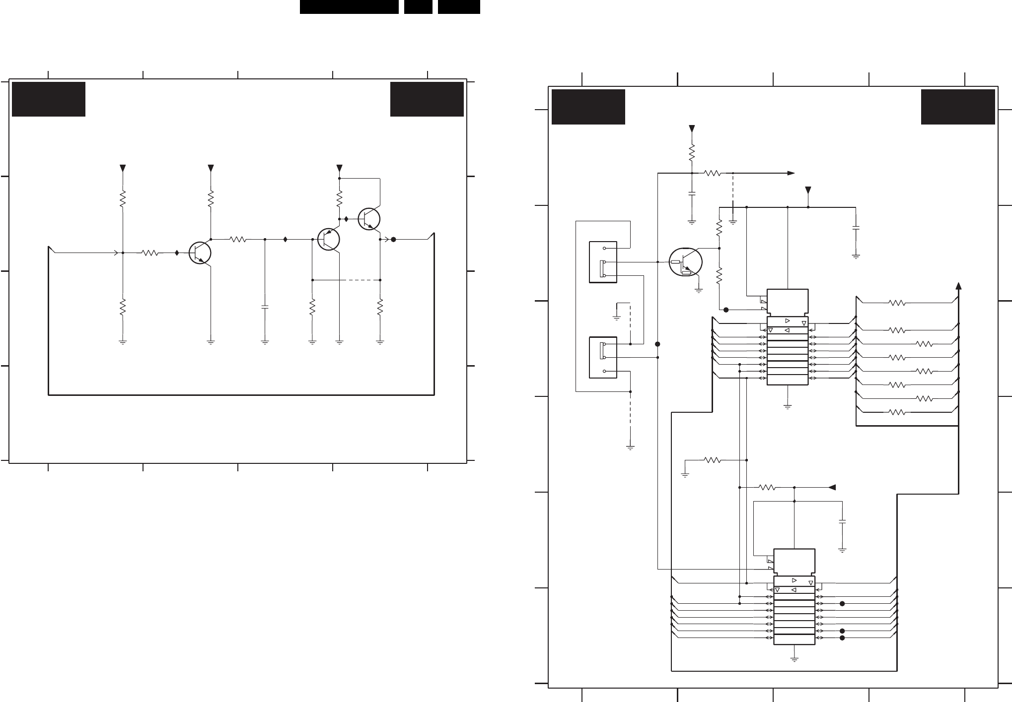
Circuit Diagrams and PWB Layouts EN 45FTL2.4E AA 7.
SSB: Backlight Control
**
*
*
*
*
FC72 B4
IC50 B4
IC51 B3
IC52 B2
B5a *
*
(
*
*
BACKLIGHT CONTROL
*
*
7020 B2
7021-1 B4
7021-2 B4
9019 C4
BACKLIGHT
4
A
D
A
D
2063 C3
3028 B2
3030 B2
3032 B2
3036 B4
3037 C4
3070 C3
)
B4
CONTROL
7021-2
1234
123
B
C
B
C
3022 B1
3023 C1
RES
BC847BPN
BC847BPN
7021-1
2063
100n
RES
10K
3032
3036
4K7
4K7
3030
7020
BC847BW
4K7
3028
2K2
3023
1K2
3022
3070
27K
FC72
9019
IC50
IC51
+5V_CON+5V_CON
IC52
3037
RES
+8V_CON
PWM_BACKLIGHT
ANTI-MOIRE
10K
B5B B5B
F_15460_021.eps
070405
8204 000 8482.1
SSB: OTC-Flash
G3
1
2
3EN2
3EN1
G3
1
2
3EN2
3EN1
b5a,c(2x)
b5a,c(2x)
b5a,c(2x)
b5a,c(2x)
b5a,c(2x)
b5a,c(2x)
b5c(2x)
b5c(2x)
3C00 A2
3C01 A2
3C03 B2
3C04 D2
3C05 D2
3C06-1 B4
3C06-2 C4
b5a,c(2x)
b5a,c(2x)
b5a,c(2x)
FOR SOFTWARE
OTC-FLASH
b5a(3x),c(2x)
b5a(3x),c(2x)
b5a(3x),c(2x)
b5a,c(2x)
A
B
C
D
E
F
1402 C1
1404 B1
2C00 A2
2C01 B3
2C02 E3
B5a,c
SWITCH
3V3
b5a,c(2x)
b5a,c(2x)
b5a,c(2x)
1234
A
B
C
D
E
F
3V3
b5c(2x)
b5c(2x)
b5a,c(2x)
DOWNLOAD
b5a,c(2x)
b5a,c(2x)
b5a,c(2x)
b5c(2x)
b5a,c(2x)
b5a,c(2x)
1234
b5a,c(2x)
b5a,c(2x)
b5a,c(2x)
b5a,c(2x)
b5c(2x)
b5a(3x),c(2x)
3C06-3 C4
3C06-4 C4
3C07-1 C4
3C07-2 C4
3C07-3 C4
3C07-4 D4
3C08 B2
7017 B1
7018 B3
7019 E3
9C00 A2
9C01 C1
9C02 D1
FC62 F3
FC63 F3
FC64 F3
FC65 C1
FC71 C2
b5c(2x)
SWITCH
0V1
b5a(3x),c(2x)
SWITCH
b5a,c(2x)
3C01
10R
b5a,c(2x)
b5a(3x),c(2x)
3C00
2K2
470R
3C05
3C04
10K
3C06-1
10R
3C03
10K
+3V3_INTOTC
10R
3C07-2
FC71
FC63
19
20
18
17
16
15
14
13
12
11
1
10
2
3
4
5
6
7
8
9
7019
74LVC245APW
9C02 9C01
7017
PDTC144EU
2C01
100n
10R
3C07-1
2C02
100n
2C00
100n
FC62
3C08
10K
11
1
10
19
20
6
7
8
9
18
17
16
15
14
13
12
74LVC245APW
7018
2
3
4
53C06-4
10R
10R
3C06-3
SSSS8
1402 3C06-2
10R
FC65
FC64
3C07-4
10R
10R
3C07-3
+3V3_INTOTC
+3V3_INTOTC
9C00
1404
SSSS8
EP_WE
SW_WE
SW_CS
SW_OE
EP_CS
EP_OE
VCCW
VCCW
WP
WP
WE
RAM_CS
RAM_OE
ROM_CS
ROM_OE
VPP-SW
VPP-EPG
SW_WE
EP_WE
EP_CS
SW_OEROM_OE
ROM_CS
RAM_OE
RAM_CS
WE
SW_CS
EP_OE
VPP-EPG
VPP-SW
EAn
VPP-EPG
VCCW
WP
WP
WE
RAM_CS
RAM_OE
ROM_CS
ROM_OE
VPP-SW
SW_WE
EP_WE
EP_CS
EP_OE
SW_CS
SW_OE
B5C B5C
F_15460_022.eps
080405
8204 000 8482.1
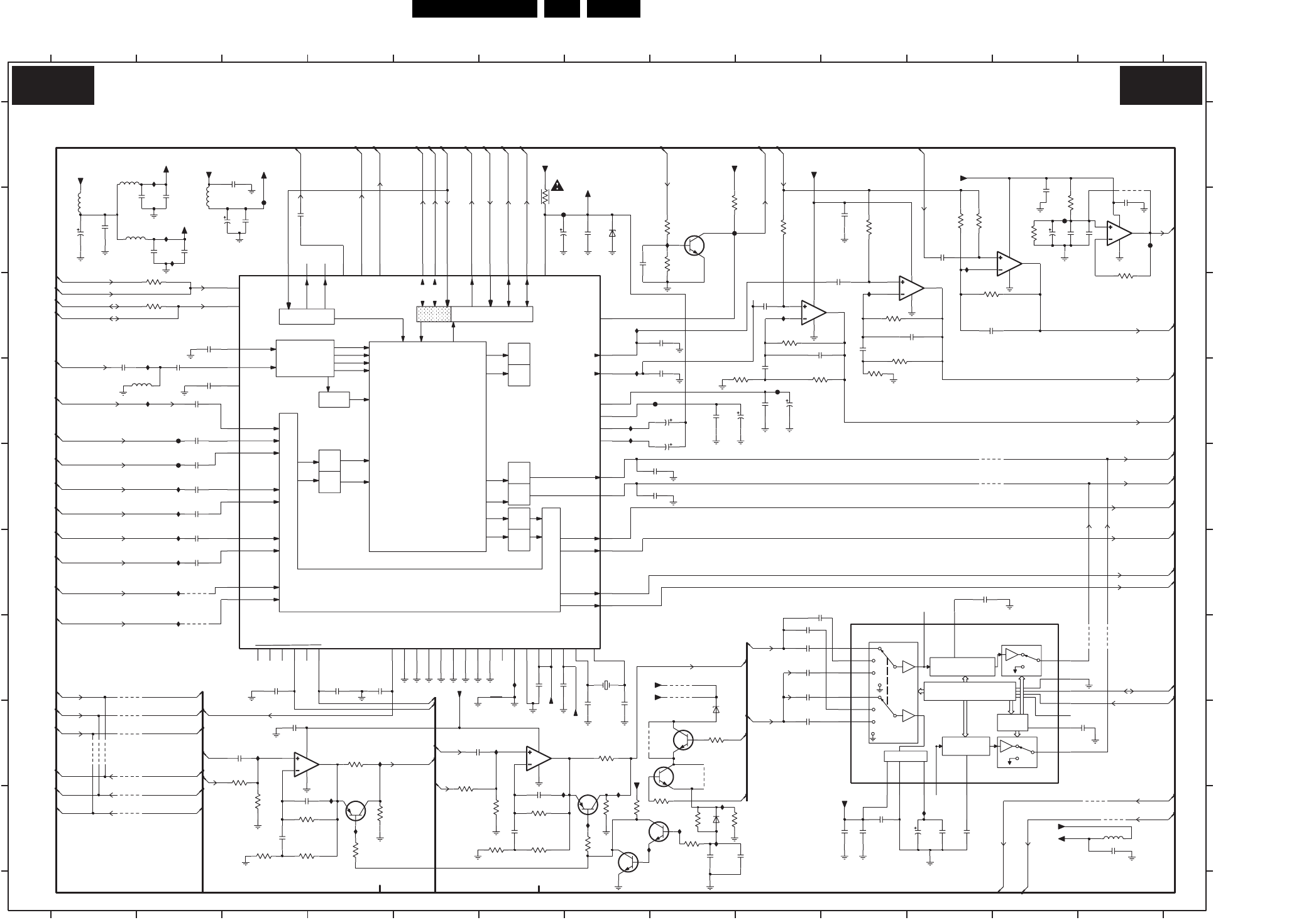
EN 46FTL2.4E AA 7.
Circuit Diagrams and PWB Layouts
SSB: Audio Demodulator
interface
FM2
I2S
FM1 S1...4
interface
SCART-L
HEADPHONE L
NC
HEADPHONE R
HEADPHONE
IDENT
DSP
IDENT
LOUDSPEAKER
SCART 4
Switching Facilities
SCART
LOUDSPEAKER R
LOUDSPEAKER L
D/A
D/A
I2SL/R
I2SL/R
NICAM B
NICAM A
ADR
DEMODULATOR
D/A
D/A
D/A
D/A
A/D
A/D
SCART 1
SCART 2
MONO
SCART-R
SCART 3
SCART-R
SCART-L
B15b,c
IA25 B2
IA35 D7
IA36 E7
IA40 I8
IA41 I8
IA42 I7
IA43 I6
IA46 I8
IA47 I8
IA48 I4
IA49 I4
cA01 G6
FA27 E2
FA28 B3
IA00 H3
IA01 H6
B6a
IA08 D7
IA09 G6
IA10 A2
IA12 B2
IA13 E2
IA14 E2
IA15 F2
IA16 F2
IA17 F2
IA18 G2
IA21 I11
IA22 B8
IA23 D2
IA24 D2
9A04 H1
9A05 H1
9A06 H1
9A07 G8
B2(2x)
6V5
C(3x)
B14c,B15b
B6a
B3a
B6b,d
9A15 I1
9A16 I13
9A17 I13
9A18 B13
9A67 F2
9A71 G2
9A78 H7
9A79 H8
FA12 B12
FA13 B7
FA14 B8
FA17 B13
FA23 D9
FA24 D8
FA26 D2
6A01 I8
6A02 H8
7A00-1 B12
7A00-2 B13
IA02 H4
IA03 I7
IA04 B11
IA05 C10
IA06 C9
IA07 C7
B14b,d(2x)
B2
7A07-1 H3
7A07-2 H6
7A08-1 I7
7A08-2 I7
7A09 I4
7A31-1 H8
7A31-2 H8
9A00 E11
9A01 E11
9A02 G13
9A03 G13
3A48 I4
3A49 I3
3A51 I6
3A52 I3
9A08 G8
9A10 G1
9A11 H1
9A12 H1
9A13 H1
9A14 I1
B6a(3x),C(3x)
B6a(3x),
3A64 I8
3A65 I8
3A66 C9
5A00 A1
5A01 B2
5A02 B1
5A03 B1
5A06 I13
5A19 D2
6A00 B7
3A15 B12
3A16 B13
3A17 C2
3A18 C11
7A01 B8
7A02 B3
7A03-1 C9
7A03-2 B11
7A04 I7
7A06 G10
B14c,B15b
B6b
B6c
*
B6c
B6a
B6d
*
3A26 D9
3A27 D10
3A28 D9
3A40 I6
3A45 H3
3A46 I3
3A47 H5
2AA9 H7
2AB0 H7
2AB2 G4
2AB3 H3
3A53 I6
3A55 I4
3A60 I6
3A61 I7
3A62 I7
3A63 H7
3A01 B8
3A03 B6
3A04 H4
3A05 H8
3A06 I7
3A07 I8
3A09 B8
3A11 B12
3A12 B11
3A13 B9
3A14 B10
2A72 G9
2A74 G9
2A75 H9
2A76 H13
3A19 C2
3A20 C10
3A21 B11
3A22 I3
3A23 C10
3A24 I8
B3a
B14b,d(2x)
B14c
B14c,B15b B21
B6a,b,c
B14c,B15c
B5a,B14b
B6b,d
3V6
B15b,c
2A90 I11
2A91 I3
2A92 I6
2A95 I13
2A99 I3
2AA5 I6
2AA6 G6
2AA7 G6
2A37 D2
2A39 D2
2A40 D9
2A41 D9
2AB4 H5
2AB5 D8
2AB6 G4
2AB7 G3
2AB8 B12
3A00 B8
B6a,b,c
B6a,b,c
B2
B6c,B21
2A50 E8
2A51 I9
2A53 E2
2A54 E8
2A56 E2
2A59 F2
2A62 F2
2A64 F11
2A66 F9
2A69 G9
2A70 G9
B2
2A15 B12
2A16 B12
2A17 B7
2A79 H3
2A80 I10
2A81 I10
2A83 I10
2A88 I11
2A89 I11
B14d(2x)
AUDIO DEMODULATOR
B15b
B6a
B6c
B6a
B6a
2A26 C10
2A27 C8
2A29 C2
2A30 C11
2A31 D9
2A32 D1
2A33 D2
2A35 D8
2A36 C9
2A03 B2
2A04 B3
2A05 B1
2A06 B1
2A42 D8
2A43 D8
2A44 D8
2A46 D2
2A47 I8
2A49 E2
B6a,b,c
3V6
B6a,B14d(2x)
B14d
B21
6V3
B
C
D
E
2A18 B6
2A20 B11
2A21 B7
2A22 C10
2A23 C9
2A25 C11
B14b
B14b(2x)
nc
B6c,B21
B6c
0V
6V5
2A01 B2
2A02 B2
345
2A07 B2
2A08 B2
2A09 B3
2A10 B13
2A11 B10
2A14 B13
5V2
B2 , B3a
5V2
*
*
*
B15b,c
12 13
A
6789
F
G
H
I
A
B
B6a,B14d(2x)
B6a,B14d(2x)
B14d
B6c
B2 , B3a
B6c
6V5
C
D
E
F
67891011
B3a
3V9
B14c
5V2
B6b,c
B14c,B15b,c
4V2
B14b(2x)
12345
*
B6a,B14d(2x)
B6c,B21
10 11 12 13
12
B6a(3x),C(3x)
B14d
B6A(3X)B6C(3X)
2V7
G
H
I
1A00 G7
1A01 G7
2A00 A3
B14d(2x)
IA48
IA47
LM833D
7A03-2
5
6
7
8
4
IA49
3A62
100K
1u0
2A69
1n0
2A17
5A06
9A06
100p
2A36
1n0
2A06
9A04
2
1
8
4
100n
2A16
1
LM833D
7A03-1
3
VS
16
BC847BS
7A08-1 2
6
LOUDL
LOUDR
12
2
OUTL
9
OUTR
1
RECL
RECR
10
5
SCL
4
SDA
CSM
6
DGND
17 IN1L
14 IN1R
18 IN2L
13 IN2R
20 IN3L
11 IN3R
19
MUTE
8
ADDR
AGND
7
CREF
15
3
7A06 TDA7309D-TR
SOFT
+ LATCHES
SERIAL BUS DECODER
LOUDNESS
VOLUME+
LOUDNESS
VOLUME+
SUPPLY
INPUT
SELECTOR
MUTE
MUTE
2A47
1u0
7A07-1
MC33178D3
2
1
8
4
IA43
IA41
GND-AUD
IA42
BC847BS
7A08-2 5
3
4
9A71
IA05
1u0
GND-AUD
1u0
2A99
2A62
3A23
68K
FA27
IA13
FA26
3A14
47K
47K
3A13
47K
3A47
3A52
56K
2A07
1n0
3A17
100R
2A14
1n0
3A21
27K
2AA7
1n0
IA36
+5VF
2A90
22u
100n
2A40
9A67
1n0
2A50
FA17
2A92
1u0
9A05
53 TESTEN
56 TP
27 VREF1
19 VREF2
46
VREFTOP
54 XTAL-IN
55 XTAL-OUT
+5V
42 SC2-IN-R
26SC2-OUT-L
25SC2-OUT-R
38 SC3-IN-L
39 SC3-IN-R
35 SC4-IN-L
36 SC4-IN-R
63 STANDBYQ
13 NC5
24 NC8
16
RESETQ
44 SC1-IN-L
45 SC1-IN-R
29SC1-OUT-L
28SC1-OUT-R
41 SC2-IN-L
5I2S-DA-O1
4I2S-WS
15
I2S-WS3
47 MONO-IN
58 NC1
59 NC2
64 NC3
22 NC4
11 DVSS
10 DVSUP
1I2C-CL
2I2C-DA
3I2S-CL
14
I2S-CL3
6I2S-DA-IN1
12I2S-DA-IN2
32
CAPL-M
61
D-CTR-IO0
60
D-CTR-IO1
18DACA-L
17DACA-R
21DACM-L
20DACM-R
23 DACM-SUB
52 ANA-IN2+
43 ASG0
40 ASG1
37 ASG2
57
AUD-CL-OUT
48 AVSS
49 AVSUP
30
CAPL-A
7ADR-DA
62 ADR-SEL
8ADR-WS
34
AGNDC
33 AHVSS
31
AHVSUP
51 ANA-IN-
50 ANA-IN1+
7A02
MSP4450
9ADR-CL
3A65
1M0
IA23
IA24
6A02
BZX384-C3V3
6A01
BAS316
5
6
7
8
4
1u0
2A04
LM833D
7A00-2
100u
2A15
2A35
1n0
2AB2
1n0
+5DB
100p
2A32
3A28
100n
4K7
9A02
2A88
1u0
2AB3
IA06
100n
2A21
9A17
9A18
3A61
330R
IA04
IA21
1n0
2A27
MC33178D
7A07-2
5
6
7
8
4
9A13
2A10
100n
IA15
9A10
2A05
100u 16V
47K
3A45
10u
2A43
2A72
1u0
9A11 1u0
2A74
10u
2A41
1n0
2AA6
2A75
1u0
1n0
2A81
9A15
2A70
1u0
3A27
4K7
2A80
1u0
IA17
1u0
2A89
3A09
22K
3A12
47K
GND-AUD
GND-AUD
BC857B
7A04
100u
9A00
2A18
100n
9A14
2A11
100n
2A23
330R
3A55
2A49
2AB6
1n0
1u0
2AA5
2AB8
1u0
100p
100n
2A79
2A03
100u
100n
2A83
+11V_S
GND-AUD
2A51
1u0
100n
2A76
2A25
2A53
100p
1u0
3A24
180R
3A40
9A01
+11V_AUD
47K
33K
3A18
GND-AUD
2A54
1n0
100p
2A30
3A03
6R8
3A64
1u0
2A08
47K
100n
2A22
+5V
3A06
100K
3
4
22K
3A05
6
1
7A31-2
BC847BS
5
7A31-1
BC847BS
2
+8VC
GND-AUD
IA16
+5DA
+11V_AUD
+8V
FA14
FA23
IA22
IA18
IA09
IA00
2A09
10n
2A64 100n
FA24
+5V
5A01
IA02
GND-AUD
IA03
IA14
1n0
2A01
3A01
2K2
100K
2AA9
3A11
3p3
3A48
100K
IA01
FA12
IA12
FA28
IA10
100K
3A63
IA08
1A01
18M432
DSX840GA
IA07
IA35
68K
100K
3A04
3A26
FA13
2AB7
1n0
9A12
5A00
1n0
2A00
GND-AUD
3A22
2A44
100n
4K7
100K
3A46 3A49
47K
100K
3A07
9A78
9A79
100K
3A66
56K
3A53
3p3
2A59
1u0
2AB0
1u0
2A56
16V
10u
2A42
5A03
BC857B
7A09
+11V_AUD
+5V
+5DB
cA01
2AB4
1u0
10u
16V
2AB5
7A00-1
LM833D
3
2
1
8
4
IA46
BC847BW
7A01
2A37
100p
1u0
2A26
3A19
9A08
+11V_AUD
100R
9A07
2A33
220p
2A95
100n
+8VC
3A51
3A15
100K
4K7
2A02
9A16
1u0
1u0
2A31
3A16
100R
3A20
100K
5A19
IA40
22u
3A00
22K
1u0
2A46
1u0
2A39
1u0
2A66
9A03
5A02
IA25
100K
3A60
2A91
100p
100p
2A20
2A29
6A00
PDZ10-B
1u0
SYS-RESET
SNDL-MON-OUT
SNDR-MON-OUT
SNDL-SC1-OUT-DC
SNDR-SC1-OUT-DC
I2S-MSP-CLK
I2S-MSP-IN
I2S-DPL-OUT
I2S-MSP-OUT
I2S-MSP-WS
I2S-DPL-CLK
I2S-DPL-WS
REG-SW
SUBW-SPI-SW
SCL-F-AUD
SDA-F-AUD
SCL-F-AUD
SDA-F-AUD
MSP-CENTER
MSP-SURR
+5DA
DACM-SUB
+5DB
POR
SYS-RESET
REF-AUD
AUDIO-R
AUDIO-L
QSS_AM
V-PIP+MAIN-OUT
U-PIP+MAIN-OUT
Y-PIP+MAIN-OUT
SNDL-SEC-IN
SNDR-SEC-IN
HEADPHONE-L
HEADPHONE-R
+5DA
SNDR-MAIN-IN
SNDL-MAIN-IN
SNDR-SC2-IN
SNDL-SC2-IN
SNDR-SEC-IN
SNDL-SEC-IN
HPN-L
SCL-F
HPN-R
SND-CENTER-IN
RESET-AUDIO
AUDIO-SW
IN-Y50
IN-U50
HA50-PIP
HA50
VA50
VA50-PIP
DACM-SUB
HPN-R
SNDR-DVI-IN
SNDL-DVI-IN
HPN-L
REF-AUD
REF-AUD
SDA-F
SYS-CLK0
REF-AUD
Y50
U50
V50 IN-V50
V-PIP+MAIN-IN
Y-PIP+MAIN-IN
U-PIP+MAIN-IN
B6A B6A
F_15460_023.eps
070405
8204 000 8477.1
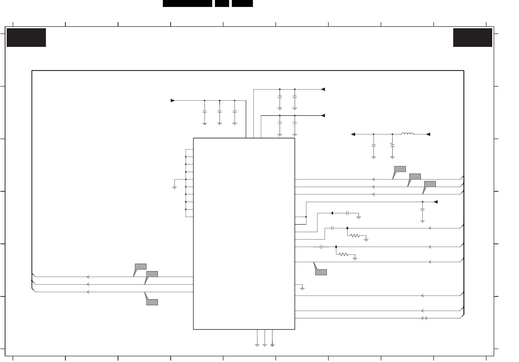
Circuit Diagrams and PWB Layouts EN 47FTL2.4E AA 7.
SSB: Dolby Digital Decoder
B6a,d
B6a(2x),C
AND
DOLBY DIGITAL
DOLBY DIGITAL DECODER
B
C
D
E
F
2AC1 B4
MPEG-1 LAYER-2
B6c
123456789
12345
B6a
B14b
B6a(2x),C
AUDIO DECODER
B6c
2AD3 B4
2AD4 B6
2AD5 B5
2AD6 B6
2AE2 D8
678
B6a,d
3V1
B6a,C
7A30 B4
IA71 D7
IA72 D7
IA75 D7
9
A
B
C
D
E
F
A
B6c
B14b
2AD0 B6
2AD1 B6
2AE3 D7
2AE5 D7
2AF0 E6
2AF3 C8
2AF4 C7
3A74 D7
3A77 E7
5A38 B8
B6c
4V9
100n
2AF4
220p
2AC1
3A74
75R
2AD0
1n0
2AD5
1n0
+5M
75R
3A77
2AD4
1u0
1u0
2AD3
2AF0
10n
+5M
1n0
2AD6
23
XVDD
22 XVSS
43 _EOD
36
_PCS
5
_POR
42 _RTR
41 _RTW
40
SPDI_2
39
SPREF
44 SYNC
6
TE
2
VDD
1VSS
9
XTI
10
XTO
25 SOC
27 SOD
14 SOD1
15 SOD2
16 SOD3
26 SOI
17 SPDIFOUT
38
SPDI_1
4
SCL
3
SDA
19
SIC
32 SIC_PI16
21
SID
30 SID_PI14
20
SII
31 SII_PI15
28 PI12
29 PI13
33 PI17
34 PI18
35 PI19
18 PI4
24 PI8
37
PR
8
AVDD
7AVSS
13 CLKO
11 NC1
12 NC2
7A30
IC MAS3528E
IA75
A8
+5M
5A38
2AD1
1u0
A2
+5M
100u
2AF3
10n
2AE5
1n0
2AE2
IA71
IA72
+5V
+5M
2AE3
10n
A4
SCL-F-AUD
SDA-F-AUD
I2S-MSP-CLK
I2S-MSP-OUT
I2S-MSP-WS
SYS-CLK1
SYS-RESET
A5
SPDIF-IN1
SPDIF-BO-OUT
I2S-DD-OUT
I2S-DD-CLK
I2S-DD-WS
A3
A6
A7
B6B B6B
F_15460_024.eps
070405
8204 000 8477.1
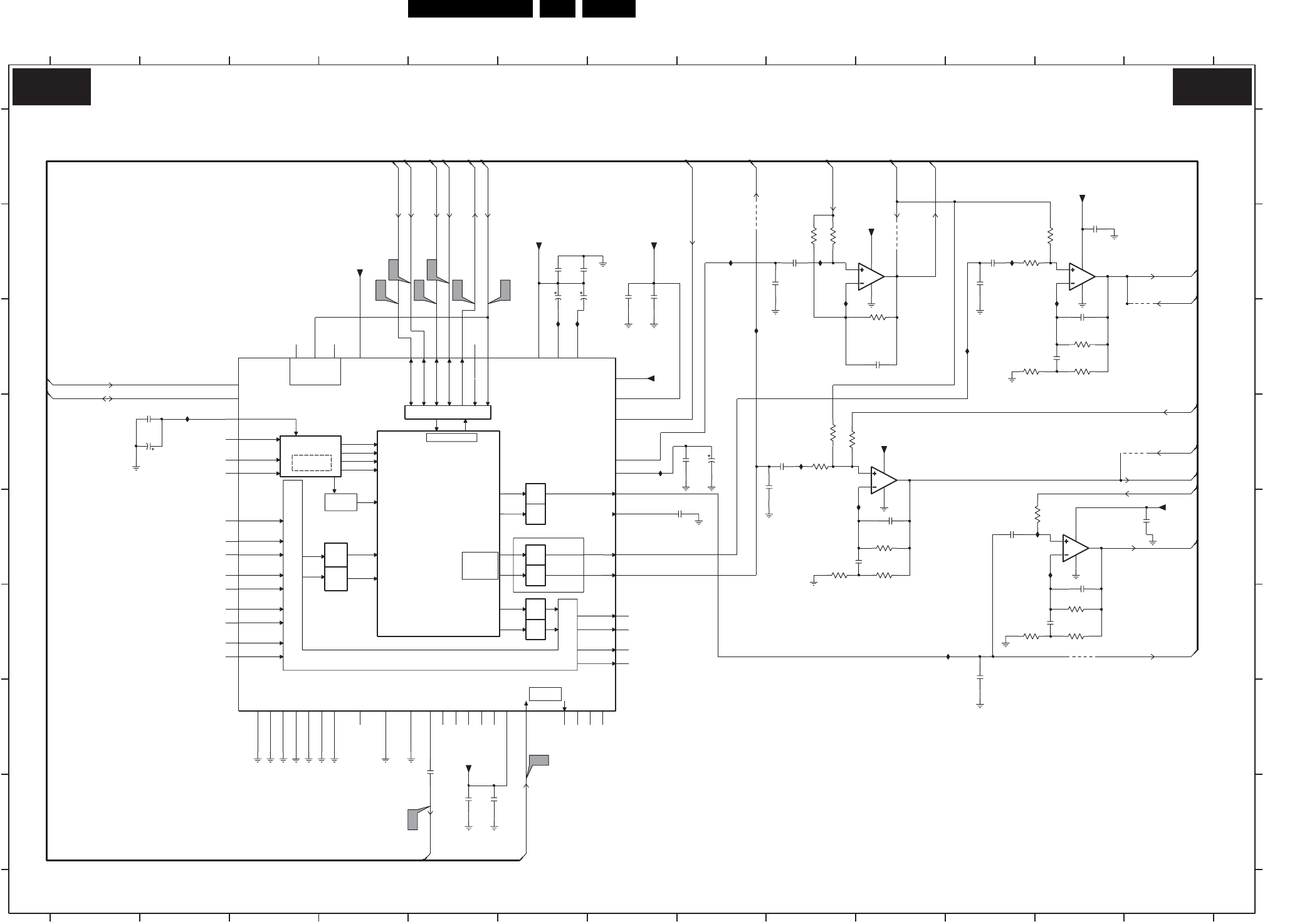
EN 48FTL2.4E AA 7.
Circuit Diagrams and PWB Layouts
SSB: Dolby Pro Logic Processor
LOUDSPEAKER R
D/A
SCART-R
SCART
D/A
SCART-L
HEADPHONE L
FM2
SCART 3
D/A
IDENT
LOUDSPEAKER
DEMODULATOR
NICAM B
NICAM A
HEADPHONE
SCART 1
AUDIO PLL
A/D
DECODER
NICAM
Switching Facilities
IDENT
HEADPHONE R
SCART-L
SCART-R
D/A
SCART 4
A/D
SCART 2
D/A
LOUDSPEAKER L
D/A
DSP
I2SL/R
I2S INTERFACE
I2SL/R
FM1
7 8 9 101112
6V5
B6a
B6b
6V5
2AK2 B7
2AK3 B7
2AK4 B6
2AK5 B6
2AK6 D2
B
C
13
A
2AK7 D2
2AK8 B6
2AK9 B6
2AL0 B12
2AL1 B9
2AL2 B11
B6b
9 10111213
123456
6V5
B6a,B21
B6a
G
H
2AK0 G5
2AK1 G5
D
E
F
G
H
A
B
C
D
E
F
B21
6V5
B6a,B21
B6a
B6a(4x),C(2x)
12345678
2AM0 C10
2AM1 E13
2AM2 E11
2AM3 E7
2AM5 D9
2AM6 F12
2AM7 D8
2AM9 E12
2AN0 E9
2AN1 E10
2AN5 D7
B6a
0V2
B6b
2AN6 D8
2AN7 G5
3AA0 B9
3AA1 D9
3AA4 C10
3AA5 C12
B6b
B6a,b
2AL3 B9
2AL4 B11
2AL8 C12
2AL9 C12
2ALA F11
3AA6 B9
3AA7 C12
3AA9 C11
3AB0 E11
3AB2 D9
3AB3 F12
3AB4 D9
3AB5 F12
3AB6 E10
3AB7 F11
3AB8 E10
3AB9 E9
3AC0 B12
3AC1 B11
7A61-A B12
7A61-B B10
B14b,e
B6a
IA52 B9
IA53 E12
IAA1 E12
IAA2 B8
IAA3 E9
IAA4 C9
IAA5 D2
B14b,e
B14b
B6a
IAB1 C9
IAB2 C12
B6a,B21
B6a(4x),C(2x)
DOLBY PRO LOGIC PROCESSOR
3V8
7A62-A E12
7A62-B D10
7A63 C3
9A19 C13
9A20 D13
9A60 B8
9A61 F12
9A65 B10
IA50 D9
IA51 B11
B6a(2x),b
B6a(4x),C(2x)
B6a(2x),b
IAA6 C11
IAA7 F11
IAA8 C6
IAA9 C7
IAB0 D7
+11V_AUD
2AL0
100n
IAB1
+8VC
9A65
2AM0
100p
+11V_AUD
2AK3
1n0
IAA9
1n0
2AK1
2AM6
100n
2AL9
100p
IAA4
3AB7
IAA7
6K8
4K7
3AB9
A15
A14
9A20
9A19
XTAL_IN
55 XTAL_OUT
47K
3AB4
SC4-IN-L
36 SC4-IN-R
63
STANDBYQ
53 TESTEN
56 TP1
27 VREF1
19 VREF2
46 VREFTOP
54
SC1_OUT_L
28SC1_OUT_R
26SC2-OUT-L
25SC2-OUT-R
41 SC2_IN_L
42 SC2_IN_R
38 SC3-IN-L
39 SC3-IN-R
35
NC2
64 NC3
13 NC4
22 NC5
24 NC6
16
RESETQ
44 SC1_IN_L
45 SC1_IN_R
29
I2S-CL3
6I2S-DA-IN1
12I2S-DA-IN2|3
5I2S-DA-OUT1
4I2S-WS
15I2S-WS3
47 MONO_IN
58 NC1
59
DACM-SUB
21DACM_L
20DACM_R
11 DVSS
10
DVSUP
1I2C_CL
2I2C_DA
3I2S-CL
14
AVSS
49 AVSUP
30
CAPL-A
32
CAPL-M
61 D-CTR-IO0
60 D-CTR-IO1
18DACA-L
17DACA-R
23
AHVSUP
52 ANA-IN2+
51 ANA_IN-
50 ANA_IN1+
43 ASG0
40 ASG1
37 ASG2
57 AUD-CL-OUT
48 9
ADR-CL
7
ADR-DA
8
ADR-WS
62
ADR_SEL
34
AGNDC
33 AHVSS
31
7A63
DPL4519G
2AL4
1n0
A
47K
3AB2
IAA1
IAA5
2AN7
10n
3AA4
47K
IAB2
2AK7
10u
9A61
2AK5
1n0
8
4
+5DA
2AK8
10u
7A62-1
LM833D
3
2
1
1u0
3AA6
6K8
2AL1
2AK4
1u0
1n0
2AM7
1u0
2AK0
3AC1
18K
+11V_AUD
3AC0
47K
A13
A9
1n0
2AM3
100K
3AB6
470n
2AM5
2AM9
IAA3
100p
+5DB
A16
3AA0
47K
7A62-2
LM833D
5
6
7
8
4
9A60
18K
3AA1
GND-AUD
10u
2AK9
68K
3AB8
68K
3AB5
3AA5
100K
IA50
+5DB
2AN0
1u0
+11V_AUD
GND-AUD
100n
2AM1
100n
2AM2
2AN6
10u
100n
2AK6
IAA2
47K
3AB0
100K
3AB3
IA52
IA53
IA51
IAA6
2AK2
1u0
1n0
2ALA
IAA8
IAB0
+5DB
3AA9
4K7
1u0
2AL8
A11
100p
2AN1
4
3AA7
68K
7A61-2
LM833D
5
6
7
8
2AL3
1n0
GND-AUD
2AN5
100n
2
1
8
4
2AL2
470n
LM833D
7A61-1
3
SYS-CLK0
SCL-F-AUD
SDA-F-AUD
I2S-DD-CLK
I2S-DD-OUT
I2S-DPL-OUT
I2S-DD-WS
I2S-DPL-CLK
I2S-DPL-WS
SYS-RESET
MSP-CENTER
MSP-SURR
SUBW
REF-AUD
AUDIO-SW
SURR-R
AUDIO-R
SURR-L
AUDIO-L
REF-AUD
REF-AUD
AUDIO-C
SYS-CLK1
A10
A12
B6C B6C
F_15460_025.eps
070405
8204 000 8477.1
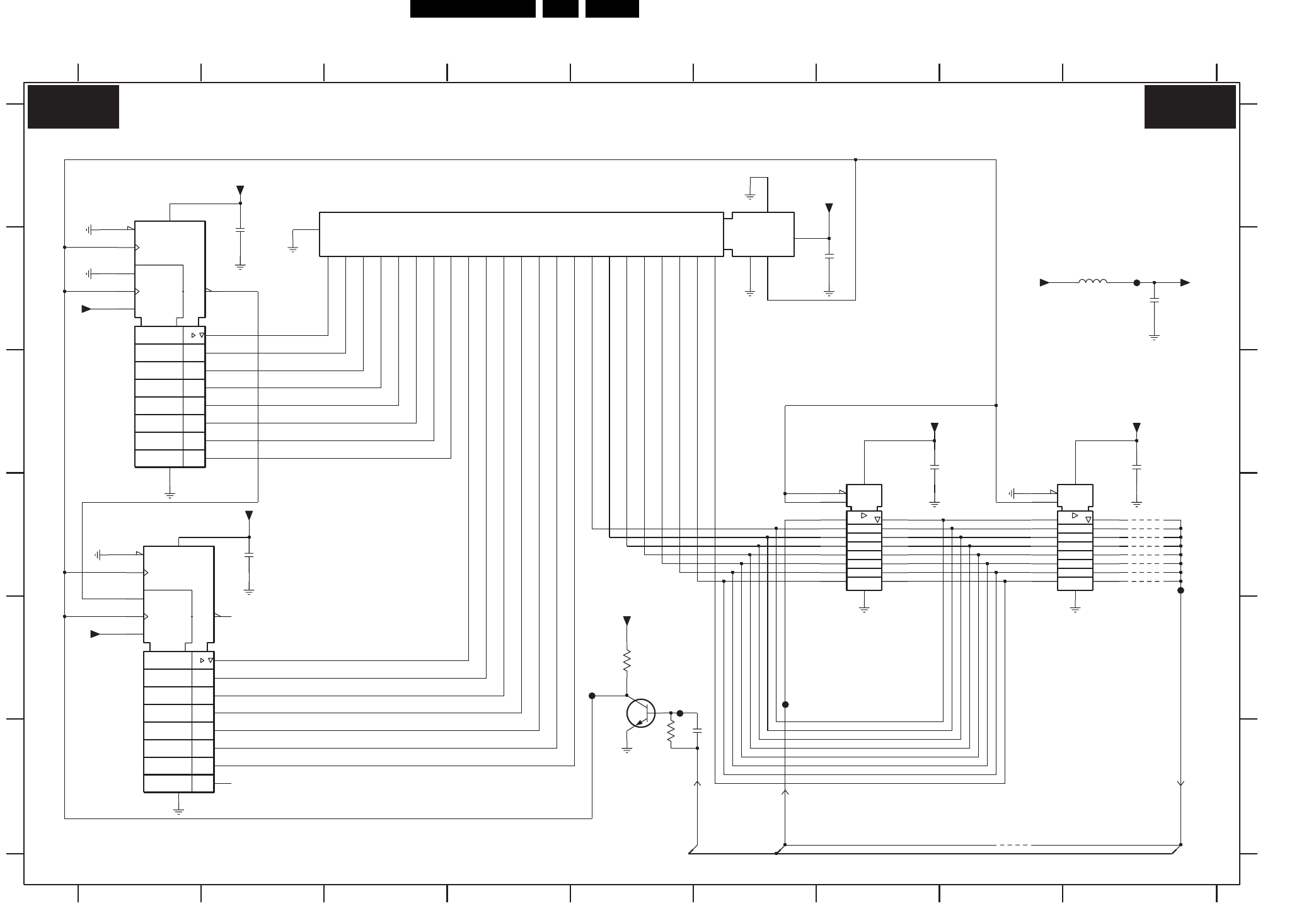
Circuit Diagrams and PWB Layouts EN 49FTL2.4E AA 7.
SSB: Audio Delay
EN
C1
1D
EN
C1
1D
C2
G1
1+
CT=0
CTR8
(CT=255)Z4
2D 3
4
EN3
C2
G1
1+
CT=0
CTR8
(CT=255)Z4
2D 3
4
EN3
2A45 B7
3A02 F5
3A67 E5
5A07 B9
7A11 A1
7A12 D1
B6a,b
B
C
D
E
F
2A12 B2
2A13 D2
2A19 F5
2A24 C7
2A34 C9
2A38 B9
B6a,b
AUDIO DELAY
B6a
12345678 9
1
7A13 E5
7A14 D7
7A15 D9
7A16 A5
2345678 9
A
9A75 D9
FA00 B9
FA01 E5
FA02 E5
FA03 D9
FA04 E6
B
C
D
E
F
A
47K
9A21 D9
9A22 D9
9A23 D9
9A24 D9
9A25 F8
9A72 D9
9A73 D9
9A74 D9
+5D
3A02
+5D
FA00
2A38
1u0
9A23
FA04
3A67
470R
1
19
18
17
16
15
14
13
12
20
2
3
4
5
6
7
8
9
10
11
7A14
74HCT573PW
2A19
27p
+5D
100n
2A13
5A07
+5M
2A24
100n
2A12
100n
+5D
9A24
100n
2A34
+5D
FA02
FA01
+5D
9A73
9A72
BC847BW
FA03
7A13
19 I|O7
22 OE_
28
VCC
27 WE_
14 GND
11 I|O0
12 I|O1
13 I|O2
15 I|O3
16 I|O4
17 I|O5
18 I|O6
25 A3
26 A4
1A5
2A6
3A7
4A8
5A9
20
CE_
21 A0
23 A1
6A10
7A11
8A12
9A13
10 A14
24 A2
7A16
CY7C199B-15ZC
9A25
9A74
9A21
+5D
9A75
3
4
5
6
7
13
9
16
+5D
11
12
10
8
14
15
1
2
6
7
13
9
16
M74HC590T
7A12
12
10
8
14
15
1
2
3
4
5
M74HC590T
7A11
11
2A45
100n
19
18
17
16
15
14
13
12
20
2
3
4
5
6
7
8
9
10
11
1
7A15
74HCT573PW
+5D
9A22
I2S-MSP-CLK
I2S-MSP-OUT
I2S-MSP-IN
B6D B6D
F_15460_026.eps
070405
8204 000 8477.1
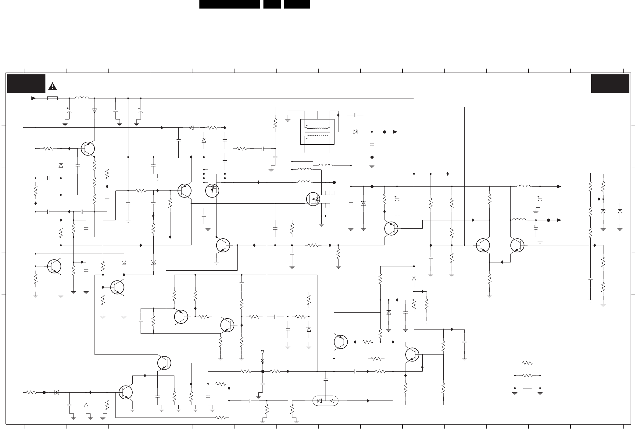
EN 50FTL2.4E AA 7.
Circuit Diagrams and PWB Layouts
SSB: DC/DC Convertor
F
B
C
D
E
F
G
H
1U01 A1
2U01 A8
2U02 B9
2U04 B5
2U05 C2
2U06 C3
1%
12
1V7
1V6
21V4
C
D
E
B3e,B14a,B19b,B13c
678910111213
12345678910 14
A
B
G
H
A
3V4
2U07 C3
2U08 C8
2U09 D6
2U10 A3
2U11 E102U03 B4
2U13 E14
2U14 B5
2U15 A1
2U16 C2
2U17 D5
2U18 B2
2U19 H1
2U20 H4
2U21 B3
2U22 H6
345
0V7
2U27 D2
2U28 E2
2U29 C9
2U30 C1
2U31 D13
2U32 C1
2U33 F10
2U34 G11
2U35 H8
14
2U37 B6
2U38 A3
2U39 F6
2U40 F3
2U41 F7
2U42 E6
3U01 C14
3U02 B1
3U03 C1
3U04 C2
11 12 13
DC/DC - CONVERTOR
3U10 D14
3U11 D4
3U12 G10
3U13 D7
3U14 D1
3U15 D14
3U16 D11
3U17 D7
3U18 E112U12 E7
3U20 E14
3U21 E2
3U22 E12
3U23 E14
3U24 G6
3U25 F2
3U26 H4
3U27 H10
3U28 E1
3U29 C22U23 C13
2U24 G8
2U25 H5
2U26 H6
21V6
3U33 H2
3U34 H4
3U35 H5
3U36 H10
3U37 F9
2U36 B6
3U39 G9
3U40 G9
3U41 H6
3U42 H5
3U43 G6
3U44 D2
3U45 E2
3U46 C10
3U51 A5
3U52 F10
3U05 C3
3U06 C12
3U07 C9
3V4
3U08 C11
3U09 C4
3U57 A6
3U58 G12
3U59 G12
3U60 F4
3U61 F5
3U62 F7
3U63 F6
3U64 F7
3U65 F5
3U19 E8
3U67 G5
3U68 G6
3U69 F6
3U70 C14
5U01 B8
5U02 A2
5U03 B7
5U04 C7
5U05 C12
5U06 D12
3U30 C2
3U31 B2
3U32 H1
6U03 A4
6U04 B5
6U08 E3
6U09 E3
6U10 H1
6U11 H2
6U12 F9
6U13 E10
6U14 H8
6U16 F7
6U17 D14
3U38 G9
7U02 C4
7U03 C7
7U04 C5
7U05 D9
7U06-A D12
7U06-B D12
7U07-1 G10
7U07-2 F8
7U08 D5
7U09 E1
3U53 F10
3U54 H7
3U55 E9
1%
3U56 B6
1%
7U13-1 F5
7U13-2 F4
3U66 F4
FU04 B9
FU05 C8
FU06 G6
FU07 H1
FU08 C9
FU09 D13
IU01 B2
IU02 C1
IU03 D1
IU04 E3
5U07 B8
6U01 A2
6U02 A8
6U05 B1
6U06 C9
6U07 D14
IU11 A5
IU13 D8
IU14 D6
IU15 A8
IU16 C11
IU17 D9
IU18 D11
IU19 C14
IU20 D10
7U01 B2
IU22 E12
IU25 H4
IU26 E2
IU27 G3
IU28 H2
IU30 C3
IU31 C2
7U10 G4
7U11 E3
7U12 H3
6V9
1%
IU32 E2
IU34 H6
IU35 G7
IU36 G9
IU37 F8
IU38 G9
IU39 G9
IU40 G10
FU03 B9
IU41 H9
IU42 C6
IU43 E10
IU44 F11
IU45 F9
IU46 F5
IU47 F6
cU01 H12
IU21 D14
IU05 D3
IU06 D4
IU07 D4
IU08 C4
IU09 B4
IU10 A4
IU17
420
1%
1K5
3U08
2U08
22u
120R
3U30
GND_SUPPLY
+11V
3U05
1K0
GND_SUPPLY
IU22
18K
3U53
22K
3U39
3U07
IU32
22R
GND_SUPPLY
GND_SUPPLY
1M0
3U44
GND_SUPPLY
7U02
BC857B
3U69
1K0
BC857BW
7U05
2U12
10n
FU08
4
FU03
GND_SUPPLY
7U07-2
BC847BPN
5
3
1n0
2U24
GND_SUPPLY
GND
100R
3U67
1K0
3U65
3U66
10K
2U14
470n
22K
3U27
5678
4
123
3U12
22K
GND_SUPPLY
7U03
SI4410DY
6U05
BZX384-C12
2n2
2U37
2U23
100u
BC857B
7U01
PDZ8.2-B
6U13
3U10
1R0
22K
3U26
2K2
3U38
3U34
330K
22R
3U51
res
2U01
2n2
22u
2U06
3U46
47K
GND_SUPPLY
BC817-25
7U09
IU10
IU35
10K
3U42
GND_SUPPLY
3U02
1K0
res
2U29
330u 6.3V
IU42
IU04
1500mAT
1U01
IU36
10u
5U06
GND_SUPPLY
IU34
10K
3U35
3U23
1R0
3U11
120R
GND_SUPPLY
100u
2U31
3U58
1R0
GND_SUPPLY
res
7U08
BC817-25
10K
3U57
GND_SUPPLY
IU30
IU19
3U31
120R
5U04
5U03
IU45
IU43
IU39
2U38
220u 16V
res
120p
2U18
GND_SUPPLY
2U27
6n8
IU02
GND_SUPPLY
IU25
+3V3-ILINK
270R
3U22
470n
2U21
IU08
1u0
2U03
FU04
6U01
BAS316
2K2
3U63
3U60
1K0
3U18
1K0
IU18
IU07
100n
2U36
7U13-1
BC847BPN
BAT54 COL
6U08
3U24
22K
3K3
3U15
100R
3U54 3U13
10K
IU40
22K
3U37
100n
2U19
GND_SUPPLY
5
3
4
GND_SUPPLY
2U25
100n
7U06-2
BC847BS
1K0
3U41
3U40
150K
IU21
IU01
IU14 IU13
5U01
1
10
3
5
6
IU31
res
GND_SUPPLY
GND_SUPPLY
3U45
1M0
3U06
470R
GND_SUPPLY
GND_SUPPLY
6U03
BAS316
BZX384-C5V1
6U12
23
BZG05C3V9
6U06
7U04
5678
4
1
FU05
SI4410DY
IU15
3U32
18K
3U17
4R7
+3V3_DCDCFBX
GND_SUPPLY
IU37
GND_SUPPLY
IU09
1u0
2U20
1K0
GND_SUPPLY
GND_SUPPLY
3U20
10K
3U33
47K
3U21
2
6
1
IU11
BC847BPN
7U07-1
7U11
BC847BW
1K0
3U64
3U68
10K
2U40
2n2
3U62
1K0
GND
6U14 BAV99 COL
2U30
120p
10K
3U61
7U13-2
BC847BPN
cU01
10u
5U07
3U70
1K0
IU28
100n
2U26
7U10
BC847BW
IU38
GND_SUPPLY
res
47u
2U02
IU16
1u0
2U33
IU20
GND_SUPPLY
3U36
2K2
BC847BS
7U06-1
2
6
1
220K
3U25
IU06
4n7
2U16
2U15
100u
GND_SUPPLY
1K0
3U55
3U29
10R
220n
2U13
5U02
10u
FU07
IU03
res
STPS2L30A
6U02
2U05
1n0
82p
2U07
BAS316
6U11
1K0
22K
3U43
3U52
IU46
FU09
IU47
6n8
2U28
4K7
3U19
1R0
3U59
IU27
res
5U05
10u
GND-ILINK
GND_SUPPLY
GND-ILINK
2U22
1u0
GND_SUPPLY
GND_SUPPLY
GND GND
2U39
100n
2U41
6n8
GND_SUPPLY
3U16
120R
GND_SUPPLY
GND_SUPPLY
IU44
3n3
2U32
47n
2U42
4K7
3U56
3U09
5K6
IU26
2U04
470n
2U09
1n0
2U11
1n0
3U14
1K0
6U17
PDZ6.8-B
2U10
22u
GND
+3V3_SIM
6U16
BZX384-C5V1
FU06
GND_SUPPLY
6U10
BZX384-C15
470n
2U17
IU05
6U09
BAT54 COL
22n
2U34
PDZ6.8-B
6U07
3U28
47K
3U04
120R
3U03
33K
7U12
BC847BW IU41
BAS316
6U04
2U35
1u0
1K0
3U01
3V3_FAULT
B12 B12
F_15460_027.eps
070405
8204 000 8480.1
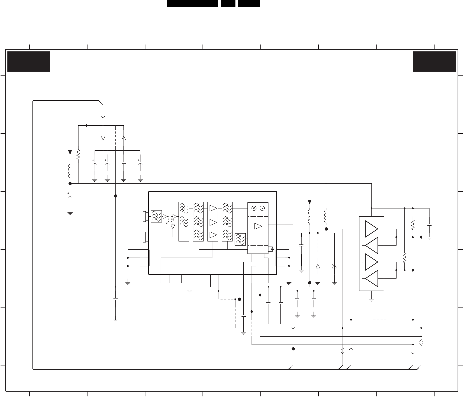
Circuit Diagrams and PWB Layouts EN 51FTL2.4E AA 7.
SSB: Main Tuner
MIX-OSC
PRE-FIL TRACK
FILTER
GAIN
CTRL
PRE-AMP
TRACK
FILTER
RF
MT
OUT
INTMED
FILTER
PRE-FIL BOOSTER
SPLITTER
MT
IN
RF
PLL
AGC
DET
IF AMP
IT51 D4
IT52 D4
IT53 C7
IT54 D7
MAIN TUNER
RES
FT51 C2
FT52 D4
FT53 C6
FT54 D5
B13b
B13b
RES
IT50 A1
5T25 C6
6T01 B2
6T03 B2
6T05 D6
RES
6T08 D5
7T50 C6
9T01 B2
9T04 D4
9T05 E4
9T07 E4
9T08 E4
9T12 E7
9T14 C5
9T50 E7
AT00 E5
FT50 B1
4567
2T01 B2
2T04 C5
2T05 C1
2T06 E4
2T09 D5
2T12 C7
2T13 B2
2T15 D5
2T17 D2
2T60 B2
2T61 B2
2T62 D5
2T63 D5
3T03 B1
3T05 C7
3T06 D7
5T20 B1
5T22 C5
C
D
E
1T01 B3
RES
RES
123
B2
B2
0V5
1234567
A
B
C
D
E
A
B
FT50
2T12
100n
5T22
22n
2T09
9T05
IT53
9T07
3T05
10K
9T04
9T14
AT00
220n
2T62
2T63
220n
9T08
2T17
10n
220u
2T01
FT51
3T03
47n
2T04
FT54
+5V
FT53
10K
3T06
SML4752-33V
6T05
9T50
6T01
BAS316
220u
2T05
2T61
47u 6.3V
2T60
220u 6.3V
IT52
IT51
10n
2T13
PDZ33-B
6T08
BAS316
6T03
2T15
1u0
10u
5T25
FT52
VCC
8
5T20
GND
4
RX 2
RY 6
SX1
SY7
TX 3
5TY
7T50
P82B96TD
IT50
IT54
+33V
9T01
6NC1
NC2
10
SCL
4
SDA5
TU2
9T12
8
AGC1
AS3
IFOUT 11
12
13
14
15
16
17
UV1318ST/AIH-MK3
1T01
933V
5V7
ADC
10n
2T06
S-SDA-PIP
AGC
S-SCL-PIP
SDA-S
SCL-S
IF-TER
B13A B13A
F_15460_028.eps
080405
8204 000 8479.1
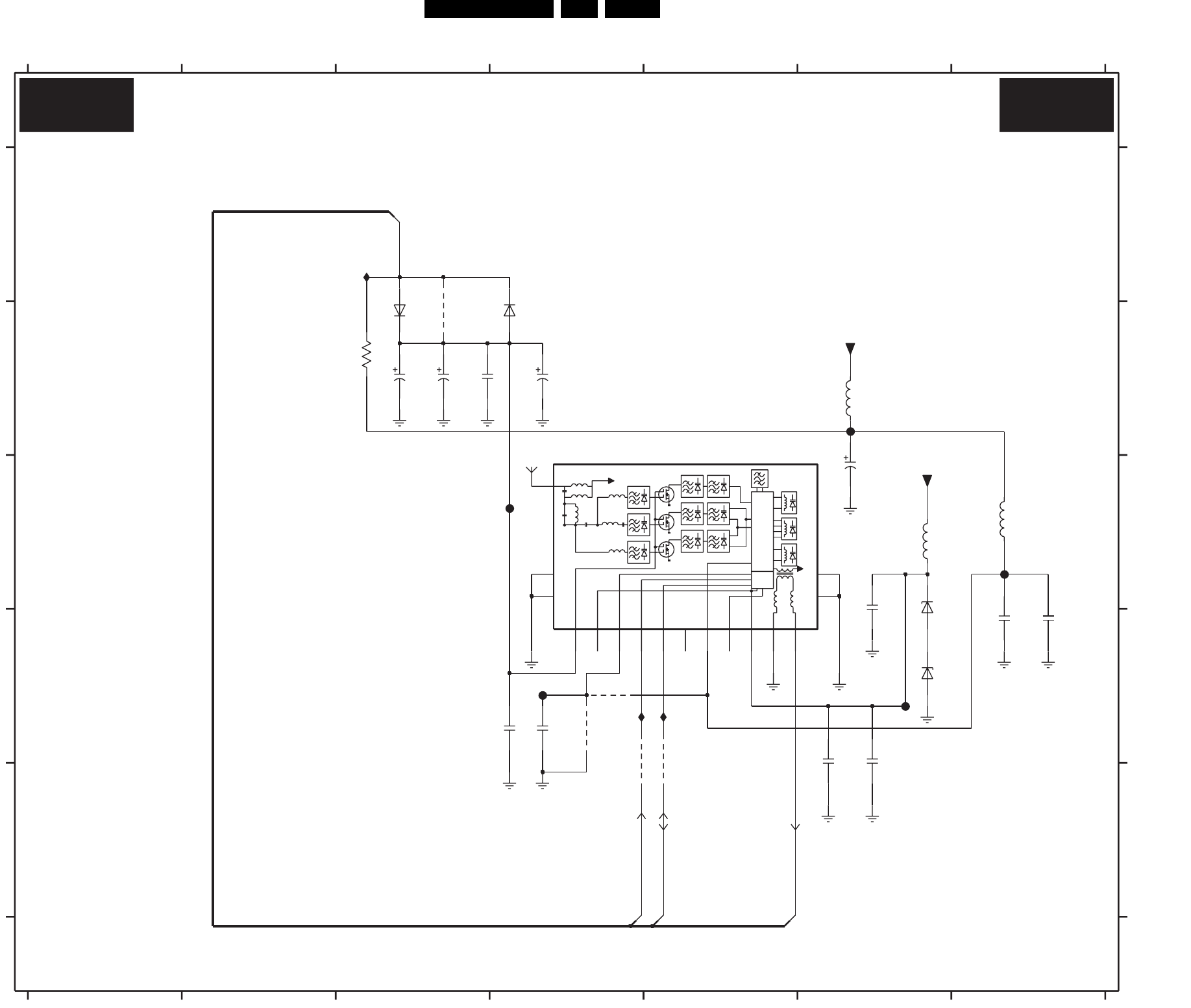
EN 52FTL2.4E AA 7.
Circuit Diagrams and PWB Layouts
SSB: Sub Tuner
M
LL
H
M
H
PLL
FT04 C4
FT05 D6
RES
5V1
33V5
RES
IT10 A3
IT17 B6
IT18 D4
IT19 D5
6T04 B4
6T06 C6
B13a
B15A
RES
RES
9T09 D4
9T10 D5
E
1T02 B4
B13a
SUB TUNER
B15A
IT07 D4
IT09 C7
5T04 B6
6T02 B3
1234567
123
6T07 D6
9T02 B3
9T03 D4
9T06 D4
C
D
4567
A
B
C
D
E
A
B
2T02 C6
2T03 B3
2T07 D4
2T10 D7
2T11 B4
2T14 B3
2T16 D7
2T18 D4
2T19 C6
2T20 B3
2T21 D6
2T22 D6
3T04 B3
5T02 C6
5T03 C7
6.3V47u
2T11
2T19
220u
FT05
2T16
1u0
10n
2T14
9T02
2T22
220n
2T21
220n
IT19
PDZ33-B
6T06
IT10
9T03
9T06
IT18
5T02
+5V
IT09
PDZ33-B
6T07
220u
2T03
5T04
10u
5T03
9T09
47n
2T02
+33V
22n
2T10
IT17
10n
2T07
FT04
2T18
10n BAS316
6T04
6T02
BAS316
2T20
220u 6.3V
10K
3T04
9
9T10
13
MT3 14
MT4 15
NC1
6
SCL4
SDA5
TU2
VS7
VST
UV1318S
1T02
ADC8
AGC1
AS3
IF111
IF2|NC210
12 MT1
MT2
IT07
AGC2
IF-TER2
S-SCL-PIP
S-SDA-PIP
B13B B13B
F_15460_029.eps
080405
8204 000 8476.1
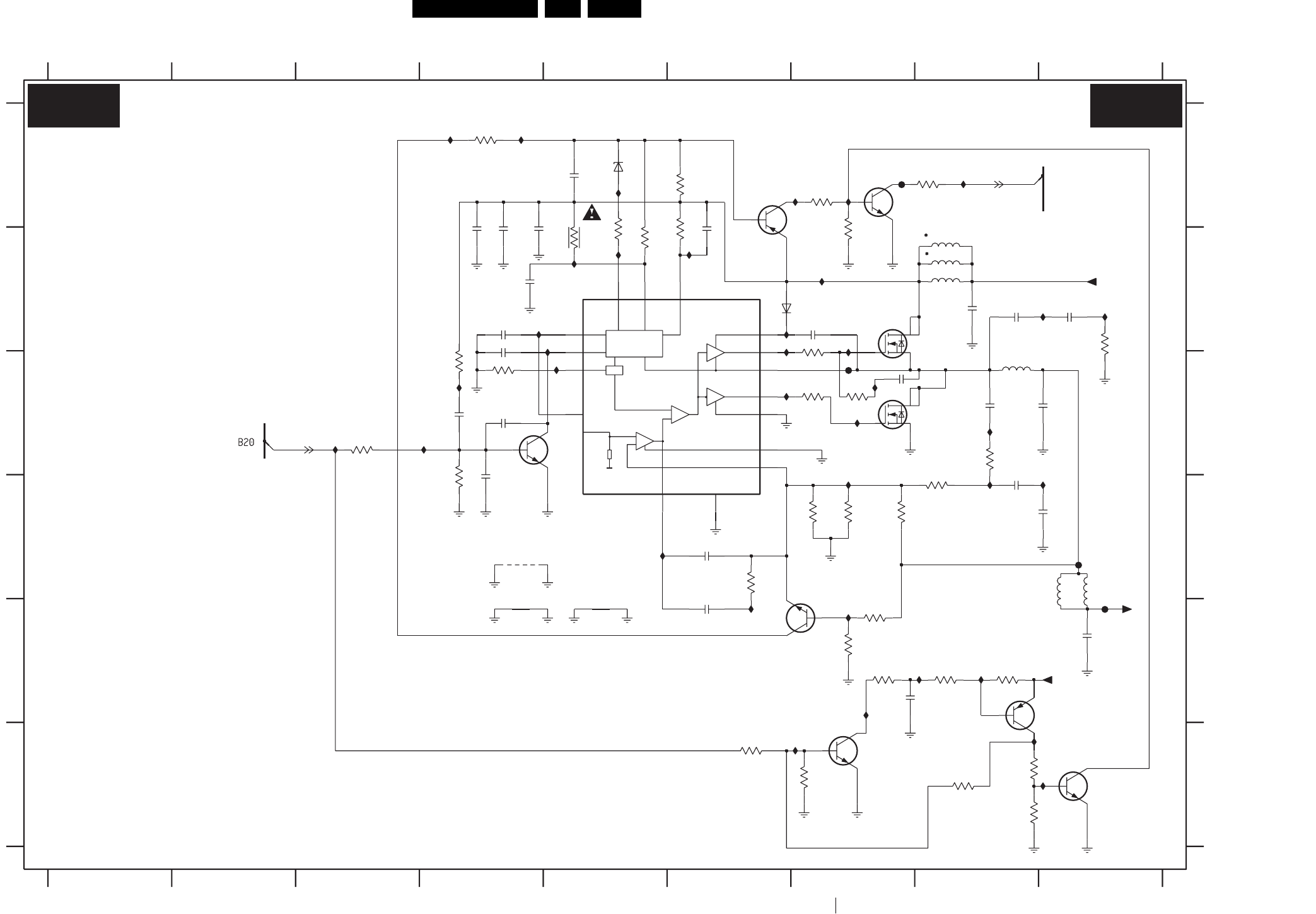
Circuit Diagrams and PWB Layouts EN 53FTL2.4E AA 7.
SSB: DC/DC Converter
OSC
Monitor
Protection & Ref
VREF
SS
OSC
EAREF
COMP
NC
VFB
GND
PGND
LGATE
PHASE
HGATE
BOOT
OCSET
VCC
PGOOD
7T13-2 E8
9T11 D4
FT10 C4
FT11 B7
IT16 A7
IT02 B5
IT04 B5
IT05 B5
IT22 E7
IT23 B9
IT24 B9
3T60 C7
5T10 B8
IT25 A8
IT26 A5
IT30 D5
IT34 B7
IT41 C7
IT32 E6
IT33 C8
IT43 A7
IT44 C4
IT45 B5
IT46 F7
6T11 A5
IT47 E7
IT48 E7
IT60 F9
IT61 F9
IT62 E8
IT63 C7
7T11-2 A6
7T12 F9
7T13-1 F7
3T33 B5
3T51 B5
3T52 F8
3T53 F8
FT12 C7
FT13 D9
FT14 E9
FT15 A7
IT00 A4
IT01 A4
IT20 D8
IT21 C9
DC - DC CONVERTER
IT06 C5
IT08 C3
IT11 B7
IT12 C6
IT13 B7
IT15 C7
3T11 A6
3T12 B6
3T13 B5
3T14 C4
5T11 C8
5T12 B8
5T13 B8
5T14 D9
5T15 D9
6T10 B6
IT42 B6
3T22 D7
3T23 E7
7T01-1 B7
7T01-2 C7
7T04 B5
7T10-1 C5
7T10-2 E6
7T11-1 A7
3T30 A7
3T31 A8
3T32 D8
C
D
E
F
3T54 F8
3T55 E8
3T56 E8
3T57 E7
3T58 F7
3T59 F6
B12
2T53 C7
2T54 A5
3T10 A4
2T41 B8
2T42 C8
2T43 C8
2T44 D8
3T15 C3
3T16 C4
3T17 D4
3T18 D6
3T19 E7
3T20 D7
9
12
3T24 D7
3T25 C8
3T26 C7
3T27 B7
3T28 B9
3T29 B7
9
A
B
A
B
C
D
E
F
2T30 B4
2T31 B4
2T32 B4
2T51 E9
2T52 E7
2T37 D4
2T38 B7
2T40 B8
2T35 B4
2T36 C4
2T49 B6
2T50 C4
2T45 D8
2T46 B9
2T47 D6
2T48 E6
1234 8567
345678
7T10-2
BC847BS
5
3
4
1T03 E4
1T04 E5
2T33 B4
2T34 B4
IT02
4R7
3T60
FT14
GND5V
GND-P
10n
2T45
GND5V
3T33
10R
3K9
3T24
IT46
3T30
10K
470K
3T53
2R2
3T26
3T27
10R
3T32
1K0
330R
IT08
3T19
4
3
3T22
4K7
SI4936ADY
7T01-2
56
7T01-1
SI4936ADY
78
2
1
16
3
2
13
9
10
4
15
6
1
7T04
L6910
12
5
8
7
11
14
3T14
47K
IT47
IT62
IT61
IT48
6T10
BAS316
IT42
IT23
1T03
10K
3T52
IT45
1K0
3T51
47K
3T58
10K
3T59
100R
3T57
IT44
100n
2T54
3T18
2K7
2T36
1u0
2T43
22u
22u
2T31
2T30
22u
10n
2T44
2T42
2T48
100n
22n
IT60
10u
5T11
GND-P
1n0
2T34
GND5V
GND5V GND5V
2
6
1GND-P
FT11
BC847BS
7T10-1
IT01
IT05
IT06
2T40
100n
10K
3T113T12
1K0
3T13
10K
3T20
1K0
10K
3T29
10K
3T15
3T23
1K0
IT63
GND5V
3n3
2T53
FT13
2T51
1u0
VDISP
5T15
5T14
9T11 IT30
3T16
100K
IT11
IT34
3T54
10K
IT12
IT26
IT15
6T11
BZX384-C9V1
10n
2T50
IT04
3T28
10R
1u0
2T52
GND-P
1T04
FT15
5T12
IT22
res
res
5T13
2T37
10n
2T47
470p
4
100n
2T33
BC847BPN
7T11-2
5
3
GND-P GND-P
GND-P
2T38
100n
2T49
1n0
IT13
1n0
2T46
7T12
BC847BW
3T56
10K 10K
3T55
FT10
+11V_DC
10K
3T10
3T31
1K0
BC847BPN
7T13-1
1
7T13-2
BC847BPN
BC847BPN
7T11-1
2
6IT25
FT12
IT43IT16
6K8
3T25
3T17
10K
2T41
1n0
GND5V
+11V_DC
IT20
IT21IT41
IT32
GND5V
100n
2T32
2T35
100n
IT33
IT24
10u
5T10
IT00
3V3_FAULT
5V-ENABLE
B13C B13C
F_15460_030.eps
080405
8204 000 8476.1
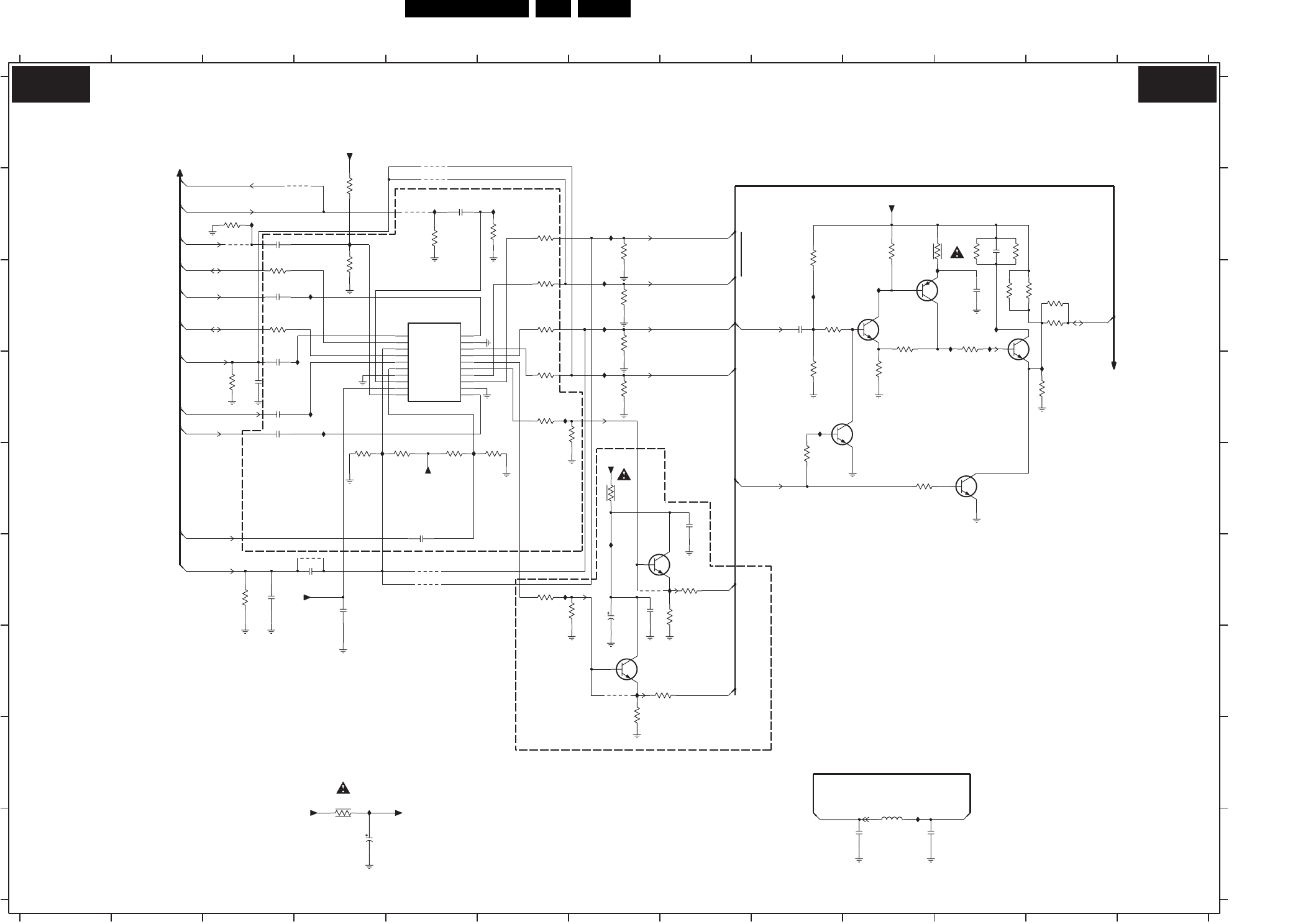
EN 54FTL2.4E AA 7.
Circuit Diagrams and PWB Layouts
SSB: I/O1: MMC
II16 C9
IIC0 I10
IIC1 G7
IIC2 F7
IIC3 F8
IIC4 D12
IIC5 B7
IIC6 B5
IIC7 B3
IIC8 H4
IIC9 C10
IIG1 C11
IIG2 D9
RES FOR MMC
*
*
II02 D4
II03 D3
II04 D4
II05 D5
II06 E6
II07 C7
II08 B6
II09 C7
II10 D7
II11 D6
II12 F6
II13 C11
II14 C10
II15 C11
7I06 F8
7I24 C1
*
*
res
7I24 D5
7I35 D10
7I36 C10
7I37 C11
7I38 C11
7I60 G7
7I62 E11
9I00 A5
9I01 B5
9I02 F5
9I03 F5
9I15 F4
9I20 F7
9I21 G7
9I78 B5
9I95 B4
9I96 B3
II00 C4
II01 B4
3IP3 C12
3IP4 C10
res
B21
TO PIP/DW (HIP SUB)
For US (AV3)
B14b,c
res
3IP5 B10
3IP6 B10
3IP7 C9
3IP8 B11
3IQ0 C11
3IQ1 C11
3IQ2 F8
3IQ3 G8
3IQ4 C11
3IT9 E10
5I01 I10
3I24 E5
3I25 E6
B5a,B14b,B15b
B
B
B2,B14b
RESERVED FOR MMC
B14b
3I26 G7
3I27 F8
3IHG C12
3IJ8 D12
3IK4 D3
3IK5 F3
3IK7 H4
3IK8 E7
3IN1 B11
3IP0 B9
3IP1 D9
3IP2 D10
3I10 B6
3I11 B6
B14b
From Scart 4
I/O1: MMC
From Front
3I12 B7
3I13 C6
3I14 C7
3I15 C6
3I16 C7
3I17 D6
3I18 D7
3I19 D6
3I20 D6
3I21 F6
3I22 F6
3I23 E5
E
F
B15a
B2
B2 B14b,c(2x)
B15a
2IJ3 E8
2IJ4 C11
2IL0 B11
3I01 B4
3I02 C4
3I03 B3
3I04 C3
3I05 C3
3I06 B5
3I08 E9
3I09 E4
12 13
B12
A
B
C
D
E
F
G
H
I
A
B
C
D
910
B14b
B15c
2I08 E5
B21
B2,B14b,c (2x)
B15a
11 12 13
1234567891011
B2
B2
(USA AV3)
23
From PIP/DW
45678
I
2I01 F4
2I02 B3
2I03 C3
2I04 D3
2I05 D3
2I06 D3
2I07 F4
H
2I55 I10
2I56 I10
2IA5 I4
2IA6 F7
2IE0 B5
2IG1 C9
2IJ0 F3
2IJ1 D3
2IJ2 F7
1
*
From HIP MAIN
B2,B14a,B15a
IIC6
G
res
3I03
75R
3IQ4
1K2
II12
3IP1
2K2
3I18
470R
res
3IK8
4R7
75R
3IK4
res
1K0
3I27
II09
3IHG
II10
1K8
1K0
3IJ8
3I13
560R
470R
3I22
res
OUT3
16
OUT4
17
OUT5
18
OUT6
7PROG
9VCC
IN3
6IN4
8IN5
10 IN6 11
IN7
20
IN8
13
OUT1
14
OUT2
15
4CLK
2DATA
12
GND1
19
GND2
1IN1
3IN2
5TEA6415CD
7I24
2IJ0
470p
IIC7
2IG1
100n
+8VA
res 100K
3I01
II08
II13
100u
2IA5
560R
3I11
220n
2IE0
IIC1
res
3IK5
75R
+8V
IIC3
2I06
220n
100n
3I04
100R
2I08
220n
2I02
2
3IP0
8K2
7I60
BC847BW
1
3
IIC0
560R
3I15
II02
+8VA
100K
3I24
res
2I01
100n
68K
3I25
470R
3I20
res
560R
3I17
100R
3I05
IIG2
IIG1
3I16
1K5
res
2I07
220n res
IIC4
BC847BW
7I38
II15
res
10n
2I55
6u8
5I01
3IP2
220R
100R
3I19
IIC5
9I15
2IA6
100u
res
II01
2I56
10n
II04
220n
2I03
2IJ1
100p
res
1K0
3I26
II14
II11
68K
3I02
BC847BW
7I06
3I23
100K
9I00
9I03
3I08
330R
3IP4
270R
3I10
9I21
1K0
II00
II05
4R7
3IK7
+8V
9I95 res
7I37
BC857BW
9I20
res
+8VA
3I14
470R
+8VA
1K2
3IQ1
100n
2IJ2
3I09
68K
II03
7I35
BC847BW
II16
II06
7I36
BC847BW
IIC8
+8VA
75R
3IQ3
9I01
330R
3IT9
BC847BW
7I62
2I04
220n
res
9I96
3IP6
1K0
3IP5
2R2
IIC9
10R
3IQ0
2K7
3IP7
9I02
75R
3I06
2IJ3
100n
470R
3I12
res
IIC2
II07
220n
2I05
9I78
3IQ2
75R
75R
3IP3
2IJ4
100n
3IN1
1K0
1K0
3IP8
10p
2IL0
3I21
100R
C-SC2_SVHS-IN
SC2-B_C-OUT
FRONT-C-IN
Y-CVBS-SC2_AV2-IN
SCL-S
SDA-S
PIP-OUT1
PIP-OUT
C-MMC-OUT
C-RECORD-IN
CVBS-Y-RECORD-IN
Y-CVBS-MMC-OUT
AV3-CVBS-IN
FRONT-Y-CVBS-IN
SC2-FBL
3V3_FAULT 3V3_FAULT_PIP
C-FRONT-IN
C-PIPDW-OUT
Y-CVBS-FRONT-IN
Y-CVBS-PIPDW-OUT
C-FRONT-IN
B14A B14A
F_15460_031.eps
080405
8204 000 8478.1
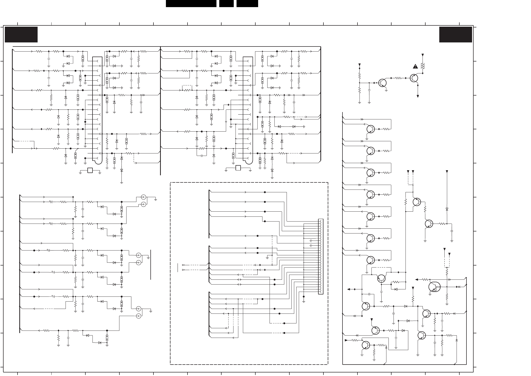
Circuit Diagrams and PWB Layouts EN 55FTL2.4E AA 7.
SSB: I/O2: Connections
8
B14b
SUBWOOFER
B14b(3x)
B
C
D
E
F
G
H
I
J
1I01-1 A3
1I01-2 E3
H
1I02 C6
1I03 D3
1I04-1 A7
1I04-2 E7
1I05 F4
1I06 I4
B14d(2x)
12345678910111213
1234567
1I35 B2
91011
B15a
B14b
B14b
12 13
A
B
C
D
E
F
G
1I49 F4
I
J
A
SURROUND
B5a,B21
B2
B14d(2x)
1I08 D4
1I09 H4
1I11 F9
1I34 A2
2I22 A6
1I36 C3
1I37 B3
1I38 A3
B14d
B2
*
B14b
B14d
SCART1
B14b
B14b(4x)
B14b
B14b(4x)
1I39 A7
1I40 B7
1I41 C6
1I42 D6
1I43 D8
1I44 C8
1I45 C8
1I46 B8
1I47 A8
1I48 F4
2IH3 I13
1I50 G4
1I52 H4
B14f
B14b
B14b(4x)
B14b
1I54 I4
1I58 J3
1I71 C2
1I72 C2
1I73 D2
1I74 D2
1I75 D7
1I76 D8
2I11 H11
2I12 J12
2I15 F13
2I16 A1
2I17 B1
2I18 B4
2I19 B4
2I20 C4
2I21 B6
3I64 C4
2I23 B9
2I24 B9
B14b(4x)
B14b
B14a
B14b(4x)
2I25 C9
2I26 F2
2I27 F2
2I28 G2
2I29 H2
2I30 I2
2I31 H2
2I32 H2
2I36 J2
2I39 H11
2I46 B11
2I47 J13
2IA4 I12
2IC0 F1
2IC1 F1
2IC2 G1
2IC9 D6
3I90 F3
3I07 I11
3I28 I1
B15b,B5a,B14a
B14d (2x)
B14b(3x)
*
DOLBY DIGITAL
b6a,B14d (2x)
B14c(2x)
B14b
B14c(2x)
B5a
3I34 I11
3I35 D9
3I36 J11
3I37 H12
3I38 J11
3I50 A1
3I51 A2
3I52 B1
3I53 B2
3I54 B1
3I55 C2
3I56 C1
3I57 C2
3I58 C1
3I59 D2
3I60 D2
3I61 A4
3I62 B4
3I63 B4
3IB5 B11
3I65 D4
3I66 D3
B15a
B6b
B6a
B15a
B6c
B14b,f
3I67 D3
3I68 D4
3I69 A5
3I70 A6
3I71 B5
3I72 B6
3I73 B5
3I75 C5
3I76 D5
3I77 D6
3I78 D6
3I79 A8
3I80 B8
3I81 C8
3I82 B8
3I83 C8
3I84 C8
3I86 D8
3I87 D8
3I89 F2
6I13 I12
3I91 F2
VARIABLE LEVEL
B14b(4x)
B14b
B14a,c (2x)
B14d
B2
B14b(4x)
B14b
b6a,B14d (2x)
3I92 F3
3I94 G2
3I95 G3
3I96 H2
3I97 H3
3I98 J13
3I99 H2
3IA0 H3
3IA1 J13
3IA2 I2
3IA3 J2
3IA4 C11
3IA5 D11
3IA6 E11
3IA7 E11
3IA8 F11
3IA9 G11
3IB0 G11
3IB2 A4
3IB4 B11
6I49 C8
3IC1 B12
I/O 2: CONNECTIONS
B14b,f
B2,B14g,B15a
B2,B14g,B15a
B2,B14g,B15a
3IC2 I13
3IC3 I13
3IC4 B4
3IC6 A9
3IC9 F12
3ID0 B12
3ID1 F13
3ID7 H12
3ID8 J10
3IH1 H12
3IK2 A9
3IK3 B9
3IN5 A4
3IN6 B4
3IS2 B9
3IT0 F2
3IT1 F2
3IT2 G2
3IT3 H2
3IT4 I2
3IW4 H13
3IW5 H13
6I10 F13
6I11 H12
6I12 I12
7I05-1 H11
6I22 A2
B14b
VARIABLE LEVEL
B15a
B5a,B6a
B14a
6I23 A2
6I24 B2
6I25 B2
6I26 C2
6I27 C2
6I28 D2
6I29 D2
6I30 A3
6I31 B3
6I32 B3
6I33 B3
6I35 D3
6I36 D3
6I37 A6
6I38 A6
6I39 B6
6I40 B6
6I41 C6
6I42 C6
6I43 D6
6I44 D6
6I45 A8
6I46 B8
6I47 B8
6I48 B8
9I92 G8
6I50 C8
B14b
6I51 D8
6I52 D8
6I53 F3
6I54 F3
6I55 F3
6I56 G3
6I57 G3
6I58 H3
6I59 H3
6I60 H3
6I61 H3
6I62 I3
6I68 E4
6I69 I3
6I70 J3
6I75 C9
6I77 E8
6IA0 C3
6IA7 I12
7I01-1 C11
7I01-2 D11
7I02-1 E11
7I02-2 E11
7I03-1 G11
7I03-2 G11
7I04 F11
FI18 G8
7I05-2 I11
B2
B14c(2x)
B2,B14a,c (2x)
B14d
7I07 B12
7I09 B11
7I21-1 F12
7I21-2 E13
7I44-1 J12
7I44-2 I13
7I49 H13
7I50-1 J11
7I50-2 I11
9I04 I7
9I08 H7
9I09 G7
9I10 I8
9I11 H7
9I12 I8
9I13 I1
9I16 C9
9I17 D1
9I18 D4
9I19 D9
9I22 I7
9I39 B5
9I50 H11
9I51 F12
9I60 I7
FI47 B7
9I93 H7
B14d
B14c (2x)
B14a
Multi Media Connector (MMC)
B14b
B6c,B14c
B14d
B14d
SCART2
9I94 G8
9I97 I7
9IA4 E12
9IA5 E12
9IA6 G13
9IA7 G13
9IB1 G6
9IB2 H6
FI10 H9
FI11 I8
FI12 I8
FI13 I8
FI14 H8
FI16 G8
FI94 I8
B5a,B21
B6b
B14a,c
B6c,B14c
B14b
FI19 G8
FI20 G8
FI21 H8
FI22 H8
FI32 A2
FI33 B2
FI34 B2
FI35 B2
FI36 C2
FI37 C2
FI38 C2
FI39 D2
FI40 D2
FI41 A3
FI42 B3
FI43 B3
FI44 D3
FI45 D3
FI46 A6
II45 I12
B14b
B14d
FI48 B7
FI49 B7
FI50 E8
FI51 C7
FI52 D6
FI53 D7
FI54 D8
FI55 C8
FI56 D8
FI57 B8
FI58 B8
FI59 A8
FI60 F4
FI61 F3
FI62 G3
FI63 H3
FI64 I3
FI68 J3
FI69 F8
FI91 G1
FI92 H1
FI93 H1
B2
*
*
0V7
B14c
FI96 F8
FIA9 F8
FIC1 H8
II25 A1
II26 B1
II27 C1
II29 B4
II32 A6
II33 B6
II34 D8
II35 B8
II36 B9
II37 A9
II38 E2
II41 H2
II42 H2
II43 I2
II44 I11
B14d (2x)
TO B4
0V
B4,B21(2x)
5V2
B14b
II46 B11
II47 B11
II48 B12
II49 B10
IIA0 C1
IIA1 A4
IIA2 B4
IIA3 C7
IIA4 G2
IIA5 F2
IIA9 I12
IIB0 I11
IID0 B12
IID1 H12
RES
IIH2 I11
RES
4V9
4V1
4V2
4V2
4V2
B2,B14a
3V6
IID2 H10
IID3 I12
IID4 J11
IID5 J13
IID6 I13
IID7 H11
IIG3 C11
IIG4 D11
IIG5 E11
IIG6 E11
4V2
*
0V
0V
IIG7 F11
IIG8 G11
IIG9 G11
IIH0 B12
IIH1 H13
3I38
22K
2223
75R
1I04-2
MT
HR-AG0741S-0
IIH0
IID0
22K
3IB5
II46
II47
II48
1n0
2I46
II49
+11V_S
3IB4
22K
9IA5
+5V2-STBY
BZX384-C6V8
6I37
9IA4
6I46
2K7
II29
3IW5
3IC1
1R5
res
9I17
BZX384-C6V8
6I28
3
12
+5V2-APLOP
1I05
YKC21-3226
FI62
FI52
3I95
100R
3I71
270R
II42
9I92
FI57
1I36
6I48
3
12
YKC21-4591N
1I06
100p
2I27
BC847BPN
7I05-1
+5V2-STBY
PDTC144EU
7I49
BZX384-C6V8
6I44
BC847BPN
7I50-2
47K
3IT4
270R
3I99
II37
FI34
FI49
II36
6I62
3
4
BC847BS
7I44-2
5
100R
3I35
1I45
IIA4
75R
3I57
270R
3I69
IIA0
FI93
4K7
3ID0
FI37
75R
3I78
3I98
100K
IIH2
II35
9I97
6I58
2I23
100p
FI44
FI14
BZX384-C6V8
6I45
1I49
FI43
6I39
BZX384-C6V8
7I01-1
BC847BS
1
3
2
3I53
100R
7I09
BC847BW
6I25
100R
3I70
100R
3I76
IID6
6I40
1u0
2IA4
3I63
3K9
FI55
75R
3I59
II26
BZX384-C6V8
6I41
270R
3I91
BC847BPN
7I21-2
5
3
4
6I23
FIA9
3I86
75R
FI33
FI11
1K0
3IA5
6I22
BZX384-C6V8
2IC9
220p
47K
6I10
BAS316
9I51
3IA9
1K0
IIB0
6I38
22K
3IK3
+5V2-APLOP
IIA2
IID7
BC847BPN
7I50-1
+11V
270R
3I94
3I79
100R
6I56
28
29
3
30
4
5
6
7
8
9
18
19
2
20
21
22
23
24
25
26
27
1
10
11
12
13
14
15
16
17
30FMN-BMT-A-TFT
1I11
9IB1
9I39
100R
3IB2
FI12
100R
3I65
II43
FIC1
3K9
3I82
2I47
1n0
IIG3
+5V
1I02
FI47
IIA1
1
FI41
BC847BS
7I03-1 2
6
+5V2-APLOP
100R
3I28
+5V
FI21
2I19
100p
9I94
II33
75R
BAS316
6I13
IIG8
9IB2
IIG9
IIG5
IIG6
100R
3I68
FI69
6I69
BZX384-C6V8
1I75
3I60
75R
3I55
75R
9IA6
9IA7
9I18
3IW4
6K8
10K
3I34
100p
2I24
9I08
7I07
BC869
9I50
1I44
1I71
6I60
FI56
1I38
8K2
3I64
20
21
3
4
5
6
7
8
9
1I72
11
12
13
14
15
16
17
18
19
2
1I01-1
1
10
6I30
BZX384-C6V8
IIH1
IIG7
FI54
BZX384-C6V8
6I51
7I02-1
9I93
BC847BS
9I13
3IA1
100K
9I60
IID1
6I27
BZX384-C6V8
47n
2I39
BZX384-C6V8
6I29
1I52
BZX384-C6V8
6I61
1I58
+5V
6I43
BZX384-C6V8
+5V
+11V_S
6I49
BZX384-C12
2I15
1u0
1I40
3ID1
150K
3ID7
100K
3ID8
100K
2
6
1
3IC9
22K
7I21-1
BC847BPN
47K
3IH1
270R
3I52
3
12
FI58
+5V2-APLOP
YKC21-3226
1I09
BC847BS
7I01-2
8K2
3I81
100p
2I16
3I50
270R
3IC2
22K
II32
FI45
3IN5
22K
BZX384-C6V8
6I32
IID3
BZX384-C6V8
6I24
1I48
6I35
BZX384-C6V8
II25
9I09
FI51
FI46
3IA4
1K0
FI59
BZX384-C6V8
6I68
1I08
FI36 3I75
100R
FI53
3I62
100R
6I50
BZX384-C6V8
FI39
6I52
BZX384-C6V8
10u
2I32
7I02-2
BC847BS
100R
3I83
22K
3IA3
3I54
100R
75R
3I66
BAS316
6I12
1I43
100R
3I90
BZX384-C6V8
6I57
1K0
3IB0
6I59
BZX384-C6V8
IIA9
II27
FI18
FI68
2IC1
10u
3IT3
47K
FI64
II45
1I76
II38
22K
3I37
3IA7
1K0
1I41
FI50
100p
2I18
1I35
FI61
2I28
100p
100p
2I36
75R
3I67
9I10
100R
3I72
II34
3IT1
47K
1I03
6I36
BZX384-C6V8
270R
3I89
3I73
100R
res
1n0
2IH3
2223
HR-AG0741S-0
MT
1I01-2
FI32
9I16
FI40
BAS316
6IA7
2I17
100p
3I58
100R
3I77
75R
6I55
BZX384-C6V8
2I12
1u0
IID5
FI96
2I31
10u
75R
3I84
1I54
FI92
FI19
100R
3IS2
2I11
100R
3I61
1u0
9I22
1I37
1I50
2I26
100p
9I19
1I42
100R
3I51
FI60
2IC0
10u
100R
3IA2
22K
3IN6
FI91
IIA3
3IC3
22K
2
20
21
3
4
5
6
7
8
9
1
10
11
12
13
14 15
16
17
18
19
1I04-1
3I07
10K
II41
1I39
FI94
2I22
100p
IIA5
100R
3I92
6I54
BZX384-C6V8
6I26
6I31
1I74
IIG4
BZX384-C12
100R
3I97
6IA0
2I20
330p
FI13
3I36
22K
FI63
6I47
BZX384-C6V8
6I11
BAS316
6
1
FI38
7I44-1
BC847BS
2
BZX384-C6V8
6I42
IID2
47K
3IT2
100p
2I29
FI48
FI42
BC847BW
7I04
1I34
5
3
4
2I30
100p
7I03-2
BC847BS
FI16
6I70
100R
3I87
BC847BPN
7I05-2
FI10
1I471I46
10u
2IC2
FI20
FI22
100R
3IC6
100R
3I56
IID4
6I33
9I04
100R
3I80
1K0
3IA6
3IK2
22K
100R
3IC4
BZX384-C6V8
6I53
3IA0
100R
II44
FI35
BZX384-C6V8
6I75
6I77
BZX384-C6V8
47K
3IT0
1K0
3IA8
3I96
270R
330p
2I25
100p
2I21
9I12
9I11
1I73
SNDR-BO-IN
SNDR-BO-OUT
SNDL-BO-OUT
SDA-S
SCL-S
IRQ-DIGITAL
MMC-G
MMC-B
SPDIF-BO-OUT
C-RECORD-IN
CVBS-Y-RECORD-IN
SNDL-BO-IN
RESET-AUDIO
POR-LINEOUT
POR
SC2-B-IN_C-OUT
SC2-G-IN
SC2-R_C-IN_AV2
MMC-R
SEL-SVHS-RR_STATUS2
CVBS-SC1_AV1-IN
SC1-STATUS
Y-CVBS-SC2_AV2-IN
C-SC2_SVHS-IN
POR-LINEOUT
SURR-R
SND-CENTER-IN
A-PLOP
SC1-R
CVBS-TER-OUT
SC1-FBL
IN-CVBS-SC1_AV1-SUB
CVBS-SC2_MON-OUT
SC2-R_C-IN
IN-Y-CVBS-SC2_AV2
TER-CVBS-OUT-SUB
SC2-FBL
SPDIF-IN1
A-PLOP_E
SOUND-ENABLE
Y-CVBS-MMC-OUT
C-MMC-OUT
VD-ANA
HD-ANA
AR-SC1-IN
AL-SC1-IN
AR-SC2-IN
AL-SC2-IN
AP-FRONT-L
AP-FRONT-R
AP-SURR-L
AP-SURR-R
AP_SUBW
AP-FRONT-R
SC1-G
VD-ANA
2FH-VD100
HD-ANA
2FH-HD100
AP_SUBW
A-PLOP_E
A-PLOP
A-PLOP
A-PLOP_E
A-PLOP_E
AP-SNDR-SC2-OUT
A-PLOP
AP-SNDL-SC2-OUT
A-PLOP
SURR-L
SNDL-SC2-OUT
SNDR-MON-OUT
SNDL-MON-OUT
SC2-B_C-OUTSC1-B
SNDL-SC1-OUT
SNDR-SC1-OUT SNDR-SC2-OUT
AP-SNDR-SC2-OUT
AP-SNDL-SC2-OUT
SC2-G
AP-FRONT-L
AP-SURR-L
AP-SURR-R
SUBW
P50
B14B B14B
F_15460_032.eps
080405
8204 000 8478.1
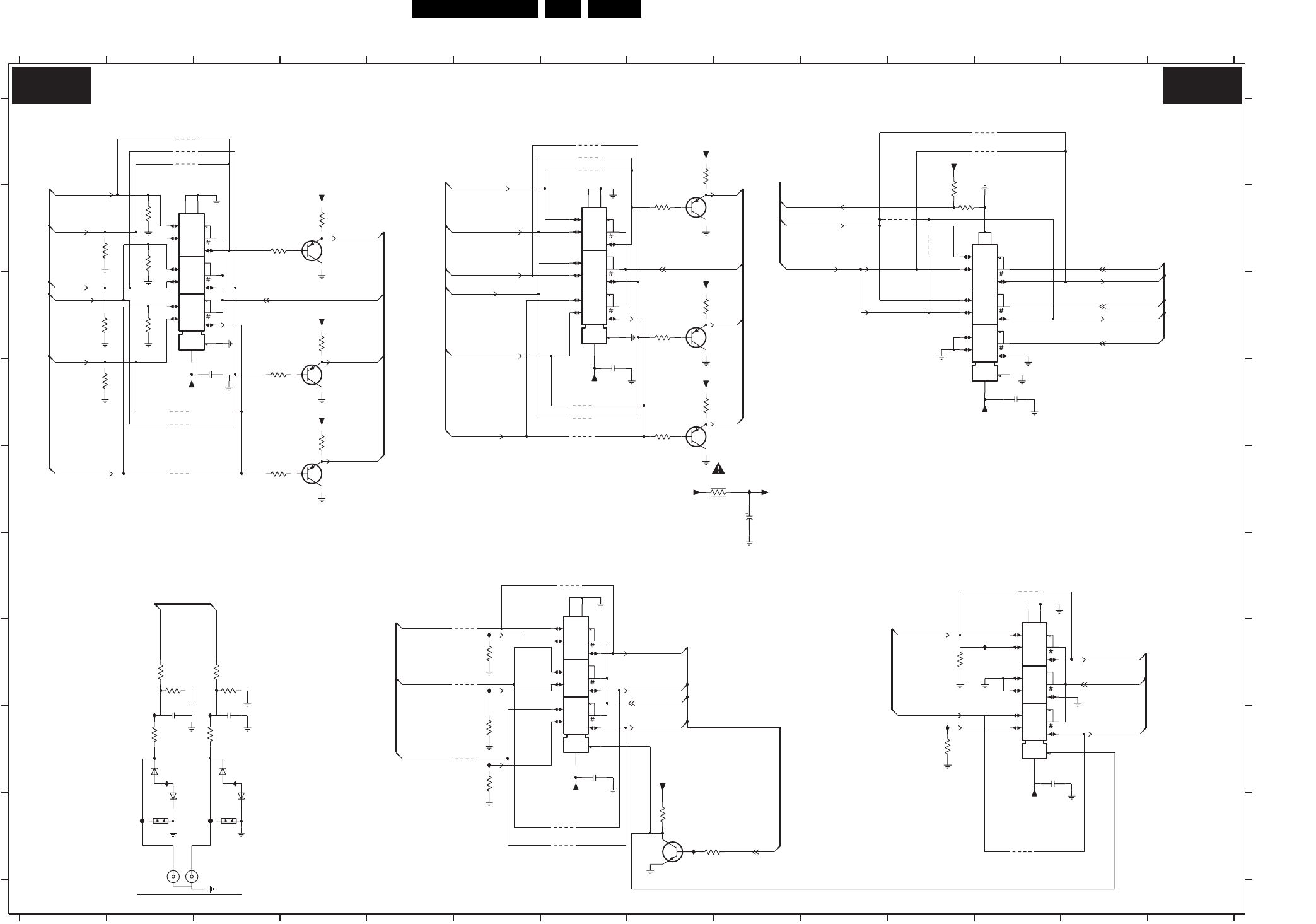
EN 56FTL2.4E AA 7.
Circuit Diagrams and PWB Layouts
SSB: I/O3: Switch
MUXDX
MUXDX
MUXDX
MUXDX
MUXDX
*
**
*
*
B14a,b,c
*
IO3: SWITCH
B14b B14c(2x),f,g,B15b
B15a
B14c,B15b
*
*
*
*
B6a
B14b,c
*
*
B6a,B15c
B14c(2x),f,g,B15b
B2
B14b,c
B2,B14a,b,c
9I89 G6
9I90 H6
IIB2 H2
IIB3 H3
IID8 G6
IID9 G6
IIE0 H6
IIE1 H11
IIH3 I8
*
*
*
B14a,b,c
B6a
9I37 A7
9I41 A12
9I42 B11
9I59 A7
9I61 A7
9I62 E2
B14b,c
FIB1 I3
II39 G12
II50 H2
II51 H3
IIB1 E9
B6a,B15b
RES
B15a
B15a
B14b,c
B14b,c
3IO5 B11
3IO6 B11
3IP9 D1
3IS4 B2
6I90 H2
6I91 I2
9IA2 B11
9IF0 F7
9IF1 I7
9IF2 I7
9IF3 I12
9IF4 F12
FIB0 I2
B14c(2x),f,g
B14g(2x)
B14b,c
B14c(2x),f,g,B15b
B2
7I30 D8
7I31 E4
7I32 D12
7I33 C7
7I80 H7
7I81 H12
7I82 I8
9I25 D7
9I26 D7
9I27 D7
3IFD H11
3IFE I8
3IFF G11
3IFL I8
3IH7 D4
3IL1 A8
9I63 D2
9I64 D2
9I65 A2
9I66 A2
9I67 A2
9I79 A12
9I87 G6
B14b,c
*
*
B2
2FH
B14g,B19a
RESERVED
B14b,c
3IN4 E9
3IN8 E3
3I85 B1
3I93 C1
3IC8 B4
3ID5 B3
3ID9 C4
3IE2 G3
6I92 H3
6I93 I3
7I12 D3
7I26 B8
7I27 B4
7I28 C8
7I29 D4
B14g(2x)
6
*
3IFB H6
3IFC H6
10 11 12 13 14
A
3IL3 B8
3IL8 C8
3IM0 C8
3IM4 D8
3IN0 D8
3IN2 B2
3IN3 C2
B2
B15a
B2,B15a
B6a,B15b
B14a,b
B14g,B19a
B6a,B15b,c
2IC3 D12
B2,B14a,b,c
RESERVED
B14c,B15b
2IR1 H12
B14g(2x)
1234
3IE3 G2
3IE7 D3
3IE9 G2
3IF5 G3
3IF6 H3
3IF7 H2
3IFA G6
14
12345 789
I
A
BB
C
D
E
F
G
H
1I69 I3
2I49 D7
2I50 D3
2I57 H2
2I58 H3
2IA9 E9
2IR0 H7
B6a,B15b
*
B2
B14c(2x),f,g
B14c(2x),f,g
5 6 7 8 9 10111213
C
D
E
F
G
H
I
1I07 I2
1I68 I2
22K
3IF5
10R
3IN0
3I93
75R
res
+5VIO
9I61 res
10R
3IL3
100n
res
2IC3
IIE0
9I79
75R
3IS4
res
3IN2
75R
res
IIE1
2IA9
100u
9IF2
res
IIB1
75R
3I85
res
3IL8
560R
3IM0
10R
+5VIO
6I93
2I57
100p
II51
100R
3IE3
6I92
BZX384-C6V8
1I68
3IN4
2R2
res
9I25
9I66
+5VIO
IIB2
6I91
IID9
100K
3IFB
res
res
100K
3IFF
+5VIO
res
9IA2
3IFA
100K
res
9I63
res
1I69
IIB3
100n
2IR1
II50
100R
3IE2
res
9I65
2I49
100n
9I67
3
1
2
res
+5V
1I07
YKC21-3226
9
+5VIO
3
3z 4
G3 6
8
GND
VCC
16
VEE
7
s0 11
s1 10
s2
1y0
12
1y1
13
1z 14
2y0
2
2y1
1
2z 15
3y0
5
3y1
74HC4053PW
7I12
3z 4
G3 6
8
GND
VCC
16
VEE
7
s0 11
s1 10
s2 9
1y0
12
1y1
13
1z 14
2y0
2
2y1
1
2z 15
3y0
5
3y1
3
74HC4053PW
7I33
100p
2I58
10K
3IO6
FIB1
+5VIO
res
9IF4
IID8
100R
3IF6
10R
3IN8
+5VIO
7I27
BC857BW
3IE9
22K
3ID5
10R
8
GND
VCC
16
VEE
7
s0 11
s1 10
s2 9
1z 14
2y0
2
2y1
1
2z 15
3y0
5
3y1
3
3z 4
G3 6
74HC4053PW
7I32
1y0
12
1y1
13
75R
3IN3
res
10K
3IO5
9I64 res
75R
3IP9
res
BC857BW
7I26
+5VIO
560R
3IL1
res
res
9IF1
16
VEE
7
s0 11
s1 10
s2 9
9IF0
2y1
1
2z
15
3y0
5
3y1
3
3z 4
G3 6
GND
8
VCC
7I80
74HC4053PW
1y0
12
1y1
13
1z
14
2y0
2
+5VIO
7I29
BC857BW
II39
3IE7
10R
3IC8
560R560R
3IH7
100n
2I50
9I59 res
BC857BW
7I30
VEE
7
s0 11
s1 10
s2 9
+5VIO
2y1
1
2z 15
3y0
5
3y1
3
3z 4
G3 6
8
GND
VCC
16
74HC4053PW
7I81
1y0
12
1y1
13
1z 14
2y0
2
res
100K
3IFD
9I90
9I87
9I89
+5VIO
7I28
BC857BW
res
9I62
4K7
3IFE
FIB0
BC847BW
7I82
3ID9
560R
+5VIO
res
9IF3
3IFC
100K
res
BC857BW
7I31
2IR0
100n
RES
9I27
9I42
res
3IF7
100R
+5VIO
+5VIO
res
9I26
9I41
IIH3
RES
1K0
3IFL
9I37 RES
BZX384-C6V8
6I90
3IM4
SWITCH-SUB
SC1-FBL-IN
FBL-SC1-IN
SWITCH-MAIN
SWITCH-SUB
SWITCH-MAIN
HS-2FH
VS-2FH
TRI-STATE-DVI
560R
SC1-B
SC1-G
SC2-G SWITCH-MAIN
SC1-B
TRI-STATE-DVI
R-SC1_V-IN
B-SC1-IN_U-IN
G-SC1-IN_Y-IN
SUB-V
SUB-Y
SUB-U
B-VGA
G-VGA
R-VGA
TRI-STATE-DVI
V-PIP+MAIN-OUT
Y-PIP+MAIN-OUT
U-PIP+MAIN-OUT
VA50-PIP
HA50-PIP
SC2-FBL-IN
SC1-FBL
SC1-R SC2-FBL
SC2-B_C-OUT
SC1-R
C-SC2_SVHS-IN
C-SC2_SVHS-IN
SC1-G
SC2-G
SC2-B_C-OUT
SNDR-DVI-IN
SNDL-DVI-IN
B14C B14C
F_15460_033.eps
080405
8204 000 8478.1
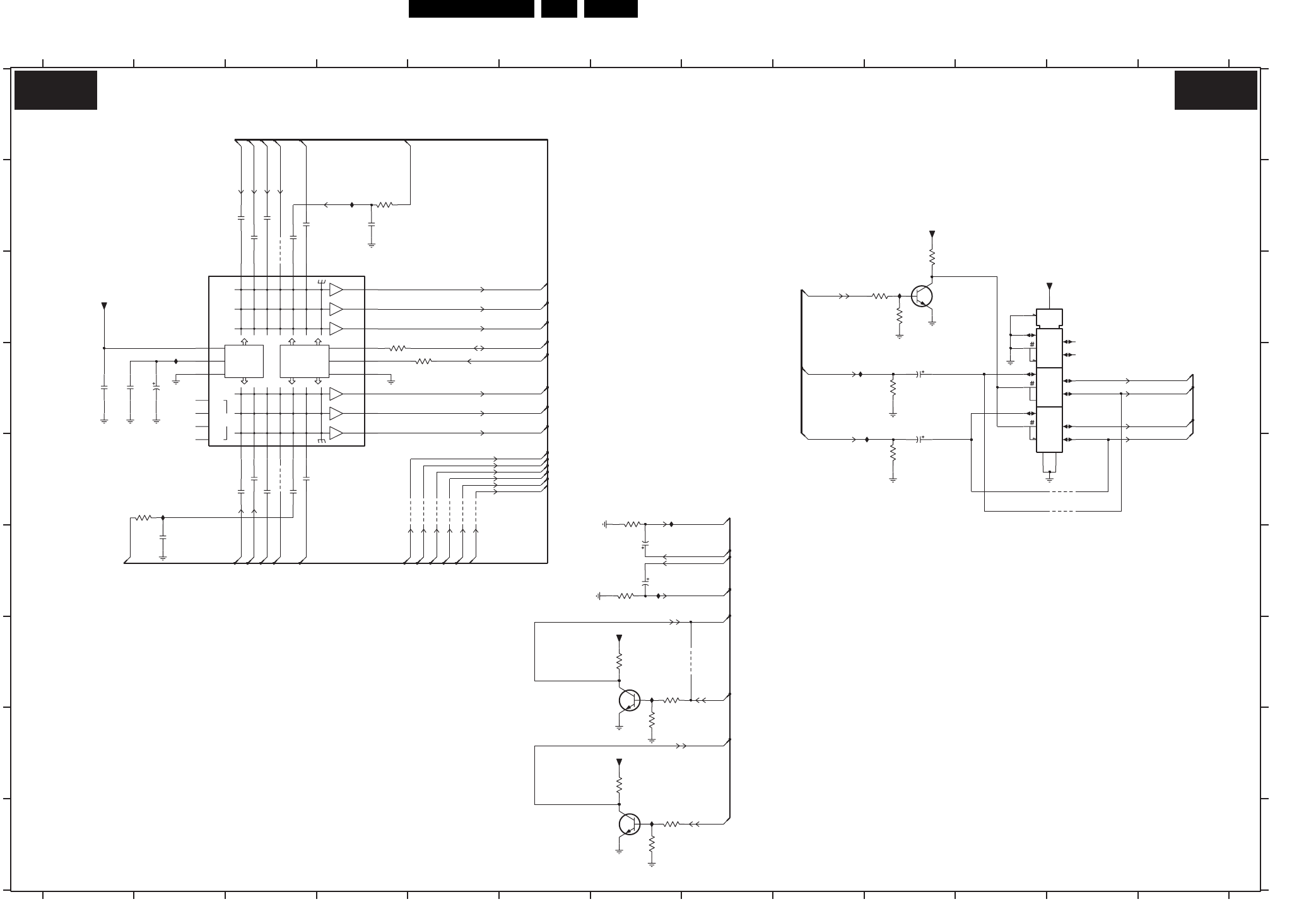
Circuit Diagrams and PWB Layouts EN 57FTL2.4E AA 7.
SSB: I/O4: Audio
MUXDX
3I39 E2
3I43 B4
3IH8 D10
3IH9 E7
3II0 C10
3II1 C10
3II2 C10
3II3 E10
3II4 F7
9IA3 E3
II67 C10
3IJ2 G7
3IJ3 G7
3IJ4 H7
7I17 C2
7I20 C12
7I22 C10
7I23-1 I7
7I23-2 G7
9I30 E5
9I31 E5
9I32 E5
9I33 E5
9I34 E5
9I35 E5
2I76 B3
2I77 D1
2I78 D1
2I79 D2
2I80 E3
2I81 E3
2I82 E3
2I84 E3
2I85 E3
2I99 F7
2IA0 D10
9I57 E12
9I58 E12
B14b.d
B14b.d
B14b,d
9IA1 B3
B14c(3x),f
B6a (2x),B14d
B14d,B21
B6a,B14b,B14d
B6a,B14d
B5a
12 13
A
B
C
D
E
3II5 H7
3II6 I7
II69 G7
II70 I7
II72 D2
IIE2 D9
IIE3 D10
IIE4 F7
IIE5 E7
IIE6 E2
IIE7 B4
B14b
B15a
3II7 I7
3IJ0 D4
3IJ1 D5
2I75 B3
12 13
123456789
2IA1 E10
2IA2 F7
B15b
9I68 G8
B14b
B6a (2x),B14d
B14d,B21
B6a (2x),B14d
B14b
23456
F
G
B6a , B14d
RES
B14b,d
B14d,B21
B6a (2x),B14d
B6a,B14b,B14d
B14b
91011
B6a,B14b,B14d
B6a,B14b,B14d
10 11
B14b.d
B14b
B6a , B14d
B
C
D
E
F
G
H
I
2I13 F2
2I14 B4
2I71 B3
78
B6a
B14b
B6a , B14d
B6a ,B14d
1
B14b
B14d,B21
B14e
B14b
B6a
H
I
A
B6a,B14d
I/O4: AUDIO
B6a , B14d
B6a
B14b.d
B14b.d
B5a
B14b.d
B6a,B14d
2I72 B3
2I73 B3
4K7
3I43
5
3
4
1u0
2I75
BC847BS
7I23-2
3IJ4
RES
22K
2I81
1u0
2IA0
16V10u
10K
22K
3IJ3
3IJ2
RES
RES
1u0
2I80
II70
9I68
3IJ1
100R
2I14
2n2
3II5
10K
+8V
3IH8
IIE7
47K
+8V
II69
2I13
10n
IIE2
22K
3II1
II72
2I77
9I33
1u0
1u0
2I71
1u0
2I73
3IJ0
100R
47K
3II4
4
G3
6
8
GND
VCC 16
VEE
7
s0
11
s1
10
s2
9
12
1y1 13
1z
14
2y0 2
2y1 1
2z
15
3y0 5
3y1 3
3z
74HC4053PW
7I20
1y0
VS
10u
2I99
R4
19
R5
18
R6
13
ROUT1
15
ROUT2
17
ROUT3
27
SCL
28
SDA
3
LOUT3
7NC1
8NC2
21 NC3
22 NC4
25
R1
24
R2
23
R3
20
L1
5L2
6L3
9L4
10 L5
11 L6
12
LOUT1
14
LOUT2
16
DECODER
BUS
SUPPLY
NC
TEA6422
7I17
26
ADDR
2CAP
1GND
4
IIE3
3II2
22K
2IA2
10u
9I32
22u
2I79
9I34
47K
3II3
3II0
10K
9I30
1u0
2I82
7I22
BC847BW
9I57
9I35
9I31
1u0
2I72
9IA1
1u0
2I85
22K
3II7
2I76
1u0
+8V
IIE6
2IA1
16V10u
2I84
1u0
22K
IIE4
3II6
3IH9
47K
2I78
1u0
+5V
9IA3
4K7
II67
IIE5
3I39
2
6
1
+5V
9I58
7I23-1
BC847BS
SNDR-BO-IN
SNDL-MAIN-IN
SNDL-SEC-IN
SNDL-BO-IN
SNDR-MAIN-IN
SNDL-MAIN-IN
SDA-S
SCL-S
SNDR-BO-OUT
SNDR-MAIN-IN
SNDR-SEC-IN
AR-SC1-IN
SNDL-BO-OUT
SNDL-SC2-OUT
SNDR-SC2-OUT
SNDR-SC1-OUT
SNDL-SC1-OUT
TRI-STATE-DVI
R-FRONT-INL-FRONT-IN
SNDR-SEC-IN
SNDL-SEC-IN
SNDL-MON-OUT
SEL_IN_2
SEL_IN_1_B
AL-SC2-IN
AR-SC2-IN
AR-SC2-IN
AL-SC1-IN
SNDL-SC1-OUT-DC
REG-SW
SNDR-SC1-OUT-DC
SNDR-MON-OUT
SNDL-MON-OUT
L-FRONT-IN
R-FRONT-IN
AL-SC1-IN
AR-SC1-IN
AL-SC2-IN
SNDL-SC2-IN
SNDR-SC2-IN
SNDR-MON-OUT
PIP-AM
PIP-FM
SNDR-SC1-OUT-DC
SNDL-SC1-OUT-DC
SEL_IN_1
B14D B14D
F_15460_034.eps
080405
8204 000 8478.1
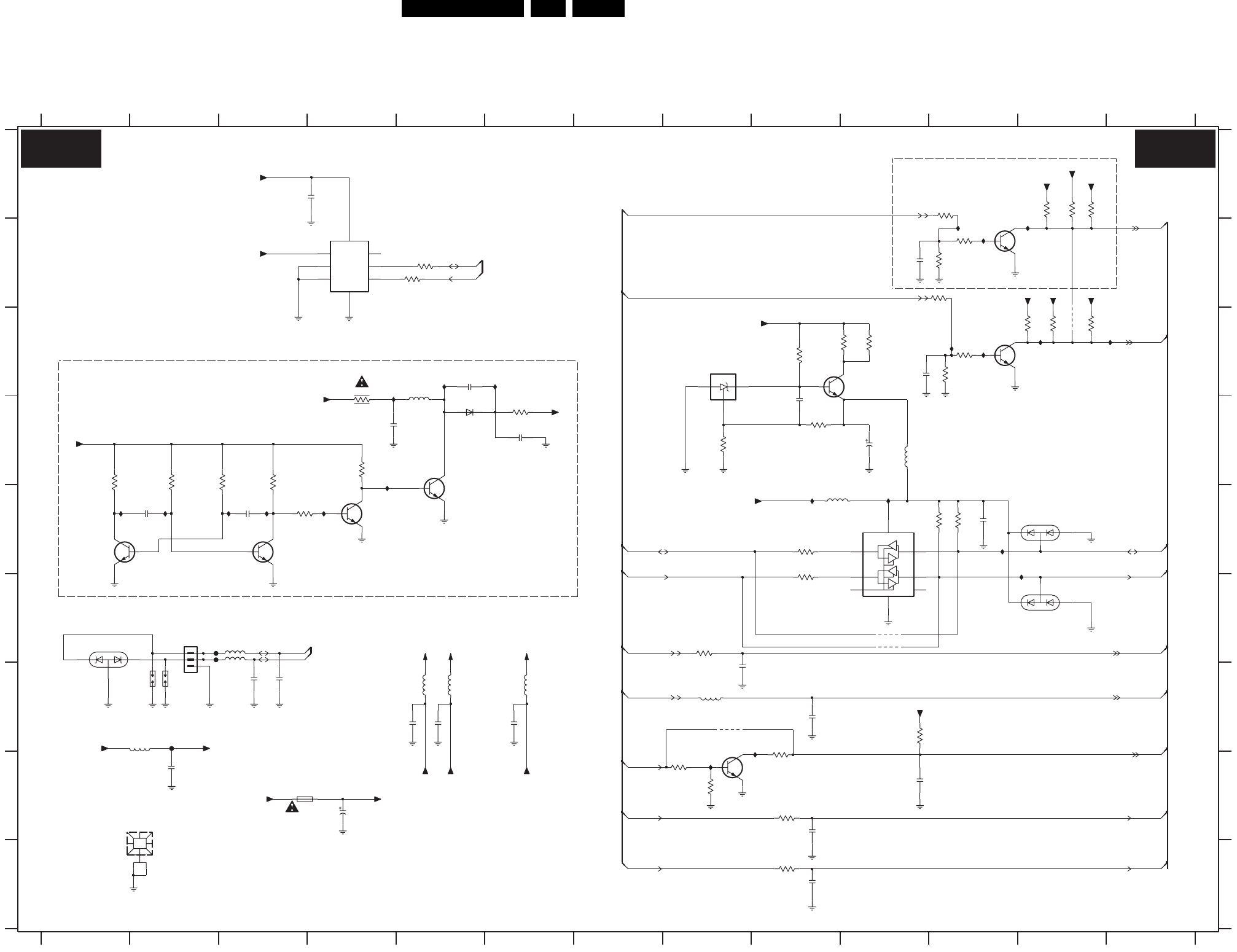
EN 58FTL2.4E AA 7.
Circuit Diagrams and PWB Layouts
SSB: I/O: 5
FIC5 F2
II75 D4
II76 E3
II77 C4
II78 E2
II79 B12
II80 E1
IIE8 H8
IIE9 G9
IIF1 C13
IIH4 B11
7I16-1 E3
7I16-2 E1
NC
B21
B21
IIH5 C11
7I46 C10
9I05 F10
9I06 F10
9I99 C12
9ID0 G8
FI15 G2
FIC4 G2
B5a
7I40 C11
7I45 C8
7I11 G8
7I13 E5
B21
RES
RES
II81 C11
II82 B11
II83 E4
II84 E3
II85 E10
II86 C5
II87 C6
II88 C12
II89 E11
II95 E12
II96 E97I14 B11
7I15 E45I47 G6
6I03 F12
B14d
B5a,B14e,B21
I/O: 5
RES
NC
RES
B5a
6I05 D5
6I99 F1
7I08 B4
7I10 E10
5I22 H2
5I45 G5
RES
NC
B5a,B14e,B21
RES
SENSOR
B21
5I46 G5
3IGF C11
3IGH H8
RES
6I04 E12
5I05 F3
5I06 G3
5I10 C5
5I21 G8
3IC0 C9
3IC5 C9
SERVICE
B21
CONNECTOR
3IC7 C10
3ID2 C4
3ID3 A12
T3A 420
B6c,B14b
B6c,B14b
3IGB C12
3IGC B11
3IGD B11
3IGE C11
D
E
TEMPERATURE
3IH0 A12
3IH2 B11
3IH4 C12
3IS3 H9
3IS6 I9
3IW3 B5
3IW9 B5
5I02 E9
5I04 D10
3IB8 G10
3IB9 G9
3IBA E9
3IBB E9
56
NC
78910
3ID4 C12
3ID6 D6
3IE0 A11
3IF0 F8
3IF1 D1
3IF2 D2
3IF3 D2
3IF4 D3
3IF8 D4
3IF9 E3
3IGA A12
I
A
B
C
2I59 E11
2I60 E2
2I62 H10
2I64 G9
2I65 G3
2IA3 G8
2IB7 D4
2IJ5 D6
123456789
2IJ6 H9
2IJ7 I9
2IK5 G5
2IK6 G5
2IK7 G6
2IS6 H4
3I00 H8
3IB1 E11
3IB3 E11
3IB6 D8
3IB7 D9
1234
B21
F
G
H
I
1I10 G2
1I12 G2
1I79 H3
1I99 H2
1M15 F2
2I00 H2
2I10 A3
11 12 13
A
B
C
D
E
F
G
H
5I46
2I33 D9
2I34 D10
2I37 B10
2I38 G3
2I40 C10
2I48 E3
2I52 C5
B21
10 11 12 13
FI15
A1
6
A2
5
GND
4
OS 3
SCL 2
SDA 1
7I08
LM75ADP
+VS 8
A0
7
IIF1
*
5I22
100R
3IS6
+5V
+3V3_SIM
100n
2IK6
II89
2I34
10u 16V
1n0
2I33
330R
3IB7
220R
3IC7
II85
II76
1n0
2I60
2I38
100p
3IF2
2K7
+5V
5I10
1m0
2IK5
100n
+33V
4K7
3IGA
3IF1
470R
1n0
2I48
II86
3IH4
2K2
9I06
5I21
1
3
2
+5V
+5V
BC847BW
7I15
3IF9
3K3
II82
3ID3
4K7
+5V
*
2I59
100n
II81
9I99
+11V_SF 3IB9
100R
5I02
II83
3I00
10K
*
II77
II84
3IF3
10K
5I05
2I62
100p
100n
2IB7
10K
3IB8
2I00
100p
+5V2-STBY
5I04
7I46
BC847BW
100R
3IW9
+3V3_SIM
IIE8
*
IIH5
+5V2-STBY
47K
3IGF
*
100p
2I65
2IK7
100n
5I06
3IF4
EMC HOLE
1I99
470R
II95
BAV99 COL
6I03
+8V
9I05
*
2I10
10n
*
10K
3IB3
II96
2IA3
1n0
*
5I45
1I10
+11V_S
5I47
+11V_DC
*
7I40
BC847BW
3IF0
100R
100p
2I64
220p
2I52 RES
II80
7I13
BC817-25W
II75
II78
3IB1
10K
FIC4
*
9ID0
3IE0
47K
BC847BW
7I14
+5V2-STBY
IIH4
IIE9
T3000mA
1I79
3IF8
2K2
*
2I40
100n
4K7
3ID4
2
6
1
BC847BS
7I16-1
+5V
+11V
3IC5
220R
1K0
3IC0
1K0
3IB6
*
3IW3
100R
II88
BAS316
6I05
4K7
3IH0
7SCL1
3 SDA0 6SDA1
8
VCC
+5V2-STBY
PCA9515DP
5EN
4
GND
1
NC
2SCL0
II79
*
7I10
100n
2IJ5
3IS3
100R
7I11
BC847BW
1R0
3ID2
100p
2IJ7
II87
2IJ6
100p
1
R
2
1u0
2I37
7I45
TS2431
A
3K
FIC5
47K
3IH2
3IGH
100K
*
+5V
2IS6
100u 16V
2K2
3ID6
*
3IGE
10K
4K7
+3V3_SIM
1
2
3
*
3IGB
S3B-EH
1M15
10K
3IGC
+8V
3
4
1I12
BC847BS
7I16-2 5
*
BAV99 COL
6I04
6I99
PLVA2656A
3
21
100R
100R
3IBB
3IBA
3IGD
47K
CPU-GO
PDP-GO
SCL-DISP
SDA-SF
SCL-SF
SDA-S
SCL-S
SDA-DISP
SURR-RF
SURR-LFSURR-L
+5V_VDP
+5V_CON
+8V_VDP
STATUS-SC3 STATUS-SC3-F
SCL-S
SDA-S
STANDBY
ON-OFF-LED
LED1
SEL_IN_1_BFSEL_IN_1_B
STANDBY
SURR-R
F_15460_035.eps
080405
B14E B14E
8204 000 8478.1
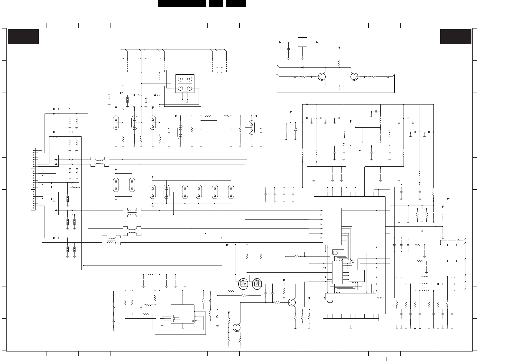
Circuit Diagrams and PWB Layouts EN 59FTL2.4E AA 7.
SSB: I/O6: Digital Input
COM
OUTIN
PD
CIPHER
SCDT
RECEIVER
RESET_
PANELLINK
DE
HSYNC
VSYNC
BIT DAC
MODE
SELECT
DACPD
C
VREF-IN VREF-OUT
HDCP
TRIPPLE 8-
CLK
VSYNC
HSYNC
DE
CNTL3
DB[7:0]
DG[7:0]
DR[7:0]
DR
DG
DB
8
8
8
PLLCK
FORMATTER
SCL
ADR
0
1
2 SDA
WC
2IE4 D11
B14g,B19d
B14g
B14g
FI74 I8
2IH5 D11
2IJ8 I8
2IJ9 I9
3I29 D4
3I30 D4
2I97 F9
2I98 F9
2IB0 A9
2IB3 F9
2IB5 F8
2IB8 H5
2IB9 H4
2IC5 H6
B14b
RES
SCL_DVI
3IK9 B9
B14g
3I46 I5
3I47 I5
3I48 I5
3I49 I7
3II8 B12
3II9 B11
FI71 D2
2IE5 D12
2IE6 E12
2IE7 E12
2IE8 D12
2I66 I12
2I67 I13
2I68 I13
2I69 I13
2I70 I14
2I86 I14
2I87 H13
2I88 G13
DVI
RES
RX1-
SDA_DVI
CONNECTOR
B14g
RES
RES
RX1+
2IH4 D12
B14g
2IG9 D13
2IH1 H5
2IH2 D13
FI73 I10
FI83 C6
FI75 H10
FIC3 F2
II60 B10
II61 D11
II62 D11
II63 D11
9I85 G14
9IB3 B7
9ID1 B4
9ID2 B4
9ID3 B4
9ID4 B5
9ID5 B5
9ID6 B5
II64 E11
II65 E10
II66 E10
II68 B11
II92 E13
II93 G13
II94 G14
II97 F14
+5V
IIG0 J7
IIH6 I9
FI29 H14
FI30 G14
FI70 D2
FI03 E2
FI72 I5
FI05 F2
FI06 G2
FI07 G2
FI08 E2
FI09 E2
6I14 F5
6I15 F5
6I16 F6
6I17 F6
6I18 F7
6I19 F7
6I20 E4
6I21 E4
FI76 C10
FI77 H14
FI78 H14
FI79 I14
FI80 B4
FI81 C4
FI82 C5
7I53-1 J8
FI84 C8
7I61 B10
7I64 B11
7I65 A9
9I07 F14
9I14 G14
5I31 D12
5I32 D13
5I33 D10
5I34 D10
5I35 F13
5I36 H13
5I37 H13
5I38 I13
9ID7 B7
9ID8 B7
9ID9 B7
FI00 C2
FI01 C2
FI02 E2
5I40 C12
FI04 F2
6I01 D3
6I06 D4
6I07 C5
6I08 C6
6I09 C8
3IR0 I9
3IR1 I10
3IR2 H8
3IR3 H8
3IR4 H9
3IR5 G13
3IR6 H13
3IR7 F13
6I63 I7
6I64 I7
6I65 I4
6I66 J4
7I18 F10
7I19 I6
7I51 I8
7I52 I8
3IT5 I14
7I53-2 I9
3IV0 I9
3IV1 J7
3IV2 J7
3IV3 J7
5I30 D11
3I31 D5
3I32 D6
3I33 C7
3I40 C7
3I41 D8
3I42 E2
3I44 I4
3I45 I4
B14g
B14g
5I39 H5
2IE2 E11
5I41 E13
3IQ5 I6
3IQ6 I7
3IQ7 I8
3IQ8 I9
3IQ9 I9
2IE9 D9
2IG2 D9
2IG3 C10
2IG4 C10
2IG5 C11
2IG6 C12
2IG7 C13
2IG8 C12
RX2-
RX2+
B14g
B14f
3IR8 F13
3IR9 I13
3IS0 I13
3IS1 I13
3IS5 I12
2I90 G12
3IT6 I14
2I92 F13
2I93 F13
2I94 F12
2I95 F12
2I96 F13
J
A
B
C
D
E
F
G
I/O6: DIGITAL INPUT
CONNECTOR
B14b
B14g
RES
res
res
2IC6 D7
2IC7 D6
2IC8 E10
2IE1 E10
1I60 C2
2IE3 D11
1I62 D2
1I64 E2
1I65 E2
1I66 F2
1I67 F2
13 14
A
B
C
D
E
F
RXC-
RECEIVER
B14c (3x),g,B15b
B14b(2x)
B14b
B14f
2I89 G13
2I91 G12
G
H
I
11 12 13 14
1234
B14c (3x),g,B15b
B14b(2x)
B14g
DVI INPUT
res
HOT PLUG
1I57 F4
1I59 G4
6
1I61 C2
8 9 10 11 12
1I17 D8
1I18 D5
1I19 C5
1I20 C4
1I21 C3
1I53 G4
1I55 F2
1I56 E3
DVI INPUT
RXC+
4678910
RX0+
RX0-
57
H
I
J
1D01-1 D1
1D01-4 B6
1I14 D2
1I15 G2
1I16 G2
123 5
FI03
9ID8
3IR7
470R
100n
2IE9
BAV99 COL
6I17
1K0
1K0
3IV1
3IQ9
100n
2IB0
1u0
2IB5
5I34
1u0
2IC8
1I66
22u
2IG2
3I30
75R
3I41
1K0
2I66
6I64
47p
BAS316
1I53
DLW21S
1I59
DLW21S
100n
2IB8
5I33
res
9ID7
100n
2I93
5I41
1u0
BAV99 COL
6I20
2IJ9
FI79
9ID1
100n
2I95
2IE2
100n
3I46
100R
2IC7
47p
1u0
2IJ8
1I65
BAV99 COL
6I19
6I63
3
2
1
BAS316
3
2
1
6I08
PLVA2656A
32
PLVA2656A
6I09
LD1117DT33C
7I65
1
3V3-Si-IO
3V3-Si-IO
II63
FI06
II93
FI07
2IE5
2IE8
1u0
100n
2IE6
5I31
100n
3IS0
FI29
7I64
RES
120R
II68
BC847BW
BSH112
7I51
2IB3
100n
BAS316
6I66
+8V-VIDEO
IIG0
IIH6
2IH4
1u0
5I40
4K7
3IR2
4K7
3IR3
FI30
7I61
1K0
3II8
RES
BC847BW
II94
+8V-VIDEO
47p
120R
2I67
9I14
3IR9
9
10
11
12
13
14
15
16
4
5
6
7
8
YKF45-7005
1
2
3
+8V-VIDEO
1D01-1
100n
2IB9
II97
II64
3IR5
47R
2I89
1u0
II62
100n
2IH2
100n
2IH5
75R
3I29
II60
FI05
1
6I07
BAV99 COL
5I39
9I07
2IC5
100n
20
21
22
23
24
17
18
19
1I56
DLW21S
FI74
FI08
FI71
FI76
2IG8
100n 100n
2IG7
res
9IB3
3I42
9ID3
1K0
2I88
100p
100p
2I87 3IR8
3K3
3IV0
8K2
6-M7
3IQ8
3K3 2I98
100n
6I65
II92
BAS316
1I62
1I14
1I57
DLW21S
5I35
2I92
1u0
75R
3I31
5I32
2IE7
1u0
BAV99 COL
FI84
6I18
2I96
1u0
3II9
1K0
C428
31
32
29
30
1K0
3IK9
1D01-4
C1 25C226
27C3
YKF45-7005
1K0
3I32
FI78
100n
9I85
2IE1
1I60
FI09
II66
II61
II65
100n
2IG5
100n
2I97
1I67
1I55
3IR4
3IT5
120R
3V3-Si-IO
100R
3IV3
3I48
2K2
47p
1K0
3IR1
2I68
FI77
270R
1K2
3IR0
3IQ5
47K
6I14
FI70
BAV99 COL
FI82
1I18
1I19
res
9ID2
res
9ID6
res
9ID4
3IT6
120R
33p
2I70
3I40
100R
2IC6
3IR6
47p
47R
BC847BPN
7I53-1
2
6
1
FI04
470R
3V3-Si-IO
3IV2
33p
2I69 120R
3IS1
FI73
5
3
4
3I47
2K2 BC847BPN
7I53-2
FI75
1I21
FI72
BSH112
7I52
VCC1
13
VCC1
VCC2
VCC2
22
VCC3
VCC3
46
VSYNC
VSYNC 19
RX2-
RX2-49
RXC+
RXC+5
RXC-
RXC-6
SCDT
SCDT 40
SCLM
SCLM34
SCLS
SCLS15
SDAM
SDAM36
SDAS
SDAS14
RESERVED 38RESERVED
RESET_
RESET_39
RSET
RSET29
RX0+
2 RX0+
RX0-
RX0-3
RX1+
RX1+51
RX1-
RX1-52
RX2+
RX2+48
OGND1
OGND1
16
OGND2
OGND2
43
OVCC1
OVCC1
17
OVCC2
OVCC2
41
PD-DAC_
PD-DAC_20
PD_
PD_11
PGND
PGND
10
PVCC
PVCC
9
GND1
GND1
21
GND2
GND2
12
GND3
GND3
45
HSYNC
HSYNC 18
IOB
IOB 31
IOG 26IOG
IOR
IOR 23
ODCK
ODCK 42
DACGNDG
DACGNDG
28
DACGNDR
DACGNDR
25
DACVCC
DACVCC
37
DACVCCB
DACVCCB
32
DACVCCG
DACVCCG
27
DACVCCR
DACVCCR
24
DE
DE 44
EXT-RES
EXT-RES 8
AGND1
AGND1
47
AGND2
AGND2
50
AGND3
AGND3
4
AVCC1
AVCC1
1
AVCC2
AVCC2
7
COMP
COMP 30
DACGND
35
DACGND
DACGNDB
DACGNDB
33
SII905CQ52
7I18
BAV99 COL
6I21
100n
2IG6
FIC3
FI01
2IG4
1u0
2I90
100n
FI81
BAV99 COL
6I06
9ID9
1I20
9ID5
5I38
220n
220n
5I37
220n
5I36
3IQ7
100R
3IQ6
100R
3I49
100R
1I17
FI83
100n
2IH1
100R
3I33
1I64
5I30
BAV99 COL
6I15
3I45
47K
3IS5
120R
2I91
100n
1u0
2IE3
100n
2IE4
2I94
100n
BAV99 COL
6I16
1
2
3
6
5
84
7
(256x8)
Φ
EEPROM
7I19
M24C02-WDW6
6I01
BAV99 COL
FI80
100n
2IG3
1I16
1I15
FI02
2I86
33p
2IG9
100n
3V3-Si-IO
1I61
FI00
3I44
10K
+3V3-SI
+5V
H-DVI
R-DVI
B-DVI
MMC-G
MMC-B
AV6-H
AV6-V
AV6-B
AV6-G
AV6-R
G-DVI
V-DVI
+3V3-SI
V
H
R
3V3-TMDS
3V3-TMDS
DVI-PWR-DOWN
VCC-Si
3V3-TMDS
+3V3-SI
HS-DET
TRI-STATE-DVI
SWITCH-MAIN
DVI-PWR-DOWN
HD-ANA
VD-ANA
MMC-R
F_15460_036.eps
080405
B14F B14F
8204 000 8478.1
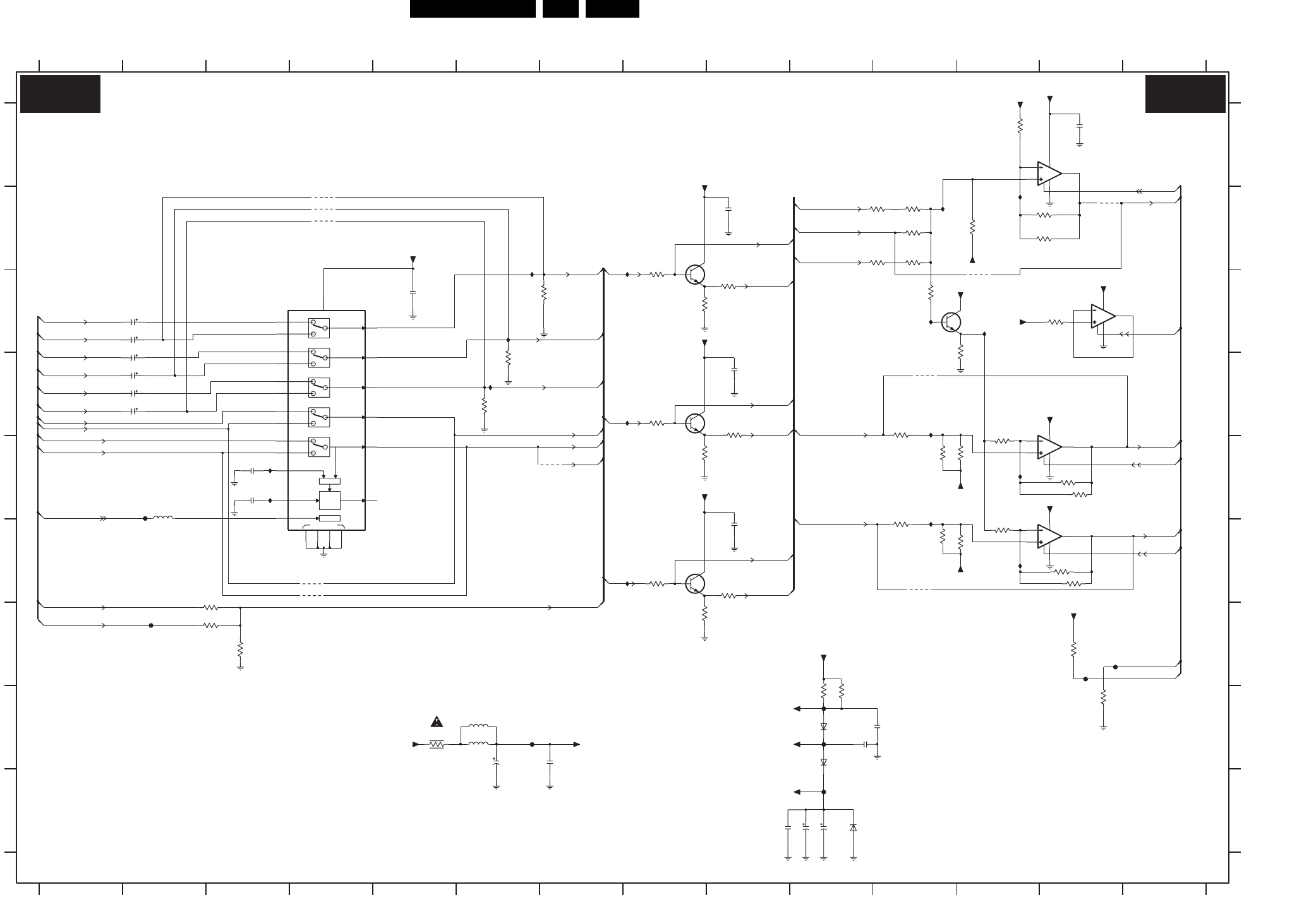
EN 60FTL2.4E AA 7.
Circuit Diagrams and PWB Layouts
SSB: I/O: 7
GROUND
1
LOGIC
SEPA
SYNC
DET
2
1
1
1
2
1
2
2
2
SB1
SB1
SB2_
SB2_
B14c,B19a
B14f
B14f
B14f
B2,B14b,B15a
B14g (2x)
B14g (2x)
IIB9 F12
IIF2 B6
IIF4 D6
IIF5 C8
IIF6 D8
IIF7 F8
IIH7 C12
IIH8 C11
B14g (2x)
B19a,d
B14g (2x)
B19d
res
B14c,g
B14g (2x)
B14c,g
B14c,g
7I54-C D13
7I54-D F13
7I56 C8
7I57 D8
7I58 F8
9I23 B13
9I28 C12
9I29 B4
9I45 D11
9I49 F11
9I81 F4
9I84 E7
9I88 F4
9I91 B4
9I98 B4
FIB2 G2
FIB3 I10
FIB5 H6
FIB6 G13
FIB7 G13
FIB8 H10
FIB9 H10
FIC2 E2
II30 E3
II31 E3
IIB4 B11
IIB5 B12
IIB6 D11
IIB7 E12
IIB8 E11
3IW2 E11
3IW7 B11
IIF3 C6
3IZ0 F12
3IZ1 F12
3IZ2 F13
3IZ3 B11
3IZ4 B11
3IZ5 B11
RES
RES
RESERVED
3IZ6 C13
3IZ7 B12
3IZ8 B13
3IZ9 A12
5I12 H6
5I13 H6
5I42 E2
6I80 H10
6I81 I10
6IA1 H10
7I41 C12
7I54-A A13
7I54-B C13
3IT8 G3
3IU0 H5
7I55 C4
3IU2 B13
3IU3 H13
3IU5 D11
3IU6 E12
3IU7 E12
3IU8 E13
B14c,B19a
B14g (2x)
3IU9 F11
3IV4 C7
3IV5 D6
3IV6 D6
3IV7 E13
3IV8 F11
3IV9 F13
3IW1 H10
2IN8 E3
2IN9 E3
3IW8 B11
3IG1 F8
3IG3 E8
3IG4 D8
3IG6 C8
3IG7 C8
3IG9 H10
RES
B14g
B14g (2x)
RES
3IHA F9
3IHB E9
3IHC C9
3IJ6 C11
3IJ7 C12
3IK0 G3
3IT7 G3
2IF8 D2
2IF9 D2
3IU1 G13
2IH7 D2
2IH8 C2
2IH9 C2
2IK1 C5
2IK2 H10
2IK3 H11
B2,B14b,B15a
RGB-OUTPUT SELECTION
B19a
B14g (2x)
B14g (3x),f,B15b
2IK4 I10
B
C
3IG0 G8
E
F
G
H
I
A
B14f
B14f,B19d
RES
B19a(2x)
B14f
2IF5 H7
2IF6 A13
34
2IH6 D2
67891011
HDI : RGB-YPbPr
B2,B14a,B15a
B14f
B14c,g
B14c,g
12 13 14
A
34
D
67891011
B14f
RES
RES
B19a
12 13 14
12
D
E
5
F
G
H
I
2I09 I10
2IF0 I9
2IF1 F9
2IF2 D9
2IF3 B9
2IF4 H6
B14g (2x)
B14c,g
B14g (2x)
I/O: 7
B14g (2x)
12 5
B14g
B14f
B2,B14b,B15a
B14g
B14g (2x)
B14f
B
C
470R
3IJ7
9I84
1K2
3IW8
VD1-IN
12
VD2-IN
13
6.3V
22u
2IF8
HD-S-SIG-DET
2
HD1-IN
24
HD2-IN
23
R-OUT 21
R1-IN
1
R2-IN
7
20
VCC
VD-OUT 14
CTL
16
G-OUT 19
G1-IN
3
G2-IN
9
4
6
8
10
22
HD-OUT
7I55
B-OUT 15
B1-IN
5
B2-IN
11
C-S-OUT 17
C-V-IN
18
BA7657F
680R
3IW1
9I88
res
9I98
IIF3
220n
2IK1
9I29
res
9I81
2IF2
100n
3IJ6
100R
FIC2
BFR93AW
7I41
1K0
3IT8
FIB2
FIB7
IIF2
1K0
3IW7
REF3
BAS316
6IA1
100n
2IF3
2IF6
220n
2IN9
100n
+8V-VIDEO
3IV6
1K0
res
+8V
BC847BW
7I56
47u
2IK4
5I13
16V
REF3
2IH7
6.3V
22u
100n
2IN8
3IW2
10K
3IT7
1K0
3IG4
10R
IIB9
3IG3
560R
+8V-VIDEO
BZX384-C3V9
6I81
1K0
+8V-VIDEO
1K0
3IZ0
3IZ9
3IZ2
2K2
IIB7
+8V-VIDEO
IIB4
2IH8
22u
6.3V
IIB8
100n
2IF5
REF2
+8V-VIDEO
100n
2IK2
FIB3
2IK3
FIB8
100n
560R
3IG0
100n
2IF1
7I58
6I80
BC847BW
16V47u
2IF4
BAS316
3IV8
47K
II30
FIB5
3IV4
1K0
res
3IU0
2R2
9I91
22u
2IF9
6.3V
REF3
10R
3IG7
3IZ7
330R
4
13
IIF4
7I54-2
TSH95ID
5
6
7
8
7I54-1
3
2
1
8
4
13
TSH95ID
9I45
9I28
FIB6
+8V-VIDEO
REF2
2IH9
6.3V
22u
IIF7
REF1
2IH6
6.3V
22u
3IZ8
res
2K2
1K0
3IV5
680R
3IG9
FIB9
+8V-VIDEO
5I12
10K
3IU1
+8V-VIDEO
3IZ6
100K
IIH7
2IF0
+8V-VIDEO
IIH8
100n
1K2
3IZ1
REF2
10R
3IG1
II31
9I49
3IK0
1K0
3IU3
10K
1K0
3IZ3
5I42
18K
3IV7
9I23
12
11
10
9
4
13
IIF6
TSH95ID
7I54-3
3IZ5
res
REF2
3K9
10u
2I09
3IHA
100R
3IHB
100R
3IHC
100R
1K2
3IU6
100K
3IV9
1K2
3IU7
res
3IU8
3K3
3IG6
IIB6
560R
3IU5
3K3
IIB5
+8V-VIDEO
+8V-VIDEO
IIF5
3K3
3IU9
100K
3IU2
7I54-4
TSH95ID
14
15
16
9
4
13
+5VIO
BC847BW
7I57
3IZ4
1K0
STANDBY1
STANDBY2
STANDBY2
R-VGA-BUF
G-VGA-BUF
B-VGA-BUF
SC2-B-IN_C-OUT
STANDBY1
U-2FH
V-2FH
R-VGA
G-VGA
B-VGA
H-DVI
HS-2FH
AV6-H
VS-2FH
AV6-V
B-VGA
G-VGA
R-VGA
V-DVI
R-DVI
AV6-G
G-DVI
AV6-B
B-DVI
STANDBY1
STANDBY2
G-VGA-BUF
B-VGA-BUF
R-VGA-BUF
HS-DET
B-VGA-BUF
R-VGA-BUF
H-2FH-DIV-2
AV3-CVBS-INV-2FH-AD-OUT
SC2-G-IN
SC2-R_C-IN_AV2
Y-2FH
SWITCH-MAIN
AV6-R
F_15460_037.eps
080405
B14G B14G
8204 000 8478.1
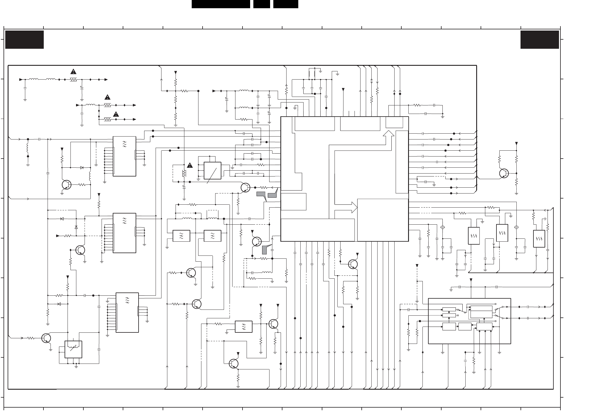
Circuit Diagrams and PWB Layouts EN 61FTL2.4E AA 7.
SSB: PIP HIP
IF DEM
SUPPLY CTRL SYNC
OUTP SWITCH
LUMA & CHROMA PROC.
I/O SWITCH
DELAY COR.
GROUP
2H/4H DELAY
ADAPTIVE
COMB FILTER
FILTER
TUNING
CLOCK
CLAMP
GEN
CLAMP
SAND-
CASTLE
NC
ISWI
I
O2
GND
O1
O
GND
I
O
GND
I
O
GND
I
O
GND
I
O
GND
I
NC
I2
I1
O2
GND
O1
NC
I2
I1
O2
GND
O1
O
GND
I
RES
B15a
*
B15a
B2(2x),B15a(3X)
HIP
5V0
B14b
B
C
D
E
F
G
H
I
1P00 E11
1P03 E13
1P04 C4
1P05 E4
*
B15a
B15c
8V0
B15a
B15a
RES
B2, B14c
123456789101112
B15a
B2, B14b,g
8V0
B13b
*
SAW-FILTER AUDIO
*
B13b
*
2V7
13 14
1234567891011
B15b
*
*
*
2P24 B7
1P06 G4
1P07 H7
1P08 E5
1P09 E6
1P10 E13
1P11 F14
1P12 E12
2P00 B1
2P01 B2
2P02 B2
2P03 C1
2P04 D2
2P05 D5
2P06 G3
2P07 G3
2P08 H3
2P09 B8
2P10 F8
B14c
RES
2P43 F13
*
B15b
B14c
2P11 F8
2P12 F8
2P13 F8
2P14 F8
2P15 F8
2P16 F7
2P17 E7
2P18 D7
2P19 D6
2P20 C7
2P21 C7
2P22 C6
2P23 B7
RES
*
RES
B14c
*
B15a
2P25 B6
2P26 B8
2P27 B8
2P28 B9
2P29 B11
2P30 B11
2P31 C11
2P32 C11
2P33 C11
2P34 F11
2P35 F11
2P36 F11
2P37 F11
2P38 F12
2P39 F12
2P40 F12
2P41 F13
2P42 F13
B14b
*
*
*
*
3P17 G2
2P44 F14
2P45 C11
2P46 D11
2P47 D11
2P48 D11
2P49 D6
2P91 G11
2P92 I12
2P93 G14
2P94 G14
2P95 G13
2P96 G12
2P97 F14
2P98 B7
2P99 B7
2PG0 C7
2PG1 C7
2PG2 F7
8V0
5V0
B15c
*
B14b
SAW-FILTER VIDEO
3P00 B2
3P01 B3
3P02 B3
3P03 B5
3P04 B5
3P05 B5
3P06 B5
3P07 D2
3P08 D2
3P09 E3
3P10 D5
3P11 E5
3P12 E2
3P13 F2
3P14 F5
3P15 G5
3P16 G5
COIL 40.4 SUPPRESSION
RES
RES
RES
3P18 G2
3P19 G2
3P20 H1
3P21 B7
3P22 B10
3P23 B10
3P24 B11
3P25 D7
3P26 D7
3P27 E6
3P28 E6
3P29 E11
3P30 F9
3P31 F8
3P32 F7
3P33 I6
3P34 G9
3P35 G9
*
7V6
RES
*
7V6
*
B15a
*
6P00 E2
5V4
3P36 H7
3P37 H7
3P38 H6
3P39 G7
3P40 F6
3P41 D13
3P42 D13
3P43 D13
3P44 F9
3P45 H11
3P46 H11
3P47 I12
3P48 B8
3P71 F7
3P90 E12
3P91 E13
3P92 E14
B15c
5V0
B2(4x),B15a(3x)
B15a
*
RES
*
B15c
SAW-FILTER VIDEO
2V8
B15a
3P93 E14
5P00 A2
5P01 B3
5P02 C1
5P03 A1
5P04 D3
5P05 E5
5P06 E6
5P07 H2
5P08 C6
5P09 B7
5P10 B7
5P11 F7
B14a
RES
RES
*
PIP HIP
F_15460_038.eps
080405
B15A B15A
8204 000 8475.1
RES
RES
RES
9P17 H6
6P01 E2
6P02 G2
6P03 D2
7P00 D2
7P01 F2
7P02 H1
7P03 F5
7P04 G5
7P05 D6
7P06 E7
7P07-1 H7
7P07-2 I6
7P08 F9
7P09 D9
7P10 D13
7P11 G11
9P00 E6
9P01 C3
B14a
B2,B14a,g
*
B15a
*
*
0V5
9P02 D5
9P03 D6
9P04 E2
9P05 E5
9P06 E7
9P07 F7
9P08 G6
9P09 F6
9P10 F3
9P11 E3
9P12 G8
9P13 D11
9P14 G6
9P15 E7
9P16 E3
B2, B14b,g
8V0
RES
B15a
FP25 D12
FP26 D12
FP27 D5
9P18 G7
9P19 H5
9P20 F11
9P21 G11
9P22 G11
9P23 H6
9P24 G9
9P25 F9
9P26 E11
9P27 E11
9P28 F12
9P29 F13
9P30 F7
AP02 C1
AP04 C4
AP05 C4
AP06 C5
AP07 C5
B2(4x),B15a(3x)
RES
0V5
*
RES
B15b
IP25 B2
IP26 B4
IP27 B3
RES
*
B14b
AP09 G3
FP02 B8
FP03 C1
FP08 B5
FP11 I7
FP12 G9
FP13 F7
FP14 E6
FP15 D7
FP16 C7
FP17 F7
FP23 B11
FP24 D12
RES
*
B15a
*
RES
2V4
B2(4x),B15a(3x)
B2
B15a
FP29 H11
FP36 G9
FP37 C12
FP38 C12
FP39 C12
FP40 C12
FP41 H8
FP42 H9
IP00 B5
IP01 E5
IP02 B5
IP03 E5
IP10 H8
IP17 C7
IP20 B8
IP21 B9
IP22 D5
IP23 A2
*
*
B15c
B2(2x),B15a
*
MODULATOR COIL
RES
IP73 D14
cP00 A8
cP01 A8
IP28 B3
IP29 B4
IP30 A3
IP31 B3
IP32 C3
IP33 B6
IP34 B7
IP35 B7
IP36 B10
IP37 H11
IP38 H11
IP39 H12
IP40 G13
IP41 G14
IP42 G13
IP43 G14
IP68 F2
IP69 F5
*
*
B15a
*
B15a
*
0V5
B
C
D
E
F
G
H
I
A
B15a
B15b
B2(2x),B15a
B15b
B15a
RES
B15a
IP70 G5
IP71 E7
IP72 F9
RES
B14c
IP24 A3
RES
RES
0V5
*
*
B15a
B14a
B14a
B2, B14b,g
12 13 14
A
100n
2P93
9P20
Y_CVBS4
23
+5VHIP
FP29
VOUT 51
X3.575 56
X3.579 57
X3.582 55
X4.43 54
YCOMBIN
28
YOUT 49
Y_CVBS3
20
TUNERAGC
62
UOUT 50
VA 61
VCO1
7
VCO2
8
VIF1
2
VIF2
3
VIFOUT
10
SEC_DEC 53
SIF1
63
SIF2
64
SVBCOUT
30
SW0 19
SW01 22
SYS1
25
SYS2
27
PIPOUT
32
PLLRILT
6
QSS_AM 5
R1IN 36
R2IN 41
SCL 46
SCOUT
59
SDA 47
G1IN 37
G2IN 42
GND_1 44
GND_2 9
HA 60
HPLL 58
IN
12
OUT
13
CVBS2
18
CVBSINT
14
CVBSOUT
34
DEC 35
DIGDEC 33
DIGGND 31
FBL1IN 39
FBL2IN 40
B1IN 38
B2IN 43
C3
21
C4
24
CCOMBIN
29
COL_PLL 52
COMBOUT
26
CVBS1
16
+8_1 11
+8_2 45
ADSEL 48
AGCDEC
4
AGCSIF
1
AV1 15
AV2 17
TDA9321H/N2
7P09
2P25
10u
100n
2P13
2P26
22n
IP22
3P45
100K
1K5
3P43
100K
3P46
+8VHIP
BC847BW
7P06
2P19
100n
2P35
2P14
100n
100n
FP37
100n
2P16
IP38
100n
2P95
100n
2P00
3P29
100K
IP37
560R
3P92
9P19
BA591
6P03
BC847BS
7P07-1
2
6
1
2P03
9P09
4n7
IP03
9P07
2
1
I
3
O
9P16
1P12
5M5
SFSRH
+8VHIP
5P09
100n
2P33
3P15
5K6
+8VHIP
47R
3P18
IP34
2n2
2P97
3P13
5K6
5P10
BC847BW
7P00
17
7
8
IP29
6
9
10
13
14
15
2
3
11
12
16
1
18
4
5
SYS1
10 SYS2
6
VCC
5
VDD
12 Y|CVBS1
3 Y|CVBS2
14Y|CVBSO
40M4
OFWK9656L
1P04
CIN
16COUT
4DGND
9 FSC
8 FSCSEL
2 INPSEL
15 OUTSEL
7SC
11
7P11
TDA9181
13 AGND
1
100n
2P47
BC847BS
7P07-2
5
3
4
+8V
9P06
9P03
3P11
470R
5P11
33u
47p2PG2
2K7
3P07
FP02
+8VHIP
+8VHIP
9P11
5P01
3P34
47R
FP23
IP32
9P04
2P30
4n7
FP27
470R
3P31
9P15
4K7
3P16
9P30
3P25
390R
100u
2P98
IP36
IP01
1
I
3
O
100K
3P21
5M5
SFSRH
1P11
2p7
2P44
9P00
1u02PG1
FP36
FP15
9P22
4n7
2P04
4K7
3P04
BC847BW
7P02
+5V
560R
3P71
3P35
470R
AP09
IP17
3P44
FP24
100R
I
1
O
3
BC847BW
7P05
5M5
1P10
SFSRH
100n
2P92
IP35
V2
4K7
3P09
9P26
5K6
3P14
3P47
100K
+8VPIP
FP03
3P24
15K
BFR93AW
7P10
560R
3P32
+8VHIP
FP16
15p
2P39
5P04
6u8
IP39
3P05
5K6
IP26
FP25
1u02PG0
9P27
9P10
1K0
3P38
3P17
2K7
330n
5P02
TPWKA
1P09
2
13
9P02
3P28
390R
100n
2P02
IP33
2P07
+8VHIP
9P13
68p
2P46
100n
FP42
2P32
100n
100u
2P01
2P36
3n3
2P37
15p
2u2
5P06
5P03
2R2
3P01
IP10
9P08
100n
2P45
+8VHIP
SFSKA
1P07
4M5
2
13
7P08
BC847BW
22n
2P22
4
6
7
8
IP43
5P08
1
2
3
9P25
9P24
1K8
3P42
2P91
100n
FP11
+5VHIP
2P29
1u0
IP68
IP27
100R
V1
3P48
IP20
3K3
3P41
+8VHIP
IP42
cP01
10p
2P43
1SS356
6P01
3K9
3P19
2P34
100n
100n
2P11
7P03
BC847BW
2P38
1p2
4p72P49
+8VHIP
560R
3P90
5P07
1
2
34
5
6
7
8
9P12
FP40
1K0
3P36
5K6
3P20
2P28
100n
100R
3P23
3
11
12
16
17
7
8
FP14
1
18
4
5
6
9
10
13
14
15
2
1P06
OFWK3953L
38M9
IP23
IP21
+5VHIP
2P41
15p
9P17
9P28
FP08
AP05
FP12
7
8
GND_DEC
FP38
10
13
14
15
2
3
11
12
16
17
1P05
OFWM1967L
45M75
1
18
4
5
6
9
+8VHIP
2P05
47u
FP13
IP28
220p
2P06
IP02
3u9
5P05
2P31
100n
cP00
33p
2P48
3P30
100R
2P99
100u
4K7
3P39
IP41
IP40
FP39
6P02
1SS356
IP31
2P18
5p6
9P23
2P12
100n
9P14
5P00
FP17
9P21
1R0
3P02
4K7
3P08
FP41
560R
3P91
IP00
AP02
3P37
4K7
7P01
BC847BW
FP26
2R2
3P00
6P00
1SS356
3P40
120R
2P24
+8VHIP
9P05
100n
+5VHIP
3P27
180R
3P33
1K0
2
13
3P06
100R
1P08
TPWKA
4M433619
1P03
HC-49/U
9P18
2P17
470n
1u0
2P09
AP07
IP73
IP30
IP72
IP71
2P10
100n
9P29
100n
2P15
2p2
2P40
IP25
I6
7P04
BC857BW
2P42
2p2
2p7
2P08
IP69
IP70
100n
2P96
2P94 100n
2P20 1u0
AP06
680R
3P93
9P01
IP24
3P26
470R
4M433619
1P00
HC-49/U
100R
3P22
3P12
2K7
+8VHIP
2P23
100n
2P21 1u0
2K2
3P03
3P10
6R8
AP04
BG
LMN
HS-HIP-OUT
VS-HIP-OUT
2P27
1u0
SC1-FBL-IN
SC2-FBL-IN
U-HIP-OUT
V-HIP-OUT
PIP-COMB-C-OUT
PIP-SC
PIP-FSC
PIP-SYS1
PIP-SYS2
PIP-COMB-Y_CVBS-OUT
7P55-BG
7P11-P4
PIP-SYS1
PIP-SYS2
PIP-SC
SIF-OUT
7P55-I
7P55-DK
7P55-M
SIF-OUT
TER-CVBS-OUT-SUB
MONO-HIP-OUT
PIP-AM
PIP-OUT1
PIP-CVBS-COMB
7P11-P4
PIP-FSC
PIP-COMB-C-OUT
PIP-COMB-Y_CVBS-OUT
PIP-CVBS-COMB
PIP-CVBS-MON
SC2-R_C-IN_AV2
SC2-G-IN
SC2-B-IN_C-OUT
MONO-HIP-OUT
CVBS-PIP_TUN1-2-CVBS-IN
LMN
C-PIPDW-OUT
Y-HIP-OUT Y-HIP-OUT
AGC2
SCL-S
SC2-R_C-IN
AV3-CVBS-IN
IN-Y-CVBS-SC2_AV2
LMN
LMN
SUB-V
SUB-Y
SUB-U
SDA-S
IN-CVBS-SC1_AV1-SUB
Y-CVBS-PIPDW-OUT
IF-TER2
BG
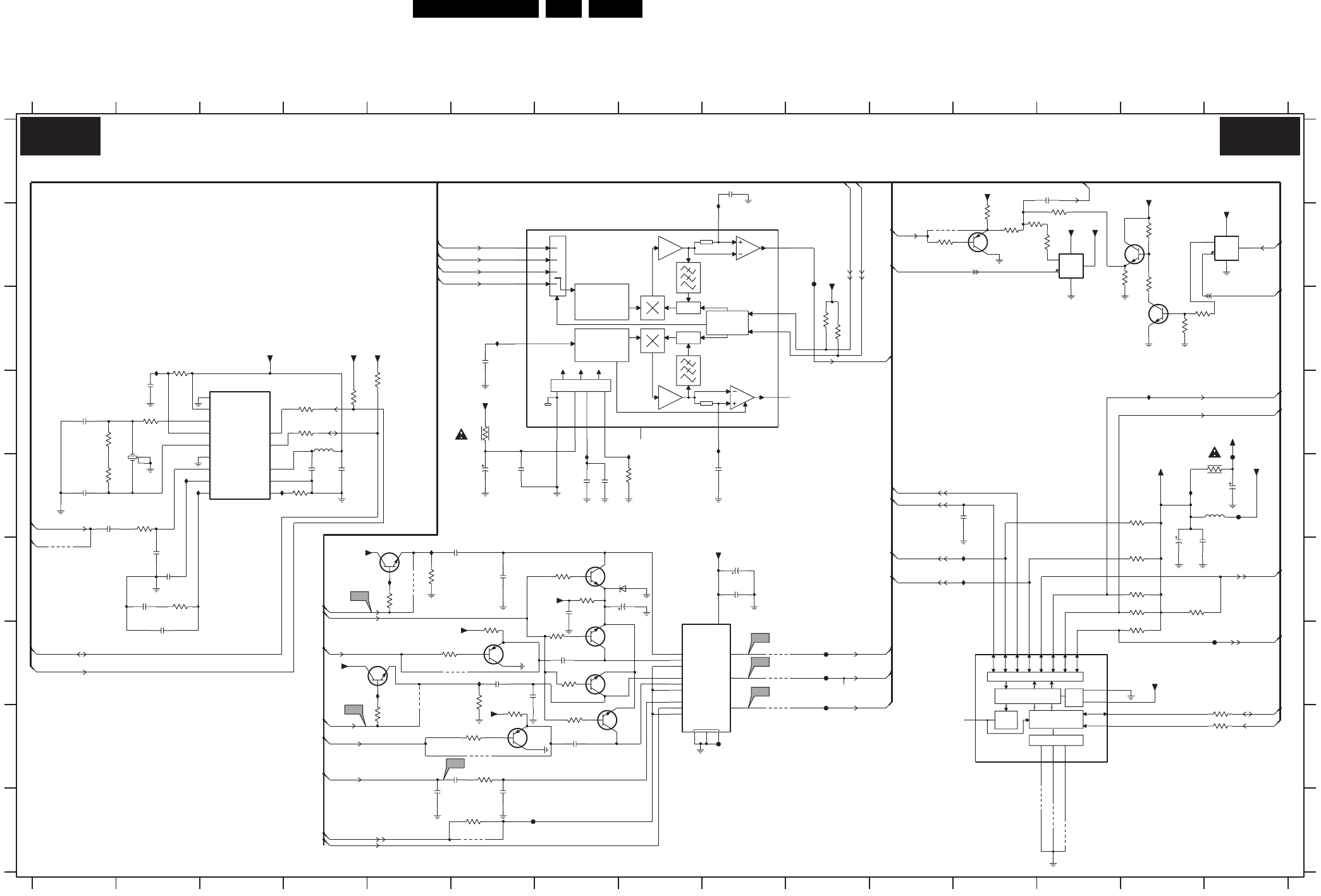
EN 62FTL2.4E AA 7.
Circuit Diagrams and PWB Layouts
SSB: PIP Switch
1
X1
1
1
X1
1
8
888
88
VCC
GND
2V5
B14c(2x)
B15c
B14c(3x),f,g
*
FP57 I6
FP59 G15
FP60 H9
IP58 E7
IP59 B9
IP60 C6
IP61 D9
IP62 D14
IP63 F12
IP64 F12
IP74 G4
IP75 F5
7V9
AUDIO DEMODULATOR
B15a
*
*
9P71 I13
9P72 F1
9P73 G9
9P74 G9
9P75 H9
9PB7 B11
*
IP56 E14
IP57 E8
0V1
*
PIP SWITCH
B15c
7P59-2 F7
7P60 B15
7P61-1 B14
7P61-2 C14
7P62 B13
7P63 B12
9P31 H6
IP50 C2
IP51 E3
IP52 F5
IP53 E2
IP54 E2
IP55 G6
*
*
*
B15B
0V
*
0V1
3PJ6 B14
3PJ7 B14
3PJ8 C14
3PJ9 C14
5P50 D4
5P51 E15
6P10 F8
FP50 E15
FP51 G10
FP52 G10
FP53 G10
FP55 E15
FP56 B10
*
0V1
*
4V4
0V1
7P58-1 G7
7P58-2 H7
7P59-1 G73P85 F14
3P86 C10
3P87 C10
3P88 D6
3P94 D5
3P95 D4
3P96 G7
9P32 G6
9P52 F5
9P53 G5
9P54 I6
9P69 I13
9P70 I13
0V1
B6a,B14c
2V5
B6a,B14c
*
RES
B6a,B15c
3PJ3 B12
3PJ4 B13
3PJ5 B143P61 E8
3P62 H6
3P63 H6
3P64 H7
3P65 H15
3P66 H15
3P67 G14
7P51 D3
7P52-1 F5
7P52-2 G4
7P53-1 G6
7P53-2 H6
7P54 G9
7P55 B6
7P56 G12
0V1
0V1
B14d
B15a
I/O EXPANDER
RES
3P80 C2
3P81 D4
3P82 D22P81 F14
2P87 D2
2P88 D1
2P90 E6
2PE7 H7
2PE8 G7
2PE9 A13
3P97 G7
3P98 G5
3P99 G6
3PG7 F7
3PG8 F7
3PJ0 B11
3PJ1 B12
3PJ2 B12
5V2
*
RES
*
B6a,B15c
3P56 H5
3P57 G6
3P60 F5
*
2P62 F6
2P63 F7
2P65 F9
3P68 F14
3P69 F14
3P70 F14
3P72 E14
3P74 E15
3P75 H6
3P76 F5
3P79 D4
V-CHIP
B6a,B14c
*
*
RES
2P77 E4
2P78 E12
2P79 E7
2P80 F14
A
B
C
D
E
F
G
2PG6 F8
3P49 B13
3P50 D1
3P51 E1
3P52 E4
3P53 E2
3P54 F2
3P55 I6
B15B
B15c
RES
2345678
2P66 F9
2P70 E6
2P71 E15
2P72 E7
2P73 E9
2P74 C6
2P75 A9
2P76 E1
0V1
7 8 9 101112131415
2P50 E4
2P51 E1
2P52 F2
2P53 F2
2P54 F2
2P55 G2
2P56 G6
H
I
A
B
C
D
E
F
RES
*
B15a
0V1
0V1
1
B5a,B14a,b
*
B15a
*
B15c
9 101112131415
1
*
23456
(US ONLY)
B15b
B15b
*
G
H
I
1P50 E2
2P57 G6
2P58 F6
2P59 I5
2P60 H6
2P61 I6
*
*
B15c
VIDEO SWITCH
V37
+5VPIP
100n
2P78
4K7
RES
3P64
47p
2P61
8
VAF2 7
VCOREF
11
VP
14
7P63
BC857BW
16
IN1B|G
1
IN1D|K
2
IN1M
3
IN2
15
4NC1
S1 5
S2 6
VAF1
9
C1C2
10
CSTAB
12
GND
13
IN11
UNIT
CONTROL
SUPPLY
VCO2
AMPLIFIER 2
LIMITER
7 STAGE
AMPLIFIER 1
LIMITER
7 STAGE
VCO1
TDA9820
7P55
4K7
3P85
7P60 74LVC1G66GW
4
35
1
2
+5VPIP
3PJ5
820R
2P66
100n
680R
3PJ1
3PJ2
330R
+5VPIP
9P69
1u0
2P73
9P32
3P98
10R
1u0
2P75
9P73
3P51
10M
10R
res
9PB7
3PJ0
2P79
1u0
3R9
3P88
100u
3PJ4
680R
2P90
4K7
3P72
+5VPIP
FP57
100n
2P70
+8VPIP
10M
3P50
IP58
68n
2P54
10K
3P52
IP52
9P72
BC847BS
5
3
4
FP56
7P61-2
V35
3PJ7
2K2
+5VD
V38
2P50
100n
6K8
3P80
2PE7
BC857BS
7P53-2
1u0
2P58
1u0
10u
2P71
27K
1u0
3P61
+5VPIP
2P72
FP59
10R
47p
V33
3P76
1
V39
2P59
7P52-1BC847BS
2
6
9P52
3P81
100R
7P59-1
BC847BS
5P50
+5VD
6u8
2P53
100n
2PG6
10u10V
BZX384-C2V7
6P10
3PG7
4K7
IP54
IP50
9P75
8p2
2P76
2P80
3P69
4K7
100u
56p
2P52
100n
2P77
FP55
3PJ8
1K8
IP62
+5VPIP
IP55
10R
3P62
100R
3P79
IP53
5
3
4
680R
3P57
2
+5VPIP
BC847BS7P52-2
74LVC1G66GW
7P62
4
35
1
3P60
680R
3P68
4K7
3P82
470K
3P49
390R
3PJ9
4K7
+5VPIP
+5VPIP
IP63
3PJ3
120R
2PE9
100n
6n8
2P55
3P65 100R
3P86
10K
BC847BS
7P59-2
IP60
IP59
9P53
1u0
2P57
9P74
FP53
FP50
100n
2P74
+5VPIP
+5V
BC847BS
7P61-1 2
6
1
3P67
4K7
100n
2P81
2P63
100n
IP56
9P54
3P87
10K
IP64
1K0
3P55
RES
10R
3P56
9P31
BC857BS
+5VD
+5VPIP
7P53-1
680R
3PJ6
res
3PG8
1K0
FP60
1u0
2P87
IP57
FP52
FP51
100n
2P51
DMX-26S
1P50
32K768
3P66 100R
9P71
IP61
+5VD
2R2
3P74
4K7
3P94
3P95
4K7
2P60
1u0
10u
2P65
470R
3P53
OUT3 6
13
10V
15
IN1A
1
IN1B
16
IN2A
14
IN2B
11
IN3A
8
IN3B
9
OUT1 3
OUT2 5
7P54
BA7609F
Φ
3-CHANNEL
VIDEO SWITCH
2CTL1
12 CTL2
CTL3
7
4
10
3P70
4K7
BC847BS
7P58-2
2
SCL
3
SDA
1SO
13
VDD
5
D1
6
D2
7
D3
9
D4
10
D5
11
D6
12
D7
8
GND
CHIP SELECT
I
2
C BUS
TRANSCEIVER
I/O PORT
DATA LATCHES
PWR
RES
OUTI/O
IN
SHIFT
REG
16 CS0
15 CS1
14 CS2
4
D0
IP51
7P56
M62320FP
+8VPIP
9P70
3
3P99
680R
14
SDO 16
SEN
4
SMS
6
VDD 12
VIDEO
7
VIN-INTRO 13
VSS 11
XOUT
5
HSEL
2
I2C-SEL
1
LPF
9
NC1 17
NC2 18
RREF 10
SCK 15
SDA
7P51
Z86130-12SSC
CSYNC
8
HIN-XIN
2PE8
1u0
+5VPIP
4K7
3P97
IP75
+5VD
V34
2P88
22p
6K8
3P54
3P96
4K7
3P75
100R
680R
3P63
RES 2P62
47p
IP74
BC847BS
7P58-1
47p
RES
5P51
SUB-ATTENUATION
FBLK
SWITCH-MAIN
PIP_RESET
SWITCH-SUB
2P56
SCL-VCHIP
SDA-VCHIP
PIP-FM
SEL_PIP_SOUND1
SEL_PIP_SOUND2
7P55-I
7P55-BG
7P55-DK
7P55-M
SEL_PIP_SOUND2
SUB-SYNC-INSERT
SEL_PIP_SOUND1
HA50-PIP
IN-Y50
SUB-ATTENUATION
SUB-SYNC-INSERT
HA50-PIP
DY
DY-IN
Y-PIP+MAIN-OUT
V-PIP+MAIN-OUT
U-PIP+MAIN-OUT
DY-IN
IN-U50
DU
IN-V50
DV
CVBS-Y-RECORD-IN
PIP-CVBS-MON
MUPPET_BLK
SCL-S
SDA-S
F_15460_039.eps
080405
B15B B15B
8204 000 8475.1
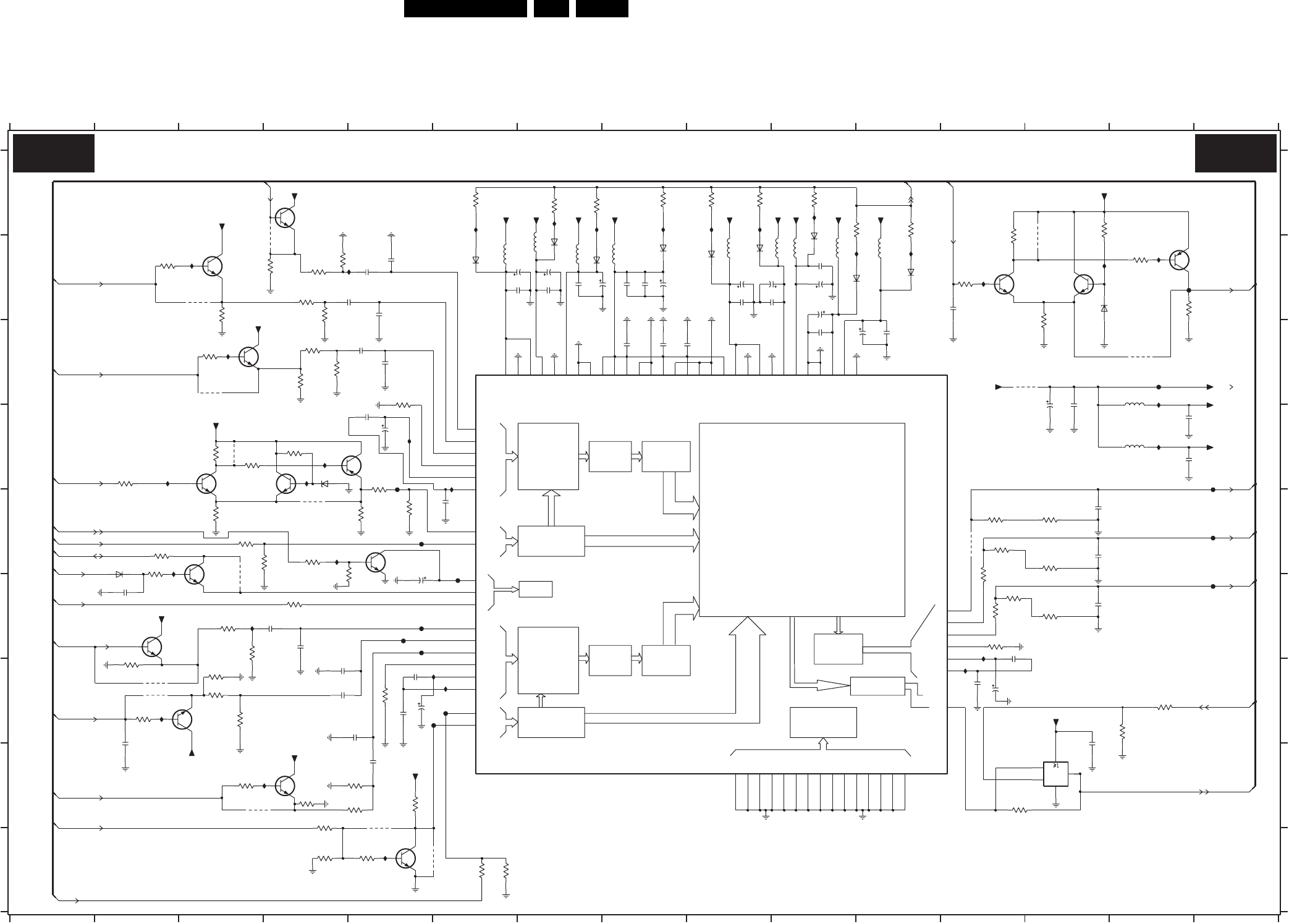
Circuit Diagrams and PWB Layouts EN 63FTL2.4E AA 7.
SSB: PIP Muppet
GENERATION
PLL AND CLOCK
CONVERTER
AND A/D
CLAMP
GENERATION
PLL AND CLOCK
CONVERTER
AND A/D
CLAMP
CONTROL
IIC BUS
PROCESSING
DAC
CONTROL
DISPLAY
CONTROL
TEST
LINE MEMORYH/V FILTER
LINE MEMORYH/V FILTER
IPB1 B14
IPC2 A9
IPC3 A9
IPC4 B11
IPC5 B11
B15a
1V2
RES
RES
H
I
2PA0 B5
2PA1 B5
2PA2 B5
2PA3 B5
2PA4 C5
2PA5 C5
2PA6 E6
2PA7 D5
2PA8 F2
2PA9 E5
B15a
RES
RES
1
IPB2 D2
IPB3 D4
IPB4 B5
IPB5 F3
678910
IPB6 A7
IPB7 A6
IPB8 A8
IPB9 A8
IPC1 A10
123456789101112
B15c(2x)
RES
RES
B15b
B14a
C
D
E
F
G
RES
13 14 15
A
B
RES
C
D
2345
I
A
B
RES
11 12 13 14 15
2PB0 F4
2PB1 G4
2PB2 G4
2PB3 G5
2PB4 G5
2PB5 H2
2PB6 G5
2PB7 H5
2PC2 B7
2PC3 B7
2PC4 B8
RES
RES
RES
RES
2PC5 B8
2PC6 B8
2PC7 C8
2PC8 C8
E
F
G
H
2PD3 B10
2PD4 B10
2PD5 B10
B6a,B15b
B15a
RES
RES
B15c(2x)
B6a,B15b
RES
RES
2PD6 B10
2PD7 C10
2PD8 C10
2PD9 C112PB8 B7
2PB9 B7
2PC0 B7
2PC1 B7
2PE4 G12
2PE5 F12
2PE6 H13
2V7
RES
B6a,B14c
RES
2PF1 D13
2PF2 D13
2PF3 F4
2PF5 D14
2PF6 D14
2PF7 D5
2PF8 G5
2PF9 G12
3PA0 B2
3PA1 B4
2PC9 C8
2PD0 B9
2PD1 B9
2PD2 B10
3PA6 C4
3PA7 C4
3PA8 C3
PIP MUPPET
RES
B15c(2x)
MUPPET
3PA9 C5
3PB0 D4
3PB1 D3
3PB2 D2
3PB3 D3
3PB4 E3
3PB5 E5
3PB6 D5
3PB7 E2
3PB8 E3
3PB9 F2
2PE0 B12
2PE1 E13
2PE2 E13
2PE3 F13
3PC4 G2
3PC5 E4
3PC6 G5
RES
1V0
B6a,B15b
RES
3PC7 G2
3PC8 G3
3PC9 G3
3PD0 H3
3PD1 H5
3PD2 H5
3PD3 H4
3PD4 H5
3PD5 I4
3PD6 I5
3PD7 I6
3PD8 I6
3PA2 B4
3PA3 B4
3PA4 B4
3PA5 H12
3PE3 A13
3PE4 B14
3PE5 B14
B15a(2x)
RES
3PF0 F12
3PF1 G14
3PF2 F12
3PF3 G14
3PF4 F12
3PF5 F4
3PF6 E12
3PF7 E13
3PF8 E12
3PF9 E13
3PG0 F12
3PC0 E3
3PC1 F4
3PC2 F3
3PC3 F3
3PG5 G3
3PG6 H4
3PH2 A7
RES
B15b
B15b
3PH3 A7
3PH4 A8
3PH5 A9
3PH6 A9
3PH7 A10
3PH8 A11
3PH9 A11
3PI0 A6
5PA0 B6
5PA1 B7
5PA2 B7
5PA3 B8
5PA4 B9
5PA5 B10
3PD9 E5
3PE0 B12
3PE1 B12
3PE2 C13
5PB0 D14
6PA0 D4
6PA1 E2
B15b
0V2
RES
6PA2 B13
6PB1 B6
6PB2 B7
6PB3 B7
6PB4 B8
6PB5 B9
6PB6 B9
6PB7 B10
6PB8 B10
6PB9 B11
7PA0 B3
7PA1 C3
3PG1 F13
3PG2 B4
3PG3 B3
3PG4 C4
7PA6 C6
7PA7 F2
7PA8 G3
B15a
0V
3V2
1V0
RES
7PA9 H4
7PB0 I5
7PB1 H13
7PB2 B12
7PB3 B13
7PB4 B14
7PB5 E5
7PB6 A4
9PA0 B3
9PA1 C3
9PA2 E4
9PB5 B13
5PA6 B10
5PA7 B10
5PA8 B11
5PA9 C14
9PA8 I5
9PB1 C14
9PB2 C13
RES
FPA0 E5
FPA1 D5
FPA2 F5
FPA3 F5
FPA4 G6
FPA5 G6
FPA6 B15
FPA7 D15
FPA8 E15
FPA9 F15
FPB0 C14
FPB1 F5
FPB2 F6
IP76 B3
IP77 C3
IP78 D4
IP79 E4
9PB8 E12
7PA2 D3
7PA3 D4
7PA4 D5
7PA5 E3
IP80 E2
IP81 H4
IP82 G2
IP83 I5
IP84 B14
B15b
B15a
IP85 B12
IPA1 C14
IPA3 D14
IPA5 F12
IPA6 G12
IPA7 D5
IPA8 D6
IPA9 G6
IPB0 G69PA3 F3
9PA4 G2
9PA5 G2
9PA6 H3
9PA7 H5
2V7
9PB3 B4
9PB4 D3
IP76
IP77
100R
3PA1
2PC9
100n
9PB4
IPA5
3PB9
3K3
4u7
5PA2
+3V
IPB0
2PD3
100n
39K
3PC9
2PB4
150p
820n
5PA4
47p
2PE3
100n
2PA4
IP84
IP82
IP80
FPB2
IP83
3PF6
560R
39K
3PD1
7PA1
BC847BW
10u
2PF1
+3.3V
3PF1
1K5
1K8
3PD3
2PD6
10u
16V
2PF7
10u 10V
IPA6
120R
3PF0
6PA2
BZX384-C3V9
7PA2
BC847BW
68R
3PG1
IP85
1u0
2PA0
IP81
7PB4
BC857BW
RES2PD2
10u
BC847BW
7PA8
12u
5PA1
3PF3
3K3
2PC2
100n
1K5
3PE2
3PB4
1K5
39K
3PA9
RES
9PB3
100R
3PC1
2PA7
100n
+3VD
+5VPIP
2PF2
100n
1K0
3PF5
3PE3
1K5
10u
2PD5
IP79
IP78
100n
2PB7
+5VPIP
100R
3PD2
3PA6
39K
680R
3PG5
47p
2PE2
+3.3V
IPA1
2PB8
10u
3PG3
680R
2PE5
100n
9PA7
RES
2PC6
10u
2PA1
IPA7
470R
3PF7
150p
RES
9PA6
100n
2PB9
5PA5
12u
6PB1
BAS316
150p
2PA5
9PB5
2PF3
150p
120R
3PF9
3PF2
270R
100R
3PA3
3PA0
2PE1
47p
220R
+5VPIP
10K
3PD6 RES
3PE1
470R
RES
RES
3PA5
220R
10V
10u
2PA9
3PH7
47R
FPB1
FPA8
+3VD
3PD0
220R
4K7
3PC5
BC847BW
7PB0
7PB6
BC847BW
2PA2
100n
RES
9PA4
+3V
39K
3PC6
100R
3PA7
+3.3V
FPB0
FPA9
5PA9
BC847BW
7PA5
1u0
2PB0
100R
3PB7
100n
2PC4
47p
2PB5
RES
39K
3PA4
IPA9
100n
2PD4
7PB3
BC847BW
3PG0
2PD0
10u
2PD1
100n
560R
1
2
35
4
2PC5
100n
7PB1
74LVC1G32GW
BC847BW
7PA3
3K3
3PD8
FPA7
9PA3
2PE6
100n
3K3
3PC0
3PC2
100R
9PA2
47R
3PI0
FPA1
FPA5
5PA6
12u
680R
3PG2
VSSDT1
19
VSSDT2
30
VSSDT3
48
VSSDT4
49
VSSDT5
50
VSSDT6
51
VSSDT7
62
VSSDT8
63
VSSDT9
VSSDDA
96
VSSDMA
16
VSSDP1
65
VSSDP2
40
VSSDRL
41
VSSDRM
61
VSSDRP
85
VSSDSA
18
VREFTMA
82 VREFTSA
7
VSSADA
91
VSSADP
4
VSSAMA
77
VSSASA
90
VSSASP
66
VSSDD
15
VDDDRL
42
VDDDRM
20
VDDDRP
86
VDDDSA
VREFBDA 13
1VREFBMA
80 VREFBSA
11
VREFTDA
99
VDDASA
78
VDDASF
89
VDDASP
67
VDDDD
14
VDDDDA
95
VDDDMA
17
VDDDP1
64
VDDDP2
39
TM
9
VBIASDA
97 VBIASMA
84 VBIASSA
6
VDDADA
92
VDDADP
5
VDDAMA
3
VDDAMF
76
T5
88
T6
93
T7
38
TC
46
TCBC
45
TCBD
47
TCBR
43
TCLK
44
SV
72 SVSYNC
83 SY
37
T0
36
T1
35
T2
34
T3
33
T4
32
NC8
29
NC9
69
PKOFF
75 POR
73 SCL
74 SDA
87 SHSYNC
79 SU
81
NC18
60
NC19
22
NC2
23
NC3
24
NC4
25
NC5
26
NC6
27
NC7
28
NC10
52
NC11
53
NC12
54
NC13
55
NC14
56
NC15
57
NC16
58
NC17
59
DV
70 DVSYNC
8
DY
68
FBL
2MU
100 MV
98 MY
21
NC1
31 71
DCLK
94 DHSYNC
12
DU
10
SAB9081H/N4
7PA6
+3V
BC847BW
7PB5
FPA0
IPA3
100n
2PF6
1K5
3PE0
1K0
3PB5
100n
2PB2
1K2
3PD7
39K
3PC3
3PE4
220R
1K2
3PB6
3PD9
3K3
+5VPIP
6PB2
BAS316
3PH3
47R
RES
FPA3
+5VPIP
9PA8
220R
3PB3
3PG6
680R
16V10u
2PF8
RES
9PA0
16V10u
2PF9
2PD7
100n
BAS316
6PB8
9PA1 RES
BC857BW
7PA4
3PH5
47R
+3V +3VD
12u
5PA7
+5VPIP
2PE0
3n3
100n
2PA6
IPC2IPB9
IPB6
IPB8
100n
BAS316
6PB4
100n
2PB6
2PB3
9PB1
6PB9
BAS316
3PC8
100R
4u7
5PA3
IPB5
2PC7
100n
+5VPIP
9PB8
IPB2
FPA4
3PA8
220R
2PF5
100n
6PB5
BAS316
BC847BW
7PB2
3PC4
680R
100n
2PE4
IPA8
+3V3_SIM
6PB7
BAS316
+3V
RES
470R
3PB1
680R
3PG4
47R
3PH4
9PB2
47R
3PH8
2PC0
10u
1K5
3PB2
150p
2PB1
2PC1
100n
5PA0
820n
BZX384-C3V9
6PA0
IPC3
IPC1
IPC5
5PB0
IPC4
22K
3PF4
+3VD
6PA1
BAS316
3PB8
1K8
IPB7
3PH2
47R
FPA2
FPA6
150p
100n
2PC8
2PA3
IPB4
3PH9
47R
10u
2PC3
3PB0
1K5
RES
4K7
3PD4
220R
3PC7
7PA9
BC847BW
47R
3PH6
+3VD
100n
2PD9
BAS316
6PB6
RES
10u
2PD8
+5VPIP
+3V
BC847BW
7PA0
12u
5PA8
3PD5
3K3
6PB3
BAS316
820R
3PF8
3PE5
1K0
9PA5 RES
7PA7
BC847BW
2PA8
100n
IPB1
39K
3PA2
IPB3
V-HIP-OUT
3V3_FAULT_PIP
DU
HA50-PIP
PIP_RESET
FBLK
Y-HIP-OUT
SCL-S
IN-Y50
IN-V50
HA
IN-U50
SDA-S
HA
U-HIP-OUT
MUPPET_BLK
HA
DV
DY
VS-HIP-OUT
VA50-PIP
HS-HIP-OUT
F_15460_040.eps
080405
B15C B15C
8204 000 8475.1
EN 64FTL2.4E AA 7.
Circuit Diagrams and PWB Layouts
SSB: HDI A/D Converter
COM
OUTIN
SERIAL REGISTER
VDD
REF
8
A/D
8
SYNC
PROCESSING
AND CLOCK
GENERATION
PVD
AND
PWR MANAGMENT
VD
CLAMP
8
GND
A/DCLAMP
CLAMP
A/D
3L33 G5
5L02 C2
3L02 E5
3L03 H5
3L04 C2
3L05 E2
5L14 B3
RES
B19b
B14c,g
5L15 C3
5L16 A3
5L17 B3
5L18 B3
7L01 C6
7L02 A2
3L30 E4
3L31 F4
3L32 G4
3L08 H3
3L11 F2
AL02 G10
AL06 C1
AL07 E1
AL08 F1
FE02 A3
3L29 C4
2L50 F2
2L51 C3
2L52 C6
2L54 F6
FL03 G10
FL04 G10
FL05 H10
FL09 C3
FL10 E3
RESRES
B14g(2x),B19a
5L04 E2
5L06 F2
5L13 A3
2L60 G4
D
E
F
G
B14c(2x)
B19b,d
B19d
2L29 E3
2L30 F3
3L12 G3
3L19 D4
3L20 E4
3L21 F4
3L28 G6
2L49 E2
78910
B14g
B14g
E
F
2L56 G4
2L57 E6
2L58 A3
2L59 E5
C
78910
RES
2L20 C4
2L21 C4
3L06 H5
11
2L31 H2
2L32 H2
2L33 A2
2L34 A3
2L48 D2
6
2L10 A5
2L11 F6
2L12 B4
2L13 B4
B19b,d
11
HDI A/D CONVERTER
G
H
I
A
B
6
IL09 H6
IL10 A5
IL11 B5
IL12 C5
RES
2L14 B4
2L15 B4
2L16 B4
2L17 B5
2L18 E5
2L19 A1
2L25 H10
2L26 H2
2L27 H2
2L28 D3
A/D CONVERTER
2L02 A4
2L03 A4
12345
2L09 C4
RES
2L06 A5
2L07 A5
B14g(2x)B19a
A
B
C
D
B14g,B19d
2L08 C4
FL11 G4
to EPLD
FL17 A1
IL06 F6
IL07 H3
12345
IL08 H3
B19d
B19d
B19d
B19d
2L01 A4
H
I
2L00 B3
RES
RES
RES
2L04 A4
2L05 A4
FL12 F3
FL13 G4
FL15 G10
2L00
22u 6.3V
100R
3L06
470n
IL11
5L06
100n
2L04
100R
3L03
3L32
470R
FL10
100n
2L25
VD
FL17
3L12
5L14
470R
2L57
47n
100n
2L08
5L17
3L33
470R
22u
2L51
VD
6.3V
2L13
100n
3L20
680R
IL08
2L26
2L01
100n
33n
3L31
150R
PVD
FL15
100n
2L20
2L59
1n0
IL09
2
47n
2L52
7L02
LD1117DT33C
1
3
3L08
2K7
2L34
100n
470n
47p
2L18
5L04
39p
AL08
IL06
2L30
100R
3L05
100R
3L04
2L50
47p
2L60
4p7
2L58
IL12
6.3V22u
PVD
2L09
100n
5L18
2L15
100n
100n
2L16
IL07
470R
2L29
3L02
39p
2L03
100n
VDD
FL04
100n
2L10
2L17
100n
680R
3L19
470n
5L02
AL07
3L21
680R
+3V3-AD
2L05
100n
3n3
+5V
2L32
FL03
FL13
47n
2L31
FL12
5L15
1n0
2L56
2L27
FE02
VDD
4n7
2L12
PVD
100n
IL10
3L29
150R
2L07
100n
100n
2L02
2L11
100n
AL06
5L13
3L30
150R
100n
2L33
2L21
100n
FL11
2L49
VD
4p7
100R
3L11
47n
2L54
470R
3L28
2L28
39p
5L16
PVD
22u
2L19
FL05
6.3V
FL09
78
79
64VSOUT
31 VSYNC
AL02
39
42
45
46
51
52
59
11
22
23
69
71
ROUTA6
70
ROUTA7
56 SCL
57 SDA
49 SOGIN
65SOGOUT
26
62
27
54 RAIN
58
REF-BYPASS
77
ROUTA0
76
ROUTA1
75
ROUTA2
74
ROUTA3
73
ROUTA4
72
ROUTA5
GOUTA4
4
GOUTA5
3
GOUTA6
2
GOUTA7
66HSOUT
30 HSYNC
37 MIDSCV
34
35
25
28
32
36
9
GOUTA0
8
GOUTA1
7
GOUTA2
6
GOUTA3
5
53
60
61
63
68
10
80
20
21
24
COAST 67DATACK
33 FILT
48 GAIN
1
40
41
44
47
50
BOUTA1
17
BOUTA2
16
BOUTA3
15
BOUTA4
14
BOUTA5
13
BOUTA6
12
BOUTA7
38 CLAMP
29
7L01
AD9883AKST
55 A0
43 BAIN
19
BOUTA0
18
2L06
100n
2L48
4p7
100n
2L14
COAST
SYNCDET
CLK-2FH
SDA-F3
SCL-F3
Y-AD-7
Y-AD-6
Y-AD-5
Y-AD-4
Y-AD-1
U-AD-5
Y-AD-3
Y-2FH
HS-2FH
VS-2FH
UV-AD-0
UV-AD-1
UV-AD-2
UV-AD-3
UV-AD-4
UV-AD-5
UV-AD-6
UV-AD-7
U-AD-0
U-AD-1
U-AD-3
U-AD-4
U-AD-6
U-AD-7
U-AD-2
H-2FH-AD-OUT
V-2FH-AD-OUT
V-2FH
Y-2FH
U-2FH
Y-AD-0
Y-AD-2
F_15460_041.eps
080405
B19A B19A
8204 000 8484.1
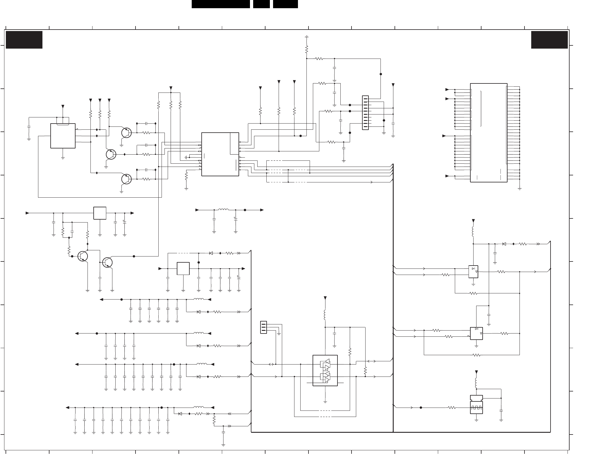
Circuit Diagrams and PWB Layouts EN 65FTL2.4E AA 7.
SSB: EPLD Control
COM
OUTIN
EN
EN
VCCA
GNDA
GNDG
GND
PLL2
BANK1
PLL2
PLL1
PLL1
VCCIO
PLL1
PLL2
BANK2
BANK3
BANK4
VCCINT
COM
OUTIN
STATUS
2
1
0
CEO
TMS
TCK
TDO
TDI
SCAN
CLK
MSEL
3
ASDO
CSO
DCLK
DATA0
1
0
CE
CONFIG
CONF_DONE
DATA
GND
ASDI
DCLK
CS_
VCC
IE27 E2
IE29 G5
IE30 H5
IE33 E12
IE34 C3
B3A
B19b
7E01 E5
7E02 B2
7E03 F11
7E04 G11
7E05 D3
7E06 I12
IE20 B4
IE21 C3
IE22 B3
IE23 C4
IE24 C4
IE25 C3
7V01-1 B5
7V01-6 A12
9E57 I8
9E58 I8
IE31 I5
IE32 G5
9E61 D7
9E62 C7
ONLY
USE
FACTORY
FOR
IE26 E2
B19b(5x),B19d(2x)
3E79 B8
3E80 C8
3E81 E12
3E82 F12
3E83 F11
FE05 F5
FE50 I10
FE51 B8
FE52 A9
5E50 H5
5E51 I5
5E52 G5
5E53 D6
FE57 H4
FE58 I4
5E56 H11
5E58 G8
FE61 E3
FE66 B9
FE67 E2
B3A
3E84 G10
3E85 G12
3E86 G11
3E87 I11
3E88 H5
3E89 I5
3E01 B4
3E02 C4
3E03 D4
3E20 F11
5E54 F5
5E55 E11
3E51 B4
3E52 B4
9E63 C7
9E64 C7
9E65 D7
B19b
B12
B19b
RES
RES
3E56 E2
3E57 E2
3E58 G5
3E59 B3
2E84 B1
2E86 E2
2E87 E6
2E88 A8
3E64 B3
3E69 H8
2E91 C8
2E92 B9
3E74 I5
3E77 A8
3E78 A8
2E56 H4
2E57 H4
2E58 H4
2E59 H4
2E62 H3
2E65 H3
12 13
A
B
2E70 I4
2E71 I4
E
F
3E53 B7
3E54 G5
3E55 E2
RES
RES
123
B19a,d,c
2D11 G3
2D12 G3
2D15 I5
2E01 G4
10 11 12 13
2E43 F4
2E49 E3
34
2E52 G8
2E54 G4
2E55 H4
B19d
B19b,d
A
B
C
RES
891011
1E02 B9
1E04 G6
2D03 E5
2D04 F3
C
D
G
H
I
B19b,d
B3a,B19b
456789
12
D
E
F
G
H
I
2D09 G3
2D10 G3
567
B19d
2E78 I2
2E79 F5
2E80 F5
2E81 I2
2E82 G3
2E83 G4
2E03 G4
2E06 G4
2E41 F5
2E42 F6
2E89 B8
2E90 B8
2E50 E3
FOR FACTORY
USE ONLY
I2C BUFFER
B3a,B19b
B19a,d,c
B3a
B19b
B3a
B19b
B3c
B19a
RES
FE60 F3
FE53 C7
FE54 C9
FE55 B8
FE56 D6
B3c
FE59 G3
2E74 I3
2E75 I3
2E77 I2
2E51 E2
RES
3E73 B6
7E10 H8
7E12-1 F3
7E12-2 E2
7E25 C3
7E26 B3
7E27 C3
3E60 A8
3E61 E6
3E62 D5
3E63 B7
9E59 E5
9E60 C7
3E70 H9
IE35 C4
IE36 B4
IE37 E5
B19b
B19b
I2C BUFFER
2E73 I3
2E96 B4
2E97 C4
2E98 C4
2E99 F6
3E00 B2
2E66 H3
2E67 H3
2E68 I4
2E69 I4
3E21 H11
3E50 B4
2E72 I3
6E51 E5
6E52 G5
6E53 G5
EPLD CONTROL
RES
6E54 I5
6E55 H5
6E56 E12
2E93 G12
2E94 E12
2E95 I12
100n
2E74
IE27
IE32
100n
2E83
3E62
1K0
10n
2E57
2E87
100u 16V
2D15
10n
FE67
IE26
2E71
10n
+1V5-INT
+3V3-IO
5E53
10u
3E77
47R
9E57
3E73
10K
100n
2E79
4V47u
2E99
3E50
10K
1
5
4
FE57
7E03
74LVC1G126GW
2
3
2E88
100p
9E62
2E68
10n
1u0
2E81
+3V3-EPLD
+3V3-EPLD
5E55
2
3
1
5
4
74LVC1G125GW
7E04
IE24
10n
2E70
47R
3E78
2E84
100n
100n
2E43
7E01
LF15ABDT
GND
2
IN
1
OUT
3
+3V3-IO
2E56
10n
+3V3-SD
10K
3E51
9E65
2D03
1n0
6E56
BAS316
3E88
+3V3-IO
2D04
1n0
47R
LF15ABDT
2 GND
IN
1
OUT
3
T3
L7
L10
T14
7E05
K7
C1
G6
P1
A14
F10
F7
A3
P16
K11
C16
A7
K9
T7
T10
A10
G8
G10
H7
H9
J8
J10
F8
F9
F11
G7
J6
J11
J5
J12
H6
H11
A16
L8
L9
L11
T1
T5
T12
T16
A5
A12
F6
A1
G9
G11
H8
H10
J7
J9
K6
K8
K10
L6
POWER
Φ
7V01-6
EP1C12F256C8
7E12-1
BC847BS
FE52
3E60
10K
10K
3E63
100n
2E93
2E94
100n
10R
3E86
+1V5
100n
2E72
10K
3E53
6E54
BAS316
res
+1V5
10n
2E59
9E63 res
9E64
FE66
+3V3-EPLD
10n
2E42
BAS316
6E51
2E75
100n
100p
2E91
J15
100n
2E41
H3
K13
G4
H2
K4
J3
J2
J13
J14
H14
H15
CONTROL
Φ
7V01-1
EP1C12F256C8
K3
H4
J4
G1
H1
G16
H16
+1V5
IE22
IE25
+3V3-EPLD
IE20
IE23
+2V5-IO
+3V3-IO
res
2
1
4
3
FXO-34FL
14M31818
7E06
IE29
IE30
FE50
2E55
1u0
47R
3E81
47R
3E54
FE51
4K7
+3V3-IO
3E70
BC847BS
+3V3-IO
7E12-2
2E86
+3V3-EPLD
+1V5-PLL
+1V5-PLL
100n
+3V3-EPLD
FE58
5E54
5E52
100n
+3V3-IO
+3V3-IO
2E82
47R
3E61
9E59
res
100n
2E06
3E58
47R
BAS316
6E53
2E03
100n
IE21 FE53
100p
2E98
2E97
100p
+3V3-EPLD
FE54
2E95
100n res
IE31
+3V3-IO
47R
3E79
3E83
10R
10R
3E82
BAS316
+2V5-IO
2E90
100p
6E52
2E73
100n
47R
3E87
res
5E56
res
10R
2E92
100p
3E84
4
3
7
8
2E58
10n
Φ
SCD
7E02
EPCS4SI8
5
1
26
100n
2D09
9E60
BAS316
6E55
FE59
100n
2E49
FE60
2E69
10n
5E51
2E78
100n
2E66
100n
+1V5-INT
9E58
2E50
47u 4V10n
2D11
2E52
100n
100n
2E65
1u0
2E51
+3V3_SIM
3E57
100K
10R
3E85
3E20
10R
FE05
2E54
100n
3E02
1K0
100n
2E01
IE33
4K7
3E69
3E55
10K
+3V3-EPLD
3E59
10K
1K0
3E03
100p
2E96
IE35
IE37
IE36
IE34
7E27
BC857BW
FE61
FE56
2E89
100p
3E21
10R
8
9
FE55
1E02
1
10
2
3
4
5
6
7
147279-2
10K
3E64
9E61 res
3E74
47R
2E62
100n
100n
2E67
3E80
+3V3-IO
47R
2D10
1u0
2E80
100n
3
3E52
10K
1E04
B3B-PH-SM3-TBT
1
2
10K
3E00
1K0
3E01
+3V3-IO
7E26
BC857BW
5E58
NC 1
SCL02 SCL1 7
SDA03 SDA1 6
VCC
8
7E10
PCA9515DP
EN5
GND
4
3E56
33K
5E50
3E89
47R
2D12
10n
BC857BW
7E25
CLK32I
100n
2E77
CLK64
CLK32P_EPLD
PROT
SWITCH-2FH
CLK32E
SWITCH-2FH
REFCLK
SDA-F3
PROT
CLK32P_EPLD
REFCLK
PROT
PROT
SCL-EPLD
SDA-EPLD
3V3_FAULT
PROT
CLK-VID
CLK-2FH
PROT
SCL-F3
F_15460_042.eps
080405
B19B B19B
8204 000 8484.1
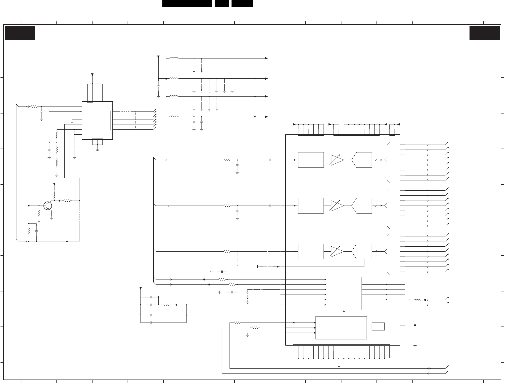
EN 66FTL2.4E AA 7.
Circuit Diagrams and PWB Layouts
SSB: EPLD OSD
AIN-
PWRDWN
2
DATA
GND
3
7
VD VDD
VREFIN
5
4
VREFOUT
AIN+
1
0
6
ENCODE
SERIAL REGISTER
VDD
REF
8
A/D
8
SYNC
PROCESSING
AND CLOCK
GENERATION
PVD
AND
PWR MANAGMENT
VD
CLAMP
8
GND
A/DCLAMP
CLAMP
A/D
B3a
B3a
E
F
3E04 D1
3E05 C1
3E06 D6
3E07 E6
IE03 E1
2E07 A5
2E08 C5
2E09 A6
2E10 B5
2E28 H4
2E29 H4
2E30 H4
2E32 F1
2E34 H4
2E35 I12
2E39 B1
2E48 G6
2E53 G6
IE04 E2
IE05 F2
IL01 A7
IL02 B7
A/D CONVERTER
IL03 C7
2E21 D8
2E22 D7
B3a,B19d
B3a
B19c,d
B19d
B3a
3E11 G6
3E12 G6
3E13 E1
3E14 G7
3E15 F1
3E16 H5
3E18 H7
3E19 H7
3E37 B1
3E90 D1
5E03 C5
7E22 E1
7E23 C8
7E24 B2
9E74 E2
9E78 B3
AL10 H12
FE01 G6
FE03 G6
FE04 H12
FL01 A4
IE00 H4
2E23 E8
2E24 E7
2E25 F7
2E26 G7
2E27 G7
IL05 G8
B3a
11 12 13
1
IE01 H5
3E08 F6
3E09 E1
3E10 E2
12345678910
A
B
C
D
B
C
D
E
F
G
H
I
2E02 D1
2E04 D2
2E05 B4
3456
B19a,b,d
B19a,b,d
2
G
H
I
A
EPLD OSD
5E00 A5
5E01 A5
5E02 B5
7 8 9 10 11 12 13
2E17 B6
2E18 B6
2E19 B6
2E20 C6
B19c
B19c
B19d
2E11 B6
2E12 B6
2E13 B6
2E14 B6
2E15 B6
2E16 B5
3E91 H12
5E03
VBL
3E16
2K7
IL05
IE00
3E06
100R
2E27
100n
FE01
100n
2E08
10p
2E39
2E22
22p
1K5
3E05
100n
2E02
3E08
100R
100R
3E07
IL03
3E10
33R
3E19
100R
100n
2E18
100n
2E17
2E48
10p
10p
2E53
100n
2E35
4n7
2E30
VDDO
100n
2E13
3E91
33R
IL01
3E90
68R
47n
2E28
3n3
100R
3E09
2E34
3E15
100R
+3V3-AD
100n
2E07
PVDO
2E24
FE04
22p
5E00
PVDO
VDO
2E09
100n
9E78
AL10
IE01
100R
3E18
100n
2E16
2E20
100n
VDO
2E05
100n
2E19
100n
2E12
100n
100n
2E11
2E10
100n
33n
2E29
PVDO
FL01
PVDO
7E22
BC847BW
2E32
10p
VBL
IE03
2E04
100n
2E26
22p
2E23
47n
47n
2E25
3E12
470R
3E11
470R
IL02
VDDO
3E04
5E01
1K0
23
69
78
79
64VSOUT
31 VSYNC
62
27
39
42
45
46
51
52
59
11
22
72
ROUTA5
71
ROUTA6
70
ROUTA7
56 SCL
57 SDA
49 SOGIN
65SOGOUT
26
35
54 RAIN
58
REF-BYPASS
77
ROUTA0
76
ROUTA1
75
ROUTA2
74
ROUTA3
73
ROUTA4
GOUTA3
5
GOUTA4
4
GOUTA5
3
GOUTA6
2
GOUTA7
66HSOUT
30 HSYNC
37 MIDSCV
34
21
24
25
28
32
36
9
GOUTA0
8
GOUTA1
7
GOUTA2
6
47
50
53
60
61
63
68
10
80
20
CLAMP
29 COAST 67DATACK
33 FILT
48 GAIN
1
40
41
44
BOUTA0
18
BOUTA1
17
BOUTA2
16
BOUTA3
15
BOUTA4
14
BOUTA5
13
BOUTA6
12
BOUTA7
38
7E23
AD9883AKST
55 A0
43 BAIN
19
FE03
100R
3E37
47n
2E21
1
5
8
15
3
2
19
18
17
14
13
12
11
10
4
9
16
8-BIT
Φ
ADC
AD9283BRS-50
7E24
7
620
5E02
2E14
100n
IE05
IE04
RES
9E74
3E13
1K0
100n
2E15
+3V3-AD
3E14
1K0
CLK-BL
CLK-OSD
CLK-BL
BACKLIGHT-DIMMING
G-OSD-0
G-OSD-2
R-OSD
G-OSD
B-OSD
HD3-OTC
VD-OTC
B-OSD-6
B-OSD-5
B-OSD-4
B-OSD-3
B-OSD-2
B-OSD-1
B-OSD-0
G-OSD-1
G-OSD-3
G-OSD-4
G-OSD-5
G-OSD-6
G-OSD-7
SCL-F3
R-OSD-0
R-OSD-1
R-OSD-2
R-OSD-3
R-OSD-4
R-OSD-5
R-OSD-6
R-OSD-7
B-OSD-7
BL-OSD
BL-OSD-1
BL-OSD-2
BL-OSD-3
BL-OSD-4
BL-OSD-5
BL-OSD-6
BL-OSD-7
SDA-F3
F_15460_043.eps
080405
B19C B19C
8204 000 8484.1
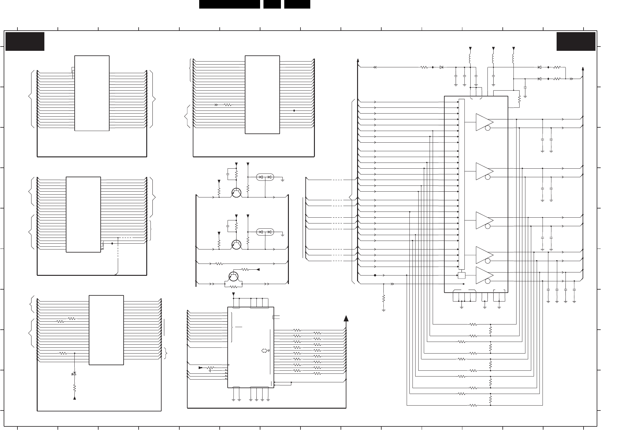
Circuit Diagrams and PWB Layouts EN 67FTL2.4E AA 7.
SSB: EPLD I/O
PLL
TTL PARALLEL-TO-LVDS TTL PARALLEL-TO-LVDS
GND
PLL
GND
LSVD
VCC
GND
DEV_OE
DEV_CLR
INIT_DONE
CLKUSR
8
NC
L
U
10
16
1
2
3
4
5
9
10
11
12
13
512K-1
DQM
VDD
0
VSSQ
A
14
15
RAS
CAS
WE
A11
3
2
CLK
D
VSS
VDDQ
1
0
CKE
CS
9
8
7
6
5
4
6
7
B20
B14g
I
A
B
C
D
E
3V30 H12
B3b,c
B3c
3V40 H1
B3b,c
B19a
B19d
B3a
B3c
B3c
B19a
B20,B21
B19d,B3b,c
B14g,B19a
3V21-1 H8
3V21-2 H7
3V21-3 H8
3V21-4 G7
3V33 I11
3V34 I12
3V35 F6
3V36 B6
3V37 G2
3V38 G1
3V39 H5
13 14
1
3V32 I12
B14f,g
3V31 I11
B3a,B19c
LVDS TRANSMITTER
2V23 G14
2V24 G14
2V25 G14
3V01 H12
3V02 H12
3V07 G10
3V25 G12
3V26 H12
3V27 H11
3V28 H12
3V29 H11
3V08 B13
3V14 A11
3V15 A14
3V16 A14
3V17 H12
B19b
B19d
B19d
32
B3a,c,d
B3b,c
B3a
B3a,c
10 11 12
B13b,B20(2x)
123456
3V19 I12
3V20 I12
B3c
B3c
B3c
B3a
B20
B20
B19b
3V18 I2
B3b,c
B3b,c
B19d
B19c
14
B19a,b,c
B3b,c
B21,B19b(2x)
F
G
H
I
2V06 B13
2V07 A11
2V08 A12
2V09 A12
78
RES
B19c
B19c,d
B19d
B19c(2x)
B19a
B19a
B19a
7V01-4 G3
7V01-5 A7
7V02 B11
7V03 G6
7V04-1 D6
7V04-2 F6
7V06 F6
9E66 D8
9E67 E8
9E68 E8
9E69 E8
9E70 D8
B3c
B19a,b,c
G
C
F
B3c
B3c
B19d
H
9
A
B
3V56 F5
3V57 F6
5V06 A12
5V07 A12
5V08 A13
6V01 A11
6V02 A13
6V03 A13
6V05 I2
6V06 D7
6V07 E7
7V01-2 A2
7V01-3 D2
B19d
B19d
B19a
*
*
3V24-4 I8
B3a
3V50 D5
3V51 D6
3V52 D6
3V53 E6
3V54 E6
3V55 E5
3V24-3 H7
B20
B19d
3V24-1 H7
3V24-2 H8
D
E
B3c
B19c(4x)
B19d
B3c
B3b,c
3V23-2 H8
3V23-4 H8
3V23-3 H7
B20
B20
EPLD I/O
2V10 A12
2V11 E6
3V22-1 H8
3V22-2 H7
3V22-3 H8
3V22-4 H7
3V23-1 H7
2V12 D6
2V16 C13
2V17 C14
2V18 D13
2V19 D14
B3c
9E71 E8
9E72 F8
9E73 F8
9E75 E3
9E76 F3
9E77 D8
AV01 F9
IV01 E3
IV02 A14
IV03 A14
RES
IV04 A11
B3b,c
B19d
IV05 B7
109
B3c
B19b
678
2V22 G14
B3c
B3c
B20
2V20 E13
2V21 E14
B20
45
B19d
B19d
B21
B21
B21
B20,B21B3b,e,B19d
B19d
B19d
B19d
B20
B20
13
B19a
1211
*
180R
3V02
10K
3V50
9E72
9E71
+5V+3V3-IO
+3V3-IO
3V51
10K
3V21-2 68R27
BAV99 COL
6V07
2V23
10p
6V06
BAV99 COL
45
5V06
68R
3V24-4
3V16
47R
68R
3V22-3 36
+3V3-IO
10K
3V57
7V06
BC847BW
5V08
12
+3V3-SD
5V07
100R
3V35
120R
3V31
2V10
100n
100R
3V40
3V21-4 68R45
9E69
9E68
9E67
9E66
3V30
120R
120R
3V25
2V06
100n
+3V3-EPLD
42
TXOUT3+ 37
TXOUT3- 38
26
9
1
4
TXIN86
TXIN97
TXOUT0+ 47
TXOUT0- 48
TXOUT1+ 45
TXOUT1- 46
TXOUT2+ 41
TXOUT2-
27
TXIN2528
TXIN2630
TXIN2750
TXIN355
TXIN456
TXIN52
TXIN63
TXIN7
18
TXIN1819
TXIN1920
TXIN254
TXIN2022
TXIN2123
TXIN2224
TXIN2325
TXIN24
52
TXIN108
TXIN1110
TXIN1211
TXIN1312
TXIN1414
TXIN1515
TXIN1616
TXIN17
33 PLLVCC 34
PWRDWN_32
R-FB 17
TXCLKIN31
TXCLKOUT+ 39
TXCLKOUT- 40
TXIN051
TXIN1
5
13
21
29
53
36
43
49
LVDSVCC 44
35
DS90C385MTD
7V02
3V27
9E77
120R
10p
2V18
3V38
100R
9E70
+3V3-EPLD
3V17
180R
9E76
68R3V24-3 3 6
3V32
3V24-1 1 8
120R
2V24
10p
68R
9E73
IV02
120R
3V34
IV03
18
BAS316
6V02
3V21-1 68R
3V23-3 68R36
3V23-2 68R27
IO_88 R15
9E75
IO_80 M12
IO_81 P12
IO_82 R12
IO_83 T13
IO_84 R13
IO_85 R14
IO_86 P13
IO_87 T15
IO_72 N10
IO_73 P10
IO_74 R11
IO_75 P11
IO_76 N11
IO_77 N12
IO_78 M9
IO_79 M11
IO_64
P8
IO_65 M10
IO_66 R9
IO_67 T9
IO_68 P9
IO_69 N9
IO_70 R10
IO_71 T11
IO_56
T6
IO_57
R7
IO_58
P7
IO_59
N7
IO_60
R8
IO_61
T8
IO_62
M8
IO_63
N8
IO_48
P5
IO_49
M5
IO_50
M6
IO_51
N5
IO_52
N6
IO_53
P6
IO_54
R6
IO_55
M7
IO_41
R2
IO_42
T2
IO_43
R3
IO_44
P4
IO_45
R4
IO_46
T4
IO_47
R5
Φ
BANK 4
EP1C12F256C8
7V01-5
100R
3V37
3V07
4K7
3V01
180R
3V29
120R
1 8 68R
3V22-1
10p
2V25
3V18
390R
3V26
47R
3V15
18
120R
3V23-1 68R
IO_3
C2
IO_4
B1
IO_40 N4
IO_5
G5
IO_6
F4
IO_7
D3
IO_8
E4
IO_9
F5
IO_32 L5
IO_33 M4
IO_34 N3
IO_35 K5
IO_36 L4
IO_37 R1
IO_38 P2
IO_39 P3
IO_24 K1
IO_25 L1
IO_26 L2
IO_27 M1
IO_28 N1
IO_29 M2
IO_30 N2
IO_31 M3
IO_18
G2
IO_19
F1
IO_1
D4
IO_2
C3
IO_20
H5
IO_21 J1
IO_22 K2
IO_23 L3
IO_10
E3
IO_11
D2
IO_12
E2
IO_13
D1
IO_14
F3
IO_15
G3
IO_16
F2
IO_17
E1
7V01-2
EP1C12F256C8
BANK 1
Φ
+3V3-IO
36
3V21-3 68R
2V19
10p
IO_175 B4
IO_176 C4
IO_177 B3
IO_178 A2
IO_179 B2
120R
3V28
IO_167 C6
IO_168 D6
IO_169 D5
IO_170 E6
IO_171 E5
IO_172 C5
IO_173 B5
IO_174 A4
IO_159 A8
IO_160 B8
IO_161 D7
IO_162 C7
IO_163 B7
IO_164 A6
IO_165 E7
IO_166 B6
IO_151
A9
IO_152
B9
IO_153
D9
IO_154
C9
IO_155
E10
IO_156
C8
IO_157 D8
IO_158 E8
IO_143
D12
IO_144
D11
IO_145
C11
IO_146
B11
IO_147
A11
IO_148
B10
IO_149
C10
IO_150
D10
IO_135
C13
IO_136
B13
IO_137
A13
IO_138
B12
IO_139
C12
IO_140
E12
IO_141
E11
IO_142
E9
Φ
BANK 2
EP1C12F256C8
7V01-3
IO_132
B15
IO_133
A15
IO_134
B14
IO_95
K12
IO_96
K14
IO_97
L12
IO_98
N14
IO_99
M13
IO_130 C14
IO_131 D13
IO_89
N13
IO_90
P14
IO_91
P15
IO_92
R16
IO_93
N15
IO_94
N16
IO_122 E14
IO_123 F12
IO_124 E13
IO_125 D14
IO_126 H13
IO_127 G12
IO_128 B16
IO_129 C15
IO_114 F16
IO_115 F14
IO_116 F13
IO_117 F15
IO_118 E16
IO_119 E15
IO_120 D16
IO_121 D15
IO_106
L16
IO_107
K16
IO_108
K15
IO_109
J16
IO_110
H12
IO_111 G14
IO_112 G13
IO_113 G15
7V01-4
EP1C12F256C8
IO_100
M14
IO_101
L13
IO_102
M15
IO_103
M16
IO_104
L14
IO_105
L15
BANK 3
Φ
AV01
3V39 4K7
6V05
TLMG3100
3V23-4 68R45
IV04
3V33
120R
27
IV05
68R3V22-2
10p
2V17
6V03
BAS316
68R3V22-4 4 5
2V20
10p
10p
2V21
6V01
100n
2V07
BAS316
47R
3V14
3V56
100R
3V36
100R
2V08
100n
3V08
1K0
2V12
470p
3V20
180R
470p
2V11
+3V3-SD
2V16
10p
47K
3V52
+3V3-IO
+3V3-IO
100n
2V09
47K
+5V
10K
3V54
3V53
180R
3V19
3
4
3V55
10K
7V04-2
BC847BS
5
50
4
10
41
47
15
10p
2V22
33
37
17
36
1
25
7
13
38
44
26
49
3
5
6
8
9
11
12
39
14
16
34
35
18
2
40
42
43
45
46
48
22
20
19
23
24
27
28
29
30
31
32
DRAM
512K X 16 X 2
Φ
MSM56V16160F-7T3
7V03
21
27
IV01
68R
3V24-2
+3V3-EPLD
BC847BS
7V04-1 2
6
1
FRAME
AL-CL-IN
AL-DA-IN
R4 ODC
AL-DA-IN
LAMP LAMP-ON
AL-CL
AL-DA
R-OSD-2
G-OSD-6
G-OSD-3
G-OSD-5
BACKLIGHT-DIMMING R3
G-OSD-1 B2
G-OSD-0 G0
B-OSD-1 R2
BL-OSD-1
B-OSD-0
R-OSD-1
R-OSD-0 G3
BL-OSD-2
RST-FBX
BL-OSD-2 G1
R6
R1
R0
BL-OSD-3
BL-OSD-4
B-OSD-4
BL-OSD-5
BL-OSD-6
B-OSD-2
BL-OSD-7
B-OSD-5
R-OSD-6
R-OSD-5
G-OSD-2
R-OSD-4
R-OSD-3
G-OSD-4
R-OSD-7
SD-DQ1
SYNCDET
SD-CLK
SWITCH-2FH
CLK32E
O_VAL
YOUT(9)
YOUT(6)
YOUT(5)
YOUT(8)
YOUT(4)
YOUT(3)
YOUT(0)
YOUT(7)
SDA-F3
SCL-F3
YOUT(2)
YOUT(1)
U_VOUT(1)
U_VOUT(0)
U_VOUT(2)
U_VOUT(6)
B-OSD-6
B-OSD-7
B-OSD-3
TXCLKLCD+
G1
G3
G4
B6
B7
G2
LAMP
LCD-PWR-ON
SD-CLK
SD-A0
SD-A1
SD-A10
SD-A2
SD-A3
SD-A4
SD-A5
SD-A8
SD-A9
SD-DQM
SD-WE
SD-CAS
SD-A7
SD-A6
SD-A11
SD-RAS
SD-DQ3
TXLCD0-
TXLCD0+
TXLCD3+
TXLCD3-
TXCLKLCD-
YG(0)
Y-AD-2
SD-DQ2
SD-DQ4
SD-DQ5
SD-DQ7
SD-DQ6
SD-DQ8
SD-DQ9
SD-DQ11
SD-DQ10
SD-DQ12
SD-DQ13
SD-DQ15
SD-DQ14
SD-DQ16
UV-AD-2
UV-AD-4
SD-DQ5
SD-DQ4
SD-DQ7
SD-DQ8
SD-WE
SD-DQ10
G4
G2
R7
R5
B4
DE-OUT
G6
G7
B3
G5
B0
B7
B6
B5
PARITY
LVDS-PWR-DOWN
VS-OUT
CLK-OUT
G-OSD-7
B1
HS-OUT
SD-DQ9
SD-RAS
CLK-OUT
R5
YG(1)
YG(5)
HD3-OTC
VREF
VA
RSTR_EPLD
HREF
SN-CL_EPLD
SN-DA_EPLD
FALREF
YG(4)
VD_E
REFIN
REF
HD_E
U_VOUT(9)
U_VOUT(8)
U_VOUT(5)
U_VOUT(7)
U_VOUT(4)
U_VOUT(3)
R6
R0
R1
HREF_EXT
YG(7)
VD-OTC
H-2FH-DIV-2
HS-DET
UV-AD-1
Y-AD-5
Y-AD-6
PROT
PROT
U-AD-7
SD-DQ14
G6
G7
TXLCD1+
G5
TXLCD2+
B5
B1
R7
R6
G0
B0
PARITY
SD-DQ11
SD-DQ6
SD-A10
SD-A0
SD-A3
SD-A1
CLK-OSD
SD-A2
SD-A6
SD-A5
SD-A4
SD-A7
SD-A11
SD-A8
SD-A9
SD-CAS
V-2FH-AD-OUT
H-2FH-AD-OUT
CLK-VID
COAST
AL-CL-IN
U-AD-0
U-AD-2
U-AD-3
Y-AD-0
U-AD-4
U-AD-1
U-AD-5
Y-AD-1
R4
G0
B2
UVG(0)
G3
UVG(1)
UVG(2)
UVG(3)
UVG(7)
YG(3)
YG(2)
UVG(4)
UVG(5)
UVG(6)
YG(6)
UV-AD-3
Y-AD-7
UV-AD-5
UV-AD-6
UV-AD-7
UV-AD-0
U-AD-6
Y-AD-4
SD-DQM
Y-AD-3
SD-DQ1
SD-DQ2
SD-DQ16
SD-DQ15
SD-DQ13
SD-DQ3
SD-DQ12
R0
R1
B2
R2
B3
B4
HS-OUT
VS-OUT
DE-OUT
R3
R4
TXLCD1-
TXLCD2-
LVDS-PWR-DOWN
G1
R2
R3
F_15460_044.eps
080405
B19D B19D
8204 000 8484.1
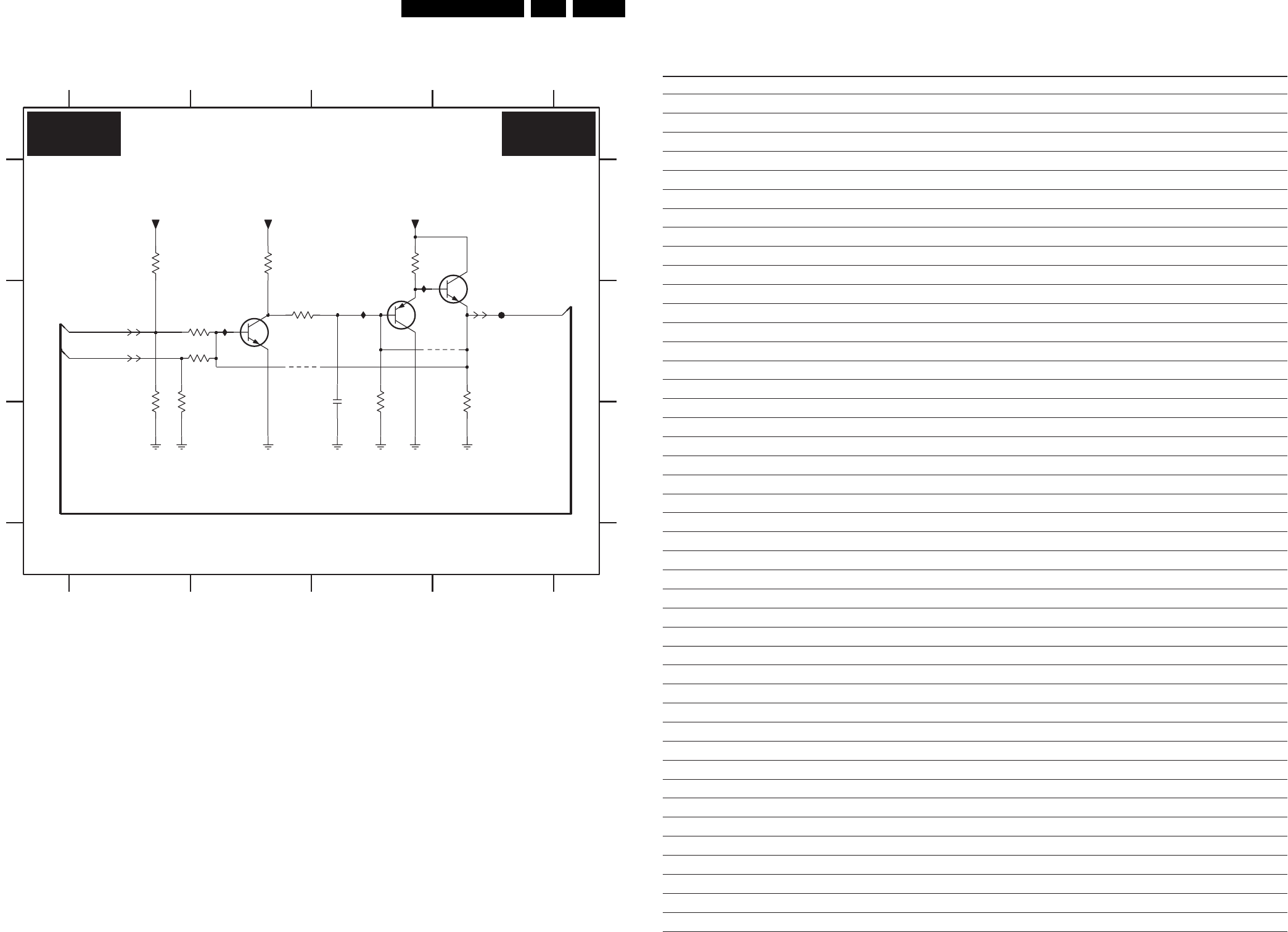
EN 68FTL2.4E AA 7.
Circuit Diagrams and PWB Layouts
SSB: Backlight Control
7L04-2 B3
7L05 B2
9L00 B4
9L01 B2
FL06 B4
IL13 B3
IL14 B2
IL15 A33L44 B2
3L45 B2
3L46 B1
3L47 B1
3L48 B3
3L49 B4
7L03-1 B4
*
*
*
**
*
*
***
3L42 A3
3L43 B2
B19c
*
1234
1234
A
B
C
A
B
C
2L22 B3
3L40 A1
3L41 A2
BACKLIGHT CONTROL
B5a
B4
*
9L01
10K
3L47
IL15
3L45
4K7
IL13
IL14
9L00
FL06
+5V+5V
3L49
10K
BC847BPN
RES
7L04-2
RES
7L03-1
BC847BPN
10K
100n
2L22
4K7
3L42
3L43
RES
3L41
4K7
BC847BW
7L05
3L44
4K7
3L46
2K2
+8V
3L40
1K2
27K
3L48
BACKLIGHT-CNTRL
BACKLIGHT-DIMMING
BACKLIGHT-CNTRL-DC
F_15460_045.eps
240605
B19E B19E
8204 000 8484.1
Personal Notes:
E_06532_012.eps
131004
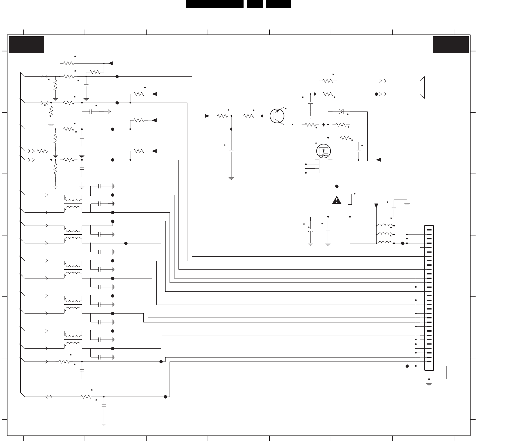
Circuit Diagrams and PWB Layouts EN 69FTL2.4E AA 7.
SSB: Screen Interface
3Z22 A1
3Z23 A5
B19d
SCREEN INTERFACE
FZ40 E3
res
2Z53 E2
2Z54 B6
2Z55 B4
2Z56 A5
B14e
5Z08 D6
6Z00 B6
7Z00 A4
res
FZ16 E2
FZ14 D2
B19d
B19d
B19d
DISPLAY
3Z35 B1
3Z36 A1
3Z37 A1
B19d
3Z24 B2
3Z25 B2
3Z26 A2
3Z28 C6
B
CFZ43 A2
FZ44 A2
FZ45 B2
FZ46 B2
FZ66 A6
234567
A
2Z57 B1
2Z58 A1
B19d
res
2Z59 A2
2Z60 F1
E
B19d
2Z49 D2
2Z50 E2
FZ17 E2
FZ18 E2
FZ20 D7
FZ21 C6
res
B19d
3Z53 B1
3Z54 A1
3Z31 B5
3Z32 B4
3Z33 B4
C
D
LVDS
CONNECTOR
TO
3Z39 B1
3Z50 F1
3Z51 F2
3Z52 B1
3Z29 B6
3Z30 B6
D
E
F
A
B
IZ00 B5
IZ01 A5
IZ02 B4
IZ03 A4
B19d,B21 2Z51 E2
2Z52 E2
B19c
567
1
3Z34 B1
2Z61 F2
2Z62 B1
2Z63 C6
2Z64 C5
2Z65 C5
F
1G50 C7
2Z44 C2
2Z45 C2
2Z46 C2
2Z47 D2
2Z48 D2
1
FZ08 D2
(IRQ)
(PDWN)
resres
3Z38 A2
3Z55 A1
3Z56 A5
5Z01 C1
5Z02 C1
5Z03 D1
B19e
B19d
7Z01 B5
FZ02 C2
FZ04 C2
FZ07 C2
B19d
FZ10 D2
FZ12 D2
B14e
B14e
234
B4
res
5Z04 E1
5Z05 E1
5Z06 C6
5Z07 C6
FZ41 F3
FZ42 F7
B19d
2Z65
10V10u
2Z64
100n
1
2
4
3
FZ08
5Z02
DLW21S
22p
FZ07
2Z46
2
4
3
2Z49
22p
DLW21S
5Z01 1
IZ02
1u0
2Z54
+3V3_SIM
4K73Z38
FZ21
FZ20
2.0AT
1Z28
3Z30
BZX384-C5V6
6Z00
47K
1K0
3Z35 4K7
3Z22
3Z34
1K0
1K0
2
5
6
3
4
3Z26
7Z01
SI3441BDV
1
100R
3Z54
2Z57
100p
2Z48
22p
3Z33
10K
+3V3_SIM
FZ41
47R
3Z29
3Z53
100R
100p
2Z61
FZ66
FZ04
FZ02
10K
3Z32
FZ10
5Z04
DLW21S
1
2
4
3
VDISP
3Z55
100R
+3V3_SIM
100n
2Z63
5Z08
FZ42
FZ44
FZ43
FZ45
5
6
7
8
9
32
33
23
24
25
26
27
28
29
3
30
31
4
13
14
15
16
17
18
19
2
20
21
22
FI-WE31P-HFE-E1500
1
10
11
12
1G50
3Z37
4K7
7Z00
BC847BW
3Z31
47K
3Z36
10K
+11V
IZ00
IZ01
3Z25
100R
100R
3Z52
3Z24
100R
FZ14
FZ17
2Z59
100p
100p
2Z58
2Z62
100p
100R
3Z51
FZ40
2Z60
100p
FZ46
2Z55
100n
3
FZ12
1
2
4
FZ16
5Z03
DLW21S
3Z56
1K0
3Z23
100R
+3V3_SIM
5Z07
+3V3_SIM
100R
3Z39
2Z45
22p
2Z44
22p
2Z47
22p
2Z51
22p
22p
2Z52
22p
2Z50
2Z53 22p
1n0
2Z56
3Z50
100R
5Z06
1
2
4
3
IZ03
FZ18
DLW21S
5Z05
TXLCD2+
TXLCD1+
TXLCD1-
TXLCD0+
TXLCD0-
LAMP-ON
5V-ENABLE
PDP-GO
BACKLIGHT-CNTRL
LCD-PWR-ON
CPU-GO
SCL-DISP
TXLCD3-
TXLCD3+
TXCLKLCD-
TXCLKLCD+
TXLCD2-
SDA-DISP
LCD-PWR-ON
F_15460_046.eps
080405
B20 B20
8204 000 8486.1
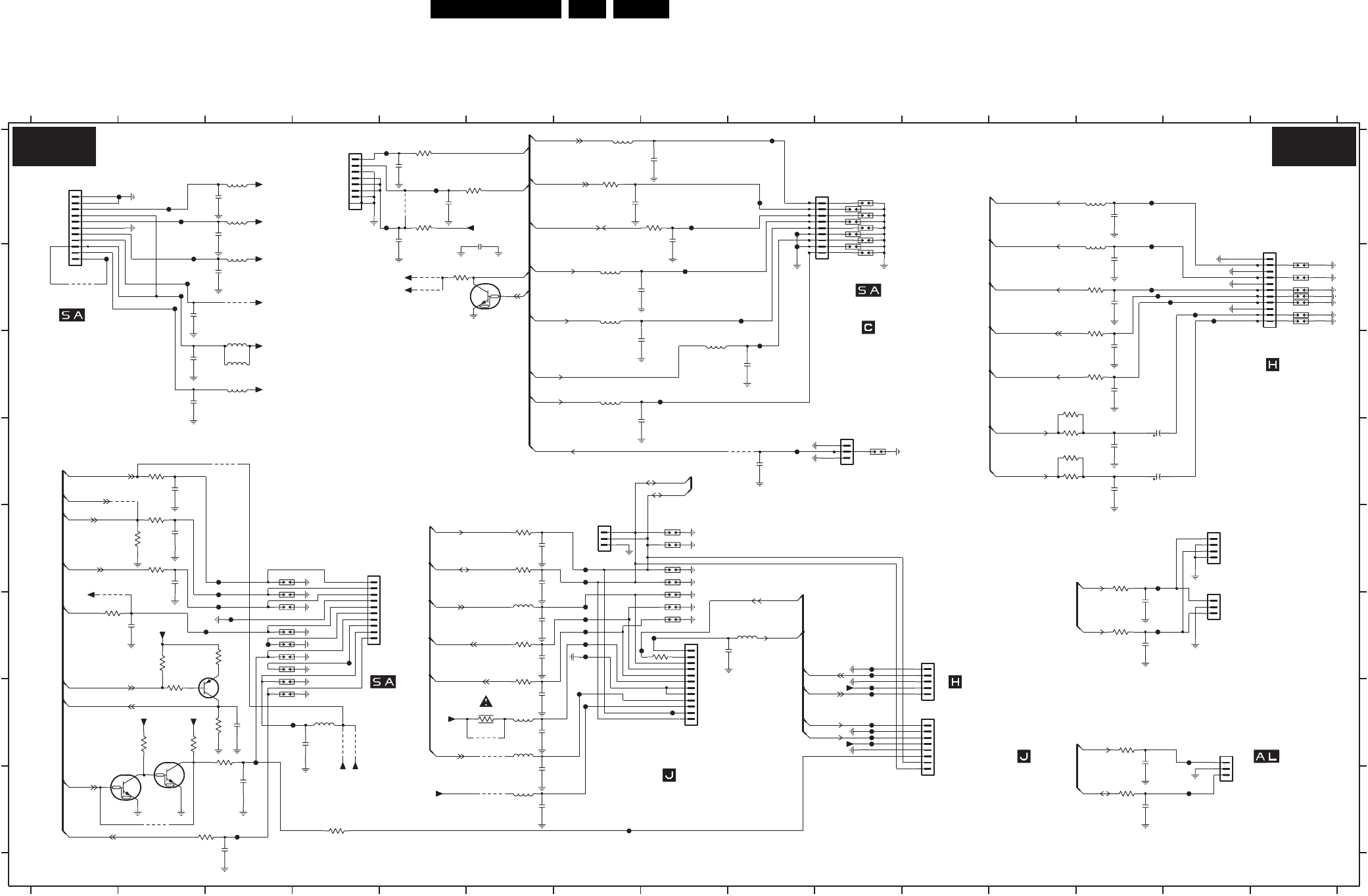
EN 70FTL2.4E AA 7.
Circuit Diagrams and PWB Layouts
SSB: Connection
FY81 H14
FY82 H7
FY85 A5
FY86 E13
FY87 F13
*
FY68 G9
FY69 G9
FY70 G9
FY71 G9
FY72 G9
*
*
*
*
*
TO 1M03
FY73 G9
FY74 A5
FY75 A5
FY76 G8
FY77 F8
FY78 F8
FY79 F3
FY80 G14
FY51 B13
FY52 B14
FY53 B14
FY54 B14
FY55 B14
B21
LED + SWITCH
LED + SWITCH
*
SCART 3
SDI SUPPLY
TO
FY59 B8
FY60 B9
FY61 C7
FY62 C9
FY63 C8
FY64 C8
FY65 A2
FY66 F10
FY67 F9
FY29 F4
FY30 G4
FY31 H3
FY32 D9
FY37 E7
*
res
TO 1M01
SCART 3
B6a
B14e
OR
FY38 E7
FY39 F7
FY40 F7
FY41 F7
FY42 F7
FY43 G7
FY44 F7
FY45 G7
FY46 B2
FY47 B2
FY48 A2
FY49 A13
FY50 A13
7Y01 B5
7Y02 G3
7Y03 G2
7Y04 H2
9Y00 D9
N.C.
B6a,c
TO 1M20
N.C.
B14e
AUDIO-STBY
9Y16 B5
9Y17 B5
FY00 A2
FY01 B2
FY03 B2
FY05 B1
FY22 E3
FY23 E3
FY24 F3
FY25 F3
FY26 F3
FY28 H3
5Y01 G6
5Y02 C3
5Y03 C3
5Y06 A3
5Y07 B3
B21
TO 1M07
B14e
N.C.
B14e
5Y09 C3
5Y11 G6
5Y12 H6
5Y14 F6
5Y15 A3
5Y16 A13
5Y17 B13
5Y18 A7
5Y19 B7
5Y20 B7
5Y21 C8
5Y22 C7
5Y23 F9
3Y19 C13
3Y20 C12
3Y21 D12
3Y22 D12
3Y23 D12
B14d(2x)
B5a
B21
B19d
3Y24 B5
3Y25 A7
3Y27 H13
3Y28 G13
3Y30 E2
3Y33 A6
3Y34 E13
3Y35 F13
3Y36 A8
3Y37 F2
3Y38 F3
3Y39 G2
3Y40 E6
5Y00 G4
3Y00 D2
3Y01 E2
3Y02 E2
3Y03 F1
3Y04 H4
B5a
3Y05 G3
3Y06 A5
3Y07 G6
3Y08 H3
3Y09 E6
3Y10 F6
3Y11 F6
3Y12 F8
3Y13 A5
3Y14 G3
3Y15 G2
3Y16 G2
3Y17 B13
3Y18 B13
2Y31 D13
2Y32 D13
2Y33 D13
2Y34 A3
2Y37 A8
B21
B6a
B14a
B6a,c
B6b
2Y38 A7
2Y39 B7
2Y40 C7
2Y41 C9
2Y42 D7
2Y43 A6
2Y44 H13
2Y45 G13
2Y48 A5
2Y49 F13
2Y50 F13
2Y51 A8
2Y52 G3
2Y53 F92Y13 H3
2Y14 G6
2Y15 H6
2Y16 H6
2Y17 G6
B5a,B14b
CONNECTION
B4,B14b,B21
2Y18 F6
2Y19 F6
2Y20 E6
2Y21 E6
2Y22 A5
2Y23 D9
2Y25 A13
2Y26 B13
2Y27 B13
2Y28 C13
2Y29 C13
2Y30 D13
1Y33 B15
1Y34 B15
1Y35 B15
1Y37 B15
1Y38 A10
*
*
(SOUND PROTECT)
B5a
B14e
B5a,B14e(2x)
1Y39 A10
2Y00 A3
2Y01 B3
2Y02 B2
2Y03 C3
2Y04 C3
2Y06 D2
2Y07 E2
2Y08 E2
2Y09 F2
2Y10 H3
2Y11 A5
2Y12 G4
B
C
D
E
F
B14a
1Y11 E4
1Y12 F4
1Y13 F4
1Y14 F4
1Y15 F4
1Y16 F4
1Y17 F4
1Y18 G4
1Y21 E8
1Y22 E8
1Y23 E8
1Y24 F8
1Y25 F8
1Y26 E8
1Y27 E8
1Y28 D10
1Y30 B15
1Y31 B15
1Y32 B15
678910
B14d(2x)
B20,B19d
B4,B5a
B6a,c
11 12 13 14 15
A
B
C
D
E
F
G
H
A
1M52 A10
1Y02 A10
1Y04 A10
1Y05 A10
1Y06 A10
1Y07 A10
1Y08 A10
1Y09 B10
1Y10 E3
B5a
123456789101112131415
12345
9Y03 F1
9Y04 H2
9Y05 G6
9Y06 H6
9Y07 D3
9Y09 D2
9Y12 A5
9Y13 B3
9Y14 B1
9Y15 G4
SDI SUPPLY
B4,B14b,B21
G
H
1M01 D10
1M02 E7
1M03 E5
1M07 F10
1M09 G10
1M17 A4
1M20 F8
1M36 B15
1M46 A1
1M48 G14
1M49 F14
1M51 E14
OR
AUDIO-STBY
B19e
OR
FY56 A9
FY57 A9
FY58 A8
*
*
*
*
B21
TO 1M46
TO 1M37
*
nc
B14e
9Y01 G4
9Y02 G6
FY67
B19d
B5a
B5a
B19d
B19d
B14b,B5a
B21
*
TO 1793
PDP AUDIO
AUDIO-STBY
B14e
10p
2Y21
1Y13
3Y05
100R
4
9Y07
B4B-PH-K
1M51
1
2
3
1Y02
2Y51
100p
100R
3Y33
100p
2Y48
+5V2-STBY
9Y04
+5V2-STBY
3Y15
10K
3Y16
4K7
PDTC114EU
7Y03
7Y04
PDTC114EU
1Y14
1M49
1
2
3
FY87 B3B-PH-K
100R
3Y35
6
7
8
9
B11B-PH-K
1M46
1
10
11
2
3
4
5
9V_STBY
5Y06
1n0
2Y27
2Y34
100p
1Y12
FY78
2Y37
100p
2Y22
100p
100p
2Y03
5Y16
3Y09
100R
1Y39
+5V2-STBY
2Y10
100p
2Y26
100p
FY26
FY42
3Y25
100R
FY80
1Y38
FY82
FY49
100p
2Y15
1Y26
2Y32
1n0
16V
1Y23
2Y31
100u
5Y17
3Y20
68R
5Y19
2K2
3Y04
1Y32
1Y09
9Y05
FY72
9Y01
FY60
1
2
3
+8V
S3B-PH-K
1M02
100p
2Y09
+5V2-STBY 3Y24
100K
1Y07
1Y22
FY31
1n0
2Y33
100R
3Y40
FY63
FY40
+5V2-STBY
9V_STBY
1Y08
FY75
+3V3_SIM
FY81
2Y53
100p
5Y23
3Y37
4K7
5Y14
FY58
FY74
1Y17
1Y05
1Y21
FY62
9Y17
1Y10
2Y28
1n0
100p
2Y19
3Y12 100R
16V 100u
2Y30
res
+5V2-STBY
FY37
3Y28
100R
9Y03
+5V
FY64
FY24
+33V
1Y18
3
4
5
6
7
8
9
1M36
B11B-PH-K
1
10
11
2
FY76
FY77
1Y34
3Y21
100p
2Y11
2
3
4
5
68R
1M07
B5B-PH-K
1
FY61
9Y16
1
2
3
4
5
6
789
FY32
1M17
BM07B-SRSS-TBT
FY00
2Y08
100p
10p
2Y44
res
100R
3Y27 res
BC857BW
7Y02
3Y38
2K2
100p
2Y43
100p
2Y39
100p
2Y38
FY52
FY47
1Y28
+5V
1Y24
9Y15
3Y13
100R
2Y06
100p
1Y37
1Y06
1Y04
FY57
100R
3Y36
2Y13
100n
100p
2Y14
3Y34
100R
5Y07
9Y09
100p
+5V
2Y41
FY65
FY29
res
1
2
3
FY25
B3B-PH-K
1M48
5Y01
3Y39
10K
5Y11
3Y17
FY85
FY01
100R
FY70
FY69
100p
2Y00
5Y20
3Y14
4K7
3Y22
68R
3Y00
100R
2Y18
100p
FY28
9Y00
FY45
FY22
FY56
+11V_SF
5
6
7
8
9
FY79
B9B-PH-K
1M52
1
2
3
4
FY54
3Y18
100R
9Y12
3Y19
9Y06
100R
100p
2Y12
FY48
100p
2Y23
FY03
10p
2Y50
+11V_SF
5Y18
FY30
100R
3Y03
9Y14
3
4
5
6
7
8
9
1Y30
B12P-PH-K
1M20
1
10
11
12
2
3Y10
100R
3Y08
100R
7Y01
PDTC144EU
FY43
5Y02
+11V
5Y03
1Y33
GND-AUD
1Y27
FY41
FY50
100p
2Y07
5Y12
5Y22
3Y30
15K
1Y16
1Y31
FY23
FY73
FY66
100p
2Y42
FY39
100n
FY05
2Y52
FY86
3Y06
100R
2Y49
10p
4
5
6
7
8
9
1M03
B10P-PH-K-S
1
10
2
3
2Y17
1Y35
100p
1Y11
100p
100R
3Y01
2Y01
2Y40
100p
FY44
FY51
1M01
B3B-PH-K
1
2
3
3
4
5
6
7
8
5Y15
1M09
B8P-PH-K
1
2
5Y09
68R
3Y23
+8V
+5V
2Y16
100p
9Y02
FY71
2Y04
100p
3Y02
100R
FY59
FY53
100R
3Y11
5Y00
100p
2Y02
FY38
9Y13
1Y25
2Y45
10p
res
FY68
FY55
1n0
2Y29
5Y21
FY46
100p
2Y25
3Y07
1R0
1Y15
GND-AUD
2Y20
10p
STANDBY
PROT-AUDIOSUPPLY
PROT-AUDIOSUPPLY
KEYBOARD
IRQ-DIGITAL
ODC
AL-CL
AL-DA
CON-SND
LED2
SCL-SF
SDA-SF
FRAME
PWR-OK-PDP
POR
POR
POR-CLASSD
SDA-S
STANDBY-IO4
SURR-RF
SURR-LF
STATUS-SC3-F
SEL_IN_1_BF
SCL-S
FRONT-Y-CVBS-IN
FRONT-C-IN
L-FRONT-IN
FRONT-DETECT
R-FRONT-IN
HEADPHONE-R
HEADPHONE-L
AUDIO-C
AUDIO-L
AUDIO-R
AUDIO-SW
POR-CLASSD
SOUND-ENABLE
LIGHT-SENSOR
RC
LED1
SDA-S
SCL-S
KEYBOARD
PWR-OK-PDP
FAN-SPEED
LAMP-ON
BACKLIGHT-CNTRL-DC
F_15460_047.eps
110405
B21 B21
8204 000 8485.1
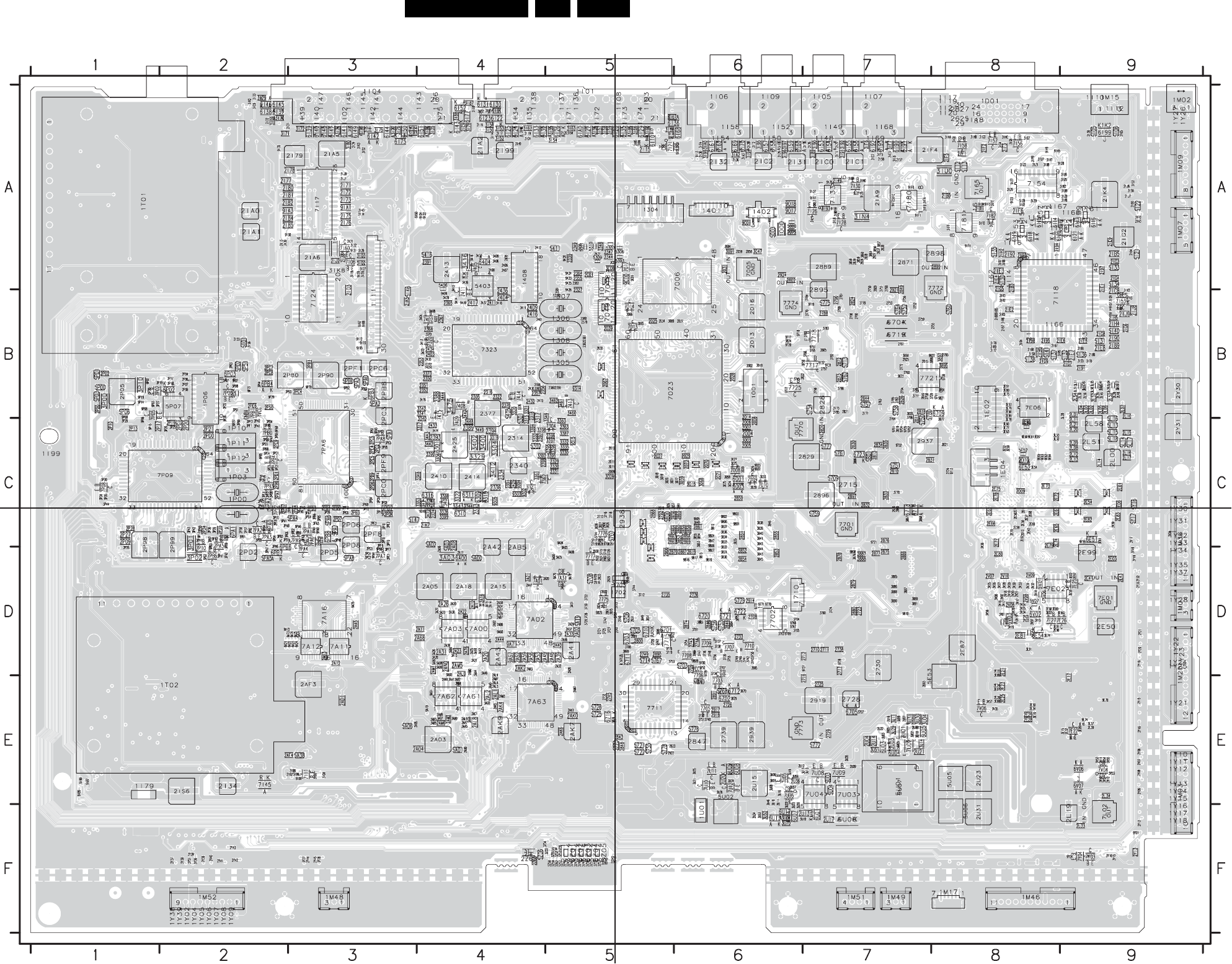
Circuit Diagrams and PWB Layouts EN 71FTL2.4E AA 7.
Layout SSB (Top Side Overview)
F_15460_048.eps
120405
3104 313 6003.7
Part 1
F_15460_048a.eps Part 2
F_15460_048b.eps
Part 3
F_15460_048c.eps Part 4
F_15460_048d.eps

EN 72FTL2.4E AA 7.
Circuit Diagrams and PWB Layouts
Layout SSB Mapping (Top Side)
F_15460_048m.eps
110405
1000 A6
1001 B6
1304 A5
1305 B5
1306 B4
1307 B5
1308 B4
1401 A6
1402 A6
1408 A4
1702 D5
1703 D5
1710 D7
1D01 A8
1E02 B8
1E04 C8
1I01 A5
1I04 A4
1I05 A7
1I07 A7
1I09 A6
1I11 B3
1I53 A8
1I56 A9
1I57 A8
1I59 A9
1I79 E1
1M01 D9
1M02 A9
1M03 E9
1M07 A9
1M09 A9
1M15 A9
1M17 F8
1M20 D9
1M36 C9
1M46 F8
1M48 F3
1M49 F7
1M51 F7
1M52 F2
1P00 C2
1P03 C2
1P06 B2
1P10 C2
1P11 C2
1P12 C2
1T01 A2
1T02 E2
1U01 F6
2002 B6
2004 C6
2005 C6
2006 C6
2007 C6
2008 C6
2009 C5
2011 C5
2012 C5
2013 B6
2014 B6
2016 B6
2018 B6
2020 C6
2025 B5
2027 C5
2028 B6
2029 C6
2031 A6
2034 B5
2035 B5
2037 B6
2039 B5
2058 A6
2059 A6
2067 B5
2070 C6
2071 C6
2073 C6
2075 A6
2301 C4
2305 B4
2314 C4
2315 C4
2316 B4
2317 B4
2318 B4
2322 B4
2324 C4
2327 B5
2329 C5
2330 C5
2331 C5
2332 C4
2333 C4
2334 C4
2336 C4
2339 A5
2340 C4
2344 A5
2347 A5
2348 A5
2349 A5
2350 B4
2351 B4
2352 B4
2353 B4
2355 A5
2356 B4
2357 B4
2358 B4
2359 B5
2360 B5
2361 B5
2362 B5
2363 C5
2364 A5
2365 B4
2367 B4
2368 B4
2373 B4
2376 B4
2377 B4
2379 B5
2380 B5
2381 B5
2382 B5
2383 A5
2388 B4
2389 C4
2391 A4
2393 C4
2394 C4
2395 C5
2396 C5
2397 C4
2398 C4
2401 B4
2403 B4
2404 B4
2405 A4
2406 A4
2407 A4
2408 A4
2409 B4
2410 C4
2411 B4
2412 A4
2413 A4
2414 C4
2416 B4
2417 B4
2425 C4
2427 A5
2428 A5
2429 C4
2430 B4
2432 B4
2433 C4
2434 B4
2435 B4
2436 B4
2707 D6
2708 D6
2709 D6
2710 D7
2711 D7
2712 D7
2715 C7
2716 E7
2717 D7
2718 C5
2719 C5
2720 D5
2721 D5
2722 D5
2723 D7
2724 C8
2725 E7
2726 E6
2728 E7
2729 E7
2730 D7
2732 E5
2733 D6
2735 D5
2736 D6
2738 D7
2739 E6
2740 D5
2741 D5
2742 D5
2743 D6
2744 D6
2745 E5
2747 D5
2749 D5
2750 A7
2751 A7
2752 B7
2753 B7
2755 B8
2756 B7
2758 B7
2759 B7
2760 B7
2761 B7
2762 B7
2763 B7
2764 C7
2765 B8
2768 A7
2770 B7
2771 B7
2772 B7
2773 B7
2777 B7
2778 B7
2780 B7
2781 B7
2782 B7
2784 B7
2785 B7
2787 B7
2788 B7
2790 B7
2792 C5
2794 B7
2795 B7
2796 B7
2797 B7
2798 B7
2799 B7
2800 D5
2802 A6
2805 B7
2809 A7
2810 C7
2811 C7
2813 C7
2814 B8
2815 B7
2816 B7
2818 B7
2819 D6
2820 C7
2821 B7
2822 B6
2824 B7
2826 B7
2828 B7
2829 C7
2830 C7
2831 C7
2832 C7
2833 C7
2834 C7
2835 C7
2836 C5
2837 A7
2838 A7
2839 A7
2840 C5
2841 C6
2843 E5
2844 B7
2845 D6
2846 D6
2847 E6
2848 E5
2849 B7
2850 C6
2851 C6
2852 D6
2853 D6
2854 D6
2855 C6
2856 C6
2857 C6
2858 C6
2859 C6
2860 C6
2861 C6
2862 C5
2863 C5
2864 C5
2865 C6
2866 D5
2867 D6
2868 C5
2869 C6
2870 D5
2871 A7
2872 B7
2873 B7
2874 D6
2875 D7
2876 C7
2877 D7
2878 D7
2879 D7
2880 D7
2881 D5
2886 D7
2887 D7
2888 D7
2889 A7
2890 D5
2891 E6
2895 A7
2896 C6
2897 C7
2898 A8
2899 A8
2900 C5
2901 D5
2902 D5
2914 D6
2915 C5
2916 D5
2917 E6
2918 E6
2919 E7
2921 B7
2922 E5
2923 E5
2924 A6
2925 B7
2926 A7
2927 A7
2928 A7
2929 D5
2931 D5
2935 D5
2936 C7
2937 C7
2938 C5
2939 E6
2A00 E4
2A02 D5
2A03 E4
2A04 E4
2A05 D4
2A06 D4
2A08 C4
2A09 D5
2A10 D4
2A11 D4
2A12 D3
2A13 D3
2A14 D4
2A15 D4
2A16 D4
2A17 D4
2A18 D4
2A20 D4
2A21 D4
2A22 D4
2A23 D4
2A25 D4
2A26 D4
2A27 D4
2A29 D5
2A30 D4
2A31 D4
2A32 D5
2A33 D5
2A35 D4
2A36 D4
2A37 D5
2A39 D5
2A40 D5
2A41 D5
2A42 D4
2A43 D4
2A44 D4
2A45 D3
2A46 D5
2A49 D4
2A50 D4
2A53 D4
2A54 D4
2A56 D4
2A59 D4
2A62 D4
2A66 D4
2A76 D4
2A95 E3
2AA6 D5
2AA7 D4
2AB2 D4
2AB5 D4
2AB6 D4
2AB7 D4
2AD1 E3
2AF3 E3
2AF4 E3
2AK0 E5
2AK1 E5
2AK2 D4
2AK3 D4
2AK4 E4
2AK5 E4
2AK6 E5
2AK7 E5
2AK9 E4
2AL0 D4
2AL1 E4
2AL2 E4
2AL3 E4
2AL4 D4
2AL8 E4
2AL9 E4
2ALA E4
2AM0 D4
2AM1 D4
2AM2 E4
2AM3 E4
2AM5 D4
2AM6 E4
2AM7 E4
2AM9 E4
2AN0 D4
2AN1 E4
2AN7 E5
2C01 A5
2D03 E7
2D09 C8
2D10 C8
2D11 C8
2D12 C8
2E01 C9
2E03 D9
2E06 C9
2E17 E9
2E21 D8
2E22 D8
2E23 E8
2E24 E8
2E25 E8
2E26 E8
2E28 E8
2E29 E8
2E30 E8
2E32 E9
2E34 E8
2E39 E9
2E41 D9
2E42 C8
2E43 D9
2E50 D9
2E54 C9
2E56 C8
2E57 C8
2E58 C8
2E59 C8
2E62 C8
2E65 C8
2E66 C8
2E67 C8
2E68 C8
2E69 C8
2E70 C8
2E71 C8
2E72 C8
2E73 C8
2E74 C8
2E75 C8
2E77 C8
2E78 C8
2E79 C8
2E80 D8
2E81 D8
2E82 C9
2E83 C9
2E87 D8
2E89 B8
2E90 B8
2E91 B8
2E95 C8
2E96 D8
2E97 D9
2E98 D8
2E99 D9
2I00 A9
2I03 B3
2I13 A2
2I14 A3
2I15 A5
2I16 A4
2I17 A4
2I18 A4
2I19 A4
2I20 A5
2I21 A2
2I22 A2
2I23 A2
2I24 A3
2I25 A3
2I26 A7
2I27 A7
2I28 A6
2I29 A6
2I30 A6
2I31 A7
2I32 A6
2I34 E2
2I36 A6
2I38 A9
2I49 A7
2I55 B2
2I56 B2
2I57 A7
2I58 A7
2I62 E3
2I64 A9
2I65 A9
2I66 B9
2I67 B8
2I68 B8
2I71 A3
2I72 A3
2I73 A3
2I75 A3
2I76 A3
2I77 A2
2I78 A3
2I79 A3
2I80 A2
2I81 A2
2I82 A2
2I84 A2
2I85 A2
2I86 B9
2I87 B8
2I88 B8
2I89 B9
2I90 B9
2I91 B9
2I92 A8
2I93 A8
2I94 A8
2I95 B8
2I96 B8
2I97 A9
2I98 B8
2I99 A4
2IA0 A2
2IA1 A2
2IA2 A4
2IA3 A9
2IA5 A3
2IA6 A3
2IA9 A7
2IB0 A8
2IB3 A8
2IB5 A9
2IC0 A7
2IC1 A7
2IC2 A6
2IC8 B9
2IC9 A4
2IE1 A9
2IE2 B8
2IE3 A8
2IE4 A8
2IE5 B9
2IE6 B9
2IE7 B9
2IE8 B9
2IE9 A9
2IF1 A8
2IF2 A8
2IF3 A8
2IF4 A7
2IF5 A8
2IF6 A8
2IG2 A9
2IG3 A9
2IG4 A9
2IG5 A8
2IG6 B9
2IG7 B9
2IG8 B9
2IG9 B8
2IH2 A8
2IH4 B9
2IH5 B9
2IJ2 A3
2IJ3 A3
2IJ6 A9
2IJ7 A9
2IJ8 B9
2IJ9 B9
2IK4 A9
2IK5 B3
2IK7 C4
2IR1 A8
2IS6 E2
2L00 C9
2L01 B9
2L02 B9
2L03 B9
2L04 B9
2L05 B9
2L06 B9
2L07 B9
2L08 C9
2L09 C9
2L10 B9
2L11 C9
2L12 C9
2L13 C9
2L14 C9
2L15 C9
2L16 C9
2L17 C9
2L19 F8
2L20 C9
2L21 C9
2L28 B9
2L29 B9
2L30 B9
2L33 F9
2L34 E9
2L48 B9
2L49 B9
2L50 B9
2L51 C9
2L52 B9
2L54 B9
2L57 B9
2L58 B9
2P00 B1
2P02 B1
2P03 B2
2P04 B2
2P05 B1
2P06 B2
2P07 B2
2P08 B2
2P09 C1
2P10 C1
2P13 C1
2P17 C1
2P19 C2
2P20 C2
2P21 C2
2P22 B2
2P26 D1
2P27 C1
2P28 C1
2P34 C2
2P35 C2
2P36 C2
2P37 C2
2P38 C2
2P39 C2
2P40 C2
2P41 C2
2P42 C2
2P43 C2
2P44 C2
2P48 C2
2P50 B2
2P80 B2
2P81 B3
2P90 B3
2P98 C1
2P99 C2
2PA4 C3
2PA5 C3
2PA6 C2
2PA7 C2
2PA8 C2
2PB3 C3
2PB4 C3
2PB5 C3
2PB6 C3
2PB7 C2
2PB8 B3
2PB9 C3
2PC0 C3
2PC1 C3
2PC2 C3
2PC3 B3
2PC4 B3
2PC5 C3
2PC6 B3
2PC7 B2
2PC8 B2
2PC9 C2
2PD1 C2
2PD2 D2
2PD3 C3
2PD4 C3
2PD5 D3
2PD6 C3
2PD7 C3
2PD8 C3
2PD9 C3
2PE0 C2
2PE1 D3
2PE2 C3
2PE3 C3
2PE4 C3
2PE5 C3
2PE6 B2
2PF1 B3
2PF3 C3
2PF8 C3
2PF9 C3
2PG0 C2
2PG1 C2
2U03 E7
2U04 E7
2U05 E7
2U07 E7
2U09 E7
2U11 E6
2U12 E6
2U13 F7
2U14 E7
2U15 E6
2U16 E7
2U17 F7
2U18 E7
2U20 E6
2U21 E7
2U23 E8
2U30 E7
2U31 F8
2U32 E7
2U34 F6
2U36 E6
2V06 D8
2V07 D8
2V08 D8
2V09 D8
2V10 D8
2V11 E9
2V12 E9
2V16 D8
2V17 D8
2V18 D8
2V19 D8
2V20 D8
2V21 D8
2V22 D8
2V23 D8
2V24 D8
2V25 D8
2Y06 E9
2Y07 E9
2Y08 E9
2Y09 E9
2Y12 F9
2Y13 F9
2Y15 E9
2Y16 E9
2Y19 D9
2Y20 D9
2Y21 D9
2Y30 B9
2Y31 C9
2Y32 D9
2Y33 D9
2Y37 F2
2Y38 F2
2Y39 F2
2Y40 F2
2Y41 F2
2Y42 F2
2Y43 F2
2Y44 F3
2Y45 F3
2Y51 F2
2Z44 F5
2Z45 F5
2Z46 F5
2Z47 F5
2Z48 F5
2Z49 F5
2Z50 F5
2Z51 F5
2Z52 F5
2Z53 F5
2Z57 F5
2Z58 F5
2Z59 F5
2Z60 F5
2Z61 F5
2Z62 F5
2Z63 F4
2Z65 F4
3003 C6
3011 C5
3012 B5
3018 C5
3019 C5
3020 C5
3021 C5
3024 C6
3025 C6
3026 C6
3027 C6
3033 C6
3035 B5
3039 C6
3047 A6
3058 C6
3059 C6
3065 B5
3066 B5
3068 C6
3073 C6
3074 C5
3075 C6
3076 C5
3077 C6
3078 C5
3084 A6
3089 B5
3090 C6
3091 A6
3099 C6
3302 C4
3304 C4
3306 C4
3317 C4
3318 C4
3320 B4
3321 B4
3322 C4
3329 C4
3330 C5
3332 C5
3335 C5
3336 C4
3340 C4
3341 B4
3342 B4
3343 C4
3344 C4
3345 C4
3346 C4
3347 C4
3348 C4
3349 B5
3353 C4
3361 C4
3363 C5
3370 B4
3371 B4
3372 B4
3376 B4
3377 B4
3387 C5
3388 C4
3390 C4
3393 B4
3394 C4
3395 C5
3396 C5
3397 C5
3398 C4
3399 C4
3400 C4
3402 C4
3404 B4
3406 A4
3409 A4
3411 B4
3412 C4
3413 B4
3416 A4
3418 B4
3422 B4
3423 A4
3433 A4
3436 A4
3437 B4
3439 B4
3442 C4
3443 C4
3444 B4
3447 B4
3448 C4
3449 C4
3460 B5
3461 B5
3462 B5
3472 C4
3473 B4
3474 C4
3475 B4
3476 B4
3701 D6
3703 D6
3704 D6
3705 D6
3706 D5
3707 E7
3712 D5
3713 C5
3714 C5
3715 D5
3716 C5
3717 C5
3718 D5
3719 D5
3720 D5
3721 D5
3722 D6
3723 D5
3724 D7
3725 D5
3726 D5
3727 D5
3728 D5
3729 B8
3730 D5
3732 E6
3733 D6
3734 D6
3736 D6
3737 D6
3738 D6
3739 D6
3740 E6
3741 D6
3742 D6
3743 D6
3744 D5
3745 B6
3746 D6
3747 D6
3748 D6
3749 D6
3750 D6
3751 E6
3752 D6
3753 D5
3754 D6
3755 D6
3756 D6
3760 D7
3765 B7
3766 B7
3778 C7
3782 B7
3783 B7
3796 B7
3798 B7
3805 C7
3819 C7
3820 B7
3821 C8
3823 B7
3824 B6
3826 C5
3827 C5
3829 E6
3830 D6
3831 D6
3832 D6
3833 C6
3834 C6
3835 C6
3836 C6
3837 C6
3838 C6
3839 C6
3840 C6
3841 C6
3842 C6
3843 D6
3844 D6
3845 D6
3846 C6
3847 C6
3848 C6
3849 D5
3850 B7
3851 D5
3853 C6
3854 C6
3855 C6
3856 A7
3857 A7
3858 A7
3859 A7
3860 A7
3861 A7
3864 D6
3865 D6
3867 C7
3868 C7
3869 D5
3870 E6
3874 E5
3875 D6
3876 D7
3877 C8
3885 D7
3886 D7
3887 D7
3888 D7
3889 D7
3890 D7
3891 D7
3895 B8
3897 B8
3898 B8
3903 D6
3905 D6
3906 C7
3909 D5
3913 D5
3914 D5
3915 C5
3916 C5
3917 C5
3922 D5
3923 D5
3924 D5
3925 D5
3926 C5
3927 C5
3928 C5
3929 C5
3930 D5
3931 D5
3932 D5
3933 D5
3A00 D5
3A01 D5
3A03 D4
3A05 D5
3A07 D5
3A09 D5
3A11 D4
3A12 D4
3A13 D4
3A14 D4
3A15 D4
3A16 D4
3A18 D4
3A20 D4
3A21 D4
3A23 D4
3A26 D4
3A27 D4
3A28 D4
3A66 D4
3AA0 E4
3AA1 E4
3AA4 D4
3AA5 E4
3AA6 D4
3AA7 E4
3AA9 E4
3AB0 E4
3AB2 E4
3AB3 E4
3AB4 E4
3AB5 E4
3AB6 D4
3AB7 E4
3AB8 D4
3AB9 D4
3AC0 E4
3AC1 E4
3C01 A5
3C03 A5
3C06 A5
3C07 B5
3C08 A5
3C09 C5
3E00 D8
3E01 D8
3E02 D9
3E03 D8
3E06 D8
3E07 E8
3E08 E8
3E09 E9
3E10 E9
3E13 E9
3E15 E9
3E16 E8
3E37 E9
3E50 C8
3E52 C8
3E53 B8
3E54 C8
3E59 D9
3E60 C8
3E61 C9
3E62 C8
3E63 C8
3E64 D9
3E73 B8
3E74 D8
3E77 C8
3E78 C8
3E79 B8
3E80 B8
3E87 C8
3E91 D8
3I00 E3
3I19 A3
3I20 A3
3I21 A3
3I22 A3
3I26 A3
3I27 A3
3I35 A4
3I39 A2
3I43 A3
3I50 A4
3I51 A4
3I52 A4
3I53 A4
3I54 A5
3I55 A5
3I56 A5
3I57 A5
3I58 A5
3I59 A5
3I60 A5
3I61 A4
3I62 A4
3I63 A5
3I64 A5
3I65 A5
3I66 A5
3I67 A5
3I68 A5
3I69 A2
3I70 A2
3I71 A2
3I72 A3
3I73 A3
3I74 A3
3I75 A3
3I76 A3
3I77 A3
3I78 A4
3I79 A2
3I80 A3
3I81 A3
3I82 A3
3I83 A3
3I84 A3
3I86 A4
3I87 A4
3I88 A4
3I89 A7
3I90 A7
3I91 A7
3I92 A7
3I93 A7
3I94 A6
3I95 A6
3I96 A6
3I97 A6
3I99 A6
3IA0 A6
3IA2 A6
3IA3 A6
3IB2 A4
3IB8 E3
3IB9 E3
3IC4 A4
3IC6 A2
3IC9 A6
3ID1 A5
3IE2 A7
3IE3 A7
3IE9 A7
3IF0 A9
3IF5 A7
3IF6 A7
3IF7 A7
3IFA A7
3IFB A7
3IFC A7
3IFD A8
3IFE A8
3IFF A8
3IFL A8
3IG0 A8
3IG1 A8
3IG3 A8
3IG4 A8
3IG6 A8
3IG7 A8
3IGH E3
3IH9 A4
3IHA A8
3IHB A8
3IHC A8
3II4 A4
3IJ0 A3
3IJ1 A3
3IK0 B8
3IK2 A2
3IK3 A3
3IK8 A3
3IL1 A7
3IL3 A7
3IL8 A7
3IM0 A7
3IM4 A7
3IN0 A7
3IN4 A7
3IN5 A4
3IN6 A4
3IQ2 A3
3IQ3 A3
3IQ8 B9
3IQ9 B9
3IR2 B8
3IR3 B8
3IR4 B8
3IR5 B8
3IR6 B8
3IR7 A8
3IR8 A8
3IR9 B8
3IS0 B8
3IS2 A3
3IS3 A9
3IS5 B9
3IS6 A9
3IT0 A7
3IT1 A7
3IT2 A6
3IT3 A6
3IT4 A6
3IT6 B9
3IT7 B8
3IT8 B8
3IU0 A8
3IU2 A8
3IU5 A9
3IU6 A9
3IU7 A8
3IU8 A8
3IU9 A9
3IV0 B9
3IV1 B9
3IV2 B9
3IV3 B9
3IV7 A8
3IV8 A9
3IV9 A8
3IW2 A9
3IW4 A5
3IW5 A5
3IZ0 A9
3IZ1 A8
3IZ2 A8
3IZ6 A8
3IZ7 A8
3IZ8 A8
3IZ9 A8
3L04 B9
3L05 B9
3L11 B9
3L19 B9
3L20 B9
3L21 B9
3L28 B9
3L29 B9
3L30 B9
3L31 B9
3L32 C8
3L33 C8
3P00 C1
3P01 C2
3P02 D2
3P07 B2
3P08 B2
3P10 B1
3P17 B2
3P18 B2
3P19 B1
3P20 B1
3P25 C2
3P26 C2
3P27 B1
3P28 C1
3P29 C2
3P30 C1
3P34 C1
3P35 C1
3P41 C2
3P42 C2
3P43 C2
3P44 C1
3P61 C3
3P90 C2
3P91 B2
3P93 B3
3PA0 C3
3PA1 D2
3PA2 D2
3PA3 C3
3PA4 C3
3PA5 C2
3PA6 C3
3PA7 C3
3PA8 C2
3PA9 C3
3PB0 C2
3PB1 C2
3PB2 C2
3PB3 C2
3PB4 C2
3PB5 C3
3PB6 C3
3PB7 C2
3PB8 C2
3PB9 C2
3PC1 C2
3PC2 D3
3PC3 D3
3PC4 D3
3PC6 C3
3PC7 C3
3PC8 C3
3PC9 C3
3PD0 C3
3PD1 C2
3PD2 C3
3PD3 C2
3PD4 C2
3PD5 C2
3PD6 C2
3PD8 C2
3PD9 C3
3PE0 C2
3PE1 C2
3PE2 C2
3PE3 C2
3PE4 C2
3PE5 C2
3PF0 C3
3PF1 C2
3PF2 C3
3PF3 C2
3PF4 C3
3PF6 C3
3PF7 D3
3PF8 C3
3PF9 C3
3PG0 C3
3PG2 D2
3PG3 C3
3PG4 C3
3PG5 C3
3PG6 C2
3PH2 C3
3PH3 B3
3PH4 B2
3PH6 C2
3PH7 D2
3PH8 C3
3U01 F6
3U02 E7
3U03 E7
3U04 E7
3U05 E7
3U06 E6
3U07 E6
3U08 E6
3U09 E7
3U10 F7
3U11 E7
3U13 E7
3U14 E7
3U15 F7
3U16 E6
3U17 E7
3U18 E6
3U19 E6
3U20 F6
3U21 E6
3U22 F6
3U23 F6
3U25 E6
3U26 E6
3U28 E7
3U29 E7
3U30 E7
3U31 E7
3U34 E6
3U46 E6
3U51 E7
3U52 F6
3U53 F6
3U56 E6
3U57 E6
3U70 F6
3V01 D8
3V02 D8
3V07 D8
3V08 D8
3V14 D8
3V15 D8
3V16 D8
3V17 D8
3V19 D8
3V20 D8
3V21 C9
3V22 C9
3V23 C9
3V24 C9
3V25 D8
3V26 D8
3V27 D8
3V28 D8
3V29 D8
3V30 D8
3V31 D8
3V32 D8
3V33 D8
3V34 D8
3V35 E8
3V36 C8
3V39 C9
3V50 E9
3V51 E9
3V52 E9
3V53 E9
3V54 E9
3V55 E9
3V56 D8
3V57 E8
3Y04 C9
3Y15 F9
3Y16 F9
3Y17 C9
3Y18 D9
3Y19 D9
3Y27 F3
3Y28 F3
3Y36 F2
3Y39 F2
3Z22 F5
3Z34 F5
3Z35 F5
3Z50 F5
3Z51 F5
3Z52 F5
3Z53 F5
3Z54 F4
3Z55 F5
5000 A6
5001 A6
5003 A6
5301 C4
5302 C4
5303 A5
5306 A5
5307 A5
5309 A5
5310 A5
5311 A5
5403 A4
5405 B4
5406 A4
5411 A5
5416 A4
5703 D6
5705 D5
5706 D5
5707 C5
5708 D5
5709 C7
5713 B7
5714 D5
5721 E5
5722 E5
5725 E5
5726 E5
5750 C7
5751 C7
5752 B7
5753 D6
5754 B7
5755 E5
5756 D6
5757 B7
5758 B7
5759 C7
5760 B8
5761 C7
5762 B7
5764 B7
5767 D5
5768 E6
5772 E7
5773 E5
5775 B7
5776 E6
5777 C7
5778 E5
5779 D6
5780 B7
5800 C5
5801 C7
5A00 D4
5A01 E4
5A02 C4
5A03 C4
5A06 E3
5A19 D5
5A38 E3
5E51 D8
5E52 C8
5E53 E7
5E56 C8
5I01 B2
5I05 A9
5I06 A9
5I12 A8
5I13 A8
5I21 A9
5I22 A9
5I30 A8
5I31 B9
5I32 B9
5I33 A9
5I34 A9
5I35 A8
5I36 B9
5I37 B8
5I38 B8
5I40 B9
5I41 B8
5I46 B3
5I47 C3
5L02 B9
5L04 B9
5L06 B9
5L13 C9
5L14 C9
5L15 C9
5L16 C9
5L17 C9
5L18 C9
5P00 B1
5P01 B1
5P02 B2
5P03 B1
5P04 B2
5P06 B1
5P07 B2
5P51 B2
5PA0 B3
5PA1 C3
5PA2 B3
5PA3 B3
5PA4 C3
5PA5 D2
5PA6 C3
5PA7 C3
5PA8 D3
5PB0 B3
5U01 F7
5U02 F6
5U03 E7
5U04 E7
5U05 E8
5U06 F8
5U07 E7
5V06 D8
5V07 D8
5V08 D8
5Y16 C9
5Y17 C9
5Z01 F5
5Z02 F5
5Z03 F5
5Z04 F5
5Z05 F5
5Z06 F4
6001 C6
6003 C6
6301 C4
6309 C4
6310 C4
6311 C4
6316 C4
6319 C4
6404 A4
6701 D5
6702 E6
6703 D5
6704 B7
6705 E7
6709 C8
6710 D5
6711 D5
6712 E6
6716 E5
6717 C7
6718 C7
6719 B7
6720 D6
6721 D6
6722 D6
6723 C7
6A00 D4
6E51 C9
6E52 C8
6E54 D8
6I10 A5
6I14 A9
6I15 A8
6I16 A9
6I17 A9
6I18 A8
6I19 A8
6I20 A8
6I21 A9
6I22 A4
6I23 A4
6I24 A4
6I25 A4
6I26 A5
6I27 A5
6I28 A5
6I29 A5
6I30 A4
6I31 A4
6I32 A4
6I33 A4
6I35 A5
6I36 A5
6I37 A2
6I38 A2
6I39 A3
6I40 A3
6I41 A3
6I42 A3
6I43 A4
6I44 A3
6I45 A2
6I46 A2
6I47 A3
6I48 A3
6I49 A3
6I50 A3
6I51 A4
6I52 A4
6I53 A7
6I54 A7
6I55 A7
6I56 A7
6I57 A6
6I58 A6
6I59 A6
6I60 A6
6I61 A6
6I62 A6
6I68 A6
6I69 A6
6I70 A6
6I75 A3
6I77 A4
6I90 A7
6I91 A7
6I92 A7
6I93 A7
6I99 A9
6IA0 A5
6P02 B2
6P03 B2
6PA0 C2
6PA1 C2
6PA2 C2
6PB2 C3
6PB3 B3
6PB4 B2
6PB6 D2
6PB7 C2
6PB8 C3
6U01 F7
6U03 E7
6U04 E7
6U05 E7
6U06 F7
6U07 F6
6U08 E6
6U09 E6
6U13 F6
6U17 F6
6V01 D8
6V02 D8
6V03 D8
6V06 E9
6V07 E9
7005 A6
7006 A6
7008 C6
7009 C6
7010 C6
7013 B5
7014 B5
7017 A5
7018 A5
7019 B5
7023 B5
7304 B5
7320 B4
7323 B4
7340 C4
7361 C4
7362 C5
7402 B4
7405 A4
7408 B4
7409 C4
7411 B4
7413 B5
7414 B4
7415 B4
7701 C7
7702 D6
7703 E6
7705 E6
7706 D6
7707 D6
7708 D6
7709 D6
7710 D6
7711 D5
7715 D6
7717 B7
7718 B7
7721 B7
7725 B6
7770 C6
7772 B8
7773 E6
7774 B6
7775 D5
7776 C5
7777 D5
7A00 D4
7A01 D4
7A02 D4
7A03 D4
7A11 D3
7A12 D3
7A16 D3
7A31 D5
7A61 E4
7A62 E4
7A63 E4
7E01 D9
7E02 D8
7E06 B8
7E22 E9
7E25 D9
7E26 D9
7E27 D8
7I06 A3
7I11 E3
7I17 A3
7I18 B9
7I21 A6
7I24 B3
7I26 A7
7I28 A7
7I30 A7
7I33 A7
7I45 E2
7I53 B9
7I54 A8
7I56 A8
7I57 A8
7I58 A8
7I60 A3
7I65 A8
7I80 A7
7I81 A8
7I82 A8
7L02 F9
7P00 B2
7P02 B1
7P05 B1
7P08 C1
7P09 C2
7P10 C2
7PA0 C3
7PA1 C3
7PA2 C2
7PA3 C2
7PA4 C3
7PA5 C2
7PA6 C2
7PA7 D3
7PA8 C3
7PA9 C3
7PB0 C2
7PB1 B2
7PB2 C2
7PB3 C2
7PB4 C2
7PB6 D2
7U01 E7
7U02 E7
7U03 E7
7U04 E7
7U05 E6
7U06 E6
7U08 E7
7U09 E7
7U10 E6
7U11 E6
7U12 E6
7V04 E9
7V06 E8
7Y03 F9
7Y04 F9
9016 C6
9017 A6
9018 A6
9022 C6
9023 C6
9302 C4
9303 C4
9304 C4
9305 C4
9314 B5
9315 C5
9316 C4
9322 B4
9408 B4
9409 B4
9412 A4
9414 B4
9416 A4
9417 A4
9419 B4
9423 A5
9424 A5
9425 A5
9426 B5
9428 A5
9700 D6
9703 D5
9704 C7
9705 C7
9707 D5
9708 C5
9709 D5
9711 B8
9713 C8
9717 B6
9718 B6
9719 B7
9720 B6
9721 C7
9722 D5
9727 D7
9728 D7
9729 D6
9730 B8
9731 B7
9732 B7
9750 B7
9751 B7
9752 C7
9761 C7
9762 C7
9767 D6
9768 D6
9769 D6
9770 D6
9771 D6
9772 D6
9776 D5
9777 B6
9800 C6
9801 C6
9802 C6
9803 C6
9804 C6
9805 C6
9806 C6
9807 D6
9808 D7
9809 D6
9810 D7
9812 C6
9815 D6
9816 D6
9817 D6
9818 D6
9821 B8
9822 B8
9825 D5
9826 C5
9827 D5
9A04 C5
9A05 D5
9A06 D5
9A19 E4
9A21 D2
9A22 D3
9A23 D3
9A24 D3
9A25 D3
9A60 D4
9A61 E4
9A65 D4
9A67 D4
9A71 D4
9A72 D2
9A73 D2
9A74 D3
9A75 D3
9A78 D5
9A79 D5
9C00 A5
9C01 A6
9E59 C9
9E60 C8
9E61 C8
9E62 C8
9E63 C8
9E64 C8
9E65 C8
9E74 E9
9E78 E9
9I04 A4
9I07 B9
9I08 B3
9I10 B3
9I12 B3
9I13 A6
9I14 B9
9I17 A5
9I18 A5
9I20 A3
9I21 A3
9I22 A4
9I23 A8
9I25 A7
9I26 A7
9I27 A7
9I28 A9
9I30 A2
9I35 A2
9I37 A7
9I45 A8
9I49 A8
9I51 A6
9I59 A7
9I60 A3
9I61 A7
9I84 A8
9I85 B8
9I87 E1
9I89 E1
9I90 E1
9I95 B3
9I97 B3
9IA1 A3
9IA3 A2
9IA6 A5
9IA7 A5
9ID0 E3
9IF0 A7
9IF1 A7
9IF2 A7
9IF3 A8
9IF4 A8
9P00 B1
9P01 B2
9P02 B1
9P03 B1
9P06 C1
9P08 B1
9P13 C2
9P14 B1
9P15 C1
9P19 B1
9P26 C2
9P27 C2
9P29 B2
9P70 B3
9P72 B2
9PA0 C3
9PA1 C2
9PA2 C3
9PA3 C2
9PA4 D3
9PA5 C3
9PA6 C3
9PA7 C2
9PA8 C2
9PB1 C2
9PB2 B3
9PB3 C2
9PB4 C2
9PB5 C2
9PB8 D3
9Y01 F9
9Y04 F9
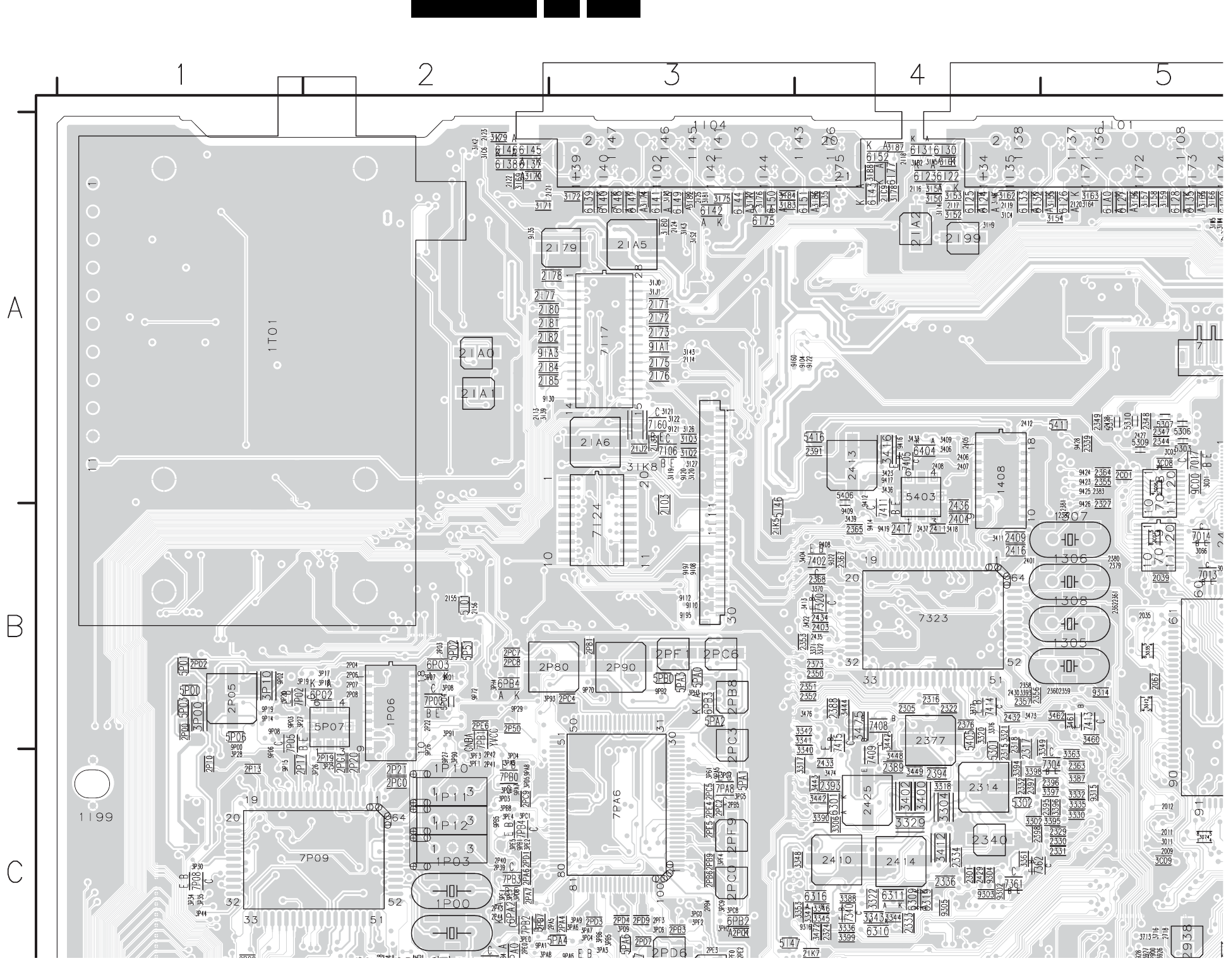
Circuit Diagrams and PWB Layouts EN 73FTL2.4E AA 7.
Layout SSB (Top Side Part 1)
Part 1
F_15460_048a.eps
080405
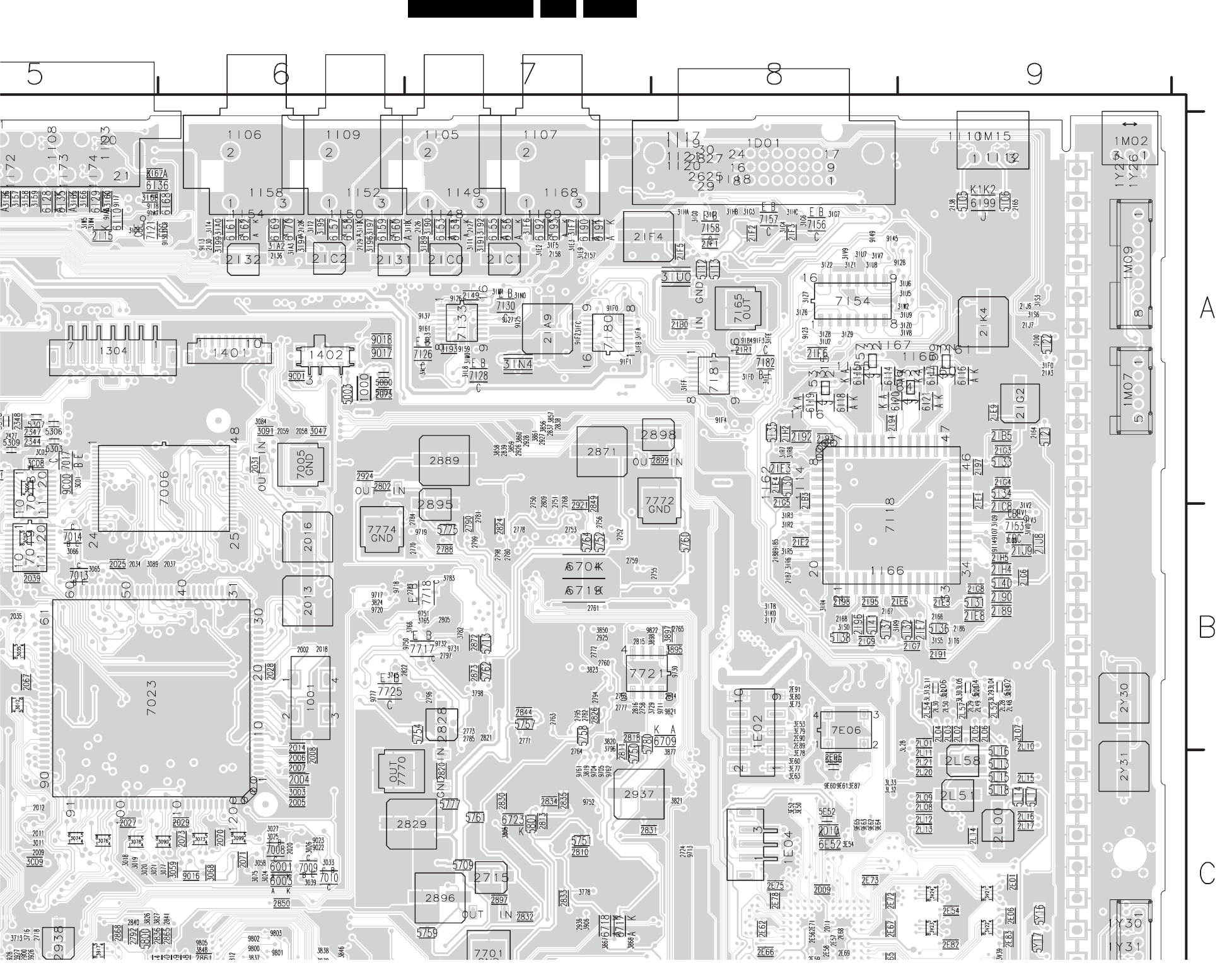
EN 74FTL2.4E AA 7.
Circuit Diagrams and PWB Layouts
Layout SSB (Top Side Part 2)
Part 2
F_15460_048b.eps
120405
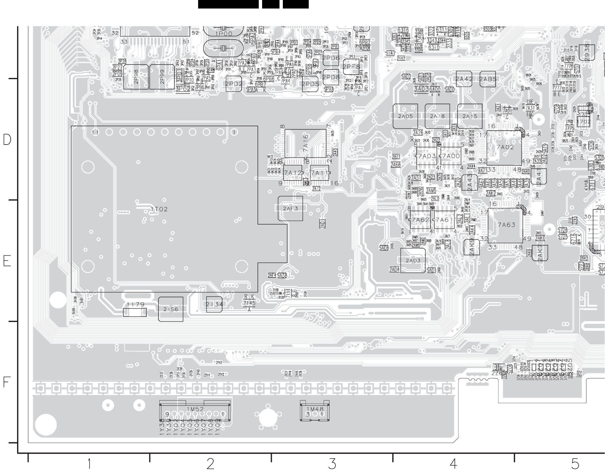
Circuit Diagrams and PWB Layouts EN 75FTL2.4E AA 7.
Layout SSB (Top Side Part 3)
Part 3
F_15460_048c.eps
120405
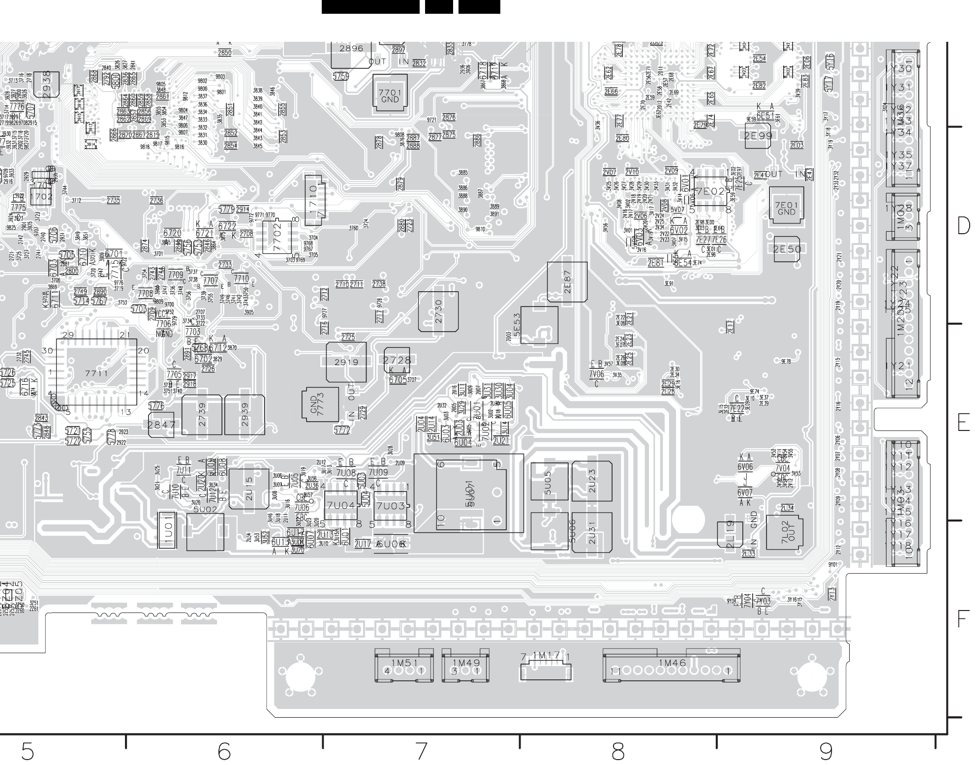
EN 76FTL2.4E AA 7.
Circuit Diagrams and PWB Layouts
Layout SSB (Top Side Part 4)
F_15460_048d.eps
120405
Part 4
Circuit Diagrams and PWB Layouts EN 77FTL2.4E AA 7.
Layout SSB (Overview Bottom Side)
3104 313 6003.7
Part 1
F_15460_049a.eps
Part 2
F_15460_049b.eps
Part 3
F_15460_049c.eps Part 4
F_15460_049d.eps
F_15460_049.eps
080405

EN 78FTL2.4E AA 7.
Circuit Diagrams and PWB Layouts
Layout SSB Mapping (Bottom Side)
F_15460_049m.eps
110405
1301 B5
1404 A4
1406 A6
1407 A6
1409 A5
1410 B6
1411 B6
1A01 D5
1G50 F5
1P04 B8
1P05 C8
1P07 C8
1P08 B9
1P09 C9
1Z28 E5
2003 B4
2010 C5
2017 B5
2019 A5
2022 C4
2023 B4
2024 B4
2026 B5
2033 B5
2036 B4
2038 B4
2040 B4
2041 B5
2052 A4
2053 A4
2054 A4
2055 A4
2056 A4
2057 A4
2060 A4
2061 A4
2063 C4
2068 C5
2072 C5
2074 C5
2300 B6
2302 B6
2303 C6
2304 C6
2306 B6
2307 C6
2308 C6
2309 B6
2310 B6
2311 B6
2312 B6
2313 B6
2319 C6
2320 B5
2321 C5
2323 C5
2325 B6
2326 C6
2328 C5
2335 C6
2337 C6
2338 C6
2341 C6
2342 C6
2343 C6
2345 A5
2346 A5
2354 B6
2366 B6
2369 B6
2370 C6
2371 B6
2372 B6
2374 B6
2375 B6
2378 B6
2384 B6
2385 B6
2386 C6
2387 B6
2392 B6
2402 B6
2415 B6
2418 B6
2419 B6
2420 B6
2421 B6
2422 B6
2423 B6
2424 B6
2426 A5
2431 C5
2713 E5
2714 E5
2727 E4
2731 E5
2734 D4
2737 C2
2746 E5
2748 E5
2754 E5
2757 D5
2769 B3
2786 B4
2789 A3
2791 A3
2793 A3
2804 D5
2806 D5
2807 D5
2808 B4
2812 B3
2817 D3
2823 A3
2825 A3
2827 A3
2882 D3
2883 D3
2884 D3
2885 D3
2892 E3
2893 D3
2894 D3
2920 D5
2932 C5
2933 C5
2A01 D6
2A07 C6
2A19 D7
2A24 D7
2A34 D8
2A38 D7
2A47 D5
2A51 C5
2A64 D6
2A69 D6
2A70 D6
2A72 D6
2A74 D6
2A75 D6
2A79 D6
2A80 D6
2A81 D6
2A83 D6
2A88 D6
2A89 D6
2A90 D6
2A91 D5
2A92 D6
2A99 D5
2AA5 D6
2AA9 D5
2AB0 D5
2AB3 D6
2AB4 D6
2AB8 D6
2AC1 E7
2AD0 E7
2AD3 E7
2AD4 E8
2AD5 E7
2AD6 E8
2AE2 D7
2AE3 D8
2AE5 E8
2AF0 D7
2AK8 E6
2AN5 E6
2AN6 E6
2C00 A5
2C02 B5
2D04 D1
2D15 D1
2E02 E1
2E04 E1
2E05 E2
2E07 E1
2E08 E2
2E09 D1
2E10 E2
2E11 E2
2E12 D2
2E13 E2
2E14 E2
2E15 D2
2E16 E1
2E18 D2
2E19 D1
2E20 E2
2E27 E2
2E35 D2
2E48 E2
2E49 D1
2E51 D1
2E52 C2
2E53 E2
2E55 C2
2E84 D2
2E86 D1
2E88 C2
2E92 B2
2E93 B2
2E94 B2
2I01 B7
2I02 B8
2I04 A7
2I05 B7
2I06 B7
2I07 A8
2I08 A8
2I09 A1
2I10 A6
2I11 A4
2I12 A5
2I33 E8
2I37 F6
2I39 A5
2I40 F6
2I46 A2
2I47 A5
2I48 E6
2I50 A3
2I52 E5
2I59 E8
2I60 F6
2I69 B2
2I70 B2
2IA4 A5
2IB7 E6
2IB8 A1
2IB9 B2
2IC3 A3
2IC5 B1
2IC6 A2
2IC7 A2
2IE0 B8
2IF0 A1
2IF8 A2
2IF9 A2
2IG1 A8
2IH1 B1
2IH3 A5
2IH6 A2
2IH7 A2
2IH8 A2
2IH9 A2
2IJ0 A8
2IJ1 A7
2IJ4 A8
2IJ5 E5
2IK1 A2
2IK2 A1
2IK3 A1
2IK6 C6
2IL0 A7
2IN8 A2
2IN9 A2
2IR0 A3
2L18 B1
2L22 F1
2L25 B1
2L26 C2
2L27 C2
2L31 C2
2L32 C2
2L56 B1
2L59 B1
2L60 B1
2P01 C8
2P11 C9
2P12 C9
2P14 C9
2P15 C9
2P16 C9
2P18 C8
2P23 C8
2P24 C8
2P25 C9
2P29 C8
2P30 C8
2P31 C9
2P32 D9
2P33 C9
2P45 C9
2P46 C9
2P47 C8
2P49 C8
2P51 C8
2P52 C7
2P53 C7
2P54 C7
2P55 C7
2P56 C7
2P57 C7
2P58 C7
2P59 D8
2P60 D7
2P61 D7
2P62 D7
2P63 C7
2P65 C7
2P66 C7
2P70 B7
2P71 C7
2P72 B7
2P73 B7
2P74 C7
2P75 B7
2P76 C7
2P77 C7
2P78 B8
2P79 B7
2P87 B8
2P88 B7
2P91 C9
2P92 C9
2P93 C9
2P94 C9
2P95 C8
2P96 C8
2P97 C7
2PA0 C7
2PA1 C7
2PA2 C7
2PA3 C7
2PA9 C8
2PB0 C7
2PB1 C7
2PB2 C7
2PD0 C8
2PE7 C7
2PE8 C7
2PE9 C7
2PF2 B7
2PF5 B7
2PF6 B7
2PF7 C8
2PG2 C9
2PG6 D7
2T01 A9
2T02 D9
2T03 D8
2T04 A9
2T05 A9
2T06 A9
2T07 D8
2T09 A9
2T10 D9
2T11 D8
2T12 A9
2T13 A9
2T14 D8
2T15 A9
2T16 D8
2T17 A9
2T18 D8
2T19 D8
2T20 D8
2T21 D9
2T22 D9
2T30 E9
2T31 E8
2T32 E9
2T33 E8
2T34 E8
2T35 E8
2T36 E9
2T37 E8
2T38 E9
2T40 D9
2T41 D8
2T42 E8
2T43 E8
2T44 E8
2T45 E8
2T46 D8
2T47 E9
2T48 E8
2T49 E9
2T50 E9
2T51 E8
2T52 E9
2T53 E8
2T54 E9
2T60 A9
2T61 A9
2T62 A9
2T63 A9
2U01 F3
2U02 E3
2U06 E4
2U08 F2
2U10 F3
2U19 E4
2U22 E4
2U24 E4
2U25 E4
2U26 F4
2U27 E3
2U28 E3
2U29 F2
2U33 F4
2U35 E4
2U37 E3
2U38 E4
2U39 E4
2U40 E4
2U41 E4
2U42 E4
2Y00 F2
2Y01 F2
2Y02 F2
2Y03 F2
2Y04 F2
2Y10 E1
2Y11 F2
2Y14 E1
2Y17 E1
2Y18 D1
2Y22 F2
2Y23 D1
2Y25 C1
2Y26 C1
2Y27 C1
2Y28 D1
2Y29 D1
2Y34 F2
2Y48 F2
2Y49 F3
2Y50 F3
2Y52 F8
2Y53 D1
2Z54 E5
2Z55 E5
2Z56 E5
2Z64 F6
3001 C5
3002 C5
3004 B5
3005 B5
3006 B4
3007 B4
3008 B5
3009 C4
3010 B5
3013 B5
3014 B5
3015 B5
3016 B5
3017 B5
3022 C4
3023 C4
3028 C4
3029 B5
3030 C4
3031 B5
3032 C4
3034 B4
3036 C4
3037 C4
3038 C4
3040 B5
3041 B5
3042 C5
3045 A4
3046 A4
3048 B5
3049 B5
3050 B5
3051 B5
3052 B4
3053 C5
3054 B4
3055 B4
3056 B4
3057 B4
3061 B4
3062 B4
3064 C5
3067 B5
3069 C5
3070 C4
3072 B4
3079 C5
3080 C4
3081 B4
3082 B4
3083 B4
3085 B5
3086 B5
3087 B4
3088 C5
3092 C5
3093 B5
3094 C5
3095 C5
3096 C5
3097 A4
3098 A4
3100 C5
3101 C5
3102 B4
3103 C4
3300 B6
3301 B6
3303 B6
3305 C6
3307 C6
3308 C6
3310 C6
3311 C6
3312 C6
3313 C6
3314 C6
3315 B6
3316 C6
3319 C6
3323 B6
3324 B6
3325 C6
3326 B6
3327 B6
3328 B6
3331 C5
3333 B5
3334 B6
3337 C6
3338 C6
3339 C6
3350 C6
3351 C6
3352 C6
3354 C6
3355 C6
3356 C6
3357 C6
3358 C6
3359 C6
3360 C6
3362 C6
3364 C6
3365 C6
3366 C6
3367 C6
3369 C6
3378 B6
3380 B6
3382 B6
3383 C6
3384 C6
3385 B6
3386 C6
3389 C6
3391 C6
3401 B6
3405 B6
3407 A6
3408 B6
3410 A6
3414 B6
3415 B6
3417 A6
3419 A6
3420 B6
3421 A6
3434 A6
3435 A6
3441 B6
3445 A6
3450 B6
3451 B6
3452 B6
3453 C6
3454 C6
3455 C6
3456 B6
3457 B6
3459 C6
3463 B6
3465 C6
3467 C6
3468 B6
3470 C6
3471 C6
3700 D4
3702 E4
3709 E5
3710 D5
3711 E4
3757 A3
3758 E5
3759 D5
3761 D4
3762 C3
3763 C3
3764 C3
3767 C3
3768 C3
3769 C3
3770 C3
3771 A3
3772 A3
3773 A3
3774 C3
3775 C3
3776 A3
3777 C3
3779 C3
3780 C3
3781 C3
3784 C3
3792 A3
3793 B4
3794 A3
3795 A3
3797 B4
3799 B4
3800 A3
3801 A3
3802 A3
3803 C3
3804 C3
3811 A3
3812 A3
3814 A3
3815 A3
3817 A3
3818 A3
3822 D4
3825 B4
3871 E3
3872 D3
3873 E3
3880 D3
3881 D3
3882 D3
3883 D3
3884 D3
3894 A3
3896 B2
3900 B3
3901 C3
3902 C3
3911 B3
3912 B3
3918 B3
3919 B3
3921 B3
3A02 D7
3A04 D5
3A06 D6
3A17 D6
3A19 D6
3A22 D5
3A24 C5
3A40 D6
3A45 D5
3A46 D5
3A47 D6
3A48 D5
3A49 D5
3A51 D6
3A52 D6
3A53 D6
3A55 D5
3A60 D6
3A61 D6
3A62 D6
3A63 D6
3A64 D5
3A65 C5
3A67 D7
3A74 E8
3A77 D7
3C00 A5
3C04 A5
3C05 A5
3C10 B5
3C11 C5
3C12 B5
3E04 E1
3E05 E1
3E11 E2
3E12 E2
3E14 E2
3E18 D2
3E19 D2
3E20 B2
3E21 B2
3E51 D1
3E55 D1
3E56 D1
3E57 D1
3E58 D1
3E69 C2
3E70 C2
3E81 C2
3E82 B2
3E83 C2
3E84 B2
3E85 B2
3E86 B2
3E88 D2
3E89 D1
3E90 E1
3I01 A8
3I02 B8
3I03 B8
3I04 A7
3I05 B7
3I06 B8
3I07 A5
3I08 A8
3I09 A8
3I10 B7
3I11 B7
3I12 B7
3I13 B7
3I14 B7
3I15 B7
3I16 B7
3I17 A7
3I18 A7
3I23 A8
3I24 A8
3I25 B8
3I28 A4
3I29 A3
3I30 A2
3I31 A3
3I32 A2
3I33 A2
3I34 A4
3I36 A4
3I37 A4
3I38 A4
3I40 A2
3I41 A2
3I42 B2
3I44 A1
3I45 A2
3I46 A1
3I47 B1
3I48 B1
3I49 A2
3I85 A3
3I98 A5
3IA1 A5
3IA4 A8
3IA5 A8
3IA6 A3
3IA7 A3
3IA8 A4
3IA9 A4
3IB0 A3
3IB1 E8
3IB3 E8
3IB4 A2
3IB5 A2
3IB6 E8
3IB7 E8
3IBA E8
3IBB E8
3IC0 E8
3IC1 A3
3IC2 A5
3IC3 A5
3IC5 E8
3IC7 E8
3IC8 A3
3ID0 A3
3ID2 E6
3ID3 F6
3ID4 F6
3ID5 A3
3ID6 E5
3ID7 A5
3ID8 A5
3ID9 A3
3IE0 F6
3IE7 A3
3IF1 E6
3IF2 E6
3IF3 F6
3IF4 E6
3IF8 E6
3IF9 E6
3IG9 A1
3IGA F6
3IGB F6
3IGC F6
3IGD F6
3IGE F6
3IGF F6
3IH0 F6
3IH1 A5
3IH2 F6
3IH4 F6
3IH7 A3
3IH8 A8
3IHG A7
3II0 A8
3II1 A8
3II2 A8
3II3 A8
3II5 A2
3II6 A2
3II7 A2
3II8 B2
3II9 B2
3IJ2 A2
3IJ3 A2
3IJ4 A2
3IJ6 A2
3IJ7 A2
3IJ8 A7
3IK4 A7
3IK5 A8
3IK7 A7
3IK9 B2
3IN1 A7
3IN2 A3
3IN3 A3
3IN8 A3
3IO5 A3
3IO6 A3
3IP0 A8
3IP1 A8
3IP2 A8
3IP3 A7
3IP4 A8
3IP5 A8
3IP6 A8
3IP7 A8
3IP8 A7
3IP9 A3
3IQ0 A7
3IQ1 A7
3IQ4 A7
3IQ5 B2
3IQ6 A2
3IQ7 A2
3IR0 B1
3IR1 B1
3IS1 B2
3IS4 A3
3IT5 B2
3IT9 A8
3IU1 A2
3IU3 A1
3IV4 A2
3IV5 A2
3IV6 A2
3IW1 A1
3IW3 A6
3IW7 A2
3IW8 A2
3IW9 A6
3IZ3 A2
3IZ4 A2
3IZ5 A2
3L02 B1
3L03 C2
3L06 C2
3L08 C2
3L12 B1
3L40 F1
3L41 F1
3L42 F1
3L43 F1
3L44 E1
3L45 E1
3L46 E1
3L47 E1
3L48 F1
3L49 E1
3P03 C8
3P04 C8
3P05 C8
3P06 C8
3P09 B8
3P11 B9
3P12 B8
3P13 B8
3P14 B8
3P15 B8
3P16 C9
3P21 C8
3P22 C8
3P23 C8
3P24 C8
3P31 C9
3P32 C9
3P33 C9
3P36 C9
3P37 C8
3P38 C9
3P39 C9
3P40 B9
3P45 C8
3P46 C8
3P47 C9
3P48 C8
3P49 C8
3P50 C7
3P51 C7
3P52 C7
3P53 C8
3P54 C7
3P55 D7
3P56 C7
3P57 C7
3P60 C7
3P62 C7
3P63 C7
3P64 C7
3P65 B8
3P66 B8
3P67 B7
3P68 B7
3P69 B7
3P70 B7
3P71 C8
3P72 B8
3P74 B7
3P75 D7
3P76 C7
3P79 C8
3P80 C8
3P81 C7
3P82 B7
3P85 B8
3P86 B7
3P87 B7
3P88 B7
3P92 C8
3P94 C8
3P95 C8
3P96 C7
3P97 D7
3P98 C7
3P99 C7
3PC0 C8
3PC5 B7
3PD7 C8
3PF5 B7
3PG1 C7
3PG7 D7
3PG8 C7
3PH5 D8
3PH9 D7
3PI0 B7
3PJ0 D8
3PJ1 D8
3PJ2 D8
3PJ3 D8
3PJ4 C7
3PJ5 C7
3PJ6 C7
3PJ7 C7
3PJ8 C7
3PJ9 C7
3T03 A9
3T04 D8
3T05 A9
3T06 A9
3T10 E9
3T11 E9
3T12 E9
3T13 E9
3T14 E9
3T15 E9
3T16 E8
3T17 E8
3T18 E8
3T19 E8
3T20 E9
3T22 E9
3T23 E8
3T24 E8
3T25 E8
3T26 E8
3T27 E9
3T28 D8
3T29 E9
3T30 E9
3T31 E9
3T32 E8
3T33 E9
3T51 E9
3T52 E9
3T53 E9
3T54 E9
3T55 E9
3T56 E9
3T57 E9
3T58 E9
3T59 E9
3T60 E9
3U12 F5
3U24 E4
3U27 E5
3U32 E3
3U33 E3
3U35 E4
3U36 F5
3U37 F4
3U38 F4
3U39 E4
3U40 E4
3U41 E4
3U42 E4
3U43 F4
3U44 E3
3U45 E3
3U54 E5
3U55 F4
3U58 E3
3U59 E3
3U60 E4
3U61 E4
3U62 E4
3U63 E4
3U64 E4
3U65 E4
3U66 E4
3U67 E4
3U68 E4
3U69 E4
3V18 C2
3V37 C2
3V38 C2
3V40 C2
3Y00 E1
3Y01 E1
3Y02 E1
3Y03 E1
3Y05 E1
3Y06 F2
3Y07 F1
3Y08 F1
3Y09 D1
3Y10 E1
3Y11 E1
3Y12 D1
3Y13 F2
3Y14 F8
3Y20 D1
3Y21 D1
3Y22 D1
3Y23 D1
3Y24 F9
3Y25 F8
3Y30 F1
3Y33 F2
3Y34 F3
3Y35 F3
3Y37 F8
3Y38 F8
3Y40 D1
3Z23 E5
3Z24 F5
3Z25 F5
3Z26 F5
3Z29 E5
3Z30 E5
3Z31 E5
3Z32 E5
3Z33 E5
3Z36 E5
3Z37 F5
3Z38 F6
3Z39 F5
3Z56 E5
5304 A5
5305 A5
5308 A5
5312 B6
5313 C6
5314 C6
5315 C6
5318 B6
5401 B6
5402 A6
5404 B6
5408 B6
5702 C5
5719 E4
5720 E4
5723 E5
5724 E5
5727 E5
5728 E5
5763 D3
5769 E3
5770 D3
5771 D3
5A07 D7
5E00 E1
5E01 E2
5E02 E2
5E03 E2
5E50 C2
5E54 D1
5E55 C2
5E58 C2
5I02 E8
5I04 E8
5I10 E6
5I39 B2
5I42 A2
5I45 C6
5P05 B9
5P08 C8
5P09 C8
5P10 C8
5P11 C9
5P50 C7
5PA9 B7
5T02 D9
5T03 D8
5T04 E8
5T10 D9
5T11 E8
5T12 D9
5T13 D9
5T14 E8
5T15 E8
5T20 A9
5T22 A9
5T25 A9
5Y00 F1
5Y01 E1
5Y02 F2
5Y03 F2
5Y06 F2
5Y07 F2
5Y09 F1
5Y11 E1
5Y12 E1
5Y14 D1
5Y15 F2
5Y18 F8
5Y19 F8
5Y20 F8
5Y21 F8
5Y22 F8
5Y23 D1
5Z07 F6
5Z08 F6
6002 A4
6004 C4
6005 A4
6006 C4
6303 B6
6304 B6
6306 B6
6307 B6
6308 C6
6312 B6
6313 B6
6314 C6
6317 C6
6334 B6
6402 A6
6403 B6
6405 A6
6713 E3
6714 D3
6715 E3
6A01 C5
6A02 C6
6E53 D1
6E55 D2
6E56 C2
6I01 A3
6I03 E8
6I04 E8
6I05 E5
6I06 A2
6I07 A3
6I08 A2
6I09 A2
6I11 A4
6I12 A5
6I13 A5
6I63 B2
6I64 A2
6I65 A1
6I66 A2
6I80 A1
6I81 A1
6IA1 A1
6IA7 A5
6P00 B8
6P01 B8
6P10 C7
6PB1 B7
6PB5 D8
6PB9 D7
6T01 A9
6T02 D8
6T03 A9
6T04 D8
6T05 A9
6T06 D9
6T07 D9
6T08 A9
6T10 E9
6T11 E9
6U02 E3
6U10 E3
6U11 E4
6U12 F4
6U14 E4
6U16 E4
6V05 C2
6Z00 E5
7002 B5
7003 B5
7004 B5
7007 A5
7011 C5
7012 B4
7015 C5
7016 C5
7020 C4
7021 C4
7022 C4
7301 C6
7302 C6
7303 B6
7305 C6
7306 C6
7307 B6
7309 C6
7310 C6
7312 B6
7313 C6
7314 C6
7315 C6
7316 C6
7317 C6
7318 C6
7319 C6
7322 B6
7375 C6
7401 A6
7403 B6
7406 A6
7407 A6
7410 B6
7412 B7
7712 E5
7713 D4
7714 D3
7719 C3
7720 B3
7752 C4
7753 C4
7760 D3
7A04 D6
7A06 D6
7A07 D6
7A08 D5
7A09 D5
7A13 D7
7A14 D7
7A15 D8
7A30 E8
7E03 B2
7E04 C2
7E05 D1
7E10 C2
7E12 D1
7E23 E2
7E24 E1
7I01 A8
7I02 A3
7I03 A4
7I04 A4
7I05 A5
7I07 A3
7I08 A6
7I09 A2
7I10 E8
7I12 A3
7I13 E5
7I14 F6
7I15 E6
7I16 E6
7I19 B1
7I20 A8
7I22 A8
7I23 A2
7I27 A3
7I29 A3
7I31 A3
7I32 A3
7I35 A8
7I36 A8
7I37 A8
7I38 A7
7I40 F6
7I41 A2
7I44 A5
7I46 E8
7I49 A5
7I50 A5
7I51 B2
7I52 B2
7I55 A2
7I61 B2
7I62 A8
7I64 B2
7L01 B1
7L03 F1
7L04 F1
7L05 E1
7P01 B8
7P03 B9
7P04 B9
7P06 C9
7P07 C9
7P11 C9
7P51 C7
7P52 C7
7P53 C7
7P54 C7
7P55 C7
7P56 B7
7P58 C7
7P59 C7
7P60 C8
7P61 C8
7P62 C8
7P63 D8
7PB5 B7
7T01 D9
7T04 E9
7T10 E8
7T11 E9
7T12 E9
7T13 E9
7T50 A9
7U07 F4
7U13 E4
7V01 C2
7V02 D2
7V03 C1
7Y01 F9
7Y02 F8
7Z00 E5
7Z01 E5
9001 C5
9002 C5
9003 C5
9004 B5
9005 A4
9006 A4
9007 A4
9008 C4
9009 C4
9010 C5
9011 C5
9012 C4
9013 C4
9014 B5
9015 C5
9019 C4
9021 C4
9024 C4
9025 C4
9308 C6
9309 C6
9310 C6
9311 C6
9312 C6
9313 C6
9318 B6
9319 B6
9401 A6
9402 A6
9403 A6
9404 B6
9405 A6
9406 B6
9407 B6
9410 B6
9413 B6
9415 B6
9418 A6
9420 A6
9421 C6
9422 B6
9427 B6
9701 E5
9702 E5
9706 D5
9710 D5
9712 B4
9714 C2
9715 B4
9716 B4
9723 B3
9726 D5
9740 B4
9753 B4
9754 B4
9755 B4
9756 B4
9757 B4
9758 B4
9759 B4
9760 B4
9763 B4
9764 B4
9765 B4
9766 B4
9773 B4
9774 B4
9775 B4
9811 D3
9820 D4
9823 B3
9A00 D6
9A01 D6
9A02 D6
9A03 D6
9A07 D6
9A08 D6
9A10 E6
9A11 E6
9A12 E6
9A13 E6
9A14 E6
9A15 E6
9A16 E6
9A17 E6
9A18 D6
9A20 E6
9C02 A4
9E57 C2
9E58 C2
9E66 D1
9E67 D1
9E68 D1
9E69 D1
9E70 D1
9E71 D1
9E72 D1
9E73 D2
9E75 D1
9E76 D1
9E77 D2
9I00 A7
9I01 A7
9I02 A7
9I03 B7
9I05 E8
9I06 E8
9I09 A7
9I11 A7
9I15 A8
9I16 A8
9I19 B7
9I29 A2
9I31 A7
9I32 A7
9I33 A7
9I34 A8
9I39 A7
9I41 A3
9I42 A3
9I50 A4
9I57 A8
9I58 A8
9I62 A3
9I63 A3
9I64 A3
9I65 A3
9I66 A3
9I67 A3
9I68 A2
9I78 B8
9I79 A3
9I81 A2
9I88 A2
9I91 A2
9I92 A7
9I93 A7
9I94 A7
9I96 B8
9I98 A2
9I99 F6
9IA2 A3
9IA4 A5
9IA5 A5
9IB1 A7
9IB2 A7
9IB3 A2
9ID1 A3
9ID2 A3
9ID3 A2
9ID4 A2
9ID5 A2
9ID6 A2
9ID7 A2
9ID8 A2
9ID9 A2
9L00 F1
9L01 F1
9P04 B8
9P05 B9
9P07 C9
9P09 B9
9P10 B8
9P11 B8
9P12 C9
9P16 B8
9P17 C8
9P18 B9
9P20 C8
9P21 C8
9P22 C9
9P23 C8
9P24 C9
9P25 C9
9P28 C8
9P30 C9
9P31 C7
9P32 C7
9P52 C7
9P53 C7
9P54 D7
9P69 B7
9P71 B7
9P73 D7
9P74 D7
9P75 D7
9PB7 D8
9T01 A9
9T02 D8
9T03 D8
9T04 A9
9T05 A9
9T06 D8
9T07 A9
9T08 A9
9T09 D8
9T10 D8
9T11 E8
9T12 A9
9T14 A9
9T50 A9
9Y00 D1
9Y02 F1
9Y03 F1
9Y05 E1
9Y06 E1
9Y07 E1
9Y09 F1
9Y12 F2
9Y13 F2
9Y14 F2
9Y15 F1
9Y16 F9
9Y17 F9
Personal Notes:
E_06532_012.eps
131004
Circuit Diagrams and PWB Layouts EN 79FTL2.4E AA 7.
Layout SSB (Bottom Side Part 1)
Part 1
F_15460_049a.eps
120405
EN 80FTL2.4E AA 7.
Circuit Diagrams and PWB Layouts
Layout SSB (Bottom Side Part 2)
Part 2
F_15460_049b.eps
120405
Circuit Diagrams and PWB Layouts EN 81FTL2.4E AA 7.
Layout SSB (Bottom Side Part 3)
Part 3
F_15460_049c.eps
120405
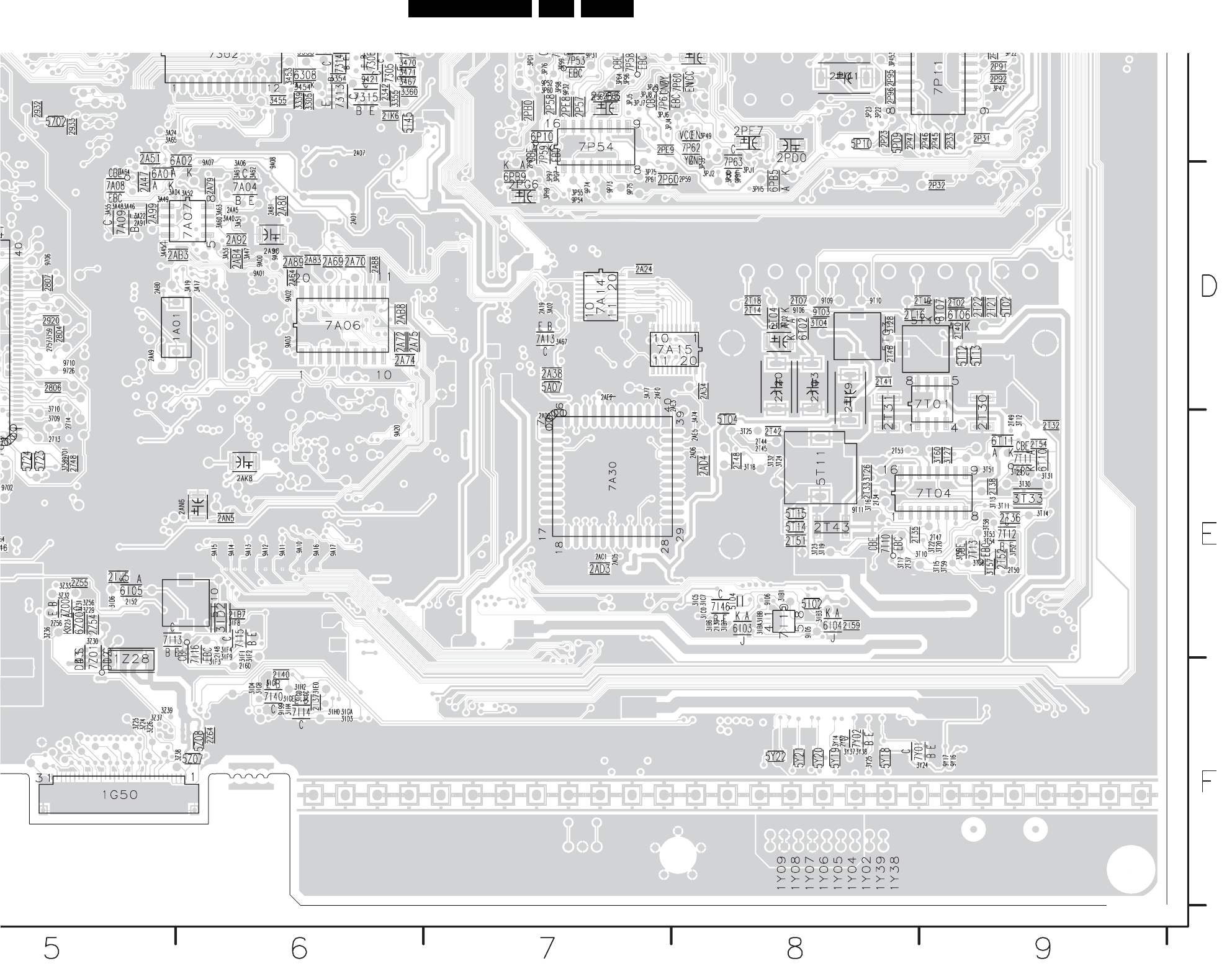
EN 82FTL2.4E AA 7.
Circuit Diagrams and PWB Layouts
Layout SSB (Bottom Side Part 4)
Part 4
F_15460_049d.eps
120405
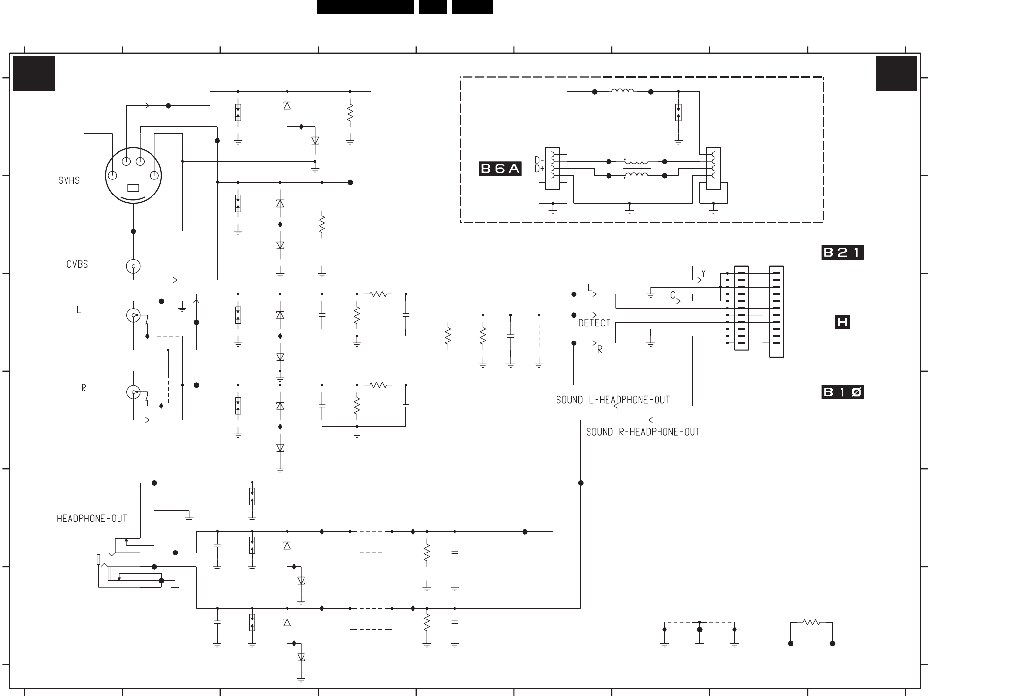
Circuit Diagrams and PWB Layouts EN 83FTL2.4E AA 7.
Side I/O Panel
RES
I012 F8
I013 F3
I014 E3
F024 E6
F025 E6
I001 C2
I002 C3
I003 D2
I004 A3
I005 F4
I006 F4
I007 E4
VIPER
I008 E4
I009 B3
I010 D3
I011 F7
F014 A6
F015 A7
F016 A6
F017 A7
F018 F7
F019 F2
F020 B4
F021 C6
F022 C6
EMGT
OR
OR
F023 C6
9007 F8
9008 F4
9009 F4
9010 E4
9011 E4
F001 A2
F002 A2
F003 B2
F004 C2
SSB EMGT
TO 1M36
TO 1H01
F005 C2
F006 D2
F007 E2
F008 E2
F009 E2
F010 F8
F011 F9
F012 A6
F013 A7
3020 E5
3999 F9
5000 A7
6000 A3
6001 A3
6002 B3
6003 B3
6004 C3
6005 C3
C
SIDE I/O
6006 D3
6007 D3
6008 F3
6009 F3
6010 E3
6011 F3
9003 C6
9004 C2
9005 D2
9006 F7
2010 E2
2011 E5
3000 A4
3004 B3
3008 C5
3009 C4
3010 C4
3011 C5
3012 D4
3013 D4
3016 F5
789
A
B
C
D
E
F
SSB JAGUAR
TO 1M36
SCART 3
TO 1M36
1M60
OR
2004 C3
2005 C4
2006 D3
2007 D4
2008 F2
2009 F5
1108 D3
1109 E3
1110 F3
1111 E3
1112 A7
1H01 A6
1M36 B8
1M37 B8
2003 C5
Y / CVBS
123456789
123456
7
8
9
USB
CONNECTOR
JAGUAR ONLY
A
B
C
D
E
F
1001 B2
1002-1 B1
1002-2 C1
1002-3 D1
1005 A8
1010 E1
1050 A7
1101 A3
1102 B3
1106 C3
1
10
11
2
3
4
5
6
1M36
GND_AUD
I002
9
7
8
1K0
3012
RED
1002-3
1106
GNDB
GNDB
F006
6007
PDZ6.8-B
I003
I012
6002
PDZ6.8-B
F009
6003
PDZ6.8-B
F002
GNDB
GNDB
GNDB
PDZ6.8-B
6011
1
2
3
4
56
GND_AUD
1H01
F014
9006
F013
F003
1101
2007
100p
F001
I004
PDZ6.8-B
6009
6010
PDZ6.8-B
PDZ6.8-B
6004
PDZ6.8-B
6005
GNDB
F025
GNDB
F023
GNDB
F011
F004
9007
I005
F016
I008
1109
9
12
13
3011
3K9
1
10
11
2
3
4
5
6
7
8
1M37
B11B-PH-SM3-TBT
F015
F020
GND_AUD
GND_AUD
GND_AUD
9004
1108
5000
3020
10K
3000
75R
1
2
3
4
5
7
8
1010
1110
F010
3999
150R
2003
1u0
I006
F007
GND_AUD
GND_AUD
I007
F017
F018
GNDB
9011
9010
I001
22n
2010
6006
PDZ6.8-B
2008
22n
680p
2006
3009
1K0
100p
2005
1
2
1002-1
YELLOW
680p
3010
33K
2004
1111
9005
I010
F005
9003
GNDBGNDB
6
4
5
GNDB
GNDB
WHITE
1002-2
1
2
3
4
56
GND_AUD
1005
1050
DLW31S
9008
F012
9009
F019
3016
F024
10K
10n
2009
1112
1102
GNDB
I009
5
134
2
1001
3004
75R
I011
PDZ6.8-B
6001
F022
F021
2K2
3008
6000
PDZ6.8-B
GNDB
F008
6008
PDZ6.8-B
2011
10n
33K
3013
I014
I013
D D
3104 313 6058.4 F_15460_053.eps
110405
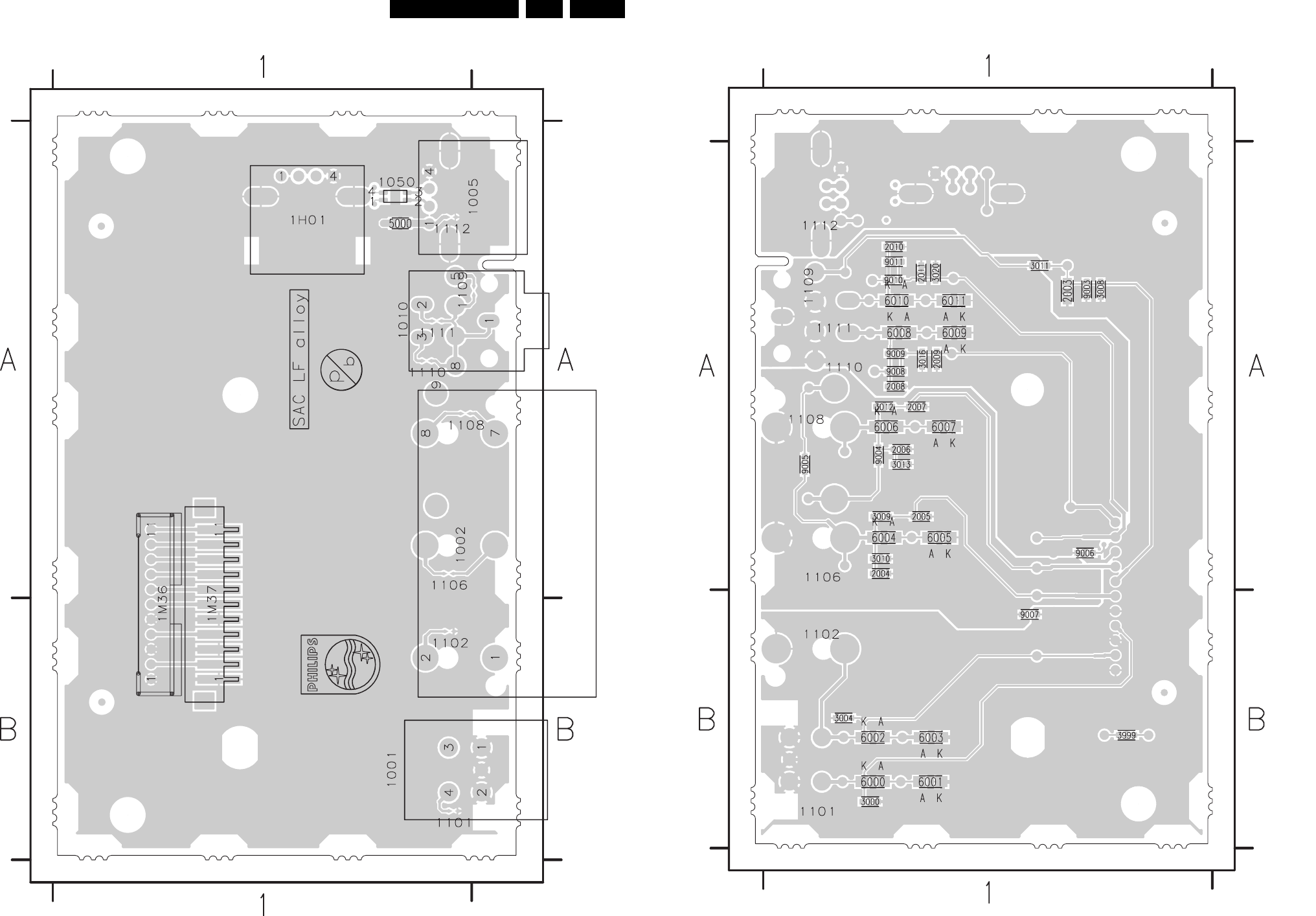
EN 84FTL2.4E AA 7.
Circuit Diagrams and PWB Layouts
Layout Side I/O Panel (Top Side)
3104 313 6058.4 F_15460_054.eps
110405
1001 B1
1002 A1
1005 A1
1010 A1
1050 A1
1H01 A1
1M36 B1
1M37 B1
5000 A1
Layout Side I/O Panel (Bottom Side)
3104 313 6058.4 F_15460_055.eps
110405
2003 A1
2004 A1
2005 A1
2006 A1
2007 A1
2008 A1
2009 A1
2010 A1
2011 A1
3000 B1
3004 B1
3008 A1
3009 A1
3010 A1
3011 A1
3012 A1
3013 A1
3016 A1
3020 A1
3999 B1
6000 B1
6001 B1
6002 B1
6003 B1
6004 A1
6005 A1
6006 A1
6007 A1
6008 A1
6009 A1
6010 A1
6011 A1
9003 A1
9004 A1
9005 A1
9006 A1
9007 B1
9008 A1
9009 A1
9010 A1
9011 A1
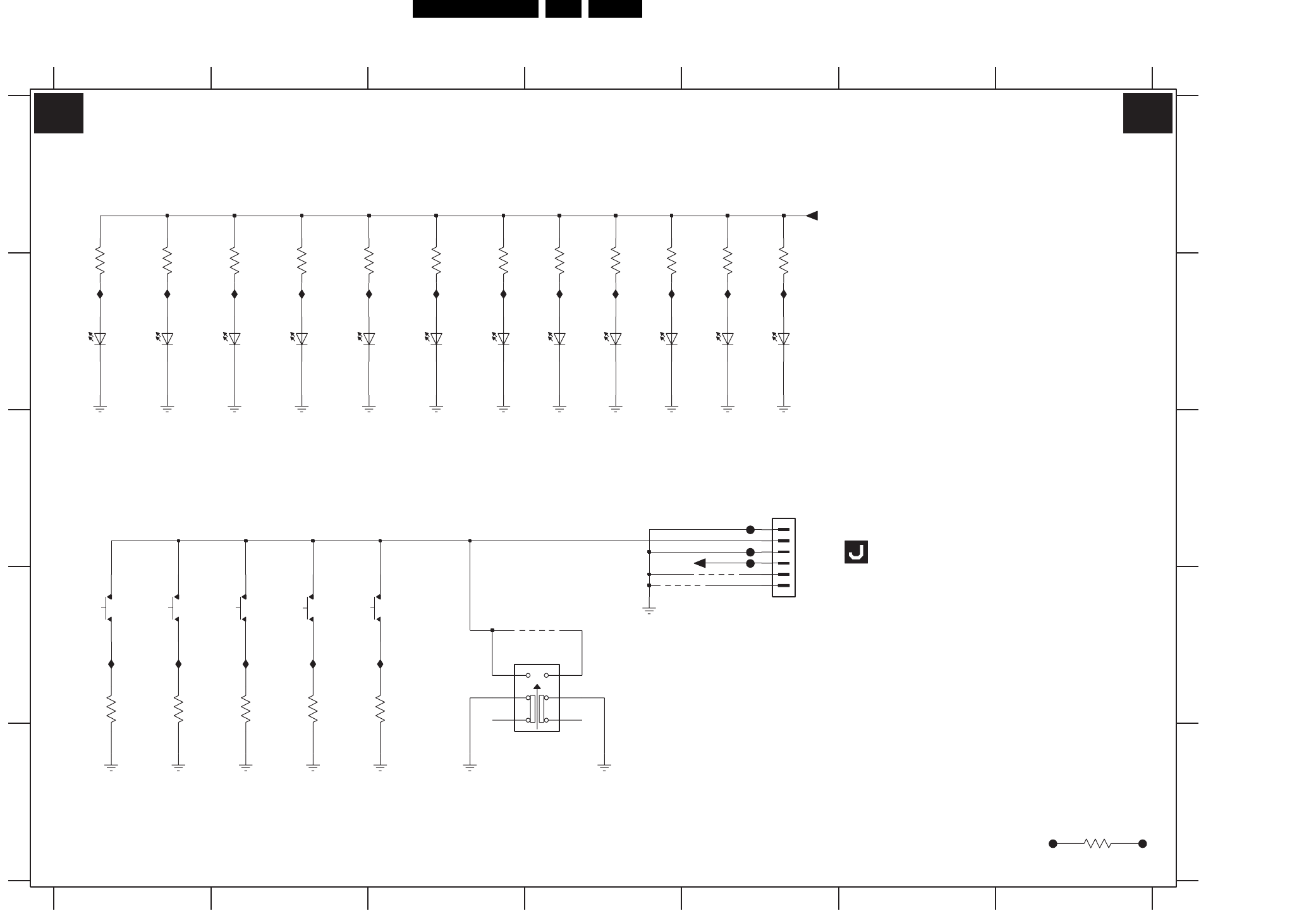
Circuit Diagrams and PWB Layouts EN 85FTL2.4E AA 7.
Top Control Panel
I114 B2
I115 B3
I116 B3
I117 B4
F007 E7
I105 D1
I106 D2
I107 D2
I108 D2
I109 D1
I110 B1
I111 B1
I112 B2
I113 B2
6009 B4
6010 B4
6011 B5
6012 B5
TOP CONTROL
9000 D4
9001 D5
9002 D5
F001 C5
F002 C5
F005 C5
F006 E7
3027 B5
3028 B5
3999 E7
6001 B1
LED + SWITCH
KEYBOARD
6002 B1
6003 B2
6004 B2
6005 B2
6006 B3
6007 B3
6008 B4
D
E
A
B
C
D
ON / OFF
CHANNEL +
CHANNEL -
MENU
VOLUME +
VOLUME -
TO
3025 B4
3026 B4
3019 B2
3020 B2
3021 B2
3022 B3
3023 B3
3024 B4
1234567
1234567
A
B
C
I118 B4
I119 B4
I120 B5
I121 B5
E
0345 C5
1701 D1
1702 D1
1703 D2
1704 D2
1705 D2
1710 E4
3008 D3
3010 D2
3011 D2
3013 D1
3014 D1
3017 B1
3018 B1
SML512BC2T
6003
6002
SML512BC2T
SKQNAB
1704
1705
SKQNAB
1702
SKQNAB
BACKLIGHT-TC
620R
3008
F007
9001
9002
I114I110
F005
F002
I105
F001
I121
3028
33R
6012
SML512BC2T
I120
33R
3027
SML512BC2T
6011
I107I106I108
I113
I109
SKQNAB
1703
33R
I119
6010
SML512BC2T
3026
I118
1K1
3010
I116
390R
3014
I115
1710
25
14
36
200R
3013
33R
3025
SML512BC2T
6009
33R
I117
6008
SML512BC2T
3024
3018
33R
33R
3017
SML512BC2T
6007
6006
SML512BC2T
SML512BC2T
6005
6004
SML512BC2T
SML512BC2T
6001
9000
I112I111
2K2
3999
F006
2K0
3011
1
2
3
4
5
6
BACKLIGHT-TC
0345
SKQNAB
1701
33R
3023
3022
33R
33R
3021
33R
3020
3019
33R
E E
3104 313 6020.3 F_15460_056.eps
110405
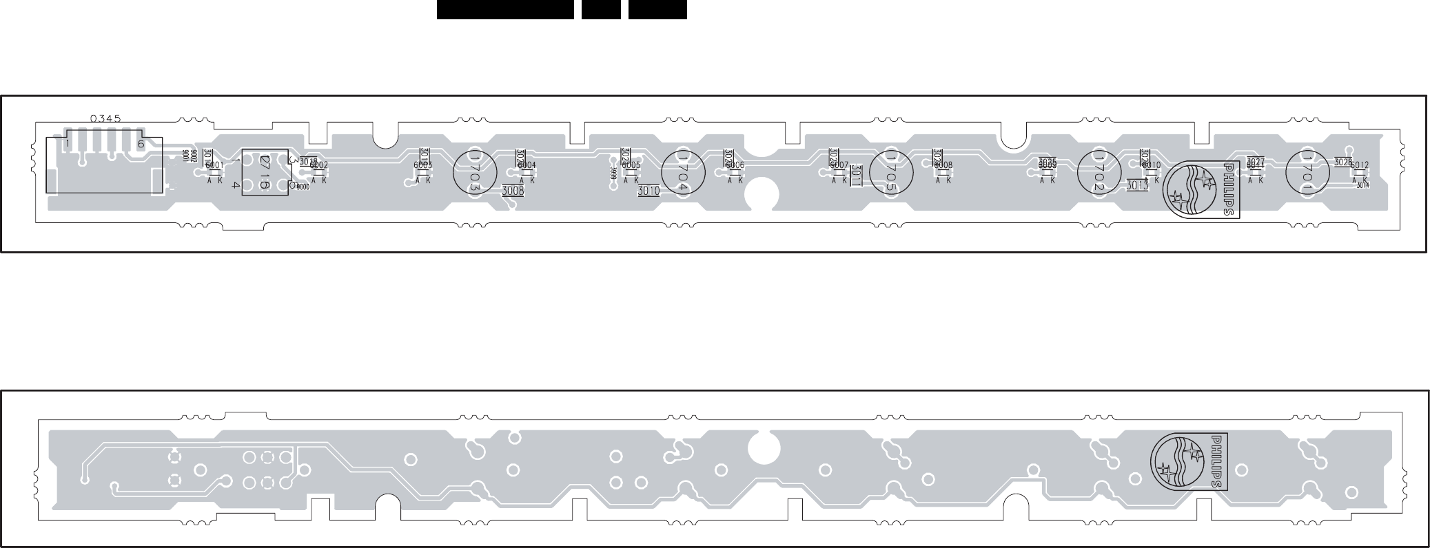
EN 86FTL2.4E AA 7.
Circuit Diagrams and PWB Layouts
Layout Top Control Panel (Top Side)
Layout Top Control Panel (Bottom Side)
3104 313 6020.3 F_15460_057.eps
110405
0345 --
1701 --
1702 --
1703 --
1704 --
1705 --
1710 --
3008 --
3010 --
3011 --
3013 --
3014 --
3017 --
3018 --
3019 --
3020 --
3021 --
3022 --
3023 --
3024 --
3025 --
3026 --
3027 --
3028 --
3999 --
6001 --
6002 --
6003 --
6004 --
6005 --
6006 --
6007 --
6008 --
6009 --
6010 --
6011 --
6012 --
9000 --
9001 --
9002 --
3104 313 6020.3 F_15460_058.eps
110405
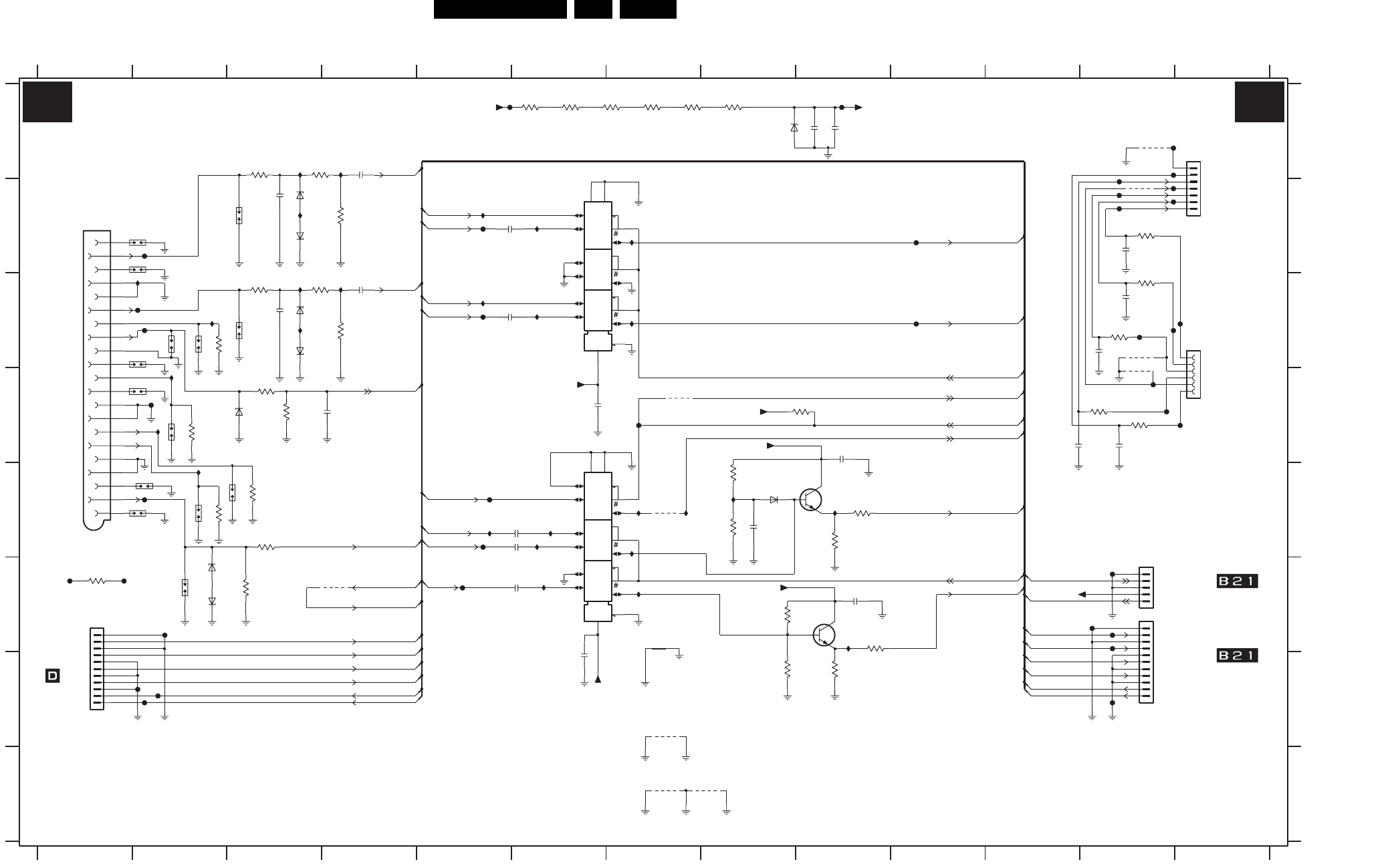
Circuit Diagrams and PWB Layouts EN 87FTL2.4E AA 7.
SCART 3 Panel
MUXDX
MUXDX
567
TO 1M36
ITV
FOR
ONLY
G
H
0244 B13
1003 B1
1005 C13
1500 B3
1501 C2
1502 C3
1504 F2
1505 E2
1506 E3
1507 D2
1508 C2
1509 B2
1510 E2
1511 B2
1512 C2
1513 D2
1514 E2
1M07 F12
1M36 F1
D
E
F
SCART
12345678910111213
1234
2515 E5
2516 F6
2517 B5
SSB EMG
TO 1M07
ITV
FOR
ONLY
SSB EMG
TO 1M36
SIDE I/O
SCART 3
8 9 10 11 12 13
A
B
C
D
E
F
G
H
A
B
C
3507 D2
3508 E2
3509 E3
1M37 F12
2500 A4
2501 B3
2502 C4
2503 C3
2504 E6
2505 C5
2506 D6
2507 A9
2508 A9
2509 G6
2510 D4
2511 D9
2512 E8
2513 F9
3531 C12
3532 C12
3533 D12
2520 B12
2521 C12
2522 C12
2523 D11
2524 D12
3500 A3
3501 A3
3502 B4
3503 C3
3504 C3
3505 C4
3506 C2
7501 E9
7502 F9
7515 B6
3510 F3
3511 A6
3512 A6
3513 A7
3514 A7
3515 A7
3516 A8
3517 E8
3522 D3
3523 E8
3524 E9
3525 E9
3526 D3
3527 F8
3528 G8
3529 G9
3530 B12
F500 B2
F501 C2
F502 C2
RES
3534 D12
3535 F9
3536 D9
3543 E3
3999 F1
6500 B3
6501 B3
6502 C3
6503 C3
6504 E8
6505 F2
6506 F2
6507 D2
6508 A8
F525 F12
F526 F12
F527 G1
7516 D6
9500 F4
9501 E7
9502 D7
9503 B12
9504 D12
9505 C12
9506 A12
9516 H8
9517 H7
9521 G7
F544 B10
F545 C10
F546 D12
F503 E2
F510 A12
F512 B12
F513 B13
F514 B12
F515 B13
F516 B12
F517 C13
F518 C12
F519 C12
F520 E5
F521 F1
F522 F1
F523 F12
F524 F2
I565 C7
I570 E5
I571 E6
F528 G2
F529 G1
F530 G12
F531 A12
F532 A5
F536 A9
F538 D2
F539 B5
F540 C5
F541 D7
F542 E5
F543 F5
I582 F6
I583 F9
c001 F7
F547 D12
F548 D13
F549 F12
I503 A3
I504 C2
I505 A4
I508 B3
I516 C3
I518 C4
I519 C3
I549 C2
I550 D2
I551 D2
I552 E2
I560 B5
I562 C5
I564 B7
I572 E7
I573 F7
I575 E7
I576 B6
I577 C6
I578 E8
I579 E7
I580 E9
I581 E6
I580
I582
I578
F513
F531
F512
I583
F510
F530
F518
F548
F517
9500
F514
75R
3508
F520
F529
F527 F528
A-GND
1502
F540
I562
F522
F546
F521
1u0
2516
1u0
2515
1u0
2504
100R
3500
F525
F526
V-GND
F523
V-GND
V-GND
V-GND
9502
+11V-SFS
3536
10K
BZX384-C12
6507
+11V-SFS
+11V-SFS
V-GND
V-GND
2517
1u0
2505
1u0
I571
100p
2524
100R
3534
9506
V-GND
F502
3524
47R
1K0
3525
7501
BC847BW
2509
100n
F547
A-GND
A-GND
2511
2512
100n
100n
22K
3523
47K
3517
+11V-SFS
I552
F542
I579
I570
F544
21
3
4
5
6
7
8
9
A-GND
13
14
15
16
17
18
19
2
20
1003
1
10
11
12
75R
3507
75R
3543
F524
I505
F538
3999
1K0
BZX384-C6V8
6505 1506
8
VCC
16
VEE
7
s0 11
s1 10
s2 9
14
2y0
2
2y1
1
2z 15
3y0
5
3y1
3
3z 4
G3 6
GND
7515
74HC4053PW
1y0
12
1y1
13
1z
GND
8
VCC
16
VEE
7
s0 11
s1 10
s2 9
14
2y0
2
2y1
1
2z 15
3y0
5
3y1
3
3z 4
G3 6
7516
74HC4053PW
1y0
12
1y1
13
1z
A-GND
3504
100R
22K
3505
3503
100R
V-GND
1500
I518
I575
F541
I573
I572
3528
22K
47R
3535
3529
1K0
7502
9
9501
RES
BC847BW
1
10
11
2
3
4
5
6
7
8
I503
1M37
B11B-PH-K
F539
I560
F532
1514
4
5
6
F519
1005
440050-1
1
2
3
c001
1510
6500
BZX384-C6V8
I519
1509
BZX384-C6V8
6501
3516
47R47R
3511
+11V-SF
22K
3502
3512
47R
3506
75R
V-GND
F515
1u0
2508
1n0
2507
9505
F516
F501
I516
F543
BAS316
6504
9503
2523
100p
100p
2522
3509
100R
100p
2520
3533
100R
100R
3531
3530
100R
47R
A-GND
A-GND
A-GND
3513
2503
100p
2501
100p
100n
2506
BZX384-C6V8
6502
47R
F536
3514
8K2
3526
1511
1513
BZX384-C10
6508
6506
BZX384-C6V8
1u0
2502
1504
+11V-SF
68K
3527
V-GND
9504
F500
V-GND 1
2
3
4
5
3510
75R
1M07
B5B-PH-K
100R
3501
0244
1
2
3
4
5
6
7
B7B-PH-K
I504
1505
I581
I549
6503
BZX384-C6V8
I551
3515
47R
100R
3532
V-GND
95169517
9521
V-GND
I577
F549
I576
F545
I550
V-GND
100n
2513
+11V-SFS
1508
330p
2510
1u0
2500
I508
+11V-SFS
1501
2521
100p
V-GND
V-GND
F503
1507
2K7
3522
4
5
6
7
8
9
1
10
11
2
3
I564
B11B-PH-K
1M36
I565
1512
SNDR-IN
SNDL-IN
STATUS-SC3-F
FRONT-SC3-C
FRONT-SC3-Y-CVBS
SEL_FRONT_SC3
FRONT-SC3-Y-CVBS
CVBS-SC3-IN
SNDR-SC3-IN
SNDL-SC3-IN
STATUS-SC3-F
CVBS-SC3-IN
SEL_IN_1_BF
SEL_FRONT_SC3
SNDR-IN
SNDL-IN
SEL_IN_1_BF
STATUS-SC3-F
CVBS-SC3-IN
SNDL-SC3-IN
SNDR-SC3-IN
SEL_FRONT_SC3
FRONT-R
FRONT-L
SEL_FRONT_SC3
FRONT-Y-CVBS
FRONT-C
B
G
R
FBL
FRONT-Y-CVBS
FRONT-C
HEADPHONE-L HEADPHONE-R
FRONT-L
FRONT-R
FRONT-SC3-C
FRONT-SC3-Y-CVBS
HEADPHONE-R
HEADPHONE-L
H H
3104 313 6023.4
F_15460_059.eps
110405
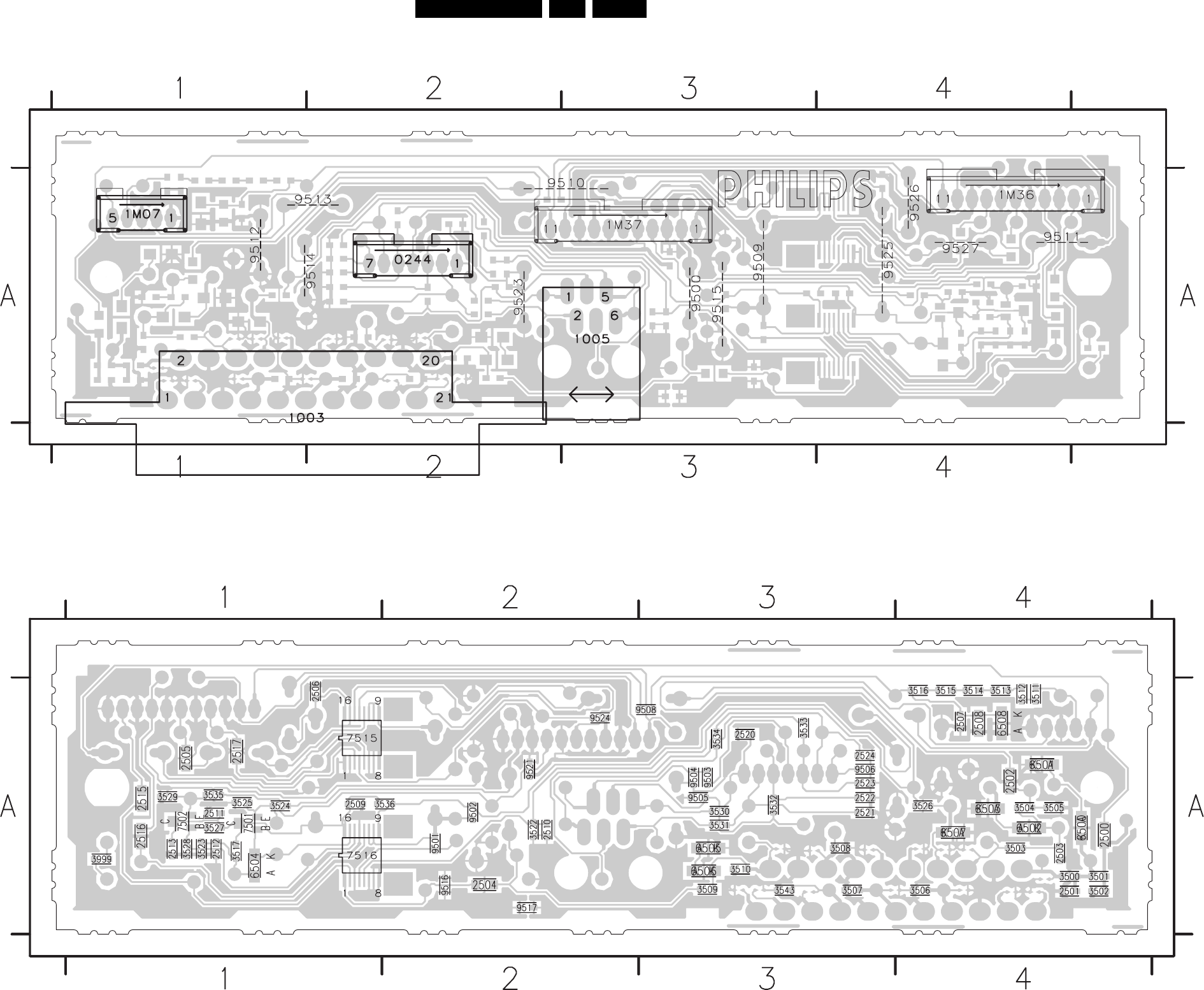
EN 88FTL2.4E AA 7.
Circuit Diagrams and PWB Layouts
Layout SCART 3 Panel (Top Side)
Layout SCART 3 Panel (Bottom Side)
3104 313 6023.4 F_15460_060.eps
110405
0244 A2 1003 A1 1005 A3 1M07 A1 1M36 A4 1M37 A3 9500 A3 9509 A3 9510 A3 9511 A4 9512 A1 9513 A2 9514 A1 9515 A3 9523 A2 9525 A4 9526 A4 9527 A4
3104 313 6023.4 F_15460_061.eps
110405
2500 A4
2501 A4
2502 A4
2503 A4
2504 A2
2505 A1
2506 A1
2507 A4
2508 A4
2509 A1
2510 A2
2511 A1
2512 A1
2513 A1
2515 A1
2516 A1
2517 A1
2520 A3
2521 A3
2522 A3
2523 A3
2524 A3
3500 A4
3501 A4
3502 A4
3503 A4
3504 A4
3505 A4
3506 A4
3507 A3
3508 A3
3509 A3
3510 A3
3511 A4
3512 A4
3513 A4
3514 A4
3515 A4
3516 A4
3517 A1
3522 A2
3523 A1
3524 A1
3525 A1
3526 A4
3527 A1
3528 A1
3529 A1
3530 A3
3531 A3
3532 A3
3533 A3
3534 A3
3535 A1
3536 A2
3543 A3
3999 A1
6500 A4
6501 A4
6502 A4
6503 A4
6504 A1
6505 A3
6506 A3
6507 A4
6508 A4
7501 A1
7502 A1
7515 A2
7516 A2
9501 A2
9502 A2
9503 A3
9504 A3
9505 A3
9506 A3
9508 A3
9516 A2
9517 A2
9521 A2
9524 A2
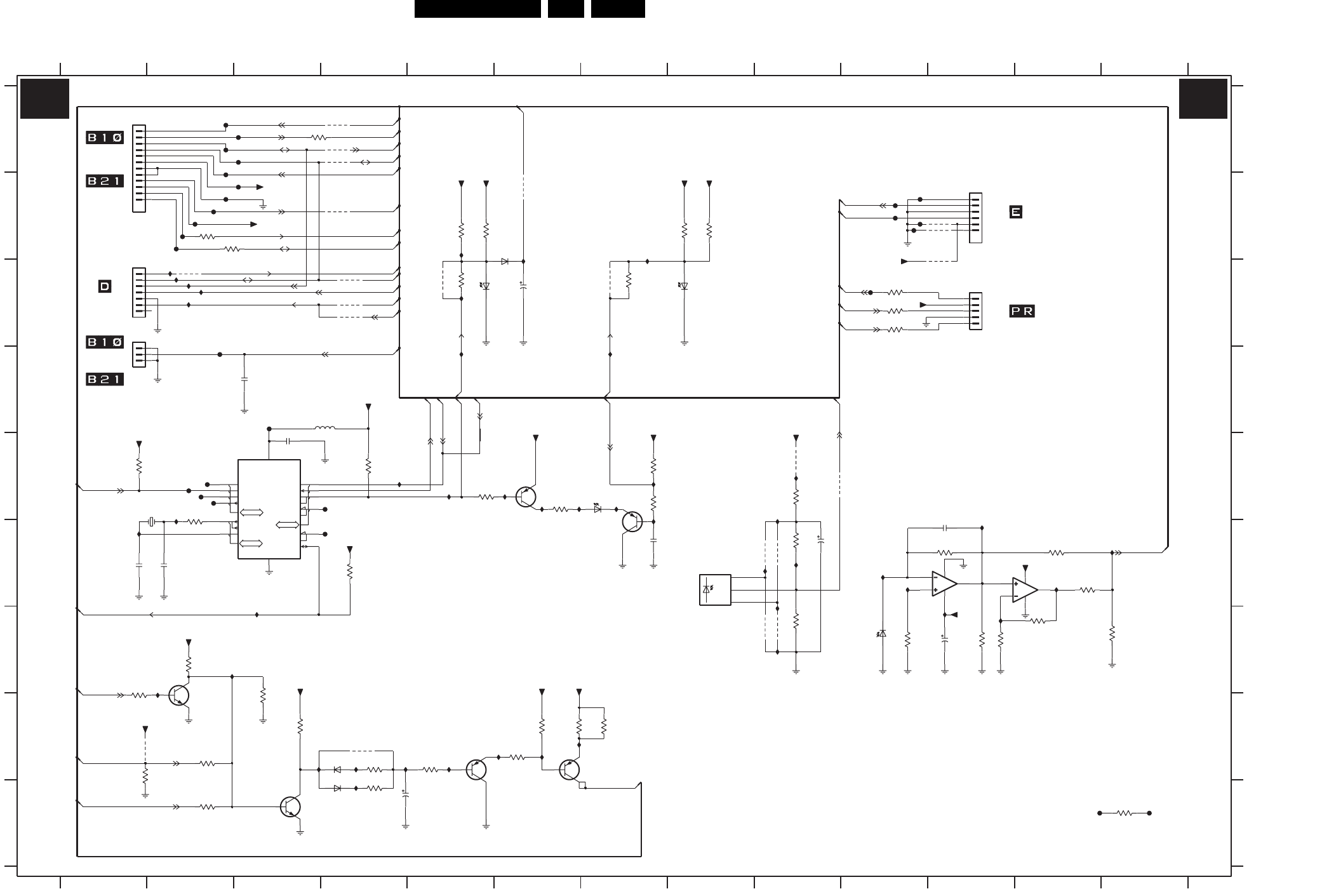
Circuit Diagrams and PWB Layouts EN 89FTL2.4E AA 7.
LED and Switch Panel
P0<3:6>
X2
P2<0:1>
P1<0:3>
T0
SDA
P1.5
P1.7
CIN1B
X1
CLKOUT
CMP1
CMPREF
CIN1A
VDD
RST
INT0
SCL
RXD
TXD
VSS
TO 0244
SSB JAGUAR
TO 1M20
PROXIMITY SENSOR
TO 0350
"RED"
"BLUE"
"LED DIMMING" "IR RECEIVER"
F
G
H
I
0244 C1
0345 B11
0350 C11
1020 E2
1040 F8
1M01 C1
1M20 A1
2014 D3
2020 F2
2021 E3
2022 F7
2023 F1
2030 I4
2040 F9
SIDE I/O
OR
12345678910111213
12345678910111213
A
B
C
D
E
F
G
H
I
A
B
C
D
E
"PROXIMITY"
2060 C6
2070 F11
2071 G11
3010 B2
3011 A3
3012 B2
3020 E1
3021 E5
3022 E6
3023 E7
3024 E7
3025 E4
3026 F4
3027 E2
3030 H3
3031 H4
3032 I4
3033 H5
3034 H6
3035 H6
3036 H6
3037 H7
3040 E9
(RES)
3041 G9
3042 F9
3051 B8
3052 B8
3053 C7
3060 C5
3061 B5
3062 B5
3070 G10
3071 F11
3072 G11
3073 G12
3074 F12
3075 F12
3076 G13
3077 G11
3080 C10
3081 C10
3082 C10
3091 H1
3092 G2
3093 H3
3094 G1
3095 I2
3096 H2
3999 I13
5020 D4
6030 H4
6031 I4
6051 C8
6060 C5
6061 B6
6070 G10
6080 E7
7020 E6
7021 F7
7030 H5
7031 H6
7032 I3
7070-1 F11
7070-2 F12
7075 E3
7092 H2
9010 C4
9012 B4
9013 E9
9014 C2
9015 A4
9016 A4
9017 A4
9018 C4
9019 C4
9031 H4
9040 G9
9041 F9
9042 G9
9043 F9
9044 E9
9050 C7
9060 C5
9061 B6
9081 B11
9082 B11
9083 C11
9093 H1
F010 A2
F011 A3
F012 A3
F013 B3
F014 B2
F015 A3
F016 B2
F017 A2
F018 B2
F019 B2
F020 B2
F021 D2
F027 E2
F028 E2
(RES)
(RES)
(RES)
(RES)
(RES)
F029 E2
F030 E4
F031 D3
F032 E2
F033 F4
F038 I12
F039 I13
F083 B10
F084 B10
F086 B10
F087 C10
F088 B10
F089 B10
I019 E5
I020 C2
I021 E4
I022 C2
I023 C2
I024 C2
I025 C2
TOP CONTROL
TO 0345
I026 F11
I027 E7
I028 F1
I029 F2
I030 E6
I031 E6
I032 E7
I033 I4
I034 G3
I035 E6
I036 F7
I037 H6
I038 H6
I039 H3
I040 H4
I041 G9
FOR ITV
I042 G9
I043 F9
I044 E9
I045 F9
I046 E9
I047 H4
I048 H5
I049 H7
I051 D7
I052 B7
I061 C5
"LIGHT SENSOR"
I062 B5
I063 C6
I064 D5
I071 F10
I072 F13
I073 G11
I074 G11
I075 F10
I076 F12
I093 G2
I094 G2
c001 E5
I022
SSB EMG
TO 1M01
SSB JAGUAR
OR
SSB EMG
2022
220n
1K0
3072
I041
I044
I062
+5V2-STBY
2021
100n
100R
3081
3080
100R
3K3
3077
75R
3022
+5V2-STBY
9041
F086
F083
I043
3035
4K7
3K3
3073
9017
I048
9016
9013
+8V
16V10u
2071
9014
3052
560R
+5V2-STBY
I045
9083
I035
+5V2-STBY
F013
3095
10K
I073
I034
2070
470n
1K0
3034
F018
12
2
3
4
5
6
7
8
9
13 14
1M20
B12B-PH-SM3-TBT
1
10
11
2K2
3021
I049
BAS316
F033
6061
F031
F010
I032
2R2
BC857BW
3036
7030
1K0
3033
+5V2-STBY
100K
3031
3024
3K3
9061
5020
330R
3040
I020
I076
330R
3051
3042
6K8
3070
4M7
3025
10K
1
2
3
B3B-PH-SM3-TBT
1M01
10K
3074
F027
I029
F032
BCP53
I023
7031
F014
GND
OUT
VS
I025
1040
TSOP34836YA1
9010
I024
3071
+5V2-STBY
4M7
F028
4K7
3030
I061
10K
3094
20M
DSX840GA
1020
I052
I075
I071
15p
2020
2030
16V10u
3041
10K
15p
2023
TSAL5300
6080
I042
9031
3027
220R
330R
+5V2-STBY
3061
I036
+8V
I094
10K
3999
I093
2R2
3037
F038
I039
7020
BC857CW
9043
I047
6031
BAS316
9082
I031
3K3
3076
7021
BC857CW
F016
I037
6060
SML512BC4T
F021
3012
100R
100R
3010
+5V2-STBY
F087
3082
100R
I026
F039
+5V2-STBY
9060
I072
3093
+5V2-STBY
10K
+5V2-STBY
3096
10K
9050
c001
I038
3020
10K
3011
2
3
4
5
100R
B5B-PH-SM3-TBT
0350
1
7092
BC847BW
+5V2-STBY
3075
F029
+5V2-STBY
4K7
5
6
7
84
9081
7070-2
LM358P
I028
I063
I033
8
9018
B6B-PH-SM3-TBT
1
2
3
4
5
6
7
I046
0345
3026
10K
F084
3023
47K
F088
+8V
+8V
9040
BAS316
6030
I064 I051
F030
+5V2-STBY
180K
3032
I027
10K
3091
I021
F020
I019
F019
560R
3062
9015
+8V
9093
F017
6070
TEMD5000
6051 12
3
2
1
84
TLMH3100
OPT_LED
7070-1
LM358P
3092
10K
I074
9012
2
3
4
5
6
7
B7B-PH-SM3-TBT
0244
1
I040
F011
F012
3060
100R
+8V
7032
BC847BW
10
9
8
7
6
2
1
5
4
113
MICROCONTROLLER
Φ
P87LPC760BDH
14
13
12
9044
7075
9042
I030
16V100u
2040
100R
3053
F089
+5V2-STBY
22u
F015
2060
16V
100n
2014
9019
LIGHT-SENSOR
COM-SND
RC2
PWM-OUT
PULSE-OUT
STATUS-POWER
RC
KEYBOARD
PROX-DET
LED2
LED1
STATUS-POWER
PULSE-OUT
COM-SND
RC
RC2
PROX-DET
LED1
SCL-S
SDA-S
KEYBOARD
LED2
SDA-S
COM-SND
STATUS-POWER
LED1
SCL-S
LIGHT-SENSOR
PWM-OUT
RC
BLACKLIGHT-TC
BLACKLIGHT-TC
RC
KEYBOARD
PWM-OUT
J J
3104 313 6016.5 F_15460_062.eps
110405
LED & SWITCH PANEL
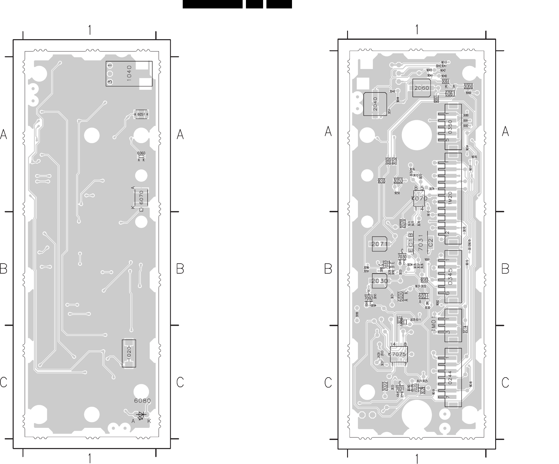
EN 90FTL2.4E AA 7.
Circuit Diagrams and PWB Layouts
Layout LED and Switch Panel (Top Side)
3104 313 6023.4 F_15460_063.eps
110405
1020 C1
1040 A1
6051 A1
6060 A1
6070 A1
6080 C1
Layout LED and Switch Panel (Bottom Side)
3104 313 6023.4 F_15460_064.eps
110405
0244 C1
0345 B1
0350 A1
1M01 B1
1M20 A1
2014 C1
2020 C1
2021 B1
2022 C1
2023 C1
2030 B1
2040 A1
2060 A1
2070 B1
2071 B1
3010 B1
3011 B1
3012 B1
3020 B1
3021 C1
3022 C1
3023 C1
3024 C1
3025 C1
3026 B1
3027 C1
3030 B1
3031 B1
3032 B1
3033 B1
3034 B1
3035 B1
3036 B1
3037 B1
3040 A1
3041 A1
3042 A1
3051 A1
3052 A1
3053 A1
3060 A1
3061 A1
3062 A1
3070 B1
3071 B1
3072 A1
3073 A1
3074 A1
3075 A1
3076 A1
3077 B1
3080 A1
3081 A1
3082 A1
3091 B1
3092 B1
3093 B1
3094 B1
3095 B1
3096 B1
3999 B1
5020 B1
6030 B1
6031 B1
6061 A1
7020 C1
7021 C1
7030 B1
7031 B1
7032 B1
7070 A1
7075 C1
7092 B1
9010 B1
9012 B1
9013 A1
9014 A1
9015 B1
9016 A1
9017 A1
9018 C1
9019 C1
9031 B1
9040 A1
9041 A1
9042 A1
9043 A1
9044 A1
9050 A1
9060 A1
9061 A1
9081 B1
9082 B1
9083 B1
9093 A1
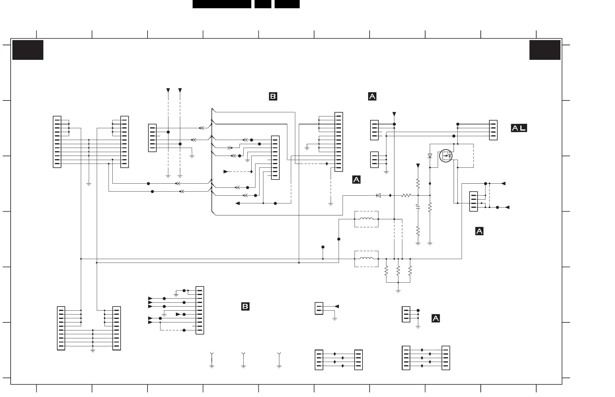
Circuit Diagrams and PWB Layouts EN 91FTL2.4E AA 7.
LCD Standby & Audio Panel: Connections
F140 B8
I524 C8
I525 C7
I550 C6
I551 C4
I552 F6
SA1 (3x)
TO
AMBI LIGHT
I553 F6
I554 F6
I555 F6
I556 F7
I557 F8
I558 F7
I559 F8
I560 F7
F104 C3
F105 C3
F108 C9
F109 E3
F110 B8
F111 B4
LCD SUPPLY
BL 2.X
JL 2.X
30"/37"/42"
DISPLAY
F112 E7
F113 B5
F114 E3
F115 C4
F117 F3
F119 D6
F120 D6
F121 C4
F122 C5
F131 E3
F132 E3
F135 E3
F136 E3
F137 B3
F138 B3
F139 C4
6516 C7
7515 C8
9001 F3
9002 C3
9003 C3
9004 C6
TO 1M10
LCD SUPPLY
TO
LCD SUPPLY
DISPLAY
TO
9005 D6
9006 D7
9007 D7
9008 B3
9009 B3
9010 D6
9011 E6
9012 C5
9013 C5
9014 C6
9016 B8
9018 C9
9113 C4
F101 C9
F103 B7
1M03 B5
1M10 B9
1M46 E4
1M49 F6
1M63 E6
2517 C7
42"
TO
42"
JL 2.X
FTV 2.X
3190 E7
3191 E7
3192 E7
3520 C8
3525 C7
3526 C7
3527 D7
5018 D6
5019 D6
6515 B8
1317 B2
1318 B3
1319 B6
1320 B7
1D40 F7
1D42 F8
SA1 (3x)
TO 1303
TO 1309
TO
TO 1M46
FTV 2.X
1K49 F6
E
F
A
B
C
D
DISPLAY
DISPLAY
SA1 (3x)
1315 E2
1316 B1
234567
DISPLAY
TO 1320
30"/32"/37"/42"
LCD SUPPLY
TO 1M46
SA1 (3x)
89
A
B
C
D
CONNECTIONS
BL 2.X
LC 4.X
SA2
E
F
0001 F4
0002 F4
0003 F5
1303 B7
1304 C8
1309 E7
1314 E1
SA1 (3x)
123456789
1
1
GND-SSP
+12V
TO 1304
LC 4.X
GND screw
0002
+12V
+5V2-RELAY-IO2_PWM
GND-SSP
+24V_2
9018
F101
F112
+5V2
1318
B6B-PH-K
1
2
3
4
5
6
F105
F131
F103
5
6
7
8
9
F139
B10P-PH-K-S
1M03
1
10
2
3
4
1
2
GND-SSP
3
4
B2B-PH-K
1M63
1304
B4P-VH
1
2
F114
9001
F122
GND-SSP
1309
B3P-VH
1
2
3
F111
F135
GND-SSP
1320
B3P-VH
1
2
3
GND-SSP
GND-SSP
9113
1K49
B4B-PH-K
1
2
3
4
1
2
3
4
F110
B4B-PH-K
1M49
3190
3
4
5
6
7
8
9
1K2
1M46
B11B-PH-K
1
10
11
2GND-SSP
GND-SSP
F121
1
2
3
4
I525
B4P-VH
1303
+5V_SW
F115
F140
I524 +12V_+24V
9004
GND-SSP
F104
+5V_SW
GND-SSP
1
1K2
3192
0003
GND screw
GND-SSP
9007
GND-SSP
9014
F137
VTUN
GND-SSP
GND-SSP
3526
470R
3527
100R
1
10
2
3
4
5
6
7
8
9
8
9
B10P-PH-K-S
1314
11
12
13
14
2
3
4
5
6
7
B14B-PH-K
1319
1
10
BAS316
6516
9011
9005
5018
68u
9010
F109
+8V6 F136
9006
I558
I557
F120
I556
I555
F113
F117
I554
I552
I553
+5V_SW
F138
RES
9009
I551
9
I550
10
11
12
2
3
4
5
6
7
88
9
B12P-PH-K
1316
1
10
11
12
2
3
4
5
6
7
1317
B12P-PH-K
1
10
2
3
4
5
6
7
8
9
B10P-PH-K-S
1315
1
9008
GND-SSP
9012
F108
F132
0001
1
+5V_SW
1
2
3
4
5
GND screw
1D40
B5B-PH-K
9016
VTUN
GND-SSP
F119
GND-SSP
4u7
2517
9013
100K
50V
220K
3525
3520
7515
BSP030
2
4
1
3
BZX384-C15
6515
4
5
3191
1K2
B5B-PH-K
1
2
3
1
2
3
4
1D42
+12V_A
B4B-PH-K
1M10
9003
RES
+5V_SW
9002
RES
68u
5019
I560
GND-SSP
I559
POR
DIM_CONTROL
ON_OFF
ON_OFF
DRIVE_AMBILIGHT
DIM_CONTROL
DIM_CONTROL
ON_OFF
DIM_CONTROL
ON_OFF
STANDBY
PROT_AUDIOSUPPLY
SA1 SA1
F_15490_005.eps
090605
8204 000 8449.2
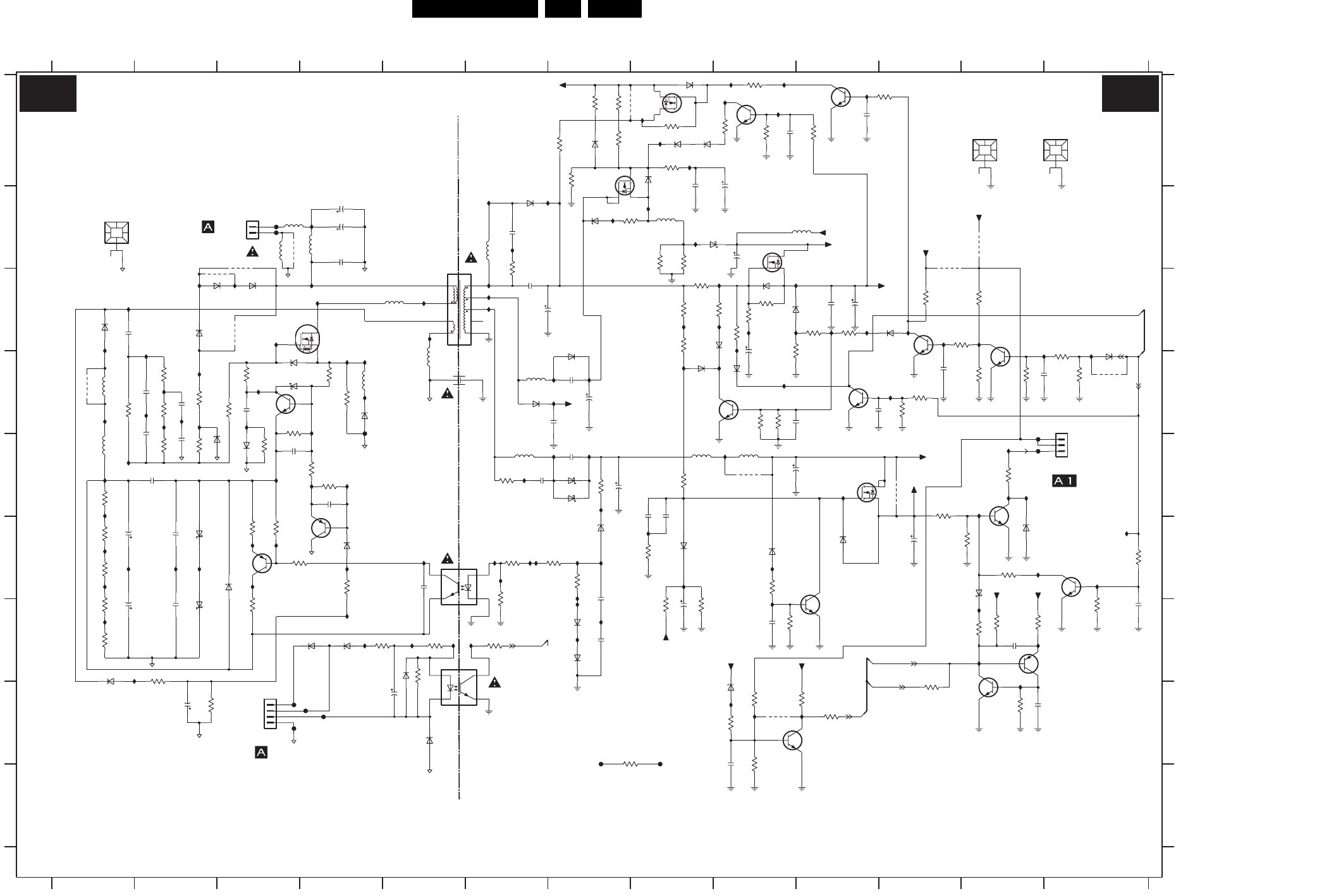
EN 92FTL2.4E AA 7.
Circuit Diagrams and PWB Layouts
LCD Standby & Audio Panel: Standby
SA2 SA2
F_15490_006.eps
120405
8204 000 8450.4
0V8 (0V8)
6789
3127 F3
3128 F6
3132 D9
3134 C10
3135 C9
3137 B8
2506 D5
2507 C6
2508 C6
2509 G13
2160 C9
2162 D2
2163 G1
2503 D10
11V9 (11V8)
3139 B8
3140 C8
G
H
I
1301 B1
1305 D13
1311 A12
2101 C1
2102 F1
2103 D2
2544 G12
3100 G3
3101 D2
3102 E2
3103 D2
3107 F1
3108 D4
0V2 (0V2)
SA2
HOT GROUND
3502 C9
3503 D11
3504 D11
3506 H11
3105 D2
3106 E1
B
C
D
E
F
10 11 12 13
A
2149 G7
2150 H5
2152 B4
2153 F5
2154 G9
2105 D2
2107 B4
2108 B4
3124 F7
3125 F3
3126 F3
3528 C11
3529 C11
3530 D13
3531 D13
3138 E2
RES
TO 1306
3533 D12
3534 H9
1
1306 B3
1307 H3
1310 A13
11 12 13
1234
3104 D3
3161 C9
3171 C9
3172 C10
3175 G8
3176 G9
5112 D6
5115 B8
5500 C5
5501 B3
3507 F13
COLD GROUND
8V9 (8V8)
5505 B4
5506 E8
2109 F7
2110 G2
2111 E2
2112 E3
2115 E6
G
H
I
A
B
C
D
E
F
2144 F2
2159 E2
3519 A8
3521 B7
3522 A9
3523 A9
3524 A10
6130 C9
6132 C9
6133 D8
6134 C9
3532 C12
+12Vstby
LCD SUPPLY
TO 1305
LCD SUPPLY
2510 E7
2511 B9
2512 E9
2513 E7
2515 A10
2345678910
2539 E8
5
5104 C5
5105 D5
5106 D1
5108 D4
5110 B6
6540 F12
6562 F12
7100 F3
7101 D3
5504 B3
30"/32"/37"/42"
0V (0V)
HOT GROUND
RES
SA3(2x),
275V
3109 F1
2118 D7
2123 E4
2124 H2
2129 B6
2131 C10
2132 C10
2140 G8
2141 D7
2143 D7
3122 B6
2145 D3
6119 C3
6120 G7
6121 G7
6122 F7
6125 B8
9015 E11
9019 A7
9020 C3
9021 B3
6140 D6
SA2
3141 F9
3142 G8
3145 G2
3146 F4
3147 H2
2518 A8
2522 A9
2523 A9
2533 F11
2534 E8
2535 D9
2536 D11
2537 D13
2538 H9
3159 E8
2540 H12
6513 A8
6514 B7
6517 A7
6531 F10
6532 C11
F128 H4
F129 H4
F130 H4
F133 H7
7102 C4
30"/32"/37"/42"
SA1
3110 G1
3111 D1
3112 G1
3113 E7
3114 F6
3115 E6
3116 A7
3117 D3
3118 A7
3517 A11
3123 F7
7513 B7
7514 A9
7531 E10
7532 D9
7560 E12
I111 C3
I112 C9
I113 C4
I114 C6
9022 B3
TO 1307
3535 H9
3536 H10
3537 H9
3538 F8
3539 H10
3148 E4
3149 E4
3150 D4
3152 E3
3153 C8
3155 G4
3156 G5
3157 H5
3158 G6
5102 E1
3160 D3
F123 B3
F124 B3
F125 E12
F126 E12
F127 H3
I127 B8
I128 D7
I129 D7
I130 C3
F134 H8
5507 B10
5508 E9
6103 C1
6104 E2
6105 D3
3508 G13
3509 A7
3510 F12
3511 C8
3512 C9
3513 D9
3514 A7
3515 A8
3516 A9
6117 C2
3518 A7
I106 C10
I107 C8
I108 C8
I109 C11
I110 C2
I143 D2
I144 D2
I145 D3
I146 D4
I115 C11
SA1
11V5 (12V)
6142 F2
6144 E3
6147 D4
6148 F8
3540 G12
3541 G12
3542 H12
3543 D12
3544 G12
3560 E11
3561 F12
3562 E12
3999 H7
6510 C13
5103 E6
I122 C1
I123 C6
I124 C5
I125 D8
I126 D9
I158 F7
I159 F8
I160 F7
I161 F9
I131 C2
30"/37"/42"
7105 F4
7131 B9
7140 G10
6106 F2
6107 E7
6108 G2
6109 A8
6110 A8
6113 C7
6114 G1
6115 D3
6116 F4
7511 A8
6118 C2 I138 E7
I139 E12
I140 C1
I141 D2
I142 D2
I176 G7
I177 F1
I178 G13
I179 G12
I147 E1
(289V)
LCD SUPPLY
COLD GROUND
6149 F9
6150 G4
6151 G4
6153 H5
6156 G5
6503 D9
6504 B6
6505 E7
6508 H9
9121 B12
6511 A8
I153 E1
I154 E4
I155 E3
I156 E4
I157 F6
I501 F6
I502 F6
I503 F6
I504 G12
I162 E1
5V3 (5V3)
7150 G5
7501 F6
7503 D10
7505 G12
7506 C11
7507 C12
7508 H10
7509 H12
7510 F13
I104 C9
7512 A10
I171 F5
I172 F2
I173 F2
I174 F2
I175 F4
I519 B8
I520 A8
I521 A8
I522 A9
I180 G4
11V7 (11V7)
34V (34V)
RES
9023 C2
9024 D13
9110 H9
9111 D1
9112 E9
9120 B11
I120 C6
F100 E4
I191 G4
I192 H9
I197 C9
I198 D7
I199 D4
I505 F12
5V3 (5V3)
I100 B4
I101 B6
I102 B6
I103 C9
I136 D2
I105 B6
I514 E6
I515 E9
I516 D9
I517 C13
I518 B7
I507 F13
I508 A8
I509 A9
I510 A9
I523 A9
0V7 (0V6)
I513 D1
STANDBY
SA1
I116 C10
I117 C12
I118 C5
I119 C4
I151 E12
I121 C12
I186 G6
I187 D11
I188 D9
I182 G12
I183 G5
I184 G5
I185 F3
I170 G7
I163 F8
I164 F7
I132 D4
I133 D4
I134 D2
I135 D3
I169 F1
I137 E7
I506 F13
I165 G7
I166 F3
I167 F3
I168 G9
I512 H9
I511 A10
3509
I148 E10
I149 E7
I150 E12
I189 H10
I190 G1
I152 F12
I181 G1
2K2
3529
100R
2535
10n
3141
470R
F133
2112
10n
PMSTA42
7514
I188
GNDHOT
GNDHOT
GND-SSP
3109
390R
GND-SSP
GND-SSP
7509
BC847BW
I191
2515
2n2
1
2
3
4
1307
B4P-VH
6150
BZG03-C200
I107
3140
22K
I126
I129
+5V2
I163
6510
PDZ2.7-B
GND-SSP
SB360
6505
+11V
GNDHOT
I114
2129
1n0
VTUN
390R
3112
22K
3514
GND-SSP
100K
3518
I522
GND-SSP
I161
GND-SSP
HEATSINK
1311
1
2
I159
GND-SSP
GND-SSP
I166
7140
BC847BW
3172
9015
33K
I122
9120
3176
10K
3544
GND
GND-SSP
GND-SSP
GND-SSP
220R
6130
BZX384-C12
GND-SSP
GND-SSP
I157
GND-SSP
3135
330R
+5V_SW
I155
3158
47R
GND-SSP
3560
6K8
3175
10K
3538
100R
16V220u
2132
I147
I117
I164
I144
RES
3536
10K
7508
BC847BW
3127
5K6
RES
1u0
2144
GNDHOT
I171
2518
220n
I521
GND-SSP
I518
+12V
1n0
2115
6125
SB340
2118
1m0 35V
7510
BC847BW
15K
3503
I149
3539
470R
I152
3153
22K
6106
PDZ22-B
PDZ22-B
6514
GND-SSP
I116
3524
4K7
6122
PDZ3.9-B
1u0
2539
I111
I165
I101
GNDHOT
I505
100R
3118
27K
3116
2512
25V1m0
3562
4R7
6114
BYV27-200
220R
I513
3161
12K
3510
3147
22K
I186
6147
BZG05C6V8
6540
BAS316
BAT54 COL
6120
3115
1K0
2544
10n
GND-SSP
I110
I153
I119
6108
I190
+5V2
BAT54 COL
2537 2n2
3531
1K0
7560
BC817-25W
+12V
3561
3K9
2
4
1
3
GND-SSP
+5V2-RELAY-IO2_PWM
BSP030
7513
50V22u
2522
6562
BZX384-C22
22u
5106
4K7
3516
I187
GNDHOT
I124
GND-SSP
I134
3117
47R
9020
GND-SSP
100p
2105
6140
BYW36
470n
2141
F100
I168
15u
I514
5507
I192
+5V2
3530
470R
I120
GNDHOT
GNDHOT
6109
PDZ6.8-B
6110
PDZ6.8-B
6517
BAS316
9112
BAT54 COL
6115
GND-SSP
BC817-25W
I123
7101
F126
9024
3156
1K0
3110
390R
I136
3146
47R
I137
56
7
8
9
5500
110
2
3
3113
22R
5112
2103
100p
I151
I121
I125
6116
BZX384-C5V6
BZX384-C12
6513
7131
STP16NF06FP
I181
I198
I502
I503
3149
10K
GND-SSP
GND-SSP GND-SSP
GND-SSP
33K
3513
+12V_A
+8V6
6503
BAS316 470R
3502
6148
BAS316
100K
3515
2534
1u0
2509
100R
3519
2n2
I102
1
2
HEATSINK
1310
1K0
3102
BZX384-C33
6151
I512
3155
10K
3537
3K3
RES
I189
4R7
3108
I108
GND
I174
3512
470R
I520
3138
GND-SSP GND-SSP
1M0
RES
470p
2159
RES
5501
I160
100R
BAS316
6133
GND-SSP
3150
I142
2K2
I128
I139
3540
2540
10n
22K
3517
2536
10n
470n
2109
1
2
BC857BW
7505
1301
HEATSINK
GND-SSP
3105
220R
I175
I180
I115
+11V
10n
I106
2538
GND-SSP
10K
3504
I511
3128
4R7
I501
GND-SSP
9021
F129
9023
2124
10u50V
3123
10R
I197
GNDHOT
3152
1K0
GND-SSP
I506
I504
RES
9111
47R
3521
+5V2
I103
2507
100p
7507
F123
BC847BW
F124
3159
47R
2150
220u 25V
RES
I510
I141
5508
15u
I138
2533
100u 25V
7506
BC847BW
GND-SSP
5110
BAS316
6532
10u
9022
I507
3171
100R
9110
14
32
I127
TCET1102(G)
7150
I172
2149
470n
2510
2m2 10V
F134
1K0
3999
I146
I167
RES
6117
BZX384-C33
2107
10u
450V
I199
I519
470R
3522
I154
I109
GND-SSP
I132
I516
BC847BW
7503
I508
GND-SSP
GND-SSP
I509
470R
3506
BAS316
6121
22K3157
GND-SSP
2111
47n
25V 100u
2163
7105
BC857BW
I177
I140
3523
I523
4K7
5506
I104
6504
BYV27-600
3122
470R
BAT54 COL
6142
GND-SSP GND-SSP
470p
2506
GND-SSP
2110
1u0
6156
BAS316
GND-SSP
F127
I100
I517
3507
10K
6134
BAS316
6531
BZX384-C15
3508
15K
GND-SSP
2154
15n
3543 22K
3103
1K0
2160
1u0 50V
1306
B2P-VA-BF-BK
1
2
2101
2n2
3104
47R
2145
470p
RES
6508
BZX384-C9V1
B3B-EH-A
1305
1
2
3
2K2
3541
14
3
2
3132
33K
TCET1102(G)
7501
GND-SSP
RES
6119
BZX384-C33
RES
BZX384-C33
6118
6103
I150
3126
BYV27-200
I184
10K
I183
3535
2K2
BAS316
RES
F130
6144
I156
2503
2n2
I148
7102
STP6NK60Z
I515
I143
2123
100n
I131
3160
1K0
3124
33R
6n8
25V220u
2511
2153
5505
GND-SSP
GND-SSP
GND-SSP
2523
2n2
GND-SSP
3542
10K
6149
BZX384-C5V6
5105
3528
4K7
2140
10u 50V
3142
12K
3114
220R
6107
STPS8H100FP
5103
I105
390R
3107
47R
3148
9121
I162
I169
I133
I176
5104
BZX384-C15
6105
GND-SSP
6104
I118
BZX384-C27
3137
100K
2162
3
I182
RES
470p
BSP030
7531
2
4
1
10K
3534
I145
GNDHOT
BZX384-C12
6511
GND-SSP
I130
I185
I135
F125
3
1
2
5108
BST82
7511
100R
3100
10n
2152
RES
9019
1K5
3533
BC857BW
7100
6132
PDZ6.8-B
I113
I173
GND-SSP
F128
+5V2
6113
BYW29EX-200
BZG03-C200
6153
3101
4M7
2n2
2513
2108
10u
450V
GND-SSP
33u
5504
3111
1K5
I158
GND-SSP GND-SSP
GNDHOT
I112
7532
BC847BW
2102
GND-SSP
GND-SSP
GND-SSP
100u25V
3134
1K0
2143
2n2
I179
I178
2508
22u 100V
3125
15R
3106
390R
5102
470R
3139
I170
5115
3532
4K7
3145
4K7
3511
68K
2131
22n
PMSTA42
7512
STANDBY
PROT_AUDIOSUPPLY
Prot-OVV
DRIVE_AMBILIGHT
Prot-OVV
POR
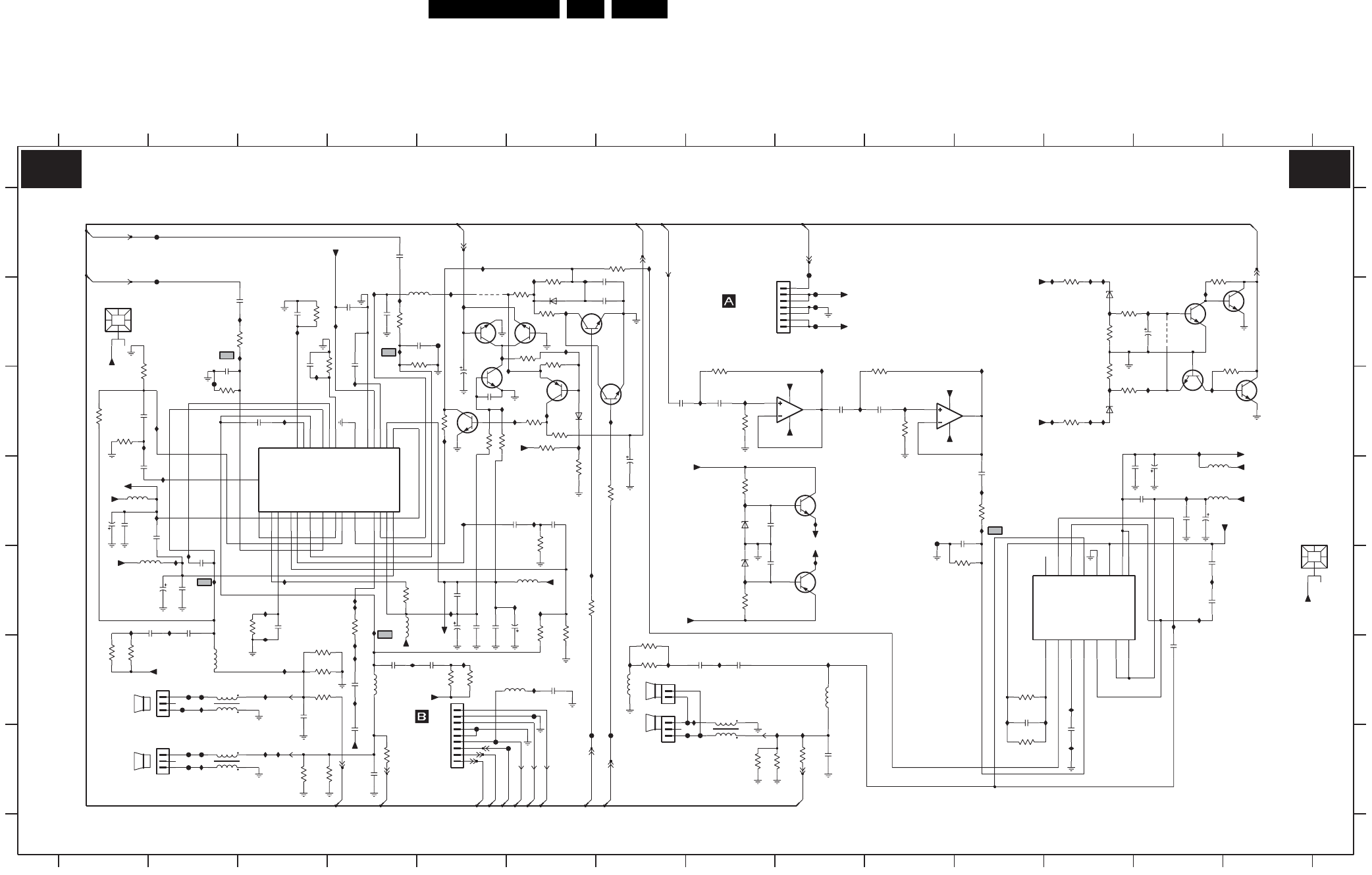
Circuit Diagrams and PWB Layouts EN 93FTL2.4E AA 7.
LCD Standby & Audio Panel: Audio
SA3 SA3
F_15490_007.eps
090605
8204 000 8450.4
F722 F2
F731 G8
6710 D8
6711 E8 F747 G5
TO 1M02
FTV 2.X
JL 2.X
LC 4.C
BL 2.X
-18V
TO 1M52
I700 E6
I701 E6
I702 A6
I703 B6
I704 A6
I705 D6
I706 D5
I707 E3
I708 F11
7709 C13
7710 B13
F711 A2
F712 B2
F713 C2
F714 B5
F718 D10
F720 G8
F721 G2
I718 B5
F710 G2
F708 F2
30"/37"/42"
7701 B7
7702 E11
7703 C7
7704 B5
7705 B6
7706 C6
7707 C5
7708 C13
3790 B4
3791 C2 5730 F2
5731 G2
5732 G8
6701 C6
6702 B12
6703 C12
6704 B6
9718 B13
5703 B5
5702 F2
LCD SUPPLY
R
E
F
G
1735 F2
1736 G2
7711 B13
7712 D9
7713 E9
7714 C5
7715-1 C9
7715-2 C11
9717 B5
67
1737 F7
1738 F7
1739 F5
1M02 A9
2702 B5
SA3
3
3792 B3
3793 B4
3794 D11
3795 C5
3796 E11
3797 C5
3798 D6
78
A
B
C
D
E
F
G
0044 D14
0045 B1
D
SA1,SA2,SA3
12345
2711 E2
2712 E5
8 9 10 11 12 13 14
12
2722 D1
SA3(3x)
15W/8
SA1,SA2,SA3
SA3
456
2756 G12
2758 G9
9 1011121314
A
B
C
2780 E5
SA3
-18V
AUDIO
CENTERWOOFER
2704 C2
2705 A7
2706 B4
2707 B4
2708 G4
2709 D6
2710 D6
2790 E2
2791 C7
2713 B7
2714 C3
2715 F4
2716 B3
2717 G4
2718 E3
2719 F5
2720 F4
2721 C1
3702 B6
SA3
15W/8
SA3
2723 F8
2725 F6
2726 E2
2727 E2
2728 B3
2729 F3
2741 F11
2743 F13
2753 E13
2754 D11
2755 D11
3711 E4
3712 E32759 F8
2762 E13
2764 B2
2766 A4
2768 E5
2769 E5
2777 D1
2778 C5
2779 E2
3723 C1
SA3
SA3
SA3(3x)
SA3
SA3
2781 E5
2782 D12
2783 D7
2784 D13
2785 B13
2786 B4
2787 C5
2788 D1
2789 D2
3746 C6
3747 C62792 C8
2793 D13
2794 C9
2795 D13
2796 C10
2797 D8
2798 E8
2799 D13
3701 E6
3757 G3
SA3
SA3(3x)
SA3 (3x)
3703 A6
3704 B6
3705 E4
3706 E6
3707 D6
3708 F6
3709 F5
3710 B3
3767 B12
3768 B13
3713 D7
3714 C6
3715 B6
3716 B6
3717 F3
3718 G4
3720 F7
3721 C1
3722 C1
5701 F4
SA3
15W/8
SA3
3724 F1
3725 B4
3726 F1
3727 F5
3729 G9
3730 F7
3741 F11
3743 F3
3744 G11
5722 D13
5723 D13
3748 C5
3749 A7
3750 G3
3751 G8
3752 B8
3753 G8
3754 C8
3755 B10
3756 F3
7700 C3
L
3758 C10
3759 D8
3760 E8
3761 B12
3762 B12
3763 C12
3764 C12
3765 C12
3766 C14
I729 C5
I730 F7
F736 G7
F737 G6
F738 F2
F739 G2
F741 G8
F742 B9
F743 B9
F744 B9
F745 A9
I740 D9
F748 G5
F749 G6
F751 F65704 F7
5705 F6
5707 D1
5708 E1
5711 E6
5712 E4
5720 F9
I751 A12
I752 E13
I709 C3
I710 F5
I711 B4
I712 A5
I713 B3
I714 C8
I715 A7
I716 C3
I717 B5
I762 D11
I763 C6
I764 D13
I765 D13
I719 F3
I720 C8
I721 E4
I722 B2
I723 B9
I724 E2
I725 E1
I726 C2
I727 B5
I728 C9 I778 E2
I779 E2
I731 B11
I732 C6
I733 C10
I734 F12
I735 D8
I736 E8
I737 C6
I738 C6
I739 B6 I790 F3
I741 E9
I742 C12
I743 C12
I744 E6
I745 B4
I746 E13
I747 D11
I748 F4
I749 E4
I750 B12
I753 F4
I754 E2
I755 F4
I756 C1
I757 D2
I758 G12
I759 F12
I760 C5
I761 F8
I791 B12
I792 B13
I793 B13
I794 B12
I795 F6
I796 C12
I797 C12
I798 E5
I799 E3
I766 G9
I767 F2
I768 G3
I769 F3
I770 G2
I771 G3
I772 F8
I773 G9
I774 F9
I775 F7
I776 E4
I777 D2
4K7
I780 E13
I781 C13
I782 C13
I783 B2
I784 F4
I785 B4
I786 B4
I787 C4
I788 C7
3721
I728
16V22u
2783
33n
2714
3760
3K3 3K3
3759
2716
330p
2717
I722
-Vf11
680n
I768
6702
BZX384-C10
1
2
B2B-PH-K
1737
F736
100u
2768
220n
2712
-Vf1
I716
-Vf21
I710
3724
220R
I739
I799
7703
BC847BW
8K2
3758
2727
3726
1n0
220R
I778
2792
1u0
BZX384-C10
6703
5704
I740
-Vf1
I763
2K2
I715
3750
120K
3795
I783
100K
3729
I741
470p
2721
-Vf11
I713
3767
100K
2705
470n
1u0
2796
2784
220n
-Vf1
3722
68K
68u
5702
10R
3764
F748
56K
3723
I730
5708
F710
3752
+16V+19V
330R
220n
2782
220n
2789
I784
I753
3725
22K
I729
5703
2711
1n0
2728
330p
3710
22K
I794
I792
I735
I736
1u0
2791
I724
I747
I709
2769
100u
470R
3748
220n
2720
9717
10K
3704
F751
+16V+19V
F747
I726
I714
470R
3755
68u
5720
3702
10K
F708
Vm
I727
100K
3765
3792
10K
5
6
7
8
4
I762
I787
LM833D
7715-2
3711
Vp
120K
5701
68u
2797
220n
2K2
3751
F721
-Vf21
470R
3749
3753
Vp
Vm
2K2
2794
1u0
7707
BC847BW
I734
3701
10K
I754
I775
2u2
2u2
2766
2764
3798
15K
F749
3761
-16V-19V
10R
I723
I759
3768
100K
BC847BW
7709
7710
BC847BW
220n
2753
2K73790
2722
470p
I720
470p
2756
4u7
2778
3754
47K
3716
22K
3762
1n0
2759
2K2
6704
BAS316
F720
F741
-Vf1
3715
47K
I796
I797 I782
33n
2743
680n
2758
I742
I750
I743
3706
4K7
100K
3744
-Vf21
220n
2795
3713
1K2
3796
2K7
2799
100u
VCCPOWp
13
8
VCCSIGNn
VCCSIGNp
11
12 VREG
6FREQ
9IN
4
NC
OUT 1
SGN_GND 7
10 ST_BY|MUTE
14
VCCPOWn1 15
VCCPOWn2
7702
TDA7482
BOOT 3
2
BOOTDIODEFEEDCAP
5
PLT09H
5732
1
2
4
3
12
43
2
43
5731
PLT09H
PLT09H
5730 1
6711
BZX384-C15
Vp
BZX384-C15
6710
I780
I764
2741
22p
F743
I733
+16V+19V
2793
100u
I721
1n0
2719
I786
3747
47K
I745
470p
I772
2710
+16V+19V
I781
220R
1
2
3730
1
2
0044 HEATSINK
I705
HEATSINK
0045
F731
I788
F712
F713
I701
-16V-19V
220K
3797
2787
1u0
F739
I798
10K
3712
220n
2777
470p
2709
2729
680n
I795
I725
2725
100p
3705
8R2 2707
I746
100n
F722
2723
1n0
I790
2
1
8
4
I761
7715-1
LM833D
3
F738
I765
3791
2K7
I731
22p
2718
2706100n
2779
220n
I785
I751
I773
B3B-PH-K
1735
1
2
3
2726
I776
33n
F744
BC847BW
7714
220n
2798
F718
1
2
3
4
5
6
7
B7B-EH-A
1M02
F714
22n
2786
9718
1
2
3
4
5
6
7
8
9
1739
B9B-PH-K
5707
I702
7708
BC847BW
3766
100K
2u2
2754
I738
-16V-19V
F711
220R
3720
3718
220n
100K
I711
2762
5712
2K2
3743
3707
68K
I774
-16V-19V
2704
1n0
2708
220n
-16V-19V
-16V-19V
F737
BC847BW
7705
470n
2713
3756
2K2
1n0
2755
I703
2K2
3763
I704
I779
I777
I760
3794
10K
2788 100u
100u
2790
47K
3714
I793
3703
33K
I757
1736
B3B-PH-K
1
2
3
5723
I700
I718
I756
I717
I758
BC857BW
7713
2785
100u 16V
BC847BW
7712
5722
I708
I752
I737
7711
BC847BW
I769
220n
2781
1n0
2702
F745
I744
3746
39K
3708
56K
I707
BC857BW
7706
5711
I706
BC847BW
7704
I749
-Vf11
220n
2780
I748
2K2
3757
+16V+19V
3709
220R
NC1 20
OSC
8
3
OUT1
OUT2 23
6STBY-MUTE
11
T1
15
T2
VREG
25
CURREF
14
FEED1
7
9FEED2
FEED3
17
19 FEED4
13
GND
IN1
10
18 IN2
4+VCCPOW1
+VCCPOW2
22
16
-5V
-VCCPOW1 2
-VCCPOW2 24
-VCCSIGNSUB 1
5
BOOT1
BOOT2 21
7700
TDA7490L
+5V
12
I719
I766
I791
BAS316
6701
100K
3717 3741
F742
10K
I732
379310K
I755
220R
3727
+16V+19V
+16V+19V
5705
2715
1n0
Vm
7701
BC847BW
2
3
I712
B3B-PH-K
1738
1
I771
I767
I770
AUDIO-L
PROT1
AUDIO-SW
DCPROT
DCPROT
PROT_AUDIOSUPPLY
PROT1
PROT1
PROT1
AUDIO-L
AUDIO-R
PROT_AUDIOSUPPLY
SOUND-ENABLE
POR-CLASSD
AUDIO-R
SOUND-ENABLE
AUDIO-SW
POR-CLASSD
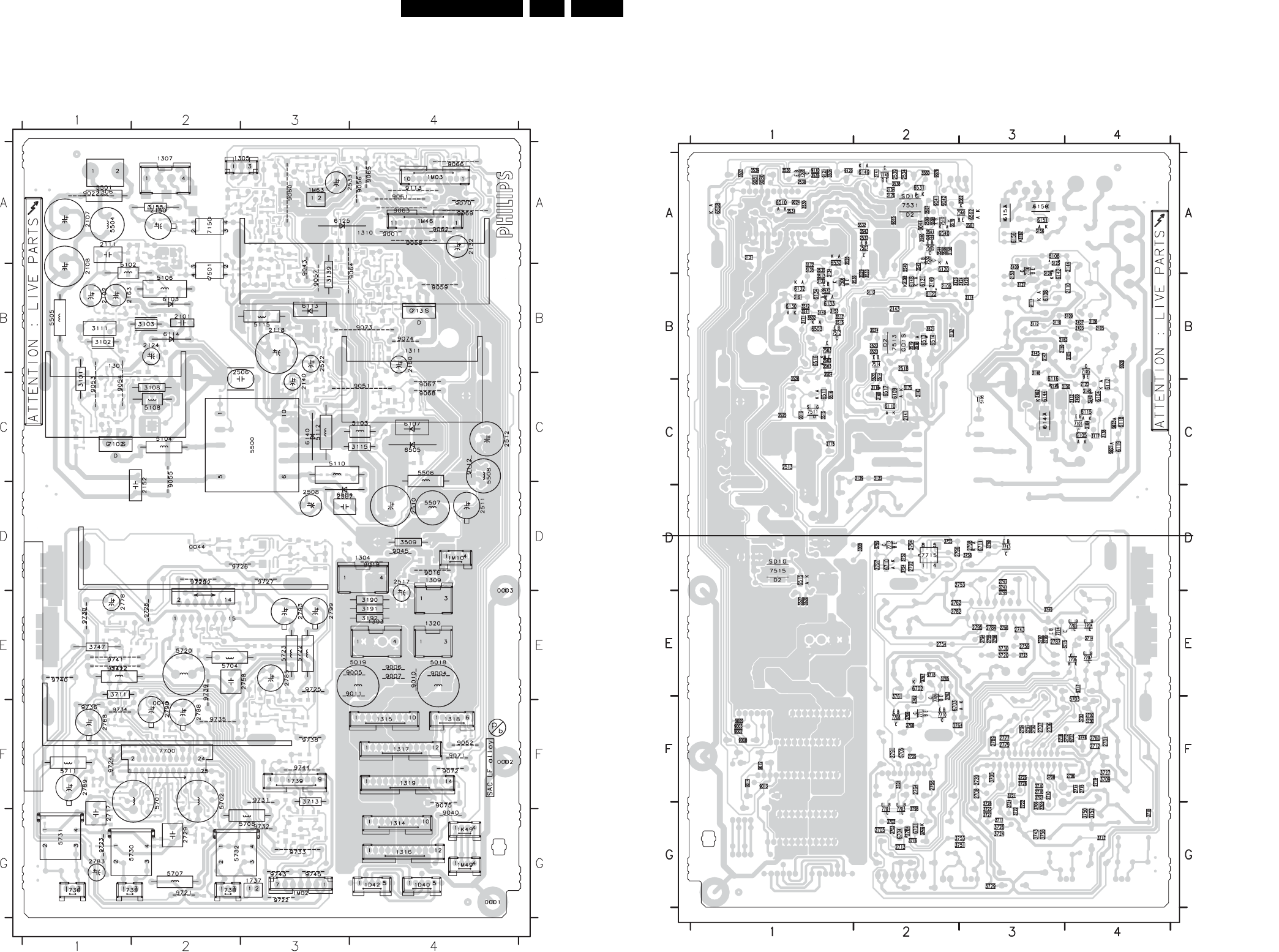
EN 94FTL2.4E AA 7.
Circuit Diagrams and PWB Layouts
Layout LCD Standby & Audio Panel (Top Side)
F_15490_008.eps
120405
3104 303 3957.4
0001 G4
0002 F4
0003 D4
0044 D1
0045 E1
1301 C1
1303 E4
1304 D4
1305 A3
1306 A1
1307 A2
1309 D4
1310 A3
1311 B4
1314 G4
1315 F4
1316 G4
1317 F4
1318 F4
1319 F4
1320 E4
1735 G1
1736 G1
1737 G3
1738 G2
1739 F3
1D40 G4
1D42 G4
1K49 G4
1M02 G3
1M03 A4
1M10 D4
1M46 A4
1M49 G4
1M63 A3
2101 B2
2102 B1
2107 A1
2108 A1
2111 A1
2118 B3
2124 B2
2132 A4
2140 C3
2150 A2
2152 D2
2160 B4
2163 B1
2506 B2
2507 D3
2508 D3
2510 D4
2511 D4
2512 C4
2517 D4
2522 B3
2533 A4
2717 F1
2729 G2
2758 E3
2768 F1
2769 F1
2778 E1
2783 G1
2785 E3
2788 F2
2790 E2
2793 E3
2799 E3
3101 C1
3102 B1
3103 B2
3108 C2
3111 B1
3115 C4
3139 B3
3155 A2
3190 E3
3191 E3
3192 E3
3509 D4
3711 F1
3713 F3
3747 E1
5018 E4
5019 E4
5102 B2
5103 C4
5104 C2
5106 B2
5108 C2
5110 C3
5112 C3
5115 B3
5500 C3
5501 A1
5504 A1
5505 B1
5506 C4
5507 D4
5508 C4
5701 F2
5702 F2
5704 E2
5707 G2
5708 G3
5711 F1
5712 E1
5720 E2
5722 E3
5723 E3
5730 G2
5731 G1
5732 G3
6103 B2
6107 C4
6113 B3
6114 B2
6125 A3
6140 C3
6504 D3
6505 C4
7102 C1
7131 B4
7150 A2
7501 B2
7700 F2
7702 D2
9001 A4
9004 E4
9005 E4
9006 E4
9007 E4
9010 E4
9011 E4
9016 D4
9018 D4
9022 A1
9040 G4
9043 B3
9045 D4
9051 C4
9052 F4
9053 B1
9054 B1
9055 C2
9056 A4
9057 A3
9058 A4
9059 B4
9060 A3
9061 A4
9062 A4
9063 A4
9064 A3
9065 A4
9066 A4
9067 C4
9068 C4
9069 A4
9070 A4
9071 F4
9072 F4
9073 B4
9074 B4
9075 F4
9112 C4
9113 A4
9721 G2
9722 G3
9723 G1
9724 F1
9725 E3
9726 D2
9727 D3
9728 E2
9729 D2
9730 E1
9731 F3
9732 G3
9733 G3
9734 F1
9735 F3
9736 F1
9738 F3
9739 F2
9740 E1
9741 E1
9742 E1
9743 G3
9744 F3
9745 G3
Layout LCD Standby & Audio Panel (Overview Bottom Side)
F_15490_009.eps
120405
3104 303 3957.4
2103 B4
2105 B4
2109 B2
2110 B4
2112 C4
2115 C1
2123 C4
2129 C2
2131 A1
2141 C2
2143 B2
2144 A4
2145 C3
2149 B2
2153 B3
2154 A2
2159 B3
2162 B3
2503 B1
2509 A2
2513 C1
2515 B1
2518 B2
2523 B2
2534 A2
2535 A1
2536 B2
2537 A2
2538 A1
2539 A2
2540 A2
2544 A2
2702 F4
2704 F3
2705 G2
2706 F3
2707 F3
2708 F3
2709 G3
2710 F3
2711 G3
2712 F4
2713 G2
2714 F4
2715 F4
2716 F3
2718 F3
2719 F4
2720 F3
2721 G3
2722 G3
2723 E3
2725 F2
2726 G3
2727 G3
2728 F3
2741 D3
2743 E3
2753 D3
2754 E2
2755 E3
2756 E3
2759 E3
2762 E2
2764 F2
2766 F2
2777 F3
2779 F3
2780 F4
2781 F4
2782 E2
2784 E3
2786 F4
2787 E3
2789 F3
2791 F2
2792 D2
2794 D2
2795 E3
2796 D2
2797 D2
2798 D3
3100 A3
3104 C4
3105 B4
3106 B4
3107 B4
3109 B4
3110 B3
3112 B3
3113 B2
3114 B3
3116 C2
3117 C4
3118 C2
3122 C2
3123 B2
3124 B3
3125 A3
3126 A3
3127 B3
3128 B3
3132 B1
3134 A1
3135 A1
3137 B2
3138 C4
3140 B1
3141 A2
3142 C2
3145 B3
3146 B3
3147 B3
3148 C4
3149 C4
3150 C4
3152 C3
3153 B1
3156 A3
3157 A3
3158 A2
3159 B2
3160 C4
3161 B1
3171 B1
3172 A1
3175 C2
3176 A2
3502 B1
3503 B1
3504 B1
3506 A2
3507 A2
3508 A2
3510 A2
3511 B1
3512 B1
3513 B1
3514 B2
3515 C1
3516 C1
3517 B1
3518 B2
3519 B2
3520 E1
3521 B2
3522 B2
3523 B2
3524 B2
3525 C1
3526 B1
3527 E1
3528 A1
3529 B2
3530 A1
3531 A1
3532 A2
3533 B2
3534 A1
3535 A1
3536 A1
3537 A1
3538 A2
3539 A1
3540 A2
3541 A2
3542 A2
3543 A2
3544 A2
3560 A2
3561 A3
3562 A3
3701 F2
3702 G2
3703 G2
3704 G2
3705 F3
3706 G3
3707 F3
3708 F3
3709 F4
3710 F3
3712 F4
3714 E4
3715 E3
3716 G2
3717 G4
3718 G4
3720 E3
3721 F3
3722 G3
3723 G3
3724 G3
3725 F3
3726 G3
3727 F4
3729 G3
3730 E3
3741 D3
3743 G3
3744 E3
3746 G2
3748 F4
3749 E3
3750 G4
3751 G3
3752 D2
3753 G3
3754 D2
3755 D2
3756 G3
3757 G4
3758 D3
3759 D2
3760 D3
3761 F2
3762 F2
3763 E2
3764 F2
3765 E2
3766 F2
3767 E2
3768 F2
3790 F4
3791 F3
3792 F3
3793 F4
3794 E3
3795 E3
3796 E3
3797 E3
3798 G2
3999 D2
5105 C3
5703 F4
5705 F2
6104 C4
6105 C4
6106 A3
6108 B3
6109 C2
6110 C2
6115 C4
6116 B3
6117 B4
6118 C4
6119 C4
6120 A2
6121 B2
6122 B2
6130 B1
6132 B1
6133 B1
6134 B1
6142 B3
6144 C3
6147 C3
6148 B2
6149 A2
6150 A3
6151 A3
6153 A3
6156 A3
6503 B1
6508 A1
6510 A1
6511 C1
6513 B2
6514 B2
6515 D1
6516 B1
6517 C2
6531 A2
6532 A1
6540 A2
6562 A3
6701 G2
6702 E2
6703 F3
6704 G2
6710 D2
6711 D3
7100 A3
7101 C4
7105 B4
7140 A2
7503 B1
7505 A2
7506 B1
7507 A2
7508 A1
7509 A2
7510 A2
7511 C1
7512 B1
7513 B2
7514 B2
7515 D1
7531 A2
7532 B1
7560 A3
7701 G2
7703 G2
7704 E4
7705 E4
7706 E4
7707 E4
7708 F2
7709 F2
7710 F2
7711 F2
7712 D2
7713 D3
7714 E3
7715 D2
9002 F1
9003 F1
9008 F1
9009 F1
9012 F1
9013 F1
9014 F1
9015 A2
9019 C1
9020 B4
9021 C4
9023 C4
9024 A1
9041 A2
9042 A2
9044 A2
9076 A2
9080 A1
9081 A1
9110 A1
9111 B3
9120 A1
9121 A1
9717 E4
9718 E2
9737 F4
Part 1
F_15490_009a.eps
Part 2
F_15490_009b.eps
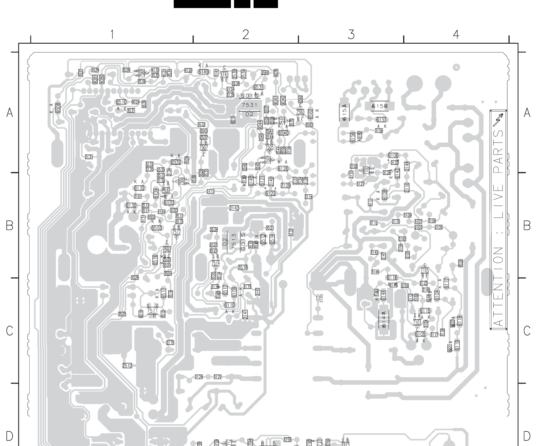
Circuit Diagrams and PWB Layouts EN 95FTL2.4E AA 7.
Layout LCD Standby & Audio Panel (Part 1 Bottom Side)
F_15490_009a.eps
120405
Part 1
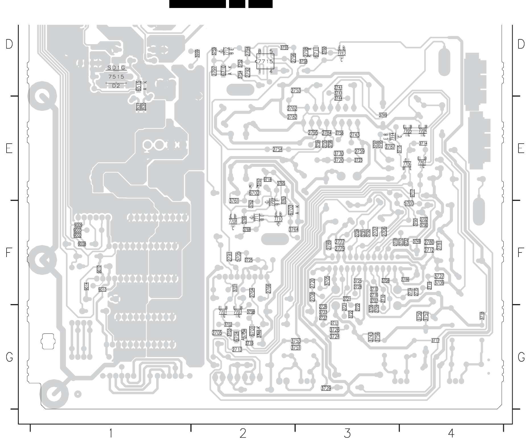
EN 96FTL2.4E AA 7.
Circuit Diagrams and PWB Layouts
Layout LCD Standby & Audio Panel (Part 2 Bottom Side)
F_15490_009b.eps
120405
Part 2

Alignments EN 97FTL2.4E AA 8.
8. Alignments
Index of this chapter:
8.1 General Alignment Conditions
8.2 Hardware Alignments
8.3 Software Alignments
8.4 Option Settings
Note: The Service Default Mode (SDM) and Service Alignment
Mode (SAM) are described in chapter 5. Menu navigation is
done with the CURSOR UP, DOWN, LEFT or RIGHT keys of
the remote control transmitter.
8.1 General Alignment Conditions
8.1.1 Start Conditions
Perform all electrical adjustments under the following
conditions:
• Power supply voltage (depends on region):
–AP-NTSC: 120 VAC or 230 VAC / 50 Hz (r 10%).
–AP-PAL-multi: 120 - 230 VAC / 50 Hz (r 10%).
–EU: 230 VAC / 50 Hz (r 10%).
–LATAM-NTSC: 120 - 230 VAC / 50 Hz (r 10%).
–US: 120 VAC / 60 Hz (r 10%).
• Connect the set to the mains via an isolation transformer
with low internal resistance.
• Allow the set to warm up for approximately 15 minutes.
• Measure voltages and waveforms in relation to chassis
ground (with the exception of the voltages on the primary
side of the power supply).
Caution: never use heatsinks as ground.
• Test probe: Ri > 10 Mohm, Ci < 20 pF.
• Use an isolated trimmer/screwdriver to perform
alignments.
8.1.2 Initial Settings
Perform all electrical adjustments with the following initial
settings (via the "Active Control" button on the RC):
1. To avoid the working of the lightsensor, set "Active Control"
to "Off".
2. Set "Smart Picture" to "Natural".
3. Set "Active Display" to "Off"
8.1.3 Alignment Sequence
• First, set the correct options:
– In SAM, select SERVICE OPTIONS -> OPT. NO,
– Fill in the option settings according to the set sticker
(see also paragraph "Option Settings"),
– Select STORE OPTIONS and push "OK" on the
remote control,
– After storing, the set must be restarted!
• Warming up (>10 minutes).
• White-D alignment.
8.2 Hardware Alignments
8.2.1 Backlight Voltage Alignment
Switch the set "on" and measure the voltage between pin 1 of
connector 1304 and pin 1 of connector 1309 (ground). Align
potmeter R3026 until this voltage is 12 VDC +/- 0.1 V.
Caution: This voltage must be aligned very precisely. When it
is too high, it can destroy the inverters, but when it is too low,
the backlight will not start up.
8.3 Software Alignments
Put the set in SAM mode (see the "Service Modes, Error Codes
and Fault Finding" section). The SAM menu will now appear on
the screen. Select ALIGNMENTS and go to one of the sub
menus. The alignments are explained below.
Notes:
• All changes must be stored manually.
• If an empty EAROM (permanent memory) is detected, all
settings are set to pre-programmed default values.
8.3.1 General
For the next alignments, supply the following test signals via a
video generator to the RF input:
•EU/AP-PAL models: a PAL B/G TV-signal with a signal
strength of at least 1 mV and a frequency of 475.25 MHz
•US/AP-NTSC models: an NTSC M/N TV-signal with a
signal strength of at least 1 mV and a frequency of 61.25
MHz (channel 3).
•LATAM models: an NTSC M or PAL M TV-signal with a
signal strength of at least 1 mV and a frequency of 61.25
MHz (channel 3).
Luma Gain
Fixed setting of "1".
IF AFC
Alignment procedure:
1. During the IF AFC-parameter adjustment, one can see
OSD feedback on the screen.
2. The OSD feedback can give 4 kinds of messages:
3. The first item ("IN/OUT") informs you whether you are in or
out of the AFC-window.
4. The second item ("HIGH/LOW") informs you whether the
AFC-frequency is too high or too low.
Table 8-1 AFC
1. Adjust the IF AFC parameter until the first value is within
the AFC window (= IN).
2. Next, adjust the IF AFC parameter until the second value
is LOW.
IF Lprime AFC
Same procedure as described above, but with SECAM L/L'
signal source.
Tuner AGC
Measure the DC voltage on pin 1 of the (main) Tuner. You can
adjust this voltage by adjusting the TUNER AGC item in the
SAM menu. Alignment is correct when the DC voltage is just
below 3.5 V.
Blend Intensity
Use this alignment when you replace the microcontroller, NVM,
or the EBILD. It aligns the level of transparency of the menu-
picture blended into the main-picture. Fixed setting of "16".
AFC-window AFC-frequency vs. reference
Out High
In High
[ In ] [ Low ]
Out Low
Alignments
EN 98 FTL2.4E AA8.
8.3.2 2fh ADC Alignment
Only necessary to set, when the A/D convertor or NVM is
replaced. Use the default values as mentioned in the table.
Table 8-2 “2fH ADC alignment”
8.3.3 White D Alignment
• Set ACTIVE CONTROL to "Off" (via RC).
• In the TV -> PICTURE user menu set:
– DYNAMIC CONTRAST to "Off".
– COLOUR ENHANCEMENT to "Off".
– COLOUR to "0".
– CONTRAST to "100".
– BRIGHTNESS to "43".
• Go to the SAM and select ALIGNMENTS -> WHITE
POINT.
Method 1 (with colour analyser):
• Use a 100% white screen as input signal and set the
following values:
– COLOR TEMPERATURE: "Tint to be aligned".
– WHITEPOINTRED: "127".
– WHITEPOINTGREEN: "127".
– WHITEPOINTBLUE: "127".
– RED BL OFFSET: "7"
– GREEN BL OFFSET: "7".
• Measure with a calibrated (phosphor- independent) colour
analyser in the centre of the screen. Use a contactless
analyser (e.g. Minolta CA-210) to align an LCD TV. The
colour analyser may not touch the screen surface.
Consequently, the measurement needs to be done in a
dark environment.
Note: The colour analyser needs to be calibrated for LCD!
• Adjust, by means of decreasing the value of one or two
whitepoints, the correct x,y coordinates (see table "White D
alignment values"). Tolerance: dx,dy: r 0.004.
• Repeat this step for the other Colour Temperatures that
need to be aligned.
• When finished press "Store" to store the aligned values to
the NVM.
Table 8-3 White D alignment values
Method 2 (without colour analyser):
If you do not have a colour analyser, you can use the default
values. This is the next best solution. The default values are
average values coming from production (statistics).
1. Select a COLOUR TEMPERATURE (e.g. COOL,
NORMAL, or WARM).
2. Set the RED, GREEN and BLUE default values according
to the values in the "Tint settings" table.
3. When finished press "Store" to store the aligned values to
the NVM.
Table 8-4 Tint settings
8.3.4 Lum. Del.
With this Luminance Delay alignment, you place the luminance
information exactly on the chrominance information (brightness
is pushed onto the colour). Use a colour bar / grey scale pattern
as test signal.
•Lum. Delay PAL BG: Apply a PAL BG colour bar / grey
scale pattern as a test signal. Adjust this parameter until
the transients of the colour part and black and white part of
the test pattern are at the same position.
Default value is "7".
•Lum. Delay PAL I: Apply a PAL I colour bar/grey scale
pattern as a test signal. Adjust this parameter until the
transients of the colour part and black and white part of the
test pattern are at the same position.
Default value is "9".
•Lum. Delay SECAM: Apply a SECAM colour bar/grey
scale pattern as a test signal. Adjust this parameter until
the transients of the colour part and black and white part of
the test pattern are at the same position.
Default value is "9".
•Lum. Delay Bypass: apply a NTSC colour bar/greyscale
pattern as a test signal. Adjust this value until the transients
of the colour and black and white part of the test area are
at the same position.
Default value is "6".
8.4 Option Settings
8.4.1 Introduction
The microprocessor communicates with a large number of I2C
ICs in the set. To ensure good communication and to make
digital diagnosis possible, the microprocessor has to know
which ICs to address. The presence / absence of these specific
ICs (or functions) is made known by the option codes.
Notes:
• After changing the option(s), save them with the STORE
command.
• The new option setting is only active after the TV is
switched "off" and "on" again with the Mains switch (the
EAROM is then read again).
Menu item Value
Red Gain RGB 106
Blue Gain RGB 112
Green Gain RGB 133
Red Offset RGB 40
Blue Offset RGB 41
Green Offset RGB 43
Red Gain YPbPr * 115
Blue Gain YPbPr * 118
Green Gain YPbPr * 102
Red Offset YPbPr * 59
Blue Offset YPbPr * 56
Green Offset YPbPr * 35
* = only for sets with YPbPr input
Coordinates Cool Normal Warm
X0.276 0.287 0.314
Y0.281 0.292 0.320
Cool Normal Warm
White Point R 127 127 127
White Point G 126 123 116
White Point B 112 104 86
Alignments EN 99FTL2.4E AA 8.
8.4.2 Dealer Options
Table 8-5 Dealer option overview
8.4.3 Service Options
Select the sub menu's to set the initialisation codes (options) of
the set via text menus.
Table 8-6 Service option overview
Menu name Subjects Options Description
Personal
Options
Picture Mute Yes Picture (blue) mute active in case no picture detected
No Noise in case of no picture detected
Virgin Mode Yes TV starts up (once) with language selection menu after mains switch
"on" for the first time (virgin mode)
No TV does not starts up (once) with language selection menu after mains
switch "on" for the first time (virgin mode)
Auto Store Mode (only for EU and
AP-PAL/M sets)
None Autostore mode disabled (not in installation menu)
PDC-VPS Autostore mode via ATS (PDC/VPS) enabled
TXT page Autostore mode via ACI enabled
PDC-VPS-TXT Autostore mode via ACI or ATS enabled
TXT Preference (only for EU and AP-
PAL sets)
TOP Preference to TOP Teletext
FLOF Preference to FLOF Teletext
DVD door lock (only for sets with
integrated DVD)
Yes To disable the DVD tray opening function
No To enable the DVD tray opening function
AmbiLight Demo (only when Ambi
Light option is “on”)
Yes Activation of AmbiLight demo via local "MENU" button possible
No Activation of AmbiLight demo via local "MENU" button not possible
Menu-item Subjects Options Description
Dual Screen PIP/Dual Screen Yes / No Feature present / not present
Text/EPG Yes / No Feature present / not present
DS/PIP Tuner Yes / No Feature present / not present (only selectable if PIP/Dual Screen option is
"on")
Teletext NexTView type None Feature not present
Textguide only Feature present, but only as text guide
Nextview 2c3 Feature present, for countries that support NexTView
Display Screen (the used display
code is also printed on the
option code sticker inside the
set)
Value "000" 42 inch PDP SDI
Value "001" 50 inch PDP SDI
Value "002" 42 inch PDP FHP
Value "003" 30 inch LCD LPL
Value "004" 37 inch LCD LPL
Value "005" 42 inch LCD LPL
Value "006" 32 inch LCD Sharp
Value "007" 42 inch PDP SDI VGA
Value "008" 37 inch PDP FHP
Video Repro Feature box type 1050i/1250i HD input
Eagle 1B "Eagle version 1B" present (Pixel Plus 1)
Eagle 1C "Eagle version 1C" present (Pixel Plus 2)
Lightsensor Yes / No Feature present / not present
3D Comb filter Yes / No Only selectable when Columbus is present
Improved Noise Reduction Yes / No Only selectable when Columbus is present
PixelPlus Version 1 Standard PP: only selectable with Eagle 1C
2 Improved PP: only selectable with Eagle 1C
720p Yes / No Enable for high resolution displays
Source
Selection
EXT3 1Fh (2003) Yes / No Not selectable

Alignments
EN 100 FTL2.4E AA8.
8.4.4 Opt. No. (Option numbers)
Select this sub menu to set all options at once (expressed in
two long strings of numbers).
An option number (or "option byte") represents a number of
different options. When you change these numbers directly,
you can set all options very quickly. All options are controlled
via eight option numbers.
When the EAROM is replaced, all options will require resetting.
To be certain that the factory settings are reproduced exactly,
you must set both option number lines. You can find the correct
option numbers on a sticker inside the TV set.
Example: The options sticker gives the following option
numbers:
• 04368 00005 01066 08707
• 00000 00032 00512 00000
The first line (group 1) indicates hardware options 1 to 4, the
second line (group 2) indicates software options 5 to 8.
Every 5-digit number represents 16 bits (so the maximum value
will be 65536 if all options are set).
When all the correct options are set, the sum of the decimal
values of each Option Byte (OB) will give the option number.
See next table for the option overview.
Audio Repro Acoustic System FTV Top Cabinet design (xxPF9986 and xxPF9996 with NXT).
See styling 499 in Product Survey.
Soft Wrap Cabinet design (xxPF9956 and xxPF9966 standard).
See styling 496 in Product Survey.
Wrap Cabinet design (xxPF9956 and xxPF9966 standard).
See styling 500 in Product Survey.
FTV2.3 Cabinet design (for future)
AVL Yes / No Enable / disable Automatic Volume Limiter
Miscellaneous Home Cinema Yes / No Model with / without Home Cinema Link (EU only)
Integrated RC Yes / No Control pheripheral equipment via TV IR receiver (EU only)
Tuner type UV1316 / TEDE9 Model with Philips tuner / Alps tuner
P50 DVD menu line Yes / No Enable / disable DVD control via user menu with TV RC (EU only)
Hotel Mode Yes / No Enable / disable Hotel Mode
Option no. Group 1 Group 1 option code overview (see set sticker)
Group 2 Group 2 option code overview (see set sticker)
Store Options <OK> Store options when changed
Menu-item Subjects Options Description

Alignments EN 101FTL2.4E AA 8.
Table 8-7 Option overview
Byte Bit (dec. value) Subject Options Settings (in decimal values) Remarks
1 0 (1) Video Repro Feature Box Type 3= Eagle 1B, 4= Eagle 1C, 5= 1050i/1250i
1 (2)
2 (4)
3 (8) Personal Ambi Light Demo 0= Off, 8= On
4 (16) Video Repro Auto Scavem 0= No, 16= Yes Only selectable for CRT sets.
5 (32) Improv. Noise Reduction 0= No, 32= Yes Fixed to "Yes" in case Columbus is present
6 (64) Light Sensor 0= No, 64= Yes
7 (128) n.a. n.a.
8 (256) Video Repro Digital Option 0 (No)= Dig. Natural Motion (for PP1) or PixelPlus
(for PP2), 256 (Yes)= PixelPlus (for PP1) or
PixelPlus2 (for PP2)
This depends on the "Pixel Plus Version" option (see also Byte 1
- bit 14), and gives the info that is visible in the user menu.
9 (512) n.a.
10 (1024) Source Selection 1152i 0= Off, 1024= On
11 (2048) Video Repro n.a.
12 (4096) Signalling Bits 0= No, 4096= Yes Fixed to: "Yes" in EU and AP-P, "No" for other versions.
13 (8192) 3D Comb Filter 0= No (2D Comb), 8192= Yes (3D Comb)
14 (16384) PP (Pixel Plus) Version 0= “1”, 16384= “2” Only selectable when "Feature Box" option is "Eagle 1C". See
also Byte 1- bit 8 "Digital Option".
15 (32768) 720p 0= No, 32768= Yes
2 0 (1) Audio Repro n.a.
1 (2) Dolby Pro Logic 0= No, 2= Yes
2 (4) Virtual Rear Speakers 0= No, 4= Yes Fixed to: "Yes" for sets with Dolby Pro Logic.
3 (8) Cordless Rear Speakers 0= No, 8= Yes Fixed to: "No" for all versions, except for EU.
4 (16) Dolby Digital 0= No, 16= Yes When Dolby Digital is "Yes", the AVL (Byte 8 - bit 6) option must
be "No".
5 (32) Virtual Dolby 0= No, 32= Yes Fixed to: "No" in case the "Dolby Pro Logic" option (Byte 2 - Bit 1)
unequals "none".
6 (64) Sub woofer 0= No Sub woofer present, 64= Sub woofer present.
7 (128)
8 (256) Chassis/Region Chassis 0= EM6, 256= EM5, 512 = EM3 FTx2.x= EM6
9 (512)
10 (1024)
11 (2048)
12 (4096) Teletext n.a.
13 (8192) Flash RAM 0= No, 8192= Yes NexTView type 2C3 and 2 need a Flash RAM.
14 (16384) NexTView type 0= None, 16384= Textguide only,
32768= NexTView 2C3, 49152= NexTView 2
Only available for EU.
15 (32768)
3 0 (1) n.a. n.a.
1 (2) n.a. n.a.
2 (4) n.a. n.a.
3 (8) n.a. n.a.
4 (16) Dual Screen PIP/Dual Screen 0= No, 16= Yes
5 (32) n.a.
6 (64) TXT/EPG Dual Screen 0= No, 64= Yes. Fixed to: "Off" for AP-N, US, and LA versions.
7 (128) n.a.
8 (256) Display CRT type (Aspect Ratio) 0= 4:3, 256= 16:9
9 (512) Picture Rotation 0= No, 512= Yes Only selectable for CRT sets.
10 (1024) Monitor 0= No, 1024= Yes Reserved for Flat TV monitor.
11 (2048) Miscellaneous Integrated Radio 0= No, 2048= Yes
12 (4096) Stand Alone 0= No, 4096= Yes Reserved for Flat TV monitor.
13 (8192) Integrated DVD 0= No, 8192= Yes
14 (16384) Home Cinema 0= No, 16384= Yes Fixed to: "No" in all versions except for EU.
15 (32768) Integrated RC 0= No, 32768= Yes Fixed to: "No" in all versions except for EU.
4 0 (1) Dual Screen DS/PIP (Aux) Tuner 0= Aux Tuner not present,
1= Aux Tuner present
Only selectable in the EU version, provided the "PIP/Dual
Screen" option is "Yes".
1 (2) DS/PIP (Aux) Tuner Type 0= UV1316, 2= TEDE9
2 (4) Miscellaneous 38.0 (or China) IF 0= No, 4= Yes Fixed to: "No" in all versions except for AP-P.
3 (8) Tuner Type 0= UV1316, 8= TEDE9
4 (16) Teletext n.a.
5 (32) n.a.
6 (64) n.a.
7 (128) n.a.
8 (256) Miscellaneous Integrated Dig. Module 0= No, 256= Yes
9 (512) Integrated HDD 0= No, 512= Yes
10 (1024) n.a.
11 (2048) n.a.
12 (4096) Anti Aging 0= No, 4096= Yes Fixed to: "Yes" for FTV.
13 (8192) Personal DVD Door Lock 0= No, 8192= Yes
14 (16384) n.a.
15 (32768) n.a.
Alignments
EN 102 FTL2.4E AA8.
5 0 (1) Personal n.a.
1 (2) Auto Store Mode 0= None, 2= PDC/VPS, 4= TXT Page,
6= PDC/VPS/TXT Page
Fixed to: "None" in the AP-N and US versions.
2 (4)
3 (8) 2CS Korea 0= BTSC, 8= Korean Stereo As the MSP can not automatically detect if Korean stereo (2CS)
or BTSC is transmitted, this option is needed to tell the MSP what
detection should be done.
4 (16) Blue (or Picture) Mute 0= No, 16 = Yes
5 (32) n.a.
6 (64) Virgin Mode 0= No, 64= Yes
7 (128) Miscellaneous Hotel Mode 0= No, 128= Yes
8 (256) Personal Flex TV Demo 0= No, 256= Yes
9 (512) n.a. n.a.
10 (1024) Miscellaneous Dimming Backlight 0= No, 1024= Yes
11 (2048) n.a. n.a.
12 (4096) Personal TXT Preference 0= Top, 4096= FLOF Only available in the EU version.
13 (8192) n.a. n.a.
14 (16384) n.a. n.a.
15 (32768) n.a. n.a.
6 0 (1) Miscellaneous P50 DVD Menu Line 0= No, 1= Yes Fixed to: "No" in all versions except for EU.
1 (2) n.a.
2 (4) n.a.
3 (8) n.a.
4 (16) Chassis/Region Region 0= EU, 16= AP-P,
32= AP-N, 48= US,
64= Latam, 80= Australia
5 (32)
6 (64)
7 (128)
8 (256) Display Screen "000" (0)= 42-inch PDP (SDI),
"001" (256)= 50-inch PDP (SDI),
"002" (512)= 42-inch PDP (FHP),
"003" (768)= 30-inch LCD (LPL),
"004" (1024)= 37-inch LCD (LPL),
"005" (1280)= 42-inch LCD (LPL),
"006" (1536)= 32-inch LCD (Sharp),
"007" (1792)= 42-inch PDP (SDI) VGA,
"008" (2048)= 37-inch PDP (FHP).
Fixed to "0" in case of CRT.
9 (512)
10 (1024)
11 (2048)
12 (4096)
13 (8192)
14 (16384)
15 (32768)
7 0 (1) Source Selection EXT4 1fH 0= No, 1= Yes
1 (2) EXT1 2fH 0= No, 2= Yes
2 (4) n.a.
3 (8) n.a.
4 (16) n.a.
5 (32) EXT3 1fH 0= No, 32= Yes
6 (64) DVI/VGA 0= No, 64= Yes
7 (128) HDMI (Europe) 0= No, 128= Yes
8 (256) AV3 1fH 0= No, 256= Yes
9 (512) AV1 2fH 0= No, 512= Yes
10 (1024) AV2 2fH 0= No, 1024= Yes
11 (2048) n.a.
12 (4096) n.a.
13 (8192) n.a.
14 (16384) n.a.
15 (32768) HDMI (Non- Europe) 0= No, 32768= Yes
8 0 (1) Audio Repro Acoustic System 0= FTV-Top (499), 1= Soft Wrap (496, 498),
2= Wrap (496, 498), 3= FTV2.3 (505),
4= FL9 Monitor (n.a.), 5= FL10 (n.a.),
6= FL11 or FL11-upgr. (380, 382, 406, 425, 426,
534), 7= FL12 (296, 305, 395, 408, 428, 444),
8= FL14 (n.a.), 9= PV02 (462), 10= FL13A (456),
11= Soft Design Line (336, 383), 12= Tech Design
Line (419), 14= FL13B (456), 15= Others
Used for setting dynamic audio parameters.
Between brackets the styling numbers are mentioned as listed in
the quarterly Product Survey.
1 (2)
2 (4)
3 (8)
4 (16) n.a. n.a.
5 (32) n.a. n.a.
6 (64) Audio Repro AVL 0= No, 64= Yes Switch to "No" when Dolby Digital is present.
7 (128) 1080i Screen 0= 2fH path, 128= 3fH path
8 (256) Display CRT Size 0= 28", 256= 32", 512= 36" MEC, 768= 29",
1024= 34", 1280= 38", 1536= 28" Mk2,
1792= 36" PH, 2048= 32" MEC, 2304= 32" PH,
2560= 30", 2816= 37", 3072= 42",
3328= 50", 3840= Others
9 (512)
10 (1024)
11 (2048)
12 (4096) Anti Moire Filter 0= No, 4096= Yes Only for CRT
13 (8192) Display Type 0= LCD (LPL), 8192= PDP, 16384= CRT,
24576= LCoS, 32768= PTV, 40960= LCD (AUO),
49152= LCD (Sharp)
14 (16384)
15 (32768)
Byte Bit (dec. value) Subject Options Settings (in decimal values) Remarks

Circuit Descriptions, Abbreviation List, and IC Data Sheets EN 103FTL2.4E AA 9.
9. Circuit Descriptions, Abbreviation List, and IC Data Sheets
Index of this chapter:
9.1 Introduction
9.2 Abbreviation List
Note:
Only new (not recently published) circuits are described here.
As this chassis does not contain any really new circuits, use the
FTL2.2x manual for the circuit descriptions.
9.1 Introduction
This chassis contains, compared to its predecessor, the
following new/changed features/components:
•Small Signal Board (SSB). Small layout changes and new
software to support the 720p feature.
•Dual Ambient Light inverter panels: To reduce the heat
dissipation and improve the efficiency, two separate CCFL
inverter panels are introduced in some models.
•Dimming Backlight : Feature to improve the contrast of
LCD displays. When there is no (or little) white content in
the picture, the LCD backlight will be dimmed to make the
black look darker. The picture content is measured by the
EPLD, which will adapt the PWM signal to the backlight
(see also diagrams B19E and B20).
The chassis consists of a full sized SSB, two Power Supplies
(Main and Stand-by), and some smaller panels for Audio, I/O,
and Control functions. The main functionalities are:
•LCD power supply: same as used in the FTL2.2x.
•SSB: Core TV functionalities, being TXT/control, video and
audio decoding, feature box, video featuring, and sync/
geometry control. The SSB is a high tech module (four
layer, 2 sides reflow technology, full SMC) with very high
component density and full shielding for EMC-reasons.
Despite this, it is designed in such a way, that repair on
component level is possible. To achieve this, attention was
paid to:
– Clearance around surface mounted ICs (for replacing).
– Detailed diagnostics and fault finding is possible via
ComPair.
– Software upgrading (only for main software) is possible
via ComPair.
9.2 Abbreviation List
1080i 1080 visible lines, interlaced
1080p 1080 visible lines, progressive scan
2DNR Spatial (2D) Noise Reduction
3DNR Temporal (3D) Noise Reduction
AARA Automatic Aspect Ratio Adaptation:
algorithm that adapts aspect ratio to
remove horizontal black bars; keeping
up the original aspect ratio
ACI Automatic Channel Installation:
algorithm that installs TV sets directly
from cable network by means of a
predefined TXT page
ADC Analogue to Digital Converter
AFC Automatic Frequency Control: control
signal used to tune to the correct
frequency
AGC Automatic Gain Control: algorithm that
controls the video input of the feature-
box
AM Amplitude Modulation
ANR Automatic Noise Reduction: one of the
algorithms of Auto TV
AR Aspect Ratio: 4 by 3 or 16 by 9
Artistic See OTC 2.5: main processor
ASF Auto Screen Fit: algorithm that adapts
aspect ratio to remove horizontal black
bars but without throwing away video
information
ATV See Auto TV
AUDIO_C Audio Centre
AUDIO_L Audio Left
AUDIO_R Audio Right
AUDIO_SL Audio Surround Left
AUDIO-SR Audio surround right
AUDIO_SW Audio Sub woofer
Auto TV A hardware and software control
system that measures picture content,
and adapts image parameters in a
dynamic way
B/G Monochrome TV system. Sound
carrier distance is 5.5 MHz. B= VHF-
band, G= UHF-band
B-SC1-IN Blue SCART1 in
B-SC2-IN Blue SCART2 in
B-TXT Blue teletext
CL Constant Level: audio output to
connect with an external amplifier
ComPair Computer aided rePair
CSM Customer Service Mode
CTI Colour Transient Improvement:
manipulates steepness of chroma
transients
CVBS Composite Video Blanking and
Synchronisation
CVBS-TER CVBS terrestrial
COLUMBUS COLour LUMinance Baseband
Universal Subsystem. IC performing
noise reduction and 2D/3D comb
filtering
DAC Digital to Analogue Converter
DBE Dynamic Bass Enhancement: extra
low frequency amplification
DDC Display Data Channel; is a part of the
"Plug and Play" feature
DFU Direction For Use: description for the
end user
D/K Monochrome TV system. Sound
carrier distance is 6.5 MHz. D= VHF-
band, K= UHF-band

Circuit Descriptions, Abbreviation List, and IC Data Sheets
EN 104 FTL2.4E AA9.
DNR Digital Noise Reduction: noise
reduction feature of the box
DPL Dolby ProLogic
DSP Digital Signal Processing
DST Dealer Service Tool: special remote
control designed for dealers to enter
e.g. service mode
DVD Digital Versatile Disc
DVI(-d)(-i) Digital Visual Interface (d= digital only)
(i= integrated); a digital video interface
to a display, designed to replace the
analogue YPbPr or RGB interface
Eagle Feature box IC performing peaking,
zooming and sub pixel LTI in both
horizontal and vertical direction, CTI
and other colour features
EDID Extended Display Identification Data
(VESA standard)
EEPROM Electrically Erasable and
Programmable Read Only Memory
EHT Extra High Tension
EPG Electronic Program Guide: system
used by broadcasters to transmit TV
guide information (= NexTView)
EPLD Erasable Programmable Logic Device
EU EUrope
EXT External (source), entering the set via
SCART or via cinches
FALCONIC SAA4992H, Feature Box IC
performing Digital Natural Motion,
3DNR, and vertical zoom and vertical
peaking
FBL Fast Blanking: DC signal
accompanying RGB signals
FBL-PIP The fast blanking signal for PIP
FBL-TXT The fast blanking signal for TXT. It has
a higher priority than FBL-PIP
FBX Feature Box: part of small signal /
separate module which contains 100
Hz processing, extra featuring and
AutoTV algorithms (FBX6= based on
PICNIC, FBX7= based on PICNIC and
Eagle)
FDS Full Dual Screen
FEM Falconic Embedded Memory; IC
(SAA4998H) that is the successor of
the SAA4993H with jagged line
removal and embedded memory
FHP Fujitsu Hitachi Plasma display Ltd.
FLOF Full Level One Features, TXT
standard
FLASH Flash memory
FM Field Memory or Frequency
Modulation
G-TXT Green teletext
HA Horizontal Acquisition: horizontal sync
pulse coming out of the HIP
HD at HOME A signal from the OTC, to switch the
HOP to the Pixel Plus standard (75 Hz
frame)
HIP High-end video Input Processor
(TDA9320): video and chroma
decoder of EM5E
HP Head phone
I Monochrome TV system. Sound
carrier distance is 6.0 MHz. VHF- and
UHF-band
I/O Input/Output
I2C Inter IC bus (also called IIC)
IF Intermediate Frequency
Interlaced Scan mode where two fields are used
to form one frame. Each field contains
half the number of the total amount of
lines. The fields are written in "pairs",
causing line flicker
Last Status The settings last chosen by the
customer, read, and stored in RAM or
in the NVM. They are called at start-up
of the set to configure it according the
customers wishes
LCD Liquid Crystal Display
LPL LG-Philips LCD (supplier)
LED Light Emitting Diode
L/L’ Monochrome TV system. Sound
carrier distance is 6.5 MHz. L' is Band
I, L is all bands except for Band I
LNA Low Noise Adapter
LORE LOcal REgression based noise
reduction
LSP Large signal panel
LVDS Low Voltage Differential Signalling;
Data transmission system for high
speed and low EMI communication
M/N Monochrome TV system. Sound
carrier distance is 4.5 MHz. M= 525
lines @ 60 Hz, N= 625 lines @ 50 Hz
MUTE Mute-Line
NC Not Connected
NICAM Near Instantaneously Companded
Audio Multiplexing; This is a digital
sound system, mainly used in Europe
NTSC National Television Standard
Committee; Colour system mainly
used in North America and Japan.
Colour carrier NTSC M/N= 3.579545
MHz, NTSC 4.43= 4.433619 MHz (this
is a VCR norm, it is not transmitted off-
air)
NVM Non Volatile Memory: IC containing
TV related data e.g. alignments
O/C Open Circuit
OSD On Screen Display
OTC On screen display Teletext and
Control; also named Artistic
(SAA5800)
P50 Project 50 communication: protocol
between TV and peripherals
PAL Phase Alternating Line; Colour system
mainly used in West Europe (colour
carrier= 4.433619 MHz) and South
America (colour carrier PAL M=
3.575612 MHz and PAL N= 3.582056
MHz)
PCB Printed Circuit Board
PDP Plasma Display Panel
PFC Power Factor Corrector (or Pre-
conditioner)
PICNIC Peripheral Integrated Combined
Network IC (SAA4978): main IC for
100 Hz featuring and feature
processing
PIP Picture In Picture
PLL Phase Locked Loop; Used for e.g.
FST tuning systems. The customer
can directly provide the desired
frequency
POR Power On Reset; Signal to reset the
µP
Progressive Scan Scan mode where all scan lines are
displayed in one frame at the same
time, creating a double vertical
resolution.
PSU Power Supply Unit
PWB Printed Wiring Board
RAM Random Access Memory
R-TXT Red teletext
RC Remote Control
RC5 / RC6 Signal protocol from the remote
control receiver
RESET Reset signal

Circuit Descriptions, Abbreviation List, and IC Data Sheets EN 105FTL2.4E AA 9.
RGB Red, Green, and Blue colour space;
The primary colour signals for TV. By
mixing levels of R, G, and B, all colours
(Y/C) are reproduced
RGBHV Red, Green, Blue, Horizontal sync,
and Vertical sync
ROM Read Only Memory
SAM Service Alignment Mode
S/C Short Circuit
SCL-F Clock signal on fast I2C bus
SD Standard Definition
SDA-F Data signal on fast I2C bus
SDI Samsung Display Industry (supplier)
SECAM SÉquence Couleur Avec Mémoire;
Colour system mainly used in France
and East Europe. The chroma is FM
modulated and the R-Y and B-Y
signals are transmitted line sequential.
Colour carriers= 4.406250 MHz and
4.250000 MHz
SIF Sound Intermediate Frequency
SMD Surface Mounted Device
SMPS Switched Mode Power Supply
SNERT Synchronous No parity Eight bit
Reception and Transmit
SSB Small Signal Board
STBY Stand-by
SW Sub woofer
SVGA 800x600 (4:3)
SVHS Super Video Home System
TMDS Transition Minimised Differential
Signalling
TOP Table Of Pages; TXT standard
TXT Teletext
uP Microprocessor
UV Colour difference signals
UVSH UHF, VHF, S-, and Hyper-band
VA Vertical Acquisition
V-a Addressing voltage for the plasma
display
VDS Virtual Dolby Surround
VESA Video Electronics Standards
Association
VFB Vertical Flyback Pulse: vertical sync
pulse coming from the Feature Box
VGA Video Graphics Array; 640x480 (4:3)
VL Variable Level out: processed audio
output towards external amplifier
V-ra Setting voltage for V_a
V-rs Setting voltage for V_s
V-s Sustain voltage for the plasma display
WSS Wide Screen Signalling; used by
broadcasters to transmit e.g.
PALPLUS and 16:9 Aspect Ratio
WXGA Wide eXtended Graphics Array;
1280x768 (15:9) or 1366x768 (16:9)
WYSIWYR What You See Is What You Record:
record selection that follows main
picture and sound
XGA Extended Graphics Array; 1024x768
(4:3)
XTAL Quartz crystal
Y Luminance signal
Y100 Y from Feature Box
YPbPr This is a scaled version of the YUV
colour space. Y= Luminance, Pb/Pr=
Colour difference signals B-Y and R-Y,
other amplitudes w.r.t. to YUV
Y-OUT Luminance-signal to HOP IC
YUV Colour space used by the NTSC and
PAL video systems. Y is the luminance
and U/V are the colour difference
signals
9.3 IC Data Sheets
See FTL2.2 manual.

Spare Parts List
EN 106 FTL2.4E AA10.
10. Spare Parts List
Set Level
Various
1004h8204 000 78291 LCD LQ315T3LZ2X
1088 3104 328 39552 Ambilight Inverter assy
1089 3104 328 39552 Ambilight Inverter assy
1112 3104 328 32471 Mains Switch / LED assy
1114 3104 328 35721 Control assy
1116 3104 328 32461 Side I/O assy
1175 2722 171 00251 Ambilight assy
1176 2722 171 00252 Ambilight assy
8250 3104 311 08901 Cable 31P/230/30P
8302 3104 311 04721 Cable 7P/680/7P
8310 3104 311 07061 Cable 4P/280/4P
8314 3104 311 08531 Cable 10P/820/10P
8315 3104 311 08531 Cable 10P/820/10P
8318 3104 311 06841 Cable 6P/820/6P
8504 3104 311 08281 Cable 4P/480/4P
8505 3104 311 08431 Cable 3P/480/3P
8506 3104 311 08361 Cable 2P3/400/2P3
8507h3104 311 08381 Cable 4P/400/4P
8508 3104 311 08471 Cable 4p/680/4p
8509 3104 311 08311 Cable 3P/480/4P
8548 3104 311 10351 Cable 3P/680/3P
8735 3104 311 08601 Cable 2P3/820/2xPosi
8736 3104 311 09471 Cable 2P/1600/2P
8737 3104 311 08251 Wire ring/180/POSI 4.8
LCD Supply [A]
Various
1007h4822 071 55002 Fuse T5A 250V
1304 2422 025 10647 Connector 4p m
1305 4822 267 10735 Connector 3p
1306h2422 025 16374 Connector 2p m
1307 2422 025 10647 Connector 4p m
1308h4822 265 20723 Connector 2p
1309 2422 025 11143 Connector 3p m
1400h4822 253 50145 Fuse 3.15A T
1402 4822 252 60151 Surge protect
1410 4822 265 11253 Fuse holder
1411 4822 265 11253 Fuse holder
1450h2422 132 07411 Relay 1p 5V 5A
1M02 2422 025 11244 Connector 7p m
g
2000h2252 811 95022 1.5nF 20% 250V
2002 4822 124 11767 470PF 20% 25V
2003 4822 124 80061 1000PF 20% 25V
2007 4822 126 14583 470nF 10% 16V 0805
2008 4822 126 14583 470nF 10% 16V 0805
2009 2238 867 18101 100pF 1% 50V 0603
2010 4822 124 40207 100PF 20% 25V
2012 4822 126 14138 680pF 10% 2kV
2013 4822 126 14138 680pF 10% 2kV
2014h4822 126 13451 2.2nF 10% 2kV
2015 5322 126 11583 10nF 10% 50V 0603
2016 2238 586 59812 100nF 20% 50V 0603
2019 5322 126 11583 10nF 10% 50V 0603
2020 4822 124 12285 2200PF 20% 16V
2021 4822 124 12285 2200PF 20% 16V
2022 2020 021 00039 1800PF 20% 35V
2023 4822 126 14583 470nF 10% 16V 0805
2024 2020 552 96326 220nF 10% 16V
2025 2020 552 96683 220nF 10% 50V
2026 4822 126 14238 2.2nF 50V 0603
2028 5322 126 11578 1nF 10% 50V 0603
2029 5322 126 11578 1nF 10% 50V 0603
2031 5322 126 11583 10nF 10% 50V 0603
2033 2020 552 96683 220nF 10% 50V
2034 2238 867 18101 100pF 1% 50V 0603
2035 2238 867 18101 100pF 1% 50V 0603
2038 2020 021 00039 1800PF 20% 35V
2039 4822 126 14583 470nF 10% 16V 0805
2040 4822 126 14249 560pF 10% 50V 0603
2041 2020 552 96683 220nF 10% 50V
2042 2020 552 96683 220nF 10% 50V
2043 2020 552 96683 220nF 10% 50V
2044 5322 126 11578 1nF 10% 50V 0603
2045 5322 126 11578 1nF 10% 50V 0603
2046 3198 017 34730 47nF 16V 0603
2047 5322 126 11583 10nF 10% 50V 0603
2048 5322 126 11578 1nF 10% 50V 0603
2050 5322 126 11578 1nF 10% 50V 0603
2051 2020 552 96683 220nF 10% 50V
2052 2020 552 96683 220nF 10% 50V
2053 2020 552 96683 220nF 10% 50V
2060 4822 126 14238 2.2nF 50V 0603
2061 4822 126 14238 2.2nF 50V 0603
2062 4822 126 14238 2.2nF 50V 0603
2063 4822 126 13881 470pF 5% 50V
2064 4822 126 13881 470pF 5% 50V
2065 4822 126 14238 2.2nF 50V 0603
2071 5322 126 11578 1nF 10% 50V 0603
2072 5322 126 11578 1nF 10% 50V 0603
2077 4822 126 14238 2.2nF 50V 0603
2290 5322 126 11583 10nF 10% 50V 0603
2291 4822 126 13881 470pF 5% 50V
2292 4822 124 12417 2200PF 20% 25V
2293 4822 126 13881 470pF 5% 50V
2294 4822 124 12417 2200PF 20% 25V
2400h2222 338 22474 470nF 20% 275V
2407h2252 811 95017 470pF 10% 250V
2816 2020 024 00001 330PF 20% 400V
2816 2020 024 90749 330PF 20% 400V
f
3000h4822 052 10478 4.7: 5% 0.33W
3001 4822 051 30101 100: 5% 0.062W
3002 4822 117 12925 47k: 1% 0.063W 0603
3003 4822 117 13632 100k: 1% 0603 0.62W
3004 4822 051 30273 27k: 5% 0.062W
3005 4822 051 30333 33k: 5% 0.062W
3006 4822 051 30103 10k: 5% 0.062W
3007 4822 051 30103 10k: 5% 0.062W
3008 4822 051 30331 330: 5% 0.062W
3009 4822 051 30332 3.3: 5% 0.062W
3010 4822 051 30471 47: 5% 0.062W
3011 4822 051 30471 47: 5% 0.062W
3012 4822 051 30153 15k: 5% 0.062W
3013 4822 051 30103 10k: 5% 0.062W
3014h4822 052 10101 100: 5% 0.33W
3015h4822 052 10479 47: 5% 0.33W
3016 4822 051 30332 3.3: 5% 0.062W
3017h4822 052 10101 100: 5% 0.33W
3018h4822 052 10479 47: 5% 0.33W
3019 4822 051 30332 3.3: 5% 0.062W
3020 4822 051 30332 3.3: 5% 0.062W
3021 4822 117 12971 15: 5% 0603 0.62W
3022 4822 051 30681 680: 5% 0.062W
3023 4822 051 30153 15k: 5% 0.062W
3025 3198 021 31820 1.8k: 5% 0.062W 0603
3026 2120 368 90118 Potm. lin. 470: hor.
3027 4822 117 13632 100k: 1% 0603 0.62W
3028 4822 051 30332 3.3: 5% 0.062W
3029 4822 051 30332 3.3: 5% 0.062W
3030 4822 051 30183 18k: 5% 0.062W
3031 4822 051 30103 10k: 5% 0.062W
3032 4822 051 30103 10k: 5% 0.062W
3032 4822 051 30223 22k: 5% 0.062W
3033h4822 052 11108 1: 5% 0.5W
3034 4822 051 30102 1k: 5% 0.062W
3035 4822 051 30332 3.3: 5% 0.062W
3037 4822 051 30153 15k: 5% 0.062W
3040 3198 021 38220 8.2k: 5% 0.062W 0603
3041 4822 051 30333 33k: 5% 0.062W
3043 4822 051 30109 10: 5% 0.062W
3045 4822 117 12971 15: 5% 0603 0.62W
3046 4822 117 12971 15: 5% 0603 0.62W
3047 4822 051 30479 47: 5% 0.062W
3048 4822 051 30272 2.7k: 5% 0.062W
3050 4822 050 28204 820k: 1% 0.6W
3052 2322 704 67502 7.5k: 1% 0.5W
3053 4822 050 26804 680k: 1% 0.6W
3055 4822 051 30221 220: 5% 0.062W
3056 4822 117 12968 820: 5% 0.62W
3057 4822 051 30221 220: 5% 0.062W
3058 4822 053 20565 5.6M: 5% 0.25W
3061 4822 051 30683 68k: 5% 0.062W
3064 4822 051 30103 10k: 5% 0.062W
3065 4822 117 13632 100k: 1% 0603 0.62W
3066 4822 051 30103 10k: 5% 0.062W
3067 4822 051 30101 100: 5% 0.062W
3068 4822 051 30222 2.2k: 5% 0.062W
3070 4822 051 30102 1k: 5% 0.062W
3071 4822 051 30103 10k: 5% 0.062W
3075 4822 051 30102 1k: 5% 0.062W
3089 4822 051 30103 10k: 5% 0.062W
3100 4822 051 30109 10: 5% 0.062W
3292 4822 051 30561 560: 5% 0.062W
3400h2122 550 00158 VDR 1mA 612V
3401h4822 053 21475 4.7M: 5% 0.5W
3402h4822 053 21475 4.7M: 5% 0.5W
3403h4822 053 21475 4.7M: 5% 0.5W
3404 4822 116 83872 220: 5% 0.5W
3999 4822 051 30682 6.8: 5% 0.062W
b
5001 2422 531 02444 Transf. S13932-04Y
5002h3104 308 21231 Transf. 2652.0001A
5005 4822 526 10704 Bead 50 : at 100MHz
5007 4822 526 10704 Bead 50 : at 100MHz
5008 4822 526 10704 Bead 50 : at 100MHz
5009 4822 157 11411 Bead 80: at 100MHz
5010 4822 157 11411 Bead 80: at 100MHz
5013 4822 526 10704 Bead 50 : at 100MHz
5015 4822 157 11411 Bead 80: at 100MHz
5016 4822 157 11411 Bead 80: at 100MHz
5017 4822 526 10704 Bead 50 : at 100MHz
5025 4822 526 10704 Bead 50 : at 100MHz
5026 4822 526 10704 Bead 50 : at 100MHz
5027 4822 526 10704 Bead 50 : at 100MHz
5028 4822 526 10704 Bead 50 : at 100MHz
5040 4822 157 11411 Bead 80: at 100MHz
5291 2422 536 00776 33PH 10%
5292 2422 536 00776 33PH 10%
5293 2422 536 00776 33PH 10%
5403 3104 308 21201 Line filter DTH40383H65
d
6002 4822 130 11397 BAS316
6003 4822 130 11397 BAS316
6004 4822 130 80622 BAT54
6005 4822 130 80622 BAT54
6006 4822 130 11397 BAS316
6007 4822 130 11397 BAS316
6008 4822 130 11397 BAS316
6009 4822 130 11152 UDZ18B
6010 4822 130 11397 BAS316
6011 4822 130 11397 BAS316
6012 9322 208 80685 BZG05C15
6013 9322 208 80685 BZG05C15
6014 9340 548 67115 PDZ22B
6015 4822 130 11397 BAS316
6017 4822 130 11397 BAS316
6020 4822 130 11397 BAS316
6021 9322 206 26687 STPS20H100CT
6022 4822 130 11148 UDZ4.7B
6023 4822 130 11397 BAS316
6025 9322 206 26687 STPS20H100CT
6027 4822 130 11397 BAS316
6028 4822 130 11397 BAS316
6044 9322 207 11687 STPS20L45CT
6045 9322 207 11687 STPS20L45CT
6051 4822 130 11397 BAS316
6077 9322 202 55685 BYG22D
6078 9322 202 55685 BYG22D
6079 9322 202 55685 BYG22D
6080 9322 202 55685 BYG22D
6081 9340 548 67115 PDZ22B
6291 4822 130 11572 STPS8H100F
6293 4822 130 11572 STPS8H100F
6460 4822 130 11397 BAS316
6461 4822 130 11397 BAS316
6506h4822 130 83147 DF06M
6807h9322 199 74682 GBJ6J-B15
ce
7001 9322 108 21682 MC34067P
7002h9322 149 04682 TCET1102
7004 3198 010 42310 BC847BW
7005 9322 192 18687 STP15NK50ZFP
7005 9322 205 26687 FQPF18N50V2
7006 9322 192 18687 STP15NK50ZFP
7006 9322 205 26687 FQPF18N50V2
7007 3198 010 42320 BC857BW
7008 3198 010 42320 BC857BW
7009 3198 010 42320 BC857BW
7010 9322 192 16685 TS2431AI
7017 3198 010 42320 BC857BW
7018 3198 010 42310 BC847BW
7030 3198 010 42310 BC847BW

Spare Parts List EN 107FTL2.4E AA 10.
Ambi Light [AL]
Various
0615 3104 317 09401 SW (see Prod. Survey)
1010 2422 086 00657 Fuse 3A 125V F SMD
1050 2422 543 01431 Xtal 20MHz 16pF
1M08 2422 025 09406 Connector 4p m
1M10 2422 025 09406 Connector 4p m
1M11 2422 025 19068 Connector 11p m
1M12 2422 025 19069 Connector 3p m
1M48 2422 025 10768 Connector 3p m
1M49 2422 025 18884 Connector 4p m
g
2001 2020 012 00018 1000PF 20% 16V
2002 2238 586 59812 100nF 20% 50V 0603
2003 2020 552 96618 1nF 10% 50V 0402
2004 2020 552 96618 1nF 10% 50V 0402
2005 3198 034 01590 15pF 1% 50V 0402
2006 3198 034 01590 15pF 1% 50V 0402
f
3003 4822 117 13596 220: 5% 0.01W 0402
3004 4822 051 20471 470: 5% 0.1W
3005 4822 051 20561 560: 5% 0.1W
3006 2322 762 60102 1k: 5% 2512
3007 2322 762 60102 1k: 5% 2512
3008 4822 051 20471 470: 5% 0.1W
3009 4822 051 20561 560: 5% 0.1W
3010 2322 762 60102 1k: 5% 2512
3011 2322 762 60102 1k: 5% 2512
3012 4822 051 20471 470: 5% 0.1W
3013 4822 051 20561 560: 5% 0.1W
3014 2322 762 60102 1k: 5% 2512
3015 2322 762 60102 1k: 5% 2512
3016 3198 031 04720 4.7k: 5% 0402
3017 3198 031 04720 4.7k: 5% 0402
3018 3198 031 04720 4.7k: 5% 0402
3019 3198 031 04720 4.7k: 5% 0402
3020 3198 031 04720 4.7k: 5% 0402
3022 4822 117 13545 100: 1% 0402
3023 4822 117 13545 100: 1% 0402
3024 3198 031 04720 4.7k: 5% 0402
3025 3198 031 04720 4.7k: 5% 0402
3028 4822 117 13606 10k: 5% 0.01W 0402
3029 3198 031 04720 4.7k: 5% 0402
3030 3198 031 04720 4.7k: 5% 0402
3031 3198 031 04720 4.7k: 5% 0402
3042 4822 053 20105 1M: 5% 0.25W
3999 4822 051 30103 10k: 5% 0.062W
b
5002 2422 536 00923 22PH 10% LHL10
5007 2422 536 00923 22PH 10% LHL10
5008 2422 536 00923 22PH 10% LHL10
5014 3104 308 21271 Transf. BD21416-00
5015 3104 308 21271 Transf. BD21416-00
5016 3104 308 21271 Transf. BD21416-00
d
6000 4822 130 11397 BAS316
6001 4822 130 11397 BAS316
6002 4822 130 11397 BAS316
6003 4822 130 11397 BAS316
6004 4822 130 11397 BAS316
6005 4822 130 11397 BAS316
6006 4822 130 11152 UDZ18B
6007 4822 130 11152 UDZ18B
6008 4822 130 11152 UDZ18B
6009 4822 130 11152 UDZ18B
6010 4822 130 11152 UDZ18B
6011 4822 130 11152 UDZ18B
ce
7001 9352 711 46118 P87LPC760BDH
7002 9322 202 58668 LD1117DT50
7009 3198 010 42310 BC847BW
7010 3198 010 42310 BC847BW
7011 3198 010 42310 BC847BW
7015 9322 214 20668 SI4946EY
7016 9322 214 20668 SI4946EY
7017 9322 214 20668 SI4946EY
7018 3198 010 42310 BC847BW
7019 3198 010 42310 BC847BW
7020 3198 010 42310 BC847BW
Small Signal Board [B]
Various
0601 3104 317 09961 SW (see Prod. Survey)
0602 3104 337 00141 SW (see Prod. Survey)
0603 3104 317 06592 SW (see Prod. Survey)
0605 3104 317 47621 SW (see Prod. Survey)
1000 2422 086 11092 Fuse 500mA 50V F SMD
1001 2422 543 01497 Xtal 6Mhz 20pF
1003 2422 025 14911 Socket Euro 21p f
1026 3104 328 29591 SCART 3 assy
1305 2422 543 01488 Xtal 4.433619Mhz 20pF
1308 2422 543 01486 Xtal 3.579545Mhz 16pF
1404 2422 127 00543 Switch 1p 2pos
1407 2422 549 00458 Filter 5M5/5M74
1408 2422 549 44372 SAW 38.9MHz K3953L
1409 2422 549 44369 SAW 38.9MHz K9656L
1703 2422 540 00002 Resonator CSTCE*G52
1A01 2422 543 01059 Resonator 18MHz 12p
1D01 2422 033 00515 Socket DVI-I 29p f
1E02 2422 025 17274 Connector 10p m
1E04 2422 025 18738 Connector 3p m
1G50 2422 025 18427 Connector 31p f
1I01 2422 025 18133 Socket SCART
1I04 2422 025 18133 Socket SCART
1I05 2422 026 05539 Socket Cinch 2p f WhRd
1I06 2422 026 05527 Socket Cinch 2p f
1I07 2422 026 05054 Socket Cinch 2p f WhRd
1I53 2422 549 45325 Bead 67: at 100MHz
1I56 2422 549 45325 Bead 67: at 100MHz
1I57 2422 549 45325 Bead 67: at 100MHz
1I59 2422 549 45325 Bead 67: at 100MHz
1I79h2422 086 00623 Fuse 3A T 125V
1M01 2422 025 10768 Connector 3p m
1M03 2422 025 10771 Connector 10p m
1M07 4822 267 10637 Connector 5p
1M15 4822 267 10748 Connector 3p
1M17 2422 025 17765 Connector 7p m
1M20 2422 025 10772 Connector 12p m
1M36 2422 025 10655 Connector 11p m
1M37 2422 025 10655 Connector 11p m
1M46 2422 025 10655 Connector 11p m
1M51 2422 025 18884 Connector 4p m
1M52 2422 025 10769 Connector 9p m
1T01 3139 147 22161 Tuner UV1318S/A I H N-3
1U01h2422 086 11112 Fuse 1A T 125V
8220 3104 311 08631 Cable12P/480/12P
8303 3104 311 06511 Cable 10p/280/10p
8307 3104 311 05691 Cable 5p/100/5p
8308 3104 311 06951 Cable 2P3/180/2P
8317 3104 311 07871 Cable 7P/180/7P
8336h3104 311 07451 Cable 11P/220/11P
8337 3104 311 07451 Cable 11P/220/11P
8346 3104 311 06991 Cable 11P/280/11P
8349 3104 311 10341 Cable 4P/400/4P
8352 3104 311 07381 Cable 9P/220/9P
g
2002 3198 034 02790 47pF 1% 50V 0402
2003 2238 780 15654 220nF 10% 16V 0805
2004 2238 780 15654 220nF 10% 16V 0805
2005 2238 586 59812 100nF 20% 50V 0603
2006 2238 586 59812 100nF 20% 50V 0603
2007 2238 586 59812 100nF 20% 50V 0603
2008 2238 586 59812 100nF 20% 50V 0603
2013 2020 021 91557 100PF 20% 16V
2016 4822 124 12095 100PF 20% 16V
2017 2238 586 59812 100nF 20% 50V 0603
2018 4822 126 14324 33pF 5% 50V 0402
2019 2238 586 59812 100nF 20% 50V 0603
2020 3198 035 02210 220pF 5% 50V 0402
2022 2238 586 59812 100nF 20% 50V 0603
2023 2238 586 59812 100nF 20% 50V 0603
2024 2238 586 59812 100nF 20% 50V 0603
2025 2238 586 59812 100nF 20% 50V 0603
2026 2238 586 59812 100nF 20% 50V 0603
2027 2238 586 59812 100nF 20% 50V 0603
2028 2238 586 59812 100nF 20% 50V 0603
2029 2238 586 59812 100nF 20% 50V 0603
2031 2238 586 59812 100nF 20% 50V 0603
2033 2238 869 15829 82pF 5% 50V 0402
2034 2238 869 15829 82pF 5% 50V 0402
2035 2238 869 15829 82pF 5% 50V 0402
2036 2238 869 15829 82pF 5% 50V 0402
2037 2238 869 15829 82pF 5% 50V 0402
2038 2238 586 59812 100nF 20% 50V 0603
2039 2238 586 59812 100nF 20% 50V 0603
2040 2238 586 59812 100nF 20% 50V 0603
2063 2238 586 59812 100nF 20% 50V 0603
2067 2238 586 59812 100nF 20% 50V 0603
2072 2238 586 59812 100nF 20% 50V 0603
2073 3198 017 44740 470nF 10V 0603
2074 2238 586 59812 100nF 20% 50V 0603
2075 2238 586 59812 100nF 20% 50V 0603
2305 2238 586 59812 100nF 20% 50V 0603
2316 2238 586 59812 100nF 20% 50V 0603
2322 2238 586 59812 100nF 20% 50V 0603
2324 5322 126 11583 10nF 10% 50V 0603
2350 2238 586 59812 100nF 20% 50V 0603
2351 2238 586 59812 100nF 20% 50V 0603
2352 2238 586 59812 100nF 20% 50V 0603
2356 2238 586 59812 100nF 20% 50V 0603
2357 2238 586 59812 100nF 20% 50V 0603
2358 3198 035 03320 3.3nF 5% 50V 0402
2359 3198 034 01590 15pF 1% 50V 0402
2360 3198 034 01580 1.5pF 1% 50V 0402
2361 3198 034 01280 1.2pF 1% 50V 0402
2362 2238 869 15109 10pF 5% 50V 0402
2365 2238 586 59812 100nF 20% 50V 0603
2366 2238 586 59812 100nF 20% 50V 0603
2367 2238 586 59812 100nF 20% 50V 0603
2368 2238 586 59812 100nF 20% 50V 0603
2369 2238 586 59812 100nF 20% 50V 0603
2370 2238 586 59812 100nF 20% 50V 0603
2371 3198 035 14720 4.7nF 5% 25V 0402
2372 2022 552 05679 1PF 10% 16V 0805
2373 2238 586 59812 100nF 20% 50V 0603
2374 2022 552 05679 1PF 10% 16V 0805
2375 2238 787 15641 22nF 5% 16V 0402
2376 2238 586 59812 100nF 20% 50V 0603
2377 2020 021 91557 100PF 20% 16V
2378 2238 586 59812 100nF 20% 50V 0603
2384 2238 586 59812 100nF 20% 50V 0603
2387 2022 552 05679 1PF 10% 16V 0805
2391 2238 586 59812 100nF 20% 50V 0603
2392 2022 552 05679 1PF 10% 16V 0805
2394 2022 552 05679 1PF 10% 16V 0805
2403 2238 586 59812 100nF 20% 50V 0603
2404 2022 552 05679 1PF 10% 16V 0805
2405 3198 035 14720 4.7nF 5% 25V 0402
2406 4822 117 13605 Jumper 0402
2409 2022 552 05679 1PF 10% 16V 0805
2410 2020 021 91557 100PF 20% 16V
2411 2238 586 59812 100nF 20% 50V 0603
2412 3198 035 14720 4.7nF 5% 25V 0402
2414 2020 021 91557 100PF 20% 16V
2415 2238 586 59812 100nF 20% 50V 0603
2416 2022 552 05679 1PF 10% 16V 0805
2417 4822 126 14583 470nF 10% 16V 0805
2418 3198 034 05680 5.6pF 1% 50V 0402
2425 2020 021 91557 100PF 20% 16V
2430 4822 126 14324 33pF 5% 50V 0402
2432 2238 586 59812 100nF 20% 50V 0603
2433 2238 586 59812 100nF 20% 50V 0603
2434 2238 586 59812 100nF 20% 50V 0603
2435 2020 552 96618 1nF 10% 50V 0402
2436 2022 552 05679 1PF 10% 16V 0805
2500 2022 552 05679 1PF 10% 16V 0805
2501 2020 552 94427 100pF 5% 50V
2502 2022 552 05679 1PF 10% 16V 0805
2503 2020 552 94427 100pF 5% 50V
2504 2022 552 05679 1PF 10% 16V 0805
2505 2022 552 05679 1PF 10% 16V 0805
2506 2238 586 59812 100nF 20% 50V 0603
2507 5322 126 11578 1nF 10% 50V 0603
2508 2022 552 05679 1PF 10% 16V 0805
2509 2238 586 59812 100nF 20% 50V 0603
2510 4822 126 14241 330pF 0603 50V
2511 2238 586 59812 100nF 20% 50V 0603
2512 2238 586 59812 100nF 20% 50V 0603
2513 2238 586 59812 100nF 20% 50V 0603
2515 2022 552 05679 1PF 10% 16V 0805
2516 2022 552 05679 1PF 10% 16V 0805
2517 2022 552 05679 1PF 10% 16V 0805
2707 3198 034 02790 47pF 1% 50V 0402
2709 2238 586 59812 100nF 20% 50V 0603
2710 2238 586 59812 100nF 20% 50V 0603
2711 2238 586 59812 100nF 20% 50V 0603
2712 2238 586 59812 100nF 20% 50V 0603
2716 2238 586 59812 100nF 20% 50V 0603
2717 2238 586 59812 100nF 20% 50V 0603
2721 2238 869 15101 100pF 5% 50V 0402
2722 2238 869 15101 100pF 5% 50V 0402
2723 2238 586 59812 100nF 20% 50V 0603
2725 2238 586 59812 100nF 20% 50V 0603
2726 2238 586 59812 100nF 20% 50V 0603
2727 2238 586 59812 100nF 20% 50V 0603
2728 2020 021 91854 10PF 20% 16V
2729 2238 586 59812 100nF 20% 50V 0603
2730 2020 021 91557 100PF 20% 16V

Spare Parts List
EN 108 FTL2.4E AA10.
2731 2238 586 59812 100nF 20% 50V 0603
2732 2020 552 96618 1nF 10% 50V 0402
2733 2238 586 59812 100nF 20% 50V 0603
2734 2238 586 59812 100nF 20% 50V 0603
2735 2238 586 59812 100nF 20% 50V 0603
2736 2238 586 59812 100nF 20% 50V 0603
2738 2238 586 59812 100nF 20% 50V 0603
2739 2020 021 91557 100PF 20% 16V
2740 2238 787 15641 22nF 5% 16V 0402
2741 2238 787 15641 22nF 5% 16V 0402
2742 2238 787 15641 22nF 5% 16V 0402
2743 2238 586 59812 100nF 20% 50V 0603
2744 2238 586 59812 100nF 20% 50V 0603
2745 2238 586 59812 100nF 20% 50V 0603
2746 2238 586 59812 100nF 20% 50V 0603
2748 2238 586 59812 100nF 20% 50V 0603
2749 2238 586 59812 100nF 20% 50V 0603
2750 2020 552 96618 1nF 10% 50V 0402
2751 2020 552 96618 1nF 10% 50V 0402
2752 2020 552 96618 1nF 10% 50V 0402
2753 2020 552 96618 1nF 10% 50V 0402
2754 2020 552 96618 1nF 10% 50V 0402
2755 2020 552 96618 1nF 10% 50V 0402
2756 2020 552 96618 1nF 10% 50V 0402
2757 2238 787 15641 22nF 5% 16V 0402
2759 2020 552 96618 1nF 10% 50V 0402
2760 2238 787 15641 22nF 5% 16V 0402
2761 2238 787 15641 22nF 5% 16V 0402
2762 2238 787 15641 22nF 5% 16V 0402
2763 2238 787 15641 22nF 5% 16V 0402
2764 2238 787 15641 22nF 5% 16V 0402
2768 2238 787 15641 22nF 5% 16V 0402
2769 2020 552 96618 1nF 10% 50V 0402
2770 2020 552 96618 1nF 10% 50V 0402
2771 2020 552 96618 1nF 10% 50V 0402
2772 2238 787 15641 22nF 5% 16V 0402
2773 2020 552 96618 1nF 10% 50V 0402
2777 2020 552 96618 1nF 10% 50V 0402
2778 2020 552 96618 1nF 10% 50V 0402
2780 2020 552 96618 1nF 10% 50V 0402
2781 2020 552 96618 1nF 10% 50V 0402
2782 2020 552 96618 1nF 10% 50V 0402
2784 2238 787 15641 22nF 5% 16V 0402
2785 2238 787 15641 22nF 5% 16V 0402
2788 2238 586 59812 100nF 20% 50V 0603
2789 2238 586 59812 100nF 20% 50V 0603
2790 2238 586 59812 100nF 20% 50V 0603
2791 2238 586 59812 100nF 20% 50V 0603
2792 2238 586 59812 100nF 20% 50V 0603
2793 2238 586 59812 100nF 20% 50V 0603
2794 2020 552 96618 1nF 10% 50V 0402
2795 2020 552 96618 1nF 10% 50V 0402
2796 2020 552 96618 1nF 10% 50V 0402
2797 2020 552 96618 1nF 10% 50V 0402
2798 2020 552 96618 1nF 10% 50V 0402
2799 2020 552 96618 1nF 10% 50V 0402
2800 2238 586 59812 100nF 20% 50V 0603
2802 2238 586 59812 100nF 20% 50V 0603
2804 2238 586 59812 100nF 20% 50V 0603
2805 2020 552 96618 1nF 10% 50V 0402
2806 2238 586 59812 100nF 20% 50V 0603
2807 2238 586 59812 100nF 20% 50V 0603
2808 2020 552 96618 1nF 10% 50V 0402
2809 2020 552 96618 1nF 10% 50V 0402
2810 2238 586 59812 100nF 20% 50V 0603
2811 2238 586 59812 100nF 20% 50V 0603
2812 3198 031 02290 22: 5% 0.1W 0402
2813 2238 586 59812 100nF 20% 50V 0603
2817 2238 586 59812 100nF 20% 50V 0603
2819 2238 586 59812 100nF 20% 50V 0603
2821 2238 787 15641 22nF 5% 16V 0402
2822 2238 787 15641 22nF 5% 16V 0402
2823 2238 586 59812 100nF 20% 50V 0603
2824 2238 586 59812 100nF 20% 50V 0603
2825 2238 586 59812 100nF 20% 50V 0603
2826 2238 586 59812 100nF 20% 50V 0603
2827 2238 586 59812 100nF 20% 50V 0603
2829 2020 021 91557 100PF 20% 16V
2830 2238 586 59812 100nF 20% 50V 0603
2831 2238 586 59812 100nF 20% 50V 0603
2832 2238 586 59812 100nF 20% 50V 0603
2833 2238 586 59812 100nF 20% 50V 0603
2834 2238 586 59812 100nF 20% 50V 0603
2835 2238 586 59812 100nF 20% 50V 0603
2836 2238 586 59812 100nF 20% 50V 0603
2837 2238 869 15101 100pF 5% 50V 0402
2838 2238 869 15101 100pF 5% 50V 0402
2843 2238 586 59812 100nF 20% 50V 0603
2844 2238 586 59812 100nF 20% 50V 0603
2845 2238 586 59812 100nF 20% 50V 0603
2846 2238 586 59812 100nF 20% 50V 0603
2849 2238 586 59812 100nF 20% 50V 0603
2850 2238 586 59812 100nF 20% 50V 0603
2851 2238 586 59812 100nF 20% 50V 0603
2852 2238 586 59812 100nF 20% 50V 0603
2853 2238 586 59812 100nF 20% 50V 0603
2854 2238 586 59812 100nF 20% 50V 0603
2855 2238 586 59812 100nF 20% 50V 0603
2856 2238 586 59812 100nF 20% 50V 0603
2857 2238 586 59812 100nF 20% 50V 0603
2858 2238 586 59812 100nF 20% 50V 0603
2859 2238 586 59812 100nF 20% 50V 0603
2860 2238 586 59812 100nF 20% 50V 0603
2861 2238 586 59812 100nF 20% 50V 0603
2862 2238 586 59812 100nF 20% 50V 0603
2863 2238 586 59812 100nF 20% 50V 0603
2864 2238 586 59812 100nF 20% 50V 0603
2865 2238 586 59812 100nF 20% 50V 0603
2866 2238 586 59812 100nF 20% 50V 0603
2867 2238 586 59812 100nF 20% 50V 0603
2868 2238 586 59812 100nF 20% 50V 0603
2869 2238 586 59812 100nF 20% 50V 0603
2870 2238 586 59812 100nF 20% 50V 0603
2871 2020 021 91557 100PF 20% 16V
2872 2238 586 59812 100nF 20% 50V 0603
2873 2238 586 59812 100nF 20% 50V 0603
2874 2238 586 59812 100nF 20% 50V 0603
2875 2238 586 59812 100nF 20% 50V 0603
2876 2238 586 59812 100nF 20% 50V 0603
2877 2238 586 59812 100nF 20% 50V 0603
2878 2238 586 59812 100nF 20% 50V 0603
2879 2238 586 59812 100nF 20% 50V 0603
2880 2238 586 59812 100nF 20% 50V 0603
2881 3198 034 02790 47pF 1% 50V 0402
2882 2238 586 59812 100nF 20% 50V 0603
2883 2238 586 59812 100nF 20% 50V 0603
2884 2238 586 59812 100nF 20% 50V 0603
2885 2238 586 59812 100nF 20% 50V 0603
2886 2238 586 59812 100nF 20% 50V 0603
2887 2238 586 59812 100nF 20% 50V 0603
2888 2238 586 59812 100nF 20% 50V 0603
2889 2020 021 91557 100PF 20% 16V
2890 2238 586 59812 100nF 20% 50V 0603
2891 2238 586 59812 100nF 20% 50V 0603
2892 2238 586 59812 100nF 20% 50V 0603
2893 2238 586 59812 100nF 20% 50V 0603
2894 2238 586 59812 100nF 20% 50V 0603
2895 2020 021 91854 10PF 20% 16V
2898 2020 021 91854 10PF 20% 16V
2899 2238 586 59812 100nF 20% 50V 0603
2900 3198 034 04790 27pF 1% 50V 0402
2901 3198 034 04790 27pF 1% 50V 0402
2902 3198 034 04790 27pF 1% 50V 0402
2915 3198 034 01510 150pF 1% 50V 0402
2916 3198 034 01510 150pF 1% 50V 0402
2917 2238 586 59812 100nF 20% 50V 0603
2919 2020 021 91557 100PF 20% 16V
2920 2238 586 59812 100nF 20% 50V 0603
2921 2238 586 59812 100nF 20% 50V 0603
2922 2020 552 96628 10nF 10% 16V 0402
2923 2020 552 96628 10nF 10% 16V 0402
2924 2238 586 59812 100nF 20% 50V 0603
2931 3198 034 01510 150pF 1% 50V 0402
2932 2238 586 59812 100nF 20% 50V 0603
2933 2238 586 59812 100nF 20% 50V 0603
2937 2020 021 91557 100PF 20% 16V
2938 2020 021 91854 10PF 20% 16V
2939 2020 021 91557 100PF 20% 16V
2A00 2020 552 96618 1nF 10% 50V 0402
2A01 2020 552 96618 1nF 10% 50V 0402
2A02 2022 552 05679 1PF 10% 16V 0805
2A03 2020 021 91557 100PF 20% 16V
2A04 2022 552 05679 1PF 10% 16V 0805
2A05 2020 021 91557 100PF 20% 16V
2A06 2020 552 96618 1nF 10% 50V 0402
2A07 2020 552 96618 1nF 10% 50V 0402
2A08 2022 552 05679 1PF 10% 16V 0805
2A10 2238 586 59812 100nF 20% 50V 0603
2A11 2238 586 59812 100nF 20% 50V 0603
2A12 2238 586 59812 100nF 20% 50V 0603
2A13 2238 586 59812 100nF 20% 50V 0603
2A14 2020 552 96618 1nF 10% 50V 0402
2A15 2020 021 91557 100PF 20% 16V
2A16 2238 586 59812 100nF 20% 50V 0603
2A17 2020 552 96618 1nF 10% 50V 0402
2A18 2020 021 91557 100PF 20% 16V
2A19 3198 034 02790 47pF 1% 50V 0402
2A20 2022 552 05679 1PF 10% 16V 0805
2A21 2238 586 59812 100nF 20% 50V 0603
2A22 2238 586 59812 100nF 20% 50V 0603
2A23 2238 586 59812 100nF 20% 50V 0603
2A24 2238 586 59812 100nF 20% 50V 0603
2A25 2238 869 15101 100pF 5% 50V 0402
2A26 2022 552 05679 1PF 10% 16V 0805
2A27 2020 552 96618 1nF 10% 50V 0402
2A29 2238 869 15101 100pF 5% 50V 0402
2A30 2238 869 15101 100pF 5% 50V 0402
2A31 2022 552 05679 1PF 10% 16V 0805
2A32 2238 869 15101 100pF 5% 50V 0402
2A33 2238 586 59812 100nF 20% 50V 0603
2A34 2238 586 59812 100nF 20% 50V 0603
2A35 2020 552 96618 1nF 10% 50V 0402
2A36 2238 869 15101 100pF 5% 50V 0402
2A37 2238 869 15101 100pF 5% 50V 0402
2A38 2022 552 05679 1PF 10% 16V 0805
2A39 2022 552 05679 1PF 10% 16V 0805
2A40 2238 586 59812 100nF 20% 50V 0603
2A41 2020 021 91854 10PF 20% 16V
2A42 2020 021 91854 10PF 20% 16V
2A43 2020 021 91854 10PF 20% 16V
2A44 2238 586 59812 100nF 20% 50V 0603
2A45 2238 586 59812 100nF 20% 50V 0603
2A46 2022 552 05679 1PF 10% 16V 0805
2A47 2022 552 05679 1PF 10% 16V 0805
2A49 2022 552 05679 1PF 10% 16V 0805
2A50 2020 552 96618 1nF 10% 50V 0402
2A53 2022 552 05679 1PF 10% 16V 0805
2A54 2020 552 96618 1nF 10% 50V 0402
2A56 2022 552 05679 1PF 10% 16V 0805
2A59 2022 552 05679 1PF 10% 16V 0805
2A62 2022 552 05679 1PF 10% 16V 0805
2A79 2238 586 59812 100nF 20% 50V 0603
2A91 2238 869 15101 100pF 5% 50V 0402
2A92 2022 552 05679 1PF 10% 16V 0805
2A95 3198 035 02210 220pF 5% 50V 0402
2A99 2022 552 05679 1PF 10% 16V 0805
2AA5 2238 869 15101 100pF 5% 50V 0402
2AA6 2020 552 96618 1nF 10% 50V 0402
2AA7 2020 552 96618 1nF 10% 50V 0402
2AA9 3198 034 05680 5.6pF 1% 50V 0402
2AB0 3198 034 05680 5.6pF 1% 50V 0402
2AB2 2020 552 96618 1nF 10% 50V 0402
2AB3 2022 552 05679 1PF 10% 16V 0805
2AB4 2022 552 05679 1PF 10% 16V 0805
2AB5 2020 021 91854 10PF 20% 16V
2AB6 2020 552 96618 1nF 10% 50V 0402
2AB7 2020 552 96618 1nF 10% 50V 0402
2AB8 2022 552 05679 1PF 10% 16V 0805
2AF3 4822 124 12095 100PF 20% 16V
2AF4 2238 586 59812 100nF 20% 50V 0603
2C00 2238 586 59812 100nF 20% 50V 0603
2C01 2238 586 59812 100nF 20% 50V 0603
2C02 2238 586 59812 100nF 20% 50V 0603
2D04 2020 552 96618 1nF 10% 50V 0402
2D09 2238 586 59812 100nF 20% 50V 0603
2D10 2022 552 05679 1PF 10% 16V 0805
2D11 2020 552 96628 10nF 10% 16V 0402
2D12 2020 552 96628 10nF 10% 16V 0402
2E01 2238 586 59812 100nF 20% 50V 0603
2E02 2238 586 59812 100nF 20% 50V 0603
2E03 2238 586 59812 100nF 20% 50V 0603
2E04 2238 586 59812 100nF 20% 50V 0603
2E06 2238 586 59812 100nF 20% 50V 0603
2E07 2238 586 59812 100nF 20% 50V 0603
2E08 2238 586 59812 100nF 20% 50V 0603
2E09 2238 586 59812 100nF 20% 50V 0603
2E10 2238 586 59812 100nF 20% 50V 0603
2E11 2238 586 59812 100nF 20% 50V 0603
2E12 2238 586 59812 100nF 20% 50V 0603
2E13 2238 586 59812 100nF 20% 50V 0603
2E14 2238 586 59812 100nF 20% 50V 0603
2E15 2238 586 59812 100nF 20% 50V 0603
2E16 2238 586 59812 100nF 20% 50V 0603
2E17 2238 586 59812 100nF 20% 50V 0603
2E18 2238 586 59812 100nF 20% 50V 0603
2E19 2238 586 59812 100nF 20% 50V 0603
2E20 2238 586 59812 100nF 20% 50V 0603
2E21 3198 017 34730 47nF 16V 0603
2E22 4822 126 14519 22pF 5% 50V 0402
2E23 3198 017 34730 47nF 16V 0603
2E24 4822 126 14519 22pF 5% 50V 0402
2E25 3198 017 34730 47nF 16V 0603
2E26 4822 126 14519 22pF 5% 50V 0402
2E27 2238 586 59812 100nF 20% 50V 0603
2E28 3198 017 34730 47nF 16V 0603
2E29 3198 017 33330 33nF 20% 16V 0603
2E34 3198 035 03320 3.3nF 5% 50V 0402
2E35 2238 586 59812 100nF 20% 50V 0603
2E39 2238 869 15109 10pF 5% 50V 0402
2E41 2238 586 59812 100nF 20% 50V 0603
2E42 2020 552 96628 10nF 10% 16V 0402
2E43 2238 586 59812 100nF 20% 50V 0603
2E49 2238 586 59812 100nF 20% 50V 0603
2E50 4822 124 81058 47PF 20% 4V
2E51 2022 552 05679 1PF 10% 16V 0805
2E52 2238 586 59812 100nF 20% 50V 0603
2E54 2238 586 59812 100nF 20% 50V 0603
2E55 2022 552 05679 1PF 10% 16V 0805
2E56 2020 552 96628 10nF 10% 16V 0402
2E57 2020 552 96628 10nF 10% 16V 0402
2E58 2020 552 96628 10nF 10% 16V 0402
2E59 2020 552 96628 10nF 10% 16V 0402

Spare Parts List EN 109FTL2.4E AA 10.
2E62 2238 586 59812 100nF 20% 50V 0603
2E65 2238 586 59812 100nF 20% 50V 0603
2E66 2238 586 59812 100nF 20% 50V 0603
2E67 2238 586 59812 100nF 20% 50V 0603
2E68 2020 552 96628 10nF 10% 16V 0402
2E69 2020 552 96628 10nF 10% 16V 0402
2E70 2020 552 96628 10nF 10% 16V 0402
2E71 2020 552 96628 10nF 10% 16V 0402
2E72 2238 586 59812 100nF 20% 50V 0603
2E73 2238 586 59812 100nF 20% 50V 0603
2E74 2238 586 59812 100nF 20% 50V 0603
2E75 2238 586 59812 100nF 20% 50V 0603
2E77 2238 586 59812 100nF 20% 50V 0603
2E78 2238 586 59812 100nF 20% 50V 0603
2E79 2238 586 59812 100nF 20% 50V 0603
2E80 2238 586 59812 100nF 20% 50V 0603
2E81 2022 552 05679 1PF 10% 16V 0805
2E82 2238 586 59812 100nF 20% 50V 0603
2E83 2238 586 59812 100nF 20% 50V 0603
2E84 2238 586 59812 100nF 20% 50V 0603
2E86 2238 586 59812 100nF 20% 50V 0603
2E87 4822 124 12095 100PF 20% 16V
2E93 2238 586 59812 100nF 20% 50V 0603
2E94 2238 586 59812 100nF 20% 50V 0603
2E96 2238 869 15101 100pF 5% 50V 0402
2E97 2238 869 15101 100pF 5% 50V 0402
2E98 2238 869 15101 100pF 5% 50V 0402
2E99 4822 124 81058 47PF 20% 4V
2I00 2238 869 15101 100pF 5% 50V 0402
2I11 2022 552 05679 1PF 10% 16V 0805
2I12 4822 126 14585 100nF 10% 0805 50V
2I15 2022 552 05679 1PF 10% 16V 0805
2I16 2238 869 15101 100pF 5% 50V 0402
2I17 2238 869 15101 100pF 5% 50V 0402
2I18 2238 869 15101 100pF 5% 50V 0402
2I19 2238 869 15101 100pF 5% 50V 0402
2I20 3198 035 03310 330pF 5% 50V 0402
2I21 2238 869 15101 100pF 5% 50V 0402
2I22 2238 869 15101 100pF 5% 50V 0402
2I23 2238 869 15101 100pF 5% 50V 0402
2I24 2238 869 15101 100pF 5% 50V 0402
2I25 3198 035 03310 330pF 5% 50V 0402
2I26 2238 869 15101 100pF 5% 50V 0402
2I27 2238 869 15101 100pF 5% 50V 0402
2I30 2238 869 15101 100pF 5% 50V 0402
2I32 4822 124 23002 10PF 16V
2I36 2238 869 15101 100pF 5% 50V 0402
2I38 2238 869 15101 100pF 5% 50V 0402
2I46 2020 552 96618 1nF 10% 50V 0402
2I47 2020 552 96618 1nF 10% 50V 0402
2I50 2238 586 59812 100nF 20% 50V 0603
2I57 2238 869 15101 100pF 5% 50V 0402
2I58 2238 869 15101 100pF 5% 50V 0402
2I64 2238 869 15101 100pF 5% 50V 0402
2I65 2238 869 15101 100pF 5% 50V 0402
2I69 4822 126 14324 33pF 5% 50V 0402
2I70 4822 126 14324 33pF 5% 50V 0402
2I86 4822 126 14324 33pF 5% 50V 0402
2I87 2238 869 15101 100pF 5% 50V 0402
2I88 2238 869 15101 100pF 5% 50V 0402
2I89 2022 552 05679 1PF 10% 16V 0805
2I90 2022 552 05679 1PF 10% 16V 0805
2I91 2238 586 59812 100nF 20% 50V 0603
2I92 2022 552 05679 1PF 10% 16V 0805
2I93 2238 586 59812 100nF 20% 50V 0603
2I94 2238 586 59812 100nF 20% 50V 0603
2I95 2238 586 59812 100nF 20% 50V 0603
2I96 2022 552 05679 1PF 10% 16V 0805
2I97 2238 586 59812 100nF 20% 50V 0603
2I98 2238 586 59812 100nF 20% 50V 0603
2I99 4822 124 23002 10PF 16V
2IA0 4822 124 23002 10PF 16V
2IA1 4822 124 23002 10PF 16V
2IA2 4822 124 23002 10PF 16V
2IA3 2020 552 96618 1nF 10% 50V 0402
2IA4 4822 126 14585 100nF 10% 0805 50V
2IA5 2020 021 91557 100PF 20% 16V
2IA9 2020 021 91557 100PF 20% 16V
2IB0 2238 586 59812 100nF 20% 50V 0603
2IB3 2238 586 59812 100nF 20% 50V 0603
2IB5 2022 552 05679 1PF 10% 16V 0805
2IB8 2238 586 59812 100nF 20% 50V 0603
2IB9 2238 586 59812 100nF 20% 50V 0603
2IC0 4822 124 23002 10PF 16V
2IC1 4822 124 23002 10PF 16V
2IC3 2238 586 59812 100nF 20% 50V 0603
2IC5 2238 586 59812 100nF 20% 50V 0603
2IC6 3198 034 04790 27pF 1% 50V 0402
2IC7 3198 034 04790 27pF 1% 50V 0402
2IC8 2022 552 05679 1PF 10% 16V 0805
2IC9 4822 126 13883 220pF 5% 50V
2IE1 2238 586 59812 100nF 20% 50V 0603
2IE2 2238 586 59812 100nF 20% 50V 0603
2IE3 2022 552 05679 1PF 10% 16V 0805
2IE4 2238 586 59812 100nF 20% 50V 0603
2IE5 2238 586 59812 100nF 20% 50V 0603
2IE6 2238 586 59812 100nF 20% 50V 0603
2IE7 2022 552 05679 1PF 10% 16V 0805
2IE8 2022 552 05679 1PF 10% 16V 0805
2IE9 2238 586 59812 100nF 20% 50V 0603
2IF1 2238 586 59812 100nF 20% 50V 0603
2IF2 2238 586 59812 100nF 20% 50V 0603
2IF3 2238 586 59812 100nF 20% 50V 0603
2IF4 4822 124 80151 47PF 16V
2IF5 2238 586 59812 100nF 20% 50V 0603
2IF8 4822 124 11946 22PF 20% 16V
2IF9 4822 124 11946 22PF 20% 16V
2IG1 2238 586 59812 100nF 20% 50V 0603
2IG2 5322 124 41945 22PF 20% 35V
2IG3 2238 586 59812 100nF 20% 50V 0603
2IG4 2238 586 59812 100nF 20% 50V 0603
2IG5 2238 586 59812 100nF 20% 50V 0603
2IG6 2238 586 59812 100nF 20% 50V 0603
2IG7 2238 586 59812 100nF 20% 50V 0603
2IG8 2238 586 59812 100nF 20% 50V 0603
2IG9 2238 586 59812 100nF 20% 50V 0603
2IH1 2238 586 59812 100nF 20% 50V 0603
2IH2 2238 586 59812 100nF 20% 50V 0603
2IH3 2020 552 96618 1nF 10% 50V 0402
2IH4 2022 552 05679 1PF 10% 16V 0805
2IH5 2238 586 59812 100nF 20% 50V 0603
2IH6 4822 124 11946 22PF 20% 16V
2IH7 4822 124 11946 22PF 20% 16V
2IH8 4822 124 11946 22PF 20% 16V
2IH9 4822 124 11946 22PF 20% 16V
2IJ4 2238 586 59812 100nF 20% 50V 0603
2IJ8 2022 552 05679 1PF 10% 16V 0805
2IJ9 2022 552 05679 1PF 10% 16V 0805
2IK1 2238 780 15654 220nF 10% 16V 0805
2IK5 2238 586 59812 100nF 20% 50V 0603
2IK6 2238 586 59812 100nF 20% 50V 0603
2IK7 2238 586 59812 100nF 20% 50V 0603
2IL0 2238 869 15109 10pF 5% 50V 0402
2IN8 2238 586 59812 100nF 20% 50V 0603
2IN9 2238 586 59812 100nF 20% 50V 0603
2IS6 4822 124 12095 100PF 20% 16V
2L00 4822 124 23237 22PF 6.3V
2L01 2238 586 59812 100nF 20% 50V 0603
2L02 2238 586 59812 100nF 20% 50V 0603
2L03 2238 586 59812 100nF 20% 50V 0603
2L04 2238 586 59812 100nF 20% 50V 0603
2L05 2238 586 59812 100nF 20% 50V 0603
2L06 2238 586 59812 100nF 20% 50V 0603
2L07 2238 586 59812 100nF 20% 50V 0603
2L08 2238 586 59812 100nF 20% 50V 0603
2L09 2238 586 59812 100nF 20% 50V 0603
2L10 2238 586 59812 100nF 20% 50V 0603
2L11 2238 586 59812 100nF 20% 50V 0603
2L12 2238 586 59812 100nF 20% 50V 0603
2L13 2238 586 59812 100nF 20% 50V 0603
2L14 2238 586 59812 100nF 20% 50V 0603
2L15 2238 586 59812 100nF 20% 50V 0603
2L16 2238 586 59812 100nF 20% 50V 0603
2L17 2238 586 59812 100nF 20% 50V 0603
2L19 4822 124 23237 22PF 6.3V
2L20 2238 586 59812 100nF 20% 50V 0603
2L21 2238 586 59812 100nF 20% 50V 0603
2L22 2238 586 59812 100nF 20% 50V 0603
2L25 2238 586 59812 100nF 20% 50V 0603
2L26 3198 017 33330 33nF 20% 16V 0603
2L27 3198 035 14720 4.7nF 5% 25V 0402
2L28 3198 034 03990 39pF 1% 50V 0402
2L29 3198 034 03990 39pF 1% 50V 0402
2L30 3198 034 03990 39pF 1% 50V 0402
2L31 3198 017 34730 47nF 16V 0603
2L32 3198 035 03320 3.3nF 5% 50V 0402
2L33 2238 586 59812 100nF 20% 50V 0603
2L34 2238 586 59812 100nF 20% 50V 0603
2L51 4822 124 23237 22PF 6.3V
2L52 3198 017 34730 47nF 16V 0603
2L54 3198 017 34730 47nF 16V 0603
2L56 2020 552 96618 1nF 10% 50V 0402
2L57 3198 017 34730 47nF 16V 0603
2L58 4822 124 23237 22PF 6.3V
2L60 3198 034 04790 27pF 1% 50V 0402
2P80 4822 124 12095 100PF 20% 16V
2P81 2238 586 59812 100nF 20% 50V 0603
2T01 3198 032 28210 220PF 20% 6.3V
2T04 2238 586 15641 22nF 10% 50V 0603
2T05 3198 032 28210 220PF 20% 6.3V
2T06 2020 552 96628 10nF 10% 16V 0402
2T09 3198 017 34730 47nF 16V 0603
2T12 2238 586 59812 100nF 20% 50V 0603
2T13 2020 552 96628 10nF 10% 16V 0402
2T15 2022 552 05679 1PF 10% 16V 0805
2T21 2020 552 96683 220nF 10% 50V
2T22 2020 552 96683 220nF 10% 50V
2T30 2022 552 05635 22PF 10% 16V
2T31 2022 552 05635 22PF 10% 16V
2T32 2238 586 59812 100nF 20% 50V 0603
2T33 2238 586 59812 100nF 20% 50V 0603
2T34 2020 552 96618 1nF 10% 50V 0402
2T35 2238 586 59812 100nF 20% 50V 0603
2T36 2022 552 05679 1PF 10% 16V 0805
2T37 2020 552 96628 10nF 10% 16V 0402
2T38 2238 586 59812 100nF 20% 50V 0603
2T40 2238 586 59812 100nF 20% 50V 0603
2T41 5322 126 11578 1nF 10% 50V 0603
2T42 2238 916 15641 22nF 10% 25V 0603
2T43 2022 552 05635 22PF 10% 16V
2T44 2020 552 96628 10nF 10% 16V 0402
2T45 2020 552 96628 10nF 10% 16V 0402
2T46 5322 126 11578 1nF 10% 50V 0603
2T47 3198 035 04710 470pF 50V 0402
2T48 2238 586 59812 100nF 20% 50V 0603
2T49 2020 552 96618 1nF 10% 50V 0402
2T50 2020 552 96628 10nF 10% 16V 0402
2T51 2022 552 05679 1PF 10% 16V 0805
2T52 2022 552 05679 1PF 10% 16V 0805
2T53 3198 035 03320 3.3nF 5% 50V 0402
2T54 2238 586 59812 100nF 20% 50V 0603
2T60 3198 032 28210 220PF 20% 6.3V
2T62 2020 552 96683 220nF 10% 50V
2T63 2020 552 96683 220nF 10% 50V
2U03 2022 552 05679 1PF 10% 16V 0805
2U04 4822 126 14583 470nF 10% 16V 0805
2U05 2020 552 96618 1nF 10% 50V 0402
2U06 2022 552 05635 22PF 10% 16V
2U07 2238 869 15829 82pF 5% 50V 0402
2U08 2022 552 05635 22PF 10% 16V
2U09 2020 552 96618 1nF 10% 50V 0402
2U10 2022 552 05635 22PF 10% 16V
2U11 2020 552 96618 1nF 10% 50V 0402
2U12 2020 552 96628 10nF 10% 16V 0402
2U13 2238 780 15654 220nF 10% 16V 0805
2U14 4822 126 14583 470nF 10% 16V 0805
2U15 4822 124 12095 100PF 20% 16V
2U16 3198 035 14720 4.7nF 5% 25V 0402
2U17 4822 126 14583 470nF 10% 16V 0805
2U18 3198 034 01210 120pF 1% 50V 0402
2U19 2238 586 59812 100nF 20% 50V 0603
2U20 2022 552 05679 1PF 10% 16V 0805
2U21 4822 126 14583 470nF 10% 16V 0805
2U22 2022 552 05679 1PF 10% 16V 0805
2U23 4822 124 12095 100PF 20% 16V
2U24 2020 552 96618 1nF 10% 50V 0402
2U25 2238 586 59812 100nF 20% 50V 0603
2U26 2238 586 59812 100nF 20% 50V 0603
2U27 3198 035 26820 6.8nF 10% 16V 0402
2U28 3198 035 26820 6.8nF 10% 16V 0402
2U30 3198 034 01210 120pF 1% 50V 0402
2U31 4822 124 12095 100PF 20% 16V
2U32 3198 035 03320 3.3nF 5% 50V 0402
2U33 2022 552 05679 1PF 10% 16V 0805
2U34 2238 787 15641 22nF 5% 16V 0402
2U35 2022 552 05679 1PF 10% 16V 0805
2U36 2238 586 59812 100nF 20% 50V 0603
2U37 2020 552 96623 2.2nF 10% 50V 0402
2U39 2238 586 59812 100nF 20% 50V 0603
2U40 2020 552 96623 2.2nF 10% 50V 0402
2U41 3198 035 26820 6.8nF 10% 16V 0402
2U42 3198 017 34730 47nF 16V 0603
2V11 3198 035 04710 470pF 50V 0402
2V12 3198 035 04710 470pF 50V 0402
2Y00 2238 869 15101 100pF 5% 50V 0402
2Y01 2238 869 15101 100pF 5% 50V 0402
2Y02 2238 869 15101 100pF 5% 50V 0402
2Y03 2238 869 15101 100pF 5% 50V 0402
2Y06 2020 552 96618 1nF 10% 50V 0402
2Y07 2238 869 15101 100pF 5% 50V 0402
2Y08 2020 552 96618 1nF 10% 50V 0402
2Y09 2238 869 15101 100pF 5% 50V 0402
2Y10 2238 869 15101 100pF 5% 50V 0402
2Y11 2020 552 96618 1nF 10% 50V 0402
2Y12 2238 869 15101 100pF 5% 50V 0402
2Y14 2238 869 15101 100pF 5% 50V 0402
2Y15 2238 869 15101 100pF 5% 50V 0402
2Y16 2238 869 15101 100pF 5% 50V 0402
2Y17 2238 869 15101 100pF 5% 50V 0402
2Y18 2238 869 15101 100pF 5% 50V 0402
2Y19 2238 869 15101 100pF 5% 50V 0402
2Y22 2020 552 96618 1nF 10% 50V 0402
2Y23 2238 869 15101 100pF 5% 50V 0402
2Y25 2238 869 15101 100pF 5% 50V 0402
2Y26 2238 869 15101 100pF 5% 50V 0402
2Y27 2020 552 96618 1nF 10% 50V 0402
2Y28 2020 552 96618 1nF 10% 50V 0402
2Y29 2020 552 96618 1nF 10% 50V 0402
2Y30 4822 124 12095 100PF 20% 16V
2Y31 4822 124 12095 100PF 20% 16V
2Y32 2020 552 96618 1nF 10% 50V 0402
2Y33 2020 552 96618 1nF 10% 50V 0402

Spare Parts List
EN 110 FTL2.4E AA10.
2Y34 2238 869 15101 100pF 5% 50V 0402
2Y37 2238 869 15101 100pF 5% 50V 0402
2Y38 2238 869 15101 100pF 5% 50V 0402
2Y39 2238 869 15101 100pF 5% 50V 0402
2Y40 2238 869 15101 100pF 5% 50V 0402
2Y41 2238 869 15101 100pF 5% 50V 0402
2Y42 2238 869 15101 100pF 5% 50V 0402
2Y43 2238 869 15101 100pF 5% 50V 0402
2Y49 2238 869 15101 100pF 5% 50V 0402
2Y50 2238 869 15101 100pF 5% 50V 0402
2Y51 2238 869 15101 100pF 5% 50V 0402
2Y52 2238 787 15641 22nF 5% 16V 0402
2Y53 2238 869 15101 100pF 5% 50V 0402
2Z44 4822 126 14519 22pF 5% 50V 0402
2Z45 4822 126 14519 22pF 5% 50V 0402
2Z46 4822 126 14519 22pF 5% 50V 0402
2Z47 4822 126 14519 22pF 5% 50V 0402
2Z48 4822 126 14519 22pF 5% 50V 0402
2Z49 4822 126 14519 22pF 5% 50V 0402
2Z50 4822 126 14519 22pF 5% 50V 0402
2Z51 4822 126 14519 22pF 5% 50V 0402
2Z52 4822 126 14519 22pF 5% 50V 0402
2Z53 4822 126 14519 22pF 5% 50V 0402
2Z55 2238 586 59812 100nF 20% 50V 0603
2Z56 2020 552 96618 1nF 10% 50V 0402
2Z63 2238 586 59812 100nF 20% 50V 0603
2Z64 2238 586 59812 100nF 20% 50V 0603
f
3001 3198 031 04720 4.7k: 5% 0402
3002 3198 031 04720 4.7k: 5% 0402
3003 4822 117 13525 24k: 1% 0.62W 0603
3005 4822 117 13606 10k: 5% 0.01W 0402
3006 4822 117 13543 470: 5% 0402
3007 2350 033 10471 4 x 470: 5%
3008 2350 033 10101 4 x 100: 5%
3009 3198 031 01810 180: 5% 0402
3010 4822 117 13606 10k: 5% 0.01W 0402
3011 3198 031 04720 4.7k: 5% 0402
3012 2350 033 10101 4 x 100: 5%
3013 4822 117 13606 10k: 5% 0.01W 0402
3014 3198 031 06820 6.8k: 5% 0.01W 0402
3016 2322 706 71502 1.5k: 1% 0402
3017 3198 031 04720 4.7k: 5% 0402
3018 4822 117 13606 10k: 5% 0.01W 0402
3019 3198 031 04720 4.7k: 5% 0402
3020 4822 117 13606 10k: 5% 0.01W 0402
3021 4822 117 13606 10k: 5% 0.01W 0402
3022 3198 031 01230 12k: 5% 0402
3023 4822 117 13601 22k: 5% 0402
3024 3198 031 02730 27k: 5% 0402
3025 4822 117 13596 220: 5% 0.01W 0402
3026 3198 031 04720 4.7k: 5% 0402
3027 3198 031 04730 47: 5% 0402
3028 3198 031 04720 4.7k: 5% 0402
3029 2350 033 10101 4 x 100: 5%
3030 3198 031 04720 4.7k: 5% 0402
3031 2350 033 10101 4 x 100: 5%
3032 4822 117 13606 10k: 5% 0.01W 0402
3033 4822 117 11297 100k: 5% 0.1W
3034 2350 033 10101 4 x 100: 5%
3035 2350 033 10101 4 x 100: 5%
3036 3198 031 04730 47: 5% 0402
3037 4822 117 13548 1k: 5% 0402
3038 4822 117 13606 10k: 5% 0.01W 0402
3039 4822 117 13597 330: 5% 0402 0.01W
3046 2350 033 10101 4 x 100: 5%
3048 2350 033 10101 4 x 100: 5%
3049 2350 033 10101 4 x 100: 5%
3050 2350 033 10101 4 x 100: 5%
3051 2350 033 10101 4 x 100: 5%
3052 2350 033 10101 4 x 100: 5%
3053 4822 117 13606 10k: 5% 0.01W 0402
3054 2350 033 10101 4 x 100: 5%
3055 2350 033 10101 4 x 100: 5%
3056 2350 033 10101 4 x 100: 5%
3057 2350 033 10101 4 x 100: 5%
3061 2350 033 10101 4 x 100: 5%
3062 4822 117 13606 10k: 5% 0.01W 0402
3064 2350 033 10101 4 x 100: 5%
3065 3198 031 04720 4.7k: 5% 0402
3066 3198 031 04730 47: 5% 0402
3068 4822 051 30472 4.7: 5% 0.062W
3069 3198 031 01820 1.8k: 5% 0.01W 0402
3072 2350 033 10101 4 x 100: 5%
3073 2350 033 10471 4 x 470: 5%
3074 2350 033 10471 4 x 470: 5%
3075 2020 552 96628 10nF 10% 16V 0402
3076 2350 033 10471 4 x 470: 5%
3077 3198 031 04720 4.7k: 5% 0402
3078 2350 033 10471 4 x 470: 5%
3079 3198 031 01820 1.8k: 5% 0.01W 0402
3080 4822 117 13606 10k: 5% 0.01W 0402
3081 4822 117 13543 470: 5% 0402
3082 2350 033 10101 4 x 100: 5%
3083 2350 033 10101 4 x 100: 5%
3084 4822 117 13606 10k: 5% 0.01W 0402
3085 2350 033 10101 4 x 100: 5%
3086 2350 033 10101 4 x 100: 5%
3087 4822 117 13545 100: 1% 0402
3088 3198 031 01820 1.8k: 5% 0.01W 0402
3089 4822 117 13545 100: 1% 0402
3090 2350 033 10471 4 x 470: 5%
3092 3198 031 01820 1.8k: 5% 0.01W 0402
3093 4822 117 13606 10k: 5% 0.01W 0402
3097 4822 117 13543 470: 5% 0402
3099 2350 033 10471 4 x 470: 5%
3100 4822 117 13596 220: 5% 0.01W 0402
3101 4822 117 13596 220: 5% 0.01W 0402
3102 2350 033 10101 4 x 100: 5%
3103 4822 117 13543 470: 5% 0402
3304h2322 750 63908 3.9: 5% Fuse 1206
3370 4822 117 13545 100: 1% 0402
3371 4822 117 13546 47: 5% 0402
3372 4822 117 13543 470: 5% 0402
3376 4822 117 13545 100: 1% 0402
3377 4822 117 13545 100: 1% 0402
3378 3198 031 01530 15k: 5% 0.01W 0402
3380 4822 117 13545 100: 1% 0402
3382 4822 117 13543 470: 5% 0402
3385 4822 117 13543 470: 5% 0402
3393 4822 117 11297 100k: 5% 0.1W
3400h4822 117 11152 4.7: 5%
3402h2322 750 63908 3.9: 5% Fuse 1206
3405 4822 117 13548 1k: 5% 0402
3408 4822 117 13545 100: 1% 0402
3411 3198 031 02720 2.7k: 5% 0.01W 0402
3412h4822 117 11152 4.7: 5%
3413 3198 031 02710 270: 5% 0.1W 0402
3414 3198 031 04720 4.7k: 5% 0402
3415 4822 117 13602 2.2k: 5% 0.01W 0402
3418 3198 031 03910 390: 1% 0402
3419 3198 031 03390 33: 1% 0402
3422 4822 117 13548 1k: 5% 0402
3435 3198 031 04720 4.7k: 5% 0402
3436 3198 031 01810 180: 5% 0402
3437 4822 117 13543 470: 5% 0402
3439 4822 117 13597 330: 5% 0402 0.01W
3441 3198 031 05620 5.6k: 5% 0.01W 0402
3445 4822 117 13543 470: 5% 0402
3463 3198 031 04720 4.7k: 5% 0402
3473 4822 117 13548 1k: 5% 0402
3474 3198 031 01090 10: 5% 0.01W 0402
3475h5322 117 11726 10: 5%
3500 4822 051 30101 100: 5% 0.062W
3501 4822 051 30101 100: 5% 0.062W
3502 4822 051 30223 22k: 5% 0.062W
3503 4822 051 30101 100: 5% 0.062W
3504 4822 051 30101 100: 5% 0.062W
3505 4822 051 30223 22k: 5% 0.062W
3506 4822 051 30759 75: 5% 0.062W
3507 4822 051 30759 75: 5% 0.062W
3508 4822 051 30759 75: 5% 0.062W
3509 4822 051 30101 100: 5% 0.062W
3510 4822 051 30759 75: 5% 0.062W
3511 4822 051 30479 47: 5% 0.062W
3512 4822 051 30479 47: 5% 0.062W
3513 4822 051 30479 47: 5% 0.062W
3514 4822 051 30479 47: 5% 0.062W
3515 4822 051 30479 47: 5% 0.062W
3516 4822 051 30479 47: 5% 0.062W
3517 4822 117 12925 47k: 1% 0.063W 0603
3522 4822 051 30272 2.7k: 5% 0.062W
3523 4822 051 30223 22k: 5% 0.062W
3524 4822 051 30479 47: 5% 0.062W
3525 4822 051 30102 1k: 5% 0.062W
3526 5322 117 13056 8.2k: 1% 0.063W 0603
3527 4822 051 30683 68k: 5% 0.062W
3528 4822 051 30223 22k: 5% 0.062W
3529 4822 051 30102 1k: 5% 0.062W
3535 4822 051 30479 47: 5% 0.062W
3536 4822 051 30103 10k: 5% 0.062W
3543 4822 051 30759 75: 5% 0.062W
3599 4822 051 30102 1k: 5% 0.062W
3700 3198 031 02290 22: 5% 0.1W 0402
3701 4822 117 13548 1k: 5% 0402
3702 3198 031 01090 10: 5% 0.01W 0402
3706 4822 117 13545 100: 1% 0402
3707 4822 117 13545 100: 1% 0402
3709 4822 117 13545 100: 1% 0402
3710 4822 117 13545 100: 1% 0402
3712 3198 031 04730 47: 5% 0402
3713 4822 117 13605 Jumper 0402
3714 4822 117 13605 Jumper 0402
3715 4822 117 13605 Jumper 0402
3721 4822 117 13545 100: 1% 0402
3722 4822 117 13548 1k: 5% 0402
3724 4822 117 13545 100: 1% 0402
3725 3198 031 03320 3.3k: 5% 0402
3726 3198 031 01220 1.2k: 5% 0.01W 0402
3727 3198 031 01510 150: 5% 0.01W 0402
3728 3198 031 01510 150: 5% 0.01W 0402
3729 4822 117 13605 Jumper 0402
3732 3198 031 04730 47: 5% 0402
3733 4822 117 13548 1k: 5% 0402
3734 4822 117 13545 100: 1% 0402
3736 4822 117 13545 100: 1% 0402
3737 4822 117 13548 1k: 5% 0402
3738 4822 117 13548 1k: 5% 0402
3739 3198 031 01230 12k: 5% 0402
3740 3198 031 04720 4.7k: 5% 0402
3742 4822 117 13601 22k: 5% 0402
3743 4822 117 13606 10k: 5% 0.01W 0402
3746 3198 031 03920 3.9k: 5% 0402
3747 3198 031 04730 47: 5% 0402
3748 2322 705 70124 120k: 5% 0402
3749 3198 031 03920 3.9k: 5% 0402
3750 3198 031 03920 3.9k: 5% 0402
3751 3198 031 03320 3.3k: 5% 0402
3752 4822 117 13605 Jumper 0402
3753 4822 117 13605 Jumper 0402
3754 4822 117 13545 100: 1% 0402
3755 3198 031 04720 4.7k: 5% 0402
3756 4822 117 13606 10k: 5% 0.01W 0402
3757 3198 031 01510 150: 5% 0.01W 0402
3758 3198 031 04720 4.7k: 5% 0402
3759 4822 117 13596 220: 5% 0.01W 0402
3762 3198 031 06890 68: 5% 0402
3763 3198 031 06890 68: 5% 0402
3764 3198 031 06890 68: 5% 0402
3766 4822 117 13548 1k: 5% 0402
3767 3198 031 06890 68: 5% 0402
3768 3198 031 06890 68: 5% 0402
3769 3198 031 06890 68: 5% 0402
3770 3198 031 06890 68: 5% 0402
3771 3198 031 07590 75: 5% 0402
3772 3198 031 07590 75: 5% 0402
3773 3198 031 07590 75: 5% 0402
3774 3198 031 06890 68: 5% 0402
3775 3198 031 06890 68: 5% 0402
3776 3198 031 07590 75: 5% 0402
3777 3198 031 06890 68: 5% 0402
3778 3198 031 04720 4.7k: 5% 0402
3779 3198 031 06890 68: 5% 0402
3780 3198 031 06890 68: 5% 0402
3781 3198 031 06890 68: 5% 0402
3782 4822 117 13548 1k: 5% 0402
3784 3198 031 06890 68: 5% 0402
3792 3198 031 01510 150: 5% 0.01W 0402
3793 4822 117 13602 2.2k: 5% 0.01W 0402
3794 3198 031 07590 75: 5% 0402
3795 3198 031 01510 150: 5% 0.01W 0402
3797 3198 031 04720 4.7k: 5% 0402
3800 3198 031 07590 75: 5% 0402
3801 3198 031 01510 150: 5% 0.01W 0402
3802 3198 031 01510 150: 5% 0.01W 0402
3803 3198 031 06890 68: 5% 0402
3804 3198 031 06890 68: 5% 0402
3805 4822 117 13545 100: 1% 0402
3811 3198 031 07590 75: 5% 0402
3812 3198 031 07590 75: 5% 0402
3814 3198 031 07590 75: 5% 0402
3815 3198 031 07590 75: 5% 0402
3817 3198 031 07590 75: 5% 0402
3818 3198 031 07590 75: 5% 0402
3820 3198 031 04720 4.7k: 5% 0402
3821 3198 031 03390 33: 1% 0402
3823 3198 031 06890 68: 5% 0402
3826 4822 117 13545 100: 1% 0402
3827 4822 117 13545 100: 1% 0402
3829 4822 117 13545 100: 1% 0402
3830 3198 031 06890 68: 5% 0402
3831 3198 031 06890 68: 5% 0402
3832 3198 031 06890 68: 5% 0402
3833 3198 031 06890 68: 5% 0402
3834 3198 031 06890 68: 5% 0402
3835 3198 031 06890 68: 5% 0402
3836 3198 031 06890 68: 5% 0402
3837 3198 031 06890 68: 5% 0402
3838 3198 031 06890 68: 5% 0402
3839 3198 031 06890 68: 5% 0402
3840 3198 031 06890 68: 5% 0402
3841 3198 031 06890 68: 5% 0402
3842 3198 031 06890 68: 5% 0402
3843 3198 031 06890 68: 5% 0402
3844 3198 031 06890 68: 5% 0402
3845 3198 031 06890 68: 5% 0402
3846 3198 031 04720 4.7k: 5% 0402
3853 3198 031 04730 47: 5% 0402
3855 3198 031 04720 4.7k: 5% 0402

Spare Parts List EN 111FTL2.4E AA 10.
3856 3198 031 01090 10: 5% 0.01W 0402
3857 3198 031 01090 10: 5% 0.01W 0402
3858 3198 031 01090 10: 5% 0.01W 0402
3859 3198 031 01090 10: 5% 0.01W 0402
3860 3198 031 01090 10: 5% 0.01W 0402
3861 3198 031 01090 10: 5% 0.01W 0402
3864 4822 117 13545 100: 1% 0402
3865 4822 117 13545 100: 1% 0402
3867 4822 117 13545 100: 1% 0402
3868 4822 117 13545 100: 1% 0402
3869 4822 117 13545 100: 1% 0402
3870 4822 117 13545 100: 1% 0402
3871 4822 117 13545 100: 1% 0402
3872 4822 117 13545 100: 1% 0402
3873 4822 117 13545 100: 1% 0402
3874 4822 117 13545 100: 1% 0402
3880 3198 031 04730 47: 5% 0402
3881 3198 031 04730 47: 5% 0402
3882 3198 031 04730 47: 5% 0402
3883 3198 031 04730 47: 5% 0402
3884 3198 031 04730 47: 5% 0402
3885 4822 117 13548 1k: 5% 0402
3886 4822 117 13548 1k: 5% 0402
3887 4822 117 13548 1k: 5% 0402
3888 4822 117 13548 1k: 5% 0402
3889 4822 117 13548 1k: 5% 0402
3890 4822 117 13548 1k: 5% 0402
3891 4822 117 13548 1k: 5% 0402
3894 3198 031 01510 150: 5% 0.01W 0402
3896 4822 117 13605 Jumper 0402
3900 3198 031 06890 68: 5% 0402
3901 3198 031 06890 68: 5% 0402
3902 3198 031 06890 68: 5% 0402
3903 4822 117 11297 100k: 5% 0.1W
3905 3198 031 04720 4.7k: 5% 0402
3909 4822 117 13545 100: 1% 0402
3911 2350 033 11689 4x 68: 5% Netw.
3912 2350 033 11689 4x 68: 5% Netw.
3913 2350 033 11229 4x 22: 5% Netw.
3914 2350 033 11229 4x 22: 5% Netw.
3915 2350 033 11229 4x 22: 5% Netw.
3916 2350 033 11229 4x 22: 5% Netw.
3917 2350 033 11229 4x 22: 5% Netw.
3918 3198 031 06890 68: 5% 0402
3919 3198 031 06890 68: 5% 0402
3921 3198 031 06890 68: 5% 0402
3922 4822 117 13596 220: 5% 0.01W 0402
3923 3198 031 06810 680: 5% 0.01W 0402
3924 4822 117 13596 220: 5% 0.01W 0402
3927 4822 117 13596 220: 5% 0.01W 0402
3928 3198 031 06810 680: 5% 0.01W 0402
3929 4822 117 13596 220: 5% 0.01W 0402
3930 4822 117 13596 220: 5% 0.01W 0402
3931 4822 117 13596 220: 5% 0.01W 0402
3932 3198 031 06810 680: 5% 0.01W 0402
3999 4822 051 30102 1k: 5% 0.062W
3A00 4822 117 13601 22k: 5% 0402
3A01 4822 117 13606 10k: 5% 0.01W 0402
3A02 3198 031 04730 47: 5% 0402
3A03h4822 117 13568 6.8: 5% 1206
3A04 4822 117 13601 22k: 5% 0402
3A05 4822 117 13601 22k: 5% 0402
3A06 4822 117 11297 100k: 5% 0.1W
3A07 4822 117 11297 100k: 5% 0.1W
3A09 4822 117 13601 22k: 5% 0402
3A11 4822 117 11297 100k: 5% 0.1W
3A12 3198 031 04730 47: 5% 0402
3A13 3198 031 04730 47: 5% 0402
3A14 3198 031 04730 47: 5% 0402
3A15 4822 117 11297 100k: 5% 0.1W
3A16 4822 117 13545 100: 1% 0402
3A17 4822 117 13545 100: 1% 0402
3A18 3198 031 06830 68k: 5% 0.01W 0402
3A19 4822 117 13545 100: 1% 0402
3A20 4822 117 11297 100k: 5% 0.1W
3A21 3198 031 06830 68k: 5% 0.01W 0402
3A22 4822 117 11297 100k: 5% 0.1W
3A23 3198 031 06830 68k: 5% 0.01W 0402
3A24 3198 031 06810 680: 5% 0.01W 0402
3A26 3198 031 06830 68k: 5% 0.01W 0402
3A27 3198 031 06820 6.8k: 5% 0.01W 0402
3A28 3198 031 06820 6.8k: 5% 0.01W 0402
3A40 3198 031 01830 18k: 5% 0.01W 0402
3A45 3198 031 04730 47: 5% 0402
3A46 3198 031 01530 15k: 5% 0.01W 0402
3A47 3198 031 04730 47: 5% 0402
3A49 3198 031 01830 18k: 5% 0.01W 0402
3A51 3198 031 01530 15k: 5% 0.01W 0402
3A52 3198 031 05630 56k: 5% 0402
3A53 3198 031 05630 56k: 5% 0402
3A55 4822 117 13597 330: 5% 0402 0.01W
3A60 4822 117 11297 100k: 5% 0.1W
3A61 4822 117 13597 330: 5% 0402 0.01W
3A63 4822 117 13601 22k: 5% 0402
3A64 3198 031 04730 47: 5% 0402
3A65 4822 117 11297 100k: 5% 0.1W
3A66 4822 117 11297 100k: 5% 0.1W
3A67 4822 117 13543 470: 5% 0402
3C00 4822 117 13602 2.2k: 5% 0.01W 0402
3C01 3198 031 01090 10: 5% 0.01W 0402
3C03 4822 117 13606 10k: 5% 0.01W 0402
3C04 4822 117 13606 10k: 5% 0.01W 0402
3C05 4822 117 13543 470: 5% 0402
3C08 4822 051 30103 10k: 5% 0.062W
3C10 4822 117 13545 100: 1% 0402
3C11 4822 117 13545 100: 1% 0402
3C12 3198 031 06890 68: 5% 0402
3E00 4822 117 13606 10k: 5% 0.01W 0402
3E01 4822 117 13548 1k: 5% 0402
3E02 4822 117 13548 1k: 5% 0402
3E03 4822 117 13548 1k: 5% 0402
3E04 4822 117 13548 1k: 5% 0402
3E05 3198 031 01520 1.2k: 5% 0.01W 0402
3E06 4822 117 13545 100: 1% 0402
3E07 4822 117 13545 100: 1% 0402
3E08 4822 117 13545 100: 1% 0402
3E11 4822 117 13543 470: 5% 0402
3E12 4822 117 13543 470: 5% 0402
3E14 4822 117 13548 1k: 5% 0402
3E16 3198 031 02720 2.7k: 5% 0.01W 0402
3E18 4822 117 13545 100: 1% 0402
3E19 4822 117 13545 100: 1% 0402
3E37 4822 117 13545 100: 1% 0402
3E50 4822 117 13606 10k: 5% 0.01W 0402
3E51 4822 117 13606 10k: 5% 0.01W 0402
3E52 4822 117 13606 10k: 5% 0.01W 0402
3E53 4822 117 13606 10k: 5% 0.01W 0402
3E54 4822 117 13546 47: 5% 0402
3E55 4822 117 13606 10k: 5% 0.01W 0402
3E56 4822 117 13603 33k: 5% 0402
3E57 4822 117 11297 100k: 5% 0.1W
3E58 4822 117 13546 47: 5% 0402
3E59 4822 117 13606 10k: 5% 0.01W 0402
3E61 4822 117 13546 47: 5% 0402
3E62 4822 117 13548 1k: 5% 0402
3E63 4822 117 13606 10k: 5% 0.01W 0402
3E64 4822 117 13606 10k: 5% 0.01W 0402
3E69 3198 031 04720 4.7k: 5% 0402
3E70 3198 031 04720 4.7k: 5% 0402
3E73 4822 117 13606 10k: 5% 0.01W 0402
3E74 4822 117 13546 47: 5% 0402
3E77 4822 117 13546 47: 5% 0402
3E78 4822 117 13546 47: 5% 0402
3E79 4822 117 13546 47: 5% 0402
3E80 4822 117 13546 47: 5% 0402
3E81 4822 117 13546 47: 5% 0402
3E82 3198 031 01090 10: 5% 0.01W 0402
3E83 3198 031 01090 10: 5% 0.01W 0402
3E84 3198 031 01090 10: 5% 0.01W 0402
3E85 3198 031 01090 10: 5% 0.01W 0402
3E86 3198 031 01090 10: 5% 0.01W 0402
3E88 4822 117 13546 47: 5% 0402
3E89 4822 117 13546 47: 5% 0402
3E90 3198 031 06890 68: 5% 0402
3E91 3198 031 03390 33: 1% 0402
3I07 4822 117 13606 10k: 5% 0.01W 0402
3I08 4822 117 13597 330: 5% 0402 0.01W
3I28 4822 117 13545 100: 1% 0402
3I29 4822 051 30759 75: 5% 0.062W
3I30 4822 051 30759 75: 5% 0.062W
3I31 4822 051 30759 75: 5% 0.062W
3I32 4822 117 13548 1k: 5% 0402
3I33 4822 051 30101 100: 5% 0.062W
3I34 4822 117 13606 10k: 5% 0.01W 0402
3I35 4822 051 30101 100: 5% 0.062W
3I36 4822 117 13601 22k: 5% 0402
3I37 4822 117 13601 22k: 5% 0402
3I38 4822 117 13601 22k: 5% 0402
3I40 4822 051 30101 100: 5% 0.062W
3I41 4822 117 13548 1k: 5% 0402
3I42 4822 117 13548 1k: 5% 0402
3I44 4822 117 13606 10k: 5% 0.01W 0402
3I45 3198 031 04730 47: 5% 0402
3I46 4822 117 13545 100: 1% 0402
3I47 4822 117 13602 2.2k: 5% 0.01W 0402
3I49 4822 117 13545 100: 1% 0402
3I50 4822 051 30271 270: 5% 0.062W
3I51 4822 051 30101 100: 5% 0.062W
3I52 4822 051 30271 270: 5% 0.062W
3I53 4822 051 30101 100: 5% 0.062W
3I54 4822 051 30101 100: 5% 0.062W
3I55 4822 051 30759 75: 5% 0.062W
3I56 4822 051 30101 100: 5% 0.062W
3I57 4822 051 30759 75: 5% 0.062W
3I58 4822 051 30101 100: 5% 0.062W
3I59 4822 051 30759 75: 5% 0.062W
3I60 4822 051 30759 75: 5% 0.062W
3I61 4822 051 30101 100: 5% 0.062W
3I62 4822 051 30101 100: 5% 0.062W
3I63 4822 051 30392 3.9: 5% 0.063W 0603
3I64 3198 031 08220 8.2k: 5% 0.5W
3I65 4822 051 30101 100: 5% 0.062W
3I66 4822 051 30759 75: 5% 0.062W
3I67 4822 051 30759 75: 5% 0.062W
3I68 4822 051 30101 100: 5% 0.062W
3I69 4822 051 30271 270: 5% 0.062W
3I70 4822 051 30101 100: 5% 0.062W
3I71 4822 051 30271 270: 5% 0.062W
3I72 4822 051 30101 100: 5% 0.062W
3I75 4822 051 30101 100: 5% 0.062W
3I76 4822 051 30101 100: 5% 0.062W
3I77 4822 051 30759 75: 5% 0.062W
3I78 4822 051 30759 75: 5% 0.062W
3I79 4822 051 30101 100: 5% 0.062W
3I80 4822 051 30101 100: 5% 0.062W
3I81 3198 031 08220 8.2k: 5% 0.5W
3I82 4822 051 30392 3.9: 5% 0.063W 0603
3I83 4822 051 30101 100: 5% 0.062W
3I84 4822 051 30759 75: 5% 0.062W
3I86 4822 051 30759 75: 5% 0.062W
3I87 4822 051 30101 100: 5% 0.062W
3I88 4822 051 30759 75: 5% 0.062W
3I89 4822 051 30271 270: 5% 0.062W
3I90 4822 051 30101 100: 5% 0.062W
3I91 4822 051 30271 270: 5% 0.062W
3I92 4822 051 30101 100: 5% 0.062W
3I98 4822 117 13605 Jumper 0402
3I99 4822 051 30271 270: 5% 0.062W
3IA0 4822 051 30101 100: 5% 0.062W
3IA2 4822 051 30101 100: 5% 0.062W
3IA3 4822 117 13601 22k: 5% 0402
3IA4 4822 117 13548 1k: 5% 0402
3IA5 4822 117 13548 1k: 5% 0402
3IA6 4822 117 13548 1k: 5% 0402
3IA7 4822 117 13548 1k: 5% 0402
3IA8 4822 117 13548 1k: 5% 0402
3IB2 4822 117 13545 100: 1% 0402
3IB4 4822 117 13601 22k: 5% 0402
3IB5 4822 117 13601 22k: 5% 0402
3IC1h4822 117 13574 1.5: 5% 1206
3IC2 4822 117 13601 22k: 5% 0402
3IC3 4822 117 13601 22k: 5% 0402
3IC4 4822 117 13545 100: 1% 0402
3IC6 4822 117 13545 100: 1% 0402
3IC9 4822 117 13601 22k: 5% 0402
3ID0 3198 031 04720 4.7k: 5% 0402
3ID1 3198 031 01540 150k: 5% 0402
3ID5 3198 031 01090 10: 5% 0.01W 0402
3ID7 4822 117 11297 100k: 5% 0.1W
3ID8 4822 117 11297 100k: 5% 0.1W
3IE2 4822 117 13545 100: 1% 0402
3IE3 4822 117 13545 100: 1% 0402
3IE7 3198 031 01090 10: 5% 0.01W 0402
3IE9 4822 117 13601 22k: 5% 0402
3IF0 4822 117 13545 100: 1% 0402
3IF5 4822 117 13601 22k: 5% 0402
3IF6 4822 051 30101 100: 5% 0.062W
3IF7 4822 051 30101 100: 5% 0.062W
3IG1 3198 031 01090 10: 5% 0.01W 0402
3IG4 3198 031 01090 10: 5% 0.01W 0402
3IG7 3198 031 01090 10: 5% 0.01W 0402
3IH1 3198 031 04730 47: 5% 0402
3IH8 3198 031 04730 47: 5% 0402
3IH9 3198 031 04730 47: 5% 0402
3IHA 4822 117 13545 100: 1% 0402
3IHB 4822 117 13545 100: 1% 0402
3IHC 4822 117 13545 100: 1% 0402
3IHG 3198 021 31820 1.8k: 5% 0.062W 0603
3II0 4822 117 13606 10k: 5% 0.01W 0402
3II1 4822 117 13601 22k: 5% 0402
3II2 4822 117 13601 22k: 5% 0402
3II3 3198 031 04730 47: 5% 0402
3II4 3198 031 04730 47: 5% 0402
3II6 4822 117 13601 22k: 5% 0402
3II7 4822 117 13601 22k: 5% 0402
3II9 4822 117 13548 1k: 5% 0402
3IJ8 4822 117 13548 1k: 5% 0402
3IK0 4822 117 13548 1k: 5% 0402
3IK2 4822 117 13601 22k: 5% 0402
3IK3 4822 117 13601 22k: 5% 0402
3IK7h4822 117 11152 4.7: 5%
3IN1 4822 117 13548 1k: 5% 0402
3IN4h4822 117 11748 Fuse 2.2: 5% 1206
3IN5 4822 117 13601 22k: 5% 0402
3IN6 4822 117 13601 22k: 5% 0402
3IN8 3198 031 01090 10: 5% 0.01W 0402
3IO5 4822 117 13606 10k: 5% 0.01W 0402
3IO6 4822 117 13606 10k: 5% 0.01W 0402
3IP0 3198 031 08220 8.2k: 5% 0.5W
3IP1 4822 117 13602 2.2k: 5% 0.01W 0402
3IP2 4822 117 13596 220: 5% 0.01W 0402
3IP3 4822 051 30759 75: 5% 0.062W

Spare Parts List
EN 112 FTL2.4E AA10.
3IP4 3198 031 02710 270: 5% 0.1W 0402
3IP5h4822 117 11748 Fuse 2.2: 5% 1206
3IP6 4822 117 13548 1k: 5% 0402
3IP7 3198 031 02720 2.7k: 5% 0.01W 0402
3IP8 4822 117 13548 1k: 5% 0402
3IQ0 3198 031 01090 10: 5% 0.01W 0402
3IQ5 3198 031 04730 47: 5% 0402
3IQ6 4822 117 13545 100: 1% 0402
3IQ7 4822 117 13545 100: 1% 0402
3IQ8 3198 031 03320 3.3k: 5% 0402
3IQ9 4822 117 13548 1k: 5% 0402
3IR1 3198 031 02710 270: 5% 0.1W 0402
3IR2 3198 031 04720 4.7k: 5% 0402
3IR3 3198 031 04720 4.7k: 5% 0402
3IR4 4822 117 13545 100: 1% 0402
3IR5 4822 117 13546 47: 5% 0402
3IR6 4822 117 13546 47: 5% 0402
3IR7 4822 117 13543 470: 5% 0402
3IR8 3198 031 03320 3.3k: 5% 0402
3IR9 2322 706 71201 120: 1% 0402
3IS0 2322 706 71201 120: 1% 0402
3IS1 2322 706 71201 120: 1% 0402
3IS2 4822 117 13545 100: 1% 0402
3IS5 2322 706 71201 120: 1% 0402
3IT0 3198 031 04730 47: 5% 0402
3IT1 3198 031 04730 47: 5% 0402
3IT4 3198 031 04730 47: 5% 0402
3IT5 2322 706 71201 120: 1% 0402
3IT6 2322 706 71201 120: 1% 0402
3IT7 4822 117 13548 1k: 5% 0402
3IT8 4822 117 13548 1k: 5% 0402
3IT9 4822 117 13597 330: 5% 0402 0.01W
3IU0h4822 117 11748 Fuse 2.2: 5% 1206
3IV0 3198 031 08220 8.2k: 5% 0.5W
3IV1 4822 117 13548 1k: 5% 0402
3IV2 4822 117 13543 470: 5% 0402
3IV3 4822 117 13548 1k: 5% 0402
3IW4 3198 031 06820 6.8k: 5% 0.01W 0402
3IW5 3198 031 02720 2.7k: 5% 0.01W 0402
3L03 4822 117 13545 100: 1% 0402
3L04 4822 117 13545 100: 1% 0402
3L05 4822 117 13545 100: 1% 0402
3L06 4822 117 13545 100: 1% 0402
3L08 3198 031 02720 2.7k: 5% 0.01W 0402
3L11 4822 117 13545 100: 1% 0402
3L12 4822 117 13543 470: 5% 0402
3L28 4822 117 13543 470: 5% 0402
3L29 3198 031 01510 150: 5% 0.01W 0402
3L30 3198 031 01510 150: 5% 0.01W 0402
3L31 3198 031 01510 150: 5% 0.01W 0402
3L32 4822 117 13543 470: 5% 0402
3L33 4822 117 13543 470: 5% 0402
3L41 3198 031 04720 4.7k: 5% 0402
3L42 3198 031 04730 47: 5% 0402
3L43 4822 117 13606 10k: 5% 0.01W 0402
3L44 4822 117 13605 Jumper 0402
3P65 4822 117 13545 100: 1% 0402
3P66 4822 117 13545 100: 1% 0402
3P67 3198 031 04720 4.7k: 5% 0402
3P69 3198 031 04720 4.7k: 5% 0402
3P70 3198 031 04720 4.7k: 5% 0402
3P72 3198 031 04720 4.7k: 5% 0402
3T10 4822 117 13606 10k: 5% 0.01W 0402
3T11 4822 117 13606 10k: 5% 0.01W 0402
3T12 4822 117 13548 1k: 5% 0402
3T13 4822 117 13606 10k: 5% 0.01W 0402
3T14 3198 031 04730 47: 5% 0402
3T15 4822 117 13606 10k: 5% 0.01W 0402
3T16 4822 117 11297 100k: 5% 0.1W
3T17 4822 117 13606 10k: 5% 0.01W 0402
3T18 3198 031 02720 2.7k: 5% 0.01W 0402
3T19 4822 117 13596 220: 5% 0.01W 0402
3T20 2322 706 71002 1k: 1% 0402
3T22 3198 031 04720 4.7k: 5% 0402
3T23 4822 117 13548 1k: 5% 0402
3T24 2322 706 73902 3.9k: 1% 0402
3T25 3198 031 06820 6.8k: 5% 0.01W 0402
3T26 4822 117 13613 2.2: 5% 0603
3T27 4822 051 30109 10: 5% 0.062W
3T28 4822 051 30109 10: 5% 0.062W
3T29 4822 117 13606 10k: 5% 0.01W 0402
3T30 4822 117 13606 10k: 5% 0.01W 0402
3T31 4822 117 13545 100: 1% 0402
3T32 4822 117 13548 1k: 5% 0402
3T33h5322 117 11726 10: 5%
3T51 4822 117 13548 1k: 5% 0402
3T52 4822 117 13606 10k: 5% 0.01W 0402
3T54 4822 117 13606 10k: 5% 0.01W 0402
3T55 4822 117 13606 10k: 5% 0.01W 0402
3T56 4822 117 13606 10k: 5% 0.01W 0402
3T57 4822 051 30101 100: 5% 0.062W
3T58 3198 031 04730 47: 5% 0402
3T59 4822 117 13606 10k: 5% 0.01W 0402
3T60 4822 117 13608 4.7: 5% 0603 0.62W
3U01 4822 051 30102 1k: 5% 0.062W
3U02 4822 117 13548 1k: 5% 0402
3U03 4822 117 13603 33k: 5% 0402
3U04 4822 051 20121 120: 5% 0.1W
3U05 4822 117 13548 1k: 5% 0402
3U06 4822 117 13543 470: 5% 0402
3U07 3198 031 02290 22: 5% 0.1W 0402
3U08 2322 706 71502 1.5k: 1% 0402
3U09 3198 031 05620 5.6k: 5% 0.01W 0402
3U10 4822 117 13596 220: 5% 0.01W 0402
3U11 4822 051 30121 120: 5% 0.062W
3U12 4822 117 13601 22k: 5% 0402
3U13 4822 117 13606 10k: 5% 0.01W 0402
3U14 4822 051 30102 1k: 5% 0.062W
3U15 2322 706 73302 3.3k: 1% 0402
3U17 3198 031 04780 4.7: 5% 0402
3U18 2322 706 71002 1k: 1% 0402
3U19 3198 031 04720 4.7k: 5% 0402
3U20 2322 706 71002 1k: 1% 0402
3U21 3198 031 04730 47: 5% 0402
3U22 3198 031 02710 270: 5% 0.1W 0402
3U23 3198 031 01090 10: 5% 0.01W 0402
3U24 4822 117 13601 22k: 5% 0402
3U25 3198 031 02240 220k: 5% 0.1W 0402
3U26 4822 117 13601 22k: 5% 0402
3U27 4822 117 13601 22k: 5% 0402
3U28 3198 031 04730 47: 5% 0402
3U29 4822 051 30109 10: 5% 0.062W
3U30 4822 051 20121 120: 5% 0.1W
3U31 4822 051 20121 120: 5% 0.1W
3U32 3198 031 01830 18k: 5% 0.01W 0402
3U33 4822 117 13606 10k: 5% 0.01W 0402
3U35 4822 117 13606 10k: 5% 0.01W 0402
3U36 4822 117 13602 2.2k: 5% 0.01W 0402
3U37 4822 117 13601 22k: 5% 0402
3U38 4822 117 13602 2.2k: 5% 0.01W 0402
3U39 4822 117 13601 22k: 5% 0402
3U40 3198 031 01540 150k: 5% 0402
3U41 4822 117 13548 1k: 5% 0402
3U42 4822 117 13606 10k: 5% 0.01W 0402
3U43 4822 117 13601 22k: 5% 0402
3U44 3198 031 01050 1M: 5% 0402
3U45 3198 031 01050 1M: 5% 0402
3U46 2322 706 74703 47k: 1% 0402
3U51 9965 000 23109 22: 5% 0603
3U52 4822 051 30102 1k: 5% 0.062W
3U53 3198 031 01830 18k: 5% 0.01W 0402
3U54 4822 117 13545 100: 1% 0402
3U55 4822 051 30102 1k: 5% 0.062W
3U56 3198 031 04720 4.7k: 5% 0402
3U57 4822 117 13606 10k: 5% 0.01W 0402
3U60 4822 117 13548 1k: 5% 0402
3U61 4822 117 13606 10k: 5% 0.01W 0402
3U62 4822 117 13548 1k: 5% 0402
3U63 4822 117 13602 2.2k: 5% 0.01W 0402
3U64 4822 117 13548 1k: 5% 0402
3U65 4822 117 13548 1k: 5% 0402
3U66 4822 117 13606 10k: 5% 0.01W 0402
3U67 4822 117 13545 100: 1% 0402
3U68 4822 117 13606 10k: 5% 0.01W 0402
3U69 4822 117 13548 1k: 5% 0402
3U70 4822 051 30102 1k: 5% 0.062W
3V01 3198 031 01810 180: 5% 0402
3V02 3198 031 01810 180: 5% 0402
3V17 3198 031 01810 180: 5% 0402
3V19 3198 031 01810 180: 5% 0402
3V20 3198 031 01810 180: 5% 0402
3V21 2350 033 11689 4x 68: 5% Netw.
3V22 2350 033 11689 4x 68: 5% Netw.
3V23 2350 033 11689 4x 68: 5% Netw.
3V24 2350 033 11689 4x 68: 5% Netw.
3V25 3198 031 01810 180: 5% 0402
3V26 3198 031 01810 180: 5% 0402
3V27 3198 031 01810 180: 5% 0402
3V28 3198 031 01810 180: 5% 0402
3V29 3198 031 01810 180: 5% 0402
3V30 3198 031 01810 180: 5% 0402
3V31 3198 031 01810 180: 5% 0402
3V32 3198 031 01810 180: 5% 0402
3V33 3198 031 01810 180: 5% 0402
3V34 3198 031 01810 180: 5% 0402
3V35 4822 117 13545 100: 1% 0402
3V36 4822 117 13545 100: 1% 0402
3V37 4822 117 13545 100: 1% 0402
3V38 4822 117 13545 100: 1% 0402
3V39 3198 031 04720 4.7k: 5% 0402
3V40 4822 117 13545 100: 1% 0402
3V50 4822 117 13606 10k: 5% 0.01W 0402
3V51 4822 117 13606 10k: 5% 0.01W 0402
3V52 4822 117 13602 2.2k: 5% 0.01W 0402
3V53 4822 117 13602 2.2k: 5% 0.01W 0402
3V54 4822 117 13606 10k: 5% 0.01W 0402
3V55 4822 117 13606 10k: 5% 0.01W 0402
3V56 4822 117 13545 100: 1% 0402
3Y00 4822 117 13545 100: 1% 0402
3Y02 4822 117 13545 100: 1% 0402
3Y04 4822 117 13602 2.2k: 5% 0.01W 0402
3Y05 4822 117 13545 100: 1% 0402
3Y06 4822 117 13543 470: 5% 0402
3Y07h4822 117 11151 1: 5%
3Y09 4822 117 13545 100: 1% 0402
3Y10 4822 117 13545 100: 1% 0402
3Y11 4822 117 13545 100: 1% 0402
3Y12 4822 117 13545 100: 1% 0402
3Y13 4822 117 13543 470: 5% 0402
3Y14 3198 031 04720 4.7k: 5% 0402
3Y15 4822 117 13606 10k: 5% 0.01W 0402
3Y16 3198 031 04720 4.7k: 5% 0402
3Y17 4822 117 13545 100: 1% 0402
3Y19 4822 117 13545 100: 1% 0402
3Y20 3198 031 06890 68: 5% 0402
3Y21 3198 031 06890 68: 5% 0402
3Y22 3198 031 06890 68: 5% 0402
3Y23 3198 031 06890 68: 5% 0402
3Y24 4822 117 11297 100k: 5% 0.1W
3Y25 4822 117 13545 100: 1% 0402
3Y34 4822 117 13545 100: 1% 0402
3Y35 4822 117 13545 100: 1% 0402
3Y36 4822 117 13545 100: 1% 0402
3Y37 3198 031 04720 4.7k: 5% 0402
3Y38 4822 117 13602 2.2k: 5% 0.01W 0402
3Y39 4822 117 13606 10k: 5% 0.01W 0402
3Y40 4822 117 13545 100: 1% 0402
3Z22 3198 031 04720 4.7k: 5% 0402
3Z23 4822 117 13545 100: 1% 0402
3Z30 4822 117 13606 10k: 5% 0.01W 0402
3Z31 4822 117 13606 10k: 5% 0.01W 0402
3Z32 4822 117 13606 10k: 5% 0.01W 0402
3Z33 4822 117 13606 10k: 5% 0.01W 0402
3Z37 3198 031 04720 4.7k: 5% 0402
3Z56 4822 117 13548 1k: 5% 0402
9001 4822 117 13605 Jumper 0402
9002 4822 117 13605 Jumper 0402
9007 4822 117 13605 Jumper 0402
9010 4822 117 13605 Jumper 0402
9011h4822 117 13605 Jumper 0402
9012 4822 117 13605 Jumper 0402
9013 4822 117 13605 Jumper 0402
9023 4822 117 13605 Jumper 0402
9024 4822 117 13605 Jumper 0402
9322 4822 117 13605 Jumper 0402
9410 4822 117 13605 Jumper 0402
9413 4822 117 13605 Jumper 0402
9416 4822 117 13605 Jumper 0402
9417 4822 117 13605 Jumper 0402
9418 4822 117 13605 Jumper 0402
9419 4822 117 13605 Jumper 0402
9420 4822 117 13605 Jumper 0402
9423 4822 117 13605 Jumper 0402
9424 4822 117 13605 Jumper 0402
9425 4822 117 13605 Jumper 0402
9426 4822 117 13605 Jumper 0402
9427 4822 117 13545 100: 1% 0402
9428 4822 117 13605 Jumper 0402
9502 4822 051 30008 Jumper 0603
9508 4822 051 30008 Jumper 0603
9509 3198 036 90010 Wire 0.58mm
9510 3198 036 90010 Wire 0.58mm
9511 3198 036 90010 Wire 0.58mm
9512 3198 036 90010 Wire 0.58mm
9513 3198 036 90010 Wire 0.58mm
9514 3198 036 90010 Wire 0.58mm
9515 3198 036 90010 Wire 0.58mm
9521 4822 051 30008 Jumper 0603
9523 3198 036 90010 Wire 0.58mm
9524 4822 051 30008 Jumper 0603
9525 3198 036 90010 Wire 0.58mm
9526 3198 036 90010 Wire 0.58mm
9702 4822 117 13605 Jumper 0402
9704 4822 117 13605 Jumper 0402
9706 4822 117 13605 Jumper 0402
9707 2238 869 15189 18pF 5% 50V 0402
9708 2238 869 15189 18pF 5% 50V 0402
9709 2238 869 15189 18pF 5% 50V 0402
9710 4822 117 13605 Jumper 0402
9713 4822 117 13605 Jumper 0402
9714 4822 117 13605 Jumper 0402
9715 4822 117 13605 Jumper 0402
9716 4822 117 13605 Jumper 0402
9717 4822 117 13605 Jumper 0402
9718 4822 117 13605 Jumper 0402
9720 4822 117 13605 Jumper 0402
9721 4822 117 13605 Jumper 0402
9722 4822 117 13605 Jumper 0402
9723 4822 117 13605 Jumper 0402
9727 4822 117 13605 Jumper 0402
9728 4822 117 13605 Jumper 0402
9730 4822 117 13605 Jumper 0402

Spare Parts List EN 113FTL2.4E AA 10.
9732 4822 117 13605 Jumper 0402
9751 4822 117 13605 Jumper 0402
9752 4822 117 13605 Jumper 0402
9753 4822 117 13605 Jumper 0402
9754 4822 117 13605 Jumper 0402
9755 4822 117 13605 Jumper 0402
9756 4822 117 13605 Jumper 0402
9757 4822 117 13605 Jumper 0402
9758 4822 117 13605 Jumper 0402
9760 4822 117 13605 Jumper 0402
9761 4822 117 13605 Jumper 0402
9762 4822 117 13605 Jumper 0402
9763 4822 117 13605 Jumper 0402
9765 4822 117 13605 Jumper 0402
9766 4822 117 13605 Jumper 0402
9772 4822 117 13605 Jumper 0402
9773 4822 117 13605 Jumper 0402
9774 4822 117 13605 Jumper 0402
9775 4822 117 13605 Jumper 0402
9776 4822 117 13605 Jumper 0402
9777 4822 117 13605 Jumper 0402
9800 4822 117 13605 Jumper 0402
9801 4822 117 13605 Jumper 0402
9802 4822 117 13605 Jumper 0402
9803 4822 117 13605 Jumper 0402
9804 4822 117 13605 Jumper 0402
9805 4822 117 13605 Jumper 0402
9806 4822 117 13605 Jumper 0402
9808 4822 117 13605 Jumper 0402
9809 4822 117 13605 Jumper 0402
9811 4822 117 13605 Jumper 0402
9812 4822 117 13605 Jumper 0402
9815 4822 117 13605 Jumper 0402
9816 4822 117 13605 Jumper 0402
9817 4822 117 13605 Jumper 0402
9818 4822 117 13605 Jumper 0402
9820 4822 117 13605 Jumper 0402
9821 4822 117 13605 Jumper 0402
9822 4822 117 13605 Jumper 0402
9823 3198 031 06890 68: 5% 0402
9A00 4822 117 13605 Jumper 0402
9A01 4822 117 13605 Jumper 0402
9A04 4822 117 13605 Jumper 0402
9A05 4822 117 13605 Jumper 0402
9A06 4822 117 13605 Jumper 0402
9A07 4822 117 13605 Jumper 0402
9A22 4822 117 13605 Jumper 0402
9A65 4822 117 13605 Jumper 0402
9A67 4822 051 20008 Jumper 0805
9A71 4822 051 20008 Jumper 0805
9C02 4822 117 13605 Jumper 0402
9E60 4822 117 13605 Jumper 0402
9E62 4822 117 13605 Jumper 0402
9E65 4822 117 13605 Jumper 0402
9E66 4822 117 13605 Jumper 0402
9E67 4822 117 13605 Jumper 0402
9E68 4822 117 13605 Jumper 0402
9E69 4822 117 13605 Jumper 0402
9E70 4822 117 13605 Jumper 0402
9E71 4822 117 13605 Jumper 0402
9E72 4822 117 13605 Jumper 0402
9E73 4822 117 13605 Jumper 0402
9E74 4822 117 13605 Jumper 0402
9E76 4822 117 13605 Jumper 0402
9E77 4822 117 13605 Jumper 0402
9I00 4822 117 13605 Jumper 0402
9I02 4822 117 13605 Jumper 0402
9I07 4822 117 13605 Jumper 0402
9I15 4822 117 13605 Jumper 0402
9I28 4822 117 13605 Jumper 0402
9I30 4822 117 13605 Jumper 0402
9I31 4822 117 13605 Jumper 0402
9I32 4822 117 13605 Jumper 0402
9I33 4822 117 13605 Jumper 0402
9I34 4822 117 13605 Jumper 0402
9I35 4822 117 13605 Jumper 0402
9I39 4822 117 13605 Jumper 0402
9I45 4822 117 13605 Jumper 0402
9I49 4822 117 13605 Jumper 0402
9I68 4822 117 13605 Jumper 0402
9I85 4822 117 13605 Jumper 0402
9IA5 4822 117 13605 Jumper 0402
9IA7 4822 117 13605 Jumper 0402
9ID0 4822 117 13605 Jumper 0402
9ID1 4822 117 13605 Jumper 0402
9ID3 4822 117 13605 Jumper 0402
9ID5 4822 117 13605 Jumper 0402
9ID8 4822 117 13605 Jumper 0402
9ID9 4822 117 13605 Jumper 0402
9L01 4822 117 13605 Jumper 0402
9P69 4822 117 13605 Jumper 0402
9P70 4822 117 13605 Jumper 0402
9P71 4822 117 13605 Jumper 0402
9T01 4822 117 13601 22k: 5% 0402
9T04 4822 117 13605 Jumper 0402
9T07 4822 117 13605 Jumper 0402
9T08 4822 117 13605 Jumper 0402
9T11 4822 117 13605 Jumper 0402
9T12 4822 117 13605 Jumper 0402
9T14 4822 117 13605 Jumper 0402
9T50 4822 117 13605 Jumper 0402
9Y00 3198 031 01090 10: 5% 0.01W 0402
9Y01 4822 117 13605 Jumper 0402
9Y03 4822 117 13605 Jumper 0402
9Y05 4822 117 13605 Jumper 0402
9Y06 4822 117 13605 Jumper 0402
9Y12 4822 117 13605 Jumper 0402
9Y13 4822 117 13605 Jumper 0402
9Y14 4822 117 13605 Jumper 0402
9Y16 4822 117 13605 Jumper 0402
b
5003 2422 549 43769 Bead 30: at 100MHz
5401 3198 018 56880 6.8PH 10% 0603
5404 4822 157 11506 Bead 120: at 100MHz
5405 4822 157 11506 Bead 120: at 100MHz
5406 3198 018 52280 2.2PF 10% 1008
5408 2422 549 00232 Trimmer 78MHz 5JKH
5411 4822 157 11892 0.22PH 10% 0805
5416 4822 157 11716 Bead 30: at 100MHz
5702 4822 157 11716 Bead 30: at 100MHz
5703 4822 157 11716 Bead 30: at 100MHz
5705 4822 157 11876 6.8PH 10% 0805
5706 4822 157 11876 6.8PH 10% 0805
5707 4822 157 11876 6.8PH 10% 0805
5708 4822 157 11876 6.8PH 10% 0805
5713 4822 157 11716 Bead 30: at 100MHz
5714 4822 157 11716 Bead 30: at 100MHz
5719 4822 157 11716 Bead 30: at 100MHz
5720 4822 157 11716 Bead 30: at 100MHz
5724 4822 157 11716 Bead 30: at 100MHz
5725 4822 157 11716 Bead 30: at 100MHz
5727 4822 157 11716 Bead 30: at 100MHz
5750 4822 157 11716 Bead 30: at 100MHz
5751 4822 157 11716 Bead 30: at 100MHz
5752 4822 157 11716 Bead 30: at 100MHz
5753 4822 157 11716 Bead 30: at 100MHz
5756 4822 157 11716 Bead 30: at 100MHz
5757 4822 157 11716 Bead 30: at 100MHz
5758 4822 157 11716 Bead 30: at 100MHz
5759 4822 157 11716 Bead 30: at 100MHz
5760 4822 157 11716 Bead 30: at 100MHz
5761 4822 157 11716 Bead 30: at 100MHz
5762 4822 157 11716 Bead 30: at 100MHz
5763 4822 157 11716 Bead 30: at 100MHz
5764 4822 157 11716 Bead 30: at 100MHz
5767 4822 157 11716 Bead 30: at 100MHz
5768 4822 157 11716 Bead 30: at 100MHz
5769 4822 157 11716 Bead 30: at 100MHz
5770 4822 157 11716 Bead 30: at 100MHz
5771 4822 157 11716 Bead 30: at 100MHz
5772 4822 157 11716 Bead 30: at 100MHz
5773 4822 157 11716 Bead 30: at 100MHz
5775 4822 157 11716 Bead 30: at 100MHz
5777 4822 157 11716 Bead 30: at 100MHz
5778 4822 157 11876 6.8PH 10% 0805
5800 4822 157 11716 Bead 30: at 100MHz
5801 4822 157 11716 Bead 30: at 100MHz
5A00 2422 549 44197 Bead 220: at 100MHz
5A01 2422 549 44197 Bead 220: at 100MHz
5A02 2422 549 44197 Bead 220: at 100MHz
5A03 2422 549 44197 Bead 220: at 100MHz
5A06 2422 549 44197 Bead 220: at 100MHz
5A07 2422 549 44197 Bead 220: at 100MHz
5A19 4822 157 11828 22PH 20% 0805
5A38 2422 549 44197 Bead 220: at 100MHz
5E00 4822 156 21729 Bead 1k: 100MHz 0805
5E01 2422 549 42896 Bead 120: 100MHz
5E02 4822 156 21729 Bead 1k: 100MHz 0805
5E03 4822 156 21729 Bead 1k: 100MHz 0805
5E50 4822 157 11499 Bead 60: at 100MHz
5E51 2422 549 42896 Bead 120: 100MHz
5E52 2422 549 43062 Bead 600: at 100MHz
5E53 2422 536 00779 10PH 20%
5E54 4822 157 11499 Bead 60: at 100MHz
5E55 2422 549 43062 Bead 600: at 100MHz
5E58 2422 549 43062 Bead 600: at 100MHz
5I05 4822 157 11716 Bead 30: at 100MHz
5I06 4822 157 11716 Bead 30: at 100MHz
5I12 4822 157 11716 Bead 30: at 100MHz
5I13 4822 157 11716 Bead 30: at 100MHz
5I21 4822 157 11716 Bead 30: at 100MHz
5I22 4822 157 11716 Bead 30: at 100MHz
5I30 4822 157 11716 Bead 30: at 100MHz
5I31 4822 157 11716 Bead 30: at 100MHz
5I32 4822 157 11716 Bead 30: at 100MHz
5I33 4822 157 11716 Bead 30: at 100MHz
5I34 4822 157 11716 Bead 30: at 100MHz
5I35 4822 157 11716 Bead 30: at 100MHz
5I36 4822 157 11892 0.22PH 10% 0805
5I37 4822 157 11892 0.22PH 10% 0805
5I38 4822 157 11892 0.22PH 10% 0805
5I39 4822 157 11716 Bead 30: at 100MHz
5I40 4822 157 11716 Bead 30: at 100MHz
5I41 4822 157 11716 Bead 30: at 100MHz
5I42 4822 156 21729 Bead 1k: 100MHz 0805
5I45 4822 157 11716 Bead 30: at 100MHz
5I46 4822 157 11716 Bead 30: at 100MHz
5I47 4822 157 11716 Bead 30: at 100MHz
5L02 3198 018 54770 0.47PF 10% 0603
5L04 3198 018 54770 0.47PF 10% 0603
5L06 3198 018 54770 0.47PF 10% 0603
5L13 4822 156 21729 Bead 1k: 100MHz 0805
5L14 4822 156 21729 Bead 1k: 100MHz 0805
5L15 4822 156 21729 Bead 1k: 100MHz 0805
5L16 4822 157 11716 Bead 30: at 100MHz
5L17 4822 157 11716 Bead 30: at 100MHz
5L18 4822 157 11716 Bead 30: at 100MHz
5P51 4822 157 11716 Bead 30: at 100MHz
5T10 2422 536 00779 10PH 20%
5T11 2422 535 94995 10PF 20% 10145
5T14 2422 549 44197 Bead 220: at 100MHz
5T15 2422 549 44197 Bead 220: at 100MHz
5T20 4822 157 11716 Bead 30: at 100MHz
5T22 4822 157 11716 Bead 30: at 100MHz
5T25 2422 535 94134 10PH 20% 0805
5U01 3104 308 20661 Transf. BD13118-02
5U02 2422 536 00779 10PH 20%
5U03 2422 549 44197 Bead 220: at 100MHz
5U04 2422 549 44197 Bead 220: at 100MHz
5U05 2422 536 00779 10PH 20%
5U06 2422 536 00779 10PH 20%
5Y00 2422 549 44197 Bead 220: at 100MHz
5Y01 2422 549 44197 Bead 220: at 100MHz
5Y02 2422 549 44197 Bead 220: at 100MHz
5Y03 2422 549 44197 Bead 220: at 100MHz
5Y06 2422 549 44197 Bead 220: at 100MHz
5Y07 2422 549 44197 Bead 220: at 100MHz
5Y11 2422 549 44197 Bead 220: at 100MHz
5Y12 2422 549 44197 Bead 220: at 100MHz
5Y14 2422 549 44197 Bead 220: at 100MHz
5Y15 2422 549 44197 Bead 220: at 100MHz
5Y16 2422 549 44197 Bead 220: at 100MHz
5Y17 2422 549 44197 Bead 220: at 100MHz
5Y18 2422 549 44197 Bead 220: at 100MHz
5Y19 4822 157 11716 Bead 30: at 100MHz
5Y20 2422 549 44197 Bead 220: at 100MHz
5Y21 4822 117 10353 150: 1% 0.1W
5Y22 4822 117 10353 150: 1% 0.1W
5Y23 2422 549 44197 Bead 220: at 100MHz
5Z01 2422 549 45325 Bead 67: at 100MHz
5Z02 2422 549 45325 Bead 67: at 100MHz
5Z03 2422 549 45325 Bead 67: at 100MHz
5Z04 2422 549 45325 Bead 67: at 100MHz
5Z05 2422 549 45325 Bead 67: at 100MHz
5Z06 2422 549 44197 Bead 220: at 100MHz
5Z07 2422 549 44197 Bead 220: at 100MHz
5Z08 2422 549 44197 Bead 220: at 100MHz
d
6001 4822 130 80622 BAT54
6003 4822 130 80622 BAT54
6004 4822 130 80622 BAT54
6005 4822 130 11422 PLVA2650A
6006 4822 130 11564 UDZ3.9B
6403 9340 552 30115 BA591
6500 4822 130 11416 PDZ6.8B
6501 4822 130 11416 PDZ6.8B
6502 4822 130 11416 PDZ6.8B
6503 4822 130 11416 PDZ6.8B
6504 4822 130 11397 BAS316
6505 4822 130 11416 PDZ6.8B
6506 4822 130 11416 PDZ6.8B
6507 9322 129 41685 BZM55-C12
6508 4822 130 11551 UDZS10B
6701 4822 130 11397 BAS316
6702 4822 130 11397 BAS316
6703 4822 130 11397 BAS316
6705 4822 130 11397 BAS316
6710 4822 130 11397 BAS316
6711 4822 130 11397 BAS316
6712 4822 130 11397 BAS316
6713 4822 130 11397 BAS316
6714 4822 130 11397 BAS316
6715 4822 130 11397 BAS316
6716 4822 130 11397 BAS316
6717 4822 130 11397 BAS316
6718 4822 130 11397 BAS316

Spare Parts List
EN 114 FTL2.4E AA10.
6719 9322 128 69685 S1D
6720 4822 130 11397 BAS316
6721 4822 130 11397 BAS316
6723 4822 130 11397 BAS316
6A00 4822 130 11551 UDZS10B
6A01 4822 130 11397 BAS316
6A02 9322 159 70685 MM3Z9V1
6E51 4822 130 11397 BAS316
6E52 4822 130 11397 BAS316
6E53 4822 130 11397 BAS316
6E54 4822 130 11397 BAS316
6E55 4822 130 11397 BAS316
6E56 4822 130 11397 BAS316
6I01 4822 130 10328 BAV99W
6I06 4822 130 10328 BAV99W
6I07 4822 130 10328 BAV99W
6I08 4822 130 11423 PLVA2656A
6I09 4822 130 11423 PLVA2656A
6I10 4822 130 11397 BAS316
6I11 4822 130 11397 BAS316
6I12 4822 130 11397 BAS316
6I13 4822 130 11397 BAS316
6I14 4822 130 10328 BAV99W
6I15 4822 130 10328 BAV99W
6I16 4822 130 10328 BAV99W
6I17 4822 130 10328 BAV99W
6I18 4822 130 10328 BAV99W
6I19 4822 130 10328 BAV99W
6I20 4822 130 10328 BAV99W
6I21 4822 130 10328 BAV99W
6I22 4822 130 11416 PDZ6.8B
6I23 4822 130 11416 PDZ6.8B
6I24 4822 130 11416 PDZ6.8B
6I25 4822 130 11416 PDZ6.8B
6I26 4822 130 11416 PDZ6.8B
6I27 4822 130 11416 PDZ6.8B
6I28 4822 130 11416 PDZ6.8B
6I29 4822 130 11416 PDZ6.8B
6I30 4822 130 11416 PDZ6.8B
6I31 4822 130 11416 PDZ6.8B
6I32 4822 130 11416 PDZ6.8B
6I33 4822 130 11416 PDZ6.8B
6I35 4822 130 11416 PDZ6.8B
6I36 4822 130 11416 PDZ6.8B
6I37 4822 130 11416 PDZ6.8B
6I38 4822 130 11416 PDZ6.8B
6I39 4822 130 11416 PDZ6.8B
6I40 4822 130 11416 PDZ6.8B
6I41 4822 130 11416 PDZ6.8B
6I42 4822 130 11416 PDZ6.8B
6I43 4822 130 11416 PDZ6.8B
6I44 4822 130 11416 PDZ6.8B
6I45 4822 130 11416 PDZ6.8B
6I46 4822 130 11416 PDZ6.8B
6I47 4822 130 11416 PDZ6.8B
6I48 4822 130 11416 PDZ6.8B
6I49 9322 129 41685 BZM55-C12
6I50 4822 130 11416 PDZ6.8B
6I51 4822 130 11416 PDZ6.8B
6I52 4822 130 11416 PDZ6.8B
6I53 4822 130 11416 PDZ6.8B
6I54 4822 130 11416 PDZ6.8B
6I55 4822 130 11416 PDZ6.8B
6I56 4822 130 11416 PDZ6.8B
6I61 4822 130 11416 PDZ6.8B
6I62 4822 130 11416 PDZ6.8B
6I63 4822 130 11397 BAS316
6I64 4822 130 11397 BAS316
6I65 4822 130 11397 BAS316
6I66 4822 130 11397 BAS316
6I68 4822 130 11416 PDZ6.8B
6I69 4822 130 11416 PDZ6.8B
6I70 4822 130 11416 PDZ6.8B
6I75 4822 130 11416 PDZ6.8B
6I77 4822 130 11416 PDZ6.8B
6I90 4822 130 11416 PDZ6.8B
6I91 4822 130 11416 PDZ6.8B
6I92 4822 130 11416 PDZ6.8B
6I93 4822 130 11416 PDZ6.8B
6I99 4822 130 11423 PLVA2656A
6IA0 9322 129 41685 BZM55-C12
6IA7 4822 130 11397 BAS316
6T01 4822 130 11397 BAS316
6T03 4822 130 11397 BAS316
6T08 9340 548 71115 PDZ33B
6T10 4822 130 11397 BAS316
6T11 9340 548 58115 PDZ9.1B
6U01 4822 130 11397 BAS316
6U03 4822 130 11397 BAS316
6U04 4822 130 11397 BAS316
6U05 9322 129 41685 BZM55-C12
6U06 9322 203 37685 BZG05C3V9
6U07 4822 130 11416 PDZ6.8B
6U08 4822 130 80622 BAT54
6U09 4822 130 80622 BAT54
6U10 4822 130 11522 UDZ15B
6U11 4822 130 11397 BAS316
6U12 9340 548 52115 PDZ5.1B
6U13 9340 548 58115 PDZ9.1B
6U14 4822 130 10328 BAV99W
6U16 9340 548 52115 PDZ5.1B
6U17 4822 130 11416 PDZ6.8B
6V06 4822 130 10328 BAV99W
6V07 4822 130 10328 BAV99W
ce
7001 9352 684 81557 SAA5801H/015
7002 3198 010 42320 BC857BW
7003 3198 010 42310 BC847BW
7004 3198 010 42310 BC847BW
7005 9322 172 45668 LF33ABDT
7006 For SW see item 0601
7007 9322 200 55668 IS41LV16100-50K
7008 3198 010 42310 BC847BW
7009 3198 010 42310 BC847BW
7010 3198 010 42320 BC857BW
7011 9322 130 41668 M24C64-WMN6
7012 9322 199 93668 M29W400DT-55N6
7013 3198 010 42310 BC847BW
7014 3198 010 42320 BC857BW
7017 9340 310 30215 PDTC144ET
7018 9352 115 40118 74LVC245APW
7019 9352 115 40118 74LVC245APW
7020 3198 010 42310 BC847BW
7021 9340 425 30115 BC847BPN
7022 3198 010 42320 BC857BW
7320 3198 010 42310 BC847BW
7322 3198 010 42310 BC847BW
7323 9352 625 24518 TDA9321H/N2
7402 3198 010 42310 BC847BW
7403 3198 010 42310 BC847BW
7407 3198 010 42320 BC857BW
7410 3198 010 42310 BC847BW
7411 3198 010 42310 BC847BW
7414 3198 010 42310 BC847BW
7415 3198 010 42310 BC847BW
7501 3198 010 42310 BC847BW
7502 3198 010 42310 BC847BW
7515 9351 869 40118 74HC4053PW
7516 9351 869 40118 74HC4053PW
7703 3198 010 42310 BC847BW
7705 3198 010 42310 BC847BW
7706 3198 010 70400 74LVC1G14GW
7707 3198 010 42310 BC847BW
7708 3198 010 42310 BC847BW
7709 3198 010 42310 BC847BW
7710 3198 010 42310 BC847BW
7711 For SW see item 0605
7712 9352 190 20118 74LVC573APW
7713 9352 688 09557 SAA4978H/V204
7714 9965 000 02179 MS81V04160-25TB
7717 4822 209 73852 PMBT2369
7719 9322 206 19672 MSM56V16160F-7T3-FG
7720 9322 211 71702 T6TX5AFG-0001
7752 9322 204 76671 T6TU5XBG-0001
7753 9322 206 19672 MSM56V16160F-7T3-FG
7760 9352 730 86557 SAA4998H/V1
7772 9322 170 14668 LF15ABDT
7773 9322 179 78668 LF18ABDT
7774 9322 142 88668 LF25CDT
7775 3198 010 42320 BC857BW
7776 3198 010 42320 BC857BW
7777 3198 010 42320 BC857BW
7A00 4822 209 30095 LM833D
7A01 3198 010 42310 BC847BW
7A02 9322 196 03702 MSP3411G-QI-B8V3
7A03 4822 209 30095 LM833D
7A04 4822 130 60373 BC856B
7A07 9322 183 05668 TS482ID
7A08 9340 425 20115 BC847BS
7A09 4822 130 60373 BC856B
7A11 9322 199 16668 M74HC590T
7A12 9322 199 16668 M74HC590T
7A13 3198 010 42310 BC847BW
7A14 9351 869 90118 74HCT573PW
7A15 9351 869 90118 74HCT573PW
7A16 9322 208 98668 M68AF031AM70N6
7A31 9340 425 20115 BC847BS
7E01 9322 142 88668 LF25CDT
7E02 For SW see item 0602
7E03 9352 687 21165 74LVC1G126GW
7E04 9352 687 20125 74LVC1G125GW
7E05 9322 170 14668 LF15ABDT
7E10 9352 759 98118 PCA9515ADP
7E12 9340 425 20115 BC847BS
7E23 9322 181 72671 AD9883AKST-110
7E24 9322 205 36668 AD9283BRSZ-50
7E25 3198 010 42320 BC857BW
7E26 3198 010 42320 BC857BW
7E27 3198 010 42320 BC857BW
7I01 9340 425 20115 BC847BS
7I02 9340 425 20115 BC847BS
7I03 9340 425 20115 BC847BS
7I04 3198 010 42310 BC847BW
7I05 9340 425 30115 BC847BPN
7I07 4822 130 60142 BC869
7I09 3198 010 42310 BC847BW
7I12 9351 869 40118 74HC4053PW
7I18 9322 183 61682 SII907BCQ52
7I19 For SW see item 0603
7I20 9351 869 40118 74HC4053PW
7I21 9340 425 30115 BC847BPN
7I22 3198 010 42310 BC847BW
7I23 9340 425 20115 BC847BS
7I27 3198 010 42320 BC857BW
7I29 3198 010 42320 BC857BW
7I31 3198 010 42320 BC857BW
7I32 9351 869 40118 74HC4053PW
7I35 3198 010 42310 BC847BW
7I36 3198 010 42310 BC847BW
7I37 3198 010 42320 BC857BW
7I38 3198 010 42310 BC847BW
7I44 9340 425 20115 BC847BS
7I49 9340 310 30215 PDTC144ET
7I50 9340 425 30115 BC847BPN
7I51 9340 560 35235 BSH112
7I52 9340 560 35235 BSH112
7I53 9340 425 30115 BC847BPN
7I55 4822 209 16095 BA7657F
7I56 3198 010 42310 BC847BW
7I57 3198 010 42310 BC847BW
7I58 3198 010 42310 BC847BW
7I62 3198 010 42310 BC847BW
7I65 4822 209 17398 LD1117DT33
7L01 9322 181 72671 AD9883AKST-110
7L02 4822 209 17398 LD1117DT33
7P56 4822 209 17345 M62320FP
7T01 9322 160 70668 SI4936ADY
7T04 9322 182 77668 L6910
7T10 9340 425 20115 BC847BS
7T11 9340 425 30115 BC847BPN
7T12 3198 010 42310 BC847BW
7T13 9340 425 30115 BC847BPN
7U01 4822 130 60373 BC856B
7U02 4822 130 60373 BC856B
7U03 9340 563 82518 SI4410DY
7U04 9340 563 82518 SI4410DY
7U05 3198 010 42320 BC857BW
7U06 9340 425 20115 BC847BS
7U07 9340 425 30115 BC847BPN
7U08 4822 130 42804 BC817-25
7U09 4822 130 42804 BC817-25
7U10 3198 010 42310 BC847BW
7U11 3198 010 42310 BC847BW
7U12 3198 010 42310 BC847BW
7U13 9340 425 30115 BC847BPN
7V01 9322 217 35671 EP1C12F256C8N
7V03 9322 206 19672 MSM56V16160F-7T3-FG
7V04 9340 425 20115 BC847BS
7Y01 9340 310 30215 PDTC144ET
7Y02 3198 010 42320 BC857BW
7Y03 9340 310 30215 PDTC144ET
7Y04 9340 310 30215 PDTC144ET
7Z00 3198 010 42310 BC847BW
Side I/O Panel [D]
Various
0206 3104 308 12561 Side I/O bracket
1001 2422 026 05133 Connector SVHS 4p f
1002 4822 267 10975 Connector 3p
1010 4822 267 31014 Socket head phone
1016 3104 328 28881 Side I/O assy
1M36 2422 025 17179 Connector 11p m
g
2003 2022 552 05679 1PF 10% 16V 0805
2004 3198 016 36810 680pF 25V 0603
2005 2020 552 94427 100pF 5% 50V
2006 3198 016 36810 680pF 25V 0603
2007 2020 552 94427 100pF 5% 50V
2008 2238 916 15641 22nF 10% 25V 0603
2009 5322 126 11583 10nF 10% 50V 0603
2010 2238 916 15641 22nF 10% 25V 0603
2011 5322 126 11583 10nF 10% 50V 0603

Spare Parts List EN 115FTL2.4E AA 10.
f
3000 4822 051 30759 75: 5% 0.062W
3004 4822 051 30759 75: 5% 0.062W
3008 4822 051 30222 2.2k: 5% 0.062W
3009 4822 051 30102 1k: 5% 0.062W
3010 4822 051 30333 33k: 5% 0.062W
3011 4822 051 30392 3.9: 5% 0.063W 0603
3012 4822 051 30102 1k: 5% 0.062W
3013 4822 051 30333 33k: 5% 0.062W
3016 4822 051 30103 10k: 5% 0.062W
3020 4822 051 30103 10k: 5% 0.062W
9004 4822 051 30008 Jumper 0603
9005 4822 051 30008 Jumper 0603
9006 4822 051 30008 Jumper 0603
9007 4822 051 30008 Jumper 0603
9008 4822 051 30008 Jumper 0603
9009 4822 051 30008 Jumper 0603
9010 4822 051 30008 Jumper 0603
9011 4822 051 30008 Jumper 0603
d
6000 4822 130 11416 PDZ6.8B
6001 4822 130 11416 PDZ6.8B
6002 4822 130 11416 PDZ6.8B
6003 4822 130 11416 PDZ6.8B
6004 4822 130 11416 PDZ6.8B
6005 4822 130 11416 PDZ6.8B
6006 4822 130 11416 PDZ6.8B
6007 4822 130 11416 PDZ6.8B
6008 4822 130 11416 PDZ6.8B
6009 4822 130 11416 PDZ6.8B
6010 4822 130 11416 PDZ6.8B
6011 4822 130 11416 PDZ6.8B
Top Control Assy [E]
Various
0049 3104 308 11601 Mains knob
0054 3104 308 11591 Mains knob frame
0345 2422 025 16544 Connector 6p m
1701 4822 276 13775 Switch
1702 4822 276 13775 Switch
1703 4822 276 13775 Switch
1704 4822 276 13775 Switch
1705 4822 276 13775 Switch
1710 4822 276 14007 Switch 2P 0.1A 12V
8345 3104 311 06941 Cable 6P/680/6P
f
3008 4822 117 10845 620: 1% 0.1W
3010 4822 117 11534 1.1k: 1% 0.1W
3011 4822 117 11951 2k: 1% 0.1W
3013 4822 117 13528 200: 1% 0.125W 0805
3014 3198 031 03910 390: 1% 0402
3017 4822 051 30339 33: 5% 0.062W
3018 4822 051 30339 33: 5% 0.062W
3019 4822 051 30339 33: 5% 0.062W
3020 4822 051 30339 33: 5% 0.062W
3021 4822 051 30339 33: 5% 0.062W
3022 4822 051 30339 33: 5% 0.062W
3023 4822 051 30339 33: 5% 0.062W
3024 4822 051 30339 33: 5% 0.062W
3025 4822 051 30339 33: 5% 0.062W
3026 4822 051 30339 33: 5% 0.062W
3027 4822 051 30339 33: 5% 0.062W
3028 4822 051 30339 33: 5% 0.062W
3999 4822 117 13602 2.2k: 5% 0.01W 0402
9000 4822 117 13605 Jumper 0402
d
6001 9322 198 19685 SML512BC2T
6002 9322 198 19685 SML512BC2T
6003 9322 198 19685 SML512BC2T
6004 9322 198 19685 SML512BC2T
6005 9322 198 19685 SML512BC2T
6006 9322 198 19685 SML512BC2T
6007 9322 198 19685 SML512BC2T
6008 9322 198 19685 SML512BC2T
6009 9322 198 19685 SML512BC2T
6010 9322 198 19685 SML512BC2T
6011 9322 198 19685 SML512BC2T
6012 9322 198 19685 SML512BC2T
SCART 3 [H]
Various
1003 2422 025 14911 Socket Euro 21p f
1M07 4822 267 10637 Connector 5p
g
2500 2022 552 05679 1PF 10% 16V 0805
2501 2020 552 94427 100pF 5% 50V
2502 2022 552 05679 1PF 10% 16V 0805
2503 2020 552 94427 100pF 5% 50V
2504 2022 552 05679 1PF 10% 16V 0805
2505 2022 552 05679 1PF 10% 16V 0805
2506 2238 586 59812 100nF 20% 50V 0603
2507 5322 126 11578 1nF 10% 50V 0603
2508 2022 552 05679 1PF 10% 16V 0805
2509 2238 586 59812 100nF 20% 50V 0603
2510 4822 126 14241 330pF 0603 50V
2511 2238 586 59812 100nF 20% 50V 0603
2512 2238 586 59812 100nF 20% 50V 0603
2513 2238 586 59812 100nF 20% 50V 0603
2515 2022 552 05679 1PF 10% 16V 0805
2516 2022 552 05679 1PF 10% 16V 0805
2517 2022 552 05679 1PF 10% 16V 0805
f
3500 4822 051 30101 100: 5% 0.062W
3501 4822 051 30101 100: 5% 0.062W
3502 4822 051 30223 22k: 5% 0.062W
3503 4822 051 30101 100: 5% 0.062W
3504 4822 051 30101 100: 5% 0.062W
3505 4822 051 30223 22k: 5% 0.062W
3506 4822 051 30759 75: 5% 0.062W
3507 4822 051 30759 75: 5% 0.062W
3508 4822 051 30759 75: 5% 0.062W
3509 4822 051 30101 100: 5% 0.062W
3510 4822 051 30759 75: 5% 0.062W
3511 4822 051 30479 47: 5% 0.062W
3512 4822 051 30479 47: 5% 0.062W
3513 4822 051 30479 47: 5% 0.062W
3514 4822 051 30479 47: 5% 0.062W
3515 4822 051 30479 47: 5% 0.062W
3516 4822 051 30479 47: 5% 0.062W
3517 4822 117 12925 47k: 1% 0.063W 0603
3522 4822 051 30272 2.7k: 5% 0.062W
3523 4822 051 30223 22k: 5% 0.062W
3524 4822 051 30479 47: 5% 0.062W
3525 4822 051 30102 1k: 5% 0.062W
3526 5322 117 13056 8.2k: 1% 0.063W 0603
3527 4822 051 30683 68k: 5% 0.062W
3528 4822 051 30223 22k: 5% 0.062W
3529 4822 051 30102 1k: 5% 0.062W
3535 4822 051 30479 47: 5% 0.062W
3536 4822 051 30103 10k: 5% 0.062W
3543 4822 051 30759 75: 5% 0.062W
3599 4822 051 30102 1k: 5% 0.062W
3999 4822 051 30102 1k: 5% 0.062W
9502 4822 051 30008 Jumper 0603
9508 4822 051 30008 Jumper 0603
9509 3198 036 90010 Wire 0.58mm
9510 3198 036 90010 Wire 0.58mm
9511 3198 036 90010 Wire 0.58mm
9512 3198 036 90010 Wire 0.58mm
9513 3198 036 90010 Wire 0.58mm
9514 3198 036 90010 Wire 0.58mm
9515 3198 036 90010 Wire 0.58mm
9521 4822 051 30008 Jumper 0603
9523 3198 036 90010 Wire 0.58mm
9524 4822 051 30008 Jumper 0603
9525 3198 036 90010 Wire 0.58mm
9526 3198 036 90010 Wire 0.58mm
d
6500 4822 130 11416 PDZ6.8B
6501 4822 130 11416 PDZ6.8B
6502 4822 130 11416 PDZ6.8B
6503 4822 130 11416 PDZ6.8B
6504 4822 130 11397 BAS316
6505 4822 130 11416 PDZ6.8B
6506 4822 130 11416 PDZ6.8B
6507 9340 548 61115 PDZ12B
6508 4822 130 11551 UDZS10B
ce
7501 3198 010 42310 BC847BW
7502 3198 010 42310 BC847BW
7515 9351 869 40118 74HC4053PW
7516 9351 869 40118 74HC4053PW
LED Panel [J]
Various
0163 3122 124 36081 Day light filter
0345 2422 025 16961 Connector 6p m SMD
0345 2422 025 18741 Connector 6p m
1040 9322 206 81667 TSOP34836YA1
1M01 2422 025 17103 Connector 3p m SMD
1M01 2422 025 18738 Connector 3p m
1M20 2422 025 17441 Connector 12p m
1M20 2422 025 18736 Connector 12p m
g
2030 4822 124 23002 10PF 16V
2040 4822 124 12095 100PF 20% 16V
2060 5322 124 41945 22PF 20% 35V
2070 4822 126 14583 470nF 10% 16V 0805
2071 4822 124 23002 10PF 16V
f
3011 4822 117 13545 100: 1% 0402
3020 4822 117 13606 10k: 5% 0.01W 0402
3030 3198 031 04720 4.7k: 5% 0402
3031 4822 117 11297 100k: 5% 0.1W
3031 4822 117 12889 270k: 1% 0.063W 0603
3031 4822 117 13632 100k: 1% 0603 0.62W
3032 2322 705 70184 180: 5% 0402
3033 4822 051 30102 1k: 5% 0.062W
3033 4822 117 13548 1k: 5% 0402
3034 4822 117 13548 1k: 5% 0402
3035 3198 031 04720 4.7k: 5% 0402
3036 3198 031 02280 2.2: 5% 0.1W 0402
3037 3198 031 02280 2.2: 5% 0.1W 0402
3040 4822 117 13597 330: 5% 0402 0.01W
3041 4822 117 13606 10k: 5% 0.01W 0402
3042 3198 031 06820 6.8k: 5% 0.01W 0402
3051 4822 117 13597 330: 5% 0402 0.01W
3060 4822 117 13606 10k: 5% 0.01W 0402
3061 4822 051 30331 330: 5% 0.062W
3062 4822 117 11373 100: 1% 0805
3063 4822 117 13606 10k: 5% 0.01W 0402
3064 4822 117 11373 100: 1% 0805
3070 2322 705 70475 4.7M: 5% 0402
3071 2322 705 70475 4.7M: 5% 0402
3072 4822 117 13548 1k: 5% 0402
3073 3198 031 03320 3.3k: 5% 0402
3074 4822 117 13606 10k: 5% 0.01W 0402
3075 3198 031 04720 4.7k: 5% 0402
3076 3198 031 03320 3.3k: 5% 0402
3077 3198 031 03320 3.3k: 5% 0402
3078 3198 031 03320 3.3k: 5% 0402
3079 3198 031 03320 3.3k: 5% 0402
3091 4822 117 13606 10k: 5% 0.01W 0402
3093 4822 117 13606 10k: 5% 0.01W 0402
3096 4822 117 13606 10k: 5% 0.01W 0402
3999 3198 031 04720 4.7k: 5% 0402
9010 4822 117 13605 Jumper 0402
9012 4822 117 13605 Jumper 0402
9013 4822 117 13605 Jumper 0402
9014 4822 117 13605 Jumper 0402
9015 4822 117 13605 Jumper 0402
9016 4822 117 13605 Jumper 0402
9017 4822 117 13605 Jumper 0402
9019 4822 117 13605 Jumper 0402
9022 4822 051 30008 Jumper 0603
9024 4822 051 30008 Jumper 0603
9026 4822 117 13605 Jumper 0402
9027 4822 117 13605 Jumper 0402
9040 4822 117 13605 Jumper 0402
9041 4822 117 13605 Jumper 0402
9042 4822 117 13605 Jumper 0402
9043 4822 117 13605 Jumper 0402
9044 4822 117 13605 Jumper 0402
9050 4822 117 13605 Jumper 0402
9060 4822 117 13605 Jumper 0402
9081 4822 117 13605 Jumper 0402
9082 4822 117 13605 Jumper 0402

Spare Parts List
EN 116 FTL2.4E AA10.
d
6030 4822 130 11397 BAS316
6031 4822 130 11397 BAS316
6051 4822 130 11395 TLMH3100
6051 4822 130 83915 TLMV3100
6060 9322 208 45685 SML512BC4TL
6061 4822 130 11397 BAS316
6070 9322 140 63685 TEMD5000
ce
7030 3198 010 42320 BC857BW
7031 5322 130 62804 BCP53
7032 3198 010 42310 BC847BW
7060 3198 010 42310 BC847BW
7061 3198 010 42310 BC847BW
7070 9322 192 63668 LM358P
LCD Standby / Audio [SA]
Various
1304 2422 025 10647 Connector 4p m
1305 4822 267 10735 Connector 3p
1306h2422 025 16374 Connector 2p m
1307 2422 025 10647 Connector 4p m
1309 2422 025 11143 Connector 3p m
1314 2422 025 10771 Connector 10p m
1315 2422 025 10771 Connector 10p m
1316 2422 025 10772 Connector 12p m
1317 2422 025 10772 Connector 12p m
1318 2422 025 08149 Connector 6p m
1735 4822 267 10918 Connector 3p
1736 2422 025 10768 Connector 3p m
1739 2422 025 10769 Connector 9p m
1D40 4822 267 10637 Connector 5p
1D42 4822 267 10637 Connector 5p
1K49 2422 025 18884 Connector 4p m
1M02 2422 025 11244 Connector 7p m
1M03 2422 025 10771 Connector 10p m
1M10 2422 025 09406 Connector 4p m
1M46 2422 025 10655 Connector 11p m
1M49 2422 025 18884 Connector 4p m
1M63 2422 025 09405 Connector 2p m
g
2101 4822 121 51598 2.2nF 5% 400V
2102 4822 124 40207 100PF 20% 25V
2103 2020 552 94427 100pF 5% 50V
2105 2020 552 94427 100pF 5% 50V
2109 4822 126 14583 470nF 10% 16V 0805
2110 2022 552 05679 1PF 10% 16V 0805
2111 4822 121 43526 47nF 5% 250V
2112 5322 126 11583 10nF 10% 50V 0603
2123 2238 586 59812 100nF 20% 50V 0603
2124 4822 124 40248 10PF 20% 63V
2129 5322 126 11578 1nF 10% 50V 0603
2131 2238 586 15641 22nF 10% 50V 0603
2132 4822 124 40207 100PF 20% 25V
2140 4822 124 40248 10PF 20% 63V
2141 4822 126 14583 470nF 10% 16V 0805
2144 2022 552 05679 1PF 10% 16V 0805
2145 4822 126 13881 470pF 5% 50V
2149 4822 126 14583 470nF 10% 16V 0805
2150 4822 124 12379 220PF 25V
2152 4822 121 70162 10nF 5% 400V
2153 5322 126 11582 6.8nF 10% 63V
2154 3198 017 31530 15nF 20% 50V 0603
2160 4822 124 21913 1PF 20% 63V
2163 4822 124 40207 100PF 20% 25V
2506h2252 811 95017 470pF 10% 250V
2507 4822 126 13682 100pF 5% 1kV
2508 4822 124 40764 22PF 100V
2510 2020 021 91668 2200PF 20% 10V
2511 4822 124 12379 220PF 25V
2512 4822 124 80061 1000PF 20% 25V
2513 2222 930 56627 2.2nF 10% 200V 0805
2515 4822 126 14238 2.2nF 50V 0603
2533 4822 124 40207 100PF 20% 25V
2534 2022 552 05679 1PF 10% 16V 0805
2535 5322 126 11583 10nF 10% 50V 0603
2536 5322 126 11583 10nF 10% 50V 0603
2537 4822 126 14238 2.2nF 50V 0603
2538 5322 126 11583 10nF 10% 50V 0603
2539 2022 552 05679 1PF 10% 16V 0805
2540 5322 126 11583 10nF 10% 50V 0603
2544 5322 126 11583 10nF 10% 50V 0603
2702 5322 126 11578 1nF 10% 50V 0603
2704 5322 126 11578 1nF 10% 50V 0603
2705 2020 552 96684 470nF 10% 25V 0805
2706 2222 580 15649 100nF 10% 50V 0805
2707 4822 126 14585 100nF 10% 0805 50V
2708 2020 552 96326 220nF 10% 16V
2709 4822 126 13881 470pF 5% 50V
2710 4822 126 13881 470pF 5% 50V
2711 5322 126 11578 1nF 10% 50V 0603
2712 2020 552 96683 220nF 10% 50V
2713 2020 552 96684 470nF 10% 25V 0805
2714 3198 017 33330 33nF 20% 16V 0603
2715 5322 126 11578 1nF 10% 50V 0603
2716 4822 126 14241 330pF 0603 50V
2717 5322 121 42498 680nF 5% 63V
2718 4822 122 33761 22pF 5% 50V
2719 5322 126 11578 1nF 10% 50V 0603
2720 2020 552 96326 220nF 10% 16V
2721 4822 126 13881 470pF 5% 50V
2722 4822 126 13881 470pF 5% 50V
2725 2020 552 94427 100pF 5% 50V
2726 3198 017 33330 33nF 20% 16V 0603
2727 5322 126 11578 1nF 10% 50V 0603
2728 4822 126 14241 330pF 0603 50V
2729 5322 121 42498 680nF 5% 63V
2764 4822 126 14491 2.2PF 10V 0805
2766 4822 126 14491 2.2PF 10V 0805
2768 4822 124 40255 100PF 20% 63V
2769 4822 124 40255 100PF 20% 63V
2777 2020 552 96683 220nF 10% 50V
2778 4822 124 40769 4.7PF 20% 100V
2779 2020 552 96683 220nF 10% 50V
2780 2020 552 96683 220nF 10% 50V
2781 2020 552 96683 220nF 10% 50V
2783 4822 124 41751 47PF 20% 50V
2786 2238 586 15641 22nF 10% 50V 0603
2788 4822 124 40255 100PF 20% 63V
2789 2020 552 96683 220nF 10% 50V
2790 4822 124 40255 100PF 20% 63V
f
3100 4822 051 30101 100: 5% 0.062W
3101 4822 053 20475 4.7M: 5% 0.25W
3102 2312 915 11002 1k: 1% 0.5W
3103 2312 915 11002 1k: 1% 0.5W
3104 9965 000 23109 22: 5% 0603
3105 4822 051 30221 220: 5% 0.062W
3106 4822 051 30391 390: 5% 0.062W
3107 4822 051 30391 390: 5% 0.062W
3108 4822 053 10478 4.7: 5% 1W
3109 4822 051 30391 390: 5% 0.062W
3110 4822 051 30391 390: 5% 0.062W
3111 4822 053 10152 1.5k: 5% 1W
3112 4822 051 30391 390: 5% 0.062W
3113 9965 000 23109 22: 5% 0603
3114 4822 051 30221 220: 5% 0.062W
3117 4822 051 30479 47: 5% 0.062W
3122 4822 051 30471 47: 5% 0.062W
3123 4822 051 30109 10: 5% 0.062W
3124 4822 051 30339 33: 5% 0.062W
3125 4822 117 12971 15: 5% 0603 0.62W
3126 4822 051 30103 10k: 5% 0.062W
3127 4822 051 30562 5.6k: 5% 0.063W 0603
3128 4822 117 13608 4.7: 5% 0603 0.62W
3132 4822 051 30333 33k: 5% 0.062W
3134 4822 051 30102 1k: 5% 0.062W
3135 4822 051 30331 330: 5% 0.062W
3138 4822 051 30105 1M: 5% 0.062W
3140 4822 051 30223 22k: 5% 0.062W
3141 4822 051 30471 47: 5% 0.062W
3145 4822 051 30472 4.7: 5% 0.062W
3146 4822 051 30479 47: 5% 0.062W
3147 4822 051 30223 22k: 5% 0.062W
3148 4822 051 30479 47: 5% 0.062W
3149 4822 051 30103 10k: 5% 0.062W
3150 4822 051 30101 100: 5% 0.062W
3152 4822 051 30102 1k: 5% 0.062W
3153 4822 051 30223 22k: 5% 0.062W
3155 4822 050 21003 10k: 1% 0.6W
3156 4822 051 30102 1k: 5% 0.062W
3157 4822 051 30223 22k: 5% 0.062W
3158 4822 051 30479 47: 5% 0.062W
3159 4822 051 30479 47: 5% 0.062W
3160 4822 051 30102 1k: 5% 0.062W
3161 4822 051 30123 12k: 5% 0.1W
3171 4822 051 30101 100: 5% 0.062W
3172 4822 051 30333 33k: 5% 0.062W
3175 4822 051 30103 10k: 5% 0.062W
3176 4822 051 30103 10k: 5% 0.062W
3190 4822 053 10122 1.2k: 5% 1W
3191 4822 053 10122 1.2k: 5% 1W
3192 4822 053 10122 1.2k: 5% 1W
3509 4822 053 10222 2.2k: 5% 1W
3511 4822 051 30683 68k: 5% 0.062W
3512 4822 051 30471 47: 5% 0.062W
3513 4822 051 30333 33k: 5% 0.062W
3515 4822 117 13632 100k: 1% 0603 0.62W
3516 4822 051 30472 4.7: 5% 0.062W
3517 4822 051 30223 22k: 5% 0.062W
3528 4822 051 30472 4.7: 5% 0.062W
3529 4822 051 30101 100: 5% 0.062W
3531 4822 051 30153 15k: 5% 0.062W
3532 4822 051 30472 4.7: 5% 0.062W
3533 4822 051 30152 1.5: 5% 0.062W
3534 4822 051 30103 10k: 5% 0.062W
3538 4822 051 30101 100: 5% 0.062W
3539 4822 051 30471 47: 5% 0.062W
3540 4822 051 30222 2.2k: 5% 0.062W
3541 4822 051 30222 2.2k: 5% 0.062W
3542 4822 051 30103 10k: 5% 0.062W
3543 4822 051 30223 22k: 5% 0.062W
3544 4822 051 30221 220: 5% 0.062W
3560 4822 051 30682 6.8: 5% 0.062W
3561 4822 051 30392 3.9: 5% 0.063W 0603
3562 4822 117 13608 4.7: 5% 0603 0.62W
3701 4822 051 30103 10k: 5% 0.062W
3702 4822 051 30682 6.8: 5% 0.062W
3703 4822 051 30333 33k: 5% 0.062W
3704 4822 117 10833 10k: 1% 0.1W
3705 4822 051 20828 8.2: 5% 0.1W
3706 4822 051 30472 4.7: 5% 0.062W
3707 4822 051 30683 68k: 5% 0.062W
3708 4822 051 30563 56k: 5% 0.062W
3709 4822 117 11503 220: 1% 0.1W
3710 4822 051 30223 22k: 5% 0.062W
3711 4822 050 21204 120k: 1% 0.6W
3712 4822 051 30103 10k: 5% 0.062W
3713 2312 915 11202 1.2k: 1% 0.5W
3714 4822 117 12925 47k: 1% 0.063W 0603
3715 4822 117 12925 47k: 1% 0.063W 0603
3716 4822 117 12925 47k: 1% 0.063W 0603
3717 4822 117 13632 100k: 1% 0603 0.62W
3718 4822 117 13632 100k: 1% 0603 0.62W
3721 4822 051 30472 4.7: 5% 0.062W
3722 4822 051 30683 68k: 5% 0.062W
3723 4822 051 30563 56k: 5% 0.062W
3724 4822 117 11503 220: 1% 0.1W
3725 4822 051 30223 22k: 5% 0.062W
3726 4822 117 11503 220: 1% 0.1W
3727 4822 117 11503 220: 1% 0.1W
3743 4822 117 11449 2.2k: 5% 0.1W 0805
3746 4822 051 30223 22k: 5% 0.062W
3747 4822 050 21004 100k: 1% 0.6W
3748 4822 051 30471 47: 5% 0.062W
3750 4822 117 11449 2.2k: 5% 0.1W 0805
3756 4822 117 11449 2.2k: 5% 0.1W 0805
3757 4822 117 11449 2.2k: 5% 0.1W 0805
3759 4822 051 30332 3.3: 5% 0.062W
3760 4822 051 30332 3.3: 5% 0.062W
3761 4822 051 20109 10: 5% 0.1W
3762 4822 051 30222 2.2k: 5% 0.062W
3763 4822 051 30222 2.2k: 5% 0.062W
3764 4822 051 20109 10: 5% 0.1W
3765 4822 051 30103 10k: 5% 0.062W
3766 4822 117 13632 100k: 1% 0603 0.62W
3767 4822 117 13632 100k: 1% 0603 0.62W
3768 4822 117 13632 100k: 1% 0603 0.62W
3790 4822 051 30272 2.7k: 5% 0.062W
3791 4822 051 30272 2.7k: 5% 0.062W
3792 4822 051 30183 18k: 5% 0.062W
3793 4822 051 30183 18k: 5% 0.062W
3798 4822 051 30153 15k: 5% 0.062W
3999 4822 051 30103 10k: 5% 0.062W
9041 4822 051 20008 Jumper 0805
9042 4822 051 20008 Jumper 0805
9044 4822 051 20008 Jumper 0805
9080 4822 051 20008 Jumper 0805
9081 4822 051 20008 Jumper 0805
b
5102 4822 526 10704 Bead 50 : at 100MHz
5103 4822 526 10704 Bead 50 : at 100MHz
5104 4822 157 11411 Bead 80: at 100MHz
5105 2422 549 43769 Bead 30: at 100MHz
5106 4822 157 11441 22PH 5%
5108 4822 526 10704 Bead 50 : at 100MHz
5110 4822 157 71736 10PH 5%
5500h3104 308 21181 Transf. BS25320-00
5504 2422 536 00776 33PH 10%
5505 4822 157 11411 Bead 80: at 100MHz
5506 4822 157 11411 Bead 80: at 100MHz
5507 2422 536 00433 15PH 10%
5701 2422 536 00951 68PH 20% LHL10
5702 2422 536 00951 68PH 20% LHL10
5703 4822 157 11716 Bead 30: at 100MHz

Spare Parts List EN 117FTL2.4E AA 10.
5705 4822 157 11716 Bead 30: at 100MHz
5707 4822 157 11411 Bead 80: at 100MHz
5708 4822 157 11411 Bead 80: at 100MHz
5711 4822 157 11411 Bead 80: at 100MHz
5712 4822 157 11411 Bead 80: at 100MHz
5730 2422 549 00112 Line filt. 50V 3A
5731 2422 549 00112 Line filt. 50V 3A
d
6103 4822 130 10871 SBYV27-200
6104 9340 548 69115 PDZ27B
6105 4822 130 11522 UDZ15B
6106 9340 548 67115 PDZ22B
6107 4822 130 11572 STPS8H100F
6108 4822 130 80622 BAT54
6114 4822 130 10871 SBYV27-200
6115 4822 130 80622 BAT54
6116 3198 020 55680 BZX384-C5V6
6120 4822 130 11397 BAS316
6121 4822 130 11397 BAS316
6122 9322 129 34685 BZM55-C3V9
6130 9322 129 41685 BZM55-C12
6132 4822 130 11416 PDZ6.8B
6133 4822 130 11397 BAS316
6134 4822 130 11397 BAS316
6140 4822 130 83755 BYW36
6142 4822 130 80622 BAT54
6144 4822 130 11397 BAS316
6147 9322 208 44685 BZG05C6V8
6148 4822 130 11397 BAS316
6149 3198 020 55680 BZX384-C5V6
6150 9340 292 50135 BZG03-C200
6151 9340 548 71115 PDZ33B
6153 9340 292 50135 BZG03-C200
6156 4822 130 11397 BAS316
6504 9340 418 70133 BYV27-600
6511 9322 129 41685 BZM55-C12
6531 4822 130 11522 UDZ15B
6532 4822 130 11397 BAS316
6540 4822 130 80622 BAT54
6562 9340 548 67115 PDZ22B
6701 4822 130 11397 BAS316
6702 4822 130 11551 UDZS10B
6703 4822 130 11551 UDZS10B
ce
7100 3198 010 42320 BC857BW
7101 9340 219 30115 BC817-25W
7102 9322 160 34687 FQPF3N60
7105 3198 010 42320 BC857BW
7131 9340 557 69127 PHX9NQ20T
7140 3198 010 42310 BC847BW
7150h9322 149 04682 TCET1102
7501h9322 149 04682 TCET1102
7505 3198 010 42320 BC857BW
7506 3198 010 42310 BC847BW
7507 3198 010 42310 BC847BW
7509 3198 010 42310 BC847BW
7511 9337 331 10215 BST82
7512 9340 422 80115 PMSTA42
7531 9340 436 50115 BSP030
7532 3198 010 42310 BC847BW
7560 9340 219 30115 BC817-25W
7700 9322 163 86682 TDA7490L
7701 3198 010 42310 BC847BW
7703 3198 010 42310 BC847BW
7704 3198 010 42310 BC847BW
7705 3198 010 42310 BC847BW
7706 3198 010 42320 BC857BW
7707 3198 010 42310 BC847BW
7708 3198 010 42310 BC847BW
7709 3198 010 42310 BC847BW
7710 3198 010 42310 BC847BW
7711 3198 010 42310 BC847BW

Revision List
EN 118 FTL2.4E AA11.
11. Revision List
Manual xxxx xxx xxxx.0
• First release.