Philips Chassis LC4.6U AA Service Manual. Www.s Manuals.com. Tv Ch Manual
User Manual: LCD TV Philips LC4.6U AA Chassis - Service manuals and Schematics. Free.
Open the PDF directly: View PDF ![]() .
.
Page Count: 94
- Contents
- 1. Technical Specifications, Connections, and Chassis Overview
- 1.1 Technical Specifications
- 1.2 Connections
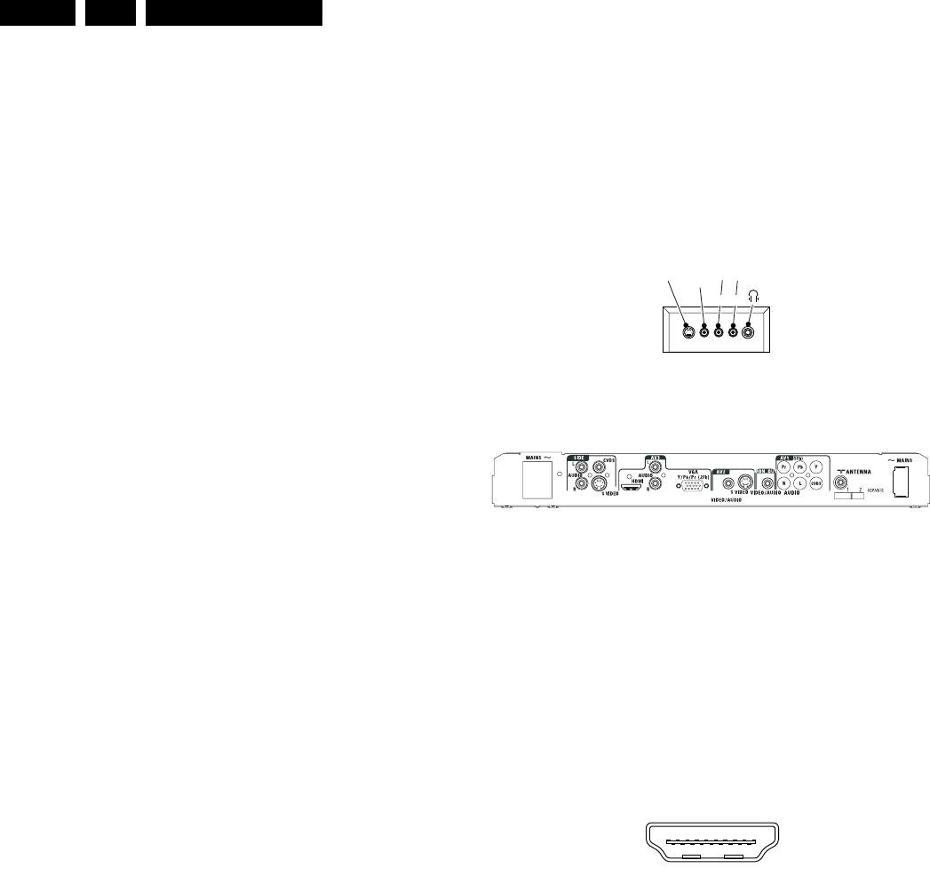
- 1.2.1 Rear I/O Connections
- Figure 1-1 Rear I/O connections (part 1)
- Figure 1-2 Rear connections (part 2)
- SIDE Cinch: CVBS - In, Audio - In
- SIDE SVHS: Y/C - In
- AV3 HDMI: Digital Video - In, Digital Audio - In
- AV3 Cinch: Audio - In
- AV3 VGA: Video 2fH RGB - In
- AV2 Mini Jack: Video 1fH CVBS - In, Audio - In
- AV2 SVHS: Video 1fH Y/C - In
- Monitor Out Mini Jack: Video CVBS - Out, Audio - Out
- AV1 Cinch: Video 1fH CVBS/YPbPr - In, Audio - In
- Aerial - In
- Service connector 1 (UART)
- Service connector 2 (ComPair)
- 1.2.1 Rear I/O Connections
- 1.3 Chassis Overview
- 2. Safety Instructions, Warnings, and Notes
- 3. Directions for Use
- 4. Mechanical Instructions
- 5. Service Modes, Error Codes, and Fault Finding
- 5.1 Test Points
- 5.2 Service Modes
- 5.3 Problems and Solving Tips Related to CSM
- 5.4 ComPair
- 5.5 Error Codes
- 5.6 The Blinking LED Procedure
- 5.7 Fault Finding and Repair Tips
- 6. Block Diagrams, Testpoint Overviews, and Waveforms
- 7. Circuit Diagrams and PWB Layouts
- SSB: Tuner and VIF
- SSB: Histogram and Hercules
- SSB: Histogram and Hercules
- SSB: Audio Delay line (Lipsync)
- SSB: Audio Amplifier
- SSB: TV Supply
- SSB: Scaler
- SSB: Scaler Supply
- SSB: Scaler Interface
- SSB: SDRAM
- SSB: Flash / Control
- SSB: HDMI
- SSB: PCHD MUX
- SSB: Supply
- SSB: DC-DC Converter
- SSB: PCHD IO
- SSB: Cinch IO
- Layout Small Signal Panel (Top Side Overview)
- Layout Small Signal Panel (Top Side Part 1)
- Layout Small Signal Panel (Top Side Part 2)
- Layout Small Signal Panel (Top Side Part 3)
- Layout Small Signal Panel (Top Side Part 4)
- Layout Small Signal Panel (Bottom Side Overview)
- Layout Small Signal Panel (Bottom Side Part 1)
- Layout Small Signal Panel (Bottom Side Part 2)
- Layout Small Signal Panel (Bottom Side Part 3)
- Layout Small Signal Panel (Bottom Side Part 4)
- Power Supply Unit (30-32 Inch): Mains Filter and Standby
- Power Supply Unit (30-32 Inch): Supply
- Layout Power Supply Unit (30-32 Inch) (Top Side)
- Layout Power Supply Unit (30-32 Inch) (Overview Bottom Side)
- Layout Power Supply Unit (30-32 Inch) (Part 1 Bottom Side)
- Layout Power Supply Unit (30-32 Inch) (Part 2 Bottom Side)
- 3D Comb Filter
- Layout 3D Comb Filter (Top Side)
- Layout 3D Comb Filter (Bottom Side)
- Side I/O Panel
- Layout Side I/O Panel (Top Side)
- Layout Side I/O Panel (Bottom Side)
- Top Control Panel
- Layout Top Control Panel (Top Side)
- Layout Top Control Panel (Top Side)
- LED and Switch Panel
- Layout LED and Switch Panel (Top Side)
- Layout LED and Switch Panel (Bottom Side)
- LCD Standby Audio Panel: Connections
- LCD Standby Audio Panel: Standby
- LCD Standby Audio Panel: Audio
- Layout LCD Standby Audio Panel (Top Side)
- Layout LCD Standby Audio Panel (Overview Bottom Side)
- Layout LCD Standby Audio Panel (Part 1 Bottom Side)
- Layout LCD Standby Audio Panel (Part 2 Bottom Side)
- 8. Alignments
- 9. Circuit Descriptions, Abbreviation List, and IC Data Sheets
- 10. Spare Parts List
- 11. Revision List

Published by WO 0472 Service PaCE Printed in the Netherlands Subject to modification EN 3122 785 14733
©
Copyright 2004 Philips Consumer Electronics B.V. Eindhoven, The Netherlands.
All rights reserved. No part of this publication may be reproduced, stored in a
retrieval system or transmitted, in any form or by any means, electronic,
mechanical, photocopying, or otherwise without the prior permission of Philips.
Colour Television Chassis
LC4.6U
AA
E_14710_000.eps
240604
Contents Page Contents Page
1. Technical Specifications, Connections, and Chassis
Overview 2
2. Safety Instructions, Warnings, and Notes 4
3. Directions for Use 5
4. Mechanical Instructions 6
5. Service Modes, Error Codes, and Fault Finding 9
6. Block Diagrams, Testpoint Overviews, and
Waveforms
Wiring Diagram 15
Block Diagram Supply and Standby 16
Testpoint Overview Supply and Standby 17
Block Diagram Tuner, Hercules and Audio 18
Block Diagram Scaler and Supply 19
Testpoint Overview SSB (Top Side) 20
I2C IC Overview 21
Supply Voltage Overview 22
7. Circuit Diagrams and PWB Layouts Diagram PWB
SSB: Tuner and VIF (A1) 23 40-49
SSB: Histogram and Hercules (A2) 24 40-49
SSB: Histogram and Hercules (A3) 25 40-49
SSB: Audio Delay line (Lipsync) (A4) 26 40-49
SSB: Audio Amplifier (A5) 27 40-49
SSB: TV Supply (A6) 28 40-49
SSB: Scaler (A7) 29 40-49
SSB: Scaler Supply (A8) 30 40-49
SSB: Scaler Interface (A9) 31 40-49
SSB: SDRAM (A10) 32 40-49
SSB: Flash / Control (A11) 33 40-49
SSB: HDMI (A12) 34 40-49
SSB: PCHD MUX (A13) 35 40-49
SSB: Supply (A14) 36 40-49
SSB: DC-DC Converter (A15) 37 40-49
SSB: PCHD IO (A16) 38 40-49
SSB: Cinch IO (A17) 39 40-49
Power Supply Unit (30-32 Inch): Mains Filter and
Standby (AS1) 50 52-55
Power Supply Unit (30-32 Inch): Supply (AS2) 51 52-55
3D Comb Filter (CB) 56 57
Side I/O Panel (D) 58 59
Top Control Panel (E) 60 61
LED and Switch Panel (J) 62 63
LCD Standby Audio Panel: Connections (SA1) 64 67-69
LCD Standby Audio Panel: Standby (SA2) 65 67-69
LCD Standby Audio Panel: Audio (SA3) 66 67-69
8. Alignments 71
9. Circuit Descriptions, Abbreviation List, and IC Data
Sheets 75
Abbreviation List 80
IC Data Sheets 82
10. Spare Parts List 85
11. Revision List 93
Technical Specifications, Connections, and Chassis Overview
EN 2 LC4.6U AA1.
1. Technical Specifications, Connections, and Chassis Overview
Index of this chapter:
1.1 Technical Specifications
1.2 Connections
1.3 Chassis Overview
Note: Figures below can deviate slightly from the actual
situation, due to the different set executions.
1.1 Technical Specifications
1.1.1 Vision
Display type : LCD-IPS
Screen size : 30” (76 cm), 15:9
Resolution (HxV pixels) : 1280x768
Contrast ratio : 600:1 (AUO)
: 500:1 (LPL)
Light output (cd/m2) : 600 (AUO)
: 500 (LPL)
Viewing angle (HxV degrees) : 170x170
Tuning system : PLL
TV Color systems : NTSC M 3.58
Video playback : NTSC M 3.58
Supported computer formats : VGA (640x480)
: VGA (720x400)
: VGA (640x350)
: MAC (640x480)
: MAC (832x624)
: SVGA (800x600)
: XVGA (1024x768)
: WXGA (1280x768)
Supported video formats : PAL 576i 1fH CVI
: NTSC 480i 1fH CVI
: PAL 576p 2fH HD
: NTSC 480p 2fH HD
: ATSC 720p 2fH HDMI
: ATSC 1080i 2fH
HDMI
Channel selections : 120 presets
:VHF
: UHF
: S-band
: Hyper-band
Aerial input : 75 ohm, Coax
:F-type
1.1.2 Sound
Sound systems : BTSC
Maximum power (WRMS) : 2 x 15 (int.)
1.1.3 Miscellaneous
Power supply:
- AC Power voltage (VAC) : 108 - 132
- AC Power frequency (Hz) : 60
Ambient conditions:
- Temperature range (deg. C) : +5 to +40
- Maximum humidity : 90% R.H.
Power consumption
- Normal operation (W) : 185
- Standby (W) : < 2
Dimensions (WxHxD) in cm : 89.1x48.9x11.0
Weight (kg) : 18
1.2 Connections
Note: The following connector color abbreviations are used
(acc. to DIN/IEC 757): Bk= Black, Bu= Blue, Gn= Green, Gy=
Grey, Rd= Red, Wh= White, and Ye= Yellow.
1.2.1 Rear I/O Connections
Figure 1-1 Rear I/O connections (part 1)
Figure 1-2 Rear connections (part 2)
SIDE Cinch: CVBS - In, Audio - In
Rd - Audio R 0.5 VRMS / 10kohm jq
Wh - Audio L 0.5 VRMS / 10kohm jq
Ye - Video CVBS 1 VPP / 75 ohm jq
SIDE SVHS: Y/C - In
1 - Ground Y Gnd H
2 - Ground C Gnd H
3 - Video Y 1 VPP / 75 ohm j
4 - Video C 0.3 VPP / 75 ohm j
AV3 HDMI: Digital Video - In, Digital Audio - In
Figure 1-3 HDMI (type A) connector
1 - D2+ Data channel j
2 - Shield Gnd H
3 - D2- Data channel j
4 - D1+ Data channel j
5 - Shield Gnd H
6 - D1- Data channel j
7 - D0+ Data channel j
8 - Shield Gnd H
9 - D0- Data channel j
10 - CLK+ Data channel j
11 - Shield Gnd H
12 - CLK- Data channel j
13 - n.c.
14 - n.c.
15 - DDC_SCL DDC clock j
16 - DDC_SDA DDC data jk
17 - Ground Gnd H
18 - +5V j
19 - HPD Hot Plug Detect j
20 - Ground Gnd H
AV3 Cinch: Audio - In
Wh - Audio L 0.5 VRMS / 10 kohm jq
Rd - Audio R 0.5 VRMS / 10 kohm jq
LR
AudioS-Video Video
E_14710_005.eps
210404
1
610
11
5
15
19 1
18 2
E_14710_059.eps
260704
(PDP)
(PDP)
(LCD)
19 1
18 2
E_06532_017.eps
050404
Technical Specifications, Connections, and Chassis Overview EN 3LC4.6U AA 1.
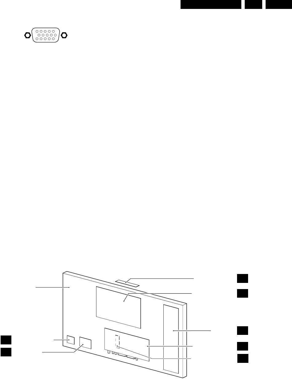
AV3 VGA: Video 2fH RGB - In
Figure 1-4 VGA Connector
1 - Video Red 0.7 VPP / 75 ohm j
2 - Video Green 0.7 VPP / 75 ohm j
3 - Video Blue 0.7 VPP / 75 ohm j
4-n.c.
5 - Ground Gnd H
6 - Ground Red Gnd H
7 - Ground
Green Gnd H
8 - Ground Blue Gnd H
9 - +5V_DC +5 VDC j
10 - Gnd Sync Gnd H
11 - n.c.
12 - DDC_SDA DDC data j
13 - H-sync 0 - 5 V j
14 - V-sync 0 - 5 V j
15 - DDC_SCL DDC clock j
AV2 Mini Jack: Video 1fH CVBS - In, Audio - In
1 - Audio R 0.5 VRMS / 10 kohm jq
2 - Gnd CVBS Gnd H
3 - Video CVBS 1 VPP / 75 ohm jq
4 - Audio L 0.5 VRMS / 10 kohm jq
AV2 SVHS: Video 1fH Y/C - In
1 - Ground Y Gnd H
2 - Ground C Gnd H
3 - Video Y 1 VPP / 75 ohm j
4 - Video C 0.3 VPP / 75 ohm j
Monitor Out Mini Jack: Video CVBS - Out, Audio - Out
1 - Audio R 0.5 VRMS / 10 kohm kq
2 - Gnd CVBS Gnd H
3 - Video CVBS 1 VPP / 75 ohm kq
4 - Audio L 0.5 VRMS / 10 kohm kq
AV1 Cinch: Video 1fH CVBS/YPbPr - In, Audio - In
Rd - Video Pr 0.7 VPP / 75 ohm jq
Rd - Audio R 0.5 VRMS / 10 kohm jq
Wh - Video Pb 0.7 VPP / 75 ohm jq
Wh - Audio L 0.5 VRMS / 10 kohm jq
Gn - Video Y 1 VPP / 75 ohm jq
Ye - Video CVBS 1 VPP / 75 ohm jq
Aerial - In
- - F-type Coax, 75 ohm D
Service connector 1 (UART)
1 - UART_TX Transmit data k
2 - Ground Gnd H
3 - UART_RX Receive data j
Service connector 2 (ComPair)
1 - SDA-S I2C Data (0 - 5 V) jk
2 - SCL-S I2C Clock (0 - 5 V) j
3 - Ground Gnd H
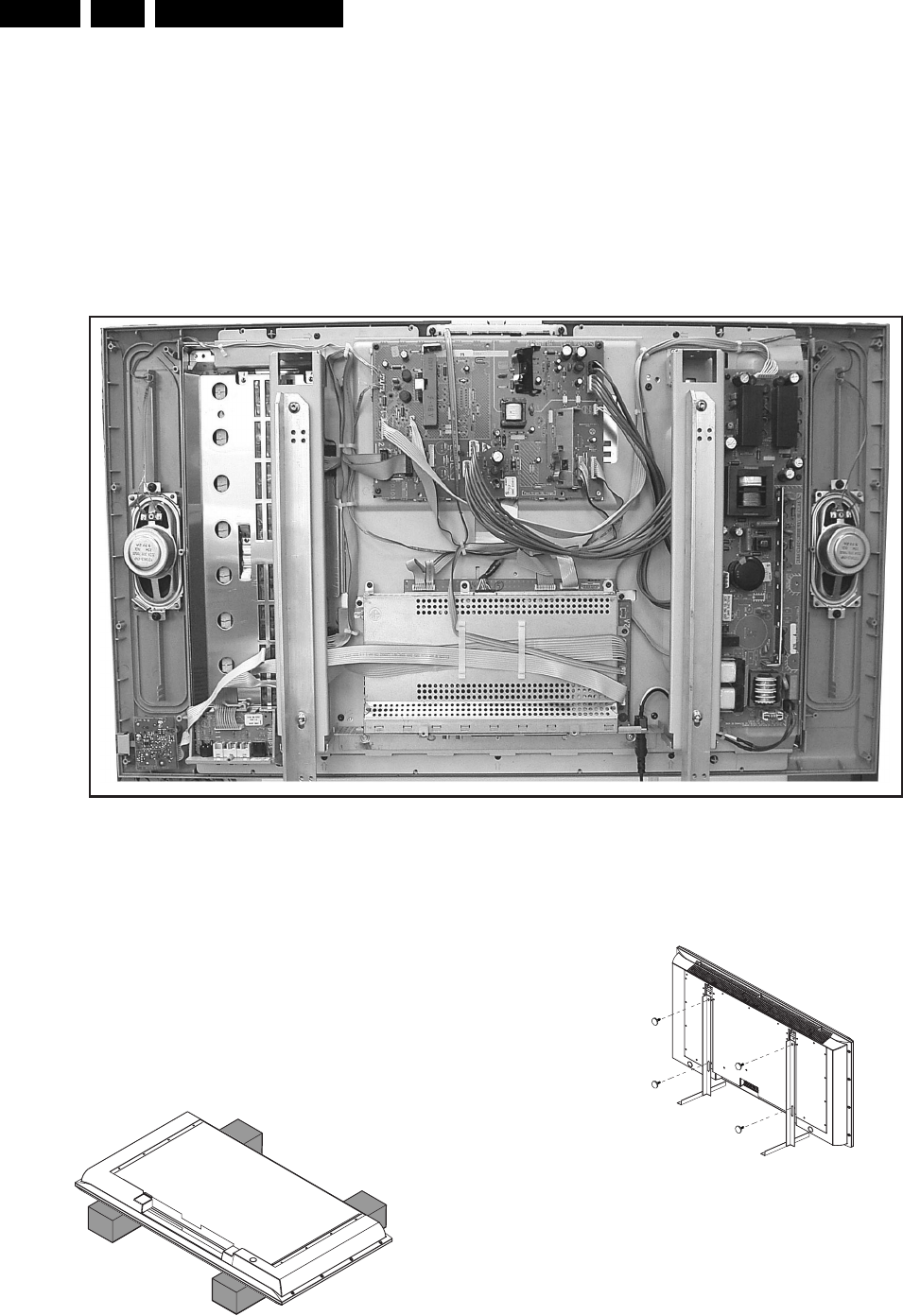
1.3 Chassis Overview
Figure 1-5 CBA locations
1
610
11
5
15
E_06532_002.eps
050404
E_14710_001.eps
271204
CB
3D COMB FILTER
(ONLY FOR NTSC SETS)
TOP CONTROL PANEL E
SMALL SIGNAL BOARD A
LCD STANDBY / AUDIO SA
LCD PANEL
LED + SWITCH PANEL
J
SIDE I/O PANEL
D
LCD SUPPLY AS

Safety Instructions, Warnings, and Notes
EN 4 LC4.6U AA2.
2. Safety Instructions, Warnings, and Notes
Index of this chapter:
2.1 Safety Instructions
2.2 Warnings
2.3 Notes
2.1 Safety Instructions
Safety regulations require that during a repair:
• Connect the set to the AC Power via an isolation
transformer (> 800 VA).
• Replace safety components, indicated by the symbol h,
only by components identical to the original ones. Any
other component substitution (other than original type) may
increase risk of fire or electrical shock hazard.
Safety regulations require that after a repair, the set must be
returned in its original condition. Pay in particular attention to
the following points:
• Route the wire trees correctly and fix them with the
mounted cable clamps.
• Check the insulation of the AC Power lead for external
damage.
• Check the strain relief of the AC Power cord for proper
function.
• Check the electrical DC resistance between the AC Power
plug and the secondary side (only for sets which have a AC
Power isolated power supply):
1. Unplug the AC Power cord and connect a wire
between the two pins of the AC Power plug.
2. Set the AC Power switch to the "on" position (keep the
AC Power cord unplugged!).
3. Measure the resistance value between the pins of the
AC Power plug and the metal shielding of the tuner or
the aerial connection on the set. The reading should be
between 4.5 Mohm and 12 Mohm.
4. Switch "off" the set, and remove the wire between the
two pins of the AC Power plug.
• Check the cabinet for defects, to avoid touching of any
inner parts by the customer.
2.2 Warnings
• All ICs and many other semiconductors are susceptible to
electrostatic discharges (ESD w). Careless handling
during repair can reduce life drastically. Make sure that,
during repair, you are connected with the same potential as
the mass of the set by a wristband with resistance. Keep
components and tools also at this same potential. Available
ESD protection equipment:
– Complete kit ESD3 (small tablemat, wristband,
connection box, extension cable and earth cable) 4822
310 10671.
– Wristband tester 4822 344 13999.
• Be careful during measurements in the high voltage
section.
• Never replace modules or other components while the unit
is switched "on".
• When you align the set, use plastic rather than metal tools.
This will prevent any short circuits and the danger of a
circuit becoming unstable.
2.3 Notes
2.3.1 General
• Measure the voltages and waveforms with regard to the
chassis (= tuner) ground (H), or hot ground (I), depending
on the tested area of circuitry. The voltages and waveforms
shown in the diagrams are indicative. Measure them in the
Service Default Mode (see chapter 5) with a colour bar
signal and stereo sound (L: 3 kHz, R: 1 kHz unless stated
otherwise) and picture carrier at 475.25 MHz for PAL, or
61.25 MHz for NTSC (channel 3).
• Where necessary, measure the waveforms and voltages
with (D) and without (E) aerial signal. Measure the
voltages in the power supply section both in normal
operation (G) and in stand-by (F). These values are
indicated by means of the appropriate symbols.
• The semiconductors indicated in the circuit diagram and in
the parts lists, are interchangeable per position with the
semiconductors in the unit, irrespective of the type
indication on these semiconductors.
• Manufactured under license from Dolby Laboratories.
“Dolby” and the “double-D symbol”, are trademarks of
Dolby Laboratories.
2.3.2 Schematic Notes
• All resistor values are in ohms and the value multiplier is
often used to indicate the decimal point location (e.g. 2K2
indicates 2.2 kohm).
• Resistor values with no multiplier may be indicated with
either an "E" or an "R" (e.g. 220E or 220R indicates 220
ohm).
• All capacitor values are given in micro-farads (µ= x10-6),
nano-farads (n= x10-9), or pico-farads (p= x10-12).
• Capacitor values may also use the value multiplier as the
decimal point indication (e.g. 2p2 indicates 2.2 pF).
• An "asterisk" (*) indicates component usage varies. Refer
to the diversity tables for the correct values.
• The correct component values are listed in the Spare Parts
list. Therefore, always check this list when there is any
doubt.
2.3.3 Rework on BGA (Ball Grid Array) ICs
General
Although (LF)BGA assembly yields are very high, there may
still be a requirement for component rework. By rework, we
mean the process of removing the component from the PWB
and replacing it with a new component. If an (LF)BGA is
removed from a PWB, the solder balls of the component are
deformed drastically so the removed (LF)BGA has to be
discarded.
Device Removal
As is the case with any component that, it is essential when
removing an (LF)BGA, the board, tracks, solder lands, or
surrounding components are not damaged. To remove an
(LF)BGA, the board must be uniformly heated to a temperature
close to the reflow soldering temperature. A uniform
temperature reduces the chance of warping the PWB.
To do this, we recommend that the board is heated until it is
certain that all the joints are molten. Then carefully pull the
component off the board with a vacuum nozzle. For the
appropriate temperature profiles, see the IC data sheet.
Area Preparation
When the component has been removed, the vacant IC area
must be cleaned before replacing the (LF)BGA.
Removing an IC often leaves varying amounts of solder on the
mounting lands. This excessive solder can be removed with
either a solder sucker or solder wick. The remaining flux can be
removed with a brush and cleaning agent.
After the board is properly cleaned and inspected, apply flux on
the solder lands and on the connection balls of the (LF)BGA.
Note: Do not apply solder paste, as this has shown to result in
problems during re-soldering.

Directions for Use EN 5LC4.6U AA 3.
Device Replacement
The last step in the repair process is to solder the new
component on the board. Ideally, the (LF)BGA should be
aligned under a microscope or magnifying glass. If this is not
possible, try to align the (LF)BGA with any board markers.
So as not to damage neighbouring components, it may be
necessary to reduce some temperatures and times.
More Information
For more information on how to handle BGA devices, visit this
URL: www.atyourservice.ce.philips.com (needs subscription,
not available for all regions). After login, select “Magazine”,
then go to “Workshop Information”. Here you will find
Information on how to deal with BGA-ICs.
2.3.4 Lead Free Solder
Philips CE is going to produce lead-free sets (PBF) from
1.1.2005 onwards.
Figure 2-1 Lead-free logo
This sign normally has a diameter of 6 mm, but if there is less
space on a board also 3 mm is possible.
Regardless of this logo (is not always present), one must treat
all sets from this date onwards according to the following rules.
Due to lead-free technology some rules have to be respected
by the workshop during a repair:
• Use only lead-free soldering tin Philips SAC305 with order
code 0622 149 00106. If lead-free solder paste is required,
please contact the manufacturer of your soldering
equipment. In general, use of solder paste within
workshops should be avoided because paste is not easy to
store and to handle.
• Use only adequate solder tools applicable for lead-free
soldering tin. The solder tool must be able
– To reach at least a solder-tip temperature of 400°C.
– To stabilise the adjusted temperature at the solder-tip.
– To exchange solder-tips for different applications.
• Adjust your solder tool so that a temperature around 360°C
- 380°C is reached and stabilised at the solder joint.
Heating time of the solder-joint should not exceed ~ 4 sec.
Avoid temperatures above 400°C, otherwise wear-out of
tips will rise drastically and flux-fluid will be destroyed. To
avoid wear-out of tips, switch “off” unused equipment or
reduce heat.
• Mix of lead-free soldering tin/parts with leaded soldering
tin/parts is possible but PHILIPS recommends strongly to
avoid mixed regimes. If not to avoid, clean carefully the
solder-joint from old tin and re-solder with new tin.
• Use only original spare-parts listed in the Service-Manuals.
Not listed standard material (commodities) has to be
purchased at external companies.
• Special information for lead-free BGA ICs: these ICs will be
delivered in so-called "dry-packaging" to protect the IC
against moisture. This packaging may only be opened
short before it is used (soldered). Otherwise the body of the
IC gets "wet" inside and during the heating time the
structure of the IC will be destroyed due to high (steam-
)pressure inside the body. If the packaging was opened
before usage, the IC has to be heated up for some hours
(around 90°C) for drying (think of ESD-protection!).
Do not re-use BGAs at all!
• For sets produced before 1.1.2005, containing leaded
soldering tin and components, all needed spare parts will
be available till the end of the service period. For the repair
of such sets nothing changes.
In case of doubt whether the board is lead-free or not (or with
mixed technologies), you can use the following method:
• Always use the highest temperature to solder, when using
SAC305 (see also instructions below).
• De-solder thoroughly (clean solder joints to avoid mix of
two alloys).
Caution: For BGA-ICs, you must use the correct temperature-
profile, which is coupled to the 12NC. For an overview of these
profiles, visit the website www.atyourservice.ce.philips.com
(needs subscription, but is not available for all regions)
You will find this and more technical information within the
"Magazine", chapter "Workshop information".
For additional questions please contact your local repair help
desk.
2.3.5 Practical Service Precautions
•It makes sense to avoid exposure to electrical shock.
While some sources are expected to have a possible
dangerous impact, others of quite high potential are of
limited current and are sometimes held in less regard.
•Always respect voltages. While some may not be
dangerous in themselves, they can cause unexpected
reactions - reactions that are best avoided. Before reaching
into a powered TV set, it is best to test the high voltage
insulation. It is easy to do, and is a good service precaution.
3. Directions for Use
You can download this information from the following websites:
http://www.philips.com/support
http://www.p4c.philips.com
P
b
Mechanical Instructions
EN 6 LC4.6U AA4.
4. Mechanical Instructions
Index of this chapter:
4.1 Cable Dressing
4.2 Service Positions
4.3 Assy/Panel Removal
4.4 Set Re-assembly
Notes:
• Figures below can deviate slightly from the actual situation,
due to the different set executions.
• Follow the disassemble instructions in described order.
4.1 Cable Dressing
Figure 4-1 Cable dressing
4.2 Service Positions
For easy servicing of this set, there are a few possibilities
created:
• The buffers from the packaging (see figure "Rear cover").
• Foam bars (created for service).
• Aluminium service stands (created for Service).
4.2.1 Foam Bars
Figure 4-2 Foam bars
The foam bars (order code 3122 785 90580 for two pieces) can
be used for all types and sizes of Flat TVs. By laying the TV
face down on the (ESD protective) foam bars, a stable situation
is created to perform measurements and alignments.
By placing a mirror under the TV, you can monitor the screen.
4.2.2 Aluminium Stands
Figure 4-3 Aluminium stands (drawing of MkI)
The aluminium stands (order code 3122 785 90480) can be
mounted with the back cover removed or still left on. So, the
stand can be used to store products or to do measurements. It
is also very suitable to perform duration tests without taking
much space, without having the risk of overheating, or the risk
of products falling. The stands can be mounted and removed
quick and easy with use of the delivered screws that can be
tightened and loosened manually without the use of tools. See
figure above.
Note: Only use the delivered screws to mount the monitor to
the stands.
E_14710_011.eps
020804
E_06532_018.eps
170504
E_06532_019.eps
170504
Mechanical Instructions EN 7LC4.6U AA 4.
4.3 Assy/Panel Removal
4.3.1 Rear Cover
Warning: Disconnect the mains power cord before you remove
the rear cover.
1. Remove the screws, which secure the rear cover. The
screws are located at the top, bottom, left and right sides;
next to the Side/IO and Rear connections. There are also
three deeper located screws next to the stands.
2. Lift the rear cover from the cabinet. Make sure that wires
and flat foils are not damaged during cover removal.
4.3.2 Side I/O Panel
1. Disconnect the cable from the panel.
2. To replace the complete bracket, remove the two fixation
screws on either side of the panel.
3. Release the two fixation clamps and lift the panel out of the
bracket.
4.3.3 LED/Switch Panel
1. Remove the two fixation screws.
2. Disconnect the cable from the rear of the panel.
4.3.4 Top Control Panel
1. Remove the two fixation screws.
2. Release the two fixation clamps and lift the panel out of the
bracket.
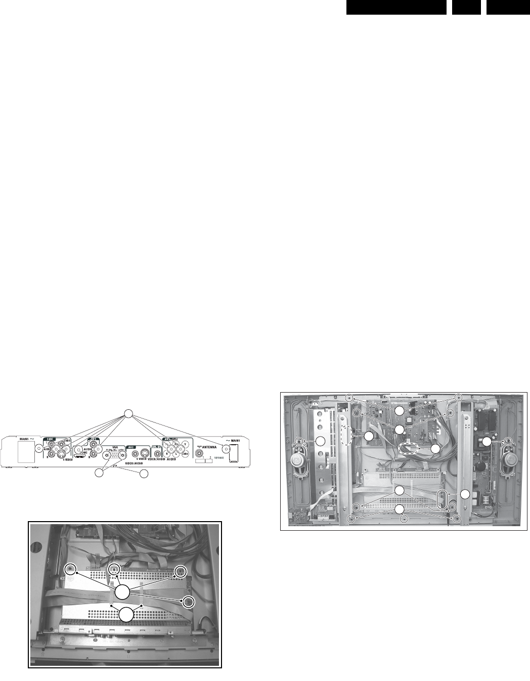
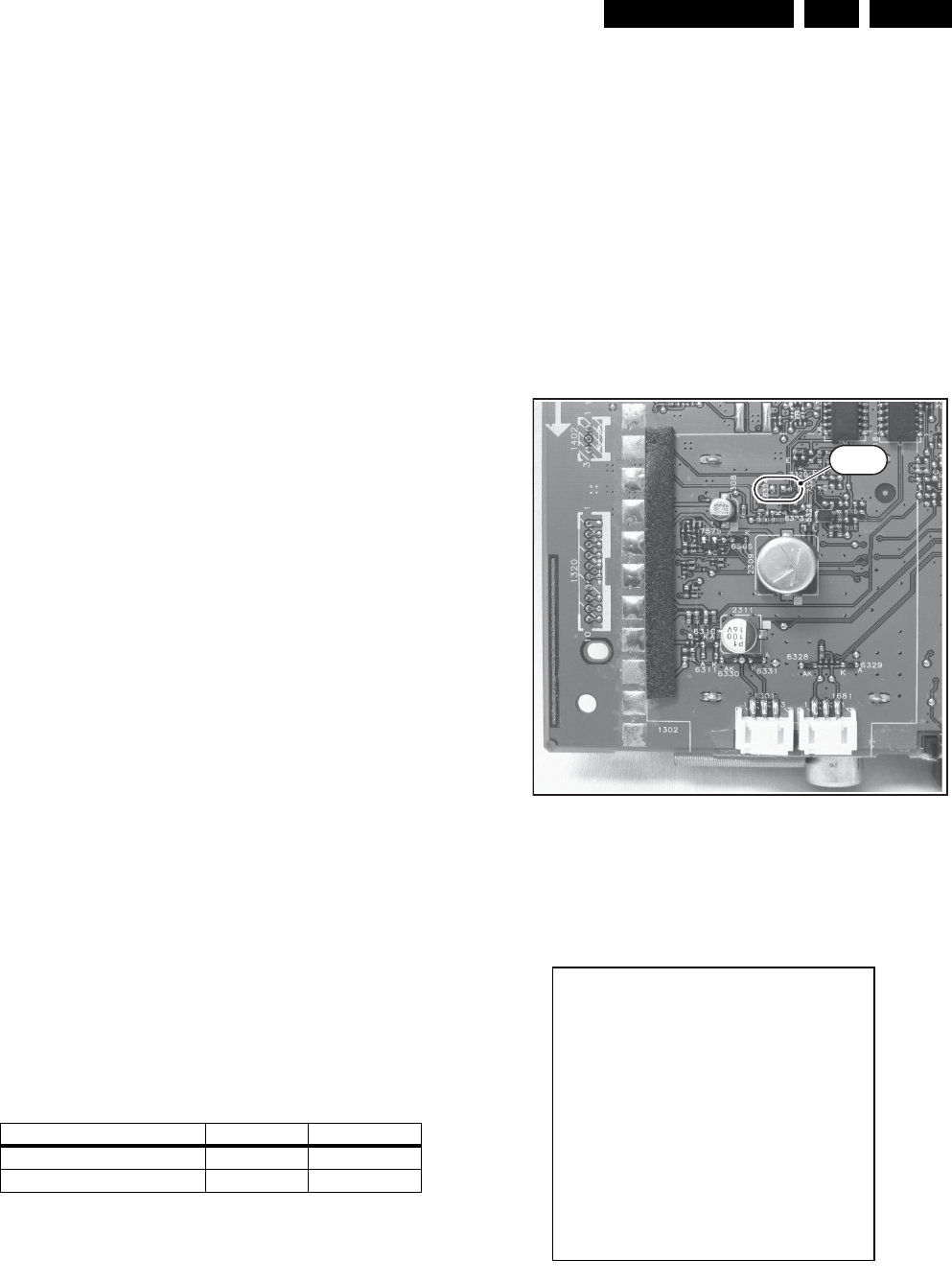
4.3.5 Small Signal Panel (SSB) and 3D Comb Filter
Figure 4-4 SSB Connector plate
Figure 4-5 Shielding of the SSB
1. Remove the middle fixation screw (1) from the bottom side
of the connector plate (as this holds the SSB bracket).
Note: Sometimes it is easier to loosen the complete
connector plate and remove it together with the SSB.
2. Remove all connector fixation screws (2) from the front
side of the connector plate.
3. Remove the two female screw locks (3) of the VGA
connector.
4. Release the plastic cable clips (4) on the shielding and
disconnect all cables from the SSB.
Note: Be careful with the fragile LVDS connector on the
SSB.
5. Now, completely remove the SSB (together with all the
shieldings) from the set.
6. Once the SSB is out, remove the fixation screws (5) from
the shielding.
7. Remove the shielding, it hinges at the left side (acc. photo).
8. Remove the fixation screws that hold the panel, and take
out the panel. On the rear side of the SSB, the 3D Comb
Filter is mounted with plastic clips.
Notes:
• Pay special attention to the EMC foam on the SSB
shielding. These must be replaced in their initial positions
during set re-assembly.
• Insulate the tuner pins, so they cannot touch the shielding
(see also figure “SDM Service jumper” in Chapter 5).
4.3.6 LCD Supply Panel
1. Disconnect all cables from the panel.
2. Remove the fixation screws and take out the panel.
4.3.7 LCD Standby/Audio Panel
1. Disconnect all cables from the panel.
2. Remove the fixation screws and take out the panel.
4.3.8 LCD Panel
Figure 4-6 LCD panel disassembly
1. Remove the T10 screws (1) from the mounting frame.
2. Remove all mounting LCD panel T20 screws (2).
3. Important: Unplug the LVDS connector (3) at the LCD
panel. Be careful, as this is a very fragile connector!
4. Unplug the following connectors (4).
– LCD back light (disconnect at the LCD side)
– Loudspeaker (easiest to disconnect at the speaker and
to release the cable holders a little.
– Top Control cable (disconnect at SSB side).
– Cable between LED/Switch panel and SSB.
5. Lift the metal frame (together with all CBAs) from the LCD
panel.
6. After removal of the frame, you can lift the LCD display
from the set.
1
610
11
5
15
19 1
18 2
E_14710_060.eps
030804
(PDP)
(PDP)
(LCD)
2
31
E_14710_003.eps
210404
5
4
E_14710_061.eps
030804
24
4
3
4
2
4
1
1

Mechanical Instructions
EN 8 LC4.6U AA4.
4.4 Set Re-assembly
To re-assemble the whole set, execute all processes in reverse
order.
Notes:
• While re-assembling, make sure that all cables are placed
and connected in their original position. See figure "Wire
dressing".
• Pay special attention not to damage the EMC foams at the
SSB shielding. Check that EMC foams are put correctly in
place.
Service Modes, Error Codes, and Fault Finding EN 9LC4.6U AA 5.
5. Service Modes, Error Codes, and Fault Finding
Index of this chapter:
5.1 Test Points
5.2 Service Modes
5.3 Problems and Solving Tips Related to CSM
5.4 ComPair
5.5 Error Codes
5.6 The Blinking LED Procedure
5.7 Fault Finding and Repair Tips
5.1 Test Points
This chassis is equipped with test points in the service printing.
In the schematics test points are identified with a rectangle box
around Fxxx or Ixxx. These test points are specifically
mentioned in the service manual as “half moons” with a dot in
the centre.
Perform measurements under the following conditions:
• Television set in Service Default Alignment Mode.
• Video input: Color bar signal.
• Audio input: 3 kHz left channel, 1 kHz right channel.
5.2 Service Modes
Service Default mode (SDM) and Service Alignment Mode
(SAM) offers several features for the service technician, while
the Customer Service Mode (CSM) is used for communication
between the call centre and the customer.
This chassis also offers the option of using ComPair, a
hardware interface between a computer and the TV chassis. It
offers the abilities of structured troubleshooting, error code
reading, and software version read-out for all chassis.
Minimum requirements for ComPair: a Pentium processor, a
Windows OS, and a CD-ROM drive (see also paragraph
"ComPair").
5.2.1 Service Default Mode (SDM)
Purpose
• To create a predefined setting for measurements to be
made.
• To override software protections.
• To start the blinking LED procedure.
• To inspect the error buffer.
• To check the life timer.
Specifications
Table 5-1 SDM default settings
• All picture settings at 50% (brightness, color contrast, hue).
• Bass, treble and balance at 50%; volume at 25%.
• All service-unfriendly modes (if present) are disabled. The
service unfriendly modes are:
– Timer / Sleep timer.
– Child / parental lock.
– Blue mute.
– Hotel / hospital mode.
– Auto shut off (when no “IDENT” video signal is
received for 15 minutes).
– Skipping of non-favourite presets / channels.
– Auto-storage of personal presets.
– Auto user menu time-out.
– Auto Volume Levelling (AVL).
How to enter
To enter SDM, use one of the following methods:
• Press the following key sequence on the remote control
transmitter: “062596” directly followed by the MENU
button (do not allow the OSD display to time out between
entries while keying the sequence).
• Short SDM jumper (item 4022, see Figure "Service
jumper") on the TV board and apply AC Power. Remove
the short after start-up.
Caution: Entering SDM by shorting "Service" jumpers will
override the software protections. Do this only for a short
period. When doing this, the service-technician must
know exactly what he is doing, as it could damage the
television set.
Figure 5-1 SDM Service jumper
After entering SDM, the following screen is visible, with SDM in
the upper right corner of the screen to indicate that the
television is in Service Default Alignment Mode.
Figure 5-2 SDM menu (example from LC4.2E)
How to navigate
When you press the MENU button on the remote control, the
set will switch on the normal user menu in the SDM mode.
How to exit
Switch the set to STANDBY by pressing the POWER button on
the remote control transmitter.
Region Freq. (MHz) Default system
Europe, AP-PAL/Multi 475.25 PAL B/G
NAFTA, AP-NTSC, LATAM 61.25 (ch. 3) NTSC M
I2C UART
E_14710_062.eps
260804
SDM
00022 LC42EP1 2.03/S42GV1 2.02 SDM
ERR 0 0 0 0 0
OP 000 057 140 032 120 128 000
E_14710_006.eps
240604

Service Modes, Error Codes, and Fault Finding
EN 10 LC4.6U AA5.
If you turn the television set off by removing the mains (i.e.,
unplugging the television) or by using the POWER button on
the TV set, the television set will remain in SDM when mains is
re-applied, and the error buffer is not cleared.
5.2.2 Service Alignment Mode (SAM)
Purpose
• To change option settings.
• To display / clear the error code buffer.
• To perform alignments.
Specifications
• Operation hours counter (maximum five digits displayed).
• Software version, Error codes, and Option settings display.
• Error buffer clearing.
• Option settings.
• Software alignments (Tuner, White Tone, Geometry, and
Audio).
• NVM Editor.
• ComPair Mode switching.
How to enter
Press the following key sequence on the remote control
transmitter: “062596" directly followed by the OSD/STATUS/
INFO button (do not allow the OSD display to time out between
entries while keying the sequence).
After entering SAM, the following screen is visible, with SAM in
the upper right corner of the screen to indicate that the
television is in Service Alignment Mode.
Figure 5-3 SAM menu (example from LC4.2E)
Menu explanation
1. LLLLL. This represents the run timer. The run timer counts
normal operation hours (including “on/off” switching), but
does not count stand-by hours.
2. AAAABCD-X.YY/EEEEEE_F.GG. This is the software
identification of the Main/Scaler microprocessor:
–A= the chassis name.
–B= the region: E= Europe, A= Asia Pacific, U= NAFTA,
L= LATAM.
–C= the software diversity:
•Europe: T= 1 pg TXT, F= Full TXT, V= Voice ctrl.
•LATAM and NAFTA: N= Stereo non-dBx,
S= Stereo dBx.
•Asian Pacific: T= TXT, N= non-TXT, C= NTSC.
•ALL regions: M= mono, D= DVD, Q= Mk2.
–D= the language cluster number.
–X= the Main software version number (updated with a
major change that is incompatible with previous
versions).
–YY= the sub software version number (updated with a
minor change that is compatible with previous
versions).
–EEEEEE= the Scaler SW cluster
–F= the Scaler SW version no.
–GG= the sub-version no.
3. SAM. Indication of the Service Alignment Mode.
4. Error Buffer (ERR). Shows all errors detected since the
last time the buffer was erased. Five errors possible.
5. Option Bytes (OP). Shows all option settings. See
“Options” in the Alignments section for a detailed
description. Seven codes are available.
6. Clear. Erases the contents of the error buffer. Select the
CLEAR menu item and press the CURSOR RIGHT key.
The content of the error buffer is cleared.
7. Options. Used to set the option bits. See “Options” in the
Alignments section for a detailed description.
8. Tuner. Used to align the tuner. See “Tuner” in the
Alignments section for a detailed description.
9. White Tone. Used to align the white tone. See “White
Tone” in the Alignments section for a detailed description.
10. Audio. No audio alignment is necessary for this television
set.
11. NVM Editor. Can be used to change the NVM data in the
television set.
12. SC NVM Editor. Can be used to edit Scaler NVM.
13. Test Pattern. For future use.
14. ComPair. Can be used to switch the television to “In
System Programming” (ISP) mode, for software uploading
via ComPair.
Caution: When this mode is selected without ComPair
connected, the TV will be blocked. Remove the AC power
to reset the TV.
How to navigate
• In SAM, select menu items with the CURSOR UP/DOWN
keys on the remote control transmitter. The selected item
will be highlighted. When not all menu items fit on the
screen, use the CURSOR UP/DOWN keys to display the
next / previous menu items.
• With the CURSOR LEFT/RIGHT keys, it is possible to:
– Activate the selected menu item.
– Change the value of the selected menu item.
– Activate the selected submenu.
• In SAM, when you press the MENU button twice, the set
will switch to the normal user menus (with the SAM mode
still active in the background). To return to the SAM menu
press the MENU button again.
• When you press the MENU key in while in a submenu, you
will return to the previous menu.
How to store SAM settings
To store the settings changed in SAM mode, leave the top level
SAM menu by using the POWER button on the remote control
transmitter or the television set.
How to exit
Switch the set to STANDBY by pressing the POWER button on
the remote control transmitter or on the television set.
5.2.3 Customer Service Mode (CSM)
Purpose
The Customer Service Mode shows error codes and
information on the TV’s operation settings. The call centre can
instruct the customer (by telephone) to enter CSM in order to
identify the status of the set. This helps the call centre to
diagnose problems and failures in the TV set before making a
service call.
The CSM is a read-only mode; therefore, modifications are not
possible in this mode.
E_14710_007.eps
240604
00022 LC42EP1 2.03/S42GV1 2.02 SAM
ERR 0 0 0 0 0
OP 000 057 140 032 120 128 000
. Clear Clear ?
. Options
. Tuner
. White Tone
. Audio
. NVM Editor
. SC NVM Editor
. Test Pattern
. ComPair Mode On

Service Modes, Error Codes, and Fault Finding EN 11LC4.6U AA 5.
How to enter
To enter CSM, press the following key sequence on the remote
control transmitter: “123654” (do not allow the OSD display to
time out between entries while keying the sequence).
Upon entering the Customer Service Mode, the following
screen will appear:
Figure 5-4 CSM menu (example from LC4.2E)
Menu explanation
1. Indication of the decimal value of the operation hours
counter, Main/Scaler software version (see "Service
Alignment Mode" for an explanation), and service mode
(CSM= Customer Service Mode).
2. Displays the last five errors detected in the error code
buffer.
3. Displays the option bytes.
4. Displays the type number version of the set (option).
5. Reserved.
6. Indicates the television is receiving an "IDENT" signal on
the selected source. If no "IDENT" signal is detected, the
display will read "NOT TUNED"
7. Displays the detected Color system (e.g. PAL/NTSC).
8. Displays the detected Audio (e.g. stereo/mono).
9. Displays the picture setting information.
10. Displays the sound setting information.
How to exit
To exit CSM, use one of the following methods:
• Press the MENU, STATUS (or EXIT/INFO/[i+]), or POWER
button on the remote control transmitter.
• Press the POWER button on the television set.
5.3 Problems and Solving Tips Related to CSM
5.3.1 Picture Problems
Note: The problems described below are all related to the TV
settings. The procedures used to change the value (or status)
of the different settings are described.
Picture too dark or too bright
If:
• The picture improves when you press the AUTO PICTURE
button on the remote control transmitter, or
• The picture improves when you enter the Customer
Service Mode,
Then:
1. Press the AUTO PICTURE button on the remote control
transmitter repeatedly (if necessary) to choose
PERSONAL picture mode.
2. Press the MENU button on the remote control transmitter.
This brings up the normal user menu.
3. In the normal user menu, use the CURSOR UP/DOWN
keys to highlight the PICTURE sub menu.
4. Press the CURSOR LEFT/RIGHT keys to enter the
PICTURE sub menu.
5. Use the CURSOR UP/DOWN keys (if necessary) to select
BRIGHTNESS.
6. Press the CURSOR LEFT/RIGHT keys to increase or
decrease the BRIGHTNESS value.
7. Use the CURSOR UP/DOWN keys to select PICTURE.
8. Press the CURSOR LEFT/RIGHT keys to increase or
decrease the PICTURE value.
9. Press the MENU button on the remote control transmitter
twice to exit the user menu.
10. The new PERSONAL preference values are automatically
stored.
White line around picture elements and text
If:
The picture improves after you have pressed the AUTO
PICTURE button on the remote control transmitter,
Then:
1. Press the AUTO PICTURE button on the remote control
transmitter repeatedly (if necessary) to choose
PERSONAL picture mode.
2. Press the MENU button on the remote control transmitter.
This brings up the normal user menu.
3. In the normal user menu, use the CURSOR UP/DOWN
keys to highlight the PICTURE sub menu.
4. Press the CURSOR LEFT/RIGHT keys to enter the
PICTURE sub menu.
5. Use the CURSOR UP/DOWN keys to select
SHARPNESS.
6. Press the CURSOR LEFT key to decrease the
SHARPNESS value.
7. Press the MENU button on the remote control transmitter
twice to exit the user menu.
8. The new PERSONAL preference value is automatically
stored.
Snowy picture
Check CSM line 6. If this line reads “Not Tuned”, check the
following:
• Antenna not connected. Connect the antenna.
• No antenna signal or bad antenna signal. Connect a proper
antenna signal.
• The tuner is faulty (in this case line 2, the Error Buffer line,
will contain error number 10). Check the tuner and replace/
repair the tuner if necessary.
Black and white picture
If:
• The picture improves after you have pressed the AUTO
PICTURE button on the remote control transmitter,
Then:
1. Press the AUTO PICTURE button on the remote control
transmitter repeatedly (if necessary) to choose
PERSONAL picture mode.
2. Press the MENU button on the remote control transmitter.
This brings up the normal user menu.
3. In the normal user menu, use the CURSOR UP/DOWN
keys to highlight the PICTURE sub menu.
4. Press the CURSOR LEFT/RIGHT keys to enter the
PICTURE sub menu.
5. Use the CURSOR UP/DOWN keys to select COLOR.
6. Press the CURSOR RIGHT key to increase the COLOR
value.
1 00022 LC42EP1 2.03/S42GV1 2.02 CSM
2 CODES 0 0 0 0 0
3 OP 000 057 140 032 120 128 000
4
5
6 NOT TUNED
7 PAL
8 STEREO
9 CO 50 CL 50 BR 50
0 AVL Off
E_14710_008.eps
240604
Service Modes, Error Codes, and Fault Finding
EN 12 LC4.6U AA5.
7. Press the MENU button on the remote control transmitter
twice to exit the user menu.
8. The new PERSONAL preference value is automatically
stored.
Menu text not sharp enough
If:
• The picture improves after you have pressed the AUTO
PICTURE button on the remote control transmitter,
Then:
1. Press the AUTO PICTURE button on the remote control
transmitter repeatedly (if necessary) to choose
PERSONAL picture mode.
2. Press the MENU button on the remote control transmitter.
This brings up the normal user menu.
3. In the normal user menu, use the CURSOR UP/DOWN
keys to highlight the PICTURE sub menu.
4. Press the CURSOR LEFT/RIGHT keys to enter the
PICTURE sub menu.
5. Use the CURSOR UP/DOWN keys to select PICTURE.
6. Press the CURSOR LEFT key to decrease the PICTURE
value.
7. Press the MENU button on the remote control transmitter
twice to exit the user menu.
8. The new PERSONAL preference value is automatically
stored.
5.4 ComPair
5.4.1 Introduction
ComPair (Computer Aided Repair) is a service tool for Philips
Consumer Electronics products. ComPair is a further
development on the European DST (service remote control),
which allows faster and more accurate diagnostics. ComPair
has three big advantages:
• ComPair helps you to quickly get an understanding on how
to repair the chassis in a short time by guiding you
systematically through the repair procedures.
• ComPair allows very detailed diagnostics (on I2C level) and
is therefore capable of accurately indicating problem areas.
You do not have to know anything about I2C commands
yourself because ComPair takes care of this.
• ComPair speeds up the repair time since it can
automatically communicate with the chassis (when the
microprocessor is working) and all repair information is
directly available. When ComPair is installed together with
the Force/SearchMan electronic manual of the defective
chassis, schematics and PWBs are only a mouse click
away.
5.4.2 Specifications
ComPair consists of a Windows based fault finding program
and an interface box between PC and the (defective) product.
The ComPair interface box is connected to the PC via a serial
(or RS-232) cable.
For this chassis, the ComPair interface box and the TV
communicate via a bi-directional service cable via the service
connector(s).
The ComPair fault finding program is able to determine the
problem of the defective television. ComPair can gather
diagnostic information in two ways:
• Automatic (by communication with the television): ComPair
can automatically read out the contents of the entire error
buffer. Diagnosis is done on I2C/UART level. ComPair can
access the I2C/UART bus of the television. ComPair can
send and receive I2C/UART commands to the micro
controller of the television. In this way, it is possible for
ComPair to communicate (read and write) to devices on
the I2C/UART busses of the TV-set.
• Manually (by asking questions to you): Automatic
diagnosis is only possible if the micro controller of the
television is working correctly and only to a certain extend.
When this is not the case, ComPair will guide you through
the fault finding tree by asking you questions (e.g. Does the
screen give a picture? Click on the correct answer: YES /
NO) and showing you examples (e.g. Measure test-point I7
and click on the correct oscillogram you see on the
oscilloscope). You can answer by clicking on a link (e.g.
text or a waveform picture) that will bring you to the next
step in the fault finding process.
By a combination of automatic diagnostics and an interactive
question / answer procedure, ComPair will enable you to find
most problems in a fast and effective way.
Beside fault finding, ComPair provides some additional
features like:
• Up- or downloading of pre-sets.
• Managing of pre-set lists.
• Emulation of the (European) Dealer Service Tool (DST).
• If both ComPair and Force/SearchMan (Electronic Service
Manual) are installed, all the schematics and the PWBs of
the set are available by clicking on the appropriate
hyperlink.
Example: Measure the DC-voltage on capacitor C2568
(Schematic/Panel) at the Mono-carrier.
– Click on the “Panel” hyperlink to automatically show
the PWB with a highlighted capacitor C2568.
– Click on the “Schematic” hyperlink to automatically
show the position of the highlighted capacitor.
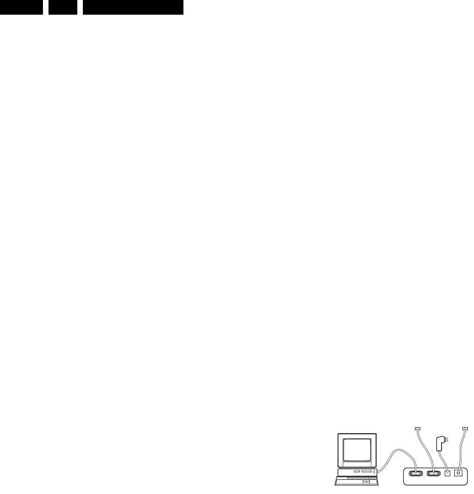
5.4.3 How To Connect
This is described in the chassis fault finding database in
ComPair .
Figure 5-5 ComPair interface connection
5.4.4 How To Order
ComPair order codes (US):
• ComPair Software: ST4191.
• ComPair Interface Box: 4822 727 21631.
• AC Adapter: T405-ND.
• ComPair Quick Start Guide: ST4190.
• ComPair interface extension cable: 3139 131 03791.
• ComPair UART interface cable: 3122 785 90630
Note: If you encounter any problems, contact your local
support desk.
5.5 Error Codes
The error code buffer contains all errors detected since the last
time the buffer was erased. The buffer is written from left to
right. When an error occurs that is not yet in the error code
buffer, it is displayed at the left side and all other errors shift one
position to the right.
E_06532_021.eps
180804
PC VCR I2CPower
9V DC
TO
UART SERVICE
CONNECTOR
TO
I2C SERVICE
CONNECTOR

Service Modes, Error Codes, and Fault Finding EN 13LC4.6U AA 5.
5.5.1 How To Read The Error Buffer
You can read the error buffer in 3 ways:
• On screen via the SAM (if you have a picture).
Examples:
– ERROR: 0 0 0 0 0: No errors detected
– ERROR: 6 0 0 0 0: Error code 6 is the last and only
detected error
– ERROR: 9 6 0 0 0: Error code 6 was detected first and
error code 9 is the last detected (newest) error
• Via the blinking LED procedure (when you have no
picture). See “The Blinking LED Procedure”.
•Via ComPair.
5.5.2 How To Clear The Error Buffer
The error code buffer is cleared in the following cases:
• By using the CLEAR command in the SAM menu:
– To enter SAM, press the following key sequence on the
remote control transmitter: “062596” directly followed
by the OSD/STATUS button (do not allow the OSD
display to time out between entries while keying the
sequence).
– Make sure the menu item CLEAR is highlighted. Use
the CURSOR UP/DOWN buttons, if necessary.
– Press the CURSOR RIGHT button to clear the error
buffer. The text on the right side of the “CLEAR” line will
change from “CLEAR?” to “CLEARED”
• If an error does not reoccur within 50 hours it is deleted
from the error buffer.
5.5.3 Error Codes
In case of non-intermittent faults, write down the errors present
in the error buffer and clear the error buffer before you begin
the repair. This ensures that old error codes are no longer
present.
If possible, check the entire contents of the error buffer. In
some situations, an error code is only the result of another error
and not the actual cause of the problem (for example, a fault in
the protection detection circuitry can also lead to a protection).
Table 5-2 Error code overview
5.6 The Blinking LED Procedure
Using this procedure, you can make the contents of the error
buffer visible via the front LED. This is especially useful when
there is no picture.
When the SDM is entered, the front LED will blink the contents
of the error-buffer:
• The LED blinks with as many pulses as the error code
number, followed by a time period of 1.5 seconds, in which
the LED is “off”.
• Then this sequence is repeated.
Any RC5 command terminates this sequence.
Example of error buffer: 12 9 6 0 0
After entering SDM, the following occurs:
• 1 long blink of 5 seconds to start the sequence,
• 12 short blinks followed by a pause of 1.5 seconds,
• 9 short blinks followed by a pause of 1.5 seconds,
• 6 short blinks followed by a pause of 1.5 seconds,
• 1 long blink of 1.5 seconds to finish the sequence,
• The sequence starts again at 12 short blinks.
5.7 Fault Finding and Repair Tips
Notes:
• It is assumed that the components are mounted correctly
with correct values and no bad solder joints.
• Before any fault finding actions, check if the correct options
are set.
Error Device Error description Check item Diagram
0 Not applicable - - -
1 Not applicable - - -
2 Not applicable - - -
3 Not applicable - - -
4 GM1501
Scaler
Flash-ROM
I2C error while
communicating with
the Genesis Scaler
and/or Flash-ROM
is faulty/empty
7401
7530
A7
A11
5 Not applicable +5V protection 7930 A6
6 I2C bus General I2C error 7011, 3088, 3096 A2
7 Not applicable - - -
8M24C32 I
2C error while
communicating with
the Scaler EEPROM
7531 A11
9M24C16 I
2C error while
communicating with
the EEPROM
7099 A2
10 Tuner I2C error while
communicating with
the PLL tuner
1302, 3302, 3303, 3327 A1
11 Not applicable - - -
12 Not applicable - - -
13 Not applicable - - -
14 K4D263238M Read-write error
with the Scaler
SDRAM
7501 A10
15 TDA9178T/N1 I2C error while
communicating with
Histogram
7560 A3
16 TDA9178T/N1 I2C error while
communicating with
EPLD on Pixel Plus
panel
7560 A3
Service Modes, Error Codes, and Fault Finding
EN 14 LC4.6U AA5.
5.7.1 NVM Editor
In some cases, it can be handy if one directly can change the
NVM contents. This can be done with the “NVM Editor” in SAM
mode. With this option, single bytes can be changed.
Table 5-3 NVM editor overview
5.7.2 Load default NVM values
In case a blank NVM is placed or when the NVM content is
corrupted, default values can be downloaded into the NVM.
After the default values are downloaded it will be possible to
start up and to start aligning the TV set. This is no longer
initiated automatically; to initiate the download the following
action has to be performed:
1. Switch “off” the TV set via the AC Power switch.
2. Short circuit the SDM jumpers (keep short-circuited).
3. Press P+ or Ch+ on the local keyboard (and keep it
pressed).
4. Switch on the TV set via the AC Power switch.
5. When the set has started, the P+/Ch+ button can be
released and the short circuit of the SDM jumpers can be
removed.
6. The red LED will be on continuously to indicate that the
download is initiated (normally when SDM is activated the
red LED will start with the Blinking LED sequence).
7. Wait +/- 30 s (time needed to download default values to
the NVM).
5.7.3 Tuner and IF
No Picture in RF mode
1. Check whether picture is present in AV. If not, go to Video
processing troubleshooting section.
2. If present, check that the Option settings are correct.
3. Check that all supply voltages are present.
4. Check if I2C lines are working correctly (3.3V).
5. Manually store a known channel and check if there is IF
output at Tuner pin 11.
6. Feed in 105 dBuV at Tuner pin 11 and check whether there
is RGB output from Video Processing IC. If yes, Tuner may
be defect. Replace Tuner.
Required system is not selected correctly
1. Check whether a Service jumper (#4022, 0805 size) is
present. If yes, remove it.
5.7.4 Video Processing
No power
1. Check +12 V and 3V3 at position 1910.
2. If no supply, check the connector 1910.
3. If it is correct, check the power supply board.
Power supply is correct but no green LED
1. Check if connectors 1005 and 1601 are properly inserted.
2. If yes, check if the 3V3 is present.
No picture display
1. Check the RGB signal.
2. If it is present, check 3-IC7016 (NE555).
3. If it has output, the problem is in SCALER part.
4. Otherwise, check H-out on pin 2 of NE555. If the input
signal of pin2 is present, but no output, the IC is defect.
Note:
• If the H-out (pin 67) doesn’t have signal or the level is low,
check the output of NE555 (pin 3) during start up.
• If the H-out (pin 67) has a signal (or has a signal for a very
short time), change IC7016 (NE555).
No TV but PC is present
1. Check if HSYNC and VSYNC are present at pin 3 of 7017
and 7015.
2. If they are present, check RGB output.
3. If there is no RGB output, the IC TDA120xx can be defect.
Comb Filter not working
Check Option Byte 5 in SAM (see also chapter 8 “Alignments”).
5.7.5 Power Supply
This power supply contains two fuses. One is near the AC
Power (mains) inlet connector 1308 and the other is near
connector 1307.
1. Check with power supply in “off” state by means of ohmic
measurement.
2. Fuse 1400 may open in case of severe lightning strikes
and/or failures in the power supply.
3. Fuses 1401 may open in case of a problem with the
Standby Supply. Replacement of the fuse is needed, but
not before the cause of the overload conditions is resolved.
Hex Dec Description
.ADR 0x000A 10 Existing value
.VAL 0x0000 0 New value
.Store Store ?
Block Diagrams, Testpoint Overviews, and Waveforms 15LC4.6U AA 6.
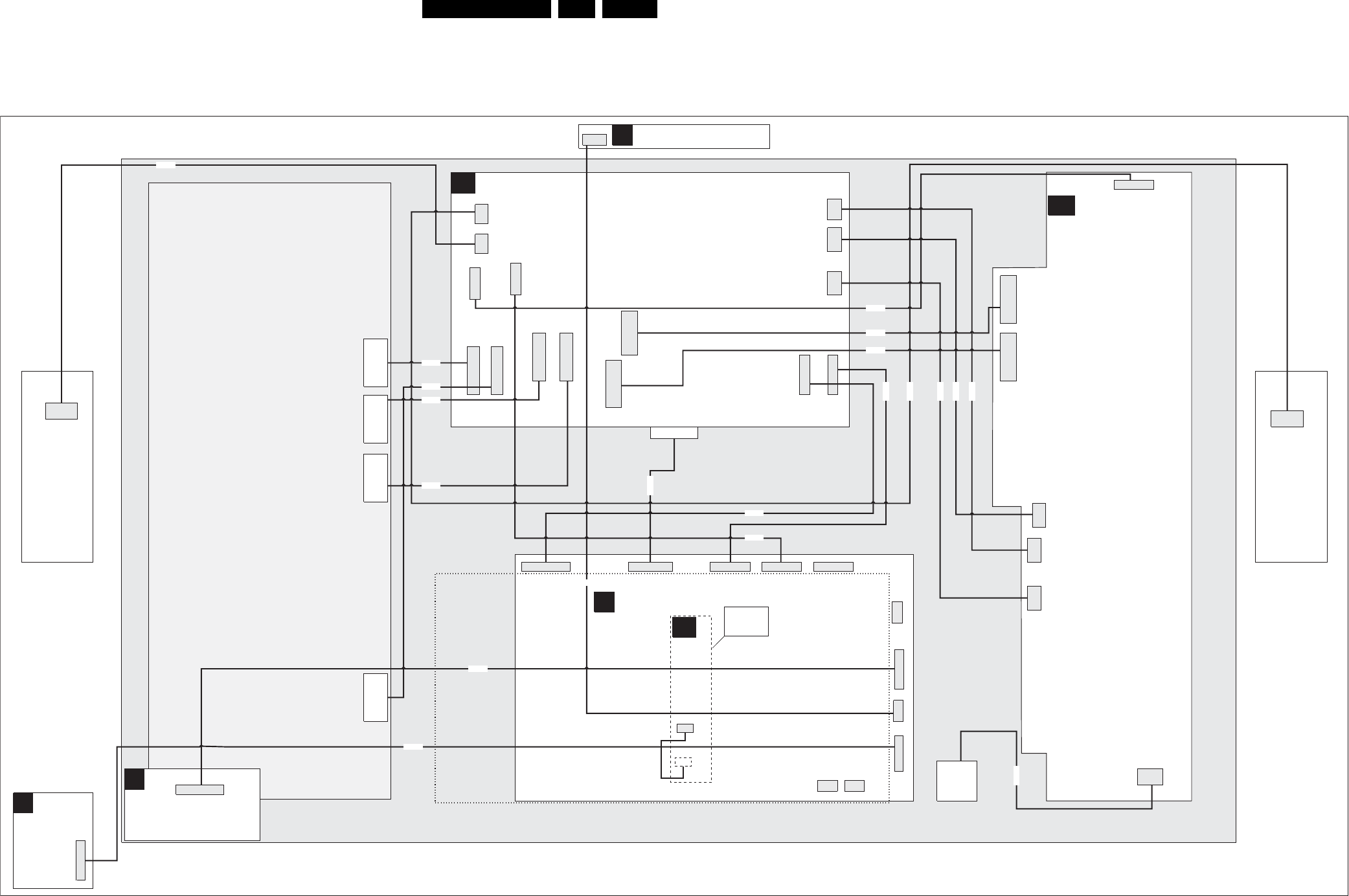
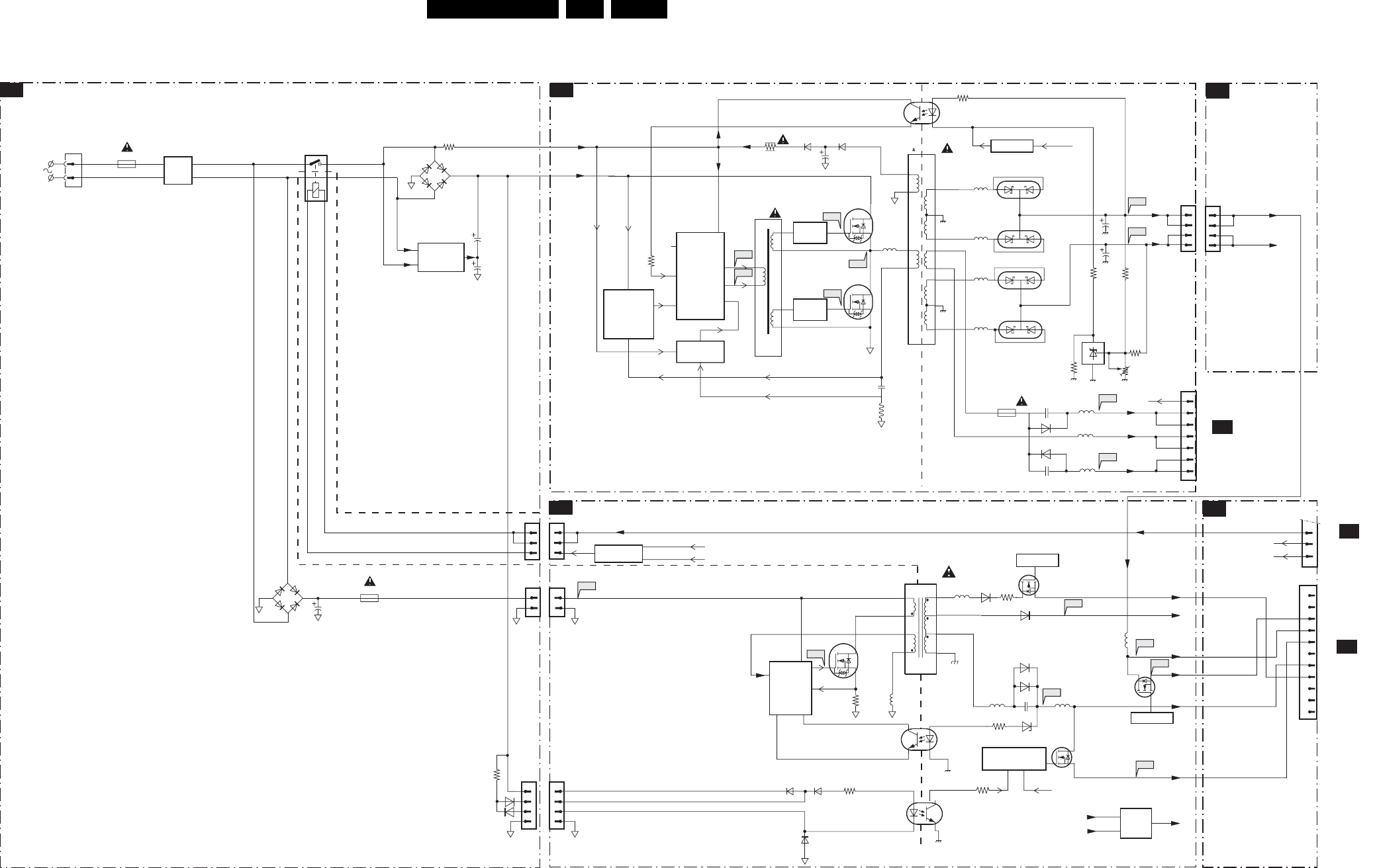
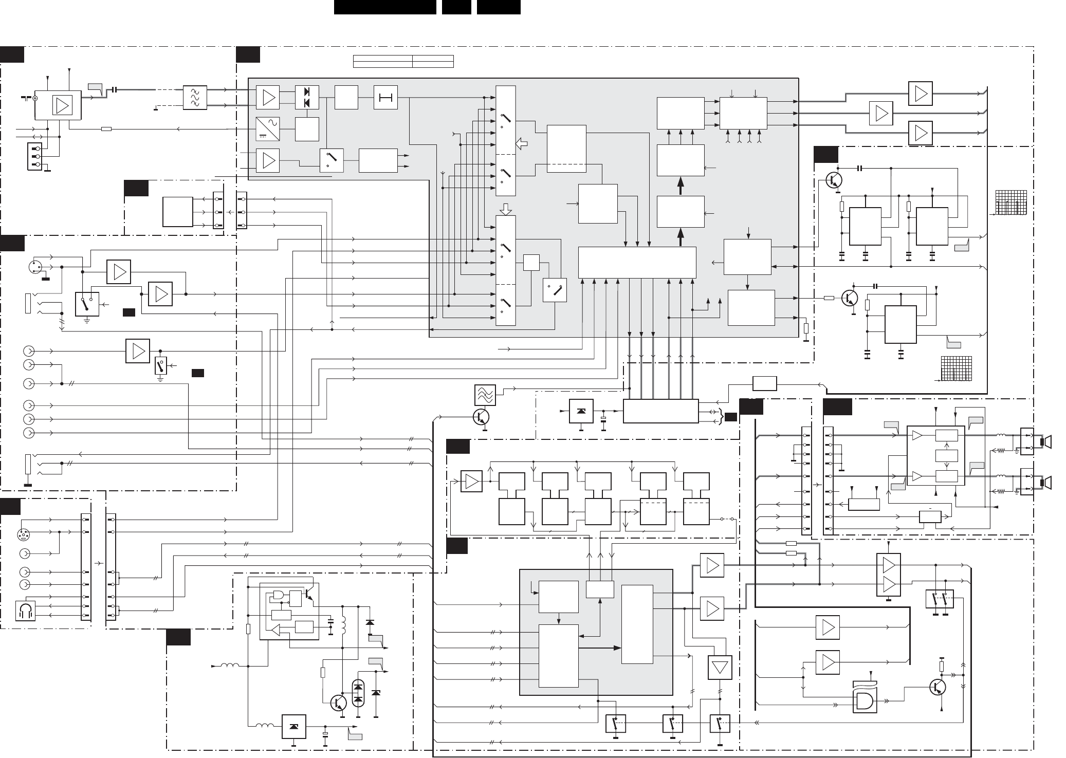
6. Block Diagrams, Testpoint Overviews, and Waveforms
Wiring Diagram
LVDS CONNECTOR
Left
Speaker
Right
Speaker
LPL
LPL
Lspeak
posilock
Lspeak
posilock
Mains
outlet
8345
AUO
AUO
SA STANDBY SUPPLY / AUDIO
ETOP CONTROL PANELZ
ALC04 SSB
CB
AS MF SUPPLY
DSIDE I/O
JLED/SWITCH
WIRING DIAGRAM
E_14710_082.eps
281204
1736
2P3
1735
2P3
1MO2
7P
1739
9P
1313
16P
1312
16P
1317
12P
1315
10P
1309
3P 1304
4P
1M46
11P
1M03
10P
1306
2P
1307
4P
1305
3P
1304
4P
1309
3P
1M02
7P
1307
4P
1306
2P
1305
3P
1308
2P
0320
10P
0936
11P
1M46 (1251)
11P
1G51 (1450)
31P
1MO3 (1403)
10P
1M52 (1752)
9P
1M02 (1702)
7P
1M36(1336)
11P
1M01(1402)
3P
1M20(1320)
10P
3P 3P
1408 1301
1735
4P
1004
10P
0345
3P
8336
8320
8308
8306
8307
8305
8736
8303
8302
8304
8309
8313
8312
8317
8315
8350
8346
8352
8735
1801
10P
CB
3D COMB
MOUNTED
ON REAR
SIDE SSB
16LC4.6U AA 6.
Block Diagrams, Testpoint Overviews, and Waveforms
Block Diagram Supply and Standby
7805
7806
VOLTAGE
DOUBLER
(for 110V only)
US DOUBLER
AP AUTO DOUBLER
WITH TRIAC
2816
2815
6807
GBJ6J
-
+
6506
DF06M
-
+
2
1
1305
7001
MC34067P 15
7017
7018
7007
7020
HIGH
SIDE
DRIVE
7004
7009
5001
BIAS SUPPLY
SOFT
START
+
CURRENT
PROTECTION
CONTROL
VCC
OSCC
ERROR
SOST
OB
OA
FI
2
4
11
7
1
14
12
10
7005
STU16NB501
7002
TCET1102
10
11
5
3
7
8
9
10
11
12
13
5002
7008,
7021, 7022
LOW
SIDE
DRIVE
7006
STU16NB501
14
13
5040
2003
3057
3022 3052
3000 60786079
3007
7010
TL431ACD
3026
VS Voltage
Adj.
3024
3030
+12V_A
+12V_+24V
HOT
COLD
1400
T3.15AH
1308
5401
5402
5403
23
MAINS
FILTER
2
1
14
CONTROL
3
7501
TCET1102
2
1
4
3
1450
OVER
VOLTAGE
PROTECTION
+5V2-RELAY-IO2
3
2
1
1306
1401
T1AE
3810
400V_HOT
25V_HOT
14
15
16
3
4
1304
2
1
5027
5025
5026
5028
2
1
1306
2
1
1307
3
4
2
1
1305
3
3108
7100
7101
7105
7150
TCET1102
2
14
6151
6150
7511
7131
VTUN
+11V
+8V6
+5V2
+5V_SW
5500
5110 6504 3509
6140
5103 2513 5506
7531
6505
6107
+12V
6
7
10
STANDBY
7507
7506
7512
STANDBY
OVERVOLTAGE
PROTECTION
8
3128 6122
1M46
10
11
5105
STANDBY
SA2
SUPPLY
AS2
MAINS FILTER + STANDBY
AS1
CONNECTIONS
SA1
8
9
6
7
4
5
2
3
1
HOT COLD
A15
TO 1251
CONNECTIONS
HOT
COLD
3
3155
5
2
1
7102
THYRISTOR
7505/7509/7560
1M03
9
3
4
2
1
1304
SUPPLY + STANDBY
A9
TO 1403
CONNECTIONS
2
1
1307
3
4
6044
STPS20L45CT
1
2
6021
STPS20H100CT
3
6025
STPS20H100CT
6045
STPS20L45CT
1
2
3
1
2
3
1
2
3
EUR, CHINA 1X MAINS FILTER + HORMONIC COIL
US, AP 2X MAINS FILTER + IR INRUSH CURRENT
1007
T5A
5239
5292
5291
1M02
2291
6291
6293
2293
7
6
5
4
3
2
1
SA3
TO 1M02
AUDIO
VSND_POS
VSND_NEG
GND_SND
DC_PROT
HOT COLD
6155
6154
CONNECTIONS
SA1
2503
2021
2038
MAINS IN
EUR: 198 - 264V~
CHINA: 160 - 270V~
US: 108 - 132V~
APmulti: 90 - 175V~
DC_PROT
SEE ALSO
BLOCK DIAGRAM
SUPPLY LINE
+12V
+24V
+5V2-RELAY-IO2
OVERVOLTAGE PROTECTION
7508
OR
9110
+5V2
+5V2-RELAY-IO2
POR
STANDBY: LOW = ON
HIGH = STBY
3158
3V MAX
1V MAX STBY
2011
DC_PROT
PRINTED
COMPONENT
400V_HOT
3101
6153
8
7
STANDBY
PROT_AUDIOSUPPLY
5507
+12V_A
PROT_AUDIOSUPPLY
STANDBY
E_14710_033.eps
231204
F194
F003
F016
F297
I198
I138
F136
F109
I104
F298
F025
F004
I130
I038
F005
I057
Block Diagrams, Testpoint Overviews, and Waveforms 17LC4.6U AA 6.
Testpoint Overview Supply and Standby
1
3
25
7700
I776
10
I711
18
I722
23
I778
F109
F124
F125
1M46
I130
I198
I138
7102
5500
6104
6140
G
D
S
5
6
1
10
2506
11
1
5
F136 4
F135 3
7501 7150
43
21
21
43
1306
1305
1
1
3
2
COLD HOT
3104 313 6010.4
SA
3104 313 6009.4
6025
J
176-5
A2
A1
7005
D
S
G
F025
F298
6021
J
A2
A1
1M02
J
A2
A1
F016
F003
6044
6045
J
A2
A1
F297
8
6
1
16
5002
18
116
14
F004
12
89 I038
7006
D
S
G
F005
I057
COLD
HOT
AS
E_14710_057.eps
271204
I778
20V / div AC
2us / div
I776
10V / div DC
2us / div
I711
F109 = 5V2
F124 = 263V
F125 = 5V1
F135 = 8V9
F136 = 12V5
I138 = 5V2
I198 = 13V9
200mV / div DC
2ms / div
I722
200mV / div DC
2ms / div
I130
5V / div DC
5µs / div
T
F003
7001
5V / div DC
5µs / div
F004
5V / div DC
5µs / div
F005 F016 = 12V6
F025 = 24V4
F297 = 19V2
F298 = -19V2
500mV / div AC
5µs / div
I038
50V / div DC
5µs / div
I057
5V / div DC
5µs / div
18LC4.6U AA 6.
Block Diagrams, Testpoint Overviews, and Waveforms
Block Diagram Tuner, Hercules and Audio
1302
UV1338
+5VSW
6,7 9
451
11
A 3 TUNER + VIF
TV
+VTUN
Sound
Tr a p s
VIF2
VIF1
RF_AGC
25
24
31
30
29
7011 - IF
A2
QSS Mixer/
AM Demod.
61
62,63
49,50
34,35
56,57
A5
A2
A2
A2
SIDE I/O
D
7376-B
7377-B
53,54
HP_LROUT
SVHS _AV2_Y_CVBS_IN
SVHS_C_IN
7371
7910
3910
A6
TV SUPPLY
SC1_COMP_R_V_IN
SC1_FBL_IN
SSIF(Tuner FM) 33
A1
SDA
SCL
SQ
R
OSC
REF
5
1
2
3
4
2931
+5VSW
VCC
6
7
7930
3931
6930
5931
8
7710
EXT_MUTE
7706
12
13
OUT_MUTE
3707
11
A2
POWER_DOWN
A6
A2 SOUND_ENABLE SOUND_ENABLE
POR_AUDIO
A9
+3V3STBY
AUD_SUP
14
QSS/FM
AGC
De
3D
COMB
FILTER
tect
CVBS1 Input
sw.
INA..D
cvbs/y
c
Output
sw.
CS1A..D
cvbs
+
55
58
51
59
48
52
64
A1
1328 7
8
3311
2
3
2321 4327
4331
Dig. 2H/4H
Combfilter
Y Delay Adj.
PA L / N T S C /
SECAM
Decoder &
Baseband
Delay
Yint
Chroma
Uint
Vint
RGB/YPRPB Insert
YUV Interface
78 79 8077 74 75 76
Pix Improvement
(Histogram)
7560
70 71 72
Peaking
SCAVEM
U/V Delay
YUV IN/OUT
Skin Tone
U/V Tint
Saturation
RGB Matrix
Blue & Black
Stretch
Gamma Corr.
YUV
SAT
SCAVEM
on Text
RGB Matrix
Blue & Black
Stretch
Gamma Corr.
G_OSD
R_OSD
B_OSD
Fast Blanking
CON BRI
85
86
87
H/V
Sync Sep
H-OSC
H-Shift
H-Drive
Vertical & East-
West Geometry
H/V 66
67
HOUT
FB/SC
VDRB
VDRA 23
22
YOU T
UOUT
VOUT
VIN
UIN
YIN
R/Pr-3
INSSW3
G/Y3
B/Pb-3
SC1_COMP_AV1_G_Y_CVBS_IN
SC1_COMP_B_U_IN
SC1_COMP_R_V_IN
SC1_COMP_AV1_G_Y_CVBS_IN
SC1_COMP_B_U_IN
EF
7013
EF
7014
EF
7012
RO
GO
BO
R_SDTV
G_SDTV
B_SDTV
SCL
SDA
68916 17 19
14
11
20
L
VIDEO
R
A 3
A17
SC2_C_IN
SC2_CVBS_MON_OUT
SC
AV5_C_IN
1_CVBS_IN
SC2_Y_IN
SV
CVBS_COMB
YOUT_COMB
COUT_COMB
HS_AV2_Y_CVBS_IN
SVHS_C_IN
SVHS_C_IN
cvbs/y
CVBS/Y-X
C-X
CVBS/Y- X
C-X
AD Conv
Std Stereo
Decoder
Audio Select
ADC/DAC
Audio
Control
Vo l/T reb/
Bass
Features
DACs
I2S Proc
QSS/FM
SC1_COMP_AV1_LR_IN
SC2_LR_IN
SC1
AV1_CVBS_IN SC1_CVBS_RF_OUT
STATUS_2
STATUS_1
SC1_CVBS_RF_OUT
SC1_CVBS_IN
_COMP_AV1_LR_IN
SC2_LR_IN
SC2_LR_MON_OUT
SC2_LR_MON_OUT
AM
SC1_COMP_AV1_LR_IN
Const_LR_OUT
SC1_LR_RF_OUT
SC2_LR_IN
SC2_LR_MON_OUT
7370
SVHS_LR_IN
AudioIN2LR
60
36,37
1:1
1:1
7372
7708
7376-A
7377-A
7714
7713
HP_LOUT
AUDOUTLSR
A
AUDIO_L
AUDIO_R
UDOUTL
I2SDI1
SL
2
67
1
77
3753
3752 40
7561
7563
+3V3STBY
HP_ROUT
6910
+VTUN
6911
5920
5930
+12VSW
+8VSW_TV
2921
7920
13
2
SC2_CVBS_RF_OUT 43
SVHS_LR_IN
HP_DET_IN
HP_LROUT
SVHS_LR_IN
HP_DET_IN
36
45
A5
A5
VCC
TR
DISC
CTRL
RES
OUT
THR
2028
7018
3021
2051
7016#
VCC
TR
DISC
CTRL
RES
OUT
THR
2021
3347
2042
7015#
VCC
TR
DISC
CTRL
RES
OUT
THR
2047
3346
2034
7017#
2020
H_CS_SDTV
7019
2022
7004
5010
2055
V_SDTV
SANDCASTLE
+5VSW
+5VSW
# = NE555 TIMER
8
2
4
3
5
7
6
8
2
4
3
7
6
8
2
4
3
6
7
5
5
3010
A3
HISTOGRAM
3058
SAND
CASTLE
SANDCASTLE
1
A2
HERCULES
AUDIO
AMPLIFIER
SA3
AUDIO
A13
A13
A13
A13
A13
A1
N.C.
N.C.
2
7011 - SOUND
SYSTEM 7011
NTSC TDA15021H
HERCULES
COMPAIR
1301
1
2
3
Y_NOTCH
A7
REAR IO SCART
2561
7562
13
2
+12VSW
F306
F915
F912
F913
I357
E_14710_084.eps
281204
2
5
SVHS
CVBS
L
2
6
R8
7
10
11
4
2
6
8
7
10
11
4
0936 1336
1
34 9
1739
SC
PROC.
A4
AUDIO DELAY LINE (LIPSYNC)
8x 8x
15
I2SCLK
7x
7x
RAM
COUNTER COUNTER
"D" F.F. "D" F.F.
75847583758275817580
7585
NC
8x
2
7x8x
8x
4590
PWM
-16V-19V
-16V-19V
I722
18
3
24 22
+16 +19V
24
10
6
I778
3
1
1735
1736
-16V-19V+16V+19V
23
I776
3
1
5702
5701
OSC
STBY-
MUTE
7700
TDA7490
PWM
PROT
+16V+19V +16V+19V
3717
3718
I711
7701 : 7707
SOUND_
ENABLE
POR-AUDIO
SOUND_ENABLE
PROTECT_AUDIO
N.C.
N.C.
AUDIO_R
AUDIO_L
POR_CLASSD
AUDIO_R
AUDIO_L
PROT1
SOUND
ENABLE
15W/
8R
15W/
8R
L
R
8
7
6
1
4
5
3
2
9
8
7
6
1
4
5
3
2
1752
33D COMB FILTER
CB
FRONT_DETECT
L
R
Y/CVBS
C
TDA9178T
I2SDO
I354
I357
I354
1V / div DC
5ms / div
1V / div DC
20us / div
N.C.
MON.
OUT
L
C
Y
VIDEO
R
AV2
1801
7240
7225
7241
3
8
9
2004
3
8
9
V
U
Y
R
L
VIDEO
AV1
SVHS
7226/7227
EF
7228
EF
Block Diagrams, Testpoint Overviews, and Waveforms 19LC4.6U AA 6.
Block Diagram Scaler and Supply
A
ADDRESS
DDR
FRAME
STORE
INTERFACE
EXT.
FLASH
ROM
INTER-
FA CE
DISPLAY
TIMING
GEN
DV I
INPUT
PORT
ANALOG
INPUT
PORT
A16
1
5
11
15
PC-IN
DDC
NVM
7693
65
8
DDC_5V
6073
6075
RED_PR
GRN_Y
BLU_PB
PC_HD_DET+
VS
+5VSWI
HS
UART_TX
UART_RX
RES
RES
3783 PC_HD_DET-
VS
HS
PC_HD_DET+
R_PR-
G_Y-
B_PB-
RED_PR
GRN_Y
BLU_PB
u-Processor
KEYBOARD
STATU S_2
STATU S_1
LIGHT-SENSOR-SDM
SEL_IF
SOUND_ENABLE
PC-TV-LED
SCL
SDA
IR
EXT_MUTE
TV_SC_COM
TV_IRQ
NV
2k x 8
M
NVM_WP
4022
SDM PINS
7099
HERCULES
IC
7011
6565
7579
7887
N.C.
3579 +3V3STBY
A2
A2
HERCULES
A1
A5
A5
A3
A7
A7
A7
FLASH
ROM
7606
9, 17, 19
14
12
1
15
11
2
PC_HD_SEL
A7
A11
A14
SDRAM
1Mx32x4
DATA
GRAPHIC
ZOOM
VIDEO
ZOOM
OSD CONTROLLER
OUT BLENDER
BRIGHTNESS/CONTRAST/HUE/SAT
INTERNAL
ROM &
RAM
UART
INTERFACE
MICRO-
CONTROLLER
80186
UART_TX
UART_R X A7
A7
UART_
TXB0-
T
TO LCD PANEL
X
UART_RX
A16
A16
SCL
SDA
TV_IRQ
TXB0+
LVDSA-
+12V_LCD
LVDSA+
A2
A2
A2
PC_HD_DETA13
PC_HDMI-AUDIO_SEL A12
SD_HD_SEL
P50_LINE_ITV_IR_SW
A7
56
7
104
108
109
107
111
114
102
99
98
12
106
105
I2SCLK
FOR AUDIO LIPSYNC
I2SD01
I2SDI1
103
0
115
97
116
119
123
SC-STANDBY
122
SQ
R
OSC
REF
5
1
2
3
4
2956
+5VSWI
VCC
6
7
7952
3951//52
6951
5953
8
3954
5952
2957
SUPPLY
A14
2953
+12VSW
7954
PA NEL-PWR-CTL
3955
5957
3958
7955
+3V3STBY
PA N _ V C C
2960
A7
PA N E L - P W R - C T L
2996
7995 +1V8
32
1
5997
5996
5998
+3V3STBY +1V8_DVI
+1V8_ADC
+1V8_CORE
2994
7992
13
2
5994
+2V5_DDR
+12VSW
VCC
RESET
GND
7532
2,3
4
5
+3V3STBY
+3 NVM
4k x 8
NVM-WP
A11
FLASH CONTROL
5
6
7
SDA_IO
SCL_IO
7531
7530
A10
SDRAM
7501
A7
A9
SCALER
A14
A13
A2
A4
A4
A4
A3
A3
A17
A17
A3
NC
A17
127
+3V3STBY
7070
+1V8_B
3,93,96
100,117,118,124
14
7001,7003
+3V3STBY
+1V8_A
DECDIG
P1.4
+5VSW
4,5,7,9,88,90,94
15,69,82
A3
A5
126
7075
P50
POWER_DOWN
POWER_DOWN_P50
128
POWER_DOWN
A6
A6
+5VSW
7401
GM1601
SXGA
DISPLAY
CONTROLLER
1
3
2
1304
UART FOR
SERVICE
A1
BU_LIGHT_ADJ1
OCM_TIMER1 A6
OCM_INT1
OCM_OD0
OCM_OD1
A13
HD_FILT ER
PWM1
LAMP_ON-OFF
PBIAS A6
PC_HD_SEL A13
GPIO_G09_B0
GPIO_G09_B1
TV_SC_COM GPI_G09_B3
GPIO_G09_B4
A2
Y_NOTCH GPIO_16
A2
GPIO_G07_B7 GPIO_G07_B5
VGA_SCL
VGA_SDA
GPIO_G07_B0
PPWR
RESET
MSTR_SCL
MSTR_SDA
GPIO_G09_B4
2488 1401
TCLK
XTAL
2487
+3V3_PLL
PCHD-IO
A12
HDMI
2007
1001
2006
10
11
E_14710_086.eps
281204
I996
F954
F960
I992
7605
H_CS_SDTV
V_SDTV
VS
HS
SD_HD_SEL
7604
123 4
11 10
13 12
569 8
13
12
1
3
14
15
9,11
6604
PC_HD_DET-
6605
PC_HD_DET+
HD_FILT ER
7604-5
7604-6
7607
R_PR+
G_Y+
B_PB+
9
17
14
11
R_SDTV
G_SDTV
B_SDTV
RED_PR
GRN_Y
BLU_PB
H_CS
V
PC_HD_DET
27
2
7
25
1
5
21
A2
A2
A2
A13
PCHD-MUX
A7
A2
A2
A7
SOG
SD_HD_SEL
A7 22
PC_HD_SEL
7607 L H PIN
SD_HD_SEL SDTV HDTV 22
PC_HD_SEL ENABLE DISABLE 9
A7
A7
F625
F624
F613
F615
F617
F626
6262
6259
3614
3616
3618
2614
2616
2618
LED PANEL
J
HISTOGRAM
A3
SCALER INTERFACE (SUPPLY)
SCALER INTERFACE (LVDS)
A9
0320
RED
GREEN
RC
RECEIVER
ON/OFF
SWITCH
1
2
2
3
7
3
2
1
6
5
4
1
2
4
7103
6103
6127
7120
7107 7105
3
4
5
6
7
8
9
10
N.C.
GREEN-LED
RED-LED
+8V6
LIGHT-SENSOR-IN
+9V-STBY
+9V-STBY-SW
+3V3 STBY
PC-TV-LEDLED-RED 3066
IR
LIGHT-SENSOR-SDM
+8V6
+5V2
+5V2_RELAIS_IO2
RC-IN
+5V-STBY-SW
1101
0320
1
2
3
4
5
6
7
8
9
10
N.C.
PROTECT_AUDIO
SC_STANDBY
LAMP_ON_OFF
N.C.
N.C.
STANDBY
TO IM03
1403
1
2
3
4
5
6
7
8
9
10
POR
A2
A3
SA1
A9
A5
A7
A7
7416
BU_LIGHT_ADJ1
+5VSWI
+5V
+5V2_RELAIS_IO2
+3V3STBY
12
8
1
5
+5V2_RELAIS_IO2
+8V6
+12 UNREG
+12VSW
+5V2
BLACKLIGHT_CTRL
A7
A7
DS
G
DC-DC CONVERTER
A15
TO IM46
1251
3
4
7
9
SA1
5251
5252
5258
5262
6257
5257
5267 5268
3267
3251
SUPPLY
3268
7260
7262
1450
1
12
13
TXB1-
TXB1+
LVDSB-
LVDSB+
15
16
TXB2-
TXB2+
LVDSC-
LVDSC+
18
19
TXBC-
TXBC+
LVDSK-
LVDSK+
21
22
TXB3-
TXB3+
LVDSD-
LVDSD+
24
25
5874
PAN_VCC
TOP CONTROL
E
2
5x 0345
KEYBOARD
CHANNEL +
CHANNEL-
VOLUME+
VOLUME-
MENU / OK
KEYBOARD
HERCULES
2
KEYBOARD_IO2
1402
A2
3415
7
6
4
3
1
16
18
13
12
9
19
HDMI-IN
PC-AUDIO-IN
15
10
3690
HDMI
PANEL-LINK
RECEIVER
Q [23:0] 24-BIT PIXEL DATA BUS
Audio
DAC
DDC
NVM
7801
65
4
TMDS input data pair
1416
1
13
AudioIN2L
AudioIN2R
PC_AUDIO_L
PC_AUDIO_R
2
12
A2
A2
14
15
+3V3STBY
+3V3STBY
DOC_SCL
DOC_SDA
77
76
+5VHDMI
8
7808
7809
7810
A7
PC_HDMI-AUDIO_SEL
10,11
shifter
#RESET 72
SDA_IO
SCL_IO
75
74
RX1-
RX0+
PC_AUDIO_L
PC_AUDIO_R
RX1+
SCL_IO
RX2-
RX2+
RX0-
RXC+
RXC-
CEC
SDA_IO
+5V_HDMI
DDRESS
DATA
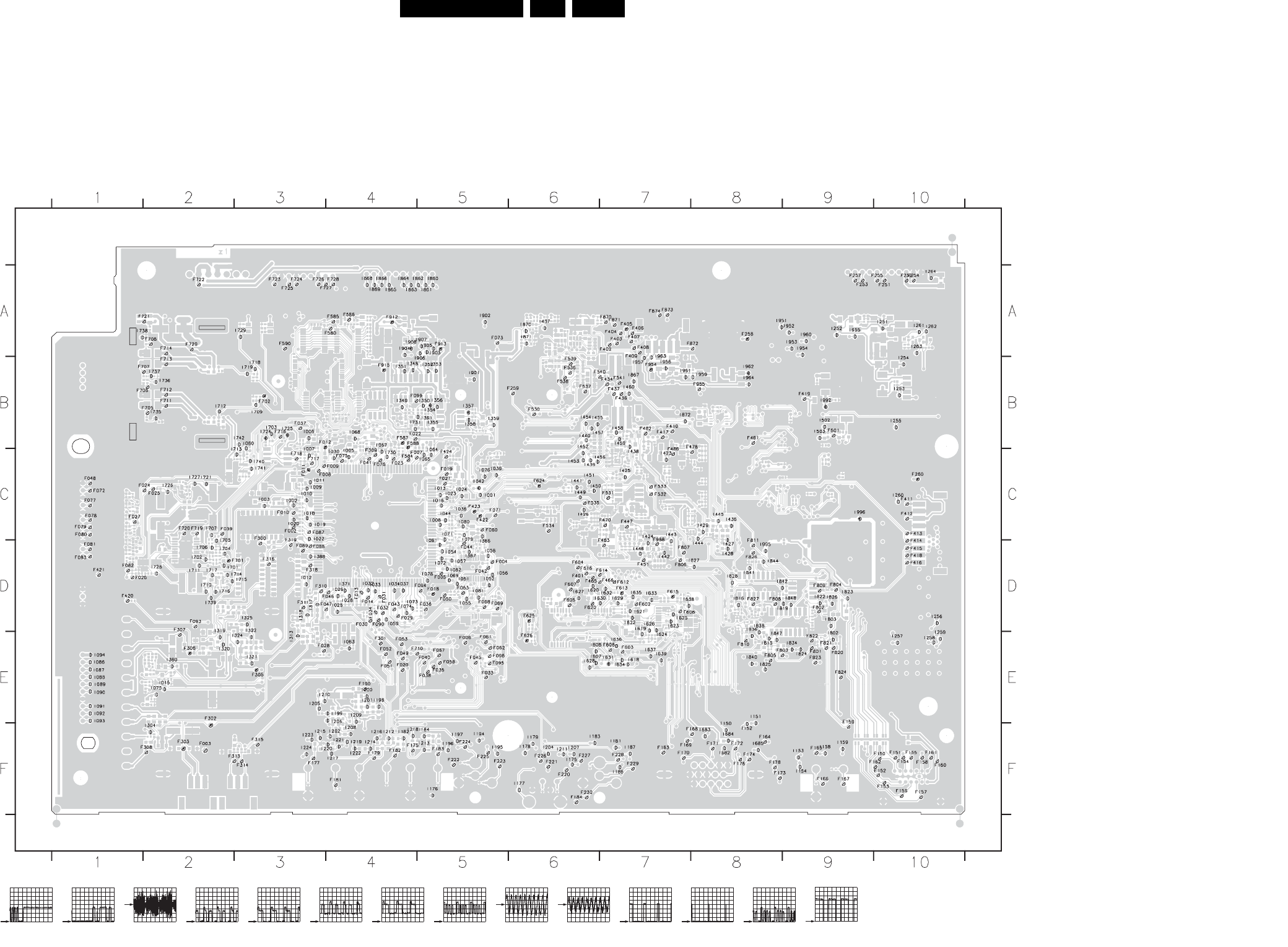
20LC4.6U AA 6.
Block Diagrams, Testpoint Overviews, and Waveforms
Testpoint Overview SSB (Top Side)
E_14710_087.eps
071004
3139 123 5867.2
1V / div DC
20us / div
F302 F626 F701 F702 I904
I357
I354
F624 F625
F613 F615F303 F306 F011 1V9
F012 1V9
F915 5V3
F912 33V7
F913 8V
F954 5V4
1V / div DC
20us / div
200mV / div AC
20us / div
200mV / div DC
20us / div
200mV / div DC
20us / div
500mV / div DC
20us / div
500mV / div DC
20us / div
500mV / div DC
20us / div
20mV / div AC
1ms / div
20mV / div AC
1ms / div
1V / div DC
5ms / div
1V / div DC
20us / div
2V / div DC
5us / div
I631
200mV / div DC
20us / div
F002 C3
F003 F2
F004 D5
F005 D5
F006 E5
F007 C4
F008 C3
F009 C4
F010 C3
F011 C3
F012 B3
F013 D4
F014 D4
F018 D5
F019 C5
F020 E4
F021 C5
F022 B4
F023 C4
F024 C2
F025 C2
F026 D1
F027 C1
F028 E3
F029 D4
F030 D4
F031 D4
F032 D4
F033 E5
F034 D4
F035 E5
F036 D5
F037 B3
F038 E5
F039 C2
F040 E5
F041 C4
F042 D5
F043 D4
F044 D5
F045 E5
F046 D4
F047 D4
F048 C1
F049 E4
F050 D5
F051 E4
F052 E4
F053 E4
F058 E5
F060 C5
F061 E5
F062 E5
F063 D5
F067 E5
F068 D5
F069 D5
F071 C5
F072 C1
F073 A5
F075 C4
F076 C4
F077 C1
F078 C1
F079 C1
F080 C1
F081 D1
F082 D1
F083 D1
F087 C3
F088 D3
F089 D3
F090 D4
F093 D2
F094 D5
F095 E5
F096 E5
F099 B4
F150 F10
F151 F10
F152 F10
F153 F10
F154 F10
F155 F10
F156 F10
F157 F10
F158 F10
F159 E9
F160 F10
F161 F10
F162 F10
F163 F7
F164 F8
F165 F9
F166 F9
F167 F9
F168 F8
F169 F7
F170 F7
F171 F8
F172 F8
F173 F8
F174 F8
F175 F4
F176 F8
F177 F3
F178 F8
F179 F4
F181 F4
F182 F4
F183 F5
F184 F6
F190 E4
F220 F6
F221 F6
F222 F5
F223 F5
F224 F5
F225 F5
F226 F6
F227 F6
F228 F7
F229 F7
F230 F6
F251 A10
F252 A10
F253 A9
F254 A10
F255 A10
F257 A9
F258 A8
F259 B6
F260 C10
F300 C3
F301 E4
F302 E2
F303 F2
F305 E3
F306 E2
F306 E2
F307 D2
F308 F2
F309 C4
F310 D3
F311 D3
F313 F2
F314 F3
F315 F3
F316 D3
F318 D3
F319 C3
F401 D6
F402 A7
F403 A7
F404 A7
F405 A7
F406 A7
F407 A7
F408 A7
F409 A7
F410 B7
F411 C10
F412 C10
F413 C10
F414 D10
F415 D10
F416 D10
F417 B7
F418 D10
F419 B9
F420 D1
F421 D1
F422 C5
F423 C5
F424 C5
F434 B7
F436 B7
F437 B7
F447 C7
F451 D7
F461 B8
F463 D7
F465 D6
F466 D7
F470 C7
F478 B8
F482 B7
F486 C7
F501 B9
F530 B6
F531 C7
F532 C7
F533 C7
F534 C6
F535 C6
F536 B6
F537 B6
F538 B6
F539 B6
F540 B7
F541 B7
F580 A4
F584 C4
F585 A4
F586 A4
F587 B4
F588 B4
F590 A3
F602 D7
F603 E7
F604 D6
F605 D6
F606 D7
F607 D6
F608 E7
F612 D7
F613 D7
F614 D7
F615 D7
F616 D6
F620 D6
F624 C6
F625 D6
F626 E6
F701 D3
F702 B3
F705 B2
F706 B1
F707 B2
F708 A2
F710 E5
F711 B2
F712 B2
F713 B2
F714 A2
F716 B3
F717 C3
F718 C3
F719 C2
F720 C2
F721 A2
F722 A2
F723 A3
F724 A3
F725 A3
F726 A3
F727 A4
F728 A4
F729 A2
F801 E9
F802 D9
F803 E9
F804 D9
F805 E8
F806 D7
F807 D7
F808 D8
F809 D9
F810 E8
F811 D8
F820 E9
F821 E9
F822 E9
F823 E9
F824 E9
F826 D8
F827 D8
F870 A7
F871 A7
F872 A8
F873 A7
F874 A7
F912 A4
F913 A5
F915 B4
F954 B7
F955 B8
F988 C7
I001 C5
I002 C3
I003 C3
I005 C4
I006 B3
I007 C3
I008 C5
I009 C3
I010 C3
I011 C3
I012 D3
I013 C5
I015 E2
I016 C5
I018 C3
I019 C3
I020 C3
I022 C3
I023 C5
I024 C5
I025 D4
I026 D4
I028 D4
I030 C4
I032 D4
I033 D4
I034 D4
I036 C5
I037 D4
I039 C5
I042 C5
I044 C5
I051 D5
I052 D5
I054 D5
I055 D5
I056 D5
I057 D5
I058 D5
I059 D4
I060 B3
I061 D5
I063 E4
I064 C5
I065 C5
I067 B4
I068 B4
I069 D5
I071 C5
I072 D5
I073 D4
I074 D4
I075 E2
I076 C5
I078 D5
I079 C5
I080 C5
I081 D5
I082 D5
I086 E1
I087 E1
I088 E1
I089 E1
I090 E1
I091 E1
I092 E1
I093 E1
I094 E1
I150 F8
I151 E8
I152 F8
I153 F9
I154 F9
I158 F9
I159 F9
I175 F6
I176 F5
I177 F6
I178 F6
I179 F6
I181 F7
I182 F4
I183 F6
I184 F5
I186 F7
I187 F7
I194 F5
I195 F5
I196 F5
I197 F5
I198 E4
I199 E4
I200 E4
I201 E4
I202 F4
I204 F6
I205 E3
I206 E4
I207 F6
I208 F4
I209 E4
I210 E3
I211 F6
I212 F4
I213 F5
I214 F4
I215 F3
I216 F4
I217 F4
I218 F4
I219 F4
I220 F4
I221 F4
I222 F4
I223 F3
I224 F3
I251 A10
I252 A9
I253 B10
I254 B10
I255 B10
I256 D10
I257 E10
I258 E10
I259 E10
I260 C10
I261 A10
I262 A10
I263 A10
I264 A10
I304 F2
I313 E3
I317 D3
I318 D3
I319 D2
I320 E2
I321 E3
I322 D3
I324 E3
I325 D3
I348 B4
I349 B4
I350 B5
I351 B4
I352 B5
I353 B5
I354 B5
I355 B5
I356 B5
I357 B5
I358 B5
I359 B5
I360 E2
I361 B5
I371 D4
I386 D5
I387 D5
I388 D3
I423 C7
I424 C7
I425 C7
I426 C6
I427 D8
I428 D8
I429 C8
I436 C8
I437 A6
I438 C7
I439 C6
I440 B6
I441 C6
I442 D7
I443 C7
I444 D8
I445 C8
I446 D7
I449 C6
I450 C6
I451 C6
I452 B6
I453 C6
I454 B6
I455 B6
I456 C7
I457 B6
I458 B7
I459 B7
I460 B7
I502 B9
I503 B9
I607 E6
I608 E6
I618 E7
I619 D7
I620 D6
I621 D7
I622 D7
I623 D7
I624 E7
I625 D7
I626 D7
I627 D6
I628 E6
I629 D7
I630 D7
I631 E7
I632 D7
I633 D7
I634 E7
I635 D7
I636 E7
I637 E7
I638 D7
I639 E7
I682 F8
I683 F8
I684 F8
I685 F8
I701 D2
I702 D2
I703 B3
I704 D2
I705 D2
I706 D2
I707 C2
I709 B3
I710 D2
I711 D2
I712 B2
I713 C3
I714 D3
I715 D3
I716 D2
I717 D2
I718 B3
I719 B3
I721 C2
I724 B3
I725 B3
I726 C2
I727 C2
I728 D2
I729 A3
I730 C4
I731 B4
I735 B2
I736 B2
I737 B2
I738 A1
I739 D2
I740 C3
I741 C3
I742 B3
I802 E9
I803 D9
I815 E8
I816 D8
I819 D9
I822 D9
I823 D9
I824 E9
I825 E8
I826 D9
I827 D8
I828 D8
I834 E9
I836 D8
I838 D8
I840 E8
I841 D8
I842 D8
I844 D8
I847 E8
I848 D9
I860 A5
I861 A5
I862 A5
I863 A4
I864 A4
I865 A4
I866 A4
I867 B7
I868 A4
I869 A4
I870 A6
I871 A6
I872 B7
I901 B5
I902 A5
I903 A5
I904 A4
I905 A5
I906 B5
I907 A5
I908 A4
I951 A8
I952 A9
I953 A9
I954 A9
I955 A9
I956 B7
I957 B7
I959 B8
I960 A9
I961 B7
I962 B8
I963 A7
I964 B8
I992 B9
I995 D8
I996 C9
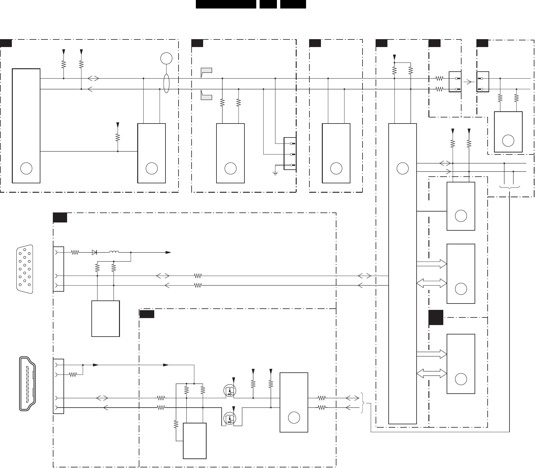
Block Diagrams, Testpoint Overviews, and Waveforms 21LC4.6U AA 6.
I2C IC Overview
E_14710_083.eps
281204
6692 5691
3787
DDC_5V
3789
3786
A2 HERCULES
I2C BUS INTERCONNECTION DIAGRAM
1301
1
2
3
7011
SET
PROCESSOR
PART OF
VIDEO-
PROCESSER
(HERCULES)
ERR
6
7099
M24C16
EEPROM
(NVM)
ERR
9
ERR
10
3096 3088
+3V3STBY +3V3STBY
3822 3823
+3V3STBY +3V3STBY
+3V3STBY
+3V3STBY
3433 3432
+3V3STBY
3097
+3.3V
SDA
SCL
NVM_WP
108
104
109
56
7693
M24C02
EEPROM
256x8
56
7560
TDA9178T
HISTOGRAM
ERR
15
14 11
7531
M24C32
EEPROM
ERR
8
ERR
11
7530
M29W040B
FLASH
ROM
512kx8
ERR
4
7501
K4D263238M
SDRAM
IMx32x4
ERR
14
56
7
A1 TUNER IF A3
7401
GM1601
SCALER
ERR
4
ERR
6
N1 N2
P3
P4
HISTOGRAM A7 SCALER CB 3D COMB
A2
A11 FLASH/CONTROL
A10 SDRAM
A12 HDMI
1302
TUNER
3302
1004
6
5
1801
5
6
3303
54
For
ComPair
only
HDMI CONNECTOR
VGA CONNECTOR
PCHD-IO
A16
SDA_IO
SCL_IO
SDA_IO
SCL_IO
SDAO
SCLO
ADDRESS
DATA
ADDRESS
DATA
M1
M2
UART_RX
UART_TX
SDA_VGA
SCL_VGA
SDA_IO
SCL_IO
1687
9
15
12
1688
18
15
16
1
5
11
15
F303
F302
3697 3696
7801
M24C02
EEPROM
256x8
5
7
WC
6
75
74
76
77
+3V3_STBY
DOC_SDA
DOC_SCL
9
+5V_HDMI+5V_HDMI
+3V3_STBY
3810
3808
3809
7823
UPD64083
3D COMB
60 59
3881
3882
19 1
18 2
7807
BSN20
7806
BSN20
7808
SII9993CT
HDMI
PANEL LINK
RECEIVER
ERR
13
3824
3825
3071
3064
3429 3428
3590
3832
3828
NVM_WPP
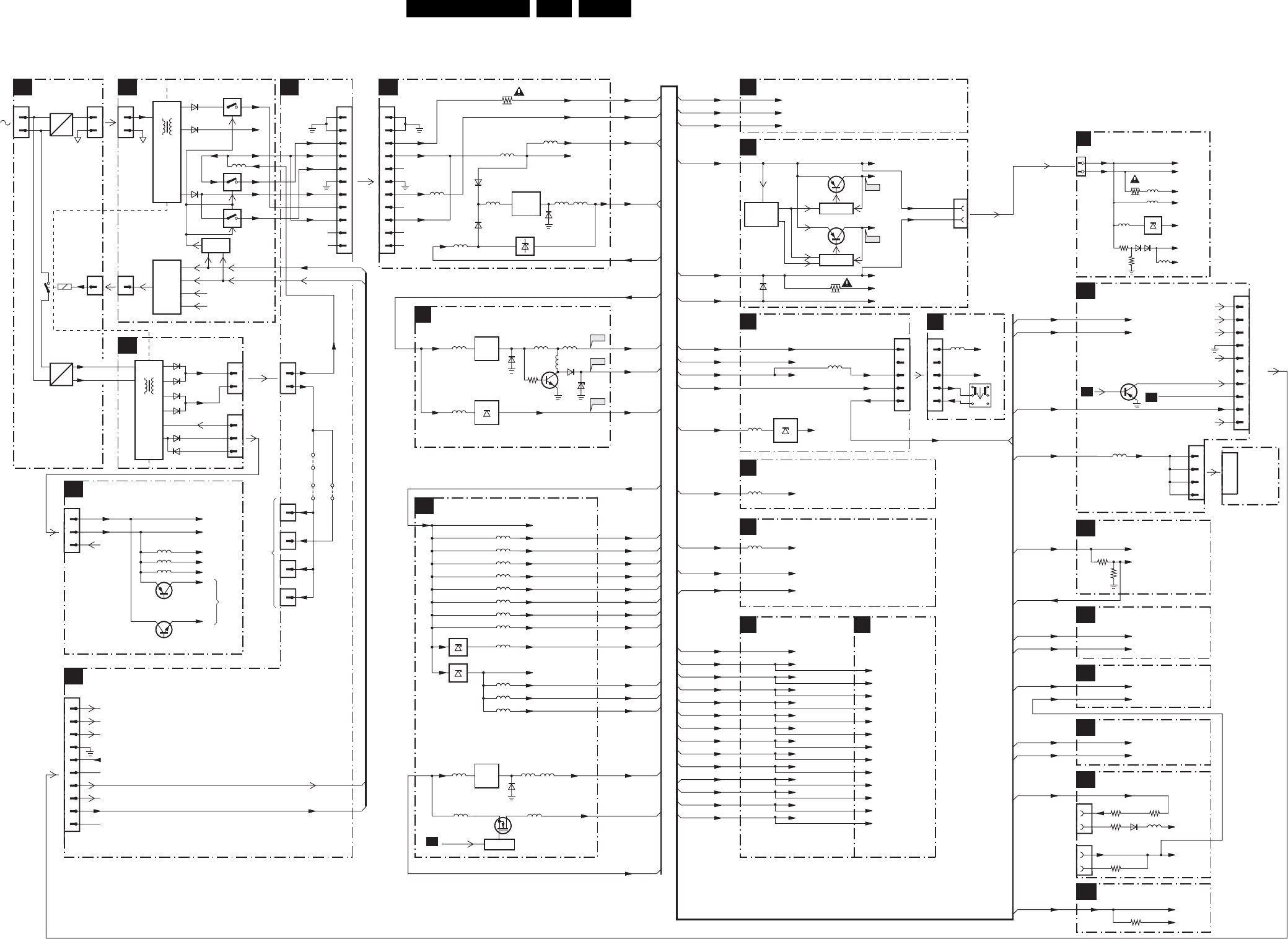
22LC4.6U AA 6.
Block Diagrams, Testpoint Overviews, and Waveforms
Supply Voltage Overview
2
1
1251
3
4
5
6
7
8
9
10
11
+8VSW_TV+8VSW_TV
31
+12VSW
7920
L78M08CDT
5920
+5VSW
26
+12VUNREG
+5V2
+5VSW +5VSW
+VTUN
+12VSW
+12V
7930
MC34063AD
5930
6930
5507
5931 5932
7011
7001
7003
3374
5691
5874
5067
5560
5720
5100
5910
7910
31
7562
SUPPLY
IC
26
7952
5952
6951
5953 5954
SUPPLY
IC
CONTROL
HERCULES
3910
6910
6911
-/C33
F913
F912
F915
DC-DC CONVERTER
A15
TV-SUPPLY
A6
TUNER IF
A1
HERCULES
A2
HISTOGRAM
A3 SWITCH PANEL
J
SUPPLY
A14
5252
3251
5251
52685267
6267
6259
6262
5262
5258
A13
A12
A11
A9
A7
A5
A3
A2
A1
A4
A3
A17
A2
A1
A1
A2
+3V3STBY
+3V3STBY
+3V3STBY
+12VSW
+12VSW
PANEL_PWR_CTL
+3V3_PLL
A15
+12VSW A15
A5
A3
A14
A3
A6
A14
A3
A3
A6
+VTUN +VTUN
A6
+3V3STBY +3V3STBY
A15
+3V3STBY +3V3STBY
+1V8_A
+1V8_B
A15
14
4
88
109
127
+3V3STBY +3V3STBY
+3V3STBY
A15
+5V2
A15
+12VSW +8VSW_2
A15
+8VSW_TV +8VSW_TV
A6
TO 45 - 7011
+5VSW +5VSW
A6
5984
+3V3_ADC
5985
+3V3_DVI
5986
+3V3_IO
5987
+3V3_LBADC
5988
+3V3_LVDSA
5989
+3V3_LVDSB
5990
+3V3_LVDS
+3V3_PLL
+3V3_ADC
+3V3_DVI
+3V3_IO
+3V3_LBADC
+3V3_LVDSA
+3V3_LVDSB
+3V3_LVDS
5991
+2V5_DDR +2V5_DDR
5994
7992
+1V8
A7
A8
A7
A8
A7
A8
A7
A8
A7
A8, A11
A7
A8
A7
A8
A7
A8
A7
A8
A7
A8
A10
A7
A8
A7
A8
+1V8_ADC
5996
+1V8_DVI
5997
+1V8_CORE
+1V8_ADC
+1V8_DVI
+1V8_CORE
A9
A13
A16
A9
A15
PAN_VCC PAN_VCC
+5VSWI +5VSWI
5998
7995
D
S
G
5957
5956
+12V
+8V6
+8V6
+5V2
A2
A7
A5
N.C.
N.C.
N.C.
2
1
1306
N.C.
2
1
1M03
3
4
5
6
7
8
9
10
2
1
1M46
3
4
5
6
7
8
9
10
11
+12V
+12V
+5V_SW
+8V6
+5V2
VTUN
VTUN
+11V
N.C.
N.C.
CONTROL
CONTROL
1320
AUDIO AMPLIFIER (PARTLY USED)
A5
+5V2 AUDIO_SUP
A15
5580
+5VSW +5VD
A6
A15 +3V3STBY
A3 +5V2_RELAIS_IO2 +5V2_RELAIS_IO2
SCALER
A7 SCALER
SUPPLY
A8
AUDIO DELAY LINE (LIPSYNC)
A4
SDRAM
FLASH/CONTROL
A10
A11
+2V5_DDR +2V5_DDR
A14
FSVREF
SCALER INTERFACE
A9
A8
A7
FSVREF
A15
A14 +3V3_DVI
+3V3STBY
A14 +3V3_PLL
A14 +3V3_LBADC
A14
+3V3_IO
A14
+3V3_LVDSB
A14
+2V5_DDR
A14
+3V3_LVDSA
A14
A14 +3V3_LVDS
A10 FSVREF
A14 +1V8_DVI
A14 +1V8_ADC
A14 +3V3_ADC
+3V3_DVI
+3V3STBY
+3V3_PLL
+3V3_LBADC
+3V3_IO
+1V8_CORE +1V8_CORE
+3V3_LVDSB
+2V5_DDR
+3V3_LVDSA
+3V3_LVDS
FSVREF
+1V8_DVI
+1V8_ADC
+3V3_ADC
+3V3_DVI
+3V3_PLL
+3V3_LBADC
+3V3_IO
+1V8_CORE
+3V3_LVDSB
+2V5_DDR
+3V3_LVDSA
+3V3_LVDS
FSVREF
+1V8_DVI
+1V8_ADC
+3V3_ADC
A9
3501
3502
A15
A14 +3V3_IO
+3V3STBY
+3V3_IO
+3V3STBY
+3V3STBY
HDMI
A12
A15 +3V3STBY +3V3STBY
+5VHDMI
CINCH IO
A17
+5VSW_1
3190
3789
3791 3790
6692
A6 +5VSW +5VSW +5VSW
A15 +3V3STBY
A14 +5VSWI
+3V3STBY
+5VSWI
A3
A9
A5
A15
+5V2_RELAIS_IO2 +5V2_RELAIS_IO2
PROTECT_AUDIO
A14 PAN_VCC
VGA
CONN. DCC_5V
+5VSWI
9
10
1687
PCHD-MUX
A13
PCHD-IO
A16
A15 +3V3STBY
A14 +5VSWI
A14 +5VSWI
+5VSWI
E_14710_085.eps
281204
+5V2_RELAIS_IO2
+5VSW
A6
+8V6 +8V6
A15
+5VSW
3793
HDMI
CONN.
+5VHDMI
+5VHDMI
29
18
1688
2
1
1403
3
4
5
7
6
8
9
10
+3V3STBY
+8V6
0320
ON / OFF
SWITCH
ON
7
6
8
9
10
6
7
8
9
10
BACKLIGHT_CTRL
POR
LIGHT_ON
FAN_SPEED
2
1
1458
3
4
-12V_2CD
POWER_OK
STANDBY
SC_STANDBY
N.C.
N.C.
N.C.
N.C.
(N.C.)
N.C.
7887
LCD
DISPLAY
(LVDS
CONNECTOR)
LVD S
CONNECTOR
F011
F012
6005
1101
1
2
3
4
5
6
7955
7954
51
7260
18
7262
+12VSW
+12VSW
+5V2
+3V3STBY
+8V6
+5V2_RELAIS_IO2
SUPPLY
IC
AUDIO OUTPUT AMPLIFIER
SA3
CONNECTIONS
SA1
1312
CONNECTIONS
SA1
STANDBY SUPPLY
SA2
1313
1317
1315
5711
5707
5723
7713
1,2
5,6
1M02
7DCPROT
DIM_CONTROL (N.C.)
POR
ON/OFF (N.C.)
+5V_SW (N.C.)
N.C.
STANDBY
PROT_AUDIO_SUPPLY
+5V2_RELAIS_IO2
STANDBY
+5V2_RELAIS_IO2
N.C.
+16V +19V
-16V -19V
+16V +19V
-16V -19V
-V f1
-V f11
-V f21
Vm
N.C.
7712
Vp
TO
LCD
SCREEN
+12V
+5V_SW
+8V6
+5V2
HOT COLD
HOT
COLD
+
CONTROL
+
CONTROL
CONTROL
CONTROL
1,2
3,4
1304
1
1305
1,2
3,4
1304
5,6
7
1,2
1M02
2
1
1306
2
1
1308
MAIN FILTER
STANDBY
AS1
SUPPLY
AS2
+5V2_RELAIS_IO2
STANDBY
PROT_OVV
PROT_AUDIOSUPPLY
+12V_A
+12V_A
+12V
+24V
DC_PROT
VSND_POS
VSND_NEG
+12V_24V
1
1305
AC
DC
AC
DC
400V_HOT
25V_HOT
+3V3STBY
+5V2
+5V2_RELAIS_IO2
9007
9004 9005
6044
6045
6021
6025
6291
6293
6504
7511
7931
7131
6140
6107
+3V3STBY
+8VSW_TV
1
10
1004
3D COMB FILTER
CB
3876
3878 5870
5851
5856
5855
3855
2V5P
2V5D
2V5A
OUTIN
3V3_400mA
8V3d
8V3
8V3 3V3STBY
3V3STBY
68756876
7851
LF25CDT
1801
1
10
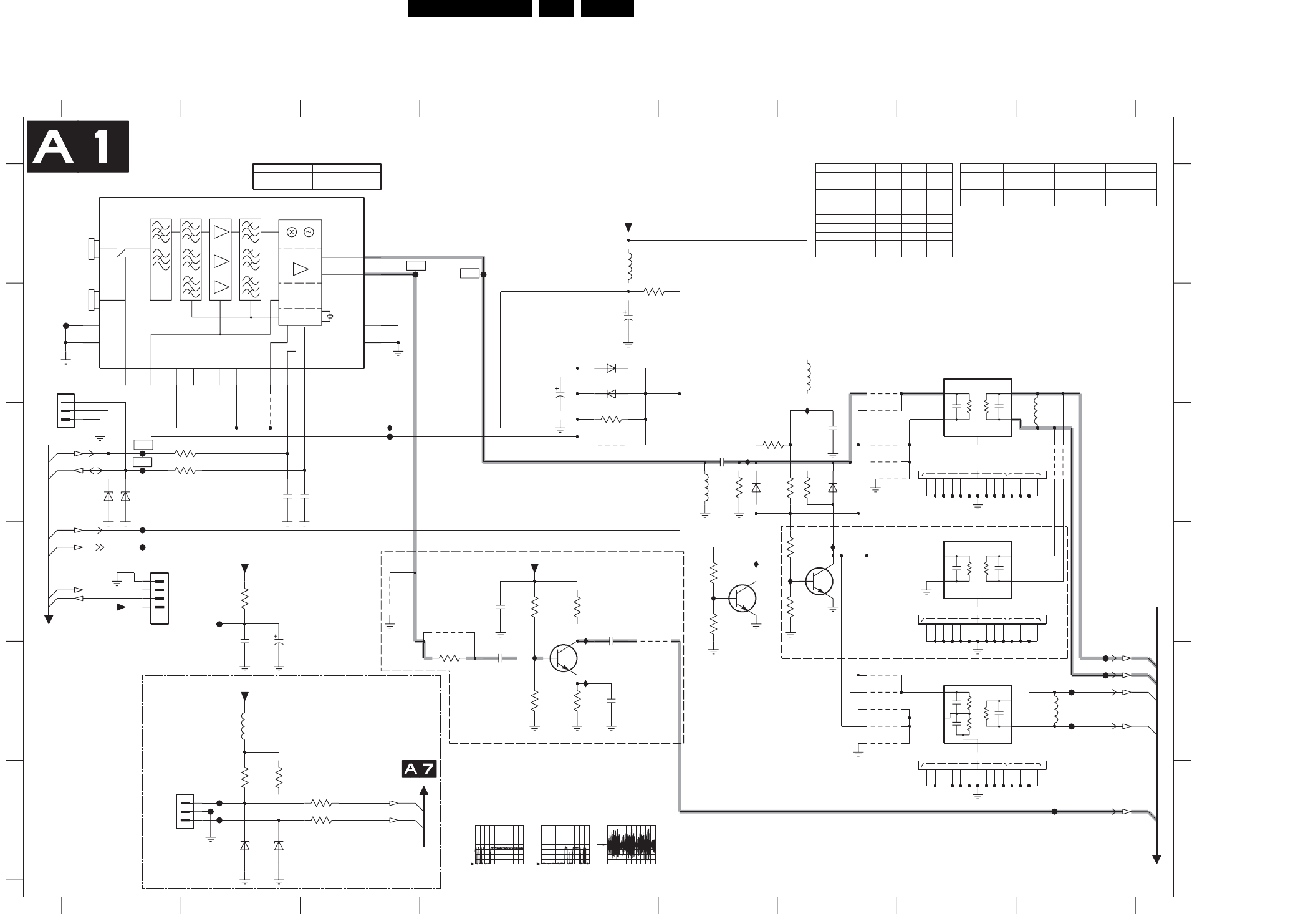
Circuit Diagrams and PWB Layouts 23LC4.6U AA 7.
7. Circuit Diagrams and PWB Layouts
SSB: Tuner and VIF
PLL
AGC
DET
IF AMP
MIX-OSC
PRE-FIL TRACK
FILTER
GAIN
CTRL
PRE-AMP
TRACK
FILTER
RF
MT
FM
MT
TV
RF
NCMT
NCMT
NCMT
TUNER + VIF
5V3
2V6
2V6
RES
7V1
RES
NC
A2
A2
A2
A2
5V3
1V7
0V
0V
*
RES
RES
A2
A2
A2
A2
A2
EUROPE & AP
PAL-MUTLI
ONLY
RESERVE
*
NC
A7
A7
COMPAIR
FOR TESTING DURING DR STAGE :
PIN1=TX, PIN2=GND,PIN3=RX
FROM SCALER
For FM Radio Only
UART
For ITV Only
123456789
123456789
A
B
C
D
E
F
A
B
C
D
E
F
1301 B1
1302 A1
1305 D1
1328-A B8
1328-B C8
1329-A D8
1329-B D8
1330-A E8
1330-B E8
1681 F2
2302 C2
2303 C3
2307 D2
2308 D2
2309 B5
2311 B5
2313 E4
2314 D4
2317 E5
2318 D5
2321 C6
2324 C7
3302 C1
3303 C1
3304 F2
3305 F2
3309 A5
3311 C5
3313 E4
3314 D5
3315 E5
3316 D5
3317 E5
3319 D6
3320 D6
3321 C6
3322 C6
3323 C6
3324 C7
3325 D7
3326 D7
3327 D2
3328 F3
3329 F3
4312 D3
4313 D4
4318 D5
4327 B7
4328 C7
4329 C7
4330 C7
4331 C7
4332 E7
4333 E7
4334 E7
4335 E7
4336 E7
4337 C9
4338 C9
4339 C2
4340 C5
5304 E2
5309 A5
5321 C6
5324 B7
5339 C9
5340 E9
6310 B5
6311 B5
6323 C6
6324 C7
6328 F2
6329 F2
6330 C1
6331 C1
7316 E5
7320 D6
7325 D7
F300 E9
F301 B1
F302 C1
F303 C1
F305 A3
F306 A4
F307 D2
F308 C3
F309 D1
F310 F9
F311 D1
F313 F2
F314 F2
F315 F2
F316 E9
F318 E9
F319 E9
I304 C3
I313 E4
I317 E5
I318 D5
I319 D6
I320 D6
I321 C6
I322 D7
I324 C7
I325 D7
3314
100K
+3V3STBY
1305
1
2
3
4
56
F319
F318
F314
F315 100R
3329
F313 100R
3328
BZX384-C6V8
6329
6328
BZX384-C6V8
6331
BZX384-C6V8 BZX384-C6V8
6330
F300
F316
F310
4340
F309
+3V3STBY
10K
33053304
10K
5304
1
2
3
1
2
3
1681
1301
4SCL
5SDA
2 TU|FM
VCC7
9VT
IFOUT
12
13 14
15
NC1
6
8NC2
1AGC
3AS
FM-IFOUT 10
11
UR1336/A F S H-3
1302
I319
I325
I322
I320
I321
I324
I318
I313
I317
4339
+5VSW
3327
1K0
910
1314
15 1112
1617
OFWK9656L
1330-B
118456
1314
15 1112
1617
1329-B
OFWK3955L
118456910
OFWK9656L
2
3
7
8
1329-A OFWK3955L
2
3
7
8
1330-A
10
1314
15 1112
1617
1184569
1328-A
OFWK3953L
2
3
7
8
OFWK3953L
1328-B
+VTUN
7316
BFS20
4318
4313
2314
100n
2313
1n0
2318
1n0
2317
1n0
3313
3316
3317
560R
820R
150K
3315
4338
4337
5340
5324
6u8
4332
4336
4333
4335
4334
5339
820n
4331
4330
4329
4328
5321
4327
10n
390n
2324
10n
2321
27K
3319
3320
18K
3321
2K2
7320
6323
BC847BW
1SS356
2K2
3322
6K8
3323
22K
3325
47K
3326
BC847BW
6324
7325
2K2
1SS356
3324
3309
10K
I304
5309
12u
4312
2308
2u2 50V
35V22u
2311
16V470u
2309
+5VSW
6311
BAS316
6310
100R3303
3302 100R
F311
F303
F302
2303
22p
F301
22p
2302
F307
F305
F308
F306
2307
47n
3311
10K
UART_RX
SCL
SDA
UART_TX
VIF1
VIF2
SIF1
SIF2
SEL_IF
RF_AGC
SCL
SDA IF-TER
SSIF
PAL / SECAM
NTSC / LATAM
*
1302
UR1318
UR1338
1328
OFWK3953LEUROPE
OFWK7265LAP
OFWK3956LCHINA
1329
OFWK9656L
OFWK9361L
OFWK9352L
NAFTA OFWM1967L
1330
--
--
OFWK9355L
-- --
4339
4338
4337
4336
4334
4333
4331
4329
4328
4327
EU AP CHINA NAFTA
YY Y
Y
Y
Y
Y
Y
Y
Y
Y
Y
Y
Y
Y
--
--
--
--
--
--
--
--
--
--
--
--
--
--
--
--
--
--
--
--
--
--
--
-- --
FM No FM
UV1318
UV1338
E_14710_063.eps
100804
3139 123 5867.2
1V / div DC
20us / div
F302 F303 F306
1V / div DC
20us / div
200mV / div AC
20us / div
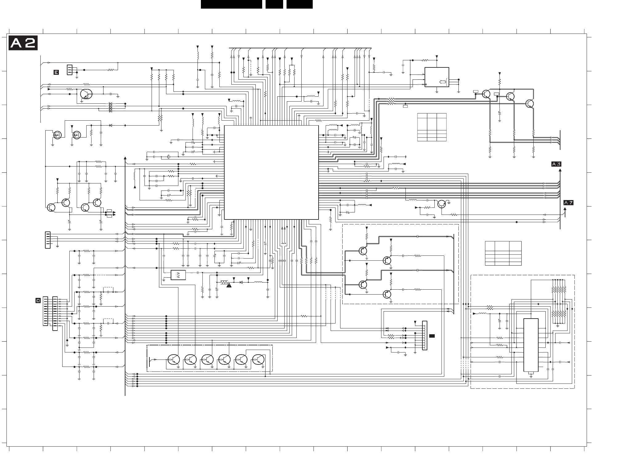
24LC4.6U AA 7.
Circuit Diagrams and PWB Layouts
SSB: Histogram and Hercules
A7,A3,A1
A7,A3,A1
A2
A2
TO 1801
3D COMB
CB
S1A
D2
S1B
IN1
IN2
S2B
D1
S2A
NC
S4B
D4
S4A
IN4
S3B
D3
S3A
IN3
VDD
GND VSS
O
GND
I
SCL
ADR
0
1
2SDA
WC
VDRB
VDRA
VIFIN1
VIFIN2
VSC
IREF
GNDIF
VP2
SVO/IFOUT/CVBS1
AUDIOIN4L
AUDIOIN4R
CVBS4/Y4
C4
AUDIOIN2L
AUDIOIN2R
CVBS2/Y2
AUDIOIN3L
AUDIOIN3R
CVBS3Y3
C2/C3
VSSP2
VDDA3(3.3V)
VREF_POS_LSL
VREF_NEG_LSL+LSR
VREF_NEG_HPL+HPR
VREF_POS_LSR+HPL
VREF_POS_HPR
XTALIN
XTALOUT
VSSA1
VGUARD/SWIO
DECDIG
VP1
PH2LF
PH1LF
GND1
SECPLL
DECBG
AVL/EWD
G/Y-3
B/Pb-3
GND3
VP3
BCLIN
BLKIN
RO
GO
BO
VDDA1(3.3V)
VREFAD_NEG
VREFAD_POS
VREFAD
DVBIN1/SIFIN1
DVBIN2/SIFIN2
AGCOUT
EHTO
AVL/SWO/
SSIF/REFIN
AUDIOIN5L
AUDIOIN5R
AUDOUTSL
AUDOUTSR
DECSDEM
AMOUT/QSSO/AUDEEM
GND2
PLLIF
SIFAGC/DVBAGC
DVBO//IFVO/FMRO
DVBO/FMRO
VCC8V
AGC2SIF
P2.0/PMW
P2.1/PWM0
P2.2/PWM1
P2.3/PWM2
P3.0/ADC0
P3.1/ADC1
VDDC1(1.8)
DECV1V8
P3.2/ADC2
P3.3/ADC3
VSSC1/P
P2.4/PWM3
P2.5/PWM4
AUDOUTLSL
AUDOUTLSR
AUDOUTHPL
AUDOUTHPR
CVBSO/PIP
SVM
FBISO/CSY
HOUT
VSScomb
VDDcomb
VIN(R/Pr-2/C-X)
UIN(B/Pb-2)
IN(G/Y-2/CVBS/Y-X)
YSYNC
YOUT
UOUT(INSW-S)
VOUT(SWO1)
INSSW3
/Pr-3
VSSC4
VDDC4
VDDC3
VSSC3
P1.2/INT2
P1.4/RX
P1.5/TX
VDDA(1.8V)
VDDA2(3.3V)
GNDA
VSSadc
VDDadc(1.8)
INT0/P0.5
P1.0/INT1
P1.1/T0
VDDC2
VSSC2
P0.4/I2SWS
P0.3/I2SCLK
P0.2/I2SD02
P0.1/12SD01
P0.0/I2SDI1
P1.3/T1
P1.6/SCL
P1.7/SDA
VDDP(3.3V)
TDA 15021H
HISTOGRAM & HERCULES
UAB11-932214725682
AUDIO PROCESSING
A4
A4
A4
A5
A5
A5
A5
A4
AUDIO PROCESSING
A1
A5
RES
RES
RES
*EMC *EMC
RES
RES
A7
A7
A7
A13
A13
A13
A12
A12
RES
A3
A3
A3
FOR SERVICE
A17
A17
A17
A5
A17
A17
EU ONLY
NAFTA ONLY
(1M06)
A3
A3
A3
A3
A3
A3
A3
A17
A3
A3
TO HISTOGRAM
A17
A17
A17
A17
A17
A17
A17
A17
A17
A17
A17
A17
A17
A17
A17
A5
A5
A17
A5
A17
A17
A17
A17
A17
A17
A17
A1
A1
A1
A1
A1
A1
(1M01)
RES
(1M36)
A3
A7
TO HISTOGRAM
RES RES RES
0R 0R 0R
DMMI - IFH YPbPr {RES}
No 3D 3DItem
4004 - Yes
4005 Yes -
4006 - Yes
4007 Yes -
4002 Yes -
3009 Yes -
2083 - Yes
(RES)
*
*
*
*
HETV
(15W)
MTV
(5W)
*
3380
3381
3382
3383
5K6
5K6
5K6
5K6
10K
10K
10K
10K
A3
A1
A1
To 0345 of
TOP CONTROL
To 0936 of SIDE I/O
For ITV only
1 2 3 4 5 6 7 8 9 10 11 12 13 14 15 16 17
1 2 3 4 5 6 7 8 9 10 11 12 13 14 15 16 17
A
B
C
D
E
F
G
H
I
J
K
L
A
B
C
D
E
F
G
H
I
J
K
L
1001 D5
1002 F2
1004 I13
1009 G5
1036 H2
1336 H2
1402 A2
2000 D3
2001 E3
2002 F10
2004 C7
2005 D6
2006 D5
2007 D5
2008 E5
2009 E5
2010 E5
2011 E6
2012 F3
2013 H8
2014 G8
2015 G9
2016 G9
2017 G9
2018 G9
2023 E10
2024 F2
2025 E11
2026 E11
2027 E11
2029 E11
2030 E11
2031 E11
2032 E11
2033 D12
2035 D12
2036 H3
2037 I3
2038 E4
2040 C15
2041 D11
2043 E4
2044 D11
2052 D11
2053 J12
2054 C3
2055 E13
2056 F13
2059 G3
2060 E5
2061 E5
2063 F6
2064 D3
2065 G5
2066 G6
2068 C5
2069 G3
2070 B3
2071 D6
2072 B6
2073 B7
2074 C7
2076 B9
2077 C11
2078 B11
2079 H3
2080 H3
2081 H3
2082 F7
2083 G8
2084 D10
2087 H3
2088 I3
2090 I3
2091 I3
2092 I3
2093 J3
2094 J3
2095 J3
2096 J3
2097 J3
2098 J3
2099 A12
2355 G8
2356 G7
2357 G7
2358 G7
2359 F6
2360 I15
2361 I17
2363 J15
2364 J17
2365 J17
2366 J16
2367 I15
2368 K15
2370 G6
2371 G6
2372 G6
2373 G6
2374 G7
2375 G7
2376 F13
2377 G13
2378 C10
2380 C11
2381 D11
2382 D6
2386 H12
2387 G6
2388 G6
2392 G12
2394 C11
2395 H7
2396 H7
2397 G9
2398 G10
3000 D3
3001 E3
3002 E3
3003 E2
3004 E2
3005 D3
3006 D6
3007 E5
3008 E5
3009 G8
3010 E6
3011 E12
3012 H17
3013 I9
3014 D15
3015 C16
3016 D16
3017 C16
3018 D16
3019 B15
3023 I3
3024 I3
3025 J3
3027 J3
3028 F10
3031 H17
3033 H17
3034 I17
3035 E11
3036 I17
3037 I3
3038 H3
3040 E13
3048 D11
3049 B12
3050 B12
3051 B12
3052 C15
3053 E6
3054 D11
3055 I17
3056 B2
3057 B10
3059 E5
3060 F6
3064 I12
3065 F6
3067 G3
3068 G3
3069 H3
3070 B3
3071 I12
3072 H3
3073 C5
3074 H6
3075 B5
3077 B5
3078 B5
3079 B5
3080 A7
3081 B7
3082 B7
3083 B8
3084 B8
3085 A8
3086 B9
3087 B9
3088 B9
3089 C3
3091 B11
3092 B11
3093 A11
3094 C9
3096 B8
3097 A13
3098 F14
3357 C5
3358 G7
3359 G8
3360 H17
3361 H17
3362 H17
3363 I17
3364 I17
3365 I17
3366 H15
3367 I15
3368 I15
3369 J15
3370 F7
3371 G5
3372 G5
3373 J15
3374 H7
3378 H13
3380 F11
3381 G12
3382 G11
3383 H12
3386 G13
3389 B10
3390 G9
3391 G9
3392 G9
3393 G10
3394 C6
3415 A3
4002 G8
4004 H10
4005 H10
4006 H10
4007 H10
4008 B11
4022 A8
4023 H3
4062 E6
4085 H3
4086 I3
4360 J14
4361 J14
4362 J14
4363 J14
5001 C6
5002 C7
5003 E4
5004 H8
5005 E11
5006 D12
5007 C11
5008 C11
5010 E12
5060 C6
5070 A6
5071 B7
5072 B9
5360 I14
5370 C10
5371 C10
5372 C11
6001 C3
6005 H7
6073 C3
6074 C3
6075 B3
6076 C3
7001 E3
7002-1 F3
7002-2 F2
7003 E2
7004 F14
7005 C2
7011 D8
7012 B15
7013 B15
7014 B16
7070 C3
7075 B3
7099 A13
7360 I16
7370-1 J5
7370-2 J6
7371-1 J6
7371-2 J7
7372-1 J7
7372-2 J8
7376-A H11
7376-B H12
7377-A G11
7377-B G12
F002 E6
F003 C6
F004 D5
F005 F10
F006 B6
F007 A6
F008 C6
F009 B4
F010 D6
F011 F3
F012 F3
F013 H7
F014 H8
F019 C10
F020 C10
F021 C11
F022 A12
F023 B9
F024 I3
F025 J3
F026 J3
F027 I3
F028 I5
F029 I5
F030 I5
F031 I5
F032 I5
F033 B7
F034 I5
F035 I5
F036 I5
F037 I5
F038 J4
F039 J5
F040 K4
F041 B7
F042 K4
F043 I5
F044 K4
F045 K4
F046 F5
F047 G5
F048 I2
F049 G5
F050 K4
F051 G5
F052 B2
F053 G5
F072 G2
F077 G2
F078 H3
F079 I2
F080 I2
F081 I2
F082 J2
F083 J2
F087 E6
F088 E6
F089 E6
F090 I12
F093 I13
F094 J12
F095 I12
F096 I12
F099 B14
F420 A3
F421 B3
F422 B14
F423 B15
F424 F15
I001 A7
I002 D6
I003 D2
I005 B6
I006 C3
I007 C4
I008 D10
I009 C7
I010 D6
I011 C6
I012 F7
I013 D10
I015 C8
I016 B11
I018 D6
I019 D6
I020 E6
I022 E6
I023 C11
I024 C11
I025 G7
I026 G7
I028 G8
I030 B7
I032 F8
I033 F8
I034 F9
I036 D11
I037 F9
I039 B11
I042 C12
I044 D12
I051 E12
I052 H16
I054 E10
I055 H17
I056 I15
I057 E10
I058 H17
I059 I12
I060 J12
I061 E10
I063 G7
I064 C10
I065 C10
I073 G11
I074 H11
I079 H14
I080 H14
I081 H14
I371 F7
I386 I16
I387 J16
I388 F6
+1V8_B
+1V8_A
10u
2999
1
2
3
4
5
67
BM05B-SRSS-TBT
1002
+8VSW_TV
100n
2056
68K
3040
4086
2036
1u0
4085
1u0
2037
47K
3037 3038
47K
I388
I387
F424
I386
F423
I061
F422
BC847BW
7004
100R
3098
27p
2055
47u5010
1K8
3011
I012
5370
33p
2388 2387
33p
3065 680R
16V 10u
2002
100R
3057
220n2084
+3V3STBY
6076 BAT54 COL
I060
I063
I059
I055
I056
I058
I039
I052
I042
I064
I044
I065
F088
I030
F089
F087
F082
F083
F080
F081
F078
F079
F077
F072
3357
1K0
3394
75R
1u0
2377
1u0
2376
7005
BSH103
2064
3
4
5
6
7
8
9
B11B-PH-K
1
10
11
2
1336
3000 5K6
2u2
2000
I006 6001
BAS316
BSH103
7070
2054
22n
3089
150K
I007
+1V8_B
+3V3STBY
4023
2083 1u0
100K
B3B-PH-K
1
2
3
3028
1402
3415
10R
F421
F420
10p
10p
2098
10R
2097
3027
10p
2059
2069
10R
10p
3067
10p
2096 2095
10R
10p
3025
2093
10p
2094
10p
10R
3024
10p
2091
2092
10p
22K
3023
10p
2090
2088
10p
68R
3072
10p
2081
2087
10p
22K
3069
2080
10p
10p
2079
68R
3068
3
4
5
6
7
8
9
13 14
1
10
11
12
2
I081
1036
I079
I074
I080
I073
I054
I057
I036
I051
I024
I016
I023
I015
I037
I034
I033
I028
I032
I026
I022
I025
I020
I019
I011
I010
I018
I009
I001
I005
F048
F052
F053
F051
F050
F047
F049
F046
F044
F045
F042
F043
F041
F039
F040
F038
F036
F037
F035
F033
F034
F032
F030
F031
F029
F027
F028
F026
F024
F025
F023
F021
F022
F020
F014
F019
F013
F011
F012
F010
F008
F009
F007
16V
470u
6005
BAS321
+3V3STBY
2382
+3V3STBY
4K73085
10K
3087
2K23086
4022
3053
3373
F006
10K
1n0
47K3055
2082
3036
3033 47K
47K 3031 47K
47K3034 3012 47K
F005
47K
3365 47K
47K
3362
3364 3361 47K
3363 47K 47K
3360
2368 1u0
100n
2367
1u0
2386
1u0
2392
100R3064
100R
3071
16V
10R
3374
+3V3STBY
2071 100u
3056 4K7
2024
100u 16V 16V100u
2012
+3V3STBY
2365
1u0
2366
1u0
2363 2364
1u0
1u0
2361
1u0
100K
3009
2371 1u0
2370 1u0
2397 1u0
1u0
2398
100R
100R
3378
3386
+8VSW_TV
BC857BS
7376-B
3383
7376-A
BC857BS
3382
+8VSW_TV
+8VSW_TV
BC857BS
7377-B
3381
7377-A
BC857BS
3054
2052
+3V3STBY
3369 100R
3368 100R
3367 100R
2360
3366 100R
16V10u
+5VSW 5360
4363
4362
4361
14
19
17
16
5
4360
1
10
11
20
15
2
4
9
7
12
SWITCH
ADG734BRU
3
8
13
18
6
Φ
7360
SPDT
1n0
2372
4062
2373
1n0
470n
2008
10V
2053
1n0
4008
6074
2066
BAT54 COL
BAT54 COL6073
100K
3074
2065
1009
4M5
+8VSW_TV
4007
4005
4004
6
7
8
9
11 12
4006
1
10
2
3
4
5
+3V3STBY
1004
BAT54 COL6075
7075
PDTC114ET
3018
3017
7014
BC847BW
3016
3015
BC847BW
7013
+5VSW
3014
16V
3052
2040
10u
100R
3019
BC847BW
7012
100R
3389
+3V3STBY
+3V3STBY
+3V3STBY
2035
25V
10u
F093
F095
F096
F094
5
3
4
F090
6
1
BC847BS
7002-2
BC847BS
7002-1
2
3004
22K 3R9
3003
3R9
3001
7001
BCP69-25
+1V8_A
BCP69-25
7003
I003 I002
3002
3005 5K6
22K
220n
2001
1u0
+8VSW_TV +5VSW
2070
7372-2
PUMH7
PUMH7
7372-17371-2
PUMH7
7371-1
PUMH7
7370-2
PUMH7
+8VSW_TV
3380
+1V8_A
+1V8_B
+5VSW
+5VSW
+3V3STBY
+3V3STBY
+3V3STBY
+3V3STBY
+3V3STBY
+3V3STBY
7370-1
PUMH7
2099
F099
1n0
4K73097
3
6
5
84
7
7099
M24C16-WMN6
(2Kx8)
1
2
I371
Φ
EEPROM
10u
2396
16V
2044 220n 5008
5002
4K7
3092
4002
3370
680R
6p82007
2006 6p8
3358 100R
F002
F004
I013
F003
3094
I008
10R
2005 100n
47K3008
2068
220n
3073
15K
100R3070
3081
100R
4K73082
3083 4K7
2073
1n03075
4K7
3079
4K7
3077
4K7
3078
1u0
4K7
2077
2078 100p
100R3084
2072
220n
5070 1K5
1%
3080
220n2076
3088
5072
3K3
3K33096
3091
100R
4K7
3093
220n2074
+1V8_B 5071
2394 100n
5372
220n2378
5371
100n
2381
100u16V
2380
50072041
100R
220n
3051
100R
3050
3049 100R
10K3048
220n
+5VSW
2033
5006
2032 100n
100n2031
2030 100n
100R3035
2027 100n
2026 100n
100n
2029 100n
2025
2023
100n
+3V3STBY
5005
3393 100R
3392
3391
100R
100R
100R3390
100n2018
100n
2017
2016 100n
100n2015
2014 100n
3013 100R
2355 2u2 50V
100n
2013
100n
2395
5004
2356
2u2 50V
390R
3359
100n
2358
2357
3n3
10u 50V
2375 2374
100n
3372 100R
100R3371
2359 10n
150n2063
1K03010
3060 39K
10u
16V
2061
2060
2011
100n
220n
3007 4K7
10V
2009 1u0
6n82010
1K03059
2043
5003
100n
100R3006
1001 24M576
5001
1m0
2004
220n
96
97
98
99
5060
87
88
89
9
90
91
92
93
94
95
77
78
79
8
80
81
82
83
84
85
86
68
69
7
70
71
72
73
74
75
76
60
61
62
63
64
65
66
67
53
54
55
56
57
58
59
6
46
47
48
49
5
50
51
52
39
4
40
41
42
43
44
45
31
32
33
34
35
36
37
38
24
25
26
27
28
29
3
30
17
18
19
2
20
21
22
23
126
127
128
13
14
15
16
118
119
12
120
121
122
123
124
125
110
111
112
113
114
115
116
117
104
105
106
107
108
109
11
1
10
100
101
102
103
SVHS_C_IN
Y_NOTCH
SC1_CVBS_RF_OUT
H_CS_SDTV
V_SDTV
7011
HEADPH-L
HEADPH-R
FRONT-Y_CVBS-IN
SVHS_AV2_Y_CVBS_IN
SVHS_L_IN
SVHS_R_IN
KEYBOARD_IO2
INTF_Y_OUT
HERC_RESET
FRONT-C-IN
AVS_C_IN
L-FRONT-IN
FRONT_DETECT
HP_ROUT
HP_DET_R_DC
HP_LOUT
VSYNC
DMMI_RGB_SW
DMMI_FBL_IN
DMMI_B_U_IN
DMMI_R_V_IN
DMMI_G_Y_IN
SC1_COMP_B_U_IN
SC1_COMP_AV1_G_Y_CVBS_IN
SC1_COMP_R_V_IN
B_SDTV
G_SDTV
R_SDTV
P50
SC_STANDBY
PC-TV-LED
POWER-DOWN_BOLT-ON
HP_DET_IN
YOUT-COMB
YOUT-COMB
SCL
SDA
DMMI_RGB_SW
IR
EXT_MUTE
SC2_Y_IN
SC2_Y_IN
SC2_C_IN
SC2_C_IN
SC1_FBL_IN
OUT_MUTE
AUDOUTLSL
AUDOUTLSR
Const_L_OUT
Const_L_OUT
Const_L_OUT
Const_R_OUT
Const_R_OUT
COUT-COMB
COUT-COMB
SW-I2C-SDA
KEYBOARD
LIGHT-SENSOR-SDM
SC1_COMP_R_V_IN_1
RC_IN
TV_IRQ
SVHS_C_IN
MAIN_OUTL
MAIN_OUTR
SC2_L_MON_OUT
SC2_L_MON_OUT
SC2_L_MON_OUT
SC2_R_MON_OUT
SC2_R_MON_OUT
SC2_R_MON_OUT
SVHS_AV2_Y_CVBS_IN
SVHS_AV2_Y_CVBS_IN
HOUT
INTF_Y_IN
INTF_V_IN
INTF_U_IN
SC1_FBL_IN_1
SC1_COMP_AV1_G_Y_CVBS_IN_1
SC1_COMP_B_U_IN_1
SC1_L_RF_OUT
SC1_L_RF_OUT
SC1_R_RF_OUT
SC1_R_RF_OUT
SC1_CVBS_RF_OUT
SC2_CVBS_MON_OUT
SC1_CVBS_IN
SC1_CVBS_IN
SVHS_C_IN
CVBS-COMB
CVBS-COMB
CVBS-COMB
SANDCASTLE
INTF_U_OUT
INTF_V_OUT
TV_SC_COM
SVHS_L_IN
SVHS_L_IN
SVHS_R_IN
SVHS_R_IN
AudioIN2L
AudioIN2R
SC2_L_IN
SC2_L_IN
SC2_R_IN
SC2_R_IN
VIF2
SIF1
SIF1
SIF2
SIF2
RF_AGC
SSIF
SSIF
SC1_COMP_AV1_L_IN
SC1_COMP_AV1_R_IN
STATUS_2
STATUS_2
P50_LINE_ITV_IR_SW
POWER_DOWN_BOLTON_P50
POWER_DOWN
VIF1
VIF1
VIF2
I2SCLK
NVM_WP
I2SDO1
I2SDI1
SCL
SCL
SDA
SDA
SOUND_ENABLE
SW-I2C-SCL
SEL_IF
STATUS_1
STATUS_1
E_14710_064.eps
120804
3139 123 5867.2
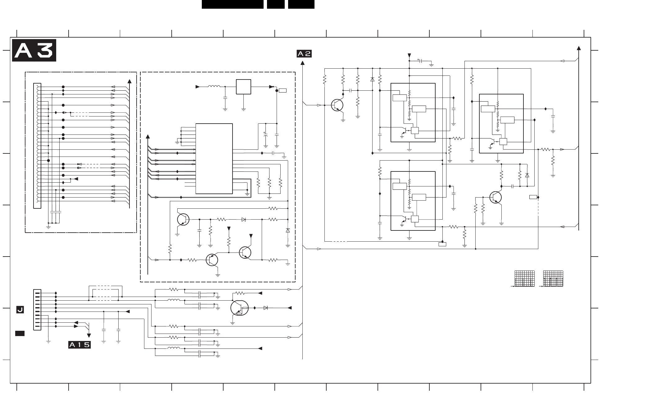
Circuit Diagrams and PWB Layouts 25LC4.6U AA 7.
SSB: Histogram and Hercules
PDP
TO 1320 OF
EMC
OR
TO 0320 OF
MAIN
SWITCH (LCD)
COM
OUTIN
COMP
FF
COMP
COMP
FF
COMPCOMP
FF
COMP
HISTOGRAM & HERCULES
A2
RES
RES
HISTOGRAM
"560" ~ "569"
A2
A2
A2
A2
A2
A2
A2
A2
A2
A2
A2
A2
A2
TO 1XXX OF DMMI BD
DMMI (RES)
A15
A15
(1M20)
A2
TO HERCULES
A2
FROM DC-DC CONVERTER
A2
RESRES
RES
RES
RES
RES
I349 A7
I350 B7
I351 A8
I352 C7
I353 C9
I354 D9
I355 A9
I356 B11
I357 C11
I358 B11
I359 C10
I360 E5
F018 A6
F058 B1
F060 B1
F061 B1
F062 B1
F063 B1
F067 C1
F068 C1
F069 C1
F071 C1
F073 C1
F075 C1
F076 A2
I067 A1
I068 A1
I069 B1
I071 C4
I072 C4
I075 C1
I076 C4
I078 C4
I082 C5
I086 E1
I087 E1
I088 E1
I089 E1
I090 F1
I091 F1
I092 F1
I093 F1
I094 E1
I348 A9
3569 D5
3570 D3
3579 E5
4009 B2
4010 B2
4011 C2
4012 C2
4015 D7
4016 D11
4017 E2
4018 E2
4019 E2
4020 E2
5066 E3
5067 F3
5560 A4
6020 A7
6021 C10
6563 D5
6564 D6
6565 E5
7015 C8
7016 A8
7017 A9
7018 B7
7019 C10
7560 B5
7561-1 E5
7561-2 E4
7562 A5
7563 D4
7579 E5
2564 A4
2565 F2
2566 F3
3020 A7
3021 A8
3022 A7
3026 F3
3029 B11
3030 C10
3032 C10
3039 A7
3058 C9
3063 F3
3066 E3
3340 A6
3342 B9
3343 B9
3344 D9
3345 C11
3346 A9
3347 C7
3348 D9
3349 C10
3560 C6
3561 C5
3562 C5
3563 D5
3564 D5
3565 D4
3566 D4
3567 E4
3568 E5
C
D
E
F
1008 A1
1320 E1
2003 F4
2019 A8
2020 A7
2021 C9
2022 C10
2028 B9
2034 B9
2042 D8
2045 E4
2046 E4
2047 B11
2048 F4
2049 F4
2050 F4
2051 B8
2057 E4
2058 E4
2062 F4
2067 F4
2085 D1
2086 D1
2089 D1
2560 B5
2561 B5
2562 B5
2563 D4
LIGHT-SENSOR-SDM
1234567891011
1234567891011
A
B
C
D
E
F
A
B
+5VSW
3570
3569
2K2
7561-2
BC847BPN
5
3
4
I348
68K
3039
7
8
9
3334
26
27
28
29
3
30
31
32
4
5
6
16
17
18
19
2
20
21
22
23
24
25
1
10
11
12
13
14
15
I360
1008
SFV32R-2STE1
I359
I357
I358
I355
I356
I354
I353
I351
I352
I349
I350
4017
4018
4020
4019
F076
25662565
+5VSW
2
6
13568
1K8
7561-1
BC847BPN
220R
3567
BZX384-C3V3
6565
I078
I094
I092
I093
I091
I089
I090
I088
I086
I087
I082
I072
I076
I071
I069
I075
I067
I068
+5VSW
+3V3STBY
7579
PDTC114ET
1K03579
+8V6
+5V2
+5V2-RELAIS-IO2
+3V3STBY
10p
2067
2062 10p
5067 1u0
2049 10p
10p2050
68R3063
2048 10p
10p2003
3026 68R
10p
2045
2046 10p
5066 1u0
10p
2058 10p
2057
68R
4
5
6
7
8
9
3066B10P-PH-K-S
1320
1
2
3
F075
F071
F073
F069
F067 F068
F063
F062
F060
F061
F058
+3V3STBY
2089 1n0
1n02086
2085 1n0
4012
4011
4010
4009
7563
3564
1K2
PMBT2369
4n7
2563
3566
1K0
1K8
3565 6563
BZX384-C2V7
6564
3563
1K0
F018
100u
2561
16V
+12VSW +8VSW_2
2560
100n
13
L7808CD2T
7562
2
25V10u
2564
5560
3562
100K
3561
100K
3560
100K
100n
2562
20
VEE 18
VIN
9
16 VOUT
YIN 6
YOUT
19
24
1
SCSCL
11
14 SDA
SOUT
21
UIN
8
UOUT
17
VCC
ADEXT3 5
ADR 7
CF
22
15
DECDIG
2
10
12
13
23
7560
TDA9178T/N1
IMPROVEMENT
Φ
ADEXT1 3
ADEXT2 4
4015
PICTURE
4016
+5VSW
TR 2
VCC
8NE555D
7016
CTRL 5
DISC7
GND
1
OUT 3
RES 4
THR6
NE555D
7017
5CTRL
7DISC
1
GND
3OUT
4RES
6THR
2TR
8
VCC
NE555D
7015
5CTRL
7DISC
1
GND
3OUT
RES 4
6THR
2TR
8
VCC
47u
2019
3029
16V
1K0
1K0
3344
3342
15K
3345
4K7
2047
10n
2034
3n3
2022
220p
470R
3058
1K8
3349
7019
BC847B
3030 3032
220K
100K
6021
BAS316
3346
56K
4K7
3348
10n
2021
3n3
2042
820R
3347
BC847B
7018
3340 3020
22K
100p
2020
1K0 10K
3022
BAS316
6020
10n
2028
3n3
2051
2K7
3021
4K7
3343
SC1_R_RF_OUT
SANDCASTLE
LED_RED
RC_IN
LIGHT_SENSOR
PC-TV-LED
STBY-LED
IR
DMMI_R_V_IN
DMMI_G_Y_IN
DMMI_FBL_IN
Const_L_OUT
Const_R_OUT
SC2_CVBS_MON_OUT
RC_IN
IR
IR_OUT
IR_IN
H_CS_SDTV
V_SDTV
SC_STANDBY
POWER-DOWN_BOLT-ON
SC1_CVBS_RF_OUT
SC1_L_RF_OUT
SW-I2C-SDA
SW-I2C-SCL
P50_LINE_ITV_IR_SW
SC2_L_IN
SC2_R_IN
SVHS_AV2_Y_CVBS_IN
SC2_Y_IN
CVBS_IN
DMMI_B_U_IN
V_SDTV
SANDCASTLE
SCL
SDA
INTF_U_OUT
INTF_U_IN
INTF_V_OUT
INTF_V_IN
INTF_Y_OUT
INTF_Y_IN
H_CS_SDTV
HOUT
VSYNC
E_14710_065.eps
100804
3139 123 5867.2
I357 I354
1V / div DC
5ms / div
1V / div DC
20us / div
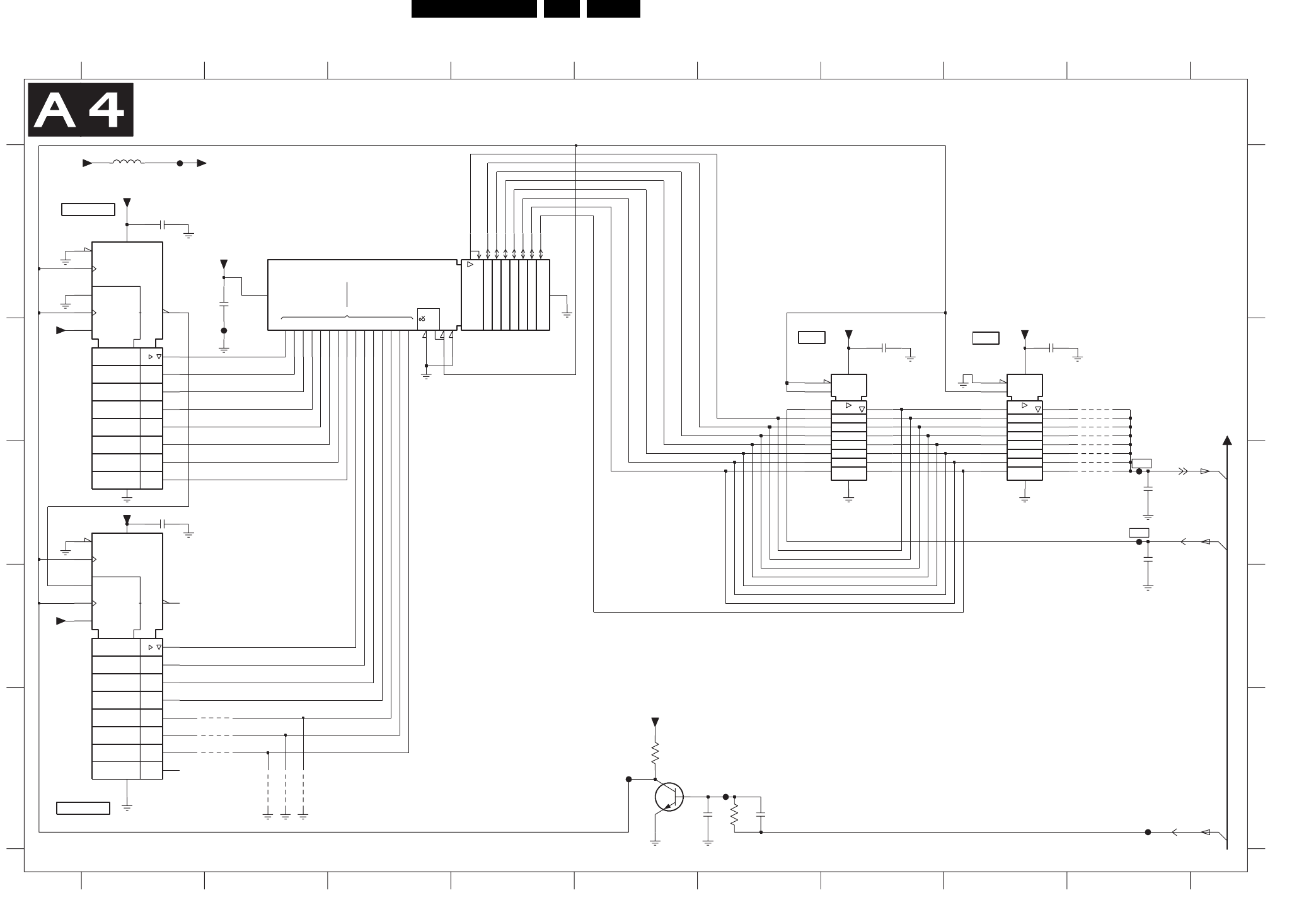
26LC4.6U AA 7.
Circuit Diagrams and PWB Layouts
SSB: Audio Delay line (Lipsync)
EN
C1
1D
EN
C1
1D
2C1
14
13
11
10
9
8
7
6
5
4
3
2
1
0
2EN
32k-1
0
A
A,1D
12
A
G2
C2
G1
1+
CT=0
CTR8
(CT=255)Z4
2D 3
4
EN3
C2
G1
1+
CT=0
CTR8
(CT=255)Z4
2D 3
4
EN3
AUDIO DELAY LINE (LIPSYNC)
COUNTER
COUNTER
DFF DFF
A2
A2
A2
2V3
2V3
5V3
5V3
2V6
2V6
2V6
2V6
2V6
2V6
2V6
5V3
2V5
2V5
2V5
2V5
2V5
2V5
2V5
2V5
2V3
5V3
2V3
5V3
5V3
2V6
2V6
2V6
2V6
2V6
2V6
2V6
2V3
0V2
5V3
2V3
2V6
2V3
5V3
2V6
(1)
(1)
(1)
(1)
(1)
(1)
(1)
(1) NOT USED
(1) NOT USED
(1)
(1)
(1)
123456789
123456789
A
B
C
D
E
A
B
C
D
E
2580 A1
2581 C1
2582 A2
2583 B7
2584 B8
2585 E6
2586 E6
2587 C9
2588 C9
3580 E5
3581 E6
4580 E2
4581 E2
4582 E2
4583 E2
4584 E2
4585 E2
4586 B9
4587 B9
4588 B9
4589 B9
4590 C9
4591 C9
4592 C9
4593 C9
5580 A1
7580 A1
7581 E1
7582 A2
7583 B6
7584 B8
7585 E5
F580 A1
F584 E9
F585 E5
F586 E6
F587 C9
F588 C9
F590 B2
CY62256LL-70ZC
7582
19
14
22
28
27
F590
3
4
5
20
11
12
13
15
16
17
18
7
8
9
10
24
25
26
1
2
32kx8
RAM
21
23
6
82p
2586
470p
2588
20
330p
2587
11
1
19
18
17
16
15
14
13
12
2
3
4
5
6
7
8
9
10
13
12
20
74HC573PW
7583
9
10
11
1
19
18
17
16
15
14
2
3
4
5
6
7
8
F584
74HC573PW
7584
4583
4585
F585
F588
F586
F587
4593
4591
4592
4590
4589
4588
4587
+5VD
4586
4584
4580
4581
4582
BC847BW
7585
3581
47K
3580
470R
2585
82p
+5VD
2584
100n
+5VD
+5VD
2583
100n
+5VD
2582
100n
+5VD
2581 100n
2580
+5VD
+5VD
100n
+5VD
F580
+5VSW 5580 1u0
4
5
6
7
13
9
VCC
16
12
10
GND
8
14
15
1
2
3
7581
M74HC590T
11
3
4
5
6
7
13
9
VCC
16
12
10
GND
8
14
15
1
2
7580
M74HC590T
11
I2SCLK
I2SDI1
I2SDO1
E_14710_066.eps
050804
3139 123 5867.2
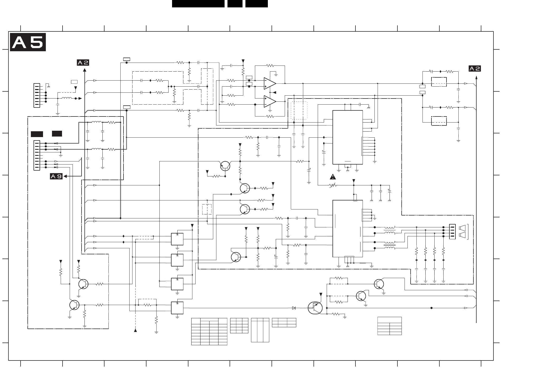
Circuit Diagrams and PWB Layouts 27LC4.6U AA 7.
SSB: Audio Amplifier
N.C.
N.C.
SA3
PDP
TO 1320 OF
EMC
OR
PGND
HS
OUT2B
OUT2A
OUT1B
OUT1A
SGND 1 2
NC
VP1 VP2
SVRR
MODE
IN2-
IN1+
+
-
OUT1
OUT2
IN
+
SGND
2
MUTE
VCC
PW_GND
-
1
STBY
NC
+T
For ITV Only
8 OHMS/5W
ITV MTV
2702
2708
4701
4702
7708
1701
1703
YES
YES
NO
NO
NO
NO
YES
YES
YES
YES
NO
NO
NO YES
AUDIO AMPLIFIER
A2
A15
A2
A2
A2
A2
A2
A2
A2
*EMC
*EMC
*EMC
*EMC
*EMC*EMC
*EMC
*EMC
For ITV
A2
A2
A2
A2
RES
RES
R
L
* AV BUNDLE
NC
NC
(1M02)
FROM HERCULES
FROM HERCULES
HETV AUDIO SUPPLY
HE-TV AUDIO CONN.
NC
NC
TO SCALER INTERFACE
4706
**
ITV MTV
YES NO
4707 YES NO
4708 NO YES
4709 YES NO
*
3714
3726
2 X 3W 2 X 5W
12K
12K
8K2
8K2
**
**
**
**
39R
39R
(INTERNAL AUDIO)
(EXTERNAL AUDIO)
A2
A2
*EMC
*EMC
*EMC
*EMC
INTERNAL AUDIO
(NOT FOR HETV)
from DC-DC Conv
A15
For LCD BZX384-2V7
For PDP BZX384-6V2
PDTA143ET
RES
BC847BS PUMH7
3716
3721 4711
7708
4710
#
##
#
#
LCD PDP
3702
3704
3728
3729
2K2
470R
2K2
3K9
6K8
1K
5K6
3K3
HETV MTV
MTV
HETV
10K
-
-
-
##
#
4714
4715
4716
-
-
-
-
Yes Yes
Yes
Yes
No
I725 B10
I726 A11
I727 B11
I728 E7
I729 D3
I730 E3
I731 E3
I735 F10
I736 F10
I737 F10
I738 F11
I739 C6
I740 D6
I741 E6
I742 E6
F718 B6
F719 B1
F720 B1
F721 B1
F722 B1
F723 C1
F724 C1
F725 C1
F726 C1
F727 C1
F728 C1
F729 B2
I701 A5
I702 B7
I703 B7
I704 A5
I705 A4
I706 A4
I707 A4
I709 C6
I710 C8
I711 C8
I712 C7
I713 E7
I714 D6
I715 D5
I716 D6
I717 D6
I718 D7
I719 D7
I721 G8
I724 A10
5736 E9
6701 G7
7006 D8
7702-1 D6
7702-2 C5
7703-1 E5
7703-2 D6
7706-1 E4
7706-2 E4
7706-3 F4
7706-4 F4
7707 B8
7708-1 F9
7708-2 G8
7710 F8
7713 F2
7714 G2
7740-1 A6
7740-2 B7
F701 A3
F702 B3
F705 E10
F706 E10
F707 E10
F708 E10
F710 G10
F711 E9
F712 E9
F713 E9
F714 E9
F716 A6
F717 A6
3741 A6
3742 B6
3743 B6
3744 E7
3745 B6
3746 E6
3747 D6
3748 E6
3749 D6
3750 E6
3751 E7
3752 B3
3753 C3
4701 A5
4702 B5
4703 D5
4704 B7
4705 B7
4706 A11
4707 B11
4708 E3
4709 E3
4710 F8
4711 F8
4714 G3
4715 F3
4716 F4
4720 B2
5720 B2
5721 B2
5722 C2
5735 E9
3704 G2
3705 A5
3706 E6
3707 G8
3708 A4
3709 A4
3710 A4
3711 A11
3712 B4
3713 B5
3714 C6
3715 C6
3716 F8
3717 C6
3718 B11
3719 C5
3720 C7
3721 F8
3722 C6
3723 F2
3724 F2
3725 D6
3726 D7
3727 E7
3728 G4
3729 G4
3735 E10
3736 E10
3737 E10
3738 E11
3739 A5
3740 A6
8 9 10 11
A
B
C
D
E
F
G
A
B
C
D
E
F
G
1701 D8
1702 A1
1735 E11
1752 C1
2701 B9
2702 A5
2703 E7
2704 A3
2705 A5
2706 A3
2707 A10
2708 B5
2709 C8
1234567891011
4567
6
15
2710 A11
2711 B11
2712 C6
2713 D9
2714 D9
2715 B10
2716 C7
2718 D7
2719 D9
2720 B2
2735 F10
2736 F10
2737 F10
2738 F11
2739 B7
2740 B7
2741 C7
2742 E7
2743 A6
2744 A6
2746 E7
2747 B2
2748 B3
2749 C2
2750 C3
3701 F1
3702 G2
3703 A4
5
2
16
19
1
10
11
20
13
9
7
14
8
3
4
12
17
18
7006
TDA7297D
Φ
AMPLIFIER
BRIDGE
4714
3729
4715
4716
3728
3704
3721
470R
470R
3716
+5V2-RELAIS-IO2
3707
4710
+5V2
4711
AUD-SUP
AUD-SUP
4720
I741
I742
I740
I738
I739
I737
I735
I736
F728
F729
F727
F726
F724
F725
F723
4709
4708
4
4R8
1701
TS482IDT
7740-2
5
6
7
8
3
2
1
84
TS482IDT
7740-1
F721
F722
F720
F718
F719
F717
F714
F716
F712
F713
F711
5721
100p
2747 2748
100p
3752
150R
5722
2749
100p 100p
2750
150R
3753
4
5
6
7
8
9
1752
1
2
3
+3V3STBY
BC847BW
7713
10K
3724
+3V3STBY
3723
1K0
BC847BW
7714 3702
43
3701
1K0
5735
DLW5BS
12
12
43
+3V3STBY
5736
DLW5BS
3747
10K
AUD-SUP
3749
10K
7703-2
BC847BS
3750
6K8
+3V3STBY
3748
10K
3746
BC847BS
7703-1
10K
I713
10u
2703
16V
10K
3706
AUD-SUP
P-GND
I731
I730
10p
2720
I729
AUD-SUP
P-GND
5720
1702
1
2
3
4
5
6
7
B7B-EH-A
I726
I727
I724
I721
I725
I719
I717
I714
I718
I728
I715
I716
I711
I712 I710
I706
I709
I707
I704
I705
I702
I703
I701
F708
F710
F706
F707
F705
F701
F702
100K
3745 +3V3STBY
+3V3STBY
1735
1
2
3
4
B4B-PH-K
4704
4705
6K8
3751
16V
4703
2744
100u
2709
2743
1u0
1u0
22K
3742
22K
3739
3743
22K
3740
100K
3741
22K
2742
470p
470p
2741
470p
27392740
470p
1n0
2736
1n0
2735
1n0
2737
2R2
3735
2738
1n0
3736
2R2
3737
2R2
3738
2R2
114
5
15 16
P-GND
14
19
20
8
9
12
13
10 21
3
18
17 1
2
6
7
TDA1517ATW
POWER
AMPLIFIER
Φ
7707
P-GND
100n
2719
2718
1u0
1K8
3727
8K2
3726
2714
16V
P-GND
2713
P-GND
470u
100n
1u0
2712
1K8
3715
8K2
3714
3
4
7708-2
BC847BS
5
2
6
1
6701
BC847BS
7708-1
7710
11
+3V3STBY
7706-4
12
13
7
14
74HC08PW
7706-3
9
10
7
14
8
74HC08PW
7
14
6
74HC08PW
7706-2
4
5
7706-1
74HC08PW
1
2
7
14
3
+3V3STBY
+3V3STBY
3725
AUD-SUP
10K
10K
3719
BC847BS
7702-2
7702-1
BC847BS
3717
8K2
3722
10K
3720
10K
10u
P-GND
2716
16V
100n
2701
2706
1u0
1u0
2704
33K
3709 3710
33K
3708
33K
10K
3712
10K
37131u0
2708
2705 1u0
4702
10K
4701
3705
3703
10K
2702
1u0
10V
1u0
2746
10K
3744
470u 16V
4707
3718
2715
4706
470u
2707
16V
3711
470p
2710
2711
PROTECT_AUDIO
470p
POR-AUDIO
SOUND-ENABLE
AUDIO-L
AUDIO-R
HP_DET_IN
VSD_POS
SC_STANDBY
SOUND_ENABLE
POWER_DOWN
EXT_MUTE
OUT_MUTE
HP_DET_R_DC
HPIC_LIN
AUDOUTLSL
HPIC_RIN
SC2_L_MON_OUT
SC2_R_MON_OUT
AUDOUTLSR
L-
L+
R-
R+
HP_LOUT
HP_LOUT
HP_ROUT
HP_ROUT
HPIC_ROUT HPIC_ROUT
HPIC_LOUT HPIC_LOUT
E_14710_067.eps
081004
3139 123 5867.2
TO 1739 OF
AUDIO (LCD)
28LC4.6U AA 7.
Circuit Diagrams and PWB Layouts
SSB: TV Supply
COM
OUTIN
1%
1%
RES
11V7
11V8
1V2
0V7
5V5
11V7
TV-SUPPLY
123456789
123456789
A
B
C
D
E
A
B
C
D
E
2910 D8
2911 D9
2920 E4
2921 E5
2930 C3
2931 B6
2932 C4
2933 C7
2934 C4
2935 C8
3910 B7
3911 D7
3930 B3
3931 B4
3932 C4
3933 C4
5910 D8
5920 E3
5930 C3
5931 B7
5932 C8
6910 D8
6911 D9
6930 C7
7910 D7
7920 E4
7930 A5
F912 D9
F913 E9
F915 C9
I901 B4
I902 C3
I903 C4
I904 B7
I905 B6
I906 C7
I907 D8
I908 D7
I907
I908
I905
I903
I904
I902
F915
I901
F912
F913
2
13
+12VSW +8VSW_TV
L78M08CDT
7920
5920
16V47u
2921
16V47u
2920
TUN_GND
TUN_GND
TUN_GND
+VTUN
BC817-25
7910
BZX384-C33
6911
6910
BAV99
5910
1m0
35V22u
2911
2910
470p
1K0
3911
2K2
3910
+12VSW
SUP_GND
+5VSW
5932
10u
16V470u
2935
16V470u
2930
2933
470u 16V
SUP_GND
4n7
2934
I906
3933
3K3
DCOL
8DCOL
GND
4
GND
IS
7IS
SWC
1
SWC
SWE
2SWE
TIMC
3
TIMC
VCC
6VCC
7930
MC34063AD
REGULATOR
REFERENCE
OSC
IPK
Q
R
S
CIN_NEG
5
220u
5931
2932
1K0
3932 SUP_GND
SUP_GND
SUP_GND
SUP_GND
6930
SS14
2931
470p
5930
10u
1R0
3930
1R0
3931
E_14710_068.eps
100804
3139 123 5867.2
33V7
5V3
8V
I904
2V / div DC
5us / div
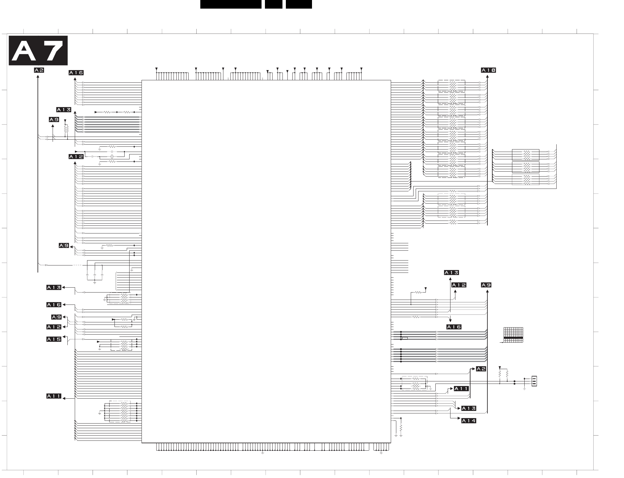
Circuit Diagrams and PWB Layouts 29LC4.6U AA 7.
SSB: Scaler
RX0-
RX1+
RX1-
RX2+
RX2-
IR0
MSTR_SCL
MSTR_SDA
/OCM_WE
EXTCLK
XTAL
TCLK
NO_CONNECT
NO_CONNECT
ACS_RSET_HD
VRED0
VRED1
NO_CONNECT
VGA_SCL
VGA_SDA
AHSYNC
AVSYNC
VGRN6
VGRN7
VBLU0
VBLU1
VBLU2
VBLU3
VBLU4
VBLU5
VBLU6
VBLU7
VDV
VODD
DVI_SCL
DVI_SDA
RX0+
OCMDATA14
OCMDATA13
OCMDATA12
OCMDATA11
VVS
VHS_CSYNC
VCLAMP
PWM0
PWM1
PWM2
OCM_TIMER1
LBADC_IN3
RXC+
RXC-
NO_CONNECT
NO_CONNECT
REXT
BLUE-
BLUE+
GREEN-
GREEN+
RED-
RED+
SOG
SVODD
SVVSYNC
SVHSYNC
SVCLK
OCM_UD0
OCM_UD1
/RESET
IR1
IO_3.3
IO_3.3
IO_3.3
IO_3.3
/OCM_RE
/ROM_CS
/OCM_INT2
/OCM_INT1
/OCM_CS2
/OCM_CS1
/OCM_CS0
OCMADDR19
VRED2
VRED3
VRED4
VRED5
VRED6
VRED7
VGRN0
VGRN1
VGRN2
VGRN3
VGRN4
VGRN5
OCMADDR6
OCMADDR5
OCMADDR4
OCMADDR3
OCMADDR2
OCMADDR1
OCMADDR0
OCMDATA15
DVI_1.8
DVI_1.8
DVI_1.8
DVI_3.3
OCMDATA10
OCMDATA9
OCMDATA8
OCMDATA7
OCMDATA6
OCMDATA5
OCMDATA4
OCMDATA3
LBADC_IN2
LBADC_IN1
LBADC_RETURN
SVDATA0
SVDATA1
SVDATA2
SVDATA3
SVDATA4
SVDATA5
SVDATA6
SVDATA7
SVDV
CORE_1.8
CORE_1.8
CORE_1.8
CORE_1.8
VDDA18_DLL
IO_3.3
IO_3.3
IO_3.3
D_GND
D_GND
D_GND
D_GND
IO_3.3
IO_3.3
IO_3.3
IO_3.3
LBACD_33
FS_2.5
FS_2.5
FS_2.5
OCMADDR18
OCMADDR17
OCMADDR16
OCMADDR15
OCMADDR14
OCMADDR13
OCMADDR12
OCMADDR11
OCMADDR10
OCMADDR9
OCMADDR8
OCMADDR7
LVDSB_3.3
LVDSA_3.3
LVDSA_3.3
LVDSA_3.3
VDDD33_LVDS
FSVREF
FSVREF
DVI_1.8
D_GND
D_GND
D_GND
D_GND
DVI_3.3
DVI_3.3
DVI_3.3
DVI_3.3
ADC_1.8
ADC_1.8
ADC_3.3
ADC_3.3
OCMDATA2
OCMDATA1
OCMDATA0
CORE_1.8
CORE_1.8
CORE_1.8
CORE_1.8
CORE_1.8
CORE_1.8
CORE_1.8
CORE_1.8
CORE_1.8
D_GND
D_GND
D_GND
D_GND
D_GND
D_GND
D_GND
D_GND
DVI_GND
DVI_GND
LBADC_GND
VSSA33_RPLL
D_GND
D_GND
D_GND
D_GND
D_GND
D_GND
D_GND
D_GND
FS_2.5
FS_2.5
FS_2.5
FS_2.5
FS_2.5
FS_2.5
FS_2.5
FS_2.5
FS_2.5
FS_2.5
LVDSB_3.3
LVDSB_3.3
D_GND
D_GND
D_GND
D_GND
D_GND
D_GND
D_GND
D_GND
FSDATA22
FSDATA23
FSDATA24
FSDATA25
D_GND
D_GND
D_GND
D_GND
D_GND
D_GND
D_GND
LVDSB_GND
ADC_3.3
ADC_3.3
VDDA33_RPLL
VDDA33_PLL
VDDA33_FPLL
VDDA33_SDDS
VDDA33_SDDS
VDDA33_DDDS
VDDA33_DDDS
D_GND
D_GND
D_GND
ADC_AGND
ADC_AGND
ADC_AGND
DVI_GND
DVI_GND
DVI_GND
DVI_GND
DVI_GND
FSCKEU
FSBKSELU0
FSBKSELU1
GPIO_G06_B0
VSSA33_PLL
VSSA33_FPLL
VSSA33_SDDS
VSSA33_SDDS
VSSA33_DDDS
VSSA33_DDDS
FSDATA0
FSDATA1
D_GND
D_GND
D_GND
D_GND
D_GND
D_GND
D_GND
D_GND
D_GND
D_GND
VSSA18_DLL
D_GND
FSDATA14
FSDATA15
FSDATA16
FSDATA17
FSDATA18
FSDATA19
FSDATA20
FSDATA21
GPIO_G07_B5
GPIO_G07_B6
GPIO_G07_B7
LVDS_SHIELD(0)
FSDATA26
FSDATA27
FSDATA28
FSDATA29
FSDATA30
FSDATA31
FSADDR0
FSADDR1
LVDSB_GND
LVDSB_GND
VSSA33A_LVDS
VSSA33A_LVDS
VSSA33A_LVDS
VSSD33_LVDS
FSVREFVSS
FSVREFVSS
ADC_DGND
ADC_AGND
ADC_AGND
ADC_DGND
FSDQS
FSDQMU0
FSDQMU1
FSDQMU2
FSDQMU3
/FSWEU
/FSCASU
/FSRASU
GPIO_G09_B2
GPIO_G09_B1
GPIO_G09_B0
PPWR
GPIO_G06_B1
GPIO_G06_B2
GPIO_G06_B3
A3+
A3-
AC+
AC-
GPIO_G05_B0
FSDATA2
FSDATA3
FSDATA4
FSDATA5
FSDATA6
FSDATA7
FSDATA8
FSDATA9
FSDATA10
FSDATA11
FSDATA12
FSDATA13
GPIO_G04_B5
GPIO_G04_B6
GPIO_G04_B7
GPIO_G07_B0
GPIO_G07_B1
GPIO_G07_B2
GPIO_G07_B3
GPIO_G07_B4
B3+
B3-
BC+
BC-
LVDS_SHIELD(4)
LVDS_SHIELD(5)
B2+
B2-
B1+
B1-
B0+
B0-
FSADDR2
FSADDR3
FSADDR4
FSADDR5
FSADDR6
FSADDR7
FSADDR8
FSADDR9
FSADDR10
FSADDR11
FSCLKp
FSCLKn
GPIO_G08_B4/JTAG_TDO
GPIO_G08_B3
GPIO_G08_B2/JTAG_TDI
GPIO_G08_B1/JTAG_MODE
GPIO_G08_B0/JTAG_CLK
GPIO_G09_B5
GPIO_G09_B4
GPIO_G09_B3
DCLK
GPIO_14
GPIO_15
GPIO_16
GPIO_G08_B5/JTAG_RESET
GPIO_G05_B3
A2+
A2-
A1+
A1-
A0+
A0-
GPIO_G04_B0
GPIO_G04_B1
GPIO_G04_B2
GPIO_G04_B3
GPIO_G04_B4
PBIAS
NO_CONNECT
OEXTR
D_GND
VCLK
LVDS_SHIELD(1)
LVDS_SHIELD(2)
LVDS_SHIELD(3)
SCALER
TO FLASH CONTROL
FROM SDRAM
RESERVED TO PCHD-IO
(RES)
(RES)
TO HDMI
TO SUPPLY
TO PCHD-MUX
TO SCALER INTERFACE
TO PCHD-MUX
TO PCHD-MUX
TO HERCULES / HISTOGRAM
NC
NC
NC
NC
(RESERVE)
(RESERVE)
NC
NC
TO FLASH CONTROL
TO HDMI
For SW testing use
FROM SUPPLY
A2
TO HERCULES
A2
A2
FROM/TO PCHD-MUX
A13
A13
A13
A13
A13
A13
A13
A13
A13
A16
A16
A16
A16
A16
A16
A16
A16
A16
A16
FROM HDMI
A12
A12
A12
A12
A12
A12
A12
A12
A12
A12
A12
A12
A12
A12
A12
A12
A12
A12
A12
A12
A12
A12
A12
A12
A12
A12
A12
A12
A10
A10
A10
A10
A10
A10
A10
A10
A10
A10
A10
A10
A10
A10
A10
A10
A10
A10
A10
A10
A10
A10
A10
A10
A10
A10
A10
A10
A10
A10
A10
A10
A10
A10
A10
A10
A10
A10
A10
A10
A10
A10
A10
A10
A10
A10
A10
A10
A10
A10
A10
A10
A10
A10
A10
A10
A10
A16
A16
A13
A11
A11
A11
A11
A11
A11
FROM PCHD-IO
TO PCHD-IO
TO SCALER INTERFACE
A9
A9
TO SCALER INTERFACE A9
(NC)
(NC)
(NC)
(NC)
(NC)
(NC)
(NC)
(NC)
(NC)
(NC)
TO 1409 SCALER INTERFACE
A16
A13
A12
A9
A14
A11
A13
A13
A13
A2
A2
A9
A9
A9
A9
A9
A9
A9
A9
A9
A9
A9
A9
A9
A9
A9
A2
RES
(RES)
SCALER
12345678910111213141516
12345678910111213141516
A
B
C
D
E
F
G
H
I
J
K
L
A
B
C
D
E
F
G
H
I
J
K
L
1401 C3
1408 J15
2487 C3
2488 C2
2490 G2
2491 G3
2492 G3
3401-1 A13
3401-2 A13
3401-3 A13
3401-4 A13
3402-1 B13
3402-2 B13
3402-3 B13
3402-4 B13
3403-1 B13
3403-2 B13
3403-3 B13
3403-4 B13
3404-1 C13
3404-2 B13
3404-3 B13
3404-4 B13
3405-1 C13
3405-2 C13
3405-3 C13
3405-4 C13
3406-1 C13
3406-2 C13
3406-3 C13
3406-4 C13
3407-1 D13
3407-2 D13
3407-3 C13
3407-4 C13
3408-1 D13
3408-2 D13
3408-3 D13
3408-4 D13
3409-1 C15
3409-2 C15
3409-3 C15
3409-4 C15
3410-1 D15
3410-2 D15
3410-3 D15
3410-4 D15
3411-1 D15
3411-2 D15
3411-3 D15
3411-4 D15
3412-1 E13
3412-2 E13
3412-3 E13
3412-4 E13
3413-1 E13
3413-2 E13
3413-3 E13
3413-4 E13
3414 E13
3422 D13
3423 K11
3424 B3
3425 C3
3426 D3
3428 C2
3429 C2
3432 H3
3433 H3
3436 J15
3437 J14
3438-1 J12
3438-2 J12
3438-3 J12
3438-4 J12
3439-1 K3
3439-2 K3
3439-3 K3
3439-4 K3
3440-1 K3
3440-2 K3
3440-3 K3
3440-4 K3
3441-1 I3
3441-2 I3
3441-3 I3
3441-4 I3
3442-1 G3
3442-2 H3
3442-3 H3
3442-4 G3
3443 F3
3446 B3
3447 E13
3448 H12
3449 G12
4446 G2
7401 A4
F402 H12
F403 I12
F404 I12
F405 I12
F406 I12
F407 I12
F408 I12
F409 I12
F410 I12
F417 I12
F436 J15
F437 J15
I423 K11
I424 B3
I425 C4
I426 C4
I427 F4
I429 F4
I438 J11
I439 K4
I440 K4
I441 I4
I442 G4
I443 F4
I446 B4
I449 I4
I450 I4
I451 I4
I452 K4
I453 K4
I454 K4
I455 K4
I456 K4
I457 K4
I458 J11
I459 J11
I460 J15
RES
3K3
+3V3_IO
3449
F417
F409
F410
F407
F408
F406
F404
F405
F403
F402
4446
I460
I449
I459
I457
I458
I456
I454
I455
I453
I451
I452
I450
+3V3STBY
F436
F437
10R3448
I427
I429
I423
I440
I438
I439
I441
I443
I442
I426
I424
I425
1%
I446
2
3
100R
3446
B3B-PH-SM3-TBT
1408
1
2490
100n 100n
2491 2492
10K3443
100n
18
27
3442-1
3442-3 3 6
3442-2
3442-4 4 5
18
10K
27
3441-1
10K
3441-2
3441-3 3 6
3441-4 4 5
3440-1 1 8
3440-2 2 7
10K
36
45
3440-3
18
3440-4
7
3439-1
6
3439-2
10K
2
3439-3 3
3439-4 4 5
3438-1 1 8
10K27
10K
10K3438-3 3 6
3438-2
45
+3V3_IO
10K3438-4
10K
3437 3436
10K
+3V3STBY 3432 10K
10K3433
10K
+3V3STBY
3428 3429
10K
U25
U26
U3
U4
V1
V2
V23
V24
V25
V26
V3
V4
W1
W2
W23
W24
W25
W26
W3
W4
Y1
Y2
Y23
Y24
Y25
Y26
Y3
Y4
R25
R26
R3
R4
T1
T10
T11
T12
T13
T14
T15
T16
T17
T2
T23
T24
T25
T26
T3
T4
U1
U10
U11
U12
U13
U14
U15
U16
U17
U2
U23
U24
N26
N3
N4
P1
P10
P11
P12
P13
P14
P15
P16
P17
P2
P23
P24
P25
P26
P3
P4
R1
R10
R11
R12
R13
R14
R15
R16
R17
R2
R23
R24
L26
L3
L4
M1
M10
M11
M12
M13
M14
M15
M16
M17
M2
M23
M24
M25
M26
M3
M4
N1
N10
N11
N12
N13
N14
N15
N16
N17
N2
N23
N24
N25
J26
J3
J4
K1
K10
K11
K12
K13
K14
K15
K16
K17
K2
K23
K24
K25
K26
K3
K4
L1
L10
L11
L12
L13
L14
L15 L16
L17
L2
L23
L24
L25
E26
E3
E4
F1
F2
F23
F24
F25
F26
F3
F4
G1
G2
G23
G24
G25
G26
G3
G4
H1
H2
H23
H24
H25
H26
H3
H4
J1
J2
J23
J24
J25
C9
D1
D10
D11
D12
D13
D14
D15
D16
D17
D18
D19
D2
D20
D21
D22
D23
D24
D25
D26
D3
D4
D5
D6
D7
D8
D9
E1
E2
E23
E24
E25
B3
B4
B5
B6
B7
B8
B9
C1
C10
C11
C12
C13
C14
C15
C16
C17
C18
C19
C2
C20
C21
C22
C23
C24
C25
C26
C3
C4
C5
C6
C7
C8
AF21
AF22
AF23
AF24
AF25
AF26
AF3
AF4
AF5
AF6
AF7
AF8
AF9
B1
B10
B11
B12
B13
B14
B15
B16
B17
B18
B19
B2
B20
B21
B22
B23
B24
B25
B26
AE16
AE17
AE18
AE19
AE2
AE20
AE21
AE22
AE23
AE24
AE25
AE26
AE3
AE4
AE5
AE6
AE7
AE8
AE9
AF1
AF10
AF11
AF12
AF13
AF14
AF15
AF16
AF17
AF18
AF19
AF2
AF20
AD10
AD11
AD12
AD13
AD14
AD15
AD16
AD17
AD18
AD19
AD2
AD20
AD21
AD22
AD23
AD24
AD25
AD26
AD3
AD4
AD5
AD6
AD7
AD8
AD9
AE1
AE10
AE11
AE12
AE13
AE14
AE15
AB24
AB25
AB26
AB3
AB4
AC1
AC10
AC11
AC12
AC13
AC14
AC15
AC16
AC17
AC18
AC19
AC2
AC20
AC21
AC22
AC23
AC24
AC25
AC26
AC3
AC4
AC5
AC6
AC7
AC8
AC9
AD1
A15
A16
A17
A18
A19
A2
A20
A21
A22
A23
A24
A25
A26
A3
A4
A5
A6
A7
A8
A9
AA1
AA2
AA23
AA24
AA25
AA26
AA3
AA4
AB1
AB2
AB23
7401
GM1601
A1
A10
A11
A12
A13
A14
3423
3K3
22R3412-1 1 8
22R27
22R36
3412-2
45
3412-3
22R
3412-4 22R
3422
22R3414
8
3447 22R
22R3413-1 1
3413-2 2 7
3413-3 22R36
22R
45
3411-1 1 8
3413-4 22R
3411-2 22R27
22R
3411-3 3 6
45
22R
8
22R3411-4
22R3410-1 1
3410-2 22R27
3410-3 3 6
3410-4 22R45
22R
18
27
3409-1 22R
36
3409-2 22R
45
3409-3 22R
8
22R3409-4
3401-1 1
22R3401-2 2 7
22R
36
22R3401-4 4 5
22R3401-3
18
22R27
3402-1 22R
36
3402-2
45
3402-3 22R
8
3402-4 22R
22R3403-1 1
22R3403-2 2 7
22R3403-3 3 6
45
18
22R3403-4
27
3404-1 22R
36
3404-2 22R
45
3404-3 22R
8
3404-4 22R
22R3405-1 1
22R3405-2 2 7
22R3405-3 3 6
22R3405-4 4 5
3406-1 22R18
3406-2 22R27
3406-3 3 6
3406-4 4 5
22R
8
22R
3407-1 22R1
22R3407-2 2 7
22R3407-3 3 6
22R3407-4 4 5
3408-1 22R18
27
36
3408-2 22R
45
3408-3 22R
3408-4 22R
+3V3_DVI +1V8_ADC +3V3_ADC +3V3_PLL+3V3_LVDSA
+3V3_LVDS
FSVREF +1V8_DVI+3V3_LBADC +2V5_DDR
+3V3_LVDSB
+3V3_DVI
+1V8_CORE +3V3_IO
3424
150R 1%
3425
22p2487
+3V3_PLL
10K
22p2488 SMD-49
1401
14M31818
3426
TXBC+
TXBC-
TXB3+
TXB3-
BU_LHT_ADJ1
KEYBOARD
TXB2+
POWER_OK_UP
UART_TX
UART_RX
HOT_PLUG
TXB2-
FSDATA3
FSDATA5
FSDATA4
FSDATA6
FSDQM0
FSDQM3
FSDQM1
FSDQM2
JTAG_TDI_SDA JTAG_TDI_SDA
LAMP_ON-OFF
OCMADDR19
FSCLK+
FSDATA15
FSDATA14
FSDATA16
FSDATA18
FSDATA19
FSDATA21
FSDATA10
FSDATA11
PIXEL+_SYNC
PDP_GO_UP
VS_ON
SD_HD_SEL
PC_HDMI-AUDIO_SEL
PIXEL+_RESET
FSCLK-
DMMI_HD_SEL
TV_SC_COM
Y_NOTCH
TXB1-
TXB0-
PC_HD_SEL
TV_IRQ
TXB1+
TXB0+
PC_HD_DET
NVM-WP
FSRASU
FSCKEU
FSBKSELU0
FSBKSELU1
FSBKSELU1
FSBKSELU0
FSBKSEL1
FSBKSEL0
FSCKE
FSRAS
FSCAS
FSWE
HDMI_VDV
JTAG_CLK_SCL
PANEL-PWR-CTL
FSADDR3
FSADDRU5 FSADDR5
FSADDRU6 FSADDR6
FSADDRU7 FSADDR7
FSADDRU8 FSADDR8
FSADDRU10 FSADDR10
FSADDRU11 FSADDR11
FSADDRU9 FSADDR9
FSADDRU4 FSADDR4
FSDQMU3
FSDQMU2
FSDQMU1
FSDQMU0
FSCKEU
FSRASU
FSCASU
FSWEU
FSDQS
FSDQMU0
FSDQMU1
FSDQMU2
FSDQMU3
FSWEU
FSCASU
FSDATAU29 FSDATA29
FSDATAU2 FSDATA2
FSDATAU1 FSDATA1
FSDATAU0 FSDATA0
FSADDRU0
FSADDRU1
FSADDRU2
FSADDRU3
FSADDRU4
FSADDRU5
FSADDRU6
FSADDRU7
FSADDRU8
FSADDRU9
FSADDRU10
FSADDRU11
FSADDRU0 FSADDR0
FSADDRU1 FSADDR1
FSADDRU2 FSADDR2
FSADDRU3FSDATAU8 FSDATA8
FSDATAU9 FSDATA9
FSDATAU22 FSDATA22
FSDATAU23 FSDATA23
FSDATAU13 FSDATA13
FSDATAU12 FSDATA12
FSDATAU20 FSDATA20
FSDATAU17 FSDATA17
FSDATAU15
FSDATAU16
FSDATAU18
FSDATAU14
FSDATAU19
FSDATAU10
FSDATAU11
FSDATAU21
FSDATAU24 FSDATA24
FSDATAU25 FSDATA25
FSDATAU7 FSDATA7
FSDATAU26 FSDATA26
FSDATAU17
FSDATAU18
FSDATAU19
FSDATAU20
FSDATAU21
FSDATAU22
FSDATAU23
FSDATAU24
FSDATAU25
FSDATAU26
FSDATAU27
FSDATAU28
FSDATAU29
FSDATAU30
FSDATAU31
FSDATAU28 FSDATA28
FSDATAU27 FSDATA27
FSDATAU31 FSDATA31
FSDATAU30 FSDATA30
FSDATAU3
FSDATAU4
FSDATAU6
FSDATAU5
FSDATAU0
FSDATAU1
FSDATAU2
FSDATAU3
FSDATAU4
FSDATAU5
FSDATAU6
FSDATAU7
FSDATAU8
FSDATAU9
FSDATAU10
FSDATAU11
FSDATAU12
FSDATAU13
FSDATAU14
FSDATAU15
FSDATAU16
RX1+IN
RX0-IN
RX0+IN
SDA_DVI
SCL_DVI
V
H_CS
SDA
SCL
SOG
R_PR+
R_PR-
G_Y+
G_Y-
B_PB+
B_PB-
RXC-IN
RXC+IN
RX2-IN
RX2+IN
RX1-IN
HDMI_VHS
HDMI_VVS
HDMI_VCLK
HDMI_VBLU0
HDMI_VBLU1
HDMI_VBLU2
HDMI_VBLU3
HDMI_VBLU4
HDMI_VBLU5
HDMI_VBLU6
HDMI_VBLU7
HDMI_VGRN0
HDMI_VGRN1
HDMI_VGRN2
HDMI_VGRN3
HDMI_VGRN4
HDMI_VGRN5
HDMI_VGRN6
HDMI_VGRN7
HDMI_VRED0
HDMI_VRED1
HDMI_VRED2
HDMI_VRED3
HDMI_VRED4
HDMI_VRED5
HDMI_VRED6
HDMI_VRED7
V-CHIP_INT
POWER_DOWN
#RESET
SCL_IO
SDA_IO
PIP_CLK
PIP_DATA0
PIP_DATA1
PIP_DATA2
PIP_DATA3
PIP_DATA4
PIP_DATA5
PIP_DATA6
PIP_DATA7
TEMP_SENSOR
LBADC3
BU_LHT_ADJ2
HD_FILTER
FAN_SPEED1
#OCM_WE
#OCM_RE
#ROM_CS
OCMADDR18
OCMADDR17
OCMADDR16
OCMADDR15
OCMADDR14
OCMADDR13
OCMADDR12
OCMADDR11
OCMADDR10
OCMADDR9
OCMADDR8
OCMADDR7
OCMADDR6
OCMADDR5
OCMADDR4
OCMADDR3
OCMADDR2
OCMADDR1
OCMADDR0
OCMDATA7
OCMDATA6
OCMDATA5
OCMDATA4
OCMDATA3
OCMDATA2
OCMDATA1
OCMDATA0
E_14710_069.eps
100804
3139 123 5867.2
F405
500mV / div DC
20us / div
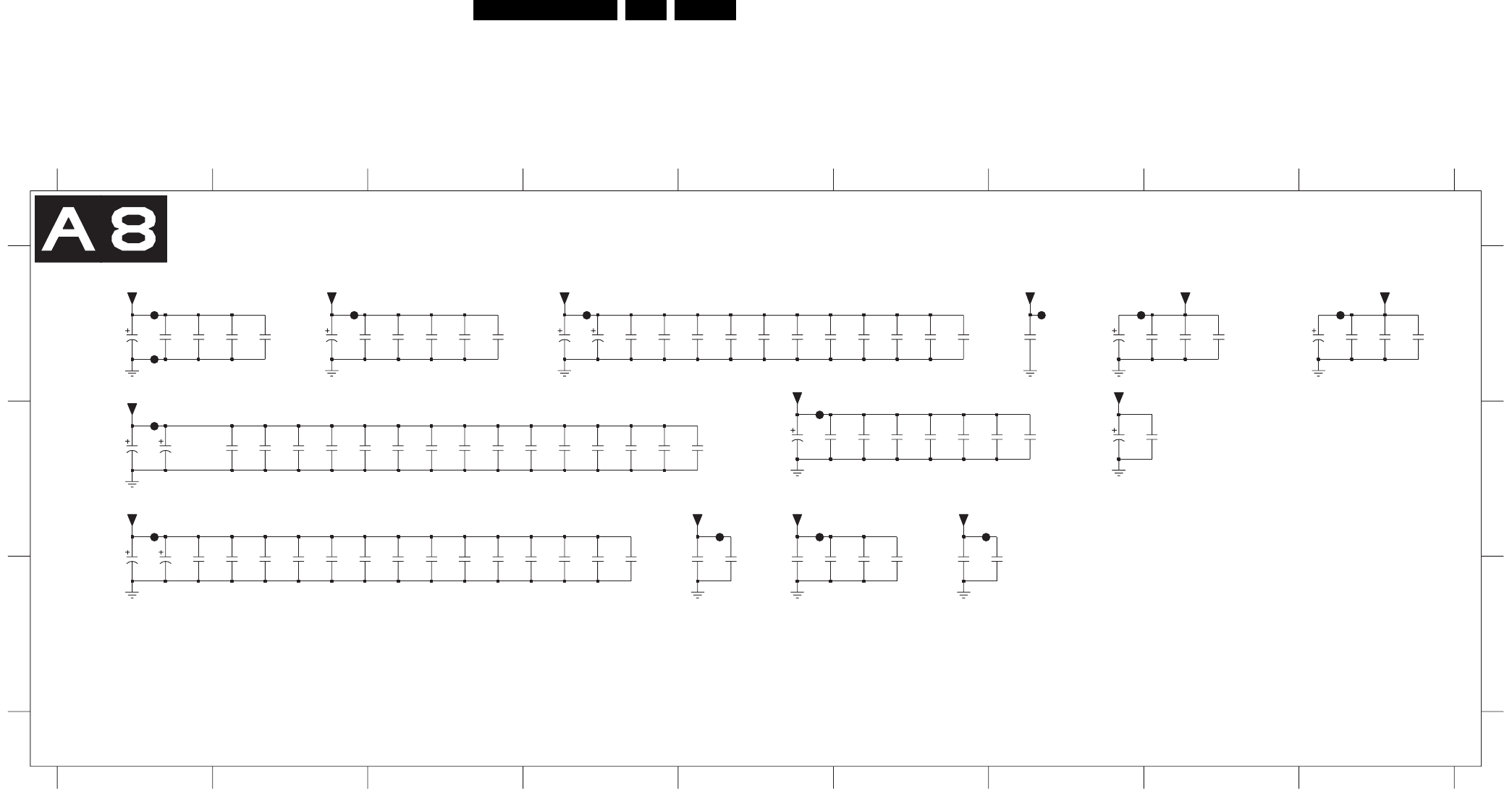
30LC4.6U AA 7.
Circuit Diagrams and PWB Layouts
SSB: Scaler Supply
SCALER SUPPLY
123456789
123456789
A
B
C
A
B
C
2401 B1
2402 B1
2403 B2
2404 B2
2405 B2
2406 B2
2407 B2
2408 B3
2409 B3
2410 B3
2411 B3
2412 B3
2413 B4
2414 B4
2415 B4
2416 B4
2417 B1
2418 B1
2419 B2
2420 B2
2421 B2
2422 B2
2423 B3
2424 B3
2425 B3
2426 B3
2427 B3
2428 B4
2429 B4
2430 B4
2431 B4
2432 B5
2433 B5
2434 A4
2435 A4
2436 A4
2437 A5
2438 A5
2439 A5
2440 A5
2441 A5
2442 A6
2443 A6
2444 A6
2445 A6
2446 A6
2447 B5
2448 B6
2449 B6
2450 B6
2451 A2
2452 A3
2453 A3
2454 A3
2455 A3
2456 A3
2461 B6
2462 B7
2463 B5
2464 B5
2465 A1
2466 A1
2467 A2
2468 A2
2469 A2
2470 B5
2471 B6
2472 B6
2473 B6
2474 B6
2475 B6
2476 B7
2477 B7
2478 A7
2479 A8
2480 A8
2481 A8
2482 A8
2483 A9
2484 A9
2485 A9
2486 A7
2495 B7
2496 B8
F401 B1
F419 B1
F434 A4
F447 B5
F451 A2
F461 B6
F463 B5
F465 A1
F466 A1
F470 B5
F478 A7
F482 A9
F486 A7
2419
100n
F461F447F401 F463
F470
F482
F419
F478F434
F486
F451
F465
F466
47u
2495
100n
2496
16V
+3V3_LBADC
+3V3_LVDS
2486
100n
2485
100n16V
+3V3_LVDSB
2482
22u 100n
24842483
100n100n
2481
+3V3_LVDSA
16V22u
2478 2480
100n100n
2479
FSVREF
100n
2461
+1V8_ADC
2462
100n
2463
100n 100n
2464
22u
+3V3_ADC
2465
16V 100n
24682467
100n100n
2466 100n
2469
2470
22u 16V
2473
100n100n
24722471
100n
2477
100n
100n
24762475
100n
+3V3_PLL
100n
2474
100n
24502449
100n100n
2448
+1V8_DVI
2447
100n
2451
47u 16V 100n
2455
100n
2456
2454
100n100n
2453
+3V3_DVI
2452
100n 2445
100n
47u
2434 2435
47u 16V16V 100n
2444 2446
100n
2443
100n100n
24422441
100n100n
24402439
100n
2438
100n100n
2437
+3V3_IO
2436
100n
+2V5_DDR
100n
2433
2404
100n 100n
2416
2415
100n100n
24142413
100n100n
24122411
100n100n
24102409
100n100n
2408
100n100n
2406 2407
+1V8_CORE
2405
100n
2401
47u 16V 16V47u
2402 100n
2403
100n
2420 100n100n
2431 2432
100n
2429 2430
100n
2428
100n100n
24272426
100n100n
24252424
100n100n
24232422
100n100n
2421
47u
2417 2418
47u 16V
16V
E_14710_070.eps
060804
3139 123 5867.2
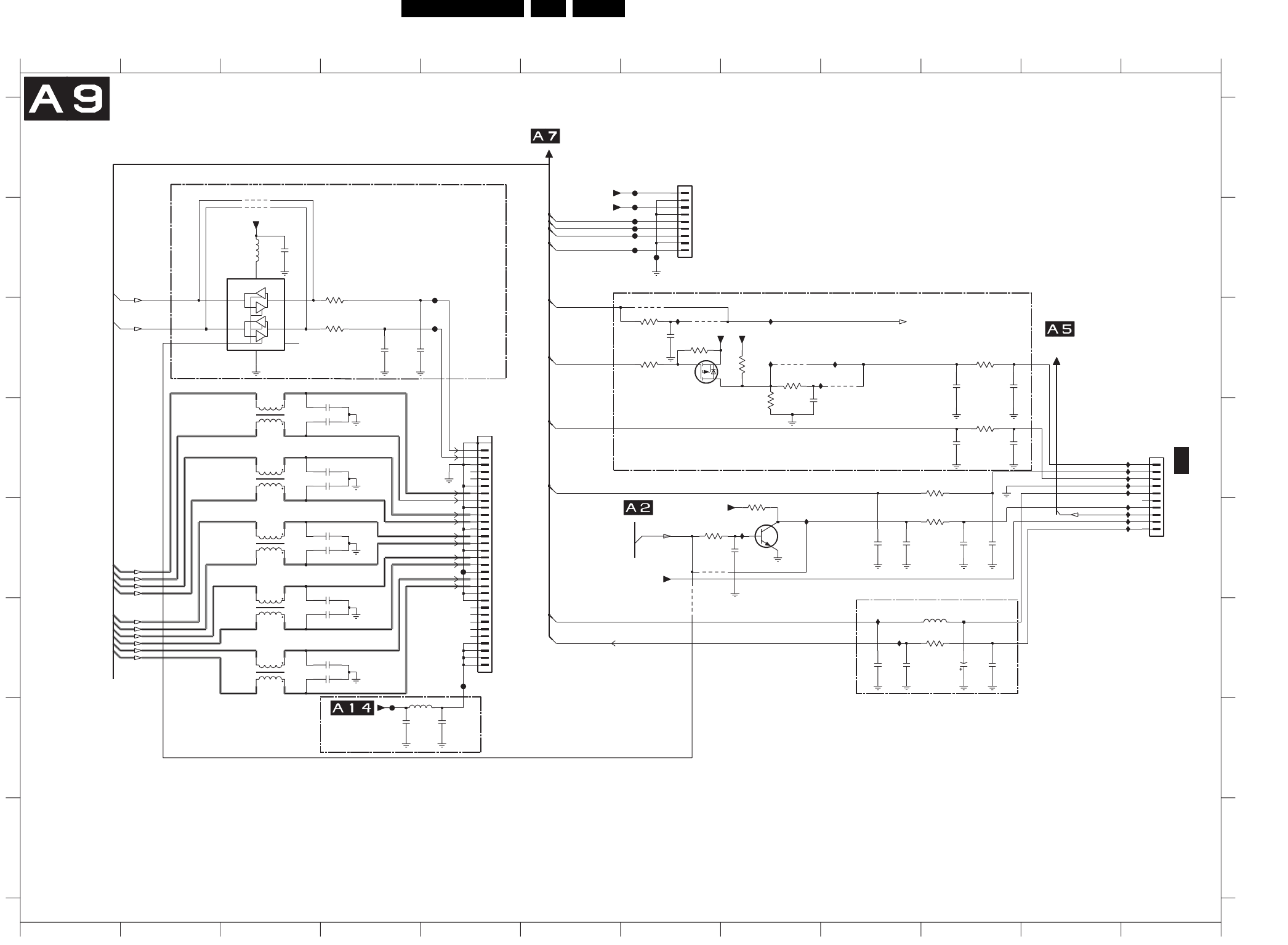
Circuit Diagrams and PWB Layouts 31LC4.6U AA 7.
SSB: Scaler Interface
SA1
(LCD)
OR
TO CN9005 OF SUB SUPPLY (PDP)
SCALER INTERFACE
TO SCALER
PROVISION FOR
PIXEL+ MODULE
NC
FROM HERCULES
FOR PDP ONLY
FROM AUDIO
RES
RES
RES
(NC)
FOR LCD ONLY
RES
RES
RES
(NC)
(NC)
(NC)
(NC)
(NC)
FOR PDP ONLY
FOR LCD ONLY
(1G50)
NC
A7
A7
A7
A7
A7
A7
A7
A7
A7
A7
A7
A7
RES
LVDS CONNECTOR
(PDP)
(RES)
123456789101112
123456789101112
A
B
C
D
E
F
G
H
A
B
C
D
E
F
G
H
1403 D12
1409 A7
1450 D5
1860 D3
1861 D3
1862 E3
1863 F3
1864 F3
2493 C9
2494 C7
2860 D3
2861 D3
2862 D3
2863 D3
2864 E3
2865 E3
2866 E3
2867 F3
2868 F3
2869 F3
2870 C4
2871 C5
2872 B3
2874 G4
2875 G5
2876 C10
2877 E9
2878 D10
2879 C11
2880 E10
2881 D11
2882 F9
2883 E9
2884 E8
2885 F9
2886 F10
2887 E10
2889 F10
3416 C7
3417 C8
3418 C7
3427 C7
3444 C8
3460 C8
3870 C4
3871 B4
3876 C10
3877 D9
3879 D10
3883 E9
3885 F9
3886 D8
3887 E7
4427 C7
4428 C7
4444 C9
4445 C8
4871 B3
4872 B3
4887 E7
4888 E7
5872 B3
5874 G5
5882 F9
7416 C7
7872 B2
7887 E8
F411 A7
F412 B7
F413 B7
F414 B7
F415 B7
F416 B7
F418 B7
F870 B5
F871 C5
F872 G4
F873 F5
F874 E5
I428 C7
I436 C8
I437 C9
I444 C8
I445 C9
I860 D12
I861 D12
I862 D12
I863 D12
I864 D12
I865 E12
I866 E12
I867 F9
I868 E12
I869 E12
I870 E8
I871 E8
I872 F9
A2
AMPLIFIER
2884
10n
I872
390R
3418
I871
F874
I870
F873
F870
F871
F872
F418
4888
F416
F415
F413
F414
F411
F412
+5VSWI
+3V3STBY
1
2
3
4
5
6
7
8
9
1409
S9B-PH-SM3-TB-A
I444
4871
4872
100n
2872
5872
SCL1 7
SDA03SDA16
VCC
8
+3V3STBY
7872
PCA9515DP
EN5
GND
4
NC 1
SCL02
10p
2875
PAN_VCC
2874
10p
5874
2870
10p 10p
2871
68R
3870
3871
68R
4
5
6
7
8
9
32
33
22
23
24
25
26
27
28
29
3
30
31
13
14
15
16
17
18
19
2
20
21
1450
FI-WE31P-HF-E1500
1
10
11
12
1
2
4
3
1864
DLW21S
DLW21S
1863
1
2
4
32
4
3
1862
DLW21S
11
2
4
3
4
3
DLW21S
1861
1860
DLW21S
1
2
2869 10p
2868 10p
10p2867
10p
10p
2865
2866
10p
2863
2864
2862
10p
10p
2860
10p
2861
10p
+5VSWI
1K0
3460
+5VSWI
3417
3
1
2
1K0
3416
7416
SI2301DS-T1
I437
I436
I428
I445
2493
1u0
4445
10K
3444 4444
2494
3427
4428
4427
I868
I867
I869
I865
I866
I864
I862
I863
I861
I860
4887
10K
+3V3STBY
BC847BW
7887
3886
10K
3887
2889
10p
10u
2886
+5V2_RELAIS_IO2
2885
10p
2887
10p
2883
10p
2882
10p
68R3885
3883 68R
1u0
2881
10n
5882
10n
2878
68R
2880
3879
10p
2877
10p
3877 68R
2879
10n10n
2876
5
6
7
8
9
3876 68R
1403
1
10
2
3
4
SDA_IO
SCL_IO
BUF_ENABLE
BUF_ENABLE
PIXEL+_SYNC
PIXEL+_RESET
SCL_IO
SDA_IO
TXB1+
TXB1-
TXB0-
TXB0+
+12V_LCD
SCL_DMA_BUS1_DISP
SDA_DMA_BUS1_DISP
VDISP2
VDISP_2
CTRL_DISP1
CTRL_DISP2
CTRL_DISP3
LVDSD+
LVDSD-
LVDSC+
LVDSC-
LVDSB+
LVDSB-
LVDSA+
LVDSA-
TXBC+
TXB3-
TXBC-
LVDSCLK+
LVDSCLK-
TXB2+
TXB2-
POWER_OK_UP
SC_STANDBY
BU_LHT_ADJ2
BU_LIGHT_ADJ2
BU_LHT_ADJ1
TXB3+
LIGHT_ON
FAN_SPEED1
LAMP_ON-OFF
BACKLIGHT_CTRL
POWER_OK
FAN_SPEED
STANDBY
PROTECT_AUDIO
BU_LIGHT_ADJ1
POR
E_14710_071.eps
120804
3139 123 5867.2
TO 1M03 OF SUPPLY
32LC4.6U AA 7.
Circuit Diagrams and PWB Layouts
SSB: SDRAM
FSVREF
VREF
28
27
26
25
24
D
DQS
0
1
2
3
DM
11
RFU
12
9
8
9
10
2
3
4
21
20
19
18
17
16
31
30
6
1
0
A
11
14
CAS
RAS
29
5
6
7
8
VDDQVDD
WE
0
MCL
NC
13
NC
1BA
23
22
7
5
4
3
2
15
VSS VSSQ
10
CS
CKE
CK
D
0
1
CK
SDRAM
TO/FROM SCALER
A7
A7
A7
A7
A7
A7
A7
A7
A7
A7
A7
A7
A7
A7
A7
A7
A7
A7
A7
A7
A7
A7
A7
A7
A7
A7
A7
A7
A7
A7
A7
A7
A7
A7
A7
A7
A7
A7
A7
A7
A7
A7
A7
A7
A7
A7
A7
A7
A7
A7
A7
A7
A7
A7
A7
A7
A7
A7
A7
12345678
12345678
A
B
C
D
E
F
A
B
C
D
E
F
2501 A1
2502 A1
2503 A1
2504 A1
2505 A2
2506 A2
2507 A2
2508 A3
2509 A3
2510 A3
2511 A3
2512 A4
2513 A4
2514 A4
2515 A5
2516 A5
2517 B4
2526 A4
3501 A3
3502 B3
3503 B2
7501 B3
F501 B3
I502 B2
I503 B2
62
70
76
82
92
99
25
+2V5_DDR
+2V5_DDR
2526
22u16V
F501
I503
I502
FSVREF
1%
1%
10K
3502
150R
3503
2517
100n
3501
10K
1%
73
79
86
5816
46
66
85
5
11
19
15
35
65
96
2
95
8
14
22
59
67
39
40
41
42
43
44
87
8827
93
3
4
6
7
60
61
94
52
38
89
90
91
74
75
77
78
80
81
1
83
84
72
9
10
12
13
100
17
18
20
21
23
56
24
57
97
98
63
64
68
69
71
51
45
29
30
26
55
53
54
28
31
32
36
37
33
34
47
48
49
50
+2V5_DDR
Φ
SDRAM
1M X 32 X 4
K4D263238M-QC50
7501
100n
2516
100n
25152514
100n100n
25132512
100n100n
25112510
100n
2508
100n 100n
2509
100n
25072506
100n100n
25052504
100n100n
2503
47u
2502
47u
FSDQM0
FSDQM1
FSDQM2
FSDQM3
FSRAS
FSCAS
FSWE
FSBKSEL0
FSBKSEL1
FSCLK+
FSCLK-
2501
FSDATA2
FSDATA20
FSDATA21
FSDATA22
FSDATA23
FSDATA24
FSDATA25
FSDATA26
FSDATA27
FSDATA28
FSDATA29
FSDATA3
FSDATA30
FSDATA31
FSDATA4
FSDATA5
FSDATA6
FSDATA7
FSDATA8
FSDATA9
FSDQS
FSCLK-
FSCKE
FSADDR0
FSADDR1
FSADDR10
FSADDR11
FSADDR2
FSADDR3
FSADDR4
FSADDR5
FSADDR6
FSADDR7
FSADDR8
FSADDR9
FSCLK+
FSDATA0
FSDATA1
FSDATA10
FSDATA11
FSDATA12
FSDATA13
FSDATA14
FSDATA15
FSDATA16
FSDATA17
FSDATA18
FSDATA19
E_14710_072.eps
100804
3139 123 5867.2
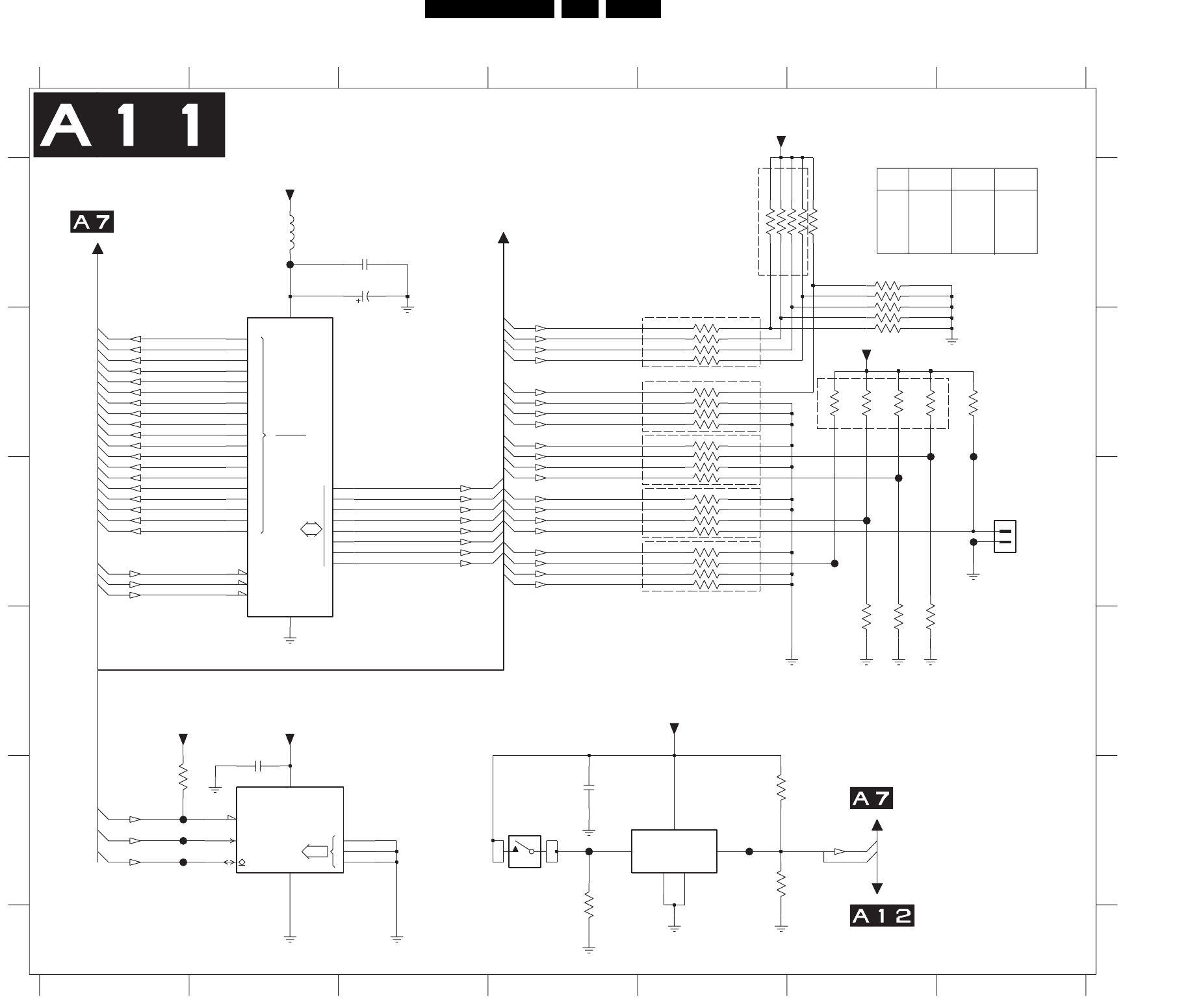
Circuit Diagrams and PWB Layouts 33LC4.6U AA 7.
SSB: Flash / Control
SCL
ADR
0
1
2SDA
WC
12
CE
WE
14
17
18
6
5
4
3
2
1
0
15
0
10
9
8
7
OE
11
13
DQ
16
7
512K-1
0
A
E_14710_073.eps
060804
3139 123 5867.2
FLASH / CONTROL
RES
TO SCALER
RES RES RES
FOR TESTING USE
TO HDMI
A7
A12A7
A7
A7
TO SCALER
A7
A7
A7
A7
A7
A7
A7
A7
A7
A7
A7
A7
A7
A7
A7
A7
A7
A7
A7
A7
A7
A7
A7
A7
A7
A7
A7
A7
A7
A7
A7
A7
A7
A7
A7
A7
A7
A7
A7
A7
A7
A7
A7
A7
A7
A7
A7
A7
A7
A7 RES
RES
RES
RES
RES
1234567
1234567
A
B
C
D
E
A
B
C
D
E
1530 C7
1532 E4
2530 A3
2531 E2
2532 E4
2533 A3
3531 E2
3532 E4
3533 E6
3534 E6
3536 B7
3538-1 C5
3538-2 C5
3538-3 C5
3538-4 C5
3539-1 C5
3539-2 C5
3539-3 C5
3539-4 C5
3540-1 B6
3540-2 B6
3540-3 B6
3540-4 B6
3541 D6
3542 D6
3543 D7
3544-1 B5
3544-2 B5
3544-3 C5
3544-4 C5
3545-1 B5
3545-2 B5
3545-3 B5
3545-4 B5
3546-1 B5
3546-2 B5
3546-3 B5
3546-4 B5
3547-1 A5
3547-2 A5
3547-3 A6
3547-4 A6
3548 A6
3549 B6
3550 A6
3551 B6
3552 A6
3553 A6
5530 A2
7530 A2
7531 E3
7532 E5
F530 A2
F531 E2
F532 E2
F533 E2
F534 E4
F535 E5
F536 C7
F537 C6
F538 C6
F539 C6
F540 C7
F541 C7
For Software
Development
only - (RES)
Item LCD 30" PQP 42"
3549
3550
3551
3552
3553
1K 1K
1K 1K
1K RES
1K 1K
1K 1K
(RES)
AUO 30"
RES
1K
RES
RES
1K
3550
3548 10K
+3V3_IO
3552
3553
3551
45
3549
6
10K
3547-4
3547-3 10K
3
10K
3547-2 2 7
3547-1 10K
18
F541
F539
F540
F538
F536
F537
F534 F535
F533
F532
F530
F531
45
+3V3STBY
36
3546-4 10K
27
3546-3 10K
18
3546-2 10K
45
3546-1 10K
10K3545-4
10K3545-3 3 6
10K3545-2 2 7
10K3545-1 1 8
45
36
3544-4 10K
27
3544-3 10K
18
3544-2 10K
3544-1 10K
100n
2533
3536
10K
1530
B2B-PH-SM3-TBT
1
2
35433542
3540-4
45
+3V3_IO
3540-3
36
27
18
3540-2
10K
3540-1
3541
45
36
3539-4 10K
27
3539-3 10K
8
3539-2 10K
3539-1 10K1
10K3538-4 4 5
10K3538-3 3 6
10K3538-2 2 7
10K3538-1 1 8
10K
3532
1532
SKQR
5530
24
3216
31
+3V3_IO
16V10u
2530
22
13
14
15
17
18
19
20
21
1
10
9
8
7
6
5
27
26
11
23
25
4
28
29
3
2
30
7530
M29W040B-55K1
[FLASH]
ROM
512Kx8
12
1K0
3534
2531
100n
3533
2532
100n
+3V3STBY
+3V3STBY
10K
3531 8
4
7
7531
EEPROM
Φ
(4Kx8)
M24C32-WMN6T
1
2
3
6
5
1MR
2SUB
VCC 5
4
VOUT
NE56610-27
7532
GND
3
OCMADDR13
OCMADDR8
OCMADDR9
OCMADDR19
OCMADDR4
OCMADDR5
OCMADDR6
OCMADDR7
OCMADDR0
OCMADDR1
OCMADDR2
OCMADDR3
OCMADDR5
OCMADDR6
OCMADDR7
OCMADDR8
OCMADDR9
#ROM_CS
OCMDATA0
OCMDATA1
OCMDATA2
OCMDATA3
OCMDATA4
OCMDATA5
OCMDATA6
OCMDATA7
#OCM_RE
#OCM_WE
OCMADDR10
OCMADDR11
OCMADDR12
OCMADDR15
OCMADDR16
OCMADDR18
OCMADDR17
OCMADDR14
SCL_IO
SDA_IO
NVM-WP
#RESET
OCMADDR0
OCMADDR1
OCMADDR10
OCMADDR11
OCMADDR12
OCMADDR13
OCMADDR14
OCMADDR15
OCMADDR16
OCMADDR17
OCMADDR18
OCMADDR2
OCMADDR3
OCMADDR4
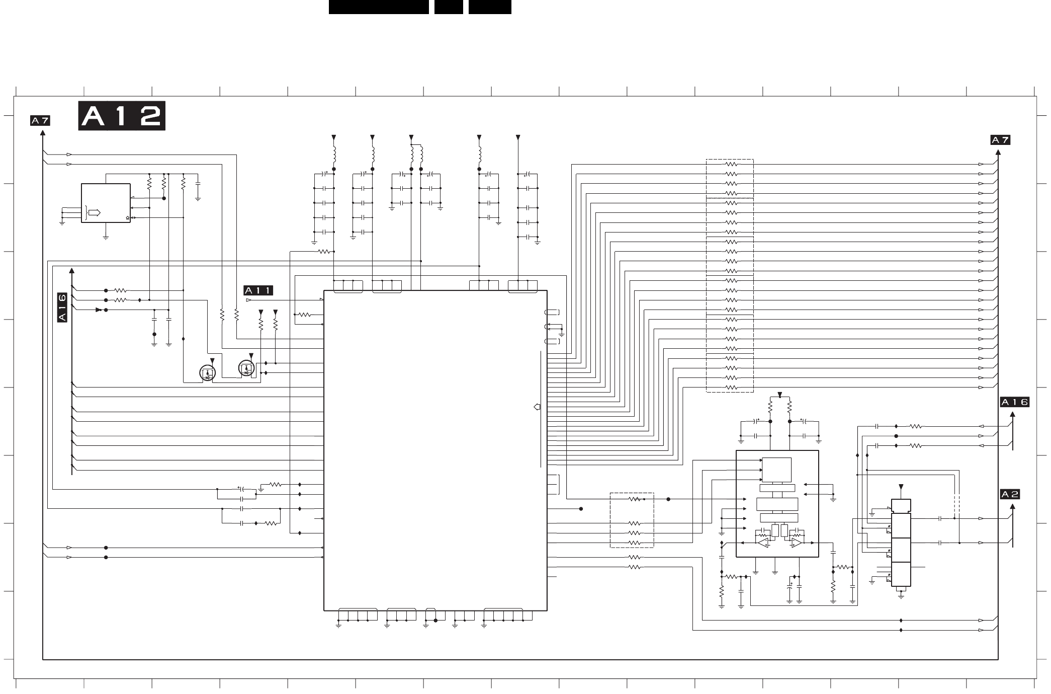
34LC4.6U AA 7.
Circuit Diagrams and PWB Layouts
SSB: HDMI
4X1
G4
4X2
1
2
VDD
VEE VSS
DIGITAL
DE-EMPHASIS
INTERPOLATION
DAC
NOISE SHAPER
FILTER
INTERFACE
DAC
SCL
ADR
0
1
2 SDA
WC
22
21
20
19
18
17
16
15
14
13
12
11
10
9
8
7
6
5
RSET
RX2+
RX2-
RX1+
RX1-
RESET
MCLKIN
CSCL
CSDA
DSCL
DSDA
RXC-
VSYNC
GND PGND OGND
RSVDL
DE
ODCK
INT
Q
NC
RXC+
RX0-
RX0+
AGND
GND_HS
DACGNDG
DACGNDB
DACGND
DACGNDR
23
VCCAVCC
MCLKOUT
OVCC1
DACVCCB
DACVCCG
DACVCCR
DACVCC
PVCC2
PVCC1
ANRPR
ANGY
ANBPB
SPDIF
SDO
WS
SCK
HSYNC
4
3
2
1
0
RSVDO
EXT-RES
PLLOUT
PLLIN
COMP
NC
NC
NC
NC
HDMI
TO SCALER
(NC)
RESERVED FOR HDMI CONNECTION
NC
NC
NC
FROM SCALER
TO HERCULES
FROM PCHD-IO
FROM FLASH/CONTROL
A7
A7
A7
A7
A7
A7
A7
A7
A7
A7
A7
A7
A7
A7
A7
A7
A7
A7
A7
A7
A7
A7
A7
A7
A7
A7
A7
A16
A16
A2
A2
A7
A7
A7
A7
0R
0R
123456789101112131415
123456789101112131415
A
B
C
D
E
F
G
H
A
B
C
D
E
F
G
H
2803 A6
2806 A8
2807 B6
2808 B8
2809 A7
2810 A5
2811 B6
2812 A3
2813 A7
2814 B7
2815 B8
2816 B5
2817 B6
2818 A6
2819 B7
2820 B7
2821 B8
2822 B5
2823 B5
2824 B6
2825 B7
2826 B7
2827 B8
2828 B5
2829 B6
2830 B6
2832 C3
2833 E11
2834 E12
2835 E11
2836 E12
2837 F4
2838 F4
2839 F4
2840 F4
2841 G11
2842 G13
2843 G12
2844 G12
2845 G11
2846 G13
2847 E13
2848 E13
2849 C2
2850 F14
2851 G14
3801-1 A11
3801-2 A11
3801-3 A11
3801-4 B11
3802-1 B11
3802-2 B11
3802-3 B11
3802-4 B11
3803-1 B11
3803-2 B11
3803-3 C11
3803-4 C11
3804-1 C11
3804-2 C11
3804-3 C11
3804-4 C11
3805-1 C11
3805-2 D11
3805-3 D11
3805-4 D11
3806-1 D11
3806-2 D11
3806-3 D11
3806-4 D11
3807 G9
3808 A2
3809 A3
3810 A3
3813-1 G9
3813-2 G9
3813-3 F9
3813-4 F9
3815 G11
3816 G11
3817 G12
3819 G13
3821 C5
3822 C4
3823 C4
3824 C4
3825 C4
3826 E12
3827 E12
3828 C2
3830 G9
3831 F4
3832 C2
3834 F4
3835 B5
3836 E14
3838 E14
4836 F14
4838 F14
5801 A6
5802 A5
5803 A7
5804 A6
5805 A7
7801 A2
7806 D4
7807 D3
7808 C5
7809 E11
7810 F13
F801 A6
F802 A5
F803 A7
F804 A6
F805 A7
F806 G2
F807 G2
F808 H7
F809 B3
F810 F10
F811 E13
F820 C2
F821 C2
F822 C2
F823 F9
F824 D2
F826 E12
F827 E12
I802 C2
I803 D3
I815 G11
I816 G11
I819 G13
I822 D4
I823 D4
I824 F5
I825 F5
I826 G5
I827 H14
I828 H14
I834 F5
I836 E13
I838 E13
I840 F4
I841 G11
I842 G12
I844 G12
I847 E13
I848 E13
14
15
4
9
16
7
8
13
1
3
12
2
5
HEF4053B
7810
MDX
6
11
10
2851
1u0
2850
1u0
I827
I828
I826
I824
I825
I823
F823
F824
F822
F821
F811
F820
F826
F827
F810
F807
F808
F806
F803
F804 F805
F802 F801
F809
4836
4838
I834
I840
I822
I802
I803
I841
I815
I816 I844 I842
I819
I848
I838
I847
+5VHDMI
I836
10n
2849
2848
1u0
2847
1u0
3836
10K
10K
3838
100R
3834
3835
390R
+3V3STBY
33R3807
45
33R3830
36
33R3806-4
7
33R3806-3
33R3806-2 2
33R3806-1 1 8
45
36
3805-4 33R
3805-2 2 7
3805-3 33R
18
33R
33R3805-1
3804-4 33R45
33R36
3804-2 2 7
3804-3
3804-1 1 8
33R
45
33R
36
3803-4 33R
27
3803-3 33R
18
3803-2 33R
3803-1 33R
3802-4 33R45
3802-3 33R36
3802-2 33R27
1833R3802-1
2846
100n
3819
100R
3817
1u0
2842
10V
220K
2845
100n
3815
100R
220K
10V1u0
3816
2841
6.3V
2843
47u
2844
100n
1R0
3827
1R0
6.3V
3826
2834
47u
+3V3STBY
2836
100n
6.3V47u
2833
2835
100n
45
36
3801-4 33R
27
3801-3 33R
18
3801-2 33R
VSSD
2WS
33R3801-1
SFOR1
6SYSCLK
13
VDDA
4
VDDD
14 VOL 16
VOR
12
VREF-DAC
15
VSSA
5
1BCK
3DATAI
9DEEM
8MUTE
10 PCS
11
SFOR0
7
7809
UDA1334BT/N2
2806
6.3V22u
2815
1n0
1n0
28202822
1n0
2811
1n0
5801
3813-4 4 5
36
33R
27
3813-3 33R
18
3813-2 33R
3813-1 33R
3831
3K9
2840 10u
2838 10n
47n2839
2837 10u
16V
3832
3828
1n0
2832
28123810 100n
3809
4K7 4K7
4
7
3808
4K7
1
2
3
6
5
8
+3V3STBY
+3V3STBY
7801
(256x8)
Φ
EEPROM
M24C02-WMN6
+3V3STBY+3V3STBY
3822
4K7
3823
4K7
3824
100R 100R
3825
7806
BSN20
7807
BSN20
33R
3821
+3V3STBY
5802
+3V3STBY
+3V3STBY
16V
2818
5804
2813
16V10u 10u
+3V3STBY
5805 5803
10u 16V
2809
2803
+3V3STBY
2810
22u 6.3V22u 6.3V
100n
2808
100n
28142819
100n
100n
2824
2807
100n
2816
100n
2821
1n0
2827
1n0
2826
1n0
2825
1n0
2830
1n0
2817
1n0
1n0
2823 2829
1n0
30
29
17
40
64
100
34
31
2828
1n0
20
87
86
92
91
97
96
84
83
32
62
61
60
59
58
55
72
9
18
73
19
48
44
43
42
68
39
38
37
36
63
80
23
70
69
54
53
52
51
50
49
57
66
78
21
47
56
67
79
22
24
25
101
33
71
27
26
3
4
46
28
45
11
6
35
77
76
81
16
41
65
99
95
8
74
75
2
13
10
5
1
14
85
88
90
94
98
15
12
7
82
89
93
7808
SII9993CT100
RECEIVER
PANELLINK
HDMI
Φ
PC_AUDIO_L
DOC_SCL
DOC_SDA
HDMI_VGRN0
HDMI_VGRN1
HDMI_VGRN2
HDMI_VGRN3
HDMI_VGRN4
HDMI_VGRN5
HDMI_VGRN6
HDMI_VGRN7
HDMI_VRED0
HDMI_VRED1
HDMI_VRED2
HDMI_VRED3
HDMI_VRED4
HDMI_VRED5
HDMI_VRED6
HDMI_VRED7
HDMI_VDV
HDMI_VCLK
PC_HDMI-AUDIO_SEL
AudioIN2L
AudioIN2R
PC_AUDIO_R
HDMI_VBLU0
HDMI_VBLU1
HDMI_VBLU2
HDMI_VBLU3
HDMI_VBLU4
HDMI_VBLU5
HDMI_VBLU6
HDMI_VBLU7
SCL_IO
SDA_IO
+5VHDMI
RX1+
RX1-
RX2+
RX2-
RXC+
RXC-
SPDIF
HDMI_VVS
COMP
COMP
HDMI_VHS
PLLIN
PLLIN
#RESET
RX0+
RX0-
E_14710_074.eps
060804
3139 123 5867.2
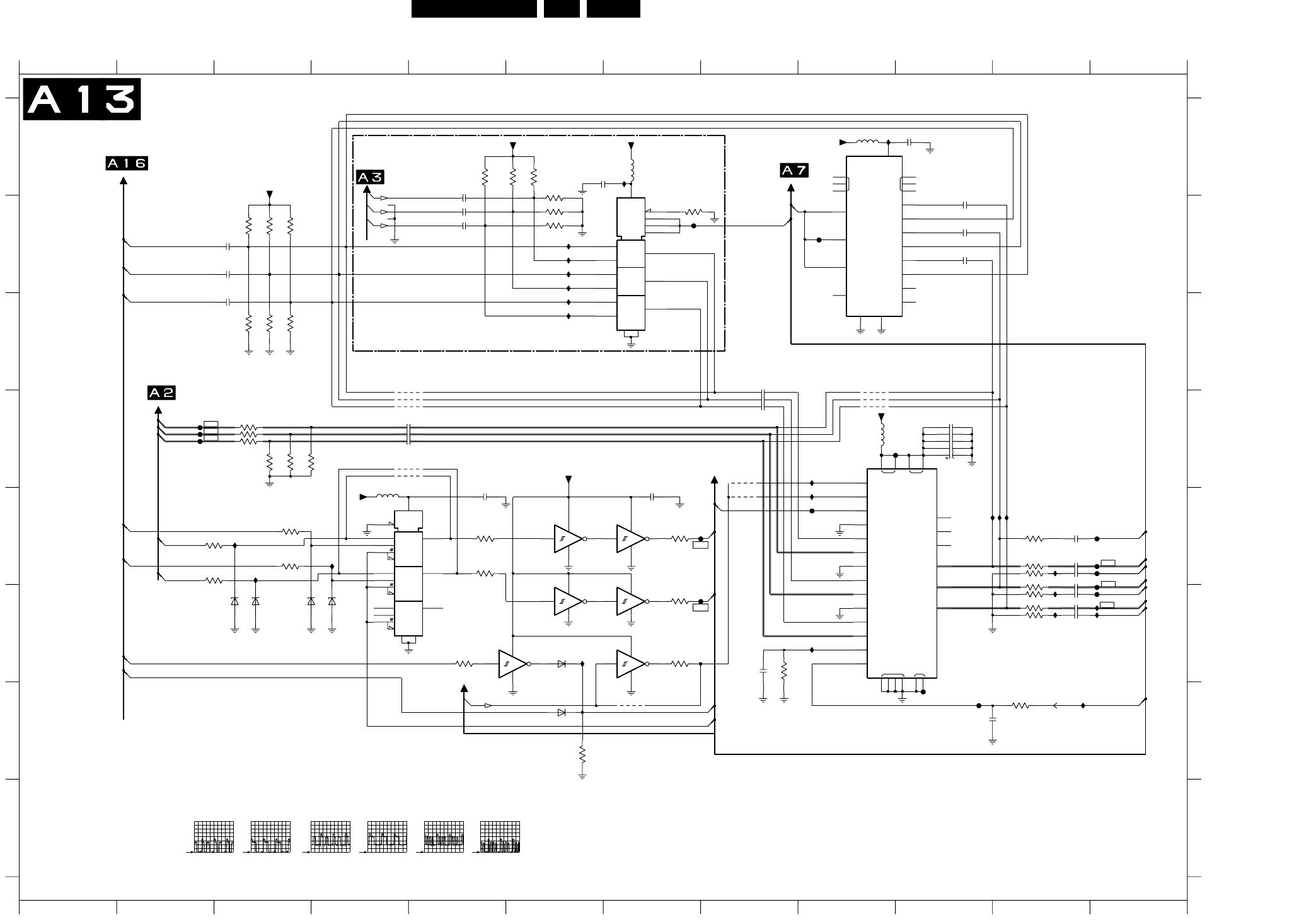
Circuit Diagrams and PWB Layouts 35LC4.6U AA 7.
SSB: PCHD MUX
NC
S2
IN1
D3
S3
D4
S4
D1
S1
NC
IN3
IN4
GND_HS
D2
IN2
VDD
GND
GND_HS
GINA|UINA
GINB|UINB
GSG1
RINB|YINB
RINA|YINA
VCC
GND
BOUT|VOUT
GOUT|UOUT
ROUT|YOUT
NC3
NC2
NC1
VCC
DISABLE
THROUGH
MUXSEL
GSR1
GSB1
BINA|VINA
BINB|VINB
RFC
VFC
S2B
VSS
S2A
S3B
S1A
S3A
S1B
D3
EN
GND
A0
A1
A2
D1
D2
VDD
4X1
G4
4X2
1
2
VDD
VEE VSS
PCHD-MUX
DMMI
TO SCALER
DIGITAL INTERFACE
FROM HERCULES / HISTOGRAM
(RESERVED)
RES
RES
RES
DMMI
RES
FROM PCHD-IO
A7
RES
RES
RES
123456789101112
123456789101112
A
B
C
D
E
F
G
H
A
B
C
D
E
F
G
H
2601 A7
2605 E7
2606 E5
2607 D10
2608 D10
2609 D10
2610 D10
2611 D10
2612 E11
2613 E11
2614 E11
2615 F11
2616 F11
2617 F11
2618 F11
2619 F8
2620 G11
2621 B3
2622 B3
2623 C3
2624 D4
2625 D4
2626 D4
2627 A5
2628 B5
2629 B5
2630 C8
2631 D8
2632 D8
2633 B10
2634 B10
2635 B10
2636 A10
3601 B7
3605 E7
3606 F7
3607 E5
3608 E5
3609 F5
3610 G6
3612 E11
3613 E11
3614 E11
3615 F11
3616 F11
3617 F11
3618 F11
3619 F8
3620 G11
3621 B3
3622 C3
3623 B3
3624 C3
3625 B3
3626 C3
3627 A5
3628 A6
3629 A6
3630 A6
3631 B6
3632 B6
3633 F7
3634 E3
3635 E3
3638 E2
3639 E2
3641 D3
3642 D3
3643 D3
3644 D3
3645 D3
3646 D4
4601 D5
4602 D5
4603 D5
4604 D9
4605 D9
4606 D9
4607 E8
4608 D8
4609 G7
4610 D5
4611 D5
5601 A7
5605 E4
5607 D9
5636 A9
6604 F6
6605 G6
6634 F4
6635 F4
6638 F3
6639 F3
7601 A7
7604-1 E6
7604-2 E7
7604-3 E6
7604-4 E7
7604-5 F6
7604-6 F7
7605 E4
7606 A9
7607 D10
F602 B7
F603 E8
F604 F8
F605 E9
F606 B9
F607 D10
F608 G10
F612 E12
F613 E12
F614 E12
F615 F12
F616 F12
F620 G10
F624 D2
F625 D2
F626 D2
I607 E9
I608 D9
I618 F12
I619 A7
I620 G12
I621 B6
I622 B6
I623 B6
I624 B6
I625 C6
I626 C6
I627 E3
I628 E3
I629 F6
I630 F9
I631 F12
I632 E11
I633 F11
I634 F11
I635 E10
I636 E11
I637 E11
I638 A9
I639 E4
4601
I639
4610
4611
I638
I619
I635
I637
I636
I634
I632
I633 I631
I629
I630
I628
I622
I627
I626
I624
I625
I623
I621
3645
330R 330R
36463644
330R
330R
3643 330R
3642
330R3641
F625
F626
I607
F624
I620
I608
F615
F616
I618
F614
F613
F604
F612
F603
F620
F605
F608
F606
F607
100R
F602
3638
6638
BZX384-C2V7
100R
3639
BZX384-C2V7
6639
6635
BZX384-C2V7
BZX384-C2V7
6634
100R
3635
100R
3634
3633
100R
4609
3610
22K
100n
2636
5636
+3V3STBY 5605 2606 100n
3607
100R
3608
100R
3609
100R
22K
3630
3631
3632
22K
+5VSWI
22K
22K
36293628
22K22K
3627
+5VSWI
22K
3626
3625
22K
3624
22K
3623
22K
22K
3622
3621
22K
1u0
1u0
2633
2634
1u0
2635 1u0
1u0
2630
1u0
2631
2632
2627 1u0
2628 1u0
2629 1u0
1u0
2621
1u0
2622
1u0
2623
4608
4607
470n
2624
2625 470n
470n
2626
2607 100n
100n
2608
2609 100n
2611 47u
6.3V
2612 10n470R
3612
2614 10n
10n2616
2618 10n
22R
3614
22R
3616
22R
3618
10n2613
10n2615
10n2617
3613 22R
3615 22R
3617 22R
2620
1u0
3620
100K
820R
36192619
33p
100n
2610
+5VSWI
15
12
24
21
5607
22
4
8
28
20
25
27
17
23
18
3
16
13
10
19
29
30
14
6
2
26
ΦSM5301BS-G
7607
5
7
11
9
1
BAS316
6605
3606
100R
BAS316
6604
3605
100R
+3V3STBY
2605
100n
12
7604-6
13
7
14
74LVC14APW
7604-5
11
7
14
10
74LVC14APW
9
7
14
8
14
6
74LVC14APW
7604-4
74LVC14APW
7604-3
5
7
74LVC14APW
7604-2
3
7
14
41
7
14
2
74LVC14APW
7604-1
4605
4606
4604
+5VSWI
16
18
20
2
14
12
4
13
5
3
21
19
17
9
7
6
8
10
7606
ADG781BCP
SWITCH
SPST
1
15
11
4603
Φ
4602
3601 10K
+5VSWI
100n
5601
2601
5
14
15
4
9
16
78
13
1
3
12
2
74HC4053D
7605
6
11
10
8
12
13
2
1
5
3
16
7
MDX
11
10
9
14
15
4
6
Φ
7601
ADG733BRU
G_Y-
R_PR-
SOG
H_CS_SDTV
PC_HD_DET-
BLU_PB
GRN_Y
RED_PR
V_SDTV
VS
HS
SD_HD_SEL
HD_FILTER
B_PB+
G_Y+
R_PR+
B_PB-
G-Y-ADC
B_SDTV
G_SDTV
H_CS
V
PC_HD_SEL
PC_HD_DET
PC_HD_DET+
DMMI_HD_SEL
SD_HD_SEL
SD_HD_SEL
DMMI_G_Y_IN
DMMI_B_U_IN
DMMI_R_V_IN
R_SDTV
PC_HD_SEL
B-PB-ADC
B-PB-ADC
R-PR-ADC
R-PR-ADC
G-Y-ADC
E_14710_075.eps
100904
3139 123 5867.2
F626
F624 F625
F613 F615
200mV / div DC
20us / div
200mV / div DC
20us / div
500mV / div DC
20us / div
500mV / div DC
20us / div
500mV / div DC
20us / div
I631
200mV / div DC
20us / div
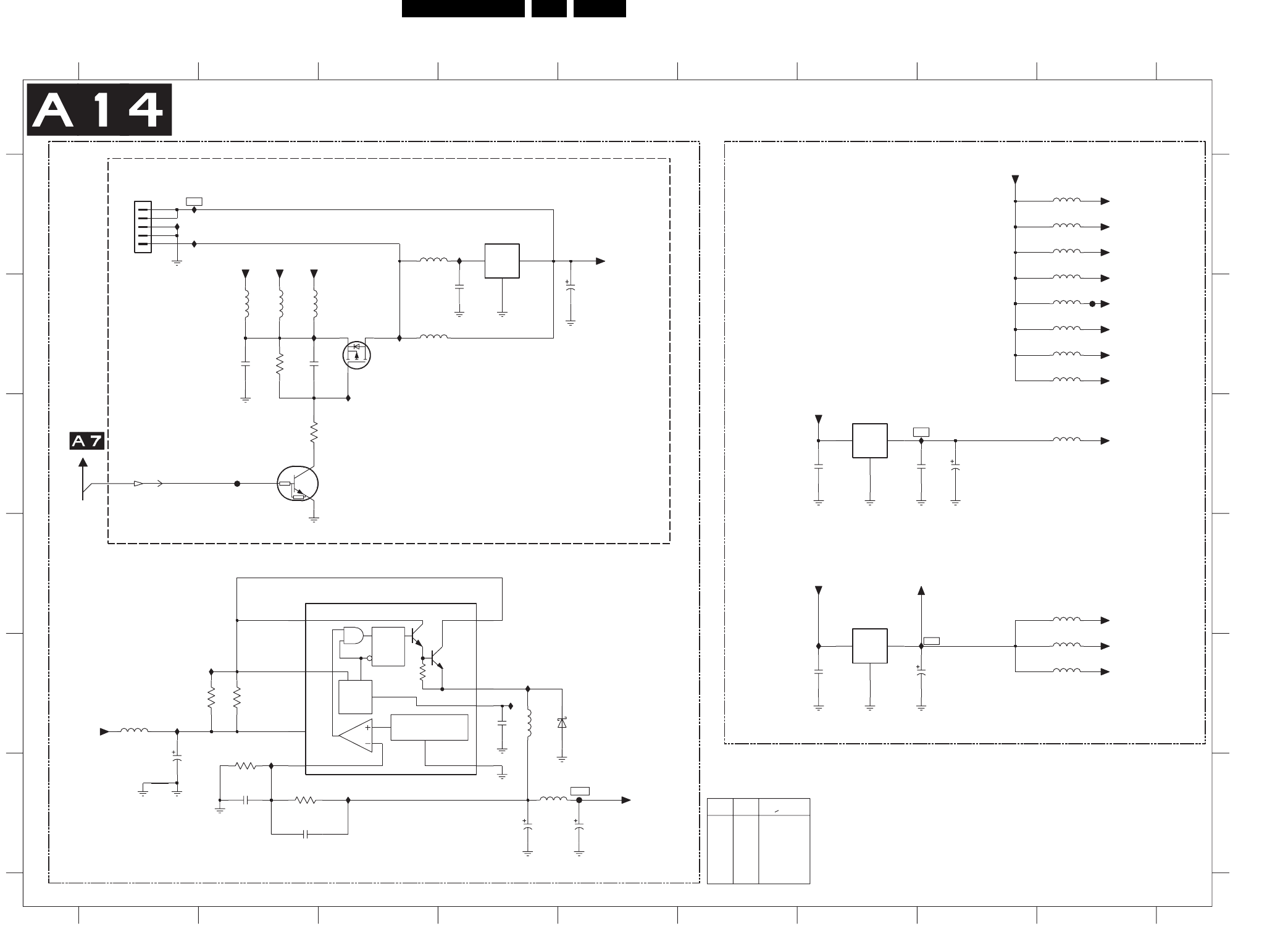
36LC4.6U AA 7.
Circuit Diagrams and PWB Layouts
SSB: Supply
COM
OUTIN
COM
OUTIN
COM
OUTIN
RES
**
*
SS = 4V9
0V6
(0V)
*
11V7
11V7
11V7
1V2
ITEM
2959
3958
5955
5956
5957
5954
7953
13"
1K
YES
YES
>15"
15K
100N
YES
YES
L4940D2T12
---
---
---
---
---
---
*
*
"951"~"979"
RES
*
1%
1%
SUPPLY
SUPPLY FOR SCALER
"980"~"999"
FROM SCALER
RES
RES
PROVISION FOR 1.5A 5V
NOT FOR PDP
RES
RES
RES
123456789
123456789
A
B
C
D
E
F
A
B
C
D
E
F
1951 A1
2953 E1
2954 F2
2955 F2
2956 E4
2957 F4
2958 F5
2959 B4
2960 B5
2961 B3
2962 B2
2992 C7
2993 C8
2994 C8
2995 E7
2996 E8
3951 E2
3952 E2
3953 F2
3954 F2
3955 B2
3958 C3
5952 E1
5953 E4
5954 F4
5955 B2
5956 B3
5957 B3
5959 A3
5960 B2
5984 A9
5985 A9
5986 A9
5987 A9
5988 B9
5989 B9
5990 B9
5991 B9
5994 C9
5996 D9
5997 E9
5998 E9
6951 E5
7952 D2
7953 A4
7954 B3
7955 C3
7992 C7
7995 D7
F954 F5
F955 C2
F988 B9
I951 E2
I952 E1
I953 F2
I954 F3
I955 E4
I956 B3
I957 B3
I959 A4
I960 E4
I961 B3
I962 A1
I963 A1
I964 A1
I992 C8
I995 E7
I996 E8
2954
5986
10n
2962
I960
16V470u
2960
I964
I963
I962
+5VSWI
+5VSWI
I995
I992
I996
F988
F954
F955
I955
I953
I954
I951
I961
I952
I956
I959
I957
1
2
3
4
5
SUPP_GNDGND
1951
5960
+3V3_PLL
+3V3STBY
+3V3STBY
+3V3_ADC
5984
5985
+1V8_ADC
+1V8
5996
5998
+1V8_CORE
5997
+1V8_DVI
16V
2996
47u
100n
2995
LD1086D2T18
7995
1
32
+2V5_DDR
5994
2994
470u 16V1n0
29932992
100n
LF25CDT
7992
2
13
+3V3_LVDS
+3V3STBY
+3V3_IO
+3V3_LBADC
+3V3_LVDSA
+3V3_LVDSB
5991
+3V3_DVI
5989
5990
5987
5988
SUPP_GND
6951
SS14
SUPP_GND
+12VSW
SUPP_GND
1
SWE 2
TIMC 3
VCC
6
SUPP_GND
SUPP_GND
MC34063AD
7952
CIN_NEG
5
DCOL
8
GND 4
IS7
SWC
10u
5954
REGULATOR
REFERENCE
OSC
IPK
Q
R
S
5952 220u
5953
3954
10u
3K3
3953
1K0
1R0
39523951
1R0
2958
16V470u
2955
4n7
2957
16V470u
2956
470p
3955
2953
16V470u
2961
10K
PAN_VCC
10n
13
7953
L4940D2T12
2
2959
5959
5957
+12VSW
5955
3958
15K
5956
7955
+3V3STBY
3
1
2
PDTC114ET
SI2301DS-T1
7954
PANEL-PWR-CTL
E_14710_076.eps
060804
3139 123 5867.2
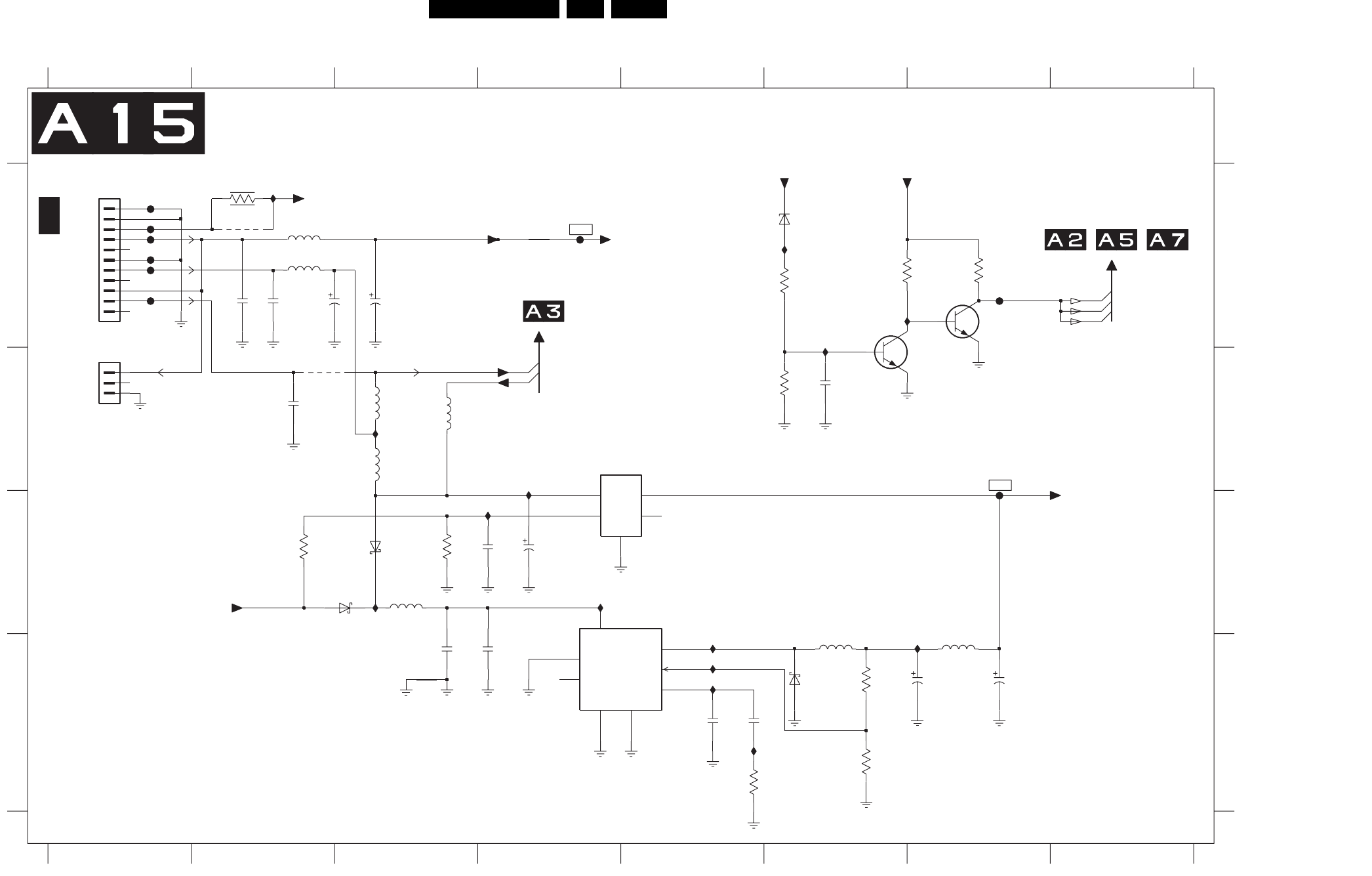
Circuit Diagrams and PWB Layouts 37LC4.6U AA 7.
SSB: DC-DC Converter
TO 1M46 OF SUPPLY (LCD)
SA1
OR
TO CN9005 OF SUB SUPPLY (PDP)
OUTIN
CTRL NC
COM
FB
OUT
COMP
VREFVCC
INH
SYNC
GND GND_HS
DC-DC CONVERTER
SUPPLY
TO/FROM 1M20 OF HERCULES
NC
NC
(LCD)
(LCD)
(PDP)
NC
NC
NC
(PDP)
(PDP)
NC
A2
A3
A3
A5
RES
RES
A7
for ITV only
12345678
12345678
A
B
C
D
A
B
C
D
1251 A1
1252 B1
2251 A2
2252 A2
2253 A3
2254 A2
2255 B2
2261 C4
2262 C4
2263 D3
2264 D4
2265 D5
2266 D5
2268 D7
2269 D7
2271 B6
3251 A2
3259 C2
3260 C3
3266 D5
3267 D6
3268 D6
3270 A6
3271 B6
3273 A7
3274 A7
4251 A2
4255 B2
5251 A2
5252 A2
5257 B3
5258 B3
5259 B3
5262 C3
5267 D6
5268 D7
6259 C3
6262 C3
6267 D6
6270 A6
7260 B4
7262 C4
7271 B7
7272 A7
F251 A1
F252 A1
F253 A1
F254 A1
F255 A1
F257 A1
F258 A4
F259 A7
F260 B7
I251 B3
I252 B4
I253 C4
I254 C3
I255 C4
I256 D5
I257 D5
I258 D5
I259 D5
I260 D7
I261 A6
I262 A6
I263 A6
I264 A2
1252
1
2
3
I264
I262
1R0
3251
I263
I260
I261
I259
I257
I258
I256
I254
I255
I252
I253
I251
F259
F260
F257
F255
F253
F254
F251
F252 4251
5
6
7
8
9
+5V2
+5V2_RELAIS_IO2
1
10
11
2
3
4
SupplyGnd
SupplyGnd
1251
F258
9
3
1
2
8
6
SupplyGnd
+12VSW
L5973D
7262
Φ
4
5
7
LF33CPT
2
3
1
4
5
7260
2262
47u 16V
10u
2263 5268
10u
10u
2264
5259
16V
2269
470u470u
2268
16V
3268
3K3
1%
3267
5K6
1%
33u
5267
SupplyGnd
SupplyGnd
SupplyGnd
6267
SS36
4K7
3266
SupplyGnd
2266
22n
SupplyGnd
+3V3STBY
220p
2265
10K
3259 22613260
6K8
SS14
6259
SS24
6262
+12VUNREG 10u
5262
SupplyGnd
SupplyGnd
+3V3STBY
3274
22K220K
3273
7272
BC847BW
7271
BC847BW
2271
10n820R
2K2
3271
+12VUNREG
3270
6270
BZX384-C8V2
5258
52572255
10p
4255
2254
16V10u
2252
10p
+12VUNREG
+8V6
5252
10u 16V
2253
5251
10p
2251
+9V_STBY_PDP
+12V
+5V
POWER_DOWN
E_14710_077.eps
130804
3139 123 5867.2
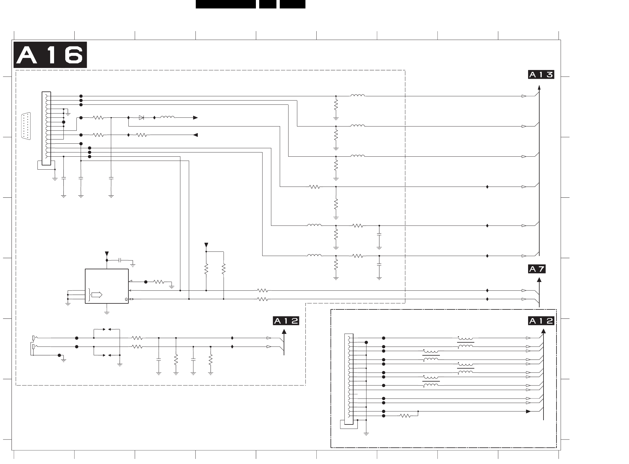
38LC4.6U AA 7.
Circuit Diagrams and PWB Layouts
SSB: PCHD IO
SCL
ADR
0
1
2SDA
WC
PC AUDIO IN
PCHD-IO
TO PCHD-MUX
TO HDMI
HDMI CONNECTOR
HDMI - (NAFTA & AP ONLY)
VGA Connector
A13
A13
A13
A13
A13
A13
TO HDMI
A7
A7
TO SCALER
AV3: VGA + 2fHYPbPr
123456789
123456789
A
B
C
D
E
F
A
B
C
D
E
F
1686 E1
1687 A1
1688 E6
1690 E8
1691 E7
1692 E8
1693 E7
2682 D6
2683 B2
2688 C6
2693 C2
2698 E3
2699 E4
2784 B1
2785 B2
3682 C6
3688 D6
3690 C6
3691 A6
3692 A6
3693 D3
3694 C6
3695 B6
3696 D4
3697 D4
3698 E2
3699 E2
3700 E3
3781 E4
3785 B5
3786 D4
3787 D4
3789 A2
3790 A3
3791 A2
3792 C6
3793 F7
5681 C5
5682 C5
5688 A6
5689 A6
5690 B6
5691 A3
6692 A3
7693 D2
F150 E6
F151 E6
F152 E6
F153 E6
F154 E6
F155 E6
F156 E6
F157 F6
F158 F6
F159 F6
F160 F6
F161 F6
F162 E6
F163 A1
F164 D3
F165 E1
F166 E2
F167 E2
F168 A2
F169 A2
F170 A2
F171 A2
F172 A2
F173 B2
F174 B2
F176 B2
F178 B2
I150 B8
I151 C8
I152 C8
I153 D8
I154 D8
I158 E4
I159 E4
I682 A2
I683 A3
I684 A2
I685 D2
S698 E2
S699 E2
14
23
1K03793
23
ACM
1693 ACM
1692
14
ACM
1691
14
23
14
23
I684
ACM
1690
I683I682
I685
F176
F178
F173
F174
F171
F172
F169
F170
F168
F163
F165
+5VSWI
3787 1R0
1R03786
3791
1K0
3790
10K
1K0
3792
I151
I150
I152
2785
330p330p
2784
DDC_5V
5691
6692
BAS316
100n
2683
3789
150R
5
6
7
8
9
1617
10
11
12
13
14
15
2
3
4
1687
788624-1
1
3785
100R
3695
75R
5690
75R
3691
5689
100p
2688
220R
3694
2K2
3682
5682
5688
75R
3692
100p
2682
220R
3690
2K2
3688
5681
F162
F160
F161
F158
F159
F157
F156
F154
F155
F152
F153
F151
+5VHDMI
F150
3
4
5
6
7
8
9
15
16
17
18
19
2
1688
1
10
11
12
13
14
DC1
S698
S699
I154
F164
I153
F166
F167 I159
DDC_5V
I158
3
1
2
3697
10K
1686
LPR6520-J920G
10K
3696
10K
3693
3781
47K
3700
47K
2698
100p
2699
100p
150R
150R3699
3698
2693
100n
DDC_5V
6
5
84
7
EEPROM
Φ
(256x8)
M24C02-WMN6
7693
1
2
3
GRN_Y
BLU_PB
CEC
DOC_SDA
VS
RED_PR
PC_HD_DET+
HS
RX2-
RXC+
RXC-
DOC_SCL
RX0+
RX0-
RX1+
RX1-
RX2+
SDA_VGA
UART_TX
SCL_VGA
UART_RX
PC_AUDIO_L
PC_AUDIO_R
E_14710_078.eps
100804
3139 123 5867.2
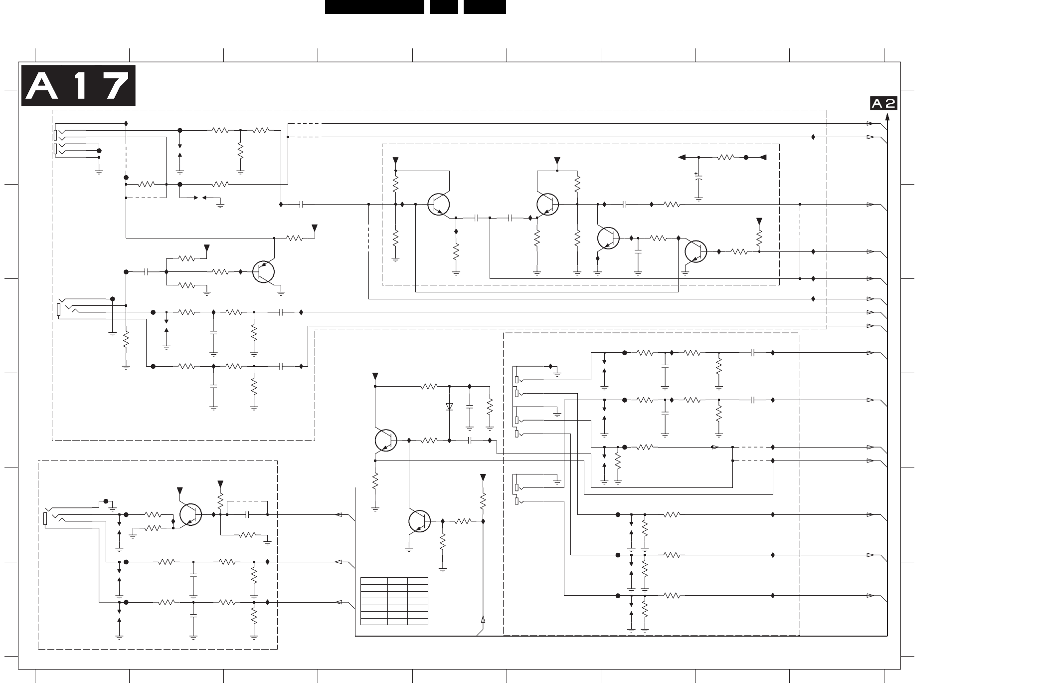
Circuit Diagrams and PWB Layouts 39LC4.6U AA 7.
SSB: Cinch IO
SVHS
MINI
JACK
MINI
JACK
SET WITH 3D COMBFILTER
CINCH-IO
AV1:CVBS+YPbPr+Audio L/R
MONITOR OUT: CVBS + Audio L/R
AV2: SVHS+CVBS+Audio L/R
1 2 3 4 5 6 7 8 9
1 2 3 4 5 6 7 8 9
A
B
C
D
E
F
A
B
C
D
E
F
1175-1 E6
1175-2 C6
1177 E1
1182 C1
1183 A1
2179 B7
2182 C7
2183 C8
2184 D7
2185 D8
2190 A7
2191 E3
2193 F2
2195 F2
2201 B2
2225 B3
2227 B5
2228 B6
2231 C2
2232 C3
2233 D2
2234 C3
2238 B7
2240 D5
2241 D5
3175 F7
3176 F7
3177 E7
3178 F7
3179 E7
3180 E7
3181 D7
3182 C7
3183 C8
3184 D7
3185 D8
3186 B8
3187 B8
3188 B7
3189 A2
3190 A8
3191 A3
3192 D7
3193 E2
3194 E2
3195 E3
3196 E2
3197 F3
3198 F3
3199 E2
3200 F2
3201 B2
3202 C2
3203 B3
3204 B2
3220 A3
3221 A2
3222 C1
3223 A2
3225 A4
3226 B4
3227 B5
3228 B6
3229 A6
3230 B6
3231 C2
3232 C3
3233 C2
3234 D3
3235 C3
3236 C3
3237 C7
3238 B7
3239 D7
3240 D5
3241 D5
3242 D5
3243 E4
3244 E5
3245 E5
3246 E5
3247 E3
3248 F3
4175 A1
4176 D8
4177 D8
4178 B2
4191 E3
4223 A3
4224 A3
4226 B4
4230 B9
6240 D5
7138 E2
7201 B3
7225 A5
7226 B8
7227 B6
7228 A6
7240 D4
7241 E5
F175 F7
F177 E7
F179 E7
F181 D7
F182 C7
F183 D7
F184 A1
F190 A8
F220 A2
F221 A2
F222 E1
F223 E1
F224 E1
F225 F1
F226 A1
F227 C1
F228 C2
F229 C2
F230 B1
I175 B3
I176 C6
I177 A2
I178 B2
I179 B3
I181 C2
I182 C7
I183 C3
I184 D7
I186 C2
I187 C3
I194 E2
I195 E2
I196 E3
I197 F3
I198 B4
I199 B7
I200 B6
I201 B5
I202 B6
I204 A9
I205 B7
I206 B7
I207 B7
I208 B8
I209 B9
I210 B9
I211 C9
I212 C8
I213 D8
I214 D8
I215 D8
I216 E8
I217 E8
I218 F8
I219 D5
I220 D4
I221 D5
I222 D5
I223 E5
I224 E5
S175 F7
S177 F7
S179 E7
S181 D6
S182 C6
S184 D6
S185 C2
S191 E1
S192 F1
S193 F1
S194 B2
S195 A2
STATUS_2
47R
3190
3189
33R
I179
F230 I178
+5VSW_1
3203
1K0
BC857BW
7201
100R
3204
+5VSW_1
100K
100K
3202
2u2
3201
2201
F224
F225
F222
F223
150R
3247
3248
3239
150R
150R
150R
3237
3236
150R
3235
150R
I222
I224
I223
I220
I221
I219
+5VSW_1
+5VSW_1
6240
BAS316
1u0
2241
220n
2240
47K
3241
82K
3240
1K0
3242
4K7
3244
27K
3246
3245
10K
7241
BC847BW
10K
3243
7240
BC847BW
F226
F227
LGY6509-0100F
1182
9
4
7
LPR6520-K030G
1175-2
5
8
6
LPR6520-K030G
2
3
1
2
3
4
1
1175-1
1
2
3
4
5
LGY6509-0100F
1177
1183
LAP5100-1411F
6
4178
S192
I196
150R
3199
2193
330p 3197
220K
S193
3200
150R 2195
330p 3198
220K
I197
4191
S191
+5VSW_1
+5VSW_1
I194
47K
3195
I195
1K0
3196 7138
BC847B
2191
12K
3193
2u2
68R
3194
S185
I213
I215
I212
I214
I187
I209
I183
I211
I204
I176
I210
I208
I205
I207I206
I199
I202
I200
I198
I201
I175
I181
I186
F229
I177
F228
3192
75R
33R
3191
4176
4226
4177
330R
4223
2238 3238
4230
100n
+5VSW_1
3230
100K
100K
3229
4K7
3228
100n
2228
BC847BW
7228
2227
100n
3227
4K7
7225
BC847BW
100K
3226
+5VSW_1
100n
2225
3225
100K
BC847BW
7227 10n
2179
10K
3188 7226
BC847BW
3187
10K
+5VSW_1
3186
4K7
1u0
2234
3234
2233
47K
150R
3233
330p
2232
1u0
3232
47K
330p
2231
4224
3231
150R
3185
47K
47K
3183
330R
F181 3181
S181
F183
F184
F182
I184
I182
330R
3220
330R
3176
1u0
2185
1u0
2183
220R
3221
3184
150R
3182
150R
3177
330R
2184
330p
S184
2182
330p
S182
4175
3223
75R
75R
3222
F221
F177
F179
F220
F175
S194
S195
S177 S179S175
3179
75R
75R
3178
3175
75R
I216
330R
3180
I217
I218
F190
+5VSW
2190
+5VSW_1
10u 16V
SC2_CVBS_MON_OUT
SC2_R_MON_OUT
SC2_L_MON_OUT
AV2_Y_IN
AV2_C_IN
AV1_CVBS_IN SC1_CVBS_IN
SC1_CVBS_IN
SC1_COMP_R_V_IN
SC2_Y_IN
SC1_COMP_AV1_G_Y_CVBS_IN
STATUS_1
SC2_C_IN
SC1_COMP_B_U_IN
SC2_L_IN
SC1_COMP_AV1_L_IN
SC2_R_IN
SC1_COMP_AV1_R_IN
SC1_CVBS_RF_OUT
SVHS_C_IN
AVS_C_IN
E_14710_079.eps
050804
3139 123 5867.2
3D NO 3D
4223
4224
4226
4230
4176
4177
Y
Y
Y
Y
Y
Y
--
--
--
--
--
--
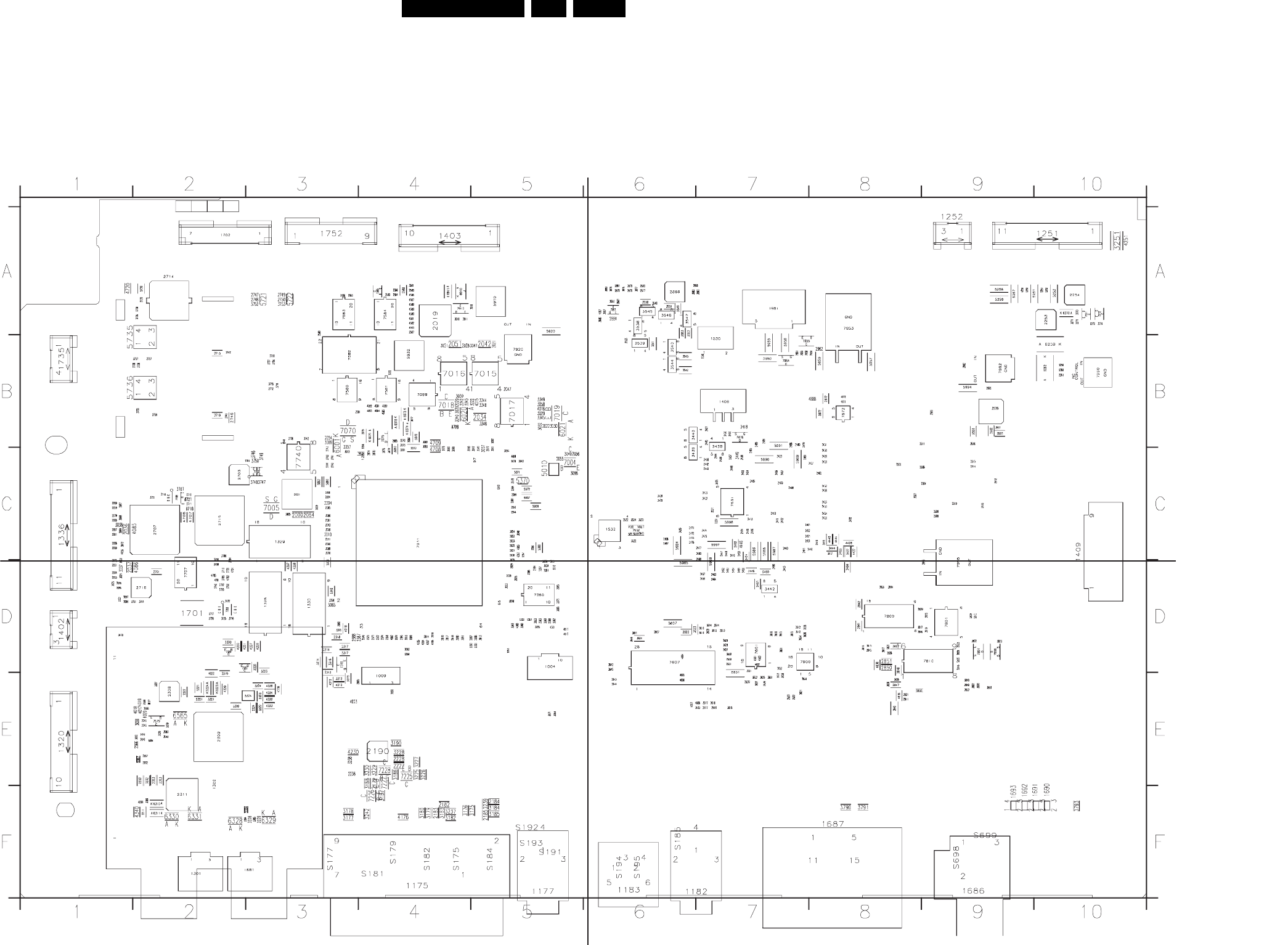
40LC4.6U AA 7.
Circuit Diagrams and PWB Layouts
Layout Small Signal Panel (Top Side Overview)
E_14710_080.eps
060804
3139 123 5867.2
Part 1
E_14710_080a.eps
Part 2
E_14710_080b.eps
Part 4
E_14710_080d.eps
Part 3
E_14710_080c.eps
1004 D5
1009 E4
1301 F2
1328 D3
1329 C3
1330 D3
1408 B7
1409 C10
1530 B7
1532 C6
1681 F3
1690 F10
1691 F10
1692 F9
1693 F9
1701 D2
1951 A7
2000 C3
2001 C3
2003 E2
2004 C3
2005 C3
2010 C3
2011 C3
2013 D4
2014 D4
2015 D4
2016 D4
2017 D4
2018 D4
2019 A4
2020 B4
2021 B5
2022 B5
2023 D5
2025 D5
2026 D5
2028 B4
2029 D5
2030 C5
2031 C5
2032 C5
2033 C5
2034 B5
2036 C1
2037 D1
2041 C5
2042 B5
2043 C3
2044 C5
2045 E2
2046 E2
2047 B5
2048 E2
2049 E2
2050 E2
2051 B4
2052 C5
2053 D5
2054 B3
2055 C5
2056 C5
2057 E2
2058 E2
2059 C1
2060 C3
2062 E2
2064 C3
2065 E3
2066 E4
2067 E2
2068 C3
2069 C1
2070 C4
2072 C4
2073 B4
2074 C4
2076 C4
2077 C5
2078 C5
2079 C1
2080 C1
2081 C1
2082 D3
2083 D4
2084 C5
2085 B4
2086 B4
2087 C1
2088 C1
2090 C1
2091 D1
2092 D1
2093 D1
2094 D1
2095 D1
2096 D1
2097 D1
2098 D1
2099 C4
2179 E4
2182 F4
2183 F4
2184 F5
2185 F5
2190 E4
2227 E4
2228 E4
2238 E3
2251 A10
2252 A10
2253 A10
2254 A10
2255 A9
2261 B10
2271 A10
2302 E2
2303 E2
2307 E2
2308 E2
2309 E2
2311 F2
2313 D3
2314 D3
2317 D3
2318 D3
2321 E2
2324 E3
2358 D4
2359 D3
2361 D5
2363 D5
2364 D5
2365 D5
2366 D5
2367 D5
2368 D5
2370 D4
2371 D4
2372 D4
2373 D4
2374 D4
2378 C5
2381 C5
2387 D4
2388 D3
2394 C5
2395 D4
2397 D5
2398 D5
2403 C7
2404 C7
2405 C7
2406 C7
2407 C7
2408 C7
2409 C7
2410 C7
2411 C7
2412 C7
2413 C7
2414 C7
2415 C7
2416 C7
2419 C8
2420 C7
2421 C7
2422 C7
2423 C8
2424 C8
2425 C8
2426 C8
2427 C8
2428 C8
2429 C8
2430 C8
2431 B8
2432 C8
2433 C8
2436 C7
2437 C7
2438 C7
2439 C7
2440 C7
2441 C7
2442 C7
2443 C7
2444 C7
2445 B7
2446 C8
2447 C7
2448 C7
2449 C7
2450 C7
2452 D7
2453 D7
2454 D7
2455 D7
2456 D7
2461 C7
2462 C8
2463 D7
2464 D7
2466 D7
2467 D7
2468 C7
2469 C7
2471 C6
2472 C6
2473 C6
2474 C7
2475 C7
2476 C6
2477 C7
2479 B7
2480 B7
2481 C7
2483 C7
2484 B7
2485 B7
2486 B7
2487 C6
2488 C6
2490 D7
2491 D7
2492 C7
2493 C8
2494 D8
2496 D7
2503 B9
2504 C9
2505 C8
2506 C9
2507 C8
2508 C9
2509 C9
2510 C9
2511 B9
2512 C9
2513 C9
2514 C9
2515 C9
2516 B9
2517 B9
2526 B9
2531 C7
2532 C6
2533 B6
2566 E2
2580 A3
2581 B3
2582 B4
2583 A3
2584 A4
2585 A4
2586 A4
2587 A4
2588 A3
2601 D7
2607 D6
2608 D7
2609 D7
2610 E7
2612 D7
2613 D7
2614 D7
2615 D7
2616 D7
2617 E7
2618 E7
2619 D7
2620 D6
2621 E7
2622 E7
2623 E7
2624 D6
2627 D7
2628 E7
2629 E7
2630 D7
2631 D7
2632 D7
2633 E7
2634 D7
2635 D7
2636 D7
2701 D2
2702 D2
2703 C2
2704 D2
2705 D2
2706 C2
2707 C2
2710 C2
2711 C2
2712 B3
2713 B2
2714 A2
2715 C2
2716 D2
2718 B3
2719 B2
2720 A2
2735 B2
2736 B2
2737 B2
2738 A2
2739 D2
2740 D2
2741 B2
2742 B2
2743 C3
2744 C3
2746 B2
2747 A3
2748 A3
2749 A3
2750 A3
2811 E8
2812 D9
2815 D9
2816 D9
2817 D8
2821 E8
2822 D9
2823 D9
2827 D8
2828 D9
2829 D8
2832 E9
2835 D8
2836 D8
2840 E8
2841 D8
2842 D8
2844 D8
2845 D8
2846 D8
2847 E8
2848 D8
2849 E9
2850 D8
2851 D8
2872 B8
2876 A6
2877 A6
2878 A6
2879 A6
2880 A6
2881 A6
2883 A6
2884 A6
2885 A7
2886 A6
2887 A6
2889 A6
2910 A5
2959 B8
2961 B7
2962 B8
2992 B9
2993 B9
2995 D9
3000 C3
3005 C3
3006 C3
3008 C3
3009 D4
3010 C3
3012 D5
3013 D5
3020 B4
3021 B4
3022 B5
3023 D1
3024 D1
3025 D1
3026 E2
3027 D1
3028 D5
3029 B5
3030 B5
3031 D5
3032 B5
3033 D5
3034 D5
3035 C5
3036 D5
3037 D1
3038 C1
3039 B4
3040 C5
3048 C5
3054 C5
3055 D5
3056 B4
3057 C5
3058 B5
3059 C3
3063 E2
3064 E5
3065 D3
3066 E2
3067 C1
3068 C1
3069 C1
3070 B4
3071 E5
3072 C1
3073 C3
3074 D4
3075 B4
3077 B4
3078 C4
3079 C4
3080 C4
3081 C4
3082 B4
3083 B4
3084 E2
3088 C4
3089 B3
3091 C5
3092 B5
3093 C5
3094 C5
3096 C4
3097 C5
3098 C5
3175 F5
3176 F4
3177 F3
3178 F3
3179 F4
3180 F4
3182 F4
3183 F4
3184 F5
3185 F5
3186 E4
3187 F4
3188 E4
3190 E4
3225 E4
3226 E4
3227 E4
3228 E4
3229 E4
3230 E4
3237 F4
3238 E3
3239 F5
3242 F4
3251 A10
3259 B10
3260 B10
3270 A10
3271 A10
3273 A10
3274 A10
3302 E2
3303 E2
3304 F2
3305 F3
3309 F2
3311 F2
3313 E3
3314 D3
3315 E3
3316 D3
3317 D3
3319 E2
3320 D2
3321 E2
3322 E3
3323 E3
3324 E3
3325 D3
3326 D3
3327 E2
3328 F3
3329 F3
3340 B4
3342 B4
3343 B4
3344 B5
3345 B5
3346 B5
3347 B5
3348 B5
3349 B5
3357 B3
3358 D4
3360 D5
3361 D5
3362 D5
3363 D5
3365 D5
3366 C5
3367 C5
3368 D5
3369 D5
3370 D3
3373 D5
3389 C5
3390 D4
3391 D4
3392 D5
3393 D5
3394 C3
3415 D1
3416 C8
3417 C8
3418 B7
3422 C8
3423 C7
3424 C7
3425 C7
3426 C6
3427 C8
3428 C6
3429 C6
3432 C7
3433 C7
3436 B7
3437 B7
3438 B7
3439 C6
3440 B6
3442 D7
3443 D7
3444 C8
3446 D7
3448 C7
3449 C7
3460 B7
3501 B9
3502 B9
3503 B9
3531 C7
3532 C6
3533 C6
3534 C6
3536 B7
3538 A6
3539 B6
3540 B6
3541 B6
3542 B6
3543 B6
3544 B6
3545 A6
3546 A6
3547 A6
3548 A6
3549 A6
3550 A6
3551 A6
3552 A6
3553 A6
3579 E2
3580 A4
3581 A4
3601 D7
3612 D7
3613 D7
3614 D7
3615 D7
3616 D7
3617 E7
3618 E7
3619 D7
3620 D6
3625 E7
3626 E7
3627 E7
3628 E7
3629 D7
3630 D7
3631 E7
3632 E7
3633 E7
3641 D6
3642 D6
3643 E6
3644 E6
3645 D6
3646 D6
3703 D2
3705 D2
3706 C3
3707 C2
3708 D2
3709 C2
3710 D2
3711 C2
3714 B3
3715 B3
3716 C2
3717 D2
3718 C2
3719 D2
3720 D2
3721 C2
3722 D2
3725 D2
3726 B3
3727 B3
3728 B4
3735 B2
3736 B2
3737 B2
3738 A2
3739 B3
3740 B3
3741 C3
3742 B3
3743 C3
3744 D2
3745 C3
3746 C3
3747 C3
3748 C3
3749 C3
3750 C3
3751 D2
3752 A3
3753 A3
3790 F8
3791 F8
3793 F10
3808 E9
3809 D9
3810 E9
3815 D8
3816 D8
3817 D8
3819 D9
3822 D9
3823 D9
3827 D8
3828 E9
3832 E9
3836 E8
3838 E8
3876 A6
3877 A6
3879 A6
3883 A6
3885 A6
3886 A6
3887 A6
3910 A4
3911 A4
3955 B7
3958 B7
4002 D4
4004 D4
4005 D4
4006 D4
4007 D4
4008 C5
4011 D5
4012 D5
4015 B5
4016 B5
4017 E2
4018 E2
4019 E2
4020 E2
4022 E2
4023 E3
4085 C2
4086 D2
4176 F4
4230 E3
4251 A10
4255 A9
4312 E3
4313 E3
4318 D3
4327 D3
4328 D3
4329 E2
4330 D2
4331 D2
4332 E3
4333 E3
4334 E3
4335 E3
4336 E3
4337 D3
4338 D3
4339 F2
4340 F2
4360 D5
4361 D5
4362 C5
4363 C5
4427 C8
4428 C8
4444 C8
4445 C8
4446 C7
4580 B4
4581 B4
4582 B4
4583 B4
4584 B4
4585 B4
4586 A4
4587 A4
4588 A4
4589 A4
4590 A4
4591 A4
4592 A4
4593 A4
4601 D7
4602 D7
4603 D7
4604 D6
4605 E6
4606 E6
4607 E6
4608 E7
4701 D2
4702 D2
4703 C1
4704 D2
4705 D2
4706 C2
4707 C2
4708 C4
4709 B4
4710 C2
4711 C2
4716 B4
4720 A1
4836 E8
4838 D8
4871 B8
4872 B8
4887 A6
4888 B8
5001 C3
5002 C3
5007 C5
5008 C5
5010 C5
5060 C3
5066 E2
5067 E2
5070 B4
5071 C4
5251 A9
5252 A10
5257 A9
5258 A9
5259 A9
5304 F3
5309 E2
5321 E2
5324 E3
5339 D3
5340 D3
5360 C5
5370 C5
5371 C5
5372 C5
5580 A4
5601 D7
5607 D6
5720 A2
5721 A3
5722 A3
5735 B1
5736 B1
5803 E8
5872 B8
5910 A5
5920 A5
5932 B4
5955 B7
5956 B7
5957 B8
5959 B8
5960 B7
5984 C6
5985 D6
5986 C7
5987 C7
5988 C7
5989 C7
5990 C7
5991 B7
5994 B9
5996 D7
5997 C7
5998 C7
6001 B3
6020 B4
6021 B5
6073 B4
6074 B4
6075 B4
6076 B4
6259 B10
6262 B10
6270 A10
6310 F2
6311 F2
6323 E2
6324 E2
6328 F2
6329 F3
6330 F2
6331 F2
6565 E2
6910 A4
6911 A4
7004 C5
7005 C3
7011 C4
7015 B5
7016 B4
7017 B5
7018 B4
7019 B5
7070 B3
7075 B4
7099 B4
7225 E4
7226 F4
7227 E4
7228 E4
7260 B10
7271 A10
7272 A10
7316 D3
7320 D2
7325 D2
7360 D5
7416 B7
7531 C7
7532 C6
7579 E2
7580 B3
7581 B4
7582 B3
7583 A3
7584 A4
7585 A4
7601 D7
7606 D7
7607 D6
7702 D2
7703 C3
7707 D2
7708 C2
7740 C3
7801 D9
7806 D9
7807 D9
7809 D8
7810 D9
7872 B8
7887 A6
7910 A4
7920 B5
7953 A8
7954 B7
7955 B7
7992 B9
7995 D9
S175 F4
S177 F3
S179 F4
S181 F4
S182 F4
S184 F5
S185 F6
S191 F5
S192 F5
S193 F5
S194 F6
S195 F6
S698 F9
S699 F9
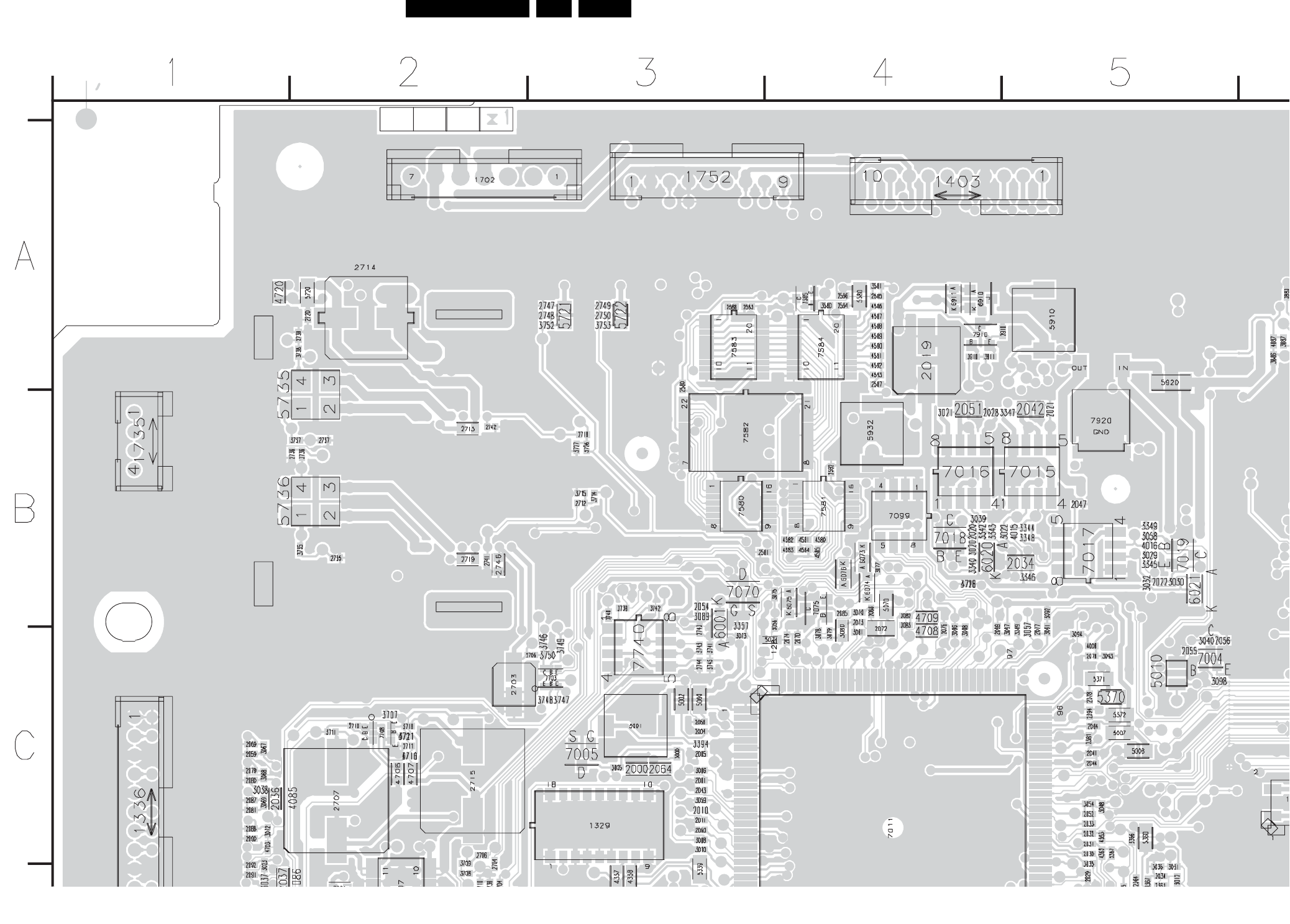
Circuit Diagrams and PWB Layouts 41LC4.6U AA 7.
Layout Small Signal Panel (Top Side Part 1)
Part 1
E_14710_080a.eps
151104
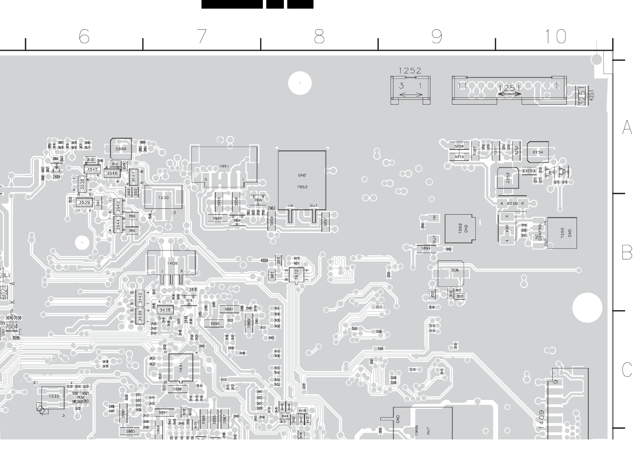
42LC4.6U AA 7.
Circuit Diagrams and PWB Layouts
Layout Small Signal Panel (Top Side Part 2)
E_14710_080b.eps
151104
Part 2
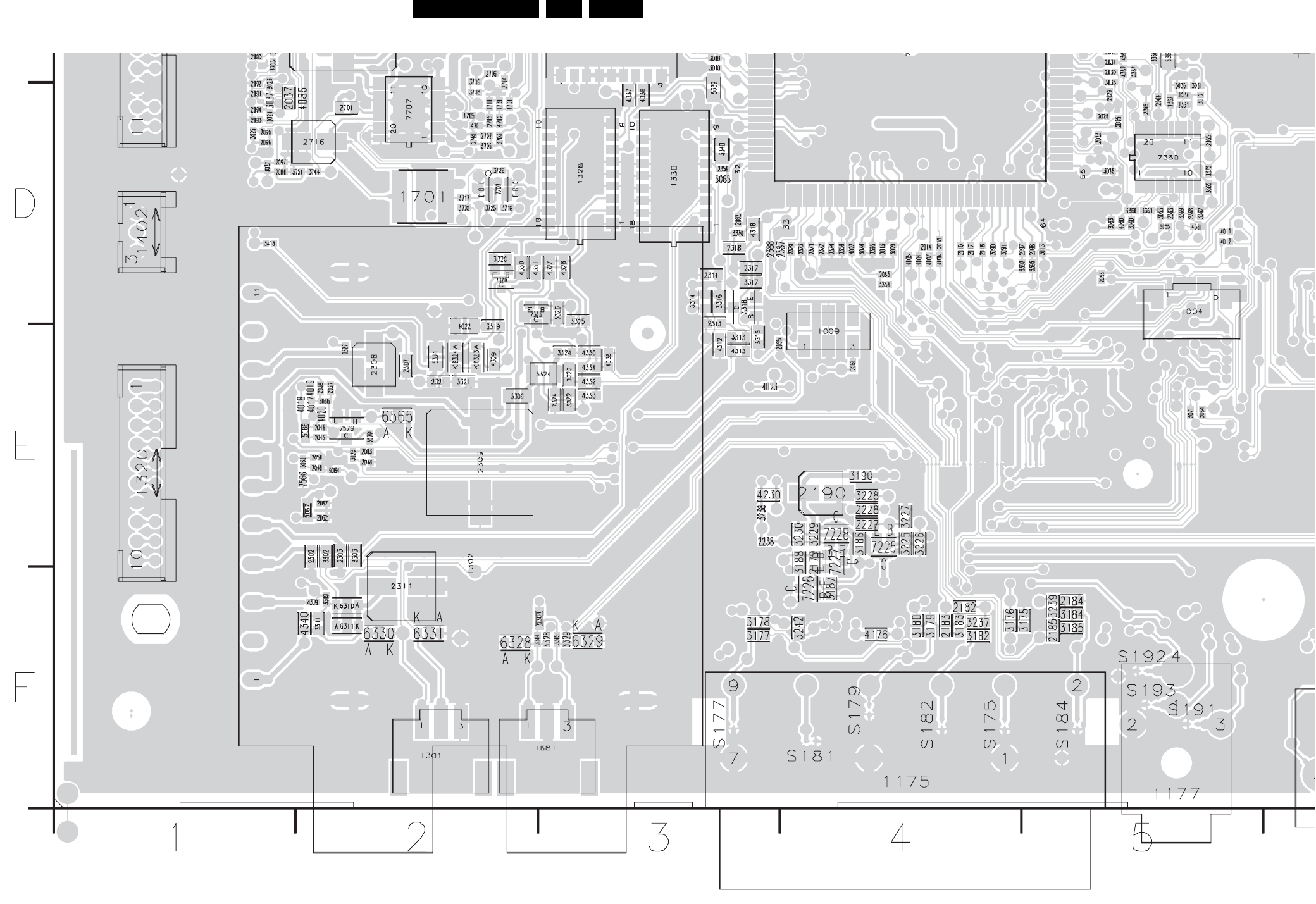
Circuit Diagrams and PWB Layouts 43LC4.6U AA 7.
Layout Small Signal Panel (Top Side Part 3)
E_14710_080c.eps
151104
Part 3
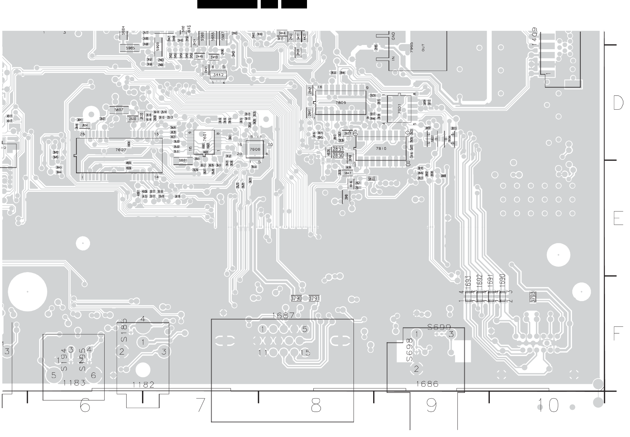
44LC4.6U AA 7.
Circuit Diagrams and PWB Layouts
Layout Small Signal Panel (Top Side Part 4)
E_14710_080d.eps
151104
Part 4
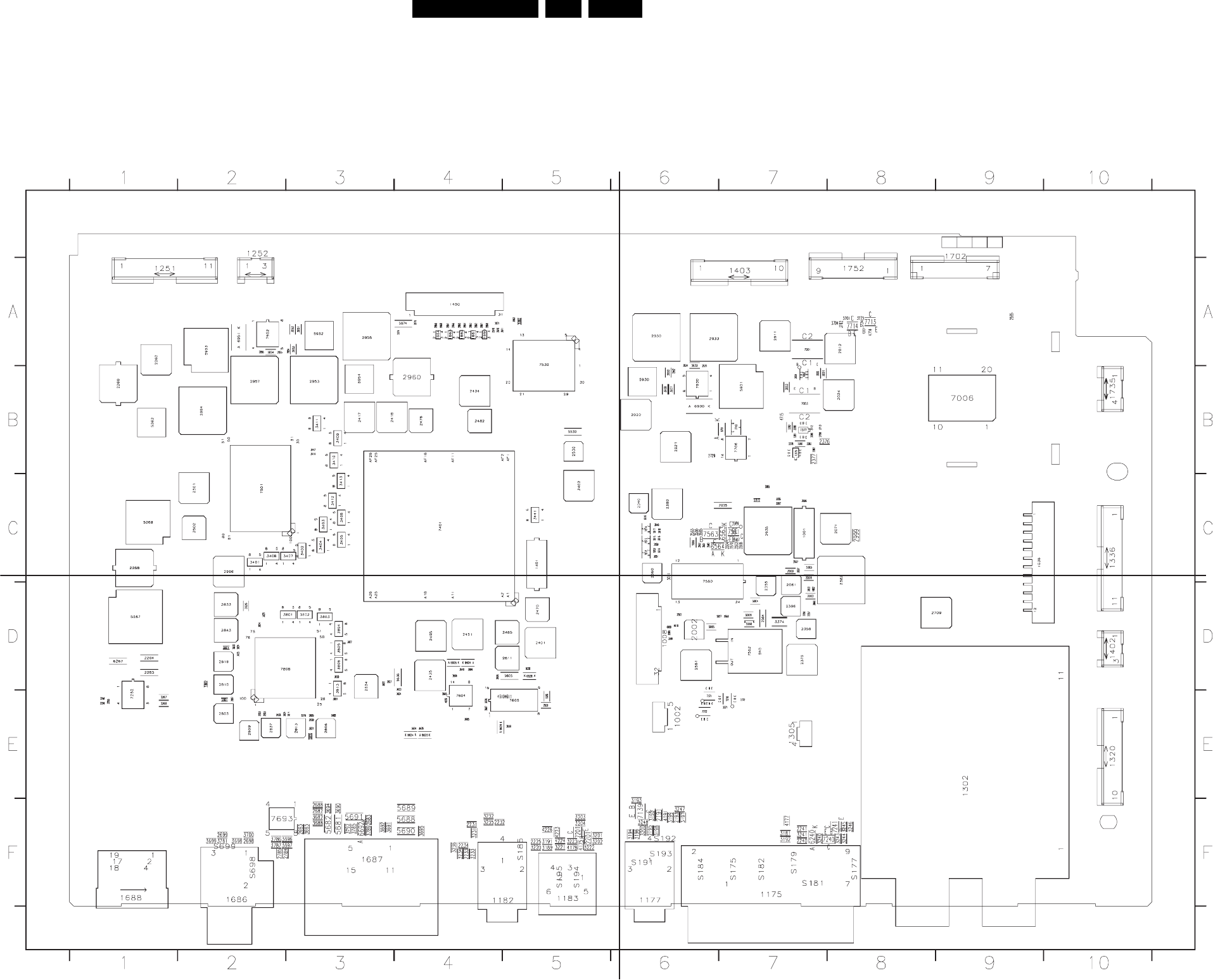
Circuit Diagrams and PWB Layouts 45LC4.6U AA 7.
Layout Small Signal Panel (Bottom Side Overview)
3139 123 5867.2 E_14710_081.eps
060804
Part 1
E_14710_081a.eps
Part 2
E_14710_081b.eps
Part 4
E_14710_081d.eps
Part 3
E_14710_081c.eps
1001 C7
1002 E6
1008 D6
1036 C9
1305 E7
1401 C5
1450 A4
1860 A4
1861 A4
1862 A4
1863 A4
1864 A4
2002 D6
2006 C7
2007 C7
2008 C7
2009 C7
2012 A8
2024 B8
2027 D7
2035 C7
2040 C6
2061 D7
2063 D7
2071 C8
2089 D6
2191 F6
2193 F6
2195 F6
2201 F5
2225 F5
2231 F4
2232 F4
2233 F4
2234 F4
2240 F7
2241 F7
2262 A1
2263 D1
2264 D1
2265 E1
2266 E1
2268 C1
2269 B1
2355 D7
2356 D7
2357 D7
2360 C6
2375 D7
2376 B7
2377 B7
2380 C6
2382 C8
2386 B7
2392 B7
2396 D7
2401 D5
2402 C5
2417 B3
2418 B3
2434 B4
2435 D4
2451 D4
2465 D5
2470 D5
2478 B4
2482 B4
2495 D4
2501 C2
2502 C2
2530 B5
2560 D7
2561 D6
2562 D6
2563 C6
2564 D7
2565 A9
2605 E4
2606 D4
2611 D5
2625 E5
2626 E5
2682 F3
2683 F3
2688 F3
2693 F3
2698 F2
2699 F2
2708 B7
2709 D9
2784 F2
2785 F2
2803 E2
2806 E3
2807 E2
2808 E3
2809 E2
2810 D2
2813 E3
2814 E3
2818 D2
2819 E3
2820 E2
2824 D2
2825 E3
2826 E2
2830 D2
2833 D2
2834 D3
2837 E2
2838 E2
2839 E3
2843 D2
2860 A4
2861 A4
2862 A4
2863 A4
2864 A4
2865 A4
2866 A4
2867 A4
2868 A4
2869 A4
2870 A4
2871 A4
2874 A4
2875 A4
2882 A5
2911 A7
2920 B6
2921 B6
2930 A6
2931 B6
2932 B6
2933 A6
2934 A6
2935 C7
2953 B3
2954 A3
2955 A2
2956 A2
2957 B2
2958 A3
2960 B4
2994 B2
2996 C2
2999 C8
3001 B7
3002 B7
3003 B7
3004 B7
3007 C7
3011 C6
3014 C6
3015 C6
3016 C6
3017 C6
3018 C6
3019 C6
3049 C6
3050 C6
3051 C6
3052 C6
3053 D7
3060 D7
3085 C7
3086 C7
3087 C7
3181 F7
3189 F5
3191 F5
3192 F7
3193 F6
3194 F6
3195 F6
3196 F6
3197 F6
3198 F6
3199 F6
3200 F6
3201 F5
3202 F5
3203 F5
3204 F5
3220 F5
3221 F5
3222 F5
3223 F5
3231 F4
3232 F4
3233 F4
3234 F4
3235 F4
3236 F4
3240 F7
3241 F7
3243 F8
3244 F8
3245 F8
3246 F8
3247 F6
3248 F6
3266 E1
3267 E1
3268 E1
3359 D7
3364 D6
3371 E7
3372 E7
3374 D7
3378 B7
3380 B7
3381 B7
3382 B7
3383 B7
3386 B7
3401 C2
3402 C3
3403 C3
3404 C3
3405 C3
3406 C3
3407 C3
3408 C2
3409 B3
3410 B3
3411 B3
3412 C3
3413 C3
3414 B3
3441 C5
3447 B3
3560 C6
3561 C6
3562 C6
3563 C7
3564 C7
3565 C6
3566 C6
3567 C7
3568 C7
3569 C7
3570 C7
3605 E4
3606 D4
3607 E4
3608 E4
3609 D4
3610 D4
3621 D3
3622 D3
3623 D4
3624 E4
3634 E4
3635 E4
3638 D5
3639 E5
3682 F3
3688 F3
3690 F3
3691 F3
3692 F3
3693 F3
3694 F3
3695 F4
3696 F3
3697 F3
3698 F2
3699 F2
3700 F2
3701 A8
3702 A8
3704 A8
3712 B7
3713 B7
3723 A8
3724 A8
3729 B6
3781 F2
3785 F3
3786 F2
3787 F2
3789 F3
3792 F3
3801 D3
3802 D3
3803 D3
3804 D3
3805 D3
3806 D3
3807 D3
3813 D3
3821 E3
3824 D2
3825 D2
3826 D2
3830 D3
3831 E3
3834 E2
3835 D2
3870 A4
3871 A4
3930 B6
3931 B6
3932 B6
3933 A6
3951 A3
3952 A3
3953 A3
3954 A2
4009 D6
4010 D6
4062 D7
4175 F5
4177 F7
4178 F5
4191 F6
4223 F5
4224 F5
4226 F5
4609 E4
4610 E4
4611 E5
4714 A8
4715 B7
5003 C7
5004 D7
5005 D6
5006 C6
5072 C7
5262 B1
5267 D1
5268 C1
5530 B5
5560 D7
5605 D5
5636 D4
5681 F3
5682 F3
5688 F4
5689 F4
5690 F4
5691 F3
5801 E2
5802 D2
5804 D2
5805 E3
5874 A4
5882 A5
5930 B6
5931 B7
5952 A3
5953 A2
5954 B3
6005 D7
6240 F7
6267 D1
6563 C7
6564 C6
6604 D4
6605 D4
6634 E4
6635 E4
6638 D5
6639 E4
6692 F3
6701 B7
6930 B6
6951 A2
7001 A7
7002 B7
7003 B7
7006 B9
7012 C6
7013 C6
7014 C6
7139 F6
7201 F5
7240 F8
7241 F8
7262 E1
7370 E7
7371 E6
7372 E6
7376 B7
7377 B7
7401 C4
7501 C2
7530 A5
7560 C6
7561 C7
7562 D7
7563 C6
7604 E4
7605 E5
7693 F2
7706 B7
7710 B7
7713 A8
7714 A8
7808 D2
7930 B6
7952 A2
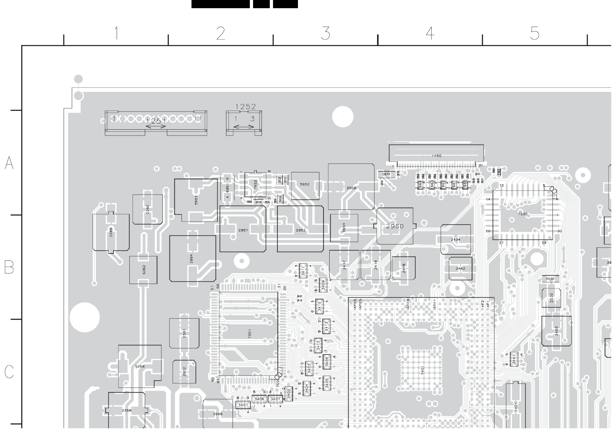
46LC4.6U AA 7.
Circuit Diagrams and PWB Layouts
Layout Small Signal Panel (Bottom Side Part 1)
Part 1
E_14710_081a.eps
151104
Part 1
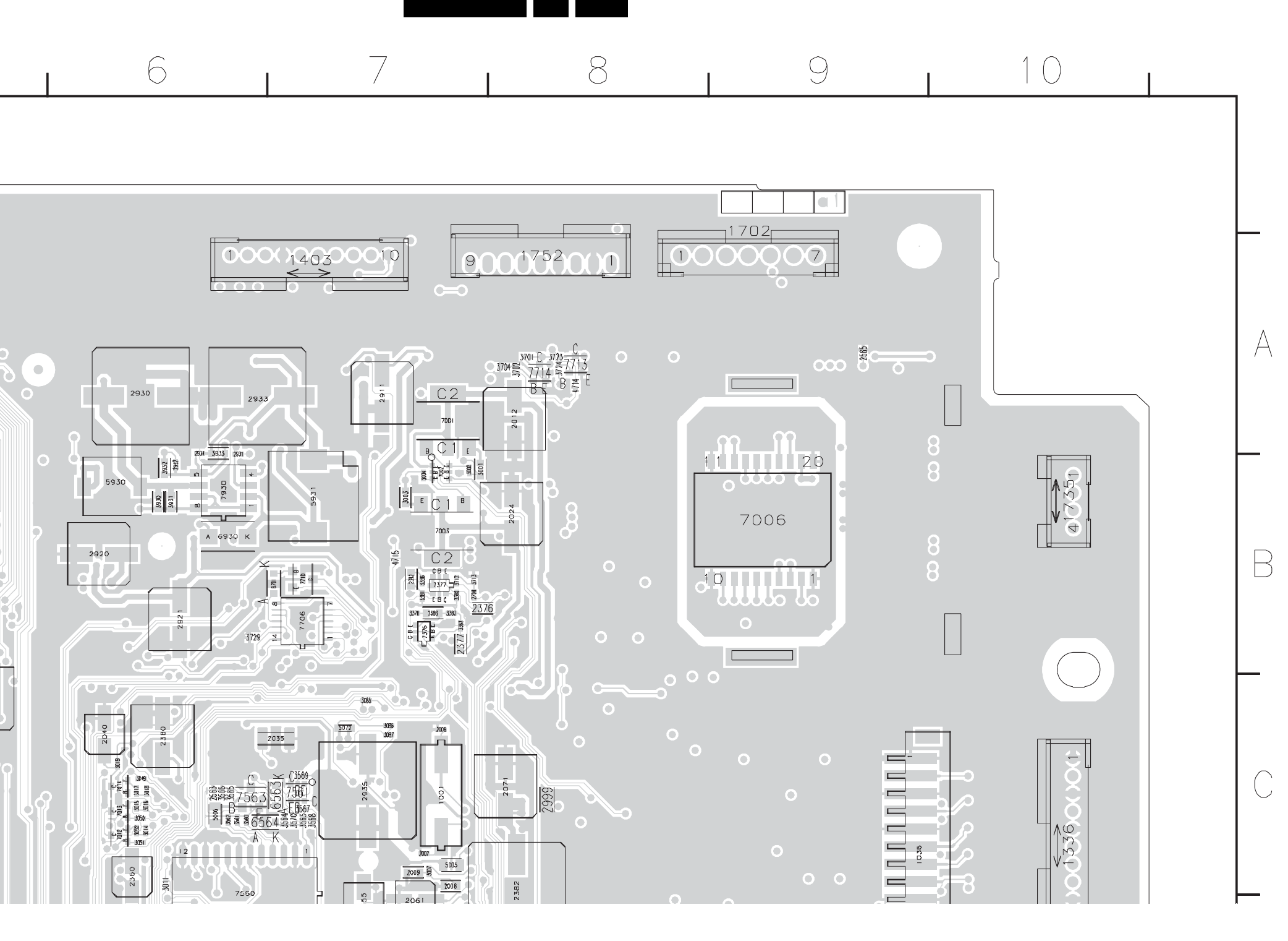
Circuit Diagrams and PWB Layouts 47LC4.6U AA 7.
Layout Small Signal Panel (Bottom Side Part 2)
E_14710_081b.eps
060804
Part 2
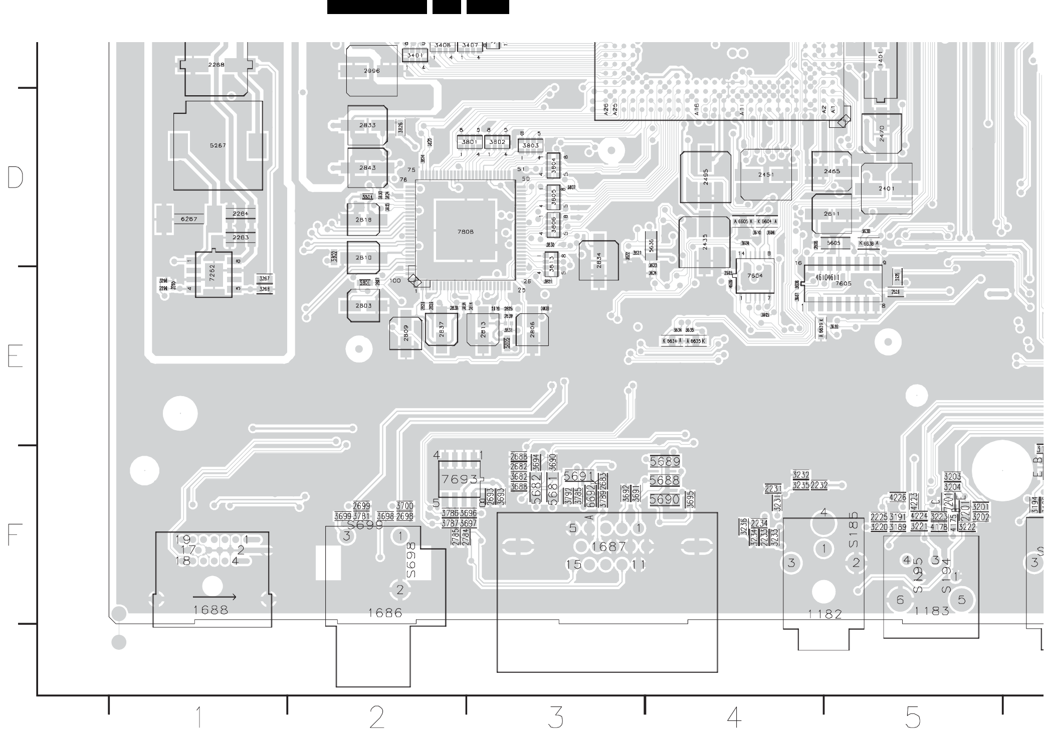
48LC4.6U AA 7.
Circuit Diagrams and PWB Layouts
Layout Small Signal Panel (Bottom Side Part 3)
E_14710_081c.eps
060804
Part 3
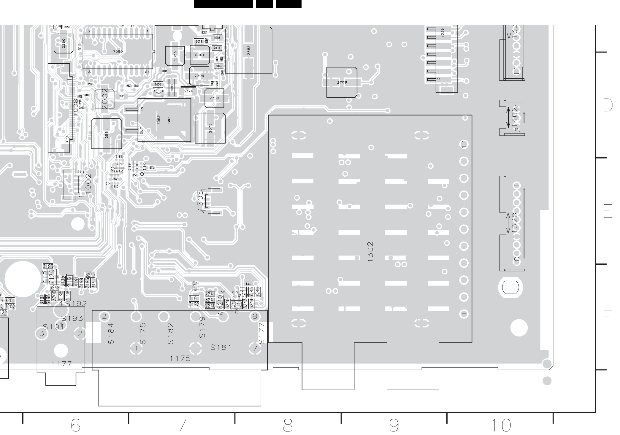
Circuit Diagrams and PWB Layouts 49LC4.6U AA 7.
Layout Small Signal Panel (Bottom Side Part 4)
E_14710_081d.eps
060804
Part 4
50LC4.6U AA 7.
Circuit Diagrams and PWB Layouts
Power Supply Unit (30-32 Inch): Mains Filter and Standby
AS1 AS1
MODE
VM
OSIN
VSS
OSOUT
VG
NC
VDD
V
C
D
E
F
G
A
B
C
1001 D4
1011 E5
1305 F7
1306 F2
1307 B13
1308 C1
1400 C2
1401 F3
AUDIO-STANDBY
TO 1307
TO 1305
AUDIO-STANDBY
T5AH 250V(US)
1234567
AUDIO-STANDBY
TO 1306
MAINS INPUT
8
D
E
F
G
1000 D2
12345678
T5AH 250V(AP)
95-264Vac
MAINS FILTER + STANDBY
A
B
COLD
HOT
1402 D3
1403 D3
9 10111213
2407 C4
2408 C6
2503 E6
2802 E10
2803 C11
2804 C10
2806 F10
2808 E11
9 10111213
3400 C3
3401 C1
3402 C2
3403 D2
3404 D4
3405 D3
3450 B6
3451 C6
3800 E9
3802 E10
3803 E11
3804 E9
3805 E12
1450 C8
2400 C2
2401 C4
2404 C3
2406 C5
5403 B5
5804 E11
MAINS FILTER
6154 C12
6155 C12
6460 E8
6461 D8
6506 E6
6807 C10
6808 E9
6809 D9
7805 D10
7806 E11
9001 C5
9003 C5
2809 E12
2810 D12
2815 C11
2816 D12
3101 C12
9812 E11
9813 C12
9814 C12
F410 B2
F411 B2
F412 C1
F413 C1
F414 C2
F415 C1
F416 C2
F417 C2
F418 C1
F419 C2
F420 F7
F421 F8
F422 B10
3806 E9
3807 E9
3810 B10
5401 C3
5402 C5
F428 F4
I410 C3
T3.15AH 250V(EUR)
I411 C4
I412 C5
I413 C8
I414 B13
I415 C6
I416 C4
I417 B13
I418 C12
I419 D2
I420 D12
I421 E11
I422 E11
9005 C6
9806 E9
9808 C12
9810 D10
9811 D12
I428 E10
I429 D2
290V (303V)
288V (0)
COLD
4V8 (0V)
I430 D4
I431 D3
I432 D5
I442 B6
I444 B6
I445 C6
I455 D4
I456 E7
I810 B10
I811 B11
I812 B11
I813 C10
I814 E9
I815 E9
I816 E9
I817 C11
I820 F9
I824 E12
I825 E12
F423 B10
F424 F2
F425 F2
F426 F2
F427 F3
9005
GNDHOT
I826 E12
I828 E9
I423 E10
I424 E7
I425 E10
I426 E10
I427 E10
3802
91K
I413
220R
3404
2408
100n
1000
GND screw
1
1403
500V
I442
F420
1
2
4
3
2808
47n
9808
5403
9814
I429
I431
I430
2804
56n
4M7
3402
I811
I814
I416
I419
3803
390R
F419
100n
BAS316
6460
500V
2809
1402
470n
2401
I412
I422
76
23
4
58
1
AVS1ACP08
7805
I825
F418
F415 F416
3450
1R
47p
2406
G5PA-1-5VDC
1450
F425
F424
3807
22K
F417
F412
25V_HOT
I415
9811
1401
T1AE 250V
PTF/65
400V_HOT
F413
4R7
3805
2802
2806
47u 50V
100p
1
2
I410
56n
2803
1308
9003
I427
1
2
3
9813
I817
1305
B3B-EH-A
I812
1N5062
6808
I828
I816
3806
470R
I456
I810
3810
12K
9806
DF06M
6506
F422
2816
470n
2400
330u
I820
GNDHOT
9812
6461
I445
BAS316
4M7
3403
1
2
I824
6807
1306
GBJ6J
1011
HEATSINK
4
1K0
3101
1307
B4P-VH
1
2
3
2503
10u
100n
2810
F421
I826
I813
BYG10
6154
F414
F423
AVS10CB
7806
I414
3405
220R
F411
F410
I421
6155
BYG10
I418
14
23
DMF3547HB60
5401
33u
5804
I428
I455
I815
23
DMF3547HB60
5402
14
F426
F427
I411
I425
I423
3800
I426
1M0
I420
I444
4M7
3401
I424
I432
3400
9001
1R
3451
3804
20K
2407
220p
9810
47p
2404
I417
PTF/65
1400
1N5062
6809
F428
330u
2815
GND screw
1001
1
E_14710_037.eps
230604
3104 313 6009.5
Circuit Diagrams and PWB Layouts 51LC4.6U AA 7.
Power Supply Unit (30-32 Inch): Supply
AS2
NC
VCC UVLO/
ENABLE
VARIABLE
FREQUENCY
OSCILLATOR
2.5V CLAMP
ERROR
SOFT-START
5.0 V
REFERENCE
VREF UVLO
STEERING
FLIP-FLOP
FAULT DET/
LATCH
ONE-SHOT
C
D
E
F
G
H
I
1007 G10
1009 H10
1010 H11
1012 H11
1304 H13
1309 I13
1M02 H13
2000 E9
2002 A2
2003 A5
2004 C2
2005 D2
2006 C2
2007 E1
2008 G4
0V (0V)
A2
A2
24V4 (0V)
TO 1309
1 23456789101112 13
123
11V3 (0V)
32" SHARP
HIGH SIDE
20V4 (0V) 22V(0V)
288V(0V)
456789101112 13
A
B
C
D
E
F
G
H
I
A
B
13V4
2009 D1
10V2 (0V)
2010 H1
2011 E9
2012 E8
2013 C8
2014 F6
2015 F5
2016 E6
2017 C9
2018 F5
2019 H2
2020 C11
2021 C11
2022 E11
2023 A12
2024 E12
2025 E13
2026 G3
2027 F3
2028 B10
2029 D11
2030 F12
CURRENT
DRIVE
HOT COLD
2031 B12
2032 E13
2033 E13
2034 C1
2035 C2
2036 A13
2037 B13
2038 D11
2039 B10
2040 C1
2041 D13
2042 D13
2043 D13
2044 C10
2045 E11
2046 I4
2047 I5
AUDIO - STBY
TO 1M02
AUDIO - STBY
CONTROL
2048 I4
2050 E3
2051 D13
2052 D13
2053 D13
2060 C7
2061 B7
2062 D7
2063 C6
2064 D6
2065 D7
2071 E7
2072 C7
2077 H4
2290 G10
2291 G11
2292 G11
2293 H11
2294 H11
COLD
SUPPLY
3000 A2
3001 F5
3002 C1
3003 C1
3004 D1
3005 C2
3006 D2
3007 E2
3008 E2
3009 E1
3010 H2
3011 H2
3012 F3
3013 G4
3014 C7
3015 C8
3016 C7
3017 D8
3018 E8
BIAS SUPPLY
Voltage
3021 G6
3022 C11
3023 E12
3024 E13
3025 F13
3026 G13
3027 G3
3028 E7
3029 C7
3030 F11
3031 A11
3032 B10
3033 A5
3034 F13
3035 C7
3036 A13
3037 C12
3038 E13
3039 A13
3040 E13
3041 F13
HOT GROUND
TO 1304
Adj.
3043 D1
3044 A13
3045 G5
3046 F6
3047 H3
3048 D2
3049 A12
3050 E3
3051 B12
3052 C12
3053 E3
3054 C12
3055 I5
3056 I3
3057 A12
3058 E2
3059 A13
3061 E4
3064 F3
3065 E4
3066 F3
COLD GROUND
GND_SND
3019 E7
3020 E7
3067 G1
3068 G4
3070 H4
3071 H4
3075 G5
3089 H6
3100 A9
3292 G10
3999 A11
5001 C6
5002 D9
5004 D8
5005 C9
5007 B8
5008 B8
5009 B5
5010 A6
3042 B13
VSND_NEG
5013 E8
5015 C6
5016 D6
5017 A3
5025 D10
5026 D10
5027 B10
5028 C10
5040 D9
5041 E8
5291 G11
5292 H11
5293 G11
6001 D2
6002 D7
6003 C7
6004 D6
6005 D6
DRIVE
6006 I4
6007 C7
6008 D7
6009 H1
6010 G4
6011 F4
6012 E8
6013 C8
6014 H6
6015 G6
6017 I5
6020 H1
6021 D11
6022 H2
6023 E13
6025 E11
6027 C7
6028 E7
6030 A12
6044 B10
6045 C10
6051 H3
6054 A13
6077 A5
6078 A6
6079 A4
6080 A4
6081 A2
6082 A3
6291 G11
6293 G11
7001 C3
7002 A9
7004 H5
7005 C8
7006 D8
7007 C8
CONTROL
HOT
PROTECTION
Vs
7008 E8
7009 G4
7010 F12
7017 F3
7018 F3
7030 A10
7031 B13
9002 G13
9004 B5
9008 A4
9009 A3
9010 C11
9024 D8
9025 E8
F001 H12
F002 C8
F003 C6
F004 D6
F005 D8
F006 I12
F007 F3
VSND_POS
VS-CONTROLLER
F008 D6
F009 D6
F014 F12
F016 B11
F017 D11
F018 A8
F021 A11
F022 A12
F023 F9
F024 D11
F025 D11
F027 D11
F028 C11
F029 C9
F290 G12
F292 G12
F293 G12
F294 H12
F295 H12
F296 G13
F297 G12
F298 H12
F299 A8
CONNECTION
LOW SIDE
I002 B8
I003 C7
I004 D8
I005 A10
I006 B2
I007 C2
I008 C2
I009 C2
I010 D2
I011 I5
I012 D4
I013 A13
I014 A13
I015 A13
I016 A12
I017 B13
I018 E3
I020 F3
I021 E1
I022 F3
I023 F3
FLM 1/6W
I024 F4
I025 F2
F010 H12
F012 D11
I029 G2
I033 F5
I034 F6
I036 F5
I037 C8
I038 C8
I039 D7
I042 C7
I045 C7
I046 C8
I051 E8
I052 D7
I055 E8
I057 D8
I059 E8
I062 A10
I063 A10
I064 B7
I070 B10
I072 C10
I073 D10
I074 D10
I076 D10
F300 F9
I001 B8
I081 F7
I084 F9
I085 E12
I088 E13
I089 E12
I092 F13
I093 F13
I094 G12
I095 A4
I096 A3
I097 A3
I098 A5
I099 A6
I100 A6
I101 A6
I103 C1
I104 D2
I105 E3
I106 E6
I107 C6
I108 D6
SOFTSTART
I109 C7
I110 D8
I111 C8
I112 E8
I113 E8
I114 D9
I116 C10
I117 C10
I027 C3
I028 G2
I121 E13
I122 F13
I123 F10
I124 G10
I131 I5
I132 I4
I133 I4
I134 I3
I135 G3
I136 H4
I137 G4
I138 H4
I139 G4
I140 G5
I141 H1
I142 H1
I143 G1
I145 E7
I290 G11
I291 G11
I292 H10
ONLY FOR
I077 E10
I080 F10
1
3
2
I293 H11
I294 C8
I295 H6
I296 G6
c001 G9
c002 E8
I119 C12
I120 C12
RES
STPS20H100CT
6021
15K
3037
470n
2008
16
33K
3041
I038
5040
6013
SML4744
SML4744
2K7
3048
6012
2000V
2014
2n2
470p
2000 16
2024
220n
50
2015
10n
9002
F008
3055
220R
5008
2047
10n
F012
F298
I077
6077
BYG22D
2009
I294
+12V
100p
BAS316
6006
I099
I073
3000
4R7
I138
2063
470p
1010
HEATSINK
7005
STP15NK50ZFP
I110
I052
I039
I076
3K3
3009
2043
220n
I046
3025
1K8
1%
6004
BAT54 COL
I104
6044
STPS20L45CT
1
3
2
5007
I022
3057
220R
3K3
3020
2016
16 100n
I116
1n0
2071
I109
9004
GND3
I003
I033
I106
I034
470R
3011
3010
470R
F004
F003
100u
2010
BZX384-C4V7
6022
100p
I093
3026
2034
I070
470R
2m2
2294
F027
F025
F029
F021
F028
c001
I055
I114
330R
3008
I072
3
2
I036
6025
STPS20H100CT
1
50V
I004
13
2
1n0
2044
STPS20L45CT
6045
6291
STPS8H100FP
50V
1n0
RES
I001
2045
33K
3038
5009
I089
3040
8K2
BAS316
6011
I290
I097
I296
2290
10n 50
I295
2061
2n2
I062
25V_HOT
3007
10K
10K
3013
1304 VH
1
2
3
4
F010
2041
220n
I095
I011
RES
RES
100n
2018
1m
5010
9008
BYG22D
F296
I122
6080
STP15NK50ZFP
7006
2065
2n2
I045
470n
2023
10n
2017 1600
I121
5M6
3058
2021
2m2
I108
47R
3018
3027
100K
I101
2033
220n
100R
3067
I123
3033
1R0
I105
I037
I057
5
R
8
I008
7010
TL431ACD
2
A
3
6
7
K1
4
I063
3068
2K2
14
32
BAS316
6002
100K
TCET1102
7002
I025
3065
I292
5005
I028
3001
100R
HEATSINK
1009
3023
15K
3005
33K
3034
RES
1%
I012
I145
2002
470u
3999
1K0
2040
560p
3014
100R
2005
630
100p 2035
100p
BC857BW
7009
5041
6017
BAS316
BC847BW
7004
3071
10K
7
I007
1M02
1
2
3
4
5
6
B7B-EH-A
BC847BW
7018
2n2
2062
7007
BC857BW
2048
1n0
16
2030
100n
6001
BAS316
RES
I143
3022
680R
F022
9024
9025
I139
3056
220R
100R
3017
I291
I293
2042
220n
5028
3016
3K3
50V
2028
1n0
7017
BC857BW
I009
2
3
4
6
7
9
I020
5001
S13932-04
10
BAS316
6020
6
EN|UA9
FI 10
GND
4
I+8
I-
7
OA 14
OB 12
OS16
OSCC1
OSCCC3
OSCR2
PGND 13
SOST
11
VCC
15
VREF
5
7001
MC34067P
EAO
5004
I137
I136
400V_HOT
50
2027
15n
RES
I029
4m7 16V
I027
2038
I112
10R
3100
25
2006
1n
3003
100K
3006
10K
3075
1K
10n
2011
1600
2292
2m2
I111
I094
I117
7030
BC857BW
7008
BC847BW
9010
10K 3031
2020
2m2 25
3064
10K
2077
2n2
I006
c002
33K
3024
MRS25 1%
I107
F014
F292
470n
2007
16
470n
2039
I113
I064
2046
47n
3029
3K3
6003
BAS316
5027
5015
1309
1
2
3
B3P-VH
3052
33K
I005
3K3
3035
STPS8H100FP
6293
3043
10R
I002
3050
820K
3047
47R
6028
BAS316
22R
3045
3046
22R
BAS316
6027
F290
F005
+12V
F002
I141
F016
3066
10K
3061
68K
5013
50
2026
2n2
I084
RES
BAS316
6007
220n
2051
2032
4n7
220n
2052
2n2
2060
19372
1007
T5A 250V
+24V
3004
27K
630
3030
18K
I088
200p
2004
F299
I119
F024
2037
470n
BAS316
6030
3054
4K7
3051
4K7
F007
BYG22D
6078
2003
1m0
1012
HEATSINK
5026
2072
1n0
I085
RES
BAS316
6051
I051
2031
10n
6009
PDZ-18B
560R
3292
6010
BAS316
1n5
2012
6079
BYG22D
2000V
3K3
3028
BAS316
6023
I081
3K3
3019
5025
I131
2000V
2013
1n5
2022
4m7 16V
I018
I042
50V
2029
1n0
2064 470p
3015
47R
5016
I059
3036
100K
7031
BC847BW
33u
5293
I092
I021
BAT54 COL 6005
15K
3012
22R
3021
400V_HOT
220n
2053
I096
I023
5292
33u
3053
680K
I124
+24V
I134
F023
3042
12K
470n
2036
F017
F293
F294
I080
F009
F018
F297
470p
2291
50
I103
I098
9009
33K
RES
BAS316
6082 3049
3039
1K0
I142
F295
5017
I120
I132
1n0
2050
I135
F300
I133
I074
3044
470R
6008
BAS316
I017
I016
I014
I015
+12V
I013
6054
3059
2K2
BZX384-C10
GND_SND
50
2293
470p
I024
6
7
89
3070
1K
1
10
11
12
13
14
15
16
2
3
5
BS51312-01
5002
I010
2025
220n
F006
2019
10n
47K
3032
3002
39K
6014
BZX384-C22
6015
BAS316
10K
3089
BZX384-C22
6081
I100
I140
33u
5291
F001
DC_PROT
DC_PROT
E_14710_038.eps
230604
3104 313 6009.5
F003
5V / div DC
5µs / div
F004
5V / div DC
5µs / div
F005 F016 = 12V6
F025 = 24V4
F297 = 19V2
F298 = -19V2
500mV / div AC
5µs / div
I038
50V / div DC
5µs / div
I057
5V / div DC
5µs / div
52LC4.6U AA 7.
Circuit Diagrams and PWB Layouts
Layout Power Supply Unit (30-32 Inch) (Top Side)
E_14710_039.eps
080604
3104 313 6009.4
1000 A1
1001 A3
1007 B10
1009 B9
1010 C9
1011 C3
1012 A9
1304 A10
1305 A3
1306 A4
1307 A5
1308 C1
1309 A8
1400 C1
1401 A4
1402 A2
1403 B1
1450 A3
1M02 B10
2000 A7
2002 A7
2003 A6
2004 A6
2005 A6
2010 A7
2011 B7
2012 C7
2013 C6
2014 A7
2017 B6
2020 C8
2021 C8
2022 A8
2038 A9
2292 A10
2294 C10
2400 C2
2401 B1
2404 B1
2406 A3
2407 A3
2408 B3
2503 A4
2803 B3
2804 B4
2806 B4
2809 C4
2810 C4
2815 A3
2816 A5
3000 A5
3014 B6
3015 C5
3017 C7
3018 C7
3026 A9
3033 A6
3050 A5
3053 A5
3058 A5
3400 C2
3401 C2
3402 A1
3403 A1
3404 A2
3405 B1
3450 A2
3451 A3
3800 A4
3805 C4
3807 B4
3810 A4
5001 B6
5002 A7
5004 C6
5005 C6
5007 B6
5008 C5
5009 B7
5010 B6
5013 C7
5015 A6
5016 A6
5017 A5
5025 B9
5026 A9
5027 C9
5028 C9
5040 B6
5041 C7
5291 B10
5292 C10
5293 B10
5401 B2
5402 A1
5403 A3
5804 B4
6021 B9
6025 B10
6044 C10
6045 C10
6291 A9
6293 A10
6506 A4
6807 C3
6808 A4
6809 A4
7001 A6
7002 A8
7005 C6
7006 C7
7805 B4
7806 C4
9001 A3
9003 A3
9004 A7
9005 B3
9006 C10
9007 A8
9010 A10
9011 A8
9012 C8
9013 B8
9014 B1
9016 A7
9017 A5
9018 A6
9019 A6
9020 B7
9021 A6
9022 C3
9023 C3
9024 C6
9025 B7
9026 C8
9027 B9
9028 B9
9031 A9
9032 A9
9033 A9
9034 A10
9035 B8
9036 B9
9037 B8
9038 A9
9039 A9
9040 B9
9041 B9
9042 B10
9043 B10
9044 C9
9045 C9
9046 C9
9047 C10
9080 A7
9081 C2
9086 B10
9087 B9
9088 A10
9090 A10
9091 A9
9092 A7
9093 A7
9098 B3
9808 B5
9811 B5
9812 B4
9813 B5
9814 A5
Circuit Diagrams and PWB Layouts 53LC4.6U AA 7.
Layout Power Supply Unit (30-32 Inch) (Overview Bottom Side)
E_14710_040.eps
080604
3104 313 6009.4
Part 1
E_14710_040a.eps
Part 2
E_14710_040b.eps
2006 A5
2007 A6
2008 A5
2009 A5
2015 A5
2016 A5
2018 A5
2019 A5
2023 B1
2024 B1
2025 A1
2026 A6
2027 A6
2028 C2
2029 B2
2030 B1
2031 A1
2032 A1
2033 A1
2034 A5
2035 A5
2036 C1
2037 C1
2039 B1
2040 A5
2041 A1
2042 A1
2043 A1
2044 C1
2045 B1
2046 A4
2047 A5
2048 A5
2050 A5
2051 A1
2052 A1
2053 A1
2060 C6
2061 B5
2062 C5
2063 A5
2064 A5
2065 C4
2071 C4
2072 C5
2077 A4
2290 B3
2291 A2
2293 A1
2802 B7
2808 C7
3001 A4
3002 A5
3003 A5
3004 A5
3005 A5
3006 A5
3007 A6
3008 A6
3009 A6
3010 A4
3011 A5
3012 A5
3013 A5
3016 C6
3019 C4
3020 C4
3021 A4
3022 B1
3023 B1
3024 A1
3025 B1
3027 A6
3028 C4
3029 C6
3030 B1
3031 B1
3032 B1
3034 B1
3035 C6
3036 C1
3037 A1
3038 B1
3039 C1
3040 B1
3041 B1
3042 C1
3043 A5
3044 C1
3045 A5
3046 A4
3047 A4
3048 A5
3049 C1
3051 C1
3052 A1
3054 C1
3055 A4
3056 A4
3057 A1
3059 C1
3061 A5
3064 A5
3065 A6
3066 A5
3067 A4
3068 A4
3070 A4
3071 A4
3075 A4
3089 A4
3100 A4
3101 A6
3292 B3
3802 B7
3803 B6
3804 B7
3806 B7
3999 B8
6001 A5
6002 C4
6003 C6
6004 A5
6005 A5
6006 A5
6007 B6
6008 C5
6009 A4
6010 A5
6011 A5
6012 B4
6013 C5
6014 A4
6015 A4
6017 A5
6020 A4
6022 A5
6023 A1
6027 C6
6028 C4
6030 C1
6051 A4
6054 C1
6077 A5
6078 B5
6079 A5
6080 A6
6081 A4
6082 A6
6154 A6
6155 A6
6460 A8
6461 A8
7004 A4
7007 C5
7008 C5
7009 A4
7010 A1
7017 A5
7018 A6
7030 B1
7031 C1
9002 B1
9008 A6
9009 A6
9030 A1
9085 B1
9806 B7
9810 B7
54LC4.6U AA 7.
Circuit Diagrams and PWB Layouts
Layout Power Supply Unit (30-32 Inch) (Part 1 Bottom Side)
E_14710_040a.eps
080604
Part 1
Circuit Diagrams and PWB Layouts 55LC4.6U AA 7.
Layout Power Supply Unit (30-32 Inch) (Part 2 Bottom Side)
E_14710_040b.eps
080604
Part 2
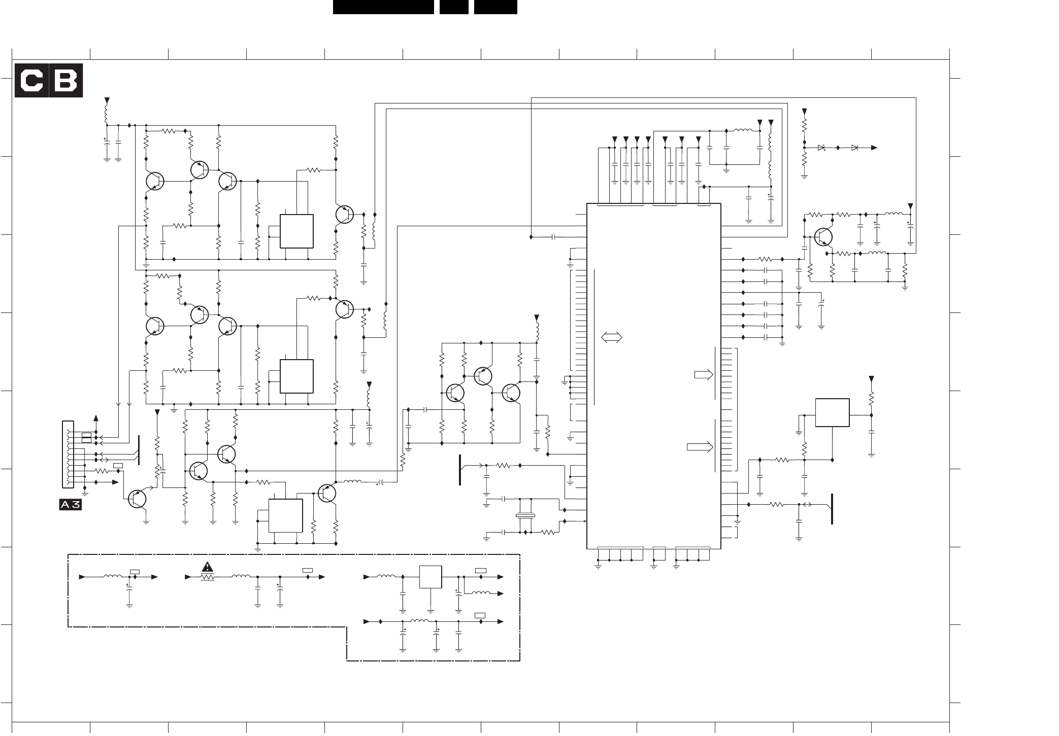
56LC4.6U AA 7.
Circuit Diagrams and PWB Layouts
3D Comb Filter
3
2
1
0
VRBY
VCLY
CBPY
CBPC
DVDDOIO
FSCI
12
11
10
09
08
07
06
05
04
03
14
15
16
23
CLK8
CKMD
TEST26
25
24
18
13
DVDDRAM
DGNDDGNDRAM
DYCO
EXTDYCO
6
5
4
3
2
1
7
17
ACO
AGND
AY0
0
EXALTF
9
8
7
6
5
4
NSTD
SCL
XI
XO
8
VRBC
VRTY
VRTC
AVDD DVDD
ST1
ST0
SLA0
SDA
RSTB
RPLL
9
19
20
21
02
01
TESTIC2
TESTIC1
ACI
AYI
Φ
Y/C SEPARATION
FSCO
ALTF
TEST
22
CSI
KIL
LINE
COM
OUTIN
3D COMB FILTER
100 MHz / 120R
100 MHz / 120R
100 MHz / 120R
100 MHz / 120R
100 MHz / 120R
100 MHz / 120R
100 MHz / 120R
100 MHz / 120R
NC
NC
NC
NC
NC
NC
TO
SUPPLY CIRCUIT
1004
3V1 2V5
2V5 2V4
2V4
7V3
2V
2V6
6V6
6V
1V8
1V1 2V
1V3
0V
7V
2V1
2V7
6V3
5V7
1V9
1V2
2V
0V
1V4
3V2
7V2
7V2
2V5
2V5
2V8
2V1
0V
2V3
3V2
3V3
2V1
0V1
2V9
3V2
3V2
3V2
2V1
1V4
2V5
1V1
1V4
1V3
1V1
1V
0V7
2V5
2V5
0V8
1V3
2V4
2V4
2V4
2V4
3V3
1V2
1V2
1V3
1V2
2V4
3V2
1V4
1V4
2V4
2V9
,400mA
NC
NC
NC
NC
NC
0R
0R
1 2 3 4 5 6 7 8 9 10 11 12
1 2 3 4 5 6 7 8 9 10 11 12
A
B
C
D
E
F
G
H
A
B
C
D
E
F
G
H
1801 E1
1883 F7
2800 C3
2801 C3
2802 A2
2803 A2
2816 D3
2817 D3
2829 D5
2833 E5
2834 E5
2835 F5
2836 C11
2837 C10
2839 C5
2840 B8
2841 C10
2842 C10
2843 D10
2844 C10
2845 B8
2846 C10
2847 D10
2848 E3
2849 A10
2851 G5
2852 G6
2853 A10
2854 A10
2855 G4
2856 G4
2861 D7
2862 E6
2863 E6
2864 E7
2866 G2
2870 H6
2871 H6
2872 H6
2874 E12
2875 F11
2877 F10
2878 F6
2879 F10
2881 B9
2882 B8
2883 F7
2884 F7
2885 B9
2886 B9
2887 B9
2888 B10
2889 B10
2890 B11
2891 B11
2892 C10
2893 C11
2894 C12
2895 B7
2896 B12
2897 C10
3801 A3
3802 B2
3803 C2
3804 A2
3805 B3
3806 B3
3807 A3
3808 C3
3809 A3
3810 B4
3811 B4
3812 C5
3813 A4
3814 B5
3815 C4
3816 C2
3817 D2
3818 D2
3819 C2
3820 D3
3821 C3
3822 D3
3823 D3
3824 C3
3825 D4
3826 C4
3827 D5
3828 C4
3829 D5
3830 D4
3832 E3
3833 E3
3834 F3
3835 F3
3836 E3
3837 F2
3838 E2
3839 E2
3841 F4
3842 F4
3843 E5
3844 F5
3847 F3
3855 G3
3860 E7
3861 D7
3862 D6
3863 D6
3864 E6
3865 E6
3866 E6
3867 E7
3875 E12
3876 A11
3878 A11
3879 E11
3881 F10
3882 E7
3883 E10
3884 F7
3890 B11
3891 B11
3892 C11
3893 C11
3894 C11
3895 C12
3896 C10
5801 A2
5802 B4
5804 D4
5806 F4
5832 E5
5835 F5
5840 D5
5841 B5
5849 A10
5851 G5
5852 G7
5855 G3
5856 G2
5860 D7
5870 G6
5888 B10
5889 A10
5890 B12
5891 C12
6875 A11
6876 A11
7800 B3
7801 B3
7802 B3
7803 B5
7807 C5
7808 F3
7809 E3
7812 F5
7816 D3
7817 C3
7818 D3
7823 B8
7837 F2
7851 G6
7860 D7
7861 D6
7862 E6
7875 E11
7890 C11
I801 A2
I802 A3
I803 B2
I804 B5
I806 B4
I807 B3
I808 B2
I809 B5
I810 B4
I811 B3
I812 B5
I813 C3
I814 C5
I815 C3
I817 C2
I818 C5
I820 C5
I821 D4
I822 D5
I823 D5
I824 D3
I825 D2
I827 D3
I828 E3
I829 E1
I830 E1
I831 E1
I832 E1
I833 E1
I834 E2
I835 F2
I836 F1
I837 E3
I838 E3
I839 F4
I843 F5
I844 E4
I845 E5
I846 D7
I847 D7
I848 D6
I849 D6
I850 E6
I851 E7
I852 E7
I853 E6
I854 C10
I855 C5
I856 B5
I857 C10
I859 C10
I860 D10
I861 C10
I863 C10
I864 D10
I865 A10
I866 G7
I867 G2
I868 G6
I869 H5
I870 G4
I871 E12
I872 A11
I873 A11
I874 B11
I875 B11
I876 B11
I877 E10
I878 C11
I879 C11
I880 C10
I881 F7
I882 F10
I883 C7
I884 F8
I885 F7
I886 C10
I887 F8
I888 B9
I889 E11
I892 C3
I893 C3
I897 G6
+8V3
BC857BW
7837
3839
560R
100n
2874
3838 1K0
+3V3STBY
I860
+2V5A
2843 100n
2
3
89
95
90
94
91
47
48
35
36
37
39
41
42
43
44
98
99
9
10
11
12
13
14
15
16
17
33
34
57
59
60
58
61
62
4
5
6
7
8
25
26
27
28
52
50
79
78
63
77
71
72
73
74
18
19
20
21
22
23
24
64
100
38
31
32
65
66
67
68
69
70
54
56
76
1
40
55
29
30
80
45
97
75
46
53
81
92
93
84
88
82
85
UPD64083
7823
96
83
49
51
86
87
I897
+3V3STBY
I892
I887
I893
I886
I888
I884
I879
I885
I878
I875
I880
I874
I876
I881
I877
I882
I873 I872
I871
I864
I865
I863
I859
I861
I857
I856
I854
I851
I855
I853
I848
I850
I849
I843
I846
I837
I839
I838
I820
I828
I818
I827
I822
I824
I821
I825
I815
I817
I812
I804
I809
I810
I813
I811
I807
I806
I808
I802
I803
I801
6.3V330u
10u
5856
2866
+3V3
I867 I866
I836
I835
I829
I833
I832
3837
560R
2848
47u 16V
+2V5D
+3V3STBY
10u
5852
+8V3 +8V3d
I869
5855
10u
16V47u
2856
2855
100n
1R0
3855
I870
+2V5D
I868
16V 10u
2872
+2V5P
2871
10u16V
2870
100n
+2V5A
5870
10u
GND
IN OUT
LF25CDT
7851
10u
5851
2u2
2851
10V
16V
2852
100u
9
1112
+3V3STBY
+8V3
1
10
2
3
4
5
6
7
8
1801
470R
3835
I852
I823
I814
I844
2897
150p
2879 22p
3896 100R
22p
2878
100n
2854
2877
22p
2853
100n
2839
22p
22p
2829
8
5806
4FUS
1
2
34
6
7
1
2
34
6
78
6
78
5804
4FUS
5802
4FUS
1
2
34
1
GND
2RESET_
3
VCC
LM809M3-3.08
7875
I889
I883
I845
I847
I834
I830
I831
5835
50V
1u0
2835
2836
10u 16V
2837
100n
100n2845
2847 100n
100n
2846
2844 100n
100n
2841 100n
2840
2842 100n
5841
5840
+2V5A
+3V3
5860
1u0
2862
220R
3864
2863
1n0
27K
2861
100n
3862
3863
3866
1K0
3865
220K
3860
470R2K2
3861
4K7
7861
BC857BW
BC847BW
7862
7860
BC847BW
2864
22p
3867
470R
100n2881
+2V5D
3881 47R
47R
3882
+2V5D
+3V3
BAS17
6876
1PS76SB10
6875
220R
3875
3876
150R
100K
3878
22p
2875
100K
3879
1K0
3883
+2V5P
2882 100n
10n2895
+3V3
10u
5890
16V10u
2896
2891
10u 16V
2890
100n
10R
3891
1K5
3890
1K0
3895
150p
2894
2893
150p
5891
15u
470R
3893
BC847BW
7890
470R
3894
2K7
3892
2892
10n
22p
22p
2883
2884 1883
DSX151GA
1
42
3
220R
3884
+2V5D
20M
+2V5P
2886 100n
+3V3
100n
2885
2887 100n
+2V5D
5888
10u
5889
2889
16V10u100n
2888
+2V5D
100n
2849
5849
5832
+8V3d
2834
16V47u100n
2833
10R
3844
3K3
BF550
7812
3842
3841
820R
470R
3834
3847
12K
BC847BW
7809
7808
BC847BW
10R 1K5
3843
10R
3836
3832 3833
12K
22p
2817
10R
2816
22p
3829
3828
2K7
3827
10R
3826
560R
3825
5K6
3830
5K6
3823
120R
3822
120R
330R
3820
3821
180R
3824
330R
BC857BW
7807
7818
BF570
7817
BC857BW
47R
7816
BC847BW
47R
3816 3819
3818
3817
1K0
+8V3d
5801
16V47u
2802
100n
2803
2801
22p22p
2800
3814
10R
2K7
3813
10R
3812
560R
3811
5K6
3810
1K8
3815
120R
3808
120R
3806
3805
100R
120R
3807
330R
3809
BF570
7802
7803
BC857BW
BC857BW
7801
33R
BC847BW
7800
3804
47R
3801
3802
1K0
3803
CVBS-COMB
SCL0
SDA0
SCL0
SDA0
COUT-COMB
YOUT-COMB
3139 123 5785.1 E_14490_078.eps
150704
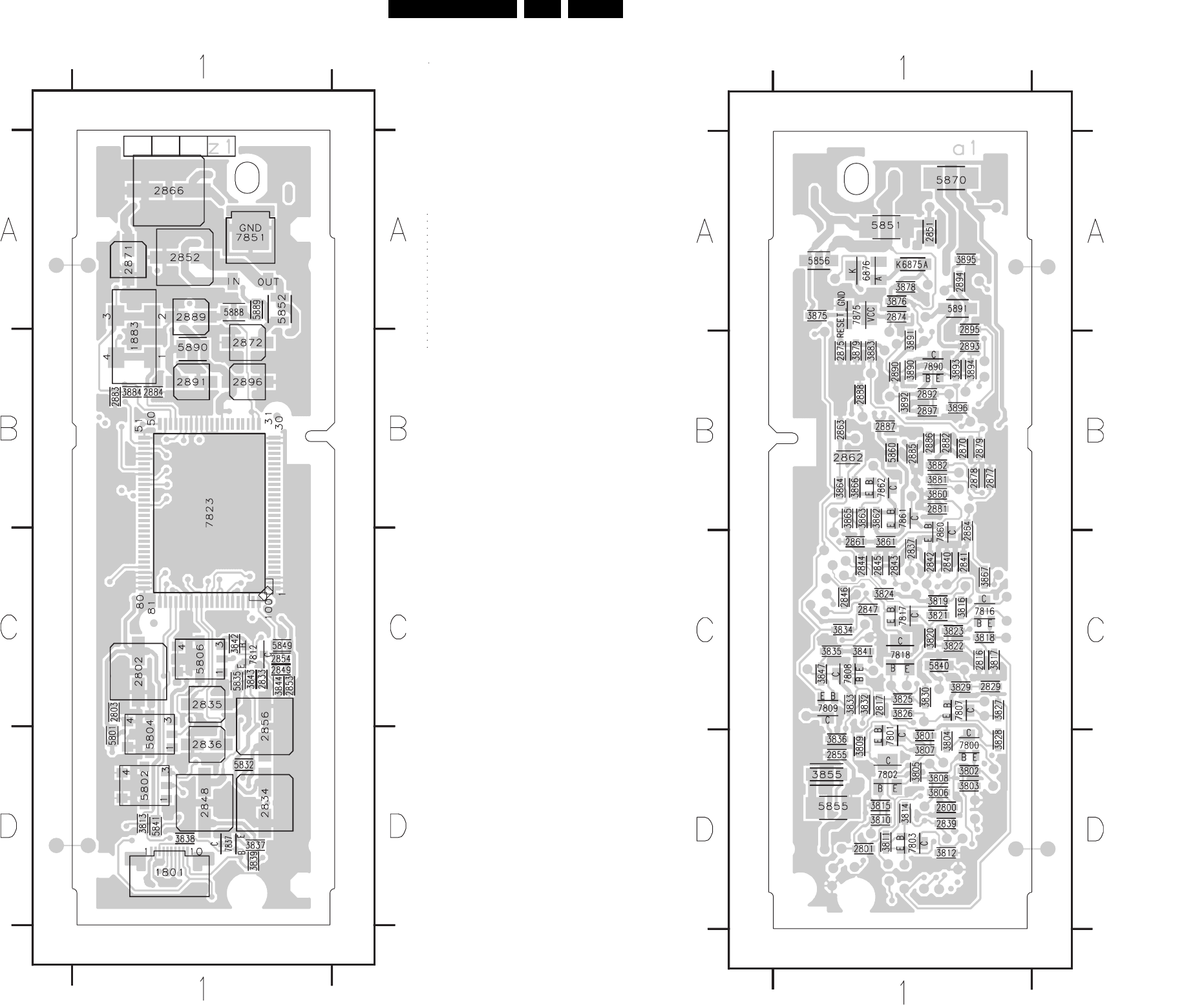
Circuit Diagrams and PWB Layouts 57LC4.6U AA 7.
Layout 3D Comb Filter (Top Side)
1801 D1
1883 B1
2802 C1
2803 C1
2833 C1
2834 D1
2835 C1
2836 D1
2848 D1
2849 C1
2852 A1
2853 C1
2854 C1
2856 D1
2866 A1
2871 A1
2872 B1
2883 B1
2884 B1
2889 A1
2891 B1
2896 B1
3813 D1
3837 D1
3838 D1
3839 D1
3842 C1
3843 C1
3844 C1
3884 B1
5801 D1
5802 D1
5804 D1
5806 C1
5832 D1
5835 C1
5841 D1
5849 C1
5852 A1
5888 A1
5889 A1
5890 B1
7812 C1
7823 B1
7837 D1
7851 A1
3139 123 5785.1 E_14490_079.eps
150704
Layout 3D Comb Filter (Bottom Side)
2800 D1
2801 D1
2816 C1
2817 C1
2829 C1
2837 C1
2839 D1
2840 C1
2841 C1
2842 C1
2843 C1
2844 C1
2845 C1
2846 C1
2847 C1
2851 A1
2855 D1
2861 C1
2862 B1
2863 B1
2864 C1
2870 B1
2874 A1
2875 B1
2877 B1
2878 B1
2879 B1
2881 B1
2882 B1
2885 B1
2886 B1
2887 B1
2888 B1
2890 B1
2892 B1
2893 B1
2894 A1
2895 A1
2897 B1
3801 D1
3802 D1
3803 D1
3804 D1
3805 D1
3806 D1
3807 D1
3808 D1
3809 D1
3810 D1
3811 D1
3812 D1
3814 D1
3815 D1
3816 C1
3817 C1
3818 C1
3819 C1
3820 C1
3821 C1
3822 C1
3823 C1
3824 C1
3825 C1
3826 C1
3827 C1
3828 D1
3829 C1
3830 C1
3832 C1
3833 C1
3834 C1
3835 C1
3836 D1
3841 C1
3847 C1
3855 D1
3860 B1
3861 C1
3862 B1
3863 B1
3864 B1
3865 B1
3866 B1
3867 C1
3875 A1
3876 A1
3878 A1
3879 B1
3881 B1
3882 B1
3883 B1
3890 B1
3891 B1
3892 B1
3893 B1
3894 B1
3895 A1
3896 B1
5840 C1
5851 A1
5855 D1
5856 A1
5860 B1
5870 A1
5891 A1
6875 A1
6876 A1
7800 D1
7801 D1
7802 D1
7803 D1
7807 C1
7808 C1
7809 C1
7816 C1
7817 C1
7818 C1
7860 C1
7861 B1
7862 B1
7875 A1
7890 B1
3139 123 5785.1 E_14490_080.eps
150704
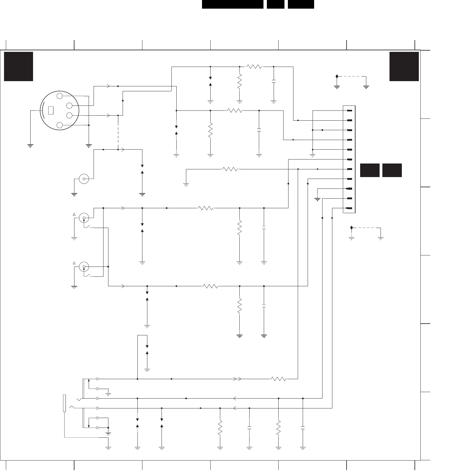
58LC4.6U AA 7.
Circuit Diagrams and PWB Layouts
Side I/O Panel
FROM
1336
OF
LC04
A2
Audio_in_gnd
3907
47K
F
Y/CVBS
CVBS
RIGHT
0936 A5
1000 F2
1001 F3
1002 E3
1003 D3
1004 C3
1005 B3
1006 B3
HP-DETECT
*
3907 C4
3908 D4
3909 D4
3910 E5
3911 F5
3912 F4
4901 B2
21
0902 E2
0901-C C2
0900-A B1
0901-A B1
0901-B C2
3
4902 A6
4903 C6
D
C
B
A
6
C
R-FRONT-IN
FROM
1S36
*
LEFT
2904
3n3
5
LEFT
RIGHT
(RED)
(WHITE)
(YELLOW)
E
1007 A4
2901 A4
2902 B4
2903 C4
2904 D4
2905 F5
2906 F4
3901 A4
FRONT-DETECT
HEADPH-R
HEADPH-L
C-FRONT-IN
3902 A4
3903 A4
3904 B4
3905 B4
3906 C3
SIDE I/O
HEADPHONE
L-FRONT-IN
SVHS IN
* RESERVED
OF
Y-CVBS-FRONT-IN
456
1234
I120
I119
220n
2902
220n
2901
2903
3n3
Audio_in_gnd
4901
1007
0901-B
YKC21-5617
45
6
3
4
2
3904
75R
0900
YKF51-5564
5
1
3910
3K9
3908
1K
Headph_gnd
Headph_gnd
1000
YKC21-5617
0901-A
12
YKC21-5617
0901-C
7
8
9
Headph_gnd
Headph_gnd
3903
100R
Audio_in_gnd
2905
10n
1003
2906
10n
Headph_gnd
Audio_in_gnd
Headph_gnd
Headph_gnd
Headph_gnd
Audio_in_gnd
Audio_in_gnd
1001
Headph_gnd
Headph_gnd
Headph_gnd
3901
100R
3902
75R
Audio_in_gnd
3909
47K
3906
1K
Audio_in_gnd
2
3
4
5
7
8
3905
1K
1004
0902
YKB21-5101A
1
1005
3911
10K
1002
4902
Audio_in_gnd
4903
1006
7
8
9
EH-B
0936
1
10
11
2
3
4
5
6
Headph_gnd
3912
10K
8204.000 6393.5
E_14710_043.eps
210704
B1
DD
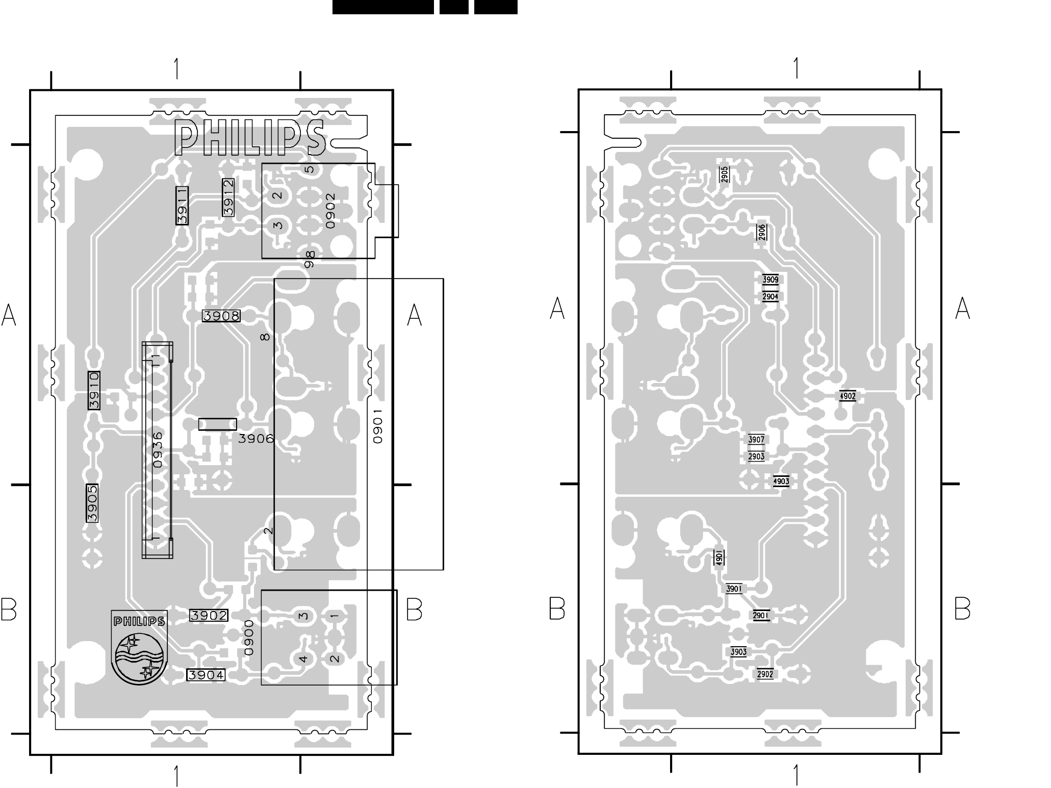
Circuit Diagrams and PWB Layouts 59LC4.6U AA 7.
Layout Side I/O Panel (Top Side)
3104 303 3649.5 E_14710_041.eps
080604
0900 B1
0901 A1
0902 A1
0936 A1
3902 B1
3904 B1
3905 B1
3906 A1
3908 A1
3910 A1
3911 A1
3912 A1
Layout Side I/O Panel (Bottom Side)
0900 B1
0901 A1
0902 A1
0936 A1
2901 B1
2902 B1
2903 A1
2904 A1
2905 A1
2906 A1
3901 B1
3902 B1
3903 B1
3904 B1
3905 B1
3906 A1
3907 A1
3908 A1
3909 A1
3910 A1
3911 A1
3912 A1
4901 B1
4902 A1
4903 A1
3104 303 3649.5 E_14710_042.eps
080604
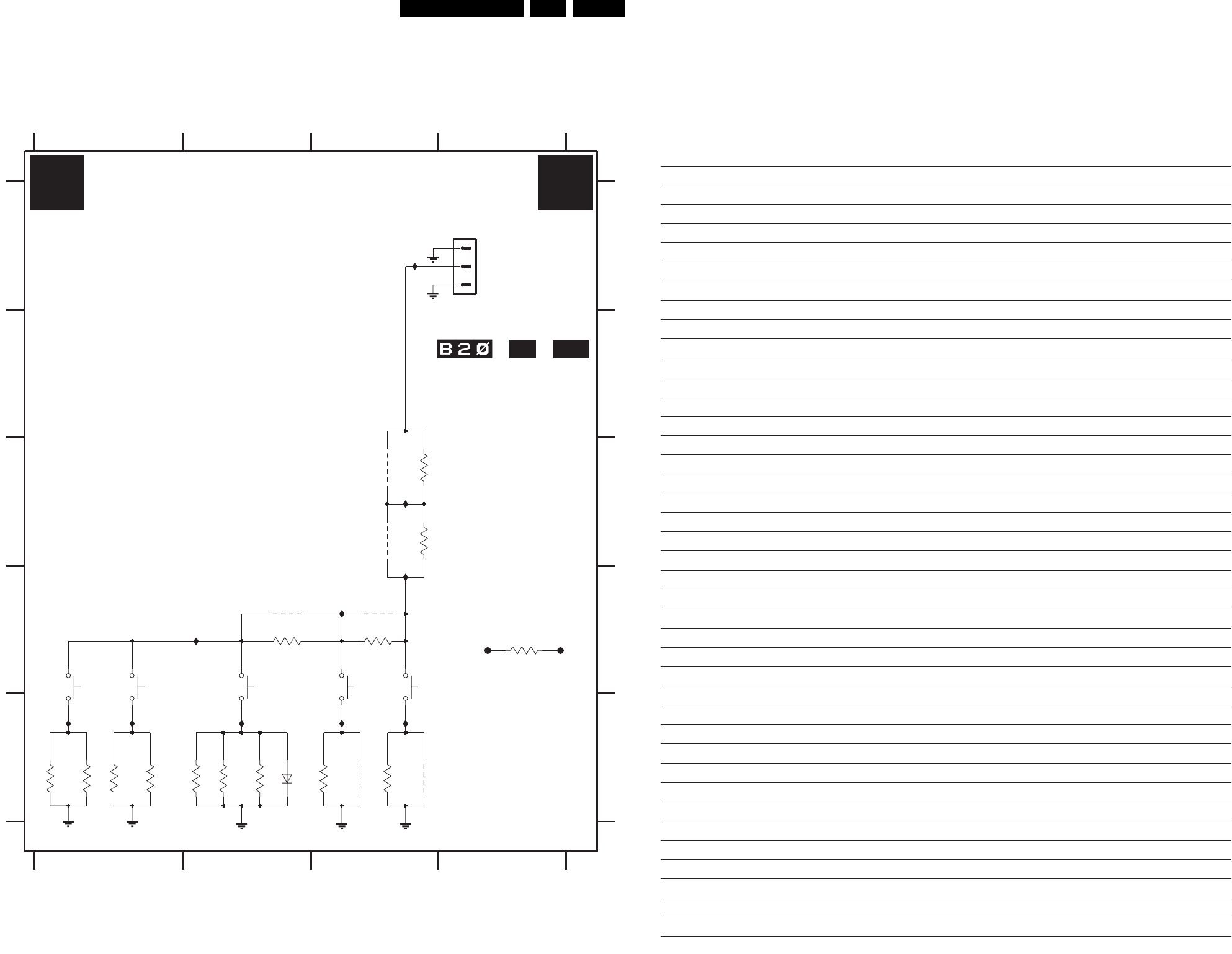
60LC4.6U AA 7.
Circuit Diagrams and PWB Layouts
Top Control Panel
1402
LC04
(LCD)
TO
A2
1345
LC04
(PDP)
TO
EMC
OR OR
C
D
E
0345 A4
1701 D1
1702 D1
1703 D3
1704 D3
1705 D2
3001 E1
3002 E1
3003 E1
3004 E1
3005 E2
3006 E2
3007 E2
3008 D2
3009 E3
3010 D3
3011 E3
3012 C3
3013 C3
3999 D4
GND_KEYBOARD
KEYBOARD
1 234
1 234
A
B
C
D
E
A
B
TOP CONTROL
6005 E2
9001 D2
9002 E3
9003 D3
9004 E3
9005 C3
9006 C3
F701 D4
F702 D4
I701 C3
I702 D3
I703 D3
I704 D2
I705 E3
I706 E3
I707 E2
I708 E1
1Y45
I709 E1
I710 A3
1K5
3004
*
I/02
* FOR SAA56XX
GND_KEYBOARD
TO
1702
200R
3003
F702
VOLUME +
1K
3999
F701
I709
I710
I707I708 I706
I704
I705
I703
I701
I702
VOLUME -
1705
MENU
390R
3001
1701
0345
1
2
3
3K3
3002
*
*
*
3013
560R
9006
3012
390R
9005
9003
560R
3010*
270R
3008*
9001
9004
620R
3011
9002
**
1K1
3009
3007
3K3
6005
1PS76SB10
**
3006
1K5
*
CHANNEL +
2K
3005
CHANNEL -
1704
1703
8204 000 6604.3
E_14710_044.eps
210704
E E
na
l Notes:
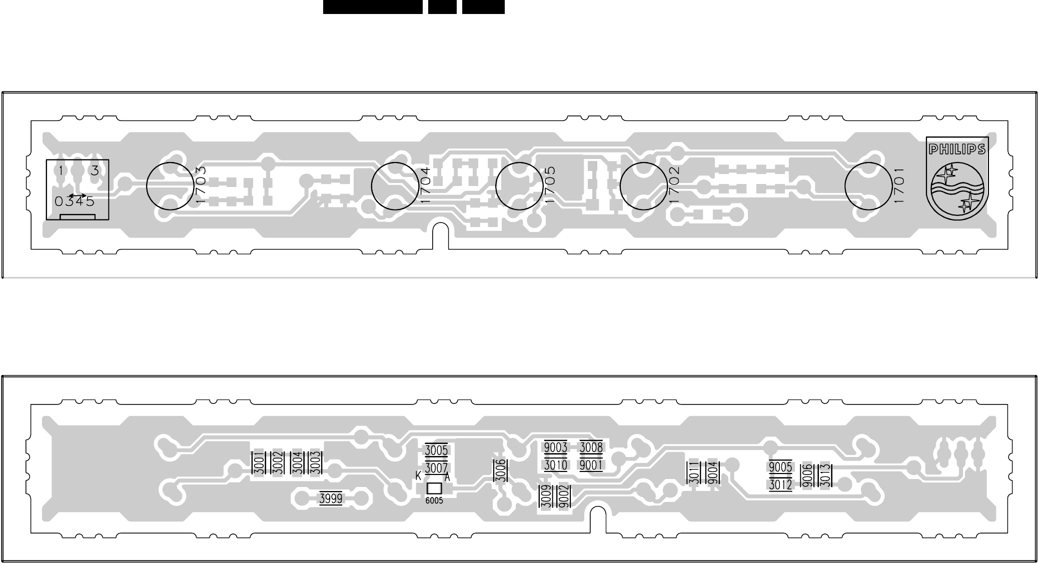
Circuit Diagrams and PWB Layouts 61LC4.6U AA 7.
Layout Top Control Panel (Top Side)
Layout Top Control Panel (Top Side)
3104 303 3851.3
0345 1701 1702 1703 1704 1705
E_14710_045.eps
080604
3104 303 3851.3
E_14710_046.eps
080604
3001
3002 3003
3004 3005
3006 3007
3008 3009
3010 3011
3012 3013
3999 6005
9001 9002
9003 9004
9005 9006
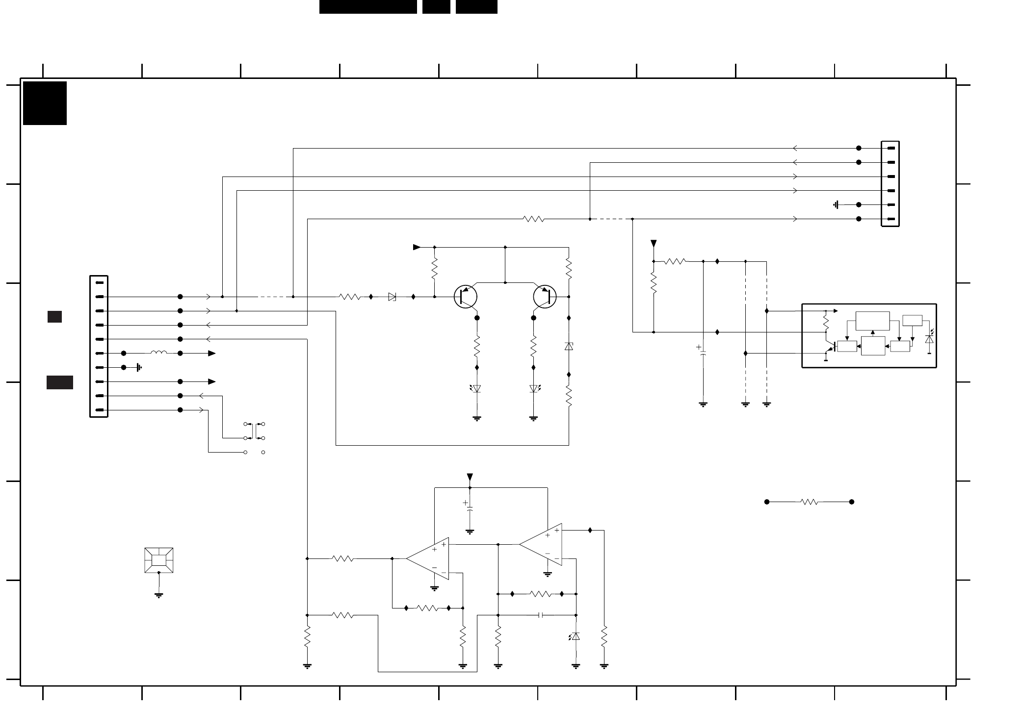
62LC4.6U AA 7.
Circuit Diagrams and PWB Layouts
LED and Switch Panel
1345
LC04
(PDP)
TO
EMC
1320
(LCD)
OR
DEM BAND
PASS
CTRL
CIRCUIT
AGC
INP
PIN
I103 C4
I104 C5
I105 C5
I106 C6
I107 C6
I109 B7
I111 C7
I112 C8
I113 C8
I120 F4
I123 F5
I125 F5
I126 F6
I127 E6
F103 C2
F104 C2
F105 C2
F106 C1
F107 C1
F108 C2
F109 D2
F110 C5
F111 C6
F112 D2
F115 A9
F116 A9
F119 B9
F120 B9
F121 E8
F122 E9
I102 C4
3125 F5
3126 F6
3127 F6
3128 E8
4101 C3
4107 B6
4108 C8
FROM
LED PANEL DISPLAY
ON / OFF
4109 C8
4110 C8
4111 C8
5100 C2
6101 C4
6103-A D5
6103-B D5
6105 C6
6127 F6
7103 B5
7105 C5
7107 C9
7120-A E5
7120-B E4
F101 C2
F102 C2
89
A
B
C
D
E
F
A
B
C
D
3103 C5
3104 B6
3105 C5
3106 D6
3107 B5
3108 B7
3109 B7
3120 E4
3121 F4
3122 F3
3123 F4
3124 F5
GREEN
ICONN
RED
SWITCH
12345678 9
1234567
E
F
0222 E2
0317 A9
0320 B1
1101 D3
2107 C7
2120 E5
2126 F6
3101 C4
3102 B4
F103
10u
2120
F104
F107
470K
3126
1K
3122
I106
3124
1K
470K
3127
F120
BZX384-C3V9
6105
LM358D
7120-A 3
2
1
8
4
I127
+5V_STBY_SW
I105
3104
100K
I109
F111
I102
4107
330R
3105
4K7
3120
4K7
3121
5
14
36
5100
100MHZ
1101
2
150R
3101
F112
+8V6
+5V_STBY_SW
3109
100R
220n
2126
3K3
3125
+8V6
150R
3106
7103
F106
5
6
7
8
4
BC857BW
3
GND
OUT
1
VS
2
LM358D
7120-B
4101 7107
TSOP2236
3
4
5
6
I120
I112
95009
0317
1
2
I113
2107
100u
I125
TEMD5000
6127
4
F102
6103-A
TLMV3100
21
6103-B
TLMV3100
3
I126
6101
BZX384-C3V9
I123
470R
3107
F101
10K
3123
F110
F108
BC857BW
7105
6
7
8
9
4108
0320
PH-S
1
10
2
3
4
5
SHIELDING 3.3
F109
0222
I104
220R
3103
F116
F115
F119
+5V_STBY_SW
I103
F121 F122
1K0
3128
F105
4111 4110
4109
I107
10K
3108
3102
100K
IR_RX
I111
RC_IN
RED_LED
RED_LED
GREEN_LED
GREEN_LED
LIGHT_SENSOR_IN
+5V_STBY_SW
IR_TX
LED_DISPLAY
+9V_STBY
+9V_STBY_SW
J
E_14710_052.eps
210704
8204 000 6676.1
A3
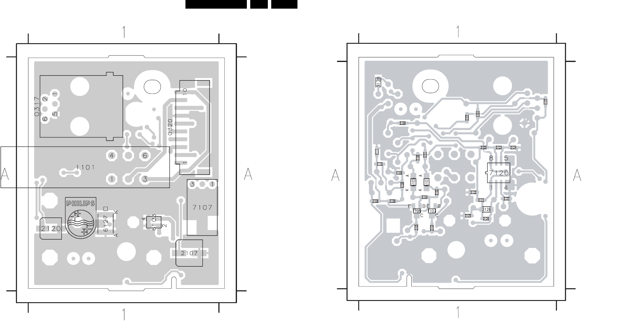
Circuit Diagrams and PWB Layouts 63LC4.6U AA 7.
Layout LED and Switch Panel (Top Side)
E_14710_053.eps
140604
3104 303 3924.1
0317 A1
0320 A1
1101 A1
2107 A1
2120 A1
6103 A1
6127 A1
7107 A1
Layout LED and Switch Panel (Bottom Side)
E_14710_054.eps
140604
3104 303 3924.1
0317 A1
1101 A1
2126 A1
3101 A1
3102 A1
3103 A1
3104 A1
3105 A1
3106 A1
3107 A1
3108 A1
3109 A1
3120 A1
3121 A1
3122 A1
3123 A1
3124 A1
3125 A1
3126 A1
3127 A1
3128 A1
4101 A1
4107 A1
4108 A1
4109 A1
4110 A1
4111 A1
5100 A1
6101 A1
6105 A1
7103 A1
7105 A1
7107 A1
7120 A1
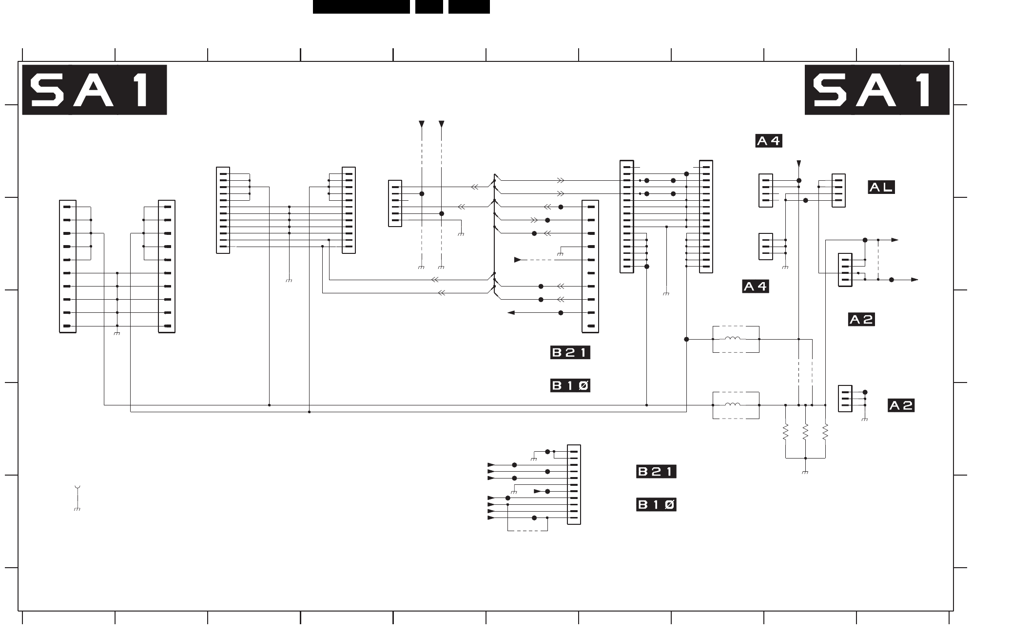
64LC4.6U AA 7.
Circuit Diagrams and PWB Layouts
LCD Standby Audio Panel: Connections
F108 B10
F109 E6
F110 B9
F111 B6
F112 D10
F113 B6
F114 E6
F115 B6
F117 E6
F119 B7
F120 C8
F121 B6
F122 C6
F131 D6
F132 E6
F135 D6
F136 D6
F137 A5
F138 B5
F139 C6
9009 A5
9010 C8
TO 1M03
TO 1303
SSB EMG
9011 D8
9018 B10
9113 B6
F101 B10
F102 A8
F103 A9
F104 A7
F105 A7
F106 A7
F107 B7
1M46 D7
3190 D9
SA1
3191 D9
3192 D9
5018 C8
5019 D8
9001 E6
9002 B5
9003 B5
9004 C8
9005 D8
9006 C9
9007 C9
9008 A5
D
E
TO 1M46 SSB JAGUAR
1312 A8
1313 A7
1314 B1
1315 B2
1316 A3
1317 A4
1318 A5
1320 B9
1M03 B7
1M10 A9
78
LCD SUPPLY
TO
DISPLAY
CONNECTIONS
910
A
B
C
D
E
A
B
C
56
LCD SUPPLY
TO 1304
78910
123456
1304 B9
1309 D9
42"
LCD SUPPLY
OR
SA1 (3x)
SA1 (3x)
SA1
SA2
SA2
SA1 (3x)
DISPLAY
TO
DISPLAY
TO
DISPLAY
TO
42"
DISPLAY
TO
30"/37"/42"
TO 1320
SSB JAGUARTO 1M03
OR
TO 1M46 SSB EMG
1234
SA2
TO
DISPLAY
SA1
SA1 (3x)
TO
AMBI LIGHT
TO 1309
LCD SUPPLY
30"/37"/42"
0001 E1
1303 A9
3192
1K2
1K2
3191
F107
F110
F122
1
2
3
B3P-VH
1309
GND-SSP
+5V_SW
F106
F105
F111
F115
F136
1M10
B4B-PH-K
1
2
3
4
9001
9008
F101
9011
GND-SSP
9010
F137
GND-SSP
GND-SSP
GND screw
0001
1
3
4
5
6
7
8
9
B12P-PH-K
1
10
11
12
2
1316
F103
GND-SSP
F112
1K2
3190
9003
GND-SSP
RES
9002
RES
F132
F135
F119
F102
F104
9007
F113
F121
1
2
3
9018
F131
B3P-VH
1320
9006
F114
F109
F139
GND-SSP
GND-SSP
10
2
3
4
5
6
7
8
9
3
4
5
6
7
8
9
PH-B
1315
1
GND-SSP
1314
PH-B
1
10
2
2
3
4
5
6
7
8
9
GND-SSP
B11B-PH-K
1M46
1
10
11
1304
1
2
3
4
10
2
3
4
5
6
7
8
9
B4P-VH
6
7
8
9
1M03
PH-B
111
12
13
14
15
16
2
3
4
5
1313
440091-7
1
10
15
16
2
3
4
5
6
7
8
9
1
10
11
12
13
14
GND-SSP
440091-7
1312
1
2
3
4
5
6
+5V_SW
B6B-PH-K
1318
9004
9005
5019
68u RES
F108
GND-SSP
11
12
2
3
4
5
6
7
8
9
B12P-PH-K
1317
1
10
1303
B4P-VH
1
2
3
4
GND-SSP
9009
RES
+5V_SW
F138
9113
F120
F117
68u
5018
RES
+5V_SW
9V_STBY_SW
9V_STBY
+12V
ON_OFF
DIM_CONTROL
DIM_CONTROL
ON_OFF
+24V_2
+12V_+24V
ON_OFF
DIM_CONTROL
DIM_CONTROL
POR
ON_OFF
STANDBY
PROT_AUDIOSUPPLY
+5V2-RELAY-IO2
+12V
+12V_A
+5V2
VTUN
+8V6
E_14620_132.eps
020704
8204 000 8314.5
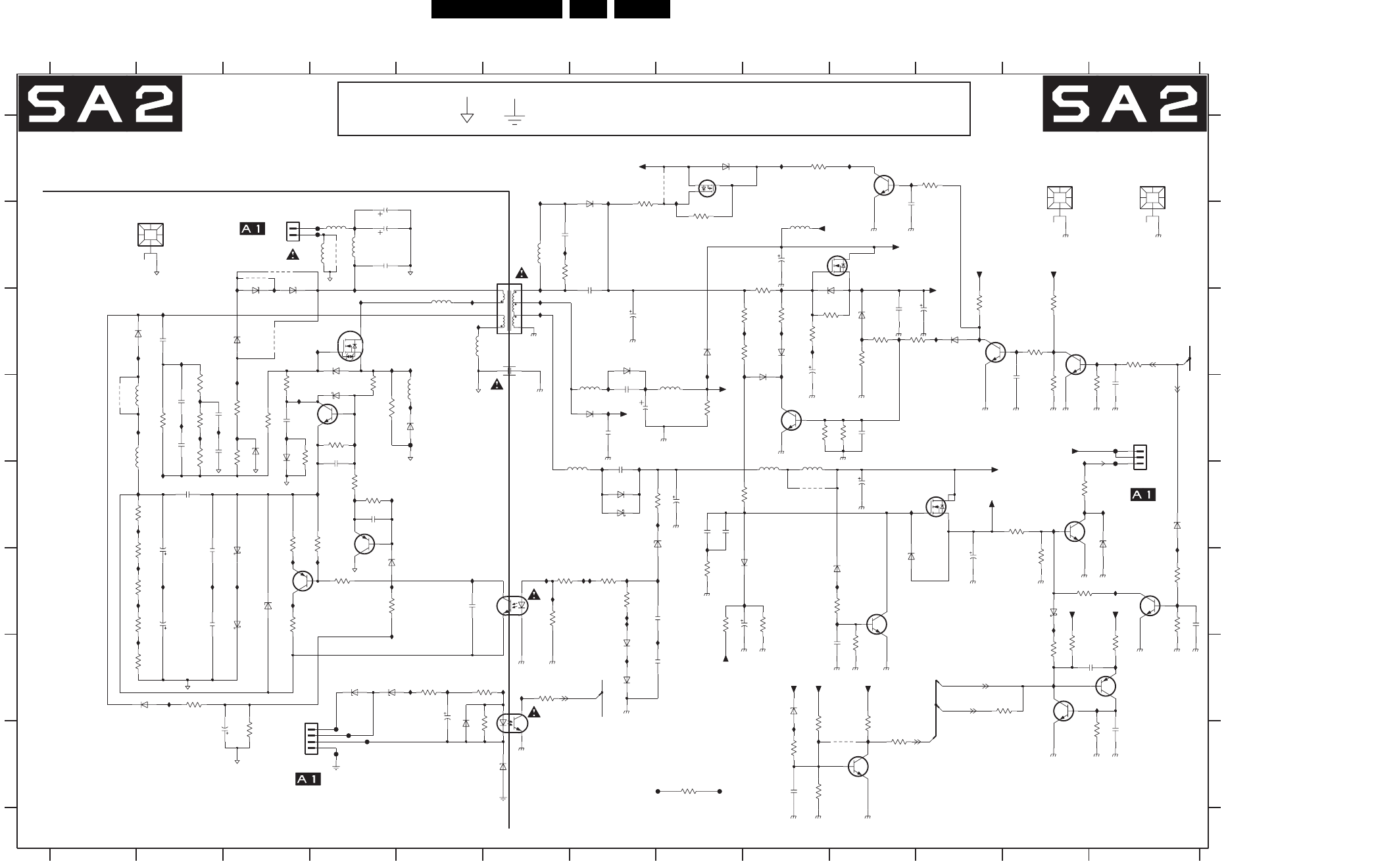
Circuit Diagrams and PWB Layouts 65LC4.6U AA 7.
LCD Standby Audio Panel: Standby
6119 B3
6120 G7
6121 G7
6122 E7
6125 C8
6130 B10
6132 C10
6133 C9
6134 C9
6140 D7
6153 H6
6156 H5
6504 A7
6505 E7
6508 G9
5504 B4
5505 B4
5506 E9
5507 B9
5508 E9
6103 C1
6104 D3
6105 C4
6106 F3
6107 E7
6510 E13
6511 A8
6531 F10
6532 C11
6540 F12
6562 E13
7100 F4
7101 D4
7102 C4
7105 E4
TO 1306
LCD SUPPLY
30"/37"/42"
6114 G2
6115 D4
6116 F4
6117 C3
6118 B3
3536 H10
3537 H9
3538 F8
3539 H10
3540 G13
3541 G12
3542 H13
3544 G12
6142 F3
6144 D3
6147 D5
6148 F8
6149 F9
6150 G4
6151 G5
5110 B6
5112 D7
5115 D8
5500 B6
5501 B4
3516 A9
3517 A11
3528 C11
3529 C12
3530 D13
3531 C13
3532 C12
3533 D12
3534 H9
3535 H9
COLD GROUND
HOT GROUND
6108 F3
6113 C7
3172 C10
3175 F8
3176 G10
3506 G12
3507 F13
3508 F13
3560 E12
3561 F12
3562 E12
3999 H8
5102 D1
5103 E7
5104 C5
5105 C5
5106 D1
5108 D5
3510 F12
3511 B9
3512 C9
3513 D10
3515 B8
3152 D3
3153 C8
3155 G5
3156 G6
3157 H5
3158 G6
3159 E8
3160 D4
3161 C10
3171 C9
3125 E3
3126 E4
3127 F4
3128 F6
3132 D9
3134 C10
3135 C10
3137 D8
3138 D3
3140 C8
3509 A7
3146 F4
3147 H3
3148 E4
3149 E4
3150 D4
3106 E1
3107 F1
3108 D4
3109 F1
3110 F1
3111 D2
3112 G1
3113 E7
3114 F6
3117 D3
SA2
SA1
STANDBY
E_14620_133.eps
060704
8204 000 8314.5
3122 B6
3123 F7
3124 F7
2510 E8
2511 B9
2512 E10
2513 E7
2515 B10
2533 F11
2534 E8
2535 D10
2536 D12
2537 D13
SA1
SA2
3141 F10
3142 F9
3145 G2
3101 D3
3102 D2
3103 D2
3104 D3
3105 D2
G
H
A
B
C
D
E
F
G
H
2163 F2
2506 C6
2507 B7
2508 C7
2509 F13
12345678910
5V3 (5V3)
LCD SUPPLY
TO 1305
34V (34V)
2538 H9
2539 E8
2540 H13
2544 G13
3100 F3
B
C
D
E
F
2112 D4
2118 D7
2123 E4
2124 H2
2129 B6
2131 C10
2132 C11
2140 F8
2141 D7
2143 D7
30"/37"/42"
COLD GROUNDHOT GROUND
0V (0V)
2144 F2
2145 D3
2149 G7
2150 G5
2152 B4
2153 F5
2154 G10
2159 D2
2160 C9
2162 D2
9101112 13
9112 E9
F100 D5
F123 B4
F124 B4
F125 D13
F126 E13
F127 H4
F128 H4
F129 H4
F130 H4
11V5 (12V)
11V9 (11V8) 8V9 (8V8)
0V8 (0V8)
5V3 (5V3)
11V7 (11V7)
0V7 (0V6)
0V2 (0V2)
275V
11 12 13
A
2107 A4
2108 B4
2109 F7
2110 F2
2111 E2
I120 C6
I121 C13
I122 C2
I123 C6
I124 C5
I125 D8
I126 D9
I127 C8
I128 D7
I129 D7
7131 B10
7140 F10
7150 H6
7501 F6
LCD SUPPLY
30"/37"/42"
(289V)
TO 1307
SA1
12345678 9021 B3
9022 B4
9023 B3
9110 H10
9111 D1
I152 E12
I153 E1
I154 E4
I155 E4
I156 E4
I157 F6
I158 F7
I159 F8
I160 F8
I161 F9
F133 H8
F134 H8
I100 B4
I101 A6
1301 B2
1305 D13
1306 B3
1307 H4
1310 A13
1311 A12
2101 C2
2102 F2
2103 D2
2105 D2
I115 C12
I116 C10
I117 C12
I118 C5
I119 C4
I184 G6
I185 F3
I186 G6
I189 H10
I190 G2
I191 G5
I192 H9
I197 C9
I198 D7
I199 D5
I130 C4
I131 C2
I132 C4
I133 C5
7505 G13
7506 C11
7507 C12
7508 H10
7509 G12
7510 F13
7511 A8
7512 A10
7531 E11
7532 D9
7560 E12
9019 A8
9020 C3
I147 E2
I148 E10
I149 E7
I150 E13
I151 E13
I504 F12
I505 F13
I506 F13
I507 F13
I508 A8
I509 A9
I510 A10
I511 A10
I512 H9
I513 D1
I162 E2
I163 F9
I164 F7
I165 F7
I102 A7
I103 C9
I104 B10
I105 B7
I106 C11
I107 C8
I108 C9
I109 C11
I110 C3
I111 C3
I112 C10
I113 B4
I114 B6
I168 F9
I169 F2
I170 G8
I171 F5
I172 F2
I173 F2
I174 F3
I175 F5
I176 G7
I177 F2
I178 G13
I179 G12
I180 G5
I181 G2
I182 G13
I183 G5
I501 F7
I502 F7
I503 F6
I134 D3
I135 D3
I136 D2
I137 E7
I138 E7
I139 E12
I140 C1
I141 D3
I142 D2
I143 D3
I144 D2
I145 D3
I146 D4
PDZ2.7-B
6510
I166 F3
I167 F4
I173
I181
15K
3508
GND-SSP
I177
I507
1u0
2534
9022
5501
RES
F133
I503
I501
I502
4R7
3128
3509
2K2
10K
3536
RES
BC847BW
7508
RES
GNDHOT
VTUN
I102
I129
I105
I139
I172
GND-SSP
BZX384-C9V1
6508
RES
+11V
I198
5106
10u
I508
I511
GND-SSPGND-SSP
I509
F129
3517
22K
6511
BZX384-C12
3516
4K7
I146
GND-SSP
I167
33K
GND-SSP
I166
3135
3172
330R
GND-SSP
PDZ6.8-B
6132
I155
GND-SSP
I158
I153
I506
3515
100K
I137
I504
2509
2n2
GND-SSP
9020
I160
GND-SSP
I163
3510
I513
220R
220R
GND-SSP
3544
2132
100u 25V
9111
RES
I117
+5V2-RELAY-IO2
+5V2
+5V2-RELAY-IO2
I116
470R
3539
3153
22K 22K
3140
10V2m2
2510
RES
3534
10K
GNDHOT
GNDHOT
2K2
3535
I101
GNDHOT
I197
1
2
I124
+12V
HEATSINK
1301
I199
I183 I184
6140
GND-SSP
F123
BYV95C
F124
I156
F130
F127 F128
F126
GND-SSP GND-SSP
I135
GND-SSP
1K0
3134
220R
3114
14
32
BZX384-C5V6
6116
7501
TCET1102
STP16NF06FP
7131
GND-SSP
50V1u0
2160
I140
GND-SSP
I505
I165
I159
I141
10K
3507
I138
I157
I119 I118
I168
BC847BW
7510
I152
I148
I151
+11V
I121
I115
I106 I109
6153
BZG03-C200
+5V2
TCET1102
7150
14
32 9110
6133
BAS316
100R
3150
10n
2112
1K0
3160
33R
3124
6121
BAS316
10n
2538
3541
2K2
GNDHOT
F100
I123
GNDHOT
I114
1
2
I136
1311
HEATSINK
GND-SSP
GND-SSP
I186
2141
470n
I191
I190
I175
I180
GND-SSP
I154
I133
GND-SSP
I130
I132
22n
2131
6532
BAS316
BC847BW
7506
2152
10n
5110
10u
10u
2108
5504
33u
6n8
2153
BYV27-200
6114
100R
3171
GND-SSP
12K
3161
I147
I144
I164
GND-SSP
I149
I143
GND-SSP
GND-SSP
I131
I100
I111
I161
I110
+5V_SW
I122
+5V2
47R
3158
3157
+5V2
+5V2-RELAY-IO2
22K
68K
3511
470R
3512
BAS316
6134
6105
BZX384-C15
6104
BZX384-C27
RES
3138
1M0
2159
470p
6115
BAT54 COL
BC817-25W
7101
BAS316
6120
10R
3123
10n
2544
I120
GNDHOT
10K
GNDHOT
GNDHOT
3542
1
2
3
GND-SSP
I145 1305
B3B-EH-A
GND-SSP
4R7
3562
GND-SSP
I171
GND-SSPGND-SSPGND-SSP
3532
4K7
GND-SSP
GND-SSP GND-SSP
4K7
3528
BYV27
6504
470R
3122
1n0
2129
6103
BYV27-200
3126
10K
7100
BC857BW
3125
5505
15R
1306
1
2
4K7
3145
B2P-VA-BF-BK
10u
2124
BZX384-C12
6130
50V
I142
GND-SSP
GND-SSP
GND-SSP
BC847BW
7140
GND-SSP
I134
SB340
6125
GND
6505
SB360
1
2
3
4
I113
B4P-VH
1307
BZG03-C200
6150 6151
BZX384-C33 10K
3155
47R
3159
25V220u
2150
BAS316
6156
1K0
3156
BC847BW
7532
3108
4R7
5104
7102
4M7
3101
STP6NK60Z
2513
2n2
2n2
2143
470p RES
100K
3137
1K
3103
2162
47R
3104
470p
2145
1u
2149
2K2
3540
GNDHOT
7509
10n
2540
GND-SSP
BC847BW
BZX384-C22
6562
10K
3149
3148
47R
10K
3176
6K8
3560
GND-SSP
15K
3531
2n2
2537
22K
3530
100p
2507
7507
BC847BW
100R
3529
6
7
8
10n
2536
5500
110
2
3
5
3107
390R 390R
3106 5102
3127
2144
1u
5K6
390R
3112
RES
2512
220u 25V
PDZ-20B
6106
6108
BAT54 COL
I185
RES15u
5508
22K
3147
GND-SSP
25V100u
2533
BZX384-C15
6531
15n
2154
GNDHOT
3113
GND-SSP
5115
22R
3102
1K 220R
3105
GND
10K
3175
100R
3538
BC817-25W
7560
3K9
3561
BYW29EX-200
6113
10n
2535
3513
33K
33K
3132
5108
6119
RES
6118
BZX384-C33
RES
BZX384-C33
BZX384-C33
6117
RES
STPS8H100
6107
5103
22u
2508
1K5
3111
100V
2n2
2101
47n
2111
2163
100u25V
BC857BW
7105
2109
1u
1K0
3152
2107
7505
BC857BW
47R
3146
10u
BAT54 COL
6540
100n
2123
I112
470R
3141
BZX384-C5V6
6149
5506
I103
I104
+5V2
2506
470p
5105
2102
25V 100u
50V10u
2140
12K
3142
6142
BAT54 COL
9112
1u
2110
GND-SSP
7531
BSP030
BAS316
6144
PDZ-3.9B
6122
2539
1u0
BAS316
6148
390R
3110 3109
SML4736-6V8
6147
390R
251m
2118
47R
3117
2105
100p 100p
2103
1310
HEATSINK
1
2
5112
I169
GND-SSP
GND-SSP
I162
I176
I170
I108
I126
I107
RES
I125
1K5
9019
GND-SSP
3533
GND-SSP
I128
I127
F134
3999
1K0
RES
I512
I510
3K3
3537
I189
I192
2n2
2515
3506
470R
9021
+12V_A
+8V6
9023
+12Vstby
F125
7512
PMSTA42
100R
7511
BST82
I150
3100
I178
I179
2511
220u 25V
I182
15u
5507
I174
+12V
PROT_AUDIOSUPPLY
Prot-OVV
Prot-OVV
POR
STANDBY
Caution: Both and symbols can indicate a HOT ground in this schematic!!
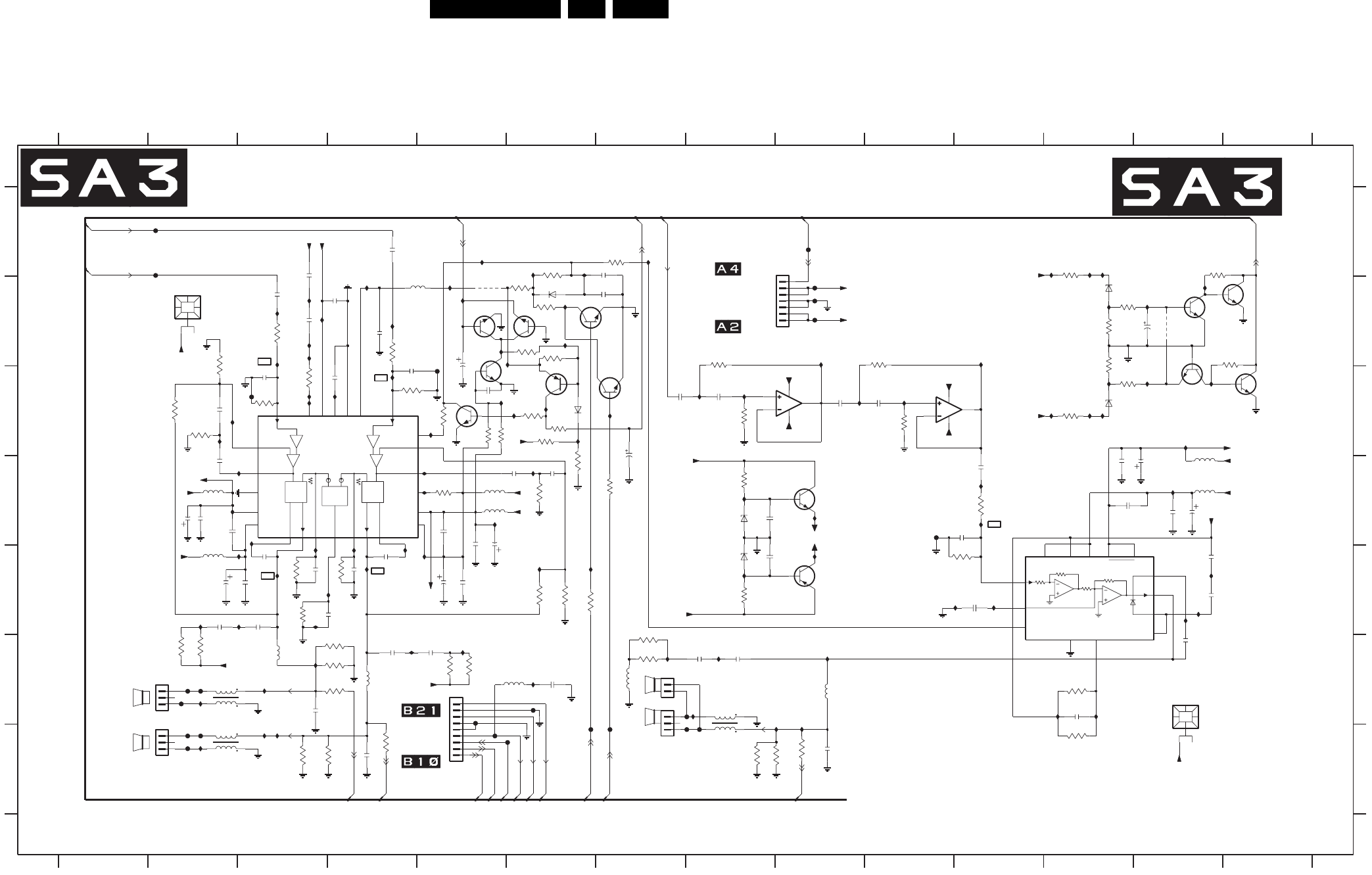
66LC4.6U AA 7.
Circuit Diagrams and PWB Layouts
LCD Standby Audio Panel: Audio
-VCC
PRE
PWM
+VCC
PWM
STAGE2
G=2.5
PRE-AMP1
INTERGR 1
INTERGR 2
PWM
STAGE2
OSC
G=2.5
PRE-AMP2
I784 B3
I785 B4
I786 B4
I787 C4
I788 C7
I790 F3
I791 B12
I792 B13
I793 B13
I794 B12
I795 F6
I796 C12
I797 C12
I798 E5
I799 E4
I762 D11
I763 C6
I764 C13
I765 D13
I766 F9
I767 F2
I768 G3
I769 F3
I770 G2
I771 G3
I772 F8
I773 F9
I774 F9
I776 E4
TO 1M02
LCD SUPPLY 42"
I777 D2
I778 E3
I779 E3
I780 E13
I781 C13
I782 C13
I783 B3
I748 B3
I749 C3
I750 B12
I751 A12
I752 E13
I753 B3
I754 E3
I755 F4
I756 C2
I757 D2
I758 E11
I759 E11
LCD SUPPLY 30"/37"
TO 1M02
I760 C5
I761 F8
I734 F12
I735 D8
I736 E8
I737 C6
I738 C6
I739 B6
I740 D9
I741 E9
I742 C12
I743 C12
I744 D5
I745 B4
I746 E13
I747 D11
SSB JAGUAR
OR
TO 1M52
SSB EMG
TO 1M52
OR
-18V
15W/8
L
I713 E4
I714 C8
I715 A7
I716 E3
I717 B5
I718 B5
I719 E3
I720 C8
I721 C3
I722 B3
I723 B9
I724 D3
I725 E2
I726 C3
I727 B5
I728 C9
I729 C5
I730 F7
I731 B11
I732 B6
I733 C10
F742 B9
F743 B9
F744 B9
F745 A9
F747 F5
F748 G5
F749 G6
F751 F6
I700 E6
I701 E6
I702 A6
I703 B6
I704 A6
I705 D6
SA3
SA3
SA3
I706 D5
I707 D5
I708 F12
I709 E4
I710 F5
I711 C4
I712 A5
7714 C5
7715-1 C9
7715-2 C11
9717 B5
9718 B13
F708 F2
F710 G2
F711 A2
F712 A2
F713 C3
F714 B5
F718 D10
F720 G8
F721 G2
-18V
F722 F2
F731 G8
F736 G7
F737 G6
F738 F2
F739 G2
F741 F8
5730 F2
5731 G2
5732 G8
6701 C6
6702 B12
6703 C12
6704 B6
6710 D8
6711 E8
7700 C5
7701 B7
7702 E11
7703 C7
7704 B5
7705 B6
7706 C6
7707 C5
7708 C13
7709 C13
7710 B13
7711 B13
7712 D9
7713 E9
3767 B12
3768 A13
3790 C4
3791 C3
3792 B3
3793 B4
3794 D11
3795 C5
3796 E11
3797 C5
3798 D6
5701 F4
5702 F3
5703 B5
SA3
SA3
5704 F7
5705 F6
5707 D2
5708 E2
5711 D5
5712 D5
5720 F9
5722 D13
5723 D133749 A7
3750 G3
3751 G8
3752 B8
3753 G8
3754 C8
3755 B10
3756 F4
3757 G3
3758 C10
3759 D8
3760 E8
3761 A12
3762 B12
SA3
SA3
SA3 (3x)
SA3
SA3
AUDIO
SA3
3763 B12
3764 C12
3765 C12
3766 B143712 E3
3713 D7
3714 C6
3715 B6
3716 B6
3717 F4
3718 G4
3720 F7
3721 B2
3722 C2
3723 C2
3724 F2
3725 E3
3726 F2
SA3
SA3
3727 F5
3729 G9
3730 F7
3741 F12
3743 F4
3744 G12
3746 C6
3747 C6
3748 C5
2785 B13
2786 B4
2787 C5
2788 D2
2789 D2
2790 E2
2791 C7
2792 C8
2793 D13
2794 C9
2795 D12
2796 C10
2797 D8
2798 E8
15W/8
SA3
CENTERWOOFER
2799 D13
3701 E6
3702 B6
3703 A6
3704 B6
3705 C3
3706 E6
3707 D6
3708 E6
3709 F5
3710 E4
3711 D5
2728 E3
2729 F3
2741 F12
2743 F13
2753 E13
2754 D11
2755 D11
2756 E11
2758 G9
2759 F8
2762 E13
2764 B3
2766 A4
2768 E5
SA3
SA3
SA3
15W/8
2769 D5
2777 D2
2778 C5
2779 E3
2780 E5
2781 D5
2782 D12
2783 C7
2784 D13
2708 A3
2709 D6
2710 D6
2711 E2
2712 D5
2713 B7
2714 E4
2715 F4
2716 E4
2717 G4
2718 E3
2719 F5
2720 B3
2721 C2
SA3
2722 D2
2723 F8
2725 F6
2726 E3
2727 E3
11 12 13 14
12345678910
1737 F7
1738 F7
1739 F5
1M02 A9
2702 C4
2704 C3
2705 A7
2706 B4
2707 C4
G
0044 F13
0045 B2
1735 F2
1736 G2
123
R
45678910
11 12 13 14
A
B
C
D
E
F
G
A
B
C
D
E
F
1K2
3713
100u
2799
2741
2K7
3796
2K7
3791
22p
I765
2K2
3749
470R
330p
2716
3753
220R
3709
3757
2K2
2778
4u7
100u
2769
3716
47K
3754
22K
I783
2768
100u
100K
3767
2783
22u 16V
4K7
3721
I739
I741
3748
470R
I747
2721
470p
I724
3727
220R
BAS316
6704
4
3I708
5732
PLT09H
1
2
PLT09H
5731 12
43
12
43
F722 5730
PLT09H
2781
220n
F721
3726
220R
3720
220R
220R
I721
7706
BC857B
3724
I794
3725
22K
I740
I728 3764
10R
1u0
2792
6703
BZX384-C10
I759
I763
F710
I730
5708
2791
1u0
2789
220n
2782
220n
I727
F708
3765
100K
10K
3792
5702
I757
68u
I755
I795
100p
2725
5705
1n
2715
3717
100K
100K
3718
I719
I716
I791
1
2
3
2K2
3756
1738
B3B-PH-K
5720
68u
I714
10K
3793
BZX384-C10
6702
2718
22p
100n
2706
220n
2779
I793
33K
3703
1735
B3B-PH-K
1
2
3
1
2
3
B3B-PH-K
1736
2795
220n
5723
68u
5701
I705
2720
1n
2723
I790
220n
I780
I723
I736
I792
I731
I735
I733
100K
3768
7709
BC847B
BC847B
7710
2753
220n
47K
3747
1n
2727
2766
2u2
56K
2u2
2764
F751
3723
F747
F749
F748
10R
15K
3798
3761
10K
3702
2702
1n
I754
9
4
NC
1OUT
STBY|MUTE
10
13
12 VREG
2755
1n 7702
TDA7482
+VCCS
11
14 -VCC1 15
-VCC2
8
-VCCS
BOOT 3
BOOTD
2
FEEDCAP
5
6
FREQGNDS
7
IN
3741
10K
2796
1u0
220n
2784
68K
3722
7704
BC847B
2712
220n
680n
2729
I781
I706
470p
2709
I746
2707
100n
1
2
F737
1
2
HEATSINK0044
0045 HEATSINK
I788
LM833D
7715-1
3
2
1
8
4
F738
I779
I704
I777
BC847B
7708
100K
3766
2754
2u2
5
6
7
8
4
2743
33n
7715-2
LM833D
Vm
Vp
I787
9717
8R2
3705
3704
10K
I712
BC847B
7701
I726
3755
470R
I761
3752
330R
2K2
3763
F742
I703
I744
F745
56K
3708
39K
3746
2719
1n
470n
2705
5711
I786
I751
I785
I748
I745
I749
I713
I776
I707
2710
470p
33n
2726
F744
220R
3730
3707
68K
I796
I797
I762
I782
F720 F731
I701
BC847B
7703
I799
3758
8K2
2K2
3750
3729
100K
I715
Vm
33n
2714
3744
100K
330p
2728
120K
3711
2717
680n
220n
2797
2786
22n
3751
2K2
F713
F714
F712
5707
I732
100u
I725
2758
680n
2793
I750
I743I742
2777
220n
4K7
3706
1n
2704
2708
220n
BZX384-C15
6711 6710
BZX384-C15
1u0
2794
BC847B
7707
7705
BC847B
I734
2713
470n
470p
2722
3790
2K7
5703
30R
I729
GND 13
IN1 10
IN2 18
NC
20
OSC8
OUT13
OUT223
STBY-MUTE
6
T111
T215
VREG 25
+5V 12
+VCC1
4
+VCC2
22
-5V 16
-VCC1 1
-VCC2
2
-VCC3
24
BOOT15
BOOT221
CURREF
14
FEED1
7
FEED2
9
FEED3
17
FEED4
19
F741
7700
TDA7490
47K
3715
3797
220K
1u0
2787
7714
BC847BW
I773
I756
I772
Vm
I758
7713
BC857B
7712
BC847B
2798
220n
F718
1M02
B7B-EH-A
1
2
3
4
5
6
7
I771
I770
I769
I767
I702
F711
I752
BC847B
7711
I738 I737
1n
220n
2762
2711
3743
2K2
5712
I778
I774
Vp
Vp
3K3
3760 3759
3K3
5704
10K
3701
I764
3710
F743
I766
22K
6701
BAS316
I720
2756
470p
2759
1n
I753
3762
2K2
I722
I768
1
2
3795
120K
F736
1737
B2B-PH-K
I760
10K
3794
2790
100u
100u
2788
3714
47K
I710
I784
I709
I700
I711
I717
I718
100u
2785
9718
16V
1
2
3
4
5
6
7
8
9
B9B-PH-K
1739
5722
F739
220n
2780
3712
10K
I798
+16V+19V
-Vf21
-16V-19V
-Vf1
AUDIO-SW
-16V-19V
+16V+19V
-Vf21
POR-CLASSD
AUDIO-R
AUDIO-L
-Vf21
DCPROT
+16V+19V
DCPROT
-16V-19V
PROT_AUDIOSUPPLY
+16V+19V
-16V-19V
AUDIO-SW
-Vf11
POR-CLASSD
-Vf1
+16V+19V
PROT1
PROT1
PROT1
PROT1
+16V+19V
-Vf11
AUDIO-L
AUDIO-R
PROT_AUDIOSUPPLY
SOUND-ENABLE
-Vf11
SOUND-ENABLE
-Vf1
-Vf1
+16V+19V
-16V-19V
-16V-19V
E_14620_134.eps
031104
8204 000 8313.5
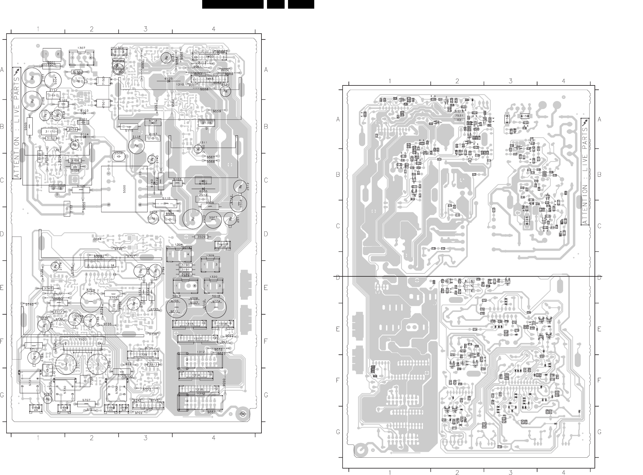
Circuit Diagrams and PWB Layouts 67LC4.6U AA 7.
Layout LCD Standby Audio Panel (Top Side)
E_14620_135.eps
020704
3104 313 6010.5
0001 G4
0044 D1
0045 E1
1301 B1
1303 E4
1304 D4
1305 A3
1306 A1
1307 A2
1309 D4
1310 A3
1311 B4
1312 F4
1313 G4
1314 G4
1315 F4
1316 G4
1317 F4
1318 F4
1320 E4
1735 G1
1736 G1
1737 G3
1738 G2
1739 F3
1M02 G3
1M03 A4
1M10 D4
1M46 A4
2101 B2
2102 B1
2107 A1
2108 A1
2111 A1
2118 B3
2124 B2
2132 A4
2140 C3
2143 B3
2150 A2
2152 D2
2160 B4
2163 B1
2506 B2
2507 D3
2508 D3
2510 D4
2511 D4
2512 C4
2513 C4
2533 A4
2717 F1
2729 G2
2758 E3
2768 F1
2769 F1
2778 E1
2783 G1
2785 E3
2788 F2
2790 E2
2793 E3
2799 E3
3101 B1
3102 B1
3103 B2
3108 C2
3111 B1
3155 A2
3190 E3
3191 E3
3192 E3
3509 D4
3711 F1
3713 F3
3747 E1
5018 E4
5019 E4
5102 B2
5103 C4
5104 C2
5108 C1
5110 C3
5112 C3
5115 B3
5500 C3
5501 A1
5504 A1
5505 B1
5506 C4
5507 D4
5508 C4
5701 F2
5702 F2
5704 E2
5707 G2
5708 G3
5711 F1
5712 E1
5720 E2
5722 E3
5723 E3
5730 G2
5731 G1
5732 G3
6103 B2
6107 C4
6113 B3
6114 B2
6125 A3
6140 C3
6504 D3
6505 C4
7102 C1
7131 B4
7150 A2
7501 B2
7700 F2
7702 E3
9001 A4
9004 E4
9005 E4
9006 E4
9007 E4
9010 E4
9011 E4
9018 D4
9022 A1
9050 G4
9051 G4
9052 F4
9053 B1
9054 B1
9055 C2
9056 A4
9057 A3
9058 A4
9059 B4
9060 A3
9061 A4
9062 A4
9063 A4
9064 A3
9065 A4
9066 A4
9067 C4
9068 C4
9069 A4
9070 A4
9071 F4
9072 F4
9073 F4
9112 C4
9113 A4
9721 G2
9722 G3
9723 G1
9724 F1
9725 E3
9726 D2
9727 D3
9728 E2
9729 D2
9730 E1
9731 F3
9732 G3
9733 G3
9734 F1
9735 F3
9736 F1
9738 F3
9739 F2
9740 E1
9741 E1
9742 E1
9743 G3
9744 F3
9745 G3
Layout LCD Standby Audio Panel (Overview Bottom Side)
E_14620_136.eps
131004
3104 313 6010.5
Part 1
E_14620_136a.eps
Part 2
E_14620_136b.eps
2103 B4
2105 B4
2109 B2
2110 B4
2112 C4
2123 C4
2129 C2
2131 A1
2141 C2
2144 A4
2145 C3
2149 B2
2153 B3
2154 A2
2159 B3
2162 B3
2509 A2
2515 B1
2534 A2
2535 A1
2536 B2
2537 A1
2538 A1
2539 A2
2540 A2
2544 A2
2702 F4
2704 F3
2705 G2
2706 F3
2707 F3
2708 F3
2709 G3
2710 F3
2711 G3
2712 F4
2713 G2
2714 F4
2715 F4
2716 F3
2718 F3
2719 F4
2720 F3
2721 G3
2722 G3
2723 E3
2725 F2
2726 G3
2727 G3
2728 F3
2741 D3
2743 E3
2753 D3
2754 E2
2755 E3
2756 E3
2759 E3
2762 E2
2764 F2
2766 F2
2777 F3
2779 F3
2780 F4
2781 F4
2782 E2
2784 E3
2786 F4
2787 E3
2789 F3
2791 F2
2792 D2
2794 D2
2795 E3
2796 D2
2797 D2
2798 D3
3100 A3
3104 C4
3105 B4
3106 B4
3107 B4
3109 B4
3110 B3
3112 B3
3113 B2
3114 B3
3117 C4
3122 C2
3123 B2
3124 B3
3125 A3
3126 A3
3127 B3
3128 B3
3132 B1
3134 A1
3135 A1
3137 B2
3138 C4
3140 B1
3141 A2
3142 C2
3145 B3
3146 B3
3147 B3
3148 C4
3149 C4
3150 C4
3152 C3
3153 B1
3155 A3
3156 A3
3157 A3
3158 A2
3159 B2
3160 C4
3161 B1
3171 B1
3172 A1
3175 C2
3176 A2
3190 E1
3191 E1
3192 E1
3506 A2
3507 A2
3508 A2
3509 D1
3510 A2
3511 B1
3512 B1
3513 B1
3515 B1
3516 B1
3517 B1
3528 A1
3529 B2
3530 A1
3531 A1
3532 A2
3533 B2
3534 A1
3535 A1
3536 A1
3537 A1
3538 A2
3539 A1
3540 A2
3541 A2
3542 A2
3544 A2
3560 A2
3561 A3
3562 A3
3701 F2
3702 G2
3703 G2
3704 G2
3705 F3
3706 G3
3707 F3
3708 F3
3709 F4
3710 F3
3711 E4
3712 F4
3713 F2
3714 E4
3715 E3
3716 G2
3717 G4
3718 G4
3720 E3
3721 F3
3722 G3
3723 G3
3724 G3
3725 F3
3726 G3
3727 F4
3729 G3
3730 E3
3741 D3
3743 G3
3744 E3
3746 G2
3747 E4
3748 F4
3749 E3
3750 G4
3751 G3
3752 D2
3753 G3
3754 D2
3755 D2
3756 G3
3757 G4
3758 D3
3759 D2
3760 D3
3761 F2
3762 F2
3763 E2
3764 F2
3765 E2
3766 F2
3767 E2
3768 F2
3790 F4
3791 F3
3792 F3
3793 F4
3794 E3
3795 E3
3796 E3
3797 E3
3798 G2
3999 D2
5105 C3
5106 B3
5703 F4
5705 F2
6104 C4
6105 C4
6106 A3
6108 B3
6115 C4
6116 B3
6117 B4
6118 C4
6119 C4
6120 A2
6121 B2
6122 B2
6130 B1
6132 B1
6133 B1
6134 B1
6142 B3
6144 C3
6147 C3
6148 B2
6149 A2
6150 A3
6151 A3
6153 A3
6156 A3
6508 A1
6510 A2
6511 B1
6531 A2
6532 A1
6540 A2
6562 A3
6701 G2
6702 E2
6703 F3
6704 G2
6710 D2
6711 D3
7100 A3
7101 C4
7105 B4
7140 A2
7505 A2
7506 B1
7507 A2
7508 A1
7509 A2
7510 A2
7511 B1
7512 B1
7531 A2
7532 B1
7560 A3
7701 G2
7703 G2
7704 E4
7705 E4
7706 E3
7707 E4
7708 F2
7709 F2
7710 F2
7711 F2
7712 D2
7713 D3
7714 E3
7715 D2
9002 F1
9003 F1
9008 F1
9009 F1
9019 B1
9020 B4
9021 C4
9023 C4
9074 A2
9110 A1
9111 B3
9717 E4
9718 E2
9737 F4
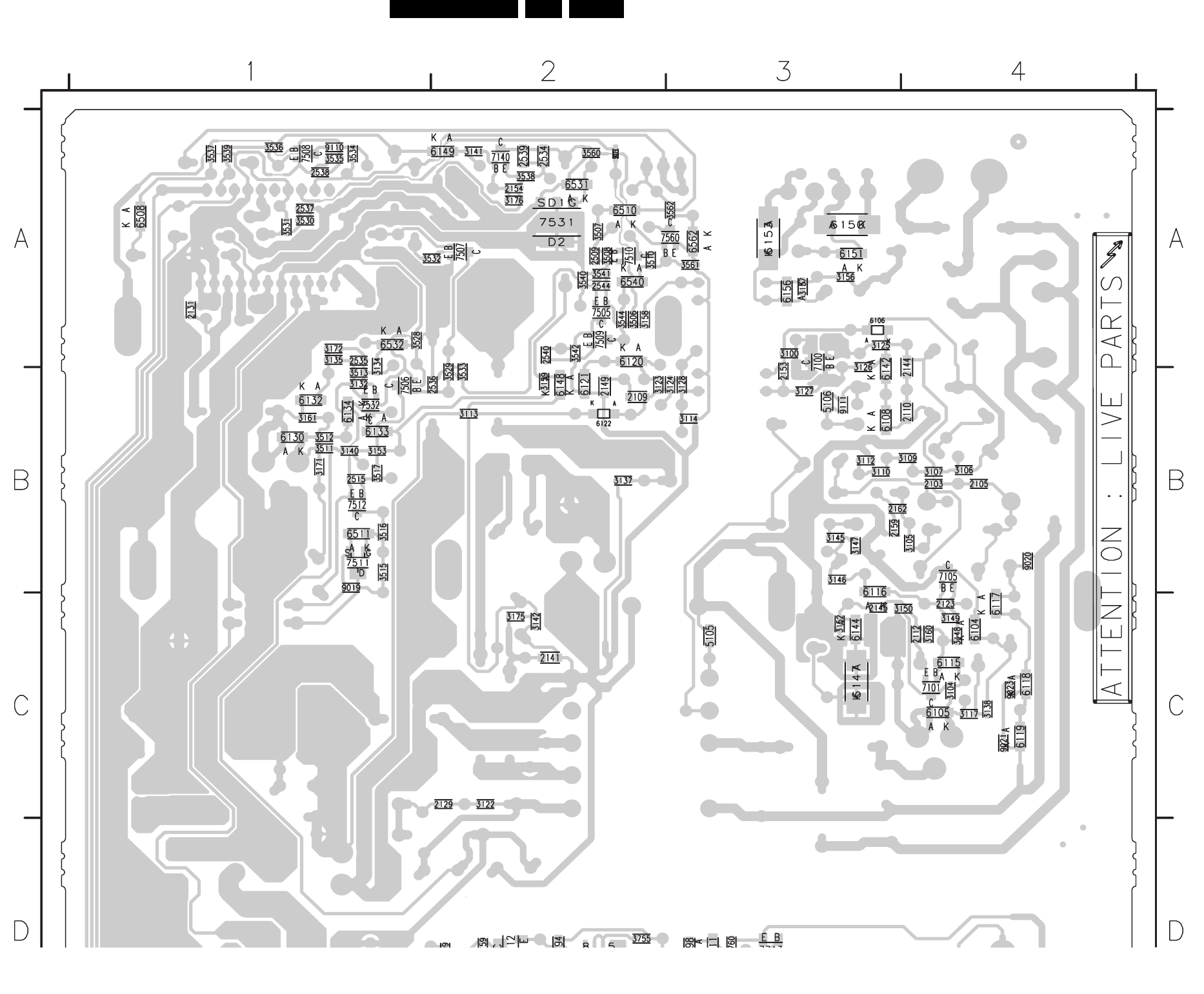
68LC4.6U AA 7.
Circuit Diagrams and PWB Layouts
Layout LCD Standby Audio Panel (Part 1 Bottom Side)
E_14620_136a.eps
131004
Part 1
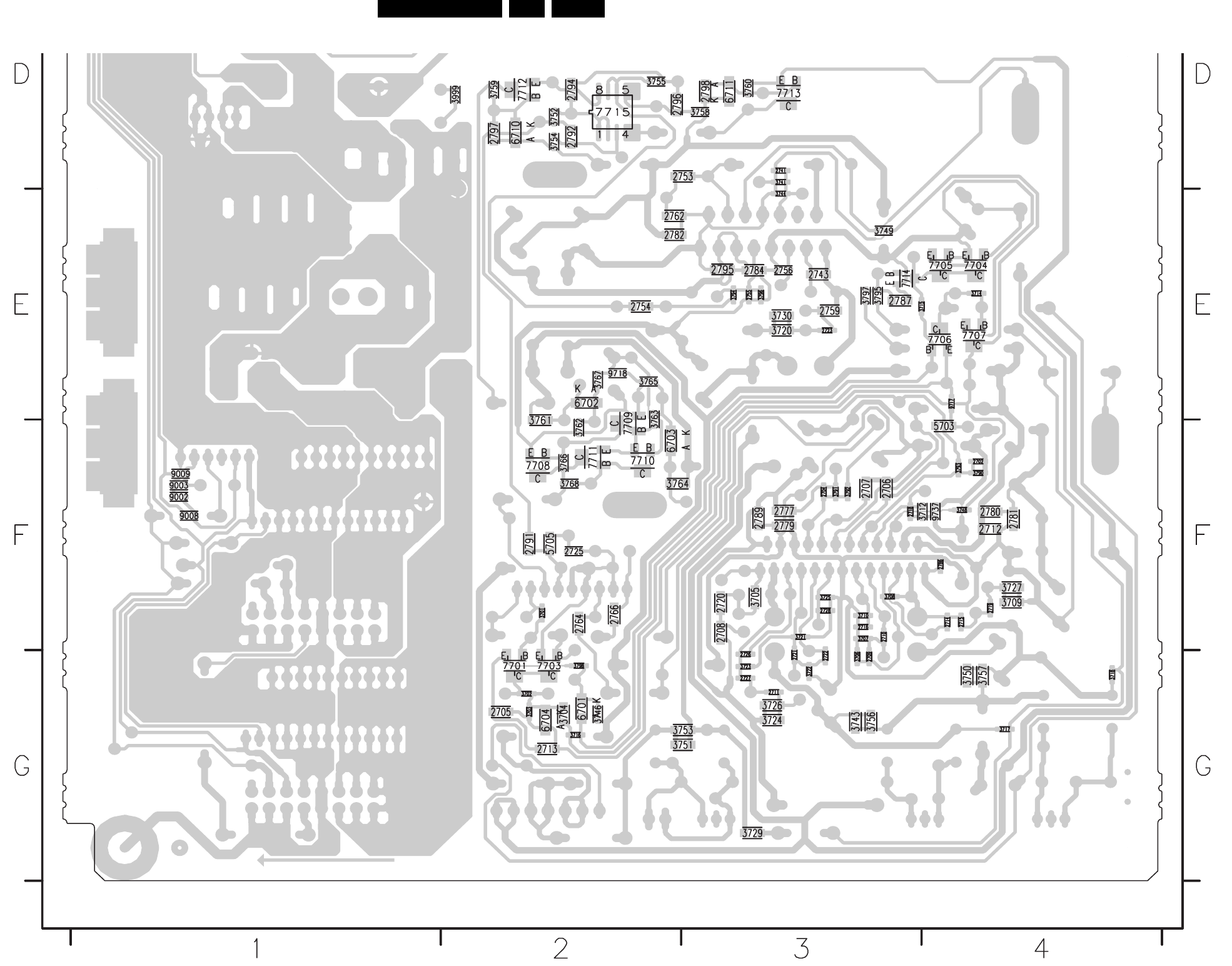
Circuit Diagrams and PWB Layouts 69LC4.6U AA 7.
Layout LCD Standby Audio Panel (Part 2 Bottom Side)
E_14620_136b.eps
131004
Part 2

70LC4.6U AA 7.
Circuit Diagrams and PWB Layouts
Personal Notes:
E_06532_013.eps
131004
Alignments EN 71LC4.6U 8.
8. Alignments
Index of this chapter:
8.1 General Alignment Conditions
8.2 Hardware Alignments
8.3 Software Alignments
Note: The Service Default Mode (SDM) and Service Alignment
Mode (SAM) are described in chapter 5. Menu navigation is
done with the CURSOR UP, DOWN, LEFT or RIGHT keys of
the remote control transmitter.
8.1 General Alignment Conditions
Perform all electrical adjustments under the following
conditions:
• Power supply voltage (depends on region):
– AP-NTSC: 120 VAC or 230 VAC / 50 Hz (± 10%).
– AP-PAL-multi: 120 - 230 VAC / 50 Hz (± 10%).
– EU: 230 VAC / 50 Hz (± 10%).
– LATAM-NTSC: 120 - 230 VAC / 50 Hz (± 10%).
– US: 120 VAC / 60 Hz (± 10%).
• Connect the set to the AC Power via an isolation
transformer with low internal resistance.
• Allow the set to warm up for approximately 15 minutes.
• Measure voltages and waveforms in relation to chassis
ground (with the exception of the voltages on the primary
side of the power supply).
Caution: It is not allowed to use heatsinks as ground.
• Test probe: Ri > 10 Mohm, Ci < 20 pF.
• Use an isolated trimmer/screwdriver to perform
alignments.
8.1.1 Initial Settings
Perform all electrical adjustments with the following initial
settings:
1. To avoid the working of the lightsensor, set "Active Control"
to "Off" (via the "Active Control" button on the RC).
2. Set "Smart Picture" to "Natural" or “Soft” (via the "Smart
Picture" button on the RC).
8.1.2 Alignment Sequence
• First, set the correct options:
– In SAM, select OPTIONS,
– Fill in the option settings according to the set sticker
(see also paragraph "Option Settings"),
– Store the OPTIONS by switching the set to STAND-
BY.
• Warming up (>15 minutes).
• White-D alignment.
8.2 Hardware Alignments
8.2.1 Backlight Voltage Alignment
Switch the set "on" and measure the voltage between pin 3 (or
4) of connector 1304 (on MF panel) and ground. Align R3026
until this voltage is 12.2 VDC +/- 0.1 V.
Caution: This voltage must be aligned very precisely (within
1%): when it is too high, it can destroy the inverters. When it is
too low, the backlight will not start up.
8.3 Software Alignments
With the software alignments of the Service Alignment Mode
(SAM), Options can be set and the WHITE TONE, TUNER (IF)
and AUDIO settings can be aligned.
To store the data: Use the RC button MENU to switch to the
main menu and then switch to STAND-BY mode.
For the next alignments, supply the following test signals via a
video generator to the RF input:
•EU/AP-PAL models: a PAL B/G TV-signal with a signal
strength of at least 1 mV and a frequency of 475.25 MHz
•US/AP-NTSC models: an NTSC M/N TV-signal with a
signal strength of at least 1 mV and a frequency of 61.25
MHz (channel 3).
•LATAM models: an NTSC M or PAL M TV-signal with a
signal strength of at least 1 mV and a frequency of 61.25
MHz (channel 3).
8.3.1 SAM Menu
Figure 8-1 Overview SAM menu (example from EU set).
8.3.2 White Tone
Method 1 (with color analyzer):
1. Supply a 100% white uniformity test signal (100 IRE white)
to the tuner.
2. Enter SAM menu (color features are switched “off”
automatically).
3. Do NOT change the SMART PICTURE, ACTIVE
CONTROL, and CONTRAST+ settings to prevent
activating of Green Enhancement, Blue Stretch, and Black
Stretch.
Offset values in NVM are used for HD-, HDMI-, and VGA mode,
therefore only the settings in TV mode need to be set.
SAM SAM
. OP1 0 . Delta Cool Red -3
. OP2 57 . Delta Cool Green -1
. OP3 140 . Delta Cool Blue 5
. OP4 32
. OP5 120
. OP6 128
. OP7 0
SAM SAM
. IFPLL 32 . Normal Red 32
. AGC 30 . Normal Green 35
. AGCL' 255 . Normal Blue 41
SAM SAM
. Cool . Delta Warm Red 2
. Normal . Delta Warm Green -3
. Warm . Delta Warm Blue -13
SAM
SAM
.ADR 0x0000 0
.VAL 0x0000 0
.Store Store ?
SAM
.ADR 0x0000 0
.VAL 0x0000 0
.Store Store ?
E_14710_009.eps
240604
1 00022 LC42EP1 2.03/S42GV1 2.02 CSM
2 CODES 0 0 0 0 0
3 OP 000 057 140 032 120 128 000
4
5
6 NOT TUNED
7 PAL
8 STEREO
9 CO 50 CL 50 BR 50
0 AVL Off
00022 LC42EP1 2.03/S42GV1 2.02 SDM
. QSS Off
. FMI On
. NICAM Alignment 63
. Lip Sync Off
. DBE Off
ERR 0 0 0 0 0
OP 000 057 140 032 120 128 000
00022 LC42EP1 2.03/S42GV1 2.02 SAM
ERR 0 0 0 0 0
OP 000 057 140 032 120 128 000
. Clear Clear ?
. Options
. Tuner
. White Tone
. Audio
. NVM Editor
. SC NVM Editor
. Test Pattern
. ComPair Mode On
Alignments
EN 72 LC4.6U8.
Make the following settings in the normal user menu, when the
television is in TV Mode:
Table 8-1 User menu settings for White Tone alignment
Go to WHITE TONE in SAM and set NORMAL GREEN to:
Table 8-2 Service menu settings for White Tone alignment
1. Measure with a calibrated (phosphor- independent) color
analyzer (e.g. Minolta CA-200) in the center of the screen
(use a contact less analyzer, e.g. Minolta CA-210, to align
the LCD TV). The analyzer may not touch the screen, and
the measurement must be done in a dark environment.
Note: The color analyzer must be calibrated for the LCD or
Plasma panel in question. See the manual of the color
analyzer for the procedure on how to perform this
calibration.
2. Leave the value with the lowest output on the initial value.
3. Align the NORMAL white points, by lowering the other two
colors, to the right x-y coordinates (see table "White Tone
alignment values").
Note: To prevent clipping of the color, these values must
only be lowered!
Table 8-3 White Tone alignment values
Only the values for NORMAL are aligned with X, Y values. The
delta values for COOL and WARM are given below.
Table 8-4 Fixed delta values
After the alignment is finished, switch the set to STANDBY, in
order to store the alignments.
Note: When disconnecting the power before doing this, the
settings will not be stored.
Method 2 (without color analyzer):
If you do not have a color analyzer, you can use the default
values. These values are based on the average values in
production.
• Set the values for the NORMAL color temperature. Given
in the table “Average statistical values for NORMAL” from
production.
• Set the delta values for the COOL and WARM mode. See
table: “Fixed delta values.”
After the alignment is finished, switch the set to STANDBY, in
order to store the alignments.
Note: When disconnecting the power before doing this, the
settings will not be stored.
Table 8-5 Average statistical values for “NORMAL”
8.3.3 Tuner Adjustment
AGC (RF AGC Take Over Point)
Set pattern generator (e.g. PM5580) with color bar pattern and
connect to aerial input with RF signal amplitude -10mV and set
frequency for NTSC to 61.25 MHz (channel 3).
• Activate the SAM-menu. Go to the sub-menu TUNER,
select the sub-menu option AFC WINDOW and adjust the
value to “100 kHz”.
• Select the AGC sub-menu.
• Connect a DC multi-meter to test point F306 or pin1 of the
tuner.
• Adjust the AGC until the voltage at pin 1 of the tuner is
3.3 V +0.5 / -1.0.
• The value can be increased or decreased by pressing the
RIGHT/LEFT cursor button on the RC.
• Switch the set to STAND-BY to store the data.
8.3.4 Grey Scale Adjustment
SDTV Grey Scale Adjustment
Equipment and setting
• E.g. Fluke 54200 or Philips PM5580.
• 100% “8-step grey scale” pattern.
Alignment Method
• Switch with the RC to TV mode,
• Press the MUTE button on RC,
• Set SMART PICTURE to SOFT mode,
• Activate the auto color function by pressing key-sequence:
INFO - MUTE - MUTE - MUTE - INFO - MENU - INFO.
Expected Results
• Visual check if the 8 Grey levels are correct.
Analog PC Grey Scale Adjustment
Equipment and setting
• Quantum Data 802B.
• PC input signal, with 64 levels Grey scale pattern,
1024x768 @ 60Hz (Format= 81:DMT1060, Pattern=
123:Grey 64).
• PC input at D-sub VGA connector.
Alignment Method
• Switch with the RC to PC mode.
• Press the MUTE button on RC.
• Set BRIGHTNESS and CONTRAST to nominal “50”.
• Activate the auto color function by pressing key-sequence:
INFO - MUTE - MUTE - MUTE - INFO - MENU - INFO.
Expected Results
• Visual check if the 64 Grey levels are correct.
LCD (AUO) LCD (LPL) Plasma (SDI)
CONTRAST 99
BRIGHTNESS 42 (EU)
44 (US)
46 46 (AP+EU)
48 (US+LA)
COLOR/SAT. 50 (AP+LA+US)
60 (EU)
LCD (AUO) LCD (LPL) Plasma (SDI)
NORMAL GREEN 200 180
NORMAL color temp. (all regions)
X 0.289
Y 0.299
Screen Type Color temp. RED GREEN BLUE
LCD (AUO) DELTA COOL -3 -12 +10
DELTA WARM +5 -5 -20
LCD (LPL) DELTA COOL -8 -12 +3
DELTA WARM +2 -10 -21
Plasma DELTA COOL -6 -10 +5
DELTA WARM +4 -5 -19
Display type Colour Temp. RED GREEN BLUE
LCD (AUO) NORMAL 165 182 200
LCD (LPL) NORMAL 200 195 190
Plasma 37“ (SDI) NORMAL 174 180 178
Plasma 42” (SDI) NORMAL 173 180 172
Note: Values are valid for all regions

Alignments EN 73LC4.6U 8.
HD Grey Scale Adjustment
Equipment and setting
• Quantum Data 802B.
• HD input signal, Top half 100% color bar and bottom half
Grey scale pattern,1920x1080i@60Hz YPbPr (Format=
1080i30, Pattern= HDBar100).
• HD input at D-sub VGA connector.
Alignment Method
• Switch with the RC to HD mode.
• Press the MUTE button on RC.
• Activate the auto color function by pressing key-sequence:
INFO - MUTE - MUTE - MUTE - INFO - MENU - INFO.
Expected Results
• Visual check if Color bar tint and Grey scale is correct.
8.3.5 Sound
No adjustments needed for sound.
8.3.6 Options
Options are used to control the presence/absence of certain
features and hardware.
See for an overview, the table on the next page.
How to change an Option Byte
An Option Byte represents a number of different options.
Changing these bytes directly makes it possible to set all
options very fast. All options are controlled via seven option
bytes. Select the option byte (OP1.. OP7) with the cursor UP/
DOWN keys, and enter the new value.
Leaving the OPTION sub menu saves the changes in the
Option Byte settings. Some changes will only take effect after
the set has been switched “off” and “on” with the AC power
switch (cold start).

Alignments
EN 74 LC4.6U8.
Table 8-6 Option codes (general overview for all regions and displays)
Bit (DEC) Option Description
/78
(LATAM)
/61 (AP-
NTSC)
/69 ,79 ,98
(AP-PAL)
/93
(China)
/10, /12
(Europe)
/17, /37
(NAFTA) Remarks
7 (128) OP_PHILIPS_TUNER Philips Tuner available 1 1 1111
6 (64)OP_FM_RADIO FM Radio available 000000
5 (32)OP_LNA Low Noise Amplifier available 000000
4 (16)OP_ATS Auto Tuning System 000010
3 (8)OP_ACI ACI 000010
2 (4)OP_UK_PNP After virgin = English + Great Britain 000000
1 (2)OP_VIRGIN_MODE Activate Plug & Play menu at start-up 000000
0 (1)OP_CHINA AP-PAL tuning algorithm for China 000100
OP1: 128 128 128 129 152 128
7 (128)OP_SMART_SOUND Four smart sound settings 111111
6 (64)OP_UI_GREEN UI for Magnavox sets (NAFTA) 000000
5 (32)OP_CHANNEL_NAMINGNaming of channel feature available 111101
4 (16)OP_LTI Histogr. algorithm available (TDA9178) 111111
3 (8)OP_TILT Picture Rotation available 000000
2 (4)OP_FINE_TUNING Fine Tuning algorithm available 111111
1 (2) OP_PIP_PHILIPS_TUNER PIP Philips tuner 0 0 0000
0 (1)OP_HUE Tint for NTSC transmission 110001
OP2: 181 181 180 180 148 181
7 (128) OP_EW_FUNCTION Geometry adj. for Large screen sets 0 0 0000
6 (64)OP_2TUNER_PIP Double Tuner for PIP available 000000
5 (32)OP_PIP_SPLITTER Not used 000000
4 (16)OP_SPLITTER Not used 000000
3 (8)OP_VIRTUAL_DOLBYVirtual Dolby Effect 111111
2 (4)OP_WIDE_SCREEN 16:9 sets 111111
1 (2)OP_WSSB Wide Screen Signalling Bit detection 001010
0 (1)OP_ECO_SUBWOOFERSub woofer available 000000
OP3: 12 12 14 12 14 12
7 (128)OP_LIP_SYNC Lip Synchronisation Circuit available 000000Not for LCD
6 (64)OP_NOTUSED2 Not used 000000
5 (32)OP_ULTRA_BASS Ultra Bass Boost available 000000
4 (16)OP_DELTA_VOLUME Delta Volume feature available 000010EU only
3 (8)OP_NOTUSED3 Not used 000000
2 (4)OP_NOTUSED4 Not used 000000
1 (2)OP_STEREO_DBX Stereo DBX for NTSC available 100001NTSC only
0 (1)OP_STEREO_NICAM_2CSStereo NICAM 2CS available 001010
OP4: 2010172
7 (128)OP_AV1 External Source 1 available 111111
6 (64)OP_AV2 External Source 2 available 111111
5 (32)OP_AV3 External Source 3 (Side AV) available 111111
4 (16)OP_CVI Component Video In available 111101Not for EU
3 (8)OP_SVHS2 Super Video Home System 2 available 100000
2 (4)OP_SVHS3 Super Video Home System 3 available 100000
1 (2)OP_HOTEL_MODE LATAM specific simplified Hotel Mode 000000
0 (1)OP_NOTUSED Not used 000000
OP5: 252 240 240 240 224 240
7 (128)OP_PERSONAL_ZAPPINGZapping of channels feature available 000000
6 (64)OP_SMART_SURF Surf List available 100000
5 (32)OP_FMTRAP FM trap available 000000
4 (16)OP_COMBFILTER comb filter available 111111In Hercules
3 (8)OP_ACTIVE_CONTROLAuto Picture Impr. feature available 111111
2 (4)OP_SMART_LOCK Toggle Child Lock & Lock Chan. enabled 111111
1 (2)OP_LIGHT_SENSOR Light Sensor enabled 111111
0 (1)OP_TWIN_TEXT 2 txt pages on screen available 001110
OP6: 94 30 31 31 31 30
7 (128)OP_TIME_WIN1 1= 5 s, 0= 2 s (Europe fixed 1.2 s) 110101
5, 6 not used 000000
4 (16)OP_3DCOMB 3D comb filter available 010001NTSC only
AP-PAL
3 (8) OP_COLOR_SYSTEM_AP 1: Auto, PAL 4.43, NTSC 4.43, NTSC 3.58, SECAM
0: OFF- Auto, PAL 4.43, NTSC 4.43, NTSC 3.58
001000
2 (4) OP_SOUND_SYSTEM_AP_1 000: BG 001: BG / DK 010: I / DK 011: BG / I / DK
100: BG / I / DK / M
011100
1 (2) OP_SOUND_SYSTEM_AP_2 0 0 0000
0 (1) OP_SOUND_SYSTEM_AP_3 0 0 0000
EUROPE
3 (8)OP_DUMMY6 Not used 000000
2 (4)OP_DUMMY7 Not used 000000
1 (2)OP_WEST_EU West Europe Set (0 - East Europe Set) by default "on"000010
0 (1)OP_MULTI_STANDARD_EURFor Europe multi standard set 000010
LATAM
3 (8)OP_DUMMY6 Not used 000000
2 (4) OP_DUMMY7 000000
1 (2) OP_SYSTEM_LT_1 00: NTSC-M, 01: NTSC-M, PAL-M, 10: NTSC-M, PAL-
M, PAL-N, 11: NTSC-M, PAL-M, PAL-N, PAL-BG
000000
0 (1) OP_SYSTEM_LT_2 000000
NAFTA & AP-NTSC
3 (8)OP_DUMMY6 Not used 000000
2 (4)OP_DUMMY7 Not used 000000
1 (2)OP_DUMMY8 Not used 000000
0 (1)OP_DUMMY9 Not used 000000
OP7: 128 148 12 132 3 144
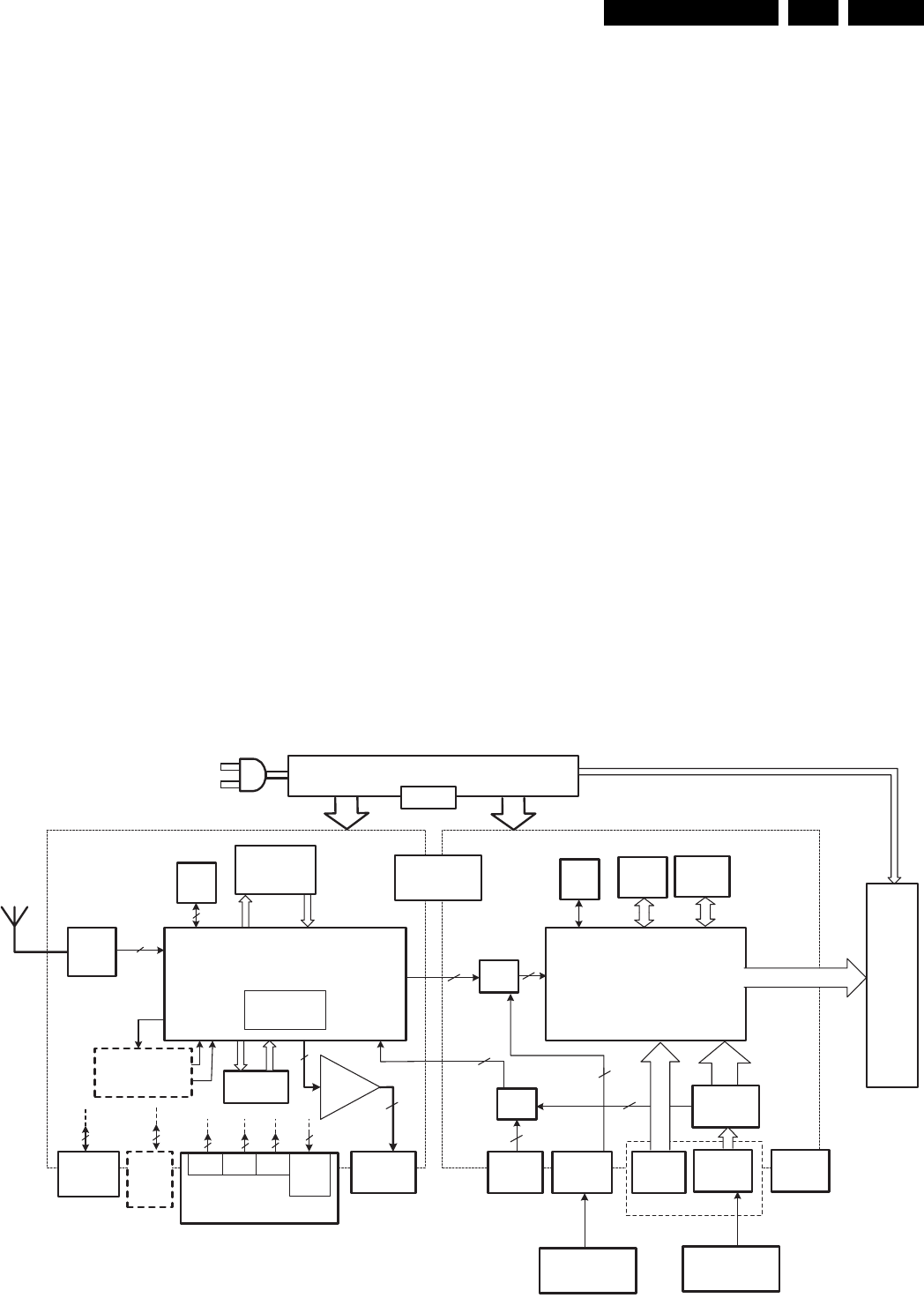
Circuit Descriptions, Abbreviation List, and IC Data Sheets EN 75LC4.6U 9.
9. Circuit Descriptions, Abbreviation List, and IC Data Sheets
Index of this chapter:
9.1 Introduction
9.2 Block Diagram
9.3 Power Supply LCD
9.4 Input/Output
9.5 Tuner and IF (diagram A1)
9.6 Video: TV Part (diagrams A1, A2, and A3)
9.7 Video: Scaler Part (diagram A7 and A13)
9.8 Audio Processing
9.9 Control
9.10 Abbreviation List
9.11 IC Data Sheets
Note:
•Only new (not recently published) circuits are described
here. For the other circuit descriptions, see a.o. the A02,
FTL13, and FTL2.1 Service Manuals.
• Figures can deviate slightly from the actual situation, due
to different set executions.
• For a good understanding of the following circuit
descriptions, please use the wiring, block and circuit
diagrams. Where necessary, you will find a separate
drawing for clarification.
9.1 Introduction
The LC4.6 LCD TV is a global LCD TV for the year 2004. It is
the successor of the LC03 LCD TV and covers screens size 30
inch with a new styling called “Entry”.
This chassis has the following (new) features:
•Audio: The sound processor is part of the UOC processor
(called “Hercules”).
•Video: Enhanced video features, video drivers, Active
Control and multiple PIP.
The architecture consists of a TV and Scaler panel, I/O panel,
Side I/O and Local Keyboard panel and Power Supply panel.
The functions for video/audio processing, microprocessor (uP),
and CC/Teletext (TXT) decoder are all combined in one IC
(TDA120xx, item 7011), the so-called third generation Ultimate
One Chip (UOC-III) or “Hercules”. This chip has the following
features:
• Control, small signal, mono/stereo, and extensive Audio/
Video switching in one IC.
• Upgrade with digital sound & video processing.
• Alignment free IF.
• FM sound, no traps/bandpass filters.
• Full multi-standard color decoder.
• One Xtal reference for all functions (microprocessor, RCP,
TXT/CC, RDS, color decoder, and stereo sound
processor).
9.2 Block Diagram
Figure 9-1 Block Diagram
HERCULES
(VDP + STEREO)
TDA9178
CTI/LTI/Hist.
NVM
Tuner
TV/FM
3DYC
uPCxxx
(Option) LIP
SYNC
GM1501
(SCALER)
NVM FLASH SDRAM
DISPLAY
PANEL
HDMI
Processor
Speakers
& HP
DMMI
(Multi-media
Interface)
Hercules-
Compair
(Service)
VGA
INPUT
HM
Link
(RJ12)
PC
Audio
INPUT
Cinch-to-VGA
Adapter
(YPbPr- HD)
MUX
MUX
ANALOGUE TV SCALER
Audio
Amp
Embedded
Flash
I2S
YUV
Interface
Analogue
Input
24-bit
Input
DVI
Input
DVI-to-HDMI
Adapter
I2CRGBHV/
YPbPr
RGB
& HV
Power Supply Unit
AC Mains
Input
HDMI
INPUT
DVI-D
INPUT
Option: Choose one
AV1 AV2 Side Const
Audio
Out
TV/IOs
(SCART/Cinch)
Compair
(UART)
DMMI
LVDS
E_14490_058.eps
190804

Circuit Descriptions, Abbreviation List, and IC Data Sheets
EN 76 LC4.6U9.
The PLL tuner delivers the IF-signal, via audio & video SAW-
filters, to the Video Signal Processor with FLASH embedded
TEXT/Control/Graphics m-Controller (TCG m-Controller) and
US Closed Caption decoder. TDA120x1 (item 7011, also called
Hercules). This IC has the following functions:
• Analogue Video Processing.
• Sound Demodulation.
• Audio Interfaces and switching.
• Volume and tone control for loudspeakers.
• Reflection and delay for loudspeaker channels.
• Micro Controller.
• Data Capture.
• Display.
The Hercules has one input for the internal CVBS signal and a
video switch with 3 external CVBS inputs and a CVBS output.
All CVBS inputs can be used as Y-input for Y/C signals.
However, only 2 Y/C sources can be selected because the
circuit has 2 chroma inputs. It is possible to add an additional
CVBS(Y)/C input (CVBS/YX and CX) when the YUV interface
and the RGB/YPRPB input are not needed. The I/O is divided
over two parts: Rear I/O and Side I/O. The rear has two AV
inputs with CVBS, Y/C and YUV, a PC (VGA) input, and an
HDMI input. The side has a CVBS and Y/C (SVHS) input.
The video part delivers the RGB signals to the Scaler IC.
The Genesis GM1501 Malibu Scaler IC can receive different
video input signals: SDTV (from Hercules), DVI/HDMI (from
external DVI/HDMI source), or PC (VGA) (from external
computer).
After the video processing, the digital data is send via a Low
Voltage Differential Signalling bus to the LCD panel. LVDS is
used to improve data speed and to reduce EMI significantly.
There are two I2C lines and two interrupt and communication
lines (TV_IRQ and TV_SC_COM) for the Scaler control. The
Scaler communicates with the Hercules as a slave device. To
avoid buffer overflow at the Scaler side, the TV_SC_COM line
provides the necessary hardware flow control. To allow bi-
directional communication, the Scaler can initiate a service
interrupt-request to the Hercules via the TV_IRQ line.
The Hercules, and EEPROM are supplied with 3.3 V, which is
also present during STANDBY.
The EEPROMs, or NVMs (Non Volatile Memory) are used to
store the settings.
The sound part is built up around the Hercules. The Source
Selection, Decoding and Processing are all done by the
Hercules.
Power supply input are several DC voltages coming from a
supply panel.
9.3 Power Supply LCD
See the FTL2.1 manual for a detailed description.
9.4 Input/Output
The I/O is divided over two parts: Rear I/O and Side I/O. The
rear has two AV inputs with CVBS, Y/C and YUV, a PC (VGA)
input, and an HDMI input. The side has a CVBS and Y/C
(SVHS) input.
AV1: The input of AV1 is CVBS + YUV + L/R.
AV2: The input of AV2 is Y/C + CVBS + L/R.
PC (VGA) in: This input is directly going to the Scaler IC. See
paragraph “Video: Scaler Part”.
HDMI in: This input is directly going to the Scaler IC. See
paragraph “Video: Scaler Part”.
The selection of the external I/O's is controlled by the Hercules.
9.5 Tuner and IF (diagram A1)
A Philips UV13xx Tuner is used in the TV board. The SIF
signals are decoded by the Hercules. Tuning is done via I2C.
9.5.1 Video IF amplifier
The IF-filter is integrated in a SAW (Surface Acoustic Wave)
filter. One for filtering IF-video (1328) and one for IF-audio
(1330). The type of these filters is depending of the standard(s)
that has to be received.
The output of the tuner is controlled via an IF-amplifier with
AGC-control. This is a voltage feedback from pin 31 of the
Hercules to pin 1 of the tuner. The AGC-detector operates on
top sync and top white level. AGC take-over point is adjusted
via the service alignment mode "Tuner” - “AGC". If there is too
much noise in the picture, then it could be that the AGC setting
is wrong. The AGC-setting could also be mis-aligned if the
picture deforms with perfect signal; the IF-amplifier amplifies
too much.
9.6 Video: TV Part (diagrams A1, A2, and A3)
The video processing is completely handled by the Hercules:
• IF demodulator.
• Chrominance decoder
• Sync separator.
• Horizontal & vertical drive.
• RGB processing.
• CVBS and SVHS source select.
It has also build in features like:
•CTI.
• Black stretch.
• Blue stretch.
• White stretch.
• Slow start up.
• Dynamic skin tone correction etc.
Further, it also incorporates sound IF traps and filters, and
requires only one crystal for all systems.
9.6.1 Histogram (YUV picture improvement) IC
The demodulated video-signal can be checked on pins 74, 75,
and 76 of IC7011 and is fed to pins 70, 71, and 72. In this path,
the Histogram IC TDA9171 is inserted.
This TDA9178 can control various picture improvements:
• Histogram processing.
• Color transient improvement.
• Luminance transient improvement.
• Black and white stretch.
• Skin tone correction.
• Green enhancement.
• Blue stretch.
• Smart peaking.
• Video dependent coring.
• Color dependent stretching.
Since the TDA9171 is connected to the Hercules, picture
improvement works only for signals that are routed through the
Hercules and not for signals directly connected to the Scaler.
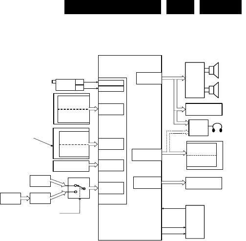
Circuit Descriptions, Abbreviation List, and IC Data Sheets EN 77LC4.6U 9.
9.7 Video: Scaler Part (diagram A7 and A13)
The Genesis GM1501 Scaler is a dual channel graphics and
video processing IC for LCD monitors and televisions
incorporating Picture in Picture, up to SXGA output resolutions.
The Scaler controls the display processing in an LCD TV, e.g.
like the deflection circuit in a CRT-based TV. It controls all the
view modes (e.g. like "zooming" and "shifting"). Features like
PC (VGA) or HD inputs, are also handled by this part.
9.7.1 Features
The Scaler provides several key IC functions:
• Scaling.
• Auto-configuration/ Auto-Detection.
• Various Input Ports:
– Analog RGB.
– Video Graphics.
• Integrated LVDS Transmitter.
• On-chip Micro-controller.
9.7.2 Inputs
Analog RGB
The RGB input is fed to pins B2, C2 and D2. This input consists
of either the Hercules RGB output or the RGB/YPbPr input of
the VGA connector. The Scaler can switch between the two
signals via the PC_HD_SEL signal and selection IC SM5301.
PC (VGA) input
The VGA input is processed by the VGA block of the Scaler.
The Scaler supports pixel frequencies up to 165 MHz.
YPbPr format is also supported via the VGA interface and
covers resolutions of: 480p/560p/720p/1080i.
HDMI input
HDMI input signals are fed to the HDMI Panellink Receiver
(item 7808 on diagram A12). This IC consists of a flexible audio
and video interface.
The video part delivers RGB/YPbPr output, that directly is fed
to the Scaler.
The audio part delivers a 2-channel I2S digital audio signal that
is fed to the audio DAC (item 7809). After DA conversion, the
signals are fed to the Hercules.
Note: For more information about the HDMI signals see the
A02 Service Manual.
9.7.3 Output
The Display Output Port provides data and control signals that
permit the Scaler to connect to a variety of display devices
using a TTL or LVDS interface. The output interface is
configurable for single or dual wide TTL/LVDS in 18, 24 or 30-
bit RGB pixels format. All display data and timing signals are
synchronous with the DCLK output clock. The integrated LVDS
transmitter is programmable to allow the data and control
signals to be mapped into any sequence depending on the
specified receiver format.
9.8 Audio Processing
Figure 9-2 Block diagram audio processing
The audio decoding is done entirely via the Hercules. The IF
output from the Tuner is fed directly to either the Video-IF or the
Sound-IF input depending on the type of concept chosen.
There are mainly two types of decoder in the Hercules, an
analogue decoder that decodes only Mono, regardless of any
standards, and a digital decoder (or DEMDEC) that can decode
both Mono and Stereo, again regardless of any standards.
In this chassis, the analogue decoder is used in two cases:
• It is used for AM Sound demodulation in the Europe
SECAM LL’ transmission.
• It is used for all FM demodulation in AV-Stereo sets.
9.8.1 Diversity
The diversity for the Audio decoding can be broken up into two
main concepts:
• The Quasi Split Sound concept used in Europe and some
AP sets.
• The Inter Carrier concept, used in NAFTA and LATAM.
The UOC-III family makes no difference any more between
QSS- and Intercarrier IF, nearly all types are software-
switchable between the two SAW-filter constructions.
Simple data settings are required for the set to determine
whether it is using the Inter Carrier or the QSS concept. These
settings are done via the “QSS” and “FMI” bit found in SAM
mode. Due to the diversity involved, the data for the 2 bits are
being placed in the NVM location and it is required to write once
during start-up.
On top of that, it can be further broken down into various
systems depending on the region. The systems or region
chosen, will in turn affect the type of sound standard that is/are
allowed to be decoded.
• For Europe, the standard consists of BG/DK/I/LL’ for a
Multi-System set. There are also versions for Eastern
Europe and Western Europe and the standard for decoding
will be BG/DK and I/DK respectively. FM Radio is a feature
diversity for the Europe. The same version can have either
FM Radio or not, independent of the system (e.g. sets with
BG/DK/I/LL’ can have or not have FM radio).
• For NAFTA and LATAM, there is only one transmission
standard, which is the M standard. The diversity then will
be based on whether it has a dBx noise reduction or a Non-
dBx (no dBx noise reduction).
• For AP, the standard consists of BG/DK/I/M for a Multi-
System set. The diversity here will depend on the region.
Side in
*All region
SCART1 out
*Europe only
SCART2 out
*Europe only
Monitor out
* Not available
SCART2 in
*Europe only
AV2 in
*AP/USA/Latam
AV1 in
*AP/USA/Latam
SCART1 in
*Europe only
Lip Sync
Circuit
2x
Amplifier
Amplifier
PC in
HDMI DAC
HEF4053
3X SPDT
PC_HDMI_AUD_SEL
(From Scaler,
GPIO_G07_B0)
AUDIO-OUTSL
AUDIO-OUTSR
AUDIO-OUTHPL
AUDIO-OUTHPR
Constant Level Out
*Europe only
AUDIO-LSL
AUDIO-LSR
Tuner
SIF
Is used on the DMMI
=> No SCART2/AV2 for
Bolt-on
AUDIO-IN5L
AUDIO-IN5R
AUDIO-IN3L
AUDIO-IN3R
AUDIOI-N4L
AUDIO-IN4R
AUDIO-IN2L
AUDIO-IN2R
SIF Input
106
105
103
P0.0/I2SDI1
P0.0/I2SDO1
P0.3/I2SCLK
I2S
FM SSIF Input
2x Stereo
Speaker
Headphone
Hercules
For iTV only
E_14490_061.eps
121104

Circuit Descriptions, Abbreviation List, and IC Data Sheets
EN 78 LC4.6U9.
AP China can have a Multi-System and I/DK version. For
India, it might only be BG standard.
9.8.2 Functionality
The features available in the Hercules are as follows:
• Treble and Bass Control.
• Surround Sound Effect that includes:
– Incredible Stereo.
– Incredible Mono.
– 3D Sound (not for AV Stereo).
– TruSurround (not for AV Stereo).
– Virtual Dolby Surround, VDS422 (not for AV Stereo).
– Virtual Dolby Surround, VDS423 (not for AV Stereo).
– Dolby Pro-Logic (not for AV Stereo).
• Bass Feature that includes:
– Dynamic Ultra-Bass.
– Dynamic Bass Enhancement.
– BBE (not for AV Stereo).
• Auto-Volume Leveller.
• 5 Band Equalizer.
• Loudness Control.
All the features stated are available for the Full Stereo versions
and limited features for the AV Stereo.
9.8.3 Audio Amplifier Panel (diagram SA3)
Introduction
This panel contains the audio filters and amplifiers necessary
for driving the speakers.
The audio inputs come from the SSB (via connector 1739).
The PSU delivers the positive and negative supply voltage of
16 VDC.
After being filtered and amplified, the signals go to the speaker
section, where the full range speakers are driven (load
impedance is 8 ohm).
Amplifier
The amplifier is an integrated class-D amplifier (TDA7490). It
combines a good performance with a high efficiency, resulting
in a big reduction in heat generation.
Principle
Audio-power-amplifier systems have traditionally used linear
amplifiers, which are well known for being inefficient. In fact, a
linear Class AB amplifier is designed to act as a variable
resistor network between the power supply and the load. The
transistors operate in their linear region, and the voltage that is
dropped across the transistors (in their role as variable
resistors) is lost as heat, particularly in the output transistors.
Class D amplifiers were developed as a way to increase the
efficiency of audio-power-amplifier systems.
The Class D amplifier works by varying the duty cycle of a
Pulse Width Modulated (PWM) signal.
By comparing the input voltage to a triangle wave, the amplifier
increases duty cycle to increase output voltage, and decreases
duty cycle to decrease output voltage.
The output transistors of a Class D amplifier switch from 'full off'
to 'full on' (saturated) and then back again, spending very little
time in the linear region in between. Therefore, very little power
is lost to heat. If the transistors have a low 'on' resistance
(RDS(ON)), little voltage is dropped across them, further
reducing losses.
A Low Pass Filter at the output passes only the average of the
output wave, which is an amplified version of the input signal.
In order to keep the distortion low, negative feedback is applied
(via R3723/3708).
The advantage of Class D is increased efficiency (= less heat
dissipation). Class D amplifiers can drive the same output
power as a Class AB amplifier using less supply current.
The disadvantage is the large output filter that drives up cost
and size. The main reason for this filter is that the switching
waveform results in maximum current flow. This causes more
loss in the load, which causes lower efficiency. An LC filter with
a cut-off frequency less than the Class D switching frequency,
allows the switching current to flow through the filter instead of
the load. The filter is less lossy than the speaker, which causes
less power dissipated at high output power and increases
efficiency in most cases.
Mute
A mute switch (item 7701) is provided at pin 6. This switch is
controlled by the SOUND_ENABLE line from the Hercules
(mute during operation).
Protections
Because of the symmetrical supply, a DC-blocking capacitor,
between the amplifier and the speaker, is not necessary.
However, it is still necessary to protect the speaker for DC
voltages. Therefore, the following protections are therefore
implemented:
• Via R3765 and R3767, each stabilised supply voltage line
is checked on deviations.
• Via R3718 and 3717, each amplifier output is checked for
DC-voltage.
9.8.4 Audio: Lip Sync (Optional)
A “lip sync” circuit with an audio delay can be added (not for all
models/regions), in order to synchronise with video delay due
to the complexity of the display processing. This video delay is
significant, due to memory based processing. For instance, the
“frame rate conversion” cause a delay of two frames, while the
LCD panel response also cause a delay.
The circuit is a (16 bit) FIFO based digital delay. E.g.: the
memory size required for a 80 ms delay (with a data clock of
1.024 MHz) can be calculated with: Memory size = delay time
* f_clk. This gives: 80 ms * 1.024 MHz = 81920 bits.
To calculate the memory size for a 16 bits mode I2S digital
audio stream we must use the following data:
• f_s = 32 kHz, 16 bits, stereo
• Data clock = 32 kHz * 16 * 2 = 1.024 MHz
• Memory size for 1 ms delay = 1 ms * 1.024 MHz = 1024 bits
= 1 kbit
So, the delay time of 80 ms can be built with five steps of 16
ms, which is close to the frame rate. Therefore, a 128 kbit
SRAM (16 x 8) is chosen.
Note that above described calculation is just an example,
values in the set can deviate.
9.9 Control
9.9.1 Hercules
The System Board has two main micro-controllers on board.
These are:
• On-chip x86 micro-controller (OCM) from Genesis LCD TV/
Monitor Controller.
• On-chip 80C51 micro-controller from Philips
Semiconductors UOCIII (Hercules) series.
Each micro-controller has it own I2C bus which host its own
internal devices.
The Hercules is integrated with the Video and Audio Processor.
For dynamic data storage, such as SMART PICTURE and
SMART SOUND settings, an external NVM IC is being used.
Another feature includes an optional Teletext/Closed Caption
decoder with the possibility of different page storage depending
on the Hercules type number.
Circuit Descriptions, Abbreviation List, and IC Data Sheets EN 79LC4.6U 9.
The Micro Controller ranges in ROM from 128 kB with no TXT-
decoder to 128 kB with a 10 page Teletext or with Closed
Caption.
9.9.2 Block Diagram
The block diagram of the Micro Controller application is shown
below.
Figure 9-3 Micro Controller block diagram
9.9.3 Basic Specification
The Micro Controller operates at the following supply voltages:
• +3.3 VDC at pins 4, 88, 94, and 109.
• +1.8 VDC at pins 93, 96, and 117.
•I
2C pull up supply: +3.3 VDC.
9.9.4 Pin Configuration and Functionality
The ports of the Micro Controller can be configured as follows:
• A normal input port.
• An input ADC port.
• An output Open Drain port.
• An output Push-Pull port.
• An output PWM port.
• Input/Output Port
The following table shows the ports used for the L04 control:
Table 9-1 Micro Controller ports overview
The description of each functional pin is explained below:
•LED. This signal is used to drive the LED for Stand-by,
Remote, and Error Indication:
– During protection mode, the LED blinks and the set is
in Stand-by mode.
– During error conditions it blinks at a predefined rate.
– After receiving a valid RC or local keyboard command
it flashes once.
– For sets with error message indication, the LED blinks
when message is active and the set is in Stand-by
mode.
•SCL. This is the clock wire of the two-wire single master bi-
directional I2C bus.
•SDA. This is the data wire of the two-wire single master bi-
directional I2C bus.
•STANDBY. The Hercules generates this signal. This can
enable the power supply in normal operation and disable it
during Stand-by. It is of logic “high” (3.3 V) under normal
operation and “low” (0 V) during Stand-by.
•IR. This input pin is connected to an RC5 remote control
receiver.
•SEL-IF. This is an output pin to switch the Video SAW filter
between M system and other systems.
– 0: NTSC M (default).
– 1: PAL B/G, DK, I, L.
•NVM_WP. The global protection line is used to enable and
disable write protection to the NVM. When write to the NVM
is required, pin 7 of the NVM must be pulled to logic “0" first
(via Write_Protect of the micro-controller pin) before a write
is performed. Otherwise pin 7 of NVM must always be at
logic “1”
– 0: Disabled.
– 1: Enabled (default).
•SOUND_ENABLE. This pin is use to MUTE the audio
amplifier. It is configured as push pull.
•STATUS_1. This signal is used to read the status of the
SCART 1 input (EU only).
•STATUS_2. This signal is used to read the status of the
SCART 2 input (EU only).
•HERC_RESET. This pin is use to switch the +1.8 V supply.
•POWER_DOWN. The power supply generates this signal.
Logic “high” (3.3 V) under normal operation of the TV and
goes “low” (0 V) when the Mains input voltage supply goes
below 70 VAC.
•KEYBOARD. Following are the Keyboard functions and
the step values (8 bit) for it.
Table 9-2 Local keyboard values
•TV_IRQ. This signal is the interrupt from the Scaler IC.
•TV_SC_COM. This signal is used for the communication
with the Scaler IC.
•EXT_MUTE. This signal is used to reduce the switch “off”
plop.
Pin Name Description Configuration
97 INT0/ P0.5 IR INT0
98 P1.0/ INT1 TV_IRQ INT2
99 P1.1/ T0 TV_SC_COM P1.1
102 P0.4/ I2SWS EXT_MUTE P0.4
103 P0.3/ I2SCLK Lip Sync I2SCLK
104 P0.2/ I2SDO2 NVM_WP P0.2
105 P0.1/ I2SDO1 Lip Sync I2SDO1
106 P0.0/ I2SDI/O Lip Sync I2SDI/O
107 P1.3/ T1 PC-TV_LED P1.3
108 P1.6/ SCL SCL SCL
109 P1.7/ SDA SDA SDA
111 P2.0/ TPWM SOUND_ENABLE P2.0
112 P2.1/ PWM0 (for future use) -
113 P2.2/ PWM1 (for future use) -
114 P2.3/ PWM2 SEL_IF P2.3
115 P3.0/ ADC0 Light Sensor - SDM ADC0
116 P3.1/ ADC1 STATUS_1 ADC1
119 P3.2/ ADC2 STATUS_2 ADC2
120 P3.3/ ADC3 KEYBOARD ADC3
122 P2.4/ PWM3 STANDBY P2.4
HERCULES SCALER
Tuner
ComPair
NVM
Sound
Amp
MUX
NVM
GPROBE for Debug
or ComPair(Scaler)
SDA
SCL
TV_IRQ
TV_SC_COM
+3V3STBY
1407
1406
1405
PC_DET
SD_PCHD_SEL
PC_HD_SEL
POWER_DOWN
LAMP_ON_OFF
PANEL_PWR_CTL
HD_FILTER
BACK_LIGHT_ADJ1
Flash ROM
83
GPIO2
NVM_WP
IIC BUS 2
93
NVRAM
_SDA
92
NVRAM
_SCL
72 71 187193194
85
(GPIO4)
88
(GPIO5)
89
(GPIO6)
68
(PBIAS)
67
(PPWR)
99
(PWM1)
98
(GPIO11/
PWM0)
78 DDC_SDA_VGA
77 DDC_SCL_VGA
82 GPIO1
81 GPIO0
+3V3STBY
111
GPIO23
90 GPIO7
ROM_ADD0-17
ROM_DATA0-7
5 6 7
103 106 107 108
HIGH or
LOW
level input
IIC BUS1
NVM_WP
Sound_Enable
HREC
RST
Sel IF/
SDM
Status1
Light
Sense
TV_IR
RC
P50_LINE_ITV_IR_SW
EXT_MUTE
Standby POWER
DOWN
127
P1.4
114
P2.3
116
ADC1
115
ADC0
123
P2.5
97
INT0
102
P0.4
122
P2.4
126
INT2
128
P1.5
SDA 109
SCL 108
INT1 98
P1.1 99
Keyboard
ADC3 120
111
P2.0
104
P0.2
E_14490_062.eps
160904
123 P2.5/ PWM4 (for future use) -
126 P1.2/ INT2 (for future use) -
127 P1.4/ RX HERC_RESET -
128 P1.5/ TX POWER_DOWN P1.5
Function
Voltage
(VDC)
Step values
(8 bit)
P+ / Ch+ 0.43 7 - 33
P- / Ch- 0.93 54 - 73
Menu (Vol - and Vol +) 1.19 74 - 96
Vol - 1.49 97 - 121
Vol + 2.12 148 - 169
Pin Name Description Configuration

Circuit Descriptions, Abbreviation List, and IC Data Sheets
EN 80 LC4.6U9.
9.10 Abbreviation List
1080i 1080 visible lines, interlaced
1080p 1080 visible lines, progressive scan
2CS 2 Carrier Sound
2DNR Spatial (2D) Noise Reduction
3DNR Temporal (3D) Noise Reduction
480i 480 visible lines, interlaced
480p 480 visible lines, progressive scan
AARA Automatic Aspect Ratio Adaptation:
algorithm that adapts aspect ratio to
remove horizontal black bars; keeping
up the original aspect ratio
ACI Automatic Channel Installation:
algorithm that installs TV channels
directly from a cable network by
means of a predefined TXT page
ADC Analogue to Digital Converter
AFC Automatic Frequency Control: control
signal used to tune to the correct
frequency
AGC Automatic Gain Control: algorithm that
controls the video input of the feature
box
AM Amplitude Modulation
AUO Acer Unipack Optronics
AP Asia Pacific
AR Aspect Ratio: 4 by 3 or 16 by 9
ASD Automatic Standard Detection
AV Audio Video
B-SC1-IN Blue SCART1 in
B-SC2-IN Blue SCART2 in
B-TXT Blue teletext
B/G Monochrome TV system. Sound
carrier distance is 5.5 MHz
BTSC Broadcast Television System
Committee
C-FRONT Chrominance front input
CBA Circuit Board Assembly (or PWB)
CL Constant Level: audio output to
connect with an external amplifier
CLUT Color Look Up Table
ComPair Computer aided rePair
CSM Customer Service Mode
CVBS Composite Video Blanking and
Synchronisation
CVBS-EXT CVBS signal from external source
(VCR, VCD, etc.)
CVBS-INT CVBS signal from Tuner
CVBS-MON CVBS monitor signal
CVBS-TER-OUT CVBS terrestrial out
DAC Digital to Analogue Converter
DBE Dynamic Bass Enhancement: extra
low frequency amplification
DFU Directions For Use: owner's manual
DNR Dynamic Noise Reduction
DRAM Dynamic RAM
DSP Digital Signal Processing
DST Dealer Service Tool: special
(European) remote control designed
for service technicians
DTS Digital Theatre Sound
DVD Digital Versatile Disc
DVI Digital Visual Interface
DW Double Window
ED Enhanced Definition: 480p, 576p
EEPROM Electrically Erasable and
Programmable Read Only Memory
EU EUrope
EXT EXTernal (source), entering the set by
SCART or by cinches (jacks)
FBL Fast Blanking: DC signal
accompanying RGB signals
FBL-SC1-IN Fast blanking signal for SCART1 in
FBL-SC2-IN Fast blanking signal for SCART2 in
FBL-TXT Fast Blanking Teletext
FLASH FLASH memory
FM Field Memory / Frequency Modulation
FMR FM Radio
FRC Frame Rate Converter
FRONT-C Front input chrominance (SVHS)
FRONT-DETECT Front input detection
FRONT-Y_CVBS Front input luminance or CVBS
(SVHS)
FTV Flat TeleVison
G-SC1-IN Green SCART1 in
G-SC2-IN Green SCART2 in
G-TXT Green teletext
H H_sync to the module
HD High Definition: 720p, 1080i, 1080p
HDMI High Definition Multimedia Interface,
digital audio and video interface
HP HeadPhone
I Monochrome TV system. Sound
carrier distance is 6.0 MHz
I2C Integrated IC bus
I2S Integrated IC Sound bus
IC Integrated Circuit
IF Intermediate Frequency
Interlaced Scan mode where two fields are used
to form one frame. Each field contains
half the number of the total amount of
lines. The fields are written in "pairs",
causing line flicker.
IR Infra Red
IRQ Interrupt ReQuest
Last Status The settings last chosen by the
customer and read and stored in RAM
or in the NVM. They are called at start-
up of the set to configure it according
the customers wishes
LATAM LATin AMerica
LC04 Philips chassis name for LCD TV 2004
project
LCD Liquid Crystal Display
LED Light Emitting Diode
L/L' Monochrome TV system. Sound
carrier distance is 6.5 MHz. L' is Band
I, L is all bands except for Band I
LPL LG Philips LCD
LS LoudSpeaker
LVDS Low Voltage Differential Signalling,
data transmission system for high
speed and low EMI communication.
M/N Monochrome TV system. Sound
carrier distance is 4.5 MHz
MOSFET Metal Oxide Semiconductor Field
Effect Transistor
MPEG Motion Pictures Experts Group
MSP Multi-standard Sound Processor: ITT
sound decoder
MUTE MUTE Line
NAFTA North American Free Trade
Association: Trade agreement
between Canada, USA and Mexico
NC Not Connected
NICAM Near Instantaneous Compounded
Audio Multiplexing. This is a digital
sound system, used mainly in Europe.
NTSC National Television Standard
Committee. Color system used mainly
in North America and Japan. Color
carrier NTSC M/N = 3.579545 MHz,
NTSC 4.43 = 4.433619 MHz (this is a
VCR norm, it is not transmitted off-air)
NVM Non Volatile Memory: IC containing
TV related data (for example, options)
O/C Open Circuit
ON/OFF LED On/Off control signal for the LED

Circuit Descriptions, Abbreviation List, and IC Data Sheets EN 81LC4.6U 9.
OSD On Screen Display
PAL Phase Alternating Line. Color system
used mainly in Western Europe (color
carrier = 4.433619 MHz) and South
America (color carrier PAL M =
3.575612 MHz and PAL N = 3.582056
MHz)
PC Personal Computer
PCB Printed Circuit Board (or PWB)
PDP Plasma Display Panel
PIG Picture In Graphic
PIP Picture In Picture
PLL Phase Locked Loop. Used, for
example, in FST tuning systems. The
customer can directly provide the
desired frequency
Progressive Scan Scan mode where all scan lines are
displayed in one frame at the same
time, creating a double vertical
resolution.
PWB Printed Wiring Board (or PCB)
RAM Random Access Memory
RC Remote Control transmitter
RC5 (6) Remote Control system 5 (6), the
signal from the remote control receiver
RGB Red, Green, and Blue. The primary
color signals for TV. By mixing levels
of R, G, and B, all colors (Y/C) are
reproduced.
RGBHV Red, Green, Blue, Horizontal sync,
and Vertical sync
ROM Read Only Memory
SAM Service Alignment Mode
SC SandCastle: two-level pulse derived
from sync signals
SC1-OUT SCART output of the MSP audio IC
SC2-B-IN SCART2 Blue in
SC2-C-IN SCART2 chrominance in
SC2-OUT SCART output of the MSP audio IC
S/C Short Circuit
SCL Clock signal on I2C bus
SD Standard Definition: 480i, 576i
SDA Data signal on I2C bus
SDI Samsung Display Industry
SDM Service Default Mode
SDRAM Synchronous DRAM
SECAM SEequence Couleur Avec Memoire.
Color system used mainly in France
and Eastern Europe. Color carriers =
4.406250 MHz and 4.250000 MHz
SIF Sound Intermediate Frequency
SMPS Switch Mode Power Supply
SND SouND
SNDL-SC1-IN Sound left SCART1 in
SNDL-SC1-OUT Sound left SCART1 out
SNDL-SC2-IN Sound left SCART2 in
SNDL-SC2-OUT Sound left SCART2 out
SNDR-SC1-IN Sound right SCART1 in
SNDR-SC1-OUT Sound right SCART1 out
SNDR-SC2-IN Sound right SCART2 out
SNDR-SC2-OUT Sound right SCART2 out
SNDS-VL-OUT Surround sound left variable level out
SNDS-VR-OUT Surround sound right variable level out
SOPS Self Oscillating Power Supply
S/PDIF Sony Philips Digital InterFace
SRAM Static RAM
STBY Stand-by
SVHS Super Video Home System
SW Sub Woofer / SoftWare
THD Total Harmonic Distortion
TXT TeleteXT
uP Microprocessor
VL Variable Level out: processed audio
output toward external amplifier
VCR Video Cassette Recorder
VGA Video Graphics Array
WD Watch Dog
WYSIWYR What You See Is What You Record:
record selection that follows main
picture and sound
XTAL Quartz crystal
YPbPr Component video (Y= Luminance, Pb/
Pr= Color difference signals B-Y and
R-Y, other amplitudes w.r.t. to YUV)
Y/C Video related signals: Y consists of
luminance signal, blanking level and
sync; C consists of color signal.
Y-OUT Luminance-signal
YUV Baseband component video (Y=
Luminance, U/V= Color difference
signals)
Circuit Descriptions, Abbreviation List, and IC Data Sheets
EN 82 LC4.6U9.
9.11 IC Data Sheets
This section shows the internal block diagrams and pin layouts
of ICs that are drawn as "black boxes" in the electrical diagrams
(with the exception of "memory" and "logic" ICs).
9.11.1 Diagram A2, Type TDA12029H (IC7011)
Figure 9-4 Internal Block Diagram and Pin Configuration
E
VIR
D-
V
DWE
OTH
E
FI D
N
UOS S
S
Q
C
G
A
R
EXI
M
S
S
Q
R
O
T
AL
U
DO
M
E
D
M
A
C
F
A
/
C
G
A/F
I
NOISIV
.
D
OMED
LLP
.PMA OEDIV
P
A
R
T
DN
U
O
S
YALED PUORG
HCTI
W
S OED
I
V
.TNED
I
O
E
D
I
V
S
R
E
TL
IF
O
E
D
IV
H4
/
H2
RETLIF BMOC
REDOC
E
D
C
S
T
N
/MACES/L
A
PDNA
B
-ESAB
ENIL YALED
.
PE
S
C
N
YS V
/
H
LLP + .
C
S
O
-H
2d
nPO
OL
TFI
H
S
-
H
EV
I
RD-
H
LACITRE
V
YRTE
M
O
E
G
T
SE
W-T
S
AE
&
N
I
B
VD/
N
IFIS
TU
O
C
GA
NIF
I
V
3Y
/
3S
B
V
C
3
C/2
C
4Y
/
4S
B
VC
4
C
/OSBVC
FISS
TU
O
H
G
NI
K
AE
P
YTICOLEV NACS
PY/BGR RPBTRESN
I
E
CAFRE
T
N
I
V
U
Y
.NOC
IRB
T
A
S
LORTNOC AMMAG
HCTERTS KCALB
µREDOCED TXETE
L
ET DNA ROSSEC
O
R
P
-
RCB
G
RL
B
OR
OG
OB
NIL
C
B
NIKLB
LO
R
TNOC BGR
TRES
N
I TXE
T
/DSO
C
C
C
.JDA .P-ETIHW
NTH
G
IRB/RTNOC
XIRTAM BGR
PSD
oidua htiw ros
secorp VT ”oerets-VA“ eht fo margaid
kcolB
MV
S
sO/I
C
Y
V/H
O
RM
F
/
O
B
VD
HCTI
W
S
OFER
FER
.J
D
A
YAL
E
D Y
MEVACS TXET NO
ENOT NIKS
TNIT V/U
Y
ALED V/U
NOITARUTAS
NOITALUDOM
H
C
T
E
R
TS EULB
2
Y/2
SB
V
C
/
OV
S
/
O
V
F
I
CNYSY
YUV IN/OUT
M
A
TUOMA/OSSQ
/OVFI/OBVD
LLP
D
NU
O
S
SISAHPMEED
S
E
RUT
AE
F
GNIS
S
E
CO
R
P
L
A
NGIS L
ATIG
ID
LB Y/G
P/R
R
P
/
BB
1
OW
SLB Y
/
G
P/
BB
oUoV o
YiY iUiV
)xC()xY/xSBVC(
P/R R
P
I
P
I
S
BVC
SDR
TCELES
O
IDUA
TUO/NI HCNIC/TRACS S2I TUO-SL
LR
LORTNOC OIDUA
EMULOV
SSAB/ELBBERT
S
E
R
U
TA
E
F
CAD/CDA
s
C
AD
RL
TUO-PH
ORMF
L
A
T
I
G
I
D
Pin configuration “stereo” and “AV-stereo” versions with Audio DSP
69
70
81
80
79
78
77
76
75
74
73
72
71
88
87
86
85
84
83
82
65
66
68
67
89
96
95
94
93
92
91
90
13
14
15
16
17
18
19
20
21
22
23
24
25
26
27
28
9
10
11
12
29
31
32
30
5
6
7
8
1
2
3
4
1
4
24
34
44
54
64
7
4
84
94
15
25
35
45
65
55
3
3
4
3
5
3
6
3
7
3
8
3
9
3
0
4
75
85
95
06
16
26
4
6
36
0
5
QFP-128 0.8 mm pitch “face down version”
A
DN
G
211
111
011
90
1
801
701
601
501
311
411
511
611
711
811
91
1
021
121
221
321
421
521
621
721
821
401
301
201
101
001
9
9
8
9
79
P0.1/I2SDO1
P0.2/I2SDO2
P0.0/I2SDI1
VSSC2
P0.3/I2SCLK
P0.4/I2SWS
VDDC2
VSSC3
)V3.3(3ADDV
)
V
8.
1(
A
DD
V
VDDC3
P3.2/ADC2
P3.3/ADC3
VSSC1/P
INT0/P0.5
P3.0/ADC0
P3.1/ADC1
P2.3/PWM2
P1.6/SCL
P2.2/PWM1
P2.1/PWM0
P2.0/PMW
P1.7/SDA
P1.3/T1
P2.4/PWM3
VDDP(3.3V)
VDDC1(1.8)
LSL_SOP_FERV
)V3.3
(
2ADDV
P1.2/INT2
ARDV
1N
IF
IV
2
N
IFIV
CSV
LLPCES
GIDCED
FL1HP
G
B
C
E
D
DWE/LVA
BRDV
FERI
TU
O
CG
A
1N
I
FIS/1N
I
BVD
2NIF
I
S/2NIBVD
P1.4/RX
1
P
V
NILATX
TU
OL
A
TX
1
A
SS
V
FIDNG
LPH+RSL_SOP_FERV
R
P
H+LPH_
G
E
N
_FERV
RPH_SOP_FERV
RSL+LSL_GEN_FERV
Y
S
C
/OS
I
BF
CVBSO/PIP
AUDIOIN5L
M
V
S
GND2
DVBO//IFVO/FMRO
DVBO/FMRO
AGC2SIF
AUDIOIN4L
SIFAGC/DVBAGC
PLLIF
AUDIOIN5R
AUDOUTLSL
AUDOUTLSR
AUDIOIN4R
VCC8V
CVBS3/Y3
AUDIOIN2L/SSIF
AUDIOIN2R
CVBS4/Y4
AUDIOIN3L
AUDIOIN3R
C4
AUDOUTHPL
AUDOUTHPR
CVBS2/Y2
VP2
SVO/IFOUT/CVBSI
C2/C3
DECSDEM
AMOUT/QSSO/AUDEEM
OTHE
b
moc
DD
V
)
.
V3.
3
(1A
D
D
V
OB
OG
OR
G
E
N
_DAFERV
TUO
H
S
O
P
_DA
F
E
R
V
b
m
ocS
S
V
3WSSNI
P
/
R
R
3-
N
I
K
L
B
NIL
C
B
P/B
B
3-
3-
Y/
G
)X-Y/SBVC/2-Y
/
G(NIY
)1OWS(TUO
V
)2
-
WSNI(
T
U
O
U
T
U
O
Y
NIU
P/R(NIV
R
)
X
-
C
/
2-
P
/B(
B
)2-
C
N
Y
SY
3P
V
3DNG
D
A
F
E
R
V
P1.O/INT1
P1.1/T0
)
8.
1(
c
d
aD
D
V
c
d
a
SSV
REFIN/REFOUT
OIWS/DRAUGV
P2.5/PWM4
DECV1V8
1DNG
AUDOUTSL
AUDOUTSR
P1.5/TX
4CDDV
4
C
SS
V
2PSSV
AVL/SWO/SSIF/
FL2HP
E_14490_063.eps
160804
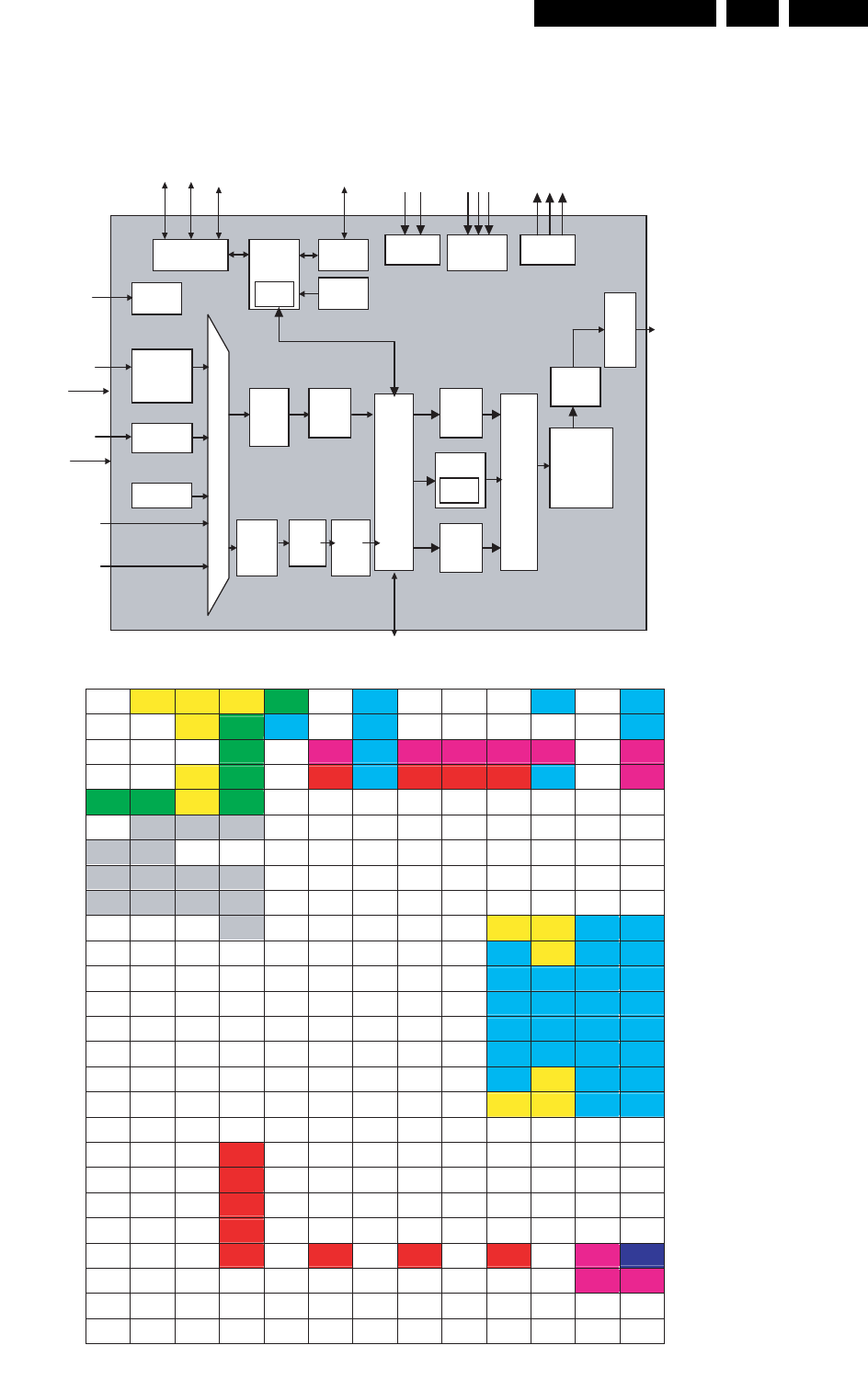
Circuit Descriptions, Abbreviation List, and IC Data Sheets EN 83LC4.6U 9.
9.11.2 Diagram A7, Type GM1501 (IC7401)
Figure 9-5 Internal Block Diagram and Pin Configuration
Infra-red Rx Low
ndwid
DC
Ba th
A
Pulse Width
Modulator
DDC2Bi
DVI
8/16 bit video
4:2:2/CCIR656
8/16/24 bit
video
(4:4:4/4:2:2/
CCIR656)
Test Pattern
Generator
Ultra-Reliable
DVI Rx
DVI-Compliant
Input
Triple ADC
and PLL
14.318 MHz
Crystal
Reference
Image
Capture
and
Measure
ment
RealColorTM
Graphics
Shrink
Filter
Clock
Generation
Frame
Store
Control
JTAG GPIO
2-wire
Serial I/F
External
ROM I/F
Internal
ROM
TTL/
LVDS
Tx
Display
Timing
Generator
OSD
Controller
Color Table
RAMs
Output
Blender
Video
Shrink
Filter
Motion
Adapt.
3:2/2:2
detection
Video
Zoom
Filter
Graphics
Zoom
Filter
Image
Capture
and
Measure
ment
Internal
RAM
X186
Micro-
controller
Interface
Parallel
ROM
IF/external
micro
Analog RGB
Input
Panel Data
/Control
DDC2Bi
analog
DDR SDRAM
I/F
Block Diagram
Pin Configuration
ANC ADC_3.3 ADC_1.8 ADC_1.8
ADC_DGND
RXC+ DVI_GND RX0+ RX1+ RX2+ DVI_GND LBADC_IN3 D_GND
BBLUE- BLUE+ ADC_3.3
ADC_DGND
DVI_GND RXC- DVI_GND RX0- RX1- RX2- REXT LBADC_IN2 D_GND
CGREEN- GREEN+ SOG ADC_AGND NC DVI_3.3 DVI_GND DVI_3.3 DVI_3.3 DVI_3.3 DVI_3.3 LBADC_IN1 LBADC_33
DRED- RED+ ADC_3.3 ADC_AGND NC DVI_1.8 DVI_GND DVI_1.8 DVI_1.8 DVI_1.8 DVI_GND LBADC_
RETURN
LBADC_GND
EADC_AGNDADC_AGND ADC_3.3 ADC_AGND
FNC VDDD33_
PLL
VSSA33_
RPLL
VDDA33_
RPLL
GVDDA33_
FPLL
VSSD33_
PLL TCLK XTAL
HVDDD33_
SDDS
VSSA33_
SDDS
VDDA33_
SDDS
VSSA33_
FPLL
JVDDD33_
DDDS
VSSA33_
DDDS
VDDA33_
DDDS
VSSD33_
SDDS
KRESETn ACS_
RSET_HD NC VSSD33_
DDDS CORE_1.8 CORE_1.8 D_GND D_GND
LOCM_INT2 OCM_INT1 AVSYNC AHSYNC D_GND CORE_1.8 D_GND D_GND
MOCM_UDO OCM_UDI IR0 IR1 D_GND D_GND D_GND D_GND
NVGA_SDA VGA_SCL DVI_SDA DVI_SCL D_GND D_GND D_GND D_GND
POCM_CS1n OCM_CS2n MSTR_SDA MSTR_SCL D_GND D_GND D_GND D_GND
RROM_CSn OCM_REn OCM_WEn EXTCLK D_GND D_GND D_GND D_GND
TOCMADDR
17
OCMADDR
18
OCMADDR
19 OCM_CS0n D_GND CORE_1.8 D_GND D_GND
UOCMADDR
13
OCMADDR
14
OCMADDR
15
OCMADDR
16 CORE_1.8 CORE_1.8 D_GND D_GND
VOCMADDR
9
OCMADDR
10
OCMADDR
11
OCMADDR
12
WOCMADDR
6
OCMADDR
7
OCMADDR
8IO_3.3
YOCMADDR
3
OCMADDR
4
OCMADDR
5IO_3.3
AA OCMADDR
0
OCMADDR
1
OCMADDR
2IO_3.3
AB
OCMDATA13 OCMDATA14 OCMDATA15
IO_3.3
AC
OCMDATA10 OCMDATA11 OCMDATA12
IO_3.3
GPIO_G09_ B2
(
DEGRN0
)
IO_3.3 DCLK IO_3.3
GPIO_G07_ B2
(
DERED4
)
IO_3.3
SHIELD[1]
(DEGRN3)
LVDSB_3.3
LVDSB_GND
AD OCMDATA9OCMDATA6 OCMDATA3 OCMDATA0
GPIO_G09_ B3
(
DEGRN1
)
GPIO_G08_ B0
(
DORED0
)
DEN
GPIO_G08_ B5
(
DOBLU1
)
GPIO_G07_ B3
(
DERED5
)
GPIO_G07_ B6
(
DERED8
)
SHIELD[2]
(DEGRN4)
LVDSB_3.3 LVDSB_3.3
AE OCMDATA8OCMDATA5 OCMDATA2
GPIO_G09_ B0
(
DERED0
)
GPIO_G09_ B4
(
DEBLU0
)
GPIO_G08_ B1
(
DORED1
)
GPIO_G08_ B3
(
DOGRN1
)
GPIO_G07_ B0
(
DERED2
)
GPIO_G07_ B4
(
DERED6
)
GPIO_G07_ B7
(
DERED9
)
SHIELD[3]
(DEGRN5)
BC+
(DEGRN8)
SHIELD[4]
(DEBLU2)
AF OCMDATA7OCMDATA4 OCMDATA1
GPIO_G09_ B1
(
DERED1
)
GPIO_G09_ B5
(
DEBLU1
)
GPIO_G08_ B2
(
DOGRN0
)
GPIO_G08_ B4
(
DOBLU0
)
GPIO_G07_ B1
(
DERED3
)
GPIO_G07_ B5
(
DERED7
)
SHIELD[0]
(DEGRN2)
B3+
(DEGRN6)
B3-
(DEGRN7)
BC-
(DEGRN9)
12345678910111213
E_14490_099.eps
241204
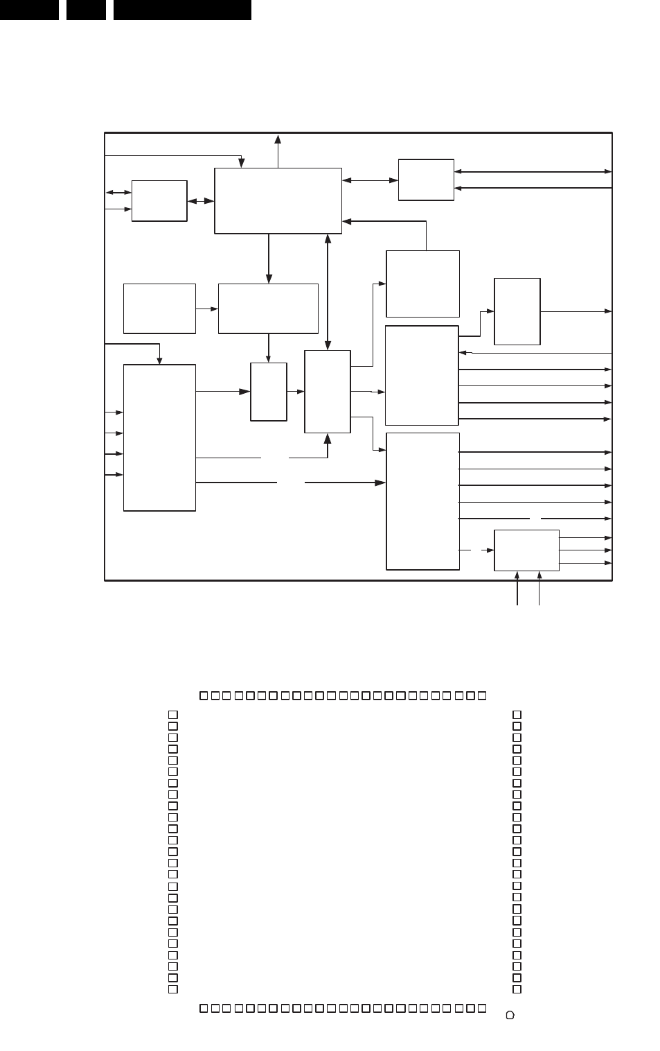
Circuit Descriptions, Abbreviation List, and IC Data Sheets
EN 84 LC4.6U9.
9.11.3 Diagram A12, Type SiI9993CT (IC7808)
Figure 9-6 Internal Block Diagram and Pin Configuration
DACVCC1
100-Pin
TQFP
(Top View)
N/C
2DACGND
3
N/C4
DACGNDR5
DACVCCR6
AnRPr7
COMP8
RSET9
DACGNDG10
DACVCCG11
AnGY12
DACGNDB13
DACVCCB14
AnBPb15
GND16
VCC17
RSVDL18
RSVDO19
RSVDO20
OVCC21
PGND222
PVCC2
23
PLLIN
24
N/C25
MCLKOUT26
MCLKIN27
OG ND28
SP DI F29
SD O30
WS31
SC K32
HSYN C33
VSYNC34
DE35
Q2336
Q2237
Q2138
Q20
39
VC C40
GND41
Q1942
Q1843
Q1744
OG ND45
ODC K46
OVCC47
Q1648
Q1549
Q1450
75
Q1
74
OVCC
73
CSDA
72
Q3
71
Q4
70
Q5
69
Q6
68
Q7
67
Q8
66
OGND
65
OVCC
64
Q9
63
Q10
62
Q11
61
Q12
60
Q13
59
58
57
56
55
54
53
52
51
Q0
VC C 100
GND 99
AG ND 9 8
RX2+ 97
RX2- 96
AVCC 95
AG ND 9 4
AVCC 93
RX1+ 92
RX1- 91
AG ND 90
AVCC 89
AGND 88
RX0+ 87
RX0- 86
AG ND 85
RXC+ 84
RXC- 83
AVCC 82
EX T _ RE S 81
PVCC1 80
PGND1 79
OG ND 7 8
DSCL 77
DSDA 76
CSCL
RSVDL
Q2
RESET#
INT
OGND
VCC
GND
SiI 9993
BLOCK DIAGRAM
PIN CONFIGURATION
E_14620_149.eps
090804
HDCP
Decryption
Engine
HDCP
Keys
EEPROM
Registers
----------------
Configuration
Logic Block
XOR
Mask
Video
Color
Space
Converter
Up/Down
Sampling
control
signals
I2C
Slave
24
DE
Q[23:0]
DSDA
DSCL
R_EXT
RXC±
RX0±
RX1±
RX2±
INT
RESET#
Audio
Data
Decode
Logic
Block
SPDIF
MCLKOUT
PanelLink
TMDS
TM
Digital
Core
MCLK
Gen
HSYNC
VSYNC
ODCK
SD0
SCK
WS
MCLKIN
Mode
Control
Aux Data
Logic
Block
control
signals
Video
DAC
30
AnGY
AnRPr
AnBPb
I2C
Slave
CSDA
CSCL
OMPC
SETR

Spare Parts List EN 85LC4.6U 10.
10. Spare Parts List
Set Level
Various
1004h9322 206 49682 LCD T296XW01 (AUO)
1004 9322 206 53682 LCD LC300W01 (LPL)
1005 3104 328 30812 LCD Supply US 30"
1006h3104 328 30002 Stand-by / Audio panel
1072 3104 328 34781 LED + Switch Panel
1102h3104 328 32764 Small Signal Panel AUO
1102h3104 328 32771 Small Signal Panel LPL
1114 3104 328 32821 Top control assy
1116 3104 328 26371 Side I/O assy LCD
8302 3104 311 04731 Cable 7p/560/7p
8303h3104 311 06511 Cable 10p/280/10p
8304 3104 311 08271 Cable 4p/340/4p
8305 3104 311 08411 Cable 3p/340/3p
8306h3104 311 01431 Cable 2P3/340/2P3
8306 3104 311 08351 Cable 2P3/340/2P3
8307 3104 311 08371 Cable 4p/340/4p
8309 3104 311 08301 Cable 3p/340/3p
8312 3104 311 06361 Cable 15p/340/15p16
8313 3104 311 08791 Cable 15P/120/15P16
8315 3104 311 06511 Cable 10p/280/10p
8317 3104 311 03611 Cable 12p/280/12p
8320 3104 311 06091 Cable 10p/680/10p
8346 3104 311 07001 Cable 11P/400/11P
8350 3104 311 08611 Cable 31P/120/20P
8352 3104 311 06811 Cable 9P/340/9P
8735 3104 311 07501 Cable 2P3/560/2P
8736 3104 311 07541 Cable 2P3/1200/2P
Small Signal Board [A]
Various
0036 3104 308 12352 Connector plate Cinch
0070 3104 308 12331 Top shielding assy
0071 3104 308 12321 Bottom shielding assy
0108 3111 254 30201 Adhesive foam
0109 3111 254 30201 Adhesive foam
0121 3104 303 10871 EMC foam tuner
0300 2422 486 80938 Socket 32p f PLCC
0328 2422 034 21798 Screwlock
0358 2511 077 00039 Connector 2p
1001 2422 543 01414 Xtal 24.576MHz
1003 3139 188 53051 3D Comb filter
1004 2422 025 15773 Connector 10p f
1175 2422 026 05384 Socket Cinch 6p f
1177 2422 026 05553 Socket phone 1p f
1182 2422 026 05553 Socket phone 1p f
1183 2422 026 05428 Connector 4p f
1251 2422 025 10655 Connector 11p m
1301 2422 025 16835 Connector 3p m
1302 3139 147 21461 Tuner UV1338/A F S H-4
1320 2422 025 10771 Connector 10p m
1328 2422 549 44377 SAW 45.75MHz M1967L
1336 2422 025 10655 Connector 11p m
1401 2422 543 01133 Xtal 14.32MHz 20pF
1402 2422 025 10768 Connector 3p m
1403 2422 025 10771 Connector 10p m
1450 2422 025 18427 Connector 31p f
1681 2422 025 16835 Connector 3p m
1686 2422 026 04754 Connector cinch 2p f
1687 2438 031 00416 Connector 15p f
1688 2422 033 00504 Socket HDMI 19p f
1690 2422 549 00146 Line filter 20V 3A
1691 2422 549 00146 Line filter 20V 3A
1692 2422 549 00146 Line filter 20V 3A
1693 2422 549 00146 Line filter 20V 3A
1752 2422 025 10769 Connector 9p m
1860 2422 549 45325 Bead 67Ω at 100MHz
1861 2422 549 45325 Bead 67Ω at 100MHz
1862 2422 549 45325 Bead 67Ω at 100MHz
1863 2422 549 45325 Bead 67Ω at 100MHz
1864 2422 549 45325 Bead 67Ω at 100MHz
8308 3104 311 07691 Cable 2p3/280/Inlet
8801 3139 131 04021 Flex foil 10p/60/10p
g
2000 2020 552 00035 2.2µF 6.3V 10% 0603
2001 2020 552 96718 220nF 10% 6.3V 0402
2002 4822 124 23002 10µF 16V
2003 2238 869 15109 10pF 5% 50V 0402
2004 2020 552 96718 220nF 10% 6.3V 0402
2005 3198 035 71040 100nF 10% 16V 0402
2006 3198 034 06880 6.8pF 1% 50V 0402
2007 3198 034 06880 6.8pF 1% 50V 0402
2008 2020 552 00124 470nF 10% 10V 0603
2009 2020 552 96807 1µF 10% 10V 0603
2010 3198 035 26820 6.8nF 10% 16V 0402
2011 2020 552 96718 220nF 10% 6.3V 0402
2012 4822 124 12095 100µF 20% 16V
2013 3198 035 71040 100nF 10% 16V 0402
2014 3198 035 71040 100nF 10% 16V 0402
2015 3198 035 71040 100nF 10% 16V 0402
2016 3198 035 71040 100nF 10% 16V 0402
2017 3198 035 71040 100nF 10% 16V 0402
2018 3198 035 71040 100nF 10% 16V 0402
2019 4822 124 80151 47µF 16V
2020 2238 869 15101 100pF 5% 50V 0402
2021 2020 552 96628 10nF 10% 16V 0402
2022 3198 035 02210 220pF 5% 50V 0402
2023 3198 035 71040 100nF 10% 16V 0402
2024 4822 124 12095 100µF 20% 16V
2025 3198 035 71040 100nF 10% 16V 0402
2026 3198 035 71040 100nF 10% 16V 0402
2027 3198 035 71040 100nF 10% 16V 0402
2028 2020 552 96628 10nF 10% 16V 0402
2029 3198 035 71040 100nF 10% 16V 0402
2030 3198 035 71040 100nF 10% 16V 0402
2031 3198 035 71040 100nF 10% 16V 0402
2032 3198 035 71040 100nF 10% 16V 0402
2033 2020 552 96718 220nF 10% 6.3V 0402
2034 2020 552 00002 3.3nF 2% 50V 0805
2035 2020 552 96656 10µF 20% 25V 1210
2036 2020 552 96807 1µF 10% 10V 0603
2037 2020 552 96807 1µF 10% 10V 0603
2040 4822 124 23002 10µF 16V
2041 2020 552 96718 220nF 10% 6.3V 0402
2042 2020 552 00002 3.3nF 2% 50V 0805
2043 3198 035 71040 100nF 10% 16V 0402
2044 2020 552 96718 220nF 10% 6.3V 0402
2045 2238 869 15109 10pF 5% 50V 0402
2046 2238 869 15109 10pF 5% 50V 0402
2047 2020 552 96628 10nF 10% 16V 0402
2048 2238 869 15109 10pF 5% 50V 0402
2049 2238 869 15109 10pF 5% 50V 0402
2050 2238 869 15109 10pF 5% 50V 0402
2051 2020 552 00002 3.3nF 2% 50V 0805
2053 2020 552 96618 1nF 10% 50V 0402
2054 2020 552 96632 22nF 10% 16V 0402
2057 2238 869 15109 10pF 5% 50V 0402
2058 2238 869 15109 10pF 5% 50V 0402
2059 2238 869 15109 10pF 5% 50V 0402
2060 3198 035 71040 100nF 10% 16V 0402
2061 4822 124 23002 10µF 16V
2062 2238 869 15109 10pF 5% 50V 0402
2063 3198 017 31540 150nF 10V 0603
2067 2238 869 15109 10pF 5% 50V 0402
2068 2020 552 96718 220nF 10% 6.3V 0402
2069 2238 869 15109 10pF 5% 50V 0402
2071 4822 124 12095 100µF 20% 16V
2072 4822 126 14076 220nF +80/-20% 25V
2073 2020 552 96618 1nF 10% 50V 0402
2074 2020 552 96718 220nF 10% 6.3V 0402
2076 2020 552 96718 220nF 10% 6.3V 0402
2077 2020 552 96834 1µF 20% 6.3V 0402
2078 2238 869 15101 100pF 5% 50V 0402
2079 2238 869 15109 10pF 5% 50V 0402
2080 2238 869 15109 10pF 5% 50V 0402
2081 2238 869 15109 10pF 5% 50V 0402
2082 2020 552 96618 1nF 10% 50V 0402
2083 2020 552 96834 1µF 20% 6.3V 0402
2084 2020 552 96718 220nF 10% 6.3V 0402
2085 2020 552 96618 1nF 10% 50V 0402
2086 2020 552 96618 1nF 10% 50V 0402
2087 2238 869 15109 10pF 5% 50V 0402
2088 2238 869 15109 10pF 5% 50V 0402
2089 2020 552 96618 1nF 10% 50V 0402
2090 2238 869 15109 10pF 5% 50V 0402
2091 2238 869 15109 10pF 5% 50V 0402
2092 2238 869 15109 10pF 5% 50V 0402
2093 2238 869 15109 10pF 5% 50V 0402
2094 2238 869 15109 10pF 5% 50V 0402
2095 2238 869 15109 10pF 5% 50V 0402
2096 2238 869 15109 10pF 5% 50V 0402
2097 2238 869 15109 10pF 5% 50V 0402
2098 2238 869 15109 10pF 5% 50V 0402
2099 2020 552 96618 1nF 10% 50V 0402
2179 5322 126 11583 10nF 10% 50V 0603
2182 4822 126 14241 330pF 0603 50V
2183 3198 017 41050 1µF 10V 0603
2184 4822 126 14241 330pF 0603 50V
2185 3198 017 41050 1µF 10V 0603
2190 4822 124 23002 10µF 16V
2191 3198 017 41050 1µF 10V 0603
2193 4822 126 14241 330pF 0603 50V
2195 4822 126 14241 330pF 0603 50V
2201 4822 126 14491 2.2µF 10V 0805
2225 2238 586 59812 100nF 20% 50V 0603
2227 2238 586 59812 100nF 20% 50V 0603
2228 2238 586 59812 100nF 20% 50V 0603
2231 4822 126 14241 330pF 0603 50V
2232 3198 017 41050 1µF 10V 0603
2233 4822 126 14241 330pF 0603 50V
2234 3198 017 41050 1µF 10V 0603
2238 3198 035 71040 100nF 10% 16V 0402
2240 4822 126 13879 220nF +80-20% 16V
2241 3198 017 41050 1µF 10V 0603
2251 2238 869 15109 10pF 5% 50V 0402
2252 2238 869 15109 10pF 5% 50V 0402
2253 4822 124 23002 10µF 16V
2254 4822 124 23002 10µF 16V
2262 4822 124 80151 47µF 16V
2263 2020 552 96656 10µF 20% 25V 1210
2264 2020 552 96656 10µF 20% 25V 1210
2265 3198 035 02210 220pF 5% 50V 0402
2266 2020 552 96632 22nF 10% 16V 0402
2268 2020 012 93795 470µF 20% 16V
2269 2020 012 93795 470µF 20% 16V
2271 2020 552 96628 10nF 10% 16V 0402
2302 4822 122 33761 22pF 5% 50V
2303 4822 122 33761 22pF 5% 50V
2307 3198 024 44730 47nF 50V 0603
2308 3198 030 82280 2.2µF 20% 50V
2309 2020 021 91871 470µF 20% 16V
2311 3198 030 72290 22µF 20% 35V
2321 5322 126 11583 10nF 10% 50V 0603
2355 3198 030 82280 2.2µF 20% 50V
2356 3198 030 82280 2.2µF 20% 50V
2357 3198 035 71040 100nF 10% 16V 0402
2358 2020 552 96625 3.3nF 10% 50V 0402
2359 2020 552 96628 10nF 10% 16V 0402
2370 2020 552 96834 1µF 20% 6.3V 0402
2371 2020 552 96834 1µF 20% 6.3V 0402
2372 2020 552 96618 1nF 10% 50V 0402
2373 2020 552 96618 1nF 10% 50V 0402
2374 3198 035 71040 100nF 10% 16V 0402
2375 4822 124 12082 10µF 20% 50V
2376 3198 017 41050 1µF 10V 0603
2377 3198 017 41050 1µF 10V 0603
2378 2020 552 96718 220nF 10% 6.3V 0402
2380 4822 124 12095 100µF 20% 16V
2381 3198 035 71040 100nF 10% 16V 0402
2382 2020 021 91871 470µF 20% 16V
2386 3198 017 41050 1µF 10V 0603
2387 4822 126 14324 33pF 5% 50V 0402
2388 4822 126 14324 33pF 5% 50V 0402
2392 3198 017 41050 1µF 10V 0603
2394 3198 035 71040 100nF 10% 16V 0402
2395 3198 035 71040 100nF 10% 16V 0402
2396 4822 124 23002 10µF 16V
2397 2020 552 96834 1µF 20% 6.3V 0402
2398 2020 552 96834 1µF 20% 6.3V 0402
2401 4822 124 80151 47µF 16V
2402 4822 124 80151 47µF 16V
2403 3198 035 71040 100nF 10% 16V 0402
2404 3198 035 71040 100nF 10% 16V 0402
2405 3198 035 71040 100nF 10% 16V 0402
2406 3198 035 71040 100nF 10% 16V 0402
2407 3198 035 71040 100nF 10% 16V 0402
2408 3198 035 71040 100nF 10% 16V 0402
2409 3198 035 71040 100nF 10% 16V 0402
2410 3198 035 71040 100nF 10% 16V 0402
2411 3198 035 71040 100nF 10% 16V 0402
2412 3198 035 71040 100nF 10% 16V 0402
2413 3198 035 71040 100nF 10% 16V 0402
2414 3198 035 71040 100nF 10% 16V 0402
2415 3198 035 71040 100nF 10% 16V 0402
2416 3198 035 71040 100nF 10% 16V 0402
2417 4822 124 80151 47µF 16V
2418 4822 124 80151 47µF 16V
2419 3198 035 71040 100nF 10% 16V 0402
2420 3198 035 71040 100nF 10% 16V 0402
2421 3198 035 71040 100nF 10% 16V 0402
2422 3198 035 71040 100nF 10% 16V 0402
2423 3198 035 71040 100nF 10% 16V 0402
2424 3198 035 71040 100nF 10% 16V 0402
2425 3198 035 71040 100nF 10% 16V 0402
2426 3198 035 71040 100nF 10% 16V 0402
2427 3198 035 71040 100nF 10% 16V 0402
2428 3198 035 71040 100nF 10% 16V 0402

Spare Parts List
EN 86 LC4.6U10.
2429 3198 035 71040 100nF 10% 16V 0402
2430 3198 035 71040 100nF 10% 16V 0402
2431 3198 035 71040 100nF 10% 16V 0402
2432 3198 035 71040 100nF 10% 16V 0402
2433 3198 035 71040 100nF 10% 16V 0402
2434 4822 124 80151 47µF 16V
2435 4822 124 80151 47µF 16V
2436 3198 035 71040 100nF 10% 16V 0402
2437 3198 035 71040 100nF 10% 16V 0402
2438 3198 035 71040 100nF 10% 16V 0402
2439 3198 035 71040 100nF 10% 16V 0402
2440 3198 035 71040 100nF 10% 16V 0402
2441 3198 035 71040 100nF 10% 16V 0402
2442 3198 035 71040 100nF 10% 16V 0402
2443 3198 035 71040 100nF 10% 16V 0402
2444 3198 035 71040 100nF 10% 16V 0402
2445 3198 035 71040 100nF 10% 16V 0402
2446 3198 035 71040 100nF 10% 16V 0402
2447 3198 035 71040 100nF 10% 16V 0402
2448 3198 035 71040 100nF 10% 16V 0402
2449 3198 035 71040 100nF 10% 16V 0402
2450 3198 035 71040 100nF 10% 16V 0402
2451 4822 124 80151 47µF 16V
2452 3198 035 71040 100nF 10% 16V 0402
2453 3198 035 71040 100nF 10% 16V 0402
2454 3198 035 71040 100nF 10% 16V 0402
2455 3198 035 71040 100nF 10% 16V 0402
2456 3198 035 71040 100nF 10% 16V 0402
2461 3198 035 71040 100nF 10% 16V 0402
2462 3198 035 71040 100nF 10% 16V 0402
2463 3198 035 71040 100nF 10% 16V 0402
2464 3198 035 71040 100nF 10% 16V 0402
2465 5322 124 41945 22µF 20% 35V
2466 3198 035 71040 100nF 10% 16V 0402
2467 3198 035 71040 100nF 10% 16V 0402
2468 3198 035 71040 100nF 10% 16V 0402
2469 3198 035 71040 100nF 10% 16V 0402
2470 5322 124 41945 22µF 20% 35V
2471 3198 035 71040 100nF 10% 16V 0402
2472 3198 035 71040 100nF 10% 16V 0402
2473 3198 035 71040 100nF 10% 16V 0402
2474 3198 035 71040 100nF 10% 16V 0402
2475 3198 035 71040 100nF 10% 16V 0402
2476 3198 035 71040 100nF 10% 16V 0402
2477 3198 035 71040 100nF 10% 16V 0402
2478 5322 124 41945 22µF 20% 35V
2479 3198 035 71040 100nF 10% 16V 0402
2480 3198 035 71040 100nF 10% 16V 0402
2481 3198 035 71040 100nF 10% 16V 0402
2482 5322 124 41945 22µF 20% 35V
2483 3198 035 71040 100nF 10% 16V 0402
2484 3198 035 71040 100nF 10% 16V 0402
2485 3198 035 71040 100nF 10% 16V 0402
2486 3198 035 71040 100nF 10% 16V 0402
2487 4822 126 14519 22pF 5% 50V 0402
2488 4822 126 14519 22pF 5% 50V 0402
2490 2238 586 59812 100nF 20% 50V 0603
2491 2238 586 59812 100nF 20% 50V 0603
2492 2238 586 59812 100nF 20% 50V 0603
2493 2020 552 96807 1µF 10% 10V 0603
2495 4822 124 80151 47µF 16V
2496 3198 035 71040 100nF 10% 16V 0402
2501 4822 124 80151 47µF 16V
2502 4822 124 11131 47µF 6.3V
2503 3198 035 71040 100nF 10% 16V 0402
2504 3198 035 71040 100nF 10% 16V 0402
2505 3198 035 71040 100nF 10% 16V 0402
2506 3198 035 71040 100nF 10% 16V 0402
2507 3198 035 71040 100nF 10% 16V 0402
2508 3198 035 71040 100nF 10% 16V 0402
2509 3198 035 71040 100nF 10% 16V 0402
2510 3198 035 71040 100nF 10% 16V 0402
2511 3198 035 71040 100nF 10% 16V 0402
2512 3198 035 71040 100nF 10% 16V 0402
2513 3198 035 71040 100nF 10% 16V 0402
2514 3198 035 71040 100nF 10% 16V 0402
2515 3198 035 71040 100nF 10% 16V 0402
2516 3198 035 71040 100nF 10% 16V 0402
2517 3198 035 71040 100nF 10% 16V 0402
2526 5322 124 41945 22µF 20% 35V
2530 4822 124 23002 10µF 16V
2531 3198 035 71040 100nF 10% 16V 0402
2532 3198 035 71040 100nF 10% 16V 0402
2533 3198 035 71040 100nF 10% 16V 0402
2560 3198 035 71040 100nF 10% 16V 0402
2561 4822 124 12095 100µF 20% 16V
2562 3198 035 71040 100nF 10% 16V 0402
2563 3198 035 14720 4.7nF 5% 25V 0402
2564 2020 552 96656 10µF 20% 25V 1210
2580 3198 035 71040 100nF 10% 16V 0402
2581 3198 035 71040 100nF 10% 16V 0402
2582 3198 035 71040 100nF 10% 16V 0402
2583 3198 035 71040 100nF 10% 16V 0402
2584 3198 035 71040 100nF 10% 16V 0402
2585 2238 869 75829 82pF 5% 50V 0402
2586 2238 869 75829 82pF 5% 50V 0402
2587 3198 035 03310 330pF 5% 50V 0402
2588 3198 035 04710 470pF 50V 0402
2605 3198 035 71040 100nF 10% 16V 0402
2606 3198 035 71040 100nF 10% 16V 0402
2607 3198 035 71040 100nF 10% 16V 0402
2608 3198 035 71040 100nF 10% 16V 0402
2609 3198 035 71040 100nF 10% 16V 0402
2610 3198 035 71040 100nF 10% 16V 0402
2611 4822 124 11131 47µF 6.3V
2612 2020 552 96628 10nF 10% 16V 0402
2613 2020 552 96628 10nF 10% 16V 0402
2614 2020 552 96628 10nF 10% 16V 0402
2615 2020 552 96628 10nF 10% 16V 0402
2616 2020 552 96628 10nF 10% 16V 0402
2617 2020 552 96628 10nF 10% 16V 0402
2618 2020 552 96628 10nF 10% 16V 0402
2619 4822 126 14324 33pF 5% 50V 0402
2620 2020 552 96807 1µF 10% 10V 0603
2621 2020 552 96834 1µF 20% 6.3V 0402
2622 2020 552 96834 1µF 20% 6.3V 0402
2623 2020 552 96834 1µF 20% 6.3V 0402
2624 3198 017 44740 470nF 10V 0603
2625 3198 017 44740 470nF 10V 0603
2626 3198 017 44740 470nF 10V 0603
2630 2020 552 96834 1µF 20% 6.3V 0402
2631 2020 552 96834 1µF 20% 6.3V 0402
2632 2020 552 96834 1µF 20% 6.3V 0402
2633 2020 552 96834 1µF 20% 6.3V 0402
2634 2020 552 96834 1µF 20% 6.3V 0402
2635 2020 552 96834 1µF 20% 6.3V 0402
2636 3198 035 71040 100nF 10% 16V 0402
2682 2020 552 94427 100pF 5% 50V
2683 2020 552 94427 100pF 5% 50V
2688 2020 552 94427 100pF 5% 50V
2693 2238 586 59812 100nF 20% 50V 0603
2698 2020 552 94427 100pF 5% 50V
2699 2020 552 94427 100pF 5% 50V
2702 2020 552 96834 1µF 20% 6.3V 0402
2707 2020 021 91871 470µF 20% 16V
2708 2020 552 96834 1µF 20% 6.3V 0402
2710 3198 035 04710 470pF 50V 0402
2711 3198 035 04710 470pF 50V 0402
2713 2238 586 59812 100nF 20% 50V 0603
2714 2020 012 93795 470µF 20% 16V
2715 2020 021 91871 470µF 20% 16V
2719 2238 586 59812 100nF 20% 50V 0603
2720 2238 869 15109 10pF 5% 50V 0402
2743 2020 552 96834 1µF 20% 6.3V 0402
2744 2020 552 96834 1µF 20% 6.3V 0402
2747 2238 869 15101 100pF 5% 50V 0402
2748 2238 869 15101 100pF 5% 50V 0402
2749 2238 869 15101 100pF 5% 50V 0402
2750 2238 869 15101 100pF 5% 50V 0402
2784 4822 126 14241 330pF 0603 50V
2785 4822 126 14241 330pF 0603 50V
2803 4822 124 23237 22µF 6.3V
2806 4822 124 23237 22µF 6.3V
2807 3198 035 71040 100nF 10% 16V 0402
2808 3198 035 71040 100nF 10% 16V 0402
2809 4822 124 23002 10µF 16V
2810 4822 124 23237 22µF 6.3V
2811 2020 552 96618 1nF 10% 50V 0402
2812 3198 035 71040 100nF 10% 16V 0402
2813 4822 124 23002 10µF 16V
2814 3198 035 71040 100nF 10% 16V 0402
2815 2020 552 96618 1nF 10% 50V 0402
2816 3198 035 71040 100nF 10% 16V 0402
2817 2020 552 96618 1nF 10% 50V 0402
2818 4822 124 23002 10µF 16V
2819 3198 035 71040 100nF 10% 16V 0402
2820 2020 552 96618 1nF 10% 50V 0402
2821 2020 552 96618 1nF 10% 50V 0402
2822 2020 552 96618 1nF 10% 50V 0402
2823 2020 552 96618 1nF 10% 50V 0402
2824 3198 035 71040 100nF 10% 16V 0402
2825 2020 552 96618 1nF 10% 50V 0402
2826 2020 552 96618 1nF 10% 50V 0402
2827 2020 552 96618 1nF 10% 50V 0402
2828 2020 552 96618 1nF 10% 50V 0402
2829 2020 552 96618 1nF 10% 50V 0402
2830 2020 552 96618 1nF 10% 50V 0402
2832 2020 552 96618 1nF 10% 50V 0402
2833 4822 124 11131 47µF 6.3V
2834 4822 124 11131 47µF 6.3V
2835 3198 035 71040 100nF 10% 16V 0402
2836 3198 035 71040 100nF 10% 16V 0402
2837 4822 124 23002 10µF 16V
2838 2020 552 96628 10nF 10% 16V 0402
2839 3198 035 74730 47nF 5% 16V 0402
2840 2020 552 96628 10nF 10% 16V 0402
2841 3198 017 41050 1µF 10V 0603
2842 3198 017 41050 1µF 10V 0603
2843 4822 124 11131 47µF 6.3V
2844 3198 035 71040 100nF 10% 16V 0402
2845 3198 035 71040 100nF 10% 16V 0402
2846 3198 035 71040 100nF 10% 16V 0402
2847 3198 017 41050 1µF 10V 0603
2848 3198 017 41050 1µF 10V 0603
2849 2020 552 96628 10nF 10% 16V 0402
2850 3198 017 41050 1µF 10V 0603
2851 3198 017 41050 1µF 10V 0603
2860 2238 869 15109 10pF 5% 50V 0402
2861 2238 869 15109 10pF 5% 50V 0402
2862 2238 869 15109 10pF 5% 50V 0402
2863 2238 869 15109 10pF 5% 50V 0402
2864 2238 869 15109 10pF 5% 50V 0402
2865 2238 869 15109 10pF 5% 50V 0402
2866 2238 869 15109 10pF 5% 50V 0402
2867 2238 869 15109 10pF 5% 50V 0402
2868 2238 869 15109 10pF 5% 50V 0402
2869 2238 869 15109 10pF 5% 50V 0402
2874 2238 869 15109 10pF 5% 50V 0402
2875 2238 869 15109 10pF 5% 50V 0402
2876 2020 552 96628 10nF 10% 16V 0402
2877 2238 869 15109 10pF 5% 50V 0402
2878 2020 552 96628 10nF 10% 16V 0402
2879 2020 552 96628 10nF 10% 16V 0402
2880 2238 869 15109 10pF 5% 50V 0402
2881 2020 552 96628 10nF 10% 16V 0402
2883 2238 869 15109 10pF 5% 50V 0402
2884 2020 552 96628 10nF 10% 16V 0402
2887 2238 869 15109 10pF 5% 50V 0402
2910 3198 035 04710 470pF 50V 0402
2911 3198 030 72290 22µF 20% 35V
2920 4822 124 80151 47µF 16V
2921 4822 124 80151 47µF 16V
2930 2020 021 91871 470µF 20% 16V
2931 3198 035 04710 470pF 50V 0402
2933 2020 021 91871 470µF 20% 16V
2934 2020 552 96793 4.7nF 10% 50V 0402
2935 2020 021 91871 470µF 20% 16V
2953 2020 021 91871 470µF 20% 16V
2955 3198 035 14720 4.7nF 5% 25V 0402
2956 3198 035 02210 220pF 5% 50V 0402
2957 2020 021 91871 470µF 20% 16V
2958 2020 021 91871 470µF 20% 16V
2960 4822 124 80151 47µF 16V
2961 3198 035 71030 10nF 16V 0402
2992 3198 035 71040 100nF 10% 16V 0402
2993 2020 552 96618 1nF 10% 50V 0402
2994 2020 021 91871 470µF 20% 16V
2995 3198 035 71040 100nF 10% 16V 0402
2996 4822 124 80151 47µF 16V
f
3000 3198 031 05620 5.6kΩ 5% 0.01W 0402
3001 2322 702 70398 3.9Ω 5% 0603
3002 4822 117 13601 22kΩ 5% 0402
3003 2322 702 70398 3.9Ω 5% 0603
3004 4822 117 13601 22kΩ 5% 0402
3005 3198 031 05620 5.6kΩ 5% 0.01W 0402
3006 4822 117 13545 100Ω 1% 0402
3007 3198 031 04720 4.7kΩ 5% 0402
3008 3198 031 04730 47Ω 5% 0402
3010 4822 117 13548 1kΩ 5% 0402
3011 4822 117 13543 470Ω 5% 0402
3013 4822 117 13545 100Ω 1% 0402
3015 4822 117 13605 Jumper 0402
3017 4822 117 13605 Jumper 0402
3019 4822 117 13545 100Ω 1% 0402
3020 4822 117 13548 1kΩ 5% 0402
3021 2322 706 72702 2.7kΩ 1% 0402
3022 4822 117 13606 10kΩ 5% 0.01W 0402
3023 4822 117 13601 22kΩ 5% 0402
3024 3198 031 01090 10Ω 5% 0.01W 0402
3025 3198 031 01090 10Ω 5% 0.01W 0402
3026 3198 031 06890 68Ω 5% 0402
3027 3198 031 01090 10Ω 5% 0.01W 0402
3028 4822 117 11297 100kΩ 5% 0.1W
3029 4822 117 13548 1kΩ 5% 0402
3030 4822 117 11297 100kΩ 5% 0.1W
3032 3198 031 02240 220kΩ 5% 0.1W 0402
3035 4822 117 13545 100Ω 1% 0402
3037 3198 031 04730 47Ω 5% 0402
3039 3198 031 06830 68kΩ 5% 0.01W 0402
3048 4822 117 13606 10kΩ 5% 0.01W 0402
3049 4822 117 13545 100Ω 1% 0402
3050 4822 117 13545 100Ω 1% 0402
3051 4822 117 13545 100Ω 1% 0402
3052 4822 117 13605 Jumper 0402
3057 4822 117 13545 100Ω 1% 0402
3058 4822 117 13543 470Ω 5% 0402
3059 4822 117 13548 1kΩ 5% 0402
3060 3198 031 03930 39kΩ 5% 0402

Spare Parts List EN 87LC4.6U 10.
3063 3198 031 06890 68Ω 5% 0402
3064 4822 117 13545 100Ω 1% 0402
3065 3198 031 06810 680Ω 5% 0.01W 0402
3066 3198 031 06890 68Ω 5% 0402
3067 3198 031 01090 10Ω 5% 0.01W 0402
3068 3198 031 06890 68Ω 5% 0402
3069 4822 117 13601 22kΩ 5% 0402
3070 4822 117 13545 100Ω 1% 0402
3071 4822 117 13545 100Ω 1% 0402
3072 3198 031 06890 68Ω 5% 0402
3073 3198 031 01530 15kΩ 5% 0.01W 0402
3074 4822 117 11297 100kΩ 5% 0.1W
3075 3198 031 04720 4.7kΩ 5% 0402
3077 3198 031 04720 4.7kΩ 5% 0402
3078 3198 031 04720 4.7kΩ 5% 0402
3079 3198 031 04720 4.7kΩ 5% 0402
3080 5322 117 13034 1.5kΩ 1% 0.063W 0603
3081 4822 117 13545 100Ω 1% 0402
3082 3198 031 04720 4.7kΩ 5% 0402
3083 3198 031 04720 4.7kΩ 5% 0402
3084 4822 117 13545 100Ω 1% 0402
3085 3198 031 04720 4.7kΩ 5% 0402
3086 4822 117 13602 2.2kΩ 5% 0.01W 0402
3087 4822 117 13606 10kΩ 5% 0.01W 0402
3088 3198 031 03320 3.3kΩ 5% 0402
3089 3198 031 01540 150kΩ 5% 0402
3091 4822 117 13545 100Ω 1% 0402
3092 3198 031 04720 4.7kΩ 5% 0402
3093 3198 031 04720 4.7kΩ 5% 0402
3094 3198 031 01090 10Ω 5% 0.01W 0402
3096 3198 031 03320 3.3kΩ 5% 0402
3097 3198 031 04720 4.7kΩ 5% 0402
3175 4822 051 30759 75Ω 5% 0.062W
3176 4822 051 30331 330Ω 5% 0.062W
3177 4822 051 30331 330Ω 5% 0.062W
3178 4822 051 30759 75Ω 5% 0.062W
3179 4822 051 30759 75Ω 5% 0.062W
3180 4822 051 30331 330Ω 5% 0.062W
3181 4822 051 30331 330Ω 5% 0.062W
3182 4822 051 30151 150Ω 5% 0.062W
3183 4822 117 12925 47kΩ 1% 0.063W 0603
3184 4822 051 30151 150Ω 5% 0.062W
3185 4822 117 12925 47kΩ 1% 0.063W 0603
3186 4822 051 30472 4.7Ω 5% 0.062W
3187 4822 051 30103 10kΩ 5% 0.062W
3188 4822 051 30103 10kΩ 5% 0.062W
3190 4822 051 30479 47Ω 5% 0.062W
3191 4822 051 30759 75Ω 5% 0.062W
3192 4822 051 30759 75Ω 5% 0.062W
3193 4822 117 13632 100kΩ 1% 0603 0.62W
3194 4822 051 30689 68Ω 5% 0.063W 0603
3195 4822 117 13632 100kΩ 1% 0603 0.62W
3196 4822 051 30102 1kΩ 5% 0.062W
3197 4822 117 12891 220kΩ 1%
3198 4822 117 12891 220kΩ 1%
3199 4822 051 30151 150Ω 5% 0.062W
3200 4822 051 30151 150Ω 5% 0.062W
3201 4822 117 13632 100kΩ 1% 0603 0.62W
3202 4822 117 13632 100kΩ 1% 0603 0.62W
3203 4822 051 30102 1kΩ 5% 0.062W
3204 4822 051 30101 100Ω 5% 0.062W
3220 4822 051 30331 330Ω 5% 0.062W
3221 4822 051 30221 220Ω 5% 0.062W
3222 4822 051 30759 75Ω 5% 0.062W
3223 4822 051 30759 75Ω 5% 0.062W
3225 4822 117 13632 100kΩ 1% 0603 0.62W
3226 4822 117 13632 100kΩ 1% 0603 0.62W
3227 4822 051 30472 4.7Ω 5% 0.062W
3228 4822 051 30472 4.7Ω 5% 0.062W
3229 4822 117 13632 100kΩ 1% 0603 0.62W
3230 4822 117 13632 100kΩ 1% 0603 0.62W
3231 4822 051 30151 150Ω 5% 0.062W
3232 4822 117 12925 47kΩ 1% 0.063W 0603
3233 4822 051 30151 150Ω 5% 0.062W
3234 4822 117 12925 47kΩ 1% 0.063W 0603
3235 4822 051 30223 22kΩ 5% 0.062W
3236 4822 051 30223 22kΩ 5% 0.062W
3237 4822 051 30223 22kΩ 5% 0.062W
3238 4822 117 13597 330Ω 5% 0402 0.01W
3239 4822 051 30223 22kΩ 5% 0.062W
3240 4822 117 12864 82kΩ 5% 0.6W
3241 4822 117 12925 47kΩ 1% 0.063W 0603
3242 4822 051 30102 1kΩ 5% 0.062W
3243 4822 051 30103 10kΩ 5% 0.062W
3244 4822 051 30472 4.7Ω 5% 0.062W
3245 4822 051 30103 10kΩ 5% 0.062W
3246 4822 051 30273 27kΩ 5% 0.062W
3247 4822 051 30151 150Ω 5% 0.062W
3248 4822 051 30151 150Ω 5% 0.062W
3251 4822 117 11151 1Ω 5%
3259 4822 117 13606 10kΩ 5% 0.01W 0402
3260 3198 031 06820 6.8kΩ 5% 0.01W 0402
3266 3198 031 04720 4.7kΩ 5% 0402
3267 5322 117 13031 5.6kΩ 1% 0.063W 0603
3268 2322 704 63302 3.3kΩ 1% 0603
3270 4822 117 13602 2.2kΩ 5% 0.01W 0402
3271 3198 031 08210 820Ω 5% 0,5W
3273 3198 031 02240 220kΩ 5% 0.1W 0402
3274 4822 117 13601 22kΩ 5% 0402
3302 4822 051 30101 100Ω 5% 0.062W
3303 4822 051 30101 100Ω 5% 0.062W
3304 4822 117 13606 10kΩ 5% 0.01W 0402
3305 4822 117 13606 10kΩ 5% 0.01W 0402
3309 4822 117 13606 10kΩ 5% 0.01W 0402
3311 4822 051 30008 Jumper 0603
3327 4822 117 13548 1kΩ 5% 0402
3328 4822 117 13545 100Ω 1% 0402
3329 4822 117 13545 100Ω 1% 0402
3340 4822 117 13601 22kΩ 5% 0402
3342 3198 031 01530 15kΩ 5% 0.01W 0402
3343 3198 031 04720 4.7kΩ 5% 0402
3344 4822 117 13548 1kΩ 5% 0402
3345 3198 031 04720 4.7kΩ 5% 0402
3346 2322 706 75603 56kΩ 1% 0402
3347 3198 031 08210 820Ω 5% 0,5W
3348 3198 031 04720 4.7kΩ 5% 0402
3349 3198 031 01820 1.8kΩ 5% 0.01W 0402
3357 4822 117 13548 1kΩ 5% 0402
3358 4822 117 13545 100Ω 1% 0402
3359 3198 031 03910 390Ω 1% 0402
3370 3198 031 06810 680Ω 5% 0.01W 0402
3371 4822 117 13545 100Ω 1% 0402
3372 4822 117 13545 100Ω 1% 0402
3374 5322 117 11726 10Ω 5%
3378 4822 117 13545 100Ω 1% 0402
3380 3198 031 05620 5.6kΩ 5% 0.01W 0402
3381 3198 031 05620 5.6kΩ 5% 0.01W 0402
3382 3198 031 05620 5.6kΩ 5% 0.01W 0402
3383 3198 031 05620 5.6kΩ 5% 0.01W 0402
3386 4822 117 13545 100Ω 1% 0402
3389 4822 117 13545 100Ω 1% 0402
3390 4822 117 13545 100Ω 1% 0402
3391 4822 117 13545 100Ω 1% 0402
3392 4822 117 13545 100Ω 1% 0402
3393 4822 117 13545 100Ω 1% 0402
3394 3198 031 07590 75Ω 5% 0402
3401 2350 035 10229 4 x 22Ω 5% 1206
3402 2350 035 10229 4 x 22Ω 5% 1206
3403 2350 035 10229 4 x 22Ω 5% 1206
3404 2350 035 10229 4 x 22Ω 5% 1206
3405 2350 035 10229 4 x 22Ω 5% 1206
3406 2350 035 10229 4 x 22Ω 5% 1206
3407 2350 035 10229 4 x 22Ω 5% 1206
3408 2350 035 10229 4 x 22Ω 5% 1206
3409 2350 035 10229 4 x 22Ω 5% 1206
3410 2350 035 10229 4 x 22Ω 5% 1206
3411 2350 035 10229 4 x 22Ω 5% 1206
3412 2350 035 10229 4 x 22Ω 5% 1206
3413 2350 035 10229 4 x 22Ω 5% 1206
3414 3198 031 02290 22Ω 5% 0.1W 0402
3415 3198 031 01090 10Ω 5% 0.01W 0402
3416 4822 117 13548 1kΩ 5% 0402
3417 4822 117 13548 1kΩ 5% 0402
3418 3198 031 03910 390Ω 1% 0402
3422 3198 031 02290 22Ω 5% 0.1W 0402
3423 3198 031 03320 3.3kΩ 5% 0402
3424 2322 704 61501 150Ω 1% 0603
3425 4822 117 13606 10kΩ 5% 0.01W 0402
3426 3198 031 03320 3.3kΩ 5% 0402
3428 4822 117 13606 10kΩ 5% 0.01W 0402
3429 4822 117 13606 10kΩ 5% 0.01W 0402
3432 4822 117 13606 10kΩ 5% 0.01W 0402
3433 4822 117 13606 10kΩ 5% 0.01W 0402
3436 4822 117 13606 10kΩ 5% 0.01W 0402
3437 4822 117 13606 10kΩ 5% 0.01W 0402
3438 3198 031 11030 4 x 10kΩ 5% 1206
3439 3198 031 11030 4 x 10kΩ 5% 1206
3440 3198 031 11030 4 x 10kΩ 5% 1206
3441 3198 031 11030 4 x 10kΩ 5% 1206
3442 3198 031 11030 4 x 10kΩ 5% 1206
3443 4822 117 13606 10kΩ 5% 0.01W 0402
3444 4822 051 30103 10kΩ 5% 0.062W
3446 5322 117 13017 100Ω 1% 0.063W 0603
3447 3198 031 02290 22Ω 5% 0.1W 0402
3448 3198 031 01090 10Ω 5% 0.01W 0402
3501 4822 117 12706 10kΩ 1% 0.063W 0603
3502 4822 117 12706 10kΩ 1% 0.063W 0603
3503 2322 704 61501 150Ω 1% 0603
3531 4822 117 13606 10kΩ 5% 0.01W 0402
3532 4822 117 13606 10kΩ 5% 0.01W 0402
3534 4822 117 13548 1kΩ 5% 0402
3536 4822 117 13606 10kΩ 5% 0.01W 0402
3538 3198 031 11030 4 x 10kΩ 5% 1206
3539 3198 031 11030 4 x 10kΩ 5% 1206
3540 3198 031 11030 4 x 10kΩ 5% 1206
3544 3198 031 11030 4 x 10kΩ 5% 1206
3545 3198 031 11030 4 x 10kΩ 5% 1206
3546 3198 031 11030 4 x 10kΩ 5% 1206
3547 3198 031 11030 4 x 10kΩ 5% 1206
3548 4822 117 13606 10kΩ 5% 0.01W 0402
3550 4822 051 30102 1kΩ 5% 0.062W
3553 4822 051 30102 1kΩ 5% 0.062W
3560 4822 117 11297 100kΩ 5% 0.1W
3561 4822 117 11297 100kΩ 5% 0.1W
3562 4822 117 11297 100kΩ 5% 0.1W
3563 4822 117 13548 1kΩ 5% 0402
3564 3198 031 01220 1.2kΩ 5% 0.01W 0402
3565 4822 117 13548 1kΩ 5% 0402
3566 4822 117 13548 1kΩ 5% 0402
3567 4822 117 13548 1kΩ 5% 0402
3568 4822 117 13606 10kΩ 5% 0.01W 0402
3579 4822 117 13548 1kΩ 5% 0402
3580 4822 117 13543 470Ω 5% 0402
3581 3198 031 04730 47Ω 5% 0402
3605 4822 117 13545 100Ω 1% 0402
3606 4822 117 13545 100Ω 1% 0402
3607 4822 117 13545 100Ω 1% 0402
3608 4822 117 13545 100Ω 1% 0402
3609 4822 117 13545 100Ω 1% 0402
3610 4822 117 13601 22kΩ 5% 0402
3612 4822 117 13543 470Ω 5% 0402
3613 3198 031 02290 22Ω 5% 0.1W 0402
3614 3198 031 02290 22Ω 5% 0.1W 0402
3615 3198 031 02290 22Ω 5% 0.1W 0402
3616 3198 031 02290 22Ω 5% 0.1W 0402
3617 3198 031 02290 22Ω 5% 0.1W 0402
3618 3198 031 02290 22Ω 5% 0.1W 0402
3619 3198 031 08210 820Ω 5% 0,5W
3620 4822 117 13632 100kΩ 1% 0603 0.62W
3621 4822 117 13601 22kΩ 5% 0402
3622 4822 117 13601 22kΩ 5% 0402
3623 4822 117 13601 22kΩ 5% 0402
3624 4822 117 13601 22kΩ 5% 0402
3625 4822 117 13601 22kΩ 5% 0402
3626 4822 117 13601 22kΩ 5% 0402
3633 4822 117 13545 100Ω 1% 0402
3634 4822 117 13545 100Ω 1% 0402
3635 4822 117 13545 100Ω 1% 0402
3638 4822 117 13545 100Ω 1% 0402
3639 4822 117 13545 100Ω 1% 0402
3641 4822 117 13597 330Ω 5% 0402 0.01W
3642 4822 117 13597 330Ω 5% 0402 0.01W
3643 4822 117 13597 330Ω 5% 0402 0.01W
3644 4822 117 13597 330Ω 5% 0402 0.01W
3645 4822 117 13597 330Ω 5% 0402 0.01W
3646 4822 117 13597 330Ω 5% 0402 0.01W
3682 4822 051 30222 2.2kΩ 5% 0.062W
3688 4822 051 30222 2.2kΩ 5% 0.062W
3690 4822 051 30221 220Ω 5% 0.062W
3691 4822 051 30759 75Ω 5% 0.062W
3692 4822 051 30759 75Ω 5% 0.062W
3693 4822 051 30103 10kΩ 5% 0.062W
3694 4822 051 30221 220Ω 5% 0.062W
3695 4822 051 30759 75Ω 5% 0.062W
3696 4822 051 30103 10kΩ 5% 0.062W
3697 4822 051 30103 10kΩ 5% 0.062W
3698 4822 051 30223 22kΩ 5% 0.062W
3699 4822 051 30223 22kΩ 5% 0.062W
3700 4822 117 12925 47kΩ 1% 0.063W 0603
3701 4822 117 13548 1kΩ 5% 0402
3702 4822 117 13602 2.2kΩ 5% 0.01W 0402
3703 4822 117 13606 10kΩ 5% 0.01W 0402
3704 4822 117 13543 470Ω 5% 0402
3705 4822 117 13606 10kΩ 5% 0.01W 0402
3711 3198 031 03390 33Ω 1% 0402
3712 4822 117 13606 10kΩ 5% 0.01W 0402
3713 4822 117 13606 10kΩ 5% 0.01W 0402
3716 4822 117 13543 470Ω 5% 0402
3718 3198 031 03390 33Ω 1% 0402
3721 4822 117 13543 470Ω 5% 0402
3723 4822 117 13548 1kΩ 5% 0402
3724 4822 117 13606 10kΩ 5% 0.01W 0402
3728 4822 117 13602 2.2kΩ 5% 0.01W 0402
3729 3198 031 03920 3.9kΩ 5% 0402
3739 4822 117 13601 22kΩ 5% 0402
3740 4822 117 13601 22kΩ 5% 0402
3741 4822 117 11297 100kΩ 5% 0.1W
3742 4822 117 13601 22kΩ 5% 0402
3743 4822 117 13601 22kΩ 5% 0402
3745 4822 117 11297 100kΩ 5% 0.1W
3752 3198 031 01510 150Ω 5% 0.01W 0402
3753 3198 031 01510 150Ω 5% 0.01W 0402
3781 4822 117 12925 47kΩ 1% 0.063W 0603
3785 4822 051 30101 100Ω 5% 0.062W
3786 4822 117 12917 1Ω 5% 0.062W
3787 4822 117 12917 1Ω 5% 0.062W
3789 4822 051 30151 150Ω 5% 0.062W
3790 4822 051 30103 10kΩ 5% 0.062W
3791 4822 051 30102 1kΩ 5% 0.062W
3792 4822 051 30102 1kΩ 5% 0.062W
3801 3198 031 13390 4X 33Ω 5% 1206
3802 3198 031 13390 4X 33Ω 5% 1206

Spare Parts List
EN 88 LC4.6U10.
3803 3198 031 13390 4X 33Ω 5% 1206
3804 3198 031 13390 4X 33Ω 5% 1206
3805 3198 031 13390 4X 33Ω 5% 1206
3806 3198 031 13390 4X 33Ω 5% 1206
3807 3198 031 03390 33Ω 1% 0402
3808 3198 031 04720 4.7kΩ 5% 0402
3809 3198 031 04720 4.7kΩ 5% 0402
3810 3198 031 04720 4.7kΩ 5% 0402
3813 3198 031 13390 4X 33Ω 5% 1206
3815 4822 117 13545 100Ω 1% 0402
3816 3198 031 02240 220kΩ 5% 0.1W 0402
3817 3198 031 02240 220kΩ 5% 0.1W 0402
3819 4822 117 13545 100Ω 1% 0402
3821 3198 031 03390 33Ω 1% 0402
3822 3198 031 04720 4.7kΩ 5% 0402
3823 3198 031 04720 4.7kΩ 5% 0402
3824 4822 117 13545 100Ω 1% 0402
3825 4822 117 13545 100Ω 1% 0402
3826 4822 117 12917 1Ω 5% 0.062W
3827 4822 117 12917 1Ω 5% 0.062W
3828 4822 117 13605 Jumper 0402
3829 4822 117 13606 10kΩ 5% 0.01W 0402
3830 3198 031 03390 33Ω 1% 0402
3831 3198 031 03920 3.9kΩ 5% 0402
3832 4822 117 13605 Jumper 0402
3833 4822 117 13606 10kΩ 5% 0.01W 0402
3834 4822 117 13545 100Ω 1% 0402
3835 3198 031 03910 390Ω 1% 0402
3836 4822 117 13606 10kΩ 5% 0.01W 0402
3837 4822 117 13606 10kΩ 5% 0.01W 0402
3838 4822 117 13606 10kΩ 5% 0.01W 0402
3839 4822 117 13606 10kΩ 5% 0.01W 0402
3876 3198 031 06890 68Ω 5% 0402
3877 3198 031 06890 68Ω 5% 0402
3879 3198 031 06890 68Ω 5% 0402
3883 3198 031 06890 68Ω 5% 0402
3886 4822 117 13606 10kΩ 5% 0.01W 0402
3887 4822 117 13606 10kΩ 5% 0.01W 0402
3910 4822 117 13602 2.2kΩ 5% 0.01W 0402
3911 4822 117 13548 1kΩ 5% 0402
3930 4822 117 12917 1Ω 5% 0.062W
3931 4822 117 12917 1Ω 5% 0.062W
3932 2322 704 61002 1kΩ 1%
3933 2322 704 63302 3.3kΩ 1% 0603
3951 4822 117 12917 1Ω 5% 0.062W
3952 4822 117 12917 1Ω 5% 0.062W
3953 2322 704 61002 1kΩ 1%
3954 2322 704 63302 3.3kΩ 1% 0603
3955 4822 117 13606 10kΩ 5% 0.01W 0402
3958 3198 031 01530 15kΩ 5% 0.01W 0402
4004 4822 117 13605 Jumper 0402
4006 4822 117 13605 Jumper 0402
4008 4822 117 13605 Jumper 0402
4017 4822 117 13605 Jumper 0402
4018 4822 117 13605 Jumper 0402
4062 4822 117 13605 Jumper 0402
4175 4822 051 30008 Jumper 0603
4177 4822 051 30008 Jumper 0603
4223 4822 051 30008 Jumper 0603
4327 4822 051 30008 Jumper 0603
4331 4822 051 30008 Jumper 0603
4360 4822 117 13605 Jumper 0402
4361 4822 117 13605 Jumper 0402
4362 4822 117 13605 Jumper 0402
4363 4822 117 13605 Jumper 0402
4444 4822 051 30008 Jumper 0603
4580 4822 117 13605 Jumper 0402
4581 4822 117 13605 Jumper 0402
4583 4822 117 13605 Jumper 0402
4590 4822 117 13605 Jumper 0402
4601 4822 117 13605 Jumper 0402
4602 4822 117 13605 Jumper 0402
4603 4822 117 13605 Jumper 0402
4608 4822 117 13605 Jumper 0402
4708 4822 051 30008 Jumper 0603
4714 4822 117 13605 Jumper 0402
4720 4822 051 30008 Jumper 0603
b
5001 2422 536 00667 1000µF 20% 7032
5002 4822 157 11716 Bead 30Ω at 100MHz
5003 4822 157 11716 Bead 30Ω at 100MHz
5004 4822 157 11716 Bead 30Ω at 100MHz
5005 4822 157 11716 Bead 30Ω at 100MHz
5006 4822 157 11716 Bead 30Ω at 100MHz
5007 4822 157 11716 Bead 30Ω at 100MHz
5008 4822 157 11716 Bead 30Ω at 100MHz
5060 4822 157 11716 Bead 30Ω at 100MHz
5066 3198 018 51080 1µH 10% 0603
5067 3198 018 51080 1µH 10% 0603
5070 4822 157 11716 Bead 30Ω at 100MHz
5071 2422 549 42896 Bead 120Ω 100MHz
5072 2422 549 42896 Bead 120Ω 100MHz
5251 2422 549 45333 Bead 120Ω 100MHz
5252 2422 549 45333 Bead 120Ω 100MHz
5257 2422 549 45333 Bead 120Ω 100MHz
5258 2422 549 45333 Bead 120Ω 100MHz
5262 2422 535 94134 10µH 20% 0805
5267 2422 536 00339 33µ 20%
5268 2422 535 94995 10µF 20% 10145
5304 4822 157 11499 Bead 60Ω at 100MHz
5309 3198 018 31290 12µH 10%
5321 3198 018 33970 0.39µF 10% 0805
5370 4822 157 11716 Bead 30Ω at 100MHz
5371 4822 157 11716 Bead 30Ω at 100MHz
5372 4822 157 11716 Bead 30Ω at 100MHz
5530 2422 549 45333 Bead 120Ω 100MHz
5560 4822 157 11716 Bead 30Ω at 100MHz
5580 4822 157 71304 1µH 10% 0805
5605 2422 549 45333 Bead 120Ω 100MHz
5607 2422 549 45333 Bead 120Ω 100MHz
5636 2422 549 45333 Bead 120Ω 100MHz
5681 2422 549 45333 Bead 120Ω 100MHz
5682 2422 549 45333 Bead 120Ω 100MHz
5688 2422 549 45333 Bead 120Ω 100MHz
5689 2422 549 45333 Bead 120Ω 100MHz
5690 2422 549 45333 Bead 120Ω 100MHz
5691 2422 549 45333 Bead 120Ω 100MHz
5720 4822 157 11716 Bead 30Ω at 100MHz
5721 4822 157 11716 Bead 30Ω at 100MHz
5722 4822 157 11716 Bead 30Ω at 100MHz
5801 2422 549 42896 Bead 120Ω 100MHz
5802 2422 549 42896 Bead 120Ω 100MHz
5803 2422 549 42896 Bead 120Ω 100MHz
5804 2422 549 42896 Bead 120Ω 100MHz
5805 2422 549 42896 Bead 120Ω 100MHz
5874 2422 549 45333 Bead 120Ω 100MHz
5910 2422 536 00667 1000µF 20% 7032
5920 2422 549 45333 Bead 120Ω 100MHz
5930 2422 535 94134 10µH 20% 0805
5931 2422 536 00689 220µF 20%
5932 2422 535 94134 10µH 20% 0805
5952 2422 535 94134 10µH 20% 0805
5953 2422 536 00689 220µF 20%
5954 2422 535 94134 10µH 20% 0805
5956 2422 549 45333 Bead 120Ω 100MHz
5957 2422 549 45333 Bead 120Ω 100MHz
5984 2422 549 45333 Bead 120Ω 100MHz
5985 2422 549 45333 Bead 120Ω 100MHz
5986 2422 549 45333 Bead 120Ω 100MHz
5987 2422 549 45333 Bead 120Ω 100MHz
5988 2422 549 45333 Bead 120Ω 100MHz
5989 2422 549 45333 Bead 120Ω 100MHz
5990 2422 549 45333 Bead 120Ω 100MHz
5991 2422 549 45333 Bead 120Ω 100MHz
5994 2422 549 45333 Bead 120Ω 100MHz
5996 2422 549 45333 Bead 120Ω 100MHz
5997 2422 549 45333 Bead 120Ω 100MHz
5998 2422 549 45333 Bead 120Ω 100MHz
d
6001 4822 130 11397 BAS316
6005 9340 553 52115 BAS321
6020 4822 130 11397 BAS316
6021 4822 130 11397 BAS316
6073 4822 130 80622 BAT54
6240 4822 130 11397 BAS316
6259 9322 128 70685 SMSS14
6262 3198 010 10720 SS24
6267 3198 010 10730 SS36
6270 4822 130 10837 UDZS8.2B
6328 4822 130 11416 PDZ6.8B
6329 4822 130 11416 PDZ6.8B
6330 4822 130 11416 PDZ6.8B
6331 4822 130 11416 PDZ6.8B
6563 9322 102 64685 UDZ2.7B
6564 4822 130 11416 PDZ6.8B
6565 4822 130 10838 UDZ3.3B
6604 4822 130 11397 BAS316
6605 4822 130 11397 BAS316
6634 9322 102 64685 UDZ2.7B
6635 9322 102 64685 UDZ2.7B
6638 9322 102 64685 UDZ2.7B
6639 9322 102 64685 UDZ2.7B
6692 4822 130 11397 BAS316
6701 9322 102 64685 UDZ2.7B
6910 5322 130 34337 BAV99
6911 9340 548 71115 PDZ33B
6930 9322 128 70685 SMSS14
6951 9322 128 70685 SMSS14
ce
7001 9339 693 90135 BCP69-25
7002 9340 425 20115 BC847BS
7003 9339 693 90135 BCP69-25
7005 9340 547 13215 BSH103
7011 For SW see item 7050
7012 3198 010 42310 BC847BW
7013 3198 010 42310 BC847BW
7014 3198 010 42310 BC847BW
7015 9322 208 05668 SM NE555D
7016 9322 208 05668 SM NE555D
7017 9322 208 05668 SM NE555D
7018 5322 130 60159 BC846B
7019 5322 130 60159 BC846B
7050 3104 317 08182 SW (check Prod.Surv.)
7051 3104 317 08191 SW (check Prod.Surv.)
7054 3104 317 06681 SW (check Prod.Surv.)
7055 3104 317 07151 SW (check Prod.Surv.)
7070 9340 547 13215 BSH103
7099 4822 209 17226 M24C08-WMN6
7138 5322 130 60159 BC846B
7201 3198 010 42320 BC857BW
7225 3198 010 42310 BC847BW
7226 3198 010 42310 BC847BW
7227 3198 010 42310 BC847BW
7228 3198 010 42310 BC847BW
7240 3198 010 42310 BC847BW
7241 3198 010 42310 BC847BW
7260 9322 139 16668 LF33CPT
7262 9322 202 34668 L5973D
7271 3198 010 42310 BC847BW
7272 3198 010 42310 BC847BW
7370 9340 550 49115 PUMH7
7371 9340 550 49115 PUMH7
7372 9340 550 49115 PUMH7
7376 9340 425 10115 BC857BS
7377 9340 425 10115 BC857BS
7401 9322 206 86671 GM1501-BD
7416 9322 157 51685 SI12301DS
7501 9322 205 70671 K4D263238F-UC50
7530 For SW see item 7051
7531 9322 156 81668 M24C32-WMN6TNKSA
7532 9352 691 71115 NE56610-27GW
7560 9352 334 10118 TDA9178T/N1
7561 3198 010 42310 BC847BW
7562 9322 199 24668 L7808CD2T
7563 4822 209 73852 PMBT2369
7579 4822 130 11155 PDTC114ET
7580 9322 199 16668 M74HC590T
7581 9322 199 16668 M74HC590T
7582 9322 201 05671 CY62256LL-70ZC
7583 9351 870 00118 74HC573PW
7584 9351 870 00118 74HC573PW
7585 3198 010 42310 BC847BW
7604 9352 607 39118 74LVC14APW
7605 4822 209 60792 74HC4053D
7606 9322 199 56668 ADG781BCP
7607 9322 199 80668 SM5301BS-G
7693 For SW see item 7054
7706 9351 742 70118 74HC08PW
7708 9340 425 20115 BC847BS
7710 9340 310 50215 PDTA143ET
7713 3198 010 42310 BC847BW
7714 3198 010 42310 BC847BW
7740 9322 183 05668 TS482ID
7801 For SW see item 7055
7806 9965 000 04199 BSN20
7807 9965 000 04199 BSN20
7808 9322 199 35671 SII9993CTG100
7809 9352 703 94118 UDA1334BT/N2
7810 5322 209 14481 HEF4053BT
7887 3198 010 42310 BC847BW
7910 4822 130 42804 BC817-25
7920 9322 163 24668 L78M08CDT
7930 5322 209 90529 MC34063AD
7952 5322 209 90529 MC34063AD
7954 9322 157 51685 SI12301DS
7955 4822 130 11155 PDTC114ET
7992 9322 142 88668 LF25CDT
7995 9322 189 19668 LD1086D2T18
LCD Supply 30" - 32" [AS]
Various
0040 4822 492 62076 Transistor clamp
0042 3104 301 24291 Clip small SOD113
0043 3104 301 24291 Clip small SOD113
0044 3122 121 67191 Clip small
0045 3122 121 67191 Clip small

Spare Parts List EN 89LC4.6U 10.
0046 3122 121 67191 Clip small
0047 3104 301 24561 Spring
0048 3104 301 24561 Spring
0049 3122 121 67191 Clip small
0051 3104 304 90401 Insulating plate
0052 3104 304 90401 Insulating plate
0053 3104 304 90401 Insulating plate
0054 3104 304 90401 Insulating plate
0305 3104 304 23841 Xtal grommet
1007h4822 071 55002 Fuse T5A 250V
1304 2422 025 10647 Connector 4p m
1305 4822 267 10735 Connector 3p
1306h2422 025 16374 Connector 2p m
1307 2422 025 10647 Connector 4p m
1308h4822 265 20723 Connector 2p
1309 2422 025 11143 Connector 3p m
1400h2422 086 00208 Fuse 4A T 250V
1401h4822 252 11224 Fuse 1A T 250V
1402 4822 252 60151 Surge protect
1410 4822 265 11253 Fuse holder
1411 4822 265 11253 Fuse holder
1450h2422 132 07411 Relay 1p 5V 5A G5PA-1
1M02 2422 025 11244 Connector 7p m
g
2000h2252 811 95022 1.5nF 20% 250V
2002 4822 124 11767 470µF 20% 25V
2003 4822 124 80061 1000µF 20% 25V
2007 4822 126 14583 470nF 10% 16V 0805
2008 4822 126 14583 470nF 10% 16V 0805
2009 2238 867 18101 100pF 1% 50V 0603
2010 4822 124 40207 100µF 20% 25V
2011 2022 333 00119 10nF 5% 1.6kV
2011 2222 375 24153 15nF 5% 1kV
2012 4822 126 13862 1.5nF 10% 2kV
2012 4822 126 14138 680pF 10% 2kV
2013 4822 126 13862 1.5nF 10% 2kV
2013 4822 126 14138 680pF 10% 2kV
2014h4822 126 13451 2.2nF 10% 2kV
2015 5322 126 11583 10nF 10% 50V 0603
2016 2238 586 59812 100nF 20% 50V 0603
2017 2022 333 00119 10nF 5% 1.6kV
2017 2222 375 24153 15nF 5% 1kV
2019 5322 126 11583 10nF 10% 50V 0603
2020 2020 021 00012 2200µF 20% 16V
2020 4822 124 12285 2200µF 20% 16V
2021 2020 021 00012 2200µF 20% 16V
2021 4822 124 12285 2200µF 20% 16V
2022 2020 021 00039 1800µF 20% 35V
2022 4822 124 81168 2200 µF 20% 35V
2023 4822 126 14583 470nF 10% 16V 0805
2024 2020 552 96326 220nF 10% 16V
2025 2020 552 96683 220nF 10% 50V
2026 4822 126 14238 2.2nF 50V 0603
2028 5322 126 11578 1nF 10% 50V 0603
2029 5322 126 11578 1nF 10% 50V 0603
2033 2020 552 96683 220nF 10% 50V
2034 2238 867 18101 100pF 1% 50V 0603
2035 2238 867 18101 100pF 1% 50V 0603
2038 2020 021 00039 1800µF 20% 35V
2038 4822 124 81168 2200 µF 20% 35V
2039 4822 126 14583 470nF 10% 16V 0805
2040 4822 126 14249 560pF 10% 50V 0603
2041 2020 552 96683 220nF 10% 50V
2042 2020 552 96683 220nF 10% 50V
2043 2020 552 96683 220nF 10% 50V
2044 5322 126 11578 1nF 10% 50V 0603
2045 5322 126 11578 1nF 10% 50V 0603
2046 3198 017 34730 47nF 16V 0603
2047 5322 126 11583 10nF 10% 50V 0603
2048 5322 126 11578 1nF 10% 50V 0603
2050 5322 126 11578 1nF 10% 50V 0603
2051 2020 552 96683 220nF 10% 50V
2052 2020 552 96683 220nF 10% 50V
2053 2020 552 96683 220nF 10% 50V
2060 4822 126 14238 2.2nF 50V 0603
2061 4822 126 14238 2.2nF 50V 0603
2062 4822 126 14238 2.2nF 50V 0603
2063 4822 126 13881 470pF 5% 50V
2064 4822 126 13881 470pF 5% 50V
2065 4822 126 14238 2.2nF 50V 0603
2071 5322 126 11578 1nF 10% 50V 0603
2072 5322 126 11578 1nF 10% 50V 0603
2077 4822 126 14238 2.2nF 50V 0603
2290 5322 126 11583 10nF 10% 50V 0603
2291 4822 126 13881 470pF 5% 50V
2292 4822 124 12417 2200µF 20% 25V
2293 4822 126 13881 470pF 5% 50V
2294 4822 124 12417 2200µF 20% 25V
2400h2222 338 22474 470nF 20% 275V
2401h2222 338 22474 470nF 20% 275V
2407h2252 811 95017 470pF 10% 250V
2407h2252 811 95065 220pF 10% 250V
2503 2020 024 90718 10µF 20% 450V
2803 2222 365 55563 56nF 10% 400V
2804 2222 365 55563 56nF 10% 400V
2815 2020 024 90748 820µF 20% 250V
2816 2020 024 00002 820µF 20% 250V
2816 2020 024 90748 820µF 20% 250V
f
3000h4822 052 10478 4.7Ω 5% 0.33W
3001 4822 051 30101 100Ω 5% 0.062W
3002 4822 051 30223 22kΩ 5% 0.062W
3002 4822 051 30393 39kΩ 5% 0.062W
3003 4822 117 13632 100kΩ 1% 0603 0.62W
3004 4822 051 30273 27kΩ 5% 0.062W
3005 4822 051 30333 33kΩ 5% 0.062W
3006 4822 051 30103 10kΩ 5% 0.062W
3007 4822 051 30103 10kΩ 5% 0.062W
3008 4822 051 30331 330Ω 5% 0.062W
3009 4822 051 30332 3.3Ω 5% 0.062W
3010 4822 051 30471 47Ω 5% 0.062W
3011 4822 051 30471 47Ω 5% 0.062W
3012 4822 051 30153 15kΩ 5% 0.062W
3013 4822 051 30103 10kΩ 5% 0.062W
3014h4822 052 10101 100Ω 5% 0.33W
3015h4822 052 10479 47Ω 5% 0.33W
3016 4822 051 30332 3.3Ω 5% 0.062W
3017h4822 052 10101 100Ω 5% 0.33W
3018h4822 052 10479 47Ω 5% 0.33W
3019 4822 051 30332 3.3Ω 5% 0.062W
3020 4822 051 30332 3.3Ω 5% 0.062W
3021 4822 117 12139 22Ω 5% 0.062W
3021 9965 000 23109 22Ω 5% 0603
3022 4822 051 30681 680Ω 5% 0.062W
3023 4822 051 30153 15kΩ 5% 0.062W
3024 2322 704 63303 33kΩ 1% 0603
3025 3198 021 31820 1.8kΩ 5% 0.062W 0603
3025 4822 117 12903 1.8kΩ 1% 0.063W 0603
3026 2120 368 90118 Potm. lin. 470Ω hor.
3026 4822 101 11383 Potm. 470Ω 30% linear
3027 4822 117 13632 100kΩ 1% 0603 0.62W
3028 4822 051 30332 3.3Ω 5% 0.062W
3029 4822 051 30332 3.3Ω 5% 0.062W
3030 4822 051 30183 18kΩ 5% 0.062W
3031 4822 051 30103 10kΩ 5% 0.062W
3032 4822 051 30103 10kΩ 5% 0.062W
3033h4822 052 11108 1Ω 5% 0.5W
3034 4822 051 30102 1kΩ 5% 0.062W
3035 4822 051 30332 3.3Ω 5% 0.062W
3040 5322 117 13056 8.2kΩ 1% 0.063W 0603
3041 4822 051 30333 33kΩ 5% 0.062W
3043 4822 051 30109 10Ω 5% 0.062W
3045 4822 117 12139 22Ω 5% 0.062W
3045 9965 000 23109 22Ω 5% 0603
3046 4822 117 12139 22Ω 5% 0.062W
3046 9965 000 23109 22Ω 5% 0603
3047 4822 051 30479 47Ω 5% 0.062W
3048 4822 051 30272 2.7kΩ 5% 0.062W
3050 4822 050 28204 820kΩ 1% 0.6W
3052 2322 704 61603 16kΩ 1% 0603
3052 2322 704 67502 7.5kΩ 1% 0.5W
3053 4822 050 26804 680kΩ 1% 0.6W
3055 4822 051 30221 220Ω 5% 0.062W
3056 4822 051 30221 220Ω 5% 0.062W
3056 4822 117 12968 820Ω 5% 0.62W
3057 4822 051 30221 220Ω 5% 0.062W
3058 4822 053 20565 5.6MΩ 5% 0.25W
3061 4822 051 30683 68kΩ 5% 0.062W
3064 4822 051 30103 10kΩ 5% 0.062W
3065 4822 117 13632 100kΩ 1% 0603 0.62W
3066 4822 051 30103 10kΩ 5% 0.062W
3067 4822 051 30101 100Ω 5% 0.062W
3068 4822 051 30222 2.2kΩ 5% 0.062W
3070 4822 051 30102 1kΩ 5% 0.062W
3071 4822 051 30103 10kΩ 5% 0.062W
3075 4822 051 30102 1kΩ 5% 0.062W
3089 4822 051 30103 10kΩ 5% 0.062W
3100 4822 051 30102 1kΩ 5% 0.062W
3101 4822 051 30102 1kΩ 5% 0.062W
3292 4822 051 30561 560Ω 5% 0.062W
3400h2122 550 00158 VDR 1mA 612V
3401h4822 053 21475 4.7MΩ 5% 0.5W
3402h4822 053 21475 4.7MΩ 5% 0.5W
3403h4822 053 21475 4.7MΩ 5% 0.5W
3404 4822 116 83872 220Ω 5% 0.5W
3450 2322 252 41108 1Ω 10% 7W
3810 2322 257 41123 12kΩ 5% 5W
3999 4822 051 30683 68kΩ 5% 0.062W
9002 4822 051 30008 Jumper 0603
9009 4822 051 30008 Jumper 0603
9030 4822 051 30008 Jumper 0603
9085 4822 051 30008 Jumper 0603
b
5001 2422 531 02444 Transformer S13932-04Y
5002h3104 308 21231 Transf. 2652.0001A
5005 4822 526 10704 Bead 50 Ω at 100MHz
5007 4822 526 10704 Bead 50 Ω at 100MHz
5008 4822 526 10704 Bead 50 Ω at 100MHz
5009 4822 157 11411 Bead 80Ω at 100MHz
5010 4822 157 11411 Bead 80Ω at 100MHz
5013 4822 526 10704 Bead 50 Ω at 100MHz
5015 4822 157 11411 Bead 80Ω at 100MHz
5016 4822 157 11411 Bead 80Ω at 100MHz
5017 4822 526 10704 Bead 50 Ω at 100MHz
5025 4822 526 10704 Bead 50 Ω at 100MHz
5026 4822 526 10704 Bead 50 Ω at 100MHz
5027 4822 526 10704 Bead 50 Ω at 100MHz
5028 4822 526 10704 Bead 50 Ω at 100MHz
5040 4822 157 11411 Bead 80Ω at 100MHz
5291 2422 536 00776 33µH 10%
5292 2422 536 00776 33µH 10%
5293 2422 536 00776 33µH 10%
5401h2422 549 43563 Filt. 23MHz 3A DMF3520
5402h2422 549 43563 Filt. 23MHz 3A DMF3520
d
6002 4822 130 11397 BAS316
6003 4822 130 11397 BAS316
6004 4822 130 80622 BAT54
6005 4822 130 80622 BAT54
6006 4822 130 11397 BAS316
6007 4822 130 11397 BAS316
6008 4822 130 11397 BAS316
6009 4822 130 11152 UDZ18B
6010 4822 130 11397 BAS316
6011 4822 130 11397 BAS316
6012 9322 197 30685 SML4744
6012 9322 208 80685 BZG05C15
6013 9322 197 30685 SML4744
6013 9322 208 80685 BZG05C15
6014 9340 548 67115 PDZ22B
6015 4822 130 11397 BAS316
6017 4822 130 11397 BAS316
6020 4822 130 11397 BAS316
6021 9322 206 26687 STPS20H100CT
6022 4822 130 11148 UDZ4.7B
6023 4822 130 11397 BAS316
6025 9322 206 26687 STPS20H100CT
6027 4822 130 11397 BAS316
6028 4822 130 11397 BAS316
6044 9322 207 11687 STPS20L45CT
6045 9322 207 11687 STPS20L45CT
6051 4822 130 11397 BAS316
6077 9322 202 55685 BYG22D
6078 9322 202 55685 BYG22D
6079 9322 202 55685 BYG22D
6080 9322 202 55685 BYG22D
6081 9340 548 67115 PDZ22B
6154 9322 099 61685 BYG10J
6155 9322 099 61685 BYG10J
6291 4822 130 11572 STPS8H100F
6293 4822 130 11572 STPS8H100F
6460 4822 130 11397 BAS316
6461 4822 130 11397 BAS316
6506h4822 130 83147 DF06M
6807h9322 199 74682 GBJ6J-B15
ce
7001 9322 108 21682 MC34067P
7002h9322 149 04682 TCET1102
7004 3198 010 42310 BC847BW
7005 9322 192 18687 STP15NK50ZFP
7005 9322 205 26687 FQPF18N50V2
7006 9322 192 18687 STP15NK50ZFP
7006 9322 205 26687 FQPF18N50V2
7007 3198 010 42320 BC857BW
7008 3198 010 42320 BC857BW
7009 3198 010 42320 BC857BW
7010 9322 125 09668 TL431AID
7017 3198 010 42320 BC857BW
7018 3198 010 42310 BC847BW
7030 3198 010 42310 BC847BW
3D Comb Filter [CB]
Various
1801 2422 025 15773 Connector 10P f
1883 2422 543 01288 Xtal 20MHz

Spare Parts List
EN 90 LC4.6U10.
g
2800 4822 122 33761 22pF 5% 50V
2801 4822 122 33761 22pF 5% 50V
2802 4822 124 80151 47µF 16V
2803 2238 586 59812 100nF 20% 50V 0603
2816 4822 122 33761 22pF 5% 50V
2817 4822 122 33761 22pF 5% 50V
2829 4822 122 33761 22pF 5% 50V
2833 2238 586 59812 100nF 20% 50V 0603
2834 4822 124 80151 47µF 16V
2835 4822 124 12084 1µF 20% 50V
2836 4822 124 23002 10µF 16V
2837 2238 586 59812 100nF 20% 50V 0603
2839 4822 122 33761 22pF 5% 50V
2840 2238 586 59812 100nF 20% 50V 0603
2841 2238 586 59812 100nF 20% 50V 0603
2842 2238 586 59812 100nF 20% 50V 0603
2843 2238 586 59812 100nF 20% 50V 0603
2844 2238 586 59812 100nF 20% 50V 0603
2845 2238 586 59812 100nF 20% 50V 0603
2846 2238 586 59812 100nF 20% 50V 0603
2847 2238 586 59812 100nF 20% 50V 0603
2848 4822 124 80151 47µF 16V
2849 2238 586 59812 100nF 20% 50V 0603
2851 4822 126 14491 2.2µF 10V 0805
2852 4822 124 12095 100µF 20% 16V
2853 2238 586 59812 100nF 20% 50V 0603
2855 2238 586 59812 100nF 20% 50V 0603
2856 4822 124 80151 47µF 16V
2861 2238 586 59812 100nF 20% 50V 0603
2862 4822 126 14043 1µF +80-20% 16V 0805
2863 3198 016 31020 1nF 25V 0603
2864 4822 122 33761 22pF 5% 50V
2866 2020 012 93761 330µF 6.3V
2870 2238 586 59812 100nF 20% 50V 0603
2871 4822 124 23002 10µF 16V
2872 4822 124 23002 10µF 16V
2874 2238 586 59812 100nF 20% 50V 0603
2875 4822 122 33761 22pF 5% 50V
2877 4822 122 33761 22pF 5% 50V
2878 4822 122 33761 22pF 5% 50V
2879 4822 122 33761 22pF 5% 50V
2881 2238 586 59812 100nF 20% 50V 0603
2882 2238 586 59812 100nF 20% 50V 0603
2883 4822 122 33761 22pF 5% 50V
2884 4822 122 33761 22pF 5% 50V
2885 2238 586 59812 100nF 20% 50V 0603
2886 2238 586 59812 100nF 20% 50V 0603
2887 2238 586 59812 100nF 20% 50V 0603
2888 2238 586 59812 100nF 20% 50V 0603
2889 4822 124 23002 10µF 16V
2890 2238 586 59812 100nF 20% 50V 0603
2891 4822 124 23002 10µF 16V
2892 5322 126 11583 10nF 10% 50V 0603
2893 3198 016 31510 150pF 10% 50V 0603
2894 3198 016 31510 150pF 10% 50V 0603
2895 5322 126 11583 10nF 10% 50V 0603
2896 4822 124 23002 10µF 16V
2897 3198 016 31510 150pF 10% 50V 0603
f
3801 4822 051 30339 33Ω 5% 0.062W
3802 4822 051 30008 Jumper 0603
3803 4822 051 30102 1kΩ 5% 0.062W
3804 4822 051 30479 47Ω 5% 0.062W
3805 4822 051 30101 100Ω 5% 0.062W
3806 4822 051 30121 120Ω 5% 0.062W
3807 4822 051 30121 120Ω 5% 0.062W
3808 4822 051 30121 120Ω 5% 0.062W
3809 4822 051 30331 330Ω 5% 0.062W
3810 4822 051 30562 5.6kΩ 5% 0.063W 0603
3811 4822 051 30561 560Ω 5% 0.062W
3812 4822 051 30109 10Ω 5% 0.062W
3813 4822 051 30272 2.7kΩ 5% 0.062W
3814 4822 051 30109 10Ω 5% 0.062W
3815 4822 117 12903 1.8kΩ 1% 0.063W 0603
3816 4822 051 30479 47Ω 5% 0.062W
3817 4822 051 30102 1kΩ 5% 0.062W
3818 4822 051 30008 Jumper 0603
3819 4822 051 30479 47Ω 5% 0.062W
3820 4822 051 30331 330Ω 5% 0.062W
3821 4822 051 30181 180Ω 5% 0.062W
3822 4822 051 30121 120Ω 5% 0.062W
3823 4822 051 30121 120Ω 5% 0.062W
3824 4822 051 30331 330Ω 5% 0.062W
3825 4822 051 30562 5.6kΩ 5% 0.063W 0603
3826 4822 051 30561 560Ω 5% 0.062W
3827 4822 051 30109 10Ω 5% 0.062W
3828 4822 051 30272 2.7kΩ 5% 0.062W
3829 4822 051 30109 10Ω 5% 0.062W
3830 4822 051 30562 5.6kΩ 5% 0.063W 0603
3832 4822 051 30123 12kΩ 5% 0.1W
3833 4822 051 30109 10Ω 5% 0.062W
3834 4822 051 30471 47Ω 5% 0.062W
3835 4822 051 30471 47Ω 5% 0.062W
3836 4822 051 30109 10Ω 5% 0.062W
3837 4822 051 30561 560Ω 5% 0.062W
3838 4822 051 30102 1kΩ 5% 0.062W
3839 4822 051 30561 560Ω 5% 0.062W
3841 4822 117 12968 820Ω 5% 0.62W
3842 4822 051 30332 3.3Ω 5% 0.062W
3843 4822 051 30152 1.5Ω 5% 0.062W
3844 4822 051 30109 10Ω 5% 0.062W
3847 4822 051 30123 12kΩ 5% 0.1W
3855 4822 117 11151 1Ω 5%
3860 4822 051 30471 47Ω 5% 0.062W
3861 4822 051 30472 4.7Ω 5% 0.062W
3862 4822 051 30273 27kΩ 5% 0.062W
3863 4822 051 30102 1kΩ 5% 0.062W
3864 4822 051 30221 220Ω 5% 0.062W
3865 4822 051 30222 2.2kΩ 5% 0.062W
3866 4822 117 12891 220kΩ 1%
3867 4822 051 30471 47Ω 5% 0.062W
3875 4822 051 30221 220Ω 5% 0.062W
3876 4822 051 30151 150Ω 5% 0.062W
3878 4822 117 13632 100kΩ 1% 0603 0.62W
3879 4822 117 13632 100kΩ 1% 0603 0.62W
3881 4822 051 30479 47Ω 5% 0.062W
3882 4822 051 30479 47Ω 5% 0.062W
3883 4822 051 30102 1kΩ 5% 0.062W
3884 4822 051 30221 220Ω 5% 0.062W
3890 4822 051 30152 1.5Ω 5% 0.062W
3891 4822 051 30109 10Ω 5% 0.062W
3892 4822 051 30272 2.7kΩ 5% 0.062W
3893 4822 051 30471 47Ω 5% 0.062W
3894 4822 051 30471 47Ω 5% 0.062W
3895 4822 051 30102 1kΩ 5% 0.062W
3896 4822 051 30101 100Ω 5% 0.062W
b
5801 4822 157 11506 Bead 120Ω at 100MHz
5802 2422 549 44784 Filt. 14.3MHz 4FUS
5804 2422 549 44784 Filt. 14.3MHz 4FUS
5806 2422 549 44784 Filt. 14.3MHz 4FUS
5832 4822 157 11506 Bead 120Ω at 100MHz
5835 4822 157 11506 Bead 120Ω at 100MHz
5840 4822 157 11506 Bead 120Ω at 100MHz
5841 4822 157 11506 Bead 120Ω at 100MHz
5849 4822 157 11506 Bead 120Ω at 100MHz
5851 4822 157 71314 10µH 5% 1210
5852 4822 157 71314 10µH 5% 1210
5855 4822 157 71314 10µH 5% 1210
5856 2422 536 00215 10µH 5%
5860 4822 157 11506 Bead 120Ω at 100MHz
5870 4822 157 71314 10µH 5% 1210
5888 2422 536 00215 10µH 5%
5889 4822 157 11506 Bead 120Ω at 100MHz
5890 4822 157 71314 10µH 5% 1210
5891 3198 018 61590 15µF 5% 1008
d
6875 4822 130 11528 1PS76SB10
6876 4822 130 81289 BAS17
ce
7800 3198 010 42310 BC847BW
7801 3198 010 42320 BC857BW
7802 4822 130 62755 BF570
7803 3198 010 42320 BC857BW
7807 3198 010 42320 BC857BW
7808 3198 010 42310 BC847BW
7809 3198 010 42310 BC847BW
7812 4822 130 42131 BF550
7816 3198 010 42310 BC847BW
7817 3198 010 42320 BC857BW
7818 4822 130 62755 BF570
7823 9322 170 65671 UPD64083GF
7837 3198 010 42320 BC857BW
7851 9322 142 88668 LF25CDT
7860 3198 010 42310 BC847BW
7861 3198 010 42320 BC857BW
7862 3198 010 42310 BC847BW
7875 9322 163 48668 LM809M3X-3.08
7890 3198 010 42310 BC847BW
Side I/O [D]
Various
0206 3104 308 10671 Side I/O bracket LCD 30"
0900 2422 026 05133 Connector SVHS 4p f
0901 4822 267 10975 Sock CINCH f YeWhRd
0902 4822 267 31014 Socket head phone
0936 2422 025 12485 Connector 11p m
1100 3139 188 52541 Side I/O Panel
1900 2422 026 05133 Connector SVHS 4p f
1901 4822 267 10975 Sock CINCH f YeWhRd
1902 4822 267 31014 Socket head phone
1936 2422 025 12485 Connector 11p m
8936 3104 311 06121 Cable 11p/560/11p
g
2903 5322 122 32531 100pF 5% 50V
2904 5322 122 32531 100pF 5% 50V
2905 4822 122 33177 10nF 20% 50V
2905 5322 122 32654 22nF 10% 63V 0805
2906 4822 122 33177 10nF 20% 50V
2906 5322 122 32654 22nF 10% 63V 0805
f
3901 4822 117 11373 100Ω 1% 0805
3902 4822 116 52201 75Ω 5% 0.5W
3903 4822 117 11373 100Ω 1% 0805
3904 4822 116 52201 75Ω 5% 0.5W
3905 4822 050 11002 1kΩ 1% 0.4W
3906 4822 050 11002 1kΩ 1% 0.4W
3908 4822 050 11002 1kΩ 1% 0.4W
3910 4822 116 52276 3.9Ω 5% 0.5W
3911 4822 050 21003 10kΩ 1% 0.6W
3912 4822 050 21003 10kΩ 1% 0.6W
4901 4822 051 20008 Jumper 0805
4903 4822 051 20008 Jumper 0805
Top Control [E]
Various
0053 3104 308 10551 TC assy knob R LCD 30"
0055 3104 308 10561 TC assy knob L LCD 30"
0057 3104 304 25831 TC frame LCD 30"
0058 3104 308 10571 TC assy knob M LCD 30"
0345 4822 267 10459 Connector 3p
1014 3104 328 25451 Top control LCD
1701 2422 128 02778 Tact switch
1702 2422 128 02778 Tact switch
1703 2422 128 02778 Tact switch
1704 2422 128 02778 Tact switch
1705 2422 128 02778 Tact switch
8345 3104 311 07211 Cable 3P/560/3P
f
3001 4822 051 20391 390Ω 5% 0.1W
3003 4822 117 13528 200Ω 1% 0.125W 0805
3005 4822 117 11951 2kΩ 1% 0.1W
3009 4822 117 11534 1.1kΩ 1% 0.1W
3011 4822 117 10845 620Ω 1% 0.1W
3999 4822 051 20471 470Ω 5% 0.1W
9001 4822 051 20008 Jumper 0805
9003 4822 051 20008 Jumper 0805
9005 4822 051 20008 Jumper 0805
9006 4822 051 20008 Jumper 0805
LED + Switch [J]
Various
0320 2422 025 16545 Connector 10p m
1101 2422 128 03123 Switch 2p 2pos 30V
g
2107 4822 124 12095 100µF 20% 16V
2120 3198 030 71090 10µF 20% 35V
2126 4822 126 14583 470nF 10% 16V 0805
f
3101 4822 051 30151 150Ω 5% 0.062W

Spare Parts List EN 91LC4.6U 10.
3103 4822 051 30331 330Ω 5% 0.062W
3105 4822 051 30681 680Ω 5% 0.062W
3106 4822 051 30151 150Ω 5% 0.062W
3107 4822 051 30471 47Ω 5% 0.062W
3108 4822 051 30103 10kΩ 5% 0.062W
3109 4822 051 30101 100Ω 5% 0.062W
3120 4822 051 30472 4.7Ω 5% 0.062W
3121 4822 051 30103 10kΩ 5% 0.062W
3122 4822 051 30332 3.3Ω 5% 0.062W
3123 4822 051 30332 3.3Ω 5% 0.062W
3124 4822 051 30102 1kΩ 5% 0.062W
3126 2322 702 60335 3.3MΩ 5% 0603
3127 2322 702 60335 3.3MΩ 5% 0603
3128 4822 051 30472 4.7Ω 5% 0.062W
4101 4822 051 30008 Jumper 0603
4107 4822 051 30008 Jumper 0603
4108 4822 051 30008 Jumper 0603
4111 4822 051 30008 Jumper 0603
b
5100 2422 549 43769 Bead 30Ω at 100MHz
d
6101 4822 130 11564 UDZ3.9B
6103 4822 130 83915 TLMV3100
6105 4822 130 11564 UDZ3.9B
6127 9322 140 63685 TEMD5000
ce
7103 3198 010 42320 BC857BW
7105 3198 010 42320 BC857BW
7107 9322 206 81667 TSOP34836YA1
7120 5322 209 82941 LM358D
LCD Stand-by / Audio [SA]
Various
0040 4822 492 62076 Transistor clamp
0050 4822 492 62076 Transistor clamp
0260 4822 404 31443 Relief
0341 3104 301 24561 Spring
1304 2422 025 10647 Connector 4p m
1305 4822 267 10735 Connector 3p
1306h2422 025 16374 Connector 2p m
1307 2422 025 10647 Connector 4p m
1309 2422 025 11143 Connector 3p m
1312 2422 025 18166 Connector 16p m
1313 2422 025 18166 Connector 16p m
1315 2422 025 10771 Connector 10p m
1317 2422 025 10772 Connector 12p m
1735 2422 025 10768 Connector 3p m
1735 4822 267 10918 Connector 3p
1736 2422 025 10768 Connector 3p m
1739 2422 025 10769 Connector 9p m
1M02 2422 025 11244 Connector 7p m
1M03 2422 025 10771 Connector 10p m
1M10 2422 025 09406 Connector 4p m
1M46 2422 025 10655 Connector 11p m
g
2101 4822 121 51598 2.2nF 5% 400V
2102 4822 124 40207 100µF 20% 25V
2103 2020 552 94427 100pF 5% 50V
2105 2020 552 94427 100pF 5% 50V
2107 2020 024 90718 10µF 20% 450V
2108 2020 024 90718 10µF 20% 450V
2109 2022 552 05679 1µF 10% 16V 0805
2110 2022 552 05679 1µF 10% 16V 0805
2111 4822 121 43526 47nF 5% 250V
2112 5322 126 11583 10nF 10% 50V 0603
2123 2238 586 59812 100nF 20% 50V 0603
2124 4822 124 40248 10µF 20% 63V
2129 5322 126 11578 1nF 10% 50V 0603
2131 2238 586 15641 22nF 10% 50V 0603
2132 4822 124 40207 100µF 20% 25V
2140 4822 124 40248 10µF 20% 63V
2141 4822 126 14583 470nF 10% 16V 0805
2144 2022 552 05679 1µF 10% 16V 0805
2145 4822 126 13881 470pF 5% 50V
2149 2022 552 05679 1µF 10% 16V 0805
2150 4822 124 12379 220µF 25V
2152h4822 121 70162 10nF 5% 400V
2153 5322 126 11582 6.8nF 10% 63V
2154 3198 017 31530 15nF 20% 50V 0603
2160 4822 124 21913 1µF 20% 63V
2163 4822 124 40207 100µF 20% 25V
2506h2252 811 95017 470pF 10% 250V
2507 4822 126 13682 100pF 5% 1kV
2508 4822 124 40764 22µF 100V
2510 2020 021 91668 2200µF 20% 10V
2511 4822 124 12379 220µF 25V
2513 4822 126 10206 2.2nF 10% 500V
2515 4822 126 14238 2.2nF 50V 0603
2533 4822 124 40207 100µF 20% 25V
2534 2022 552 05679 1µF 10% 16V 0805
2535 5322 126 11583 10nF 10% 50V 0603
2536 5322 126 11583 10nF 10% 50V 0603
2537 4822 126 14238 2.2nF 50V 0603
2538 5322 126 11583 10nF 10% 50V 0603
2539 2022 552 05679 1µF 10% 16V 0805
2540 5322 126 11583 10nF 10% 50V 0603
2544 5322 126 11583 10nF 10% 50V 0603
2701 4822 124 12379 220µF 25V
2702 5322 126 11578 1nF 10% 50V 0603
2704 5322 126 11578 1nF 10% 50V 0603
2705 2020 552 96684 470nF 10% 25V 0805
2706 2222 580 15649 100nF 10% 50V 0805
2707 4822 126 14585 100nF 10% 0805 50V
2708 2020 552 96326 220nF 10% 16V
2709 4822 126 13881 470pF 5% 50V
2710 4822 126 13881 470pF 5% 50V
2711 5322 126 11578 1nF 10% 50V 0603
2712 2020 552 96683 220nF 10% 50V
2713 2020 552 96684 470nF 10% 25V 0805
2714 3198 017 33330 33nF 20% 16V 0603
2715 5322 126 11578 1nF 10% 50V 0603
2716 4822 126 14241 330pF 0603 50V
2717 5322 121 42498 680nF 5% 63V
2718 4822 122 33761 22pF 5% 50V
2719 5322 126 11578 1nF 10% 50V 0603
2720 2020 552 96326 220nF 10% 16V
2721 4822 126 13881 470pF 5% 50V
2722 4822 126 13881 470pF 5% 50V
2725 2020 552 94427 100pF 5% 50V
2726 3198 017 33330 33nF 20% 16V 0603
2727 5322 126 11578 1nF 10% 50V 0603
2728 4822 126 14241 330pF 0603 50V
2729 5322 121 42498 680nF 5% 63V
2764 4822 126 14491 2.2µF 10V 0805
2766 4822 126 14491 2.2µF 10V 0805
2768 4822 124 40255 100µF 20% 63V
2769 4822 124 40255 100µF 20% 63V
2777 2020 552 96683 220nF 10% 50V
2778 4822 124 40769 4.7µF 20% 100V
2779 2020 552 96683 220nF 10% 50V
2780 2020 552 96683 220nF 10% 50V
2781 2020 552 96683 220nF 10% 50V
2783 4822 124 41751 47µF 20% 50V
2785 4822 124 12379 220µF 25V
2786 2238 586 15641 22nF 10% 50V 0603
2786 4822 124 12379 220µF 25V
2788 4822 124 40255 100µF 20% 63V
2789 2020 552 96683 220nF 10% 50V
2790 4822 124 40255 100µF 20% 63V
f
3100 4822 051 30101 100Ω 5% 0.062W
3101 4822 053 20475 4.7MΩ 5% 0.25W
3102 2312 915 11002 1kΩ 1% 0.5W
3102 3198 039 10020 1kΩ 1% 0.5W
3103 2312 915 11002 1kΩ 1% 0.5W
3103 3198 039 10020 1kΩ 1% 0.5W
3104 4822 051 30479 47Ω 5% 0.062W
3105 4822 051 30221 220Ω 5% 0.062W
3106 4822 051 30391 390Ω 5% 0.062W
3107 4822 051 30391 390Ω 5% 0.062W
3108 4822 053 10478 4.7Ω 5% 1W
3109 4822 051 30391 390Ω 5% 0.062W
3110 4822 051 30391 390Ω 5% 0.062W
3111 4822 053 10152 1.5kΩ 5% 1W
3112 4822 051 30391 390Ω 5% 0.062W
3113 4822 117 12139 22Ω 5% 0.062W
3113 9965 000 23109 22Ω 5% 0603
3114 4822 051 30221 220Ω 5% 0.062W
3117 4822 051 30479 47Ω 5% 0.062W
3122 4822 051 30471 47Ω 5% 0.062W
3123 4822 051 30109 10Ω 5% 0.062W
3124 4822 051 30339 33Ω 5% 0.062W
3125 4822 117 12971 15Ω 5% 0603 0.62W
3126 4822 051 30103 10kΩ 5% 0.062W
3127 4822 051 30562 5.6kΩ 5% 0.063W 0603
3128 4822 117 13608 4.7Ω 5% 0603 0.62W
3132 4822 051 30333 33kΩ 5% 0.062W
3134 4822 051 30102 1kΩ 5% 0.062W
3135 4822 051 30331 330Ω 5% 0.062W
3138 4822 051 30105 1MΩ 5% 0.062W
3140 4822 051 30223 22kΩ 5% 0.062W
3141 4822 051 30471 47Ω 5% 0.062W
3142 4822 051 30123 12kΩ 5% 0.1W
3145 4822 051 30472 4.7Ω 5% 0.062W
3146 4822 051 30479 47Ω 5% 0.062W
3147 4822 051 30223 22kΩ 5% 0.062W
3148 4822 051 30479 47Ω 5% 0.062W
3149 4822 051 30103 10kΩ 5% 0.062W
3150 4822 051 30101 100Ω 5% 0.062W
3152 4822 051 30102 1kΩ 5% 0.062W
3153 4822 051 30223 22kΩ 5% 0.062W
3155 4822 050 21003 10kΩ 1% 0.6W
3156 4822 051 30102 1kΩ 5% 0.062W
3157 4822 051 30223 22kΩ 5% 0.062W
3158 4822 051 30479 47Ω 5% 0.062W
3159 4822 051 30479 47Ω 5% 0.062W
3160 4822 051 30102 1kΩ 5% 0.062W
3161 4822 051 30123 12kΩ 5% 0.1W
3171 4822 051 30101 100Ω 5% 0.062W
3172 4822 051 30333 33kΩ 5% 0.062W
3175 4822 051 30103 10kΩ 5% 0.062W
3176 4822 051 30103 10kΩ 5% 0.062W
3509 4822 053 10222 2.2kΩ 5% 1W
3511 4822 051 30683 68kΩ 5% 0.062W
3512 4822 051 30471 47Ω 5% 0.062W
3513 4822 051 30333 33kΩ 5% 0.062W
3515 4822 117 13632 100kΩ 1% 0603 0.62W
3516 4822 051 30472 4.7Ω 5% 0.062W
3517 4822 051 30223 22kΩ 5% 0.062W
3528 4822 051 30472 4.7Ω 5% 0.062W
3529 4822 051 30101 100Ω 5% 0.062W
3530 4822 051 30223 22kΩ 5% 0.062W
3531 4822 051 30153 15kΩ 5% 0.062W
3532 4822 051 30472 4.7Ω 5% 0.062W
3533 4822 051 30152 1.5Ω 5% 0.062W
3534 4822 051 30103 10kΩ 5% 0.062W
3535 4822 051 30222 2.2kΩ 5% 0.062W
3536 4822 051 30103 10kΩ 5% 0.062W
3538 4822 051 30101 100Ω 5% 0.062W
3539 4822 051 30471 47Ω 5% 0.062W
3540 4822 051 30222 2.2kΩ 5% 0.062W
3541 4822 051 30222 2.2kΩ 5% 0.062W
3542 4822 051 30103 10kΩ 5% 0.062W
3544 4822 051 30221 220Ω 5% 0.062W
3560 4822 051 30682 6.8Ω 5% 0.062W
3561 4822 051 30392 3.9Ω 5% 0.063W 0603
3562 4822 117 13608 4.7Ω 5% 0603 0.62W
3701 4822 051 30103 10kΩ 5% 0.062W
3702 4822 051 30682 6.8Ω 5% 0.062W
3703 4822 051 30333 33kΩ 5% 0.062W
3704 4822 117 10833 10kΩ 1% 0.1W
3705 4822 051 20828 8.2Ω 5% 0.1W
3706 4822 051 30472 4.7Ω 5% 0.062W
3707 4822 051 30683 68kΩ 5% 0.062W
3708 4822 051 30563 56kΩ 5% 0.062W
3709 4822 117 11503 220Ω 1% 0.1W
3710 4822 051 30223 22kΩ 5% 0.062W
3711 4822 050 21204 120kΩ 1% 0,6W
3712 4822 051 30103 10kΩ 5% 0.062W
3713 2312 915 11202 1.2kΩ 1% 0.5W
3714 4822 117 12925 47kΩ 1% 0.063W 0603
3715 4822 117 12925 47kΩ 1% 0.063W 0603
3716 4822 117 12925 47kΩ 1% 0.063W 0603
3717 4822 117 13632 100kΩ 1% 0603 0.62W
3718 4822 117 13632 100kΩ 1% 0603 0.62W
3721 4822 051 30472 4.7Ω 5% 0.062W
3722 4822 051 30683 68kΩ 5% 0.062W
3723 4822 051 30563 56kΩ 5% 0.062W
3724 4822 117 11503 220Ω 1% 0.1W
3725 4822 051 30223 22kΩ 5% 0.062W
3726 4822 117 11503 220Ω 1% 0.1W
3727 4822 117 11503 220Ω 1% 0.1W
3743 4822 117 11449 2.2kΩ 5% 0.1W 0805
3746 4822 051 30223 22kΩ 5% 0.062W
3747 4822 050 21004 100kΩ 1% 0.6W
3747 4822 050 24703 47kΩ 1% 0.6W
3747 4822 117 12925 47kΩ 1% 0.063W 0603
3748 4822 051 30471 47Ω 5% 0.062W
3750 4822 117 11449 2.2kΩ 5% 0.1W 0805
3756 4822 117 11449 2.2kΩ 5% 0.1W 0805
3757 4822 117 11449 2.2kΩ 5% 0.1W 0805
3759 4822 051 30332 3.3Ω 5% 0.062W
3760 4822 051 30332 3.3Ω 5% 0.062W
3761 4822 051 10102 1kΩ 2% 0.25W
3761 4822 051 20109 10Ω 5% 0.1W
3762 4822 051 30222 2.2kΩ 5% 0.062W
3763 4822 051 30222 2.2kΩ 5% 0.062W
3764 4822 051 10102 1kΩ 2% 0.25W
3764 4822 051 20109 10Ω 5% 0.1W
3765 4822 051 30103 10kΩ 5% 0.062W
3765 4822 117 13632 100kΩ 1% 0603 0.62W
3766 4822 051 30103 10kΩ 5% 0.062W
3766 4822 117 13632 100kΩ 1% 0603 0.62W
3767 4822 051 30103 10kΩ 5% 0.062W
3767 4822 117 13632 100kΩ 1% 0603 0.62W

Spare Parts List
EN 92 LC4.6U10.
3768 4822 051 30103 10kΩ 5% 0.062W
3768 4822 117 13632 100kΩ 1% 0603 0.62W
3790 4822 051 30222 2.2kΩ 5% 0.062W
3790 4822 051 30682 6.8Ω 5% 0.062W
3791 4822 051 30222 2.2kΩ 5% 0.062W
3791 4822 051 30682 6.8Ω 5% 0.062W
3792 4822 051 30153 15kΩ 5% 0.062W
3792 4822 051 30183 18kΩ 5% 0.062W
3792 4822 051 30682 6.8Ω 5% 0.062W
3793 4822 051 30153 15kΩ 5% 0.062W
3793 4822 051 30183 18kΩ 5% 0.062W
3793 4822 051 30682 6.8Ω 5% 0.062W
3798 4822 051 30153 15kΩ 5% 0.062W
3999 4822 051 30472 4.7Ω 5% 0.062W
9020 4822 051 30008 Jumper 0603
9717 4822 051 30008 Jumper 0603
9737 4822 051 30008 Jumper 0603
b
5102 4822 526 10704 Bead 50 Ω at 100MHz
5103 4822 526 10704 Bead 50 Ω at 100MHz
5104 4822 157 11411 Bead 80Ω at 100MHz
5105 4822 157 11716 Bead 30Ω at 100MHz
5106 3198 018 31090 10µH 10% 0805
5108 4822 526 10704 Bead 50 Ω at 100MHz
5110 4822 157 71736 10µH 5%
5500h3104 308 21181 Transf. BS25320-00
5500h8204 000 76901 Transformer BS25320-00
5504 2422 536 00776 33µH 10%
5505 4822 157 11411 Bead 80Ω at 100MHz
5506 4822 157 11411 Bead 80Ω at 100MHz
5507 2422 536 00433 15µH 10%
5701 2422 536 00385 68µH 10%
5701 2422 536 00951 68µH 20% LHL10
5702 2422 536 00385 68µH 10%
5702 2422 536 00951 68µH 20% LHL10
5703 4822 157 11716 Bead 30Ω at 100MHz
5705 4822 157 11716 Bead 30Ω at 100MHz
5707 4822 157 11411 Bead 80Ω at 100MHz
5708 4822 157 11411 Bead 80Ω at 100MHz
5711 4822 157 11411 Bead 80Ω at 100MHz
5712 4822 157 11411 Bead 80Ω at 100MHz
5730 2422 549 00112 Line filt. 50V 3A
5731 2422 549 00112 Line filt. 50V 3A
d
6103h4822 130 10871 SBYV27-200
6104 9340 548 69115 PDZ27B
6105 4822 130 11522 UDZ15B
6106 9340 548 66115 PDZ20B
6108 4822 130 80622 BAT54
6114h4822 130 10871 SBYV27-200
6115 4822 130 80622 BAT54
6116 3198 020 55680 BZX384-C5V6
6120 4822 130 11397 BAS316
6121 4822 130 11397 BAS316
6122 9322 129 34685 BZM55-C3V9
6130 9340 548 61115 PDZ12B
6132 4822 130 11416 PDZ6.8B
6133 4822 130 11397 BAS316
6134 4822 130 11397 BAS316
6140 4822 130 41487 BYV95C
6142 4822 130 80622 BAT54
6144 4822 130 11397 BAS316
6147 9322 200 23685 SML4736
6147 9322 208 44685 BZG05C6V8
6148 4822 130 11397 BAS316
6149 3198 020 55680 BZX384-C5V6
6150 9340 292 50135 BZG03-C200
6151 9340 548 71115 PDZ33B
6153 9340 292 50135 BZG03-C200
6156 4822 130 11397 BAS316
6504 9340 418 70133 BYV27-600
6505 9322 161 78682 SB360L-7024
6511 9340 548 61115 PDZ12B
6531 4822 130 11522 UDZ15B
6532 4822 130 11397 BAS316
6540 4822 130 80622 BAT54
6562 9340 548 67115 PDZ22B
6701 4822 130 11397 BAS316
6702 4822 130 11551 UDZS10B
6703 4822 130 11551 UDZS10B
6704 4822 130 11397 BAS316
ce
7100 3198 010 42320 BC857BW
7101 9340 219 30115 BC817-25W
7102 4822 130 11417 STP3NB60FP
7102 9322 160 34687 FQPF3N60
7102 9322 194 27687 STP3NK60ZFP
7105 3198 010 42320 BC857BW
7131 9340 557 69127 PHX9NQ20T
7140 3198 010 42310 BC847BW
7150h9322 149 04682 TCET1102
7501h9322 149 04682 TCET1102
7505 3198 010 42320 BC857BW
7506 3198 010 42310 BC847BW
7507 3198 010 42310 BC847BW
7508 3198 010 42310 BC847BW
7509 3198 010 42310 BC847BW
7511 9337 331 10215 BST82
7512 9340 422 80115 PMSTA42
7531 9340 436 50115 BSP030
7532 3198 010 42310 BC847BW
7560 9340 219 30115 BC817-25W
7700 9322 163 86682 TDA7490L
7701 3198 010 42310 BC847BW
7701 5322 130 60159 BC846B
7703 3198 010 42310 BC847BW
7703 5322 130 60159 BC846B
7704 3198 010 42310 BC847BW
7704 5322 130 60159 BC846B
7705 3198 010 42310 BC847BW
7705 5322 130 60159 BC846B
7706 3198 010 42320 BC857BW
7706 4822 130 60373 BC856B
7707 3198 010 42310 BC847BW
7707 5322 130 60159 BC846B
7708 3198 010 42310 BC847BW
7709 3198 010 42310 BC847BW
7709 5322 130 60159 BC846B
7710 3198 010 42310 BC847BW
7710 5322 130 60159 BC846B
7711 3198 010 42310 BC847BW

Revision List EN 93LC4.6U 11.
11. Revision List
Manual xxxx xxx xxxx.0
• First release.
Manual xxxx xxx xxxx.1
• Update of manual including:
– Text chapters are updated and minor corrections are
made.
– Blockdiagrams are added.
– Schematics are updated and minor corrections are
made.
Manual xxxx xxx xxxx.2
• Update of manual including:
– Text chapters are updated and minor corrections are
made.
– Blockdiagrams and schematics are updated and minor
corrections are made.
– Chapter 8 “Alignments”: White Tone Alignment
updated.
– Chapter 10 “Spare Parts” updated
Manual xxxx xxx xxxx.3
• Chapter 1:
PWB CB (3D Comb filter) added to “Chassis overview”.
• Chapter 7 “Circuit Diagrams and PWB layouts”:
To improve readability, the PWB layout of the SA panel is
splitted in 2 parts.
• Chapter 8 “Alignments”:
– Default values of White Tone Alignment added.
– Backlight Voltage Alignment added.
• Chapter 9: Lip sync description added.
• All chapters: small textual and graphical improvements.