Philips Chassis LC8.2HA LA Service Manual. Www.s Manuals.com. Tv Ch Manual
User Manual: LCD TV Philips LC8.2HA LA Chassis - Service manuals and Schematics. Free.
Open the PDF directly: View PDF ![]() .
.
Page Count: 92
- Contents
- 1. Revision List
- 2. Technical Specifications and Connections
- 2.1 Technical Specifications
- 2.2 Directions for Use
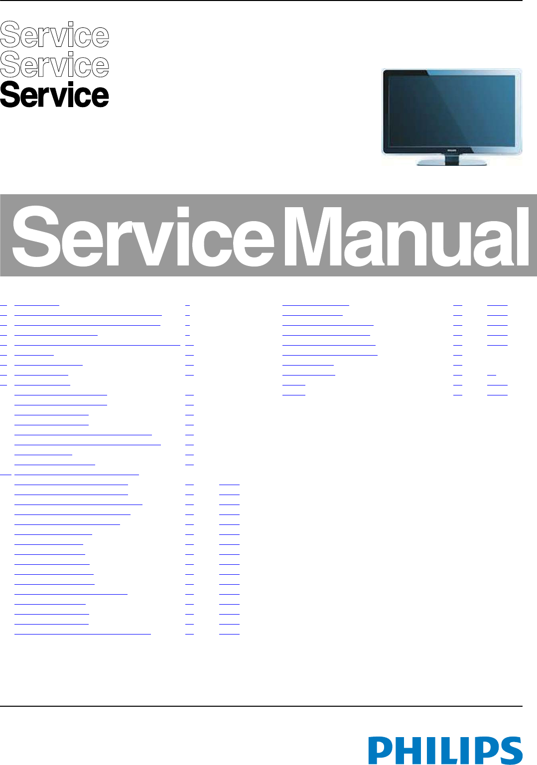
- 2.3 Connections
- Figure 2-1 Connection overview
- 2.3.1 Rear and Side Connections
- 1 - AV In: Cinch: Video CVBS - In, Audio - In
- 2 - AV Out: Cinch: Video CVBS - Out, Audio - Out
- 3 - CVI: Cinch: Video YPbPr - In, Audio - In
- 4 - Aerial - In
- 5 - Service Connector (ComPair)
- 6 - HDMI1, 2 and 3 (optional): Digital Video, Digital Audio - In
- 7 - PC: VGA: Video RGB - In, Cinch: Audio - In
- 8 - S-Video (Hosiden): Video Y/C - In
- 8 - Cinch: Video CVBS - In, Audio - In
- 9 - Head phone - Out
- 10 - HDMI: Digital Video, Digital Audio - In
- 11 - Cinch: S/PDIF - Out
- 12 - RJ45 DATA2 (Xpress Box - In/Out)
- 13 - RJ12 DATA1 (HM-Link - In/Out)
- 14 - iBoard Service Connector (RS232-UART)
- 15 - Mini Jack: Bathroom speaker (8 W / 1 W - Output)
- 16 - Mini Jack: Digital Volume Control
- 17 - Mini Jack: AUX1 Audio - Out
- 17 - Mini Jack: AUX2 Audio - Out
- 2.4 Chassis Overview
- 3. Precautions, Notes, and Abbreviation List
- 3.1 Safety Instructions
- 3.2 Warnings
- 3.3 Notes
- 3.4 Abbreviation List
- 4. Mechanical Instructions
- 5. Service Modes, Error Codes, and Fault Finding
- 6. Alignments
- 7. Circuit Descriptions
- 8. IC Data Sheets
- 8.1 IC Data Sheets
- 8.1.1 Diagram B03, Type TDA9886T (IC7113), IF-PLL demodulator
- 8.1.2 Diagram B07A, Type SIL9185 (IC7M07), HDMI switch
- 8.1.3 Diagram B07B, Type SIL9125 (IC7N01), HDMI receiver
- 8.1.4 Diagram B04A, Type SVP WX69 (IC7C01), Trident Video processor
- 8.1.5 Diagram B05A, Type MSP4450P (IC7411), Micronas Sound Processor
- 8.1.6 Diagram B05B, Type TDA8932T (IC7A01), Audio Amplifier
- 8.1.7 Diagram HC01, Type ST3232C (IC7107), RS232 Driver
- 8.1.8 Diagram HC01, Type NCP303LSN45 (IC7103), Voltage Detector
- 8.1.9 Diagram HC01, Type ST1S10 (IC7125), Stepdown Regulator
- 8.1 IC Data Sheets
- 9. Block Diagrams
- Wiring Diagram 32" (ME8)
- Wiring Diagram 42" (ME8)
- Block Diagram Video
- Block Diagram Audio
- Block Diagram Control & Clock Signals
- SSB: Test Points (Overview Bottom Side)
- SSB: Test Points (Part 1 Bottom Side)
- SSB: Test Points (Part 2 Bottom Side)
- SSB: Test Points (Part 3 Bottom Side)
- SSB: Test Points (Part 4 Bottom Side)
- I2C IC Overview
- Supply Lines Overview
- 10. Circuit Diagrams and PWB Layouts
- Main Power Supply (42"): Part 1
- Main Power Supply (42"): Part 2
- Layout Main Power Supply (42") (Top Side)
- Layout Main Power Supply (42") (Bottom Side)
- SSB: DC/DC +3V3, +1V2, & +VTUN
- SSB: DC/DC +5V, +1V8, & +2V5
- SSB: Tuner IF & Demodulator
- SSB: Micro Processor
- SSB: Trident WX69
- SSB: DDR Interface
- SSB: FPGA Interface
- SSB: FPGA I/O Banks
- SSB: LVDS Connector
- SSB: Audio Processor Micronas
- SSB: Audio Class-D
- SSB: YPbPr & SVHS
- SSB: I/O Cinch 1 & 2
- SSB: VGA, PC Audio, ComPair, UART
- SSB: HDMI Switch
- SSB: HDMI Main
- SSB: MJC MT8280 LVDS
- SSB: MJC MT8280 DDR
- SSB: MJC MT8280 Power
- SSB: SRP List Explanation
- SSB: SRP List
- Layout Small Signal Board (Overview Top Side)
- Layout Small Signal Board (Part 1 Top Side)
- Layout Small Signal Board (Part 2 Top Side)
- Layout Small Signal Board (Part 3 Top Side)
- Layout Small Signal Board (Part 4 Top Side)
- Layout Small Signal Board (Overview Bottom Side)
- Layout Small Signal Board (Part 1 Bottom Side)
- Layout Small Signal Board (Part 2 Bottom Side)
- Layout Small Signal Board (Part 3 Bottom Side)
- Layout Small Signal Board (Part 4 Bottom Side)
- IR / LED Panel
- Layout Front IR / LED Panel (Top Side)
- Layout Front IR / LED Panel (Bottom Side)
- iBoard
- iBoard
- Layout iBoard (Top side)
- Layout iBoard (Bottom side)
Published by JA/CC 0964 BU TV Consumer Care, the Netherlands Subject to modification EN 3122 785 18510
2009-Apr-10
©
Copyright 2009 Koninklijke Philips Electronics N.V.
All rights reserved. No part of this publication may be reproduced, stored in a
retrieval system or transmitted, in any form or by any means, electronic, mechanical,
photocopying, or otherwise without the prior permission of Philips.
Colour Television Chassis
LC8.2HA
LA
ME8ME8
I_17760_000.eps
040208
Contents Page Contents Page
1. Revision List 2
2. Technical Specifications and Connections 2
3. Precautions, Notes, and Abbreviation List 5
4. Mechanical Instructions 9
5. Service Modes, Error Codes, and Fault Finding 15
6. Alignments 26
7. Circuit Descriptions 29
8. IC Data Sheets 31
9. Block Diagrams
Wiring Diagram 32" (ME8) 39
Wiring Diagram 42" (ME8) 40
Block Diagram Video 41
Block Diagram Audio 42
Block Diagram Control & Clock Signals 43
SSB: Test Points (Overview Bottom Side) 44
I2C IC Overview 49
Supply Lines Overview 50
10. Circuit Diagrams and PWB Layouts Diagram PWB
Main Power Supply (42"): Part 1 (A1) 51 53-54
Main Power Supply (42"): Part 2 (A2) 52 53-54
SSB: DC/DC +3V3, +1V2, & +VTUN (B01A) 55 76-85
SSB: DC/DC +5V, +1V8, & +2V5 (B01B) 56 76-85
SSB: Tuner IF & Demodulator (B02) 57 76-85
SSB: Micro Processor (B03) 58 76-85
SSB: Trident WX69 (B04A) 59 76-85
SSB: DDR Interface (B04B) 60 76-85
SSB: FPGA Interface (B04C) 61 76-85
SSB: FPGA I/O Banks (B04D) 62 76-85
SSB: LVDS Connector (B04E) 63 76-85
SSB: Audio Processor Micronas (B05A) 64 76-85
SSB: Audio Class-D (B05B) 65 76-85
SSB: YPbPr & SVHS (B06A) 66 76-85
SSB: I/O Cinch 1 & 2 (B06B) 67 76-85
SSB: VGA, PC Audio, ComPair, UART (B06C) 68 76-85
SSB: HDMI Switch (B07A) 69 76-85
SSB: HDMI Main (B07B) 70 76-85
SSB: MJC MT8280 LVDS (B08A) 71 76-85
SSB: MJC MT8280 DDR (B08B) 72 76-85
SSB: MJC MT8280 Power (B08C) 73 76-85
SSB: SRP List Explanation 74
SSB: SRP List 75
IR / LED Panel (J) 86 87
iBoard (HC01) 88 90-91
iBoard (HC02) 89 90-91

Revision List
EN 2 LC8.2HA LA1.
2009-Apr-10
1. Revision List
Manual xxxx xxx xxxx.0
• First release.
2. Technical Specifications and Connections
Index of this chapter:
2.1 Technical Specifications
2.2 Directions for Use
2.3 Connections
2.4 Chassis Overview
Notes:
• Figures can deviate due to the different set executions.
• Specifications are indicative (subject to change).
2.1 Technical Specifications
For on-line product support please use the links in Table 2-1.
Here is product information available, as well as getting started,
user manuals, frequently asked questions and software &
drivers.
Table 2-1 Described Model numbers
2.2 Directions for Use
You can download this information from the following websites:
http://www.philips.com/support
http://www.p4c.philips.com
CTN Styling Published in:
32HFL5530/93 ME8 3122 785 18510
32HFL5530/97
42HFL5580/93
42HFL5580/97
Technical Specifications and Connections EN 3LC8.2HA LA 2.
2009-Apr-10
2.3 Connections
Figure 2-1 Connection overview
Note: The following connector colour abbreviations are used
(according to DIN/IEC 757): Bk= Black, Bu= Blue, Gn= Green,
Gy= Grey, Rd= Red, Wh= White, Ye= Yellow.
2.3.1 Rear and Side Connections
1 - AV In: Cinch: Video CVBS - In, Audio - In
Ye - Video CVBS 1 VPP / 75 Ω jq
Wh - Audio L 0.5 VRMS / 10 kΩ jq
Rd - Audio R 0.5 VRMS / 10 kΩ jq
2 - AV Out: Cinch: Video CVBS - Out, Audio - Out
Ye - Video CVBS 1 VPP / 75 Ω kq
Wh - Audio L 0.5 VRMS /10 kΩ kq
Rd - Audio R 0.5 VRMS / 10 kΩ kq
3 - CVI: Cinch: Video YPbPr - In, Audio - In
Gn - Video Y 1 VPP / 75 Ω jq
Bu - Video Pb 0.7 VPP / 75 Ω jq
Rd - Video Pr 0.7 VPP / 75 Ω jq
Wh - Audio L 0.5 VRMS / 10 kΩ jq
Rd - Audio R 0.5 VRMS / 10 kΩ jq
4 - Aerial - In
- - IEC-type (EU) Coax, 75 Ω D
5 - Service Connector (ComPair)
1 - SDA-S I2C Data (0 - 5 V) jk
2 - SCL-S I2C Clock (0 - 5 V) j
3 - Ground Gnd H
6 - HDMI1, 2 and 3 (optional): Digital Video, Digital Audio -
In
1 - D2+ Data channel j
2 - Shield Gnd H
3 - D2- Data channel j
4 - D1+ Data channel j
5 - Shield Gnd H
6 - D1- Data channel j
7 - D0+ Data channel j
8 - Shield Gnd H
9 - D0- Data channel j
10 - CLK+ Data channel j
11 - Shield Gnd H
12 - CLK- Data channel j
13 - n.c.
14 - n.c.
15 - DDC_SCL DDC clock j
16 - DDC_SDA DDC data jk
17 - Ground Gnd H
18 - +5V j
19 - HPD Hot Plug Detect j
20 - Ground Gnd H
7 - PC: VGA: Video RGB - In, Cinch: Audio - In
Figure 2-2 VGA Connector
1 - Video Red 0.7 VPP / 75 Ω j
2 - Video Green 0.7 VPP / 75 Ω j
3 - Video Blue 0.7 VPP / 75 Ω j
4-n.c.
5 - Ground Gnd H
6 - Ground Red Gnd H
7 - Ground Green Gnd H
8 - Ground Blue Gnd H
9-+5V
DC +5 V j
10 - Ground Sync Gnd H
11 - n.c.
12 - DDC_SDA DDC data j
13 - H-sync 0 - 5 V j
14 - V-sync 0 - 5 V j
15 - DDC_SCL DDC clock j
Wh - Audio L 0.5 VRMS / 10 kΩ jq
Rd - Audio R 0.5 VRMS / 10 kΩ jq
Y
L
R
HDMI 2 HDMI 3
CVI AV INAV O UT
VIDEO
L
R
L
Pr
SERV. C
R
VIDEO
HDMI 1
TV ANTENNA
75X
RL
AUDIO IN VGA
SPDIF OUT
AUX AUDIO
OUT 1
AUX AUDIO
OUT 2
DIGITAL VOLUME
CONTROL
RS 232
DATA 2
(RJ45) DATA 1 (RJ12)
SMARTPLUG
8
18510_001_090406.eps
090406
321
4
5
6
7
8
9
10
11
12 1314
151617
1
610
11
5
15
E_06532_002.eps
171108

Technical Specifications and Connections
EN 4 LC8.2HA LA2.
2009-Apr-10
8 - S-Video (Hosiden): Video Y/C - In
1 - Ground Y Gnd H
2 - Ground C Gnd H
3 - Video Y 1 VPP / 75 Ω j
4 - Video C 0.3 VPPP / 75 Ω j
8 - Cinch: Video CVBS - In, Audio - In
Ye - Video CVBS 1 VPP / 75 Ω jq
Wh - Audio L 0.5 VRMS / 10 kΩ jq
Rd - Audio R 0.5 VRMS / 10 kΩ jq
9 - Head phone - Out
Bk - Head phone 32 - 600 Ω / 10 mW rt
10 - HDMI: Digital Video, Digital Audio - In
Figure 2-3 HDMI (type A) connector
1 - D2+ Data channel j
2 - Shield Gnd H
3 - D2- Data channel j
4 - D1+ Data channel j
5 - Shield Gnd H
6 - D1- Data channel j
7 - D0+ Data channel j
8 - Shield Gnd H
9 - D0- Data channel j
10 - CLK+ Data channel j
11 - Shield Gnd H
12 - CLK- Data channel j
13 - n.c.
14 - n.c.
15 - DDC_SCL DDC clock j
16 - DDC_SDA DDC data jk
17 - Ground Gnd H
18 - +5V j
19 - HPD Hot Plug Detect j
20 - Ground Gnd H
11 - Cinch: S/PDIF - Out
Bk - Coaxial 0.4 - 0.6VPP / 75 ohm kq
12 - RJ45 DATA2 (Xpress Box - In/Out)
1 - +12V +12V/1W k
2 - Gnd Gnd H
3 - TXD Send k
4 - RXD Receive j
5 - TXD232 Send k
6 - RXD232 Receive j
7 - SDA3_IR-OUT Signal k
8 - POR (*) Signal k
9 - CVBS-terr Signal k
10 - Gnd Gnd H
(*) POR= Power On Reset
13 - RJ12 DATA1 (HM-Link - In/Out)
1 - LED-in_SCL < 0.3 V, active low j
2 - IR-in_SDA < 0.3 V, active low j
3 - MODE_HP-DET Vcc j
4 - TV Power Status 4.5 to 5 V: TV “On”
< 0.3 V: TV “Stdby”
High impedance: TV “Off” k
5 - Gnd Gnd H
6 - IR-out Signal k
14 - iBoard Service Connector (RS232-UART)
Figure 2-4 RS232 Connector
1-n.c.
2 - RXD232 Receive j
3 - TXD232 Send k
4-n.c.
5 - Gnd Ground H
6-n.c.
7-n.c.
8-n.c.
9-n.c.
15 - Mini Jack: Bathroom speaker (8 W / 1 W - Output)
1 - Control Signal OUT- ko
2 - Control Signal OUT+ ko
3 - Control Signal OUT+ ko
16 - Mini Jack: Digital Volume Control
1 - Control Signal Up/Down jo
2 - Vcc +5V_AUD ko
3 - Ground Gnd Ho
17 - Mini Jack: AUX1 Audio - Out
1 - Ground Gnd Ho
2 - Control Signal HP-DETECT ko
3 - Audio R 0.2 - 2 VRMS / 10 kohm ko
4 - Audio L 0.2 - 2 VRMS / 10 kohm ko
17 - Mini Jack: AUX2 Audio - Out
1 - Ground Gnd Ho
2 - Control Signal HP-DETECT ko
3 - Audio R 0.2 - 2 VRMS / 10 kohm ko
4 - Audio L 0.2 - 2 VRMS / 10 kohm ko
2.4 Chassis Overview
Refer to chapter “Block Diagrams” for PWB/CBA locations.
19 1
18 2
E_06532_017.eps
250505
5
1
69
E_06532_005.eps
171108

Precautions, Notes, and Abbreviation List EN 5LC8.2HA LA 3.
2009-Apr-10
3. Precautions, Notes, and Abbreviation List
Index of this chapter:
3.1 Safety Instructions
3.2 Warnings
3.3 Notes
3.4 Abbreviation List
3.1 Safety Instructions
Safety regulations require the following during a repair:
• Connect the set to the Mains/AC Power via an isolation
transformer (> 800 VA).
• Replace safety components, indicated by the symbol h,
only by components identical to the original ones. Any
other component substitution (other than original type) may
increase risk of fire or electrical shock hazard. Of de set
ontploft!
Safety regulations require that after a repair, the set must be
returned in its original condition. Pay in particular attention to
the following points:
• Route the wire trees correctly and fix them with the
mounted cable clamps.
• Check the insulation of the Mains/AC Power lead for
external damage.
• Check the strain relief of the Mains/AC Power cord for
proper function.
• Check the electrical DC resistance between the Mains/AC
Power plug and the secondary side (only for sets that have
a Mains/AC Power isolated power supply):
1. Unplug the Mains/AC Power cord and connect a wire
between the two pins of the Mains/AC Power plug.
2. Set the Mains/AC Power switch to the “on” position
(keep the Mains/AC Power cord unplugged!).
3. Measure the resistance value between the pins of the
Mains/AC Power plug and the metal shielding of the
tuner or the aerial connection on the set. The reading
should be between 4.5 MΩ and 12 MΩ.
4. Switch “off” the set, and remove the wire between the
two pins of the Mains/AC Power plug.
• Check the cabinet for defects, to prevent touching of any
inner parts by the customer.
3.2 Warnings
• All ICs and many other semiconductors are susceptible to
electrostatic discharges (ESD w). Careless handling
during repair can reduce life drastically. Make sure that,
during repair, you are connected with the same potential as
the mass of the set by a wristband with resistance. Keep
components and tools also at this same potential.
• Be careful during measurements in the high voltage
section.
• Never replace modules or other components while the unit
is switched “on”.
• When you align the set, use plastic rather than metal tools.
This will prevent any short circuits and the danger of a
circuit becoming unstable.
3.3 Notes
3.3.1 General
• Measure the voltages and waveforms with regard to the
chassis (= tuner) ground (H), or hot ground (I), depending
on the tested area of circuitry. The voltages and waveforms
shown in the diagrams are indicative. Measure them in the
Service Default Mode with a colour bar signal and stereo
sound (L: 3 kHz, R: 1 kHz unless stated otherwise) and
picture carrier at 475.25 MHz for PAL, or 61.25 MHz for
NTSC (channel 3).
• Where necessary, measure the waveforms and voltages
with (D) and without (E) aerial signal. Measure the
voltages in the power supply section both in normal
operation (G) and in stand-by (F). These values are
indicated by means of the appropriate symbols.
3.3.2 Schematic Notes
• All resistor values are in ohms, and the value multiplier is
often used to indicate the decimal point location (e.g. 2K2
indicates 2.2 kΩ).
• Resistor values with no multiplier may be indicated with
either an “E” or an “R” (e.g. 220E or 220R indicates 220 Ω).
• All capacitor values are given in micro-farads (μ=× 10-6),
nano-farads (n =× 10-9), or pico-farads (p =× 10-12).
• Capacitor values may also use the value multiplier as the
decimal point indication (e.g. 2p2 indicates 2.2 pF).
• An “asterisk” (*) indicates component usage varies. Refer
to the diversity tables for the correct values.
• The correct component values are listed on the Philips
Spare Parts Web Portal.
3.3.3 Spare Parts
For the latest spare part overview, consult your Philips Spare
Part web portal.
3.3.4 BGA (Ball Grid Array) ICs
Introduction
For more information on how to handle BGA devices, visit this
URL: http://www.atyourservice-magazine.com. Select
“Magazine”, then go to “Repair downloads”. Here you will find
Information on how to deal with BGA-ICs.
BGA Temperature Profiles
For BGA-ICs, you must use the correct temperature-profile.
Where applicable and available, this profile is added to the IC
Data Sheet information section in this manual.
3.3.5 Lead-free Soldering
Due to lead-free technology some rules have to be respected
by the workshop during a repair:
• Use only lead-free soldering tin. If lead-free solder paste is
required, please contact the manufacturer of your soldering
equipment. In general, use of solder paste within
workshops should be avoided because paste is not easy to
store and to handle.
• Use only adequate solder tools applicable for lead-free
soldering tin. The solder tool must be able:
– To reach a solder-tip temperature of at least 400°C.
– To stabilize the adjusted temperature at the solder-tip.
– To exchange solder-tips for different applications.
• Adjust your solder tool so that a temperature of around
360°C - 380°C is reached and stabilized at the solder joint.
Heating time of the solder-joint should not exceed ~ 4 sec.
Avoid temperatures above 400°C, otherwise wear-out of
tips will increase drastically and flux-fluid will be destroyed.
To avoid wear-out of tips, switch “off” unused equipment or
reduce heat.
• Mix of lead-free soldering tin/parts with leaded soldering
tin/parts is possible but PHILIPS recommends strongly to
avoid mixed regimes. If this cannot be avoided, carefully
clear the solder-joint from old tin and re-solder with new tin.

Precautions, Notes, and Abbreviation List
EN 6 LC8.2HA LA3.
2009-Apr-10
3.3.6 Alternative BOM identification
It should be noted that on the European Service website,
“Alternative BOM” is referred to as “Design variant”.
The third digit in the serial number (example:
AG2B0335000001) indicates the number of the alternative
B.O.M. (Bill Of Materials) that has been used for producing the
specific TV set. In general, it is possible that the same TV
model on the market is produced with e.g. two different types
of displays, coming from two different suppliers. This will then
result in sets which have the same CTN (Commercial Type
Number; e.g. 28PW9515/12) but which have a different B.O.M.
number.
By looking at the third digit of the serial number, one can
identify which B.O.M. is used for the TV set he is working with.
If the third digit of the serial number contains the number “1”
(example: AG1B033500001), then the TV set has been
manufactured according to B.O.M. number 1. If the third digit is
a “2” (example: AG2B0335000001), then the set has been
produced according to B.O.M. no. 2. This is important for
ordering the correct spare parts!
For the third digit, the numbers 1...9 and the characters A...Z
can be used, so in total: 9 plus 26= 35 different B.O.M.s can be
indicated by the third digit of the serial number.
Identification: The bottom line of a type plate gives a 14-digit
serial number. Digits 1 and 2 refer to the production centre (e.g.
AG is Bruges), digit 3 refers to the B.O.M. code, digit 4 refers
to the Service version change code, digits 5 and 6 refer to the
production year, and digits 7 and 8 refer to production week (in
example below it is 2006 week 17). The 6 last digits contain the
serial number.
Figure 3-1 Serial number (example)
3.3.7 Board Level Repair (BLR) or Component Level Repair
(CLR)
If a board is defective, consult your repair procedure to decide
if the board has to be exchanged or if it should be repaired on
component level.
If your repair procedure says the board should be exchanged
completely, do not solder on the defective board. Otherwise, it
cannot be returned to the O.E.M. supplier for back charging!
3.3.8 Practical Service Precautions
•It makes sense to avoid exposure to electrical shock.
While some sources are expected to have a possible
dangerous impact, others of quite high potential are of
limited current and are sometimes held in less regard.
•Always respect voltages. While some may not be
dangerous in themselves, they can cause unexpected
reactions that are best avoided. Before reaching into a
powered TV set, it is best to test the high voltage insulation.
It is easy to do, and is a good service precaution.
3.4 Abbreviation List
0/6/12 SCART switch control signal on A/V
board. 0 = loop through (AUX to TV),
6 = play 16 : 9 format, 12 = play 4 : 3
format
AARA Automatic Aspect Ratio Adaptation:
algorithm that adapts aspect ratio to
remove horizontal black bars; keeps
the original aspect ratio
ACI Automatic Channel Installation:
algorithm that installs TV channels
directly from a cable network by
means of a predefined TXT page
ADC Analogue to Digital Converter
AFC Automatic Frequency Control: control
signal used to tune to the correct
frequency
AGC Automatic Gain Control: algorithm that
controls the video input of the feature
box
AM Amplitude Modulation
AP Asia Pacific
AR Aspect Ratio: 4 by 3 or 16 by 9
ASF Auto Screen Fit: algorithm that adapts
aspect ratio to remove horizontal black
bars without discarding video
information
ATSC Advanced Television Systems
Committee, the digital TV standard in
the USA
ATV See Auto TV
Auto TV A hardware and software control
system that measures picture content,
and adapts image parameters in a
dynamic way
AV External Audio Video
AVC Audio Video Controller
AVIP Audio Video Input Processor
B/G Monochrome TV system. Sound
carrier distance is 5.5 MHz
BLR Board-Level Repair
BTSC Broadcast Television Standard
Committee. Multiplex FM stereo sound
system, originating from the USA and
used e.g. in LATAM and AP-NTSC
countries
B-TXT Blue TeleteXT
C Centre channel (audio)
CEC Consumer Electronics Control bus:
remote control bus on HDMI
connections
CL Constant Level: audio output to
connect with an external amplifier
CLR Component Level Repair
ComPair Computer aided rePair
CP Connected Planet / Copy Protection
CSM Customer Service Mode
CTI Color Transient Improvement:
manipulates steepness of chroma
transients
CVBS Composite Video Blanking and
Synchronization
DAC Digital to Analogue Converter
DBE Dynamic Bass Enhancement: extra
low frequency amplification
DDC See “E-DDC”
D/K Monochrome TV system. Sound
carrier distance is 6.5 MHz
DFI Dynamic Frame Insertion
DFU Directions For Use: owner's manual
DMR Digital Media Reader: card reader
DMSD Digital Multi Standard Decoding
DNM Digital Natural Motion
10000_024_090121.eps
090121
MODEL :
PROD.NO:
~
S
32PF9968/10
MADE IN BELGIUM
220-240V 50/60Hz
128W
AG 1A0617 000001
VHF+S+H+UHF
BJ3.0E LA

Precautions, Notes, and Abbreviation List EN 7LC8.2HA LA 3.
2009-Apr-10
DNR Digital Noise Reduction: noise
reduction feature of the set
DRAM Dynamic RAM
DRM Digital Rights Management
DSP Digital Signal Processing
DST Dealer Service Tool: special remote
control designed for service
technicians
DTCP Digital Transmission Content
Protection; A protocol for protecting
digital audio/video content that is
traversing a high speed serial bus,
such as IEEE-1394
DVB-C Digital Video Broadcast - Cable
DVB-T Digital Video Broadcast - Terrestrial
DVD Digital Versatile Disc
DVI(-d) Digital Visual Interface (d= digital only)
E-DDC Enhanced Display Data Channel
(VESA standard for communication
channel and display). Using E-DDC,
the video source can read the EDID
information form the display.
EDID Extended Display Identification Data
(VESA standard)
EEPROM Electrically Erasable and
Programmable Read Only Memory
EMI Electro Magnetic Interference
EPLD Erasable Programmable Logic Device
EU Europe
EXT EXTernal (source), entering the set by
SCART or by cinches (jacks)
FDS Full Dual Screen (same as FDW)
FDW Full Dual Window (same as FDS)
FLASH FLASH memory
FM Field Memory or Frequency
Modulation
FPGA Field-Programmable Gate Array
FTV Flat TeleVision
Gb/s Giga bits per second
G-TXT Green TeleteXT
H H_sync to the module
HD High Definition
HDD Hard Disk Drive
HDCP High-bandwidth Digital Content
Protection: A “key” encoded into the
HDMI/DVI signal that prevents video
data piracy. If a source is HDCP coded
and connected via HDMI/DVI without
the proper HDCP decoding, the
picture is put into a “snow vision” mode
or changed to a low resolution. For
normal content distribution the source
and the display device must be
enabled for HDCP “software key”
decoding.
HDMI High Definition Multimedia Interface
HP HeadPhone
I Monochrome TV system. Sound
carrier distance is 6.0 MHz
I2C Inter IC bus
I2D Inter IC Data bus
I2S Inter IC Sound bus
IF Intermediate Frequency
IR Infra Red
IRQ Interrupt Request
ITU-656 The ITU Radio communication Sector
(ITU-R) is a standards body
subcommittee of the International
Telecommunication Union relating to
radio communication. ITU-656 (a.k.a.
SDI), is a digitized video format used
for broadcast grade video.
Uncompressed digital component or
digital composite signals can be used.
The SDI signal is self-synchronizing,
uses 8 bit or 10 bit data words, and has
a maximum data rate of 270 Mbit/s,
with a minimum bandwidth of 135
MHz.
ITV Institutional TeleVision; TV sets for
hotels, hospitals etc.
LS Last Status; The settings last chosen
by the customer and read and stored
in RAM or in the NVM. They are called
at start-up of the set to configure it
according to the customer's
preferences
LATAM Latin America
LCD Liquid Crystal Display
LED Light Emitting Diode
L/L' Monochrome TV system. Sound
carrier distance is 6.5 MHz. L' is Band
I, L is all bands except for Band I
LPL LG.Philips LCD (supplier)
LS Loudspeaker
LVDS Low Voltage Differential Signalling
Mbps Mega bits per second
M/N Monochrome TV system. Sound
carrier distance is 4.5 MHz
MIPS Microprocessor without Interlocked
Pipeline-Stages; A RISC-based
microprocessor
MOP Matrix Output Processor
MOSFET Metal Oxide Silicon Field Effect
Transistor, switching device
MPEG Motion Pictures Experts Group
MPIF Multi Platform InterFace
MUTE MUTE Line
NC Not Connected
NICAM Near Instantaneous Compounded
Audio Multiplexing. This is a digital
sound system, mainly used in Europe.
NTC Negative Temperature Coefficient,
non-linear resistor
NTSC National Television Standard
Committee. Color system mainly used
in North America and Japan. Color
carrier NTSC M/N= 3.579545 MHz,
NTSC 4.43= 4.433619 MHz (this is a
VCR norm, it is not transmitted off-air)
NVM Non-Volatile Memory: IC containing
TV related data such as alignments
O/C Open Circuit
OSD On Screen Display
OTC On screen display Teletext and
Control; also called Artistic (SAA5800)
P50 Project 50: communication protocol
between TV and peripherals
PAL Phase Alternating Line. Color system
mainly used in West Europe (color
carrier= 4.433619 MHz) and South
America (color carrier PAL M=
3.575612 MHz and PAL N= 3.582056
MHz)
PCB Printed Circuit Board (same as “PWB”)
PCM Pulse Code Modulation
PDP Plasma Display Panel
PFC Power Factor Corrector (or Pre-
conditioner)
PIP Picture In Picture
PLL Phase Locked Loop. Used for e.g.
FST tuning systems. The customer
can give directly the desired frequency
POD Point Of Deployment: a removable
CAM module, implementing the CA
system for a host (e.g. a TV-set)
POR Power On Reset, signal to reset the uP
PTC Positive Temperature Coefficient,
non-linear resistor
PWB Printed Wiring Board (same as “PCB”)

Precautions, Notes, and Abbreviation List
EN 8 LC8.2HA LA3.
2009-Apr-10
PWM Pulse Width Modulation
QRC Quasi Resonant Converter
QTNR Quality Temporal Noise Reduction
QVCP Quality Video Composition Processor
RAM Random Access Memory
RGB Red, Green, and Blue. The primary
color signals for TV. By mixing levels
of R, G, and B, all colors (Y/C) are
reproduced.
RC Remote Control
RC5 / RC6 Signal protocol from the remote
control receiver
RESET RESET signal
ROM Read Only Memory
RSDS Reduced Swing Differential Signalling
data interface
R-TXT Red TeleteXT
SAM Service Alignment Mode
S/C Short Circuit
SCART Syndicat des Constructeurs
d'Appareils Radiorécepteurs et
Téléviseurs
SCL Serial Clock I2C
SCL-F CLock Signal on Fast I2C bus
SD Standard Definition
SDA Serial Data I2C
SDA-F DAta Signal on Fast I2C bus
SDI Serial Digital Interface, see “ITU-656”
SDRAM Synchronous DRAM
SECAM SEequence Couleur Avec Mémoire.
Color system mainly used in France
and East Europe. Color carriers=
4.406250 MHz and 4.250000 MHz
SIF Sound Intermediate Frequency
SMPS Switched Mode Power Supply
SoC System on Chip
SOG Sync On Green
SOPS Self Oscillating Power Supply
SPI Serial Peripheral Interface bus; a 4-
wire synchronous serial data link
standard
S/PDIF Sony Philips Digital InterFace
SRAM Static RAM
SRP Service Reference Protocol
SSB Small Signal Board
STBY STand-BY
SVGA 800x600 (4:3)
SVHS Super Video Home System
SW Software
SWAN Spatial temporal Weighted Averaging
Noise reduction
SXGA 1280x1024
TFT Thin Film Transistor
THD Total Harmonic Distortion
TMDS Transmission Minimized Differential
Signalling
TXT TeleteXT
TXT-DW Dual Window with TeleteXT
UI User Interface
uP Microprocessor
UXGA 1600x1200 (4:3)
V V-sync to the module
VESA Video Electronics Standards
Association
VGA 640x480 (4:3)
VL Variable Level out: processed audio
output toward external amplifier
VSB Vestigial Side Band; modulation
method
WYSIWYR What You See Is What You Record:
record selection that follows main
picture and sound
WXGA 1280x768 (15:9)
XTAL Quartz crystal
XGA 1024x768 (4:3)
Y Luminance signal
Y/C Luminance (Y) and Chrominance (C)
signal
YPbPr Component video. Luminance and
scaled color difference signals (B-Y
and R-Y)
YUV Component video
Mechanical Instructions EN 9LC8.2HA LA 4.
2009-Apr-10
4. Mechanical Instructions
Index of this chapter:
4.1 Cable Dressing
4.2 Service Positions
4.3 Assy/Panel Removal ME8 Styling
4.4 Set Re-assembly
Notes:
• Figures below can deviate slightly from the actual situation,
due to the different set executions.
• Follow the disassemble instructions in described order.
4.1 Cable Dressing
Figure 4-1 Cable dressing 32-inch sets
18510_206_090407.eps
090407
Mechanical Instructions
EN 10 LC8.2HA LA4.
2009-Apr-10
Figure 4-2 Cable dressing 42-inch sets
18510_205_090407.eps
090407
Mechanical Instructions EN 11LC8.2HA LA 4.
2009-Apr-10
4.2 Service Positions
For easy servicing of this set, there are a few possibilities
created:
• The buffers from the packaging.
• Foam bars (created for Service).
4.2.1 Foam Bars
Figure 4-3 Foam bars
The foam bars (order code 3122 785 90580 for two pieces) can
be used for all types and sizes of Flat TVs.
See figure Figure 4-3 for details. Sets with a display of 42" and
larger, require four foam bars [1]. Ensure that the foam bars
are always supporting the cabinet and never only the display.
Caution: Failure to follow these guidelines can seriously
damage the display!
By laying the TV face down on the (ESD protective) foam bars,
a stable situation is created to perform measurements and
alignments. By placing a mirror under the TV, you can monitor
the screen.
4.3 Assy/Panel Removal ME8 Styling
4.3.1 Rear Cover
Warning:
• Disconnect the mains power cord before you remove the
rear cover.
• The speakers (located in the rear cover) should never be
(dis)connected when the set is playing! This can damage
the amplifiers on the SSB.
Note: it is not necessary to remove the stand while removing
the rear cover.
Removal sequence:
1. Remove all screws of the rear cover.
2. Lift the rear cover from the TV. Make sure that wires and
flat coils are not damaged while lifting the rear cover from
the set.
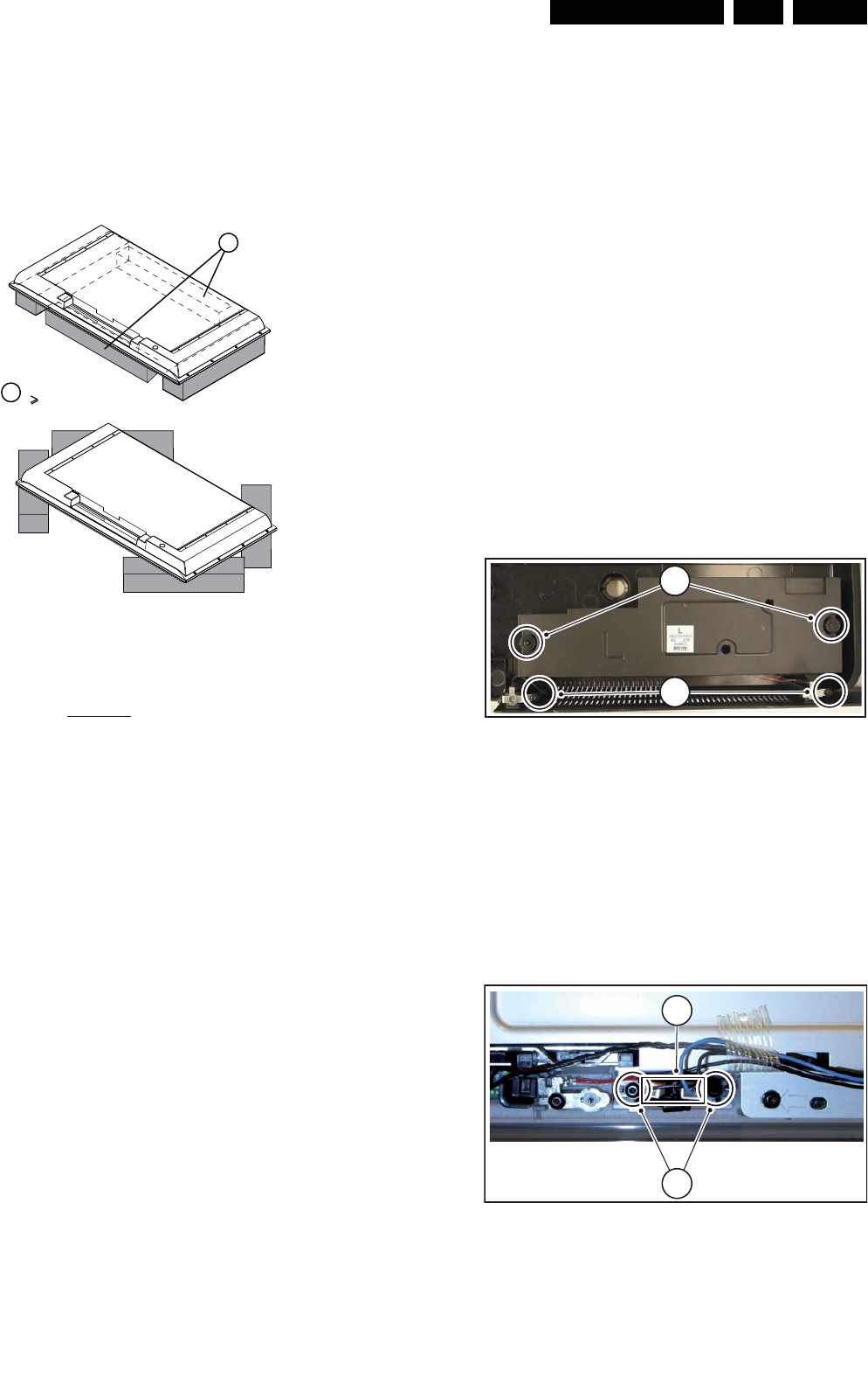
4.3.2 Woofers (in rear cover)
Refer to next figure for details.
1. Remove the screws [1] and [2] and lift the whole unit from
the rear cover.
Take the speakers out together with their casing. When
defective, replace the whole unit.
Figure 4-4 Woofer
4.3.3 Tweeters (if present)
Refer to next figure for details.
Warning: The speakers should never be connected or
disconnected when the set is playing! This can damage the
amplifiers on the SSB.
1. Release the connectors [1].
2. Remove the screws [2] and lift the whole unit from the set.
When defective, replace the whole unit.
Figure 4-5 Tweeter
10000_018_090121.eps
090121
1
Required for sets
42"
1
H_17740_023.eps
230108
32
31
H_17650_095.eps
180108
2
1
Mechanical Instructions
EN 12 LC8.2HA LA4.
2009-Apr-10
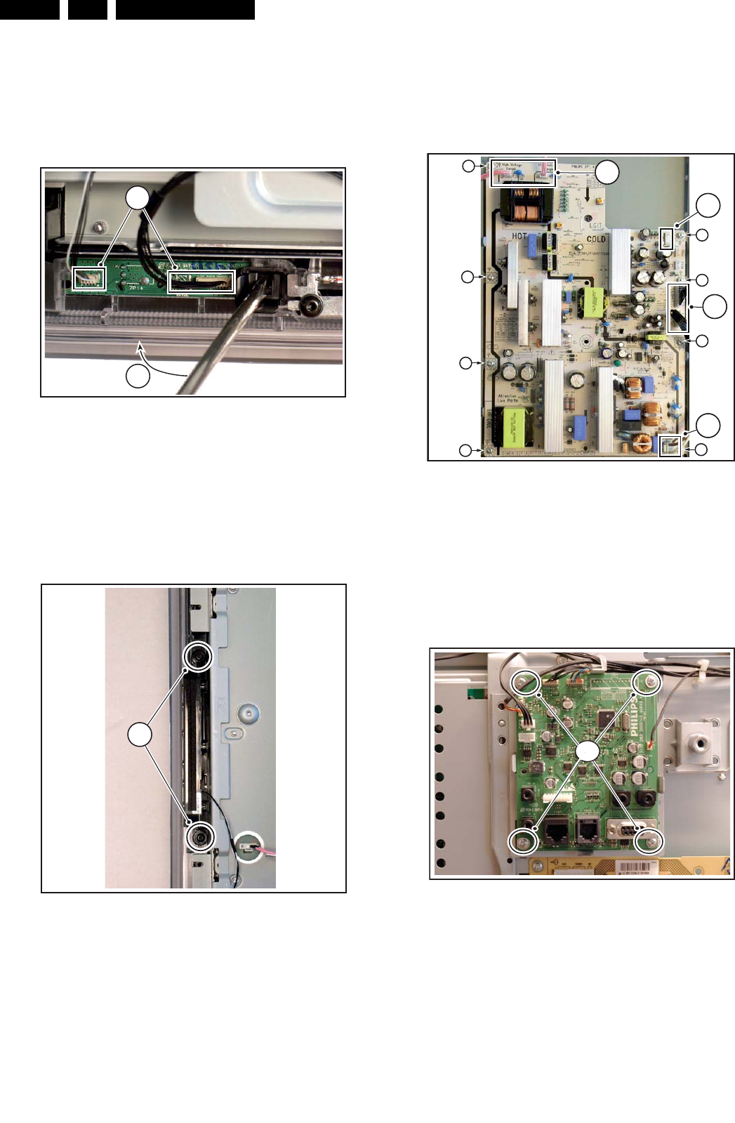
4.3.4 IR & LED Board
Refer to next figure for details.
1. Unplug connectors [1].
2. Use a flat screw driver to release the clip by pushing it in
the indicated direction [2].
3. Lift the board and take it out of the set.
When defective, replace the whole unit.
Figure 4-6 IR & LED Board
4.3.5 Key Board
Refer to next figure for details.
1. Unplug connectors.
2. Remove the screws [1].
3. Lift the unit and take it out of the set.
When defective, replace the whole unit.
Figure 4-7 Key Board
4.3.6 Display Supply Panel
Refer to next figure for details (is for 42” set, for other
screensizes the process might slightly deviate):
1. Unplug connectors [1].
2. Remove the fixation screws [2].
3. Take the board out.
Figure 4-8 Display Supply Panel (42” set)
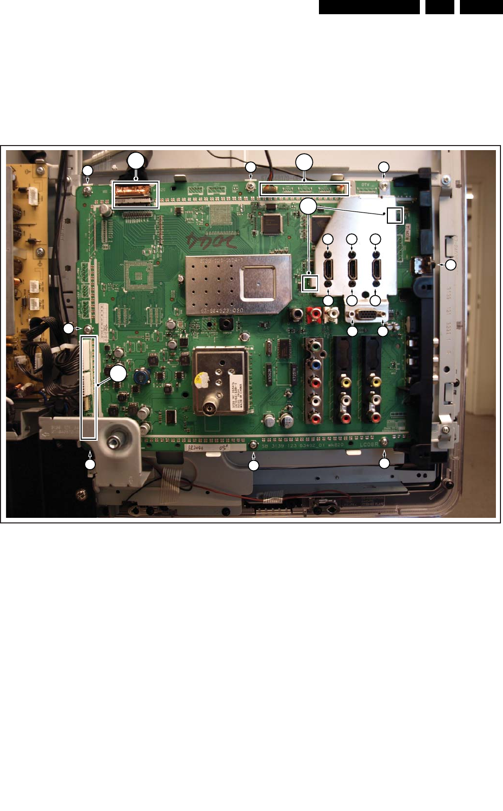
4.3.7 iBoard
Refer to next figure for details.
1. Unplug connectors.
2. Remove the screws [1].
3. Lift the unit and take it out of the set.
When defective, replace the whole unit.
Figure 4-9 iBoard
H_17650_098.eps
180108
2
1
H_17650_094.eps
180108
1
H_17740_021.eps
230108
1
1
2
2
2
2
2
2
2
2
1
1
18510_209_090409.eps
090409
1
Mechanical Instructions EN 13LC8.2HA LA 4.
2009-Apr-10
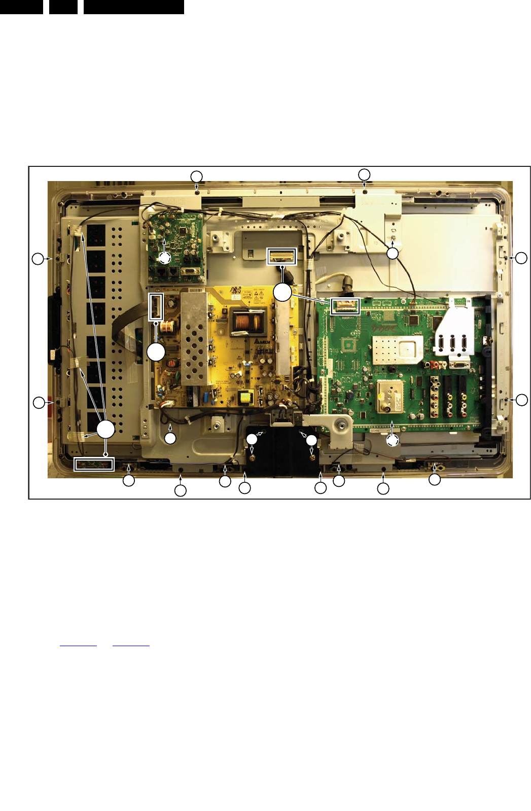
4.3.8 Small Signal Board (SSB)
Refer to next figure for details.
Caution: it is mandatory to remount all screws at their original
position during re-assembly. Failure to do so may result in
damaging the SSB.
1. Unplug the LVDS connector(s) [1].
Caution: be careful, as this is a very fragile connector!
2. Unplug the connectors [2].
3. Remove the screws [3].
4. The SSB can now be taken out of the set, together with the
front shield and the side cover.
5. To remove the shield, remove the screws [4] and lift it of
while releasing clips [5].
6. Remove screw [6] and slide the cover sidewards from the
SSB.
Figure 4-10 Small Signal Board
18510_207_090407.eps
090407
33
4 4 4
3
3
444
4 4
333
6
2
(
4x
)
5
12
(
2x
)
Mechanical Instructions
EN 14 LC8.2HA LA4.
2009-Apr-10
4.3.9 LCD Panel
Refer to next figures for details. Note that this description is
for the 32” model numbers. For other screensizes the
process might slightly deviate.
1. Remove the stand.
2. Unplug the LVDS connector(s)[1] and remove the adhesive
tape. Caution: be careful, as this is a very fragile
connector!
3. Unplug the IR/LED Panel [3] connectors and remove the
adhesive tapes.
4. Unplug the Inverter connector [4].
5. Unplug the Speaker cables at the “rim contacts” [5].
6. Remove the screws [6] that hold the complete subframe to
the front cabinet.
7. Remove the screws [7] that mount the subframe to the LCD
panel. In some sets some of these screws are hidden and
require further dismantling of the boards. This is for
instance the case with the screws hidden by the iBoard and
the SSB in the 32” sets.
8. If all these steps are taken, lift the complete subframe from
the set together with all panels.
9. The LCD panel can now be lifted from the front cabinet.
Figure 4-11 LCD Panel removal (32” sets)
4.4 Set Re-assembly
To re-assemble the whole set, execute all processes in reverse
order.
Notes:
• While re-assembling, make sure that all cables are placed
and connected in their original position.
See Figure 4-1and Figure 4-2.
• Pay special attention not to damage the EMC foams in the
set. Ensure that EMC foams are mounted correctly.
18510_208_090408.eps
090408
2
6
6
6
6
4
3
7
6
6
6
6
56
11
55
56
7
77
Service Modes, Error Codes, and Fault Finding EN 15LC8.2HA LA 5.
2009-Apr-10
5. Service Modes, Error Codes, and Fault Finding
Index of this chapter:
5.1 Test Points
5.2 Hotel mode
5.3 Service Modes
5.4 Service Tools
5.5 Error Codes
5.6 The Blinking LED Procedure
5.7 Software Upgrading
5.8 Fault Finding and Repair Tips
5.1 Test Points
In the chassis schematics and layout overviews, the test points
(Fxxx) are mentioned. In the schematics, test points are
indicated with a rectangular box around “Fxxx” or “Ixxx”, in the
layout overviews with a “half-moon” sign.
As most signals are digital, it will be difficult to measure
waveforms with a standard oscilloscope. Several key ICs are
capable of generating test patterns, which can be controlled via
ComPair. In this way it is possible to determine which part is
defective.
Perform measurements under the following conditions:
• Service Default Mode.
• Video: Colour bar signal.
• Audio: 3 kHz left, 1 kHz right.
5.2 Hotel mode
Before the service modes can be activated, the set first needs
to be switched into normal consumer mode (MTV-Mode). Use
an iTV setup remote control (type: RC2573/01, 12nc:
3139 228 88782) to key in the code ‘024995’ (slowly) directly
followed by the MENU button. The text messages “TV Is Now
In MTV Mode” and “Please Do A Cold Start!” appears on the
screen. Disconnect the set for a few seconds from the mains
supply, reconnect the set to the mains supply again. The set is
now in the normal consumer mode (MTV-Mode).
After repair, place the set into hotel mode (iTV-Mode) again.
Key-in the same code on the remote control as described
above. The text message “TV Is Now In ITV Mode” appears. A
cold start must be performed as described above. The set is
now in the hotel mode (iTV-Mode) again.
5.3 Service Modes
Service Default mode (SDM) and Service Alignment Mode
(SAM) offers several features for the service technician, while
the Customer Service Mode (CSM) is used for communication
between the call centre and the customer.
This chassis also offers the option of using ComPair, a
hardware interface between a computer and the TV chassis. It
offers the abilities of structured troubleshooting, error code
reading, and software version read-out for all chassis.
(see also section ComPair).
5.3.1 General
Some items are applicable to all Service Modes or are general.
These are listed below.
Life Timer
During the life time cycle of the TV set, a timer is kept. It counts
the normal operation hours (not the Stand-by hours). The
actual value of the timer is displayed in SDM and CSM in a
decimal value. Every two soft-resets increase the hour by +1.
Software Identification, Version, and Cluster
The software ID, version, and cluster will be shown in the main
menu display of SDM, SAM, and CSM.
The screen will show: “AAAAABCD X.YY”, where:
•AAAAA is the chassis name: LC82H.
•B is the region indication: E= Europe, A= AP/China, U=
NAFTA, L= LATAM.
•C is the display indication: L= LCD, P= Plasma.
•D is the language/feature indication: 1= standard, H=
1080p full HD.
•X is the main version number: this is updated with a major
change of specification (incompatible with the previous
software version). Numbering will go from 1 - 9 and A - Z.
– If the main version number changes, the new version
number is written in the NVM.
– If the main version number changes, the default
settings are loaded.
•YY is the sub version number: this is updated with a minor
change (backwards compatible with the previous versions)
Numbering will go from 00 - 99.
– If the sub version number changes, the new version
number is written in the NVM.
– If the NVM is fresh, the software identification, version,
and cluster will be written to NVM.
Display Option Code Selection
When after an SSB or display exchange, the display option
code is not set properly, it will result in a TV with “no display”.
Therefore, it is required to set this display option code after
such a repair.
To do so, press the following key sequence on a standard RC
transmitter: “062598” directly followed by MENU and “xxx”,
where “xxx” is a 3 digit decimal value of the panel type: see
column “Display code” in table 6-3 Option code overview, or
see sticker on the side/bottom of the cabinet. When the value
is accepted and stored in NVM, the set will switch to Stand-by,
to indicate that the process has been completed.
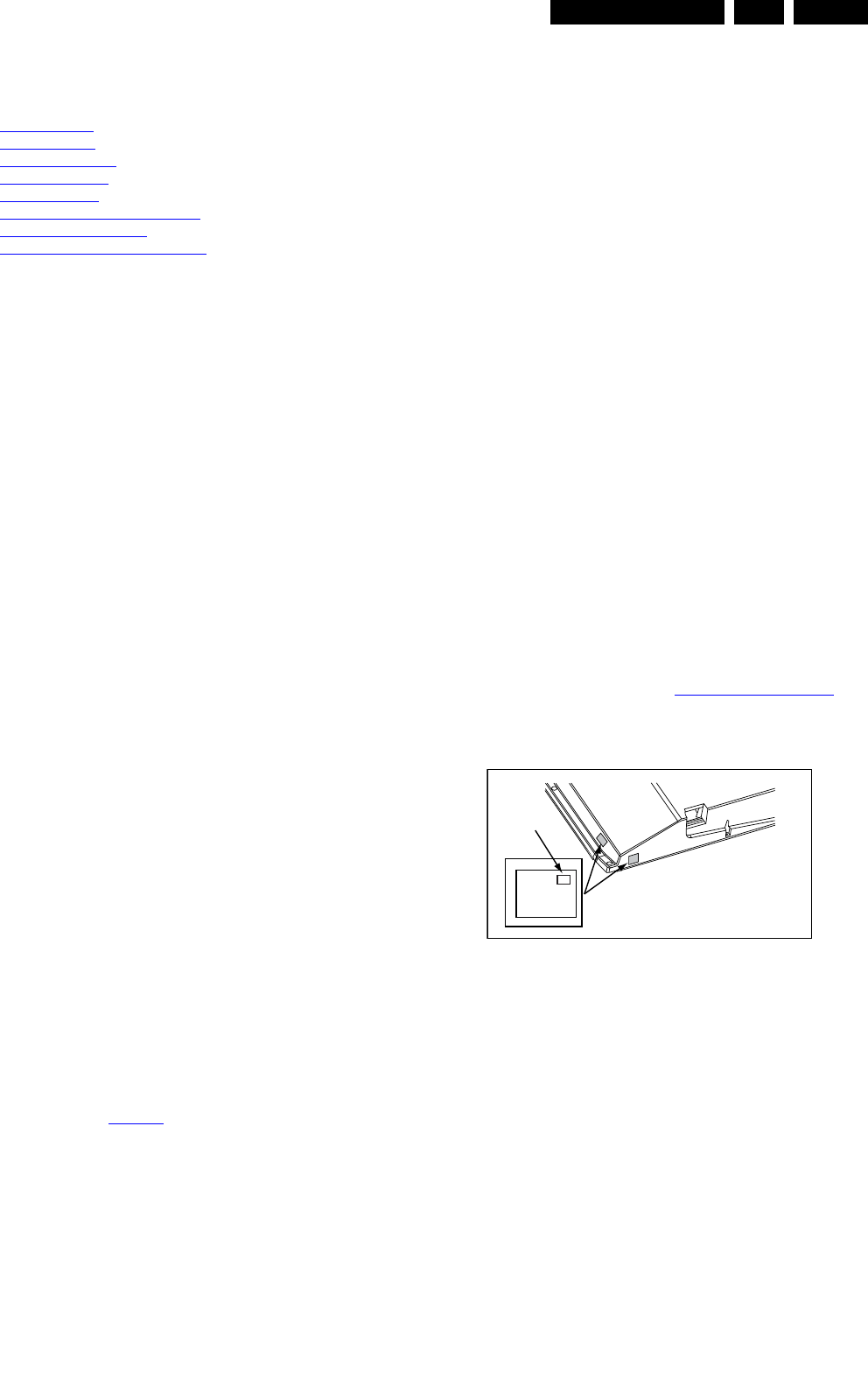
Figure 5-1 Location of Display Option Code sticker
During this algorithm, the NVM-content must be filtered,
because several items in the NVM are TV-related and not SSB-
related (e.g. Model and Prod. S/N). Therefore, “Model” and
“Prod. S/N” data is changed into “See Type Plate”.
In case a call centre or consumer reads “See Type Plate” in
CSM mode, he needs to look to the side/bottom sticker to
identify the set, for further actions.
PHILIPS
MODEL:
32PF9968/10
PROD.SERIAL NO:
AG 1A0620 000001
040
39mm
27mm
(CTN Sticker)
Display Option
Code
E_06532_038.eps
240108
Service Modes, Error Codes, and Fault Finding
EN 16 LC8.2HA LA5.
2009-Apr-10
5.3.2 Service Default Mode (SDM)
Purpose
Set the TV in SDM mode in order to be able to:
• Create a pre-defined setting for measurements to be
made.
• Override software protections.
• Start the blinking LED procedure.
• Read the error buffer.
• Check the life timer.
Specifications
Table 5-1 SDM default settings
• Set linear video and audio settings to 50%, but volume to
25%. Stored user settings are not affected.
• All service-unfriendly modes (if present) are disabled, since
they interfere with diagnosing/repairing a set. These
service unfriendly modes are:
– (Sleep) timer.
– Blue mute/Wall paper.
– Auto switch “off” (when there is no “ident” signal).
– Hotel or hospital mode.
– Child lock or parental lock (manual or via V-chip).
– Skipping, blanking of “Not favourite”, “Skipped” or
“Locked” presets/channels.
– Automatic storing of Personal Preset or Last Status
settings.
– Automatic user menu time-out (menu switches back/
OFF automatically.
– Auto Volume levelling (AVL).
How to Activate
To activate SDM, use one of the following methods:
• Press the following key sequence on the remote control
transmitter: “062596” directly followed by the MENU button
(do not allow the display to time out between entries while
keying the sequence).
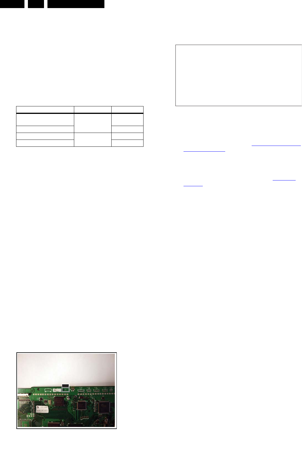
• Short (one of) the “Service” jumpers on the TV board
during cold start (see Figure “Service jumper”). Then press
the mains button (remove the short after start-up).
Caution: Activating SDM by shorting “Service” jumpers will
override the DC speaker protection (error 1), the General
I2C error (error 4), and the Trident video processor error
(error 5). When doing this, the service-technician must
know exactly what he is doing, as it could damage the
television set.
Figure 5-2 Service jumper (SSB component side)
On Screen Menu
After activating SDM, the following screen is visible, with SDM
in the upper right corner of the screen to indicate that the
television is in Service Default Mode.
Figure 5-3 SDM menu
Menu explanation:
•HHHHH: Are the operating hours (in decimal).
•AAAABCD-X.YY. See paragraph Software Identification,
Version, and Cluster for the SW name definition.
•SDM: The character “SDM” to indicate that the TV set is in
Service mode.
•ERR: Shows all errors detected since the last time the
buffer was erased. Five errors possible.
•OP: Used to read-out the option bytes. See Option Bit
Overview for a detailed description. Seven codes are
possible.
How to Navigate
As this mode is read only, there is not much to navigate. To
switch to other modes, use one of the following methods:
• Command MENU from the user remote will enter the
normal user menu (brightness, contrast, colour, etc...) with
“SDM” OSD remaining, and pressing MENU key again will
return to the last status of SDM again.
• To prevent the OSD from interfering with measurements in
SDM, command “OSD” (“STATUS” for NAFTA and
LATAM) from the user remote will toggle the OSD “on/off”
with “SDM” OSD remaining always “on”.
• Press the following key sequence on the remote control
transmitter: “062596” directly followed by the OSD/
STATUS/INFO/i+ button to switch to SAM (do not allow the
display to time out between entries while keying the
sequence).
How to Exit
Switch the set to STANDBY by pressing the mains button on
the remote control transmitter or on the television set.
If you switch the television set “off” by removing the mains (i.e.,
unplugging the television), the television set will remain in SDM
when mains is re-applied, and the error buffer is not cleared.
The error buffer will only be cleared when the “clear” command
is used in the SAM menu.
Note:
• If the TV is switched “off” by a power interrupt while in SDM,
the TV will show up in the last status of SDM menu as soon
as the power is supplied again. The error buffer will not be
cleared.
• In case the set is in Factory mode by accident (with “F”
displayed on screen), pressing and hold “VOL-” and “CH-”
together will leave Factory mode.
Region Freq. (MHz) Default syst.
Europe (except France),
AP-PAL/-Multi
475.25 PAL B/G
France SECAM L
NAFTA, AP-NTSC 61.25 (channel 3) NTSC M
LATAM PAL M
I_17760_046.eps
030308
SDM
SDM
HHHHH A A A A B C D- X . Y Y
ERR XX XX XX XX XX
O P X X X X X X X X X X X X X X X X X X
G_16860_030.eps
260107

Service Modes, Error Codes, and Fault Finding EN 17LC8.2HA LA 5.
2009-Apr-10
5.3.3 Service Alignment Mode (SAM)
Purpose
• To change option settings.
• To display / clear the error code buffer.
• To perform alignments.
Specifications
• Operation hours counter (maximum five digits displayed).
• Software version, error codes, and option settings display.
• Error buffer clearing.
• Option settings.
• Software alignments (Tuner, White Tone, and Audio).
• NVM Editor.
• ComPair Mode switching.
• Set the screen mode to full screen (all contents on screen
are viewable).
How to Activate
To activate SAM, use one of the following methods:
• Press the following key sequence on the remote control
transmitter: “062596” directly followed by the OSD/
STATUS/INFO/i+ button (it depends on region which
button is present on the RC). Do not allow the display to
time out between entries while keying the sequence.
• Or via ComPair.
After entering SAM, the following screen is visible, with SAM in
the upper right corner of the screen to indicate that the
television is in Service Alignment Mode.
Figure 5-4 SAM menu
Menu explanation:
1. LLLLL. This represents the run timer. The run timer counts
normal operation hours, but does not count Stand-by
hours.
2. AAAABCD-X.YY. See paragraph Software Identification,
Version, and Cluster for the SW name definition.
3. SAM. Indication of the Service Alignment Mode.
4. ERR (ERRor buffer). Shows all errors detected since the
last time the buffer was erased. Five errors possible.
5. OP (Option Bytes). Used to read-out the option bytes.
See Option Bit Overview for a detailed description. Seven
codes are possible.
6. Clear. Erases the contents of the error buffer. Select the
CLEAR menu item and press the MENU RIGHT key. The
content of the error buffer is cleared.
7. Options. Used to set the option bits.
See Option Bit Overview for a detailed description.
8. Tuner. Used to align the tuner.
See 6.3.1 Tuner Adjustment (RF AGC Take Over Point) for
a detailed description.
9. RGB Align. Used to align the White Tone. See 6.3.2 RGB
Alignment for a detailed description.
10. NVM Editor. Can be used to change the NVM data in the
television set. See also 5.8 Fault Finding and Repair Tips
further on.
11. ComPaIr. Can be used to switch the television to “In
Application Programming” mode (IAP), for software
uploading via ComPair. See also 5.4.1 ComPair.
Caution: When this mode is selected without ComPair
connected, the TV will be blocked. Remove the AC power
to reset the TV.
12. SW Events. Only to be used by development to monitor
SW behaviour during stress test.
How to Navigate
• In the SAM menu, select menu items with the MENU UP/
DOWN keys on the remote control transmitter. The
selected item will be indicated. When not all menu items fit
on the screen, use the MENU UP/DOWN keys to display
the next / previous menu items.
• With the MENU LEFT/RIGHT keys, it is possible to:
– Activate the selected menu item.
– Change the value of the selected menu item.
– Activate the selected sub menu.
• When you press the MENU button twice while in top level
SAM, the set will switch to the normal user menu (with the
SAM mode still active in the background). To return to the
SAM menu press the MENU button.
• Command OSD/STATUS/INFO/i+ button from the user
remote will toggle the OSD “on/off” with “SAM” OSD
remaining always “on”.
• Press the following key sequence on the remote control
transmitter: “062596” directly followed by the MENU button
to switch to SDM (do not allow the display to time out
between entries while keying the sequence).
How to Store SAM Settings
To store the settings changed in SAM mode (except the
OPTIONS settings), leave the top level SAM menu by using the
POWER button on the remote control transmitter or the
television set.
How to Exit
Switch the set to STANDBY by pressing the mains button on
the remote control transmitter or the television set.
Note:
• When the TV is switched “off” by a power interrupt while in
SAM, the TV will show up in “normal operation mode” as
soon as the power is supplied again. The error buffer will
not be cleared.
• In case the set is in Factory mode by accident (with “F”
displayed on screen), pressing and hold “VOL-” and “CH-”
together will leave Factory mode.
SAM
LLLL L A AAABCD- X. YY
ERR XX XX XX XX XX
O P X X X X X X X X X X X X X X X X X X
C l e a r > Y e s
O p t i o n s >
T u n e r >
R G B A l i g n >
N V M E d i t o r >
C o m p a i r >
S W E V E N T S >
G_16860_031.eps
260107

Service Modes, Error Codes, and Fault Finding
EN 18 LC8.2HA LA5.
2009-Apr-10
5.3.4 Customer Service Mode (CSM)
Purpose
The Customer Service Mode shows error codes and
information on the TV’s operation settings. A call centre can
instruct the customer (by telephone) to enter CSM in order to
identify the status of the set. This helps them to diagnose
problems and failures in the TV before making a service call.
The CSM is a read-only mode; therefore, modifications are not
possible in this mode.
Specifications
• Ignore “Service unfriendly modes”.
• Line number for every line (to make CSM language
independent).
• Set the screen mode to full screen (all contents on screen
are viewable).
• After leaving the Customer Service Mode, the original
settings are restored.
• Possibility to use “CH+” or “CH-” for channel surfing, or
enter the specific channel number on the RC.
How to Activate
To activate CSM, press the following key sequence on the
remote control transmitter: “123654” (do not allow the display
to time out between entries while keying the sequence).
Upon entering the Customer Service Mode, the following
screen will appear:
Figure 5-5 CSM menu -1- (example)
Figure 5-6 CSM menu -2- (example)
Menu Explanation
1. MODEL. Type number, e.g. 32PFL7762D/05. (*)
2. PROD S/N. Product serial no., e.g. AG1A0712123456. (*)
3. SW ID. Software cluster and version is displayed.
4. OP. Option code information.
5. CODES. Error buffer contents.
6. SSB. Indication of the SSB factory ID (= 12nc). (*)
7. NVM. The NVM software version no.
8. Flash Data. PQ (picture quality) and AQ (audio quality)
data version. This is a sub set of the main SW.
9. DISPLAY. Indication of the display ID (=12 nc).
10. TUNER. Indicates the tuner signal condition: “Weak” when
signal falls below threshold value, “Medium” when signal is
at mid-range, and “Strong” when signal falls above
threshold value.
11. SYSTEM. Gives information about the video system of the
selected transmitter (PAL/SECAM/NTSC).
12. SOUND. Gives information about the audio system of the
selected transmitter (MONO/STEREO/NICAM).
13. HDAU. HDMI audio stream detection. “YES” means audio
stream detected. “NO” means no audio stream present.
Only displayed when HDMI source is selected.
14. FORMAT. Gives information about the video format of the
selected transmitter (480i/480p/720p/1080i).
15. DFR SW ID. Referring to bolt-on SW ID.
16. FPGA FW. Only applicable to sets with an FPGA.
17. Reserved.
18. Reserved.
(*) If an NVM IC is replaced or initialised, the Model Number,
Serial Number, and SSB Code Number must be re-written to
the NVM. ComPair will foresee in a possibility to do this.
How to Exit
To exit CSM, use one of the following methods:
• Press the MENU button twice, or POWER button on the
remote control transmitter.
• Press the POWER button on the television set.
CS M
1 M O D E L : 4 2 P F L 7 4 0 3 / 9 3
2 P R O D S / N : AG1A0812123456
3 S W I D : L C 8 2 A L 1 - 1 . x x
4 O P : X X X X X X X X X X X X X X X X X X X X X
5 C O D E S : X X XX XX XX XX
6 S S B : 3 1 39 123 63491
7 N V M : X X X X X X X X
8 F l a s h D a t a : X X . X X . X X . X X
9 D I S P L A Y : xxxx xxx xxxxx
I_17760_026a.eps
120208
P A G E D O W N
B
y
CS M
1 0 T U N E R : W E A K / G O O D / S T R O N G
1 1 S Y S T E M : P A L / N T S C / S E C A M
1 2 S O U N D : M O N O / S T E R E O / N I C A M
1 3 H D A U : Y E S / N O
1 5 DFR SW ID : (*)
I_17760_026b.eps
120208
1 4 F O R M A T : X X X X X X X X
1 7 :
1 6 F P G A F W : xx.xx.xx
1 8 :
P A G E U P :
B
y
(*) referring to bolt-on DFI SW ID
Service Modes, Error Codes, and Fault Finding EN 19LC8.2HA LA 5.
2009-Apr-10
5.4 Service Tools
5.4.1 ComPair
Introduction
ComPair (Computer Aided Repair) is a Service tool for Philips
Consumer Electronics products. and offers the following:
1. ComPair helps you to quickly get an understanding on how
to repair the chassis in a short and effective way.
2. ComPair allows very detailed diagnostics and is therefore
capable of accurately indicating problem areas. You do not
have to know anything about I2C or UART commands
yourself, because ComPair takes care of this.
3. ComPair speeds up the repair time since it can
automatically communicate with the chassis (when the uP
is working) and all repair information is directly available.
4. ComPair features TV software up possibilities.
Specifications
ComPair consists of a Windows based fault finding program
and an interface box between PC and the (defective) product.
The (new) ComPair II interface box is connected to the PC via
an USB cable. For the TV chassis, the ComPair interface box
and the TV communicate via a bi-directional cable via the
service connector(s).
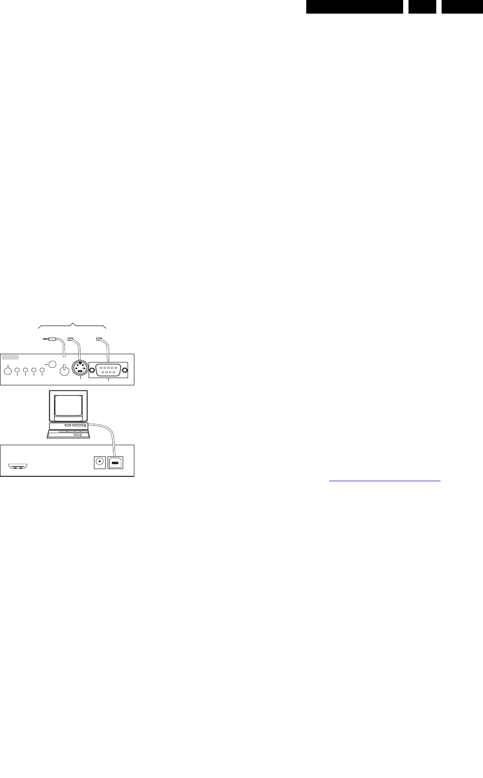
How to Connect
This is described in the ComPair chassis fault finding database.
Figure 5-7 ComPair II interface connection
Caution: It is compulsory to connect the TV to the PC as
shown in the picture above (with the ComPair interface in
between), as the ComPair interface acts as a level shifter. If
one connects the TV directly to the PC (via UART), ICs will be
blown!
How to Order
ComPair II order codes:
• ComPair II interface: 3122 785 91020.
• Software is available via the Philips Service web portal.
•ComPair I
2C interface cable: 9965 100 07325 (to be used
for upgrading the Main software).
Note: If you encounter any problems, contact your local
support desk.
5.4.2 LVDS Tool
Support of the LVDS Tool has been discontinued.
5.5 Error Codes
5.5.1 Introduction
Error codes are required to indicate failures in the TV set. In
principle a unique error code is available for every:
• Activated protection.
• Failing I2C device.
• General I2C error.
• SDRAM failure.
The last errors, stored in the NVM, are shown in the Service
menu’s. This is called the error buffer.
The error code buffer contains all errors detected since the last
time the buffer was erased. The buffer is written from left to
right. When an error occurs that is not yet in the error code
buffer, it is displayed at the left side and all other errors shift one
position to the right.
An error will be added to the buffer if this error differs from any
error in the buffer. The last found error is displayed on the left.
An error with a designated error code may never lead to a
deadlock situation. This means that it must always be
diagnosable (e.g. error buffer via OSD or blinking LED
procedure, ComPair to read from the NVM).
In case a failure identified by an error code automatically
results in other error codes (cause and effect), only the error
code of the MAIN failure is displayed.
Example: In case of a failure of the I2C bus (CAUSE), the error
code for a “General I2C failure” and “Protection errors” is
displayed. The error codes for the single devices (EFFECT) is
not displayed. All error codes are stored in the same error
buffer (TV’s NVM) except when the NVM itself is defective.
5.5.2 How to Read the Error Buffer
You can read the error buffer in 3 ways:
• On screen via the SAM/SDM/CSM (if you have a picture).
Example:
– ERROR: 0 0 0 0 0: No errors detected
– ERROR: 6 0 0 0 0: Error code 6 is the last and only
detected error
– ERROR: 9 6 0 0 0: Error code 6 was detected first and
error code 9 is the last detected (newest) error
• Via the blinking LED procedure (when you have no
picture). See 5.6 The Blinking LED Procedure.
•Via ComPair.
5.5.3 Error Codes
In case of non-intermittent faults, write down the errors present
in the error buffer and clear the error buffer before you begin
the repair. This ensures that old error codes are no longer
present.
If possible, check the entire contents of the error buffer. In
some situations, an error code is only the result of another error
and not the actual cause of the problem (for example, a fault in
the protection detection circuitry can also lead to a protection).
E_06532_036.eps
150208
TO
UART SERVICE
CONNECTOR
TO
UART SERVICE
CONNECTOR
TO
I2C SERVICE
CONNECTOR
TO TV
PC
HDMI
I
2
C only
Optional power
5V DC
ComPair II Developed by Philips Brugge
RC out
RC in
Optional
Switch
Power ModeLink/
Activity I
2
C
ComPair II
Multi
function
RS232 /UART

Service Modes, Error Codes, and Fault Finding
EN 20 LC8.2HA LA5.
2009-Apr-10
Table 5-2 Error code overview
Notes
1. Some of the error codes reported are depending on the
option code configurations.
2. This error means: no I2C device is responding to the
particular I2C bus. Possible causes: SCL/SDA shorted to
GND, SCL shorted to SDA, or SCL/SDA open (at uP pin).
The internal bus of the Trident platform should not cause
the entire system to halt as such an error can be reported.
5.5.4 How to Clear the Error Buffer
The error code buffer is cleared in the following cases:
• By using the CLEAR command in the SAM menu:
– To enter SAM, press the following key sequence on the
remote control transmitter: “062596” directly followed
by the OSD/STATUS/INFO/i+ button (do not allow the
display to time out between entries while keying the
sequence).
– Make sure the menu item CLEAR is selected. Use the
MENU UP/DOWN buttons, if necessary.
– Press the MENU RIGHT button to clear the error
buffer. The text on the right side of the “CLEAR” line will
change from “CLEAR?” to “CLEARED”
• If the contents of the error buffer have not changed for 50
hours, the error buffer resets automatically.
Note: If you exit SAM by disconnecting the mains from the
television set, the error buffer is not reset.
5.6 The Blinking LED Procedure
5.6.1 Introduction
The software is capable of identifying different kinds of errors.
Because it is possible that more than one error can occur over
time, an error buffer is available, which is capable of storing the
last five errors that occurred. This is useful if the OSD is not
working properly.
Errors can also be displayed by the blinking LED procedure.
The method is to repeatedly let the front LED pulse with as
many pulses as the error code number, followed by a period of
1.5 seconds in which the LED is “off”. Then this sequence is
repeated.
Example (1): error code 4 will result in four times the sequence
LED “on” for 0.25 seconds / LED “off” for 0.25 seconds. After
this sequence, the LED will be “off” for 1.5 seconds. Any RC5
command terminates the sequence. Error code LED blinking is
in red colour.
Example (2): the content of the error buffer is “129600”
After entering SDM, the following occurs:
• 1 long blink of 5 seconds to start the sequence,
• 12 short blinks followed by a pause of 1.5 seconds,
• 9 short blinks followed by a pause of 1.5 seconds,
• 6 short blinks followed by a pause of 1.5 seconds,
• 1 long blink of 1.5 seconds to finish the sequence,
• The sequence starts again with 12 short blinks.
5.6.2 Displaying the Entire Error Buffer
Additionally, the entire error buffer is displayed when Service
Mode “SDM” is entered. In case the TV set is in protection or
Stand-by: The blinking LED procedure sequence (as in SDM-
mode in normal operation) must be triggered by the following
RC sequence: “MUTE” “062500” “OK”.
In order to avoid confusion with RC5 signal reception blinking,
this blinking procedure is terminated when a RC5 command is
received.
To erase the error buffer, the RC command “MUTE” “062599
“OK” can be used.
5.7 Software Upgrading
In this chassis, the following SW “stack” is used:
• TV main SW (processor and processor NVM).
5.7.1 TV Main SW Upgrade
For instructions on how to upgrade the TV Main software, refer
to ComPair.
Error
code1) Description
Item
no. Remarks
0 No error.
1 DC Protection of speakers.
2 +12V protection error. 12V missing or “low”.
3 Reserved.
4 General I2C error. note 2
5 Trident Video Processor
communication error.
7C01 When Trident IC is
defective, error 10 and 14
might also be reported.
Trident communicates via
parallel bus, not via the I2C
bus. The I2C bus of Trident
is only used in ComPair
mode.
6 I2C error while communicating
with the NVM.
7L23 The TV will not start-up due
to critical data not available
from the NVM, but the LED
will blink the error code.
7 I2C error while communicating
with the Tuner.
1101
8 I2C error while communicating
with the IF Demodulator.
7113
9 I2C error communicating with
the Sound Processor.
7411
10 SDRAM defective. 7D01
11 I2C error while communicating
with the HDMI IC.
7N01
12 Brazil/China/Hong Kong
ISDTV digital bolt-on module
communication failure
13 Reserved
14 SDRAM defective. 7D02
15 Reserved
16 Reserved
17 I2C error while communicating
with FPGA
7700 or
external
18 Reserved (iTV) (iTV)
19 I2C error while communicating
with bolt-on DFI
1080p 100Hz sets only
20 Reserved
21 I2C error while communicating
with the HDMI mux IC
7M07
22 Reserved.
23 Reserved.
Service Modes, Error Codes, and Fault Finding EN 21LC8.2HA LA 5.
2009-Apr-10
5.8 Fault Finding and Repair Tips
Notes:
• It is assumed that the components are mounted correctly
with correct values and no bad solder joints.
• Before any fault finding actions, check if the correct options
are set.
5.8.1 NVM Editor
In some cases, it can be convenient if one directly can change
the NVM contents. This can be done with the “NVM Editor” in
SAM mode. With this option, single bytes can be changed.
Caution:
•Do not change the NVM settings without
understanding the function of each setting, because
incorrect NVM settings may seriously hamper the
correct functioning of the TV set!
• Always write down the existing NVM settings, before
changing the settings. This will enable you to return to the
original settings, if the new settings turn out to be incorrect.
Table 5-3 NVM editor overview
5.8.2 Load Default NVM Values
It is possible to download default values automatically into the
NVM in case a blank NVM is placed or when the NVM first 20
address contents are “FF”. After the default values are
downloaded, it is possible to start-up and to start aligning the
TV set. To initiate a forced default download the following
action has to be performed:
1. Switch “off” the TV set with the mains cord disconnected
from the wall outlet (it does not matter if this is from
“Stand-by” or “Off” situation).
2. Short-circuit the SDM jumpers on the SSB (keep short
circuited).
3. Press “P+” or “CH+” on the local keyboard (and keep it
pressed).
4. Reconnect the mains supply to the wall outlet.
5. Release the “P+” or “CH+” when the set is “on” or blue LED
is blinking.
When the downloading has completed successfully, the set
should be into Stand-by, i.e. red LED on.
Alternative method (1):
1. Go to SAM.
2. Select NVM Editor.
3. Select ADR (address) to 1 (Dec.).
4. Change the VAL (value) to 170 (Dec.).
5. Store the value.
6. Do a hard reset to make sure new default values took
place.
Alternative method (2):
It is also possible to upload the default values to the NVM with
ComPair in case the SW is changed, the NVM is replaced with
a new (empty) one, or when the NVM content is corrupted.
After replacing an EEPROM (or with a defective/no EEPROM),
default settings should be used to enable the set to start-up and
allow the Service Default Mode and Service Alignment Mode to
be accessed.
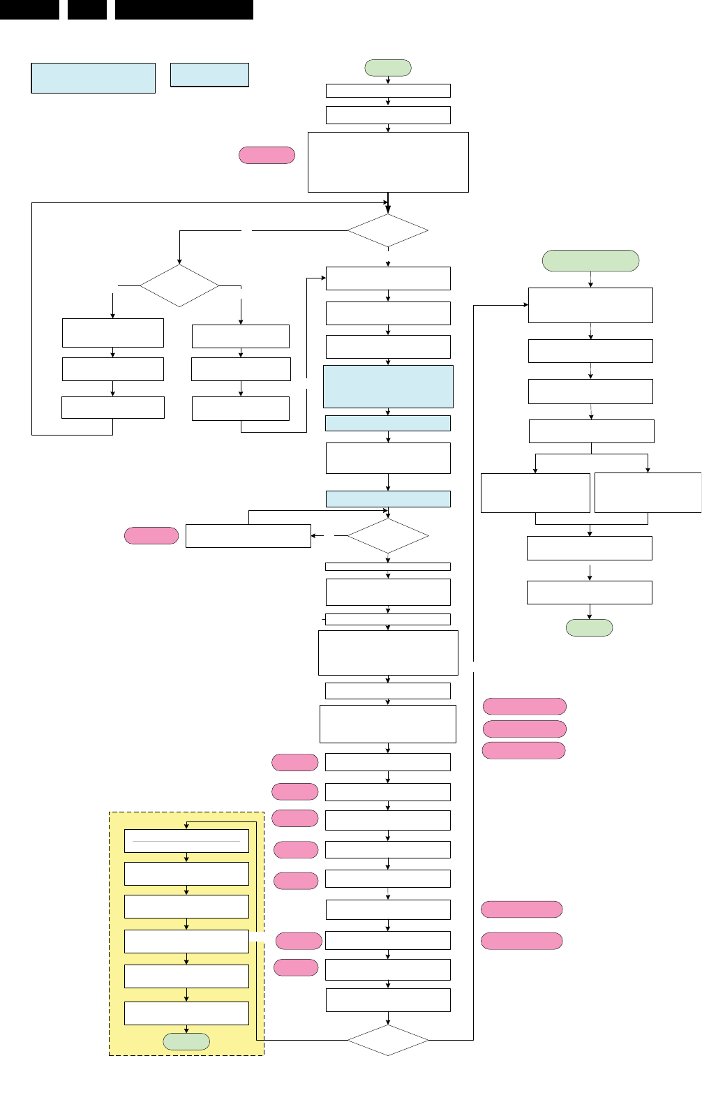
5.8.3 Start-up/Shut-down Flowcharts
On the next pages you will find start-up and shut-down
flowcharts, followed by a trouble shooting flowchart, which
might be helpful during fault finding.
Please note that some events are only related to PDP sets, and
therefore not applicable to this LCD chassis.
Hex Dec. Description
.ADR 0x000A 10 Existing value
.VAL 0x0000 0 New value
.Store Store?
Service Modes, Error Codes, and Fault Finding
EN 22 LC8.2HA LA5.
2009-Apr-10
Figure 5-8 Start-up flowchart
AC ON
LC08R
Start Up
(SVP_Trident) SVPWX_RST = LOW
HDMI_RX_BUF_RST = LOW
HDMI_MUX_RST =LOW
AUD_RST = LOW
Enable Audio Mute
(SVP_Trident) M16C SVPWX_RST = LOW
HDMI_RX_BUF_RST= HIGH
HDMI_MUX_RST = HIGH
AUD_RST = HIGH
DTV_RESET_N = HIGH
PRST = HIGH
M16C POR by +3VSTBY
STANDBY = HIGH
V1.0
21 Aug 2007
+3V3STBY Available
Initialise Trident WX
KMNPLL Latch data need 50us setup time
BL_ADJ = HIGH (100% Duty Cycle) first!!
DPTVInit( )
LCD_PWR_ON = HIGH
(Same function as CTRL-DISP2)
SDI PDP => CTRL_DISP1 = LOW
BL_On_Off=HIGH (PDP only)
For LCD:
BL_ON_OFF = HIGH
* BL_ADJ keep 100% for 3000ms
before dimming.
Switch ON LVDS Signal
Wait for 20 ms
Init. Warm Component
(For software)
Initialise IF Demodulator, Afric
TDA9886T
Initialise Tuner
Initialise HDMI Receiver, Sil 9125
Initialise Micronas
Mute Audio
Initialise FHP Panel (Provision)
* For FHP PDP Sets only
Initialise
MT8280 or 100Hz Bolt on
Last status is ON?
No
No
End
Standby Normal
Mode Yes
Wait for RC key or
Wake up event
Wait for Power Local Key
20ms
LCD_PWR_ON = LOW
SDI PDP => CTRL_DISP1 = LOW
BL_On_Off = HIGH (PDP only)
STANDBY = LOW
Is Power Down
= HIGH?
Enable Power Down INT
Enable DC_PROT INT
Wait for 100ms
Wait for 100ms
Time out = 2000msNo
Error 2
[Protection]
Yes
Wait for 300ms
Blank Picture
Picture Mode Setup & Detection
Error 5 - Trident
[Protection]
Yes
DVB recording mode
No
Yes
WP for NVM
STANDBY = LOW
Standby
Normal Mode
Recording Mode finished
Software Shutdown:
LED = WHITE for Normal mode
LED = RED for Recording mode
User wake up the sets
in DVB recording mode
BLOCK RC Key
Enable RC Key
Error 7
Error 8
Error 9
Error 11
Error 3
[Protection]
Standby Normal Mode
(RED LED)
Disable Audio Mute
Standby Soft Mode
(NO LED)
1000ms to
1500ms
100ms
300ms
1700ms
SDI PDP => CTRL_DISP1 = HIGH
FHP PDP => CTRL_DISP4 = LOW
BL_On_Off=LOW (PDP only)
For DVB Sets only (Semistandby)
Recording mode
Notes:
---------
1.Initialise HDMI MUX IIC address ( EDID,CEC)
2. Enable Mute mean ANTI_PLOP= LOW, MUTEn=HIGH
3. Disable Mute mean ANTI_PLOP = HIGH, MUTEn=LOW
160ms
Disable Audio Mute
Port Assignment in STANDBY
Port Assignment in STANDBY
Port Assignment in STANDBY
unBlank Picture &
UnMute Audio
Read NVM completed.
STOP I²C activities.
InitCold Component:
1. Check SDM port.
- If SDM pin = LOW and NVM first 20Byte = 0xFF,
reload Software default NVM value.
2. Check Panel port.
- If Panel Pin = LOW and check slave address
0x65 = 0xA5, Enter Panel Mode.
Error 6 - NVM
[Protection]
Error 10 – SDRAM 7C04
[Protection]
Error 14 – SDRAM 7C05
[Protection]
Error 17 – AmbiLight
Error 18 – iTV
For PDP:
3000ms delay
Initialise HDMI Mux, Sil 9185
Error 21
AmbiLight Set Only
Initialise AmbiLight
Wait for 50ms
Error 19
300ms
(SVP_Trident) SVPWX_RST = HIGH
DTV_RESET_N = LOW
PRST = LOW
PWN = HIGH
Wait for 300ms
300ms
I_17760_047.eps
030308
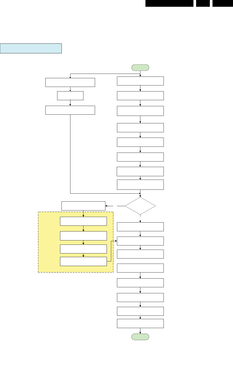
Service Modes, Error Codes, and Fault Finding EN 23LC8.2HA LA 5.
2009-Apr-10
Figure 5-9 Stand-by / Tact Switch Stand-by flowchart
I_17760_048.eps
030308
STANDBY / TACT SWITCH STANDBY
Start
Mute Audio
WP for NVM
STANDBY = HIGH
Software Shutdown:
BL_ON_OFF = LOW
Wait 300ms
Switch OFF LVDS
Wait 20ms
LCD_PWR_ON = LOW
End
LED = NO LED
for Standby soft mode
Standby using
“power key”
LED = RED No
Yes
For DVB Sets only (Semistandby)
SDI PDP => CTRL_DISP1 = HIGH
FHP PDP => CTRL_DISP4 = LOW
Off Air Downloading/ Recording Mode
IBOZ send shut down command
BL_ADJ
(PWM duty cycle 100%)
Enable Audio Mute
Port Assignment in STANDBY
300ms
20ms
Total = 360ms
40ms
Wait for 3000ms
Sets go to standby here
Blocking for the next start up to ensure
power supply discard properly.
Disable Power Down INT &
DC_PROT_INT
Wait for 3000ms
Except power tact switch
BL_ADJ = LOW
(PWM duty cycle 0%)
Disable Audio Mute
(ANTI_PLOP=LOW)
(MUTEn =HIGH)
(ANTI_PLOP =HIGH)
(MUTEn = LOW)
(ANTI_PLOP =HIGH)
(MUTEn = LOW)
Send Standby command to Digital Module
Wait for 2s
Ack received from
Digital Module or > 2s
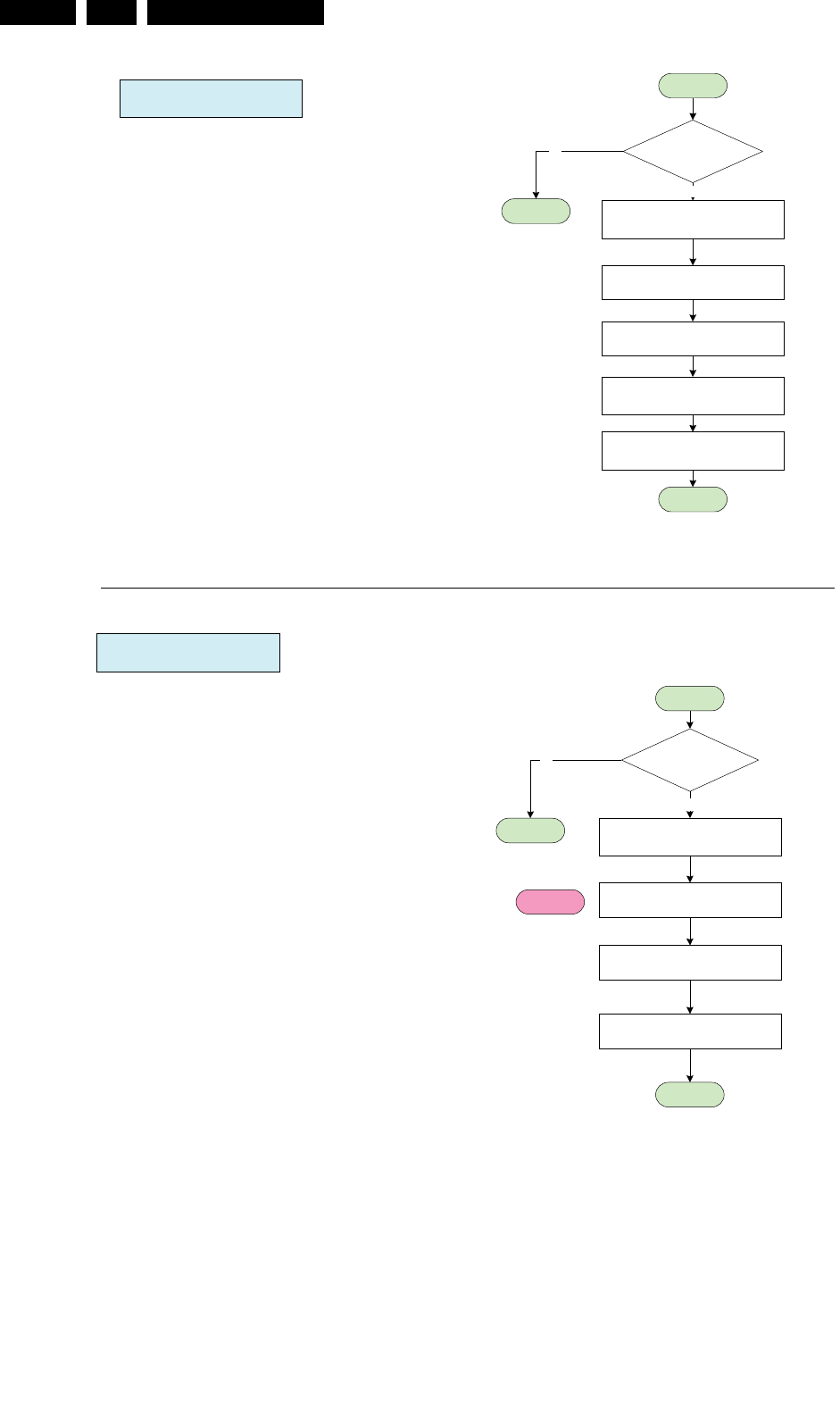
Service Modes, Error Codes, and Fault Finding
EN 24 LC8.2HA LA5.
2009-Apr-10
Figure 5-10 Power Down & DC_PROT flowchart
Start
WP for NVM
Mute Audio & VIdeo
Power Down INT:
AC OFF or Transient INT
DC_PROT INT
STANDBY = HIGH
Wait 5000 ms
Re-start: Start up
End
No
Notes:
1. Power Down INT will based on fall edge triggering
2. +3V3STBY will stay for 15ms, software must perform WP for NVM within 15ms.
Poll the Power Down
INT for 5 times
End
Avoid false trigger
Start
Mute Audio & VIdeo
No
End
Avoid false trigger
is DC_PROT = LOW
for 3 sec?
Log Error Code
STANDBY =HIGH
WP for NVM
Error 1
[Protection]
End
Yes
Yes
I_17760_027.eps
180908
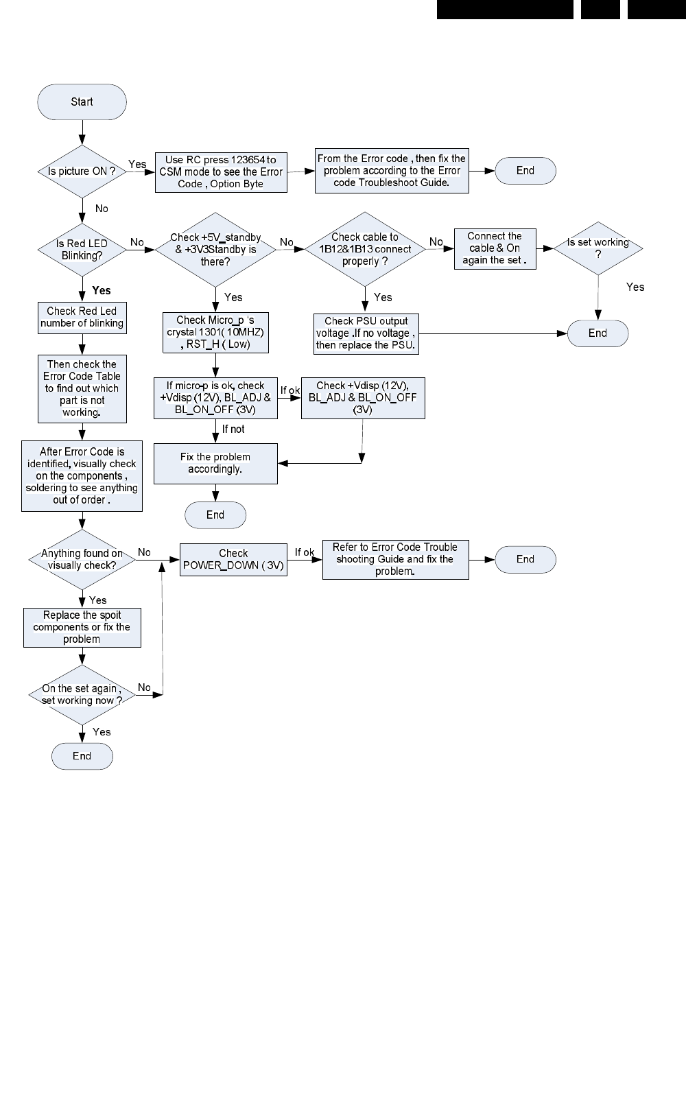
Service Modes, Error Codes, and Fault Finding EN 25LC8.2HA LA 5.
2009-Apr-10
Figure 5-11 Troubleshooting flowchart
Code
I_17760_049.eps
030308
Alignments
EN 26 LC8.2HA LA6.
2009-Apr-10
6. Alignments
Index of this chapter:
6.1 General Alignment Conditions
6.2 Hardware Alignments
6.3 Software Alignments
6.4 Option Settings
Note: Figures below can deviate slightly from the actual
situation, due to the different set executions.
General: The Service Default Mode (SDM) and Service
Alignment Mode (SAM) are described in chapter 5. Menu
navigation is done with the CURSOR UP, DOWN, LEFT or
RIGHT keys of the remote control transmitter.
6.1 General Alignment Conditions
Perform all electrical adjustments under the following
conditions:
• Power supply voltage (depends on region):
– AP-NTSC: 120 VAC or 230 VAC / 50 Hz (± 10%).
– AP-PAL-multi: 120 - 230 VAC / 50 Hz (± 10%).
– EU: 230 VAC / 50 Hz (± 10%).
– LATAM-NTSC: 120 - 230 VAC / 50 Hz (± 10%).
– US: 120 VAC / 60 Hz (± 10%).
• Connect the set to the mains via an isolation transformer
with low internal resistance.
• Allow the set to warm up for approximately 15 minutes.
• Measure voltages and waveforms in relation to correct
ground (e.g. measure audio signals in relation to
AUDIO_GND).
Caution: It is not allowed to use heatsinks as ground.
• Test probe: Ri > 10 MΩ, Ci < 20 pF.
• Use an isolated trimmer/screwdriver to perform
alignments.
6.2 Hardware Alignments
There are no hardware alignments foreseen for this chassis,
but below find an overview of the most important DC voltages
on the SSB. These can be used for checking proper functioning
of the DC/DC converters.
6.3 Software Alignments
With the software alignments of the Service Alignment Mode
(SAM) the Tuner and RGB settings can be aligned.
To store the data: Use the RC button “Menu” to switch to the
main menu and next, switch to “Stand-by” mode.
6.3.1 Tuner Adjustment (RF AGC Take Over Point)
Purpose: To keep the tuner output signal constant as the input
signal amplitude varies.
This chassis comes with the UV13x6(x) tuner. No alignment is
necessary, as the AGC alignment is done automatically
(standard value: “15”). However in case of problems use the
following method (use multi meter and RF generator):
• Apply a vision IF carrier of 38.9 (China: 38.0) MHz
(105 dBμV = 178 mVrms) to test point F143 (input via 50 Ω
coaxial cable terminated with an RC network of series
10 nF with 120 Ω to ground).
• Measure voltage on test point F116 with a FET probe.
• Adjust AGC (via SAM menu: TUNER -> AGC), until voltage
on test point F116 is 3.3 +0.5/-1.0 V.
• Store settings and quit SAM.
6.3.2 RGB Alignment
• Set “Active control” to “Off” (if present).
• Choose “TV menu”, “Picture” and set picture settings as
follows:
White Tone Alignment:
• Activate SAM mode.
• Select “RGB Align.” -> “White Tone” and choose a colour
temperature.
• Use a 100% white screen as input signal and set the
following values:
– All “White point” values initial to “256”.
– All “BlackL Offset” values to “0”.
In case you have a colour analyser:
• Measure with a calibrated contact less colour analyser
(e.g. Minolta CA-210) in the centre of the screen.
Consequently, the measurement needs to be done in a
dark environment.
• Adjust the correct x, y coordinates (while holding one of the
White point registers R, G or B on “256”) by means of
decreasing the value of one or two other white points to the
correct x, y coordinates (see table “White D alignment
values”). Tolerance: dx: ± 0.004, dy: ± 0.004.
• Repeat this step for the other colour Temperatures that
need to be aligned.
• When finished return to the SAM root menu and press
STANDBY on the RC to store the aligned values to the
NVM.
Table 6-1 White D alignment values
Description
Test
Point
Specifications
(V)
DiagramMin. Typ. Max.
+12V_DISP FP12 11.4 12.0 12.6 B01A_DC-DC
+VTUN FP11 30 33 36 B01A_DC-DC
+3V3_STBY FP10 3.20 3.30 3.40 B01A_DC-DC
+3V3+SW FP20 3.13 3.3 3.46 B01A_DC-DC
+1V2_SW FP24 1.18 1.25 1.31 B01A_DC-DC
+5V_SW FQ05 4.85 5.10 5.35 B01B_DC-DC
+1V8_SW FQ06 1.72 1.82 5.25 B01B_DC-DC
+2V5_SW FQ03 2.38 2.5 2.62 B01B_DC-DC
+5V_IF F129 4.75 5 5.25 B02_TUNER_IF
+5VS F131 4.75 5 5.25 B02_TUNER_IF
+5V_TUN F146 4.75 5 5.25 B02_TUNER_IF
+1V2_ADC FC04 1.14 1.2 1.26 B04A_TRIDENT
+1V2_PLL FC05 1.14 1.2 1.26 B04A_TRIDENT
+1V2_CORE FC06 1.14 1.2 1.26 B04A_TRIDENT
+2V5_VDDM
Q
FD01 2.38 2.5 2.62 B04B_DDR
+VDISP FR10 11.4 12.0 12.6 B04E_LVDS
+8V F401 7.60 8.00 8.40 B05A_AUDIOPR
OCESSOR
Picture Setting
Brightness 50
Colour 50
Contrast 100
Tint (for NTSC) 0
Value Cool (11000 K) Normal (9000 K) Warm (6500 K)
x 0.278 0.289 0.314
y 0.278 0.291 0.319
Alignments EN 27LC8.2HA LA 6.
2009-Apr-10
If you do not have a colour analyser, you can use the default
values. This is the next best solution. The default values are
average values coming from production (statistics).
• Set the RED, GREEN and BLUE default values per
temperature according to the values in the “Tint settings”
table.
• When finished return to the SAM root menu and press
STANDBY on the RC to store the aligned values to the
NVM.
Table 6-2 Tint settings
Black Level Offset Alignment
• Activate SAM.
• Select “RGB Align.” -> “BlackL Offset” and choose a colour.
• Set all “BlackL Offset” values to “0”.
• When finished return to the SAM root menu and press
STANDBY on the RC to store the aligned values to the
NVM.
Note: For models with “Pixel Plus”, the “Black Offset” (black
level offset) should NOT be changed in SAM. These offset
values of RGB should be set to “0”, and should NOT be
adjusted. Any adjustment of these values will affect the low
light white balance.
ADC YPbPr Gray Scale Alignment
When the grey scale is not correct, use this alignment:
• Activate SAM.
• Select “NVM Editor”.
• Enter address “26(dec)” (ADR).
• Set value (VAL) to “197(dec) ± 25”.
• Store (STORE) the value.
6.4 Option Settings
6.4.1 Introduction
The microprocessor communicates with a large number of I2C
ICs in the set. To ensure good communication and to make
digital diagnosis possible, the microprocessor has to know
which ICs to address. The presence/absence of these specific
ICs (or functions) is made known by the option codes.
Notes:
• After changing the option(s), save them with the STORE
command.
• The new option setting becomes active after the TV is
switched “off” and “on” again with the mains switch (the
EAROM is then read again).
6.4.2 How To Set Option Codes
When the NVM is replaced, all options will require resetting. To
be certain that the factory settings are reproduced exactly, you
must set all option numbers. You can find the correct option
numbers in table “Option Codes OP1...OP7” below.
How to Change Options Codes
An option code (or “option byte”) represents eight different
options (bits). When you change these numbers directly, you
can set all options very quickly. All options are controlled via
seven option bytes (OP1... OP7).
Activate SAM and select “Options”. Now you can select the
option byte (OP1 to OP7) with the CURSOR UP/ DOWN keys,
and enter the new 3 digit (decimal) value. For the correct
factory default settings, see the next table “Option codes
OP1...OP7“. For more detailed information, see the second
table “Option codes at bit level“. If an option is set (value “1”), it
represents a certain decimal value.
When all the correct options (bits) are set, the sum of the
decimal values of each Option Byte (OP) will give the option
code.
Table 6-3 Option code overview
Alignment 32" 42"
WARM_RED 256 128
WARM_GREEN 241 120
WARM_BLUE 189 110
NORMAL_RED 251 125
NORMAL_GREEN 256 128
NORMAL_BLUE 220 120
COOL_RED 243 110
COOL_GREEN 256 118
COOL_BLUE 233 140
CTN Option Code
Display
Code
32HFL5530/93 192 029 226 249 073 197 131 069
32HFL5530/97 128 029 234 249 073 196 131 069
42HFL5580/93 192 029 226 249 073 197 129 130
42HFL5580/97 128 029 234 249 073 196 129 138
Alignments
EN 28 LC8.2HA LA6.
2009-Apr-10
Option Bit Overview
Below find an overview of the Option Codes on bit level.
Table 6-4 Option codes at bit level (OP1-OP7)
Option Byte & Bit Dec. Value Option Name Description
Byte OP1
Bit 7 (MSB) 128 BBE ON = BBE is available; OFF = BBE is not available
Bit 6 64 CHINA ON = SW is for CHINA only; OFF = SW is for Non-China AP cluster
Bit 5 32 DTV_CHINA ON = DTV_CHINA will be available (Reserved); OFF = DTV_CHINA will not be available
Bit 4 16 DTV_EU ON = DTV will be available; OFF = DTV will not be available
Bit 3 8 UK_PNP ON = UK PNP is available (for analogue TV only); OFF = UK PNP is not available (for analogue
TV only)
Bit 2 4 VIRGIN_MODE ON = Virgin Mode (PNP) is available; OFF = Virgin Mode (PNP) is not available
Bit 1 2 ACI ON = ACI is available; OFF = ACI is not available
Bit 0 (LSB) 1 ATS ON = ATS is available; OFF = ATS is not available
Byte OP2
Bit 7 (MSB) 128 1080P ON = 1080p is available; OFF = 1080p is not available
Bit 6 64 LIGHT_SENSOR ON = Light Sensor is available; OFF = Light Sensor is not available
Bit 5 32 AMBILIGHT ON = Ambilight Feature will be available; OFF = Ambilight Feature will not be available
Bit 4 16 BACKLIGHT_DIMMING ON = Backlight Dimming is available; OFF = Backlight Dimming is not available
Bit 3 8 HUE ON = Hue is available; OFF = Hue is not available
Bit 2 4 2D3DCF ON = 3D Comb Filter is available; OFF = 2D Comb Filter is available
Bit 1 2 WSSB ON = WSS is available; OFF = WSS is not available
Bit 0 (LSB) 1 WIDE_SCREEN ON = TV is 16x9 set; OFF = TV is 4x3 set
Byte OP3
Bit 7 (MSB) 128 CVI1 ON=CVI1 (YPbPr) (For ROW)
Bit 6 64 HDMI3 ON = HDMI3 (rear) is available; OFF = HDMI3 (rear) is not available
Bit 5 32 HDMI4 ON = HDMI4 (side) is available; OFF = HDMI4 (side) is not available
Bit 4 16 VCHIP ON = VChip is available; OFF = VChip is not available
Bit 3 8 VIDEO_TEXT ON = Video-TXT is available; OFF = Video-TXT is not available
Bit 2 4 STEREO_DBX ON = Stereo DBX detection is available (LATAM); OFF = Stereo DBX detection is not available
Bit 1 2 STEREO_NICAM_2CS ON = Stereo NICAM 2CS detection is available (EU/AP/China); OFF = Stereo NICAM 2CS
detection is not available
Bit 0 (LSB) 1 LIP_SYNC ON = Lip Sync is available; OFF = Lip Sync is not available
Byte OP4
Bit 7 (MSB) 128 HDMI2 ON = HDMI2 is available; OFF = HDMI2 is not available
Bit 6 64 HDMI1 ON = HDMI1 is available; OFF = HDMI1 is not available
Bit 5 32 VGA ON = VGA is available; OFF = VGA is not available
Bit 4 16 SVHS3 ON = SVHS3 is available; OFF = SVHS3 is not available
Bit 3 8 AV3 ON = AV3 is available; OFF = AV3 is not available
Bit 2 4 CVI ON = CVI is available; OFF = CVI is not available
Bit 1 2 SVHS2 ON = SVHS2 is available; OFF = SVHS2 is not available
Bit 0 (LSB) 1 AV2 ON = AV2 is available; OFF = AV2 is not available
Byte OP5
Bit 7 (MSB) 128 NVM_CHECK ON = NVM (range) checking is available; OFF = NVM (range) checking is not available
Bit 6 64 DNM ON = DNM is available; OFF = DNM is not available
Bit 5 32 SUBWOOFER ON = Sub woofer is available; OFF = Sub woofer is not available
Bit 4 16 MP_ALIGN ON = Using multi-point alignment for Gamma & White Point; OFF = Using old way for Gamma (pre-
defined) & WP alignment
Bit 3 8 SYS_RECVRY ON = System Recovery is available; OFF = System Recovery is not available
Bit 2 4 ED_HD_DNM ON = DNM not available on ED and HD signal; OFF = DNM available on ED and HD signal
Bit 1 2 HOTEL ON = Hotel/BDS is available; OFF = Hotel/BDS is not available
Bit 0 (LSB) 1 SS_DEMO ON = Split Screen Demo is available; OFF = Split Screen Demo is not available
Byte OP6
Bit 7 (MSB) 128 BACKLIGHT_BOOST ON = iLAB Backlight boost feature is available; OFF = iLAB Backlight boost feature is not available
Bit 6 64 STATIC _DIMMING ON = iLAB Static Dimming feature is available; OFF = iLAB Static Dimming feature is not available
Bit 5 32 CEC ON = CEC feature available; OFF = CEC feature not available
Bit 4 16 AUTO_HDMI ON = Auto HDMI feature available; OFF = Auto HDMI feature not available
Bit 3 8 TUNER PROFILE 0 = ATV_EU_PHILIPS UV1318S/AIH-3; 1 = ATV_EU_Panasonic EN57K28G3F; 2 =
DTV_EU_PHILIPS TD1316AF/IHP-2; 3 = Not Used (Reserved); 4 = ATV_AP_PHILIPS UV1316E/
AIH-4; 5 = ATV_CHINA_PHILIPS UV1356; 6 = ATV_CHINA_ALPS TEDE9-286B; 7 =
ATV_CHINA_Tuner2 (Reserved); 8 = ATV_LATAM_PHILIPS UV1338/AIH-4; 9 =
ATV_LATAM_PHILIPS UV1336; 10 = DTV_CHINA_Tuner1 (Reserved); 11 =
DTV_CHINA_Tuner2 (Reserved); 12 = Not Used (Reserved); 13 = Not Used (Reserved); 14 = Not
Used (Reserved); 15 = Not Used (Reserved)
Bit 2 4
Bit 1 2
Bit 0 (LSB) 1
Byte OP7
Bit 7 (MSB) 128 OPC_VOL_UP_UNMUTE ON = Volume Up key will unmute the TV; OFF = Volume Up key will not unmute the TV
Bit 6 64 Reserved Not Used (Reserved)
Bit 5 32 OPC_DTV_LATAM ON = Brazil Digital available; OFF = Brazil Digital not available
Bit 4 16 CABINET PROFILE 0 = All flat response; 1 = ME8 42/47/52 Basic; 2 = ME8 42/47/52 AMBL; 3- 16 = Reserved
Bit 3 8
Bit 2 4
Bit 1 2
Bit 0 (LSB) 1
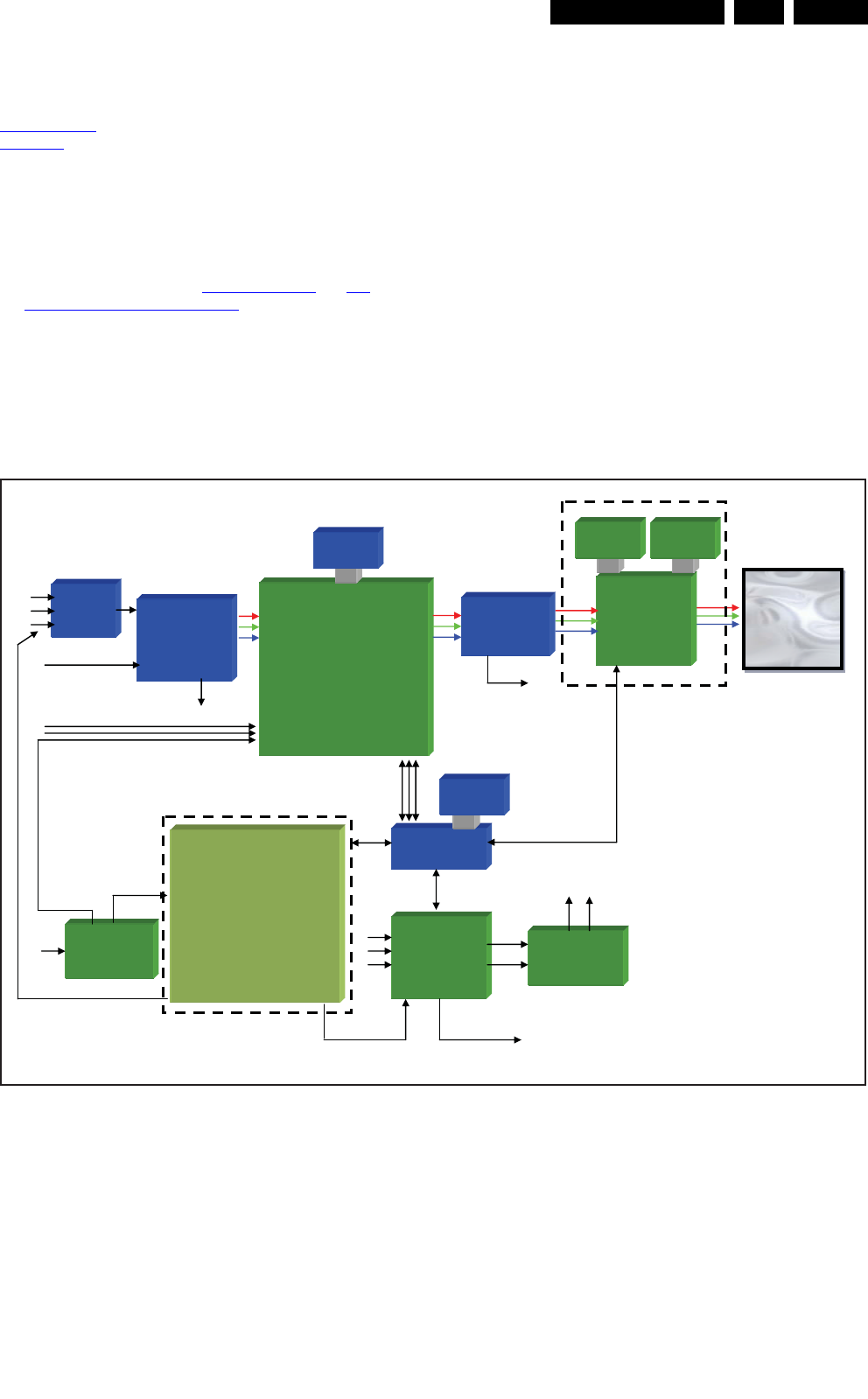
Circuit Descriptions EN 29LC8.2HA LA 7.
2009-Apr-10
7. Circuit Descriptions
Index of this chapter:
7.1 Introduction
7.2 iBoard
Notes:
•Only new circuits (circuits that are not published recently)
are described.
• Figures can deviate slightly from the actual situation, due
to different set executions.
• For a good understanding of the following circuit
descriptions, please use the 9. Block Diagrams and 10.
Circuit Diagrams and PWB Layouts. Where necessary, you
will find a separate drawing for clarification.
7.1 Introduction
The LC8.2HA LA is the Hospitality version of the LC8.2A LA
chassis. Refer to the Service Manual of the LC8.2A LA chassis
for a description of all circuits outside the iBoard scope.
The hospitality-specific features comprise:
• Advanced Hotel mode (volume lock, front control lock out,
guest menu, welcome message, etc.)
• External loudspeaker connection.
• Time synchronisation via Teletext
• Channel protection
• Energy saving features
• Multimedia Player (Philips Connectivity Panel).
• Wireless SmartLoader for fast cloning.
• SmartPlug Xpress and Serial Xpress Control interfaces.
The chassis supports these basic application types:
• Stand-alone
• Interactive via SmartCard (Serial Xpress or SmartPlug
Xpress add-on box)
• Interactive via 3rd-party set-top box.
Refer to figure “LC08R Architecture” for details.
Figure 7-1 LC08R Architecture
SVP-WX69
Digital Colour Decoder
MADI (4-field)
HD-DNM
1080P Through
32
DDR
MSP4450L
SiI9125
HDMI
Renesas uP
TV control
8
FLASH
Matrix
HD@50Hz
FHD@50Hz
FHD@100Hz
Matrix
HD@50Hz
FHD@50Hz
FHD@100Hz
Analogue inputs
TDA8932T
Class D
L/R
FPGA
(optional)
DFI
FHD 100Hz
32
DDR
SPDIF
32
DDR
2C5 FPGA
(optional)
AmbiLight
AmbiLight2
Tuner
IF
SAW
SiI9185
Switch
IISDFI Bolt-on
Bolt-on module
iBoard
ITV Bolt-on
HP Audio
Out
18510_202_090407.eps
090407
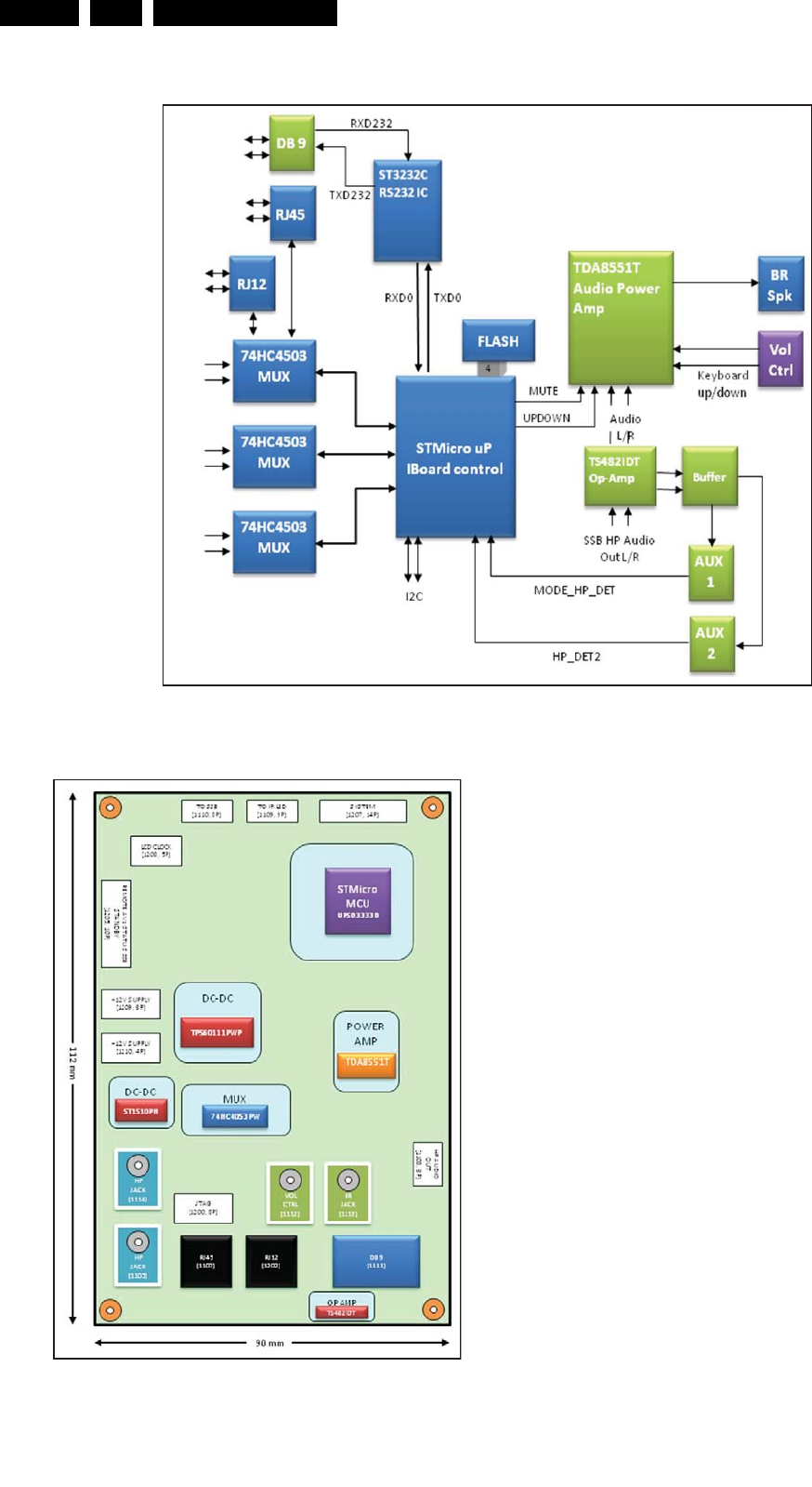
Circuit Descriptions
EN 30 LC8.2HA LA7.
2009-Apr-10
7.2 iBoard
Figure 7-2 iBoard block diagram
Figure 7-3 iBoard cell layout
The iBoard intercepts the information from the IR Receiver and
has full control over its interpretation and processing. It may
also relay the same commands to the TV or send different IR
commands to the TV. The IR signal could also be in another
encoding format and bit rate, e.g. RC6MM. The iBoard also has
full control over the LED. This makes it possible to implement
within the iBoard features such as Wireless SmartLoading,
Message Blinking, power status indication, etc. These features
are implemented without additional software in the TV
Microprocessor.
The iBoard communicates with the TV in I2C (but other protocol
is also possible). The iBoard is the I2C slave device and the TV
is the I2C master. Functionally, the iBoard controls the TV and
it is the master of the TV.
The CVBS_ter signal is used as a monitor signal for automatic
channel installation, which is controlled by the microprocessor.
18510_203_090407.eps
090407
RS232
in/out
IR
in/out
RS232
12V out
CVBS
18510_204_090407.eps
090407
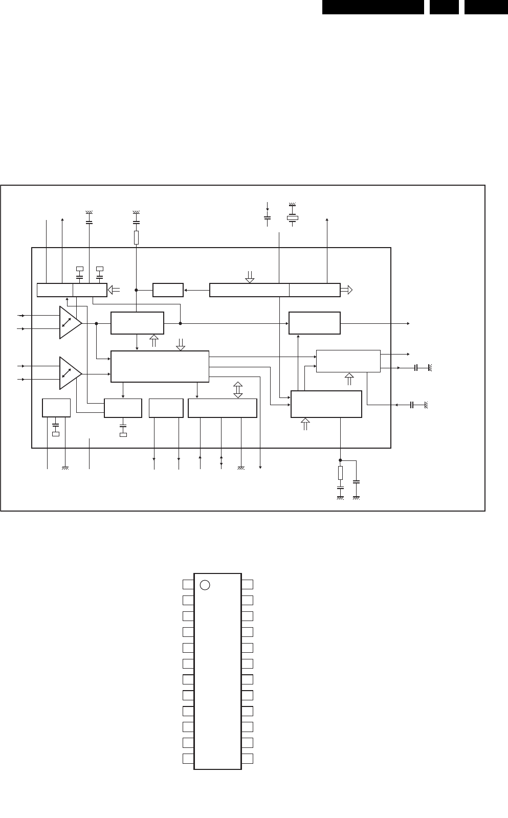
IC Data Sheets EN 31LC8.2HA LA 8.
2009-Apr-10
8. IC Data Sheets
8.1 IC Data Sheets
This section shows the internal block diagrams and pin layouts
of ICs that are drawn as “black boxes” in the electrical diagrams
(with the exception of “memory” and “logic” ICs).
8.1.1 Diagram B03, Type TDA9886T (IC7113), IF-PLL demodulator
Figure 8-1 Internal block diagram and pin configuration
Block Diagram
Pin Configuration
G_16510_059.eps
090325
TAGC
CVAGC pos
CBL
VIF-PLL
4 MHz
external
AFC
video output 2 V (p-p)
[1.1 V (p-p) without trap]
AUD
CAF
de-emphasis
network
FM-PLL filter
sound intercarrier output
CAGC
AGND
VP
VIF1
VIF-AGC RC VCO DIGITAL VCO CONTROL AFC DETECTOR
VIDEO TRAPS
4.5 to 6.5 MHz
NARROW-BAND FM-PLL
DETECTOR
I2C-BUS TRANSCEIVER
VIF-PLL
SINGLE REFERENCE QSS MIXER/
INTERCARRIER MIXER AND
AM-DEMODULATOR
SIF-AGC
SUPPLY
1
2
14 16 19 15 21
17
8
6
5
4
12
7 11 10
1820
23
24
OUTPUT
PORTS
MAD
AUDIO PROCESSING
AND SWITCHES
9
TUNER AGC
CAGC neg
322
crystal
and MAD select
TDA9885
n.c.
13
L
L
P
M
F
D
AM
O
ISD
N
GDADS
L
C
S
2P
O1
P
O
CVBS
TOP
VIF2
SIF1
SIF2 DEEM
AFD
REF
VAGC VPLL
filter
TDA9886
(1)
(1) Not connected for TDA9885.
reference
or
TDA9885
TDA9886
1
2
3
4
5
6
7
8
9
10
11
12
VIF1
VIF2
OP1
FMPLL
DEEM
AFD
DGND
AUD
TOP
SDA
SCL
SIOMAD
SIF2
SIF1
OP2
AFC
VP
VPLL
AGND
CVBS
VAGC(1)
REF
TAGC
n.c.
24
23
22
21
20
19
18
17
16
15
14
13
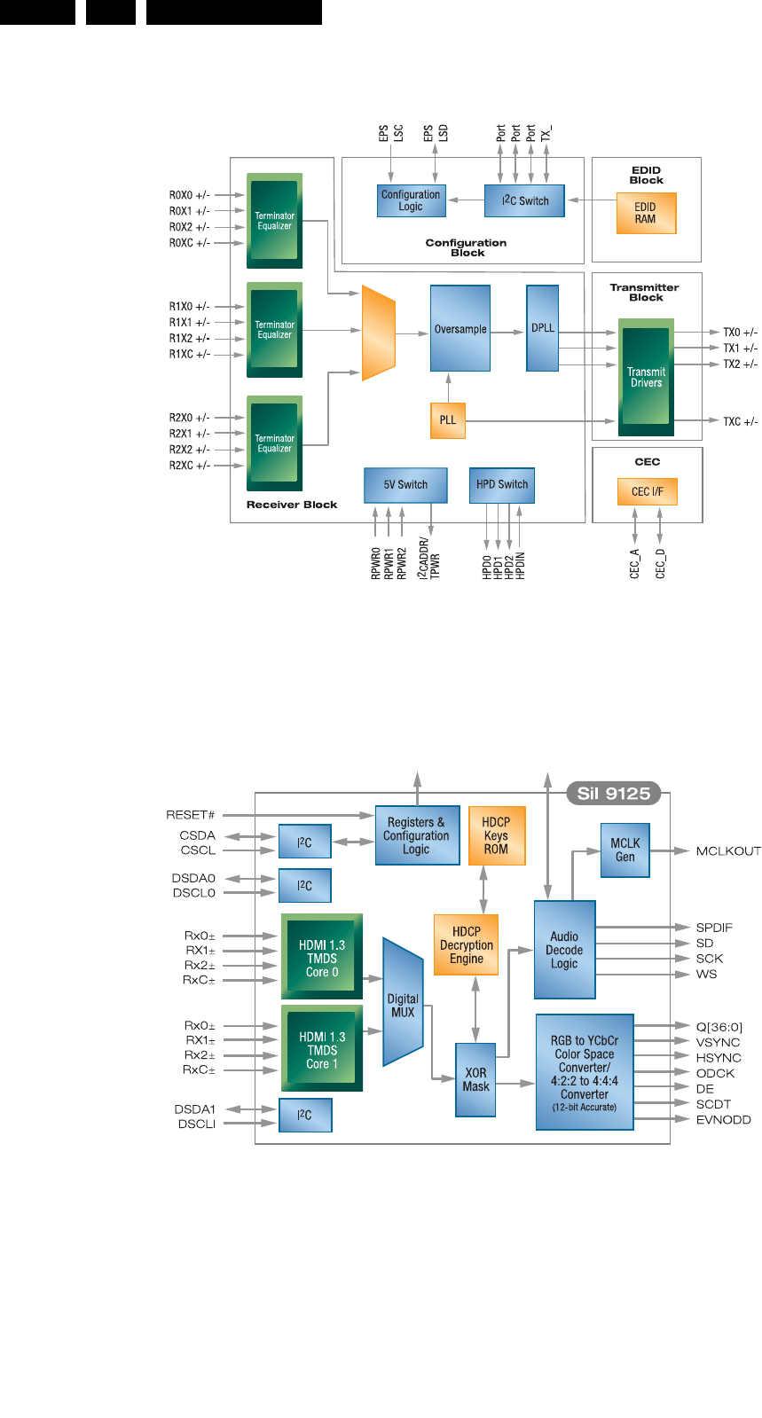
IC Data Sheets
EN 32 LC8.2HA LA8.
2009-Apr-10
8.1.2 Diagram B07A, Type SIL9185 (IC7M07), HDMI switch
Figure 8-2 Internal block diagram
8.1.3 Diagram B07B, Type SIL9125 (IC7N01), HDMI receiver
Figure 8-3 Internal block diagram
Block Diagram
H_17370_074.eps
100807
Block Diagram
H_17370_075.eps
100807
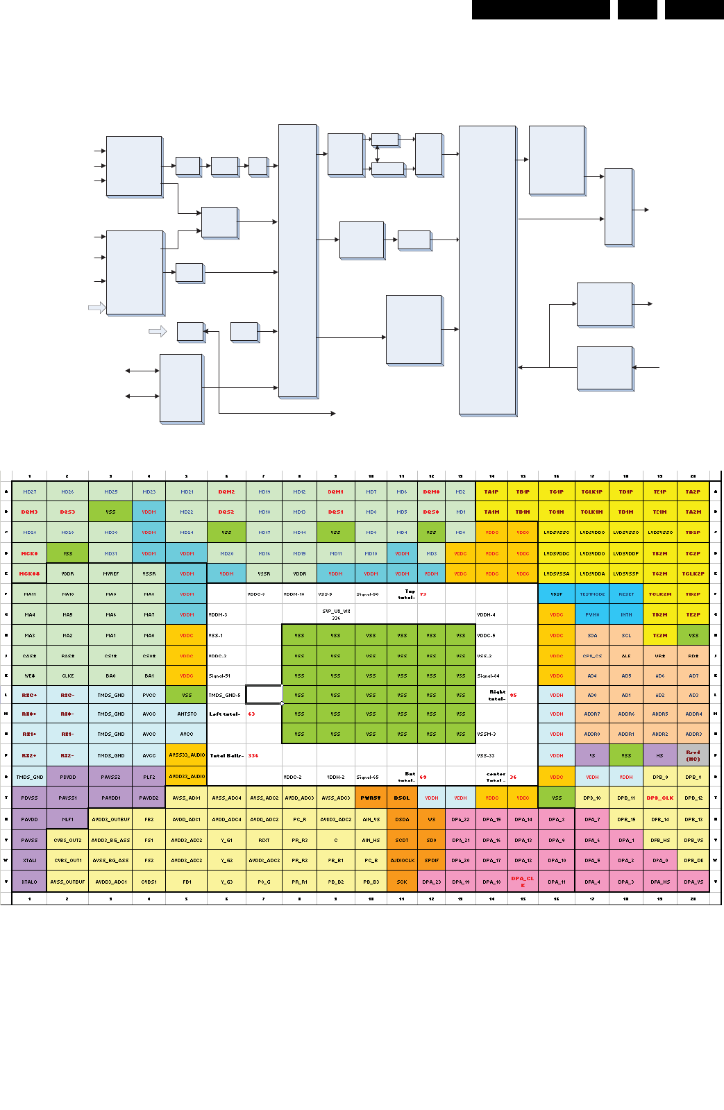
IC Data Sheets EN 33LC8.2HA LA 8.
2009-Apr-10
8.1.4 Diagram B04A, Type SVP WX69 (IC7C01), Trident Video processor
Figure 8-4 Internal block diagram and pin configuration
NTSC/PAL/
SECAM
3D Comb
Decoder/
Motion
Adaptive De-
interlacing
ICSC
CPU &
OSD
Interface
CVBS1
CVBS1
S-Video
YPbPr
SXGA RGB
(1280x1024/
60)
30-bit
Digital
RGB
Hsync/
Vsync
I2C
8 bit Add/Data
Frame
Buffer
Controller
Frame
Rate
Converter
Deinterlacer
3:2/2:2 pull
down
Deinterlace
VBI/OSD/
TELETEXT
Display
Auto Color
Adjustment
ICSC
Blender
Chroma Key
VM Control
H&V Voltage
Protection
Gamma LUT
Dual
10 bit
LVDS
CRTC/DPLL
Clock PLL
Auto Mode/Auto
Tune/Auto
Phase
LVDS
H Sync
V Sync
Crystal
BMNR NR
ICSC
Luma
chroma
Cubic4
Scalar
Cubic4
scalar
HDMI HDCP
HDMI
Differential
Signals
I2S SPDIF
ME/MC
Pin Configuration
Block Diagram
I_17760_036.eps
260208
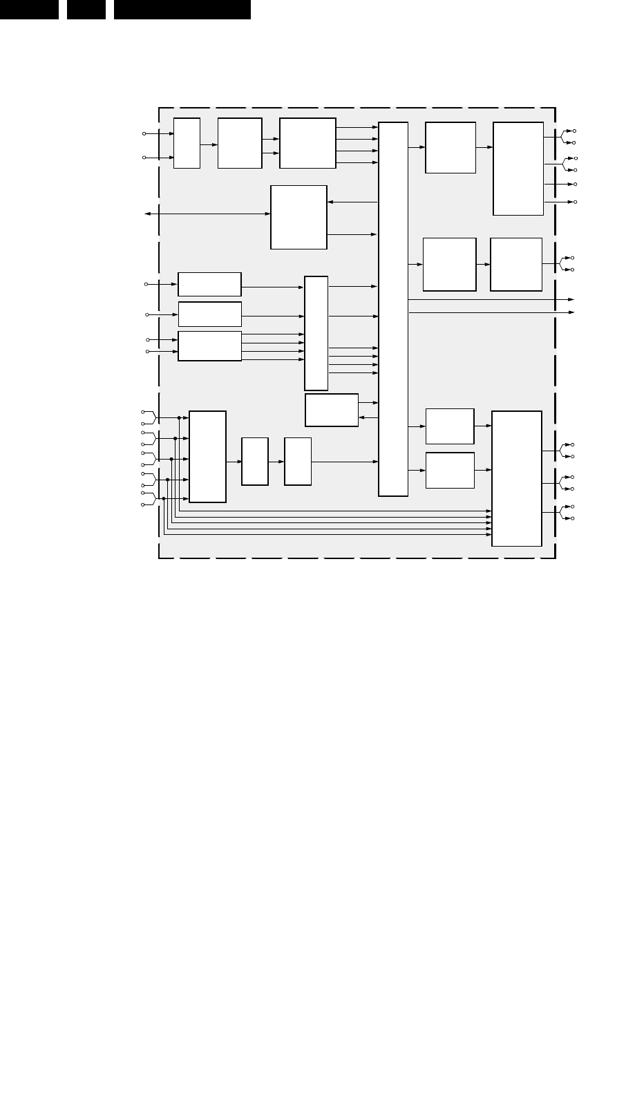
IC Data Sheets
EN 34 LC8.2HA LA8.
2009-Apr-10
8.1.5 Diagram B05A, Type MSP4450P (IC7411), Micronas Sound Processor
Figure 8-5 Internal block diagram
Source Select
SCART1
SCART2
SCART1
SCART2
SCART4
SCART3
De-
modulator
Headphone
I2S
Sound
Processing
DAC/
DAC
L
DAC
DAC
Subwoofer
Sound IF1
Sound IF2
R
Headphone
SCART
DSP
Input
Select
SCART
Output
Select
I
2
S2
I
2
S1 I
2
S
I
2
S
I
2
S3
(2..8-channel)
I
2
S
Prescale
SL
SR
Center
SCART3
SCART5
S/PDIF
ADC
Prescale
ADC
internal /
external
Audio Delay
I
2
S5
/
/
12
16
Loud-
speaker
Sound
Processing High-
Resolution
PWM
Loudspeaker
Pre-
processing
Surround
Processing
I
2
S4
Block Diagram
G_16860_041.eps
300107
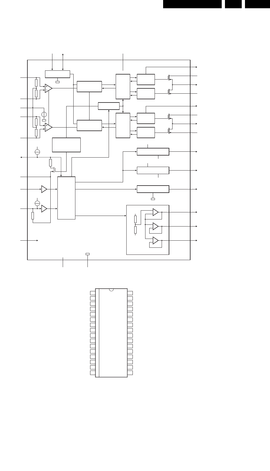
IC Data Sheets EN 35LC8.2HA LA 8.
2009-Apr-10
8.1.6 Diagram B05B, Type TDA8932T (IC7A01), Audio Amplifier
Figure 8-6 Internal block diagram and pin configuration
Block Diagram
Pin Configuration
G_16860_045.eps
300107
2
81301
28
29
27
3
12
TDA8932
OSCILLATOR
26
BOOT1
V
DDP1
OUT1
V
SSP1
PWM
MODULATOR
DRIVER
HIGH
DRIVER
LOW
CTRL
MANAGER
CTRL
PWM
MODULATOR
PROTECTIONS:
OVP, OCP, OTP,
UVP, TF, WP
STABILIZER 11 V
STABILIZER 11 V
REGULATOR 5 V
MODE
V
DDA
15
14
IN1P
VOICSOFERCSO
DDA
V
SSD
IN1N
INREF
IN2P
IN2N
6
POWERUP
4
DIAG
7
CGND
21
20
22
23
BOOT2
V
DDP2
OUT2
25 STAB1
24 STAB2
18
11
DREF
HVPREF
30 HVP1
19 HVP2
V
SSP2
DRIVER
HIGH
DRIVER
LOW
V
DDA
V
SSP1
V
SSP2
V
SSD
V
DDA
V
SSA
HALF SUPPLY VOLTAGE
5
ENGAGE
13
9
TEST
V
SSA
1, 16, 17, 32
V
SSD(HW)
TDA8932T
V
SSD(HW)
V
SSD(HW)
OICSOP1NI
1PVHN1NI
VGAID
DDP1
1TOOBEGAGNE
1TUOPUREWOP
VDNGC
SSP1
V
DDA
STAB1
V
SSA
STAB2
OSCREF V
SSP2
2TUOFERPVH
2TOOBFERNI
VTSET
DDP2
2PVHN2NI
FERDP2NI
V
SSD(HW)
V
SSD(HW)
1
2
3
4
5
6
7
8
9
10
11
12
13
14
15
16
18
17
20
19
22
21
24
23
26
25
32
31
30
29
28
27
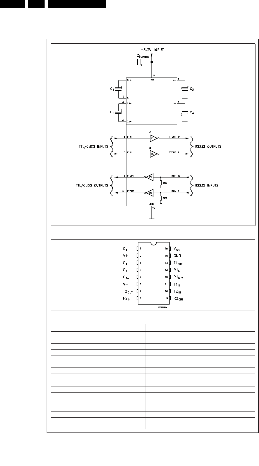
IC Data Sheets
EN 36 LC8.2HA LA8.
2009-Apr-10
8.1.7 Diagram HC01, Type ST3232C (IC7107), RS232 Driver
Figure 8-7 Internal block diagram and pin configuration
18510_301_090410.eps
090410
PIN CONFIGURATION
PIN DESCRIPTION
NOITCNUF DNA EMANLOBMYS°N NlP
1C
1
+ Positive Terminal for the first Charge Pump Capacitor
lanimreT egatloV delbuoD+V2
3C
1
- Negative Terminal for the first Charge Pump Capacitor
4C
2
+ Positive Terminal for the second Charge Pump Capacitor
5C
2
- Negative Terminal for the second Charge Pump Capacitor
lanimreT egatloV detrevnI-V6
7T2
OUT
Second Transmitter Output Voltage
8R2
IN
Second Receiver Input Voltage
9R2
OUT
Second Receiver Output Voltage
10 T2
IN
Second Transmitter Input Voltage
11 T1
IN
First Transmitter Input Voltage
12 R1
OUT
First Receiver Output Voltage
13 R1
IN
First Receiver Input Voltage
14 T1
OUT
First Transmitter Output Voltage
dnuorGDNG51
16 V
CC
Supply Voltage
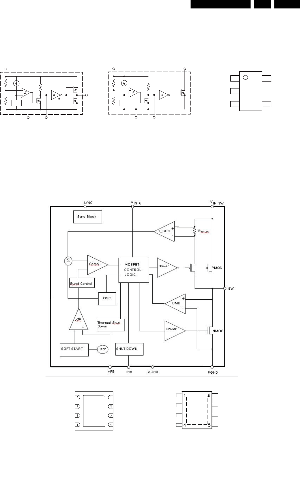
IC Data Sheets EN 37LC8.2HA LA 8.
2009-Apr-10
8.1.8 Diagram HC01, Type NCP303LSN45 (IC7103), Voltage Detector
Figure 8-8 Internal block diagram and pin configuration
8.1.9 Diagram HC01, Type ST1S10 (IC7125), Stepdown Regulator
Figure 8-9 Internal block diagram and pin configuration
Block Diagram Pin Configuration
F_15400_133.eps
100405
1
3 N.C.
Reset
Output
2
Input
Ground 4
C
D
5
xxxYW
(T op V iew)
xxx = 302 or 303
Y= Y ear
W= W ork W eek
This device contains 28 active transistors.
NCP303LSNxxT1
Open Drain Output Configuration
NCP302xSNxxT1
Complementary Output Configuration
V
ref
2 Input
1
Reset
Output
3 Gnd 5C
D
R
D
V
ref
2 Input
3 Gnd 5C
D
R
D
1Reset Output
*
Inverter for active low devices.
*
Buffer for active high devices.
PowerSO-8
DFN8 (4x4)
I_18010_083.eps
130608
Block Diagram
Pin Configuration

IC Data Sheets
EN 38 LC8.2HA LA8.
2009-Apr-10
Personal Notes:
10000_012_090121.eps
090121
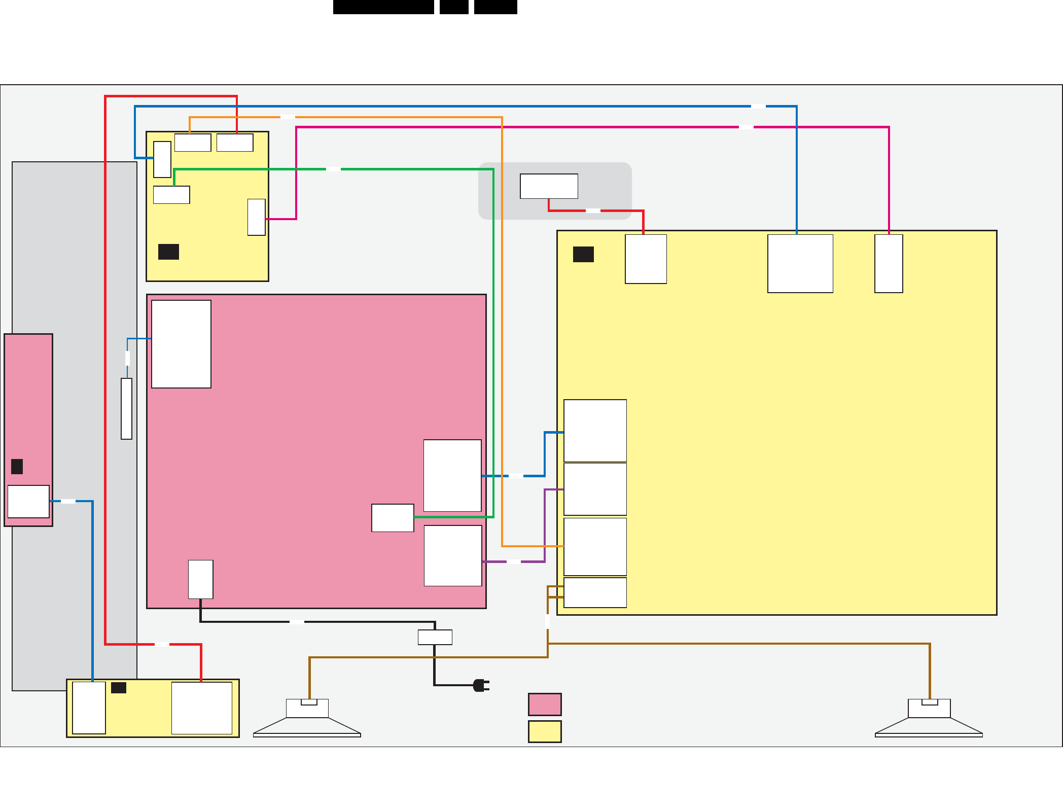
Block Diagrams EN 39LC8.2HA LA 9.
2009-Apr-10
9. Block Diagrams
Wiring Diagram 32" (ME8)
LEFT SPEAKER
14P
18510_400_090408.eps
090410
8M01
LCD DISPLAY (1004)
8P01
8418
8P02
8A35
1P10
1. LIGHT-SENSOR
2. GNDSND
3. RC
4. LED2
5. +3V3-STANDBY
6. LED1
7. KEYBOARD
8. +5V
9. KEYBOARD
1P11
1. GND
2. KEYBOARD
3. +3V3STBY
4. TACT_SWITCH_INT
CN1
2. L
1. N
J1
1. GND
2. KEYBOARD
3. +3V3STBY
4. INTERRUPT
8308
LVDS INPUT
30P
8R01
(5211) ME8 IN BACK COVER
IR LED PANEL
(1112)
J
KEYBOARD CONTROL
(0025)
E
SSB
(1150)
B
RIGHT SPEAKER
(5212) ME8 IN BACK COVER
+ - + -
INVERTER
INLET
MAIN POWER SUPPLY
(1005)
1R01(B04E)
1. ITV_I2C_SDA
2. TV_I2C_SDA
.
.
40. +VDISP
41. +VDISP
1508 (B06B)
1. GND
2. BOLT_0N _UART_RXD
3. BOLT_0N _UART_RXD
4. +3V3_STBY
5. ITV_I2C_SCL
6. ITV_I2C_SDA
7. REMOTE
8. DTV_IRQ
9. STANDBY
10. SCI_CVBS_RF_OUT
1509 (B06B)
1. HP_AUDIO_OUT_L
2. GND
3. HP_AUDIO_OUT_R
CN2
14. PDIM_Select
13. PWM
12. On/Off
11. Vbri
10. GND3
9. GND3
8. GND3
7. GND3
6. GND3
5. 24Vinv
4. 24Vinv
3. 24Vinv
2. 24Vinv
1. 24Vinv
CN6
1. 3V3Vstdby
2. Standby
3. GND1
4. GND1
5. GND1
6. +12V
7. +12V
8. +12V
9. +12V (audio)
10. GND2
11. -12V (audio)
CN7
1. +12V
2. +12V
3. GND1
4. GND1
5. BL_ON_OFF
6. DIM
7. Boost
8. ANALOG/PWM
dimming
WIRING 32" ( ME8)
1P02 (B01A)
8. ANA-DIG_DIM_SELECT
7. BACKLIGHT_BOOST
6. PWM_DIMMING
5. BACKLIGHT_ON_OFF
4. GND
3. GND
2. +12Vdisp
1. +12Vdisp
1P01 (B01A)
11. -12VAudio
10. GNDSND
9. +12VAudio
7. +12VS
6. +12VS
5. GND
4. GND
3. GND
2. STANDBY
1. +3V3STBY
1320 (B03)
9. KEYBOARD
8. +5V_SW
7. KEYBOARD
6. LED1
5. +3V3STBY
4. LED2
3. IR
2. GND
1. LIGHT_SENSOR
1A35 (B05B)
4. RIGHT+
3. GND
2. GND
1. LEFT-
CN8
1. 12V_PBS
2. SGND
3. CTRL_PBS
1209 (HC02)
3P
1110 (HC01)
8P
1109 (HC01)
9P
1205 (HC02)
10P
1108 (HC01)
3P
HC iBOARD
(1184)
8109
8CN8
8D11
8508
8509
Board Level Repair
Component Level Repair
Only For Authorized Workshop
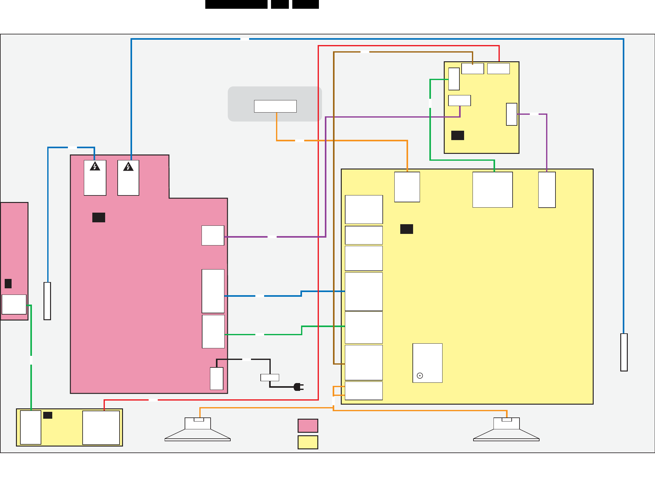
EN 40LC8.2HA LA 9.
Block Diagrams
2009-Apr-10
Wiring Diagram 42" (ME8)
INLET
KEYBOARD CONTROL
(0025)
1M01
3P
LEFT SPEAKER
TO BACKLIGHT
18510_401_090408.eps
090410
LCD DISPLAY
(1004)
8P01
8P02
8A35
8109
1P02
(B01A)
8. ANA-DIG_DIM_SELECT
7. BACKLIGHT_BOOST
6. PWM_DIMMING
5. BACKLIGHT_ON_OFF
4. GND
3. GND
2. +12Vdisp
1. +12Vdisp
1P01
(B01A)
11. -12VAudio
10. GNDSND
9. +12VAudio
7. +12VS
6. +12VS
5. GND
4. GND
3. GND
2. STANDBY
1. +3V3STBY
CN6
1. 3V3ST
2. Standby
3. GND
4. GND
5. GND
6. 12Vssb
7. 12Vssb
8. 12Vssb
9. +12Vaud
10. GND_aud
11. -12Vaud
CN7
1. 12Vssb
2. 12Vssb
3. GND
4. GND
5. INV_ON
6. DIM
7. BOOST
8. GND
1320
(B03)
9. KEYBOARD
8. +5V_SW
7. KEYBOARD
6. LED1
5. +3V3STBY
4. LED2
3. IR
2. GND
1. LIGHT_SENSOR
1A35
(B05B)
4. RIGHT+
3. GND
2. GND
1. LEFT-
1P10
1. LIGHT-SENSOR
2. GNDSND
3. RC
4. LED2
5. +3V3-STANDBY
6. LED1
7. KEYBOARD
8. +5V
9. KEYBOARD
1P11
1. GND
2. KEYBOARD
3. +3V3STBY
4. TACT_SWITCH_INT
CN1
1. N
2. L
1206
(B04C)
6. GND_24V
5. +24V_BOLT-ON
4. GND_24V
3. +24V_BOLT-ON
2. GND_24V
1. +24V_BOLT-ON
J1
1. GND
2. KEYBOARD
3. +3V3STBY
4. INTERRUPT
TO BACKLIGHT
WIRING DIAGRAM 42"
( ME8)
LVDS INPUT
50P
CN3
1. HV1
2. N.C.
3. HV1
DANGEROUS
HIGH VOLTAGE
CN2
1. HV2
2. N.C.
3. HV2
DANGEROUS
HIGH VOLTAGE
(5215) TWEETER
(5212) WOOFER IN BACK COVER
IR LED PANEL
(1112)
J
E
SSB
(1150)
B
RIGHT SPEAKER
(5215) TWEETER
(5211) WOOFER IN BACK COVER
+ - + -
1205
(B04C)
4. GND_24V
3. +24V_BOLT-ON
2. GND_24V
1. +24V_BOLT-ON
1202
(B04C)
7. GND
6. +3V3_SW
5. +3V3_FPGA
4. GND
3. AMBI_SDA
2. GND
1. AMBI_SCL
CN5
1. +12Vb
2. +12Vb
3. GND
4. GND
8R01
TUNER
1R01
(B04E)
1. ITV_I2C_SDA
2. TV_I2C_SDA
.
.
40. +VDISP
41. +VDISP
8401
8402
8M01
1212
(HC02)
4P
1110
(HC01)
8P
1109
(HC01)
9P
1205
(HC02)
10P
1108
(HC01)
3P
HC iBOARD
(1184)
1508
(B06B)
1. GND
2. BOLT_0N _UART_RXD
3. BOLT_0N _UART_RXD
4. +3V3_STBY
5. ITV_I2C_SCL
6. ITV_I2C_SDA
7. REMOTE
8. DTV_IRQ
9. STANDBY
10. SCI_CVBS_RF_OUT
1509
(B06B)
1. HP_AUDIO_OUT_L
2. GND
3. HP_AUDIO_OUT_R
8CN8
8509
8D11
8508
Board Level Repair
Component Level Repair
Only For Authorized Workshop
8308
MAIN POWER SUPPLY
(1005)
A
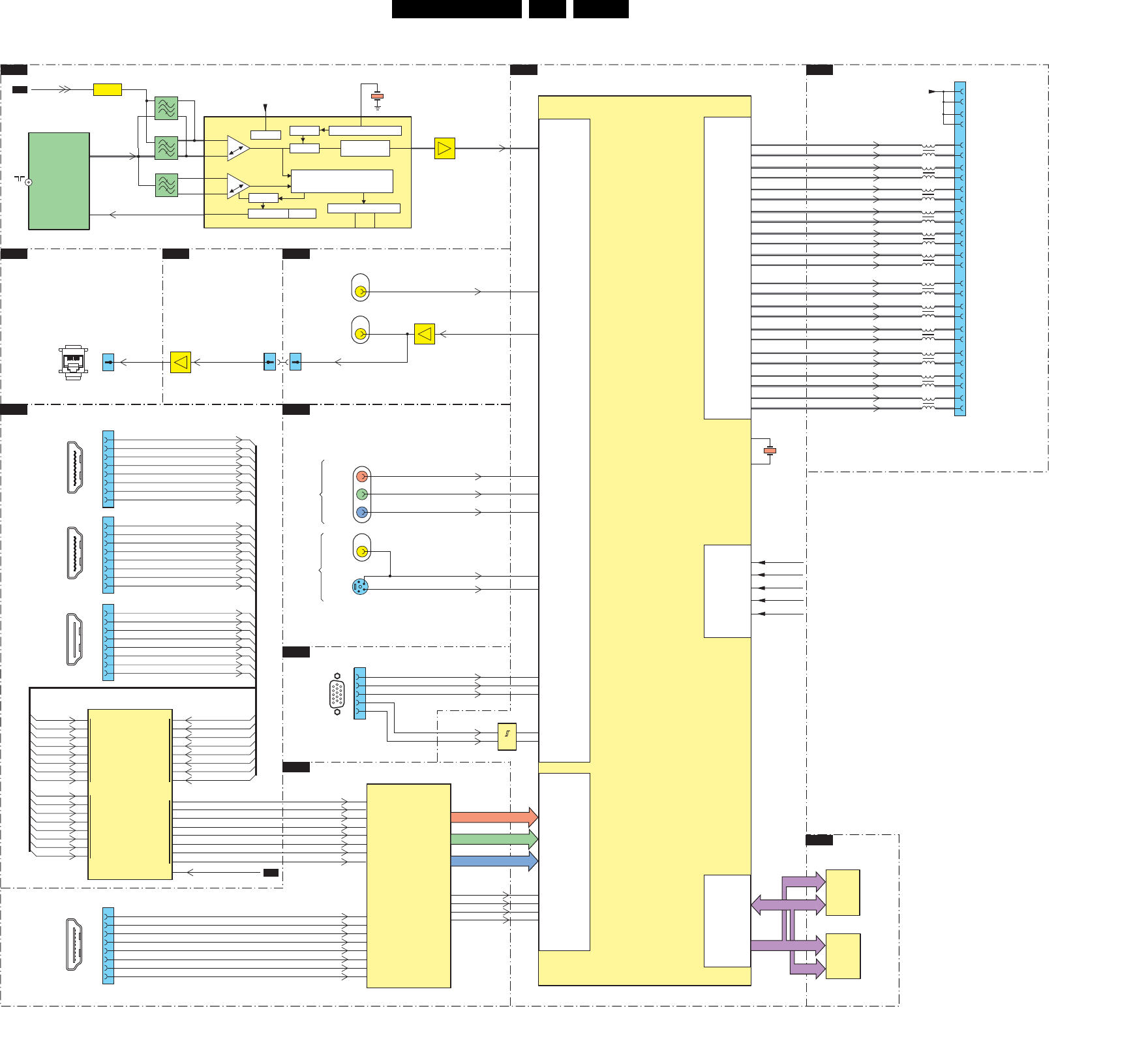
Block Diagrams EN 41LC8.2HA LA 9.
2009-Apr-10
Block Diagram Video
VIDEO
B2
TUNER IF & DEMODULATOR
B07A
HDMI SWITCH
B04A
TRIDENT - WX69
B04B
DDR INTERFACE
B07B
HDMI MAIN
B06C
VGA & PC AUDIO & COMPAIR & UART
B04E
LVDS CONNECTOR
B06B
I/O - CINCH 1 & 2
HC01
IBOARD
HC02
IBOARD
B06A
YPBPR & SVHS
1205 1508
10 10
SIF1
SIF2
VIF1
VIF2
17
CVBS
DEMODULATOR
7113
TDA9886T/V4
TUNER
IF_OUT3CVBS_RF
EF
7114
1C24
24MHz
W1
Y1
XTALI
7C01
WX69-7569-LF
7D01
EDD1216AJTA
SDRAM
7D02
EDD1216AJTA
SDRAM
Y4 CVBS1
SOUND TRAPS
4.5 to 6.5 Mhz
VIF-PLL
SINGLE REFERENCE QSS MIXER
INTERCARRIER MIXER AND
AM-DEMODULATOR
TUNER AGC VIF AGC
TA G C
SIF AGC
I2C-BUS TRANSCEIVER
MAD
SCL
SDA
SUPPLY
+5VS
1RF_AGC
DC_PWR
DIDITAL VCO COTROLRC VCO
REF
2
1
5
4
8
7
11
10 58
57
62
61
66
65
70
69
HDMI_MUX_RST
B4C
13
68
67
65
64
62
61
59
58
28
27
25
24
22
21
19
18
48
47
45
44
42
41
39
38
19 1
182
1
1M03
3
4
7
9
10
12
6
HDMI C
CONNECTOR
19 1
182
1
1M02
3
4
7
9
10
12
6
HDMI B
CONNECTOR
RJ45
1
1M01
3
4
7
9
10
12
6
1
1N03
3
4
7
9
10
12
6
TX2_A+
TX2_A-
TX1_A+
TX1_A-
TX0_A+
TX0_A-
TXC_A+
TXC_A-
19 1
182
HDMI (SIDE)
CONNECTOR
19 1
182
HDMI A
CONNECTOR
52
51
48
47
44
43
40
39
HDMI_MUX_TXC+
HDMI_MUX_TXC-
HDMI_MUX_TX0+
HDMI_MUX_TX0-
HDMI_MUX_TX1+
HDMI_MUX_TX1-
HDMI_MUX_TX2+
HDMI_MUX_TX2-
HDMI_SIDE_RX2+
HDMI_SIDE_RX2-
HDMI_SIDE_RX1+
HDMI_SIDE_RX1-
HDMI_SIDE_RX0+
HDMI_SIDE_RX0-
HDMI_SIDE_RXC+
HDMI_SIDE_RXC-
7M07
SII9185ACTU
HDMI
SWITCH
WX69
VIDEO PROCESSOR
R1X
R0X R2X
TX
20
(I2C)
7N01
SII9125CTU
HDMI
MAIN
HDMI_CR(0-9)
HDMI_Y(0-9)
HDMI_CB(0-9)
21
20 V20
Y19
HDMI_H
HDMI_V
5
19 Y20
W20
HDMI_DE
HDMI_VCLK
RX2_C+
RX2_C-
RX1_C+
RX1_C-
RX0_C+
RX0_C-
RXC_C+
RXC_C-
RX2_B+
RX2_B-
RX1_B+
RX1_B-
RX0_B+
RX0_B-
RXC_B+
RXC_B-
1
1E01
2
3
14
13
U8PC_R
VGA_R_IN
Y7 PC_G
VGA_G_IN
W10 PC_B
VGA_B_IN
V10 AIN_H
VGA_H
U10 AIN_V
VGA_V
1
610
11
5
15
VGA
CONNECTOR
DPA_HS
DPA_VS
DPB_DE
DPA_CLK
TXFPGAe_2p
1R04
TXFPGAe_2n
LVD S
CONNECTOR
TO DISPLAY
TXFPGAe_CLKp
1R05
TXFPGAe_CLKn
TXFPGAe_3p
1R06
TXFPGAe_3n
TXFPGAe_4p
1R07
TXFPGAe_4n
LTXFPGAo_0p
1R08
TXFPGAo_0n
TXFPGAo_1p
1R09
TXFPGAo_1n
TXFPGAo_2p
1R10
TXFPGAo_2n
TXFPGAo_CLKp
1R11
TXFPGAo_CLKn
TXFPGAo_TXo3p
1R12
TXFPGAo_TXo3n
TXFPGAo_TXo4p
1R13
TXFPGAo_TXo4n
TXFPGAe_0p
1R02
TXFPGAe_0n
TXFPGAe_1p
TXFPGAe_1n 1R03
A16
B16
A17
B17
A18
B18
A19
B19
A20
B20
C20
D19
D20
E19
E20
F19
F20
G19
G20
H19
A14
B14
A15
B15
1R01
6
5
4
10
9
7
14
13
12
17
16
15
21
20
19
25
24
22
29
28
27
32
31
30
38
41
40
39
VDISP
HDMI_SIDE_RX2+
HDMI_SIDE_RX2-
HDMI_SIDE_RX1+
HDMI_SIDE_RX1-
HDMI_SIDE_RX0+
HDMI_SIDE_RX0-
HDMI_SIDE_RXC+
HDMI_SIDE_RXC-
RX2_B+
RX2_B-
RX1_B+
RX1_B-
RX0_B+
RX0_B-
RXC_B+
RXC_B-
RX2_C+
RX2_C-
RX1_C+
RX1_C-
RX0_C+
RX0_C-
RXC_C+
RXC_C-
15
1104
4M0
18510_402_090408.eps
090410
WX_MD
WX_MA
(16-31)
(0-15)
(0-11)
(0-11)
10 BIT DUAL LVDS
XTALO
+1V2_CORE
+2V5_VDDMQ
+3V3_SW
+1V2_PLL
SUPPLY
DDR_VREF
C14
B4
L16
D18
K3
7C03
1
8
5
4
1502
VIDEO
IN
W6
SC2_Y_CVBS_IN Y_G1
15
1504
VIDEO
out
W2
SC1_RF_OUT_CVBS
SC1_CVBS_RF_OUTSC1_CVBS_RF_OUTCVBSterr
CVBS_OUT1
15
MEMORY
LVD S OUT
DIGITAL
VIDEO
ANALOG
VIDEO
1615
Y
Pr
Pb
Y8
V6
W9
HD_PR_IN
HD_Y_IN
HD_PB_IN
Y_G1
PB_B1
PR_R1
1
5
SVHS
24
3
1601
1602
SVHS_Y_CVBS_IN
VIDEO
V9 C
Y6 Y_G3
SVHS_C_IN
SIDE
I/O
CVI-1
2
9
12
7
1
5
4
1102 1
2
IF_ATV
11
38MHz9
1
5
4
1103
38MHz9
*38MHz
1
5
4
*1105
38MH
SAW_SWSAW_SW
7109
B03
(CONTROL)
2
10
*ONLY FOR CHINA
1101
UV1316E/ABH
*UV1356/ABHN
7503-7504
7215-7217
9
1107
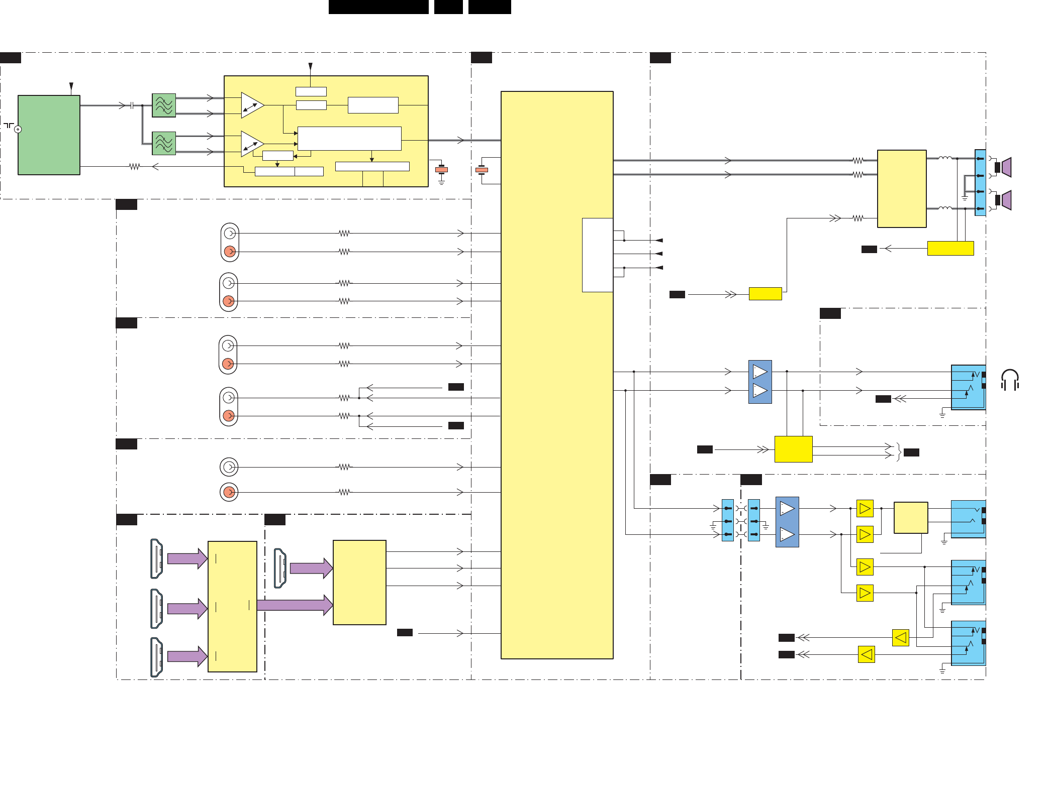
EN 42LC8.2HA LA 9.
Block Diagrams
2009-Apr-10
Block Diagram Audio
AUDIO
AUDIO - CLASS D
B05B
AUDIO PROCESSOR - MICRONAS
B05A
YPBPR & SVHS
B06A
TUNER IF & DEMODULATOR
B02
B06A YPBPR & SVHS
VGA & PC AUDIO & COMPAIR & UART
B06C
I0 - CINCH 1& 2
B06B
HDMI SWITCH
B07A HDMI MAIN
B07B
I0 - CINCH 1& 2
B06B IBOARD
HC01
7411
MSP4450P-VK-E8 000 Y
SIF 63
48
49
19 1
182
27
26
18510_403_090408.eps
090408
SOUND
PROCESSOR
ANA-IN1+
DACM-L
DACM-R
TXx_A
1615
CVI
AUDIO
L/R IN
50 SC3-IN-L
51 SC3-IN-R
AUDIO_LS_L
AUDIO_LS_R
7A01
TDA8932BTW/N2
7121
TDA8551T/N1
CLASS D
POWER
AMPLIFIER
2
14
27
22
ENGAGE 5
1
2
RIGHT
SPEAKER
SCK
WS
SD0
1A35
3
4
LEFT
SPEAKER
DC-DETECTION
3A03
3A11
7A51
HP_AUDIO_OUT_L
HP_AUDIO_OUT_R
HP_AUDIO_OUT_L
HP_AUDIO_OUT_R
LEFT
RIGHT
HP_LOUT
HP_ROUT
ANTI_PLOP
HDMI_MUX_TX
24
23
DACA-L
DACA-R
COMP_AUDIO_IN_L
COMP_AUDIO_IN_R
SC4-IN-L
SC4-IN-R
1603
2
1
3
4HEADPHONE
EXTERNAL
SPEAKER
AUDIO
L/R
OUT
AUDIO
L/R
OUT
MUTE
MUTEn
B03
B03
DC_PROT
B03
SIF1
SIF2
VIF1
VIF2
CVBS
DEMODULATOR
7113
TDA9886T/V4
SOUND TRAPS
4.5 to 6.5 Mhz
VIF-PLL
SINGLE REFERENCE QSS MIXER
INTERCARRIER MIXER AND
AM-DEMODULATOR
TUNER AGC VIF AGC
TA G C
SIF AGC
I2C-BUS TRANSCEIVER
MAD
SCL
SDA
SUPPLY
12
SIOMAD
+5VS
1411
18M432
67
68
XTALIN
XTALOUT
3A26
5A03
5A04
SC1_AUDIO _MUTE_R
SC1_AUDIO _MUTE_L
B06B
15
1104
4M0
SUPPLY
SUP_D
+8V
SUP_A
12
13
61
62
39
7A05÷7A07
3607
3611
57
58
SC5-IN-L
SC5-IN-R
VGA_AUDIO_IN_L
VGA_AUDIO_IN_R
CVI-1
AUDIO
L/R IN
3E21
3E23
20
HDMI_I2S_SCK 17
86
HDNI_I2S_WS18
85
HDMI_I2S_SD20
81
CL3
WS3
DA-3
2
6
1
7
7131
2
6
1
7
1
5
4
1102 1
2
IF-ATV
TUNER
11
IF1
14
1
VIF1
VIF2
RF_AGC
+VTUN
9
3111
2117
DC_PWR
HDMI C
HDMI B
HDMI SIDE
HDMI A
7M07
SII9185ACTU
HDMI
SWITCH
7N01
SII9125CTU
HDMI
MAIN
SIDE_AUDIO_IN_L
SIDE_AUDIO_IN_R
1602
AUDIO
L/R IN
3623
3621
HP_DETECT
B03
1504
SC1_AUDIO _OUT_R
SC1_AUDIO _OUT_L
52
53
SC2-IN-L
SC2-IN-R
37SC1-OUT-L
36SC1-OUT-R
SC1_AUDIO _MUTE_L
SC1_AUDIO _MUTE_R
B05B
B05B
AV OUT
AUDIO
L/R OUT
1502
AV IN
AUDIO
L/R IN SC2_AUDIO_IN_R
SC2_AUDIO_IN_L
19 1
182
19 1
182
19 1
182
RXx_C
RXx_B
RXx_SIDE
+
-RX0
+
-R1X
+
-R2X
+
-
TX
1N03
1M03
1M02
1M01
3507
3503
3512
3506
(CONTROL)
(CONTROL)
(CONTROL)
(CONTROL)
AUD_RST19 DA-3
B03
(CONTROL)
1E07
1E02
PC / DVI AUDIO
ANTI_PLOP
5
8
3
5
6
6
2
2
2
2
(I2C)
23
24
1
5
4
1103SIF1
SIF2
1101
UV1316E/ABH
*UV1356/ABHN
AUDIO
AMPLIFIER
DIG. VOL.
CONTROL
8
5
1
4
1509 1108
11
33
22
1114
4
1
3
2
1105
4
1
3
2
HP_DET2
Volume Control
HC02
M0DE_HP_DET
HC02
EF
7130
EF
7123
EF
7124
7110
7111
1113
2
3
1
EF
7127
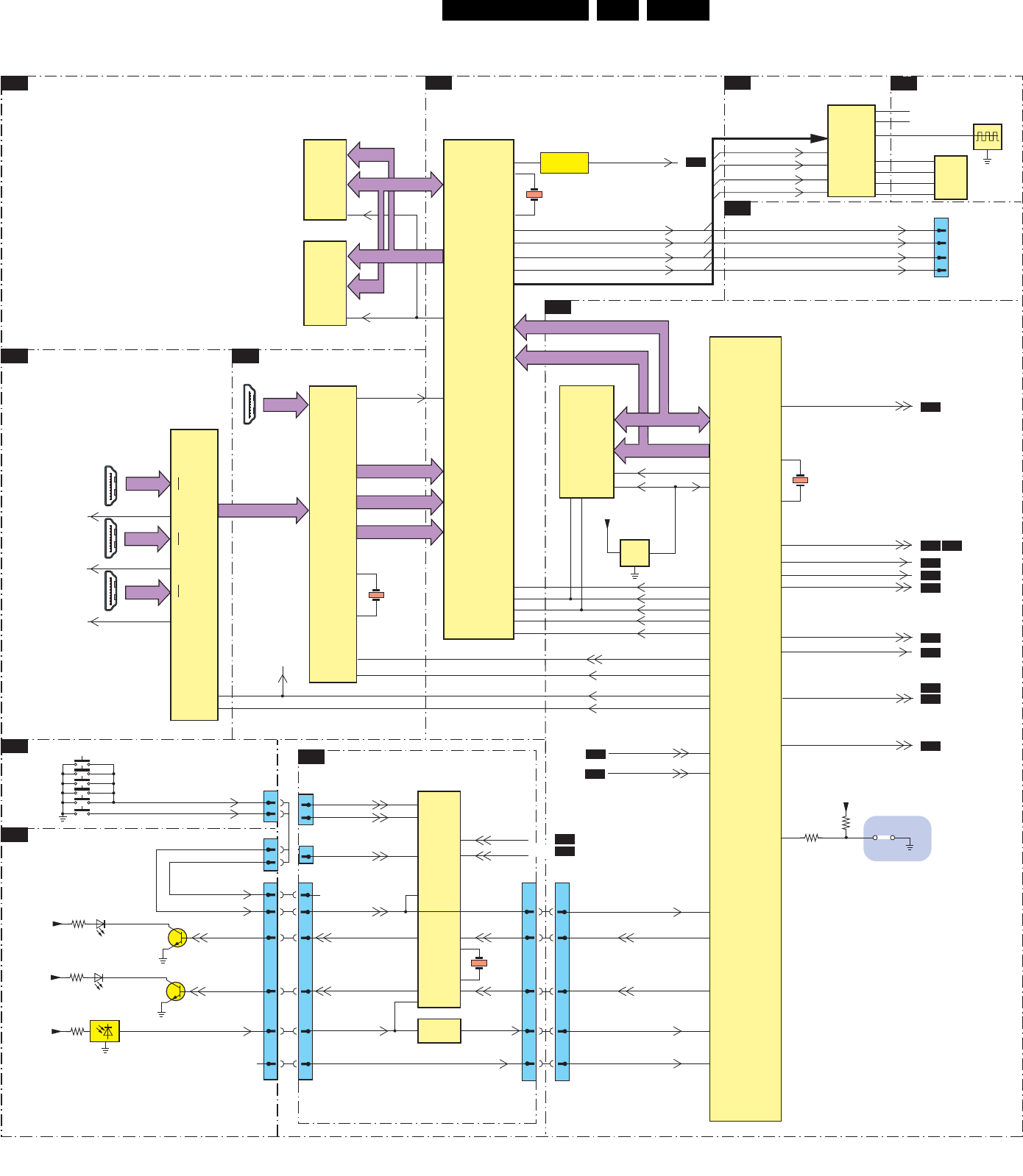
Block Diagrams EN 43LC8.2HA LA 9.
2009-Apr-10
Block Diagram Control & Clock Signals
MICROPROCESSOR
B03
KEYBOARD CONTROL
E
IR/LED PANEL
J
DDR INTERFACE
B04B
HDMI SWITCH
B07A
CONTROL & CLOCK SIGNALS
TRIDENT - WX69
B04A
HDMI MAIN
B07B
LVD S CONNECTOR
B04E
FPGA I/O BANKS
(RESERVED)
B04D FPGA INTERGACE
(ONLY FOR AMBI-LIGHT)
B04C
IBOARD
HC
1110 1320
66
33
44
77
11
1R01
25
18
93
95
87
7311
M30300SAGP
LED1
IR
SENSOR
IR
1P10 1109
66
33
44
7P11
+3V3STBY
7P14
3P16
6P11
LED1
WHITE
+5V_SW
3P11
J1
4
1P11
4
77
ON / OFF
CHANNEL -
VOLUME +
VOLUME -
CHANNEL +
MENU
LED2
7P10
6P10
LED2
RED
+5V_SW
3P10
LED1
LED2
REMOTE
KEYB
25 4301 SDM
3L56
3L79
+3V3_STBY
1301
10M
13
11
7C01
WX69-7569-LF
VIDEO
PROCESSOR
7D01
EDD1216AJTA
SDRAM
7D02
EDD1216AJTA
SDRAM
WX_MD(0-31)
WX_MA(0-11)
HDMI_Cb(0-7)
HDMI_Y(0-7)
HDMI_Cr(0-7)
19 1
182
RXx_SIDE
19 1
182
7N01
SII9125CTU
44
44
B12
WX_MCLK
HDMI_VCLK
5W20
TxFPGAe_CLKn
B17
TxLVDSe_CLKn
24
TxFPGAe_CLKp
A17
TxLVDSe_CLKp TO DISPLAY
(LVDS)
92
11 LIGHT_SENSOR
89
HDMI_HOTPLUG_RST
88 AUD_RST
B05A
99 LCD_PWR_ON
B04E
19 DDC_RST
B07A
23SAW_SW
B02
78MUTEn
75 BL_ON_OFF
B01A
74 ANTI_PLOP
B05B
18510_404_090408.eps
090410
7310
M29W800DT
EPROM
1Mx8
512Kx16
A(0-19)
AD(0-7)
A(0-7)
AD(0-7)
J17 45
CS
J20 42
RD
J19 44
WR
J1838
ALE_EMU
CPU_RST
12 10
26 48
CE
11 28
7312
BD45275G
4
(3V3)
VOUT
2,3
+3V3_STBY
5
G17
BL_ADJUST_PWM
CONTROL
7C02
7C04
B01A
3STANDBY
B01A B06B
22 BL_BOOST
B01A
7M07
SII9185ACTU
HDMI_MUX_TX
19 1
182
RXx_B
RXx_C
HDMI
SWITCH
+
-R0X
+
-R1X
+
-R2X
HDMI
MAIN
76
5
HDMI_RX_BUF_RST
100
73
HDMI_INT_MUX
35
36
HDMI_MUX_RST
13
10
TxFPGAo_CLKn
F19
TxLVDSo_CLKn
9
TxFPGAo_CLKp
E20
TxLVDSo_CLKp
7700
EP2C5F256C7N
FPGA
CYCLONE II
AMBI-LIGHT
TxFPGAe_CLKn
TxFPGAe_CLKp
TxFPGAo_CLKn
TxFPGAo_CLKp
7201
EPCS4SI8
SCD
nCSO
DCLK
ASDO
DATA0
1204
27M
H4
F4
H2
CLK_OSC1
F1
C3
J15
J16
H16
H15
N.C.
19 1
182
RXx_B
35
HP_DETECT
B06A
MICRO
PROCESSOR
F184
SVPWX_RST
2
2
99
KEYBOARD
TA C T _ SWITCH_INT
AUDIO
AUDIO
B05B
B07B
HDMI
CONNECTORS
31
DC_PROT
B05B
AUDIO
HC01
HC01
AUDIO
SUPPLY
1C24
24MHZ
W1
Y1
1
6
5
2
1N02
28M322
95
94
HDMI
CONNECTOR
SDA
SCL
70
71
TO AMBI-LIGHT
(I2C)
HPD_RST_B
36
16
HPD_RST_C
HPD_RST_SIDE
56
HDMI
CONNECTOR
TO HDMI A
CONNECTOR
DUAL LVDS
VIDEO
KEYBOARD
LIGHT_SENSOR
7207
7209
UPSD3333D
LED1
LED2
HP_DET2
LED1_OUT
N.C.
FROM CN5 PSU
FROM 1508 SSB
LED2-OUT
1
28
25
10
37
MODE_HP_DET
27
35
CONTROL
RC_IR IR_IN_TV
1203
24M
31
32
1508-91P01.2
STANDBY
34
AV1-STAT U S
52
STANDBY
39
40
CTRL_12VPBS
1209
8
1205
2
9
MCU
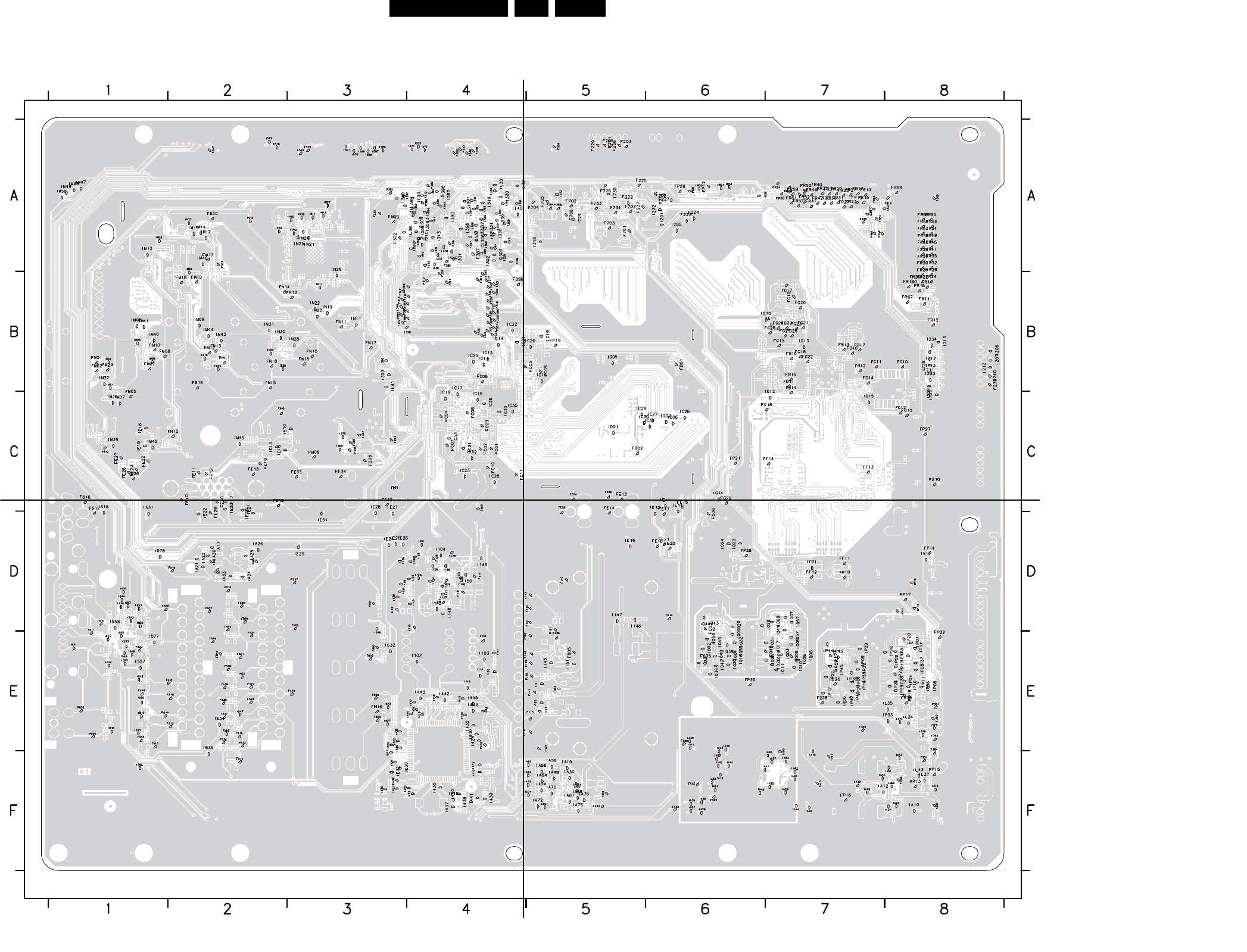
EN 44LC8.2HA LA 9.
Block Diagrams
2009-Apr-10
SSB: Test Points (Overview Bottom Side)
3139 123 6349.1
I_17760_022.eps
300708
Part 1
I_17760_022a.epsPart 2
I_17760_022b.eps
Part 4
I_17760_022d.eps
Part 3
I_17760_022c.eps
A115 D4
A116 D3
A124 E4
A125 D4
F101 D5
F112 D5
F114 D4
F115 E5
F116 E4
F117 E5
F118 E5
F119 E5
F120 E4
F121 D4
F128 D4
F129 D4
F130 D4
F131 D4
F133 E4
F134 E5
F140 D4
F142 D5
F143 D4
F146 E5
F201 A5
F202 A6
F203 A5
F204 A6
F205 A5
F207 A5
F208 C3
F210 C8
F211 B8
F222 A5
F223 A6
F224 A6
F225 A5
F227 A6
F228 A5
F229 A5
F236 A5
F237 A5
F238 E7
F239 B8
F240 B8
F302 A3
F303 A2
F305 A5
F309 A4
F310 B4
F311 B4
F312 B3
F313 B4
F314 B3
F315 A4
F316 B3
F317 B4
F318 B3
F319 B4
F320 B3
F321 B4
F322 B3
F323 A3
F324 B4
F325 B3
F326 B4
F327 B3
F328 B4
F329 B4
F330 A3
F331 B4
F332 B4
F333 B4
F334 B4
F335 B4
F336 B4
F337 B4
F338 B4
F339 B4
F340 B4
F341 B4
F345 C2
F346 A8
F347 A2
F348 A4
F349 A4
F350 C3
F351 F8
F352 A4
F353 A4
F354 A7
F356 C3
F357 E8
F360 E7
F361 A4
F362 A4
F363 A4
F364 A5
F365 A5
F366 B4
F367 A4
F368 B3
F369 B3
F380 A4
F381 A3
F382 E8
F383 E8
F384 E8
F385 A4
F386 A4
F387 A4
F388 B4
F401 E4
F402 F3
F403 E4
F404 F5
F510 E1
F511 F2
F512 E2
F513 E2
F514 E1
F515 E2
F516 D2
F517 D3
F518 E2
F519 E2
F520 E3
F521 E2
F522 E2
F523 E1
F524 E2
F525 D3
F526 D2
F527 D2
F528 D2
F529 D1
F530 D2
F531 E2
F532 E2
F534 A3
F535 A3
F536 E2
F537 E2
F538 E2
F539 E2
F540 E2
F541 E2
F542 D2
F543 E1
F544 E1
F601 E1
F602 E1
F604 D3
F605 E3
F607 E3
F608 E3
F609 E3
F610 D1
F611 D1
F612 C1
F613 C3
F614 D6
F615 E2
F616 C1
F617 C1
F618 B2
F619 C2
F620 A2
F701 A5
F702 A5
F703 A5
F704 A5
F705 A5
F706 A5
F733 A5
F734 A5
F901 D2
F904 D2
FA04 F6
FA05 F6
FA06 D2
FA07 F8
FA08 F8
FA09 E6
FA10 F7
FA11 F7
FA12 F5
FA13 F6
FA32 F7
FB10 B7
FB11 B7
FB12 B7
FB13 B7
FB14 C7
FB15 B7
FB16 B7
FB17 B7
FC01 C4
FC02 C4
FC03 C4
FC04 C4
FC05 B5
FC06 B4
FC07 C4
FC08 C4
FC09 B5
FC10 C4
FC11 C4
FD01 B6
FD02 C5
FE10 C2
FE11 C2
FE12 C2
FE13 C5
FE14 C5
FE15 C6
FE16 D6
FE17 D6
FE18 C2
FE19 C2
FE20 D6
FE21 D6
FE22 C1
FE23 C1
FE24 C5
FE25 C1
FE26 C5
FE27 C1
FE28 C5
FE29 D2
FE30 C2
FE31 C3
FE32 C3
FE33 C3
FE34 C3
FF10 D7
FF11 D7
FF12 D7
FF13 C7
FF14 C7
FG10 B8
FG11 B7
FG12 C8
FG13 C8
FG14 B7
FG15 B7
FG16 B7
FG17 B7
FG18 C7
FG19 B7
FG20 B7
FG21 B7
FG22 B7
FG23 B7
FG24 B7
FG25 B7
FG26 B7
FG27 B7
FG28 B6
FG29 C6
FM01 B1
FM02 B1
FM05 B1
FM06 C3
FM07 B1
FM08 B1
FM09 A3
FM10 B1
FM11 B2
FM12 B2
FM13 B2
FM15 B2
FM17 A2
FM18 B2
FM19 B2
FM24 B1
FM25 B2
FM26 C1
FN10 B3
FN11 B3
FN12 C2
FN13 B3
FN14 B2
FN15 B3
FN16 E3
FN17 B3
FN18 B2
FP10 E8
FP11 D8
FP12 A6
FP13 F8
FP14 D8
FP15 F8
FP16 F7
FP17 D8
FP18 E8
FP19 B5
FP20 D8
FP21 C6
FP22 E8
FP23 E8
FP24 E7
FP26 E7
FP27 C8
FP28 D6
FP29 A6
FP30 E6
FQ03 D6
FQ05 E5
FQ06 D6
FQ08 E7
FQ35 E6
FQ40 E6
FR10 A8
FR11 B8
FR12 B8
FR13 A7
FR14 B8
FR15 A7
FR16 B8
FR17 A7
FR18 B8
FR19 A7
FR20 B8
FR21 A7
FR22 B8
FR23 A7
FR24 B8
FR25 A7
FR26 B8
FR27 A7
FR28 B8
FR29 A7
FR30 A8
FR31 A7
FR32 A8
FR33 A8
FR34 A7
FR35 A8
FR36 A7
FR37 A7
FR38 A7
FR39 A8
FR40 A7
FR41 A8
FR42 A7
FR43 A8
FR44 A7
FR45 A8
FR46 A7
FR47 A7
FR48 A8
FR49 A8
FR50 A7
FR51 A7
FR52 A7
FR53 A8
FR54 A8
FR55 A7
FR56 A8
FR57 A7
FR58 A8
FR59 A7
FR60 A8
FR61 A7
FR62 A8
FR63 A7
FR64 A7
FR65 A8
FR66 A7
FR67 B8
FR68 A7
FR69 A8
I102 E4
I103 E4
I104 D4
I111 E5
I113 D4
I114 E4
I118 E4
I120 E4
I121 E5
I123 E5
I124 D4
I125 D4
I126 D4
I127 D4
I128 D3
I129 D4
I130 D3
I131 D3
I133 D4
I135 D4
I136 D3
I138 D4
I139 D4
I141 E4
I142 D4
I143 D4
I144 D4
I145 E5
I146 D5
I147 D5
I148 D4
I149 D4
I150 D4
I151 E5
I201 A6
I205 A6
I206 B8
I207 B8
I209 B8
I212 B8
I213 B8
I232 A6
I233 B8
I234 B8
I301 A4
I302 A4
I303 A4
I306 A4
I307 A4
I308 A4
I309 A4
I310 A4
I311 A4
I312 A4
I313 A4
I315 A4
I316 A4
I318 A5
I319 A4
I320 A4
I321 A4
I322 A4
I323 A4
I324 A4
I326 A4
I327 F5
I328 A4
I329 A4
I330 A7
I331 A4
I332 A8
I333 A4
I335 A4
I336 A4
I337 A4
I338 B4
I339 A4
I340 A3
I341 A4
I342 A4
I344 A4
I345 A4
I347 C3
I349 A4
I350 A4
I351 A4
I352 A4
I353 A3
I354 A4
I356 A4
I357 A3
I358 A4
I359 A4
I360 C4
I361 D4
I362 A4
I363 E5
I364 A4
I365 A4
I366 A4
I367 A4
I368 A4
I369 C3
I370 C3
I372 A5
I373 E8
I374 E8
I375 F8
I376 E8
I380 B3
I384 A4
I387 A4
I390 A4
I393 B3
I396 A4
I397 A4
I398 A4
I412 F4
I413 F4
I414 E4
I415 E4
I416 E4
I417 E4
I418 E4
I419 E4
I420 F3
I421 F3
I422 F3
I423 F4
I424 F3
I425 E3
I429 E4
I430 E4
I432 E4
I436 F4
I437 F4
I438 F4
I439 F4
I440 F4
I441 F4
I442 E4
I443 E4
I444 E4
I445 E4
I446 F4
I510 E4
I512 E1
I517 E1
I520 E1
I528 D1
I530 D1
I533 E1
I541 E2
I543 D1
I544 D1
I545 E1
I548 E1
I549 E1
I550 E1
I551 D1
I552 D1
I553 E1
I554 D1
I556 A3
I557 E1
I558 D1
I563 E2
I564 F1
I565 A3
I567 A3
I568 A3
I570 A3
I571 A3
I572 A4
I573 A4
I574 A4
I575 A2
I576 A2
I577 E1
I578 D1
I610 E3
I611 F3
I615 E1
I616 E3
I620 E3
I621 E1
I622 E3
I623 E3
I624 E1
I627 E3
I631 E1
I632 E3
I634 E2
I635 E2
I705 C8
I712 B8
I713 B8
I728 B8
I729 A5
I730 A5
IA10 F8
IA11 D8
IA12 F7
IA13 F6
IA14 F7
IA15 F7
IA16 F7
IA17 D2
IA18 D1
IA19 F5
IA20 D2
IA21 D2
IA22 D2
IA23 F8
IA24 F7
IA25 D2
IA26 D2
IA27 F6
IA28 F6
IA29 F7
IA30 F5
IA31 C1
IA32 F7
IA33 D2
IA34 D2
IA35 F6
IA36 F6
IA37 F7
IA38 E6
IA39 F7
IA40 E6
IA41 E6
IA42 E6
IA43 F6
IA44 F6
IA45 F6
IA46 F7
IA47 F7
IA48 F5
IA49 F7
IA50 F7
IA51 F6
IA52 F8
IA53 F7
IA54 F5
IA55 F7
IA56 F6
IA57 F5
IA58 F8
IA59 F5
IA60 F6
IA61 F8
IA62 F7
IA63 F5
IA64 F5
IA65 F5
IA66 F5
IA67 F5
IA68 F5
IA69 A4
IA70 F5
IA71 F5
IA72 F5
IA73 F5
IA74 F5
IA75 F5
IA76 F5
IC10 C4
IC11 B4
IC13 B4
IC14 B4
IC15 B5
IC16 C4
IC17 B4
IC18 C4
IC19 B5
IC20 B5
IC21 B4
IC22 B4
IC23 C4
IC24 C4
IC25 B4
IC26 C6
IC27 C6
IC28 C4
IC29 C5
IC30 C5
IC31 C6
IC32 C4
IC33 C4
IC35 C4
IC36 C4
ID01 C5
ID05 B5
ID06 C6
ID07 C6
IE10 C2
IE11 C6
IE12 C6
IE13 C2
IE14 D6
IE15 C3
IE16 D5
IE17 C2
IE18 C1
IE19 C1
IE20 D2
IE21 D2
IE22 D2
IE23 D2
IE24 D3
IE25 D3
IE26 D3
IE27 D3
IE28 C3
IE29 D3
IE30 F3
IE31 D3
IE32 F3
IF01 D7
IG10 B7
IG11 B6
IG12 C7
IG13 B7
IG14 C6
IG15 C7
IL25 A4
IL30 A4
IL32 A4
IL33 A4
IL34 E8
IL35 E8
IL37 F8
IL38 A3
IL39 A3
IL40 A4
IL41 B3
IL42 A4
IL43 F8
IM01 B1
IM02 B1
IM03 B1
IM04 B1
IM07 C1
IM08 B1
IM09 B2
IM10 B2
IM12 A2
IM13 A1
IM14 A2
IM15 A2
IM27 A2
IM35 A1
IM36 A2
IM37 B1
IM38 C1
IM39 C1
IM40 B1
IM41 B1
IM42 C1
IM43 B2
IM44 B2
IM45 C2
IM46 A2
IM47 A1
IM48 A1
IM49 A1
IM50 A1
IN10 A3
IN11 B3
IN12 A3
IN13 A3
IN14 A3
IN15 A2
IN16 A3
IN17 B3
IN18 A2
IN19 B3
IN20 B3
IN21 A3
IN22 B3
IN23 B2
IN24 A3
IN25 A3
IN26 A3
IN27 A3
IN28 B3
IN29 B2
IN30 B2
IN31 B2
IP01 E7
IP02 E7
IP04 E8
IP05 E8
IP06 E8
IP07 E8
IP08 E8
IP09 E7
IP10 E8
IP11 E8
IP12 E7
IP14 D8
IP15 D8
IP16 E7
IP17 E8
IP25 E8
IP26 E7
IP27 E7
IP28 E8
IP29 E7
IP31 E8
IP32 E7
IP33 E8
IP36 E7
IP37 E8
IP38 E8
IP39 E7
IP40 E7
IP41 E8
IP42 E7
IP43 E7
IP44 E7
IP45 E7
IP55 E7
IP56 E8
IP57 E8
IP59 E7
IQ01 E6
IQ02 E6
IQ03 E7
IQ04 E7
IQ05 E7
IQ06 E7
IQ07 D7
IQ08 D7
IQ09 D6
IQ10 E7
IQ11 E7
IQ12 E6
IQ16 E6
IQ17 E7
IQ23 D6
IQ24 D6
IQ25 E7
IQ26 E6
IQ27 E6
IQ28 D6
IQ29 D6
IQ31 E6
IQ32 E6
IQ36 E6
IQ37 E7
IQ39 E6
IQ40 E6
IQ41 D7
IQ42 E6
IQ43 D6
IQ44 D6
IQ45 E6
IQ55 E6
IQ56 E7
IQ57 D7
IQ59 E6
IR01 A6
IR02 A6
IR04 A6
IR06 A6
IR08 A6
IR10 A7
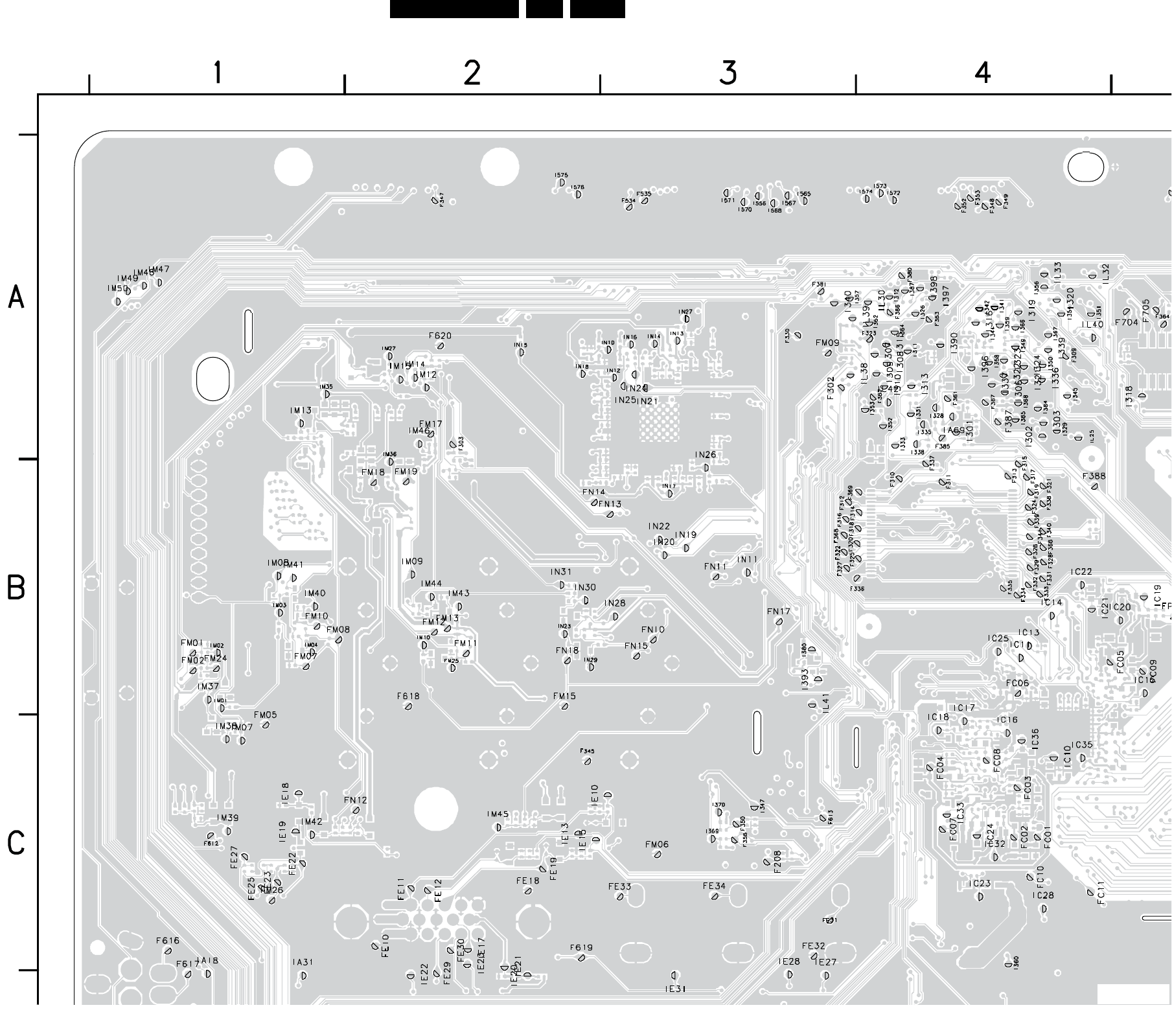
Block Diagrams EN 45LC8.2HA LA 9.
2009-Apr-10
SSB: Test Points (Part 1 Bottom Side)
I_17760_022a.eps
300708
Part 1
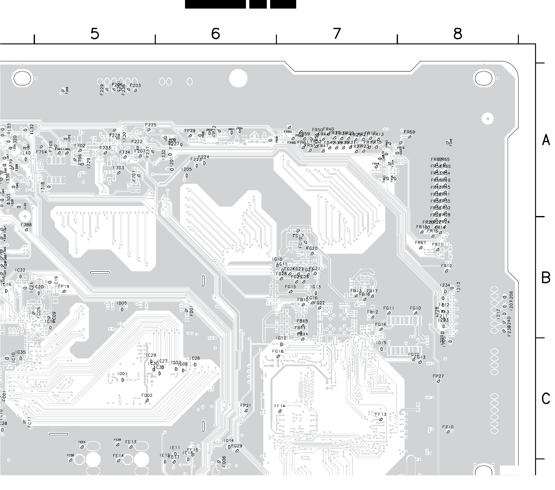
EN 46LC8.2HA LA 9.
Block Diagrams
2009-Apr-10
SSB: Test Points (Part 2 Bottom Side)
I_17760_022b.eps
300708
Part 2
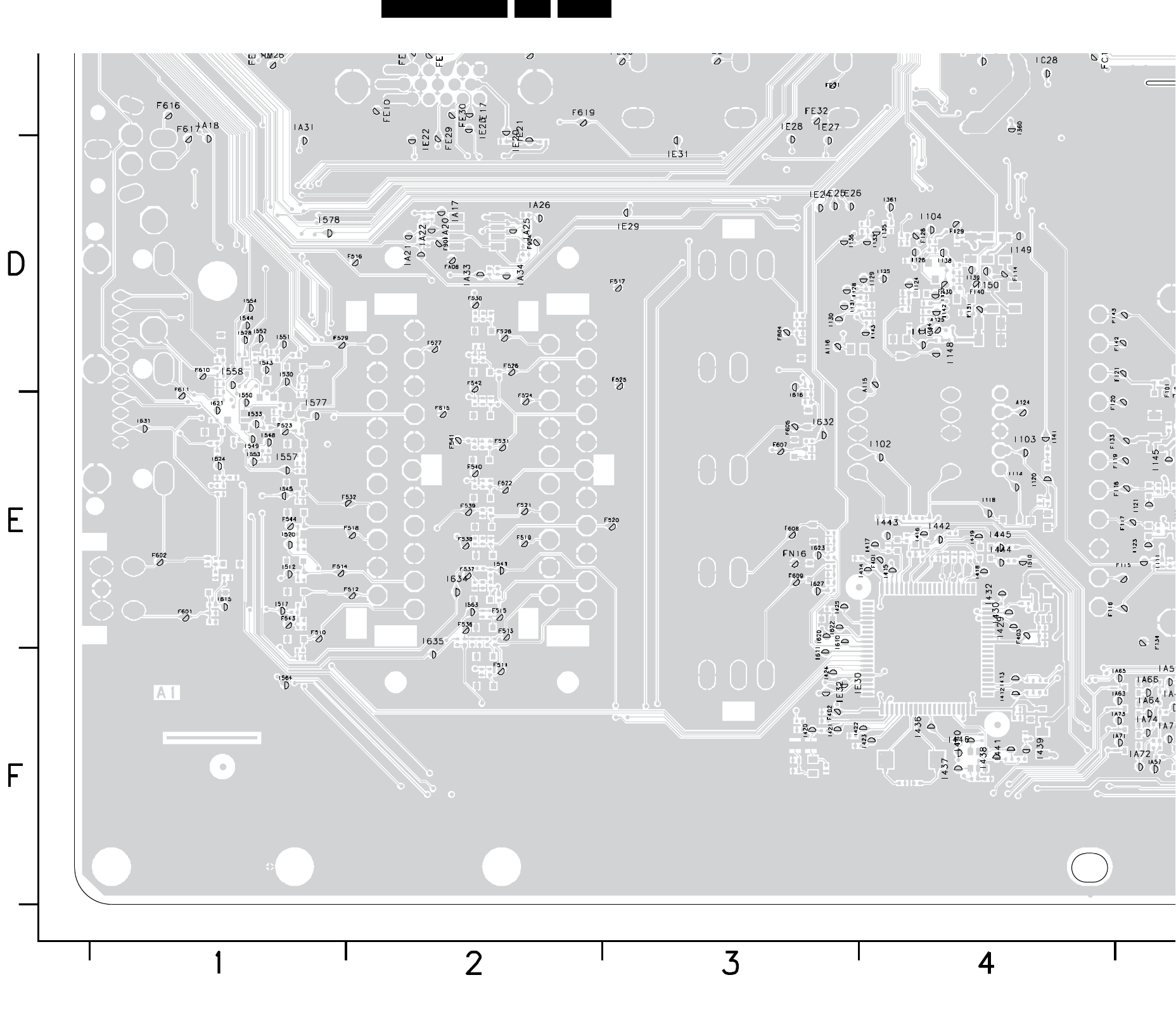
Block Diagrams EN 47LC8.2HA LA 9.
2009-Apr-10
SSB: Test Points (Part 3 Bottom Side)
I_17760_022c.eps
300708
Part 3
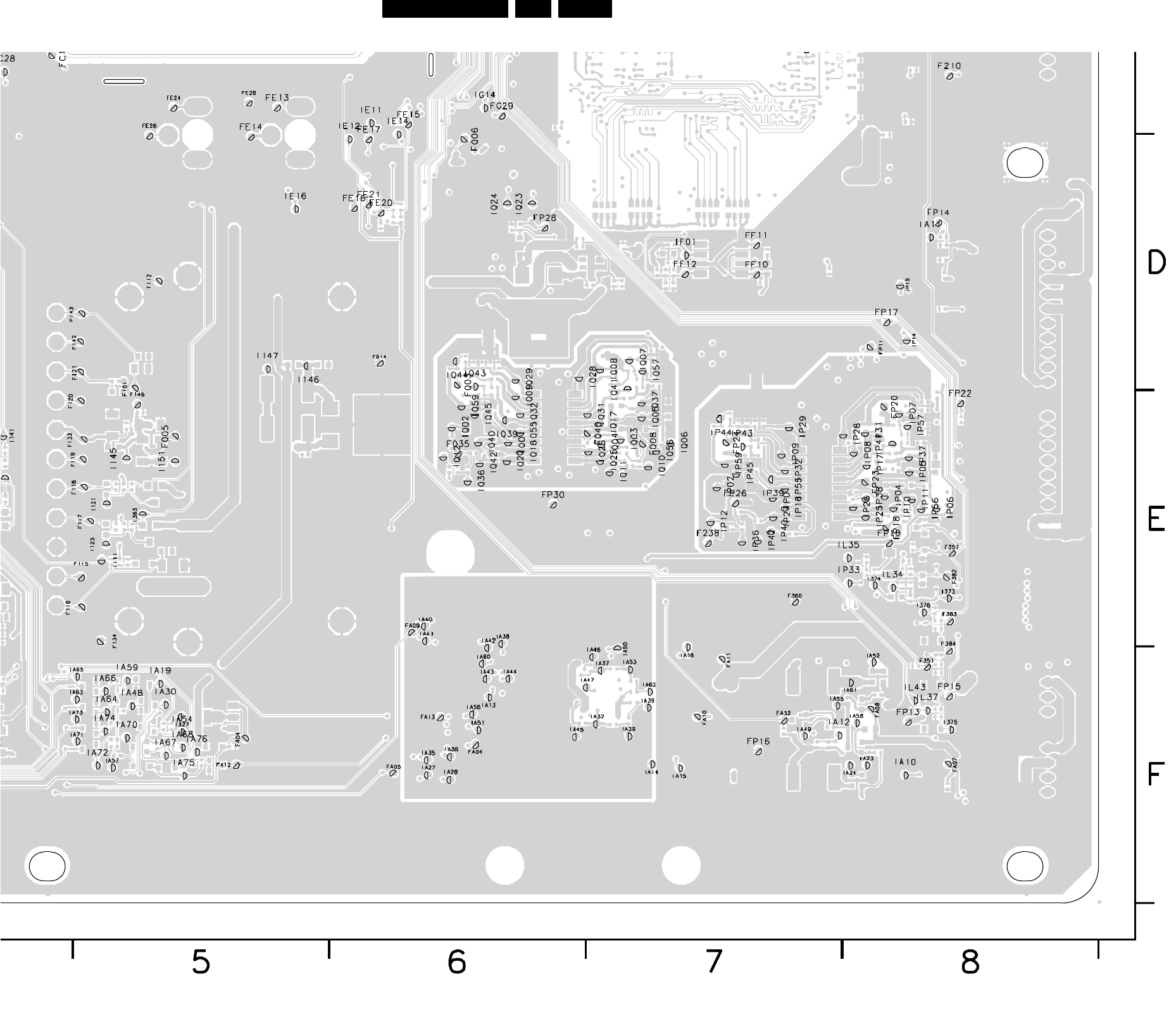
EN 48LC8.2HA LA 9.
Block Diagrams
2009-Apr-10
SSB: Test Points (Part 4 Bottom Side)
I_17760_022d.eps
300708
Part 4
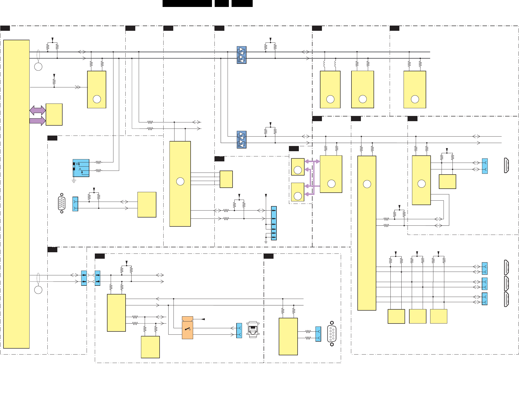
Block Diagrams EN 49LC8.2HA LA 9.
2009-Apr-10
I2C IC Overview
I²C
MICROPROCESSOR
B03
TUNER IF & DEMODULATOR
B02
MICROPROCESSOR
B03
TRIDENT - WX69
B04A
FPGA I/O BANKS
B04D
FPGA INTERFACE
B04C
I/O - CINCH 1&2
B06B
IBOARD
HC02
IBOARD
HC02
AUDIO PROCESSOR - MICRONAS
B05A
VGA & PC AUDIO & COMPAIR & UART
B06C
HDMI SWITCH
B07A
HDMI MAIN
B07B
FPGA INTERFACE
B04C
B04B
7311
M30300SAGP
19 1
182
HDMI B
BACK
7M18
M24C02
EEPROM
56
56
7M17
M24C02
EEPROM
70
71
30
31
DDC_SDA_SIDE
DDC_SCL_SIDE
DDC_SDAC
DDC_SCLC
SDA2
SCL2
14 15
7M07
SII9185ACTU
HDMI
SWITCH
ERR
21
3M21
3M20
78
77
50
51
DDC_SDAB
DDC_SCLB
1M01
16
15
1M03
16
15
1M02
16
15
+5V_SW
3M73
3M72
+5V_SW
3M68
3M67
7M16
M24C02
EEPROM
56
+5V_SW
3M63
HDMI C
BACK
HDMI
SIDE
HDMI
CONNECTOR
MICRO
PROCESSOR
1N03
16
15
HDMI A
BACK
DDC_SDAA
DDC_SCLA
7N40
M24C02
EEPROM
56
+5V_SW
3N43
3N42
19 1
182
19 1
182
19 1
182
54
1101
UV1316E/ABH
UV1356/ABHN
TUNER
ERR
07
+3V3_STBY
3L76
3L75
10 11
7113
TDA9886T/V4
IF
DEMODULATOR
ERR
08
3152
3151
5120
5121
IIC_SDA
IIC_SCL
28
27
56
7L23
M24C64
NVM
EEPROM
3L54
3355
NVM_WC 7
100
ERR
06
56
7107
ST3232C
RS232
3L54
3355
IIC_SDA_up
IIC_SCL_up
+3V3_STBY
3353
7302
PCA9515ADP
3
2
6
7
7303
PCA9515ADP
3
2
6
7
+3V3_SW
3359
3360
+3V3_SW
3362
3361
IIC_SDA_SIDE
IIC_SCL_SIDE
XCIN
XCOUT
+3V3_STANDBY
3253
3254
8
9
H17 H18
7C01
WX69-7569
VIDEO
PROCESSOR
3C08
3C09
ERR
05
PE H1
7700
EP2C5F256C7N
CYCLONE II
FPGA
AMBI-LIGHT
ERR
17
3202
3201
MAIN_SDA
MAIN_SCL
ITV_I2C_SDA
ITV_I2C_SDA
SDA_SSB
SCL_SSB
SDA1
SCL1
RXD0
TXD0
IR-IN_DATA_INSDA1
LEDIN_CLK_TXD_SCL1
32
7411
MSP4450L
AUDIO
PROCESSOR
ERR
09
3411
3410
1
610
11
5
15
3E10
3E11
EEPROM
256x8
VGA
CONNECTOR
SDA_VGA
SCL_VGA
5
6
1E01
12
15
DC_5V
1E04
2
3
COMPAIR
SERVICE
CONNECTOR
3E70
3E71
3M15
3M14
3203
3219
26 27
7N01
SII9125CTU
HDMI
MAIN
ERR
11
HDMI_MUX_TSDA
HDMI_MUX_TSCL
33
34
18510_405_090408.eps
090410
ONLY FOR AMBILIGHT
RES
RES
1202
3
1
TO
AMBI-LIGHT
MODULE
(RESERVED)
AMBI_SDA
AMBI_SCL
5
6
4
7
3203
3204
+3V3_FPGA
3206
3205
+3V3_FPGA
S_SDA
S_SCL
N2
P3
ONLY FOR AMBILIGHT
ERR
04
ERR
19
7D01
EDD1216AJTA
DRAM
7D02
EDD1216AJTA
DRAM
ERR
10
ERR
14
HDMI
CONNECTOR
+5V_SW
3M87
3M88
28
29
3N40
3N39
7201
EPCS4SI8N
SCD
nCSO
DCLK
ASDO
DATA0
1
6
5
2
F4
H4
C3
F1
3M62
IIC_SDA_SIDE
IIC_SCL_SIDE
7310
M29W800DT
EPROM
1Mx8
512Kx16
AD(0-7)
A(0-19)
7E01
M24C02
15081205
66
55
29 30
7209
UPSD3333D
MCU
3241
3264
56
13
14
7214
M24C64
EEPROM
4Kx8
3274
3275
11
2
1111
1
2
1205
1
2
1
6
5
9
3119
3120
2
12
15
14
7205
74HC4053PW
16 +5V5
MDX
SERVICE
CONNECTOR
9 POL SUB_D
RJ12
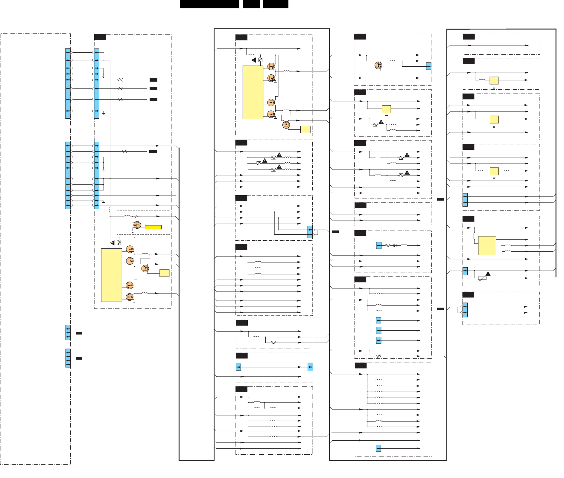
EN 50LC8.2HA LA 9.
Block Diagrams
2009-Apr-10
Supply Lines Overview
SUPPLY LINES OVERVIEW
A
MAIN
POWER SUPPLY
B01A
DC / DC +3V3 & +1V2 & +VTUN
B02
TUNER IF & DEMODULATOR
B05A
AUDIO PROCESSOR - MICRONAS
B05B
AUDIO - CLASS D
B06B
I/0 - CINCH 1 & 2
B06C
VGA & PC AUDIO & COMPAIR & UART
B07A
HDMI SWITCH
B07B
HDMI MAIN
B08A
MJC MT8280 - LVDS
B08B
MJC MT8280 - DDR
B08C
MJC MT8280 - POWER
B01B
DC/DC - 5V &1V8 & 2V5
B04B
DDR INTERFACE
B04C
FPGA INTERFACE
B04D
FPGA I/O BANKS
B03
MICROPROCESSOR
B04A
TRIDENT - WX69
B04E
LVDS CONNECTOR
J
IR & LED PANEL
HC01
IBOARD
HC02
IBOARD
CN6
1 1
66
7 7
22
33
44
55
88
STANDBY
1P01
+3V3_STBY
7P06-1
7P11
NCP5422
7P06-2
+3V3_SW
15
1
2
7P07-1
7P07-2 +1V2_SW
5Q01
16
15
7P08
2V5
STA B .
7P09
+2V5_SW
+5V_SW
+5V_SW
SUP_A
SUP_D
+3V3_SW
+3V3_SW
5M01 +3V3_ANA_MUX
+12V_DISP
+12V_DISP
7410
IN OUT
COM
+8V
+3V3_SW
+3V3_SW
+1V8_SW
+1V8_SW
B04A
+5V_SW+5V_SW
+5V_SW
+5V_SW
+5V_TUN
3P20
+3V3_SW
+3V3_SW
18510_406_090408.eps
090410
3.3VSB
PSON
SGND1
SGND1
SGND1
12VA
12V
5P01
7Q06-1
7Q11
NCP5422
+12V_DISP
7Q06-2
+5V_SW
15
1
2
7Q07-1
7Q07-2 +2V6_SW
5Q09
16
15
+12V_DISP
3Q20
5P09
+2V6_SW
+2V6_SW
+2V5_VDDMQ
5D03
+3V3_FPGA
+3V3_FPGA
+1V2_SW
+1V2_SW
+1V2-FPGA
FPGA_BL_BOOST
FPGA_BL_BOOST
5703
+1V2-PLL
+2V5_SW
+2V5_SW
+2V5out_FPGA
5701
+2V5_in-FPGA
5702
+3V3_SW
+3V3_SW
+3V3_FPGA
5700
+3V3_STBY
+3V3_STBY
CN7
1 1
66
77
22
33
44
55
88
BL_ON_OFF
1P02
BL_BOOST
BL_ADJUST_PWM
B04A
B03
12V
12V
SGND1
SGND1
BL-ON
SGND1
BL-DIM
BOOST
+12V_DISP
99+12V_AUDIO
11 11 -12V_AUDIO
10 10
ONLY FOR ANALOG TUNER
+VTUN
5P06 6P03
+3V3_SW
7P14
B01a
B01a
B01a
B01b
B01b
B01A
B01a
B01b
B01a
B4b
B01a
B01b
B01b
B04d
B01a
B01a
B01a
RES
B4a,B05b,B06c,b
B01a,B02,
B03,B04e,B05a
B05b
B05b
12V
12V
-12VA
SGND2
Dual
Out-of-Phase
Synchronous
Buck Controller
Dual
Out-of-Phase
Synchronous
Buck Controller
5P02
5Q02
7Q09
1V8
STA B .
7Q08
+1V8_SW
+5V_IF
+5VS
3133
3134
3141
5114
5115
5122
+3V3_SW
+3V3_SW
B01a
+VTUN
+VTUN
B01a+12V_DISP
+12V_DISP
B01a
+3V3_SW
+3V3_SW
B01a
+3V3_STBY
+3V3_STBY
B01a
+5V_SW
+5V_SW
B01b
+12V_DISP
+12V_DISP
B01a
+1V2_SW
+1V2_SW
+1V2_CORE
B01a
+1V2_ADC
+1V2_PLL
5C09
5C10
5C11
+3V3_SW
+3V3_SW
B01a
+3V3_STBY
+3V3_STBY
B01a
+5V_SW
+5V_SW
B01b
+2V5_VDDMQ
+2V5_VDDMQ
B04b
DDR_VREF
DDR_VREF
B04b
FPGA_BL_DIMMING
FPGA_BL_DIMMING
RES
DDR_VREF
3D15
1
1206 1205
1
+24V
5704
FPGA_BL_DIMMING
FPGA_BL_DIMMING
RES
+12V_DISP+12V_DISP
VDISP
5R02
+3V3_SW
+3V3_SW
7R05
3402
5401
5402
+12V_AUDIO
+12V_AUDIO
VDD
VDDA
B01a
3A01
5A07
5A05
-12V_AUDIO
-12V_AUDIO
VSS
VSSA
3A02
5A08
5A06
+5V_SW
+5V_SW
+3V3_STBY
+3V3_STBY
B01b
B01a
DC_5V
1E01
9
VGA
CONNECTOR
+5V_SW+5V_SW
B01b
6E04 5E01
3E07
+3V3_SW+3V3_SW
+3V3_STBY
+3V3_STBY
B01a
B01a
+1V8_SW
+1V8_SW
+1V8_ANA-MUX
5M02
+1V8_DIG-MUX
5M03
B01b
+5VHDMI_B
1M02
18
HDMI
CONNECTOR
(Optional)
+5VHDMI_C
1M03
18
HDMI
CONNECTOR
+5VHDMI_SIDE
1M01
18
HDMI
CONNECTOR
+5V_SW+5V_SW
B01b
+3V3_SW
+3V3_SW
+3V3SWA
5N02
+3V3SWE
5N09
B01a
+3V3SWB
5N03
+3V3SWC
5N07
+3V3SWD
5N08
+1V8_SW
+1V8_SW
+1V8SWA
5N01
+1V8SWB
5N04
+1V8SWC
5N05
+5VHDMI_A
1N03
18
HDMI
CONNECTOR
+5V_SW
+5V_SW
+5VHDMI_MUX_TPWR
+5VHDMI_MUX_TPWR
+1V8_SW
+1V8_SW
7F03
IN UT
COM
+0V9_VTT
B01b
5F01
+1V2_SW
+1V2_SW
7G04
IN OUT
COM
+1V
AB09
1R01
41
B01b
B01b
B01a
B01a
B01a
B02,B03,
B04a,d,e,B06c,
B07a,b,B08a,c
B04a,d,B08c
B02
B02,B03,B04a,
B05a,b,B06b,c,
B07b
B07a,b,B08b,c
B04a
B04a
B04a
B04d
TO
AMBI-LIGHT
UNIT
+3V3STBY
1P10
5
+5V_SW
8
TO 1109
iBOARD
HC01
TO 1320
SSB
B03
+5VA
+5VA
HC02
HC02
+5VB
+3V3_STANDBY
+5VB
+5VSSB
HC02
+3V3_STANDBY
+5V
+5VB
+5VA
+3V3_STANDBY
HC01
+5VSSB
+5VSSB
HC01
+12VA
+12VA
HC02 +12V
+12V
7125
IN OUT
COM
+5VAUD
+12VA
1320
8TO 1110
iBOARD
HC01
5
5704
B07a
+5VHDMI_MUX_TPWR
3M18
GNDSND
B03
(CONTROL)
(CONTROL)
CN8
1
2
3
+12V_PBS
SGND
CTRL_PBS
CN5
1
2
3
4
+12VB
SGND1
+12VB
SGND1
5115 5113
5
8
1110
+12V
1
1209
1212
7229
TPS60111PWP
DC/DC
CONVERTER
5206
75202
5203
1211
1A85
HC01
HC01
HC01
HC01
HC02
HC02
TO 1209
IBOARD 32”
HC02
TO 1212
IBOARD 42”
HC02
TO
CN5/CN8
PSU
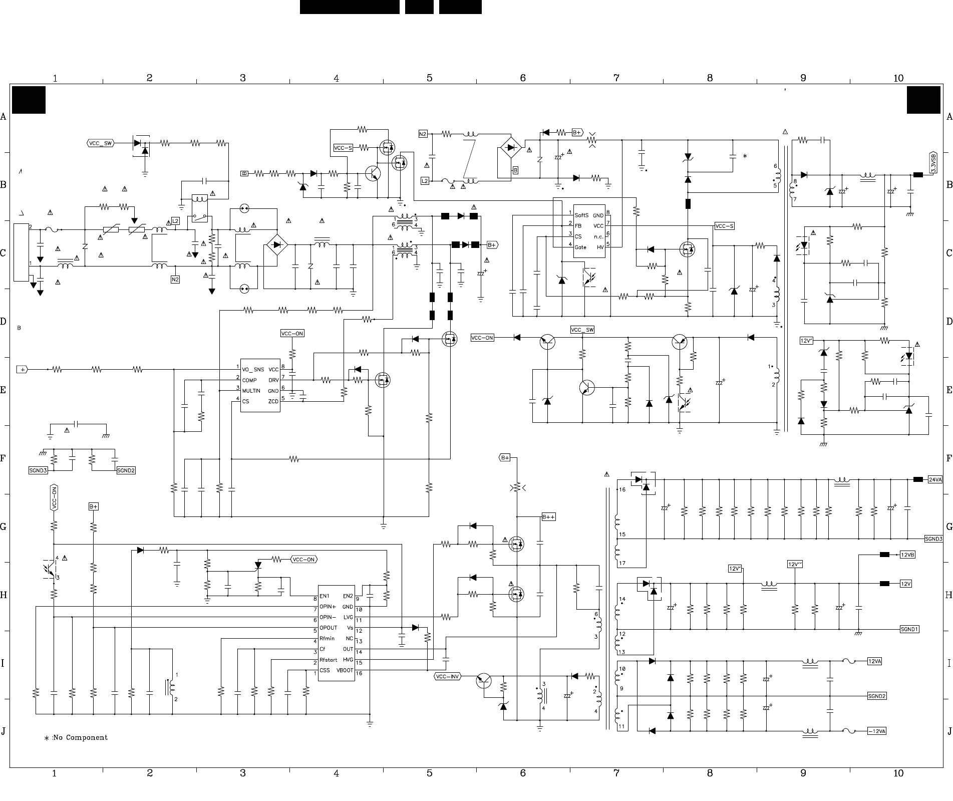
Circuit Diagrams and PWB Layouts EN 51LC8.2HA LA 10.
2009-Apr-10
10. Circuit Diagrams and PWB Layouts
Main Power Supply (42"): Part 1
R632
200
R633
1K 1/2
D602
BAS316
C610
0.1u
R604
402K/1206
R603
402K/1206
R602
402K/1206
R601
10
PC123
PC601
R819
18.7K
C108
0.1U
C107
0.1U
R101
1K
R102
1K
1.5KP/250V
CY5
R817
15K
*
R818
R812
51.1K/0805
IC801
NCP1606B
100
R815
C807
100p
C805
1.2kp
C806
1kp
C802
C804
0.1u
C803
0.47u
SCR211
P0102BL
R631
511
R629
2K
C611
1Kp
R630
100
C612
1Kp
R628
8.06K
R609
100
C602
1Kp
C603
1KP
C601
1KP
R616
10K
R611
15K
R614
19.6K
1.5M
R612
3.01K
R613
C606
0.47u
R607
25.5K
IC601
DDA 001B
C605
2.2u
1/2
CT601
100:1
R608
3.83K
CN1
D716BAV70 R704
75/1206
R703
75/1206
R701
75/1206
CY2
100P/250V
1M/1206
R820 R821
1M/1206
R822
1M/1206
Z1
TVR14681
L802
CR-20-LP2048
T5AH/250V
F1
L
N
PE
CY1
100P/250V
R39
4.7M
R40
4.7M
SCK201R0
NTC1 NTC2
SCK201R0
FL1
HFV-DP722
CX1
0.33u/275V
470P/250V
CY4
R6
1M 1M
R5
FL2
OTC28
2M/1206
R908
DSP-210M
GT1
835-1A-B-C
RL701
C7031u/0805 R909
2M/1206
C910
1u
ZD905
7.5B
D905
BAS316
R910
2M/1206
R912
1M
R913
402K
BD1
D15XB60
C810
1u/450V
C809
1u/450V
Z2
TVR10511
L801
CR-18-LP3009
*
C801
0.1uR814
10
R806
750K/0805
R805
750K/0805
R804
750K/0805
750K/0805
R803
CY3
470P/250V
R813
22
GT2
DSP-210M
R809
22
R810
100
R801
100
R808
51.1K/0805
SPA 1 5 N 6 0 C 3
Q802
C808
180u/450V
SPA 1 5 N 6 0 C 3
Q801 FB803
3.5X6
FB804
3.5X6
FB802
3.5X6
FB801
3.5X6
D802
BAS316
D801
BAS316
1u/450V
C811
PQ3220
L800A
Q903
2N7002
Q902
4401
C911
0.01u
L800B PQ3220
MUR460
D803
F2
T1AL/250V
FL4
HFV-CE5085
C813
220P/1KV
C812
220P/1KV
D805
MUR460
R923
100
R926
22
IC901
ICE3AS02
D908
BAS316
Z3
TVR10511
1N4007
D911
C918220p
R902
06J05
R924
10K
1/2
3
4
PC901
PC123
ZD906
20A
R917
2K/0805
R915
40.2K
R919
1K
C901
0.22u
Q901
4401
D907
BAS316
C903
0.22u
C917 220p
1Kp
C904
R927
1.5K R928
1
2N7002
Q906
R918
1M
R914
1M
CX2
0.1u/275V
1N4007
D910
C921
0.047u/450V
R901
1 FUSIBLE
C902
33u/450V
R904
1K /1W
BD2
S1NB80
R7
R950
5.1/1206
T901
EF12.6 C950
1KP/1206
C920
ZD908
P6KE300A
5.1K
R905
R906
10K
Q900
4403
C912
47u/63V
EGP10D
D903
FQPF3N80C
Q905
C914
0.1u
ZD902
20A
ZD602
3.3B C956
2.2u
R903
2/1W
ZD951
1N5917B
D950
SB340
R916
5.1/1206
BYV26E
D909
1
2
PC901
PC123
D906
BAV103
FB902
3.5x6
C916
47P/1KV
1/2
R952
2k
R954
2k
C954
0.47u
C953
0.1u
L951
CB-3.0-01
C951
1Ku/10V
C952
1Ku/10V
FB901
3.5X6
R953
10K
R951
750
IC951
APL431 1.25V
R503
3.83K
R511
1K C505
1U
1/2
C502
0.047u
R506
1K
1
2
PC601
PC123
R510
2K
R955
1.13K
C955
0.1u
R509
5.11K
D605
STTH1R06
18A
ZD601
Q601
4401
R624
2K/0805
R626
15
C608
1u/0805
0.47u
C609
R623
100/0805
BAV103
D606
SB560
D204
1/2
C614
100u/50v
D201
SB560
100:1
CT601
R621
15
R618
15
R627
51.1k
C607
0.1u
R615
121K
R619
10K
R617
100
R622
10K
R620
100
Q602
2SK3569
D604
BAS316
D603
BAS316
R811
10K
R634
0.1 FUSIBLE
R816
0.056/3WR802
10K
ER39L
T1
Q904
4401
CR201
STPS10H100CFP
C907
0.1U
C905
0.01U
ZD900
20A
R922
40.2K
D904 BAS316
C626
220P/1KV
C625
220P/1KV
Q603
2SK3569
CR202 STPS10L60CFP
C613
0.022u/630V
R605
200K/1W
C201
470u/35V
R201E
7.5k/1206
R201F
7.5k/1206
R201G
7.5k/1206
R201H
7.5k/1206
R201I
7.5k/1206
R201D
7.5k/1206
R201A
7.5k/1206
R201B
7.5k/1206
R201C
7.5k/1206
R202D
3.01K/1206
R203A
3.01K/1206
R203B
3.01K/1206
C204
1Ku/16V
L202
CB-3.0-01
R202A
3.01K/1206
R202B
3.01K/1206
R202C
3.01K/1206
R512
100
D608
BAS316
D607
BAS316
C906
100U/50V
ZD901
10D
1/2
3
4
PC902
PC123
R502
1K
C504
1Kp
IC501
APL431 2.5V
R504
2K
C506
1u
L201
CB-3.0-01 FB201
3.5X6
C206
0.1u
FB203
3.5X6
C205
220u/35V
FB202
3.5X6
R201J
7.5k/1206
R201K
7.5k/1206
C203
0.1u
R201L
7.5k/1206
C202
220u/35V
L204
CB-3.0-01
R204C
3.01K/1206
D202
SB560
D203
SB560
R204A
3.01K/1206
R204B
3.01K/1206
R205C
3.01K/1206
R205B
3.01K/1206
R205A
3.01K/1206
L203
CB-3.0-01
C208
470u/25V
C207
470u/25V
R205D
3.01K/1206
R204D
3.01K/1206
C210
0.1u
C211
0.1u
F201
T5A/125V
F200
T5A/125V
A1 A1
DISPLAY SUPPLY (37" & 42"): PART 1
H_16750_068.eps
260209
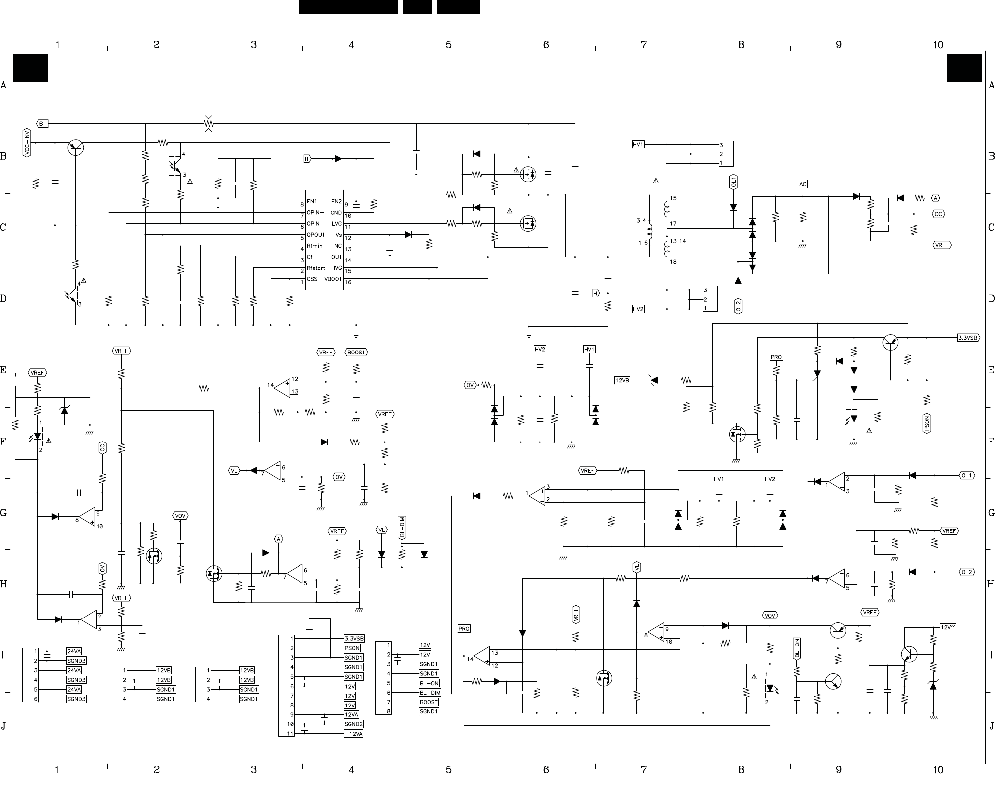
EN 52LC8.2HA LA 10.
Circuit Diagrams and PWB Layouts
2009-Apr-10
Main Power Supply (42"): Part 2
R335
2K
IC701
LM324
1/4
D701
BAS316
C706
0.022u
R713100K
R705
887
C722
0.47u
C724
R716
*
R723
Q708
*
C701
4.7kp
ZD301
5.1A
R306
1K
R768
3.24K
R702
100K
R761
5.11K
C321
1u
PC123
PC301
1/2
R334
750
1/4
R706
10K
1/4
R707
34K R708
20K
IC701
LM324
IC701
LM324
C727
0.1u
R753
60.4K
C708
1KP
D711
BAS316
BAS316
D712
R712
20K
R717
30.1K
C711
0.01u
R722
10K
Q706
2N7002
C704
0.1u
R718
4.02K
R719
1K
1/2
IC702
LM358
R726
20K
D714
BAS316
*
*
C212
0.1u
C213
0.1u
R714
10K
1/4
D702
BAS316
0.1u
C707
IC701
LM324
R715
6.49K
CN5_2
CN4
C218
0.1u
C214
0.1u
C216
0.1u
C217
0.1u
CN5_1
C215
0.1u
CN6
R317
0.1/FUSE RES
1/2
PC302
PC123
C318
1KP
C307
1KP
C305
1KP
R336
20K
R323
30.1K
R303
10K
R312
8.87K
R337
2K
R301
10
R329
1M/1206
R330
1M/1206
C303
0.1U
R302
10K
4403
Q303
R328
1M/1206
PC301
PC123
C301
1KP
R308
5.11K
R307
1.3K
1/2
D310
BAS316
C306
2.2u
C304
4.7u/0805
R331
19.6K
1M
R311
IC301
DDA001A
5.11K
R310
R709
100K
R309
20K
C309
0.22uR319
10K
Q302
STP11NM60
Q301
STP11NM60
C302
1u
D309
STTH1R06
R332
2K
R318
10K
R316
100
R315
100
R338
22
R314
22
R313
22
D302
BAS316
D303
BAS316
C308
0.47u/0805
C316
0.1u/630V
C310
330P/1KV
C311
330P/1KV
C312
0.47u/450V
UU35
T301
C317
0.01u/1206
R320
40.2
C315
0.47u/450V
R218
200
D307
BAV99
CN3
D317
BAS316
D212
BAS316
D305
BAV99
CN2
D304
BAS316
D306
BAS316
R327
27/2W
R321
27/2W
R341
1K
C319
0.01u
R344
60.4K
R342D312
*
*
R340
1K
C958
1u
R216
100
R963
100K
4403
Q604
D713
BAS316
D710
BAS316
C717
0.1u
1/4
IC703
LM324
C219
0.1u
CN7
R736
3.01K
R755100K
R735
2K
D703
BAS316
1Kp
C716
R728
10K
2N7002
Q304
IC703
LM324
1/4
R756
2K/1206
R720
30.1K
R743
51.1K
D709
BAS316
R721 200K
D717
BAS316
D715
BAS316
13K
R766
C709
0.01u
R710
1K
R325
10K
C705
0.1U
R769
17.4K
R333
30.1K
D308
BAV99
R765
4.22K
R741
2K
R326
10K
D311
BAV99
C314
0.015u
C313
0.015u
ZD210
13C
R215
1K
C333
33p/6kV
C327
33p/6kV
R212
100/1206
R737
20K
R739
10K
R742
2K
C713
0.1u
10K
R740
1/2
1Kp
C718
D313
BAV99
IC702
LM358
C326
220p
C325
220p
R343
22
R339
22
C329
22p /6KV
D314
BAV99
1/4
IC703
LM324
LL4148
D707
C330
33p /6KV
R219
10K
SCR210
P0102BL
1/4
IC703
LM324
1u
C957
R214
2K
1
2
PC902
PC123
D705
BAS316
Q707
2N7002
R221
10K R220
1K
100/1206
R213
LL4148
D704
1/2
R217
1K
BAS316
D210
BAS316
D211
R964
5.11K
D706
LL4148
R729
10K10K
R731
R734
10K
R730
4.7M
C710
0.47u
C714
0.47u
R732
4.7M
C715
0.1u
R733
2.55K
R745
2K
Q703
4401
PC302
PC1231/2
R738
2K
R746
10K
R304
2K
R744
2K
Q701
4403
D708
BAS316
3M
R711
C725
1u
C723
0.1u
R747
10K
C726
1u
R748
2K
R749
3.01K
C720
1u
R750
1K
R757
511
APL431 2.5V
IC705
Q702
4401/DIP
A2 A2
DISPLAY SUPPLY (37" & 42"): PART 2
H_16750_069.eps
260209
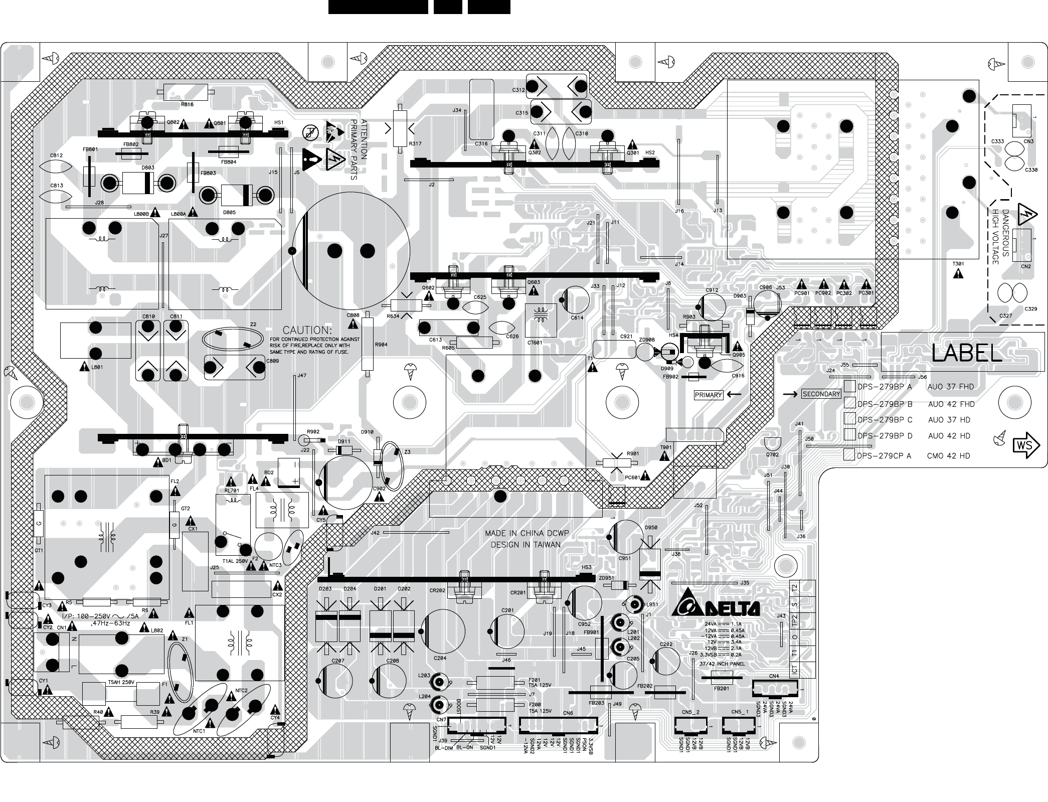
Circuit Diagrams and PWB Layouts EN 53LC8.2HA LA 10.
2009-Apr-10
Layout Main Power Supply (42") (Top Side)
H_16750_070.eps
110108
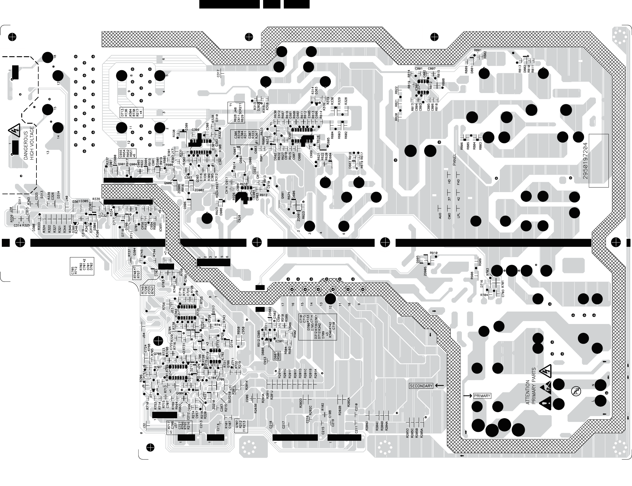
EN 54LC8.2HA LA 10.
Circuit Diagrams and PWB Layouts
2009-Apr-10
Layout Main Power Supply (42") (Bottom Side)
H_16750_071.eps
110108
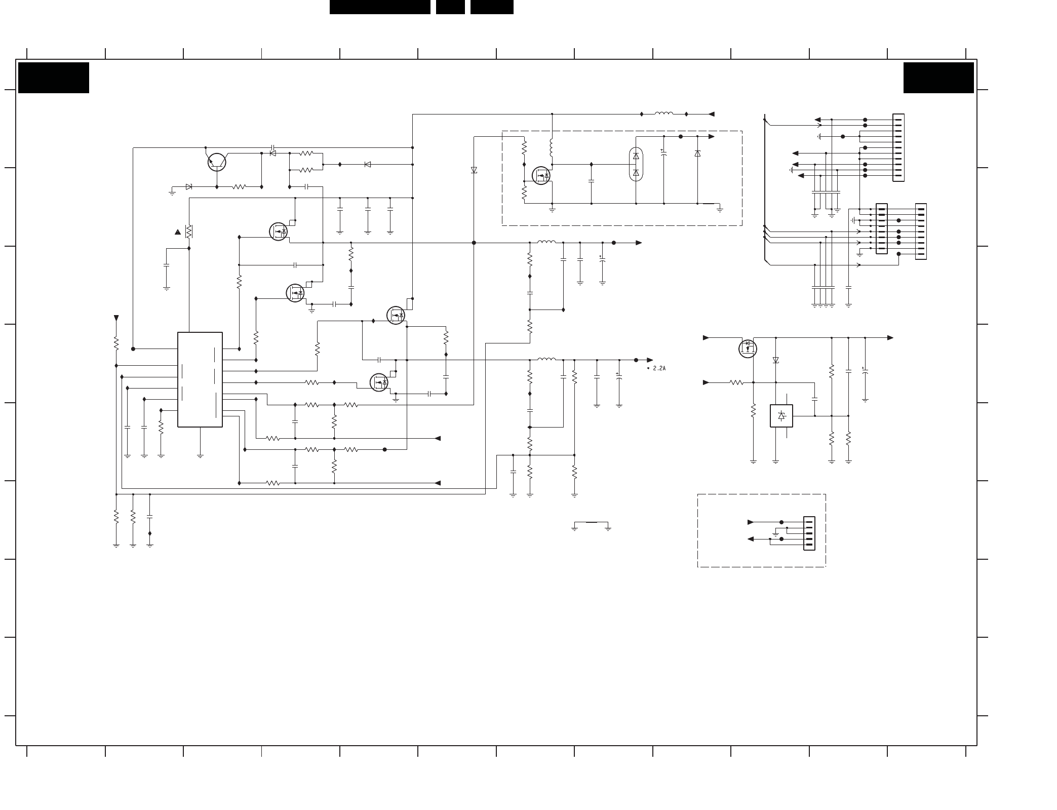
Circuit Diagrams and PWB Layouts EN 55LC8.2HA LA 10.
2009-Apr-10
SSB: DC/DC +3V3, +1V2, & +VTUN
NCNC
A
REF
K
VCC
L2
+1
-1
1
2
+2
-2
2
VFB
GAT E
IS
COMP
GAT E
GND
1
BST
ROSC
H2
L1
H1
7P14 B7
7P11 D2
FP24 D8
IP28 D2
FP27 A11
IP39 E3
5P02 A9
IP41 D4
C
IP02 A8
3P72 E4
3P74 E4
3P75 D10
IP07 C7
IP08 D2
IP09 D2
3P79 E10
3Q34 E4
3Q51 D7
3Q52 F7
IP15 A8
IP37 B3
IP17 D4
IP25 D3
IP36 D6
34V
2P07 B4
RES
IP27 D4
6P13 A5
IP29 E2
RESIP59 D7
IP32 F3
7P05 A3
2P89 D11
2P90 D11
2P91 D11
7P07-2 D5
7P08 C10
7P09 E11
3P23 C3
3P25 C5
3P26 D3
3P32 D4
FP12 A11
IP45 F2
FP14 B11
FP15 B11
3P41 E4
IP05 B4
IP06 B4
IP10 C5
2P19 A9
2P79 B11
3P49 B3
G
3P51 D2
2P36 C7
3P53 F2
3P61 D6
FP30 A11
3P68 D5
2P41 E2
4
2P33 C7
7
2P48 F7
2P49 F2
2P52 D6
2345
2P78 A4
3Q74 E4
2P80 B11
2P81 B11
12
2P83 B11
5Q01 D7
2P39 E4
2P20 B8
B
ONLY FOR ANALOG TUNER
3P47 A4
RES FOR 5V TCON
6P16 B6
2P87 C11
G
RES
2P29 B4
2P30 B5
C
6
E
2P34 C8
2P35 C5
FP19 B12
5 12
3P37 C7
3
RES
2P31 C2
DC/DC +3V3 & +1V2 & +VTUN
8
2P37 D5
2P38 C4
3P67 A7
2P40 E2
11
2
2P85 C11
2P32 C4
971
RES FOR ANALOG DIMMING
6P02 A9
2P84 C11
10
1
2P86 C11
8
RES
3P45 D7
6P03 B8
D
6P14 A4
6P15 B3
IP31 D4
6P17 D10
2P88 C11
RES
3P40 E2
FP17 B12
3P13 D4
3P15 B7
3P20 B3
FP18 B6
91011
3P34 D4
FP13 A11
3P38 D7
FP22 C12
IP57 C7
FP16 B12
RES
1P01 A12
1P03 B12
6
FP23 D2
3P50 E7
FP26 E5
3P52 F2
FP28 F10
FP29 F10
B
IP01 C3
3P69 E5
2P42 E4
2P43 D7
2P46 D8
3P76 D11
3P77 E11
3P78 E11
2P53 D6
2P54 E7
2P59 C8
2P61 D8
3Q53 E7
IP16 D4
4P16 B6
5P01 B7
2P82 B11
5P06 A7
F
IP40 D4
H
RES
IP14 A7
1P04 F11
IP26 D4
IP43 E4
FP10 A11
H
RES
FP20 B8
IP11 C5
IP33 A9
7P06-1 B4
7P06-2 C4
7P07-1 C5
RES
IP12 D6
IP38 B3
RES
FP21 B12
D
FP11 A9
A
E
IP55 E2
IP56 A5
IP04 C3
IP42 C5
1P02 B11
IP44 E7
3
IP44
RES
A
2P28 B5
F
3P48 A4
FP17
IP10
7P06-2
SI4936BDY
5
6
4
GNDDC1
+2V5_SW
FP23
+12V_DISP
2P433n3
FP16
1%
470R
3P76
IP12
+12V_DISP
2P79100n
GNDDC1
2P59
GNDDC1
IP17
100u16V
2P80100n
1K0
3P38
+5V_TCON
10R
3P61
GNDDC1
3P77
3K9
IP29
IP33
6P14
BAS316
2P871n0
IP39
2P89
100u16V
2
4
FP11
TS431AILT
7P09
53
1
3P79
1K0
1K2
3P74
+3V3_SW
100n 2P81
FP24
2P20
100p
3P78
470R 1%
6K8
3P68
GNDDC1
IP43
FP30
10R
3P25
+3V3_SW
FP20
6K8
3P69
GNDDC1
6P02
PDZ33-B
3P75
8K2
5
6
4
3
IP25
7P07-2
SI4936BDY
7
8
9
2P40 100n
1735446-9
1P03
1
2
3
4
5
6
6P15
IP55
IP59
BZX384-C18
GNDDC1
2P37
3n3
3n3
2P32
100n
2P84
3Q52
FP22
+12V_DISP
2K2
FP21
3K3
470R
3P72
+3V3_SW
3P53
1%
PHD38N02LT
2
1
3
7
8
2
1
7P08
7P06-1
SI4936BDY
6P16
BZX384-C4V7
9
2P851n0
1
10
11
2
3
4
5
6
7
8
1P01
1-1735446-1
IP14
100n
2P54
5Q01
10u
2P29
22u
1K0
3P50
GNDSND
6
7
8
GNDDC1
1P02
1735446-8
1
2
3
4
5
2P38 1n0
GNDTUN
3P67
220R
IP06
IP15
68R3P47
35V
2P19
22u
2P61
22u
1u0
2P31
10R3P13
2R2
3P32
100p
FP10
2P49
IP36
6P03
BAV99
+VTUN
GNDDC1
BAS316
6P13
IP05
BZX384-C4V7
6P17
3P45
GNDDC1
6K8
GNDDC1
IP56
7P05
BC817-25W
IP28
IP09
7P14
3
1
2
FP18
GNDDC1
2N7002
22u
2P28
22u
2P30
2R2
3P26
1%
680R
3Q53
IP32
GNDSND
100n
2P42
IP45
10R
3P23
IP40
2K2
3P34
39K
3P40
FP15
1n02P86
FP14
1K8
3Q34
FP12
1n0
2P35
IP02
FP27
FP28
1K0
6K8
3P37
3P15
+1V2_SW
IP04
3Q51
180R
+3V3_STBY
1%
IP42
IP37
1u0
2P78
IP26
3P51
1K0 1%
14
7
10
IP38
16
2
15
3
6
11
5
1213
7P11
Φ
NCP5422ADR2G
4
8
9
1
22u
2P34
IP27
+12V_DISP
FP13
2P36
-12V_AUDIO
100n
+3V3_SW
2P82100n
IP57
10u
IP11
5P02
100n2P07
3P48
IP07
68R
1K03P49
IP41
100u
2P46
16V
7P07-1
SI4936BDY
7
8
2
1
FP26
+12V_AUDIO
100p
2P48
1n0
100n2P41
GNDDC1
2P53
IP16
+1V2_SW
3K3
3P41
2P39
100n 2P83
100n
2P90 1u0
2P91
22n
1n02P88
10R
3P20
1K8
1n0
2P52
3Q74
12
IP31
5P01
22u
FP29
3n3
2P33
4K7
3P52
IP08
220u
5P06
FP19
IP01
1
2
3
4
5
1735446-5
1P04
BL_ON_OFF
BL_ADJUST_ANA
BL_BOOST
BL_ADJUST_PWM
STA N D B Y
B01A B01A
I_17760_001.eps
180208
3139 123 6349.1
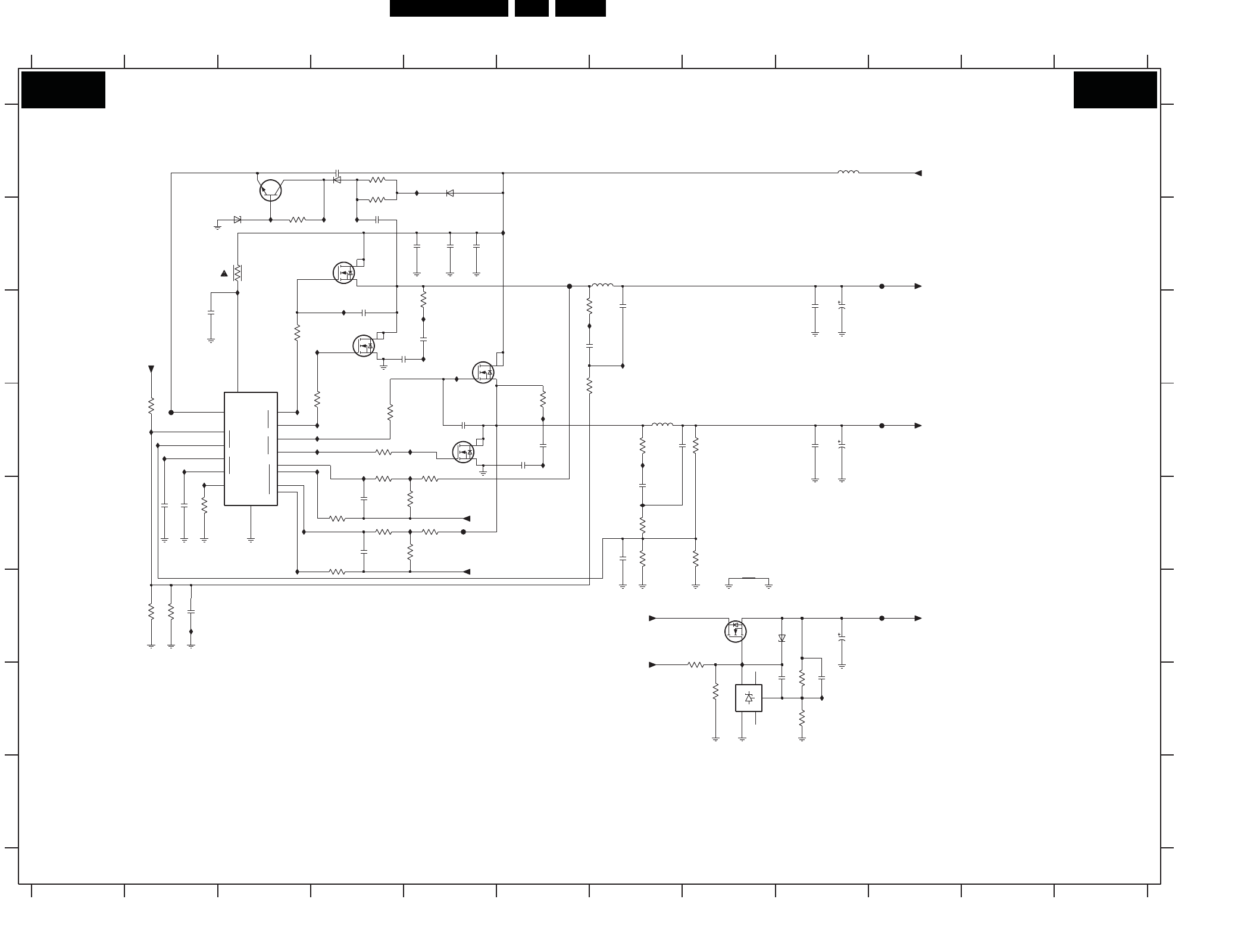
EN 56LC8.2HA LA 10.
Circuit Diagrams and PWB Layouts
2009-Apr-10
SSB: DC/DC +5V, +1V8, & +2V5
NCNC
A
REF
K
VCC
L2
+1
-1
1
2
+2
-2
2
VFB
GATE
IS
COMP
GATE
GND
1
BST
ROSC
H2
L1
H1
3P64 D2
3Q26 D4
NC
3Q32 D4
3Q69 E5
IQ29 E2
H
2Q55 F9
1
2Q49 F2
6Q13 A5
6Q05 F8
12
A
3Q25 C5
IQ16 D4
3Q45 D7
IQ55 E2
IQ56 A5
E
5
10
IQ37 B3
RES
7Q06-2 C4
3P54 F2
7Q07-2 D5
H
3Q71 E4
IQ03 C4
IQ32 F3
789
5Q02 A9
2Q59 C9
IQ39 E4
3Q54 E7
3Q48 A4
FQ40 D2
G
F
3Q50 E7
RES
C
D
E
2Q38 C4
IQ05 B4
3Q79 G8
6Q15 B3
IQ44 E7
C
RES
RES
2Q30 B5
G
2Q34 C9
DC/DC - 5V & 1V8 & 2V5
2Q28 B5
2Q39 E4
6Q14 A4
IQ43 E5
RES
FQ05 B10
3Q40 E2
IQ57 C7
3Q49 B3
RES
NC
FQ35 E5
3Q59 G9
3Q61 D6
2Q41 E2
RES
2Q40 E2
3Q72 E4
2Q29 B5
2Q36 C6
2Q37 D5
2Q35 C5
10 11
2Q31 C2
45
IQ11 C5
3Q56 E8
IQ45 F2
7
RES
3Q68 D5
2Q42 E4
RES
3Q41 E4
3Q37 C6
2Q46 D9
3Q78 F8
IQ23 F8
2Q54 E7
RES
3Q13 D4
RES
2Q58 G9
2Q73 G8
2Q61 D9
IQ27 D4
7Q06-1 B4
7Q05 A3
IQ12 D6
2
IQ17 D4
IQ42 C5
8
12
3P56 F2
2 9
IQ25 D3
3P70 D4
3P71 E4
4
3Q47 A4
IQ31 D4
IQ59 D7
IQ08 D2
IQ09 D2
IQ07 C7
B
A
D
IQ10 C5
IQ04 C4
IQ36 D6
IQ06 B4
5P09 B7
B
5Q09 D7
FQ06 F10
7Q07-1 C5
F
7Q08 G9
2Q33 C7
2Q07 B4
FQ03 D10
2Q32 C4 IQ40 D5
IQ41 D5
FQ08 B6
7Q09 F8
3Q70 E4
3Q64 D8
IQ24 G9
2Q53 D6
2Q43 D7
6
2Q52 D6
3Q23 C3
2Q48 F7
IQ01 C3
IQ02 B5
7Q11 D3
3Q38 D6
IQ28 D2
3
6
IQ26 D4
3Q20 B3
1
2Q78 A4
113
3Q77 G9
7
8
2
1
+1V8_SW
1u0
2Q31
2Q781u0
BC817-25W
7Q05
2Q30
22u
100n
GNDDC2
2Q07
2Q49
100p
3Q70
1K8
5Q02
10u
2Q41 100n
+5V_SW
2Q433n3
IQ23
IQ24
2Q54
100n
1%
2Q581u0
3Q59 470R
3Q41
3K3
2Q39
100n 5
6
4
3
7
8
2
1
SI4936BDY
7Q06-2
3Q77
SI4936BDY
7Q06-1
1K0 1%
22n
2Q73
12
SI4936BDY
7Q07-1
5Q09
10u
2Q46
100u16V
3Q48
3Q47 68R
68R
1K8
2Q29
22u
3Q71
6K8
6K8
3Q68
3Q69
IQ36
2Q37
3n3
2Q32
3n3
3Q20
3Q26 2R2
10R
2Q53
1n0
2Q52
1n0
3Q61
10R
1n0
2Q38
2Q35
10R
1n0
3Q25
IQ44
IQ01
FQ08
BZX384-C4V7
GNDDC2
GNDDC2
6Q05
2Q36
+2V6_SW
GNDDC2 GNDDC2
100n
100n2Q40
6
4
3
IQ42
SI4936BDY
7Q07-2
5
BZX384-C18
6Q15
3Q322R2
3Q23
10R
6Q14
BAS316
6Q13
BAS316
IQ37
IQ45
3K33Q72
2Q42
IQ43
100n
FQ40
8K23Q78
+12V_DISP
IQ28
IQ09
16V100u
IQ03
2Q55
IQ04
2Q59
16V100u
IQ40
2
1
3
IQ16
7Q09
PHD38N02LT
IQ25
FQ06
IQ31
FQ05
IQ12
2Q28
22u
IQ07
GNDDC2
IQ06
39K
3Q40
3Q54
2Q48
GNDDC2
+2V6_SW
10K
100p
2K2
3P70
2K2
3Q50
1K0
3P54
3Q45
6K8
IQ57
IQ59
22u
2Q34
2Q33
3n3
1K0
3Q38
GNDDC2
3Q376K8
+2V6_SW
GNDDC2 GNDDC2
3Q56
1%
+5V_SW
GNDDC2
470R
IQ10
IQ11
+12V_DISP
IQ05
3Q1310R
680R 1%
3Q49 1K0
3Q64
11
5
1213
14
7
10
NCP5422ADR2G
4
8
9
1
16
2
15
3
6
12
Φ
7Q11
22u
5P09
1K2
3P71
FQ03
120R
3P56
FQ35
1%1%
3P64
470R
IQ29
IQ55
IQ56
53
12
4
7Q08
TS431AILT
IQ02
IQ08
3Q79
GNDDC2
1K0
IQ17 IQ41
22u
2Q61
IQ26
IQ27
IQ39
GNDDC2
+5V_SW
IQ32
B01B B01B
I_17760_002.eps
180208
3139 123 6349.1
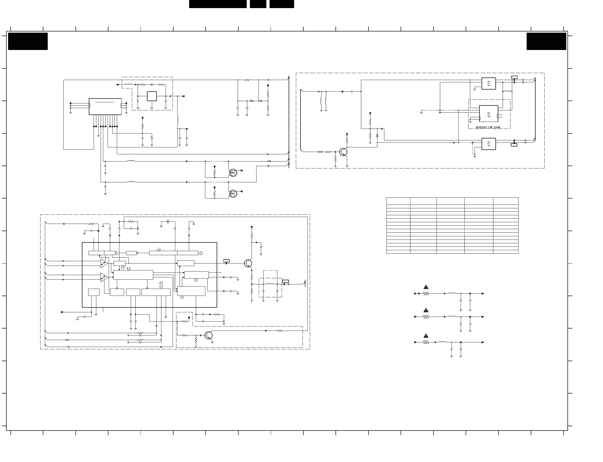
Circuit Diagrams and PWB Layouts EN 57LC8.2HA LA 10.
2009-Apr-10
SSB: Tuner IF & Demodulator
MTMT
COM
OUTIN
I
O2IGND
O1
GND
I
O2ISWI
O1
GND
O2
GND
O1
IGND
NC
ISWI
IN
SIF
AGC
AFC DETECTOR
PORTS
INTERCARRIER MIXER AND
AM-DEMODULATOR
I C-BUS TRANSCEIVER
2
RC VCO
NARROW-BAND FM-PLL
DIGITAL VCO CONTROL
SOUND TRAPS
4.5 to 6.5 Mhz
AUDIO PROCESSING
MAD
TUNER AGC VIF AGC
SUPPLY OUTPUT
VIF-PLL
SINGLE REFERENCE QSS MIXER
AND SWITCHES
DEMODULATOR
+5VS
+5V_IF
3140
3193 I6
F120 C4
1103K9656M
F143 C4
-
4103
Y
Y
K3953
3195
3193
3115 C9
1105
5121 E4
TUNER
I126 G3
*
3194
2V1
2144
RES
3123 F4
0V
7113 G3
UV1336
PEND NEW 12NC FOR TD1316AF/BHPN-5
F116 C3
22K
5118 B4
-
3117 D12
-
13
F112 C2
F115 C3
2130 I14
1103 D15
3140 J9
A125 D16
I
2117 B11
Y
2119 D5
3188 D11
3126 H8
3127 I7
I114 C12
3134 I13
7134 J7
3136 B5
A116 B16
J
1101 B3
6
D
RES
B
-
--
-
-
2135 H9
-
78
4102 C14
10
2143 F6
12
2145 I4
14
2148 B5
F
2151 J14
A
3110 B9
3192 C5
K
2137 I6
16
2V
K
-
1V5
5116 H8
2
10n
5
H
2139 I6
2140 J4
2142 D5
4104 D15
2144 I4
4122 E7
2147 B4
5111 B10
16
5114 H14
2152 J14
F117 C3
-
3194 J6
17
5115 I14
C
F134 B4
RES
RES
RES
1
2149 C8
F142 C4
RES
6
2V
4101 C13
I139 H8
4103 D14
F121 C4
4121 D7
F129 H15
4124 H8
F131 I15
2136 H7
I135 J5
3195 J6
18K
150R
RES
I149 H14
-
I147 B5
5117 B16
I137 C5
I138 H8
4104
M1971M
I143 I4
F133 C6
I145 B5
3113 C12
-
F
-
-
-
9
3152 J4
Y
--
4V9
-
17
1102 B15
2132 I14
3190 E7
2121 E4
2122 D4
7132 E7
2124 F3
3135 G8
2126 F4
3137 B5
2128 G8
3141 J13
E
I103 D15
3118 D11
I128 H7
F101 B11
3191 E7
2112 C8
6103 D12
2118 D6
7109 D11
3125 H8
I111 B8
I113 J6
4102
I118 D14
1101
I121 D6
I124 F4
I131 I6
15
F119 C3
2138 I3
2V
BC847B
5112 C6
-
RES
I148 I8
SAW FILTERS
24
F140 H9
3111 B8
I150 I14
I142 G6
F128 F3
I144 I4
F130 G7
I146 B4
F146 J14
L
5120 D4
G
2134 H8
F114 H13
2V
TUNER IF & DEMODULATOR 1104 F5
1105 C15
I127 G4
3119 D10
I129 H7
3124 F3
2120 D6
7114 G8
7131 E7
VV1316
7133 B5
I120 D10
A115 B16
I123 E6
A124 D16
I125 F5
3151 J4
4101
5119 B10
EUROPE
I104 G8
I130 I7
22K
UV1356
DEMODULATOR
5122 J14
6110 B8
Y
-
K9352
UV1316E
2V1
2V3
1102
3
10
K6274k
2123 F4
-
4
E
--
A
B
11
G
H
Y
C
2133 H7
1
3133 H13
3
2125 F3
5
2127 F5
7
2129 I14
10n
2131 I14
+3V3_SW
K7257M
F118 C3
*
I136 J5
-
I151 J14
AP CHINA
-
FOR EUROPE ONLY
RES
K9362
Y
RES
LATAM
UV1316E
I102 C14
-
7134
RES
I133 J5
I141 D10
10n
12
9
I
J
2141 J4
L
11
-
13
D
15
14
-
-
8
22K
3193
39K
3115
F117
3118
2K2
1SS356
6103
2122
15p
F142
4K7
3191
100R
I150
3151
18K
3188
7109
BC847B
2125
470n
5u6
5116
4124
2139
390p
+5V_SW
F101
F118
10n
2137
1n5
2123
I123
I121
+VTUN
4104
4103
I133
I136
F128
F134
+3V3_SW
10n
2152
+5VS
F131
I146
2145 1n0
5118
33R
10u
5114
33R
5112
5121 120R
2112
22u
2127
22p
3192
1K0
I142
3152 100R
4122
220n
2126
180R
3126
I118
2149
2u2
4121
+5V_IF
F115
2142
10u50V
I127
2135
15p
3
1
2
5
4
A124
1102
OFWK3953M
38M9
I113
I104
A115
2
13+5V_TUN
7133
L78M05CDT
10u
5115
2131
22u
A125
F121
1R0
3133
13
14
15
16
17
RF_AGC
2
SCL
4
SDA
5
6XTAL_OUT
+5V
CS
3
DC_PWR
1
IF_AGC
9IF_OUT1
8
IF_OUT2
10
11 IF_OUT3
12
TD1316AF/IHP-2
1101
TUNER
7
22u
2151
I124
F129
2141
150R
3125
10n
BC847B
7114
2128
I145
+5V_SW
I114
+5V_IF
15R
3135
I143
I144
I126
2136
470n
F116
I102 6
7
4
5
38M
3
8
2
1
10
I131
1105
OFWK6274K
38M9
3
1
2
5
4
+5V_IF
OFWK9656M
1103
3136
47R
I129
I130
I125
3113
14TA G C
9TOP
VAG C 1 6
1 VIF1
2 VIF2
19VPLL
20 Vp
6K8
OP1
22 OP2
15REF
11 SCL
10 SDA
23SIF1
24 SIF2
12 SIOMAD
AFD
18AGND
8AUD
17CVBS
5DEEM
7 DGND
4 FMPLL
13NC
3
TDA9886T/V4
7113
21AFC
6
2117
10n
I135
+5VS
+5V_SW
2140
1n0
2143
I139
2120
22u
2119
100n
I141
5117
3134
1R0
100n
2148
BC847B
330n
2147
7134
3195
18K
F133
2K2
3117
F140
I147
3190
4K7
+5V_IF
I151
10u
5122
4101
+12V_DISP
4102
I111
I103
5119
390n
3140
150R
F120
F119
F130
3127
5K6
2144
3124
100R
I120
3194
22K
2134
10n
15p
2138
22u
2129
A116
47R
3137
F114
F143
2118
10n
BAS316
I138
6110
3110
+5V_IF
3111 5K6
8K2
F112
7132
BSH111
5111
390n
3119
22K
F146
I128
3141
1R0
1104
10n
4M0
+5VS
2130
5120 120R
I148
+5V_TUN
I149
7131
BSH111
2133
10n
330R
3123
22n
2124
15p
2121
VIF1
22u
2132
IF_ATV
VIF2
SAW_SW
SIF1
SIF2
IIC_SCL
IIC_SDA
IF_ATV
CVBS_RF
SIF2
SIF1
RF_AGC
VIF2
VIF1
SIF
IIC_SDA
RF_AGC
IIC_SCL
B02 B02
I_17760_003.eps
180208
3139 123 6349.1
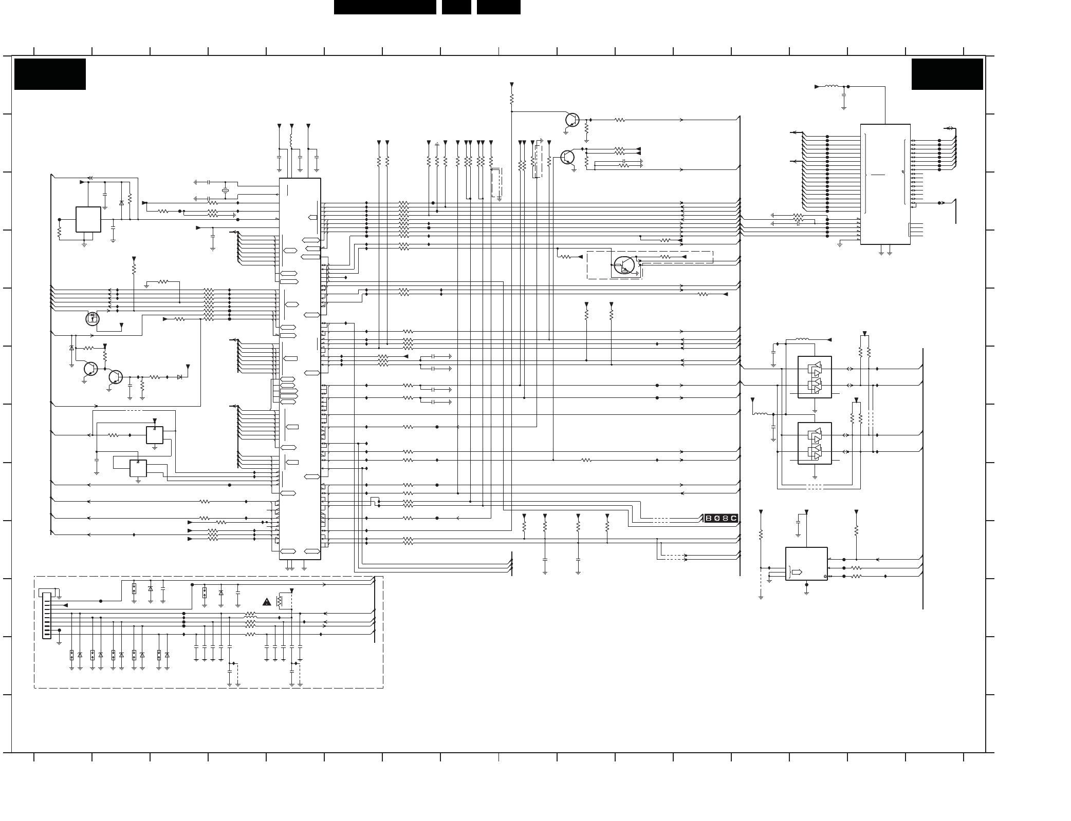
EN 58LC8.2HA LA 10.
Circuit Diagrams and PWB Layouts
2009-Apr-10
SSB: Micro Processor
DA1
8
TA 3OU T
W
9
W
ADDR
V
P1<0:7>
4
ANEX0
HLDA
6
HOLD
RXD1
INT<3:5>
7
TA 2 I N
XTAL
TA 4 O U T
RESET
SOUT4
CLK4
AVC C
TA 1 I N
VSS
TA 2 O U T
SIN4
TXD1
BYTE
8
9
10
11
P9<0:7>
6
CLK3
CTS1
SDA2
RDY
WRL
4
5
6
NMI
3
TA 3IN
CLK1
1
2
TA 1 O U T
TB5IN
TA 0 O U T
17
SIN3
ANEX1
DA0
5
2
3
3
2
1
3
P6<0:7>
TA 4 I N
INT
D<0:7>
ADDR
0
1
2
0
KI<0:3>
AN0<0:7>
WRH
BHE
RD
U
7
P3<0:7>
RTS1
19
P7<0:7>
DATA
CLK2
V
CTS2
RTS2
D<0:7>
TBIN<0:4>5
0
VCC
16
CLKOUT
P4<0:7>
ALE
P5<0:7>
OUT
AVSS
P0<0:7> SOUT3
IN
12
BCLK
ADDR
ADTRG
CNVSS
13
TA 0 I N
RXD2
SCL2
XCOUT
A<0:7>
P2<0:7>
4
WR
AN
18
U
P8<0:7>
SDA1
SDA0
SCL1
CTS0
ZP
RTS0
CTS0
CLK0
7
CLKS1
VREF
10
11
12
13
CS
TXD0
RXD0
TXD2
V
DATA
P10<0:7>
XCIN
14
15
14
15
0
1
0
2
1
AN2<0:7>
SCL1
18
16
RB
4
3
2
CE
7
6
WE
RP
1
0
BYTE
3
NC
5
8
9
10
11
12
13
14
15
A-1
10
4
9
8
7
6
0
8M-1
0
AD
5
11
2
1
17
OE
12
13
14
15
SCL
ADR
0
1
2SDA
WC
SUB
ER
GND
VOU T
VDD
3V3
I387 C4
I390 D6
I324 I6
I326 D6
3L79 B9
7322 D10
7323-1 H2
7323-2 G2
7L10 A10
I313 C6
is prohibited without the written consent of the copyright
I373 J3
I374 J5
I375 J3
IL41 F3
All rights reserved. Reproduction in whole or in parts
I358 E11
I359 H6
I360 E13
I361 F15
I362 D8
I363 F15
F320 B16
3307 B10
H
I
J
2320 I14
2323 G2
3L93 B10
UART _1R X
UART_1T X
UART _0R X
G
3326 C13
RES
RES
2319 C13
F310 B14
F311 B14
3L94 I4
3
2339 K5
2340 K4
2341 F13
RES
6301 C2
5
1V5
5678
6789
3353 I15
RES
RES
RES
5307 G13
RES
I330 E2
F339 C14
owner.
3310 C8
3386 I3
3384 H3
3315 C7
3V3
E
2313 B5
D
2343 F7
2344 F7
2345 F7
15 16
A
1309 K2
C
D
E
F
RES
F385 E4
F386 D6
F387 H4
F327 B16
4318 I11
RES
IL35 K5
3394 J4
3395 F2
3396 D11
3397 F6
3398 B10
3399 A9
3L01 C8
NC
4306 G15
4307 G15
4309 K5
4310 K4
4313 C8
F326 B14
3388 F6
3389 J4
3390 J4
3319 C2
3393 F2
RES
I372 I15
RES
I357 D6
EMC
EMC
RES
F384 J3
I323 H6
EMC
IL40 B10
F313 B14
F314 B16
F315 B14
F316 B16
F317 B14
F318 B16
F319 B14
3L02 H7
I315 E6
I316 E6
I318 I13
I319 G6
I320 G6
I370 G15
2324 B10
2327 J4
2328 K3
NC
3313 C7
RES
12
2338 F2
3354 H7
RES FOR BDS
RES FOR BDS
RES
F337 C16
F338 C14
6309 K1
6308 J4
4
2342 J3
3V2
3314 C3
3L22 I10
2310 B5
2311 A15
2314 C3
RES
NC
RES
14
91011
RES
1314 15 16
RES SDM
3L62 F7
F334 C14
F335 C14
3L59 D7
3L61 H7
7312 C1
7314 B9
RES PA N E L
3L63 H7
3L72 B10
3355 I15
3356 D11
3357 D7
3358 D10
3L64 B8
3L17 E3
3L18 F7
3L19 I9
3348 E7
3L21 I10
IL30 D7
RES
IL32 B10
I329 H4
F381 C4
F382 J3
F383 J3
I352 D4
I353 D2
I354 G6
I351 G6
F340 C14
F341 C14
F345 J14
F350 F11
F356 F11
F357 J3
F360 J1
3L58 G7
I341 E6
I342 E6
I344 E6
I345 I2
I347 G13
I376 J5
I380 F2
I384 I4
3L20 I9
5302 A14
I398 F6
IL25 G2
I396 F6
I393 F2
4323 G2
4325 I12
4326 I12
5301 B5
F380 C3
I356 G11
I397 F6
I332 E2
I333 E4
I335 E4
I336 H6
I337 I4
I338 E4
I339 H6
7301 E1
I340 D7
F361 E4
G
H
I
1301 C4
K
L
2315 C2
2316 C3
3331 E3
3336 C13
MJCMT8280 B5P
3V3
F309 H8
RES
3340 E3
I303 H4
C
3L14 I13
3333 E12
NC
RES
3332 E7
3L15 G2
B
3330 C7
3341 E3
3346 E7
3347 C9
2333 K4
3349 C7
3350 C6
3351 C8
3352 C8
1V5
I350 I11
I349 I11
EMC
F333 C14
0V6
F369 D14
RES
6310 K2
6311 K2
6312 K2
6313 J2
6317 E1
6318 F3
6319 K3
3359 F15
F362 C6
F363 I14
F364 I14
F365 I14
F366 C14
MICROPROCESSOR
RES
3350
3380 E7
RES
RES
RES
RES
3387 E7
3L71 H3
5304 J4
5306 E14
F336 C14
3382 F7
3L67 F6 I331 E4
2346 F7
2347 G13
2348 I9
2349 I10
3300 D3
3301 G10
3302 E3
F
3360 F15
3361 G15
3362 G15
11 12 13
3308 D2
2317 C2
2318 D3
RES
3338 E3
3325 D1
3339 E3
RES
2329 K3
4
I301 E4
I302 H4
F312 B16
K
0V8
RES
RES
RES
L
A
UART _0T X
123
2330 K4
2331 K4
2332 K5
12
2334 K4
2335 K5
2336 K5
2337 K5
RES
F367 C14
7311 C5
RES
7317 F1
F368 A15
RES
TO / FROM IR/ LED & KEYBOARD
3L23 I7
3L24 I7
3L53 H7
3L54 I15
3L55 G7
3L56 G7
3L57 E3
3303 C7
7302 F14
7303 G14
7308 F2
7310 B15
3316 C3
3317 C7
3318 C3
B
3320 C7
3321 C3
3322 C7
3324 C7
NC
F328 C14
EMC
I321 H6
IL37 C8
IL38 C7
IL39 E8
I322 H6
3L95 I3
3L96 C7
3L97 E10
3L98 E10
4301 B9
4303 J5
4304 H14
3329 D7
F321 B14
F322 B16
F323 C7
F324 B14
F325 B16
1306 J3
1307 K1
1308 K1
J
1310 K2
1312 J2
1313 K3
1320 J1
3L16 B10
F302 C7
F303 H8
F305 G8
F388 J2
IL33 G8
IL34 K4
RES
RES
4317 H11
4316 J13
3L13 C8
FOR PDP
NC
RES
RES
3L04 F3
3L05 C7
3L10 J5
3L12 C8
3L73 I3
3L75 C9
3L76 C9
3391 J4
3L86 E1
IL43 J5
RES
I364 D6
7L23 I14
I327 E2
I328 E2
F329 C14
F330 C1
F331 C14
F332 C14
EMC
I306 I4
I307 C6
I308 C6
I309 C6
I310 C6
I311 C6
I312 C4
4305 H14
I365 H4
I366 F6
I367 F6
I368 H4
I369 G15
IL42 C6
+3V3_STBY
2312 B5
3305 E3
3306 B10
10
2348
100p
2K2
F385
3380
3L75
100R
+3V3_STBY
3388 100R
3308
27K
3339 100R
I357
F356
F361
47K3397
10M
I318
4303
1301
3315 100R
3317 330R
100R3386
+3V3_STBY
I308
I367
15K
3393
+12V_DISP
3L72
47K
+3V3_SW
3362 3K3
F362
I398
2344 33p
F369
2342
10n
47R3390
BAS3166301
6312
BZX384-C6V8
1306
3349 10K
3387100R
+3V3_SW
3396 1K0
I360
F327
I312
F360
47R3394
IL37
I362
+3V3_STBY
I356
I302
7L10
BC847BW
1
2
48
7
NL27WZ08USG
7323-1
12
37
27
46
11
4326
40
42
44
30
32
9
10
13
14
28
15
31
34
36
39
41
43
45
33
35
38
23
22
21
20
19
18
8
7
47
26
29
25
24
6
5
4
3
2
1
48
17
16
EPROM
1Mx8/512Kx16
7310
M29W800DT-70N 6
4325
1307
100
99
98
10
14
60
96
12
62
13
11
17
16
15
9
8
5
4
3
2
1
27
26
25
24
23
22
21
20
19
18
37
36
35
34
33
32
31
30
29
28
48
47
46
45
44
43
42
41
40
39
38
58
57
56
55
54
53
52
51
50
49
71
70
69
68
67
66
65
64
63
61
59
89
88
87
78
77
76
75
74
73
72
83
82
81
80
79
95
93
92
91
90
7311
M30300SAGP
97
94
6
7
86
85
84
Φ
100R
I376
3L58
F382
I359
I307
100R3336
3391 47R
3301 100R
1K0
3321
F323
F316
I397
I349
6318
BZX384-C8V2
IL40
3L934K7
F303
3L7347K
F324
3356
I316
10K
I326
3L53100R
3L63100R
100R3L61
F363
7322
PDTC114ET
3L94 4K7
10K3347
+3V3_SW
+3V3_STBY
10K
3350
+3V3_STBY
3L79
I331
10K
3L57 100R
+3V3_SW
4K73359
6308
BZX384-C6V8
1309
1310
F330
4K7
3L98
I306
F381
+3V3_STBY
I339
I336
I313
10K3L14
3382100R
3346 100R
+3V3_STBY
F325
I365
F320
1n0
2329
I345
I337
2337 1n0
F326
100R3340
F309
F332
I311
I368
I333
F318
33p
2346
330R
3L15
2334
I321
1n0
I353
100n
2313
2315
100n
3L95 4K7
F305
2341
100n
1R0
3L10
IL33
I387
BZX384-C6V8
+3V3_SW
6310
1313
BZX384-C6V8
6319
IL34
2340 1n0
10K
3326 100R
3353
+3V3_SW
4301
IL30
333010K
F340
5301
60R
I372
F302
+3V3_STBY
+3V3_SW
1n0
+3V3_STBY
2339
F328
F329
I310
I393
+3V3_STBY
I347
+3V3_STBY
+3V3_SW
I350
234333p
IL38
I358
+3V3_SW
3303100R
IL39
3L64 10K
4316
I396
15p
2316
F345
+3V3_SW
+3V3_STBY
334847R
I320
I319
100n
2347
5307
30R
1312
1K5
3395
+3V3_SW
I384
+3V3_SW
I364
4310
I351
I328
100R
I329
3338
10K
3399
7317
BC847BW
+3V3_STBY
4317
4307
F314
F341
F312
I332
F321
I323
I324
4323
100R3302
I315
3L56 100R
F387
I301
33p
2345
SDA1
8
VCC
+3V3_STBY
EN5
4
GND
1
NC
2SCL0 7SCL1
3SDA0 6
PCA9515A
7302
4318
10K
3325
2317
100n
3307
220R5304
3L55 10K
13
2
7314
BC847BW
100R
3L59
3L133K3
100R
IL25
3320
3305
10K
3L62 100R
I309
F322
I341
4309
+3V3_STBY
+3V3_STBY
+3V3_STBY
1n02336
BZX384-C6V8
6313
F338
I338
I380
I335
SCL02SCL1 7
SDA03SDA1 6
VCC
8
5EN
GND
4
NC 1
IL41
7303
PCA9515A
3352 3K3
30R
5306
I322
I340
+3V3_SW
NL27WZ08USG
5
6
4
8
3
7323-2
+3V3_SW
I303
F313
2320
100n
I375
3333 10K
1n0
2330
23311n0
1K03L16
1K0
3306
10K3319
F337
3351 3K3
60R
5302
3L71 22R
22R
3384
100R
3318
2310
100n
I361
+3V3_STBY
I342
I330
F334
F333
I390
4305
IL35
F367
3L67
2314 15p
100R
3355
+3V3_STBY
100R
F339
F315
F311
23281n0
100p
2349
3L19
1K0
1K0
3L20
3L22
1K0
3358
4306
2K2
4313
F336
F335
+3V3_STBY 3L05 100R
10u
2311
100R
3L54
+3V3_STBY
+3V3_STBY
10n
2327
100n
2312
F357
3L18100R
+3V3_SW+3V3_STBY+3V3_STBY
F331
3389 47R
F365
3316 10K
+3V3_STBY
F380
6
5
8
4
7
(8Kx8)
M24C64-WMN6
7L23
EEPROM
Φ
1
2
3
F310
I366
100R
3357
4
5
6
7
8
9
BM09B-SRSS-TBT
1320
1
2
3
2324 1u0
+5V_SW
1K0
3L21
100R3L23
100R3L24
+3V3_STBY
+3V3_STBY
+3V3_SW
4304
2K2
3L76
3310 680R
+3V3_STBY
I354
3L86
+3V3_STBY
22K
6317
BZX384-C3V3
+3V3_SW
I374
+3V3_STBY
3L97
4K7
2319 100n
3
1
2
7301
BSH111
F364
2338
220n
BC847BW
7308
F350
1K5
3L04
I352
F366
I363
3L17 100R
F368
100n
2323
+5V_SW
I327
F386
3L02 100R
100n
2318
2332 1n0
I373
BZX384-C6V8
6309
F319
4K73341
F317
4K7
I344
3L01
3354 100R
BD45275G
Φ
1
32
5
4
7312
F388
BZX384-C6V8
6311
IL43
3329 100R
IL42
+3V3_STBY
4K73360
3322 100R
1K23300
I369
I370
3398
3K3
100K
+3V3_STBY
3361
1308
100R3331
2333 1n0
330R
3324
10K3314
100R
3L96 100K
3332
F383
F384
3K33L12
2335 1n0
IL32
330R
3313A(0)
AD(2)
AD(3)
AD(4)
AD(5)
AD(6)
AD(7)
DTV_IRQ
AD(0)
AD(1)
UART_0TX
MT8280_EN
UART_0RX
KEYB
TA C T _ SWITCH_IN T
UART_1TX
ITV_I2C_SDA
ITV_I2C_SCL
BOLT_ON_UART_TXD
BOLT_ON_UART_RXD
ALE_EMU
UART_1RX
HPD_RST_A
A(19)
A(18)
LCD_PWR_ON
NVM_WC
REMOTE
KEYB
IIC_SDA_up
IIC_SCL_up
A(17)
A(16)
CE
CS
A(15)
A(13)
A(12)
A(11)
A(10)
A(9)
A(8)
A(14)
A(6)
A(5)
A(4)
A(3)
A(2)
A(1)
A(0)
A(7)
AD(7)
AD(6)
AD(5)
AD(4)
AD(3)
AD(2)
AD(1)
AD(0)
TA C T _ SWITCH_IN T
CPU_RST
HP_DETECT
PRST
INTO
PWN
IIC_SCL_SIDE
IIC_SDA_SIDE
DC_PROT
HDMI_RX_BUF_RST
IIC_SCL
IIC_SDA
FPGA_BL_BOOST
AUD_RST
STANDBYn
SAW_SW
HDMI_HOTPLUG_RST
BL_BOOST
ANTI_PLOP
BL_ON_OFF
CTRL_DISP4_up
CTRL_DISP1_up
A(10)
A(9)
A(8)
A(19)
DDC_RST
A(15)
A(14)
A(13)
A(12)
A(11)
SVPWX_RST
A(18)
A(17)
A(16)
CEC_INT
A(0:7)
A(8:19)
A(1:7)
A(8:19)
CPU_RST
POWER_DOWN
LED1
IIC_SDA_up
IIC_SDA_up
HDMI_MUX_RST
CNVSS
STA N D B Y
MUTEn
AD(0:7)
LED2
SC2_STAT U S
SC1_STAT U S
LIGHT_SENSOR
WR
IIC_SCL_up
IIC_SCL_up
NVM_WC
WR
AD(0:7)
SVPWX_INT
A(5)
A(6)
A(7)
CE
RD
RD
A(1)
A(2)
A(3)
A(4)
LIGHT_SENSOR
LED1
LED2
REMOTE
B03B03
I_17760_004.eps
180208
3139 123 6349.1
Circuit Diagrams and PWB Layouts EN 59LC8.2HA LA 10.
2009-Apr-10
SSB: Trident WX69
NC
1413
TRIDENT - WX69
1
2
1(HIGH)
TO FPGA / TO LVDS CONNECTOR
NC
RES
0R
18
NC
RES
SINGLE 12NC : 3139_123_63491
L
M M
RES
12
RES
0(LOW)
L
NC
RES
RES
NC
MULTI 12NC : 3139_123_63481
K
2
I
A
3
10
RES
K
8
5
RES
179
RES
11
15 16
4
H
G
7
I
J
SCK Y11 I2C Slave Address=0x7E/7F(*) I2C Slave Address=0x7C/7 D
NC
Pin Name
SD0 V12 Use Rising Edge of WR# to latch data(*) Use Falling Edge of WR# to latch data
B
0(LOW)
RES
RES
13126
NC
RES
RES
RES
DP_HS P19 MPU in A/D Multiplix Mode MPU in A/D Separate Mode(*)
19
NC
N
WS U12 Use ALE to latch Address Use Falling Edges of WR#&RD# to latch Address(*)
NC
NC
B
5
N
D
F
O
1
O
P
E
F
8
RES
NC
NC
18
7
J
RES
NC
3
Pin No
20
14
NC
"C00-"C99" & "V00 - V99"
A
D
E
NC
C
NC
2019
G
NC
Pin No 1(HIGH)
6 17
H
C
15 16
94 10 11
P
Pin Name
FC07
2C69
10u
FC05
C?
100n
FC04
FC11
IC04
2V05 33p
IC03
3C49
FC06
33p2V04
FC09
FC10
FC08
+2V5_VDDMQ
3V04
100R
IC05
+3V3_SW
+1V2_ADC
100n2C38
4K7
3C47
2C65 470p 100n2C54
+1V2_PLL
2C34
22u6.3V
IC10
IC11
IC12
IC09
100n
2C76
+1V2_ADC
2C45
10u6.3V
2C46
10u6.3V
2C56
10u6.3V
33R
5C19
100n
2C61
4K7
3C45
100n
2C58
100n
2C32
2C66 470p
100n
2V02
+1V2_SW
+1V2_CORE
100n2C50
2C42
100n
2C35
100n
2C43
22u6.3V
2C41
22u6.3V
+3V3_SW
33R
5C11
+1V2_PLL
+1V2_PLL
100n
2C71
IC13
100n
2C83
MD7
A10
MD8
B10
MD9
C10
MVREF
E3
RAS_
J2
VSP17
WE_
K1
MD28
C1
MD29
C2
MD3
D12
MD30
C3
MD31
D3
MD4
C11
MD5
B11
MD6
A11
MD20
D6
MD21
A5
MD22
B5
MD23
A4
MD24
C5
MD25
A3
MD26
A2
MD27
A1
MD13
B8
MD14
C8
MD15
D8
MD16
D7
MD17
C7
MD18
B7
MD19
A7
MD2
A13
MA9
F3
MCK0
D1
MCK0_
E1
MD0
C13
MD1
B13
MD10
D10
MD11
D9
MD12
A8
MA11
F1
MA2
H2
MA3
H1
MA4
G1
MA5
G2
MA6
G3
MA7
G4
MA8
F4
DQS0
B12
DQS1
B9
DQS2
B6
DQS3
B2
HSP19
MA0
H4
MA1
H3
MA10
F2
DPB_CLK T19
DPB_DE W20
DPB_HSV19
DPB_VSV20
DQM0
A12
DQM1
A9
DQM2
A6
DQM3
B1
DPB10 T17
DPB11 T18
DPB12 T20
DPB13U20
DPB14 U19
DPB15 U18
DPB8R20
DPB9 R19
DPA6 V17
DPA7 U17
DPA8U16
DPA9 V16
DPA_CLK Y15
DPA_HSY19
DPA_VSY20
DPA2 W18
DPA20 W13
DPA21 V13
DPA22 U13
DPA23Y12
DPA3Y18
DPA4 Y17
DPA5 W17
DPA12 W15
DPA13V15
DPA14 U15
DPA15 U14
DPA16 V14
DPA17 W14
DPA18Y14
DPA19 Y13
CAS_
J1
CLKE
K2
CS0_
J4
CS1_
J3
DPA0 W19
DPA1 V18
DPA10 W16
DPA11 Y16
7C01-2
SVP WX68
BA0
K3
BA1
K4
VSS9H11
VSSR1 E4
VSSR2 E7
+3V3_SW
+1V2_CORE
VSS42 N13
VSS43P18
VSS44 T16
VSS45 H20
VSS5D2
VSS6H8
VSS7H9
VSS8 H10
VSS35M12
VSS36M13
VSS37N8
VSS38 N9
VSS39N10
VSS4C12
VSS40 N11
VSS41 N12
VSS28L11
VSS29 L12
VSS3 C9
VSS30L13
VSS31M8
VSS32M9
VSS33 M10
VSS34M11
VSS20 K10
VSS21 K11
VSS22 K12
VSS23K13
VSS24 L5
VSS25 L8
VSS26 L9
VSS27 L10
VSS13J9
VSS14 J10
VSS15 J11
VSS16 J12
VSS17 J13
VSS18K8
VSS19 K9
VSS2C6
VREFN_1
V5
VREFN_2
V7 VREFP_1
W5
VREFP_2
W7
VSS1B3
VSS10 H12
VSS11 H13
VSS12 J8
VDDM4
D5
VDDM5
D11
VDDM6
E5
VDDM7
E6
VDDM8
E9
VDDM9
E10
VDDR1
E2
VDDR2
E8
VDDH8
R18
VDDM1
B4
VDDM10
E11
VDDM11
E12
VDDM12
F5
VDDM13
G5
VDDM2
C4
VDDM3
D4
VDDC9
G16
VDDH1
L16
VDDH2
M16
VDDH3
N16
VDDH4
P16
VDDH5
T12
VDDH6
T13
VDDH7
R17
VDDC18
T15
VDDC2
C15
VDDC3
D13
VDDC4
D14
VDDC5
D15
VDDC6
E13
VDDC7
E14
VDDC8
E15
VDDC10
H5
VDDC11
H16
VDDC12
J5
VDDC13
J16
VDDC14
K5
VDDC15
K16
VDDC16
R16
VDDC17
T14
LVD S_VSSO2 C19
LVD S_VSSPE18
NC
P20
PAVDD1
T3
PAVDD2
T4
PAV SS1T2
PAV SS2R3
VDDC1
C14
LVD S_VDD A
E17
LVD S_VDD D
D16
LVD S_VDDO1
C17
LVD S_VDDO2
D17
LVD S_VDD P
D18
LVD S_VSSAE16
LVD S_VSSDC16
LVD S_VSSO1 C18
V1
AVSSLLPLL T1
AVSS_ADC1 T5
AVSS_ADC2 T7
AVSS_ADC3T9
AVSS_ADC4 T6
AVSS_BG_ASS W3
AVSS_OUTBUF Y2V3
AVDD3_OUTBUF
U3
AVDDAPLL
U1
AVDDLLPLL
R2
AVDD_ADC1
U5
AVDD_ADC2
U7
AVDD_ADC3
T8
AVDD_ADC4
U6
AVSSAPLL
7C01-4
SVP WX68
AVDD3_ADC1
Y3
AVDD3_ADC2
U9
AVDD3_BG_ASS
100n
2C77
2C67
10u6.3V
2C78
10u6.3V
3C48
22R
3C46
22R
33R
5C18
2C36
10u6.3V
33R
5C14
100n2C37
100n
2C40
100n2C39
33R
5C17
100n
2C57
2C62
10u6.3V
2C60
10u6.3V
100n2C59
2C16
DDR_VREF
100n
100n2C47
100n2C55
100n
2C51
100n
2V01
100n2C53
2C44
100n
100n2C48
100n2C52
+3V3_SW
+1V2_PLL
33R
5C10
33R
5C09
100p2C89
100n
2C68
100p2C85
+3V3_SW
100n
2C75
22R
3C33
10u6.3V
IC01
2C72
33R
5C13
+1V2_ADC
33R
5C16
+1V2_ADC
+1V2_ADC
+3V3_SW
FC02
33R
5C15
33R
5C22
33R
5C21
33R
5C20
6.3V
2C80
10u
100n
2C31
2C99
10u6.3V6.3V
100n
2C63
2C95
10u
2C93
10u6.3V
100n
2C79
100n
2V03
100n
2C98
100n2C49
100n
2C94
100n
2C92
100n
2C90
2C91
10u6.3V
+2V5_VDDMQ
+5V_SW
+3V3_SW
100n
2C33
100p2C87
100p
2C84
100p2C88
100p2C86
22R
3C37
IC02
2C70
10u6.3V
3C30
9
714
8
22R
7C03-4
74LCX14T
33R
5C12
+3V3_SW
+3V3_SW
2C64
10u6.3V
2C97
10u6.3V
14
12
100n
2C96
74LCX14T
7C03-6
13
7
11
714
10
74LCX14T
7C03-5
+3V3_SW
+5V_SW
3C31
22R
3C36
22R
5
714
6
1
714
2
7C03-3
74LCX14T
7C03-1
74LCX14T
3C07
100R
FC03
FC01
4K7
3C22
100R
2C27
3C09
10u6.3V
4K7
3C293C32
4K7
2C03100n 3C34
22R
74LCX14T
3
714
4
7C03-2
FPGA_BL_DIMMING
3C25 10K
4C08
100R
3C24
2C73
10u
18p
2C02
+3V3_SW
4K7
3C44
2C29
10u6.3V
4K7
3C41
100n
2C17
100n2C11
100n2C10
100n2C09
100n2C07
+3V3_STBY
100n
2C22
IC18
6.3V
33R
2C23
10u
5C07
100n
2C19
4K7
3C42
4K7
3C40
18
4K7
3C39
3C06-1 100R
100R18
5
3C05-1
100R3C04-4 4100R
36
100R18
+3V3_SW
3C04-3
3C04-1
BC847BW
7C02
7C04
220R
3C23
BC847BW
1C24
24M0
100n2C20
3C20 1K0
+3V3_SW+3V3_SW
100R
3C08
+3V3_SW
3C03-2 27
45
100R
3C03-4 100R
3C43
4K7
100R
3C06-336
100R
45
3C06-4
33R
5C06
22u
2C74
100n2C18
100n
2C15
36
100n2C08
3C05-3100R
100n2C06
100n2C05
100n
W6
Y_G3Y6
+3V3_SW
2C04
SDA
H17 TESTMODEF17
V5SFF16
WR_
J19
XTALI
W1
XTALO
Y1 Y_G1 V6
Y_G2
PLF2
R4
PR_R1 Y8
PR_R2 W8
PR_R3V8
PWM0 G17
RD_
J20
RESET F18
SCL
H18
INTN G18
MLF1
U2
PB_B1 W9
PB_B2 Y9
PB_B3Y10
PC_B W10
PC_G Y7
PC_R U8
CPU_CS
J17
CVBS1Y4
CVBS_OUT1 W2
CVBS_OUT2 V2
Y5
FB1
FB2 U4
FS1V4
FS2W4
ADDR4
M20
ADDR5
M19
ADDR6
M18
ADDR7
M17
V10
AIN_H
AIN_V U10
ALE
J18
CV9
AD4
K17
AD5
K18
AD6
K19
AD7
K20
N17 ADDR0
ADDR1
N18
ADDR2
N19
ADDR3
N20
7C01-1
SVP WX68
L17 AD0
AD1
L18
AD2
L19
AD3
L20
IC07
100n
2C25
100n
2C24
2C28
100n
IC16
2n72C82
33R
IC17
5C08
IXXX
100R
27
45
3C06-2
100R3C05-4
27
3C04-2 100R
100n
2C13
470R
4C07
3C19
36
IXXX
IXXX
3C03-3100R
2n72C81
27
3C05-2 100R
100n2C12
IXXX
IXXX
18p2C01
3C01
1M0
+3V3_SW
100n
2C26
2C30100n
IC14 IC15
3C02
33R
IXXX
P3TMDS_GND4
TMDS_GND5
R1
WS
U12
IXXX
TD2P F20
TE1M B19
TE1P A19
TE2M H19
TE2P G20
TMDS_GND1
L3
TMDS_GND2
M3
TMDS_GND3
N3
TC2P D20
TCLK1M B17
TCLK1P A17
TCLK2M F19
TCLK2P E20
TD1M B18
TD1P A18
TD2M G19
TA 2 P A20
TB1M B15
TB1P A15
TB2M D19
TB2P C20
TC1M B16
TC1P A16
TC2M E19
L2
SCDT
V11
SCK
Y11
SD0
V12
SPDIF
W12
TA 1 M B14
TA 1 P A14
TA 2 M B20
R5
RX0+
M1 RX0-
M2
RX1+
N1
N2 RX1-
RX2+
P1 RX2-
P2
RXC+
L1 RXC-
N4
AVCC3
N5
AVCC4
P4
DGND
P5
DSCL
T11
DSDA
U11
L4 PVCC
PWR5V
T10
REGVCC
7C01-3
ANTSTO
M5
AUDIOCLK
W11
M4 AVCC1
AVCC2
SVP WX68
IXXX
100R
18
3C03-1
100n
2C21
3C10
IXXX
22R
BL_ADJUST_PWM
CVBS_IN_DTV
SC1_G_IN
DP_HS
WX_WE#
WX_MD4
WX_MD5
WX_MD6
WX_MD7
WX_MD8
WX_MD9
WX_RAS#
WX_MD23
WX_MD24
WX_MD25
WX_MD26
WX_MD27
WX_MD28
WX_MD29
WX_MD3
WX_MD30
WX_MD31
WX_MD14
WX_MD15
WX_MD16
WX_MD17
WX_MD18
WX_MD19
WX_MD2
WX_MD20
WX_MD21
WX_MD22
WX_MA9
WX_MCK0
WX_MCK0#
WX_MD0
WX_MD1
WX_MD10
WX_MD11
WX_MD12
WX_MD13
WX_MA0
WX_MA1
WX_MA10
WX_MA11
WX_MA2
WX_MA3
WX_MA4
WX_MA5
WX_MA6
WX_MA7
WX_MA8
WX_DQM0
WX_DQM1
WX_DQM2
WX_DQM3
WX_DQS0
WX_DQS1
WX_DQS2
WX_DQS3
DP_HS
HDMI_H
HDMI_V
HDMI_Cr(0)
HDMI_Cr(1)
HDMI_Cb(0)
HDMI_Cb(1)
HDMI_Y(0)
HDMI_Y(1)
HDMI_DE
HDMI_Cr(8)
HDMI_Cr(9)
HDMI_Y(5)
HDMI_Y(6)
HDMI_Y(7)
HDMI_Y(8)
HDMI_Y(9)
HDMI_Cb(2)
HDMI_Cb(3)
HDMI_VCLK
HDMI_Cb(6)
HDMI_Cb(7)
HDMI_Cb(8)
HDMI_Cb(9)
HDMI_Cr(2)
HDMI_Cr(3)
HDMI_Cr(4)
HDMI_Cr(5)
HDMI_Y(4)
HDMI_Cr(6)
HDMI_Cr(7)
WX_BA0
WX_BA1
WX_CAS#
WX_CLKE
WX_CS0#
HDMI_Y(2)
HDMI_Y(3)
HDMI_Cb(4)
HDMI_Cb(5)
WX_AVSS_ADC1
WX_AVSS_ADC2
WX_LVDS_VSS
WX_LVDS_VD D
WX_AVDD3_ADC1
WX_AVDD3_ADC2
WX_AVDD_ADC4
WX_AVSSAPLL
WX_AVDDAPLL
WX_AVSSLLPLL
WX_AVDDLLPLL
WX_PAVSS2
WX_PAVDD 2
WX_AVSS_ADC1
WX_AVDD_ADC1
WX_AVSS_ADC2
WX_AVDD_ADC2
WX_AVSS_ADC3
WX_AVDD_ADC3
WX_AVSS_ADC4
WX_AVSS_OUTBUF
WX_AVDD3_OUTBUF
WX_AVSS_BG_ASS
WX_AVDD3_BG_ASS
WX_PAVSS1
WX_PAVDD 1
WX_AVSS_ADC4
WX_AVSS_BG_ASS
WX_AVSS_OUTBUF
WX_LVDS_VD D
WX_LVDS_VSS
WX_PAVDD 1
WX_PAVDD 2
WX_PAVSS1
WX_PAVSS2
WX_AVDD3_ADC1
WX_AVDD3_ADC2
WX_AVDD3_BG_ASS
WX_AVDD3_OUTBUF
WX_AVDDAPLL
WX_AVDDLLPLL
WX_AVDD_ADC1
WX_AVDD_ADC2
WX_AVDD_ADC3
WX_AVDD_ADC4
WX_AVSSAPLL
WX_AVSSLLPLL
WX_AVSS_ADC1
WX_AVSS_ADC2
WX_AVSS_ADC3
WX_PAVDD 1
WX_PAVDD 2
PC_VGA_H
PC_VGA_V
VGA_H
VGA_V
BL_ADJUST_ANA
WX_REGVCC
VGA_G_IN
VGA_B_IN
WX_PVCC
WX_AVCC
SC1_B_IN
SC1_CVBS_IN
HD_PR_IN
SC2_C_IN
SC1_R_IN
VGA_R_IN
CVBS_RF
HD_Y_IN
SC2_Y_CVBS_IN
SVHS_Y_CVBS_IN
SVHS_C_IN
HD_PB_IN
IIC_SCL_SIDE
IIC_SDA_SIDE
CS
SVPWX_RST
A(5)
A(6)
A(7)
A(0:7)
AD(0:7)
A(0)
A(1)
A(2)
A(3)
A(4)
AD(5)
AD(6)
AD(7)
AD(0)
AD(1)
AD(2)
AD(3)
AD(4)
RD
WR
SC1_RF_OUT_CVBS
SC2_CVBS_MON_OUT
SC1_FBL_IN
SVPWX_INT
PC_VGA_H
PC_VGA_V
ALE_EMU
TxFPGAe_4p
TxFPGAe_4n
TxFPGAo_4n
TxFPGAo_4p
TxFPGAe_CLKp
WX_AVCC
WX_PVCC
WX_REGVCC
TxFPGAe_2n
TxFPGAe_2p
TxFPGAe_3n
TxFPGAe_3p
TxFPGAe_CLKn
TxFPGAo_CLKp
TxFPGAe_0n
TxFPGAe_0p
TxFPGAe_1n
TxFPGAe_1p
TxFPGAo_2p
TxFPGAo_3n
TxFPGAo_3p
TxFPGAo_CLKn
TxFPGAo_0n
TxFPGAo_0p
TxFPGAo_1n
TxFPGAo_1p
TxFPGAo_2n
B04A B04A
I_17760_005.eps
180208
3139 123 6349.1
IC35 J4
IC36 J8
2C10 B9
2C11 B9
2C12 C9
2C02 B6
2C01 A6
1C24 B7
2C13 B9
IC31 H10
IC32 H8
IC33 I8
2C87 L2
2C88 L3
2C89 L2
2C90 G7
2C94 H7
2C95 H8
2C96 H7
3C03-4 C7
3C04-1 B7
5C07 B2
5C08 C2
5C09 E2
5C10 F2
3C03-2 C7
3C03-3 C7
2C38 F4
2C39 F4
2C40 F4
2C41 F2
2C45 G2
2C74 D12
2C73 E10
2C71 I2
2C72 J2
2C03 B9
2C04 B9
2C05 C9
2C27 B2
2C28 C2
2C29 C2
2C30 D9
3C37 C15
3C39 D2
3C40 D2
3C41 D3
2C06 B9
FC09 J2
FC10 J2
FC11 K2
IC10 B4
5C18 G8
5C17 G8
5C16 K2
3C32 B13
3C33 B13
3C34 B15
3C36 B15
5C15 J2
2C50 G3
2C51 G3
2C52 G3
2C53 G3
2C57 H2
2V02 J7
2V03 K7
2V04 D7
2V05 D8
2C62 J8
2C63 H3
2C64 K8
2C65 H4
IC16 D2
IC17 D3
IC18 D3
IC19 D11
2C81 B7
IC30 H10
2C80 K2
2C82 B7
3C08 C7
3C09 C7
3C10 D7
3C19 C9
2C79 K2
2C47 G2
2C48 G3
2C49 G3
FC08 I2
2C58 H3
2C69 I4
2C70 I2
5C19 I8
5C20 I8
5C21 J8
5C22 J8
7C01-1 B8
7C01-2 F11
7C01-3 B4
7C01-4 F5
7C02 E11
7C03-1 A14
2C54 G3
2C55 G4
2C56 H2
FC07 I2
7C03-6 C16
7C04 D11
FC01 B2
FC02 B2
FC03 C2
FC04 E2
FC05 F2
FC06 F2
2C24 B2
2C25 B2
2C26 B2
2C91 G8
2C86 K3
3C07 D10
2C31 H3
2C32 H3
2C33 B15
2C34 E2
3C20 C9
3C22 D11
3C23 D11
3C24 D12
2C92 G7
2C93 G8
2C83 K2
2C84 K2
2C85 K2
2C07 B9
2C08 B9
2C09 B9
3V04 E12
4C07 D9
4C08 E11
5C06 B2
2C15 C9
2C16 H3
2C17 C9
5C11 F2
5C12 I2
5C13 I2
5C14 J2
3C06-4 C7
2C23 B2
3C04-2 B7
3C04-3 B7
3C04-4 B7
3C05-1 B7
3C06-2 C7
3C06-3 C7
3C05-2 B7
3C05-3 B7
3C05-4 C7
3C06-1 C7
3C29 A13
3C30 A15
3C31 A13
7C03-2 B14
7C03-3 B14
7C03-4 C14
7C03-5 C16
3C25 D9
2C18 C9
IC14 D8
IC15 D9
2C19 C9
2C20 D9
2C21 D9
2C22 B2
IC20 D11
IC21 D10
IC22 E9
IC23 G8
IC24 G8
IC25 G13
IC26 H10
IC27 H10
IC28 H8
IC29 H10
2C35 E2
2C36 F3
2C37 F4
2C97 H8
2C98 I7
2C99 I8
2V01 I7
2C42 F2
2C43 F2
2C44 F2
2C46 G2
2V06 C9
3C01 B7
3C02 B7
3C03-1 C7
3C42 D2
3C43 D2
3C44 D3
3C45 G13
3C46 H8
3C47 H13
3C48 H8
3C49 I3
2C75 J2
2C76 J2
2C77 J3
2C78 K2
2C66 H4
2C67 I2
2C68 I2
2C59 H3
2C60 I8
2C61 H3
IC11 C8
IC13 C8
EN 60LC8.2HA LA 10.
Circuit Diagrams and PWB Layouts
2009-Apr-10
SSB: DDR Interface
VDDQ
VSS VSSQ
VDDVDDQ
VSS VSSQ
VDD
3D02-1 E5
34
NC
2D32 B4
2D11 C3
2D04 C3
3D40 F7
A
B
3D06-3 D5
A
2D58 C9
C
3D11 F2
H
2D08 C4
2D31 B4
F
G
E
2D09 C4
3D10 G2
3D16 B5
2D38 C9
5
3D05-1 D5
RES
3D05-3 D5
3D05-4 D5
2D12 C4
3D06-2 D5
3D44-4 D11
3D43-2 D11
NC
3D47-1 E11
3D38 F7
3D44-2 D11
3D44-3 D11
3D43-1 D11
3D47-2 E11
2D34 B5
2D37 C9
2D03 C4
2D39 C10
ID06 E8
23
3D44-1 D11
2D59 C9
DDR INTERFACE
2D71 B2
ID05 G9
7D01 D3
7D02 D9
3D01-1 E5
3D01-2 E5
12
ID01 G3
3D01-4 E5
5D03 B2
10
3D02-4 D5
2D73 B10
3D47-3 D11
3D47-4 D11
3D48-1 E11
3D48-2 E11
2D43 C9
3D43-3 D11
3D43-4 D11
3D05-2 D5
3D14 G2
3D15 B5
ID07 G2
3D06-4 D5
3D48-3 E11
3D48-4 E11
3D02-2 E5
3D02-3 D5
3D09 F2
FD01 B3
FD02 B4
912
2D60 C10
11
2D10 C4
89
3D06-1 D5
45
67
2D72 B3
1
2D78 B11
10 11
3D01-3 E5
12
D
E
RES FOR EMC
76
8
B
F
G
2D14 G2
2D18 C3
2D02 C3
C
D
2D46 C8
2D57 C9
2D33 B5
H
+2V6_SW
10u
2D18
100n2D10
ID05
2D60 470p
2D57 10n
83D05-1 22R1
6.3V
2D71
22u
2D59 10n
2D5810n
273D05-2 22R
FD02
53D05-4 22R4
10n2D09
ID06
ID01
470p2D12
470p
2D11
10n
2D08
3D06-1 22R
18
273D06-2 22R
+2V5_VDDMQ
2D72
10n
2D43470p
2D39100n
ID07
36
3D05-322R
3D47-322R36
3D47-4 4545 22R22R3D02-4
3D01-2 2 7
18
22R
22R3D01-1
10n2D04
100n2D03
100n2D02
10u
2D46
36
5
3D06-322R
3D06-4 22R4
10n
2D14 3D10 51R 1%
3D43-336
22R45
22R
3D43-4
FD01
100n
2D31
4 5 22R
3D01-4
27
18
3D02-2 22R
3D02-1 22R
5D03
33R
27
DDR_VREF
18
3D43-2 22R
3D43-1 22R
22n
2D78
2D73
22n
+2V5_VDDMQ
15R3D40
4522R
3D44-4
22R
3D48-336
3D14 51R 1%
3D11 15R
2D32
100n
64
WE_
21
DDR_VREF
55
61
VREF
49
34
48
66
6
12
52
58
RAS_
23
UDM
47
UDQS
51
1
18
33
3
9
15
LDM
20
LDQS
16
NC1 14
NC2 17
NC325
NC4 43
NC5 53
NC6 42
DQ2 5
DQ37
DQ4 8
DQ5 10
DQ6 11
DQ7 13
DQ854
56
DQ9
DQ0 2
DQ1 4
DQ10 57
DQ11 59
DQ12 60
DQ1362
DQ14 63
DQ15 65
BA1
27
CAS_
22
CK
45
CKE
44 CK_
46
24 CS_
19
DNU1 50
DNU2
A3
32
A4
35
A5
36
A6
37
A7
38
A8
39
A9
40
BA0
26
A0
29
A1
30
28A10|AP
A11
41
A2
31
7D01
K4D261638K
6
3D09 15R
3D02-33 22R
+2V5_VDDMQ
3D48-2 27
1K0
3D16
22R
2D34
100n
27
3D44-336
22R
3D44-2
22R
22R18
3D47-1
+2V5_VDDMQ+2V5_VDDMQ
22R
273D47-2
DDR_VREF
2D33
100n
3D48-4 45
18
+2V5_VDDMQ
22R
22R
3D48-1
15R
3D38
3D44-1 1 8
22R3D01-33 6
22R
1K0
3D15
2D38 100n
2D37100n
52
58
64
WE_
21
9
15
55
61
VREF
49
34
48
66
6
12
53
NC6 42
RAS_
23
UDM
47
UDQS
51
1
18
33
3
54
DQ9 56
LDM
20
LDQS
16
NC1 14
NC2 17
NC325
NC4 43
NC5
63
DQ15 65
DQ2 5
DQ37
DQ4 8
DQ5 10
DQ6 11
DQ7 13
DQ8
19
DNU1 50
DNU2
DQ0 2
DQ1 4
DQ10 57
DQ11 59
DQ12 60
DQ1362
DQ14
40
BA0
26
BA1
27
CAS_
22
CK
45
CKE
44 CK_
46
CS_
24
41
A2
31
A3
32
A4
35
A5
36
A6
37
A7
38
A8
39
A9
A0
29
A1
30
A10|AP
28
A11
7D02
K4D261638K
WX_MD18
WX_MD17
WX_MCK0
WX_MCK0#
WX_MD27
WX_MD29
WX_MD28
WX_MD31
WX_MD30
WX_MD16
WX_MD19
WX_MD9
WX_MD20
WX_MD21
WX_MD22
WX_MD23
WX_MD24
WX_MD25
WX_MD26
WX_MD1
WX_MD0
WX_MD4
WX_MD15
WX_MD14
WX_MD12
WX_MD13
WX_MD11
WX_MD10
WX_MD8
2_DQ19
2_DQ17
2_DQ18
WX_MD7
WX_MD3
WX_MD6
WX_MD2
WX_MD5
2_DQ16
WX_CS0# WX_CS0#
2_DQ31
2_DQ30
2_DQ20
2_DQ21
2_DQ22
2_DQ23
2_DDQS2
2_DDQS3
2_DQ24
2_DQ25
2_DQ26
2_DQ27
2_DQ29
2_DQ28
1_DQ2
1_DQ1
1_DQ0
1_DQ13
1_DQ11
1_DQ10
1_DQ8
1_DQ9
1_DDQS1
1_DDQS0
WX_DQM2
WX_DQM3
1_DQ15
1_DQ14
1_DQ7
1_DQ6
1_DQ5
1_DQ4
1_DQ12
1_DQ3
WX_CLKE
WX_RAS#
WX_CAS#
WX_WE#
WX_DQS2
WX_DQS3
WX_BA0
WX_BA1
WX_MA2
WX_MA3
WX_MA4
WX_MA5
WX_MA6
WX_MA7
WX_MA8
WX_MA9
WX_MA10
WX_MA11
WX_BA1
WX_DQM1
WX_DQM0
WX_CLKE
WX_RAS#
WX_CAS#
WX_WE#
WX_MCK0
WX_MCK0#
WX_DQS1
WX_DQS0
WX_MA0
WX_MA1
WX_MA0
WX_MA1
WX_MA2
WX_MA3
WX_MA4
WX_MA5
WX_MA6
WX_MA7
WX_MA8
WX_MA9
WX_MA10
WX_MA11
WX_BA0
B04B B04B
I_17760_006.eps
180208
3139 123 6349.1
Circuit Diagrams and PWB Layouts EN 61LC8.2HA LA 10.
2009-Apr-10
SSB: FPGA Interface
I233 E5
I232 B5
I213 F4
I212 E4
I209 D1
I207 F2
I206 F2
I205 B1
I201 A4
F239 E4
F238 C6
F238 E4
F237 B6
F236 C6
5202 A5
5201 A1
4206 E3
4205 F1
4204 F3
4203 F2
4202 E1
4201 E2
3248 F5
3247 E5
3246 C4
3240 C4
3238 C4
3236 B5
3235 C4
F229 C6
F228 C4
F227 C2
F225 C4
F224 B2
F223 B2
F222 B2
F211 D1
F210 E7
F208 D6
F207 C6
F205 C6
F204 C4
F203 C6
F202 C4
F201 C6
I234 F5
2215 F2
2214 B4
2211 B1
2210 F5
2209 F4
2208 F4
2207 F4
2206 F4
2205 F4
2204 E1
2203 E2
2202 D6
2201 D5
1206 E8
1205 E7
3234 C4
3232 B4
3231 B4
3225 E5
3224 E5
3222 E5
3207 F5
3206 D1
3205 D1
3204 D1
3203 D2
3202 D5
3201 C5
2219 F3
2218 F2
2217 F2
7201 B1
E
D
C
B
A
87
1204 B5
1203 C6
1202 E3
F
E
D
C
B
A
2216 F2
654321
654321
8
F
7
DATA
GND
ASDI
DCLK
CS_
VCC
F237 B6
RES
FPGA INTERFACE
F236 C6
I205 B1
F238 C6
F239 E4
I232 B5
I213 F4
I209 D1
F238 E4
I201 A4
TO DRIVE IC AL DRIVERS
RES
I207 F2
I206 F2
I212 E4
AMBILIGHT ONLY
I233 E5
3247 E5
3248 F5
4201 E2
3236 B5
3246 C4
3240 C4
3235 C4
4202 E1
3238 C4
2217 F2
7201 B1
5202 A5
5201 A1
4206 E3
4205 F1
4204 F3
4203 F2
F203 C6
F202 C4
F211 D1
F222 B2
I234 F5
FOR PROGRAMMING FPGA
F204 C4
RES
F208 D6
F205 C6
RES
RES
F207 C6
F201 C6
F210 E7
F229 C6
F228 C4
F227 C2
F225 C4
F224 B2
F223 B2
(FOR DEVELOPMENT)
RES
3234 C4
SOFTWARE DEBUGGER
3232 B4
3231 B4
1205 E7
1206 E8
E
D
C
B
A
2216 F2
2215 F2
2214 B4
2211 B1
2210 F5
2209 F4
2208 F4
2207 F4
2206 F4
2205 F4
2204 E1
2203 E2
2202 D6
2201 D5
3203 D2
3202 D5
3204 D1
RES
3207 F5
2218 F2
3205 D1
3201 C5
2 CONNECTORS
OVERLAPPING 7PIN
3206 D1
2219 F3
3225 E5
3224 E5
3222 E5
1203 C6
7
1202 E3
1204 B5
F
FOR PWM AL DRIVER
7654321
654321
8
F
E
D
C
B
A
8
2207 1n0
2203
1n01n0
2204
F204
4206
F202
100R
3206
3
1204
DSO751SV
2
14
27M0
3235 100R
10u
2214
F208
+3V3_FPGA
F205
F236
+3V3_FPGA
4202
100n 2217
2218
100n
3232
100n 2219
F228
4204
4203
2216
100n
4
5
6
1206
1735446-6
1
2
3
1
2
3
4
5
6
7
1202
1735446-7
100R3234
I233
10n
+3V3_FPGA
2211
100R
3248
100R
100R3202
4
3
7
8
3201
EPCS4SI8
7201
SCD
5
1
26
I212
Φ
F203
F207
2206 1n0
1
2
3
4
+3V3_FPGA
1735446-4
1205
F238
100R
3207
100R
3225
F201
1K5
3204
I201
1K0
2215
100n
3231
4205
3240 100R
100R3246
30R
5201
F222
F229
F210
F237
+3V3_FPGA
I206
+3V3_FPGA
I234
F240
I232
F239
F211
I209
4201
2205 1n0
1K0
3238
2202
100p100p
2201
GNDDC24V
3247 100R
I213
+3V3_FPGA
F224
F225
F223
I205
3203
1K5
GNDDC24V
2209 1n0
2210 1n0
100R3224
100R
3222
I207
5202
30R
3205 100R
3236
47R
6
1
2
3
4
5
+24V
1203
1735446-6
22081n0
+3V3_FPGA
+3V3_FPGA
JTAG_TD O
JTAG_TD I
JTAG_TMS
F227
I2S_SEL1
JTAG_TC K
I2S_SEL2
S_SDA
S_SCL
ambi_pwm(1)
ambi_pwm(0)
ambi_pwm(2)
ambi_pwm(3)
ambi_pwm(4)
ambi_pwm(5)
TCK_FPGA
TDO_FPGA
TMS_FPGA
TDI_FPGA
CLK_OSC1
AMBI_SCL
AMBI_SDA
IIC_SCL_up
IIC_SDA_up
nCSO
DCLK
ASDO
D ATA 0
MAIN_SCL
MAIN_SDA
B04C B04C
I_17760_007.eps
180208
3139 123 6349.1
EN 62LC8.2HA LA 10.
Circuit Diagrams and PWB Layouts
2009-Apr-10
SSB: FPGA I/O Banks
CLK
MSEL
6
5
4
3
2
1
0
7
DATA0
DCLK
TDI
TDO
TMS
TCK
1
0
CONF_DONE
CONFIG
STAT U S
CE
NCNC
VCCA_PLL
VCCD_PLL
GNDA_PLL
GND
GND
GND
VCCIO4
VCCINT
1
2
1
2
2
1
GND_PLL2
GND_PLL1
VCCIO3
VCCIO2
VCCIO1
456
2706 C2
8
A
F
11
E
NC
C
K
NC
C
B
6
J
K
913
L
J
D
E
10
G
7
11
G
I
12
I
H
478
NC
3722 B11
3723 C11
3724 C11
3743 D7
L
10
2701 B2
2702 B4
B
NC
FPGA I/O BANKS
RES
F
NC
NC
3
I728 H3
4701 G11
3742 D7
F706 G10
3744 D7
2
3728 D11
3729 D11
2703 B4
14 15
3725 C11
3739 C7
13
3749 B7
1
3738 B7
5703 D2
7700-5 C9
2713 C5
3731 D11
3732 E11
3748 B7
2704 B5
F734 G10
3701 F11
3750 G7
3733 E11
F705 F2
7700-4 I14
3736 C7
F704 E3
F703 D2
I729 G10
3746 D7
3702 G11
I730 G11
2715 C5
3726 C11
2700 I2
2730 F3
2714 C5
3727 C11
2719 D3
7700-1 F9
4700 F11
2725 E3
5700 B2
3747 B7
2707 C3
9
2709 C3
2710 C4
12
16 17
A
H
3721 B11
53
INPUT BANK
2721 D4
RES
NC NC
2729 F3
NC
OUTPUT BANK
RES
15
D
17
12
F733 G10
5704 E2
F702 C2
3741 D7
2726 E4
3752 G7
3700 F10
5705 E3
2711 C4
3703 F10
14
F701 B2
3720 B11
2717 D2
2718 D3
3737 C7
2720 D3
2708 C3
2724 E3
I712 H5
3740 C7
2734 H8
7700-6 E15
5702 D2
2705 B5
I713 H3
16
3735 C7
3713 G7
3714 G7
2712
30R
5704
3734 E11
3751 G7
7700-7 I16
3753 G7
2712 C4
3730 D11
I705 H5
3745 D7
7700-2 G4
7700-3 H12
5701 C2
180R
3738
22R
3748
3714
180R
180R
3724
F706
22R
180R
3736
3746
2715
10n
22R
3750
+1V2-PLL
+3V3_FPGA
FPGA_BL_DIMMING
3732
22R
3722
22R
2700
1n0
22R
3744
3742
+3V3_FPGA
I712
180R
I713
2729
1u0
180R
3733
22R
3734
22R
3743
3730
180R
22R
3740
+1V2_SW
F702
22R
3735
3720
22R
F734
375322R
3721
180R
30R
5702
5703
30R
10K
3701
10n
2703
+3V3_FPGA
2702
10n
3751 22R
10K
3703
+2V5in-FPGA
+3V3_FPGA
F704
2734
1n0
180R
3737
3739
22R
F733
2726
10n
2706
4u7
22R
3731
3728
22R
22R
3726
+2V5_SW22R
3723
+2V5in-FPGA
22R
3752
FPGA_BL_BOOST
10n 10n
+1V2-FPGA
2714
22R
3749
3747
22R
F701
180R
3745
3741
22R
F2
H5
G2
G1
I705
H15
J15
J16
J5
L13
F1
H4
J13
K12
M13
EP2C5F256C7N
G5H2
H1
J2
J1
H16
7700-1
CONTROL
Φ
IO_T8|LVDS53p
T9 IO_T9|LVDS52p
I728
IO_T12|LVDS46p
T13IO_T13|LVDS45p
T14 IO_T14|LVDS44p
T3
IO_T3|LVDS58p
T4
IO_T4|LVDS56p
T5
IO_T5|LVDS55p
T6
IO_T6
T7
IO_T7|LVDS54p
T8
IO_R3|LVDS58n
R4
IO_R4|LVDS56n
R5
IO_R5|LVDS55n
R7
IO_R7|LVDS54n
R8IO_R8|LVDS53n
R9 IO_R9|LVDS52n
T10 IO_T10|LVDS49n
T11 IO_T11|LVDS51p
T12
IO_P13|LVDS47n
P4
IO_P4|LVDS57n
P5
IO_P5|LVDS57p
R10 IO_R10|LVDS49p
R11 IO_R11|LVDS51n
R12 IO_R12|LVDS46n
R13IO_R13|LVDS45n
R14 IO_R14|LVDS44n
R3
IO_L9|LVDS50p
M11 IO_M11|LVDS43p
N10
IO_N10|LVDS59n
N11
IO_N11|VREFB4N0 N8
IO_N8|VREFB4N1
N9
IO_N9|LVDS59p
P11
IO_P11
P12 IO_P12|LVDS47p
P13
K10 IO_K10|LVDS48n
K11 IO_K11|LVDS48p
L10 IO_L10|LVDS50n
L11 IO_L11|LVDS43n
L12
IO_L12
L7
IO_L7|LVDS60p L8
IO_L8|LVDS60n
L9
7700-5
EP2C5F256C7N
Φ
BANK4
10n
2725
3729
+1V2-FPGA
22R
3725
+2V5out-FPGA
22R
2705
+3V3_SW
10n
180R
10n
3713
10n
2719
2710
2717
4u7
5705
30R
I730
2721
10n
2711
M7
P10
P7
T15
T2
10n
A15
A2
C10
C7
E10
E7
B16
G14
K14
R16
M10
E12
L6
F11
G9
H10
H7
J7
B1
G3
K3
R1
E8
E9
G8
M6
E11
L5
N5
D12
F12
M5
P8
P9
R15
R2
T1
T16
B15
B2
C8
C9
H3
H8
H9
J14
J3
J8
J9
K9
M8
A16
M9
EP2C5F256C7N
Φ
POWER
7700-6
A1
H14
I729
D9
E13
E15
+2V5out-FPGA
K8
N3
N4
N6
N7
P6
R6
C16
D1
D2
D7
F14
F5
G4
H6
J10
J6
K13
K6
K7
C15
Φ
NC
EP2C5F256C7N
7700-7
B8
F13
IO_P3P3
3700
10K
IO_M1 M1
IO_M2 M2
IO_M3M3
IO_M4|PLL1_OUTn M4
IO_N1|LVDS1p
N1
IO_N2|LVDS1n
N2
IO_P1|LVDS0p
P1
IO_P2|LVDS0n
P2
IO_K1|LVDS4n
K1
IO_K2|LVDS4p
K2
IO_K4|LVDS3 p
K4
IO_K5|LVDS3 n
K5
IO_L1|LVDS2p
L1
IO_L2|LVDS2n
L2
IO_L3L3
IO_L4|PLL1_OUTp L4
E1 IO_E1|LVDS5p
E2 IO_E2|LVDS5n
IO_E3|LVDS7p E3
IO_E4|LVDS7n E4
IO_E5|LVDS8 nE5
IO_F3|VREFB1N0 F3
IO_F4|CSO_
F4
IO_J4|VREFB1N1 J4
IO_C1|LVDS9p C1
C2
IO_C2|LVDS9n
IO_C3|ASDO
C3
IO_D3|LVDS6p
D3
IO_D4|LVDS6n
D4
IO_D5|LVDS8 pD5
Φ
BANK1
EP2C5F256C7N
7700-2
F9 IO_F9|LVDS12p
G10
IO_G10|LVDS24n
G11
IO_G11|LVDS24p
G6 IO_G6|LVDS11n
G7 IO_G7|LVDS11p
F705
D11
IO_D11|LVDS22n
D6 IO_D6|LVDS17n D8
IO_D8|VREFB2N1
E6 IO_E6|LVDS13p
F10 IO_F10|LVDS12n
F6 IO_F6|LVDS13n
F7 IO_F7|LVDS19n
F8IO_F8|LVDS19p
B9
IO_B9|LVDS21p
C11
IO_C11|VREFB2N0
C12
IO_C12|LVDS27p C13
IO_C13|LVDS27n
C4 IO_C4|LVDS10p
C5 IO_C5|LVDS10n
C6 IO_C6|LVDS17p
D10
IO_D10|LVDS22p
B12
IO_B12|LVDS25n
IO_B13|LVDS26n B13
B14
IO_B14|LVDS28n
B3IO_B3|LVDS14n
B4 IO_B4|LVDS15n
B5 IO_B5|LVDS16n
B6 IO_B6|LVDS18n
B7 IO_B7|LVDS20p
A5 IO_A5|LVDS16p
A6 IO_A6|LVDS18p
A7 IO_A7|LVDS20n
A8
IO_A8
A9
IO_A9|LVDS21n
B10
IO_B10|LVDS23n
B11
IO_B11
A10
IO_A10|LVDS23p
A11
IO_A11
A12
IO_A12|LVDS25p
A13
IO_A13|LVDS26p
A14
IO_A14|LVDS28p
A3IO_A3|LVDS14p
A4 IO_A4|LVDS15p
7700-3
EP2C5F256C7N
Φ
BANK2
5700
30R
2713
10n
2718
10n
2704
30R
10n
IO_N16|LVDS39p
P14
IO_P14
P15
IO_P15|LVDS40n
P16
IO_P16|LVDS40p
5701
IO_M12|LVDS42p
M14
IO_M14|VREFB3N1
M15
IO_M15|LVDS38n
M16
IO_M16|LVDS38p
N12
IO_N12|LVDS42n
IO_N13|LVDS41n N13
IO_N14|LVDS41p N14
N15
IO_N15|LVDS39n
N16
IO_H13|VREFB3N0
J11 IO_J11|LVDS32n
J12 IO_J12|LVDS35p
K15 IO_K15|LVDS36p
IO_K16|LVDS36n
K16 IO_L14 L14
L15 IO_L15|LVDS37n
L16 IO_L16|LVDS37p
M12
IO_F15|LVDS33n
F16 IO_F16|LVDS33p
G12 IO_G12|LVDS31n
G13IO_G13|LVDS31p
G15 IO_G15|LVDS34p
IO_G16|LVDS34n
G16
H11 IO_H11|LVDS32p
H12 IO_H12|LVDS35n
H13
7700-4
C14 IO_C14|LVDS29n
D13IO_D13|LVDS29p
D14
IO_D14|PLL2_OUTn
IO_D15|LVDS30n
D15 IO_D16|LVDS30p
D16
IO_E14|PLL2_OUTp E14
IO_E16 E16
F15
EP2C5F256C7N
Φ
BANK3
180R
3727
2707
+1V2-PLL
10n
1u0
2701
47u
3702
10K
F703
4V
2724
2730
10n
2720
10n
4701
10n
27082709
10n
4700
TxFPGAo_CLKn
TxFPGAe_CLKp
TxFPGAe_CLKn
TxFPGAo_4n
TxFPGAo_3p
TxFPGAo_3n
TxFPGAo_CLKp
TxFPGAo_1p
TxFPGAo_1n
TxFPGAo_2p
TxFPGAo_2n
TxFPGAo_4p
TxFPGAe_0p
TxFPGAe_0n
TxFPGAe_4p
TxFPGAe_4n
TxFPGAo_0p
TxFPGAo_0n
TxFPGAe_3n
TxFPGAe_2p
TxFPGAe_2n
TxFPGAe_1p
TxFPGAe_1n
TxFPGAe_3p
CLK_OSC1
MAIN_SCL
TDO_FPGA
TDI_FPGA
DATA0
TCK_FPGA
DCLK
TMS_FPGA
AMBI_SDA
ambi_pwm(3)
ambi_pwm(2)
ambi_pwm(5)
MAIN_SDA
AMBI_SCL
ambi_pwm(0)
ambi_pwm(1)
ASDO
ambi_pwm(4)
nCSO
B04D B04D
I_17760_008.eps
180208
3139 123 6349.1
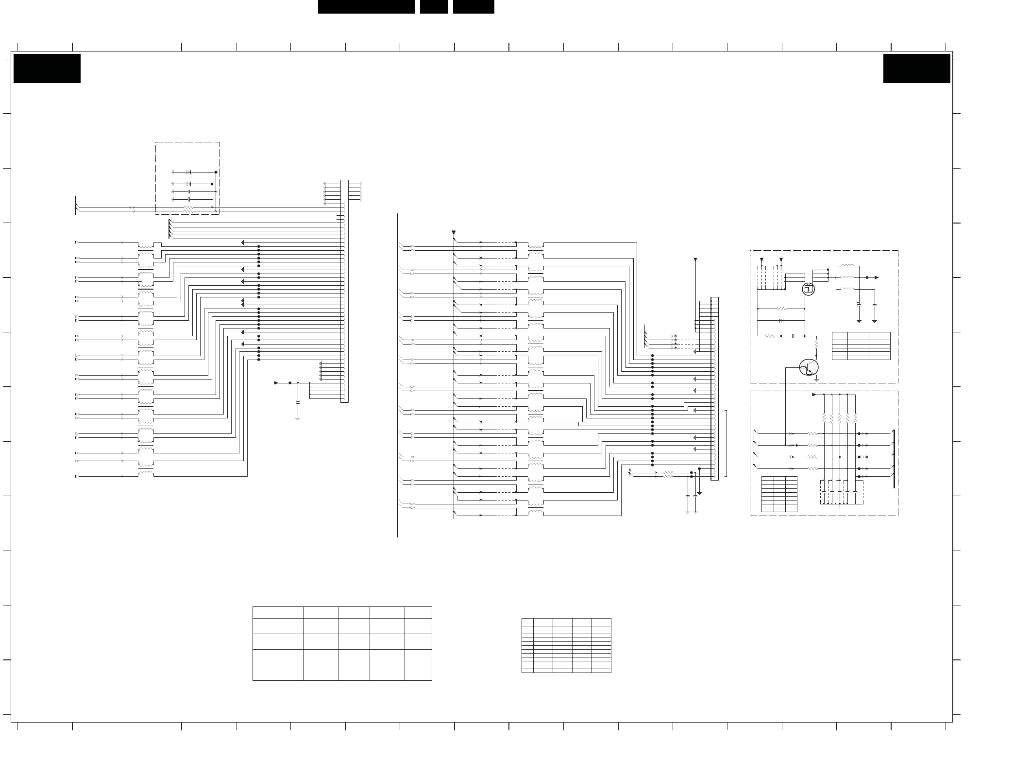
Circuit Diagrams and PWB Layouts EN 63LC8.2HA LA 10.
2009-Apr-10
SSB: LVDS Connector
A
B
C
D
1R06
*
1080p
I
J
K
L
--
16
Off time : Don’t care
1R05
--
Y
*
Y
MAIN_RESET
Y
FR18 D5
FR16 D5
FR17 F12
100R
--
-
3V2
10 Bit Dual
FR35 E5
4R12 D14
4R22 F13
4R24 F13
4R26 F13
1R12
3R52
Y
--
3R50 G16
3R51 G16
3R52 H15
3R35
Y
2R02 I13
2R10 F15
2R11 E16
2R12 E16
LVD S
100R
100R
Y
2R25 C3
2R26 C3
2R28 G6
2R29 I16
16 17
12
3R26 H12
3R35 G15
3R48 G15
3R49 G15
*
4R11
4R03
1R13
--
Y
On time : H
On time : H
RES
RES
LVDS CONNECTOR
RES
100R
--
4R07 H15
4R08 H16
4R10 D14
4R11 D14
9
Y
4R27 F13
4R31-1 D9
4R31-2 D9
4R31-3 D9
78
Y
4R36-2 H9
4R36-3 H9
4R36-4 H9
-
4R06 H15
RES
4R32-3 E9
4R32-4 E9
4R33-1 H9
8 Bit Dual
FR19 F12
4R34-2 F9
4R34-3 F9
4R34-4 F9
4R35-1 F9
FR24 D5
FR25 F12
FR26 D5
FR27 F12
4R04 D14
4R05 H15
Y
--
Y
--
1R04
FR20 D5
FR21 F12
FR22 D5
FR23 F12
--
Y
FR28 D5
FR29 G12
FR30 E5
FR31 G12
1R01 E13
1R02 D10
1R03 D10
LGE
LVD S
--
--
Y
LCD
RES
4R33-2 H9
4R33-3 I9
4R33-4 I9
4R34-1 F9
4R35-2 G9
4R35-3 G9
4R35-4 G9
4R36-1 G9
1314 15
Y
--
FR66 H13
FR67 H16
FR68 H13
FR69 F6
IR06 F15
IR08 D15
IR10 H15
*
4R06
FHP
RESET
*
SDI
4R12
On time : H
PDP
--
1R02
Y
E
F
G
H
--
3R53
IR02 F14
12V1
C
D
Y
IR04 F15
CTRL-DISP3(Rev_Standby)
CPU-GO
FR56 H16
FR57 H12
FR58 F5
CTRL-DISP4
8 Bit Single
15
FR63 H16
FR64 H13
FR65 F5
3456
IR01 E15
E
F
G
H
Y
FROM MJC-LVDS 8280
Y
1108 C6
Y
RES
RES
1R05 E10
1R06 F10
1R07 F10
1R08 G10
4R02
RES FOR DISPLAY I2C CONTROL
1R13 I10
1R14 D3
1R15 D3
1R16 E3
FR59 H12
FR60 F5
FR61 H12
FR62 F5
*
Y
SINGLE
--
1R10
FR32 E5
FR33 E5
FR34 G12
4R07
--
Y
LVD S
FR42 G12
FR43 E5
FR44 G12
FR45 E5
Y
3R53 H15
3R54 H15
3R55 C3
FR49 E5
FR50 G12
FR51 H16
FR52 H12
1R23 H3
1R24 H3
1R25 F3
1R03
4R10
FROM FPGA
1R08
1
DISPEN
Off time : Don’t care
Semi standby : L
4R05
6789
Y
Y
4R08
--
1R07
On time : H
Y
Y
CTRL-DISP2(LCD_PWR_on)
10 11 12
*
+12V_DISP
Y
112 345 10
3R54
Y
*
*
--
Y
Y
*
Y
*
1R20 F3
1R21 G3
1R22 G3
I
J
K
L
--
Y
LCD PDP
2R01 I13
1R19 F3
0V
PDP-GO
PDWIN
2R20 I15
2R21 I15
2R23 I16
2R24 I16
FR36 G12
FR37 G12
FR38 G12
Off time : Don’t care
3R10 E14
3R12 F14
3R13 F15
3R25 H12
1R18 E3
10 Bit Single
LVD S
1R17 E3
FR46 G16
FR47 G12
FR48 E5
Y
FR53 F5
FR54 F5
FR55 H12
4R43 H16
5R01 D16
5R02 D16
FR41 E5
FR40 G12
7R05 D15
7R07 F15
FR10 D16
FR11 C4
LVD S
4R31-4 E9
4R32-1 E9
4R32-2 E9
FR39 E5
VDISP-SWITCH
-
RES
--
1R11
1R09
4R04
-
Y
Y
Semi standby : H
-
-
Y
Y
CTRL-DISP1
3R56 C3
3R57 G16
4R02 D14
4R03 D14
12 1314
Y
Y
Normal and off : L
----
--
Y
+5V_TCON
1R04 E10
5R03 E16
6R02 E14
6R04 C3
6R05 C3
1R09 G10
1R10 G10
1R11 H10
1R12 H10
FR12 C4
FR13 F12
FR14 D5
FR15 F12
17
A
B
Off time : Don’t care
LVDS_B_TXo1n
LVDS_B_TXo0p
LVDS_B_TXo0n
LVDS_B_TXe2n
LVD S_SEL
LVD S_SEL
+VDISP
Y
Y
Y
1R12
DLW21S
3R12
47R
FR13
IR02
1R07
DLW21S
1R13
DLW21S
FR52
FR38
SI4835BDY
7R05
100p
2R21
4R34-2
4R34-1
4R35-1
4R34-3
FR19
FR47
IR01
FR15
FR17
3R35
100R
4R03
FR44
+5V_TCON
6R02
BZX384-C5V6
7R07
PDTC114ET
FR63
FR46
FR57
25V220u
2R11
4R32-4
FR59
47K
3R10
2R01
2R02 100p
100p
100R
3R25
4R11
33R
4R10
5R02
4R35-2
DLW21S
1R09
BZX384-C6V8
FR21
6R04
100p
2R24
3R53
100R
+12V_DISP
FR27
FR25
2R23100p
100R
3R54
3R26
DLW21S
1R03
100R
4R07
4R05
4R06
FR37
FR61
FR55
FR40
3R49
IR08
4K7
4R02
4R12
1R08
DLW21S
FR29
2R10
1u0
3R55 22R
4K7
3R50
FR23
4K7
3R51
+VDISP
FR34
FR11
8
4R31-11
5R03
33R
5R01
33R
1R06
DLW21S
1R05
DLW21S
4R32-2
IR06
22R3R56
FR36
FR31
FR12
BZX384-C6V8
6R05
FR41
FR18
IR10
FR60
61
53
54 55
56 57
5859
60
48
49
5
50
51
6
7
8
9
52
38
39
4
40
41
42
43
44
45
46
47
28
29
3
30
31
32
33
34
35
36
37
19
2
20
21
22
23
24
25
26
27
1
10
11
12
13
14
15
16
17
18
1108
FI-RE51S-HF
2R12
FR53
100n
FR33
FR51
FR39
4R27
FR32
1R02
DLW21S
FR26
FR20
FR49
4R24
4R31-227
4R43
1R04
DLW21S
3R57 4K7
FR68
FR14
+3V3_SW
FR54
FR58
4R36-1
FR62
4R35-4
4R33-4
45
FR30
100p
2R20
4R36-2
4R36-4
4R04
1R16
DLW21S
4R33-3
1R10
DLW21S
FR24
4R26
FR67
3R484K7
FR28
FR66
DLW21S
1R15
4R31-336
45
4R31-4
6
7
8
9
42 43
44 45
46 47
48
35
36
37
38
39
4
40
41
5
25
26
27
28
29
3
30
31
32
33
34
15
16
17
18
19
2
20
21
22
23
24
1R01
FX15SC-41S-0.5SH
1
10
11
12
13
14
4R33-1
FR43
4R36-3
DLW21S
1R21
100p
2R29
DLW21S
1R25 1R18
DLW21S
10p
2R25
DLW21S
1R11
1R24
DLW21S
FR48
FR65
4R08
47K
3R13
FR50
4R33-2
FR45
FR35
1R14
DLW21S
4R22
4R32-1
FR22
4R35-3
FR16
DLW21S
1R20 1R19
DLW21SDLW21S
1R17
2R26 10p
DLW21S
1R231R22
DLW21S
2R28100n
FR10
3R52
100R
FR64
IR04
FR42
FR69
4R34-4
4R32-3
FR56
+VDISP
LVD S_A_TXe3p
LVD S3_SCL_DISP
LVSD3_SDA_DISP
LVD S_A_TXeCLKn
LVD S_A_TXo1n
LVD S_A_TXo1p
LVD S_A_TXe0n
LVD S_A_TXe2p
LVD S_A_TXe2n
LVD S_A_TXe0p
LVD S_A_TXe3n
LVD S_A_TXeCLKp
LVD S_A_TXo3p
LVD S_A_TXo0p
LVD S_A_TXo0n
LVD S_A_TXe1n
LVD S_A_TXe1p
LVD S_A_TXe4p
LVD S_A_TXo4p
LVD S_A_TXo4n
TxFPGAe_2p
LVDS_B_TXo4p
TxFPGAo_4p
TxFPGAo_3n
TxFPGAo_3p
TxFPGAo_CLKp
TxFPGAe_1p
TxFPGAo_0n
LVDS_B_TXe4p
TxFPGAe_4p
TxFPGAo_2n
TxFPGAo_2p
LVDS_B_TXe1n
TxFPGAe_2n
TxFPGAe_1n
LVDS_B_TXe1p
LVDS_B_TXe2p
TxFPGAe_CLKn
LVDS_B_TXo3n
LVDS_B_TXoCLK p
LVDS_B_TXoCLK n
LVDS_B_TXo2p
LVDS_B_TXo2n
LVDS_B_TXo1p
LVDS_B_TXe4n
LVDS_B_TXe3p
LVDS_B_TXe3n
LVDS_B_TXeCLK p
LVDS_B_TXo4n
LVDS_B_TXo3p
CTRL_DISP1
CTRL_DISP2
CTRL_DISP3
CTRL_DISP4
ITV_I2C_SDA
ITV_I2C_SCL
LVDS_B_TXeCLK n
LVDS_B_TXe0p
LVDS_B_TXe0n
LVD S_A_TXe4n
LVD S_A_TXo3n
LVD S_A_TXoCLKp
LVD S_A_TXoCLKn
LVD S_A_TXo2p
LVD S_A_TXo2n
TxFPGAe_0n
TxFPGAe_0p
LCD_PWR_ON
STANDBY
CTRL_DISP4_up
CTRL_DISP1
CTRL_DISP3
CTRL_DISP4
CTRL_DISP2
CTRL_DISP1_up
LVD Se_4n
TxFPGAo_4n
TxFPGAe_4n
ITV_I2C_SCL
ITV_I2C_SDA
TxFPGAe_3n
TxFPGAo_1n
TxFPGAo_CLKn
TxFPGAo_0p
TxFPGAo_1p
LVD Se_0p
LVD Se_0n
TxFPGAe_CLKp
TxFPGAe_3p
LVD Se_2n
LVD Se_1p
LVD Se_1n
LVD So_3p
LVD So_3n
LVD So_CLKp
LVD Se_4p
LVD Se_3p
LVD Se_3n
LVD Se_CLK p
LVD Se_CLK n
LVD Se_2p
LVD So_CLKn
LVD So_2p
LVD So_2n
LVD So_1p
LVD So_1n
LVD So_0p
LVD So_0n
CTRL_DISP1
CTRL_DISP2
CTRL_DISP3
CTRL_DISP4
LVD So_4n
LVD So_4p
B04E B04E
I_17760_009.eps
180208
3139 123 6349.1
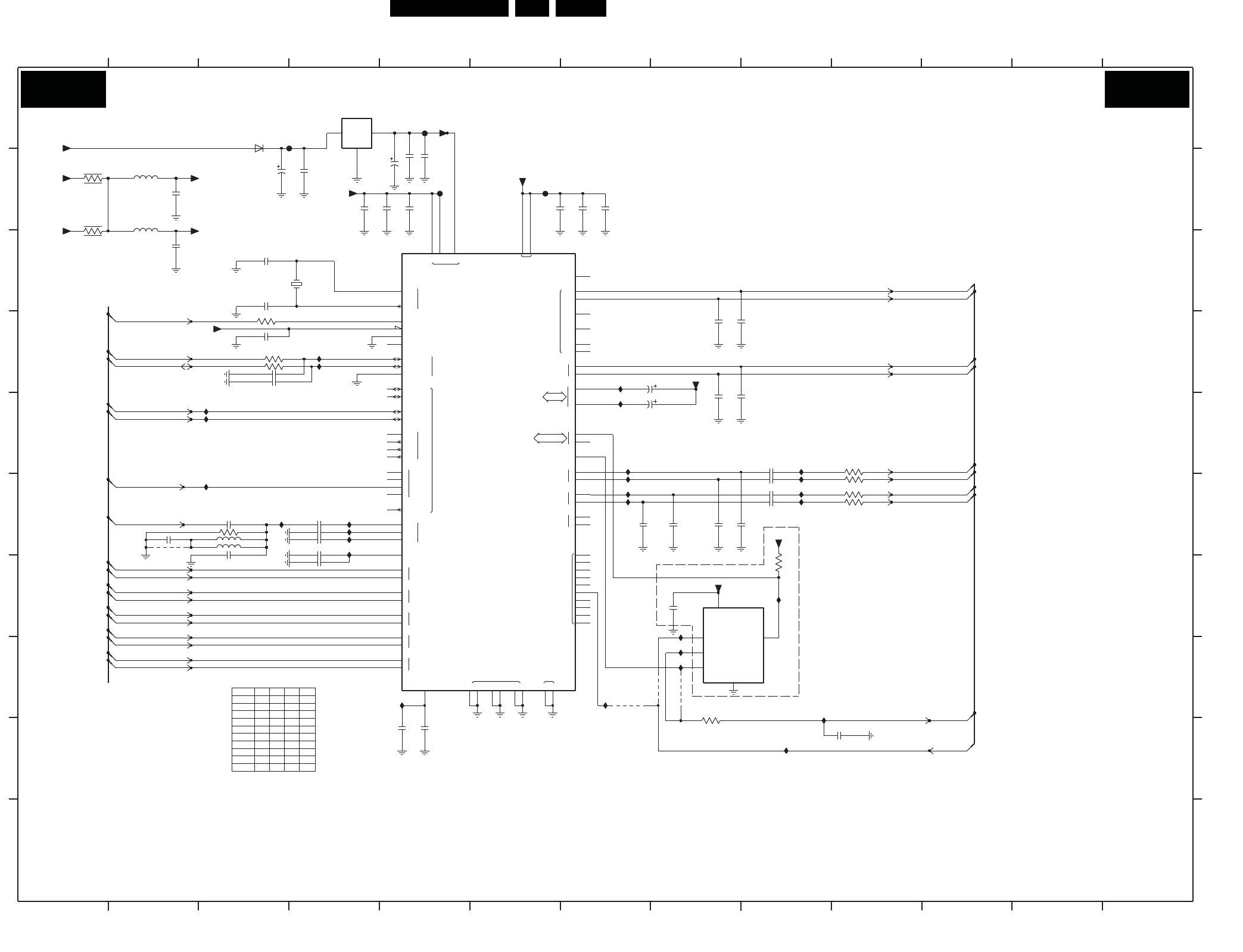
EN 64LC8.2HA LA 10.
Circuit Diagrams and PWB Layouts
2009-Apr-10
SSB: Audio Processor Micronas
VDD
GND
S2
D
S1
IN
COM
OUTIN
WS
OUT
IN
C
SR
SL
L
R
SC3_OUT
A
DEL
L
R
L
R
L
CL3
TP
1
R
2AH
AH
L
R
L
R
VREFTOP
L
R
RESETQ
SUB
ADR_SEL
TESTEN
AD
XTAL
I2C
DA
I2S
ANA
SC1_IN
SC2_IN
SC3_IN
SC4_IN
VSS VREF
NC
L
R
3
IN-
IN1+
IN2+
DA
L
RSC5_IN
CL
CL
4
SPDIF_OUT
AUD_CL_OUT
1
0
DVSUP
STNDBYQ
A
IN
OUT
SC2_OUT
SC1_OUT
DCTR_IO
DACM
DACA
CAPL
SUP
WS3
2
DA_OUT
1
CL
WS
L
R
M
AGNDC
--
Y
56p
--
Y
56p
RES
A
2
--
330p
I
33p
37
B
C
AP
RES
D
G
47p
22u
56p
--
4
47p
--
RES
13
E
47p
EU
RES
--
56p
"400-499"
5
A
16
*
150p
*
LA
*
*
2K2
--
1
56p
12
2434
*
22u
56p
9
B
2433
56p
330p
2432
Y
2
56p
3416
2435
56
*
5403--
F
H
D
12
--
MULTI 12NC: 3139 123 63421
I
7
E
--
11
AUDIO PROCESSOR - MICRONAS
*
2448
--
38
13
11
F
10
22u
9
--
5404
RES
4
12u
C
56p
4448
J
*
--
RES
*
180p
*
330p
--
108
*
H
CH
SINGLE 12NC: 3139 123 63431
G
MSP4450L-VK-E8 000
2449
J
2438
100n
F404
10u2424
25V220u
2439
10u2425
4402
4448
ADG719BRTZ
7412
Φ
SPST
SWITCH
5
3
1
4
6
2
I440
+8V
100p
2446
I418
470R3416
3p3
2416
2408470p
16V242310u
2451
100n
100R3411
2433 330p
I423
16V
330u
2410
3
1
I439
7410
L78L08ACU
2
1K2
3423
+12V_DISP
2414
10u
I441
BAS316
6402
2447 100p
SUP_A
I425
58
76
80
66
69
35
25
56
67
68
53
34
33
50
51
42
41
48
49
57
47
71
72
73
74
19
54
55
37
36
52
8
9
11
5
18
1
75
22
32
46
2
3
4
17
7
16
20
21
6
10
27
26
31
30
29
78
77
14
15 12
13
59
60
61
62
38
40
24
23
28
79
45
43
44
39
64
63
65
70
Φ
MULTISTANDARD
SOUND PROCESSOR
7411
100n2419
330p
2418
I417
+5V_SW
2422
330p
100p
2431
5401
120R
I444
I443
I442
I413
I429
2443
1n5
2428
100p
180p2449
5404 12u
330p
2421
2444
470p
470p
2442
2448
100R3417
3402
1R0
I432
+5V_SW
3p3
2415
3420 100R
56p2434
120R
5402
I436
10u
2411
I420
I424
4401
4403
3410 100R
100R3428
10u2426
SUP_A
10u
2437
I412
I415
I416
16V10u2420
2413
220p
4K7
3427
I438
330p
2417
100p
2429
+5V_SW
2430
100p
F401
F403
I422
+3V3_SW
2409 1n5
SUP_D
I437
I430
33p
2450
1n5
2441
I419
I414
22u5403
3418100R
+8V
10u
2436
I421
1411
18M432
56p2435
56p2432
220p
2412
100R3419
2440
100n
SUP_A
1R0
3403
100n2445
SUP_D
F402
I446
I445
10u2427
AUDIO_LS_R
HP_AUDIO_OUT_L
HP_AUDIO_OUT_R
AUDIO_LS_L
SPDIF_OUT
SPDIF_IN
XTALI N
XTALOUT
AUD_RST
SC1_AUDIO_IN_R
SC1_AUDIO_IN_L
VGA_AUDIO_IN_R
VGA_AUDIO_IN_L
HDMI_I2S_SD
SIDE_AUDIO_IN_R
SIDE_AUDIO_IN_L
IIC_SCL
IIC_SDA
SC1_AUDIO_OUT_R
SC1_AUDIO_OUT_L
SC2_AUDIO_OUT_R
SC2_AUDIO_OUT_L
HDMI_I2S_SCK
HDMI_I2S_WS
SIF
SC2_AUDIO_IN_R
SC2_AUDIO_IN_L
COMP_AUDIO_IN_R
COMP_AUDIO_IN_L
B05A B05A
I_17760_010.eps
180208
3139 123 6349.1
2416 C3
2432 E3
2428 E7
2429 E7
2430 E8
2436 E4
2437 G5
3423 G8
3427 E8
2442 B5
2443 B6
2426 E8
I419 E7
I423 E4
I425 G5
I429 D3
2431 E8
I414 D7
3419 E9
3420 E9
I417 D7
I418 E7
2440 B4
2441 B5
4402 G7
4403 F7
I437 F8
F403 B6
I436 G7
I440 F7
I444 E9
I441 F7
I442 D9
I443 D9
F402 B5
I445 E9
I446 G8
I413 C4
I415 D7
I416 D7
3428 C3
4401 F7
I420 E3
I421 E4
I422 E4
I424 E4
7410 A4
7411 B5
3403 B2
3410 C3
F404 A4
I412 C4
2425 D8
2427 E8
2447 D3
2448 E2
2424 D8
2409 B5
2412 B4
2410 B5
I430 D3
I432 D3
5402 B2
5403 E3
I438 F7
I439 G9
2449 E3
2450 G9
7412 F8
F401 A5
2421 D8
2422 D8
3411 C3
3416 E3
2408 B5
2433 E4
2434 E4
4448 E3
5401 B2
2445 E4
2446 C3
5404 E3
6402 A3
2451 F7
3402 B2
2420 D7
2423 D7
2413 B6
2411 B3
2414 B3
2415 B3
2417 C8
2418 C8
2419 C3
3417 D9
3418 D9
2435 E4
1411 C4
2438 G5
2439 B4
2444 B7
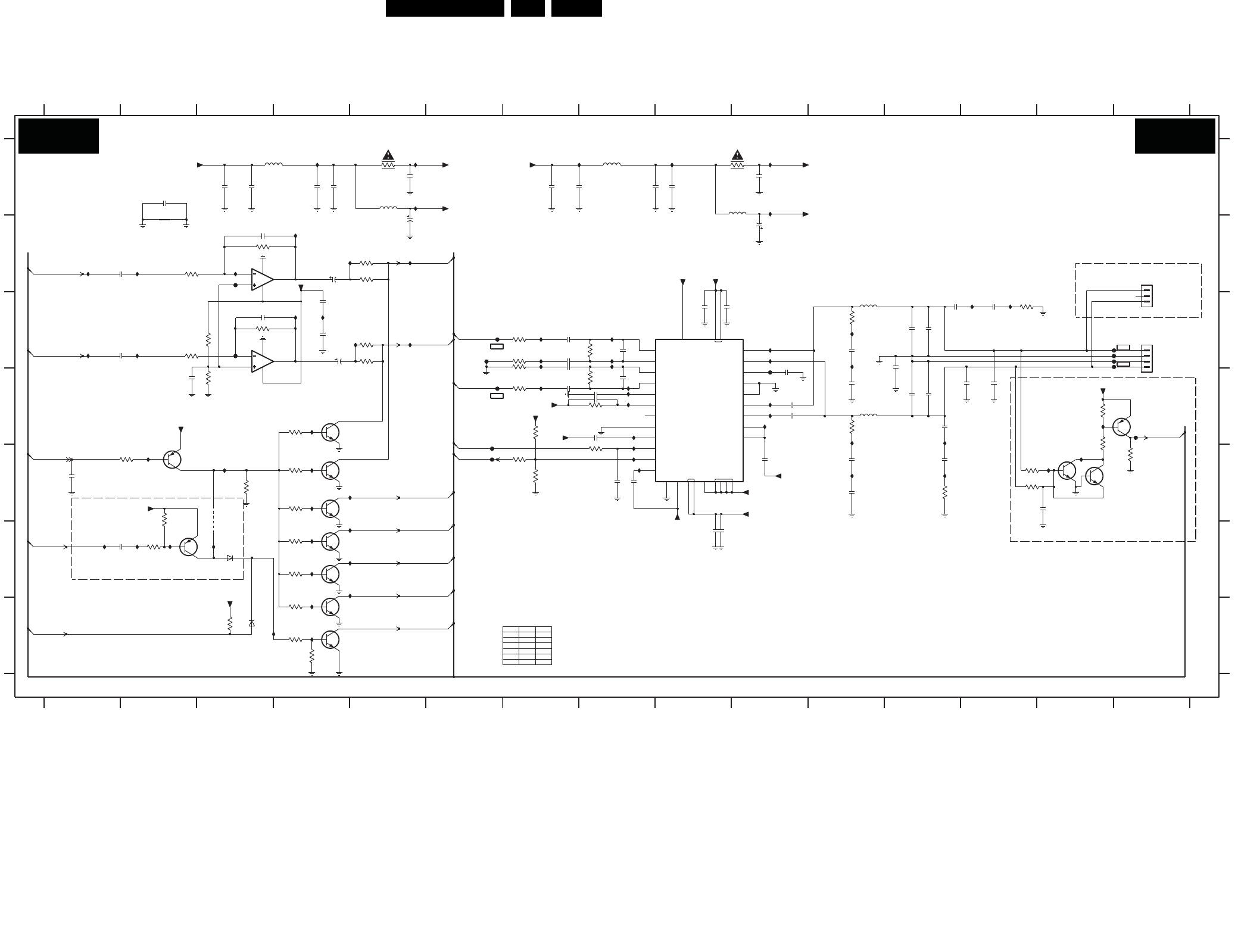
Circuit Diagrams and PWB Layouts EN 65LC8.2HA LA 10.
2009-Apr-10
SSB: Audio Class-D
HVP1
DIAG
OUT2
OUT1
CGND VSSA
IN1P
VSSD|HW
IN1N
IN2P
IN2N
INREF
OSCREF
OSCIO
HVPREF
DREF
ENGAGE
POWERUP
TEST
GND_HS
VDDP
VSSP
VDDA
STA B 2
STA B 1
BOOT2
BOOT1
HVP2
A
B
C
D
E
F
G
-2V8
GND
3A04
D
2A01 A5
C
5A07 A4
2V6
IA34 C2 IA62 E11
IA63 E5
IA64 E4
IA65 F5
IA66 F4
IA67 F2
IA68 F2
B
*
2A02 A10
2A04 A5
2A59 D2
2A60 E1
2A61 F2
2A19 D8
2A20 D7
2A21 C11
2A22 D8
2A23 D12
5V3
RES
-2V8
IA13 A5
RES
IA12 A9
12K
7A07 E14
2V6
-2V8
3A73 F4
4V7
-1V3
3A71 E4
3A72 F4
3A63 F2
3A68 D4
3A69 E4
3A07 C7
3A08 D8
3A09 C11
3A11 D7
3A13 D8
3A08
3A11
3A74 G4
3A29 D14
3A30 D14
6K8
NC
EMC
-12V2
3A62 E2
3V2
3A55 C3
7A55 E4
7A56 E4
7A57 F4
7A58 F4
7A59 G4
7A60 G4
F901 B3
2A57 C2
2A58 C4
2A71 D13
2A72 D13
2A67 A3
3A56 C3
3A57 C5
3A58 C2
3A59 C5
3A60 D3
3A61 E2
IA14
3A51 B3
3A52 B5
3A53 B2
3A54 B5
LCD PDP
3A06
8910
2A11 C7 IA29 C11
2V6
1A02 B15
1A35 C15
IA58 E14
IA59 E4
IA60 E8
IA61 E12
12K
IA76 G4
RES
2A16 C7
2A17 C12
2A18 C10
7891011
IA75 G3
RES
IA43 D8
IA44 D8
IA45 D10
IA46 D10
IA47 D10
IA22 B2
RESERVED
TO SUBWOOFER OUT
22K
NC
G
2A27 D10
6 13
2A12 C8
2A13 C12
2A14 C12
2A15 C7
IA14 A10
IA54 E2
IA55 E14
IA56 E8
IA57 E3
0V 6K8
0V
23
LEFT +
2V6
12
2A25 D10
2A26 D12
2A55 C3
2A56 C4
2A24 D8
1
2V6
0V
2A68 A3
2A69 A7
7A54 D4
IA15 A5
IA16 A10
IA17 B4
IA18 B5
IA19 B5
IA20 B3
IA21 B1
2A70 A7
2A29 D8
2A28 D12
3A04 C8
3A05 C13
3A06 C7
2A35 D11
2A36 E11
2A37 C13
2A38 E12
2A40 E8
6K8
-8V2
FA05 C6
FA06 C6
IA74 G4
IA73 F5
F904 C3
3A70 E3
RES
RES
5V3
FA07 C15
8V9
FA08 C15
10K
2A32 E8
2A33 F9
2A34 F9
11 12 1314 15
IA33 C1
IA72 F4IA30 C5
IA31 C4
IA26 C4
IA27 C7
IA28 C8
FA04 D10
3V3
MUTING CIRCUIT
-2V8
IA70 F3
RES
2V6
IA69 F1
IA71 F5
IA32 C10
3A01 A5
3A02 A9
2V6
5
10K
3A03
GND
10K
3A75 G3FA10 C15
FA11 C15
FA12 E6
FA13 E6
FA32 D15
IA10 A4
IA11 A8
TO SPEAKERS
22K
2A53 B4
2A54 C4
2A41 E14
3A17 D11
3A19 E7
3A26 E8
2A30 E10
2A31 E11 5A08 A8
6A51 F3
6A52 G3
2A52 B2
2A51 B3
6K8
FA09 D6
IA35 C7
IA36 C8
IA37 C10
IA38 C8
IA39 C11
IA40 D7
IA41 D7
67
E
F
A
2A45 C12
2A08 B10
2A09 C9
2A10 C9
IA24 C13
10K
RIGHT -
45
IA25 C4
IA48 D4
IA49 D14
IA50 D8
IA51 D8
IA52 D12
IA53 D11
IA42 D8
14 15
1234
DC-DETECTION
IA23 C13
-7V6
3A31 E15
3A32 D7
2A62 A4
2A63 A4
2A64 A8
2A65 A9
2A66 A2
3A07
7A52 E2
7A51-1 B3
7A51-2 C3
7A01 C9
7A05 D15
7A06 E143A33 E7
12V2
7A53 F2
RES
3V9
VDD
VSSA
IA52
AUDIO - CLASS D
-2V6
11V9
EMC
-12V2
3A03 C7
3A27 E13
3A28 E13
3A14 E12
3A76 G4
3A77 G4
4A51 E3
5A03 C11
5A04 D11
5A05 A5
5A06 A9
GNDSND
4K7
GNDSND
2A67
10n
3A63
3A52
IA41
3
4
33R
1735446-4
1A35
1
2
IA29
100n
2A66
1u0
FA12
2A16
IA66
IA61
IA12
GNDSND
FA06
IA51
470n
2A28
IA31
3A07
1K0
100K
3A73
3A56
GNDSND
IA49
IA73
BC847BW
7A58
1
3
2
IA20
IA65
3A74
1K0
IA38
4K73A26
IA58
+5V_SW
IA55
4A51
5A06 30R
470n
2A57
IA40
2A02
IA62
VDDA
100n
10n
2A69
F904
3A60
100K
IA53
GNDSND
5A03
22u
2A70
IA10
1n0
F901
IA11
IA18
FA10
220n
2A26
1
3
2
GNDSND
7A57
BC847BW
2A04
33R
3A57
25V
220u
3A06
IA69
1u0
2A61
2A01
100n
GNDSND
22u
5A07
GNDSND
33R
IA35
3A59
GNDSND
470n
2A52
IA43
1u02A20
12K
3A33
2A21
1n0
1u0
2A41
IA39
3A14
22R
5A08
22u
12
BAS316
6A51
FA04
IA57
1
2
3
3
2
1735446-3
1A02
7A56
BC847BW
1
GNDSND
FA07
47u6.3V
2A53
10R
3A02
-12V_AUDIO
220u
25V
6.3V
2A08
1u0
2A60
10R
VSSA
1K0
3A71
3A01
47K
3A32
BC847BW
TS482IDT
3
2
1
84
7A06
47K
7A51-1
3A30
IA72
3A1339K
IA28
IA48
220p
2A12
2A55 GNDSND
IA22
33p
IA16
3A04
2A58
47u6.3V
2A31
1n0
IA56
+12V_AUDIO
FA32
GNDSND
IA37
IA36
IA27
2A51 33p
7A05
BC857BW
GNDSND
IA54
220n
2A56
GNDSND
10K
IA24
3A75
2A25 15n
IA60
3A58
47K
2A10 100n
2A38
1n0
2A63
220n 3A27
220K
3A72
1K0
IA50
220n
2A37
100n2A24
IA42
1u0
IA21
2A11
3A77
22K
10K
3A76
FA13
1n0
2A17
IA23
470n
2A59
IA19
2A09
FA08
100n
IA17
FA05
3A68
2A15 1u0
2A32
1K0
1n0
IA26
2A68
1n0
GNDSND
3A03
2A34 100n
VSSA
3A11
VDDA
VSS
1n0
IA71
2A65
IA64
7A07
BC847BW
IA70
470n
2A14
+3V3_STBY
3A09
3A62
10R
GNDSND
4K7
4K7
3A61
1K0
3A69
IA45
7A59
BC847BW
1
3
2
5A04
22u
IA75
GNDSND
IA33
1n0
2A35
3A29
47K
+3V3_STBY
3A28
220K
GNDSND
2A54
220n
1n0
2A72
17
32
26
23
6
25
24
13
8
29
20
9
1
16
11
3
2
14
15
12
31
10
27
22
7A01
28
21
7
4
18
5
33
30
19
IA68
Φ
TDA8932BTW
AMPLIFIER
POWER
CLASS D
BAS316
6A52
IA25
100n2A33
VDD
IA74
7A60
GNDSND
1n0
BC847BW
VSS
2A45
3A31
10K
120K3A51
IA30
IA15
10K
3A19
3A55 120K
BC857BW
+3V3_STBY
IA34
7A52
5A05
GNDSND
30R
GNDSND
3A54
33R
3A08
IA63
5
6
7
84
2
7A51-2
TS482IDT
7A55
BC847BW
1
3
IA76
IA59
470n
2A40
IA32
GNDSND
IA47
GNDSND
10R
3A17
1n0
2A23
1n0
2A36
2A13
220n
2A27 15n
IA67
7A53
22R
VDD
BC857BW
3A05
2
VDDA
IA13
7A54
BC847BW
1
3
IA44
2A30
100n
GNDSND
FA11
VSSA
47K
GNDSND
3A53
3A70
10K
1n0
10n
2A62
2A71
IA46
2A22 100n
2A29
GNDSND
100n
2A18
1n0
220p
2A19
GNDSND
FA09
10n
2A64
VSS
VSSA
DC_PROT
HP_LOUT
ENGAGE
SC2_AUDIO_MUTE_L
SC2_AUDIO_MUTE_R
SC1_AUDIO_MUTE_L
SC1_AUDIO_MUTE_R
STANDBYn
POWER_DOWN
ANTI_PLOP
AUDIO_LS_L
AUDIO_LS_R
ENGAGE
HP_ROUT
HPIC_RIN
HP_AUDIO_OUT_R
HP_AUDIO_OUT_L HPIC_LIN
HPIC_LOUT
HPIC_ROUT
MUTEn
B05B B05B
I_17760_011.eps
180208
3139 123 6349.1
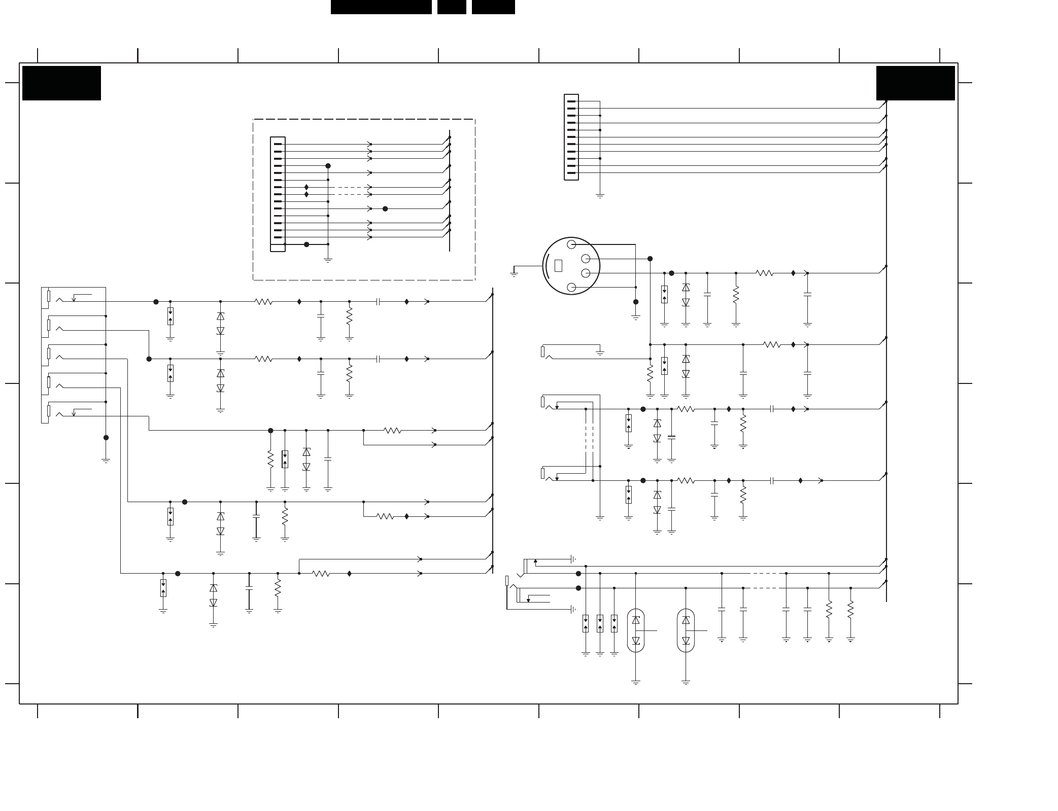
EN 66LC8.2HA LA 10.
Circuit Diagrams and PWB Layouts
2009-Apr-10
SSB: YPbPr & SVHS
3623 D7
3624 E8
4601 D6
4602 D6
RES
2608 C3
6604 C7
6606 C7
6610 E2
2610 C4
2622 D7
A
2609 C8
RES
F
A
2607 C4
220n
2
B
C
For DTV onl y
1
3612 C4
3613 F8
1618 F6
1619 F6
2600 C7
4
2603 D4
2606 E3
RES
I631 C8
2625 C8
B
C
2626 C8
HEADPHONE
RES
RES
I632 E4
4604 F8
I627 C3
2612 C3
2613 F7
D
E
3602 C8
3622 D8
3604 C8
3605 F3
F617 E6
RES
6612 F2
6613 C2
2614 F8
2615 F8
2616 F8
2621 D8
F616 E6
RES
RES
3621 D7
F614 C1
3603 D3
RES
7
I623 C3
I624 E7
9
RES
RES
I634 A3
I635 B3
F615 C6
6611 D3
8
F601 B7
RED
White
6622 E7
E
F
1601 B6
1602-1 C6
F608 C2
F609 C2
F610 D6
F611 D7
RED
Blue
Green
D
F618 A4
F619 B4
F620 B3
3611 C3
1608 C7
1609 C7
1620 F6
1621 A3
1615-1 D1
RES
1615-2 E1
3
RES
1613 C2
1616 D6
1617 E6
67
I610 C4
I611 C4
I615 B8
I616 E4
I620 D8
I621 D7
I622 D8
F605 E2
4603 E8
2602 E3
4605 B4
4606 B4
F607 E2
YPBPR & SVHS
2624 E7
2623 D8
RES
(near to 1504 )
1606 E2
12356
3607 C3
3608 C4
3609 C6
1615-3 C1
1607 D3
89
2627 D7
2628 E7
3600 B8
3601 E3
1602-2 D6
1602-3 D6
1603 E5
1605 A6
6616 F7
6621 D7
RES
1610 F2
1611 C2
RES
SVHS
RES
45
RES
RES
F602 B7
F604 D3
6614 C2
6615 F7
CVBS
3614 F9
3617 E4
3618 D4
3619 E3
2610
F619
2621
1620
F618
F614
2602
2606
33p
2626
150R
3621
3608
33K
I620
F620
2608
1n0
I615
1608
I622
1618
F610
3607
150R
5
6
7
8
9
1n0
2612
1605
1-1735446-1
1
10
11
2
3
4
75R
3603
I627
22n
2614
2622
F604 1n0
6
4
5
1602-2
WHITE
MTJ-032-37BAA-432 NI
6606
PESD5V0S1BA
2627 33p
1611
4601
F605
1606
DF3A6.8
3
12
6616
I621
33R
3618
3623
150R
I611
F607
1613
220n
F611
6614
PESD5V0S1BA
2603
6612
PESD5V0S1BA
2624
1n0
I623
10n
2615 3614
10K
4605
3602
100R
1609
I634
10K
3613
5
1
3
4
2
1601
MDC-013V1-B
4602
2
3
4
5
6
7
8
9
MSP-636H1-01
1615
1
10
11
12
I632
F602
6610
PESD5V0S1BA
F617
2
1607
6615
3
1
2607
DF3A6.8
220n
4603
1610
PESD5V0S1BA
6604
I610
1602-1 1
2
F615
MTJ-032-37BAA-432 NI
YELLOW
4606
1617
2616
10n
2623
7
8
9
15 16
220n
10
11
12
13
14
2
3
4
5
6
BM14B-SRSS-TBT
1621
1
3600
100R
I635
F608
33p
2625
3612
33K
2600
F601
I616
33K
3624
I624
PESD5V0S1BA
6621
4604
2
3
4
5
7
8
1603
MSJ-035-10A B AG PPO
1
PESD5V0S1BA
6611
I631
22n
2613
2609
6622
PESD5V0S1BA
9
7
8
1602-3
RED
MTJ-032-37BAA-432 NI
1619
3611
150R
3619
1616
33R
F616
F609
3622
33K
PESD5V0S1BA
6613
3601
75R 33R
3617
3609
75R
3604
75R
75R
3605
33p2628
HD_Y_IN_ITV
HP_LOUT
HP_ROUT
SVHS_Y_CVBS_IN
SVHS_C_IN
SIDE_AUDIO_IN_L
HP_DETECT
SIDE_AUDIO_IN_R
HD_PR_IN_ITV
HD_PB_IN_ITV
COMP_AUDIO_IN_R
SC1_AUDIO_IN_L
SC1_AUDIO_IN_R
SVHS_Y_CVBS_IN
COMP_AUDIO_IN_L
DTV_IRQ
SVHS_C_IN
HD_Y_IN
CVBS_IN_DTV
HD_PR_IN_ITV
HD_Y_IN_ITV
HD_PB_IN_ITV
BOLT_ON_UART_RXD
BOLT_ON_UART_TXD
SPDIF_IN
HD_PR_IN
HD_PB_IN
HP_ROUT
HP_LOUT
SIDE_AUDIO_IN_R
SIDE_AUDIO_IN_L
HP_DETECT
B06A B06A
I_17760_012.eps
180208
3139 123 6349.1
Circuit Diagrams and PWB Layouts EN 67LC8.2HA LA 10.
2009-Apr-10
SSB: I/O Cinch 1 & 2
I565 A6
F530 H5
I570 B6
RES
RES
3518 E3
RES
6504 D3
F520 D2
F518 D8
F519 D2
I578 I12
RES
RES
TO BE REMOVED FOR IT V
PESD5V0S1BA
6525
F352
RES
2524 F10
3522 G9
3523 F4
3524 I11
6511 H3
F525 E2
RES
6514 E3
I564 B4
2535 H3
Function_Sw
D
2515 C4
3
1515 F8
3526 F3
6513 G4
3529 H10
E
2512 D10
F534 B4
3552 F10
6519 C3
6520 E3
3537 I12
3503 B3
1531 C2
1506 A5
CODE 2422 025 20251 IN ECM
1521 H9
RES
F347 A2
1522 G2
3553 F10
8
11
1504 C1
10
2502 C10
3540 I11
F348 A2
3546 H3
2536 G9
6517 H3
F510 D8
1520 G2
3559 B7
3515 D4
12 13
I
A
Terr_CVBS_out
7502 G11
7503 I10
7504 I11
Audio-R_out
F543 C10
I552 G11
I548 I11
RES
I558 I12
I520 D11
RES
F511 C2
F512 D8
AITV_Connector A:
2509 D11
3550 E10
F352 A2
3512 D10
3513 E10
2517 D4
F
1517 E2
7
Audio-R_out
RES
F531 E2
RES
1509 A11
1508 A1
I553 I10
RES
6
RES
I563 B4
ITV-Connector B
F613 B9
4502 G11
RES
3507 C3
3551 E10
F353 A2
F354 B2
2520 E10
H
1516 E2
RES
12
3517 E3
F517 C2
6501 D9
F528 F2
4508 C2
I572 A9
I541 D5
3
RES
6522 C9
RES
Video/YC-Y_in
2533 I10
3531 H10
I
6518 C3
1
D
RGB-G_in
AV IN
RES
4504 I12
RES
4510 G2
3519 G10
I550 G4
I551 G10
F516 D8
I573 A9
I576 A11
F
RES
F527 F8
RGB-R_out/YC-C_in
I567 A6
E
1500 C9
RES
RES
1507 A4
RES
6523 C9
RGB-BL_in
F536 C4
F537 D4
F526 F2
I512 C10
F513 C2
RES
3508 D10
RES
5
G
C
1511 D2
2525 G10
2526 G9
2527 F3
3525 G10
2534 I10
3V7
12 7
1512 E2
1513 E8
1514 E9
2528 E3
6512 G4
B
3511 D4
9
2508 B3
2518 D11
6521 G3
2514 C3
10
RES
RES
F542 G5
Video_in
4506 F9
F541 F5
3516 E4
Function_Sw
RES
7500 G10
F538 E5
F539 E5
F515 C2
Audio-R_in
RGB-R_in
IO - CINCH 1 & 2
Audio-L_in
Audio-L_out
3V
I574 A9
I575 A11
RES
CVI-2 / AV OUT
I577 F8
3520 E3
RES
RES FOR ITV
I556 H12
F522 D2
I554 I12
I530 G10
RES
RES FOR ROW
4505 F8
6525 G9
F540 F5
6524 E9
F514 D8
I517 D11
5V2
ITV-Connector D
ITV-Connector C
CVBS_out
RES
Audio-R_in
6505 E9
F521 D2
I544 G11
4
Audio-L_out
I557 F11
4509 C2
F524 E2
I568 A6
F529 F8
I533 H12
1501 C9
3538 G11
Audio-L_in
1518 G9
3530 G3
6516 G3
5
RES
2538 H3
3500 B10
2
1523 H2
136
9
B
RES
F346 A2
F612 B9
F544 D10
F349 A2
I549 I11
I543 G10
I562 A4
3510 C3
1505 A8
2506 C10
11
RES
3545 H3
3506 D10
F351 A21519 F2
I528 G12
I545 E10
3554 I12
3555 H12
3514 D3
2523 D4
G
2521 D4
8
1510 E9
3521 G12
6507 D3
6509 F9
6510 H9
1503 D9
F523 F9
I571 B6
F532 E9
I510 B10
F535 C4
C
3532 G4
4
2529 F3
3528 F4
2531 G3
6515 F3
RES
H
1502 D7
3535 H3
3536 H4
3502 C10
1532 D2
1524 H2
1531
1533 E9
1534 C2
1535 D2
ITV Connector E
3533 G3
RGB-B_in
2530 H10
3537
1K0
I570
F349
150R
3502
7500
BC847B
3511
3555
33K
68R
11
1503
1
2
3
4
5
6
7
8
910
1506
6509
PESD5V0S1BA
I554
PESD5V0S1BA
6505
2531
150R
3503
2525
220n
BC847B
7503
F536
15R
3519
2528
I577
1518
I571
2521
220n
3513
33K
F534
1K0
3536
3524
15R
220n
2533
2514
330p
I533
F524
I512
6510
I541
1501
PESD5V0S1BA
1n0
2523
6520
PESD5V0S1BA
6519
PESD5V0S1BA
3552
100R
1K0
3525
2530
2535
PESD5V0S1BA
6501
1535
6504
PESD5V0S1BA
6507
PESD5V0S1BA
+5V_SW
F522
1533
F537
F510
+5V_SW
75R
3526
I549
220n
2536
I553
1512
2538
150R
3500
I548
1514
F544
F538
F543
I578
75R
3517
6512
1N4148
150R
3507
3540
4K7
I557
6511
PESD5V0S1BA
I517
I520
1515
F523
F526
2509
220n
3518
27K
3546
75R
2502
330p
I564
I556
F521
1500
2529
2527
2524
I544
4K7
3538
F531
F532
I528
1516
1523
F530
3530
75R
27K
3550
F525
I545
F612
F528
I558
150R
3514
6513
1N4148
F515
F519
F520
100R
F348
3516
1517
PESD5V0S1BA
6517
1522
7502
BC857BW
68R
3522
F354 I563
3553
75R
3520
F529
6K8
2518
220n
I530
F517
2512
1n0
75R
3533
F513
4506
I568
PESD5V0S1BA
6518
75R
3559
150R
3510
1532
I567
1534
I576
4505
6523
PESD5V0S1BA
F351 1
2
345
+3V3_STBY 1509
F613
68R3535
1520
3551
6K8
I550
PESD5V0S1BA
6522
PESD5V0S1BA
6521
2520
1n0
1519
330p
2506
78
I573
1
2
3
4
5
6
1505
6515
PESD5V0S1BA
F511
F347
3
4
5
6
7
8
9
1112
1
10
2
4510
1508
7504
BC857BW
4508
3554
68R
F514
F518
I572
I551
F353
I575
PESD5V0S1BA
6524
F516
2534
220n
75R
4509
3531
1510
1511
100R
3523
I574
3
4
5
6
7
8
9
12
13
14
15
16
17
18
19
2
20
21
MTJ-505H-01 NI LF
1504
1
10
11
6
7
8
910
1
2
3
4
5
1521
1507
4502
F346
33K
3508
150R
3506
I565
I552
1K0
3532
3528
100R
F539
I510
6516
F541
PESD5V0S1BA
4504
2515
220n
1524
3515
33K
PESD5V0S1BA
6514
2526
150R
3512
F527
F512
1513
2517
1n0
1K0
3521
2508
330p
3529 100R
F542
F540
9
F535
19
2
20
21
3
4
5
6
7
8
1
10
11
12
13
14
15
16
17
18
1502
MTJ-505H-01 NI LF
I543
3545
100R
SC2_Y_CVBS_IN_ITV
HD_PB_IN_ITVSC2_AUDIO_IN_L
SC2_C_IN_ITV
SC2_Y_CVBS_IN_ITV
HD_PR_IN_ITV
HD_Y_IN_ITV
SC1_FBL_IN
SC1_R_IN
SC1_G_IN
SC1_B_IN
SC2_AUDIO_IN_R
HP_AUDIO_OUT_L
VGA_H
VGA_V
SC1_AUDIO_OUT_R
SC1_AUDIO_OUT_L
BOLT_ON_UART_TXD
BOLT_ON_UART_RX D
ITV_I2C_SCL
SC2_CVBS_MON_OUT_ITVDTV_IRQ
SC1_CVBS_RF_OUT
STA N D B Y
REMOTE
ITV_I2C_SDA
HP_AUDIO_OUT_R
SC2_AUDIO_OUT_L
SC2_AUDIO_OUT_R
SC1_RF_OUT_CVBS
SC1_CVBS_RF_OUT
SC2_CVBS_MON_OUT_ITV
SC2_AUDIO_MUTE_L
SC1_AUDIO_MUTE_R
SC1_AUDIO_MUTE_L
SC2_AUDIO_MUTE_R
SC2_STAT U S
SC2_C_IN
SC1_AUDIO_IN_R
SC1_FBL_IN
SC1_AUDIO_IN_L
SC2_Y_CVBS_IN
SC2_CVBS_MON_OUT
SC2_C_IN_ITV
SC1_AUDIO_OUT_L
SC2_AUDIO_OUT_L
SC2_AUDIO_OUT_R
SC1_G_IN
SC1_STAT U S
SC1_B_IN
SC1_AUDIO_OUT_R
SC2_AUDIO_IN_R
SC2_AUDIO_IN_L
SC1_CVBS_IN
SC1_R_IN
B06B B06B
I_17760_013.eps
180208
3139 123 6349.1
EN 68LC8.2HA LA 10.
Circuit Diagrams and PWB Layouts
2009-Apr-10
SSB: VGA, PC Audio, ComPair, UART
INH
Φ
VCC
Y1
Y2
GND
COM
A
SCL
ADR
0
1
2SDA
WC
INH
Φ
VCC
Y1
Y2
GND
COM
A
3E23 H3
2E01 A3
2E02 B3
2E03 B3
2E05 D2
2E06 D2
2E07 D5
456
2E77 F8
3E83 A8
COMPAI R
2E76 F10
3E82 A8
2E09 E2
2E10 F2
2E11 C2
TO MJC
MICROP B03
2E20 G3
3E86 A8
3E01 A4
3E02 A3
3E03 B4
F
3E05 B4
3E06 B3
3E07 C2
3E22 G3
6E01 A3
3E09 C3
1E19 D7
3E21 G3
1E90 G7
3E14 E4
5E71 F7
3E08 C2
FE33 G2
3E24 H3
6E06 F3
6E07 D7
6E08 D7
3E70 D7
6E10 B7
6E21 H2
6E22 H2
FE14 A7
PC / DVI AUDIO
FE13 A7
RES
7E71 F8
3E79 F9
IE19 C3
6E72 F7
RES
RES
1E93 G11
RES
RES
RES
12
IE32 H4
6
FROM ANALOG-IOs
1E92 G10
11
5mm x 4.02mm Slot Screw Hole
13
12
FE25 D4
FE34 H2
IE10 A4
IE11 A10
IE12 A11
6E09 B7
IE13 B4
FE10 A2
7E03 A11
IE14 B9
7E02 A9
IE15 B4
7E01 D4
6E04 C3
1E97 G13
3E67 F9
3E68 F8
3E69 F9
2E04 C3
3E71 D7
3E77 F8
3E78 F8
FE12 A2
RED
2E21 G3
4.02mm Round Screw Hole
3E85 B7
3E84 A7
RES
FE11 A2
2E12 C2
2E13 A10
2E14 A11
FE15 B11
2E79 F7
4E11 B10
4E12 B10
4E13 B12
3E04 B3
5E01 C3
5E13 E3
5E14 F3
DIGITIAL AUDIO OUT
RES
FE27 D4
5E17 A9
6E02 B3
3E15 E3
FE26 D7
6E03 B3
3E10 D2
3E11 D3
3E12 D4
IE16 B9
3E87 A8
FE17 B12
FE18 B6
FE19 B2
4E14 B12
FE21 B9
FE22 D5
FE23 D4
RES
IE20 C3
IE21 C2
FE30 F2
IE22 E3
FE29 E2
6E05 E3
RES
5E15 A9
5E16 A11
FE24 D7
5E18 A11
FE28 D6
2E78 F7
D
E
G
H
A
345
RES
RES
SPDIF OUTPUT
1E94 G11
1E95 G12
RES
3E18 F4
3E20 F3
1E21 F7
1E96 G8
D
2E23 H3
H
2E22 H3
3
1E01 A1
1E02 G1
1E04 C6
7
RES
10
FROM VPbPr & SVHS
12 13
A
B
C
1E06 F6
1E07 H1
E
F
G
1106 B7
1107 B7
1311 A6
UART_1TX
1E11 A2
1E12 B2
1E13 B2
89
UART_1R X
11
UART_0TX
UART_0R X
WHITE
VGA
1E14 E2
1E15 F2
1E16 G2
1E17 H2
1E18 D7
IE17 C2
IE18 C3
FE16 B12
UART (SERVICE)
RES
FE20 B12
IE23 F3
IE24 F9
IE25 F9
IE26 F8
IE27 F8
FE31 F7
FE32 F6
FE12
IE14
12
RES
RES
IE28 F9
IE29 G3
IE30 G4
IE31 H3
78910 12
VGA, PC AUDIO, COMPAIR, UART
B
C
1n0
2E11
+3V3_SW
30R5E16
FE22
IE31
4E12
+3V3_STBY
4E11
4K73E87
IE24
3E18
220R
EMC REF HOLE
1E94
5E18
30R
+3V3_STBY+3V3_STBY
30R
5E17
1E18
3E06
75R
IE28
IE22
2E10
100p
FE27
IE13
EMC REF HOLE
1E90
5E15 30R
30R
5E71
1E14
100n
2E04
IE20
5E01
60R
3E05
33R
FE28
3E70 100R
4K73E86
IE10
3E83
4K7
IE17
5E13
120R
FE14
BC847BW
7E71
1E19
4E13
FE33
DC_5V
3E68
180R
3E15
2K2
100R3E71
3E10
10K
6E08
PESD3V3L1BA
3E08
1K0
3E07
150R
4E14
EMC REF HOLE
1E96
EMC HOLE
1E95
8
7
6
FE16
5
1
3
4
2
SN74LVC2G53DCU
7E02
PESD5V0S1BA
6E22
1E11
3E69
560R
1E15
150R
3E23
+5V_SW
100p
2E09
3E24
33K
FE10
1E06
MTJ-032-21B-43 NI NE LF
1
2
1n0
2E12
6E06
PESD5V0S1BA
150R
3E21 2E20
220n
IE25
3E82
+3V3_SW
4K7
1
2
IE15
IE19
YKB11-3002V
1E02
5
84
7(256x8)
Φ
EEPROM
7E01
M24C02-WMN6
1
2
3
6
3E11
10K
10p
2E01
75R
3E04
FE19
6E04
BAS316
IE29
120R
5E14
2E77
100n
2K2
3E20
FE26
EMC REF HOLE
1E92
+3V3_SW
FE24
IE32
3E02
75R
3E77
2E14 100n
3E78
68R
1E16
3E12
10K
FE25
6E03
PESD5V0S1BA
3E01
33R
33R3E85
FE32
FE15
330p
6E02
2E06
PESD5V0S1BA
6E01
PESD5V0S1BA
DC_5V
3n3
2E23
IE12
IE26
2E07
100n
1106
DC_5V
+5V_SW
BZX384-C5V1
6E72
FE17
1E13
FE29
EMC REF HOLE
1E97
220n
2E22
FE23
IE21
3E67
1K0
2E21
3n3
IE18
6
7
8
9
16
17
11
12
13
14
15
2
3
4
5
1226-00B-15S-FAE-02
1E01
1
10
13
MSJ-035-29D PPO (PHT)
1E04
2
10p
2E03
1K0
3E79
2E13
100n
FE18
BZX384-C6V8
6E09
6E21
PESD5V0S1BA
FE13
FE20
IE11
2E02
10p
FE11
100n
2E76
1E17
1E21
3E14
220R
330p
2E05
PESD5V0S1BA
6E05
IE30
2
13
6E10
BZX384-C6V8
MSJ-035-29D PPO (PHT)
1311
33K
3E22
FE34
IE16
3E8433R
1107
FE31
100n
2E78
FE30IE23
33p
2E79
12
6E07
PESD3V3L1BA
EMC REF HOLE
1E93
FE21
1
2
YKB11-3001V
1E07
33R
3E03
3E09
10K
1E12
7E03
SN74LVC2G53DCU
5
1
3
4
2
8
7
6
IE27
UART_TX
UART_0TX
UART_RX
UART_1RX
UART_0RX
UART_1TX
MT8280_EN
MT8280_EN
IIC_SDA_up
IIC_SCL_up
VGA_AUDIO_IN_R
SPDIF_OUT
VGA_V
VGA_AUDIO_IN_ L
SCL_VGA
SDA_VGA
VGA_H
WR_EN
VGA_R_IN
VGA_G_IN
VGA_B_IN
B06C B06C
I_17760_014.eps
180208
3139 123 6349.1
Circuit Diagrams and PWB Layouts EN 69LC8.2HA LA 10.
2009-Apr-10
SSB: HDMI Switch
0-
A
1+
LSCL
D
2+
2-
R0X
0+
DSCL
RESET
C-
0
2-
2+
1-
C+
C+
C-
2-
DGND
AVC C 33
2+
1-
0+
DVCC18
AGND
R1X
1
C+
C-
0+
0-
1+
1-
2+
2-
R2X
TX
EPSEL1
LSDA
EPSEL0
CEC
TPWR
I2CSEL
INT
RSVDL
2
0
1
2
DSDA
0
RPWR
2
1
0
HPD
2
1
TSDA
EXT_SWING
AVC C1 8
HPDIN
1+
0-
0+
C-
C+
TSCL
I2CADDR
0-
1+
1-
SCL
ADR
0
1
2SDA
WC
SCL
ADR
0
1
2SDA
WC
SCL
ADR
0
1
2SDA
WC
I
4M01 F12
11
RES
2M20 B14
17
2M46 D7
3
2M48 K7
1M04 G2
1M05 A9
7
1
8910
NC
SWITCH 1
3M08 G8
3M07 F7
12
RES
RES
RES
16
A
3M19 F9
B
3M21 E10
D
3M32 F12
F
G
9
I
J
K
L
2M08 C13
RES
RES
BOLT ON DTV
2M09 C13
RES
4M47 F4
4M48 F4
4M49 F4
2M04 B13
4M51 F4
3M40 J7
3M61 D7
13
RES
2M17 B13
15
3M73 K7
2M21 B14
3M79 C7
2M47 H7
3M81 G6
2M50 C7
2M51 C7
6
2M53 F7
2M54 J7
2M55 J7
2M56 E10
RES
3M09 G9
RES
4M05 H12
7M07 F10
3M10 I9
7M16 D6
7M17 H6
7M18 K6
3M03 C7
7M20 C6
4M02 B12
14 15
3M15 H12
17
4M32 D7
3M20 E10
4M37 C7
3M31 J8
4M39 G7
3M33 D10
3M34 G9
H
3M36 B7
3M37 F7
3M38 F7
3M39 J7
RES
3M63 D7
RES
4M52 F4
7M04 G7
3M62 D7
4M53 F4
IM03 G7
2M10 C13
1M06 E3
1M07 E3
1M08 F3
B
RES
C C
D
E
F
G
J
K
12 1314
2M07 C13
RES
RES
2M06 B13
H
RES
NC
NC
RES
RES
RES
2M01 B13
16
2M03 B13
HDMI SWITCH
A
2
HDMI D
1
HDMI SIDE
HDMI B
2M05 B13
E
RES
+3V3_SW
456 87
3M67 H7
3M68 H7
6M13 G12
3M72 K7
IM35 B12
6M16 G12
IM37 C6
6M18 G12
IM40 G6
6M20 D5
6M21 G6
3M84 J6
6M23 K5
6M24 K5
7M02 C7
6M22 G5
FM06 E6
FM07 F6
RES
HDMI C
IM04 F7
4M50 F4
IM46 I9
IM47 F4
RES
RES
IM50 F4
4M12 F12
RES
RES
2M02 B13
RES
RES
RES
3M04 C8
10 11
L
1M01 A5
1M02 E5
1M03 I5
45
23
1M09 F3
2M57 E10
2M15 B13
2M16 B13
3M71 K7
2M19 B14
6M15 H12
3M78 C6
6M17 G12
3M80 C6
6M19 D5
3M82 G7
3M83 G6
2M52 F7
3M85 K7
3M86 K6
3M87 I13
3M88 I13
4M06 H12
3M11 I9
IM48 F4
IM49 F4
7M09 J7
FM24 C6
FM25 J7
IM15 H12
IM27 H12
IM02 C7
4M10 C12
7M21 G6
3M13 J7
3M14 H12
4M30 H12
3M18 F9
FM11 J6
4M36 C7
FM13 J6
4M38 G7
FM17 B14
4M40 K7
4M41 K7
3M35 B7
4M43 E4
4M44 E4
4M45 F4
3M66 H7
IM36 C12
RES
IM38 C6
IM39 D6
IM42 G6
IM43 J6
IM44 K6
IM45 K6
FM09 E2
FM12 J6
IM08 G7
IM09 K7
IM10 J7
IM12 F9
5M02 B12
4M20 D12
4M29 G12
FM08 F6
4M31 G12
FM10 F6
IM07 C7
FM15 I6
4M54 H7
5M01 C12
FM18 B14
FM19 C14
4M42 E4
FM26 H7
IM01 C7
4M46 F4
5M03 B12
6M08 F13
IM13 F12
IM14 H12
6M14 G12
NC
7M22 J6
FM01 B6
FM02 C6
FM05 B6
IM41 G6
4M20
+1V8_DIG-MUX
IM37
IM09
3
6
5
84
7
(256x8)
Φ
EEPROM
7M17
M24C02-WMN6
1
2
4M41
3M84
1K0
3M35 47K
47K3M36
3M11
1K0
3M7347K
3M34
4K7
100n2M04
100n2M05
BC847BW
7M22
+5VHDMI_C
3M33
4K7
4M29
9
2M48100n
1
10
2
3
4
5
6
7
8
1M05
1-1735446-0
FM12
FM11
4M39
47K
3M63
47K
3M62
BAT54 CO L
6M24
10p
2M53
IM15
3M82
2K2
3M67 47K
3M66 4K7
100n2M47
3M6847K
5M03
33R
5M01
33R
5M02
33R
+5V_SW
6M13
BAT54 CO L
6M23
+5V_SW
BAT54 CO L
4M40
10u2M02
100n2M03
+5V_SW
IM27
2K2
3M08
FM15
4M31
7M04
BC847BW
7M02
BC847BW
IM36
+1V8_DIG-MUX
IM35
IM13
3M03100R
IM12
1K0
3M81
BAT54 CO L
6M19
4M38
4K7
3M09
100K
+1V8_ANA-MUX
+3V3_SW
3M83
IM08
4M49
4M48
4M36
4M12
1
2
3
6
5
84
7
M24C02-WMN6
7M16
EEPROM
Φ
(256x8)
100n2M16
4K7
3M61
4M05
4M06
3M87
47K
+5VHDMI_B
+5VHDMI_SIDE
4M44
2425
2627
2829
2M19 100n
21
3
4
5
6
7
8
9
2223
11
12
13
14
15
16
17
18
19
2
20
1M04
FI-RE21S-HF-R1500
1
10
+5V_SW
BAT54 CO L6M18
+3V3_ANA-MUX
3
IM38
1
2
4
DLW21S
1M081
2
4
3
1M09
DLW21S
+3V3_ANA-MUX
BAT54 CO L
6M20
IM39
4M46
4M43
3M15 100R
4M42
33p
IM40
2M57
+5V_SW
3M13100R
11
75
78
77
7
8
4
5
1
2
10
65
64
68
67
59
58
13
32
52
72
18
42
41
45
44
48
47
39
38
62
61
79
35
15
14
22
21
25
24
28
27
19
30
50
70
33
73
12
16
36
56
76
23
43
55
63
54
53
34
74
31
51
71
60
66
80
6
17
29
37
49
57
69
SII9185CTU
7M07
3
9
20
26
40
46
Φ
HDMI
SWITCH
4M32
2M46 100n
+5V_SW
3M31
2K2
FM26
4M54
2K2
3M85
100n2M20
6M16
+5VHDMI_C
BAT54 CO L
+1V8_ANA-MUX
FM08
6M22
BAT54 CO L
IM42
4M53
4M52
4M51
4M50
FM25
3M04
2K2
100n2M10
2M09
1
2
4
3
100n
3
1M07
DLW21S
DLW21S
1M06 1
2
4
+1V8_SW
4M47
3M40
4M45
+5VHDMI_B
47K
47K
3M88
+5V_SW
+5VHDMI_C
+5V_SW
3M39 47K
6M21
BAT54 CO L
FM05
FM13
4M30
+5VHDMI_B
+1V8_SW
+5VHDMI_SIDE
IM46
IM43
2M55 10p
2M54 10p
FM10
IM07
IM14
IM10
FM07
8
9
2021
2223
2425
26
16
17
18
19
2
3
4
5
6
7
DC1R019WBER220
1M03
1
10
11
12
13
14
15
FM09
7M21
BC847BW
+5V_SW
BAT54 COL6M17
+1V8_ANA-MUX
1K0
3M78
+5VHDMI_MUX_TPWR
+3V3_ANA-MUX
BAT54 CO L
6M14
BAT54 COL6M15
47K
3M72
4K7
3M71
100R3M14
3M20 100R
2M21 100n
IM48
IM47
IM50
IM49
9
2021
2223
2425
26
16
17
18
19
2
3
4
5
6
7
8
DC1R019WBER220
1M02
1
10
11
12
13
14
15
10u2M07 10u2M01
4M37
FM17
IM41
+5VHDMI_B
47K
3M37
3M38 47K
10u2M15
100K
3M80
4K7
+3V3_ANA-MUX
3M19
4M10
4M02
100n2M06
FM06
FM01
BC847BW
7M09
3M32
82K
3M21 100R
33p
2M56
IM02
+5VHDMI_SIDE
+3V3_ANA-MUX
3M07 100R
FM18
100n2M17
4M01
10u2M08
+5VHDMI_SIDE
2M51 10p
2M50 10p
FM24
+5VHDMI_C
FM02
IM04
IM03
6
7
8
9
2021
2223
13
14
15
16
17
18
19
2
3
4
5
DC1R019JBAR190
1
10
11
12
3M18
1M01
6M08
4K7
5
84
7
BAT54 CO L
Φ
(256x8)
1
2
3
6
M24C02-WMN6
7M18
EEPROM
FM19
100K
3M86
IM01
10p
2M52
BC847BW
7M20
2K2
3M79
3M10
470R
IM45
DDC_RST
IM44
RX0_C-
WR_EN
HDMI_HOTPLUG_RST
IIC_SCL_SIDE
IIC_SDA_SIDE
HDMI_RX_BUF_RST
DDC_SDAC
RX2_C-
RX1_C+
RX1_C-
RX0_C+
HDMI_CEC_A
RX2_C+
RXC_C+
RXC_C-
HDMI_CEC_A
DDC_SCLC
HDMI_MUX_TSCL
RX0_B-
RX0_B+
RX1_B-
RX1_B+
RX2_B-
RX2_B+
HDMI_MUX_TSDA
DDC_SDAB
DDC_SCLB
RXC_B-
RXC_B+
HDMI_SIDE_RX0+
HDMI_SIDE_RX0-
HDMI_SIDE_RX1+
HDMI_SIDE_RX1-
HDMI_SIDE_RX2+
HDMI_SIDE_RX2-
RX0_C-
RX1_C+
RX1_C-
RX2_C+
RX2_C-
HDMI_SIDE_RXC+
HDMI_SIDE_RXC-
RX1_B-
RX2_B+
RX2_B-
RXC_C+
RXC_C-
RX0_C+
HDMI_HOTPLUG_RST
CEC_INT
RXC_B+
RXC_B-
RX0_B+
RX0_B-
RX1_B+
HPD_RST_B
HPD_RST_SIDE
HDMI_HOTPLUG_RST
HDMI_HOTPLUG_RST
DDC_SDAB
DDC_SCLC
DDC_SDAC
WR_EN
DDC_SCLC
DDC_SDAC
DDC_SDA_SIDE
DDC_SCL_SIDE
DDC_SDA_SIDE
WR_EN
DDC_SCLB
DDC_SCL_SIDE
HPD_RST_MUX
HPD_RST_C
IIC_SCL_SIDE
IIC_SDA_SIDE
HDMI_MUX_RST
HDMI_CEC_A
DDC_RST
DDC_SCLB
DDC_SDAB
DDC_SCL_SIDE
DDC_SDA_SIDE
HPD_RST_SIDE
HPD_RST_B
DDC_RST
HDMI_CEC_A
HPD_RST_C
DDC_RST
HDMI_MUX_TX0+
HDMI_MUX_TX0-
HDMI_MUX_TX1+
HDMI_MUX_TX1-
HDMI_MUX_TX2+
HDMI_MUX_TX2-
HDMI_HOTPLUG_RST
HDMI_SIDE_RX0+
HDMI_SIDE_RX0-
HDMI_SIDE_RXC+
HDMI_SIDE_RXC-
HDMI_MUX_TXC+
HDMI_MUX_TXC-
HDMI_SIDE_RX2+
HDMI_SIDE_RX2-
HDMI_SIDE_RX1+
HDMI_SIDE_RX1-
B07A B07A
I_17760_015.eps
180208
3139 123 6349.1
EN 70LC8.2HA LA 10.
Circuit Diagrams and PWB Layouts
2009-Apr-10
SSB: HDMI Main
+
-R0X2
R1XC
R1X0
+
-R1X1
+
-
DSCL1
DSDA1
CSCL
CSDA
CI2CA
SCDT
R0PWR5V
R1PWR5V
-
+
-
+
-
+
-
RSVDL
+
18
IN
OUT
MCLK
SCK
WS
SD
SPDIF
MUTEOUT
ODCK
R0XC
R0X0
+
-R0X1
34
33
32
31
30
29
28
27
26
25
24
23
22
21
20
19
DSCL0
RESET
INT
17
16
15
14
13
12
11
10
R1X2
XTAL
Q
RSVDNC
DSDA0
9
8
7
6
5
4
3
2
1
0
EVNODD
VSYNC
HSYNC
DE
35
DGND
CGNDIOGND
GND_HS
REGVCC
DVCC18
XTALVCC
IOVCC33 CVCC18AVCC33 AVCC18
AGND
SCL
ADR
0
1
2SDA
WC
VIA
VIA
VIA
VIA
2N41 1n0
12
D
4
RES
H
1
SINGLE 12NC : 3139_123_63491
9
I
8
G
2
B
RES
J
RES
4
RES
I
C
"N00 ~ N99"
RES
RES
NC
F
D
NC
11
6
NC
A
NC
3
NC
61
NC
12
E
NC
B
9
7
F
NC
133 5
11 13
A
H
NC
710
C
E
RES
G
HDMI A
J
HDMI MAIN
MULTIPLE 12NC : 3139_123_63481
NC
NC
2
10
NC
5
8
NC
BAT54 COL
6N42
3N22 33R
2N631n0
BAT54 COL
6N41
FN08
36
+5V_SW
3N02-333R
100n
2N17
+3V3_SW
27
4K7
3N41
33R3N06-2
FN09
IN09
5
84
7
(256x8)
1
2
3
6
M24C02-WMN6
7N40
EEPROM
Φ
2N47 100n
47K
3N43
2N33
8
100n
33R3N02-1 1
32
74
88
104
113
125
137
97
96
17
31
73
87
103
112
124
136
6
18
80
91
107
119
131
143
93
92
145
4
68
11
23
79
90
106
118
130
142
12
24
25
54
72
38
42
46
50
56
60
64
36
41
45
49
53
59
63
67
71
37
94
7N01-2
SII9125CTU
POWER
82
83
84
98
101
86
81
78
21
85
95
66
65
70
69
58
57
100
99
55
76
77
43
48
47
52
51
40
39
30
62
61
109
108
10
9
8
7
3
2
35
44
123
122
121
120
117
116
13
115
114
111
110
139
138
135
134
133
132
14
129
128
127
126
102
89
75
5
16
15
1
144
141
140
105
27
26
19
34
29
33
28
22
20
MAIN
7N01-1
SII9125CTU
3N15 33R
100n2N35
2N14 18p
+1V8_SW
33R
3N21
+1V8_SW
+3V3_SW
4N06
120R
5N08
2N68100n
120R
5N03
2N49 1n0
3N04-1 1 8
+3V3_SW
IN17
33R
2N37 100n
2N40 100n
154
IN07
166
167
168
169
170
148
149
150
151
152
153
156
157
158
159
160
161
162
163
164
147
165
VIA
7N01-3
SII9125CTU
146
155
28M322
1N02
+1V8_SW
3N20 33R
2N16 100n
47K
3N42
FN10
3N09 33R
3N05 33R
36
+5VHDMI_A
3N08-333R
100n
2N44
2N54 1n0
IN30
FN07
IN08
3N49
2K2
120R
5N04
120R
5N07
100n
2N53100n
2N27
1n02N28
2N391n0
45
IN28
36
33R3N12-4
3N06-333R
1n0
2N42
2N1318p
1M0
3N24
100n
2N20
120R
5N01
IN14
IN12
IN10
47K3N47
183N08-1 33R
2N25
1n0
1n0
2N66
120R
1n0
2N38
5N09
2N36100n
4K7
3N33
100K
3N51
4N05
273N02-2 33R
33R
3N16
+3V3_SW
1n0
2N32
5N02
120R
FN01
4N08
8
1n0
2N59
3N11-1 33R1
3N11-333R
36
5N05
120R
1n0
2N61
2N51 1n0
33R3N10
33R
3N07
33R3N08-4 4 5
1n0
2N46
+1V8_SW
33p
2N69
4N14
BC847BW
7N44
+3V3SWA
100n
2N56
IN27
2N15 1n0
33R
3N14
1n0
2N26
2N30100n
2N311n0
2N341n0
3N12-333R36
2N45 1n0
33p
2N65
2N181n0
IN15
IN13
IN11
33R3N08-2 2 7
4533R3N02-4
100n
FN03
45
2N64
33R
3N11-4
3N34
4K7
+3V3SWC
+3V3SWE
2K2
3N52
+1V8SWB
1K0
3N50
3N40 100R
2N29 1n0
120R
5N06
1n0
2N62
4K7
3N37
2N60 1n0
+3V3_ANA-MUX
IN34
4N07
273N11-2 33R
1n0
2N48
+5VHDMI_MUX_TPWR
3N38
4K7
3N1333R
+5VHDMI_A
IN06
2N431n0
IN32
4N15
FXXX
+1V8SWA
+3V3SWB
2N581n0
1XXX
DC1R019WBER220
+1V8SWC
FN04
+3V3_SW
100R3N39
+3V3SWD
33R
3N19
33R1 83N12-1
BC847BW
7N43
10p
2XXX
45
IN29
3N04-4 33R
33R3N03
FN02
2XXX
10p
3N12-2 33R27
IN36
6
IN35
3N04-333R
3
47K
IN33
3N46
2N55
+5VHDMI_A
1n0
IN16
IN31
183N06-1 33R
3N48
100R
2N52
27
1n0
3N04-2 33R
2N70
33p
100n
2N50
33R453N06-4
33R
3N01
+5VHDMI_A
DDC_SCLA
HDMI_CEC_A
TXC_A-
TXC_A+
TX2_A+
TX0_A+
TX1_A-
TX1_A+
TX2_A-
HDMI_HOTPLUG_RST1
DDC_SDAA
TX0_A-
TXC_A+
TXC_A-
HDMI_HOTPLUG_RST
TX0_A-
TX1_A+
TX1_A-
TX2_A+
TX2_A-
HDMI_MUX_TX0+
HDMI_MUX_TX0-
HDMI_MUX_TX1+
HDMI_MUX_TX1-
HDMI_MUX_TX2+
HDMI_MUX_TX2-
HDMI_MUX_TXC+
HDMI_MUX_TXC-
TX0_A+
HPD_RST_A
DDC_RST
HDMI_Cr(2)
HDMI_Cr(3)
HDMI_Cr(5)
HDMI_Cr(4)
DDC_SCLA
DDC_SDAA
WR_EN
HDMI_MUX_TSDA
IIC_SCL_SIDE
DDC_SCLA
HDMI_MUX_TSCL
HDMI_I2S_SCK
HDMI_I2S_WS
HDMI_I2S_SD
DDC_SDAA
IIC_SDA_SIDE
HDMI_Y(2)
HDMI_Cr(1)
HDMI_Cr(9)
HDMI_Y(1)
HDMI_Y(8)
HDMI_V
HDMI_Cb(2)
HDMI_Cb(3)
HDMI_Y(7)
HDMI_Y(0)
HDMI_VCLK
HDMI_Cr(8)
HDMI_Y(3)
HDMI_RX_BUF_RST
HDMI_Cr(0)
HDMI_Cb(9)
HDMI_Y(6)
HDMI_Y(9)
HDMI_Cr(6)
HDMI_Cr(7)
HDMI_Cb(5)
HDMI_DE
HDMI_H
HDMI_Cb(8)
HDMI_Cb(7)
HDMI_Cb(6)
HDMI_Cb(4)
HDMI_Cb(1)
HDMI_Cb(0)
HDMI_Y(4)
HDMI_Y(5)
B07B
I_17760_016.eps
180208
3139 123 6349.1
2N13 E5
2N30 B11
2N31 B10
3N01 C7
2N64 F11
IN13 B12
2N70 C5
3N42 B2
3N40 C5
2N15 A10
2N62 B11
3N11-3 E7
2N32 B11
2N51 E10
2N69 C5
3N41 B2
2N68 B3
2N52 E10
2N29 B10
2N50 E11
IN12 A12
2N63 E10
3N39 C5
4N06 B5
3N06-2 D7
FN15 C3
3N20 F5
IN14 C12
2N16 A10
2N60 F10
2N61 B10
3N37 A5
IN30 F3
IN31 F3
IN18 E12
3N08-1 C7
IN21 E5
4N05 A5
3N06-1 D7
IN17 D12
3N06-3 D7
5N01 A12
7N01-1 B7
IN19 E8
5N04 C12
5N05 C12
5N06 D12
2N59 E10
3N33 B8
3N34 C6
5N02 A12
IN24 E5
IN25 F5
IN26 F8
2N34 C10
2N49 E11
2N53 E11
1N02 E5
1N03 D2
2N71 E3
2N26 B10
2N27 B11
2N55 E11
2N17 A10
2N18 A10
2N20 A10
2N14 E5
2N72 E3
2N66 C10
IN27 F12
3N02-1 C7
3N46 E2
3N47 E2
7N01-3 F9
3N48 F2
7N43 F3
3N50 E2
IN15 C12
3N52 F3
3N19 E5
3N21 F5
2N58 E11
2N39 D10
4N15 F3
3N07 D7
2N42 D10
2N43 D10
3N08-3 C7
3N08-4 C7
IN28 F2
3N10 D7
5N08 E12
IN22 E8
IN10 A12
FN10 A5
3N43 B3
5N03 B12
4N07 C6
4N08 C6
4N14 F3
5N07 D12
IN29 F3
3N38 A5
FN12 B3
3N22 E5
IN20 E8
3N14 E7
3N15 E7
3N16 F7
7N01-2 B9
IN11 A2
7N40 B2
3N24 E5
FN16 D2
FN17 E2
FN18 F4
3N08-2 C7
FN13 B5
FN14 B5
FN11 B5
7N44 F2
2N54 E10
3N13 E7
3N12-2 E7
3N02-2 C7
3N02-3 C7
3N02-4 C7
3N03 C7
3N49 F3
3N04-2 D7
3N51 F2
3N04-4 D7
3N05 D7
2N37 D11
2N38 D10
3N06-4 D7
2N41 D10
2N44 D11
2N45 D10
3N09 D7
2N47 D11
3N11-1 E7
5N09 F12
IN23 E3
6N42 B2
2N28 B10
3N04-1 D7
2N33 C11
3N04-3 D7
2N35 D11
2N36 C11
2N40 D11
2N56 E11
2N25 B10
2N65 F8
2N46 D11
2N48 D10
3N11-2 E7
6N41 A2
3N11-4 E7
3N12-1 E7
3N12-3 E7
3N12-4 E7
IN16 D12
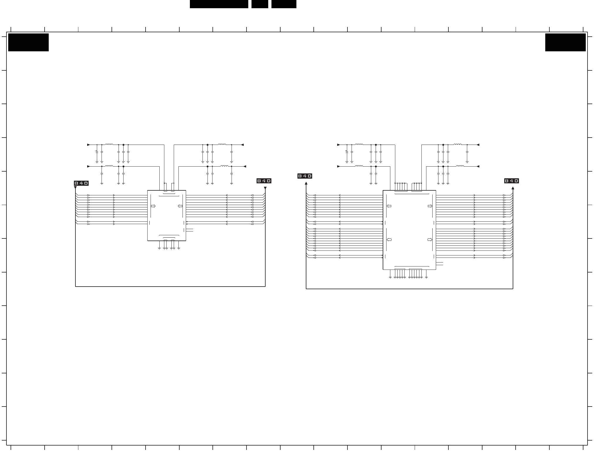
Circuit Diagrams and PWB Layouts EN 71LC8.2HA LA 10.
2009-Apr-10
SSB: MJC MT8280 LVDS
3N
3P
4N
4P
N
P
RO
ROCLK
RE
RECLK
CLKGENPLL RXORXE
N
P
LVD S
VIPLL
AVDD33
RXE RXO
LVD S
CLKGEN_CK
CLKGENPLL
AVSS3 3
VIPLL
0N
0P
1N
1P
2N
2P
3N
3P
4N
4P
N
P
0N
0P
1N
1P
2N
2P
AVD D1 2
N
4P
TN2
TP2
0N
0P
1N
1P
2N
2P
3N
3P
4N
0N
0P
1N
1P
2N
2P
3N
3P
4N
4P
N
P
4P
AO
AECK
N
PAOCK
BE
BECK
0N
0P
1N
1P
2N
2P
3N
3P
4N
4P
N
P
BO
BECK
TXA TXB VPLL
AVSS3 3
P
AVSS12
TXA TXB VPLL
AVD D 33
AE
0N
0P
1N
1P
2N
2P
3N
3P
4N
11 12 1314 15 16 17
123456 15 16
FB15 D6
FB16 D11
FB17 D13
1234
3B03-2 F4
3B03-1 F4
3B02-4 F4
3B02-3 E4
3B02-2 F4
3B02-1 F4
3B03-4 F4
3B04-1 E6
3B04-2 E6
3B04-3 E6
3B04-4 E6
3B05-1 E6
A
H
I
3B03-3 F4
J
3B05-2 F6
3B05-3 F6
3B05-4 F6
3B06-1 F6
3B06-2 F6
3B06-3 F6
3B06-4 F6
5B10 D3
5B11 D7
5B12 D11
5B13 D14
5B14 D3
5B15 D7
L
2B10 D3
2B15 D6
B
C
D
2B17 D6
2B16 D6
7G01-3 E12
7G01-4 E5
FB10 D4
FB11 D6
2B18 D7
2B19 D10
5B16 D11
5B17 D14
2B14 D4
2B12 D4
2B13 D4
MJC MT8280 - LVDS
3B01-3 E4
3B01-4 E4
2B22 D11
2B23 D11
2B24 D13
56789
2B25 D13
2B26 D13
2B27 D14
E
F
G
NC
9101112
NC
NC
NC
K
L
A
B
C
D
E
F
G
H
I
J
K
1314
H22
F21
F22
B21
A21
30R5B12
FROM LVDS
FROM LVDS
17
FROM LVDS
10
2B28 E3
2B29 E4
2B30 E4
2B31 E6
2B32 E6
2B33 E7
2B34 E11
2B35 E11
2B36 E13
2B37 E13
2B38 E13
3B01-1 E4
3B01-2 E4
78
FROM LVDS
30R
2B20 D11
2B21 D11
2B11 D3
FB12 D11
FB13 D13
FB14 D4
FB14 5B15
2B32 10u
5B10
FB16
30R 30R5B11
+3V3_SW
10u2B30
2B29 100n
2B281u0
100n2B31
1u02B33
M22
C21
C22
D21
D22
E21
E22
G21
G22
H21
J21
J22
K21
K22
L21
L22
N21
N22
P21
P22
M21
C16
C17
C18
C19
J20
K20
L20
M20
N20
P20
B22
C13
C14
D20
E20
F20
G20
H20
A22
C20
C15
B13
A13
B14
A14
B12
A12
D19
C9
C10
C11
C12
B20
A20
B18
A18
B9
A9
B10
A10
B11
A11
MT8280
LVDS_TX
Φ
B15
A15
B16
A16
B17
A17
B19
A19
AB13
AA11
AB11
7G01-3
AA17
AB17
AA8
AB8
AA9
AB9
AA10
AB10
AA12
AB12
AA13
AB7
AA14
AB14
AA15
AB15
AA16
AB16
AA18
AB18
AA19
AB19
Y9
Y10
Y11
W8
Y12
Y13
W9
W10
W11
AA7
7G01-4
MT8280
LVDS_RX
Φ
Y8
Y14
Y15
100n2B36
10u2B38
FB12
5B16 30R
FB15
5B14
FB11
30R
+3V3_SW +3V3_SW
FB10
+3V3_SW
FB13
2B2310u
2B16 10n
2B15 100n
2B181u0
2B14 10u
2B19 10u
100n2B21
16V
100n2B24
+3V3_SW
+3V3_SW
100n2B12
10u2B10
16V
100n
+3V3_SW
2B37
5B1330R
10n2B22
2B26 10u
+1V2_SW
1u02B11
10n2B25
2B34 100n
1u02B35
1u02B27
1u02B20
5B17
FB17 30R
10n2B13
10u2B17
TxFPGAe_4n
TxFPGAe_3p
TxFPGAe_CLKn
TxFPGAe_CLKp
TxFPGAe_4p
TxFPGAe_1p
TxFPGAe_2n
TxFPGAe_2p
TxFPGAe_3n
TxFPGAe_0n
TxFPGAe_0p
TxFPGAe_1n
TxFPGAo_CLKn
TxFPGAo_CLKp
TxFPGAo_4n
TxFPGAo_4p
TxFPGAo_2p
TxFPGAo_3n
TxFPGAo_3p
TxFPGAo_1n
TxFPGAo_1p
TxFPGAo_2n
LVD S_B_TXoCLKn
LVD S_B_TXoCLKp
TxFPGAo_0n
TxFPGAo_0p
LVD S_B_TXe2n
LVD S_B_TXe2p
LVD S_B_TXe1n
LVD S_B_TXe1p
LVD S_B_TXe0n
LVD S_B_TXe0p
LVD S_B_TXeCLKp
LVD S_B_TXeCLKn
LVD S_B_TXo1p
LVD S_B_TXo0n
LVD S_B_TXo0p
LVD S_B_TXe4n
LVD S_B_TXe4p
LVD S_B_TXe3n
LVD S_B_TXe3p
LVD S_B_TXo2p
LVD S_B_TXo1n
LVD S_B_TXo2n
LVD S_B_TXo3p
LVD S_B_TXo3n
LVD S_B_TXo4n
LVD S_B_TXo4p
LVD S_A_TXeCLKn
LVD S_A_TXoCLKn
LVD S_A_TXoCLKp
LVD S_A_TXe2p
LVD S_A_TXe1n
LVD S_A_TXe1p
LVD S_A_TXe0n
LVD S_A_TXe0p
LVD S_A_TXeCLKp
LVD S_A_TXo1p
LVD S_A_TXo0n
LVD S_A_TXo0p
LVD S_A_TXe4n
LVD S_A_TXe4p
LVD S_A_TXe3n
LVD S_A_TXe3p
LVD S_A_TXe2n
LVD S_A_TXo2p
LVD S_A_TXo1n
LVD S_A_TXo2n
LVD S_A_TXo3p
LVD S_A_TXo3n
LVD S_A_TXo4n
LVD S_A_TXo4p
B08A B08A
I_17760_017.eps
180208
3139 123 6349.1
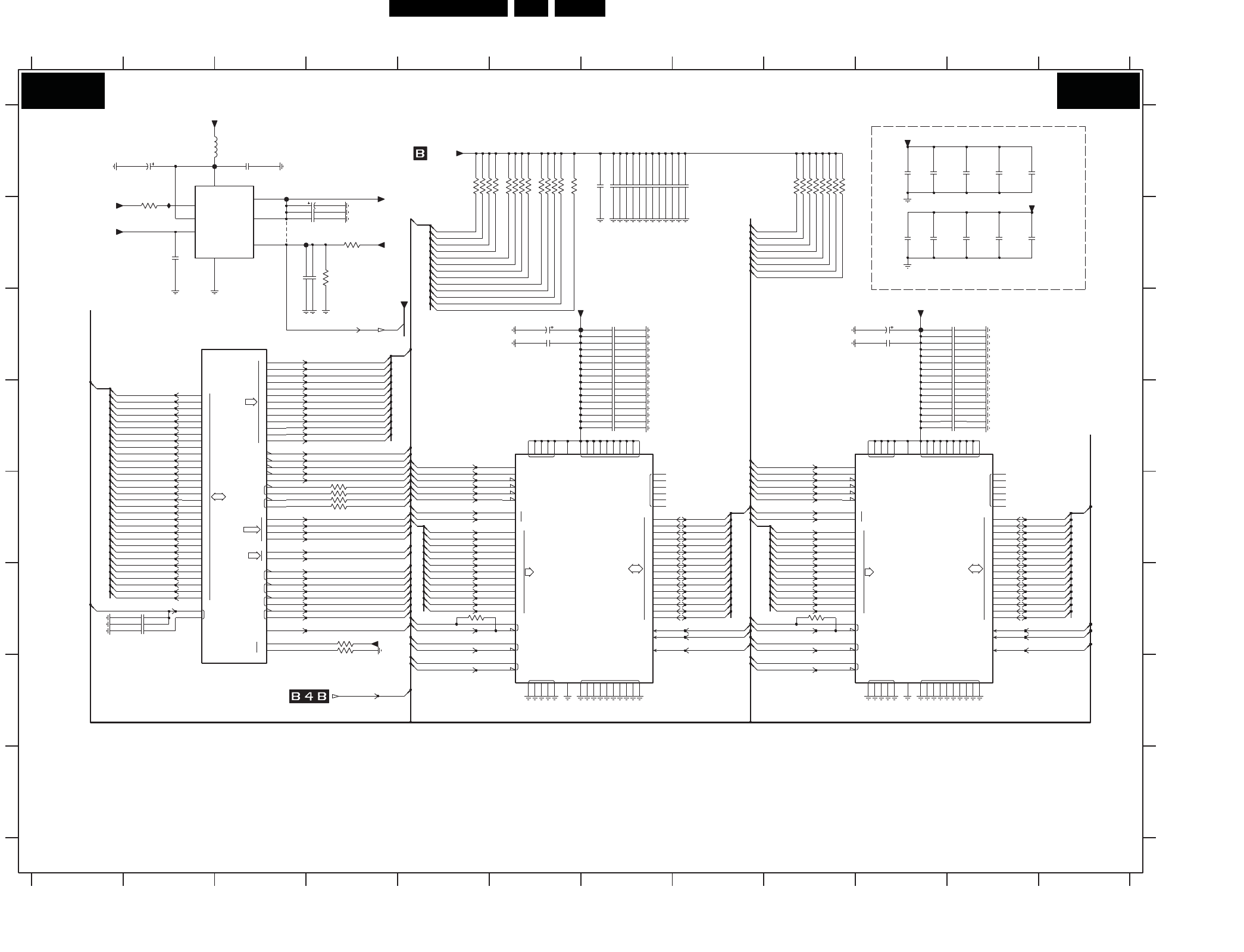
EN 72LC8.2HA LA 10.
Circuit Diagrams and PWB Layouts
2009-Apr-10
SSB: MJC MT8280 DDR
12
11
10
9
8
7
6
5
4
3
0
1
2
3
4
5
6
7
8
9
10
11
12
CK
VDDL
VREF
VSSDL
14
VDDQ
VSS VSSQ
BA
A
LDQS
UDQS
NC
DQ
CKE
WE
ODT
RAS
1
CS
CAS
0
0
1
2
VDD
LDM
UDM
15
13
30
15
RA
DQM
BA
REXT
1
DN
DQS0
UP
DQS1
RODT
DQS2
DQS3
0
1
2
3
4
5
17
6
7
8
9
10
11
12
RCS
RAS
CAS
RWE
CKE
RCLK0
0
RCLK1
3
0
1
2
18
19
20
21
22
23
24
25
26
27
28
29
31
RVREF
0
1
2
3
4
5
6
7
8
9
10
11
12
13
14
DQ
16
12
11
10
9
8
7
6
5
4
3
0
1
2
3
4
5
6
7
8
9
10
11
12
CK
VDDL
VREF
VSSDL
14
VDDQ
VSS VSSQ
BA
A
LDQS
UDQS
NC
DQ
CKE
WE
ODT
RAS
1
CS
CAS
0
0
1
2
VDD
LDM
UDM
15
13
7
2F58 D10
9
2F60 F2
11
2F62 A2
1
2F44 D10
2F35 C7
2F24 C10
2F42 C10
2F26 C10
2F65 B7
3F12-4 B6
2F68 B7
2F66 B7
2F70 B7
3F09-4 B5
3F40 B9
3F41 C4
3F12-3 B6
3F11-4 B6
3F12-2 B9
3F35 F5
NC
FF14 C10
NC
NC NC
3F14-3 B9
DDR #1
NC
7F02 D10
2F57 D7
3F11-1 B6
2F59 F2
3F11-3 B6
2F61 F2
3F12-1 B9
2F63 A3
2F67 B7
3F31 E4
DDR #2
NC
MJC MT8280 - DDR
3F09-1 B5
3F09-2 B6
2F69 B7
3F13-1 B6
3F13-3 B9
3F37 F4
B
11 12
B
C
D
E
9
TO MJC-DDR
2
RES
64
RES
NC
G
H
12
RES
8
RES FOR EMC
F
2F29 C6
A
2F31 C10
23
D
5678
2F39 C7
10
H
2F46 D10
2F72 B7
2F48 D10
2F74 B7
2F50 D10
2F76 B8
2F52 D10
2F55 D7
3F09-3 B6
3F38 F4
2F80 B3
3B19 B4
2F82 C3
4F01 B3
2F84 A10
7F01 D6
2F86 A11
7F03 A3
2F88 A11
FF10 A2
2F90 B10
FF12 B4
2F92 B11
2F93 B11
2F53 D7
C
2F47 D7
E
2F49 D7
2F51 D7
2F23 C6
2F36 C10
2F37 C7
53
NC
2F79 B3
2F81 B2
2F83 C4
2F85 A10
2F87 A11
2F89 B10
2F54 D10
2F91 B11
2F56 D10
2F27 C7
8
4
10
NC
2F33 C7
NC
NC NC
2F25 C7
1
2F41 C7
2F28 C10
G
2F30 C7
2F43 D7
2F32 C10
2F34 C10
2F45 D7
F
A
2F38 C10
2F64 B3
2F40 C10
2F71 B7
3F39 B2
2F73 B7
3F14-2 B9
2F75 B7
3F14-4 B9
2F77 B8
3F34 E4
3F36 F9
FF13 C7
IF01 B2
3F13-2 B5
5F01 A3
3F13-4 B6
3F14-1 B9
3F11-2 B6
7G01-2 C2
FF11 A3
3F32 E4
3F33 E4
33R3F37
3F14-1 47R1
GND
PVIN
7
2SD_
5
VDDQ
4
VREF
3
VSENSE
8
VTT
7F03
LP2996M
6AVIN
1
+1V8_SW
FF12
2F70 100n
4u7
100n2F69
2F79
2F72 100n
1%
75R3F41
100n2F71
3F40 47R
3F11-347R36
5F01
30R
100u
16V
4F01
2F62
47R27
+1V8_SW
3F13-2
3F39 4K7
2F82
FF11
+1V8_SW
1u0
2F80100n
2F64 100u16V
+0V9_VTT
100n
IF01
2F81
FF10
47R
3F14-2 27
45
3F13-4 47R
18
+1V8_SW
47R
3F13-1
6
100n2F77
3F14-347R3
2F76 100n
100n
100n2F75
2F74
100n2F73
FF13
2F68100n
100n2F67
2F66 100n
45
18
47R
3F11-4
3F11-1 47R
47R
3F12-336
100n
2F63
18
5
47R
3F12-1
47R
3F09-4 4
2F83 100n
27
75R3B19
47R
3F09-2
+1V8_SW
1%
4 5 47R
3F14-4
A7
H8
B2
B8
D2
D8
E7
F2
F8
H2
K3
G1
G3
G7
J2
A3
E3
J3
N1
P9
J7
M9
R1
J1
A9
G9
C1
C3
C7
C9
E9
R7
R8
K9
K7
B3
B7
A8
A1
E1
J9
F9
C8
C2
F3
F7
E8
A2
E2
L1
R3
D7
D3
D1
D9
B1
B9
H7
H3
H1
H9
F1
P8
P3
L2
L3
L7
J8
K2
K8
L8
G8
G2
M3
M2
P7
R2
M7
N2
N8
N3
N7
P2
7F01
EDE2516ACSE-6E-E
SDRAM
Φ
M8
3F38 33R
36 47R
3F13-3
2F65 4u7
AB6
AA6
J4
B7
A6
G2
P4
P5
P1
L2
M2
L3
P3
K2
M3
J2
N4
H1
F2
F1
C2
W2
W1
AB2
AA2
K3
L1
L4
J1
R3D6
G3
E3
A2
B1
Y1
AB1
B3
A3
C1
AA3
AB5
Y3
W4
AA5
A5
W5
AB4
B6
C5
C4
U3
U1
U4
T2
D5
T1
T4
V3
V2
Y4
N1
H3
R2
C7
B4
D2
E4
D3
E1
F4
H4
Φ
DRAM
MT8280
7G01-2
N2
+1V8_SW
FF14
2 7 47R
3F11-2
3F12-4 47R45
47R27
+0V9_VTT
3F12-2
3F09-347R36
18
3F09-1 47R
100n
2F25
4u7
+1V8_SW
2F29
100n 2F61
2F30100n
22R3F32
3F34 22R
100n
100n
2F37
2F39
100n
2F35
100n
2F33
2F27 100n
2F23
16V
100u
2F57 100n
100n
2F55
2F51 100n
100n
2F49
2F47 100n
16V
2F24 100u
2F46 100n
100n
2F42
3F36100R100R
3F35
3F31 22R
100n
2F40
2F38 100n
100n
2F53
2F34100n
100n
2F28
100n
2F43
100n
2F45
100n
2F26
2F41 100n
4u7
2F31
A7
H8
B2
B8
D2
D8
E7
F2
F8
H2
K3
G1
G3
G7
J2
A3
E3
J3
N1
P9
J7
M9
R1
J1
A9
G9
C1
C3
C7
C9
E9
R7
R8
K9
K7
B3
B7
A8
A1
E1
J9
F9
C8
C2
F3
F7
E8
A2
E2
L1
R3
D7
D3
D1
D9
B1
B9
H7
H3
H1
H9
F1
P8
P3
L2
L3
L7
J8
K2
K8
L8
G8
G2
M3
M2
P7
R2
M7
N2
N8
N3
N7
P2
Φ
SDRAM
EDE2516ACSE-6E-E
7F02
M8
100n
2F48
2F44 100n
22R3F33
100n
2F36
100n
2F32
100n
2F58
+1V8_SW
2F56 100n
100n
4u7
2F54
100n
2F52
2F60
100n 2F59
2F50 100n
22n
2F90
22n
2F88
22n
2F86
22n
2F84
2F87
22n22n
2F92
2F85
22n
+1V8_SW
2F93
22n
2F91
22n
MJC_VREF
2F89
22n
MJC_RCASn
MJC_RRASn
MJC_RCSn
MJC_RODT
MEM_VREF
MJC_RBA1
MJC_RBA0
MJC_RWEn
MJC_RCKE
MJC_RA(11)
MJC_RA(12)
MJC_RA(2)
MJC_RA(3)
MJC_RA(4)
MJC_RA(5)
MJC_RA(6)
MJC_RA(7)
MJC_RA(8)
MJC_RA(9)
MJC_RA(10)
MJC_RDQS3
MJC_RDQS3n
MJC_RDQM2
MJC_RDQM3
MJC_RA(0:12)
MJC_RA(0)
MJC_RA(1)
MJC_RDQ(29)
MJC_RDQ(30)
MJC_RA(0:12)
MJC_RDQ(0:31)
MJC_RCASn
MJC_RCKE
MJC_RCSn
MJC_RODT
MJC_RRASn
MJC_RWEn
MJC_RBA0
MJC_RBA1
MJC_RCLK1
MJC_RCLK1n
MJC_RDQS2
MJC_RDQS2n
MJC_RDQ(19)
MJC_RDQ(20)
MJC_RDQ(21)
MJC_RDQ(22)
MJC_RDQ(23)
MJC_RDQ(24)
MJC_RDQ(25)
MJC_RDQ(26)
MJC_RDQ(27)
MJC_RDQ(28)
MJC_RDQ(16)
MJC_RDQ(17)
MJC_RDQ(18)
MJC_RA(10)
MJC_RA(11)
MJC_RA(12)
MJC_VREF
MJC_RA(0)
MJC_RA(1)
MJC_RA(2)
MJC_RA(3)
MJC_RA(4)
MJC_RA(5)
MJC_RA(6)
MJC_RA(7)
MJC_RA(8)
MJC_RA(9)
MJC_RCLK1n
MJC_RCLK1
MJC_RA(0)
MJC_RA(1)
MJC_RA(2)
MJC_RA(3)
MJC_RA(4)
MJC_RA(5)
MJC_RA(6)
MJC_RA(7)
MJC_RA(8)
MJC_RA(9)
MJC_RA(10)
MJC_RA(11)
MJC_RA(12)
MJC_RA(0:12)
MJC_VREF
MJC_RDQM0
MJC_RDQM1
MJC_RDQ(31)
MJC_RWEn
MJC_RBA0
MJC_RBA1
MJC_RBA0
MJC_RBA1
MJC_RCSn
MJC_RCASn
MJC_RRASn
MJC_RCKE
MJC_RWEn
MJC_RODT
MJC_RCLK0
MJC_RCLK0n
MJC_RDQS0
MJC_RDQS0n
MJC_RDQS1
MJC_RDQS1n
MJC_RCLK0n
MJC_RCLK0MJC_RDQ(15)
MJC_RDQM1
MJC_RDQS1
MJC_RDQS1n
MJC_RDQM2
MJC_RDQS2
MJC_RDQS2n
MJC_RDQM3
MJC_RDQS3
MJC_RDQS3n
MJC_RDQ(16)
MJC_RDQ(17)
MJC_RDQ(18)
MJC_RDQ(19)
MJC_RDQ(20)
MJC_RDQ(21)
MJC_RDQ(22)
MJC_RDQ(23)
MJC_RDQ(24)
MJC_RDQ(25)
MJC_RDQ(26)
MJC_RDQ(27)
MJC_RDQ(28)
MJC_RDQ(29)
MJC_RDQ(30)
MJC_RDQ(31)
MJC_RCASn
MJC_RCKE
MJC_RCSn
MJC_RODT
MJC_RRASn
MJC_RDQ(6)
MJC_RDQ(7)
MJC_RDQM0
MJC_RDQS0
MJC_RDQS0n
MJC_RDQ(8)
MJC_RDQ(9)
MJC_RDQ(10)
MJC_RDQ(11)
MJC_RDQ(12)
MJC_RDQ(13)
MJC_RDQ(14)
MJC_RDQ(4)
MJC_RDQ(5)
MJC_RDQ(6)
MJC_RDQ(7)
MJC_RDQ(8)
MJC_RDQ(9)
MJC_RDQ(10)
MJC_RDQ(11)
MJC_RDQ(12)
MJC_RDQ(13)
MJC_RDQ(14)
MJC_RA(0:12)
MJC_RDQ(0:31)
MJC_RDQ(0:31)
MJC_RDQ(0)
MJC_RDQ(1)
MJC_RDQ(2)
MJC_RDQ(3)
MJC_RDQ(4)
MJC_RDQ(5)
MJC_RDQ(0)
MJC_RDQ(1)
MJC_RDQ(2)
MJC_RDQ(3)
MJC_RDQ(15)
MJC_VREF
MJC_RA(0)
MJC_RA(1)
MJC_RA(2)
MJC_RA(3)
MJC_RA(4)
MJC_RA(5)
MJC_RA(6)
MJC_RA(7)
MJC_RA(8)
MJC_RA(9)
MJC_RA(10)
MJC_RA(11)
MJC_RA(12)
B08B B08B
I_17760_018.eps
180208
3139 123 6349.1
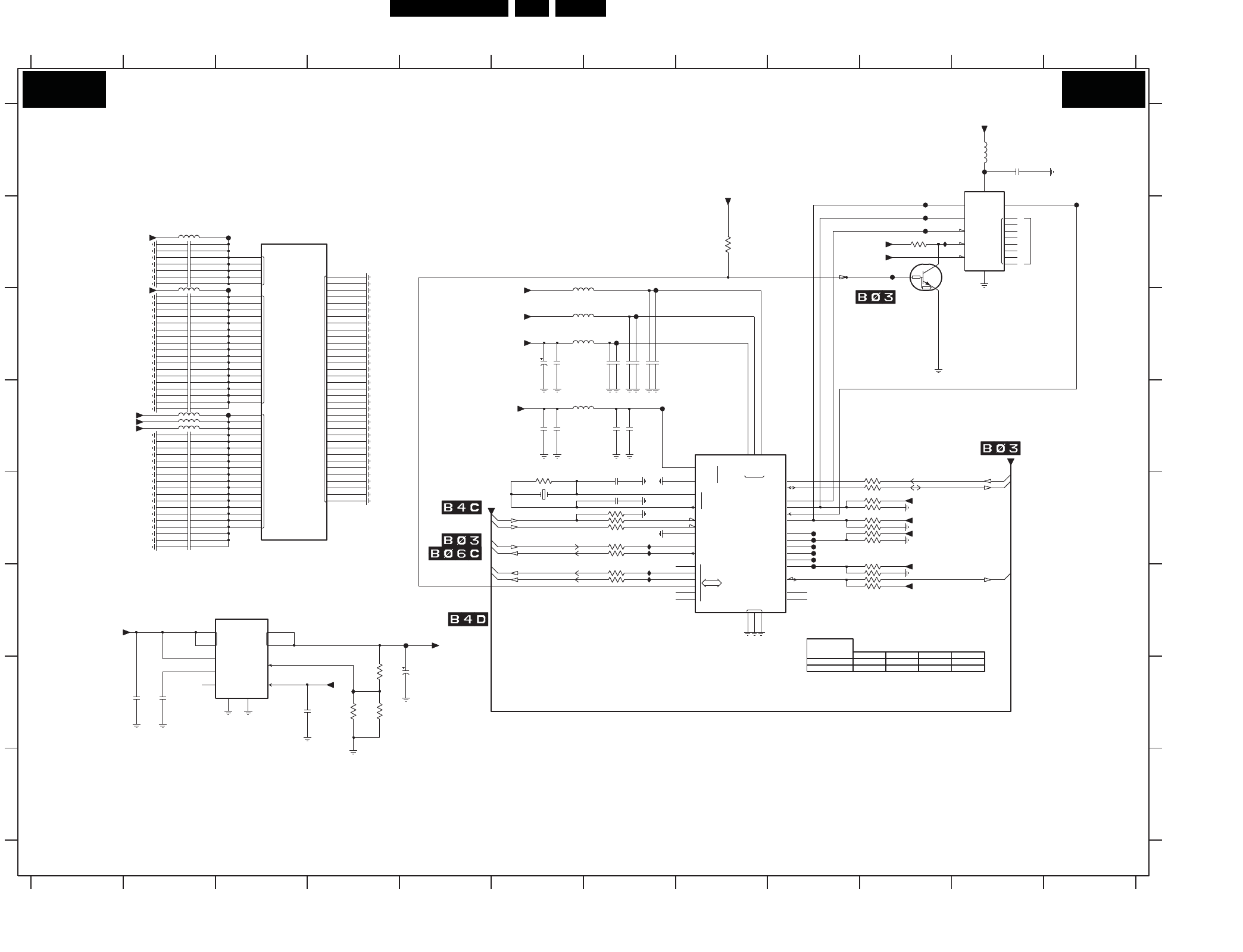
Circuit Diagrams and PWB Layouts EN 73LC8.2HA LA 10.
2009-Apr-10
SSB: MJC MT8280 Power
DVSS
DVSS
DVSS
DVSS
DVSS
DVDD 1 8
DVDD 1 0
DVDD33
DVDD 1 0
DVDD 1 8
DVDD 1 8
DVDD 1 0
PRST
O
SFCS
SFCK
XTAL
I
SCL
SDA
NS_XTAL
GPIO
SFDI
SFDO
JTMS
AVDD12
AVSS_PLL
TXD
0
EFUSE
RXD
JTRST
JRTCK
JTCK
JTDI
JTDO
INT0
TN0
TP0
SYSPLL
MJCPLL
DMPLL
5
4
3
2
1
PWN
AVDD33
AVSS33
DU
VCC
Q
VSS
D
C
S
W
HOLD
OUT
BIASPG
SS
EN
IN
GND
GND_HS
FB
0R
FG25 E9
FG26 E9
3G24 E7
3G27 F9
3G29 F9
3G31 F9
IG13 F7
IG14 G4
IG15 B10
3G23 E7
2G64 E2
2G65 E2
(1)
2G68 G5
(0)
SFCK
( ) DEFAULT MODE
FG13 B10
FG27 E9
FG28 F9
FG29 F5
IG10 E7
FG18 C3
3G16 E7
IG11 E7
IG12 F7
3G17 E7
3G18 E9
3G19 E7
3G20 E9
13G22 E9
2G63 E2
2G50 D2
2G51 D2
2G66 E2
3G30 F7
2G54 E2
0R
3G32 F9
3G33 F7
3G34 G4
3G35 G4
5G17 D2
5G19 D2
7G01-5 D8
7G02 A11
5G14 C6
5G15 C6
5G16 D6
FG19 C7
FG20 C7
FG21 D7
3G10 B10
3G13 E9
FG11 B12
2G57 E2
2G31 C6
5
TO FLASH&NVM
FG14 B10
FG15 B3
FG16 B10
FG17 B7
119
(1)
RES
TEST_CPUM
TRAP MODE
2G58 E2
2G59 E2
2G60 E7
3G21 E9
2G62 E2
2G19 C2
2G20 C2
2G21 C2
2G52 D2
2G67 E2
6
2G24 C2
2G32 C6
B
A
13
H
JTDO
X
2G40 D2
NORM
2G42 D2
2G45 D2
2G46 D6
2G47 D6
2G48 D7
2G61 E2
2G49 D7
2G27 C2
2G28 C2
1
2G53 D2
2
4
45
7
NC
(1)
3G36 G4
3G38 B8
5G10 A11
SFDO
NC
TO Microp
1G01 E6
2G22 C2
2G23 C2
2G70 G2
F
G
H
F
2G56 E7
10
2G13 B2
2G33 C7
2G14 B2
MJC MT8280 - POWER
2G29 C2
7G03 B10
0
JTRST
7G04 F3
FG10 A11
7G01-1 B3
3G11 E6
3G12 E9
FG12 B10
3G15 E9
FG22 D3
FG23 E9
FG24 E9
2G10 A11
8
TO Microp
1
67
FLASH
G
2G34 C7
B
C
D
E
89
2G11 B2
2G12 B2
2G35 C7
2G15 B2
2G37 C7
2G25 C2
2G26 C2
0R
NC
5G11 B2
5G12 C6
RES
5G13 C2
RES
RES
RES
2G69 G2
5G18 D2
2G71 G4
C
D
E
2G55 E2
3G14 E9
11 12
A
2G30 C2
2G36 C7
3
2G38 C7
2G39 D2
2G41 D2
2G43 D2
2G44 D2
UART_0RX
UART_0TX
10
2G16 B2
2G17 B2
2G18 C2
122
2G64 10n
100R3G13
10n2G63
3G12 100R
2G54 100n
1u02G32
FG10
FG14
+1V
2G431u0
FG29
IG14
3G34
2G364u7
10K
100n2G35
Y18
AB21
Y19
AB20
D8
A7
B8
A8
U21
U22
AA20
V17
AA22
Y21
W20
AA21
Y22
W21
V21
V22
W18
U20
R20
R21
R22
W15
Y6
Y7
Y16
W16
W17
V16
Φ
PHERIPHERAL
MT8280
7G01-5
T21
T22
T20
V20
Y5
AA1
D1
D4
E2
J3
J9
J11
N13
P2
P9
P11
P12
R1
C3
R4
T3
W6
Y2
L9
L11
L12
L14
M9
B5
M11
M12
M14
N10
C8
D9
W7
W19
Y20
A4
J12
K1
K4
K10
K13
W3
AA4
AB3
B2
C6
D7
F3
G1
G4
H2
M1
K12
K14
L10
L13
A1
M4
N3
U2
V1
V4
N9
N11
N12
N14
P10
P13
P14
J13
J14
K9
K11
Φ
POWER
MT8280
7G01-1
J10
M10
M13
+1V2_SW30R5G12 FG17
IG15
FG21
IG13
IG11
IG12
100n2G13
2G11 4u7
IG10
2G184u7
+3V3_SW
FG16
2G19 100n
2G21 100n
2G37100n
3G33 100R
100n2G53
3G16 10K
3G19
5G17
FG13
30R
100n2G45
+3V3_SW
FG22
10K
3G32
3G184K7
4K7
3G14 +3V3_SW
100R3G24
100n2G15
2G14 100n
2G27 10n
+3V3_SW
100n2G26
8
7
210
9
16
15
3
4
5
6
11
12
13
14
1
M25P16-VMF
7G02
FLASH
2Mx8
Φ
FG27
FG25
FG26
2G71
1u0
2G62 100n
100n2G20
3G31
100R3G23
4u72G38
2G57 100n
100n2G55
FG19
+1V2_SW5G14 30R
3G20 4K7
4K7
3G15
3G11 820K
10n2G40
10K
3G22
30R5G19
+1V
+3V3_SW
3G17
3G38
10K
16V
2G3110u
FG18
+1V8_SW
1u02G42
FG28
+3V3_SW4K73G10
+3V3_SW
FG23
FG24
+5V_SW
1u0
2G69
100n2G61
100R3G30
+1V2_SW
+3V3_SW30R5G16
+3V3_SW5G11 30R
3G29 4K7
2G3910n
2G30
8
6
11
1
2
9
10
3
7
10n
Φ
7G04
TPS74801DRCR
4
5
2G41 10n
2G4810u
10n2G28
+1V
FG11
5G1830R
2G47 1u0
5%
3G35
2K2
3G36
680R
1%
5G1330R
1n0
2G70
FG12
30R
5G10
100n2G50
100n
2G10
1u02G67
+3V3_SW
4K7
3G27
7G03
PDTC114ET
2G16 100n
2G25 100n
2G12 100n
100n2G24
FG15
2G23100n
2G65 1u0
100n2G22
4u72G34
2G29 10n
2G33 100n
FG20
100n2G49
+1V2_SW
10u2G46
30R5G15
2G68
2G52 100n
+1V
22u
6.3V
2G51
4u72G44
100n
2G59 100n
2G66 1u0
+3V3_SW
100n2G58
3G21 10K
22p2G60
27M0
22p2G56
1G01
2G17 1u0
FLASH_MJC_WE
UART_1TX
BL_ON_OFF
LCD_PWR_ON
IIC_SCL_up
IIC_SDA_up
INT0
PRST
PWN
UART_1RX
SF_CK
SF_S0SF_DO
SF_CS0
B08C B08C
I_17760_019.eps
180208
3139 123 6349.1
EN 74LC8.2HA LA 10.
Circuit Diagrams and PWB Layouts
2009-Apr-10
SSB: SRP List Explanation
1 . 1 . Introduction
Example
SRP (Service Re ference Protocol) is a softw are too l that creates a list w i th all refer e n c es to signal lines. The list contains
references to the signals w i thin all schemat ics of a PWB. It replaces the text refe r ences currentl y p r inted next t o the signal
names in the schematics. These printed refe rences are created man ually an d are t h e r efore n o t guar an teed to be 100 %
correct. In additio n , in the current crowded schema t ics there is often none or ver y little pl ace for these references.
Some of the PW
B schematics w ill use SRP while others w ill sti ll use the manual refe rences. Either there w ill be an SRP
r e fer ence list for a schematic, or ther e w ill be pr inted r e ferences in the schematic.
1.2. No n - SRP Schematics
There a r e severa l different signals available in a schematic:
1.2.1. Po w e r Supply Lines
All pow er suppl y lines are available in t he suppl y line overview (see chapter 6). I n th e schematics (se e chapter 7) is n o t
indicated w h e r e supplies are coming from or going to.
It is how ever indi cated if a supply is incoming (created elsew h e r e), o r outgoing (cr eat ed or adapt ed in the current sche m atic).
+5 V +5 V
Outgoing Incoming
1.2.2. Normal Signals
For no rmal signals, a schematic r e ference (e. g . B1 4b) is placed next to the signals.
si gnal _nam e
B 14b
1.2.3. Grounds
For no rmal and s pecial grounds (e .g. GN DH OT o r GND3V3 etc.), n o thing is indicate d.
1.3. SRP Schematics
SRP is a tool, w h ich automatically creates a list w i th signal reference s , indicating on which sc hematic t he signals are used.
A reference is cr eated for all signals indicat ed w i th an SRP s y mbol, these s y mbols are:
+5 V +5 V
Power suppl y li ne.
na m e na m e Stand alone signal or sw itching li ne (used as less as possible).
na m e na m e
Signal line into a w i re tree.
na m e na m e
Sw itching line into a w i re tre e .
na m e
Bi-directional lin e (e.g. SDA ) into a w i r e tree.
na m e
Signal line into a w i r e tree, its dir e ction depends on t he circuit (e.g. ingoing for PD P, outgoing for L C D sets).
Remarks:
• When there is a black dot on the "signal dire ction arrow" it is an SRP symbol, so there will be a reference to the signal
name in the SRP list.
• All references to normal grounds (Ground symbols without additi onal text) are not listed in the reference list, this to keep
it concise.
• Signals that are not used in multiple schematics, but only onc e or several times in the same schematic, are included
in the SRP reference list, but only with one reference.
Additional Tip:
When using the PDF service manual file, you can very easily search for signal names and follow the signal over all the
schematics. In Adobe PDF reader:
• Select the signal name you want to sear ch for, with the "Select text" tool.
• Copy and paste the signal name in the "Search PDF" tool.
• Search for all occurrences of the signal name.
• Now you can quickly jump between the different occurrences and follow the signal over all schematics. It is advised to
"zoom in" to e.g. 150% to see clearly, which text is select ed. Then you can zoom out, to get an overview of the complete
schematic.
PS. It is recommended to use at least Adobe PDF (reader) version 6. x, due to better search possibilities in this version.
E_06532_031.eps
230606
Net Name Diagram
+12-15V AP1 (4x)
+12-15V AP4 (4x)
+12-15V AP5 (12x)
+12-15V AP6 (4x)
+12-15V AP7 (8x)
+12V AP1 (4x)
+12V_NF AP1 (2x)
+12VAL AP1 (2x)
+25VLP AP1 (4x)
+25VLP AP2 (1x)
+3V3-STANDBY AP5 (3x)
+400V-F AP1 (2x)
+400V-F AP2 (2x)
+400V-F AP3 (2x)
+5V2 AP1 (6x)
+5V2 AP2 (1x)
+5V2-NF AP1 (1x)
+5V2-NF AP2 (1x)
+5V-SW AP1 (6x)
+5V-SW AP2 (1x)
+8V6 AP1 (3x)
+AUX AP1 (2x)
+AUX AP2 (1x)
+DC-F AP1 (2x)
+DC-F AP3 (2x)
+SUB-SPEAKER AP5 (1x)
+SUB-SPEAKER AP6 (2x)
-12-15V AP1 (4x)
-12-15V AP4 (6x)
-12-15V AP5 (14x)
-12-15V AP6 (6x)
-12-15V AP7 (8x)
AL-OFF AP1 (2x)
AUDIO-L AP4 (1x)
AUDIO-L AP5 (1x)
AUDIO-PROT AP5 (3x)
AUDIO-R AP4 (1x)
AUDIO-R AP5 (1x)
AUDIO-SW AP5 (1x)
AUDIO-SW AP7 (1x)
BOOST AP1 (2x)
CPROT AP4 (2x)
CPROT AP5 (1x)
CPROT-SW AP5 (1x)
CPROT-SW AP6 (2x)
-DC-F AP1 (2x)
-DC-F AP3 (2x)
DC-PROT AP1 (1x)
DC-PROT AP5 (2x)
DIM-CONTROL AP1 (2x)
FEEDBACK+SW AP6 (2x)
FEEDBACK-L AP4 (2x)
FEEDBACK-R AP4 (2x)
FEEDBACK-SW AP6 (2x)
GND-AL AP1 (2x)
GNDHA AP1 (40x)
GNDHA AP2 (20x)
GNDHA AP3 (2x)
GNDHOT AP3 (2x)
GND-L AP1 (2x)
GND-L AP4 (4x)
GND-L AP5 (34x)
GND-LL AP4 (7x)
GND-LL AP5 (1x)
GND-LR AP4 (7x)
GND-LR AP5 (1x)
GND-LSW AP5 (1x)
GND-LSW AP6 (15x)
GND-S AP1 (11x)
GND-SA AP4 (8x)
GND-SA AP5 (2x)
GND-SA AP6 (8x)
GND-SA AP7 (6x)
GNDscrew AP3 (2x)
GNDscrew AP5 (2x)
GND-SSB AP5 (3x)
GND-SSP AP1 (51x)
GND-SSP AP2 (15x)
IN+SW AP6 (2x)
IN-L AP4 (2x)
IN-R AP4 (2x)
IN-SW AP6 (2x)
INV-MUTE AP4 (1x)
INV-MUTE AP5 (1x)
INV-MUTE AP6 (1x)
LEFT-SPEAKER AP4 (1x)
LEFT-SPEAKER AP5 (1x)
MUTE AP4 (2x)
MUTE AP5 (1x)
MUTE AP6 (2x)
ON-OFF AP1 (3x)
OUT AP6 (1x)
OUT AP7 (2x)
OUTN AP6 (1x)
OUTN AP7 (1x)
POWER-GOOD AP1 (2x)
POWER-OK-PLATFORM AP1 (2x)
RIGHT-SPEAKER AP4 (1x)
RIGHT-SPEAKER AP5 (1x)
SOUND-ENABLE AP5 (3x)
STANDBY AP1 (5x)
STANDBY AP2 (1x)
-SUB-SPEAKER AP5 (1x)
-SUB-SPEAKER AP6 (2x)
V-CLAMP AP1 (1x)
V-CLAMP AP3 (2x)
Personal Notes:

Circuit Diagrams and PWB Layouts EN 75LC8.2HA LA 10.
2009-Apr-10
SSB: SRP List
Netname Diagram
+0V9_VTT B08C (2x)
+12V_AUDIO B01B (1x)
+12V_AUDIO B06A (1x)
+12V_DISP B01B (4x)
+12V_DISP B02 (2x)
+12V_DISP B03 (1x)
+12V_DISP B04A (1x)
+12V_DISP B05A (1x)
+12V_DISP B05B (1x)
+1V2_ADC B04B (5x)
+1V2_CORE B04B (2x)
+1V2_PLL B04B (4x)
+1V2_SW B01B (2x)
+1V2_SW B04B (1x)
+1V2_SW B04E (1x)
+1V2_SW B08B (1x)
+1V2-FPGA B04E (2x)
+1V2-PLL B04E (2x)
+1V8_ANA-MUX B07B (3x)
+1V8_DIG-MUX B07B (2x)
+1V8_SW B02 (1x)
+1V8_SW B07B (2x)
+1V8_SW B08A (4x)
+1V8_SW B08C (9x)
+1V8SWA B08A (1x)
+1V8SWB B08A (1x)
+1V8SWC B08A (1x)
+24V B04D (1x)
+2V5_SW B01B (1x)
+2V5_SW B04E (1x)
+2V5_VDDMQ B04B (2x)
+2V5_VDDMQ B04C (6x)
+2V5in-FPGA B04E (2x)
+2V5out-FPGA B04E (2x)
+2V6_SW B02 (3x)
+2V6_SW B04C (1x)
+3V3_ANA-MUX B07B (5x)
+3V3_ANA-MUX B08A (1x)
+3V3_FPGA B04D (9x)
+3V3_FPGA B04E (4x)
+3V3_STBY B01B (1x)
+3V3_STBY B04A (33x)
+3V3_STBY B04B (1x)
+3V3_STBY B06A (3x)
+3V3_STBY B06C (1x)
+3V3_STBY B07A (3x)
+3V3_SW B01B (4x)
+3V3_SW B03 (2x)
+3V3_SW B04A (17x)
+3V3_SW B04B (17x)
+3V3_SW B04E (1x)
+3V3_SW B05A (1x)
+3V3_SW B05B (1x)
+3V3_SW B07A (3x)
+3V3_SW B07B (2x)
+3V3_SW B08A (5x)
+3V3_SW B08B (7x)
+3V3SWA B08A (1x)
+3V3SWB B08A (1x)
+3V3SWC B08A (1x)
+3V3SWD B08A (1x)
+3V3SWE B08A (1x)
+5V_IF B03 (6x)
+5V_SW B02 (3x)
+5V_SW B03 (3x)
+5V_SW B04A (2x)
+5V_SW B04B (2x)
+5V_SW B05B (3x)
+5V_SW B06A (1x)
+5V_SW B06C (2x)
+5V_SW B07A (2x)
+5V_SW B07B (9x)
+5V_SW B08A (1x)
+5V_TCON B01B (1x)
+5V_TCON B05A (1x)
+5V_TUN B03 (2x)
+5VHDMI_A B08A (4x)
+5VHDMI_B B07B (4x)
+5VHDMI_C B07B (4x)
+5VHDMI_MUX_TPWR B07B (1x)
+5VHDMI_MUX_TPWR B08A (1x)
+5VHDMI_SIDE B07B (4x)
+5VS B03 (4x)
+8V B05B (2x)
+VDISP B05A (3x)
+VTUN B01B (1x)
+VTUN B03 (1x)
-12V_AUDIO B01B (1x)
-12V_AUDIO B06A (1x)
A(0) B04A (2x)
A(0) B04B (1x)
A(0:7) B04A (1x)
A(1) B04A (2x)
A(1) B04B (1x)
A(1:7) B04A (1x)
A(10) B04A (2x)
A(11) B04A (2x)
A(12) B04A (2x)
A(13) B04A (2x)
A(14) B04A (2x)
A(15) B04A (2x)
A(16) B04A (2x)
A(17) B04A (2x)
A(18) B04A (2x)
A(19) B04A (2x)
A(2) B04A (2x)
A(2) B04B (1x)
A(3) B04A (2x)
A(3) B04B (1x)
A(4) B04A (2x)
A(4) B04B (1x)
A(5) B04A (2x)
A(5) B04B (1x)
A(6) B04A (2x)
A(6) B04B (1x)
A(7) B04A (2x)
A(7) B04B (1x)
A(8) B04A (2x)
A(8:19) B04A (2x)
A(9) B04A (2x)
AD(0) B04A (2x)
AD(0) B04B (1x)
AD(0:7) B04A (2x)
AD(1) B04A (2x)
AD(1) B04B (1x)
AD(2) B04A (2x)
AD(2) B04B (1x)
AD(3) B04A (2x)
AD(3) B04B (1x)
AD(4) B04A (2x)
AD(4) B04B (1x)
AD(5) B04A (2x)
AD(5) B04B (1x)
AD(6) B04A (2x)
AD(6) B04B (1x)
AD(7) B04A (2x)
AD(7) B04B (1x)
ALE_EMU B04A (1x)
ALE_EMU B04B (1x)
ambi_pwm(0) B04D (1x)
ambi_pwm(0) B04E (1x)
ambi_pwm(1) B04D (1x)
ambi_pwm(1) B04E (1x)
ambi_pwm(2) B04D (1x)
ambi_pwm(2) B04E (1x)
ambi_pwm(3) B04D (1x)
ambi_pwm(3) B04E (1x)
ambi_pwm(4) B04D (1x)
ambi_pwm(4) B04E (1x)
ambi_pwm(5) B04D (1x)
ambi_pwm(5) B04E (1x)
AMBI_SCL B04D (1x)
AMBI_SCL B04E (1x)
AMBI_SDA B04D (1x)
AMBI_SDA B04E (1x)
ANTI_PLOP B04A (1x)
ANTI_PLOP B06A (1x)
ASDO B04D (1x)
ASDO B04E (1x)
AUD_RST B04A (1x)
AUD_RST B05B (1x)
AUDIO_LS_L B05B (1x)
AUDIO_LS_L B06A (1x)
AUDIO_LS_R B05B (1x)
AUDIO_LS_R B06A (1x)
BL_ADJUST_ANA B01B (1x)
BL_ADJUST_ANA B04B (1x)
BL_BOOST B01B (1x)
BL_BOOST B04A (1x)
BL_ON_OFF B01B (1x)
BL_ON_OFF B04A (1x)
BOLT_ON_UART_RXD B04A (1x)
BOLT_ON_UART_RXD B06B (1x)
BOLT_ON_UART_RXD B06C (1x)
BOLT_ON_UART_TXD B04A (1x)
BOLT_ON_UART_TXD B06B (1x)
BOLT_ON_UART_TXD B06C (1x)
CE B04A (1x)
CLK_OSC1 B04D (1x)
CLK_OSC1 B04E (1x)
COMP_AUDIO_IN_L B05B (1x)
COMP_AUDIO_IN_L B06B (1x)
COMP_AUDIO_IN_R B05B (1x)
COMP_AUDIO_IN_R B06B (1x)
CPU_RST B04A (1x)
CS B04A (1x)
CS B04B (1x)
CTRL_DISP1 B05A (2x)
CTRL_DISP1_up B04A (1x)
CTRL_DISP1_up B05A (1x)
CTRL_DISP2 B05A (2x)
CTRL_DISP3 B05A (2x)
CTRL_DISP4 B05A (2x)
CTRL_DISP4_up B04A (1x)
CTRL_DISP4_up B05A (1x)
CVBS_IN_DTV B04B (1x)
CVBS_IN_DTV B06B (1x)
CVBS_RF B03 (1x)
CVBS_RF B04B (1x)
DATA0 B04D (1x)
DATA0 B04E (1x)
DC_5V B07A (3x)
DC_PROT B04A (1x)
DC_PROT B06A (1x)
DCLK B04D (1x)
DCLK B04E (1x)
DDC_RST B04A (1x)
DDC_RST B07B (5x)
DDC_RST B08A (1x)
DDC_SCL_SIDE B07B (2x)
DDC_SCLA B08A (2x)
DDC_SCLB B07B (2x)
DDC_SCLC B07B (2x)
DDC_SDA_SIDE B07B (2x)
DDC_SDAA B08A (2x)
DDC_SDAB B07B (2x)
DDC_SDAC B07B (2x)
DDR_VREF B04B (1x)
DDR_VREF B04C (3x)
DP_HS B04B (2x)
DTV_IRQ B04A (1x)
DTV_IRQ B06B (1x)
DTV_IRQ B06C (1x)
ENGAGE B06A (1x)
FPGA_BL_BOOST B04E (1x)
FPGA_BL_DIMMING B04B (1x)
FPGA_BL_DIMMING B04E (1x)
GNDDC1 B01B (13x)
GNDDC2 B02 (13x)
GNDDC24V B04D (2x)
GNDSND B01B (2x)
GNDSND B06A (27x)
GNDTUN B01B (1x)
HD_PB_IN B04B (1x)
HD_PB_IN B06B (1x)
HD_PB_IN_ITV B06B (2x)
HD_PB_IN_ITV B06C (1x)
HD_PR_IN B04B (1x)
HD_PR_IN B06B (1x)
HD_PR_IN_ITV B06B (2x)
HD_PR_IN_ITV B06C (1x)
HD_Y_IN B04B (1x)
HD_Y_IN B06B (1x)
HD_Y_IN_ITV B06B (2x)
HD_Y_IN_ITV B06C (1x)
HDMI_Cb(0) B04B (1x)
HDMI_Cb(0) B08A (1x)
HDMI_Cb(1) B04B (1x)
HDMI_Cb(1) B08A (1x)
HDMI_Cb(2) B04B (1x)
HDMI_Cb(2) B08A (1x)
HDMI_Cb(3) B04B (1x)
HDMI_Cb(3) B08A (1x)
HDMI_Cb(4) B04B (1x)
HDMI_Cb(4) B08A (1x)
HDMI_Cb(5) B04B (1x)
HDMI_Cb(5) B08A (1x)
HDMI_Cb(6) B04B (1x)
HDMI_Cb(6) B08A (1x)
HDMI_Cb(7) B04B (1x)
HDMI_Cb(7) B08A (1x)
HDMI_Cb(8) B04B (1x)
HDMI_Cb(8) B08A (1x)
HDMI_Cb(9) B04B (1x)
HDMI_Cb(9) B08A (1x)
HDMI_CEC_A B07B (1x)
HDMI_CEC_A B08A (1x)
HDMI_Cr(0) B04B (1x)
HDMI_Cr(0) B08A (1x)
HDMI_Cr(1) B04B (1x)
HDMI_Cr(1) B08A (1x)
HDMI_Cr(2) B04B (1x)
HDMI_Cr(2) B08A (1x)
HDMI_Cr(3) B04B (1x)
HDMI_Cr(3) B08A (1x)
HDMI_Cr(4) B04B (1x)
HDMI_Cr(4) B08A (1x)
HDMI_Cr(5) B04B (1x)
HDMI_Cr(5) B08A (1x)
HDMI_Cr(6) B04B (1x)
HDMI_Cr(6) B08A (1x)
HDMI_Cr(7) B04B (1x)
HDMI_Cr(7) B08A (1x)
HDMI_Cr(8) B04B (1x)
HDMI_Cr(8) B08A (1x)
HDMI_Cr(9) B04B (1x)
HDMI_Cr(9) B08A (1x)
HDMI_DE B04B (1x)
HDMI_DE B08A (1x)
HDMI_H B04B (1x)
HDMI_H B08A (1x)
HDMI_HOTPLUG_RST B04A (1x)
HDMI_HOTPLUG_RST B07B (5x)
HDMI_HOTPLUG_RST B08A (1x)
HDMI_I2S_SCK B05B (1x)
HDMI_I2S_SCK B08A (1x)
HDMI_I2S_SD B05B (1x)
HDMI_I2S_SD B08A (1x)
HDMI_I2S_WS B05B (1x)
HDMI_I2S_WS B08A (1x)
HDMI_MUX_RST B04A (1x)
HDMI_MUX_RST B07B (1x)
HDMI_MUX_TX0- B07B (1x)
HDMI_MUX_TX0- B08A (1x)
HDMI_MUX_TX0+ B07B (1x)
HDMI_MUX_TX0+ B08A (1x)
HDMI_MUX_TX1- B07B (1x)
HDMI_MUX_TX1- B08A (1x)
HDMI_MUX_TX1+ B07B (1x)
HDMI_MUX_TX1+ B08A (1x)
HDMI_MUX_TX2- B07B (1x)
HDMI_MUX_TX2- B08A (1x)
HDMI_MUX_TX2+ B07B (1x)
HDMI_MUX_TX2+ B08A (1x)
HDMI_MUX_TXC- B07B (1x)
HDMI_MUX_TXC- B08A (1x)
HDMI_MUX_TXC+ B07B (1x)
HDMI_MUX_TXC+ B08A (1x)
HDMI_RX_BUF_RST B04A (1x)
HDMI_RX_BUF_RST B07B (2x)
HDMI_RX_BUF_RST B08A (1x)
HDMI_SIDE_RX0- B07B (2x)
HDMI_SIDE_RX0+ B07B (2x)
HDMI_SIDE_RX1- B07B (2x)
HDMI_SIDE_RX1+ B07B (2x)
HDMI_SIDE_RX2- B07B (2x)
HDMI_SIDE_RX2+ B07B (2x)
HDMI_SIDE_RXC- B07B (2x)
HDMI_SIDE_RXC+ B07B (2x)
HDMI_V B04B (1x)
HDMI_V B08A (1x)
HDMI_VCLK B04B (1x)
HDMI_VCLK B08A (1x)
HDMI_Y(0) B04B (1x)
HDMI_Y(0) B08A (1x)
HDMI_Y(1) B04B (1x)
HDMI_Y(1) B08A (1x)
HDMI_Y(2) B04B (1x)
HDMI_Y(2) B08A (1x)
HDMI_Y(3) B04B (1x)
HDMI_Y(3) B08A (1x)
HDMI_Y(4) B04B (1x)
HDMI_Y(4) B08A (1x)
HDMI_Y(5) B04B (1x)
HDMI_Y(5) B08A (1x)
HDMI_Y(6) B04B (1x)
HDMI_Y(6) B08A (1x)
HDMI_Y(7) B04B (1x)
HDMI_Y(7) B08A (1x)
HDMI_Y(8) B04B (1x)
HDMI_Y(8) B08A (1x)
HDMI_Y(9) B04B (1x)
HDMI_Y(9) B08A (1x)
HP_AUDIO_OUT_L B05B (1x)
HP_AUDIO_OUT_L B06A (1x)
HP_AUDIO_OUT_L B06C (1x)
HP_AUDIO_OUT_R B05B (1x)
HP_AUDIO_OUT_R B06A (1x)
HP_AUDIO_OUT_R B06C (1x)
HP_DETECT B04A (1x)
HP_DETECT B06B (1x)
HP_LOUT B06A (1x)
HP_LOUT B06B (1x)
HP_ROUT B06A (1x)
HP_ROUT B06B (1x)
HPD_RST_A B04A (1x)
HPD_RST_A B08A (1x)
HPD_RST_B B07B (2x)
HPD_RST_C B07B (2x)
HPD_RST_SIDE B07B (2x)
IF_ATV B03 (2x)
IIC_SCL B03 (2x)
IIC_SCL B04A (1x)
IIC_SCL B05B (1x)
IIC_SCL_SIDE B04A (1x)
IIC_SCL_SIDE B04B (1x)
IIC_SCL_SIDE B07B (3x)
IIC_SCL_SIDE B08A (1x)
IIC_SCL_up B04A (1x)
IIC_SCL_up B04D (1x)
IIC_SCL_up B07A (1x)
IIC_SDA B03 (2x)
IIC_SDA B04A (1x)
IIC_SDA B05B (1x)
IIC_SDA_SIDE B04A (1x)
IIC_SDA_SIDE B04B (1x)
IIC_SDA_SIDE B07B (3x)
IIC_SDA_SIDE B08A (1x)
IIC_SDA_up B04A (1x)
IIC_SDA_up B04D (1x)
IIC_SDA_up B07A (1x)
ITV_I2C_SCL B04A (1x)
ITV_I2C_SCL B05A (1x)
ITV_I2C_SCL B06C (1x)
ITV_I2C_SDA B04A (1x)
ITV_I2C_SDA B05A (1x)
ITV_I2C_SDA B06C (1x)
KEYB B04A (2x)
LCD_PWR_ON B04A (1x)
LCD_PWR_ON B05A (1x)
LED1 B04A (2x)
LED2 B04A (2x)
LIGHT_SENSOR B04A (1x)
LVD S_A_TXe0n B05A (1x)
LVD S_A_TXe0n B08B (1x)
LVD S_A_TXe0p B05A (1x)
LVD S_A_TXe0p B08B (1x)
LVD S_A_TXe1n B05A (1x)
LVD S_A_TXe1n B08B (1x)
LVD S_A_TXe1p B05A (1x)
LVD S_A_TXe1p B08B (1x)
LVD S_A_TXe2n B05A (1x)
LVD S_A_TXe2n B08B (1x)
LVD S_A_TXe2p B05A (1x)
LVD S_A_TXe2p B08B (1x)
LVD S_A_TXe3n B05A (1x)
LVD S_A_TXe3n B08B (1x)
LVD S_A_TXe3p B05A (1x)
LVD S_A_TXe3p B08B (1x)
LVD S_A_TXe4n B05A (1x)
LVD S_A_TXe4n B08B (1x)
LVD S_A_TXe4p B05A (1x)
LVD S_A_TXe4p B08B (1x)
LVD S_A_TXeCLKn B05A (1x)
LVD S_A_TXeCLKn B08B (1x)
LVD S_A_TXeCLKp B05A (1x)
LVD S_A_TXeCLKp B08B (1x)
LVD S_A_TXo0n B05A (1x)
LVD S_A_TXo0n B08B (1x)
LVD S_A_TXo0p B05A (1x)
LVD S_A_TXo0p B08B (1x)
LVD S_A_TXo1n B05A (1x)
LVD S_A_TXo1n B08B (1x)
LVD S_A_TXo1p B05A (1x)
LVD S_A_TXo1p B08B (1x)
LVD S_A_TXo2n B05A (1x)
LVD S_A_TXo2n B08B (1x)
LVD S_A_TXo2p B05A (1x)
LVD S_A_TXo2p B08B (1x)
LVD S_A_TXo3n B05A (1x)
LVD S_A_TXo3n B08B (1x)
LVD S_A_TXo3p B05A (1x)
LVD S_A_TXo3p B08B (1x)
LVD S_A_TXo4n B05A (1x)
LVD S_A_TXo4n B08B (1x)
LVD S_A_TXo4p B05A (1x)
LVD S_A_TXo4p B08B (1x)
LVD S_A_TXoCLKn B05A (1x)
LVD S_A_TXoCLKn B08B (1x)
LVD S_A_TXoCLKp B05A (1x)
LVD S_A_TXoCLKp B08B (1x)
LVD S_B_TXe0n B05A (1x)
LVD S_B_TXe0n B08B (1x)
LVD S_B_TXe0p B05A (1x)
LVD S_B_TXe0p B08B (1x)
LVD S_B_TXe1n B05A (1x)
LVD S_B_TXe1n B08B (1x)
LVD S_B_TXe1p B05A (1x)
LVD S_B_TXe1p B08B (1x)
LVD S_B_TXe2n B05A (1x)
LVD S_B_TXe2n B08B (1x)
LVD S_B_TXe2p B05A (1x)
LVD S_B_TXe2p B08B (1x)
LVD S_B_TXe3n B05A (1x)
LVD S_B_TXe3n B08B (1x)
LVD S_B_TXe3p B05A (1x)
LVD S_B_TXe3p B08B (1x)
LVD S_B_TXe4n B05A (1x)
LVD S_B_TXe4n B08B (1x)
LVD S_B_TXe4p B05A (1x)
LVD S_B_TXe4p B08B (1x)
LVD S_B_TXeCLKn B05A (1x)
LVD S_B_TXeCLKn B08B (1x)
LVD S_B_TXeCLKp B05A (1x)
LVD S_B_TXeCLKp B08B (1x)
LVD S_B_TXo0n B05A (1x)
LVD S_B_TXo0n B08B (1x)
LVD S_B_TXo0p B05A (1x)
LVD S_B_TXo0p B08B (1x)
LVD S_B_TXo1n B05A (1x)
LVD S_B_TXo1n B08B (1x)
LVD S_B_TXo1p B05A (1x)
LVD S_B_TXo1p B08B (1x)
LVD S_B_TXo2n B05A (1x)
LVD S_B_TXo2n B08B (1x)
LVD S_B_TXo2p B05A (1x)
LVD S_B_TXo2p B08B (1x)
LVD S_B_TXo3n B05A (1x)
LVD S_B_TXo3n B08B (1x)
LVD S_B_TXo3p B05A (1x)
LVD S_B_TXo3p B08B (1x)
LVD S_B_TXo4n B05A (1x)
LVD S_B_TXo4n B08B (1x)
LVD S_B_TXo4p B05A (1x)
LVD S_B_TXo4p B08B (1x)
LVD S_B_TXoCLKn B05A (1x)
LVD S_B_TXoCLKn B08B (1x)
LVD S_B_TXoCLKp B05A (1x)
LVD S_B_TXoCLKp B08B (1x)
LVD S_SEL B05A (1x)
MAIN_SCL B04D (1x)
MAIN_SCL B04E (1x)
MAIN_SDA B04D (1x)
MAIN_SDA B04E (1x)
MEM_VREF B08C (2x)
MJC_RA(0) B08C (3x)
MJC_RA(1) B08C (3x)
MJC_RA(10) B08C (3x)
MJC_RA(11) B08C (3x)
MJC_RA(12) B08C (3x)
MJC_RA(2) B08C (3x)
MJC_RA(3) B08C (3x)
MJC_RA(4) B08C (3x)
MJC_RA(5) B08C (3x)
MJC_RA(6) B08C (3x)
MJC_RA(7) B08C (3x)
MJC_RA(8) B08C (3x)
MJC_RA(9) B08C (3x)
MJC_RBA0 B08C (3x)
MJC_RBA1 B08C (3x)
MJC_RCASn B08C (3x)
MJC_RCKE B08C (3x)
MJC_RCLK0n B08C (1x)
MJC_RCLK1n B08C (1x)
MJC_RCSn B08C (3x)
MJC_RDQ(0) B08C (2x)
MJC_RDQ(1) B08C (2x)
MJC_RDQ(10) B08C (2x)
MJC_RDQ(11) B08C (2x)
MJC_RDQ(12) B08C (2x)
MJC_RDQ(13) B08C (2x)
MJC_RDQ(14) B08C (2x)
MJC_RDQ(15) B08C (2x)
MJC_RDQ(16) B08C (2x)
MJC_RDQ(17) B08C (2x)
MJC_RDQ(18) B08C (2x)
MJC_RDQ(19) B08C (2x)
MJC_RDQ(2) B08C (2x)
MJC_RDQ(20) B08C (2x)
MJC_RDQ(21) B08C (2x)
MJC_RDQ(22) B08C (2x)
MJC_RDQ(23) B08C (2x)
MJC_RDQ(24) B08C (2x)
MJC_RDQ(25) B08C (2x)
MJC_RDQ(26) B08C (2x)
MJC_RDQ(27) B08C (2x)
MJC_RDQ(28) B08C (2x)
MJC_RDQ(29) B08C (2x)
MJC_RDQ(3) B08C (2x)
MJC_RDQ(30) B08C (2x)
MJC_RDQ(31) B08C (2x)
MJC_RDQ(4) B08C (2x)
MJC_RDQ(5) B08C (2x)
MJC_RDQ(6) B08C (2x)
MJC_RDQ(7) B08C (2x)
MJC_RDQ(8) B08C (2x)
MJC_RDQ(9) B08C (2x)
MJC_RDQM0 B08C (2x)
MJC_RDQM1 B08C (2x)
MJC_RDQM2 B08C (2x)
MJC_RDQM3 B08C (2x)
MJC_RDQS0 B08C (1x)
MJC_RDQS0n B08C (2x)
MJC_RDQS1 B08C (1x)
MJC_RDQS1n B08C (2x)
MJC_RDQS2 B08C (1x)
MJC_RDQS2n B08C (2x)
MJC_RDQS3 B08C (1x)
MJC_RDQS3n B08C (2x)
MJC_RODT B08C (3x)
MJC_RRASn B08C (3x)
MJC_RWEn B08C (3x)
MJC_VREF B08C (4x)
MT8280_EN B04A (1x)
MT8280_EN B07A (2x)
MUTEn B04A (1x)
MUTEn B06A (1x)
nCSO B04D (1x)
nCSO B04E (1x)
NVM_WC B04A (2x)
PC_VGA_H B04B (2x)
PC_VGA_V B04B (2x)
POWER_DOWN B04A (1x)
POWER_DOWN B06A (1x)
PRST B04A (1x)
PWN B04A (1x)
RD B04A (1x)
RD B04B (1x)
REMOTE B04A (2x)
REMOTE B06C (1x)
RF_AGC B03 (2x)
RX0_B- B07B (2x)
RX0_B+ B07B (2x)
RX0_C- B07B (2x)
RX0_C+ B07B (2x)
RX1_B- B07B (2x)
RX1_B+ B07B (2x)
RX1_C- B07B (2x)
RX1_C+ B07B (2x)
RX2_B- B07B (2x)
RX2_B+ B07B (2x)
RX2_C- B07B (2x)
RX2_C+ B07B (2x)
RXC_B- B07B (2x)
RXC_B+ B07B (2x)
RXC_C- B07B (2x)
RXC_C+ B07B (2x)
SAW_SW B03 (1x)
SAW_SW B04A (1x)
SC1_AUDIO_IN_L B05B (1x)
SC1_AUDIO_IN_L B06B (1x)
SC1_AUDIO_IN_L B06C (1x)
SC1_AUDIO_IN_R B05B (1x)
SC1_AUDIO_IN_R B06B (1x)
SC1_AUDIO_IN_R B06C (1x)
SC1_AUDIO_MUTE_L B06A (1x)
SC1_AUDIO_MUTE_L B06C (1x)
SC1_AUDIO_MUTE_R B06A (1x)
SC1_AUDIO_MUTE_R B06C (1x)
SC1_AUDIO_OUT_L B05B (1x)
SC1_AUDIO_OUT_L B06C (2x)
SC1_AUDIO_OUT_R B05B (1x)
SC1_AUDIO_OUT_R B06C (2x)
SC1_B_IN B04B (1x)
SC1_B_IN B06C (2x)
SC1_CVBS_IN B04B (1x)
SC1_CVBS_IN B06C (1x)
SC1_CVBS_RF_OUT B06C (2x)
SC1_FBL_IN B04B (1x)
SC1_FBL_IN B06C (2x)
SC1_G_IN B04B (1x)
SC1_G_IN B06C (2x)
SC1_R_IN B04B (1x)
SC1_R_IN B06C (2x)
SC1_RF_OUT_CVBS B04B (1x)
SC1_RF_OUT_CVBS B06C (1x)
SC1_STAT U S B04A (1x)
SC1_STAT U S B06C (1x)
SC2_AUDIO_IN_L B05B (1x)
SC2_AUDIO_IN_L B06C (2x)
SC2_AUDIO_IN_R B05B (1x)
SC2_AUDIO_IN_R B06C (2x)
SC2_AUDIO_MUTE_L B06A (1x)
SC2_AUDIO_MUTE_L B06C (1x)
SC2_AUDIO_MUTE_R B06A (1x)
SC2_AUDIO_MUTE_R B06C (1x)
SC2_AUDIO_OUT_L B05B (1x)
SC2_AUDIO_OUT_L B06C (1x)
SC2_AUDIO_OUT_R B05B (1x)
SC2_AUDIO_OUT_R B06C (1x)
SC2_C_IN B04B (1x)
SC2_C_IN B06C (1x)
SC2_C_IN_ITV B06C (2x)
SC2_CVBS_MON_OUT B04B (1x)
SC2_CVBS_MON_OUT B06C (1x)
SC2_CVBS_MON_OUT_ITV B06C (1x)
SC2_STAT U S B04A (1x)
SC2_STAT U S B06C (1x)
SC2_Y_CVBS_IN B04B (1x)
SC2_Y_CVBS_IN B06C (1x)
SC2_Y_CVBS_IN_ITV B06C (2x)
SIDE_AUDIO_IN_L B05B (1x)
SIDE_AUDIO_IN_L B06B (1x)
SIDE_AUDIO_IN_R B05B (1x)
SIDE_AUDIO_IN_R B06B (1x)
SIF B03 (1x)
SIF B05B (1x)
SIF1 B03 (2x)
SIF2 B03 (2x)
SPDIF_IN B05B (1x)
SPDIF_IN B06B (1x)
SPDIF_OUT B05B (1x)
SPDIF_OUT B07A (1x)
STANDBY B01B (1x)
STANDBY B04A (1x)
STANDBY B05A (1x)
STANDBY B06C (1x)
STANDBYn B04A (1x)
STANDBYn B06A (1x)
SUP_A B05B (3x)
SUP_D B05B (2x)
SVHS_C_IN B04B (1x)
SVHS_C_IN B06B (1x)
SVHS_Y_CVBS_IN B04B (1x)
SVHS_Y_CVBS_IN B06B (1x)
SVPWX_INT B04A (1x)
SVPWX_INT B04B (1x)
SVPWX_RST B04A (1x)
SVPWX_RST B04B (1x)
TACT_SWITCH_INT B04A (1x)
TCK_FPGA B04D (1x)
TCK_FPGA B04E (1x)
TDI_FPGA B04D (1x)
TDI_FPGA B04E (1x)
TDO_FPGA B04D (1x)
TDO_FPGA B04E (1x)
TMS_FPGA B04D (1x)
TMS_FPGA B04E (1x)
TX0_A- B08A (2x)
TX0_A+ B08A (2x)
TX1_A- B08A (2x)
TX1_A+ B08A (2x)
TX2_A- B08A (1x)
TX2_A+ B08A (2x)
TXC_A- B08A (2x)
TXC_A+ B08A (2x)
TxFPGAe_0n B04B (1x)
TxFPGAe_0n B04E (1x)
TxFPGAe_0n B05A (1x)
TxFPGAe_0n B08B (1x)
TxFPGAe_0p B04B (1x)
TxFPGAe_0p B04E (1x)
TxFPGAe_0p B05A (1x)
TxFPGAe_0p B08B (1x)
TxFPGAe_1n B04B (1x)
TxFPGAe_1n B04E (1x)
TxFPGAe_1n B05A (1x)
TxFPGAe_1n B08B (1x)
TxFPGAe_1p B04B (1x)
TxFPGAe_1p B04E (1x)
TxFPGAe_1p B05A (1x)
TxFPGAe_1p B08B (1x)
TxFPGAe_2n B04B (1x)
TxFPGAe_2n B04E (1x)
TxFPGAe_2n B05A (1x)
TxFPGAe_2n B08B (1x)
TxFPGAe_2p B04B (1x)
TxFPGAe_2p B04E (1x)
TxFPGAe_2p B05A (1x)
TxFPGAe_2p B08B (1x)
TxFPGAe_3n B04B (1x)
TxFPGAe_3n B04E (1x)
TxFPGAe_3n B05A (1x)
TxFPGAe_3n B08B (1x)
TxFPGAe_3p B04B (1x)
TxFPGAe_3p B04E (1x)
TxFPGAe_3p B05A (1x)
TxFPGAe_3p B08B (1x)
TxFPGAe_4n B04B (1x)
TxFPGAe_4n B04E (1x)
TxFPGAe_4n B05A (1x)
TxFPGAe_4n B08B (1x)
TxFPGAe_4p B04B (1x)
TxFPGAe_4p B04E (1x)
TxFPGAe_4p B05A (1x)
TxFPGAe_4p B08B (1x)
TxFPGAe_CLKn B04B (1x)
TxFPGAe_CLKn B04E (1x)
TxFPGAe_CLKn B05A (1x)
TxFPGAe_CLKn B08B (1x)
TxFPGAe_CLKp B04B (1x)
TxFPGAe_CLKp B04E (1x)
TxFPGAe_CLKp B05A (1x)
TxFPGAe_CLKp B08B (1x)
TxFPGAo_0n B04B (1x)
TxFPGAo_0n B04E (1x)
TxFPGAo_0n B05A (1x)
TxFPGAo_0n B08B (1x)
TxFPGAo_0p B04B (1x)
TxFPGAo_0p B04E (1x)
TxFPGAo_0p B05A (1x)
TxFPGAo_0p B08B (1x)
TxFPGAo_1n B04B (1x)
TxFPGAo_1n B04E (1x)
TxFPGAo_1n B05A (1x)
TxFPGAo_1n B08B (1x)
TxFPGAo_1p B04B (1x)
TxFPGAo_1p B04E (1x)
TxFPGAo_1p B05A (1x)
TxFPGAo_1p B08B (1x)
TxFPGAo_2n B04B (1x)
TxFPGAo_2n B04E (1x)
TxFPGAo_2n B05A (1x)
TxFPGAo_2n B08B (1x)
TxFPGAo_2p B04B (1x)
TxFPGAo_2p B04E (1x)
TxFPGAo_2p B05A (1x)
TxFPGAo_2p B08B (1x)
TxFPGAo_3n B04B (1x)
TxFPGAo_3n B04E (1x)
TxFPGAo_3n B05A (1x)
TxFPGAo_3n B08B (1x)
TxFPGAo_3p B04B (1x)
TxFPGAo_3p B04E (1x)
TxFPGAo_3p B05A (1x)
TxFPGAo_3p B08B (1x)
TxFPGAo_4n B04B (1x)
TxFPGAo_4n B04E (1x)
TxFPGAo_4n B05A (1x)
TxFPGAo_4n B08B (1x)
TxFPGAo_4p B04B (1x)
TxFPGAo_4p B04E (1x)
TxFPGAo_4p B05A (1x)
TxFPGAo_4p B08B (1x)
TxFPGAo_CLKn B04B (1x)
TxFPGAo_CLKn B04E (1x)
TxFPGAo_CLKn B05A (1x)
TxFPGAo_CLKn B08B (1x)
TxFPGAo_CLKp B04B (1x)
TxFPGAo_CLKp B04E (1x)
TxFPGAo_CLKp B05A (1x)
TxFPGAo_CLKp B08B (1x)
UART_1RX B04A (1x)
UART_1RX B07A (1x)
UART_1TX B04A (1x)
UART_1TX B07A (1x)
VDD B06A (3x)
VDDA B06A (3x)
VGA_AUDIO_IN_L B05B (1x)
VGA_AUDIO_IN_L B07A (1x)
VGA_AUDIO_IN_R B05B (1x)
VGA_AUDIO_IN_R B07A (1x)
VGA_B_IN B04B (1x)
VGA_B_IN B07A (1x)
VGA_G_IN B04B (1x)
VGA_G_IN B07A (1x)
VGA_H B04B (1x)
VGA_H B06C (1x)
VGA_H B07A (1x)
VGA_R_IN B04B (1x)
VGA_R_IN B07A (1x)
VGA_V B04B (1x)
VGA_V B06C (1x)
VGA_V B07A (1x)
VIF1 B03 (2x)
VIF2 B03 (2x)
VSS B06A (3x)
VSSA B06A (5x)
WR B04A (1x)
WR B04B (1x)
WR_EN B07A (1x)
WR_EN B07B (1x)
WR_EN B08A (1x)
WX_AVCC B04B (2x)
WX_BA0 B04B (1x)
WX_BA0 B04C (2x)
WX_BA1 B04B (1x)
WX_BA1 B04C (2x)
WX_CAS# B04B (1x)
WX_CAS# B04C (2x)
WX_CLKE B04B (1x)
WX_CLKE B04C (2x)
WX_CS0# B04B (1x)
WX_CS0# B04C (2x)
WX_DQM0 B04B (1x)
WX_DQM0 B04C (1x)
WX_DQM1 B04B (1x)
WX_DQM1 B04C (1x)
WX_DQM2 B04B (1x)
WX_DQM2 B04C (1x)
WX_DQM3 B04B (1x)
WX_DQM3 B04C (1x)
WX_DQS0 B04B (1x)
WX_DQS0 B04C (1x)
WX_DQS1 B04B (1x)
WX_DQS1 B04C (1x)
WX_DQS2 B04B (1x)
WX_DQS2 B04C (1x)
WX_DQS3 B04B (1x)
WX_DQS3 B04C (1x)
WX_MA0 B04B (1x)
WX_MA0 B04C (2x)
WX_MA1 B04B (1x)
WX_MA1 B04C (2x)
WX_MA10 B04B (1x)
WX_MA10 B04C (2x)
WX_MA11 B04B (1x)
WX_MA11 B04C (2x)
WX_MA2 B04B (1x)
WX_MA2 B04C (2x)
WX_MA3 B04B (1x)
WX_MA3 B04C (2x)
WX_MA4 B04B (1x)
WX_MA4 B04C (2x)
WX_MA5 B04B (1x)
WX_MA5 B04C (2x)
WX_MA6 B04B (1x)
WX_MA6 B04C (2x)
WX_MA7 B04B (1x)
WX_MA7 B04C (2x)
WX_MA8 B04B (1x)
WX_MA8 B04C (2x)
WX_MA9 B04B (1x)
WX_MA9 B04C (2x)
WX_MCK0 B04B (1x)
WX_MCK0 B04C (2x)
WX_MCK0# B04B (1x)
WX_MCK0# B04C (2x)
WX_MD0 B04B (1x)
WX_MD0 B04C (1x)
WX_MD1 B04B (1x)
WX_MD1 B04C (1x)
WX_MD10 B04B (1x)
WX_MD10 B04C (1x)
WX_MD11 B04B (1x)
WX_MD11 B04C (1x)
WX_MD12 B04B (1x)
WX_MD12 B04C (1x)
WX_MD13 B04B (1x)
WX_MD13 B04C (1x)
WX_MD14 B04B (1x)
WX_MD14 B04C (1x)
WX_MD15 B04B (1x)
WX_MD15 B04C (1x)
WX_MD16 B04B (1x)
WX_MD16 B04C (1x)
WX_MD17 B04B (1x)
WX_MD17 B04C (1x)
WX_MD18 B04B (1x)
WX_MD18 B04C (1x)
WX_MD19 B04B (1x)
WX_MD19 B04C (1x)
WX_MD2 B04B (1x)
WX_MD2 B04C (1x)
WX_MD20 B04B (1x)
WX_MD20 B04C (1x)
WX_MD21 B04B (1x)
WX_MD21 B04C (1x)
WX_MD22 B04B (1x)
WX_MD22 B04C (1x)
WX_MD23 B04B (1x)
WX_MD23 B04C (1x)
WX_MD24 B04B (1x)
WX_MD24 B04C (1x)
WX_MD25 B04B (1x)
WX_MD25 B04C (1x)
WX_MD26 B04B (1x)
WX_MD26 B04C (1x)
WX_MD27 B04B (1x)
WX_MD27 B04C (1x)
WX_MD28 B04B (1x)
WX_MD28 B04C (1x)
WX_MD29 B04B (1x)
WX_MD29 B04C (1x)
WX_MD3 B04B (1x)
WX_MD3 B04C (1x)
WX_MD30 B04B (1x)
WX_MD30 B04C (1x)
WX_MD31 B04B (1x)
WX_MD31 B04C (1x)
WX_MD4 B04B (1x)
WX_MD4 B04C (1x)
WX_MD5 B04B (1x)
WX_MD5 B04C (1x)
WX_MD6 B04B (1x)
WX_MD6 B04C (1x)
WX_MD7 B04B (1x)
WX_MD7 B04C (1x)
WX_MD8 B04B (1x)
WX_MD8 B04C (1x)
WX_MD9 B04B (1x)
WX_MD9 B04C (1x)
WX_PAVDD1 B04B (1x)
WX_PAVDD2 B04B (1x)
WX_PVCC B04B (2x)
WX_RAS# B04B (1x)
WX_RAS# B04C (2x)
WX_REGVCC B04B (2x)
WX_WE# B04B (1x)
WX_WE# B04C (2x)
3104 313 6349.1
I_17763_001.eps
010807
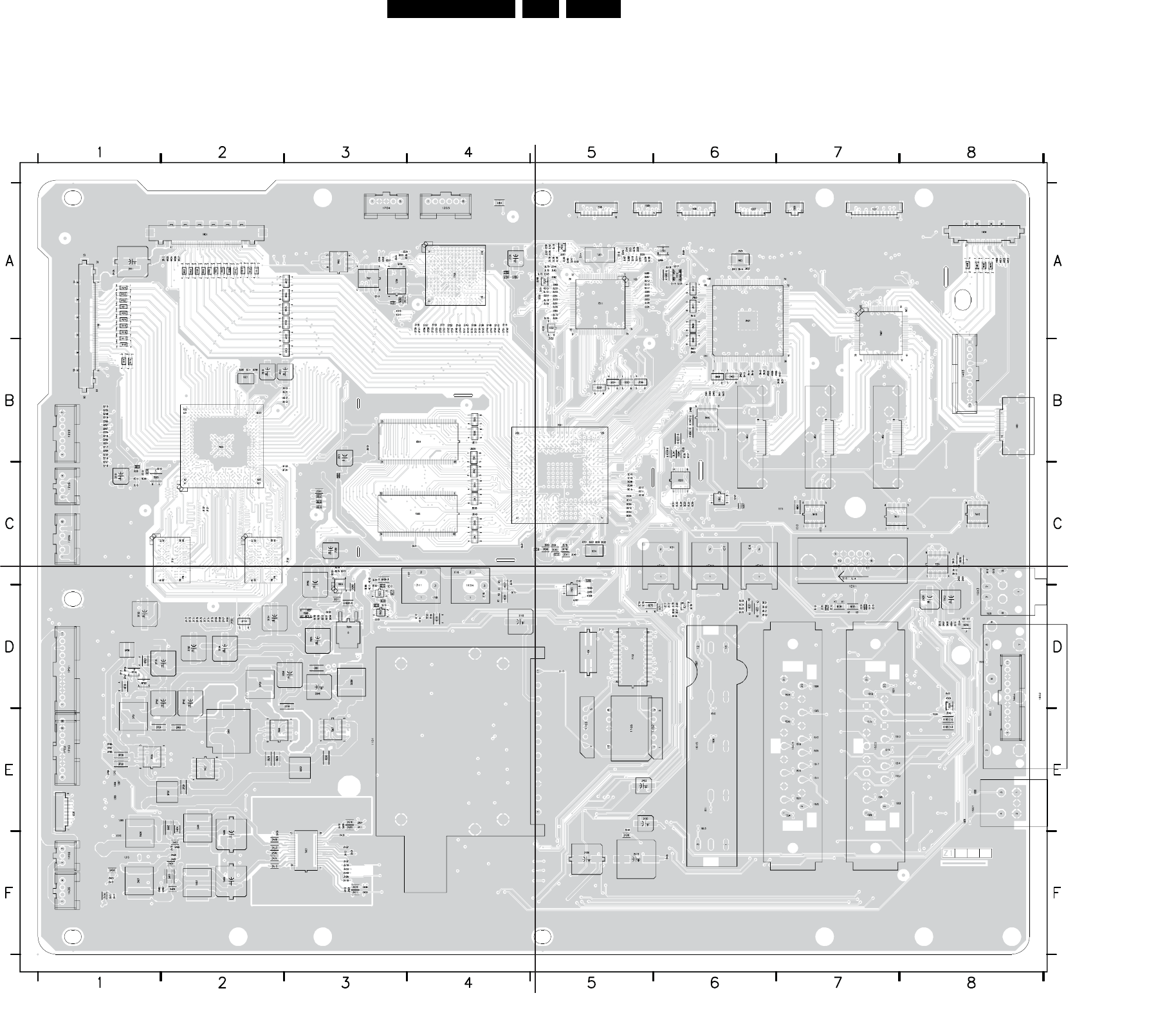
EN 76LC8.2HA LA 10.
Circuit Diagrams and PWB Layouts
2009-Apr-10
Layout Small Signal Board (Overview Top Side)
3139 123 6349.1
Part 1
I_17760_020a.eps
Part 2
I_17760_020b.eps
Part 4
I_17760_020d.eps
Part 3
I_17760_020c.eps
I_17760_020.eps
110208
1101 E3
1102 E5
1103 E5
1104 D5
1105 E5
1106 D4
1107 C4
1108 A1
1202 B1
1203 A4
1204 A3
1205 C1
1206 C1
1301 A5
1311 D4
1320 E1
1500 E7
1501 E7
1502 E7
1503 E7
1504 E7
1505 A5
1506 A6
1507 A6
1508 A5
1509 A7
1510 E7
1511 E7
1512 E7
1513 E7
1514 E7
1515 E7
1516 E7
1517 E7
1518 D7
1519 E7
1520 E7
1521 D7
1522 E7
1523 D7
1524 D7
1531 E7
1532 E7
1533 E7
1534 E7
1535 E7
1601 E8
1602 D8
1603 D8
1605 D8
1606 E6
1607 D6
1608 E8
1609 E8
1610 E6
1611 E6
1613 E6
1615 E6
1616 D8
1617 E8
1618 C8
1619 C8
1620 D8
1621 A7
1A02 F1
1A35 F1
1C24 C5
1E01 D7
1E02 C6
1E04 D4
1E06 C6
1E07 C6
1E14 C7
1E15 C7
1E16 C6
1E17 C6
1E18 C4
1E19 D4
1E21 C6
1G01 B2
1M01 B8
1M02 B7
1M03 B7
1M04 A8
1M05 B8
1M06 A8
1M07 A8
1M08 A8
1M09 A8
1N02 A6
1N03 B6
1P01 D1
1P02 E1
1P03 E1
1P04 A3
1R01 A2
1R02 A2
1R03 A2
1R04 A2
1R05 A2
1R06 A2
1R07 A2
1R08 A2
1R09 A2
1R10 A2
1R11 A2
1R12 A2
1R13 A2
1R14 B1
1R15 B1
1R16 B1
1R17 A1
1R18 A1
1R19 A1
1R20 A1
1R21 A1
1R22 A1
1R23 A1
1R24 A1
1R25 A1
2117 D5
2127 D5
2142 D4
2205 B1
2206 B1
2207 B1
2208 B1
2209 B1
2210 B1
2211 A3
2214 A3
2215 B1
2216 C1
2217 B1
2218 B1
2219 B1
2314 A5
2315 A6
2316 A5
2317 A6
2323 A5
2324 A5
2338 B6
2341 C5
2343 A5
2344 A5
2345 A5
2346 A5
2347 C6
2409 F6
2410 F5
2420 E5
2423 E5
2436 F5
2439 F5
2445 E5
2613 C8
2614 D8
2615 C8
2616 D8
2724 A4
2A01 F2
2A02 F2
2A04 F2
2A08 F2
2A09 F2
2A10 F2
2A11 F3
2A12 F3
2A14 F1
2A15 F3
2A16 E3
2A17 F1
2A18 F3
2A19 E3
2A20 E3
2A22 F3
2A23 F1
2A24 F3
2A28 F1
2A29 F2
2A30 F2
2A32 F3
2A33 F2
2A34 F2
2A40 F3
2A53 D8
2A58 D8
2A62 F1
2A63 F2
2A67 F2
2A68 F2
2A69 F2
2A70 F2
2A71 F1
2A72 F1
2B10 B2
2B19 C1
2B20 C1
2C01 C5
2C02 C5
2C03 C5
2C04 C5
2C05 C5
2C06 C5
2C08 C5
2C09 C5
2C10 C5
2C11 C5
2C12 C5
2C13 C5
2C15 C5
2C17 C5
2C18 C5
2C19 C5
2C78 C5
2C79 C5
2C80 C5
2C81 C5
2C83 C5
2C94 C5
2C95 C5
2D31 C4
2D32 C4
2D71 B3
2D72 B3
2E09 D7
2E10 D7
2E13 D3
2E14 D3
2E20 D6
2E21 D6
2E22 D6
2E23 D6
2E76 D6
2E77 D6
2E78 D5
2E79 D5
2F23 D1
2F24 D2
2F62 D2
2F64 D2
2F65 D2
2F66 D2
2F67 D2
2F68 D2
2F69 D2
2F70 D2
2F71 D2
2F72 D2
2F73 D2
2F74 D2
2F75 D2
2F76 D2
2F77 D2
2G10 C1
2G31 B2
2G44 C3
2G56 B2
2G60 B2
2G68 C3
2G69 D3
2G70 C3
2G71 D3
2N13 A6
2N14 A6
2N55 A6
2N68 B6
2N71 B6
2N72 B6
2P19 D1
2P20 D1
2P28 E1
2P29 E2
2P30 E1
2P34 E1
2P46 D2
2P59 D1
2P61 E2
2P84 E1
2P86 E1
2P87 E1
2P88 E1
2P89 C3
2Q28 E2
2Q29 E2
2Q30 E3
2Q34 D3
2Q46 D3
2Q55 D3
2Q58 D3
2Q59 D2
2Q61 D3
2Q73 D3
2R11 A1
2R12 A2
2R28 A1
3207 B1
3222 B1
3224 B1
3225 B1
3231 A3
3232 A3
3234 A3
3235 A3
3236 A3
3238 A3
3240 A3
3246 A3
3247 C1
3248 B1
3301 A5
3303 A5
3306 A5
3307 A5
3313 A5
3314 A5
3315 A5
3316 A5
3317 A5
3318 A5
3319 A6
3320 A5
3321 A5
3322 A5
3324 A5
3325 A6
3329 A5
3332 A5
3346 A5
3347 A5
3351 A5
3352 A5
3354 A5
3356 A5
3357 A5
3358 A5
3359 D5
3360 D5
3380 A5
3382 A5
3386 A5
3387 A5
3388 A5
3395 B6
3396 A6
3398 A5
3399 A5
3537 D8
3540 E8
3554 E8
3559 A6
3613 C8
3614 D8
3713 A4
3714 A4
3720 A4
3721 A4
3722 A4
3723 A4
3724 A4
3725 A4
3726 A4
3727 A4
3728 A4
3729 A4
3730 A4
3731 A4
3732 A4
3733 A4
3734 A4
3735 A4
3736 A4
3737 A4
3738 A4
3739 A4
3740 A4
3741 A4
3742 A4
3743 A4
3744 A4
3745 A4
3746 A4
3747 A4
3748 A4
3749 A4
3750 A4
3751 A4
3752 A4
3753 A4
3A01 F2
3A02 E2
3A03 F3
3A04 F3
3A06 F3
3A07 E3
3A08 E3
3A11 E3
3A13 F3
3A19 F3
3A26 F3
3A32 F3
3A33 F3
3A52 C8
3A54 C8
3A57 D8
3A59 D8
3C01 C5
3C02 C5
3C03 B5
3C04 B5
3C05 B5
3C06 B5
3C29 C6
3C30 C6
3C31 C6
3C32 C6
3C33 C6
3C34 C6
3C36 B6
3C37 B6
3C46 C5
3D01 B4
3D02 C4
3D05 B4
3D06 B4
3D09 B4
3D11 B4
3D38 C4
3D40 C4
3D43 C4
3D44 C4
3D47 C4
3D48 C4
3E14 D7
3E15 D7
3E18 D7
3E20 D7
3E21 D6
3E22 D6
3E23 D6
3E24 D6
3E67 D6
3E68 D6
3E69 D6
3E70 C4
3E71 D4
3E77 D6
3E78 D6
3E79 D6
3E82 D3
3E83 D4
3E84 C3
3E85 D4
3E86 D3
3E87 D3
3F14 D2
3F31 C2
3F32 C2
3F33 C3
3F34 C3
3G10 C1
3G11 B2
3G12 B3
3G13 B
3
3G14 C1
3G15 C1
3G23 B3
3G24 B3
3G34 C3
3G35 C3
3G36 C3
3G38 C1
3L01 A5
3L02 A5
3L04 B6
3L05 A5
3L12 A5
3L13 A5
3L15 A5
3L16 A5
3L53 A5
3L55 A5
3L56 A5
3L58 A5
3L59 A5
3L61 A5
3L62 A5
3L63 A5
3L64 A5
3L67 A5
3L72 A5
3L73 A5
3L75 A5
3L76 A5
3L79 A5
3L93 A5
3L94 A5
3L95 A5
3N02 B6
3N03 B6
3N04 B6
3N05 B6
3N06 A6
3N07 B6
3N08 B6
3N10 A6
3N11 A6
3N12 A6
3N13 B6
3N14 B6
3N15 B6
3N22 A6
3N24 A6
3N37 B7
3N38 B7
3N39 B6
3N40 B6
3N41 B6
3N42 B6
3N43 B6
3P15 D1
3P67 D1
3Q59 D3
3Q77 D3
3Q78 D3
3Q79 D3
4301 A4
4306 D5
4307 D5
4313 A5
4317 A3
4318 A3
4323 A5
4504 D8
4603 C8
4604 D8
4E11 D3
4E12 C3
4E13 D4
4E14 D4
4M50 A8
4M51 A8
4M52 A8
4M53 A8
4M54 C7
4N05 B6
4N06 B6
4N07 B7
4N08 B6
4R22 A2
4R24 A2
4R26 A2
4R27 A2
4R31 B3
4R32 A3
4R33 A3
4R34 A3
4R35 A3
4R36 A3
5201 A3
5202 A3
5306 C5
5307 C6
5703 A4
5704 A4
5705 A4
5A03 F2
5A04 E2
5A05 F2
5A06 E2
5A07 F1
5A08 F1
5B12 C1
5C15 C5
5C16 C5
5D03 C3
5E13 D7
5E14 D7
5E15 D3
5E16 D3
5E17 D3
5E18 D3
5E71 D6
5G10 C1
5G17 C3
5G18 C3
5G19 C3
5P01 E1
5P02 E2
5P06 D1
5P09 D2
5Q01 E2
5Q02 E3
5Q09 D3
6301 A6
6317 B6
6318 B6
6512 E8
6513 E8
6615 C8
6616 D8
6E05 D7
6E06 D7
6E07 C4
6E08 D4
6E09 C3
6E10 D4
6E21 D6
6E22 D6
6E72 D5
6N41 B6
6N42 B6
6P02 D1
6P03 D1
6P16 D1
6Q05 D3
7113 D5
7201 A3
7302 D5
7303 C6
7311 A5
7312 A6
7314 A5
7322 A6
7323 A5
7504 D8
7700 A4
7A01 F3
7C01 B5
7C03 C6
7D01 B4
7D02 C4
7E01 C8
7E02 D3
7E03 D3
7E71 D6
7F01 C2
7F02 C3
7G01 B2
7G03 C1
7G04 C3
7L10 A5
7M07 A7
7M16 C8
7M17 C7
7M18 C7
7N01 A6
7N40 B6
7P06 E1
7P07 E2
7P14 D1
7Q06 E2
7Q07 E3
7Q08 D3
7Q09 D3
7R05 A3
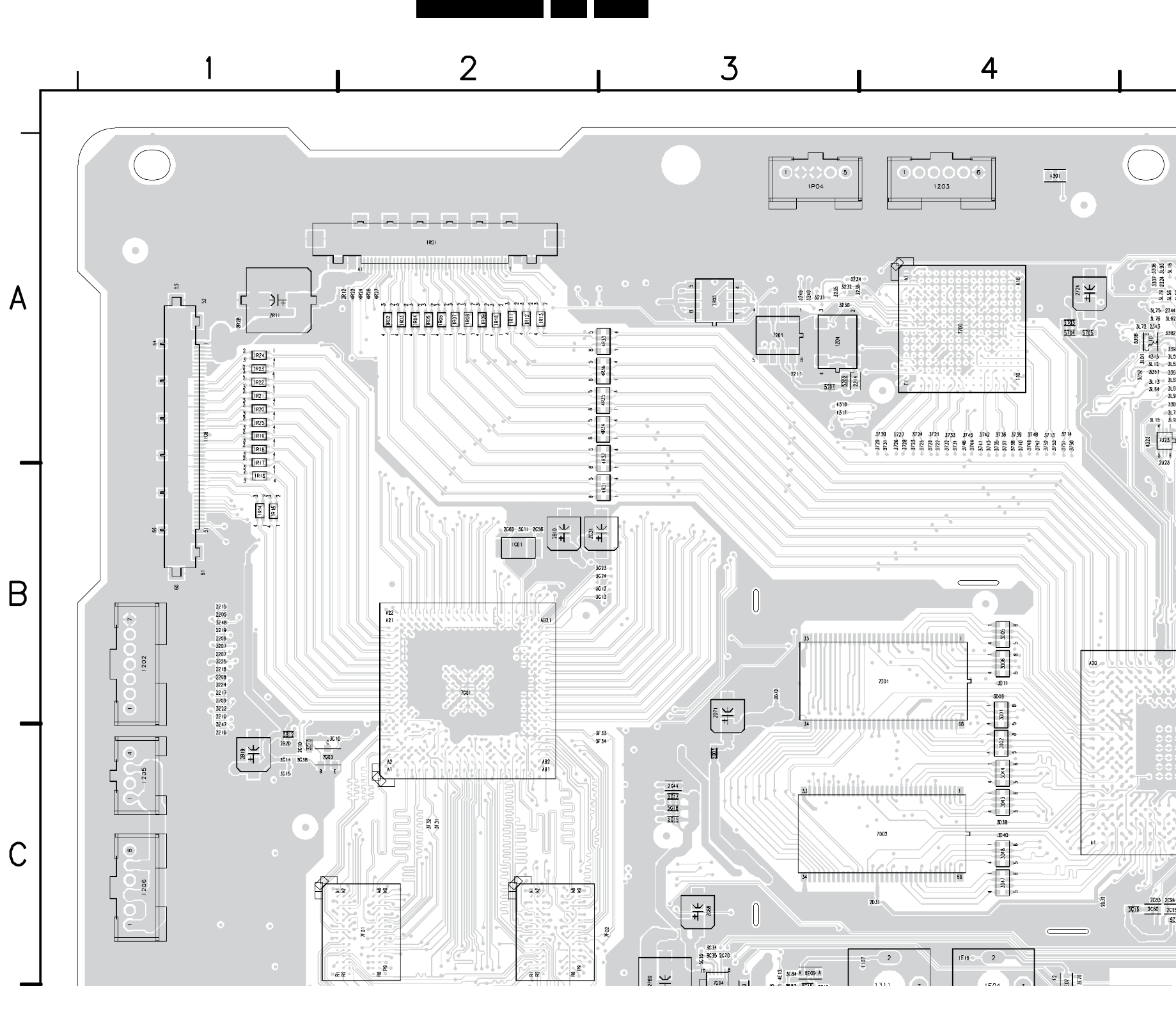
Circuit Diagrams and PWB Layouts EN 77LC8.2HA LA 10.
2009-Apr-10
Layout Small Signal Board (Part 1 Top Side)
Part 1
I_17760_020a.eps
110208
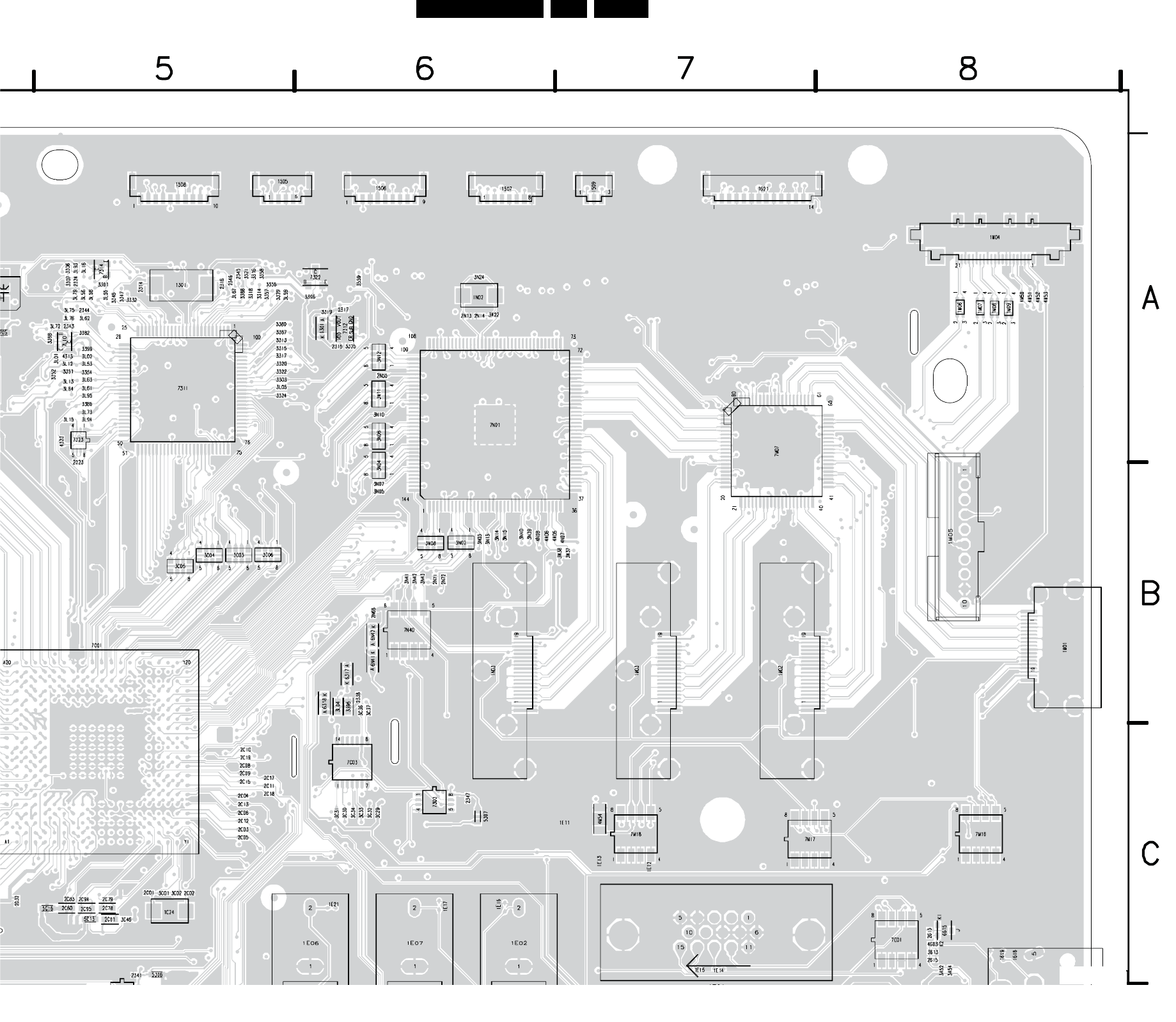
EN 78LC8.2HA LA 10.
Circuit Diagrams and PWB Layouts
2009-Apr-10
Layout Small Signal Board (Part 2 Top Side)
Part 2
I_17760_020b.eps
110208
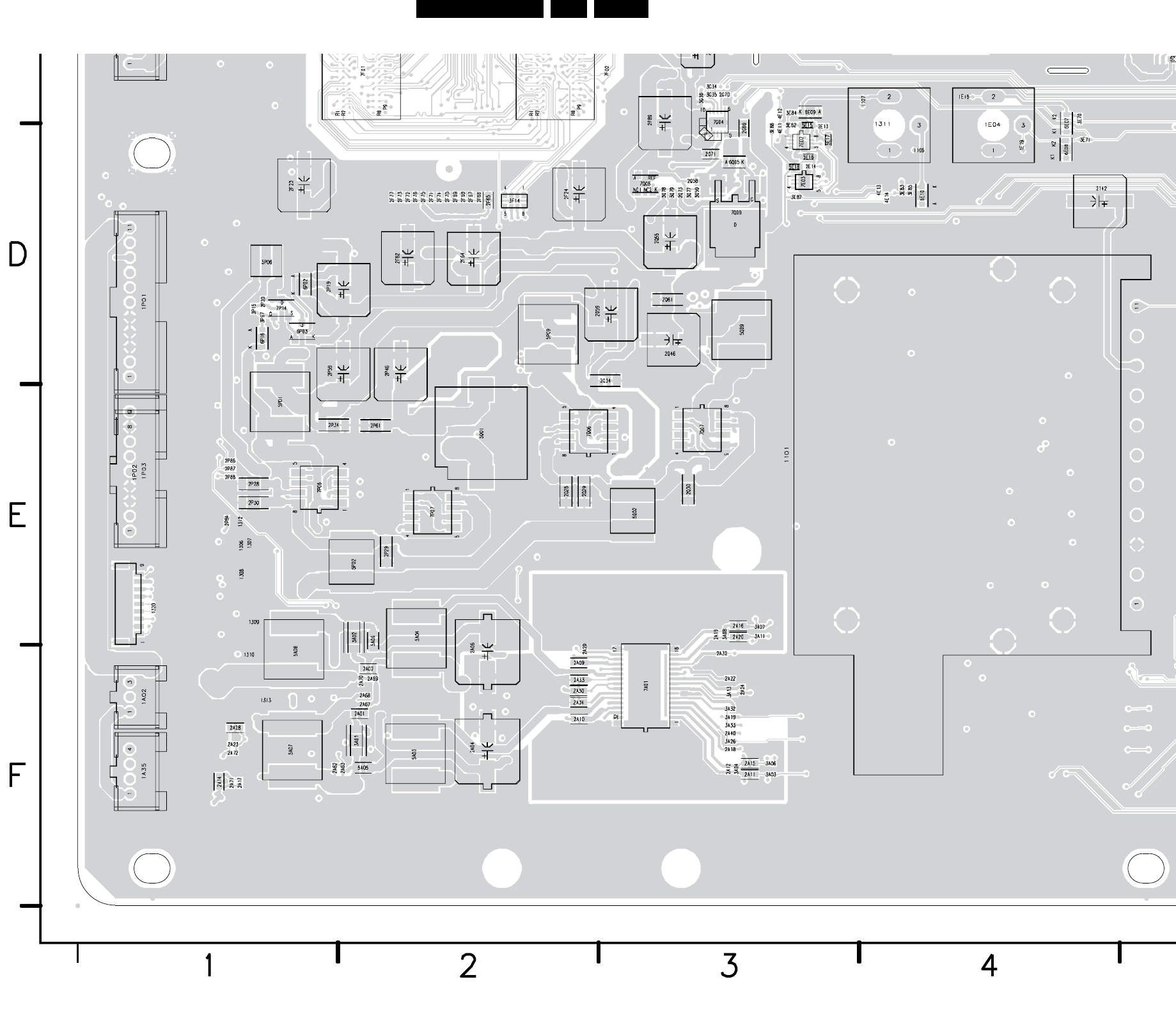
Circuit Diagrams and PWB Layouts EN 79LC8.2HA LA 10.
2009-Apr-10
Layout Small Signal Board (Part 3 Top Side)
Part 3
I_17760_020c.eps
110208
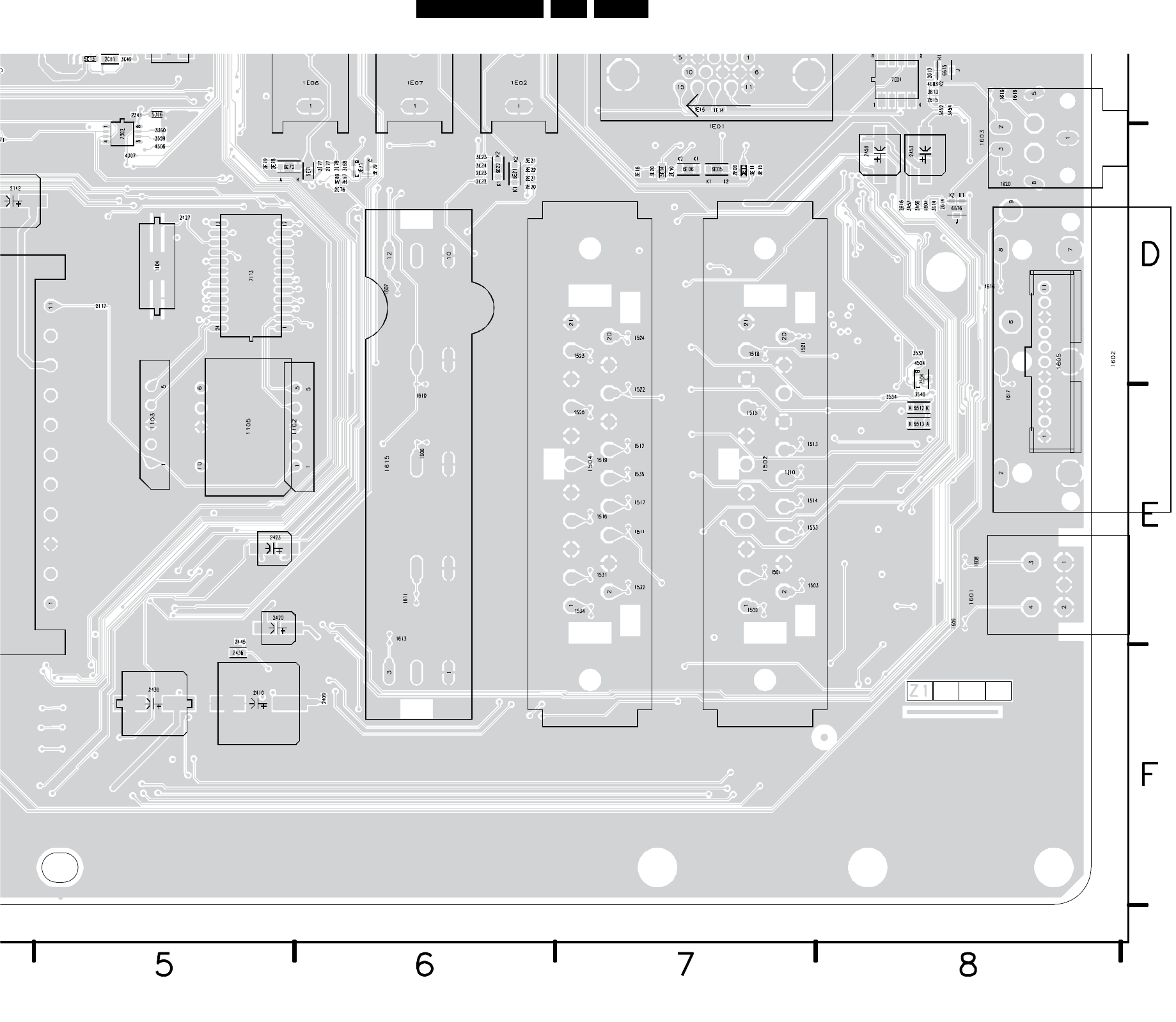
EN 80LC8.2HA LA 10.
Circuit Diagrams and PWB Layouts
2009-Apr-10
Layout Small Signal Board (Part 4 Top Side)
Part 4
I_17760_020d.eps
110208
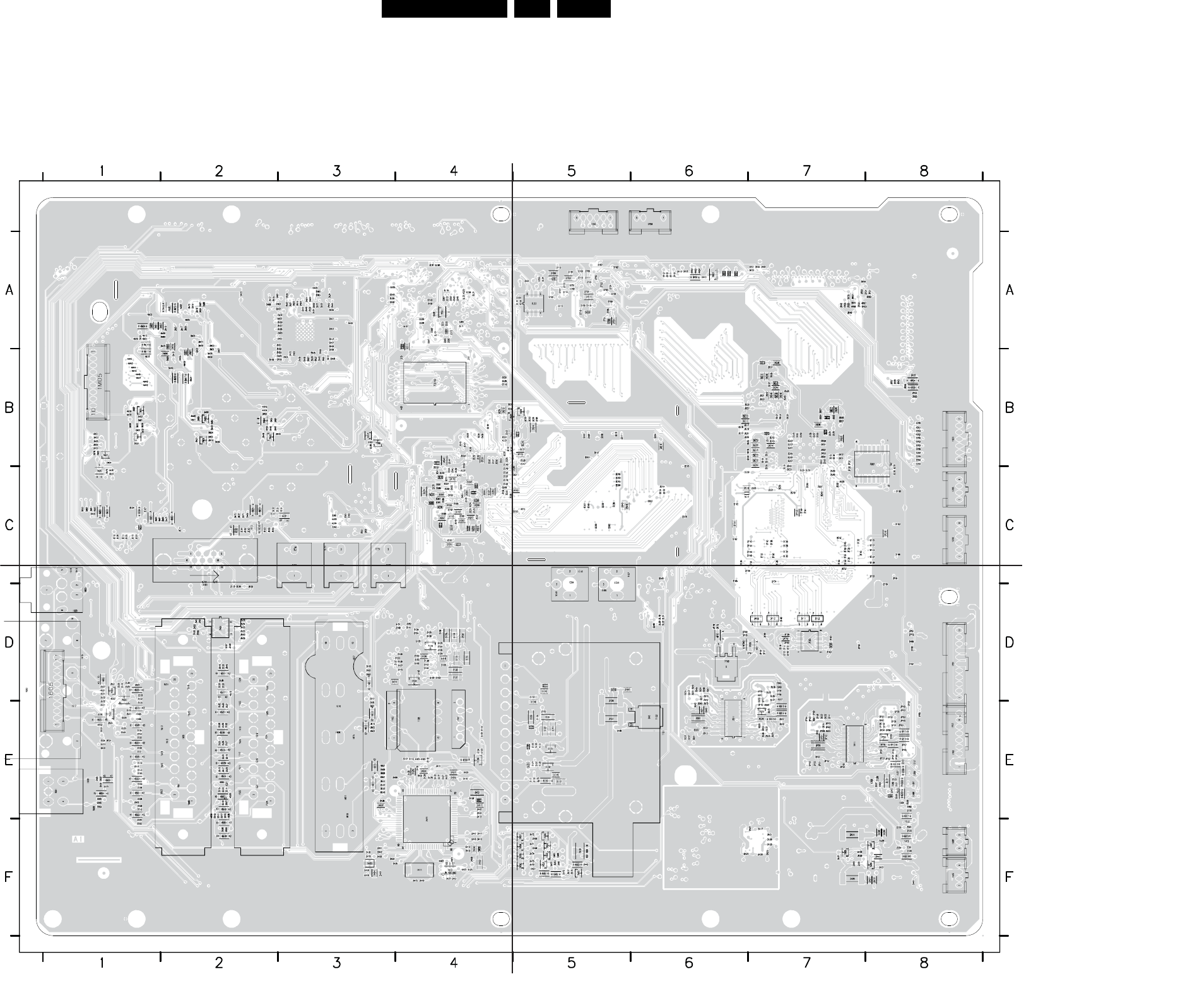
Circuit Diagrams and PWB Layouts EN 81LC8.2HA LA 10.
2009-Apr-10
Layout Small Signal Board (Overview Bottom Side)
3139 123 6349.1
Part 1
I_17760_021a.eps
Part 2
I_17760_021b.eps
Part 4
I_17760_021d.eps
Part 3
I_17760_021c.eps
I_17760_021.eps
110208
1306 E8
1307 E8
1308 E8
1309 E8
1310 F8
1312 E8
1313 F8
1411 F4
1E11 C2
1E12 C2
1E13 C2
2112 E5
2118 E5
2119 E5
2120 E5
2121 E5
2122 E5
2123 D4
2124 D4
2125 D4
2126 D4
2128 D4
2129 D4
2130 D4
2131 D4
2132 D4
2133 D4
2134 D4
2135 D4
2136 D4
2137 D4
2138 D4
2139 D4
2140 D4
2141 D4
2143 D4
2144 D4
2145 D4
2147 D5
2148 E5
2149 E5
2151 E5
2152 E5
2201 C3
2202 C3
2203 B8
2204 B8
2310 A4
2311 A4
2312 A4
2313 A4
2318 A4
2319 B4
2320 A5
2327 E8
2328 F8
2329 F8
2330 E8
2331 E8
2332 E8
2333 E8
2334 F8
2335 F8
2336 E8
2337 E8
2339 E8
2340 E8
2342 E8
2348 D6
2349 C6
2408 E3
2411 E4
2412 F4
2413 E4
2414 F4
2415 F4
2416 F4
2417 E4
2418 E4
2419 F4
2421 E4
2422 E4
2424 E4
2425 E4
2426 E4
2427 E4
2428 E4
2429 E4
2430 E4
2431 E4
2432 F3
2433 F3
2434 F3
2435 F3
2437 E3
2438 E3
2440 F5
2441 F3
2442 F3
2443 E4
2444 E4
2446 F4
2447 F4
2448 F3
2449 F3
2450 F4
2451 F4
2502 F1
2506 E1
2508 F2
2509 E1
2512 E1
2514 E2
2515 E2
2517 E2
2518 E1
2520 E1
2521 E2
2523 E2
2524 E1
2525 D1
2526 D1
2527 E2
2528 E2
2529 E2
2530 E1
2531 E2
2533 E1
2534 E1
2535 D2
2536 D1
2538 D2
2600 E1
2602 E3
2603 D3
2606 E3
2607 E3
2608 E3
2609 E1
2610 E3
2612 E3
2621 E1
2622 D1
2623 E1
2624 E1
2625 E1
2626 E1
2627 D1
2628 E1
2700 A5
2701 A5
2702 A5
2703 A5
2704 A5
2705 A5
2706 A5
2707 A5
2708 A5
2709 A5
2710 A5
2711 A5
2712 A5
2713 A5
2714 A5
2715 A5
2717 A5
2718 A5
2719 A5
2720 A5
2721 A5
2725 A5
2726 A5
2729 A5
2730 A5
2734 A5
2A13 F8
2A21 F7
2A25 F6
2A26 F8
2A27 F7
2A31 F7
2A35 F7
2A36 F7
2A37 F8
2A38 F8
2A41 F8
2A45 F8
2A51 D2
2A52 D2
2A54 D2
2A55 D2
2A56 D2
2A57 D2
2A59 D2
2A60 F5
2A61 F5
2A64 F7
2A65 F7
2A66 D8
2B11 B7
2B12 B7
2B13 B7
2B14 B7
2B15 B7
2B16 B7
2B17 B7
2B18 B7
2B21 B7
2B22 B7
2B23 B7
2B24 B7
2B25 B7
2B26 B7
2B27 B7
2B28 B7
2B29 C7
2B30 B7
2B31 B7
2B32 B7
2B33 B7
2B34 B7
2B35 B7
2B36 B7
2B37 B7
2B38 B7
2C07 C4
2C16 C4
2C20 B4
2C21 B4
2C22 C4
2C23 C4
2C24 C4
2C25 C4
2C26 C4
2C27 C4
2C28 C4
2C29 C4
2C30 B5
2C31 C5
2C32 C4
2C33 C4
2C34 C4
2C35 C4
2C36 B4
2C37 C4
2C38 B4
2C39 B4
2C40 B4
2C41 B4
2C42 B4
2C43 B4
2C44 B4
2C45 C4
2C46 C4
2C47 B5
2C48 B4
2C49 C4
2C50 B4
2C51 B4
2C52 B4
2C53 C4
2C54 B4
2C55 B4
2C56 C5
2C57 C4
2C58 C4
2C59 C4
2C60 C4
2C61 C5
2C62 C4
2C63 C5
2C64 C4
2C65 C4
2C66 C4
2C67 C4
2C68 C4
2C69 C5
2C70 C4
2C71 C4
2C72 B5
2C73 B4
2C74 B5
2C75 B4
2C76 B4
2C77 B5
2C82 C4
2C84 C4
2C85 C4
2C86 C4
2C87 C4
2C88 C4
2C89 C4
2C90 C4
2C91 C4
2C92 C4
2C93 C4
2C96 C4
2C97 C4
2C98 C4
2C99 C4
2D02 B5
2D03 B5
2D04 B6
2D08 B5
2D09 B5
2D10 B5
2D11 B5
2D12 B5
2D14 C6
2D18 B6
2D33 C5
2D34 C5
2D37 C5
2D38 C5
2D39 C5
2D43 C5
2D46 C5
2D57 C6
2D58 C5
2D59 C5
2D60 C5
2D73 C6
2D78 C6
2E01 C2
2E02 C2
2E03 C2
2E04 C1
2E05 C1
2E06 C1
2E07 C1
2E11 C2
2E12 D2
2F25 C8
2F26 C7
2F27 C8
2F28 C7
2F29 C8
2F30 C7
2F31 C6
2F32 C7
2F33 C7
2F34 C7
2F35 C7
2F36 C7
2F37 C8
2F38 C7
2F39 C8
2F40 C7
2F41 C8
2F42 C7
2F43 C7
2F44 C7
2F45 C7
2F46 C7
2F47 C7
2F48 C7
2F49 C7
2F50 C7
2F51 C7
2F52 C7
2F53 C7
2F54 C7
2F55 C8
2F56 C7
2F57 C7
2F58 C6
2F59 C7
2F60 C7
2F61 C7
2F63 D7
2F79 D7
2F80 D7
2F81 D7
2F82 D7
2F83 D7
2F84 D8
2F85 C6
2F86 C8
2F87 C6
2F88 C8
2F89 D7
2F90 D7
2F91 C8
2F92 C6
2F93 C8
2G11 B6
2G12 B7
2G13 B7
2G14 C7
2G15 B7
2G16 B7
2G17 B6
2G18 C6
2G19 C7
2G20 C7
2G21 C7
2G22 C7
2G23 C7
2G24 C7
2G25 C7
2G26 C7
2G27 C7
2G28 C7
2G29 C7
2G30 C7
2G32 B7
2G33 B7
2G34 B7
2G35 B7
2G36 B7
2G37 B7
2G38 B7
2G39 C7
2G40 B7
2G41 B7
2G42 C7
2G43 B7
2G45 B7
2G46 B7
2G47 B7
2G48 B7
2G49 B7
2G50 B7
2G51 B7
2G52 B7
2G53 B7
2G54 B7
2G55 B7
2G57 B7
2G58 B7
2G59 B7
2G61 B7
2G62 B7
2G63 B7
2G64 B7
2G65 B7
2G66 B7
2G67 B7
2M01 A1
2M02 A2
2M03 A2
2M04 B2
2M05 B2
2M06 B2
2M07 B2
2M08 B2
2M09 A2
2M10 A2
2M15 A2
2M16 B2
2M17 A2
2M19 A2
2M20 A2
2M21 A2
2M46 C1
2M47 C2
2M48 C2
2M50 B1
2M51 B1
2M52 B1
2M53 B1
2M54 B2
2M55 B2
2M56 B2
2M57 B2
2N15 A2
2N16 B2
2N17 A2
2N18 B
3
2N20 A3
2N25 B3
2N26 A3
2N27 A3
2N28 B3
2N29 A3
2N30 B3
2N31 A3
2N32 A3
2N33 A3
2N34 A3
2N35 B3
2N36 A3
2N37 B3
2N38 B3
2N39 B3
2N40 B3
2N41 A3
2N42 A3
2N43 A3
2N44 A3
2N45 A3
2N46 B3
2N47 A3
2N48 A3
2N49 A3
2N50 B3
2N51 B3
2N52 A3
2N53 A3
2N54 B3
2N56 A3
2N58 B3
2N59 A3
2N60 A3
2N61 A3
2N62 A3
2N63 A3
2N64 A3
2N65 B3
2N66 A3
2N69 B3
2N70 B3
2P07 E8
2P31 E7
2P32 E8
2P33 E8
2P35 E8
2P36 E8
2P37 E7
2P38 E8
2P39 E8
2P40 E8
2P41 E7
2P42 E7
2P43 E7
2P48 E7
2P49 E8
2P52 E7
2P53 E7
2P54 E7
2P78 E8
2P79 D8
2P80 D8
2P81 D8
2P82 D8
2P83 E8
2P85 E8
2P90 D6
2P91 D7
2Q07 D7
2Q31 E6
2Q32 E7
2Q33 D7
2Q35 E7
2Q36 D7
2Q37 E6
2Q38 E7
2Q39 D7
2Q40 D7
2Q41 D6
2Q42 D6
2Q43 D6
2Q48 D6
2Q49 D7
2Q52 E6
2Q53 E6
2Q54 D6
2Q78 E7
2R01 A7
2R02 A7
2R10 A6
2R20 A7
2R21 A7
2R23 A7
2R24 A8
2R25 B8
2R26 B8
2R29 B8
2V01 C4
2V02 C4
2V03 C4
2V04 B4
2V05 B4
2V06 C4
3110 E5
3111 E5
3113 E4
3115 E5
3117 E4
3118 E4
3119 E4
3123 D4
3124 D4
3125 D4
3126 D4
3127 D4
3133 D4
3134 D4
3135 D4
3136 D5
3137 E5
3140 D4
3141 E5
3151 D4
3152 D4
3188 E4
3190 E5
3191 E5
3192 D5
3193 D4
3194 D4
3195 D4
3201 C3
3202 C3
3203 B8
3204 B8
3205 B8
3206 B8
3300 A4
3302 A4
3305 A4
3308 A4
3310 A3
3326 B4
3330 A3
3331 A4
3333 A3
3336 B4
3338 A4
3339 A4
3340 A4
3341 A4
3348 A4
3349 A4
3350 A4
3353 A5
3355 A5
3361 C3
3362 C3
3384 A4
3389 E8
3390 E8
3391 F8
3393 B3
3394 F8
3397 A4
3402 E4
3403 F4
3410 F4
3411 F4
3416 F3
3417 E4
3418 E4
3419 E4
3420 E4
3423 F4
3427 F4
3428 E4
3500 F1
3502 E1
3503 F2
3506 E1
3507 E2
3508 E1
3510 E2
3511 E2
3512 E1
3513 E1
3514 E2
3515 E2
3516 E2
3517 E2
3518 E2
3519 D1
3520 E2
3521 D1
3522 D1
3523 E2
3524 E1
3525 E1
3526 E2
3528 E2
3529 E1
3530 E2
3531 E1
3532 E2
3533 E2
3535 D2
3536 D2
3538 D1
3545 D2
3546 D2
3550 E1
3551 E1
3552 E1
3553 E1
3555 D1
3600 E1
3601 E3
3602 E1
3603 D3
3604 E1
3605 E3
3607 E3
3608 E3
3609 E1
3611 E3
3612 E3
3617 D3
3618 D3
3619 E3
3621 D1
3622 E1
3623 E1
3624 E1
3700 A5
3701 A5
3702 A5
3703 A5
3A05 F7
3A09 F7
3A14 F7
3A17 F7
3A27 F8
3A28 F8
3A29 F7
3A30 F7
3A31 F7
3A51 D2
3A53 D2
3A55 D2
3A56 D2
3A58 D2
3A60 D2
3A61 F5
3A62 F5
3A63 F5
3A68 F5
3A69 F5
3A70 F5
3A71 F5
3A72 F5
3A73 F5
3A74 F5
3A75 F5
3A76 F5
3A77 F5
3B19 D7
3C07 B4
3C08 B4
3C09 B4
3C10 B4
3C19 B4
3C20 B4
3C22 B5
3C23 B5
3C24 B5
3C25 B4
3C39 C4
3C40 C4
3C41 C4
3C42 C4
3C43 C4
3C44 C4
3C45 B4
3C47 B4
3C48 C4
3C49 C4
3D10 C6
3D14 C6
3D15 C5
3D16 C5
3E01 C3
3E02 C2
3E03 C2
3E04 C2
3E05 C2
3E06 C2
3E07 C1
3E08 D2
3E09 D2
3E10 C1
3E11 C1
3E12 C1
3F09 D7
3F11 D7
3F12 D7
3F13 D7
3F35 C7
3F36 C6
3F37 B7
3F38 C7
3F39 D7
3F40 D7
3F41 D7
3G16 B6
3G17 B6
3G18 C8
3G19 B6
3G20 C8
3G21 B7
3G22 B7
3G27 B6
3G29 B6
3G30 C6
3G31 B6
3G32 B6
3G33 B7
3L10 E8
3L14 A5
3L17 A4
3L18 A4
3L19 D6
3L20 D6
3L21 D6
3L22 D6
3L23 A4
3L24 A4
3L54 A5
3L57 A4
3L71 A4
3L86 B3
3L96 A3
3L97 A4
3L98 A4
3M03 B1
3M04 B1
3M07 B1
3M08 B1
3M09 A2
3M10 A2
3M11 A2
3M13 B2
3M14 A2
3M15 A2
3M18 A2
3M19 B2
3M20 B2
3M21 B2
3M31 B2
3M32 A1
3M33 A2
3M34 A2
3M35 B1
3M36 B1
3M37 B1
3M38 B1
3M39 B2
3M40 B2
3M61 C1
3M62 C1
3M63 C1
3M66 C2
3M67 C1
3M68 C1
3M71 C2
3M72 C2
3M73 C2
3M78 B1
3M79 C1
3M80 B1
3M81 B1
3M82 B1
3M83 B1
3M84 B2
3M85 B2
3M86 B2
3M87 A2
3M88 A2
3N01 B2
3N09 A3
3N16 B3
3N19 A3
3N20 A3
3N21 A3
3N33 A3
3N34 A3
3N46 B2
3N47 B2
3N48 B3
3N49 B2
3N50 B2
3N51 B2
3N52 B2
3P13 E7
3P20 E7
3P23 E8
3P25 E8
3P26 E8
3P32 E7
3P34 E8
3P37 E8
3P38 E8
3P40 E7
3P41 E8
3P45 E7
3P47 E8
3P48 E8
3P49 E8
3P50 E7
3P51 E8
3P52 E8
3P53 E8
3P54 D7
3P56 D7
3P61 E7
3P64 D7
3P68 E8
3P69 E7
3P70 E7
3P71 D7
3P72 E7
3P74 E8
3P75 D6
3P76 D6
3P77 D7
3P78 D7
3P79 D6
3Q13 E6
3Q20 E6
3Q23 E7
3Q25 E7
3Q26 E7
3Q32 E6
3Q34 E7
3Q37 D7
3Q38 D7
3Q40 E6
3Q41 D7
3Q45 E6
3Q47 E7
3Q48 E7
3Q49 E7
3Q50 D6
3Q51 E7
3Q52 E7
3Q53 E7
3Q54 D6
3Q56 D6
3Q61 E6
3Q64 D6
3Q68 E7
3Q69 E6
3Q70 E6
3Q71 D6
3Q72 D6
3Q74 E7
3R10 A6
3R12 A6
3R13 A6
3R25 A7
3R26 A7
3R35 A7
3R48 A7
3R49 A7
3R50 A8
3R51 A8
3R52 A7
3R53 A7
3R54 A7
3R55 B8
3R56 B8
3R57 B8
3V04 B5
4101 E4
4102 E4
4103 E4
4104 E4
4121 E5
4122 E5
4124 D4
4201 B8
4202 B8
4203 B8
4204 B8
4205 B8
4206 B8
4303 E8
4304 C3
4305 C3
4309 E8
4310 E8
4316 A5
4325 A4
4326 A4
4401 F4
4402 F4
4403 F4
4448 F3
4502 D1
4505 E1
4506 E1
4508 E2
4509 E2
4510 D2
4601 D1
4602 E1
4605 E2
4606 E2
4700 A5
4701 A5
4A51 F5
4C07 B4
4C08 B4
4F01 D7
4M01 A1
4M02 A1
4M05 A2
4M06 A2
4M10 B2
4M12 A1
4M20 A1
4M29 B1
4M30 A2
4M31 B2
4M32 C1
4M36 C1
4M37 C1
4M38 B1
4M39 B1
4M40 B2
4M41 B2
4M42 B1
4M43 B1
4M44 B1
4M45 B1
4M46 B1
4M47 B1
4M48 B1
4M49 B1
4N14 B2
4N15 B2
4R02 A6
4R03 A6
4R04 A6
4R05 A7
4R06 A7
4R07 A7
4R08 A7
4R10 A6
4R11 A6
4R12 A6
4R43 B8
5111 D5
5112 E5
5114 D4
5115 D4
5116 D4
5117 D3
5118 D5
5119 D5
5120 E5
5121 E5
5122 E5
5301 A4
5302 A4
5304 E8
5401 E4
5402 F4
5403 F3
5404 F3
5700 A5
5701 A5
5702 A5
5B10 B7
5B11 B7
5B13 B7
5B14 B7
5B15 B7
5B16 B7
5B17 B7
5C06 C4
5C07 C4
5C08 C4
5C09 C4
5C10 B5
5C11 B4
5C12 C4
5C13 C4
5C14 B5
5C17 C4
5C18 C4
5C19 C4
5C20 C4
5C21 C4
5C22 C4
5E01 C1
5F01 D7
5G11 B6
5G12 B7
5G13 C6
5G14 B7
5G15 B7
5G16 B7
5M01 B2
5M02 A1
5M03 A2
5N01 A2
5N02 A3
5N03 A3
5N04 A3
5N05 A2
5N06 A3
5N07 B3
5N08 A2
5N09 A3
5R01 A6
5R02 A6
5R03 A6
6103 E4
6110 E5
6308 E8
6309 E8
6310 E8
6311 E8
6312 F8
6313 E8
6319 F8
6402 F5
6501 E1
6504 F2
6505 E1
6507 E2
6509 E1
6510 E1
6511 D2
6514 E2
6515 E2
6516 E2
6517 D2
6518 F2
6519 E2
6520 E2
6521 E2
6522 E1
6523 E1
6524 E1
6525 D1
6604 E1
6606 E1
6610 E3
6611 D3
6612 E3
6613 E3
6614 E3
6621 D1
6622 E1
6A51 F5
6A52 F5
6E01 C3
6E02 C2
6E03 C2
6E04 C1
6M08 A1
6M13 B1
6M14 A2
6M15 A2
6M16 B2
6M17 B2
6M18 A1
6M19 C1
6M20 C1
6M21 C1
6M22 C2
6M23 C2
6M24 C2
6P13 E8
6P14 E8
6P15 E8
6P17 D6
6Q13 E7
6Q14 E7
6Q15 E7
6R02 A6
6R04 B8
6R05 B8
7109 E4
7114 D4
7131 E5
7132 E5
7133 E6
7134 D4
7301 A4
7308 B3
7310 B4
7317 B3
7410 F5
7411 F4
7412 F4
7500 D1
7502 D1
7503 E1
7A05 F7
7A06 F8
7A07 F8
7A51 D2
7A52 F5
7A53 F5
7A54 F5
7A55 F5
7A56 F5
7A57 F5
7A58 F5
7A59 F5
7A60 F5
7C02 B4
7C04 B5
7F03 D7
7G02 B8
7L23 A5
7M02 B1
7M04 B1
7M09 B2
7M20 C1
7M21 B1
7M22 B2
7N43 B2
7N44 B2
7P05 E8
7P08 D6
7P09 D7
7P11 E7
7Q05 E7
7Q11 E6
7R07 A6
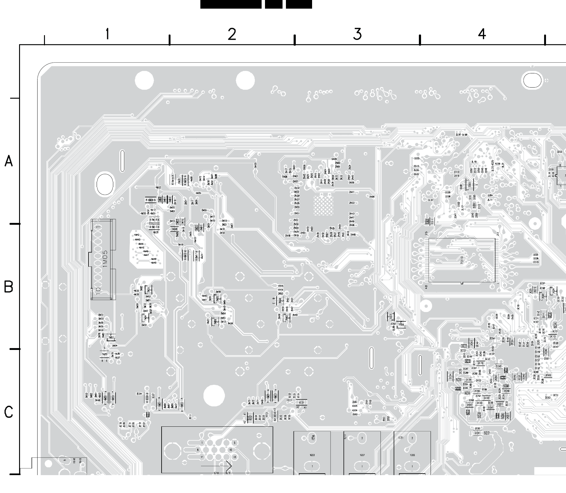
EN 82LC8.2HA LA 10.
Circuit Diagrams and PWB Layouts
2009-Apr-10
Layout Small Signal Board (Part 1 Bottom Side)
Part 1
I_17760_021a.eps
120208
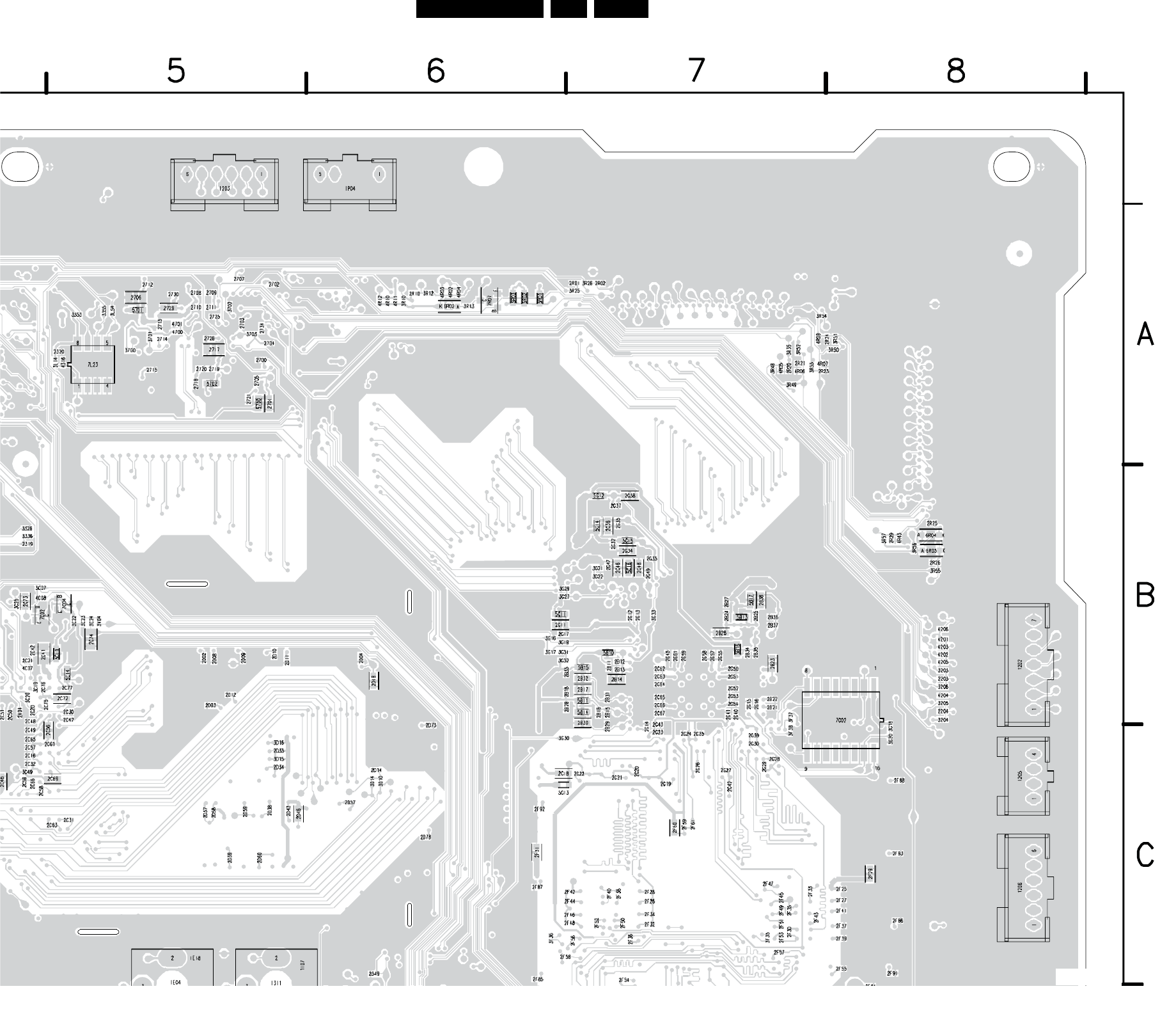
Circuit Diagrams and PWB Layouts EN 83LC8.2HA LA 10.
2009-Apr-10
Layout Small Signal Board (Part 2 Bottom Side)
Part 2
I_17760_021b.eps
120208
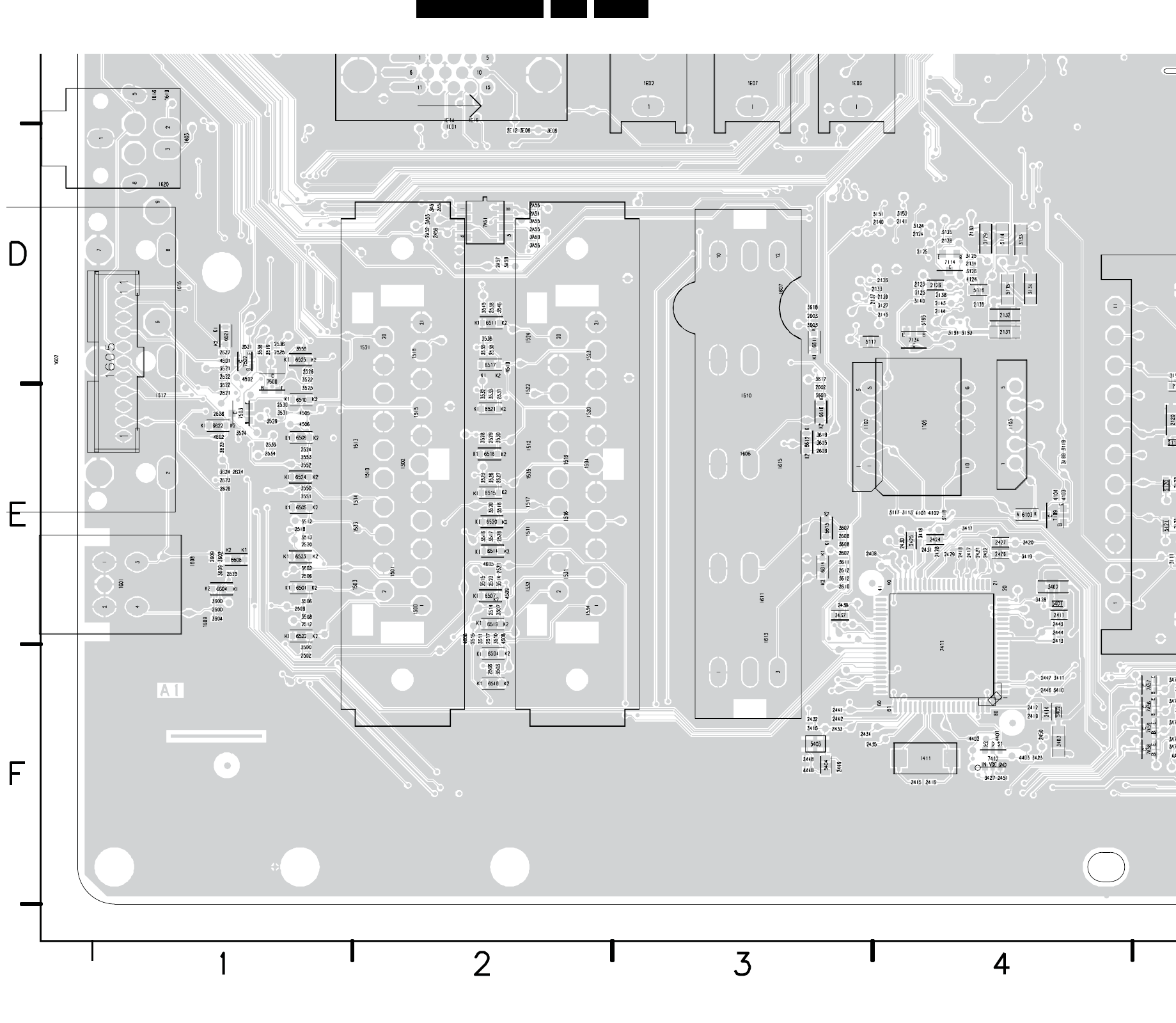
EN 84LC8.2HA LA 10.
Circuit Diagrams and PWB Layouts
2009-Apr-10
Layout Small Signal Board (Part 3 Bottom Side)
Part 3
I_17760_021c.eps
120208
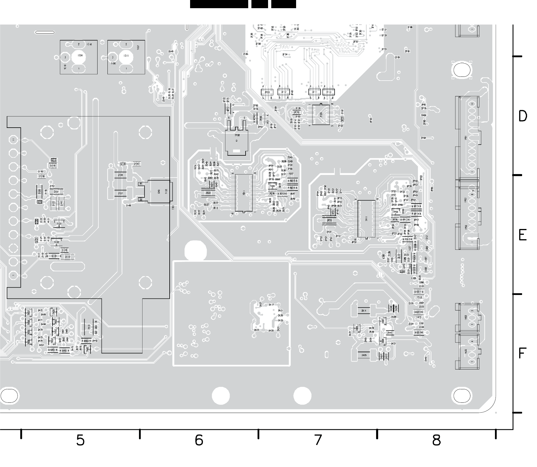
Circuit Diagrams and PWB Layouts EN 85LC8.2HA LA 10.
2009-Apr-10
Layout Small Signal Board (Part 4 Bottom Side)
Part 4
I_17760_021d.eps
120208
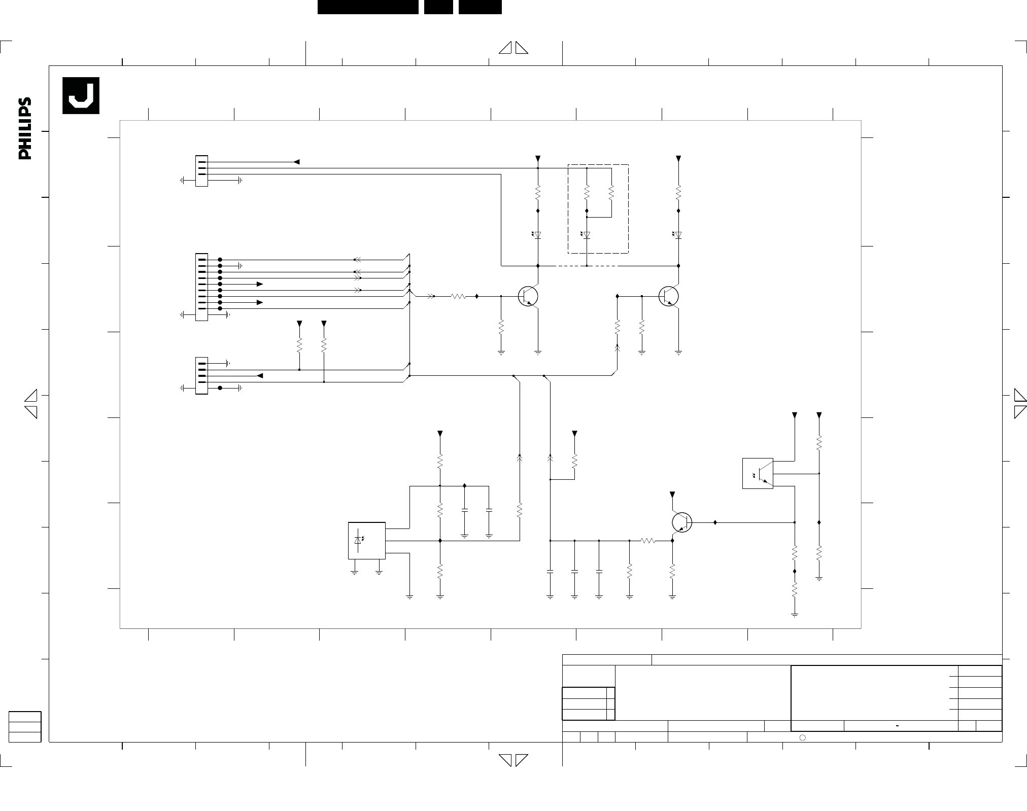
EN 86LC8.2HA LA 10.
Circuit Diagrams and PWB Layouts
2009-Apr-10
IR / LED Panel
C
J
2
"WHITE"
E
RES
11
PCB MB ME8 IR : 3139_123_63263_02
13
A
B
C
D
E
1P09 A1
1P10 B1
1P11 C1
2P10 E5
2P11 E5
2P12 E6
4
B
10
2P13 E6
2P14 E4
3P07 C3
3P08 C2
FROM ME8 KEYB
78
3P09 D6
3P10 A7
3P11 A5
3P12 A6
3P13 A6
3P14 B6
3P15 B4
3P16 D4
3P17 E5
3P18 D8
3P19 E4
3P20 E6
18
C
2345
All rights reserved. Reproduction in whole or in parts
B
C
D
E
12
G
F
2
123456
H H
I
3P27 B5
3P28 B6
4P01 B5
4P02 B6
"P00" ~ "P99"
D
TO ME8 SSB
7P11 B5
7P12 D8
7P13 E7
7P14 E3
6
45
C
I
8
9
3
(RES FOR BDS)
1
FP11 B1
FP12 B1
FP13 B1
FP14 B1
678
A
FP20 B1
IP10 A5
IP11 A7
IP12 B5
B
RES
E
9
10
A
PCB SB ME8 IR : 3139_123_63273_02
IR
is prohibited without the written consent of the copyright
13
J
5
D
3P21 E8
3P22 E8
3P23 E4
3P24 E7
3P25 E6
3P26 E8
IP15 B6
IP16 D4
IP17 E7
IP18 E8
6P10 A7
6P11 A5
6P12 A6
7P10 B7
IP19 E7
IP20 E4
IP21 E8
IP22 A6
RES
"RED"
SAME LOCATION WITH 7012
RES
7
F
12
G
7
A
6
FP10 B1
FP15 B1
FP16 B1
FP17 B1
FP18 C1
RES
owner.
0R
RES
1
"IR RECEIVER"
"LIGHT SENSOR"
11
3
TO ME8 LIGHT GUIDE
IP13 B7
IP14 B4
456
+5V_SW
IP12
BM04B-SRSS-TBT
1P11
1
2
3
FP20
3P14
IP19
2P11
10K
+5V_SW
10u
PCB SB IR
LC08
A3
2007-09-21
-- -- --
2007-11-283
03101
+5V_SW
3
2
2007-10-24
Chen Li Min
DC 319372
2008-08-19
SV
**** *** *****
ROYAL PHILIPS ELECTRONICS N.V. 2007
2007-05-23
3PB310
********SETNAMECHN
CLASS_NO
1
SUPERS.
4
NAME
DATECHECK
3139 123 6327
3P10
1K8
+5V_SW
IP20
IP21
FP14
BC847BW
7P10
+3V3STBY
3P09
22K
6P11
19-113/T7D-CS2T2B2-3T
IP10
3
1
2
7P12
TEMT6000X01
1
2
345
+3V3STBY
1P09
BM03B-SRSS-TBT
910 11
3P17
1P10
1
2
3
4
5
6
7
8
BM09B-SRSS-TBT
10K
3P15
+3V3STBY
FP12
8K2
3P11
IP15
SML-512
6P10
+3V3STBY
2P12
6K8
3P19
10u
FP15
270K
3P26
3P23
100K
+3V3STBY
IP13
100K
3P18
3P20
10K
10K
3P24
IP18
IP16
BC847BW
7P11
+3V3STBY
FP11
4P01
TSML1020
6P12
3
GND
4
5
OUT 1
VS2
GP1UE260RKVF
7P14
+5V_SW
10K
3P22
3P16
100R
270R
3P13
3P073P08
680R 680R
IP22
3P12
270R
2P14
10u
270K
3P21
BC847BW
7P13
10K
3P28
3P27
10K
+5V_SW
IP11
2P13
10u
+3V3STBY
IP17
FP13
FP18
FP10
3P25
39K
4P02
FP17
10u
2P10
1-D5
FP16
1-C5
1-F7
1-D8
1-C5
1-F7
1-C5
11
IP14
1-D6
IR
LED2
LIGHT_SENSOR
IR
LED2
LED1
TACT_SWITCH_INT
KEYBOARD
LIGHT_SENSOR
{KEYBOARD,LED1,LED2,LIGHT_SENSOR,RC,TACT_SWITCH_INT,IR}
LED1
TACT_SWITCH_INT
KEYBOARD
3139 123 63274
18510_500_090407.eps
090407
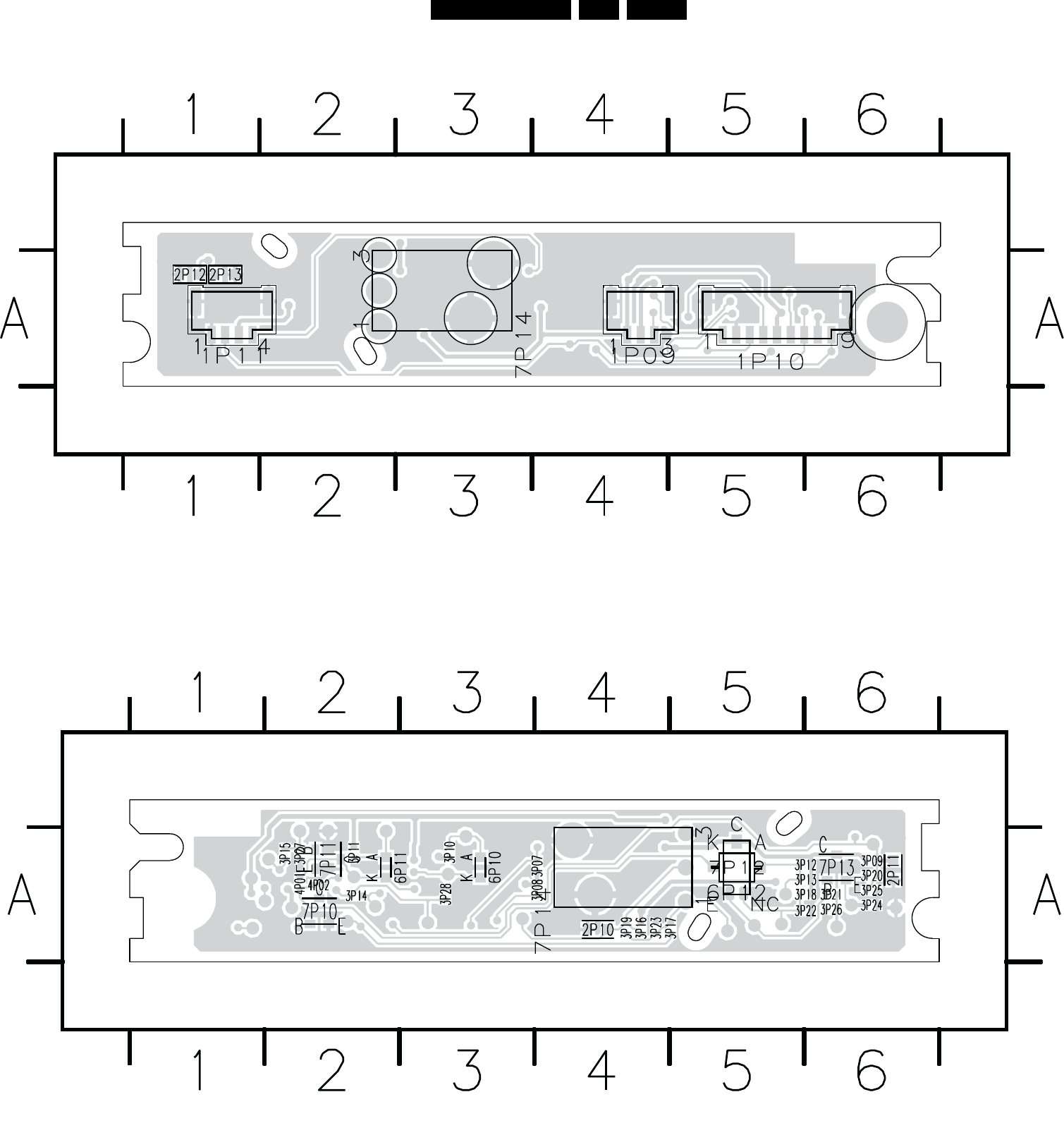
Circuit Diagrams and PWB Layouts EN 87LC8.2HA LA 10.
2009-Apr-10
Layout Front IR / LED Panel (Top Side)
Layout Front IR / LED Panel (Bottom Side)
I_17760_035.eps
090410
3139 123 6327.4
1P09 A4 1P10 A5 1P11 A1 2P12 A1 2P13 A1
I_17760_034.eps
090410
3139 123 6327.4
2P10 A4
2P11 A6
3P07 A4
3P08 A4
3P09 A6
3P10 A3
3P11 A2
3P12 A6
3P13 A6
3P14 A2
3P15 A2
3P16 A4
3P17 A5
3P18 A6
3P19 A4
3P20 A6
3P21 A6
3P22 A6
3P23 A4
3P24 A6
3P25 A6
3P26 A6
3P27 A2
3P28 A3
4P01 A2
4P02 A2
6P10 A3
6P11 A3
6P12 A5
7P10 A2
7P11 A2
7P12 A5
7P13 A6
7P14 A4
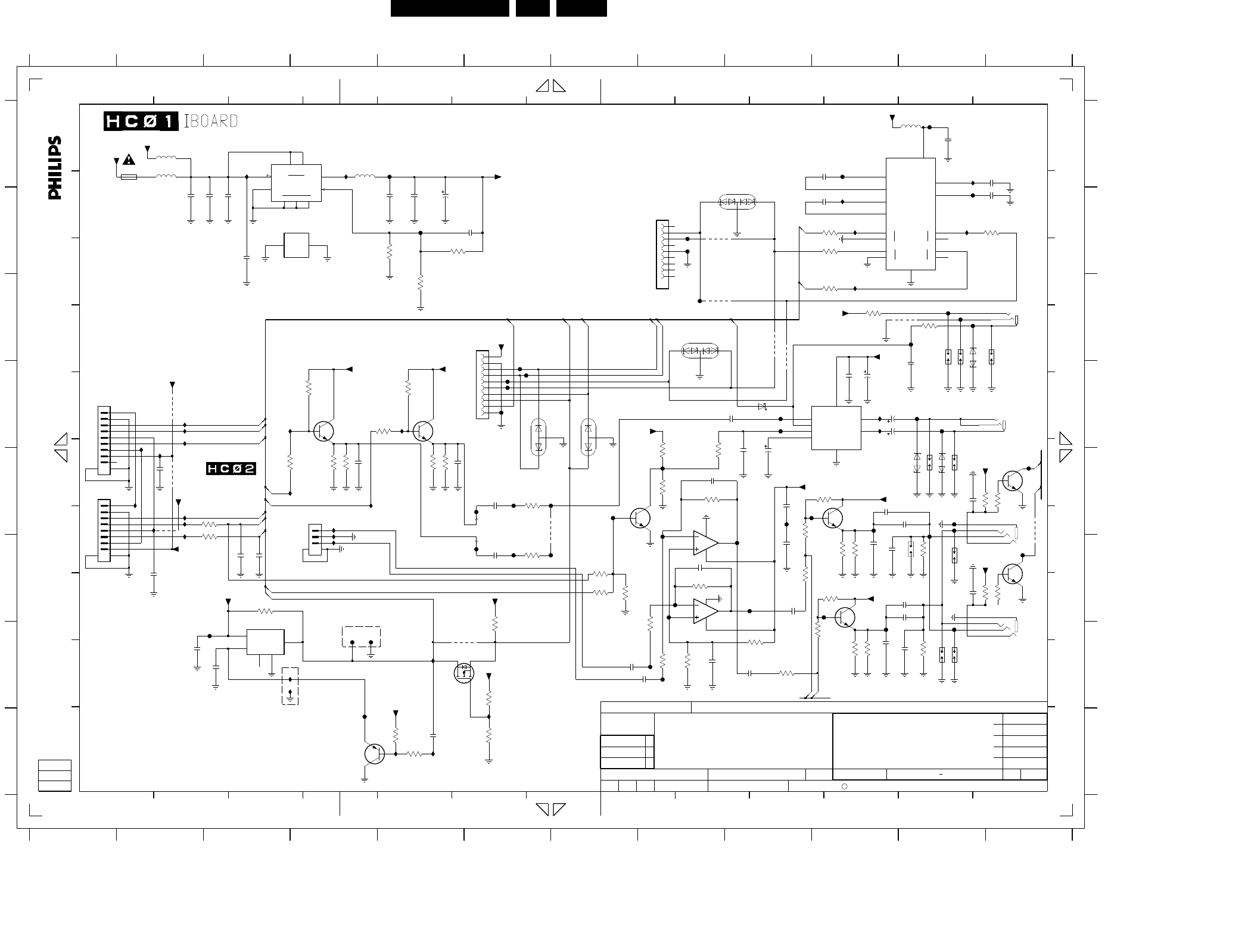
EN 88LC8.2HA LA 10.
Circuit Diagrams and PWB Layouts
2009-Apr-10
iBoard
C
V+
V-
VCC
C1+
C1-
C2+
T2
T1
IN
IN OUT
OUT
GND
T1
C2-
R2
R1
T2
R1
R2
GND
VIN
HSPA
INH
SYNC
SW
VFB
A
SW
VIA
IN
UP|DOWN
MODE
SVR
GND
OUT+
OUT-
VP
I174 H5
I175 H5
RES
RES
PESD12VL2BT
RJ45
I180 E4
I181 E5
I182 E4
I183 E4
I184 F4
I186 H6
F166 F6
I187 E2
F168 G8
I188 E2
F170 B8
F171 B8
F172 C8
F173 A11
F174 A10
F175 B11
F176 E10
B
NC
A
owner.
F177 E11
I144 E2
I147 E2
I163 A3
I164 D10
I166 D10
I167 A4
I171 G5
I118 B11
I119 C10
I140 D2
I141 D2
I142 D2
I143 E2
F144 F11
I146 E2
F146 G11
I150 E2
F148 C11
F149 C11
F150 D11
F151 D11
F152 F11
F153 E12
F154 F8
is prohibited without the written consent of the copyright
J
F
All rights reserved. Reproduction in whole or in parts
A
I176 G4
I177 G4
I178 D4
I179 D5
F160 D9
F161 D9
F162 F12
F163 G3
F164 E6
F165 E7
7120 G6
F167 F7
7122 E8
F169 G8
7124 D4
7125-1 A3
7125-2 B3
7127 E10
7130 F10
7131-1 F8
7131-2 F8
2
Reset pin
TOP SIDE
E
G
F178 E9
F180 G10
F181 E7
F182 E8
I115 B10
I116 A11
I117 B10
F138 D6
F139 D6
F140 D6
F141 D6
F142 A5
F143 B5
4117 B8
F145 G10
4119 C9
F147 C11
4121 C11
5109 A11
5113 A4
5114 A2
5115 A2
6100 C8
6102 D6
G
J
6
E
11
11
F155 F9
F156 F8
F157 F9
F158 F8
F159 C11
6108 D9
7103 G3
7105 H4
7107 A10
7110 E12
7111 F12
3186 D5
7121 D10
3188 E5
7123 D5
3190 F10
3191 E10
3192 F9
3193 F10
3194 E4
3195 E5
3196 G10
1
F
65 8
CC
NC
F129 E6
F130 F6
F131 E10
F133 H4
F134 G4
F135 G4
F137 D6
4101 G6
4102 E2
4110 E2
4111 D2
4112 E6
4113 E12
3141 E11
4118 C8
3143 F12
4120 C9
3158 E3
3169 G10
3170 G10
3171 G6
3172 H6
3174 G6
3175 B5
PESD15VS2UT
POWER ON RESET
B
NC
6103 D7
6104 B9
6105 C11
6106 E11
6107 E11
3180 C11
3181 E8
3182 E8
3183 F7
3184 D5
3185 D4
3114 H5
3187 E3
3119 B10
3189 E4
3121 C10
3122 E6
3123 F6
3127 F7
3128 F7
3130 G8
3131 G8
H
I
42
RES
I
8
13
9
3197 E8
3199 F10
3134 G8
3135 G11
3136 G9
3137 F11
3138 F9
3140 E12
2162 F10
3142 F11
2168 E8
3157 F3
2170 G8
2171 G9
2172 G7
2173 G8
2174 E9
2175 F9
2176 F9
H
RES
712
7
3176 C5
3177 B5
3178 C10
2180 F11
2181 E11
2182 F11
3111 F3
3112 E8
3113 H5
2123 F6
3118 B10
2129 G11
3120 B11
2143 D10
2144 D10
2146 B2
2147 B3
2148 B3
2149 B3
2150 B5
9
D
10
TO SSB
3
3
1 10
3132 F8
3133 G9
2156 E9
2157 D8
2158 E9
2159 B6
2160 E5
2161 E4
3
2163 F10
5
2169 F8
789 101112
A
PCB SB IBOARD : 3129_283_3009_1
4
D
5
TO SSB
1122 G11
13
2177 E10
2178 F11
2179 E11
2116 A10
2117 B10
2119 A11
2120 A11
2121 B11
2122 E6
1112 C12
2128 G10
1113 D12
2136 G2
1114 E12
1115 C11
1116 C11
1117 E11
1119 F11
1120 F11
1121 G11
PESD15VS2UT
NOT CONNECTED ANYWHERE
12
TO IR LED PANEL
1
RES
2151 B5
2152 B5
2153 D11
2154 D10
2155 D10
9 101112
6421
RESRES
PCB MB IBOARD : 3129_283_3008_1
B
C
D
E
F
G
H
A
B
C
D
E
F
G
1125 C12
2109 F3
2110 E2
2111 G3
2112 F2
2113 H5
2114 F3
H
1104 A2
1105 F12
1107 C6
1108 E4
1109 D1
1110 E1
1111 B8
2345678
47K
3128
5109
6u8
1K0
3175
2121 100n
3
21
+5V_AUD
6100
1120
1
2
3
4
5
6
7
8910
1110
BM08B-SRSS-TBT
5
6
7
84
+5V_AUD
21
84
7131-2
TS482IDT
7131-1
TS482IDT
3
2172
2143
1u0
I180
6.3V330u
2109
1u0
4119
+12V
I184
I183
12
4120
I182
I181
2153
100n
F151
F141 F150
F138
2169
33p
3188
68R
4101
10K
3174
10u
2119
14
701
2
6
16
1
3
4
5
15
2131
98
11
+3V3_STANDBY
Φ
RS232
ST3232C
7107
3111
2K2
470R
3122
-
SUPERS.
1
NAME
DATECHECK
3139 283 3009
PCB SB IBOARD AP/CH iLC08
ITV
A3
2009-02-06
-
2009-02-061
03101
2
1
3
3
2
2009-03-20
Ronnie Tan
DC378818
2009-03-20
SVROYAL PHILIPS ELECTRONICS N.V. 2009
2008-05-27
1
3PB310
2
SETNAMECHN
CLASS_NO
1113
MSJ-035-29D PPO
F155
1K0
3157
+12VA
47K
3113
250mA
1104
1
3
2
3118100R
BC817-25
7130
I164
F147
I175
4111
1n0
2129
+5V_AUD
2178
1122
47u
1u0
2113
1121
I179
10
2
3
4
5
6
7
8
9
5450-V01-112-A2
1107
1
100R
3119
1u0
I186
2114
2116 100n
F169
+5V_AUD
4118
I178
3172
10K
11
3185
10K
ST1S10PH
7125-2
10
4
9
2
8
7
35
1
6
7125-1
ST1S10PH
3171
12K
F152
100n
2111
PESDXL2BT
6104
2
1
3
33R
5114
MSJ-035-29D PPO
1112
I176
3191 22K
1114
LGT1509-0200F
2
3
4
1
F161
+12V
F160
1115
+5V_AUD
6103
PESDXS2UT
4121
2148
10u
10u
2147
F137
+5VB
F134
3138 33R
I142
I146
2112 1u0
10u
F157
2151
F177
F180
10u
2158
F178
3169 220R
F182
F168
F181
F166
1
3
2
1
BC817-25
7123
1105
LGT1509-0200F
2
3
4
F148
I171
I163
3132
120K
3192
+5V_AUD
1119
220R
F154
100R
3121
4113
F162
2149
100n
1n0
2161
+5VA
3176
18K
I144
+5VSSB
6102
PESDXS2UT
1u0
2110
2157 1u0
2128
1n0
F163
68R
3190
F153
2159
2u2
I140
100n2120
3183
2K2
33p
2168
3112
120K
F176
2175
220n
+3V3_STANDBY
1n0
2180
22K3199
3
4
5
6
7
8
91011
1111
1-338313-2
1
2
3134
100K
F164
2171
10u
4102
3182
560R
3181
12K
7122
BC847BW
F129
1
3
2
F149
7124
BC817-25
F133
+5VB
3194
68R
1
3
2
7105
BC857BW
2174
220n
F170
F171
6106 PESD5V0S1BA
F159
I177
10u
2150
+5V_AUD
100n
2136
F139
16V100u
2152
F174
F173
2122
1u0
100R3120
470R
3123
68R
3196
560R
3180
F146
1125
I167
2K2
3127
7127
BC817-25
+5VA
2154
100n
2163
PESD5V0S1BA
1n0
I143
6105
I115
4117
1n0
2179
22K
3142
+5VA
3143
2170
1K0
470n
F144
2176
10u
100K
3177
F156
F158
4112
47u2182
68R3195
100n2117
2173
1u0
+5V_AUD
1116
7120
BSH111
68R3189
F142
313710K
10K
3135
33R
I166
3136
3131
47K
2144
330u6.3V
45
BM03B-SRSS-TBT
1108
1
2
3
I174
3130
47K
2155
47u16V
F135
PESD5V0S1BA
6107
1117
10u
5113
31581K0
I188
F130
I187
3133
100K
3170 68R
10K
3184
I147
7110
BC847BW
7111
BC847BW
+12VA
33R
5115
16V
I118
2156
100u
560R
I116
F140
3178
1K0
3140
10K3141
1
6
I150
TDA8551T
7121
7
4
2
8
5
3
2162
1n0
F131
I141
2160
1n0
11
3186
100R
1
2
3
4
5
6
7
8
910
1109
BM09B-SRSS-TBT
F175
F143
F172
1K0
3187
3114
100R
3197
22K
47u
2181
319368R
F167
I119
1
F165
NCP303LSN45
7103
CD
5
3
GND
INP
2
NC
4
OUTP
2177
2123
1u0
47u
BAT7606108
4110
+5V_AUD
10u
I117
F145
2146
+5VA
HP_DET2
MODE_HP_DET
RXD232
TXD232
LEFT
LEFT
RIGHT
HP_AUDIO_OUT_R
HP_AUDIO_OUT_R
HP_AUDIO_OUT_L
HP_AUDIO_OUT_L
RIGHT
MUTE
LED2
IR_IN_TV
LIGHT_SENSOR
UPDOWN
LED1_OUT
POR
KEYBOARD
TXD00
SDA3_IR_OUT
POR1
RC_IR
RXD00
TXD0
RXD0
CVBSterr
LED1
LED2_OUT
18510_501_090407.eps
090407
RS232
Digital volume
control
Aux Audio
out 2
Aux Audio
out 1
Speaker out
8 Ω
DATA 2
RJ45
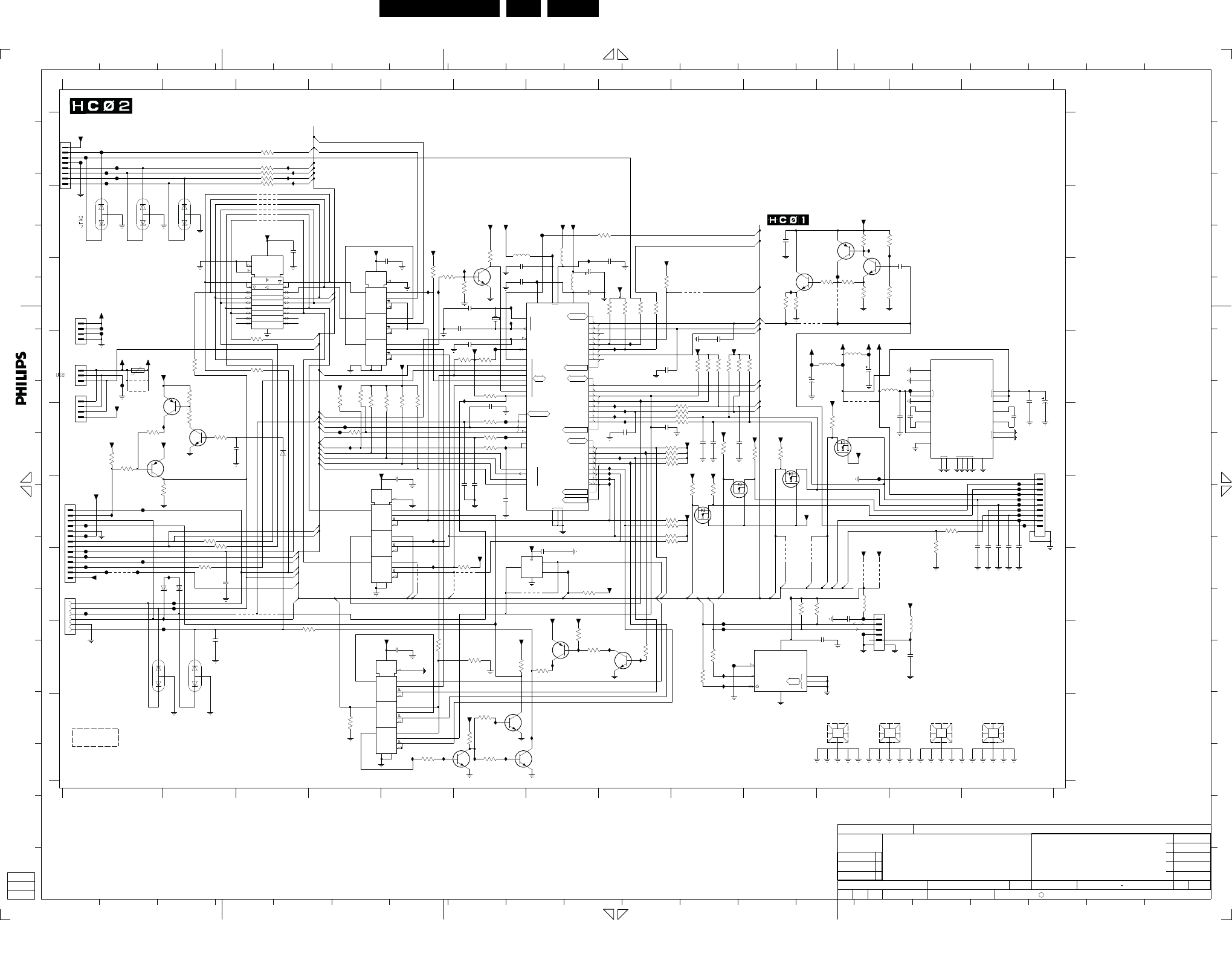
Circuit Diagrams and PWB Layouts EN 89LC8.2HA LA 10.
2009-Apr-10
iBoard
4X1
G4
4X2
1
2
VDD
VEEVSS
C
GND PGND
CLK
COM
SKIP
IN
C1+
C1-
ENABLE
SYNC
C2+
C2-
VIA
FB
OUT
GND_HS
G3
1
2
3EN2
3EN1
4X1
G4
4X2
1
2
VDD
VEEVSS
4X1
G4
4X2
1
2
VDD
VEEVSS
+T
SCL
ADR
0
1
2SDA
WC
PD1
AVCC
RESET_IN
DEBUG
ADC<0:7>
SCL
SDA
C1
C0
TG1
TG0
TXD0
SPIRXD
SPICLK
TXD1
RXD1
T2X
T2
P4 <0:7>
TCM<0:5>
PCACLK 0:1
5
3
4
3V3VCC
X2T2
T2
P1 <0:7>
XTAL
1
TMS
TDO
TDI
7
6
SPISEL
VDD
SPITXD
PC7
PC <2:4>
TCK
JTAG
CLKIN
SPIRXD
RXD1
TXD1
SPICLK
GND
2
1
0
PB
VSTBY
TERR
TSTAT
RXD0
P3 <0:7>
EXINT 0:1
SPISEL
SPITXD
I277 F5
I278 G5
I279 I6
I280 I7
I281 I5
I282 I5
I283 I6
I284 I6
F255 E6
F256 E6
I287 E8
I288 E8
I285 G10
I286 H12
I227 C10
I228 C5
I229 C6
I230 C11
I291 H8
I292 H7
14
J
I218 A3
I219 B7
I220 A3
I222 A3
I223 C6
I224 C7
I226 C5
F227 F1
F228 F13
F229 F13
F230 F13
I231 C10
I232 C6
I245 E2
I250 E8
I251 E8
I252 E8
I275 H9
I276 H9
I258 E4
I260 E6
I261 E8
I263 E8
I264 E8
I266 F1
I267 G7
I268 G2
I269 H6
I270 H2
F245 F1
F246 F1
F247 G1
F248 G1
F249 G1
F250 G1
F251 A1
F252 B7
F253 D6
F254 D1
F212 A1
F213 A1
F214 A1
F215 A1
F259 G1
F260 G1
I289 F8
F257 C11
F258 D12
I217 B7
209
2 18
L
B
16
11
IBOARD
NOTE:
SSB
1
F223 F13
F224 F13
F225 F13
F226 F13
7208 B6
7209 C7
7210 I5
7211 I6
F231 H9
F232 H2
I235 D8
I248 D6
I249 D8
F236 H11
0R
A
16
RES
F237 G1
F238 F13
F239 F13
F240 C1
F241 G2
F242 G2
F243 D1
7224 F9
7225 E10
7226 E11
7227 G6
7228 H8
7229 D12
7230 B3
F116 E8
F210 A1
F211 A1
5203 D11
5204 B7
5205 H12
5206 D12
F216 D11
F217 D11
I213 A3
I290 F8
I216 B11
F222 F11
20
* 1204 use as I2C
C
19
J
BZX384-C5V6
N
3
6206 H2
6207 G2
6208 G1
7102 E2
7205 C4
7206 F4
7207 H4
4213 G6
4214 G6
4215 G3
4216-1 B3
7212 I6
7213 H7
F233 H9
I237 D8
F235 G11
7217 C11
SYSTEM
2
D
8
15
7
7219 D1
7221 E2
7223 F9
13
RJ12
4219 G11
4220 G3
4221 C9
5200 B6
5201 C7
5202 D11
3296-3 E8
3296-4 E8
3297 H5
3298 H6
5207 G11
6201 E3
F218 D11
I215 B12
F220 E4
6205 H1
AV1-STATUS-SSB
9
RES
6
K
3
1.85A
4206 G5
4209 G10
4210 G10
4211 C11
4212 G7
3279 F9
3280 E9
3281 E10
3282 E10
4216-2 B3
4216-3 B3
7214 H10
F234 H9
7216 B11
4218 G11
13
4
PCB SB IBOARD : 3139_283_3009_1
O
15
All rights reserved. Reproduction in whole or in parts
10 14
3295-3 F8
3295-4 F8
3296-1 E8
3296-2 E8
3259 E1
3260 D2
3261 E2
3263 E4
3299 D9
4103 G1
6202 B1
F219 E4
6204 B2
4205 D11
8
P
11
REMOTE
PCB MB IBOARD : 3139_283_3008_1
RES
6
0R
Clock
12
O
3277 G10
3278 F9
3229 H7
3230 H7
3231 C8
3232 C8
3284 E11
3285 E4
4216-4 B3
7215 C11
4217-2 B3
3289 D4
3290 B8
3292 G7
3293 H7
3294 H8
3295-1 F8
3295-2 F8
220R
0R
5
A
3250 C11
3251 B11
3252 C11
3253 D9
3254 D10
3255 D9
3256 E1
3257 E1
3258 F1
3202 A3
3203 E6
3204 D3
3205 H3
3264 E9
3265 A3
4201 C10
6203 B1
4203 D1
3269 G2
3270 D4
3271 D5
3272 D5
3274 H9
3275 H9
3276 G10
H
4
is prohibited without the written consent of the copyright
STANDBY
3221 G6
3222 I5
3223 D6
3224 I6
3225 I6
3226 I6
3227 H6
3228 D5
2226 D10
2229 D9
2230 D8
2231 E8
3234 C8
3236 E9
3286 D2
4217-1 B3
3288 I4
3242 D9
3244 D9
3245 C10
3246 C10
3247 C11
3248 C11
3249 B11
E
C
18
M
2246 H2
2247 G13
2248 G13
2250 H12
2251 E6
2252 B3
3200 E2
3201 D3
13
A
B
C
3206 F12
3207 F12
3266 A3
4202 D1
3268 A3
3214 C5
3215 C5
3216 C6
3217 B6
3218 D6
3219 E6
3220 E6
RES
owner.
P
2213 E9
2214 F6
2215 F6
2216 H11
2217 B10
2218 C12
2219 D11
2220 G11
2221 C8
2224 G7
5678
2232 E8
2233 F6
3239 C8
3287 D6
3241 E8
2239 E9
2240 G2
2241 E12
2242 E12
2243 E13
2244 D13
2245 D13
1
17
I I
220R
19
RES
E
89101112
1211 D1
1212 D1
2200 E2
2202 C5
D
E
3208 F2
3267 A3
3210 C8
I
A
B
C
D
E
F
17
B
2209 C6
2210 C7
2211 C7
2212 E9
LCD
D
12
G
1234
2203 F5
2204 H5
9101112
2236 G13
3240 E8
2238 G13
1234567
7
H
RES
G
N
G
H
I
1096 I13
1097 I12
1098 I12
1099 I11
1200 A1
1202 G1
1203 C6
1205 E13
1207 F1
1208 G11
1209 D1
1210 C1
F
3209 F2
H
2206 C5
2207 D6
2208 C6
G
2205 C6
10
5
F
F116
I293 H8
I294 H7
RES
F
L
2237 G13
13
RES
K
M
I293
10K
3293
15
4
+3V3_STANDBY
I280
16
7
8
13
1
3
12
2
5
14
6
11
10
9
+5VA
MDX
7205
74HC4053PW
+5VA
I231
I281
I215
I278
1
3
2
I219
7208
BC847BW
325310K
3
2
+5VA
BC857BW
7221
1
F256
22
F255
3283 1K0
10K 3242
2216
100n
BAS316
6201
3226
1K0
3215
10K
+5VB
+3V3_STANDBY
3206
10K
F210
I286
I290
I285
F257
F258
1
2
3
+12V
1735446-3
1209
F252
F253
100K
3200
4215
I248
2
3
4
5
6
7
8
9
1
10
11
12
13
14
1-1735446-4
1207
2009-02-061
03101
4K7
3260
2009-03-20
SVROYAL PHILIPS ELECTRONICS N.V. 2009
2008-05-27
2
3PB310
2
SETNAMECHN
CLASS_NO
-
SUPERS.
1
NAME
DATECHECK
3139 283 3009
PCB SB IBOARD AP/CH iLC08
ITV
A2
2009-02-06
-
1212
1
2
3
4
3
2
2009-03-20
Ronnie Tan
DC378818
3223
1735446-4
100K
F242
7216
BC857BW
1
3
2
F254
+5VSSB
F251
I283
I282I284
100R
36
3263
3295-3
10K
1K0
3225
3203100R
F246
F215
F245
1210
1735446-4
1
2
3
4
3275 100R
3204100R
+5VA
I252
+3V3_STANDBY
F222
47K
+5VA
3251
I222
+3V3_STANDBY
3257
10K
221327p
F229
BSH111
7225
3
1
2
100n
2209
100R
3247
27p2214
22
23
2242 1u0
7
14
5
16
9
10
11
12
17
2
8
15
13
19
18
3
4
1
20
21
7229
TPS60111PWP
CONVERTER
DC/DC
Φ
6
2215 27p
F232
F231
+5VB
10n2207
6203
PESDXS2UT
F224
10n
2248
I217
2240
27p
10K
3292
I289
I288
I294
I287
3248
220R
2246
220p
220R5205
2252
100n
3216
10K
+3V3_STANDBY
F217
10K
3288
3287
10K
4206
F220
4K7
I227
3224
I264
2239
10n
3259
100R
F212
F237
3231
10K
10K
3285
F216
3255 10K
BH8B-PH
1
2
3
4
5
6
7
8
+5VA
1200
2245
100u16V
1u0
2243
PESDXS2UT
6204
22p
2238
1
3
2
1K0
3246
7215
BC847BW
+12VA
2
3
4
5
67
6208
BM05B-SRSS-TBT
1208
1
20
16
15
14
13
12
11
1
10
19
2
3
4
5
6
7
8
9
18
17
7230
74LVC245A
4203
I226
3290 100R
220R5200
+5VB
3267 100R
4216-1 18
+5VB
100R
3269
10K
3217
100n
2200
I220
+3V3_STANDBY
22p
2205
+5VA
+5VA
5207 220R
6205
PESDXS2UT
2
5
14
15
4
10
9
16
7
8
13
1
3
12
74HC4053PW
7206
MDX
6
11
+5VA
4201
+3V3_STANDBY
10K
3232
3299 1K0
I261
560R
3249
+12V
I235
3240
2247 10n
F236
100R
F235
I245
I258
100n
2250
3214 10K
I263
+5VB
I270
+5VB
+5VA
+5VA
100R3266
3201
100R
2226
100u16V
10n
2232
2244
22u
10K3218
F218
I250
3295-2
27
10K
2208
100n
+5VA
F243
100K
3271
3202 100R
1
3
2
BC847BW
7217
I228
I266
10K
3254
I216
27
2218
1u0
3296-2
10K
3264 100R
+5VA
4211
3297
5
14
15
4
+3V3_STANDBY
1K2
9
16
7
8
13
1
3
12
2
7207
74HC4053PW
6
11
10
F233
MDX
3265 100R
F223
+5VB
F240
6206
PESDXS2UT
+5VB
I269
I267
4K7
3279
3261
2K2
10K
3284
4K7
3276
+5VA
2233
+12VA
10n
7102
1
3
2
1
2
3
4
5
6
BC847BW
95022-2667
1202
100R
3236
10K
45
3296-4
+5VB
+5VA
3277
4K7
100R
3286
45
36
4216-4
4216-2 27
4216-3
I249
100n
2211
84
7
2230
10n
(4K×8)
Φ
EEPROM
7214
M24C32-WMN6
1
2
3
6
5
I275
REF EMC HOLE
1098
1211
1850mA
100n
2224
24M
1203
BC847BW
7228
+5VA
I213
+5VB
+5V
3
2
2241 22u6.3V
BC857BW
7213
1
4202
1K5 3289
I224
3258
10K
4219
I268
220R
3250
3270
100K
3207
3K3
7
8
9
1112
F214
BM10B-SRSS-TBT
1205
1
10
2
3
4
5
6
F226
+3V3_STANDBY
4103
+5VB
+5VA
F238
F248
10K
3244
F247
5206
6u8
4213
10n
2251
4K7
3281
1
3
2
7219
BC857BW
1
3
2
27p2212
7212
BC847BW
150R
3229
22p
1
3
2
2237
7211
BC847BW
10K
3280
7
3282
10K
18
4217-2 2
4217-1
I232
F219
4214
100R
3274
6u8
100K
5203
5204
3272
100n
2220
6202
PESDXS2UT
3
1
2
1
2
BSH111
7223
7224
BSH111
3
2
35
4
7227
74HC1G081
7226
BSH111
3
1
2
10K
3227
I260
100R
3234
3208
100R
I229
47K
+5VB
3252
6u85202
2K2
3298
F227
I277
I279
F250
F249
100n
2204 3230
1K0
4220
+3V3_STANDBY
3209
100R
3245
16V
21
47R
2219
100u
10K
3296-3
36
F230
2229
I218
10n
5201
+3V3_STANDBY
3239
100R
100R3205
6207
100n
2217
322110K
3295-4
45
10K
100n
2202
I251
+5VA
I276
4210
33
31
32
REF EMC HOLE
1096
48
46
43
42
11
10
7
2
1
44
8
18
17
16
15
14
52
51
50
49
24
25
26
27
28
29
30
22
21
20
13
34
35
36
37
38
39
40
41
23
6
47
5
9
19
45
12
4
3
Φ
MCU
UPSD3333D-40
7209
REF EMC HOLE
1097
I230
4209
F239
10n
2236
F228
F225
10K
3256
100n
+3V3_STANDBY
2221
F234
+5VA
4218
1K0
3294
I223
18
3295-1
10K
3228
2203
100n
100K
I237
16V 100u
2210
100R3241
2231
10n
F211
2206 22p
F241
100R3268
2
F213
10K
3222
BC847BW
7210
1
3
100R
3219
I291
REF EMC HOLE
1099
I292
+3V3_STANDBY
4212
4205
3278
10K
3220
100R
F260F259
+3V3_STANDBY
3210
1K0
HP_DET2
UPDOWN
4221
AV1-STATUS
CTRL_12VPBS
LED2_OUT
LED1_OUT
IB_IR_OUT
IB_IR_OUT1
IB_IR_OUT1
MODE_HP_DET
CVBSterr
RXD0
MODE_HP_DET
LED1
SDA3_IR_OUT
STATUS_DATA_OUT_RXD
RXD0
TXD0
CTRL_12VPBS
TXD0
RC+PEND_IR
RC+PEND_IR RC+PEND_IR
RXD0
SDA3
SDA_SSB
SCL_SSB
STANDBY
RC_IR
RC_IR
IR_OUT
HEFSW2
HEFSW0
CTRL_12VPBS
SC1_CVBS_RF_OUT
RXD_BOLT_ON
LED2
AV1-STATUS
HEFSW0
STANDBY
TXD_BOLT_ON
IR-IN_DATA_IN_RXD_SDA1
RC_IR
NVM_LOAD
STATUS_DATA_OUT_RXD
LEDIN_CLK_TXD_SCL1
LEDIN_CLK_TXD_SCL1
IR-IN_DATA_IN_SDA1
CVI_75R
GPIO
DATA_IN_SLOT
IR_DATA_IN
RJIR_IN
RJIR_IN
RC_PULLUP
RJ_PEND_IR
IR_PULLUP_SW
HEFSW5
HEFSW4
HEFSW3
HEFSW1
DATA_OUT1
TCK
TMS
PEND_IR
SDA1
SDA1
SCL1
SDA3_IR_OUT
STATUS_DATA_OUT_RXD
LEDIN_CLK_TXD_SCL1
CVBSterr
RXD0
TXD0
KEYBOARD
IR_IN_TV
PEND_IR
SCL1
POR
POR1
RXD00
TXD00
POR
MUTE
RXD0
TXD0
TDI
TDO
TMS
TCK
TDO
TDI
18510_502_090407.eps
090407
Smartplug
Data 1
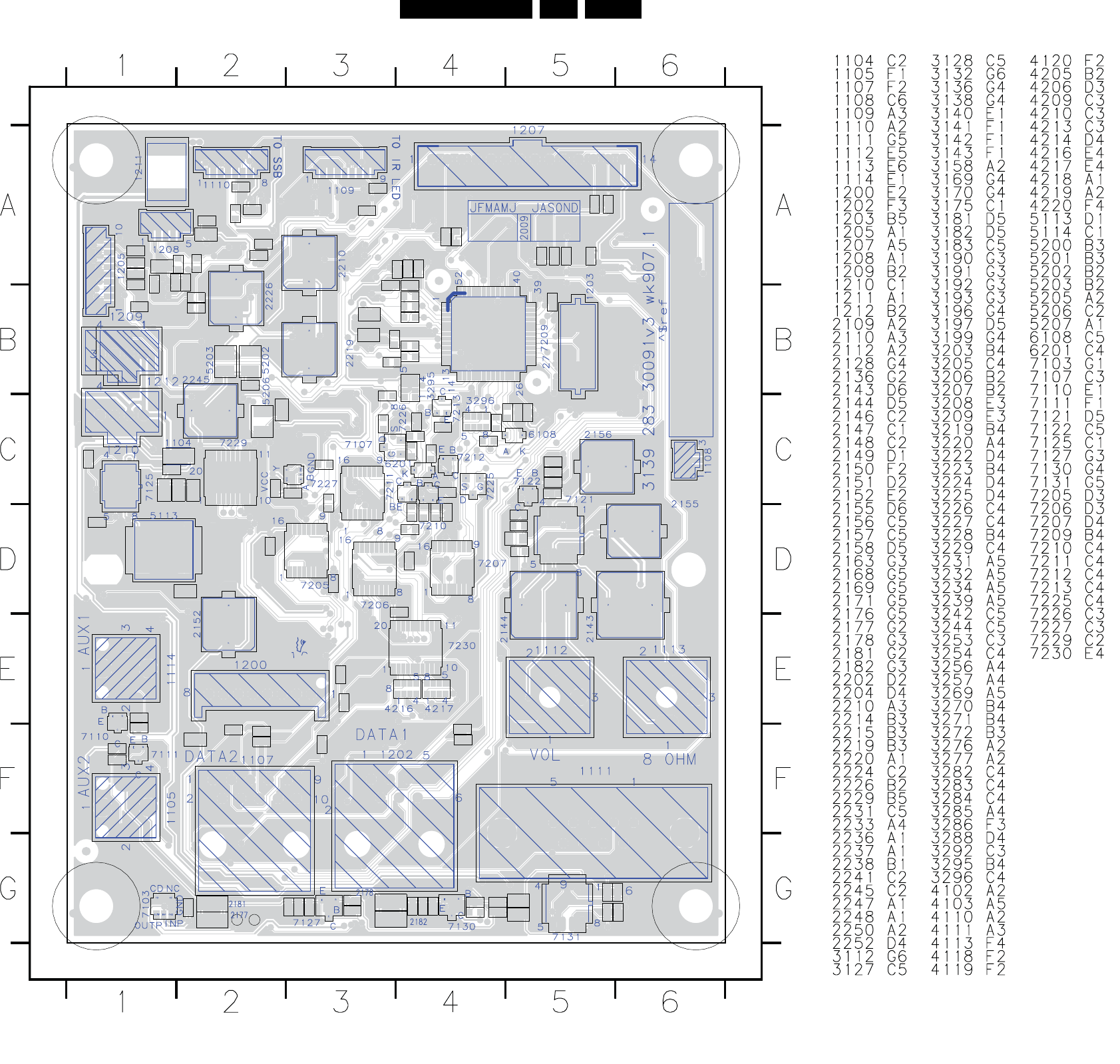
EN 90LC8.2HA LA 10.
Circuit Diagrams and PWB Layouts
2009-Apr-10
Layout iBoard (Top side)
31392833009.1
18510_550_090408.eps
090409
1096 1097
10981099
1104
1105
1107
1108
11091110
1111
1112 1113
1114 1200
1202
1203
1205
1207
1208
1209
1210
1211
1212
2109
2110
2112
2128
2136
2143
2144
2146
2147
2148
2149
2150
2151
2152
2155
2156
2157
2158
2163
2168
2169
2171
2176
2177
2178
2181
2182
2202
2204
2210
2214
2215
2219
2220
2224
2226
2229
2231
2233
2236
2237
2238
2241
2245
2247
2248
2250
2252
3112
3127
3128
3132
3136
3138
3140
3141
3142
3143
3158
3169
3170
3175
3181
3182
3183
3190
3191
3192
3193
3196
3197
3199
3203
3205
3206
3207
32083209
3219
3220
3222
3223
3224
3225
3226
3227
3228
3229
3231
3232
3234
3239
3242
3244
3253
3254
3256
3257
3269
3270
3271
3272
3276
3277
3282
3283
3284
3285
3286
3288
3292
3295
3296
4102
4103
4110 4111
4113
4118
4119
4120
4205
4206 4209
4210
4213
4214
4216 4217
4218
4219
4220
5113
5114
5200
5201
5202
5203
5205
5206
5207
6108
6201
7103
7107
7110
7111
7121
7122
7125
7127 7130
7131
7205
7206
7207
7209
7210
7211
7212 7213
7225
7226
7227
7229
7230
F134F135
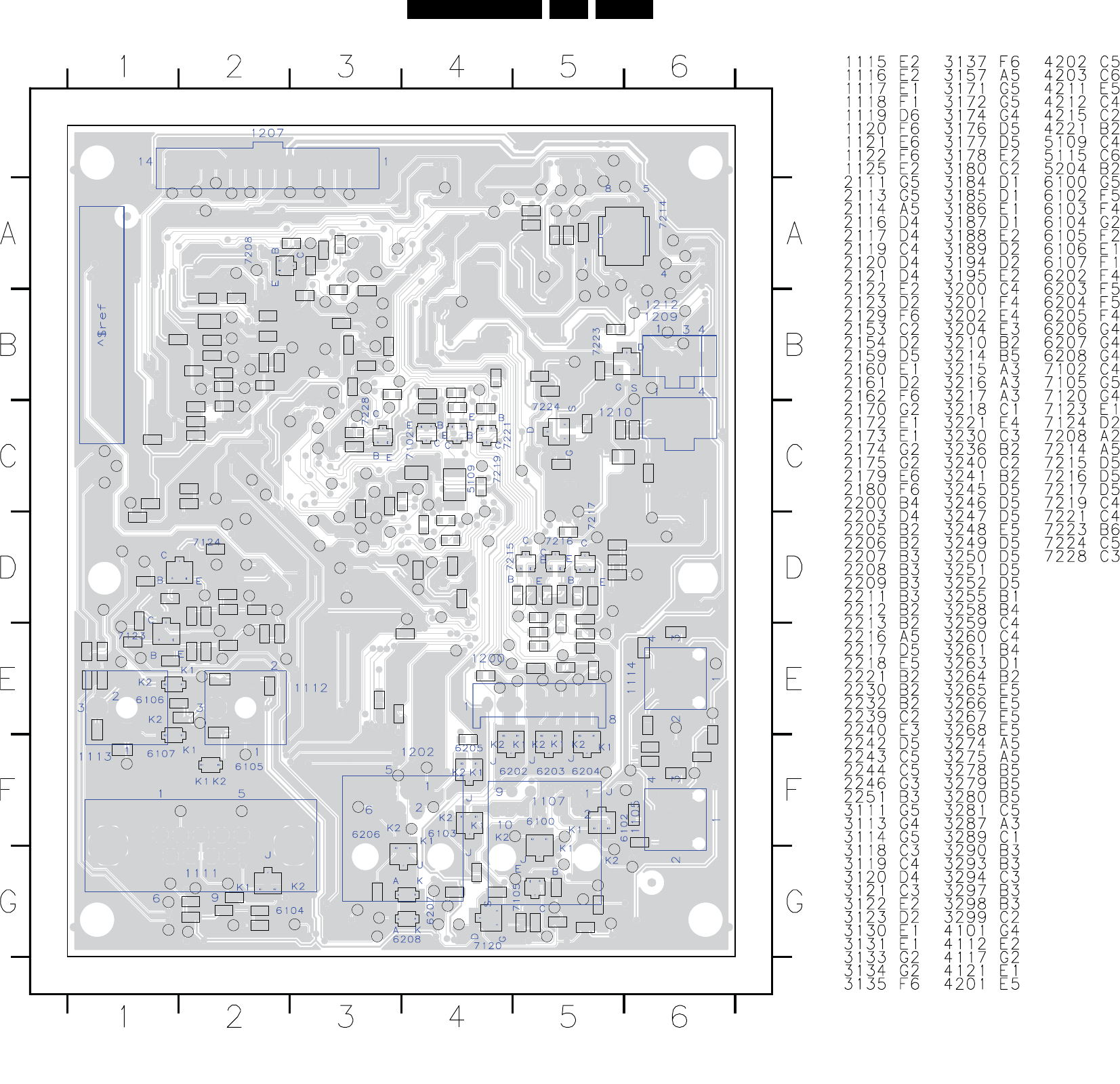
Circuit Diagrams and PWB Layouts EN 91LC8.2HA LA 10.
2009-Apr-10
Layout iBoard (Bottom side)
31392833009.1 18510_551_090408.eps
090409
1115
1116
1117
1118
1119
1120
1121
1122
1125
2111
2113
2114
2116
2117
2119
2120
2121
2122
2123
2129
2153
2154
2159
2160
2161
2162
2170
2172
2173
2174
2175
2179
2180
2200
2203
2205
2206
2207
2208
2209
2211
2212
2213
2216
2217
2218
2221
2230
2232
2239
2240
2242
22432244
2246
2251
3111
3113
3114
3118
3119
3120
3121
3122
3123
3130
3131
3133 3134
31353137
3157
3171
3172
3174
3176
3177
3178
3180
3184
3185
3186
3187
3188 3189
31943195
3200
3201
3202
3204
3210
3214
3215
3216
3217
3218
3221
3230
3236
3240
3241
3245
3246
3247
3248
3249
3250
3251
3252
3255
3258
3259
3260
3261
3263
3264
3265 3266
3267
3268
3274
3275
3278
3279
3280
3281
3287
3289
3290
3293
3294
3297
3298
3299
4101
4112
4117
4121
4201
4202
4203
4211
4212
4215
4221
5109
5115
5204
6100
6102
6103
6104
6105
6106
6107 6202 62036204
6205
6206
6207
6208
7102
7105
7120
7123
7124
7208
7214
7215
7216
7217
7219
7221
7223
7224
7228
F116
F129
F130
F131
F133
F137
F138
F139
F140
F141
F142
F143
F144
F145
F146
F147
F148
F149
F150
F151
F152
F153
F154
F155
F156
F157
F158
F159
F160
F161
F162
F163
F164
F165
F166
F167F168
F169
F170
F171F172
F173
F174
F175
F176
F177
F178
F180
F181
F182
F210
F211 F212
F213
F214
F215
F216
F217
F218
F219
F220
F222
F223
F224
F225
F226
F227
F228
F229
F230
F231
F232
F233
F234
F235
F236
F237
F238
F239
F240
F241
F242
F243
F245F246F247
F248
F249
F250
F251
F252
F253
F254
F255
F256
F257
F258
F259
F260
I115
I116
I117 I118
I119
I140
I141
I142 I143
I144
I146
I147
I150
I163
I164
I166
I167
I171
I174 I175
I176
I177
I178
I179
I180
I181
I182
I183
I184
I186
I187
I188
I213
I215
I216
I217
I218
I219
I220
I222
I223
I224
I226
I227
I228
I229
I230
I231
I232
I235I237
I245
I248
I249
I250
I251
I252
I258
I260
I261
I263
I264
I266
I267
I268
I269
I270
I275I276
I277
I278
I279
I280
I281
I282
I283
I284
I285
I286
I287
I288
I289
I290
I291
I292
I293
I294